Numerical Analysis of Pool Fire Consequences in Confined ...
Upload
independentCategory
view
0download
0
1
Highly Quantum-Confined InAs Nanoscale Membranes
Kuniharu Takei1,2,3,†
, Hui Fang1,2,3,†
, Bala Kumar4,†
, Rehan Kapadia1,2,3
, Qun Gao4, Morten Madsen
1,2,3, Ha
Sul Kim1,2,3
, Chin-Hung Liu5, Yu-Lun Chueh
5, Elena Plis
6, Sanjay Krishna
6, Hans A. Bechtel
7, Jing Guo
4,
Ali Javey1,2,3,
*
1Electrical Engineering and Computer Sciences, University of California, Berkeley, CA, 94720.
2Materials Sciences Division, Lawrence Berkeley National Laboratory, Berkeley, CA 94720.
3Berkeley Sensor and Actuator Center, University of California, Berkeley, CA, 94720.
4Electrical and Computer Engineering, University of Florida, Gainsville, FL, 32611
5Materials Science and Engineering, National Tsing Hua University, Hsinchu 30013, Taiwan, R.O.C.
6Center for High Technology Materials, University of New Mexico, Albuquerque, NM 87106.
7Advanced Light Source, Lawrence Berkeley National Laboratory, Berkeley, CA 94720
† These authors contributed equally to this work.
* Correspondence should be addressed to A.J. ([email protected]).
Abstract - Nanoscale size-effects drastically alter the fundamental properties of semiconductors.
Here, we investigate the dominant role of quantum confinement in the field-effect device
properties of free-standing InAs nanomembranes with varied thicknesses of 5-50 nm. First,
optical absorption studies are performed by transferring InAs "quantum membranes" (QMs) onto
transparent substrates, from which the quantized sub-bands are directly visualized. These sub-
bands determine the contact resistance of the system with the experimental values consistent
with the expected number of quantum transport modes available for a given thickness. Finally,
the effective electron mobility of InAs QMs is shown to exhibit anomalous field- and thickness-
dependences that are in distinct contrast to the conventional MOSFET models, arising from the
strong quantum confinement of carriers. The results provide an important advance towards
establishing the fundamental device physics of 2-D semiconductors.

2
2-D materials are of profound interest for exploring fundamental properties at the
nanoscale1,2,3
and enabling novel practical applications, such as high performance electronics4,5,6
or quantum optics7. Over the past several years, various layered semiconductors, including
graphene and MoS2, have been extensively studied owing to their intriguing properties6,8,9,10,11
.
The InAs QMs reported here present another class of 2-D materials, where the band-structure
can be precisely tuned from bulk to 2-D by changing the thickness. Specifically, given the large
Bohr radius of ~34 nm for bulk InAs, a strong quantum confinement is expected, even for layers
with 10’s of nm in thickness. Thus, the basic material properties can be systematically studied as
the material is quantum confined with the size effects being fundamentally different than those of
the layered semiconductors. In contrast to conventional III-V quantum-well (QW) structures
where confinement is achieved by the use of a large band-gap semiconductor layer on an
epitaxial growth substrate12,13
, QMs are confined at the surface by either an insulator layer or
air/vacuum15, 14
, and are free to be placed on a user-defined substrate. This QM structural
configuration enables the direct contact of the active semiconductor layer with the gate stack,
which is essential for enabling high performance devices. We recently demonstrated the promise
of this material concept by the fabrication of ultrathin-body InAs transistors on Si/SiO2 support
substrates with excellent electrical properties15
, taking advantage of the high electron mobility of
III-V semiconductors16,17,18
and the well-established processing technology of Si. Here, we use
InAs QMs as a model system for probing the drastic role of quantum confinement on the contact
resistance and carrier transport properties of field-effect transistors (FETs) as a function of
material thickness through detailed experiments and theoretical modeling. The work presents
fundamental understanding of the device physics and the projected performance limits of
nanoscale III-V FETs.
3
InAs QMs were fabricated on Si/SiO2 and CaF2 substrates by using an epitaxial layer
transfer (ELT) method15,19,20,21
(see Methods for process detail). Figures 1a & b show the low
and high resolution transmission electron microscopy (TEM) images of a typical 7 nm InAs
membrane capped by SiO2 on a Si/SiO2 substrate, illustrating the high quality, single-crystalline
InAs QM of just a few atomic layers in thickness. The interfaces between InAs and SiO2 are
abrupt as evident from TEM. Fourier transform infrared (FTIR) spectroscopy was used to
directly probe the optical absorption transitions of InAs QMs, thereby experimentally elucidating
the electronic band structure quantization as a function of InAs thickness. Here, InAs QMs were
transferred onto a CaF2 substrate, which is transparent for the photon wavelengths of interest (1-
4 µm). Figure 2a shows the normalized transmittance spectra of 6-19 nm thick InAs QMs at
room temperature. The clear steps observed in the transmittance are attributed to the interband
transitions between the 2-D sub-bands, with the spacing of the steps decreasing as the QM
thickness is increased.
The onset energies of the absorption steps can be estimated by E=Eg+Ehn+Een’, where Eg
is the band gap of bulk InAs, and Ehn (Een’) are the n (n’) -th sub-band energy of holes
(electrons) due to quantum confinement. Note that due to the band edge roughness induced by
various surface defects (e.g. interface traps, surface roughness, etc.), the absorption edge is not
strictly sharp. By modeling InAs QM as a finite potential well structure, the n’th sub-band
energy can be numerically calculated from the 1-D Schrodinger equation (see Supp. Info. for
calculation details), as shown in Fig. 2b. Selection rules require the sub-bands involved in the
transition to have matching envelope functions, or parity. Consequently, electrons in the first
electron sub-band (e1) can only transit to the first hole sub-bands (either 1st heavy hole, hh1;
light hole, lh1; or split-off, so1), i.e., ∆n=n’-n=0. Other transitions are also possible but are weak.

4
Figure 2c shows the FTIR absorption onsets for each QM thickness (see Supp. Info., Fig. S2),
along with the calculated interband transition energies (e1hh1, e1lh1, e2hh2, e2lh2). The
experimental results closely match the theoretical calculations. The FTIR data is a direct
observation of the electronic band structure quantization in ultrathin InAs QMs. This clearly
presents an important utility of the proposed platform for exploring the basic properties of
nanoscale material by decoupling the active material from the original growth (i.e., GaSb)
substrate.
Next, the effect of quantum confinement on the contact resistance, Rc, of InAs QMs is
explored by fabricating back-gated, field-effect transistors on Si/SiO2 substrates. Ni source/drain
(S/D) metal contacts were used for this study as Ni forms ohmic contact to the conduction band
of InAs, with negligible parasitic junction resistances (i.e., without tunneling barriers) for
electron injection22
. This enables the study of the fundamental limits of the metal-semiconductor
junction resistance of QMs as a function of thickness. The transmission line method (TLM) 10
was used to extract the contact resistance. Typical IDS-VGS curves of a back-gated (50 nm SiO2
gate dielectric) 18 nm-thick InAs QM with different channel lengths are shown in Fig. 3a. The
ON-state resistance at VGS-Vth=9 V, where Vth is the threshold voltage, as a function of L
(measured by SEM) was extracted for InAs QMs with different thicknesses and is plotted in Fig.
3b. The ON-state resistance monotonically increases with L since the devices are operating in the
diffusive regime for the explored length scales. The y-intercept of the ON-resistance versus L
plot is approximately equal to 2Rc. The extracted contact resistance is plotted as a function of
InAs thickness in Fig. 3c. A low contact resistance value of ~80 Ω-µm is observed for TInAs ≥ 10
nm. As the thickness is reduced to ≤ 10 nm, a sharp increase in the resistance is observed with
Rc~ 600 Ω-µm at TInAs = 5 nm.
5
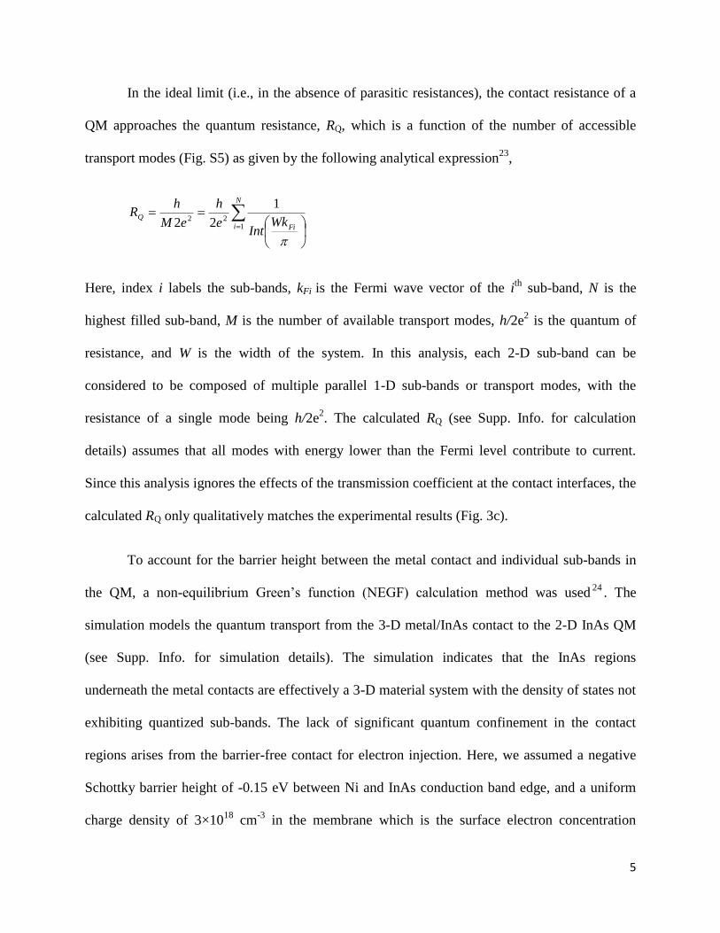
In the ideal limit (i.e., in the absence of parasitic resistances), the contact resistance of a
QM approaches the quantum resistance, RQ, which is a function of the number of accessible
transport modes (Fig. S5) as given by the following analytical expression23
,
N
i Fi
QWk
Inte
h
eM
hR
122
1
22
Here, index i labels the sub-bands, kFi is the Fermi wave vector of the ith
sub-band, N is the
highest filled sub-band, M is the number of available transport modes, h/2e2 is the quantum of
resistance, and W is the width of the system. In this analysis, each 2-D sub-band can be
considered to be composed of multiple parallel 1-D sub-bands or transport modes, with the
resistance of a single mode being h/2e2. The calculated RQ (see Supp. Info. for calculation
details) assumes that all modes with energy lower than the Fermi level contribute to current.
Since this analysis ignores the effects of the transmission coefficient at the contact interfaces, the
calculated RQ only qualitatively matches the experimental results (Fig. 3c).
To account for the barrier height between the metal contact and individual sub-bands in
the QM, a non-equilibrium Green’s function (NEGF) calculation method was used24
. The
simulation models the quantum transport from the 3-D metal/InAs contact to the 2-D InAs QM
(see Supp. Info. for simulation details). The simulation indicates that the InAs regions
underneath the metal contacts are effectively a 3-D material system with the density of states not
exhibiting quantized sub-bands. The lack of significant quantum confinement in the contact
regions arises from the barrier-free contact for electron injection. Here, we assumed a negative
Schottky barrier height of -0.15 eV between Ni and InAs conduction band edge, and a uniform
charge density of 3×10¹⁸
cm-3
in the membrane which is the surface electron concentration

6
previously reported for InAs25,26
. The experimental and ballistic NEGF simulation curves are
nearly identical (Fig. 3c), providing a strong evidence that the measured Rc purely arises from the
quantum resistance of the system and the associated transmission probability for each transport
mode, without parasitic resistances.
Quantization is also expected to drastically alter the field-effect transport properties of
InAs QMs through changes in both the carrier effective mass and charge centroid position in the
channel. Detailed transport studies of back-gated (50 nm SiO2 gate dielectric) devices were
performed, and the effective electron mobility was extracted as a function of the applied gate-
voltage (i.e., vertical electric-field), temperature and QM thickness. Current flow in the
conventional MOSFETs occurs near the oxide-semiconductor interface. The distance of the
charge centroid from the surface (zD) determines the surface scattering rate. In Si MOSFETs, zD
is heavily affected by the gate-field, reducing significantly at high gate-fields, resulting in the
observed field-induced degradation of carrier mobility. However, for a highly confined system,
such as ultrathin InAs QMs, zD is expected to be nearly unaffected by the gate-field and is
instead determined by the thickness of the layer. Thus, the scattering models, especially the field
and thickness dependence of surface scattering mechanisms, are expected to be drastically
different in QM FETs as compared to the conventional Si MOSFETs27
.
To explore this phenomenon, we examined electron transport properties for three cases:
(i) 2-D QMs (e.g., TInAs=8nm, Fig. 4a), (ii) quasi-2-D QMs (e.g., TInAs=18nm, Fig. 4b), and (iii)
3-D QMs (e.g., TInAs=48nm), corresponding to the bulk case. The electron distributions were
calculated for all three cases via a Poisson-Schrodinger solver (Figs. 4c-d and Fig. S7). For
TInAs= 8 nm, the charge distribution clearly follows the ground state wave function of a quantum-
well for all fields, with only the lowest sub-band being populated (Fig. S7a), and more
7
importantly, zD is ~TInAs/2 = 4 nm and nearly independent of the applied field (Fig. 4e). On the
other hand, for the 18 nm QM, at low fields only the first sub-band, which is structurally-
confined, contributes to the current, while at higher fields, a second field-confined sub-band is
also populated (Fig. S7b). For the 48 nm-thick QM, transport takes place in multiple field-
confined sub-bands beneath the gate oxide, with the charge centroid moving closer to the oxide
interface at high fields (Fig. S7c). The final case is identical to the characteristics observed in
conventional Si MOSFETs28
.
Figure 4f shows the experimental effective mobility as a function of the back-gate
voltage for TInAs= 8, 18 and 48 nm at 100 K as extracted from the transfer characteristics (Fig.
S8). The dashed lines represent the theoretical mobility model considering surface roughness
(SR), surface polar phonon (SPP) and impurity scattering events (Fig. S9), showing a close fit to
the experiments. Although multiple scattering mechanisms were considered, surface roughness
scattering was found to be dominant at low temperatures (e.g., 100 K) since phonons are mostly
frozen. From the electrical measurements, the 8 nm QM shows almost no field-dependence of
mobility, except at very high fields, which is in distinct contrast to conventional MOSFET
model. This is well explained by the calculated charge carrier distribution profiles of Figs. 4c and
4e, where the position of charge centroid for a truly 2-D system was found to exhibit minimal
field dependence. On the other hand, the 48 nm QM shows the expected bulk MOSFET
behavior, with a monotonic decrease in the mobility as a function of the field. The most
interesting case occurs for the 18 nm QM. At low fields, transport occurs within a single
structurally-confined sub-band; at slightly higher fields, the sub-band becomes field-confined,
and the mobility drops with the gate voltage; finally, at a VGS-Vth~4V a second structurally-
confined sub-band is populated. Here, the observed kink in the mobility versus field plot

8
represents the onset of population of the 2nd
sub-band, which is once again consistent with the
calculated charge density distribution profiles. The results highlight the importance of
quantization on the surface roughness scattering of QMs, and while thinner layers are more
desired for scaled FET applications, the optimal thickness need to be wisely selected as a
compromise with the enhanced surface scattering rates.
In conclusion, through detailed experiments and theoretical modeling, InAs QMs are
presented as a model material system for elucidating the dominant role of the quantum
confinement in the basic field-effect transport properties of carriers, including effective mobility
and quantum resistance. InAs is specifically ideal for this study given the large Bohr radius
which allows for heavy quantization at sub-20 nm thicknesses, and the ease of ohmic metal
contact formation. Besides understanding the basic transport physics as a function of thickness,
this work presents important practical implications for exploring the ultimate performance limits
of ultrathin body InAs QM FETs, as well as providing guidelines for future device designs.
Importantly, the contact resistance and mobility models in QM FETs are found to be drastically
different than the previously established universal models for conventional MOSFETs, thereby,
presenting a new insight into the device physics of 2-D field-effect transistors. While InAs QMs
were explored here, the results are generic for any structurally quantum confined material
system.

9
Figure Captions
Figure 1. TEM analyses of InAs QMs. (a) Low magnification and (b) high resolution TEM
images of a 7 nm InAs QM capped with SiO2 on a Si/SiO2 substrate.
Figure 2. FTIR measurements of InAs QMs on CaF2 substrates. (a) The transmission spectra for
various InAs QM thicknesses, illustrating clear steps, corresponding to the optical transitions
between the 2-D sub-bands. (b) The calculated ground and excited states for electrons and holes
(light and heavy). (c) Comparison of absorption steps from FTIR and the first four theoretical
interband transition energies (e1-hh1, e1-lh1, e2-hh2, e2-lh2) for various InAs QM thicknesses.
Note that for 14 and 19 nm InAs QMs, e1-hh1 and e1-lh1 transitions are so close that cannot be
clearly resolved by FTIR.
Figure 3. Quantum contact resistance of InAs QMs. (a) Typical IDS-VGS results of a 18 nm-thick
InAs QM with different channel lengths, L. (b) ON-resistance of InAs QMs (TInAs, 5-48 nm) at
VGS-Vth=9 V as a function of the channel length. (c) Experimentally extracted (red symbols),
NEGF simulated (dashed line), and analytically calculated (dotted line) contact resistance values
versus thickness. The error bars in the experimental data corresponds to the standard error or
regression. (d) Calculated energy band diagrams of the contact interface for 8 nm (top) and 18
nm (bottom) thick InAs QMs. The Fermi level, Ef, conduction band edge, Ec, and ground and
excited states (e1- e4) are labeled. The sub-bands that are below Ef are ohmically contacted while
those that are above are Schottky contacted.
Figure 4. Electron transport analyses of back-gated InAs QM FETs. (a) (b) The calculated band
diagrams of back-gated InAs QM FETs for TInAs = 8 nm and 18 nm, respectively. The calculation

10
is shown for both low (left) and high (right) vertical gate fields. The population percentage for
each sub-band is also labeled. (c) (d) The calculated carrier density vs. position as a function of
the applied gate field for TInAs = 8 nm and 18 nm, respectively. (e) The calculated charge centroid
position as a function of the gate-field for different InAs QM thicknesses. f, Experimental (solid
lines) and simulated (dashed lines) effective mobilities as a function of gate voltage for varied
InAs QM thicknesses at 100 K and VDS=10 mV.

11
Acknowledgements
This work was funded by FCRP/MSD Focus Center and NSF E3S Center. The materials
characterization part of this work was partially supported by the Director, Office of Science,
Office of Basic Energy Sciences, and Division of Materials Sciences and Engineering of the U.S.
Department of Energy under Contract No. De-Ac02-05Ch11231, and the Electronic Materials
(E-Mat) program. The Advanced Light Source is supported by the Director, Office of Science,
Office of Basic Energy Sciences, of the U.S. Department of Energy under Contract No. DE-
AC02-05CH11231. A.J. acknowledges a Sloan Research Fellowship, NSF CAREER Award, and
support from the World Class University program at Sunchon National University. Y.-L.C.
acknowledges support from the National Science Council, Taiwan, through grant no. NSC 98-
2112-M-007-025-MY3. R.K. and M.M. acknowledge an NSF Graduate Fellowship and a
postdoctoral fellowship from the Danish Research Council for Technology and Production
Sciences, respectively. J.G. acknowledges support form NSF and SRC.
Supporting information
Sample preparation and FTIR measurement details; temperature dependent FTIR measurement;
calculated 2-D sub-band edges; quantum resistance calculations; NEGF simulations of contact
resistance; simulations of the charge density profiles; low-temperature transfer characteristics of
InAs QM FETs; theoretical mobility models; temperature, vertical-field, and thickness
dependency of the effective mobility. This material is available free of charge via the Internet at
http://pubs.acs.org.

12
References
1. McEuen, P. L. Science 1997, 278, 1729-1730.
2. Yoffe, A.D. Adv. Phys. 1993, 42, 173-262.
3. Yu, H.; Li, J.; Loomis, R.A.; Wang, L.-W.; Buhro, W.E. Nature Mater. 2003, 2. 517-520.
4. Kim, D.-H.; del Alamo, J. A. IEEE Trans. Electron Devices 2010, 57, 1504-1511.
5. Pavorka, P.; Alam, A.; Wolter, M.; Fox, A.; Marso, M.; Heuken, M.; Luth, H.; Kordos, P.
IEEE Electron Device Lett. 2002, 23, 4-6.
6. Geim, A. K.; Novoselov, K. S. Nature Mater. 2007, 6, 183-191.
7. Yonezu, H. Semicond. Sci. Technol. 2002, 17, 762-768.
8. Han, M. Y.; Ozyilmaz, B.; Zhang, Y.; Kim, P. Phys. Rev. Lett. 2007, 98, 206805.
9. Xu, X.; Gabor, N. M.; Alden, J. S.; van der Zande, A. M.; McEuen, P. L. Nano Lett. 2010, 10,
562-566.
10. Xia, F.; Perebeinos, V.; Lin, Y.; Wu, Y.; Avouris, P. Nature Nanotech. 2011, 6, 179-184.
11. Radisavljevic, B.; Radenovic, A.; Brivio, J.; Giacometti, V.; Kis, A. Nature Nanotech. 2011,
6, 147-150.
12. Somerville, M. H.; Greenberg, D. R.; del Alamo, J. A. Appl. Phys. Lett. 1994, 64, 3276-3278.
13. de Picciotto, R.; Stormer, H. L.; Pfeiffer, L. N.; Baldwin, K. W.; West, K. W. Nature 2001,
411, 51-54.

13
14. Yablonovitch, E.; Cox, H. M.; Gmitter, T. J. Appl. Phys. Lett. 1988, 52, 1002 – 1004.
15. Ko, H.; Takei, K.; Kapadia, R.; Chuang, S.; Fang, H.; Leu, P. W.; Ganapathi, K.; Plis, E.;
Kim , H. S.; Chen, S.-Y.; Madsen, M.; Ford, A. C.; Chueh, Y.-L.; Krishna, S.; Salahuddin, S.;
Javey, A. Nature 2010, 468, 286-289.
16. Radosavljevic, M.; Chu-Kung, B.; Corcoran, S.; Dewey, G.; Hudait, M. K.; Fastenau, J. M.;
Kavalieros, J.; Liu, W. K.; Lubyshev, D.; Metz, M.; Millard, K.; Mukherjee, N.; Rachmady,
W.; Shah, U.; Chau, R. IEEE IEDM Tech. Digest 2009, 319-322.
17. Liu, Y.; Pal, H. S.; Lundstrom, M. S.; Kim, D.-H., del Alamo, J. A.; Antoniadis, D. A.
Fundamental of III-V Semiconductor MOSFETs (Springer, New York, 2010).
18. Heyns, M.; Tsai, W. MRS Bull. 2009, 34, 485-488.
19. Yoon, J.; Jo, S.; Chun, I. S.; Jung, I.; Kim, H.-S.; Meitl, M.; Menard, E.; Li, X.; Coleman, J.
J.; Paik, U.; Rogers, J. A. Nature 2010, 465, 329-333.
20. Yablonovitch, E.; Hwang, D. M.; Gmitter, T. J.; Florez, L. T.; Harbison, J. P. Appl. Phys.
Lett. 1990, 56, 2419–2421.
21. Meitl, M. A.; Zhu, Z.-T.; Kumar, V.; Lee, K. J.; Feng, X.; Huang, Y. Y.; Adesida, I.; Nuzzo,
R. G.; Rogers, J. A. Nature Mater. 2006, 5, 33-38.
22. Chueh, Y.-L.; Ford, A. C.; Ho, J. C.; Jacobson, Z. A.; Fan, Z.; Chen, C.-Y.; Chou, L.-J.;
Javey, A. Nano Lett. 2008, 8, 4528–4533.
23. Datta, S. Electronic Transport in Mesoscopic Systems (Cambridge University Press,
Cambridge, 2001).
14
24. Gao, Q.; Ouyang, Y.; Guo, J. J. Appl. Phys. 2011, 109, 104307.
25. Wieder, H. H. J. Vac. Sci. Technol. B 2003, 21, 1915-1919.
26. Bell, G. R.; Jones, T. S.; McConville C. F. Appl. Phys. Lett. 1997, 71, 3688-3690.
27. Uchida, K.; Koga, J.; Takagi, S. J. Appl. Phys. 2007, 102, 074510.
28. Rudenko, T.; Kilchytska, V.; Raskin, J.-P.; Nazarov, A.; Flandre, D. in Semiconductor-On-
Insulator Materials for Nanoelectronics, Special features of the back-gate effects in ultra-thin
body SOI MOSFETs (eds Nazarov et al.) 323-339 (Springer-Verlag Berlin Heidelberg, 2011).

15
Figure 1

16
Figure 2

17
Figure 3

18
Figure 4
19
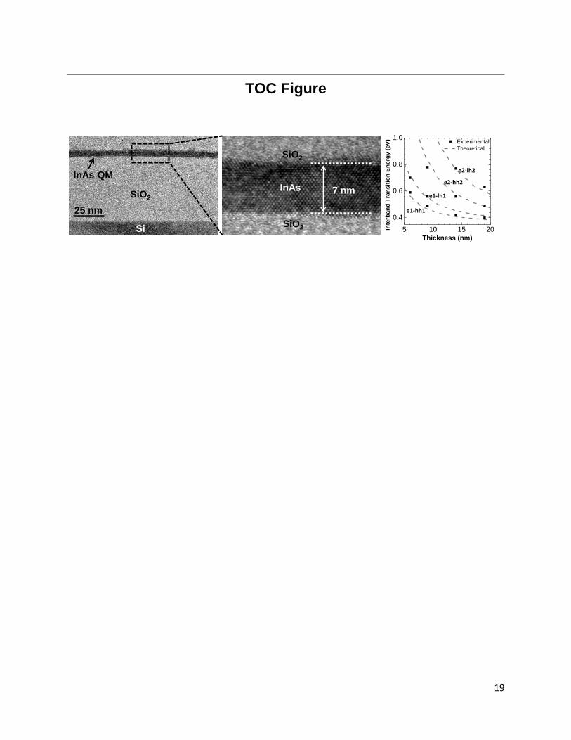
TOC Figure
7 nmInAs
SiO2
SiO2
InAs QM
SiO2
Si
25 nm
5 10 15 20
0.4
0.6
0.8
1.0
Inte
rba
nd
Tra
nsit
ion
En
erg
y (
eV
)
Thickness (nm)
Experimental
Theoretical
e1-hh1
e1-lh1
e2-hh2
e2-lh2

S1
SUPPORTING INFORMATION
Highly Quantum-Confined InAs Nanoscale Membranes
Kuniharu Takei1,2,3,†, Hui Fang1,2,3,†, Bala Kumar4,†, Rehan Kapadia1,2,3, Qun Gao4, Morten Madsen1,2,3, Ha
Sul Kim1,2,3, Chin-Hung Liu5, Yu-Lun Chueh5, Elena Plis6, Sanjay Krishna6, Hans A. Bechtel7, Jing Guo4,
Ali Javey1,2,3,*
1Electrical Engineering and Computer Sciences, University of California, Berkeley, CA, 94720.
2Materials Sciences Division, Lawrence Berkeley National Laboratory, Berkeley, CA 94720.
3Berkeley Sensor and Actuator Center, University of California, Berkeley, CA, 94720.
4Electrical and Computer Engineering, University of Florida, Gainsville, FL, 32611
5Materials Science and Engineering, National Tsing Hua University, Hsinchu 30013, Taiwan, R. O. C.
6Center for High Technology Materials, University of New Mexico, Albuquerque, NM 87106.
7Advanced Light Source, Lawrence Berkeley National Laboratory, Berkeley, CA 94720
† These authors contributed equally to this work.
* Correspondence should be addressed to A.J. ([email protected]).
S2
Sample preparation
Epitaxial layer transfer: AlGaSb (60 nm) and InAs heteroepitaxial thin films were grown by
molecular beam epitaxy on a GaSb handling wafer. The InAs layer was pattern etched into
nanoribbons with a Polymethylmethacrylate (PMMA) mask (pitch, ~840 nm; line-width, ~350
nm) using a mixture of citric acid (1 g per ml of water) and hydrogen peroxide (30%) at 1:20
volume ratio (etch rate, ~1 nm/sec). To release the InAs nanoribbons from the source substrate,
the AlGaSb sacrificial layer was selectively etched by ammonium hydroxide (3% in water)
solution for 110 min prior to PMMA stripping in acetone. Next, an elastomeric
polydimethylsiloxane (PDMS) substrate (~2 mm thick) was used to detach the nearly full
released InAs ribbons from the GaSb donor substrate and transfer them onto a Si/SiO2 receiver
substrate. During the transfer process, any strain in the InAs ultrathin layers due to a lattice
mismatch with the growth substrate is released1, resulting in free-standing, fully-relaxed InAs
QMs on insulator. For FTIR studies, the InAs layer was pattern etched and transferred with a
resist mask (pitch, ~10 µm; line-width, ~5 µm). The resist was stripped after transferring the
InAs layers onto CaF2 substrates. InAs membranes transferred without a resist cap are often
thinner by ~1 nm than those with a cap as observed from TEM studies.
Device fabrication: InAs layers were transferred onto thermally grown 50 nm-thick SiO2 on p+
Si substrates using the ELT process. Next, Ni/Au metal S/D contacts were fabricated by
lithography, evaporation and lift-off. Contact annealing was carried out in N2 ambient at 300oC
for 1 min. Subsequently, a 7 nm thick ZrO2 layer was deposited as a capping layer using atomic
layer deposition at 130oC with tetrakis(ethylmethylamido)ziroconium and water as the
precursors. Finally, via contacts were opened on the bonding pads by 2% HF etch. The electrical
measurements were performed using the p+ Si substrate as the global back gate.

S3
FTIR measurements
The optical transmittance data of InAs QMs (TInAs=5-48 nm) were measured by FTIR
micro-spectroscopy using a Thermo Scientific Nicolet Continuµm Infrared Microscope and a
Thermo Scientific Nicolet 6700 FTIR spectrometer equipped with a CaF2 beamsplitter at
Beamlines 1.4 and 5.4 at the Advanced Light Source. InAs layers were transferred to CaF2
crystal substrates (International Crystal Laboratories, double side polished, 1mm thick) using the
ELT technique. Spectra in the 1200-7700 cm-1 (0.15 eV-0.95 eV) range were collected with an
aperture size of 50×50 µm2 and 8 cm-1 (1 meV) resolution and averaged 512 times.

S4
FTIR spectrum of a 49 nm thick InAs membrane
Figure S1 shows the transmittance spectrum of a 49 nm-thick InAs layer transferred onto
a CaF2 substrate, exhibiting no clear optical transition steps. As expected, this shows that the 49
nm InAs membrane behaves nearly like a 3-D material, in terms of absorption and electronic
band structure.
Figure S1. The FTIR transmission spectrum for a 49 nm thick InAs membrane.
0.2 0.4 0.6 0.8
Tra
nsm
itta
nce
(a.u
.)
E (eV)

S5
Extraction of absorption onsets from FTIR spectra of InAs QMs
Due to the band edge roughness, the absorption steps observed in Fig. 2a are not strictly
sharp. To determine the absorption onsets from the transmittance spectra, the first derivatives
were obtained, where the location of each peak (downward) corresponds to the onset energy of
an interband transition. Firstly, the transmittance spectra are smoothed by the Savitzky-Golay
function with second polynomial order and 51 points, and then first order derivatives were
calculated, as shown in Fig. S2.
Figure S2. Absorption onsets determination for the FTIR transmission spectra of (a) 6 nm, (b) 9 nm, (c) 14 nm and (d) 19 nm InAs QMs.
0.2 0.4 0.6 0.8
14 nm spetrum
Smoothing curve
1st derivative
E (eV)
Tra
ns
mit
tan
ce (
a.u
.) 1
st d
eriv
ativ
e (a
.u.)
0.2 0.4 0.6 0.8
19 nm spetrum
Smoothing curve
1st derivative
E (eV)
Tra
ns
mit
tan
ce
(a
.u.)
1s
t deriv
ativ
e (a
.u.)
0.2 0.4 0.6 0.8
9 nm spetrum
Smoothing curve
1st derivative
E (eV)
Tra
nsm
itta
nce
(a.u
.)
1s
t deriv
ativ
e (a
.u.)
0.2 0.4 0.6 0.8
6 nm spetrum
Smoothing curve
1st derivative
E (eV)
Tra
nsm
itta
nce
(a.u
.)
1s
t deriv
ativ
e (a
.u.)
a b
c d
S6
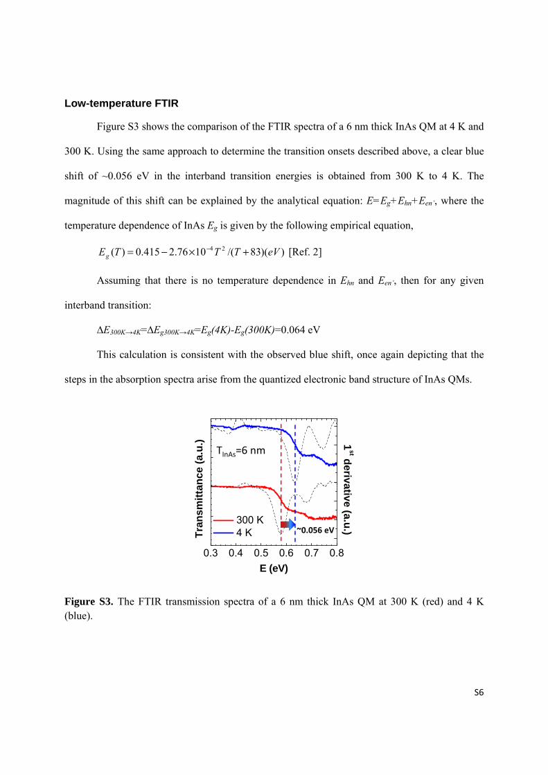
Low-temperature FTIR
Figure S3 shows the comparison of the FTIR spectra of a 6 nm thick InAs QM at 4 K and
300 K. Using the same approach to determine the transition onsets described above, a clear blue
shift of ~0.056 eV in the interband transition energies is obtained from 300 K to 4 K. The
magnitude of this shift can be explained by the analytical equation: E=Eg+Ehn+Een’, where the
temperature dependence of InAs Eg is given by the following empirical equation,
))(83/(1076.2415.0)( 24 eVTTTEg +×−= − [Ref. 2]
Assuming that there is no temperature dependence in Ehn and Een’, then for any given
interband transition:
∆E300K→4K=∆Eg300K→4K=Eg(4K)-Eg(300K)=0.064 eV
This calculation is consistent with the observed blue shift, once again depicting that the
steps in the absorption spectra arise from the quantized electronic band structure of InAs QMs.
Figure S3. The FTIR transmission spectra of a 6 nm thick InAs QM at 300 K (red) and 4 K (blue).
0.3 0.4 0.5 0.6 0.7 0.8
300 K 4 K
E (eV)
Tra
nsm
itta
nc
e (
a.u
.) 1s
t deriv
ativ
e (a
.u.)~0.056 eV
TInAs=6 nm
S7
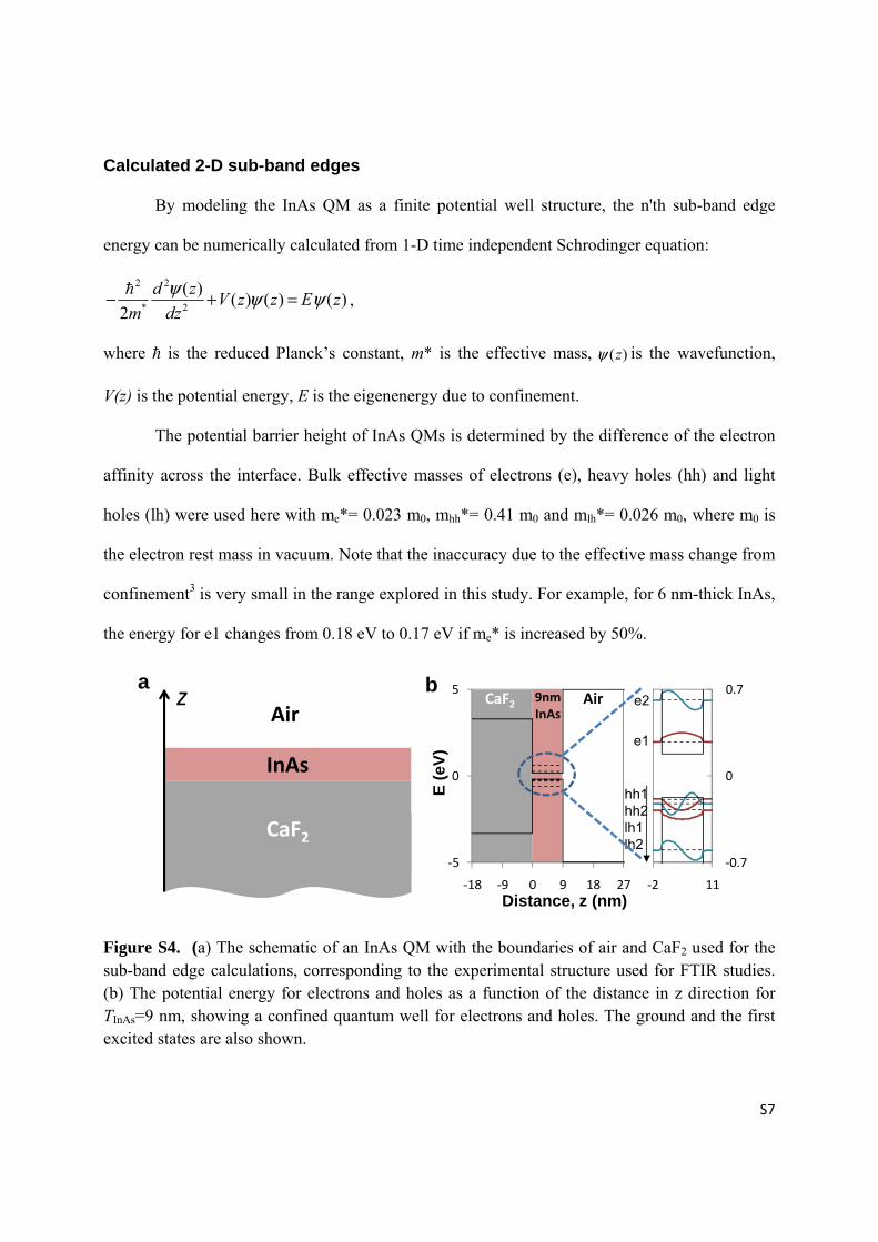
Calculated 2-D sub-band edges
By modeling the InAs QM as a finite potential well structure, the n'th sub-band edge
energy can be numerically calculated from 1-D time independent Schrodinger equation:
)()()()(2 2
2
*
2
zEzzVdz
zdm
ψψψ =+− h,
where h is the reduced Planck’s constant, m* is the effective mass, )(zψ is the wavefunction,
V(z) is the potential energy, E is the eigenenergy due to confinement.
The potential barrier height of InAs QMs is determined by the difference of the electron
affinity across the interface. Bulk effective masses of electrons (e), heavy holes (hh) and light
holes (lh) were used here with me*= 0.023 m0, mhh*= 0.41 m0 and mlh*= 0.026 m0, where m0 is
the electron rest mass in vacuum. Note that the inaccuracy due to the effective mass change from
confinement3 is very small in the range explored in this study. For example, for 6 nm-thick InAs,
the energy for e1 changes from 0.18 eV to 0.17 eV if me* is increased by 50%.
Figure S4. (a) The schematic of an InAs QM with the boundaries of air and CaF2 used for the sub-band edge calculations, corresponding to the experimental structure used for FTIR studies. (b) The potential energy for electrons and holes as a function of the distance in z direction for TInAs=9 nm, showing a confined quantum well for electrons and holes. The ground and the first excited states are also shown.
-0.7
0
0.7
-2 11
-5
0
5
-18 -9 0 9 18 27
CaF2 Air9nmInAs
e2
e1
hh1hh2lh1lh2
E (
eV
)
Distance, z (nm)
a b
CaF2
InAs
Airz
S8
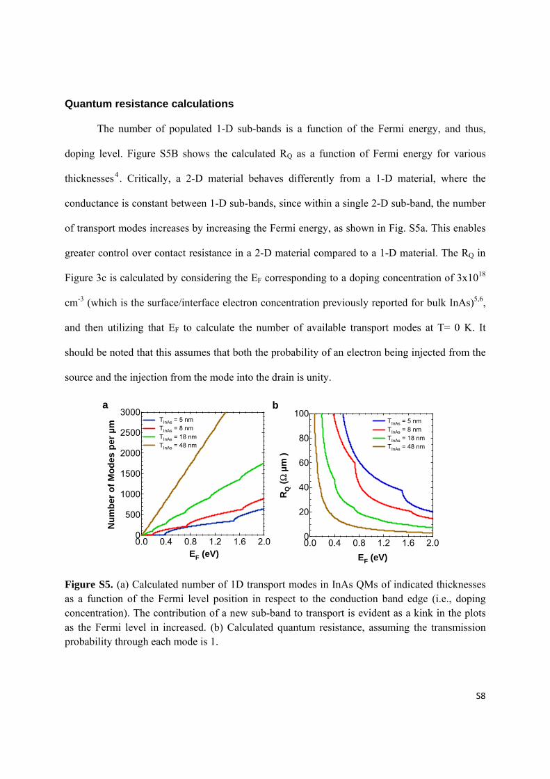
Quantum resistance calculations
The number of populated 1-D sub-bands is a function of the Fermi energy, and thus,
doping level. Figure S5B shows the calculated RQ as a function of Fermi energy for various
thicknesses4. Critically, a 2-D material behaves differently from a 1-D material, where the
conductance is constant between 1-D sub-bands, since within a single 2-D sub-band, the number
of transport modes increases by increasing the Fermi energy, as shown in Fig. S5a. This enables
greater control over contact resistance in a 2-D material compared to a 1-D material. The RQ in
Figure 3c is calculated by considering the EF corresponding to a doping concentration of 3x10¹⁸
cm-3 (which is the surface/interface electron concentration previously reported for bulk InAs)5,6,
and then utilizing that EF to calculate the number of available transport modes at T= 0 K. It
should be noted that this assumes that both the probability of an electron being injected from the
source and the injection from the mode into the drain is unity.
Figure S5. (a) Calculated number of 1D transport modes in InAs QMs of indicated thicknesses as a function of the Fermi level position in respect to the conduction band edge (i.e., doping concentration). The contribution of a new sub-band to transport is evident as a kink in the plots as the Fermi level in increased. (b) Calculated quantum resistance, assuming the transmission probability through each mode is 1.
3000
2500
2000
1500
1000
500
0
Nu
mb
er
of
Mo
de
s p
er
µm
2.01.61.20.80.40.0 EF (eV)
TInAs = 5 nm TInAs = 8 nm TInAs = 18 nm TInAs = 48 nm
a b100
80
60
40
20
0
RQ (
Ω µ
m )
2.01.61.20.80.40.0 EF (eV)
TInAs = 5 nm TInAs = 8 nm TInAs = 18 nm TInAs = 48 nm

S9
NEGF simulation of contact resistance
The non-equilibrium Green's function (NEGF) method is employed to perform
theoretical modeling of the contacts, and the approach is described in Ref. 7. The simulation
describes two-dimensional quantum transport from the contact to the XOI body. The
conductance per width (G/W=1/Rc) is given as:
∫ ∑+∞
∞−
∂+−∂⋅=zk
zz EmkEfETrdEhe
WG )/)/()((2 22
2
h
where f is the Fermi distribution function, h is the Plank constant, Tr(E) is the transimission
function and mz is the effective mass along width. Since transmission probability T(E) and H are
independent of kz, G/W can be explained as,
)/)(()(2 1
2
EEfETdEhe
WG
D ∂−∂⋅⋅= ∫+∞
∞−
Here, f1D(E) is the 1D k-summed Fermi function described as,
( ) = 2 ℏ / −
where F-1/2 is the Fermi-Dirac integral of order -1/2.
Here, a doping concentration of 3×1018 cm-3 and an Schottky barrier height of -0.15 eV to
the conduction band edge are used, corresponding to the values reported in literature5,6. Ballistic
transport is assumed, which corresponds to the limit of zero source-channel XOI diffusion
resistance. In the simulation, the contact length is chosen to be LC =280 nm because further
increase of LC plays a negligible role on the simulated contact resistance. This choice most
accurately reflects the actual structure while minimizing the computation time.

S10
Quantum simulations of the charge density profiles
Figure S6. Simulated structure for the charge density profiles. Effective masses for SiO2 and ZrO2 used here are 0.5m0 and 0.3m0, respectively8.
Air (εr=1)
ZrO2 (εr=25)
SiO2 (εr=4)
InAs (εr=15.6)
VGS
Floating boundary
200 nm
7 nmTInAs=8,18
50 nm

S11
Figure S7. Calculated carrier density profiles, showing the population density of 1st – 3rd sub-bands as a function of the vertical-field bias (VGS - Vth) for (a) 8 nm, (b) 18 nm and (c) 48 nm InAs QMs. The devices are back-gated with 50 nm SiO2 as the gate dielectric.
10
8
6
4
2
0Ch
arg
e d
en
sit
y (
x1
018 c
m-3
)
10
8
6
4
2
0Ch
arg
e d
en
sit
y (
x1
018 c
m-3
)
50403020100Depth of InAs (nm)
10
8
6
4
2
0Ch
arg
e d
en
sit
y (
x1
01
8 c
m-3
)
10
8
6
4
2
0Ch
arg
e d
en
sit
y (
x1
01
8 c
m-3
)
10
8
6
4
2
0Ch
arg
e d
en
sit
y (
x10
18 c
m-3
)
20151050Depth of InAs (nm)
10
8
6
4
2
0Ch
arg
e d
en
sit
y (
x1
018 c
m-3
)
10
8
6
4
2
0Ch
arg
e d
en
sit
y (
x1
018 c
m-3
)
10
8
6
4
2
0Ch
arg
e d
en
sit
y (
x1
01
8 c
m-3
)
10
8
6
4
2
0Ch
arg
e d
en
sit
y (
x1
018 c
m-3
)
86420Depth of InAs (nm)
10
8
6
4
2
0Ch
arg
e d
en
sit
y (
x1
018 c
m-3
)
10
8
6
4
2
0Ch
arg
e d
en
sit
y (
x1
01
8 c
m-3
)
10
8
6
4
2
0Ch
arg
e d
en
sit
y (
x1
018 c
m-3
)
Tota
l1st
subb
and
2ndsu
bban
d3rd
subb
and
a b c
10 V
0 V
VG
S-V
th 10 V
0 V
VG
S-V
th 10 V
0 V
VG
S-V
th
SiO
2&
Gat
eSi
O2
& G
ate
SiO
2&
Gat
eSi
O2
& G
ate
SiO
2&
Gat
eSi
O2
& G
ate
SiO
2&
Gat
eSi
O2
& G
ate
SiO
2&
Gat
eSi
O2
& G
ate
SiO
2&
Gat
eSi
O2
& G
ate
ZrO
2Zr
O2
ZrO
2Zr
O2
ZrO
2Zr
O2
ZrO
2Zr
O2
ZrO
2Zr
O2
ZrO
2Zr
O2
S12
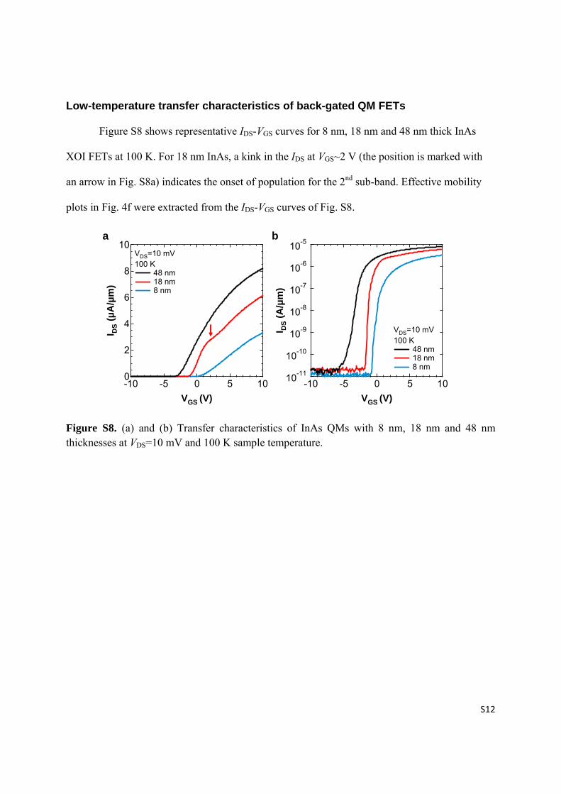
Low-temperature transfer characteristics of back-gated QM FETs
Figure S8 shows representative IDS-VGS curves for 8 nm, 18 nm and 48 nm thick InAs
XOI FETs at 100 K. For 18 nm InAs, a kink in the IDS at VGS~2 V (the position is marked with
an arrow in Fig. S8a) indicates the onset of population for the 2nd sub-band. Effective mobility
plots in Fig. 4f were extracted from the IDS-VGS curves of Fig. S8.
Figure S8. (a) and (b) Transfer characteristics of InAs QMs with 8 nm, 18 nm and 48 nm thicknesses at VDS=10 mV and 100 K sample temperature.
10
8
6
4
2
0
I DS (
µA
/µm
)
-10 -5 0 5 10VGS (V)
VDS=10 mV100 K
48 nm 18 nm 8 nm
10-11
10-10
10-9
10-8
10-7
10-6
10-5
I DS (
A/µ
m)
-10 -5 0 5 10VGS (V)
VDS=10 mV100 K
48 nm 18 nm 8 nm
a b
S13
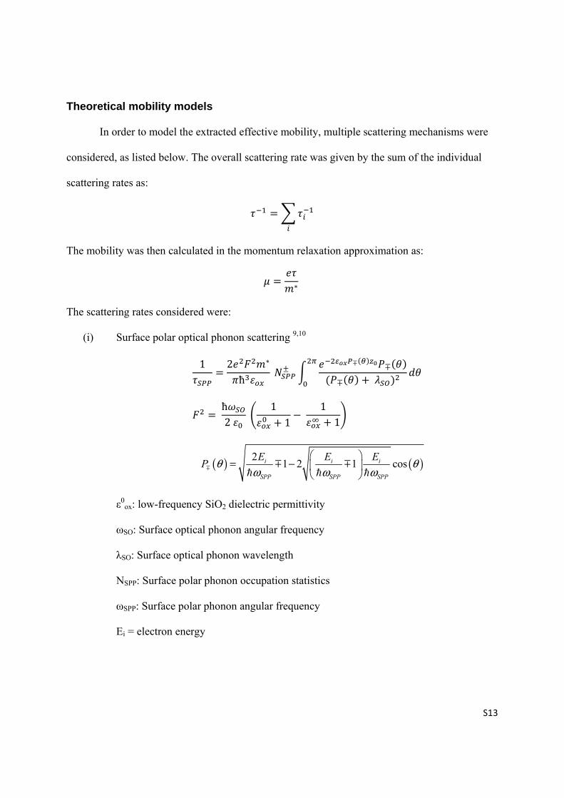
Theoretical mobility models
In order to model the extracted effective mobility, multiple scattering mechanisms were
considered, as listed below. The overall scattering rate was given by the sum of the individual
scattering rates as: =
The mobility was then calculated in the momentum relaxation approximation as: = ∗ The scattering rates considered were:
(i) Surface polar optical phonon scattering 9,10 1 = 2 ∗ħ ± ∓( ) ∓( )( ∓( ) + ) = ħ2 1+ 1 − 1+ 1
( ) ( )2 1 2 1 cosi i i
SPP SPP SPP
E E EP θ θω ω ω
⎛ ⎞= − ⎜ ⎟
⎝ ⎠m m m
h h h
ε0ox: low-frequency SiO2 dielectric permittivity
ωSO: Surface optical phonon angular frequency
λSO: Surface optical phonon wavelength
NSPP: Surface polar phonon occupation statistics
ωSPP: Surface polar phonon angular frequency
Ei = electron energy
S14
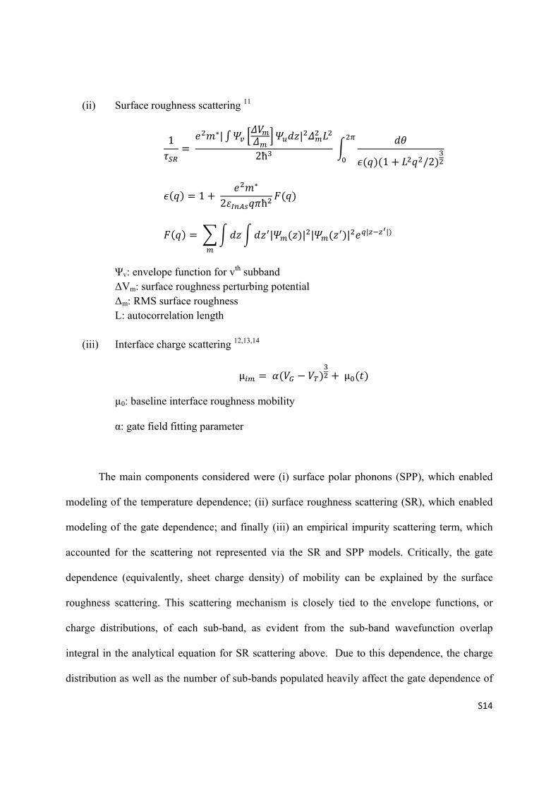
(ii) Surface roughness scattering 11
1 = ∗| |2ħ ( )(1 + /2) ( ) = 1 + ∗2 ħ ( )( ) = | ( )| | ( )| | |)
Ψv: envelope function for vth subband ΔVm: surface roughness perturbing potential Δm: RMS surface roughness L: autocorrelation length
(iii) Interface charge scattering 12,13,14
μ = ( − ) +μ ( ) µ0: baseline interface roughness mobility
α: gate field fitting parameter
The main components considered were (i) surface polar phonons (SPP), which enabled
modeling of the temperature dependence; (ii) surface roughness scattering (SR), which enabled
modeling of the gate dependence; and finally (iii) an empirical impurity scattering term, which
accounted for the scattering not represented via the SR and SPP models. Critically, the gate
dependence (equivalently, sheet charge density) of mobility can be explained by the surface
roughness scattering. This scattering mechanism is closely tied to the envelope functions, or
charge distributions, of each sub-band, as evident from the sub-band wavefunction overlap
integral in the analytical equation for SR scattering above. Due to this dependence, the charge
distribution as well as the number of sub-bands populated heavily affect the gate dependence of

S15
the SR mobility. There is a visible ‘kink’ in the effective mobility versus sheet charge density
plot for the 18 nm QM (Fig. 4f and S9), which coincides with the population of the second sub-
band. The change in slope, causing the kink, can be understood by noting that the charge
centroid of the 2nd sub-band is not a function of sheet density. Thus the change in charge centroid
as a function of gate field, or equivalently, sheet density is significantly reduced.

S16
Temperature, vertical-field, and thickness dependency of the effective mobility
Figure S9. (a), (b), (c) InAs QM mobility calculated by only including the surface roughness (SR) and surface polar phonon (SPP) scattering events, which is in qualitative agreement for the experimental data. The mobility for 8nm QM is approximately independent of the gate-field because the charge centroid remains near the middle of the body regardless of the gate voltage, which is different from a thicker body in which the applied gate voltage moves the centroid closer to the surface (Fig. 4c&d, Fig. S7), resulting in a decrease of mobility due to enhanced SR scattering. For the 8nm QM, only one sub-band is occupied and an ideal 2D electron gas is obtained, which is in contrast to the thicker body case, where multiple sub-bands are populated. For a body thickness of 18nm QM, the shoulder in the mobility curve at T=100K and VDS=10 mV as evident in both the simulation and experimental data is due to the second sub-band being populated. Though qualitative features are understood by the interplay of quantum confinement effects and SR scattering, quantitative difference exists, likely due to other scattering mechanisms such as dislocations, ionized impurities, and surface charge traps. The exact scattering mechanism responsible for the difference requires further study. However, by superimposing the mobility in the first column (SR and SPP) with an empirical model for dislocation scattering, quantitative agreement with experimental data can be achieved, as shown in (d), (e), (f). To determine the extent the surface polar phonons determine the temperature dependence of mobility at VGS-Vth=9 V and VDS=10 mV, the SPP contribution to mobility (purple line) was subtracted from the total calculated mobility (black line) to produce the difference
10324
10424
1052
Mo
bil
ity
(c
m2/V
s) Exp.
Total SPP Total-SPP
10324
10424
1052
Mo
bilit
y (
cm
2/V
s) Exp.
Total SPP Total-SPP
1000
2x10³
3
4
Mo
bilit
y (
cm
2/V
s)
12 3 4 5 6
10VGS-Vth (V)
Exp. Sim. 100 K 200 K 300 K
103
2
4
68104
2
Mo
bil
ity
(c
m2/V
s)
71
2 3 4 5 6 710
VGS-Vth (V)
100 K 200 K 300 K
10324
10424
1052
Mo
bil
ity
(c
m2/V
s)
103
104
105
106
Mo
bil
ity
(c
m2/V
s)
10324
10424
1052
Mo
bilit
y (
cm
2/V
s)
300250200150100Temperature (K)
Exp. Total SPP Total-SPP
48 nm InAs 48 nm InAs
18 nm InAs 18 nm InAs
8 nm InAs 8 nm InAs
a
b
c
d
e
f
g
h
i
48 nm InAs
18 nm InAs
8 nm InAs
2
3
456
104M
ob
ilit
y (
cm
2/V
s)
2
3
4
5678
104
Mo
bilit
y (
cm
2/V
s)
S17
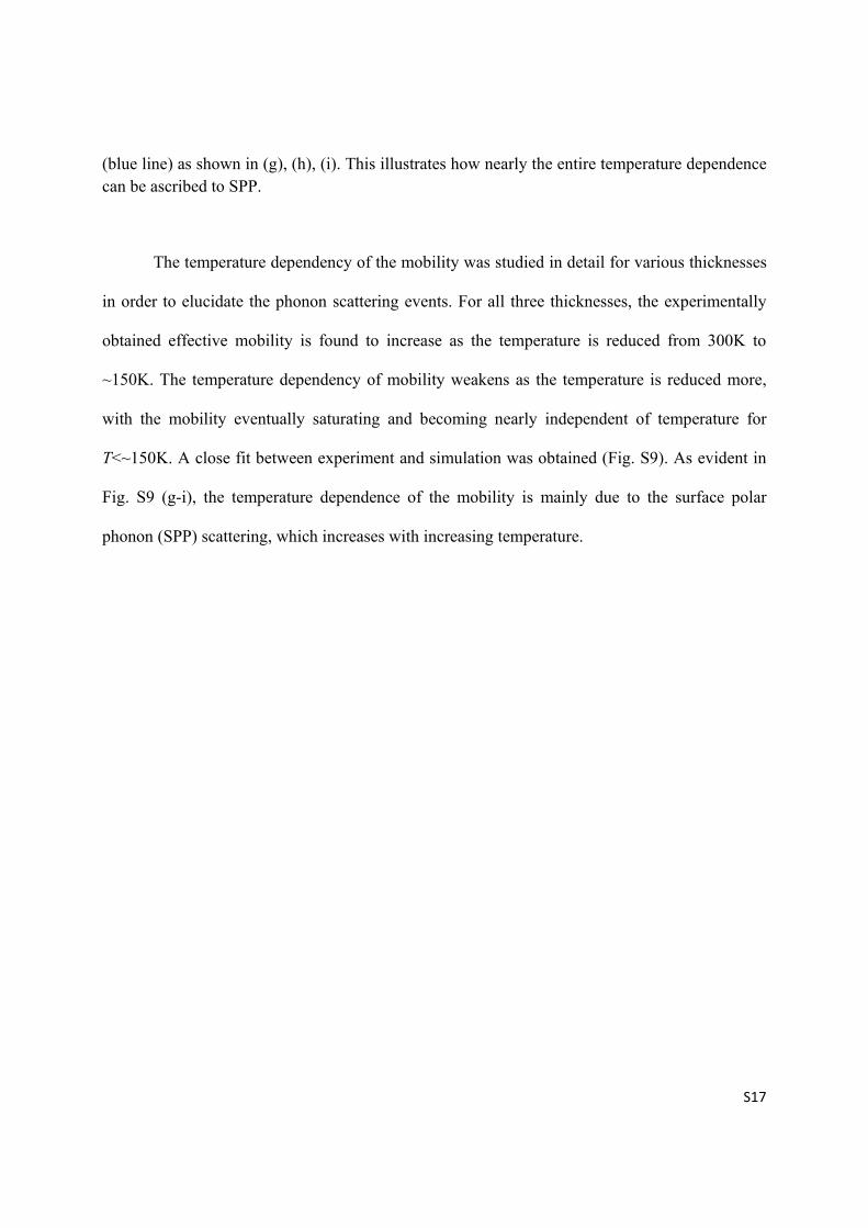
(blue line) as shown in (g), (h), (i). This illustrates how nearly the entire temperature dependence can be ascribed to SPP.
The temperature dependency of the mobility was studied in detail for various thicknesses
in order to elucidate the phonon scattering events. For all three thicknesses, the experimentally
obtained effective mobility is found to increase as the temperature is reduced from 300K to
~150K. The temperature dependency of mobility weakens as the temperature is reduced more,
with the mobility eventually saturating and becoming nearly independent of temperature for
T<~150K. A close fit between experiment and simulation was obtained (Fig. S9). As evident in
Fig. S9 (g-i), the temperature dependence of the mobility is mainly due to the surface polar
phonon (SPP) scattering, which increases with increasing temperature.

S18
References
1. Fang, H.; Madsen, M.; Carraro, C.; Takei, K.; Kim, H. S.; Plis, E.; Chen, S.-Y.; Krishna, S.;
Chueh, Y.-L.; Maboudian, R.; Javey, A. Appl. Phys. Lett. 2011, 98, 012111.
2. Fang, Z. M.; Ma, K. Y.; Jaw, D. H.; Cohen, R. M.; Stringfellow, G. B. J. Appl. Phys. 1990, 67,
7034-7039.
3. Ekenberg, U. Phys. Rev. B 1989, 40, 7714-7726.
4. Datta, S. Electronic Transport in Mesoscopic Systems (Cambridge University Press,
Cambridge, 2001).
5. Wieder, H. H. J. Vac. Sci. Technol. B 2003, 21, 1915-1919.
6. Bell, G. R.; Jones, T. S.; McConville C. F. Appl. Phys. Lett. 1997, 71, 3688-3690.
7. Gao, Q.; Ouyang, Y.; Guo, J. J. Appl. Phys. 2011, 109, 104307.
8. Houssa, M.; Tuominen, M.; Naili, M.; Afanasev, V.; Stesmans, A.; Haukka, S.; Heyns, M. M.
J. Appl. Phys. 2000, 87, 8615-8620.
9. Konar, A.; Fang, T.; Jena, D. Phys. Rev. B, 2010, 82, 115452.
10. Li, X.; Barry, E. A.; Zavada, J. M.; Nardelli, M. B.; Kim, K. W. Appl. Phys. Lett. 2010, 97,
232105.
11. Gámiz, F.; Roldán, J. B.; Cartujo-Cassinello, P.; López-Villanueva, J. A.; Cartujo, P. J. Appl.
Phys. 2001, 89, 1764-1770.
12. Jena, D.; Gossard, A. C.; Mishra U. K. Appl. Phys. Lett. 2000, 76, 1707-1709.
13. Asgari, A.; Kalafi, M.; Faraone, L. J. Appl. Phys. 2004, 95, 1185-1190.
14. Gurusinghe, M. N.; Davidsson, S. K.; Andersson, T. G. Phys. Rev. B 2005, 72, 045316.
Copyright © 2022 FDOKUMEN