Interfacial charge transfer in nanoscale polymer transistors
19
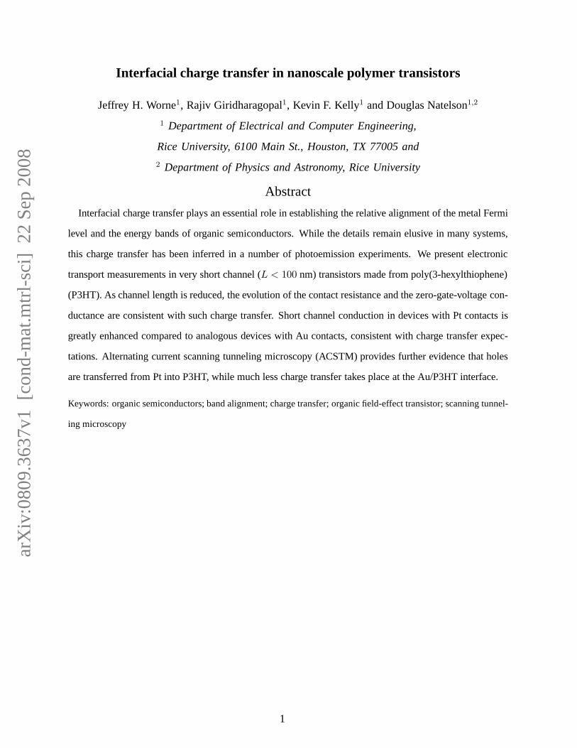
arXiv:0809.3637v1 [cond-mat.mtrl-sci] 22 Sep 2008 Interfacial charge transfer in nanoscale polymer transistors Jeffrey H. Worne 1 , Rajiv Giridharagopal 1 , Kevin F. Kelly 1 and Douglas Natelson 1,2 1 Department of Electrical and Computer Engineering, Rice University, 6100 Main St., Houston, TX 77005 and 2 Department of Physics and Astronomy, Rice University Abstract Interfacial charge transfer plays an essential role in establishing the relative alignment of the metal Fermi level and the energy bands of organic semiconductors. While the details remain elusive in many systems, this charge transfer has been inferred in a number of photoemission experiments. We present electronic transport measurements in very short channel (L< 100 nm) transistors made from poly(3-hexylthiophene) (P3HT). As channel length is reduced, the evolution of the contact resistance and the zero-gate-voltage con- ductance are consistent with such charge transfer. Short channel conduction in devices with Pt contacts is greatly enhanced compared to analogous devices with Au contacts, consistent with charge transfer expec- tations. Alternating current scanning tunneling microscopy (ACSTM) provides further evidence that holes are transferred from Pt into P3HT, while much less charge transfer takes place at the Au/P3HT interface. Keywords: organic semiconductors; band alignment; charge transfer; organic field-effect transistor; scanning tunnel- ing microscopy 1
-
Upload
independent -
Category
Documents
-
view
1 -
download
0
Transcript of Interfacial charge transfer in nanoscale polymer transistors
arX
iv:0
809.
3637
v1 [
cond
-mat
.mtr
l-sci
] 22
Sep
200
8
Interfacial charge transfer in nanoscale polymer transistors
Jeffrey H. Worne1, Rajiv Giridharagopal1, Kevin F. Kelly1 and Douglas Natelson1,2
1 Department of Electrical and Computer Engineering,
Rice University, 6100 Main St., Houston, TX 77005 and
2 Department of Physics and Astronomy, Rice University
Abstract
Interfacial charge transfer plays an essential role in establishing the relative alignment of the metal Fermi
level and the energy bands of organic semiconductors. Whilethe details remain elusive in many systems,
this charge transfer has been inferred in a number of photoemission experiments. We present electronic
transport measurements in very short channel (L < 100 nm) transistors made from poly(3-hexylthiophene)
(P3HT). As channel length is reduced, the evolution of the contact resistance and the zero-gate-voltage con-
ductance are consistent with such charge transfer. Short channel conduction in devices with Pt contacts is
greatly enhanced compared to analogous devices with Au contacts, consistent with charge transfer expec-
tations. Alternating current scanning tunneling microscopy (ACSTM) provides further evidence that holes
are transferred from Pt into P3HT, while much less charge transfer takes place at the Au/P3HT interface.
Keywords: organic semiconductors; band alignment; chargetransfer; organic field-effect transistor; scanning tunnel-
ing microscopy
1
Understanding the band alignment between organic semiconductors (OSCs) and metal elec-
trodes is of basic physical interest as well as significant technological importance[1]. Such en-
ergetic considerations are crucial for optimizing charge injection in organic light emitting diodes
(OLEDs) and organic field-effect transistors (OFETs). Similarly, the relative band alignment at
such interfaces also affects the open circuit photovoltageachievable in organic photovoltaic appli-
cations. Because interfacial dipoles can be used to modulate the effective work function of a metal
surface, self-assembled monolayers (SAMs) of polar molecules have been used in both OLEDs
and OFETs to engineer charge injection[2, 3, 4].
Conceptually the issue is straightforward, though very complicated in detail. In equilibrium the
chemical potential throughout a metal/organic heterointerface must be constant. This condition
is achieved through a combination of interfacial dipole formation, charge transfer, and the self-
consistent solution of the electrostatics to equilibrate carrier drift and diffusion. Dipole formation
and charge transfer lead to deviations from the Schottky-Mott limit, so that simple alignment of
vacuum levels does not give an accurate picture of the true heterojunction energetics[5].
The relative alignment of levels is most readily measured via photoemission experiments. Re-
cent investigations using electroluminescent polymers[6] as well as small molecule OSCs and
conducting polymers[7] have shown Fermi level pinning at the metal-organic interface. For the
case of holes, when the Fermi level of the metal is relativelyfar above the highest occupied molec-
ular orbital (HOMO) of the molecules (the center of the disorder-broadened valence band, in the
case of polymers), the system is in the Schottky-Mott limit.When the Fermi level approaches the
HOMO, strong deviations from the Schottky-Mott limit are reported[6]. There are several sug-
gested mechanisms for these deviations, including changesin the interfacial dipole (via chemical
reactions or the “pillow effect”[8]), shifting of frontierorbitals and formation of induced states[9],
and charge transfer involving polaron formation[6, 10]. Recent photoemission experiments exam-
ining metal/polymer interfaces show evidence of charge transfer into valence band tail states and
accompanying band bending[11].
Other data consistent with charge transfer and band bendingat similar interfaces has been seen
in transport measurements[4, 16] of contact resistance in P3HT-based OFETs. In devices with
high electrode work functions, hole injection remains Ohmic down to very low carrier densities,
a natural result if interfacial charge transfer effectively dopes the contact interface. Similarly
current-voltage characteristics in devices with (lower work function) electrode metals giving non-
Ohmic injection are consistent with a nanoscale region (between 10 nm and 100 nm in extent)
2
of reduced mobility at the metal/organic interface[12, 13,14, 15]. This may be due to interfacial
structural disorder in the organic semiconductor, but it would also be compatible with the forma-
tion of an effective depletion region near the contacts due to band bending. Conduction in P3HT
takes place via hopping through a density of localized states in the valence band tail. A local
change in the chemical potential farther into the band tail would simultaneously deplete holes and
reduce the spatial density of available hopping sites, reducing the mobility as well.
In this paper we present additional evidence that significant charge transfer takes place at the
Pt/P3HT interface, leading to a population of mobile holes within a nanoscale distance of the
interface. Measurements of Pt-based OFET device resistance as a function of channel length,L,
show a decrease in resistance asL is reduced below 100 nm. In the same devices this corresponds
to nearly a factor of 10 increase in zero-gate-bias (ZGB) current over the sameL range. In contrast,
identically prepared short channel Au-based devices show an increase in resistance, as well as ZGB
currents orders of magnitude lower than in Pt devices. Devices with Au surfaces functionalized
with SAMs known to increase the electrode effective work function show trends intermediate
between the Au and Pt cases. Further measurements using alternating current scanning tunneling
microscopy (ACSTM) show clear evidence for excess holes in thin P3HT films on Pt, in marked
contrast to ACSTM measurements on identically prepared P3HT films on Au.
Devices are fabricated onn+ silicon with 200nm of thermally grown oxide as the gate dielec-
tric. Electrodes are patterned using electron beam lithography, e-beam evaporation, and liftoff
processing. Using two-step lithography, various channel lengths,L, are fabricated, from∼50 nm
to 5 µm, with widths,w of 50 µm for short channel device studies. In addition, for comparison
a structure of interdigitated electrodes withL = 1 − 50 µm andw = 200 µm is fabricated on
the same chip in order to allow standard transmission line measurements of P3HT field effect
mobility. Electrode films are 15 nm of either gold or platinumwith a 1 nm titanium adhesion
layer. Following lithography and liftoff, the devices are cleaned under ultraviolet exposure, 1
minute of oxygen plasma, and a 1 minute soak in piranha etch (3:1 H2SO4:H2O2 (30%)). For
functionalized Au electrode devices, the piranha etch stepis followed by self-assembly of fluori-
nated oligo(phenylene ethynylene) (F-OPE)[4] by immersion for 24 h in a solution of F-OPE at
0.25 mg/mL concentration in 1:1 ethanol:chloroform under nitrogen gas, with standard thioacetate
deprotection chemistry[17].
After the SiO2 dielectric surface is treated with octadecyltricholorosilane (OTS) (10µL OTS
in 8 mL hexadecane, assembled in the dark at room temperaturefor ∼12 hours), P3HT (0.1%
3
by weight in chloroform) is then spin-coated to a thickness of 5 nm (measured via AFM) over the
entire substrate. Contact to the substrate is made, and the Si becomes the gate of the device. Figure
1b illustrates a typical short channel device. Devices are transferred to a variable temperature
vacuum probe station immediately upon completion of spin coating. Devices remain in vacuum
(∼ 10−6 mTorr) for at least 1 hour before any measurements are performed. Individual OFETs are
isolated from one another by using a probe tip to scratch awaythe P3HT film in a rectangle around
each device to prevent stray current paths.
Using the interdigitated electrodes of fixedw but varyingL, device characteristics (ID vs.
VSD at fixedVG, whereID is drain current andVSD is source-drain voltage) are measured via a
semiconductor parameter analyzer. In the shallow channel regime (|VSD| << |VG|) we find these
characteristics to be linear, consistent with Ohmic injection. As in our previous work[4, 18] we use
the transmission line approach to characterize the contactresistances and field-effect mobilities as
a function of gate voltage,VG. In the shallow channel regime at a particularVG, the measured
source-drain resistanceR = (∂ID/∂VSD)−1 is plotted as a function ofL and found to be linear
for long (L > 1 µm) devices. Channel resistance,RC, is determined by the slope of this line
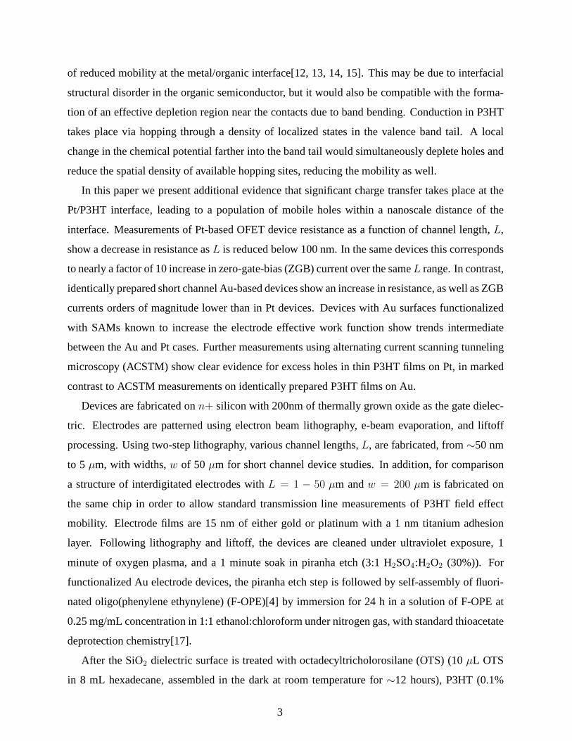
and the effective contact resistance,RS is determined by extrapolating this line to zero channel
length, as shown in Fig. 1a. This linearity observed in longer devices indicates that the overall film
uniformity is good, even for the relatively thin P3HT layersused here.
This extrapolation to inferRS assumes that the device properties are uniform down to arbitrarily
short channel lengths. In practice this may not be true, for anumber of reasons. For example, a
change in polymer morphology near the metal contacts would lead to deviations from linearity in
R(L) at short distances as contact regions interact with each other[19]. Similarly, there is indirect
evidence[12, 13, 14] that nanoscale regions of poor effective mobility can exist near contacts
due to band bending and depletion effects. Note that the characteristic size of these regions is
constrained experimentally[14] to less than∼ 100 nm, since larger regions would be detectable
within the resolution of scanning potentiometry experiments. If two such depletion regions were
to intersect for sufficiently short channel devices, one would expect the measuredR(L) to have an
up-turn asL → 0, as shown by the red line in Fig. 1a.
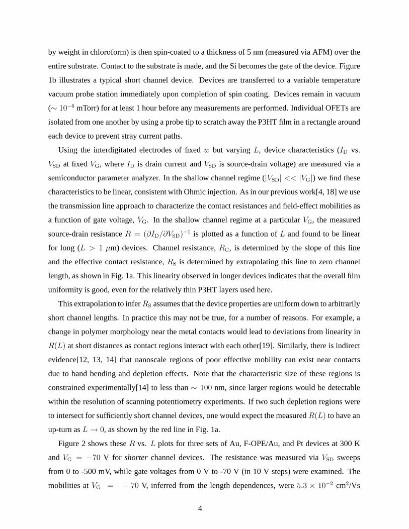
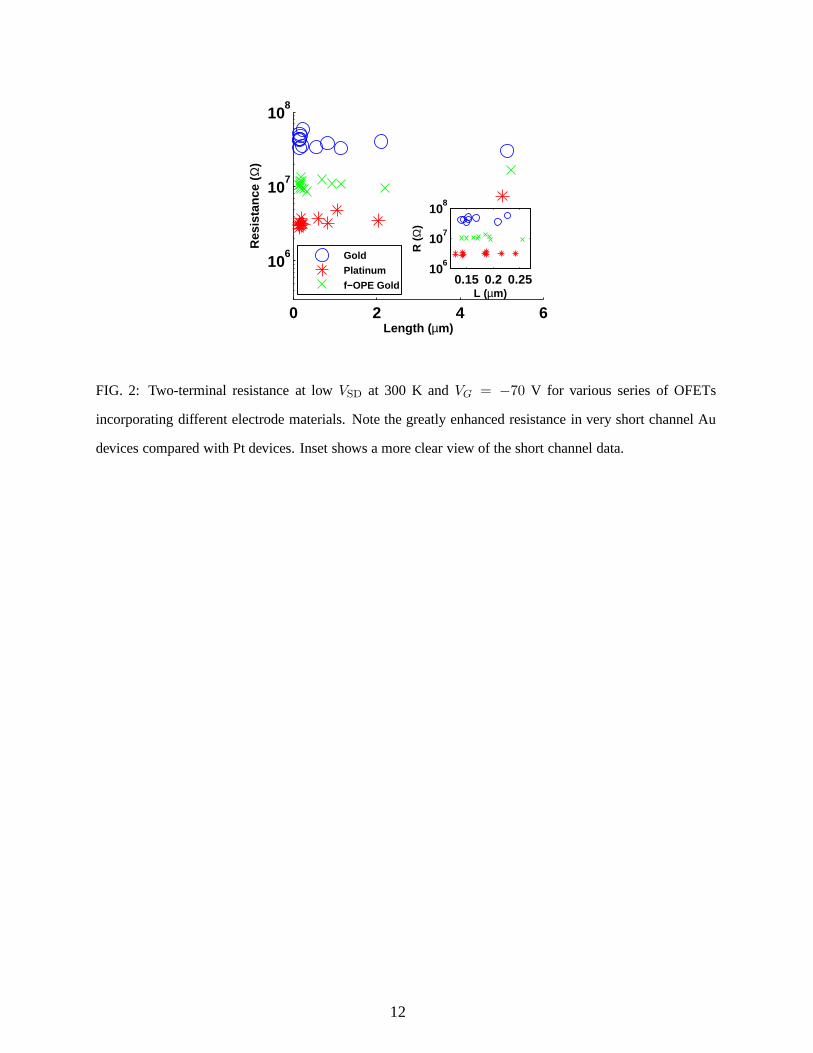
Figure 2 shows theseR vs. L plots for three sets of Au, F-OPE/Au, and Pt devices at 300 K
andVG = −70 V for shorter channel devices. The resistance was measured viaVSD sweeps
from 0 to -500 mV, while gate voltages from 0 V to -70 V (in 10 V steps) were examined. The
mobilities atVG = − 70 V, inferred from the length dependences, were5.3 × 10−2 cm2/Vs
4
(Au), 5.3 × 10⁻² cm2/Vs (F-OPE/Au), and8.7 × 10−2 cm2/Vs (Pt). Initial measured resistances
from the 5µm channel length devices span roughly an order of magnitude between the three
different electrode materials, with the highest resistance coming from the gold electrodes and the
lowest resistance from the platinum devices. As the channellength is reduced significantly below
1 µm, there are qualitative differences between the three types of devices. The Au-based devices
have much-increased resistances, while the Pt-based devices have decreased resistances. The F-
OPE/Au structures are intermediate in their smallL properties. We analyzed several ensembles of
identically prepared devices, and all exhibited these trends. These trends continued to hold at other
gate voltages and asT was reduced. Channel lengths in the short-channel devices were measured
via electron microscopyafter electrical characterization, to ensure that electrode contamination
during imaging did not affect the results.
At the smallest channel lengths there is significant device-to-device variability inR, much
more so than in the longer channel devices. This appears to reflect that microscopic differences in
the metal/organic interface can have significant local impact on the injection process and contact
resistances, even when large-scale properties are uniformand well defined. However, even with
this variability the overall trends and the systematic deviation between the different electrode types
are clear.
One possibility is that the morphology of the P3HT may differat the metal/P3HT interface
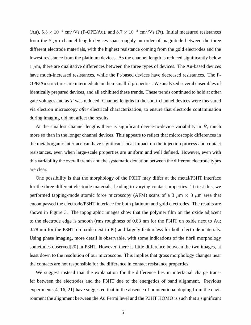
for the three different electrode materials, leading to varying contact properties. To test this, we
performed tapping-mode atomic force microscopy (AFM) scans of a 3µm × 3 µm area that
encompassed the electrode/P3HT interface for both platinum and gold electrodes. The results are
shown in Figure 3. The topographic images show that the polymer film on the oxide adjacent
to the electrode edge is smooth (rms roughness of 0.83 nm for the P3HT on oxide next to Au;
0.78 nm for the P3HT on oxide next to Pt) and largely featureless for both electrode materials.
Using phase imaging, more detail is observable, with some indications of the fibril morphology
sometimes observed[20] in P3HT. However, there is little difference between the two images, at
least down to the resolution of our microscope. This impliesthat gross morphology changes near
the contacts are not responsible for the difference in contact resistance properties.
We suggest instead that the explanation for the difference lies in interfacial charge trans-
fer between the electrodes and the P3HT due to the energeticsof band alignment. Previous
experiments[4, 16, 21] have suggested that in the absence ofunintentional doping from the envi-
ronment the alignment between the Au Fermi level and the P3HTHOMO is such that a significant
5
hole injection barrier exists. In this case one may expect the tail of the P3HT valence band to be
locally depleted in the vicinity of the of the interface. In contrast, measurements involving the
interface between P3HT and higher work function systems such as Pt[4, 16] and F-OPE/Au[4]
show much lower contact resistances and persistent Ohmic injection in field-effect structures even
under treatment conditions where the bulk two-terminal conductivity of the P3HT is immeasurably
small. Consistent with recent photoemission experiments[11], we suggest that the charge transfer
responsible for pinning the Pt Fermi level above the P3HT HOMO populates the tail states with
mobile holes, leading to comparatively enhanced conduction in the shortest devices.
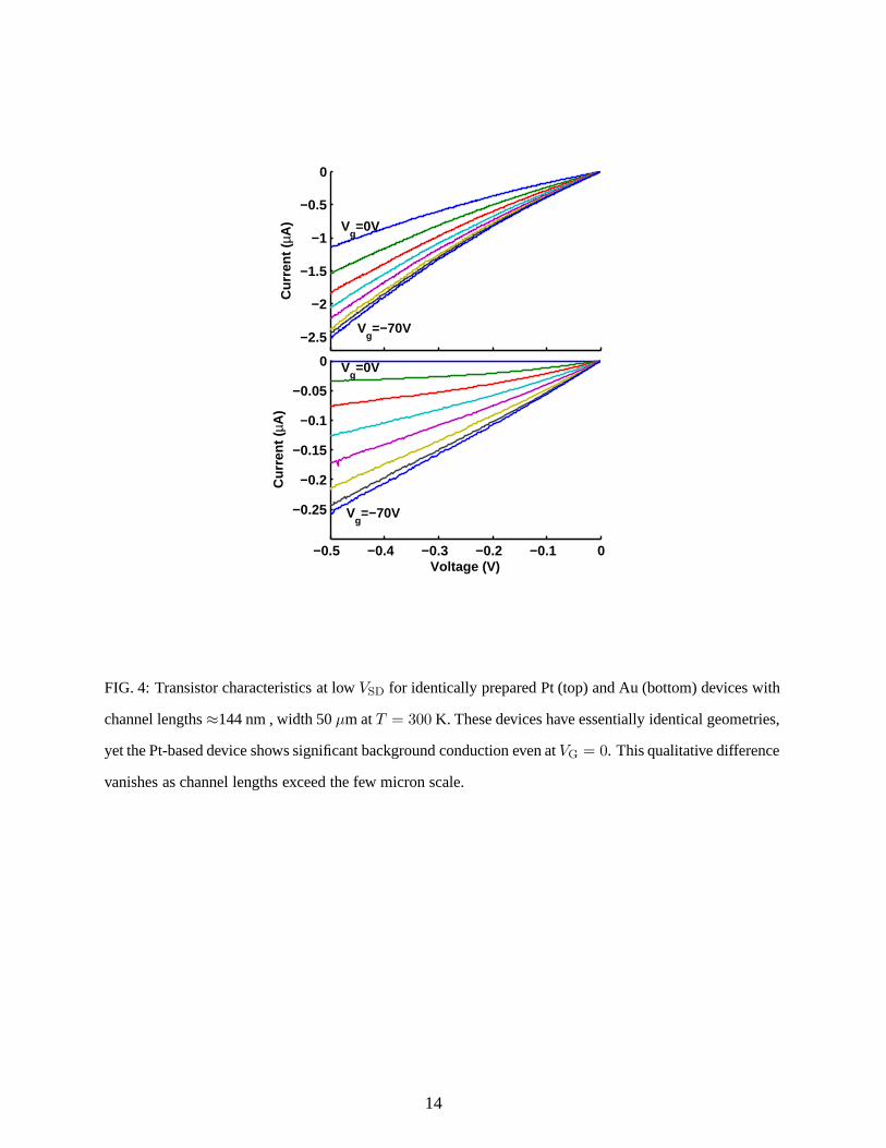
This interpretation is supported by other experimental signatures. First, we examine the low
VSD transistor characteristics as a function ofVG for short-channel devices withidentical geome-
tries. This is more revealing thanID − VG transfer characteristics since the changing channel
geometry asL is reduced, high electric fields at largeVSD, and hysteresis inVG complicate the
interpretation of inferred threshold voltages. A typical result is shown in Fig. 4, for Pt (top) and
Au (bottom) devices withL ≈ 100 nm atT = 300 K. Note that there is a large qualitative differ-
ence between these devices. The Pt device shows significant background conduction atVG = 0,
qualitatively similar to what is seen in the presence of doping. This conduction vanishes in adja-
cent, simultaneously fabricated Pt devices as channel lengths are increased into the micron range,
showing that it is an effect of the contacts.
We investigate this further by examining the two-terminal source-drain conductance atVG = 0
for the short channel devices (L < 5 µm) atVSD = −0.5 V. Representative data are shown in Fig.
5. At the 5µm limit the ZGB current is essentially the same for all devices. As the channel length
decreases, however, the measured currents in devices with platinum contacts continue to increase
by orders of magnitude, while the measured currents in devices with gold contacts do not follow
this trend. Rather, the Au deviceVG = 0 currents tend to be fairly constant over the measured
channel length range. The current measured from the F-OPE/Au electrodes remains fairly constant
and similar to that of gold over the longer channel lengths, but as the channel lengths decrease well
below 200 nm, the zero-bias current displays a rapid increase. Since all of the devices of a given
electrode composition are prepared simultaneously and measured in one run, these dependences
of theVG = 0 conduction onL cannot arise from dopants from the environment.
To further examine charge transfer between the electrodes and the P3HT film, we used an ex-
tension of scanning tunneling microscopy (STM) known as alternating current scanning tunneling
microscopy (ACSTM). STM and related spectroscopic techniques have long been used to char-
6
acterize the electronic properties of conducting polymer materials. More common spectroscopies
provide high-resolution analysis of properties such as thedensity of states and work function, yet
fail to provide capacitance versus voltage (C −V ) information, which is critical for understanding
dopant effects. Unlike conventional STM, microwave frequency ACSTM can be used to obtain
localC − V data.
In the ACSTM technique, microwave frequency radiation is applied to the tip-sample junction.
By exploiting the nonlinear behavior of the junction using high frequencies, ACSTM can be used
to acquire capacitance information. Specifically, the tunneling current response at microwave
frequencies when imaging semiconductors reflects the∂C/∂V data[22]. In this way, ACSTM can
provide high-resolution spatial capacitance informationon semiconducting polymer films. The
magnitude of the ACSTM signal ultimately reflects the carrier concentration in the substrate. For
example, this microwave signal has been used previously in both STM and AFM mode to measure
the dopant concentration in silicon[23, 24, 25].
For this ACSTM experiment a loop antenna geometry was used toapply microwave radia-
tion to the junction similar to studies previously reported[27]. We used the difference frequency
ACSTM technique[23, 24, 25, 26] to simplify detection of thehigh frequency modulation of the
tunneling signal by allowing the use of conventional lock-in amplifier equipment. Care was taken
to ensure that the ACSTM data on both samples were acquired under nearly identical scanning
conditions[28]. The ACSTM signal was acquired at each pointduring scanning, thus producing
∂C/∂V spectral images (magnitude and phase) and the topography image simultaneously. All
scans were taken in ultrahigh vacuum at base pressures on theorder of 10−10 torr using a com-
mercial RHK STM and mechanically cut Pt:Rh (80:20) tips. TheSTM was modified to include
the antenna so that the loop antenna encircled the STM tip during scanning, similar to a method
reported previously[27] and could be moved aside for tip andsample exchange. P3HT films were
spin-coated onto Au- and Pt-coated SiO2/Si substrates following the same procedure as in the
fabrication of the OFET devices.
In Fig. 6, the topography and ACSTM image are both shown at various bias conditions for
P3HT deposited on Au and Pt, respectively[29]. The ACSTM images are shown at the same
relative color scale in units of mV, directly proportional to local∂C/∂V and therefore carrier con-
centration (as seen in doped Si devices[23]). Bear in mind that the carrier concentration seen in
semiconductors in ACSTM depends to some degree on the bias conditions and gap geometry. The
gap resistance was kept constant at∼ 100 GΩ to eliminate the influence of tip height on the result-
7
ing data. A direct comparison of the ACSTM data on Au and Pt shows a marked contrast in carrier
concentration. Averaged over the scan area, the carrier concentration is 25% larger for P3HT on
Pt than on Au, but there is also a higher spatial variance on the Pt sample despite the comparable
surface structure. This is consistent with the interpretation that there are more mobile holes in the
P3HT layer on Pt. Measurements taken at multiple locations on each film confirm these results. In
addition, the percentage difference between average ACSTMsignal on Pt vs. Au increases to 69%
as the tip bias relative to the sample is increased to 2 V. Thisshows that the carriers present on Au
are easier to deplete relative to those on Pt. It is difficult to compare quantitatively the ACSTM
data in these vertical layered structures with the situation in the transistor geometry. However,
the ACSTM data presented here clearly indicate that Pt increases the carrier concentration in the
P3HT film more than the Au layer.
Interestingly, both films show inhomogeneities in the magnitude and phase of their AC response
that do not correlate in any immediately obvious way with sample topography, although Figs. 6A
and 6C show that the surface features of the two films are similar. In particular the variation takes
place on length scales that are not correlated with intrinsic structural properties of the underlying
polycrystalline metal films, such as grain size.
The transport and ACSTM indications of charge transfer are consistent with simple calcula-
tions using a model for charge transfer developed by Paasch and Scheinert[30]. Their model was
developed to explain charge transfer and band bending in thin layers of disordered organic semi-
conductor on top of metal films. This is precisely the situation of the ACSTM samples, and at zero
source-drain bias should be reasonably applicable to the organic channel in the immediate vicin-
ity of the source or drain electrodes. Assuming an exponential density of states for the organic
semiconductor characterized by an energy scalekBT0 = 0.1 eV, the local potential in the organic
semiconductor of layer thicknessd as a function of distancex away from the metal interface is
given by
U(x) = Ud ± kBT0 ln
[
1 + tan2
(
d − x
2Ld
exp|Ud|
2kBT0
)]
, (1)
whereUd is the potential atx = d, Ld ≡√
ǫǫ0kBT/2e2n is the intrinsic screening length, and
n =√
NcNv exp(−Eg/2kBT0) is the effective intrinsic carrier density[30]. Hereǫ is the relative
dielectric constant of the organic semiconductor,Eg is the band gap of the organic semiconductor,
Nc andNv are the effective densities of states in the conduction and valence bands. The± sign is
positive (negative) for hole(electron) accumulation. ThePoisson equation can be used to find the
8
relationship betweend andUd:
d = 2Ld exp
(
− |Ud|2kBT0
)
arctan
[
exp
( |Us − Ud|kBT0
)
− 1
]0.5
. (2)
HereUs ≡ Eg/2 − Φh, whereΦh is the hole injection barrier. Rough values used for our estima-
tions areNc, Nv = 1021 cm−3, Eg = 2 eV, ǫ = 3.24, andT = 300 K.
Working with Eqs. (1, 2) and Poisson’s equation, we can determine the charge density in the
organic semiconductor layer. Varying the metals involved affects the local potentialU(x) and
carrier density by alteringΦh. Recalling previous photoemission results for P3HT on platinum
and gold[16], for platinum withΦh = 0.6 eV, the charge carrier density very near the interface
is estimated to be∼ 9.6 × 1017cm−3; for gold with Φh = 1.2 eV, we find∼ −1018 cm−3, with
the negative sign indicating adepletion of hole density. These precise numbers should be viewed
cautiously, since different surface preparations can alter the effective work functions of metals
and the density of states values used are rough. The trend, however, from Au to Pt should be
robust and these results are unlikely to change qualitatively upon inclusion of corrections for a
Gaussian density of states for the polymer. For both the Pt, theΦh = 0.6 eV value is consistent
with prior photoemission experiments[16] as well as recentFermi level pinning results for P3HT
and estimates of polaron formation energy relevant to Pt/P3HT charge transfer[6]. The estimate
of Φh for Au also comes from the same photoemission experiments[16]. The resulting calculation
supports the claim that higher work function metals, with Fermi levels pinned relatively close to
the valence band, locally dope the organic material very near the interface.
We have presented a series of experiments examining the contact resistance and ZGB current in
very short channel bottom-contact OFETs incorporating P3HT. The striking differences observed
between devices with Pt and Au electrodes are consistent with expectations of metal/P3HT charge
transfer inferred from photoemission experiments. In particular, it appears that a significant den-
sity of mobile holes are transferred from Pt into neighboring P3HT on the nanoscale. ACSTM
measurements further support this conclusion, showing a significantly higher free carrier response
in P3HT films on Pt compared to identically prepared films on Au. Further experiments, particu-
larly those probing spatial scales comparable to small numbers of polymer chains, should be able
to shed further light on the complex problem of charge transfer and Fermi level pinning, com-
plementing spatially averaging techniques such as photoemission. Techniques like ACSTM point
the way toward detailed quantitative assessment of local charge density, information that will be
extremely useful in refining theoretical models of these important but complicated problems.
9
Acknowledgments
The authors gratefully acknowledge Jun Zhang for experimental assistance, Paul Weiss for use-
ful discussions, Prof. J. W. Ciszek and Prof. J. M. Tour for synthesis of the F-OPE molecule, and
the support from NSF grant ECCS-0601303. RG acknowledges the support of an NSF graduate
fellowship. DN also aknowledges the David and Lucille Packard Foundation, the Alfred P. Sloan
Foundation, the Robert A. Welch Foundation, and the Research Corporation. KFK also acknowl-
edges the Rochester MURI on Nanoscale Subsurface Spectroscopy and Tomography (F49620-
031-0379), administered by the Air Force Office of ScientificResearch.
10
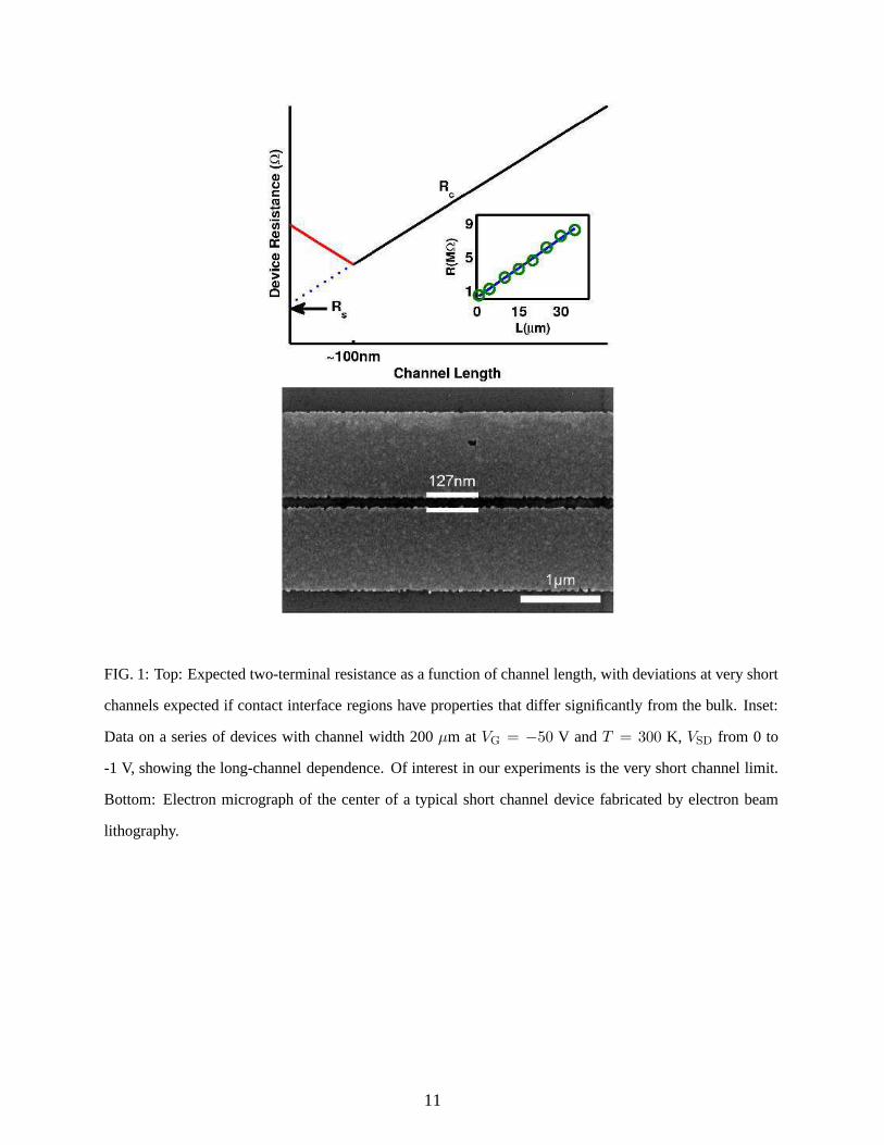
FIG. 1: Top: Expected two-terminal resistance as a functionof channel length, with deviations at very short
channels expected if contact interface regions have properties that differ significantly from the bulk. Inset:
Data on a series of devices with channel width 200µm atVG = −50 V and T = 300 K, VSD from 0 to
-1 V, showing the long-channel dependence. Of interest in our experiments is the very short channel limit.
Bottom: Electron micrograph of the center of a typical shortchannel device fabricated by electron beam
lithography.
11
0 2 4 6
106
107
108
Length ( µm)
Res
ista
nce
(Ω
)
Gold
Platinum
f−OPE Gold 0.15 0.2 0.2510
6
107
108
L (µm)
R (
Ω)
FIG. 2: Two-terminal resistance at lowVSD at 300 K andVG = −70 V for various series of OFETs
incorporating different electrode materials. Note the greatly enhanced resistance in very short channel Au
devices compared with Pt devices. Inset shows a more clear view of the short channel data.
12
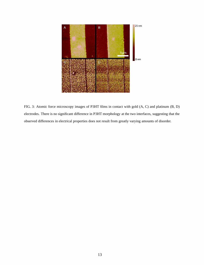
FIG. 3: Atomic force microscopy images of P3HT films in contact with gold (A, C) and platinum (B, D)
electrodes. There is no significant difference in P3HT morphology at the two interfaces, suggesting that the
observed differences in electrical properties does not result from greatly varying amounts of disorder.
13
−2.5
−2
−1.5
−1
−0.5
0
Vg=0V
Vg=−70V
Cur
rent
(µA
)
−0.5 −0.4 −0.3 −0.2 −0.1 0
−0.25
−0.2
−0.15
−0.1
−0.05
0 Vg=0V
Vg=−70V
Voltage (V)
Cur
rent
(µA
)
FIG. 4: Transistor characteristics at lowVSD for identically prepared Pt (top) and Au (bottom) devices with
channel lengths≈144 nm , width 50µm atT = 300 K. These devices have essentially identical geometries,
yet the Pt-based device shows significant background conduction even atVG = 0. This qualitative difference
vanishes as channel lengths exceed the few micron scale.
14
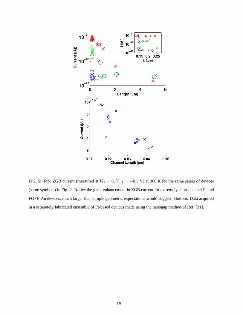
FIG. 5: Top: ZGB current (measured atVG = 0, VSD = −0.5 V) at 300 K for the same series of devices
(same symbols) in Fig. 2. Notice the great enhancement in ZGBcurrent for extremely short channel Pt and
FOPE-Au devices, much larger than simple geometric expectations would suggest. Bottom: Data acquired
in a separately fabricated ensemble of Pt-based devices made using the nanogap method of Ref. [31].
15
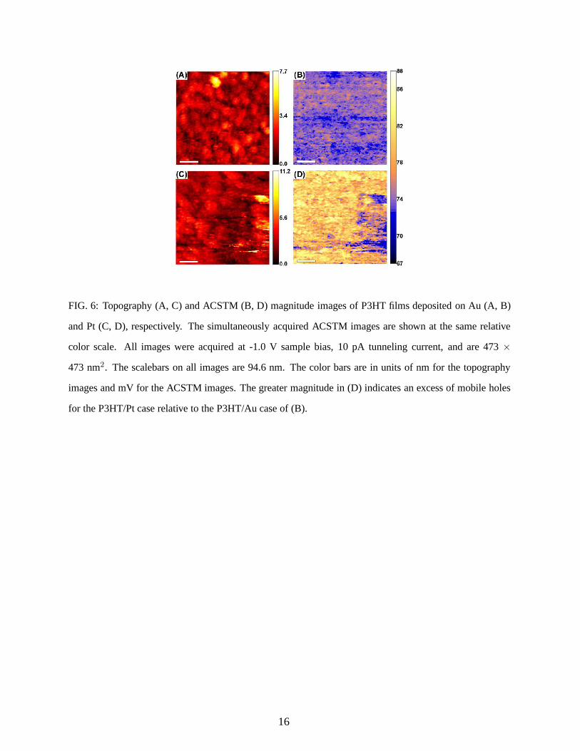
FIG. 6: Topography (A, C) and ACSTM (B, D) magnitude images ofP3HT films deposited on Au (A, B)
and Pt (C, D), respectively. The simultaneously acquired ACSTM images are shown at the same relative
color scale. All images were acquired at -1.0 V sample bias, 10 pA tunneling current, and are 473×
473 nm2. The scalebars on all images are 94.6 nm. The color bars are inunits of nm for the topography
images and mV for the ACSTM images. The greater magnitude in (D) indicates an excess of mobile holes
for the P3HT/Pt case relative to the P3HT/Au case of (B).
16
[1] Koch, N. Energy levels at interfaces between metals and conjugated organic molecules.J. Phys: Con-
dens. Matter 2008, 20, 184008.
[2] Campbell, I. H.; Rubin, S.; Zawodzinski, T. A.; Kress, J.D.; Martin, R. L.; Smith, D. L.; Barashkov,
N. N.; Ferraris, J. P. Controlling Schottky energy barriersin organic electronic devices using self-
assembled monolayers.Phys. Rev. B 1996, 54, R14321-R14324.
[3] Nuesch, F.; Rotzinger, F.; Si-Ahmed, L.; Zuppiroli, L.Chemical potential shifts at organic device
electrodes produced by grafted monolayers.Chem. Phys. Lett. 1998, 288, 861-867.
[4] Hamadani, B. H.; Corley, D. A.; Ciszek, J. W.; Tour, J. M.;Natelson, D. Controlling charge injection
in organic field-effect transistors using self-assembled monolayers.Nano Lett. 2006, 6, 1303-1306.
[5] Hill, I. G.; Rajagopal, A.; Kahn, A.; Hu, Y. Molecular level alignment at organic semiconductor-metal
interfaces.Appl. Phys. Lett. 1998, 73, 662-664.
[6] Tengstedt, C.; Osikowicz, W.; Salaneck, W. R.; Parker, I. D.; Hsu C.-H.; Fahlman, M. Fermi-level
pinning at conjugated polymer interfaces.Appl. Phys. Lett. 2006, 88, 053502.
[7] Koch N.; Vollmer, A. Electrode-molecular semiconductor contacts: Work-function-dependent injec-
tion barriers versus Fermi-level pinning.Appl. Phys. Lett. 2006, 89, 162107.
[8] Vazquez, H.; Dappe, Y. J.; Ortega, J.; Flores, F. Energylevel alignment at metal/organic semiconduc-
tor interfaces: “Pillow” effect, induced density of interface states, and charge neutrality level.J. Chem.
Phys. 2007, 126, 144703.
[9] Vazquez, H.; Flores, F.; Oszwaldowski, R.; Ortega, J.;Perez, R.; Kahn, A. Barrier formation at metal-
organic interfaces: dipole formation and the charge neutrality level. Appl. Surf. Sci. 2004, 234, 1-4.
[10] Crispin, A.; Crispin, X.; Fahlman, M.; Berggren, M.; Salaneck, W. R. Transition between energy level
alignment regimes at a low band gap polymer-electrode interfaces.Appl. Phys. Lett. 2006, 89, 213503.
[11] Hwang, J.; Kim, E.-G.; Liu, J.; Bredas, J.-L.; Duggal,A.; Kahn, A. Photoelectron spectroscopic study
of the electronic band structure of polyfluorene and fluorene-arylamine copolymers at interfaces.J.
Phys. Chem. C 2007, 111, 1378-1384.
[12] Burgi, L.; Richards, T. J.; Friend, R. H.; Sirringhaus, H. Close look at charge carrier injection in
polymer field-effect transistors.J. Appl. Phys. 2003, 94, 6129-6137.
[13] Li, T.; Ruden, P. P.; Campbell, I. H.; Smith, D. L. Investigation of bottom-contact organic field effect
transistors by two-dimensional device modeling.J. Appl. Phys. 2003, 93, 4017-4022.
17
[14] Hamadani, B. H.; Natelson, D. Nonlinear charge injection in organic field-effect transistors.J. Appl.
Phys. 2005, 97, 064508.
[15] Ng, T. N.; Silveira, W. R.; Marohn, J. A. Dependence of charge injection on temperature, electric field,
and energetic disorder in an organic semiconductor.Phys. Rev. Lett. 2007, 98, 066101.
[16] Hamadani, B. H.; Ding, H.; Gao, Y.; Natelson, D. Doping-dependent charge injection and band align-
ment in organic field-effect transistors.Phys. Rev. B 2005, 72, 235302.
[17] Cai, L. ; Yao, Y.; Yang, J.; Price, Jr., D. W.; Tour, J. M. Chemical and potential assisted assembly of
thioacetyl-terminated oligo(phenylene ethynylene)s on gold surfaces.Chem. Mater. 2002, 14, 2905-
2909.
[18] Hamadani, B. H.; Natelson, D. Temperature-dependent contact resistances in high quality polymer
field-effect transistors.Appl. Phys. Lett. 2004, 84, 443-445.
[19] Gundlach, D. J.; Royer, J. E.; Park, S. K.; Subramanian,S.; Jurchescu, O. D.; Hamadani, B. H.;
Moad, A. J.; Kline, R. J.; League, L. C.; Kirillov, O.; Richter, C. A.; Kushmerick, J. G.; Richter, L.
J.; Parkin, S. R.; Jackson, T. N.; Anthony, J. E. Contact-induced crystallinity for high-performance
soluble acene-based transistors and circuits.Nature Mater. 2008, 7, 216-221.
[20] Merlo, J. A.; Frisbie, C. D. Field effect conductance ofconducting polymer nanofibers.J. Polymer
Sci. B: Polymer Phys. 2003, 41, 2674-2680.
[21] Rep, D. B. A.; Morpurgo, A. F.; Klapwijk, T. Doping-dependent charge injection into regioregular
poly(3-hexylthiophene).Org. Elect. 2003, 4, 201-207.
[22] Bourgoin, J. P.; Johnson, M. B.; Michel, B. Semiconductor characterization with the scanning surface
harmonic microscope.Appl. Phys. Lett. 1994, 65, 2045-2047.
[23] Donhauser, Z. J.; McCarty, G. S.; Bumm, L. A.; Weiss P. S.High resolution dopant profiling using a
tunable AC scanning tunneling microscope. InCharacterization and Metrology for ULSI Technology:
2000 International Conference, Seiler, D. G.et al., Eds.; American Institute of Physics: New York,
2001, pp. 641-646.
[24] Kelly, K. F.; Donhauser, Z. J.; Mantooth, B. A.; Weiss, P. S. Expanding the capabilities of the scanning
tunneling microscope. InNATO ASI Series II: Mathematics, Physics, and Chemistry, Vilarinho, P.;
Rosenwaks, Y.; Kingon, A., Eds.; Springer: New York, 2005, pp 153-171.
[25] Schmidt, J.; Rapoport, D. H.; Frohlich, H.-J. Microwave-frequency alternating current scanning tun-
neling microscopy by difference frequency detection: Atomic resolution imaging on graphite.Rev.
Sci. Instr. 1999, 70, 3377-3380.
18
[26] Bumm, L. A.; Arnold, J. J.; Cygan, M. T.; Dunbar, T. D.; Burgin, T. P. ; Jones, II, L.; Allara, D. L.;
Tour, J. M.; Weiss, P. S. Are single molecular wires conducting? Science 1996, 271, 1705-1707.
[27] Lee, J.; Tu, X.; Ho, W. Spectroscopy and microscopy of spin-sensitive rectification current inducted
by microwave radiation.Nano Lett. 2005, 5, 2613-2617.
[28] Frequencies used were 300 and 300.004 MHz, approximately 3.7 dbm for the Pt sample and 3.0 dbm
for the Au sample. The difference is due to the change in antenna position when switching between
samples, and was adjusted by monitoring the input at the lock-in amplifier to ensure that the initial
out-of-tunneling input signal strength at the difference frequency was the same for both samples. The
same tip was used for both samples.
[29] Topography images were processed using plane-/offset-subtraction and median filtering in MATLAB,
while ACSTM images were only median filtered.
[30] Paasch, G.; Scheinert, S. Space charge layers in organic field-effect transistors with Gaussian or expo-
nential semiconductor density of states.J. Appl. Phys. 2007, 101, 024514.
[31] Fursina, A.; Lee, S.; Sofin, R. G. S.; Shvets, I. V.; Natelson, D. Nanogaps with very large aspect ratios
for electrical measurements.Appl. Phys. Lett. 2008, 92, 113102.
19