
Logic Circuits with Complementary Transistors - DTU Orbit
20
General rights Copyright and moral rights for the publications made accessible in the public portal are retained by the authors and/or other copyright owners and it is a condition of accessing publications that users recognise and abide by the legal requirements associated with these rights. Users may download and print one copy of any publication from the public portal for the purpose of private study or research. You may not further distribute the material or use it for any profit-making activity or commercial gain You may freely distribute the URL identifying the publication in the public portal If you believe that this document breaches copyright please contact us providing details, and we will remove access to the work immediately and investigate your claim. Downloaded from orbit.dtu.dk on: Jul 25, 2022 Logic Circuits with Complementary Transistors Hansen, Knud Bent Publication date: 1966 Document Version Publisher's PDF, also known as Version of record Link back to DTU Orbit Citation (APA): Hansen, K. B. (1966). Logic Circuits with Complementary Transistors. Danmarks Tekniske Universitet, Risø Nationallaboratoriet for Bæredygtig Energi. Denmark. Forskningscenter Risoe. Risoe-R No. 126
-
Upload
khangminh22 -
Category
Documents
-
view
1 -
download
0
Transcript of Logic Circuits with Complementary Transistors - DTU Orbit

General rights Copyright and moral rights for the publications made accessible in the public portal are retained by the authors and/or other copyright owners and it is a condition of accessing publications that users recognise and abide by the legal requirements associated with these rights.
Users may download and print one copy of any publication from the public portal for the purpose of private study or research.
You may not further distribute the material or use it for any profit-making activity or commercial gain
You may freely distribute the URL identifying the publication in the public portal If you believe that this document breaches copyright please contact us providing details, and we will remove access to the work immediately and investigate your claim.
Downloaded from orbit.dtu.dk on: Jul 25, 2022
Logic Circuits with Complementary Transistors
Hansen, Knud Bent
Publication date:1966
Document VersionPublisher's PDF, also known as Version of record
Link back to DTU Orbit
Citation (APA):Hansen, K. B. (1966). Logic Circuits with Complementary Transistors. Danmarks Tekniske Universitet, RisøNationallaboratoriet for Bæredygtig Energi. Denmark. Forskningscenter Risoe. Risoe-R No. 126

Riso Report No. 126
Danish Atomic Energy Commission
Research Establishment Riso
Logic Circuits with Complementary
Transistors
by K. B. Hansen
May, 1966
Sales distributors: Jul. Gjellerup, 87, Sblvgade, Copenhagen K, Denmark
Available on exchange from: Ubrary, Danish Atomic Energy Commiiaion, Ri»o, Roikilde, Denmark
SO
d
I
2

May, 1966 Ris6 Report No. 126
Logic Circuits with Complementary Transistors
by
K. B. Hansen
The Danish Atomic Energy Commission
Research Establishment RisO
Electronics Department
Abstract
This report presents circuits with complementary transistors in
tended for the realization of logical functions. The advantage of these ci r
cuits is shown to be the simple dimensioning, leading to great flexibility in
the realization of logical functions and efficient utilization of the components.
This is paid for by a lower transmission speed than that ultimately possible
with the same active components.
The basic circuits are interpreted as representing single logical
functions (AND, OR and NOT) in double-polarity logic, while the single-
polarity logic circuits normally used represent combined logical functions
(NOR and NAND).
2
Contents
Page
1. Introduction 3
2.. Logic Circuits with pnp and npn Transistors 3
Acknowledgement 5
Appendix 6
A. 1. Dimensioning of Logic Circuits with
pnp and npn Transistors 6
A. 2. Calculation of Standard Component Values 9
A. 3. The Load Conditions of the NOT Circuit H
References H
Figures 1 2

3
1. Introduction
The present report is intended to give a brief description of the cir
cuits used by the data-processing section of the Electronics Department for
the realization of logical functions. These circuits must not be regarded as
standard circuits for use in all digital systems to be designed. However,
they have proved very useful for experimental work in enabling us to design
data-recording equipment with the fewest possible components, simple di
mensioning and a high degree of reliability. In some measure these advan
tages have been obtained at the expense of speed, but in most equipment in
current use the reaction time of the logic circuits is unimportant as com
pared with that of other components such as relays, recording units and
motors.
2. Logic Circuits with pnp and npn Transistors
Even if we confine ourselves to the realization of logical functions
by means of semiconductor components, there are many possibilities. The
most frequently used circuits are based on resistance-transistor or diode-
transistor logic circuits, in which the logical function is realized by means
of resistances and diodes respectively, while the transistor serves as an 1 2 3) amplifier. The circuits described * • ' are all based on the use of mainly
one type of transistor, either pnp or npn. This means that the logical truth
value ("1") is represented by either a negative or a positive voltage (single-
polarity logic). In consequence, a circuit usually satisfies a combined logi
cal function, either NOT-OR (NOR) or NOT-AND (NAND).
In its work with digital technique, the data-processing section has
employed another circuit type, based on the utilization of the complementary
properties of pnp and npn transistors; the two kinds of transistor are used
alternately, i. e . , the outputs of pnp transistors activate the inputs of npn
transistors. One advantage of this combination is the possibility of dimen
sioning with a wider safety margin (the "efficiency" is greater) as the col
lector current of a transistor is utilized to a higher degree for the control
of the following stages. At the same tims the basis of the dimensioning (see
the appendix) is simpler and provides a better possibility of individual di
mensioning. Thus one is allowed more liberty in the choice of fan-in and
fan-out numbers and hence a better possibility of realizing a given logical
function by means of the fewest possible components. It is natural to inter-
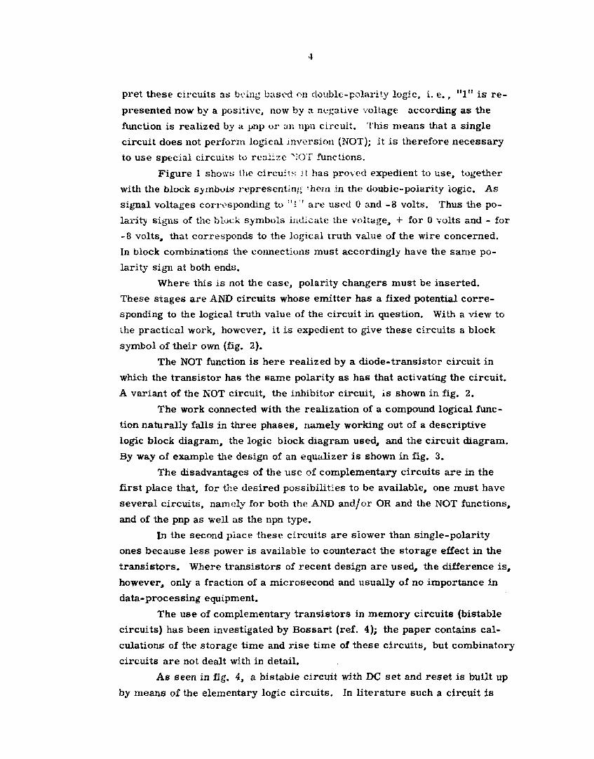
4
pret these circuits 3s being based on double-polarity logic, i. e. , " 1 " is r e
presented now by a positive, now by a negative voltage according as the
function is realized by a pnp or an npn circuit. This means that a single
circuit does not perform logical inversion (NOT); it is therefore necessary
to use special circuits to realize \:OT functions.
Figure 1 shows the circuits it has proved expedient to use, together
with the block symbols representing 'hem in the double-polarity logic. As
signal voltages corresponding to "1 ' are used 0 and -8 volts. Thus the po
larity signs of the block symbols indicate the voltage, + for 0 volts and - for
-8 volts, that corresponds to the logical truth value of the wire concerned.
In block combinations the connections must accordingly have the same po
larity sign at both ends.
Where this is not the case, polarity changers must be inserted.
These stages are AND circuits whose emitter has a fixed potential corre
sponding to the logical truth value of the circuit in question. With a view to
the practical work, however, it is expedient to give these circuits a block
symbol of their own (fig. 2).
The NOT function is here realized by a diode-transistor circuit in
which the transistor has the same polarity as has that activating the circuit.
A variant of the NOT circuit, the inhibitor circuit, is shown in fig. 2.
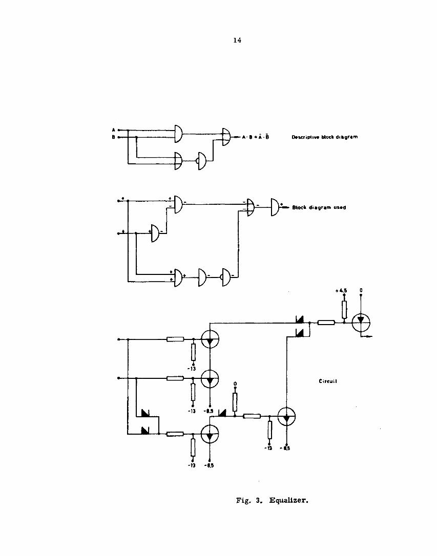
The work connected with the realization of a compound logical func
tion naturally falls in three phases, namely working out of a descriptive
logic block diagram, the logic block diagram used, and the circuit diagram.
By way of example the design of an equalizer is shown in fig. 3.
The disadvantages of the use of complementary circuits are in the
first place that, for the desired possibilities to be available, one must have
several circuits, namely for both the AND and/or OR and the NOT functions,
and of the pnp as well as the npn type.
In the second place these circuits are slower than single-polarity
ones because less power is available to counteract the storage effect in the
transistors. Where transistors of recent design are used, the difference is ,
however, only a fraction of a microsecond and usually of no importance in
data-processing equipment.
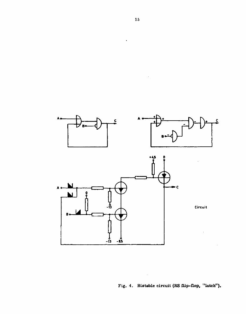
The use of complementary transistors in memory circuits (bistable
circuits) has been investigated by Bossart (ref. 4); the paper contains cal
culations of the storage time and rise time of these circuits, but combinatory
circuits are not dealt with in detail.
As seen in fig. 4, a bistable circuit with DC set and reset is built up
by means of the elementary logic circuits. In literature such a circuit is

5
often referred to as "latch" to distinguish it from the flip-flop, which r e
quires a shift pulse to be brought into a state corresponding to the conditions
indicated on it. The flip-flop or triggered bistable circuit is used with ad
vantage for instance in shift registers because the memory required during
the shift may be realized by means of passive components.
Figure 5 shows the realization of a triggered bistable circuit with
complementary transistors. The set-reset function is here performed by
a symmetrical transistor; if A is 0 volts (+.rue value, "1"), the symmetrical
transistor will work as an emitter follower and, by a pulse at its base, set
the bistable circuit; if A is not 0 volts (false value, "0"), the transistor will
work as a collector follower and, by a pulse at its base, reset the circuit.
Acknowledgement
The author is indebted to Flemming Steenbuch for the translation of
this report into English.

6
A. 1. Dimensioning of Logic Circuits with pnp and npn Transistors
Figure 6 shows a section of a circuit from a logic system in which
the complementary properties of pnp and npn transistors are utilized. If
the block diagram is realized by means of the circuits shown in fig. 1, an
AND block will result in a chain of transistors (p and q), while the OR blocks
will be realized by diode matrices (m, n and m', n*). If we consider a tran
sistor in the chain q, we may determine the collector current that the tran
sistor must be capable of supplying to the n1 following stages, and thus the
base current required by the transistor.
In the absence of this base current, the transistor must be securely
cut off by means of the resistance RA and the voltage V«.
When all the n chains loading a chain p have been determined in this
way, the conditions for the chain p have been fixed.
The following symbols are used in addition to those indicated in the
figure:
I , : diode reverse current Q
Vp : voltage drop of the collector emitter in the case of
conducting transistor
V_ : voltage drop of the base emitter in the case of
conducting transistor
V n : voltage drop of the diode
I r R O : collector cut-off current ,
The maximum value of the collector current that the chain q must be
able to supply to the row k» will be
n1 v / m ' n' n' v
ffiaxlc" Z *k-j T ^ + I 1 aij r a k T r VjjW1* j=l j=l i=l 3*1
where a.. s 1 when a diode is inserted between the wires i and j ; in the
absence of a diode, a.. = 0.

7
The f i rs t t e r m of eq. (I) is the total base cur ren t to be supplied by
the chain q, the last t e r m is the maximum total diode r e v e r s e cur ren t to be
given off. This happens when only one cf the rows in the ma t r ix network
m ' n 1 i s activated ( represents logical "1") .
F r o m eq. (1) we have
n' y n' . m ' .
m a x l c = I a k I j ^ • + I U Z a „ - 1 ] l d . (2)
3=1 " 3=1 V l J
The minimum base cur ren t available to a t r ans i s to r in the chain q i s
V 2 - ( p + q - l ) V c - V B - V D V 3 + t q - l ) V c + V B
B R B R A
On inser t ion of the cu r r en t amplification p = -y— we derive from lB
eqs . (2) and (3) the following inequality, which must be fulfilled to ensure
that a t r ans i s to r i s conducting, that i s , that the voltage drop of the col lector
emi t te r i s sma l l e r than the knee voltage:
JV2-(l*q-l)VVB-VD V(q-1)VVBX n' V2 * , £ X
(4)
To ensure the cut-off of the t rans i s to r the following inequality mus t
be satisfied:
v m m n m
T T - r " u ^ B O + f 1 a i l I a i j - E a i l ) J d +
A i=l M=l j=l i=l /
XCBO ; (5)
the f i rs t t e r m is the collector cut-off cur ren ts from al l t r a n s i s t o r s that can
activate the t r a n s i s t o r considered, the second t e r m is the diode r e v e r s e
cu r ren t s in those rows of the mat r ix network which a r e connected to the
column 1, and the las t t e rm is the cut-off cur ren t of the t r ans i s to r itself.
Eq. (5) may be rewri t ten as

8
m ni n
^ >( I a . i + xj I C B O + I au ( I ^ - l ) Id . (6) A V i= l ' i=l Vj=l 7
It should be noted that the quantities on both s ides of the inequality sign in
(4) should in fact be co r rec t ed for the position of the t rans i s to r in the chain
q since a t r ans i s to r at the bottom of the chain must also supply the base
current of the other t r a n s i s t o r s in the chain. This i s compensated for by
the fact that the bottom t r ans i s to r i s i tself supplied with a s t ronger base
cur rent , and we find that if the inequality
R B R A
(VC + V C \
i s satisfied, (4) holds. This is the case , to a sufficient approximation, with
the c i rcui t s used in p rac t ice .
If we compare (4) and (6) with the corresponding inequalit ies for
s ingle-polar i ty logic c i rcu i t s (ref. 1), we see that the advantage of ca lcu
lating the double-polari ty c i rcui ts is that from (6) we may determine R .
independently of the other s tages (and R,,) and then, by means of (4) , may
determine R R from our kno^ ledge of the preceding and the following s t age .
F r o m (3) and p I B = I c we obtain for R f i the expression
R WB
V, - ( k+ 1 - 1) V c - V B - V D
i c . v 3 + ( i - i > v c + v B p R A
This express ion has the form
RB*TTTT7" l C + v 3
where V 2 and V« a r e cor rec ted for the t r ans i s to r and diode voltage d rops .

9
A. 2. Calculation of Slandard Component Values
By a circui t with standard component values is understood a c i rcui t
with fixed t r an s i s t o r s , diodes and res i s t ance values. If a logic system is
real ized with such c i rcu i t s , the load must be kept within the permiss ib le
values of these .
For c i rcui ts of >.his kind we must have
n' m ' m n
I akIj I &ij = I an I j=l i=l i=l j=l
and
R B , = R B .
By means of (6), express ion (4) may then be rewri t ten
n' ,T ^ p [ *i ~—J" "** V*I '(7)
Putting
2. a , , . a N (fan-out number) , K J 3 - 1
we have
V 2 ( l - f ) - ( p + q - l ) V c - V B - V D R B
Vg(l + J . ) + ( q - D V c + V B *Z
Example:
The nominal voltages used a r e
V 2 » - 8 . 5 volts
V^ « - 4 . 5 vol ts .

10
For the t r ans i s to r s , OC47 and OC141, and the diode, OA85, we have
V c ~ 0.20 volt (OC 47 and OC 141; I c * 10 mA; T « 25°C)
V f i ~ 0. 35 volt ( " " " " " )
P ~ 30 (min OC 4 7 : 5 0 ; OC141.-100; I c = 15 mA)
V D ~ 0.5 volt (OA85; I D • 2 mA; T = 25°C) .
If we assume tolerances of +10% for V„ and -10% for V„, +5% for R R and
- 5 % for R« (wors t -case design) and nominal values of R R and RA of
RB * 3 .9k fi
R A * 4 . 7 k Q ,
we obtain the following inequality that must be fulfilled:
N + 0.8 p + 1.5 q < 10.
p • q » 1; N < 8
p • q » 2; N < 5
p » q « 3 ; N < 3 .
The condition (6) se ts a limit to the number of diodes. With the values
• . o . I C B , " 100 uA (max OC47 and OC141; 35 uA; V c • 5 volts; T = 60"C)
Id 50 uA (max OA 85:40 uA; - V D = 10 vol ts ; T » 60°C)
and the ea r l i e r used values of Vq and R . , with the most unfavourable
to lerances , we obtain the condition
m
1 ail ( I aij + *)* 1 4 ' i-1 j * l

11
We put
m n 1 an I a i j = I N ,
i«l j=l
which is the sum of the fan-out numbers of al l t r ans i s to r s activating the
t r ans i s to r considered. Fur the r we put
m
L a,, * M (fan-in number)
i-1
and obtain
M + I N £ 14 .
A. 3. The Load Conditions of the NOT Circuit
The NOT circui t employed, and the var iants NOR and INHIBITOR,
a re dimensioned on the basis of the formulae given by Masher ' . F igure 7
shows the pe rmiss ib le load conditions, the symbols being the same as above.
The values of voltages, cu r ren t s , to lerances , e t c . , a r e likewise the s a m e
as those used in the foregoing.
References
1) D. P . Masher , The Design of Diode-Trans i s tor NOR Ci rcu i t s .
I. R . E . Transact ions on Electronic Computers EC-9 (1960) 15-24.
2) W. J . Wray, DC Design of Resistance Coupled T rans i s t o r Logic
Ci rcu i t s . I. R. E . Transact ions on Circui t Theory CT-6 (1959)
304-310.
3) W.B. Cagle and W.H. Chen, A New Method of Designing Low Level,
High Speed Semiconductor Logic Circui s . Wescon Convention
Record, P t . 2 (1957) 3-9.
4) Lee M. Bossar t , Complementary T rans i s to r Memory Circuit and
Logic Applications. SCTM 51-62 (72) (1962).

12
=D- =&- H)-AND OR
3.9 h
-13
0 OCH1
3.9li H h
a.5
" I I OC47
I T 13 -8.5
• 4 5 0
Jt
•J 0C*7
0*85
NOT
3>
3>
5 0CH1 V
O
$ *
Logic circuit and corresponding symbols for double-polar i ty logic
The signs indicate the signal polarity of the logical truth value
# *
Fig. 1. Logic block symbols.

13
© OCKl
+ I \ - Polarity changsr I J logical identity
-13 -8.5
7,
X 2.7 U © 3> OCKl
-13 -8.5
-13 -».5
Inhibitor
•». 0 C H 1 L /
OR-NOT(NOR)
Fig, 2. Variants of circuits in :*ig. 1,
14
B • - D—jS- A-B+A-B Ocscriptiv« Mock diagram
3> V
F M >
H^
Bloch diagram ui«d
• c 1 ^ ^
-13
0 ®
SO 13 - M
é
• A.5 0
<£
Circuil
Fig. 3. Equalizer.
15
t/B. if
ZSS - i — h
I
x
©
•*5 o
e -13
Bo \m i i 1- © •13 -as
Circuit
Fig. 4 . Bistable circuit (RS flip-flop, "latch").

16
• 45 O 1 f
4-^B A+±
1-t-
Symbol
R i
t
Fig. 5. Triggered bistable circuit (RST flip-ilop).

17
I i
Block diagram
^
^
fr
£ £-
^
-v,
) • 1 2
,. , - *
±_±
*é' & $
Circuit
1 2 I"
- S - *
k'
^
"¥
Fig. 6. Calculation of component values.

13
P s 1 O-
M*IN<K
<*1 rtk ®
N <a 0CH1
-13 -8.5
Fig. 7. Load conditions of the NOR inhibitor.