Short-Channel Organic Thin-Film Transistors - Universität ...
260
Short-Channel Organic Thin-Film Transistors: Fabrication, Characterization, Modeling and Circuit Demonstration Von der Fakult¨at Informatik, Elektrotechnik und Informationstechnik der Universit¨ at Stuttgart zur Erlangung der W¨ urde eines Doktors der Ingenieurwissenschaften (Dr.-Ing.) genehmigte Abhandlung Vorgelegt von Tarek Zaki geboren am 24.10.1987 in Kairo, ¨ Agypten Hauptberichter: Prof. Dr.-Ing. Joachim N. Burghartz Mitberichter: Prof. Dr.-Ing. Manfred Berroth Tag der Einreichung: 12.06.2014 Tag der m¨ undlichen Pr¨ ufung: 25.11.2014 Institut f¨ ur Nano- und Mikroelektronische Systeme der Universit¨ at Stuttgart 2014
-
Upload
khangminh22 -
Category
Documents
-
view
2 -
download
0
Transcript of Short-Channel Organic Thin-Film Transistors - Universität ...
Short-Channel Organic Thin-Film Transistors:
Fabrication, Characterization, Modeling
and Circuit Demonstration
Von der Fakultat Informatik, Elektrotechnik und Informationstechnikder Universitat Stuttgart zur Erlangung der Wurde eines Doktorsder Ingenieurwissenschaften (Dr.-Ing.) genehmigte Abhandlung
Vorgelegt von
Tarek Zaki
geboren am 24.10.1987 in Kairo, Agypten
Hauptberichter: Prof. Dr.-Ing. Joachim N. Burghartz
Mitberichter: Prof. Dr.-Ing. Manfred Berroth
Tag der Einreichung: 12.06.2014
Tag der mundlichen Prufung: 25.11.2014
Institut fur Nano- und Mikroelektronische Systemeder Universitat Stuttgart
2014

Tarek ZakiShort-Channel Organic Thin-Film Transistors:Fabrication, Characterization, Modeling and Circuit DemonstrationInstitut fur Nano- und Mikroelektronische Systemeder Universitat Stuttgart

Dedicated to my beloved parents


Abstract
Plastic electronics based on organic thin-film transistors (OTFTs) pave theway for cheap, flexible and large-area products. Over the past few years,OTFTs have undergone remarkable progress in terms of reliability, perfor-mance and scale of integration. This work takes advantage of high-resolutionsilicon stencil masks to build air-stable complementary OTFTs using a low-temperature fabrication process. Many factors contribute to the allure ofthis technology; the masks exhibit excellent stiffness and stability, thus al-lowing to pattern the OTFTs with submicrometer channel lengths and superbdevice uniformity. Furthermore, the OTFTs employ an ultra-thin gate di-electric that provides a sufficiently high capacitance of the order of 1 µF/cm2
to enable the transistors to operate at voltages as low as 3 V.The critical challenges in this development are the subtle mechanisms
that govern the properties of the aggressively-scaled OTFTs. These mecha-nisms, dictated by device physics, have to be described and implemented intocircuit design tools to ensure adequate simulation accuracy. This is particu-larly beneficial to gain deeper insight into materials-related limitations. Theprimary objective of this work is to bridge the gap between device modelingand mixed-signal circuits by establishing an OTFT compact model, togetherwith realizing the world-fastest organic digital-to-analog converter (DAC).
A unified model that captures the essence in the static/dynamic behav-ior of the OTFTs is derived. Approaches to incorporate the implicit bias-dependent parasitic effects in the model are elucidated and accordingly areliable fit to experimental data of OTFTs with different dimensions is ob-tained. It is demonstrated that the charge storage behavior in the intrinsicOTFTs agrees very well with Meyer’s capacitance model. Moreover, the firstcomprehensive study of the frequency response of OTFTs using S-parametercharacterization is presented. In view of the low supply voltage and air stabil-ity, a record cutoff frequency of 3.7 MHz for a channel length of 0.6 µm and agate overlap of 5 µm is accomplished. Finally, a 6-bit current-steering DAC,comprising as many as 129 OTFTs, is designed. The converter achieves athousand-fold faster update rate (100 kS/s) than prior state of the art.
Keywords
Cutoff frequency, device modeling, digital-to-analog converter, organic cir-cuits, organic thin-film transistors, scattering parameters, stencil masks.
v

Kurzfassung
Schaltungen basierend auf organischen Dunnschichttransistoren (OTFTs)ebnen den Weg fur preiswerte, flexible und großflachige Anwendungen. In denvergangenen Jahren haben OTFTs einen beachtlichen Schritt in RichtungZuverlassigkeit, Performance und Integration in komplexen Systemen vollzo-gen. Die vorliegende Arbeit nutzt hochauflosende Silizium Stencil-Maskenzur Herstellung kurzkanaliger und luftstabiler komplementarer Niedervolt-OTFTs. Viele Faktoren tragen zur Einzigartigkeit dieser Technologie bei,begrundet durch die hervorragende Steifheit und Stabilitat der Stencil-Masken. Dies ermoglicht Strukturen von OTFTs, welche eine hohe Gleich-formigkeit aufweisen und Kanallangen im unteren µm-Bereich besitzen.
Die große Herausforderung sind die Mechanismen, die die Eigenschaftenstark skalierter OTFTs beherrschen und die in Design-Tools implementiertwerden mussen. Das Hauptaugenmerk dieser Arbeit liegt darauf, die Luckezwischen der Bauteilmodellierung und der Mixed-Signal-Schaltung zuschließen. Ein statisch/dynamisches OTFT-Modell wurde eingefuhrt und derweltweit schnellste organische Digital-Analog-Wandler (DAC) hergestellt.
Losungen, die impliziten bias-abhangigen parasitaren Effekte im Modellmit einzubeziehen, werden aufgezeigt, und eine entsprechende zuverlassigeUbereinstimmung mit experimentell gewonnenen Daten von OTFTs unter-schiedlicher Dimension wird nachgewiesen. Es wird gezeigt, dass das Ladungs-speicherungsverhalten in intrinsischen OTFTs sehr gut mit MeyersKapazitatsmodell ubereinstimmt. Daruberhinaus wird die erste umfassendeUntersuchung des Frequenzverhaltens von OTFTs mittels S-Parameter-Charakterisierung vorgestellt. Eine in Blick auf die niedrige Versorgungs-spannung und die Luftstabilitat rekordverdachtige Grenzfrequenz von 3,7MHz bei einer Kanallange von 0,6 µm und einer Gate-Uberlappung von5 µm ist demonstriert. Schliesslich wird ein stromgesteuerter 6-Bit-DAC,bestehend aus 129 OTFTs, entworfen. Der DAC erreicht eine tausendfacheSample-Rate (100 kS/s) gegenuber dem bisherigen Stand der Technik.
Schlagworter
Bauteilmodellierung, D/A-Wandler, Grenzfrequenz, organische Schaltung,organische Dunnschichttransistoren, S-Parameter, Stencil-Masken.
vii

Contents
Abstract v
Kurzfassung vii
List of Tables xiii
List of Figures xv
Nomenclature xix
1 Motivation 1
2 Introduction to Organic Electronics 42.1 History . . . . . . . . . . . . . . . . . . . . . . . . . . . . . . . . . 42.2 Materials . . . . . . . . . . . . . . . . . . . . . . . . . . . . . . . . 112.3 Devices and Applications . . . . . . . . . . . . . . . . . . . . . . 16
2.3.1 Organic Light-Emitting Diodes . . . . . . . . . . . . . . 162.3.2 Organic Photovoltaic Cells . . . . . . . . . . . . . . . . . 182.3.3 Organic Thin-Film Transistors . . . . . . . . . . . . . . 212.3.4 Systems-in-Foil . . . . . . . . . . . . . . . . . . . . . . . . 26
2.4 Summary . . . . . . . . . . . . . . . . . . . . . . . . . . . . . . . 27
3 Organic Thin-Film Transistors 283.1 Architecture and Materials . . . . . . . . . . . . . . . . . . . . . 283.2 Operation Principle . . . . . . . . . . . . . . . . . . . . . . . . . 313.3 Transistor Parameters . . . . . . . . . . . . . . . . . . . . . . . . 373.4 Stability and Circuit Performance Measures . . . . . . . . . . . 42
3.4.1 Device Matching . . . . . . . . . . . . . . . . . . . . . . . 433.4.2 Air Stability . . . . . . . . . . . . . . . . . . . . . . . . . 453.4.3 Ring Oscillator Speed . . . . . . . . . . . . . . . . . . . . 47
3.5 Summary . . . . . . . . . . . . . . . . . . . . . . . . . . . . . . . 49
4 Fabrication Process 504.1 Deposition and Patterning Techniques . . . . . . . . . . . . . . 504.2 Silicon Stencil Masks . . . . . . . . . . . . . . . . . . . . . . . . 54
4.2.1 Fabrication Process . . . . . . . . . . . . . . . . . . . . . 554.2.2 Refurbishment . . . . . . . . . . . . . . . . . . . . . . . . 584.2.3 Defect Analysis . . . . . . . . . . . . . . . . . . . . . . . 604.2.4 Uniformity of Evaporated Patterns . . . . . . . . . . . . 62
ix

x Contents
4.3 Organic Transistor Fabrication . . . . . . . . . . . . . . . . . . . 634.4 Layout Design Rules . . . . . . . . . . . . . . . . . . . . . . . . . 694.5 Mask Set Designs . . . . . . . . . . . . . . . . . . . . . . . . . . . 724.6 Summary . . . . . . . . . . . . . . . . . . . . . . . . . . . . . . . 74
5 Static Characterization 755.1 Transmission Line Method . . . . . . . . . . . . . . . . . . . . . 755.2 Compact Charge-Drift Model . . . . . . . . . . . . . . . . . . . 805.3 Non-linear Contact Resistance . . . . . . . . . . . . . . . . . . . 845.4 Summary . . . . . . . . . . . . . . . . . . . . . . . . . . . . . . . 86
6 Admittance Characterization 876.1 Parameter Extraction . . . . . . . . . . . . . . . . . . . . . . . . 876.2 Frequency Response Analysis . . . . . . . . . . . . . . . . . . . 916.3 Effective Delay of Gate-Induced Charges . . . . . . . . . . . . . 966.4 Meyer’s Capacitance Model . . . . . . . . . . . . . . . . . . . . 996.5 Summary . . . . . . . . . . . . . . . . . . . . . . . . . . . . . . . 103
7 Scattering Parameter Characterization 1047.1 Measurement Setup . . . . . . . . . . . . . . . . . . . . . . . . . 1047.2 Small-Signal Model . . . . . . . . . . . . . . . . . . . . . . . . . 1117.3 Current-Gain Cutoff Frequency . . . . . . . . . . . . . . . . . . 1207.4 Asymmetric Organic Transistors . . . . . . . . . . . . . . . . . . 1247.5 Summary . . . . . . . . . . . . . . . . . . . . . . . . . . . . . . . 126
8 Digital-to-Analog Converters 1288.1 Organic Circuit Design Methodologies . . . . . . . . . . . . . . 1288.2 Functionality and Specifications . . . . . . . . . . . . . . . . . . 133
8.2.1 Operation Principle . . . . . . . . . . . . . . . . . . . . . 1338.2.2 Characterization Parameters . . . . . . . . . . . . . . . 1348.2.3 Design Architectures . . . . . . . . . . . . . . . . . . . . 137
8.3 A High-Performance Unipolar Design . . . . . . . . . . . . . . . 1408.3.1 A 6-bit Binary Current-Steering DAC . . . . . . . . . . 1408.3.2 Current-to-Voltage Converter . . . . . . . . . . . . . . . 1438.3.3 Layout and Floorplan . . . . . . . . . . . . . . . . . . . . 1448.3.4 Calibration . . . . . . . . . . . . . . . . . . . . . . . . . . 1458.3.5 Measurement Setup . . . . . . . . . . . . . . . . . . . . . 1468.3.6 Static and Dynamic Performances . . . . . . . . . . . . 1468.3.7 Benchmarking . . . . . . . . . . . . . . . . . . . . . . . . 148
8.4 Impact of Parasitics in a Complementary Design . . . . . . . . 1508.4.1 A 3-bit Unary Current-Steering DAC . . . . . . . . . . 1508.4.2 Binary-to-Thermometer Decoder . . . . . . . . . . . . . 1508.4.3 Switching Scheme . . . . . . . . . . . . . . . . . . . . . . 1528.4.4 Measurement and Simulation Results . . . . . . . . . . 153
8.5 Summary . . . . . . . . . . . . . . . . . . . . . . . . . . . . . . . 156
Contents xi
9 Conclusion 157
A Physical Layout Design 161
B De-embedding Procedure 167
C Analytical Derivations 171C.1 Derivation of the Channel Capacitance . . . . . . . . . . . . . . 171C.2 Derivation of the Contact Resistance . . . . . . . . . . . . . . . 174
D Code Listings 178D.1 Cadence SKILL Codes for Layout Design . . . . . . . . . . . . 178D.2 IC-CAP PEL Codes for Measurement Routines . . . . . . . . . 184D.3 MATLAB Codes for S-Parameter Characterization . . . . . . 198
Bibliography 201
Curriculum Vitae 229
Author Publications 231
Acknowledgements 235


List of Tables
3.1 Simulation parameters of p-channel organic transistors . . . . 363.2 Characteristic parameters of a p-channel organic transistor . . 37
4.1 Comparison between fabrication processes in organics . . . . . 544.2 Fabrication process steps of the silicon stencil masks . . . . . 564.3 Defect analysis of the silicon stencil masks . . . . . . . . . . . . 634.4 Fabrication process steps of the organic transistors . . . . . . 654.5 List of layout layers . . . . . . . . . . . . . . . . . . . . . . . . . 694.6 Layout design rules of organic integrated circuits . . . . . . . . 714.7 Layout design rules of silicon stencil masks . . . . . . . . . . . 71
6.1 Parameters used in the small-signal equivalent circuit . . . . . 94
7.1 Summary of the small-signal model parameters . . . . . . . . . 1197.2 Current-gain cutoff frequency benchmark . . . . . . . . . . . . 124
8.1 Characteristics of the 6-bit digital-to-analog converter . . . . . 1498.2 Simulated propagation delays of the thermometer decoder . . 155
A.1 Geometries of the ring oscillators . . . . . . . . . . . . . . . . . 163
xiii


List of Figures
1.1 Micrographs of a stencil mask and an organic transistor . . . 3
2.1 Historical development of the electronic devices . . . . . . . . 52.2 Development of the carrier mobility in organic transistors . . 132.3 Schematic cross section of basic organic-based devices . . . . . 172.4 Organic-based lighting, solar film and display applications . . 19
3.1 Schematic cross section of the transistor configurations . . . . 293.2 Schematic cross section of the fabricated organic transistor . . 303.3 Molecular structure of the used organic materials . . . . . . . 313.4 Measured static current–voltage characteristics . . . . . . . . . 323.5 Energy band diagrams of sections of an organic transistor . . 333.6 Electrical characteristics of sixteen identical transistors . . . . 443.7 Electrical characteristics of matched transistor arrays . . . . . 453.8 Comparison between stencil and polyimide shadow masks . . 463.9 Air-induced degradation of the organic transistors . . . . . . . 473.10 Signal delay per stage of organic ring oscillators . . . . . . . . 49
4.1 Fabrication process steps of the silicon stencil masks . . . . . 574.2 Layout of the silicon stencil mask used for testing . . . . . . . 584.3 Gold layer removal from the silicon stencil mask . . . . . . . . 594.4 Aluminum layer removal from the silicon stencil mask . . . . . 594.5 Critical dimension measurements of the silicon stencil mask . 604.6 Characterization of the silicon stencil mask . . . . . . . . . . . 614.7 A pyramidal shaped defect in the silicon stencil mask . . . . . 624.8 Minimum feature size in the silicon stencil mask . . . . . . . . 624.9 Uniformity of the silicon stencil mask structures . . . . . . . . 644.10 Uniformity of the evaporated metal patterns . . . . . . . . . . 644.11 Fabrication process steps of the organic transistors . . . . . . 674.12 Design flow of the organic integrated circuits . . . . . . . . . . 684.13 Sample layout with the design-rule-check numbers . . . . . . . 704.14 Top-level cell layout of the three designed dies . . . . . . . . . 73
5.1 Drain currents of transistors with different channel lengths . . 765.2 Characterization using the transmission line method . . . . . 775.3 Measured vesrus modeled parasitic contact resistances . . . . 79
xv

xvi List of Figures
5.4 Static model results of a p-channel organic transistor . . . . . 835.5 Static model results of a short p-channel organic transistor . . 855.6 Static model results of an n-channel organic transistor . . . . 86
6.1 Measured capacitance–voltage characteristics . . . . . . . . . . 896.2 Measured capacitance–frequency characteristics . . . . . . . . 926.3 Equivalent circuit model of an organic transistor . . . . . . . . 936.4 Measured versus modeled admittance of several transistors . . 956.5 Extracted cutoff frequency from admittance measurements . . 966.6 Calculated effective delay of the accumulated channel . . . . . 986.7 Measured gate-source and gate-drain capacitances . . . . . . . 102
7.1 Block diagram of a two-port network . . . . . . . . . . . . . . . 1077.2 Standard loads used for the de-embedding procedure . . . . . 1107.3 Evaluation of the de-embedding procedure . . . . . . . . . . . 1117.4 Measured static drain current of organic transistors . . . . . . 1147.5 Small-signal model of the organic transistor . . . . . . . . . . . 1157.6 Measured versus simulated S-parameters . . . . . . . . . . . . . 1187.7 Extracted short-circuit current gain . . . . . . . . . . . . . . . . 1217.8 Extracted current-gain cutoff frequency . . . . . . . . . . . . . 1227.9 Characterization of asymmetric organic transistors . . . . . . . 125
8.1 Inverter designs using organic transistors . . . . . . . . . . . . 1308.2 Static specifications of a digital-to-analog converter . . . . . . 1358.3 Dynamic specifications of a digital-to-analog converter . . . . 1368.4 Digital-to-analog converters with current-division topology . . 1398.5 Digital-to-analog converters with current-mirror topology . . 1408.6 Schematic of the 6-bit binary digital-to-analog converter . . . 1418.7 Schematic of the current-to-voltage converter . . . . . . . . . . 1438.8 Floorplan of current-steering digital-to-analog converters . . . 1458.9 Static measurements of the 6-bit binary converter . . . . . . . 1478.10 Dynamic measurements of the 6-bit binary converter . . . . . 1478.11 Maximum speed and output swing of the 6-bit converter . . . 1488.12 Output spectrum and step response of the 6-bit converter . . 1498.13 Schematic of the 3-bit unary digital-to-analog converter . . . 1518.14 Switching schemes for the 3-bit unary converter . . . . . . . . 1528.15 Static measurements of the 3-bit unary converter . . . . . . . 1538.16 Measured output of the thermometer decoder . . . . . . . . . . 1548.17 Simulated case study of the thermometer decoder . . . . . . . 154
A.1 Dimensions of the test transistors on the first die design . . . 162A.2 Layout of test structures for admittance measurements . . . . 162A.3 Layout of test structures for S-parameter measurements . . . 163A.4 Layout of the ring oscillators . . . . . . . . . . . . . . . . . . . . 164A.5 Layout of the digital-to-analog converters . . . . . . . . . . . . 165

List of Figures xvii
A.6 Layout of the physical layer labels and institute logos . . . . . 166A.7 Layout of alignment structures . . . . . . . . . . . . . . . . . . . 166
B.1 Block diagram of a two-port test system . . . . . . . . . . . . . 168B.2 Signal flow diagram of the twelve-term error model . . . . . . 168B.3 Signal flow diagram of the three-term error model . . . . . . . 170
C.1 Small-signal equivalent circuit of the intrinsic transistor . . . 172C.2 Equivalent circuit model of the contact resistance . . . . . . . 175

Nomenclature
Abbreviations
a-Si:H Hydrogenated Amorphous Silicon
AC Alternating Current
ADC Analog-to-Digital Converter
AFM Atomic Force Microscopy
AM-LCD Active-Matrix Liquid Crystal Display
BHJ Bulk Heterojunction
BJT Bipolar Junction Transistor
CD Critical Dimension
CRT Cathode Ray Tube
CSA Current-Source Array
CVC Current-to-Voltage Converter
DAC Digital-to-Analog Converter
DC Direct Current
DFM Design For Manufacturability
DNL Differential Non-Linearity
DNTT Dinaphtho-Thieno-Thiophene
DRC Design Rule Check
DRIE Deep Reactive Ion Etching
DSSC Dye-Sensitised Solar Cell
DUT Device Under Test
EL Electroluminescence
F16CuPc Hexadecafluorocopperphthalocyanine
FET Field-Effect Transistor
GDS Graphic Database System
xix

xx Nomenclature
GSG Ground-Signal-Ground
HBT Heterojunction Bipolar Transistor
HOMO Highest Occupied Molecular Orbital
IC Integrated Circuit
ICC Integrated Circuit Card
IGFET Insulated-Gate Field-Effect Transistor
IMS CHIPS Institute for Microelectronics Stuttgart
INL Integral Non-Linearity
LCR Inductance-Capacitance-Resistance
LSB Least Significant Bit
LUMO Lowest Unoccupied Molecular Orbital
MFP Membrane Flow Process
MIM Metal-Insulator-Metal
MIS Metal-Insulator-Semiconductor
MOS Metal-Oxide-Semiconductor
MPI-SSR Max Planck Institute for Solid-State Research
MSB Most Significant Bit
NV-RAM Non-Volatile Random Access Memory
OHJ Ordered Heterojunction
OLED Organic Light-Emitting Diode
OPVC Organic Photovoltaic Cell
OTFT Organic Thin-Film Transistor
OVPD Organic Vapor Phase Deposition
PANI Polyaniline
PCell Parameterized Cell
PEL Parameter Extraction Language
PEN Poly(ethylene 2,6-naphthalate)
PET Poly(ethylene terephthalate)
PHJ Planar Heterojunction
PLED Polymer Light-Emitting Diode
PoC Point-of-Care

Nomenclature xxi
PTC Positive Temperature Coefficient
RC Resistance-Capacitance
RF Radio Frequency
RFID Radio-Frequency Identification
rMSE Relative Mean Square Error
ROM Read Only Memory
SAM Self-Assembled Monolayer
SAP Self-Aligned Inkjet Printing
SEM Scanning Electron Microscope
SFDR Spurious Free Dynamic Range
SiF System-in-Foil
SIJ Sub-Femtoliter Inkjet Printing
SMU Source Measure Unit
SOI Silicon-on-Insulator
SSL Solid-State Lighting
SWA Switch Array
TEOS Tetraethyl Orthosilicate
TFT Thin-Film Transistor
TLM Transmission Line Method
TMAH Tetra Methyl Ammonium Hydroxide
VNA Vector Network Analyzer
VRH Variable Range Hopping
VTC Voltage Transfer Characteristic
VTE Vacuum Thermal Evaporation
WFP Wafer Flow Process
WORM Write Once Read Many
Symbols
β Short-circuit current gain —
µ Effective charge carrier mobility cm2/Vs
µo Intrinsic charge carrier mobility cm2/Vs
ω Angular frequency rad/s
xxii Nomenclature
ρc Normalized contact resistivity Ωm2
τ Effective charge response time s
τd Signal delay per ring oscillator stage s
εi Insulator effective permittivity —
εo Vacuum permittivity F/m
Cch Channel capacitance F
Cgd Gate-drain capacitance F
Cgs Gate-source capacitance F
CG Total gate capacitance F
CI Insulator capacitance per unit area nF/cm2
ci Dielectric capacitance per unit length F/cm
Cj Junction capacitance at the contact nF/cm2
Cov Gate-overlap capacitance F
cs Semiconductor capacitance per unit length F/cm
d Semiconductor layer thickness nm
dox Oxide layer thickness nm
dSAM Self-assembled monolayer thickness nm
di Insulator layer thickness nm
EG Band gap eV
Ech Electric field in the channel V/m
EC Conduction band minimum eV
EF Fermi energy level eV
EV Valence band maximum eV
f Frequency Hz
frio Oscillation frequency of a ring oscillator Hz
fT Current-gain cutoff frequency Hz
Gch Channel conductance A/V
gch Channel conductance A/V
gm Transconductance A/V
ID Drain current A
Ion/Ioff On/off current ratio A/A

Nomenclature xxiii
Iref Reference current A
ISS Reverse bias saturation current A
kB Boltzmann constant eV/K
L Channel length µm
Lov Gate-overlap length µm
Lgd Gate-drain overlap length µm
Lgs Gate-source overlap length µm
LT Transfer length µm
NA Doping concentration cm−3
Nif Fixed interface charges concentration cm−2
no Total conducting charge per unit area C/cm2
q Absolute electron charge C
qφAl Aluminum work function eV
qφAu Gold work function eV
qφs Semiconductor work function eV
Qch Sheet charge density of the channel C/cm2
QG Total intrinsic gate charges C
Qif Interface-trapped charge concentration C/cm2
Qi Insulator charge concentration C/cm2
Rch Channel resistance Ω
rch Channel resistance per unit length Ω/cm
RC Contact resistance Ω
RD Drain contact resistance Ω
rj Junction resistance at the contact Ω cm
ro Output resistance Ω cm
Rsheet Sheet resistance Ω/◻
RS Source contact resistance Ω
rs Series resistance at the contact Ω cm
Rtot Total transistor resistance Ω
Ss-th Subthreshold slope mV/dec
T Temperature K
xxiv Nomenclature
Vbias Bias voltage V
VDD Supply voltage V
VD Drain voltage V
vd Drift velocity m/s
VFB Flat-band voltage V
VGT Gate-overdrive voltage V
VG Gate voltage V
VOH Inverter output high voltage V
VOL Inverter output low voltage V
VON Turn-on voltage V
Vsw,on Switch input ON voltage V
Vswing Swing voltage V
VS Source voltage V
VTH Threshold voltage V
W Channel width µm
ZS Source impedance Ω
ZL Load impedance Ω
Zo Characteristic impedance Ω
1Motivation
The rapid evolution of semiconductor technology is fueled by an unendingdemand for better performance and more functionality at reduced manu-facturing costs [1]. A new generation of thin, flexible electronics based onorganic semiconductors arises [2]. The organic materials are all the moreappealing as they can be deposited over large areas at or near room tem-perature, thus providing compatibility with a wide range of unconventionalsubstrates such as glass, plastic, fabric and paper. Furthermore, the abilityto process the organic materials from solution opens a plethora of alternativehigh-throughput, low-cost patterning techniques that are adapted from thegraphic art printing industry [3]. These strengths are currently unfoldingin the production of organic thin-film transistors (OTFTs), light-emittingdiodes (OLEDs) and photovoltaic cells (OPVCs) [4]. The ensuing appli-cations are manifold; they result in what some see as visually stimulatingobjects, such as flexible displays, panel lighting and transparent solar cells,and others see as a promotion to ubiquitous sensing in the form of low-endradio-frequency identification, smart food packaging, electronic nose and skinfor robotics, and implantable or disposable health monitoring devices [5].
The field of flexible electronics is progressing quite dynamically and manyother candidate materials, such as metal oxides, graphene and carbon nano-tubes, are coming into sight [6, 7]. Also monolithic silicon chips can alreadybe fabricated with a thickness of 20 µm and below, making them as flexible asfoils [8–11]. Organic materials, on the contrary, display a notable advantagethat they can be synthesized into seemingly limitless compound variations.Hence, their properties, including electrical, optical, appearance, chemicalinteractivity and biocompatibility, can be optimized depending on the targetapplication. The question is not which technology will win this developmentrace; instead, the aim should be to combine the best aspects of the differenttechnologies in a hetero-integrated system approach [2]. The global marketfor printed, flexible and organic electronics reached $16.04 billion in 2013 andis projected to cross $75 billion in 2023, as forecasted by IDTechEx [12]. Thisis dominated by displays, while emerging integrated circuits and sensors aremuch smaller segments though with a huge growth potential.
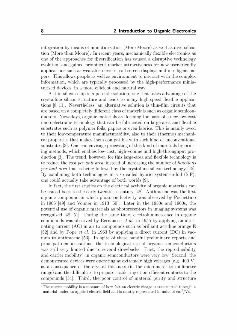
This work is devoted to the development of short-channel OTFTs, theperformance and matching of which rivals that of the low-voltage, air-stableOTFTs reported to date. In cooperation with the Institute for Microelectron-
1
2 1 Motivation
ics Stuttgart (IMS CHIPS) and the Max Planck Institute for Solid-State Re-search (MPI-SSR), a new OTFT fabrication process based on high-resolutionsilicon stencil masks is established [13–17]. Figure 1.1 shows close-up micro-graphs of a stencil mask and an OTFT with a feature size of 0.6 µm, demon-strating that submicrometer channels with a very smooth edge roughness isfeasible. This is, to the best of our knowledge, the shortest channel OTFTfabricated so far through stencil mask lithography. The process intends notonly to provide a solution for fast individual OTFTs, but also to enable therealization of large-scale organic mixed-signal integrated circuits that canoperate—for the first time—in the high kilohertz range.
In order to boost the combination of high-functionality and compactness,the durability of the stencil masks has to be characterized. Moreover, thedownscaling of OTFTs tends to augment crucial non-ideal properties, whichhave to be implemented in a device model for use in circuit simulation. Forexample, the increasing impact of device parasitics in short-channel OTFTsnow hampers further progress towards the attained intrinsic performance. Inview of these aspects, this work targets the following four key objectives:
• Technology—Investigate the reliability of the silicon stencil maskswith respect to minimum dimensions, refurbishment, manufacturabil-ity, defects and uniformity. This is to ensure proper yield and to furtherpush miniaturization and integration.
• Characterization—Carry out a comprehensive experimental study ofthe static/dynamic response of the OTFTs using different methods. Forthe first time, the cutoff frequency of stand-alone OTFTs is extractedby means of scattering parameter measurements. The correspondencebetween the different characterization techniques is elucidated and aperformance benchmark for the state-of-the-art OTFTs is presented.
• Modeling—Derive a unified static/dynamic compact model and asmall-signal equivalent circuit that describe accurately the intrinsic aswell as the extrinsic effects of the OTFTs. The model parameters arephysically justified; thus, they can be extracted from measurements ina consistent and convenient way. Experimentally-validated recommen-dations are also given to accomplish a breakthrough in the performanceof organic integrated circuits.
• Demonstrator—Design fast organic mixed-signal integrated circuitsto demonstrate the reproducibility and matching capability of the newmanufacturing process. This leads to the first successful realization oforganic current-steering digital-to-analog converters (DACs).
This work, therefore, offers a promising technology platform that extends thefavorable advancement of OTFTs and opens up the prospect of many novelapplications in fields ranging from communication and robotics to healthcare.

3
3 µm 20 µm
0.6 µm
0.6 µm
Gate
Source
Drain
(a)
3 µm 20 µm
0.6 µm
0.6 µm
Gate
Source
Drain
(b)
Figure 1.1 (a) Photograph of a silicon stencil mask used to pattern the sourceand drain contacts of an OTFT. (b) Top-view photograph of an inverted-staggered(bottom-gate, top-contacts) OTFT with a channel length of 0.6 µm fabricated ona glass substrate. The organic semiconductor layer is transparent [18].
This thesis is organized in nine chapters, including this motivation. Thematerials, devices and applications in organic electronics are broad. Forthis reason, Chapter 2 gives a historical perspective and a general overviewof the field. Chapter 3 focuses on the architecture and operation princi-ple of an OTFT. Making use of the gradual channel approximation, theimportant electrical characteristics and extracted device parameters are de-scribed. In addition, the outstanding air stability, uniformity and perfor-mance (using ring oscillators) of the utilized low-voltage, inverted-staggeredOTFTs are illustrated. Chapter 4 presents the new OTFT fabrication pro-cess, which employs silicon stencil masks for parallel patterning of submi-crometer features without the need of chemicals or elevated temperatures.Issues concerning mask pattern distortion and membrane deformation, andmethods to mitigate these effects, are also discussed. Chapter 5 is devotedto the static characterization and modeling of the OTFT, primarily usingthe transmission line method. The model takes into account not only the in-trinsic steady-state behavior of the OTFT but also the boundary conditionsimposed by the device geometry, particularly the contact resistances whichare not necessarily linear. The charge storage dynamics of the OTFT areanalyzed by means of admittance characterization and compact modeling,as explained in Chapter 6. Furthermore, a small-signal equivalent circuit isbuilt to describe the conduction mechanism and quantitatively evaluate theparasitic impedance. Chapter 7 provides a study of the frequency response ofaggressively-scaled and asymmetric OTFTs using scattering parameter char-acterization. Chapter 8 introduces the design, simulation and test results ofa 6-bit binary and a 3-bit unary current-steering DAC, comprising unipolarand complementary OTFTs, respectively. Finally, in Chapter 9, conclusionsand an outlook to future work are presented.
2Introduction toOrganic Electronics
Organic electronics is forming a new basis for low-cost microelectronic tech-nology on thin, lightweight and mechanically flexible substrates. The purposeof this chapter is to provide a general overview of the topic. The chapter de-scribes the historical development of microelectronics starting from the evo-lution of vacuum tubes until the rise of organic devices, namely transistors,light-emitting diodes and photovoltaic cells. Emphasis is also made on recentleading advances in terms of materials, devices and applications.
2.1 HISTORY
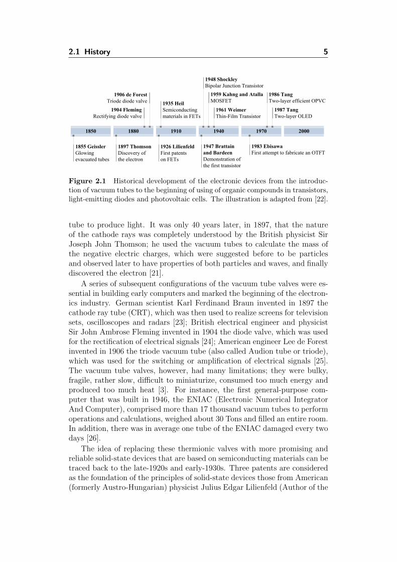
Integrated circuits are often said to be the most important invention of thetwentieth century. They have become ubiquitous in modern technology, find-ing their way into nearly all industries available including telecommunica-tions, automotive, consumer electronics and many others [1]. An integratedcircuit, also referred to as microchip, is a tiny electronic circuit in which allthe components, such as resistors, capacitors and transistors, are housed ona single chip. Transistors, however, are the main building blocks of an elec-tronic circuit; they are solid-state active devices, which act as switches oramplifiers [19]. Early transistors were discrete and large in size (few squarecentimeters), but the rapid pace of progress of integrated circuits has en-abled packing of more than billion transistors onto a single chip (also withfew square centimeters of area).
Before transistors and microchips, the electronic circuits were based onbulky devices and had to be painstakingly assembled piece by piece. Themain family of such bulky devices was vacuum tubes (also called thermionicvalves), which were used for rectification, amplification, switching or similarprocessing of electrical signals (Fig. 2.1). It was German scientist HeinrichGeissler who is credited with building the first vacuum tubes (also calledGeissler tubes; they were almost completely evacuated) in 1855. He alsonoticed their strange glow of colored light when applying an electric fieldacross the vacuum between two electrodes in 1857 [20]. It was describedlater that the colored light is caused by rays, called cathode rays, which arecarrying negative electric charges and hitting the air molecules inside the
4
2.1 History 5
1850 1880 1910 1940 1970 2000
1855 GeisslerGlowing evacuated tubes
1897 ThomsonDiscovery of the electron
1904 FlemingRectifying diode valve
1906 de ForestTriode diode valve
1926 LilienfeldFirst patents on FETs
1935 HeilSemiconducting materials in FETs
1947 Brattain and BardeenDemonstration of the first transistor
1948 ShockleyBipolar Junction Transistor
1959 Kahng and AtallaMOSFET
1961 WeimerThin-Film Transistor
1986 TangTwo-layer efficient OPVC
1987 TangTwo-layer OLED
1983 EbisawaFirst attempt to fabricate an OTFT
Figure 2.1 Historical development of the electronic devices from the introduc-tion of vacuum tubes to the beginning of using of organic compounds in transistors,light-emitting diodes and photovoltaic cells. The illustration is adapted from [22].
tube to produce light. It was only 40 years later, in 1897, that the natureof the cathode rays was completely understood by the British physicist SirJoseph John Thomson; he used the vacuum tubes to calculate the mass ofthe negative electric charges, which were suggested before to be particlesand observed later to have properties of both particles and waves, and finallydiscovered the electron [21].
A series of subsequent configurations of the vacuum tube valves were es-sential in building early computers and marked the beginning of the electron-ics industry. German scientist Karl Ferdinand Braun invented in 1897 thecathode ray tube (CRT), which was then used to realize screens for televisionsets, oscilloscopes and radars [23]; British electrical engineer and physicistSir John Ambrose Fleming invented in 1904 the diode valve, which was usedfor the rectification of electrical signals [24]; American engineer Lee de Forestinvented in 1906 the triode vacuum tube (also called Audion tube or triode),which was used for the switching or amplification of electrical signals [25].The vacuum tube valves, however, had many limitations; they were bulky,fragile, rather slow, difficult to miniaturize, consumed too much energy andproduced too much heat [3]. For instance, the first general-purpose com-puter that was built in 1946, the ENIAC (Electronic Numerical IntegratorAnd Computer), comprised more than 17 thousand vacuum tubes to performoperations and calculations, weighed about 30 Tons and filled an entire room.In addition, there was in average one tube of the ENIAC damaged every twodays [26].
The idea of replacing these thermionic valves with more promising andreliable solid-state devices that are based on semiconducting materials can betraced back to the late-1920s and early-1930s. Three patents are consideredas the foundation of the principles of solid-state devices those from American(formerly Austro-Hungarian) physicist Julius Edgar Lilienfeld (Author of the

6 2 Introduction to Organic Electronics
two patents [27] and [28] filed in 1926 and 1928, respectively) and Germanelectrical engineer Oskar Heil (Author of the patent [29] filed in 1935). Bothdescribed in their patents different variations of a method, aperture or de-vice to control the flow of an electric current between two terminals of anelectronically active material by means of a third potential applied to an in-sulated third terminal. Lilienfeld suggested in [28] that the active layer couldbe either pure metallic such as copper (Cu), compound such as cuprous oxide(Cu2O), or preferably, a mixture of both. Although Cu2O is a semiconduc-tor, there was absolutely no definite indication in his claims of this class ofsolid materials or the necessity of using it for the active layer. Heil, on theother hand, is believed to be the first one who stated clearly in his patentthat the active material should be made of thin layer of semiconductor suchas tellurium (Te) or cuprous oxide (Cu2O) [30, 31]. He also described thatthe semiconducting layer changes its resistance depending on the potentialapplied at the controlling metal terminal.
The presented inventions of Lilienfeld and Heil only embody conceptsof solid-state devices as possible substitutes for the thermionic valves, withno indication of any reduction to practice. This class of solid-state deviceswas later named Field-Effect Transistors (FETs), where the name transistoris a shortened version of the original term transfer resistor, which conveysthe operation principal of the device. Subsequent to these key conceptualinventions, many electronic device physicists and engineers pursued researchon realizing semiconductor replacements for the unreliable vacuum tubes.More than a decade later, in 1947, the first successful semiconductor tran-sistor was demonstrated [32–34]. This has marked the beginning of a seriesof milestones, at which different device configurations and materials wereintroduced. Four of the most important milestones are listed below:
• In 1947, American physicists Walter Brattain and John Bardeen demon-strated the first transistor action in a germanium point-contact device[34]. The transistor could amplify an input power up to 40 times [35],but had delicate mechanical configuration and was difficult to manu-facture in high volume with sufficient reliability.
• In 1948, American physicist William Shockley invented the concept ofBipolar Junction Transistors (BJTs) [36, 37]. At that time, Shock-ley was actually leading a solid-state physics group at Bell Labs thatincluded both Brattain and Bardeen. All the three scientists wereawarded the 1956 Nobel Prize in Physics for their invention. For aboutthree decades, the BJT was the main device of choice in the designof discrete and integrated circuits. BJTs are nowadays mostly madefrom silicon germanium (SiGe) and their use is often limited to veryhigh-speed applications such as radio-frequency circuits for wireless sys-tems [1].
2.1 History 7
• In 1959, South-Korean physicist Dawon Kahng and Egyptian engineerMartin M. Atalla demonstrated the first Metal-Oxide-SemiconductorField-Effect Transistor (MOSFET), which had been long anticipatedby Lilienfeld and Heil [38–40]. The device is mainly constructed by astack of three layers: (i) silicon semiconductor as a base material, (ii)thermally-grown native oxide as an insulator, and (iii) metallic gateelectrode as a controlling terminal. The MOSFET had largely super-seded the BJT, owing to many favorable properties of silicon, especiallydue to the controllable and stable surface oxide. With the extraordinaryprogress and continued miniaturization of the silicon-based technology,MOSFETs became the dominant device used in integrated circuits andelectronics industry until today (with the exception of large-area ap-plications).
• In 1961, American physicist Paul Weimer developed the first thin-filmtransistor (TFT), which is a FET-like device similar to the ones pro-posed by Lilienfeld and Heil [41–43]. The TFTs are fabricated on aninsulating substrate such as glass. In a typical process, TFT wouldcomprise polycrystalline or amorphous semiconducting materials (onlyin some few cases crystalline semiconductors are used as well). For ex-ample, Weimer used a semiconducting film of polycrystalline cadmiumsulfide (CdSe) in his first demonstration [41]. Unlike MOSFETs, TFTsare supreme for large-area applications that do not require significantlyhigh speeds such as active-matrix liquid crystal displays (AM-LCDs).The most common semiconducting material used today for TFTs ishydrogenated amorphous silicon (a-Si:H), owing to its low fabricationcost and easy processability [44].
Ever since, the evolution and development of the semiconductor tech-nology have been following two main approaches, namely silicon monolithiccircuits and thin-film circuits. The advancement of both technologies hasbeen aiming of shrinking device geometries, increasing production through-put and yield, improving circuit reliability and fault tolerance, minimizingmismatch effects and reducing manufacturing costs. The rapid pace of in-novation for both technologies has been pursuing certain trends [45]. Forexample, one of the major trends that enabled the proliferation of siliconmonolithic circuits until they became omnipresent today in our daily life iscommonly known as Moore’s Law [46, 47]:
“Transistor density on integrated circuitdoubles about every two years.”
—Gordon Moore (1965; updated 1975)
Increasing the density of transistors on chip implies more speed, complex-ity and functionality. Emerging applications, though, do require smarter
8 2 Introduction to Organic Electronics
integration by means of miniaturization (More Moore) as well as diversifica-tion (More than Moore). In recent years, mechanically flexible electronics asone of the approaches for diversification has caused a disruptive technologyevolution and gained prominent market attractiveness for new user-friendlyapplications such as wearable devices, roll-screen displays and intelligent pa-pers. This allows people as well as environment to interact with the complexinformation, which are typically processed by the high-performance minia-turized devices, in a more efficient and natural way.
A thin silicon chip is a possible solution, one that takes advantage of thecrystalline silicon structure and leads to many high-speed flexible applica-tions [8–11]. Nevertheless, an alternative solution is thin-film circuits thatare based on a completely different class of materials such as organic semicon-ductors. Nowadays, organic materials are forming the basis of a new low-costmicroelectronic technology that can be fabricated on large-area and flexiblesubstrates such as polymer foils, papers or even fabrics. This is mainly owedto their low-temperature manufacturability, also to their (thermo) mechani-cal properties that makes them compatible with such kind of unconventionalsubstrates [3]. One can envisage processing of this kind of materials by print-ing methods, which enables low-cost, high-volume and high-throughput pro-duction [3]. The trend, however, for this large-area and flexible technology isto reduce the cost per unit area, instead of increasing the number of functionsper unit area that is being followed by the crystalline silicon technology [45].By combining both technologies in a so called hybrid system-in-foil (SiF),one could actually take advantage of both worlds [9].
In fact, the first studies on the electrical activity of organic materials canbe traced back to the early twentieth century [48]. Anthracene was the firstorganic compound in which photoconductivity was observed by Pochettinoin 1906 [49] and Volmer in 1913 [50]. Later in the 1950s and 1960s, thepotential use of organic materials as photoreceptors in imaging systems wasrecognized [48, 51]. During the same time, electroluminescence in organiccompounds was observed by Bernanose et al. in 1955 by applying an alter-nating current (AC) in air to compounds such as brilliant acridine orange E[52] and by Pope et al. in 1963 by applying a direct current (DC) in vac-uum to anthracene [53]. In spite of these handful preliminary reports andprincipal demonstrations, the technological use of organic semiconductorswas still very limited due to several drawbacks. First, the reproducibilityand carrier mobility1 in organic semiconductors were very low. Second, thedemonstrated devices were operating at extremely high voltages (e.g. 400 V)as a consequence of the crystal thickness (in the micrometer to millimeterrange) and the difficulties to prepare stable, injection-efficient contacts to thecompounds [54]. Third, the poor control of material purity and structure
1The carrier mobility is a measure of how fast an electric charge is transmitted through amaterial under an applied electric field and is mostly represented in units of cm2/Vs.

2.1 History 9
ordering were also obstacles. Finally, the materials used so far did achieveneither sufficient efficiency nor satisfying stability [54]. However, the researchand interest in this field were flourished in 1977 by the successful synthesis ofelectrically conducting organic polymers through controlled halogen doping[55]. This discovery by Alan G. MacDiarmid, Alan J. Heegar, Hideki Shi-rakawa and co-workers was considered a major breakthrough, opened manynew and exciting applications and honored with the 2000 Nobel Prize inChemistry.
The first available organic materials were intractable, immobile, or eveninsoluble [5]. Nevertheless, the rapid advancement of the materials and pro-cessing has enabled the development of soluble organic compounds. Solu-bility is a key prominent feature, one that opened the possibility for cheapand high-volume production of printed electronics. Henceforth, the utiliza-tion of organic materials by various electronic components has given them,incontrovertibly, a place in the development of this theme [5]. Three com-ponents that can be considered as the foundation of organic electronics areorganic photovoltaic cells (OPVCs), organic light-emitting diodes (OLEDs)and organic thin-film transistors (OTFTs):
First, the use of conjugated polymers, such as poly(sulphur nitride) andpolyacetylene, for the realization of OPVCs were firstly investigated in the1980s; their power conversion efficiencies, however, were well below 0.1%[48]. A major breakthrough came in 1986 when American physical chemistChing W. Tang discovered that a two-layer OPVC by bringing a donor andan acceptor in one cell could dramatically improve the efficiency to 1% [56].Subsequent developments of OPVCs achieved in early-2013 efficiency as highas 12% according to recent announcements from the German company Heli-atek [57].
Second, OLEDs in the form available today were firstly presented in 1987by Ching W. Tang and Steven Van Slyke using a double layer structure of or-ganic thin films (8-hydroxylquinoline aluminum Alq3 and aromatic diamine)[58]. Later, in 1990, the research on polymer electroluminescence culminatedin the first successful demonstration of green-yellow polymer-based OLEDusing 100 nm thick film of poly(p-phenylene vinylene) as an active layer [59].The improved efficiencies combined with increased shelf and operating life-times, also superior material properties and manufacturing techniques, havepushed OLEDs already to the market place in applications like OLED-basedlighting and displays. For example, the South-Korean company Samsung hasjust recently launched in August 2013 the first 55 inch full high-definition2
(Full HD) OLED television with a curved panel (S9C series) [60].Last, the debut of the field effect in organic semiconductors date back
to 1970 [61–64], yet the potential use of the OTFT (at that time mostly re-
2The full high-definition (Full HD) is implying a resolution of 1920×1080 (2.1 megapixel)in a 16:9 aspect ratio.
10 2 Introduction to Organic Electronics
ferred to as metal-insulator-semiconductor field-effect transistor MISFET) asan electronic device was only identified in 1983 when Ebisawa et al. reportedthe first attempt to fabricate an OTFT that utilizes polyacetylene as an ac-tive semiconducting layer [65]. From this point forward, several studies weredevoted to realize successful TFTs based on organic semiconductors such aspolyacetylene [65, 66], polythiophenes [67, 68] and metallophthalocyanines[69, 70]. However, their carrier mobilities were very low in the range of 10−4
to 10−5 cm2/Vs. It was not until nearly seven years later, in 1990, thatthe carrier mobility in organic semiconductors approached and even reachedthat in amorphous silicon when Garnier et al. reported a carrier mobility ashigh as 4.3×10⁻¹ cm2/Vs for TFTs that used evaporated hexathiophene asan active material [71]. For comparison, the carrier mobilities in conventionala-Si:H TFTs are in the range of 10−1 to 1 cm2/Vs. The performance and sta-bility of OTFTs have continuously improved since then. Hence, some OTFTsnow compete with a-Si:H TFTs to enable revolutionary design possibilities innew large-area and mechanically-flexible applications. The most compellingapplication of OTFTs is backplanes for flexible active-matrix displays; ac-cordingly, the German company Plastic Logic is currently manufacturingultra-thin and lightweight plastic displays that are able to bend, twist andeven roll-up like a piece of paper [72].
The field of organic electronics has been well-profiled and recognizedby several international awards bestowed upon great scholars and scientistsworking on this subject. As mentioned above, the 2000 Novel Prize in Chem-istry was awarded jointly to the Americans Alan G. MacDiarmid and Alan J.Heegar, and the Japanese Hideki Shirakawa for their discovery and develop-ment of conductive polymers [55]. Furthermore, the 2010 Millennium Tech-nology Prize3 was awarded to the British Sir Richard Friend (as one of thethree laureates in that year) whose team discovered electroluminescent diodesbased on polymers (PLEDs) and greatly participated in the development ofOTFTs and OPVCs [59, 66]. In addition, the 2011 Deutscher Zukunftpreis4
(German Future Prize) was awarded to Karl Leo, Jan Blochwitz-Nimoth andMartin Pfeiffer for their major contribution in the advancement of organicfunctional materials and manufacturing techniques, especially for applica-tions in lighting and photovoltaics [75–78]. Finally, it is worth mentioningthat despite all these advances, the field of organic electronics is still in itsinfancy and there is still much room for improvement and much to be learnedand investigated.
3The Millennium Technology Prize is the world’s largest technology award. It is awardedevery two years by Technology Academy Finland, an independent foundation establishedby Finnish industry and the Finnish state in partnership [73].
4The Deutscher Zukunftpreis (German Future Prize) is one of the most prestigious awardsconferred for science and innovation within Germany. It is awarded annually by theFederal President of Germany [74].
2.2 Materials 11
2.2 MATERIALS
Organic electronics have been promising on account of their low-cost, low-temperature and fast manufacturability in addition to their compatibilitywith various kinds of substrates that are thin, large in area, transparent ormechanically flexible. In principle, organic electronics rely on electricallyactive materials that are based on conjugated organic compounds whosemolecules contain carbon and hydrogen elements. A basic device, such asan organic transistor, is generally comprised of a stack of conducting, semi-conducting and insulating thin-film layers. There are many attempts torealize all these layers solely from organic materials [79, 80]; however, theyare mostly combined with special inorganic thin-films in order to optimizethe device performance [81]. The structures and applications of the differentorganic-based devices are given in Section 2.3, where the different fabricationprocesses used to deposit and pattern the thin-film layers are discussed inSection 4.1. In this section, an overview of the different organic as well asinorganic materials is presented.
The materials are classified in this section as the following: (i) semicon-ductors, (ii) conductors, (iii) dielectrics, (iv) passivation, and (v) substrates.Each material in every class has its advantages and limitations, where oftenthe process conditions as well as the interplay of the material with otherlayers have a large influence on the device performance [82]. Therefore, theselection of the materials has to be carefully done to meet application andtechnology parameters such as thermal, mechanical and optical properties.For example, transparency is very important for the realization of solar pan-els that are going to be mounted on building facades, but not for displaysthat are designed for e-book readers. A summary of the key application andtechnology parameters is listed below [82]:
• Electrical Performance—The performance (operation frequency, cur-rent driving capability) of the devices depends on the carrier mobilityin the semiconductor, conductivity of the conductor and the dielectricalbehavior of the dielectric material.
• Resolution and Registration—The reliability and performance of thedevices depend on the lateral distance of the electrodes (pitch, or res-olution) within the devices and the overlay accuracy (Registration)between different patterned layers. In addition, scalability is necessaryto have a sustainable technology development.
• Environmental Stability—For the sustainability and proper lifetime ofthe devices, the sensitivity of the materials to oxygen and moisture hasto be well considered. This depends also on the barrier properties ofthe protective sealing layers (substrate and encapsulation).
12 2 Introduction to Organic Electronics
• Mechanics and Optics—The mechanical and optical properties includethin form factors, flexibility, bending radius, conformability, weight,transparency, color and appearance. Accordingly, the material, designand process have to be carefully chosen.
• Process Parameters—The process parameters include throughput, tem-perature and ambient conditions. For a reliable production, it is im-portant to adjust the process parameters for the different employedmaterials.
• Cost and Yield—High volume production is only possible when the pro-cesses allow fabrication at an acceptable yield. This includes adjustedmaterials, circuit designs as well as in-line quality control for low-costand low-requirement (e.g. disposable sensors) to high-cost and high-performance (e.g. flexible OLED display) products.
Semiconductors
Organic semiconductors are traditionally classified as small molecules5 orpolymers6 [3]. Polymers often have excellent solubility, which makes themamenable to mass printing processes such as flexographic and gravure print-ing [81]. On the other hand, small molecules are usually deposited by vacuumsublimation; nevertheless, recent advancements enabled some of the semicon-ducting small-molecules to be processed in solution or dispersion [82], whichmakes them no longer restricted to evaporation/sublimation processes.
The carrier mobility is commonly used as a figure of merit to charac-terize the performance of materials, devices or fabrication methods. It isfound that the carrier mobility in organic semiconductors varies greatly de-pending on the choice of material, its chemical purity and its microstructure,also on the process conditions and the interface to other layers in the device[3, 82]. For example, Fig. 2.2a illustrates the difference in the carrier mobil-ity depending on the substrate temperature during deposition of the differentsemiconducting small-molecules. Furthermore, amorphous films of solution-processed semiconducting polymers usually have mobilities in the range of10−6 to 10−3 cm2/Vs [81]. However, the mobilities of certain semiconductingpolymers can be increased to about 1 cm2/Vs through molecular engineeringand also by inducing semicrystalline order through better control of the filmformation [83]. Small-molecule organic semiconductors, on the other hand,are often forming polycrystalline films when deposited by vacuum sublima-tion, which results in carrier mobilities as large as about 6 cm2/Vs [84].
5An organic small molecule is a compound containing carbon atoms that are bonded intostable individual molecular unit.
6An organic polymer is a compound with a molecular structure formed from many identicalorganic small molecules bonded together.

2.2 Materials 13
20 40 60 80 100 120 14010
-6
10-4
10-3
10-2
10-1
100
101
Substrate temperature (°C)
2C
arri
er m
ob
ilit
y (c
m/V
s)
1985 1990 1995 2000 2005 201010
-8
10-6
10-4
10-2
100
102
YearB
est
rep
ort
ed m
obil
ity
2
(cm
/Vs)
pentacenediethyl-6T
PTCDI−CH C F2 3 7
F CuPc16
PTCDI−(CN) CH C F2 2 3 7−
PTCDI−CH C H CF2 6 4 3
DNTT
10-5
single crystalssolution-processed polymers
vacuum-processed small-moleculessolution-processed small-molecules
p-channeln-channel
a-Si
(a)
20 40 60 80 100 120 14010
-6
10-4
10-3
10-2
10-1
100
101
Substrate temperature (°C)
2C
arri
er m
ob
ilit
y (c
m/V
s)
1985 1990 1995 2000 2005 201010
-8
10-6
10-4
10-2
100
102
YearB
est
rep
ort
ed m
obil
ity
2
(cm
/Vs)
pentacenediethyl-6T
PTCDI−CH C F2 3 7
F CuPc16
PTCDI−(CN) CH C F2 2 3 7−
PTCDI−CH C H CF2 6 4 3
DNTT
10-5
single crystalssolution-processed polymers
vacuum-processed small-moleculessolution-processed small-molecules
p-channeln-channel
a-Si
(b)
Figure 2.2 (a) Relationship between the carrier mobility in the transistor chan-nel and the substrate temperature during the deposition of the organic semi-conductor layer for five different small molecules: DNTT [85], pentacene [86],diethyl-sexithiophene [87], PTCDI–CH2C3F7 [88], F16CuPc [89], PTCDI–(CN)2–CH2C3F7 [90] and PTCDI–CH2C6H4CF3 [91]. (b) Development of the carriermobility in organic transistors based on small molecules, polymers and single crys-tals. The data is categorized according to the deposition process, material classand type of injected carriers. The seven categories are the following (with referenceto the publications from which the highest carrier mobilities are extracted): singlecrystals (p-channel [92]), vacuum-processed small molecules (p-channel [84] andn-channel [88]), solution-processed small molecules (p-channel [93] and n-channel[94, 95]) and solution-processed polymers (p-channel [83] and n-channel [96]). Bothgraphs are adopted from [81].
Figure 2.2b depicts the development of the best reported field-effect mo-bility of p- and n-channel OTFTs based on small-molecule and polymericsemiconductors since 1984. The carrier mobility in organic semiconductors,though still underperform that of the crystalline silicon, has improved dra-matically until it approached and even surpassed that of the amorphoussilicon (a-Si). Unlike inorganic semiconductors, organic semiconductors arenot atomic solids but they are π-conjugated materials for which the chargetransport mechanism is based on hopping between the individual conjugatedmolecules [5]. In this case, the mobility is mainly limited by trapping ofcharges in localized states [81, 97]. As for inorganic media, in a differentmanner, defaults such as traps, along with molecular and macromolecularstructural irregularities, have a crucial impact on the charge transport [5].
It is very important to note that organic semiconductors are usually un-doped (intrinsic semiconductors) and the notions of p- and n-channel OTFTs
14 2 Introduction to Organic Electronics
do not imply the same meaning as for inorganic semiconductors. An n-channel OTFT is one in which electrons are more easily injected than holes.This has something to do with the matching of energy levels of the metal con-tacts and the semiconductor employed by the transistor as further clarifiedin the following chapter. The n-channel OTFTs are actually of special con-cern as they suffer from more than tenfold lower carrier mobility than theirp-channel contenders (if in the same organic technology). In addition, theyare highly sensitive to ambient conditions, especially to oxygen and moisture[98]. As a result, most organic-based circuits today make use of p-channeldesigns only [99, 100].
Several research efforts are currently devoted to realize stable n-channelOTFTs with relatively high carrier mobility as this enables the use of com-plementary circuit topologies, which offer higher-robustness, lower powerconsumption and larger noise-margin compared to unipolar circuits [101].There are also other attempts to integrate the p-channel OTFTs with n-channel TFTs that are based on metal-oxide semiconductors (e.g. amorphousindium-gallium-zinc-oxide a-IGZO), as they can achieve electron mobilitieslarger than 10 cm2/Vs [6, 102–104]. In general, the ongoing developmentof organic semiconductors is not limited only to the performance measures,but also extended to other essential issues such as lifetime in real-world envi-ronmental conditions, matching over large areas, reproducibility, productionyield and operation voltage.
Conductors
The need for conductive traces in all electronic products is indispensable. Aseach conducting material has its own properties, the choice of the materialstrongly depends on the application. Conductive inks, which are typicallyconsisting of micron-seized conducting flake particles, organic resins, solventsand rheology modifiers, are offering promising properties [82]. These com-positions are compatible with a wide variety of substrates and are suitablefor low-cost and high-speed manufacturing techniques such as screen andflexographic printing. For applications that demand highly conductive fea-tures, silver inks that can have electrical conductivity as large as 104 S/cmis a preferable choice [82]. Examples of mechanically flexible applicationsthat utilize printed silver inks are membrane touch switches, keyboards andon-chip antennas. Another favorable choice for less demanding applicationsis conductive carbon inks. In addition, some special compositions of carboninks can also be used as resistors or positive temperature coefficient (PTC)heaters [82].
Moreover, some devices like OLEDs and OPVCs require not only me-chanical flexibility and good conductivity, but also translucency or hightransparency for their metal electrodes. In this case, inorganic conduc-

2.2 Materials 15
tors like indium tin oxide (ITO) or polymeric conductors like poly(3, 4-ethylenedioxythiophene):poly(styrene-sulfonate) (PEDOT:PSS) are possiblesolutions [81, 82]. Meanwhile, these materials are used already for appli-cations such as touch screens and electrochromic displays. An alternativefor ITO and PEDOT:PSS is a mesh of very thin (20–80 nm) and narrow(15 µm) metal layers (e.g. silver or copper). Such a pattern with a spacingof about 200 µm can achieve a transparency of about 65% over the entirewavelength range from 400 to 900 nm. For comparison, the transparency ofan ITO film is ranging from about 60% to 85% for wavelengths from 400 to900 nm, respectively [105].
For the OTFTs, material properties of the conducting layers, especiallyfor the source and drain contacts, are very critical as they affect significantlythe devices performance. The choice of the material in this case dependson the architecture employed by the OTFT, i.e., the order of which thedevice layers are deposited. The typical used materials are aluminum (Al) orchromium (Cr) for the gate electrode, and gold (Au) for the source and draincontacts [81]. For the design of an all-polymer OTFT, conductive polymerssuch as polyaniline (PANI) or PEDOT:PSS are also suitable for the gate,source and drain electrodes.
Dielectrics
Dielectrics are used in both active and passive devices such as OTFTs andcapacitors, respectively. The majority of OTFTs to date have used inorganicdielectrics, mostly silicon oxide. In fact, the performance of the device de-pends strongly on the quality, physical properties and chemical nature of theinsulator-semiconductor interface [3]. For instance, trapping states at thementioned interface immobilize the carrier charges in the channel and cor-respondingly limit the performance [81, 98]. Significant improvements canbe achieved as demonstrated in literature just by inserting few nanometersof organic single layer between the insulator and the semiconductor [106].In order to take advantage of the complementary design features while notincreasing the production cost, the challenge is to ensure that the dielectricmaterial functions well with both p- and n-channel OTFTs.
Passivation
Passivation materials (encapsulation) are used to protect the devices againstenvironmental influences such as scratches and degradation due to the pres-ence of the water, oxygen or light [82]. In some applications, the use ofencapsulation is highly necessary to ensure an adequate lifetime for the de-vices. As an example, OTFTs that are developed for medical applications canbe encapsulated with poly(chloro-para-xylylene) (parylene) and gold layersto protect them against water [107].
16 2 Introduction to Organic Electronics
Substrates
Finally, the substrate is the base material onto which the devices are man-ufactured. Key material parameters for choosing the substrate material are:optical transmittance, dimensional stability, surface smoothness, durability,barrier capability, temperature tolerance and mechanical properties (bendingradius, deformation and hysteresis behavior) [82]. Nowadays, the majority ofapplications are using glass (also thin and flexible glass) or stainless steel sub-strates, also polymer substrates such as poly(ethylene terephthalate) (PET)or poly(ethylene 2,6-naphthalate) (PEN). In addition, paper (cellulose) ortextile substrates are sometimes used.
2.3 DEVICES AND APPLICATIONS
Given the advances in chemicals and materials by international leading firmslike DuPont in the USA and Merck in Germany, organic electronics promisereal growth opportunities for developers in new innovative products, someof which are already translated into commercial reality. The flexible andlarge-area from factors as well as the potential low production costs of theorganic technology are key benefits over their bulk, or rigid, silicon and otherinorganic counterparts. The technology is versatile enough to be used in awide range of applications as discussed herein. The organic materials can becombined to a number of active electronic components such as transistors,light-emitting diodes, photovoltaic cells, various types of sensors, memories orbatteries, also passive devices such as conductive traces, antennas, resistors,capacitors or inductors [82].
2.3.1 Organic Light-Emitting Diodes
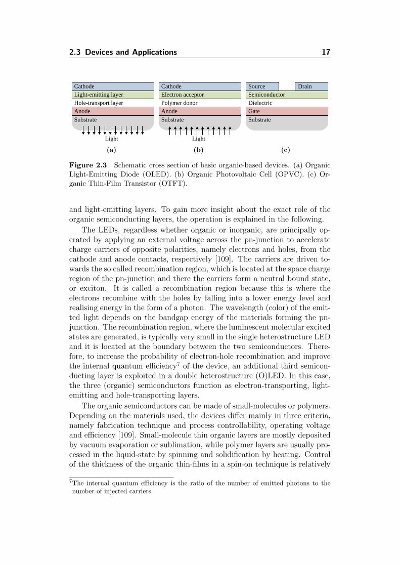
The most established and largest sector within the organic electronics indus-try, even by some margin, is OLEDs. Besides the display market, lightingapplications have emerged recently as more than a niche market for OLEDs[108]. The basic device structure of an OLED is shown in Fig. 2.3a. Thestructure comprises two organic semiconducting layers, which are sandwichedby anode and cathode electrodes laying on a transparent substrate (e.g.glass). Depending on the transparency of the anode and cathode electrodes,the light is transmitted either from top, bottom or both directions of thedevice. This basic device structure is called heterostructure OLED, or some-times referred to as bilayer structure, which resembles a pn-junction and issimilar to the one used in the very first demonstration of an efficient electrolu-minescence (EL) OLED based on organic thin-films that was built in 1987 byChing W. Tang and Steven Van Slyke of Eastman Kodak Co. [58]. In thisstructure, the two organic semiconductors function as a hole-transporting
2.3 Devices and Applications 17
Substrate
Gate
Dielectric
Semiconductor
Source
Substrate
Anode
Polymer donor
Electron acceptor
Cathode
Light
Substrate
Anode
Hole-transport layer
Light-emitting layer
Cathode
Light
Drain
(a)
Substrate
Gate
Dielectric
Semiconductor
Source
Substrate
Anode
Polymer donor
Electron acceptor
Cathode
Light
Substrate
Anode
Hole-transport layer
Light-emitting layer
Cathode
Light
Drain
(b)
Substrate
Gate
Dielectric
Semiconductor
Source
Substrate
Anode
Polymer donor
Electron acceptor
Cathode
Light
Substrate
Anode
Hole-transport layer
Light-emitting layer
Cathode
Light
Drain
(c)
Figure 2.3 Schematic cross section of basic organic-based devices. (a) OrganicLight-Emitting Diode (OLED). (b) Organic Photovoltaic Cell (OPVC). (c) Or-ganic Thin-Film Transistor (OTFT).
and light-emitting layers. To gain more insight about the exact role of theorganic semiconducting layers, the operation is explained in the following.
The LEDs, regardless whether organic or inorganic, are principally op-erated by applying an external voltage across the pn-junction to acceleratecharge carriers of opposite polarities, namely electrons and holes, from thecathode and anode contacts, respectively [109]. The carriers are driven to-wards the so called recombination region, which is located at the space chargeregion of the pn-junction and there the carriers form a neutral bound state,or exciton. It is called a recombination region because this is where theelectrons recombine with the holes by falling into a lower energy level andrealising energy in the form of a photon. The wavelength (color) of the emit-ted light depends on the bandgap energy of the materials forming the pn-junction. The recombination region, where the luminescent molecular excitedstates are generated, is typically very small in the single heterostructure LEDand it is located at the boundary between the two semiconductors. There-fore, to increase the probability of electron-hole recombination and improvethe internal quantum efficiency7 of the device, an additional third semicon-ducting layer is exploited in a double heterostructure (O)LED. In this case,the three (organic) semiconductors function as electron-transporting, light-emitting and hole-transporting layers.
The organic semiconductors can be made of small-molecules or polymers.Depending on the materials used, the devices differ mainly in three criteria,namely fabrication technique and process controllability, operating voltageand efficiency [109]. Small-molecule thin organic layers are mostly depositedby vacuum evaporation or sublimation, while polymer layers are usually pro-cessed in the liquid-state by spinning and solidification by heating. Controlof the thickness of the organic thin-films in a spin-on technique is relatively
7The internal quantum efficiency is the ratio of the number of emitted photons to thenumber of injected carriers.
18 2 Introduction to Organic Electronics
harder than in vapor deposition. However, polymer-based OLEDs can usu-ally operate at lower power than that of small-molecule-based OLEDs. Thisis owed to the high conductivity of organic polymers. The operation supplyvoltage of polymer-based OLEDs is in the range of 2–5 V, which is about1–2 V less than that of small-molecule-based OLEDs. Furthermore, the ef-ficiency of polymer-based OLEDs is typically higher than that of the small-molecule-based OLEDs. Nevertheless, focusing now on one single process ormethod would not be favorable, as the technologies are not mature enoughto determine the optimal method. Display as well as lighting industries arecurrently focusing on different technical approaches for both solution- andvacuum-processable organic materials to develop cost-effective OLEDs.
For many years, the LCDs has been the norm for the display industries[108]. However, the growing number of laptops, mobile phones, televisionsand many other applications increase the demand for higher quality products.In contrast to LCDs, the superior virtues of OLED displays are the thinnest-ever form factor, deeper black levels when individual pixels switch off, andhigh contrast ratio. The main problem that was setting back the OLEDsfor many years was the lifetime, yet it has continued to improve every yearreaching now a sufficient level to compete with LCDs. Meanwhile, Asiancompanies such as Samsung and LG dominate the manufacturing of bothLCD and OLED flat panel displays.
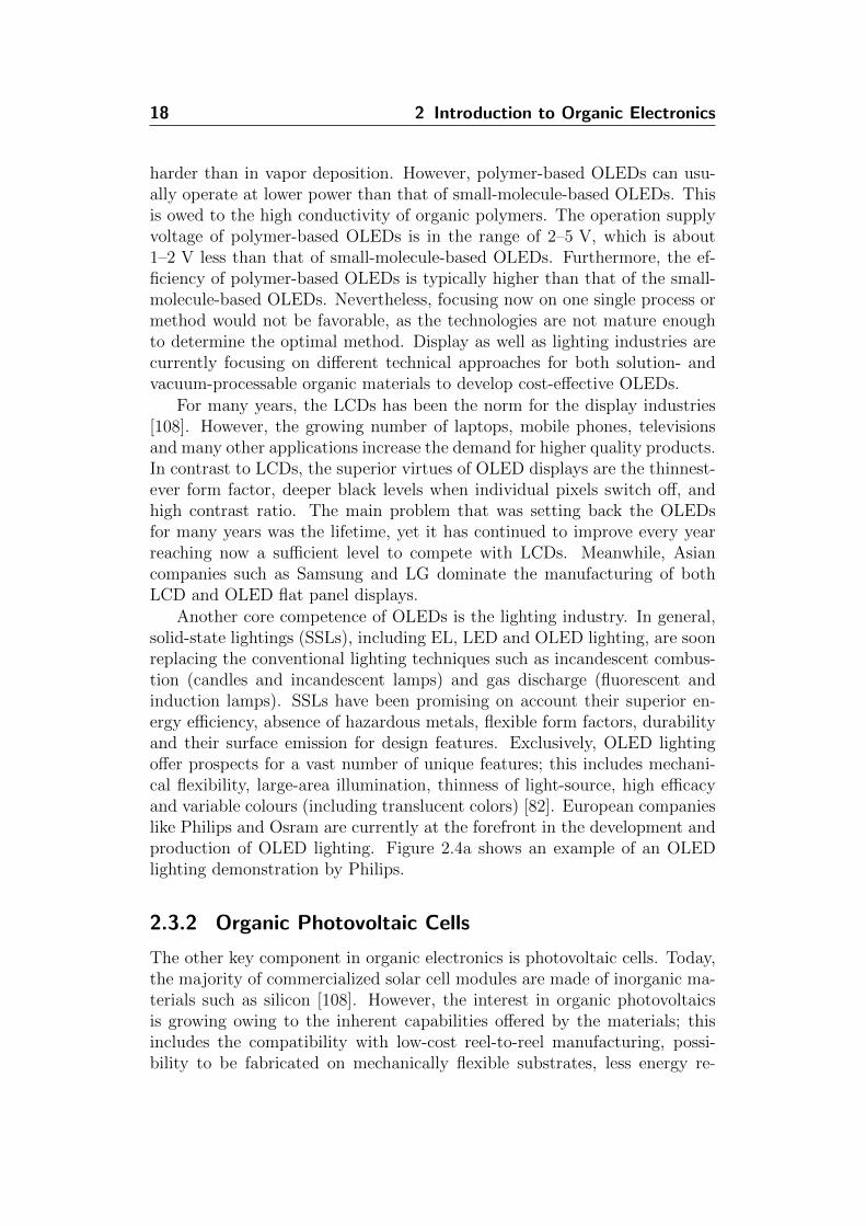
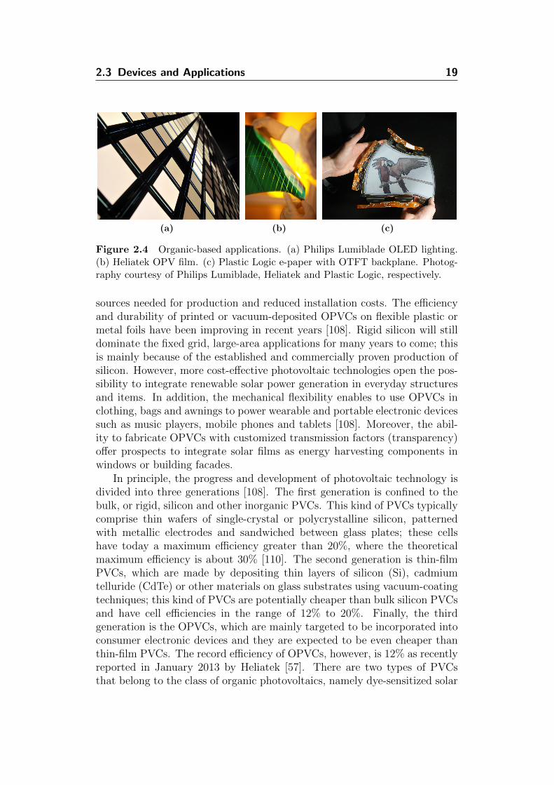
Another core competence of OLEDs is the lighting industry. In general,solid-state lightings (SSLs), including EL, LED and OLED lighting, are soonreplacing the conventional lighting techniques such as incandescent combus-tion (candles and incandescent lamps) and gas discharge (fluorescent andinduction lamps). SSLs have been promising on account their superior en-ergy efficiency, absence of hazardous metals, flexible form factors, durabilityand their surface emission for design features. Exclusively, OLED lightingoffer prospects for a vast number of unique features; this includes mechani-cal flexibility, large-area illumination, thinness of light-source, high efficacyand variable colours (including translucent colors) [82]. European companieslike Philips and Osram are currently at the forefront in the development andproduction of OLED lighting. Figure 2.4a shows an example of an OLEDlighting demonstration by Philips.
2.3.2 Organic Photovoltaic Cells
The other key component in organic electronics is photovoltaic cells. Today,the majority of commercialized solar cell modules are made of inorganic ma-terials such as silicon [108]. However, the interest in organic photovoltaicsis growing owing to the inherent capabilities offered by the materials; thisincludes the compatibility with low-cost reel-to-reel manufacturing, possi-bility to be fabricated on mechanically flexible substrates, less energy re-
2.3 Devices and Applications 19
(a) (b) (c)
Figure 2.4 Organic-based applications. (a) Philips Lumiblade OLED lighting.(b) Heliatek OPV film. (c) Plastic Logic e-paper with OTFT backplane. Photog-raphy courtesy of Philips Lumiblade, Heliatek and Plastic Logic, respectively.
sources needed for production and reduced installation costs. The efficiencyand durability of printed or vacuum-deposited OPVCs on flexible plastic ormetal foils have been improving in recent years [108]. Rigid silicon will stilldominate the fixed grid, large-area applications for many years to come; thisis mainly because of the established and commercially proven production ofsilicon. However, more cost-effective photovoltaic technologies open the pos-sibility to integrate renewable solar power generation in everyday structuresand items. In addition, the mechanical flexibility enables to use OPVCs inclothing, bags and awnings to power wearable and portable electronic devicessuch as music players, mobile phones and tablets [108]. Moreover, the abil-ity to fabricate OPVCs with customized transmission factors (transparency)offer prospects to integrate solar films as energy harvesting components inwindows or building facades.
In principle, the progress and development of photovoltaic technology isdivided into three generations [108]. The first generation is confined to thebulk, or rigid, silicon and other inorganic PVCs. This kind of PVCs typicallycomprise thin wafers of single-crystal or polycrystalline silicon, patternedwith metallic electrodes and sandwiched between glass plates; these cellshave today a maximum efficiency greater than 20%, where the theoreticalmaximum efficiency is about 30% [110]. The second generation is thin-filmPVCs, which are made by depositing thin layers of silicon (Si), cadmiumtelluride (CdTe) or other materials on glass substrates using vacuum-coatingtechniques; this kind of PVCs are potentially cheaper than bulk silicon PVCsand have cell efficiencies in the range of 12% to 20%. Finally, the thirdgeneration is the OPVCs, which are mainly targeted to be incorporated intoconsumer electronic devices and they are expected to be even cheaper thanthin-film PVCs. The record efficiency of OPVCs, however, is 12% as recentlyreported in January 2013 by Heliatek [57]. There are two types of PVCsthat belong to the class of organic photovoltaics, namely dye-sensitized solar
20 2 Introduction to Organic Electronics
cells (DSSCs) and organic photovoltaic cells (OPVCs). In fact, the DSSCsmainly do not comprise organic materials with the exception of a thin film oforganic molecular dye. Nevertheless, the DSSCs production and applicationsare similar to that of OPVCs. There is a mirror analogy between DSSCs,OPVCs and double-, single-heterostructure OLEDs, respectively.
First, the DSSC is composed of the following five layers (from top to bot-tom) [111]: (i) transparent top conductor with low series resistance, throughwhich the light can be penetrated; (ii) porous semiconducting layer of tita-nium dioxide nano-particles, which is used solely for charge transport; (iii)molecular dye that absorbs the light rays such as chlorophyll or porphyrinorganic materials; (iv) electrolyte solution based on iodide/triiodide redoxsystem, from which the electrons are recovered by the dye before decompo-sition; and (v) base conducting substrate that serves also as a counter elec-trode. The operation principle in this case is called artificial photosynthesis;the light enters the cell through the transparent top conductor, striking thedye at the surface of the semiconductor, where the charge separation takesplace. Only photons with enough energy, larger than the bandgap of the dyematerial, are absorbed and are able to make the electrons in their excitedstate. Excited electrons are then injected directly into the conduction bandof the semiconducting layer, through which they diffuse to the top-electrode(anode) to power the load. Before the dye molecules are decomposed, the dyerecovers the lost electrons from the iodide in the electrolyte, oxidising it intotriiodide. This reaction takes place before the injected electrons recombineto prevent short circuiting. Finally, the missing electrons needed to recoverthe trioxide then diffuses from the counter electrode (cathode), from whichthey are provided by the load.
Second, the structure and operation of OPVCs are similar to inorganicsolar cells, where the incoming light creates electron-hole exciton, at the in-terface between the donor and acceptor. If a polymer donor is used, theelectron-hole pair will have a binding energy of 0.1–1.4 eV, which is in factlarger than the few milli electron-volts provided in the case of inorganic mate-rials [112]. By applying an electric field, ideally all excitons are separated intoelectrons and holes that migrate to the corresponding electrodes, i.e., anodeand cathode contacts. Referring to Fig. 2.3b, the simplest configuration thatsupports this kind of operation principal is the planar heterojunction (PHJ)solar cells; in this case, the donor and acceptor are sandwiched between atransparent anode (such as ITO) and a reflecting cathode (such as Al). How-ever, the efficiency is limited here by the exciton diffusion length8, which isabout 3–10 nm in most organic semiconductors. Therefore, for a normalorganic thin-film thickness of about 100 nm, most of the excited electronsrecombine before reaching the electrode and the active region is only lim-
8The diffusion length is the distance over which the excitons travel from the donor to theacceptor before undergoing recombination.
2.3 Devices and Applications 21
ited to a very thin region around the donor/acceptor interface, which is notenough to capture a reasonable amount of incoming light. For this reason,nano-structuring in bulk and ordered heterojunction (BHJ and OHJ) solarcells is investigated by researchers to alleviate this limitation. A photographof an OPV film produced at Heliatek is shown in Fig. 2.4b.
The most promising organic-based PVC design, however, appear to bethe tandem cells, which stack several DSSCs or OPVCs [108]. The advantageof this stacked configuration is to increase the power efficiency by means ofthe following [112]: (i) reduction of the thermalization losses of high-energyphotos by stacking different absorbers, (ii) absorption of the entire spectrumby optimising each subcell to one part of the solar light spectrum, and (iii)compensation of the aforementioned problem of PHJ, i.e., the thin activeregion, by stacking a large number of subcells.
2.3.3 Organic Thin-Film Transistors
Organic thin-film transistors (OTFTs) offer prospects for a vast numberof unique circuit applications in mechanically flexible, inexpensive, large-area and biomedical electronics. In principal, OTFTs are metal-insulator-semiconductor (MIS) field-effect transistors (FETs) in which the semiconduc-tor is a conjugated organic material [81]. Figure 2.3c shows a basic structureof an OTFT; it is a three terminal device that consists of four thin-film layersdeposited on an insulating substrate, namely gate electrode, gate dielectric,organic semiconductor and source/drain contacts. When a voltage is appliedbetween the gate and the semiconductor, a thin sheet of mobile charges iscreated in the semiconductor in close vicinity of the semiconductor/dielec-tric interface [81], i.e., a channel is created between the source and draincontacts. This charge layer balances the charges of opposite polarity locatedon the gate electrode. By tuning the applied gate voltage, the charge densityin the semiconductor channel is varied. Thus, the electric conductance ofthis channel is accordingly modulated.
There are four different possible (O)TFT planar configurations that arecategorized according to the location of the gate and the source/drain con-tacts relative to the semiconductor layer, namely coplanar, inverted coplanar,staggered, inverted staggered structure [3, 30]. The transistor shown in Fig.2.3c employs the inverted staggered (bottom-gate, top-contact) device struc-ture. More details about the different device configuration are given in thefollowing chapter. There are many different fields and applications in whichthe advantages of OTFTs can be exploited, but at this point, it is too early todesignate one as a killer application. It is worthwhile to mention that thereis a lot of movement and activity in this field through established and newstart-up companies to develop novel and previously unexpected applications.Some of the major application areas of OTFTs are reviewed in the following.

22 2 Introduction to Organic Electronics
One of the most important applications of OTFTs is radio-frequency iden-tification (RFID) tags. They are frequency-coupled portable devices that areused to identify, track, sort and detect items or persons; they can be used incard authentication, ticketing, gaming and surveillance. Together with inte-grated sensors (e.g. temperature sensor [113]), low-cost RFID labels can berealized, which are able to monitor supply chains, ensuring for example thattemperature-sensitive medicines, vaccines and food products are kept coolwhile being transported along extensive distribution network [108]. In anRFID, the communication takes place between a reader and a transponder(tag). The tag comprises a small chip and an antenna, where the antennais solely used to couple RF energy from the reader into the tag; there aredifferent coupling techniques, including backscatter, inductive and capacitivecoupling. Organic RFIDs are expected to be deployed at the item-level as asmart replacement to barcodes. Using these tags for example in a supermar-ket would save much time by allowing customers to walk a cart that is full ofgoods past a scanner and the scanner would read all the items in the cart, cre-ate a list of the merchandise and finally calculates the total amount of chargein an instant; they could also be used to collect all the information about theproducts in the store and generate an inventory within a few seconds.
There are basically two types of RFID tags, namely passive and activetags. The passive tags do not employ an energy supply and they are merelyactivated by the reader, while the active tags comprise a battery (to enablelarger reading distance) or sensors (to monitor data such as temperature).Although, the cost of silicon-based RFIDs has dropped to just few cents, thecost of assembly and packaging with the antenna and products is still high.As a result, the use of silicon-based RFIDs is limited to small-scale volumes.However, the potential ultra-low-cost production of printable OTFT-basedRFIDs together with the antenna on thin plastic or paper substrates opensthe possibility for individual item-level development. Companies like PolyICin Germany and OrganicID in the USA are working on printed RFIDs basedon OTFTs, while others, such as Kovio in the USA, are developing printedRFIDs based on silicon inks. At this time, the performance and capabilitiesof printed organic-based RFID tags are lower than that of the silicon-basedones in many aspects like memory size, data rate and reading distances;however, the research is focusing now on the development of these aspects inaddition to minimising production costs.
Besides being used in RFID tags, printed memories are an attractiveapplication for OTFTs, which gained also market attention. They can beused in various other devices that require information storage (e.g. games,sound, video and smart cards). Since most printed applications nowadays donot employ an integrated battery, non-volatile memories are generally used.Depending on the application, either ROM (Read Only Memory), WORM(Write Once Read Many memory) or NV-RAM (Non-Volatile Random Ac-

2.3 Devices and Applications 23
cess Memory) are used. The company Thin Film Electronics ASA in Norwayis an international front runner in the development and commercialization ofprinted memory devices based on polymeric materials [114].
Another key application of OTFTs is backplanes for mechanically flexibledisplays. Many flat panel displays are consisting of a matrix of pixels, formedat the intersection of rows and columns, where each pixel is an LED that iscapable to emit light by being switched on or off [115]. Colored displaysare realized by positioning matrices of red, green and blue pixels very closetogether. There are two ways to control the pixels and thus forming thedesired image, i.e., either passive or active matrix driver methods are used.In a passive matrix, each row and each column of the display has its owndriver. In this case, each pixel should maintain its state until it can berefreshed again. Passive drivers tend to be used only for simple and cheapmodules because the realization of such kind of drivers gets more difficultwhen the current required to brighten a pixel increases and also when the areaof the display increases. Consequently, active-matrix displays are used in suchcases, where each pixel is efficiently addressed by incorporating a transistor(typically TFTs are comprised) in series that provide control over the currentand hence the brightness of individual pixels. Therefore, smaller currents canflow in this case through the control wires and the wires can be finer as aresult. This means that higher resolution is realizable. Furthermore, thetransistor is also capable of holding the current setting, keeping the pixel atthe required brightness until it receives another control signal.
This class of display drivers are currently being built by inorganic tran-sistors (mostly using a-Si:H TFTs) on glass substrate, which forbid the capa-bility of being mechanically flexible. Semiconductor materials such as conju-gated organic compounds and metal oxides are being explored to enable theflexibility. Sony has demonstrated, in 2008, a bendable OLED display that isdriven by OTFTs [116]; they have also proposed conceptual prototypes suchas a laptop with flexible OLED screen and a wrist wearable music player atthe 2009 CEATEC exhibition in Japan. Moreover, sony has announced in2010 the first successful demonstration of an OLED panel that is capableof reproducing moving images while being rolled-up around a cylinder witha radius of only 4 mm [117]. These demonstrations are achieved by the in-tegration of OLEDs and OTFTs on top of plastic films; these displays arethin, light-weighted, bendable, foldable and they can be rolled-up or droppedwithout being broken.
Besides backlit-LCD and LED flat panel displays that emit light, electr-onic-paper (e-paper), also referred to as e-reader, is another technology thatimitates the appearance of ordinary ink on paper. The display elementsused by e-papers feature a memory function that enable continuous displayof the same image even if no current is driven. Furthermore, images canbe changed using very low currents. An example of such display elements
24 2 Introduction to Organic Electronics
is Electrophoretic cells9. These features open the possibility to develop thebackplane drivers for such kind of displays using OTFTs, which offer virtuesin manufacturing flexible, thin, light-weighted and large-area e-papers at lowproduction costs. The German company Plastic Logic is commercializing arange of high-quality plastic e-papers, which are shatterproof daylight read-able displays and extremely flexible with proven lifetimes. Figure 2.4c showsone of their demonstrated displays that is driven by OTFTs. Just recently,in September 2013, a start-up company popSLATE in the USA had joinedforces with Plastic Logic to create an always-on secondary screen display forApple iPhones [118]. Owing to the unique and novel features of these dis-plays, they can be easily embedded into accessory cases of smartphones orsimilar devices.
Likewise an OTFT-based active-matrix strategy can be used in large-area,low-end and conformable array of sensors and/or actuators. Electronic-skin(e-skin) that mimic the sensitivity of real skin is a good example [119, 120].Considering the vast amount of pain receptors in a person’s skin and thelarge surface area of the human’s body, active-matrix driver holds a greatadvantage for such a sensor array. To gain more insight about the complexity,the human skin has more than two million receptors, which is equivalent tothe number of pixels found in a typical high-definition television; moreover,an average adult’s skin exceeds two square meters of surface area, which isnearly as big as the largest flat-screen LCD television.
Researchers at the University of Tokyo demonstrated recently, in July2013, the world’s lightest and thinnest flexible tactile sensor. This OTFT-driven prototype has a thickness of 2 µm, which is about one-fifth the thick-ness of plastic kitchen wrap, and comprises an array of 144 pixels over an areaof 48×48 mm2 [121]. In addition, this sensor could stand repeatable bending,be crumpled like a paper and accommodate stretching of up to 230%. It canalso work at high temperatures and aqueous environments (e.g. in saline solu-tions), which enables the functionality of this sensor even inside the human’sbody. This is considered as a major breakthrough to successfully mimic thesensitivity of a biological skin and opens up a wide range of new applicationsin fields ranging from healthcare and biomedicine to welfare [122]. For ex-ample, the same research group has used this ultrathin OTFT technology torealize a 64 channel surface electromyogram (EMG) measurement sheet forprosthetic hand control [123].
Other four examples of large-area sensors or actuators that could bedriven by OTFTs are the following. First, smart textile carpets or mats,ones that are useful for safety or security purposes. For instance, they can be
9Electrophoretic cells are transparent microcapsules incorporating charged pigment parti-cles. A matrix of these cells, sandwiched between two layers (top transparent electrodeand bottom patterned line-electrodes), is forming an electrophoretic display. Dependingon the individually applied electric field on each cell, or pixel, a visible image is displayed.

2.3 Devices and Applications 25
deployed in patient rooms in hospitals to indicate a dangerous fall, heart at-tack, stroke, or similar complications and accordingly warn the staff. Second,flexible sheet image sensors or photodetectors as demonstrated by ISORG (astart-up company in France) and Plastic Logic at the 2013 Printed Electron-ics USA. They have developed the first fully-organic image sensor with anarea of 40×40 mm2 and 8930 pixels, combining ISORG’s organic photodetec-tors with Plastic Logic’s OTFT backplanes [124]. Third, large-scale stresssensors that could be placed on a randomly shaped body such as a surface of aplane, allowing to detect micro-cracks soon enough during the flight. Finally,a sheet of braille actuators, which can be felt and read by blind persons. Thesame research group from the University of Tokyo has successfully developedin 2005 an integrated circuit card (ICC) that features a mechanically flexiblebraille display built in an OTFT technology [125].
Given the wide variety and novel features of organic semiconductors,OTFTs have been also explored for chemical and biological sensors [126].Unlike the silicon-based technology (Chemically Sensing Gate Field-EffectTransistor ChemFET), OTFT-based sensors are promising on account oftheir upside-down device structure, which makes the semiconductor in directcontact with the analytes [127]. Examples of such parameters are the bulkconductivity, channel conductivity, threshold voltage and field-effect mobil-ity. On the other hand, sensing occurs in the silicon-based technology atthe gate or the gate/insulator interface and by indirect modulation of thedrain current through capacitive coupling. In principal, organic conjugatedcompounds can perform weak chemical reactions with a variety of analytes,including both vapor- and water-based analytes as demonstrated in [128] and[129], respectively. Furthermore, it was shown in [128] that the response ofdifferent organic semiconducting materials to different analytes is distinctive.This facilitates the possibility to construct an electronic-nose (e-nose) withwhich an analyte (odor) can be uniquely identified from a coded reception ofdifferent organic semiconductors.
In addition, OTFT-based chemical and biological detectors are ideal forcheap, mass-produced, flexible sensors that can be used in a range of new dis-posable healthcare products. Using for example point-of-care (PoC) devices,people could diagnose or monitor illness quite easily in private, much likepregnancy tests and hygiene tests for life sciences and food handling applica-tions. Companies and research facilities, such as Molecular Vision in the UK,Acreo in Sweden and VTT Technical Research Center in Finland, do havethe vision to develop lab-on-a-chip technologies using organic semiconduc-tors. This is to promote a more proactive approach to healthcare, with theonus on prevention of diseases and early self-diagnosis [108]. However, sucha flexible system would require not only sensors but also circuits and otherelectronic components; this is commonly known as a system-in-foil (SiF) asdiscussed in the following.

26 2 Introduction to Organic Electronics
2.3.4 Systems-in-Foil
Systems-in-Foil (SiF) are an emerging new class of flexible electronic prod-ucts in which complete systems are integrated in thin polymeric foils [8]. Thisis achieved by combining sensors, displays, power sources (batteries or pho-tovoltaics), circuits, discrete components and/or interconnect traces all in athin polymeric foil (or in some cases on the foil) to give a flexible end prod-uct. Being very thin and easy to glue to other substrates or even integratedinto textiles, these systems can easily make arbitrary objects have smart in-teractive surfaces. In addition, they can also be fitted to existing equipmentas retrofit sensors; for example, the power distribution of an equipment canbe monitored using an attached temperature sensor foil [130].
As mentioned above, disposable biosensor systems are one example of SiFthat could be used in different application areas such as point-of-care, foodsafety, environmental monitoring and agriculture [131]. Acreo is currentlyworking on the realization of an all-printed biosensor system that includesbattery, sensor, display and electronics on a single foil. Another example ofSiF could be a contactless user interface, combining optical sensors, LEDsand flexible interconnects, as being developed by ISORG. Such a platformcan allow hand proximity detection, gesture recognition or linear control.Furthermore, trading cards and board games could integrate RFIDs, displaysor buttons in a form of SiF to add more functionalities and user engagementas well as authenticity when being susceptible to counterfeits [108].
Packaging is also a viable market for printed and organic electronics.The main role of packaging is to protect, advertise and provide informationof its content, all at a cost commensurate with what is essentially a dispos-able item [108]. Currently, packages use low-cost holograms, watermarks,barcodes and safety labels as tools to indicate whether a product is real orfake. However, the idea of using low-end, mass-produced, printed RFIDs,sensors and optical feedback in a SiF could potentially provide new waysfor simultaneously branding, promoting and protecting the products. Thiscan only be feasible once the cost of printing such functional components be-comes comparable to that of printing text and graphics on everyday packages,but this will take several years to achieve. Consequently, several technologystart-ups and established suppliers of printing equipment are investing intoreel-to-reel, high-throughput manufacturing of organic semiconductors. Un-til this technology comes to commercial reality, packaging companies, such asKarl Knauer in Germany, are developing and producing for example simpleluminescent packaging [132].
Since lots of packaging and labels are made from paper-based materials(cellulose), there is also much research activity in paper-based electronics.For instance, a research group at the University of Cincinnati has been work-ing on building circuits, displays and solar cells onto paper substrates [133].
2.4 Summary 27
Others, at Harvard University and the University of Washington, are tryingto develop paper-based microfluidic devices as sensing elements. In addition,some of the paper manufacturers, such as Felix Schoeller in Germany, are ac-tive in this field; they are developing high-end coating techniques to producehigh-quality, smooth paper substrates for printed electronics.
2.4 SUMMARY
The electrical activity of organic materials has been explored since the twen-tieth century. However, these materials remained with no significant tech-nological use for many years mainly due to their very low reproducibilityand carrier mobility, poor control of material purity and structural ordering,and process difficulties to prepare stable, injection-efficient contacts to thecompounds. This was only until 1977 when the research and interest in thisfield were flourished by the successful synthesis of electrically conducting or-ganic polymers through controlled halogen doping. Owing to the excellentsolubility of many organic polymers, they are amenable to mass printing pro-cesses, which have been well established in the graphic art printing industry.This groundbreaking discovery by MacDiarmid, Heegar and Shirakawa washonored with the 2000 Nobel Prize in Chemistry. Henceforth, the utilizationof organic materials by various electronic components, including transistors,light-emitting diodes and photovoltaic cells, has given them incontrovertiblya place in the development of this theme.
Organic electronics pose nowadays a strategic challenge to the marketand they have shown lately a rapid progressive development towards higherlevel of integration and better performance. The carrier mobility in organicsemiconductors, though still underperform that in the crystalline silicon andis likely to retain this position in the foreseeable future, has improved dramat-ically until it approached and even surpassed that in the amorphous silicon.In principle, the organic materials have to be carefully exploited since pro-cess conditions as well as the interplay with other layers (can be organic orinorganic thin films) have a large influence on the device performance.
The organic technology is versatile enough to be used in a wide rangeof new applications in fields ranging from healthcare to welfare, especiallywhen flexibility, transparency, large area and/or low cost are paramount.Recent advances in organic materials have permitted a disruptive evolutionin nearly all electronic products such as displays, lighting, power sources,sensors and integrated smart systems-in-foil. The following chapters are fo-cusing on organic thin-film transistor (OTFT) fabrication, characterization,modeling and circuits design.
3Organic Thin-Film Transistors
Organic thin-film transistors (OTFTs) are providing impetus in flexible, low-cost and large-area integrated circuit applications. The choice of the OTFTarchitecture has a considerable impact on the electrical performance, becauseof differences in the charge injection mechanism, but often limitations existdue to restrictions in processing methods or incompatibility of the materialsemployed [3]. These issues are discussed herein, together with simplifiedmodeling equations and characteristic parameters to gain deeper insight ofthe operation principle of the device. Furthermore, stability and performancemeasures of the OTFTs used in this work are demonstrated.
3.1 ARCHITECTURE AND MATERIALS
OTFTs are three-terminal devices in which the semiconductor is a thin layerof conjugated organic molecules. An OTFT is basically consisting of four lay-ers, namely gate electrode, gate dielectric, semiconductor and source/draincontacts, all deposited on an insulating substrate. The organic semicon-ductor can either be small molecule or polymer. In this work, only small-molecule organic semiconductors are considered. The other three TFT lay-ers can be either made of organic or inorganic materials [97]. For instance,the source/drain contacts are usually made from a noble metal (e.g. goldor palladium), but they can also be made from a conducting conjugatedpolymer (e.g. PEDOT:PSS). Depending on the sequence in which the lay-ers are deposited, four different TFT configurations can be distinguishedas shown in Fig. 3.1 [81]. The configurations are designated as coplanar(top-gate, top-contact), inverted-coplanar (bottom-gate, bottom-contacts),staggered (top-gate, bottom-contacts) and inverted-staggered (bottom-gate,top-contact) TFTs. Besides these planar TFTs, there are also vertical TFTsin which the critical dimension is a film thickness rather than a lateral dis-tance [134–136]. However, we focus here only on the planar configurations.
It has been shown in literature by experiments [137] and simulations [138]that coplanar OTFTs often have a larger contact resistance in comparisonto their staggered counterparts (note: this is similar for the inverted config-urations as well). This is because the gate fields are partially shielded in thecoplanar OTFTs by the source and drain contacts, and thus, a channel isinduced only in the region between the contacts. As a result, the efficient
28

3.1 Architecture and Materials 29
Figure 3.1 Schematic cross section of the four TFT configurations, namelycoplanar (top-gate, top-contact), inverted-coplanar (bottom-gate, bottom-contact), staggered (top-gate, bottom-contact) and inverted-staggered (bottom-gate, top-contact) TFTs.
charge transfer between the contacts and the semiconductor is limited in thiscase only to the narrow regions where the gate-induced channel touches thecontact edges [139]. In staggered OTFTs, however, the source and draincontacts are located opposite to the gate dielectric; therefore, the channelextends beyond the contact edges along the entire gate-overlap lengths. Con-sequently, the area available for the charge transfer in staggered OTFTs islarger than in coplanar OTFTs, which explains why the staggered OTFTsoften have a smaller contact resistance than the coplanar OTFTs.
In addition, the top-gate configurations (coplanar and staggered OTFTs)are typically useful for polymer-based OTFTs but not for small-molecule-based OTFTs. This is because thin films of small molecules often exhibita rough three-dimensional growth (in contrast to the smooth amorphousfilms of spin-coated polymers), so that the dielectric/semiconductor interfacewould be also rough, and thus, the carrier mobility would be low [97].
The inverted-staggered (bottom-gate, top-contact) configuration, whichbenefits from a smooth dielectric/semiconductor interface and typically hasa small contact resistance, is therefore chosen for our OTFTs. This kind ofOTFTs can be fabricated by evaporation through shadow masks [140, 141],by soft lamination [142, 143], by self-aligned printing [144, 145], or by sub-femtoliter inkjet printing [146]. In this work, high-resolution silicon shadow(stencil) masks are employed to fabricate OTFTs with submicrometer accu-racy and superb device uniformity [13, 14, 139]. Moreover, the use of shadowmasks allow to pattern the source/drain contacts without the need of solventsor elevated temperatures that might cause undesirable phase transition forthe high-mobility small-molecule organic semiconductors [13, 147, 148].

30 3 Organic Thin-Film Transistors
Figure 3.2 Schematic cross section of the fabricated inverted-staggered (bottom-gate, top-contact) OTFT, where L is the channel length and Lov is the gate-overlaplength [151].
The small-molecule organic semiconductors are deposited in vacuum bysublimation through the silicon shadow masks to form well-ordered polycrys-talline films [97]. In principle, the exact morphology and nucleation densityon the surface depends mainly on the substrate temperature, substrate sur-face energy, surface roughness and deposition rate [97, 149]. As a result, anelevated substrate temperature of about 60–100 is utilized during the de-position to provide additional energy to the molecules, so that the diffusionlength on the surface increases and the number of nucleation centres reduces.Furthermore, glass substrates Eagle2000 from Corning are used because oftheir very smooth surface roughness of about 0.2 nm (root mean square)[150], noting that this fabrication process is also compatible with mechani-cally flexible substrates. The silicon shadow masks are manufactured at IMSCHIPS, while the OTFTs are prepared at MPI-SSR. The fabrication processis explained in detail in Chapter 4.
Figure 3.2 depicts the schematic cross section of the fabricated inverted-staggered OTFT. The OTFT layers, namely 30-nm-thick aluminium gate, 11-nm-thick organic semiconductor and 25-nm-thick gold source/drain contacts,are deposited in vacuum through shadow masks. Prior to the semiconductordeposition, a hybrid dielectric, which consists of an oxygen-plasma-grownAlOx layer (3.6-nm thick) and a solution-processed self-assembled monolayer(SAM) of n-tetradecylphoshonic acid (1.7-nm thick), is formed. This hybriddielectric features a high capacitance of the order of 1 µF/cm2, which allowsthe OTFTs to operate at low supply voltages (≤ 3 V) [106, 152]. The organicsemiconductor dinaphtho[2,3-b:2’,3’-f]thieno[3,2-b]thiophene (C22H12S2;DNTT) is used for our p-channel OTFTs as it features high intrinsic mo-bility, promising shelf-life and bias-stress stability, as well as little hystere-sis behavior [106, 153]. As for the n-channel OTFTs, the air-stable organicsemiconductors hexadecafluorocopperphthalocyanine (F16CuPc) or N,N’-bis-(heptafluorobutyl)-2,6-dichloro-1,4,5,8-naphthalene tetracarboxylic diimide[NTCDI-CI2-(CH2C3F7)2] are employed [13, 101]. The molecular structureof the used organic materials are shown in Fig. 3.3.
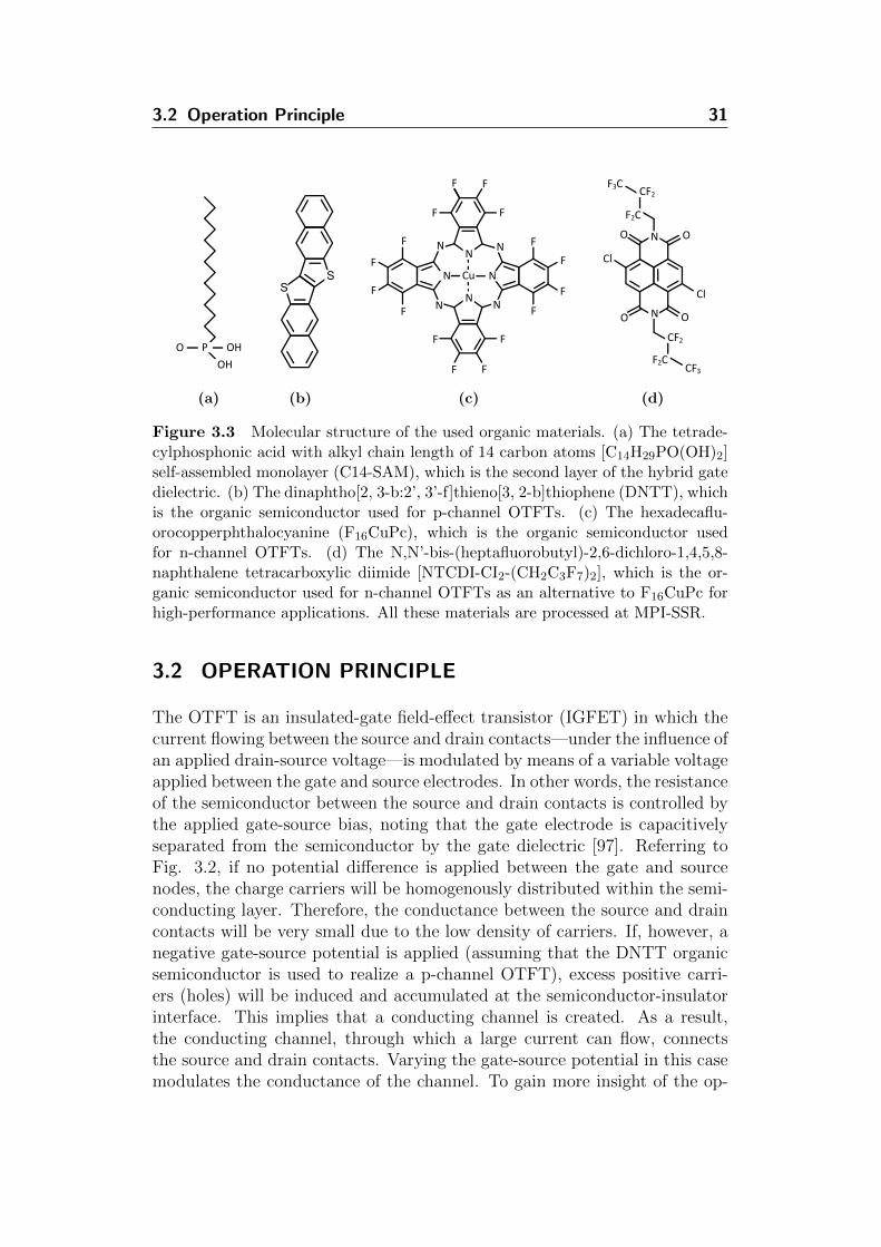
3.2 Operation Principle 31
(a) (b) (c) (d)
Figure 3.3 Molecular structure of the used organic materials. (a) The tetrade-cylphosphonic acid with alkyl chain length of 14 carbon atoms [C14H29PO(OH)2]self-assembled monolayer (C14-SAM), which is the second layer of the hybrid gatedielectric. (b) The dinaphtho[2, 3-b:2’, 3’-f]thieno[3, 2-b]thiophene (DNTT), whichis the organic semiconductor used for p-channel OTFTs. (c) The hexadecaflu-orocopperphthalocyanine (F16CuPc), which is the organic semiconductor usedfor n-channel OTFTs. (d) The N,N’-bis-(heptafluorobutyl)-2,6-dichloro-1,4,5,8-naphthalene tetracarboxylic diimide [NTCDI-CI2-(CH2C3F7)2], which is the or-ganic semiconductor used for n-channel OTFTs as an alternative to F16CuPc forhigh-performance applications. All these materials are processed at MPI-SSR.
3.2 OPERATION PRINCIPLE
The OTFT is an insulated-gate field-effect transistor (IGFET) in which thecurrent flowing between the source and drain contacts—under the influence ofan applied drain-source voltage—is modulated by means of a variable voltageapplied between the gate and source electrodes. In other words, the resistanceof the semiconductor between the source and drain contacts is controlled bythe applied gate-source bias, noting that the gate electrode is capacitivelyseparated from the semiconductor by the gate dielectric [97]. Referring toFig. 3.2, if no potential difference is applied between the gate and sourcenodes, the charge carriers will be homogenously distributed within the semi-conducting layer. Therefore, the conductance between the source and draincontacts will be very small due to the low density of carriers. If, however, anegative gate-source potential is applied (assuming that the DNTT organicsemiconductor is used to realize a p-channel OTFT), excess positive carri-ers (holes) will be induced and accumulated at the semiconductor-insulatorinterface. This implies that a conducting channel is created. As a result,the conducting channel, through which a large current can flow, connectsthe source and drain contacts. Varying the gate-source potential in this casemodulates the conductance of the channel. To gain more insight of the op-
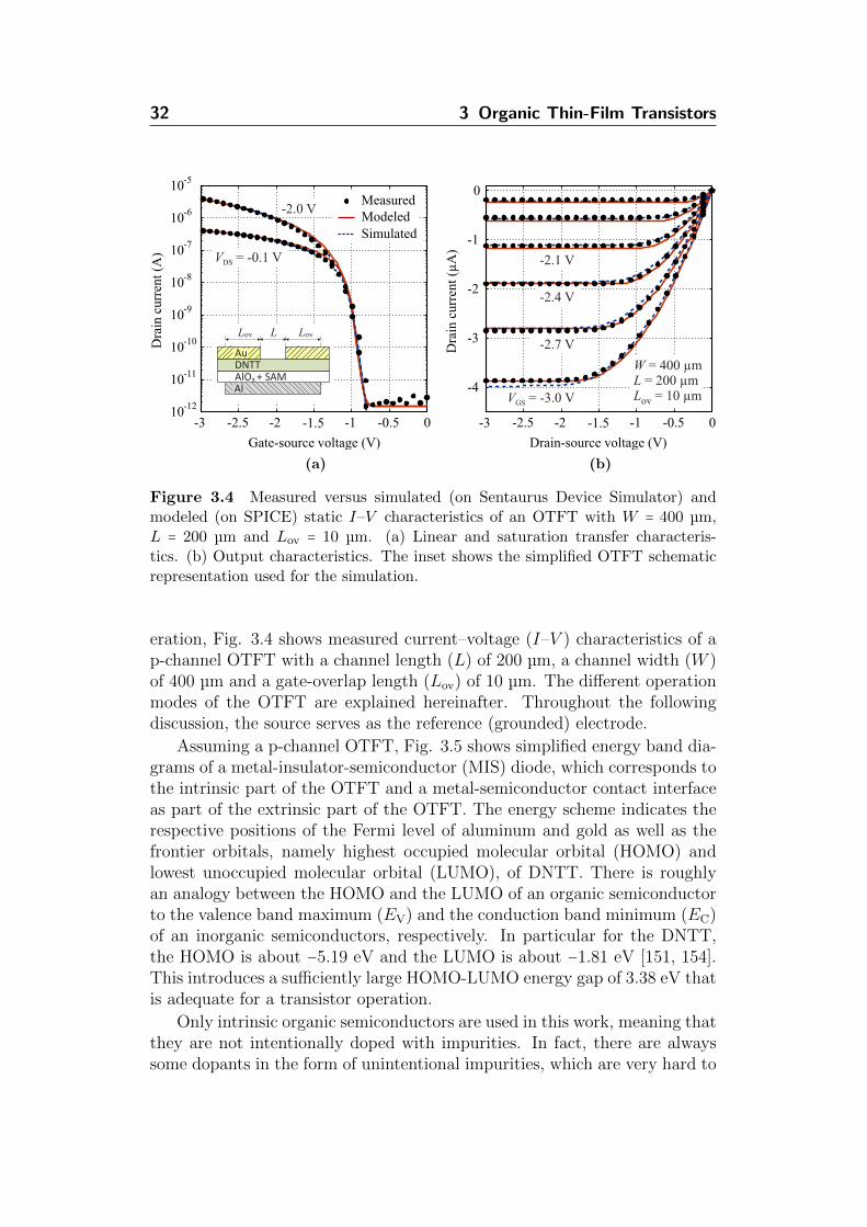
32 3 Organic Thin-Film Transistors
-3 -2 -1 0
-4
-3
-2
-1
0
Dra
in c
urre
nt (
µA
)
-3 -2 -1 010
-12
10-11
10-10
10-9
10-8
10-7
10-6
10-5
Dra
in c
urre
nt (
A)
Lov L Lov
AuDNTTAlO + SAMAl
x
Gate-source voltage (V) Drain-Source Voltage (V)
MeasuredModeledSimulated
V = -0.1 VDS
-2.5 -1.5 -0.5 -2.5 -1.5 -0.5
V = -3.0 VGS
W = 400 µmL = 200 µmL = 10 µmov
-2.7 V
-2.4 V
-2.1 V
-2.0 V
(a)
-3 -2 -1 0
-4
-3
-2
-1
0
Dra
in c
urre
nt
(µA
)
-3 -2 -1 010
-12
10-11
10-10
10-9
10-8
10-7
10-6
10-5
Dra
in c
urre
nt (
A)
Lov L Lov
AuDNTTAlO + SAMAl
x
Gate-Source Voltage (V) Drain-source voltage (V)
MeasuredModeledSimulated
V = -0.1 VDS
-2.5 -1.5 -0.5 -2.5 -1.5 -0.5
V = -3.0 VGS
W = 400 µmL = 200 µmL = 10 µmov
-2.7 V
-2.4 V
-2.1 V
-2.0 V
(b)
Figure 3.4 Measured versus simulated (on Sentaurus Device Simulator) andmodeled (on SPICE) static I–V characteristics of an OTFT with W = 400 µm,L = 200 µm and Lov = 10 µm. (a) Linear and saturation transfer characteris-tics. (b) Output characteristics. The inset shows the simplified OTFT schematicrepresentation used for the simulation.
eration, Fig. 3.4 shows measured current–voltage (I–V ) characteristics of ap-channel OTFT with a channel length (L) of 200 µm, a channel width (W )of 400 µm and a gate-overlap length (Lov) of 10 µm. The different operationmodes of the OTFT are explained hereinafter. Throughout the followingdiscussion, the source serves as the reference (grounded) electrode.
Assuming a p-channel OTFT, Fig. 3.5 shows simplified energy band dia-grams of a metal-insulator-semiconductor (MIS) diode, which corresponds tothe intrinsic part of the OTFT and a metal-semiconductor contact interfaceas part of the extrinsic part of the OTFT. The energy scheme indicates therespective positions of the Fermi level of aluminum and gold as well as thefrontier orbitals, namely highest occupied molecular orbital (HOMO) andlowest unoccupied molecular orbital (LUMO), of DNTT. There is roughlyan analogy between the HOMO and the LUMO of an organic semiconductorto the valence band maximum (EV) and the conduction band minimum (EC)of an inorganic semiconductors, respectively. In particular for the DNTT,the HOMO is about −5.19 eV and the LUMO is about −1.81 eV [151, 154].This introduces a sufficiently large HOMO-LUMO energy gap of 3.38 eV thatis adequate for a transistor operation.
Only intrinsic organic semiconductors are used in this work, meaning thatthey are not intentionally doped with impurities. In fact, there are alwayssome dopants in the form of unintentional impurities, which are very hard to
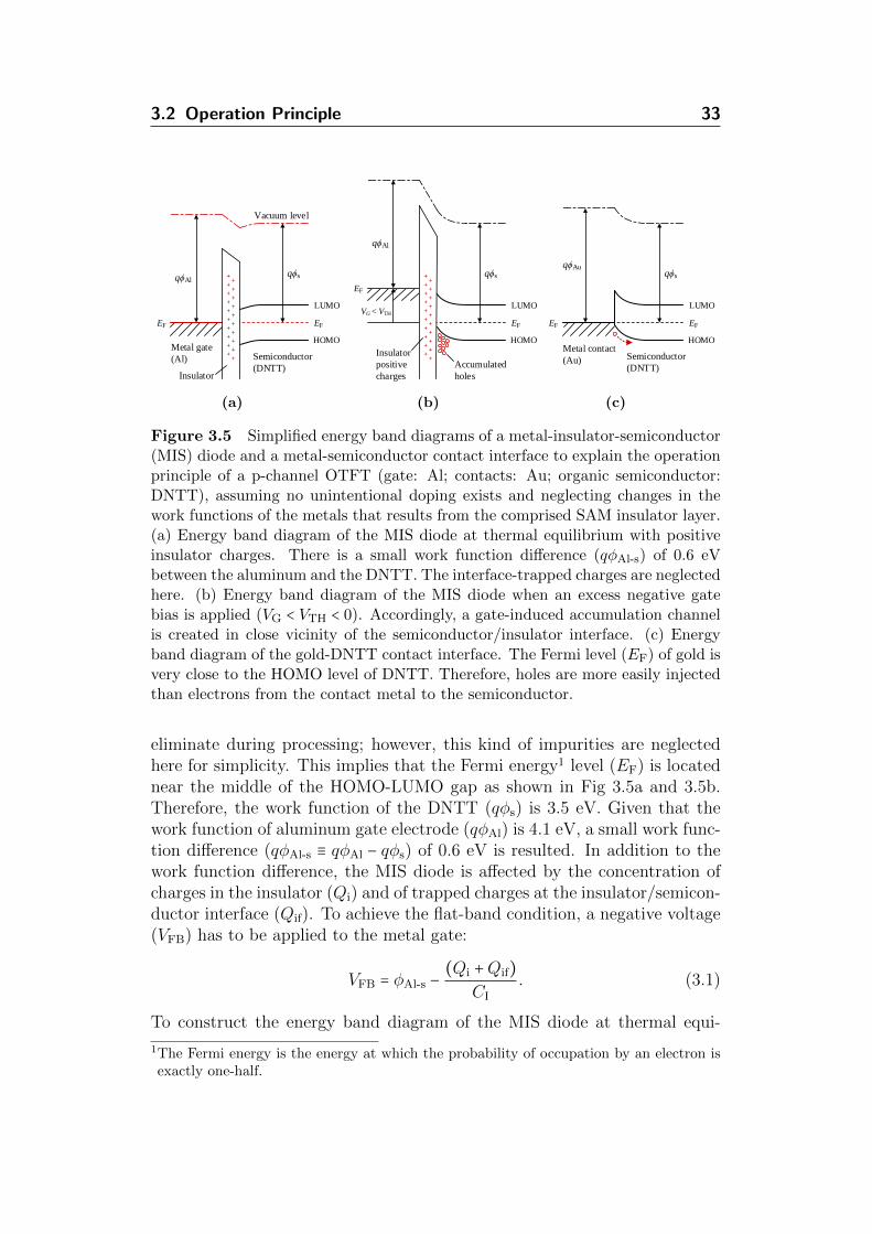
3.2 Operation Principle 33
Insulator
Metal gate
(Al) Semiconductor
(DNTT)
qϕs qϕAl
Vacuum level
HOMO
LUMO
EF EF
VG < VTH
EF
HOMO
LUMO
EF
Accumulated
holes
HOMO
LUMO
EF
qϕs qϕAu
Metal contact
(Au) Semiconductor
(DNTT)
EF
+
+
+
+
+
+
+
+
+
+
+
+
+
+
+
+
+
+
+
+
+
+
+
+
+
+
+
+
+
+
+
+
++
++
++
++
qϕAl
qϕs
Insulator
positive
charges
(a)
Insulator
Metal gate
(Al) Semiconductor
(DNTT)
qϕs qϕAl
Vacuum level
HOMO
LUMO
EF EF
VG < VTH
EF
HOMO
LUMO
EF
Accumulated
holes
HOMO
LUMO
EF
qϕs qϕAu
Metal contact
(Au) Semiconductor
(DNTT)
EF
+
+
+
+
+
+
+
+
+
+
+
+
+
+
+
+
+
+
+
+
+
+
+
+
+
+
+
+
+
+
+
+
++
++
++
++
qϕAl
qϕs
Insulator
positive
charges
(b)
Insulator
Metal gate
(Al) Semiconductor
(DNTT)
qϕs qϕAl
Vacuum level
HOMO
LUMO
EF EF
VG < VTH
EF
HOMO
LUMO
EF
Accumulated
holes
HOMO
LUMO
EF
qϕs qϕAu
Metal contact
(Au) Semiconductor
(DNTT)
EF
+
+
+
+
+
+
+
+
+
+
+
+
+
+
+
+
+
+
+
+
+
+
+
+
+
+
+
+
+
+
+
+
++
++
++
++
qϕAl
qϕs
Insulator
positive
charges
(c)
Figure 3.5 Simplified energy band diagrams of a metal-insulator-semiconductor(MIS) diode and a metal-semiconductor contact interface to explain the operationprinciple of a p-channel OTFT (gate: Al; contacts: Au; organic semiconductor:DNTT), assuming no unintentional doping exists and neglecting changes in thework functions of the metals that results from the comprised SAM insulator layer.(a) Energy band diagram of the MIS diode at thermal equilibrium with positiveinsulator charges. There is a small work function difference (qφAl-s) of 0.6 eVbetween the aluminum and the DNTT. The interface-trapped charges are neglectedhere. (b) Energy band diagram of the MIS diode when an excess negative gatebias is applied (VG < VTH < 0). Accordingly, a gate-induced accumulation channelis created in close vicinity of the semiconductor/insulator interface. (c) Energyband diagram of the gold-DNTT contact interface. The Fermi level (EF) of gold isvery close to the HOMO level of DNTT. Therefore, holes are more easily injectedthan electrons from the contact metal to the semiconductor.
eliminate during processing; however, this kind of impurities are neglectedhere for simplicity. This implies that the Fermi energy1 level (EF) is locatednear the middle of the HOMO-LUMO gap as shown in Fig 3.5a and 3.5b.Therefore, the work function of the DNTT (qφs) is 3.5 eV. Given that thework function of aluminum gate electrode (qφAl) is 4.1 eV, a small work func-tion difference (qφAl-s ≡ qφAl − qφs) of 0.6 eV is resulted. In addition to thework function difference, the MIS diode is affected by the concentration ofcharges in the insulator (Qi) and of trapped charges at the insulator/semicon-ductor interface (Qif). To achieve the flat-band condition, a negative voltage(VFB) has to be applied to the metal gate:
VFB = φAl-s −(Qi +Qif)
CI
. (3.1)
To construct the energy band diagram of the MIS diode at thermal equi-
1The Fermi energy is the energy at which the probability of occupation by an electron isexactly one-half.

34 3 Organic Thin-Film Transistors
librium, the Fermi level must be constant and the vacuum level must becontinuous [19]. To accommodate the work function difference and positiveinsulator charges, assuming negligible interface-trapped charges, the semi-conductor bands bend downward as shown in Fig. 3.5a.
In single-crystalline silicon MOSFETs, the threshold voltage is definedas the gate-source voltage at the onset of inversion in the transistor channel[97]. Organic transistors, however, do not operate in inversion; they arerather operating in the accumulation mode. Instead, the threshold voltagein OTFTs is often considered as the gate-source voltage necessary to achievethe flat-band condition (VTH = VFB). When an excess negative voltage (VG <
VTH) is applied to the gate, the energy bands are bent upwards as shownin Fig. 3.5b, which in turn gives rise to an enhanced concentration, and anaccumulation of holes near the insulator/semiconductor interface is created.
Considering now the metal-semiconductor contact interface (Fig. 3.5c),when a positive voltage is applied to the gate electrode, negative chargesare accordingly induced at the source contact. However, the LUMO level ofDNTT is quite far away from the Fermi level of gold (with qφAu = 5.0 eV),so there is a substantial energy barrier that the electrons need to overcome.Thus, electron injection is very unlikely and nearly no current passes throughthe semiconducting layer [3]. In contrast, when a negative gate voltage isapplied, holes can be easily injected to the semiconductor because the Fermilevel of gold is very close to the HOMO level of DNTT and the barrierheight is relatively low. Given that a gate-induced accumulation channelis created at the insulator/semiconductor interface, charge carriers can nowbe driven from the source to the drain by applying a second, independent,bias to the drain. Because holes are more easily injected than electrons, thetransistors based on DNTT are said to be p-channel OTFTs. Similarly, thetransistors are said to be n-channel OTFTs, when the LUMO of the organicsemiconductor (such as F16CuPc) is closer to the Fermi level of the goldcontact than the HOMO.
This concept differs from that of doping in conventional inorganic semi-conductors [3]. In particular, the effect of intentional doping in organic semi-conductors only appears for large densities of dopants, thus making the mate-rials act as conductors rather than semiconductors. Only interstitial dopingcan be exploited in the organic materials, where the dopants “flee” in theorganic lattice and do not change the composite [5]. The charge transfer be-tween alkali dopants and organic materials lead to n-doping, while the chargetransfer between halogen dopants and organic materials lead to p-doping.However, the usual substitutional doping, which is used for inorganic mate-rials, cannot be performed with organics because this process requires thebreaking of the chemical bonds that inevitably lead to the loss of the chemi-cal characteristics of the organic material [5]. As noted above, only intrinsic(undoped) organic semiconductors are used in this work.
3.2 Operation Principle 35
Furthermore, the small (ohmic) contact barrier shown in Fig. 3.5c for thetransfer of holes from the metal into the organic semiconductor contributes tothe contact resistance of the OTFT. Besides surface modification techniques[97], this barrier is typically reduced by choosing a source/drain contact metalwith a proper work function that matches the LUMO or HOMO energy levelsof the organic semiconductor for n-channel or p-channel OTFTs, respectively.By choosing the proper materials, the contact resistance can be accordinglyminimized.
Borkan and Weimer have presented in [155] a simplified model for theevaluation of the drain current ID of TFTs based on gradual channel ap-proximation. In the following, the model is going to be derived for n-channelTFTs; for p-channel TFTs, the polarities of the voltages and currents arejust inverted. Referring to Fig. 3.2, the charge at an arbitrary distance xfrom the source is given by CI(VG −VS −Vx), where CI is the capacitance perunit area of the insulator layer of thickness di (CI = εoεi/di), VG is the gatevoltage, VS is the source voltage and Vx is the potential in the semiconduct-ing film at an arbitrary distance x from the source node (0 ≤ x ≤ L, whereL is the channel length). The potential Vx is varying continuously along thechannel from VS at the source node to VD at the drain node, whereas VG isconstant along the channel. For an initial number of free carriers in the semi-conductor per unit area of no, the total conducting charge per unit area canbe expressed as noq +CI(VGS − Vx), where q is the absolute electron charge.Hence, the drain current ID can be expressed as
ID = µW [noq +CI(VGS − Vx)]dVxdx
, (3.2)
where µ is the charge carrier mobility and dVx is the potential differenceacross an incremental section of the channel. By defining VTH = −noq/CI, weobtain
ID∫
L
0dx = µCIW ∫
VD
VS[(VGS − VTH) − Vx]dVx. (3.3)
After integration, the drain current ID can be written as
ID = µCIW
L[(VGS − VTH)VDS −
V 2DS
2] , (3.4)
where VTH is the gate threshold voltage on which the conducting channelis created. For VTH > 0, the transistor is said to be in the enhancementmode (normally OFF), while for VTH < 0, the transistor is said to be in thedepletion mode (normally ON). Equation (3.4) is only valid at VGS > VTH; thedrain current is very close to zero if the gate-to-source voltage is less than thethreshold voltage. If a small drain-source voltage is applied, electrons willflow from the source to the drain (the corresponding current will flow from thedrain to the source) through the conducting channel [19]. Thus, the channel

36 3 Organic Thin-Film Transistors
Table 3.1 Simulation and material parameters of the p-channel OTFTs [151].
Parameter Notation Value Unit
Al-gate work function qφAl 4.1 eVAu-contacts work function qφAu 5.0 eVDNTT-semiconductor thickness d 11 nmAlOx-dielectric thickness dox 3.6 nmSAM-dielectric thickness dSAM 1.7 nmAlOx/SAM effective permittivity εi 3.37 –Dielectric capacitance per unit area CI 560 nF/cm2
DNTT highest occupied molecular orbital HOMO −5.19 eVDNTT lowest unoccupied molecular orbital LUMO −1.81 eVDNTT band gap EG 3.38 eVIntrinsic charge carrier mobility µo 2.0 cm2/VsDoping concentration in the DNTT NA 1 × 1016 cm−3
Fixed interface charges concentration Nif 5 × 1011 cm−2
acts as a resistor and ID is proportional to the drain voltage. This is thelinear region, as indicated by the constant-resistor lines (at VDS < VGS −VTH)in the measured output characteristics shown in Fig. 3.4b.
When the drain voltage increases, eventually it reaches a maximum ofVDS = VDS,sat = VGS−VTH (pinch-off point), at which the drain current ID startsto remain essentially the same as depicted in Fig. 3.4b. Beyond the pinch-off point (at VDS ≥ VGS − VTH) is the saturation region, since ID is constantregardless of an increase in the drain voltage. Substituting VDS = VDS,sat in(3.4) yields the following expression for the saturated drain current ID,sat:
ID,sat = µCIW
2L(VGS − VTH)2. (3.5)
Figure 3.4 shows the measured versus simulated data for the I–V outputand transfer characteristics of the OTFT with L = 200 µm. Here we distin-guish between two different simulations. The first is a 2-D device simulationdeveloped by our partners at the University of Ilmenau on Sentaurus Devicesimulator from Synopsys (designated as simulated in Fig. 3.4), while thesecond is a simple compact DC model adopted from the equations presentedabove and implemented on a SPICE simulator (designated as modeled inFig. 3.4).
For the 2-D device simulation, the TFT design is slightly simplified asillustrated in the inset of Fig. 3.4. However, comparative simulations forboth structures showed negligible error. The used simulation parameters aresummarized in Table 3.1. As for the compact DC model, the following modelparameters are used: µ = 2.0 cm2/Vs, VTH = −1.0 V and CI = 560 nF/cm2.

3.3 Transistor Parameters 37
Table 3.2 Measured and extracted characteristic parameters of the p-channelOTFT with W = 400 µm, L = 200 µm and Lov = 10 µm, operating at ≤3 V.
Parameter Notation Value Unit
Maximum on/off current ratio Ion/Ioff 106 –Subthreshold slope Ss-th 62.3 mV/decadeTransconductancea gm 4.5 µA/VChannel conductancea gch 4 µA/VTurn-on voltage VON −0.8 VThreshold voltage VTH −1.0 VInsulator capacitance per unit area CI 560 nF/cm2
Effective charge carrier mobility µ 2.0 cm2/VsContact resistancea RC 2.5 kΩSheet resistancea Rsheet 420 kΩ/◻Current-gain cutoff frequencya fT 1.35 kHz
aThese transistor parameters are extracted at a gate-source voltage of −3 V.
The extraction of the simulation/model parameters is described in the follow-ing section. As shown in Fig. 3.4, an excellent agreement between measured,simulated and modeled data using the same device parameters is achieved.
3.3 TRANSISTOR PARAMETERS
There are eleven important parameters that are used to characterize andbenchmark the (O)TFTs, namely on/off current ratio (Ion/Ioff), subthresh-old slope (Ss-th), turn-on voltage (VON), transconductance (gm), channel con-ductance (gch), sheet resistance (Rsheet), threshold voltage (VTH), insulatorcapacitance per unit area (CI), charge carrier mobility (µ), contact resistance(RC) and current-gain cutoff frequency (fT). The parameters of the OTFT,of which the measured characteristics are shown in Fig. 3.4, are summa-rized in Table 3.2. The description and extraction of these parameters arepresented in detail herein.
On/off current ratio
The on/off current ratio (Ion/Ioff) is a measure of how efficient the current canbe modulated by the gate-source voltage; it is simply the ratio between theon-state drain current at maximum gate-source voltage (∣VGS∣ = 3 V) and theoff-state drain current at minimum gate-source voltage (∣VGS∣ = 0 V). Fromthe measured input transfer characteristics shown in Fig. 3.4a, the on/offcurrent ratios can be easily extracted; the OTFT has Ion/Ioff of about 106
and 105 in the saturation and linear regimes, respectively.
38 3 Organic Thin-Film Transistors
Subthreshold slope and turn-on voltage
The subthreshold slope (Ss-th) is a measure of how fast the transition betweenthe off- and on-states takes place. The subthreshold region is for gate-sourcevoltages below the threshold voltage (VTH) and above the turn-on voltage(VON), which is the voltage on which the off-state current starts to increasedramatically. In principle, a steep subthreshold slope can be achieved bymaximizing the gate dielectric capacitance and/or by utilizing a gate dielec-tric that forms less trap states at the dielectric/semiconductor interface [97].Again from the measured input transfer characteristics shown in Fig. 3.4a,the turn-on voltage and subthreshold slope can be extracted; the OTFT hasVON of −0.8 V and Ss-th of 62.3 mV/decade.
Transconductance
The transconductance (gm) describes the response of the drain current tochanges of the gate-source voltage at a constant drain-source voltage:
gm =∂ID
∂VGS
∣VDS
. (3.6)
By substituting for ID using (3.4) and (3.5), the transconductance can becalculated in the linear and saturation regimes, respectively:
gm =
⎧⎪⎪⎪⎪⎪⎪⎨⎪⎪⎪⎪⎪⎪⎩
µCIW
LVDS for VDS < VGS − VTH,
µCIW
L(VGS − VTH) for VDS ≥ VGS − VTH.
(3.7)
Thus, the transconductance is proportional to the gate-overdrive voltage(VGS − VTH) in the saturation regime, but it is constant in the linear regime.
By substituting for ID using the measured transfer characteristics (Fig.3.4a) in (3.6), the transconductance (gm) is extracted. The transconductancein the saturation regime (at VDS = −2 V) is found to be proportional to thegate-overdrive voltage (VGS − VTH) with a maximum of gm,sat = 4.5 µA/V (atVGS = −3 V) and a slope of about 2.4 µA/V2 (slope = µCIW /L). Accordingly,the threshold voltage (VTH) can be deduced; the threshold voltage is foundto be VTH = −1.0 V. On the other hand, the transconductance in the linearregime (at VDS = −0.1 V) is found to be fairly constant with a value ofgm,lin = 0.23±0.04 µA/V. All the results correspond closely to what is expectedfrom (3.7).
Channel conductance and sheet resistance
The channel conductance (gch), which is also referred to as the output con-ductance, describes the response of the drain current to changes of the drain-

3.3 Transistor Parameters 39
source voltage at a constant gate-source voltage:
gch =∂ID
∂VDS
∣VGS
. (3.8)
Again by substituting for ID using (3.4) and (3.5), the channel conductancecan be calculated in the linear and saturation regimes, respectively:
gch =
⎧⎪⎪⎪⎪⎨⎪⎪⎪⎪⎩
µCIW
L(VGS − VTH − VDS) for VDS < VGS − VTH,
0 for VDS ≥ VGS − VTH.
(3.9)
Note that at very small drain-source voltages (VDS ≪ VGS −VTH), the expres-sion of gch reduces to µCI(W /L)(VGS−VTH). Ideally, the channel conductanceis equal to zero in the saturation regime; in practice, however, it has a finitevalue, which corresponds to an effect called channel length modulation asexplained in Chapter 5.
Furthermore, at sufficiently small drain-source voltage (VDS ≪ VGS−VTH),the gate-induced accumulation channel is assumed to have a nominally uni-form thickness. Accordingly, the sheet resistance (Rsheet), which is a measureof the resistance of the channel, can be calculated from the channel conduc-tance (gch) as follows:
1
Rsheet
=gchL
W= µCI(VGS − VTH) for VDS ≪ VGS − VTH. (3.10)
By substituting for ID using the measured output characteristics (Fig.3.4a) in (3.8), the channel conductance (gch) is extracted. In the linearregime, the channel conductance is found to be ranging from 0.7 to 4 µA/V(this corresponds to Rsheet of 2.9 MΩ/◻ and 500 kΩ/◻, respectively) at gate-source voltages ranging from −1.5 to −3 V. In the saturation regime, however,the channel conductance is found to be very close to zero. These valuesconform closely to what is expected from (3.9).
Threshold voltage
As mentioned before, the threshold voltage (VTH) is the gate-source voltageon which the conducting channel is created and it is often considered inliterature to be the gate-source voltage necessary to achieve the flat-bandcondition [97]. Using (3.4) and (3.5), the threshold voltage can be estimatedby extrapolating the measured ID (or
√ID) in the linear (or saturation)
transfer characteristics to the intersection with the x-axis. An alternativeapproach is to use (3.7), i.e., the transconductance, to extract the thresholdvoltage in a similar way. All methods yield to approximately the same valueof VTH = −1.08 ± 0.02 V.
40 3 Organic Thin-Film Transistors
Insulator capacitance
To extract the insulator capacitance per unit area (CI), dedicated metal-insulator-metal (MIM) devices are measured using an LCR (Inductance-Capacitance-Resistance) meter as described in Chapter 6. In principle, theMIM is a two-terminal pendant of the OTFT sharing the same layer struc-ture except for the semiconductor. The average value measured for MIMswith different dimensions (200 × 200, 100 × 100, 50 × 50 and 10 × 10 µm2) isfound to be CI = 560 nF/cm2. With the hybrid insulator thickness of aboutdi = 5.3 nm, an effective value of εi = 3.37 resulted for the relative dielectricconstant. Given that µCIW /L = 2.4 µA/V2, which is found during the ex-traction of the tansconductance, a charge carrier mobility (µ) of 2.1 cm2/Vscan be calculated.
Carrier mobility and contact resistance
As mentioned in the previous chapter, the charge carrier mobility is a mea-sure of how fast an electric charge is transmitted through a material underan applied electric field. However, one should distinguish between the intrin-sic (µo) and the effective (µ) charge carrier mobilities. The intrinsic chargecarrier mobility (µo) is a property of the material and thus it is a constant.On the other hand, the effective charge carrier mobility (µ) includes othereffects such as the contact resistance (RC). The expression of RC is derivedin Appendix C.2, assuming an ohmic distributed resistance network for ourinverted-staggered (bottom-gate, top-contact) OTFTs. Furthermore, the ef-fective charge carrier mobility (µ) decreases as the channel length reduces.This is owed to the increase in the relative contribution of the contact resis-tance to the total device resistance [139]. The relation between µ, µo and RC
can be derived as follows.Assuming an ohmic contact resistance (RC) for a symmetrical OTFT,
i.e., both the source and drain resistances are equal to the contact resistance(RS,D = RC), the drain current ID given by (3.4) can be rewritten as thefollowing (VDS is replaced by VDS−2IDRC, VGS is replaced by VGS−IDRC andµ is replaced by µo):
ID = µoCIW
L⋅ (VDS − 2IDRC) ⋅ (VGS − IDRC − VTH −
VDS
2+ IDRC)
= µoCIW
L⋅ (VDS − 2IDRC) ⋅ (VGS − VTH −
VDS
2)
=µoL
L + 2µoWCIRC(VGS − VTH − VDS/2)⋅CI
W
L⋅ [(VGS − VTH)VDS −
V 2DS
2] .
Hence, the effective charge carrier mobility (µ) in the linear and saturation
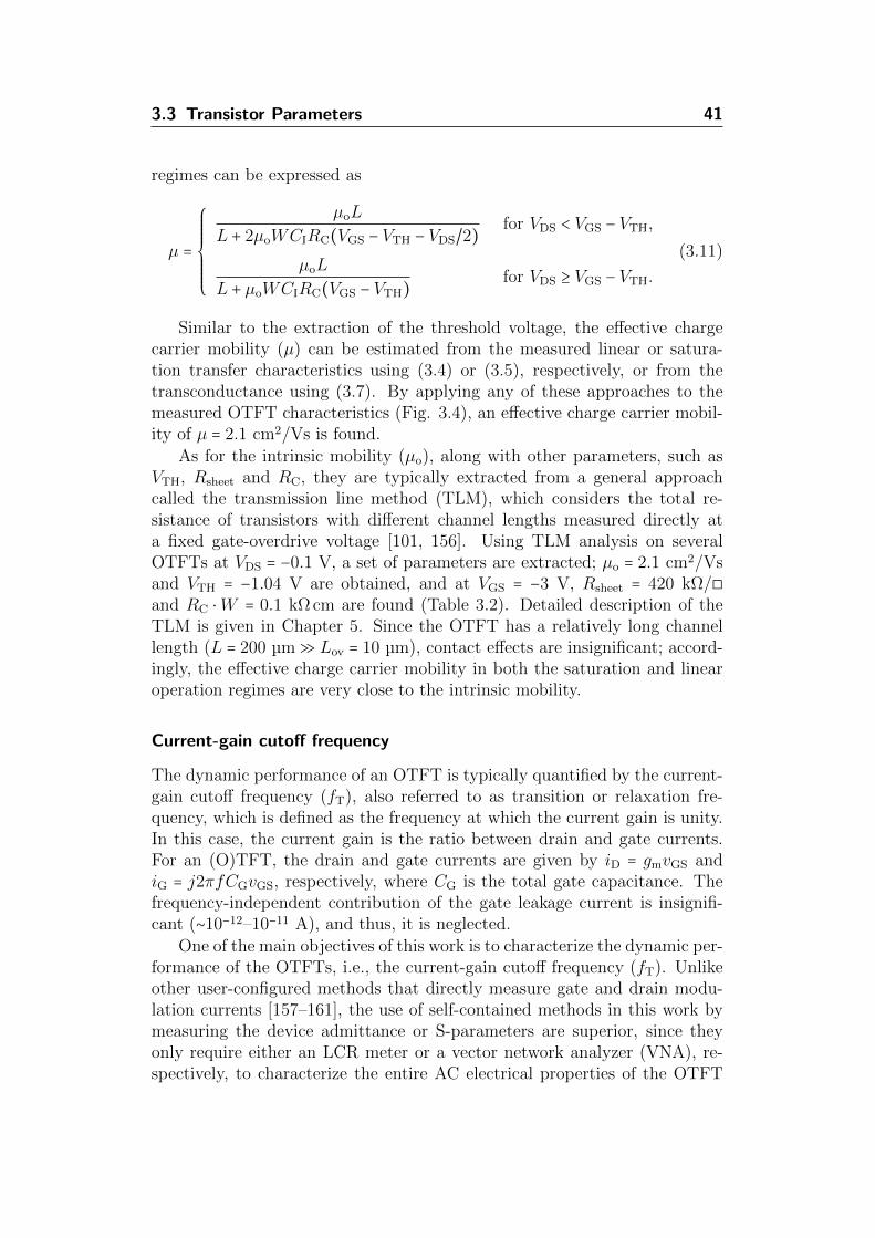
3.3 Transistor Parameters 41
regimes can be expressed as
µ =
⎧⎪⎪⎪⎪⎪⎪⎨⎪⎪⎪⎪⎪⎪⎩
µoL
L + 2µoWCIRC(VGS − VTH − VDS/2)for VDS < VGS − VTH,
µoL
L + µoWCIRC(VGS − VTH)for VDS ≥ VGS − VTH.
(3.11)
Similar to the extraction of the threshold voltage, the effective chargecarrier mobility (µ) can be estimated from the measured linear or satura-tion transfer characteristics using (3.4) or (3.5), respectively, or from thetransconductance using (3.7). By applying any of these approaches to themeasured OTFT characteristics (Fig. 3.4), an effective charge carrier mobil-ity of µ = 2.1 cm2/Vs is found.
As for the intrinsic mobility (µo), along with other parameters, such asVTH, Rsheet and RC, they are typically extracted from a general approachcalled the transmission line method (TLM), which considers the total re-sistance of transistors with different channel lengths measured directly ata fixed gate-overdrive voltage [101, 156]. Using TLM analysis on severalOTFTs at VDS = −0.1 V, a set of parameters are extracted; µo = 2.1 cm2/Vsand VTH = −1.04 V are obtained, and at VGS = −3 V, Rsheet = 420 kΩ/◻and RC ⋅W = 0.1 kΩ cm are found (Table 3.2). Detailed description of theTLM is given in Chapter 5. Since the OTFT has a relatively long channellength (L = 200 µm ≫ Lov = 10 µm), contact effects are insignificant; accord-ingly, the effective charge carrier mobility in both the saturation and linearoperation regimes are very close to the intrinsic mobility.
Current-gain cutoff frequency
The dynamic performance of an OTFT is typically quantified by the current-gain cutoff frequency (fT), also referred to as transition or relaxation fre-quency, which is defined as the frequency at which the current gain is unity.In this case, the current gain is the ratio between drain and gate currents.For an (O)TFT, the drain and gate currents are given by iD = gmvGS andiG = j2πfCGvGS, respectively, where CG is the total gate capacitance. Thefrequency-independent contribution of the gate leakage current is insignifi-cant (∼10−12–10−11 A), and thus, it is neglected.
One of the main objectives of this work is to characterize the dynamic per-formance of the OTFTs, i.e., the current-gain cutoff frequency (fT). Unlikeother user-configured methods that directly measure gate and drain modu-lation currents [157–161], the use of self-contained methods in this work bymeasuring the device admittance or S-parameters are superior, since theyonly require either an LCR meter or a vector network analyzer (VNA), re-spectively, to characterize the entire AC electrical properties of the OTFT
42 3 Organic Thin-Film Transistors
[18, 151]. These characterization techniques, which are used to extract fT,are discussed in detail in Chapters 6 and 7.
Regardless of the device structure (staggered or coplanar) and the fab-rication process (printing or vacuum evaporation), the usual lack of self-alignment OTFT process typically necessitates the design of non-negligibleoverlaps between the source/drain contacts and the gate electrode [144].Therefore, the total gate capacitance of an OTFT is considered as the sumof the channel capacitance (Cch) and the parasitic gate-overlap capacitances(Cov), i.e., CG = Cch + 2Cov ≅ CIW (L + 2Lov). Consequently the current-gaincutoff frequency can be estimated in the saturation regime by the followingexpression:
fT =gm
2πCG
≅µ(VGS − VTH)
2πL(L + 2Lov). (3.12)
This is often designated in literature as the gain-bandwidth product. Us-ing the extracted parameters for the measured OTFT with L = 200 µm andLov = 10 µm (Fig. 3.4): µ = 2.1 cm2/Vs and VTH = −1.08 V, a current-gaincutoff frequency (fT) of 1.46 kHz at VGS = −3 V is calculated. This valueconforms closely to fT = 1.35 kHz that is extracted by means of admittancemeasurements as shown in Chapter 6. Finally, equation (3.12) shows that thecurrent-gain cutoff frequency can be increased by using an (organic) semi-conductor with a higher carrier mobility or by reducing the (O)TFT lateraldimensions, i.e., the channel or gate-overlap lengths [97]. Using an OTFTtechnology based on high-resolution silicon stencil masks, we demonstrate inSection 7.3 a record cutoff frequency of 3.7 MHz for air-stable, high-mobilityp-channel OTFTs with L = 0.6 µm and Lov = 5 µm operating at low supplyvoltages (≤ 3 V).
3.4 STABILITY AND CIRCUITPERFORMANCE MEASURES
The organic semiconductor dinaphtho-thieno-thiophene (DNTT), which wasintroduced by Yamamoto and Takimiya in 2007 [154, 162], is mainly usedin this work as it offers high charge carrier mobility. Haas and co-workersreported a hole mobility as high as 8.3 cm2/Vs and we have measured ahole mobility of 3 cm2/Vs for single-crystal and polycrystalline DNTT-basedTFTs, respectively [97, 163]. This makes DNTT a good candidate for high-performance applications. The potential use of our OTFTs in the market-place, however, depends critically on the uniformity of the transistors andthe ability of the DNTT to sustain its electrical performance without sig-nificant degradation. In general, the electrical stability and performance ofOTFTs depend on how they are fabricated and how the chemical composi-tions of the used materials change over time. The transistors in this work
3.4 Stability and Circuit Performance Measures 43
are fabricated by a new OTFT technology based on high-resolution siliconstencil masks, offering a dramatic performance boost to the circuits throughsub-micrometer channel lengths and far improved device matching.
This section is organized as follows. In the first part, the device uniformityof our OTFTs is demonstrated. In the second part, the shelf-life stability ofthe DNTT during exposure to ambient conditions is explored. In the thirdpart, the dynamic performance of p- and n-channel OTFTs by measuringthe propagation delay of ring oscillators are presented; in addition, a com-parison to the results reported in literature is given. All the measurementsare performed at MPI-SSR in ambient air and at room temperature.
3.4.1 Device Matching
As presented in the previous section, The OTFTs are modeled and character-ized through parametric testing. The resulting (mostly DC) device param-eters either consist of directly measurable observables (currents or voltagesunder specific biasing and environmental conditions), or of derived model pa-rameters such as resistances, capacitances, threshold voltages, current gains,etc. [164]. These parameters and their spreads determine the performancespecs of the OTFTs, including their limits and their performance variations.The functionality of many analog and mixed-signal integrated circuit blocks,such as data converters, comparators, operational amplifiers, depend sub-stantially on the availability of pairs or larger groups of identical transistors(matched transistors). These transistors are typically placed in a close prox-imity and in an identical layout environment. Furthermore, they experiencethe same technological treatment, and thus, they are generally more iden-tical than devices made on different dies at different times in the processlife-cycle. Nevertheless, parametric differences are generally observed evenbetween such matched devices. These parametric mismatches for our OTFTsare discussed herein.
Figure 3.6 depicts the electrical characteristics of 16 DNTT-based p-channel OTFTs with channel lengths of 5 µm fabricated using high-resolutionsilicon stencil masks on the same substrate. The drain current in the out-put characteristics shows a linear increase for small drain-source voltages(VDS < VGS−VTH) and good current saturation for large drain-source voltages(VDS ≥ VGS − VTH). Moreover, the transistors show excellent matching withan average transconductance (normalized to the channel width) of 0.16±0.01Sm−1 and an average threshold voltage (defined as the gate-source voltagefor which ID = 100 pA) of −0.99 ± 0.01 V. The threshold voltage variationis less than one percent with respect to the maximum supply voltage of 3V. From the transfer characteristics, a hole mobility of ∼0.6 cm2/Vs, a sub-threshold slope of 90 mV/dec and an on/off current ratio of more than 108
are extracted.

44 3 Organic Thin-Film Transistors
-3 -2 -1 0-12
-10
-8
-6
-4
-2
0
-3 010
-13
10-11
10-9
10-7
10-5
140 150 160 170 1800
1
2
3
4
5
6
-0.96 -0.98 -1 -1.020
2
4
6
8
10
-2 -1 Gate-source voltage (V)
Dra
in a
nd
gat
e cu
rren
ts (
A)
Dra
in C
urr
ent
(µA
)
Drain-Source Voltage (V)
V = -3.0 VGS
-2.7 V
-2.4 V
-2.1 V
W = 50 µmL = 5 µm
V = -1.5 VDS
Cou
nt
Transconductance (mS/m) Threshold Voltage (V)
Cou
nt
g = 0.16 ± 0.014 S/mm V = -0.99 ± 0.012 VTH
Gate current
Drain current
(a)
-3 0-12
-10
-8
-6
-4
-2
0
-3 -2 -1 010
-13
10-11
10-9
10-7
10-5
140 150 160 170 1800
1
2
3
4
5
6
-0.96 -0.98 -1 -1.020
2
4
6
8
10
Gate-Source Voltage (V)
Dra
in a
nd
Gat
e C
urre
nts
(A)
Dra
in c
urre
nt
(µA
)
-2 -1 Drain-source voltage (V)
V = -3.0 VGS
-2.7 V
-2.4 V
-2.1 V
W = 50 µmL = 5 µm
V = -1.5 VDS
Cou
nt
Transconductance (mS/m) Threshold Voltage (V)
Cou
nt
g = 0.16 ± 0.014 S/mm V = -0.99 ± 0.012 VTH
Gate current
Drain current
(b)
-3 -2 -1 0-12
-10
-8
-6
-4
-2
0
-3 -2 -1 010
-13
10-11
10-9
10-7
10-5
140 150 160 170 1800
1
2
3
4
5
6
-0.96 -0.98 -1 -1.020
2
4
6
8
10
Gate-Source Voltage (V)
Dra
in a
nd G
ate
Cu
rren
ts (
A)
Dra
in C
urr
ent
(µA
)Drain-Source Voltage (V)
V = -3.0 VGS
-2.7 V
-2.4 V
-2.1 V
W = 50 µmL = 5 µm
V = -1.5 VDS
Cou
nt
Transconductance (mS/m) Threshold Voltage (V)
Cou
nt
g = 0.16 ± 0.014 S/mm V = -0.99 ± 0.012 VTH
Gate current
Drain current
(c)
-3 -2 -1 0-12
-10
-8
-6
-4
-2
0
-3 -2 -1 010
-13
10-11
10-9
10-7
10-5
140 150 160 170 1800
1
2
3
4
5
6
0
2
4
6
8
10
Gate-Source Voltage (V)
Dra
in a
nd G
ate
Cu
rren
ts (
A)
Dra
in C
urre
nt
(µA
)Drain-Source Voltage (V)
V = -3.0 VGS
-2.7 V
-2.4 V
-2.1 V
W = 50 µmL = 5 µm
V = -1.5 VDS
Cou
nt
Transconductance (mS/m)
-0.96 -0.98 -1 -1.02 Threshold voltage (V)
Cou
nt
g = 0.16 ± 0.014 S/mm V = -0.99 ± 0.012 VTH
Gate current
Drain current
(d)
Figure 3.6 Measured electrical characteristics of 16 p-channel OTFTs with W =
50 µm and L = 5 µm. (a) Transfer characteristics and gate leakage currents.(b) Output characteristics. (c) Extracted transconductance (gm). (d) Extractedthreshold voltage (VTH) [99].
Furthermore, Fig. 3.7 demonstrates the excellent parameter uniformityof the p-channel OTFTs with channel lengths of 1 and 2 µm. Given thatthe transistors shown in both Figs. 3.6 and 3.7 have the same aspect ra-tio (W /L), all the measurements of the 47 p-channel OTFTs show nearlythe same characteristics. In contrast to the conventional polyimide shadowmask technology, which provides a minimum of 10 µm for both the channellength and the gate-overlap [165], the high-resolution silicon stencil masktechnology allow minimum channel length and gate-overlap down to 0.6 and

3.4 Stability and Circuit Performance Measures 45
-3 010
-13
10-11
10-9
10-7
10-5
-2 -1 Gate-source voltage (V)
Dra
in a
nd g
ate
curr
ents
(A
)
-3 -2 -1 010
-13
10-11
10-9
10-7
10-5
Gate-Source Voltage (V)D
rain
and
Gat
e C
urre
nts
(A)
V = -1.5 VDS V = -1.5 VDS
W = 20 µmL = 2 µm
W = 10 µmL = 1 µm
Gate current
Drain current
(a)
-3 -2 -1 010
-13
10-11
10-9
10-7
10-5
Gate-Source Voltage (V)
Dra
in a
nd G
ate
Cur
rent
s (A
)
-3 010
-13
10-11
10-9
10-7
10-5
-2 -1 Gate-source voltage (V)
Dra
in a
nd g
ate
curr
ents
(A
)
V = -1.5 VDS V = -1.5 VDS
W = 20 µmL = 2 µm
W = 10 µmL = 1 µm
Gate current
Drain current
(b)
Figure 3.7 Measured electrical characteristics of matched transistor arrays. (a)15 p-channel OTFTs with W = 20 µm and L = 2 µm. (b) 16 p-channel OTFTswith W = 10 µm and L = 1 µm [139].
2 µm, respectively [14, 18, 139]. Accordingly, a dramatic improvement ofthe transistors dynamic performance is expected. A comparison between themeasured saturation transfer characteristics of 16 identical p-channel OTFTsfabricated using both the polyimide shadow masks and the silicon stencilmasks is depicted in Fig. 3.8, noting the noticeable edge roughness in thecase of Fig. 3.8a with a channel length of 30 µm in comparison to the verysmooth edges in the case of Fig. 3.8b with a channel length of only 2 µm.The figure shows that the 16 OTFTs with L = 30 µm and fabricated by thepolyimide shadow masks have σI/I = 11%, whereas the 16 OTFTs with L = 2µm and fabricated by the silicon stencil masks have σI/I = 4%.
3.4.2 Air Stability
One of the main challenges in the development of OTFTs is to find a conju-gated semiconductor that provides both a large charge carrier mobility and agood stability during operation in ambient air [106]. Taking for example thesmall-molecule hydrocarbon pentacene, it has been a popular candidate forOTFTs as it can be operated in air and initially provide a relatively largecarrier mobility of about 1 cm2/Vs [166–168]. However, the main problem ofpentacene is that the molecules get easily oxidized in air, and thus, the carriermobility decreases over time when the devices are exposed to oxygen or watervapor (humidity) [169]. In principle, the mobility degradation can be reducedby encapsulation or storage under an inert atmosphere [170, 171]; never-theless, air-stable organic semiconductors are very desirable as they greatly
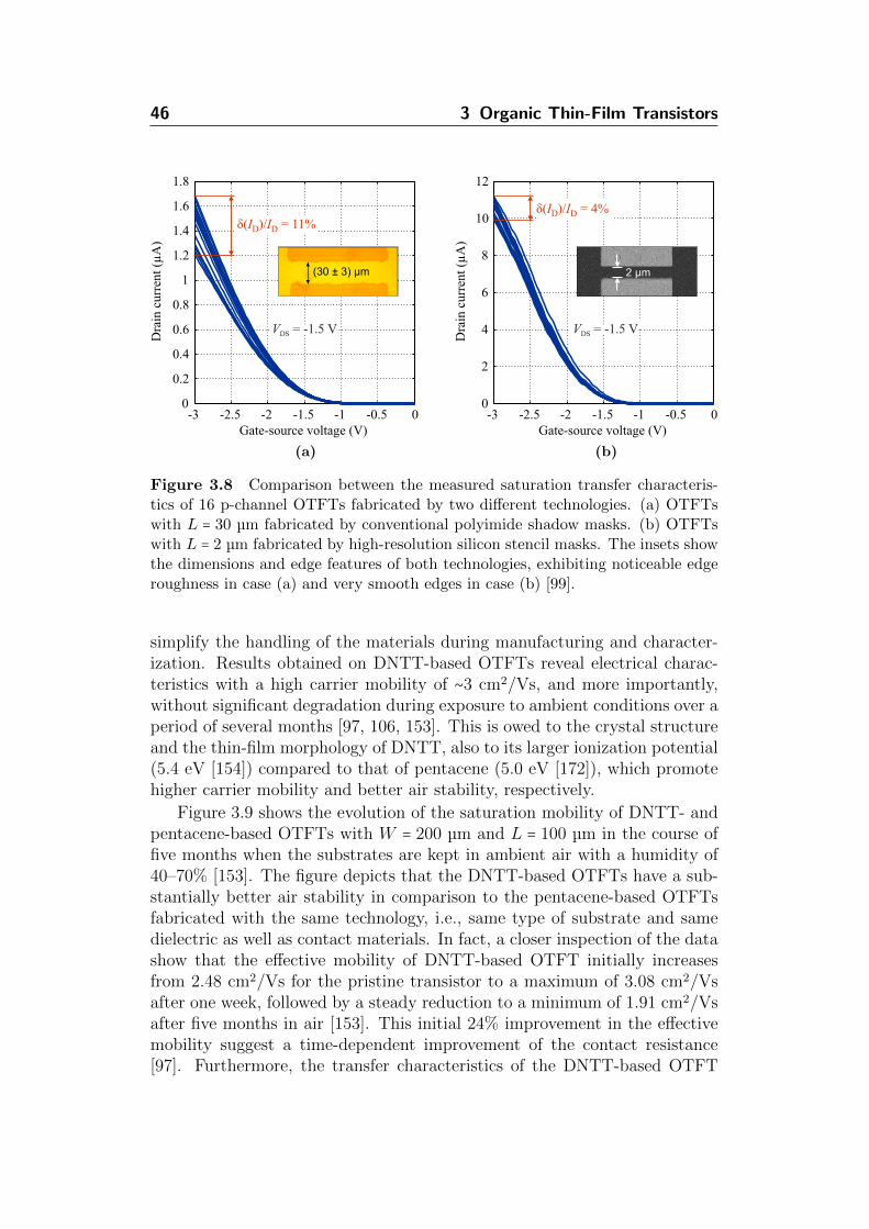
46 3 Organic Thin-Film Transistors
-3 -2.5 -2 -1.5 -1 -0.5 00
0.2
0.4
0.6
0.8
1
1.2
1.4
1.6
1.8
-3 -2.5 -2 -1.5 -1 -0.5 00
2
4
6
8
10
12
(30 µm± 3) 2 µm
V = -1.5 VDS V = -1.5 VDS
Gate-source voltage (V) Gate-source voltage (V)
Dra
in c
urre
nt (
A)
µ
Dra
in c
urre
nt (
µA
)
δ(I )/I = 11%D D
δ(I )/I = 4%D D
(a)
-3 -2.5 -2 -1.5 -1 -0.5 00
0.2
0.4
0.6
0.8
1
1.2
1.4
1.6
1.8
-3 -2.5 -2 -1.5 -1 -0.5 00
2
4
6
8
10
12
(30 µm± 3) 2 µm
V = -1.5 VDS V = -1.5 VDS
Gate-source voltage (V) Gate-source voltage (V)
Dra
in c
urre
nt (
A)
µ
Dra
in c
urre
nt (
µA
)
δ(I )/I = 11%D D
δ(I )/I = 4%D D
(b)
Figure 3.8 Comparison between the measured saturation transfer characteris-tics of 16 p-channel OTFTs fabricated by two different technologies. (a) OTFTswith L = 30 µm fabricated by conventional polyimide shadow masks. (b) OTFTswith L = 2 µm fabricated by high-resolution silicon stencil masks. The insets showthe dimensions and edge features of both technologies, exhibiting noticeable edgeroughness in case (a) and very smooth edges in case (b) [99].
simplify the handling of the materials during manufacturing and character-ization. Results obtained on DNTT-based OTFTs reveal electrical charac-teristics with a high carrier mobility of ∼3 cm2/Vs, and more importantly,without significant degradation during exposure to ambient conditions over aperiod of several months [97, 106, 153]. This is owed to the crystal structureand the thin-film morphology of DNTT, also to its larger ionization potential(5.4 eV [154]) compared to that of pentacene (5.0 eV [172]), which promotehigher carrier mobility and better air stability, respectively.
Figure 3.9 shows the evolution of the saturation mobility of DNTT- andpentacene-based OTFTs with W = 200 µm and L = 100 µm in the course offive months when the substrates are kept in ambient air with a humidity of40–70% [153]. The figure depicts that the DNTT-based OTFTs have a sub-stantially better air stability in comparison to the pentacene-based OTFTsfabricated with the same technology, i.e., same type of substrate and samedielectric as well as contact materials. In fact, a closer inspection of the datashow that the effective mobility of DNTT-based OTFT initially increasesfrom 2.48 cm2/Vs for the pristine transistor to a maximum of 3.08 cm2/Vsafter one week, followed by a steady reduction to a minimum of 1.91 cm2/Vsafter five months in air [153]. This initial 24% improvement in the effectivemobility suggest a time-dependent improvement of the contact resistance[97]. Furthermore, the transfer characteristics of the DNTT-based OTFT
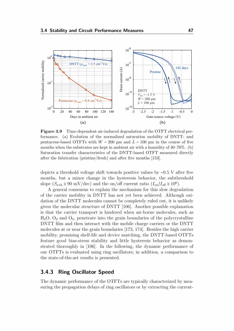
3.4 Stability and Circuit Performance Measures 47
0 20 40 60 80 100 120 14010
-2
10-1
100
Days in ambient air
Nor
mal
ized
car
rier
mob
ilit
y
-3 -2.5 -2 -1.5 -1 -0.5 0
10-13
10-11
10-9
10-7
10-5
Gate-source voltage (V)D
rain
cur
rent
(A
)
2DNTT (µ = 2.5 cm /Vs)start
Pentacene 2
(µ = 0.8 cm /Vs)start
Pristine142 days
DNTTV = -1.5 VDS
W = 200 µmL = 100 µm
(a)
0 20 40 60 80 100 120 14010
-2
10-1
100
Days in ambient air
Nor
mal
ized
car
rier
mob
ilit
y
-3 -2.5 -2 -1.5 -1 -0.5 0
10-13
10-11
10-9
10-7
10-5
Gate-source voltage (V)D
rain
cur
rent
(A
)
2DNTT (µ = 2.5 cm /Vs)start
Pentacene 2
(µ = 0.8 cm /Vs)start
Pristine142 days
DNTTV = -1.5 VDS
W = 200 µmL = 100 µm
(b)
Figure 3.9 Time-dependent air-induced degradation of the OTFT electrical per-formance. (a) Evolution of the normalized saturation mobility of DNTT- andpentacene-based OTFTs with W = 200 µm and L = 100 µm in the course of fivemonths when the substrates are kept in ambient air with a humidity of 40–70%. (b)Saturation transfer characteristics of the DNTT-based OTFT measured directlyafter the fabrication (pristine/fresh) and after five months [153].
depicts a threshold voltage shift towards positive values by ∼0.5 V after fivemonths, but a minor change in the hysteresis behavior, the subthresholdslope (Ss-th ≅ 90 mV/dec) and the on/off current ratio (Ion/Ioff ≅ 106).
A general consensus to explain the mechanism for this slow degradationof the carrier mobility in DNTT has not yet been achieved. Although oxi-dation of the DNTT molecules cannot be completely ruled out, it is unlikelygiven the molecular structure of DNTT [106]. Another possible explanationis that the carrier transport is hindered when air-borne molecules, such asH2O, O2 and O3, penetrate into the grain boundaries of the polycrystallineDNTT film and then interact with the mobile charge carriers or the DNTTmolecules at or near the grain boundaries [173, 174]. Besides the high carriermobility, promising shelf-life and device matching, the DNTT-based OTFTsfeature good bias-stress stability and little hysteresis behavior as demon-strated thoroughly in [106]. In the following, the dynamic performance ofour OTFTs is evaluated using ring oscillators; in addition, a comparison tothe state-of-the-art results is presented.
3.4.3 Ring Oscillator Speed
The dynamic performance of the OTFTs are typically characterized by mea-suring the propagation delays of ring oscillators or by extracting the current-
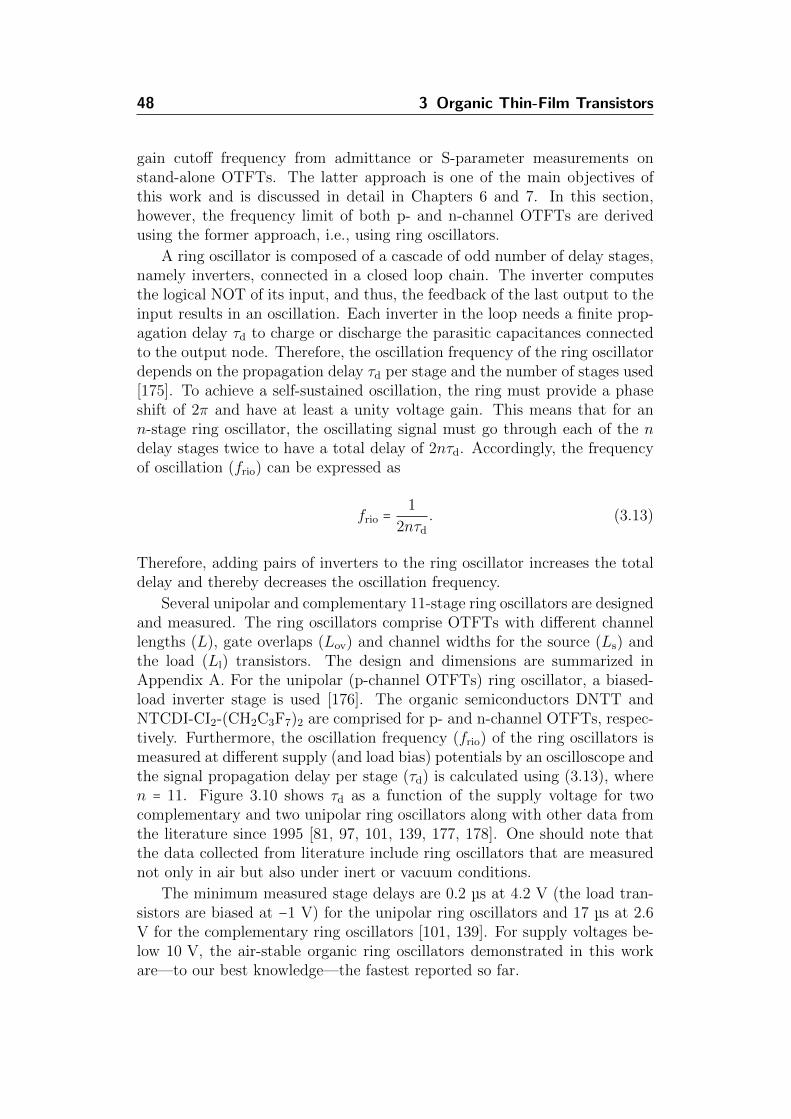
48 3 Organic Thin-Film Transistors
gain cutoff frequency from admittance or S-parameter measurements onstand-alone OTFTs. The latter approach is one of the main objectives ofthis work and is discussed in detail in Chapters 6 and 7. In this section,however, the frequency limit of both p- and n-channel OTFTs are derivedusing the former approach, i.e., using ring oscillators.
A ring oscillator is composed of a cascade of odd number of delay stages,namely inverters, connected in a closed loop chain. The inverter computesthe logical NOT of its input, and thus, the feedback of the last output to theinput results in an oscillation. Each inverter in the loop needs a finite prop-agation delay τd to charge or discharge the parasitic capacitances connectedto the output node. Therefore, the oscillation frequency of the ring oscillatordepends on the propagation delay τd per stage and the number of stages used[175]. To achieve a self-sustained oscillation, the ring must provide a phaseshift of 2π and have at least a unity voltage gain. This means that for ann-stage ring oscillator, the oscillating signal must go through each of the ndelay stages twice to have a total delay of 2nτd. Accordingly, the frequencyof oscillation (frio) can be expressed as
frio =1
2nτd
. (3.13)
Therefore, adding pairs of inverters to the ring oscillator increases the totaldelay and thereby decreases the oscillation frequency.
Several unipolar and complementary 11-stage ring oscillators are designedand measured. The ring oscillators comprise OTFTs with different channellengths (L), gate overlaps (Lov) and channel widths for the source (Ls) andthe load (Ll) transistors. The design and dimensions are summarized inAppendix A. For the unipolar (p-channel OTFTs) ring oscillator, a biased-load inverter stage is used [176]. The organic semiconductors DNTT andNTCDI-CI2-(CH2C3F7)2 are comprised for p- and n-channel OTFTs, respec-tively. Furthermore, the oscillation frequency (frio) of the ring oscillators ismeasured at different supply (and load bias) potentials by an oscilloscope andthe signal propagation delay per stage (τd) is calculated using (3.13), wheren = 11. Figure 3.10 shows τd as a function of the supply voltage for twocomplementary and two unipolar ring oscillators along with other data fromthe literature since 1995 [81, 97, 101, 139, 177, 178]. One should note thatthe data collected from literature include ring oscillators that are measurednot only in air but also under inert or vacuum conditions.
The minimum measured stage delays are 0.2 µs at 4.2 V (the load tran-sistors are biased at −1 V) for the unipolar ring oscillators and 17 µs at 2.6V for the complementary ring oscillators [101, 139]. For supply voltages be-low 10 V, the air-stable organic ring oscillators demonstrated in this workare—to our best knowledge—the fastest reported so far.
3.5 Summary 49
100
101
102
10-7
10-6
10-5
10-4
10-3
10-2
10-1
100
Supply voltage (V)
Sig
nal
dela
y pe
r st
age
(s)
100
101
102
10-7
10 -6
10-5
10-4
10 -3
10-2
10-1
100
Supply voltage (V)S
igna
l de
lay
per
stag
e (s
)
L = 4 µm, L = 20 ov µm
L = 1 µm, L = 5 µmov
Literature
(a)
100
101
102
10-7
10-6
10-5
10-4
10-3
10-2
10-1
100
Supply voltage (V)
Sig
nal
dela
y pe
r st
age
(s)
100
101
102
10-7
10 -6
10-5
10-4
10 -3
10-2
10-1
100
Supply voltage (V)S
igna
l de
lay
per
stag
e (s
)
L = 4 µm, L = 20 ov µm
L = 1 µm, L = 5 µmov
Literature
(b)
Figure 3.10 Signal propagation delay per stage as a function of supply voltageof (a) unipolar and (b) complementary organic ring oscillators. The measureddata for the 11-stage ring oscillators are given in blue (L = 4 µm, Lov = 20 µm,Wsource/Wload = 110 µm/24 µm for unipolar, and Wn-channel/Wp-channel = 80 µm/40µm for complementary) and red (L = 1 µm, Lov = 5 µm, Wsource/Wload = 72 µm/24µm for unipolar, and Wn-channel/Wp-channel = 80 µm/40 µm for complementary)colors [101, 139]. The air-stable organic semiconductors employed for the p- andn-channel OTFTs are DNTT and NTCDI-CI2-(CH2C3F7)2, respectively. The datagiven in black color are collected from literature since 1995 [81, 97, 177, 178].
3.5 SUMMARY
The processing method used for the fabrication of OTFTs in addition tothe device architecture and materials play a significant role in realizing thedesired electrical performance. Only small-molecule organic semiconductors,namely DNTT for p-channel and F16CuPc or NTCDI-CI2-(CH2C3F7)2 forn-channel OTFTs are considered. The p-channel OTFTs, in particular, aremostly employed as they are more stable and offer higher carrier mobilitythan their n-channel contenders. The inverted-staggered (bottom-gate, top-contact) TFT configuration, which benefits from a smooth dielectric/semi-conductor interface and provides a small contact resistance, is selected forour OTFTs. The transistors are fabricated by high-resolution silicon stencilmasks, allowing to pattern the OTFT layers with sub-micrometer accuracyand without the need of solvents or elevated temperatures. The OTFTs fea-ture excellent device uniformity, promising shelf-life and bias-stress stability,as well as little hysteresis behavior. Organic unipolar and complementaryring oscillators are fabricated and the measured signal delay per stage forboth are the lowest reported values at supply voltages below 10 V.
4Fabrication Process
This chapter addresses the fabrication process of the low-voltage submicrom-eter OTFTs using vacuum evaporation through high-resolution silicon stencilmasks. A brief overview of the different deposition and patterning techniquesis presented and the reasons of using the stencil lithography, in particular, areexplained herein. The stencil masks and the OTFTs are fabricated at IMSCHIPS and MPI-SSR, respectively. Characterization of the stencil maskswith respect to refurbishment, defects and uniformity, as part of this work,are discussed in detail. Importance is also given to the design rules of thephysical layout. Finally, the design of three mask sets is introduced.
4.1 DEPOSITION AND PATTERNING TECHNIQUES
A wide range of fabrication techniques can be used for organic electronics,particularly organic thin-film transistors. The key challenge now is to in-tegrate the organic devices using a cost-effective process at an acceptableyield, resolution and registration. A reasonable classification of the fabrica-tion processes can be made according to the the deposition technique, namelyvapor or solution processing [3]. The vapor deposition typically yields smallerdimensions and thus higher thin-film transistor performance. The solutionprocessing, however, is preferable for high-volume, low-cost production. Asa rule of thumb, processes with higher resolution often have a lower through-put. Furthermore, solution processing simplifies the manufacturing processcompared to vapor deposition, especially for large areas. It is preferable thatall layers, and not only the organic semiconductor, are processed from solu-tion. Besides the deposition, solution processing opens up various alternativepatterning techniques such as printing, stamping and selective dewetting.Other typical patterning methods used for the fabrication of organic devicesare photolithography, stencil lithography and laser ablation. In principle,there is no single standard fabrication process existing today for organic de-vices and circuitry; however, different deposition and patterning techniquesare often combined to optimize for the requirement of each device and/orthin-film layer.
Organic materials are deposited at or near room temperature. Therefore,the fabrication may involve a host number of unconventional large area, flex-ible or transparent substrates such as glass, paper, textile or plastic films.
50

4.1 Deposition and Patterning Techniques 51
Each of these substrates has its individual strengths and weaknesses in pro-cessability, appearance, yield, lifetime, scalability, sustainability and cost.The appropriate substrate is chosen depending on the target application,functional materials and fabrication technique. Flexible substrates, in par-ticular low-cost, low-temperature plastic substrates such as PET and PEN,limit the process temperature window to achieve the optimum material per-formance and stability to less than 150 [3]. Otherwise, the substrate wouldexhibit significant distortion when exposed to excess temperatures and insome cases also when exposed to excess humidity variations or mechanicalstress. If these distortions occurred during device processing in between thedeposition and patterning of two layers, an undesired change in the dimen-sions would be resulted and thus malfunctioning might occur.
In former times, it was very convenient to take advantage of the well-established inorganic-based fabrication techniques such as oxidation and pho-tolithography. In this context, the OTFTs are built on a highly doped siliconwafer that serves as a global bottom gate. The gate dielectric is thermallygrown and then the source/drain contacts are patterned using photolithog-raphy. The organic semiconducting layer is in this case deposited lastly onthe top to avoid exposure to high temperatures. This results in an invertedcoplanar OTFT configuration. However, such process would not make use ofthe unique properties of the organic semiconductors such as the mechanicalflexibility.
The ability to develop materials with well defined structural, chemical,physical or biological functionality that can be processed from solution hasenabled the possibility to adapt graphic art printing techniques to manufac-ture functional devices and circuits [3]. Examples of printing techniques thatcan be used to process functional materials are flexographic, rotogravure,offset, screen and inkjet printing. However, numerous technological diffi-culties need first to be overcome before reliable electronic products can beproduced by commercial printing techniques. For example, to fabricate all-printed OTFTs, a complete set of solution-processable functional materialsmust be developed to meet the required processing conditions and desiredperformance criteria. This includes not only semiconductors, conductors anddielectrics, but also planarization, passivation and isolation materials. Fur-thermore, the printing equipment and processes must also be improved tomeet the rather strict design rules of OTFTs. The typical resolution capa-bility of printing processes is in the range of 20–100 µm.
An alternative to the above printing methods is printing by thermal imag-ing [3]. It is a digital technique used by the proofing industry and proceedsvia the laser-ablative transfer of solid layers. Therefore, the limitations ofchemical compatibility in solution-based printing are entirely avoided. Inthis process, a fully addressable laser beam is directed to a donor film, whichis coated with the material to be printed (e.g. conducting layer). A light-to-

52 4 Fabrication Process
heat conversion takes place, decomposing an ejecting layer, which is placedin between the donor substrate and the target material, into gaseous state.As a result, a high-temperature bubble is generated that pushes the targetfilm to the substrate with the desired pattern. This fabrication method iscompatible with flexible substrates and enables printing of areas up to about1 m2 with a resolution down to 5 µm.
For cost-driven applications, such as RFID tags, printing methods aremost prominent. At present, silicon RFID tags have relatively high costs (inthe range of $0.2). As a result, their use is limited only to applications thatcan tolerate their price level such as access control and animal tagging. Toenable ubiquitous replacement of optical barcodes by RFID tags (maybe in-tegrated with smart sensors), manufacturing solutions for integrated circuitsthat can be printed directly onto the packaging or an adhesive label at acost of $0.01 or less must be found [3]. An ultimate goal here is to developa commercial reel-to-reel solution-based printing technology to manufactureultra-low cost electronics. However, to allow an early market entry for theorganic technology and to investigate its performance limits, industrial com-panies as well as research facilities tend to use standard, mature processingtechniques such as spin coating followed by photolithography (solution-basedprocess) or evaporation through stencil masks (vapor-based process).
On the other hand, high-performance organic devices, especially thosethat are based on small-molecule organic compounds, are fabricated usingvapor-based processes. The pattern definition in this case takes place bystencil lithography using shadow masks. The shadow mask is a thin mem-brane with a pattern cut out of it, through which the compounds can bedeposited on the substrate. Unlike photolithography, this process does notinvolve any heat or chemical treatment of the substrates.
Conventional vacuum thermal evaporation (VTE) is a commonly usedvapor-based deposition technique. It is a high-vacuum evaporation process,where the functional material evaporates from a hot source (e.g. heatingfilament) and condenses on the target substrate (e.g. glass). The vacuumallows the vapor particles to travel directly to the substrate without collisionwith the background gas and thus prevents any contamination of parasiticsurfaces. VTE is an ideal technique for laboratory usage but it has limitationsin scalability and cost effective manufacturing capabilities.
For industrial scale fabrication, however, organic vapor phase deposition(OVPD) is a prominent solution. OVPD employs the gas-phase transportprinciple, in which the evaporation and the condensation are decoupled. Con-sequently, the evaporation design can be optimized to any chemical needswithout affecting the design for uniform and controlled large-area organicfilm deposition [3]. In this process, the organic materials are evaporated inindividual and decoupled quartz pipes and then carried to the cooled targetsubstrate using an inert carrier gas (e.g. nitrogen). Two or more organic
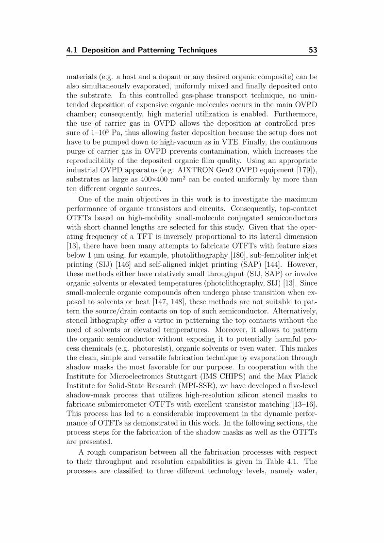
4.1 Deposition and Patterning Techniques 53
materials (e.g. a host and a dopant or any desired organic composite) can bealso simultaneously evaporated, uniformly mixed and finally deposited ontothe substrate. In this controlled gas-phase transport technique, no unin-tended deposition of expensive organic molecules occurs in the main OVPDchamber; consequently, high material utilization is enabled. Furthermore,the use of carrier gas in OVPD allows the deposition at controlled pres-sure of 1–103 Pa, thus allowing faster deposition because the setup does nothave to be pumped down to high-vacuum as in VTE. Finally, the continuouspurge of carrier gas in OVPD prevents contamination, which increases thereproducibility of the deposited organic film quality. Using an appropriateindustrial OVPD apparatus (e.g. AIXTRON Gen2 OVPD equipment [179]),substrates as large as 400×400 mm2 can be coated uniformly by more thanten different organic sources.
One of the main objectives in this work is to investigate the maximumperformance of organic transistors and circuits. Consequently, top-contactOTFTs based on high-mobility small-molecule conjugated semiconductorswith short channel lengths are selected for this study. Given that the oper-ating frequency of a TFT is inversely proportional to its lateral dimension[13], there have been many attempts to fabricate OTFTs with feature sizesbelow 1 µm using, for example, photolithography [180], sub-femtoliter inkjetprinting (SIJ) [146] and self-aligned inkjet printing (SAP) [144]. However,these methods either have relatively small throughput (SIJ, SAP) or involveorganic solvents or elevated temperatures (photolithography, SIJ) [13]. Sincesmall-molecule organic compounds often undergo phase transition when ex-posed to solvents or heat [147, 148], these methods are not suitable to pat-tern the source/drain contacts on top of such semiconductor. Alternatively,stencil lithography offer a virtue in patterning the top contacts without theneed of solvents or elevated temperatures. Moreover, it allows to patternthe organic semiconductor without exposing it to potentially harmful pro-cess chemicals (e.g. photoresist), organic solvents or even water. This makesthe clean, simple and versatile fabrication technique by evaporation throughshadow masks the most favorable for our purpose. In cooperation with theInstitute for Microelectronics Stuttgart (IMS CHIPS) and the Max PlanckInstitute for Solid-State Research (MPI-SSR), we have developed a five-levelshadow-mask process that utilizes high-resolution silicon stencil masks tofabricate submicrometer OTFTs with excellent transistor matching [13–16].This process has led to a considerable improvement in the dynamic perfor-mance of OTFTs as demonstrated in this work. In the following sections, theprocess steps for the fabrication of the shadow masks as well as the OTFTsare presented.
A rough comparison between all the fabrication processes with respectto their throughput and resolution capabilities is given in Table 4.1. Theprocesses are classified to three different technology levels, namely wafer,
54 4 Fabrication Process
Table 4.1 Comparison between the fabrication processes used for organic elec-tronics with respect to resolution and throughput. Data is adopted from [3, 181].
Technology Level Fabrication Process Feature Size Throughput(µm) (m2/s)
Wafer VTEa 1–10 <10−4
OVPD 5–20 <10−4
Hybrid Rotary Photolithography 3–5 10−4–10−1
Thermal Imaging 5–40 10−4–10−3
Inkjet Printing 15–50 10−3–1Screen Printing 20–100 10−2–10
Continuous Offset Printing 10–50 1–102
Rotogravure Printing 20–80 10−1–102
Flexographic Printing 40–80 1–102
aUsing high-resolution silicon stencil masks, it is also feasible to fabricate sub-micrometer feature sizes as demonstrated in Chapter 7.
hybrid and continuous technologies [181]. First, the wafer technologies arethose that allow the fabrication of high resolution features but at relativelyhigh production cost; however, they are compatible with mechanically flexiblesubstrates and can be extended to rotary (sheet-to-sheet) processes. Second,the hybrid technologies are those that include large-area processes that makeuse of flexible substrates and/or produced at medium cost level. Finally,the continuous technologies are the reel-to-reel processes that enable high-volume, low-cost mass production but so far with medium resolution.
4.2 SILICON STENCIL MASKS
Stencil masks, which are also referred to as shadow masks, are used in sten-cil lithography to fabricate micro- and nano-meter scale patterns. A stencilmask is a membrane with a pattern cut out of it, through which evaporatedor sputtered particles can be deposited marking the same pattern on the sub-strate. In principle, there are numerous application areas for stencil masksand they vary from medical cell filters to exposure masks for semiconduc-tor lithography. Depending on the used radiation, which can be photons,charged particles, or atoms, different technical implementations of stencilmasks are reported in literature. For example, they have been exploited inclassical beam shaping in semiconductor applications for silicon wafer resistexposures with single/multi e-beam lithography [182], ion-beam lithography[183], ion-assisted etching and milling [184] and ion-implantation for pat-terned magnetic media [185].
4.2 Silicon Stencil Masks 55
The quality of the stencil masks is very critical as they define the finalpattern properties, including minimum feature size and line edge roughness,thus directly affecting the device performance. Different materials have beenexplored for the fabrication of stencil masks such as metals, polymers andsilicon nitride; however, these materials suffer from patterning and stabilityproblems for membrane areas above 100 mm2. As a result, monocrystallinesilicon stencil masks are selected for this study as they offer virtues withrespect to mechanical stability, stiffness and nano-patterning capability [15].
A novel silicon stencil mask process flow is developed at IMS CHIPS forthe fabrication of OTFTs. This groundbreaking work in cooperation withthe MPI-SSR led to a considerable improvement in the device uniformity andperformance [14, 15]. One should note that the stencil mask properties arechanging during operation due to an interaction between the used radiationand the mask itself. This produces stress variations within the membraneand changes in the critical dimensions (CD) of the mask pattern due toresidues in the openings, which worsen the image of the stencil mask duringillumination. During the fabrication of the OTFTs, materials are continu-ously deposited onto the mask membrane and stencil openings, which resultsin clogging, stress induced pattern distortions and membrane deformations[15]. Therefore, etching of the deposited materials, cleaning and inspectionis mandatory to maintain a good pattern fidelity. The silicon stencil maskprocess flow is explained in detail in this section. Furthermore, details aboutminimum feature sizes, refurbishment and defects, which are part of thiswork, are presented.
4.2.1 Fabrication Process
The fabrication of the stencil masks can be implemented in two techniques,namely membrane flow process (MFP) and wafer flow process (WFP) [186,187]. In the MFP, a membrane has to be first prepared from a solid wafer,then all the patterning processes are applied on the membrane. In the WFP,however, all the critical patterning steps are carried out on the solid wafersubstrate and the membrane etching is applied later. The latter option isfavorable for our purpose because it is compatible with the standard processtools and silicon wafer fabrication processes.
The fabrication process of the silicon stencil masks is described in detailin Table 4.2 and a corresponding illustration is depicted in Fig. 4.1. A 150mm (6 inch) silicon-on-insulator (SOI) wafer is used as a base substrate. Theburied silicon oxide layer serves as an etch stop for the stencil etching fromthe wafer frontside and the membrane etching from the wafer backside. Thisoffers a clear separation between the microelectrical patterning steps and themicromechanical membrane etching steps. As a result, risk of contaminationis significantly reduced.
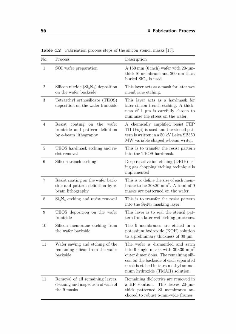
56 4 Fabrication Process
Table 4.2 Fabrication process steps of the silicon stencil masks [15].
No. Process Description
1 SOI wafer preparation A 150 mm (6 inch) wafer with 20-µm-thick Si membrane and 200-nm-thickburied SiO2 is used.
2 Silicon nitride (Si3N4) depositionon the wafer backside
This layer acts as a mask for later wetmembrane etching.
3 Tetraethyl orthosilicate (TEOS)deposition on the wafer frontside
This layer acts as a hardmask forlater silicon trench etching. A thick-ness of 1 µm is carefully chosen tominimize the stress on the wafer.
4 Resist coating on the waferfrontside and pattern definitionby e-beam lithography
A chemically amplified resist FEP171 (Fuji) is used and the stencil pat-tern is written in a 50 kV Leica SB350MW variable shaped e-beam writer.
5 TEOS hardmask etching and re-sist removal
This is to transfer the resist patterninto the TEOS hardmask.
6 Silicon trench etching Deep reactive ion etching (DRIE) us-ing gas chopping etching technique isimplemented
7 Resist coating on the wafer back-side and pattern definition by e-beam lithography
This is to define the size of each mem-brane to be 20×20 mm2. A total of 9masks are patterned on the wafer.
8 Si3N4 etching and resist removal This is to transfer the resist patterninto the Si3N4 masking layer.
9 TEOS deposition on the waferfrontside
This layer is to seal the stencil pat-tern from later wet etching processes.
10 Silicon membrane etching fromthe wafer backside
The 9 membranes are etched in apotassium hydroxide (KOH) solutionto a preliminary thickness of 30 µm.
11 Wafer sawing and etching of theremaining silicon from the waferbackside
The wafer is dismantled and sawninto 9 single masks with 30×30 mm2
outer dimensions. The remaining sili-con on the backside of each separatedmask is etched in tetra methyl ammo-nium hydroxide (TMAH) solution.
11 Removal of all remaining layers,cleaning and inspection of each ofthe 9 masks
Remaining dielectrics are removed ina HF solution. This leaves 20-µm-thick patterned Si membranes an-chored to robust 5-mm-wide frames.
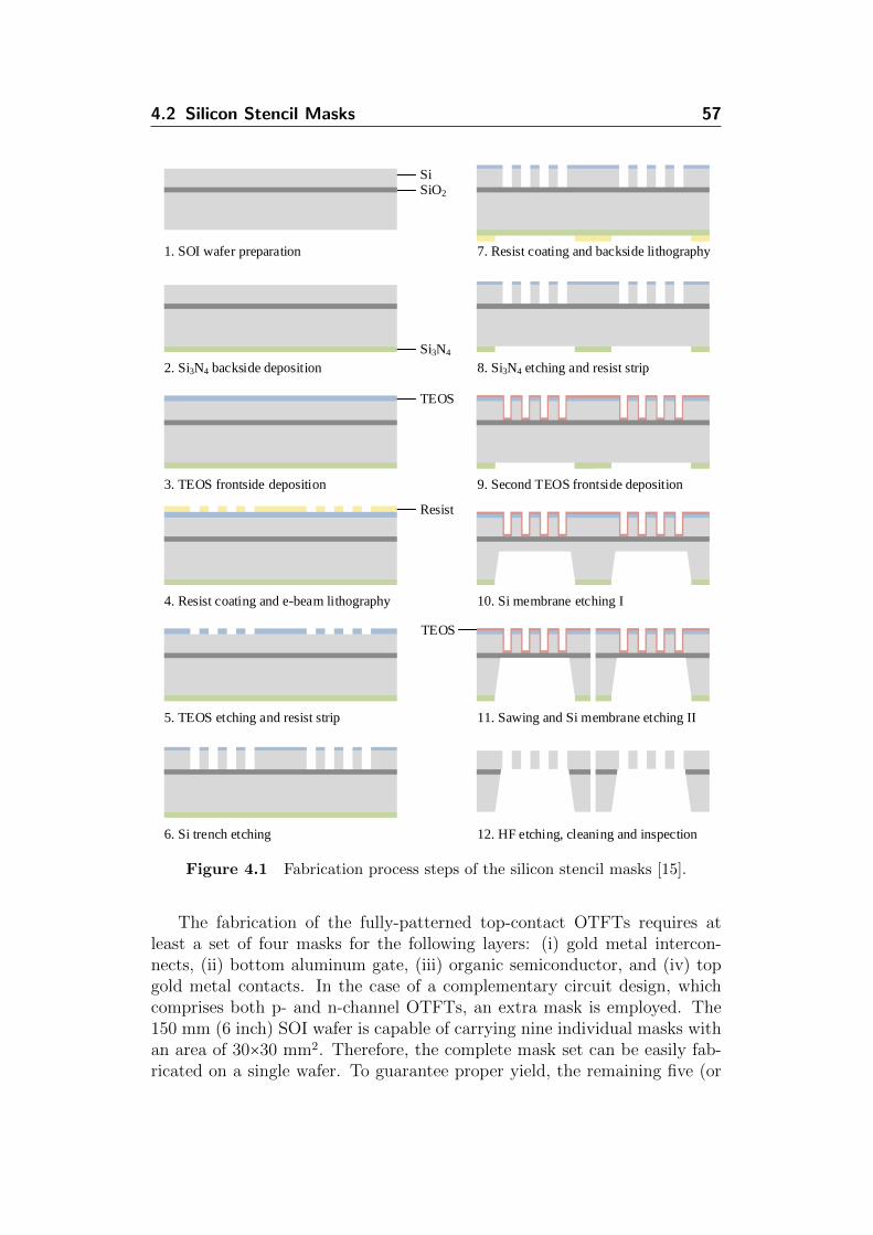
4.2 Silicon Stencil Masks 57
Resist
TEOS
Si3N4
1. SOI wafer preparation
2. Si3N4 backside deposition
3. TEOS frontside deposition
4. Resist coating and e-beam lithography
5. TEOS etching and resist strip
6. Si trench etching
7. Resist coating and backside lithography
8. Si3N4 etching and resist strip
9. Second TEOS frontside deposition
10. Si membrane etching I
SiSiO2
TEOS
12. HF etching, cleaning and inspection
11. Sawing and Si membrane etching II
Figure 4.1 Fabrication process steps of the silicon stencil masks [15].
The fabrication of the fully-patterned top-contact OTFTs requires atleast a set of four masks for the following layers: (i) gold metal intercon-nects, (ii) bottom aluminum gate, (iii) organic semiconductor, and (iv) topgold metal contacts. In the case of a complementary circuit design, whichcomprises both p- and n-channel OTFTs, an extra mask is employed. The150 mm (6 inch) SOI wafer is capable of carrying nine individual masks withan area of 30×30 mm2. Therefore, the complete mask set can be easily fab-ricated on a single wafer. To guarantee proper yield, the remaining five (or

58 4 Fabrication Process
41 42
31 32
21 22
11
43 44
33 34
23 24
13 1412
45
35
25
15
46
36
26
16
51 52 53 54 55 56
47
37
27
17
57
W = 2 µm
W = 5 µm
W = 10 µm
W = 20 µm
W = 30 µm
W = 50 µm
W = 100 µm
Lg = 100 µm
Figure 4.2 Simplified layout of the test mask, containing a matrix of 5×7 cells,where each cell has seven row modules for the source/drain contacts with channelwidths (W ) of 2–100 µm and channel lengths (L) of 4, 2, 1, 0.9, 0.8, 0.7, 0.6, 0.5,0.4 and 0.3 µm, and one row module for the gate patterns with lengths (Lg) of 100µm and widths (Wg) of 8, 6, 4, 2, 1, 0.8, 0.6, 0.5, 0.4 and 0.3 µm.
four) slots on the wafer are utilized for mask duplicates, especially for thelast mask, i.e., the top gold metal contacts mask, which has the most criticalstructures with the minimum feature size. The design rules for the physicallayout of a particular circuit, which are necessary to ensure a successful fab-rication, are discussed in Section 4.4. Furthermore, the different mask setsdesigned for this work are presented in Section 4.5.
In the following, emphasis is made on the characterization of the siliconstencil masks, with respect to refurbishment, defect analysis and uniformityof evaporated patterns, to achieve a good pattern fidelity and a cost effectivemask technology. To carry out this study on the manufacturing process, aspecial testing mask is designed thereto. Figure 4.2 shows the layout of thismask, containing a matrix of source/drain and gate patterns with variousdimensions. The mask comprises a total of 5×7 cells that cover the com-plete active mask area, where each cell has eight row modules (seven for thesource/drain and one for the gate patterns). The source/drain patterns havechannel widths and lengths of 100–2 µm and 4–0.3 µm, respectively, whereasthe gate patterns have widths of 8–0.3 µm and lengths of 100 µm.
4.2.2 Refurbishment
For the fabrication of the OTFTs, two different metals, i.e., aluminum andgold, are used to define the gate and the source/drain contacts. Therefore,two different wet-chemical metal etching processes are developed at IMS

4.2 Silicon Stencil Masks 59
0.6 µm 0.6 µm 0.6 µm 0.6 µm
(a)
0.6 µm 0.6 µm 0.6 µm 0.6 µm
(b)
0.6 µm 0.6 µm 0.6 µm 0.6 µm
(c)
0.6 µm 0.6 µm 0.6 µm 0.6 µm
(d)
Figure 4.3 SEM top-down images of a 0.5-µm-wide isolated line (bridge) in thesilicon stencil mask. (a) Initially before any processing. (b) After the depositionof 0.2-µm-thick gold layer. (c) After the deposition of 0.5-µm-thick gold layer. (d)After gold etching [15].
1 µm 1 µm 1 µm 1 µm
(a)
1 µm 1 µm 1 µm 1 µm
(b)
1 µm 1 µm 1 µm 1 µm
(c)
1 µm 1 µm 1 µm 1 µm
(d)
Figure 4.4 SEM top-down images of a 2-µm-wide isolated space (hole) in thesilicon stencil mask. (a) Initially before any processing. (b) After the deposition of0.1-µm-thick aluminum layer. (c) After the deposition of 0.3-µm-thick aluminumlayer. (d) After aluminum etching [15].
CHIPS for the selective removal of the two metals to the base silicon stencilmask material [15]. This is necessary to ensure a cost effective and multipleusage of the silicon stencil masks in the deposition processes. To evaluatethe reliability of the etching processes, initial CD measurements are carriedout for two silicon stencil masks, then after aluminum and gold depositionsteps, and finally after the metal removal and cleaning.
Figure 4.3 shows scanning electron microscope1 (SEM) top-down imagesof a 0.5-µm-wide isolated line (bridge) initially before any processing, aftera sequence of gold depositions and finally after gold etching. Furthermore,Fig. 4.4 shows SEM top-down images of a 2-µm-wide isolated space (hole)initially before any processing, after a sequence of aluminum deposition andfinally after aluminum etching. The widening of the bridge and the closureof the hole due to the metal deposition are obvious in both figures. Notethat the deposition steps are carried out in this experiment on an oldermask sample using sputter tool and not on the standard OTFT evaporationtool due to time and availability reasons. The gold layer is removed in a
1The scanning electron microscope (SEM) is an electron microscope that produces anelectronic image by moving a beam of focused electrons over an object and reading boththe electrons scattered by the object and the secondary electrons produced by it.
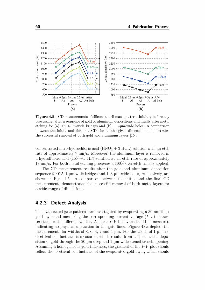
60 4 Fabrication Process
Cri
tica
l di
men
sion
(nm
)
Cri
tica
l di
men
sion
(nm
)
Cur
rent
(m
A)
Cri
tica
l di
men
sion
(nm
)
InitialSi
0.2 µmAu
After Au Etch
500
600
700
800
900
1000
1100
1200
1300
1400
1500
Process
750
1000
1250
1500
1750
2000
2250
2500
2750
3000
3250
Process
0.4 µmAu
0.5 µmAu
InitialSi
0.1 µmAl
After Al Etch
0.2 µm
Al0.3 µm
Al
0.6 µm
0.5 µm
0.7 µm
0.9 µm
1 µm
0.8 µm
1 µm
2 µm
3 µm
1.5 µm
-0.1-2.0
-0.06 -0.02 0.02 0.06 0.1
-1.5
-1.0
-0.5
0.0
0.5
1.0
1.5
2.0
Voltage (V)
1 2 3 4 5200
400
600
800
1000
1200
1400
1600
Row number
8
6 µm4 µm2 µm1 µm
µm
Silicon stencil maskEvaporated gold patterns
(a)
Cri
tica
l di
men
sion
(nm
)
Cri
tica
l di
men
sion
(nm
)
Cur
rent
(m
A)
Cri
tica
l di
men
sion
(nm
)
InitialSi
0.2 µmAu
After Au Etch
500
600
700
800
900
1000
1100
1200
1300
1400
1500
Process
750
1000
1250
1500
1750
2000
2250
2500
2750
3000
3250
Process
0.4 µmAu
0.5 µmAu
InitialSi
0.1 µmAl
After Al Etch
0.2 µm
Al0.3 µm
Al
0.6 µm
0.5 µm
0.7 µm
0.9 µm
1 µm
0.8 µm
1 µm
2 µm
3 µm
1.5 µm
-0.1-2.0
-0.06 -0.02 0.02 0.06 0.1
-1.5
-1.0
-0.5
0.0
0.5
1.0
1.5
2.0
Voltage (V)
1 2 3 4 5200
400
600
800
1000
1200
1400
1600
Row number
8
6 µm4 µm2 µm1 µm
µm
Silicon stencil maskEvaporated gold patterns
(b)
Figure 4.5 CD measurements of silicon stencil mask patterns initially before anyprocessing, after a sequence of gold or aluminum depositions and finally after metaletching for (a) 0.5–1-µm-wide bridges and (b) 1–3-µm-wide holes. A comparisonbetween the initial and the final CDs for all the given dimensions demonstratesthe successful removal of both gold and aluminum layers [15].
concentrated nitro-hydrochloric acid (HNO3 + 3 HCL) solution with an etchrate of approximately 7 nm/s. Moreover, the aluminum layer is removed ina hydrofluoric acid (15%wt. HF) solution at an etch rate of approximately18 nm/s. For both metal etching processes a 100% over-etch time is applied.
The CD measurement results after the gold and aluminum depositionsequence for 0.5–1-µm-wide bridges and 1–3-µm-wide holes, respectively, areshown in Fig. 4.5. A comparison between the initial and the final CDmeasurements demonstrates the successful removal of both metal layers fora wide range of dimensions.
4.2.3 Defect Analysis
The evaporated gate patterns are investigated by evaporating a 30-nm-thickgold layer and measuring the corresponding current–voltage (I–V ) charac-teristics for the different widths. A linear I–V behavior should be measuredindicating no physical separation in the gate lines. Figure 4.6a depicts themeasurements for widths of 8, 6, 4, 2 and 1 µm. For the width of 1 µm, noelectrical conductance is measured, which results from an insufficient depo-sition of gold through the 20 µm deep and 1-µm-wide stencil trench opening.Assuming a homogeneous gold thickness, the gradient of the I–V plot shouldreflect the electrical conductance of the evaporated gold layer, which should

4.2 Silicon Stencil Masks 61
Cri
tica
l di
men
sion
(nm
)
Cri
tica
l di
men
sion
(nm
)
Cur
rent
(m
A)
Cri
tica
l di
men
sion
(nm
)
InitialSi
0.2 µmAu
After Au Etch
500
600
700
800
900
1000
1100
1200
1300
1400
1500
Process
750
1000
1250
1500
1750
2000
2250
2500
2750
3000
3250
Process
0.4 µmAu
0.5 µmAu
InitialSi
0.1 µmAl
After Al Etch
0.2 µm
Al0.3 µm
Al
0.6 µm
0.5 µm
0.7 µm
0.9 µm
1 µm
0.8 µm
1 µm
2 µm
3 µm
1.5 µm
-0.1-2.0
-0.06 -0.02 0.02 0.06 0.1
-1.5
-1.0
-0.5
0.0
0.5
1.0
1.5
2.0
Voltage (V)
1 2 3 4 5200
400
600
800
1000
1200
1400
1600
Row number
8
6 µm4 µm2 µm1 µm
µm
Silicon stencil maskEvaporated gold patterns
(a)
Cri
tica
l di
men
sion
(nm
)
Cri
tica
l di
men
sion
(nm
)
Cur
rent
(m
A)
Cri
tica
l di
men
sion
(nm
)
InitialSi
0.2 µmAu
After Au Etch
500
600
700
800
900
1000
1100
1200
1300
1400
1500
Process
750
1000
1250
1500
1750
2000
2250
2500
2750
3000
3250
Process
0.4 µmAu
0.5 µmAu
InitialSi
0.1 µmAl
After Al Etch
0.2 µm
Al0.3 µm
Al
0.6 µm
0.5 µm
0.7 µm
0.9 µm
1 µm
0.8 µm
1 µm
2 µm
3 µm
1.5 µm
-0.1-2.0
-0.06 -0.02 0.02 0.06 0.1
-1.5
-1.0
-0.5
0.0
0.5
1.0
1.5
2.0
Voltage (V)
1 2 3 4 5200
400
600
800
1000
1200
1400
1600
Row number
8
6 µm4 µm2 µm1 µm
µm
Silicon stencil maskEvaporated gold patterns
(b)
Figure 4.6 (a) Measured I–V characteristics of 1–8-µm-wide evaporated gatemodules. (b) CD measurements of 0.8-µm-wide and 30-µm-long bridges in thestencil mask and the corresponding evaporated gold source/drain patterns on atest sample; for each row module, there are seven data points, which correspondto the seven columns from the left to the right side of the sample [15].
be proportional to the cross-section area of the conductor. This complies forwidths of 8, 6 and 4 µm, but not for 2 µm, indicating that the evaporationlimit in this process is at an aspect ratio of 1:10.
It is found that most defects in this fabrication process occur duringthe final membrane etch step in the TMAH solution. This results due todefects in the TEOS protection layer. As shown in Fig. 4.7, this kind ofdefects occurs at the wafer frontside and is determined by a pyramidal shapedanisotropic silicon etch that is located at the edge of the bridge. In the figure,the defect is located only at one end of the bridge, but sometimes it occursat both ends. To resolve this issue, a change in the membrane etch strategyis implemented into the process flow. By just reducing the etch time inthe TMAH solution by about 50%, the number of defects are reduced by afactor of five. This is because the exposure time of the wafer frontside to theetch solution is much less than before. Table 4.3 summarizes the number ofdefects when using the two etching schemes for channel widths of 100 and 30µm and various channel lengths ranging from 4 µm down to 0.3 µm.
Figure 4.8 depicts stable stencil features with excellent sharp edges forthe minimum feature size of 0.3 µm and channel widths of 100 and 30 µm.By evaporating a 30-nm-thick gold layer onto a test sample, the channellength of 0.3 µm could be successfully realized without electrical shortage asillustrated in Fig. 4.8d. This implies the potential use of the silicon stencilmasks to fabrication submicrometer OTFTs.
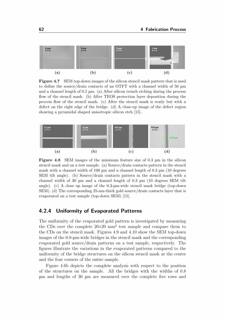
62 4 Fabrication Process
6 µm 6 µm 6 µm 2 µm
(a)
6 µm 6 µm 6 µm 2 µm
(b)
6 µm 6 µm 6 µm 2 µm
(c)
6 µm 6 µm 6 µm 2 µm
(d)
Figure 4.7 SEM top-down images of the silicon stencil mask pattern that is usedto define the source/drain contacts of an OTFT with a channel width of 50 µmand a channel length of 0.5 µm. (a) After silicon trench etching during the processflow of the stencil mask. (b) After TEOS protection layer deposition during theprocess flow of the stencil mask. (c) After the stencil mask is ready but with adefect on the right edge of the bridge. (d) A close-up image of the defect regionshowing a pyramidal shaped anisotropic silicon etch [15].
15 µm 6 µm 0.8 µm 0.8 µm
0.28 µm
(a)
15 µm 6 µm 0.8 µm 0.8 µm
0.28 µm
(b)
15 µm 6 µm 0.8 µm 0.8 µm
0.28 µm
(c)
15 µm 6 µm 0.8 µm 0.8 µm
0.28 µm
(d)
Figure 4.8 SEM images of the minimum feature size of 0.3 µm in the siliconstencil mask and on a test sample. (a) Source/drain contacts pattern in the stencilmask with a channel width of 100 µm and a channel length of 0.3 µm (10 degreesSEM tilt angle). (b) Source/drain contacts pattern in the stencil mask with achannel width of 30 µm and a channel length of 0.3 µm (10 degrees SEM tiltangle). (c) A close up image of the 0.3-µm-wide stencil mask bridge (top-downSEM). (d) The corresponding 25-nm-thick gold source/drain contacts layer that isevaporated on a test sample (top-down SEM) [15].
4.2.4 Uniformity of Evaporated Patterns
The uniformity of the evaporated gold pattern is investigated by measuringthe CDs over the complete 20×20 mm2 test sample and compare them tothe CDs on the stencil mask. Figures 4.9 and 4.10 show the SEM top-downimages of the 0.8-µm-wide bridges in the stencil mask and the correspondingevaporated gold source/drain patterns on a test sample, respectively. Thefigures illustrate the variations in the evaporated patterns compared to theuniformity of the bridge structures on the silicon stencil mask at the centerand the four corners of the entire sample.
Figure 4.6b depicts the complete analysis with respect to the positionof the structures on the sample. All the bridges with the widths of 0.8µm and lengths of 30 µm are measured over the complete five rows and
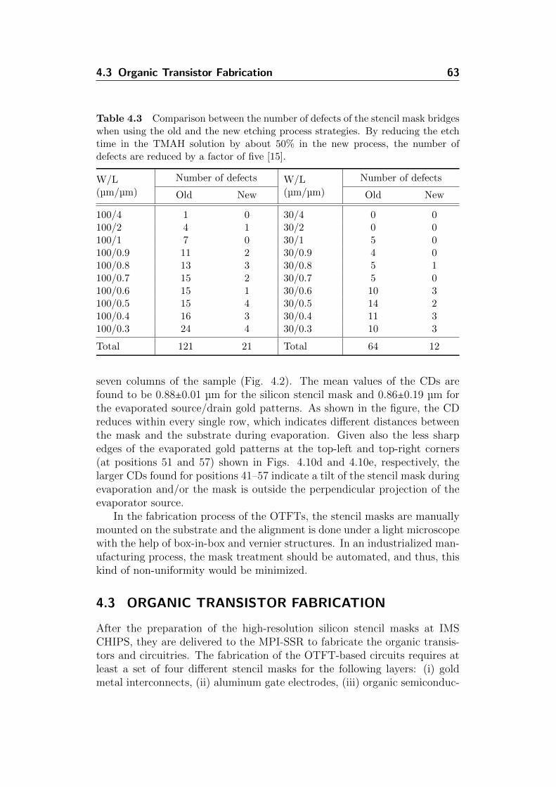
4.3 Organic Transistor Fabrication 63
Table 4.3 Comparison between the number of defects of the stencil mask bridgeswhen using the old and the new etching process strategies. By reducing the etchtime in the TMAH solution by about 50% in the new process, the number ofdefects are reduced by a factor of five [15].
W/L(µm/µm)
Number of defects W/L(µm/µm)
Number of defects
Old New Old New
100/4 1 0 30/4 0 0100/2 4 1 30/2 0 0100/1 7 0 30/1 5 0100/0.9 11 2 30/0.9 4 0100/0.8 13 3 30/0.8 5 1100/0.7 15 2 30/0.7 5 0100/0.6 15 1 30/0.6 10 3100/0.5 15 4 30/0.5 14 2100/0.4 16 3 30/0.4 11 3100/0.3 24 4 30/0.3 10 3
Total 121 21 Total 64 12
seven columns of the sample (Fig. 4.2). The mean values of the CDs arefound to be 0.88±0.01 µm for the silicon stencil mask and 0.86±0.19 µm forthe evaporated source/drain gold patterns. As shown in the figure, the CDreduces within every single row, which indicates different distances betweenthe mask and the substrate during evaporation. Given also the less sharpedges of the evaporated gold patterns at the top-left and top-right corners(at positions 51 and 57) shown in Figs. 4.10d and 4.10e, respectively, thelarger CDs found for positions 41–57 indicate a tilt of the stencil mask duringevaporation and/or the mask is outside the perpendicular projection of theevaporator source.
In the fabrication process of the OTFTs, the stencil masks are manuallymounted on the substrate and the alignment is done under a light microscopewith the help of box-in-box and vernier structures. In an industrialized man-ufacturing process, the mask treatment should be automated, and thus, thiskind of non-uniformity would be minimized.
4.3 ORGANIC TRANSISTOR FABRICATION
After the preparation of the high-resolution silicon stencil masks at IMSCHIPS, they are delivered to the MPI-SSR to fabricate the organic transis-tors and circuitries. The fabrication of the OTFT-based circuits requires atleast a set of four different stencil masks for the following layers: (i) goldmetal interconnects, (ii) aluminum gate electrodes, (iii) organic semiconduc-
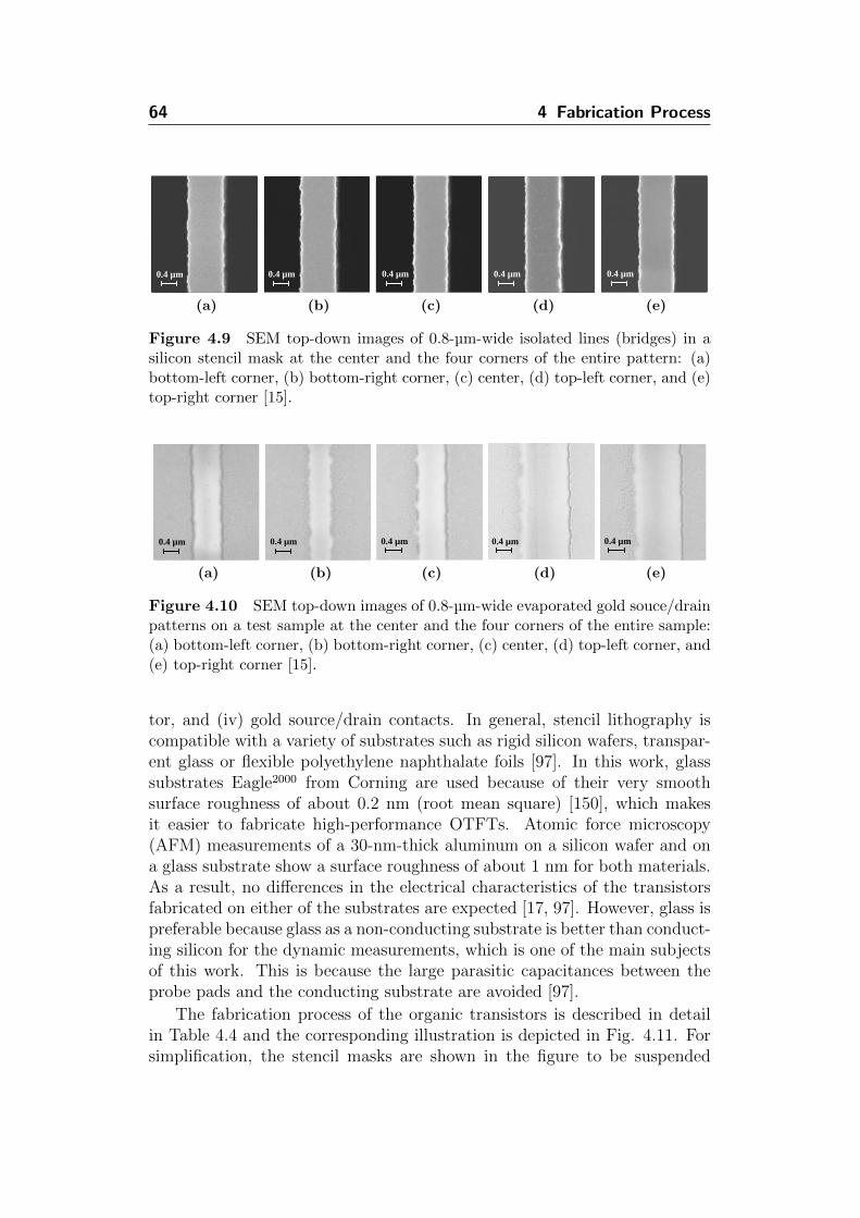
64 4 Fabrication Process
0.4 µm0.4 µm0.4 µm0.4 µm0.4 µm
(a)
0.4 µm0.4 µm0.4 µm0.4 µm0.4 µm
(b)
0.4 µm0.4 µm0.4 µm0.4 µm0.4 µm
(c)
0.4 µm0.4 µm0.4 µm0.4 µm0.4 µm
(d)
0.4 µm0.4 µm0.4 µm0.4 µm0.4 µm
(e)
Figure 4.9 SEM top-down images of 0.8-µm-wide isolated lines (bridges) in asilicon stencil mask at the center and the four corners of the entire pattern: (a)bottom-left corner, (b) bottom-right corner, (c) center, (d) top-left corner, and (e)top-right corner [15].
0.4 µm0.4 µm0.4 µm0.4 µm0.4 µm
(a)
0.4 µm0.4 µm0.4 µm0.4 µm0.4 µm
(b)
0.4 µm0.4 µm0.4 µm0.4 µm0.4 µm
(c)
0.4 µm0.4 µm0.4 µm0.4 µm0.4 µm
(d)
0.4 µm0.4 µm0.4 µm0.4 µm0.4 µm
(e)
Figure 4.10 SEM top-down images of 0.8-µm-wide evaporated gold souce/drainpatterns on a test sample at the center and the four corners of the entire sample:(a) bottom-left corner, (b) bottom-right corner, (c) center, (d) top-left corner, and(e) top-right corner [15].
tor, and (iv) gold source/drain contacts. In general, stencil lithography iscompatible with a variety of substrates such as rigid silicon wafers, transpar-ent glass or flexible polyethylene naphthalate foils [97]. In this work, glasssubstrates Eagle2000 from Corning are used because of their very smoothsurface roughness of about 0.2 nm (root mean square) [150], which makesit easier to fabricate high-performance OTFTs. Atomic force microscopy(AFM) measurements of a 30-nm-thick aluminum on a silicon wafer and ona glass substrate show a surface roughness of about 1 nm for both materials.As a result, no differences in the electrical characteristics of the transistorsfabricated on either of the substrates are expected [17, 97]. However, glass ispreferable because glass as a non-conducting substrate is better than conduct-ing silicon for the dynamic measurements, which is one of the main subjectsof this work. This is because the large parasitic capacitances between theprobe pads and the conducting substrate are avoided [97].
The fabrication process of the organic transistors is described in detailin Table 4.4 and the corresponding illustration is depicted in Fig. 4.11. Forsimplification, the stencil masks are shown in the figure to be suspended

4.3 Organic Transistor Fabrication 65
from the substrate during evaporation. In practice, however, three steps arenecessary with every single mask. At first the mask is aligned and fixedto the substrate, second evaporation of material with the desired thicknesstakes place, and finally the mask is released carefully from the substrate toavoid any scratches on the sample. The alignment of the stencil masks to thesubstrate is done under a light microscope with the help of box-in-box andvernier structures with an accuracy of about 2–5 µm. In the final evaporationstep, the alignment is very critical due to the definition of the gate-sourceand gate-drain overlaps, which determine the dominating parasitics of thetransistor and thus the dynamic performance [188].
The gate dielectric of the OTFTs is composed of two-stacked layers,namely a 3.6-nm-thick aluminum oxide (AlOx) layer and a 1.7-nm-thick self-assembled monolayer (SAM). The hybrid gate dielectric has a capacitance ofthe order of 1 µF/cm2, which is sufficiently high to allow the transistors tooperate at voltages as low as 3 V [106]. Although, the SAM adds only 1.7nm to the total dielectric thickness, it reduces the leakage current density bythree orders of magnitude from 5×10⁻⁵ A/cm−2 to (5±1)×10−8 A/cm−2 at 2 V[152]. Furthermore, the gate dielectric has a low surface energy of 20 mN/m[189], which is useful to achieve a high carrier mobility in the small-moleculeorganic films deposited on top of this gate dielectric [97].
Table 4.4 Fabrication process steps of the organic transistors [14, 97, 152].
No. Process Description
1 Substrateprepara-tion
An alkali-free glass substrate Eagle2000 from Corning isused. The substrate is initially cleaned with deionized wa-ter, 2-propanol and acetone. After that, the substrate iscovered with 8-nm-thick Al2O3 using atomic layer depo-sition to increase the adhesion to the following processedlayers.
2 Golddeposition
A 20-nm-thick gold (Au) layer is deposited through thefirst shadow mask in a turbo-pumped vacuum evaporatorusing a resistively heated tungesten filament with a 1–2A/s deposition rate and a 10−6 mbar base pressure. Thisbottom-metal layer defines the interconnects between thetransistors.
3 Aluminumdeposition
A 30-nm-thick aluminum (Al) layer is deposited by ther-mal evaporation through the second shadow mask in asimilar way as the previous step but with a 10–12 A/s de-position rate. This layer defines the bottom-gate electrodesof the transistors. A direct contact is created wherever thealuminum gate is deposited over the gold bottom metal.
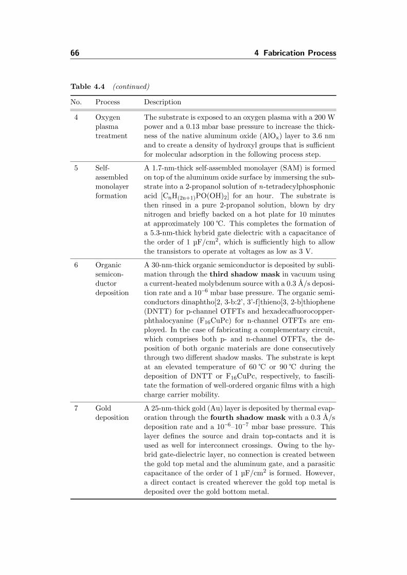
66 4 Fabrication Process
Table 4.4 (continued)
No. Process Description
4 Oxygenplasmatreatment
The substrate is exposed to an oxygen plasma with a 200 Wpower and a 0.13 mbar base pressure to increase the thick-ness of the native aluminum oxide (AlOx) layer to 3.6 nmand to create a density of hydroxyl groups that is sufficientfor molecular adsorption in the following process step.
5 Self-assembledmonolayerformation
A 1.7-nm-thick self-assembled monolayer (SAM) is formedon top of the aluminum oxide surface by immersing the sub-strate into a 2-propanol solution of n-tetradecylphosphonicacid [CnH(2n+1)PO(OH)2] for an hour. The substrate isthen rinsed in a pure 2-propanol solution, blown by drynitrogen and briefly backed on a hot plate for 10 minutesat approximately 100 . This completes the formation ofa 5.3-nm-thick hybrid gate dielectric with a capacitance ofthe order of 1 µF/cm2, which is sufficiently high to allowthe transistors to operate at voltages as low as 3 V.
6 Organicsemicon-ductordeposition
A 30-nm-thick organic semiconductor is deposited by subli-mation through the third shadow mask in vacuum usinga current-heated molybdenum source with a 0.3 A/s deposi-tion rate and a 10−6 mbar base pressure. The organic semi-conductors dinaphtho[2, 3-b:2’, 3’-f]thieno[3, 2-b]thiophene(DNTT) for p-channel OTFTs and hexadecafluorocopper-phthalocyanine (F16CuPc) for n-channel OTFTs are em-ployed. In the case of fabricating a complementary circuit,which comprises both p- and n-channel OTFTs, the de-position of both organic materials are done consecutivelythrough two different shadow masks. The substrate is keptat an elevated temperature of 60 or 90 during thedeposition of DNTT or F16CuPc, respectively, to fascili-tate the formation of well-ordered organic films with a highcharge carrier mobility.
7 Golddeposition
A 25-nm-thick gold (Au) layer is deposited by thermal evap-oration through the fourth shadow mask with a 0.3 A/sdeposition rate and a 10−6–10−7 mbar base pressure. Thislayer defines the source and drain top-contacts and it isused as well for interconnect crossings. Owing to the hy-brid gate-dielectric layer, no connection is created betweenthe gold top metal and the aluminum gate, and a parasiticcapacitance of the order of 1 µF/cm2 is formed. However,a direct contact is created wherever the gold top metal isdeposited over the gold bottom metal.
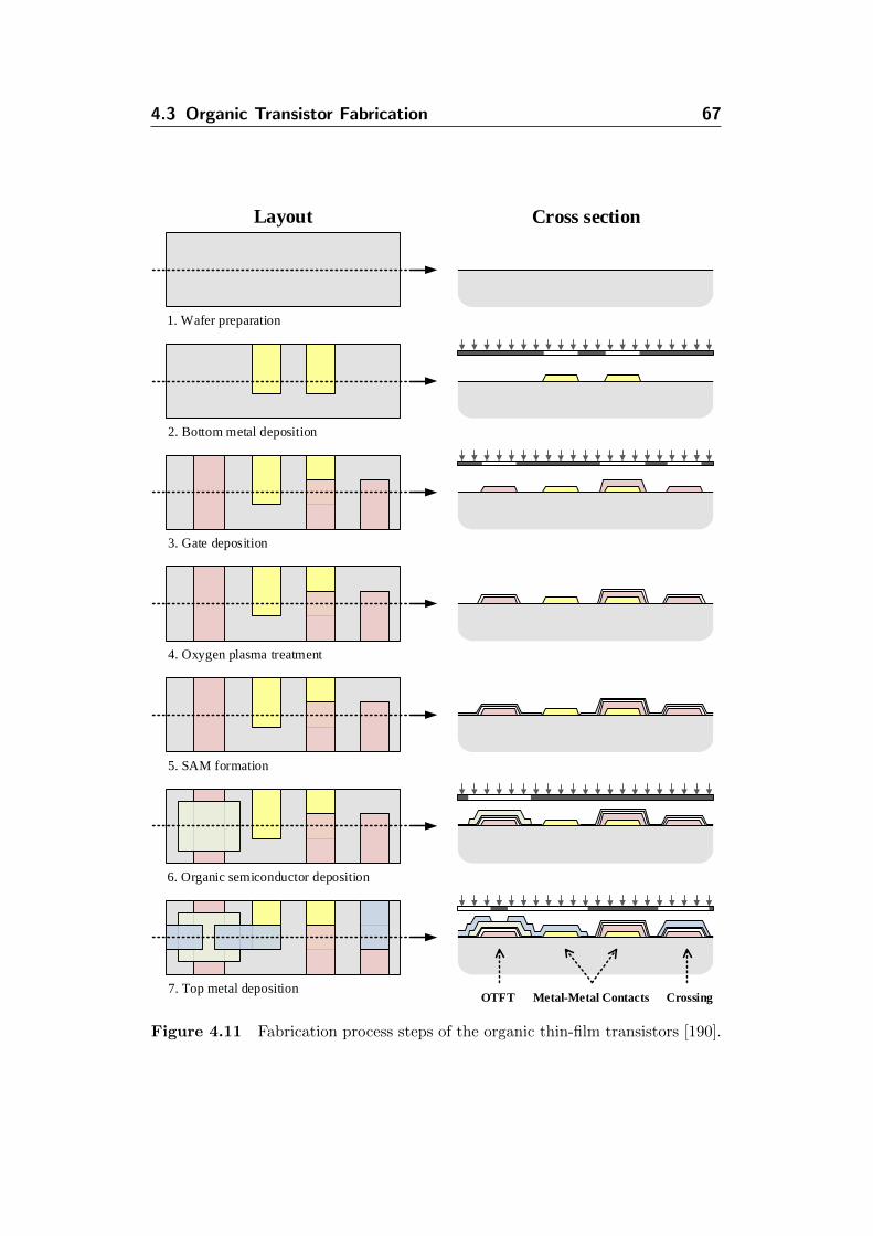
4.3 Organic Transistor Fabrication 67
Layout Cross section
1. Wafer preparation
2. Bottom metal deposition
3. Gate deposition
4. Oxygen plasma treatment
5. SAM formation
6. Organic semiconductor deposition
7. Top metal depositionCrossingMetal-Metal ContactsOTFT
Figure 4.11 Fabrication process steps of the organic thin-film transistors [190].

68 4 Fabrication Process
(a) (b) (c)
Figure 4.12 Design flow of the organic ICs. (a) Physical layout of organic ICsdesigned on an active die area of 20×20 mm2. (b) Photograph of the silicon stencilmask used to pattern the top-metal contacts. (c) Die photograph of the organicICs fabricated on a glass substrate.
Referring to Fig. 4.12, the design cycle of the organic integrated circuits(ICs) involves several steps. In the beginning, a feasibility study and an ICsize estimate is made. Accordingly, one or more ICs along with duplicates,alignment and test structures are planned to be included on the active diearea of 20×20 mm2. Using OTFT models, the circuit(s) are designed and sim-ulated on a SPICE (Simulation Program with Integrated Circuit Emphasis)simulator (e.g. LTspice or Cadence Virtuoso).
Subsequently, the physical layout of the die is implemented (Fig. 4.12a),including floorplanning, design for manufacturability (DFM) and design rulechecking (DRC). Attention must be given to the interconnect crossings andthe positioning of the transistors as they affect significantly the device per-formance and matching, respectively. For DFM, the design is modified tomake it easier and more efficient to produce, also to comply to the designrules, which are set by IMS CHIPS and MPI-SSR. This is achieved for exam-ple by improving the stability of the stencil masks by adding support grids(anchors), where possible, to hold sensitive structures on the mask. A specialDRC code is written to check the design rules of the stencil masks and theorganic ICs; these are discussed in detail in the following section.
After that, the layout is sent to IMS CHIPS in the GDSII2 (GraphicDatabase System) standard format for tapeout to fabricate the stencil maskset (Fig. 4.12b). The masks are then inspected under the microscope andthe critical structures are characterized by CD measurements if necessary.Afterwards, the mask set is sent to MPI-SSR to fabricate organic die samples(Fig. 4.12c). Finally, the samples are brought back to IMS CHIPS for testing.
2The GDSII (Graphic Database System) is an industry standard database file format thatis used for data exchange of IC layout artwork.
4.4 Layout Design Rules 69
Table 4.5 List of layout layers and their corresponding GDSII numbers.
Layer type Name Material Mask GDSII
Drawn Bottom metal Gold 1st 51
Bottom gate Aluminium 2nd 46
Semiconductor n-channel F16CuPc 3rd 40
Semiconductor p-channel DNTT 4th 39
Top metal Gold 5th 49
Not drawn Substrate Glass – –Substrate coat Al2O3 – –Oxide insulator AlOx – –SAM insulator CnH(2n+1)PO(OH)2 – –
4.4 LAYOUT DESIGN RULES
As discussed before, the inverted-staggered OTFT structure, which is alsoreferred to as bottom-gate/top-contact configuration, is used in this studyas it offers better performance compared to its coplanar counterparts. Table4.5 summarizes the layout layers and their corresponding materials, maskand GDSII numbers, noting that the dielectric layers (AlOx/SAM) as well asthe substrate are not drawn layers. To gain more insight of a typical OTFTcircuit layout design, a sample schematic and layout of a complementaryNAND logic gate is shown in Fig. 4.13. The numbers given in the figuredesignate the layout design rules, which are going to be explained in detailherein. The top-metal layer is mainly used for the source/drain contacts,while the bottom-metal layer is used for the interconnects. Another usageof the top-metal layer is to connect long bottom-metal lines that are cutinto shorter fragments for mask stability reasons. As for the crossing, thetop-metal layer is separated from the bottom-gate layer by a stack of twodielectric layers, namely a 3.6-nm-thick AlOx layer and a 1.7-nm-thick SAM.The total thickness of the hybrid gate dielectric is 5.3 nm with an equivalentcapacitance of the order of 1 µF/cm2. Exact capacitance measurements aregiven in Chapter 6.
In general, the Manhattan layout design style is employed, where anglesbetween zero and 90 degrees are ruled out, with the exception for the text la-bels, which do not have any electrical activity. Furthermore, the coordinatesof the layout components, such as wires, contacts, cells and modules, must beplaced on grid with a spacing of 0.1 µm. All dimensions drawn are supposedto be equal to the final dimensions on the wafer as well as the stencil masks.The origin (0,0) of the top hierarchy of a design has to be located at thelower left corner.

70 4 Fabrication Process
LayoutSchematic
VDD
VOUT
VBVA
VA
VB
1
2
34
4
4
45
5
5
5
54
5
5
5
5
5
6
6
78
6
7
3
3
3
Figure 4.13 Sample schematic and layout of a complementary NAND logic gate.The designated numbers represent the layout design rules for the DRC.
Referring to Fig. 4.13, the most important layout design rules are sum-marized in Tables 4.6 and 4.7. The dimensions given in these tables areminimum values. It is recommended, however, to use less critical valueswhenever significant increase in the area is not resulted. This applies partic-ularly to the width and the spacing of long interconnection lines, which arerealized by the bottom-metal layer.
Starting with the OTFT design rules, a minimum channel length (L) of2 µm defined by the top-metal layer is recommended (Rule 1). Furthermore,the minimum gate-overlap length (Lov), which is defined by the overlap be-tween the top metal and the bottom gate within the transistor active region,is set to 20 µm (Rule 2). However, during the characterization of the per-formance limits of this OTFT technology through AC measurements, thechannel length and the gate overlap are both reduced down to 0.6 and 5 µm,respectively. The enclosure rules, including the enclosure of the semiconduc-tor inside the top metal, enclosure of the top metal inside the semiconductor,enclosure of the gate inside the semiconductor and finally the enclosure ofthe semiconductor inside the gate, are all set to 20 µm (Rule 3). Neverthe-less, if the circuit area is relatively large, it is recommended to increase theenclosures of the gate and the top metal inside the semiconductor. This isbecause the semiconductor materials are translucent, and thus, they are hardto align when being deposited on the substrate.

4.4 Layout Design Rules 71
Table 4.6 Layout design rules of the organic integrated circuits.
No. Rule Layers Value Unit
1 Channel length Top-to-Top 2a µm
2 Gate Overlap Top-over-Gate 20a µm
3 Enclosures Top-enclose-Semib 20 µmSemi-enclose-Top 20 µmSemi-enclose-Gate 20 µmGate-enclose-Semi 20 µm
4 Related clearances Top-to-Top 20 µmGate-to-Gate 20 µmPSemi-to-PSemi 20 µmNSemi-to-NSemi 20 µmBottom-to-Bottom 20 µm
5 Non-related spacings Top-to-Gate 20 µmTop-to-PSemi 20 µmTop-to-NSemi 20 µmTop-to-Bottom 20 µmGate-to-PSemi 20 µmGate-to-NSemi 20 µmGate-to-Bottom 20 µmPSemi-to-NSemi 20 µmPSemi-to-Bottom 20 µmNSemi-to-Bottom 20 µm
6 Metal widths Top 20 µmGate 20 µmBottom 20 µm
7 Direct contact areas Top-Bottom-contact 20×20 µm2
Gate-Bottom-contact 20×20 µm2
8 Crossing area Top-Gate-crossing 20×20 µm2
aIn AC measurements, the L and Lov are reduced to 0.6 and 5 µm, respectively.bThe Semi layer is for both p- and n-channel semiconductors.
Table 4.7 Layout design rules of the silicon stencil masks (valid for all layers).
No. Rule Value Unit
9 Remaining silicon area (average over 1 mm2) ≥ 50% –
10 Length-to-width ratio of beams attached at both ends ≤ 50 µm
11 Length-to-width ratio of beams attached at one end ≤ 15 µm
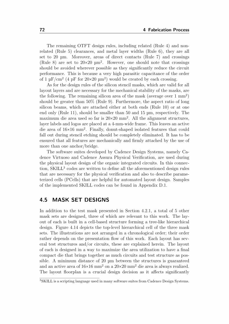
72 4 Fabrication Process
The remaining OTFT design rules, including related (Rule 4) and non-related (Rule 5) clearances, and metal layer widths (Rule 6), they are allset to 20 µm. Moreover, areas of direct contacts (Rule 7) and crossings(Rule 8) are set to 20×20 µm2. However, one should note that crossingsshould be avoided wherever possible as they significantly reduce the circuitperformance. This is because a very high parasitic capacitance of the orderof 1 µF/cm2 (4 pF for 20×20 µm2) would be created by each crossing.
As for the design rules of the silicon stencil masks, which are valid for alllayout layers and are necessary for the mechanical stability of the masks, arethe following. The remaining silicon area of the mask (average over 1 mm2)should be greater than 50% (Rule 9). Furthermore, the aspect ratio of longsilicon beams, which are attached either at both ends (Rule 10) or at oneend only (Rule 11), should be smaller than 50 and 15 µm, respectively. Themaximum die area used so far is 20×20 mm2. All the alignment structures,layer labels and logos are placed at a 4-mm-wide frame. This leaves an activedie area of 16×16 mm2. Finally, donut-shaped isolated features that couldfall out during stencil etching should be completely eliminated. It has to beensured that all features are mechanically and firmly attached by the use ofmore than one anchor/bridge.
The software suites developed by Cadence Design Systems, namely Ca-dence Virtuoso and Cadence Assura Physical Verification, are used duringthe physical layout design of the organic integrated circuits. In this connec-tion, SKILL3 codes are written to define all the aforementioned design rulesthat are necessary for the physical verification and also to describe parame-terized cells (PCells) that are helpful for automated layout design. Samplesof the implemented SKILL codes can be found in Appendix D.1.
4.5 MASK SET DESIGNS
In addition to the test mask presented in Section 4.2.1, a total of 5 othermask sets are designed, three of which are relevant to this work. The lay-out of each is built in a cell-based structure forming a tree-like hierarchicaldesign. Figure 4.14 depicts the top-level hierarchical cell of the three masksets. The illustrations are not arranged in a chronological order; their orderrather depends on the presentation flow of this work. Each layout has sev-eral test structures and/or circuits, these are explained herein. The layoutof each is designed in a way to maximize the area utilization to have a finalcompact die that brings together as much circuits and test structure as pos-sible. A minimum distance of 20 µm between the structures is guaranteedand an active area of 16×16 mm2 on a 20×20 mm2 die area is always realized.The layout floorplan is a crucial design decision as it affects significantly
3SKILL is a scripting language used in many software suites from Cadence Design Systems.
4.5 Mask Set Designs 73
(a) (b) (c)
Figure 4.14 Top-level hierarchical cell layout of the three designed 20×20 mm2
organic dies. (a) Die 1 that includes OTFTs for static and dynamic charac-terization. It also includes metal-insulator-metal (MIM) and metal-insulator-semiconductor (MIS) structures for admittance measurements. (b) Die 2 thatincludes aggressively-scaled OTFTs for scattering-parameter (S-parameter) mea-surements. (c) Die 3 that includes ring oscillators and digital-to-analog converters.
the matching and the data-related interference. Accordingly, the followingcriteria are necessary during the design of the layouts:
• The area of each circuit has to be minimized to allow further circuits,or even duplicates of the same circuit, to be fabricated and tested onthe same die.
• When device uniformity is paramount for some circuit topologies, cer-tain blocks should be designed with the minimum possible area. Thisis because the increased distance between the transistors makes themmore susceptible to mismatch effects and gradient errors.
• Again when the device uniformity is critical, identical transistors shouldbe placed as close as possible to improve the matching capability. Inaddition, symmetry should be achieved wherever possible to ensure thesame environment for all the transistors.
• Only one metal layer should be used for the design of a complete circuit,noting that the top metal and the bottom metal are both on the sameelectrical layer. Therefore, any overlap between them is considered asa physical connection.
• Crossings between the top metal and the bottom gate can be fabricated.Nevertheless, they should be avoided wherever possible to minimizecross coupling and improve the circuit performance.
Referring to Fig. 4.14, the three designed mask sets are labeled as Die 1 ,Die 2 and Die 3 . The first design, Die 1, includes OTFTs with channel
74 4 Fabrication Process
widths of 200 µm, channel lengths of 100–1 µm and gate overlaps of 100–2 µm,which are dedicated for the static characterization. Furthermore, relativelylarge OTFTs with channel widths of 400 and 1000 µm, channel lengths of400–5 µm and gate overlaps of 50–5 µm in addition to metal-insulator-metal(MIM) and metal-insulator-semiconductor (MIS) structures with differentdimensions (200×200, 100×100, 50×50, 10×10 µm2) are designed on the samedie for the dynamic characterization using admittance measurements.
The second design, Die 2, includes aggressively-scaled OTFTs for S-parameter measurements. For the stability of the stencil masks, the OTFTsare dissected into four parallel transistors sharing the same semiconductor.The OTFTs have channel widths of 100 µm (4×25 µm), channel lengths of10–0.4 µm and gate overlaps of 20 and 5 µm. To study the impact of mis-alignment between the gate-source (Lgs) and gate-drain (Lgd) overlaps, whereLgs +Lgd = 2Lov, the OTFTs with gate overlaps of 5 µm and channel lengthsof 1 and 0.6 µm are duplicated and intentionally misaligned on the masklevel in order to realize OTFTs with well-defined Lgs = 1, 2, ..., 9 µm, whilekeeping Lgs + Lgd = 10 µm. Vernier structures are employed to measure theparticular degree of misalignment. The standard calibration structures, i.e.,short, open and through, are also designed on the same die to remove theparasitics and to obtain the desired S-parameters at the device terminals.
The third design, Die 3, includes fast and compact organic ICs, namelyunipolar (only p-channel OTFTs) and complementary (both p- and n-channelOTFTs) ring oscillators (presented before in Section 3.4.3), and 6-bit binaryand 3-bit unary current-steering digital-to-analog converters (DACs). Fi-nally, more detailed description of the layout design of the three dies can befound in Appendix A.
4.6 SUMMARY
High-resolution silicon stencil masks are used for the fabrication of OTFTswith submicrometer channel lengths. The masks have a silicon membranethickness of 20 µm and an area of 20×20 mm2. A minimum channel lengthof 0.3 µm for the top-metal evaporation process is realized. Characterizationof the masks show that the evaporated gold contacts and aluminum gatescan be easily etched with excellent pattern fidelity. The OTFTs employ ahybrid gate dielectric that is composed of a 3.6-nm-thick aluminum oxide anda 1.7-nm-thick organic self-assembled monolayer. The gate dielectric has acapacitance of the order of 1 µF/cm2, which is sufficiently high to allow thetransistors to operate at voltages as low as 3 V. The stencil masks and theorganic ICs have recommended layout design rules; accordingly, a CadenceSKILL code is written for the physical verification of the designs. A total ofthree mask sets are designed during the course of this work to fabricate fastand compact organic transistors and circuits.

5Static Characterization
An analytical model describing the steady-state characteristics of the OTFTsis presented herein. The model captures the physical behavior of the device,which helps to improve the electrical performance, stability and uniformityof OTFTs, as well as the design and optimization of organic integrated cir-cuits. In general, contact effects in OTFTs are significant and they limitthe device performance; therefore, source and drain contact resistances areexperimentally investigated to analyze and model their behavior. It is foundthat contact resistances are dependent on the applied biasing potentials andon the dimensions of the OTFTs. The static model is validated by com-paring the numerical solutions with measured characteristics of both p- andn-channel OTFTs; a reliable fit of the data is demonstrated.
5.1 TRANSMISSION LINE METHOD
The transmission line method (TLM)—introduced by Murrmann and Wid-mann in 1969 [191]—is used to extract some intrinsic and extrinsic charac-teristics of the OTFTs, including the contact resistance at the metal/semi-conductor interface and the sheet resistance of the organic semiconductor,from which the threshold voltage and the intrinsic carrier mobility of thedevices can be calculated [97, 192]. The theory and implementation of thismethod on our DNTT OTFTs are described in this section. For this method,a set of OTFTs with different channel lengths is required; correspondingly,eleven OTFTs with W = 200 µm, Lov = 100 µm and L = 100–4 µm arefabricated. Figure 5.1 shows the measured static drain currents (ID) of sixof those OTFTs. The characteristics show that ID increases when L is re-duced. The OTFTs have on/off current ratios (Ion/Ioff) of about 106 andsubthreshold slopes (Ss-th) of 90 mV/decade. From the saturation transfercurves, effective mobilities (µ) of 2.7, 2.4, 2.0, 1.8, 1.6 and 1.2 cm2/Vs, andtransconductances (gm) of 5, 12, 20, 30, 40 and 60 µA/V (at VGS = −3 V) areextracted for L = 100, 40, 20, 12, 8 and 4 µm, respectively. The reductionof µ as L reduces is owed to the increase in the relative contribution of thecontact resistances to the total device resistance [139].
Since the output characteristics of the DNTT OTFTs (p-channel) shownin Fig. 5.1 do not exhibit a non-linearity at low drain-source voltages, it canbe assumed in the following analysis that the OTFTs have ohmic contact
75

76 5 Static Characterization
-3 -2.5 -2 -1.5 -1 -0.5 00
10
20
30
40
50
Drain-source voltage (V)
Dra
in c
urre
nt (
µA
)
-3 -2.5 -2 -1.5 -1 -0.5 010
-13
10-11
10-9
10-7
10-5
10-3
Gate-source voltage (V)D
rain
and
gat
e cu
rren
ts (
A)
Drain currentGate current
L = 100 µmov
W = 200 µm
V = -3 VGS
V = -2 VDS
L = 4 µm
8 µm
100 µm
12 µm
20 µm
40 µm
(a)
-3 -2.5 -2 -1.5 -1 -0.5 00
10
20
30
40
50
Drain-source voltage (V)
Dra
in c
urre
nt (
µA
)
-3 -2.5 -2 -1.5 -1 -0.5 010
-13
10-11
10-9
10-7
10-5
10-3
Gate-source voltage (V)D
rain
and
gat
e cu
rren
ts (
A)
Drain currentGate current
L = 100 µmov
W = 200 µm
V = -3 VGS
V = -2 VDS
L = 4 µm
8 µm
100 µm
12 µm
20 µm
40 µm
(b)
Figure 5.1 Measured static I–V characteristics of inverted-staggered DNTTOTFTs with W = 200 µm, Lov = 100 µm, and L = 100, 40, 20, 12, 8 and 4 µm. (a)Output characteristics at VGS = −3 V. (b) Transfer characteristics at VDS = −2 V.
resistances; however, it is demonstrated in Section 5.3 that this is not thecase for aggressively-scaled DNTT OTFTs (with L < 1 µm) and for F16CuPcOTFTs (n-channel) as well. Accordingly, the total resistance of the OTFT(Rtot) is given by the sum of the source/drain contact resistances (2RC;assuming also that the OTFT is symmetrical) and the channel resistance(Rch = 1/gch): Rtot = 2RC +Rch. By substituting for Rch = 1/gch using (3.10)at low drain-source voltages (VDS ≪ VGS − VTH), we obtain
RtotW = 2RCW +RsheetL. (5.1)
Figure 5.2a depicts the extracted width-normalized total resistance (RtotW )of all the eleven OTFTs as a function of L at various gate-source voltagesabove threshold and at a low drain-source voltage of −0.1 V. At each VGS, theresistances Rsheet and RC can be calculated from the slope and the intersec-tion with the y-axis (when L = 0) of the linear least-square fit, respectively.
As described in Chapter 3, the drain current (ID) when considering ohmiccontact resistances for symmetrical OTFTs can be written as
ID = µoCIW
L⋅ (VDS − 2IDRC) ⋅ (VGS − VTH −
VDS
2). (5.2)
At a sufficiently small drain-source voltage (VDS ≪ VGS − VTH), ID can besimplified to the following expression:
ID = µoCIW
L⋅ (VDS − 2IDRC) ⋅ (VGS − VTH). (5.3)
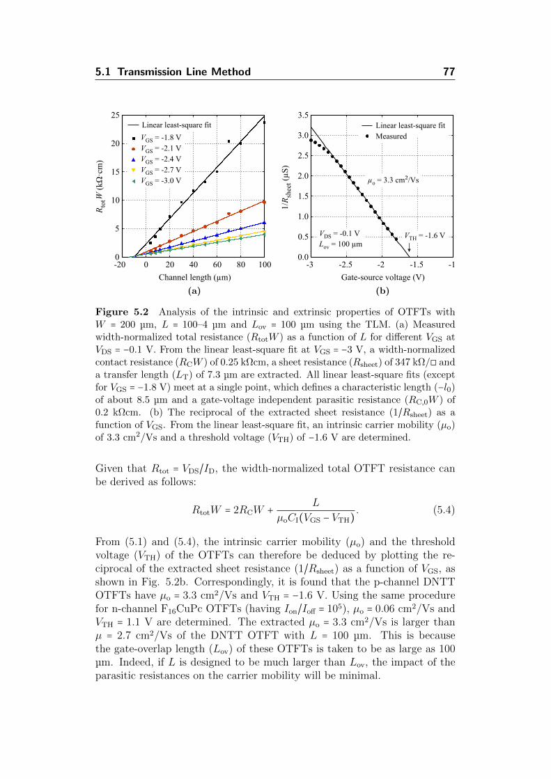
5.1 Transmission Line Method 77
-20 0 20 40 60 80 1000
5
10
15
20
25
Channel length ( m)µ
RW
(kΩ
·cm
)
tot
-3 -2.5 -2 -1.5 -10.0
0.5
1.0
1.5
2.0
2.5
3.0
3.5
Gate-source voltage (V)1/R
(µ
S)
shee
t
L = 100 µmov
V = -0.1 VDS
µ = 3.3 cm²/Vso
V = -1.6 VTH
Linear least-square fit
V = -1.8 VGS
V = -2.1 VGS
V = -2.4 VGS
V = -2.7 VGS
V = -3.0 VGS
Linear least-square fit
Measured
(a)
-20 0 20 40 60 80 1000
5
10
15
20
25
Channel length ( m)µ
RW
(kΩ
·cm
)
tot
-3 -2.5 -2 -1.5 -10.0
0.5
1.0
1.5
2.0
2.5
3.0
3.5
Gate-source voltage (V)1/R
(µ
S)
shee
t
L = 100 µmov
V = -0.1 VDS
µ = 3.3 cm²/Vso
V = -1.6 VTH
Linear least-square fit
V = -1.8 VGS
V = -2.1 VGS
V = -2.4 VGS
V = -2.7 VGS
V = -3.0 VGS
Linear least-square fit
Measured
(b)
Figure 5.2 Analysis of the intrinsic and extrinsic properties of OTFTs withW = 200 µm, L = 100–4 µm and Lov = 100 µm using the TLM. (a) Measuredwidth-normalized total resistance (RtotW ) as a function of L for different VGS atVDS = −0.1 V. From the linear least-square fit at VGS = −3 V, a width-normalizedcontact resistance (RCW ) of 0.25 kΩcm, a sheet resistance (Rsheet) of 347 kΩ/◻ anda transfer length (LT) of 7.3 µm are extracted. All linear least-square fits (exceptfor VGS = −1.8 V) meet at a single point, which defines a characteristic length (−l0)of about 8.5 µm and a gate-voltage independent parasitic resistance (RC,0W ) of0.2 kΩcm. (b) The reciprocal of the extracted sheet resistance (1/Rsheet) as afunction of VGS. From the linear least-square fit, an intrinsic carrier mobility (µo)of 3.3 cm2/Vs and a threshold voltage (VTH) of −1.6 V are determined.
Given that Rtot = VDS/ID, the width-normalized total OTFT resistance canbe derived as follows:
RtotW = 2RCW +L
µoCI(VGS − VTH). (5.4)
From (5.1) and (5.4), the intrinsic carrier mobility (µo) and the thresholdvoltage (VTH) of the OTFTs can therefore be deduced by plotting the re-ciprocal of the extracted sheet resistance (1/Rsheet) as a function of VGS, asshown in Fig. 5.2b. Correspondingly, it is found that the p-channel DNTTOTFTs have µo = 3.3 cm2/Vs and VTH = −1.6 V. Using the same procedurefor n-channel F16CuPc OTFTs (having Ion/Ioff = 105), µo = 0.06 cm2/Vs andVTH = 1.1 V are determined. The extracted µo = 3.3 cm2/Vs is larger thanµ = 2.7 cm2/Vs of the DNTT OTFT with L = 100 µm. This is becausethe gate-overlap length (Lov) of these OTFTs is taken to be as large as 100µm. Indeed, if L is designed to be much larger than Lov, the impact of theparasitic resistances on the carrier mobility will be minimal.

78 5 Static Characterization
As depicted in Fig. 5.2b, the reciprocal of the sheet resistance slightlydeviates from the linear least-square fit at high gate bias (∣VGS∣ ≥ 2.7 V),which implies that the OTFTs have about 10% lower carrier mobility at thisbiasing regime. This can be attributed to bias-stress effects. Even thoughthe OTFTs exhibit very low hysteresis when being measured in the forwardand backward directions (not shown here), a similar effect is observed inthe linear transfer characteristics, i.e., the measured drain current is slightlylower in the backward bias stream than in the forward bias stream due tothe lower carrier mobility caused by bias stress at high gate-source voltages.
Furthermore, Fig. 5.3a shows the extracted width-normalized contactresistances (2RCW ) as a function of the gate voltage. Apparently, the contactresistance is largely modulated by the gate voltage due to the presence ofthe overlaps between the source/drain contacts and the gate electrode; thecontact resistance of the OTFTs decreases with increasing the absolute gatevoltage. An empirical model for this effect can be easily deduced from theTLM data [193]. As shown in Fig. 5.2a, the RtotW versus L curves merge atl0 ≅ 8.5 µm and has a residual value of a gate-voltage independent parasiticresistance (RC,0W ) of 0.2 kΩcm. From (5.4), the width-normalized contactresistances (2RCW ) must therefore satisfy the following relation [193]:
2RCW = RC,0W +l0
µ0CI(VGS − VTH). (5.5)
That is, the contact resistance can be considered as an accumulation channelresistance of length l0 in series with a minimum effective contact resistance.The output of the model with µ0 = 3.3–2.9 cm2/Vs (as a function of VGS),CI = 700 nF/cm2, l0 = 8.5 µm and RC,0W = 2.2 kΩcm is shown as a dashedline in Fig. 5.3a; the model fitted quite well with the extracted data.
Only the channel length dependence of the OTFT performance with afixed gate-overlap length (Lov) of 100 µm is considered so far. Based onthe discussions above, RC should depend also on Lov because of the currentdistribution under the contacts. To investigate this effect, other similar sixsets of OTFTs but with Lov = 50, 30, 20, 10, 5 and 2 µm are fabricated onthe same substrate. Figure 5.3b shows the width-normalized contact resis-tances (2RCW ) extracted using the TLM for each OTFT set at VGS = −3 V.An accurate evaluation of the contact resistance for these inverted-staggered(bottom-gate, top-contact) OTFTs requires the use of a distributed resis-tance network underneath the source/drain contacts as derived in AppendixC.2; accordingly, RC is analytically described by [192]
2RCW = 2RsheetLT coth(Lov
LT
), (5.6)
where LT is a characteristic transfer length over which 63% of the currentflows from the semiconductor into the metal or from the metal into the

5.1 Transmission Line Method 79
-3 -2.8 -2.6 -2.4 -2.2 -2 -1.80.0
0.4
0.8
1.2
1.6
2.0
2.4
2.8
Gate-source voltage (V)
2RW
C(kΩ
·cm
)
0 20 40 60 80 1000.2
0.4
0.6
0.8
1.0
1.2
1.4
1.6
Gate-overlap length ( m)µ2R
W (
kΩ
·cm
)
C
Measured
Modeled
Measured
Gate
Contact
LT
Lov
L T = 7.3 µm
Empirically modeled
Analytically modeled
(a)
-3 -2.8 -2.6 -2.4 -2.2 -2 -1.80.0
0.4
0.8
1.2
1.6
2.0
2.4
2.8
Gate-source voltage (V)
2RW
C(kΩ
·cm
)
0 20 40 60 80 1000.2
0.4
0.6
0.8
1.0
1.2
1.4
1.6
Gate-overlap length ( m)µ2R
W (
kΩ
·cm
)
C
Measured
Modeled
Measured
Gate
Contact
LT
Lov
L T = 7.3 µm
Empirically modeled
Analytically modeled
(b)
Figure 5.3 (a) Measured and modeled 2RCW as a function of VGS for theOTFTs with W = 200 µm, L = 100–4 µm and Lov = 100 µm. The dashed line repre-sents the empirical model given by (5.5) with µo = 3.3–2.9 cm2/Vs (as a function ofVGS), l0 = 8.5 µm and RC,0W = 2.2 kΩcm. The solid line represents the analyticalmodel given by (5.6) and (3.10) with constants LT = 7.3 µm and VTH = −1.6 V.(b) Measured and modeled 2RCW as a function of Lov. The solid line representsthe analytical model given by (5.6) with LT = 7.3 µm and Rsheet = 347 kΩ/◻.The figure depicts the excellent agreement between the measured and modeled RC
characteristics with the parameters extracted using the TLM. The inset shows aschematic diagram illustrating the current distribution underneath the source ordrain contacts of the OTFTs (adopted from [194]), assuming that Lov > LT, whereLT is the characteristic transfer length over which 63% of the current flows fromthe top-metal contact to the organic semiconductor or vice versa.
semiconductor [194]. As defined in Appendix C.2, the transfer length (LT)is given by
LT =
√ρc
Rsheet
, (5.7)
where ρc (Ωm2) is the contact resistivity multiplied by the effective distancebetween the source/drain contacts and the accumulated channel. Moreover,the expression of RCW given by (5.6) can be simplified to the following twoconditions [192]:
RCW ≅ ρc/Lov for Lov ≪ LT,
ρc/LT for Lov ≫ LT.(5.8)
If Lov ≪ LT, the effective contact area is the actual contact area of LovW . IfLov ≫ LT, however, the effective contact area is LTW , which is smaller thanthe actual contact area, leading to an increased current density than if theentire contact area was active.

80 5 Static Characterization
In principle, the transfer length (LT) can be extracted from the RtotWversus L curves shown in Fig. 5.2a. By substituting (5.7) and (5.8) in (5.1)for long gate-overlap lengths (Lov ≫ LT), the width-normalized total OTFTresistance can be expressed as
RtotW = Rsheet(2LT +L). (5.9)
Therefore, LT can be calculated at each VGS from the intersection of thelinear least-square fit with the x-axis (when RtotW = 0). Referring to Fig.5.2a, the OTFTs with Lov = 100 µm have Rsheet = 347 kΩ/◻ and LT = 7.3 µm(extracted at VGS = −3 V). Using these values, the analytical model of RCWgiven by (5.6) yielded an excellent fit to the measured results, as illustratedby the solid line in Fig. 5.3b. Moreover, a precise fit is also achieved in Fig.5.3a by substituting in (5.6) for Rsheet using (3.10).
5.2 COMPACT CHARGE-DRIFT MODEL
The steady-state characteristics of the OTFTs have been extensively studiedand several static models have been proposed in literature [195–200]. Brownet al. [195] observed that the charge carrier mobility in amorphous organictransistors is bias dependent, i.e., the mobility increases when the gate volt-age increases. According to that perceived effect, Vissenberg and Matters[196] and Meijer et al. [197] developed analytical models based on chargedrift in the presence of variable-range hopping1 (VRH). However, these mod-els are limited to the linear operating regime. Calvetti et al. [198] andMarinov and Deen [199] derived analytical models based on the same com-mon points, but on the other hand, the models cover both the linear and thesaturation operating regimes with a single formulation. Each of these modelsand many others [201–205] were proposed to explain the conduction mech-anism of their specific devices while taking into consideration the mobilityenhancement behavior at higher gate bias.
In general, it is quite challenging to define a unified compact DC modelfor OTFTs due to various reasons, among them are the following [199]: (i)there is a wide range of OTFT technologies, including the use of differentmaterials, processing steps and diverse transistor configurations; and (ii)there is significant variability in experimental data for similar devices inliterature. Consequently, many models are developed to reflect the uniquefeatures for the particular OTFTs.
1The variable-range hopping (VRH) is a model describing the conduction mechanism ina strongly disordered system, assuming the charge-carrier transport as hopping betweenlocalized electronic states. These states can be considered as charge traps induced bychemical impurities, structural defects or grain boundaries. The hopping rate betweentwo localized states, which corresponds to the carrier mobility, is thermally activated ortunneling assisted and the relaxation takes place under phonon emission [97].
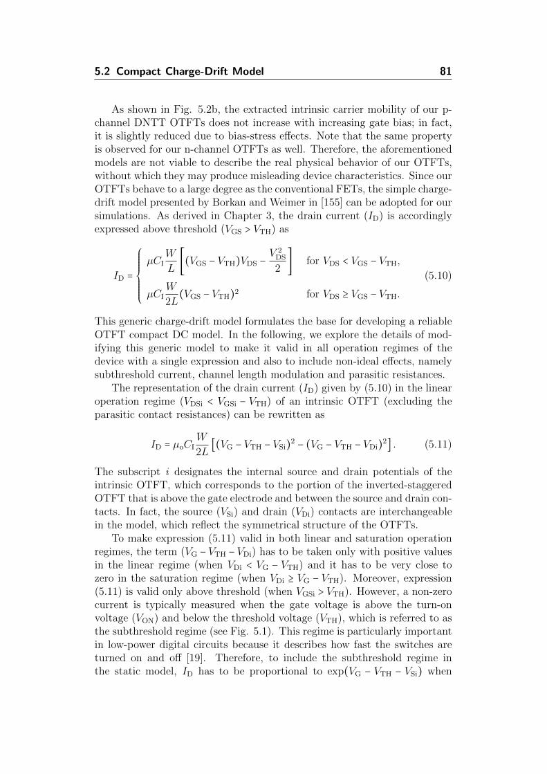
5.2 Compact Charge-Drift Model 81
As shown in Fig. 5.2b, the extracted intrinsic carrier mobility of our p-channel DNTT OTFTs does not increase with increasing gate bias; in fact,it is slightly reduced due to bias-stress effects. Note that the same propertyis observed for our n-channel OTFTs as well. Therefore, the aforementionedmodels are not viable to describe the real physical behavior of our OTFTs,without which they may produce misleading device characteristics. Since ourOTFTs behave to a large degree as the conventional FETs, the simple charge-drift model presented by Borkan and Weimer in [155] can be adopted for oursimulations. As derived in Chapter 3, the drain current (ID) is accordinglyexpressed above threshold (VGS > VTH) as
ID =
⎧⎪⎪⎪⎪⎪⎪⎨⎪⎪⎪⎪⎪⎪⎩
µCIW
L[(VGS − VTH)VDS −
V 2DS
2] for VDS < VGS − VTH,
µCIW
2L(VGS − VTH)2 for VDS ≥ VGS − VTH.
(5.10)
This generic charge-drift model formulates the base for developing a reliableOTFT compact DC model. In the following, we explore the details of mod-ifying this generic model to make it valid in all operation regimes of thedevice with a single expression and also to include non-ideal effects, namelysubthreshold current, channel length modulation and parasitic resistances.
The representation of the drain current (ID) given by (5.10) in the linearoperation regime (VDSi < VGSi − VTH) of an intrinsic OTFT (excluding theparasitic contact resistances) can be rewritten as
ID = µoCIW
2L[(VG − VTH − VSi)
2 − (VG − VTH − VDi)2] . (5.11)
The subscript i designates the internal source and drain potentials of theintrinsic OTFT, which corresponds to the portion of the inverted-staggeredOTFT that is above the gate electrode and between the source and drain con-tacts. In fact, the source (VSi) and drain (VDi) contacts are interchangeablein the model, which reflect the symmetrical structure of the OTFTs.
To make expression (5.11) valid in both linear and saturation operationregimes, the term (VG − VTH − VDi) has to be taken only with positive valuesin the linear regime (when VDi < VG − VTH) and it has to be very close tozero in the saturation regime (when VDi ≥ VG − VTH). Moreover, expression(5.11) is valid only above threshold (when VGSi > VTH). However, a non-zerocurrent is typically measured when the gate voltage is above the turn-onvoltage (VON) and below the threshold voltage (VTH), which is referred to asthe subthreshold regime (see Fig. 5.1). This regime is particularly importantin low-power digital circuits because it describes how fast the switches areturned on and off [19]. Therefore, to include the subthreshold regime inthe static model, ID has to be proportional to exp(VG − VTH − VSi) when
82 5 Static Characterization
VGSi < VTH. These conditions can be easily incorporated into the genericcharge-drift model by replacing the terms (VG−VTH−VSi) and (VG−VTH−VDi)in (5.11) with an asymptotically interpolation function [Veff(V ), where V =
VSi or VDi] that is given by [199]
Veff(V ) = VSS ln [1 + exp(VG − VTH − V
VSS
)] (5.12)
≅
⎧⎪⎪⎪⎪⎪⎪⎪⎪⎪⎪⎪⎪⎪⎪⎨⎪⎪⎪⎪⎪⎪⎪⎪⎪⎪⎪⎪⎪⎪⎩
VSS exp(VG − VTH − V
VSS
)
for subthreshold regime,when VG − VTH − V < −VSS,
VG − VTH − Vfor above-threshold regime,when VG − VTH − V > VSS,
(5.13)
where VSS is related to the steepness of the subthreshold characteristics of theOTFT. Note that Veff(V ) is very close to zero when V > VG −VTH, which is anecessary condition as mentioned above to make the model valid in the linearand saturation regimes using a single formulation. A similar interpolationhas been also used for MOSFETs [206] and polysilicon TFTs [207].
In the saturation regime, the drain current is determined by the channellength (L) and the gate-overdrive voltage (VGS−VTH). The saturation regimestarts at the pinch-off point when VDS = VGS − VTH. Once the pinch-off pointoccurs, any further increase in the drain potential results in shortening ofthe accumulated channel, thus increasing the drain current correspondingly.This effect is referred to as channel length modulation. A simple modificationto (5.11) can be implemented to incorporate this phenomenon by replacingthe channel length L with L −∆L, given that [199]
L(1 −∆L
L) ≅
L
1 + λ∣VDi − VSi∣, (5.14)
where λ is the channel-length modulation coefficient. By taking the absolutevalue of VDSi, the inherent symmetry of the model is preserved.
The final representation of the drain current (ID) of the intrinsic OTFTis determined by substituting for the subthreshold region using (5.12) andthe channel length modulation using (5.14) in (5.11) to obtain
ID = µoCIW
2L⋅ (1 + λ∣VDi − VSi∣) ⋅ [Veff(VSi)]
2− [Veff(VDi)]
2. (5.15)
All expressions derived so far are for n-channel OTFTs. Similar characteristicequations are valid for p-channel OTFTs, for which the polarities of thevoltages and currents have to be inverted.
5.2 Compact Charge-Drift Model 83
W = 100 µm L = 4 µmL = 20 µmov
= -3 VVGS
-2.7 V
-2.4 V
-2.1 V
= -0.1 VVDS
-1.5 V
Measured
Modeled
-3 -2.5 -2 -1.5 -1 -0.5 00
4
8
12
16
20
Drain-source voltage (V)
Dra
in c
urre
nt (
µA
)
-3 -2.5 -2 -1.5 -1 -0.5 010
-12
10-11
10-10
10-9
10-8
10-7
10-6
10-5
10-4
Gate-source voltage (V)D
rain
cur
ren
t (A
)
IDVG
VD
VS
VDi
RC
RC
VSi
0.5
(a)
W = 100 µm L = 4 µmL = 20 µmov
= -3 VVGS
-2.7 V
-2.4 V
-2.1 V
= -0.1 VVDS
-1.5 V
Measured
Modeled
-3 -2.5 -2 -1.5 -1 -0.5 00
4
8
12
16
20
Drain-source voltage (V)
Dra
in c
urre
nt (
µA
)
-3 -2.5 -2 -1.5 -1 -0.5 010
-12
10-11
10-10
10-9
10-8
10-7
10-6
10-5
10-4
Gate-source voltage (V)D
rain
cur
ren
t (A
)
IDVG
VD
VS
VDi
RC
RC
VSi
0.5
(b)
Figure 5.4 Measured versus simulated I–V characteristics of a p-channel DNTTOTFT with W = 100 µm, L = 4 µm and Lov = 20 µm. (a) Output characteristics.(b) Linear and saturation transfer characteristics. The inset shows the OTFT DCmodel schematic. The model parameters are Kp = µCI = 478 nA/V2, VTH = −1.08V, λ = 0.5 %/V and VSS = 90 mV.
As discussed in the previous section, the parasitic contact resistances(2RC) of OTFTs contribute substantially to the total device resistance andhave a considerable impact on the drain currents. In fact, measurementsshow that RC is dependent on the gate bias as demonstrated in Fig. 5.3.Consequently, the model of RC given by (5.6) is used in the static OTFTmodel to account for this field dependence.
Ideally, the model is geometry scalable. However, the variability inthe characteristics of OTFTs is relatively large and in practice there is al-ways some discrepancy between idealized assumptions and experimentallyacquired data [199]. In addition, some parameters, such as the contact re-sistance, might have different scaling rules. Thus, one should allow for somevariability in the values of µ, VTH, λ and VSS for OTFTs with different di-mensions, even if the they are fabricated on the same substrate.
The model is implemented in a SPICE simulator. Figure 5.4 shows themeasured versus simulated data for the I–V output and transfer character-istics of a p-channel DNTT OTFT with W = 100 µm, L = 4 µm and Lov = 20µm. The accurate agreement of the simulated to the measured data justi-fies the reliability of the proposed model, which is needed to carry out morecomplex simulations for integrated circuits based on OTFTs. Note that theOTFT, the characteristics of which are shown in Fig. 5.4, is located on thesame sample as the digital-to-analog converters presented in Chapter 8. The
84 5 Static Characterization
model is tested on several p- and n-channel OTFTs with different dimen-sions and a quite good agreement between the measured and simulated datais generally achieved. However, it is observed that the output characteris-tics of aggressively-scaled p-channel (only those that are freshly fabricated)and n-channel OTFTs exhibit a pronounced non-linearity at low drain-sourcevoltages, i.e., the contact resistances are dependent not only on the gate biasbut also on the drain bias. This eventually necessitated the implementa-tion of a simple modification to the OTFT model to consider this non-idealcontact effect, as discussed hereinafter.
5.3 NON-LINEAR CONTACT RESISTANCE
Non-ideal contacts in TFTs strongly affect the device characteristics andperformance, especially for short channel devices, where these effects becomedominant [208]. In the previous section, it is demonstrated that the char-acteristics of p-channel DNTT OTFTs with channel lengths down to 4 µmcan be accurately modeled with ohmic contact resistances that are depen-dent only on the gate bias. However, measurements of aggressively-scaledOTFTs with channel lengths below 1 µm show pronounced non-linearity ofthe output characteristics at low drain-source voltages (∣VDS∣ < ∣VGS − VTH∣),as depicted in Fig. 5.5. This implies that these transistors exhibit non-linearparasitic contact resistances, which are not ohmic because they are not onlydependent on the gate bias but also on the drain bias. A similar effect ismeasured also for the n-channel F16CuPc OTFTs even with a channel lengthof 4 µm, as shown in Fig. 5.6. It is important to note that the non-lineardrain current increase observed in the aggressively-scaled DNTT OTFTs haddisappeared 5 months after fabrication [97]; this suggests that their contactresistances had improved over time. In principle, the non-ohmic contact re-sistances severely limit the effective carrier mobility of the OTFTs and mightalso lead to frequency dispersion of their current–voltage and capacitance–voltage characteristics [208]. Therefore, we present in the following a mod-ification to the compact model allowing to simulate the highly non-linearsource and drain contact resistances for the said devices.
Referring to Figs. 5.5 and 5.6, the non-linear regions of the output char-acteristics at ∣VDS∣ < ∣VGS−VTH∣ indicate that the contact resistances decreasewith ∣VDS∣. In order to simulate this contact effect, we propose an equiva-lent circuit that consists of a pair of anti-parallel diodes, a parallel resistance(Rp) and a series resistance (Rs) for each contact. The corresponding equiv-alent circuit representing a complete OTFT compact model that reflects thenon-ohmic nature of the source and drain contacts is depicted in the insetof Figs. 5.5 and 5.6. A similar model is used by Necliudov et al. [209, 210]for inverted-coplanar (bottom-gate, bottom-contact) OTFTs, of which thecontact resistances are also dependent on the gate and drain biases.

5.3 Non-linear Contact Resistance 85
W = 5 µm L = 0.8 µmL = 20 µmov
-2.7 V
-2.4 V
-2.1 V
= -0.1 VVDS
-1.5 V
Measured
Modeled
-3 -2.5 -2 -1.5 -1 -0.5 00
1
2
3
4
5
6
Drain-source voltage (V)
Dra
in c
urre
nt (
)µ
A
-3 -2.5 -2 -1.5 -1 -0.5 010
-13
10-12
10-11
10-10
10-9
10-8
10-7
10-6
10-5
Gate-source voltage (V)D
rain
cu
rren
t (A
)
= -3 VVGS
IDVG
VD
VS
Rs
Rs
0.5
(a)
W = 5 µm L = 0.8 µmL = 20 µmov
-2.7 V
-2.4 V
-2.1 V
= -0.1 VVDS
-1.5 V
Measured
Modeled
-3 -2.5 -2 -1.5 -1 -0.5 00
1
2
3
4
5
6
Drain-source voltage (V)
Dra
in c
urre
nt (
)µ
A
-3 -2.5 -2 -1.5 -1 -0.5 010
-13
10-12
10-11
10-10
10-9
10-8
10-7
10-6
10-5
Gate-source voltage (V)D
rain
cu
rren
t (A
)
= -3 VVGS
IDVG
VD
VS
Rs
Rs
0.5
(b)
Figure 5.5 Measured versus simulated I–V characteristics of a p-channel DNTTOTFT with W = 5 µm, L = 0.8 µm and Lov = 20 µm. (a) Output characteristics.(b) Linear and saturation transfer characteristics. The inset shows the OTFTDC model schematic. The model parameters are Kp = µCI = 830 nA/V2, VTH =
−1.16 V, λ = 4 %/V, VSS = 95 mV, ISS = 1.6 µA and η = 3.5. Note that thesecharacteristics are measured immediately after the fabrication and the high non-linearity observed in (a) at low ∣VDS∣ had disappeared after 5 months [97].
A pair of anti-parallel diodes is used at each contact to preserve thesymmetry of the current–voltage characteristics of the OTFTs. The diodecurrent (Idiode) at a given voltage (Vdiode) is given by
Idiode = ISS [exp(qVdiode
ηkBT) − 1] , (5.16)
where ISS is the reverse bias saturation current, also referred to as the scalecurrent, k is the Boltzmann constant, T is the temperature and η is theideality factor. The scale current (ISS) and the ideality factor (η), whichare responsible for the steepness of the current–voltage characteristic, areused as fitting parameters in the model. At very low drain-source voltages∣VDS∣ ≪ ∣VGS − VTH∣, each diode contributes little to the current conduction.Thus, the total device resistance is viewed in this case as a pair of contactresistors Rs and Rp in series with Rch, i.e., Rtot = 2Rs + 2Rp + Rch. Usingthe TLM, similar to that shown in Fig. 5.2, one can extract the contactresistance (RC = Rs +Rp) as well as the intrinsic channel resistance (Rch) asa function of the gate-source voltage (VGS). However, when ∣VDS∣ exceeds thediode turn-on voltage, the impact of the parallel resistance (Rp) diminishes;therefore, the total device resistance is given in this case by Rtot = 2Rs +Rch,meaning that the contact resistance is reduced to RC = Rs [210].
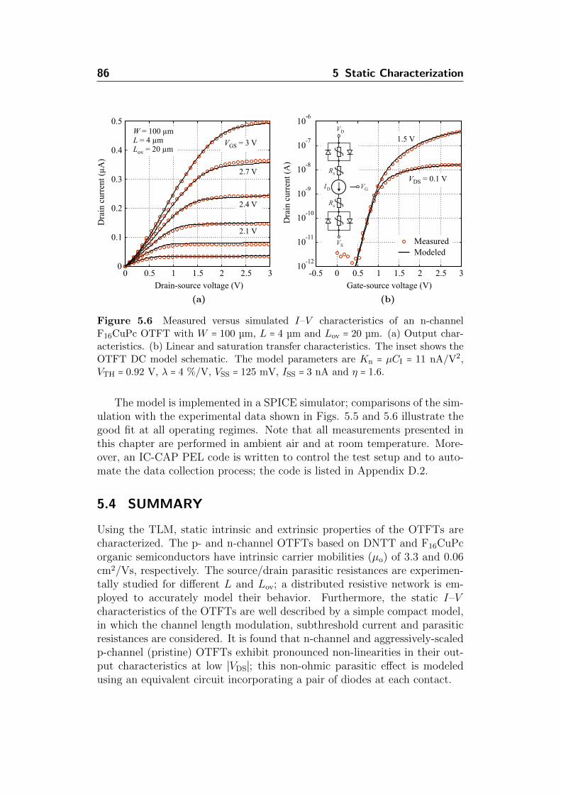
86 5 Static Characterization
W = 100 µm L = 4 µmL = 20 µmov
= 3 VVGS
2.7 V
2.4 V
2.1 V
= 0.1 VVDS
1.5 V
Measured
Modeled
0 0.5 1 1.5 2 2.5 30
0.1
0.2
0.3
0.4
0.5
Drain-source voltage (V)
Dra
in c
urr
ent
(A
)µ
0 0.5 1 1.5 2 2.5 310
-12
10-11
10-10
10-9
10-8
10-7
10-6
Gate-source voltage (V)D
rain
curr
ent
(A)
I D
VD
VS
Rs
Rs
VG
-0.5
(a)
W = 100 µm L = 4 µmL = 20 µmov
= 3 VVGS
2.7 V
2.4 V
2.1 V
= 0.1 VVDS
1.5 V
Measured
Modeled
0 0.5 1 1.5 2 2.5 30
0.1
0.2
0.3
0.4
0.5
Drain-source voltage (V)
Dra
in c
urr
ent
(A
)µ
0 0.5 1 1.5 2 2.5 310
-12
10-11
10-10
10-9
10-8
10-7
10-6
Gate-source voltage (V)D
rain
curr
ent
(A)
I D
VD
VS
Rs
Rs
VG
-0.5
(b)
Figure 5.6 Measured versus simulated I–V characteristics of an n-channelF16CuPc OTFT with W = 100 µm, L = 4 µm and Lov = 20 µm. (a) Output char-acteristics. (b) Linear and saturation transfer characteristics. The inset shows theOTFT DC model schematic. The model parameters are Kn = µCI = 11 nA/V2,VTH = 0.92 V, λ = 4 %/V, VSS = 125 mV, ISS = 3 nA and η = 1.6.
The model is implemented in a SPICE simulator; comparisons of the sim-ulation with the experimental data shown in Figs. 5.5 and 5.6 illustrate thegood fit at all operating regimes. Note that all measurements presented inthis chapter are performed in ambient air and at room temperature. More-over, an IC-CAP PEL code is written to control the test setup and to auto-mate the data collection process; the code is listed in Appendix D.2.
5.4 SUMMARY
Using the TLM, static intrinsic and extrinsic properties of the OTFTs arecharacterized. The p- and n-channel OTFTs based on DNTT and F16CuPcorganic semiconductors have intrinsic carrier mobilities (µo) of 3.3 and 0.06cm2/Vs, respectively. The source/drain parasitic resistances are experimen-tally studied for different L and Lov; a distributed resistive network is em-ployed to accurately model their behavior. Furthermore, the static I–Vcharacteristics of the OTFTs are well described by a simple compact model,in which the channel length modulation, subthreshold current and parasiticresistances are considered. It is found that n-channel and aggressively-scaledp-channel (pristine) OTFTs exhibit pronounced non-linearities in their out-put characteristics at low ∣VDS∣; this non-ohmic parasitic effect is modeledusing an equivalent circuit incorporating a pair of diodes at each contact.
6Admittance Characterization
An accurate modeling of the dynamic response of OTFT-based circuits re-quires an analysis of the charge storage behavior in the transistors. Accord-ingly, this chapter presents an experimental study of the OTFT admittance atdifferent biasing potentials and validates the results with accurate modelingas well as 2-D device simulations. Effects induced by the parasitic elementsthat extend beyond the periphery of the intrinsic transistor, including fringecurrent and contact impedance, are carefully considered. Furthermore, asmall-signal model is built to characterize both the resistive and the reac-tive parts of the measured device admittance. Finally, the implications ofthe measurements are also discussed relating to the OTFTs dynamic perfor-mance, particularly the cutoff frequency and the charge response time.
6.1 PARAMETER EXTRACTION
For admittance measurements, fully-patterned OTFTs with channel widths(W ) of 400 µm and channel lengths (L) of 200, 160, 140, 120, 100, 80, 50and 30 µm are fabricated. To minimize and precisely control the parasiticcapacitances, the top-contact layer is carefully aligned with the patternedbottom-gate layer. Considering the good alignment capability of the high-resolution silicon stencil masks, the gate-overlap length is symmetrically laidout at 10 µm for the source and drain electrodes. Moreover, the organicsemiconductor layer extends beyond the periphery of the intrinsic OTFTsby 30 µm on each side (also called fringe regions).
In the beginning, static current–voltage (I–V ) measurements are per-formed using a DC source/monitor unit (HP 4141B) on the chip, in thedark, in ambient air and at room temperature. Using the transmission linemethod (TLM) analysis, which is described in detail in the previous chapter,at a drain-source voltage (VDS) of −0.1 V, a set of parameters are extracted;an intrinsic charge carrier mobility (µo) of 2.1 cm2/Vs and a threshold voltage(VTH) of −1.04 V are calculated, and at a gate-source voltage (VGS) of −3 V,a sheet resistance (Rsheet) of 420 kΩ/◻ and a contact resistance (RCW ) of 0.1kΩ cm (this value is equal to half of the value reported in [151] due to the dif-ferent notation used) are found. The I–V output and transfer characteristicsof the OTFT with L = 200 µm is shown previously in Fig. 3.4. Furthermore,the simulation and modeling parameters are given in Tables 3.1 and 3.2, not-
87

88 6 Admittance Characterization
ing that some of the values are extracted from admittance measurements asdemonstrated further below. It is observed from the measurements that theOTFTs have very little hysteresis (not shown in Fig. 3.4) indicating a lowinterface trap density and good electrical stability of the DNTT layer on theSAM/AlOx gate dielectric. Since the transistor has a relatively long channel(L = 200 µm ≫ Lov = 10 µm), contact effects are insignificant; accordingly,the effective charge carrier mobility in both the saturation and linear oper-ation regimes are very close to the intrinsic mobility (µo = 2.1 cm2/Vs) andindependent of the gate voltage.
The frequency response analysis by means of admittance (Y ) measure-ments is subsequently conducted to provide much insight with regard to thelimitation factors of the device performance and their origin. For example,the admittance of OTFTs has been investigate in literature to obtain thedoping concentration and charge carrier mobility [211, 212]. Moreover, it hasbeen a useful tool to understand the charge transport mechanism in the poly-crystalline organic semiconducting films that include many grain boundariesand trap sites [213], also to study the charge injection mechanism through thecontact interfaces between the metallic source/drain contacts and the organicsemiconductor [214, 215]. The admittance (Y ) measurements are carried outusing an LCR meter (HP 4284A) at frequencies from 100 Hz up to 1 MHzand at different bias potentials ranging from zero to −3 V under the sameatmospheric conditions as in the static measurements. The IC-CAP PELcodes written to control the LCR meter and to automate data collection aregiven in Appendix D.2. The capacitance (C) and the conductance (G) arecalculated using equations C = Im(Y /ω) and G = Re(Y ), respectively, whereω is the angular frequency.
To initially extract the gate insulator capacitance per unit area (CI),dedicated metal-insulator-metal (MIM) devices with different dimensions(200 × 200, 100 × 100, 50 × 50 and 10 × 10 µm2) are fabricated on the samesubstrate. In principle, the MIM is a two-terminal pendant of the OTFTsharing the same layer structure except for the semiconductor. Figure 6.1ashows the measured capacitance–voltage (C–V ) curves of the MIM struc-tures at frequencies ranging from 500 Hz upto 1 MHz. The average valuemeasured for the MIMs with different areas is found to be CI = 560 nF/cm2
(Tables 3.1 and 3.2). With the hybrid insulator thickness of about di = 5.3nm, an effective value of εi = 3.37 resulted for the relative dielectric constant.
Figure 6.1b shows also the C–V curves of the OTFT with L = 200 µmcalculated from the measured admittance [151]. For this setup, the sourceand drain contacts are electrically shorted and connected to the low terminal(virtual ground) of the LCR meter, while the gate electrode is connected tothe high terminal. A DC potential sweep from zero to −3 V along with asuperimposed AC voltage (Vm) of ±100 mV is applied to the gate. The C–Vcurves show a typical step-like transition from depletion (at low absolute
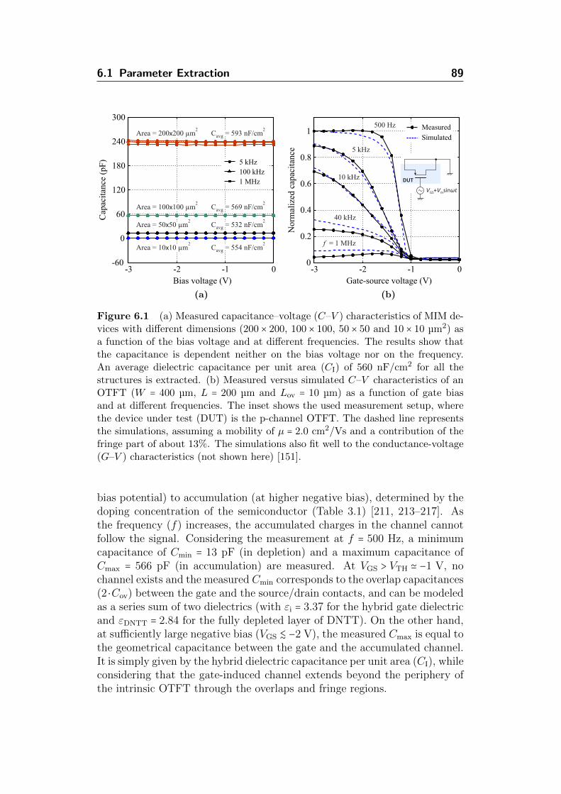
6.1 Parameter Extraction 89
-3 -2 -1 00
0.2
0.4
0.6
0.8
1
Gate-source voltage (V)
No
rmal
ized
Cap
acit
ance
-3 -2 -1 0-60
0
60
120
180
240
300
Bias voltage (V)
Cap
acit
ance
(p
F)
f = 1 MHz
40 kHz
10 kHz
5 kHz
500 Hz Measured
Simulated
DUT
V +V sinωtGS m
2Area = 10x10 µm C = 554 nF/cmavg
2
2Area = 50x50 µm C = 532 nF/cmavg
2
2Area = 100x100 µm C = 569 nF/cmavg
2
2Area = 200x200 µm C = 593 nF/cmavg
2
5 kHz
100 kHz
1 MHz
(a)
-3 -2 -1 00
0.2
0.4
0.6
0.8
1
Gate-source voltage (V)N
orm
aliz
ed c
apac
itan
ce
-3 -2 -1 0-60
0
60
120
180
240
300
Bias voltage (V)
Cap
acit
ance
(p
F)
f = 1 MHz
40 kHz
10 kHz
5 kHz
500 Hz Measured
Simulated
DUT
V +V sinωtGS m
2Area = 10x10 µm C = 554 nF/cmavg
2
2Area = 50x50 µm C = 532 nF/cmavg
2
2Area = 100x100 µm C = 569 nF/cmavg
2
2Area = 200x200 µm C = 593 nF/cmavg
2
5 kHz
100 kHz
1 MHz
(b)
Figure 6.1 (a) Measured capacitance–voltage (C–V ) characteristics of MIM de-vices with different dimensions (200 × 200, 100 × 100, 50 × 50 and 10 × 10 µm2) asa function of the bias voltage and at different frequencies. The results show thatthe capacitance is dependent neither on the bias voltage nor on the frequency.An average dielectric capacitance per unit area (CI) of 560 nF/cm2 for all thestructures is extracted. (b) Measured versus simulated C–V characteristics of anOTFT (W = 400 µm, L = 200 µm and Lov = 10 µm) as a function of gate biasand at different frequencies. The inset shows the used measurement setup, wherethe device under test (DUT) is the p-channel OTFT. The dashed line representsthe simulations, assuming a mobility of µ = 2.0 cm2/Vs and a contribution of thefringe part of about 13%. The simulations also fit well to the conductance-voltage(G–V ) characteristics (not shown here) [151].
bias potential) to accumulation (at higher negative bias), determined by thedoping concentration of the semiconductor (Table 3.1) [211, 213–217]. Asthe frequency (f) increases, the accumulated charges in the channel cannotfollow the signal. Considering the measurement at f = 500 Hz, a minimumcapacitance of Cmin = 13 pF (in depletion) and a maximum capacitance ofCmax = 566 pF (in accumulation) are measured. At VGS > VTH ≃ −1 V, nochannel exists and the measured Cmin corresponds to the overlap capacitances(2 ⋅Cov) between the gate and the source/drain contacts, and can be modeledas a series sum of two dielectrics (with εi = 3.37 for the hybrid gate dielectricand εDNTT = 2.84 for the fully depleted layer of DNTT). On the other hand,at sufficiently large negative bias (VGS ≲ −2 V), the measured Cmax is equal tothe geometrical capacitance between the gate and the accumulated channel.It is simply given by the hybrid dielectric capacitance per unit area (CI), whileconsidering that the gate-induced channel extends beyond the periphery ofthe intrinsic OTFT through the overlaps and fringe regions.
90 6 Admittance Characterization
The usual lack of a self-alignment OTFT process makes the gate-to-contact overlap capacitances inevitable [18, 144, 145, 216]. As a result, thegate electrode is patterned to minimize the impact of the parasitics. Thepronounced ratio between the measured capacitances in the depletion andaccumulation modes (44 times) is due to the patterning of the gate layer andthe use of a relatively small overlap length (Lov = 10 µm ≪ L = 200 µm).This helps in modeling the OTFT intrinsic capacitance accurately. Notethat this change in the capacitance is more evident than previously reportedworks (≲ 6 times) [211, 213–217] owing to the better accuracy and alignmentcapability of the high-resolution silicon stencil masks [13–16].
Furthermore, Fig. 6.1b depicts the results of the 2-D device simulation,which are performed by our partners at the University of Ilmenau on Sen-taurus Device simulator from Synopsys [151]. At the frequency of f = 500Hz, the transition slope between the accumulation and depletion modes isdetermined only by an unintentional doping in the organic semiconductor(NA). From the minimum capacitance, the effective layer thickness (d) ofthe organic semiconductor is estimated. At this frequency, the measuredcurve is well described with NA = 1016 cm−3 and d = 11 nm (Table 3.1) withthe exception of the transition near VGS = −1 V; however, the error in thisregion is less than 10% and probably caused by the large voltage step takenin the measurements. To simulate correctly the flat band voltage, a con-centration of fixed interface charges of Nif = 1.1 × 1012 cm−2 is assumed. Aslightly larger Nif is used in the dynamic simulation compared to the valueused in the static simulation (Nif = 5× 1011 cm−2 given in Table 3.1) becauseof the negative bias stress caused by VGS = −3 V during the measurementsand resulted in a negative shift of the threshold voltage (VTH). The frequencydependence of the C–V curves is well simulated by considering a mobilityof µ = 2.0 cm2/Vs for the injected holes from the source/drain electrodes.As for the highest frequencies (40 KHz and 1 MHz), a smaller contributionof the fringe part should be assumed to reduce the error. Nevertheless, thevalue of the mobility corresponds very well with the aforementioned TLMmeasurements and static simulation.
The sheet charge density of the channel (Qch) in the OTFT can be calcu-lated from the C–V measurements; accordingly, the charge carrier mobility(µ) can be easily extracted from the corresponding linear I–V characteristicsas follows [212]. The carrier mobility (µ) is defined as the drift velocity (vd)of the charge carriers divided by the electric field in the channel (Ech). Giventhat v = ID/(WQch), the charge carrier mobility can be written as
µ =ID
WQchEch
. (6.1)
At sufficiently low drain-source bias (VDS ≪ VGS − VTH; ID in the linearoperation regime), the gate-induced accumulated charges at the semiconduc-

6.2 Frequency Response Analysis 91
tor/dielectric interface are assumed to be uniformly distributed along thechannel length (L); consequently, the electric field across the entire channelis approximately constant (Ech = VDS/L). Moreover, the induced charge den-sity in the channel at different gate-source voltages can be determined fromthe C–V measurements at a low drain-source voltage (VDS = −0.1 V) usingthe following expression [212]:
Qch = ∫
VGS
+∞(Cch
WL)dV, (6.2)
where Cch is the channel capacitance and is obtained by subtracting theoverlap capacitances (2 ⋅Cov) between the gate and the source/drain contactsfrom the total measured OTFT capacitance.
Large contact resistances in the OTFT may introduce error into the calcu-lation of the mobility [212]. Therefore, to minimize the effects of the contactresistances, the measured C–V and I–V (Figs. 6.1b and 3.4) characteristicsof the longest channel (L = 200 µm) are considered here. From the TLM, itis found that the contact resistances are significantly smaller (< 3%) than thechannel resistance for the OTFT with W = 400 µm and L = 200 µm. Sub-tracting the measured minimum capacitance (Cmin = 13 pF) at VGS = −0.8–0V, which corresponds to the overlap capacitances (2 ⋅ Cov), from the mea-sured C–V characteristics at the frequency of f = 500 Hz (Fig. 6.1b) yieldsthe desired channel capacitance (Cch). A sheet charge density (Qch) of 1.23µC/cm2 is therefore obtained at VGS = −3 V by substituting Cch in (6.2).At VDS = −0.1 V, a linear drain current (∣ID∣) of 0.46 µA is measured anda constant electric field (∣Ech∣) of 500 V/m is calculated. Finally, a chargecarrier mobility (µ) of 1.9 cm2/Vs is extracted from (6.1). This value cor-responds very well with the aforementioned TLM measurements and staticsimulations.
6.2 FREQUENCY RESPONSE ANALYSIS
To further investigate the charge response behavior, the capacitance (C) andthe loss (G/ω) of the OTFTs are measured as a function of the frequency.This helps to clarify the limitation factors for the AC characteristics of theOTFTs. Similar to the previous setup shown in the inset of Fig. 6.1b, theresults include the intrinsic as well as the parasitic OTFT components, i.e.,the fringe regions that extend beyond the periphery of the intrinsic OTFTand the overlap regions between the gate and the source/drain electrodes.
Figure 6.2 show the admittance measurements of the OTFT withW = 400µm, L = 200 µm and Lov = 10 µm [151]. Above threshold (VTH = −1.08 V), theholes appear to respond well to the applied small signal and the measuredcapacitance is proportional to the channel length. This is valid up to acertain frequency depending on the applied gate potential; however, their
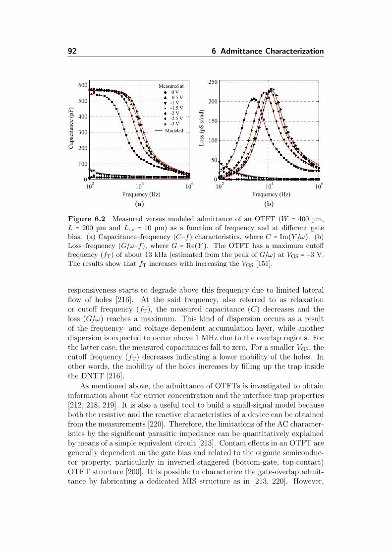
92 6 Admittance Characterization
102
104
106
0
100
200
300
400
500
600
Frequency (Hz)
Cap
acit
ance
(pF
)
102
104
106
0
50
100
150
200
250
Frequency (Hz)L
oss
(pS
s/r
ad)
Modeled
0 V-0.5 V-1 V-1.5 V-2 V-2.5 V-3 V .
Measured at
(a)
102
104
106
0
100
200
300
400
500
600
Frequency (Hz)
Cap
acit
ance
(pF
)
102
104
106
0
50
100
150
200
250
Frequency (Hz)L
oss
(pS
s/r
ad)
Modeled
0 V-0.5 V-1 V-1.5 V-2 V-2.5 V-3 V .
Measured at
(b)
Figure 6.2 Measured versus modeled admittance of an OTFT (W = 400 µm,L = 200 µm and Lov = 10 µm) as a function of frequency and at different gatebias. (a) Capacitance–frequency (C–f) characteristics, where C = Im(Y /ω). (b)Loss–frequency (G/ω–f), where G = Re(Y ). The OTFT has a maximum cutofffrequency (fT) of about 13 kHz (estimated from the peak of G/ω) at VGS = −3 V.The results show that fT increases with increasing the VGS [151].
responsiveness starts to degrade above this frequency due to limited lateralflow of holes [216]. At the said frequency, also referred to as relaxationor cutoff frequency (fT), the measured capacitance (C) decreases and theloss (G/ω) reaches a maximum. This kind of dispersion occurs as a resultof the frequency- and voltage-dependent accumulation layer, while anotherdispersion is expected to occur above 1 MHz due to the overlap regions. Forthe latter case, the measured capacitances fall to zero. For a smaller VGS, thecutoff frequency (fT) decreases indicating a lower mobility of the holes. Inother words, the mobility of the holes increases by filling up the trap insidethe DNTT [216].
As mentioned above, the admittance of OTFTs is investigated to obtaininformation about the carrier concentration and the interface trap properties[212, 218, 219]. It is also a useful tool to build a small-signal model becauseboth the resistive and the reactive characteristics of a device can be obtainedfrom the measurements [220]. Therefore, the limitations of the AC character-istics by the significant parasitic impedance can be quantitatively explainedby means of a simple equivalent circuit [213]. Contact effects in an OTFT aregenerally dependent on the gate bias and related to the organic semiconduc-tor property, particularly in inverted-staggered (bottom-gate, top-contact)OTFT structure [200]. It is possible to characterize the gate-overlap admit-tance by fabricating a dedicated MIS structure as in [213, 220]. However,
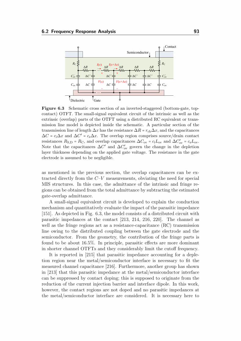
6.2 Frequency Response Analysis 93
Figure 6.3 Schematic cross section of an inverted-staggered (bottom-gate, top-contact) OTFT. The small-signal equivalent circuit of the intrinsic as well as theextrinsic (overlap) parts of the OTFT using a distributed RC equivalent or trans-mission line model is depicted inside the schematic. A particular section of thetransmission line of length ∆x has the resistance ∆R = rch∆x, and the capacitances∆C = ci∆x and ∆C ′ = cs∆x. The overlap region comprises source/drain contactresistances RS,D = RC, and overlap capacitances ∆Cov = ciLov and ∆C ′
ov = csLov.Note that the capacitances ∆C ′ and ∆C ′
ov govern the change in the depletionlayer thickness depending on the applied gate voltage. The resistance in the gateelectrode is assumed to be negligible.
as mentioned in the previous section, the overlap capacitances can be ex-tracted directly from the C–V measurements, obviating the need for specialMIS structures. In this case, the admittance of the intrinsic and fringe re-gions can be obtained from the total admittance by subtracting the estimatedgate-overlap admittance.
A small-signal equivalent circuit is developed to explain the conductionmechanism and quantitatively evaluate the impact of the parasitic impedance[151]. As depicted in Fig. 6.3, the model consists of a distributed circuit withparasitic impedances at the contact [213, 214, 216, 220]. The channel aswell as the fringe regions act as a resistance-capacitance (RC) transmissionline owing to the distributed coupling between the gate electrode and thesemiconductor. From the geometry, the contribution of the fringe parts isfound to be about 16.5%. In principle, parasitic effects are more dominantin shorter channel OTFTs and they considerably limit the cutoff frequency.
It is reported in [215] that parasitic impedance accounting for a deple-tion region near the metal/semiconductor interface is necessary to fit themeasured channel capacitance [216]. Furthermore, another group has shownin [213] that this parasitic impedance at the metal/semiconductor interfacecan be suppressed by contact doping; this is supposed to originate from thereduction of the current injection barrier and interface dipole. In this work,however, the contact regions are not doped and no parasitic impedances atthe metal/semiconductor interface are considered. It is necessary here to

94 6 Admittance Characterization
Table 6.1 List of model parameters used in the OTFT (W = 400 µm and Lov =
10 µm) small-signal equivalent circuit. The parameters listed below, namely thesheet resistance (Rsheet) and semiconductor capacitance (CS), are those that aredependent on the gate-source voltage (VGS). In addition, RC ⋅W = 0.12 kΩ cm andCI = 560 nF/cm2 are included in the model.
Model parameterGate-source voltage [VGS (V)]
0 −0.5 −1.0 −1.5 −2.0 −2.5 −3.0
Rsheet = rch ⋅W (kΩ/◻) ⇑ ⇑ ⇑ 3100 1000 620 500
CS = cs/W (µF/cm2)a 0.2 0.23 0.35 10.5 ⇑ ⇑ ⇑
aIn depletion, CS governs the change in the depletion layer thickness.
include only contact resistances and overlap capacitances into the model toproperly simulate the measured data.
Referring to Fig. 6.3, the model consists of five parameters, namelysource/drain contact resistances (RS,D), channel resistance per unit length(rch), dielectric capacitance per unit length (ci) and semiconductor capac-itance per unit length (cs) [151]. The resistance in the gate electrode isneglected because the resistance in the channel is large enough in this exper-iment. The resistances RS,D (Ω) and rch (Ω/cm) are directly obtained fromthe TLM, where RS,D = RC and rch = Rsheet/W . Note that the expressionof RC for our inverted-staggered OTFTs is derived in Appendix C.2. Sincethere is no potential difference between the drain and source electrodes inthis setup, rch is assumed to be uniform along the channel. The accumu-lated charges of the intrinsic gate region of the OTFT are, however, non-uniformly distributed along the channel when a drain-source bias is applied.Furthermore, rch is assumed to be uniform along the channel also becausethe amount of accumulated holes does not change considerably during theadmittance measurements by the AC small signal under high negative DCgate-source bias [216]. In depletion, the capacitance cs (F/cm) governs thechange in the depletion layer thickness depending on the applied gate voltage.In accumulation, the influence of the semiconductor capacitance is negligible(cs ≫ ci). Finally, ci (F/cm) is acquired from the capacitance measurementsof the MIM structure (Fig. 6.1a), where ci = CI ⋅W .
At VGS = −3 V, the following values are used: RC ⋅W = 0.12 kΩ cm,Rsheet = 500 kΩ/◻ and CI = 560 nF/cm2. There is only a slight difference(less than 20%) to the values extracted from the TLM. Table 6.1 summarizesall the modeling parameters used at the different gate-source voltages. Asdepicted in Fig. 6.2, the model shows an excellent agreement with both thecapacitance and loss of the measured admittance over the complete frequencyrange (100 Hz–1 MHz).
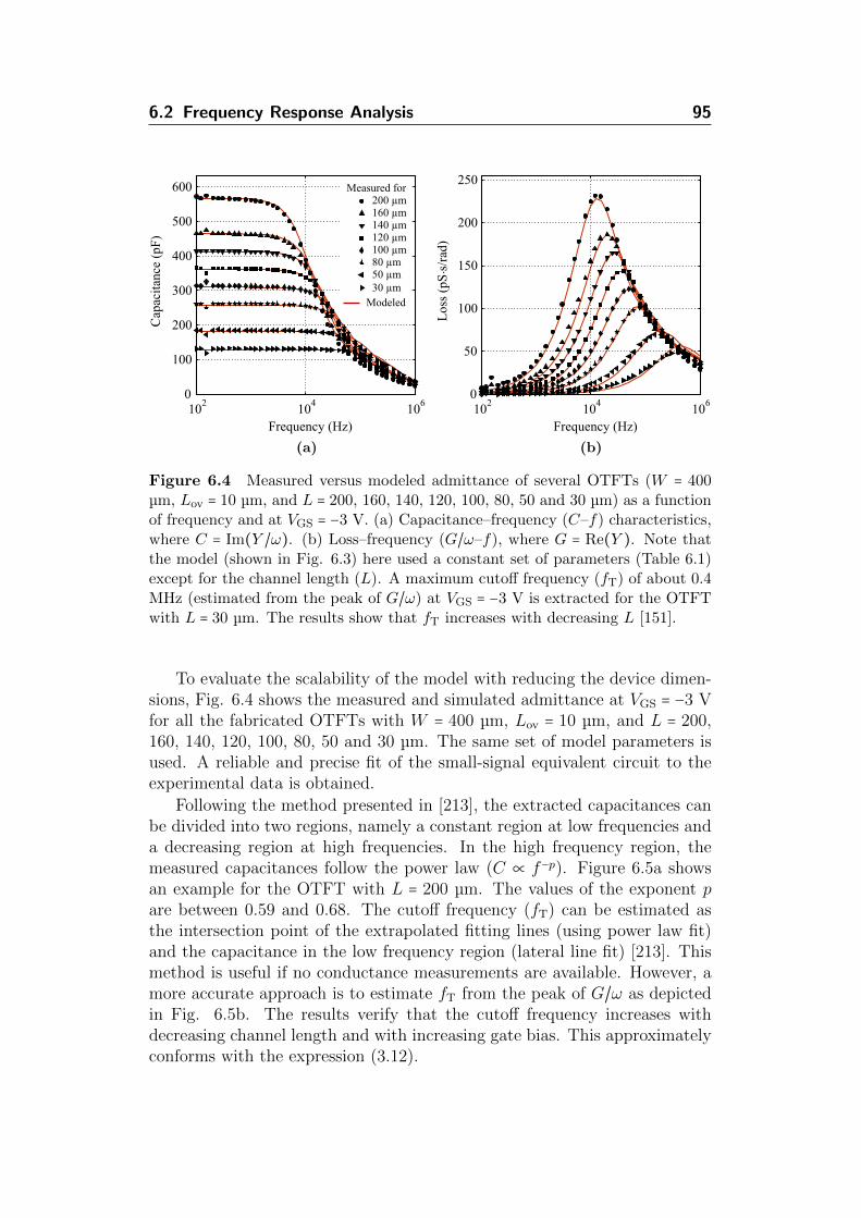
6.2 Frequency Response Analysis 95
102
104
106
0
100
200
300
400
500
600
Frequency (Hz)
Cap
acit
ance
(pF
)
102
104
106
0
50
100
150
200
250
Frequency (Hz)
200 µm160 µm140 µm120 µm100 µm80 µm50 µm30 µm
Measured for
Modeled
Los
s (p
S s
/rad
).
(a)
102
104
106
0
100
200
300
400
500
600
Frequency (Hz)
Cap
acit
ance
(pF
)
102
104
106
0
50
100
150
200
250
Frequency (Hz)
200 µm160 µm140 µm120 µm100 µm80 µm50 µm30 µm
Measured for
Modeled
Los
s (p
S s
/rad
).
(b)
Figure 6.4 Measured versus modeled admittance of several OTFTs (W = 400µm, Lov = 10 µm, and L = 200, 160, 140, 120, 100, 80, 50 and 30 µm) as a functionof frequency and at VGS = −3 V. (a) Capacitance–frequency (C–f) characteristics,where C = Im(Y /ω). (b) Loss–frequency (G/ω–f), where G = Re(Y ). Note thatthe model (shown in Fig. 6.3) here used a constant set of parameters (Table 6.1)except for the channel length (L). A maximum cutoff frequency (fT) of about 0.4MHz (estimated from the peak of G/ω) at VGS = −3 V is extracted for the OTFTwith L = 30 µm. The results show that fT increases with decreasing L [151].
To evaluate the scalability of the model with reducing the device dimen-sions, Fig. 6.4 shows the measured and simulated admittance at VGS = −3 Vfor all the fabricated OTFTs with W = 400 µm, Lov = 10 µm, and L = 200,160, 140, 120, 100, 80, 50 and 30 µm. The same set of model parameters isused. A reliable and precise fit of the small-signal equivalent circuit to theexperimental data is obtained.
Following the method presented in [213], the extracted capacitances canbe divided into two regions, namely a constant region at low frequencies anda decreasing region at high frequencies. In the high frequency region, themeasured capacitances follow the power law (C ∝ f−p). Figure 6.5a showsan example for the OTFT with L = 200 µm. The values of the exponent pare between 0.59 and 0.68. The cutoff frequency (fT) can be estimated asthe intersection point of the extrapolated fitting lines (using power law fit)and the capacitance in the low frequency region (lateral line fit) [213]. Thismethod is useful if no conductance measurements are available. However, amore accurate approach is to estimate fT from the peak of G/ω as depictedin Fig. 6.5b. The results verify that the cutoff frequency increases withdecreasing channel length and with increasing gate bias. This approximatelyconforms with the expression (3.12).

96 6 Admittance Characterization
0
100
200
300
400
500
600
200 µm160 µm140 µm120 µm
100 µm80 µm50 µm30 µm
Extracted for
102
104
106
0
100
200
300
400
500
600
Frequency (Hz)
Cap
acit
ance
(pF
)
-3-2.5-2-1.5
Gate-source voltage (V)
Cut
off
freq
uenc
y (
kHz)
0 V-0.5 V-1 V-1.5 V-2 V-2.5 V-3 V
Measured at
C ∞ f-p
(a)
0
100
200
300
400
500
600
200 µm160 µm140 µm120 µm
100 µm80 µm50 µm30 µm
Extracted for
102
104
106
0
100
200
300
400
500
600
Frequency (Hz)
Cap
acit
ance
(pF
)
-3-2.5-2-1.5
Gate-source voltage (V)C
utof
f fr
eque
ncy (
kHz)
0 V-0.5 V-1 V-1.5 V-2 V-2.5 V-3 V
Measured at
C ∞ f-p
(b)
Figure 6.5 (a) Measured capacitance–frequency (C–f) characteristics of anOTFT with (W = 400 µm, L = 200 µm and Lov = 10 µm) as a function of fre-quency and at different gate bias. At VGS > VTH, the capacitance follow the powerlaw (C ∝ f−p) in the high frequency region and is nearly constant in the low fre-quency region, noting that the cutoff frequency can be roughly estimated from theintersection point between the two fitting lines [213]. The values of the exponentp are 0.59, 0.6, 0.62 and 0.68 at VGS = −1.5, −2.0, −2.5 and −3.0 V, respectively.(b) Extracted cutoff frequency (fT) of all the OTFTs (W = 400 µm, Lov = 10 µm,and L = 200, 160, 140, 120, 100, 80, 50 and 30 µm) from the peak of G/ω. Theresults verify that fT approximately complies with (3.12), i.e., fT increases withdecreasing L and with increasing VGS.
6.3 EFFECTIVE DELAY OF GATE-INDUCED CHARGES
The charges in the OTFT channel cannot be induced instantaneously withthe applied gate-source voltage; therefore, the charge response time can be abottleneck in the high frequency operation of the device [220]. A quantitativeevaluation of the effective RC delay time (τ), which is needed to make thecharges induced in the channel, requires first to derive expressions for thegate-to-channel capacitance (Cch) and loss (Gch/ω) of the intrinsic OTFT.Referring to Fig. 6.3, a transmission line model (RC network) is used for thecalculation of the capacitance. Assuming the transistor is operated in theaccumulation regime, the influence of the capacitances ∆C ′ and ∆C ′
ov thatgovern the change in the depletion layer thickness depending on the gatevoltage are negligible, i.e., ∆C ≫ ∆C ′ and ∆Cov ≫ ∆C ′
ov. Considering onlythe intrinsic part of the OTFT (valid when L ≫ Lov), a particular sectionof the transmission line of length ∆x has the resistance ∆R = Rsheet∆x/Wand the capacitance ∆C = CIW∆x. By following a procedure similar to that

6.3 Effective Delay of Gate-Induced Charges 97
used in [221] and [222], we apply Kirchhoff’s voltage and current laws andtake the limit ∆x→ 0 to obtain
∂I
∂x= −jωCIWV (x), (6.3)
∂V
∂x= −
Rsheet
WI(x). (6.4)
We then combine (6.3) and (6.4) and solve the resulting second-order lineardifferential equation to get expressions for the current I(x) and the volt-age V (x). After a considerable amount of algebra, it can be deduced thatthe gate-to-channel capacitance (Cch) and loss (Gch/ω) are expressed by thefollowing [151, 220, 221]:
Cch =1
ωIm [
2I(x = 0)
V (x = 0)] =
CIWL
α(
sinhα + sinα
coshα + cosα) , (6.5)
Gch
ω= Re [
2I(x = 0)
V (x = 0)] =
CIWL
α(
sinhα − sinα
coshα + cosα) , (6.6)
where α =√ωRsheetCIL2/2. Detailed steps for the derivation of Cch and
Gch/ω are given in Appendix C.1.When α = 1, the channel capacitance (Cch) given in (6.5) is equal 0.97 ×
CIWL. Therefore, the delay time (τ = 1/ω) that is needed for 97% of thetotal charges in the channel to be induced and effectively responding, isaccordingly determined as
τ =RsheetCIL2
2. (6.7)
This relation is slightly different from the one reported in [220] because ofthe different device structure used. Figure 6.6a shows the calculated τ as afunction of L using the same modeling parameters: Rsheet = 500 kΩ/◻ andCI = 560 nF/cm2 [151]. Such a plot can be used to deduce information aboutthe maximum frequency achieved for a given minimum channel length and/ormaximum channel length needed for a given frequency. For example, one canestimate from Fig. 6.6a that for a successful operation at f = 10 kHz, theOTFT should have L ≤ 106 µm. To verify this estimation, normalized C–Vcharacteristics of the OTFTs with L = 200, 160, 140, 120, 100, 80, 50 and30 µm measured at 10 kHz are depicted in Fig. 6.6b. The normalization isimplemented by dividing the measured C–V data by 1.165CIW (L + 2Lov)
to account for the parasitic components, i.e., the fringe (16.5%) and overlapregions (Lov = 10 µm). There is an error of less than 3% because of thisassumption; when L = 100 µm, the normalized channel capacitance almostreaches unity at VGS = −3 V, but longer devices cannot fully induce the
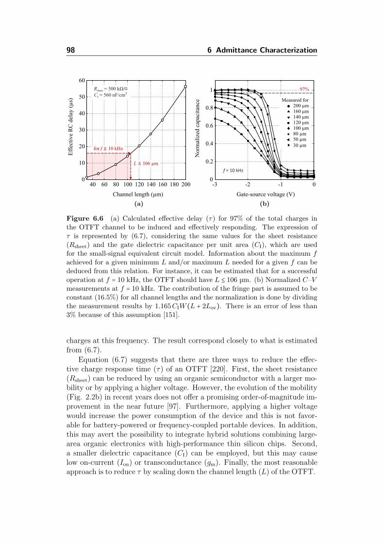
98 6 Admittance Characterization
40 60 80 100 120 140 160 180 2000
10
20
30
40
50
60
Channel length (µm)
Eff
ecti
ve R
C d
elay
(µ
s)
-3 -2 -1 00
0.2
0.4
0.6
0.8
1
Gate-source voltage (V)N
orm
aliz
ed c
apac
itan
ce
97%
200 µm160 µm140 µm120 µm100 µm80 µm50 µm30 µm
Measured for
f = 10 kHz
R = 500 kΩ/sheet
C = 560 nF/cmI2
for f ≥ 10 kHz
L ≤ 106 µm
(a)
40 60 80 100 120 140 160 180 2000
10
20
30
40
50
60
Channel length (µm)
Eff
ecti
ve R
C d
elay
(µ
s)
-3 -2 -1 00
0.2
0.4
0.6
0.8
1
Gate-source voltage (V)N
orm
aliz
ed c
apac
itan
ce
97%
200 µm160 µm140 µm120 µm100 µm80 µm50 µm30 µm
Measured for
f = 10 kHz
R = 500 kΩ/sheet
C = 560 nF/cmI2
for f ≥ 10 kHz
L ≤ 106 µm
(b)
Figure 6.6 (a) Calculated effective delay (τ) for 97% of the total charges inthe OTFT channel to be induced and effectively responding. The expression ofτ is represented by (6.7), considering the same values for the sheet resistance(Rsheet) and the gate dielectric capacitance per unit area (CI), which are usedfor the small-signal equivalent circuit model. Information about the maximum fachieved for a given minimum L and/or maximum L needed for a given f can bededuced from this relation. For instance, it can be estimated that for a successfuloperation at f = 10 kHz, the OTFT should have L ≤ 106 µm. (b) Normalized C–Vmeasurements at f = 10 kHz. The contribution of the fringe part is assumed to beconstant (16.5%) for all channel lengths and the normalization is done by dividingthe measurement results by 1.165CIW (L + 2Lov). There is an error of less than3% because of this assumption [151].
charges at this frequency. The result correspond closely to what is estimatedfrom (6.7).
Equation (6.7) suggests that there are three ways to reduce the effec-tive charge response time (τ) of an OTFT [220]. First, the sheet resistance(Rsheet) can be reduced by using an organic semiconductor with a larger mo-bility or by applying a higher voltage. However, the evolution of the mobility(Fig. 2.2b) in recent years does not offer a promising order-of-magnitude im-provement in the near future [97]. Furthermore, applying a higher voltagewould increase the power consumption of the device and this is not favor-able for battery-powered or frequency-coupled portable devices. In addition,this may avert the possibility to integrate hybrid solutions combining large-area organic electronics with high-performance thin silicon chips. Second,a smaller dielectric capacitance (CI) can be employed, but this may causelow on-current (Ion) or transconductance (gm). Finally, the most reasonableapproach is to reduce τ by scaling down the channel length (L) of the OTFT.
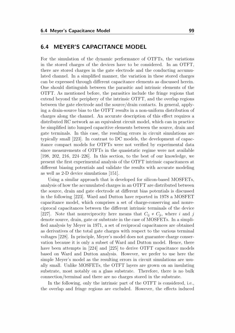
6.4 Meyer’s Capacitance Model 99
6.4 MEYER’S CAPACITANCE MODEL
For the simulation of the dynamic performance of OTFTs, the variationsin the stored charges of the devices have to be considered. In an OTFT,there are stored charges in the gate electrode and the conducting accumu-lated channel. In a simplified manner, the variation in these stored chargescan be expressed through different capacitance elements as discussed herein.One should distinguish between the parasitic and intrinsic elements of theOTFT. As mentioned before, the parasitics include the fringe regions thatextend beyond the periphery of the intrinsic OTFT, and the overlap regionsbetween the gate electrode and the source/drain contacts. In general, apply-ing a drain-source bias to the OTFT results in a non-uniform distribution ofcharges along the channel. An accurate description of this effect requires adistributed RC network as an equivalent circuit model, which can in practicebe simplified into lumped capacitive elements between the source, drain andgate terminals. In this case, the resulting errors in circuit simulations aretypically small [223]. In contrast to DC models, the development of capac-itance compact models for OTFTs were not verified by experimental datasince measurements of OTFTs in the quasistatic regime were not available[198, 202, 216, 224–226]. In this section, to the best of our knowledge, wepresent the first experimental analysis of the OTFT intrinsic capacitances atdifferent biasing potentials and validate the results with accurate modelingas well as 2-D device simulations [151].
Using a similar approach that is developed for silicon-based MOSFETs,analysis of how the accumulated charges in an OTFT are distributed betweenthe source, drain and gate electrode at different bias potentials is discussedin the following [223]. Ward and Dutton have reported in 1978 a MOSFETcapacitance model, which comprises a set of charge-conserving and nonre-ciprocal capacitances between the different intrinsic terminals of the device[227]. Note that nonreciprocity here means that Cij ≠ Cji, where i and jdenote source, drain, gate or substrate in the case of MOSFETs. In a simpli-fied analysis by Meyer in 1971, a set of reciprocal capacitances are obtainedas derivatives of the total gate charges with respect to the various terminalvoltages [228]. In principle, Meyer’s model does not guarantee charge conser-vation because it is only a subset of Ward and Dutton model. Hence, therehave been attempts in [224] and [225] to derive OTFT capacitance modelsbased on Ward and Dutton analysis. However, we prefer to use here thesimple Meyer’s model as the resulting errors in circuit simulations are usu-ally small. Unlike MOSFETs, the OTFT layers are grown on an insulatingsubstrate, most notably on a glass substrate. Therefore, there is no bulkconnection/terminal and there are no charges stored in the substrate.
In the following, only the intrinsic part of the OTFT is considered, i.e.,the overlap and fringe regions are excluded. However, the effects induced
100 6 Admittance Characterization
by the parasitic elements on the capacitance measurements are investigatedhereinafter. According to the Meyer’s capacitance model, the distributedintrinsic capacitances of an OTFT can be split into the following two lumpedcapacitances, namely gate-source (Cgs) and gate-drain (Cgd) capacitances,which are expressed as
Cgs =∂QG
∂VGS
∣VGD
, (6.8)
Cgd =∂QG
∂VGD
∣VGS
, (6.9)
where QG is the total intrinsic gate charges [223]. The capacitances Cgs
(F) and Cgd (F) are assumed to be dominated by the gate-induced accumu-lated charges. Thus, the contribution of the accumulated charges to the gatecharges is determined by integrating the sheet charge density of the channel(Qch) over the active gate area:
QG = CIW ∫L
0(VG − VTH − Vx)dx, (6.10)
where Vx is the voltage at an arbitrary distance x from the source. Using thewell-established concept of charge drift, the drain current (ID) in an OTFTcan be deduced from (6.1) as
ID = µCIW (VG − VTH − Vx)∂Vx
∂x. (6.11)
The current is constant along the channel and dVx = (∂Vx/∂x)dx. By sub-stituting for dx using (6.11) in (6.10) and changing the integral limits, weobtain
QG =µC2
I W2
ID∫
VD
VS(VG − VTH − Vx)
2 dVx
=µC2
I W2
3ID
[(VGS − VTH)3 − (VGD − VTH)3] . (6.12)
Using the expression (3.4) for the drain current (ID) in the linear operationregime and replacing VDS by VGS − VGD, we get
ID =µCIW
L[(VGS − VTH)VDS −
V 2DS
2]
=µCIW
2LVDS [(VGS − VTH) + (VGD − VTH)]
=µCIW
L[(VGS − VTH)2 − (VGD − VTH)2] . (6.13)

6.4 Meyer’s Capacitance Model 101
Substituting (6.13) in (6.12), the total intrinsic gate charges (QG) can there-fore be expressed as
QG =2
3CIWL
(VGS − VTH)3 − (VGD − VTH)3
(VGS − VTH)2 − (VGD − VTH)2. (6.14)
Finally, The gate-source (Cgs) and gate-drain (Cgd) capacitances can be ob-tained by substituting (6.14) in (6.8) and (6.9), respectively:
Cgs =2
3CIWL
⎡⎢⎢⎢⎢⎣
1 − (VGT − VDS
2VGT − VDS
)
2⎤⎥⎥⎥⎥⎦
, (6.15)
Cgd =2
3CIWL
⎡⎢⎢⎢⎢⎣
1 − (VGT
2VGT − VDS
)
2⎤⎥⎥⎥⎥⎦
, (6.16)
where VGT = VGS − VTH, also called the gate-overdrive voltage. At VDS = 0 V,both the gate-source and gate-drain capacitances are equal to 1/2 ⋅ CIWL.In saturation regime (VDS ≥ VGS − VTH), the drain-source voltage is givenby VDS = VGT, and thus, Cgs and Cgd are equal to 2/3 ⋅ CIWL and zero,respectively. This indicates that a small change in the applied drain-sourcevoltage (VDS) when the channel is pinched off during the saturation regimedoes not have an impact on the gate or channel charges; however, the channelis completely assigned to the source terminal, resulting in a maximum valuefor the gate-source capacitance (Cgs,max = 2/3 ⋅CIWL) [223].
Discontinuities in the derivatives of the Meyer capacitances given by(6.15) and (6.16) occur at the onset of saturation. Such discontinuities shouldbe avoided in the device models since they give rise to increased simulationtime and conversion problems in circuit simulators [223]. A smooth tran-sition between the nonsaturated (linear or off regimes) and the saturatedregimes is assured by replacing VDS in (6.15) and (6.16) by VDSe, where VDSe
is an effective drain-source voltage that is equal to VDS for VDS < VGT andis equal to VGT for VDS > VGT. This is achieved by the following asymptoticinterpolation function for the effective drain-source voltage (VDSe) [223]:
VDSe =1
2[VDS + VGT −
√
V 2δ + (VDS − VGT)
2], (6.17)
where Vδ is a constant voltage that determines the width of the transitionregion; It is a fitting parameter that is extracted from the measurements.
We have considered so far admittance measurements with shorted sourceand drain contacts, however, a different setup is used here to account for thevariations in the stored charges of the OTFT at different drain-source (VDS)and gate-source (VGS) voltages. Accordingly, the gate electrode is connectedto the low terminal (virtual ground) of the LCR meter, while the source and
102 6 Admittance Characterization
-3 -2 -1 00
50
100
150
200
250
300
350
400
Drain-source voltage (V)
Cap
acit
ance
(pF
)
-3 -2 -1 00
50
100
150
200
250
300
350
400
Gate-source voltage (V)C
apac
itan
ce (
pF)
Measured for
V = -1.0 VDS
V = -1.5 VDS
V = -0.5 VDS
ModeledSimulated
Measured at
V = -2.5 VGS
V = -3.0 VGS
V = -2.0 VGS Cgd
Cgs
Cgd
CgsV + V sinωtGD mVGS
DUT
Cgs Cgd
(a)
-3 -2 -1 00
50
100
150
200
250
300
350
400
Drain-source voltage (V)
Cap
acit
ance
(pF
)
-3 -2 -1 00
50
100
150
200
250
300
350
400
Gate-source voltage (V)C
apac
itan
ce (
pF)
Measured at
V = -1.0 VDS
V = -1.5 VDS
V = -0.5 VDS
ModeledSimulated
Measured for
V = -2.5 VGS
V = -3.0 VGS
V = -2.0 VGS Cgd
Cgs
Cgd
CgsV + V sinωtGD mVGS
DUT
Cgs Cgd
(b)
Figure 6.7 Measured gate-source (Cgs) and gate-drain (Cgd) capacitances alongwith modeled and simulated results of an OTFT (W = 400 µm, L = 200 µm andLov = 10 µm) at f = 500 Hz. (a) Cgs and Cgd as a function of VDS. (b) Cgs
and Cgd as a function of VGS. Note that the modeled curves are represented by(6.15) and (6.16) along with the interpolation function (6.17), which are validabove threshold (solid lines). The voltage-dependent fringe factor of the simulatedcurves is calculated by dividing the measured value of Cgs by the simulated intrinsicvalue. The inset shows the used measurement setup, where the gate electrode isconnected to the low terminal (virtual ground) of the LCR meter, and the sourceand drain contacts are connected alternatively to the high terminal of the LCRmeter and the DC voltage source [151].
drain contacts are connected alternatively to the high terminal of the LCRmeter (HP 4284A precision LCR meter) and a DC voltage source (Keithley230 programmable voltage source) [151, 216]. The DC voltages VDS and VGS
are both swept from zero to −3 V and an AC signal of ±100 mV with f = 500Hz is applied to either the source or the drain.
Figure 6.7 shows the measured gate-source (Cgs) and gate-drain (Cgd)capacitances along with modeled and simulated results for the OTFT withW = 400 µm, L = 200 µm and Lov = 10 µm [151]. The measured datainclude both the intrinsic and parasitic components. Similar to the previousmeasurements, the parasitic component is composed of about 16.5% for thefringe region and a constant Cov = 6.5 pF for each of the gate-source andgate-drain overlap areas. By excluding the parasitic components from themeasured data, it is found that Cgs = Cgd = 1/2 ⋅ CIWL at VDS = 0 V, whileCgs and Cgd approach 2/3 ⋅CIWL and zero, respectively, at VDS ≥ VGS − VTH
(saturation regime). This charge storage effect complies with the Meyer’scapacitance model described above.

6.5 Summary 103
Using CI = 580 nF/cm2, VTH = −1.18 V and Vδ = 0.1 V in additionto multiplying both (6.15) and (6.16) by 1.165 for the fringe region andadding 6.5 pF for the overlap capacitance (Cov), a precise fit between themodeled and measured data is accomplished as demonstrated in Fig. 6.7.Furthermore, the measured and modeled characteristics are compared to 2-D device simulation results. Using the same simulation parameters given inTable 3.1, an excellent agreement for all voltage regions is obtained for bothCgs and Cgd. It is necessary here to include a voltage-dependent fringe factorbecause otherwise the results would not be well described. The reason issimply the smaller influence of fringe effects for small intrinsic capacitances,which occurs in the case of the subthreshold or the linear operation regions.The fringe factor is calculated by dividing the measured Cgs–VGS by thesimulated intrinsic values at the different drain-source voltages. The resultsdo not show a strong dependency of the fringe factor on the drain-sourcevoltage but it changes considerable depending on the gate-source voltageranging from about 0.6 at VGS = −1.3 V to 1.19 at VGS = −3 V.
6.5 SUMMARY
Frequency response analysis on inverted-staggered (bottom-gate, top-contact)OTFTs based on DNTT organic semiconductor by means of admittance mea-surements is performed. The results confirm that the cutoff frequency (fT)of the OTFTs increases with decreasing channel length (L) and with increas-ing gate-source bias (VGS). A small-signal equivalent circuit based on a dis-tributed RC network or a transmission line model is used to produce a preciseand reliable fit to the data for different operating frequencies (100 Hz–1 MHz),biasing potentials (−3 V to zero) and channel lengths (30µm to 200µm). Aquantitative evaluation of the effective RC delay time (τ), which is neededto make the charges induced in the OTFT channel, is demonstrated. Fur-thermore, the charge storage behavior in the OTFT is very well describedby compact modeling and verified against 2-D device simulations. The de-pendence of the intrinsic gate-source (Cgs) and gate-drain (Cgd) capacitanceson the applied gate-source (VGS) and gate-drain (VGD) voltages shows anexcellent agreement with Meyer’s capacitance model, which can in principlebe easily incorporated into a SPICE simulator. This is the first study toundertake experimental analysis of OTFT intrinsic capacitances at differentbiasing potentials and validate the results with accurate modeling and sim-ulations. The material parameters used for all the dynamic characterizationcorrespond closely to those extracted from the static measurements, withthe exception of the density of fixed interface states (Nif). This is because ofthe negative bias stress imposed during the dynamic measurements, whichresults in a negative shift of the threshold voltage (VTH).
7Scattering ParameterCharacterization
Recent developments of the performance of OTFTs in the past few years haveled to a renewed interest in characterizing their AC electrical properties usinga self-contained method. Accordingly, the first comprehensive experimen-tal study of the frequency response of OTFTs using scattering S-parametermeasurements is introduced in this chapter. A small-signal model, whichincludes intrinsic as well as extrinsic components, derived from the physicalbehavior of the device is presented. An excellent fit between measured andsimulated S-parameters is demonstrated. The frequency performance of themodel is examined in terms of its current-gain cutoff frequency. The channellength dependence of the cutoff frequency is described in a compact modeland a close agreement to the measured data of OTFTs with variable devicedimensions is shown. Moreover, the correspondence between static and dy-namic characterization is discussed. For this study, low-voltage OTFTs basedon the air-stable DNTT organic semiconductor having various channel andgate-overlap lengths are utilized. Furthermore, the impact of misalignmentbetween the source/drain contacts and the patterned gate on the dynamicTFT performance is explored and a simple method to estimate the degreeof misalignment from the measured S-parameters is proposed. The inten-tional asymmetry between gate-source and gate-drain overlaps is preciselycontrolled by the use of high-resolution silicon stencil masks.
7.1 MEASUREMENT SETUP
Analysis of the frequency response of OTFTs is of great interest to gaindeeper insight into the physics of the device and for comparing differentstructures as well as assessing materials-related limitations [18]. In addition,it helps to predict the maximum operating frequency of which circuits basedon OTFTs, such as an amplifier, can work satisfactorily without reductionof the gain [229]. So far, the frequency limit has been derived from thepropagation delay of a ring oscillator, which only provides an average delayfigure. As presented in Section 3.4, the minimum measured stage delays are0.2 µs for unipolar and 17 µs for complementary ring oscillators, where bothcomprised air-stable organic semiconductors, fabricated using high-resolution
104

7.1 Measurement Setup 105
silicon stencil masks and operated at supply voltages below 5 V [101, 139].It is also mentioned that simultaneous achievement of low operation voltageand small propagation delay is very difficult for OTFTs-based ring oscillatorsbecause of the limited carrier mobility, particularly for the air-stable organicsemiconductors, and the large parasitic capacitances and contact resistances[230]. Nevertheless, in view of the low supply voltage and air stability, theseresults mark a record accomplishment in the OTFT technology. Given thevariability of state-of-the-art OTFTs and the design variations of the ringoscillators, this characterization method is not fully satisfactory.
To fairly compare different OTFTs with respect to their frequency re-sponse, the bandwidth has to be measured in a consistent way [159]. It isshown in the previous chapter that AC admittance measurements on stand-alone OTFTs, under certain DC bias, can be used to give information aboutthe cutoff frequency and/or charge response time within the channel. Thischaracterization is essential for estimating all the circuit elements presentin the device and in particular for constructing an equivalent circuit model[161]; however, it is only appropriate for relatively large devices to ensureaccurate measurements. For this reason, others have demonstrated the pos-sibility to extract the cutoff frequency on individual OTFTs using directmeasurement of the gate and drain modulation currents [157–159, 161]. Inthis setup, the gate and drain are biased by a DC voltage source, whilea superimposed AC signal is applied to the gate through a bias tee usinga function generator. The input and output AC current components aremeasured by special current probes (Integrated Sensor Technologies 711Sstandard) without electrical connection and monitored using a digital os-cilloscope [157, 158]. An alternative approach is to measure the input andoutput AC currents by a lock-in amplifier [159, 161]. In both cases, thefrequency scan is done by reprogramming (computer-controlled) the func-tion generator. Such user-configured measurement setup, involving multipletest instruments, is cumbersome and makes the extraction of device para-sitics very difficult. Therefore, a self-contained method for characterizingthe cutoff frequency of OTFTs by means of S-parameter measurements ishighly desirable, as demonstrated on other field-effect transistor types suchas ZnO TFTs [231], graphene FETs [232], heterojunction bipolar transistors(HBTs) [233] and radio-frequency MOSFETs [234]. In this work, to the bestof our knowledge, we present the first report on S-parameter measurementsof OTFTs [18].
Unlike previous techniques, the use of a self-contained method by measur-ing S-parameters is superior, since it only requires a vector network analyzer(VNA) to characterize the entire AC electrical properties of the OTFTs [188].This simple and accurate approach is well suited for wafer probing systemsbecause it is very fast and is performed at relatively low frequencies (100kHz–5 MHz) [235]. Therefore, a large amount of data directly connected
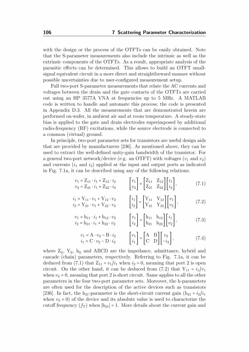
106 7 Scattering Parameter Characterization
with the design or the process of the OTFTs can be easily obtained. Notethat the S-parameter measurements also include the intrinsic as well as theextrinsic components of the OTFTs. As a result, appropriate analysis of theparasitic effects can be determined. This allows to build an OTFT small-signal equivalent circuit in a more direct and straightforward manner withoutpossible uncertainties due to user-configured measurement setup.
Full two-port S-parameter measurements that relate the AC currents andvoltages between the drain and the gate contacts of the OTFTs are carriedout using an HP 3577A VNA at frequencies up to 5 MHz. A MATLABcode is written to handle and automate this process; the code is presentedin Appendix D.3. All the measurements that are demonstrated herein areperformed on-wafer, in ambient air and at room temperature. A steady-statebias is applied to the gate and drain electrodes superimposed by additionalradio-frequency (RF) excitations, while the source electrode is connected toa common (virtual) ground.
In principle, two-port parameter sets for transistors are useful design aidsthat are provided by manufacturers [236]. As mentioned above, they can beused to extract the well-defined unity-gain bandwidth of the transistor. Fora general two-port network/device (e.g. an OTFT) with voltages (v1 and v2)and currents (i1 and i2) applied at the input and output ports as indicatedin Fig. 7.1a, it can be described using any of the following relations:
v1 = Z11 ⋅ i1 + Z12 ⋅ i2v2 = Z21 ⋅ i1 + Z22 ⋅ i2
[v1
v2] = [
Z11 Z12
Z21 Z22] [i1i2] , (7.1)
i1 = Y11 ⋅ v1 +Y12 ⋅ v2
i2 = Y21 ⋅ v1 +Y22 ⋅ v2[i1i2] = [
Y11 Y12
Y21 Y22] [v1
v2] , (7.2)
v1 = h11 ⋅ i1 + h12 ⋅ v2
i2 = h21 ⋅ i1 + h22 ⋅ v2[v1
i2] = [
h11 h12
h21 h22] [i1v2
] , (7.3)
v1 = A ⋅ v2 −B ⋅ i2i1 = C ⋅ v2 −D ⋅ i2
[v1
i1] = [
A BC D
] [v2
−i2] , (7.4)
where Zij, Yij, hij and ABCD are the impedance, admittance, hybrid andcascade (chain) parameters, respectively. Referring to Fig. 7.1a, it can bededuced from (7.1) that Z11 = v1/i1 when i2 = 0, meaning that port 2 is opencircuit. On the other hand, it can be deduced from (7.2) that Y11 = i1/v1
when v2 = 0, meaning that port 2 is short circuit. Same applies to all the otherparameters in the four two-port parameter sets. Moreover, the h-parametersare often used for the description of the active devices such as transistors[236]. In fact, the h21-parameter is the short-circuit current gain (h21 = i2/i1when v2 = 0) of the device and its absolute value is used to characterize thecutoff frequency (fT) when ∣h21∣ = 1. More details about the current gain and

7.1 Measurement Setup 107
2-port
Networkv1
+
_
v2
+
_
i1 i2
2-port
Network
Device plane
b1
a1
a2
b2ZS
ZL
VS
ZoZo
(a)
2-port
Networkv1
+
_
v2
+
_
i1 i2
2-port
Network
Device plane
b1
a1
a2
b2ZS
ZL
VS
ZoZo
(b)
Figure 7.1 Block diagram of two-port network/device with defined (a) volt-ages and currents, and (b) traveling waves. In (b), the network/device is con-nected to a VNA using two line segments (transmission lines) with a characteristicimpedance Zo. Only the forward direction is illustrated when the source and loadare connected to port 1 and port 2, respectively. The source (ZS) and load (ZL)impedances are configured by the VNA. When perfect terminations (ZS = ZL = Zo)are applied in this configuration, the input reflection (S11) and forward trans-mission (S21) coefficients can be measured. In addition, the connections can bereversed by the VNA to measured the full two-port S-parameters [237].
the cutoff frequency of a transistor are presented in the following two sections.Finally, the ABCD-parameters are very useful for cascaded circuit topologiesas they allow matrix multiplications of single circuit/network components,which are connected in series.
In order to measure the two-port parameter sets, namely Z-, Y-, h- andABCD-parameters, open and short terminations are required. These termi-nations, however, create some problems when measured at high frequencies(especially at radio frequencies, which are relevant to this work) [236]. Athigh frequencies, these terminations are difficult to obtain due to stray induc-tances and capacitances. Furthermore, it is problematic to directly measurevoltages and currents in a test setup because they depend on the length of thecables used to connect the DUT to the measurement equipment. Accordingly,the measured values depend on the position along the cables. Therefore, inorder to avoid these drawbacks, S-parameter set can be used to characterizea two-port network, which is related to the scattering and reflection of theincident waves on the network rather than the total voltages and currents[238]. Instead of the short and open terminations, the ports are terminatedin this case by a cable of a certain characteristic impedance1 (Zo), usually50 Ω, and a matched load with an impedance of ZL = Zo to compute theindividual S-parameters. Moreover, assuming a lossless transmission line isused, the traveling waves do not vary in magnitude along the line.
1A characteristic impedance (Zo) of a cable, i.e., a uniform transmission line, is the ratioof the amplitudes of the voltage and the current of a single wave propagating forwardalong the line. It is determined by the geometry and the materials of the cable, but it isindependent of the cable length. Typical values are Zo = 50, 75, 90 or 300 Ω.

108 7 Scattering Parameter Characterization
Referring to Fig. 7.1, the traveling waves a1 and b1 at port 1, and a2 andb2 at port 2 are defined in terms of v1, v2, i1, i2 and the real-valued positivecharacteristic impedance Zo as follows [237]:
a1 =v1 +Zoi1
2√Zo
, a2 =v2 +Zoi2
2√Zo
,
b1 =v1 −Zoi1
2√Zo
, b2 =v2 −Zoi2
2√Zo
.
The square of the magnitude of these variables (a1, a2, b1 and b2) has theunit watt. Hence, these incoming and outgoing waves can be consideredto be in the form of power waves travelling in both directions along thelines. Assuming that the used transmission lines (cables) are uniform incross section; therefore, the transmission line (Fig. 7.1b) can be modeled bya general equivalent circuit with a series impedance and a shunt admittanceper unit length. Accordingly, the characteristic impedance (Zo) is expressedgenerally as [238]
Zo =
√R + jωL
G + jωC. (7.5)
For a lossless line, the series resistance (R) and the shunt conductance (G)are both zero, and thus, the expression of the characteristic impedance givenby (7.5) can be simplified to Zo =
√L/C.
The S-parameters completely define the network/device characteristics;in addition, they provide a clear physical interpretation of the transmissionand reflection performance of the network/device [238]. For the two-portnetwork shown in Fig. 7.1b, the S-parameters are defined using the reflectedor emanating waves (b1 and b2) as the dependent variables, and the incidentwaves (a1 and a2) as the independent variables [238]. The general expressionsfor these waves as a function of the S-parameters are given by
b1 = S11 ⋅ a1 + S12 ⋅ a2
b2 = S21 ⋅ a1 + S22 ⋅ a2[b1
b2] = [
S11 S12
S21 S22] [a1
a2] . (7.6)
The parameters S11 and S22 are the complex-valued input and output reflec-tion coefficients, whereas S21 and S12 are the complex-valued forward andreverse transmission coefficients, respectively. Using (7.6), the individualS-parameters can be determined by taking the ratio of the reflected or trans-mitted wave to the incident wave with a perfect termination placed at thecorresponding port. For example, when a matched load (ZL = Zo) is ap-plied to port 2 as depicted in Fig. 7.1b, the input reflection and forwardtransmission coefficients can be calculated using S11 = b1/a1 and S21 = b2/a1,respectively. The matched termination means that the load impedance (ZL)
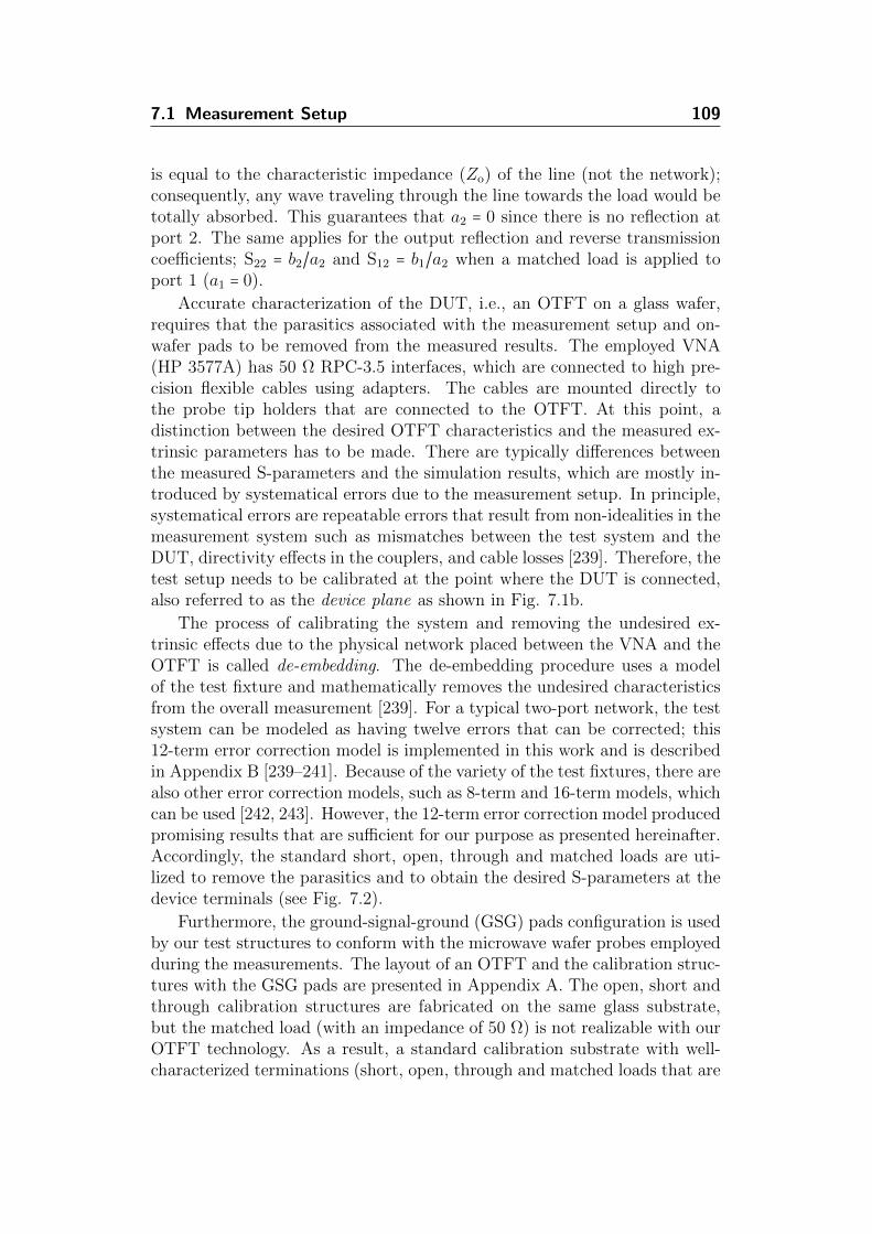
7.1 Measurement Setup 109
is equal to the characteristic impedance (Zo) of the line (not the network);consequently, any wave traveling through the line towards the load would betotally absorbed. This guarantees that a2 = 0 since there is no reflection atport 2. The same applies for the output reflection and reverse transmissioncoefficients; S22 = b2/a2 and S12 = b1/a2 when a matched load is applied toport 1 (a1 = 0).
Accurate characterization of the DUT, i.e., an OTFT on a glass wafer,requires that the parasitics associated with the measurement setup and on-wafer pads to be removed from the measured results. The employed VNA(HP 3577A) has 50 Ω RPC-3.5 interfaces, which are connected to high pre-cision flexible cables using adapters. The cables are mounted directly tothe probe tip holders that are connected to the OTFT. At this point, adistinction between the desired OTFT characteristics and the measured ex-trinsic parameters has to be made. There are typically differences betweenthe measured S-parameters and the simulation results, which are mostly in-troduced by systematical errors due to the measurement setup. In principle,systematical errors are repeatable errors that result from non-idealities in themeasurement system such as mismatches between the test system and theDUT, directivity effects in the couplers, and cable losses [239]. Therefore, thetest setup needs to be calibrated at the point where the DUT is connected,also referred to as the device plane as shown in Fig. 7.1b.
The process of calibrating the system and removing the undesired ex-trinsic effects due to the physical network placed between the VNA and theOTFT is called de-embedding. The de-embedding procedure uses a modelof the test fixture and mathematically removes the undesired characteristicsfrom the overall measurement [239]. For a typical two-port network, the testsystem can be modeled as having twelve errors that can be corrected; this12-term error correction model is implemented in this work and is describedin Appendix B [239–241]. Because of the variety of the test fixtures, there arealso other error correction models, such as 8-term and 16-term models, whichcan be used [242, 243]. However, the 12-term error correction model producedpromising results that are sufficient for our purpose as presented hereinafter.Accordingly, the standard short, open, through and matched loads are uti-lized to remove the parasitics and to obtain the desired S-parameters at thedevice terminals (see Fig. 7.2).
Furthermore, the ground-signal-ground (GSG) pads configuration is usedby our test structures to conform with the microwave wafer probes employedduring the measurements. The layout of an OTFT and the calibration struc-tures with the GSG pads are presented in Appendix A. The open, short andthrough calibration structures are fabricated on the same glass substrate,but the matched load (with an impedance of 50 Ω) is not realizable with ourOTFT technology. As a result, a standard calibration substrate with well-characterized terminations (short, open, through and matched loads that are
110 7 Scattering Parameter Characterization
Zoa0
b0
b3
a3
(a)
Zoa1
b1
b2
a2
(b)
Zoa1
b1
b2
a2
(c)
Zoa1
b1
b2
a2
(d)
Zoa1
b1
b2
a2
(e)
Figure 7.2 Schematic diagram of several devices under test (DUT) with a fic-titious two-port error adapter (red-colored blocks). The error adapter separatesthe DUT from an ideal measurement system, thus creating a distinction betweenthe intrinsic (actual; related to the traveling waves a1, a2, b1 and b2 shown in Fig.7.1b) and extrinsic (measured; related to the traveling waves a0, a3, b0 and b3shown in this figure) S-parameters. In the used model, the error adapter containstwelve error terms as described in Appendix B. The devices/terminations depictedin the figure are the standard (a) short, (b) open, (c) through, and (c) matched(Zo) loads used for the calibration/de-embedding procedure in addition to (e) anOTFT as an active load. The schematic is adopted from [244].
necessary for the 12-term error correction model) at the desired frequencyrange (≤ 5 MHz) is employed. Note that the contact pads can also incorporateparasitic capacitance and inductance to the system, and in fact, the accuracyof the de-embedding procedure strongly depends on the quality as well as thelayout of the terminations. Therefore, identical layout of the active device(including the contact pads) with that of the calibration structures is usedto achieve high fidelity in the de-embedding process [232].
There are basically two main approaches to implement the de-embeddingprocess [239]. The first is to measured the OTFT and the calibration struc-tures beforehand and then mathematically remove the undesired parasiticsfrom the measurements using any error correction model. The second usesthe VNA itself to directly perform the de-embedding calculations, given thatthe error correction model is incorporated in the VNA. The latter approachallows the user to examine the de-embedded S-parameters in real-time. How-ever, the used HP 3577A VNA offers only one-port calibration (3-term errorcorrection model), which is not appropriate for our OTFT measurements.Therefore, the first approach using the 12-term error correction model, whoseequations are described in Appendix B, is implemented on MATLAB to cal-culate the desired de-embedded S-parameters.
The calibration steps are as follows. First, the standard short, open,through and matched loads are measured, from which the twelve error termsare extracted using MATLAB. Second, the full two-port S-parameters of anOTFT are measured. Finally, the de-embedded S-parameters of the OTFTare calculated using MATLAB. As long as the measurement system and thetemperature are stable over time, the same twelve error terms can be usedfor de-embedding all subsequent measurements [239].

7.2 Small-Signal Model 111
Short load
Open load
Through load
Before calibration
After calibration
0 1 2 3 4 5-1
-0.8
-0.6
-0.4
-0.2
0
0.2
0.4
0.6
0.8
1
Frequency (MHz)
Re(
S)
11
0 1 2 3 4 5-0.5
-0.4
-0.3
-0.2
-0.1
0
0.1
0.2
0.3
0.4
0.5
Frequency (MHz)Im
(S)
11(a)
Short load
Open load
Through load
Before calibration
After calibration
0 1 2 3 4 5-1
-0.8
-0.6
-0.4
-0.2
0
0.2
0.4
0.6
0.8
1
Frequency (MHz)
Re(
S)
11
0 1 2 3 4 5-0.5
-0.4
-0.3
-0.2
-0.1
0
0.1
0.2
0.3
0.4
0.5
Frequency (MHz)Im
(S)
11(b)
Figure 7.3 Comparison between the measured input reflection coefficient (S11)of the standard short, open and through loads before and after calibration. (a)The real part of S11 [Re(S11)]. (b) The imaginary part of S11 [Im(S11)]. Thecalibration procedure is implemented by de-embedding the parasitics associatedwith the measurement setup and on-wafer pads using the 12-term error correctionmodel as explained in Appendix B. The same calibration accuracy is obtained forS12, S21 as well as S22 (not shown here).
Figure 7.3 shows the measured input reflection coefficient (S11) of theshort, open and through loads before and after calibration. The differencesbetween the measured and expected values of the real and imaginary compo-nents of S11 result from the systematical errors, of which the impacts are suc-cessfully removed by the de-embedding process over the complete frequencyrange (0.1–5 MHz) as depicted in the figure. For example, the measured S11
of a short load before calibration are between −0.96−0.05j and −0.82+0.47jat f = 0.1 and 5 MHz, respectively; however, the expected value of S11 = −1is achieved after calibration for the entire frequency range. Same appliesfor the other S-parameters, namely S12, S21 and S22, and all load structures.This verifies the AC measurement and the calibration procedure used herefor studying the frequency response of OTFTs.
7.2 SMALL-SIGNAL MODEL
Over the past few years, tremendous research efforts have been devoted toincrease the field-effect mobility in organic materials by choosing the propercomposite or improving the deposition conditions. As a result of these ef-forts, many OTFTs with high mobilities exceeding 1 cm2/Vs have been re-ported [157, 229]. In particular, high mobilities of more than 5 cm2/Vs in
112 7 Scattering Parameter Characterization
OTFTs based on pentacene and fullerene C60 organic semiconductors havebeen demonstrated [157]; this surpasses the mobilities of the conventionala-Si:H TFTs by about ten times. Besides high field-effect mobility, otherways of improving the dynamic performance of OTFTs, such as reducingthe lateral dimensions of the device, has also attracted considerable atten-tion [157, 229]. Downscaling the channel length results in an increase ofthe transconductance; furthermore, reducing the gate-overlaps results in adecrease of the parasitic capacitances [14]. In principle, high frequency op-eration is expected in the planar OTFTs with high mobility as well as smalllateral dimensions. However, this can be difficult because in many cases themobilities of OTFTs decreases with the channel length as a result of theparasitic contact resistances [157]. This problem can be resolved by choosingan appropriate device configuration (e.g. inverted-staggered topology) or bysuppressing the parasitic resistance (e.g. by contact doping or choosing aproper material for the contact metal with a work function that matches theLUMO/HOMO energy level of the organic semiconductor) [97].
As described in Chapter 3, OTFTs are commonly fabricated in the in-verted configuration, i.e., inverted-coplanar or inverted-staggered topologies(Fig. 3.1). It depends on weather the source/drain contacts are deposited ontop of the organic semiconductor film or on the gate dielectric prior to the de-position of the organic semiconductor film, they are referred to as top-contactor bottom-contact OTFTs, respectively [229]. The bottom-contact OTFTshas the advantage that the standard photolithography and spin coating tech-niques, which are used in the established IC and display industries, can beused to obtain short channel devices. In this case, the organic semiconduc-tor is deposited merely at the end of the process to avoid degradation of theconjugated organic compound due to solvents or elevated temperatures. Nev-ertheless, the bottom-contact OTFTs suffer from higher contact resistancecompared to that of the top-contact OTFTs [137, 138]; the adhesion layersfor the bottom contacts and the carrier injection barrier into the organicmaterial typically cause the large contact resistance [157]. This results in asignificant reduction of the field-effect mobility, which contradicts with therequirement of high mobility for the high-frequency operation. On the otherhand, the top-contact OTFTs have been commonly fabricated using plasticshadow masks, which result in a relatively large minimum channel lengths ofabout 10–20 µm [14]. However, we are able to fabricate top-contact OTFTswith submicrometer channel lengths (down to 0.6 µm as demonstrated fur-ther below) and very small contact resistance without exposing the semicon-ductor layer to potentially harmful solvents during device processing usinghigh-resolution silicon stencil masks [18].
Furthermore, it is demonstrated in [229] that top-contact OTFTs havesmaller gate capacitance compared to that of the bottom-contact OTFTs,resulting in improved frequency performance. If one ignores the artifacts

7.2 Small-Signal Model 113
introduced by the contact resistance, the gate-source capacitance is foundto be similar for both configurations. However, the gate-drain capacitanceis found to be lower in top-contact OTFTs, particularly in the saturationoperation regime, because the absence of the accumulation layer beneath thecontact area makes the organic semiconductor film to behave as a dielectriclayer. As a result, a smaller gate-drain overlap capacitance and a largerbandwidth are expected for top-contact OTFTs.
In view of the promising advantages of the top-contact configuration andthe advances offered by the new OTFT technology process developed at IMSCHIPS and MPI-SSR, the top-contact OTFTs fabricated by high-resolutionsilicon stencil masks becomes the most attractive choice for this study. Be-sides the differences between the bottom- and top-contact OTFT configura-tions mentioned above, there are also other important aspects that relate tothe organic semiconductor film thickness, of which implication with respectto the device performance is not discussed so far. According to the devicesimulations presented in [229], significantly higher device speed can be ob-tained just by choosing an optimal thickness of the organic semiconductorfilm. In principle, there is a tradeoff when choosing the organic semiconduc-tor film thickness, i.e., a larger thickness would result in an increase of thecontact resistance but a decrease of the overlap capacitance. A thickness of20 nm for the organic semiconductor film is chosen for our OTFTs.
All the OTFTs fabricated for this study are prepared on the same sub-strate in order to minimize the device-to-device variations. Moreover, thegate electrodes are patterned to minimize the parasitic capacitances asso-ciated with overlap between the gate and the source/drain contacts. Thechannel width (W ) of all the OTFTs is 100 µm, the channel length (L) is10, 2, 1 or 0.6 µm, and the gate-overlap length (Lov) is 20 or 5 µm. Toensure proper fabrication yield, each transistor is dissected to four parallelOTFTs with W = 25 µm sharing the same semiconductor layer; this is tocomply with the layout design rules constrained by the required mechanicalstability of the silicon stencil masks (Table 4.7). The layout of the OTFTswith the dissected top contacts and connected to the aforementioned GSGpads is shown in Appendix A. Despite the fact that there are OTFTs, such asthose based on pentacene and fullerene C60 organic semiconductors, offeringhigh mobilities of more than 5 cm2/Vs, we prefer to use the DNTT owingto its better air stability. Furthermore, the DNTT-based OTFTs featurepromising shelf-life, bias-stress stability, matching and hysteresis behavior asdemonstrated thoroughly in [106] and [14]. An intrinsic mobility (µo) of ∼ 2.5cm2/Vs and a contact resistance (2RCW ) of 0.1 kΩ cm are extracted for thefabricated DNTT-based OTFTs using the TLM. For comparison, this mea-sured value of the contact resistance is substantially smaller than that of thevalues reported for the OTFTs based on pentacene (2RCW = 0.94 kΩ cm)and fullerene C60 (2RCW = 3 kΩ cm) organic semiconductors [157].
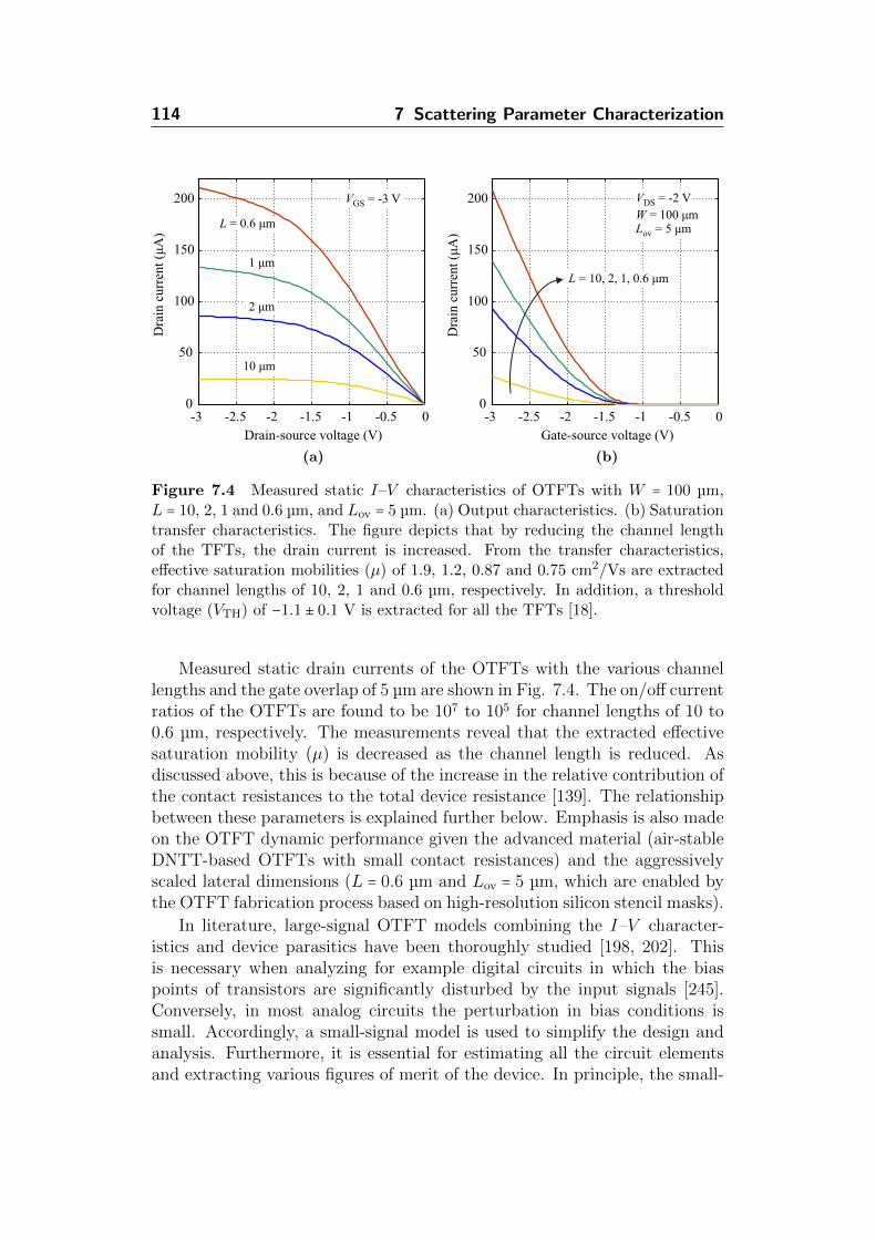
114 7 Scattering Parameter Characterization
-3 -2.5 -2 -1.5 -1 -0.5 00
50
100
150
200
Drain-source voltage (V)
Dra
in c
urr
ent
(μA
)
-3 -2.5 -2 -1.5 -1 -0.5 00
50
100
150
200
Gate-source voltage (V)
Dra
in c
urr
ent
(μA
)
L = 0.6 μm
1 μm
2 μm
10 μm
L = 10, 2, 1, 0.6 μm
V = -3 VGS V = -2 VDS
W = 100 μmL = 5 μmov
(a)
-3 -2.5 -2 -1.5 -1 -0.5 00
50
100
150
200
Drain-source voltage (V)
Dra
in c
urr
ent
(μA
)
-3 -2.5 -2 -1.5 -1 -0.5 00
50
100
150
200
Gate-source voltage (V)D
rain
curr
ent
(μA
)
L = 0.6 μm
1 μm
2 μm
10 μm
L = 10, 2, 1, 0.6 μm
V = -3 VGS V = -2 VDS
W = 100 μmL = 5 μmov
(b)
Figure 7.4 Measured static I–V characteristics of OTFTs with W = 100 µm,L = 10, 2, 1 and 0.6 µm, and Lov = 5 µm. (a) Output characteristics. (b) Saturationtransfer characteristics. The figure depicts that by reducing the channel lengthof the TFTs, the drain current is increased. From the transfer characteristics,effective saturation mobilities (µ) of 1.9, 1.2, 0.87 and 0.75 cm2/Vs are extractedfor channel lengths of 10, 2, 1 and 0.6 µm, respectively. In addition, a thresholdvoltage (VTH) of −1.1 ± 0.1 V is extracted for all the TFTs [18].
Measured static drain currents of the OTFTs with the various channellengths and the gate overlap of 5 µm are shown in Fig. 7.4. The on/off currentratios of the OTFTs are found to be 107 to 105 for channel lengths of 10 to0.6 µm, respectively. The measurements reveal that the extracted effectivesaturation mobility (µ) is decreased as the channel length is reduced. Asdiscussed above, this is because of the increase in the relative contribution ofthe contact resistances to the total device resistance [139]. The relationshipbetween these parameters is explained further below. Emphasis is also madeon the OTFT dynamic performance given the advanced material (air-stableDNTT-based OTFTs with small contact resistances) and the aggressivelyscaled lateral dimensions (L = 0.6 µm and Lov = 5 µm, which are enabled bythe OTFT fabrication process based on high-resolution silicon stencil masks).
In literature, large-signal OTFT models combining the I–V character-istics and device parasitics have been thoroughly studied [198, 202]. Thisis necessary when analyzing for example digital circuits in which the biaspoints of transistors are significantly disturbed by the input signals [245].Conversely, in most analog circuits the perturbation in bias conditions issmall. Accordingly, a small-signal model is used to simplify the design andanalysis. Furthermore, it is essential for estimating all the circuit elementsand extracting various figures of merit of the device. In principle, the small-

7.2 Small-Signal Model 115
rogmvgsi
Cgd
Cgs
vd
vs
vg
rj
rs
rs
rj
Cj
Cj
vdi
vsi
Intrinsic transistor
Figure 7.5 Schematic diagram of the OTFT small-signal model including bothintrinsic (highlighted) and extrinsic (not highlighted) components. The subscripti designates the internal potential of the intrinsic OTFT, which corresponds tothe portion of the OTFT above the gate and between the source/drain contacts.Though the capacitances Cgs and Cgd are highlighted, each includes a constantoverlap capacitance (Cov), which is a contribution of the extrinsic part of theOTFT [188].
signal model is just an approximation of the large-signal model around anoperating point [246]. This has been demonstrated for OLEDs and OPVCs togive deeper insight into the transport properties and operational mechanismin these devices [161, 247, 248]. Therefore, the knowledge of the small-signalmodel of an OTFT is very beneficial in many aspects: (i) simplification ofthe analyses and the design of analog/hybrid circuits, (ii) determination ofthe device performance, (iii) verification of the large signal model, (iv) char-acterization of the technology process, and (e) extraction of the materialproperties. In the following, a physics-based small-signal OTFT model anda verification of the model to S-parameter measurements are presented. Themodel is simple to allow convenient upgradability of further effects and itincludes no empirical fitting parameters.
Since most transistors in analog circuitry are biased in the saturationoperation regime; correspondingly, Fig. 7.5 shows a proposed OTFT small-signal equivalent circuit including both intrinsic and extrinsic components.Nevertheless, in the linear regime the transistors operate as a switch, whichcan be roughly modeled by a linear resistor with an equivalent voltage-dependent resistance of L/(µCIW (VGS − VTH)) together with the device ex-trinsic components. The values of the small-signal parameters are constantwith the change in the frequency but they depend on the large-signal param-eters and the DC quiescent point as described hereinafter.
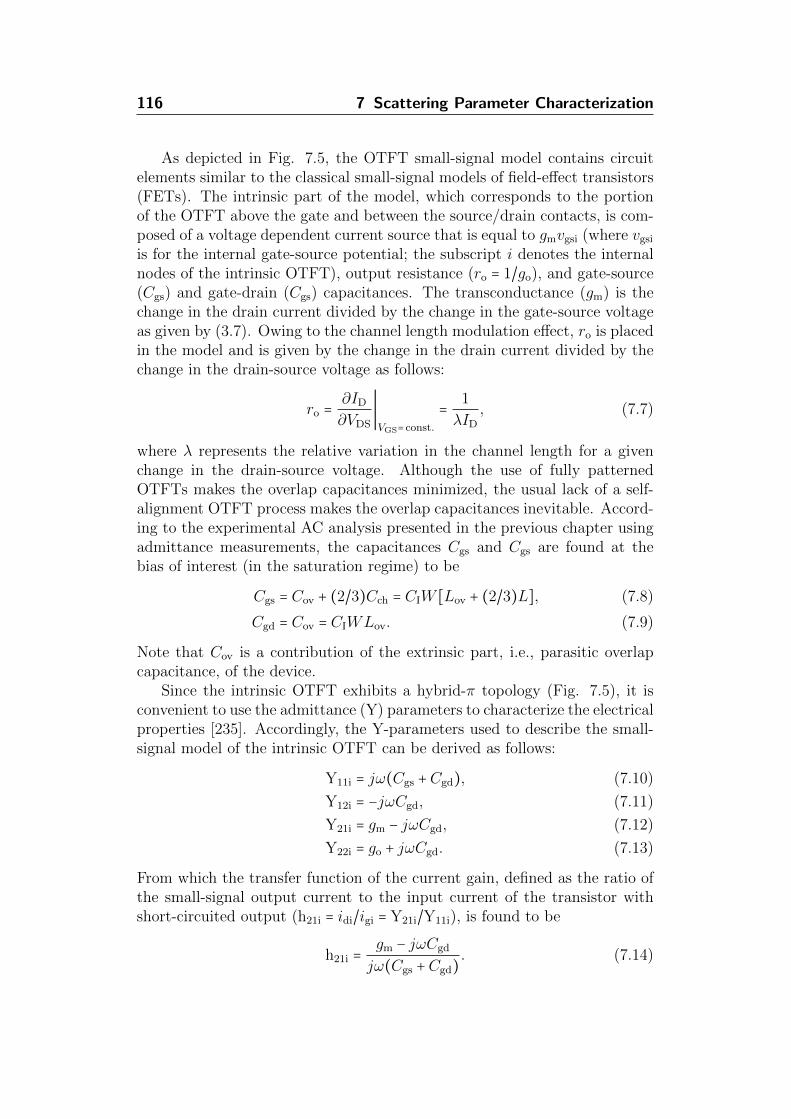
116 7 Scattering Parameter Characterization
As depicted in Fig. 7.5, the OTFT small-signal model contains circuitelements similar to the classical small-signal models of field-effect transistors(FETs). The intrinsic part of the model, which corresponds to the portionof the OTFT above the gate and between the source/drain contacts, is com-posed of a voltage dependent current source that is equal to gmvgsi (where vgsi
is for the internal gate-source potential; the subscript i denotes the internalnodes of the intrinsic OTFT), output resistance (ro = 1/go), and gate-source(Cgs) and gate-drain (Cgs) capacitances. The transconductance (gm) is thechange in the drain current divided by the change in the gate-source voltageas given by (3.7). Owing to the channel length modulation effect, ro is placedin the model and is given by the change in the drain current divided by thechange in the drain-source voltage as follows:
ro =∂ID
∂VDS
∣VGS= const.
=1
λID
, (7.7)
where λ represents the relative variation in the channel length for a givenchange in the drain-source voltage. Although the use of fully patternedOTFTs makes the overlap capacitances minimized, the usual lack of a self-alignment OTFT process makes the overlap capacitances inevitable. Accord-ing to the experimental AC analysis presented in the previous chapter usingadmittance measurements, the capacitances Cgs and Cgs are found at thebias of interest (in the saturation regime) to be
Cgs = Cov + (2/3)Cch = CIW [Lov + (2/3)L], (7.8)
Cgd = Cov = CIWLov. (7.9)
Note that Cov is a contribution of the extrinsic part, i.e., parasitic overlapcapacitance, of the device.
Since the intrinsic OTFT exhibits a hybrid-π topology (Fig. 7.5), it isconvenient to use the admittance (Y) parameters to characterize the electricalproperties [235]. Accordingly, the Y-parameters used to describe the small-signal model of the intrinsic OTFT can be derived as follows:
Y11i = jω(Cgs +Cgd), (7.10)
Y12i = −jωCgd, (7.11)
Y21i = gm − jωCgd, (7.12)
Y22i = go + jωCgd. (7.13)
From which the transfer function of the current gain, defined as the ratio ofthe small-signal output current to the input current of the transistor withshort-circuited output (h21i = idi/igi = Y21i/Y11i), is found to be
h21i =gm − jωCgd
jω(Cgs +Cgd). (7.14)

7.2 Small-Signal Model 117
Note that the current gain (h21) of a transistor is often denoted in literatureby the symbol β [18, 188]; however, this distinction is not made in this workfor the sake of clarification.
It is shown so far that the small-signal model of the OTFTs is similar incomposition to those of conventional FETs, i.e., consisting of gm, ro, Cgs andCgd. Furthermore, the dynamic performance of the OTFTs is strongly limitedby the contact interface between the metallic source/drain electrodes and thesemiconductor layer [213]. Detailed analyses of the capacitance-voltage (C–V ) characteristics and frequency responses of metal-insulator-semiconductor(MIS) structures have been presented in literature to describe the current in-jection mechanism through the contact interfaces of OTFTs [211, 213, 215].As shown in the schematic diagram of the proposed small-signal model, theextrinsic part that is used to describe the non-ohmic source/drain contactsconsists of a junction capacitance (Cj), a junction resistance (rj) and a seriesresistance (rs). The origin of the junction capacitance in the contact model ismost likely due to the formation of a small depletion region near the metal-semiconductor interface, while the junction resistance governs the injectioncurrent to the channel [215]. Both are highly dependent on the processingconditions; for example, they can be considerably reduced when performinglocal doping into the contact interface [213]. It is demonstrated in the follow-ing that the contribution of the junction capacitance in our OTFTs can beneglected. Unlike the MIS structures, the resistances rj and rs has to accountnot only for the vertical but also for the much larger horizontal componentof the total OTFT contact resistance (Appendix C.2) [139].
Each terminal (gate, source and drain) of the OTFTs is in fact exhibitinga very small ohmic resistance resulting from the resistivity of the aluminiumand gold conductive materials; nevertheless, they are neglected in the abovemodel for simplicity. Moreover, the gate leakage current is also not consid-ered, but it can be easily incorporated into the model by distinctive resistorstied between the gate and source/drain contacts. The proposed model isadequate for most frequency analyses and can be even further simplified byutilizing only the intrinsic part of the model while considering the contactresistances in the calculation of the effective charge carrier mobility using(3.11); the validity of this simplification is demonstrated hereinafter.
Using the test setup described in the previous section, full two-port S-parameter measurements that constitute a complete set of coefficients to de-scribe the input/output behavior of the OTFTs are performed. Figure 7.6adepicts measured and simulated S-parameters of the OTFT with W = 100µm, L = 1 µm and Lov = 20 µm [188]. The measurements are carried outunder various bias conditions, but only the saturation regime (at VGS = −3 Vand VDS = −2 V) is illustrated here, as it is the bias of interest for mostanalog circuits. A relatively large gate-overlap length of 20 µm is utilized inthis experiment in order to minimize the impact of unintentional misalign-

118 7 Scattering Parameter Characterization
0.2 0.4 0.6 0.8 1-100
-80
-60
-40
-20
0
20
Frequency (MHz)
S-P
aram
eter
s (d
B)
S11
105
106
-2
0
2
4
6
8
10
12
Frequency (Hz)
Cur
ren
t ga
in (
dB)
S22
S21
S12
V = -3 VGS
V = -2 VDS
W = 100 µm L = 1 µmL = 20 µmov
-20 dB/decade
MeasuredModeled (Schematic)Modeled (Compact)
Modeled (Schematic)Measured
(a)
0.2 0.4 0.6 0.8 1-100
-80
-60
-40
-20
0
20
Frequency (MHz)
S-P
aram
eter
s (d
B)
S11
105
106
-2
0
2
4
6
8
10
12
Frequency (Hz)C
urre
nt
gain
(dB
)
S22
S21
S12
V = -3 VGS
V = -2 VDS
W = 100 µm L = 1 µmL = 20 µmov
-20 dB/decade
MeasuredModeled (Schematic)Modeled (Compact)
Modeled (Schematic)Measured
(b)
Figure 7.6 (a) Full two-port measured and simulated S-parameters of the OTFTwith W = 100 µm, L = 1 µm and Lov = 20 µm operated in the saturation regime.(b) Extracted short-circuit current gain of the OTFT. The solid (black) lines rep-resent the schematic simulations, while the dashed (red) line represents the sim-plified compact model when ohmic contact resistances are considered. The resultsdemonstrate the reliability of the proposed OTFT small-signal model [18, 188].
ment on the measurement results, noting that this effect is carefully studiedand the results are presented in Section 7.4. The corresponding model pa-rameter set used for the small-signal simulation is summarized in Table 7.1.The intrinsic mobility and the contact resistance are initially extracted us-ing the TLM (µo = 2.5 cm2/Vs and 2RCW = 0.1 kΩ cm); subsequently therest of the parameters are calculated from the analytical formulas and/oroptimized to fit the simulations to the measurements. Owing to the parts ofthe organic semiconductor that extend beyond the periphery of the intrinsictransistor and cause additional fringe currents, the model has to account foran additional induced parsitic capacitance by adding CIAfringe to (7.8), whereAfringe ≃ 480 µm2 (about 12% of the total overlap area). As depicted in thefigure, the simulation results agree well with the measured S-parameters overthe entire frequency range from 100 kHz to 1 MHz. The relative mean squareerrors (rMSEs) are found to be < 0.03%, 10.4%, 6.9% and < 0.03% for S11,S12, S21 and S22, respectively. The equation describing the calculation of theerrors is given by [249]
Eij =1
n
n
∑k=1
(∣Sij,sim∣ − ∣Sij,meas∣
∣Sij,meas∣)
2
, (7.15)
where n is the number of the data points and the subscripts i and j are equalto 1 and/or 2.
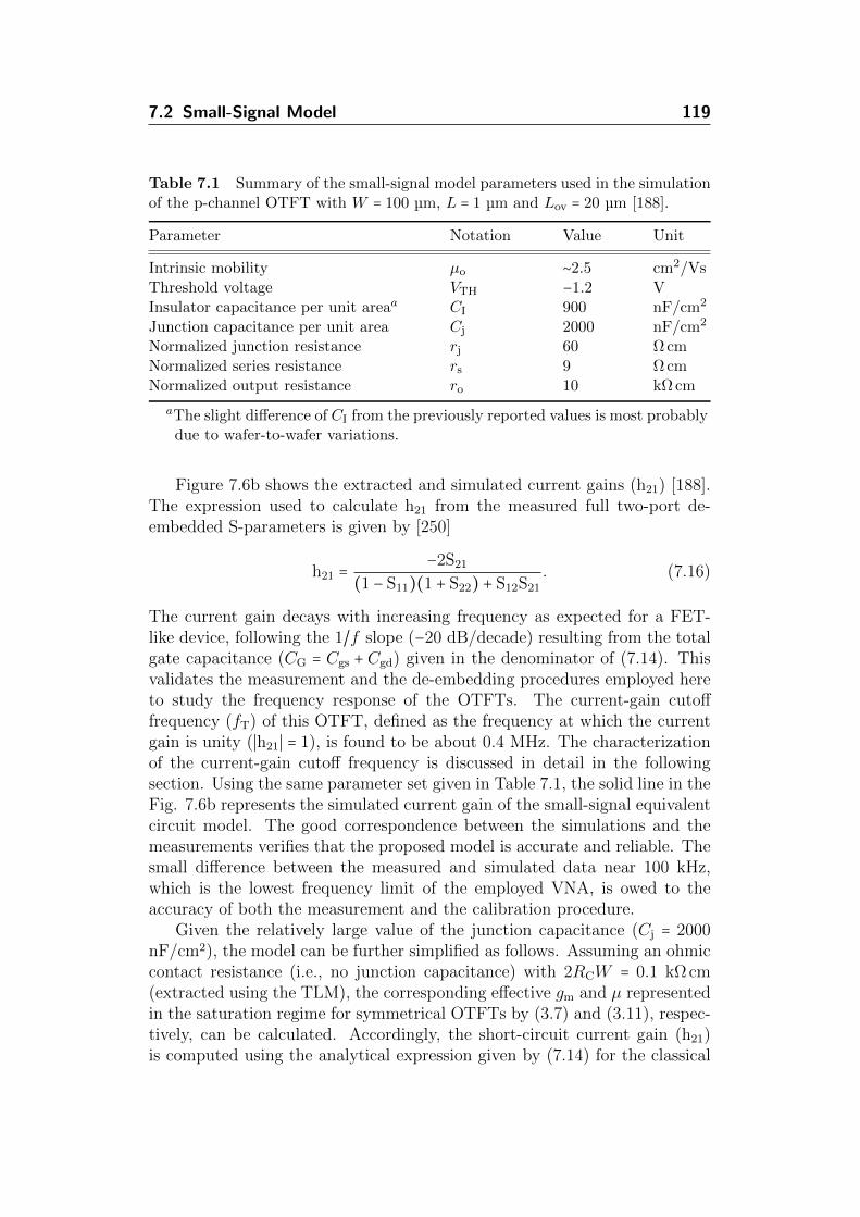
7.2 Small-Signal Model 119
Table 7.1 Summary of the small-signal model parameters used in the simulationof the p-channel OTFT with W = 100 µm, L = 1 µm and Lov = 20 µm [188].
Parameter Notation Value Unit
Intrinsic mobility µo ∼2.5 cm2/VsThreshold voltage VTH −1.2 VInsulator capacitance per unit areaa CI 900 nF/cm2
Junction capacitance per unit area Cj 2000 nF/cm2
Normalized junction resistance rj 60 Ω cmNormalized series resistance rs 9 Ω cmNormalized output resistance ro 10 kΩ cm
aThe slight difference of CI from the previously reported values is most probablydue to wafer-to-wafer variations.
Figure 7.6b shows the extracted and simulated current gains (h21) [188].The expression used to calculate h21 from the measured full two-port de-embedded S-parameters is given by [250]
h21 =−2S21
(1 − S11)(1 + S22) + S12S21
. (7.16)
The current gain decays with increasing frequency as expected for a FET-like device, following the 1/f slope (−20 dB/decade) resulting from the totalgate capacitance (CG = Cgs + Cgd) given in the denominator of (7.14). Thisvalidates the measurement and the de-embedding procedures employed hereto study the frequency response of the OTFTs. The current-gain cutofffrequency (fT) of this OTFT, defined as the frequency at which the currentgain is unity (∣h21∣ = 1), is found to be about 0.4 MHz. The characterizationof the current-gain cutoff frequency is discussed in detail in the followingsection. Using the same parameter set given in Table 7.1, the solid line in theFig. 7.6b represents the simulated current gain of the small-signal equivalentcircuit model. The good correspondence between the simulations and themeasurements verifies that the proposed model is accurate and reliable. Thesmall difference between the measured and simulated data near 100 kHz,which is the lowest frequency limit of the employed VNA, is owed to theaccuracy of both the measurement and the calibration procedure.
Given the relatively large value of the junction capacitance (Cj = 2000nF/cm2), the model can be further simplified as follows. Assuming an ohmiccontact resistance (i.e., no junction capacitance) with 2RCW = 0.1 kΩ cm(extracted using the TLM), the corresponding effective gm and µ representedin the saturation regime for symmetrical OTFTs by (3.7) and (3.11), respec-tively, can be calculated. Accordingly, the short-circuit current gain (h21)is computed using the analytical expression given by (7.14) for the classical
120 7 Scattering Parameter Characterization
hybrid-π small-signal model, while taking into consideration the impact ofthe contact resistance on the mobility. An excellent agreement is achieved asdemonstrated by the dashed line in Fig. 7.6b. However, it is important tonote that these two models do not represent any different physical operationor performance of the OTFT; they are just different representations of thesame device.
7.3 CURRENT-GAIN CUTOFF FREQUENCY
In principle, the dynamic performance of the OTFTs can be improved byreducing the lateral dimensions. As a measure of the device speed, the pa-rameter current-gain cutoff frequency is selected for this study. To inves-tigate the dependence of the lateral dimensions on the frequency response,the OTFTs with various channel and gate-overlap lengths down to 0.6 and5 µm, respectively, are characterized herein. Correspondingly, Fig. 7.7 showsthe short-circuit small-signal current gain (h21) derived from the measuredS-parameters of the OTFTs with W = 100 µm, L = 10, 2, 1 and 0.6 µm, andLov = 20 and 5 µm at a gate-source voltage (VGS) of −3 V and a drain-sourcevoltage (VDS) of −2 V [18]. For all the transistors, the de-embedded currentgain is inversely proportional to the frequency (f), following the 1/f slope ex-pected for a conventional FET [232]. Referring to (7.14), this 1/f frequencydependence of h21, which is equivalent to a decay slope of −20 dB/decade,results from the total gate capacitance (CG = Cgs +Cgd). This observation issignificant because it not only validates the used characterization approachbut also verifies the regular FET-like behavior of the OTFTs. At high fre-quencies, however, the decay levels off as depicted in Fig. 7.7; this is due tothe zero in the transfer function h21, which denotes a current flow throughthe relatively large gate-drain capacitance (Cgd).
In the following, the capacitance Cgd is neglected during the derivation ofthe current-gain cutoff frequency, but its impact is discussed in detail in thenext section. For a typical FET, the input current (gate current) induced byan applied AC gate voltage increases linearly with the frequency due to thefinite gate capacitance (iG = j2πfCGvGS), assuming that the independentDC contribution of the gate leakage current is insignificant. Furthermore,the output current (drain current) is mainly given by the transistor’s DCcharacteristics and a small superimposed AC component (iD = gmvGS). Forthe unity-gain bandwidth, the upper frequency limit of the device is reachedif the input and output AC levels exhibit the same amplitude. Beyond thesaid frequency, also referred to as the cutoff or transition frequency (fT), thetransistor is not able to drive another load transistor of the same kind. Hence,no circuitry that is composed of such transistors can operate at a frequencybeyond fT [159]. Accordingly, the cutoff frequency (fT) is considered asone of the most important figures of merit for characterizing the dynamic

7.3 Current-Gain Cutoff Frequency 121
105
106
0
5
10
15
20
25
30
Frequency (Hz)
Cur
rent
gai
n (d
B)
105
106
-5
0
5
10
15
Frequency (Hz)
Curr
ent
gain
(dB
) -20 dB/decade
V = -3 VGS
V = -2 VDS
L = 10, 2, 1, 0.6 μm
f = 3.7 MHzT
(a)
105
106
0
5
10
15
20
25
30
Frequency (Hz)C
urre
nt g
ain
(dB
)
105
106
-5
0
5
10
15
Frequency (Hz)
Curr
ent
gain
(dB
) -20 dB/decade
V = -3 VGS
V = -2 VDS
L = 10, 2, 1, 0.6 μm
f = 3.7 MHzT
(b)
Figure 7.7 Short-circuit current gain (h21) derived from the de-embedded fulltwo-port S-parameter measurements of OTFTs with W = 100 µm, L = 10, 2, 1 and0.6 µm, (a) Lov = 20 µm, and (b) Lov = 5 µm. The current gain decreases with in-creasing frequency, following the 1/f slope as expected for a FET-like device. Thisdecay slope is represented by the −20 dB/decade solid lines. At high frequencies,the decay levels off due to the zero in the transfer function h21. The cutoff fre-quency (fT) of each OTFT is extracted from the point at which the extrapolatedroll-off slope (−20 dB/decade) crosses the x-axis (when ∣h21∣ = 1) [18].
performance of the transistors. In this connection, fT given by (3.12) can berewritten in the saturation regime as
fT =gm
2π(Cgs +Cgd)=
µ(VGS − VTH)
2πL[(2/3)L + 2Lov]. (7.17)
Therefore, the current-gain cutoff frequency results from an interplay betweenthe transconductance and the device capacitances [229]. To attain high cutofffrequency, a small variation in gate voltage should create a huge drain currentmodulation, i.e., a large transconductance (gm); furthermore, the total gatecapacitance (CG) should be minimized to reduce the gate current [159]. Inother words, a high bandwidth is achieved by a transistor with high mobility,short channel length, low threshold voltage and low parasitic capacitances[157]. It is important to note that for transistors with short channels andlarge gate overlaps, the total gate capacitance in (7.17) has to account forthe additional fringe region that extend beyond the periphery of the intrinsictransistor.
In practice, fT is extracted from the measured de-embedded current-gain(h21) at the point at which the extrapolated roll-off slope (−20 dB/decade)due to the pole in the transfer function h21 crosses the x-axis (when ∣h21∣ = 1,

122 7 Scattering Parameter Characterization
-3 -2.5 -2 -1.5 -1 -0.5 00
20
40
60
80
100
120
Gate-source voltage (V)T
ransc
ondu
ctan
ce (
µA
/V)
0 2 4 6 8 10 12
0.0
0.5
1.0
1.5
2.0
2.5
3.0
3.5
4.0
Channel length (µm)
Cuto
ff f
reque
ncy
(M
Hz)
Measured
Simulated ( μ = μ )o
Simulated ( μ = f (μ , R , L))o C
V = -2 VDS
W = 100 µm L = 1 µmL = 5 µmov
C = 8.5 pFG
gm
2πCG f T
L = 5 μmov
L = 20 μmov
(a)
-3 -2.5 -2 -1.5 -1 -0.5 00
20
40
60
80
100
120
Gate-source voltage (V)T
ransc
ondu
ctan
ce (
µA
/V)
0 2 4 6 8 10 12
0.0
0.5
1.0
1.5
2.0
2.5
3.0
3.5
4.0
Channel length (µm)
Cuto
ff f
reque
ncy
(M
Hz)
Measured
Simulated ( μ = μ )o
Simulated ( μ = f (μ , R , L))o C
V = -2 VDS
W = 100 µm L = 1 µmL = 5 µmov
C = 8.5 pFG
gm
2πCG f T
L = 5 μmov
L = 20 μmov
(b)
Figure 7.8 (a) Current-gain cutoff frequency (fT) extracted for the OTFTs withthe different L and Lov. Note that there is an additional point for an OTFT withW = 100 µm, L = 0.8 µm and Lov = 5 µm, of which the short-circuit current gain(h21) characteristics is not shown in Fig. 7.7. The dashed lines represent simulatedfT with a constant effective mobility (µ) that is equal to the intrinsic mobility (µo).The solid lines represent the simulated fT with an effective mobility (µ) that ischannel-length dependent as given by (3.11), providing excellent agreement withthe measured data. (b) Extracted fT and gm as a function of VGS. A total gatecapacitance (CG) of 8.5 pF is extracted from the linear relation between fT andgm as given by (7.17). The figure confirms the close correspondence between theDC and AC measurements [151].
which is equivalent to zero decibel) as illustrated by the solid lines in Fig. 7.7.Correspondingly, the extracted fT of all the tested OTFTs are plotted in Fig.7.8a to investigate the impact of scaling down the channel and gate-overlaplengths on the dynamic performance. In the figure, there is an additionalpoint for an OTFT with W = 100 µm, L = 0.8 µm and Lov = 5 µm, of whichthe measured current gain is not shown in Fig. 7.7. As expected, the cutofffrequency is found to increase consistently with reduced channel and/or gate-overlap lengths. A maximum fT = 3.7 MHz is obtained for the OTFT withW = 100 µm, L = 0.6 µm and Lov = 5 µm. To the best of our knowledge, thisis the highest value measured for low-voltage, air-stable OTFTs to date.
In order to check the validity of the method, a comparison between theextracted and simulated cutoff frequencies is carried out. The solid anddashed lines in Fig. 7.8a represent fT calculated using (7.17) and two differentrepresentations for the effective saturation mobility (µ). It is shown that fora constant µ (dashed lines) of 2.5 cm2/Vs, which is equal to the intrinsiccarrier mobility (µo), the results are overestimated for shorter channels. This
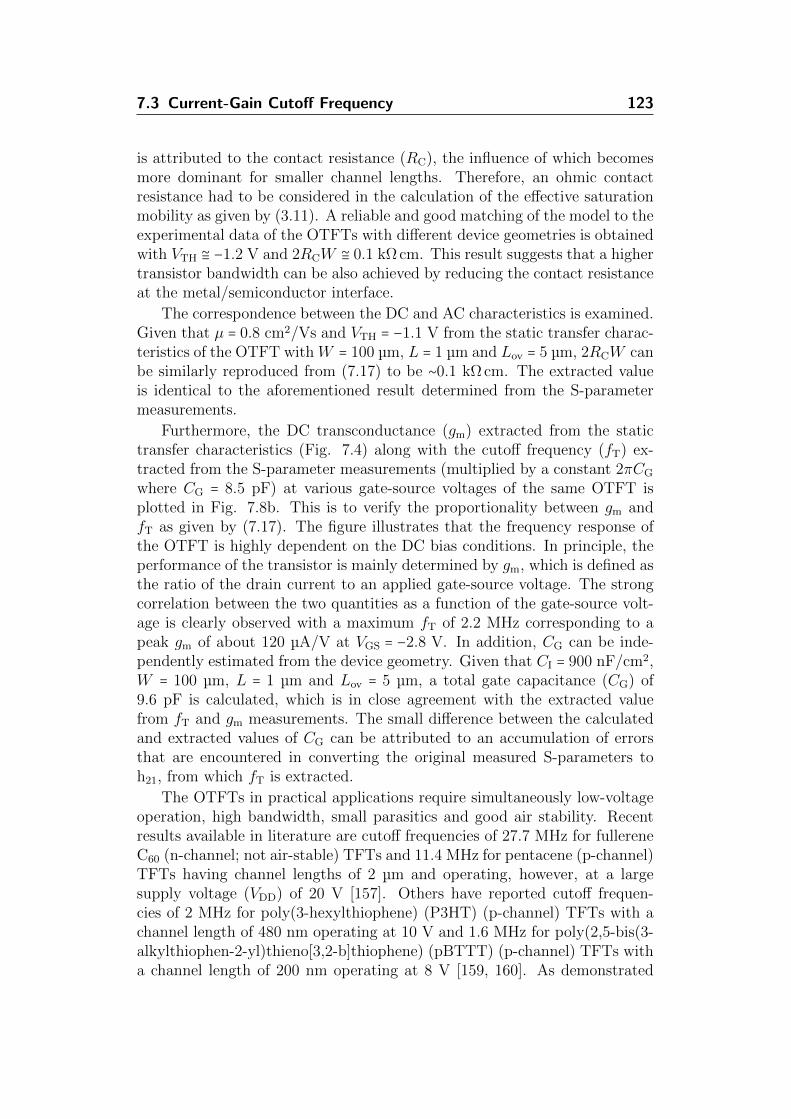
7.3 Current-Gain Cutoff Frequency 123
is attributed to the contact resistance (RC), the influence of which becomesmore dominant for smaller channel lengths. Therefore, an ohmic contactresistance had to be considered in the calculation of the effective saturationmobility as given by (3.11). A reliable and good matching of the model to theexperimental data of the OTFTs with different device geometries is obtainedwith VTH ≅ −1.2 V and 2RCW ≅ 0.1 kΩ cm. This result suggests that a highertransistor bandwidth can be also achieved by reducing the contact resistanceat the metal/semiconductor interface.
The correspondence between the DC and AC characteristics is examined.Given that µ = 0.8 cm2/Vs and VTH = −1.1 V from the static transfer charac-teristics of the OTFT with W = 100 µm, L = 1 µm and Lov = 5 µm, 2RCW canbe similarly reproduced from (7.17) to be ∼0.1 kΩ cm. The extracted valueis identical to the aforementioned result determined from the S-parametermeasurements.
Furthermore, the DC transconductance (gm) extracted from the statictransfer characteristics (Fig. 7.4) along with the cutoff frequency (fT) ex-tracted from the S-parameter measurements (multiplied by a constant 2πCG
where CG = 8.5 pF) at various gate-source voltages of the same OTFT isplotted in Fig. 7.8b. This is to verify the proportionality between gm andfT as given by (7.17). The figure illustrates that the frequency response ofthe OTFT is highly dependent on the DC bias conditions. In principle, theperformance of the transistor is mainly determined by gm, which is defined asthe ratio of the drain current to an applied gate-source voltage. The strongcorrelation between the two quantities as a function of the gate-source volt-age is clearly observed with a maximum fT of 2.2 MHz corresponding to apeak gm of about 120 µA/V at VGS = −2.8 V. In addition, CG can be inde-pendently estimated from the device geometry. Given that CI = 900 nF/cm2,W = 100 µm, L = 1 µm and Lov = 5 µm, a total gate capacitance (CG) of9.6 pF is calculated, which is in close agreement with the extracted valuefrom fT and gm measurements. The small difference between the calculatedand extracted values of CG can be attributed to an accumulation of errorsthat are encountered in converting the original measured S-parameters toh21, from which fT is extracted.
The OTFTs in practical applications require simultaneously low-voltageoperation, high bandwidth, small parasitics and good air stability. Recentresults available in literature are cutoff frequencies of 27.7 MHz for fullereneC60 (n-channel; not air-stable) TFTs and 11.4 MHz for pentacene (p-channel)TFTs having channel lengths of 2 µm and operating, however, at a largesupply voltage (VDD) of 20 V [157]. Others have reported cutoff frequen-cies of 2 MHz for poly(3-hexylthiophene) (P3HT) (p-channel) TFTs with achannel length of 480 nm operating at 10 V and 1.6 MHz for poly(2,5-bis(3-alkylthiophen-2-yl)thieno[3,2-b]thiophene) (pBTTT) (p-channel) TFTs witha channel length of 200 nm operating at 8 V [159, 160]. As demonstrated
124 7 Scattering Parameter Characterization
Table 7.2 Measured current-gain cutoff frequency (fT) benchmarked againstdata reported in literature for individual OTFTs.
Material Type L (nm) VDD (V) fT (MHz) Reference
Fullerene C60a n-channel 2000 20 27.7 [157]
Pentacene p-channel 2000 20 11.4 [157]
Pentaceneb p-channel 1000 50 0.9 [252]P3HT p-channel 480 10 2 [159]pBTTT p-channel 200 8 1.6 [160]Sexithiophene p-channel 30 2 0.02 [253]DNTT p-channel 600 3 3.7 This work
aFullerene C60 is not an air-stable organic semiconductor.bThis OTFT is implemented using the vertical-channel configuration.
above, a peak cutoff frequency of 3.7 MHz for DNTT TFTs with a channellength of 0.6 µm, a gate overlap of 5 µm and operating at a supply voltage of3 V is measured [18]. In fact, an important advantage of the organic semi-conductor DNTT over pentacene and poly(3-hexylthiophene) is its better airstability [106, 251]. Table 7.2 summarizes the cutoff frequencies (measuredon individual transistors) reported for the state-of-the-art OTFTs. In viewof the low supply voltage and good air stability, the results presented in thiswork mark a record performance achievement in the OTFT technology.
7.4 ASYMMETRIC ORGANIC TRANSISTORS
Regardless of the device structure (staggered or coplanar) and the fabricationtechnique (printing or vacuum evaporation), the usual lack of a self-alignmentprocess typically necessitates the design of non-negligible overlaps betweenthe source/drain contacts and the gate electrode [144]. Since these overlapshave a significant impact on the static and/or dynamic TFT characteristics,it is necessary to include these contact effects in all the models presented inthis work. Furthermore, the limited alignment capabilities of most OTFTtechnologies, especially printing techniques, make it very difficult to avoida mismatch between the gate-source and gate-drain overlaps, which has adirect influence on the device performance and is particularly detrimentalfor OTFTs with small feature sizes [188]. Therefore, a detailed frequencyanalysis of aggressively scaled asymmetric OTFTs is presented herein.
To study the impact of asymmetry between the gate-source (Lgs) andgate-drain (Lgd) overlap lengths, where Lgs + Lgd = 2Lov, the OTFT withW = 100 µm, L = 1 µm and Lov = 5 µm is duplicated and intentionallymisaligned on the mask level in order to realize several OTFTs with well-
7.4 Asymmetric Organic Transistors 125
106
-10
-5
0
5
10
15
20
Frequency (Hz)
Cur
ren
t ga
in (
dB)
L = 7 µmgs
L = 4 µmgs
L = 1 µmgs
0 1 2 3 4 5 6 7 81
1.5
2
2.5
3
3.5
4
4.5
5
Gate-to-source overlap length (µm)C
uto
ff f
requ
ency
(M
Hz)
5x10⁶
0.5x10⁶
-20 dB/decade
Measured
Modeled
Cutoff Frequency
L + gs L = 10 µmgd
L = 7 µmgs
L = 4 µmgs
L = 1 µmgs
V = -3 VGS
V = -2 VDS
L + L = 10 µmgs gd
W = 100 µm L = 1 µm
(a)
106
-10
-5
0
5
10
15
20
Frequency (Hz)
Cur
ren
t ga
in (
dB)
L = 7 µmgs
L = 4 µmgs
L = 1 µmgs
0 1 2 3 4 5 6 7 81
1.5
2
2.5
3
3.5
4
4.5
5
Gate-to-source overlap length (µm)C
uto
ff f
requ
ency
(M
Hz)
5x10⁶
0.5x10⁶
-20 dB/decade
Measured
Modeled
Cutoff Frequency
L + gs L = 10 µmgd
L = 7 µmgs
L = 4 µmgs
L = 1 µmgs
V = -3 VGS
V = -2 VDS
L + L = 10 µmgs gd
W = 100 µm L = 1 µm
(b)
Figure 7.9 Short-circuit current gain (h21) derived from the de-embedded fulltwo-port S-parameter measurements of asymmetric OTFTs with W = 100 µm,L = 1 µm and Lgs + Lgd = 10 µm. The −20 dB/decade slopes starts to level offat lower frequencies for OTFTs with smaller Lgs. (b) Extracted unity-gain cutofffrequency f(∣h21∣ = 1) for all the OTFTs with Lgs = 1, 2, . . ., 7 µm, while keepingconstant Lgs+Lgd = 10 µm. As a reference, the dashed line represents the simulatedprevalent FET-based cutoff frequency (fT) calculated from (7.17). The solid line,however, represents the modeled f(∣h21∣ = 1) given by (7.18), showing an accurateand reliable fit to the measured data [188].
defined Lgs = 1, 2, . . ., 7 µm, while keeping constant Lgs + Lgd = 10 µm.The seven OTFTs are placed in close proximity to minimize the device-to-device variations and ensure proper device uniformity. The utilization ofthe OTFT process based on high-resolution silicon stencil masks enabled thefabrication of such small dimensions. Vernier structures, which are originallyused to resolve alignment errors more accurately than the minimum featuresize of a given technology, are employed to measure the particular degree ofmisalignment.
Figure 7.9a shows the current gain of the asymmetric OTFTs with W =
100 µm, L = 1 µm, Lgs = 1, 4 and 7 µm, and Lgs + Lgd = 10 µm [188]. It isfound that the 1/f slopes (−20 dB/decade) level off at lower frequencies forsmaller Lgs. This occurs due to a current flow through the relatively largegate-drain capacitance (Cgd), which can be understood mathematically fromthe zero in the current-gain transfer function (h21) given by (7.14). In otherwords, as Cgd decreases for smaller Lgd, the decay in the measured currentgain levels off at higher frequencies, which implies that the device behavesmore like a conventional silicon MOSFET, where Cgd ≃ 0 and Cgd ≪ Cgs inthe saturation regime.

126 7 Scattering Parameter Characterization
As discussed in the previous section, the current-gain cutoff frequency(fT) is generally defined as the frequency at which the magnitude of thecurrent gain (h21) of the device drops to unity when a short-circuited loadis applied at the output. Therefore, the expression of fT given by (7.17) isvalid when Cgd ≪ Cgs. On the other hand, f(∣h21∣ = 1) can be derived from(7.14) and written as
f(∣h21∣ = 1) =gm
2πCgs
⋅1
√1 + 2Cgd/Cgs
. (7.18)
Figure 7.9b depicts the extracted frequency at which the current gain isunity (∣h21∣ = 1) for each of the asymmetric OTFTs [188]. The solid line rep-resent f(∣h21∣ = 1) calculated using (7.18) with gm = 120 µA/V. Even thoughthe impact of misalignment is not considered in gm, a reasonable agreementis obtained. This indicates that in this frequency range, the impact of mis-alignment on the overlap capacitances is more detrimental. Furthermore, thedashed line designates the cutoff frequency (fT) that is commonly calculatedusing (7.17). As shown in the figure, the expression of fT produces a rea-sonable approximation but is not well-suited for characterizing asymmetricOTFTs.
The result of this study is worthwhile for understanding the device physicsand for process corner simulations of OTFT-based circuits. Moreover, it canbe deduced from (7.14) that the current gain levels off at ∣h21∣ = Lgd/(Lgs +
Lgd). Given that the sum Lgs+Lgd = 10 µm, one can easily estimate the valuesof Lgs and Lgd separately from the measurements, i.e., the degree of misalign-ment can be determined from the measured S-parameters. For example, theupper (green) curve in Fig. 7.9a levels off at ∣h21∣ ≃ −1 dB, accordingly, thegate-overlap lengths Lgs = 1 µm and Lgd = 9 µm are calculated. These valuesmatch properly with the designed dimensions.
7.5 SUMMARY
S-parameter characterization of OTFTs is, for the first time, demonstratedin this work. A physics-based OTFT small-signal model is presented, whichis well-suited for the design and analysis of analog/hybrid circuitry. Themodel includes the contact effects and reflects closely the characteristicsof the OTFTs. The correspondence of the S-parameter characterization toprevalent methods, such as the admittance measurements presented in theprevious chapter for relatively large OTFT devices, is illustrated. A reliablefit between the theoretical and experimental S-parameters is achieved. Theshort-circuit current gain, which is calculated from the S-parameter measure-ments, shows the ideal 1/f frequency dependence, confirming the reliabilityof the characterization technique and the FET-like behavior of the OTFTs.
7.5 Summary 127
Furthermore, the extracted current-gain cutoff frequency is found to increasewith decreasing channel and/or gate-overlap lengths. The deviation of themeasured cutoff frequency for short channels owing to the device contacts isphysically modeled and a good agreement to the measured data of OTFTswith various channel and gate-overlap lengths is accomplished. Moreover, byvarying the gate-source voltage, the linear dependence between the measuredcutoff frequency and the DC transconductance is verified. In view of the low3-V supply voltage, a record cutoff frequency of 3.7 MHz is measured on anair-stable DNTT OTFT with a channel length of 0.6 µm and a gate-overlaplength of 5 µm. To the best of our knowledge, this is the highest valuereported for low-voltage, air-stable OTFTs so far.
In addition, the impact of misalignment in OTFTs, occurring betweenthe source/drain contacts and the gate electrode, on the TFT dynamic per-formance is investigated. Due to the limited alignment capabilities of manyOTFT technologies, this effect has to be considered during circuit design inprocess corner simulations. Although OTFTs are similar in many aspects toconventional FETs, the study of asymmetric transistors shows that incorpo-rating assumptions like Cgd ≪ Cgs into the calculation of the cutoff frequencymight produce underestimated results. The submicrometer patterning andthe precise control of the misalignment are attributed to the OTFT processthat is based on the high-resolution silicon stencil masks.

8Digital-to-Analog Converters
The unique processing characteristics and demonstrated performance ofOTFTs suggest that they can be competitive candidates for emerging com-mercial applications such as flexible displays, low-end RFID tags and smartsensors systems. In such applications, data conversion to interface the digitalprocessors with the analog world is an essential necessity. Hereby, the firstdemonstration of organic-based current-steering digital-to-analog converters(DACs) is reported [99, 190, 245, 254, 255]. Given that many state-of-the-artOTFTs suffer from intrinsically low carrier mobility and large behavioral pa-rameter variations, this chapter gives first an overview of the circuit designtechniques used in literature to address these challenges. This is followedby a discussion on the operation principal and the different architectures ofDACs, with an emphasis on the current-steering topology. Then the designand measurements of a 6-bit binary and a 3-bit unary current-steering DACsare presented. The 6-bit binary current-steering DAC uses p-channel OTFTs;it marks records in speed (100 kS/s) and compactness (2.6 × 4.6 mm2) ow-ing to the OTFT fabrication process that is based on high-resolution siliconstencil masks. The 3-bit unary current-steering DAC, however, uses com-plementary OTFTs and is employed as a circuit test vehicle in a simulationcase study to investigate the impact of parasitics as well as the influence ofusing the relatively slow n-channel OTFTs on the circuit performance. Thestudy is based on extrapolations from a well calibrated circuit simulation,resulting from optimized DC/AC SPICE models for both p- and n-channelOTFTs. The models are validated by transient measurements of the drivingcomplementary logic of the DAC, i.e., a binary-to-thermometer decoder, upto a maximum operating frequency of 1 kHz.
8.1 ORGANIC CIRCUIT DESIGN METHODOLOGIES
Integrated circuits based on OTFTs have recently shown a rapid progres-sive development towards higher level of integration and better performance,particularly in applications where large-area, low-cost and novel form factorssuch as flexibility and transparency are important considerations [126]. Thetechnology is being developed for active-matrix backplanes of flexible elec-trophoretic (e-paper) [180] and OLED [116, 117] displays. Furthermore, ithas attracted considerable attention for realizing memories [256–258], RFID
128
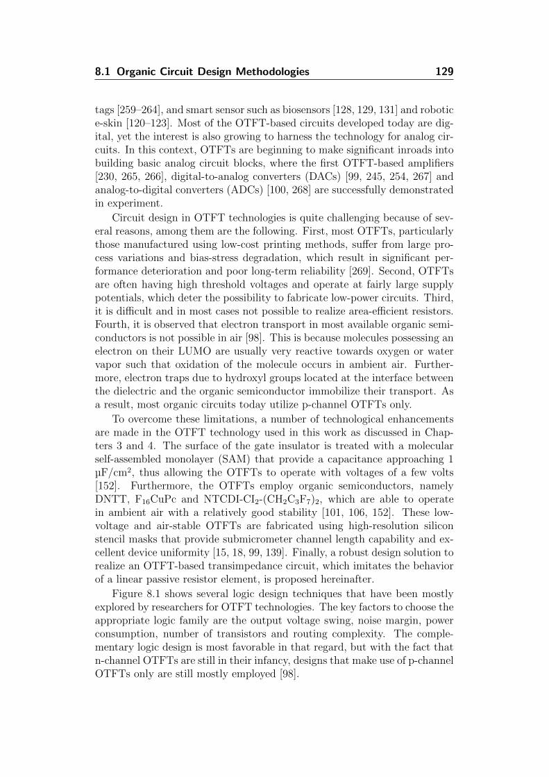
8.1 Organic Circuit Design Methodologies 129
tags [259–264], and smart sensor such as biosensors [128, 129, 131] and robotice-skin [120–123]. Most of the OTFT-based circuits developed today are dig-ital, yet the interest is also growing to harness the technology for analog cir-cuits. In this context, OTFTs are beginning to make significant inroads intobuilding basic analog circuit blocks, where the first OTFT-based amplifiers[230, 265, 266], digital-to-analog converters (DACs) [99, 245, 254, 267] andanalog-to-digital converters (ADCs) [100, 268] are successfully demonstratedin experiment.
Circuit design in OTFT technologies is quite challenging because of sev-eral reasons, among them are the following. First, most OTFTs, particularlythose manufactured using low-cost printing methods, suffer from large pro-cess variations and bias-stress degradation, which result in significant per-formance deterioration and poor long-term reliability [269]. Second, OTFTsare often having high threshold voltages and operate at fairly large supplypotentials, which deter the possibility to fabricate low-power circuits. Third,it is difficult and in most cases not possible to realize area-efficient resistors.Fourth, it is observed that electron transport in most available organic semi-conductors is not possible in air [98]. This is because molecules possessing anelectron on their LUMO are usually very reactive towards oxygen or watervapor such that oxidation of the molecule occurs in ambient air. Further-more, electron traps due to hydroxyl groups located at the interface betweenthe dielectric and the organic semiconductor immobilize their transport. Asa result, most organic circuits today utilize p-channel OTFTs only.
To overcome these limitations, a number of technological enhancementsare made in the OTFT technology used in this work as discussed in Chap-ters 3 and 4. The surface of the gate insulator is treated with a molecularself-assembled monolayer (SAM) that provide a capacitance approaching 1µF/cm2, thus allowing the OTFTs to operate with voltages of a few volts[152]. Furthermore, the OTFTs employ organic semiconductors, namelyDNTT, F16CuPc and NTCDI-CI2-(CH2C3F7)2, which are able to operatein ambient air with a relatively good stability [101, 106, 152]. These low-voltage and air-stable OTFTs are fabricated using high-resolution siliconstencil masks that provide submicrometer channel length capability and ex-cellent device uniformity [15, 18, 99, 139]. Finally, a robust design solution torealize an OTFT-based transimpedance circuit, which imitates the behaviorof a linear passive resistor element, is proposed hereinafter.
Figure 8.1 shows several logic design techniques that have been mostlyexplored by researchers for OTFT technologies. The key factors to choose theappropriate logic family are the output voltage swing, noise margin, powerconsumption, number of transistors and routing complexity. The comple-mentary logic design is most favorable in that regard, but with the fact thatn-channel OTFTs are still in their infancy, designs that make use of p-channelOTFTs only are still mostly employed [98].
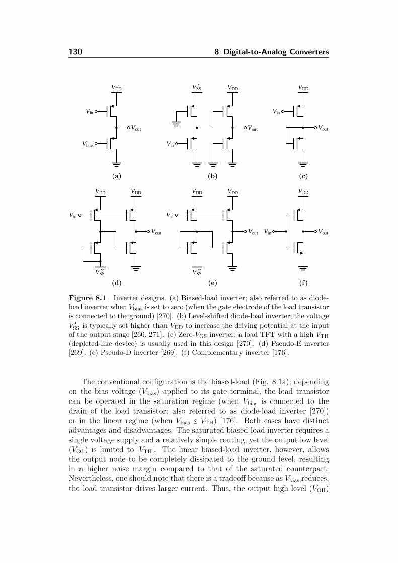
130 8 Digital-to-Analog Converters
Vin
VDD
Vbias
Vout
Vin
VDD
Vout
Vin
VDD
Vout
VDD VDD
Vout
Vin
VDD VDD
Vout
Vin
Vin
VDD
Vout
VSS
VSS
´ VSS
(a)
Vin
VDD
Vbias
Vout
Vin
VDD
Vout
Vin
VDD
Vout
VDD VDD
Vout
Vin
VDD VDD
Vout
Vin
Vin
VDD
Vout
VSS
VSS
´ VSS
(b)
Vin
VDD
Vbias
Vout
Vin
VDD
Vout
Vin
VDD
Vout
VDD VDD
Vout
Vin
VDD VDD
Vout
Vin
Vin
VDD
Vout
VSS
VSS
´ VSS
(c)
Vin
VDD
Vbias
Vout
Vin
VDD
Vout
Vin
VDD
Vout
VDD VDD
Vout
Vin
VDD VDD
Vout
Vin
Vin
VDD
Vout
VSS
VSS
´ VSS
(d)
Vin
VDD
Vbias
Vout
Vin
VDD
Vout
Vin
VDD
Vout
VDD VDD
Vout
Vin
VDD VDD
Vout
Vin
Vin
VDD
Vout
VSS
VSS
´ VSS
(e)
Vin
VDD
Vbias
Vout
Vin
VDD
Vout
Vin
VDD
Vout
VDD VDD
Vout
Vin
VDD VDD
Vout
Vin
Vin
VDD
Vout
VSS
VSS
´ VSS
(f)
Figure 8.1 Inverter designs. (a) Biased-load inverter; also referred to as diode-load inverter when Vbias is set to zero (when the gate electrode of the load transistoris connected to the ground) [270]. (b) Level-shifted diode-load inverter; the voltageV ′
SS is typically set higher than VDD to increase the driving potential at the inputof the output stage [260, 271]. (c) Zero-VGS inverter; a load TFT with a high VTH
(depleted-like device) is usually used in this design [270]. (d) Pseudo-E inverter[269]. (e) Pseudo-D inverter [269]. (f) Complementary inverter [176].
The conventional configuration is the biased-load (Fig. 8.1a); dependingon the bias voltage (Vbias) applied to its gate terminal, the load transistorcan be operated in the saturation regime (when Vbias is connected to thedrain of the load transistor; also referred to as diode-load inverter [270])or in the linear regime (when Vbias ≤ VTH) [176]. Both cases have distinctadvantages and disadvantages. The saturated biased-load inverter requires asingle voltage supply and a relatively simple routing, yet the output low level(VOL) is limited to ∣VTH∣. The linear biased-load inverter, however, allowsthe output node to be completely dissipated to the ground level, resultingin a higher noise margin compared to that of the saturated counterpart.Nevertheless, one should note that there is a tradeoff because as Vbias reduces,the load transistor drives larger current. Thus, the output high level (VOH)
8.1 Organic Circuit Design Methodologies 131
also reduces, which results in a lower noise margin. The main drawback of thelinear biased-load inverter is the use of two separate power supplies, but thiscan be actually utilized as a built-in post fabrication tool to compensate forprocess variation and device degradation or can be also employed to switch offthe inverter when it is not needed by applying Vbias = VDD. In general, bothsaturated and linear biased-load inverters suffer from low gain and relativelyhigh stand-by power dissipation.
In the biased-load inverter, the output swing as well as the trip voltageare dependent on the applied bias voltage Vbias. To have a better control overthe trip voltage without affecting much the output swing, a level shifter (Fig.8.1b) can be used at the input [260, 271]. In this special case, a diode-loadinverter is used at the output stage to have only one additional power supplyV ′
SS and accordingly reduce the routing complexity. Therefore, by adjustingV ′
SS, the trip voltage can be shifted towards VDD/2. This design, thoughimproves the balance between the high and low noise margins, consumesmore power due to the larger flow of current compared to the previous design.
Another approach is by using a zero-VGS load (Fig. 8.1c); this configura-tion can alleviate the high power dissipation of the level-shifted diode-loadinverter at the cost of a slower speed [270]. The zero-VGS load providesa higher output resistance and thus higher gain, sharper voltage transfercharacteristic (VTC) and better noise margin. Given that the mobility inOTFTs is dependent on the gate voltage, the load in this case must be sig-nificantly wider than the driver to achieve positive noise margins [272]. Notonly does this make the area of the inverter larger, it also increases the totalgate capacitance, resulting in a slower inverter speed. In order to increase thepull-down force and improve the asymmetric characteristics without area andspeed overhead, a zero-VGS OTFT load with a high VTH, i.e., a depletion-likedevice, can be used. This dual-VTH implementation can reduce the area by 30times compared to the single-VTH inverter, assuming a trip voltage at VDD/2[272]. However, the problem with the high stand-by power dissipation is stillpresent in this approach because the load transistor always has a conductingchannel regardless of the input and output voltage levels.
Organic transistors are mostly not intentionally doped; therefore, thethreshold voltages of all OTFTs on a substrate are similar [98]. In principle,electrical doping of organic semiconductors is possible, but this is not favor-able as discussed in Chapter 3. Alternatively, several methods have beenstudied in literature to achieve VTH control in OTFTs: (i) different SAMsin the gate dielectric [273], (ii) floating-gate structure [274], (iii) back-gatebias [275], or (iv) gate materials with different work functions [272, 276].Despite the successful tuning of the VTH, each of these methods has certaindrawbacks for use in practical applications. These methods generally requirespecial process manipulation, add an electrode in each transistor that resultin more interconnect lines, create a very small (sometimes negligible) amount
132 8 Digital-to-Analog Converters
of VTH shift relative to the typical supply voltage VDD, or induce substantialadverse effects on the OTFT characteristics including performance and sta-bility. Nevertheless, the control of the threshold voltage after manufacturingusing the floating- or back-gate methods is beneficial for many OTFT tech-nologies, since VTH is known to change inadvertently during operation due tobias stress and air exposure [274, 275]. In 2011, the first organic 8-bit micro-processor was introduced, which employed the dual-VTH OTFT architecturewith back-gate bias [277, 278]. The microprocessor runs at a clock speed of40 Hz with a supply voltage of 10 V; however, a very high back-gate voltageof 50 V is needed to tune properly the threshold voltage.
A new logic family called Pseudo-CMOS that avoids the process complex-ities introduced by the dual-VTH technologies while attaining a comparableinverter performance was recently proposed [269, 279, 280]. Pseudo-E (Fig.8.1d) and Pseudo-D (Fig. 8.1e) are two design variations of this category;they differ in the gate connection of the load transistor of the input stage.Similar to the level-shifted diode-load inverter, four OTFTs are needed torealize an inverter. Moreover, the additional tuning voltage V ′′
SS is also usedpost fabrication to compensate for the process variations and to keep thedevice performance in check. The difference to the previous configurationsis that the load transistor connected to the output node is switched off whenthe input is low to prevent a direct current from VDD to ground, resultingin a high output swing. Nevertheless, the load transistor in the input stagealways has a conducting channel regardless of the input voltage level.
The operation of all the inverters considered so far is controlled primarilyby switching the driver transistor. In addition, a nonzero steady-state cur-rent is always drawn from the power supply to the ground when the drivertransistor is switched on, which results in an inevitable significant DC powerconsumption [176]. On the other hand, the complementary inverter (Fig.8.1f), which comprises both p- and n-channel OTFTs, operates in a differ-ent way. For a logic high input, the n-channel OTFT drives (pulls down)the output node while the p-channel OTFT is switched off; however, for alogic low input, the p-channel OTFT drives (pulls up) the output node whilethe n-channel OTFT acts is switched off. A direct flow of current from thepower supply to the ground occurs only when switching between the high-and low-level states, resulting in a negligible static power dissipation (< 1 nW[152]). In the steady-state operation, only the gate leakage current (suppos-edly small current) between the gate electrode and the contacts is present.As a result, the VTC of the complementary inverter exhibits a full outputswing between 0 V and VDD with a sharp transition between the logic states.
The low power consumption in organic transistors is highly desirable forbattery-powered or frequency-coupled applications. However, the integrationof n-channel OTFTs is beneficial only if the electron mobility is comparablewith the hole mobility [272]. In the dual-VTH inverter presented in [272],
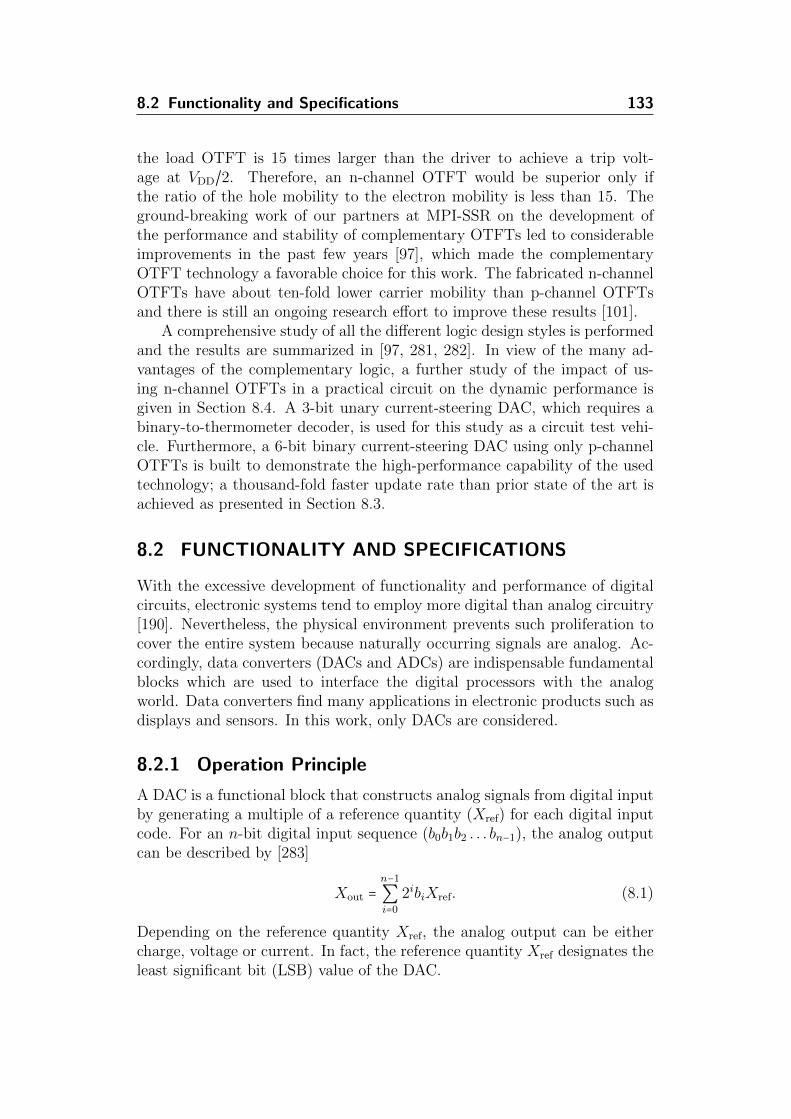
8.2 Functionality and Specifications 133
the load OTFT is 15 times larger than the driver to achieve a trip volt-age at VDD/2. Therefore, an n-channel OTFT would be superior only ifthe ratio of the hole mobility to the electron mobility is less than 15. Theground-breaking work of our partners at MPI-SSR on the development ofthe performance and stability of complementary OTFTs led to considerableimprovements in the past few years [97], which made the complementaryOTFT technology a favorable choice for this work. The fabricated n-channelOTFTs have about ten-fold lower carrier mobility than p-channel OTFTsand there is still an ongoing research effort to improve these results [101].
A comprehensive study of all the different logic design styles is performedand the results are summarized in [97, 281, 282]. In view of the many ad-vantages of the complementary logic, a further study of the impact of us-ing n-channel OTFTs in a practical circuit on the dynamic performance isgiven in Section 8.4. A 3-bit unary current-steering DAC, which requires abinary-to-thermometer decoder, is used for this study as a circuit test vehi-cle. Furthermore, a 6-bit binary current-steering DAC using only p-channelOTFTs is built to demonstrate the high-performance capability of the usedtechnology; a thousand-fold faster update rate than prior state of the art isachieved as presented in Section 8.3.
8.2 FUNCTIONALITY AND SPECIFICATIONS
With the excessive development of functionality and performance of digitalcircuits, electronic systems tend to employ more digital than analog circuitry[190]. Nevertheless, the physical environment prevents such proliferation tocover the entire system because naturally occurring signals are analog. Ac-cordingly, data converters (DACs and ADCs) are indispensable fundamentalblocks which are used to interface the digital processors with the analogworld. Data converters find many applications in electronic products such asdisplays and sensors. In this work, only DACs are considered.
8.2.1 Operation Principle
A DAC is a functional block that constructs analog signals from digital inputby generating a multiple of a reference quantity (Xref) for each digital inputcode. For an n-bit digital input sequence (b0b1b2 . . . bn−1), the analog outputcan be described by [283]
Xout =n−1
∑i=0
2ibiXref. (8.1)
Depending on the reference quantity Xref, the analog output can be eithercharge, voltage or current. In fact, the reference quantity Xref designates theleast significant bit (LSB) value of the DAC.

134 8 Digital-to-Analog Converters
In principle, a DAC is characterized by two main parameters, namelyresolution and update rate. For an n-bit resolution, the digital signal canonly have 2n values. Furthermore, the update rate is the rate at which theinput digital codes are converted. Therefore, for the realization of an accurateDAC, the resolution and update rate have to be maximized. According toNyquist-Shannon theorem, the minimum update rate of the DAC has to beat least equal to two times the highest frequency of the signal; this is to avoidaliasing and to be able to fully construct the output analog signal. In thefollowing, detailed description of the different characterization parameters ofa DAC is presented.
8.2.2 Characterization Parameters
The performance of DACs is evaluated by several specification parameters.These help to evaluate and select the most suitable DAC architecture fromthe numerous available alternative designs for a given application. The pa-rameters are classified into two categories, namely static and dynamic mea-sures. The static parameters are offset error, gain error, differential non-linearity (DNL) and integral non-linearity (INL). Furthermore, the dynamicparameters in the time and frequency domains are maximum update rate, set-tling time, slew rate, glitch energy and spurious free dynamic range (SFDR).The definition of each of these nine parameters is as follows [190, 283].
Offset and gain errors
The offset error is the constant DC offset of the DAC transfer characteristics,while the gain error is the deviation of the characteristic slope from the idealone (Fig. 8.2a). Note that these errors do not introduce any non-linearityand has no effect on the frequency domain.
Differential non-linearity
The maximum DNL error is the worst case deviation of the actual to theideal step size of 1 LSB between two adjacent input codes (Fig. 8.2b). Themaximum DNL is expressed as
DNLmax = max(Vout(i + 1) − Vout(i) −∆VLSB
∆VLSB
), (8.2)
where i = 0, 1, . . ., 2n − 2 and ∆VLSB is given by
∆VLSB =Vout(2n − 1) − Vout(0)
2n − 1. (8.3)
In general, it is preferable to have a DAC with a DNL error that is less than±1 LSB to guarantee proper operation.
8.2 Functionality and Specifications 135
00
0
00
1
01
0
01
1
10
0
10
1
11
0
11
1
00
0
00
1
01
0
01
1
10
0
10
1
11
0
11
1
An
alo
g o
utp
ut
An
alo
g o
utp
ut
Digital input Digital input
Gain error
Offset error
Ideal output
DNL + 1 LSB
INL
(a)
00
0
00
1
01
0
01
1
10
0
10
1
11
0
11
1
00
0
00
1
01
0
01
1
10
0
10
1
11
0
11
1
An
alo
g o
utp
ut
An
alo
g o
utp
ut
Digital input Digital input
Gain error
Offset error
Ideal output
DNL + 1 LSB
INL
(b)
Figure 8.2 Static specifications of a DAC. (a) Ideal transfer characteristics inaddition to offset and gain errors. (b) Differential non-linearity (DNL) and inte-gral non-linearity (INL) errors [283]. The INL shown here is extracted from thebest-fit line, which is fitted to the data using the minimum mean square error(MMSE) approach. Another commonly used method is to extract the INL fromthe end-point line, which is a line that connects the points on the transfer functioncorresponding to the lowest and highest input codes. The latter approach typicallyyields larger INL values.
Integral non-linearity
The maximum INL error is the worst case deviation of the actual to theideal linear output curve. After nullifying the gain and offset errors, theideal output curve is either an end-point line connecting the minimum andfull scale points or a best-fit line that is based on the minimum mean squareerror (MMSE) distance from line to samples. The latter approach—as shownin Fig. 8.2b—is used in this work.
For the end-point line approach, however, the maximum INL of a DACis represented by the following expression:
INLmax = max[Vout(i) − Vout(0) −∆VLSB ⋅ i], (8.4)
where i = 0, 1, . . ., 2n − 1, and ∆VLSB is the slope of the line through theend points and is given by (8.3). The resulting INL using this expression istypically larger than when using the best-fit line.
By definition, a DAC is called monotonic when its output never decreaseswith an increasing digital input, i.e., the analog output always increases orremains constant as the digital input increases. For guaranteed monotonicity,the INL error should be less than or equals to ±0.5 LSB.

136 8 Digital-to-Analog Converters
Anal
og o
utp
ut
Outp
ut
ampli
tude
(dB
)
Time
Setting time
Ideal response
Glitch energy
Slew rate
DNL
Fundamental signal
First harmonic
SFDR (dB)
Frequency
(a)
Anal
og O
utp
ut
Outp
ut
ampli
tude
(dB
)
Time
Setting time
Ideal response
Glitch energy
Slew rate
DNL
Fundamental signal
First harmonic
SFDR (dB)
Frequency
(b)
Figure 8.3 Dynamic specifications of a DAC. (a) Analog output of a DAC asa function of time, showing the settling time, slew rate and glitch energy. (b)Frequency spectrum of a DAC output signal, illustrating the spurious free dynamicrange (SFDR) [283].
Update rate
The update rate is the rate at which the output is sampled. According toNyquist-Shannon theorem, the minimum update rate of the DAC has to beat least equal to two times the maximum frequency of the signal. The updaterate is given in unit samples per second (S/s).
Settling time
The settling time is defined to be the time needed by the DAC to experiencea full scale transition and settle around its final value (Fig. 8.3a).
Slew rate
The slew rate is defined to be the maximal rate at which the output of theDAC can change with the varying input (Fig. 8.3a).
Glitch energy
The glitch energy is the area under the transient response when the DACswitches between two consecutive input codes (Fig. 8.3a). An acceptablequantitative approximation of the glitch energy can be evaluated by assuminga square-shaped glitch impulse (worst case calculation). Therefore, the glitchenergy is given by Egl = tgl×Agl, where tgl and Agl are the timing error and the

8.2 Functionality and Specifications 137
amplitude of the glitch, respectively. In practice, the glitch energy has to beadequately smaller than the LSB energy, which is given by ELSB = tLSB×ALSB.Therefore, for a good dynamic performance, the ratio Egl/ELSB has to beminimized. A simple way to minimize Egl is to reduce tgl by using well-placed synchronized blocks in the DAC.
Spurious free dynamic range
The SFDR is defined to be the ratio between the fundamental signal power(Psig) and the largest distortion component power (Pmax-dist) within a specificmeasured frequency window (Fig. 8.3b). Accordingly, the SFDR is expressedas follows:
SFDR =Psig
Pmax-dist
. (8.5)
Note that the SFDR depends on the operating conditions and the updaterate of the DAC.
8.2.3 Design Architectures
This section gives an overview and comparison of different DAC architecturesexisting today [190]. Emphasis is made on the area, complexity and dynamicspecifications of the DACs. For more detailed study of the operation of eacharchitecture, the reader is referred to [284].
The DACs are mainly classified into three main categories, namely resis-tive, capacitive and current-steering DACs. This classification is recognizedfrom the reference quantity (Xref) used. Correspondingly, the DAC out-put signal can either be voltage, charge or current, respectively. Note thatthere are also other DAC topologies such as hybrid resistive-capacitive andpulse-width-modulation-based DACs; however, these architectures are notcomprised in the focus of this work. For each of the DAC architectures,various implementations ranging from high-speed to high-accuracy designsare proposed in literature. This gives the designer the freedom to choose themost suitable implementation for a given application; nevertheless, there isalways a tradeoff and a compromise has to be made.
In general, chip area and process limitations rule out the resistive-basedDACs for our OTFT technology. This is because accurate and compact resis-tors cannot be yet realized. On the other hand, the capacitive-based DACscan be implemented using charge-divider, multiplying-capacitive or switched-capacitor designs [284]. The very large chip area needed by the charge-dividerdesign makes it not suitable for high resolution DACs. Furthermore, the com-plexity of the multiplying-capacitive design makes it not a favorable choicefor an OTFT technology. The switched-capacitor design, however, is suitable
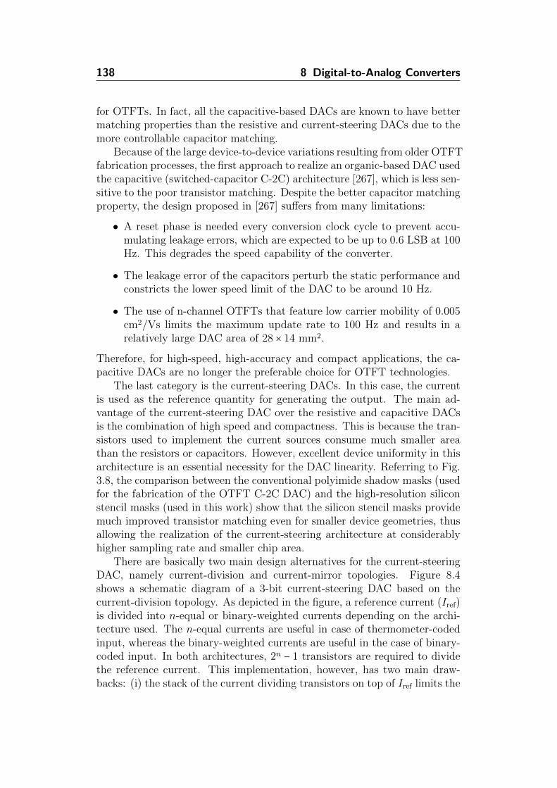
138 8 Digital-to-Analog Converters
for OTFTs. In fact, all the capacitive-based DACs are known to have bettermatching properties than the resistive and current-steering DACs due to themore controllable capacitor matching.
Because of the large device-to-device variations resulting from older OTFTfabrication processes, the first approach to realize an organic-based DAC usedthe capacitive (switched-capacitor C-2C) architecture [267], which is less sen-sitive to the poor transistor matching. Despite the better capacitor matchingproperty, the design proposed in [267] suffers from many limitations:
• A reset phase is needed every conversion clock cycle to prevent accu-mulating leakage errors, which are expected to be up to 0.6 LSB at 100Hz. This degrades the speed capability of the converter.
• The leakage error of the capacitors perturb the static performance andconstricts the lower speed limit of the DAC to be around 10 Hz.
• The use of n-channel OTFTs that feature low carrier mobility of 0.005cm2/Vs limits the maximum update rate to 100 Hz and results in arelatively large DAC area of 28 × 14 mm2.
Therefore, for high-speed, high-accuracy and compact applications, the ca-pacitive DACs are no longer the preferable choice for OTFT technologies.
The last category is the current-steering DACs. In this case, the currentis used as the reference quantity for generating the output. The main ad-vantage of the current-steering DAC over the resistive and capacitive DACsis the combination of high speed and compactness. This is because the tran-sistors used to implement the current sources consume much smaller areathan the resistors or capacitors. However, excellent device uniformity in thisarchitecture is an essential necessity for the DAC linearity. Referring to Fig.3.8, the comparison between the conventional polyimide shadow masks (usedfor the fabrication of the OTFT C-2C DAC) and the high-resolution siliconstencil masks (used in this work) show that the silicon stencil masks providemuch improved transistor matching even for smaller device geometries, thusallowing the realization of the current-steering architecture at considerablyhigher sampling rate and smaller chip area.
There are basically two main design alternatives for the current-steeringDAC, namely current-division and current-mirror topologies. Figure 8.4shows a schematic diagram of a 3-bit current-steering DAC based on thecurrent-division topology. As depicted in the figure, a reference current (Iref)is divided into n-equal or binary-weighted currents depending on the archi-tecture used. The n-equal currents are useful in case of thermometer-codedinput, whereas the binary-weighted currents are useful in the case of binary-coded input. In both architectures, 2n − 1 transistors are required to dividethe reference current. This implementation, however, has two main draw-backs: (i) the stack of the current dividing transistors on top of Iref limits the
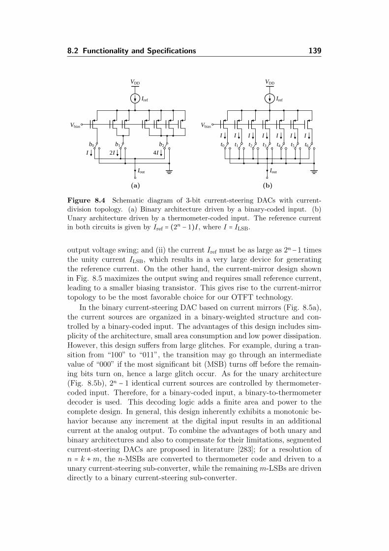
8.2 Functionality and Specifications 139
Vbias
VDD
b2b1b0
Iref
Iout
I 2 I 4 I
Vbias
VDD
t0
Iref
Iout
t1 t2 t3 t4 t5 t6
I I I I I I I
(a)
Vbias
VDD
b2b1b0
Iref
Iout
I 2 I 4 I
Vbias
VDD
t0
Iref
Iout
t1 t2 t3 t4 t5 t6
I I I I I I I
(b)
Figure 8.4 Schematic diagram of 3-bit current-steering DACs with current-division topology. (a) Binary architecture driven by a binary-coded input. (b)Unary architecture driven by a thermometer-coded input. The reference currentin both circuits is given by Iref = (2n − 1)I, where I = ILSB.
output voltage swing; and (ii) the current Iref must be as large as 2n−1 timesthe unity current ILSB, which results in a very large device for generatingthe reference current. On the other hand, the current-mirror design shownin Fig. 8.5 maximizes the output swing and requires small reference current,leading to a smaller biasing transistor. This gives rise to the current-mirrortopology to be the most favorable choice for our OTFT technology.
In the binary current-steering DAC based on current mirrors (Fig. 8.5a),the current sources are organized in a binary-weighted structure and con-trolled by a binary-coded input. The advantages of this design includes sim-plicity of the architecture, small area consumption and low power dissipation.However, this design suffers from large glitches. For example, during a tran-sition from “100” to “011”, the transition may go through an intermediatevalue of “000” if the most significant bit (MSB) turns off before the remain-ing bits turn on, hence a large glitch occur. As for the unary architecture(Fig. 8.5b), 2n − 1 identical current sources are controlled by thermometer-coded input. Therefore, for a binary-coded input, a binary-to-thermometerdecoder is used. This decoding logic adds a finite area and power to thecomplete design. In general, this design inherently exhibits a monotonic be-havior because any increment at the digital input results in an additionalcurrent at the analog output. To combine the advantages of both unary andbinary architectures and also to compensate for their limitations, segmentedcurrent-steering DACs are proposed in literature [283]; for a resolution ofn = k +m, the n-MSBs are converted to thermometer code and driven to aunary current-steering sub-converter, while the remaining m-LSBs are drivendirectly to a binary current-steering sub-converter.

140 8 Digital-to-Analog Converters
VDD
b2b1b0
Iout
I 2 I 4 I
VDD
t0
Iout
t1 t2 t3 t4 t5 t6
I I I I I I I
ILSBILSB
(a)
VDD
b2b1b0
Iout
I 2 I 4 I
VDD
t0
Iout
t1 t2 t3 t4 t5 t6
I I I I I I I
ILSBILSB
(b)
Figure 8.5 Schematic diagram of 3-bit current-steering DACs with current-mirror topology. (a) Binary architecture driven by a binary-coded input. (b)Unary architecture driven by a thermometer-coded input. The reference currentin both circuits is given by Iref = ILSB = I.
The use of silicon stencil masks in this work made it possible to fabri-cate top-contact OTFTs with high resolution and excellent uniformity. Suchprecise matching between the transistors is highly desirable in the current-steering DAC, where device matching is paramount. Accordingly, a 6-bitbinary current-steering DAC using only p-channel OTFTs is implemented tobenchmark the recently published 6-bit switched-capacitor DAC that usescomplementary OTFTs [99, 267]. By comparing the results of both circuits,the presented current-steering DAC offers a dramatic performance boost(1000 times faster) and greatly reduced area consumption (30 times smaller).Furthermore, a 3-bit unary current-steering DAC is designed and fabricated,allowing to demonstrate the feasibility to realize a fully custom complemen-tary logic block, i.e., a binary-to-thermometer decoder. The functionality ofthis DAC is validated and a study of the impact of device and interconnectparasitics as well as the use of relatively slow n-channel OTFTs on the circuitperformance is carried out. The DAC designs and measurement results arepresented in the following sections. Given the successful realization of bothdesigns, it is proposed to combine in the future both implementations in ahigh-resolution segmented current-steering DAC.
8.3 A HIGH-PERFORMANCE UNIPOLAR DESIGN
8.3.1 A 6-bit Binary Current-Steering DAC
The schematic diagram of the designed 6-bit current-steering DAC is shownin Fig. 8.6 [99, 190, 254]. The binary-weighted current-steering architectureis employed here because of its lower complexity, smaller area consumption
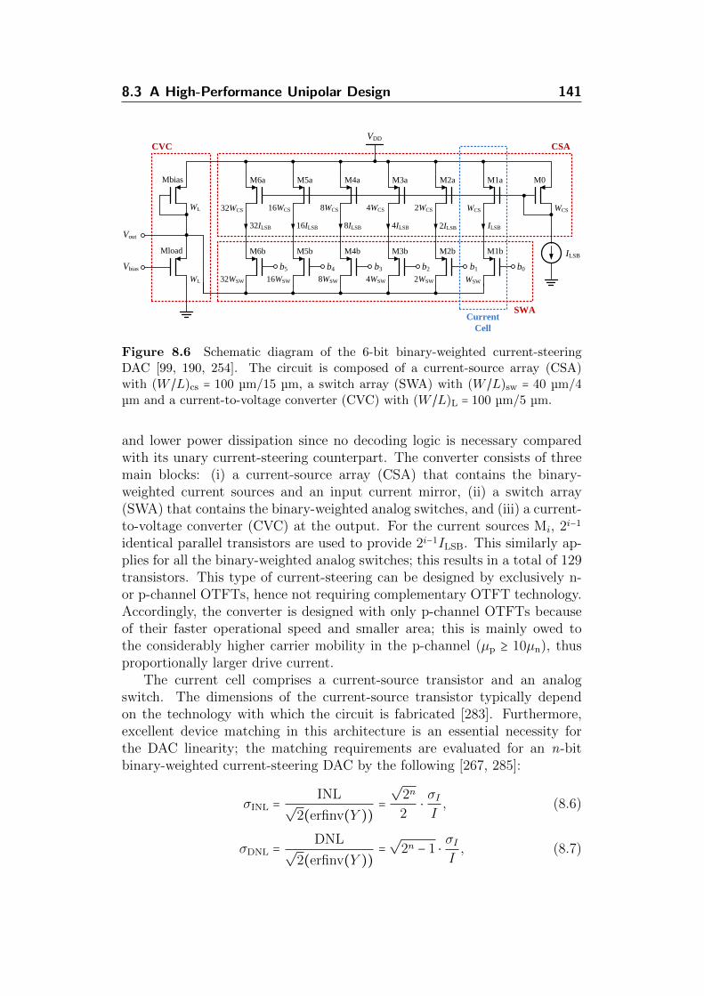
8.3 A High-Performance Unipolar Design 141
ILSB2ILSB4ILSB8ILSB16ILSB32ILSB
b0b1b2b3b4b5
CVC CSA
SWA
WCS2WCS4WCS8WCS16WCS32WCS
WSW2WSW4WSW8WSW16WSW32WSW
WCS
Current
Cell
VDD
Vbias
ILSB
WL
Mload
M6a M5a M4a M3a M2a M1a
M6b M5b M4b M3b M2b M1b
M0Mbias
WL
Vout
Figure 8.6 Schematic diagram of the 6-bit binary-weighted current-steeringDAC [99, 190, 254]. The circuit is composed of a current-source array (CSA)with (W /L)cs = 100 µm/15 µm, a switch array (SWA) with (W /L)sw = 40 µm/4µm and a current-to-voltage converter (CVC) with (W /L)L = 100 µm/5 µm.
and lower power dissipation since no decoding logic is necessary comparedwith its unary current-steering counterpart. The converter consists of threemain blocks: (i) a current-source array (CSA) that contains the binary-weighted current sources and an input current mirror, (ii) a switch array(SWA) that contains the binary-weighted analog switches, and (iii) a current-to-voltage converter (CVC) at the output. For the current sources Mi, 2i−1
identical parallel transistors are used to provide 2i−1ILSB. This similarly ap-plies for all the binary-weighted analog switches; this results in a total of 129transistors. This type of current-steering can be designed by exclusively n-or p-channel OTFTs, hence not requiring complementary OTFT technology.Accordingly, the converter is designed with only p-channel OTFTs becauseof their faster operational speed and smaller area; this is mainly owed tothe considerably higher carrier mobility in the p-channel (µp ≥ 10µn), thusproportionally larger drive current.
The current cell comprises a current-source transistor and an analogswitch. The dimensions of the current-source transistor typically dependon the technology with which the circuit is fabricated [283]. Furthermore,excellent device matching in this architecture is an essential necessity forthe DAC linearity; the matching requirements are evaluated for an n-bitbinary-weighted current-steering DAC by the following [267, 285]:
σINL =INL
√2(erfinv(Y ))
=
√2n
2⋅σII, (8.6)
σDNL =DNL
√2(erfinv(Y ))
=√
2n − 1 ⋅σII, (8.7)

142 8 Digital-to-Analog Converters
where σI/I is the current relative standard deviation (transistor’s currentmismatch). For n = 6 bits, INL ≤ 1 LSB, DNL ≤ 1 LSB and Y = 0.95, whichcorresponds to a confidence interval of 2-σ, the required current mismatchshould be σI/I ≤ 6.4%, which is the minimum value resulting from equations(8.6) and (8.7).
Referring to Fig. 3.8, the 16 OTFTs fabricated by the conventional poly-imide shadow masks with a channel length of 30 µm have σI/I = 11%, whichexceeds already the upper limit calculated above, whereas the 16 OTFTs fab-ricated by the high-resolution silicon stencil masks with a channel length ofonly 2 µm have σI/I = 4% [99, 139]. Because of the large device-to-device vari-ations resulting from the older OTFT fabrication processes, the first approachto realize an organic-based DAC used the capacitive (switched-capacitor C-2C) architecture which is less sensitive to the poor transistor matching [267].However, the improved transistor matching even for smaller dimensions of-fered by the silicon stencil masks allow the realization of the current-steeringarchitecture at considerably higher sampling rate and smaller area consump-tion. Therefore, for the design of the current-source transistors in our DAC,a sufficiently large channel length of 15 µm and a channel width of 100 µmare utilized to ensure even better matching than the value displayed in Fig.3.8b and to guarantee that σI/I ≤ 6.4%.
As long as the voltage swing at the drain nodes of the current-sourcetransistors is reduced during switching, the considerable capacitance of thecurrent sources would not be charged and discharged, thus the dynamic per-formance would not be degraded. This would have been achieved by usingdifferential analog switches with reduced cross-point voltage at their controlsignals [286]. By doing so, the interconnect crossings, featuring very highparasitic capacitances (∼800 nF/cm2) and degrading the circuit performance,would have been indispensable. Therefore, single-ended analog switches areused mainly to avoid interconnect crossings and also to minimize the areaconsumption. Furthermore, the analog switches are designed to be operatingin the saturation mode during the full output voltage swing. This approachavoids the use of cascode current sources, which require larger area and limitthe output swing, while maintaining the shielding effect of the cascode struc-ture by isolating the drain nodes of the current source transistors from thevariant output node. In addition, the non-linearities of the output current-voltage characteristics of the OTFTs at low drain bias due to the non-ohmiccontacts can be avoided.
These specific operating conditions put a constraint on the switch inputON voltage (Vsw,on) to keep both the current source and analog switch tran-sistors in the saturation mode. For proper circuit operation and in closeagreement with simulations, the analog switch transistors are designed witha channel length of 4 µm and a channel width of 40 µm and the switch inputON voltage is set to be 1 V.
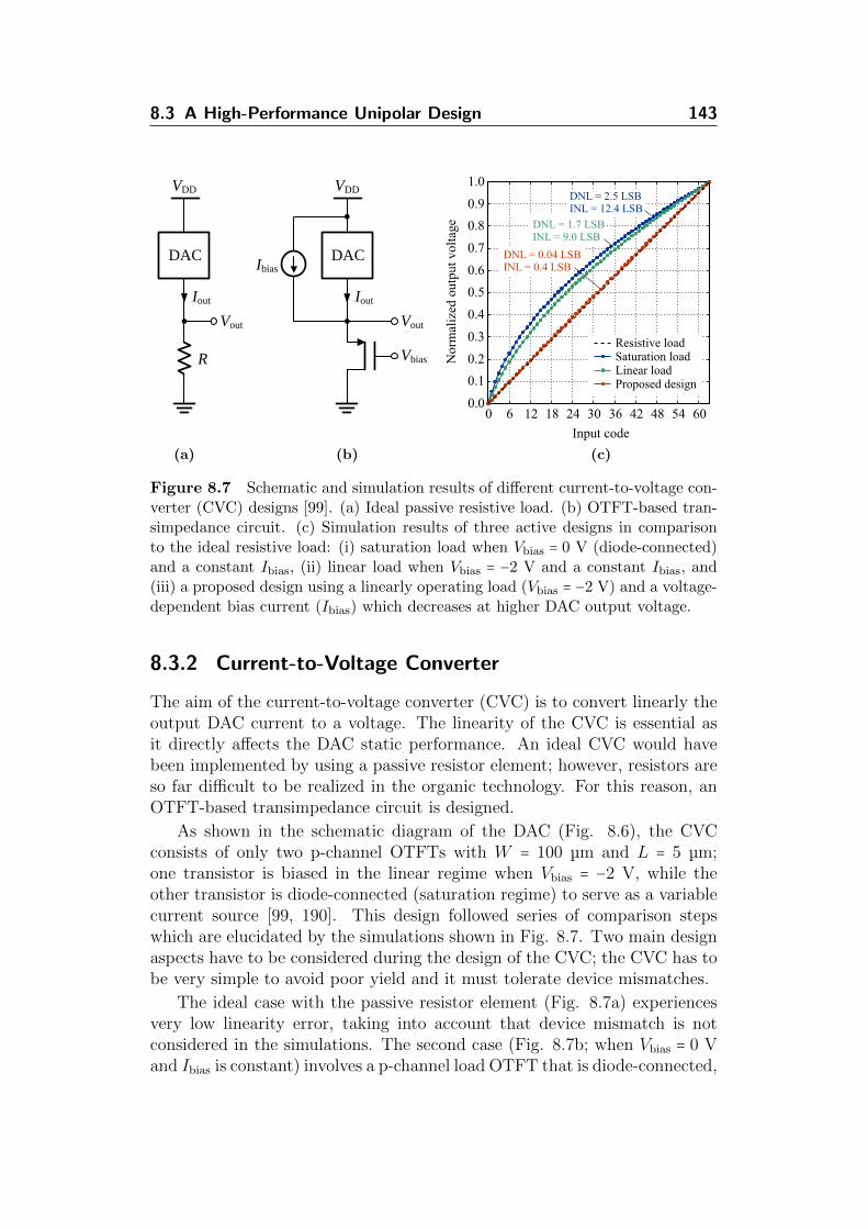
8.3 A High-Performance Unipolar Design 143
VDD
DAC
Iout
Vout
Ibias
Vbias
VDD
DAC
Iout
Vout
R
(a)
VDD
DAC
Iout
Vout
Ibias
Vbias
VDD
DAC
Iout
Vout
R
(b)
0 6 12 18 24 30 36 42 48 54 600
6
12
18
24
30
36
42
48
54
60
x
y
0 6 12 18 24 30 36 42 48 54 600.0
0.1
0.2
0.3
0.4
0.5
0.6
0.7
0.8
0.9
1.0
Input codeN
orm
aliz
ed o
utpu
t vo
ltag
e
Resistive loadSaturation loadLinear loadProposed design
DNL = 1.7 LSBINL = 9.0 LSB
DNL = 2.5 LSBINL = 12.4 LSB
DNL = 0.04 LSBINL = 0.4 LSB
(c)
Figure 8.7 Schematic and simulation results of different current-to-voltage con-verter (CVC) designs [99]. (a) Ideal passive resistive load. (b) OTFT-based tran-simpedance circuit. (c) Simulation results of three active designs in comparisonto the ideal resistive load: (i) saturation load when Vbias = 0 V (diode-connected)and a constant Ibias, (ii) linear load when Vbias = −2 V and a constant Ibias, and(iii) a proposed design using a linearly operating load (Vbias = −2 V) and a voltage-dependent bias current (Ibias) which decreases at higher DAC output voltage.
8.3.2 Current-to-Voltage Converter
The aim of the current-to-voltage converter (CVC) is to convert linearly theoutput DAC current to a voltage. The linearity of the CVC is essential asit directly affects the DAC static performance. An ideal CVC would havebeen implemented by using a passive resistor element; however, resistors areso far difficult to be realized in the organic technology. For this reason, anOTFT-based transimpedance circuit is designed.
As shown in the schematic diagram of the DAC (Fig. 8.6), the CVCconsists of only two p-channel OTFTs with W = 100 µm and L = 5 µm;one transistor is biased in the linear regime when Vbias = −2 V, while theother transistor is diode-connected (saturation regime) to serve as a variablecurrent source [99, 190]. This design followed series of comparison stepswhich are elucidated by the simulations shown in Fig. 8.7. Two main designaspects have to be considered during the design of the CVC; the CVC has tobe very simple to avoid poor yield and it must tolerate device mismatches.
The ideal case with the passive resistor element (Fig. 8.7a) experiencesvery low linearity error, taking into account that device mismatch is notconsidered in the simulations. The second case (Fig. 8.7b; when Vbias = 0 Vand Ibias is constant) involves a p-channel load OTFT that is diode-connected,

144 8 Digital-to-Analog Converters
thus operating in the saturation mode (VDG < ∣VTH∣). In this case, the CVCrelation is controlled by the OTFT saturation equation given by the following:
ID,sat = −µCIW
2L(−VGS + VTH)2, (8.8)
Vout =
√
Iout2L
µCIW− VTH. (8.9)
This non-linear relation directly reflects the high output linearity error ob-tained by the simulation. In the third case (Fig. 8.7b; when Vbias = −2 Vand Ibias is constant), a linearly operating load is used. Given that the DACoutput voltage does not exceed 2.5 V, a bias voltage of −2 V is set in a way toensure that the gate-source voltage does not exceed the breakdown voltage(∼ 6 V) during the complete output swing. Owing to the field-dependencein the OTFT contact resistance, which decreases as the gate-source voltageincreases, the DAC linearity is perturbed. Therefore, it is proposed in thelast case (Fig. 8.7b; when Vbias = −2 V and Ibias is voltage dependent) to usea variable driver current source, which decreases at higher DAC output volt-age, to compensate for the non-linearity of the load. Using a diode-connectedOTFT, as shown previously in the schematic (Fig. 8.6), the variable currentsource is realized. In this case, the gate-source voltage of the diode-connectedOTFT is given by VGS = Vout−VDD. Therefore, the absolute value of the satu-ration current ID,sat passing through the transistor given by (8.8) decreases asthe DAC output voltage (Vout) increases. The proposed CVC circuit provedto provide optimized DAC linearity.
8.3.3 Layout and Floorplan
Device matching and data interference have a strong impact on the DACperformance. Consequently, strict requirements apply to the design of theDAC layout and floorplan due to the relatively large number of transistorsemployed, especially for an organic-based analog circuit [99, 190]. Figure 8.8shows two possible approaches for the floorplan, namely merged SWA-CSAand separated SWA-CSA [283, 287]. In the merged SWA-CSA, each unit cellcomprises both the current source and the analog switch transistors. Thisapproach has a simplified layout; however, it increases the distances betweenthe current source transistors and so the layout would be potentially moresusceptible to the systematical gradient effects. As for the separated SWA-CSA, the identical transistors are placed in separate arrays, thus ensuringbetter device matching, easing power routing and minimizing signal interfer-ence due to the division of the digital and the analog parts. In spite of theincreased layout complexity in the latter approach (Fig. 8.8b), it is used asit offers a substantially better conversion performance.

8.3 A High-Performance Unipolar Design 145
...
...
...
...
...
...
...
...
CSA +
SWA
CS
A
SWA
...
...
...
... ...
...
SW CS
Input code
...Input code
1
2
2
4
4
4
4
8
8
8
8
8
8
8
8
16
16
16
16
16
16
16
16
16
16
16
16
16
16
16
16
32
32
32
32
32
32
32
32
32
32
32
32
32
32
32
32
32
32
32
32
32
32
32
32
32
32
32
32
32
32
32
32
(a)
...
...
...
...
...
...
...
...
CSA +
SWA
CS
A
SWA
...
...
...
... ...
...
SW CS
Input code
...Input code
1
2
2
4
4
4
4
8
8
8
8
8
8
8
8
16
16
16
16
16
16
16
16
16
16
16
16
16
16
16
16
32
32
32
32
32
32
32
32
32
32
32
32
32
32
32
32
32
32
32
32
32
32
32
32
32
32
32
32
32
32
32
32
(b)
Figure 8.8 Floorplan of current-steering DACs [99, 287]. (a) Merged SWA-CSA. (b) Separated SWA-CSA. In the separated SWA-CSA, identical transistorsare placed in closer proximity, allowing better control of device matching. Thenumbers given in the CSA of the separated floorplan designate the arrangementof the binary-weighted OTFTs used in our 6-bit binary current-steering DAC.
Furthermore, the transistors are placed in a matrix-like orientation ineach array to keep the identical transistors in closer proximity. This makesit possible to exploit the excellent feature size control enabled by the stencilmask technology regardless of the non-uniformity introduced by materialdeposition through evaporation. Figure 8.8b shows clearly the arrangementof the transistors in the CSA by designating the binary-weights. In thisway, the complexity of the routing matrix between the SWA and the CSAis minimized. With this careful layout and floorplan design, no interconnectcrossings that feature high parasitic capacitances are comprised. The layoutof the DAC is presented in Appendix A. Using the OTFT process technologypresented in Chapter 4, the DAC is fabricated on a glass substrate. The totalarea of the DAC including the contact pads is only 2.6 × 4.6 mm2.
8.3.4 Calibration
After the chip is fabricated, multiple DACs are measured and a noticeablenon-linearity error is observed in the transfer characteristics only duringthe transition of the input bit stream from “011111” to “100000” [99, 190].

146 8 Digital-to-Analog Converters
Therefore, to guarantee monotonicity, the DAC is calibrated by tuning man-ually the switch input ON voltage (Vsw,on) for the most significant bit (MSB)to be 0 V instead of 1 V. As a result, a slightly larger current for the MSB isenabled to the output, hence the DAC linearity is optimized. The calibrationmethod used here has a lower complexity compared to the one used in [267],where a 2-bit off-chip calibration circuit is employed.
8.3.5 Measurement Setup
By revisiting the layout of the 6-bit binary current-steering DAC, the con-verter has 12 input/output connections, namely the 6 digital binary-codedinput bit stream (Vsw1, Vsw2, . . ., Vsw5), the power supplies (VDD and VGND),the load biasing voltage (Vbias), the biasing LSB current (ILSB), the outputvoltage (Vout), and finally an optional testing connection (VX) that is con-nected to the LSB line in the routing matrix between the CSA and the SWA[99, 190]. The fabricated samples are measured in a manual probe station(SUSS PM5 analytical probe system from Karl Suss) with a careful con-nection between the probeheads and the 55-nm-thick gold pads. The 6-bitdigital input stream is provided by a data generator (HP 8180A data gen-erator from Hewlett Packard), while the remaining four inputs (VDD, VGND,Vbias and ILSB) are supplied by a source measure unit (SMU; E5270B 8-slot precision measurement mainstream from Agilent Technologies). DuringDC measurements, the output node (Vout) is captured by the SMU. DuringAC measurements, however, the output node is connected to an oscilloscope(TDS3000B oscilloscope from Tektronix). An IC-CAP PEL code is writtento control the equipment and automate the process by synchronizing thesignals from the data generator and the SMU (see Appendix D.2). All mea-surements are performed in ambient air, at room temperature, at a supplyvoltage (VDD) of 3.3 V and at relatively dimmed light environment.
8.3.6 Static and Dynamic Performances
The measured static and dynamic characteristic parameters, which fully eval-uate the performance of the 6-bit binary current-steering DAC, are presentedherein [99, 190]. Figure 8.9 shows the measured DC transfer function togetherwith the corresponding DNL and INL errors. Before calibration, an unde-sired abrupt step during the transition of the input bit stream from “011111”to “100000” is observed, resulting in a degraded static linearity; the maxi-mum DNL and INL are −0.97 and −1.64 LSB, respectively. After calibration,however, the transfer function shows a monotonic behavior, where the maxi-mum output voltage swing (Vswing) is 1.94 V with a power dissipation of 260µW and an improved static linearity is attained. The maximum DNL andINL are −0.29 and −1.21 LSB, respectively.

8.3 A High-Performance Unipolar Design 147
(a)
0 6 12 18 24 30 36 42 48 54 600.0
0.2
0.4
0.6
0.8
1.0
1.2
1.4
1.6
1.8
2.0
2.2
Input code
Outp
ut
volt
age
(V)
Before calibration
After calibration
0 6 12 18 24 30 36 42 48 54 60-1.5
-1.0
-0.5
0.0
0.5
1.0
-1.0
-0.5
0.0
0.5
1.0
1.5
Input codeD
NL
(L
SB
)IN
L (
LS
B)DNL = -0.97 LSB
INL = -1.64 LSB
DNL = -0.29 LSBINL = -1.21 LSB
After calibration
(b)
Figure 8.9 Measured DC characteristics of the 6-bit binary current-steeringDAC [99]. (a) Transfer characteristics before and after calibration. (b) CalculatedDNL and INL errors after calibration.
0 6 12 18 24 30 36 42 48 54 60-1.5
-1.0
-0.5
0.0
0.5
1.0
-1.0
-0.5
0.0
0.5
1.0
1.5
Input code
DN
L (
LS
B)
INL
(L
SB
)
0 6 12 18 24 30 36 42 48 54 600.0
0.2
0.4
0.6
0.8
1.0
1.2
1.4
1.6
Input code
Out
put
vol
tage
(V
)
at 1 kS/s
(a)
0 6 12 18 24 30 36 42 48 54 60-1.5
-1.0
-0.5
0.0
0.5
1.0
-1.0
-0.5
0.0
0.5
1.0
1.5
Input code
DN
L (
LS
B)
INL
(L
SB
)
0 6 12 18 24 30 36 42 48 54 600.0
0.2
0.4
0.6
0.8
1.0
1.2
1.4
1.6
Input code
Out
put
vol
tage
(V
)
at 1 kS/s
(b)
Figure 8.10 Measured characteristics of the 6-bit binary current-steering DACat an update rate of 1 kS/s, after calibration, and at an output voltage swing of1.3 V [99]. (a) Transfer characteristic. (b) Calculated DNL and INL errors.
Furthermore, Fig. 8.10 depicts the measured transfer function along withthe calculated DNL and INL errors after calibration, at an output voltageswing of 1.3 V (at a reduced ILSB), and at an update rate of 1 kS/s; themaximum DNL and INL are −0.69 and 1.16 LSB, respectively. Figure 8.11illustrates the upper speed limit of the DAC in worst case conditions, i.e., the
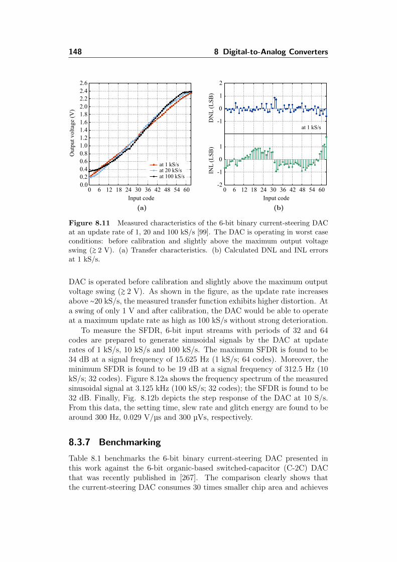
148 8 Digital-to-Analog Converters
0 6 12 18 24 30 36 42 48 54 600.0
0.20.4
0.6
0.8
1.01.2
1.41.6
1.8
2.0
2.2
2.4
2.6
Input code
Out
put
volt
age
(V)
at 1 kS/sat 20 kS/sat 100 kS/s
0 6 12 18 24 30 36 42 48 54 60-2
-1
0
1
-1
0
1
2
Input code
DN
L (
LS
B)
INL
(L
SB
)
at 1 kS/s
(a)
0 6 12 18 24 30 36 42 48 54 600.0
0.20.4
0.6
0.8
1.01.2
1.41.6
1.8
2.0
2.2
2.4
2.6
Input code
Out
put
volt
age
(V)
at 1 kS/sat 20 kS/sat 100 kS/s
0 6 12 18 24 30 36 42 48 54 60-2
-1
0
1
-1
0
1
2
Input code
DN
L (
LS
B)
INL
(L
SB
)
at 1 kS/s
(b)
Figure 8.11 Measured characteristics of the 6-bit binary current-steering DACat an update rate of 1, 20 and 100 kS/s [99]. The DAC is operating in worst caseconditions: before calibration and slightly above the maximum output voltageswing (≳ 2 V). (a) Transfer characteristics. (b) Calculated DNL and INL errorsat 1 kS/s.
DAC is operated before calibration and slightly above the maximum outputvoltage swing (≳ 2 V). As shown in the figure, as the update rate increasesabove ∼20 kS/s, the measured transfer function exhibits higher distortion. Ata swing of only 1 V and after calibration, the DAC would be able to operateat a maximum update rate as high as 100 kS/s without strong deterioration.
To measure the SFDR, 6-bit input streams with periods of 32 and 64codes are prepared to generate sinusoidal signals by the DAC at updaterates of 1 kS/s, 10 kS/s and 100 kS/s. The maximum SFDR is found to be34 dB at a signal frequency of 15.625 Hz (1 kS/s; 64 codes). Moreover, theminimum SFDR is found to be 19 dB at a signal frequency of 312.5 Hz (10kS/s; 32 codes). Figure 8.12a shows the frequency spectrum of the measuredsinusoidal signal at 3.125 kHz (100 kS/s; 32 codes); the SFDR is found to be32 dB. Finally, Fig. 8.12b depicts the step response of the DAC at 10 S/s.From this data, the setting time, slew rate and glitch energy are found to bearound 300 Hz, 0.029 V/µs and 300 µVs, respectively.
8.3.7 Benchmarking
Table 8.1 benchmarks the 6-bit binary current-steering DAC presented inthis work against the 6-bit organic-based switched-capacitor (C-2C) DACthat was recently published in [267]. The comparison clearly shows thatthe current-steering DAC consumes 30 times smaller chip area and achieves
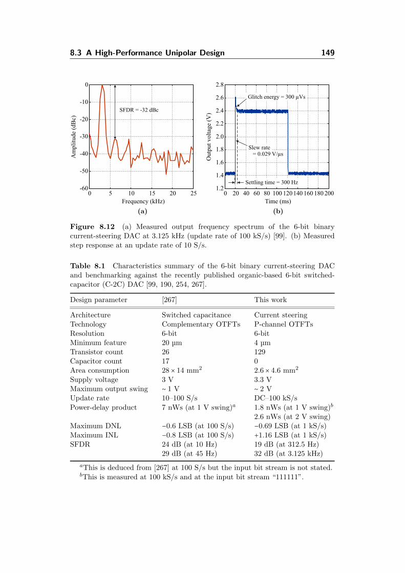
8.3 A High-Performance Unipolar Design 149
0 5 10 15 20 25-60
-50
-40
-30
-20
-10
0
Frequency (kHz)
Am
plit
ude
(dB
c)
0 20 40 60 80 100 120 140 160 180 2001.2
1.4
1.6
1.8
2.0
2.2
2.4
2.6
2.8
Time (ms)O
utpu
t vo
ltag
e (V
)
SFDR = -32 dBc
Glitch energy = 300 µVs
Settling time = 300 Hz
Slew rate = 0.029 V/µs
(a)
0 5 10 15 20 25-60
-50
-40
-30
-20
-10
0
Frequency (kHz)
Am
plit
ude
(dB
c)
0 20 40 60 80 100 120 140 160 180 2001.2
1.4
1.6
1.8
2.0
2.2
2.4
2.6
2.8
Time (ms)O
utpu
t vo
ltag
e (V
)
SFDR = -32 dBc
Glitch energy = 300 µVs
Settling time = 300 Hz
Slew rate = 0.029 V/µs
(b)
Figure 8.12 (a) Measured output frequency spectrum of the 6-bit binarycurrent-steering DAC at 3.125 kHz (update rate of 100 kS/s) [99]. (b) Measuredstep response at an update rate of 10 S/s.
Table 8.1 Characteristics summary of the 6-bit binary current-steering DACand benchmarking against the recently published organic-based 6-bit switched-capacitor (C-2C) DAC [99, 190, 254, 267].
Design parameter [267] This work
Architecture Switched capacitance Current steeringTechnology Complementary OTFTs P-channel OTFTsResolution 6-bit 6-bitMinimum feature 20 µm 4 µmTransistor count 26 129Capacitor count 17 0Area consumption 28 × 14 mm2 2.6 × 4.6 mm2
Supply voltage 3 V 3.3 VMaximum output swing ∼ 1 V ∼ 2 VUpdate rate 10–100 S/s DC–100 kS/s
Power-delay product 7 nWs (at 1 V swing)a 1.8 nWs (at 1 V swing)b
2.6 nWs (at 2 V swing)Maximum DNL −0.6 LSB (at 100 S/s) −0.69 LSB (at 1 kS/s)Maximum INL −0.8 LSB (at 100 S/s) +1.16 LSB (at 1 kS/s)SFDR 24 dB (at 10 Hz) 19 dB (at 312.5 Hz)
29 dB (at 45 Hz) 32 dB (at 3.125 kHz)
aThis is deduced from [267] at 100 S/s but the input bit stream is not stated.bThis is measured at 100 kS/s and at the input bit stream “111111”.
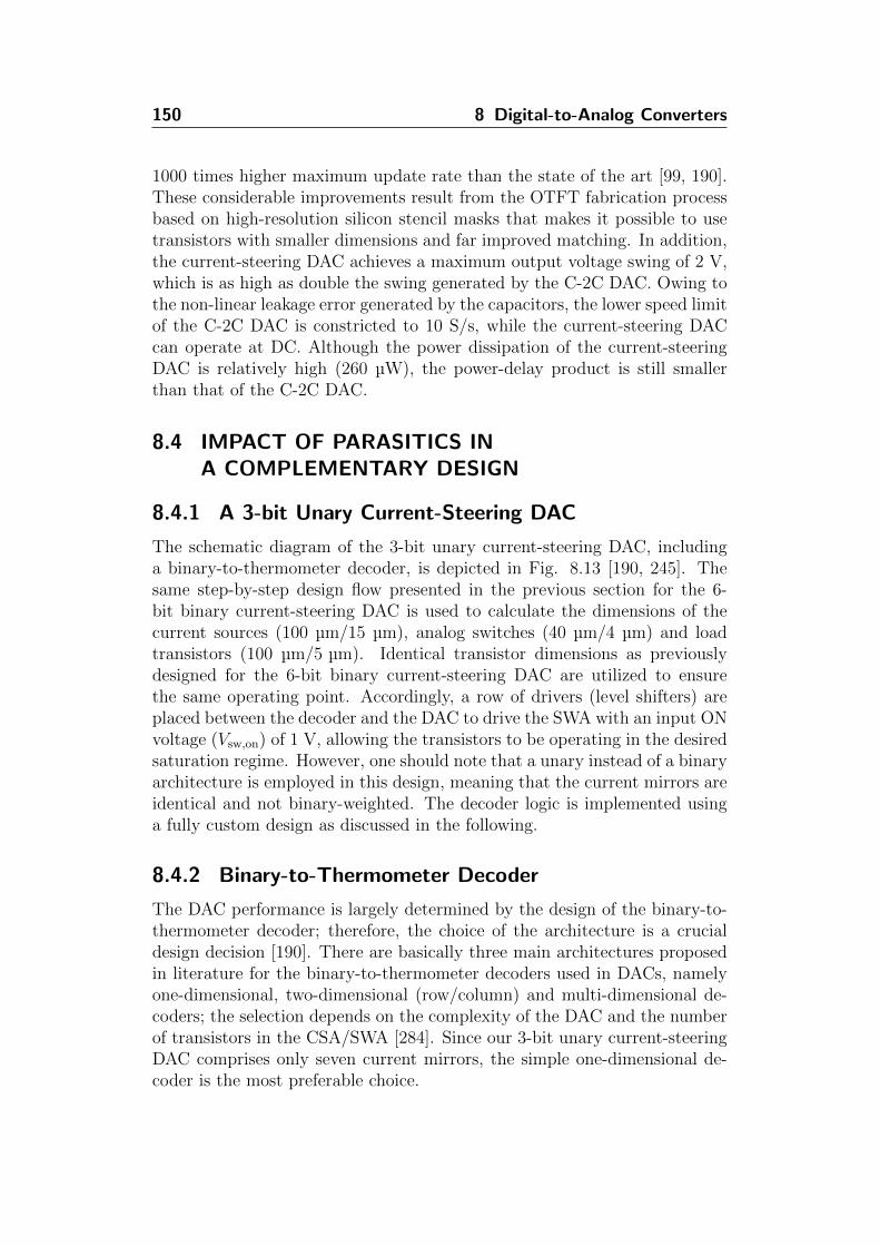
150 8 Digital-to-Analog Converters
1000 times higher maximum update rate than the state of the art [99, 190].These considerable improvements result from the OTFT fabrication processbased on high-resolution silicon stencil masks that makes it possible to usetransistors with smaller dimensions and far improved matching. In addition,the current-steering DAC achieves a maximum output voltage swing of 2 V,which is as high as double the swing generated by the C-2C DAC. Owing tothe non-linear leakage error generated by the capacitors, the lower speed limitof the C-2C DAC is constricted to 10 S/s, while the current-steering DACcan operate at DC. Although the power dissipation of the current-steeringDAC is relatively high (260 µW), the power-delay product is still smallerthan that of the C-2C DAC.
8.4 IMPACT OF PARASITICS INA COMPLEMENTARY DESIGN
8.4.1 A 3-bit Unary Current-Steering DAC
The schematic diagram of the 3-bit unary current-steering DAC, includinga binary-to-thermometer decoder, is depicted in Fig. 8.13 [190, 245]. Thesame step-by-step design flow presented in the previous section for the 6-bit binary current-steering DAC is used to calculate the dimensions of thecurrent sources (100 µm/15 µm), analog switches (40 µm/4 µm) and loadtransistors (100 µm/5 µm). Identical transistor dimensions as previouslydesigned for the 6-bit binary current-steering DAC are utilized to ensurethe same operating point. Accordingly, a row of drivers (level shifters) areplaced between the decoder and the DAC to drive the SWA with an input ONvoltage (Vsw,on) of 1 V, allowing the transistors to be operating in the desiredsaturation regime. However, one should note that a unary instead of a binaryarchitecture is employed in this design, meaning that the current mirrors areidentical and not binary-weighted. The decoder logic is implemented usinga fully custom design as discussed in the following.
8.4.2 Binary-to-Thermometer Decoder
The DAC performance is largely determined by the design of the binary-to-thermometer decoder; therefore, the choice of the architecture is a crucialdesign decision [190]. There are basically three main architectures proposedin literature for the binary-to-thermometer decoders used in DACs, namelyone-dimensional, two-dimensional (row/column) and multi-dimensional de-coders; the selection depends on the complexity of the DAC and the numberof transistors in the CSA/SWA [284]. Since our 3-bit unary current-steeringDAC comprises only seven current mirrors, the simple one-dimensional de-coder is the most preferable choice.
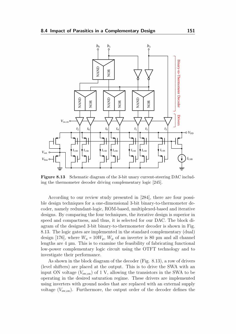
8.4 Impact of Parasitics in a Complementary Design 151
Driv
ersB
inary
-to-T
herm
om
eter Deco
der
VbiasILSB
Vout
Vsw, on
ILSB
t6
ILSB
t2
ILSB
t3
ILSB
t4
ILSB
t0
ILSB
t5
ILSB
t1
b0
VDD
b1 b3
NO
R
NA
ND
NO
R
NA
ND
NO
R
NA
ND
NO
R
NA
ND
Figure 8.13 Schematic diagram of the 3-bit unary current-steering DAC includ-ing the thermometer decoder driving complementary logic [245].
According to our review study presented in [284], there are four possi-ble design techniques for a one-dimensional 3-bit binary-to-thermometer de-coder, namely redundant-logic, ROM-based, multiplexed-based and iterativedesigns. By comparing the four techniques, the iterative design is superior inspeed and compactness, and thus, it is selected for our DAC. The block di-agram of the designed 3-bit binary-to-thermometer decoder is shown in Fig.8.13. The logic gates are implemented in the standard complementary (dual)design [176], where Wn = 10Wp, Wp of an inverter is 80 µm and all channellengths are 4 µm. This is to examine the feasibility of fabricating functionallow-power complementary logic circuit using the OTFT technology and toinvestigate their performance.
As shown in the block diagram of the decoder (Fig. 8.13), a row of drivers(level shifters) are placed at the output. This is to drive the SWA with aninput ON voltage (Vsw,on) of 1 V, allowing the transistors in the SWA to beoperating in the desired saturation regime. These drivers are implementedusing inverters with ground nodes that are replaced with an external supplyvoltage (Vsw,on). Furthermore, the output order of the decoder defines the

152 8 Digital-to-Analog Converters
0 1 2 3 4 5 6 7-0.6
-0.4
-0.2
0.0
0.2
0.4
0.6
Input code
INL
err
or (
LS
B)
0 1 2 3 4 5 6 7-0.6
-0.4
-0.2
0
0.2
0.4
0.6
Input code
INL
err
or (
LS
B)
Sequential order
Proposed switching scheme
(a)
0 1 2 3 4 5 6 7-0.6
-0.4
-0.2
0
0.2
0.4
0.6
Input code
INL
err
or (
LS
B)
0 1 2 3 4 5 6 7-0.6
-0.4
-0.2
0.0
0.2
0.4
0.6
Input codeIN
L e
rror
(L
SB
)
Sequential order
Proposed switching scheme
(b)
Figure 8.14 Calculated INL error when using the sequential and the proposedswitching schemes for the 3-bit unary current-steering DAC, assuming (a) lineargradient errors with 0.5 LSB peak-to-peak amplitude and (b) symmetrical gradienterrors with 0.5 LSB peak-to-peak amplitude.
switching scheme with which the unary current-sources are enabled to theDAC output. This switching scheme is used to compensate for errors thatare introduced by systematical gradient effects (linear and/or symmetrical).A detailed analysis of the switching scheme is given in the following.
8.4.3 Switching Scheme
The switching scheme is defined to be the order of which the current sourceswithin the CSA are switched to the DAC output [190, 283]. Conventionally,the current sources are switched in a sequential order. However, with carefullayout, another switching order can be used to compensate the systematic er-rors that are introduced by linear and/or symmetrical gradient errors, whichoccur due to process, temperature or stress variations. These errors haveto be considered because they contribute to the performance of the DAC.By reducing the impact of these systematic errors using a switching scheme,random errors will dominate. However, random errors are kept within thedesired boundary (INL and DNL < 1 LSB) by adjusting the dimensions ofthe active current-source transistors as discussed in the previous section.
The developed switching scheme (labelled t0, t1, . . ., t6) for our 3-bit unarycurrent-steering DAC is depicted in Fig. 8.13. Given that the current-sourcetransistors are arranged in a one-dimensional array, they are only influencedby lateral gradient errors. A comparison between the sequential order and ourproposed scheme is shown in Fig. 8.14, assuming a peak-to-peak amplitude

8.4 Impact of Parasitics in a Complementary Design 153
2.2 0.4
2.00.2
DN
L (
LS
B)
1.80.01.6
Out
put
volt
age
(V)
1.4 -0.2
I µLSB = 10 A
I µLSB = 8 A
I µLSB = 6 A
I = 5 ALSB µ
I µLSB = 17 A I µLSB = 17 A
0 1 2 3 4 5 6 7
0.2
0.4
0.6
0.8
1.01.2
Input code
0.0 0 1 2 3 4 5 6 7
-0.4
-0.2
0.0
0.2
Input codeIN
L (
LS
B)
(a)
2.2 0.4
20.2
DN
L (
LS
B)
1.80.01.6
Out
put
volt
age
(V)
1.4 -0.2
I µLSB = 10 A
I µLSB = 8 A
I µLSB = 6 A
I = 5 ALSB µ
I µLSB = 17 A I µLSB = 17 A
0 1 2 3 4 5 6 70
0.2
0.4
0.6
0.8
1
1.2
Input code
0 1 2 3 4 5 6 7
-0.4
-0.2
0.0
0.2
Input codeIN
L (
LS
B)
(b)
Figure 8.15 Measured DC characteristics of the 3-bit unary current-steeringDAC. (a) Transfer characteristics for different applied least-significant-bit currents(ILSB). (b) Calculated DNL and INL errors when ILSB = 17 µA.
of 0.5 LSB for the linear as well as the symmetrical gradient errors. Asmaller maximum INL is achieved by the proposed scheme in the case oflinear gradient error, whereas the same maximum INL is provided in thecase of symmetrical gradient error. The analysis presented in Section 4.2.4suggests that the linear gradient error is dominant in our OTFT technology(see Figs. 4.6b and 4.10); this results from a tilt of the stencil mask duringevaporation and/or the sample is outside the perpendicular projection of theevaporator source during material deposition. Nevertheless, if the linear andsymmetrical gradient errors are present (by adding both components in Fig.8.14), the proposed scheme still yields a much smaller maximum INL of −0.33LSB compared to −0.75 LSB for the conventional sequential order.
8.4.4 Measurement and Simulation Results
The 3-bit unary current-steering DAC is fabricated on a glass substrate witha total area of 3.1 × 6.6 mm2. The area is optimized at the cost of a largenumber of metal crossings (∼70) with about 12 pF capacitance each; thisis to investigate the impact of interconnect parasitics on the circuit perfor-mance. The layout of the DAC is presented in Appendix A. Measurementsare performed in ambient air and at a supply voltage of 3 V using the sametest setup presented in the previous section. Figure 8.15 shows the measuredDC transfer function together with the calculated DNL and INL errors. Themaximum output voltage swing (Vswing) of the DAC is 1.75 V; in addition,the maximum DNL and INL errors are 0.23 and 0.22 LSB, respectively.

154 8 Digital-to-Analog Converters
0 10 20 30 40 50 60 70 800
1
2
3
4
Time (ms)
t (
V)
4
0 1 2 3 4 5 6 7 80
1
2
3
4
Time (ms)
t(V
)4
at 100 Hz
at 1 kHz
tdelay,HLtdelay,HL
tdelay,HLtdelay,LH
tdelay,HLtdelay,HL
tdelay,HLtdelay,LH
Measured
Simulated
100 101 110 111 000 001 010 011
Binary input Code
Figure 8.16 Measured and simulated output of the binary-to-thermometer de-coder circuit at node t4 at (upper) 100 Hz and (lower) 1 kHz [245].
10 10.5 11 11.5 12 12.5 13 13.5 140
1
2
3
4
Time (ms)
t (
V)
4
at 500 Hz Case 1Case 2Case 3
Case 4Case 5Case 6tdelay,HL
Figure 8.17 Simulation case study to investigate the impact of device and in-terconnect parasitics as well as the influence of using the slow n-channel OTFTson the performance of the binary-to-thermometer decoder circuit at 500 Hz.
The maximum possible performance of the circuit in this case is limitedby the complementary driving logic. This is attributed to the slow n-channelOTFTs and the large number of metal crossings utilized. Therefore, a casestudy is carried out on the binary-to-thermometer decoder to investigate theimpact of the device and interconnect parasitic capacitances on the circuitperformance, in particular [245].
Transient measurements and simulations of the binary-to-thermometerdecoder at the output node t4 at frequencies of 100 Hz, 500 Hz and 1 kHzare depicted in Figs. 8.16 and 8.17. In fact, the node t4 is the output of theslowest logic path in the circuit (see Fig. 8.13), also known as the criticalpath1. The simulations are based on a DC/AC SPICE model for both p- andn-channel OTFTs (adopted from Chapters 5 and 6). The frequency 1 kHz is
1The critical path is the longest synthesizable path of which the largest delay of thecircuit/network occurs from the input to the output.
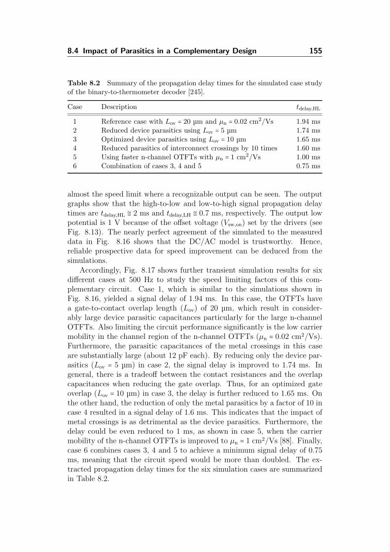
8.4 Impact of Parasitics in a Complementary Design 155
Table 8.2 Summary of the propagation delay times for the simulated case studyof the binary-to-thermometer decoder [245].
Case Description tdelay,HL
1 Reference case with Lov = 20 µm and µn = 0.02 cm2/Vs 1.94 ms2 Reduced device parasitics using Lov = 5 µm 1.74 ms3 Optimized device parasitics using Lov = 10 µm 1.65 ms4 Reduced parasitics of interconnect crossings by 10 times 1.60 ms5 Using faster n-channel OTFTs with µn = 1 cm2/Vs 1.00 ms6 Combination of cases 3, 4 and 5 0.75 ms
almost the speed limit where a recognizable output can be seen. The outputgraphs show that the high-to-low and low-to-high signal propagation delaytimes are tdelay,HL ≅ 2 ms and tdelay,LH ≅ 0.7 ms, respectively. The output lowpotential is 1 V because of the offset voltage (Vsw,on) set by the drivers (seeFig. 8.13). The nearly perfect agreement of the simulated to the measureddata in Fig. 8.16 shows that the DC/AC model is trustworthy. Hence,reliable prospective data for speed improvement can be deduced from thesimulations.
Accordingly, Fig. 8.17 shows further transient simulation results for sixdifferent cases at 500 Hz to study the speed limiting factors of this com-plementary circuit. Case 1, which is similar to the simulations shown inFig. 8.16, yielded a signal delay of 1.94 ms. In this case, the OTFTs havea gate-to-contact overlap length (Lov) of 20 µm, which result in consider-ably large device parasitic capacitances particularly for the large n-channelOTFTs. Also limiting the circuit performance significantly is the low carriermobility in the channel region of the n-channel OTFTs (µn = 0.02 cm2/Vs).Furthermore, the parasitic capacitances of the metal crossings in this caseare substantially large (about 12 pF each). By reducing only the device par-asitics (Lov = 5 µm) in case 2, the signal delay is improved to 1.74 ms. Ingeneral, there is a tradeoff between the contact resistances and the overlapcapacitances when reducing the gate overlap. Thus, for an optimized gateoverlap (Lov = 10 µm) in case 3, the delay is further reduced to 1.65 ms. Onthe other hand, the reduction of only the metal parasitics by a factor of 10 incase 4 resulted in a signal delay of 1.6 ms. This indicates that the impact ofmetal crossings is as detrimental as the device parasitics. Furthermore, thedelay could be even reduced to 1 ms, as shown in case 5, when the carriermobility of the n-channel OTFTs is improved to µn = 1 cm2/Vs [88]. Finally,case 6 combines cases 3, 4 and 5 to achieve a minimum signal delay of 0.75ms, meaning that the circuit speed would be more than doubled. The ex-tracted propagation delay times for the six simulation cases are summarizedin Table 8.2.
156 8 Digital-to-Analog Converters
From this study, it can be concluded that the reduction of the para-sitic capacitances of the devices and metal crossings, which is achievable bymeans of mask overlay and layout advancements, already leads to promis-ing performance improvements. However, to achieve even higher speeds,the complex relationships between the channel length, gate-overlap length,contact resistance, overlap capacitance and field-effect mobility has to becarefully investigated as demonstrated in [139] and [18]. Moreover, furtherimprovements have to come from a higher carrier mobility in the n-channelOTFTs, allowing for smaller transistors and thus even lower parasitic devicecapacitances.
8.5 SUMMARY
A record in performance and compactness for organic integrated circuits isintroduced in this work by using the OTFT fabrication process that is basedon high-resolution silicon stencil masks. The process offers submicrometerchannel lengths and superb transistor matching, thus allowing to exploitcircuit concepts and topologies that would not be feasible otherwise. Ac-cordingly, the first current-steering DACs built in an OTFT technology aredemonstrated. A 6-bit binary current-steering DAC using p-channel OTFTsis realized; measurement results show that this converter is 1000 times faster,30 times smaller and achieves 2 times higher output swing than prior stateof the art. The design of the DAC includes a new highly linear current-to-voltage converter, which employs only two p-channel OTFTs and alsocompensates for the inherent non-linearity of the transistors. The converterhas a maximum update rate of 100 kS/s, a maximum output voltage swing of2 V and consumes an area of 2.6×4.6 mm2. Moreover, another 3-bit current-steering DAC, but using the unary architecture and complementary OTFTs,is fabricated on the same substrate. This converter is used as a circuit testvehicle in a simulation case study to indicate advancement opportunities forthe low-voltage complementary OTFT technology. The study is based onan accurate agreement of simulated and measured data up to 1 kHz, whichis the maximum operating frequency of the DAC; this is owed to the opti-mized DC/AC SPICE models for both p- and n-channel OTFTs. Simulationresults indicate that considerable improvements in circuit performance mayresult from (i) optimizing drain and source overlaps with the gate electrode,(ii) avoiding metal-interconnect crossings in the circuit layout or reducingtheir corresponding parasitics through better dielectrics, and (iii) developinglow-voltage n-channel OTFTs with a higher charge carrier mobility.
9Conclusion
In this final chapter we draw a series of conclusions on key aspects of thisthesis. We also make reference to our own publications in which parts of theresults presented herein have been published previously. Organic thin-filmtransistors (OTFTs) are making significant inroads into flexible, large-areaelectronics. Together with IMS CHIPS and MPI-SSR, a new OTFT fabri-cation process based on high-resolution silicon stencil masks is developed,offering submicrometer channel lengths and far improved transistor match-ing [13–17]. This work is set out to implement a unified DC/AC compactmodel for the OTFTs and to demonstrate fast digital and analog organicintegrated circuits. It is also sought to determine the matching capabilityof this new OTFT technology, to investigate the impact of parasitics on thedevice performance and to characterize the frequency response of individualOTFTs using a self-contained method.
Technology—The OTFTs employ air-stable, small-molecule organicsemiconductors (e.g. DNTT and F16CuPc) and exploit the inverted-staggered(bottom-gate, top-contact) configuration. The use of silicon stencil masksallows to pattern the source/drain contacts on top of the organic semicon-ductors without the need of solvents or elevated temperatures, which wouldmake the small molecules prone to degradation. Furthermore, the OTFTstake full advantage of combining an oxide layer (AlOx) with a molecular self-assembled monolayer (C14-SAM) to form a 5.3-nm-thick gate dielectric witha capacitance of the order of 1 µF/cm2. This relatively high capacitanceenables the transistors to operate at voltages as low as 3 V, at which a suffi-ciently high carrier concentration (1012–1013 cm−2) can be reached to createthe channel. The low-voltage operation competence makes the OTFTs well-suited for battery-powered or frequency-coupled portable devices and opensthe possibility to build hybrid flexible systems-in-foil (SiF), integrating large-area organic electronics with high-performance thin silicon chips.
Device matching—The uniformity of the evaporated source/drain con-tacts through the stencil masks is investigated by measuring the critical di-mensions (CDs) of 35 0.8-µm-wide isolated lines dispersed over the entire areaof a test sample. The mean values of the CDs are found to be 0.88±0.01 µmfor the mask and 0.86±0.19 µm for the contacts [15]. On closer inspection, asystematic variation is observed on the sample, indicating a tilt of the maskduring evaporation and/or a displacement of the sample from the perpendic-
157
158 9 Conclusion
ular projection of the evaporator source. This can be alleviated by installingan automated handling system in the future. Nevertheless, electrical charac-terization of 16 OTFTs fabricated by the silicon stencil masks with a channellength of 2 µm yields a standard deviation of only 4% for the drain current,which is less than half the value measured for 16 OTFTs fabricated by con-ventional polyimide shadow masks but with a much larger channel length of30 µm [99]. This eminent improvement enables to exploit circuit concepts,such as the current-steering DACs and ADCs that are known to be superiorin speed and compactness, for which device matching is paramount.
Static model—For the design of organic integrated circuits, a reliablecompact model describing the steady-state characteristics of the OTFTs ishighly desired. It is reported in literature that some of the OTFTs expe-rience mobility enhancement at higher gate voltages. Conversely, the mea-sured OTFTs display a fairly constant mobility; in fact, it reduces by just10% at high gate voltages due to bias stress. This makes the ensuing modelsbased on that special mobility-enhancement behavior not adequate. There-fore, a simple unified model of the static I–V characteristics that covers alloperating regimes, namely subthreshold, linear and saturation, is derived.Effects induced by the voltage-dependent parasitic resistances are carefullyconsidered [101, 139, 245]. A precise fit of the model to the measurementsof various OTFTs is achieved. Being geometry scalable, the model typicallyrequires a single parameter set for the simulation of OTFTs with differ-ent feature sizes. There is still, however, noticeable process variations andtime-dependent characteristics of OTFTs [153], which necessitate the con-sideration of some variability in the model parameters.
Dynamic model—To analyse the charge storage behavior of the OTFTs,admittance (Y) measurements have been conducted at frequencies from 100Hz up to 1 MHz. As anticipated, the cutoff frequency (fT) of the OTFTstends to increase with decreasing channel length and with increasing gatebias. Because of the distributed coupling between the gate electrode and thesemiconductor, a small-signal equivalent circuit based on an RC network isdeveloped to accurately model the frequency dispersion effects; a perfect fitto the measurements over the complete frequency range is obtained [151].Furthermore, an in-depth analysis of the intrinsic capacitances have indi-cated that at VDS = 0 V, Cgs and Cgd are both equal to 1/2 ⋅ CIWL, whileat VDS ≥ VGS − VTH, Cgs and Cgd are equal to 2/3 ⋅ CIWL and zero, respec-tively. Thus, it is demonstrated that the channel charge dynamics can bewell described by the unified Meyer’s capacitance model [151]. These resultsin conjunction with recently published findings in [288] establish an essentialmodeling support for dynamic simulations and performance optimization oforganic integrated circuits.
Record performance—The ultimate frequency performance of OTFTsrelies heavily on the combination of material properties, device configuration
159
and dimensions. The propagation delay per stage of ring oscillators is com-monly used as a practical benchmark for the frequency response of organicintegrated circuits [17, 101, 139]. Given the variability of most OTFTs, ringoscillators provide only an average delay figure. Hence, the cutoff frequency(fT) of stand-alone OTFTs are also evaluated in this work for the first timeusing S-parameter measurements. The relation between the cutoff frequencyand the channel length as well as the gate overlap is physically modeledand a good agreement to the experimental data is obtained. A record cut-off frequency as high as 3.7 MHz has been measured at VGS = −3 V for aDNTT OTFT with L = 0.6 µm and Lov = 5 µm [18]. These results justifythat the OTFT technology can be well extended to the submicrometer rangeand that high-frequency characterization of OTFTs by means of S-parametermeasurements is feasible.
Asymmetric OTFTs—Although the use of fully-patterned OTFTs min-imizes the gate overlaps, the usual lack of a self-alignment process makes theoverlap capacitances inevitable. It is likewise very difficult to avoid a mis-match between the source/drain contact overlaps because of the limited align-ment capability of most OTFT technologies. For these reasons, the frequencyresponse of asymmetric OTFTs, particularly those with small dimensions(L = 1 µm and Lov = 5 µm), is examined. The intentional misalignment is fa-cilitated by the high fidelity of the silicon stencil masks. It is thereby revealedthat underestimation of the cutoff frequency is probable when assumptions,such as Cgd << Cgs for a typical FET device, are incorporated [188].
Integrated circuits—Owing to the remarkable uniformity and repro-ducibility of the fabricated OTFTs, the first organic current-steering DACsare reported in this work. A 6-bit binary DAC, comprising as many as 129p-channel DNTT OTFTs, is implemented. The converter has a maximumupdate rate of 100 kS/s, a maximum output swing of 2 V, and consumesan area of 2.6 × 4.6 mm2, establishing the state of the art for organic cir-cuits [99, 254]. Lately, an OTFT-driven flexible AM-OLED display usingair-stable DNTT has been demonstrated in [289]. The adoption of the sameorganic semiconductor enables further integration of the DAC and the displaybackplane on the same foil, resulting in potential cost savings and improvedreliability. The exceptional OTFT properties and DAC performance com-mensurate with the ever-increasing demands of having AM-OLED displayswith flexible form factor, higher resolution and faster refresh rate.
While for the 6-bit DAC the use of both n-channel OTFTs and metal-interconnect crossings could be avoided, this is quite often not possible aslow-power circuit design calls for a complementary technology and complexinterconnect schemes. Therefore, a study of the impact of device and inter-connect parasitics on the circuit performance is carried out, for which a 3-bitunary DAC as a circuit test vehicle is utilized. The converter has a maximumupdate rate of 1 kS/s, consumes an area of 3.1 × 6.6 mm2, and incorporates
160 9 Conclusion
42 p-channel and 25 n-channel OTFTs [245]. The key findings of the studyare as follows. First, significant reduction of the gate-overlap lengths can becounterproductive as there is a tradeoff between the overlap capacitances andthe contact resistances. Second, the influence of the interconnect crossingsis as detrimental as the device parasitics because of using the same gate-dielectric layer at the crossings. Finally, the performance of complementaryorganic circuits is strongly limited by the slow n-channel OTFTs. Thus, itis desired to introduce at least another properly isolated metal layer and im-prove the performance of air-stable n-channel OTFTs without sacrificing thegeneral process compatibility.
Outlook—The OTFTs require simultaneously low-voltage operation, airstability and high bandwidth to find use in practical applications. To meetthese necessary criteria, there are ongoing research efforts to develop neworganic semiconductors. In view of the many advantages of complemen-tary technologies, it is expected that this type of circuits will be furtheradvanced. However, the performance and stability of n-channel OTFTs re-main more problematic. As a result, there is an increasing interest of usingoxide-based semiconductors, which mostly exhibit electron transport charac-teristics, in high-performance TFTs as a plausible replacement of the slown-channel OTFTs. Although the achieved carrier mobilities are rather high,the intrinsic performance of the materials cannot be fully utilized in short-channel (O)TFTs because of the contact resistances. Accordingly, doping ofthe contact areas as well as using device structures with split-gate electrodesto reduce this effect are worth considering.
Besides process variations, the OTFTs are generally sensitive to atmo-spheric oxygen and water, bias stress, temperature and light. Effective encap-sulation is thus needed to ensure sufficient lifetime and increase robustnessto environmental conditions. Albeit the increased area and complexity, it isencouraging to employ circuit styles and/or special devices that allow built-inpost-fabrication tunability to compensate for these effects. In addition, theOTFT models have to be modified to account for the time-dependent changeof parameters, without which misleading characteristics may be predicted.Moreover, it is envisaged to exploit the stencil masks in a reel-to-reel man-ufacturing process to increase the throughput and fabricate commerciallyviable products. The first products using OTFTs are already introducedinto the marketplace, yet many new innovative and promising applicationswill continue to appear. These are outcomes of organic chemistry and assuch can be varied in a near infinite number of ways [5]:
“If atoms were musical notes, and macromolecules music, therange of structures attainable would be beyond anything as yetheard by humankind.”
—Andre Moliton and Roger C. Hirons (2012)
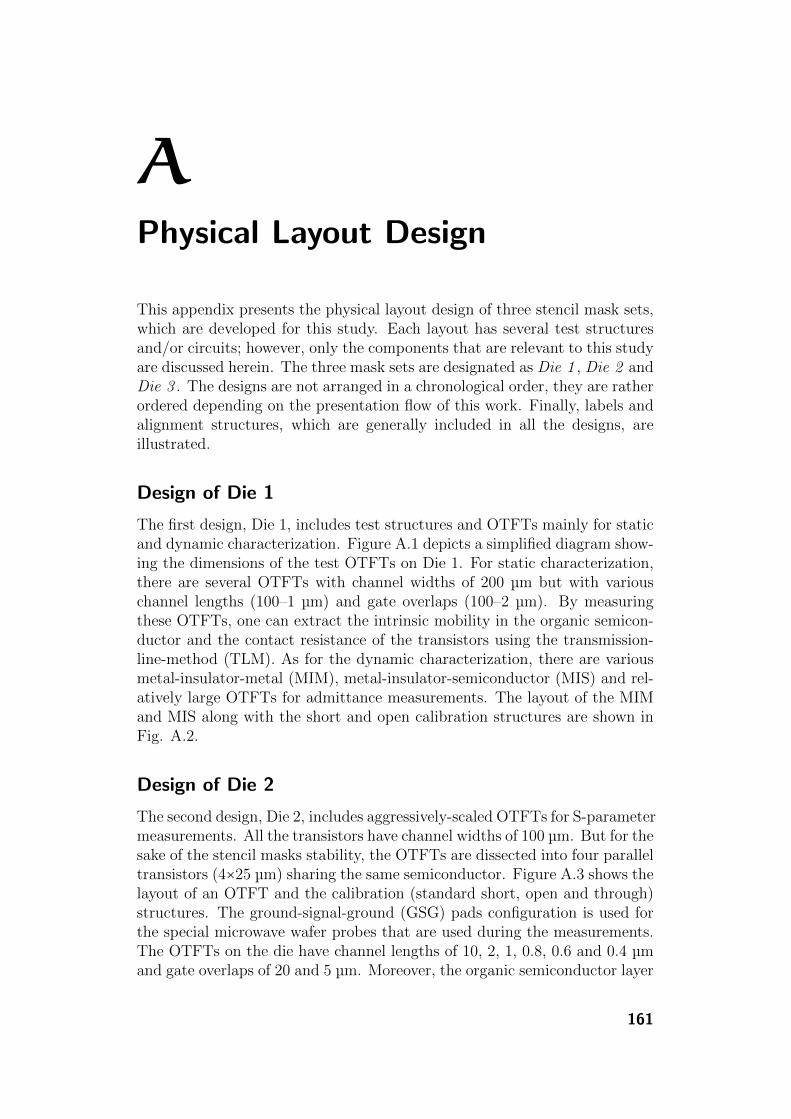
APhysical Layout Design
This appendix presents the physical layout design of three stencil mask sets,which are developed for this study. Each layout has several test structuresand/or circuits; however, only the components that are relevant to this studyare discussed herein. The three mask sets are designated as Die 1 , Die 2 andDie 3 . The designs are not arranged in a chronological order, they are ratherordered depending on the presentation flow of this work. Finally, labels andalignment structures, which are generally included in all the designs, areillustrated.
Design of Die 1
The first design, Die 1, includes test structures and OTFTs mainly for staticand dynamic characterization. Figure A.1 depicts a simplified diagram show-ing the dimensions of the test OTFTs on Die 1. For static characterization,there are several OTFTs with channel widths of 200 µm but with variouschannel lengths (100–1 µm) and gate overlaps (100–2 µm). By measuringthese OTFTs, one can extract the intrinsic mobility in the organic semicon-ductor and the contact resistance of the transistors using the transmission-line-method (TLM). As for the dynamic characterization, there are variousmetal-insulator-metal (MIM), metal-insulator-semiconductor (MIS) and rel-atively large OTFTs for admittance measurements. The layout of the MIMand MIS along with the short and open calibration structures are shown inFig. A.2.
Design of Die 2
The second design, Die 2, includes aggressively-scaled OTFTs for S-parametermeasurements. All the transistors have channel widths of 100 µm. But for thesake of the stencil masks stability, the OTFTs are dissected into four paralleltransistors (4×25 µm) sharing the same semiconductor. Figure A.3 shows thelayout of an OTFT and the calibration (standard short, open and through)structures. The ground-signal-ground (GSG) pads configuration is used forthe special microwave wafer probes that are used during the measurements.The OTFTs on the die have channel lengths of 10, 2, 1, 0.8, 0.6 and 0.4 µmand gate overlaps of 20 and 5 µm. Moreover, the organic semiconductor layer
161

162 A Physical Layout Design
1 2 4 6
12
20
30
40
50
60
70
80
100 10
20
30
50
80
100
120
140
160
200
400
5
10
20
30
50
2
5
10
20
30
50
100
5
Channel length (µm)Channel length (µm)
Gat
e o
ver
lap
(µ
m)
Gat
e o
ve
rlap
(µ
m)
Different LDifferent Lov
L = Lov L/Lov = 20
(a)
1 2 4 6
12
20
30
40
50
60
70
80
100 10
20
30
50
80
100
120
140
160
200
400
5
10
20
30
50
2
5
10
20
30
50
100
5
Channel length (µm)Channel length (µm)
Gat
e o
ver
lap
(µ
m)
Gat
e o
ve
rlap
(µ
m)
Different LDifferent Lov
L = Lov L/Lov = 20
(b)
Figure A.1 Simplified diagram (not to scale) showing the dimensions of the testOTFTs on Die 1. (a) OTFTs with channel widths of 200 µm for static characteri-zation using the transmission line method (TLM). (b) OTFTs with channel widthsof 400 and 1000 µm for dynamic characterization using admittance measurements.
30 µm
(a)
30 µm
(b)
30 µm
(c)
30 µm
(d)
Figure A.2 Layout of test structures on Die 1 dedicated for admittance mea-surements. (a) Short and (b) open calibration structures. (c) Metal-insulator-metal (MIM). (d) Metal-insulator-semiconductor (MIS). The die includes several ofthese structures but with different top-to-gate overlap area, i.e., 200×200, 100×100,50×50, 10×10, 500×20 and 1000×40 µm2. In all of these test structures, the enclo-sure of the top metal inside the semiconductor as well as the non-related clearancesare all set to 30 µm.
extends beyond the periphery of the intrinsic OTFTs by 30 µm on each side(also called fringe regions). To study the impact of misalignment betweenthe gate-source (Lgs) and gate-drain (Lgd) overlaps, where Lgs + Lgd = 2Lov,the OTFTs with the gate-overlap lengths (Lov) of 5 µm and the channellengths (L) of 1 and 0.6 µm are duplicated and intentionally misaligned onthe mask level. A total of 19 OTFTs with intentional misalignment of ±1,±2, ..., ±9 are realized. This is to guarantees the fabrication of OTFTs withwell-defined Lgs = 1, 2, ..., 9 µm, while keeping Lgs +Lgd = 10 µm. Vernierstructures are employed to measure the particular degree of misalignment.
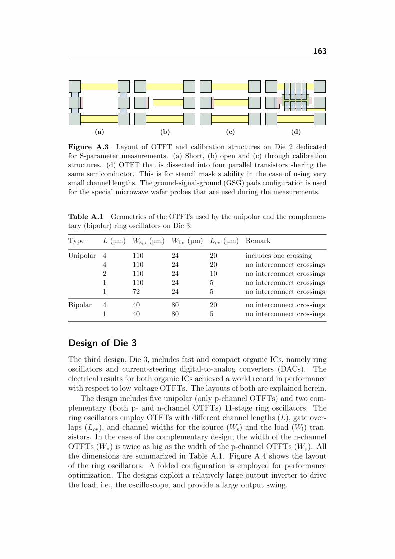
163
(a) (b) (c) (d)
Figure A.3 Layout of OTFT and calibration structures on Die 2 dedicatedfor S-parameter measurements. (a) Short, (b) open and (c) through calibrationstructures. (d) OTFT that is dissected into four parallel transistors sharing thesame semiconductor. This is for stencil mask stability in the case of using verysmall channel lengths. The ground-signal-ground (GSG) pads configuration is usedfor the special microwave wafer probes that are used during the measurements.
Table A.1 Geometries of the OTFTs used by the unipolar and the complemen-tary (bipolar) ring oscillators on Die 3.
Type L (µm) Ws,p (µm) Wl,n (µm) Lov (µm) Remark
Unipolar 4 110 24 20 includes one crossing4 110 24 20 no interconnect crossings2 110 24 10 no interconnect crossings1 110 24 5 no interconnect crossings1 72 24 5 no interconnect crossings
Bipolar 4 40 80 20 no interconnect crossings1 40 80 5 no interconnect crossings
Design of Die 3
The third design, Die 3, includes fast and compact organic ICs, namely ringoscillators and current-steering digital-to-analog converters (DACs). Theelectrical results for both organic ICs achieved a world record in performancewith respect to low-voltage OTFTs. The layouts of both are explained herein.
The design includes five unipolar (only p-channel OTFTs) and two com-plementary (both p- and n-channel OTFTs) 11-stage ring oscillators. Thering oscillators employ OTFTs with different channel lengths (L), gate over-laps (Lov), and channel widths for the source (Ws) and the load (Wl) tran-sistors. In the case of the complementary design, the width of the n-channelOTFTs (Wn) is twice as big as the width of the p-channel OTFTs (Wp). Allthe dimensions are summarized in Table A.1. Figure A.4 shows the layoutof the ring oscillators. A folded configuration is employed for performanceoptimization. The designs exploit a relatively large output inverter to drivethe load, i.e., the oscilloscope, and provide a large output swing.

164 A Physical Layout Design
(a) (b)
Figure A.4 Layout of (a) unipolar (only p-channel OTFTs) and (b) comple-mentary (both p- and n-channel OTFTs) 11-stage ring oscillators [190].
Furthermore, the design also includes two different DACs, namely a 6-bitbinary current-steering DAC and a 3-bit unary current-steering DAC. Strictrequirements apply here to the design of the layout and floorplan due to therelatively large number of transistors employed, particularly for an organic-based analog circuit [190]. Device matching and data interference have astrong impact on the DAC performance.
In principle, there are two methods for arranging the transistors in acurrent-steering DAC, i.e., either by merging the switches and the current-source transistors in one array or by splitting them into two separate arrays,namely switch array (SWA) and current-source array (CSA). In the mergedapproach, each unit cell comprises both the current-source and the switchtransistors. This method has a simplified layout; however, it increases thedistance between the current-source transistors and so the layout will bepotentially more susceptible to systematical gradient effects. As for the sep-arated SWA-CSA, the identical transistors are placed in separate arrays, thusensuring better device matching, easing power routing, and minimizing signalinterference as a result of keeping the digital and the analog blocks apart. Inspite of the increased layout complexity in the latter approach, it is selectedhere as it offers a substantially better conversion performance.
For simplicity, the layout design of the DACs is described here by mak-ing use of the so called stick diagrams. These are just simple line-basedillustrations that allow layout engineering to handle the routing without theconsideration of spacings and geometries.
With respect to the 6-bit binary current-steering DAC, 63 current-sourceand 63 switch transistors are needed [99]. Therefore, a matrix-like orientationof the OTFTs in the SWA and the CSA is preferable to bring the transistorsin close proximity. This makes it possible to exploit the excellent featuresize control enabled by the stencil mask technology regardless of the non-uniformity introduced by material deposition through evaporation. Withcareful layout and floorplan design, no interconnect crossings that featurehigh parasitic capacitances are comprised. A simplified version of the layoutof the 6-bit binary DAC is shown in Fig. A.5a, noting that the binary input
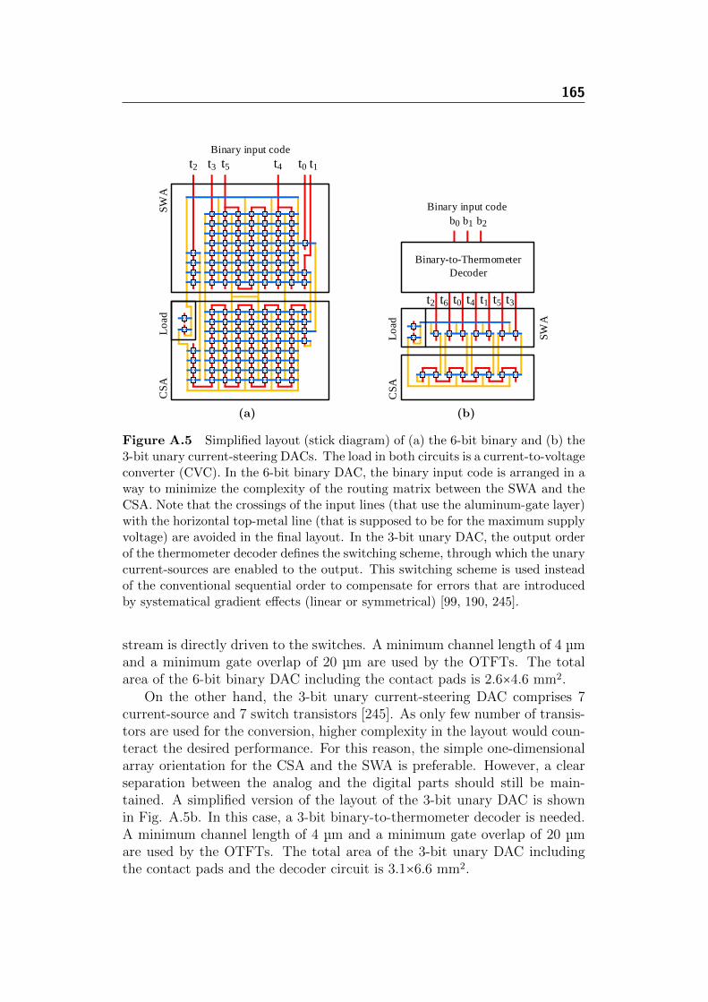
165
SW
AC
SA
Lo
ad
t2
Binary input code
Binary-to-Thermometer
Decoder
Binary input code
t2
Lo
ad
CS
A
SW
A
t3 t5 t4 t0 t1
b0 b1 b2
t6 t0 t4 t1 t5 t3
(a)
SW
AC
SA
Lo
ad
t2
Binary input code
Binary-to-Thermometer
Decoder
Binary input code
t2
Lo
ad
CS
A
SW
A
t3 t5 t4 t0 t1
b0 b1 b2
t6 t0 t4 t1 t5 t3
(b)
Figure A.5 Simplified layout (stick diagram) of (a) the 6-bit binary and (b) the3-bit unary current-steering DACs. The load in both circuits is a current-to-voltageconverter (CVC). In the 6-bit binary DAC, the binary input code is arranged in away to minimize the complexity of the routing matrix between the SWA and theCSA. Note that the crossings of the input lines (that use the aluminum-gate layer)with the horizontal top-metal line (that is supposed to be for the maximum supplyvoltage) are avoided in the final layout. In the 3-bit unary DAC, the output orderof the thermometer decoder defines the switching scheme, through which the unarycurrent-sources are enabled to the output. This switching scheme is used insteadof the conventional sequential order to compensate for errors that are introducedby systematical gradient effects (linear or symmetrical) [99, 190, 245].
stream is directly driven to the switches. A minimum channel length of 4 µmand a minimum gate overlap of 20 µm are used by the OTFTs. The totalarea of the 6-bit binary DAC including the contact pads is 2.6×4.6 mm2.
On the other hand, the 3-bit unary current-steering DAC comprises 7current-source and 7 switch transistors [245]. As only few number of transis-tors are used for the conversion, higher complexity in the layout would coun-teract the desired performance. For this reason, the simple one-dimensionalarray orientation for the CSA and the SWA is preferable. However, a clearseparation between the analog and the digital parts should still be main-tained. A simplified version of the layout of the 3-bit unary DAC is shownin Fig. A.5b. In this case, a 3-bit binary-to-thermometer decoder is needed.A minimum channel length of 4 µm and a minimum gate overlap of 20 µmare used by the OTFTs. The total area of the 3-bit unary DAC includingthe contact pads and the decoder circuit is 3.1×6.6 mm2.
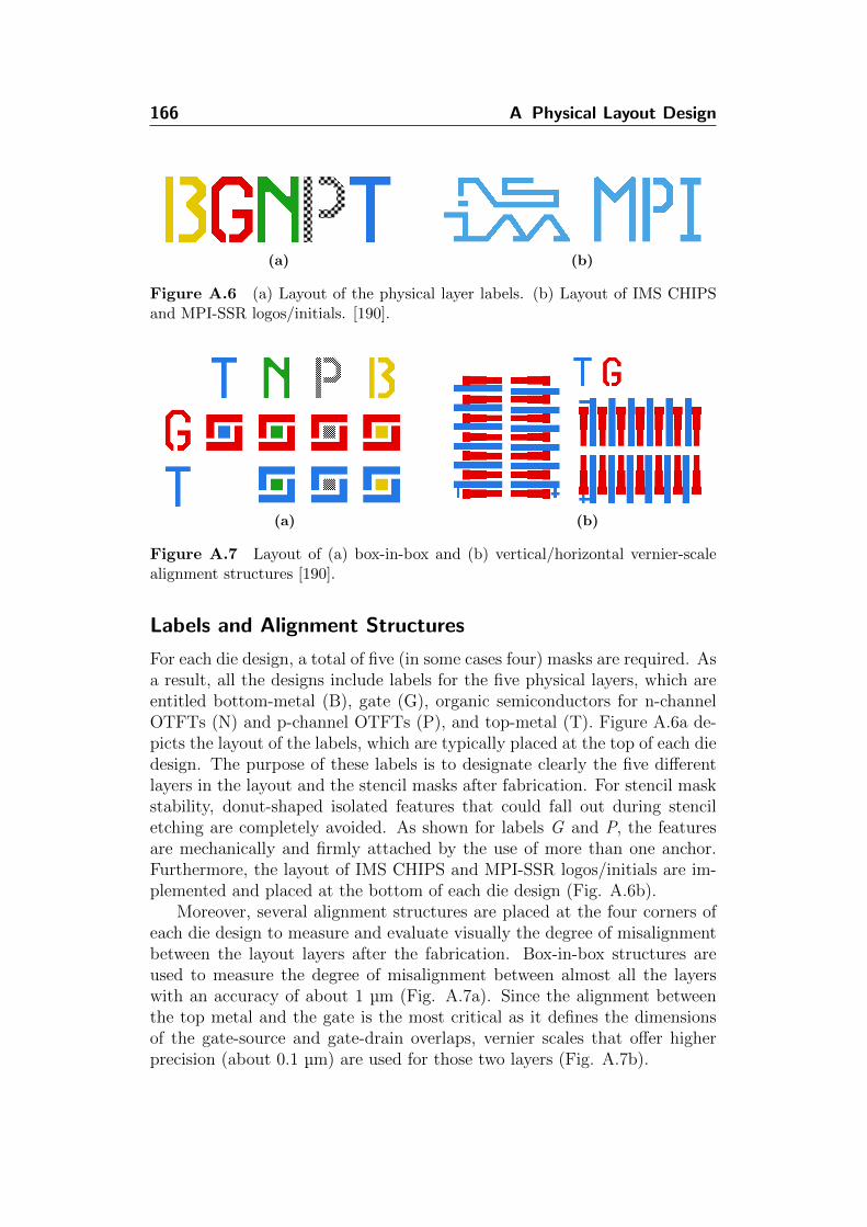
166 A Physical Layout Design
(a)
(b)
Figure A.6 (a) Layout of the physical layer labels. (b) Layout of IMS CHIPSand MPI-SSR logos/initials. [190].
(a)
(b)
Figure A.7 Layout of (a) box-in-box and (b) vertical/horizontal vernier-scalealignment structures [190].
Labels and Alignment Structures
For each die design, a total of five (in some cases four) masks are required. Asa result, all the designs include labels for the five physical layers, which areentitled bottom-metal (B), gate (G), organic semiconductors for n-channelOTFTs (N) and p-channel OTFTs (P), and top-metal (T). Figure A.6a de-picts the layout of the labels, which are typically placed at the top of each diedesign. The purpose of these labels is to designate clearly the five differentlayers in the layout and the stencil masks after fabrication. For stencil maskstability, donut-shaped isolated features that could fall out during stenciletching are completely avoided. As shown for labels G and P, the featuresare mechanically and firmly attached by the use of more than one anchor.Furthermore, the layout of IMS CHIPS and MPI-SSR logos/initials are im-plemented and placed at the bottom of each die design (Fig. A.6b).
Moreover, several alignment structures are placed at the four corners ofeach die design to measure and evaluate visually the degree of misalignmentbetween the layout layers after the fabrication. Box-in-box structures areused to measure the degree of misalignment between almost all the layerswith an accuracy of about 1 µm (Fig. A.7a). Since the alignment betweenthe top metal and the gate is the most critical as it defines the dimensionsof the gate-source and gate-drain overlaps, vernier scales that offer higherprecision (about 0.1 µm) are used for those two layers (Fig. A.7b).
BDe-embedding Procedure
Full two-port S-parameters of OTFTs are measured in this work using anHP 3577A vector network analyzer (VNA). Systematical errors, which aremostly introduced by the test setup, are observed during the measurements[239]. Accordingly, a de-embedding process is employed to remove the unde-sired parasitic effects of the physical network placed between the VNA andthe device under test (DUT), i.e., an OTFT. In principle, the de-embeddingprocess uses a model of the test fixture and mathematically removes the par-asitics from the overall measurements. There are many different approachesthat have been developed for modeling and removing these errors such as3-term, 8-term, 12-term and 16-term error correction models [239–241]. Inthis work, the 12-term error correction model, which requires standard short,open, through and matched terminations for a two-port network calibration,is utilized; the method produced quite promising results. This appendixdescribes the error model and the calibration method used.
Figure B.1 shows a generic block diagram of a two-port network withan error adapter, which separates the DUT (an OTFT in our case) from anideal measurement system [243]. Furthermore, Fig B.2 depicts the twelvesystem errors involved when measuring a two-port device/network in theforward and reverse directions [239]. The error model and the S-parametersof the DUT are represented with a signal flow graph, which is a simpleway to represent and helps to analyze the transmitted and reflected signalsfrom a device/network [239]. Moreover, it is useful for cascaded networktopologies, since flow graphs of adjacent networks can be connected in series.Directed lines in the flow graph represent the dependency of the signal flowthrough the network; for example, the signal flow from node a1 to b1 isdefined as the input reflection coefficient (S11i). At this point, there has tobe a clear distinction between the intrinsic (actual de-embedded) and theextrinsic (measured) S-parameters, which are given by
b1 = S11i ⋅ a1 + S12i ⋅ a2
b2 = S21i ⋅ a1 + S22i ⋅ a2[b1
b2] = [
S11i S12i
S21i S22i] [a1
a2] , (B.1)
b0 = S11e ⋅ a0 + S12e ⋅ a3
b3 = S21e ⋅ a0 + S22e ⋅ a3[b0
b3] = [
S11e S12e
S21e S22e] [a0
a3] . (B.2)
The subscripts i and e denote the intrinsic (of the DUT) and extrinsic (in-cluding parasitics) S-parameters, respectively.
167
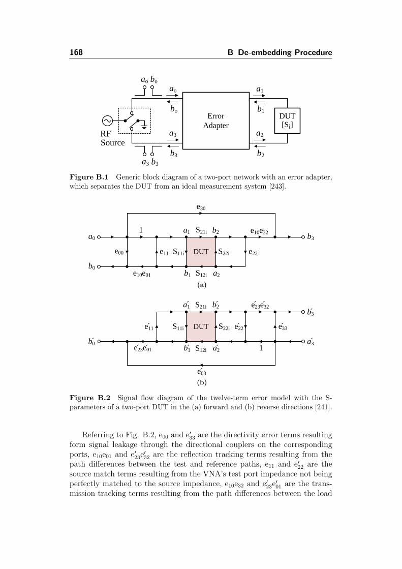
168 B De-embedding Procedure
Error
Adapter
ao bo
a3 b3
ao
bo
a3
b3
a1
b1
a2
b2
RFSource
DUT[Si]
Figure B.1 Generic block diagram of a two-port network with an error adapter,which separates the DUT from an ideal measurement system [243].
DUT
DUT
a0
b0
a1 b2
b1 a2
b3
1
e00 e11
e10e01
S11i S22i
S21i
S12i
e22
e10e32
e30
a3
b3
a2b1
b2a1
b01
e33e22
e23e32
S22iS11i
S12i
S21i
e11
e23e01
e03
´ ´ ´ ´ ´
´ ´ ´ ´
´
´ ´
´ ´ ´
(a)
DUT
DUT
a0
b0
a1 b2
b1 a2
b3
1
e00 e11
e10e01
S11i S22i
S21i
S12i
e22
e10e32
e30
a3
b3
a2b1
b2a1
b01
e33e22
e23e32
S22iS11i
S12i
S21i
e11
e23e01
e03
´ ´ ´ ´ ´
´ ´ ´ ´
´
´ ´
´ ´ ´
(b)
Figure B.2 Signal flow diagram of the twelve-term error model with the S-parameters of a two-port DUT in the (a) forward and (b) reverse directions [241].
Referring to Fig. B.2, e00 and e′33 are the directivity error terms resultingform signal leakage through the directional couplers on the correspondingports, e10e01 and e′23e′32 are the reflection tracking terms resulting from thepath differences between the test and reference paths, e11 and e′22 are thesource match terms resulting from the VNA’s test port impedance not beingperfectly matched to the source impedance, e10e32 and e′23e′01 are the trans-mission tracking terms resulting from the path differences between the load
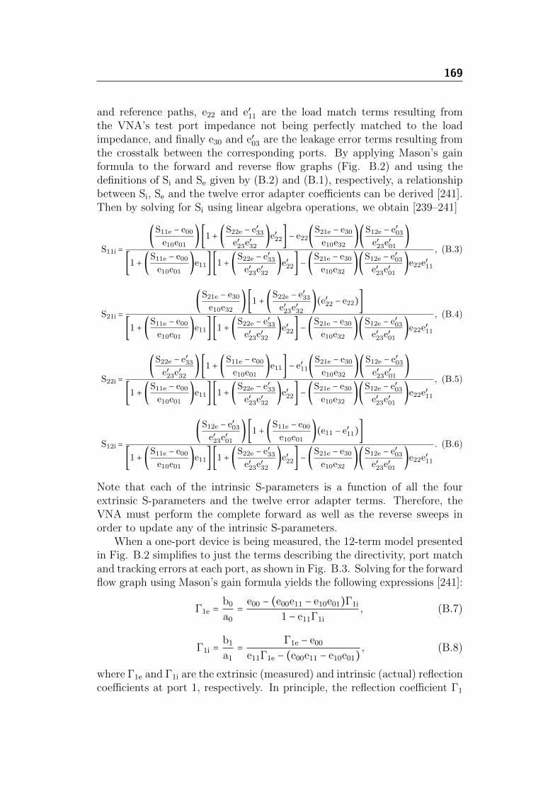
169
and reference paths, e22 and e′11 are the load match terms resulting fromthe VNA’s test port impedance not being perfectly matched to the loadimpedance, and finally e30 and e′03 are the leakage error terms resulting fromthe crosstalk between the corresponding ports. By applying Mason’s gainformula to the forward and reverse flow graphs (Fig. B.2) and using thedefinitions of Si and Se given by (B.2) and (B.1), respectively, a relationshipbetween Si, Se and the twelve error adapter coefficients can be derived [241].Then by solving for Si using linear algebra operations, we obtain [239–241]
S11i =
(S11e − e00
e10e01)[1 + (
S22e − e′33e′23e′32
)e′22] − e22(S21e − e30
e10e32)(
S12e − e′03e′23e′01
)
[1 + (S11e − e00
e10e01)e11] [1 + (
S22e − e′33e′23e′32
)e′22] − (S21e − e30
e10e32)(
S12e − e′03e′23e′01
)e22e′11
, (B.3)
S21i =
(S21e − e30
e10e32)[1 + (
S22e − e′33e′23e′32
)(e′22 − e22)]
[1 + (S11e − e00
e10e01)e11] [1 + (
S22e − e′33e′23e′32
)e′22] − (S21e − e30
e10e32)(
S12e − e′03e′23e′01
)e22e′11
, (B.4)
S22i =
(S22e − e′33
e′23e′32)[1 + (
S11e − e00e10e01
)e11] − e′11(S21e − e30
e10e32)(
S12e − e′03e′23e′01
)
[1 + (S11e − e00
e10e01)e11] [1 + (
S22e − e′33e′23e′32
)e′22] − (S21e − e30
e10e32)(
S12e − e′03e′23e′01
)e22e′11
, (B.5)
S12i =
(S12e − e′03
e′23e′01)[1 + (
S11e − e00e10e01
)(e11 − e′11)]
[1 + (S11e − e00
e10e01)e11] [1 + (
S22e − e′33e′23e′32
)e′22] − (S21e − e30
e10e32)(
S12e − e′03e′23e′01
)e22e′11
. (B.6)
Note that each of the intrinsic S-parameters is a function of all the fourextrinsic S-parameters and the twelve error adapter terms. Therefore, theVNA must perform the complete forward as well as the reverse sweeps inorder to update any of the intrinsic S-parameters.
When a one-port device is being measured, the 12-term model presentedin Fig. B.2 simplifies to just the terms describing the directivity, port matchand tracking errors at each port, as shown in Fig. B.3. Solving for the forwardflow graph using Mason’s gain formula yields the following expressions [241]:
Γ1e =b0
a0
=e00 − (e00e11 − e10e01)Γ1i
1 − e11Γ1i
, (B.7)
Γ1i =b1
a1
=Γ1e − e00
e11Γ1e − (e00e11 − e10e01), (B.8)
where Γ1e and Γ1i are the extrinsic (measured) and intrinsic (actual) reflectioncoefficients at port 1, respectively. In principle, the reflection coefficient Γ1
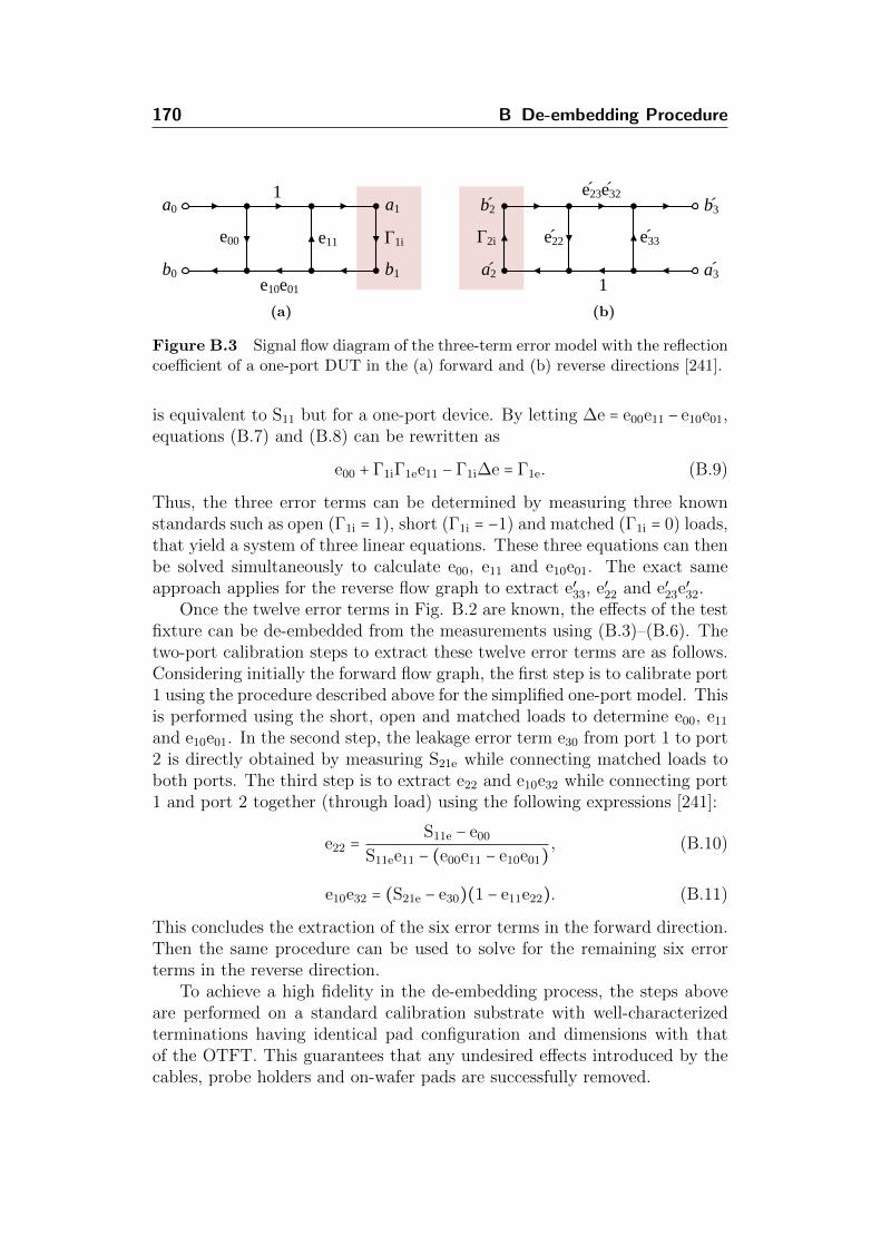
170 B De-embedding Procedure
a0
b0
1
e00 e11
e10e01
Γ1i
a1
b1 a3
b3
a2
1
e33e22
e23e32
Γ2i
´ ´ ´
´
´ ´
´ ´
b2
(a)
a0
b0
1
e00 e11
e10e01
Γ1i
a1
b1 a3
b3
a2
1
e33e22
e23e32
Γ2i
´ ´ ´
´
´ ´
´ ´
b2
(b)
Figure B.3 Signal flow diagram of the three-term error model with the reflectioncoefficient of a one-port DUT in the (a) forward and (b) reverse directions [241].
is equivalent to S11 but for a one-port device. By letting ∆e = e00e11 − e10e01,equations (B.7) and (B.8) can be rewritten as
e00 + Γ1iΓ1ee11 − Γ1i∆e = Γ1e. (B.9)
Thus, the three error terms can be determined by measuring three knownstandards such as open (Γ1i = 1), short (Γ1i = −1) and matched (Γ1i = 0) loads,that yield a system of three linear equations. These three equations can thenbe solved simultaneously to calculate e00, e11 and e10e01. The exact sameapproach applies for the reverse flow graph to extract e′33, e′22 and e′23e′32.
Once the twelve error terms in Fig. B.2 are known, the effects of the testfixture can be de-embedded from the measurements using (B.3)–(B.6). Thetwo-port calibration steps to extract these twelve error terms are as follows.Considering initially the forward flow graph, the first step is to calibrate port1 using the procedure described above for the simplified one-port model. Thisis performed using the short, open and matched loads to determine e00, e11
and e10e01. In the second step, the leakage error term e30 from port 1 to port2 is directly obtained by measuring S21e while connecting matched loads toboth ports. The third step is to extract e22 and e10e32 while connecting port1 and port 2 together (through load) using the following expressions [241]:
e22 =S11e − e00
S11ee11 − (e00e11 − e10e01), (B.10)
e10e32 = (S21e − e30)(1 − e11e22). (B.11)
This concludes the extraction of the six error terms in the forward direction.Then the same procedure can be used to solve for the remaining six errorterms in the reverse direction.
To achieve a high fidelity in the de-embedding process, the steps aboveare performed on a standard calibration substrate with well-characterizedterminations having identical pad configuration and dimensions with thatof the OTFT. This guarantees that any undesired effects introduced by thecables, probe holders and on-wafer pads are successfully removed.
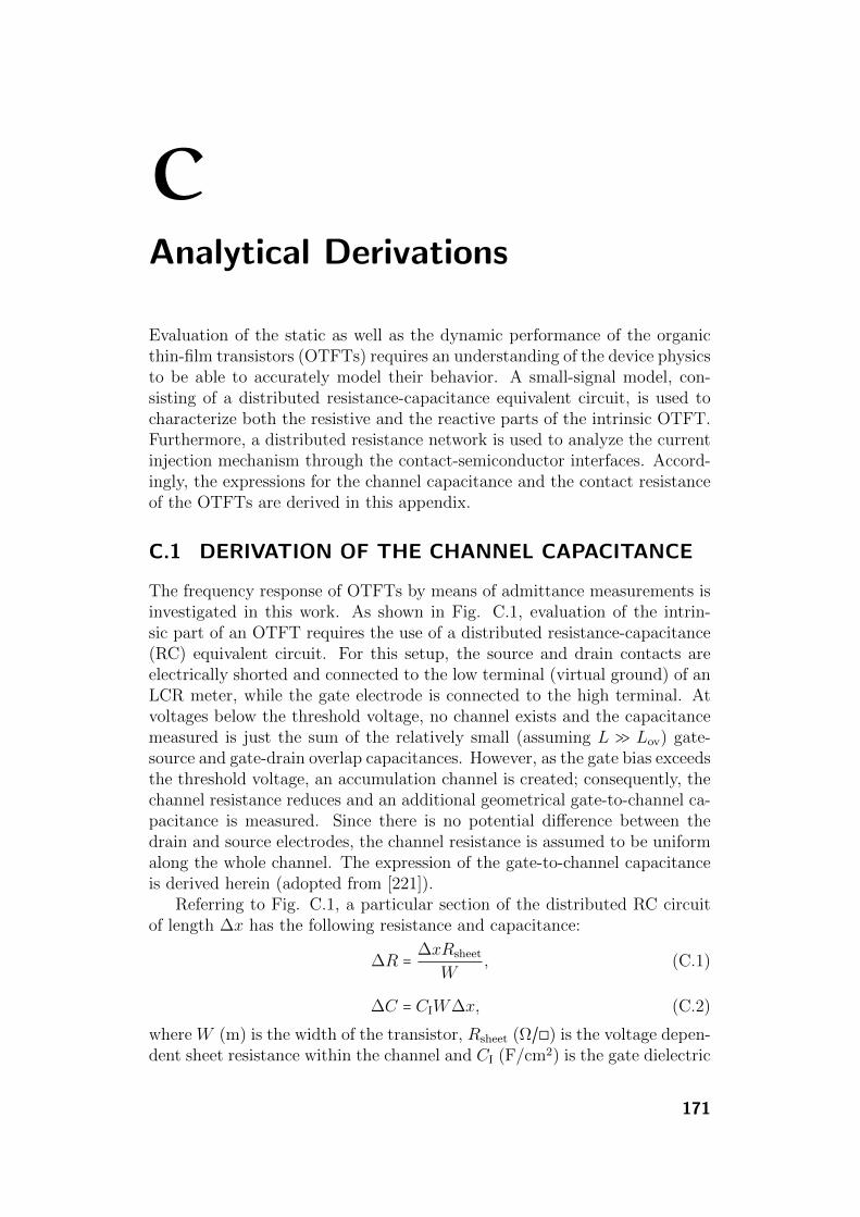
CAnalytical Derivations
Evaluation of the static as well as the dynamic performance of the organicthin-film transistors (OTFTs) requires an understanding of the device physicsto be able to accurately model their behavior. A small-signal model, con-sisting of a distributed resistance-capacitance equivalent circuit, is used tocharacterize both the resistive and the reactive parts of the intrinsic OTFT.Furthermore, a distributed resistance network is used to analyze the currentinjection mechanism through the contact-semiconductor interfaces. Accord-ingly, the expressions for the channel capacitance and the contact resistanceof the OTFTs are derived in this appendix.
C.1 DERIVATION OF THE CHANNEL CAPACITANCE
The frequency response of OTFTs by means of admittance measurements isinvestigated in this work. As shown in Fig. C.1, evaluation of the intrin-sic part of an OTFT requires the use of a distributed resistance-capacitance(RC) equivalent circuit. For this setup, the source and drain contacts areelectrically shorted and connected to the low terminal (virtual ground) of anLCR meter, while the gate electrode is connected to the high terminal. Atvoltages below the threshold voltage, no channel exists and the capacitancemeasured is just the sum of the relatively small (assuming L ≫ Lov) gate-source and gate-drain overlap capacitances. However, as the gate bias exceedsthe threshold voltage, an accumulation channel is created; consequently, thechannel resistance reduces and an additional geometrical gate-to-channel ca-pacitance is measured. Since there is no potential difference between thedrain and source electrodes, the channel resistance is assumed to be uniformalong the whole channel. The expression of the gate-to-channel capacitanceis derived herein (adopted from [221]).
Referring to Fig. C.1, a particular section of the distributed RC circuitof length ∆x has the following resistance and capacitance:
∆R =∆xRsheet
W, (C.1)
∆C = CIW∆x, (C.2)
where W (m) is the width of the transistor, Rsheet (Ω/◻) is the voltage depen-dent sheet resistance within the channel and CI (F/cm2) is the gate dielectric
171

172 C Analytical Derivations
Figure C.1 Schematic cross section of an inverted-staggered (bottom-gate, top-contact) OTFT (not to scale) with a channel length that is much larger thanthe gate-overlap length (L ≫ Lov). The small-signal model of the intrinsic partof the OTFT using a distributed RC equivalent circuit, assuming the transistoris operated in the accumulation regime, is depicted inside the schematic. In theshown setup, the source and drain contacts are electrically shorted and connectedto the low terminal (virtual ground) of an LCR meter, while the gate electrodeis connected to the high terminal to bias the transistor with a DC potential (VG)along with a superimposed AC potential (Vm sin ωt).
capacitance per unit area. By applying the Kirchhoff’s current law and thensubstituting for ∆C using (C.2), we get
I(x +∆x) − I(x) = −jω∆C V (x +∆x)
I(x +∆x) − I(x) = −jωCIW∆xV (x +∆x)
I(x +∆x) − I(x)
∆x= −jωCIW [V (x) −∆RI(x)],
where ω (rad/s) is the angular frequency at which the capacitance is mea-sured. By substituting for ∆R using (C.1) and then taking the limit ∆x→ 0at both sides, we obtain
lim∆x→0
(I(x +∆x) − I(x)
∆x) = lim
∆x→0( − jωCIW[V (x) −
∆xRsheetI(x)
W])
∂I
∂x= −jωCIWV (x). (C.3)
On the other hand, applying Kirchhoff’s voltage law yields the following:
V (x +∆x) − V (x) = −∆RI(x).
Again by substituting for ∆R using (C.1) and then taking the limit ∆x→ 0
C.1 Derivation of the Channel Capacitance 173
at both sides, we get
lim∆x→0
(V (x +∆x) − V (x)
∆x) = lim
∆x→0( −
Rsheet
WI(x))
∂V
∂x= −
Rsheet
WI(x). (C.4)
Solving (C.3) and (C.4) together gives the following second-order linear dif-ferential equation:
∂2V
∂x2= jωRsheetCIV (x). (C.5)
Let 1/λ2 = jωRsheetCI, equation (C.5) has the general solution V (x) = Aex/λ+Be−x/λ in which λ is a complex decay length. To evaluate the terminalcapacitance, we impose the boundary conditions V (x = 0) = V (x = L) = Vm
to obtain A and B:
A = Vm (1 − e−L/λ
eL/λ − e−L/λ) ,
B = Vm (eL/λ − 1
eL/λ − e−L/λ) .
Thus, the function V (x) can now be expressed as
V (x) =Vm
eL/λ − e−L/λ[(1 − e−L/λ)ex/λ − (1 − eL/λ)e−x/λ] . (C.6)
The current I(x) can then be evaluated by substituting V (x) in (C.4):
I(x) = −W
λRsheet
Vm
eL/λ − e−L/λ[(1 − e−L/λ)ex/λ + (1 − eL/λ)e−x/λ] . (C.7)
We can deduce from this expression that I(x = 0) = −I(x = L) as expectedfrom the setup shown in Fig. C.1.
The measured admittance by the LCR meter is given by Ych = Gch+jωCch,where Gch and Cch are the measured channel conductance and capacitance.From the setup shown in Fig. C.1, the measured capacitance Cch is expressedas follows:
Cch =1
ωIm [
2I(x = 0)
V (x = 0)] = −
1
ωIm [
2I(x = L)
V (x = L)] . (C.8)
Substituting (C.7) in (C.8) results in
Cch = Im[2W
ωλRsheet
´¹¹¹¹¹¹¹¹¹¹¹¹¹¹¹¸¹¹¹¹¹¹¹¹¹¹¹¹¹¹¹¹¶f1
f3
³¹¹¹¹¹¹¹¹¹¹¹¹¹¹¹¹¹¹¹¹¹¹¹¹¹¹¹¹¹¹¹¹¹¹¹¹¹¹¹¹¹¹¹¹¹¹¹¹¹¹¹¹¹¹¹¹¹¹¹¹¹¹¹¹¹¹¹¹¹¹¹¹¹¹¹¹¹¹¹¹¹¹¹¹¹¹¹¹¹¹¹¹·¹¹¹¹¹¹¹¹¹¹¹¹¹¹¹¹¹¹¹¹¹¹¹¹¹¹¹¹¹¹¹¹¹¹¹¹¹¹¹¹¹¹¹¹¹¹¹¹¹¹¹¹¹¹¹¹¹¹¹¹¹¹¹¹¹¹¹¹¹¹¹¹¹¹¹¹¹¹¹¹¹¹¹¹¹¹¹¹¹¹¹¹µ1
eL/λ − e−L/λ( eL/λ´¸¶f2
+e−L/λ − 2) ]. (C.9)

174 C Analytical Derivations
Given that 1/λ2 = jωRsheetCI, the terms given by f1 and f2 in (C.9) can bewritten as
f1 =
√2CIW 2
ωRsheet
(1 + j) =CIWL
α(1 + j), (C.10)
f2 = e
√ωRsheetCIL
2
2(1+j)
= eα(1+j), (C.11)
where α =√ωRsheetCIL2/2. Substituting (C.11) into the term given by f3 in
(C.9) yields
f3 =eα(1+j) + e−α(1+j) − 2
eα(1+j) − e−α(1+j)
=(eα + e−α) cosα + j(eα − e−α) sinα − 2
(eα − e−α) cosα + j(eα + e−α) sinα. (C.12)
The measured capacitance Cch can therefore be finally obtained by substi-tuting (C.10) and (C.12) in (C.9) and applying some simplification to thetrigonometric expression:
Cch =CIWL
α(
sinhα + sinα
coshα + cosα) . (C.13)
Following a similar procedure to that used to derive the capacitance, themeasured loss (Gch/ω) can be expressed as
Gch
ω=CIWL
α(
sinhα − sinα
coshα + cosα) . (C.14)
C.2 DERIVATION OF THE CONTACT RESISTANCE
The contact resistance has a considerable impact on the performance of theOTFTs. When the channel length is reduced, the relative contribution of thecontact resistance to the total device resistance increases, and thus, the ef-fective mobility decreases [139]. In a general approach, the transmission linemethod (TLM) is used to extract the contact resistance of the OTFTs [192].Evaluation of the contact resistance of our inverted-staggered (bottom-gate,top-contact) OTFTs, in particular, requires the use of a distributed resis-tance network as shown in Fig. C.2. The distributed resistance network isa simplified equivalent circuit that is used to electrically describe and modelthe current injection mechanism through the contact interfaces between themetallic source/drain contacts and the organic semiconductor. In this sec-tion, the equivalent circuit is analyzed and accordingly the expression of theequivalent contact resistance RC is derived (adopted from [192]).
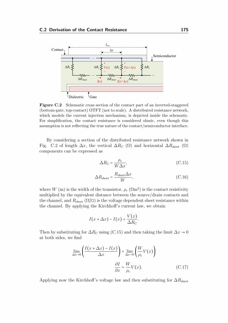
C.2 Derivation of the Contact Resistance 175
Figure C.2 Schematic cross section of the contact part of an inverted-staggered(bottom-gate, top-contact) OTFT (not to scale). A distributed resistance network,which models the current injection mechanism, is depicted inside the schematic.For simplification, the contact resistance is considered ohmic, even though thisassumption is not reflecting the true nature of the contact/semiconductor interface.
By considering a section of the distributed resistance network shown inFig. C.2 of length ∆x, the vertical ∆RC (Ω) and horizontal ∆Rsheet (Ω)components can be expressed as
∆RC =ρc
W∆x, (C.15)
∆Rsheet =Rsheet∆x
W, (C.16)
where W (m) is the width of the transistor, ρc (Ωm2) is the contact resistivitymultiplied by the equivalent distance between the source/drain contacts andthe channel, and Rsheet (Ω/◻) is the voltage dependent sheet resistance withinthe channel. By applying the Kirchhoff’s current law, we obtain
I(x +∆x) − I(x) =V (x)
∆RC
.
Then by substituting for ∆RC using (C.15) and then taking the limit ∆x→ 0at both sides, we find
lim∆x→0
(I(x +∆x) − I(x)
∆x) = lim
∆x→0(W
ρc
V (x))
∂I
∂x=W
ρc
V (x). (C.17)
Applying now the Kirchhoff’s voltage law and then substituting for ∆Rsheet
176 C Analytical Derivations
using (C.16) result in the following:
V (x +∆x) − V (x) = ∆RsheetI(x +∆x)
V (x +∆x) − V (x) =Rsheet∆x
WI(x +∆x)
V (x +∆x) − V (x)
∆x=Rsheet
W[I(x) +
V (x)
∆RC
].
By substituting for ∆RC using (C.15) and then taking the limit ∆x → 0 atboth sides, we obtain
lim∆x→0
(V (x +∆x) − V (x)
∆x) = lim
∆x→0(Rsheet
W[I(x) +
W∆x
ρc
V (x)])
∂V
∂x=Rsheet
WI(x). (C.18)
Solving (C.17) and (C.18) together gives the following second-order lineardifferential equation:
∂2I
∂x2=Rsheet
ρc
I(x). (C.19)
Let 1/L2T = Rsheet/ρc, equation (C.19) has the general solution I(x) = Aex/LT+
Be−x/LT , where LT is a characteristic transfer length over which 63% ofthe charge flow between the source/drain contacts and the semiconductortransfers [97]. To evaluate the equivalent contact resistance, we impose theboundary conditions I(x = 0) = 0 and I(x = Lov) = Im, where Lov (m) is thegate-overlap length, to obtain A and B:
A = −B =Im
eLov/LT − e−Lov/LT.
Thus, the function I(x) can now be expressed as
I(x) =Im
eLov/LT − e−Lov/LT(ex/LT − e−x/LT) . (C.20)
Moreover, the function V (x) can then be evaluated by substituting I(x) in(C.17):
V (x) =ρc
WLT
Im
eLov/LT − e−Lov/LT(ex/LT + e−x/LT) . (C.21)
Accordingly, the equivalent contact resistance RC can be calculated as fol-lows:
RC =V (x = Lov)
I(x = Lov)=
ρc
WLT
(eLov/LT + e−Lov/LT)
(eLov/LT − e−Lov/LT). (C.22)

C.2 Derivation of the Contact Resistance 177
Given that 1/L2T = Rsheet/ρc, the contact resistance (only at one side of the
OTFT, i.e., either the source or the drain side) can be finally reduced to thefollowing expression:
RC =RsheetLT
Wcoth(
Lov
LT
). (C.23)
This expression describes the relationship between the transfer length LT
and the gate-overlap length Lov [97]. If the overlap length is much largerthan the transfer length (Lov ≫ LT), equations (C.22) and (C.23) simplify toRC ≅ ρc/(WLT), which indicates that the contact resistance is independenton the overlap length. This implies that, in this case, the contact region ispartially active with an equivalent overlap area of W ⋅LT. On the other hand,if the contact length is much smaller than the transfer length (Lov ≪ LT),equations (C.22) and (C.23) simplify to RC ≅ ρc/(WLov). This means that,in this case, the contact resistance is inversely proportional to the contactlength and the entire contact region with an area of W ⋅Lov is active.
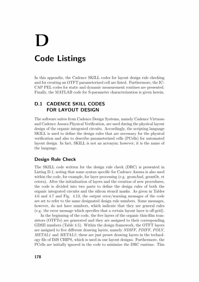
DCode Listings
In this appendix, the Cadence SKILL codes for layout design rule checkingand for creating an OTFT parameterized cell are listed. Furthermore, the IC-CAP PEL codes for static and dynamic measurement routines are presented.Finally, the MATLAB code for S-parameter characterization is given herein.
D.1 CADENCE SKILL CODESFOR LAYOUT DESIGN
The software suites from Cadence Design Systems, namely Cadence Virtuosoand Cadence Assura Physical Verification, are used during the physical layoutdesign of the organic integrated circuits. Accordingly, the scripting languageSKILL is used to define the design rules that are necessary for the physicalverification and also to describe parameterized cells (PCells) for automatedlayout design. In fact, SKILL is not an acronym; however, it is the name ofthe language.
Design Rule Check
The SKILL code written for the design rule check (DRC) is presented inListing D.1, noting that some syntax specific for Cadence Assura is also usedwithin the code, for example, for layer processing (e.g. geomAnd, geomOr, etcetera). After the initialization of layers and the creation of new procedures,the code is divided into two parts to define the design rules of both theorganic integrated circuits and the silicon stencil masks. As given in Tables4.6 and 4.7 and Fig. 4.13, the output error/warning messages of the codeare set to refer to the same designated design rule numbers. Some messages,however, do not have numbers, which indicate that they are general rules(e.g. the error message which specifies that a certain layout layer is off-grid).
In the beginning of the code, the five layers of the organic thin-film tran-sistors (OTFTs) are generated and they are assigned to their correspondingGDSII numbers (Table 4.5). Within the design framework, the OTFT layersare assigned to five different drawing layers, namely NDIFF, PDIFF, POLY,METAL1 and METAL2 ; these are just preset drawing layers in the technol-ogy file of IMS CHIPS, which is used in our layout designs. Furthermore, thePCells are initially ignored in the code to minimize the DRC runtime. This
178
D.1 Cadence SKILL Codes for Layout Design 179
is because it is ensured already during the description of the PCells that theysatisfy the recommended design rules.
The listed code for the DRC is restricted to the geometric and connectiv-ity configuration shown in Fig. 4.13. However, a more sophisticated versionof the code (not listed herein) is also implemented to take into considerationother issues, for example, other transistor configurations (e.g. fingers andmultipliers of OTFTs). The simplified version is given herein just to demon-strate the concept. Moreover, design rules 10 and 11 (Table 4.7), which setmaximum aspect ratios for the mask bridges attached at both ends and atone end, respectively, are checked in the given version of the code only forthe top-metal layer. This is because the top-metal layer includes the mostcritical and finest structures.
Listing D.1 SKILL code for layout design rule checking (DRC).1 ;−−− Star t o f des ign ru l e check ing code2 drcExtractRules (34 ;−−− Ignor ing PCel l s from the DRC5 avParameters (6 ?ignoreCell ( ce l l ( "PCELLS " ) )7 )89 ;−−− Generation o f commonly used der ived l a y e r s
10 layerDefs ( "df2"11 nsemi = layer ( "NDIFF" type ( "drawing " ) )12 psemi = layer ( "PDIFF" type ( "drawing " ) )13 gate = layer ( "POLY" type ( "drawing " ) )14 top = layer ( "METAL1 " type ( "drawing " ) )15 bottom = layer ( "METAL2 " type ( "drawing " ) )16 c h i p s i z e = layer ( "prBoundary " type ( "drawing " ) )17 dataextent = cellBoundary ( root )18 )1920 layerDefs ( "gds2"21 nsemi = layer (40)22 psemi = layer (39)23 gate = layer (46)24 top = layer (49)25 bottom = layer (51)26 )2728 ;−−− Layer d e r i v a t i on r u l e s29 ngate = geomAnd( nsemi gate )30 pgate = geomAnd( psemi gate )31 npgate = geomCat( ngate pgate )32 npsemi = geomAnd( nsemi psemi )33 semi = geomCat( nsemi psemi )34 g a t e f = geomAndNot( gate semi )35 a l l l a y = geomOr( bottom gate nsemi psemi top )3637 ;−−− Contacts38 gatecont = geomAnd( gate bottom )39 metalcont = geomAnd( top bottom )4041 ;−−− Def ine new procedures42 procedure (
180 D Code Listings
43 procWidthCheck ( l aye r1 value comment )44 drc ( l aye r1 width < value comment withCornerTouch )45 )4647 procedure (48 procSpCkSameLay ( l aye r1 value comment )49 drc ( l aye r1 sepNotch < value comment )50 )5152 procedure (53 procSpCkDifLay ( l aye r1 l aye r2 value comment)54 drc ( l aye r1 l aye r2 sep < value comment )55 )5657 procedure (58 procEnclCheck ( l aye r1 l aye r2 value comment )59 drc ( l aye r1 l aye r2 enc < value comment s h i e l d e d ( l aye r2 ) oppos i t e )60 )6162 procedure (63 procOverlapCheck ( l aye r1 l aye r2 value comment )64 drc ( l aye r1 l aye r2 ovlp < value comment )65 )6667 procedure (68 procMinSizeCk ( l aye r1 value comment )69 checker r1 = drc ( l aye r1 width < value )70 checker r2 = drc ( l aye r1 area < value ∗ value )71 checke r r = geomOr( checker r1 checker r2 )72 errorLayer ( checker r comment)73 )7475 procedure (76 procAreaCheck ( l aye r1 value comment )77 drc ( l aye r1 area > value comment )78 )7980 ;−−−−−−−−−−−−−−−−−−−−−−−−−−−−−−81 ;−−− CHECK ORGANIC IC RULES −−−82 ;−−−−−−−−−−−−−−−−−−−−−−−−−−−−−−8384 ;−−− Check o f f −g r id e r r o r s85 offGrid ( nsemi 0 .1 "original NSemi grid should be 0.1" )86 offGrid ( psemi 0 .1 "original PSemi grid should be 0.1" )87 offGrid ( gate 0 .1 "original Gate grid should be 0.1" )88 offGrid ( top 0 .1 "original Top grid should be 0.1" )89 offGrid ( bottom 0 .1 "original Bottom grid should be 0.1" )9091 ;−−− Check non−90−degree e r r o r s92 non 90 = geomOr(93 geomGetNon90( nsemi )94 geomGetNon90( psemi )95 geomGetNon90( gate )96 )97 errorLayer ( non 90 "only horizontal or vertical edges are allowed " )9899 ;−−− Check non−45−degree e r r o r s
100 non 45 = geomOr(101 geomGetNon45( top )102 geomGetNon45( bottom )103 )104 errorLayer ( non 45 "only edges with a multiple of 45 degrees are allowed " )105106 ;−−− Check channel l ength107 gate and semi = geomAnd( gate semi )

D.1 Cadence SKILL Codes for Layout Design 181
108 t r a n s a c t i v e = geomOverlap( gate and semi top keep >= 2)109 m e t a l f o r t r a n s = geomOverlap( top t r a n s a c t i v e )110 grown semi = geomGrow( semi 20 20 20 20)111 m e t a l f o r t r a n s = geomAnd( m e t a l f o r t r a n s grown semi )112 procSpCkSameLay ( m e t a l f o r t r a n s 2 .0 "1.1, min. channel length is 2" )113114 ;−−− Check gate −over lap115 procOverlapCheck ( top t r a n s a c t i v e 20 .0 "2.1, min. gate -overlap is 20" )116117 ;−−− Check en c l o su r e s118 procEnclCheck ( top semi 20 .0 "3.1, min. Top -enclose -Semi is 20" )119 procEnclCheck ( semi top 20 .0 "3.2, min. Semi -enclose -Top is 20" )120 procEnclCheck ( semi gate 20 .0 "3.3, min. Semi -enclose -Gate is 20" )121 procEnclCheck ( gate semi 20 .0 "3.4, min. Gate -enclose -Semi is 20" )122123 ;−−− Check top−metal spac ing out s id e t r a n s i s t o r a c t i v e r e g i on s124 top wo trans = geomAndNot( top m e t a l f o r t r a n s )125 procSpCkSameLay ( top wo trans 20 .0 "4.1, min. Top -to -Top space is 20" )126127 ;−−− Check r e l a t e d c l e a r an c e s128 procSpCkSameLay ( gate 20 .0 "4.2, min. Gate -to -Gate space is 20" )129 procSpCkSameLay ( psemi 20 .0 "4.3, min. PSemi -to-PSemi space is 20" )130 procSpCkSameLay ( nsemi 20 .0 "4.4, min. NSemi -to-NSemi space is 20" )131 procSpCkSameLay ( bottom 20 .0 "4.5, min. Bottom -to-Bottom space is 20" )132133 ;−−− Check non− r e l a t e d l ay e r spac ings134 procSpCkDifLay ( top gate 20 .0 "5.1, min. Top -to-Gate space is 20" )135 procSpCkDifLay ( top semi 20 .0 "5.2 & 5.3, min. Top -to-Semi space is 20" )136 procSpCkDifLay ( top bottom 20 .0 "5.4, min. Top -to-Bottom space is 20" )137 procSpCkDifLay ( gate semi 20 .0 "5.5 & 5.6, min. Gate -to -Semi space is 20" )138 procSpCkDifLay ( gate bottom 20 .0 "5.7, min. Gate -to -Bottom space is 20" )139 procSpCkDifLay ( psemi nsemi 20 .0 "5.8, min. PSemi -to-NSemi space is 20" )140 procSpCkDifLay ( semi bottom 20 .0 "5.9 & 5.10, min. Semi -to -Bot space is 20" )141142 ;−−− Check l ay e r widths143 procWidthCheck ( top 20 .0 "6.1, min. Top width is 20.0" )144 procWidthCheck ( gate 20 .0 "6.2, min. Gate width is 20.0" )145 procWidthCheck ( bottom 20 .0 "6.3, min. Bottom width is 20.0" )146147 ;−−− Check d i r e c t contact a reas148 procMinSizeCk ( metalcont 20 .0 "7.1, min. Top -to -Bottom cont. area is 20x20" )149 procMinSizeCk ( gatecont 20 .0 "7.2, min. Gate -to -Bottom cont. area is 20x20" )150151 ;−−− Check in t e r connec t c r o s s i n g s152 top and gate = geomAnd( top gate )153 i n t c o n c r o s s i n g = geomAndNot( top and gate t r a n s a c t i v e )154 procMinSizeCk ( i n t c o n c r o s s i n g 20 .0 "8.1a, min. crossing area is 20x20" )155 errorLayer ( i n t c o n c r o s s i n g "8.1b, warning: crossings should be avoided " )156157 ;−−−−−−−−−−−−−−−−−−−−−−−−−−−−−−−−158 ;−−− CHECK STENCIL MASK RULES −−−159 ;−−−−−−−−−−−−−−−−−−−−−−−−−−−−−−−−160161 ;−−− Check maximum ac t i v e chip area162 s i z e x 1 = geomShift ( dataextent 0 1 . 0 )163 s i z e x 2 = geomAndNot( s i z e x 1 dataextent )164 s i z e x 3 = drc ( s i z e x 2 area > 1 . 0∗16000 . 0 )165 errorLayer ( s i z e x 3 "max. recom. horiz. active chip area is 16 mm" )166167 s i z e y 1 = geomShift ( dataextent 1 .0 0)168 s i z e y 2 = geomAndNot( s i z e y 1 dataextent )169 s i z e y 3 = drc ( s i z e y 2 area > 1 . 0∗16000 . 0 )170 errorLayer ( s i z e y 3 "max. recom. vert. active chip area is 16 mm" )171172 ;−−− Check donut−shaped ho le s t r u c t u r e s
182 D Code Listings
173 hol bottom = geomGetHoled( bottom )174 h o l g a t e = geomGetHoled( gate )175 ho l nsemi = geomGetHoled( nsemi )176 ho l psemi = geomGetHoled( psemi )177 ho l top = geomGetHoled( top )178 h o l s t r u c = geomCat( hol bottom h o l g a t e ho l nsemi ho l psemi ho l top )179 errorLayer ( h o l s t r u c t u r e s "donut -shaped holes are not acceptable " )180181 ;−−− Check remaining mask s i l i c o n area182 drc ( a l l l a y coverage >= 0.5 "9, remain. mask silicon area should be >=50%" )183184 ;−−− Check aspect r a t i o o f beams attached at both ends185 ;−−− Checking only f o r top−metal l a y e r with s epa ra t i on <= 20186 ;−−− Checking only at the t r a n s i s t o r a c t i v e r e g i on s187 brdg = drc ( m e t a l f o r t r a n s sep <= 20 app > 0 .0 oppos i t e p a r a l l e l s h i e l d e d )188 bad br idges = geomGetRectangle( brdg aspectRat io > 50)189 errorLayer ( bad br idges "10, aspect ratio of bridges should be <= 50" )190191 ;−−− Check aspect r a t i o o f beams attached at one end192 ;−−− Checking only f o r top−metal l a y e r with s epa ra t i on <= 20193 n o t c h s h i e l d e d = drc ( top notch <= 20 app > 0 .0 oppos i t e p a r a l l e l s h i e l d e d )194 bad notches = geomGetRectangle( n o t c h s h i e l d e d aspectRat io > 15)195 errorLayer ( bad notches "11, aspect ratio of notches should be <= 15" )196197 ;−−− End o f des ign ru l e check ing code198 )
Parameterized Cells
The SKILL code written to create an OTFT PCell is presented in ListingD.2. In principle, a PCell represents a circuit component that depends onits governing parameters and is automatically generated by the code. OtherPCells are also implemented to create more components, such as labels, test-ing modules, pads and alignment structures, all with the desired drawinglayers. However, only the OTFT PCell is given herein for reference. Thesame drawing layers mentioned above are used again in this code.
The OTFT PCell has five input parameters, namely channel type (Type),top-metal width (Top width), channel length (Ch length), gate overlap(Gate ovlp), enclosure of the top metal inside the semiconductor(Semi enc Top) and finally the amount of intentional vertical misalignmentof the top metal with the bottom gate (Vernier). The latter parameter,which quantifies the amount of intentional misalignment, is called Vernierbecause it is very similar to the vernier scale that is typically placed on chipto resolve the alignment errors. This parameter is needed, especially in thisstudy, to characterize the impact of unintentional process misalignment onthe device performance.
It is important to note that the channel width of the OTFT dependson the value of the parameter Semi enc Top. If Semi enc Top is greaterthan zero, then the channel width is defined by the top-metal width; but ifSemi enc Top is smaller than zero, then the channel width is defined by thesemiconductor width.
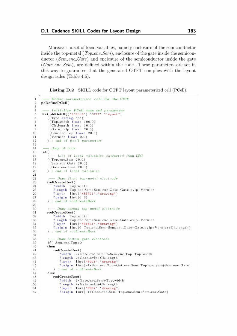
D.1 Cadence SKILL Codes for Layout Design 183
Moreover, a set of local variables, namely enclosure of the semiconductorinside the top-metal (Top enc Sem), enclosure of the gate inside the semicon-ductor (Sem enc Gate) and enclosure of the semiconductor inside the gate(Gate enc Sem), are defined within the code. These parameters are set inthis way to guarantee that the generated OTFT complies with the layoutdesign rules (Table 4.6).
Listing D.2 SKILL code for OTFT layout parameterized cell (PCell).1 ;−−− Def ine parameter ized c e l l f o r the OTFT2 pcDefinePCell (34 ;−−− I n i t i a l i z e PCell name and parameters5 l i s t (ddGetObj( "PCELLS " ) "OTFT" "layout " )6 ( ( Type s t r i n g "p" )7 ( Top width f l o a t 100 . 0 )8 ( Ch length f l o a t 10 . 0 )9 ( Gate ovlp f l o a t 20 . 0 )
10 ( Sem enc Top f l o a t 2 0 . 0 )11 ( Vern ier f l o a t 0 . 0 )12 ) ; end o f p c e l l parameters1314 ;−−− Body o f code15 let (16 ;−−− L i s t o f l o c a l v a r i a b l e s ex t rac t ed from DRC17 ( ( Top enc Sem 2 0 . 0 )18 ( Sem enc Gate 20 . 0 )19 ( Gate enc Sem 2 0 . 0 )20 ) ; end o f l o c a l v a r i a b l e s2122 ;−−− Draw f i r s t top−metal e l e c t r od e23 rodCreateRect (24 ? width Top width25 ? l ength Top enc Sem+Sem enc Gate+Gate ovlp+Vern ier26 ? l a y e r l i s t ( "METAL1 " , "drawing " )27 ? o r i g i n l i s t (0 0)28 ) ; end o f rodCreateRect2930 ;−−− Draw second top−metal e l e c t r od e31 rodCreateRect (32 ? width Top width33 ? l ength Top enc Sem+Sem enc Gate+Gate ovlp −Vernier34 ? l a y e r l i s t ( "METAL1 " , "drawing " )35 ? o r i g i n l i s t (0 Top enc Sem+Sem enc Gate+Gate ovlp+Vernier+Ch length )36 ) ; end o f rodCreateRect3738 ;−−− Draw bottom−gate e l e c t r od e39 i f ( Sem enc Top>040 then41 rodCreateRect (42 ? width 2∗Gate enc Sem+2∗Sem enc Top+Top width43 ? l ength 2∗ Gate ovlp+Ch length44 ? l a y e r l i s t ( "POLY" , "drawing " )45 ? o r i g i n l i s t (−1∗Sem enc Top−Gat enc Sem Top enc Sem+Sem enc Gate )46 ) ; end o f rodCreateRect47 else48 rodCreateRect (49 ? width 2∗Gate enc Sem+Top width50 ? l ength 2∗ Gate ovlp+Ch length51 ? l a y e r l i s t ( "POLY" , "drawing " )52 ? o r i g i n l i s t (−1∗Gate enc Sem Top enc Sem+Sem enc Gate )
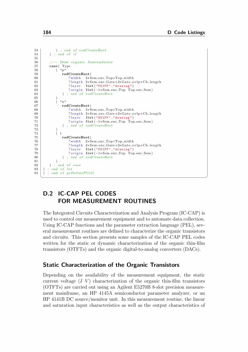
184 D Code Listings
53 ) ; end o f rodCreateRect54 ) ; end o f i f5556 ;−−− Draw organ i c Semconductor57 case ( Type58 ( "p"59 rodCreateRect (60 ? width 2∗Sem enc Top+Top width61 ? l ength 2∗Sem enc Gate+2∗Gate ovlp+Ch length62 ? l a y e r l i s t ( "PDIFF" , "drawing " )63 ? o r i g i n l i s t (−1∗Sem enc Top Top enc Sem )64 ) ; end o f rodCreateRect65 )66 ( "n"67 rodCreateRect (68 ? width 2∗Sem enc Top+Top width69 ? l ength 2∗Sem enc Gate+2∗Gate ovlp+Ch length70 ? l a y e r l i s t ( "NDIFF" , "drawing " )71 ? o r i g i n l i s t (−1∗Sem enc Top Top enc Sem )72 ) ; end o f rodCreateRect73 )74 ( t75 rodCreateRect (76 ? width 2∗Sem enc Top+Top width77 ? l ength 2∗Sem enc Gate+2∗Gate ovlp+Ch length78 ? l a y e r l i s t ( "PDIFF" , "drawing " )79 ? o r i g i n l i s t (−1∗Sem enc Top Top enc Sem )80 ) ; end o f rodCreateRect81 )82 ) ; end o f case83 ) ; end o f l e t84 ) ; end o f pcDef inePCel l
D.2 IC-CAP PEL CODESFOR MEASUREMENT ROUTINES
The Integrated Circuits Characterization and Analysis Program (IC-CAP) isused to control our measurement equipment and to automate data collection.Using IC-CAP functions and the parameter extraction language (PEL), sev-eral measurement routines are defined to characterize the organic transistorsand circuits. This section presents some samples of the IC-CAP PEL codeswritten for the static or dynamic characterization of the organic thin-filmtransistors (OTFTs) and the organic digital-to-analog converters (DACs).
Static Characterization of the Organic Transistors
Depending on the availability of the measurement equipment, the staticcurrent–voltage (I–V ) characterization of the organic thin-film transistors(OTFTs) are carried out using an Agilent E5270B 8-slot precision measure-ment mainframe, an HP 4145A semiconductor parameter analyzer, or anHP 4141B DC source/monitor unit. In this measurement routine, the linearand saturation input characteristics as well as the output characteristics of

D.2 IC-CAP PEL Codes for Measurement Routines 185
the OTFTs are measured consecutively. The IC-CAP PEL code written toautomate this process is given in Listing D.3, noting that all the input andoutput parameters are adjusted in advance using the graphical user inter-face of IC-CAP. The written code runs the different measurement setups andsaves the results to a certain directory. It is found that the OTFTs are pho-tosensitive; therefore, before taking any real measurements, the transistorsare typically measured several times in advance using less number of inputsamples to remove any hysteresis that could be present as a result of usingthe light source of the microscope. To perform special measurements, suchas up/down staircase sweep, other codes are written thereto, but only thesimplest version of the codes is listed herein for reference.
Listing D.3 IC-CAP PEL code for static characterization of OTFTs.1 !−−− Star t o f DC measurements2 update explicit34 !−−− Global v a r i a b l e s d e c l a r a t i o n5 global var f i l e n a m e67 !−−− Se t t i ng names and l a b e l s8 Sample = "IMS2"
9 Trans type = "P"
10 Width = "100" ! in micrometers11 Length = "4" ! in micrometers12 GOV = "20" ! in micrometers1314 !−−− Getting the date from the system15 hour = system$ ( "date +%H" )16 minute = system$ ( "date +%M" )17 second = system$ ( "date +%S" )18 time = val$ ( hour )&val$ ( minute )&val$ ( second )19 f i l e n a m e = val$ ( Sample )&"_"&val$ ( Trans type )&"_W"& . . .20 val$ (Width )&"L"&val$ ( Length )&"G"& . . .21 val$ (GOV) !&@" "@&val$ ( time )2223 !−−− Set output path24 output path= "C:\ Agilent\user\Zaki\Test_Transistors\"&val$ ( f i l e n a m e )2526 !−−− Remove h y s t e r e s i s27 i c c a p f u n c ( "." , "Measure " )28 i c c a p f u n c ( "." , "Measure " )29 i c c a p f u n c ( "." , "Measure " )30 i c c a p f u n c ( "." , "Measure " )3132 !−−− S t a t i c c h a r a c t e r i s a t i o n o f the OTFT33 i c c a p f u n c ( "../ Test_Transfer_Linear " , "Measure " )34 i c c a p f u n c ( "../ Test_Transfer_Linear " , "Export Data Measured " , . . .35 output path&"_tLin" )3637 i c c a p f u n c ( "../ Test_Transfer_Sat " , "Measure " )38 i c c a p f u n c ( "../ Test_Transfer_Sat " , "Export Data Measured " , . . .39 output path&"_tSat" )4041 i c c a p f u n c ( "../ Test_Out " , "Measure " )42 i c c a p f u n c ( "../ Test_Out " , "Export Data Measured " , . . .43 output path&"_out" )44
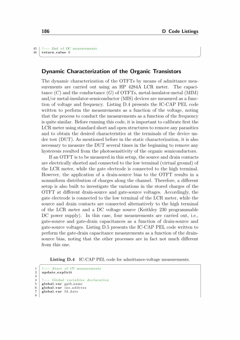
186 D Code Listings
45 !−−− End o f DC measurements46 return value 0
Dynamic Characterization of the Organic Transistors
The dynamic characterization of the OTFTs by means of admittance mea-surements are carried out using an HP 4284A LCR meter. The capaci-tance (C) and the conductance (G) of OTFTs, metal-insulator-metal (MIM)and/or metal-insulator-semiconductor (MIS) devices are measured as a func-tion of voltage and frequency. Listing D.4 presents the IC-CAP PEL codewritten to perform the measurements as a function of the voltage, notingthat the process to conduct the measurements as a function of the frequencyis quite similar. Before running this code, it is important to calibrate first theLCR meter using standard short and open structures to remove any parasiticsand to obtain the desired characteristics at the terminals of the device un-der test (DUT). As mentioned before in the static characterization, it is alsonecessary to measure the DUT several times in the beginning to remove anyhysteresis resulted from the photosensitivity of the organic semiconductors.
If an OTFT is to be measured in this setup, the source and drain contactsare electrically shorted and connected to the low terminal (virtual ground) ofthe LCR meter, while the gate electrode is connected to the high terminal.However, the application of a drain-source bias to the OTFT results in anonuniform distribution of charges along the channel. Therefore, a differentsetup is also built to investigate the variations in the stored charges of theOTFT at different drain-source and gate-source voltages. Accordingly, thegate electrode is connected to the low terminal of the LCR meter, while thesource and drain contacts are connected alternatively to the high terminalof the LCR meter and a DC voltage source (Keithley 230 programmableDC power supply). In this case, four measurements are carried out, i.e.,gate-source and gate-drain capacitances as a function of drain-source andgate-source voltages. Listing D.5 presents the IC-CAP PEL code written toperform the gate-drain capacitance measurements as a function of the drain-source bias, noting that the other processes are in fact not much differentfrom this one.
Listing D.4 IC-CAP PEL code for admittance-voltage measurements.1 !−−− Star t o f CV measurements2 update explicit34 !−−− Global v a r i a b l e s d e c l a r a t i o n5 global var gpib name6 global var i n s a d d r e s s7 global var f d da t e8
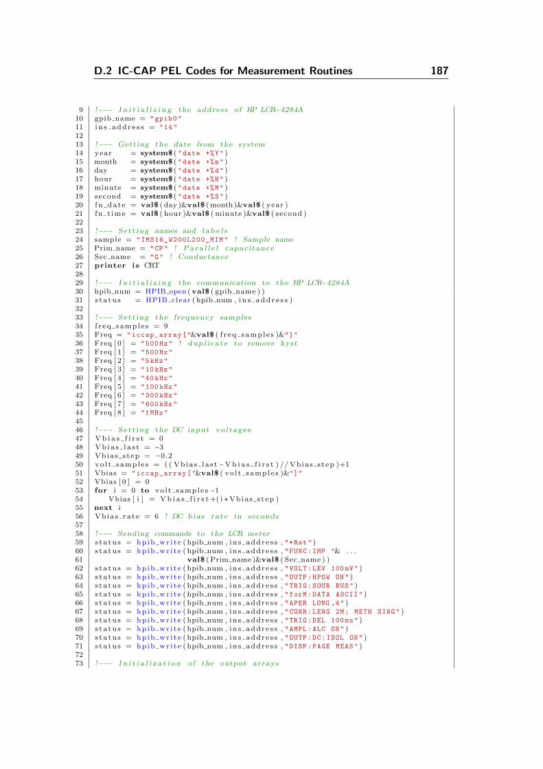
D.2 IC-CAP PEL Codes for Measurement Routines 187
9 !−−− I n i t i a l i z i n g the address o f HP LCR−4284A10 gpib name = "gpib0"
11 i n s a d d r e s s = "14"
1213 !−−− Getting the date from the system14 year = system$ ( "date +%Y" )15 month = system$ ( "date +%m" )16 day = system$ ( "date +%d" )17 hour = system$ ( "date +%H" )18 minute = system$ ( "date +%M" )19 second = system$ ( "date +%S" )20 fn da t e = val$ ( day )&val$ (month)&val$ ( year )21 fn t ime = val$ ( hour )&val$ ( minute )&val$ ( second )2223 !−−− Se t t i ng names and l a b e l s24 sample = "IMS16_W200L200_MIM " ! Sample name25 Prim name = "CP" ! P a r a l l e l capac i tance26 Sec name = "G" ! Conductance27 printer i s CRT2829 !−−− I n i t i a l i z i n g the communication to the HP LCR−4284A30 hpib num = HPIB open (val$ ( gpib name ) )31 s t a t u s = HPIB clear ( hpib num , i n s a d d r e s s )3233 !−−− Se t t i ng the f requency samples34 f r eq samp l e s = 935 Freq = "iccap_array["&val$ ( f r eq samp l e s )&"]"
36 Freq [ 0 ] = "500Hz" ! dup l i c a t e to remove hyst37 Freq [ 1 ] = "500Hz"
38 Freq [ 2 ] = "5kHz"
39 Freq [ 3 ] = "10kHz"
40 Freq [ 4 ] = "40kHz"
41 Freq [ 5 ] = "100 kHz"
42 Freq [ 6 ] = "300 kHz"
43 Freq [ 7 ] = "600 kHz"
44 Freq [ 8 ] = "1MHz"
4546 !−−− Se t t i ng the DC input vo l t ag e s47 V b i a s f i r s t = 048 V b i a s l a s t = −349 Vbias s tep = −0.250 vo l t s amp l e s = ( ( Vb ia s l a s t −V b i a s f i r s t ) // Vbias s tep )+151 Vbias = "iccap_array["&val$ ( vo l t s amp l e s )&"]"
52 Vbias [ 0 ] = 053 for i = 0 to vo l t samples −154 Vbias [ i ] = V b i a s f i r s t +( i ∗ Vbias s tep )55 next i56 Vb ia s ra t e = 6 ! DC b ia s ra t e in seconds5758 !−−− Sending commands to the LCR meter59 s t a t u s = hp ib wr i t e ( hpib num , in s addr e s s , "*Rst" )60 s t a t u s = hp ib wr i t e ( hpib num , in s addr e s s , "FUNC:IMP "& . . .61 val$ ( Prim name )&val$ ( Sec name ) )62 s t a t u s = hp ib wr i t e ( hpib num , in s addr e s s , "VOLT:LEV 100mV" )63 s t a t u s = hp ib wr i t e ( hpib num , in s addr e s s , "OUTP:HPOW ON" )64 s t a t u s = hp ib wr i t e ( hpib num , in s addr e s s , "TRIG:SOUR BUS" )65 s t a t u s = hp ib wr i t e ( hpib num , in s addr e s s , "forM:DATA ASCII " )66 s t a t u s = hp ib wr i t e ( hpib num , in s addr e s s , "APER LONG ,4" )67 s t a t u s = hp ib wr i t e ( hpib num , in s addr e s s , "CORR:LENG 2M; METH SING" )68 s t a t u s = hp ib wr i t e ( hpib num , in s addr e s s , "TRIG:DEL 100ms" )69 s t a t u s = hp ib wr i t e ( hpib num , in s addr e s s , "AMPL:ALC ON" )70 s t a t u s = hp ib wr i t e ( hpib num , in s addr e s s , "OUTP:DC:ISOL ON" )71 s t a t u s = hp ib wr i t e ( hpib num , in s addr e s s , "DISP:PAGE MEAS" )7273 !−−− I n i t i a l i z a t i o n o f the output ar rays

188 D Code Listings
74 prim meas = "iccap_array["&val$ ( vo l t s amp l e s ∗ f r eq samp l e s )&"]"
75 sec meas = "iccap_array["&val$ ( vo l t s amp l e s ∗ f r eq samp l e s )&"]"
76 prim meas [ 0 ] = ""
77 sec meas [ 0 ] = ""
78 dummy=07980 !−−− Loop to measure at each f requency sample81 for f r e q i d x = 0 to f r eq sample s −182 ! Pr int header83 print ""
84 print "------------------"
85 print "Freq["&val$ ( f r e q i d x )&"] = "&val$ ( Freq [ f r e q i d x ] )86 print "------------------"
87 print ""
8889 ! Def ine bu f f e r90 s t a t u s = hp ib wr i t e ( hpib num , in s addr e s s , "MEM:DIM DBUF ,"& . . .91 val$ ( f r eq samp l e s ∗ vo l t s amp l e s ) )92 s t a t u s = hp ib wr i t e ( hpib num , in s addr e s s , "MEM:FILL DBUF" )93 s t a t u s = hp ib wr i t e ( hpib num , in s addr e s s , "FREQ "&val$ ( Freq [ f r e q i d x ] ) )9495 ! Loop to measure at each DC vo l tage96 for v o l t i d x = 0 to vo l t samples −197 print "Measuring at Vbias["&val$ ( v o l t i d x )&"] = "& . . .98 val$ ( Vbias [ v o l t i d x ] )&"V"
99 s t a t u s = hp ib wr i t e ( hpib num , in s addr e s s , "BIAS:STATE OFF" )100 s t a t u s = hp ib wr i t e ( hpib num , in s addr e s s , "BIAS:VOLT "& . . .101 val$ ( Vbias [ v o l t i d x ] ) )102 s t a t u s = hp ib wr i t e ( hpib num , in s addr e s s , "BIAS:STATE ON" )103 s t a t u s = hp ib wr i t e ( hpib num , in s addr e s s , "trig" )104 dummy = wait ( Vb ia s ra t e )105 next v o l t i d x106107 ! Ask LCR meter f o r measured data108 s t a t u s = hp ib wr i t e ( hpib num , in s addr e s s , "MEM:READ? DBUF" )109110 ! Loop to read the measurements at each DC vo l tage111 for v o l t i d x = 0 to ( vo l t samples −1)112 s t a t u s = hpib read ( hpib num , in s addr e s s , 1 2 , "A" , . . .113 prim meas [ f r e q i d x ∗ vo l t s amp l e s+v o l t i d x ] )114 s t a t u s = hpib read ( hpib num , in s addr e s s , 1 , "A" ,dummy)115 s t a t u s = hpib read ( hpib num , in s addr e s s , 1 2 , "A" , . . .116 sec meas [ f r e q i d x ∗ vo l t s amp l e s+v o l t i d x ] )117 s t a t u s = hpib read ( hpib num , in s addr e s s , 7 , "A" ,dummy)118119 i f prim meas [ f r e q i d x ∗ vo l t s amp l e s+v o l t i d x ] == +9.90000E+37 then120 prim meas [ f r e q i d x ∗ vo l t s amp l e s+v o l t i d x ] = 0121 end i f122 i f sec meas [ f r e q i d x ∗ vo l t s amp l e s+v o l t i d x ] == +9.90000E+37 then123 sec meas [ f r e q i d x ∗ vo l t s amp l e s+v o l t i d x ] = 0124 end i f125126 print ""
127 print "Vbias["&val$ ( v o l t i d x )&"] = "&val$ ( Vbias [ v o l t i d x ] )128 print "" , "PRIM("&val$ ( f r e q i d x ∗ vo l t s amp l e s+v o l t i d x )&") = "& . . .129 val$ ( prim meas [ f r e q i d x ∗ vo l t s amp l e s+v o l t i d x ] )130 print "" , "SEC("&val$ ( f r e q i d x ∗ vo l t s amp l e s+v o l t i d x )&") = "& . . .131 val$ ( sec meas [ f r e q i d x ∗ vo l t s amp l e s+v o l t i d x ] )132 next v o l t i d x133134 ! Clear data bu f f e r135 s t a t u s = hp ib wr i t e ( hpib num , in s addr e s s , "MEM:CLE DBUF" )136 next f r e q i d x137138 !−−− Set DC b ia s s t a t e to o f f

D.2 IC-CAP PEL Codes for Measurement Routines 189
139 s t a t u s = hp ib wr i t e ( hpib num , in s addr e s s , "BIAS:STATE OFF" )140141 !−−− Print measured data to a f i l e142 path = "C:/ Agilent/user/Zaki/AC_Measurements/"& . . .143 val$ ( sample )&"_CV_Meas_ "&val$ ( f n da t e )144 op d i r = sys path$ (val$ ( path ) )145 dummy = system ( "mkdir -p "&val$ ( path ) )146147 !−−− Create output f i l e d i r e c t o r y f o r the primary parameter148 pr im op d i r = path&"/"&val$ ( sample )&"_CV_"&val$ ( Prim name )& . . .149 "_V"&val$ ( vo l t s amp l e s )&"F"&val$ ( f r eq samp l e s )& . . .150 "_"&val$ ( fn t ime )&".txt"
151 pr im op d i r = sys path$ (val$ ( pr im op d i r ) )152 dummy = system ( "rm -f "&val$ ( pr im op d i r )&" 2> /dev/null" )153 dummy = system ( "touch "&val$ ( pr im op d i r ) )154155 !−−− Create output f i l e d i r e c t o r y f o r the secondary parameter156 s e c o p d i r = path&"/"&val$ ( sample )&"_CV_"&val$ ( Sec name )& . . .157 "_V"&val$ ( vo l t s amp l e s )&"F"&val$ ( f r eq samp l e s )& . . .158 "_"&val$ ( fn t ime )&".txt"
159 s e c o p d i r = sys path$ (val$ ( s e c o p d i r ) )160 dummy = system ( "rm -f "&val$ ( s e c o p d i r )&" 2> /dev/null" )161 dummy = system ( "touch "&val$ ( s e c o p d i r ) )162163 !−−− Writing headers to the output f i l e s164 Header1 = "Vbias [V]"
165 Header2 = "Vbias [V]"
166 Subhead = ""
167 for f r e q i d x = 0 to f r eq sample s −1168 Header1 = Header1&" "&val$ ( Prim name )169 Header2 = Header2&" "&val$ ( Sec name )170 Subhead = Subhead&" freq="&val$ ( Freq [ f r e q i d x ] )171 next f r e q i d x172 printer i s val$ ( pr im op d i r )173 print Header1174 print Subhead175 printer i s val$ ( s e c o p d i r )176 print Header2177 print Subhead178 printer i s CRT179180 !−−− Write measured data to the output f i l e s181 for i = 0 to vo l t samples −1182 prim textbody = val$ ( Vbias [ i ] )183 sec textbody = val$ ( Vbias [ i ] )184 for k = 0 to f r eq sample s −1185 prim textbody = prim textbody&" "&val$ ( prim meas [ i+k∗ vo l t s amp l e s ] )186 sec textbody = sec textbody&" "&val$ ( sec meas [ i+k∗ vo l t s amp l e s ] )187 next k188 printer i s val$ ( pr im op d i r )189 print prim textbody190 printer i s val$ ( s e c o p d i r )191 print s ec textbody192 next i193 printer i s CRT194195196 !−−− Plot the data in IC−CAP197 for i = 0 to f r eq sample s −1198 ! Trim the un i t from the value199 Freq [ i ] = trim$ (val$ ( Freq [ i ] ) , "Hz" )200 l eng = strlen (val$ ( Freq [ i ] ) )201 ! In IC−CAP 1e6 i s r ep r e s en ted by MEG and not M202 i f substr$ (val$ ( Freq [ i ] ) , l eng ) == "M" then203 Freq [ i ] = substr$ (val$ ( Freq [ i ] ) , 1 , leng −1)&"MEG"
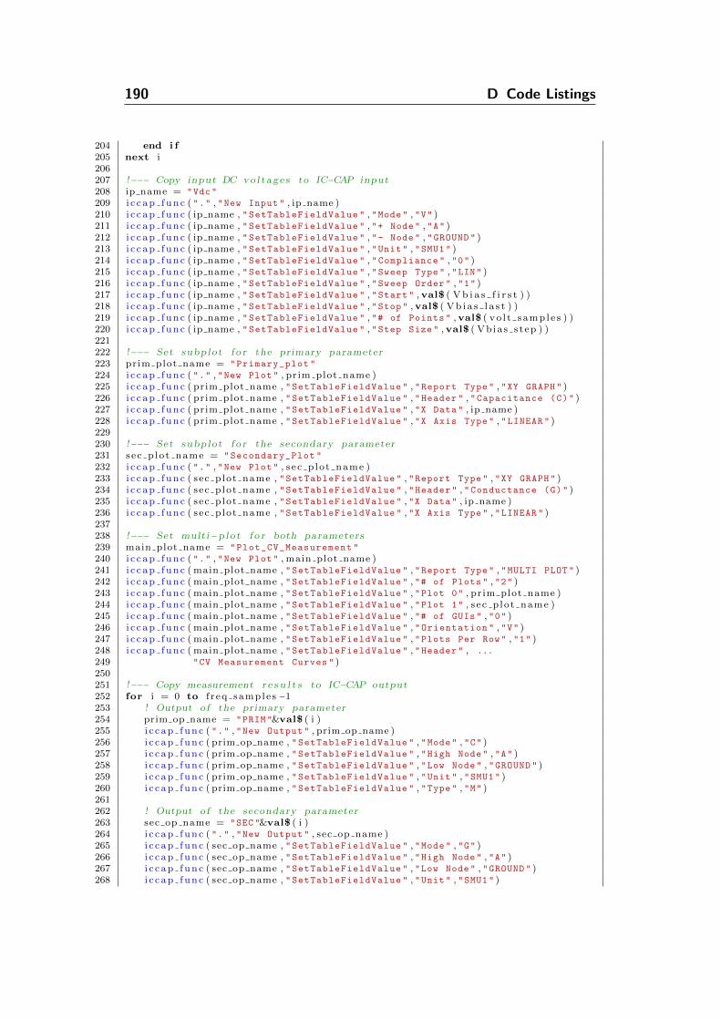
190 D Code Listings
204 end i f205 next i206207 !−−− Copy input DC vo l t ag e s to IC−CAP input208 ip name = "Vdc"
209 i c c a p f u n c ( "." , "New Input" , ip name )210 i c c a p f u n c ( ip name , "SetTableFieldValue " , "Mode" , "V" )211 i c c a p f u n c ( ip name , "SetTableFieldValue " , "+ Node" , "A" )212 i c c a p f u n c ( ip name , "SetTableFieldValue " , "- Node" , "GROUND " )213 i c c a p f u n c ( ip name , "SetTableFieldValue " , "Unit" , "SMU1" )214 i c c a p f u n c ( ip name , "SetTableFieldValue " , "Compliance " , "0" )215 i c c a p f u n c ( ip name , "SetTableFieldValue " , "Sweep Type" , "LIN" )216 i c c a p f u n c ( ip name , "SetTableFieldValue " , "Sweep Order" , "1" )217 i c c a p f u n c ( ip name , "SetTableFieldValue " , "Start" ,val$ ( V b i a s f i r s t ) )218 i c c a p f u n c ( ip name , "SetTableFieldValue " , "Stop" ,val$ ( V b i a s l a s t ) )219 i c c a p f u n c ( ip name , "SetTableFieldValue " , "# of Points " ,val$ ( vo l t s amp l e s ) )220 i c c a p f u n c ( ip name , "SetTableFieldValue " , "Step Size" ,val$ ( Vbias s tep ) )221222 !−−− Set subplot f o r the primary parameter223 prim plot name = "Primary_plot "
224 i c c a p f u n c ( "." , "New Plot" , pr im plot name )225 i c c a p f u n c ( prim plot name , "SetTableFieldValue " , "Report Type" , "XY GRAPH" )226 i c c a p f u n c ( prim plot name , "SetTableFieldValue " , "Header " , "Capacitance (C)" )227 i c c a p f u n c ( prim plot name , "SetTableFieldValue " , "X Data" , ip name )228 i c c a p f u n c ( prim plot name , "SetTableFieldValue " , "X Axis Type" , "LINEAR " )229230 !−−− Set subplot f o r the secondary parameter231 sec p lot name = "Secondary_Plot "
232 i c c a p f u n c ( "." , "New Plot" , s ec p lot name )233 i c c a p f u n c ( sec plot name , "SetTableFieldValue " , "Report Type" , "XY GRAPH" )234 i c c a p f u n c ( sec plot name , "SetTableFieldValue " , "Header " , "Conductance (G)" )235 i c c a p f u n c ( sec plot name , "SetTableFieldValue " , "X Data" , ip name )236 i c c a p f u n c ( sec plot name , "SetTableFieldValue " , "X Axis Type" , "LINEAR " )237238 !−−− Set multi −p lo t f o r both parameters239 main plot name = "Plot_CV_Measurement "
240 i c c a p f u n c ( "." , "New Plot" , main plot name )241 i c c a p f u n c ( main plot name , "SetTableFieldValue " , "Report Type" , "MULTI PLOT" )242 i c c a p f u n c ( main plot name , "SetTableFieldValue " , "# of Plots" , "2" )243 i c c a p f u n c ( main plot name , "SetTableFieldValue " , "Plot 0" , pr im plot name )244 i c c a p f u n c ( main plot name , "SetTableFieldValue " , "Plot 1" , s ec p lot name )245 i c c a p f u n c ( main plot name , "SetTableFieldValue " , "# of GUIs" , "0" )246 i c c a p f u n c ( main plot name , "SetTableFieldValue " , "Orientation " , "V" )247 i c c a p f u n c ( main plot name , "SetTableFieldValue " , "Plots Per Row" , "1" )248 i c c a p f u n c ( main plot name , "SetTableFieldValue " , "Header " , . . .249 "CV Measurement Curves " )250251 !−−− Copy measurement r e s u l t s to IC−CAP output252 for i = 0 to f r eq sample s −1253 ! Output o f the primary parameter254 prim op name = "PRIM"&val$ ( i )255 i c c a p f u n c ( "." , "New Output " , prim op name )256 i c c a p f u n c ( prim op name , "SetTableFieldValue " , "Mode" , "C" )257 i c c a p f u n c ( prim op name , "SetTableFieldValue " , "High Node" , "A" )258 i c c a p f u n c ( prim op name , "SetTableFieldValue " , "Low Node" , "GROUND " )259 i c c a p f u n c ( prim op name , "SetTableFieldValue " , "Unit" , "SMU1" )260 i c c a p f u n c ( prim op name , "SetTableFieldValue " , "Type" , "M" )261262 ! Output o f the secondary parameter263 sec op name = "SEC"&val$ ( i )264 i c c a p f u n c ( "." , "New Output " , sec op name )265 i c c a p f u n c ( sec op name , "SetTableFieldValue " , "Mode" , "G" )266 i c c a p f u n c ( sec op name , "SetTableFieldValue " , "High Node" , "A" )267 i c c a p f u n c ( sec op name , "SetTableFieldValue " , "Low Node" , "GROUND " )268 i c c a p f u n c ( sec op name , "SetTableFieldValue " , "Unit" , "SMU1" )
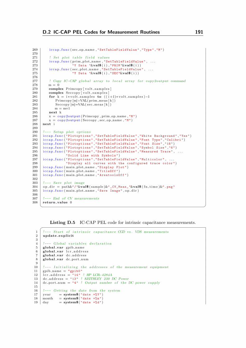
D.2 IC-CAP PEL Codes for Measurement Routines 191
269 i c c a p f u n c ( sec op name , "SetTableFieldValue " , "Type" , "M" )270271 ! Set p l o t t ab l e f i e l d va lue s272 i c c a p f u n c ( prim plot name , "SetTableFieldValue " , . . .273 "Y Data "&val$ ( i ) , "PRIM"&val$ ( i ) )274 i c c a p f u n c ( sec plot name , "SetTableFieldValue " , . . .275 "Y Data "&val$ ( i ) , "SEC"&val$ ( i ) )276277 ! Copy IC−CAP g l oba l array to l o c a l array f o r copy2output command278 m = 0279 complex Primcopy [ vo l t s amp l e s ]280 complex Seccopy [ vo l t s amp l e s ]281 for k = i ∗ vo l t s amp l e s to ( ( i +1)∗ vo l t s amp l e s )−1282 Primcopy [m]=VAL( prim meas [ k ] )283 Seccopy [m]=VAL( sec meas [ k ] )284 m = m+1285 next k286 x = copy2output ( Primcopy , prim op name , "M" )287 x = copy2output ( Seccopy , sec op name , "M" )288 next i289290 !−−− Setup p lo t opt ions291 i c c a p f u n c ( "Plotoptions " , "SetTableFieldValue " , "White Background " , "Yes" )292 i c c a p f u n c ( "Plotoptions " , "SetTableFieldValue " , "Font Type" , "Calibri " )293 i c c a p f u n c ( "Plotoptions " , "SetTableFieldValue " , "Font Size" , "18" )294 i c c a p f u n c ( "Plotoptions " , "SetTableFieldValue " , "Symbol Size" , "6" )295 i c c a p f u n c ( "Plotoptions " , "SetTableFieldValue " , "Measured Trace " , . . .296 "Solid Line with Symbols " )297 i c c a p f u n c ( "Plotoptions " , "SetTableFieldValue " , "Multicolor " , . . .298 "Display all curves with the configured trace color" )299 i c c a p f u n c ( main plot name , "Display Plot" )300 i c c a p f u n c ( main plot name , "TitleOff " )301 i c c a p f u n c ( main plot name , "AreatoolsOff " )302303 !−−− Save p l o t image304 op d i r = path&"/"&val$ ( sample )&"_CV_Meas_ "&val$ ( fn t ime )&".png"
305 i c c a p f u n c ( main plot name , "Save Image " , op d i r )306307 !−−− End o f CV measurements308 return value 0
Listing D.5 IC-CAP PEL code for intrinsic capacitance measurements.1 !−−− Star t o f i n t r i n s i c capac i tance CGD vs . VDS measurements2 update explicit34 !−−− Global v a r i a b l e s d e c l a r a t i o n5 global var gpib name6 global var l c r a d d r e s s7 global var dc addre s s8 global var dc port num9
10 !−−− I n i t i a l i z i n g the addre s s e s o f the measurement equipment11 gpib name = "gpib0"
12 l c r a d d r e s s = "14" ! HP LCR−4284A13 dc addre s s = "13" ! KEITHLEY 230 DC Power14 dc port num = "4" ! Output number o f the DC power supply1516 !−−− Getting the date from the system17 year = system$ ( "date +%Y" )18 month = system$ ( "date +%m" )19 day = system$ ( "date +%d" )
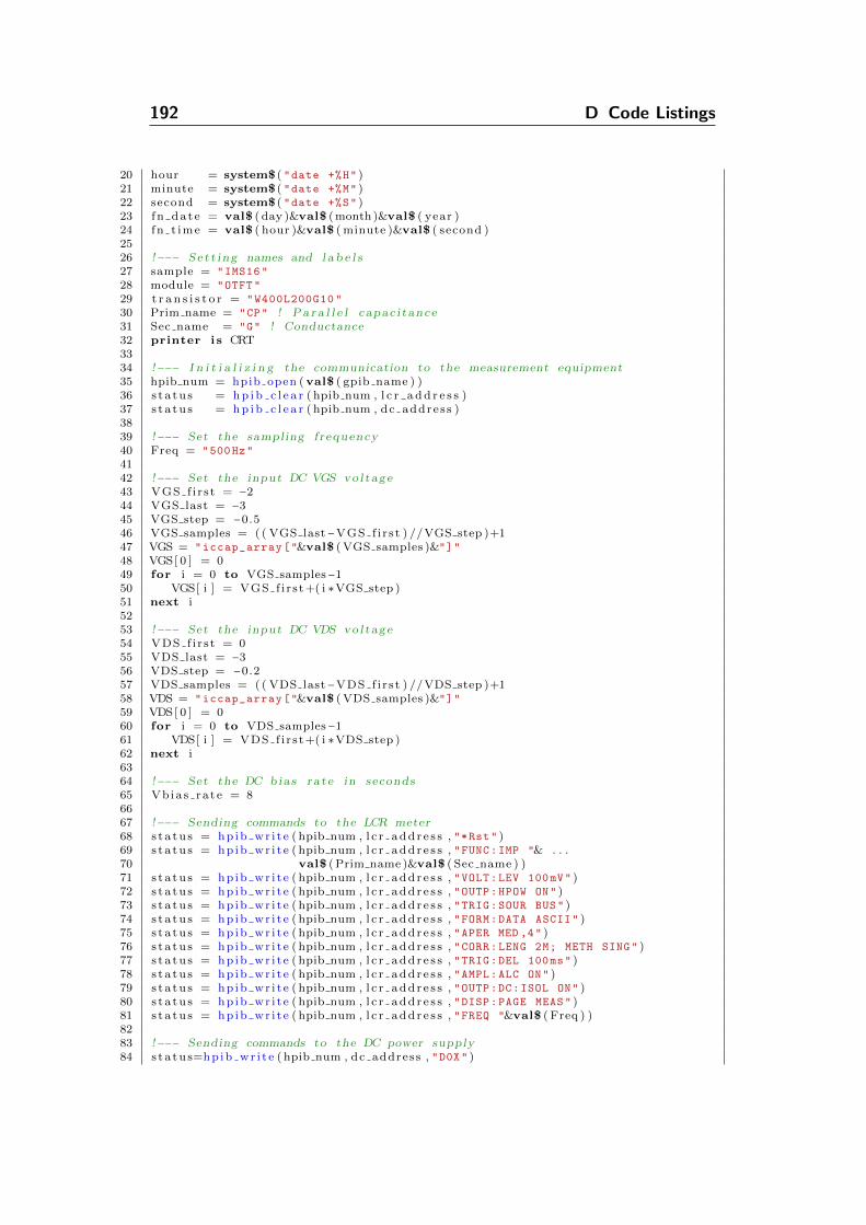
192 D Code Listings
20 hour = system$ ( "date +%H" )21 minute = system$ ( "date +%M" )22 second = system$ ( "date +%S" )23 fn da t e = val$ ( day )&val$ (month)&val$ ( year )24 fn t ime = val$ ( hour )&val$ ( minute )&val$ ( second )2526 !−−− Se t t i ng names and l a b e l s27 sample = "IMS16"
28 module = "OTFT"
29 t r a n s i s t o r = "W400L200G10 "
30 Prim name = "CP" ! P a r a l l e l capac i tance31 Sec name = "G" ! Conductance32 printer i s CRT3334 !−−− I n i t i a l i z i n g the communication to the measurement equipment35 hpib num = hpib open (val$ ( gpib name ) )36 s t a t u s = h p i b c l e a r ( hpib num , l c r a d d r e s s )37 s t a t u s = h p i b c l e a r ( hpib num , dc addre s s )3839 !−−− Set the sampling f requency40 Freq = "500Hz"
4142 !−−− Set the input DC VGS vo l tage43 VGS f i r s t = −244 VGS last = −345 VGS step = −0.546 VGS samples = ( ( VGS last−VGS f i r s t ) //VGS step )+147 VGS = "iccap_array["&val$ ( VGS samples )&"]"
48 VGS[ 0 ] = 049 for i = 0 to VGS samples−150 VGS[ i ] = VGS f i r s t+( i ∗VGS step )51 next i5253 !−−− Set the input DC VDS vo l tage54 VDS f i r s t = 055 VDS last = −356 VDS step = −0.257 VDS samples = ( ( VDS last−VDS f i r s t ) //VDS step )+158 VDS = "iccap_array["&val$ ( VDS samples )&"]"
59 VDS[ 0 ] = 060 for i = 0 to VDS samples−161 VDS[ i ] = VDS f i r s t+( i ∗VDS step )62 next i6364 !−−− Set the DC b ia s ra t e in seconds65 Vb ia s ra t e = 86667 !−−− Sending commands to the LCR meter68 s t a t u s = hp ib wr i t e ( hpib num , l c r a d d r e s s , "*Rst" )69 s t a t u s = hp ib wr i t e ( hpib num , l c r a d d r e s s , "FUNC:IMP "& . . .70 val$ ( Prim name )&val$ ( Sec name ) )71 s t a t u s = hp ib wr i t e ( hpib num , l c r a d d r e s s , "VOLT:LEV 100mV" )72 s t a t u s = hp ib wr i t e ( hpib num , l c r a d d r e s s , "OUTP:HPOW ON" )73 s t a t u s = hp ib wr i t e ( hpib num , l c r a d d r e s s , "TRIG:SOUR BUS" )74 s t a t u s = hp ib wr i t e ( hpib num , l c r a d d r e s s , "FORM:DATA ASCII " )75 s t a t u s = hp ib wr i t e ( hpib num , l c r a d d r e s s , "APER MED ,4" )76 s t a t u s = hp ib wr i t e ( hpib num , l c r a d d r e s s , "CORR:LENG 2M; METH SING" )77 s t a t u s = hp ib wr i t e ( hpib num , l c r a d d r e s s , "TRIG:DEL 100ms" )78 s t a t u s = hp ib wr i t e ( hpib num , l c r a d d r e s s , "AMPL:ALC ON" )79 s t a t u s = hp ib wr i t e ( hpib num , l c r a d d r e s s , "OUTP:DC:ISOL ON" )80 s t a t u s = hp ib wr i t e ( hpib num , l c r a d d r e s s , "DISP:PAGE MEAS" )81 s t a t u s = hp ib wr i t e ( hpib num , l c r a d d r e s s , "FREQ "&val$ ( Freq ) )8283 !−−− Sending commands to the DC power supply84 s t a t u s=hp ib wr i t e ( hpib num , dc address , "D0X" )
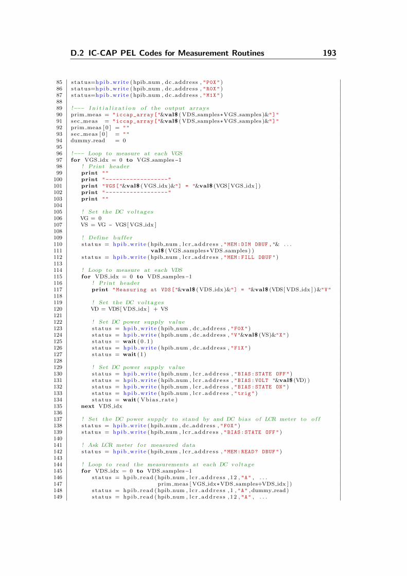
D.2 IC-CAP PEL Codes for Measurement Routines 193
85 s t a t u s=hp ib wr i t e ( hpib num , dc address , "P0X" )86 s t a t u s=hp ib wr i t e ( hpib num , dc address , "R0X" )87 s t a t u s=hp ib wr i t e ( hpib num , dc address , "M1X" )8889 !−−− I n i t i a l i z a t i o n o f the output ar rays90 prim meas = "iccap_array["&val$ ( VDS samples∗VGS samples )&"]"
91 sec meas = "iccap_array["&val$ ( VDS samples∗VGS samples )&"]"
92 prim meas [ 0 ] = ""
93 sec meas [ 0 ] = ""
94 dummy read = 09596 !−−− Loop to measure at each VGS97 for VGS idx = 0 to VGS samples−198 ! Pr int header99 print ""
100 print "------------------"
101 print "VGS["&val$ ( VGS idx )&"] = "&val$ (VGS[ VGS idx ] )102 print "------------------"
103 print ""
104105 ! Set the DC vo l t ag e s106 VG = 0107 VS = VG − VGS[ VGS idx ]108109 ! Def ine bu f f e r110 s t a t u s = hp ib wr i t e ( hpib num , l c r a d d r e s s , "MEM:DIM DBUF ,"& . . .111 val$ ( VGS samples∗VDS samples ) )112 s t a t u s = hp ib wr i t e ( hpib num , l c r a d d r e s s , "MEM:FILL DBUF" )113114 ! Loop to measure at each VDS115 for VDS idx = 0 to VDS samples−1116 ! Pr int header117 print "Measuring at VDS["&val$ ( VDS idx )&"] = "&val$ (VDS[ VDS idx ] )&"V"
118119 ! Set the DC vo l t ag e s120 VD = VDS[ VDS idx ] + VS121122 ! Set DC power supply value123 s t a t u s = hp ib wr i t e ( hpib num , dc address , "F0X" )124 s t a t u s = hp ib wr i t e ( hpib num , dc address , "V"&val$ (VS)&"X" )125 s t a t u s = wait ( 0 . 1 )126 s t a t u s = hp ib wr i t e ( hpib num , dc address , "F1X" )127 s t a t u s = wait (1 )128129 ! Set DC power supply value130 s t a t u s = hp ib wr i t e ( hpib num , l c r a d d r e s s , "BIAS:STATE OFF" )131 s t a t u s = hp ib wr i t e ( hpib num , l c r a d d r e s s , "BIAS:VOLT "&val$ (VD) )132 s t a t u s = hp ib wr i t e ( hpib num , l c r a d d r e s s , "BIAS:STATE ON" )133 s t a t u s = hp ib wr i t e ( hpib num , l c r a d d r e s s , "trig" )134 s t a t u s = wait ( Vb ia s ra t e )135 next VDS idx136137 ! Set the DC power supply to stand by and DC bia s o f LCR meter to o f f138 s t a t u s = hp ib wr i t e ( hpib num , dc address , "F0X" )139 s t a t u s = hp ib wr i t e ( hpib num , l c r a d d r e s s , "BIAS:STATE OFF" )140141 ! Ask LCR meter f o r measured data142 s t a t u s = hp ib wr i t e ( hpib num , l c r a d d r e s s , "MEM:READ? DBUF" )143144 ! Loop to read the measurements at each DC vo l tage145 for VDS idx = 0 to VDS samples−1146 s t a t u s = hpib read ( hpib num , l c r a d d r e s s , 1 2 , "A" , . . .147 prim meas [ VGS idx∗VDS samples+VDS idx ] )148 s t a t u s = hpib read ( hpib num , l c r a d d r e s s , 1 , "A" , dummy read )149 s t a t u s = hpib read ( hpib num , l c r a d d r e s s , 1 2 , "A" , . . .

194 D Code Listings
150 sec meas [ VGS idx∗VDS samples+VDS idx ] )151 s t a t u s = hpib read ( hpib num , l c r a d d r e s s , 7 , "A" , dummy read )152153 i f prim meas [ VGS idx∗VDS samples+VDS idx ] == +9.90000E+37 then154 prim meas [ VGS idx∗VDS samples+VDS idx ] = 0155 end i f156 i f sec meas [ VGS idx∗VDS samples+VDS idx ] == +9.90000E+37 then157 sec meas [ VGS idx∗VDS samples+VDS idx ] = 0158 end i f159160 print ""
161 print "VDS["&val$ ( VDS idx )&"] = "&val$ (VDS[ VDS idx ] )162 print "" , "PRIM("&val$ ( VGS idx∗VDS samples+VDS idx )&") = "& . . .163 val$ ( prim meas [ VGS idx∗VDS samples+VDS idx ] )164 print "" , "SEC("&val$ ( VGS idx∗VDS samples+VDS idx )&") = "& . . .165 val$ ( sec meas [ VGS idx∗VDS samples+VDS idx ] )166 next VDS idx167168 ! Clear data bu f f e r169 s t a t u s = hp ib wr i t e ( hpib num , l c r a d d r e s s , "MEM:CLE DBUF" )170 next VGS idx171172 ! Set to l o c a l mode and terminate HPIB communication173 s t a t u s = hp ib wr i t e ( hpib num , dc address , "X" )174 s t a t u s = hpib command ( hpib num , 1 , dc addre s s )175 s t a t u s = h p i b c l o s e ( hpib num , dc addre s s )176 s t a t u s = h p i b c l o s e ( hpib num , l c r a d d r e s s )177178 !−−− Print measured data to a f i l e179 path = "C:/ Agilent/user/Zaki/AC_Measurements/"& . . .180 val$ ( sample )&"_CGD_vs_VDS_ "&val$ ( f n da t e )181 op d i r = sys path$ (val$ ( path ) )182 dummy = system ( "mkdir -p "&val$ ( path ) )183184 !−−− Create output f i l e d i r e c t o r y f o r the primary parameter185 pr im op d i r = path&"/"&val$ ( sample )&"_"&val$ ( module )&"_"& . . .186 val$ ( t r a n s i s t o r )&"_CGD_vs_VDS_ "&"VDS"& . . .187 val$ ( VDS samples )&"VGS"&val$ ( VGS samples )&"_"& . . .188 val$ ( fn t ime )&".txt"
189 pr im op d i r = sys path$ (val$ ( pr im op d i r ) )190 dummy = system ( "rm -f "&val$ ( pr im op d i r )&" 2> /dev/null" )191 dummy = system ( "touch "&val$ ( pr im op d i r ) )192193 !−−− Create output f i l e d i r e c t o r y f o r the secondary parameter194 s e c o p d i r = path&"/"&val$ ( sample )&"_"&val$ ( module )&"_"& . . .195 val$ ( t r a n s i s t o r )&"_GGD_vs_VDS_ "&"VDS"& . . .196 val$ ( VDS samples )&"VGS"&val$ ( VGS samples )&"_"& . . .197 val$ ( fn t ime )&".txt"
198 s e c o p d i r = sys path$ (val$ ( s e c o p d i r ) )199 dummy = system ( "rm -f "&val$ ( s e c o p d i r )&" 2> /dev/null" )200 dummy = system ( "touch "&val$ ( s e c o p d i r ) )201202 !−−− Writing headers to the output f i l e s203 Header1 = "VDS [V]"
204 Header2 = "VDS [V]"
205 Subhead = ""
206 for VGS idx = 0 TO VGS samples−1207 Header1 = Header1&" "&val$ ( Prim name )208 Header2 = Header2&" "&val$ ( Sec name )209 Subhead = Subhead&" VGS="&val$ (VGS[ VGS idx ] )210 next VGS idx211 printer i s val$ ( pr im op d i r )212 print Header1213 print Subhead214 printer i s val$ ( s e c o p d i r )
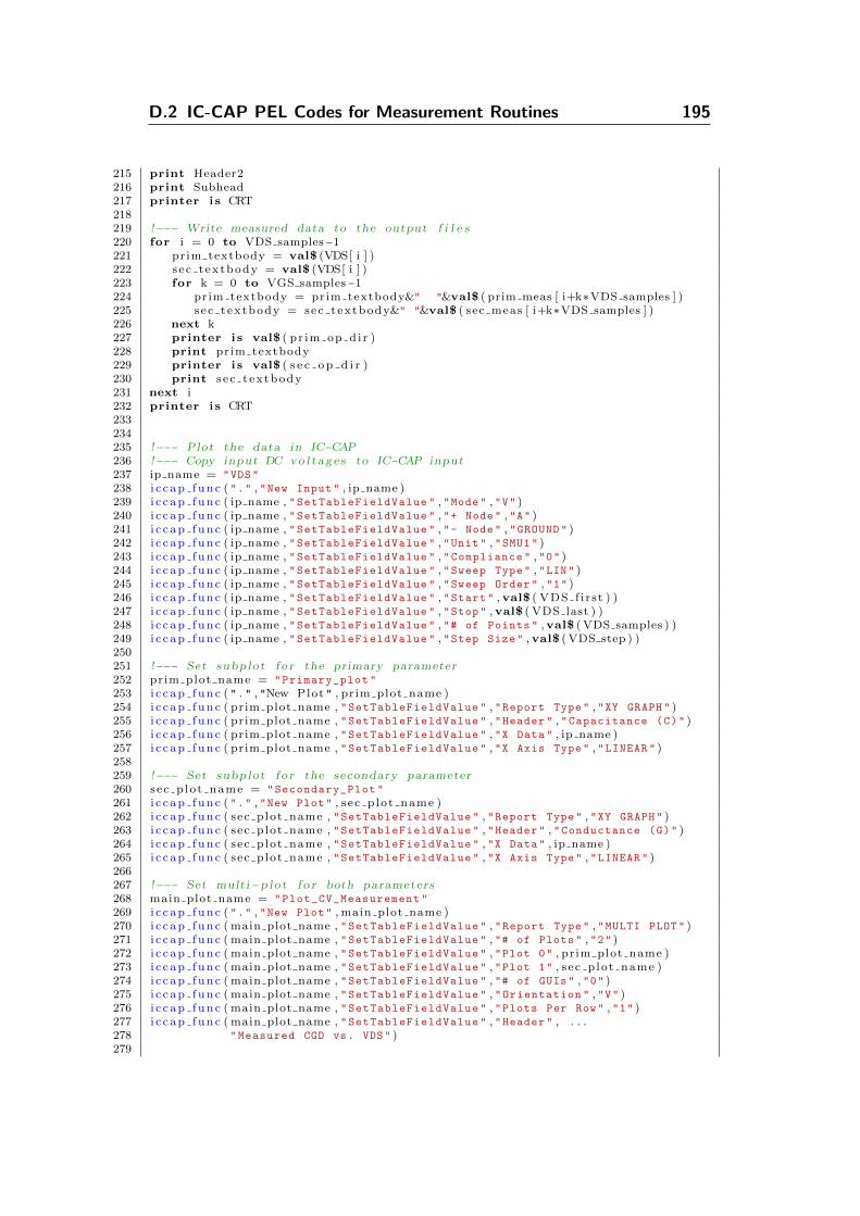
D.2 IC-CAP PEL Codes for Measurement Routines 195
215 print Header2216 print Subhead217 printer i s CRT218219 !−−− Write measured data to the output f i l e s220 for i = 0 to VDS samples−1221 prim textbody = val$ (VDS[ i ] )222 sec textbody = val$ (VDS[ i ] )223 for k = 0 to VGS samples−1224 prim textbody = prim textbody&" "&val$ ( prim meas [ i+k∗VDS samples ] )225 sec textbody = sec textbody&" "&val$ ( sec meas [ i+k∗VDS samples ] )226 next k227 printer i s val$ ( pr im op d i r )228 print prim textbody229 printer i s val$ ( s e c o p d i r )230 print s ec textbody231 next i232 printer i s CRT233234235 !−−− Plot the data in IC−CAP236 !−−− Copy input DC vo l t ag e s to IC−CAP input237 ip name = "VDS"
238 i c c a p f u n c ( "." , "New Input" , ip name )239 i c c a p f u n c ( ip name , "SetTableFieldValue " , "Mode" , "V" )240 i c c a p f u n c ( ip name , "SetTableFieldValue " , "+ Node" , "A" )241 i c c a p f u n c ( ip name , "SetTableFieldValue " , "- Node" , "GROUND " )242 i c c a p f u n c ( ip name , "SetTableFieldValue " , "Unit" , "SMU1" )243 i c c a p f u n c ( ip name , "SetTableFieldValue " , "Compliance " , "0" )244 i c c a p f u n c ( ip name , "SetTableFieldValue " , "Sweep Type" , "LIN" )245 i c c a p f u n c ( ip name , "SetTableFieldValue " , "Sweep Order" , "1" )246 i c c a p f u n c ( ip name , "SetTableFieldValue " , "Start" ,val$ ( VDS f i r s t ) )247 i c c a p f u n c ( ip name , "SetTableFieldValue " , "Stop" ,val$ ( VDS last ) )248 i c c a p f u n c ( ip name , "SetTableFieldValue " , "# of Points " ,val$ ( VDS samples ) )249 i c c a p f u n c ( ip name , "SetTableFieldValue " , "Step Size" ,val$ ( VDS step ) )250251 !−−− Set subplot f o r the primary parameter252 prim plot name = "Primary_plot "
253 i c c a p f u n c ( " . " , "New Plot " , pr im plot name )254 i c c a p f u n c ( prim plot name , "SetTableFieldValue " , "Report Type" , "XY GRAPH" )255 i c c a p f u n c ( prim plot name , "SetTableFieldValue " , "Header " , "Capacitance (C)" )256 i c c a p f u n c ( prim plot name , "SetTableFieldValue " , "X Data" , ip name )257 i c c a p f u n c ( prim plot name , "SetTableFieldValue " , "X Axis Type" , "LINEAR " )258259 !−−− Set subplot f o r the secondary parameter260 sec p lot name = "Secondary_Plot "
261 i c c a p f u n c ( "." , "New Plot" , s ec p lot name )262 i c c a p f u n c ( sec plot name , "SetTableFieldValue " , "Report Type" , "XY GRAPH" )263 i c c a p f u n c ( sec plot name , "SetTableFieldValue " , "Header " , "Conductance (G)" )264 i c c a p f u n c ( sec plot name , "SetTableFieldValue " , "X Data" , ip name )265 i c c a p f u n c ( sec plot name , "SetTableFieldValue " , "X Axis Type" , "LINEAR " )266267 !−−− Set multi −p lo t f o r both parameters268 main plot name = "Plot_CV_Measurement "
269 i c c a p f u n c ( "." , "New Plot" , main plot name )270 i c c a p f u n c ( main plot name , "SetTableFieldValue " , "Report Type" , "MULTI PLOT" )271 i c c a p f u n c ( main plot name , "SetTableFieldValue " , "# of Plots" , "2" )272 i c c a p f u n c ( main plot name , "SetTableFieldValue " , "Plot 0" , pr im plot name )273 i c c a p f u n c ( main plot name , "SetTableFieldValue " , "Plot 1" , s ec p lot name )274 i c c a p f u n c ( main plot name , "SetTableFieldValue " , "# of GUIs" , "0" )275 i c c a p f u n c ( main plot name , "SetTableFieldValue " , "Orientation " , "V" )276 i c c a p f u n c ( main plot name , "SetTableFieldValue " , "Plots Per Row" , "1" )277 i c c a p f u n c ( main plot name , "SetTableFieldValue " , "Header " , . . .278 "Measured CGD vs. VDS" )279

196 D Code Listings
280 !−−− Copy measurement r e s u l t s to IC−CAP output281 for i = 0 to VGS samples−1282 ! Output o f the primary parameter283 prim op name = "C_VGS"&val$ ( i )284 i c c a p f u n c ( "." , "New Output " , prim op name )285 i c c a p f u n c ( prim op name , "SetTableFieldValue " , "Mode" , "C" )286 i c c a p f u n c ( prim op name , "SetTableFieldValue " , "High Node" , "A" )287 i c c a p f u n c ( prim op name , "SetTableFieldValue " , "Low Node" , "GROUND " )288 i c c a p f u n c ( prim op name , "SetTableFieldValue " , "Unit" , "SMU1" )289 i c c a p f u n c ( prim op name , "SetTableFieldValue " , "Type" , "M" )290291 ! Output o f the secondary parameter292 sec op name = "G_VGS"&val$ ( i )293 i c c a p f u n c ( "." , "New Output " , sec op name )294 i c c a p f u n c ( sec op name , "SetTableFieldValue " , "Mode" , "G" )295 i c c a p f u n c ( sec op name , "SetTableFieldValue " , "High Node" , "A" )296 i c c a p f u n c ( sec op name , "SetTableFieldValue " , "Low Node" , "GROUND " )297 i c c a p f u n c ( sec op name , "SetTableFieldValue " , "Unit" , "SMU1" )298 i c c a p f u n c ( sec op name , "SetTableFieldValue " , "Type" , "M" )299300 ! Set p l o t t ab l e f i e l d va lue s301 i c c a p f u n c ( prim plot name , "SetTableFieldValue " , . . .302 "Y Data "&val$ ( i ) , "C_VGS"&val$ ( i ) )303 i c c a p f u n c ( sec plot name , "SetTableFieldValue " , . . .304 "Y Data "&val$ ( i ) , "G_VGS"&val$ ( i ) )305306 ! Copy IC−CAP g l oba l array to l o c a l array f o r copy2output command307 m = 0308 complex Primcopy [ VDS samples ]309 complex Seccopy [ VDS samples ]310 for k = i ∗VDS samples to ( ( i +1)∗VDS samples )−1311 Primcopy [m]=VAL( prim meas [ k ] )312 Seccopy [m]=VAL( sec meas [ k ] )313 m = m+1314 next k315 x = copy2output ( Primcopy , prim op name , "M" )316 x = copy2output ( Seccopy , sec op name , "M" )317 next i318319 !−−− Setup p lo t opt ions320 i c c a p f u n c ( "PlotOptions " , "SetTableFieldValue " , "White Background " , "Yes" )321 i c c a p f u n c ( "PlotOptions " , "SetTableFieldValue " , "Font Type" , "Calibri " )322 i c c a p f u n c ( "PlotOptions " , "SetTableFieldValue " , "Font Size" , "18" )323 i c c a p f u n c ( "PlotOptions " , "SetTableFieldValue " , "Symbol Size" , "6" )324 i c c a p f u n c ( "PlotOptions " , "SetTableFieldValue " , "Measured Trace " , . . .325 "Solid Line with Symbols " )326 i c c a p f u n c ( "PlotOptions " , "SetTableFieldValue " , "Multicolor " , . . .327 "Display all curves with the configured trace color" )328 i c c a p f u n c ( "." , "Close All" )329 i c c a p f u n c ( main plot name , "Display Plot" )330 i c c a p f u n c ( main plot name , "TitleOff " )331 i c c a p f u n c ( main plot name , "AreaToolsOff " )332333 !−−− Save p l o t image334 op d i r = path&"/"&val$ ( sample )&"_"&val$ ( module )&"_"& . . .335 val$ ( t r a n s i s t o r )&"_CGD_vs_VDS_ "&"VDS"& . . .336 val$ ( VDS samples )&"VGS"&val$ ( VGS samples )&"_"& . . .337 val$ ( fn t ime )&".png"
338 i c c a p f u n c ( main plot name , "Save Image " , op d i r )339340 !−−− End o f i n t r i n s i c capac i tance CGD vs . VDS measurements341 return value 0
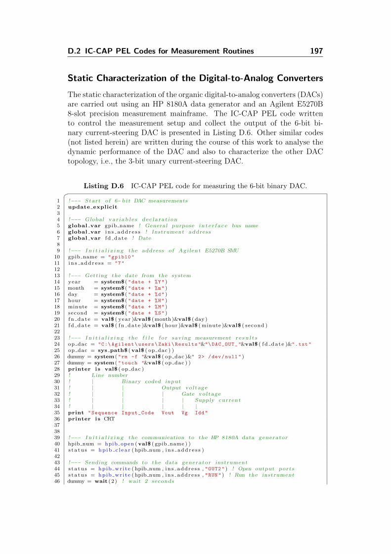
D.2 IC-CAP PEL Codes for Measurement Routines 197
Static Characterization of the Digital-to-Analog Converters
The static characterization of the organic digital-to-analog converters (DACs)are carried out using an HP 8180A data generator and an Agilent E5270B8-slot precision measurement mainframe. The IC-CAP PEL code writtento control the measurement setup and collect the output of the 6-bit bi-nary current-steering DAC is presented in Listing D.6. Other similar codes(not listed herein) are written during the course of this work to analyse thedynamic performance of the DAC and also to characterize the other DACtopology, i.e., the 3-bit unary current-steering DAC.
Listing D.6 IC-CAP PEL code for measuring the 6-bit binary DAC.1 !−−− Star t o f 6− b i t DAC measurements2 update explicit34 !−−− Global v a r i a b l e s d e c l a r a t i o n5 global var gpib name ! General purpose i n t e r f a c e bus name6 global var i n s a d d r e s s ! Instrument address7 global var f d da t e ! Date89 !−−− I n i t i a l i z i n g the address o f Ag i l ent E5270B SMU
10 gpib name = "gpib10 "
11 i n s a d d r e s s = "7"
1213 !−−− Getting the date from the system14 year = system$ ( "date + %Y" )15 month = system$ ( "date + %m" )16 day = system$ ( "date + %d" )17 hour = system$ ( "date + %H" )18 minute = system$ ( "date + %M" )19 second = system$ ( "date + %S" )20 fn da t e = val$ ( year )&val$ (month)&val$ ( day )21 fd da t e = val$ ( f n da t e )&val$ ( hour )&val$ ( minute )&val$ ( second )2223 !−−− I n i t i a l i z i n g the f i l e f o r sav ing measurement r e s u l t s24 op dac = "C:\ Agilent\users\Zaki\Results "&"\DAC_OUT_ "&val$ ( f d da t e )&".txt"
25 op dac = sys path$ (val$ ( op dac ) )26 dummy = system ( "rm -f "&val$ ( op dac )&" 2> /dev/null" )27 dummy = system ( "touch "&val$ ( op dac ) )28 printer i s val$ ( op dac )29 ! Line number30 ! | Binary coded input31 ! | | Output vo l tage32 ! | | | Gate vo l tage33 ! | | | | Supply cur rent34 ! | | | | |35 print "Sequence Input_Code Vout Vg Idd"
36 printer i s CRT373839 !−−− I n i t i a l i z i n g the communication to the HP 8180A data genera tor40 hpib num = hpib open (val$ ( gpib name ) )41 s t a t u s = h p i b c l e a r ( hpib num , i n s a d d r e s s )4243 !−−− Sending commands to the data genera to r instrument44 s t a t u s = hp ib wr i t e ( hpib num , in s addr e s s , "OUT2" ) ! Open output por t s45 s t a t u s = hp ib wr i t e ( hpib num , in s addr e s s , "RUN" ) ! Run the instrument46 dummy = wait (2 ) ! wait 2 seconds

198 D Code Listings
4748 !−−− Measurement o f the ramp s i g n a l f o r the 6− b i t DAC49 for i = 1 to 64 ! Outer loop : 64 input codes50 s t a t u s = hp ib wr i t e ( hpib num , in s addr e s s , "FWD" )51 for j = 1 to 5 ! Inner loop : Five time measurement52 i c c a p f u n c ( "." , "Measure " )53 printer i s val$ ( op dac )54 print val$ ( i ) ,val$ ( i −1) ,val$ ( Vout [ 0 ] ) ,val$ (VGcs [ 0 ] ) ,val$ ( Idd [ 0 ] )55 printer i s CRT56 next j57 next i5859 !−−− Sending commands to the data genera to r instrument60 s t a t u s = hp ib wr i t e ( hpib num , in s addr e s s , "STP" ) ! Stop the instrument61 s t a t u s = hp ib wr i t e ( hpib num , in s addr e s s , "OUT1" ) ! Close output por t s62 s t a t u s = hp ib wr i t e ( hpib num , in s addr e s s , "GTL" ) ! Go to l o c a l6364 !−−− End o f 6− b i t DAC measurements65 return value 0
D.3 MATLAB CODESFOR S-PARAMETER CHARACTERIZATION
Besides IC-CAP, MATLAB (Matrix Laboratory) has been used to controlmeasurement equipment and to automate data collection, particularly forS-parameter characterization. Full two-port S-parameter measurements thatrelate the AC currents and voltages between the drain and the gate electrodesof our OTFTs are carried out using an HP 3577A vector network analyzer(VNA) at frequencies up to 5 MHz. The MATLAB code written to automatethis process is given in Listing D.7.
Furthermore, MATLAB has been exploited in this work to analyze all themeasurements (e.g. to remove the impact of parasitics from the measuredS-parameters using the de-embedding procedure presented in Appendix B)and also to implement compact models, which are not only related to the S-parameter characterization. These codes, however, are not not listed herein.
Listing D.7 MATLAB code for S-parameter characterization of OTFTs.1 %−−− Star t o f S−parameter measurements2 clc ;3 clear a l l ;45 %−−− Disconnect and d e l e t e a l l instrument ob j e c t s6 I n s t r r e s e t ;78 %−−− I n i t i a l i z e the vec to r network ana lyze r (VNA)9 VNA name = 'H3577A ' ;
10 VNA hpib address = 8 ;11 disp ( [ 'Inititalize VNA ' , VNA name , . . .12 ' Instrument (HP -IB Address: ' , num2str( VNA hpib address ) , ')' ] )13 VNA = visa ( 'agilent ' , [ 'GPIB0::' , num2str( VNA hpib address ) , '::0::INSTR ' ] ) ;14 set (VNA, 'InputBufferSize ' , 50000 , 'Timeout ' , 60) ;15 fopen (VNA) ;
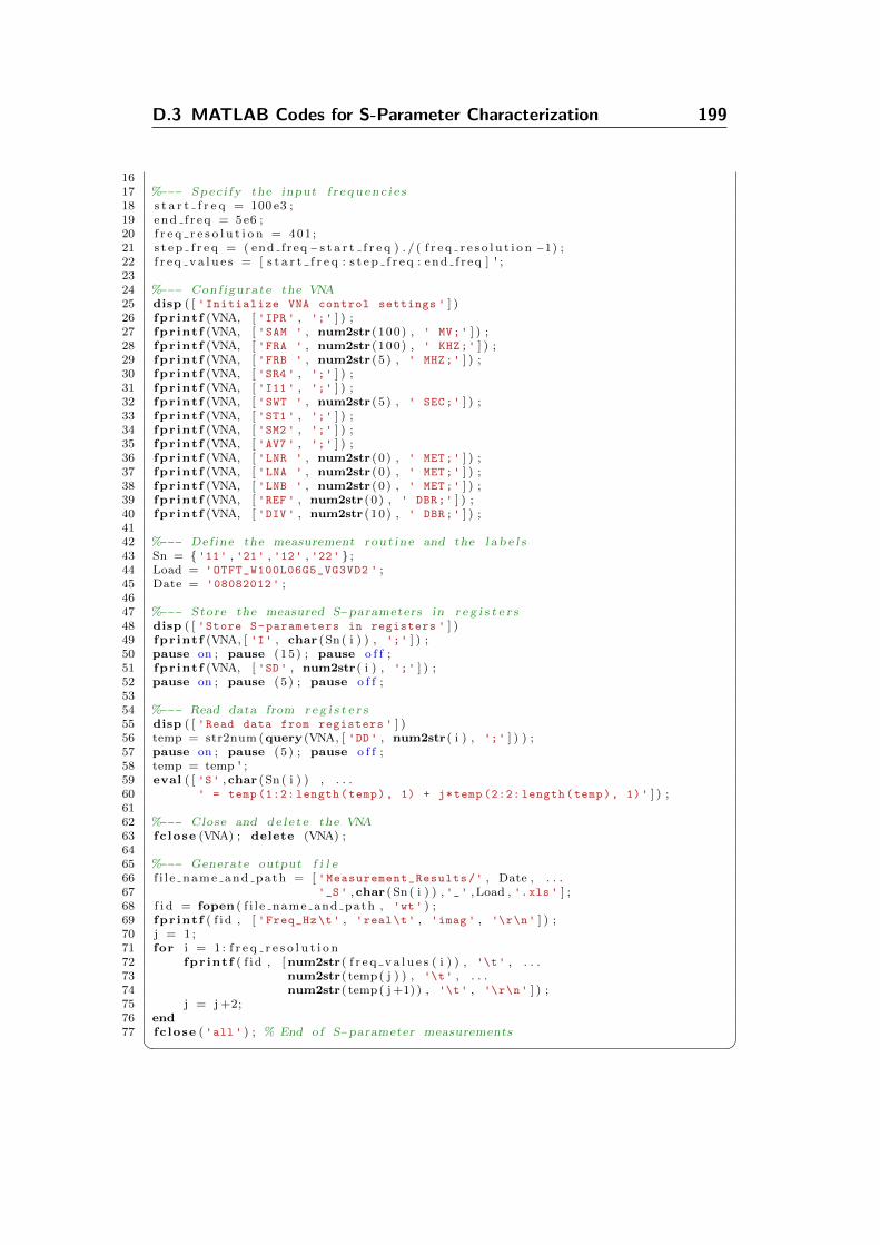
D.3 MATLAB Codes for S-Parameter Characterization 199
1617 %−−− Spec i f y the input f r e qu en c i e s18 s t a r t f r e q = 100 e3 ;19 end f r eq = 5e6 ;20 f r e q r e s o l u t i o n = 401 ;21 s t e p f r e q = ( end freq − s t a r t f r e q ) . / ( f r e q r e s o l u t i o n −1) ;22 f r e q v a l u e s = [ s t a r t f r e q : s t e p f r e q : end f r eq ] ' ;2324 %−−− Conf igurate the VNA25 disp ( [ 'Initialize VNA control settings ' ] )26 fpr intf (VNA, [ 'IPR ' , ';' ] ) ;27 fpr intf (VNA, [ 'SAM ' , num2str (100) , ' MV;' ] ) ;28 fpr intf (VNA, [ 'FRA ' , num2str (100) , ' KHZ;' ] ) ;29 fpr intf (VNA, [ 'FRB ' , num2str (5 ) , ' MHZ;' ] ) ;30 fpr intf (VNA, [ 'SR4 ' , ';' ] ) ;31 fpr intf (VNA, [ 'I11 ' , ';' ] ) ;32 fpr intf (VNA, [ 'SWT ' , num2str (5 ) , ' SEC;' ] ) ;33 fpr intf (VNA, [ 'ST1 ' , ';' ] ) ;34 fpr intf (VNA, [ 'SM2 ' , ';' ] ) ;35 fpr intf (VNA, [ 'AV7 ' , ';' ] ) ;36 fpr intf (VNA, [ 'LNR ' , num2str (0 ) , ' MET;' ] ) ;37 fpr intf (VNA, [ 'LNA ' , num2str (0 ) , ' MET;' ] ) ;38 fpr intf (VNA, [ 'LNB ' , num2str (0 ) , ' MET;' ] ) ;39 fpr intf (VNA, [ 'REF ' , num2str (0 ) , ' DBR;' ] ) ;40 fpr intf (VNA, [ 'DIV ' , num2str (10) , ' DBR;' ] ) ;4142 %−−− Def ine the measurement rou t in e and the l a b e l s43 Sn = '11' , '21' , '12' , '22' ;44 Load = 'OTFT_W100L06G5_VG3VD2 ' ;45 Date = '08082012 ' ;4647 %−−− Store the measured S−parameters in r e g i s t e r s48 disp ( [ 'Store S-parameters in registers ' ] )49 fpr intf (VNA, [ 'I' , char (Sn ( i ) ) , ';' ] ) ;50 pause on ; pause (15) ; pause o f f ;51 fpr intf (VNA, [ 'SD ' , num2str( i ) , ';' ] ) ;52 pause on ; pause (5 ) ; pause o f f ;5354 %−−− Read data from r e g i s t e r s55 disp ( [ 'Read data from registers ' ] )56 temp = str2num (query (VNA, [ 'DD ' , num2str( i ) , ';' ] ) ) ;57 pause on ; pause (5 ) ; pause o f f ;58 temp = temp ' ;59 eval ( [ 'S' ,char (Sn ( i ) ) , . . .60 ' = temp (1:2: length(temp), 1) + j*temp (2:2: length(temp), 1)' ] ) ;6162 %−−− Close and d e l e t e the VNA63 fc lose (VNA) ; delete (VNA) ;6465 %−−− Generate output f i l e66 f i l e name and path = [ 'Measurement_Results/' , Date , . . .67 '_S ' ,char (Sn ( i ) ) , '_' , Load , '.xls ' ] ;68 f i d = fopen ( f i l e name and path , 'wt ' ) ;69 fpr intf ( f i d , [ 'Freq_Hz\t' , 'real\t' , 'imag ' , '\r\n' ] ) ;70 j = 1 ;71 for i = 1 : f r e q r e s o l u t i o n72 fpr intf ( f i d , [num2str( f r e q v a l u e s ( i ) ) , '\t' , . . .73 num2str( temp ( j ) ) , '\t' , . . .74 num2str( temp ( j +1) ) , '\t' , '\r\n' ] ) ;75 j = j +2;76 end77 fc lose ( 'all ' ) ; % End o f S−parameter measurements

Bibliography
[1] J. N. Burghartz, Ed., Guide to State-of-the-Art Electron Devices.Chichester, UK: Wiley-IEEE Press, 2013.
[2] K. Bock, “Polymer electronics systems—Polytronics,” Proceedings ofthe IEEE, vol. 93, no. 8, pp. 1400–1406, Aug. 2005.
[3] H. Klauk, Ed., Organic Electronics Materials, Manufacturing and Ap-plications, 2nd ed. Weinheim, BW, Germany: Wiley-VCH, 2008.
[4] G. Meller and T. Grasser, Eds., Organic Electronics, ser. Advances inPolymer Science. Berlin, BE, Germany: Springer, 2010, vol. 223.
[5] A. Moliton and R. C. Hiorns, “The origin and development of (plastic)organic electronics,” Polymer International, vol. 61, no. 3, pp. 337–341,Mar. 2012.
[6] S. R. Thomas, P. Pattanasattayavong, and T. D. Anthopoulos,“Solution-processable metal oxide semiconductors for thin-film tran-sistor applications,” Chemical Society Reviews, vol. 42, no. 16, pp.6910–6923, Aug. 2013.
[7] D.-M. Sun, C. Liu, W.-C. Ren, and H.-M. Cheng, “A review of carbonnanotube- and graphene-based flexible thin-film transistors,” Small,vol. 9, no. 8, pp. 1188–1205, Apr. 2013.
[8] J. N. Burghartz, Ed., Ultra-thin chip technology and applications.Berlin, BE, Germany: Springer, 2011.
[9] J. N. Burghartz, “You can’t be too thin or too flexible,” IEEE Spec-trum, vol. 50, no. 3, pp. 38–61, Mar. 2013.
[10] J. N. Burghartz, W. Appel, H. D. Rempp, and M. Zimmermann, “Anew fabrication and assembly process for ultrathin chips,” IEEE Trans-actions on Electron Devices, vol. 56, no. 2, pp. 321–327, Feb. 2009.
[11] K. De Munck, T. Chiarella, P. De Moor, B. Swinnen, and C. Van Hoof,“Influence of extreme thinning on 130-nm standard CMOS devices for3-D integration,” IEEE Electron Device Letters, vol. 29, no. 4, pp.322–324, Apr. 2008.
201
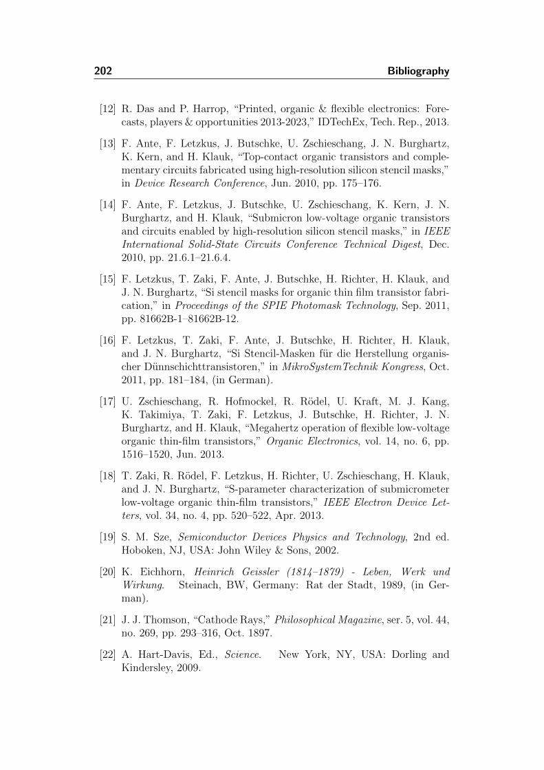
202 Bibliography
[12] R. Das and P. Harrop, “Printed, organic & flexible electronics: Fore-casts, players & opportunities 2013-2023,” IDTechEx, Tech. Rep., 2013.
[13] F. Ante, F. Letzkus, J. Butschke, U. Zschieschang, J. N. Burghartz,K. Kern, and H. Klauk, “Top-contact organic transistors and comple-mentary circuits fabricated using high-resolution silicon stencil masks,”in Device Research Conference, Jun. 2010, pp. 175–176.
[14] F. Ante, F. Letzkus, J. Butschke, U. Zschieschang, K. Kern, J. N.Burghartz, and H. Klauk, “Submicron low-voltage organic transistorsand circuits enabled by high-resolution silicon stencil masks,” in IEEEInternational Solid-State Circuits Conference Technical Digest, Dec.2010, pp. 21.6.1–21.6.4.
[15] F. Letzkus, T. Zaki, F. Ante, J. Butschke, H. Richter, H. Klauk, andJ. N. Burghartz, “Si stencil masks for organic thin film transistor fabri-cation,” in Proceedings of the SPIE Photomask Technology, Sep. 2011,pp. 81662B-1–81662B-12.
[16] F. Letzkus, T. Zaki, F. Ante, J. Butschke, H. Richter, H. Klauk,and J. N. Burghartz, “Si Stencil-Masken fur die Herstellung organis-cher Dunnschichttransistoren,” in MikroSystemTechnik Kongress, Oct.2011, pp. 181–184, (in German).
[17] U. Zschieschang, R. Hofmockel, R. Rodel, U. Kraft, M. J. Kang,K. Takimiya, T. Zaki, F. Letzkus, J. Butschke, H. Richter, J. N.Burghartz, and H. Klauk, “Megahertz operation of flexible low-voltageorganic thin-film transistors,” Organic Electronics, vol. 14, no. 6, pp.1516–1520, Jun. 2013.
[18] T. Zaki, R. Rodel, F. Letzkus, H. Richter, U. Zschieschang, H. Klauk,and J. N. Burghartz, “S-parameter characterization of submicrometerlow-voltage organic thin-film transistors,” IEEE Electron Device Let-ters, vol. 34, no. 4, pp. 520–522, Apr. 2013.
[19] S. M. Sze, Semiconductor Devices Physics and Technology, 2nd ed.Hoboken, NJ, USA: John Wiley & Sons, 2002.
[20] K. Eichhorn, Heinrich Geissler (1814–1879) - Leben, Werk undWirkung. Steinach, BW, Germany: Rat der Stadt, 1989, (in Ger-man).
[21] J. J. Thomson, “Cathode Rays,” Philosophical Magazine, ser. 5, vol. 44,no. 269, pp. 293–316, Oct. 1897.
[22] A. Hart-Davis, Ed., Science. New York, NY, USA: Dorling andKindersley, 2009.
Bibliography 203
[23] F. Braun, “Ueber ein Verfahren zur Demonstration und zum Studiumdes zeitlichen Verlaufes variabler Strome,” Annalen der Physik, vol.296, no. 3, pp. 552–559, 1897, (in German).
[24] J. A. Fleming, “Instrument for converting alternating electric currentsinto continuous currents,” U.S. Patent 803 684, Nov. 7, 1905.
[25] L. de Forest, “Device for amplifying feeble electrical currents,” U.S.Patent 841 387, Jan. 15, 1907.
[26] S. Levy. (2013) The brief history of the ENIAC computer. [Online].Available: http://www.smithsonianmag.com/history-archaeology/The-Brief-History-of-the-ENIAC-Computer-228879421.html
[27] J. E. Lilienfeld, “Method and apparatus for controlling electric cur-rents,” U.S. Patent 1 745 175, Jan. 28, 1930.
[28] J. E. Lilienfeld, “Device for controlling electric current,” U.S. Patent1 900 018, Mar. 7, 1933.
[29] O. Heil, “Improvements in or relating to electrical amplifiers and othercontrol arrangements and devices,” U.K. Patent 439 457, Dec. 6, 1935.
[30] C. R. Kagan and P. Andry, Eds., Thin-Film Transistors. New York,NY, USA: Marcel Dekker, 2003.
[31] T. P. Brody, “The thin film transistors—A late flowering bloom,” IEEETransactions on Electron Devices, vol. 31, no. 11, pp. 1614–1628, Nov.1984.
[32] J. Bardeen and W. H. Brattain, “The transistor, a semi-conductortriode,” Physical Review, vol. 74, pp. 230–231, Jun. 1948.
[33] J. Bardeen and W. H. Brattain, “Three-electrode circuit element uti-lizing semiconductive materials,” U.S. Patent 2 524 035, Oct. 3, 1950.
[34] W. H. Brattain, Bell Telephone Laboratories, Notebook no. 18194 (caseno. 38138-7), pp. 192–194, Dec. 16, 1947.
[35] W. H. Brattain, Bell Telephone Laboratories, Notebook no. 21780 (caseno. 38138-7), pp. 7–8, Dec. 24, 1947.
[36] W. Shockley, Bell Telephone Laboratories, Notebook no. 20455, pp.128–132, Jan. 24, 1948.
[37] W. Shockley, “Circuit element utilizing semiconductive material,” U.S.Patent 2 569 347, Sep. 25, 1951.
204 Bibliography
[38] M. M. Atalla, E. Tannenbaum, and E. J. Scheibner, “Stabilizationof silicon surface by thermally grown oxides,” Bell System TechnicalJournal, vol. 38, no. 3, pp. 749–783, May 1959.
[39] D. Kahng, “Electric field controlled semiconductor device,” U.S. Patent3 102 230, Aug. 27, 1963.
[40] M. M. Atalla, “Insulated-gate field effect transistor with electrostaticprotection means,” U.S. Patent 3 413 497, Nov. 26, 1968.
[41] P. K. Weimer, “An evaporated thin-film triode,” IRE Transactions onElectron Devices, vol. 8, no. 5, p. 421, Sep. 1961.
[42] P. K. Weimer, “Evaporated circuits incorporating a thin-film transis-tor,” in IEEE International Solid-State Circuits Conference TechnicalDigest, Feb. 1962, pp. 32–33.
[43] P. K. Weimer, “The TFT—A new thin-film transistor,” Proceedings ofthe IRE, vol. 50, no. 6, pp. 1462–1469, Jun. 1962.
[44] R. A. Street, Ed., Technology and Applications of Amorphous Silicon.Berlin, BE, Germany: Springer, 2000.
[45] B. Redman-White, B. Murmann, S. Kosonocky, S. Rusu, R. Thewes,K. Zhang, A. Cathelin, H.-J. Yoo, D. Su, and D. Friedman, “ISSCC2013 technology trends,” IEEE International Solid-State CircuitsConference, 2013. [Online]. Available: http://isscc.org/trends/
[46] G. E. Moore, “Cramming more components onto integrated circuits,”Electronics, vol. 38, no. 8, pp. 114–117, Apr. 1965.
[47] G. E. Moore, “Progress in digital integrated electronics,” in IEEE In-ternational Electron Devices Meeting Technical Digest, Dec. 1975, pp.11–13.
[48] H. Spanggaard and F. C. Krebs, “A brief history of the developmentof organic and polymeric photovoltaics,” Solar Energy Materials andSolar Cells, vol. 83, no. 2–3, pp. 125–146, Jun. 2004.
[49] A. Pochettino and A. Sella, “Photoelectric behavior of anthracene,”Academy Lincei Rendus, vol. 15, pp. 355–363, Mar. 1906.
[50] M. Volmer, “Die verschiedenen lichtelektrischen Erscheinungen am An-thracen, ihre Beziehungen zueinander, zur Fluoreszenz und Dianthra-cenbildung,” Annalen der Physik, vol. 345, no. 4, pp. 775–796, Feb.1913, (in German).
Bibliography 205
[51] P. M. Borsenberger and D. S. Weiss, Organic Photoreceptors for Imag-ing Systems. New York, NY, USA: Marcel Dekker, 1993.
[52] A. Bernanose, “Electroluminescence in organic compounds,” BritishJournal of Applied Physics, vol. 6, no. S4, pp. S54–S56, Apr. 1955.
[53] M. Pope, H. P. Kallmann, and P. Magnante, “Electroluminescence inorganic crystals,” Journal of Chemical Physics, vol. 38, no. 8, pp. 2042–2043, Apr. 1963.
[54] W. Brutting, Encyclopedia of Physics, 3rd ed., R. G. Lerner and G. L.Trigg, Eds. Weinheim, BW, Germany: Wiley-VCH, 2005, vol. 2, ch.Organic Semiconductors, pp. 1866–1876.
[55] H. Shirakawa, E. J. Louis, A. G. MacDiarmid, C. K. Chiang, and A. J.heeger, “Synthesis of electrically conducting organic polymers: Halo-gen derivatives of polyacetylene, (CH)x,” Journal of Chemical Society,Chemical Communications, no. 24, pp. 578–580, Jan. 1977.
[56] C. W. Tang, “Two-layer organic photovoltaic cell,” Applied PhysicsLetters, vol. 48, no. 2, pp. 183–185, Jan. 1986.
[57] “Heliatek consolidates its technology leadership by establishing a newworld record for organic solar technology with a cell efficiency of12%,” Press Release, Heliatek, Jan. 16, 2013. [Online]. Available:http://www.heliatek.com/newscenter/?lang=en
[58] C. W. Tang and S. A. VanSlyke, “Organic electroluminescent diodes,”Applied Physics Letters, vol. 51, no. 12, pp. 913–915, Sep. 1987.
[59] J. H. Burroughes, D. D. C. Bradley, A. R. Brown, R. N. Marks,K. Mackay, R. H. Friend, R. L. Burns, and A. B. Holmes, “Light-emitting diodes based on conjugated polymers,” Nature, vol. 347, pp.539–541, Oct. 1990.
[60] “UHD TV S9C OLED,” Spec Sheet, Samsung, 2013. [Online].Available: http://www.samsung.com/us/video/tvs/KN55S9CAFXZA
[61] D. F. Barbe and C. R. Westgate, “Surface state parameters of metal-free phthalocyanine single crystals,” Journal of Physics and Chemistryof Solids, vol. 31, no. 12, pp. 2679–2687, Dec. 1970.
[62] M. L. Petrova and L. D. Rozenshtein, “Field effect in the organicsemiconductor chloranil,” Fiz. Tverd. Tela (Soviet Phys. Solid State),vol. 12, pp. 961–962, Dec. 1970.

206 Bibliography
[63] G. Horowitz, “Organic field-effect transistors,” Advanced Materials,vol. 10, no. 5, pp. 365–377, Mar. 1998.
[64] G. Horowitz, “Organic field-effect transistors: From theory to real de-vices,” Journal of Materials Research, vol. 19, no. 7, pp. 1946–1962,Jul. 2004.
[65] F. Ebisawa, T. Kurokawa, and S. Nara, “Electrical properties of poly-acetylene/polysiloxane interface,” Journal of Applied Physics, vol. 54,no. 6, pp. 3255–3259, Jun. 1983.
[66] J. H. Burroughes, C. A. Jones, and R. H. Friend, “New semiconductordevice physics in polymer diodes and transistors,” Nature, vol. 335, pp.137–141, Sep. 1988.
[67] A. Tsumura, H. Koezuka, and T. Ando, “Polythiophene field-effecttransistor: Its characteristics and operation mechanism,” SyntheticMetals, vol. 25, no. 1, pp. 11–23, Jul. 1988.
[68] A. Assadi, C. Svensson, M. Willander, and O. Inganas, “Field-effectmobility of poly(3-hexylthiophene),” Applied Physics Letters, vol. 53,no. 3, pp. 195–197, Jul. 1988.
[69] R. Mardru, G. Guillaud, M. Al Sadoun, M. Maitrot, J.-J. Andre, J. Si-mon, and R. Even, “A well-behaved field effect transistor based on anintrinsic molecular semiconductor,” Chemical Physics Letters, vol. 145,no. 4, pp. 343–346, Apr. 1988.
[70] C. Clarisse, M. T. Riou, M. Gauneau, and M. Le Contellect, “Field-effect transistor with diphthalocyanine thin film,” Electronics Letters,vol. 24, no. 11, pp. 674–675, May 1988.
[71] F. Garnier, G. Horowitz, X. Peng, and D. Fichou, “An all-organic“soft” thin film transistor with very high carrier mobility,” AdvancedMaterials, vol. 2, no. 12, pp. 592–594, Dec. 1990.
[72] (2013) Plastic Logic Technology. [Online]. Available: http://www.plasticlogic.com/technology/
[73] (2013) Technology Academy Finland. [Online]. Available: http://www.technologyacademy.fi
[74] (2013) Deutscher Zukunftpreis. [Online]. Available: http://www.deutscher-zukunftspreis.de
Bibliography 207
[75] M. Riede, C. Uhrich, J. Widmer, R. Timmreck, D. Wynands,G. Schwartz, W.-M. Gnehr, D. Hildebrandt, A. Weiss, J. Hwang,S. Sundarraj, P. Erk, M. Pfeiffer, and K. Leo, “Efficient organic tandemsolar cell based on small molecules,” Advanced Functional Materials,vol. 21, no. 16, pp. 3019–3028, Aug. 2011.
[76] J. Meiss, T. Menke, K. Leo, C. Uhrich, W.-M. Gnehr, S. Sonntag,M. Pfeiffer, and M. Riede, “Highly effiecient semitransparent tandemorganic solar cells with complementary absorber materials,” AppliedPhysics Letters, vol. 99, no. 4, pp. 043301-1–043301-3, Jul. 2011.
[77] M. Pfeiffer, K. Leo, X. Zhou, J. S. Huang, M. Hofmann, A. Werner,and J. Blochwitz-Nimoth, “Doped organic semiconductors: Physicsand application in light emitting diodes,” Organic Electronics, vol. 4,no. 2–3, pp. 89–103, Sep. 2003.
[78] X. Zhou, J. Blochwitz-Nimoth, M. Pfeiffer, B. Maennig, J. Drechsel,A. Werner, and K. Leo, “High-efficiency low-voltage stable invertedtransparent electrophosphorescent organic light-emitting diodes: Com-bining electrically doped carrier transport layers and iridium-complexdoped emissive layer,” Synthetic Metals, vol. 137, no. 1–3, pp. 1063–1064, Apr. 2003.
[79] P. Cosseddu and A. Bonfiglio, “Soft lithography fabrication of all-organic bottom-contact and top-contact field effect transistors,” Ap-plied Physics Letters, vol. 88, no. 2, pp. 023506-1–023506-3, Jan. 2006.
[80] M. Halik, H. Klauk, U. Zschieschang, T. Kriem, G. Schmid, W. Radlik,and K. Wussow, “Fully patterned all-organic thin film transistors,”Applied Physics Letters, vol. 81, no. 2, pp. 289–291, Jul. 2002.
[81] H. Klauk, “Organic thin-film transistors,” Chemical Society Reviews,vol. 39, no. 7, pp. 2643–2666, Apr. 2010.
[82] W. Clemens, D. Lupo, K. Hecker, and S. Breitung, Eds., “OE-Aroadmap for organic and printed electronics,” White Paper, 4thed., Organic Electronics Association, 2011. [Online]. Available:http://www.oe-a.org/en GB/
[83] I. McCulloch, M. Heeney, M. L. Chabinyc, D. DeLongchamp, R. J.Kline, M. Colle, W. Duffy, D. Fischer, D. Gundlach, B. Hamadani,R. Hamiliton, L. Richter, A. Salleo, M. Shkunov, D. Sparrowe, S. Tier-ney, and W. Zhang, “Semiconducting thienothiophene copolymers: De-sign, synthesis, morphology, and performance in thin-film organic tran-sistors,” Advanced Materials, vol. 21, no. 10–11, pp. 1091–1109, Mar.2009.
208 Bibliography
[84] C. G. Choi and B.-S. Bae, “Effects of hydroxyl groups in gate dielectricson the hysteresis of organic thin film transistors,” Electrochemical andSolid-State Letters, vol. 10, no. 11, pp. H347–H350, Sep. 2007.
[85] T. Yamamoto and K. Takimiya, “Facile synthesis of highly π-extended heteroarenes, dinaphtho[2,3-b:2’,3’-f]chalcogenopheno[3,2-b]chalcogenophenes, and their application to field-effect transistors,”Journal of The American Chemical Society, vol. 129, no. 8, pp. 2224–2225, Feb. 2007.
[86] C. Kim, A. Facchetti, and T. J. Marks, “Probing the surface glass tran-sition temperature of polymer films via organic semiconductor growthmode, microstructure, and thin-film transistor response,” Journal ofThe American Chemical Society, vol. 131, no. 25, pp. 9122–9132, Jun.2009.
[87] Y. Ishii, R. Ye, M. Baba, and K. Ohta, “Correlation between morphol-ogy and electrical properties of α,α’-diethyl-sexithiophene thin films,”Japanese Journal of Applied Physics, vol. 47, no. 2, pp. 1256–1258,Feb. 2008.
[88] R. Schmidt, J. H. Oh, Y.-S. Sun, M. Deppisch, A.-M. Krause,K. Radacki, H. Braunschweig, M. Konemann, P. Erk, Z. Bao, andF. Wurthner, “High-performance air-stable n-channel organic thin filmtransistors based on halogenated perylene bisimide semiconductors,”Journal of The American Chemical Society, vol. 131, no. 17, pp. 6215–6228, Apr. 2009.
[89] Z. Bao, A. J. Lovinger, and J. Brown, “New air-stable n-channel or-ganic thin-film transistors,” Journal of The American Chemical Soci-ety, vol. 120, no. 1, pp. 207–208, Jan. 1998.
[90] R. T. Weitz, K. Amsharov, U. Zschieschang, E. B. Villas, D. K.Goswami, M. Burghard, H. Dosch, M. Jansen, K. Kern, and H. Klauk,“Organic n-channel transistors based on core-cyanated perylene car-boxylic diimide derivatives,” Journal of The American Chemical Soci-ety, vol. 130, no. 14, pp. 4637–4645, Mar. 2008.
[91] Y. Hosoi, D. Tsunami, H. Ishii, and Y. Furukawa, “Air-stablen-channel organic field-effect transistors based on N,N ’-bis(4-trifluoromethylbenzyl)perylene-3,4,9,10-tetracarboxylic diimide,”Chemical Physics Letters, vol. 436, no. 1–3, pp. 139–143, Feb. 2007.
[92] O. D. Jurchescu, M. Popinciuc, B. J. van Wees, and T. T. M. Palstra,“Interface-controlled, high-mobility organic transistors,” Advanced Ma-terials, vol. 19, no. 5, pp. 688–692, Mar. 2007.

Bibliography 209
[93] R. Hamilton, J. Smith, S. Ogier, M. Heeney, J. E. Anthony, I. Mc-Culloch, J. Veres, D. D. C. Bradley, and T. D. Anthopoulos, “High-performance polymer-small molecule blend organic transistors,” Ad-vanced Materials, vol. 21, pp. 1166–1171, Mar. 2009.
[94] S. Handa, E. Miyazaki, K. Takimiya, and Y. Kunugi, “Solution-processable n-channel organic field-effect transistors based ondicyanomethylene-substituted terthienoquinoid derivative,” Journal ofThe American Chemical Society, vol. 129, no. 38, pp. 11684–11685,Aug. 2007.
[95] H. Usta, A. Facchetti, and T. J. Marks, “Air-stable, solution-processable n-channel and ambipolar semiconductors for thin-film tran-sistors based on the indenofluorenebis(dicyanovinylene) core,” Journalof The American Chemical Society, vol. 130, no. 27, pp. 8580–8581,Jun. 2008.
[96] H. Yan, Z. Chen, Y. Z. C. Newman, J. R. Quinn, F. Dotz, M. Kastler,and A. Facchetti, “A high-mobility electron-transporting polymer forprinted transistors,” Nature, vol. 457, pp. 679–686, Feb. 2009.
[97] F. Ante, “Contact effects in organic transistors,” Ph.D. dissertation,Swiss Federal Institute of Technology in Lausanne, Lausanne, Switzer-land, Dec. 2011.
[98] P. Heremans, W. Dehaene, M. Steyaert, K. Myny, H. Marien, J. Genoe,G. Gelinck, and E. van Veenendaal, “Circuit design in organic semicon-ductor technologies,” in Proceedings of the European Solid-State DeviceResearch Conference, Sep. 2011, pp. 5–12.
[99] T. Zaki, F. Ante, U. Zschieschang, J. Butschke, F. Letzkus, H. Richter,H. Klauk, and J. N. Burghartz, “A 3.3 V 6-Bit 100 kS/s current-steeringdigital-to-analog converter using organic p-type thin-film transistors onglass,” IEEE Journal of Solid-State Circuits, vol. 47, no. 1, pp. 292–300, Jan. 2012.
[100] H. Marien, M. S. J. Steyaert, E. van Veenendaal, and P. Heremans,“A fully integrated ∆Σ ADC in organic thin-film transistor technologyon flexible plastic foil,” IEEE Journal of Solid-State Circuits, vol. 46,no. 1, pp. 276–284, Jan. 2011.
[101] R. Rodel, F. Letzkus, T. Zaki, J. N. Burghartz, U. Kraft, U. Zschi-eschang, K. Kern, and H. Klauk, “Contact properties of high-mobility,air-stable, low-voltage organic n-channel thin-film transistors based ona naphthalene tetracarboxylic diimide,” Applied Physics Letters, vol.102, no. 233303, pp. 233303-1–233303-5, Jun. 2013.
210 Bibliography
[102] J. H. Na, M. Kitamura, and Y. Arakawa, “High field-effect mobilityamorphous InGaZnO transistors with aluminum electrodes,” AppliedPhysics Letters, vol. 93, no. 6, pp. 063501-1–063501-3, Aug. 2008.
[103] G. Oike, T. Yajima, T. Nishimura, K. Nagashio, and A. Toriumi, “Highelectron mobility (>16 cm2/Vsec) FETs with high on/off ratio (>106)and highly conductive films (σ>102 S/cm) by chemical doping in verythin (∼20 nm) TiO2 films on thermally grown SiO2,” in IEEE Inter-national Electron Devices Meeting Technical Digest, Dec. 2013, pp.11.5.1–11.5.4.
[104] M. Rockele, D.-V. Pham, A. Hoppe, J. Steiger, S. Botnaras, M. Nag,S. Steudel, K. Myny, S. Schols, R. Muller, B. van der Putten, J. Genoe,and P. Hermans, “Low-temperature and scalable complementary thin-film technology based on solution-processed metal oxide n-TFTs andpentacene p-TFTs,” Organic Electronics, vol. 12, no. 11, pp. 1909–1913, Nov. 2011.
[105] “PolyTC® transparent conductive films,” Spec Sheet, PolyIC, 2013.[Online]. Available: http://www.polyic.com/products/polytcr.html
[106] U. Zschieschang, F. Ante, D. Kalblein, T. Yamamoto, K. Takimiya,H. Kuwabara, M. Ikeda, T. Sekitani, T. Someya, J. Blochwitz-Nimoth,and H. Klauk, “Dinaphtho[2,3-b:2’,3’-f]thieno[3,2-b]thiophene (DNTT)thin-film transistors with improved performance and stability,” OrganicElectronics, vol. 12, no. 8, pp. 1370–1375, Aug. 2011.
[107] K. Kuribara, H. Wang, N. Uchiyama, K. Fukuda, Tomoyuki, U. Zschi-eschang, C. Jaye, D. Fischer, H. Klauk, T. Yamamoto, K. Takimiya,M. Ikeda, H. Kuwabara, T. Sekitani, Y.-L. Loo, and T. Someya, “Or-ganic transistors with high thermal stability for medical applications,”Nature Communications, vol. 3, pp. 723-1–723-7, Mar. 2012.
[108] J. Thompson, Ed., +Plastic Electronics, vol. 2, no. 3, Plastic Electron-ics Foundation, 2009.
[109] S. Forrest, P. Burrows, and M. Thompson, “The dawn of organic elec-tronics,” IEEE Spectrum, vol. 37, no. 8, pp. 29–34, Aug. 2000.
[110] T. Tiedje, E. Yablonovitch, G. D. Cody, and B. G. Brooks, “Limitingefficiency of silicon solar cells,” IEEE Transactions on Electron Devices,vol. 31, no. 5, pp. 711–716, May 1984.
[111] B. O’Regan and M. Gratzel, “A low-cost, high-efficiency solar cell basedon dye-sensitized colloidal TiO2 films,” Nature, vol. 353, pp. 737–740,Oct. 1991.
Bibliography 211
[112] A. C. Mayer, S. R. Scully, B. E. Hardin, M. W. Rowell, and M. D.McGehee, “Polymer-based solar cells,” Materials, vol. 10, no. 11, pp.741–748, Nov. 2007.
[113] “Thinfilm demonstrates first integrated printed electronic system withrewritable memory,” Press Release, Thin Film Electronics ASA, Dec.20, 2012. [Online]. Available: http://www.thinfilm.no/news/
[114] (2013) Thinfilm MemoryTM. [Online]. Available: http://www.thinfilm.no/products/memory/
[115] J. Thompson, Ed., +Plastic Electronics, vol. 1, no. 3, Plastic Electron-ics Foundation, 2008.
[116] I. Yagi, N. Hirari, Y. Miyamoto, M. Noda, A. Imaoka, N. Yoneya,K. Nomoto, J. Kasahara, A. Yumoto, and T. Urabe, “A flexible full-color AMOLED display driven by OTFTs,” Journal of the Society forInformation Display, vol. 16, no. 1, pp. 15–20, Jan. 2008.
[117] M. Noda, N. Kobayashi, M. Katsuhara, A. Yumoto, S.-I. Ushikura,R.-I. Yasuda, N. Hirai, G. Yukawa, I. Yagi, K. Nomoto, and T. Urabe,“A rollable AM-OLED display driven by OTFTs,” in Society for Infor-mation Display Symposium Technical Digest, vol. 41, no. 1, May 2010,pp. 710–713.
[118] “popSLATE partners with Plastic Logic to create the always-onsecond screen display for their Apple iPhone 5 & 5S accessory,”Press Release, Plastic Logic, Sep. 13, 2013. [Online]. Available:http://www.plasticlogic.com/news/
[119] T. Someya, “Building bionic skin,” IEEE Spectrum, vol. 50, no. 9, pp.50–56, Sep. 2013.
[120] T. Someya, Y. Kato, T. Sekitani, S. Iba, Y. Noguchi, Y. Murase,H. Kawaguchi, and T. Sakurai, “Conformable, flexible, large-area net-works of pressure and thermal sensors with organic transistor activematrixes,” Proceedings of the National Academy of Sciences of theUnited States of America, vol. 102, no. 35, pp. 12321–12325, Aug. 2005.
[121] M. Kaltenbrunner, T. Sekitani, J. Reeder, T. Yokota, K. Kuribara,T. Tokuhara, M. Drack, R. Schwodiauer, I. Graz, S. Bauer-Gogonea,S. Bauer, and T. Someya, “An ultra-lightweight design for impercepti-ble plastic electronics,” Nature, vol. 499, pp. 458–463, Jul. 2013.
[122] T. Someya, T. Sekitani, M. Kaltenbrunner, T. Yokota, H. Fuketa,M. Takamiya, and T. Sakurai, “Ultraflexible organic devices for
212 Bibliography
biomedical applications,” in IEEE International Electron Devices Meet-ing Technical Digest, Dec. 2013, pp. 8.5.1–8.5.4.
[123] H. Fuketa, K. Yoshioka, Y. Shinozuka, K. Ishida, T. Yokota, N. Mat-suhisa, Y. Inoue, M. Sekino, T. Sekitani, M. Takamiya, T. Someya, andT. Sakurai, “1µm-thickness 64-channel surface electromyogram mea-surement sheet with 2V organic transistors for prosthetic hand con-trol,” in IEEE International Solid-State Circuits Conference TechnicalDigest, Feb. 2013, pp. 104–105.
[124] “Plastic Logic and ISORG demo thin film plastic image sensor atIDTechEx,” Press Release, Plastic Logic and ISORG, Nov. 19, 2013.[Online]. Available: http://www.plasticlogic.com/news/
[125] Y. Kato, T. Sekitani, M. Takamiya, M. Doi, K. Asaka, T. Sakurai,and T. Someya, “Sheet-type braille displays by integrating organicfield-effect transistors and polymeric actuators,” IEEE Transactionson Electron Devices, vol. 54, no. 2, pp. 202–209, Feb. 2007.
[126] A. Dodabalapur, “Organic and polymer transistors for electronics,”Materials Today, vol. 9, no. 4, pp. 24–30, Apr. 2006.
[127] R. Shinar and J. Shinar, Eds., Organic Electronics in Sensors andBiotechnology. New York, NY, USA: McGraw-Hill, 2009.
[128] B. Crone, A. Dodabalapur, A. Gelperin, L. Torsi, H. E. Katz, A. J.Lovinger, and Z. Bao, “Electronic sensing of vapors with organic tran-sistors,” Applied Physics Letters, vol. 78, no. 15, pp. 2229–2231, Feb.2001.
[129] T. Someya, A. Dodabalapur, A. Gelperin, H. E. Katz, and Z. Bao,“Integration and response of organic electronics with aqueous microflu-idics,” Langmuir, vol. 18, no. 13, pp. 5229–5302, Jun. 2002.
[130] L. Jamet, “Printed electronics opens up large flexible sensor designopportunities,” EETimes Europe, pp. 34–35, Jul./Aug. 2013.
[131] A. P. F. Turner, “Biosensors: Sense and sensibility,” Chemical SocietyReviews, vol. 42, no. 8, pp. 3175–3648, Apr. 2013.
[132] (2013) Illuminated Packaging for Bombay Sapphire. [Online].Available: http://www.karlknauer.com
[133] A. J. Steckl, “Circuits on cellulose,” IEEE Spectrum, vol. 50, no. 2, pp.48–61, Feb. 2013.
Bibliography 213
[134] Y. Yang and A. J. Heeger, “A new architecture for polymer transis-tors,” Nature, vol. 372, pp. 344–346, Nov. 1994.
[135] M. Yi, X. Xia, T. Yang, Y. Liu, L. Xie, X. Zhou, and W. Huang, “Ver-tical n-type organic transistors with tri(8-hydroxyquinoline) aluminumas collector and fullerene as emitter,” Applied Physics Letters, vol. 98,no. 7, pp. 073309-1–073309-3, Feb. 2011.
[136] R. Parashkov, E. Becker, S. Hartmann, G. Ginev, D. Schneider,H. Krautwald, T. Dobbertin, D. Metzdorf, F. Brunetti, C. Schild-knecht, A. Kammoun, M. Brandes, T. Riedl, H.-H. Johannes, andW. Kowalsky, “Vertical channel all-organic thin-film transistors,” Ap-plied Physics Letters, vol. 82, no. 25, pp. 4579–4580, Jun. 2003.
[137] D. J. Gundlach, L. Zhou, J. A. Nichols, T. N. Jackson, P. V. Necliudov,and M. S. Shur, “An experimental study of contact effects in organicthin film transistors,” Journal of Applied Physics, vol. 100, no. 2, pp.024509-1–024509-13, Jul. 2006.
[138] C. H. Shim, F. Maruoka, and R. Hattori, “Structural analysis on or-ganic thin-film transistor with device simulation,” IEEE Transactionson Electron Devices, vol. 57, no. 1, pp. 195–200, Jan. 2010.
[139] F. Ante, D. Kalblein, T. Zaki, U. Zschieschang, K. Takimiya, M. Ikeda,T. Sekitani, T. Someya, J. N. Burghartz, K. Kern, and H. Klauk, “Con-tact resistance and megahertz operation of aggressively scaled organictransistors,” Small, vol. 8, no. 1, pp. 73–79, Jan. 2012.
[140] S. H. Jin, K. D. Jung, H. Shin, B. G. Park, and J. D. Lee, “Grain sizeeffects on contact resistance of top-contact pentacene TFTs,” SyntheticMetals, vol. 156, no. 2–4, pp. 196–201, Feb. 2006.
[141] K. Sidler, N. V. Cvetkovic, V. Savu, D. Tsamados, A. M. Ionescu,and J. Brugger, “Organic thin film transistors on flexible polyimidesubstrates fabricated by full wafer stencil lithography,” Sensors andActuators A: Physical, vol. 162, no. 2, pp. 155–159, Aug. 2010.
[142] J. Zaumseil, T. Someya, Z. Bao, Y. L. Loo, R. Cirelli, and J. A. Rogers,“Nanoscale organic transistors that use source/drain electrodes sup-ported by high resolution rubber stamps,” Applied Physics Letters,vol. 82, no. 5, pp. 793–795, Feb. 2003.
[143] J. Zaumseil, K. W. Baldwin, and J. A. Rogers, “Contact resistance inorganic transistors that use source and drain electrodes formed by softcontact lamination,” Journal of Applied Physics, vol. 93, no. 10, pp.6117–6124, May 2003.

214 Bibliography
[144] Y.-Y. Noh, N. Zhao, M. Caironi, and H. Sirringhaus, “Downscalingof self-aligned, all-printed polymer thin-film transistors,” Nature Nan-otechnology, vol. 2, pp. 784–789, Nov. 2007.
[145] M. Caironi, E. Gili, T. Sakanoue, X. Cheng, and H. Sirringhaus, “Highyield, single droplet electrode arrays for nanoscale printed electronics,”ACS Nano, vol. 4, no. 3, pp. 1451–1456, Feb. 2010.
[146] T. Sekitani, Y. Noguchi, U. Zschieschang, H. Klauk, , and T. Someya,“Organic transistors manufactured using inkjet technology with sub-femtoliter accuracy,” Proceedings of the National Academy of Sciencesof the United States of America, vol. 105, no. 13, pp. 4976–4980, Apr.2008.
[147] T. Ji, S. Jung, and V. K. Varadan, “On the correlation of postannealinginduced phase transition in pentacene with carrier transport,” OrganicElectronics, vol. 9, no. 5, pp. 895–898, Oct. 2008.
[148] D. J. Gundlach, T. N. Jackson, D. G. Schlom, and S. F. Nelson,“Solvent-induced phase transition in thermally evaporated pentacenefilms,” Applied Physics Letters, vol. 74, no. 22, pp. 3302–3304, May1999.
[149] A. A. Virkar, S. Mannsfeld, Z. Bao, and N. Stingelin, “Organic semi-conductor growth and morphology considerations for organic thin-filmtransistors,” Advanced Materials, vol. 22, no. 34, pp. 3857–3875, Sep.2010.
[150] H. C. Shah and R. W. Davis Jr., “The effect of the roughness of theglass substrate on the roughness of the barrier layer used during fabri-cation of poly-Si TFTs,” in Society for Information Display SymposiumTechnical Digest, vol. 34, no. 1, May 2003, pp. 1516–1519.
[151] T. Zaki, S. Scheinert, I. Horselmann, R. Rodel, F. Letzkus, H. Richter,U. Zschieschang, H. Klauk, and J. N. Burghartz, “Accurate capacitancemodeling and characterization of organic thin-film transistors,” IEEETransactions on Electron Devices, vol. 61, no. 1, pp. 98–104, Jan. 2014.
[152] H. Klauk, U. Zschieschang, J. Pflaum, and M. Halik, “Ultralow-powerorganic complementary circuits,” Nature, vol. 445, pp. 745–748, Feb.2007.
[153] U. Kraft, U. Zschieschang, M. J. Kang, K. Takimiya, T. Zaki, F. Let-zkus, J. N. Burghartz, E. Weber, and H. Klauk, “Evolution of the field-effect mobility and the contact resistance of low-voltage organic thin-film transistors based on air-stable, high-mobility thioacenes,” in Ma-terials Research Society Spring Meeting and Exhibit, Apr. 2013, poster.

Bibliography 215
[154] T. Yamamoto and K. Takimiya, “Facile synthesis of highly π-extended heteroarenes, dinaphtho[2,3-b:2’,3’-f]chalcogenopheno[3,2-b]chalcogenophenes, and their applications to field-effect transistors,”Journal of the American Chemical Society, vol. 129, no. 8, pp. 2224–2225, Feb. 2007.
[155] H. Borkan and P. K. Weimer, “An analysis of the characteristics ofinsulated-gate thin-film transistors,” RCA Review, vol. 24, pp. 153–165, Jun. 1963.
[156] D. Natali and M. Caironi, “Charge injection in solution-processedorganic field-effect transistors: Physics, models and characterizationmethods,” Advanced Materials, vol. 24, no. 11, pp. 1357–1387, Mar.2012.
[157] M. Kitamura and Y. Arakawa, “High current-gain cutoff frequenciesabove 10 MHz in n-channel C60 and p-channel pentacene thin-film tran-sistors,” Japanese Journal of Applied Physics, vol. 50, pp. 01BC01-1–01BC01-4, Jan. 2011.
[158] M. Kitamura and Y. Arakawa, “Current-gain cutoff frequencies above10 MHz for organic thin-film transistors with high mobility and low par-asitic capacitance,” Applied Physics Letters, vol. 95, no. 2, pp. 023503-1–023503-3, Jul. 2009.
[159] V. Wagner, P. Wobkenberg, A. Hoppe, and J. Seekamp, “Mega-hertz operation of organic field-effect transistors based on poly(3-hexylthiophene),” Applied Physics Letters, vol. 89, no. 24, pp. 243515-1–243515-3, Dec. 2006.
[160] M. Caironi, Y.-Y. Noh, and H. Sirringhaus, “Frequency operation oflow-voltage, solution-processed organic field-effect transistors,” Semi-conductor Science and Technology, vol. 26, no. 3, pp. 034006-1–034006-8, Mar. 2011.
[161] M. Jaiswal and R. Menon, “Equivalent circuit for an organic field-effect transistor from impedance measurements under dc bias,” AppliedPhysics Letters, vol. 88, no. 12, pp. 123504-1–123504-3, Mar. 2006.
[162] T. Yamamoto and K. Takimiya, “FET characteristics of dinaphthoth-ienothiophene (DNTT) on Si/SiO2 substrates with various surface-modifications,” Journal of Photopolymer Science and Technology,vol. 20, no. 1, pp. 57–59, Aug. 2007.
216 Bibliography
[163] S. Haas, Y. Takahashi, K. Takimiya, and T. Hasegawa, “High-performance dinaphtho-thieno-thiophene single crystal field-effect tran-sistors,” Applied Physics Letters, vol. 95, no. 2, pp. 022111-1–022111-3,Jul. 2009.
[164] H. Tuinhout, N. Wils, and P. Andricciola, “Parametric mismatch char-acterization for mixed-signal technologies,” IEEE Journal of Solid-State Circuits, vol. 45, no. 9, pp. 1687–1696, Sep. 2010.
[165] H. Klauk, U. Zschieschang, and M. Halik, “Low-voltage organic thin-film transistors with large transconductance,” Journal of AppliedPhysics, vol. 102, no. 7, pp. 074514-1–074514-7, Oct. 2007.
[166] M. Kutamura and Y. Arakawa, “High-performance pentacene thin-film transistors with high dielectric constant gate insulators,” AppliedPhysics Letters, vol. 89, no. 22, pp. 223525-1–223525-3, Nov. 2006.
[167] C. Y. Han, W. M. Tang, C. H. Leung, C. M. Che, and P. T. Lai, “High-performance pentacene thin-film transistors with high-κ HfLaON asgate dielectric,” IEEE Electron Device Letters, vol. 34, no. 11, pp.1397–1399, Nov. 2013.
[168] M. W. Alam, Z. Wang, S. Naka, and H. Okada, “Mobility enhancementof top contact pentacene based organic thin film transistors with bi-layer GeO/Au electrodes,” Applied Physics Letters, vol. 102, no. 6, pp.061105-1–061105-3, Feb. 2013.
[169] F. De Angelis, M. Gaspari, A. Procopio, G. Cuda, and E. Di Fabrizio,“Direct mass spectrometry investigation on pentacene thin film oxida-tion upon exposure to air,” Chemical Physics Letters, vol. 468, no. 4–6,pp. 193–196, Jan. 2009.
[170] H. E. Katz, “Recent advances in semiconductor performance and print-ing processes for organic transistor-based electronics,” Chemistry ofMaterials, vol. 16, no. 23, pp. 4748–4756, Oct. 2004.
[171] D. Bode, K. Myny, B. Verreet, B. van der Putten, P. Bakalov,S. Steudel, S. Smout, P. Vicca, J. Genoe, and P. Heremans, “Or-ganic complementary oscillators with stage-delays below 1 µs,” AppliedPhysics Letters, vol. 96, no. 13, pp. 133307-1–133307-3, Mar. 2010.
[172] M. Schwoerer and H. C. Wolf, Organic Molecular Solids. Weinheim,BW, Germany: Wiley-VCH, 2007.
Bibliography 217
[173] D. Li, E.-J. Borkent, R. Nortrup, H. Moon, H. Katz, and Z. Bao,“Humidity effect on electrical performance of organic thin-film transis-tors,” Applied Physics Letters, vol. 86, no. 4, pp. 042105-1–042105-3,Jan. 2005.
[174] R. T. Weitz, K. Amsharov, U. Zschieschang, M. Burghard, M. Jansen,M. Kelsch, B. Rhamati, P. A. van Aken, K. Kern, and H. Klauk, “Theimportance of grain boundaries for the time-dependent mobility degra-dation in organic thin-film transistors,” Chemistry of Materials, vol. 21,no. 20, pp. 4949–4954, Oct. 2009.
[175] M. K. Mandal and B. C. Sarkar, “Ring oscillators: Characteristics andapplications,” Indian Journal of Pure and Applied Physics, vol. 48, pp.136–145, Feb. 2010.
[176] S.-M. Kang and Y. Leblebici, CMOS Digital Integrated Circuits: Anal-ysis and Design, 3rd ed. New York, NY, USA: McGraw-Hill, 2003.
[177] M. Ha, Y. Xia, A. A. Green, W. Zhang, M. J. Renn, C. H. Kim, M. C.Hersam, and C. D. Frisbie, “Printed, sub-3V digital circuits on plasticfrom aqueous carbon nanotube inks,” ACS Nano, vol. 4, no. 8, pp.4388–4395, Jun. 2010.
[178] S. Geib, U. Zschieschang, M. Gsanger, M. Stolte, F. Wurthner,H. Wadepohl, H. Klauk, and L. H. Gade, “Core-brominated tetraaza-peropyrenes as n-channel semiconductors for organic complementarycircuits on flexible substrates,” Advanced Functional Materials, vol. 23,no. 31, pp. 3866–3874, Aug. 2008.
[179] “OVPD® mass production equipment,” Spec Sheet, AIXTRON,2013. [Online]. Available: http://www.aixtron.com/en/products/product-portfolio/
[180] G. H. Gelinck, H. E. A. Huitema, E. van Veenendaal, E. Cantatore,L. Schrijnemakers, J. B. P. H. van der Putten, T. C. T. Geuns, M. Been-hakkers, J. B. Giesbers, B.-H. Huisman, E. J. Meijer, E. M. Benito,F. J. Touwslager, A. W. Marsman, B. J. E. van Rens, and D. M.de Leeuw, “Flexible active-matrix displays and shift registers based onsolution-processed organic transistors,” Nature Materials, vol. 3, pp.106–110, Jan. 2004.
[181] W. Clemens, D. Lupo, K. Hecker, and S. Breitung, Eds., “OE-Aroadmap for organic and printed electronics,” White Paper, 5thed., Organic Electronics Association, 2013. [Online]. Available:http://www.oe-a.org/en GB/

218 Bibliography
[182] E. Platzgummer, S. Cernusca, C. Klein, J. Klikovits, S. Kvasnica, andH. Loeschner, “eMET: 50 keV electron mask exposure tool developmentbased on proven multi-beam projection technology,” in Proceedings ofthe SPIE Photomask Technology, Sep. 2010, pp. 782308-1–782308-12.
[183] R. Kaesmaier, A. Ehrmann, and H. Loschnerc, “Ion projection lithog-raphy: Status of tool and mask developments,” Microelectronic Engi-neering, vol. 57–58, pp. 145–153, Sep. 2001.
[184] A. A. Tseng, “Recent developments in nanofabrication using ion pro-jection lithography,” Small, vol. 1, no. 6, pp. 594–608, Jun. 2005.
[185] W. H. Bruenger, C. Dzionk, R. Berger, H. Grimm, A. H. Dietzel, F. Let-zkus, and R. Springer, “Evaluation of ion projection using heavy ionssuitable for resistless patterning of thin magnetic films,” Microelec-tronic Engineering, vol. 61–62, pp. 295–300, Jul. 2002.
[186] J. Butschke, A. Ehrmann, B. Hofflinger, M. Irmscher, R. Kasmaier,F. Letzkus, H. Loschnerb, J. Mathuni, C. Reuter, C. Schomburg, andR. Springer, “SOI wafer flow process for stencil mask fabrication,”Microelectronic Engineering, vol. 46, no. 1–4, pp. 473–476, May 1999.
[187] F. Letzkus, J. Butschke, B. Hofflinger, M. Irmscher, C. Reuter,R. Springer, A. Ehrmann, and J. Mathuni, “Dry etch improvementsin the SOI wafer flow process for IPL stencil mask fabrication,” Micro-electronic Engineering, vol. 53, no. 1–4, pp. 609–612, Jun. 2000.
[188] T. Zaki, R. Rodel, F. Letzkus, H. Richter, U. Zschieschang, H. Klauk,and J. N. Burghartz, “AC characterization of organic thin-film transis-tors with asymmetric gate-to-source and gate-to-drain overlaps,” Or-ganic Electronics, vol. 14, no. 5, pp. 1318–1322, May 2013.
[189] U. Zschieschang, F. Ante, M. Schloerholz, M. Schmidt, K. Kern, andH. Klauk, “Mixed self-assembled monolayer gate dielectric for contin-uous threshold voltage control in organic transistors and circuits,” Ad-vanced Materials, vol. 22, no. 40, pp. 4489–4493, Oct. 2010.
[190] T. Zaki, “Design of current-steering D/A converters using organic thin-film transistors enabled by high-resolution silicon stencil masks,” M.Sc.thesis, University of Stuttgart, Stuttgart, BW, Germany, Oct. 2010.
[191] H. Murrmann and D. Widmann, “Current crowding on metal contactsto planar devices,” IEEE Transactions on Electron Devices, vol. 16,no. 12, pp. 1022–1024, Dec. 1969.
[192] D. K. Schroder, Semiconductor Material and Device Characterization,3rd ed. Hoboken, NJ, USA: Wiley-IEEE Press, 2006.
Bibliography 219
[193] S. Luan and G. W. Neudeck, “An experimental study of thesource/drain parasitic resistance effects in amorphous silicon thin filmtransistors,” Journal of Applied Physics, vol. 72, no. 2, pp. 766–772,Jul. 2004.
[194] T. J. Richards and H. Sirringhaus, “Analysis of the contact resistance instaggered, top-gate organic field-effect transistors,” Journal of AppliedPhysics, vol. 102, no. 9, pp. 094510-1–094510-6, Nov. 2007.
[195] A. R. Brown, C. P. Jarrett, D. M. de Leeuw, and M. Matters, “Field-effect transistors made from solution-processed organic semiconduc-tors,” Synthetic Metals, vol. 88, no. 1, pp. 37–55, Apr. 1997.
[196] M. C. J. M. Vissenberg and M. Matters, “Theory of the field-effectmobility in amorphous organic transistors,” Physical Review B, vol. 57,no. 20, pp. 12964–12967, May 1998.
[197] E. J. Meijer, C. Tanase, P. W. M. Blom, E. van Veenendaal, B.-H.Huisman, D. M. de Leeuw, and T. M. Klapwijk, “Switch-on voltagein disordered organic field-effect transistors,” Applied Physics Letters,vol. 80, no. 20, pp. 3838–3840, May 2002.
[198] E. Calvetti, L. Colalongo, and Z. M. Kovacs-Vajna, “Organic thin filmtransistors: A DC/dynamic analytical model,” Solid-State Electronics,vol. 49, no. 4, pp. 567–577, Apr. 2005.
[199] O. Marinov, M. J. Deen, U. Zschieschang, and H. Klauk, “Organic thin-film transistors: Part I—Compact DC modeling,” IEEE Transactionson Electron Devices, vol. 56, no. 12, pp. 2952–2961, Dec. 2009.
[200] C.-W. Sohn, T.-U. Rim, G.-B. Choi, and Y.-H. Jeong, “Analysis ofcontact effects in inverted-staggered organic thin-film transistors basedon anisotropic conduction,” IEEE Transactions on Electron Devices,vol. 57, no. 5, pp. 986–994, May 2019.
[201] M. Estrada, A. Cerdeira, J. Puigdollers, L. Resendiz, J. Pallares, L. F.Marsal, C. Voz, and B. Inıguez, “Accurate modeling and parameterextraction method for organic TFTs,” Solid-State Electronics, vol. 49,no. 6, pp. 1009–1016, Jun. 2005.
[202] M. Fadlallah, G. Billiot, W. Eccleston, and D. Barclay, “DC/AC unifiedOTFT compact modeling and circuit design for RFID applications,”Solid-State Electronics, vol. 51, no. 7, pp. 1047–1051, Jul. 2007.
[203] B. Inıguez, R. Picos, D. Veksler, A. Koudymov, M. S. Shur, T. Ytterdal,and W. Jackson, “Universal compact model for long- and short-channel

220 Bibliography
thin-film transistors,” Solid-State Electronics, vol. 52, no. 3, pp. 400–405, Mar. 2008.
[204] F. Torricelli and Z. M. Kovacs-Vajna, “A charge-based OTT modelfor circuit simulation,” IEEE Transaction on Electron Devices, vol. 56,no. 1, pp. 20–30, Jan. 2009.
[205] C. H. Kim, A. Castro-Carranza, M. Estrada, A. Cerdeira, Y. Bon-nassieux, G. Horrowitz, and B. Inıguez, “A compact model for organicfield-effect transistors with improved output asymptotic behaviors,”IEEE Transaction on Electron Devices, vol. 60, no. 3, pp. 1136–1141,Mar. 2013.
[206] Y. Tsividis, Operation and Modeling of the MOS Transistors, 2nd ed.New York, NY, USA: McGraw-Hill, 1999.
[207] M. Jacunski, M. Shur, A. Owsu, T. Ytterdal, M. Hack, and B. Inıguez,“A short-channel DC SPICE model for polysilicon thin-film transistorsincluding temperature effects,” IEEE Transaction on Electron Devices,vol. 46, no. 6, pp. 1146–1158, Jun. 1999.
[208] M. S. Shur, D. Veksler, V. Chivukula, A. Koudymov, T. Ytterdal,B. Inıguez, and W. Jackson, “Modeling of thin film transistors withnon-ideal contacts,” ECS Transactions, vol. 8, no. 1, pp. 165–170, Aug.2007.
[209] P. V. Necliudov, M. S. Shur, D. J. Gundlach, and T. N. Jackson, “Mod-eling of organic thin film transistors of different designs,” Journal ofApplied Physics, vol. 88, no. 11, pp. 6594–6597, Dec. 2000.
[210] P. V. Necliudov, M. S. Shur, D. J. Gundlach, and T. N. Jackson, “Con-tact resistance extraction in pentacene thin film transistors,” Solid-State Electronics, vol. 47, no. 2, pp. 259–262, Feb. 2003.
[211] S. Grecu, M. Bronner, A. Opitz, and W. Brutting, “Characterizationof polymeric metal-insulator-semiconductor diodes,” Synthetic Metals,vol. 146, no. 3, pp. 359–363, Nov. 2004.
[212] K. Ryu, I. Kymissis, V. Bulovic, and C. G. Sodini, “Direct extractionof mobility in pentacene OFETs using C–V and I–V measurements,”IEEE Electron Device Letters, vol. 26, no. 10, pp. 716–718, Oct. 2005.
[213] T. Miyadera, T. Minari, K. Tsukagoshi, H. Ito, and Y. Aoyagi, “Fre-quency response analysis of pentacene thin-film transistors with lowimpedance contact by interface molecular doping,” Applied PhysicsLetters, vol. 91, no. 1, pp. 013512-1–013512-3, Aug. 2007.
Bibliography 221
[214] D. M. Taylor and N. Alves, “Separating interface state responsefrom parasitic effects in conductance measurements on organic metal-insulator-semiconductor capacitors,” Journal of Applied Physics, vol.103, no. 5, pp. 054509-1–054509-6, Mar. 2008.
[215] B. H. Hamadani, C. A. Richter, J. S. Suehle, and D. J. Gundlach,“Insights into the characterization of polymer-based organic thin-filmtransistors using capacitance–voltage analysis,” Applied Physics Let-ters, vol. 92, no. 20, pp. 203303-1–203303-3, May 2008.
[216] K. Kim and Y. Kim, “Intrinsic capacitance characterization of top-contact organic thin-film transistors,” IEEE Transactions on ElectronDevices, vol. 57, no. 9, pp. 2344–2346, Sep. 2010.
[217] E. Itoh and K. Miyairi, “Interfacial charge phenomena at the semicon-ductor/gate insulator interface in organic field effect transistors,” ThinSolid Films, vol. 499, no. 1–2, pp. 95–103, Mar. 2006.
[218] C. A. Mills, D. M. Taylor, A. Riul, and A. P. Lee, “Effects of spacecharge at the conjugated polymer/electrode interface,” Journal of Ap-plied Physics, vol. 91, no. 8, pp. 5182–5189, Apr. 2002.
[219] I. Torres and D. M. Taylor, “Interface states in polymer metal-insulator-semiconductor devices,” Journal of Applied Physics, vol. 98,no. 7, pp. 073710-1–073710-9, Oct. 2005.
[220] K.-D. Jung, C. A. Lee, D.-W. Park, B.-G. Park, H. Shin, and J. D.Lee, “Admittance measurements on OFET channel and its modelingwith R–C network,” IEEE Electron Device Letters, vol. 28, no. 3, pp.204–206, Mar. 2007.
[221] D. W. Greve and V. R. Hay, “Interpretation of capacitance-voltagecharacteristics of polycrystalline silicon thinfilm transistors,” Journalof Applied Physics, vol. 61, no. 3, pp. 1176–1180, Feb. 1987.
[222] D. W. Greve, “Programming mechanism of polysilicon resistor fuses,”IEEE Transactions on Electron Devices, vol. 29, no. 4, pp. 719–724,Apr. 1982.
[223] T. Ytterdal, Y. Cheng, and T. Fjeldly, Device Modeling for Analog andRF CMOS Circuit Design. Chichester, UK: John Wiley & Sons, 2003.
[224] A. Castro-Carranza, M. Estrada, J. C. Nolasco, A. Cerdeira, L. F.Marsal, B. Inıguez, and J. Pallares, “Organic thin-film transistor bias-dependent capacitance compact model in accumulation regime,” IETCircuits, Devices and Systems, vol. 6, no. 2, pp. 130–135, Mar. 2012.
222 Bibliography
[225] O. Marinov and M. J. Deen, “Quasistatic compact modelling of organicthin-film transistors,” Organic Electronics, vol. 14, no. 1, pp. 295–311,Jan. 2013.
[226] F. Torricelli, Z. M. Kovacs-Vajna, and L. Colalongo, “A charge-basedOTFT model for circuit simulation,” IEEE Transactions on ElectronDevices, vol. 56, no. 1, pp. 20–30, Jan. 2009.
[227] D. E. Ward and R. W. Dutton, “A charge-oriented model for MOStransistor capacitance,” IEEE Journal of Solid-State Circuits, vol. 13,no. 5, pp. 703–708, Oct. 1978.
[228] J. E. Meyer, “MOS models and circuit simulation,” RCA Review,vol. 32, no. 1, pp. 42–63, Mar. 1971.
[229] M. N. Islam and B. Mazhari, “Comparative analysis of unity gain fre-quency of top and bottom-contact organic thin film transistors,” Solid-State Electronics, vol. 53, no. 10, pp. 1067–1075, Oct. 2009.
[230] K. Fukuda, T. Sekitani, T. Yokota, K. Kuribara, T.-C. Huang, T. Saku-rai, U. Zschieschang, H. Klauk, M. Ikeda, H. Kuwabara, T. Yamamoto,K. Takimiya, K.-T. Cheng, and T. Someya, “Organic pseudo-CMOScircuits for low-voltage large-gain high-speed operation,” IEEE Elec-tron Device Letters, vol. 32, no. 10, pp. 1448–1450, Oct. 2011.
[231] B. Bayraktaroglu, K. Leedy, and R. Neidhard, “Microwave ZnO thin-film transistors,” IEEE Electron Device Letters, vol. 29, no. 9, pp.1024–1026, Sep. 2008.
[232] Y.-M. Lin, K. A. Jenkins, A. Valdes-Garcia, J. P. Small, D. B. Farmer,and P. Avouris, “Operation of graphene transistors at gigaherz frequen-cies,” Nano Letters, vol. 9, no. 1, pp. 422–426, Dec. 2009.
[233] O. Sevimli, A. E. Parker, A. P. Fattorini, and J. T. Harvey, “Very lowfrequency S-parameter measurements for transistor noise modeling,”in International Conference on Electromagnetics in Advanced Applica-tions, Sep. 2010, pp. 386–389.
[234] S. Lee, “Accurate extraction and analysis of intrinsic cutoff frequencyof sub-0.1 µm MOSFETs,” Electronic Letters, vol. 42, no. 16, pp. 945–947, Aug. 2006.
[235] G. Dambrine, A. Cappy, F. Helidore, and E. Playez, “A new methodfor determining the FET small-signal equivalent circuit,” IEEE Trans-actions on Microwave Theory and Techniques, vol. 36, no. 7, pp. 1151–1159, Jul. 1988.
Bibliography 223
[236] S. Wagner, “Small-signal device and circuit simulation,” Ph.D. disser-tation, Vienna University of Technology, Vienna, Austria, Apr. 2005.
[237] S. J. Orfanidis, Electromagnetic Waves and Antennas. Piscataway,NJ, USA: E-Book, 2013. [Online]. Available: http://www.ece.rutgers.edu/∼orfanidi/ewa/
[238] “S-parameter design,” Application Note 154, Hewlett Packard, 1990.
[239] “De-embedding and embedding S-parameter networks using a vec-tor network analyzer,” Application Note 1364-1, Agilent Technologies,2001.
[240] “Applying error correction to network analyzer measuerements,” Ap-plication Note 1287-3, Agilent Technologies, 1999.
[241] D. K. Rytting, “Network analyzer error models and calibration meth-ods,” Presentation, Agilent Technologies, 1998.
[242] H. van Hamme and M. Vanden Bossche, “Flexible vector network an-alyzer calibration with accuracy bounds using an 8-term or a 16-termerror correction model,” IEEE Transactions on Microwave Theory andTechniques, vol. 42, no. 6, pp. 976–987, Jun. 1994.
[243] J. V. Butler, D. K. Rytting, M. F. Iskander, R. D. Pollard, and M.Vanden Bossche, “16-term error model and calibration procedure foron-wafer network analysis measurements,” IEEE Transactions on Mi-crowave Theory and Techniques, vol. 39, no. 12, pp. 2211–2217, Dec.1991.
[244] L. F. Tiemeijer, R. M. T. Pijper, J. A. van Steenwijk, and E. van derHeijden, “A new 12-term open-short-load de-embedding method foraccurate on-wafer characterization of RF MOSFET structures,” IEEETransactions on Microwave Theory and Techniques, vol. 58, no. 2, pp.419–433, Feb. 2010.
[245] T. Zaki, F. Ante, U. Zschieschang, J. Butschke, F. Letzkus, H. Richter,H. Klauk, and J. N. Burghartz, “Circuit impact of device and inter-connect parasitics in a complementary low-voltage organic thin-filmtechnology,” in Semiconductor Conference Dresden, Sep. 2011, pp. 1–4.
[246] B. Razavi, Design of Analog CMOS Integrated Circuits. New York,NY, USA: McGraw-Hill, 2001.
[247] S.-C. Chang, Y. Yang, F. Wudl, G. He, and Y. Li, “AC impedance char-acteristics and modeling of polymer solution light-emitting devices,”
224 Bibliography
Journal of Physical Chemistry B, vol. 105, no. 46, pp. 11419–11423,Oct. 2001.
[248] L. Han, N. Koide, Y. Chiba, and T. Mitate, “Modeling of an equivalentcircuit for dye-sensitized solar cells,” Applied Physics Letters, vol. 84,no. 13, pp. 2433–2435, Mar. 2004.
[249] D. Lovelace, J. Costa, and N. Camilleri, “Extracting small-signalmodel parameters of silicon MOSFET transistors,” in InternationalMicrowave Symposium Digest, May 1994, pp. 865–868.
[250] D. A. Frickey, “Conversions between S, Z, Y, h, ABCD, and T param-eters which are valid for complex source and load impedances,” IEEETransactions on Microwave Theory and Techniques, vol. 42, no. 2, pp.205–211, Feb. 1994.
[251] U. Zschieschang, F. Ante, T. Yamamoto, K. Takimiya, H. Kuwabara,M. Ikeda, T. Sekitani, T. Someya, K. Kern, and H. Klauk, “Flexiblelow-voltage organic transistors and circuits based on a high-mobilityorganic semiconductor with good air stability,” Advanced Materials,vol. 22, no. 9, pp. 982–985, Mar. 2010.
[252] T. Takano, H. Yamauchi, M. Iizuka, M. Nakamura, and K. Kudo,“High-speed operation of vertical type organic transistors utilizing step-edge structures,” Applied Physics Express, vol. 2, no. 7, pp. 071501-1–071501-3, Jul. 2009.
[253] J. Collet, O. Tharaud, A. Chapoton, and D. Vuillaume, “Low-voltage,30 nm channel length, organic transistors with a self-assembled mono-layer as gate insulating films,” Applied Physics Letters, vol. 76, no. 14,pp. 1941–1943, Apr. 2000.
[254] T. Zaki, F. Ante, U. Zschieschang, J. Butschke, F. Letzkus, H. Richter,H. Klauk, and J. N. Burghartz, “A 3.3V 6b 100kS/s current-steeringD/A converter using organic thin-film transistors on glass,” in IEEEInternational Solid-State Circuits Conference Technical Digest, Feb.2011, pp. 324–325.
[255] U. Zschieschang, R. Rodel, U. Kraft, K. Takimiya, T. Zaki, F. Letzkus,J. Butschke, H. Richter, J. N. Burghartz, W. Xiong, B. Murmann,and H. Klauk, “Low-voltage organic transistors for flexible electronics,”in Proceedings of the Conference on Design, Automation and Test inEurope, Mar. 2014, pp. 1–6.
Bibliography 225
[256] T. Sekitani, T. Yokota, U. Zschieschang, H. Klauk, S. Bauer,K. Takeuchi, M. Takamiya, T. Sakurai, and T. Someya, “Organic non-volatile memory transistors for flexible sensor arrays,” Science, vol.326, no. 5959, pp. 1516–1519, Dec. 2009.
[257] K. Fukuda, T. Sekitani, U. Zschieschang, H. Klauk, K. Kurib-ara, T. Yokota, T. Sugino, K. Asaka, M. Ikeda, H. Kuwabara,T. Fukushima, T. Aida, M. Takamiya, T. Sakurai, and T. Someya,“A 4 V operation, flexible braille display using organic transistors, car-bon nanotube actuators, and organic static random-access memory,”Advanced Functional Materials, vol. 21, no. 21, pp. 4019–4027, Nov.2011.
[258] W. Zhang, M. Ha, D. Braga, M. J. Renn, C. D. Frisbie, and C. H. Kim,“A 1V printed organic DRAM cell based on ion-gel gated transistorswith a sub-10nW-per-cell refresh power,” in IEEE International Solid-State Circuits Conference Technical Digest, Feb. 2011, pp. 326–328.
[259] E. Cantatore, T. C. Geuns, A. F. A. Gruijthuijsen, G. H. Gelinck,S. Drews, and D. M. de Leeuw, “A 13.56MHz RFID system basedon organic transponders,” in IEEE International Solid-State CircuitsConference Technical Digest, Feb. 2006, pp. 1042–1051.
[260] E. Cantatore, T. C. T. Geuns, G. H. Gelinck, E. van Veenendaal,A. F. A. Gruijthuijsen, L. Schrijnemakers, S. Drews, and D. M.de Leeuw, “A 13.56-MHz RFID system based on organic transpon-ders,” IEEE Journal of Solid-State Circuits, vol. 42, no. 1, pp. 84–92,Jan. 2007.
[261] K. Myny, S. van Winckel, S. Steudel, P. Vicca, S. de Jonge, M. J.Beenhakkers, C. W. Sele, N. A. J. M. van Aerle, G. H. Gelinck, J. Ge-noe, and P. Heremans, “An inductively-coupled 64b organic RFID tagoperating at 13.56MHz with a data rate of 787b/s,” in IEEE Interna-tional Solid-State Circuits Conference Technical Digest, Feb. 2008, pp.290–614.
[262] K. Myny, S. Steudel, P. Vicca, M. J. Beenhakkers, N. A. J. M. vanAerle, G. H. Gelinck, J. Genoe, W. Dehaene, and P. Heremans, “Plasticcircuits and tags for 13.56 MHz radio-frequency communication,” Solid-State Electronics, vol. 53, no. 12, pp. 1220–1226, Dec. 2009.
[263] R. Blache, J. Krumm, and W. Fix, “Organic CMOS circuits for RFIDapplications,” in IEEE International Solid-State Circuits ConferenceTechnical Digest, Feb. 2009, pp. 208–209.

226 Bibliography
[264] K. Myny, S. Steudel, S. Smout, P. Vicca, F. Furthner, B. van derPutten, A. K. Tripathi, G. H. Gelinck, J. Genoe, W. Dehaene, andP. Heremans, “Organic RFID transponder chip with data rate com-patible with electronic product coding,” Organic Electronics, vol. 11,no. 7, pp. 1176–1179, Jul. 2010.
[265] H. Marien, M. Steyaert, E. van Veenendaal, and P. Heremans, “DC-DC converter assisted two-stage amplifier in organic thin-film transistortechnology on foil,” in Proceedings of the European Solid-State CircuitsConference, Sep. 2011, pp. 411–414.
[266] D. Raiteri, F. Torricelli, E. Cantatore, and A. H. M. van Roermund, “Atunable transconductor for analog amplification and filtering based ondouble-gate organic TFTs,” in Proceedings of the European Solid-StateCircuits Conference, Sep. 2011, pp. 415–418.
[267] W. Xiong, Y. Guo, U. Zschieschang, H. Klauk, and B. Murmann, “A 3-V 6-Bit C-2C digital-to-analog converter using complementary organicthin-film transistors on glass,” IEEE Journal of Solid-State Circuits,vol. 45, no. 7, pp. 1380–1388, Jul. 2010.
[268] W. Xiong, U. Zschieschang, H. Klauk, and B. Murmann, “A 3V 6bsuccessive-approximation ADC using complementary organic thin-filmtransistors on glass,” in IEEE International Solid-State Circuits Con-ference Technical Digest, Feb. 2010, pp. 134–135.
[269] T.-C. Huang, K. Fukuda, C.-M. Lo, Y.-H. Yeh, T. Sekitani, T. Someya,and K.-T. Cheng, “Pseudo-CMOS: A design style for low-cost androbust flexible electronics,” IEEE Transactions on Electron Devices,vol. 58, no. 1, pp. 141–150, Jan. 2011.
[270] E. Cantatore and E. J. Meijer, “Transistor operation and circuit perfor-mance in organic electronics,” in IEEE International Solid-State Cir-cuits Conference Technical Digest, Sep. 2003, pp. 29–36.
[271] H. Klauk, M. Halik, U. Zschieschang, G. Schmid, and W. Radlik, “Poly-mer gate dielectric pentacene TFTs and circuits on flexible substrates,”in IEEE International Electron Devices Meeting Technical Digest, Dec.2002, pp. 557–560.
[272] I. Nausieda, K. K. Ryu, D. D. He, A. I. Akinwande, and V. Bulovic,“Dual threshold voltage organic thin-film transistor technology,” IEEETransactions on Electron Devices, vol. 57, no. 11, pp. 3027–3032, Nov.2010.

Bibliography 227
[273] K. P. Pernstich, S. Haas, D. Oberhoff, C. Goldmann, D. J. Gundlach,B. Batlogg, A. N. Rashid, and G. Schitter, “Threshold voltage shift inorganic field effect transistors by dipole monolayers on the gate insula-tor,” Journal of Applied Physics, vol. 96, no. 11, pp. 6431–6438, Dec.2004.
[274] T. Yokota, T. Nakagawa, T. Sekitani, Y. Noguchi, K. Fukuda, U. Zschi-eschang, H. Klauk, K. Takeuchi, M. Takamiya, T. Sakurai, andT. Someya, “Control of threshold voltage in low-voltage organic com-plementary inverter circuits with floating gate structures,” AppliedPhysics Letters, vol. 98, no. 19, pp. 193302-1–193302-3, May 2011.
[275] K. Myny, M. J. Beenhakkers, N. A. J. M. van Aerle, G. H. Gelinck,J. Genoe, W. Dehaene, and P. Heremans, “Unipolar organic transistorcircuits made robust by dual-gate technology,” IEEE Journal of Solid-State Circuits, vol. 46, no. 5, pp. 1223–1230, May 2011.
[276] Y. Chung, O. Johnson, M. Deal, Y. Nishi, B. Murmann, and Z. Bao,“Engineering the metal gate electrode for controlling the threshold volt-age of organic transistors,” Applied Physics Letters, vol. 101, no. 6, pp.063304-1–063304-4, Aug. 2012.
[277] K. Myny, E. van Veenendaal, G. H. Gelinck, J. Genoe, W. Dahaene,and P. Heremans, “An 8b organic microprocessor on plastic foil,” inIEEE International Solid-State Circuits Conference Technical Digest,Feb. 2011, pp. 322–324.
[278] K. Myny, E. van Veenendaal, G. H. Gelinck, J. Genoe, W. Dahaene,and P. Heremans, “An 8-bit, 40-instructions-per-second organic micro-processor on plastic foil,” IEEE Journal of Solid-State Circuits, vol. 47,no. 1, pp. 284–291, Jan. 2012.
[279] T.-C. Huang, K. Fukuda, C.-M. Lo, Y.-H. Yeh, T. Sekitani, T. Someya,and K.-T. Cheng, “Pseudo-CMOS: A novel design style for flexibleelectronics,” in Design, Automation and Test in Europe Conferenceand Exhibition, Mar. 2010, pp. 154–159.
[280] T.-C. Huang and K.-T. Cheng, “Design for low power and reliableflexible electronics: Self-tunable cell-library design,” Journal of DisplayTechnology, vol. 5, no. 6, pp. 206–214, Jun. 2009.
[281] M. Elsobky, “Measurements and characterization of low-voltage organictransistors and digital logic gates,” B.Sc. thesis, University of Stuttgart,Stuttgart, BW, Germany, Aug. 2013.
228 Bibliography
[282] M. Elattar, “Design of an organic-based driver circuit for smart skinapplications,” B.Sc. thesis, University of Stuttgart, Stuttgart, BW,Germany, Aug. 2014.
[283] A. Van den Bosch, M. Steyaert, and W. Sansen, Static and DynamicPerformance Limitations for High Speed D/A Converters. Boston,MA, USA: Kluwer Academic Publishers, 2004.
[284] T. Zaki, “A compact 12-bit current-steering D/A converter for HDRC®
camera systems,” Institute for Microelectronics Stuttgart, Tech. Rep.,2010.
[285] M. Gustavsson, J. J. Wikner, and N. N. Tan, CMOS Data Convertersfor Communications. New York, NY, USA: Springer, 2000.
[286] J. Bastos, A. M. Marques, M. S. J. Steyaert, and W. Sansen, “A 12-bitintrinsic accuracy high-speed CMOS DAC,” IEEE Journal of Solid-State Circuits, vol. 33, no. 12, pp. 1959–1969, Dec. 1998.
[287] K. O’Sullivan, C. Gorman, M. Hennessy, and V. Callaghan, “A 12-bit320-MSample/s current-steering CMOS D/A converter in 0.44 mm2,”IEEE Journal of Solid-State Circuits, vol. 39, no. 7, pp. 1064–1072,Jul. 2004.
[288] S. Scheinert, T. Zaki, R. Rodel, I. Horselmann, H. Klauk, and J. N.Burghartz, “Numerical analysis of capacitance compact models for or-ganic thin-film transistors,” Organic Electronics, vol. 15, no. 7, pp.1503–1508, Jul. 2014.
[289] Y. Fujisaki, Y. Nakajima, T. Takei, H. Fukagawa, T. Yamamoto, andH. Fujikake, “Flexible active-matrix organic light-emitting diode dis-play using air-stable organic semiconductor of dinaphtho[2,3-b:2’,3’-f]thieno[3,2-b]thiophene,” IEEE Transactions on Electron Devices,vol. 59, no. 12, pp. 3442–3449, Dec. 2012.
Curriculum Vitae
Personal Information
Name: Tarek Zaki
Date of Birth: 24 October 1987
Place of Birth: Cairo, Egypt
Education
2010–2014 University of Stuttgart, Germany
Ph.D. degree in Engineering Sciences
Summa cum laude - GPA: 1.0/1.0
2008–2010 University of Stuttgart, Germany
M.Sc. degree in Information Technology
Very Good with Distinction - GPA: 1.0/1.0
2004–2009 German University in Cairo, Egypt
B.Sc. degree in Information Engineering and Technology
Excellent with Highest Honours - GPA: 0.7/0.7
2003–2004 Rajac American School, Cairo, Egypt
American High School Diploma
Excellent - GPA: 3.949/4.0
Profession
since 2014 Institute for Microelectronics Stuttgart, Germany
Research staff member in the department of
System Development
2010–2014 Institute for Microelectronics Stuttgart, Germany
Research fellow in the department of ASIC Development
2011–2014 University of Stuttgart, Germany
Research fellow at the Institute for Nano-
and Microelectronic Systems
Honors
2013 IEEE-EDS Ph.D. Student Fellowship
229


Author Publications
Journal Articles
1. J. Milvich, T. Zaki, M. Aghamohammadi, R. Rodel, U. Kraft, H. Klauk,and J. N. Burghartz, “Flexible low-voltage organic phototransistors basedon air-stable dinaphtho[2,3-b:2’,3’-f]thieno[3,2-b]thiophene,” OrganicElectronics, vol. 20, pp. 63–68, May 2015.
2. U. Kraft, M. Sejfic, M. J. Kang, K. Takimiya, T. Zaki, F. Letzkus, J.N. Burghartz, E. Weber, and H. Klauk, “Flexible low-voltage organiccomplementary circuits: Finding the optimum combination of semicon-ductors and monolayer gate dielectrics,” Advanced Materials, vol. 27,no. 2, pp. 207–214, Jan. 2015.
3. S. Scheinert, T. Zaki, R. Rodel, I. Horselmann, H. Klauk, and J. N.Burghartz, “Numerical analysis of capacitance compact models for or-ganic thin-film transistors,” Organic Electronics, vol. 15, no. 7, pp.1503–1508, Jul. 2014.
4. T. Zaki, S. Scheinert, I. Horselmann, R. Rodel, F. Letzkus, H. Richter,U. Zschieschang, H. Klauk, and J. N. Burghartz, “Accurate capacitancemodeling and characterization of organic thin-film transistors,” IEEETransactions on Electron Devices, vol. 61, no. 1, pp. 98–104, Jan. 2014.
5. R. Rodel, F. Letzkus, T. Zaki, J. N. Burghartz, U. Kraft, U. Zschi-eschang, K. Kern, and H. Klauk, “Contact properties of high-mobility,air-stable, low-voltage organic n-channel thin-film transistors based on anaphthalene tetracarboxylic diimide,” Applied Physics Letters, vol. 102,no. 233303, pp. 233303-1–233303-5, Jun. 2013.
6. U. Zschieschang, R. Hoffmockel, R. Rodel, U. Kraft, M. J. Kang, K.Takimiya, T. Zaki, F. Letzkus, J. Butschke, H. Richter, J. N. Burghartz,and H. Klauk, “Megahertz operation of flexible low-voltage organic thin-film transistors,” Organic Electronics, vol. 14, no. 6, pp. 1516–1520,Jun. 2013.
7. T. Zaki, R. Rodel, F. Letzkus, H. Richter, U. Zschieschang, H. Klauk,and J. N. Burghartz, “AC characterization of organic thin-film transis-
231

232 Author Publications
tors with asymmetric gate-to-source and gate-to-drain overlaps,” OrganicElectronics, vol. 14, no. 5, pp. 1318–1322, May 2013.
8. T. Zaki, R. Rodel, F. Letzkus, H. Richter, U. Zschieschang, H. Klauk,and J. N. Burghartz, “S-parameter characterization of submicrometerlow-voltage organic thin-film transistors,” IEEE Electron Device Letters,vol. 34, no. 4, pp. 520–522, Apr. 2013.
9. T. Zaki, F. Ante, U. Zschieschang, J. Butschke, F. Letzkus, H. Richter,H. Klauk, and J. N. Burghartz, “A 3.3 V 6-bit 100 kS/s current-steeringD/A converter using p-type organic thin-film transistors on glass,” IEEEJournal of Solid-State Circuits, vol. 47, no. 1, pp. 292–300, Jan. 2012.
10. F. Ante, D. Kalblein, T. Zaki, U. Zschieschang, K. Takimiya, M. Ikeda,T. Sekitani, T. Someya, J. N. Burghartz, K. Kern, and H. Klauk, “Con-tact resistance and megahertz operation of aggressively scaled organictransistors,” Small, vol. 8, no. 1, pp. 73–79, Jan. 2012.
Conferences
1. U. Kraft, M. Sejfic, T. Zaki, F. Letzkus, J. N. Burghartz, K. Takimiya,E. Weber, and H. Klauk, “Air-stable, low-voltage organic transistors:High-mobility thienoacene derivatives for unipolar and complementaryring oscillators on flexible substrates,” in Device Research Conference,Jun. 2014, pp. 283–284.
2. U. Kraft, M. Sejfic, T. Zaki, F. Letzkus, J. N. Burghartz, K. Takimiya,E. Weber, and H. Klauk, “Air-stable, low-voltage organic transistors:High-mobility thienoacene derivatives for flexible unipolar and comple-mentary ring oscillators,” in International Conference on Science andTechnology of Synthetic Metals, Jun. 2014, p. 81.
3. R. Rodel, F. Letzkus, T. Zaki, J. N. Burghartz, U. Kraft, U. Zschi-eschang, K. Kern, and H. Klauk, “Contact properties of high-mobility,air-stable, low-voltage organic n-channel transistors,” in Electronic Ma-terials Conference, Jun. 2014, p. AA3.
4. U. Zschieschang, R. Rodel, U. Kraft, K. Takimiya, T. Zaki, F. Letzkus,J. Butschke, H. Richter, J. N. Burghartz, W. Xiong, B. Murmann, and H.Klauk, “Low-voltage organic transistors for flexible electronics,” in Pro-ceedings of the Conference on Design, Automation and Test in Europe,Mar. 2014, pp. 1–6.
5. U. Kraft, U. Zschieschang, M. J. Kang, K. Takimiya, T. Zaki, F. Let-zkus, J. N. Burghartz, E. Weber, and H. Klauk, “Evolution of the field-effect mobility and the contact resistance of low-voltage organic thin-film
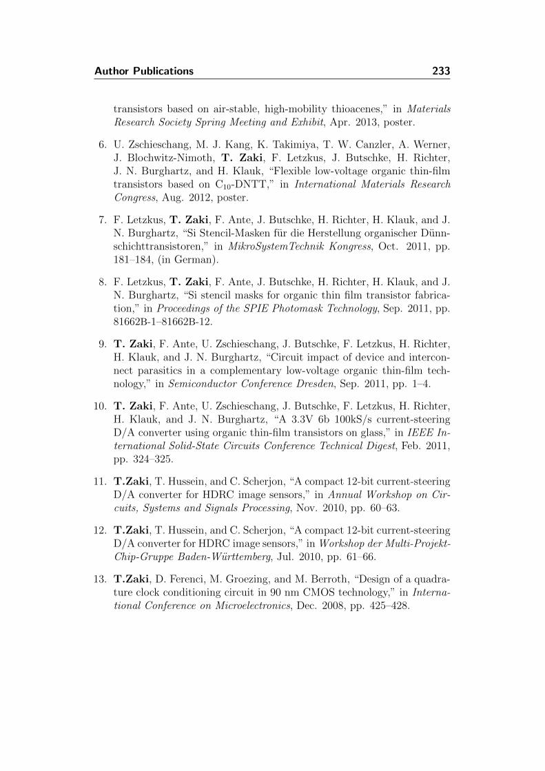
Author Publications 233
transistors based on air-stable, high-mobility thioacenes,” in MaterialsResearch Society Spring Meeting and Exhibit, Apr. 2013, poster.
6. U. Zschieschang, M. J. Kang, K. Takimiya, T. W. Canzler, A. Werner,J. Blochwitz-Nimoth, T. Zaki, F. Letzkus, J. Butschke, H. Richter,J. N. Burghartz, and H. Klauk, “Flexible low-voltage organic thin-filmtransistors based on C10-DNTT,” in International Materials ResearchCongress, Aug. 2012, poster.
7. F. Letzkus, T. Zaki, F. Ante, J. Butschke, H. Richter, H. Klauk, and J.N. Burghartz, “Si Stencil-Masken fur die Herstellung organischer Dunn-schichttransistoren,” in MikroSystemTechnik Kongress, Oct. 2011, pp.181–184, (in German).
8. F. Letzkus, T. Zaki, F. Ante, J. Butschke, H. Richter, H. Klauk, and J.N. Burghartz, “Si stencil masks for organic thin film transistor fabrica-tion,” in Proceedings of the SPIE Photomask Technology, Sep. 2011, pp.81662B-1–81662B-12.
9. T. Zaki, F. Ante, U. Zschieschang, J. Butschke, F. Letzkus, H. Richter,H. Klauk, and J. N. Burghartz, “Circuit impact of device and intercon-nect parasitics in a complementary low-voltage organic thin-film tech-nology,” in Semiconductor Conference Dresden, Sep. 2011, pp. 1–4.
10. T. Zaki, F. Ante, U. Zschieschang, J. Butschke, F. Letzkus, H. Richter,H. Klauk, and J. N. Burghartz, “A 3.3V 6b 100kS/s current-steeringD/A converter using organic thin-film transistors on glass,” in IEEE In-ternational Solid-State Circuits Conference Technical Digest, Feb. 2011,pp. 324–325.
11. T.Zaki, T. Hussein, and C. Scherjon, “A compact 12-bit current-steeringD/A converter for HDRC image sensors,” in Annual Workshop on Cir-cuits, Systems and Signals Processing, Nov. 2010, pp. 60–63.
12. T.Zaki, T. Hussein, and C. Scherjon, “A compact 12-bit current-steeringD/A converter for HDRC image sensors,” in Workshop der Multi-Projekt-Chip-Gruppe Baden-Wurttemberg, Jul. 2010, pp. 61–66.
13. T.Zaki, D. Ferenci, M. Groezing, and M. Berroth, “Design of a quadra-ture clock conditioning circuit in 90 nm CMOS technology,” in Interna-tional Conference on Microelectronics, Dec. 2008, pp. 425–428.

Acknowledgements
“The essence of all beautiful art, all great art, is gratitude.”—Friedrich Nietzsche (1844–1900)
The past four years of my research journey at the University of Stuttgartand the Institute for Microelectronics Stuttgart (IMS CHIPS) have beenchallenging, where certainly the rewards are inspirational, sensational andpowerful. In the same way, I am in awe of the German University in Cairo(GUC) for setting the primary bricks of that journey and for that I amvery grateful. It has given me immense honor to learn from and work withmany distinguished scholars and colleagues. I am very fortunate to have beenendowed with a true passion for knowledge and cherish all these unforgettableexperiences. With the deepest gratitude, I wish to express my thankfulnesshere to all those who supported me in making this work possible.
First and foremost, I am very grateful to my advisor, Prof. Dr.-Ing.Joachim N. Burghartz, director of IMS CHIPS, for his invaluable guidanceand encouragement. His rich knowledge and insightful suggestions from theinitial conception to the end of this work are highly appreciated. I am alsogreatly indebted to his assistance in matters that were beyond the academicconcerns, which have helped me to endure all kinds of difficulties during thecourse of my graduate studies.
Furthermore, I would like to sincerely thank my supervisor, Dr. HaraldRichter, head of the ASIC department at IMS CHIPS. He enlightened mewith the first glance of research in the field of organic electronics and kept memotivated since then. He has been truly a constant inspiration to me owingto his vast amount of skills and expertise in many areas. It is no doubt thathis precious support has contributed enormously to the success of this workand I could not have imagined of a better supervisor.
I would also like to acknowledge with much appreciation the essentialrole of our partners and collaborators, who have shared generously theirmaterials, experiences and ideas. This includes Dr. Hagen Klauk and all hisgroup at the Max Planck Institute for Solid State Research; particularly Dr.Ute Zschieschang, Dr. Frederik Ante, Mr. Reinhold Rodel and Ms. UlrikeKraft. No enough words could possibly convey my thankfulness fully to themfor their endless support in fabricating the organic samples for us. Moreover,I owe special thanks to PD Dr.-Ing. habil. Susanne Scheinert and Mr. IngoHorselmann of the Institute of Solid State Electronics, Technical University
235
236 Acknowledgements
of Ilmenau, who introduced me to two-dimensional device simulations of ourorganic transistors. I have been delighted by their kind hospitality, whichmade my stay in the city of Ilmenau absolutely wonderful. I still rememberquite well the stunning view of the city from the top of Kickelhahn hill (861meter) where Goethe has written one of his most famous and admirablepoems (Wanderer’s Night Song II) onto a wall of a wooden lodge:
Over all of the hillsPeace comes anew,The woodland stillsAll through;The birds make no sound on the bough.Wait a while,Soon nowPeace comes to you.
—Goethe (1780) and translated by John Whaley (1999)
These are truly thoughtful words that I will never forget. Furthermore,my deep gratitude goes to Prof. Dr.-Ing. Manfred Berroth, Dr. SandraKlinger and Mr. Johannes Digel of the Institute of Electrical and OpticalCommunications Engineering, University of Stuttgart, for their assistance inhigh-frequency characterization. Finally, I extend my sincere thankfulnessand appreciation to Prof. Dr. Boris Murmann and Mr. Alex Omid-Zohoor,Stanford University, for their helpful and constructive discussions.
This work is partially funded by the German Research Foundation (DFG)under Grant BU 1962/4-1, thereby I would like to take this opportunity tothank them for their generous support. Likewise, I am grateful to the IEEEElectron Device Society (IEEE-EDS) for selecting me as the recipient of the2013 EDS PhD Student Fellowship award. It is an achievement that hasbrought pride to my family, colleagues, friends and myself.
I am indebted to all my colleagues at IMS CHIPS for making a veryfriendly and receptive work atmosphere, especially Dr. Florian Letzkus forfabricating stencil masks, Dr. Horst Rempp, Dr. Stefan Endler and Mr.Alexander Frank for being the best supportive office-mates, Mr. ThomasDeuble for his help with translating the abstract, Ir. Cor Scherjon for alwayssharing his wise advice, Ms. Helga Schmidtke for managing all administrativeissues, Mr. Mahadi Ul-Hassan for helping me in the laboratory and Mr.Jurgen Ade for taking professional photographs, not to mention the emotionalsupport and pleasurable company of all my friends in Germany and Egypt.
Last but not least, I must save my most intense gratitude to my belovedparents, for the most treasured and heartfelt of gifts; their wonderful love,endless support and priceless encouragement.
Tarek ZakiStuttgart, Germany