Bipolar Junction Transistors (BJTs) - Microelectronic Circuits ...

Organic Electronics 11 (2010) 1974–1990
Contents lists available at ScienceDirect
Organic Electronics
journal homepage: www.elsevier .com/locate /orgel
Environmentally sustainable organic field effect transistors
Mihai Irimia-Vladu a,f,⇑, Pavel A. Troshin b, Melanie Reisinger a, Guenther Schwabegger c,Mujeeb Ullah c, Reinhard Schwoediauer a, Alexander Mumyatov b, Marius Bodea d,Jeffrey W. Fergus e, Vladimir F. Razumov b, Helmut Sitter c, Siegfried Bauer a,Niyazi Serdar Sariciftci f
a Department of Soft Matter Physics, Johannes Kepler University, A-4040 Linz, Austriab Institute of Problems of Chemical Physics of Russian Academy of Sciences, Semenov Prospect 1, 142432, Chernogolovka, Moscow Region, Russiac Institute of Semiconductor and Solid State Physics, Johannes Kepler University, A-4040 Linz, Austriad Institute of Applied Physics, Johannes Kepler University, A-4040 Linz, Austriae Materials Research and Education Center, Auburn University, Auburn, AL 36849, USAf Linz Institute for Organic Solar Cells (LIOS), Physical Chemistry, Johannes Kepler University, A-4040 Linz, Austria
a r t i c l e i n f o a b s t r a c t
Article history:Received 16 July 2010Received in revised form 3 September 2010Accepted 4 September 2010Available online 26 September 2010
Keywords:Environmentally sustainable electronicsOrganic field effect transistorsNatural materialsBiodegradable electronicsBiocompatible electronicsEdible electronics
1566-1199/$ - see front matter � 2010 Elsevier B.Vdoi:10.1016/j.orgel.2010.09.007
⇑ Corresponding author at: Department of Soft MaInstitute for Organic Sollar Cells, Johannes Kepler UnStrasse Nr. 69, 4040 Linz, Austria. Tel.: +43 732 2462468 9273.
E-mail address: [email protected] (M. Ir
Environmentally sustainable systems for the design, production, and handling of electronicdevices should be developed to solve the dramatic increase in electronic waste. Sustain-ability in plastic electronics may be the production of electronic devices from natural mate-rials, or materials found in common commodity products accepted by society. Therebybiodegradable, biocompatible, bioresorbable, or even metabolizable electronics maybecome reality. Transistors with an operational voltage as low as 6 V, a source drain cur-rent of up to 0.5 lA and an on–off ratio up to four orders of magnitude, with saturated fieldeffect mobilities in the range of 1.5 � 10�4 to 2 � 10�2 cm2/V s, have been fabricated withsuch materials. Our work comprises steps towards environmentally safe devices in low-cost, large volume, disposable or throwaway electronic applications, such as in food pack-aging, plastic bags, and disposable dishware. In addition, there is significant potential touse such electronic items in biomedical implants. As such, organic materials offer a uniqueopportunity to guide electronics industry towards an environmentally safe direction.
� 2010 Elsevier B.V. All rights reserved.
1. Introduction
Two major concerns in the world nowadays are plasticconsumption and waste. Due to the economic growthand the increased demand in developing countries, plasticsconsumption is projected to increase by a factor of two tothree during the current decade [1]. A consequence of thisincessant demand of plastics in the world is the accumula-tion of non-biodegradable solid waste and plastic litter
. All rights reserved.
tter Physics and Linziversity, Altenberger
8 9293; fax: +43 732
imia-Vladu).
with negative effects on our environment. As an example,the amount of municipal solid waste per person per yearaverages �440 kg/yr for China, �550 kg/yr for the Euro-pean Union and �790 kg/yr for the United States, withroughly half of the waste being electronic products andplastics [1,2]. Taking into account the expected increaseof plastic electronics in low-cost, large volume, disposableor throwaway applications, plastic waste problems maybecome even more dramatic. More effort will be necessaryin order to minimize the negative impact of the increasingproduction, consumption and disposal of both polymermaterials and electronic circuits [3].
There have been so far several initial reports addressingthe use of biodegradable substrates in organic electronics,such as poly (L-lactide-co-glycolide) [4], paper [5–9],

M. Irimia-Vladu et al. / Organic Electronics 11 (2010) 1974–1990 1975
leather [10] or even silk [11,12]. Here we present an initialstudy of using natural, nature-inspired and common com-modity materials which are widely accepted by society forsustainable electronics. The rationale for choosing materi-als from sugar family, small molecular nucleobases, beta-carotene, indigo, food colors (indanthrenes) and cosmeticcolors (perylene diimide) on substrates such as glucose,hard gelatine and biodegradable polymers is to showhow large the materials base may become for organic elec-tronics, when low cost and sustainability is a concern. Welimit our work to the electrical characterization of thesematerials and to the demonstration of field-effect transis-tors, a first step towards building more complex electronicintegrated circuits. We consider unusual substrates, suchas Ecoflex, hard gelatine capsules and caramelized glucose,to enhance the substrate materials base for organic elec-tronics. High-performance, biocompatible and biodegrad-able organic field-effect transistors operating at lowvoltages are demonstrated by the evaporation of ultrathinlayers of natural nucleobase dielectrics (adenine and guan-ine) on inorganic oxide dielectrics, a viable alternative tothe passivation of such oxide dielectrics with self-assem-bled monolayers [13,14]. Semiconductors chosen includenatural compounds like beta-carotene and indigo, as wellas perylene diimide (a lipstick colorant), indanthrene yel-low G and indanthrene brilliant orange RF, colorants usedfor example in textile and food industry. Having identifiednatural and nature-inspired p- and n-type semiconductors,opens ways to fabricate integrated circuits, based oninverters, ring oscillators, logical elements, etc. We hopethat this initial study initiates an intense search for newmaterials and material combinations to finally end up withsustainable plastic electronic products.
2. Experimental
2.1. Preparation and/or purification of materials
Dielectric and semiconductor compounds employed(adenine, guanine, cytosine, thymine, caffeine, indigo,indanthrene yellow G) were purchased from Sigma–Aldrich and additionally purified by two vacuum sublima-tion cycles performed in a closed quartz tube. Indanthrenebrilliant orange RF was purchased from Shanghai JuchengChemical Co., and purified by three vacuum sublimationcycles; its chemical composition was proven by mass spec-trometry. Poly (vinyl alcohol) (Mowiol�40-88, electronicgrade) was purchased from Kuraray Specialities EuropeGmbH and used as received. D-(+)-glucose, lactose, andbeta-carotene were purchased from Sigma–Aldrich andused without further purification. Ecoflex foil was pur-chased from BASF and hard gelatine capsules from a localpharmacy in Linz, Austria.
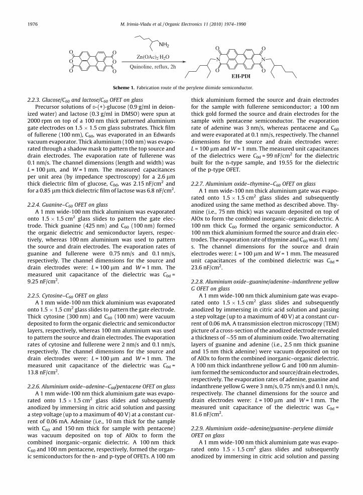
2.1.1. Perylene diimide: synthesis and analysisPerylene diimide (EH-PDI) was synthesized as shown in
Scheme 1. Perylene-3,4,9,10-tetracarboxylic acid dianhy-dride (5 g, 12.8 mmol) was mixed with 60 ml of freshly dis-tilled quinoline, 15 g (116 mmol) of 2-ethylhexylamineand ca. 100 mg of Zn(OAc)2�H2O.
The obtained mixture was heated at reflux for 2 h,cooled down to room temperature and poured into600 ml of 10% aqueous hydrochloric acid. The precipitateformed was removed by filtration, extracted with metha-nol and dried in air. The resulting crude sample of perylenediimide was purified by column chromatography. Elutionwith a CH2Cl2–methanol mixture (95.5:0.5 v/v) produceda pure compound EH-PDI. The final purification was per-formed by sublimation at 450–500 �C under a reducedpressure of �10�2 mbar. The yield of EH-PDI was in therange of 45–55%.
The NMR and FTIR spectra are summarized below:1H NMR (400 MHz, CDCl3,) d = 8.83 (d, 4H, H-Ar), 8.75
(d, 4H, H-Ar), 4.31 (m, 4H, NCH2), 2.14 (m, 2H, CH), 1.58(m, 8H, CH2), 1.50 (m, 8H, CH2), 1.13 (t, 6H, CH3), 1.06 (t,6H, CH3), ppm. Chemical analysis: C40H42N2O4.
Calculated: C, 78.15; H, 6.89; N, 4.56. Found: C, 77.95;H, 6.97; N, 4.61.
IR spectrum (KBr pellet): m = 745, 809, 1178, 1247, 1308,1346, 1380, 1403, 1441, 1577, 1594, 1615, 1650, 1695,2859, 2873, 2930, 2958 cm�1.
2.2. Device fabrication
2.2.1. Glucose/caffeine-beta-carotene OFET on glassPrecursor solution of D-(+)-glucose (0.9 g/ml) and
caffeine (0.02 g/ml) was prepared in deionized water(�18 MX cm). The mixture was stirred for 60 min at60 �C. Beta-carotene solutions (10 mg/ml in chloroform)were prepared under inert atmosphere in a glove bow.Thin films of glucose containing also caffeine were spunat 2000 rpm on top of a 100 nm thick patterned aluminiumgate on a 1.5 � 1.5 cm glass substrate. The spun sampleswere dried overnight in a vacuum oven at 55 �C. Beta-carotene thin film was spin coated at 2000 rpm for 60 sunder inert atmosphere. A 100 nm thick gold layer wasevaporated through a shadow mask to pattern the topsource and drain electrodes. The channel dimensions(length and width) was L = 100 lm, and W = 1 mm. Themeasured capacitance per unit area (by impedance spec-troscopy) of a 3.1 lm thick dielectric film of glucose withcaffeine was C0d = 1.9 nF/cm2. The measured unit capaci-tance of a 2.6 lm thick film cast from glucose solution(0.9 g/ml in deionized water, with no caffeine addition)was 2.15 nF/cm2.
2.2.2. PVA/Indigo OFET on glassPrecursor solution of PVA (0.08 g/ml) was prepared in
deionized water (�18 MX cm) and the mixture was stirredfor 24 h at 90 �C. Thin films of PVA were spun at 2000 rpmon top of a 100 nm thick patterned aluminium gate on a1.5 � 1.5 cm glass substrate. 100 nm thick indigo layerwas vacuum processed in an Edwards evaporator. A100 nm thick aluminium layer was evaporated through ashadow mask to pattern the top source and drain elec-trodes. The evaporation rate of indigo was 0.1 nm/s. Thechannel dimensions (length and width) was L = 100 lm,and W = 1 mm. The measured capacitance per unit area(by impedance spectroscopy) of a 2 lm thick dielectric filmof PVA was C0d = 3.1 nF/cm2.
OO
O
OO
OQuinoline, reflux, 2h
Zn(OAc)2.H2O N
O
O
N
O
O
EH-PDI
NH2
Scheme 1. Fabrication route of the perylene diimide semiconductor.
1976 M. Irimia-Vladu et al. / Organic Electronics 11 (2010) 1974–1990
2.2.3. Glucose/C60 and lactose/C60 OFET on glassPrecursor solutions of D-(+)-glucose (0.9 g/ml in deion-
ized water) and lactose (0.3 g/ml in DMSO) were spun at2000 rpm on top of a 100 nm thick patterned aluminiumgate electrodes on 1.5 � 1.5 cm glass substrates. Thick filmof fullerene (100 nm), C60, was evaporated in an Edwardsvacuum evaporator. Thick aluminium (100 nm) was evapo-rated through a shadow mask to pattern the top source anddrain electrodes. The evaporation rate of fullerene was0.1 nm/s. The channel dimensions (length and width) wasL = 100 lm, and W = 1 mm. The measured capacitancesper unit area (by impedance spectroscopy) for a 2.6 lmthick dielectric film of glucose, C0d, was 2.15 nF/cm2 andfor a 0.85 lm thick dielectric film of lactose was 6.8 nF/cm2.
2.2.4. Guanine–C60 OFET on glassA 1 mm wide-100 nm thick aluminium was evaporated
onto 1.5 � 1.5 cm2 glass slides to pattern the gate elec-trode. Thick guanine (425 nm) and C60 (100 nm) formedthe organic dielectric and semiconductor layers, respec-tively, whereas 100 nm aluminium was used to patternthe source and drain electrodes. The evaporation rates ofguanine and fullerene were 0.75 nm/s and 0.1 nm/s,respectively. The channel dimensions for the source anddrain electrodes were: L = 100 lm and W = 1 mm. Themeasured unit capacitance of the dielectric was C0d =9.25 nF/cm2.
2.2.5. Cytosine–C60 OFET on glassA 1 mm wide-100 nm thick aluminium was evaporated
onto 1.5 � 1.5 cm2 glass slides to pattern the gate electrode.Thick cytosine (300 nm) and C60 (100 nm) were vacuumdeposited to form the organic dielectric and semiconductorlayers, respectively, whereas 100 nm aluminium was usedto pattern the source and drain electrodes. The evaporationrates of cytosine and fullerene were 2 nm/s and 0.1 nm/s,respectively. The channel dimensions for the source anddrain electrodes were: L = 100 lm and W = 1 mm. Themeasured unit capacitance of the dielectric was C0d =13.8 nF/cm2.
2.2.6. Aluminium oxide–adenine–C60/pentacene OFET on glassA 1 mm wide-100 nm thick aluminium gate was evapo-
rated onto 1.5 � 1.5 cm2 glass slides and subsequentlyanodized by immersing in citric acid solution and passinga step voltage (up to a maximum of 40 V) at a constant cur-rent of 0.06 mA. Adenine (i.e., 10 nm thick for the samplewith C60 and 150 nm thick for sample with pentacene)was vacuum deposited on top of AlOx to form thecombined inorganic–organic dielectric. A 100 nm thickC60 and 100 nm pentacene, respectively, formed the organ-ic semiconductors for the n- and p-type of OFETs. A 100 nm
thick aluminium formed the source and drain electrodesfor the sample with fullerene semiconductor; a 100 nmthick gold formed the source and drain electrodes for thesample with pentacene semiconductor. The evaporationrate of adenine was 3 nm/s, whereas pentacene and C60
and were evaporated at 0.1 nm/s, respectively. The channeldimensions for the source and drain electrodes were:L = 100 lm and W = 1 mm. The measured unit capacitancesof the dielectrics were C0d = 99 nF/cm2 for the dielectricbuilt for the n-type sample, and 19.55 for the dielectricof the p-type OFET.
2.2.7. Aluminium oxide–thymine–C60 OFET on glassA 1 mm wide-100 nm thick aluminium gate was evapo-
rated onto 1.5 � 1.5 cm2 glass slides and subsequentlyanodized using the same method as described above. Thy-mine (i.e., 75 nm thick) was vacuum deposited on top ofAlOx to form the combined inorganic–organic dielectric. A100 nm thick C60 formed the organic semiconductor. A100 nm thick aluminium formed the source and drain elec-trodes. The evaporation rate of thymine and C60 was 0.1 nm/s. The channel dimensions for the source and drainelectrodes were: L = 100 lm and W = 1 mm. The measuredunit capacitances of the combined dielectric was C0d =23.6 nF/cm2.
2.2.8. Aluminium oxide–guanine/adenine–indanthrene yellowG OFET on glass
A 1 mm wide-100 nm thick aluminium gate was evapo-rated onto 1.5 � 1.5 cm2 glass slides and subsequentlyanodized by immersing in citric acid solution and passinga step voltage (up to a maximum of 40 V) at a constant cur-rent of 0.06 mA. A transmission electron microscopy (TEM)picture of a cross-section of the anodized electrode revealeda thickness of�55 nm of aluminium oxide. Two alternatinglayers of guanine and adenine (i.e., 2.5 nm thick guanineand 15 nm thick adenine) were vacuum deposited on topof AlOx to form the combined inorganic–organic dielectric.A 100 nm thick indanthrene yellow G and 100 nm alumin-ium formed the semiconductor and source/drain electrodes,respectively. The evaporation rates of adenine, guanine andindanthrene yellow G were 3 nm/s, 0.75 nm/s and 0.1 nm/s,respectively. The channel dimensions for the source anddrain electrodes were: L = 100 lm and W = 1 mm. Themeasured unit capacitance of the dielectric was C0d =81.6 nF/cm2.
2.2.9. Aluminium oxide–adenine/guanine–perylene diimideOFET on glass
A 1 mm wide-100 nm thick aluminium gate was evapo-rated onto 1.5 � 1.5 cm2 glass slides and subsequentlyanodized by immersing in citric acid solution and passing

M. Irimia-Vladu et al. / Organic Electronics 11 (2010) 1974–1990 1977
a step voltage (up to a maximum of 40 V) at a constant cur-rent of 0.06 mA. Two alternating layers of guanine and ade-nine (i.e., 2.5 nm thick guanine and 15 nm thick adenine)were vacuum deposited on top of aluminium oxide to formthe combo inorganic–organic dielectric. A 100 nm thickperylene diimide and 100 nm aluminium patterned thesemiconductor and source and drain electrodes, respec-tively. The evaporation rates of adenine, guanine and per-ylene diimide were 3 nm/s, 0.75 nm/s and 0.1 nm/s,respectively. The source and drain electrodes had the chan-nel dimensions: L = 100 lm, W = 1 mm. The measuredcapacitance per unit area of the combined dielectric wasC0d = 81.6 nF/cm2. The measured capacitance per unit areaof the plain AlOx was 140 nF/cm2.
2.2.10. Aluminium oxide–adenine/guanine–indanthrenebrilliant orange RF OFET on glass
A 1 mm wide-100 nm thick aluminium gate was evapo-rated onto 1.5 � 1.5 cm2 glass slides and subsequentlyanodized by immersing in citric acid solution, using themethod described. Two alternating layers of guanine andadenine (i.e., 2.5 nm thick guanine and 15 nm thick ade-nine) were vacuum deposited; followed by 100 nm thickindanthrene brilliant orange RS and 100 nm gold sourceand drain electrodes. The source and drain electrodes hadthe channel dimensions: L = 35 lm, W = 7 mm. Gold,rather than aluminium, was used for contacting the n-typesemiconductor. Adenine was evaporated at a rate of 3 nm/s, guanine at 0.75 nm/s and indanthrene brilliant orange RFat a rate of 0.1 nm/s. The measured capacitance per unitarea of the dielectric was C0d = 81.6 nF/cm2.
2.2.11. Adenine–perylene diimide OFET on EcoflexAurin (0.1 g/ml in pure ethyl alcohol) was spun at
2000 rpm for 60 s onto 1.5 � 1.5 cm2 Ecoflex foils to actas a smoothening layer. A 1 mm wide-100 nm thick alu-minium gate was evaporated through a shadow mask; A1.1 lm thick adenine and 100 nm thick perylene diimidewere evaporated in an Edwards high vacuum evaporationsystem at a pressure of 10�6 torr to pattern the gate dielec-tric and semiconductor, respectively. A 100 nm thickaluminium layer formed the top drain and source elec-trodes. The evaporation rate was 3 nm/s for adenine, and0.1 nm/s for perylene diimide. The channel dimensionswere L = 100 lm, W = 1 mm. The measured capacitanceper unit area of the dielectric was C0d = 3.1 nF/cm2.
2.2.12. Adenine/guanine–indanthrene yellow G OFET oncaramelized glucose
As received powder of D-(+)-glucose was melted on topof a hot plate at �225–250 �C and droplets were depositedwith a glass rod on aluminium foil wrapped around1.5 � 1.5 cm glass slides. Wrapping aluminium aroundthe glass slides was necessary to prevent the solidified glu-cose from cracking during cooling to room temperature. Athin layer of rosolic acid (50 nm) was vacuum evaporatedto serve a double role: (1) to act as a smoothening layerand (2) to prevent the caramelized glucose substrate toswollen during the gold gate electrode patterning. A100 nm thick-1 mm wide gold gate electrode was evapo-rated in a metal evaporator. The gate dielectric was formed
by four alternating layers of guanine and adenine (75 nmthick each of the first three layers of guanine and adenine,and 400 nm thick adenine-the fourth layer), and 100 nmindanthrene yellow G was used as organic semiconductor.Adenine was evaporated at a rate of 3 nm/s, whereas guan-ine and indanthrene yellow G at a rate of 0.1 nm/s. A100 nm thick layer of gold patterned the source and drainelectrodes. The channel dimensions were: L = 100 lm andW = 1 mm. The measured unit capacitance of the combineddielectric was C0d = 5.6 nF/cm2.
2.2.13. Adenine/guanine–perylene diimide OFET on hardgelatine capsules
Hard gelatine capsules were cut open and stuck withthe aid of a double-side scotch tape on 1.5 � 1.5 cm2 glasssubstrates in order to force the gelatine substrate remain ina flat-open position. Rosolic acid (0.1 g/ml in pure ethyl-alcohol) was spun at 2000 rpm for 60 s on top of capsulesubstrates to act as a smoothening layer. A 1 mm wide-100 nm thick gold gate was evaporated through a shadowmask followed by four alternating layers of guanine andadenine (75 nm thick the first and the third layer of guan-ine, 100 nm and 500 nm thick the second and fourth layerof adenine) to form the gate electrode and gate dielectric,respectively. A 100 nm thick perylene diimide was evapo-rated to pattern the semiconductor layer and a 100 nmthick gold source and drain electrodes were subsequentlyevaporated. The evaporation rate was 1 nm/s for guanine,3 nm/s for adenine, and 0.1 nm/s for perylene diimide.The source and drain electrodes had the channel dimen-sions: L = 100 lm, W = 1 mm. The measured capacitanceper unit area of the dielectric was C0d = 5.1 nF/cm2.
2.3. Device characterization
Steady state current–voltage measurements were per-formed with an Agilent E5273A instrument. Both transferand output characteristics were measured at a sweep rateof 66 mV s�1, with 1 s for each of the hold, delay and stepdelay times, respectively.
Dielectric characterization of the gate dielectrics wasperformed with metal–insulator–metal capacitors using aNovocontrol Alpha Analyzer. X-ray diffraction was per-formed using a Bruker AXS X-ray Diffractometer (Cu Ka)X-ray Diffractometer. AFM investigation was performedusing a Digital Instruments Dimension 3100 microscopeworking in tapping mode.
3. Results and discussion
3.1. Field effect transistors
Field effect transistors rely on an electric field (suppliedby the gate voltage, Vgs, applied between the groundedsource and the gate) to control the conductivity of a chan-nel at the interface between the semiconductor and theinsulator, and hence the current between source and draincontacts Ids. A measure of the quality of the dielectric isgiven by the leakage current from the gate to the sourcecontacts through the insulator layer, Igs. Field effect

1978 M. Irimia-Vladu et al. / Organic Electronics 11 (2010) 1974–1990
transistor preparation requires substrates, smoothing lay-ers when the substrate is rough, metal electrodes, gatedielectrics and organic semiconductors. Fig. 1 illustrates
Fig. 1. Natural materials or materials inspired by nature used for fabrication of enbottom-gate, top-contact OFET employed in this work; (b) schematic of rosolic aproduced from potato and corn starch, hard gelatine capsule originating from cnucleobase and sugar families: adenine, guanine, cytosine, thymine glucose andp- and n-type organic semiconductors; indanthrene yellow G and indanthrene band perylene diimide, a cosmetic color. Glass, aluminium oxide, poly(vinyl alcohsemiconductor materials widely employed in the field, used here for comparisinspired materials may ultimately provide the basis for ‘‘sustainable green elect
such a transistor with all the components employed in thiswork presented in the schematic form. In the following, westart discussing first substrates, then gate dielectrics and
vironmentally sustainable organic field effect transistors. (a) Schematic ofcid (aurin), used here as smoothener; (c) substrates investigated: Ecoflexollagen and caramelized glucose; (d) natural dielectrics materials in thelactose; (e) semiconductor materials: b-carotene and indigo are natural
rilliant orange RF are semiconductors derived from natural anthraquinoneol), C60 and pentacene are examples of workhorse substrate, dielectric andon. Transistors and integrated circuits produced from natural or natureronics”.

Fig. 2. AFM pictograms of (a) plain Ecoflex foil (rms �70 nm); (b) aurin-coated Ecoflex foil (rms �8 nm); (c) plain hard gelatine capsule (rms �30 nm); (d)aurin-coated hard gelatine capsule (rms �9 nm).
Table 1Dielectric performance of investigated materials.
Material Dielectric constant(at 1 kHz)
Breakdownfield (MV/cm)
Loss tangent(at 100 mHz)
DielectricsAdenine �3.85 �1.5 �4 � 10�3
Cytosine �4.65 �3.4 �5 � 10�3
Guanine �4.35 �3.5 �7 � 10�3
Thymine �2.4 �0.9 �1 � 10�2
Glucose �6.35 �1.5 �5 � 10�2
Lactose �6.55 �4.5 �2 � 10�2
Caffeine �4.1 �2 �9 � 10�2
PVA �6.1 �2 �4 � 10�2
AlOx �9 �3.5 �4 � 10�3
M. Irimia-Vladu et al. / Organic Electronics 11 (2010) 1974–1990 1979
organic semiconductors, together with examples of field-effect transistors built on either glass or biodegradable/biocompatible substrates.
3.1.1. Substrates for sustainable electronicsFabric, hot-pressed cotton-fiber paper, leather and silk
have been recently reported as examples of biodegradableand biocompatible-sustainable substrates for organic fieldeffect transistors [4,5,10,11]. Other examples of such sub-strates are presented here; they include hard gelatine,commercially available biodegradable polymers and evencaramelized sugar for edible devices.
Hard gelatine capsule is a fully biocompatible and bio-degradable substrate employed extensively in the pharma-ceutical field for oral drug delivery. Gelatine capsules aremade from pork skin and bones and may contain smalladditions of plasticizers (e.g., glycerin and sorbitol), preser-vatives, colors, flavors (e.g., ethylvanilin and essential oil),sugars, etc. Their widespread availability, the ease of pro-duction in various forms and the complete biodegradabil-ity make gelatine capsules an interesting substrate forelectronics. Such electronics may even be ingested in thebody in biomedical applications. Ecoflex is a commercially
available (BASF) biodegradable polymer based on potatostarch, corn and polylactic acid. Ecoflex degrades in com-post in 6 months without leaving any residue [15]. Sincethe use of such polymers for various low-end, biodegrad-able applications will most likely increase, it is interestingto explore them also as a substrate for organic electronics.Caramelized glucose is employed as another example ofsubstrates for the preparation of OFETs; it allows for the

Fig. 3. AFM of nucleobase thin films on aluminium covered glass a) 1000 nm adenine (rms �14.5); (b) 425 nm guanine (rms �3); (c) 350 nm cytosine (rms�24); (d) 450 nm thymine (rms �65).
1980 M. Irimia-Vladu et al. / Organic Electronics 11 (2010) 1974–1990
fabrication of bio-metabolizable (edible) electronics. Allsubstrates mentioned here have large surface roughnesses,with root-mean-square (rms) values between 30 nm and80 nm, necessitating the addition of a smoothing layer inorder to decrease their roughness to values that allow fab-rication of electronic components on such materials.
3.1.2. Smoothening layerInitial work on paper substrates employed a smoothen-
ing layer formed by a thin spin-coated polymer film (poly-dimethylsiloxane, PDMS) to reduce the inherent roughnessof the substrate [5,10]. While being biocompatible andsolution processible, the polymer film required thermalcross-linking to render the structure amenable for the pat-terning of electrodes and further device preparation. Aurin(rosolic acid), a compound with a simple synthetic chemis-try (i.e., produced by the reaction of phenol with oxalicacid in concentrated sulfuric acid bath) and which occursalso naturally (being extracted from the rhizomes of a freegrowing plant (Plantago asiatica L.)) [16,17] is used here asa smoothing layer. In traditional Chinese medicine,Plantago asiatica L. is known for its medicinal properties,used as anti-inflammatory, antiseptic, diuretic, expecto-
rant, etc. [18]. In the medical and pharmacological fields,aurin is currently explored as heme-oxygenase activityregulator in aortic endothelial cells or as a generator ofandrogen receptors in binding assays that mimic thefunctions of natural hormones [17,19]. Being a naturallyoccurring compound with a simple chemistry and easybiodegradability, aurin represents an interesting candidatefor the smoothening layer of various rough substrates.Fig. 2a and c shows the surface roughness of Ecoflex andgelatine capsules, with rms roughness values of �70 nmand �30 nm, respectively. As presented in Fig. 2b and d,the substrate roughness, rms, is reduced to 8 nm forEcoflex and 9 nm for hard gelatine after spin-coating aurin,solution processed in ethyl-alcohol.
3.1.3. Natural dielectrics for sustainable organic field effecttransistors
Nature provides an overwhelming number of materialsthat are degradable, so looking for natural dielectricsappears to be a promising route for sustainability in organicelectronics. We first describe dielectrics from the sugarfamily, followed by dielectrics from the nucleobase family,both groups comprising naturally occurring-biodegradable

10 20 30 40 50 60 70
0
50
100
150
0
150
300
450
24.52
2θ (deg.)
Adenine Thin Film29.42
58.4451.8449.844.08
39.4433.3431
13.9 16.8
24.5
Adenine Powder
Inte
nsity
(a.u
.)
29.26
Fig. 4. X-ray diffraction profiles of precursor adenine (a) and evaporated adenine (b); the corresponding crystallographic planes are conforming to thepattern in a standard card.
-2
10-11
10-10
10-9
10-8
10-7
Vgs (V)
I ds
(A)
Ids
Vds = + 22 V(c)
Igs
0.0
0.1
0.2
0.3
0.4
0.5
I ds
(µA
)I d
s (µ
A)
(d) 0 V 2.5 V 5 V 7.5 V 10 V 12.5 V 15 V 17.5 V 20 V 20.5 V 25 V
0.00
0.05
0.10
0.15(b) 0 V 1.5 V 3 V 4.5 V 6 V 7.5 V 9 V 10.5 V 12 V
-12
5-20-15-10 -5 0 5 10 15 20 25 0 5 10 15 20 25
0 2 4 6 8 10 12-9 -6 -3 0 3 6 9 1210-12
10-11
10-10
10-9
10-8
10-7
Vgs (V) Vds (V)
Vds (V)
I ds
(A)
Vds = + 11 V
Ids
(a)
Igs
Fig. 5. Transfer and output characteristics of OFETs with (a and b) solution processed lactose gate and C60 semiconductor channel; capacitance per unitarea, C0d = 6.8 nF/cm2, field-effect mobility l = 0.055 cm2/V s, subthreshold swing S = 2 V/dec and normalized subthreshold swing Sn = 13.6 V nF/cm2 dec; (cand d) solution processed glucose gate and C60 channel. Capacitance: C0d = 2.15 nF/cm2, field-effect mobility l = 0.085 cm2/V s, subthreshold swingS = 6.2 V/dec and normalized subthreshold swing Sn = 13.3 V nF/cm2 dec.
M. Irimia-Vladu et al. / Organic Electronics 11 (2010) 1974–1990 1981
compounds with a long history in chemistry orbiochemistry.
3.1.3.1. Dielectrics from the sugar family (lactose, glu-cose). Glucose and lactose are two of many other simplesmall molecules in the sugar family. They are industriallyproduced on a very large scale, are non-toxic and have
excellent film forming properties, when solution processedfrom water and/or DMSO. The measured dielectric proper-ties of films of glucose and lactose (dielectric constant,breakdown field and loss tangent) are displayed in Table 1.AFM graphs of the spin-cast films are essentially feature-less and display a root-mean-square (rms) roughness inthe range of 0.5–1 nm. In addition to their excellent film

0-10
-9
-8
-7
-6 -5 -4 -3 -2 -1 0 1 2 3 4 5 6
1
10
10
10
Vgs (V)
Vds = + 4.75 V
I ds
(A)
Ids
(a)
Igs
0 1 2 3 4 5
0.00
0.04
0.08
0.12
Vds (V)
I ds
(μA
)
(b) 0 V 0.5 V 1 V 1.5 V 2 V 2.5 V 3 V 3.5 V 4 V 4.5 V 5 V
0 1 2 3 4-20
0
20
40
60
80
100
Vds (V)
I ds
(nA
)
(d) 0 V 0.4 V 0.8 V 1.2 V 1.6 V 2 V 2.4 V 2.8 V 3.2 V 3.6 V 4 V
-4 -2 0 2 40-11
0-10
-9
-8
-7
1
1
10
10
10
Vgs (V)
I ds
(A)
Vds = + 3.75 V
Igs Ids
(c)
Fig. 6. Transfer and output characteristics of OFETs with (a and b) Guanine gate and C60 channel. Capacitance per area, C0d = 9.25 nF/cm2, field effectmobility l = 0.12 cm2/V s, subthreshold swing S = 1.4 V/dec and normalized subthreshold swing Sn = 12.9 V nF/cm2 dec; (c and d) cytosine gate and C60
channel. Capacitance per area, C0d = 13.8 nF/cm2, field effect mobility l = 0.09 cm2/V s, subthreshold swing S = 1.2 V/dec and normalized subthresholdswing Sn = 16.6 V nF/cm2 dec.
1982 M. Irimia-Vladu et al. / Organic Electronics 11 (2010) 1974–1990
forming properties, the two small molecules are good insu-lators as shown by the low dielectric losses measured overa wide frequency range (10 kHz to 10 mHz). In addition,glucose and lactose have relatively high breakdown volt-ages of �1.5 MV/cm and �4.5 MV/cm, respectively.
3.1.3.2. Dielectrics from the nucleobase family (adenine,guanine, cytosine and thymine). DNA, recently consideredfor photonics as well as other electronic applications[20,21], has been employed also as gate dielectric in organ-ic field effect transistors [22–24]. The main drawback ofthe use of DNA as an organic dielectric is the occurrenceof hysteresis in the transfer characteristics of organic fieldeffect transistors [22–24], probably caused by the presenceof mobile ionic impurities in the natural DNA dielectric.However, DNA is composed of alternating sequences offour nucleobases (adenine, guanine, cytosine and thy-mine). Being small molecules, nucleobases are amenablefor scrupulous purification and can be vacuum processedin thin films of thicknesses scaled down to 2.5 nm, as it willbe shown in this work. Their natural abundance, low costand low toxicity make these materials interesting candi-dates for organic electronics. Guanine and adenine, forexample, occur naturally in many biological systems.Guanine can be extracted from bat droppings, as well asfish skin and scales [25]. Currently, the cosmetic industryrelies on small additions of guanine into shampoo, facialcreams and nail enamels to render them an iridescent blu-ish-white tint. Adenine is also a natural product, freely pro-
duced in most of the fruits, whole grains, raw honey andpropolis, etc.
The dielectric properties of thin evaporated films ofadenine, guanine, cytosine and thymine presented in Table1 show low losses and featureless dielectric functions overa wide frequency window, ranging from 10 kHz to 10 mHz.The breakdown voltage of the four investigated nucleo-bases ranges from 0.9 MV/cm to 3.5 MV/cm, which makesthese materials suitable for use as gate dielectric in field ef-fect transistors.
AFM surface investigations of thin films of adenine,guanine, cytosine and thymine are presented in Fig. 3a–d.Vacuum processed nucleobase thin films show a tendencyfor crystallization, with increasing surface roughness start-ing from guanine (rms �3 nm) to adenine (rms �14.5 nm),cytosine (rms �24 nm) and thymine (rms �65 nm). Theinvestigation of the fifth nucleobase, uracil, proved difficultbecause of its extreme tendency for crystallization. Withthis respect, thin films of uracil displayed pin-holes,whereas thicker films had a roughness with root-mean-square values greater than 100 nm.
An example of the X-ray diffraction investigation foradenine in the forms of precursor powder and 1 lm thickevaporated film on aluminium coated glass slide is pre-sented in Fig. 4. The crystallographic planes are conformingto the pattern available in the standard card (JSPDS no. 24-1654) of the instrument. As shown in Fig. 4, adenine thinfilms display crystallinity and preferred orientation com-pared to precursor powder, as it is suggested by strong

0 100 200 300 400 500
0.0
0.4
0.8
1.2
I ds
(μA
)
Vds (mV)
-0.5 V -0.4 V -0.3 V -0.2 V -0.1 V 0 V 0.1 V 0.2 V 0.3 V 0.4 V 0.5 V
-1000 -500 0 50010-10
10-9
10-8
10-7
10-6
IgsI d
s (A
)
Vgs (mV)
Vds = + 0.5 V
Ids
(a)
(c) (d)
(e) (f)
(b)
-9 -6 -3 0 3 6 9 12 1510-12
10-11
10-10
10-9
10-8
10-7
10-6 Vds = + 14.5 V
Vgs (V)
I ds
(A)
Ids
Igs
0 3 6 9 12 15
0.0
0.4
0.8
1.2
1.6
2.0
I ds
(μA
)
Vds (V)
0 V 1.5 V 3 V 4.5 V 6 V 7.5 V 9 V 10.5 V 12 V 13.5 V 15 V
-16 -14 -12 -10 -8 -6 -4 -2 0-2.0
-1.6
-1.2
-0.8
-0.4
0.0
0.4
Vds (V)
I ds
(μA
) -1 V -2.4 V -3.8 V -5.2 V -6.6 V -8 V -9.4 V -10.8 V -12.2 V -13.6 V -15 V
-15 -12 -9 -6 -3 0 310-11
10-10
10-9
10-8
10-7
10-6 Vds = - 12.5 V
Ids
I ds
(A)
Vgs (V)
Igs
Fig. 7. Transfer and output characteristics of OFETs with (a and b) an AlOx–adenine gate and hot-wall epitaxial deposited C60 channel. Capacitance per area,C0d = 99 nF/cm2, field effect mobility l = 5.5 cm2/V s, subthreshold swing S = 0.25 V/dec and normalized subthreshold swing Sn = 24.7 V nF/cm2 dec; (c andd) AlOx–adenine gate and pentacene channel. Capacitance per area, C0d = 19.6 nF/cm2, field effect mobility l = 0.35 cm2/V s, subthreshold swing S = 2.5 V/dec and normalized subthreshold swing Sn = 49 V nF/cm2 dec; (e and f) AlOx–thymine gate and C60 channel. Capacitance per area, C0d = 23.6 nF/cm2, fieldeffect mobility l = 0.5 cm2/V s, subthreshold swing S = 2 V/dec and normalized subthreshold swing Sn = 47.2 V nF/cm2 dec.
M. Irimia-Vladu et al. / Organic Electronics 11 (2010) 1974–1990 1983
domination of the peak centered at 2h = 29.42�. Neverthe-less, more work is required to understand the mechanismsof film growth in nucleobase materials.
3.1.3.3. Natural dielectrics-based OFETs. Organic field effecttransistors with solution processed thin film gate dielec-trics of glucose (in deionized water) and lactose (in DMSO)and vacuum processed fullerene, C60, as semiconductor arepresented in Fig. 5a–d. The transfer and output character-istics display a minimal hysteresis, which being counter-clockwise can be attributed to the finite presence of mobileionic impurities in the two dielectric films [26,27]. Thefield effect mobility of the organic semiconductor, C60,deposited on lactose and glucose dielectrics was in therange of 5.5 � 10�2 to 8.5 � 10�2 cm2/V s, and the capaci-tances per area of the two dielectrics employed were
6.8 nF/cm2 for lactose and 2.15 nF/cm2 for glucose dielec-tric. The method used to calculate the field effect mobilitywas reported in Ref. [28]. The measured subthresholdswing values of the fullerene were 2 V/dec for the OFETwith a lactose dielectric and 6.2 V/dec for the glucosedielectric device. As described in the review article (Ref.[28]), the normalized subthreshold swing (the product ofthe dielectric capacitance per area and the subthresholdswing) is a more useful metric of comparison of semicon-ductor films deposited on different dielectrics or ondielectrics of various thicknesses. The values of thenormalized subthreshold swing (Sn) for fullerene grownon lactose and glucose dielectrics are 13.6 V nF/cm2 decand 13.3 V nF/cm2 dec, respectively. The saturated electronmobility of C60 deposited on solution processed small mol-ecules in the sugar family is somewhat lower compared to

0 20 40 60 80 100
-4048
121620
Vds (V)
I ds
(nA
)
0 V 20 V 40 V 60 V 80 V 100 V
-20 0 20 40 60 80 100
10-11
1 0
10-9
10-8
0-1
Vds = + 90 VIgsIds
I ds
(A)
Vgs (V)
-100 -80 -60 -40 -20 010-12
10-11
10-10
-9
-8
10
10 Vds = - 75 V
Vgs (V)
I ds
(A)
Igs
Ids
-100 -80 -60 -40 -20 0
-12
-8
-4
0
Vds (V)
I ds
(nA
)
0 V - 10 V - 20 V -30 V -40 V -50 V -60 V -70 V -80 V -90 V -100 V
(a) (b)
(c) (d)
Fig. 8. (a and b) Transfer and output characteristics of organic field effect transistors with glucose and caffeine gate and solution processed beta-carotene(from chloroform) channel. Capacitance per unit area, C0d = 1.9 nF/cm2, field effect mobility l = 4 � 10�4 cm2/V s, subthreshold swing S = 11 V/dec andnormalized subthreshold swing Sn = 21 V nF/cm2 dec; (c and d) transfer and output characteristics of organic field effect transistors with poly(vinyl alcohol)(PVA) gate and vacuum processed indigo organic semiconductor channel. Capacitance per unit area C0d = 3.1 nF/cm2, field effect mobilityl = 1.5 � 10�4 cm2/V s, subthreshold swing S = 34 V/dec and normalized subthreshold swing Sn = 105.4 V nF/cm2 dec.
1984 M. Irimia-Vladu et al. / Organic Electronics 11 (2010) 1974–1990
values reported elsewhere for fullerene semiconductors[29,30]. This lower electron mobility may be explainedby the finite presence of moisture in the two dielectricfilms.
Vacuum processed organic dielectrics on the other handallow fabrication of OFETs operating at low voltages[31,32]. Organic field effect transistors with vacuum pro-cessed guanine and cytosine gate and C60 channel aredisplayed in Fig. 6a–d, for transistors operating at voltagesas low as 4–5 V. The measured saturated field effect mobil-ity of C60 vacuum processed on cytosine and guaninedielectrics was 0.09 cm2/V s and 0.12 cm2/V s, respec-tively; the dielectric capacitance per area was 9.25 nF/cm2 for guanine and 13.8 nF/cm2 for cytosine. The mea-sured subthreshold swing and normalized subthresholdswing values for the structure built on guanine wereS = 1.4 V/dec and Sn = 12.9 V nF/cm2 dec, respectively; therespective values for the fullerene film grown on cytosinewere 1.2 V/dec and 16.6 V nF/cm2 dec.
Higher operating currents as well as higher saturatedfield effect mobilities are possible when organic and inor-ganic dielectrics (i.e., anodized aluminium) are combinedin hybrid structures [33]. Transistors with such hybrid gatestructures are shown in Fig. 7a–f where thin layers ofadenine (a–d) and thymine (e and f) were evaporated onaluminium oxide electrochemically grown in citric acidto produce high performance gate dielectrics. The calcu-lated field effect mobility of transistors with hot-wall
epitaxially deposited C60 and the hybrid gate (capacitanceper area, C0d = 99 nF/cm2) listed in Fig. 7a and b was5.5 cm2/V s, with a calculated subthreshold swing of0.25 V/dec and a normalized subthreshold swing of24.7 V nF/cm2 dec. The operating voltage of the respectivedevice was as low as 500 mV. It is important to note thatall the vacuum processed nucleobase dielectrics are alsoamenable to work in combination with p-type semicon-ductors (e.g., pentacene); an example of such an OFET isshown in Fig. 7c and d. In the latter case, 150 nm adeninewas vacuum processed on 55 nm aluminium oxide (AlOxwith a capacitance per unit area, C0d = 140 nF/cm2). Thefield effect mobility in the saturation regime of pentacenewas 0.35 cm2/V s, subthreshold swing S = 2.5 V/dec andnormalized subthreshold swing Sn = 49 V nF/cm2 dec, fora capacitance per unit area of the combined dielectricC0d = 19.6 nF/cm2. Despite its relatively low dielectric con-stant (i.e., 2.4 as shown in Table 1) and its high tendency ofcrystallization that renders films of high roughness(Fig. 3d), thymine passivates aluminium oxide very well.In the transistor shown in Fig. 7e and f, a 75 nm thickthymine film was vacuum processed on top of anodizedaluminium, and vacuum processed C60 was used for theorganic semiconductor. The respective OFET was hystere-sis free in both transfer and output characteristics, whiledisplaying a C60 mobility of 0.5 cm2/V s, a subthresholdswing of 2 V/dec and a normalized subthreshold swing of47.2 V nF/cm2 dec, for a capacitance per unit area of

Fig. 9. AFM of natural semiconductor thin films (a) solution processed beta-carotene in chloroform on glucose + caffeine dielectric. Average roughness,rms = �19 nm, measured in the shallow region of small grains; (b) vacuum processed indigo on poly(vinyl alcohol) dielectric. Average roughness,rms = �17 nm. Measurements were recorded in the channel of OFETs devices displayed in Fig. 8.
M. Irimia-Vladu et al. / Organic Electronics 11 (2010) 1974–1990 1985
23.6 nF/cm2 of the hybrid gate dielectric. Surprisingly, theextreme roughness of vacuum processed small moleculedielectrics described here (adenine, cytosine and thymine),as well as in our previous work (melamine), Ref. [32]), wasnot a deterrent in generating hysteresis-free devices. Theonly exception was guanine. Interestingly, guanine formedsmoother films when compared with adenine, cytosine,thymine or even melamine. We presume that the intimatebinding that occurs at the interface between the dielectricand the semiconductor layers generates the occurrence ofhysteris-free behavior in various OFETs. Further investiga-tions at the molecular level are required to elucidate themechanism of hysteresis formation in transistors with vac-uum processed small molecules dielectrics and semicon-ductors of high purity.
3.1.4. Semiconductors for sustainable electronicsEncouraged by the performance of our transistors based
on vacuum processible sustainable dielectrics and tradi-tional workhorse semiconductors we went on identifyingorganic semiconductors, which may be viewed sustainable.A short, and by no means comprehensive list of such semi-conductors, includes natural (indigo, beta-carotene), nat-ure-inspired (anthraquinone vat dyes), and commoncommodity materials (perylene diimide). All these semi-conductors have in common large scale production, easeof synthesis and low price, coupled with low toxicity, bio-degradability and wide social acceptance [34].
3.1.4.1. Natural semiconductors for organic field effecttransistors. Beta-carotene is a material with an old history.It was first reported by the German chemist HernanWachenroder, who in 1831 extracted red crystals from car-rot roots, that he ultimately called ‘‘carotene” [35]. Untilnow, applications of beta-carotene and related productshave been limited to the medical/biomedical field, asanti-aging and heart-disease prevention drug [36]. How-ever, the optical, non-linear optical, fluorescence and even
semiconducting properties of beta-carotene have been re-cently investigated by various groups [37–41].
Indigo is a naturally occurring compound, which hashistorically been extracted from plants in the Indigoferagenus. Nowadays the synthetic production of indigo (initi-ated by Adolf Baeyer in 1882) has made possible high scaleproduction of blue cotton yarn cloths with the main appli-cation of the compound remaining in the blue jeans indus-try [42]. Although the electronic and energetic levels ofindigo were recently investigated, no report of using indigoas organic semiconductor in field effect devices appearedso far [43,44].
Organic field effect transistors with solution processedp-type beta-carotene and vacuum processed n-type indigoas organic semiconductors are presented in Fig. 8a–d. Theorganic dielectrics are glucose with small additions of caf-feine in a and b and poly(vinyl alcohol) in c and d. The AFMinvestigations of the two dielectrics (glucose + caffeine andPVA) revealed featureless surfaces with rms �1.5 nm and�1 nm, respectively. The calculated field effect mobilitiesof the two natural semiconductors were 4 � 10�4 cm2/V sfor beta-carotene and 1.5 � 10�4 cm2/V s for indigo forcapacitances per area C0d = 1.9 nF/cm2 for glucose and caf-feine dielectric and C0d = 3.1 nF/cm2 for PVA dielectric. Thecalculated subthreshold swing and normalized subthresh-old swing values of the two natural semiconductors were11 V/dec and 21 V nF/cm2 dec for beta-carotene; 34 V/decand 105.4 V nF/cm2 dec for indigo, respectively. Higherperformance may be achieved by optimizing transistor de-sign and fabrication, corroborated with scrupulous purifi-cation of the chemicals.
AFM measurements of beta-carotene and indigo, per-formed in the channel of the measured devices shown inFig. 8, are depicted in Fig. 9. The top surface of beta-carotenerevealed small grains with a diameter in the range of60–150 nm and an average size of 105 nm. However, in allthe locations investigated (like for example the regionshown in Fig. 9a), large grains were also visible, with diam-eters scaling up to 900 nm. The average roughness, rms, of

10
1
1
1
-6 -3 0 3 6 910-11
-10
0-9
0-8
0-7
Igs
I ds
(A)
Vgs (V)
Vds = + 8.5 V
Ids
0 3 6 9
0.00
0.03
0.06
0.09
0.12
Vds (V)
I ds
(μA
)
0 V 1 V 2 V 3 V 4 V 5 V 6 V 7 V 8 V 9 V
0 1 2 3 4 5 6
0.00
0.04
0.08
0.12
0.16
0.20
Vds (V)
I ds
(μA
)
0 V 0.6 V 1.2 V 1.8 V 2.4 V 3 V 3.6 V 4.2 V 4.8 V 5.4 V 6 V
-4 -2 0 2 4 61
1
10-9
10-8
10-7
0-11
0-10
Vgs (V)
I ds
(A)
Igs
Vds = + 5.75 V
Ids
0 3 6 9
0.0
0.1
0.2
0.3
0.4
0.5
Vds (V)
I ds
( μA
)
9 V 8.1 V 7.2 V 6.3 V 5.4 V 4.5 V 3.6 V 2.7 V 1.8 V 0.9 V 0 V
-6 -3 0 3 6 910 1
10 0
1
1
1
1
-1
-1
0-9
0-8
0-7
0-6
I ds
(A)
Vgs (V)
Igs
Vds = + 8.75 V
Ids
(a) (b)
(c) (d)
(e) (f)
Fig. 10. (a and b) Transfer and output characteristics of organic field effect transistors with AlOx–guanine–adenine gate and perylene diimide channel.Capacitance per unit area C0d = 81.6 nF/cm2, field effect mobility l = 0.016 cm2/V s, subthreshold swing S = 1.5 V/dec and normalized subthreshold swingSn = 122.4 V nF/cm2 dec; (c and d) OFET with AlOx–guanine–adenine gate dielectric and indanthrene yellow G channel. Capacitance per unit areaC0d = 81.6 nF/cm2, field effect mobility l = 0.01 cm2/V s, subthreshold swing S = 2.4 V/dec and normalized subthreshold swing Sn = 196 V nF/cm2 dec; (e andf) OFET with AlOx–guanine–adenine gate and indanthrene brilliant orange RF channel. Capacitance per unit area C0d = 81.6 nF/cm2, field effect mobilityl = 1.9 � 10�3 cm2/V s, subthreshold swing S = 1.9 V/dec and normalized subthreshold swing Sn = 155 V nF/cm2 dec.
1986 M. Irimia-Vladu et al. / Organic Electronics 11 (2010) 1974–1990
beta-carotene measured in the shallow regions of smallgrains was �19 nm. Indigo on the other hand displayed amore uniform surface in terms of grain size and distribu-tion. Most of the indigo grains were elongated in shapeand had a diameter in the range of 150–550 nm, with anaverage of 250 nm.
3.1.4.2. Nature-inspired semiconductors for organic fieldeffect transistors. Indanthrene yellow G and indanthrenebrilliant orange RF (derivatives of natural occurring anthra-quinone-a well known laxative drug [45]) are both usedwidely in textile industry as vat dyes for fabrics coloringas well as in electronics industry as color filter in imageforming applications [46,47]. However, their low toxicity
[48], biodegradability [49,50] and ability to metabolize[51] has led to these compounds being proposed for color-ing sausage skin in food industry [52,53].
Although having a synthetic route that can be distantlyconsidered as starting from natural naphthalene, perylenediimide is not a truly nature-inspired compound [54]. Nev-ertheless, we want to list it here as environmentally sus-tainable material. The chemical inertness of perylenediimides is a prerequisite for their very low acute toxicitythat opens up numerous applications in cosmetic industryas red pigments for hair colorants, nail enamels and lip-sticks. Nowadays many perylene dyes are produced on anindustrial scale and commercially available under tradenames such as Red Dye 190 or Lumogen�F [55]. Perylene

-50 -25 0 25 5010-9
10-8
10-7
10-6
I ds
(A)
Vgs (V)
Ids
Vds = + 47.5 V
Igs
0 10 20 30 40 50
0.00
0.25
0.50
0.75
Vds (V)
I ds
( μA
)
0 V 5 V 10 V 15 V 20 V 25 V 30 V 35 V 40 V 45 V 50 V
-10 -5 0 5 10 15 2010-12
-11
-10
10-9
10-8
10-7
10
10Igs
Vds = + 19 V
Vgs (V)
I ds
(A)
Ids
0 5 10 15 20
0.00
0.04
0.08
0.12
I ds
(μA
)
Vds (V)
0 V 2 V 4 V 6 V 8 V 10 V 12 V 14 V 16 V 18 V 20 V
-15 -10 -5 0 5 10 1510-11
10-10
10-9
10-8
10-7
Igs
I ds
(A)
Vgs (V)
Vds = + 12 V
Ids
0 5 10 15
0.00
0.04
0.08
0.12
I ds
(μA
)
Vds (V)
0 V 1.5 V 3 V 4.5 V 6 V 7.5 V 9 V 10.5 V 12 V 13.5 V 15 V
(a) (b)
(c) (d)
(e) (f)
Fig. 11. (a and b) Transfer and output characteristics of an OFET on a biodegradable Ecoflex substrate; the roughness of the Ecoflex foil is reduced with asmoothing layer of aurin. Adenine forms the dielectric and perylene diimide is the semiconductor; C0d = 3.1 nF/cm2, l = 0.01 cm2/V s, S = 3.6 V/dec andSn = 11.1 V nF/cm2 dec; (c and d) Transfer and output characteristics of biocompatible and biodegradable OFETs on caramelized glucose substrates; guanineand adenine form the gate dielectric and indanthrene yellow G is the organic semiconductor. C0d = 5.6 nF/cm2, l = 8 � 10�3 cm2/V s; (e and f) Transfer andoutput characteristics of an edible OFET on a hard gelatine capsule substrate; adenine and guanine form the gate dielectric and perylene diimide is theorganic semiconductor; C0d = 5.1 nF/cm2, l = 0.02 cm2/V s, S = 3.1 V/dec and Sn = 15.8 V nF/cm2 dec. Electrodes are aluminium (a and b) and gold (c and f).
M. Irimia-Vladu et al. / Organic Electronics 11 (2010) 1974–1990 1987
diimides are also known as good n-type organic semicon-ductors widely used in organic solar cells [56].
3.1.4.3. OFETs with sustainable semiconductors on glasssubstrates. After having shown a large number of potentiallow cost organic semiconductors, we now proceed by pre-senting field effect transistors of these materials on glasssubstrates. Fig. 10a–f display transistors formed withindanthrene yellow G and indanthrene brilliant orangeRF, as well as perylene diimide. Thin layers of these organicsemiconductors have been evaporated on hybrid inor-ganic–organic gate dielectrics (55 nm aluminium oxideand thin alternating layers of guanine (2.5 nm) and ade-nine (15 nm), with a total capacitance per area of81.6 nF/cm2. The reason for using different organic dielec-
tric layers was the intention to produce dense and pinholefree layers at lower thickness than using one organicdielectric layer alone. The saturated field effect mobilitiesof perylene diimide and indanthrene yellow G were�0.015 cm2/V s, indanthrene brilliant orange RF had amobility of �2 � 10�3 cm2/V s. The mobilities of thesematerials of low cost and large scale availability are onpar with mobilities reported recently for syntheticpoly(p-phenylene vinylene) or for ambipolar polyselen-ophene organic semiconductors [57,58]. The calculatedsubthreshold swing values for the investigated nature-inspired semiconductors fell in a close range: 1.5 V/decfor perylene diimide, 2.4 V/dec for indanthrene yellow Gand 1.9 V/dec for indanthrene brilliant orange RF. The OFETdevices in Fig. 10 have been fabricated using identical

Fig. 12. AFM of various nature-inspired semiconductors employed in this work. Measurements were performed in the channel of the OFET devices shownhere; (a) perylene diimide displayed in Fig. 10a and b; average surface roughness, rms �17.5 nm (b) indanthrene yellow G displayed in Fig. 10c and d;average surface roughness, rms �10.5 nm; (c) indanthrene brilliant orange RF displayed in Fig. 10e and f; average surface roughness, rms �34 nm; (d)indanthrene yellow G displayed in Fig. 11c and d; average surface roughness, rms �22 nm.
1988 M. Irimia-Vladu et al. / Organic Electronics 11 (2010) 1974–1990
dielectric material (a hybrid inorganic–organic layer, hav-ing a capacitance per area C0d = 81.6 nF/cm2). The muchlower values of the subthreshold swing recorded for thenature-inspired semiconductors displayed in Fig. 10, com-pared to the respective values of the natural semiconduc-tors (beta-carotene and indigo) shown in Fig. 8, are not asurprise, since the subthreshold swing is highly dependenton both the semiconductor mobility and the dielectriccapacitance per unit area [28]. It also shows the need formore detailed investigations on naturally occurring organ-ic semiconductors.
3.1.4.4. OFETs with sustainable semiconductors onbiodegradable and biocompatible substrates. Having beenable to demonstrate transistors with sustainable gatedielectrics and semiconductors, we have tried to fabricatesuch devices also on natural caramelized glucose, biode-gradable Ecoflex and biocompatible hard gelatine capsulesubstrates. OFET transfer and output characteristics forsuch devices are presented in Fig. 11a–f where small mol-ecule-vacuum processed nucleobases (adenine in Fig. 11aand b or alternating layers of adenine and guanine inFig. 11c–f) have been used for gate dielectrics; perylene
diimide and indanthrene yellow G have been used for or-ganic semiconductors. The on–off ratio of transistors fabri-cated with these sustainable materials ranged from 102 to105, whereas the mobility of organic semiconductor was8 � 10�3 for indanthrene yellow G and �1 � 10�2 to2 � 10�2 cm2/V s for perylene diimide. The calculated sub-threshold swing values of the perylene diimide semicon-ductor employed in Fig. 11a, b e, and f were 3.6 V/decand 3.1 V/dec, respectively; the normalized subthresholdswing values were 11.1 V nF/cm2 and 15.8 V nF/cm2. Therecorded values of normalized subthreshold swing showa good correlation of its dependence on mobility anddielectric capacitance (i.e., 3.1 nF/cm2 for adenine dielec-tric in Fig. 11a and b and 5.1 nF/cm2 for guanine andadenine in Fig. 11e and f).
AFM investigations of the nature-inspired semiconduc-tors employed here (perylene diimide, indanthrene yellowG and indanthrene brilliant orange RF), performed in thechannel of the measured devices presented in Figs. 10a–fand 11c and d are displayed in Fig. 12. The grain size ofuniformly distributed perylene diimide (Fig. 12a) is in therange of 80–160 nm, with an average size of 125 nm.Indanthrene yellow G and indanthrene brilliant orange

M. Irimia-Vladu et al. / Organic Electronics 11 (2010) 1974–1990 1989
RF form also grains with a uniform distribution (Figs. 12band c, respectively). The indanthrene yellow G grain sizespans the range from 60 nm to 130 nm, with an averagesize of 90 nm, whereas the indanthrene brilliant orangeRF grains are somewhat larger, ranging from 100 nm to300 nm, with an average grain size of 200 nm. Fig. 12d)shows the surface of indanthrene yellow G deposited onalternating layers of guanine and adenine on caramelizedglucose substrate, the OFET device displayed in Fig. 11cand d). The surface of the latter material shows a uniformgrain distribution, with grain diameters from 70 nm to190 nm, and an average grain size of 125 nm.
It is interesting to observe that the grain sizes of the twosemiconductor materials displaying on par mobilities inFig. 10 (perylene diimide and indanthrene yellow G) werealso comparable, whereas materials that rendered films oflarger grain sizes (indanthrene brilliant orange RF, beta-carotene and indigo) recorded significantly lower mobili-ties. Moreover the subthreshold swing of various OFETdevices was in the same range for devices showing similarsemiconductor mobilities and having dielectrics of compa-rable capacitances per unit area.
4. Conclusions
In this work, we have initiated a search on low costmaterials that may find applications in sustainable biode-gradable and biocompatible organic field effect transistors.We have shown that different gate dielectrics from sugarsand nucleobases can be used in field effect transistors basedon workhorse p and n-type organic semiconductors such asC60 and pentacene. Large volume prepared dyes used in tex-tiles, cosmetics or food industry have shown surprisinglylarge mobilities in field effect devices on glass and biode-gradable/biocompatible substrates. Transistors on degrad-able substrates, such as Ecoflex, gelatine and caramelizedsugars, could be operated with voltages around 15–20 Vand source drain currents of 0.15 lA. We hope to have ini-tiated with this work an intense search for new materialsfor organic electronics, to make the vision of sustainabilityin plastics electronics coming closer to reality.
Acknowledgements
The work was financially funded by the Austrian Sci-ence Foundation ‘‘FWF” within the National Research Net-work NFN on Organic Devices (P20772-N20, S09712-N08,S09706-N08 and S9711-N08) as well as by the RussianFoundation for Basic Research (grant 10-03-00443), bythe Russian Ministry for Science and Education (contract02.740.11.0749) and by the Russian President Foundation(grant MR-4305.2009.3). We thank Philipp Stadler,Michael Ramsay, Roland Resel and Christian Teichert forvaluable discussions and suggestions.
References
[1] E. Rudnik, Compostable Polymer Materials, first ed., Elsevier,Amsterdam, 2008.
[2] R.J. Slack, J.R. Gronow, N. Voulvoulis, Hazardous components ofhousehold waste, Crit. Rev. Environ. Sci. Technol. 34 (2004) 419–445.
[3] (a) C.J. Bettinger, Z. Bao, Biomaterials-based organic electronicdevices, Polym. Int. 59 (2010) 563–567;(b) M. Irimia-Vladu, P.A. Troshin, M. Reisinger, L. Shmygleva, Y. Kanbur,G. Schwabegger, M. Bodea, R. Schwödiauer, A. Mumyatov, J. W. Fergus,V. F. Razumov, H. Sitter, N. S. Sariciftci, S. Bauer, Biocompatible andbiodegradable materials for organic field effect transistors, Adv. Funct.Mater. in press, doi:10.1002/adfm.2010.01.031.
[4] C.J. Bettinger, Z. Bao, Organic thin-film transistors fabricated onresorbable biomaterial substrates, Adv. Mater. 22 (2010) 651–655.
[5] F. Eder, H. Klauk, M. Halik, U. Zschieschang, G. Schmid, C. Dehm,Organic electronics on paper, Appl. Phys. Lett. 84 (14) (2004) 2673–2675.
[6] B. Lamprecht, R. Thünauer, M. Osterman, G. Jakopic, G. Leising,Organic photodiodes on newspaper, Phys. Status Solidi (a) 202 (5)(2009) R50–R52.
[7] A.C. Siegel, S.T. Phillips, M.D. Dickey, N. Lu, Z. Suo, G.M. Whitesides,Foldable printed circuit boards on paper substrates, Adv. Funct.Mater. 20 (2010) 28–35.
[8] A.C. Siegel, S.T. Phillips, B.J. Wiley, G.M. Whitesides, Thin,lightweight, foldable thermochromic display on paper, Lab Chip 9(2009) 2775–2781.
[9] R. Martins, P. Barquinha, L. Pereira, N. Correira, G. Goncalves, I.Fereira, E. Fortunato, Selective floating gate non-volatile papermemory transistor, Phys. Status Solidi RRL 9 (2009) 308–310.
[10] D.-H. Kim, Y.-S. Kim, J. Wu, Z. Liu, J. Song, H.-S. Kim, Y.Y. Huang, K.-C.Hwang, J.A. Rogers, Ultrathin silicon circuits with strain-isolationlayers and mesh layouts for high-performance electronics on fabric,vinyl, leather, and paper, Adv. Mater. 21 (2009) 3703–3707.
[11] D.-H. Kim, Y.-S. Kim, J. Amsden, B. Panilaitis, D.L. Kaplan, F.G. Omenetto,M.R. Zakin, J.A. Rogers, Silicon electronics on silk as a path tobioresorbable, implantable devices, Appl. Phys. Lett. 95 (2009) 133701.
[12] D.-H. Kim, J. Viventi, J.J. Amsden, J. Xiao, L. Vigeland, Y.-S. Kim, J.A.Blanco, B. Panialitis, E.S. Frechette, D. Contreras, D.L. Kaplan, F.G.Omenetto, Y. Huang, K.-C. Hwang, M.R. Zakin, B. Litt, J.A. Rogers,Dissolvable films of silk fibroin for ultrathin conformal bio-integrated electronics, Nat. Mater. 9 (2010) 511–517.
[13] L. Miozzo, A. Yassar, G. Horrowitz, Surface engineering for highperformance organic electronic devices: the chemical approach, J.Mater. Chem. 20 (2010) 2513–2538.
[14] T. Sekitani, T. Yokota, U. Zschieschang, H. Klauk, S. Bauer, K.Takeuchi, M. Takamiya, T. Sakurai, T. Someya, Organic nonvolatilememory transistors for flexible sensor arrays, Science 326 (5959)(2009) 1516–1519.
[15] Information about Ecoflex� is provided on the BASF internetpage <http://www2.basf.us/businesses/plasticportal/ksc_ecoflex_biodegradable_plastic_literature.htm>.
[16] E. Fischer, O. Fischer, Ueber das Aurin (On Aurin), Ber. Deut. Chem.Ges. 11 (1878) 473–474.
[17] R. Foresti, M. Hoque, D. Monti, C.J. Green, R. Motterlini, Differentialactivation of heme oxygenase-1 by chalcones and rosolic acid inendothelial cells, J. Pharmacol. Exp. Therap. 312 (2005) 686–693.
[18] H.C. Yeung, Handbook of Chinese Herbs and Formulas, first ed.,Institute of Chinese Medicine, Los Angeles, 1985.
[19] H. Fang, W. Tong, W.S. Branham, C.L. Moland, S.L. Dial, H. Hong, Q.Xie, R. Perkins, W. Owens, D.M. Sheehan, Study of 202 natural,synthetic, and environmental chemicals for binding to the androgenreceptor, Chem. Res. Toxicol. 16 (2003) 338–1358.
[20] A.J. Steckl, DNA-A new material for photonics?, Nat Phot. 1 (2007) 3–5.[21] Y.-W. Kwon, C. H Lee, D.-H. Choi, J.-I. Jin, Materials science of DNA, J.
Mater. Chem. 19 (2009) 1353–1380.[22] P. Stadler, K. Oppelt, B. Singh, J. Grote, R. Schwödiauer, S. Bauer, H.
Piglmayer-Brezina, D. Bäuerle, N.S. Sariciftci, Organic field-effecttransistors and memory elements using deoxyribonucleic acid(DNA) gate dielectric, Org. Electr. 8 (2007) 648–654.
[23] C. Yumusak, Th.B. Singh, N.S. Sariciftci, J.C. Grote, Bio-organic fieldeffect transistors based on crosslinked deoxyribonucleic acid (DNA)gate dielectric, Appl. Phys. Lett. 95 (2009) 263304.
[24] Y.S. Kim, K.W. Jung, U.R. Lee, K.H. Kim, M.H. Hoang, J.I. Jin, D.H. Choi,High-mobility bio-organic field effect transistors with photoreactiveDNAs as gate insulators, Appl. Phys. Lett. 96 (2010) 103307.
[25] D.M. Cohen, S.P. Atsaides, Additions to a revision of Argentine fishes,Fishery Bull. U.S. Dept. Int. 68 (1970) 13–36.
[26] J. Lancaster, D.M. Taylor, P. Sayers, H.L. Gomes, Voltage- and light-induced hysteresis effects at the high-k dielectric-poly(3-hexyl-thiophene) interface, Appl. Phys. Lett. 90 (2007) 103513.
[27] M. Egginger, M. Irimia-Vladu, R. Schwödiauer, A. Tanda, I. Frischauf,S. Bauer, N.S. Sariciftci, Mobile ionic impurities in poly(vinyl alcohol)gate dielectric. Possible source of the hysteresis in organic fieldeffect transistors, Adv. Mater. 20 (2008) 1018.

1990 M. Irimia-Vladu et al. / Organic Electronics 11 (2010) 1974–1990
[28] C.R. Newman, C. Daniel Frisbie, D.A. da Silva Filho, J.-L. Bredas, P.C.Ewbank, K.R. Mann, Introduction to organic thin film transistors anddesign of n-channel organic semiconductors, Chem. Mater. 16(2004) 4436–4451.
[29] S. Kobayashi, T. Takenobu, S. Mori, A. Fujiwara, Y. Iwasa, Fabricationand characterization of C60 thin film transistors with high field-effect mobility, Appl. Phys. Lett. 82 (25) (2003) 4581–4583.
[30] Th.B. Singh, N. Marjanovic, G.J. Matt, S. Gunes, N.S. Sariciftci, A.Montaigne Ramil, A. Andreev, H. Sitter, R. Schwoediauer, S. Bauer,High-mobility n-channel organic field-effect transistors based onepitaxially grown C60 films, Org. Electron. 6 (2005) 105–110.
[31] M. Irimia-Vladu, N. Marjanovic, A. Vlad, A Montaigne Ramil, G.Hernandez-Sosa, R. Schwödiauer, S. Bauer, N.S. Sariciftci, Vacuumprocessed polyaniline-C60 organic field effect transistors, Adv.Mater. 20 (20) (2008) 3887–3892.
[32] M. Irimia-Vladu, N. Marjanovic, M. Bodea, G. Hernandez-Sosa, A.Montaigne Ramil, R. Schwödiauer, S. Bauer, N.S. Sariciftci, F. Nüesch,Small-molecule vacuum processed melamine-C60, organic field-effect transistors, Org. Electron. 10 (2009) 408–415.
[33] L.A. Majewski, M. Grell, S.D. Ogier, J. Veres, A novel gate insulator forflexible electronics, Org. Electron. 4 (2003) 27–32.
[34] The biodegradability of perylene diimide remains howeverquestionable. Nevertheless, the low toxicity of the material madepossible its large scale applicability in cosmetic industry as a lip stickand nail polish chromophore.
[35] H. Wachenroder, Concerning the oil extracted from carrot roots,carotene, carotene sugars and components of carrot juice, Geiger’sMag. Pharm. 33 (1831) 144–172.
[36] J.A. Olson, N. Krinsky, Introduction: the colourful, fascinating worldof carotenoids: important physiologic modulators, FASEB J. 9 (1995)1547–1550.
[37] S.M. Bachilo, T. Gillbro, Beta-carotene S1 fluorescence, Proc. SPIE2370 (1995) 719–723.
[38] M. Fujiwara, Large third-order optical nonlinearity realized insymmetric nonpolar carotenoids, Phys. Rev. B 78 (2008) 161101.
[39] T.N. Misra, B. Rosenberg, R. Switzer, Effect of adsorption of gases onthe semiconductive properties of all-trans beta-carotene, J. Chem.Phys. 48 (1968) 2096–2102.
[40] E. Ehrenfreund, T.W. Hagler, D. Moses, F. Wudl, A.J. Heeger, Gapstates of iodine-doped b-carotene, Synth. Met. 49 (1-3) (1992) 77–82.
[41] R.R. Burch, Y.H. Dong, C. Fincher, M. Goldfinger, P.E. Rouviere,Electrical properties of polyunsaturated natural products: field effectmobility of carotenoid polyenes, Synth. Met. 146 (2004) 43–46.
[42] A. Baeyer, V. Drewsen, Darstellung von Indigblau ausOrthonitrobenzaldehyd. (Description of indigo blue fromorthonitro bennzaldehyde), Ber. Deut. Chem. Ges. 15 (1882) 2856–2864.
[43] M. Klwessinger, The origin of color of indigo dyes, Dyes Pigm. 3(1982) 235–241.
[44] V.T. Ngan, G. Gopakumar, T.T. Hue, M.T. Nguyen, The triplet state ofindigo: electronic structure calculations, Chem. Phys. Lett. 449(2007) 11–17.
[45] Natural Anthraquinone Drugs International Journal of Experimentaland Clinical Pharmacology, 20(Suppl. 1) (1980).
[46] M. Fukaya, Method of making photosensors, United States Patent No.4746535, 1988.
[47] S. Nakamura, I. Shimamura, Color image forming process, UnitedStates Patent No. 4242441, 1980.
[48] Substance Profile for the Challenge Benzo[h]benz[5,6]acridino[2,1,9,8-klmna]acridine-8,16-dione (Pigment Yellow 24). ChemicalAbstracts Service Registry Number 475-71-8, Environment Canada,March 2009.
[49] J. Liu, H. Luo, Degradation of anthraquinone dyes by ozone, Trans.Nonferrous Met. Soc. China 17 (2007) 880–886.
[50] S. Sirianuntapiboon, K. Chairattanawan, S. Jungphungsukpanich,Some properties of a sequencing batch reactor system for removalof vat dyes, Bioresour. Technol. 97 (2006) 1243–1252.
[51] R. Olaganathan, J. Patterson, Decolorization of anthraquinone vatblue 4 by the free cells of an autochthonous bacterium, Bacillussubtilis, Water Sci. Technol. 16 (12) (2009) 3225–3232.
[52] D. Wearing, Method of producing colored structures, United StatesPatent No. 3293340, 1966.
[53] K. D. Blumenberg, W. Neuschulz, Method for producing transparent,colored cellulose sleeves, United States Patent No. 6797015, 2004.
[54] R. Scholl, C. Seer, R. Weitzenbock, Perylen, ein hoch kondensierteraromatischer Kohlenwasserstoff C20H12 (perylene, a high aromatichydrocarbon), Ber. Deut. Chem. Ges. 43 (1910) 2202–2209.
[55] M. Medelnick, E. Pfrommer, T. Clemens, P. Erk, A. Bohm, S. Kielhorn-Bayer, H. Witteler, W. M. Dausch, H. Westenfelder, T. Wunsch, K.Mathauer, T. Habeck, T. Ikeda, H. Ichihara, Use of finely divided dye-containing polymers PD as color-imparting constituent in cosmeticcompositions, United States Patent No. 6541032, 2003.
[56] L.A. Schmidt-Mende, A. Fechtenkoetter, K. Muellen, E. Moons, R.H.Friend, J.D. MacKenzie, Self-organized discotic liquid crystals forhigh-efficiency organic photovoltaics, Science 293 (2001) 1119–1122.
[57] A.J.J.M. van Breemen, P.T. Herwig, C.H.T. Chlon, J. Sweelssen, H.F.M.Schoo, E.M. Benito, D.M. de Leeuw, C. Tanase, J. Wildeman, P.W.M.Blom, High-performance solution-processable poly(p-phenylenevinylene)s for air-stable organic field-effect transistors, Adv. Funct.Mater. 15 (5) (2005) 872–876.
[58] Z. Chen, H. Lemke, S. Albert-Seifried, M. Caironi, M.M. Nielsen, M.Heeney, W. Zhang, I. Mc. Culloch, H. Sirringhaus, High mobilityambipolar charge transport in polyselenophene conjugatedpolymers, Adv. Mater. 22 (21) (2010) 2371–2375.
Copyright © 2022 FDOKUMEN