
Advances in Linear Modeling of Microwave Transistors
12
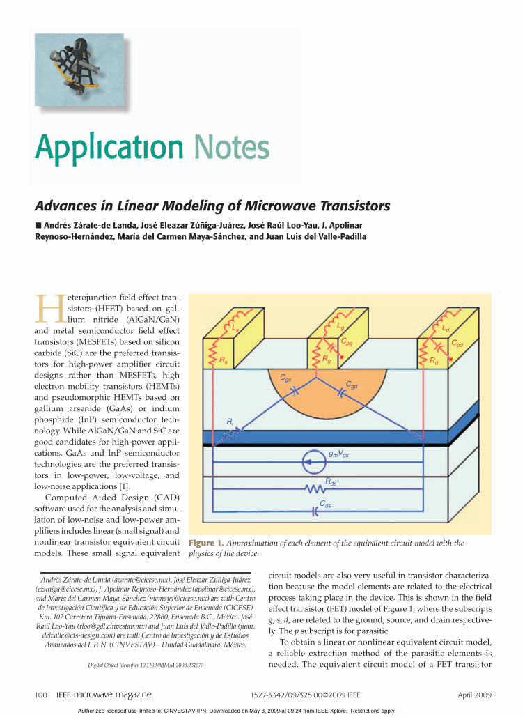
100 April 2009 1527-3342/09/$25.00©2009 IEEE Digital Object Identifier 10.1109/MMM.2008.931675 H eterojunction field effect tran- sistors (HFET) based on gal- lium nitride (AlGaN/GaN) and metal semiconductor field effect transistors (MESFETs) based on silicon carbide (SiC) are the preferred transis- tors for high-power amplifier circuit designs rather than MESFETs, high electron mobility transistors (HEMTs) and pseudomorphic HEMTs based on gallium arsenide (GaAs) or indium phosphide (InP) semiconductor tech- nology. While AlGaN/GaN and SiC are good candidates for high-power appli- cations, GaAs and InP semiconductor technologies are the preferred transis- tors in low-power, low-voltage, and low-noise applications [1]. Computed Aided Design (CAD) software used for the analysis and simu- lation of low-noise and low-power am- plifiers includes linear (small signal) and nonlinear transistor equivalent circuit models. These small signal equivalent circuit models are also very useful in transistor characteriza- tion because the model elements are related to the electrical process taking place in the device. This is shown in the field effect transistor (FET) model of Figure 1, where the subscripts g, s, d, are related to the ground, source, and drain respective- ly. The p subscript is for parasitic. To obtain a linear or nonlinear equivalent circuit model, a reliable extraction method of the parasitic elements is needed. The equivalent circuit model of a FET transistor Advances in Linear Modeling of Microwave Transistors ■ Andrés Zárate-de Landa, José Eleazar Zúñiga-Juárez, José Raúl Loo-Yau, J. Apolinar Reynoso-Hernández, María del Carmen Maya-Sánchez, and Juan Luis del Valle-Padilla L s R s L g L d C pd R d C pg R g C gs R ds C ds C gd g m V gs R i Figure 1. Approximation of each element of the equivalent circuit model with the physics of the device. Andrés Zárate-de Landa ([email protected]), José Eleazar Zúñiga-Juárez ([email protected]), J. Apolinar Reynoso-Hernández ([email protected]), and María del Carmen Maya-Sánchez ([email protected]) are with Centro de Investigación Científica y de Educación Superior de Ensenada (CICESE) Km. 107 Carretera Tijuana-Ensenada, 22860, Ensenada B.C., México. José Raúl Loo-Yau ([email protected]) and Juan Luis del Valle-Padilla (juan. [email protected]) are with Centro de Investigación y de Estudios Avanzados del I. P. N. (CINVESTAV) – Unidad Guadalajara, México. Authorized licensed use limited to: CINVESTAV IPN. Downloaded on May 8, 2009 at 09:24 from IEEE Xplore. Restrictions apply.
-
Upload
independent -
Category
Documents
-
view
4 -
download
0
Transcript of Advances in Linear Modeling of Microwave Transistors
100 April 2009 1527-3342/09/$25.00©2009 IEEE
Digital Object Identifier 10.1109/MMM.2008.931675
Heterojunction fi eld effect tran-sistors (HFET) based on gal-lium nitride (AlGaN/GaN)
and metal semiconductor fi eld effect transistors (MESFETs) based on silicon carbide (SiC) are the preferred transis-tors for high-power amplifi er circuit designs rather than MESFETs, high electron mobility transistors (HEMTs) and pseudomorphic HEMTs based on gallium arsenide (GaAs) or indium phosphide (InP) semiconductor tech-nology. While AlGaN/GaN and SiC are good candidates for high-power appli-cations, GaAs and InP semiconductor technologies are the preferred transis-tors in low-power, low-voltage, and low-noise applications [1].
Computed Aided Design (CAD) software used for the analysis and simu-lation of low-noise and low-power am-plifiers includes linear (small signal) and nonlinear transistor equivalent circuit models. These small signal equivalent
circuit models are also very useful in transistor characteriza-tion because the model elements are related to the electrical process taking place in the device. This is shown in the field effect transistor (FET) model of Figure 1, where the subscripts g, s, d, are related to the ground, source, and drain respective-ly. The p subscript is for parasitic.
To obtain a linear or nonlinear equivalent circuit model, a reliable extraction method of the parasitic elements is needed. The equivalent circuit model of a FET transistor
Advances in Linear Modeling of Microwave Transistors■ Andrés Zárate-de Landa, José Eleazar Zúñiga-Juárez, José Raúl Loo-Yau, J. Apolinar Reynoso-Hernández, María del Carmen Maya-Sánchez, and Juan Luis del Valle-Padilla
Ls
Rs
Lg Ld
Cpd
Rd
Cpg
Rg
Cgs
Rds
Cds
Cgd
gmVgs
Ri
Figure 1. Approximation of each element of the equivalent circuit model with the physics of the device.
Andrés Zárate-de Landa ([email protected]), José Eleazar Zúñiga-Juárez ([email protected]), J. Apolinar Reynoso-Hernández ([email protected]), and María del Carmen Maya-Sánchez ([email protected]) are with Centro de Investigación Científi ca y de Educación Superior de Ensenada (CICESE) Km. 107 Carretera Tijuana-Ensenada, 22860, Ensenada B.C., México. José
Raúl Loo-Yau ([email protected]) and Juan Luis del Valle-Padilla ([email protected]) are with Centro de Investigación y de Estudios Avanzados del I. P. N. (CINVESTAV) – Unidad Guadalajara, México.
Authorized licensed use limited to: CINVESTAV IPN. Downloaded on May 8, 2009 at 09:24 from IEEE Xplore. Restrictions apply.

102 April 2009
consists of parasitic (Rg, Rs, Rd, Lg, Ls, Ld, Cpg, and Cpd) and intrinsic elements (Cgs, Cgd, Cds, Ri, Rgd, gds, gm0, and t). While the intrinsic elements are bias dependent, the parasitic elements are independent of the bias voltages but de-pend on the packaged and the pad dimensions. However, several authors do consider a bias dependence of Rg and Rs [2]–[3].
Several methods based on dc [4]–[10] and RF [11]–[16] techniques to determine the parasitic elements have been reported (see “Description of the dc Method”). How ever, these methods are unsuitable for GaN tran-sistors, in particular for determining the parasitic gate resistance and inductance as well as the parasitic capac-itance Cpd. To overcome this problem, a novel method based on an RF technique is presented to obtain accurate values of the parasitic elements of the electrical equiva-lent circuit of the GaN FET. These are necessary for both
linear and nonlinear modeling. The main objective in this work is to explain the novel technique developed to extract the parasitic elements of the FET. Large signal, and nonlinear modeling are both outside the scope in this work.
Brief History of the Cold-FET TechniqueThe first method for determining parasitic resistances and inductances from S-parameters data sets at Vds = 0 was in-troduced in [17]. Then, in [18] this approach was named the cold-FET method. In 1988, Dambrine et al [19] published an extraction method to obtain the parasitic elements from a set of S-parameters of the FET measured under different large dc gate forward current (Vgs . Vbi . 0 V) and zero drain source-voltage (Vds = 0 V). Dambrine’s method requires the applica-tion of a high forward current to the gate to eliminate the effect of the differential resistance of the Schottky diode. This
Gate, source, and drain parasitic resistances can be determined using a dc method [9], [20]. The dc method is based on the planar Schottky diode model formed by gate-source or gate-drain contacts. Under forward bias conditions (VG . Fbi . 0), for any positive value of VG, the current Igs or Igd fl owing through the circuit of Figure 2 is computed by
Igs,gd 5 IS # expaVG 2 IRnUT
b , (S1)
where Is is the saturation current (A); Vg is the forward bias applied (V); n is the ideality factor of the diode; UT is the thermal potential (V), where UT = kT /q; k is the Boltzman constant (J/K); T is the absolute temperature (K); and q is the electron charge (C). The saturation current is given by
IS 5 S # A* # T 2 # expa2Fbi
UTb , (S2)
where S is the gate surface (cm2); A* is the Richardson constant (Am22K22); Fbi is the Schottky barrier (V). Assuming that the drain or source is fl oating, VG is equal to Vgs or Vgd and IG is equal to Igs or Igd. In this case Vg is given by:
VG 5 RIG 1 nUT In 1 IG 2 nUT In 1 Is 2 . (S3)
Let R(S) and R(D) defi ne the values of the series resistance R associated to real Schottky diode, with drain or source floating, respectively. In the case of the transistor, it is assumed that R can be written as
R1S2 5 Rs 1 Rg 1Rch
ai, (S4)
R1D2 5 Rd 1 Rg 1Rch
ai, (S5)
where Rch is the channel resistance and ai is a factor equal to 3.
Based on Igs(Vgs) or Igd(Vgd) measurements with drain or source floating, respectively, a least squares regression method is used for computing the coefficients of (S3), in which there is the series resistance R(S) or R(D) depending on the case. The analytical function to be optimized is derived from (S3) and can be written as follows:
X 5 am
i50
3RIGi 1 aln 0 IGi 0 1 b 2 VGi 42, (S6)
where a = nUT and b = –a ln(IS).The minimum of X occurs when the partial derivatives
with respect to R, a, and b are equal to zero. These conditions lead to a set of three simultaneous linear equation where R, a, and b are the unknowns. The resulting equation can be written in matrix form as
£Rab§ 5 F a
m
i51IGi2 a
m
i51IGiln|IGi| a
m
i51IGi
am
i51IGiln|IGi| a (
m
i51ln|IGi|)
2am
i51ln|IGi|
am
i51IGi a
m
i51ln|IGi| m
V21
F am
i51IGiVGi
am
i51ln|IGiVGi|
am
i51VGi
V.
(S7)
S G D
VdsRg
Rs Rch Rd
Igs
Vgs +
+
Figure 2. Schottky diode model.
Description of the dc Method
Authorized licensed use limited to: CINVESTAV IPN. Downloaded on May 8, 2009 at 09:24 from IEEE Xplore. Restrictions apply.

April 2009 103
leads to a direct calculation of the parasitic gate resistance and inductance, Rg and Lg, respectively.
Later, in [20], the RF cold-FET method was modified by changing the bias condition Vds = 0 V to a floating drain, which overcomes the inconsistencies between the dc and RF methods observed in [21]. For MESFETs and HEMTs based on GaAs or SiC, dc and RF methods can success-fully be applied to determine the parasitic resistances. In addition to calculating the parasitic resistances, the cold-FET method is also used to determine the gate, source, and drain inductances Lg, Ls, and Ld, respectively.
However, when it comes to AlGaN/GaN HEMTs, the Schottky diode of the transistor exhibits an inherently strong capacitive behavior, which is difficult to suppress even by applying a large dc forward current to the gate. Therefore, neither the dc nor the RF cold-FET classical methods can be applied for the calculation of Rg and Lg. Indeed, a high forward gate current could produce irre-versible and catastrophic damage to the Schottky diode properties, as reported in [22].
Hence, in recent years, studies of GaN transistors have been conducted to develop reliable methods to determine both Rg and Lg, as well as the parasitic ca-pacitances. In [23], the parasitic elements were calcu-lated using the cold-FET technique, followed by an optimization process that was difficult and time con-suming to implement. On the other hand, a method in which the parasitic elements were calculated using the cold-FET technique (high gate forward bias) along with dummy structures for computing parasitic capacitances was reported in [24]. In the paper published by Crupi et al. [25], the parasitic elements were determined under reverse gate voltage and Vds = 0 V, along with dummy structures for computing parasitic capacitances. The problem in the methods mentioned above is that they need an additional passive structure to be implement-ed. In addition, they are time consuming and difficult to implement.
In the case of AlGaN/GaN HEMTs, the gate resistance Rg and gate induc-tance Lg are difficult to extract using the classical cold-FET method. There-fore, in this article, a new method for extracting parasitic resistances and parasitic inductances is introduced. The originality of the proposed meth-od lies in the low dc gate forward cur-rent used for extracting the parasitic elements. In addition, by de- embedding the parasitic gate and drain induc-tances from the pinch-off “cold-FET” measurement and taking into account the Schottky diode capacitance, an improved method for extracting the Cpd parasitic capacitance is present-ed. After several tests, it was found that this method is not only useful
for AlGaN/GaN transistors, but it can also be applied to GaAs, SiC MESFETs, and HEMTs.
Extraction of the Transistor Equivalent Circuit Model ParametersAs discussed above, the transistor equivalent circuit model consists of parasitic and intrinsic elements as depicted in Figures 1 and 3. Parasitic elements are calcu-lated from cold-FET measurements. The cold-FET tech-nique consists of biasing the transistor with Vbi . Vgs . 0 (Vbi is the built-in voltage) and open drain, to obtain the parasitic resistances and inductances. The parasitic ca-pacitances are computed from measured Y-parameters of the cold FET biased at Vgs , VP , 0 (VP is the pinch-off voltage) and Vds = 0 V. Crupi et al [25] explained that this technique is called cold-FET because under the zero drain-source bias condition the average kinetic energy of the electron is characterized by a 2DEG equivalent tem-perature, which is cold with respect to the typical operat-ing condition. It is worth commenting that the depletion region under the gate is taken into account when model-ing the cold-FET.
On the other hand, to extract the intrinsic elements, measurements of the Y-parameters of the hot-FET are used, which means that bias gate-source and drain-source volt-ages are applied to the transistor.
Why the Classical Cold-FET Method Cannot Be Used in HFETs Based on AlGaN/GaN To determine the gate resistance, the classical cold-FET method requires that the real part of Z11 be constant at low
G
S
Intrinsic FET
Lg Rg
Rsgm = gm0e–jωτ
Ls
Cpg
Cgd Rgd
Rds
Rd
Cpd
Ld
D
Cds
CgsVgs
Ri
gmVgs
Figure 3. Small-signal equivalent circuit used for modeling the FET.
The gate resistance and inductance Rg and Lg may be obtained from a
single set of S-parameters measured at low dc forward gate current.
Authorized licensed use limited to: CINVESTAV IPN. Downloaded on May 8, 2009 at 09:24 from IEEE Xplore. Restrictions apply.

104 April 2009
frequency (less than 5 GHz). This is achieved by using a large forward gate-source current (0 . Vgs . Vbi) to suppress the capacitive behavior of the Schottky diode. Since Rg is deter-mined by linear regression, at least two sets of S-parameter measurements at different bias gate currents are needed.
Having eliminated the capacitive influence of the Schottky diode on the gate, the behavior of imaginary part of Z11 is inductive. Indeed, Lg is calculated from the
slope of the imaginary part of Z11. However, experimen-tal results in AlGaN/GaN HEMTs, shown in Figures 4 and 5, indicate that, even using large forward gate-source current, the capacitive behavior of the Schottky diode cannot be suppressed. This capacitive behavior precludes the determination of Rg and Lg using the clas-sical cold-FET method.
The New Cold-FET Model at Low dc Forward Current (0 < Vgs < Vbi; Igs > 0) and Open DrainHaving explained the constraints of the classical cold-FET method to determine Rg and Lg in AlGaN/GaN HEMTs, a new cold-FET method is presented, which allows the ac-curate determination of not only the parasitic elements, but also the Schottky diode capacitance and dynamic resistance. The method requires only a single wideband measurement of the S-parameters of the transistor, measured under a sin-gle low dc forward gate current with a floating drain.
Figure 6 shows an example of how to select, from the I(V) curve of the cold-FET, the current that will be applied to the gate. It is very important to notice the selection of a low Igs current, which will not damage the transistor, contrary to large forward current used in the classical cold-FET method.
The proposed cold-FET equivalent circuit at dc low for-ward gate bias 0 , Vgs , Vbi with a floating drain is shown in Figure 7.
In Figure 7,
Rg* 5 Rg 2
Rch
6, Rs
* 5 Rs 1Rch
2 and Rd
* 5 Rd 1Rch
2,
where Rch is the channel resistance.The Z-parameters of the circuit shown in Figure 7 are ex-
pressed as
Z11 5 Rg* 1 Rs
* 1R0
1 1 v 2 C02 R 0
2 1 jv cLg 1 Ls 2C0R0
2
1 1 v 2C0
2R0
2 d , (1)
+j0.2
+j0.5
0.0 00.2
0.5
1.0
2.0
5.0
+j1.0
+j2.0
+j5.0
−j5.0
−j2.0
−j1.0
S11 @ Igs = 3 mA
S11 @ Igs = 8 mA
S11 @ Igs = 10 mA
−j0.5
−j0.2
Figure 4. Capacitive behavior presents in the gate of GaN transistors under large gate-source currents.
0 10 20 30 40 500
10
20
30
40
50
60
70
80
Frequency (GHz)
Rea
l Par
t of Z
11
AlGaN/GaN HFET
Frequency (GHz)
AlGaN/GaN HFET
0 10 20 30 40 50–40
–30
–20
–10
0
10
20
Imag
inar
y P
art o
f Z11
Im(Z11) @ Igs = 3 mA
Im(Z11) @ Igs = 8 mA
Im(Z11) @ Igs = 10 mA
Re(Z11) @ Igs = 3 mA
Re(Z11) @ Igs = 8 mA
Re(Z11) @ Igs = 10 mA
Figure 5. Real and imaginary part of Z11 of a 300 µm GaN transistor for different bias currents. At 10 mA the gate was damaged.
Authorized licensed use limited to: CINVESTAV IPN. Downloaded on May 8, 2009 at 09:24 from IEEE Xplore. Restrictions apply.

April 2009 105
Z12 5 Z21 5 Rs* 1 jvLs, (2)
Z22 5 Rd* 1 Rs
* 1 jv 1Ld 1 Ls 2 . (3)
Parasitic Inductance CalculationUtilizing (2) and (3), Ls and Ld can be extracted from the slopes of the imaginary parts of Z12 and Z22 respectively. On the other hand, due to the R0 and C0 terms in the imagi-nary part of Z11 expressed by (1), the direct calculation of Lg is still difficult. Lg could be calculated from the imagi-nary part of Z11, provided that Ls, R0, and C0 are known. To overcome this problem, we next review a procedure for the calculation of Lg and C0 from the imaginary part of Z11, first
introduced in [26]. Based on this, the imaginary part of Z11 can be expressed as
Im 3Z11 45 v 1Lg 1 Ls 2 2v
C0
1v 0
2 1 v 2, (4)
where v0 51
R0C0. (5)
It is seen from (5) that v0 depends on the R0 and C0 values, which in turn are dependent on the forward gate bias. Fur-thermore, it is important to comment that as the forward gate bias current increases R0 decreases and C0 is almost constant [27]. Therefore, low v0 values should be expected when biasing the gate with a low dc forward gate current.
From the frequency dependence of the imaginary part of Z11, experimental results indicate that, when driving the gate with a low dc forward current, there is a frequency point denoted as vR where the imaginary part of Z11 is sup-pressed, which means that the imaginary part of Z11 ex-periences a resonance at the frequency vR. The resonance frequency can be determined from (4) and is expressed as
v R2 5 v x
2 2 v 02, (6)
where v x2 5
11Lg 1 Ls 2C0. (7)
Moreover, at low dc gate forward currents and according to (5) and (7), it is obvious that v0 would be lower than vx. Hence, assuming that vx .. v0, the resonance frequency vR becomes
v R2 5 v x
2 51
LC0, (8)
where L = Lg + Ls. (9)
Expression (8) allows the calculation of C0 as long as L is known. An expression for L and C0 can also be derived from (4) if v 2 .. v 0
2, and is expressed as
vIm 1Z11 2 5 v 2L 21C0
. (10)
It should be noted from (10) that Lg and C0 can be cal-culated using linear regression where Lg is determined
once L is obtained from the slope of the straight line and with the previous knowledge of Ls. Then, C0 is cal-culated from the intercept of the straight line with the
0 0.5 1 1.5 2 2.5Vgs (V)
Transistor Under Forward DC Gate Bias
0 < Vgs < Vbi ; Igs > 0–2
0
2
4
6
8
10
I gs
(mA
)
DC
Vds = Open
S
DG
−+
Igs
Figure 6. Example of the I(V) curves of the cold-FET model.
DLg Rg*R0 Rd* Ld
Rs*
Ls
C0
G
S
Cold-FET
ZD
Figure 7. Small-signal equivalent circuit of the transistor under low dc gate forward current with floating drain.
0 2 4 6 8 10x 1022
–3
–2
–1
0
1
2
3
4
5 x 10¹²
ω2
ω*I
m(Z
11)
M easurem entF ittingMeasurementFitting
1ω Im[Z11] = ω2 (Lg + Ls) – ⎯C0
Then:Lg = L − Ls
L = Lg + Ls
[ω Im(Z11)]⏐ω =0
1 1C0 = – = ωx m
Figure 8. Plot of vIm(Z11) versus v2 used for calculating L and C0.
Authorized licensed use limited to: CINVESTAV IPN. Downloaded on May 8, 2009 at 09:24 from IEEE Xplore. Restrictions apply.

106 April 2009
vIm(Z11) axis or from the vx expression once L is known. Figure 8 shows the plot of vIm(Z11) versus v used to extract Lg and C0.
Once vx and L are computed from Figure 8, Lg and C0 are determined as follows:
Lg = L – Ls, (11)
C0 51
v x2L
51
vIm 1Z11 2|vS0. (12)
Parasitic Resistance CalculationParasitic resistances Rs and Rd are directly determined from the real parts of Z12 and Z22, respectively, of the modified cold-FET method shown in Figure 7. An expression for determining Rg can be derived from the real part of Z11 and are expressed as
Rg* 5 Re 1Z11 2 2 Rs
* 2R0
1 1 v 2 C02 R0
2. (13)
It is seen that Rg can be determined from (13) as long as Rs, C0, and R0 are known. It should also be noted from (13) that the only unknown is R0, which can be derived from the imaginary part of Z11 as
R0 5Å vL 2 Im 1Z11 2vC0 2 v 2C0
2 3vL 2 Im 1Z11 2 4 4 v , v0. (14)
Once R0 is determined, the computation of Rg can be ac-complished either by using (13) or from the evaluation of Z11 at the resonance frequency vR. Figure 9 depicts how Rg can be extracted when the real part of Z11 is evaluated at the reso-nance frequency. Assuming that the Rch value is negligible, the expression Rg is given as:
Rg 5 Re 3Z11 4|v5vx2 Rs 2 R0av0
vxb2
. (15)
Parasitic Capacitance CalculationParasitic capacitance extraction is based on the Y-param-eters computed from S-parameters for a dc gate bias be-yond the pinch-off voltage VP, with source and drain both grounded (Vgs ,, VP; Vds = 0 V). Since drain and source electrodes are at the same potential, the depletion region under the gate is expected to be uniform and symmetrical. Figure 10 shows the equivalent circuit model of the transis-tor under pinch-off bias.
Prior to parasitic capacitance calculation and according to the algorithm presented in [28], a de-embedding of the parasitic gate and drain inductances Lg and Ld must be per-formed to eliminate their effect on the imaginary part of the Y-parameters of the pinched-off cold FET.
Models presented by Dambrine et al [19] and White and Healy [29] were developed for estimating the parasitic Cpg and Cpd capacitances. Recently, it was demonstrated by Caddemi et al [30] that with a pinched-off cold-FET (Vds = 0 V; Vgs ,, VP) the depletion region under the gate can be modeled using a T network. Based on [29]–[30], this work uses the circuit shown in Figure 11 to determine Cpg and Cpd.
0 5 10 15 20 25 30 35 40 45 50–30
–20
–10
0
10
20
30
40
50
60
70
Frequency (GHz)
Z11
(Ω
)
Real Part of Z11
Imaginary Part of Z11
Resonance Frequency ωR
Re[Z11(ωx)] = Rg + Rs + R0 ⎝⎛ ⎝
⎛
ω0ωx
2
;1
(Lg + Ls)C0ωx =
1R0C0
ω0 =
Figure 9. Real part of Z11 evaluated at the resonance frequency.
GLg Rg
Cpg
Rd
Cpd
Ld
Rs
Ls
D
S
Cgs
Cgd
Cds
Intrinsic FET
Figure 10. Equivalent circuit model of the transistor under pinch-off bias (Vgs ,, Vp; Vds 5 0).
G
CpgCpd
D
S
Cb
C0 Cb
Figure 11. Transformation from T to p network for the pinch-off equivalent circuit model.
Authorized licensed use limited to: CINVESTAV IPN. Downloaded on May 8, 2009 at 09:24 from IEEE Xplore. Restrictions apply.

April 2009 107
The parasitic capacitances Cpg, Cpd, and Cb are calculated from the Y-parameters of the network shown in Figure 11. The expressions for the parasitic capacitances follow as:
Cpg 5Im 1Y11 2 1 2Im 1Y12 2
v, (16)
Cpd 5Im 1Y22 2 1 Im 1Y12 2
v1
Cb
C0 Im 1Y12 2
v , (17)
where
Cb 52C0Im 3Y12 4
vC0 1 2Im 3Y12 4 . (18)
It is very important to comment that the expression to calculate Cpg is exactly the same as published by Dam-brine [19]. Nevertheless, the novelty of this method is the Cb/C0 term in the Cpd expression because if Cb ,, C0 the calculation of Cpd would be the same as the expression introduced by Dambrine, but if Cb 5 C0, then Cpd would be obtained by the equation presented by White [29]. However, we have found that for GaN transistors Cb 2 C0, so that neither the Dambrine nor the White method can precisely extract the value of Cpd for this kind of transistor. Recall that an expression to calculate C0 was already pre-sented in the previous section.
Calculation of Intrinsic ParametersOnce the parasitic elements are extracted, a de-embedding process is performed on the measured S-parameters of the hot FET to determine the intrinsic elements (Cgs, Cgd, Cds, Ri, Rgd, gds, gm0, and t). The intrinsic elements are extracted according to the method presented by Berroth and Bosh [31].
Limitations of the MethodThe method described above is very accurate and easy to apply. However, there are some limitations that should be
taken into account. One of these limitations is that to mod-el a GaN FET of small size, the resonance frequency occurs at a very high frequency. This implies that equipment that can measure S parameters at very high frequencies must be used.
Another limitation is that in order for the method to be applied, the condition v0 ,, vx and v0 ,, vR must be ful-filled. This can be easily accomplished by biasing the transis-tor with low forward gate currents.
Experimental ResultsTo validate the proposed method, several on-wafer and packaged transistors were used. Using the method, para-sitic elements for AlGaN/GaN, SiC, and GaAs transistors were extracted and used to construct small signal equivalent
0 10 20 30 40 500
10
20
30
40
50
60
70
Frequency (GHz)
Rea
l Par
t of Z
11
Measured GaAs MESFET
Simulated GaAs MESFET
Measured AlGaN/GaN HEMT
Simulated AlGaN/GaN HEMT
Figure 12. Plot of the measured and calculated real parts of Z11 for the AlGaN/GaN and GaAs transistors.
0 10 20 30 40 50–30
–20
–10
0
10
20
Frequency (GHz)
Imag
inar
y P
art o
f Z11
Measured GaAs MESFET
Simulated GaAs MESFET
Measured AlGaN/GaN HEMT
Simulated AlGaN/GaN HEMT
Figure 13. Plot of the measured and calculated imaginary parts of Z11 for the AlGaN/GaN and GaAs transistors.
0 10 20 30 40 50–0.02
–0.01
0
0.01
0.02
0.03
Frequency (GHz)
Imag
inar
y P
art o
f Yij
On-Wafer AlGaN/GaN HEMT
Measured
Simulated
Y12
Y22
Y11
Figure 14. Measured and simulated Y-parameters of the pinch-off equivalent circuit model of the AlGaN/GaN HEMT.
Authorized licensed use limited to: CINVESTAV IPN. Downloaded on May 8, 2009 at 09:24 from IEEE Xplore. Restrictions apply.

108 April 2009
circuits. The results for each type of transistor are shown in the following.
On-Wafer TransistorsThe method was applied to AlGaN/GaN HFET and GaAs MESFET on-wafer transistors. Prior to the RF mea-surements in the frequency range of 0.045–50GHz, an improved LRM calibration [32] was performed on the HP8510C network analyzer using GGB Industries’ cali-
bration standards model CS-5 and probe model 50A-GSG-150P. To verify the validity of the small signal equivalent circuit model of the FETs (a AlGaN/GaN HFET and a GaAs MESFET) under low dc forward gate current with a floating drain, shown in Figure 7, the real and imagi-nary parts of Z11, measured at Igs = 1 mA, were simulated and plotted in Figures 12 and 13, respectively. Accord-ing to these results, along with the very good agreement between experimental and simulated data, the validity
0 10 20 30 40 50–0.02
0
0.02
0.04
Frequency (GHz)
Imag
inar
y P
art o
f Yij
On-Wafer GaAs MESFET
Measured
Simulated
Y11
Y12
Y22
Figure 15. Measured and simulated Y-parameters of the pinch-off equivalent circuit model of the AlGaN/GaN HEMT.
TABLE 1. Parasitic elements of the AlGaN/GaN and GaAs transistors.
Element AlGaN/GaN HFET GaAs MESFET
Igs (mA) 1.0 1.0
R0 (V) 59.99 48.57
Rg (V) 0.61 1.32
Rs (V) 7.26 2.29
Rd (V) 13.36 2.84
Lg (pH) 67.91 43.27
Ls (pH) 6.59 6.90
Ld (pH) 64.07 56.71
C0 (pF) 0.43 0.66
Cpg (fF) 7.82 46.87
Cpd (fF) 15.67 63.23
+j0.2
–j0.2
+j0.5
–j0.5
+j1.0
–j1.0
+j2.0
–j2.0
+j5.0
–j5.0
0.0 ∞
S21/4
S22S11
4*S12
0.2
0.5
1.0
2.0
5.0
Measured Simulated
Figure 16. Comparison of the simulated and measured S-parameters of the AlGaN/GaN HEMT at Vgs 5 22.2 V; Vds 5 18 V; Ids 5 4.202 mA.
0.2
0.5
1.0
2.0
5.0
+j0.2
–j0.2
+j0.5
–j0.5
+j1.0
–j1.0
+j2.0
–j2.0
+j5.0
–j5.0
0.0 ∞
S21/4
S22S11
4*S12
Measured Simulated
Figure 17. Comparison of the simulated and measured S-parameters of the GaAs MESFET at Vgs 5 0 V; Vds 5 3 V; Ids 5 35.0 mA.
Authorized licensed use limited to: CINVESTAV IPN. Downloaded on May 8, 2009 at 09:24 from IEEE Xplore. Restrictions apply.

April 2009 109
of the proposed method for extracting the gate parasitic resistances and inductances is verified.
Parasitic capacitances Cpg and Cpd were extracted from the Y parameters, computed from S-parameter data measured at dc gate bias beyond pinch-off and with Vds = 0 V.
For calculating Cpg and Cpd with (12) and (13), knowl-edge of C0 and Cb are required. Recall that C0 was pre-viously determined in (8). Figures 14 and 15 show the Im(Yij) of an AlGaN/GaN HEMT and a GaAs MESFET, respectively, as a function of the frequency. Once again, the model predicts the experimental data very well, which verifies the validity of the proposed method to determine the parasitic capacitances.
The values of the parasitic elements are summarized in Table 1. To determine whether the parasitic elements were properly extracted, the FET’s intrinsic small sig-
nal equivalent circuit was used. Figures 16 and 17 show a comparison between the predicted and experimental S-parameter data of the transistor measured at Vgs = –2.2 V; Vds = 18 V; Ids = 4.202 mA for the AlGaN/GaN HEMT and Vgs = 0 V; Vds = 3 V; Ids = 35.0 mA for the GaAs MESFET, respectively.
Packaged TransistorsCommercial GaN (CHG35015) and SiC (CRF24010F) pack-aged power transistors were studied to demonstrate the use-fulness of the parasitic calculation proposed method. A test fixture along with TRL multiline calibration standards were constructed using a low cost substrate [33].
Prior to performing RF measurements, a two-tier calibra-tion was performed using the HP8510C network analyzer in the frequency range of 0.045–3 GHz. The first tier calibra-tion was performed with the SOLT calibration technique.
0 1 2 3 40
10
20
30
40
50
Frequency (GHz)
Rea
l Par
t of Z
11
GaN Measured
GaN SimulatedSiC Measured
SiC Simulated
Figure 18. Plot of the measured and calculated real parts of Z11 for the packaged GaN and SiC transistors.
0 1 2 3 4–15
–10
–5
0
5
10
15
20
Frequency (GHz)
Imag
inar
y P
art o
f Z11
GaN MeasuredGaN Simulated
SiC Measured
SiC Simulated
Figure 19. Plot of the measured and calculated imaginary parts of Z11 for the packaged GaN and SiC transistors.
0 1 2 3–0.05
0
0.05
0.1
Frequency (GHz)
Imag
inar
y P
art o
f Y
Pinched-Off GaN HEMT
MeasuredSimulated
Y11
Y12
Y22
Figure 20. Measured and simulated Y-parameters of the pinch-off equivalent circuit model of the GaN HEMT.
0 1 2 3 4–0.05
0
0.05
0.1
0.15
Frequency (GHz)
Imag
inar
y P
art o
f Y
Pinched-Off SiC HEMT
Measured
Simulated
Y11
Y12
Y22
Figure 21. Measured and simulated Y-parameters of the pinch-off equivalent circuit model of the SiC MESFET.
Authorized licensed use limited to: CINVESTAV IPN. Downloaded on May 8, 2009 at 09:24 from IEEE Xplore. Restrictions apply.

110 April 2009
The second tier calibration was performed using an im-proved multiline TRL calibration [33]. Once the systematic errors of the VNA were corrected and the reference plane was placed properly, the S parameters of the DUT (GaN or SiC) were measured.
The real and imaginary parts of Z11, measured and pre-dicted by the model for Igs = 1 mA, and a floating drain for the packaged GaN HEMT and SiC MESFETs, are plotted in Figures 18 and 19, respectively. The results reveal that the proposed parasitic method is also useful to characterize packaged power transistors.
The parasitic capacitances of the packaged GaN HEMT and SiC MESFET were also determined according to the pro-cedure explained above. The comparison between measured and modeled Yij parameters of the pinched-off GaN and SiC transistors is depicted in Figures 20 and 21.
Table 2 shows the values of the parasitic elements ex-tracted for the packaged GaN and SiC transistors. In ad-dition, Figures 22 and 23 show a comparison between the predicted and experimental S-parameter data of the transistor measured at Vgs = –2.0 V; Vds = 15 V for the GaN HEMT and Vgs = –9 V; Vds = 20 V for the GaAs MESFET, respectively.
Finally, an extraction of the intrinsic elements has been performed for 300 different bias points (0 , Vds , 20; –3 , Vgs , 0). In Figure 24, we report the bias dependence of the intrinsic elements (Cgs, Cgd, Ri, Rgd, gds, and gm). It can be noted that the behavior of the intrinsic elements matches the theo-retical physical expectations.
ConclusionsA fast and simple analytical method of extracting the para-sitic elements of a small signal equivalent circuit model of on-wafer and packaged transistors was presented.
The following conclusions can be drawn:The gate resistance and inductance Rg and Lg may be ob-1) tained from a single set of S-parameters measured at low dc forward gate current. A new expression for determining the parasitic capaci-2) tance Cpd was presented.
TABLE 2. Parasitic elements of the packaged GaN and SiC transistors.
Element GaN HEMT SiC MESFET
Rg (V) 0.56 2.22
Rs (V) 0.26 0.74
Rd (V) 0.60 1.42
R0 (V) 69.09 27.95
Lg (pH) 777.97 1,031.65
Ls (pH) 53.76 66.61
Ld (pH) 858.62 1,225.26
C0 (pF) 9.75 20.63
Cpg (fF) 694.15 1,810.70
Cpd (fF) 1,193.30 855.77
0.2
0.5
1.0
2.0
5.0
+j0.2
–j0.2
+j0.5
–j0.5
+j1.0
–j1.0
+j2.0
–j2.0
+j5.0
–j5.0
0.0 ∞
S21/32
S22
S11
8*S12
Measured Simulated
Figure 22. Comparison between the simulated and measured S-parameters of the GaN HEMT (Vds= 15 V; Vgs = –2 V).
0.2
0.5
1.0
2.0
5.0
+j0.2
–j0.2
+j0.5
–j0.5
+j1.0
–j1.0
+j2.0
–j2.0
+j5.0
–j5.0
0.0 ∞
S21/12
S22
S11
4*S12
Measured Simulated
Figure 23. Comparison between the simulated and measured S-parameters of the SiC MESFET (Vds = 20 V; Vgs = –9 V).
Authorized licensed use limited to: CINVESTAV IPN. Downloaded on May 8, 2009 at 09:24 from IEEE Xplore. Restrictions apply.

April 2009 111
This method was validated for different types of tech-3) nologies such as on-wafer and packaged AlGaN/GaN, SiC, and GaAs HEMTs and MESFETs. The authors be-lieve that this method could be also useful for MOS technology such as LDMOS.Parasitic elements were calculated from the measure-4) ments without using any optimization method.
Unfortunately, only GaN transistors on Si substrate with a maximum output power in the range of 1mW-35W were available for this study. An interesting study could be conducted to observe the reliability of the method in the extraction of the parasitic elements of a GaN FET based on a different substrate material such as SiC and analyze its influ-ence on the parasitic capacitances extraction.
AcknowledgmentThis work was supported by joint funding from CICESE, and CONACYT, project 39835-Y, Mexico. The authors would like to thank Nitronex Corporation for supplying the GaN devices.
References[1] M. Golio, “The push toward low voltages devices,” IEEE Microwave Mag.,
vol. 1, no. 1, pp. 38–45, Mar. 2000.[2] R. J. Trew, Y. Liu, G. L. Bilbro, W. Kuang, R. Vetury, and J. B. Shealy, “Non-
linear source resistance in high-voltage microwave AlGaN/GaN HFETs,” IEEE Trans. Microwave Theory Tech., vol. 54, no 5, pp. 2061–2067, May 2006.
[3] H. Yin, D. Hou, G. L. Bilbro, and R. J. Trew, “Harmonic balance simula-tion of new physics based model of the AlGaN/GaN HFET,” in 2008 IEEE MTT-S Int. Microwave Symp. Dig., June 2008, pp. 1425–1428.
[4] H. Fukui, “Determination of the basic device parameters of a GaAs MES-FET,” Bell Syst. Tech. J., vol. 58, no. 3, pp. 771–797, Mar. 1979.
[5] K. W. Lee, K. Lee, M. S. Shur, T. T. Vu, P. C. T. Roberts, and M. J. He-lix, “Source, drain, and gate series resistances and electron saturation
velocity in ion-implanted GaAs FET’s,” IEEE Trans. Electron. Devices, vol. ED-32, no. 5, pp. 987–992, May 1985.
[6] S. Chaudhuri and M. B. Das, “An investigation of the MESFET ‘end’ resis-tance using a distributed diode/resistance model,” IEEE Trans. Electron. Devices, vol. ED-32, no. 11, pp. 2262–2268, Nov. 1985.
[7] R. J. Bennett, “Interpretation of forward bias behavior of Schottky barriers,” IEEE Trans. Electron. Devices, vol. ED-34, no. 4, pp. 935–937, Apr. 1987.
[8] S. K. Cheung and N. W. Cheung, “Extraction of Schottky diode param-eters from forward current-voltage characteristics,” Appl. Phys. Lett., vol. 49, no. 2, pp. 85–87, July 1986.
[9] J. A. Reynoso-Hernandez and F. E. Rangel-Patiño, “DC and RF techniques for computing access resistances in microwave FETs,” 1996 IEEE MTT-S Int. Microwave Symp. Dig., vol. 3, pp. 1711–1714.
[10] J. A. Reynoso-Hernandez, B. Ramirez-Duran, J. Ibarra-Villaseñor, and J. Perdomo, “Reliable RF techniques for extracting parasitic elements in mi-crowave FET’S,” in Int. IEEE Workshop on Experimentally Based FET Device Mod-eling and Related Nonlinear Circuit Design, Univ. of Kassel, 1997, pp. 1.1–1.8.
[11] F. Lin and G. Kompa, “FET model parameter extraction based on opti-mization with multiplane data-fitting and bidirectional search – A new concept,” IEEE Trans. Microwave Theory Tech., vol. 42, no. 7, pp. 1114–1121, July 1994.
[12] R. Vogel, “The application of RF wafer probing to MESFET modeling,” Microwave J., vol. 31, no. 11, pp. 153–162, Nov. 1988.
[13] J. C. Costa, M. Miller, M. Golio, and G. Norris, “Fast, accurate, on-wafer extrac-tion of parasitic resistances and inductances in GaAs MESFETs and HEMTs,” 1992 IEEE MTT-S Int. Microwave Symp. Dig., June 1992, vol. 2, pp. 1011–1014.
[14] R. Tayrani, J. E. Gerber, T. Daniel, R. S. Pengelly, and U. L. Rodhe, “A new and reliable direct parasitic extraction method for MESFETs and HEMTs,” in 23rd European Microwave Conf., 1993, pp. 451–453.
[15] B.-S. Kim and S. Nam, “An iterative parasitic extraction method for HEMT,” in 25th European Microwave Conf., 1995, pp. 558–561.
[16] E. Arnold, M. Golio, M. Miller, and B. Beckwith, “Direct extraction of GaAs MESFET intrinsic element and parasitic inductance values,” in 1990 IEEE MTT-S Int. Microwave Symp. Dig., vol. 1, pp. 359–362.
[17] F. Diamant and M. Laviron, “Measurement of extrinsic series elements of a microwave MESFET under zero current conditions,” in Proc. 12th Eu-ropean Microwave Conf., 1982, pp. 451–456.
Figure 24. 3D plots of Cgs, Cgd, Ri, Rgd, gds and gm versus gate and drain voltages of a GaN HEMT.
–3–2
–10
010
20300
100
200
300
Vgs Vgs VgsVds Vds Vds
Vgs Vgs VgsVds Vds Vds
Cgs
(fF
)
Cgd
(fF
)g d
s (m
S)
g m (
mS
)
–3–2
–10
010
20300
50
100
150
200
–3–2
–10
010
20300
10
20
30
Ri (Ω
)
Rgd
(Ω
)
–3–2
–10
0
20400
10
20
30
–3–2
–10
010
20300
20
40
60
–3–2
–10
010
20300
10
20
30
40
(continued on page 146)
Authorized licensed use limited to: CINVESTAV IPN. Downloaded on May 8, 2009 at 09:24 from IEEE Xplore. Restrictions apply.

146 April 2009
tools such as a tool for automatically aligning the wafer and generating a wafer map. It is also designed to com-municate with test executive software like Agilent’s IC-CAP, Keithley’s KITE, ProPlus’ BSIMPro and many others. Combining this feature with SUSS=2 0MicroTec’s unique automated thermal
management and realign technology enables unattended test routines over multiple temperatures that can be run overnight and on weekends, signifi-cantly increasing system utilization and ultimately improving time to market and return on investment. For more in-formation see Web site www.suss.com
Peregrine Semiconductor Invents DuNE Technology for Mobile Antenna TuningPeregrine Semiconductor Corporation, a supplier of high-performance RF CMOS and mixed-signal communications ICs, today announced a breakthrough in the highly sought-after solution to mobile antenna tuning. The Company’s new DuNE Technology, a patent-pending de-sign methodology made possible by Per-egrine’s UltraCMOS process and HaRP design innovation, has enabled a single-die tunable capacitor circuit—referred to as a digitally tunable capacitor (DTC), which meets the high- performance demands for antenna tuning in leading-edge cellular and mobile applications. These demands include superb power handling and linearity; low power con-sumption; and highly integrated in a small form factor. For more than 20 years, the RF researchers have attemp ted to address these challenges with a vari-ety of micro- electromechanical systems and ferroelectric materials technologies, each having its own merit yet unable to integrate the features and functionality enabled by Peregrine’s DuNE Technol-ogy. For more information see Web site www.psemi.com
1.36 mm
0.81
mm
VDD
3-Wire SerialInterface
GND
RF–
RF+
[18] W. Curtice and R. Caamisa, “Self-cosistent GaAsFET models for ampli-fier design and device diagnostic,” IEEE Trans. Microwave Theory Tech., vol. 32, no. 12, pp. 1573–1578, July 1984.
[19] G. Dambrine, A. Cappy, F. Heliodore, and E. Playez, “A new method for determining the FET small-signal equivalent circuit,” IEEE Trans. Micro-wave Theory Tech., vol. 36, no. 7, pp. 1151–1159, July 1988.
[20] J. A. Reynoso-Hernández, F. E. Rangel-Patiño, and J. Perdomo, “Full RF characterization for extracting de small-signal equivalent circuit in microwave FET’s,” IEEE Trans. Microwave Theory Tech., vol. 44, no.12, pp. 2625–2633, Dec. 1996.
[21] R. Anholt and S. Swirhun, “Equivalent-circuit parameter extraction for Cold GaAs MESFET’s,” IEEE Trans. Microwave Theory Tech., vol. 39, no. 7, pp. 1243–1247, July 1991.
[22] E. Chigaeva and W. Walthes, “Determination of small-signal parameters of GaN-based HEMTs,” in Proc. IEEE/Cornell High Performance Devices Conf., 2000, pp. 115–122.
[23] A. Jarndal and G. Kompa, “A new small signal model parameter extrac-tion method applied to GaN devices,” presented at the IEEE MTT-S Int. Mi-crowave Symp., Long Beach, CA, June 2005.
[24] G. Chen, V. Kumar, R. Schwindt, and I. Adesida, “A reliable low gate bias model extraction procedure for AlGaN/GaN HEMTs,” pre-sented at the IEEE MTT-S Int. Microwave Symp., San Francisco, CA, June 2006.
[25] G. Crupi, D. Xiao, D. M. M.-P. Schreurs, E. Limiti, A. Caddemi, W. Rae-dt, and M. Germain, “Accurate multibias equivalent-circuit extraction for GaN HEMTs,” IEEE Trans. Microwave Theory Tech., vol. 54, no. 10, pp. 3616–3622, Oct. 2006.
[26] A. Zárate-de Landa, J. E Zúñiga-Juárez, J. A. Reynoso-Hernández, M. C. Maya-Sánchez, E. L. Piner, and K. J. Linthicum, “A new and better method for extracting the parasitic elements of the on-wafer GaN transistors,” in IEEE MTT-S Symp. Dig., Honolulu, Hawaii, June 3–8, 2007, pp. 791–794.
[27] A. Zárate-de Landa, J. E Zúñiga-Juárez, J. A. Reynoso-Hernández, M. C. Maya-Sánchez, J. L. del Valle-Padilla, and J. R. Loo-Yau, “An investigation on the modified cold-FET method for determining the gate resistance and inductance of the packaged GaN and SiC transistors,” in 70th ARFTG Conf. Dig., 2007.
[28] F. Lenk and R. Doerner, in 2000 IEEE MTT-S Int. Microwave Symp. Dig., vol. 3, 2000, pp. 1389–1392.
[29] P. M. White and R. M. Healy, “Improved equivalent circuit for determining of MESFET and HEMT parasitic capacitances from ‘coldfet’ measurements,” IEEE Microwave Guided Wave Lett., vol. 3, no. 12, pp. 453–454, Dec. 1993.
[30] A. Caddemi, G. Crupi, and N. Donato, “Microwave characterization and modelling of packaged HEMTs by a direct extraction procedure down to 30K,” IEEE Trans. Instrum. Meas., vol. 55, no. 2, pp. 465–470, Apr. 2006.
[31] M. Berroth and R. Bosh, “Broad-band determination of the FET small-signal equivalent circuit,” IEEE Trans. Microwave Theory Tech., vol. 38, no. 7, pp. 891–895, July 1990.
[32] J. A. Reynoso-Hernández, “On-wafer LRM calibration technique using a non-reflecting lossy line of arbitrary length,” in 63rd ARFTG Conf. Dig., June 2004, pp. 205–210.
[33] Z. J. J. Eleazar, J. A. Reynoso-Hernandez, M. C. Maya-Sánchez, “An improved multiline TRL method,” in 67th ARTFG Conf. Dig., June 2006, pp. 139–142.
Application Notes (continued from page 112)
Authorized licensed use limited to: CINVESTAV IPN. Downloaded on May 8, 2009 at 09:24 from IEEE Xplore. Restrictions apply.