Improvement in gate bias stress instability of amorphous indium-gallium-zinc oxide thin-film...
6
Improvement in gate bias stress instability of amorphous indium-gallium-zinc oxide thin-film transistors using microwave irradiation Kwang-Won Jo and Won-Ju Cho Citation: Applied Physics Letters 105, 213505 (2014); doi: 10.1063/1.4902867 View online: http://dx.doi.org/10.1063/1.4902867 View Table of Contents: http://scitation.aip.org/content/aip/journal/apl/105/21?ver=pdfcov Published by the AIP Publishing Articles you may be interested in Temperature dependence of negative bias under illumination stress and recovery in amorphous indium gallium zinc oxide thin film transistors Appl. Phys. Lett. 102, 143506 (2013); 10.1063/1.4801762 Electrical instability of amorphous indium-gallium-zinc oxide thin film transistors under monochromatic light illumination Appl. Phys. Lett. 100, 243505 (2012); 10.1063/1.4729478 Effect of annealing time on bias stress and light-induced instabilities in amorphous indium–gallium–zinc-oxide thin-film transistors J. Appl. Phys. 110, 114503 (2011); 10.1063/1.3662869 Effects of ambient atmosphere on the transfer characteristics and gate-bias stress stability of amorphous indium- gallium-zinc oxide thin-film transistors Appl. Phys. Lett. 96, 102107 (2010); 10.1063/1.3357431 Electrical stress-induced instability of amorphous indium-gallium-zinc oxide thin-film transistors under bipolar ac stress Appl. Phys. Lett. 95, 132101 (2009); 10.1063/1.3237169 This article is copyrighted as indicated in the article. Reuse of AIP content is subject to the terms at: http://scitation.aip.org/termsconditions. Downloaded to IP: 128.134.66.201 On: Sat, 20 Dec 2014 00:56:32
Transcript of Improvement in gate bias stress instability of amorphous indium-gallium-zinc oxide thin-film...
Improvement in gate bias stress instability of amorphous indium-gallium-zinc oxidethin-film transistors using microwave irradiationKwang-Won Jo and Won-Ju Cho Citation: Applied Physics Letters 105, 213505 (2014); doi: 10.1063/1.4902867 View online: http://dx.doi.org/10.1063/1.4902867 View Table of Contents: http://scitation.aip.org/content/aip/journal/apl/105/21?ver=pdfcov Published by the AIP Publishing Articles you may be interested in Temperature dependence of negative bias under illumination stress and recovery in amorphous indium galliumzinc oxide thin film transistors Appl. Phys. Lett. 102, 143506 (2013); 10.1063/1.4801762 Electrical instability of amorphous indium-gallium-zinc oxide thin film transistors under monochromatic lightillumination Appl. Phys. Lett. 100, 243505 (2012); 10.1063/1.4729478 Effect of annealing time on bias stress and light-induced instabilities in amorphous indium–gallium–zinc-oxidethin-film transistors J. Appl. Phys. 110, 114503 (2011); 10.1063/1.3662869 Effects of ambient atmosphere on the transfer characteristics and gate-bias stress stability of amorphous indium-gallium-zinc oxide thin-film transistors Appl. Phys. Lett. 96, 102107 (2010); 10.1063/1.3357431 Electrical stress-induced instability of amorphous indium-gallium-zinc oxide thin-film transistors under bipolar acstress Appl. Phys. Lett. 95, 132101 (2009); 10.1063/1.3237169
This article is copyrighted as indicated in the article. Reuse of AIP content is subject to the terms at: http://scitation.aip.org/termsconditions. Downloaded to IP:
128.134.66.201 On: Sat, 20 Dec 2014 00:56:32
Improvement in gate bias stress instability of amorphous indium-gallium-zincoxide thin-film transistors using microwave irradiation
Kwang-Won Jo and Won-Ju Choa)
Department of Electronic Materials Engineering, Kwangwoon University, 447-1, Wolgye-dong, Nowon-gu,Seoul 139-701, South Korea
(Received 2 October 2014; accepted 15 November 2014; published online 25 November 2014)
In this study, we evaluated the effects of microwave irradiation (MWI) post-deposition-annealing
(PDA) treatment on the gate bias stress instability of amorphous indium-gallium-zinc oxide thin-
film transistors (a-IGZO TFTs) and compared the results with a conventional thermal annealing
PDA treatment. The MWI-PDA-treated a-IGZO TFTs exhibited enhanced electrical performance
as well as improved long-term stability with increasing microwave power. The positive turn-on
voltage shift (DVON) as a function of stress time with positive bias and varying temperature was
precisely modeled on a stretched-exponential equation, suggesting that charge trapping is a domi-
nant mechanism in the instability of MWI-PDA-treated a-IGZO TFTs. The characteristic trapping
time and average effective barrier height for electron transport indicate that the MWI-PDA treat-
ment effectively reduces the defects in a-IGZO TFTs, resulting in a superior resistance against gate
bias stress. VC 2014 AIP Publishing LLC. [http://dx.doi.org/10.1063/1.4902867]
Amorphous oxide semiconductors (AOSs)-based thin-
film transistors (TFTs) are being intensively investigated as
replacements for silicon-based TFTs in information display
device applications. This is because they simultaneously offer
high electrical performance, high uniformity over a large area,
low temperature capability, good transparency to visible light,
and relatively low fabrication cost.1 However, for flexible
electronics applications, the thermal budget processing limit
of flexible substrates is a critical consideration. Although they
have a number of advantages, AOS-based TFTs are not suited
for use in flexible electronic displays practically, because high
temperatures are applied to these substances during post-
deposition treatments in order to enhance the stability of the
final device.2 Therefore, a post-deposition treatment with a
low thermal budget is indispensible for the implementation of
AOS-based TFTs in flexible electronics. Recently, microwave
irradiation (MWI) has been reported as an attractive treatment
in this regard, because of its speed and low cost, and it can
therefore improve the electrical properties of AOS-based
TFTs at a low temperature.2–5 In addition, the instability of
AOS-based TFTs can cause serious problems in terms of de-
vice performance, long term reliability, image sticking, and
pixel brightness.6 In particular, instability related to bias stress
shifts the threshold voltage (Vth) and causes harmful effects in
relation to the reliability of repetitive on/off switching. Also,
the heat generation caused by the operation of AOS-based
TFTs in a display can cause additional instability, accelerating
the Vth shifts.7 Although the instability of AOS-based TFTs
has been extensively studied by various groups, a clear cause
of and a possible solution to this issue have not been fully
developed to date. Amorphous In–Ga–Zn–O (a-IGZO), a rep-
resentative AOS, has been intensively studied as a channel
material of TFTs in various flexible and transparent electronic
devices because a-IGZO TFTs have large electron mobility.8
Recently, several prototype displays based on a-IGZO TFTs
have been demonstrated.9,10
In this study, therefore, we report highly improved insta-
bility and electrical characteristics a-IGZO TFTs fabricated
at low temperatures, below 100 �C, using MWI post-
deposition annealing (PDA) instead of conventional thermal
annealing (CTA). Additionally, the charge trapping dynam-
ics in response to prolonged application of a gate bias and
the effects of MWI on the stability of the a-IGZO TFTs were
also studied.
The a-IGZO TFTs used in this study were prepared with
a bottom-gated configuration. For the bottom gate oxide,
100-nm-thick SiO2 film was thermally grown on p-type sili-
con wafers. Then, an a-IGZO active channel layer (a-IGZO
target; In2O3:Ga2O3:ZnO¼ 1:1:1 mol. %) of 70-nm thick-
ness was deposited by RF magnetron sputtering with an Ar
flow rate of 30 sccm, a pressure of 6 mTorr, and a power of
100 W at room temperature. The active channel regions
of the IGZO TFTs with channel length (L) and width (W) of
120 lm and 90 lm, respectively, were defined through pho-
tolithography and then wet-etched using 30:1 buffered oxide
etchant (BOE). Bottom-gate top-contact a-IGZO TFTs were
obtained by depositing the Ti/Al (10/50 nm) layers through a
shadow mask for source and drain (S/D) electrodes.
Subsequently, MWI treatments were conducted at a micro-
wave frequency of 2.45 GHz for 5 min. The irradiated micro-
wave powers were 400, 600, 800, and 1000 W and the
corresponding temperatures during MWI treatments were
39, 48, 64, and 89 �C, respectively. The MWI process tem-
perature was monitored by a thermocouple in contact with
the sample. In the interests of comparison, counterpart con-
trol TFTs were also fabricated using CTA at 400 �C for
30 min in a furnace system. An Agilent 4156B Precision
Semiconductor Parameter Analyzer was used for dc biasing
and current–voltage (I–V) characterization. Samples were
kept in a dark box to prevent interference from the ambient
air. In order to test the electrical stability of the a-IGZOa)Electronic mail: [email protected]
0003-6951/2014/105(21)/213505/5/$30.00 VC 2014 AIP Publishing LLC105, 213505-1
APPLIED PHYSICS LETTERS 105, 213505 (2014)
This article is copyrighted as indicated in the article. Reuse of AIP content is subject to the terms at: http://scitation.aip.org/termsconditions. Downloaded to IP:
128.134.66.201 On: Sat, 20 Dec 2014 00:56:32
TFTs in response to the MWI or CTA treatments, the influ-
ence of a prolonged gate bias on the drain current was inves-
tigated. Both positive gate bias stress (PGBS) and negative
gate bias stress (NGBS) tests were carried out. To further
investigate the charge trapping dynamics, the bias tempera-
ture stress effects on the turn-on voltage (VON) instabilities
of the a-IGZO TFTs treated with either MWI or CTA were
evaluated at various stress temperatures.
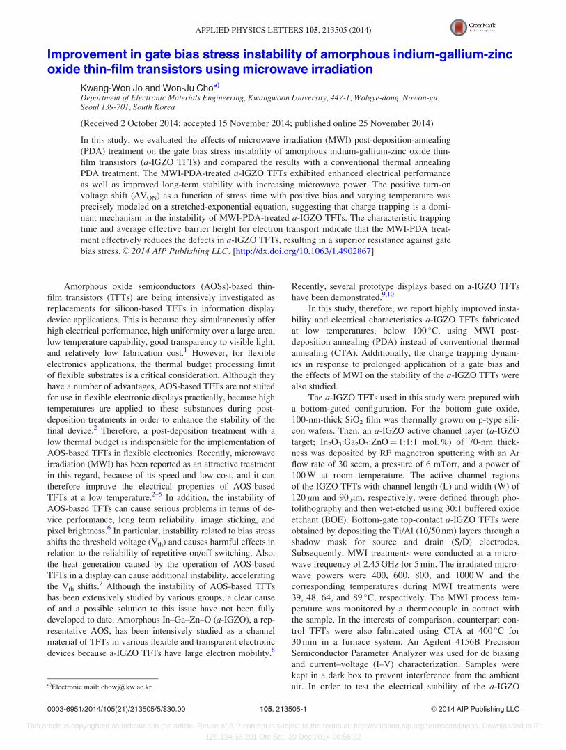
Figure 1 shows the electrical characteristics of the a-
IGZO TFTs: (a) ID–VG transfer characteristic curves, (b) out-
put characteristic curves, and (c) sub-threshold swing (SS)
and field-effect mobility (lFE) as a function of MWI power.
The transfer curve measurements were performed with a
double-sweep mode to trace the hysteresis behavior, i.e., VG
was swept up and then back down at VDS¼ 10 V. In this
work, we used the turn-on voltage (VON, defined as VG at
IDS¼ 10 pA) instead of the VTH, because a rigid shift in
transfer curves with insignificant changes in field-effect mo-
bility and subthreshold swing was observed.11 The hysteresis
behavior of the a-IGZO TFTs is shown in Fig. 1(a). The
presence of clockwise hysteresis in all transfer curves is con-
sistent with electron trapping at or near the IGZO channel/
SiO2 gate dielectrics interface or within the IGZO channel
layer. The pristine device has a large hysteresis voltage of
9.46 V, whereas the MWI treatment remarkably improves
the hysteresis characteristics. Following MWI treatment, the
hysteresis voltage (DVON) values were 8.63 V at 400 W,
3.53 V at 600 W, 2.36 V at 800 W, and 0.18 V at 1000 W.
The CTA anneal at 400 �C also significantly improves the
hysteresis voltage to 3.55 V, equivalent to the MWI-treated
result at 600 W. Shown in the inset of Fig. 1(a) is the on/off
ratio of the a-IGZO TFTs, increasing with microwave power.
When the microwave power exceeds 800 W, the on/off ratio
of the MWI-treated sample is larger than that of the CTA
case at 400 �C. Furthermore, the output characteristics of the
a-IGZO TFTs in accumulation exhibit a strong saturation
and a clear pinch off, as shown in Fig. 1(b). This implies that
the fabrication of a-IGZO TFTs with excellent performance
is feasible at a low process temperature (<100 �C) using
MWI-PDA. Moreover, the performance of the MWI-treated
samples at 89 �C (1000 W) is superior to that of the CTA
case at 400 �C. The SS and lFE results extracted from the
MWI-treated a-IGZO TFTs as functions of microwave
power and from the CTA-treated a-IGZO TFTs are shown in
Fig. 1(c). As the power increases, the lFE values are drasti-
cally increased from 1.9 (pristine) to 17.4 cm2/V s (1000 W)
and the SS is rapidly decreased from 1689 (pristine) to 224
dec/mV (1000 W). It is noteworthy that the MWI-PDA TFTs
(1000 W) have a larger lFE and a smaller SS than the CTA-
treated TFTs (400 �C) in spite of much lower temperature
process.
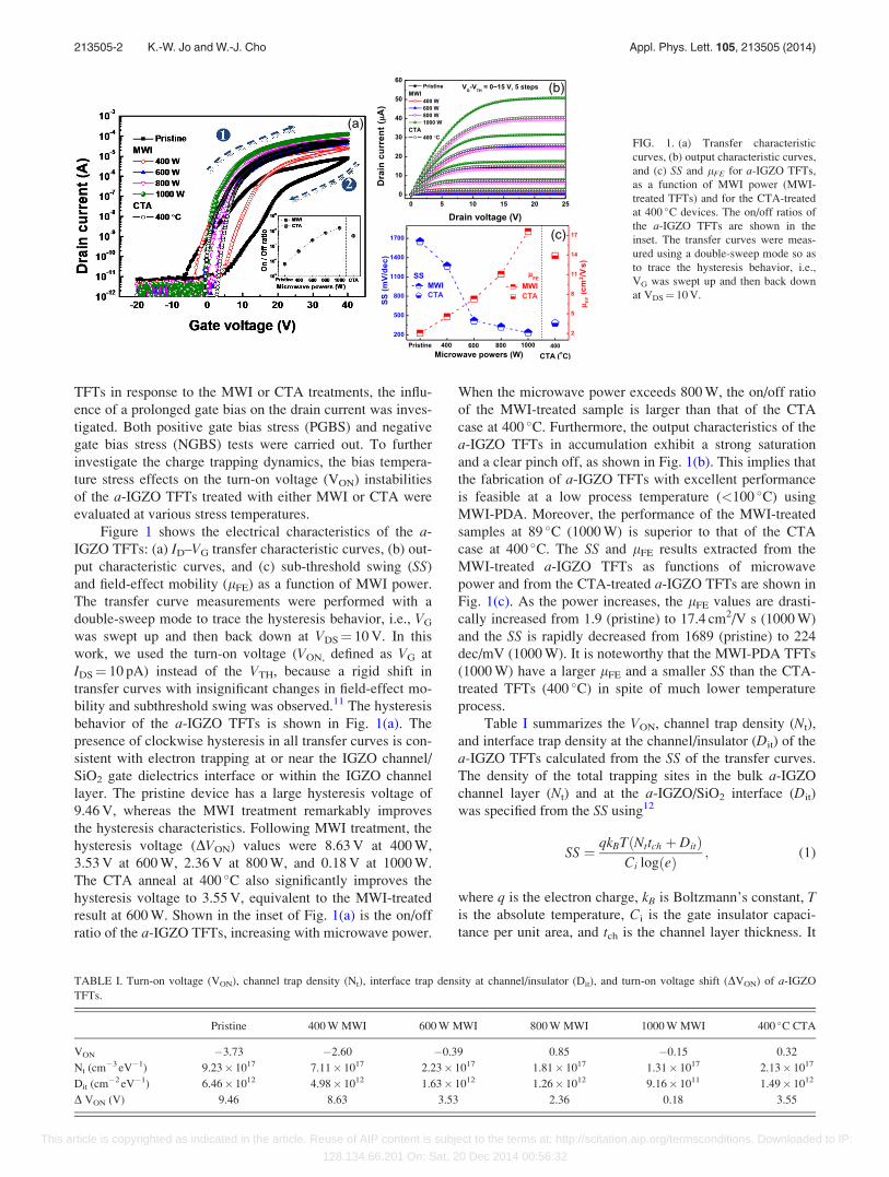
Table I summarizes the VON, channel trap density (Nt),
and interface trap density at the channel/insulator (Dit) of the
a-IGZO TFTs calculated from the SS of the transfer curves.
The density of the total trapping sites in the bulk a-IGZO
channel layer (Nt) and at the a-IGZO/SiO2 interface (Dit)
was specified from the SS using12
SS ¼ qkBT Nttch þ Ditð ÞCi log eð Þ
; (1)
where q is the electron charge, kB is Boltzmann’s constant, Tis the absolute temperature, Ci is the gate insulator capaci-
tance per unit area, and tch is the channel layer thickness. It
FIG. 1. (a) Transfer characteristic
curves, (b) output characteristic curves,
and (c) SS and lFE for a-IGZO TFTs,
as a function of MWI power (MWI-
treated TFTs) and for the CTA-treated
at 400 �C devices. The on/off ratios of
the a-IGZO TFTs are shown in the
inset. The transfer curves were meas-
ured using a double-sweep mode so as
to trace the hysteresis behavior, i.e.,
VG was swept up and then back down
at VDS¼ 10 V.
TABLE I. Turn-on voltage (VON), channel trap density (Nt), interface trap density at channel/insulator (Dit), and turn-on voltage shift (DVON) of a-IGZO
TFTs.
Pristine 400 W MWI 600 W MWI 800 W MWI 1000 W MWI 400 �C CTA
VON �3.73 �2.60 �0.39 0.85 �0.15 0.32
Nt (cm�3 eV�1) 9.23� 1017 7.11� 1017 2.23� 1017 1.81� 1017 1.31� 1017 2.13� 1017
Dit (cm�2 eV�1) 6.46� 1012 4.98� 1012 1.63� 1012 1.26� 1012 9.16� 1011 1.49� 1012
D VON (V) 9.46 8.63 3.53 2.36 0.18 3.55
213505-2 K.-W. Jo and W.-J. Cho Appl. Phys. Lett. 105, 213505 (2014)
This article is copyrighted as indicated in the article. Reuse of AIP content is subject to the terms at: http://scitation.aip.org/termsconditions. Downloaded to IP:
128.134.66.201 On: Sat, 20 Dec 2014 00:56:32
is assumed that Nt or Dit is separately set to 0 to estimate the
change in these values in response to variations in the micro-
wave irradiation conditions. Thus, the values of Nt and Dit
represent the maximum densities and demonstrate a trend.
Similar to the hysteresis in Fig. 1(a), the trap density of the
a-IGZO TFTs decreased with increasing MWI power. This
is because the MWI effectively eliminates grown-in defects,
which are included in the deposition of the a-IGZO layer,
and the interface trap density at the channel/insulator inter-
face. Consequently, the mobility and the charge trapping
characteristics of the a-IGZO TFTs are improved by means
of MWI-PDA treatment.
Meanwhile, one of the most important issues in relation
to a-IGZO TFTs is reliability. It is well established for a-Si
and poly-Si TFTs that prolonged application of a gate bias
on the TFTs can result in the deterioration of the I-V char-
acteristics. This effect leads to a change in the field effect
mobility, a change in the subthreshold slope, or a shift in
the threshold voltage. This is commonly referred to as the
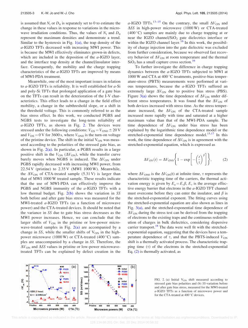
bias stress effect. In this work, we conducted PGBS and
NGBS tests to investigate the long-term reliability of
a-IGZO TFTs, as shown in Fig. 2. The devices were
stressed under the following conditions: VGS¼VON0 6 20 V
and VDS¼ 0 V for 3600 s, where VON0 is the turn-on voltage
of the pristine device. The shift in the initial VON was meas-
ured according to the polarities of the stressed gate bias, as
shown in Fig. 2(a). In particular, a PGBS results in a large
positive shift in the VON (DVON), while the transfer curve
barely moves when NGBS is induced. The DVON under
PGBS rapidly decreased with increasing MWI power, from
22.54 V (pristine) to 2.35 V (MWI 1000 W). Meanwhile,
the DVON of CTA-treated sample (5.31 V) is larger than
that of MWI 1000 W treated sample. These results indicate
that the use of MWI-PDA can effectively improve the
PGBS and NGBS immunity of the a-IGZO TFTs with a
low thermal budget. Fig. 2(b) shows the variation in SSboth before and after gate bias stress was measured for the
MWI-treated a-IGZO TFTs (as a function of microwave
power) and the CTA-treated devices. It should be noted that
the variance in SS due to gate bias stress decreases as the
MWI power increases. Hence, we can conclude that the
larger shifts of VON in the pristine or low-power micro-
wave-treated samples in Fig. 2(a) are accompanied by a
change in SS, while the smaller shifts of VON in the high-
power microwave (1000 W) or CTA-treated (400 �C) sam-
ples are unaccompanied by a change in SS. Therefore, the
DVON and DSS values in pristine or low-power microwave-
treated TFTs can be explained by defect creation in the
a-IGZO TFTs.13–15 On the contrary, the small DVON and
DSS in high-power microwave (1000 W) or CTA-treated
(400 �C) samples are mainly due to charge trapping at or
near the IGZO channel/SiO2 gate dielectrics interface or
within the IGZO channel layer.16 In this work, the possibil-
ity of charge injection into the gate dielectric was excluded
from further consideration, because we observed fast recov-
ery behavior of DVON at room temperature and the thermal
SiO2 has a small capture cross section.16
To further investigate the difference in charge trapping
dynamics between the a-IGZO TFTs subjected to MWI at
1000 W and CTA at 400 �C treatments, positive-bias temper-
ature-stress (PBTS) measurements were performed at vari-
ous temperatures, because the a-IGZO TFTs suffered an
extremely large DVON due to positive bias stress (PBS).
Figure 3(a) shows the time dependence of DVON under dif-
ferent stress temperatures. It was found that the DVON of
both devices increased with stress time. As the stress temper-
ature increased, the DVON of the CTA-treated sample
increased more rapidly with time and saturated at a higher
maximum value than that of the MWI-PDA sample. The
time dependence of DVON under bias stress has been
explained by the logarithmic time dependence model or the
stretched-exponential time dependence model.15,17 In this
work, the time dependence of DVON is in agreement with the
stretched-exponential equation, which is expressed as
DVON tð Þ ¼ DVON0 1� exp � t
s
� �b" #( )
; (2)
where DVON0 is the DVON(t) at infinite time, s represents the
characteristic trapping time of the carriers, the thermal acti-
vation energy is given by Ea¼Esb, Es is the average effec-
tive energy barrier that electrons in the a-IGZO TFT channel
must overcome before they can enter the insulator, and b is
the stretched-exponential exponent. The fitting curves using
the stretched-exponential equation are also shown as lines in
Fig. 3(a), and the stretched-exponential time dependence of
DVON during the stress test can be derived from the trapping
of electrons to the existing traps and the continuous redistrib-
ution of charges in bulk dielectrics, considering dispersive
carrier transport.18 The data were well fit with the stretched-
exponential equation, suggesting that the devices have a tem-
perature dependence of s, and that the PBTS-induced VON
shift is a thermally activated process. The characteristic trap-
ping time (s) of the electrons in the stretched-exponential
Eq. (2) is thermally activated, as
FIG. 2. (a) Initial VON shift measured according to
stressed gate bias polarities and (b) SS-variation before
and after gate bias stress, measured for the MWI-treated
a-IGZO TFTs as a function of microwave power and
for the CTA-treated at 400 �C devices.
213505-3 K.-W. Jo and W.-J. Cho Appl. Phys. Lett. 105, 213505 (2014)
This article is copyrighted as indicated in the article. Reuse of AIP content is subject to the terms at: http://scitation.aip.org/termsconditions. Downloaded to IP:
128.134.66.201 On: Sat, 20 Dec 2014 00:56:32
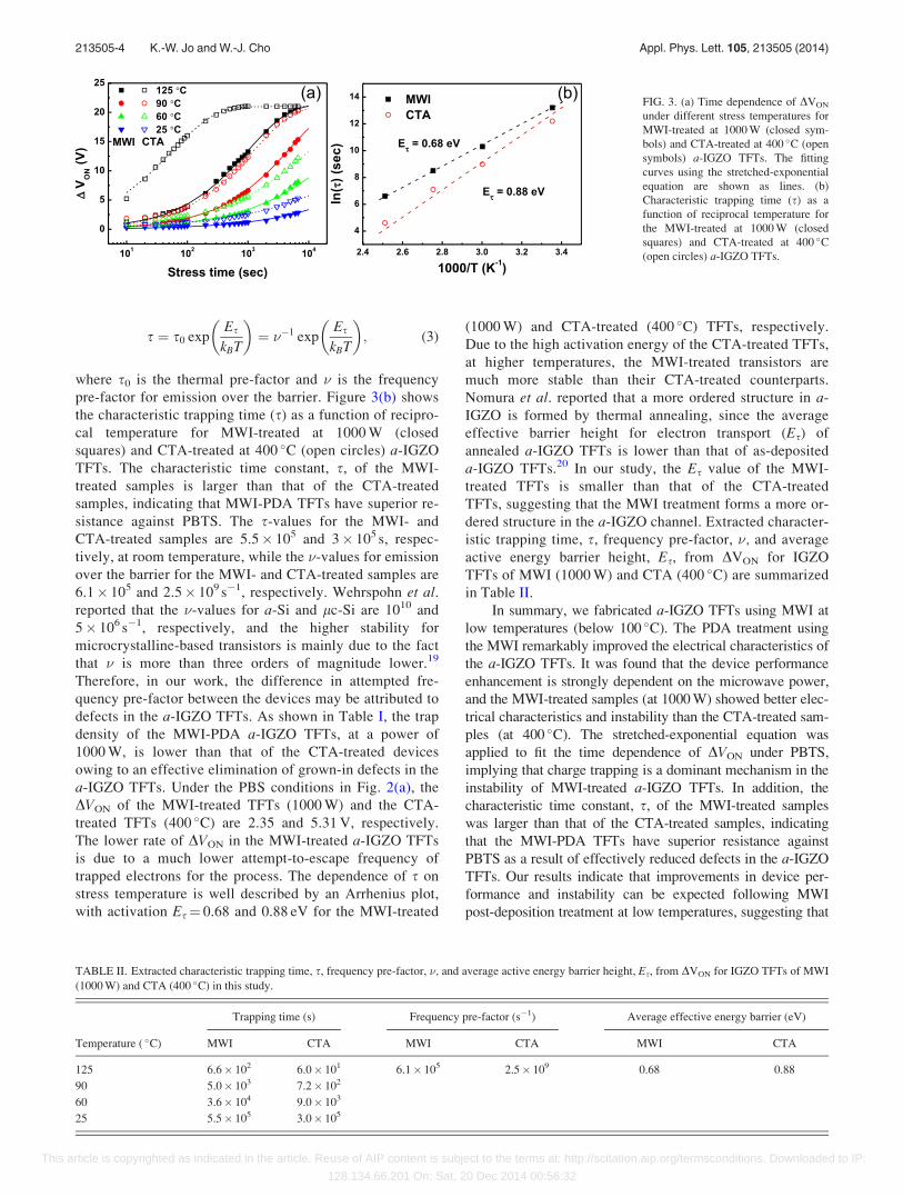
s ¼ s0 expEs
kBT
� �¼ ��1 exp
Es
kBT
� �; (3)
where s0 is the thermal pre-factor and � is the frequency
pre-factor for emission over the barrier. Figure 3(b) shows
the characteristic trapping time (s) as a function of recipro-
cal temperature for MWI-treated at 1000 W (closed
squares) and CTA-treated at 400 �C (open circles) a-IGZO
TFTs. The characteristic time constant, s, of the MWI-
treated samples is larger than that of the CTA-treated
samples, indicating that MWI-PDA TFTs have superior re-
sistance against PBTS. The s-values for the MWI- and
CTA-treated samples are 5.5� 105 and 3� 105 s, respec-
tively, at room temperature, while the �-values for emission
over the barrier for the MWI- and CTA-treated samples are
6.1� 105 and 2.5� 109 s�1, respectively. Wehrspohn et al.reported that the �-values for a-Si and lc-Si are 1010 and
5� 106 s�1, respectively, and the higher stability for
microcrystalline-based transistors is mainly due to the fact
that � is more than three orders of magnitude lower.19
Therefore, in our work, the difference in attempted fre-
quency pre-factor between the devices may be attributed to
defects in the a-IGZO TFTs. As shown in Table I, the trap
density of the MWI-PDA a-IGZO TFTs, at a power of
1000 W, is lower than that of the CTA-treated devices
owing to an effective elimination of grown-in defects in the
a-IGZO TFTs. Under the PBS conditions in Fig. 2(a), the
DVON of the MWI-treated TFTs (1000 W) and the CTA-
treated TFTs (400 �C) are 2.35 and 5.31 V, respectively.
The lower rate of DVON in the MWI-treated a-IGZO TFTs
is due to a much lower attempt-to-escape frequency of
trapped electrons for the process. The dependence of s on
stress temperature is well described by an Arrhenius plot,
with activation Es¼ 0.68 and 0.88 eV for the MWI-treated
(1000 W) and CTA-treated (400 �C) TFTs, respectively.
Due to the high activation energy of the CTA-treated TFTs,
at higher temperatures, the MWI-treated transistors are
much more stable than their CTA-treated counterparts.
Nomura et al. reported that a more ordered structure in a-
IGZO is formed by thermal annealing, since the average
effective barrier height for electron transport (Es) of
annealed a-IGZO TFTs is lower than that of as-deposited
a-IGZO TFTs.20 In our study, the Es value of the MWI-
treated TFTs is smaller than that of the CTA-treated
TFTs, suggesting that the MWI treatment forms a more or-
dered structure in the a-IGZO channel. Extracted character-
istic trapping time, s, frequency pre-factor, �, and average
active energy barrier height, Es, from DVON for IGZO
TFTs of MWI (1000 W) and CTA (400 �C) are summarized
in Table II.
In summary, we fabricated a-IGZO TFTs using MWI at
low temperatures (below 100 �C). The PDA treatment using
the MWI remarkably improved the electrical characteristics of
the a-IGZO TFTs. It was found that the device performance
enhancement is strongly dependent on the microwave power,
and the MWI-treated samples (at 1000 W) showed better elec-
trical characteristics and instability than the CTA-treated sam-
ples (at 400 �C). The stretched-exponential equation was
applied to fit the time dependence of DVON under PBTS,
implying that charge trapping is a dominant mechanism in the
instability of MWI-treated a-IGZO TFTs. In addition, the
characteristic time constant, s, of the MWI-treated samples
was larger than that of the CTA-treated samples, indicating
that the MWI-PDA TFTs have superior resistance against
PBTS as a result of effectively reduced defects in the a-IGZO
TFTs. Our results indicate that improvements in device per-
formance and instability can be expected following MWI
post-deposition treatment at low temperatures, suggesting that
FIG. 3. (a) Time dependence of DVON
under different stress temperatures for
MWI-treated at 1000 W (closed sym-
bols) and CTA-treated at 400 �C (open
symbols) a-IGZO TFTs. The fitting
curves using the stretched-exponential
equation are shown as lines. (b)
Characteristic trapping time (s) as a
function of reciprocal temperature for
the MWI-treated at 1000 W (closed
squares) and CTA-treated at 400 �C(open circles) a-IGZO TFTs.
TABLE II. Extracted characteristic trapping time, s, frequency pre-factor, �, and average active energy barrier height, Es, from DVON for IGZO TFTs of MWI
(1000 W) and CTA (400 �C) in this study.
Temperature ( �C)
Trapping time (s) Frequency pre-factor (s�1) Average effective energy barrier (eV)
MWI CTA MWI CTA MWI CTA
125 6.6� 102 6.0� 101 6.1� 105 2.5� 109 0.68 0.88
90 5.0� 103 7.2� 102
60 3.6� 104 9.0� 103
25 5.5� 105 3.0� 105
213505-4 K.-W. Jo and W.-J. Cho Appl. Phys. Lett. 105, 213505 (2014)
This article is copyrighted as indicated in the article. Reuse of AIP content is subject to the terms at: http://scitation.aip.org/termsconditions. Downloaded to IP:
128.134.66.201 On: Sat, 20 Dec 2014 00:56:32
MWI-PDA is a very promising treatment for TFTs to be used
in flexible electronic display applications.
This research was supported by the research grant from
Kwangwoon University in 2014 and by Basic Science
Research Program through the National Research Foundation
of Korea (NRF) funded by the Ministry of Education, Science
and Technology (No. 2013R1A1A2A1 0011202).
1S. H. K. Park, J. W. Kim, M. Ryu, I. Y. Eom, J. E. Pi, O. S. Kwon, E.
Park, H. Oh, and C. S. Hwang, SID Symp. Dig. Tech. Pap. 44, 18 (2013).2C. S. Fuh, P. T. Liu, L. F. Teng, S. W. Huang, and Y. J. Lee, IEEE
Electron Device Lett. 34, 1157 (2013).3L. F. Teng, P. T. Liu, Y. J. Lo, and Y. J. Lee, Appl. Phys. Lett. 101,
132901 (2012).4H. C. Chenga and C. Y. Tsayb, J. Alloys Compd. 507, L1–L3 (2010).5C. Yang, K. Hong, J. Jang, D. S. Chung, T. K. An, W. S. Choi, and C. E.
Park, Nanotechnology 20, 465201 (2009).6Y. M. Kim, K. S. Jeong, H. J. Yun, S. D. Yang, S. Y. Lee, H. D. Lee, and
G. W. Lee, Jpn. J. Appl. Phys., Part 1 51, 09MF10 (2012).7B. S. Kim, Y. T. Jeong, D. Lee, T. Y. Choi, S. H. Jung, J. W. Choi, C.
Yang, K. Jo, B. J. Lee, E. Park, D. N. Kim, Y. Kim, and S. Shin, Appl.
Phys. Lett. 103, 072110 (2013).
8K. Nomura, H. Ohta, A. Takagi, T. Kamiya, M. Hirano, and H. Hosono,
Nature (London) 432, 488 (2004).9J. K. Jeong, J. H. Jeong, J. H. Choi, J. S. Im, S. H. Kim, H. W. Yang, K. N.
Kang, K. S. Kim, T. K. Ahn, H.-J. Chung et al., SID Int. Symp. Dig. Tech.
Pap. 39, 1 (2008).10J.-H. Lee, D.-H. Kim, D.-J. Yang, S.-Y. Hong, K.-S. Yoon, P.-S. Hong,
C.-O. Jeong, H.-S. Park, S. Y. Kim, S. K. Lim et al., SID Int. Symp. Dig.
Tech. Pap. 39, 625 (2008).11D. Kang, H. Lim, C. Kim, I. Song, J. Park, Y. Park, and J. G. Chung,
Appl. Phys. Lett. 90, 192101 (2007).12D. W. Greve, Field Effect Devices and Applications: Devices for Portable,
Low-Power, and Imaging Systems, 1st ed. (Prentice-Hall, Englewood
Cliffs, New Jersey, 1998).13J. F. Conley, IEEE Trans. Device Mater. Reliab. 10, 460 (2010).14J. Jeong, G. J. Lee, J. Kim, J. Kim, and B. Choi, Appl. Phys. Express 6,
031101 (2013).15S. Zafar, A. Callegari, E. Gusev, and M. V. Fischetti, J. Appl. Phys. 93,
9298 (2003).16J. F. Zhang, S. Taylor, and W. Eccleston, J. Appl. Phys. 71, 725 (1992).17A. Suresh and J. F. Muth, Appl. Phys. Lett. 92, 033502 (2008).18F. R. Libsch and J. Kanicki, Appl. Phys. Lett. 62, 1286 (1993).19R. Wehrspohn, S. Deane, I. French, and M. Powell, Thin Solid Films 383,
117 (2001).20K. Nomura, T. Kamiya, M. Hirano, and H. Hosono, Appl. Phys. Lett. 95,
013502 (2009).
213505-5 K.-W. Jo and W.-J. Cho Appl. Phys. Lett. 105, 213505 (2014)
This article is copyrighted as indicated in the article. Reuse of AIP content is subject to the terms at: http://scitation.aip.org/termsconditions. Downloaded to IP:
128.134.66.201 On: Sat, 20 Dec 2014 00:56:32