Environmentally sustainable organic field effect transistors

RESEARCH PAPER
Nanotubes-/nanowires-based, microfluidic-integrated transistorsfor detecting biomolecules
J. N. Tey • I. P. M. Wijaya • J. Wei •
I. Rodriguez • S. G. Mhaisalkar
Received: 4 February 2010 / Accepted: 19 April 2010 / Published online: 3 June 2010
� Springer-Verlag 2010
Abstract Nanotubes and nanowires have sparked con-
siderable interest in biosensing applications due to their
exceptional charge transport properties and size compati-
bility with biomolecules. Among the various biosensing
methodologies incorporating these nanostructured materi-
als in their sensing platforms, liquid-gated field-effect
transistors (LGFETs)-based device configurations outper-
form the conventional electrochemical measurements by
their ability in providing label free, direct electronic read-
out, and real-time detection. Together with integration of a
microfluidic channel into the device architecture, nano-
tube- or nanowires-based LGFET biosensor have demon-
strated promising potential toward the realization of truly
field-deployable self-contained lab-on-chip devices, which
aim to complement the existing lab-based methodologies.
This review addresses the recent advances in microfluidic-
integrated carbon nanotubes and inorganic nanowires-
based LGFET biosensors inclusive of nanomaterials
growth, device fabrication, sensing mechanisms, and
interaction of biomolecules with nanotubes and nanowires.
Design considerations, factors affecting sensing
performance and sensitivity, amplification and multiplex-
ing strategies are also detailed to provide a comprehensive
understanding of present biosensors and future sensor
systems development.
Keywords Biosensor � Carbon nanotubes � Nanowires �Label-free detection � Field-effect transistor
1 Introduction
One-dimensional nanostructures such as carbon nanotubes
(CNTs) and nanowires (NWs) have been envisaged as ideal
building blocks for biosensor development due to their size
similarity and biocompatibility with a host of biomole-
cules. Their extremely high surface-to-volume ratio results
in most of the constituent atoms residing on the surface of
the nanostructure, which renders even the slightest distur-
bance from their proxy surrounding sufficient to alter their
electrical properties (Lacerda et al. 2006, 2007; Polizu
et al. 2006; Popov et al. 2007). As compared to their zero-
or two-dimensional counterparts, one-dimensional nano-
systems such as nanotubes and nanowires offer a major
advantage in that its length scale that extends into
micrometers offers a facile route for interfacing to the
macro world. In the case of zero-dimensional nanosystems,
such as nanoparticles and quantum dots, this interfacing
becomes a challenge due to complexities in inter-particle
charge transport. On the other hand, two-dimensional
nanosystems like graphene and flat nanocrystals, exhibit
tensor (non-scalar) nature of the conductivities, which
result in anisotropy in electrical properties. Furthermore,
any local electrostatic disturbance may not always be
detected because of the large conducting surfaces charges
may naturally circumvent such areas choosing the path of
First two authors contributed equally to this work.
J. N. Tey � J. Wei
Singapore Institute of Manufacturing Technology,
71 Nanyang Drive, Singapore 638075, Singapore
I. P. M. Wijaya � I. Rodriguez
Institute of Materials Research and Engineering,
3 Research Link, Singapore 117602, Singapore
J. N. Tey � I. P. M. Wijaya � S. G. Mhaisalkar (&)
School of Materials Science and Engineering,
Nanyang Technological University, Block N4.1,
Nanyang Avenue, Singapore 639798, Singapore
e-mail: [email protected]
123
Microfluid Nanofluid (2010) 9:1185–1214
DOI 10.1007/s10404-010-0640-1

least resistance. Both zero-dimensional and two-dimen-
sional nanosystems thus present challenges from interfac-
ing and device optimization perspective.
Different device architectures have been designed over
the last decades to utilize these nanostructured materials as
sensing elements to detect biomolecular interactions. In
general, detection methods in sensing configurations
incorporating CNTs and NWs include: (1) fluorescence
(Hazani et al. 2003; Cherukuri et al. 2006), (2) electro-
chemistry (Gooding et al. 2003; Kim et al. 2007b; Diao
et al. 2002; Huang et al. 2009), and (3) transistor-based
electrical sensing (Heller et al. 2008; Bradley et al. 2004,
2005; Jeon et al. 2006; Guo et al. 2003; Star et al. 2003;
Gui et al. 2006; Chen et al. 2004). Classical detection
techniques such as enzyme-linked immunosorbent assay
(ELISA), cyclic voltammetry, amperometry, potentiomet-
ric, and electrochemical impedance spectroscopy have
been reported to display significant improvement upon
incorporating CNTs into the measurement setup, such as
blending of CNTs into the electrodes (Gong et al. 2005;
Yun et al. 2007; Panini et al. 2008) or using them as labels
for signal amplification (Wang et al. 2004; Yu et al. 2006).
Nonetheless, these techniques typically suffer a few
drawbacks: (1) extra processing steps are required to
introduce a fluorescence or electrochemical tag to the
system in order to probe the biomolecular interaction, (2)
sensing is not performed in real-time, and (3) they are
usually not adaptable for on-site analysis.
To address these challenges, a new alternative to detect
these biomolecular interaction in label-free fashion have
recently been proposed, utilizing semiconducting CNT and
NW as the semiconducting channel in field-effect transis-
tors (FETs) (Kim et al. 2007b). While the history of
semiconductors and the first reported semiconductor FET
dates back for more than a century (Braun 1874; Bardeen
and Brattain 1948; Kahng and Atalla 1960), the advance-
ment of CNTs and NWs dates back to merely two decades
(Iijima 1991; Hu et al. 1999); with their potential for
sensing applications in transistor configuration reported
only as recently as 2000 (Kong et al. 2000; Cui et al. 2001).
Specifically, two approaches have been reported: dry-state
sensing (Gui et al. 2006; Star et al. 2006) and liquid-gated
transistor (LGFET) (Cui and Lieber 2001; Rosenblatt et al.
2002) measurement, in which the latter offers an added
benefit in permitting real-time detection of biomolecular
interactions in aqueous media, the native environment for
most biomolecules. The motivation toward transistor-based
biosensors is not to replace, but rather complement estab-
lished high sensitivity analytical methods such as ELISA,
to address needs for point-of-care diagnostics and on-site
sample analysis.
While FET-based biosensors have demonstrated prom-
ising detection limits, greater considerations for device
miniaturization, real-time sensing and portability are
required toward the realization of truly field-deployable
self-contained lab-on-chip devices. The integration of
microfluidic channel into the transistor architecture was
first demonstrated on the NW-LGFET-based biosensing
study (Cui et al. 2001), and much later after that for CNT–
LGFET (Larrimore et al. 2006). Even though the starting
point for NWs research effort took place much later than
the CNTs, the development of the former and its process
integration for lab-on-chip capability has been particularly
rapid. This rapid development in the NW–LGFET plat-
forms was facilitated by the mature body of knowledge
gleaned in the field of silicon microelectronics. The
incorporation of microfluidic channels into the sensor
architecture represents a critical innovation in the realiza-
tion of lab-on-chip devices. Advantages include (1) sig-
nificant reduction in analyte volume requirement; (2)
reduced incubation time due to shorter diffusion distances
as a result of molecules being confined in the microchan-
nel; (3) better control of molecular concentrations and
interactions; and (4) ability to execute multiple complex
reactions including lysis, amplification, mixing, filtration
among others.
In this review article, a brief survey of the recent
advances of microfluidic-integrated LGFET-based biosen-
sors is addressed. While CNTs and NWs are different in
their molecular structures, growth, and fabrication pro-
cesses, they share operational similarities when incorpo-
rated in FET-based biosensors. The objective of this review
is to present an overview of the ongoing biosensing
activities with microfluidic-integrated LGFET devices
incorporating CNTs or NWs. General principles are
explained in most part without making distinctions
between CNTs and NWs. However, comments and com-
parisons between CNTs and NWs are made when required
to elaborate their pros and cons, as well as to highlight
parametric and process control differences between the two
platforms.
The scope of this review includes aspects such as
overview of the molecular structure of CNTs and NWs, the
working principles and sensing mechanisms of LGFETs, as
well as device assembly and fabrication. In addition, fac-
tors influencing the sensitivity of the measurement,
potential techniques for signal amplification, and examples
of LGFET-based biodetection of proteins, enzymes, and
oligonucleotides will be covered. Due to the diversified
nature of CNT-based sensing platforms and a variety of
semiconducting NWs-based FET architectures (Jeon et al.
2006; Zhang et al. 2008a; Curreli et al. 2005; Patolsky et al.
2006b; Sun et al. 2010; Baker et al. 2002), it would be
impractical to attempt a broad discussion on the field. Our
discussion is therefore confined to the most promising
nanomaterials and architectures for this application, single-
1186 Microfluid Nanofluid (2010) 9:1185–1214
123

walled CNT (SWCNT) and silicon nanowire (SiNW)-
based LGFETs. Throughout this review, general terms such
as CNT and NW will refer to SWCNT and SiNW, unless
specified otherwise.
2 Working principles of liquid-gated field-effect
transistor-based biosensors
2.1 Molecular structure and electrical properties
of CNTs and NWs
The CNTs and NWs are similar in that both share most of
the characteristics of one-dimensional systems, such as
quantum confinement at circumferential and radial direc-
tions, increased band gap as their cross-sectional diameter
decreases, etc. However, the two nanosystems are also
different in many ways depending on the arrangement of
atoms.
CNTs belong to a class of carbonaceous nanomaterials
in which a unique surface arrangement of carbon atoms
coupled with one-dimensional quantum confinement gives
rise to exceptional electronic, thermal, and mechanical
properties. Numerous applications of these materials in
molecular electronics, circuits and interconnects, field
emission, actuators, energy harvesting and storage, high
strength composites, biomedical diagnostics, and drug
delivery (Dekker 1999; Kreupl et al. 2002; Endo et al.
2008) are currently being aggressively pursued. The
versatility of nanotubes stems from their unique charac-
teristics, including extremely large aspect ratios, high sur-
face-to-volume ratios, infinitely conjugated sp2 hybridized
network of carbon atoms, impressive strength-to-weight
ratios, and excellent chemical stability.
From a molecular structure perspective, the nanotubes
are tubular analogs of graphene, and may be divided into
single-walled carbon nanotubes (SWCNTs) and multi-
walled carbon nanotubes (MWCNTs), depending on the
number of graphene sheet(s) that form the structures
(Anantram and Leonard 2006). SWCNTs comprise single
graphene sheet rolled into a cylindrical architecture with
dimensions typically in the order of 1–2 nm in diameter
and several micro-meters in length. In contrast, MWCNTs
can be visualized as multiple graphene sheets rolled toge-
ther into concentric nano-sized cylinders with layer to layer
spacing of 0.3–0.4 nm, diameters of 10–100 nm and
lengths of several micro-meters (Baughman et al. 2002).
The different atomic arrangement of the two nanotubes
sub-species manifests itself in their electronic properties.
The SWCNT, for example, is well-known for its unique
electronic properties in that it can behave like either
semiconductors, or metals, depending on the specific
arrangement of the carbon atoms in the SWCNT. In
contrast, MWCNTs tend to behave more like metals. These
different electronic properties have led to divergent appli-
cations of semiconducting SWCNTs as transistors for
future microelectronic and sensing devices (Jo et al. 2007;
Kim et al. 2007b; Anantram and Leonard 2006; Bradley
et al. 2004; Star et al. 2003) and metallic MWCNTs as
microelectrodes in electrochemical sensors (Panini et al.
2008; Viswanathan et al. 2009).
The unique electronic properties of the SWCNTs, which
can display either semiconducting or metallic properties,
are product of a phenomenon observed only in the nano-
scale realm: quantum confinement. Briefly, the quantum
confinement effect takes place when the wavelength of the
charge carriers is similar to the physical environment in
which they reside. The wave continuity requirement dic-
tates that the charge carriers cannot assume all wavelength
values in such confined environments. This restriction
results in the charge carriers to assume only certain por-
tions of the energy–momentum diagram. Graphically, this
discontinuity can be depicted as slicing planes which cut
only certain portions of an otherwise continuous energy–
momentum diagram, as shown in Fig. 1a (Dresselhaus
et al. 2005). Hence, from this graph, it can be envisaged
that the rolling direction of the CNTs would dictate the
profile of the energy–momentum diagram. Therefore,
within a family of CNTs, there would be those that show a
band gap, rendering them semiconducting, and those that
are metallic.
Similar to their nanotube counterparts, one-dimensional
nanowires display differing properties as influenced by the
atomic constituents, geometry, dimensions, presence of
dopants, point defects, etc. However, unlike their nanotube
counterparts, the parameters to synthesize the nanowires
are more controllable, making the batch-to-batch properties
of these nanowires more uniform (Hu et al. 1999). In
addition, analog electrical properties are also displayed by
the nanowires, as shown in Fig. 1b (Yao et al. 2008).
Similar to the CNTs, the energy–momentum diagram of the
NWs also suffers from quantum-confinement effect. The
extent of this quantum-confinement effect is different at the
various points in the energy–momentum diagram. Indeed,
this variation to sensitivity toward the quantum-confine-
ment effect makes SiNWs very different from their bulk Si
counterparts in that the former typically is a direct band
gap semiconductor, hence rendering it a suitable material
relevant to photonic applications.
The similarity in the energy–momentum diagram as
displayed by both the NWs and the CNTs makes these two
one-dimensional nanosystems amenable to be brought into
the same LGFET platform. Specifically, the NWs and the
CNTs can be connected to source–drain electrodes at both
extremes to make a simple Schottky transistor typical of
LGFETs. Furthermore, the size similarity between most
Microfluid Nanofluid (2010) 9:1185–1214 1187
123

biomolecules with the NWs and the CNTs makes them the
preferred choice for development of real-time label-free
biosensors.
To conclude, the electrical properties of SWCNTs vary
according to their diameter and chiral distribution (Anan-
tram and Leonard 2006; LeMieux et al. 2008), which are
difficult to control during their growth processes and
challenges their viability in large-scale commercial appli-
cations. Unlike CNTs, the prime advantage of SiNWs is
that their electrical properties can be controlled by classical
doping practices, commonly employed in the microelec-
tronics field. Hence, the vast knowledge from the semi-
conductor industry can be transferred and applied to the
fabrication, doping, and surface chemical modification of
these nanowires (Cui et al. 2000; Pui et al. 2009; Zhang
et al. 2008b). In addition, distinct chemical composition,
structure, size, and morphology can be well controlled
through the growth process (Lu and Lieber 2006). The
highly reproducible electronic properties and high yield
production has made SiNW a promising nanomaterial for
future large-scale integrated systems and potential
bioapplications, including the field of environmental
sensing and medical diagnostics.
2.2 Working principles: LGFET versus dry-state FET
Typically, a CNT or NW–FET comprises CNTs or NWs as
the semiconducting channel that is capacitively coupled to
a gate electrode through a dielectric medium and flanked
by metal source–drain electrodes to provide electrical
connectivity (Fig. 2a). Voltage applied to the gate elec-
trode (VG) modulates the charge carrier concentration
induced in the semiconducting channel at the dielectric–
semiconductor interface, hence modulating the drain–
source conductance. Considering a p-type FET, an
application of negative VG bias leads to the accumulation
of hole carriers, and hence current flows from the source to
the drain electrode upon applying a source–drain Voltage
(VDS) across the channel. A positive VG bias will lead to the
depletion of carriers at the interface, restricting the current
flow.
Fig. 1 a E–k diagram showing
the energy quantization which
appears as slicing planes along
the rolling directions in (i) and
its cross-sectional view in (ii).b E–k diagram for SiNW having
a rectangular cross section with
diameter of 3.85 nm. Image
a adapted from Dresselhaus
et al. (2005). Image b adapted
with permission from Yao et al.
(2008). Copyright (2008)
American Chemical Society
1188 Microfluid Nanofluid (2010) 9:1185–1214
123

The dielectric layer, typically composed of a solid
dielectric film in a dry-state FET, is replaced by an aqueous
electrolyte solution in liquid-gated FETs (Fig. 2b). A gate
bias is applied directly to the electrolyte solution to mod-
ulate the surface carrier concentration of the semicon-
ducting channel, thereby modulating the channel
conductance. One important advantage of employing the
LGFET configuration in biosensors is that the aqueous
environment is highly compatible with biomolecules. In
addition, the VG range required to modulate the channel
conductance (hereafter referred to as VG window) is sig-
nificantly reduced, with much smaller hysteresis in the
electrical measurement.
The operation of LGFET as biosensors is sometimes
confused with ion-selective field-effect transistors (ISFET)
(Jamasb et al. 1998). In the latter, the presence of target
analyte ions in solution is captured by a suitable probe
dielectric material. Such biomolecular interactions can
only influence a thin region near the surface of a planar
device, limiting the sensitivity of the device (Lieber and
Wang 2007). In LGFET operation, when a bioanalyte
interacts with its probe molecule close to the surface of the
CNTs/NWs, it leads to depletion or accumulation of charge
carriers throughout the nanostructures, resulting in higher
sensitivity.
The gate voltage required to modulate the semicon-
ducting channel of CNT or NW–FET is governed by the
total gate channel capacitance in Eq. 1, which is composed
of two components: gate capacitance (CG) and quantum
capacitance (CQ).
CT ¼1
CG
þ 1
CQ
� ��1
ð1Þ
CQ originates from the small size of the nano-structures.
The minute size of the nanostructures results in a limited
number of the energy states available for the carriers to
occupy. Any addition of charge carriers to the
nanostructures would require an application of external
voltage to modulate the energy level to the next available
state. Hence, the requirement of voltage to add/subtract
charge carriers from the nanostructures is represented as
C = dQ/dV and CQ = e2 g(E).
For LGFETs, CG is the double-layer capacitance (CDL)
resulting from the formation of electrical charge layers at
(a) (b)
(c)
Fig. 2 a Dry-state CNT–FET
in bottom gate configuration.
b Liquid state CNT–FET in top
electrolyte gate configuration.
c Comparison of CNT–FET
transfer characteristic (ID–VG)
in air, using the bottom gate
(solid line), and in water, using
the liquid gate (dotted line).
Note the different x scales for
the bottom gate and the liquid
gate. Image c adapted with
permission from Bradley et al.
(2004). Copyright (2004)
American Chemical Society
Microfluid Nanofluid (2010) 9:1185–1214 1189
123

both the semiconducting nanostructure–solution interface
and the solution–gate electrode interface (Rosenblatt et al.
2002; Lu et al. 2006). The high dielectric constant of the
aqueous media (er * 78) and thin electrical double layer in
LGFET results in CG of a liquid-gated FET (CGL * 7 9
10-9 F/m) (Rosenblatt et al. 2002), being approximately
two orders of magnitude higher than that of the dry-state
FET, (CBG), which uses silicon dioxide (er * 3.9) as the
dielectric layer (Martel et al. 1998), and around one order
of magnitude larger than CQ of SWCNT/NW. Therefore,
CT in a back-gated dry-state SWCNT/NW–FET is con-
strained by the oxide dielectric while CT in liquid-gated
SWCNT/NW–FET is dominated by the CQ of SWCNT or
NW, yielding a 10-fold improvement in capacitance.
This improved performance of the LGFET is evident in
the ID versus VG (‘‘transfer’’) curves for a dry-state FET
and LGFET (Fig. 2c). In order to generate equivalent
current outputs, the dry-state FETs need to operate at sig-
nificantly higher voltages (10 [ VG [ -10 V) compared
with the LGFETs which may operate at less than |0.5| V
(Gruner 2006; Bradley et al. 2004).
Another significant advantage of LGFETs over dry-state
FET biosensing is the ability for real-time detection.
Examples of reported dry-state measurements include
direct detection of streptavidin (Bradley et al. 2004) and
bacteriorhodopsin (Bradley et al. 2005), as well as capture-
target analyte detection for biotin/streptavidin conjugate
(Star et al. 2003) and DNA hybridization (Star et al. 2006).
In these studies, transfer characteristics of the CNT or NW
transistor before and after bioanalytes exposure are com-
pared. To perform the measurements, the bare transistor
performance is first recorded prior to the incubation of
analytes. Upon completing the incubation process, the
device is rinsed with copious amounts of buffer solution to
remove the unbound analytes, blown dry, and post-binding
electrical measurement is executed. Repeat incubation,
rinsing, drying, and measurement steps have to be carried
out to record the change in IDVG in every step (Fig. 3a).
Multiple incubations, if required, expose the nanostruc-
tured FETs to multiple processing steps and have the
potential of introducing inconsistencies and compromise
the quality of the sensing data.
In liquid-gated configurations, handling of respective
processing steps can be simplified by conducting all the
incubation and washing steps in situ by flowing different
solutions into a micro-fluidic channel. In this scenario,
dynamic information of the interaction can be studied
without interrupting the electrical measurement, and series
of transfer curves, taken at short-time intervals, yield quasi-
kinetic data that may be analyzed in similar fashion to that
of dry-state measurements. Figure 3a shows the transfer
curves of a LGFET in an interrupted measurement and
Fig. 3b shows a kinetic measurement where all electrode
biases are held constant and the drain current with respect
to time is measured. In both figures, trace 1 is the bare
device transistor characteristic, while traces 2–4 show the
electrical characteristics after repeated steps of incubation
and rinsing.
2.3 Sensing mechanisms in LGFET-based biosensors
The change in conductance of CNT–LGFET in response
to biomolecule interactions have been attributed to several
competing mechanisms such as electrostatic gating effect
(Bradley et al. 2005; Boussaad et al. 2003), charge
transfer (Bradley et al. 2004; Star et al. 2003, 2006), and
Schottky barrier effect due to work function modulation
(Chen et al. 2004; Tang et al. 2006). Each of these
hypotheses is well supported by experimental data and the
sensing mechanism continues to be an area of active
research. A recent comprehensive theoretical and experi-
mental study reported on four possible mechanisms
operational in a biomolecule-nanostructure interaction
(Heller et al. 2008): (1) electrostatic gating, (2) Schottky
barrier, (3) mobility, and (4) capacitance modulation;
each of which exhibit a particular characteristic change in
Fig. 3 a Transfer characteristic
curves of a CNT–FET measured
at every experiment step,
through offline measurements of
current over a sweeping gate
bias, to observe the change in
transistor response as a result of
biomolecule–CNT interaction.
b Kinetic measurement to
observe the real-time response
throughout the entire sensing
experiment, obtained at a fixed
gate bias
1190 Microfluid Nanofluid (2010) 9:1185–1214
123
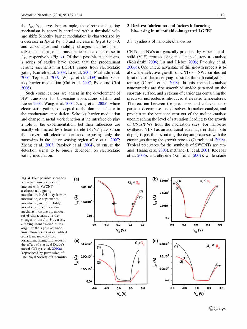
the IDS–VG curve. For example, the electrostatic gating
mechanism is generally correlated with a threshold volt-
age shift; Schottky barrier modulation is characterized by
a decrease in IDS at VG \ 0 and increase in IDS at VG [ 0;
and capacitance and mobility changes manifest them-
selves in a change in transconductance and decrease in
IDS, respectively (Fig. 4). Of these possible mechanisms,
a series of studies have shown that the predominant
sensing mechanism in LGFET comes from electrostatic
gating (Curreli et al. 2008; Li et al. 2005; Maehashi et al.
2006; Tey et al. 2009; Wijaya et al. 2009) and/or Scho-
ttky barrier modulation (Gui et al. 2007; Byon and Choi
2006).
Such complications are absent in the development of
NW transistors for biosensing applications (Hahm and
Lieber 2004; Wang et al. 2005; Zheng et al. 2005), where
electrostatic gating is accepted as the dominant factor in
the conductance modulation. Schottky barrier modulation
and change in metal work function at the interface do play
a role in the experimentation, but their influences are
usually eliminated by silicon nitride (Si3N4) passivation
that covers all electrical contacts, exposing only the
nanowires in the active sensing region (Gao et al. 2007;
Zheng et al. 2005; Patolsky et al. 2004), to ensure the
detection signal to be purely dependent on electrostatic
gating modulation.
3 Devices: fabrication and factors influencing
biosensing in microfluidic-integrated LGFET
3.1 Synthesis of nanotubes/nanowires
CNTs and NWs are generally produced by vapor–liquid–
solid (VLS) process using metal nanoclusters as catalyst
(Kolasinski 2006; Lu and Lieber 2006; Patolsky et al.
2006b). One unique advantage of this growth process is to
allow the selective growth of CNTs or NWs on desired
locations of the underlying substrate through catalyst pat-
terning (Curreli et al. 2008). In this method, catalyst
nanoparticles are first assembled and/or patterned on the
substrate surface, and a stream of carrier gas containing the
precursor molecules is introduced at elevated temperatures.
The reaction between the precursors and catalyst nano-
particles decomposes and dissolves the molten catalyst, and
precipitates the semiconductor out of the molten catalyst
upon reaching the level of saturation, leading to the growth
of CNTs/NWs from the nucleation sites. For nanowire
synthesis, VLS has an additional advantage in that in situ
doping is possible by mixing the dopant precursor with the
carrier gas during the growth process (Curreli et al. 2008).
Typical precursors for the synthesis of SWCNTs are eth-
anol (Huang et al. 2006), methane (Li et al. 2001; Kocabas
et al. 2006), and ethylene (Kim et al. 2002); while silane
Fig. 4 Four possible scenarios
whereby biomolecules can
interact with SWCNT:
a electrostatic gating
modulation, b Schottky barrier
modulation, c capacitance
modulation, and d mobility
modulation. Each possible
mechanism displays a unique
set of characteristic in the
changes of the IDS–VG curves,
allowing identification of the
origin of the signal obtained.
Simulation results as calculated
from Landauer–Buttiker
formalism, taking into account
the effect of classical Drude’s
model (Wijaya et al. 2010a).
Reproduced by permission of
The Royal Society of Chemistry
Microfluid Nanofluid (2010) 9:1185–1214 1191
123

gas and indium vapor are commonly used for the produc-
tion of silicon and In2O3 nanowires, respectively (Li et al.
2003; Cui and Lieber 2001).
Subsequent to synthesis, the as grown CNTs/NWs usu-
ally do not assume the desired orientation, spatial, and
dimensional specifications. Ultrasonication treatment is
thus needed to first release the CNTs/NWs from the grown
substrate into solution form, followed by subsequent
appropriate assembly steps to re-deposit them onto the final
substrate.
While standard micro-fabrication methodologies allow
the growth of NWs with well controlled electrical proper-
ties through doping, post-processing is particularly impor-
tant for SWCNTs, where randomized electronic properties
are generated during the batch synthesis. Additional treat-
ments are required to condition the CNTs by modifying or
sorting the electrical properties prior to assembling them
into suitable device structures. Critical processing steps
include CNT purification (Liu et al. 1998; Dillon et al.
1999), separation of metallic and semiconducting tubes
(Arnold et al. 2005; Strano et al. 2003; Stephane et al.
2007), and functionalization (Hirsch and Vostrowsky 2005)
of the tips and sidewalls prior to device integration.
3.2 Deposition of nanotubes/nanowires
for the formation of FETs
Following the dispersion of CNTs/NWs into a solvent, they
need to be assembled onto the substrate with controlled
spatial and orientation distribution. Typical deposition
methods employed include spin coating and/or drop-cast-
ing. Direct application of these techniques, however, pro-
duces a random network of CNTs/NWs without spatial and
orientation control.
The spatial distribution of the assembly can be controlled
by a ‘‘surface programmed assembly’’ (SPA) method,
where the surface of the substrate is treated chemically with
self-assembled monolayers (SAMs) whose patterns were
used to direct the adsorption and alignment of CNTs/NWs
on solid substrates from their suspension (Lee et al. 2009).
For instance, trimethylsilyl and 3-aminopropyltriethox-
ysilane (APTES) treatments were employed on silicon
oxide surface to create chemically functionalized templates
with hydrophobicity and hydrophilicity control. Upon
immersion of the treated substrates into the CNT dispersion,
the nanotubes absorb preferentially on the APTES treated
area (Fig. 5a) (Liu et al. 1999). Similar strategy using
(a) (b) (d)
(c)A
B
Fig. 5 a Schematic diagram showing the controlled deposition of
CNTs on chemically functionalized lithographic patterns (Liu et al.
1999). Reprinted with permission from Elsevier. b Illustration of
inkjet printing nanostructured materials followed by transfer printing
to receiver substrate (Kumar et al. 2009). Reprinted with permission
from Elsevier. c Schematic of fluidic channel structure of flow
assembly to obtain flow guided aligned arrays of CNT/NW. Multiple
crossed CNT/NW arrays can be achieved by changing the flow
direction through layer by layer assembly process (Huang et al. 2001).
Reprinted with permission from AAAS. d Schematic of the
directional sliding method to achieve unidirectional NWs alignment.
Multiple layers can be formed by subsequent sliding steps
1192 Microfluid Nanofluid (2010) 9:1185–1214
123

different SAM layers was also applied on SiNW (Heo et al.
2008; Lee et al. 2006).
Alternatively, the nanotubes suspension can also be
spin-coated directly onto a patterned PDMS stamp, fol-
lowed by contacting the inked stamp onto a substrate with a
higher surface energy than the PDMS (Meitl et al. 2004).
This leads to efficient transfer of the tubes from the raised
regions of the stamp. Besides the hydrophobic PDMS
stamp, porous agarose gel was also reported for direct
patterning of CNTs. The hydrophilic nature of the agarose
stamp allows inkjet printing of solution-based CNT on the
surface, followed by transfer printing to a base substrate to
complete the formation of CNT pads without the need of
photolithography (Kumar et al. 2009), as shown in Fig. 5b.
Other examples of soft-lithography transfer methods
include: (1) casting of a polymer film directly on silicon
oxide surface with pre-grown tubes and pre-defined source-
drain pads, followed by oxide etching to transfer the entire
pattern to polymer films for plastic electronics fabrication
(Bradley et al. 2003); (2) dry transfer method (Albrecht and
Lyding 2003); and (3) contact or micro-contact printing
(lCP) process through surface treatment of both PDMS
stamp and receiver substrate (Park et al. 2007; Kim et al.
2007c; Kwang et al. 2009).
In the context of orientation control, partial alignment of
CNTs can be achieved by spin coating the CNT suspen-
sions directly on APTES treated surface (LeMieux et al.
2008). The resulting network structure possesses an
alignment in radial direction from the center. Added
advantage of this technique is the combination of tube
separation, density and alignment in one step during device
fabrication. Another common technique is through flow
assembly (Park et al. 2006; Yan et al. 2006; Huang et al.
2001). The methodology involves the use of PDMS
microfluidic channel to direct the flow of CNTs/NWs
suspensions to achieve desired alignment and patterning;
eliminating typical disadvantages in other processes, such
as low deposition rate, non-scalability, the need for
chemical modification on either the nanostructure or the
substrates; or use of organic solvents that are incompatible
with plastic device components (Fig. 5c). Other effective
ways for alignment control include electric-field assisted
assembly (Wijaya et al. 2008) and Langmuir–Blodgett
(LB) technique (Lu and Lieber 2006; Kim et al. 2003).
Hierarchically stacking nanowire building blocks into
integrated arrays over large areas has been demonstrated
with LB technique. The steps involve an uniaxial com-
pression of the surfactant wrapped nanowire monolayers on
an aqueous subphase into aligned nanowires with con-
trolled spacing, followed by picking up and transfer of the
compressed layer to a planar substrate (Whang et al. 2003).
In addition to solution-based alignment processes, efforts
in transferring perfectly aligned SWCNT network from
quartz substrate to silicon oxide substrate has also been
successful with PDMS transfer through the use of Au and
polyimide/polyvinyl alcohol sacrificial layers (Kang et al.
2007a, b).
Besides the abovementioned methodologies, a transfer
technique was developed to achieve alignment by transfer
printing a ‘‘forest’’ of nanowires through directional sliding
of the growth substrate onto a receiver substrate (Fan et al.
2008). The methodology can also be extended to achieve
three-dimensional stacking nanowires array (Javey et al.
2007; Sun et al. 2010), as shown in Fig. 5d.
Alternatively, the nanowire fabrication and assembly
can be integrated into one process flow through a top–down
methodology (Gao et al. 2007; Stern et al. 2007a; Melosh
et al. 2003). The SiNWs in this case are etched from a top
layer made of single crystal silicon using oxidation and wet
etching technique to define parallel aligned nanowires with
identical dimension and properties. Despite the disadvan-
tages of high cost incurred and slow production rate, top–
down methods usually produce nanowires with high yields
and predetermined orientation and position, facilitating
integration into functional devices with good consistency
(Curreli et al. 2008).
3.3 Design and fabrication of microfluidic-integrated
FETs
Following the assembly of the nanowires and the nano-
tubes, source, drain, and gate electrodes are deposited to
complete the transistor fabrication. A passivation layer is
usually required to isolate areas such as interconnects and
junction regions, to prevent bioanalytes adsorption onto
these areas during the sensing measurement. Design con-
siderations include the effect of channel width (W), channel
length (L) which could affect the sensitivity of the sensor
platform. Analytical calculation and finite element simu-
lations highlight the importance of channel length to the
response time of sensing (Sheehan and Whitman 2005;
Nair and Alam 2007): the longer the electrical channel
length, the shorter is the required incubation time owing to
larger active region in which the biomolecules interact with
the CNTs/NWs (Sheehan and Whitman 2005). However,
device with long channel lengths will also degrade the
sensitivity of the sensor due to the low W/L ratio (Nair and
Alam 2007; Curreli et al. 2008). Hence, the FET archi-
tecture needs to be optimized to yield a balance between
high sensitivity, reasonable incubation, and response time.
The microfluidic channel is introduced as the last step of
the LGFET-based biosensors. The dimensions of the mi-
crochannel directly affect the fluid flow and hence the
sensitivity of the biosensor. Typically, a PDMS micro-
channel is placed on top of the device to guide the solution
flow to the active region where interaction and sensing
Microfluid Nanofluid (2010) 9:1185–1214 1193
123

takes place (Stern et al. 2007a), as shown in Fig. 6a. This is
the most commonly employed architecture for biosensing
with CNT and NW–LGFET, and the underlying substrate
is usually silicon. The established fabrication protocol
allows the customization of different device dimensions
and designs, and facilitates the integration of multifunc-
tionality onto the sensing platform. Rigid silicon substrates
are not a prerequisite and NWFETs on flexible polymeric
substrates were also recently demonstrated, with the added
advantages of cost effectiveness and flexibility (Timko
et al. 2009).
Alternatively, the device architecture can be modified by
introducing the microfluidic channel and biomolecular
interaction at the back gate of the transistor (Fig. 6b). In
this configuration, the back gate of the LGFET is deposited
with a thin gold layer and modified with probe molecules
which interact specifically with the target analytes. The
biomolecular interaction, in this case, alters the electronic
properties of the device through the electrostatic gating
mechanism, similar to all other architectures (Maehashi
et al. 2004). Better biomolecular attachment control in this
configuration can be expected from the well established
gold-biomolecule chemistry. However, the use of planar
substrate instead of the nanostructured material as the
sensing element might limit the achievable sensitivity of
the platform.
Figure 6c shows another approach using a two-step
lamination process for LGFET fabrication (Tey et al.
2009), in which the use of silicon substrate is no longer
required. The detailed fabrication process of this laminated
CNT–LGFET is exemplified in Fig. 7. Only two materials
are required in this fabrication route: SWCNT and PDMS.
A thin SWCNT random network, formed from suspension
through vacuum filtration method (Zhou et al. 2006), is
transfer-printed from an alumina filter onto a blank PDMS
substrate to form the semiconducting layer, while another
thick, metallic-like SWNT random network prepared from
the same methodology is transfer-printed onto another
PDMS substrate (with an integrated microfluidic channel)
as the electrode material. The stamping of CNT on the
PDMS with the defined microchannel results in the auto-
separation and formation of source–drain pads on each side
of the microchannel. Lamination of the two PDMS sub-
strates face-to-face encloses the microfluidic channel and
completes the fabrication process. The integrated micro-
channel in this fabrication route plays an active role in
forming the source–drain pads and defines the channel
length of the transistor in addition to flow control. The
main advantage of this process is that it eliminates photo-
lithography, integrates the microfluidic channel and tran-
sistor fabrication into one step and simplifies the source–
drain deposition and alignment through transfer printing
and auto-alignment capability. Furthermore, the employ-
ment of random network in lieu of single nanotubes
improves the batch-to-batch repeatability of the measure-
ment, although potentially at a slight expense of the sen-
sitivity due to the tube-to-tube contact resistance. This
methodology is extendable to other semiconductor mate-
rials such as graphene and oxide nanowires. The PDMS
substrate may readily be replaced with other polymers such
as moldable plastics as substrate materials and thus this
microfluidic-integrated LGFET based on facile fabrication
methods and solution processed semiconducting materials,
holds great potential for low cost, disposable lab-on-a-chip
devices for field applications.
It is thus evident that a wide variety of approaches have
been pursued to establish a robust fabrication platform for
CNTs/NWs-based transistors. Fabrication processes which
yield stable microfluidic-integrated transistor devices and
are scalable toward mass-production would be critical for
the realization of CNTs/NWs transistor-based sensors for
label-free detection of bioanalytes in aqueous media.
3.4 Device factors affecting the biosensing
performance in microfluidic-integrated transistors
The CNTs and NWs have proven themselves as a versatile
interface for biomolecules attachment and detection, with
potential applications in fields as diverse as healthcare
(Wang et al. 2007; Zhang et al. 2007), defense (Patolsky
Fig. 6 Different device architectures with integrated microchannel. aThe most conventional configuration where the microchannel is
placed on top of the device. b The microchannel is placed around the
back gate. c The source–drain electrodes and microchannel are
integrated into one process step and stamp on top of the semicon-
ducting channel region
1194 Microfluid Nanofluid (2010) 9:1185–1214
123

et al. 2006c; Lee et al. 2009), and environmental moni-
toring (Hussain et al. 2009). Although their high surface-to-
volume ratio constitutes their extreme sensitivity, it also
implies that the conductance can be influenced easily by
factors unrelated to the biomolecular interactions of
interest.
As highlighted below using examples of NW- and CNT-
based sensors, a number of factors need to be accounted for
in analyzing the sensing performance of these biosensors.
Indium Oxide (In2O3) nanowires (Curreli et al. 2008) used
in detection of prostate specific antigen (PSA), in 19
phosphate buffer saline (PBS) solution displayed detection
limits of 7 pM, whereas SWCNTs (Maehashi et al. 2006)
showed limits of 250 pM for the detection of Immuno-
globulin E (IgE) with aptamer probe molecules in 10 mM
PBS. The different ranges in detection limits highlight the
need for taking into account several factors that influence
biosensor performance.
In general, the biosensing performance of a LGFET is
affected by both the external environment and the intrinsic
properties of the biomolecule and CNT/NWs such as ionic
strength of the buffer solution, microchannel design, size of
the biomolecules, metal/semiconductor contact area, and
type of gate electrode employed, among others. A proper
selection of experimental parameters and platform design
are therefore crucial to ensure the validity of the detection
signal, preventing false positive sensing, and optimizing
the sensitivity of detection. The microfluidic device related
considerations are discussed in this section whereas the
biomolecular interactions related factors are discussed in
subsequent sections.
3.4.1 Electrolyte
The ionic strength of the background solution has a sig-
nificant contribution to the sensing signal. The presence of
counter-ions in the solution leads to complete or partial
neutralization of the charge and/or dipole moment that are
present on the surface of the biomolecule (Curreli et al.
2008; Poghossian et al. 2005; So et al. 2005). As a result of
this charge screening, the electrostatic potential originating
from the biomolecule surface decays in an exponential
fashion, and its penetration depth into the bulk solution is
governed by the Debye length (kD) (Israelachvili 1991;
Poghossian et al. 2005):
kD ¼ffiffiffiffiffiffiffiffiffiffiffiffiffiere0kT
2z2e2I
rð2Þ
As mentioned in Eq. 2, the kD is influenced by several
factors: (1) the relative permittivity of the dielectric (er),
which depends on the solvent (er = 78 for water); (2)
temperature (T = 300 K in standard condition), (3) the
valency of the counter-ions (z), and (4) the ionic strength of
the solution (I).
The importance of ionic strength is evident when
SWCNT–LGFET exposed to Poly(L-Lysine) (PLL) at a
fixed concentration (1 lM) in de-ionized water of differing
ionic strengths. The ionic strengths were modulated by
changing either the ion valency: K?, Ca2?, and Al3? (10-4
M); or their concentration: KCl at 10-4, 10-2, and 1 M. At
neutral pH typical of water, the PLL molecules assume
positive charge due to their high isoelectric point
(pI = 9.8), as depicted in Fig. 8a. Upon attachment, the
-
process
measurement
-
(a) (b)
CVD grown CNT network on Sioxide substrate
Formation of metal source-drain pads
using photolithgraphy process
Fill the microchannel with electrolyte (not shown)
and insert a referenceelectrode to start
PDMS substrate with microchannel
PDMS substrate
Stamp thin CNTnetwork as
semiconducting channel
Stamp thick CNTnetwork as
source-drain pads
Flip and laminate both PDMS face to face to complete the process
Fill the microchannel with electrolyte and insert a reference electrode to start measurement
Fig. 7 a Fabrication of a conventional Si based LGFET. CNTs are
first grown on silicon oxide substrate using CVD process, followed by
electrode deposition and PDMS sealing to introduce microfluidic
channel on top of the sensing region. The fabrication steps involve
high temperature growth and high cost photolithography and metal
deposition process. In contrast, fabrication of laminated, all CNTs,
PDMS-based LGFET in b simplifies the fabrication process and is
amenable to production of low-cost biosensors
Microfluid Nanofluid (2010) 9:1185–1214 1195
123

positively charged PLL induces a reduction in the hole
carriers in the nanotubes, leading to a drop of the source–
drain current (IDS). Varying the ionic strength of the
electrolyte solution by either augmenting the ion valency or
concentration results in a reduction in the LGFET con-
ductance (Fig. 8b, c) and the degradation of its sensitivity,
similar to other reported results (Curreli et al. 2008;
Maehashi et al. 2006; Li et al. 2005; Poghossian et al.
2005).
Similar observation may also be noted in NW-based
sensors. Detection of several cancer biomarkers with
SiNWs in diluted buffer media having kD * 130 nm
reported a detection limit of *2 fM (Zheng et al. 2005). In
contrast, PSA detection (Li et al. 2005) with In2O3 NWs in
undiluted PBS buffer having kD * 0.8 nm could only
achieve detection limit *8 pM. Even though the type of
NWs employed in these two reports differs, the ionic
strength of the background solution undoubtedly contrib-
uted to the detection limits (Zheng et al. 2005). It is hence
important to select a buffer that yields an appropriate
Debye length that augments the LGFET sensing response
(Stern et al. 2007b).
Another factor that warrants consideration is the pH of
the electrolyte which influences the overall charge of a
given biomolecule. Adjusting the pH below the isoelectric
point of a given biomolecule will lead to an overall net
positive charge while the opposite holds for pH above the
isoelectric point, hence affecting the resultant electrostatic
gating influence on the CNT/NW networks. In addition, the
change in net charge of the biomolecules will directly alter
the binding constant to the complementary biomolecules,
resulting in a loss of the binding efficiency.
3.4.2 Device architectures
The influence of device configuration has been studied
through modeling and simulation (Kim and Zheng 2008),
taking into account the fundamental kinetic reaction
between the biomolecules, convection in the fluid medium,
and the diffusion mass-transport of target bioanalytes to the
corresponding probe molecules. Diffusion is seen as the
limiting factor to attain high sensitivity within a reasonable
experimentation time. In this perspective, three possible
actions are suggested to tackle this diffusion limit: (1)
device substrate passivation, (2) microfluidic channel
modification, and (3) suspending the CNTs/NWs in the
middle of the microchannel (Fig. 9). All these approaches
aim to raise the local concentration of the bio-analytes in
the vicinity of the CNTs/NWs, and hence shorten the dif-
fusion time.
In addition, our calculations also reveal that diffusion
indeed plays an important role in determining the logical
incubation time that can be used in the experimentation. In
particular, the minimum expected diffusion time was
Fig. 8 a Electrostatic potential
distribution on the surface of a
PLL molecule. At neutral pH,
the molecule assumes positive
charge due to its high isoelectric
point (pI 9.8). The signal level
in SWCNT LGFET upon
exposure toward the PLL at
different ionic strengths,
modulated by either b altering
the valence of the ions: K?,
Ca2?, and Al3? (10-4 M), or
c concentration of the ions: KCl
10-4, 10-2, and 1 M. The signal
level in the LGFET dwindles as
the ionic strength is increased
1196 Microfluid Nanofluid (2010) 9:1185–1214
123

calculated by solving Fick’s second law of diffusion to
obtain the spatio-temporal distribution of the biomolecule
concentrations in a microchannel (Fig. 10). Using typical
diffusion constant for proteins (Brune and Kim 1993), and
in accordance with other reports (Kim and Zheng 2008), it
is found that a minimum incubation time of 10 min is
expected for a typical micro-channel depth of 20 lm. The
incubation time may be reduced if the microchannel height
is decreased and/or the local bioanalyte concentration
surrounding the CNTs/NWs is increased.
3.4.3 Operating bias frequency and range
The ability of LGFETs to operate in aqueous liquid media
is an advantage because it allows the device to monitor the
biomolecular interaction in their most native environment.
Fig. 9 Suggested methods to
improve the sensitivity of a
nanotube/nanowires LGFET
based on calculation as
performed in Kim and Zheng
(2008). a A standard LGFET
here is compared against
modified devices, such as
b passivation of device substrate
with repellant coating,
c suspended nanotube/
nanowires, or d modification of
microchannel; to improve the
sensitivity
Fig. 10 Spatio-temporal distribution of protein concentration in a
microchannel at time 0–100 min as obtained from solving Fick’s
second law of diffusion shown in a–d, consecutively. From these
results, it can be estimated that the minimum amount of time to
incubate the biomolecule is *10 min, which corresponds to the time
at which the biomolecules cover the entire base of the microchannel.
The X and Y represent the cross-section of a microchannel (width
40 lm, height 10 lm). The simulation assumes that the biomolecule
spread from the center of the microchannel at t = 0 min. The solidrectangle at the bottom of each figures represent the position of the
CNT/NW film. The color bar in each figure corresponds to the
concentration range (in Molar) in the microchannel at specific time
and space. Note that as time passes, the spread between the maxima
and minima concentration diminishes, indicative of homogenization,
as expected from the law of diffusion
Microfluid Nanofluid (2010) 9:1185–1214 1197
123

Nonetheless, the requirement to apply VG bias to the liquid
sample brings a disadvantage in that the applied operating
window is limited within ±1 V to avoid electrolysis of
water, which can impart erroneous conductance measure-
ments. In this context, a pulsating gate bias (Wijaya et al.
2010a) can be applied to kinetically avoid the electrolysis
reaction, allowing the LGFET to be operated at VG bias
greater than ±1 V. The principle of pulsed-gating to
overcome the electrolysis limit is by taking advantage of
the fact that electrolysis needs a certain amount of time to
complete, which is typically in the range of 1 ms (Brady
et al. 2000; Wang 2002). Hence, by applying a pulsating
VG with frequency greater than 1 kHz, the chemical reac-
tion can be avoided altogether, while allowing the operat-
ing window to be extended to greater than ±1 V.
The pulsed-gating methodology can be used to perform
both kinetic and IDS–VG measurements, with an appropriate
modification of the pulse time-profile for the corresponding
measurements, as revealed in Fig. 11a, b, respectively. The
kinetic measurement which requires a constant level of VG
can be attained with pulsed-gating by applying a string of
pulses with constant magnitude (Fig. 11a), while IDSVG
measurement which necessitates sweeping application of
VG bias within specific window can be performed with
pulsed-gating by sending a string of pulses with modulating
magnitude whose envelope is that of triangular waveform
(Fig. 11b). The success of pulsed-gating to avoid the
electrolysis reaction in this case can be observed in
Fig. 11c, which displays an IDS–VG data for DC sweep and
pulsed-gating across -2 B VG B 0 window. The down-
trend in IDS–VG for DC sweep at |VG| [ 1 volt marks the
onset of the electrolysis reaction, which is in contrast to the
IDS–VG of pulsed-gating showing a persistent IDS increase,
even at high VG range indicating absence of the electrolysis
reaction taking place in the solution. The access to larger
operating window and higher IDS level can be exploited as
a route to improve the sensitivity of the CNT/NW–LGFET
biosensor by taking advantage of the various possible
sensing mechanisms that are operational at different VG
ranges.
3.4.4 Electrode
The CNT/NW transistor biosensors respond to the modu-
lation of electrostatic potential in its immediate surround-
ing. The primary sources of modulation come from the
biomolecular binding events and the application of gate
bias (VG). However, an improper choice of bare metal wire
as the gate bias source may contribute to a false electro-
static potential modulation signal due to the interface
potential of the exposed metallic wire to the electrolyte
environment (Chen et al. 2001, 2004; Rosenblatt et al.
2002). It was shown in a later study that the surface
potential of a platinum wire as gate electrode changes
considerably upon exposure to proteins, through an open
circuit potential measurement relative to a reference elec-
trode (Minot et al. 2007).
Besides the gate electrode, the source–drain electrode is
also another concern as mentioned in Sect. 2.3 in dis-
cerning the true underlying sensing mechanism. With an
exposed source–drain contacts to the electrolyte, the bio-
molecular event can influence the work function of the
metallic materials of the electrodes, altering the height of
the Schottky barrier at the metal/semiconductor junction,
leading to a modulation in the IDS detectable through
electrical measurement (Gui et al. 2006; Dong et al. 2008;
Byon and Choi 2006). This Schottky barrier effect exists in
both CNT- and NW-transistor unless top–down approach is
adopted for the NWFET fabrication or additional annealing
treatment is carried out to ensure an ohmic contact at the
junction of two interfaces (Cui et al. 2003).
Isolating the source–drain electrodes from the sur-
rounding aqueous medium is the best logical way to pre-
vent the contribution from Schottky modulation that
complicates the signal analysis. It is thus important to use a
standard reference electrode as gate electrode to prevent
the direct contact of metal wire with the electrolyte solu-
tion, and through contact passivation to confine the bio-
molecular event solely to the channel region.
Fig. 11 VG bias time-profile for DC and pulsed-gating in a kinetic
and b IDS–VG measurement. Each pulse in the pulsed-gating lasts in a
fraction of 1 ms, and hence avoids the electrolysis reaction kineti-
cally, while allowing high VG values to be applied to the LGFET.
Evidence of kinetic avoidance of the electrolysis reaction is shown in
c which compares the IDS–VG obtained from DC bias (dashed red)
and pulsed-gating (black). The downturn in IDS–VG at |VG| [ 1 volt in
c marks the onset of electrolysis reaction, while absent of such
reaction is evidenced from persistent uptrend in the IDS–VG even at
|VG| [ 1 volt window when pulsed-gating is applied. Image adapted
from Wijaya et al. (2010a). Reproduced by permission from The
Royal Society of Chemistry
1198 Microfluid Nanofluid (2010) 9:1185–1214
123

4 Biomolecule—nanotube/nanowire interactions
and its influence on biosensing
The previous sections have emphasized device aspects of
the biosensor. In this section, the advancement of LGFET-
based biosensing will be addressed, with examples of dif-
ferent biomolecules and their contrasting sensing response.
In addition, molecular factors such as the characteristics of
biomolecules and the CNT or NW which plays a major role
in determining the performance and sensitivity of the
LGFET will be detailed in this section.
4.1 Molecular factors affecting the biosensing
performance in microfluidic-integrated transistors
4.1.1 Biomolecules: size, structure and conformation
Most biomolecules are complex, large in size (from 1 nm
to few lm), comprise multiple molecular units, which may
confer a hydrophilic and/or hydrophobic character. The
hydrophilicity of biomolecules arises because they either
have a net charge, or a dipole moment, and the charge is
influenced by the pH of the electrolyte as mentioned in
Sect. 3.4.1, which affects the interaction with nanotubes.
Besides the charge effect, understanding the impact of
Debye length has led to the awareness of the size effect of
biomolecules, particularly the receptor molecules, on the
detection limit of a sensing platform.
Typically, the size of antibodies range between 10 and
15 nm (Rudikoff and Potter 1976; Teillaud et al. 1983). In
the case of immunosensing using the direct detection
approach (Kojima et al. 2005), it is very likely that the
antibody receptor–antigen recognition binding would occur
outside the electrical double layer of a buffer solution with
a millimolar salt concentration. In this respect, receptors of
smaller size but equally high recognition and selectivity
ability are employed to improve the sensitivity of
detection.
Aptamers have been used to replace the antibody
receptors for specific antigen detection. Aptamers are
artificial oligonucleotides (DNA or RNA) with size of 1–
2 nm that can be generated and engineered to recognize a
wide variety of entities such as small organic molecules,
amino acids, drugs, proteins, and cells with high specificity
(So et al. 2005; Maehashi et al. 2006) (Fig. 12a, b). Given
its much smaller size compared to antibodies, the aptamer–
protein interaction can be brought closer to the CNT/NW
surface within the Debye length (*3 nm for 10 mM ionic
concentration) for effective signal detection on the recep-
tor–ligand binding event. Example of thrombin (36 kDa)
detection using this configuration, with SWCNTs as the
transducer element, attained detection limit of approxi-
mately 10 nM (So et al. 2005). The sensitivity
improvement was related to the relative size of thrombin as
compared to that of the aptamer; which introduces con-
siderable electrostatic potential disturbance in the imme-
diate vicinity of the nanotubes and resulting in an
improvement in sensitivity. Another similar approach
involves the use of cleaved immunoglobulin fragments for
immunoglobulin G detection (Fig. 12c), with reported
detection limit of 1 pg/ml (Kim et al. 2008).
In another study, an indirect detection strategy was
adopted (Tey et al. 2010; Wijaya et al. 2010b). In this
approach, the target analytes are first conjugated to protein
molecules, followed by immobilization of the hapten–
protein structures to the CNT, and subsequently the specific
antibody detection (Fig. 13). As the size of hapten–protein
conjugate is smaller than the antibody, the strategy allows
the recognition process to be held closer to the semicon-
ducting channel. The key concept of the indirect, com-
petitive assay used in the study lies in pre-mixing the
antibody solution of fixed concentration with a varying
concentration of target analytes prior to the solution
Fig. 12 a Schematic illustration of an antibody-modified and
aptamer-modified CNT–LGFET biosensor. Reprinted with permis-
sion from Maehashi et al. (2006). Copyright (2006) American
Chemical Society. b Example of thrombin detection using aptamer
receptor. Reprinted with permission from So et al. (2005). Copyright
(2005) American Chemical Society. c Schematic diagram of CNT–
FETs modified with three types of receptors on CNT surface: (i)
immobilization of whole antibody; (ii) immobilization of cleaved
fragment consists of two Fabs; and (iii) immobilization of cleaved
fragment with single Fab. The use of active Fab fragment brings the
subsequent immune-binding reaction to within the Debye length
distance from the CNT surface, leading to enhanced detection. Image
adapted from Kim et al. (2008). Reprinted with permission from
Elsevier
Microfluid Nanofluid (2010) 9:1185–1214 1199
123

injection onto the sensing platform, which leads to a
mixture of antibody–antigen conjugates with excess free
antibody moieties (Fig. 13ii). Upon injection of the solu-
tion mixture, the free antibodies compete for binding with
the hapten–protein conjugate receptors, resulting in a
change in electrical signal (Fig. 13iii). By determining the
concentration of the free antibodies, one could back-track
the initial concentration of the target analytes. The meth-
odology was used to demonstrate the detection of small
target analyte, in which a direct detection approach is
insufficient to generate significant disturbance signal to be
detected by the underlying CNT channel, an intrinsic
weakness of CNT- or NW-based electrical detection.
Thus far, we have only discussed the detection of bio-
molecules which have a charge associated with them. The
detection of uncharged target analyte was elegantly dem-
onstrated on SiNW–FET via the participation of a reporter
protein molecule (Chang et al. 2009). The charged reporter
molecule (1,5-EDANS moiety) was chemically attached to
the capture probe (D5-3-ketosteroid isomerase, ‘‘Art_KSI’’),
followed by immobilization on the surface of the SiNW. In
the presence of uncharged steroid target analyte (19-no-
randrostendione, ‘‘19-NA’’), the negatively charged repor-
ter is expelled from the binding site and as it presents itself
to the NW surface, an electrical response is generated
(Fig. 14a), with sensitivities down to the femtomolar levels.
4.1.2 Types of CNTs and NWs
Wide-ranging understanding and control of nanowire
properties has facilitated extensive research in improving
the sensitivity of NW biosensors. The sensitivity of a NW-
based FET biosensor is affected by the size (Elfstrom et al.
2007), surface chemistry (Bunimovich et al. 2006), and
doping density (Hahm and Lieber 2004) of the nanowire.
The smaller the diameter of the nanowire, the larger the
surface-to-volume ratio and thus the surface charges on the
sidewall of the nanowires will become increasingly
important to influence the charge density in the channel.
Simulation results show that the nanowire with diameters
beyond 150 nm are virtually insensitive to external envi-
ronments (Elfstrom et al. 2007). In addition to the diameter
effect, different surface chemistries will also affect the
biosensor performance of SiNWs. With the presence of
native oxide on the surface of NWs, the sensitivity was
found to degrade significantly. The poor performance was
attributed to the presence of interfacial electronic states on
the surface, and the screening effect caused by the insu-
lating oxide layer to biomolecular interaction event. By
removing the native oxide and directly attaching linkers to
the H-terminated SiNW surface, improved sensitivity was
achieved (Bunimovich et al. 2006).
Similar to the effect of ionic strength of an electrolyte
that screens the charge/dipole moment of target analytes
(Sect. 3.4.1), high doping concentrations result in reducing
the screening length in SiNWs. Therefore, any interference
signal resulting from the binding of biomolecules on the
sidewalls can only gate the surface layer rather than the
entire volume of NWs (Gao et al. 2009). This influential
parameter is absent in SWCNTs. Although both the CNTs
and NWs belong to quasi one-dimensional nanostructured
materials, their atomic structures are distinctly different.
The NWs typically assume a rigid, rod-like solid cylinder
geometry; whereas the SWCNTs can be visualized as the
roll-up of single layer graphene sheet into a hollow, tubular
structure. Therefore, all its carbon atoms are residing on the
surface, directly sensing the potential disturbance signal
that originates from the immediate surrounding. From the
molecular structure perspective, the SWCNTs should be
more sensitive than the NWs for biosensing applications.
Nevertheless, the drawback of the former, such as the
uncontrollable electrical properties during growth and the
limited functionalization strategies, have rendered the
realization of CNT-related applications a yet-to-achieve
target.
The sensitivity of a CNT–LGFET-based biosensors is
affected by the tube diameter and chirality, which deter-
mines its semiconducting properties. Comparison of sens-
ing performance between metallic and semiconducting
SWCNTs has led to the conclusion that metallic SWCNTs
are insensitive to molecule detection; while the sensitivity
of semiconducting SWCNTs sensitivity is largely depen-
dent on the slope of IDVG, i.e. the transconductance value:
larger detection signal was observed with greater trans-
conductance (Boussaad et al. 2003). Recent studies on both
the CNT and NW–LGFETs revealed separately that a real-
time biosensing that performed at the subthreshold regime
displays the highest sensitivity by attaining the lowest
signal-to-noise ratio (Heller et al. 2009) and highest per-
centage conductance response (Gao et al. 2010). InFig. 13 Schematic showing the competitive assay approach for
indirect detection of target analyte
1200 Microfluid Nanofluid (2010) 9:1185–1214
123

addition, the surface functionalization strategies would also
influence the attachment of receptor biomolecules onto the
CNT and NW sidewall through either covalent or non-
covalent approaches which will be elaborated in further
detail in the following sections.
4.1.3 Binding specificity
A common source of false signal contribution usually
comes from non-specific binding of the non-target analytes
to the CNT or NW channel. The undesired binding of non-
target analytes can be prevented by imparting selectivity
and specificity to the transistor sensing platform. These
functionalities can be attained by functionalizing the
CNTs/NWs with biomolecules. In this regard, the ability of
biomolecules to specifically recognize their partner imparts
specificity to the nanostructures. Hence, surface function-
alization becomes a critical integral aspect in the devel-
opment of CNT/NW–FETs.
For CNTFET, surface functionalization of CNTs with
various biomolecules can be done using both non-covalent
and covalent approaches. The former case has been shown
in most direct detection studies, where the biomolecules
absorb directly onto CNT through physisorption process,
such as van der Waals force, hydrophobic interaction, or p–
p stacking. However, one major drawback for physisorp-
tion is that receptor molecules are usually unstable and get
dislodged during subsequent rinsing steps, causing signal
inconsistency. A bifunctional linker molecule is therefore
preferred to bridge between the receptor molecules and
CNTs. The linker molecule usually has a hydrophobic end
which allows a strong interaction with CNTs, and a
hydrophilic end to allow flexibility for covalent function-
alization with receptor molecules. One of the most com-
monly used linker molecule is 1-pyrene-butanoic acid
succinimidyl ester, which has proven to be highly stable
against desorption (Chen et al. 2001) (Fig. 15a). The pyr-
ene group absorbs irreversibly onto the hydrophobic side-
wall of CNTs through p–p interaction, and the active ester
group enables formation of amide bond through nucleo-
philic substitution of N-hydroxysuccinimide with an amine
group on the protein. Tween-20 is another popular option
as linker and blocking agent with similar functionality and
reaction chemistry, as shown in Fig. 15b (Chen et al.
2003). In addition to small molecules, sidewall function-
alization of CNTs has also been demonstrated with poly-
mers (Dong et al. 2008; Star et al. 2003; Martinez et al.
2009). Apart from the ability to prevent non-specific
absorption, the polymeric shell can be further modified to
covalently couple with receptor molecules for subsequent
target specific recognition (Star et al. 2003; Martinez et al.
2009) (Fig. 15c).
Another functionalization approach in CNT is through
direct covalent bonding with receptor molecules. This is
achieved by introducing functional groups along the CNT
sidewalls and is usually carried out during the post-syn-
thesis step. One example is the generation of carboxylic
side groups on the sidewalls of acid-treated CNTs. These
carboxylated CNTs can be bound to biomolecules through
diimide-activated amidation process (Jiang et al. 2004). 2-
Fig. 14 a Illustration showing
the design of a SiNW–FET for
the detection of an uncharged
analyte. b Comparison of the
conductance response upon
addition of 19-NA to NWFET
labeled with (i) Art_KSI and (ii)Art_KSI/mA51. c The linear
correlation of the change of
conductance with respect to the
concentration of 19-NA. Images
adapted from Chang et al.
(2009). Reprinted with
permission from Elsevier
Microfluid Nanofluid (2010) 9:1185–1214 1201
123

carboxyethyl or 3-carboxypropyl side groups can also be
created on the CNT sidewalls by reacting CNTs with
succinic or glutaric acid acyl peroxides in o-dichloroben-
zene at elevated temperature (80–90�C). The side groups
can be further converted to acid chlorides by the derivati-
zation with SOCl2 (Peng et al. 2003) (Fig. 15d, e). In a
recent study on the interaction of BSA with pristine and
carboxylated SWNTs, carboxylated SWNT appeared to
have stronger interaction with BSA, as evidenced from
greater change in conductance signal and conformation of
the structure (Wijaya et al. 2009).
In the case of NWFETs, surface functionalization
scheme depends on the terminal groups present on the
SiNW surface. For hydroxyl-terminated SiNW where there
is a thin native oxide layer on the surface, surface modi-
fications can be done using SAMs of silane derivatives:
R(CH2)nSiX3 (X = Cl, OCH3, or OC2H5; R = surface
group, e.g., CH3, NH2, SH, CH = CH2, etc.) (Chauhan
et al. 2008), with the surface groups that are accessible for
subsequent immobilization of receptor molecules. Exam-
ples of the most widely used alkoxysilane derivative link-
ers are 3-(trimethoxysilyl)propyl aldehyde (Patolsky et al.
2004, 2006b; Zheng et al. 2005; Gao et al. 2007),
3-aminopropyltriethoxysilane (Kim et al. 2007a; Cui et al.
2001), and 3-mercaptopropyltrimethoxysilane (Curreli
et al. 2008). For all these SAMs, the Si-methoxide or Si-
ethoxide end groups of the linkers react to form a strong
covalent bond with native silicon oxide layers (Fig. 16a),
and the surface groups at the other end of the molecules
have to be carefully selected such that they are compatible
with subsequent functionalization with biomolecule
receptors.
Although the native oxide coating on SiNW serves as an
effective layer for functionalization with a bioaffinity
moiety, this oxidized surface can lower or limit the sensor
performance (Zhang et al. 2008b). In addition,
Fig. 15 Functionalization of CNTs through non-covalent a–c and
covalent approaches d–e. a 1-Pyrenebutanoic acid, succinimidyl ester
irreversibly adsorbs via p-stacking of pyrene base onto the sidewall of
SWNT. Adapted with permission from Chen et al. (2001). Copyright
(2001) American Chemical Society. Similarly for b tween-20 with its
aliphatic carbon backbone absorbs onto the sidewall. The dangling
end groups extending out of the tube can be further modified for
subsequent biomolecules binding (Chen et al. 2003). Copyright
(2003) National Academy of Sciences, U.S.A. c Use of polyethyle-
neimide (PEI) as blocking layer and linker for subsequent receptor
attachment. Adapted with permission from Star et al. (2003).
Copyright (2003) American Chemical Society. d Carboxylation of
CNT through acid reflux for direct linking of receptor molecules to
the CNT sidewall via two-step process of diimide-activated amidation
(Jiang et al. 2004). Reproduced by permission of The Royal Society
of Chemistry. e Reaction of SWNT with acyl peroxide in o-dichlo-
robenzene at 80–90�C to generate 2-carboxyethyl or 3-carboxypropyl
radical for sidewall acid functionalization. Adapted with permission
from Peng et al. (2003). Copyright (2003) American Chemical
Society
1202 Microfluid Nanofluid (2010) 9:1185–1214
123

inhomogeneity and variability in the relative number of Si–
O–Si and Si–OH linkages can lead to reproducibility and
homogeneity issues for bio species-modified surfaces
(Strother et al. 2000). In this regard, chemical pathways for
direct SAM functionalization on silicon surface opened up
new possibilities for highly controlled biomolecules
attachment with improved detection sensitivity. The native
oxide coating can be etched away with hydrofluoric acid
(HF), forming hydride-terminated silicon surface. The Si–
H bond can undergo two-step chlorination/alkylation route
to engender methyl-functionalized SiNWs. Improved sen-
sor characteristic with less hysteresis has been reported
with hydride and methyl-terminated SiNW (Haick et al.
2006). Alternatively, the hydride-terminal can also be
converted to aminodecane-modified silicon surface via
photochemical hydrosilation reaction (Zhang et al. 2008b;
Streifer et al. 2005; Stern et al. 2007a; Strother et al. 2000;
Bunimovich et al. 2006) (Fig. 16b). The resulting amino
groups can be coupled directly to antibody or thiol modi-
fied DNA using a heterobifunctional crosslinker (Stern
et al. 2007a; Streifer et al. 2005), or are converted to
aldehyde groups using glutaraldehydes, followed by cou-
pling to amine terminated biomoieties (Zhang et al. 2008b).
For oxide metal nanowires such as In2O3, Sn2O, and ZnO,
a simple and mild self-assembling process utilizing phos-
phonic acid derivatives was reported (Fig. 16c) (Li et al.
2005; Curreli et al. 2005). The oxide nanowire was sub-
merged in 3-phosphonopropionic acid aqueous solution,
followed by carboxyl terminal group conversion to carbox-
ylate succinimidyl ester via incubation in N,N0dicyclohex-
ylcarbodiimide (DCC) and N-hydroxysuccinimide (NHS).
With a better understanding on the device and the
molecular factors affecting the sensing performance and
sensitivity of the biosensing platform, the application
examples on a variety of biomolecules using CNT and
NW–LGFET will be discussed in the following sections.
4.2 Sensing with single to few tubes/wires-LGFET
platform
Depending on the assembly technique and channel size, the
CNT- or NW-based FET platform can be classified into
two broad categories based on the number of tubes across
the channel: (1) devices which comprise of one or few
tubes bridging the source-drain electrodes directly without
inter-tube interaction and (2) nanonet devices with high
density of overlapping and interconnected tube networks.
The following paragraphs will focus on the biosensing
examples performed using one or few tubes-/wires-based
LGFETs.
Following the reports for CNT as a gas sensor in dry-
state measurements (Kong et al. 2000), one of the first few
efforts on single tube-LGFET biosensing was performed
for glucose detection (Besteman et al. 2003). In this study,
redox enzyme glucose oxidase (GOx) was attached to the
CNT using linker molecule. Addition of 100 nM glucose to
Fig. 16 Schemes for NWs
functionalization.
a Alkoxysilane treatment on
SiO2/SiNW to produce amine-
(shown in the figure) or
aldehyde- (not shown here)
terminated surface (Chauhan
et al. 2008). With kind
permission from Springer
Science?Business Media.
b For H-terminated SiNW,
photochemical hydrosilation
reaction was employed to attach
unsaturated C=C bond to the
surface. c Phosphonate
derivatives functionalization of
metal oxide NW by deposition
from aqueous solutions
Microfluid Nanofluid (2010) 9:1185–1214 1203
123

the active sensing channel coated with GOx leads to an
increase in conductance which was attributed to the cata-
lytic reaction, where glucose is converted to gluconolac-
tone, causing conformational changes in GOx and
modifying the charge state of the functional groups on the
GOx surface. Measurement with similar device configura-
tions were carried out subsequently on direct streptavidin
(Bradley et al. 2004) and cytochrome c (Boussaad et al.
2003) detection.
Detection of DNA hybridization is also an important
aspect, with several reports in both dry and wet states.
Here, we highlight a modified liquid-gated measurement
for ultrasensitive DNA detection (Fig. 6b) (Maehashi et al.
2004). Amino-modified peptide nucleic acid (PNA) oligo-
nucletides bound to SAM/Au surface were used as capture
probes. The use of PNA is thought to reduce the charge
repulsion and enhance base-pairing of PNA/DNA due to its
neutral polypeptide backbone, thus leading to improved
hybridization efficiency. Furthermore, because of reduced
charge repulsion, lower ionic strength media can be used
without compromising the hybridization efficiency, thus
resulting in an increased sensitivity of detection. Sub-
sequent DNA hybridization was brought about by flowing
single-stranded DNAs across the back gate. Reported
sensitivity was as low as 6.8 fM in this configuration
(Maehashi et al. 2004).
For NW–LGFETs, all the device architectures employed
to-date are based on single wire devices. Advancement of
NWFET in biosensing applications was exceedingly suc-
cessful even though the first demonstration for sensing
study appeared later than CNTFETs (Cui et al. 2001). Most
of the device platforms are in miniaturized format with
integrated microfluidic channels, which can be readily
implemented in real field applications. Biomolecules tested
includes proteins (Cui et al. 2001), ATP molecules (Wang
et al. 2005), viruses (Patolsky et al. 2004), cancer markers
(Zheng et al. 2005), live mammalian neurons (Patolsky
et al. 2006a), DNA/RNA (Gao et al. 2007), protein–protein
interaction (Lin et al. 2010), to name a few.
With the aid of the mature micro-electronic fabrication
technology, large-scale integration of NW–LGFET in
arrays format is achievable, and multiplexing capability
was demonstrated with high specificity and selectivity
(Patolsky et al. 2004; Zheng et al. 2005). In these devices,
arrays of nanowire transistors were first incubated with
different receptor molecules. Upon injection of solution
mixture which consists of target analyte and other bio-
species into the microchannel, only the specific nanowire
decorated with the right receptor molecules resulted in
conductance change and the magnitude of the signal was
proportional to the concentration of the analyte (Fig. 17a,
b). The kinetic response of the measurement indicates the
following features: (1) the detection is selective and
specific; (2) the receptor-target binding is a reversible
process; and (3) no measurable non-specific binding.
Using the multiplexing approach, detection limits
obtained for PSA, carcinoembryonic antigen (CEA) and
mucin-1 were 2, 0.55, and 0.49 fM, respectively, in phos-
phate buffer (PB) solution (Zheng et al. 2005). For PSA,
further sensing was performed in desalted, undiluted serum
sample. Detectable conductance change was observed at
27 fM PSA concentration, which is equivalent to about
100 billion times lower than the background serum pro-
teins, demonstrating the potential for high sensitivity and
selectivity detection of cancer markers in human serum
(Fig. 17c).
PSA is a common choice of cancer markers used in both
CNT and NW–FET sensing. By comparing the reported
limit of detection (LOD) for both nanostructures, NW–
LGFETs (LOD for PSA * 2 fM) (Zheng et al. 2005)
Fig. 17 a Schematic illustration of multiplexed detection of cancer
marker proteins by three identical silicon nanowire devices with
different antibodies. b Solutions containing PSA, CEA, and mucin-1
of two different concentrations were delivered to the nanowire array
sequentially and specific detection was observed only on designated
device with right receptor molecules. c PSA detection in undiluted
human serum in which NW1 was functionalized with anti-PSA and
NW2 was passivated with ethanolamine. Adapted by permission from
Macmillan Publishers Ltd: Nature Biotechnology (Zheng et al. 2005),
copyright (2005)
1204 Microfluid Nanofluid (2010) 9:1185–1214
123

appears to be more sensitive than CNT–LGFETs (LOD for
PSA * 1.4 nM) (Li et al. 2005). However, it is inappro-
priate to arrive at any conclusions without and in-depth
investigation of the parameters used in the experiment. The
enormous difference lies on the fact that the measurement
for NW–LGFET was conducted in a much diluted, 10 lM
PB solution, which gave rise to Debye length of approxi-
mately 100 nm. This was in contrast to the 140 mM PBS
solution in CNT–LGFET where Debye length was
approximately 0.86 nm, in which charges from the analyte
molecules were thought to be screened by the high ionic
strength environment, drastically affecting the device sen-
sitivity (refer to Sect. 3.4.1). The case study highlights the
lack of standard testing protocols in CNT and NW–LGFET
sensors.
In order not to compromise sensitivity, testing in low
ionic strength buffer is appropriate. Nevertheless, this
greatly reduces the clinical relevance of the CNT/NW–
LGFET sensors where the target analytes are typically
obtained from high ionic strength blood serum or serous
fluids. This limitation was overcome by integrating the
purification functionality into the biosensor, where the chip
simultaneously captures multiple biomarkers from blood
samples, washes, and releases them into purified buffer for
detection. The two-stage approach enables direct electronic
sensing of analytes from whole blood sample on a NW–
LGFET sensing platform (Stern et al. 2010).
The interfacing of cells with NW and CNTFET is
another successful demonstration for potential applications
in medical monitoring and intervention for heart, brain, and
other tissues. Examples of cultured neurons (Patolsky et al.
2006a), muscle cells (Pui et al. 2009), and embryonic
chicken hearts (Timko et al. 2009) have been studied with
high signal-to-noise ratios. The recent study integrates the
multiplexing detection into the devices for the electrical
recording of embryonic chicken cardiomyocytes (Cohen-
Karni et al. 2009), using a flexible approach for the
placement of cells on top of the NWs (Fig. 18).
Taking one step forward, a biosensor which mimics the
biological means of communication for critical recogni-
tion, transport, and signal transduction would be the ulti-
mate goal in the world of biosensing—a bionanoelectronic
device. A hybrid platform combining the CNTs/NWs with
protein membranes represents an important milestone
toward the integration of biological components and
manmade structures (Zhou et al. 2007; Misra et al. 2009).
By incorporating the A pore channel into lipid bilayer
membrane, the bionanoelectronic sensing platforms display
positive ionic conductance response (Misra et al. 2009)
(Fig. 19).
The NW–LGFETs discussed above rely mostly on bot-
tom up fabrication approaches where the NWs are posi-
tioned onto desired channel regions through solution
processing methods, as described previously in Sect. 3. To
eliminate the randomness in NW positioning occurring in
solution-based techniques, ‘‘top down’’ fabrication meth-
ods compatible with complementary metal oxide semi-
conductor (CMOS) FET technology was proposed (Stern
et al. 2007a; Kim et al. 2007a). The ‘‘top–down’’ approach
allows nanofabrication of nearly identical NWs with high
reproducibility and throughput (Bunimovich et al. 2006),
enabling system-scale integration with signal processing
and information systems.
Using the top–down approach, real-time DNA detection
using physiologically relevant 165 mM electrolyte solution
was conducted on H-terminated SiNWs (Bunimovich et al.
2006). A noncovalent immobilization approach was
adopted to circumvent the Debye screening effect from
high ionic strength environment, where the receptor DNAs
were absorbed electrostatically onto the amino-modified
NWs and lying flat for the full length on the NWs. Upon
hybridization, the full DNA duplex is also expected to lay
Fig. 18 a Measurement setup for cardiomyocyte signal detection. b, c Optical images showing the patch of beating cells and their respective
conductance versus time signals on the right. Images adapted from Cohen-Karni et al. (2009)
Microfluid Nanofluid (2010) 9:1185–1214 1205
123

flat on the NWs, thus bringing the influence of electrostatic
change to within the Debye length distance. The lowest
concentration used in the study was 10 pM. A lower DNA
detection limit (25 fM) was reported later on using trim-
ethyloxysilane aldehyde as the linker to immobilize amino-
terminated PNA (Gao et al. 2007). This detection limit is in
the same range reported in CNT–LGFETs. The fabrication
process developed in the study enables etching of the NWs
and bulk contacts as one piece and thus eliminates heter-
ogeneous contact issues. In addition to DNA hybridization,
better sensitivity of H-terminated SiNWs was also dem-
onstrated for antigen detection. Specific label-free detec-
tion of immunoglobulin G and immunoglobulin A below
100 fM and streptavidin of 10 fM concentration were
reported (Stern et al. 2007a).
4.3 Sensing with nanonet-LGFETs
As it can be appreciated from the previous sections, single/
few CNT- and NW-based LGFETs have demonstrated its
sensing capability toward a wide range of bio and chemical
species. While the device performance of a NW–LGFETs
have been shown to be consistent owing to well-controlled
NWs properties from established fabrication techniques,
single/few CNT–LGFETs often lead to irreproducible
device characteristics due to a range of tube diameters and
chiralities resulting from the growth process. The com-
plexity and variation in device-to-device characteristics has
rendered the implementation of multiplexing and system
integration an impossible task. To address this intrinsic
issue of CNT–LGFET, a random nanonet semiconducting
CNT channel was offered as an alternative approach to
average out the randomized effect in single/few CNT–
LGFET.
The first specific biodetection using nanonet CNT–
LGFET was demonstrated on streptavidin, human immu-
noglobulin (IgG), and monoclonal antibody for systemic
lupus erythematosus and mixed connective tissue disease
(Chen et al. 2003). Detection of these protein molecules
was achieved by covalently functionalizing their counter-
parts, i.e., biotin, protein A, and U1A, respectively, to
tween-20, which served as both a linker and blocking agent
to the sensing platform (Fig. 15a–c). For all measurements,
selectivity of the sensing platform was confirmed by
injecting non-target biomolecules to the active region prior
to target injection. The LOD for E103, an antibody that
specifically recognizes U1A, is approximately 1 nM, which
is comparable to fluorescence-based detection with LOD of
*2.3 nM (Chen et al. 2003).
Single-stranded DNA (ssDNA) binding and subsequent
formation of double-stranded DNA (dsDNA) was evalu-
ated on SWCNT network and non-passivated Au surfaces.
XPS, fluorescent, and QCM studies revealed that efficient
DNA hybridization occurs on the Au electrodes at the
metal-tube contact, while little or no hybridization can be
observed on the semiconducting SWCNT channel. The
junction modulation effect was suggested to be the domi-
nating mechanism for DNA detection with CNT–LGFET
(Tang et al. 2006). In a separate study using theoretical
modeling, ssDNA was found to interact favorably with
SWCNT by wrapping around the tubes (Dovbeshko et al.
2003). The conclusion from both experimental and
Fig. 19 a Conductance versus VG measurement showing the con-
ductance response of a CNTFET before (solid black) and after
biotinylated supported lipid bilayer (dashed red) formation, and the
response upon the binding of streptavidin to the membrane-embedded
biotins (dotted green). b Device operation of liquid-gated NWFET
incorporates gramicidin A pores. i and ii Schematic showing the
proton transport in the bilayer incorporating a gramicidin A pore in
the absence i and presence ii of Ca2? ions. iii Kinetic measurement
showing the device response upon the pH change from 5 to 7: redtrace represents the uncoated NW device; blue trace represents the
device coated with lipid bilayer incorporating gramidicin A; blacktrace denotes the device coated with lipid bilayer incorporating
gramidicin A in the presence of Ca2?. Image a adapted by permission
from Macmillan Publishers Ltd: Nature Nanotechnology (Zhou et al.
2007), copyright (2007). Image b adapted from Misra et al. (2009)
1206 Microfluid Nanofluid (2010) 9:1185–1214
123

simulation studies suggests that the strong interaction of
ssDNA receptor with the SWCNT is the main reason
impeding the subsequent DNA hybridization process,
which needs to be taken into consideration for future
design of CNTFET-based DNA genosensors.
For immunology applications, the sensing capability of
5 ng/ml PSA detection, with possible detection limit up to
250 pg/ml was demonstrated through a direct antibody–
antigen detection methodology (Li et al. 2005). Same
detection scheme was adopted in another recent study to
compare the performance of aligned array versus nanonet
structure. It was concluded in the study that dense, aligned
nanonets leads to improve sensitivity which was attributed
to the minimal tube-to-tube contact resistance (Palaniappan
et al. 2010). Examples of other immuno-complexes tested
include 2,4-dichlorophenoxy acetic acid (2, 4-D) for her-
bicide detection, and 6-monoacetylmorphine, a morphine
metabolite (Tey et al. 2010; Wijaya et al. 2010b). Using a
competitive assay methodology, a 500 fM detection limit
was obtained for 2,4-D detection in soil extract, as shown
in Fig. 20b, c (Wijaya et al. 2010b).
4.4 Amplification schemes
In order to achieve lower detection limits, amplification
strategies are often introduced to the sensing system. For
DNA sensing, the use of divalent cations were shown to
promote hybridization efficiency by screening the charge
repulsion between DNA strands (Star et al. 2006). In
addition, increasing the junction area of a Schottky contact
has also been demonstrated to enhance the signal by 104
fold improvement, with a detection limit of 1 pM for rabbit
Immunoglobulin G (IgG) in 10 mM PBS buffer solution
(pH 7.4) (Byon and Choi 2006). The wide-tapered Au–
CNT is thought to accommodate more receptor moieties.
As mentioned in Sect. 3, another route for signal
enhancement is through pulse gating, where a larger
operating window and higher IDS level are obtained.
Figure 21a shows the marked difference between the
conventional DC sweep versus pulse-gate measurement.
Both studies gave a shift toward negative gate bias upon
PLL attachment onto the CNT nanonet, which was deduced
to be the electrostatic gating effect induced by the posi-
tively charged PLL. The shift in threshold voltage was
observed to be more prominent in pulse-gated measure-
ments. In addition, the presence of Isat level decreased at
high |VG| regions. This phenomenon was attributed to be a
capacitance effect, where an additional dielectric layer of
lower dielectric constant than electrolyte solution was
generated from the highly packed PLL binding, leading to
diminution of Isat. Such observation could only be obtained
at high bias region from pulse-gate measurement, but not
under conventional DC sweep measurement (Fig. 21b, c)
(Wijaya et al. 2010a).
Au nanoparticles have been widely used in electro-
chemical-based biosensing as labels for molecule
Fig. 20 a Schematic of
competitive assay protocol. In
this protocol, free 2,4-D
molecules are pre-mixed with a
fixed concentration of
corresponding antibody solution
to allow the formation of
antibody–antigen conjugates
with free antibodies in excess
after incubation process. By
detecting the amount of free
antibodies through sensing
experiment, the initial
concentration of the 2,4-D
molecules can be back-tracked.
b Kinetic response from the
LGFET upon exposure of free
2,4-D solution in PB buffer of
different concentrations from
50 lM to 5 fM. c Calibration
curve resultant from the
immuno-reaction. Inverse
relationship between the signal
and free 2,4-D concentration
can be revealed in the figure
(Wijaya et al. 2010b).
Reproduced by permission of
The Royal Society of Chemistry
Microfluid Nanofluid (2010) 9:1185–1214 1207
123
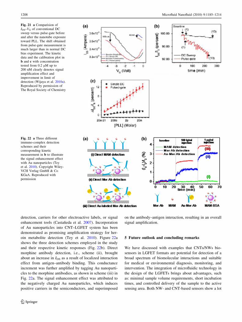
detection, carriers for other electroactive labels, or signal
enhancement tools (Castaneda et al. 2007). Incorporation
of Au nanoparticles into CNT–LGFET system has been
demonstrated as promising amplification strategy for her-
oin metabolite detection (Tey et al. 2010). Figure 22a
shows the three detection schemes employed in the study
and their respective kinetic responses (Fig. 22b). Direct
morphine antibody detection, i.e., scheme (ii), brought
about an increase in IDS as a result of localized interaction
effect from antigen–antibody binding. This conductance
increment was further amplified by tagging Au nanoparti-
cles to the morphine antibodies, as shown in scheme (iii) in
Fig. 22a. The signal enhancement effect was attributed to
the negatively charged Au nanoparticles, which induces
positive carriers in the semiconductors, and superimposed
on the antibody–antigen interaction, resulting in an overall
signal amplification.
5 Future outlook and concluding remarks
We have discussed with examples that CNTs/NWs bio-
sensors in LGFET formats are potential for detection of a
broad spectrum of biomolecular interactions and suitable
for medical or environmental diagnosis, monitoring, and
intervention. The integration of microfluidic technology in
the design of the LGFETs brings about advantages, such
as: minimal sample volume requirements, short incubation
times, and controlled delivery of the sample to the active
sensing area. Both NW- and CNT-based sensors show a lot
Fig. 21 a Comparision of
IDS–VG of conventional DC
sweep versus pulse-gate before
and after the nanotube exposure
toward PLL. The shift obtained
from pulse-gate measurement is
much larger than in normal DC
bias experiment. The kinetic
data and the calibration plot in
b and c with concentration
tested from 0.2 lM up to
200 nM clearly denotes signal
amplification effect and
improvement in limit of
detection (Wijaya et al. 2010a).
Reproduced by permission of
The Royal Society of Chemistry
Fig. 22 a Three different
immuno-complex detection
schemes and their
corresponding kinetic
measurement in b to illustrate
the signal enhancement effect
with Au nanoparticles (Tey
et al. 2010). Copyright Wiley-
VCH Verlag GmbH & Co
KGaA. Reproduced with
permission
1208 Microfluid Nanofluid (2010) 9:1185–1214
123

of promise, and the advantages in nanowire-based sensors
include the ability to control the NW properties, growth
conditions, top down processing, and the overall in-depth
understanding of the microelectronic fabrication processes
necessary for sensor fabrication and integration. With
improved CNT separation success, processing and purifi-
cation techniques, CNT-based devices continue to make
significant progress while leveraging on its fundamental
advantage that all the sensing atoms of Carbon are pre-
sented on the surface and are intimately in contact with the
interacting biomolecules.
The need for low ionic strength buffer in attaining high
sensitivity is a challenge in point-of-care testing of serous
fluids and blood serum. This limitation can be overcome by
integrating distinct components to the microchips to per-
form the separation and purification of biomolecules prior
to the delivery to CNT/NW channel (Stern et al. 2010).
Conjoining biosensors with other microfluidic technolo-
gies, such as electrophoresis chromatography (Liu et al.
2008), micro-pump (Ng et al. 2009), micro-mixing (Ng
et al. 2008), and opto-electro microfluidics (Jamshidi et al.
2008), will further the realization of lab-on-a-chip device
capabilities. The device footprint may be miniaturized
toward sub-micrometer-scaled devices which are likely to
enable higher sensitivities (Wang et al. 2006). In addition,
newer and potentially more sensitive material combina-
tions including graphene (Yan et al. 2007) and organic
semiconductors (Torsi 2006; Torsi et al. 2008) could also
be incorporated to improve the device sensitivities and
stabilities.
From an electronic device perspective, LGFETs may
further be integrated with technologies and programming
algorithms that would enable truly lab-on-chip operations
that would not need semiconductor parameter analyzer
type instrumentation for sensing signal transduction (Ma-
jewski et al. 2005; Das et al. 2007; Dunn et al. 2006;
Wedge et al. 2009; Dost et al. 2007, 2008). Combining a
voltage divider/amplifier, and variable gain methods, true
lab-on-a-chip operating at low voltages have been reported
(Wedge et al. 2009; Dost et al. 2007, 2008). Other
approaches that utilize pattern recognition and principal
component analysis of an array of sensors is an important
component of sensing technologies and has been described
elsewhere (Gardner et al. 1992; Fu et al. 2007).
Finally, the possibility to integrate the LGFET with lipid
bilayer membranes have also been demonstrated (Artyuk-
hin et al. 2005; Atanasov et al. 2005; Koper 2007; Wallace
and Sansom 2009; Thauvin et al. 2008; Zhou et al. 2007;
Knoll et al. 2008; Sinner et al. 2009; Misra et al. 2009). A
bionanoelectronic device will be the ultimate goal in bio-
sensing to realize the biomimetic e-nose or e-tongue sys-
tems which imitate biological systems such as olfactory
system (Linda 2005) or taste buds (Prinster et al. 2005) for
concurrently detecting and analyzing multiple analytes.
Odorant molecules are typically transferred from air to the
aqueous environment of the mucosa before binding to
olfactory receptors and enabling the sense of smell in
humans and animals. Approaches including use of G-pro-
tein coupled receptors (GPCRs) (Floriano et al. 2004;
Robelek et al. 2007; Leutenegger et al. 2008), ion channels
(e.g., Na?, Ca2?, and Cl-) (Naumann et al. 2003) that can
open and close upon a binding event, would enable mon-
itoring of charge translocation across the membranes
integrated with LGFET devices. ‘‘Taste’’ sensors may also
be pursued with the LGFET devices since some of the
molecules involved in triggering the taste system are highly
polar and charged (e.g., amino acids). Biomimetic sensors
for smell and taste may therefore be within the realm of
possibilities enabled by nanomaterials, biological mem-
branes, and microfluidic-integrated LGFETs.
Acknowledgements The authors would like to thank Professors Bo
Liedberg and Wolfgang Knoll for invaluable discussions and inputs
on biosensors.
References
Albrecht PM, Lyding JW (2003) Ultrahigh-vacuum scanning tunnel-
ing microscopy and spectroscopy of single-walled carbon
nanotubes on hydrogen-passivated Si(100) surfaces. Appl Phys
Lett 83:5029–5031
Anantram MP, Leonard F (2006) Physics of carbon nanotube
electronic devices. Rep Prog Phys 69:507–561
Arnold MS, Stupp SI, Hersam MC (2005) Enrichment of single-
walled carbon nanotubes by diameter in density gradients. Nano
Lett 5:713–718
Artyukhin AB, Shestakov A, Harper J, Bakajin O, Stroeve P, Noy A
(2005) Functional one-dimensional lipid bilayers on carbon
nanotube templates. J Am Chem Soc 127:7538–7542
Atanasov V, Knorr N, Duran RS, Ingebrandt S, Offenhausser A,
Knoll W, Kopper I (2005) Membrane on a chip: a functional
tethered lipid bilayer membrane on silicon oxide surfaces.
Biophys J 89:1780–1788
Baker SE, Cai W, Lasseter TL, Weidkamp KP, Hamers RJ (2002)
Covalently bonded adducts of deoxyribonucleic acid (DNA)
oligonucleotides with single-wall carbon nanotubes: synthesis
and hybridization. Nano Lett 2:1413–1417
Bardeen J, Brattain WH (1948) The transistor, a semiconductor
triode. Phys Rev 71:230
Baughman RH, Zakhidov AA, de Heer WA (2002) Carbon
nanotubes—the route toward applications. Science 297:787–792
Besteman K, Lee J-O, Wiertz FGM, Heering HA, Dekker C (2003)
Enzyme-coated carbon nanotubes as single-molecule biosensors.
Nano Lett 3:727–730
Boussaad S, Tao NJ, Zhang R, Hopson T, Nagahara LA (2003) In situ
detection of cytochrome c adsorption with single walled carbon
nanotube device. Chem Commun 1502–1503
Bradley K, Gabriel J-CP, Gruner G (2003) Flexible nanotube
electronics. Nano Lett 3:1353–1355
Bradley K, Briman M, Star A, Gruner G (2004) Charge transfer from
adsorbed proteins. Nano Lett 4:253–256
Bradley K, Davis A, Gabriel J-CP, Gruner G (2005) Integration of
cell membranes and nanotube transistors. Nano Lett 5:841–845
Microfluid Nanofluid (2010) 9:1185–1214 1209
123

Brady JE, Russell JW, Holum JR (2000) Chemistry: matter and its
changes. Wiley, New York
Braun F (1874) Uber die Stromleitung durch Schwefelmetalle. Ann
Phys Chem 153:56
Brune D, Kim S (1993) Predicting protein diffusion coefficients.
PNAS 90:3835–3839
Bunimovich YL, Shin YS, Yeo W-S, Amori M, Kwong G, Heath JR
(2006) Quantitative real-time measurements of DNA hybridiza-
tion with alkylated nonoxidized silicon nanowires in electrolyte
solution. J Am Chem Soc 128:16323–16331
Byon HR, Choi HC (2006) Network single-walled carbon nanotube-
field effect transistors (SWNT-FETs) with increased Schottky
contact area for highly sensitive biosensor applications. J Am
Chem Soc 128:2188–2189
Castaneda MT, Alegret S, Merkoci A (2007) Electrochemical sensing
of DNA using gold nanoparticles. Electroanalysis 19:743–753
Chang KS, Chen CC, Sheu JT, Li Y-K (2009) Detection of an
uncharged steroid with a silicon nanowire field-effect transistor.
Sens Actuators B 138:148–153
Chauhan AK, Aswal DK, Koiry SP, Gupta SK, Yakhmi JV, Surgers
C, Guerin D, Lenfant S, Vuillaume D (2008) Self-assembly of
the 3-aminopropyltrimethoxysilane multilayers on Si and hys-
teretic current–voltage characteristics. Appl Phys A 90:581–589
Chen RJ, Zhang Y, Wang D, Dai H (2001) Noncovalent sidewall
functionalization of single-walled carbon nanotubes for protein
immobilization. J Am Chem Soc 123:3838–3839
Chen RJ, Bangsaruntip S, Drouvalakis KA, Wong Shi Kam N, Shim
M, Li Y, Kim W, Utz PJ, Dai H (2003) Noncovalent
functionalization of carbon nanotubes for highly specific elec-
tronic biosensors. PNAS 100:4984–4989
Chen RJ, Choi HC, Bangsaruntip S, Yenilmez E, Tang X, Wang Q,
Chang Y-L, Dai H (2004) An investigation of the mechanisms of
electronic sensing of protein adsorption on carbon nanotube
devices. J Am Chem Soc 126:1563–1568
Cherukuri P, Gannon CJ, Leeuw TK, Schmidt HK, Smalley RE,
Curley SA, Weisman RB (2006) Mammalian pharmacokinetics
of carbon nanotubes using intrinsic near-infrared fluorescence.
PNAS 103:18882–18886
Cohen-Karni T, Timko BP, Weiss LE, Lieber CM (2009) Flexible
electrical recording from cells using nanowire transistor arrays.
PNAS 106:7309–7313
Cui Y, Lieber CM (2001) Functional nanoscale electronic devices
assembled using silicon nanowire building blocks. Science
291:851–853
Cui Y, Duan X, Hu J, Lieber CM (2000) Doping and electrical
transport in silicon nanowires. J Phys Chem B 104:5213–5216
Cui Y, Wei Q, Park H, Lieber CM (2001) Nanowire nanosensors for
highly sensitive and selective detection of biological and
chemical species. Science 293:1289–1292
Cui Y, Zhong Z, Wang D, Wang WU, Lieber CM (2003) High
performance silicon nanowire field effect transistors. Nano Lett
3:149–152
Curreli M, Li C, Sun Y, Lei B, Gundersen MA, Thompson ME, Zhou
C (2005) Selective functionalization of In2O3 nanowire mat
devices for biosensing applications. J Am Chem Soc 127:6922–
6923
Curreli M, Zhang R, Ishikawa FN, Chang H-K, Cote RJ, Zhou C,
Thompson ME (2008) Real-time, label-free detection of biolog-
ical entities using nanowire-based FETs. IEEE Trans Nanotech-
nol 7:651–667
Das A, Dost R, Richardson T, Grell M, Morrison JJ, Turner ML
(2007) A nitrogen dioxide sensor based on an organic transistor
constructed from amorphous semiconducting polymers. Adv
Mater 19:4018–4023
Dekker C (1999) Carbon nanotubes as molecular quantum wires. Phys
Today 52:22–28
Diao P, Liu Z, Wu B, Nan X, Zhang J, Wei Z (2002) Chemically
assembled single-wall carbon nanotubes and their electrochem-
istry. ChemPhysChem 3:898–991
Dillon AC, Gennett T, Jones KM, Alleman JL, Parilla PA, Heben MJ
(1999) A simple and complete purification of single-walled
carbon nanotube materials. Adv Mater 11:1354–1358
Dong XC, Lau CM, Lohani A, Mhaisalkar SG, Kasim J, Shen ZX, Ho
XN, Rogers JA, Li LJ (2008) Electrical detection of femtomolar
DNA via gold-nanoparticle enhancement in carbon-nanotube-
network field-effect transistors. Adv Mater 20:2389–2393
Dost R, Das A, Grell M (2007) A novel characterization scheme for
organic field-effect transistors. J Phys D 40:3563–3566
Dost R, Ray SK, Das A, Grell M (2008) Oscillator circuit based on a
single organic transistor. Appl Phys Lett 93:113505
Dovbeshko GI, Repnytska OP, Obraztsova ED, Shtogun YV (2003)
DNA interaction with single-walled carbon nanotubes: a SEIRA
study. Chem Phys Lett 372:432–437
Dresselhaus MS, Dresselhaus G, Saito R, Jorio A (2005) Raman
spectroscopy of carbon nanotubes. Phys Rep 409:47–99
Dunn L, Basu D, Wang L, Dodabalapur A (2006) Organic field effect
transistor mobility from transient response analysis. Appl Phys
Lett 88:063507
Elfstrom N, Juhasz R, Sychugov I, Engfeldt T, Karlstrom AE, Linnros
J (2007) Surface charge sensitivity of silicon nanowires: size
dependence. Nano Lett 7:2608–2612
Endo M, Strano MS, Ajayan PM (2008) In: Ascheron CE (ed) Carbon
nanotubes: advanced topics in the synthesis, structure, properties
and applications. Springer, Berlin, pp 13–61
Fan Z, Ho JC, Jacobson ZA, Yerushalmi R, Alley RL, Razavi H,
Javey A (2008) Wafer-scale assembly of highly ordered
semiconductor nanowire arrays by contact printing. Nano Lett
8:20–25
Floriano WB, Vaidehi N, Goddard WA, II I (2004) Making sense of
olfaction through predictions of the 3-D structure and function of
olfactory receptors. Chem Senses 29:269–290
Fu J, Li G, Qin Y, Freeman WJ (2007) A pattern recognition method
for electronic noses based on an olfactory neural network. Sens
Actuators B 125:489–497
Gao Z, Agarwal A, Trigg AD, Singh N, Fang C, Tung C-H, Fan Y,
Buddharaju KD, Kong J (2007) Silicon nanowire arrays for
label-free detection of DNA. Anal Chem 79:3291–3297
Gao XPA, Zheng G, Lieber CM (2009) Subthreshold regime has the
optimal sensitivity for nanowire FET biosensors. Nano Lett
10:547–552
Gao XPA, Zheng G, Lieber CM (2010) Subthreshold regime has the
optimal sensitivity for nanowire FET biosensors. Nano Lett
10:547–552
Gardner JW, Shurmer HV, Tan TT (1992) Application of an
electronic nose to the discrimination of coffees. Sens Actuators
B 6:71–75
Gong K, Yan Y, Zhang M, Su L, Xiong S, Mao L (2005)
Electrochemistry and electroanalytical applications of carbon
nanotubes: a review. Anal Sci 21:1383–1393
Gooding JJ, Wibowo R, Liu JQ, Yang W, Losic D, Orbons S, Mearns
FJ, Shapter JG, Hibbert DB (2003) Protein electrochemistry
using aligned carbon nanotube arrays. J Am Chem Soc
125:9006–9007
Gruner G (2006) Carbon nanotube transistors for biosensing appli-
cations. Anal Bioanal Chem 384:322–325
Gui E-L, Li L-J, Lee PS, Lohani A, Mhaisalkar SG, Cao Q, Kang SJ,
Rogers JA, Tansil NC, Gao Z (2006) Electrical detection of
hybridization and threading intercalation of deoxyribonucleic
acid using carbon nanotube network field-effect transistors. Appl
Phys Lett 89:232104-3
Gui EL, Li L-J, Zhang K, Xu Y, Dong X, Ho X, Lee PS, Kasim J,
Shen ZX, Rogers JA, Mhaisalkar SG (2007) DNA sensing by
1210 Microfluid Nanofluid (2010) 9:1185–1214
123

field-effect transistors based on networks of carbon nanotubes.
J Am Chem Soc 129:14427–14432
Guo J, Wang J, Polizzi E, Datta S, Lundstrom M (2003) Electrostatics
of nanowire transistors. IEEE Trans Nanotechnol 2:329–334
Hahm J-I, Lieber CM (2004) Direct ultrasensitive electrical detection
of DNA and DNA sequence variations using nanowire nano-
sensors. Nano Lett 4:51–54
Haick H, Hurley PT, Hochbaum AI, Yang P, Lewis NS (2006)
Electrical characteristics and chemical stability of non-oxidized,
methyl-terminated silicon nanowires. J Am Chem Soc
128:8990–8991
Hazani M, Naaman R, Hennrich F, Kappes MM (2003) Confocal
fluorescence Imaging of DNA-functionalized carbon nanotubes.
Nano Lett 3:153–155
Heller I, Janssens AM, Mannik J, Minot ED, Lemay SG, Dekker C
(2008) Identifying the mechanism of biosensing with carbon
nanotube transistors. Nano Lett 8:591–595
Heller I, Mannik J, Lemay SG, Dekker C (2009) Optimizing the
signal-to-noise ratio for biosensing with carbon nanotube
transistors. Nano Lett 9:377–382
Heo K, Cho E, Yang J-E, Kim M-H, Lee M, Lee BY, Kwon SG, Lee
M-S, Jo M-H, Choi H-J, Hyeon T, Hong S (2008) Large-scale
assembly of silicon nanowire network-based devices using
conventional microfabrication facilities. Nano Lett 8:4523–4527
Hirsch A, Vostrowsky O (2005) Functionalization of carbon nano-
tubes. In: Schluter AD (ed) Functional molecular nanostructures.
Springer, Berlin, pp 193–237
Hu J, Odom TW, Lieber CM (1999) Chemistry and physics in one
dimension: synthesis and properties of nanowires and nanotubes.
Acc Chem Res 32:435–445
Huang Y, Duan X, Wei Q, Lieber CM (2001) Directed assembly of
one-dimensional nanostructures into functional networks. Sci-
ence 291:630–633
Huang L, White B, Sfeir MY, Huang M, Huang HX, Wind S, Hone J,
O’Brien S (2006) Cobalt ultrathin film catalyzed ethanol
chemical vapor deposition of single-walled carbon nanotubes.
J Phys Chem B 110:11103–11109
Huang X-J, O’Mahony AM, Compton RG (2009) Microelectrode arrays
for electrochemistry: approaches to fabrication. Small 5:776
Hussain MA, Kabir MA, Sood AK (2009) On the cytotoxicity of
carbon nanotubes. Curr Sci India 96:664–673
Iijima S (1991) Helical microtubules of graphitic carbon. Nature 354:56
Israelachvili J (1991) Intermolecular and surface forces. Academic
Press Limited, London
Jamasb S, Collins S, Smith RL (1998) A physical model for drift in
pH ISFETs. Sens Actuators B 49:146–155
Jamshidi A, Pauzauskie PJ, Schuck PJ, Ohta AT, Chiou P-Y, Chou J,
Yang P, Wu MC (2008) Dynamic manipulation and separation
of individual semiconducting and metallic nanowires. Nat
Photonics 2:85–89
Javey A, Nam S, Friedman RS, Yan H, Lieber CM (2007) Layer-by-
layer assembly of nanowires for three-dimensional, multifunc-
tional electronics. Nano Lett 7:773–777
Jeon KA, Son HJ, Kim CE, Shon MS, Yoo KH, Choi AM, Jung HI,
Lee SY (2006) Biosensor with oxide nanowires. In: 5th IEEE
conference on sensors, pp 1265–1268
Jiang K, Schadler LS, Siegel RW, Zhang X, Zhang H, Terrones M
(2004) Protein immobilization on carbon nanotubes via a two-
step process of diimide-activated amidation. J Mater Chem
14:37–39
Jo G, Maeng J, Kim T-W, Hong W-K, Choi B-S, Lee T (2007)
Channel-length and gate-bias dependence of contact resistance
and mobility for In2O3 nanowire field effect transistors. J Appl
Phys 102:084508
Kahng D, Atalla MM (1960) Silicon-silicon dioxide surface device.
In: IRE device research conference
Kang SJ, Kocabas C, Kim H-S, Cao Q, Meitl MA, Khang D-Y,
Rogers JA (2007a) Printed multilayer superstructures of aligned
single-walled carbon nanotubes for electronic applications. Nano
Lett 7:3343–3348
Kang SJ, Kocabas C, Ozel T, Shim M, Pimparkar N, Alam MA,
Rotkin SV, Rogers JA (2007b) High-performance electronics
using dense, perfectly aligned arrays of single-walled carbon
nanotubes. Nat Nanotechnol 2:230–236
Kim DR, Zheng X (2008) Numerical characterization and optimiza-
tion of the microfluidics for nanowire biosensors. Nano Lett
8:3233–3237
Kim W, Choi HC, Shim M, Li Y, Wang D, Dai H (2002) Synthesis of
ultralong and high percentage of semiconducting single-walled
carbon nanotubes. Nano Lett 2:703–708
Kim Y, Minami N, Zhu W, Kazaoui S, Azumi R, Matsumoto M
(2003) Langmuir–Blodgett films of single-wall carbon nano-
tubes: layer-by-layer deposition and in-plane orientation of
tubes. Jpn J Appl Phys 42:7629–7634
Kim A, Ah CS, Yu HY, Yang J-H, Baek I-B, Ahn C-G, Park CW, Jun
MS, Lee S (2007a) Ultrasensitive, label-free, and real-time
immunodetection using silicon field-effect transistors. Appl Phys
Lett 91:103901–103903
Kim SN, Rusling JF, Papadimitrakopoulos F (2007b) Carbon
nanotubes for electronic and electrochemical detection of
biomolecules. Adv Mater 19:3214–3228
Kim Y-K, Park SJ, Koo JP, Kim GT, Hong S, Ha JS (2007c) Control
of adsorption and alignment of V2O5 nanowires via chemically
functionalized patterns. Nanotechnology 18:015304
Kim JP, Lee BY, Hong S, Sim SJ (2008) Ultrasensitive carbon
nanotube-based biosensors using antibody-binding fragments.
Anal Biochem 381:193–198
Knoll W, Koper I, Naumann R, Sinner E-K (2008) Tethered
bimolecular lipid membranes—a novel model membrane plat-
form. Electrochim Acta 53:6680–6689
Kocabas C, Shim M, Rogers JA (2006) Spatially selective guided
growth of high-coverage arrays and random networks of
single-walled carbon nanotubes and their integration into
electronic devices. J Am Chem Soc 128:4540–4541
Kojima A, Hyon CK, Kamimura T, Maeda M, Matsumoto K (2005)
Protein sensor using carbon nanotube field effect transistor. Jpn
J Appl Phys 44:1596–1598
Kolasinski KW (2006) Catalytic growth of nanowires: vapor-liquid-
solid, vapor-solid-solid, solution-liquid-solid and solid-liquid-
solid growth. Curr Opin Solid State Mater 10:182–191
Kong J, Franklin NR, Zhou C, Chapline MG, Peng S, Cho K, Dai H
(2000) Nanotube molecular wires as chemical sensors. Science
287:622–625
Koper I (2007) Insulating tethered bilayer lipid membranes to study
membrane proteins. Mol Biosyst 3:651–657
Kreupl F, Graham AP, Duesberg GS, Steinhogl W, Liebau M, Unger
E, Honlein W (2002) Carbon nanotubes in interconnect appli-
cations. Microelectron Eng 64:399–408
Kumar B, Tan HS, Ramalingam N, Mhaisalkar SG (2009) Integration
of ink jet and transfer printing for device fabrication using
nanostructured materials. Carbon 47:321–324
Kwang H et al (2009) Massive integration of inorganic nanowire-
based structures on solid substrates for device applications.
J Mater Chem 19:901
Lacerda L, Bianco A, Prato M, Kostarelos K (2006) Carbon
nanotubes as nanomedicines: from toxicology to pharmacology.
Adv Drug Deliv Rev 58:1460–1470
Lacerda L, Raffa S, Prato M, Bianco A, Kostarelos K (2007) Cell-
penetrating CNTs for delivery of therapeutics. Nano Today 2:38–43
Larrimore L, Nad S, Zhou XJ, Abruna H, McEuen PL (2006) Probing
electrostatic potentials in solution with carbon nanotube transis-
tors. Nano Lett 6:1329–1333
Microfluid Nanofluid (2010) 9:1185–1214 1211
123

Lee M, Im J, Lee BY, Myung S, Kang J, Huang L, Kwon YK, Hong S
(2006) Linker-free directed assembly of high-performance
integrated devices based on nanotubes and nanowires. Nat
Nanotechnol 1:66–71
Lee M, Baik KY, Noah M, Kwon Y-K, Lee J-O, Hong S (2009)
Nanowire and nanotube transistors for lab-on-a-chip applica-
tions. Lab Chip 9:2267–2280
LeMieux MC, Roberts M, Barman S, Jin YW, Kim JM, Bao Z (2008)
Self-sorted, aligned nanotube networks for thin-film transistors.
Science 321:101–104
Leutenegger M, Lasser T, Sinner EK, Robelek R (2008) Imaging of G
protein-coupled receptors in solid-supported planar lipid mem-
branes. Biointerphases 3:FA136–FA145
Li Y, Kim W, Zhang Y, Rolandi M, Wang D, Dai H (2001) Growth of
single-walled carbon nanotubes from discrete catalytic nanopar-
ticles of various sizes. J Phys Chem B 105:11424–11431
Li C, Zhang D, Han S, Liu X, Tang T, Zhou C (2003) Diameter-
controlled growth of single-crystalline In2O3 nanowires and their
electronic properties. Adv Mater 15:143–146
Li C, Curreli M, Lin H, Lei B, Ishikawa FN, Datar R, Cote RJ,
Thompson ME, Zhou C (2005) Complementary detection of
prostate-specific antigen using In2O3 nanowires and carbon
nanotubes. J Am Chem Soc 127:12484–12485
Lieber CM, Wang ZL (2007) Functional nanowires. MRS Bull 3:99–
108
Lin T-W, Hsieh P-J, Lin C-L, Fang Y-Y, Yang J-X, Tsai C-C, Chiang
P-L, Pan C-Y, Chen Y-T (2010) Label-free detection of protein-
protein interactions using a calmodulin-modified nanowire
transistor. PNAS 107:1047–1052
Linda BB (2005) Unraveling the sense of smell (Nobel Lecture).
Angew Chem Int Ed 44:6128–6140
Liu J, Rinzler AG, Dai H, Hafner JH, Bradley RK, Boul PJ, Lu A,
Iverson T, Shelimov K, Huffman CB, Rodriguez-Macias F, Shon
Y-S, Lee TR, Colbert DT, Smalley RE (1998) Fullerene pipes.
Science 280:1253–1256
Liu J, Casavant MJ, Cox M, Walters DA, Boul P, Lu W, Rimberg AJ,
Smith KA, Colbert DT, Smalley RE (1999) Controlled deposi-
tion of individual single-walled carbon nanotubes on chemically
functionalized templates. Chem Phys Lett 303:125–129
Liu J, Yang S, Lee CS, DeVoe DL (2008) Polyacrylamide gel plugs
enabling 2-D microfluidic protein separations via isoelectric
focusing and multiplexed sodium dodecyl sulfate gel electro-
phoresis. Electrophoresis 29:2241–2250
Lu W, Lieber CM (2006) Semiconductor nanowires. J Phys D
39:R387–R406
Lu M-P, Hsiao C-Y, Lo P-Y, Wei J-H, Yang Y-S, Chen M-J (2006)
Semiconducting single-walled carbon nanotubes exposed to
distilled water and aqueous solution: electrical measurement and
theoretical calculation. Appl Phys Lett 88:053114-3
Maehashi K, Matsumoto K, Kerman K, Takamura Y, Tamiya E (2004)
Ultrasensitive detection of DNA hybridization using carbon
nanotube field-effect transistors. Jpn J Appl Phys 43:1558–1560
Maehashi K, Katsura T, Kerman K, Takamura Y, Matsumoto K, Tamiya
E (2006) Label-free protein biosensor based on aptamer-modified
carbon nanotube field-effect transistors. Anal Chem 79:782–787
Majewski LA, Schroeder R, Grell M (2005) One volt organic
transistor. Adv Mater 17:192–196
Martel R, Schmidt T, Shea HR, Hertel T, Avouris P (1998) Single-
and multi-wall carbon nanotube field-effect transistors. Appl
Phys Lett 73:2447–2449
Martinez MT, Tseng Y-C, Ormategui N, Loinaz I, Eritja R, Bokor J
(2009) Label-free DNA biosensors based on functionalized
carbon nanotube field effect transistors. Nano Lett 9:530–536
Meitl MA, Zhou Y, Gaur A, Jeon S, Usrey ML, Strano MS, Rogers
JA (2004) Solution casting and transfer printing single-walled
carbon nanotube films. Nano Lett 4:1643–1647
Melosh NA, Boukai A, Diana F, Gerardot B, Badolato A, Petroff PM,
Heath JR (2003) Ultrahigh-density nanowire lattices and circuits.
Science 300:112–115
Minot ED, Janssens AM, Heller I, Heering HA, Dekker C, Lemay SG
(2007) Carbon nanotube biosensors: the critical role of the
reference electrode. Appl Phys Lett 91:093507
Misra N, Martinez JA, Huang S-CJ, Wang Y, Stroeve P, Grigoro-
poulos CP, Noy A (2009) Bioelectronic silicon nanowire devices
using functional membrane proteins. PNAS 106:13780–13784
Nair PR, Alam MA (2007) Design considerations of silicon nanowire
biosensors. IEEE Trans Electron Dev 54:3400–3408
Naumann R, Walz D, Schiller SM, Knoll W (2003) Kinetics of
valinomycin-mediated K? ion transport through tethered bilayer
lipid membranes. J Electroanal Chem 550–551:241–252
Ng WY, Goh S, Lam YC, Yang C, Rodriguez I (2008) DC-Biased
AC-electroosmotic and AC-electrothermal flow mixing in
microchannels. Lab Chip 9:802–809
Ng WY, Lam YC, Rodriguez I (2009) Experimental verification of
Faradaic charging in ac electrokinetics. Biomicrofluidics
3:022405
Palaniappan A, Goh WH, Tey JN, Wijaya IPM (2010) Aligned carbon
nanotubes on quartz substrate for liquid gated biosensing.
Biosens Bioelectron 25:1989–1993
Panini NV, Messina GA, Salinas E, Fernandez H, Raba J (2008)
Integrated microfluidic systems with an immunosensor modified
with carbon nanotubes for detection of prostate specific antigen
(PSA) in human serum samples. Biosens Bioelectron 23:1145–
1151
Park J-U, Meitl MA, Hur S-H, Usrey ML, Strano MS, Kenis PJA,
Rogers JA (2006) In situ deposition and patterning of single-
walled carbon nantoubes by laminar flow and controlled floccu-
lation in microfluidic channels. Angew Chem Int Ed 45:581–585
Park J, Shin G, Ha JS (2007) Thickness and density controllable
pattern transfer of DODAB/V2O5 nanowire hybrid film. Nano-
technology 18:405301
Patolsky F, Zheng G, Hayden O, Lakadamyali M, Zhuang X, Lieber
CM (2004) Electrical detection of single viruses. PNAS
101:14017–14022
Patolsky F, Timko BP, Yu G, Fang Y, Greytak AB, Zheng G, Lieber
CM (2006a) Detection, stimulation, and inhibition of neuronal
signals with high-density nanowire transistor arrays. Science
313:1100–1104
Patolsky F, Zheng G, Lieber CM (2006b) Fabrication of silicon
nanowire devices for ultrasensitive, label-free, real-time detec-
tion of biological and chemical species. Nat Protoc 1:1711–1724
Patolsky F, Zheng G, Lieber CM (2006c) Nanowire-based biosensor.
Anal Chem 4261–4269
Peng H, Alemany LB, Margrave JL, Khabashesku VN (2003)
Sidewall carboxylic acid functionalization of single-walled
carbon nanotubes. J Am Chem Soc 125:15174–15182
Poghossian A, Cherstvy A, Ingebrandt S, Offenhausser A, Schoning
MJ (2005) Possibilities and limitations of label-free detection of
DNA hybridization with field-effect-based devices. Sens Actu-
ators B 111–112:470–480
Polizu S, Savadogo O, Poulin P, Yahia L (2006) Applications of
carbon nanotubes-based biomaterials in biomedical nanotech-
nology. J Nanosci Nanotechnol 6:1883–1904
Popov AM, Lozovik YE, Fiorito S, Yahia L (2007) Biocompatibility
and applications of carbon nanotubes in medical nano robots. Int
J Nanomed 2:361–372
Prinster SC, Hague C, Hall RA (2005) Heterodimerization of G
protein-coupled receptors: specificity and functional signifi-
cance. Pharmacol Rev 57:289–298
Pui T-S, Agarwal A, Ye F, Balasubramanian N, Chen P (2009)
CMOS-compatible nanowire sensor arrays for detection of
cellular bioelectricity. Small 5:208–212
1212 Microfluid Nanofluid (2010) 9:1185–1214
123

Robelek R, Lemker ES, Wiltschi B, Kirste V, Naumann R, Oesterhelt
D, Sinner EK (2007) Incorporation of in vitro synthesized GPCR
into a tethered artificial lipid membrane system. Angew Chem
Int Ed 46:605–608
Rosenblatt S, Yaish Y, Park J, Gore J, Sazonova V, McEuen PL
(2002) High performance electrolyte gated carbon nanotube
transistors. Nano Lett 2:869–872
Rudikoff S, Potter M (1976) Size differences among immunoglobulin
heavy chains from phosphorylcholine-binding proteins. PNAS
73:2109–2112
Sheehan PE, Whitman LJ (2005) Detection limits for nanoscale
biosensors. Nano Lett 5:803–807
Sinner EK, Ritz S, Naumann R, Schiller S, Knoll W (2009) Advances
in clinical chemistry. Elsevier Academic Press Inc, San Diego,
pp 159–179
So H-M, Won K, Kim YH, Kim B-K, Ryu BH, Na PS, Kim H, Lee J-
O (2005) Single-walled carbon nanotube biosensors using
aptamers as molecular recognition elements. J Am Chem Soc
127:11906–11907
Star A, Gabriel J-CP, Bradley K, Gruner G (2003) Electronic
detection of specific protein binding using nanotube FET
devices. Nano Lett 3:459–463
Star A, Tu E, Niemann J, Gabriel JCP, Joiner CS, Valcke C (2006)
Label-free detection of DNA hybridization using carbon nano-
tube network field-effect transistors. PNAS 103:921–926
Stephane C, Moreno M, Maurizio P (2007) Separation of metallic and
semiconducting single-walled carbon nanotubes via covalent
functionalization. Small 3:1672–1676
Stern E, Klemic JF, Routenberg DA, Wyrembak PN, Turner-Evans
DB, Hamilton AD, LaVan DA, Fahmy TM, Reed MA (2007a)
Label-free immunodetection with CMOS-compatible semicon-
ducting nanowires. Nature 445:519–522
Stern E, Wagner R, Sigworth FJ, Breaker R, Fahmy TM, Reed MA
(2007b) Importance of the Debye screening length on nanowire
field effect transistor sensors. Nano Lett 7:3405–3409
Stern E, Vacic A, Rajan NK, Criscione JM, Park J, Ilic BR, Mooney
DJ, Reed MA, Fahmy TM (2010) Label-free biomarker detection
from whole blood. Nat Nanotechnol 5:138–142
Strano MS, Dyke CA, Usrey ML, Barone PW, Allen MJ, Shan H,
Kittrell C, Hauge RH, Tour JM, Smalley RE (2003) Electronic
structure control of single-walled carbon nanotube functionali-
zation. Science 301:1519–1522
Streifer JA, Kim H, Nichols BM, Hamers RJ (2005) Covalent
functionalization and biomolecular recognition properties of
DNA-modified silicon nanowires. Nanotechnology 16:1868–1873
Strother T, Hamers RJ, Smith LM (2000) Covalent attachment of
oligodeoxyribonucleotides to amine-modified Si (001) surfaces.
Nucleic Acids Res 28:3535–3541
Sun C, Mathews N, Zheng M, Sow CH, Wong LH, Mhaisalkar SG
(2010) Aligned tin oxide nanonets for high-performance tran-
sistors. J Phys Chem C 114:1331–1336
Tang X, Bansaruntip S, Nakayama N, Yenilmez E, Chang Y-l, Wang
Q (2006) Carbon nanotube DNA sensor and sensing mechanism.
Nano Lett 6:1632–1636
Teillaud JL, Desaymard C, Giusti AM, Haseltine B, Pollock RR,
Yelton DE, Zack DJ, Scharff MD (1983) Monoclonal antibodies
reveal the structural basis of antibody diversity. Science
222:721–726
Tey JN, Wijaya IPM, Wang Z, Goh WH, Palaniappan A, Mhaisalkar
SG, Rodriguez I, Dunham S, Rogers JA (2009) Laminated,
microfluidic-integrated carbon nanotube based biosensors. Appl
Phys Lett 94:013107
Tey JN, Gandhi S, Wijaya IPM, Palaniappan A, Wei J, Rodriguez I,
Suri CR, Mhaisalkar SG (2010) direct detection of heroin
metabolites using a carbon nanotubes liquid gated field effect
transistor based competitive immunoassay. Small doi:10.1002/
smll.200902139
Thauvin C, Rickling S, Schultz P, Celia H, Meunier S, Mioskowski C
(2008) Carbon nanotubes as templates for polymerized lipid
assemblies. Nat Nanotechnol 3:743–748
Timko BP, Cohen-Karni T, Yu G, Qing Q, Tian B, Lieber CM (2009)
Electrical recording from hearts with flexible nanowire device
arrays. Nano Lett 9:914–918
Torsi L (2006) Organic thin-film transistors as analytical and
bioanalytical sensors. Anal Bioanal Chem 384:309
Torsi L, Farinola GM, Marinelli F, Tanese MC, Omar OH, Valli L,
Babudri F, Palmisano F, Zambonin PG, Naso F (2008) A sensitivity-
enhanced field-effect chiral sensor. Nat Mater 7:412–417
Viswanathan S, Rani C, Anand AV, Ho JA (2009) Disposable
electrochemical immunosensor for carcinoembryonic antigen
using ferrocene liposomes and MWCNT screen-printed elec-
trode. Biosens Bioelectron 24:1984–1989
Wallace EJ, Sansom MSP (2009) Carbon nanotube self-assembly
with lipids and detergent: a molecular dynamics study. Nano-
technology 20:045101
Wang J (2002) Analytical electrochemistry. Wiley-VCH, New
Mexico
Wang J, Liu G, Jan MR (2004) Ultrasensitive electrical biosensing of
proteins and DNA: carbon-nanotube derived amplification of the
recognition and transduction events. J Am Chem Soc 126:3010–
3011
Wang WU, Chen C, Lin K-H, Fang Y, Lieber CM (2005) Label-free
detection of small-molecule-protein interactions by using nano-
wire nanosensors. PNAS 102:3208–3212
Wang L, Fine D, Sharma D, Torsi L, Dodabalapur A (2006)
Nanoscale organic and polymeric field-effect transistors as
chemical sensors. Anal Bioanal Chem 384:310–321
Wang C-W, Pan C-Y, Wu H-C, Shih P-Y, Tsai C-C, Liao K-T, Lu L-L,
Hsieh W-H, Chen C-D, Chen Y-T (2007) In situ detection of
Chromogranin A released from living neurons with a single-
walled carbon-nanotube field-effect transistor. Small 3:1350–1355
Wedge DC, Das A, Dost R, Kettle J, Madec M-B, Morrison JJ, Grell
M, Kell DB, Richardson TH, Yeates S, Turner ML (2009) Real-
time vapour sensing using an OFET-based electronic nose and
genetic programming. Sens Actuators B 143:365–372
Whang D, Jin S, Wu Y, Lieber CM (2003) Large-scale hierarchical
organization of nanowire arrays for integrated nanosystems.
Nano Lett 3:1255–1259
Wijaya IPM, Rodriguez I, Mhaisalkar SG (2008) Effect of alignment
on the temperature-resistance response of dielectrophoretically
assembled multiwalled carbon nanotube films. Int J Nanosci
7:199–205
Wijaya IPM, Gandhi S, Nie TJ, Wangoo N, Rodriguez I, Shekhawat
G, Suri CR, Mhaisalkar SG (2009) Protein/carbon nanotubes
interaction: the effect of carboxylic groups on conformational
and conductance changes. Appl Phys Lett 95:073704
Wijaya IPM, Tey JN, Palaniappan A, Rodriguez I, Mhaisalkar SG
(2010a) Investigation of sensing mechanism and signal ampli-
fication in carbon nanotube based microfluidic liquid-gated
transistors via pulsating gate bias. Lab Chip. doi:10.1039/
B2926631C
Wijaya IPM, Tey JN, Gandhi S, Boro R, Palaniappan A, Goh WH,
Rodriguez I, Suri CR, Mhaisalkar SG (2010b) Femto molar
detection of 2, 4-dichlorophenoxyacetic acid herbicides via
competitive immunoassays using microfluidic based carbon
nanotube liquid gated transistor. Lab Chip 10:634–638
Yan YH, Li S, Shen LQ, Chan-Park MB, Zhang Q (2006) Large-scale
submicron horizontally aligned single-walled carbon nanotube
surface arrays on various substrates produced by a fluidic
assembly method. Nanotechnology 17:5696–5701
Microfluid Nanofluid (2010) 9:1185–1214 1213
123
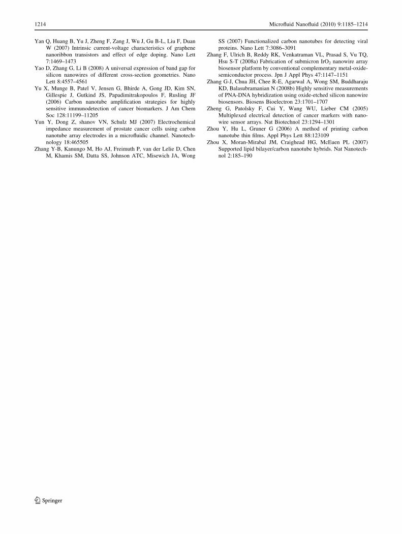
Yan Q, Huang B, Yu J, Zheng F, Zang J, Wu J, Gu B-L, Liu F, Duan
W (2007) Intrinsic current-voltage characteristics of graphene
nanoribbon transistors and effect of edge doping. Nano Lett
7:1469–1473
Yao D, Zhang G, Li B (2008) A universal expression of band gap for
silicon nanowires of different cross-section geometries. Nano
Lett 8:4557–4561
Yu X, Munge B, Patel V, Jensen G, Bhirde A, Gong JD, Kim SN,
Gillespie J, Gutkind JS, Papadimitrakopoulos F, Rusling JF
(2006) Carbon nanotube amplification strategies for highly
sensitive immunodetection of cancer biomarkers. J Am Chem
Soc 128:11199–11205
Yun Y, Dong Z, shanov VN, Schulz MJ (2007) Electrochemical
impedance measurement of prostate cancer cells using carbon
nanotube array electrodes in a microfluidic channel. Nanotech-
nology 18:465505
Zhang Y-B, Kanungo M, Ho AJ, Freimuth P, van der Lelie D, Chen
M, Khamis SM, Datta SS, Johnson ATC, Misewich JA, Wong
SS (2007) Functionalized carbon nanotubes for detecting viral
proteins. Nano Lett 7:3086–3091
Zhang F, Ulrich B, Reddy RK, Venkatraman VL, Prasad S, Vu TQ,
Hsu S-T (2008a) Fabrication of submicron IrO2 nanowire array
biosensor platform by conventional complementary metal-oxide-
semiconductor process. Jpn J Appl Phys 47:1147–1151
Zhang G-J, Chua JH, Chee R-E, Agarwal A, Wong SM, Buddharaju
KD, Balasubramanian N (2008b) Highly sensitive measurements
of PNA-DNA hybridization using oxide-etched silicon nanowire
biosensors. Biosens Bioelectron 23:1701–1707
Zheng G, Patolsky F, Cui Y, Wang WU, Lieber CM (2005)
Multiplexed electrical detection of cancer markers with nano-
wire sensor arrays. Nat Biotechnol 23:1294–1301
Zhou Y, Hu L, Gruner G (2006) A method of printing carbon
nanotube thin films. Appl Phys Lett 88:123109
Zhou X, Moran-Mirabal JM, Craighead HG, McEuen PL (2007)
Supported lipid bilayer/carbon nanotube hybrids. Nat Nanotech-
nol 2:185–190
1214 Microfluid Nanofluid (2010) 9:1185–1214
123
Copyright © 2022 FDOKUMEN