
Three-Phase AC Power Control Using Power Transistors
7
IEEE TRANSACTIONS ON INDUSTRY APPLICATIONS, VOL. IA-12, NO. 5, SEPTEMBER/OCTOBER 1976 Three-Phase AC Power Control Using Power Transistors ALEXANDER MOZDZER, JR., AND BIMAL K. BOSE, MEMBER, IEEE Abstract-A three-phase ac power control circuit using power tran- sistors which operate in a high-frequency chopping mode is described. The circuit is capable of handling several kilowatts of power at any lagging load power factor angle and the output voltage can be smoothly controlled from zero to full supply voltage. The circuit has inherently fast response and the high-frequency ripple at the output is easily fil- tered. The development, study, and experimental evaluation of the cir- cuit with resistive and induction motor loads is described. INTRODUCTION IN SOLID-STATE ac power control applications, such as light dimming, heater control, and induction motor speed control, thyristor ac switches are usually employed. A thyris- tor ac switch is essentially an inverse-parallel connected pair of thyristors, operating in a phase control line commutated mode. Although large amounts of ac power can be controlled economically by this technique, it has several limitations due to the inherent characteristics of phase control. A phase con- trol circuit presents a lagging power factor at the input even if the load power factor is unity and, in general, the input power factor angle is always greater than the load power factor angle. For a fixed firing angle, the load voltage waveform is deter- mined by the load power factor and usually contains har- monics at multiples of the supply voltage frequency which become excessive if discontinuous conduction occurs. Har-, monic currents flowing through the machine windings cause undesirable heating and contribute to pulsating developeO- torque. The response of the phase-controlled circuit is slow due to the inherent dead time lag. In special applications where the supply frequency is above several kilohertz, the minimum turnoff time requirement of thyristors prevents the successful operation of a phase control scheme. To overcome some of the problems discussed above, a single-phase and a three-phase ac power controller employing power transistors which operate in a high-frequency time-ratio mode were designed. Transistor ac switches connected in series and in shunt are controlled so that a lagging reactive load of any power factor angle can be satisfactorily handled. Power transistors are at present costly and have limited power han- dling capacity. For higher power ratings, transistor switches can be replaced by thyristors operating in the chopping mode Paper TOD-74-19, approved by the Power Semiconductor Commit- tee of the IEEE Industry Applications Society for presentation at the 1975 Tenth Annual Meeting of the IEEE Industry Applications So- ciety Atlanta, GA, September 28-October 2, 1975. Manuscript released for publication March 20, 1976. This work was supported in part by a grant from the General Electric Company. A. Mozdzer, Jr., is with the Stanley Elevator Company, Inc., Long City, NY 11101. B. K. Bose was with Rensselaer Polytechnic Institute, Troy, NY. He is now with the General Electric Co., Corporate Research and Develop- ment. Schenectady, NY 12345. N Fig. 1. Single-phase power control circuit. VL IL^ --- ' J « to-% 0002 Fig. 2. Waveforms with resistive load. at the expense of additional commutation circuitry. However, considering the current trend of development, higher power, less expensive transistors should be available in the near future. DESCRIPTION OF SINGLE-PHASE CIRCUIT The operation of the power controllers can be understood best by considering the single-phase version of the circuit, shown in Fig. 1, first. The circuit consists of two transistor ac switches, one connected in series and the other in parallel with the load as shown. Each ac switch is a pair of inverse-parallel connected n-p-n transistors, a diode in series with each to block reverse voltage. The circuit operates as a bidirectional Ichopper. Series transistors T1 and T1' chop in the positive and negative half cycles of the supply voltage, respectively, with the corresponding shunt transistor providing the free-wheeling path. The fundamental or rms voltage can be controlled by varying the time ratio, r = ton/(ton + toff), of the chopping transistors. With a resistive load, the operation of the shunt transistors is redundant and they can be disconnected from the circuit. Fig. 2 shows the load voltage and current waveforms with a resistive load. The circuit can be used for light dimming and heater control applications, but an RFI filter is required at the input. Now consider the circuit operation with an inductive load. Fig. 3 shows the load voltage and current waveforms. A com- plete cycle of supply voltage is subdivided into two modes. During mode I, which corresponds to the positive half-cycle, the transistor T1 is chopping, T1, is open, and T1' and T1,' are closed. In mode It, corresponding to the negative half- 499
-
Upload
independent -
Category
Documents
-
view
0 -
download
0
Transcript of Three-Phase AC Power Control Using Power Transistors

IEEE TRANSACTIONS ON INDUSTRY APPLICATIONS, VOL. IA-12, NO. 5, SEPTEMBER/OCTOBER 1976
Three-Phase AC Power Control Using Power Transistors
ALEXANDER MOZDZER, JR., AND BIMAL K. BOSE, MEMBER, IEEE
Abstract-A three-phase ac power control circuit using power tran-sistors which operate in a high-frequency chopping mode is described.The circuit is capable of handling several kilowatts of power at anylagging load power factor angle and the output voltage can be smoothlycontrolled from zero to full supply voltage. The circuit has inherentlyfast response and the high-frequency ripple at the output is easily fil-tered. The development, study, and experimental evaluation of the cir-cuit with resistive and induction motor loads is described.
INTRODUCTION
IN SOLID-STATE ac power control applications, such aslight dimming, heater control, and induction motor speed
control, thyristor ac switches are usually employed. A thyris-tor ac switch is essentially an inverse-parallel connected pair ofthyristors, operating in a phase control line commutatedmode. Although large amounts of ac power can be controlledeconomically by this technique, it has several limitations dueto the inherent characteristics of phase control. A phase con-
trol circuit presents a lagging power factor at the input even ifthe load power factor is unity and, in general, the input powerfactor angle is always greater than the load power factor angle.For a fixed firing angle, the load voltage waveform is deter-mined by the load power factor and usually contains har-monics at multiples of the supply voltage frequency whichbecome excessive if discontinuous conduction occurs. Har-,monic currents flowing through the machine windings cause
undesirable heating and contribute to pulsating developeO-torque. The response of the phase-controlled circuit is slowdue to the inherent dead time lag. In special applicationswhere the supply frequency is above several kilohertz, theminimum turnoff time requirement of thyristors prevents thesuccessful operation of a phase control scheme.
To overcome some of the problems discussed above, a
single-phase and a three-phase ac power controller employingpower transistors which operate in a high-frequency time-ratiomode were designed. Transistor ac switches connected in seriesand in shunt are controlled so that a lagging reactive load ofany power factor angle can be satisfactorily handled. Powertransistors are at present costly and have limited power han-dling capacity. For higher power ratings, transistor switchescan be replaced by thyristors operating in the chopping mode
Paper TOD-74-19, approved by the Power Semiconductor Commit-tee of the IEEE Industry Applications Society for presentation at the1975 Tenth Annual Meeting of the IEEE Industry Applications So-ciety Atlanta, GA, September 28-October 2, 1975. Manuscript releasedfor publication March 20, 1976. This work was supported in part bya grant from the General Electric Company.
A. Mozdzer, Jr., is with the Stanley Elevator Company, Inc., LongCity, NY 11101.
B. K. Bose was with Rensselaer Polytechnic Institute, Troy, NY. Heis now with the General Electric Co., Corporate Research and Develop-ment. Schenectady, NY 12345.
N
Fig. 1. Single-phase power control circuit.
VLIL^ ---
'J« to-% 0002
Fig. 2. Waveforms with resistive load.
at the expense of additional commutation circuitry. However,considering the current trend of development, higher power,less expensive transistors should be available in the near future.
DESCRIPTION OF SINGLE-PHASE CIRCUIT
The operation of the power controllers can be understoodbest by considering the single-phase version of the circuit,shown in Fig. 1, first. The circuit consists of two transistor acswitches, one connected in series and the other in parallel withthe load as shown. Each ac switch is a pair of inverse-parallelconnected n-p-n transistors, a diode in series with each toblock reverse voltage. The circuit operates as a bidirectionalIchopper. Series transistors T1 and T1' chop in the positive andnegative half cycles of the supply voltage, respectively, withthe corresponding shunt transistor providing the free-wheelingpath. The fundamental or rms voltage can be controlled byvarying the time ratio, r = ton/(ton + toff), of the choppingtransistors. With a resistive load, the operation of the shunttransistors is redundant and they can be disconnected from thecircuit. Fig. 2 shows the load voltage and current waveformswith a resistive load. The circuit can be used for light dimmingand heater control applications, but an RFI filter is required atthe input.Now consider the circuit operation with an inductive load.
Fig. 3 shows the load voltage and current waveforms. A com-plete cycle of supply voltage is subdivided into two modes.During mode I, which corresponds to the positive half-cycle,the transistor T1 is chopping, T1, is open, and T1' and T1,'are closed. In mode It, corresponding to the negative half-
499

IEEE TRANSACTIONS ON INDUSTRY APPLICATIONS, SEPTEMBER/OCTOBER 1976
Fig. 3. Waveforms with inductive load.
Fig. 4. Three-phase po
cycle, T1' is chopping, T1 n' is open and T1 and T1n are
closed. In submode I supply voltage is positive, but load
current is negative. The load feeds power back to the source
through the closed transistor T1'. A block of positive supplyvoltage is impressed across the load and the chopping becomesredundant. As the polarity of the current reverses, the circuitbecomes active, entering into submode I". The circuit operates
in this submode as a dc chopper where transistor T1 is chop-ping and Tl,' is free-wheeling. Mode 11 operation is similar. In
the transition from mode I to mode II, a shoot through fault
can occur due to the finite turnoff time of the transistors. Thiscan be avoided by suitable control circuit design, discussedlater in detail. The load voltage can be controlled smoothlyirrespective of load power factor by varying the time ratio of
the chopping tranisistors.
DESCRIPTION OF THREE-PHASE CIRCUIT
The principles of the single-phase power controller des-
cribed can be extended to the three-plhase version. For a star
connected load with a nieutral, the circuit conisists of thl-eeidentical single-phase controllers operating independently. If
oU,______S~~~ \
\ .>
_3
iwer control circuit.
the load is delta- or star-connected without a neutral, themode of operation of the circuit becomes quite different.Fig. 4 shows the circuit of a three-phase power controllerwithout a load neutral. Since delta and star loads are mutuallyconvertible, and the mode of circuit operation is the same ineither case, only a delta load will be described. The circuitconsists of six transistor ac switches, three connected in seriesand three in shunt as shown. The series transistors either actas chopping switches in the active mode or as closed switchesin the feedback mode as explained before. The shunt transis-tors provide a free-wheeling path in the active mode or remainopen if the corresponding line voltage is positive. With unitypower factor loads, the shunlt transistors are redundant andcanl be removed.
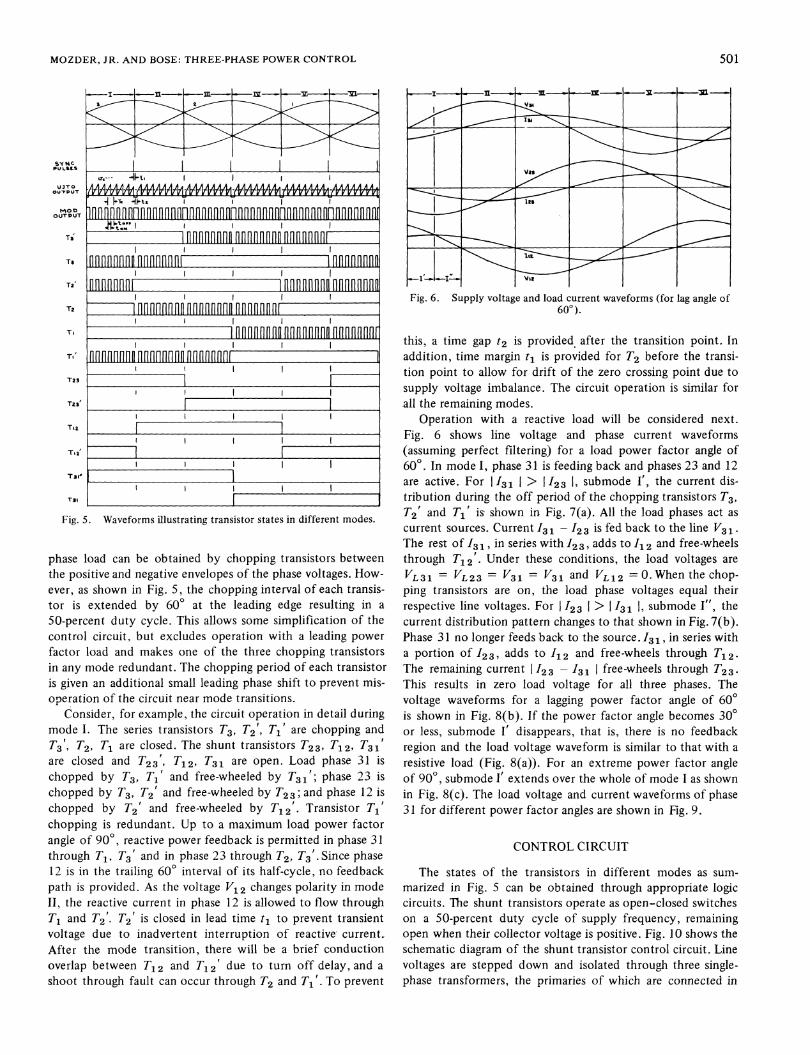
A summary of states of all the transistors in differentmodes is shown in Fig. 5. A complete cycle of supply voltageis divided into six equal, 600 modes. As shown in Fig. 4. eachphase of the load is connected to the supply through two tran-sistor ac switches, one in series with each line. One transistorin each switch is in the chopping mode to control the loadvoltage; the otlher kept closed to allow feedback currenit flow.Under ideal conditions, the composite control of thie three-
500
MOZDER, JR. AND BOSE: THREE-PHASE POWER CONTROL
SyNCPULSLS
UXTOou'rPUT
OUTPUT
Ti
To
T2
T2
Ti
T23
Tto
T,
Tjt
_ I-
! IUrc--- S .
kv *AI-t.
in nnnnnnnnnnnnnnnnnnnn[[nnnnnnnnnnnhlInnnnnnnnW;tt.fs~ ~I
-An flo BlThll[H n nnnIEnnnnnnnpnn nnno n nnnnnnnn-nnnn nnn
onnnnnnnnnnu ---p nRnnnnnnnnnoinnnannn nnnnnnnnnnngnnnnl
nnnnnnnol nnonnnnni nnnnnnnr
IIlI
I --I
II III
I ~~~~~~~~~~~~~F -Fig. 5. Waveforms illustrating transistor states in different modes.
phase load can be obtained by chopping transistors betweenthe positive and negative envelopes of the phase voltages. How-ever, as shown in Fig. 5, the chopping interval of each transis-tor is extended by 600 at the leading edge resulting in a
50-percent duty cycle. This allows some simplification of thecontrol circuit, but excludes operation with a leading powerfactor load and makes one of the three chopping transistorsin any mode redundant. The chopping period of each transistoris given an additional small leading phase shift to prevent mis-operation of the circuit near mode transitions.
Consider, for example, the circuit operation in detail duringmode I. The series transistors T3, T2', T1' are chopping andT3', T2, T1 are closed. The shunt transistors T23, T12, T31'are closed and T23', T12, T31 are open. Load phase 31 ischopped by T3, T1' and free-wheeled by T31'; phase 23 ischopped by T3, T2' and free-wheeled by T23; and phase 12 ischopped by T2' and free-wheeled by T12'. Transistor T1'chopping is redundant. Up to a maximum load power factorangle of 900, reactive power feedback is permitted in phase 31through T1, T3' and in phase 23 through T2, T3'. Since phase12 is in the trailing 600 interval of its half-cycle, no feedbackpath is provided. As the voltage V1 2 changes polarity in modeII, the reactive current in phase 12 is allowed to flow throughT1 and T2'. T2' is closed in lead time t1 to prevent transientvoltage due to inadvertent interruption of reactive current.After the mode transition, there will be a brief conductionoverlap between T12 and T12' due to turn off delay, and a
shoot through fault can occur through T2 and T1'. To prevent
Via
Xii
Vii
Fig. 6. Supply voltage and load current waveforms (for lag angle of600).
this, a time gap t2 is provided after the transition point. Inaddition, time margin t1 is provided for T2 before the transi-tion point to allow for drift of the zero crossing point due tosupply voltage imbalance. The circuit operation is similar forall the remaining modes.
Operation with a reactive load will be considered next.Fig. 6 shows line voltage and phase current waveforms(assuming perfect filtering) for a load power factor angle of600. In mode I, phase 31 is feeding back and phases 23 and 12are active. For I31 > II23 1, submode I', the current dis-tribution during the off period of the chopping transistors T3,T2' and T1' is shown in Fig. 7(a). All the load phases act ascurrent sources. Current I31 - I23 is fed back to the line V31.The rest of 131, in series with '23, adds to I1 2 and free-wheelsthrough T12'. Under these conditions, the load voltages areVL31 = VL23 = V31 = V31 and VL12 =0.When the chop-ping transistors are on, the load phase voltages equal theirrespective line voltages. For I23 > I31 1, submode I", thecurrent distribution pattern changes to that shown in Fig. 7(b).Phase 31 no longer feeds back to the source. I31, in series witha portion of 123, adds to I12 and free-wheels through T12.The remaining current I23 - I31 free-wheels through T23.This results in zero load voltage for all three phases. Thevoltage waveforms for a lagging power factor angle of 600is shown in Fig. 8(b). If the power factor angle becomes 300or less, submode I' disappears, that is, there is no feedbackregion and the load voltage waveform is similar to that with aresistive load (Fig. 8(a)). For an extreme power factor angleof 900, submode I' extends over the whole of mode I as shownin Fig. 8(c). The load voltage and current waveforms of phase31 for different power factor angles are shown in Fig. 9.
CONTROL CIRCUIT
The states of the transistors in different modes as sum-marized in Fig. 5 can be obtained through appropriate logiccircuits. The shunt transistors operate as open-closed switcheson a 50-percent duty cycle of supply frequency, remainingopen when their collector voltage is positive. Fig. 10 shows theschematic diagram of the shunt transistor control circuit. Linevoltages are stepped down and isolated through three single-phase transformers, the primaries of which are connected in
501I- x *I x,_-WI-
-U o- Isr-.-v

IEEE TRANSACTIONS ON INDUSTRY APPLICATIONS, SEPTEMBER/OCTOBER 1976
Os bJ I
W t -,0,Vs
Osa0MtOVE I Xsl I> 11Xs1 MO<WL I0 112SI AISI
Fig. 7. Current paths in mode I (for lag angle of 600).
CURRENT L&c sso
0, ~~~~~~~~~~~ACURtINT L^C *o P A
3~~~~~~~~~~~~~~~~~~~~~~~~~~~~~~~~~~~~~~~
CURRENT LAC 90'
Fig. 8. Voltage waveforms at load terminals for different lag angles. Fig. 10. Shunt transistor control
LEAD
CURRENT LAG &30'
CUQRENT LAG GO'
CUR~RENT LAkG 90'
g1t%R#ATof 4ENERATOR.
Fig. 9. Load voltage and current waveforms of phase 31 for differentlag angles. Fig. 11. Series transistor control
502
'TRb,%s4t%SO
circuit.
1l circuit.

MOZDER, JR. AND BOSE: THREE-PHASE POWER CONTROL
delta. The secondary of each transformer is connected to acomparator which converts the sine wave to a square wavewith the same phase. A series diode suppresses the negativeamplitude and drives the transistor T12' through a drivercircuit. An inverter generates a complementary voltage wave-form to drive the inverse transistor T12. Fig. 11 shows theschematic diagram of the series transistor control circuit. Thewaveforms are explained in Fig. 5. The circuit is similar toFig. 10 except that it is coupled to a pulse width modulatorcircuit and the transformer secondaries are connected throughadjustable RC lead networks to provide the margin time t1shown in Fig. 5. Outputs at A', A', etc., are each coupled tothe modular through a two-input NAND gate, providing thechopping signals for the series transistors. The modulatorconsists of a linear sawtooth UJT oscillator synchronized nearthe transition of each mode and a comparator with a dccontrol signal vC as shown. Synchronization pulses are gener-ated by a set of NAND gates (Fig. 12), differentiated and usedto trigger a one-shot which maintains the UJTO capacitordischarged (slightly negative) for the interval t1 + t2. Thesawtooth waveform is compared with the dc signal v, toprovide the modulator output. The NAND gates complementthe modulator output which is then fed to the transistordrivers. As the amplitude of v, decreases, the time ratio r =
tr0/(t1ff) increases. For r = 1, the load voltage equals thesupply voltage. However, the snychronization gap t, + t2 ismaintained at each mode transition.
The drive circuit for each power transistor is shown inFig. 13. Single-phase ac is transformer isolated, rectified andfiltered to provide a bipolar power supply for the drive circuit.The logic signal is coupled to the base of transistor T - 1which drives an optical coupler. For a logic 1 condition, thephototransistor saturates turning transistors T- 2 on and T- 3off. This in turn saturates the power transistor. For a logic 0condition, T- 3 is on and T - 2 off; the reverse base voltageV2 cutting off the power transistor. Each pair of power tran-sistors is protected by a Thyrector surge suppressor in case ofan inadvertent voltage transient in the collector circuits.
DESIGN AND TESTS
A complete model of the power control circuit wasdesigned and tested in the laboratory. The experimental resultsagreed well with the theory. Voltage and current ratings of thepower transistors determine the power handling capability ofthe circuit. Delco type DTS-430 transistors (VCEO = 400 V,4 = 5 A) were used in the model, allowing operation from a208-V, three-phase supply with a peak load current of 5 A.The chopping frequency was arbitrarily selected to be 6 kHz,but could be chosen within wide limits.
The circuit was tested first with a resistive load, varyingthe control voltage v,, to smoothly control the load voltagefrom zero to the full supply voltage. Fig. 14(a) shows the loadvoltage and current waveforms per phase for a star connectedresistive load with T = 1. The small discontinuities in thewaveforms at the mode transition points (600 intervals) aredue to the sync. signals as explained before. The gap intervals
I I
Fig. 12. Sync pulse generator circuit.
Fig. 13. Power transistor driver circuit.
(a)
(M)Fig. 14. Waveform with resistive load. (a) T= 1. (b) T7= 0.5.
503

IEEE TRANSACTIONS ON INDUSTRY APPLICATIONS, SEPTEMBER/OCTOBER 1976
S.
F.
(a)
Lc)
Fig. 15. Waveform with induction motor load. (a) T = 1. (b) T0.25. (c) T = 0.15.
t1 and t2 (see Fig. 5) are adjustable, and were both set anominal value of 20 s. Fig. 14(b) shows the waveforms r=0.5.
The circuit was tested next with 220-V, three-phase, 1.5-hpsquirrel cage induction motor with star connected statorwindings. Fig. 15 shows the load voltage and current wave-forms per phase for different values of r. Since the circuitcannot withstand high starting inrush current, the motor wasstarted with no load and gradually increasing stator voltage.The sync pulse widths were adjusted to be low in the motortests and do not appear as prominent due to the filtering actionof the load. In Fig. 15(b) and (c), the load power factor angle
______ -*0,_0411 - _-
-ll y 0-
2t00 6500 '400 6500
SPELD ,,pn-)
- CURVES ORTACEO WIrTH.ERLE PHAE. MODEL- - - CURVES OUT&ISED WITh ThREE PWHSE VARIAC
6000 %70c 1o0c
Fig. 16. Experimental torque-speed characteristic curves.
is near 30 and the load voltage waveform is identical to thatfor a resistive load as predicted. Due to the filtering action ofthe load, the current waveforms contain little ripple. Thetorque-speed characteristics of the motor were studied and theperformance compared to that obtained with an adjustableautotransformer voltage settings (Fig. 16). As expected withvoltage control of an induction motor, the scheme can only beemployed where load torque requirements are low at lowspeed, for example, blower speed control.
CONCLUSION
A three-phase ac power controller employing power tran-sistors which operate in a high-frequency chopping mode isdiscussed in detail. The load voltage is smoothly controlledfrom zero to the full sup5ply voltage by varying the time ratio rin response to a dc control signal v.- Several kilowatts ofpower can be handled at any lagging power factor angle. Thecircuit features a fast response, low load current ripple with anominal value of load inductance and the capability of instan-taneous circuit interruption if a fault occurs.
The circuit has been systematically studied and experi-mentally evaluated in the laboratory; the results agreeing wellwith the theory. A laboratory model was constructed tooperate on a 208-V, three-phase ac supply, and was tested witha resistive load and a 1.5-hp induction motor load. Designingthe circuit to other specifications is limited only by the powerhandling capabilities of the transistors.
At present, power transistors are expensive and their powerhandling capability small in comparison to thyristors, but withthe present trend of development the situation should improvein the not too distant future. Regardless, the cost can be jus-tified in part by considering the advantages of the transistorcircuit over an equivalent circuit employing thyristors.
TABLE OF SYMBOLS
01, 02, 03V12, V23, V31VL12, VL23, VL31I12, 123, I31
Three phase supply lines.Line voltages.Load voltages.Load currents.
504

IEEE TRANSACTIONS ON INDUSTRY APPLICATIONS, VOL. IA-12, NO. 5, SEPTEMBER/OCTOBER 1976
T1, 12, T23, etceT12 T12' T23, T23',etc.D1, D1', D2, D2%, etc.D12, D12', D23, D23', etc.
t2
ton
toffTcT
V-
Series circuit transistors.Shunt circuit transistors.Series circuit diodes.Shunt circuit diodes.Time margin before mode transi-tion to prevent transient overvoltage.Time margin after mode transi-tion to prevent shoot through.Chopper on time.Chopper off time.Chopper time period.ton/eT.Control voltage.
[2] A. Mozdzer, "Three-phase ac power control using power transis-tors," M.S. dissertation, Rensselaer Polytechnic Institute, Troy,NY, Aug. 1973.
Alexander Mozdzer, Jr., was born in 1952. Hereceived the B.S.E.E. cum laude and theM.E.E.E. degrees in 1973, from RensselaerPolytechnic Institute, Troy, NY.
iti0:0; At present, he is employed by the StanleyElevator Company, Inc., of Long Island City,
NY, and is in charge of the design of solid-a li li | state equipment for use in elevator systems.
REFERENCES
[1] K. Nohara, "A switched-mode modulator for power circuit,"Elec. Eng. (Japan), vol. 90, pp. 17-25, 1970.
Bimal K. Bose (S'59-M'60), for a photograph and biography please seepage 498 of this issue.
2X f) 01n o.. t-?6 /i2SS Xd1 z ('>76 /~~~~~~~~~~~~~ ,44-2--/ <t3- '-7Dynamics of Heating and Cooling Responses of Controlled
Environmental Spaces
FEI K1Tjis* J' - STJAMES R. PFAFFLIN AND ROBERT H. TULL
°23,Abstract-Models, derived from first principles, are presented for
prediction of time-temperature responses of enclosed spaces. The pro-
posed models are given in terms of the input energy and parametersof the room construction. Verification of the proposed models is givenfor the case of baseboard heating. Agreement between the propogedmodels and results of tests conducted at the Electric Space Condition-ing Institute is found to be close.
INTRODUCTION
flHERE is considerable literature on time constants in elec-T tric heating processes. A basic question has arisen concern-
ing the relation between active and passive time constants inspace heating. The active time constant T, governs the rate at
which heating proceeds and the passive time constant Tp de-
scribes the path followed in cooling. In an effort to resolve the
question, tests were run under rigidly controlled conditions at
Paper TOD-76-7, approved by the Electric Space Heating and AirConditioning Committee of the IEEE Industry Applications Societyfor presentation at the 1975 Tenth Annual Meeting of the IEEE Indus-try Applications Society, Atlanta, GA, September 28, October 2.Manuscript released for publication February 6, 1976.
J. R. Pfafflin is with the Stevens Institute of Technology, Hoboken,NJ 07030.
R. H. Tull was with the Electric Space Conditioning Institute,Morristown, NJ; he passed away in 1973.
the former Electric Space Conditioning Institute (ESCI) atMorristown, NJ. Heating and cooling tests were each of 24hour duration, and the results of baseboard heating will bereported here. A complete description of the ESCI test facilityis given in [5] , and the test procedure is described in [31 . Itshould be noted that there was no simulation of any furniturewithin the room. The two locations of prime importance (LPI)were taken as a typical thermostat location and a typical occu-pant location. The method followed in data reduction is givenin [3].
BASIC MODELS
Heating
A means of predicting the trajectory of the thermal responsesof an enclosed space would be of interest and utility to thecontrol practitioner. The following model is proposed for thecase of a baseboard heat source.A heat balance is struck among the heat energy introduced
into the room, the heat lost, and the heat stored
heat in- heat lost = heat stored
AQi dt Ek--Odt==mZ c0WdO()
1
505
H (71-1 1- . -',
-4 11,1- .4