Design and assemble of a DC/AC prototype power converter ...
55
Master Thesis Project Design and assemble of a DC/AC prototype power converter and a general-purpose interface board dedicated to control and/or monitoring functions. REPORT Authoress: Maria Lluis Viñals Director: Nicolas Patin Date: February 2012
-
Upload
khangminh22 -
Category
Documents
-
view
0 -
download
0
Transcript of Design and assemble of a DC/AC prototype power converter ...

Master Thesis Project
Design and assemble of a DC/AC prototype power converter and a general-purpose interface board dedicated to control and/or monitoring functions.
REPORT
Authoress: Maria Lluis Viñals
Director: Nicolas Patin
Date: February 2012

2
Table of contents
List of figures ................................................................................................................................4
List of tables .................................................................................................................................6
Abstract ........................................................................................................................................7
Abbreviations ...............................................................................................................................8
1- Introduction .............................................................................................................................9
2-Objectives ...............................................................................................................................11
3- Power converter: Design of an integrated 12- phase inverter ...............................................12
3.1-Design restrictions ...........................................................................................................12
3.2-Block diagram...................................................................................................................12
3.2-Components selection .....................................................................................................13
3.2.1-MOSFET: IRF7769L2TR1PbF .....................................................................................13
3.2.2- Diode .......................................................................................................................13
3.2.3- Driver : ISL2110 .......................................................................................................14
3.2.4- Linear regulator: L7805ABD2T-TR ............................................................................15
3.2.5- Digital temperature sensor: TMP100 .......................................................................15
3.2.6- Connectors ...............................................................................................................16
3.3-Simulations with LTSpice ..................................................................................................17
3.4- Electrical scheme.............................................................................................................20
3.5- List of selected components............................................................................................21
3.6- Thermal performance .....................................................................................................21
3.7- Electrical characteristics ..................................................................................................23
3.8- Layout .............................................................................................................................24
3.8.1- PCB characteristics ...................................................................................................24
3.8.2- Design rules ..............................................................................................................24
3.8.3- Views ........................................................................................................................24
3.9- Future actions .................................................................................................................25
4- ADC board: Design of a modular interface board dedicated to monitoring and control
functions of the integrated 12-phase voltage source inverter (VSI). ..........................................26
4.1- Design restrictions ...........................................................................................................26
4.2- Block diagram ..................................................................................................................27
4.3- Analog components selection .........................................................................................27
4.3.1-Voltage follower ........................................................................................................27
4.3.2-Antialiasing filter LTC1563 .........................................................................................28

3
4.3.3-Level shifter: Voltage follower + adder .....................................................................28
4.4- Analog part simulation with LTSpice ...............................................................................30
4.5- Electrical scheme.............................................................................................................31
4.6- List of selected components............................................................................................31
4.6.1- Analog components .................................................................................................32
4.6.2- Digital components ..................................................................................................35
4.6.3- Capacitors ................................................................................................................35
4.7-Thermal characteristics ....................................................................................................36
4.8- Electrical characteristics ..................................................................................................36
4.9- Layout .............................................................................................................................36
4.9.1- PCB characteristics ...................................................................................................36
4.9.2- Design rules ..............................................................................................................36
4.9.3- Views ........................................................................................................................37
4.10- Experimental results .....................................................................................................38
5-Conclusions .............................................................................................................................40
6-Acknowledgments...................................................................................................................41
7- Bibliography ...........................................................................................................................42
8-Appendices .............................................................................................................................43

4
List of figures
Figure 1: Test bench arquitecture .................................................................................... 9
Figure 2: Box’s input channels ........................................................................................ 10
Figure 3: Half bridge configuration ................................................................................. 12
Figure 4: Driver’s application .......................................................................................... 14
Figure 5: Gate to Source Voltage versus Total Gate Source........................................... 14
Figure 6: Connector's distribution and its name ............................................................ 17
Figure 7: Half bride diagram. U3&U4 are the MOSFETs and U1&U2 are the diodes .... 18
Figure 8: VG step response .............................................................................................. 18
Figure 9: VG simulation result with RG=1 Ω .................................................................... 19
Figure 10: VG simulation result without RG external resistance ..................................... 19
Figure 11: IG simulation result with RG=1 Ω ................................................................... 20
Figure 12: IG simulation result without external gate resistance ................................... 20
Figure 13: RthPCBa equivalent ........................................................................................... 22
Figure 14: MOSFET power losses and thermal resistances ............................................ 22
Figure 15: Heat sink example. ........................................................................................ 23
Figure 16: Manufactured power converter top layer view without components. ........ 24
Figure 17: Manufactured power converter top layer view ............................................ 25
Figure 18: Principal diagram of the circuit. Parts 1, 2 and 3 correspond to the analog
part, and 4 and 5 to the digital part ........................................................................ 27
Figure 19: Electric scheme of the analog part ................................................................ 27
Figure 20: Voltage follower ............................................................................................ 27
Figure 21: Filter application ............................................................................................ 28
Figure 22: Voltage follower in the level shifter…………………………………………………………..27
Figure 23: Level’s shifter adder ...................................................................................... 29
Figure 24: Offset voltage from the ADC ......................................................................... 30
Figure 25: Analog part diagram ...................................................................................... 30
Figure 26: Analog part simulation results ...................................................................... 31
Figure 27: 2.5V power supply schematic ........................................................................ 33
Figure 28: -5V/5V power supply schematic .................................................................... 33
Figure 29: Manufactured ADC board top layer view ...................................................... 37
5
Figure 30: Manufactured ADC board bottom layer view ............................................... 37
Figure 31: Mother board top layer view ........................................................................ 38
Figure 32: ADC board on the mother board. .................................................................. 38
Figure 33: Connectors location. All dimensions are in millimetres. ............................... 39
Figure a.1: Power converter top layer view ................................................................... 47
Figure a.2: Power converter top silk view ...................................................................... 47
Figure a.3: Mother board top view ................................................................................ 49
Figure a.4: Mother board bottom view .......................................................................... 49
Figure a.5: ADC board top layer view ............................................................................. 53
Figure a.6: ADC board top layer silk view ....................................................................... 53
Figure a.7: ADC board bottom layer view ...................................................................... 53
Figure a.8: ADC board bottom layer silk view ................................................................ 54
Figure a.9: ADC board ground layer view ....................................................................... 54
Figure a.10: ADC board power layer view ...................................................................... 54
6
List of tables
Table 1: Address pins and slave addresses for the temperature sensor ....................... 16
Table 2: Thickness and thermal conductivity layers. ...................................................... 23
Table 3: Power converter board’s electrical characteristics .......................................... 23
Table 4: Design rules according to the manufacturer .................................................... 24
Table 5: List of the digital and analog components ....................................................... 32
Table 6: Signals of the analog part connector (TFM) ..................................................... 34
Table 7: Signals of the digital part connector (TFM2) .................................................... 34
Table 8: ADC board’s electrical characteristics .............................................................. 36
Table 9: Layer’s names and its characteristics ............................................................... 36
Table 10: Design rules according to the manufacturer .................................................. 37

7
Abstract
The aim of this project is to develop the hardware for a flexible platform for testing
control strategies for voltage source inverters. Using a modular approach, two boards
will be designed, an inverter and a signal acquisition board. The power converter will be
manufactured using IMS technology. Electrical and thermal verification of the design
will be performed by simulations. Exhaustive details on the implementation will be
given in this document. Experimental results will be presented.

8
Abbreviations
AC= Alternating Current
ADC= Analog-to-Digital Converter
CAD= Computer-Aided Design
CNV= Convert Input
DC= Direct Current
fc= Cut-off frequency
FPGA=Field Programmable Gate Array
GND= Ground
HI= High-side Input
I= Input
I2C= Inter-Integrated Circuit
IMS= Insulated Metal Substrate
LI= Low-side Input
MOSFET= Metal Oxide Semiconductor Field Effect Transistor
O= Output
Op-Amp= Operational Amplifier
PCB= Printed Circuit Board
PWM= Pulse-Width Modulation
PWR= Power
RG= Gate Resistance
RthJC=Thermal Resistance Junction-Case
RthJA= Thermal Resistance Junction-Ambient
SCL= Serial Clock
SCK= Clock
SDA= Serial Data Line
SDI= Serial Data Input
SDO= Serial Data Output
SMB= Server Message Block
SMD= Surface Mount Device
SPI= Serial Peripheral Interface
TTL= Transistor- Transistor Logic
VSI= Voltage Source Inverter

9
1- Introduction
The mechatronics department of the UTC (Université de Technologie de Compiègne)
involves research and teaching activities that merge mechanical skills (vibrations and
acoustic noise analyses in electric machines), power electronics (specially power
electronics converters dedicated to powertrain control in electric or hybrid vehicles) and
analog/digital signal processing dedicated to real-time control and monitoring (vector
control applied to AC machines-induction and synchronous drivers).
The analysis of the acoustic noise and electromagnetic compability must be based on a
realistic model of the actual converters integrated in the targeted applications in order to
establish scientific results as relevant as possible to the industrial reality. At the same
time, these studies might require to develop complex schemes allowing us to evaluate
possible interactions betwen several converter/machine sets.
A general purpose power electronics platform is interesting in such a context. The
project is based on the architecture presented in figure 1.
Figure 1: Test bench arquitecture
This platform will be based on a modular design, involving a motherboard and several
standarized daughter boards. All these boards will be fitted in a customized box,
excepting the power converter (12-phase VSI).
The figure 2 shows the input’s box:

10
Figure 2: Box’s input channels
This box have 6 inputs because there are 6 analog input channels. It is also possible to
switch off channels independently.
Box external dimensions are:
Width:165 mm.
Length: 220 mm.
Height: 51,5 mm.
But the internal, and the usable dimensions are:
Width:140 mm.
Length: 210 mm.
Height: 50 mm.
11
2-Objectives
The project is focused in two objectives:
Topic 1: Power converter. Design of a half bridge inverter, to form an integrated 12-
phase voltage source inverter (VSI).The 12-phase inverter uses a IMS board technology
that dissipates a lot of thermal power.
Topic 2: Analog to digital converter (ADC) board. Design of an interface board
dedicated to monitoring functions of the integrated 12-phase voltage source inverter
(VSI).
In the corresponding section, their characteristics will be explained.
Each topic covers the full design process, from electric circuit proposal to final
experimental verification of the assembled boards.

12
3- Power converter: Design of an integrated 12- phase inverter
3.1-Design restrictions
This design is based on a first prototype based in a half-bridge which includes:
o Two low voltage/high current power MOSFET (100V/124A):
IRF7769L2TR.
o A high speed driver: Intersil ISL211x.
o Connectors used for input and output signal are SMB coaxial terminals
bringing a high level of signal integrity within a small footprint.
o Temperature sensor: TMP100.
o The power converter has 2 input channels accepting PWM signals up to
50 kHz.
o Power side voltage is fixed at12V
o Maximum output intensity is fixed at 50A.
o IMS technology board.
3.2-Block diagram
The design is based in a half-bridge configuration. In figure 3 it can be seen a half-
bridge:
Figure 3: Half bridge configuration
There are two different parts: the logic and the power part, so there are two different
supplies.
VccR L
Driver
V+
PWM
Logic Power

13
3.2-Components selection
3.2.1-MOSFET: IRF7769L2TR1PbF
MOSFET’s characteristics:
It is a DirectFET Power MOSFET with low conduction losses and L8 outline.
VDS=100V
IS=124A
MOSFET’s Gate Resistance (RG):
There is a additional external Gate resistance in order to limit the driver’s output
current.
In the simulation section, the MOSFET’s behaviour will be simulated in order to find
this value.
3.2.2- Diode 1
It is necessary a freewheeling protection diode for the MOSFET, so it is chosen the
120LQ100, a Schottky diode with SMD package. This diode has a fast recovery time
and high peak current.
The current rating for the diode must be the same rating of the MOSFET. It has the
following characteristics:
VRMM=100V (Maximum Peak Repetitive Reverse Voltage)
IF=120A (Maximum Average Forward Current)
IFSM=1000A (Maximum Peak One Cycle Non-Repetitive Surge Current)
1 Currently 120LQ100 is out of stock, so it is impossible to have the component now.
We found diodes with the same ratings and SMD package but they were too large for our board.
For this reason, a temporary solution (in order to test the circuit) is to use the APT100S20B diode, which
is no SMD, but has the required ratings.
There is also another solution: the 12CWQ06FNPbF diode with SMD package. This one has the
following characteristics: VRMM=60V, IF=12A, IFSM=320A. IFSM is bigger than the maximum current in
the circuit. In the next section (Simulations with LTSpice) it will be checked if the diode works.
In conclusion, the board will be tested with the APT100S20B diode and then with the 12CWQ06FNPbF
diode in order to check what is the best solution.

14
3.2.3- Driver : ISL2110
The driver is a 100V, high frequency, half bridge N-Channel power MOSFET driver.
Peak output pull-up/pull-down current is 3A/4A, which allows very high switching
frequency of the power MOSFETs.
The following figure illustrates the application block diagram:
Figure 4: Driver’s application
For the HB pin (High-side boostrap supply), a external bootstrap capacitor is required.
For the supply pin (Vdd) it is also required a decoupling capacitor.
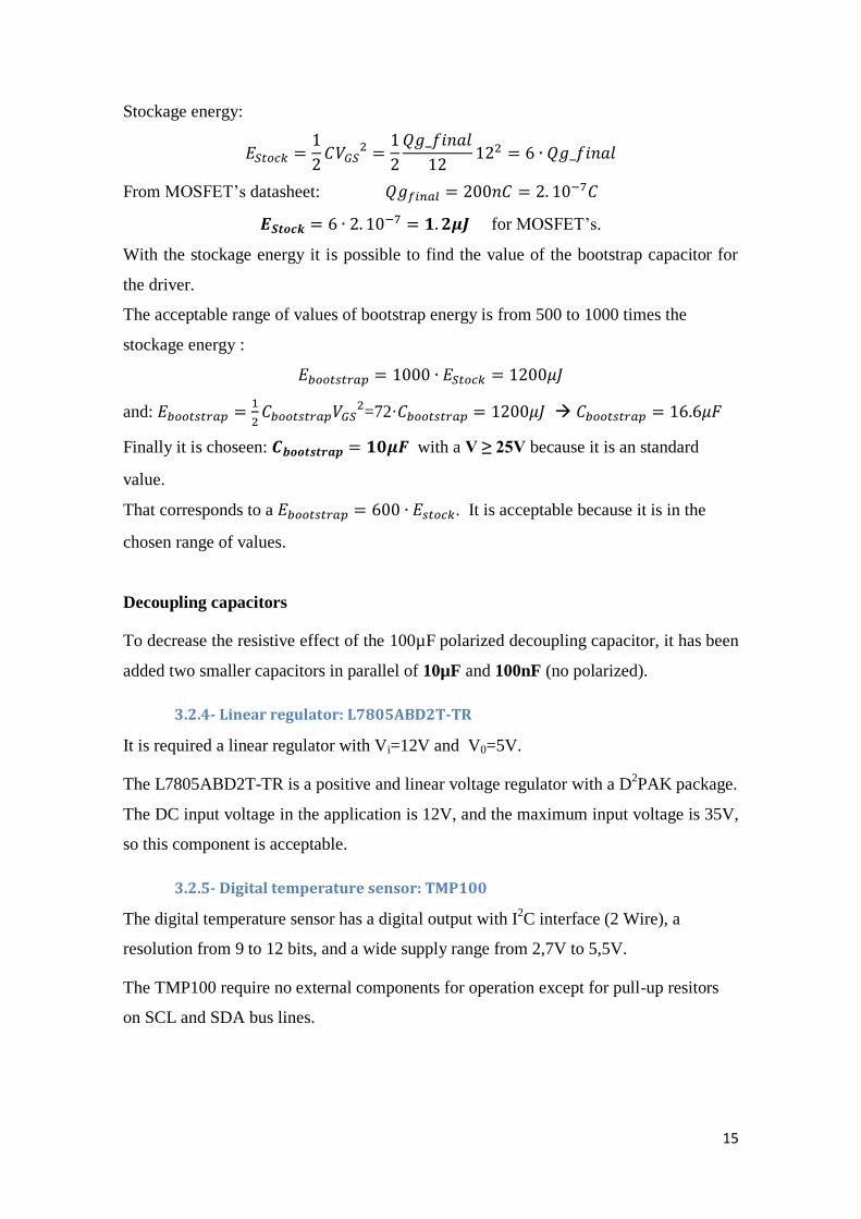
Bootstrap capacitor (Cbootstrap)
Bootstrapping refers to a self-sustaining process. So, bootstrapping in electronics, is a
form of positive feedback in an analog circuit design.
Figure 5 shows the MOSFETS’s Gate to Source Voltage (Vgs) versus the Total Gate
Charge (Qg):
Figure 5: Gate to Source Voltage versus Total Gate Source
The aim of this graphic is to calculate the stockage energy of the MOSFET.
1/C
Qg=C*Vgs
Qg_final
12V
Qg
Vgs
Cbootstrap
Cdecoupling
15
Stockage energy:
From MOSFET’s datasheet:
for MOSFET’s.
With the stockage energy it is possible to find the value of the bootstrap capacitor for
the driver.
The acceptable range of values of bootstrap energy is from 500 to 1000 times the
stockage energy :
and:
=72·
Finally it is choseen: with a V ≥ 25V because it is an standard
value.
That corresponds to a . It is acceptable because it is in the
chosen range of values.
Decoupling capacitors
To decrease the resistive effect of the 100µF polarized decoupling capacitor, it has been
added two smaller capacitors in parallel of 10µF and 100nF (no polarized).
3.2.4- Linear regulator: L7805ABD2T-TR
It is required a linear regulator with Vi=12V and V0=5V.
The L7805ABD2T-TR is a positive and linear voltage regulator with a D2PAK package.
The DC input voltage in the application is 12V, and the maximum input voltage is 35V,
so this component is acceptable.
3.2.5- Digital temperature sensor: TMP100
The digital temperature sensor has a digital output with I2C interface (2 Wire), a
resolution from 9 to 12 bits, and a wide supply range from 2,7V to 5,5V.
The TMP100 require no external components for operation except for pull-up resitors
on SCL and SDA bus lines.

16
o I2C interface:
I²C uses two bidirectional open-drain lines, Serial Data Line (SDA) and Serial Clock
(SCL).
Because of the fact that I2C protocol uses open drain outputs, a external pull-up resistor
is required for the SDA and SCL bus. The correct pull-up resistance for the I2C bus
depends on the total capacitance of the bus and the frequency you want to operate the
bus at. The sensor will work in a frequency lower than 100KHz, so, a typical and
acceptable pull-up resistance value is:
Rpull-up=1’8KΩ.
The adress pins values for the configuration of the slave adresses for the TMP100 are
shown in the table 1:
Table 1: Address pins and slave addresses for the temperature sensor
ADD1 and ADD0 pins are hardware selectable and their values can be: 0, 1 or float.
Float indicates the pin is left unconnected.
To do the 1 logic it is required a pull-up resistor to Vcc (typicaly 10 kΩ). To do a 0
logic, it is required to connect the pin to ground.
3.2.6- Connectors
There are three round connectors on the board. In the figure 6 it can be seen its location.

17
Figure 6: Connector's distribution and its name
There are also six more connection pads in the PCB. A signal wire will be soldered at
each pad. Every pad has its name printed on the board. Their names are: SCL, SDA,
12V, GND, HI, LI.
HI and LI are PWM input control signals from the PWM controller.
The connection pad named 12V corresponds to V+ signal in the circuit, and the
connector named co1 corresponds to Vcc signal.
3.3-Simulations with LTSpice
The half bridge will be simulated in order to verify its behaviour.
For the simulation is necessary to calculate the half bridge load (R and L):
The desired values for intensity and output voltage are the following:
Intensity=I=50A
Input voltage=Vin=12V so, for a PWM signal of the 50%, the output voltage of
the half bridge is: VRMSout=6V
-Resistance value:
V=R*I 6= R*50A R= 0,12Ω
-Impedance value:
τ=L/R= 2.10-3
= L/0,12 L= 2,4.10-4
F
R and L are placed in series.
VccR L
Driver
V+
PWM
Logic Power
0V:c03
Power:co1
Load:co2
18
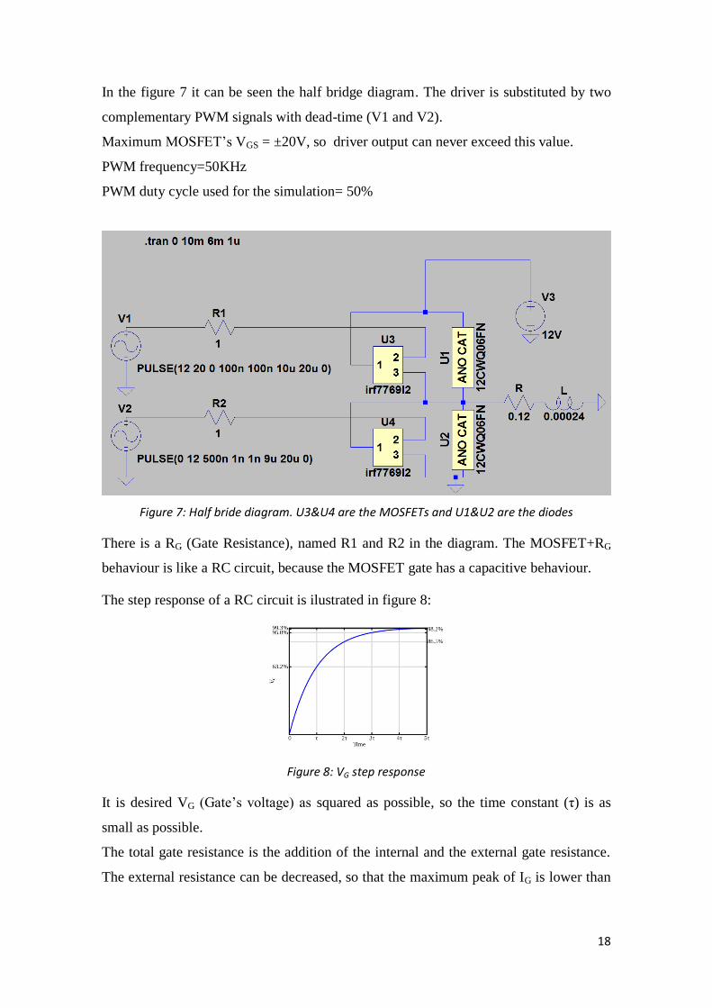
In the figure 7 it can be seen the half bridge diagram. The driver is substituted by two
complementary PWM signals with dead-time (V1 and V2).
Maximum MOSFET’s VGS = ±20V, so driver output can never exceed this value.
PWM frequency=50KHz
PWM duty cycle used for the simulation= 50%
Figure 7: Half bride diagram. U3&U4 are the MOSFETs and U1&U2 are the diodes
There is a RG (Gate Resistance), named R1 and R2 in the diagram. The MOSFET+RG
behaviour is like a RC circuit, because the MOSFET gate has a capacitive behaviour.
The step response of a RC circuit is ilustrated in figure 8:
Figure 8: VG step response
It is desired VG (Gate’s voltage) as squared as possible, so the time constant (τ) is as
small as possible.
The total gate resistance is the addition of the internal and the external gate resistance.
The external resistance can be decreased, so that the maximum peak of IG is lower than
19
3A (maximum output current of the driver). Eventually external RG might be not
necessary.
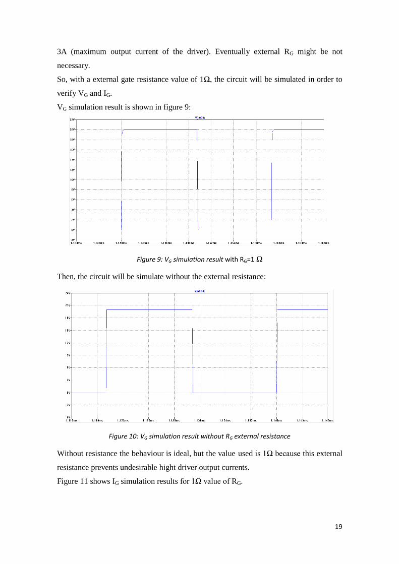
So, with a external gate resistance value of 1Ω, the circuit will be simulated in order to
verify VG and IG.
VG simulation result is shown in figure 9:
Figure 9: VG simulation result with RG=1 Ω
Then, the circuit will be simulate without the external resistance:
Figure 10: VG simulation result without RG external resistance
Without resistance the behaviour is ideal, but the value used is 1Ω because this external
resistance prevents undesirable hight driver output currents.
Figure 11 shows IG simulation results for 1Ω value of RG.
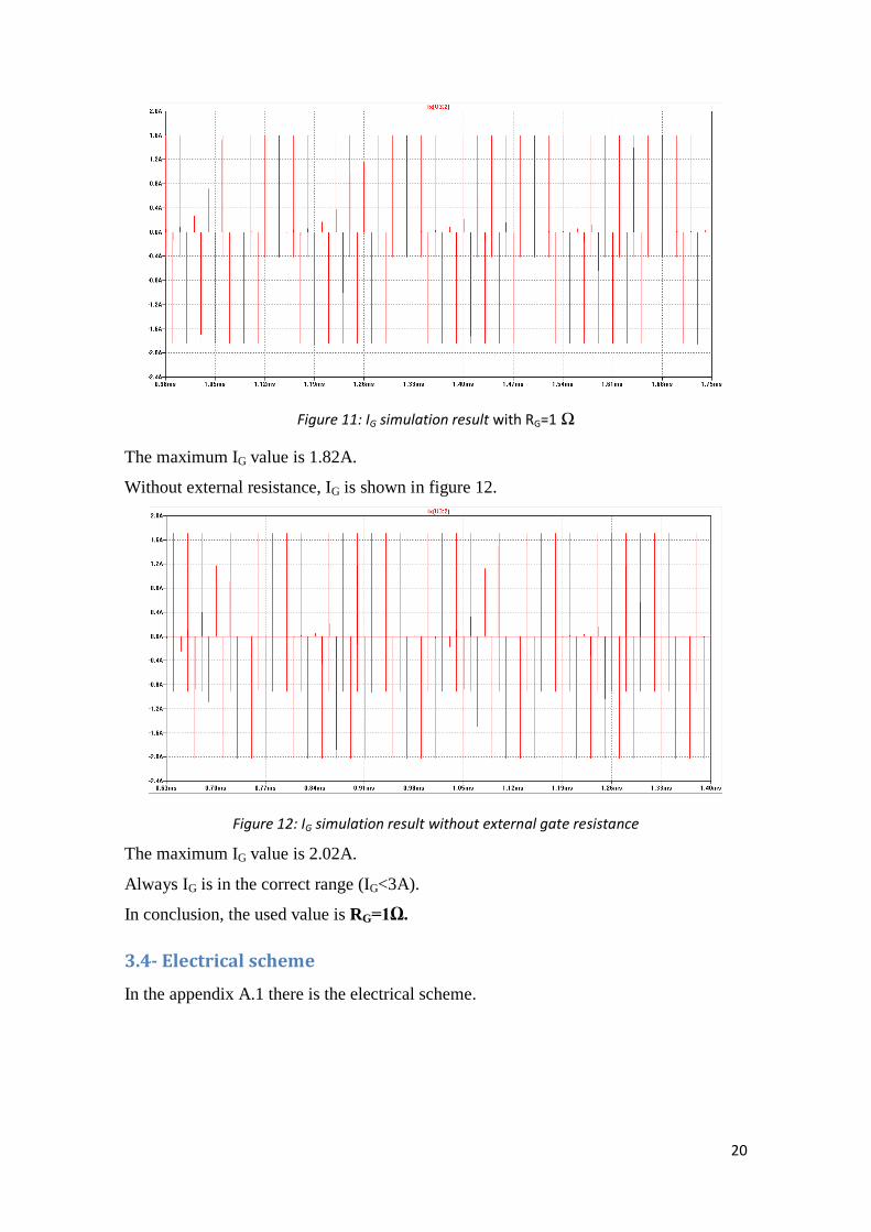
20
Figure 11: IG simulation result with RG=1 Ω
The maximum IG value is 1.82A.
Without external resistance, IG is shown in figure 12.
Figure 12: IG simulation result without external gate resistance
The maximum IG value is 2.02A.
Always IG is in the correct range (IG<3A).
In conclusion, the used value is RG=1Ω.
3.4- Electrical scheme
In the appendix A.1 there is the electrical scheme.

21
3.5- List of selected components
In the appendix A.2 there is a table that illustrates all the used components, with all their
specifications: Name, value, characteristics, manufacturer’s name, identification
manufacturer code, component unit price and total price.
3.6- Thermal performance
It is interesting to analyse the board thermal performance since it uses IMS technology.
IMS corresponds to a copper circuitry bonded onto an electrically insulated dielectric
layer, that is bonded to a metallic substrate. This technology advantages are the lower
operating temperature, improve product thermal and mechanical properties/
performance, increase the power density and enable better use of surface mount
technology.
The heat produced by the MOSFET power losses cause an increment of the
component’s temperature. So, in this section will be sized a heat sink for the MOSFET,
because it is the component with the higher power losses. The heat sink will be put in
the PCB bottom to take advantage of the IMS board technology. It helps to dissipate the
heat by transferring it to the surrounding air.
-MOSFET’s characteristics:
o Max. thermal resistance junction-to-ambient: RѲJA=45ºC/W (Surface
mounted on 1 in square Cu board, steady state).
o Max. thermal resistance Junction-to PCB mounted: RѲJ-PCB=0.5ºC/W
o Max. thermal resistance Junction-to can: RѲJ-Can=1.2ºC/W
o Storage Temperature Rang from -55 to 175 ºC.
It is considered an ambient temperature (TA) of 25ºC, and a MOSFET’s working
temperature (TJ) of 100ºC.
The MOSFET’s total thermal resistance is calculated with the following expression:
[W]
[ºC/W]
In order to find the total thermal resistance, previously it has to be calculed the
MOSFET’s power (P). Power losses will be deduced with the following expression
using the model introduced in the section 3.3:
) ) =7,368 W
The maximum power dissipation corresponds to a PWM’s duty cycle of 50%, because
there are two MOSFETS, and one is the complementary of the other.

22
The heat sink will be sized for one MOSFET and the board will have a heat sink for
every MOSFET.
So, the total thermal resistance is:
= 10,179 ºC/W
Figure 13 shows RthPCBa. It is the equivalent thermal resistance across the IMS board to
air, using a heat sink attached to the metal layer of the board:
Figure 13: RthPCBa equivalent
So, the equivalent thermal resistance can be split in the following terms:
)
The following diagram illustrates the total thermal resistance’s layout:
Figure 14: MOSFET power losses and thermal resistances
)
)
= 10,179 ºC/W
So, RthPCBa value is:
ºC/W
The thermal resistances associated to the IMS board are calculated with the following
expression:
(2)
Air
Copper
Dielectric
Base layer: Aluminium
Heat sink
Rthcopper-dielectric
Rthdielectric-alum.
Rthalum.-heat sink
Rthheat sink-air
Circuit layer
Tj=100ºC
Ta=25ºC
RthPCBa
Rthja=45ºC/W
RthjPCB=0.5ºC/W

23
d=thickness layer
A=contact area
λ= thermal conductivity
Contact area is 1.2 times the MOSFET’s area, so:
MOSFET area= 63.472 mm2 and A=1.2*MOSFET area= 76.17mm
2
The other parameters are shown in table 2:
Layer Thickness (d) Thermal conductivity(λ)
Copper 35 µm 390 W/m*K
Dielectric FR4 75 µm 0,25 W/m*K
Aluminium 1,5 mm 237 W/m*K
Table 2: Thickness and thermal conductivity layers.
Resistances calculated with expression (2) are the following:
0.001ºC/W
In order to size a heat sink it is necessary the thermal resistance value from heat sink to
air (Rth heat sink-air). So, according to equation (1) the value is:
8.655 ºC/W
According to this thermal resistance value it will be selected a proper heat sink.
Figure 15 shows a heat sink example.
Figure 15: Heat sink example.
3.7- Electrical characteristics
The electrical characteristics of the power converter are in table 3:
Input’s characteristics Output’s characteristics
PWM signal Maximum delivered power: 600W
Maximum frequency: 50KHz Maximum power side voltage: 12V
Maximum logic side supply: 12V
Table 3: Power converter board’s electrical characteristics

24
3.8- Layout
3.8.1- PCB characteristics
PCB size: 43.03 x 73.83mm
Number of layers: 1 (top)
There is a ground plane on the top layer that improves the noise immunity of the board.
There are routing constraints in this board because only a single layer is available due to
IMS (Insulated Metal Substrate) board technology. The layer is attached to a metallic
cooling surface, thus all components must have SMD packaging and be placed on top
layer.
3.8.2- Design rules
According to the design rules of the manufacturer (Eurocircuits), the following design
parameters have been chosen:
Top layer
Trace width 0,7 mm
Trace clearance 0,7 mm
Copper to board outline 1 mm
Table 4: Design rules according to the manufacturer
For the rated current of the board, the power trace's widths are wider (1mm wide) than
the signal traces to prevent overtemperature.
The designed PCB has the following service: I (IMS pool).
3.8.3- Views
In appendix A.3 there are the layout views.
The top view of the manufactured PCB without the components is shown in figure 16:
Figure 16: Manufactured power converter top layer view without components.

25
The top view of the manufactured PCB with all components is shown in figure 17:
Figure 17: Manufactured power converter top layer view
3.9- Future actions
This board will be checked. So obtain this it will be supplied with 12V. Two
complementary PWM signals of 50 kHz will be applied and a external variable load
will be connected. The output voltage will be observed.

26
4- ADC board: Design of a modular interface board dedicated to
monitoring and control functions of the integrated 12-phase
voltage source inverter (VSI).
4.1- Design restrictions
Since sampling frequency requirements are not the same for each kind of measurement,
a generic solution should be investigated (including a parameterized anti-aliasing filter)
with a unified SPI or I2C digital bus.
In order to adapt this board to as many applications as possible, it should be as small as
possible and include only one analog channel. Among all the required features, the main
ones are (for one daughter board):
o One analog channel.
o Adaptability to +/-10V voltage range using jumpers.
o Anti-aliasing filter based on active circuits (integrated circuit such as
Linear Technology LTC1563) usable over a wide frequency range (from
10Hz to 500 kHz).
o Resolution: 14 bits.
o Maximum sampling frequency: 2MS/s (Analog Devices AD7944).
o Full stand-alone operation capabilities.
High‐speed logic insulators are also required for a safe control of power converters. Key
features of such insulators are (for one daughter board):
o Time delays lower than 20ns.
o Insulation equal to (or higher than) 1kV.
o Insulation circuits, embedded DC/DC converters and PCB tracks
clearance should guarantee insulation.
o At least 16 I/O terminals are required.
o Data direction should be configurable by jumpers if possible.
o Logic voltages should be programmable by jumpers (at least TTL 5V,
3.3V are required).
27
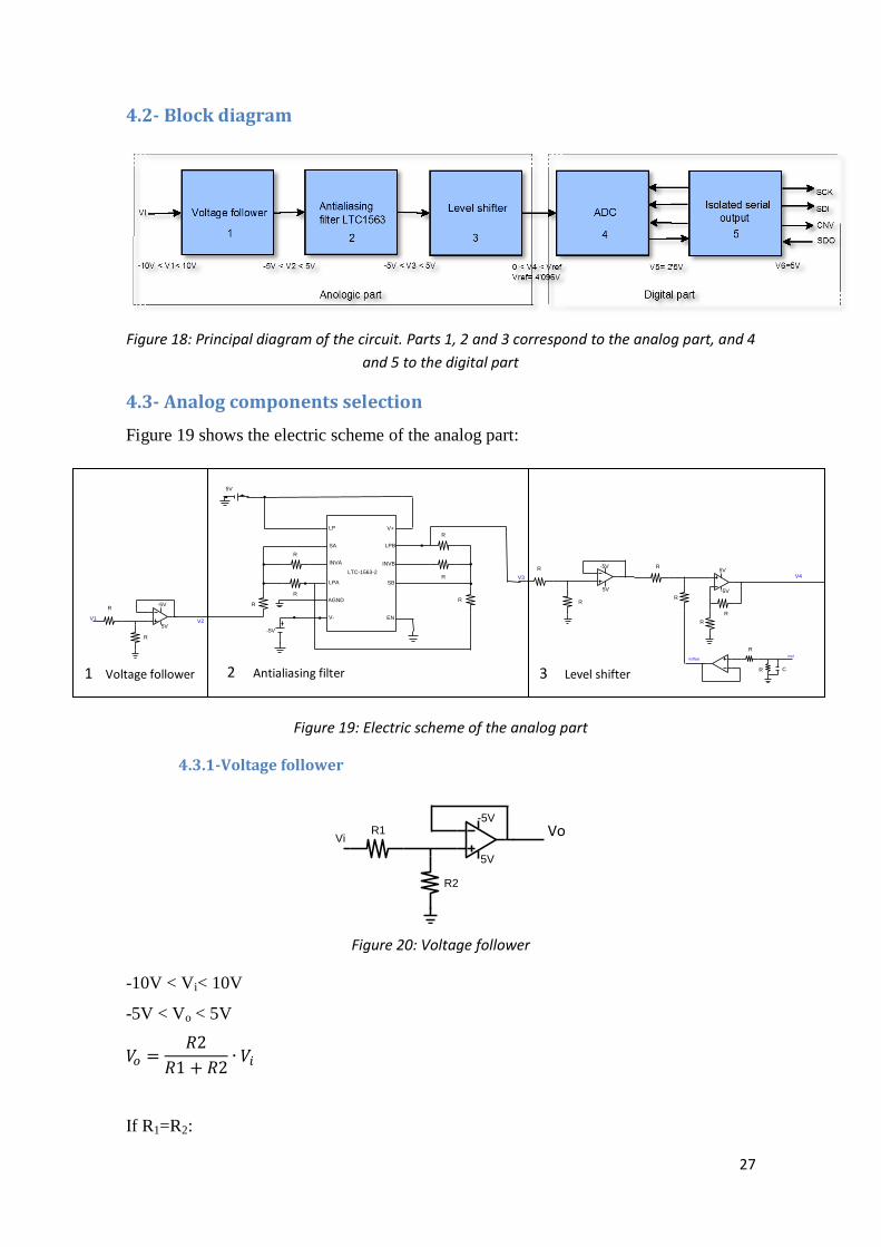
4.2- Block diagram
Figure 18: Principal diagram of the circuit. Parts 1, 2 and 3 correspond to the analog part, and 4
and 5 to the digital part
4.3- Analog components selection
Figure 19 shows the electric scheme of the analog part:
Figure 19: Electric scheme of the analog part
4.3.1-Voltage follower
Figure 20: Voltage follower
-10V < Vi< 10V
-5V < Vo < 5V
If R1=R2:
-5V
5V
R1
R2
Vi Vo
1
3
-5V
5V
V1 V2
V3
-5V
5V
-5V
5V
SA
INVA
LPA
AGND
V-
LP V+
LPB
INVB
SB
EN
LTC-1563-2V4
-5V
5V
VoffsetVref
R
R
R
R
R
R
R
R
R
R
R
R
R
R
R
R C
Voltage follower 2 Antialiasing filter Level shifter
Vo
28
A= gain
R1=R2=100KΩ
4.3.2-Antialiasing filter LTC1563 (analog low-pass filter)
Figure 21: Filter application
-5V < Vi< 5V
-5V < Vo < 5V
From filter datasheet:
(
)
fC= cutting frequency
Maximum fc that the filter works is 256KHz. fc=256KHz
(
) R= 10KΩ
4.3.3-Level shifter: Voltage follower + adder
4.3.3.1-Voltage follower
Figure 22: Voltage follower in the level shifter
-5V
5V
SA
INVA
LPA
AGND
V-
LP V+
LPB
INVB
SB
EN
LTC-1563-2
Vi
Vo
R
R
R
R
R
R
-5V
5V
R1
R2
ViVo
29
-5V < Vi < 5V
-Vref/2 < Vo < Vref/2 , Vref= 4’096V
If R1=100K R2=69,37 KΩ
R1=100KΩ
R2=69,37KΩ
For R2: They have to be 2 resistances in series because it does not exist a resistance of
69,37KΩ.
R2=R+R’
With a 0,1% tolerance and 0805 SMD package:
R=68,1KΩ
R’= 1,27KΩ
R2=R+R’=68,1KΩ+1,27KΩ
4.3.3.2-Adder
Figure 23: Level’s shifter adder
V0voltage follower=Viadder Vo=Vi’
-Vref/2 < Vi’ < Vref/2 , Vref= 4’096V
0 < Vo’ < Vref , Vo’=Vi ADC
V+=
V-=
V+=V
-
If R1=R2 Vo’=Vi’+Voff
R1=R2=100KΩ
-5V
5V
Voffset
R1
R2
R1
R2
Vi'Vo'

30
In figure 24 it will be shown how to create Voffset from Vref.
Figure 24: Offset voltage from the ADC
Vref comes from ADC pin 1 (REF1).
Vref= 4,096V
Voffset=
If R1=R2=100KΩ
Voffset= 0,5·Vref= 0,5 · 4,096= 2,048V
C=100nF
4.4- Analog part simulation with LTSpice
An analog part simulation has been done observing the inputs and outputs of the
different subcircuits.
In the figure 25 it can be seen the analog part diagram.
Figure 25: Analog part diagram
The inputs and the outputs voltages of each subcircuit shown in figure 25 are shown in
figure 26.
VoffsetVref
R1
R2 C
31
Figure 26: Analog part simulation results
V1, the red curve named V(n015), in figure 26, is the input signal of the board. (-10V <
V1 < 10V).
The output (V2) (the blue curve) is reduced by half by the voltage divider. (-5V < V2 <
5V).
Since the frequency of the input signal is 1kHz, the low pass filter is only used as an
antialiasing filter with a cut-off frequency of 256 kHz. In V3 (the light green curve
overlapping V2) it is checked that the output voltage is still reduced at the half. (-5V <
V3 < 5V).
Next is the voltage follower. With the voltage divisor it is obtained an output voltage
named V3* (the green curve): -Vref/2 < V3* < Vref/2 (-2,048V < V3* < 2,048V). Then it
is passed through the voltage adder to shift the output voltage: 0V < V4< 4.096V
V4 (the pink curve) is the output voltage and also the ADC’s input voltage.
4.5- Electrical scheme
In the appendix B.1 there is the electrical scheme.
There is the analog and digital part, and the power supply.
4.6- List of selected components
In the appendix B.2 there is a table that illustrates all the used components, with all their
specifications: Name, value, characteristics, manufacturer’s name, identification
manufacturer code, component unit price and total price.
V2 V1
V3*

32
This section explains the main characteristics of the components and also why they have
been chosen.
Before that, table 5 lists the analog part and the digital part components:
Top layer (digital) Description Bottom layer
(analog)
Description
AD7944
Analog to digital
converter
LMV721 Operational amplifier
SN74LVC8T245DGVR
Voltage converter
buffer
LTC1563 Filter
ISO7241ADW Isolated buffer LT1118CST-2.5 Voltage regulator
DCR010505U Isolated DC/DC
converter
Connectors
Table 5: List of the digital and analog components
4.6.1- Analog components
-Filter: LTC1563-2
Active RC, 4th order low pass filter family with rail-to-rail inputs and outputs and low
DC offset suitable for systems with a resolution of up to 16 bits. It has a single resistor
value that gives a unity-gain Butterworth response.
o Cut-off frequency (fc): 256Hz < fc < 256KHz
o Power dissipation= 500 mW
-4 Op-Amp: LMV721
It is a 10MHz low-noise low-voltage and low-power operational amplifier.
o Rail-to-rail output swing.
o Power supply voltage: 2.2V to 5.5V.
o High unity-Gain Bandwidth: 10 MHz.
-Power supply
It is required to have a supply of: 2.5V, 5V, -5V and 3.3V.
3.3V comes from FPGA.
The others come from LT1118CST-2.5 and DCR010505U components.
33
LT1118CST-2.5
It is a low dropout regulator that regulates the output voltage. It regulate while sourcing
or sinking current.
o Vin= 5V
o Vout= 2.5V
Figure 27 shows the power supply schematic.
Figure 27: 2.5V power supply schematic
DCR010505U
DC/DC regulated and isolated converted to supply the buffers.
o 1W
o Regulated
o Isolated
o Input voltage= 5V
o Output voltage= 5V
In the figure 28 it can be seen the power supply schematic.
Figure 28: -5V/5V power supply schematic
34
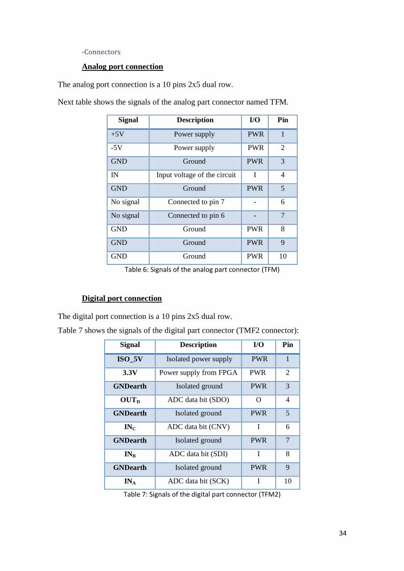
-Connectors
Analog port connection
The analog port connection is a 10 pins 2x5 dual row.
Next table shows the signals of the analog part connector named TFM.
Signal Description I/O Pin
+5V Power supply PWR 1
-5V Power supply PWR 2
GND Ground PWR 3
IN Input voltage of the circuit I 4
GND Ground PWR 5
No signal Connected to pin 7 - 6
No signal Connected to pin 6 - 7
GND Ground PWR 8
GND Ground PWR 9
GND Ground PWR 10
Table 6: Signals of the analog part connector (TFM)
Digital port connection
The digital port connection is a 10 pins 2x5 dual row.
Table 7 shows the signals of the digital part connector (TMF2 connector):
Signal Description I/O Pin
ISO_5V Isolated power supply PWR 1
3.3V Power supply from FPGA PWR 2
GNDearth Isolated ground PWR 3
OUTD ADC data bit (SDO) O 4
GNDearth Isolated ground PWR 5
INC ADC data bit (CNV) I 6
GNDearth Isolated ground PWR 7
INB ADC data bit (SDI) I 8
GNDearth Isolated ground PWR 9
INA ADC data bit (SCK) I 10
Table 7: Signals of the digital part connector (TFM2)
35
4.6.2- Digital components
-ADC: AD7944
o 14 bit resolution
o 2.0 MSPs (normal mode)
o Low power dissipation
o 0V < Vin < Vref
ADC only works in internal reference mode. Internal reference: Vref= 4’096V
Resolution:
Power supplies: AVDD= 2’5V
DVDD= 2’5V
BVDD= 5V
VIO= 2’5V
-SN74LVC8T245DGVR
Voltage converter buffer. 8 bit dual-supply bus transceiver with configurable voltage
translation and 3 state outputs. Only it is used 4 bits (4 inputs and 4 outputs).
o Vin= 2.5V
o Vout= 5V
-Isolated buffer: ISO7241ADW
It is necessary to isolate de output of the ADC of the rest of the circuit. ISO7241 it is a
high speed digital isolator.
o 1 input
o 3 outputs
o Input voltage= 3.3V
o Output voltage= 5V
4.6.3- Capacitors
Each integrated chip has its own decoupling capacitor at the feeding terminals.
The 5V and -5V supplies have a decoupling capacitor of 100nF.
The 2,5V and the 3,3V supplies have two decoupling capacitors in parallel of
decreasing value. We do this because the smaller the value, the lesser the resistive
behavior.
The first one is non polarized, a ceramic capacitor. Its value is 10nF.

36
The second one is polarized, a tantalum capacitor. Its value is 100nF.
4.7-Thermal characteristics
It is not necessary to analyse the ADC board’s thermal characteristics, because any of
the integrated chips have important power losses.
The ADC is the component with more losses, but it never will work at the maximum
frequency allowed.
4.8- Electrical characteristics
The electrical characteristics of the ADC are summarized in the following table:
Input characteristics Value Output characteristics Value
Maximum frequency 256KHz Resolution 14 bits
Input voltage +10V/-10V 4 wire, SPI protocol
Voltage supply 5V Clock frequency 50MHz
Output voltage 5V
Table 8: ADC board’s electrical characteristics
4.9- Layout
The objective is to make the interface board as small as possible, for this reason all the
components are SMD (Surface Mount Device).
4.9.1- PCB characteristics
PCB size: 26.03 x 85.09 mm
Number of layers: 4
Layer’s name Characteristics
Top Digital part of the circuit
Bottom Analog part of the circuit, isolated 0V voltage layer
GND 0V voltage layer
PWR 3 power voltages: 5V, -5V and 3.3V
Table 9: Layer’s names and its characteristics
4.9.2- Design rules
According to the design rules of the manufacturer (Eurocircuits), the following design
parameters have been chosen:

37
All layers
Trace width 0.15 mm
Trace clearance 0.15 mm
Via outer diameter 0.60 mm
Via hole diameter 0.35 mm
Copper to board outline 0.40 mm
Via Ring size 0.10 mm
Minimum sizes Drill 0.25 mm
Table 10: Design rules according to the manufacturer
In order to find via’s diameter:
The designed PCB has the following services: P (PCB proto), T (TECH pool) and S
(STANDARD pool), that is class A, B or C for the drill class and class 3, 4, 5 or 6 for
the pattern class.
For the drill class it is chosen the C class minimum NPTH=0,30 and minimum
PHD= 0,35= via hole diameter.
For the pattern class it is chosen class 6 OAR = 0,125 (ring)
So: 0,125*2+0,35=0,25+0,35= 0,6= via outer diameter.
4.9.3- Views
In appendix B.3 there are the layout views.
The manufactured PCB is the following:
-Top view:
Figure 29: Manufactured ADC board top layer view
-Bottom view:
Figure 30: Manufactured ADC board bottom layer view
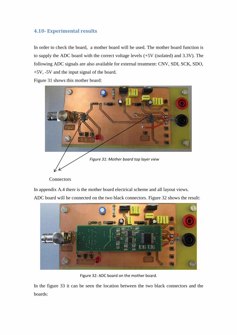
4.10- Experimental results
In order to check the board, a mother board will be used. The mother board function is
to supply the ADC board with the correct voltage levels (+5V (isolated) and 3.3V). The
following ADC signals are also available for external treatment: CNV, SDI, SCK, SDO,
+5V, -5V and the input signal of the board.
Figure 31 shows this mother board:
Figure 31: Mother board top layer view
Connectors
In appendix A.4 there is the mother board electrical scheme and all layout views.
ADC board will be connected on the two black connectors. Figure 32 shows the result:
Figure 32: ADC board on the mother board.
In the figure 33 it can be seen the location between the two black connectors and the
boards:
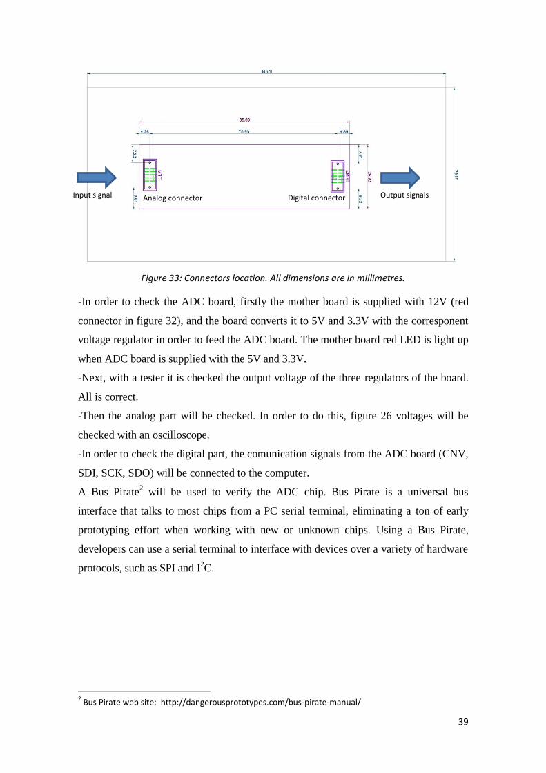
39
Figure 33: Connectors location. All dimensions are in millimetres.
-In order to check the ADC board, firstly the mother board is supplied with 12V (red
connector in figure 32), and the board converts it to 5V and 3.3V with the corresponent
voltage regulator in order to feed the ADC board. The mother board red LED is light up
when ADC board is supplied with the 5V and 3.3V.
-Next, with a tester it is checked the output voltage of the three regulators of the board.
All is correct.
-Then the analog part will be checked. In order to do this, figure 26 voltages will be
checked with an oscilloscope.
-In order to check the digital part, the comunication signals from the ADC board (CNV,
SDI, SCK, SDO) will be connected to the computer.
A Bus Pirate2 will be used to verify the ADC chip. Bus Pirate is a universal bus
interface that talks to most chips from a PC serial terminal, eliminating a ton of early
prototyping effort when working with new or unknown chips. Using a Bus Pirate,
developers can use a serial terminal to interface with devices over a variety of hardware
protocols, such as SPI and I2C.
2 Bus Pirate web site: http://dangerousprototypes.com/bus-pirate-manual/
Analog connector Digital connector Input signal Output signals

40
5-Conclusions
In this project it has been designed and built two electronic boards.
First, a power converter has been done and secondly, a data acquisition board.
The same steps have been followed to develop the two boards. Now, they will be
explained:
First, the block’s diagram has been designed according to the given design restrictions.
Then the blocks have been implemented with the actual electric circuit.
The following task was to select all components, and then the correct electrical
performances of the components have been verified with simulations.
Next, the board’s thermal characteristics have been checked. With the simulations, the
maximum power dissipation of the critical components has been calculated in order to
decide if a heat sink must be added.
Later, with CAD software, the board’s layout has been done.
Once the board has been built by the manufacturer, all components were soldered.
To finish, it is verified that the performance of the boards is the expected from the
simulations. For the ADC board this has been possible with the mother board, because
its function is to supply it.
The power converter has an inverter topology. The end user might use it as an inverter
or like a DC/DC converter, depending on the supply connections.
The principal characteristic of the designs is that all boards are very small, essential
condition to fit them in the box.
In the future, 12 identical converter boards will be built in order to have the 12-phase
inverter, and 6 identical data acquisition boards will be built in order to have the 6 input
channels of the box.

41
6-Acknowledgments
This master thesis is done at LEC (Laboratoire d’Electromécanique de Compiègne), in
the UTC (Université de Technologie de Compiègne), France. I would like to thank all
LEC members for supporting me and all their comradeship during my stage.
I would like to thank specially to Nicolas Patin, my master thesis tutor, for his support
and teachings. Without him this project wouldn’t be possible.
I would also like to thanks Jordi for his help and patience with me.

42
7- Bibliography
-Diptrace tutorial: www.diptrace.com/help/
-LTSpice tutorial: http://ltspice.linear.com/software/scad3.pdf
-Eurocircuits. Design Guidelines-January 2010: www.eurocircuits.com
-Component’s datasheets
-Distributors of electronic components web sites:
Avnet: www.avnet.com
DigiKey: www.digikey.com
Farnell: http://fr.farnell.com/
Mouser: www.mouser.com
RS (RadioSpares): http://radiospares-fr.rs-online.com/web/
-Manufacturer’s web sites:
Analog Devices: www.analog.com
International Rectifier: http://www.irf.com/
Linear Technology : www.linear.com
National Instruments: www.ni.com
Samtec : www.samtec.com
Texas Instruments: www.ti.com

43
8-Appendices
Appendix A: Power converter.
Appendix A.1 Power converter’s electrical scheme.
Appendix A.2 Power converter’s table with all used components and all their
specifications.
Appendix A.3 Power converter’s layout views.
Appendix A.4 Mother board electrical scheme and layout views.
Appendix B: ADC board.
Appendix B.1 ADC board’s electrical scheme.
Appendix B.2 ADC board’s table with all used components and all their specifications.
Appendix B.3 ADC board’s layout views.
Appendix C: Component’s datasheets.
Power converter
1-MOSFET IRF7769L2TR1PbF
2-Diode 120LQ100
3- Diode APT100S20B
4-Diode 12CWQ06FNPbF
5-Driver ISL2110
6-Linear regulator: L1805ABD2T-TR
7-Digital temperature sensor TMP100
ADC board
8-Analog to digital converter AD7944
9-Voltage converter buffer SN74LVC8T245DGVR
10- Isolated buffer ISO7241
11-Operational amplifier LMV721
12-Filter LTC1563
13-Voltage regulator LT1118CST-2.5
14- Isolated DC/DC converter DCR010505U
15-Header connector TFM-105-02-S-D-WT
16-Socket connector SFM-105-02-S-D

44
Appendix A
Power converter.
Appendix A.1
Power converter’s electrical scheme.
Appendix A.2
Power converter’s table with all used components and all their specifications.
Appendix A.3
Power converter’s layout views.
Appendix A.4
Mother board electrical scheme and layout views.

Appendix A.1
46
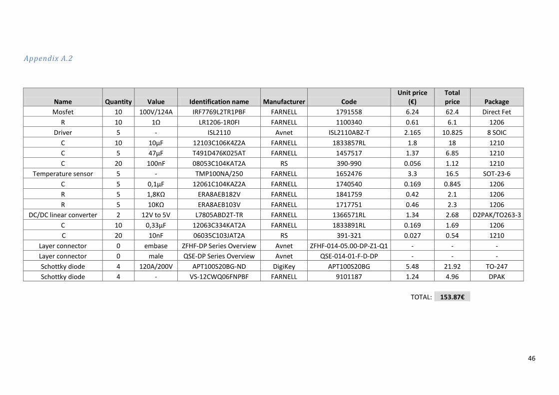
Appendix A.2
Name Quantity Value Identification name Manufacturer Code Unit price
(€) Total price Package
Mosfet 10 100V/124A IRF7769L2TR1PBF FARNELL 1791558 6.24 62.4 Direct Fet
R 10 1Ω LR1206-1R0FI FARNELL 1100340 0.61 6.1 1206
Driver 5 - ISL2110 Avnet ISL2110ABZ-T 2.165 10.825 8 SOIC
C 10 10µF 12103C106K4Z2A FARNELL 1833857RL 1.8 18 1210
C 5 47µF T491D476K025AT FARNELL 1457517 1.37 6.85 1210
C 20 100nF 08053C104KAT2A RS 390-990 0.056 1.12 1210
Temperature sensor 5 - TMP100NA/250 FARNELL 1652476 3.3 16.5 SOT-23-6
C 5 0,1µF 12061C104KAZ2A FARNELL 1740540 0.169 0.845 1206
R 5 1,8KΩ ERA8AEB182V FARNELL 1841759 0.42 2.1 1206
R 5 10KΩ ERA8AEB103V FARNELL 1717751 0.46 2.3 1206
DC/DC linear converter 2 12V to 5V L7805ABD2T-TR FARNELL 1366571RL 1.34 2.68 D2PAK/TO263-3
C 10 0,33µF 12063C334KAT2A FARNELL 1833891RL 0.169 1.69 1206
C 20 10nF 06035C103JAT2A RS 391-321 0.027 0.54 1210
Layer connector 0 embase ZFHF-DP Series Overview Avnet ZFHF-014-05.00-DP-Z1-Q1 - - -
Layer connector 0 male QSE-DP Series Overview Avnet QSE-014-01-F-D-DP - - -
Schottky diode 4 120A/200V APT100S20BG-ND DigiKey APT100S20BG 5.48 21.92 TO-247
Schottky diode 4 - VS-12CWQ06FNPBF FARNELL 9101187 1.24 4.96 DPAK
TOTAL: 153.87€
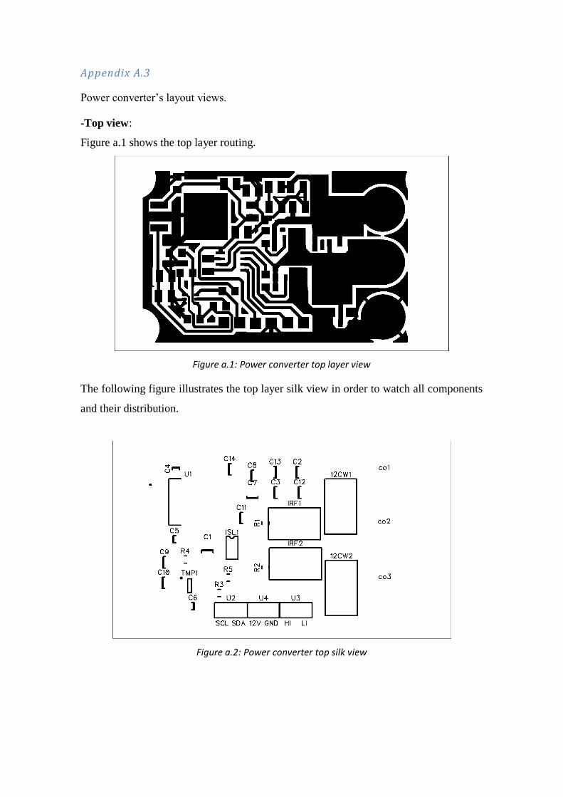
Appendix A.3
Power converter’s layout views.
-Top view:
Figure a.1 shows the top layer routing.
Figure a.1: Power converter top layer view
The following figure illustrates the top layer silk view in order to watch all components
and their distribution.
Figure a.2: Power converter top silk view

Appendix A.4
Mother board electrical scheme and layout views.
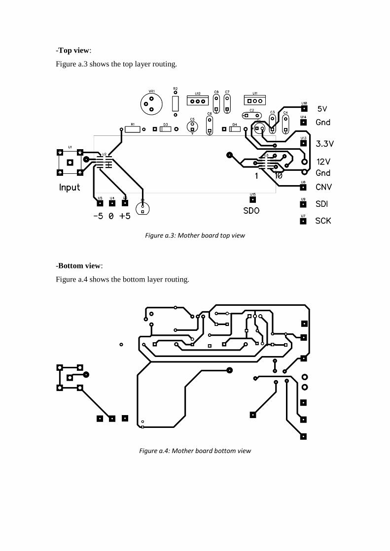
-Top view:
Figure a.3 shows the top layer routing.
Figure a.3: Mother board top view
-Bottom view:
Figure a.4 shows the bottom layer routing.
Figure a.4: Mother board bottom view

Appendix B
ADC board.
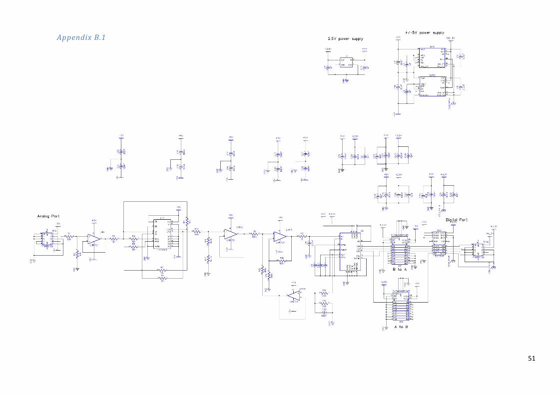
Appendix B.1
ADC board’s electrical scheme.
Appendix B.2
ADC board’s table with all used components and all their specifications.
Appendix B.3
ADC board’s layout views.
51
Appendix B.1

52
Appendix B.2
Name Quantity Value Identification name Manufacturer Code Unit price (€) Total price Package
R 20 100KΩ CPF0805B100KE1 FARNELL 1697458 0.44 8.8 0805
R 20 68,1kΩ RP73D2A68K1BTG FARNELL 1502367RL 1.38 27.6 0805
R 20 1,27kΩ ERA6AEB1271V FARNELL 1810513 0.75 15 0805
R 20 10KΩ CPF0805B10KE1 FARNELL 1697445RL 0.44 8.8 0805
R 20 15Ω CPF0805B15RE1 FARNELL 1697405RL 0.44 8.8 0805
C 20 2,7nF GRM2165C1H272JA01D RS 723-6265 0.053 1.06 0805
C 20 1µF 08053C105KAZ2A RS 698-3392 0.316 6.32 0805
C 20 2,2µF 08053C225KAT2A RS 698-3406 0.336 6.72 0805
C 20 10µF C0805C106K4PAC7800 RS 691-1161 0.372 7.44 0805
C 20 100nF 08053C104KAT2A RS 390-990 0.056 1.12 0805
C 20 10nF 06035C103JAT2A RS 391-321 0.027 0.54 0603
Operational amplifier 10 - LMV721 FARNELL 9778497 1.23 12.3 SOT-23
Filter 10 - LTC1563 FARNELL 1417718 2.85 28.5 SSOP
ADC 4 - AD7944 Analog Devices AD7944BCPZ 8.25 33 -
Voltage converter buffer (2.5V to 5V) 5 - SN74LVC8T245DGVR FARNELL 1236406 1.07 5.35 TVSOP
Voltage regulator (5V to 2,5V) 3 - LT1118CST-2.5#PBF FARNELL 1663359 3.52 10.56 SOT-223
Isolated DC/DC converter (5V to 5V) 4 1W regulated DCR010505U FARNELL 1212384 11.29 45.16 SOIC
Isolated buffer (3.3 to 5V) 5 - ISO7241ADW RS 660-7672 7.55 37.75 SOIC
10-way header 10 - TFM-105-02-S-D-WT FARNELL 1668433 2.07 20.7 -
10 way-female socket 10 - SFM-105-02-S-D FARNELL 1885907 1.91 19.1 -
Aluminium case 1 - 1455T2201BK FARNELL 1511228 31.53 31.53 -
Socket 40 tracks 2 - 3M-9140-4500PL FARNELL 1428323 5.2 10.4 -
Socket 50 tracks 2 - 3M-9150-4500PL FARNELL 1428324 6.2 12.4 -
TOTAL: 358.95€

53
Appendix B.3
ADC board’s layout views.
-Top view:
Figure a.5: ADC board top layer view
Figure a.6 shows the top layer silk view in order to watch the components and their
distribution:
Figure a.6: ADC board top layer silk view
-Bottom view:
Figure a.7: ADC board bottom layer view
Isolated 0V

54
Figure a.8: ADC board bottom layer silk view
-Ground view:
Figure a.9: ADC board ground layer view
-Power view:
Figure a.10: ADC board power layer view
5V
-5V
3.3V
0V

55
Appendix C
Component’s datasheets.
Power converter
1-MOSFET IRF7769L2TR1PbF
2-Diode 120LQ100
3- Diode APT100S20B
4-Diode 12CWQ06FNPbF
5-Driver ISL2110
6-Linear regulator: L1805ABD2T-TR
7-Digital temperature sensor TMP100
ADC board
8-Analog to digital converter AD7944
9-Voltage converter buffer SN74LVC8T245DGVR
10- Isolated buffer ISO7241
11-Operational amplifier LMV721
12-Filter LTC1563
13-Voltage regulator LT1118CST-2.5
14- Isolated DC/DC converter DCR010505U
15-Header connector TFM-105-02-S-D-WT
16-Socket connector SFM-105-02-S-D