METRO TRAIN PROTOTYPE
45
List of Contents Preface 1 Acknowledgement 2 7 1. Microcontroller 8 2.1 Introduction 8 2.2 Definition of a Microcontroller 8 2.3 Pin Configuration 10 2.4 Reset Circuit 12 2.5 Ram Architecture 13 2.6 Microcontrollers vs Microprocessors 16 2.7 Central Processing Unit 17 2.8 Bus 17 2.9 Input Output Unit 18 2.10 Serial Communication 19 2.11 Timer Unit 20 2. LCD Interfacing 21 3.1 Pin description 21 3.2 DDRAM - Display Data RAM 22 3.3 BF - Busy Flag 23 3.4 Instruction Register (IR) and Data Register (DR) 23 3.5 Commands and Instruction set 23 3.6 Sending Commands to LCD 23 4. DC Motor Interfacing 24 4.1 Push-pull four channel driver 24 4.2 Block Diagram 24 4.3 Features 25 5. Power Supply System 26 5.1 Power Supply Circuit 26 5.2 Transformer 27 5.3 Rectifier 28 5.4 Regulator 28 5.5 Filter 29
Transcript of METRO TRAIN PROTOTYPE

List of Contents
Preface 1Acknowledgement 2
71. Microcontroller 8
2.1 Introduction 82.2 Definition of a Microcontroller82.3 Pin Configuration102.4 Reset Circuit 122.5 Ram Architecture132.6 Microcontrollers vs Microprocessors162.7 Central Processing Unit172.8 Bus 172.9 Input Output Unit182.10 Serial Communication192.11 Timer Unit 20
2. LCD Interfacing 213.1 Pin description 213.2 DDRAM - Display Data RAM 223.3 BF - Busy Flag 233.4 Instruction Register (IR) and Data Register (DR)233.5 Commands and Instruction set233.6 Sending Commands to LCD 23
4. DC Motor Interfacing 244.1 Push-pull four channel driver244.2 Block Diagram 244.3 Features 25
5. Power Supply System 265.1 Power Supply Circuit 265.2 Transformer 275.3 Rectifier 285.4 Regulator 285.5 Filter 29

5.6 LED (Light Emitting Diodes)295.7 Circuit Operation29
6. Project Description306.1 Introduction of Project306.2 Circuit Diagram of Metro Train Prototype316.3 Project Methodology 326.4 Procedure 336.5 General Working 33
7. Future Scope 348. References and Bibliography
35Appendix: List of diagrams
36 Coding 37
Preface
This report is all about the embedded systems and itsapplication in various fields of real world. We areliving in the Embedded World. We are surrounded with manyembedded products and our daily life largely depends onthe proper functioning of these gadgets. Television,Radio, CD player, Washing Machine or Microwave Oven inour kitchen, Card readers, Access Controllers, Palmdevices of our work space enable us to do many of ourtasks very effectively. Apart from all these, manycontrollers embedded in our car take care of caroperations between the bumpers. All kinds of magazines
1
and journals regularly dish out details about latesttechnologies, new devices; fast applications which makeus believe that our basic survival is controlled by theseembedded products. Now we can agree to the fact thatthese embedded products have successfully invaded intoour world. What is this Embedded System?
Theoretically, an embedded controller is a combination ofpiece of microprocessor based hardware and the suitablesoftware to undertake a specific task.
I have made a Project based on Microcontroller that is aPrototype of Metro Train. This training report covers allabout the microcontroller and project description. Inthis project I have implemented the Prototype of MetroTrain that is describing a small application ofmicrocontroller.
2

Acknowledgement The completion of any project brings with it a sense of
satisfaction, but it is never complete without thanking those
people who made it possible and whose constant support has
crowned our efforts with success.
One cannot even imagine the power of the force that guides
us all and neither can we succeed without acknowledging it. Our
deepest gratitude to Almighty God for holding our hands and
guiding us throughout our lives.
I would also like to express our gratitude to Prof.
……………………………. Head of the Department, Electronics and
Communication, ………………, Bhopal for encouraging and inspiring us to
carry out the project in the department lab.
I would also like to thank, Prof. …………………………………………………
Faculty, Dept. of Electronics and Communication for his expert
guidance, encouragement and valuable suggestions at every step.
We also would like to thank all the staff members of EC
dept. for providing us with the required facilities and support
towards the completion of the project.
We are extremely happy to acknowledge and express our
sincere gratitude to our parents for their constant support and
encouragement and last but not the least, friends and well
wishers for their help and cooperation and solutions to
3

problems during the course of the project.
Also our friends at 8051projects.net who provided solutions
at times when we were against the wall in need of help.
4

1. Description of Project
6.1 IntroductionThe Need
Delhi, the National Capital with apopulation of about 12 million is,perhaps, the only city of its size inthe world, which depends almostentirely on buses on it sole mode ofmass transport.bus services areinadequate and heavily over-crowded..The result of extreme congestion on the
road, ever slowing speeds, increasing accident rate, fuel wastageand environmental pollution. Delhi has now become the fourth mostcity in the world, with automobiles contributing more than twothirds of the total atmospheric pollution. Pollution relatedhealth problems are reaching disconcerting levels.
Immediate steps are, therefore, needed to improve both the qualityand availability of mass transport service. This is possible onlyif a rail-based mass transit system, which is non-polluting, isintroduced in the city without further delay.
Delhi MRTS ProjectWith a view to reducing the problems ofDelhi’s commuter, the launching of anIntegrated Multi Mode Mass Rapid TransportSystem for Delhi had long been underconsideration. The first concrete step inthis direction was, however, taken when a
feasibility study for developing such a multi-modal MRTS systemwas commissioned by GNCTD (with support from GOI) in 1989 andcompleted by RITES in 1991.
My Prototype of metro train
5

I have made the prototype of Metro trainusing Microcontroller 89C51.The basicfunction of this project is given later. Ihave used a toy car to implementing it whichhas two DC motors. One is used for openingand closing the door and other is used formoving the car forward. The completedescription of project is given below.
6.2 Circuit Diagram of Metro Train Prototype
Following figure shows the complete Metro Train Prototype.
6
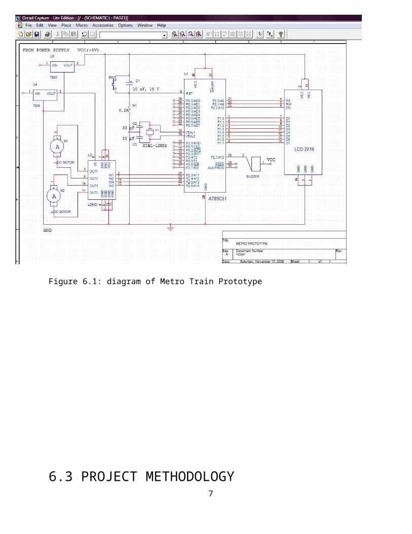
Figure 6.1: diagram of Metro Train Prototype
6.3 PROJECT METHODOLOGY7

6.3(a) Components:
Component Name Quantity
1. Power Supply Sectionplug with wire 1Step down transformer (230v/12v a.c) 11N4007 diodes 4LM7809 1LM7805 1
100 μF 1ON/OFF switch 1Red LED 11K Resistor 1
2. Microcontroller SectionMicrocontroller IC (AT89C51) with base 1Crystal Oscillator (11.0592 MHz) 1Capacitor (30pF) 2Capacitor (10µF) 1Resistor (8.2K) 1LCD Connector 1
3. Buzzer 14. LCD(16x2) 15. Load Driver (L293D) with base 16. A Car (toy-driven by a DC motor)
17. General Purpose Card 48. Single Core Connecting Wires9. Reset Switch (Push-on) 110. Old and Rough CD drive for making Door System
1(We are to use only motor and Pulley system for door)
6.3(b) Softwares used:
1. Keil µVision3.2. Top-View Simulator
8

6.3(c) Equipments used:
1. Soldering iron, solder, flux. 2. Hex Blade
6.4 Procedure of building the Prototype ofMetro Train
Step 1: Circuit diagram of the proposed system is designed andfinalized.(Refer to Figure 6.1 )Step 2: All the components and software platform to be used areselected which are also mentioned above.Step 3: All the hardware components are soldered on theirrespective printed circuit boards with the help of soldering iron,solder and flux according to the hardware schematic shown in theFigureStep 5: Code/program of the proposed system is developed using clanguage with the help of software platform (Keil u vision3).Thecoding could be seen in section Step 6: The hex code of the program being created by thesoftware platform is burnt into the flash code memory of ourmicrocontroller IC 89C51.Step 7: Testing is done at various levels to finalize theappropriate program for the most proper working of the system
6.5 General Working
When the power is turned on a message (“welcome to Bhopal metro”)is displayed on LCD.
9

Then a message “Current station is Indrapuri” is displayed anddoor is opened also.A buzzer is also turned on when door opens. After some delay thedoor is closed and car is started to move forward. A message“current station is Indrapuri” is displayed also on LCD. Aftersome delay a message “next station is Indrapuri” is displayed.Aftersome time the train stops and a message “ current station is M PNagar” is displayed. This process is continued for five stations.In the end a message “End of line” is displayed on LCD. This wholeprocess is repeated until we turned off the power supply.
7. FUTURE SCOPE
10
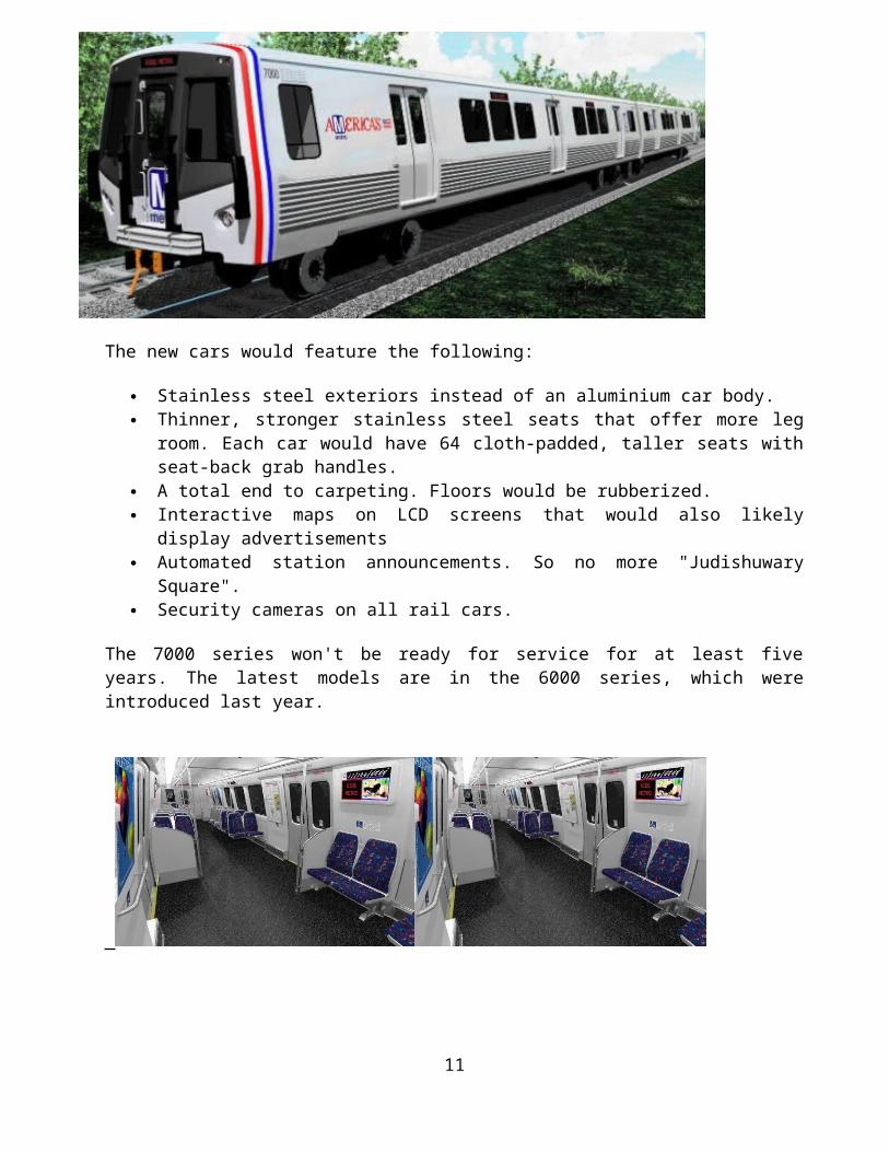
The new cars would feature the following:
Stainless steel exteriors instead of an aluminium car body. Thinner, stronger stainless steel seats that offer more leg
room. Each car would have 64 cloth-padded, taller seats withseat-back grab handles.
A total end to carpeting. Floors would be rubberized. Interactive maps on LCD screens that would also likely
display advertisements Automated station announcements. So no more "Judishuwary
Square". Security cameras on all rail cars.
The 7000 series won't be ready for service for at least fiveyears. The latest models are in the 6000 series, which wereintroduced last year.
11

2. MICROCONTROLLERS
2.1 IntroductionCircumstances that we find ourselves in today in the field ofmicrocontrollers had their beginnings in the development oftechnology of integrated circuits. This development has made itpossible to store hundreds of thousands of transistors into onechip. That was a prerequisite for production of microprocessors,and the first computers were made by adding external peripheralssuch as memory, input-output lines, timers and other. Furtherincreasing of the volume of the package resulted in creation ofintegrated circuits. These integrated circuits contained bothprocessor and peripherals. That is how the first chip containing amicrocomputer, or what would later be known as a microcontrollercame about.
2.2 Definition of a MicrocontrollerMicrocontroller, as the name suggests, are small controllers. Theyare like single chip computers that are often embedded into othersystems to function as processing/controlling unit. For example,the remote control you are using probably has microcontrollersinside that do decoding and other controlling functions. They arealso used in automobiles, washing machines, microwave ovens,toys ... etc, where automation is needed.
The key features of microcontrollers include:
High Integration of Functionality Microcontrollers sometimes are called single-chip computers
because they have on-chip memory and I/O circuitry and othercircuitries that enable them to function as small standalonecomputers without other supporting circuitry.
Field Programmability, Flexibility
12

Microcontrollers often use EEPROM or EPROM as their storagedevice to allow field programmability so they are flexible touse. Once the program is tested to be correct then largequantities of microcontrollers can be programmed to be usedin embedded systems.
Easy to Use
Assembly language is often used in microcontrollers and sincethey usually follow RISC architecture, the instruction set issmall. The development package of microcontrollers oftenincludes an assembler, a simulator, a programmer to "burn"the chip and a demonstration board. Some packages include ahigh level language compiler such as a C compiler and moresophisticated libraries.
Most microcontrollers will also combine other devices such as:
A Timer module to allow the microcontroller to perform tasksfor certain time periods.
A serial I/O port to allow data to flow between themicrocontroller and other devices such as a PC or anothermicrocontroller.
An ADC to allow the microcontroller to accept analogue inputdata for processing.
13

Figure 2.1: Showing a typical microcontroller device and itsdifferent subunits
2.3 PIN CONFIGURATION
figure 2.2 Pin configuration of Microcontroller
14

We have 4 ports in 8051 micro controller. They are port0, port1,
port2, port3 which can
be accessed as i/o ports. The pins of the micro controller are
explained below.
15
P1
RESETR XDTXDINT0INT1T0T1RDW R
XTAL1XTAL2GND
P3
Vcc
P0
EAPSENALE
P2

Reset: It resets total 8051 micro controller.
RXD: It receives data in serial communication.
TXD: It transmits data in serial communication.
INT0: External interrupt for timer 0.
INT1: External interrupt for timer1
T0: Timer0.
T1: Timer1.
RD: To read into external memory.
WR: To write into external memory.
XTAL1 & XTAL2: To connect the crystal oscillator.
ALE: Address latch enable which is used to access the
address locations
from external memory.
PSEN: Program store enable which is used for storing
programming
code into the external memory.
16

EA: External Access: 64 KB of ROM is the limit for
external memory.
2.4 RESET CIRCUITfigure2.3 : Reset circuit of microcontroller
17
Capacitor is storing charge permanently until we use it. Crystal
Oscillator is used to generate a carrier signal with stable
frequency. With the help of this oscillator we will deduce the
execution speed in terms of bytes/ sec.It generates 12 clock pulses
/machine cycle. Capacitors provide charge for crystal oscillator.

2.5 RAM ARCHITECTURE
figure 2.4: Ram Architecture
The 8051 has a bank of 128 bytes of Internal RAM. This Internal
RAM is found on-chip on the 8051 so it is the fastest RAM available,
and it is also the most flexible in terms of reading, writing, and
modifying its contents. Internal RAM is volatile, so when the 8051
is reset this memory is cleared. The 128 bytes of internal ram is
subdivided as shown on the memory map. The first 8 bytes (00h -
07h) are "register bank 0". These alternative register banks are
located in internal RAM in addresses 08h through 1Fh.Bit memory
actually resides in internal RAM, from addresses 20h through 2Fh.
The 80 bytes remaining of Internal RAM, from addresses 30h through
7Fh, may be used by user variables that need to be accessed18
frequently or at high-speed. This area is also utilized by the
microcontroller as a storage area for the operating stack.
Register Banks
The 8051 uses 8 "R" registers which are used in many of its
instructions. These "R" registers are numbered from 0 through 7
(R0, R1, R2, R3, R4, R5, R6, and R7).These registers are generally
used to assist in manipulating values and moving data from one
memory location to another. The concept of register banks adds a
great level of flexibility to the 8051.
Bit Memory
The 8051, being a communication oriented microcontroller,
gives the user the ability to access a number of bit variables. These
variables may be either 1 or 0. There are 128 bit variables
available to the user, numbered 00h through 7Fh. The user may make
use of these variables with commands such as SETB and CLR. It is
important to note that Bit Memory is really a part of Internal
RAM. In fact, the 128 bit variables occupy the 16 bytes of
Internal RAM from 20h through 2Fh.
Special Function Register (SFR) Memory
Special Function Registers (SFRs) are areas of memory that
control specific functionality of the 8051 processor. For example,
four SFRs permit access to the 8051’s 32 input/output lines.
Another SFR allows a program to read or write to the 8051’s serial
19

port .SFR is a part of Internal Memory. This is not the case. When
using this method of memory access (it’s called direct address),
any instruction that has an address of 00h through 7Fh refers to
an Internal RAM memory address; any instruction with an address of
80h through FFh refers to an SFR control register.
RegistersThe Accumulator
The Accumulator, as its name suggests, is used as a general
register to accumulate the results of a large number of
instructions. It can hold an 8-bit (1-byte) value and is the most
versatile register
The "R" registers
20

The "R" registers are a set of eight registers that are named
R0, R1, etc. up to and including R7. These registers are used as
auxiliary registers in many operations.
The "B" Register
The "B" register is very similar to the Accumulator in the
sense that it may hold an 8-bit (1-byte) value. The "B" register
is only used by two 8051 instructions: MUL AB and DIV AB.
The Data Pointer (DPTR)
The Data Pointer (DPTR) is the 8051’s only user-accessible
16-bit (2-byte) register. The Accumulator, "R" registers, and "B"
register are all 1-byte values. DPTR, as the name suggests, is
used to point to data. It is used by a number of commands which
allow the 8051 to access external memory.
The Program Counter (PC)
The Program Counter (PC) is a 2-byte address which tells the
8051 where the next instruction to execute is found in memory.
When the 8051 is initialized PC always starts at 0000h and is
incremented each time an instruction is executed.
.
The Stack Pointer (SP)
The Stack Pointer, like all registers except DPTR and PC, may
hold an 8-bit (1-byte) value. The Stack Pointer is used to
indicate where the next value to be removed from the stack should
be
21

Addressing Modes
An "addressing mode" refers to how you are addressing a given
memory location. The addressing modes are as follows,
With an example of each:
Immediate Addressing MOV A, #20h
Direct Addressing MOV A, #30h
Indirect Addressing MOV A, @R0
External Direct MOVX A, @DPTR
Code Indirect MOVC A, @A+DPTR
Each of these addressing modes provides important flexibility.
Interrupts
An interrupt is a special feature which allows the 8051 to
provide the illusion of "multitasking," although in reality the
8051 is only doing one thing at a time.
.
Timers
Timers are one of the categories of hardware time delays.
Time delays are used to keep a system into halting System or
sleepy mode. We have two timers-timer0, timer1.Hardware time
delays are used to generate exact time delays.
22

2.6 Microcontrollers versus MicroprocessorsMicrocontroller differs from a microprocessor in many ways. Firstand the most important is its functionality. In order for amicroprocessor to be used, other components such as memory, orcomponents for receiving and sending data must be added to it. Inshort that means that microprocessor is the very heart of thecomputer. On the other hand, microcontroller is designed to be allof that in one. No other external components are needed for itsapplication because all necessary peripherals are already builtinto it. Thus, we save the time and space needed to constructdevices.
2.7 Central Processing Unit Let add 3 more memory locations to a specific block that will havea built in capability to multiply, divide, subtract, and move itscontents from one memory location onto another. The part we justadded in is called "central processing unit" (CPU). Its memorylocations are called registers.
23
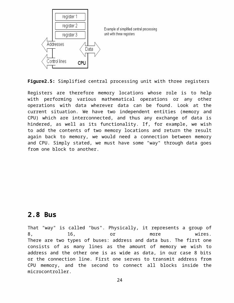
Figure2.5: Simplified central processing unit with three registers
Registers are therefore memory locations whose role is to helpwith performing various mathematical operations or any otheroperations with data wherever data can be found. Look at thecurrent situation. We have two independent entities (memory andCPU) which are interconnected, and thus any exchange of data ishindered, as well as its functionality. If, for example, we wishto add the contents of two memory locations and return the resultagain back to memory, we would need a connection between memoryand CPU. Simply stated, we must have some "way" through data goesfrom one block to another.
2.8 BusThat "way" is called "bus". Physically, it represents a group of8, 16, or more wires.There are two types of buses: address and data bus. The first oneconsists of as many lines as the amount of memory we wish toaddress and the other one is as wide as data, in our case 8 bitsor the connection line. First one serves to transmit address fromCPU memory, and the second to connect all blocks inside themicrocontroller.
24
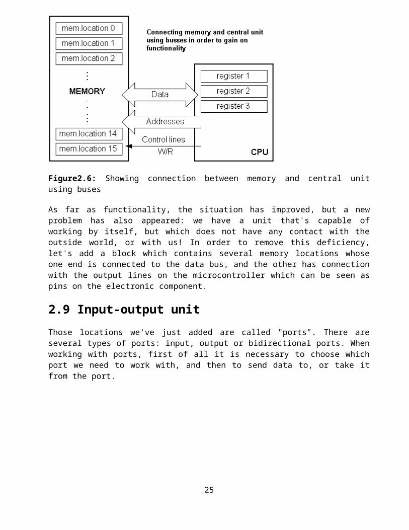
Figure2.6: Showing connection between memory and central unitusing buses
As far as functionality, the situation has improved, but a newproblem has also appeared: we have a unit that's capable ofworking by itself, but which does not have any contact with theoutside world, or with us! In order to remove this deficiency,let's add a block which contains several memory locations whoseone end is connected to the data bus, and the other has connectionwith the output lines on the microcontroller which can be seen aspins on the electronic component.
2.9 Input-output unitThose locations we've just added are called "ports". There areseveral types of ports: input, output or bidirectional ports. Whenworking with ports, first of all it is necessary to choose whichport we need to work with, and then to send data to, or take itfrom the port.
25

Figure2.7: Simplified input-output unit communicating withexternal world
When working with it the port acts like a memory location.Something is simply being written into or read from it, and itcould be noticed on the pins of the microcontroller.
2.10 Serial communicationBeside stated above we've added to the already existing unit thepossibility of communication with an outside world. However, thisway of communicating has its drawbacks. One of the basic drawbacksis the number of lines which need to be used in order to transferdata. What if it is being transferred to a distance of severalkilometers? The number of lines times’ number of kilometersdoesn't promise the economy of the project. It leaves us having toreduce the number of lines in such a way that we don't lessen itsfunctionality. Suppose we are working with three lines only, andthat one line is used for sending data, other for receiving, andthe third one is used as a reference line for both the input andthe output side. In order for this to work, we need to set therules of exchange of data. These rules are called protocol.Protocol is therefore defined in advance so there wouldn't be anymisunderstanding between the sides that are communicating witheach other. For example, if one man is speaking in French, and theother in English, it is highly unlikely that they will quickly andeffectively understand each other. Let's suppose we have thefollowing protocol. The logical unit "1" is set up on the
26

transmitting line until transfer begins. Once the transfer starts,we lower the transmission line to logical "0" for a period of time(which we will designate as T), so the receiving side will knowthat it is receiving data, and so it will activate its mechanismfor reception. Let's go back now to the transmission side andstart putting logic zeros and ones onto the transmitter line inthe order from a bit of the lowest value to a bit of the highestvalue. Let each bit stay on line for a time period which is equalto T, and in the end, or after the 8th bit, let us bring thelogical unit "1" back on the line which will mark the end of thetransmission of one data. The protocol we've just described iscalled in professional literature NRZ (Non-Return to Zero).
Figure2.8: Serial unit sending data through three lines only
As we have separate lines for receiving and sending, it ispossible to receive and send data (info.) at the same time. Socalled full-duplex mode block which enables this way ofcommunication is called a serial communication block. Unlike theparallel transmission, data moves here bit by bit, or in a seriesof bits what defines the term serial communication comes from.After the reception of data we need to read it from the receivinglocation and store it in memory as opposed to sending where theprocess is reversed. Data goes from memory through the bus to thesending location, and then to the receiving unit according to theprotocol.
2.11 Timer unit
27

Since we have the serial communication explained, we can receive,send and process data.
Figure2.9: Timer unit generating signals in regular time intervals
However, in order to utilize it in industry we need a fewadditionally blocks. One of those is the timer block which issignificant to us because it can give us information about time,duration, protocol etc. The basic unit of the timer is a free-runcounter which is in fact a register whose numeric value incrementsby one in even intervals, so that by taking its value duringperiods T1 and T2 and on the basis of their difference we candetermine how much time has elapsed. This is a very important partof the microcontroller whose understanding requires most of ourtime.
Figure2.10: Physical configuration of the interior of amicrocontroller
28

Figure2.11: Microcontroller outline with basic elements andinternal connections
For a real application, a microcontroller alone is not enough.Beside a microcontroller, we need a program that would beexecuted, and a few more elements which make up interface logictowards the elements of regulation (which will be discussed next).
3- LCD INTERFACING
3.1 Pin Configuration
29

GND Vcc80 81 82 83 84 85 86 87 88 89 8A 8B 8C 8D 8E 8FC0 C1 C2 C 3 C4 C5 C6 C7 C8 C9 CA CB CC CD CE CF
1 162 15
4
3
5
6
7 8 9 10 11 1213 14
figure 3.1: 16x2 LCD Pin configuration
3- >VARISTOR4-> RS5-> RW6-> EN7-14-> DATA LINE INPUTS
LCD stands for Liquid Crystal Display. The most commonly used LCDsfound in the market today are 1 Line, 2 Line or 4 Line LCDs whichhave only 1 controller and support at most of 80 characters.
3.2 DDRAM - Display Data RAMDisplay data RAM (DDRAM) stores display data represented in 8-bitcharacter codes. Its extended capacity is 80 X 8 bits, or 80characters. The area in display data RAM (DDRAM) that is not used
30
H ->A
for display can be used as general data RAM. So whatever you sendon the DDRAM is actually displayed on the LCD.
3.3 BF - Busy FlagBusy Flag is a status indicator flag for LCD. When we send acommand or data to the LCD for processing, this flag is set (i.e.BF =1) and as soon as the instruction is executed successfullythis flag is cleared (BF = 0). This is helpful in producing andexact amount of delay. For the LCD processing. To read Busy Flag,the condition RS = 0 and R/W = 1 must be met and The MSB of theLCD data bus (D7) act as busy flag. When BF = 1 means LCD is busyand will not accept next command or data and BF = 0 means LCD isready for the next command or data to process.
3.4 Instruction Register (IR) and DataRegister (DR)There are two 8-bit registers controller Instruction and Dataregister. Instruction register corresponds to the register whereyou send commands to LCD e.g. LCD shift command, LCD clear, LCDaddress etc. and Data register is used for storing data which isto be displayed on LCD. When send the enable signal of the LCD isasserted, the data on the pins is latched in to the data registerand data is then moved automatically to the DDRAM and hence isdisplayed on the LCD.
3.5 Commands and Instruction set
Only the instruction register (IR) and the data register (DR) ofthe LCD can be controlled by the MCU. Before starting the internaloperation of the LCD, control information is temporarily storedinto these registers to allow interfacing with various MCUs, whichoperate at different speeds, or various peripheral controldevices. The internal operation of the LCD is determined bysignals sent from the MCU.
31

3.6 Sending Commands to LCD
To send commands we simply need to select the command register.Everything is same as we have done in the initialization routine.But we will summarize the common steps and put them in a singlesubroutine.
Following are the steps: Move data to LCD port Select command register Select write operation Send enable signal Wait for LCD to process the command
4 DC MOTOR INTERFACING In this project the d.c motor interfacing consists of two
motors .One motor is used to open & close the car door and the
other is used to move the car forward. This interfacing is shown
in fig. This uses L293D IC interfacing.
4.1 Push-Pull Four Channel DriverDescription
Output currents to 1A or 600mA per channel respectively. Each
channel is controlled by a TTL-compatible logic input and each
pair of drivers (a The L293 and L293D are quad push-pull drivers
capable of delivering full bridge) is equipped with an inhibit
32

input which turns off all four transistors. A separate supply
input is provided for the logic so that it may be run off a lower
voltage to reduce dissipation. Additionally the L293D includes the
output clamping diodes within the IC for complete interfacing with
inductive loads. Both devices is available in 16-pin Batwing DIP
packages. They are also available in Power S0IC and Hermetic DIL
packages.
4.2 Block DiagramFigure 4.1: block diagram of load driver L293D
4.3 FEATURES:
Output Current 1A Per Channel (600mA for L293D)
Peak Output Current 2A Per Channel (1.2A for L293D)
Inhibit Facility33

High Noise Immunity
Separate Logic Supply
Over-Temperature Protection
ABSOLUTE MAXIMUM RATINGS:
Collector Supply Voltage,
VC. . . . . . . . . . . . . . . . . . . . . . . . . . . . . . . .
. . . . . . . . . . . . 36V
Logic Supply Voltage,
VSS . . . . . . . . . . . . . . . . . . . . . . . . . . . . . . .
. . . . . . . . . . . . . . 36V
Input Voltage, VI. . . . . . . . . . . . . . . . . . . . . . . . .
. . . . . . . . . . . . . . . . . . . . . . . . . . . . . . 7V
Inhibit Voltage,
VINH . . . . . . . . . . . . . . . . . . . . . . . . . . . . . . .
. . . . . . . . . . . . . . . . . . . .7V
Peak Output Current (Non-Repetitive), lOUT
(L293) . . . . . . . . . . . . . . . . . . . . . . . . . . 2A
lOUT (L293D) . . . . . . . . . . . . . . . . . . . . . . . . . . .
. . . . . . . . . . . . . . . . . . . . . . . . . . . . 1.2A
Total Power Dissipation
At T ground-pins = 80°C
N Batwing pkg, (Note) . . . . . . . . . . . . . . . . . . . . . .
. . . . . . . . . . . . . . . . . . . . . . . . . . . 5W
34

Storage and Junction Temperature, Tstg, TJ . . . . . . . . . . . .
. . . . . . . . . . . . -40 to +150°C
5 POWER SUPPLY SYSTEM
5.1 POWER SUPPLY CIRCUIT:
Figure 5.1: Circuit of power supply35

The power supply consists of ac voltage transformer, diode
rectifier, ripple filter, and voltage regulator. The description
of the components is shown below.
5.2 TRANSFORMER:Definition:
The transformer is a static electro-magnetic device that
transforms one alternating Voltage (current) into another voltage
(current).However; power remains the same during the
transformation. Transformers play a major role in the transmission
and distribution of ac power.
Principle:
Transformer works on the principle of mutual induction. A
transformer consists of laminated magnetic core forming the
magnetic frame. Primary and secondary coils are wound upon the two
cores of the magnetic frame, linked by the common magnetic flux.
36

When an alternating voltage is applied across the primary coil, a
current flows in the primary coil producing magnetic flux in the
transformer core. This flux induces voltage in secondary coil.
Transformers are classified as:
(a) Based on position of the windings with respect to
core i.e.
(1) Core type transformer
(2) Shell type transformer
(b) Transformation ratio:
(1) Step up transformer
(2) Step down transformer
DC power supply exists in every electronic box whether it is
a computer, TV, or equipment in the laboratory. The power supply
consists of ac voltage transformer, diode rectifier, ripple
filter, and voltage regulator. The transformer is an ac device. It
has two coil windings, the primary and the secondary, around a
common magnetic core. The current flowing in the primary winding
generates a time varying electromagnetic field which in turn
induces an output voltage across the secondary winding. The ratio
of turns in the two windings determines the ratio of the input
voltage and output voltage. The power supply that we are building
in this experiment is a linear power supply. In other words, the
circuit functions with analog signals. In our kit, we have a small
transformer which can convert 230Vac from the wall plug to 6-12 V
ac.
37

5.3 RECTIFIER:The rectifier is based on p-n junction. One can use a single
diode forming a half-wave rectifier or four diodes forming a full-
wave rectifier or a bridge rectifier. In the experiment, we are
going to use the power rectifying diode, 1N4001 or IN4007. You can
read from the specification sheet the characteristics of the
diode. The most important thing to know is the polarity of the
diode. The arrow is the p-side and the bar is the n-side. A
positive voltage is needed on the p-side to make the diode
conduct. IN4001 can block off large negative bias in the hundred
voltage range.
5.4 REGULATOR:To make the output voltage as constant as possible, one needs
a regulator. The regulator consists of a voltage reference, e.g.,
a Zener diode. It can also be an IC component with voltage
reference and feedback control circuit inside.
Finally, you will characterize the performance of the power
supply by measuring its output voltage and ripple as a function of
the load current. The more the current, the higher is the ripple.
Likewise, the more the current, the lower is the voltage. This is
called loading.
Another semiconductor component to be used in this experiment
38
is a voltage regulator, 7805. “78” indicates that it is a
regulator for positive voltage. There is a corresponding “79”
model for negative voltage. “05” indicates that it has an output
of 5 V. 7805 is an integrated circuit. Just like the operational
amplifier, the design engineer of the IC has optimized the
circuit. The regulator IC requires an input voltage at least a
couple of V higher than the output voltage in order to function
properly. In a way, it is similar to the operational amplifier;
the output is limited by the power supply voltage. Your output is
always below the input. This voltage difference keeps all
electronic circuits in the IC forwardly biased, hence, functioning
properly in the linear regime.
The lower circuit is a bridge-wave rectifier. There are four
diodes. They are arranged in such a way that the current always
flows in the same direction through the load resistor no matter
which node of the transformer is positive. You can trace the flow
of the current. When the upper node of the transformer is
positive, current flows through the first diode through the load,
which is not shown, then it flows through the last diode to the
lower node of the transformer completing the loop. When the lower
node of the transformer is positive, current flows through the
third diode to the load resistor then it flows through the second
diode to the upper node of the transformer completing the loop.
The current flows through the load resistor along the same
direction all the time. The load resistor must have sufficient
power handling capability. Otherwise, It may burn .The power
dissipation is given by voltage square divided by resistance.
5.5 FILTER:39

After the rectification process, the voltage signal contains
both an average dc component and a time varying ac component
called the ripple. To reduce or eliminate the ac component, one
needs low pass filter(s). The low pass filter will pass through
the dc but attenuate the ac at 60 Hz or its harmonics, i.e., 120
Hz. It has a resistor in front and a capacitor across the output
and ground. (C-filter).
5.6 LED (Light Emitting Diodes): As its name implies it is a diode, which emits light when
forward biased. Charge carrier recombination takes place when
electrons from the N-side cross the junction and recombine with
the holes on the P side. Electrons are in the higher conduction
band on the N side whereas holes are in the lower valence band on
the P side. During recombination, some of the energy is given up
in the form of heat and light. In the case of semiconductor
materials like Gallium arsenide (GaAs), Gallium phosphate (Gap)
and Gallium arsenide phosphate (GaAsP) a greater percentage of
energy is released during recombination and is given out in the
form of light. LED emits no light when junction is reversed
biased.
5.7 CIRCUIT OPERATION:In circuit operation, when the voltage generated by the
transformer is higher than the capacitor voltage, the current
flows through the diode charging the capacitors. At the same time,
the load resistor drains current from the capacitors. When the
amount of draining matches with the charging current, the voltage
is stabilized. A sudden increase in load current will decrease the
40
voltage across the capacitor. It will also increase the time
period during which the diodes conduct, hence, the ripple.
8. REFRENCES AND BIBLOGRAPHY
“THE 8051 MICROCONTROLLER AND EMBEDDED SYSTEM” by MuhammadAli Mazidi , Janice Gillispie Mazidi, Rolin D. Mckinlay.
“The 8051 MICROCONTROLLER” by K. J. Ayala. "Advanced Microprocessors and Microcontrollers" by B.P. Singh
& Renu Singh. "Let Us C" by Yashwant Kanitkar. "Data Structure through C" by Yashwant Kanitkar.
NET LINKS:
1.www.8051projects.net
2.www.atmel.com
3.www.electronicsforyou.com
4.www.encyclopedia.com
5.www.wikipedia.com
41
Appendix
List of Essential Diagrams:
1.Figure 2.1: showing a typical microcontroller device
and its different subunits9
2.Figure 2.2: Pin configuration of Microcontroller10
3.Figure 2.3: Reset circuit of Microcontroller11
4.Figure 2.4: Ram Architecture13
5.Figure 2.5: Simplified central processing unit with three registers
17
42

6.Figure 2.6: Showing connection between memory
and central unit using buses18
7.Figure 2.7: Simplified input-output unitcommunicating
with external world 18
8.Figure 2.8: Serial unit sending data through threelines 19
9.Figure 2.9: Timer unit generating signals in regular
time intervals 20
10. Figure 2.10: Physical configuration of theinterior of a
Microcontroller 20
11. Figure 2.11: Microcontroller outline with basicelements
And internal connections21
12. Figure 3.1: 16x2 LCD pin configuration22
13. Figure 4.1: Block diagram of load driver L293D24
14. Figure 5.1: Circuit of power supply26
15. Figure 6.1: Circuit diagram of Metro trainprototype 31
43

44