Thermal design studies of high-power heterojunction bipolar transistors
10
854 IEEE TRANSACTIONS ON ELECTRON DEVICES, VOL. 36, NO. 5, MAY 1989 Thermal Design Studies of High-Power Heterojunction Bipolar Transistors GUANG-BO GAO, SENIOR MEMBER, IEEE, MING-ZHU WANG, XIANG GUI, AND HADIS MoRKoC, FELLOW, IEEE Abstruct-A theoretical thermoelectro-feedback model has been de- veloped for thermal design considerations of high-power GaAlAs/ GaAs heterojunction bipolar transistors (HBT’s). The power-handling capability, thermal instability, junction temperature, and current dis- tributions of HBT’s with multiple emitter fingers have been numeri- cally studied. The calculated results indicate that power HBT’s on Si substrates (or Si as the collector) have excellent potential power per- formance and reliability. The power-handling capability on Si is 3.5 and 2.7 times as large as that on GaAs and InP substrates, respectively. The peak junction temperature and temperature difference on the chip decrease in comparison to the commonly used Si homostructure power transistors with the same geometry and power dissipation. Thereby HBT’s will open new vistas for microwave and millimeter-wave appli- cations. It has been also found that the nonuniform distribution of junction temperature and current can be greatly improved by a bal- lasting technique of unequally valued emitter resistors. The present model and calculated results should permit a more optimum thermal design for high-power HBT’s. IC JC K k L I Mk Nk Nce NOMENCLATURE Current gain in common emitter configura- Collector current. Collector current density. Number of heat-source cells. Boltzmann’s constant. Chip length. Length of elementary unit. Number of elementary units in the kth heat- Number of elementary units in the kth heat- Effective state density in the base conduction Effective state density in the emitter conduc- Effective state density in the base valence tion. source cell in x direction. source cell in y direction. band. tion band. band. pk, ij 4 Rb Re Ts T t vbe vcb Vces VD vd W W xk, ij xt Yk, ij Kk, ij Pnb Xb Xe Maximum allowed power density. Maximum thermally stable power density. Power density distribution function at chip’s top surface. Power density of the ith line, jth column el- ementary unit in the kth heat-source cell. Charge of electron. Base series resistor. Emitter series resistor. Temperature at any point in chip. Temperature of heat sink. Chip thickness. Base-emitter terminal voltage. Collector-base terminal voltage. Saturated collector-emitter voltage. Built-in voltage in emitter-base junction. Electron drift velocity. Chip width. Width of elementary unit. Abscissa of the central point of the ith line, jth column elementary unit in the kth heat- source cell. Transition region width of emitter junction. Ordinate of the center point of the ith column elementary unit in the kth heat-source cell. Apparent valence-band discontinuity. Dielectric constant of GaAlAs. Temperature-dependent thermal conductiv- ity. Thermal conductivity of the ith line, jth col- umn elementary unit in the kth heat-source cell. Electron mobility in base. Electron affinity in base. Electron affinity in emitter. NE Ionized donor concentration. nh Ideality factor of base-emitter junction. I. INTRODUCTION nib N recent years, investigations of heterojunction bipolar I transistors (HBT’s) have been extensively reported [ 11- Intrinsic carrier density of base. - - Manuscript received June 21, 1988; revised December 27, 1988. The [4], Many new structures and technologies, such as self- review of this paper was arranged by Associate Editor S.-S. Pei. Laboratory, Department of Electronic Engineering, Beijing Polytechnic University, Beijing 100022, China. H. Morkoq is with the Coordinated Science Laboratory, University of IEEE Log Number 8826310. G. B. Gao, M. Z, Wang, and X. Gui are with the Reliability Physics ion imp1anation, and planar techniques have been developed for HBT’s. These devices offer great promise for high speed microwave and millimeter-wave as well as optoelectronic integrated circuits. For power applications, high power densities of up to 4 W per mil- Illinois at Urbana-Champaign, Urbana, IL 61801. 0018-9383/89/0500-0854$01 .OO O 1989 IEEE
-
Upload
independent -
Category
Documents
-
view
0 -
download
0
Transcript of Thermal design studies of high-power heterojunction bipolar transistors

854 IEEE TRANSACTIONS ON ELECTRON DEVICES, VOL. 36, NO. 5 , MAY 1989
Thermal Design Studies of High-Power Heterojunction Bipolar Transistors
GUANG-BO GAO, SENIOR MEMBER, IEEE, MING-ZHU WANG, XIANG GUI, AND HADIS MoRKoC, FELLOW, IEEE
Abstruct-A theoretical thermoelectro-feedback model has been de- veloped for thermal design considerations of high-power GaAlAs/ GaAs heterojunction bipolar transistors (HBT’s). The power-handling capability, thermal instability, junction temperature, and current dis- tributions of HBT’s with multiple emitter fingers have been numeri- cally studied. The calculated results indicate that power HBT’s on Si substrates (or Si as the collector) have excellent potential power per- formance and reliability. The power-handling capability on Si is 3.5 and 2.7 times as large as that on GaAs and InP substrates, respectively. The peak junction temperature and temperature difference on the chip decrease in comparison to the commonly used Si homostructure power transistors with the same geometry and power dissipation. Thereby HBT’s will open new vistas for microwave and millimeter-wave appli- cations. It has been also found that the nonuniform distribution of junction temperature and current can be greatly improved by a bal- lasting technique of unequally valued emitter resistors. The present model and calculated results should permit a more optimum thermal design for high-power HBT’s.
I C
J C
K k L I M k
N k
Nce
NOMENCLATURE
Current gain in common emitter configura-
Collector current. Collector current density. Number of heat-source cells. Boltzmann’s constant. Chip length. Length of elementary unit. Number of elementary units in the kth heat-
Number of elementary units in the kth heat-
Effective state density in the base conduction
Effective state density in the emitter conduc-
Effective state density in the base valence
tion.
source cell in x direction.
source cell in y direction.
band.
tion band.
band.
p k , ij
4 R b
R e
Ts T
t vbe
vcb
Vces
V D
v d W W
x k , ij
x t
Y k , ij
Kk, ij
Pnb
Xb
Xe
Maximum allowed power density. Maximum thermally stable power density. Power density distribution function at chip’s
top surface. Power density of the ith line, j th column el-
ementary unit in the kth heat-source cell. Charge of electron. Base series resistor. Emitter series resistor. Temperature at any point in chip. Temperature of heat sink. Chip thickness. Base-emitter terminal voltage. Collector-base terminal voltage. Saturated collector-emitter voltage. Built-in voltage in emitter-base junction. Electron drift velocity. Chip width. Width of elementary unit. Abscissa of the central point of the ith line,
j th column elementary unit in the kth heat- source cell.
Transition region width of emitter junction. Ordinate of the center point of the ith column
elementary unit in the kth heat-source cell. Apparent valence-band discontinuity. Dielectric constant of GaAlAs. Temperature-dependent thermal conductiv-
ity. Thermal conductivity of the ith line, j th col-
umn elementary unit in the kth heat-source cell.
Electron mobility in base. Electron affinity in base. Electron affinity in emitter.
NE Ionized donor concentration. nh Ideality factor of base-emitter junction. I. INTRODUCTION nib N recent years, investigations of heterojunction bipolar I transistors (HBT’s) have been extensively reported [ 11-
Intrinsic carrier density of base. - -
Manuscript received June 21, 1988; revised December 27, 1988. The [4], Many new structures and technologies, such as self- review of this paper was arranged by Associate Editor S.-S. Pei.
Laboratory, Department of Electronic Engineering, Beijing Polytechnic University, Beijing 100022, China.
H . Morkoq is with the Coordinated Science Laboratory, University of
IEEE Log Number 8826310.
G. B. Gao, M. Z, Wang, and X. Gui are with the Reliability Physics ion imp1anation, and planar techniques have been developed for HBT’s. These devices offer great promise for high speed microwave and millimeter-wave as well as optoelectronic integrated circuits. For power applications, high power densities of up to 4 W per mil-
Illinois at Urbana-Champaign, Urbana, IL 61801.
0018-9383/89/0500-0854$01 .OO O 1989 IEEE

GAO ef al.: THERMAL DESIGN STUDIES OF HIGH-POWER HBT’S 855
limeter of emitter length in CW operation has been de- scribed in both small [ 5 ] , [6] and large [7] area HBT’s. GaAlAs/GaAs HBT’s on Si substrates and Si as the col- lector have also been demonstrated and proposed, respec- tively [8], [9]. Si has thermal conductivity about three times greater than GaAs, and the electron mobility of GaAs is six times as large as that of Si. Therefore, GaAs- on-Si composite structures are likely to have distinct ad- vantages for high-frequency power devices.
To date, the high-power attributes of HBT’s have yet to be fully realized [7], nor have the associated problems been analyzed in detail. Therefore, power HBT models, which can also be used for the thermal design rules, are needed. We suggest several basic considerations in this respect, including the following:
1) The emitter-base voltage of HBT’s has a negative temperature dependence, which means that the tempera- ture coefficient of the emitter current is positive. Thus, like conventional Si transistors, the current and junction temperature in an HBT chip form positive feedback. To solve this problem one must start with a thermoelectro- feedback model.
2) It has been shown that a two-dimensional analysis leads to temperatures reduced more strongly than the sim- ple one-dimensional model where no thermal-flow spreading is included [ 101. However, the temperatures obtained from two-dimensional calculations are still higher than the experiments since the transverse or lon- gitudinal heat conduction is neglected. For design guide- lines, a three-dimensional model where the heat-flow is spread in a cone shape is more desirable.
3 ) In view of the development of high-power HBT’s with more emitter fingers, the thermal behavior is no longer correctly characterized if based on the assumption of uniform current and junction temperature distributions over the active region. A large power HBT can be re- garded as an array constituted by M X N elementary tran- sistors, and the distributions may be treated uniformly in each elementary transistor.
4 ) The thermal conductivity of the substrate material in HBT’s has a strong temperature dependence, its value decreasing with increasing temperature over the range of interest. The temperature dependence of the thermal con- ductivity and its contribution to the thermoelectric feed- back should be taken into account while the HBT power characteristics are investigated.
5 ) It is well known that the current gain of Si planar homostructure transistors has a positive temperature coef- ficient due to the emitter bandgap narrowing induced by the heavy doping effect. But, the wide-gap emitter of HBT’s brings about a negative temperature coefficient of the current gain that weakens the thermoelectric feedback as well as the thermal instability. Consequently, HBT’s should be advantageous as microwave high-power de- vices.
Based on the above considerations, a theoretical ther- moelectro-feedback model for high-power HBT’s has been developed, and the thermal design problems related
to power performance of HBT’s have been symmetrically studied by computer-aided analysis.
11. THEORETICAL MODEL With reference to Fig. 1 , in which the power device
with multiple heat-source cells under consideration is il- lustrated, under steady state, the heat flow equation at the stable state is given by
V 2 T ( x , y , z ) = 0 (1)
and the following set of boundary conditions:
( 3 )
Here, the bottom of the chip is assumed to be held at a fixed heat-sink temperature T, for various biasing condi- tions, and the heat is assumed to be generated only at the top surface. The latter assumption is based on the fact that the junction depth is much less than the chip thickness. p ( x , y ) is a distribution function of input power density at the chip’s top surface. In the heat-source region, it rep- resents the rate at which heat is generated per unit area. The expression of p ( x , y ) is dependent on the device structure and operating condition. Two cases are consid- ered:
1) In HBT’s for integrated circuit applications, the col- lector contact is on the top surface. Thus, the power den- sity can be given by Vbe * J c ( x , y ) for the emitter junc- tion. V,, - J , ( x , y ) for the collector junction, and V,,, J , (x, y ) for the collector contact and collector region.
2) In discrete HBT’s (collector-down structure), the Joule heating induced by collector resistance can be ig- nored.
In order to universalize the present thermal model to any power device, the heat sources on the chip’s top sur- face are allowed to have arbitrary geometries, but they can be divided into K heat-source cells. We assume that there are k f k X Nk elementary units in the kth cell (k = 1,2, * . . , K ) and the temperature is uniform over the surface of each small elementary unit.
The following temperature-dependent thermal conduc- tivities of substrate materials are taken into account:
K ( T ) = 3 2 0 / ( T - 80) for Si [ 111 ( 6 )
K(Tj = 1 1 5 . 4 / ( T - 123.0) for InP’ (7 )
’Equations (7) and (8b) are fitting formulas following the data given in [12] and [14], respectively.

856 IEEE TRANSACTIONS ON ELECTRON DEVICES, VOL. 36, NO. 5, MAY 1989
K ( T ) = 0.76 - 0.001T
for semi-insulating GaAs[ 131 ( 8 4
K ( T ) = l / ( a T - b )
for n-type GaAs ( n = 3.5 X l O I 7 cm-’)’
(8b)
where a = 9.1743 X b = 0.44143, and T i s the temperature in degrees Kelvin. Equations (8a) and (8b) are used, respectively, in calculations for the collector-up and collector-down structures. The thermal conductivity of doped GaAs is slightly decreased by impurity scatter- ing.
The analytical solution of the three-dimensional heat flow equation (see (1)) with the boundary conditions given by (2)-(5) has been derived, and an iterative method is utilized to reach self-consistency between temperature and temperature-dependent thermal conductivity at each point on the chip calculated. In this way, the nonlinear partial differential equation problem could be solved with suffi- cient accuracy. Of particular interest is the temperature distribution on the top surface. Going through the proce- dures outlined in the Appendix, we have obtained this dis- tribution:
m K Mk Nk
L W m = I Am k = l i = l j = I Kk , iJ
2w = - c [A tanh ( X , t ) c c c Pk,!,
K Mk NL p k , i j
k = l i = l j = l K k , v c c E -
K Mk Nk lwt p k i j
L w k = I i = l j = l K k , i j + - C C C - + T ,
where
(9)
HEAT SOURCE
T-Ts ADIABATIC FACES
Fig. 1. Schematic diagram of power device heat-conduction model in three dimensions.
F ( m , k , i , j ) = sin h m ( X k , i j + 1/2)
- sin X , ( X k , i j - Z/2)
All the symbols used here have been defined in the No- menclature list. The calculation of Equation (9) may be much simplified with respect to the HBT’s chosen for analysis due to the relatively simple geometries of the heat sources.
As for the electrical aspects, we use the drift-diffusion emission model [ 151 to characterize the performance of abrupt emitter-base junction n-p-n GaAlAs /GaAs HBT’s. The calculated results are also applicable to other HBT’s as well.
The collector current density is given by
b e ’ = vbe - ( E w ) J c ( X , Y ) { Re(x, Y )
‘ [ h f e ( x , Y ) + 13 + R b ( X , Y ) ) / h f e ( X ? Y )
(13)
h f e ( x , Y ) = hfeo ~ X P { ~ E , / [ ~ T ( x ; Y I ‘)I} (14) where AEua is an activation energy related to the emitter junction valence-band offset, also known as “apparent” valence-band discontinuity, in which the variations of
GAO et al. : THERMAL DESIGN STUDIES OF HIGH-POWER HBT’S 857
several device parameters with temperature (e.g., mobil- ity) are included. A value of 50 meV for A E,, is used in this paper as determined from the measured temperature dependence of current gain [16]; an ideality factor nh of 1 .3 represents enhancement of electron-hole recombina- tion at the junction surface and in space-charge region; the nominal AlAs mole fraction is taken to be 0.25; the current gain at room temperature is assumed to be 50; the parameters x , e, N,, and N,, are adapted from [17].
For the purpose of evaluating the power-handling ca- pability of HBT’s, we introduce two parameters: maxi- mum thermally stable power density (denoted by P,,) , above which the transistor tends toward instability and thermal runaway will take place, and the maximum al- lowed power density (P , , ) , at which the peak junction temperature reaches a maximum allowed level. By power density is meant the power applied over the total emitter area. In order to study and compare the power capability of different HBT structures, and based upon GaAs band- gap as well as the conventional device metallization sys- tem, the maximum allowed junction temperature is as- sumed to be 300°C. The transistor power-handling capability is identified as the minimum value of P,, and
The nonlinear thermoelectric feedback equations (see (9) and (10)) have been numerically solved by utilizing an IBM-4381 computer under the condition of keeping the sum of the collector current of all individual elementary transistors constant, except in Section 111-F.
111. CALCULATED RESULTS AND DISCUSSION
P m a .
A . Effect of Substrate Material on Power-Handling Capability
The power-handling capabilities of HBT’s on different substrate materials have been calculated by using the structures shown in Fig. 2. The results are listed in Table I.
It can be seen from Table I that the power-handling ca- pability of HBT’s on Si substrates is 3.5 and 2.7 times as large as that of HBT’s on GaAs and InP substrates, re- spectively, and that the values for the discrete HBT’s are slightly higher than that of the IC structure. It is worth mentioning that the power-handling capability of HBT’s on Si and InP substrates is limited by the maximum al- lowed junction temperature rather than the device thermal instability. The maximum junction temperature can be higher if thermally stable metallization is used in Ga- AlAs/GaAs HBT’s on Si substrates, and hence the power- handling capability may be further increased. In addition, diamond (type 11) was found to have a very high thermal conductivity, more than 10 times as large as that of Si [ 181. It is anticipated that HBT’s on this substrate material will have excellent power performance.
B. Effect of Temperature Dependence of Substrate Thermal Conductivity on Device 7hermal Instability
It is widely known that the thermal conductivity of GaAs (or InP, Si) decreases rapidly as temperature in-
t - 300 I
COLLECTOR CONTACT
(a)
300
(b)
Fig. 2 . HBT geometries assumed for power-handling capability calcula- tions. Dimensions are in micrometers. (a) Discrete HBT’s. (b) HBT’s for IC applications.
TABLE I POWER HANDLING CAPABILITY ( 10’ W/cm2) OF HBT’s ON VARIOUS
SUBSTRATES AT T, = 80°C AND Vcb = 5 V
STRUCTURE I GaAs I InP 1 SI
Fig. 2(a) 1.00(Pma) 1.28 (Pma) 3.49 (Pma) it Flg. 2(b) 0.93 (Pms) 1.22 (Pma) 3 29 (Pma)
creases (see (6)-(8)). The temperature dependence of thermal conductivity strongly aggravates the thermoelec- tric feedback in bipolar devices. As an example, Fig. 3 shows the peak junction temperature as a function of the collector current (V, , = 5 V ) on GaAs of the device shown in Fig. 2(b). The thermal conductivity of GaAs being a function of temperature leads to a junction tem- perature of approximately 243”C, and the device will be- come thermally instable (dT/dZc -, 00) if the collector current reaches 11.2 mA. However, if the thermal con- ductivity of GaAs is taken to be a constant, say 0.36 W / ” C * cm (the value at 127”C), it would be found that the device will still be thermally stable even when the collector current is 19.5 mA and the junction temperature is 300°C.
Considering the aforesaid effect, the temperature de- pendence of the thermal conductivity of the substrate ma- terial is included in all of the analyses carried out in this paper.

858
> E+
Y 2 2 m
a 6
e: W 3 1 - a
IEEE TRANSACTIONS ON ELECTRON DEVICES, VOL. 36, NO. 5, MAY 1989
2 4 GaAs
300 - 280 - 260 -
h
W e 240 - W 2 2 2 0 ’
g 200 6 - z
180-
2 160’ z
G f 140
5 1 2 0 -
- 7
W a 100 -
I I I
I I /
. cm
COLLECTOR CURRENT ( m A )
Fig. 3 . Peak junction temperature versus collector current for HBT’s on GaAs substrates with the structure given in Fig. 2(b), showing the effect of temperature dependence of thermal conductivity on transistor junction temperature and thermal instability.
C. Effect of Device Lateral Size The higher operating frequency of HBT’s can be
achieved by reducing the device area. The separation be- tween the emitter and base regions can be controlled down to 0.1-0.2 pm by the state-of-the-art self-alignment pro- cess. As a result, the heat sources are highly concentrated on the chip; decreasing the ability to dissipate power and the junction temperature may be higher for the same elec- trical power. Fig. 4 indicates the effect had by varying the emitter spacing on the power-handling capability of HBT’s on various substrates.
The data presented in Fig. 4 show that the power ca- pability is decreased by 24, 16, and 14 percent for HBT’s on Si, InP, and GaAs substrates, respectively, when the emitter spacing is reduced from 8 to 4 pm (the emitter width of 2 pm is unchanged). This fact verifies once more the general knowledge that an increase in operating fre- quency is obtained only at the expense of power. Also, the elevation of junction temperature due to the reduction of device lateral size may degrade the RF parameters in return (e.g., power gain), and then probably not as much of a benefit could be expected from the self-aligned pro- cess. Attention should be paid to this problem in fabri- cating power HBT’s with self-aligned technologies.
D. Effect of Chip Thickness on Thermal Behavior of HBT’s
The calculation of the temperature profile along the di- rection of chip thickness reveals that the peak junction temperature drops rapidly within the region quite near the chip’s surface, and the curve will become relatively gentle if the active region is enlarged to scale. It is thus clear
t 0
2 4 6 8 1 0
EMITTER SPACING (urn)
Fig. 4. Effect of varying emitter spacing on power-handling capability of HBT’s on various substrates (emitter width is 2 pm, V,, = 5 V ) .
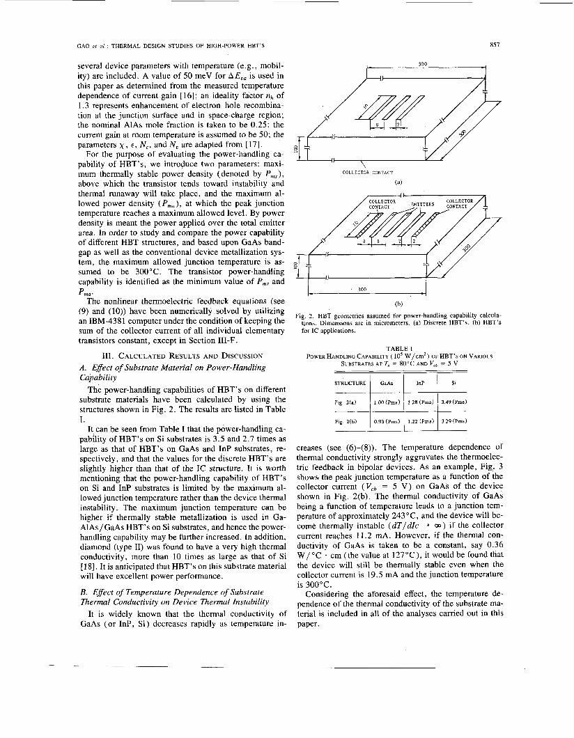
that the vertical (z-direction ) temperature profile exhibits an exponential decrease from the chip’s top surface to the bottom, and the rate of decrease depends on the ratio be- tween the dimension of the active region and the chip size.
An attempt was made to study this problem in which both the active region and the chip are assumed to be square in shape. The effect of the ratio between the two lengths of side on peak junction temperature at an iden- tical power density is shown in Fig. 5. If this ratio is equal to 0.8, which is representative of conventional Si power transistors, then the peak junction temperature decreases almost linearly with decreasing chip thickness, carre- sponding in accord with the result of one-dimensional thermal analysis. However, if the ratio is less than 0.5 (note that it is only 0.1-0.3 for the widely reported HBT’s with cutoff frequencies of up to several gigahertz), thin- ning of the substrate is found to have little influence on peak junction temperature according to the three-dimen- sional thermal analysis. In the case that the dimension of the active region is much less than the chip size, the heat flow is spread in a cone shape, the junction temperature is mainly determined by the lateral size of the device rather than the chip thickness, and the thermal behavior of HBT’s will not be remarkably improved while seriously influencing the manufacturing yield. It should, however, be pointed out that this effect is somewhat exaggerated here because the present model ignores the Joule heating within the substrate. In addition, it is also found from Fig. 5 that the peak junction temperature as a function of chip thickness does not depend on the type of substrate used, and again, that the power density of HBT’s on Si is three times greater than that of HBT’s on GaAs if these two type of transistors are so biased as to have about the same junction temperatures.
In optimizing the chip thickness, a trade-off must be considered to ensure both high device reliability and high manufacturing yield for a given device layout and power dissipation.
GAO et al. : THERMAL DESIGN STUDIES OF HIGH-POWER HBT’S
200 I
POWER DENSITY - 5000 W/cm2
859
180 V v
W e: 160 2
s W n8
w
z e 140
2 s ; 120 z
Y d
n8
100
200
180 h
U v
W
160 d
W a
140
z 0 Y
w CJ
7 Y d a
f 120
100
80
-
-
-
-
-
POWER DENSITY - 1500 W/cm2
0.1
I I I I
0.1
50 7 5 100 125 150
CHIP THICKNESS (urn)
(a)
CHIP THICKNESS (urn)
(b) Fig. 5 . Effect of substrate thickness on thermal behavior for HBT’s. Both
the active region and substrate are assumed to be in a square shape (chip area is 300 x 300 pm*). L,/L, is the ratio of side lengths between the active region and the substrate. (a) HBT’s on GaAs substrates. (b) HBT’s on Si substrates.
E. Nonuniform Distribution of Junction Temperature and Current in HBT’s with Multiple Emitter Fingers
300
Fig. 6. Ten-emitter-finger HBT geometry assumed in calculations of junc- tion temperature and current density distribution. Measuring dimensions are in micrometers.
interdigitated power chip of discrete HBT’s (see Fig. 6 ) is employed for this analysis.
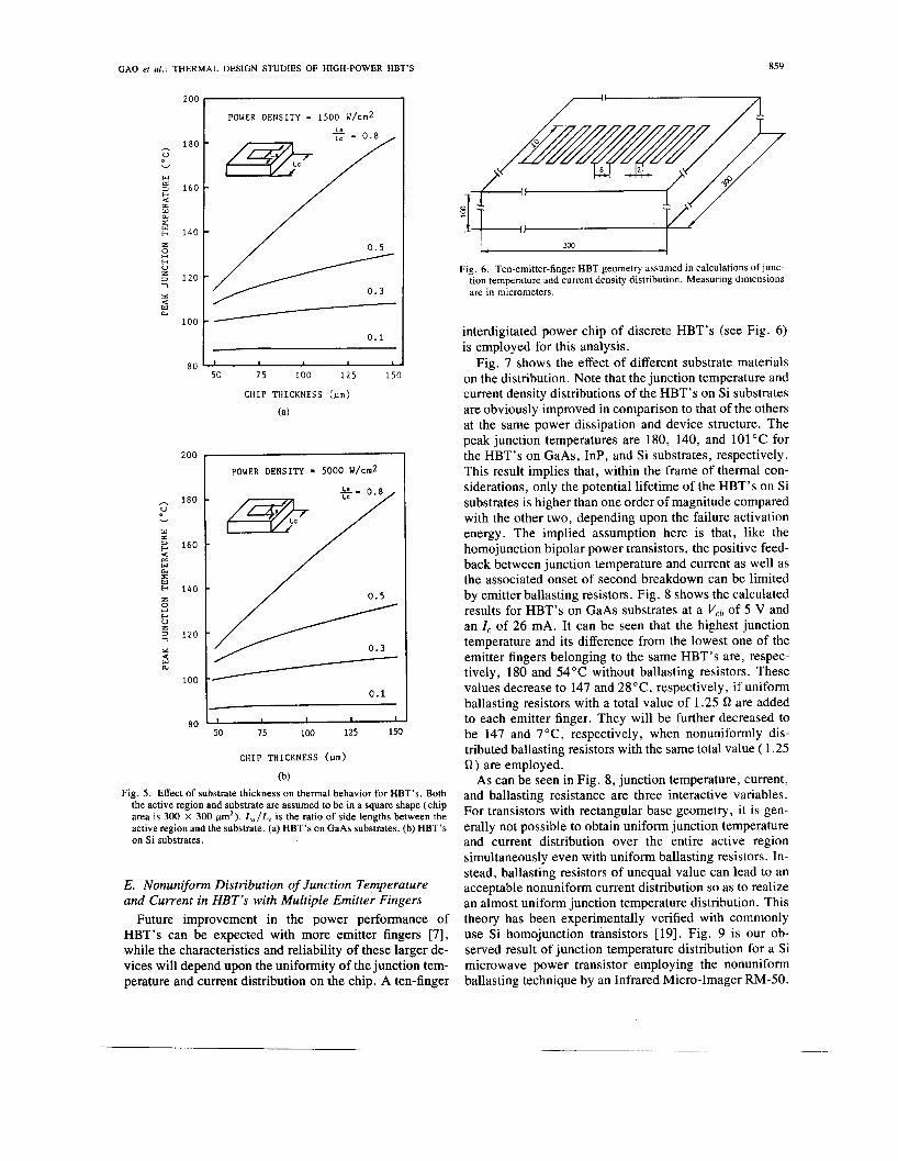
Fig. 7 shows the effect of different substrate materials on the distribution. Note that the junction temperature and current density distributions of the HBT’s on Si substrates are obviously improved in comparison to that of the others at the same power dissipation and device structure. The peak junction temperatures are 180, 140, and 101°C for the HBT’s on GaAs, InP, and Si substrates, respectively. This result implies that, within the frame of thermal con- siderations, only the potential lifetime of the HBT’s on Si substrates is higher than one order of magnitude compared with the other two, depending upon the failure activation energy. The implied assumption here is that, like the homojunction bipolar power transistors, the positive feed- back between junction temperature and current as well as the associated onset of second breakdown can be limited by emitter ballasting resistors. Fig. 8 shows the calculated results for HBT’s on GaAs substrates at a V,, of 5 V and an I , of 26 mA. It can be seen that the highest junction temperature and its difference from the lowest one of the emitter fingers belonging to the same HBT’s are, respec- tively, 180 and 54°C without ballasting resistors. These values decrease to 147 and 28”C, respectively, if uniform ballasting resistors with a total value of 1.25 !J are added to each emitter finger. They will be further decreased to be 147 and 7 ” C, respectively , when nonuniformly dis- tributed ballasting resistors with the same total value ( 1.25 !J) are employed.
As can be seen in Fig. 8, junction temperature, current, and ballasting resistance are three interactive variables. For transistors with rectangular base geometry, it is gen- erally not possible to obtain uniform junction temperature and current distribution over the entire active region simultaneously even with uniform ballasting resistors. In- stead, ballasting resistors of unequal value can lead to an acceptable nonuniform current distribution so as to realize an almost uniform junction temperature distribution. This
Future improvement in the power performance of theory has been experimentally verified with commonly HBT’s can be expected with more emitter fingers [7], use Si homojunction transistors [19]. Fig. 9 is our ob- while the characteristics and reliability of these larger de- served result of junction temperature distribution for a Si vices will depend upon the uniformity of the junction tem- microwave power transistor employing the nonuniform perature and current distribution on the chip. A ten-finger ballasting technique by an Infrared Micro-Imager RM-50.

860
I
1 1 1 1 1 1 . . , (
1 2 3 6 5 6 7 8 9 10
NUMEER OF EMITTER FINGERS
(a)
h
1 2 3 6 S 6 7 8 9 10
NUMBER OF EMITTER FINGER5
(b) Fig. 7. Effect of different substrate materials on junction temperature and
current density distribution. (a) Junction temperature distribution along the central line across the multi-emitter figners ( x = L/2 , z = 0 ) . (b) Current density distribution along the central line across the multi- emitter fingers ( x = L / 2 , z = 0 ) .
F. Effect of Temperature Dependence of Current Gain The temperature dependence of current gain in Ga-
AlAs/GaAs HBT's has been reported [16], [20]. The re- sults showed that the gain decreases with increasing tem- perature in the normal device operating range if the AlAs mole fraction in the emitter and the compositional grading at the emitter-base junction are optimized. This effect is
IEEE TRANSACTIONS ON ELECTRON DEVICES, VOL. 36, NO. 5, MAY 1989
1 2 3 6 5 6 7 8 9 10
NUMBER OF EMITTER FINGERS
(a)
NUMBER OF EMITTER FINGERS
(b) Fig. 8. Effect of emitter ballasting resistors on junction temperature and
current density distribution for HBT's on GaAs substrates. (1) Without ballasting resistors. ( 2 ) With equally valued emitter ballasting resistors (total value is 1.25 Q). (3) With an unequally-valued emitter ballasting resistors (total value is 1.25 Q). (a) Junction temperature distribution along the central line across the multi-emitter fingers. ( x = L / 2 , z = 0). (b) Current density distribution along the central line across the multi- emitter fingers ( x = L / 2 , z = 0 ) .
beneficial to power applications compared with the Si homostructure transistors whose temperature coefficient of current gain is positive.
In order to numerically simulate this effect, we assume that h, = hfeo - exp ( A E / k T ) , where A E represents an
GAO et al.: THERMAL DESIGN STUDIES OF HIGH-POWER HBT’S 86 1
Fig. 9. Photograph of a device taken by an infra-red micro imager, show- ing the uniform junction temperature distribution of Si microwave bi- polar power transistor made by the nonuniform ballasting technique.
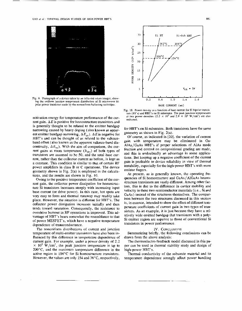
activation energy for temperature performance of the cur- rent gain. A E is positive for homostructure transistors and is generally thought to be related to the emitter bandgap narrowing caused by heavy doping (also known as appar- ent emitter bandgap narrowing, A Eg, ) . A E is negative for HBT’s and can be thought of as related to the valence- band offset (also known as the apparent valence-band dis- continuity, AE,,). With the aim of comparison, the cur- rent gains at room temperature (h fe , ) of both types of transistors are assumed to b e 50, and the total base cur- rent, rather than the collector current as before, is kept as a constant. This condition is similar to that of certain RF power amplifiers in class B or C operations. The device geometry shown in Fig. 2(a) is employed in the calcula- tions, and the results are shown in Fig. 10.
Owing to the positive temperature coefficient of the cur- rent gain, the collector power dissipation for homostruc- ture Si transistors increases steeply with increasing input base current (or drive power). In this case, hot spots are very easy to form and thermal runaway may readily take place. However, the situation is different for HBT’s. The collector power dissipation increases initially and then tends toward saturation. Consequently, the resistance to overdrive burnout in RF operations is improved. This ad- vantage of HBT’s bears somewhat the resemblance to that of power MESFET’s, which have a negative temperature dependence of transconductance.
The nonuniform distributions of current and junction temperature of multi-emitter transistors have also been in- fluenced by this difference in temperature dependence of current gain. For example, under a power density of 2.2 X lo5 W/cm2, the peak junction temperature is up to 200”C, and the maximum temperature difference in the active region is 104°C for Si homostructure transistors. However, the values are only 154 and 36 “C, respectively,
N E
4 25 - .? 0 -
20 - >I
v) z 15 - 0
Dz w
a
5
3 10 -
0.2 0.6 1.0 1.4 1.8
BASE CURRENT (mA)
Fig. 10. Power density as a function of base current for Si bipolar transis- tors (BT’s) and HBT’s on Si substrates. The peak junction temperatures at two power densities (2.2 X lo5 and 2.9 X lo5 W/cm2) are also indicated.
for HBT’s on Si substrates. Both transistors have the same geometry as shown in Fig. 2(a).
Of course, as indicated in [20], the variation of current gain with temperature may be eliminated in Ga- AlAs/GaAs HBT’s if proper selections of AlAs mode fraction and control on compositional grading are made, and this is undoubtedly an advantage in some applica- tions. But keeping up a negative coefficient of the current gain is profitable to device reliability in view of thermal instability, especially for the high-power HBT’s with more emitter fingers.
At present, as is generally known, the operating fre- quencies of Si homostructure and GaAs /AlGaAs hetero- structure transistors are vastly different. Among other fac- tors, this is due to the difference in carrier mobility and velocity in these two semiconductor materials (i.e., Si and GaAs) instead of the structures themselves. The compar- ison between the two structures discussed in this section is, in essence, intended to show the effect of different tem- perature coefficients of current gain in two types of tran- sistors. As an example, it is just because they have a rel- atively wide emitted bandgap that transistors with a poly- Si emitter region are superior to those of conventional Si transistors in power performance.
IV. CONCLUSIONS Summarizing briefly, the following conclusions can be
drawn from the above analysis: The thermoelectro-feedback model discussed in this pa-
per can be used in thermal stability study and design of high-power HBT’s.
Thermal conductivity of the substrate material and its temperature dependence strongly affect power handling

862 IEEE TRANSACTIONS ON ELECTRON DEVICES, VOL. 36, NO. 5 , MAY 1989
capability and the thermal instability of device. Ga- AlAs/GaAs HBT’s on Si substrates (or Si as the collec- tor) have the best thermal behavior. Thereby, this com- posite approach can open new avenues for microwave and millimeter-wave power applications. Of course, the tech- nology of GaAs grown on Si substrates needs to be further perfected. The defects in GaAs on Si should be eliminated as fully as possible, and the success or failure of Ga- AlAs /GaAs power HBT’s on Si substrates hinges on this problem.
Since HBT’s have negative temperature coefficient of current gain, selecting a heterostructure with a relatively large valence band discontinuity at the emitter junction is advantageous for device thermal instability.
The use of self-aligned processes in HBT’s may lead to an increase in power density. Attention should be given to this problem while developing and fabricating power HBT’s for integrated circuits.
As the ratio between the dimension of the active region and the chip size for HBT’s becomes smaller, the effect of the substrate thickness on device thermal resistance is less notable due to the three-dimensional heat flow.
Nonuniform distribution of junction temperature and current in power HBT’s with multiple emitter fingers over the whole active region can be improved by using Si sub- strates and/or adding ballasting resistors, especially un- equally valued emitter resistors. Highly thermostable HBT’s with homogeneous junction temperature are ex- pected to be fabricated by this technique.
The present model provides a tool that should permit a more optimum thermal design not only for HBT’s, but also for any other power devices, with properly modifying the current-voltage equation.
APPENDIX We provide here a brief description of the derivation of
(9). By the customary variable-separation method, the so- lution to the Laplace’s equation (see (1)) can be written in a product form. The appropriate coefficients are se- lected by using the given boundary conditions and by ex- pressing the heat-source distribution function over ther- mal conductivity (see (4)) as a double Fourier series. We then divide the kth heat-source cell ( k = 1, 2, * - - , K ) on the chip’s top surface into Mk x Nk meshes. If Mk and Nk are sufficiently large, the power density and thermal conductivity at (xk, Yk, can be replaced by the values converged to that meshpoint, Pk, and Kk, respectively. Thus, the integration equations determining the coeffi- cients of double Fourier expansion can be approximated to the corresponding summation equations. Then, after some simplifying operation, (9) can be found.
REFERENCES [I] H. Kroemer, Proc. IEEE, vol. 70, p. 13, 1982. [2] M. F. Chang, P. M. Asbeck, D. L. Miller, and K. C. Wang, IEEE
Electron Device Lett., vol. EDL-7, p. 8 , 1986. 131 0. Nakajima, K. Nagat, Y. Yamauchi, H. Ito, and T. Ishibashi, in
IEDM Tech. Dig . , 1986, p. 266.
P. M. Asbeck et a l . , IEEE Trans. Electron Devices, vol. ED-34, p. 2571, 1987. P. M. Asbeck et a l . , in IEEE Mon. Circ. Symp. Tech. Dig. , 1987, p. 1. B. Bayraktaroglu, N. Camilier, H. D. Shih, and H. Q. Tsemg, IEEE M77’-S Tech. Dig. , 1987, p. 969. N. H. Sheng et a l . , in IEDM Tech. Dig . , 1987, p. 619. R. Fischer, J. Klem, C. K. Peng, J. S. Gedymin, and H. Morkoc, IEEE Electron Device Lett., vol. EDL-7, p. 112, 1986. J . Chen, M. S. Unlu, T. Won, G. Munns, and H. Morkoc, in IEDM Tech. Dig. , 1987, p. 82. J . Dell, T. S . Kalkur, 2. Meglickl, A. G. Nassibian, and H. L. Hart- nagel, lnt. J . Electron., vol. 57, p. 155, 1984. A. G. Kokkas, RCA Rev., vol. 35, p. 579, 1974. I . Kudman and E. F. Steigmeier, Phys. Rev., vol. 133, p. A1665, 1964. W . Fallmann, H. L. Hartnagel, and P. C . Mathur, Electron. Letr., vol. 7, p. 512, 1971. A. Amith, I. Kudman, and E. F. Steigmeier, Phys. Rev., vol. 138, p. A1270, 1965. D. Ankri and L. F. Eastman, Electron. Lett., vol. 18, p. 750, 1982. H. Beneking and L. M. Su, Electron. Lett., vol. 17, p. 301, 1981. K. Tomizawa, Y. Awano, and N. Hashizume, IEEE Electron Device Lert., vol. EDL-5, p. 362, 1984. S. M. Sze, Physics ofSemiconductor Devices, 2nd ed. New York: Wiley, 1981, p. 43. G. B. Gao, Acta Electron., vol. 6 , p. 52, 1978. N. Chand et al., Appl. Phys. Lett., vol. 45, p. 1086, 1984.
* Guang-bo Gao (SM’86) was born in Shenyang, China, on January 5, 1941. He graduated from the Department of Radio and Electronics Science, Tsinghua University, Beijing, in 1965, specializ- ing in semiconductor devices and physics.
He joined Beijing Polytechnic University the same year. He is currently a Professor in the De- partment of Radio and Electronics and the Direc- tor of the Reliability Physics Laboratory at Bei- jing Polytechnic University. Since 1970, he has been working on reliabilitv Dhvsics. microwave
I . - . power transistors, thermal and electrical models of semiconductor devices, thermal failure and thermal design study of power devices, ohmic contact and metallization electromigration, and heterojunction transistors. He has authored or coauthored about 40 research articles and a research book en- titled Reliability Physics of Semiconductor Devices. Since July of 1988, he has worked with Professor H. Morkog as a Visiting Scientist at the Coor- dinated Science Laboratory, University of Illinois at Urbana-Champaign.
Mr. Gao was twice awarded the National Invention Prize of the P.R.C. in 1983 and 1984 and nine times the Science and Technology Prize of Bei- jing and the Ministry of Electronic Industry from 1979 to 1987, for con- tributions to power semiconductor devices and reliability physics. He re- ceived four best paper awards from the Beijing Science and Technology Committee and the R & QC Society of the Chinese Institute of Electronics in 1980, 1986-1988. He was awarded the title of Distinguished National Scientist of P.R.C. in 1986. He is the deputy director of the Reliability Physics Group of the R & QC Society of the Chinese Institute of Electron- ics, a council member of the Reliability Research Society of the Chinese Electrotechnical Institute, and a Fellow of the Beijing Scientist and Engi- neer Association. He is listed in Who’s Who of Chinese Contemporary In- ventors and Who’s Who of Chinese Scientists from the Ancient to the Con- temporary.
*
Ming-zhu Wang was born in Nei Monggol, China, on June 28, 1963. She received the B.S. degree from Tianjing University and the M.S. de- gree from Beijing Polytechnic University in 1984 and 1987, respectively, both in electronics engi- neering.
Since graduation, she has been doing research work and teaching at the Reliability Physics Lab- oratory of Beijing Polytechnic University.
-- I
GAO et al. : THERMAL DESIGN STUDIES OF HIGH-POWER HBT’S
Xiang Gui was born in Beijing, China, on May 30, 1957. He received the B.S.E.E. and M.S.E.E. degrees from Beijing Polytechnic University, China, in 1982 and 1988, respectively.
In 1982, he joined the faculty of the Electron- ics Engineering Department at Beijing Polytech- nic University, where he completed his post-grad- uate study on a part-time basis, and is currently a Lecturer. His research interests are in reliability physics, failure mechanism modeling, and ther- mal phenomena in operation of semiconductor de-
vices. He has published several papers in international conference pro- ceedings as well as scientific journals.
863
Hadis Morkog (S’72-M’76-SM’79-F’87) re- ceived the B.S.E.E. and M.S.E.E. degrees in 1968 and 1969 from Istanbul Technical Univer- sity, Turkey, and the Ph.D. degree in 1976 from Cornell University.
He was employed at Varian Associates (1976- 1978), and has held visiting positions at AT&T Bell Labs (1978-1979), and California Institute of Technology and Jet Propulsion Laboratory (1987- 1988). Since 1978, he has been with the Univer- sity of Illinois pursuing research in heterostruc-
ture devices and materials. Dr. Morkoq is a Fellow of the American Association for the Advance-
ment of Science and a Fellow of the American Physical Society. In 1978 he received the Electronics Letters Best Paper Award.