Advances in Magnetics Modern Microwave Ferrites
30
IEEE TRANSACTIONS ON MAGNETICS, VOL. 48, NO. 3, MARCH 2012 1075 Advances in Magnetics Modern Microwave Ferrites Vincent G. Harris, Fellow, IEEE Center for Microwave Magnetic Materials and Integrated Circuits and Department of Electrical and Computer Engineering, Northeastern University, Boston, MA 02115-5000 USA Microwave ferrites are ubiquitous in systems that send, receive, and manipulate electromagnetic signals across very high frequency to quasi-optical frequency bands. In this paper, modern microwave ferrites are reviewed including spinel, garnet, and hexaferrite systems as thin and thick films, powders and compacts, and metamaterials. Their fundamental properties and utility are examined in the context of high frequency applications ranging from the VHF to millimeter-wave bands. Perspective and outlook of advances in theory, processing, and devices occurring in the science and engineering communities since the year 2000 are presented and discussed. Index Terms—Circulator, density functional theory, ferrite, garnet, hexaferrite, liquid phase epitaxy, microstrip filter, microstrip phase shifter, molecular field theory, negative index metamaterials, pulsed laser deposition, screen printing, spinel, spin spray plating. I. INTRODUCTION AND HISTORICAL DEVELOPMENT M ICROWAVE magnetic materials operate either near the natural resonance, as absorbers or electromagnetic in- terference shielding materials, or above or below resonances as low-loss, high permeable materials in devices such as circula- tors, isolators, phase shifters, filters, inductor cores, etc. The focus of this review is principally in the area of off res- onance materials and their applications. As the operational fre- quency of these materials increases, the requirement for low- loss properties also increases, thus necessitating insulating mag- netic materials. Ideal materials possess high magnetization, high perme- ability, high permitivity, high electrical resistivity, and low electronic and magnetic losses. Insulating magnetic materials that fit this criteria include ferrites and related magnetic oxides. Ferrite materials have been known to ancient cultures for many centuries. The first known reference to ferrite materials dates to an ancient text by Guan Zhong (725-654 BCE) who de- scribed lodestone, naturally occurring minerals rich in Fe O , as “ci shi” or “loving stone” [1]. A similar reference to lode- stone was made by the Greek philosopher Thales of Miletus [2] in the 6th century BCE [3]. Fragments of lodestone suspended in a fluid, typically water, naturally orient towards a magnetic pole thus enabling the development of the first magnetic compasses [4]. The first suspended magnetic needle compass was described by Shen Kuo in CE 1088 [5]. Although lodestone found great utility in compasses for both terrestrial and nautical navigation, it was not until c. 1936 that modern ferrites were studied for their magnetic, structure, and electronic properties for use as high in- duction cores in power generation, conditioning, and conversion applications. Manuscript received September 18, 2011; accepted November 02, 2011. Date of publication December 21, 2011; date of current version March 02, 2012. Cor- responding author: V. G. Harris (e-mail: [email protected]). Color versions of one or more of the figures in this paper are available online at http://ieeexplore.ieee.org. Digital Object Identifier 10.1109/TMAG.2011.2180732 The value of ferrites as materials for ultrahigh frequency ap- plications was not realized until c. 1940 when ferrites were sys- tematically studied by Snoek et al. [6], [7] for applications in devices that send, receive, and manipulate electromagnetic sig- nals at radio-frequency (rf), microwave, and millimeter-wave frequencies. Ferrite materials are unique because they are one of a few classes of insulating magnetic oxides that possess moderate values of magnetization, high permeability, moderate to high permittivity, and low-losses at frequencies from dc to sub-mil- limeter wavelengths. These properties afford them great value in high frequency devices that require strong coupling to electromagnetic signals while experiencing low losses. Ad- ditionally, due to their intrinsic magnetism, these materials also provide non-reciprocal behavior that is essential for many device applications in radar and communications systems as isolators, circulators, etc. These properties and applications will be discussed in detail later in this review. Popular engineering ferrites principally exist as cubic and hexagonal structures having close-packed oxygen lattices. Cubic ferrites include garnets and spinels, whereas the hexafer- rites can exist in several structural variants, e.g., , in which the metal and oxygen stoichiometry vary [34], [39]. Due to their highly symmetric structures and low intrinsic magnetocrystalline anisotropy energy, cubic ferrites tend to have low magnetic anisotropy fields, while hexaferrites may possess extremely high magnetic anisotropy fields. As will be discussed in greater detail, the ferromagnetic resonance (FMR) frequency shifts with changes in magnetic anisotropy field(s), together with demagnetizing field, magnetization and applied magnetic fields (also known as bias fields), leading to the application of cubic spinels at UHF, rf and microwave frequencies and hexaferrites at microwave, mm-wave, sub-mm wave, and quasi-optical frequencies. In this review, we present recent advances in ferrite materials of various forms. For example, we will discuss the latest trends in processing, composition, theory, and the utility of ferrite films, crystals, compacts, metamaterials, and other unique het- 0018-9464/$26.00 © 2011 IEEE
-
Upload
independent -
Category
Documents
-
view
0 -
download
0
Transcript of Advances in Magnetics Modern Microwave Ferrites

IEEE TRANSACTIONS ON MAGNETICS, VOL. 48, NO. 3, MARCH 2012 1075
Advances in Magnetics
Modern Microwave FerritesVincent G. Harris, Fellow, IEEE
Center for Microwave Magnetic Materials and Integrated Circuits and Department of Electrical and Computer Engineering,Northeastern University, Boston, MA 02115-5000 USA
Microwave ferrites are ubiquitous in systems that send, receive, and manipulate electromagnetic signals across very high frequency toquasi-optical frequency bands. In this paper, modern microwave ferrites are reviewed including spinel, garnet, and hexaferrite systems asthin and thick films, powders and compacts, and metamaterials. Their fundamental properties and utility are examined in the context ofhigh frequency applications ranging from the VHF to millimeter-wave bands. Perspective and outlook of advances in theory, processing,and devices occurring in the science and engineering communities since the year 2000 are presented and discussed.
Index Terms—Circulator, density functional theory, ferrite, garnet, hexaferrite, liquid phase epitaxy, microstrip filter, microstrip phaseshifter, molecular field theory, negative index metamaterials, pulsed laser deposition, screen printing, spinel, spin spray plating.
I. INTRODUCTION AND HISTORICAL DEVELOPMENT
M ICROWAVE magnetic materials operate either near thenatural resonance, as absorbers or electromagnetic in-
terference shielding materials, or above or below resonances aslow-loss, high permeable materials in devices such as circula-tors, isolators, phase shifters, filters, inductor cores, etc.
The focus of this review is principally in the area of off res-onance materials and their applications. As the operational fre-quency of these materials increases, the requirement for low-loss properties also increases, thus necessitating insulating mag-netic materials.
Ideal materials possess high magnetization, high perme-ability, high permitivity, high electrical resistivity, and lowelectronic and magnetic losses. Insulating magnetic materialsthat fit this criteria include ferrites and related magnetic oxides.
Ferrite materials have been known to ancient cultures formany centuries. The first known reference to ferrite materialsdates to an ancient text by Guan Zhong (725-654 BCE) who de-scribed lodestone, naturally occurring minerals rich in Fe O ,as “ci shi” or “loving stone” [1]. A similar reference to lode-stone was made by the Greek philosopher Thales of Miletus [2]in the 6th century BCE [3]. Fragments of lodestone suspended ina fluid, typically water, naturally orient towards a magnetic polethus enabling the development of the first magnetic compasses[4]. The first suspended magnetic needle compass was describedby Shen Kuo in CE 1088 [5]. Although lodestone found greatutility in compasses for both terrestrial and nautical navigation,it was not until c. 1936 that modern ferrites were studied for theirmagnetic, structure, and electronic properties for use as high in-duction cores in power generation, conditioning, and conversionapplications.
Manuscript received September 18, 2011; accepted November 02, 2011. Dateof publication December 21, 2011; date of current version March 02, 2012. Cor-responding author: V. G. Harris (e-mail: [email protected]).
Color versions of one or more of the figures in this paper are available onlineat http://ieeexplore.ieee.org.
Digital Object Identifier 10.1109/TMAG.2011.2180732
The value of ferrites as materials for ultrahigh frequency ap-plications was not realized until c. 1940 when ferrites were sys-tematically studied by Snoek et al. [6], [7] for applications indevices that send, receive, and manipulate electromagnetic sig-nals at radio-frequency (rf), microwave, and millimeter-wavefrequencies.
Ferrite materials are unique because they are one of a fewclasses of insulating magnetic oxides that possess moderatevalues of magnetization, high permeability, moderate to highpermittivity, and low-losses at frequencies from dc to sub-mil-limeter wavelengths. These properties afford them great valuein high frequency devices that require strong coupling toelectromagnetic signals while experiencing low losses. Ad-ditionally, due to their intrinsic magnetism, these materialsalso provide non-reciprocal behavior that is essential for manydevice applications in radar and communications systems asisolators, circulators, etc. These properties and applicationswill be discussed in detail later in this review.
Popular engineering ferrites principally exist as cubic andhexagonal structures having close-packed oxygen lattices.Cubic ferrites include garnets and spinels, whereas the hexafer-rites can exist in several structural variants, e.g., ,in which the metal and oxygen stoichiometry vary [34], [39].Due to their highly symmetric structures and low intrinsicmagnetocrystalline anisotropy energy, cubic ferrites tend tohave low magnetic anisotropy fields, while hexaferrites maypossess extremely high magnetic anisotropy fields. As willbe discussed in greater detail, the ferromagnetic resonance(FMR) frequency shifts with changes in magnetic anisotropyfield(s), together with demagnetizing field, magnetization andapplied magnetic fields (also known as bias fields), leadingto the application of cubic spinels at UHF, rf and microwavefrequencies and hexaferrites at microwave, mm-wave, sub-mmwave, and quasi-optical frequencies.
In this review, we present recent advances in ferrite materialsof various forms. For example, we will discuss the latest trendsin processing, composition, theory, and the utility of ferritefilms, crystals, compacts, metamaterials, and other unique het-
0018-9464/$26.00 © 2011 IEEE
1076 IEEE TRANSACTIONS ON MAGNETICS, VOL. 48, NO. 3, MARCH 2012
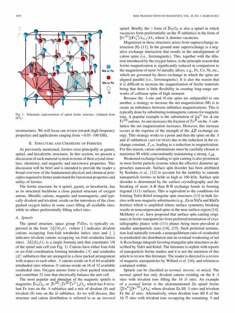
Fig. 1. Schematic representation of spinel ferrite structure. (Adapted from[87].)
erostructures. We will focus our review towards high frequencyproperties and applications ranging from 0.01–100 GHz.
II. STRUCTURE AND CHEMISTRY OF FERRITES
As previously mentioned, ferrites exist principally as garnet,spinel, and hexaferrite structures. In this section, we present adiscussion of each material system in terms of their crystal struc-ture, chemistry, and magnetic and microwave properties. Thisdiscussion will be brief and is intended to provide the reader abroad overview of the fundamental physical and chemical prin-ciples required to better understand the functional properties andutility of ferrites.
The ferrite structure, be it spinel, garnet, or hexaferrite, hasas its structural backbone a close packed structure of oxygenanions. Metallic cations, magnetic and nonmagnetic, and typi-cally divalent and trivalent, reside on the interstices of the closepacked oxygen lattice in some cases filling all available sites,while in others preferentially filling select sites.
A. Spinels
The spinel structure, space group , is typically ex-pressed in the form (where indicates divalentcations occupying four-fold tetrahedra lattice sites andindicates trivalent cations occupying six-fold octahedra latticesites). is a single formula unit that constitutes 1/8of the spinel unit cell (see Fig. 1). Cations have either four-foldor six-fold coordination forming tetrahedra and octahedra
sublattices that are arranged in a close packed arrangementwith respect to each other. cations reside on 8 of 64 availabletetrahedral sites whereas cations reside on 16 of 32 availableoctahedral sites. Oxygen anions form a close packed structureand contribute 32 ions that electrically balance the unit cell.
The most popular and abundant of the magnetic spinels ismagnetite, , or , which has 8 triva-lent Fe ions on the sublattice and a mix of divalent (8) andtrivalent (8) ions on the sublattice. As we will discuss, thisstructure and cation distribution is referred to as an inverted
spinel. Briefly, the form of is also a spinel in whichvacancies form preferentially on the sublattice in the form of
where denotes vacancies.Magnetism in these structures arises from superexchange in-
teraction [8]–[11]. In the ground state superexchange is a neg-ative exchange interaction that results in the antialignment ofcation spins (i.e., ferrimagnetic). This, together with the dilu-tion introduced by the oxygen lattice, is the principle reason thatferrite magnetization is significantly reduced in comparison tothe magnetism of most metallic alloys, e.g., Fe, Co, Ni, etc.,which are governed by direct exchange in which the spins arealigned parallel (i.e., ferromagnetic). It is also the reason thatit is difficult to increase the magnetization of ferrite materialsbeing that there is little flexibility in creating long-range net-works of collinear spins of high moment.
Because the -site and -site spins are antiparallel to oneanother, a strategy to increase the net magnetization (M) is tocreate an imbalance between sublattice magnetizations. This istypically done by substituting nonmagnetic cations for magneticions. A popular example is the substitution of for -site
cations. As one increases the fraction of on the -sub-lattice the net magnetization increases. However, this increaseoccurs at the expense of the strength of the exchange en-ergy. This strategy works to a point and then the spins on theand sublattices cant (or twist) due to the reduction in the ex-change constant, , leading to a reduction in magnetization.For this reason, cation substitutions must be carefully chosen tomaximize M while concomitantly maintaining a strong .
Weakened exchange leading to spin canting is also prominentin most ferrite particle systems when the effective diameter ap-proaches nanoscale. Surface spin disorder has been attributedby Kodama et al., [12] to account for the inability to saturatenanoparticle ferrites in fields as high as 160 kOe. Surface spindisorder is determined by the surface crystallography and thebreaking of more A-B than B-B exchange bonds in formingtrigonal (111) surfaces. This is equivalent to the conditions forforming Yafet-Kittel triangular spin structures [13] in bulk fer-rites with non-magnetic substituents (e.g., Zn in NiZn and MnZnferrites) which is amplified where surface symmetry breakingresults in noncompensated spins in the near surface region [14].McHenry et al., have proposed that surface spin canting origi-nates in ferrite nanoparticles from preferred termination of crys-tallographic planes with (111) planes being more prevalent atsmaller nanoparticle sizes [14], [15]. Such preferred termina-tion lead naturally towards a nonequilibrium ratio of octahedralto tetrahedral site distribution and an eventual weakening of netA-B exchange integrals favoring triangular spin structures as de-scribed by Yafet and Kittel. The literature is replete with reportsof nanoparticle ferrite studies and it is not the intention of thisarticle to review this literature. The reader is directed to a reviewof magnetic nanoparticles by Willard et al. [16], and referencescontained within.
Spinels can be classified as normal, inverse, or mixed. Thenormal spinel has only divalent cations residing on the 8sites with trivalent ions filling the 16 sites. An exampleof a normal ferrite is the aforementioned Zn spinel ferrite
where divalent Zn fill -sites and trivalentFe the sites. Alternatively, when divalent ions fill 8 of the16 sites with trivalent ions occupying the remaining and
HARRIS: MODERN MICROWAVE FERRITES 1077
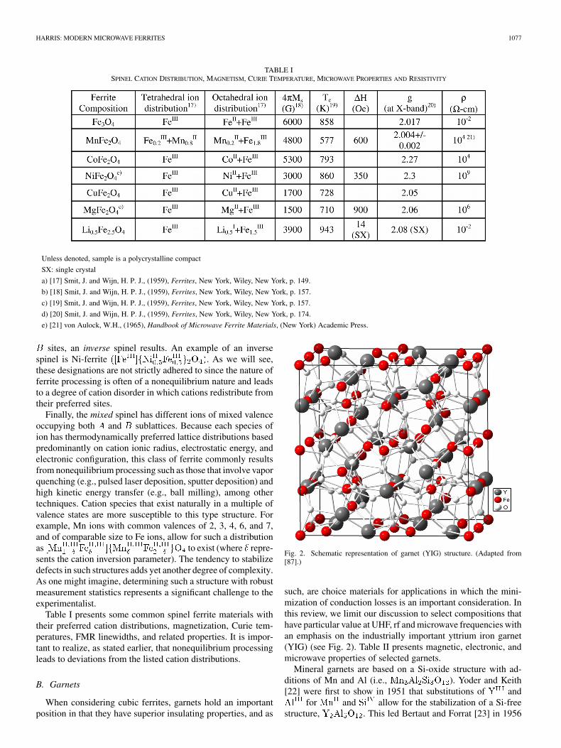
TABLE ISPINEL CATION DISTRIBUTION, MAGNETISM, CURIE TEMPERATURE, MICROWAVE PROPERTIES AND RESISTIVITY
Unless denoted, sample is a polycrystalline compact
SX: single crystal
a) [17] Smit, J. and Wijn, H. P. J., (1959), Ferrites, New York, Wiley, New York, p. 149.
b) [18] Smit, J. and Wijn, H. P. J., (1959), Ferrites, New York, Wiley, New York, p. 157.
c) [19] Smit, J. and Wijn, H. P. J., (1959), Ferrites, New York, Wiley, New York, p. 157.
d) [20] Smit, J. and Wijn, H. P. J., (1959), Ferrites, New York, Wiley, New York, p. 174.
e) [21] von Aulock, W.H., (1965), Handbook of Microwave Ferrite Materials, (New York) Academic Press.
sites, an inverse spinel results. An example of an inversespinel is Ni-ferrite . As we will see,these designations are not strictly adhered to since the nature offerrite processing is often of a nonequilibrium nature and leadsto a degree of cation disorder in which cations redistribute fromtheir preferred sites.
Finally, the mixed spinel has different ions of mixed valenceoccupying both and sublattices. Because each species ofion has thermodynamically preferred lattice distributions basedpredominantly on cation ionic radius, electrostatic energy, andelectronic configuration, this class of ferrite commonly resultsfrom nonequilibrium processing such as those that involve vaporquenching (e.g., pulsed laser deposition, sputter deposition) andhigh kinetic energy transfer (e.g., ball milling), among othertechniques. Cation species that exist naturally in a multiple ofvalence states are more susceptible to this type structure. Forexample, Mn ions with common valences of 2, 3, 4, 6, and 7,and of comparable size to Fe ions, allow for such a distributionas to exist (where repre-sents the cation inversion parameter). The tendency to stabilizedefects in such structures adds yet another degree of complexity.As one might imagine, determining such a structure with robustmeasurement statistics represents a significant challenge to theexperimentalist.
Table I presents some common spinel ferrite materials withtheir preferred cation distributions, magnetization, Curie tem-peratures, FMR linewidths, and related properties. It is impor-tant to realize, as stated earlier, that nonequilibrium processingleads to deviations from the listed cation distributions.
B. Garnets
When considering cubic ferrites, garnets hold an importantposition in that they have superior insulating properties, and as
Fig. 2. Schematic representation of garnet (YIG) structure. (Adapted from[87].)
such, are choice materials for applications in which the mini-mization of conduction losses is an important consideration. Inthis review, we limit our discussion to select compositions thathave particular value at UHF, rf and microwave frequencies withan emphasis on the industrially important yttrium iron garnet(YIG) (see Fig. 2). Table II presents magnetic, electronic, andmicrowave properties of selected garnets.
Mineral garnets are based on a Si-oxide structure with ad-ditions of Mn and Al (i.e., ). Yoder and Keith[22] were first to show in 1951 that substitutions of and
for and allow for the stabilization of a Si-freestructure, . This led Bertaut and Forrat [23] in 1956

1078 IEEE TRANSACTIONS ON MAGNETICS, VOL. 48, NO. 3, MARCH 2012
TABLE IIPROPERTIES OF MAGNETIC GARNETS (MICROWAVE PROPERTIES WERE MEASURED AT X-BAND)
Unless denoted, sample is a polycrystalline compact
SX: single crystal
[26] G.R. Harrison, L.R. Hodges, Jr., J. Am. Ceram. Soc., vol. 44, p. 214, 1961.
[27] A. Vassiliev, J. Nicolas, and M. Hildebrant, C.R. Acad. Sci., vol. 252, p. 2529, 1961.
[28] G. Goldring, M. Schieber, and Z. Vager, J. Appl. Phys., vol. 31, p. 2057, 1960.
[29] W.H. von Aulock, Handbook of Microwave Ferrite Materials, New York, Academic Press, 1965.
to report the structure and magnetic properties of ,YIG; space group . Fig. 2 is a representation of the YIGunit cell. YIG has a high Verdet constant which provides a largemagneto-optical response, high Q factor at microwave frequen-cies, low absorption in the infrared (up to 600 nm), and smallFMR linewidth [24]. YIG is used in rf, microwave, optical, andmagneto-optical applications, for example as microwave filters.It also finds utility in solid-state lasers, Faraday rotators, and innonlinear optical applications.
In the YIG structure, trivalent Fe ions occupy two octahedraland three tetrahedral sites. The yttrium ions are too large to oc-cupy the tetrahedral and/or octahedral sites and too small to sub-stitute for the oxygen anion. They instead occupy sites that areirregularly surrounded by 8 oxygen ions in a distorted cube. Inthe garnet unit cell all possible cation positions are filled leadingto uncommon chemical and structural stability as well as highinsulating properties.
The Fe ions on the and sites are coupled ferrimag-netically by superexchange as in the spinel systems. The netmoment derives from the excess on tetrahedral sites.The Curie temperature also derives from superexchange andis nearly the same for all garnets 560 K [25]. However, thesaturation magnetization and the magnetic anisotropy field arerather low, and , respectively,compared with other ferrite systems resulting in a low FMR fre-quency. For these reasons, YIG is usually biased by permanentmagnets for microwave devices applications. Notwithstandingthe need for bias magnets, YIG is a choice material for manyapplications at frequencies up to and including X-band, abovewhich the bias magnet size, weight and cost become prohibitive.
At higher frequencies, ferrites with substantially higher mag-netization and magnetic anisotropy are required. For this we turnto hexaferrites.
C. Hexaferrites
In contrast to the spinel and garnet ferrites, the hexaferriteshave hexagonal crystal symmetry leading to high magnetocrys-
Fig. 3. Schematic representation of magnetoplumbite structure �����.(Adapted from [87].)
talline anisotropy energies and magnetic anisotropy fieldsand subsequently high FMR frequencies. Among the most pop-ular of the microwave hexaferrites are those derived from the Ba
-type (or ) hexaferrite, (see Fig. 3).has the magnetoplumbite structure, space group , andconsists of 10 oxygen layers in which four successive layerseach containing four oxygen anions are followed by a fifth layercontaining three anions and a Ba cation. The structure is con-structed of spinel blocks containing two oxygen layers sep-arated by an block containing the Ba ion. Every other and
block is rotated 180 with respect to the other and is denoted

HARRIS: MODERN MICROWAVE FERRITES 1079
TABLE IIIHEXAFERRITE STRUCTURE, MAGNETISM, CURIE TEMPERATURE, AND ANISOTROPY FIELDS [39]
Unless denoted, sample is a polycrystalline compact
[39] Smit, J. and Wijn, H. P. J., (1959), Ferrites, New York, Wiley, New York, 191, p. 204.
[40] Smit, J. and Wijn, H. P. J., (1959), Ferrites, New York, Wiley, New York, 191, p. 210.
as and , respectively. Trivalent Fe ions occupy tetrahedraland octahedral sites (derived from the spinel blocks) as well asone trigonal bypyramidal (TBP) site. The TBP site resides on theBa-containing layer amidst the triagonal arrangement of oxygenanions [30].
There exist other hexaferrite structures designated as: , ,, , and , each having different structures and oxygen stoi-
chiometry and markedly difference magnetic properties. For ex-ample, the -type structure, , consists of thestacking of and blocks were the blocks can be thoughtof as blocks in which the inner most atomic layer is repeated.Having defined the , , and blocks, one can describe the
-type, , as a stacking of , andthe -type, , as . The reader isdirected to the literature to explore further types of hexaferritestructures [30]. The magnetization of the hexaferrites derivesfrom superexchange interactions among the cation sublattices.The spin coupling and orientation of ferric ions in the blockmirrors those of the spinel ferrites and include two and four
site ions. The ferric ion spin located in the block TBP siteis parallel the c-axis with its spin up orientation determined bythe strength of the oxygen mediated superexchange and numberand distance of near neighbor ferric ions.
Table III presents the stoichiometry of these compoundstogether with their room temperature saturation magnetizationand anisotropy fields that demonstrate clearly the ability totailor anisotropy and magnetization by cation substitution.Taken together, these parameters also determine the FMRfrequency and hence operational bands.
We will next discuss the properties of -type ferrites withthe implication that materials processing and device refinementare transferable to other ferrite systems such as Y, W, U, and Ztype ferrites.
The system is remarkably versatile in that substitutionfor the Fe cation can drastically reduce or increase , thusshifting the FMR frequency and the operating frequency of de-vices. For example, the substitution of Sc or In for Fe reduces
allowing for applications from X-, Ku-, K-, to Ka-bands
[31]–[33]. While substitution of Al and Ga lead to increasesin and device operation at frequencies up to and includingU-, E-, and W-bands [34]–[36]. In essence, the hexafer-rite, and its substitutional systems, allow for device applicationsfrom 1 to 100 GHz.
The utility of -type ferrites stems in part from the align-ment of the easy magnetic direction along the crystallographicc-axis and the ability to process these materials with a high de-gree of crystal texture and preferential magnetic anisotropy. Forexample, the growth of films with the crystallographicc-axis aligned perpendicular to the film plane leads to perpen-dicular magnetic anisotropy: a requirement for conventional cir-culator and isolator devices and perpendicular magnetic storagemedia.
Unlike the -type ferrites, - and -type ferrites have theirmagnetic easy axis aligned within the a-b or basal plane. Wherethe -type hexaferrites can be saturated relatively easily byfields applied along the c-axis, the - and -type ferrites canbe saturated by a small field aligned within the basal plane. Thisis of particular value for conventional phase shifter, delay lines,filter devices, and some antenna substrate applications.
In the hexaferrites, and blocks break crystal symmetryresulting in the hexagonal structure and large magnetocrys-talline anisotropy energies common to these compounds. Alsocontributing to the magnetic anisotropy are dipolar interactionsand single ion anisotropy. Remarkably, the magnetic anisotropyfield in hexaferrites can reach several 10,000s Oe. Take forexample , where is 17,000 Oe, or 1000–10,000times greater than some cubic ferrites [30], [37]. The placesthe zero field FMR frequency near 36 GHz. Thus, while anexternally applied magnetic field is still necessary to saturatethe ferrite during device operation, the magnitude of the appliedfield required to shift FMR to high frequencies is substantiallyreduced. As such, devices based upon this ferrite can operate atfrequencies as high as Ku-band for below resonance operationsand beyond Q-band for above resonance operations.
Textured polycrystalline hexaferrites can be produced withpermanent magnet properties, such that they remain in a mag-

1080 IEEE TRANSACTIONS ON MAGNETICS, VOL. 48, NO. 3, MARCH 2012
netized state in the absence of an externally applied magneticfield. In this condition, referred to as self-biased, the high in-ternal bias field required for device operation at high frequen-cies is achieved without external magnets. Bias magnets hinderefforts to reduce the size and weight of devices, assemblies,and systems, such as transmit and receive modules in radar andcommunication systems. Further discussion of self-biased fer-rite follows in Sections V-D and V-E.
In contrast to the hexaferrites mentioned so far, whichare popular for high frequency low-loss applications, stron-tium-based hexaferrites are a permanent magnet that ischaracterized as having a saturation induction of 4650 G, highcoercivity, 4000 Oe, and high remanence magnetization[37]. Strontium ferrite is a popular ceramic permanent magnetthat has found great utility in many cost-effective commercialapplications.
III. FERRITE MAGNETISM
A. Molecular Field Theory
An early theory of ferromagnetism was developed based onseminal studies performed by Weiss [41]. Weiss built on thethen recent theory of Langevin who introduced the theory ofparamagnetism [42]. Weiss’ theory proposed the existence oflong-range magnetic order in which a molecular field defines theinteraction between spins. This theory successfully addressedmany of the experimental observations of ferromagnetic be-havior in metals at the time, including the temperature depen-dent behavior of magnetization and the existence of magneticdomains. However, it failed when applied to ferrites and othermagnetic oxides that we now know are ferrimagnetic or antifer-romagnetic. Néel put forward a molecular field theory as an ex-pansion of the Curie-Weiss theory [11]. His theory introducedmultiple molecular fields to describe coupled aligned and an-tialigned spin lattices to explain complex thermomagnetic be-havior in ferrite and other magnetic oxide systems. Néel intro-duced to the magnetics community the concept of ferrimagneticand antiferromagnetic interactions.
In considering the magnetic oxide systems discussed here,the exchange energy, , between spins of neighboring metallicions is negative resulting in the antiparallel alignment of spinsas the lowest energy configuration. Since the distance betweenmetal ions is too great to support direct exchange, such as thatexperienced in most magnetic metals, the exchange is mediatedby the oxygen anion that resides between the two cations and isthus considered an indirect exchange, i.e., superexchange. Threefactors principally affect the strength of the exchange, these in-clude, the distance, direction, and angle of the cations with re-spect to the anion. While the direction and angle are definedby the relationship between Me-O-Me, the critical distance isthat between Me-O not Me-Me, the later having little impact on
. All three factors determine the degree of orbital overlap be-tween the extending 2p orbitals of oxygen and the 3d orbitalsof the cations and hence the magnitude of . By examining p-and d-orbital alignments one can readily conclude that largerMe-O-Me angles produce stronger negative exchange, while an-gles that approach 90 produce weak exchange. This is seen in
the ferrite systems where, for example, in spinel ferrites the ex-change corresponds to the largest A-O-B angle, ,which is far larger than that of the B-O-B, , . TheA-O-A correlation forms an angle less than 80 and the dis-tance between A-O is comparatively larger, , leading tothe smallest exchange, . is so comparatively small thatmany report this to be zero or ignore it altogether [17]. Mag-netization results from an imbalance of spins on the ferrimag-netically coupled sublattices. As mentioned previously, one ap-proach to increasing the net magnetization is to populate onesublattice preferential to the other with nonmagnetic cationswhile concomitantly maintaining a strong exchange energy, ,to minimize spin canting. Alternatively, one may populate onesublattice relative to the other with high spin moments. For athorough treatment of molecular fields in ferrites, the reader isdirected to a recent text by Dionne [43].
Although molecular field theory explain many aspects of fer-rite behavior, they do not allow for determination of key intrinsicproperties such as the exchange integral, energy gap, and mag-netic ordering temperatures via a first principles self-consistentformalism.
Because magnetism in ferrites derives from an indirect inter-action of valence electrons mediated by an anion, a self-consis-tent quantum theory of ferrite magnetism has remained elusive.
B. Density Functional Theory
Recent advances in density functional theory applied to oxidesystems derive from basic observations in applying the Hubbardmodel.
The Hubbard model, introduced in 1963 [44], is based on thetight-binding approximation in which electrons are viewed asoccupying standard orbitals “hopping” between atoms duringconduction. The competition between the hopping integral andonsite repulsion explains the transition from conductor to insu-lator in many transition metal oxides including many ferrites.
Let us examine the prototypical case of Mn-ferrite in whichbasic mechanisms behind ferrimagnetic and insulating groundstates are understood in the framework of Hubbard [45], [46].
As previously mentioned, the superexchange interaction be-tween cations on and sites, , is negative. Sinceis negative and larger than the antiferromagnetic and ,Mn ferrite has a ferrimagnetic ground state [47]. This has beenconfirmed by neutron diffraction experiments [48]. The insu-lating property of this material was confirmed by activation en-ergy experiments by Lotgering [49].
In order to obtain accurate calculation of the exchange inte-grals and energy gap, values of the transfer integral , on-siteCoulomb repulsion , and charge-transfer energy are re-quired. These cannot be ascertained in a self-consistent fashionusing the Hubbard model or molecular field theories.
Current band theories fail when applied to magnetic transi-tion-metal oxides due to the inaccuracy of the single electron ap-proximation and the acute sensitivity to forms of exchange andcorrelation functionals. For example, application of Hartree-Fock (HF) [50], yields an antiferromagnetic exchange weakerthan experimental values and larger band gaps. Alternatively,local spin-density approximation [51] (LSDA) tends to underes-timate the band gap. Corrections to LSDA have been profered,

HARRIS: MODERN MICROWAVE FERRITES 1081
Fig. 4. Density of states, DOS, projected on sites and the � orbits of magneticions for the magnetic structure at a � � ��� calculated using an optimizedbasis set. (Adapted from [58]).
such as the self-interaction correction (SIC) [52], generalizedgradient approximation [53], [54] (GGA), and [55].These were designed to improve band gap calculations. How-ever, in the case of , is an ad hoc parameter, whilethe SIC and GGA have proven inadequate [56] for the case ofmagnetic oxides. The reason these calculations fail to predict thecorrect band gap and exchange is due to inaccurate predictionsof and . Because HF underestimates and overestimates ,it underestimates superexchange and overestimates band gap.Since LSDA overestimates and underestimates , overesti-mates superexchange and underestimates band gap. These fail-ures are related to the choice of exchange-correlation functionalto describe electron-electron interaction. Because of the needto compensate for such dependencies, a mixture of Fock ex-change and LSDA, based on the linear interpolation of the adi-abatic Kohn-Sham density functional [57], was recently shownto provide a path towards accurately predicting superexchangestrength and band gap.
In 2002, Zuo and Vittoria [58] applied a mixture of Fockand Becke exchange to predict intrinsic magnetic and electronicproperties of . , , , , and as a func-tion of were calculated, where was a weighting factor.They found that and agreed with experimental values,and that was, calculated to be an insulator using aself-consistent approach.
In Fig. 4, Zuo and Vittoria show that and for isdominated by the bands. (In [58], they also present a corre-sponding set of and values for the ion.) is simplythe separation between the valence and conduction bands at theFermi level. As stated by Zuo [58], overestimated electron-elec-tron correlation in LSDA or GGA implies easier transfer of
electrons from one magnetic ion to another, which means ahigher conductivity at finite temperature or a narrower band gap,which also means a lower potential barrier or a smaller . In theDOS given by LSDA or GGA, if of was increased, thespin-down band and spin-down band would sep-arate and the structure becomes insulating. Unfortunately, theunderestimated electron-electron correlation yields the opposite
TABLE IVCOMPARISON BETWEEN THEORY AND EXPERIMENT
a. Using optimized basis sets and evaluated at � � ���.b. Using optimized basis sets and evaluated at � � ���.c. Using the basis sets with expanded �� wave functions and evaluated at� � ���.d. Using the basis sets with expanded �� wave functions and evaluated at� � ���.e. [59] Heager, A.J. and Houston, T.W., (1964) Phys. Rev. 135, A661.f. [60] Wegener, W., Scheerlinck, D., Legrand, E., and Hautecler, S., (1974),Solid State Commun. 15, 345.g. [61] Singh, D.J., Gupta, M., and Gupta, R., (2002), Phys. Rev. B 65,064432-1.h. [58] Zuo, X., and Vittoria, C., (2002), Phys. Rev. B66, 184420.
result. Since the functional chosen by Zuo and Vittoria is a mix-ture of Fock and Becke exchange with variable weight , it ispossible to study the dependence of and on , whichreveals the opposite natures of HF and LSDA (or GGA) in ap-proximating the electron-electron correlation. Table IV presentsa summary of these findings together with calculations of the ex-change integral by Zuo and Vittoria [58].
This approach to calculating intrinsic ferrite properties pro-vides a significant advance in understanding ferrite systemsfrom a first principles approach and in accurately predictingexchange integrals, electronic properties, magnetism and ther-momagnetic order.
In the next sections, we discuss high frequency applicationsand the needs and challenges for next generation microwave ma-terials (Section IV), recent trends in processing of ferrite mate-rials (Section V), and finally, as summary (Section VI) we willprovide a perspective of ferrite materials and technologies as weface a new age of high frequency materials and technologies.
IV. FERRITE APPLICATIONS
As we have alluded to, it is because ferrite materials pos-sess moderate to high magnetization, high permeability, mod-erate to high permittivity, and high electrical resistivity, that theyare uniquely suited for high frequency applications over manydecades of frequency. At lower frequencies, e.g.,
, ferrites commonly function as inductor cores in powergeneration, conditioning, and conversion, while at higher fre-quencies, e.g., , they function as passiveand active devices that send, receive and manipulate electromag-netic signals. Other applications not falling into these categoriesinclude EMI shielding and absorbers, among others. Here, welargely limit our scope to off-resonance ferrite devices operatingfrom .
Ferrites find a wide variety of uses in military and commer-cial radar and communication electronics as integral materials

1082 IEEE TRANSACTIONS ON MAGNETICS, VOL. 48, NO. 3, MARCH 2012
Fig. 5. Varied rf, microwave, and millimeter wave applications as they appear across the frequency spectrum from L to W bands.
in traveling wave tubes, switch mode power supplies, trans-formers, power converters, inductor cores, filters, etc. as wellas passive electronics used in transmit and receive modules inisolators, circulators, phase shifters, filters, directional couplers,power limiters, etc.
Radar applications have obvious military applications butmay also be used in commercial systems for applications incommercial aviation, severe weather warning radar, oceano-graphic satellite radar, and automobile anti-collision radar.Other applications include satellite communication uplinks anddownlinks over a broad range of frequencies (see Fig. 5).
In the quest to take advantage of ferrite dielectric properties,as early as mid-1950s a wide variety of microwave ferrite de-vices, including circulators, isolators, phase shifters, directionalcouplers, power limiters, etc. based on polycrystalline spinelferrites, were reported [62]. Early on it was understood that theFMR linewidth played a large role in determining magnetic lossand performance of rf and microwave devices [63]. The intro-duction of a new family of rare earth ferrites of the garnet struc-ture possessing very low FMR linewidths was very significant[24], [64].
Ferrites of hexagonal crystal structure were identified ascandidates for application at higher frequencies due to thehigh magnetic anisotropy fields that serve to shift the FMR fre-quency of these materials to the microwave and millimeter-wavebands [65].
Fig. 5 presents a frequency scale from 0.5 to 110 GHzin which different applications are presented, circa 2000. Theapplications include a broadband assortment of military andcommercial systems and technologies including military radar,commercial radar, military and commercial communication,and automotive anti-collision radar, to name a few. This figurenaturally omits the many classified military applications thatspan these frequency bands.
We next examine the materials needs of microwave devices.We limit ourselves here to those devices that are based on mag-netic materials to provide necessary permeability, non-recip-rocal behavior and self bias, among other properties.
A. Microwave Materials Property Needs
The specific needs of ferrite materials for microwave de-vices naturally vary depending upon the intended use of thematerials. One challenge to scientists and engineers is thechasm that exists between the vernacular employed by engineerand physicist (or chemist, materials scientist, etc.). Often thefunctional needs of the microwave engineer are not easilycommunicated to the solid state physicist whom design ferritematerials, and visa versa. For example, the microwave engineermay require an insertion loss of less than 1 dB for a Y-junctioncirculator at X-band frequencies. To the physicist/materialsscientist this constraint is difficult to translate to properties thatthey have control over in the design and processing of ferrite
HARRIS: MODERN MICROWAVE FERRITES 1083
materials such as anisotropy fields, coercivity, magnetization,etc. However, we have shown by iterative finite element method(FEM) designs, in which the FMR loss of the material (asFMR linewidth) is adjusted, that a 1 dB insertion loss roughlycorrelates to an FMR linewidth of nearly 700 Oe (at X-band).This rather crude demonstration depends upon other criticalfactors such as the operational frequency band relative to FMR,impedance matching, and conductive losses (among others)that may not be included in the linewidth calculation. TheFMR linewidth in turn depends upon the intrinsic magneticanisotropy and extrinsic parameters such as crystal quality,grain orientation, porosity, etc. [66] The later properties areoften reflected in the coercivity of the ferrite that in turn hasbeen shown to determine in part the remanent magnetizationleading to self-biased properties. The operating frequency isoften determined by the FMR frequency that is dependentupon the magnetization, anisotropy field, and applied magneticfields. Both magnetization and anisotropy field are determinedin part from atomic and electronic parameters and interactions.For example, fundamental sources of anisotropy include:magnetocrystalline, dipolar, spin-orbit coupling, single ion,pair-order, etc. These in turn are affected by the proportion,type and valence of cations, as well as the bond angle anddistance between cations and anions. Point, line, and volumedefects also contribute to changes in exchange which in turnaffect magnetic anisotropy, magnetization, thermomagneticbehavior and FMR linewidth. In this way, one can appreciatethe care in preparation that must be afforded magnetic materialsfor use at ultrahigh frequencies.
This correlation between engineering, or functional perfor-mance, and underlying physical properties is essential to the de-velopment of advanced materials that will address next genera-tion microwave engineering needs.
Prior to the 1980s, ferrite materials were prepared predomi-nantly in bulk form and often as powders and used principallyas compacts and cores. During the late 1980s to early 1990s,ferrite materials were developed for the first time as thinfilms using such techniques as magnetron sputtering, pulsedlaser deposition, and liquid phase epitaxy. Sputtered ferrites,having polycrystalline microstructures, found utility in earlygenerations of magnetic recording media [67]. Typically filmsdeposited by this technique possess copious grain boundaries(valued for recording media) leading to excessive dc andrf losses and little application value at microwave frequen-cies. However, recently, hexagonal barium ferrite films weredeposited on Si (111) substrates by radio-frequency mag-netron sputter deposition for possible microwave frequencyapplications. The films exhibited strong c-axis perpendicularorientation benefiting from a Pt buffer layer revealing ferromag-netic resonance linewidths, , 400–600 Oe at 40–60 GHz[68]. Although these properties hold promise for microwaveapplications, this technique tends to produce films of limitedthickness, 200–500 nm, which make it ill-suited for manymicrowave applications.
Pulsed laser deposition, a technique that was developed andapplied largely to oxide-based superconductors, has been ap-plied to ferrite systems with great success [69], [70]. As willbe discussed in the next section, PLD is effective at producing
near single crystal quality thin films but is largely relegated toresearch studies since the films, like in sputter deposition, arelimited in thickness. PLD also suffers from limited substratesurface area. Processing techniques leading to thick films, coat-ings, and layers, such as liquid phase epitaxy (LPE), screenprinting, tape casting, and ceramic compaction, remain the dom-inant means of industrial scale processing of ferrite materialsfor high frequency commercial and military applications. Formicrowave passive device deposition tools must provide con-trol of the direction and amplitude of the magnetic anisotropyfield, FMR linewidth, remanent magnetization, and importantly,the film/substrate thickness to greater than 10s of microns. Aparadox is faced in the refinement of ferrite materials in thatmany of these properties are optimized by the growth of nearsingle crystal structures (e.g., anisotropy fields and low FMRlinewidths) whereas other properties (e.g., high remanent mag-netization needed for self-bias operation) require high coercivefields that are often inherent in materials having copious grainboundaries and defects. This dichotomy requires compromisein the choice of materials processing methods and conditions.The fact that these materials must be 10s of microns in thick-ness provides additional challenges.
So far, we have been most concerned with devices operatingoff resonance in which high permeability, high magnetization,and low FMR linewidth are highly valued. In contrast, for thecase of electromagnetic interference (EMI) suppression and ab-sorbers, material properties require high permeability but alsohigh losses that readily allow for broadband absorption of elec-tromagnetic signals. It is also desirable to either deposit mag-netic materials directly over circuit board elements or createflexible sheets that can be affixed over radiating elements. Theseprocessing methods have until recently proven elusive. Mate-rials processing technologies are discussed in greater detail inSection V of this review.
Having discussed materials needs, we next turn to key ele-ments of transmit and receive modules for applications in radarand communication systems including circulators, isolators,phase shifters, filters, etc. In these elements there has beena trend towards microstrip designs. In Sections IV-B, IV-C,and IV-D, we discuss the merits of ferrite-based microstripdevice designs keeping in mind that there exists a plethora ofdevices and topologies that include prominantly waveguide,transmission line, and stripline.
B. Circulators and Isolators
Our discussion of devices begins with a brief description ofthe microwave isolator as a transmission line with nonreciprocalattentuation. In its most simplistic manisfestation, it consistsof a conductor positioned over a magnetic material, typicallya ferrite, biased by an external magnetic field aligned perpen-dicular to the plane of the device and conductor. Although fer-rite isolators consist of these basic elements they can operateon differernt principles: Faraday rotation, field displacement,and resonance absorption [71]. Most isolators make use of res-onant absorption (or FMR). In contrast, a circulator has three ofmore ports and the nonreciprocal properties of the ferrite lead tostanding waves that shunt electromagnetic power from one portto another while isolating the third.
1084 IEEE TRANSACTIONS ON MAGNETICS, VOL. 48, NO. 3, MARCH 2012
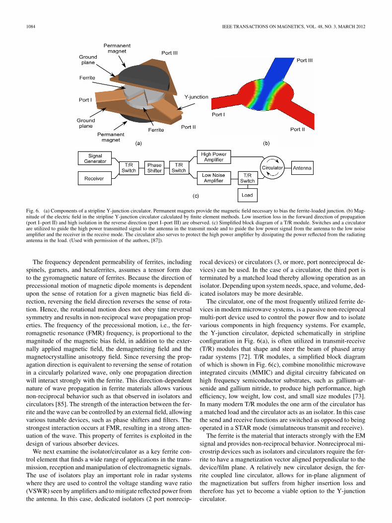
Fig. 6. (a) Components of a stripline Y-junction circulator. Permanent magnets provide the magnetic field necessary to bias the ferrite-loaded junction. (b) Mag-nitude of the electric field in the stripline Y-junction circulator calculated by finite element methods. Low insertion loss in the forward direction of propagation(port I–port II) and high isolation in the reverse direction (port I–port III) are observed. (c) Simplified block diagram of a T/R module. Switches and a circulatorare utilized to guide the high power transmitted signal to the antenna in the transmit mode and to guide the low power signal from the antenna to the low noiseamplifier and the receiver in the receive mode. The circulator also serves to protect the high power amplifier by dissipating the power reflected from the radiatingantenna in the load. (Used with permission of the authors, [87]).
The frequency dependent permeability of ferrites, includingspinels, garnets, and hexaferrites, assumes a tensor form dueto the gyromagnetic nature of ferrites. Because the direction ofprecessional motion of magnetic dipole moments is dependentupon the sense of rotation for a given magnetic bias field di-rection, reversing the field direction reverses the sense of rota-tion. Hence, the rotational motion does not obey time reversalsymmetry and results in non-reciprocal wave propagation prop-erties. The frequency of the precessional motion, i.e., the fer-romagnetic resonance (FMR) frequency, is proportional to themagnitude of the magnetic bias field, in addition to the exter-nally applied magnetic field, the demagnetizing field and themagnetocrystalline anisotropy field. Since reversing the prop-agation direction is equivalent to reversing the sense of rotationin a circularly polarized wave, only one propagation directionwill interact strongly with the ferrite. This direction-dependentnature of wave propagation in ferrite materials allows variousnon-reciprocal behavior such as that observed in isolators andcirculators [85]. The strength of the interaction between the fer-rite and the wave can be controlled by an external field, allowingvarious tunable devices, such as phase shifters and filters. Thestrongest interaction occurs at FMR, resulting in a strong atten-uation of the wave. This property of ferrites is exploited in thedesign of various absorber devices.
We next examine the isolator/circulator as a key ferrite con-trol element that finds a wide range of applications in the trans-mission, reception and manipulation of electromagnetic signals.The use of isolators play an important role in radar systemswhere they are used to control the voltage standing wave ratio(VSWR) seen by amplifiers and to mitigate reflected power fromthe antenna. In this case, dedicated isolators (2 port nonrecip-
rocal devices) or circulators (3, or more, port nonreciprocal de-vices) can be used. In the case of a circulator, the third port isterminated by a matched load thereby allowing operation as anisolator. Depending upon system needs, space, and volume, ded-icated isolators may be more desirable.
The circulator, one of the most frequently utilized ferrite de-vices in modern microwave systems, is a passive non-reciprocalmulti-port device used to control the power flow and to isolatevarious components in high frequency systems. For example,the Y-junction circulator, depicted schematically in striplineconfiguration in Fig. 6(a), is often utilized in transmit-receive(T/R) modules that shape and steer the beam of phased arrayradar systems [72]. T/R modules, a simplified block diagramof which is shown in Fig. 6(c), combine monolithic microwaveintegrated circuits (MMIC) and digital circuitry fabricated onhigh frequency semiconductor substrates, such as gallium-ar-senide and gallium nitride, to produce high performance, highefficiency, low weight, low cost, and small size modules [73].In many modern T/R modules the one arm of the circulator hasa matched load and the circulator acts as an isolator. In this casethe send and receive functions are switched as opposed to beingoperated in a STAR mode (simulatneous transmit and receive).
The ferrite is the material that interacts strongly with the EMsignal and provides non-reciprocal behavior. Nonreciprocal mi-crostrip devices such as isolators and circulators require the fer-rite to have a magnetization vector aligned perpendicular to thedevice/film plane. A relatively new circulator design, the fer-rite coupled line circulator, allows for in-plane alignment ofthe magnetization but suffers from higher insertion loss andtherefore has yet to become a viable option to the Y-junctioncirculator.

HARRIS: MODERN MICROWAVE FERRITES 1085
The first waveguide Y-junction circulators were reported inthe late 1950s [74] with stripline designs following soon there-after [75]. The first monolithic microstrip circulator on a garnetsubstrate was introduced in 1967 [76]. The theory of striplineY-junction circulators was developed by Bosma [77], [78], andFay and Comstock [79]. These theories explain the non-recip-rocal behavior of the ferrite loaded stripline Y-junction in termsof the splitting of counter-rotating dielectric resonance modesin the ferrite material due to the off-diagonal elements of thepermeability tensor proposed by Polder [80], [81].
Typical electric field configuration in the ferrite-loadedstripline Y-junction computed by finite element methods isshown in Fig. 6(b). Here one sees the stabilization of a standingwave that acts to shunt the flow of power from one port toanother while concomitantly isolating the third. The condi-tions necessary for circulation over a full octave bandwidth inmicrostrip devices were demonstrated by Wu and Rosenbaum[82]. The extensive literature on circulator theory and designis reviewed in the annotated bibliography by Knerr [83] and inbooks by von Aulock and Fay [84] and Helszajn [85].
The need to miniaturize circulator devices, to facilitatebroader integration with monolithic microwave circuits and toextend the applicable frequency range into the millimeter-waveregime, has motivated studies in utilizing the unique proper-ties of hexagonal ferrites. Textured polycrystalline hexagonalferrites, such as barium and strontium hexaferrite, can beproduced with permanent magnet properties such that theywill remain in a stable magnetized state in the absence of anexternal bias field (i.e., self-biased). High uniaxial magneticanisotropy fields in these materials, which can exceed 40 kOe,are utilized to decrease or eliminate the external biasing fieldrequirement according to Kittel’s [86] resonance equation thatincorporates both dipolar and magnetocrystalline anisotropyinteractions [87].
Polycrystalline textured strontium hexaferrite , havinga remnant magnetization of approximately 3.5 kG, uniaxialanisotropy field of 18.4 kOe, and FMR linewidth of approxi-mately 2 kOe, was utilized to develop a self-biased waveguidejunction circulator operating at 73.5 GHz by Akaiwa andOkazaki [88]. The reported insertion loss was 1.1 dB withisolation exceeding 20 dB over a 2.4 GHz bandwidth. In 1989,polycrystalline was utilized to develop a self-biasedwaveguide circulator operating at 30.7 GHz with an insertionloss of less than 1 dB and isolation of more than 20 dB overa 1% bandwidth [89]. In 1992, a textured barium/strontiumferrite with remanent magnetization of 3.5 kG and uniaxialanisotropy field of 21 kOe was utilized to design microstrip andstripline circulators operating at 37 and 32 GHz, respectively[90]. In 2001, an integrated self-biased microstrip circulatorwas fabricated through bonding of textured platelets tosilicon substrates in a low temperature process compatible withsemiconductor fabrication protocols [91]. Insertion loss of 2.8dB and isolation of 33 dB were measured at 28.9 GHz witha 20 dB bandwidth of 1%. Circulator designs utilizing singlecrystal platelets of with saturation magnetization of 3.9kG, uniaxial anisotropy field of 8.7 kOe and linewidth of 100Oe embedded into glass-microwave integrated circuit wafersresulted in operation at 22.2 GHz with a minimum insertion
loss of 2 dB and isolation of 21 dB. This performance was ob-tained with ferrite platelets partially saturated by an externallyapplied magnetic field of 2 kOe (55% saturation) [92], [93].Recently, Wang et al. [94] developed a self-biased Ku-bandcirculator. This two dimensional construct employed a self-bi-ased -type hexaferrite and demonstrated an insertion lossof less than 2 dB with a corresponding isolation of 20 dB overa bandwidth of 500 MHz with a center frequency of 13.5 GHz.This was the first such demonstration of a self-biased circulatoroperating at a frequency less than 20 GHz.
As mentioned previously, the circulator design that has themost potential for monolithic microwave circuit integration andself-bias operation is the ferrite-coupled-line (FCL) circulator.First developed in the 1980s, in contrast to Y-junction circula-tors, FCL circulators utilize longitudinally magnetized ferrite tocouple modes between closely spaced wave guiding lines [95].The non-reciprocity of ferrite coupled waveguides was first ex-plained in terms of coupled mode theory by Marcuse [96].
FCL circulators have the additional advantages of broadbandwidths, planar form factors, and smaller biasing field [97].Self-bias designs utilizing hexagonal ferrites have also beenreported [98]. Due in part to a lower demagnetizing factorassociated with a longitudinally magnetized film, self-biasedhexaferrite films are easier to produce to thicknesses necessaryfor FCL device fabrication. Therefore, self-biased FCL circu-lators have the potential for true monolithic integration wherethe ferrite film is deposited and metalized with proper circuitryduring device fabrication. There is no doubt that circulatordesigns described here, as well as other high frequency ferritedevices, will continue to benefit from further advances in ferritematerials to result in true microwave monolithic integratedcircuits.
C. Phase Shifters
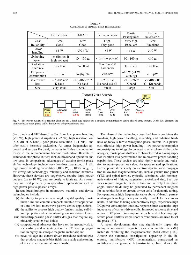
Phase shifters are critical elements for electronically scannedphased array (ESPA) antennae and are devices that allow theantennae beam to be steered without physically re-positioningthe antennae. Existing phase shifter technologies, for example,ferroelectric, semiconductor-MMIC, and MEMS each suffershortcomings or operational constraints that limit their widescale deployment across varied military and commercial plat-forms (see Table V for comparison of existing phase shiftertechnologies [99]). The key figures of merit include: phaseshift per dB of insertion loss, power budget, power handling,and size, weight, and cost. Here, we target phase shifter ap-plications in which high performance is demanded in lowprofile—lightweight devices that handle high power loads(10s Watts average power). Such applications include radarand communication phased array systems on aircraft, satellite,ships, and importantly, next generation unmanned systems.Fig. 7 illustrates, for example, the power budget of a transmitchain for an L-band T/R module for a satellite communicationactive phased array system. Of the key elements, the semicon-ductor-based phase shifter introduces a disproportionate loss.Clearly, enhanced T/R module performance would be realizedby the reduction in insertion loss of phase shifters. This is onedriving force in the development of next generation phase shiftdevice technology. Semiconductor phase shifter technologies
1086 IEEE TRANSACTIONS ON MAGNETICS, VOL. 48, NO. 3, MARCH 2012
TABLE VCOMPARISON OF PHASE SHIFTER TECHNOLOGIES
Fig. 7. The power budget of a transmit chain for an L-band T/R module for a satellite communication active phased array system. Of the key elements thesemiconductor-based phase shifter introduces a disproportionate loss.
(i.e., diode and FET-based) suffer from low power handling( 1 W), high power dissipation (1–2 W), high insertion loss(6–8 dB at X-band), poor phase resolution ( 4 bits), andoften-costly hermetic packaging. As target frequencies ap-proach and surpass Ku band, increases in IL due to conductionlosses in the semiconductor become prohibitive. Benefits ofsemiconductor phase shifters include broadband operation andlow cost. In comparison, advantages of existing ferrite phaseshifter technology include very low-loss operation, 1 dB,high power handling capabilities (100s , 1000sfor waveguide technology), reliability and radiation hardness.However, these devices are large/heavy, require large powerbudgets (up to 10 W), and are costly to fabricate. As a resultthey are used principally in specialized applications such ashigh power passive phased arrays.
Recent breakthroughs in microwave materials and devicetechnologies include:
(i) the ability to process near single crystal quality ferritethick films and ceramic compacts suitable for applicationin ultra-low loss microwave passive device applications;
(ii) the ability to process high quality ferrites having self-bi-ased properties while maintaining low microwave losses;
(iii) microstrip passive phase shifter designs that require sig-nificantly smaller bias fields;
(iv) computational advances that have set the groundwork tosuccessfully and accurately describe EM wave propaga-tion in highly anisotropic magnetic materials; and
(v) novel voltage and current driven transducer technologiesthat produce magnetic bias fields that enable active tuningof devices with minimal power loads.
The phase shifter technology described herein combines thelow-loss, high power handling, reliability, and radiation hard-ness of today’s ferrite waveguide phase shifters in a planar,cost-effective, high power handling—low power consumptionmicrostripline topology. In contrast to other phase shifter tech-nologies, ferrite phase shifters are characterized as having supe-rior insertion loss performance and microwave power handlingcapabilities. These devices are also highly reliable and radia-tion tolerant—properties valued for space related applications.Ferrite phase shifters rely on electromagnetic wave propaga-tion in low-loss magnetic materials, such as yttrium iron garnet(YIG) and spinel ferrites, typically substituted with nonmag-netic cations of lithium, magnesium, nickel, and zinc. Such de-vices require magnetic fields to bias and actively tune phaseangle. These fields may be generated by permanent magnetsfor static bias fields or current-driven coils for dynamic tuning.For operation at high frequencies (at or above -band), perma-nent magnets are large, heavy and costly. Tunable ferrite compo-nents, in addition to being comparatively large, experience highDC power consumption and slow response times due to the largeinductance of current-driven coils. Improved response time andreduced DC power consumption are achieved in latching-typeferrite phase shifters where short current pulses are used to setthe phase [87].
A recent development that may significantly impact thetuning of microwave magnetic devices is multiferroic (MF)materials exhibiting the magnetoelectric (ME) effect [100].Among the numerous investigations appearing in the lit-erature, multiferroic (MF) metamaterials, constructed asmultilayered or granular heterostructures, have drawn the

HARRIS: MODERN MICROWAVE FERRITES 1087
Fig. 8. a) Calculated dotted dashed and measured solid insertion loss. Calcu-lated (dotted) and measured (dashed) return loss. b) Calculated (dotted dashed)and measured (solid) differential phase shift. c) Measured insertion phase at anapplied electric field of 0 (solid), 3 (dashed), and 6 (dotted) kV/cm. d) Finiteelement model of the microstrip circuit. e) Fabricated device with coaxial edgemount SMA connectors. (Used with permission of the authors, [106]).
most attention [101]. Multiferroic heterostructures haveindeed been shown to offer unique opportunities in thedevelopment of many new multifunctional devices, includingelectric-field-controlled (EFC) magnetic memory elements[102]. EFC microwave devices [103] and E- and H-fieldtransducers having magnetically modulated piezoelectricityor electrically modulated magnetoelectricity [104], [105]. Inmany of these examples, mechanical coupling between piezo-electric (e.g., PZT, PMN-PT, etc.) and magnetostrictive (e.g.,Terfenol-D, Galfenol, Metglas, etc.) layers provides electricfield induced magnetic polarization of the magnetostrictivelayer(s) and magnetic field induced electric polarization ofthe piezoelectric layer. Alternatively, Geiler et al. [106] havedemonstrated the generation of magnetic fringe fields by MFheterostructures that act on nearby microwave devices thatare decoupled from the transducer. In both instances the MFheterostructures may eliminate the need for voluminous andcostly magnetic field coils to actively tune magnetic compo-nents. These developments represent a disruptive advance inthe field of multifunctional electronics.
Geiler’s voltage tuning of a meander line ferrite phaseshifter (see Fig. 8(d) and (e)) was realized by affixing a YIGsubstrate to a MF heterostructure consisting of PMN-PT/Ter-fenol-D/PMN-PT. This geometry allowed the YIG substrateto see the voltage induced magnetic fields emanating fromthe MF heterostructure without experiencing any strain ormicrowave electromagnetic coupling. A magnetic bias field of200 Oe was applied along the length of the MF heterostructure,and along the meander line elements, by an electromagnet.Measured insertion and return loss are superimposed withcalculated spectra in Fig. 8(a). At a frequency of 6.3 GHz,the insertion loss and the return loss were measured to be 3.2and 13 dB, respectively, while a differential phase shift of180 was measured at 6.3 GHz. Out of the 3.2 dB of insertionloss, 0.5 dB is attributed to impedance mismatch loss. Theremaining 1 dB between calculated and measured insertion lossis attributed to connector effects, imperfections associated with
the device fabrication process, and variations in the materialproperties from those assumed in the finite element model.The contribution of the MF heterostructure to the insertionloss was less than 0.2 dB. The magnetic fringe field was non-uniform and varied from 330 Oe near the edge of the 1.3 cmYIG substrate to 210 Oe near the center. Differential phaseshift was calculated by subtracting the insertion phase at zerointernal field from the insertion phase at 100 Oe internal field.A differential phase shift of 210 was calculated at the designfrequency (Fig. 8(b)). As the electric field increased from 0 to6 kV/cm, a linear tunable phase shift of more than 65 degreeswas observed (Fig. 8(c)). This phase change was due to the factthat the magnetic fringe fields from MF heterostructure variedby approximately 20% with applied electric field. These resultsdemonstrate the potential of MF heterostructures as externaltuning elements for microwave magnetic devices.
A different path was taken by Tatarenko, et al. [107] whodemonstrated an electric field tunable yttrium iron garnet YIG-lead zirconate titanate PZT phase shifter based on the tuningof ferromagnetic resonance at X-band. The electric field con-trol of the phase shift arose through a magnetoelectric inter-action in which a piezoelectric deformation in PZT occurredunder the application of an electric field leading to a shiftin the FMR frequency in YIG. A phase shift of 90 to 180 andan insertion loss of 1.5–4 dB was measured corresponding to an
5–8 kV/cm applied across PZT. This approach represents anew path towards realizing high performance EFC phase shifterdevices.
The discovery of metamaterials possessing negative index ofrefraction (NIM) has allowed for the development of novel mi-crowave technologies [108]. A significant recent development isthe fabrication of tunable negative index metamaterials (TNIM)utilizing high quality ferrite materials [109]–[113]. One suchexample of a microwave device making use of a ferrite-basedTNIM is the He et al., phase shifter [111], [112]. As discussedpreviously, there is significant demand in the microwave in-dustry for affordable, light weight, high power phase shifters.In ferrite phase shifters a change in permeability by the applica-tion of magnetic field causes a change in the phase velocity ofthe microwave signal traveling through the phase shifter. Tradi-tional ferrite phase shifters operate at frequencies far from theFMR in order to avoid absorption losses. As a result, the realpart of the complex permeability, , is necessarily small. Ex-perimental and theoretical investigations of field tunable nega-tive refractive index metamaterial (NIM) using a yttrium irongarnet (YIG) films and an array of copper wires in waveguideswere carried out by both P. He et al. and Y. He et al.: A key fea-ture of magnetic field tunability of the NIM in the microwavefrequency region was demonstrated [109], [110]. Transmissionpassbands were realized in the negative refractive index regionthat could be tuned by an external magnetic field. The perme-ability of the NIM was simultaneously tuned along with the re-fractive index. The change in permeability leads to a change inthe phase velocity of the signal and, therefore, the phase of thetransmission coefficient.
The advantage of using a ferrite NIM for phase shifter appli-cations is that it allows for low-loss operation over frequenciesnear FMR where is negative and relatively high. In the field

1088 IEEE TRANSACTIONS ON MAGNETICS, VOL. 48, NO. 3, MARCH 2012
Fig. 9. a) Schematic top and side views of the ���� � ���� ��� �� TNIM composite. Photograph of the microstrip test fixture, a � � �� �� upper stripon the brass ground base relative to a U.S. quarter provided for a visual size comparison. The TNIM composite is mounted under the center of the upper strip.b) Measured phase shift and corresponding transmission vs. the magnetic bias field of the TNIM composite at 9.0 GHz. The insertion phase shifts 45 while thetransmission varies from �6 to �10 dB. c) Simulated and d) measured 1.0 GHz wide TNIM passbands of over �8 dB transmission centered at 7.5, 8.0, and 8.8GHz at magnetic bias fields of 3.0, 3.5, and 4.0 kOe, respectively. e) Center frequency of the TNIM passband increases linearly from 7.6 to 10.7 GHz with the biasfield changing from 3.0 to 5.5 kOe. (Adapted from [112].)
tunable NIM, the effect of the ferrite is to provide a tunable neg-ative permeability over a continuous range of frequencies on thehigh frequency side of FMR. Complementary negative permit-tivity, , was achieved using a single periodic array of copperthin film wires deposited on Kapton. A negative refractive indexregion of 0.5 GHz in width at K band was demonstrated. In-creasing the volume of the YIG increased the absorption andtherefore a tradeoff between bandwidth for the negative indexregion and low-loss was realized. Additionally, the dielectricpermittivity of the YIG slabs reduced the effective negative per-mittivity obtained from the plasmonic copper wires. For a 1 cmlong NIM, when the applied magnetic field was varied from 6.0to 7.0 kOe, the phase varied 160 with the insertion loss varyingfrom 4.3 dB to 6.3 dB at 24 GHz.
A tunable negative refractive index metamaterial and minia-ture phase shifter were also designed and fabricated in a mi-crostripline configuration for applications in rf, microwave andmillimeter wave integrated circuits [111]–[113]. The metamate-rial consisted similarly of plasmonic copper wires and YIG slabshaving an insertion loss of 5 dB at the center of the transmissionband. The YIG enabled magnetic field tuning of the negativerefractive index from 7.0 to 11.0 GHz. The insertion phase wastuned by 45 continuously by varying the bias field from 3.8 to4.6 kOe at 9.0 GHz. Fig. 9(a)–(e) illustrate a schematic of thedevice with photograph (see Fig. 9(a)) and the devices phase
shift and transmitted signal (i.e., passband) (see Fig. 9(b)). InFig. 9(c)–(e) one sees the simulated and experimental passbandssignaling the occurrence of negative index. This passband wasshown to shift under the application of a magnetic field demon-strating broadband tunability of the NIM. H-field tuning wasshown to be broadband and linear, see Fig. 9(e).
Finally, a similarly structured tunable negative indexmetamaterial was designed, fabricated, and tested in a Q-bandrectangular waveguide [113]. The structure consisted of a singlecrystalline scandium-doped barium hexaferrite ,aligned parallel to two rows of periodic copper wires (seeFig. 10(a) and (b)). The magnetic field tunable passband wasmeasured indicating the occurrence of the negative index.The center frequency of the 5 GHz wide passband, having atransmission peak of 13 dB, was shifted linearly from 40.9to 43.9 GHz by varying the bias field from 4.0 to 7.0 kOe (seeFig. 10(c) and (d)). These examples of TNIM-based electroniccomponents represent a new approach in the design and fabri-cation of miniature microwave passive devices that rely upontuning the permeability spectrum in frequency space near FMR.
D. Filters
Microwave filter designs have been a topic of great interestfor more than seven decades [114] and continue to grow as high

HARRIS: MODERN MICROWAVE FERRITES 1089
Fig. 10. a) Top views of the TNIM design consisting of two Sc-BaM slabs, two rows of copper wires on Kapton substrate, and a Mylar spacer and the simplifiedTNIM consisting of only one Sc-BaM slab. The magnetic bias field H, the propagation constant � and the directional vector from copper wires to their vicinalferrite slab Y form a right-handed triplet. (b) The schematic drawing of the TNIM composite mounted in a Q-band rectangular waveguide. c) Measured and (d)simulated S21s of the TNIM composite containing a 1.0 mm thick Sc-BaM slab under bias fields of 5.0, 5.5 and 6.0 kOe, respectively. Inset: measured centrefrequency of the TNIM passband versus the magnetic bias field. (Adapted from [113].)
performing materials and increasingly complex designs are in-vestigated to meet stringent modern-day requirements. A majordevelopment to the field of microwave filters was the advent oftunable bandwidth parameters allowing for a single device tooperate at user-defined frequencies [115]. The tuning mecha-nisms in these filters vary from static mechanical methods suchas plungers, screw-tuned cavities, and conductor-conductor po-sitioning, to active methods such as applied E-field and H-fieldtuning, with each method offering distinct benefits [114], [115].Active methods, such as E-field and H-field tuning, allow forremote device performance tuning as well as the ability to au-tomate band tuning for frequency-modulated applications. Ac-tive tuning also enables high-speed precision band pass adjust-ments and better repeatability than mechanical tuning methods.The advantages of H-field tunable filters over E-field tunablevaractor or MEMS devices include low insertion loss and highpower handling. YIG filters, based on single crystal resonators,are among the most widely utilized H-field tuned devices of-fering multi-octave band tunability and high Q-factors.
Next, we examine a highly versatile, planar, low-loss, andlow cost alternative to YIG single crystal resonator filters witha low externally applied H-field requirement. The proposeddesign consists of a 5-pole Chebyshev bandpass filter imple-mented in microstrip hairpin-line coupled resonator geometryon a polycrystalline YIG substrate biased and tuned withan externally applied H-field above the FMR frequency (seeFig. 11(a)–(c)) [116].
The hairpin-line bandpass filters are essentially parallel-cou-pled half-wavelength resonators folded into a “U” shape andfollow the same set of design equations that govern parallel-cou-
pled half-wavelength resonator filters [115]. A 5-pole Cheby-shev equiripple response is considered, however, Butterworth,elliptical, and other filter response types are equally applicable.
The dynamic tuning of the proposed device is realized byvarying the magnetic permeability of the substrate by applyingan external magnetic field. The variation in permeability withapplied field is strongest below the FMR frequency and abovethe ferromagnetic anti-resonance (FMAR) frequency. Opera-tion sufficiently far from both resonance conditions is necessaryto achieve low-loss performance.
The measured insertion loss of a ferrite microstrip hairpin-line bandpass filter is compared with the predictions of the nu-merical model in Fig. 11(d). Good agreement in the frequencyrange of interest is observed. Under an externally applied fieldof 100 Oe, an insertion loss of 1.3 dB was measured at 8.8 GHzcompared to 0.9 dB predicted by the numerical model.
H-field tuning of the ferrite microstrip hairpin-line bandpassfilter is demonstrated (Fig. 11(e)). The device exhibits pass-band tunability with center frequency varying from 8.3 GHz to9 GHz under applied H-fields of 50 to 200 Oe. The insertion lossat the passband center frequency varies between 1 and 1.4 dBas a function of applied H-field. While a bandpass filter de-sign with a fractional bandwidth of approximately10% at X-band was demonstrated, the proposed approach lendsitself to the realization of a broad range of filter responses, in-cluding lowpass, highpass, bandpass, and bandstop, as well aspassband characteristics, including center frequency, fractionalbandwidth, passband ripple, out-of-band rejection, etc. Further-more, due to the low H-field requirement, the proposed filter de-sign has the potential for high-speed and low-power operations,
1090 IEEE TRANSACTIONS ON MAGNETICS, VOL. 48, NO. 3, MARCH 2012
Fig. 11. (a) Photograph of patterned 50 mm diameter YIG wafer. (b) Outline of the hairpin-line resonator bandpass filter design used in numerical modeling.(c) Photograph of fabricated bandpass filter device. (d) Simulated and measured passband characteristics of the ferrite microstrip hairpin line coupled resonatorbandpass filter. Measured spectrum is collected under applied magnetic field of 100 Oe. (e) Passband characteristics of the ferrite microstrip hairpin line coupledresonator bandpass filter under applied magnetic field from 50 to 200 Oe. (Adapted from [116].)
in addition to possessing radiation tolerant properties makingthem well-suited for space related applications [99].
Multiferroic (MF) heterostructures that demonstrate themagnetoelectric effect (ME) can also be adapted as tunablemicrowave filters [117]. ME resonators, consisting of 110thick (111) yttrium iron garnet (YIG) on a GGG substratebonded to PZT, have been demonstrated. In that example,YIG, having a saturation induction of 1750 G and aFMR linewidth of 1 Oe, was bonded to a PZT plate poledin an electric field of 10 kV/cm perpendicular to the sampleplane. The heterostructure consisted of a YIG film bondedto a PZT crystal with ethyl cyanoacrylate. The heterostruc-ture was placed between transducers, and was subjected toa field H parallel to the sample plane and perpendicular tothe microstrips. The frequency dependence on the insertionloss was measured from 4–10 GHz as a function of H and Efields applied across the PZT. The maximum ME coupling wasobserved at corresponding to FMR in YIG.A frequency shift was observed and attributed to the strain atthe YIG-PZT interface caused by the piezoelectric response ofthe PZT. A near-linear variation in with E was observed. Amaximum shift of 120 MHz for correspondingto 2% of the center frequency of the filter was measured [117].
Next, we review popular and effective techniques of pro-ducing high quality ferrite materials as thin and thick films,powders, compacts, quasi-single crystals, and metamaterials.
V. FERRITE MATERIALS PROCESSING
Thin film ferrites are typically produced by physical vapordeposition (PVD) techniques that may include molecular beamepitaxy (MBE), chemical vapor deposition (CVD), sputteringdeposition, and pulsed laser deposition (PLD). Alternatively,chemical hydrolysis using spin spray plating (SSP), or variantsof the same, have also been explored and demonstrated as valu-able techniques for producing thin and thick film ferrites underlow temperature conditions.
Molecular beam epitaxial growth techniques result in veryhigh quality single crystal, or quasi-single crystal ferrite films.MBE growth of ferrites has been driven by the pursuit to under-stand underlying physical phenomena of thin films of[118] and [119] grown on MgO (001) and magne-toresistance in spin valve structures consisting in part oflayers [120]. Recently, MBE has been applied to the hex-aferrite system resulting in high crystal quality films grown onMg(001)/SiC(0001) [121]. Although MBE finds great utility inthe study of fundamental phenomena in ferrites, films sufferfrom very limited thicknesses of 10–200 nm that are imprac-tical for most microwave and mm-wave applications.
A variety of chemical vapor deposition (CVD) techniqueshave been applied to the growth of ferrite film systems. CVDvariants, including plasma assisted, metalo-organic, and in-jection-CVD (and combinations of these) were successfullyapplied in the growth of [122], [123]
HARRIS: MODERN MICROWAVE FERRITES 1091
films [124], NiZn-ferrites [125], and Ba-hexaferrites [126].These techniques have been applied to realize films of severalmicrons in thickness. Although thick in comparison to MBE,PLD, and magnetron sputtering, these thicknesses remain toothin for most high frequency applications. Further, these filmstend to possess comparatively large FMR linewidths stemmingfrom chemical impurity contamination. Because of these short-comings, CVD has not yet become a mainstay technique for thegrowth of thick film ferrites for rf, microwave, and mm-waveapplications.
Magnetron sputtering has been used principally for the depo-sition of granular ferrite films for applications in high densitymagnetic recording, etc. In the case of sputtering it is not un-common to deposit ferrites as an amorphous phase that is thenheat-treated beyond crystallization to obtain the desired mor-phology and structure for high-density data recording applica-tions. Sui et al. [67] presents a review of these processes and re-sulting properties for Ba hexaferrite films. Spurred by the workof Sui et al., Snyder et al. [127], [128] showed through the ap-plication of x-ray absorption fine structure that a local struc-tural precursor within the amorphous film predetermines thecrystalline texture of the hexaferrite films valued for memorystorage.
For our discussion of thin film ferrites in Sections V-A andV-B, we limit our discussion to PLD and SSP since these tech-niques have been proven the most effective in processing a widerange of high crystal quality ferrite films attractive for high fre-quency applications.
A. Ferrite Films and Coatings Using Pulsed Laser AblationDeposition
Pulsed laser deposition (PLD) is a well-established methodfor growing ferrite films. In conventional PLD, laser pulsesfrom a high-energy laser, often an excimer laser, ablate a targetmaterial forming a molecular flux or plume. The substrateintercepts the plume allowing for the growth of films of similarcomposition as the target material on selected, often latticematched, substrates. PLD has been used in the deposition ofgarnet, spinel, and hexaferrite ferrites among other oxides suchas high temperature superconductors and magnetoresistivemanganites. Growth of ferrite films using PLD was first pro-posed by Vittoria [70] in 1991. The PLD of yttrium iron garnet(YIG) films was first demonstrated by Dorsey et al. [129]Films with thicknesses of about 1 were deposited on (111)gadolinium gallium garnet (GGG) substrates. FMR linewidthsof 1 Oe were observed in films deposited under oxygen pres-sures 250 mTorr and high substrate temperatures .Films of (BIG), (EBIG), as well asYIG/BIG and YIG/EBIG heterostructures, were investigatedby Simion et al. [130]. Thick, , epitaxial YIG filmshaving linewidths of 5.7 Oe were deposited on (111) GGGsubstrates at a high rate by Buhay et al. [131] In the same paper50–100 thick polycrystalline films where deposited on 3gold plated (100) Si wafers. The magneto-optical propertiesof Ce [132] and Bi [133], [134] substituted YIG films andYIG/GGG superlattices [135] grown by PLD on (111) GGGsubstrates have been investigated.
The first PLD-grown hexaferrite films were reportedby Dorsey et al. in 1992 [129] In the years following many re-searchers applied PLD to ferrite film synthesis. Shi et al. [92]deposited Sc-doped BaM films on c-plane sapphire having thecrystallographic c-axis aligned normal to the film plane. Amongthe highest quality films made were those by Song et al.[136] who achieved perpendicular magnetic anisotropy and anFMR linewidth of 16 Oe at 60.3 GHz.
Most research studies discussed thus far involving hexafer-rites have strived to align the crystallographic c-axis perpendic-ular to the film plane. As was discussed previously, in-planeorientation can be achieved by using suitable substrates thatare chosen for their close match to the film’s lattice parametersand thermal expansion coefficients (e.g., - or -cut sapphire).Welch et al. [137] reported the growth of films having thecrystallographic c-axis (i.e., magnetic easy axis) aligned ran-domly within the film plane, while Yoon, Vittoria and Oliver[138] subsequently reported the -axis of the (scandiumdoped ) films aligned in the film plane parallel to the -axisof the -plane sapphire substrate.
PLD growth of spinel ferrites was first realized by Tanakaet al. in 1991 [69]. In that work, polycrystalline nickel zincferrite, , films were deposited on glass sub-strates. Johnson et al. [139] reported the growth of nickel fer-rite, , on -cut sapphire substrates using both PLD andATLAD (i.e., alternating target laser ablation deposition). Post-annealing was found to enhance the magnetic properties of thesefilms including increasing the magnetization and reducing theFMR linewidthc [140].
Balestrino et al. [141] reported the PLD growth of lithium fer-rite, , and Mn and Zn-doped lithium ferrite films.Cillessens et al. [142] reported the epitaxial growth of MnZn-ferrite films on with and without buffer layers.
Guyot et al. [143] reported the growth of Co-ferrite films,while Terzzoli et al. [144] reported the growth of Co-ferritefilms on Si (100) substrates with a strong (111) crystal texture inspite of the formation of a native oxide layer at the substrate sur-face. Co-ferrite films grown on substrates werealso studied and reported by Paulsen et al. [145] for their mag-netoelastic properties. Hu et al. [146], [147] demonstrated thestructural tuning of magnetic anisotropy in PLD Co-ferrite filmsand expressed their findings in the context of cation disorder andlocal distortions. Similarly, Yang et al. [148], [149] illustratedenhanced magnetization in PLD Cu-ferrite films as a functionof working gas pressure induced cation disorder.
A long sought goal of the ferrite community has been the in-tegration of ferrite-based microwave passive devices with semi-conductor systems. One path to realizing this goal is the growthof ferrites on semiconductor substrates. Oriented ferrite filmsdeposited on semiconductor substrates are made difficult by thehigh temperatures required to grow a ferrite having low mi-crowave loss. Further difficulties arise from the formation of na-tive oxides on the substrate surface leading to a loss of epitaxy.In an example of ferrite—semiconductor integration was by Liuet al. [150] who reported the growth of oriented films onsilicon substrates with an MgO buffer layer. Zhang et al. [68]applied rf magnetron sputtering to grow highly textured thinBaM films ( 200 nm) on Pt coated Si substrates having FMRlinewidths of less than 400 Oe. Meanwhile, Y. Chen et al. [151]

1092 IEEE TRANSACTIONS ON MAGNETICS, VOL. 48, NO. 3, MARCH 2012
Fig. 12. Pole figures obtained for (a) the (006), and (b) (008) reflections, and the corresponding 2D projections (c) and (d), with �� values fixed at 23.00 and30.30 , respectively. The single dominant peak in (a) corresponds to � � � � � for the��� (006) reflection. The weaker peaks in (a) and (c) exhibiting six-foldsymmetry correspond to closely spaced ��� (104) reflections. The minor peaks exhibiting three-fold symmetry in (a) and (c) derive from closely spaced MgO(100) reflections illustrating the epitaxial nature of the ��� films grown on �������� � . Similarly, (b) and (d) show similar data for the (008) reflectionfurther supporting the epitaxial growth of films. e) Transmission electron microscopy images of the ��� film grown on �������� � in cross section.The image (f) is an expanded view of the section denoted in (e). (g) Hysteresis loops obtained by vibrating sample magnetometry (VSM) with a maximum appliedfield of 13,000 Oe aligned parallel (dashed) and perpendicular (solid) to the film plane. (h) Power derivative as a function of applied magnetic field in the regionnear the ferromagnetic resonance at 53 GHz. The linewidth measured as the peak-to-peak power derivative is 86 Oe for the as-deposited BaM film deposited on 8nm ��� ��������� � . (Adapted from [155].)
successfully screen-printed thick coatingsonto large area Si substrates buffered with alumina [152] andsilica [152] having relatively high FMR linewidths of 2400Oe. Z. Chen et al., [153]–[155] reported the PLD growth of ori-ented thin films on 6H-SiC substrates with and withoutMgO buffer layers. These films were also successfully reac-tively ion etched into pillar arrays that significantly reduced thedemagnetizing energy of the film and demonstrated a uniquepath towards self-biased structures of single crystal films. Al-though ion etching caused copious defects leading to enhancedcoercivity a post-etch heat treatment was shown to not onlyrecover the magnetic properties but in some instances to im-prove the film’s properties over those of the as-deposited films.Z. Chen et al. extended these studies to include the depositionof high quality hexaferrites on MgO(001)/GaN(0001)/sapphire substrates. The latter studies included the growth of
having perpendicular magnetic anisotropy and an FMRlinewidth (peak-to-peak in the power derivative) of less than 90Oe at 53 GHz. Fig. 12(a)–(d) depict pole figure analysis of the
(006) and (008) reflections: All reflections have been identifiedto confirm sample orientation and epitaxy with respect to thesubstrate. In Fig. 12(e) and (f) are high-resolution transmissionelectron microscopy images illustrating the sharp interface be-tween GaN/MgO. The MgO/BaM interface depicts an alloyedregion in which a spinel phase has stabilized. A narrow FMRlinewidth, 86 Oe at 53 GHz, is consistent with reduced hard axiscoercivity. These studies represent the first successful growthof any low-loss microwave ferrite on a microwave compatiblesemiconductor substrate material.
Besides , many hexaferrite materials have been de-posited by PLD. Other -type hexaferrites include strontiumand lead hexaferrites ( and ) [156]. Scandium doped
films were deposited to control magnetic anisotropy[157], whereas cobalt and titanium co-doped and alu-minum doped films were deposited for the optimizationof the magneto-optical properties [158].
A variant to conventional PLD involves the sequential abla-tion from multiple targets to construct engineered unit cell struc-
HARRIS: MODERN MICROWAVE FERRITES 1093
tures with specific chemistry and valence leading to the tailoringof magnetic properties. This technique allows one to controlcation distribution in the unit cell leading to the stabilizationof ferrite structures having far from equilibrium properties. Thistechnique has been referred to as alternating target laser ablationdeposition or ATLAD. In recent years, ATLAD has been usedby Zuo et al. [159]–[161], Yang et al. [150], and Geiler et al.[162] to control cation distribution within the ferrite lattices ofMn-ferrite, Cu-ferrite, BaM, and PbM hexaferrites. In the caseof Mn-ferrite films, low oxygen pressure was shown to lead to alow cation inversion and large single ion anisotropy increasing
from 20 to 1000 Oe. In contrast, high oxygen pressuresled to increases in cation inversion, distorting the cubic struc-ture, breaking crystal symmetry, and stabilizing a perpendicularmagnetic anisotropy field of 1000 Oe. Such properties providethese films unique potential for microwave applications at L, S,C, and X bands.
In the Cu-ferrite film system, Yang et al. [150] was able toredistribute Cu ions from 85% octahedral sites to 60% tetra-hedral sites. This created an imbalance of spins between the -and -sublattices resulting in a magnetization increase of upto 65%. The properties for near normal Cu ferrite materials waspredicted by Zuo et al. [163] using first principles band structurecalculations. Geiler et al. [164] demonstrated for the first timethe ability to calculate, locate, and confirm the lattice positionthrough synchrotron radiation measurements the distribution ofMn dopant ions in BaM. This was the first convincing demon-stration of cation engineering in ferrite systems.
A major advance allowing for this type research was thedevelopment of the x-ray absorption fine structure (XAFS)technique to track the element specific cation distribution andvalence of principle and dopant ions. The first demonstrationof XAFS to ferrites systems was Harris et al. [165]–[167] whoapplied a multiple scattering XAFS model that revealed uniquesignatures that identified - and -site lattice occupation ofcations. Calvin improved upon Harris’ approach by imposinga multi-absorption edge co-refinement leading to results thatwere more statistically robust [168]. This approach has beenapplied to thin films [146], [147], [149], [150], [165]–[168],[161]–[163]; particles [169] and nanoparticles [168]–[172]systems.
Limitations of PLD and ATLAD ferrite film fabrication in-clude limited film thickness, typically , and high tem-perature processing, typically . At these thicknessesthe films are not well-suited for microwave device applications,while growth at these high temperatures is incompatible withsemiconductor device fabrication. As a result, PLD remains avaluable research tool but does not adequately address the ma-terials needs of the microwave device community. During thelast decade, Abe and co-workers [173], [174] have developeda wet chemistry deposition technique, i.e., spin spray ferriteplating, which allows low temperature processing of thick fer-rite films. We next discuss the advantages and disadvantages ofthis technique.
B. Spin Spray Ferrite Plating
In spin spray plating (SSP) the nucleation and growth of asolid phase film is facilitated by hydrolysis without pyrolysis.Abe et al. first began developing SSP during the mid-1980s as
a means of processing ferrite films at low temperatures [173].Abe provided a thorough review of the science and technologyof SSP in 2000 [174]. The advantages of SSP include rapidgrowth rates, thick dense films, low temperature processing,and a wide range of suitable substrate materials that rangefrom plastics to ceramics. This technique involves the sprayingof metal acid solutions, commonly metal chloride solutions,and oxidizing agents, commonly sodium nitrite solutions, vianebulizers onto rotating substrate materials held at temperaturesranging from room temperature to 90 . In this depositionscheme, one can produce polycrystalline films having the spinelstructure ( , , Co, Ni, Zn, Mn, etc.) directlyfrom an aqueous solution. This technique has been extended tothe deposition of ferrites onto a variety of substrates includingrolls of plastic sheet [175]. Requiring no post-deposition heattreatments, SSP allows the deposition of ferrite films on suchnon-heat-resistant materials as semiconductor substrates [176]and polymer sheets [177] for EMI suppression and otherpurposes.
NiZn-ferrite noise suppressors have been demonstrated to ab-sorb noise currents by magnetic losses as they radiate. In usingSSP one can deposite ferrite films onto polyimide sheets that arecut and pasted onto noise sources or deposite films directly ontoprinted circuit boards, covering potential noise sources [178].
SSP NiZn ferrite films, 3 in thickness, suppress GHznoise more effectively than commercialized noise suppressors.The sheet type noise suppressors, made by a roll spray fer-rite plating process, have surface resistivities higher than
, stability to temperatures greater than 260 (i.e.,the lead-free soldering temperature) [178], and the ability towithstand the standard bend test (JIS C5016: no peel off oc-curred after one million cycles of bending at a 3 mm radiusof curvature) [179]. Spin sprayed NiZnCo ferrite films havebeen shown to have natural resonance frequencies from 3 to5 GHz and values of from 5 to 8 at frequencies up to a fewGHz. These films are promising for magnetic field shielding for900 MHz RFID applications [180].
Even with thicker SSP films samples often fall short of theneeds for many microwave applications. The FMR linewidthsof SSP films are higher than those processed by PLD, for ex-ample, with losses attributed to contaminants from chemicalprocessing.
In contrast to SPP, liquid phase epitaxy (LPE) is a techniquethat has been shown to provide thick films and near single crystalquality. We next examine the LPE growth of ferrites.
C. Liquid Phase Epitaxy of Thick Ferrite Films
In liquid phase epitaxy, oxide compounds such as ferrites aremixed and dissolved in solvents or fluxes. Common fluxes in-clude boron oxide , barium oxide (BaO) and , leadoxide (PbO), or a mixture of and PbO. In general, thecomposition of the flux mixtures is chosen so that the melt tem-perature does not exceed . The substrate acts as a seedonto which the ferrite film nucleates and grows. Appropriate lat-tice matching is considered to minimize stress-induced crystaldefects that limit film thickness and performance [181].
LPE was first employed to produce high quality yttrium irongarnet (YIG: ) films by Linares [181]. LPE-growngarnets continue to receive a great deal of attention for high
1094 IEEE TRANSACTIONS ON MAGNETICS, VOL. 48, NO. 3, MARCH 2012
frequency applications such as microwave and millimeter wavedevices and optical Faraday isolators [182]. Growth rates inLPE can be 10s leading to film thicknesses up to andgreater than 200 [183]. Rapdi growth rates is a definiteadvantage over other deposition techniques including physicalvapor deposition or chemical vapor deposition methods. Inall film deposition methods that aim to maintain epitaxy, acommon difficulty is lattice mismatching between ferrite andsubstrate. A favored substrate for the deposition of garnets,i.e., gadolinium gallium garnet (GGG), has the common garnetcrystal structure with a close match to the thermal expansioncoefficient of YIG, in addition to a lattice mismatch of only0.06% [182]. Although the lattice mismatch is exceedinglysmall compared to the mismatches of many semiconductormaterials or oxide heterostructures, these mismatches can giverise to larges stresses that have deleterious effects upon filmstructure and properties. However, the LPE growth of YIG ondouble-sided GGG provides a cancellation of in-plane stressesthat result in optimal film thicknesses in excess of 200 .These films have been measured to have FMR linewidths ofless than 1 Oe at 9 GHz [182]. A number of spinel fer-rites have been grown by LPE [184], but crystal quality andthickness have yet to reach the level of LPE garnets. LPEgrown hexagonal ferrites, especially barium hexaferrite, havereceived great attention [185]. The smallest linewidth obtainedfor LPE grown epitaxial barium hexaferrite on single crystalhexagallate, i.e., , substrates was 27 Oe at 60 GHz[186]. These values are compared with for thebest barium hexaferrite single crystal sphere [187] and a valueof 10 Oe predicted for Mn-doped hexagonal ferrite [188].Hexagonal ferrite films having the -axis perpendicular to thesubstrate plane have been grown by LPE on PLD grown seedlayers on commercially available substrates [189]–[191]. A
value, 28 Oe, was measured from a 45 film grownon double-sided (111) MgO [191]. Alternatively, a 200
film with the -axis aligned along the in-plane direction,grown on double-sided -plane had a of 70 Oe at60 GHz [189].
The LPE technique has clear advantages over other physicaland chemical deposition techniques, producing films of thick-ness having high crystal quality that in some casesapproaches that of single crystals. These films are very wellsuited for microwave and millimeter wave devices that requirelow-losses. However, they continue to require a biasing magnetto saturate the film thus adding size, weight, and assembly cost.We next examine a second technique that provides film thick-nesses in the 100s but has until recently been limited bypoor crystalline quality and high microwave losses [87].
D. Screen Printed Coatings
In general, thick films can be achieved by physical processessuch as tape casting, screen printing, and LPE, among othertechniques. Due to simplicity and cost-effectiveness, screenprinting has been extensively used in mass production of mul-tilayer chip inductors, transformers, ceramic thick film circuits,and magnetic sensors and actuators [192].
It is predicted that next generation microwave devices willbe planar, self-biased, low-loss and integratable with semicond-cutor systems. Self-biasing is an important property that elim-
inates the need for permanent bias magnets thus reduces size,weight, and cost of microwave devices, components and sys-tems [193]. In addition to high remanent magnetization and lowmicrowave losses, thicknesses of are sought.
Yuan et al. [194] reported screen printed films onalumina substrates by hydrothermal synthesis. That work de-tailed influences of precurser powders and sintering processeson static magnetic properties. Because thicknesses rangedfrom 8 to 15 and possessed low values of hysteresis loopsquareness , i.e., 77%, these films failed to meet thematerials needs of self-biased microwave electronic devices.
Y. Chen et al. demonstrated thick filmsprepared by screen printing followed by sintering heat
treatments [195], [196]. Structural, magnetic and microwavemeasurements confirmed that the polycrystalline films weresuitable for applications in self-biased microwave devices inthat they exhibited a large remanence, , highhysteresis loop squareness, 96%, and relatively low microwaveloss (derivative linewidths of 310 Oe at 55.6 GHz). Amongmechanisms contributing to the losses, an extrinsic linewidthbroadening, , was dominant. This linewidtharose from pores and the misalignment of grains. Subsequently,a narrower linewidth, at 53.5 GHz, was mea-sured for screen printed thick films by including a hot-presssintering step [184]. Fig. 13(a) shows a scanning electronmicroscopy (SEM) image with the cross-section as Fig. 13(b)of the film 250 in thickness. Fig. 13(c) is a plot ofhysteresis loops illustrating the high remanent magnetizationproviding self-bias properties. Although the films still containspores and misaligned grains, the results have demonstratedthat the screen printing technique is capable of processingthick, self-biased, low-loss films; an integral step in theprocessing of planar microwave magnetic devices [87].
E. Quasi Single Crystal and Crystallographically TexturedCompacts
In the 1950s, single crystal ferrites were routinely processedand studied for their magnetic and microwave properties. Theliterature is replete with such references and therefore we directthe reader to reviews of ferrite materials targeting this timeframe[17], [21], [197].
There is still a great need for single crystal and quasi-singlecrystal ferrites. Such materials possess among the lowest FMRlinewidths and therefore are ideal for microwave devices inwhich ultralow-losses (and high Q) are required. In this sec-tion we address recent developments in the growth of highquality compacts, quasi-single crystal compacts, and crystal-lographically textured compacts with emphasis placed on theprototypical and versatile hexaferrites.
Although single crystal ferrites remain widely used as res-onators, aspects of single crystal growth that limit their wideutility include: the inability to grow large numbers of largecrystals; the inability to grow crystals having exotic composi-tions and structures; and, the inability to grow crystals havingthe appropriate aspect ratio for low dimensional planar devicetopologies.
Since the 1980s, the study of ferrites as single crystals havelargely been confined to thin epitaxial films processed by PLD(as previously discussed), thick (quasi) single crystal ferrite

HARRIS: MODERN MICROWAVE FERRITES 1095
Fig. 13. Scanning electron microscopy images of a 200 �m screen printed filmafter alignment and heat treatment procedures: (a) surface and (b) cross-sec-tion. Magnetic hysteresis loops acquired with the applied magnetic field alignedalong the in-plane sample direction (open squares) and perpendicular to thesample plane (solid squares). (Adapted from [66].)
films processed by LPE (as previously discussed), and as singlecrystal nano-, micro-, or mesoscale particles [198]–[205]. Arecent article on the topic of magnetic particles by Willard etal. [16], provides a complete review of magnetic particles, in-cluding ferrites, prepared by chemical means. Since these smallparticles (i.e., with diameters less than the single magneticdomain) lack grain boundaries and misoriented grains, theyare typically studied to elucidate fundamental properties offerrites or in exploring dc magnetic properties of nanostructuresas opposed to functional high frequency device applications.However, small ferrite particles have found utility as microwaveabsorbers [206].
Demands for improved microwave device performance andrecent novel materials and devices, such as ferrite-based neg-ative index metamaterials (NIMs) and NIMtronic devices thatrequire ultralow-loss ferrite crystals, the need for such quasi-
single crystal materials has returned. The role of ferrites in meta-material heterostructures have been discussed.
As has been discussed earlier, garnets and spinel crystals andcompacts can operate under bias magnetic fields up to Ku fre-quencies, respectively. Sc or In doped or hexafer-rites are considered for due to their relativelylow FMR frequencies. For example, ferrite, pre-pared by conventional ceramic processing, demonstrated a mag-netization squareness of 83% and anisotropy fields of less than10 kOe. The X-band FMR derivative linewidth was measured tobe more than 800 Oe. For devices which operate at ,
-type hexaferrites are available. When doped with Al orGa the FMR is shifted to higher frequencies and these materialsmay be used up to and beyond W-band [33].
Most recently, low microwave losses and high squareness ofthe hexagonal Sc-doped Ba ferrites, having also low magne-tocrystalline anisotropy fields ( 4–10 kOe), have beensuccessfully achieved. Y. Chen et al. made use of a polymer net-work-assisted alignment processing (PNAAP) technique to ef-fectively align hexaferrite particles in high magnetic fields to re-alize a highly dense oriented Sc-doped Ba ferrite compact [207].A 2-step heat treatment of the resulting compact lead to FMRlinewidths of 500 Oe at X-band and Ka-band and high mag-netization squareness, . These materials haveunique potential for use in self-biased microwave and millimeterdevices at frequencies from 10–40 GHz.
High crystal texture in compacts were also realizedwhen nanorods of goethite, i.e., -FeOOH, were mixed with
, dispersed in a polymer solution, and oriented undera high ( 90 kOe) magnetic field during polymerization [208].The orientation arose principally from the interaction of themagnetic field with the anisotropic antiferromagnetic goethiteparticles. The oriented antiferromagnetic particles acted asseeds for the topochemical growth of ferrite grainsalong the [0001] direction. The degree of grain orientationwas determined using magnetic measurements and orientationdistribution functions and pole figures determined by electronbackscatter diffraction analysis (EBSD, see Fig. 14(a)). InFig. 14(a), the color red signifies the out of plane orientationof the hexaferrite crystallographic c-axes. This is further il-lustrated by the pole figure of Fig. 14(b) in which the (0001)reflection is seen as a well-focused peak in the figure signifiesthe high degree of crystal orientation. Finally, in Fig. 14(c)one sees the clear and unambigious anisotropy in magneticproperties. The inset shows a scanning electron microscopy(SEM) image of large, oriented, and coalesced grains.
In addition to the hexaferrite compacts for self-biasedmicrowave devices, a quasi-single crystal (QSC) Sc-doped
ferrite has attracted interest from the microwaveengineering community [209]. The material was fabricated by asingle solid-state reaction technique that included the alignmentof the ferrite seed crystals. This technique was shown to becost-effective in producing future microwave devices comparedwith those that employ single crystals. Fig. 15(a)–(c) de-pict an SEM image illustrating a collection of large, coalescedcrystals having strong c-axes alignment out of the sampleplane (see Fig. 15(b)). The QSC ferrite bulk samples showsimilar static magnetic properties to those of single crystals(see Fig. 15(c)). However, it’s FMR linewidths are 300 Oe
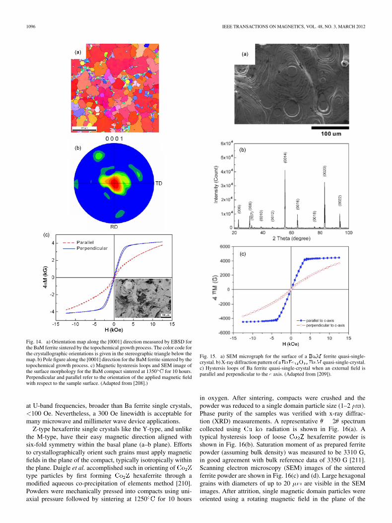
1096 IEEE TRANSACTIONS ON MAGNETICS, VOL. 48, NO. 3, MARCH 2012
Fig. 14. a) Orientation map along the [0001] direction measured by EBSD forthe BaM ferrite sintered by the topochemical growth process. The color code forthe crystallographic orientations is given in the stereographic triangle below themap. b) Pole figure along the [0001] direction for the BaM ferrite sintered by thetopochemical growth process. c) Magnetic hysteresis loops and SEM image ofthe surface morphology for the BaM compact sintered at 1350 � for 10 hours.Perpendicular and parallel refer to the orientation of the applied magnetic fieldwith respect to the sample surface. (Adapted from [208].)
at U-band frequencies, broader than Ba ferrite single crystals,100 Oe. Nevertheless, a 300 Oe linewidth is acceptable for
many microwave and millimeter wave device applications.Z-type hexaferrite single crystals like the Y-type, and unlike
the M-type, have their easy magnetic direction aligned withsix-fold symmetry within the basal plane (a–b plane). Effortsto crystallographically orient such grains must apply magneticfields in the plane of the compact, typically isotropically withinthe plane. Daigle et al. accomplished such in orienting oftype particles by first forming hexaferrite through amodified aqueous co-precipitation of elements method [210].Powders were mechanically pressed into compacts using uni-axial pressure followed by sintering at 1250 for 10 hours
Fig. 15. a) SEM micrograph for the surface of a ��� ferrite quasi-single-crystal. b) X-ray diffraction pattern of a���� � ��� quasi-single-crystal.c) Hystersis loops of Ba ferrite quasi-single-crystal when an external field isparallel and perpendicular to the � axis. (Adapted from [209]).
in oxygen. After sintering, compacts were crushed and thepowder was reduced to a single domain particle size (1–2 ).Phase purity of the samples was verified with x-ray diffrac-tion (XRD) measurements. A representative spectrumcollected using radiation is shown in Fig. 16(a). Atypical hysteresis loop of loose hexaferrite powder isshown in Fig. 16(b). Saturation moment of as prepared ferritepowder (assuming bulk density) was measured to be 3310 G,in good agreement with bulk reference data of 3350 G [211].Scanning electron microscopy (SEM) images of the sinteredferrite powder are shown in Fig. 16(c) and (d). Large hexagonalgrains with diameters of up to 20 are visible in the SEMimages. After attrition, single magnetic domain particles wereoriented using a rotating magnetic field in the plane of the

HARRIS: MODERN MICROWAVE FERRITES 1097
Fig. 16 (a) X-ray diffraction spectrum of sintered �� � hexaferrite powder compared with reference JCPDS file no. 19-0097. (b) Room temperature magnetichysteresis loop of �� � hexaferrite powder. (c) and (d) SEM images of �� � hexaferrite powder at different magnifications.
Fig. 17. (a) Permittivity and permeability spectra (linear scale) as well as(b) loss tangents (logarithmic scale) of �� � hexaferrite materials created forEBG metamaterial applications.
compact. The goal of the magnetic orientation process was toalign the anisotropic ferrite particles with their crystallographicc-axes perpendicular to the compact plane to maximize thepermeability [212], [213]. Typical spectra of the complexpermeability and permittivity of samples was measured from1 MHz to 1 GHz for magnetically oriented samples are shownin Fig. 17. Real part of the permeability was measured to beapproximately 14 while the real part of permittivity was mea-sured to be 10. These values are in good agreement with thosein previously published works [214]. For isotropic samples, thereal part of the permittivity and permeability was measured tobe 14 and 7, respectively, confirming the utility of the magnetic
field orientation method in enhancing the permeability of hex-aferrite compacts. These materials were prepared as possibleelectromagnetic bandgap substrates for antenna elements in aneffort to reduce the antenna profile [215].
F. Ferrites Exhibiting the Magnetoelectric Effect
The magnetoelectric (ME) effect, first predicted in 1894[216], described theoretically in 1959 [217], and observedexperimentally in 1960 [218], has attracted much attentionbecause of its unique potential for the development of novelME devices. The ME effect observed in the vast majority ofsingle phase materials is weak and typically observed onlyunder the application of strong magnetic fields and at lowtemperatures [219]. Some of the more significant requirementsfor realizing practical devices based on ME materials includegood insulating properties and magnetic ordering above roomtemperature [220]. Both of these requirements are satisfied inferrite materials, and indeed, several members of this magneticoxide family have exhibited the ME effect near room temper-ature. This effect, however, has been shown to be too weak atlow magnetic fields to meet the needs of practical devices. Theobservation of a strong ME effect in rare-earth based magneticoxides, such as [221], suggest the possibility of astrong coupling between magnetization and electric polarizationin long-wavelength magnetic structures (e.g., spiral or helicalspin structures. With the recent discovery of large ME effectin transition metal oxides [220], considerable effort has beendevoted to the study of magnetically frustrated systems havinglong-period magnetic structures. These advances providepromise in the simultaneous manipulation of both permittivityand permeability enhancing the dynamic response in spatial,temporal, and frequency domains. In 2005, Kimura, Lawes, and

1098 IEEE TRANSACTIONS ON MAGNETICS, VOL. 48, NO. 3, MARCH 2012
Ramirez demonstrated the control of electric polarizationby applying magnetic field to a hexaferrite crystal havingmagnetic order above room temperature [220]. The materialinvestigated was a hexagonal Y-type ,which is a non-ferroelectric helimagnetic insulator in its groundstate. The helical spin structure of canbe modulated by the application of a magnetic field perpendic-ular to the crystallographic -axis. By increasing the magnitudeof from 0 to 2.2 T, the system undergoes successive magnetictransitions, and shows concomitant ferroelectric order in someof the induced phases. The strong interplay of electric andmagnetic polarizations observed inprovides unique opportunities for applications employing hex-aferrites having structures related to magnetoplumbite (e. g.
), which has long been used as a permanent magnet[222] a magnetic recording media [67], and as a key componentin rf, microwave, and millimeter-wave devices [87]. In 2008,Ishiwata, Taguchi, Murakawa, et al. [223] demonstrated lowmagnetic field control of the electric polarization in a helical
single crystal hexaferrite. Both the magni-tude and the direction of in this longitudinal helimagnetwere controlled by manipulating the spin cone axis with small
( 0.03 T). Similar to the system,undergoes several magnetic transitions with
a maximum of measured at 5 K .As recently as 2010, Kitagawa, Hiraoka, Honda, et al. [224]demonstrated the manipulation of with low ( 0.25 T) atroom temperature in a polycrystalline Z-type hexaferrite. Thevariation in with for the ceramic sample with the com-position is shown in Fig. 18. These findingsshow the ability of this system to store information as polarizedspin helixes as binary digits. As such, Z-type hexaferritesexhibiting room temperature ME effect may be suitable for thedevelopment of ME devices, including non-volatile memory.
G. Ferrite Nanostructures as Memristors
In 1971, Leon Chua [225] conjectured from symmetry ar-guments that a fourth fundamental passive circuit element inaddition to the capacitor, inductor, and resistor should exist.He named this 4th element the memristor, short for memoryresistor. Among the many potential properties and applicationsincluded ultrahigh density two terminal electronic resistanceswitches. In 2008, Strukov et al. [226] showed that memristorsnaturally evolve in nanoscale systems where electronic andionic transport couple under the application of an electric field.Although their findings extend to many nanosystems, theymost effectively demonstrated the effect in het-erostructures. J.J. Yang et al., also in 2008 [227], demonstrateda nonvolatile memristor memory cell that stores informationin bistable conductance states. The devices are fast, small andscalable, and compatible with CMOS processing protocols pro-viding unique potential as a future static or dynamic memorytechnology. Kim et al. [228] in 2009 demonstrated the effect innanoparticle assemblies (see Fig. 19(a), (b)) of Fe O and otherspinel ferrites. In that work, assemblies of particles havingaverage sizes less than 10 nm exhibited room temperature i-vhysteresis illustrating an abrupt bistable resistance switching.The bistable i-v characteristics observed illustrate that the
Fig. 18. Room temperature magnetoelectric effect in �� �� �� � poly-crystalline ceramics sintered in oxygen. (a) Magnetic field dependence of elec-tric polarization for �2 to �2 T and (b) expanded view of the same data from�0.17 to 0.17 T. (Adapted from [224]).
Fig. 19. Nanoparticle assemblies (a) of consisting of an infinite number ofmonodispersed crystalline magnetite �� � particles below 10 nm (b) ex-hibit room temperature a voltage-current hysteresis with an abrupt and largebipolar resistance switching � �� � �� (c). (Adapted from [228]).
switching properties are related to the hysteresis behavior as thecurrent is swept through steps 1–6 of Fig. 19(c). No damage orbreakdown was experienced upon repeated cycles. In this samepublication studies were performed on Mn-ferrite revealing asimilar memresitor effect albeit at lower temperatures. Otherexamples of dynamic control of i-v properties by both electricand magnetic fields have been measured in polycrystallineMnZn-ferrite ceramic compacts [229]. In related studies,Y. Chen et al., [230] demonstrated the tunability of permittivity

HARRIS: MODERN MICROWAVE FERRITES 1099
by the application of magnetic field. This latter study was com-municated as a magnetodielectric effect but is closely relatedto the above phenomenon.
H. The Role of Ferrites in Tunable Negative IndexMetamaterials
Recent advances in metamaterials possessing negative indexof refraction (NIM) and strong dispersion characteristics hasallowed for the development of novel microwave technologies[108]. A significant recent development is the fabrication of tun-able negative index metamaterials utilizing high quality ferritematerials [109]–[113]. The tunability and low-losses observedin ferrite-based NIMs make them ideal constructs for designingtunable, broadband, compact and light weight microwave andmm-wave devices. In ferrite TNIMs a change in permeability bythe application of magnetic field causes a change in the phasevelocity of the microwave signal traveling through the TNIM.Experimental and theoretical investigations of field tunable neg-ative refractive index metamaterial (NIM) using a yttrium irongarnet (YIG) films and an array of copper wires in waveguideswere carried out by both P. He et al. and Y. He, et al.: A keyfeature of magnetic field tunability of the NIM in the microwavefrequency region was demonstrated [109]–[113]. Transmissionpassbands were realized in the negative refractive index regionthat could be tuned by an external magnetic field. The perme-ability of the NIM was simultaneously tuned along with the re-fractive index. The change in permeability or refractive indexleads to a change in the phase velocity of the signal and, there-fore, the phase of the transmission coefficient. Such an effectcan be readily employed to realize TNIM phase shifters [111],[112]. The advantage of using a ferrite NIM for phase shifter ap-plications is that it allows for low-loss operation over frequen-cies near FMR where is negative and relatively high. Thiswas presented and discussed in greater detail in Section IV-C.In the field tunable NIM, the effect of the ferrite is to providea tunable negative permeability over a continuous range of fre-quencies on the high frequency side of FMR.
Complementary negative permittivity, , can be achievedusing a single periodic array of copper thin film wires depositedon Kapton. A negative refractive index region of 0.5 GHz inwidth at K band was demonstrated by P. He [111]. Increasingthe volume of the YIG increased the absorption and therefore atradeoff between bandwidth for the negative index region andlow-loss was realized. Additionally, the dielectric permittivityof the YIG slabs reduced the effective negative permittivity ob-tained from the plasmonic copper wires. A similarly structuredtunable negative index metamaterial was designed, fabricatedand tested in a Q-band rectangular waveguide [113]. The struc-ture consisted of a single crystalline scandium-doped bariumhexaferrite , aligned parallel to two rows of pe-riodic copper wires. The magnetic field tunable passband wasmeasured indicating the occurrence of the negative refractiveindex.
These examples of TNIM-based electronic components rep-resent a new approach in the design and fabrication of minia-ture microwave passive devices that rely upon tuning the per-meability spectrum in frequency space near FMR in a NIM.
Although presently they remain in the conceptual phase, thesenovel approaches provide unique opportunities and pathways torealizing new ferrite-based microwave technologies.
VI. OUTLOOK
Modern ferrites have been studied since the 1930s and theirapplication in microwave device technology dates to the 1950s.For this reason ferrites are considered a mature technology withthe implication being that anticipated advances will be incre-mental. This in fact is far from reality. Advances in materialsprocessing and devices taking place during the last ten yearshave been dramatic and significant.
Alternating target laser ablation deposition has been shown toallow control of cation distribution within a unit cell providingopportunities to fabricate far from equilibrium structures andultimately to tailor magnetic, electronic, and microwave prop-erties for specific applications. Screen printing has been shownto be an effective tool in the processing of thick, self-biased,and low-loss ferrite films for cost effective processing of nextgeneration self-biased planar ferrites. This breakthrough couldprove to be a disruptive advance in monolithic microwave inte-grated circuits technology. Still, when nothing less than singlecrystal quality, low-loss, high Q ferrites, are needed, LPE andQSC compacts provide ultra-low FMR linewidths.
In addition to materials advances, we find that new deviceshaving enhanced performance, reduced size, and in someinstances added functionality, have been realized. The abilityto process thick film ferrites having perpendicular magneticanisotropy and self-bias properties allows for the redesignof conventional microwave passives as light weight planarconstructs. Likewise, low temperature processing of ferritecoatings by SSP on plastics allow now for improved EMIsuppression. New devices, based upon spin wave parametricpumping and nonlinear spin waves in feedback rings, employferrite films for high frequency signal processing [231], [232].Finally, NIM constructs employing low-loss ferrites, allow fora new class of tunable microwave electronics that are small insize, profile, and weight and offer broadband active tuning.
In lieu of these advances, it appears that the microwave ma-terials and device technologies are in a state of significant posi-tive change with the potential to greatly impact a wide range oftechnologies that send, receive, and manipulate electromagneticsignals.
ACKNOWLEDGMENT
Throughout my career as a scientist, engineer, educator, andentrepreneur, I have been blessed and humbled by the unselfishmentorship of leading scientists, the support and friendship ofhundreds of highly skilled colleagues and collaborators, inspi-ration gained from dozens of hard working and dedicated stu-dents, and the overwhelming support of family. I am particu-larly indebted to Prof. Carmine Vittoria, and Drs. Tim Elam,Norman Koon, and Kristl Hathaway, who all played major andunselfish roles in assisting me in all aspects of my career. I thankmy wife and partner, Linda Hsu-Harris, and daughter Bailey andson Conor for there unwavering support.

1100 IEEE TRANSACTIONS ON MAGNETICS, VOL. 48, NO. 3, MARCH 2012
REFERENCES
[1] D. Song and G. Li, History of Electromagnetism: Observation and Uti-lization of Electrical and Magnetic Phenomena. Guang Xi, China:Popular Press, 1987.
[2] M. Brand, S. Neaves, and E. Smith, “Lodestone,” Museum of Elec-tricity and Magnetism, Mag Lab U US National High Magnetic FieldLaboratory, retrieved 2009-06-21, 1995.
[3] J. F. Keithley, The Story of Electrical and Magnetic Measurements:From 500 B.C. to the 1940s. New York: Wiley-IEEE Press, 1999.
[4] S. Li, “Origine de la Boussole 11. Aimant et Boussole,” Isis, vol. 45,no. 2, pp. 175–196, Jul. 1954.
[5] J. Needham, Physics and Physical Technology, Part 1, Physics, Scienceand Civilization in China. Taipei, Taiwan: Caves Books, 1986, vol. 4.
[6] J. L. Snoek, “Magnetic and electrical properties of the binary systemMO Fe O ,” Physica, vol. 3, p. 463, 1936.
[7] J. L. Snoek, “Non-metallic magnetic material for high frequencies,”Philips Tech. Rev., vol. 8, p. 353, 1946.
[8] H. A. Kramers, “L’interaction entre les atomes magnétogènes dans uncristal paramagnétique,” Physica, vol. 1, p. 182, 1934.
[9] P. W. Anderson, “Antiferromagnetism. Theory of superexchange inter-action,” Phys. Rev., vol. 79, no. 2, pp. 350–356, 1950.
[10] J. H. Van Vleck, “Recent developments in the theory of antiferromag-netism,” J. Phys. Radium, vol. 12, no. 3, p. 262, Mar. 1951.
[11] L. Néel, Annales de Physique, Paris vol. 3, p. 137, 1948.[12] R. H. Kodama, A. E. Berkowitz, E. K. McNiff, and S. Foner, “Surface
spin disorder in NiFe O nanoparticles,” Phys. Rev. Lett., vol. 77, pp.394–397, 1996.
[13] Y. Yafet and C. Kittel, “Antiferromagnetic arrangements in ferrites,”Phys. Rev., vol. 87, pp. 290–294, 1952.
[14] R. Swaminathan, M. E. McHenry, P. Poddar, and H. Srikanth,“Magnetic properties of polydisperse and monodisperse NiZn ferritenanoparticles interpreted in a surface structure model,” J. Appl. Phys.,vol. 97, p. 10G104, 2005.
[15] S. Son, R. Swaminathan, and M. E. McHenry, “Structure and mag-netic properties of thermally plasma synthesized Mn and Mn-Zn ferritenanoparticles,” J. Appl. Phys., vol. 93, pp. 7495–7497, 2003.
[16] M. A. Willard, L. K. Kurihara, E. E. Carpenter, S. Calvin, and V.G. Harris, “Chemically prepared magnetic nanoparticles,” Int. Mater.Rev., vol. 49, no. 3–4, p. 125, 2004.
[17] J. Smit and H. P. J. Wijn, Ferrites. New York: Wiley, 1959, p. 149.[18] J. Smit and H. P. J. Wijn, Ferrites. New York: Wiley, 1959, p. 157.[19] J. Smit and H. P. J. Wijn, Ferrites. New York: Wiley, 1959, p. 157.[20] J. Smit and H. P. J. Wijn, Ferrites. New York: Wiley, 1959, p. 174.[21] W. H. von Aulock, Handbook of Microwave Ferrite Materials. New
York: Academic Press, 1965.[22] H. S. Yoder and M. L. Keith, “Complete substitution of aluminum for
silicon: The system �MnO � Al O � �SiO � �Y O � �Al O ,”Amer. Min., vol. 36, p. 519, 1951.
[23] F. Bertaut and F. Forrat, “Structure of ferrimagnetic rare-earth ferrites,”(in French.) Compt. Rend. Acad. Sci., vol. 242, p. 382, 1956.
[24] E. G. LeCraw, E. G. Spencer, and C. S. Porter, “Ferromagnetic reso-nance line widths in yttrium iron garnet single crystals,” Phys. Rev.,vol. 110, no. 6, pp. 1311–1313, Jun. 1958.
[25] J. Smit and H. P. J. Wijn, Ferrites. New York: Wiley, 1959, p. 191.[26] G. R. Harrison and L. R. Hodges, Jr., “Microwave properties of poly-
crystalline hybrid garnets,” J. Amer. Ceram. Soc., vol. 44, p. 214, 1961.[27] A. Vassiliev, J. Nicolas, and M. Hildebrant, “Sur les Proprieties des
Grenats Mixtes Yttrium-Gadolinium,” Comp. Rend., vol. 252, p. 2529,1961.
[28] G. Goldring, M. Schieber, and Z. Vager, “On the incorporation ofneodymium in mixed yttrium-neodymium-iron garnets,” J. Appl.Phys., vol. 31, p. 2057, 1960.
[29] W. H. von Aulock, Handbook of Microwave Ferrite Materials. NewYork: Academic Press, 1965.
[30] J. Smit and H. P. J. Wijn, Ferrites. New York: Wiley, 1959, pp.204–206.
[31] G. Albanese, A. Deriu, E. Lucchini, and G. Slokar, “Mössbauer inves-tigation of In and Sc substituted barium hexaferrite,” Appl. Phys. A, vol.26, pp. 45–50, 1981.
[32] T. M. Perekalina, M. A. Vinnik, R. I. Zvereva, and A. D. Shchurova,“Magnetic properties of hexagonal ferrites with weak exchange cou-pling between sublattices,” Sov. J. Exp. Theor. Phys., vol. 32, p. 813,1971.
[33] G. Albanese and A. Deriu, “Magnetic properties of Al, Ga, Sc, in sub-stituted barium ferrits: A comparative analysis,” Ceramargia Int., vol.5, no. 1, pp. 3–10, Jan.–Mar. 1979.
[34] L. G. Van Uitert and F. W. Swanekamp, “Permanent magnet ox-ides containing divalent metal ions. 11,” J. Appl. Phys., vol. 28, pp.482–485, Apr. 1957.
[35] A. H. Mones and E. J. Banks, “Cation substitutions in BaFe O ,”Phys. Chem. Solids, vol. 4, no. 3, p. 217, 1958.
[36] K. Haneda and H. Kojima, “Intrinsic coercivity of substitutedBaFe O ,” Jpn. J. Appl. Phys., vol. 12, no. 3, p. 355, 1973.
[37] J. J. Went, G. W. Rathenau, and E. W. Gorter et al., “Ferroxdure, aclass of new permanent magnet materials,” Philips Techn. Rev., vol.13, p. 194, 1952.
[38] F. Bertaut, A. Deschamps, R. Pauthenet, and S. Pickart, “Substitutiondans les hexaferrites de l’ion Fe par Al , Ga , Cr ,” J. Phys.Radium, vol. 20, no. 2–3, pp. 404–408, 1959.
[39] J. Smit and H. P. J. Wijn, Ferrites. New York: Wiley, 1959, vol. 191,p. 204.
[40] J. Smit and H. P. J. Wijn, Ferrites. New York: Wiley, 1959, vol. 191,p. 210.
[41] P. Weiss, “L’hypothèse du champ moléculaire et la propriété ferromag-nétique,” J. Phys. Theor. Appl., vol. 6, no. 1, p. 661, 1907.
[42] P. Langevin, “Magnetism and the Theory of the Electron,” Ann. Chim.Phys., 1905.
[43] G. F. Dionne, Magnetic Oxides. New York: Springer, 2009.[44] J. Hubbard, “Electron correlations in narrow energy bands,” Proc. Roy.
Soc. London, vol. A 276, no. 1365, pp. 238–257, Nov. 1963.[45] P. W. Anderson, “New approach to the theory of superexchange inter-
actions,” Phys. Rev., vol. 115, no. 1, pp. 2–13, 1959.[46] J. Kanamori, “Electron correlation and ferromagnetism of transition
metals,” Prog. Theor. Phys., vol. 30, no. 3, p. 275, 1963.[47] E. W. Gorter, “Saturation magnetization and crystal chemistry of fer-
rimagnetic oxides,” Philips Res. Rep., vol. 9, pp. 295–320, 1954.[48] J. M. Hastings and L. M. Corliss, “Neutron diffraction study of man-
ganese ferrite,” Phys. Rev., vol. 104, p. 328, 1956.[49] F. K. Lotgering, “Semiconduction and cation valencies in manganese
ferrites,” J. Phys. Chem. Solids, vol. 25, no. 1, p. 95, Jan. 1964.[50] D. R. Hartree, “The calculation of atomic structures,” Rep. Prog. Phys.,
vol. 11, p. 113, 1948.[51] P. Hohenberg and W. Kohn, “Inhomogeneous electron gas,” Phys. Rev.,
vol. 136, no. 3B, p. B864, 1964.[52] A. Zunger, J. P. Perdew, and G. L. Oliver, “A self-interaction cor-
rected approach to many-electron systems: Beyond the local spin den-sity approximation,” Solid State Commun., vol. 34, no. 12, p. 933, Jun.1980.
[53] J. P. Perdew and Y. Wang, “Accurate and simple density functional forthe electronic exchange energy: Generalized gradient approximation,”Phys. Rev. B, vol. b33, no. 12, p. 8800, Jun. 1986.
[54] A. D. Becke, “Density-functional thermochemistry. I. The effect of theexchange-only gradient correction,” J. Chem. Phys., vol. 96, p. 2155,1992.
[55] V. I. Anisimov, J. Zaanen, and O. K. Anderson, “Band theory and Mottinsulators: Hubbard � instead of Stoner � ,” Phys. Rev. B, vol. 44, no.3, pp. 943–954, 1991.
[56] P. Wei and Z. Q. Qi, “Insulating gap in the transition-metal oxides: Acalculation using the local-spin-density approximation with the on-siteCoulomb � correlation correction,” Phys. Rev. B, vol. 49, no. 16, p.10864, Apr. 1994.
[57] A. D. Becke, “Density-functional thermochemistry. III. The role ofexact exchange,” J. Chem. Phys., vol. 98, no. 7, p. 5648, 1993.
[58] X. Zuo and C. Vittoria, “Calculation of exchange integrals and elec-tronic structure for manganese ferrite,” Phys. Rev., vol. 66, no. 18, p.184420, Nov. 2002.
[59] A. J. Heager and T. W. Houston, “Nuclear magnetic resonance inferrimagnetic MnFe O ,” Phys. Rev., vol. 135, no. 3A, p. A661, 1964.
[60] W. Wegener, D. Scheerlinck, E. Legrand, and S. Hautecler, “Inelasticneutron scattering study of acoustical magnons in MnFe O ,” SolidState Commun., vol. 15, no. 2, p. 345, Jul. 1974.
[61] D. J. Singh, M. Gupta, and R. Gupta, “First-principles investigation ofMnFe O ,” Phys. Rev. B, vol. 65, no. 6, p. 064432-1, 2002.
[62] G. P. Rodrigue, “A generation of microwave ferrite devices,” Proc.IEEE, vol. 76, no. 2, pp. 121–137, Feb. 1988.
[63] B. Lax, “Frequency and loss characteristics of microwave ferrite de-vices,” Proc. IRE, vol. 44, pp. 1368–1386, Oct. 1956.
[64] F. Bertaut and R. Pauthenet, “Crystalline structure and magnetic prop-erties of ferrites having the general formula �Fe O ��M O ,” Proc.Inst. Elec. Eng., vol. 104B, pp. 261–264, 1957.
[65] D. J. DeBitetto, F. K. DePre, and F. G. Brockman, “Highly anistropicmaterials for millimeter wave applications,” in Proc. Symp. MillimeterWaves, 1959, vol. 9, p. 95.

HARRIS: MODERN MICROWAVE FERRITES 1101
[66] Y. Chen, A. L. Geiler, T. Sakai, and S. D. Yoon et al., “Microwave andmagnetic properties of self-biased barium hexaferrite screen printedthick films,” J. Appl. Phys., vol. 99, no. 8, p. 08M904, 2006.
[67] X. Sui, M. Scherge, M. H. Kryder, and J. E. Snyder et al., “Bariumferrite thin-film recording media,” J. Magn. Magn. Mater., vol. 155,no. 1–3, pp. 132–139, Mar. 1996.
[68] L. Zhang, X. D. Su, Y. Chen, and Q. F. Li et al., “Radio-frequencymagnetron sputter-deposited barium hexaferrite films on pt-coated Sisubstrates suitable for microwave applications,” Scripta Mater., vol. 63,pp. 492–495, 2010.
[69] K. Tanaka, Y. Omata, and Y. Nishikawa et al., “Formation of Ni-Zn-ferrite films using laser ablation,” IEEE Trans. J. Magn. Jpn., vol. 6,no. 11, pp. 1001–1006, Nov. 1991.
[70] C. Vittoria, “Fabrication of Ferrite Films Using Laser Deposition,” U.S.Patent 5,227,204, 1993, (disclosed 1991).
[71] J. D. Adam, L. E. Davis, G. F. Dionne, E. F. Shloemann, and S. N.Stitzer, “Ferrite devices and materials,” IEEE Trans. Microw. TheoryTech., vol. 50, no. 3, pp. 721–737, Mar. 2002.
[72] E. F. Schloemann, “Circulators for microwave and millimeter-waveintegrated circuits,” Proc. IEEE, vol. 76, no. 2, pp. 188–200, Feb.1988.
[73] A. J. Fenn, D. H. Temme, and W. P. Delaney et al., “The developmentof phased-array radar development,” Lincoln Lab. J., vol. 12, p. 321,2000.
[74] T. Schaug-Pettersen, Norwegian Electronic Research, ONR Tech. Rep.(BR) ONRL, 1957, vol. 111, p. 57.
[75] L. Davis, J. U. Milano, and J. Saunders, “A strip-line l-band compactcirculator,” Proc. IRE, vol. 48, p. 115, 1960.
[76] B. Hershenov, “All garnet microstrip circulators for integrated cir-cuits,” in IEEE-1967 G-MTT Int. Microwave Symp. Dig., May 1967,pp. 142–144.
[77] H. Bosma, “On the principle of stripline circulation,” Proc. IEE, vol.109, p. 137, 1962.
[78] H. Bosma, “On stripline Y-circulation at UHF,” IRE Trans. Microw.Theory Tech., vol. 12, no. 1, pp. 61–72, Jan. 1964.
[79] C. E. Fay and R. L. Comstock, “Operation of the ferrite junction cir-culator,” IEEE Trans. Microw. Theory Tech., vol. 13, no. 1, pp. 15–27,Jan. 1965.
[80] D. Polder, “On the phenomenology of ferromagnetic resonance,” Phys.Rev., vol. 73, no. 9, p. 1120, 1948.
[81] D. Polder, “On the theory of ferromagnetic resonance,” Phil. Mag., vol.40, no. 2, pp. 99–115, 1949.
[82] Y. S. Wu and F. J. Rosenbaum, “Wideband operation of microstripcirculators,” IEEE Trans. Microw. Theory Tech., vol. 22, p. 849,1974.
[83] R. H. Knerr, “An annotated bibliography of microwave circulatorsand isolators—1968–1975,” IEEE Trans. Microw. Theory Tech., vol.MTT-23, pp. 818–825, Oct. 1975.
[84] W. H. von Aulock and C. E. Fay, Linear Ferrite Devices for MicrowaveApplications. New York: Academic Press, 1968.
[85] J. Helszajn, Nonreciprocal Microwave Junctions and Circulators.New York: Wiley, 1975.
[86] C. Kittel, “On the theory of ferromagnetic resonance absorption,” Phys.Rev., vol. 73, no. 2, p. 155, 1948.
[87] V. G. Harris, A. Geiler, Y. Chen, and S. D. Yoon et al., “Recent ad-vances in processing and applications of microwave ferrites,” J. Magn.Magn. Mater., vol. 321, no. 14, pp. 2035–2047, Jul. 2009.
[88] Y. Akaiwa and T. Okazaki, “An application of a hexagonal ferrite to amillimeter-wave Y circulator,” IEEE Trans Magn., vol. 10, no. 2, pp.374–378, Jun. 1974.
[89] J. A. Weiss, N. G. Watson, and G. F. Dionne, “New uniaxial-ferritemillimeter-wave junction circulators,” in IEEE MTT-S Dig., Jun. 1989,vol. 1, p. 145.
[90] N. Zeina, H. How, and C. Vittoria, “Self-biasing circulators operatingat � -band utilizing M-type hexagonal ferrites,” IEEE Trans. Magn.,vol. 28, no. 5, p. 3219, Sep. 1992.
[91] S. A. Oliver, P. Shi, and W. Hu et al., “Integrated self-biased hexaferritemicrostrip circulators for millimeter-wavelength applications,” IEEETrans. Microw. Theory Tech., vol. 49, no. 2, p. 385, Feb. 2001.
[92] P. Shi, S. D. Yoon, X. Zuo, and I. Kozulin et al., “Microwave propertiesof pulsed laser deposited Sc-doped barium hexaferrite films,” J. Appl.Phys., vol. 87, no. 9, p. 4981, 2000.
[93] P. Shi, H. How, and X. Zuo et al., “MMIC circulators using hexafer-rites,” IEEE Trans. Magn., vol. 37, no. 4, p. 2389, Jul. 2001.
[94] J. W. Wang, A. L. Geiler, V. G. Harris, and C. Vittoria, “Self biasedY-junction circulator at Ku band,” IEEE Microw. Wireless Compon.Lett., vol. 21, pp. 292–294, 2011.
[95] L. E. Davis and D. Sillars, “Millimetric nonreciprocal coupled-slot fin-line components,” IEEE Trans. Microw. Theory Tech., vol. 34, no. 7,pp. 804–808, Jul. 1986.
[96] D. Marcuse, “Coupled-mode theory for anisotropic optical waveg-uides,” Bell Syst. Tech. J., vol. 54, no. 6, p. 985, 1975.
[97] C. K. Queck and L. E. Davis, “Microstrip and stripline ferrite-coupled-line (FCL) circulator’s,” IEEE Trans. Microw. Theory Tech., vol. 50,no. 12, p. 2910, Dec. 2002.
[98] C. K. Queck and L. E. Davis, “Self-biased hexagonal ferrite coupledline circulators,” Electron. Lett., vol. 39, no. 22, p. 1595, Oct. 2003.
[99] R. R. Romnanofsky, “Array phase shifters: Theory and technology,” inAntenna Engineering Handbook. New York: McGraw Hill, 2007, ch.21, p. 23.
[100] M. I. Bichurin, D. Viehland, and G. Srinivasan, “Magnetoelectricinteractions in ferromagnetic-piezoelectric layered structures: Phe-nomena and devices,” J. Electroceram., vol. 19, no. 4, pp. 243–250,2007.
[101] C. W. Nan, M. I. Bichurin, S. Dong, and D. Viehland, “Multiferroicmagnetoelectric composites: Historical perspective, status, and futuredirections,” J. Appl. Phys., vol. 103, no. 3, p. 031101, 2008.
[102] W. Eerenstein, N. D. Mathur, and J. F. Scott, “Multiferroic and mag-netoelectric materials,” Nature, vol. 442, p. 759, Aug. 2006.
[103] Y. K. Fetisov and G. Srinivasan, “Electric field tuning characteristicsof a ferrite—Piezoelelectric microwave resonator,” Appl. Phys. Lett.,vol. 88, p. 143505, 2006.
[104] Y. Chen, T. Fitchorov, C. Vittoria, and V. G. Harris, “Electricallycontrolled magnetization switching in a multiferroic heterostructure,”Appl. Phys. Lett., vol. 97, p. 052502, 2010.
[105] S. Dong, J. Zhai, J. Li, and D. Viehland, “Near-ideal magnetoelectricityin high-permeability magnetostrictive/piezofiber laminates with a (2-1)connectivity,” Appl. Phys. Lett., vol. 89, no. 25, p. 252904, 2006.
[106] A. L. Geiler, S. M. Gillette, Y. Chen, and J. Wang et al., “Multiferroicheterostructure fringe field tuning of meander line microstrip ferritephase shifter,” Appl. Phys. Lett., vol. 96, no. 5, p. 053508, 2010.
[107] A. S. Tatarenko, G. Srinivasan, and M. I. Bichurin, “Magnetoelectricmicrowave phase shifter,” Appl. Phys. Lett., vol. 88, no. 18, p. 183507,2006.
[108] D. R. Smith, J. B. Pendry, and M. C. K. Wiltshire, “Metamaterials andnegative refractive index,” Science, vol. 305, pp. 788–792, 2004.
[109] Y. He, P. He, V. G. Harris, and C. Vittoria, “Role of ferrites in negativeindex materials,” IEEE Trans. Magn., vol. 42, no. 10, pp. 2852–2854,Oct. 2006.
[110] Y. He, P. He, S. D. Yoon, P. V. Parimi, F. J. Rachford, V. G. Harris, andC. Vittoria, “Tunable negative index metamaterial using yttrium irongarnet,” J. Magn. Magn. Mater., vol. 313, no. 1, pp. 187–191, 2007.
[111] P. He, P. Parimi, V. G. Harris, and C. Vittoria, “Tunable negative re-fractive index metamaterials phase shifter,” Electron. Lett., vol. 43, no.25, pp. 1440–1441, Dec. 2007.
[112] P. He, J. Gao, C. Marinis, and P. V. Parimi et al., “A microstrip tunablenegative refractive index metamaterial and phase shifter,” Appl. Phys.Lett., vol. 93, no. 19, p. 193505, 2008.
[113] P. He, J. Gao, Y. Chen, and P. Parimi et al., “Q-band tunable nega-tive refractive index metamaterials using Sc-doped BaM hexaferrite,”J. Phys. D: Appl. Phys., vol. 42, p. 155005, 2009.
[114] R. Levy and S. B. Cohn, “A history of microwave filter research, de-sign, and development,” IEEE Trans. Microw. Theory Tech., vol. 32,pp. 1055–1067, Sep. 1984.
[115] J. Uher and W. J. R. Hoefer, “Tunable microwave and millimeter-waveband-pass filters,” IEEE Trans. Microw. Theory Tech., vol. 39, no. 4,pp. 643–653, Apr. 1991.
[116] S. Gillette, A. L. Geiler, and Z. Chen et al., “Active tuning of amicrostrip hairpin-line microwave bandpass filter on a polycrystallineYIG substrate using small magnetic fields,” J. Appl. Phys., vol. 109,p. 07A513, 2011.
[117] A. S. Tatarenko, V. Gheevarughese, and G. Srinivasan, “Magnetoelec-tric microwave bandpass filter,” Electron. Lett., p. 20060167, 2006.
[118] A. V. Mijiritskii and D. O. Boerma, “(0 0 1) surface and morphologyof thin Fe O layers grown by � -assisted molecular beam epitaxy,”Surf. Sci., vol. 486, no. 1–2, pp. 73–81, Jul. 2001.
[119] L. Horng, G. Chern, M. C. Chen, P. C. Kang, and D. S. Lee, “Magneticanisotropic properties in Fe O and CoFe O ferrite epitaxy thinfilms,” J. Magn. Magn. Mater., vol. 270, no. 3, pp. 389–396, Apr.2004.
[120] S. van Dijken, X. Fain, S. M. Watts, K. Nakajima, and J. M. D.Coey, “Magnetoresistance of Fe O �Au/Fe O and Fe O �Au/Fespin-valve structures,” J. Magn. Magn. Mater., vol. 280, no. 2–3, pp.322–326, September 2004.
1102 IEEE TRANSACTIONS ON MAGNETICS, VOL. 48, NO. 3, MARCH 2012
[121] Z. Cai, T. L. Goodrich, B. Sun, and Z. Chen et al., “Epitaxial growthof barium hexaferrite film on wide bandgap semiconductor 6H-SiC bymolecular beam epitaxy,” J. Phys. D.: Appl. Phys., vol. 43, p. 095002,2010.
[122] E. Fujii, H. Torii, A. Tomozawa, R. Takayama, and T. Hiro, “Iron oxidefilms with spinel, corundum and bixbite structure prepared by plasma-enhanced metalorganic chemical vapor deposition,” J. Cryst. Growth,vol. 151, no. 1–2, pp. 134–139, May 1995.
[123] E. Fujii and T. Hideo, “Low-temperatures preparation and propertiesof spinel-type iron oxide films by ECR plasma-enhanced metalor-ganic chemical vapor deposition,” Jpn. J. Appl. Phys., vol. 32, pp.L1527–L1529, 1993.
[124] E. Fujii, H. Torii, and M. Aoki, “Preparation of spinel ferrite thin filmsby plasma assisted MO-CVD,” IEEE Trans. J. Magn. Jpn., vol. 4, no.8, pp. 512–517, Jul. 1989.
[125] A. Tomozawa, E. Fjuii, H. Torii, and M. Hattori, “Rapid preparationof ferrite films by plasma-enhanced MOCVD,” IEEE Trans. J. Magn.Jpn., vol. 9, no. 1, pp. 146–151, Jan.–Feb. 1994.
[126] S. Pignard, J. P. Senateur, H. Vincent, J. Kreisel, and A. Abrutis, “De-position of BaFe O thin films by a new injection-CVD method,” J.Phys. IV France, vol. 7, pp. C1-483–C1-484, Mar. 1997.
[127] J. E. Snyder, V. G. Harris, N. C. Koon, X. Sui, and M. H. Kryder, “Localstructure of the amorphous precursor to Ba-hexaferrite thin films: Ananisotropic octahedral Fe-O glass network,” Phys. Rev. Lett., vol. 77,no. 16, p. 3383, Oct. 1996.
[128] J. E. Snyder, V. G. Harris, N. C. Koon, X. Sui, and M. H. Kryder,“Determination of local order in the amorphous precursor to Ba-hex-aferrite thin-film recording media,” J. Appl. Phys., vol. 79, no. 8, pp.4890–4892, Apr. 1996.
[129] P. R. Dorsey, R. Seed, and C. Vittoria et al., “Oriented barium hex-aferrite thin films prepared by pulsed laser deposition,” IEEE Trans.,Magn., vol. 28, no. 5, pp. 3216–3218, Sep. 1992.
[130] B. M. Simion, R. Ramesh, V. G. Keramidas, G. Thomas, E. Marinero,and R. L. Pfeffer, “Magnetic characterization of epitaxial Y5Fe3012/Eu1Bi2Fe5012 heterostructures grown by pulsed laser deposition,” J.Appl. Phys., vol. 76, no. 10, pp. 6287–6289, 1994.
[131] H. Buhay, J. D. Adam, M. R. Daniel, and N. J. Doyle et al., “Thickyttrium-iron-garnet (YIG) films produced by pulsed laser deposition(PLD) for integration applications,” IEEE Trans. Magn., vol. 31, no. 6,pp. 3832–3834, Nov. 1995.
[132] Y. Nakata, Y. Tashiro, and T. Okada et al., “Fabrication of Ce:YIG filmfor electric and magnetic field sensor by pulsed-laser deposition andlaser-induced forward transfer,” Proc. SPIE, vol. 4088, p. 333, 2000.
[133] H. Hayashi, S. Iwasa, and N. J. Vasa et al., “Fabrication of Bi-dopedYIG optical thin film for electric current sensor by pulsed laser depo-sition,” Appl. Surf. Sci., vol. 197, p. 463, 2002.
[134] H. Hayashi, S. Iwasa, and N. J. Vasa et al., “Characteristics of Bi:YIGmagneto-optic thin films fabricated by pulsed laser deposition methodfor an optical current transformer,” Jpn. J. Appl. Phys., vol. 41, p. 410,2002.
[135] M. Y. Chern, W. S. Lee, and D. R. Liou, “Curie temperatures ofY Fe O �Gd Fe O superlattices,” J. Magn. Magn. Mater., vol.170, p. L243, 1997.
[136] Y. Song, S. Kalarickal, and C. E. Patton, “Optimized pulsed laser de-posited barium ferrite thin films with narrow ferromagnetic resonancelinewidths,” J. Appl. Phys., vol. 94, p. 5103, 2003.
[137] R. Welch, T. Jackson, and S. Palmer, “Barium hexaferrite films pre-pared by pulsed laser deposition,” IEEE Trans. Magn., vol. 31, no. 6,pp. 2752–2754, Nov. 1995.
[138] S. D. Yoon, C. Vittoria, and S. A. Oliver, “Magnetization behavior ofscandium-substituted barium hexaferrite films having uniaxial axis inthe film plane,” J. Magn. Magn. Mater., vol. 265,no. 2,p.130,Sep.2003.
[139] M. T. Johnson, P. G. Kotula, and J. Carter, “Growth of nickel ferritethin films using pulsed-laser deposition,” J. Cryst. Growth, vol. 206,no. 4, p. 299, Nov. 1999.
[140] C. N. Chinnasamy, S. D. Yoon, and A. Yang et al., “Effect of growthtemperature on the magnetic, microwave, and cation inversion proper-ties on NiFe O thin films deposited by pulsed laser ablation deposi-tion,” J. Appl. Phys., vol. 101, no. 9, p. 09M517, 2007.
[141] G. Balestrino, S. Martelluci, A. Paoletti, and P. Paroli et al., “Lithiumferrite epitaxial films grown by pulsed laser deposition: Structural andelectrical transport properties,” Solid State Commun., vol. 96, no. 12,pp. 997–1002, Dec. 1995.
[142] J. F. M. Cillessen, R. M. Wolf, and J. B. Giesbers et al., “Growth, struc-turing and characterization of all-oxide thin film devices prepared bypulsed laser deposition,” Appl. Surf. Sci., vol. 96–98, pp. 744–751, Apr.1996.
[143] M. Guyot, A. Lisfi, and R. Krishnan et al., “Ferrimagnetic thin filmsprepared by pulsed laser deposition,” Appl. Suf. Sci., vol. 96–98, p. 802,1996.
[144] M. C. Terzzoli, S. Duhalded, S. Jacobo, L. Steren, and C. Moina, “Highperpendicular coercive field of CoFe O thin films deposited by PLD,”J. Alloys Comp., vol. 369, no. 1–2, pp. 209–212, Apr. 2004.
[145] J. A. Paulson, A. P. Ring, C. C. H. Lo, J. E. Snyder, and D. C. Jiles,“Manganese-substituted cobalt ferrite magnetostrictive materials formagnetic stress sensor applications,” J. Appl. Phys., vol. 97, p. 044502,2005.
[146] G. Hu, J. H. Choi, C. B. Eom, V. G. Harris, and Y. Suzuki, “Structuraltuning of the magnetic behavior in spinel-structure, ferrite thin films,”Phys. Rev. B, vol. 62, no. 2, pp. R779–R782, Jul. 2000.
[147] G. Hu, V. G. Harris, and Y. Suzuki, “Microstructure and magneticproperties of cobalt ferrite thin films,” IEEE Trans. Magn., vol. 37, no.4, pp. 2347–2349, Jul. 2001.
[148] A. Yang, Z. Chen, and X. Zuo et al., “Cation-disorder-enhanced mag-netization in pulsed-laser-deposited CuFe204 films,” Appl. Phys. Lett.,vol. 86, p. 252510, 2005.
[149] A. Yang, Z. Chen, S. M. Islam, C. Vittoria, and V. G. Harris,“Cation engineering of Cu-ferrite films deposited by alternatingtarget laser ablation deposition,” J. Appl. Phys., vol. 103, no. 7, pp.07E509-1–07E509-3, Apr. 2008.
[150] X. H. Liu, M. H. Hong, and W. D. Song et al., “Barium ferrite�BaFe O � thin films prepared by pulsed laser deposition on MgObuffered Si substrates,” Appl. Phys. A, vol. 80, no. 3, pp. 611–614,2005.
[151] Y. Chen, I. C. Smith, A. L. Geiler, and C. Vittoria et al., “Microstruc-tural, magnetic and microwave properties of large area BaFe Othick films �� ����m� deposited on ��SiO �Si and ��Al O �Sisubstrates,” IEEE Trans. Magn., vol. 44, no. 12, pp. 4571–4577, 2008.
[152] Y. Chen, I. C. Smith, I. , A. L. Geiler, and C. Vittoria et al., “Realizationof hexagonal barium ferrite thick films on Si substrates using a screenprinting technique,” J. Phys. D: Appl. Phys., vol. 41, p. 095006, 2008.
[153] Z. H. Chen, A. Yang, and Z. H. Cai et al., “Structure and magnetism ofBa-hexaferrite films grown on single crystal 6-H SiC with graduatedinterfacial MgO buffer layers,” IEEE Trans. Magn., vol. 42, no. 10, pp.2855–2857, Oct. 2006.
[154] Z. H. Chen, A. Yang, S. D. Yoon, and K. Ziemer et al., “Growthof Ba-hexaferrite films on single crystal 6-H SiC,” J. Magn. Magn.,Mater., vol. 301, no. 1, pp. 166–170, Jun. 2006.
[155] Z. H. Chen, A. Yang, A. L. Geiler, and V. G. Harris et al., “Epitaxialgrowth of M-type Ba-hexaferrite films on MgO (111)\\SiC (0001) withlow ferromagnetic resonance linewidths,” Appl. Phys. Lett., vol. 91, no.18, p. 182505, 2007.
[156] M. Koleva, S. Zotova, and P. Atanasov et al., “Sr-ferrite thin filmsgrown on sapphire by pulsed laser deposition,” Appl. Surf. Sci., vol.168, no. 1–4, p. 108, Dec. 2000.
[157] S. A. Oliver, M. Chen, M. , and C. Vittoria et al., “Properties of pulsedlaser deposited scandium-doped barium hexaferrite films,” J. Appl.Phys., vol. 85, p. 4630, 1999.
[158] R. Atkinson, P. Papakonstantinou, I. Salter, and R. Gerber, “Opticaland magneto-optical properties of Co-Ti-substituted barium hexafer-rite single crystals and thin films produced by laser ablation,” J. Magn.Magn. Mater., vol. 138, no. 102, pp. 222–231, Nov. 1994.
[159] X. Zuo, A. Yang, R. Mafhoum, and R. Karim et al., “Manganese fer-rite grown at the atomic scale,” IEEE Trans. Magn., vol. 40, no. 4, pp.2811–2813, Jul. 2004.
[160] X. Zuo, A. Yang, and S. D. Yoon et al., “Large induced magneticanisotropy in manganese spinel ferrite films,” Appl. Phys. Lett., vol.87, no. 15, pp. 152505-1–15205-3, Oct. 2005.
[161] X. Zuo, A. Yang, and S. D. Yoon et al., “Magnetic properties of man-ganese ferrite films grown at atomic scale,” J. Appl. Phys., vol. 97, no.10, p. 10G103, 2005.
[162] A. L. Geiler, Y. He, S. D. Yoon, and A. Yang et al., “Epitaxial growthof PbFe O thin films by alternating target laser ablation depositionof Fe O and PbO,” J. Appl. Phys., vol. 101, no. 9, p. 09M510, 2007.
[163] X. Zuo, A. Yang, C. Vittoria, and V. G. Harris, “Computational studyof copper ferrite �CuFe O �,” J. Appl. Phys., vol. 99, no. 8, p. 08M909,2006.
[164] A. L. Geiler, A. Yang, X. Zuo, S. D. Yoon, Y. Chen, V. G. Harris, andC. Vittoria, “Atomic scale design and control of cation distribution inhexagonal ferrites,” Phys. Rev. Lett., vol. 101, p. 067201, 2008.
[165] V. G. Harris, N. C. Koon, C. M. Williams, and Q. Zhang et al., “Di-rect measurement of octahedral and tetrahedral site environments inNiZn-ferrites,” IEEE Trans. Magn, vol. 31, no. 6, pp. 3473–3475, Nov.1995.
HARRIS: MODERN MICROWAVE FERRITES 1103
[166] V. G. Harris, N. C. Koon, C. M. Williams, Q. Zhang, M. Abe, andJ. Kirkland, “Cation distributions in spinel ferrites via EXAFS,” Appl.Phys. Lett., vol. 68, p. 2082, 1996.
[167] V. G. Harris, C. M. Williams, M. Abe, and Q. Zhang, “Multiple-scat-tering extended X-ray absorption fine structure analysis of spinelferrites: Cation site distribution in NiZn-ferrite films,” Le Journal dePhysique, vol. 07, pp. C1-215–C1-218, 1997.
[168] S. Calvin, E. E. Carpenter, V. G. Harris, and S. A. Morrison, “Use ofmultiple-edge refinement of extended x-ray absorption fine structure todetermine site occupancy in mixed ferrite nanoparticles,” Appl. Phys.Lett., vol. 81, no. 20, p. 3828, 2002.
[169] A. Yang, Y. Chen, Z. Chen, C. Vittoria, and V. G. Harris, “Magneticand atomic structure parameters of Sc-doped barium hexagonal fer-rites,” J. Appl. Phys., vol. 103, p. 07E511, Apr. 2008.
[170] S. Li, V. T. John, C. O’Connor, V. Harris, and E. Carpenter,“Cobalt-ferrite, nanoparticles: Structure, cation distributions, andmagnetic properties,” J. Appl. Phys., vol. 87, no. 9, p. 6233, 2000.
[171] A. Yang, C. N. Chinnasamy, J. M. Greneche, and Y. Chen et al., “Largetenability of Néel temperature by growth-rate-induced cation inver-sion in Mn-ferrite nanoparticles,” Appl. Phys. Lett., vol. 94, no. 11, p.113109, 2009.
[172] S. Li, L. Liu, V. T. John, C. J. O’Connor, and V. G. Harris, “Co-fer-rite nanoparticles: Correlations between synthesis procedures, struc-tural characteristics and magnetic properties,” IEEE Trans. Magn., vol.37, no. 4, pp. 2350–2352, 2001.
[173] M. Abe and Y. Tamaura, “Ferrite plating in aqueous solution: Newtechnique for preparing magnetic thin film,” J. Appl. Phys., vol. 55, no.6, pp. 2614–2616, Mar. 1984.
[174] M. Abe, “Ferrite plating: A chemical method preparing oxide magneticfilms at 24–100 , and its applications,” Electrochimica Acta, vol. 45,no. 20, pp. 3337–3343, Jun. 2000.
[175] K. Kondo, Y. Numata, T. Chiba, and S. Yamada et al., “Spin-sprayedferrite films highly permeable in the GHz range, with excellent heatresistance,” Trans. Magn. Soc., vol. 5, no. 4, p. 161, 2005.
[176] M. Abe, Y. Tamaura, Y. Goto, N. Kitamura, and M. Gomi, “High speeddeposition of high-quality ferrite films from aqueous solution at lowtemperatures �� �� ��,” J. Appl. Phys., vol. 61, no. 8, pp. 3211–3213,Apr. 1987.
[177] K. Kondo, T. Chiba, H. Ono, and S. Yoshida et al., “Conducted noisesuppression up to GHz range by spin-sprayed Ni Zn Fe O � (� � ���� ��) films having different natural resonance frequencies,” J.Magn. Magn. Mater., vol. 301, pp. 107–111, 2006.
[178] K. Kondo, T. Chiba, H. Ono, and S. Yoshida et al., “Conducted noisesuppression effect up to 3 GHz by NiZn ferrite film plated at 90 �directly onto printed circuit board,” J. Appl. Phys., vol. 93, no. 10, p.7130, May 2003.
[179] N. Matsushita, H. Kondo, S. Yoshida, and M. Tada et al., “Ni-Zn fer-rite films synthesized from aqueous solution usable for sheet-type con-ducted noise suppressors in GHz range,” J. Electroceram., vol. 16, no.4, p. 557, 2006.
[180] K. Kondo, S. Yoshida, H. Ono, and M. Abe, “Spin sprayed Ni(-Zn)-Coferrite films with natural resonance frequency exceeding 3 GHz,” J.Appl. Phys., vol. 101, no. 9, p. 09M502, 2007.
[181] R. C. Linares, “Epitaxial growth of narrow linewidth yttrium irongarnet films,” J. Cryst. Growth, vol. 3–4, pp. 443–446, 1968.
[182] T. Hibiya, “Surface morphologies and quality of thick liquid phase epi-taxial garnet films for magneto-optic devices,” J. Cryst. Growth, vol.62, no. 1, p. 87, Jun. 1983.
[183] H. L. Glass, “Ferrite films for microwave and millimeter-wave de-vices,” Proc. IEEE, vol. 76, no. 2, p. 151, Feb. 1988.
[184] J. M. Robertson, M. Jansen, B. Hoekstra, and P. F. Bongers, “Growthof spinel ferrite films by liquid phase epitaxy,” J. Cryst. Growth, vol.41, no. 1, pp. 29–35, 1977.
[185] F. S. Stearns and H. L. Glass, “Liquid phase epitaxy of hexagonal fer-rites and spinel ferrites on non-magnetic spinel substrates,” Mat. Res.Bull., vol. 11, no. 10, p. 1319, Oct. 1976.
[186] S. G. Wang, S. D. Yoon, and C. Vittoria, “Microwave and magnetic prop-erties of double-sided hexaferrite films on (111) magnesium oxide sub-strates,” J. Appl. Phys., vol. 92, no. 11, pp. 6728–6732, Jun. 18, 2009.
[187] M. Mita, “Two-magnon ferrimagnetic resonance linewidth of hexag-onal ferrite Zn Y,” J. Phys. Soc. Jpn., vol. 24, pp. 725–728, 1968.
[188] M. Labeyrie, J. S. Mage, and W. Simonet et al., “FMR linewidth ofbarium hexaferrites at millimeter wavelength,” IEEE Trans. Magn., vol.22, pp. 1224–1226, 1984.
[189] S. D. Yoon and C. Vittoria, “Microwave and magnetic properties ofbarium hexaferrite films having the �-axis in the film plane by liquidphase epitaxy technique,” J. Appl. Phys., vol. 93, p. 8597, 2003.
[190] S. D. Yoon and C. Vittoria, “Thick M-type barium hexaferrite filmsgrown on garnet substrates,” J. Appl. Phys., vol. 96, p. 2131, 2004.
[191] S. D. Yoon and C. Vittoria, “Preparation of high-quality hexaferritethick films by an improved liquid phase epitaxy deposition technique,”IEEE Trans. Magn., vol. 39, no. 5, pp. 3163–3165, Sep. 2003.
[192] J. Topfer, J. Murbe, A. Angermann, and S. Kracunovska et al., “Softferrite materials for ultilayer inductors,” Int. J. Appl. Ceram. Technol.,vol. 3, no. 6, p. 455, Nov. 2006.
[193] V. G. Harris, Z. Chen, Y. Chen, and S. Yoon et al., “Ba-hexaferritefilms for next generation microwave devices,” J. Appl. Phys., vol. 99,no. 8, p. 08M911, 2006.
[194] Z. C. Yuan, A. J. Williams, T. C. Shields, S. Blackburn, and C.B. Ponton, “The production of Sr hexaferrite thick films by screenprinting,” J. Magn. Magn. Mater., vol. 247, no. 3, p. 257, Jun. 2002.
[195] Y. Chen,, T. Sakai, T. Chen, S. D. Yoon, A. L. Geiler, C. Vittoria, andV. G. Harris, “Oriented barium hexaferrite thick films with narrow fer-romagnetic resonance linewidth,” Appl. Phys. Lett., vol. 88, p. 062516,2006.
[196] Y. Chen et al., “Screen printed thick self biased, low loss, barium hexa-ferrite films by hot-press sintering,” J. Appl. Phys., vol. 100, p. 043907,2006.
[197] B. Lax and K. J. Button, Microwave Ferrites and Ferrimagnetics.New York: McGraw Hill, 1962.
[198] M. H. Phan, M. B. Morales, C. N. Chinnasamy, and B. Latha et al.,“Magnetocaloric effect in bulk and nanostructured Gd Fe Omaterials,” J. Phys. D: Appl. Phys., vol. 42, no. 11, p. 115007, Jun.2009.
[199] S. A. Morrison, C. L. Cahill, E. E. Carpenter, S. Calvin, and V. G.Harris, “Preparation and characterization of MnZn-ferrite nanoparti-cles using reverse micelles,” J. Appl. Phys., vol. 9, no. 10, p. 7489,2003.
[200] V. G. Harris, D. J. Fatemi, J. O. Cross, and E. E. Carpenter et al., “One-step processing of spinel ferrites via the high-energy ball milling ofbinary oxides,” J. Appl. Phys., vol. 94, no. 1, p. 496, 2003.
[201] D. J. Fatemi, V. G. Harris, M. X. Chen, S. K. Malik, W. B. Yelon,G. J. Long, A. Mohan, and F. Grandjean, “X-ray absorption, neutrondiffraction, and Mossbauer spectroscopy studies of MnZn-ferrite pro-cessed through high-energy ball-milling,” J. Appl. Phys., vol. 85, p.5172, 1999.
[202] S. Calvin, E. E. Carpenter, B. Ravel, V. G. Harris, and S. A. Morrison,“Use of multiedge refinement of extended x-ray absorption fine struc-ture of manganese zinc ferrite nanoparticles,” Appl. Phys. Lett., vol. 81,no. 20, p. 3828, 2002.
[203] S. A. Morrison, C. L. Cahill, E. E. Carpenter, S. Calvin, R. Swaminath,M. E. McHenry, and V. G. Harris, “Magnetic and structural propertiesof nickel zinc ferrite nanoparticles synthesized at room temperature,”J. Appl. Phys., vol. 95, p. 6392, 2004.
[204] S. Calvin, M. M. Miller, R. Goswami, S.-F. Cheng, S. P. Mulvaney,L. J. Whitman, and V. G. Harris, “Determination of crystallite size ina magnetic nanocomposite using extended x-ray absorption fine struc-ture,” J. Appl. Phys., vol. 94, p. 778, 2003.
[205] S. Calvin, E. E. Carpenter, B. Ravel, V. G. Harris, and S. A. Morrison,“Multiedge refinement of extended x-ray-absorption fine structure ofmanganese zinc ferrite nanoparticles,” Phys. Rev., vol. B66, p. 224405,2002.
[206] V. B. Bregar, “Advantages of ferromagnetic nanoparticle compositesin microwave absorbers,” IEEE Trans. Magn., vol. 40, pp. 1679–1684,May 2004.
[207] Y. Chen, M. J. Nedoroscik, A. L. Geiler, C. Vittoria, and V. G. Harris,“Perpendicularly oriented polycrystalline BaFe Sc O hexafer-rite with narrow FMR linewidth,” J. Amer. Ceram. Soc., vol. 91, pp.2952–2956, 2008.
[208] Y. Chen, T. Fitchorov, A. Koblischka-Veneva, M. R. Koblischka, C.Vittoria, and V. G. Harris, “Topochemical growth of highly texturedhexaferrite polycrystalline compacts from oriented antiferromagnetic�-FeOOH nanorods,” Nanotechnology, vol. 20, p. 445606, 2009.
[209] Y. Chen, A. L. Geiler, T. Chen, T. Sakai, C. Vittoria, and V. G. Harris,“Low-loss barium ferrite quasi-single-crystals for microwave applica-tion,” J. Appl. Phys., vol. 101, p. 09M501, 2007.
[210] A. Daigle, E. DuPre’, A. Geiler, Y. Chen, P. V. Parimi, C. Vittoria,and V. G. Harris, “Preparation and characterization of pure-phaseCo2Y ferrite powders via a scalable aqueous coprecipitation method,”J. Amer. Ceram. Soc., vol. 93, no. 10, pp. 2994–2997, 2010.
[211] Landolt-Bornstein, “Numerical data and functional relationships inscience and technology,” in Magnetic and Other Properties of Oxidesand Related Compounds, K. H. Hellwege and A. M. Hellwege, Eds.Berlin, Germany: Springer, 1970, vol. 4, pt. B, pp. 593–603.

1104 IEEE TRANSACTIONS ON MAGNETICS, VOL. 48, NO. 3, MARCH 2012
[212] M. Obol and C. Vittoria, “Magnetic properties of Co2Y-type hexafer-rite particles oriented in a rotating field,” IEEE Trans. Magn., vol. 39,no. 5, pp. 3103–3105, Sep. 2003.
[213] Kato et al., “Performance of Z-type hexagonal ferrite core underdemagnetizing and external static fields,” J. Appl. Phys., vol. 108, p.033903, 2010.
[214] J. Smit and H. P. J. Wijn, “Intrinsic properties of ferrites with hexag-onal crystal structure,” in Ferrites. New York: Wiley, 1959, ch. 9, pp.177–210.
[215] A. P. Daigle, A. L. Geiler, E. Dupré, Y. Chen, P. V. Parimi, C.Vittoria, and V. G. Harris, “Numeric simulations of a novel widebandelectromagnetic band gap metamaterial utilizing oriented cobalt-sub-stituted Z-type barium hexaferrites,” IEEE Magn. Lett., vol. 2, pp.0500104–0500104, 2011.
[216] P. Curie, “Sur la symétrie dans les phénomènes physiques,” J. Phys. 3eSeries, vol. 3, p. 393, 1894.
[217] I. E. Dzyaloshinskii, “On the magneto-electrical effect in antiferromag-nets,” Sov. Phys. JETP, vol. 10, p. 628, 1960.
[218] D. N. Astrov, “The magnetoelectric effect in antiferromagnetics,” Sov.Phys. JETP, vol. 11, p. 708, 1960.
[219] G. T. Rado, “Observation and possible mechanisms of magnetoelectriceffects in a ferromagnet,” Phys. Rev. Lett., vol. 13, p. 335, 1964.
[220] T. Kimura, G. Lawes, and A. P. Ramirez, “Ferroelectricity and giantmagnetocapacitance in perovskite rare-earth manganites,” Phys. Rev.Lett., vol. 94, p. 137201, 2005.
[221] T. Kimura, T. Goto, and H. Shintani et al., “Magnetic control of ferro-electric polarization,” Nature, vol. 426, p. 55, 2003.
[222] H. Kojima, Ferromagnetic Materials, E. P. Wohlfarth, Ed. Ams-terdam, The Netherlands: North Holland, vol. 3, p. 305.
[223] S. Ishiwata, Y. Taguchi, and H. Murakawa et al., “Low-magnetic-fieldcontrol of electric polarization vector in a helimagnet,” Science, vol.319, p. 1643, 2008.
[224] Y. Kitagawa, Y. Hiraoka, and T. Honda et al., “Low-field magnetoelec-tric effect at room temperature,” Nature Mater., vol. 9, p. 797, 2010.
[225] L. O. Chua, “Memristor-the missing circuit element,” IEEE Trans. Cir-cuit Theory, vol. 18, pp. 507–519, 1971.
[226] D. B. Strukov, G. S. Snider, D. R. Stewart, and R. S. Williams, “Themissing memristor found,” Nature, vol. 453, pp. 80–83, 2008.
[227] J. J. Yang, M. D. Pickett, and X. Li et al., “Memristive switching mech-anisms for metal/oxide/metal nanodevices,” Nature Nanotechnol., vol.3, pp. 429–433, 2008.
[228] T. H. Kim, E. Y. Jang, and N. J. Lee et al., “Nanoparticle assembliesas memristors,” Nano Lett., vol. 9, pp. 2229–2233, 2009.
[229] K. Cai, R. Wang, B. Li, and J. Zhou, “Hysteresis current-voltage char-acteristics in polycrystalline ceramic ferrites,” Appl. Phys. Lett., vol.97, p. 122501, 2010.
[230] Y. Chen, X.-Y. Zhang, C. Vittoria, and V. G. Harris, “Giant magnetodi-electric effect and magnetic field tunable dielectric resonance in spinelMnZn ferrite,” Appl. Phys. Lett., vol. 94, p. 102906, 2009.
[231] M. Wu, B. Kalinikos, and C. E. Patton, “Self generation of chaoticsolitary spin wave pulses in magnetic film active feedback rings,” Phys.Rev. Lett., vol. 95, p. 237202, 2005.
[232] M. Wu and C. E. Patton, “Experimental observation of fermi-pasta-ulam recurrence in a nonlinear feedback ring system,” Phys. Rev. Lett.,vol. 98, p. 047202, 2007.
Vincent G. Harris (F’08) has had a distinguished career as an engineer, scien-tist, inventor, entrepreneur, and leader of engineers and scientists for more than25 years. He presently holds positions as University Distinguished Professor andWilliam Lincoln Smith Chair Professor of Electrical and Computer Engineeringat Northeastern University (NEU). He is the Founder and Director of the Centerfor Microwave Magnetic Materials and Integrated Circuits ��� ��� at NEUwhose mission is to develop next generation microwave materials and devicesolutions for radar and wireless communication technologies for U.S. Defenseand commercial industries. From 2008 to 2010, Harris held a guest appointmentas Professor of the National Security Institute at the Naval Postgraduate School(Monterey, CA), and from 1990 to 2003, positions as member of the technicalstaff, Head of the Complex Materials Section, and Head of the Materials PhysicsBranch at the Naval Research Laboratory (Washington, DC). His research in-terests include materials design and the study of processing, structure and mag-netism in a wide range of electronic materials and devices used principally inmicrowave applications. He has published more than 275 technical articles inpeer-reviewed science and engineering journals, including book reviews and re-view articles on the topical areas of nanotechnology, magnetism, and microwavematerials and devices. In 2007, Harris was named a Distinguished Lecturer bythe Institute of Electrical and Electronic Engineering Magnetics Society on thetopic of Frontiers in Ferrite Materials Research and Microwave Device Applica-tions. Professor Harris is a member of the Editorial Boards of IEEE MagneticsLetters, Advanced Science Letters, and Science of Advanced Materials, he isalso the Associate Editor of SAM. He is the Founder of Metamagnetics Inc., afor-profit, verteran-owned, small business and serves as Chairman of the Boardof Directors.
Prof. Harris is a Fellow of the American Physical Society, the Institute ofPhysics (Great Britain), and the Institute of Engineering and Technology (GreatBritain). He is a veteran of the U.S. Coast Guard.