
RF and Microwave Transmitter Design
838
-
Upload
khangminh22 -
Category
Documents
-
view
0 -
download
0
Transcript of RF and Microwave Transmitter Design


JWBS064-fm JWBS064-Gerbennikov March 15, 2011 22:29 Printer Name: Yet to Come

JWBS064-fm JWBS064-Gerbennikov March 15, 2011 22:29 Printer Name: Yet to Come
RF AND MICROWAVETRANSMITTER DESIGN
i

JWBS064-fm JWBS064-Gerbennikov March 15, 2011 22:29 Printer Name: Yet to Come
WILEY SERIES IN MICROWAVE AND OPTICAL ENGINEERING
KAI CHANG, EditorTexas A&M University
A complete list of the titles in this series appears at the end of this volume.
ii

JWBS064-fm JWBS064-Gerbennikov March 15, 2011 22:29 Printer Name: Yet to Come
RF AND MICROWAVETRANSMITTER DESIGN
Andrei GrebennikovBell Labs, Alcatel-Lucent, Ireland
A JOHN WILEY & SONS, INC., PUBLICATION
iii

JWBS064-fm JWBS064-Gerbennikov March 15, 2011 22:29 Printer Name: Yet to Come
Copyright C© 2011 by John Wiley & Sons, Inc. All rights reserved.
Published by John Wiley & Sons, Inc., Hoboken, New Jersey.Published simultaneously in Canada.
No part of this publication may be reproduced, stored in a retrieval system, or transmitted in any form or by any means,electronic, mechanical, photocopying, recording, scanning, or otherwise, except as permitted under Section 107 or 108 of the1976 United States Copyright Act, without either the prior written permission of the Publisher, or authorization through paymentof the appropriate per-copy fee to the Copyright Clearance Center, Inc., 222 Rosewood Drive, Danvers, MA 01923,(978) 750-8400, fax (978) 750-4470, or on the web at www.copyright.com. Requests to the Publisher for permissionshould be addressed to the Permissions Department, John Wiley & Sons, Inc., 111 River Street, Hoboken, NJ 07030,(201) 748-6011, fax (201) 748-6008, or online at http://www.wiley.com/go/permission.
Limit of Liability/Disclaimer of Warranty: While the publisher and author have used their best efforts in preparing this book,they make no representations or warranties with respect to the accuracy or completeness of the contents of this book andspecifically disclaim any implied warranties of merchantability or fitness for a particular purpose. No warranty may be created orextended by sales representatives or written sales materials. The advice and strategies contained herein may not be suitable foryour situation. You should consult with a professional where appropriate. Neither the publisher nor author shall be liable for anyloss of profit or any other commercial damages, including but not limited to special, incidental, consequential, or other damages.
For general information on our other products and services or for technical support, please contact our Customer CareDepartment within the United States at (800) 762-2974, outside the United States at(317) 572-3993 or fax (317) 572-4002.
Wiley also publishes its books in a variety of electronic formats. Some content that appears in print may not be available inelectronic formats. For more information about Wiley products, visit our web site at www.wiley.com
Library of Congress Cataloging-in-Publication Data:
Grebennikov, AndreiRF and microwave transmitter design/Andrei Grebennikov.
p. cm.Includes bibliographical references and index.ISBN 978-0-470-52099-4 (cloth)
Printed in Singapore
oBook ISBN: 978-0-470-92930-8ePDF ISBN: 978-0-470-92929-1
10 9 8 7 6 5 4 3 2 1
iv

JWBS064-fm JWBS064-Gerbennikov March 15, 2011 11:32 Printer Name: Yet to Come
CONTENTS
Preface xiii
Introduction 1References 6
1 Passive Elements and Circuit Theory 9
1.1 Immittance Two-Port Network Parameters 91.2 Scattering Parameters 131.3 Interconnections of Two-Port Networks 171.4 Practical Two-Port Networks 20
1.4.1 Single-Element Networks 201.4.2 π - and T -Type Networks 21
1.5 Three-Port Network with Common Terminal 241.6 Lumped Elements 26
1.6.1 Inductors 261.6.2 Capacitors 29
1.7 Transmission Line 311.8 Types of Transmission Lines 35
1.8.1 Coaxial Line 351.8.2 Stripline 361.8.3 Microstrip Line 391.8.4 Slotline 411.8.5 Coplanar Waveguide 42
1.9 Noise 44
1.9.1 Noise Sources 441.9.2 Noise Figure 461.9.3 Flicker Noise 53
References 53
2 Active Devices and Modeling 57
2.1 Diodes 57
2.1.1 Operation Principle 572.1.2 Schottky Diodes 592.1.3 p–i–n Diodes 612.1.4 Zener Diodes 62
2.2 Varactors 63
2.2.1 Varactor Modeling 632.2.2 MOS Varactor 65
v

JWBS064-fm JWBS064-Gerbennikov March 15, 2011 11:32 Printer Name: Yet to Come
vi CONTENTS
2.3 MOSFETs 70
2.3.1 Small-Signal Equivalent Circuit 702.3.2 Nonlinear I–V Models 732.3.3 Nonlinear C–V Models 752.3.4 Charge Conservation 782.3.5 Gate–Source Resistance 792.3.6 Temperature Dependence 792.3.7 Noise Model 81
2.4 MESFETs and HEMTs 83
2.4.1 Small-Signal Equivalent Circuit 832.4.2 Determination of Equivalent Circuit Elements 852.4.3 Curtice Quadratic Nonlinear Model 882.4.4 Parker–Skellern Nonlinear Model 892.4.5 Chalmers (Angelov) Nonlinear Model 912.4.6 IAF (Berroth) Nonlinear Model 932.4.7 Noise Model 94
2.5 BJTs and HBTs 97
2.5.1 Small-Signal Equivalent Circuit 972.5.2 Determination of Equivalent Circuit Elements 982.5.3 Equivalence of Intrinsic π - and T -Type Topologies 1002.5.4 Nonlinear Bipolar Device Modeling 1022.5.5 Noise Model 105
References 107
3 Impedance Matching 113
3.1 Main Principles 1133.2 Smith Chart 1163.3 Matching with Lumped Elements 120
3.3.1 Analytic Design Technique 1203.3.2 Bipolar UHF Power Amplifier 1313.3.3 MOSFET VHF High-Power Amplifier 135
3.4 Matching with Transmission Lines 138
3.4.1 Analytic Design Technique 1383.4.2 Equivalence Between Circuits with Lumped and Distributed
Parameters 1443.4.3 Narrowband Microwave Power Amplifier 1473.4.4 Broadband UHF High-Power Amplifier 149
3.5 Matching Networks with Mixed Lumped and Distributed Elements 151References 153
4 Power Transformers, Combiners, and Couplers 155
4.1 Basic Properties 155
4.1.1 Three-Port Networks 1554.1.2 Four-Port Networks 156
4.2 Transmission-Line Transformers and Combiners 158

JWBS064-fm JWBS064-Gerbennikov March 15, 2011 11:32 Printer Name: Yet to Come
CONTENTS vii
4.3 Baluns 1684.4 Wilkinson Power Dividers/Combiners 1744.5 Microwave Hybrids 1824.6 Coupled-Line Directional Couplers 192References 197
5 Filters 201
5.1 Types of Filters 2015.2 Filter Design Using Image Parameter Method 205
5.2.1 Constant-k Filter Sections 2055.2.2 m-Derived Filter Sections 207
5.3 Filter Design Using Insertion Loss Method 210
5.3.1 Maximally Flat Low-Pass Filter 2105.3.2 Equal-Ripple Low-Pass Filter 2135.3.3 Elliptic Function Low-Pass Filter 2165.3.4 Maximally Flat Group-Delay Low-Pass Filter 219
5.4 Bandpass and Bandstop Transformation 2225.5 Transmission-Line Low-Pass Filter Implementation 225
5.5.1 Richards’s Transformation 2255.5.2 Kuroda Identities 2265.5.3 Design Example 228
5.6 Coupled-Line Filters 228
5.6.1 Impedance and Admittance Inverters 2285.6.2 Coupled-Line Section 2315.6.3 Parallel-Coupled Bandpass Filters Using Half-Wavelength
Resonators 2345.6.4 Interdigital, Combline, and Hairpin Bandpass Filters 2365.6.5 Microstrip Filters with Unequal Phase Velocities 2395.6.6 Bandpass and Bandstop Filters Using Quarter-Wavelength
Resonators 241
5.7 SAW and BAW Filters 243References 250
6 Modulation and Modulators 255
6.1 Amplitude Modulation 255
6.1.1 Basic Principle 2556.1.2 Amplitude Modulators 259
6.2 Single-Sideband Modulation 262
6.2.1 Double-Sideband Modulation 2626.2.2 Single-Sideband Generation 2656.2.3 Single-Sideband Modulator 266
6.3 Frequency Modulation 267
6.3.1 Basic Principle 2686.3.2 Frequency Modulators 273
6.4 Phase Modulation 278

JWBS064-fm JWBS064-Gerbennikov March 15, 2011 11:32 Printer Name: Yet to Come
viii CONTENTS
6.5 Digital Modulation 283
6.5.1 Amplitude Shift Keying 2846.5.2 Frequency Shift Keying 2876.5.3 Phase Shift Keying 2896.5.4 Minimum Shift Keying 2966.5.5 Quadrature Amplitude Modulation 2996.5.6 Pulse Code Modulation 300
6.6 Class-S Modulator 3026.7 Multiple Access Techniques 304
6.7.1 Time and Frequency Division Multiplexing 3046.7.2 Frequency Division Multiple Access 3056.7.3 Time Division Multiple Access 3056.7.4 Code Division Multiple Access 306
References 308
7 Mixers and Multipliers 311
7.1 Basic Theory 3117.2 Single-Diode Mixers 3137.3 Balanced Diode Mixers 318
7.3.1 Single-Balanced Mixers 3187.3.2 Double-Balanced Mixers 321
7.4 Transistor Mixers 3267.5 Dual-Gate FET Mixer 3297.6 Balanced Transistor Mixers 331
7.6.1 Single-Balanced Mixers 3317.6.2 Double-Balanced Mixers 334
7.7 Frequency Multipliers 338References 344
8 Oscillators 347
8.1 Oscillator Operation Principles 347
8.1.1 Steady-State Operation Mode 3478.1.2 Start-Up Conditions 349
8.2 Oscillator Configurations and Historical Aspect 3538.3 Self-Bias Condition 3588.4 Parallel Feedback Oscillator 3628.5 Series Feedback Oscillator 3658.6 Push–Push Oscillators 3688.7 Stability of Self-Oscillations 3728.8 Optimum Design Techniques 376
8.8.1 Empirical Approach 3768.8.2 Analytic Approach 379
8.9 Noise in Oscillators 385
8.9.1 Parallel Feedback Oscillator 386

JWBS064-fm JWBS064-Gerbennikov March 15, 2011 11:32 Printer Name: Yet to Come
CONTENTS ix
8.9.2 Negative Resistance Oscillator 3928.9.3 Colpitts Oscillator 3948.9.4 Impulse Response Model 397
8.10 Voltage-Controlled Oscillators 4078.11 Crystal Oscillators 4178.12 Dielectric Resonator Oscillators 423References 428
9 Phase-Locked Loops 433
9.1 Basic Loop Structure 4339.2 Analog Phase-Locked Loops 4359.3 Charge-Pump Phase-Locked Loops 4399.4 Digital Phase-Locked Loops 4419.5 Loop Components 444
9.5.1 Phase Detector 4449.5.2 Loop Filter 4499.5.3 Frequency Divider 4549.5.4 Voltage-Controlled Oscillator 457
9.6 Loop Parameters 461
9.6.1 Lock Range 4619.6.2 Stability 4629.6.3 Transient Response 4639.6.4 Noise 465
9.7 Phase Modulation Using Phase-Locked Loops 4669.8 Frequency Synthesizers 469
9.8.1 Direct Analog Synthesizers 4699.8.2 Integer-N Synthesizers Using PLL 4699.8.3 Fractional-N Synthesizers Using PLL 4719.8.4 Direct Digital Synthesizers 473
References 474
10 Power Amplifier Design Fundamentals 477
10.1 Power Gain and Stability 47710.2 Basic Classes of Operation: A, AB, B, and C 48710.3 Linearity 49610.4 Nonlinear Effect of Collector Capacitance 50310.5 DC Biasing 50610.6 Push–Pull Power Amplifiers 51510.7 Broadband Power Amplifiers 52210.8 Distributed Power Amplifiers 53710.9 Harmonic Tuning Using Load–Pull Techniques 543
10.10 Thermal Characteristics 549References 552

JWBS064-fm JWBS064-Gerbennikov March 15, 2011 11:32 Printer Name: Yet to Come
x CONTENTS
11 High-Efficiency Power Amplifiers 557
11.1 Class D 557
11.1.1 Voltage-Switching Configurations 55711.1.2 Current-Switching Configurations 56111.1.3 Drive and Transition Time 564
11.2 Class F 567
11.2.1 Idealized Class F Mode 56911.2.2 Class F with Quarterwave Transmission Line 57211.2.3 Effect of Saturation Resistance 57511.2.4 Load Networks with Lumped and Distributed Parameters 577
11.3 Inverse Class F 581
11.3.1 Idealized Inverse Class F Mode 58311.3.2 Inverse Class F with Quarterwave Transmission Line 58511.3.3 Load Networks with Lumped and Distributed Parameters 586
11.4 Class E with Shunt Capacitance 589
11.4.1 Optimum Load Network Parameters 59011.4.2 Saturation Resistance and Switching Time 59511.4.3 Load Network with Transmission Lines 599
11.5 Class E with Finite dc-Feed Inductance 601
11.5.1 General Analysis and Optimum Circuit Parameters 60111.5.2 Parallel-Circuit Class E 60511.5.3 Broadband Class E 61011.5.4 Power Gain 613
11.6 Class E with Quarterwave Transmission Line 615
11.6.1 General Analysis and Optimum Circuit Parameters 61511.6.2 Load Network with Zero Series Reactance 62211.6.3 Matching Circuits with Lumped and Distributed Parameters 625
11.7 Class FE 62811.8 CAD Design Example: 1.75 GHz HBT Class E MMIC Power
Amplifier 638References 653
12 Linearization and Efficiency Enhancement Techniques 657
12.1 Feedforward Amplifier Architecture 65712.2 Cross Cancellation Technique 66312.3 Reflect Forward Linearization Amplifier 66512.4 Predistortion Linearization 66612.5 Feedback Linearization 67212.6 Doherty Power Amplifier Architectures 67812.7 Outphasing Power Amplifiers 68512.8 Envelope Tracking 69112.9 Switched Multipath Power Amplifiers 695
12.10 Kahn EER Technique and Digital Power Amplification 702
12.10.1 Envelope Elimination and Restoration 70212.10.2 Pulse-Width Carrier Modulation 704

JWBS064-fm JWBS064-Gerbennikov March 15, 2011 11:32 Printer Name: Yet to Come
CONTENTS xi
12.10.3 Class S Amplifier 70612.10.4 Digital RF Amplification 706
References 709
13 Control Circuits 717
13.1 Power Detector and VSWR Protection 71713.2 Switches 72213.3 Phase Shifters 728
13.3.1 Diode Phase Shifters 72913.3.2 Schiffman 90◦ Phase Shifter 73613.3.3 MESFET Phase Shifters 739
13.4 Attenuators 74113.5 Variable Gain Amplifiers 74613.6 Limiters 750References 753
14 Transmitter Architectures 759
14.1 Amplitude-Modulated Transmitters 759
14.1.1 Collector Modulation 76014.1.2 Base Modulation 76214.1.3 Low-Level Modulation 76414.1.4 Amplitude Keying 765
14.2 Single-Sideband Transmitters 76614.3 Frequency-Modulated Transmitters 76814.4 Television Transmitters 77214.5 Wireless Communication Transmitters 77614.6 Radar Transmitters 782
14.6.1 Phased-Array Radars 78314.6.2 Automotive Radars 78614.6.3 Electronic Warfare 791
14.7 Satellite Transmitters 79414.8 Ultra-Wideband Communication Transmitters 797References 802
Index 809

JWBS064-fm JWBS064-Gerbennikov March 15, 2011 11:32 Printer Name: Yet to Come
xii

JWBS064-fm JWBS064-Gerbennikov March 15, 2011 11:32 Printer Name: Yet to Come
PREFACE
The main objective of this book is to present all relevant information required to design the transmit-ters in general and their main components in particular in different RF and microwave applicationsincluding well-known historical and recent novel architectures, theoretical approaches, circuit simu-lation results, and practical implementation techniques. This comprehensive book can be very usefulfor lecturing to promote the systematic way of thinking with analytical calculations and practicalverification, thus making a bridge between theory and practice of RF and microwave engineering.As a result, this book is intended for and can be recommended to university-level professors as acomprehensive material to help in lecturing for graduate and postgraduate students, to researchersand scientists to combine the theoretical analysis with practical design and to provide a sufficientbasis for innovative ideas and circuit design techniques, and to practicing designers and engineers asthe book contains numerous well-known and novel practical circuits, architectures, and theoreticalapproaches with detailed description of their operational principles and applications.
Chapter 1 introduces the basic two-port networks describing the behavior of linear and nonlinearcircuits. To characterize the nonlinear properties of the bipolar or field-effect transistors, their equiv-alent circuit elements are expressed through the impedance Z -parameters, admittance Y -parameters,or hybrid H -parameters. On the other hand, the transmission ABCD-parameters are very importantfor the design of the distributed circuits such as a transmission line or cascaded elements, whereasthe scattering S-parameters are widely used to simplify the measurement procedure. The design for-mulas and curves are given for several types of transmission lines including stripline, microstrip line,slotline, and coplanar waveguide. Monolithic implementation of lumped inductors and capacitors isusually required at microwave frequencies and for portable devices. Knowledge of noise phenomenasuch as noise figure, additive white noise, low-frequency fluctuations, or flicker noise in active orpassive elements is very important for the oscillator modeling in particular and entire transmitterdesign in general.
In Chapter 2, all necessary steps to provide an accurate device modeling procedure starting withthe determination of the device small-signal equivalent circuit parameters are described and discussed.A variety of nonlinear models for MOSFET, MESFET, HEMT, and BJT devices including HBTs,which are very prospective for modern microwave monolithic integrated circuits, are given. In orderto highlight the advantages or drawbacks of one over another nonlinear device model, a comparisonof the measured and modeled volt–ampere and voltage–capacitance characteristics, as well as afrequency range of model application, are analyzed.
The main principles and impedance matching tools are described in Chapter 3. Generally, anoptimum solution depends on the circuit requirements, such as the simplicity in practical realization,frequency bandwidth and minimum power ripple, design implementation and adjustability, stableoperation conditions, and sufficient harmonic suppression. As a result, many types of the matchingnetworks are available, including lumped elements and transmission lines. To simplify and visualizethe matching design procedure, an analytical approach, which allows calculation of the parameters ofthe matching circuits using simple equations, and Smith chart traces are discussed. In addition, severalexamples of the narrowband and broadband power amplifiers using bipolar or MOSFET devices aregiven, including successive and detailed design considerations and explanations.
Chapter 4 describes the basic properties of the three-port and four-port networks, as well as avariety of different combiners, transformers, and directional couplers for RF and microwave power
xiii

JWBS064-fm JWBS064-Gerbennikov March 15, 2011 11:32 Printer Name: Yet to Come
xiv PREFACE
applications. For power combining in view of insufficient power performance of the active devices, itis best to use the coaxial-cable combiners with ferrite core to combine the output powers of RF poweramplifiers intended for wideband applications. Since the device output impedance is usually too smallfor high power level, to match this impedance with a standard 50-� load, it is necessary to use thecoaxial-line transformers with specified impedance transformation. For narrowband applications, theN -way Wilkinson combiners are widely used due to the simplicity of their practical realization. Atthe same time, the size of the combiners should be very small at microwave frequencies. Therefore,the commonly used hybrid microstrip combiners including different types of the microwave hybridsand directional couplers are described and analyzed.
Chapter 5 introduces the basic types of RF and microwave filters based on the low-pass or high-pass sections and bandpass or bandstop transformation. Classical filter design approaches using imageparameter and insertion loss methods are given for low-pass and high-pass LC filter implementa-tions. The quarterwave-line and coupled-line sections, which are the basic elements of microwavetransmission-line filters, are described and analyzed. Different examples of coupled-line filters in-cluding interdigital, combline, and hairpin bandpass filters are given. Special attention is paid tomicrostrip filters with unequal phase velocities, which can provide unexpected properties becauseof different implementation technologies. Finally, the typical structures, implementation technology,operational principles, and band performance of the filters based on surface and bulk acoustic wavesare presented.
Chapter 6 discusses the basic features of different types of analog modulation including amplitude,single-sideband, frequency, and phase modulation, and basic types of digital modulation such asamplitude shift keying, frequency shift keying, phase shift keying, or pulse code modulation andtheir variations. The principle of operations and various schematics of the modulators for differentmodulation schemes including Class S modulator for pulse-width modulation are described. Finally,the concept of time and frequency division multiplexing is introduced, as well as a brief descriptionof different multiple access techniques.
A basic theory describing the operational principles of frequency conversion in receivers andtransmitters is given in Chapter 7. The different types of mixers, from the simplest based on a singlediode to a balanced and double-balanced type based on both diodes and transistors, are described andanalyzed. The special case is a mixer based on a dual-gate transistor that provides better isolationbetween signal paths and simple implementation. The frequency multipliers that historically were avery important part of the vacuum-tube transmitters can extend the operating frequency range.
Chapter 8 presents the principles of oscillator design, including start-up and steady-state opera-tion conditions, noise and stability of oscillations, basic oscillator configurations using lumped andtransmission-line elements, and simplified equation-based oscillator analyses and optimum designtechniques. An immittance design approach is introduced and applied to the series and parallel feed-back oscillators, including circuit design and simulation aspects. Voltage-controlled oscillators andtheir varactor tuning range and linearity for different oscillator configurations are discussed. Finally,the basic circuits and operation principles of crystal and dielectric resonator oscillators are given.
Chapter 9 begins with description of the basic phase-locked loop concept. Then, the basic perfor-mance and structures of the analog, charge-pump, and digital phase-locked loops are analyzed. Thebasic loop components such as phase detector, loop filter, frequency divider, and voltage-controlledoscillator are discussed, as well as loop dynamic parameters. The possibility and particular realiza-tions of the phase modulation using phase-locked loops are presented. Finally, general classes offrequency synthesizer techniques such as direct analog synthesis, indirect synthesis, and direct digitalsynthesis are discussed. The proper choice of the synthesizer type is based on the number of fre-quencies, frequency spacing, frequency switching time, noise, spurious level, particular technology,and cost.
Chapter 10 introduces the fundamentals of the power amplifier design, which is generally a com-plicated procedure when it is necessary to provide simultaneously accurate active device modeling,effective impedance matching depending on the technical requirements and operation conditions,stability in operation, and simplicity in practical implementation. The quality of the power amplifier

JWBS064-fm JWBS064-Gerbennikov March 15, 2011 11:32 Printer Name: Yet to Come
PREFACE xv
design is evaluated by realized maximum power gain under stable operation condition with minimumamplifier stages, and the requirement of linearity or high efficiency can be considered where it isneeded. For a stable operation, it is necessary to evaluate the operating frequency domains where theactive device may be potentially unstable. To avoid the parasitic oscillations, the stabilization circuittechnique for different frequency domains (from low frequencies up to high frequencies close to thedevice transition frequency) is discussed. The key parameter of the power amplifier is its linearity,which is very important for many wireless communication applications. The relationships betweenthe output power, 1-dB gain compression point, third-order intercept point, and intermodulation dis-tortions of the third and higher orders are given and illustrated for different active devices. The devicebias conditions, which are generally different for linearity or efficiency improvement, depend on thepower amplifier operation class and the type of the active device. The basic Classes A, AB, B, and Cof the power amplifier operation are introduced, analyzed, and illustrated. The principles and designof the push–pull amplifiers using balanced transistors, as well as broadband and distributed poweramplifiers, are discussed. Harmonic-control techniques for designing microwave power amplifiersare given with description of a systematic procedure of multiharmonic load–pull simulation using theharmonic balance method and active load–pull measurement system. Finally, the concept of thermalresistance is introduced and heatsink design issues are discussed.
Modern commercial and military communication systems require the high-efficiency long-termoperating conditions. Chapter 11 describes in detail the possible circuit solutions to provide a high-efficiency power amplifier operation based on using Class D, Class F, Class E, or their newlydeveloped subclasses depending on the technical requirements. In all cases, an efficiency improvementin practical implementation is achieved by providing the nonlinear operation conditions when anactive device can simultaneously operate in pinch-off, active, and saturation regions, resulting innonsinusoidal collector current and voltage waveforms, symmetrical for Class D and Class F andasymmetrical for Class E (DE, FE) operation modes. In Class F amplifiers analyzed in frequencydomain, the fundamental-frequency and harmonic load impedances are optimized by short-circuittermination and open-circuit peaking to control the voltage and current waveforms at the deviceoutput to obtain maximum efficiency. In Class E amplifiers analyzed in time domain, an efficiencyimprovement is achieved by realizing the on/off active device switching operation (the pinch-off andsaturation modes) with special current and voltage waveforms so that high voltage and high currentdo not concur at the same time.
In modern wireless communication systems, it is very important to realize both high-efficiencyand linear operation of the power amplifiers. Chapter 12 describes a variety of techniques andapproaches that can improve the power amplifier performance. To increase efficiency over powerbackoff range, the Doherty, outphasing, and envelope-tracking power amplifier architectures, as wellas switched multipath power amplifier configurations, are discussed and analyzed. There are severallinearization techniques that provide linearization of both entire transmitter system and individualpower amplifier. Feedforward, cross cancellation, or reflect forward linearization techniques areavailable technologies for satellite and cellular base station applications achieving very high linearitylevels. The practical realization of these techniques is quite complicated and very sensitive to boththe feedback loop imbalance and the parameters of its individual components. Analog predistortionlinearization technique is the simplest form of power amplifier linearization and can be used forhandset application, although significant linearity improvement is difficult to realize. Different typesof the feedback linearization approaches, together with digital linearization techniques, are veryattractive to be used in handset or base station transmitters. Finally, the potential semidigital anddigital amplification approaches are discussed with their architectural advantages and problems inpractical implementation.
Chapter 13 discusses the circuit schematics and main properties of the semiconductor controlcircuits that are usually characterized by small size, low power consumption, high-speed performance,and operating life. Generally, they can be built based on the p–i–n diodes, silicon MOSFET, or GaAsMESFET transistors and can be divided into two basic parts: amplitude and phase control circuits.The control circuits are necessary to protect high power devices from excessive peak voltage or

JWBS064-fm JWBS064-Gerbennikov March 15, 2011 11:32 Printer Name: Yet to Come
xvi PREFACE
dc current conditions. They are also used as switching elements for directing signal between differenttransmitting paths, as variable gain amplifiers to stabilize transmitter output power, as attenuators andphase shifters to change the amplitude and phase of the transmitting signal paths in array systems, oras limiters to protect power-sensitive components.
Finally, Chapter 14 describes the different types of radio transmitter architectures, history of radiocommunication, conventional types of radio transmission, and modern communication systems.Amplitude-modulated transmitters representing the oldest technique for radio communication arebased on high- or low-level modulation methods, with particular case of an amplitude keying.Single-sideband transmitters as the next-generation transmitters could provide higher efficiency dueto the transmission of a single sideband only. Frequency-modulated transmitters then became arevolutionary step to improve the quality of a broadcast transmission. TV transmitters include differentmodulation techniques for transmitting audio and video information, both analog and digital. Wirelesscommunication transmitters as a part of the cellular technologies provide a worldwide wireless radioaccess. Radar transmitters are required for many commercial and military applications such asphased-array radars, automotive radars, or electronic warfare systems. Satellite transmission systemscontribute to worldwide transmission of any communication signals through satellite transponders andoffer communication for areas with any population density and location. Ultra-wideband transmissionis very attractive for their low-cost and low-power communication applications, occupying a verywide frequency range.
ACKNOWLEDGMENTS
To Drs. Frederick Raab and Lin Fujiang for useful comments and suggestions in book organizationand content covering.
To Dr. Frank Mullany from Bell Labs, Ireland, for encouragement and support.The author especially wishes to thank his wife, Galina Grebennikova, for performing computer-
artwork design, as well as for her constant support, inspiration, and assistance.
Andrei Grebennikov

JWBS064-cintro JWBS064-Gerbennikov March 11, 2011 19:44 Printer Name: Yet to Come
INTRODUCTION
A vacuum-tube or solid-state radio transmitter is essentially a source of a radio-frequency (RF)signal to be transmitted through antenna in different radio systems such as wireless communication,television (TV) and broadcasting, navigation, radar, or satellite, the information format and electricalperformance of which should satisfy the corresponding standard requirements. The transmissionof radio signals is produced by modulation of different types, with different output power andtransmission mode, and in different frequency ranges, from high frequencies to millimeter waves.Transmitters in which the power output is generated directly by the modulated source are consideredas possessing high-level modulation systems. In contrast, arrangements in which the modulation takesplace at a power level less than the transmitter output are referred to as low-level modulation systems.
Figure I.1 shows the simplified block diagram of a conventional radio transmitter intended tooperate at radio and microwave frequencies, which consists of the following: the source of theinformation signal, which is usually amplified, filtered, or transformed to the intermediate frequency;the local oscillator and frequency multiplier, which establish the stabilized carrier frequency orsome multiple of it; the RF modulator or mixer, which combines the signal and carrier frequencycomponents to produce one of the varieties of the RF modulated waves; the power amplifier to deliverthe RF modulated signal of required power level to the antenna; the antenna duplexer to separateand isolate transmitting and receiving paths. The power amplifier usually consists of cascaded gainstages, and each stage should have adequate linearity in the case of transmitting signal with variableamplitude corresponding to amplitude-modulated or multicarrier signals. In practice, there are manyvariations in transmitter architectures depending on the particular frequency bandwidth, output power,or modulation scheme.
Dr. Lee De Forest was an inventor who changed the world with electronics by inventing thevacuum tube, which he called the audion. In January 1907, De Forest filed a patent for an oscillationdetector based on a three-electrode device representing a vacuum tube [1]. His pioneering innovationwas the insertion of a third electrode (grid) in between the cathode (filament) and the anode (plate) ofthe previously invented diode. However, it was not until 1911 that De Forest built the first vacuum-tube amplifier based on three audions as amplifiers [2]. The original audion was capable of slightlyamplifying received signals, but at this stage could not be used for more advanced applications such asradio transmitters. The inefficient design of the original audion meant that it was initially of little valueto radio, and due to its high cost and short life it was rarely used. Eventually, vacuum-tube design wasimproved enough to make vacuum tubes more than novelties. Beginning in 1912, various researchersdiscovered that properly constructed (i.e., according to scientific and engineering principles) vacuumtubes could be employed in electrical circuits that made radio receivers and amplifiers thousands oftimes more powerful, and could also be used to make compact and efficient radio transmitters, whichfor the first time made radio broadcasting practical.
In 1914, the first vacuum-tube radio transmitters began to appear—a key technical developmentthat would lead to the introduction of widespread broadcasting. Both amateurs and commercial firmsstarted to experiment with the new vacuum-tube transmitters, employing them for a variety of pur-poses. Six years after suspending his efforts to make audio transmissions, when he had unsuccessfully
RF and Microwave Transmitter Design, First Edition. Andrei Grebennikov.C© 2011 John Wiley & Sons, Inc. Published 2011 by John Wiley & Sons, Inc.
1

JWBS064-cintro JWBS064-Gerbennikov March 11, 2011 19:44 Printer Name: Yet to Come
2 INTRODUCTION
Poweramplifier
Antennaduplexer
RxFrequencymultiplier
Localoscillator
Signalsource
Modulator/mixer
FIGURE I.1 Conventional transmitter architecture.
tried to use arc-transmitters, De Forest again took up developing radio to transmit sounds, includingbroadcasting news and entertainment, this time with much more success. He demonstrated that withthis form of transmitter it was possible to telephone one to three miles, and by means of the small3.5-V amplifier tube used with this apparatus, direct current could be transformed to alternatingcurrent at frequencies from 60 cycles per second to 1,000,000 cycles per second [3]. It is interestingthat De Forest recognized the irony that he had overlooked the potential of developing his audionas a radio transmitter at the beginning. Reviewing his earlier arc-transmitter efforts, he wrote in hisautobiography that he had been “totally unaware of the fact that in the little audion tube, which I wasthen using only as a radio detector, lay dormant the principle of oscillation which, had I but realized it,would have caused me to unceremoniously dump into the ash can all of the fine arc mechanisms whichI had ever constructed, a procedure which a few years later actually took place all over the world”[4]. Meanwhile, in June 1915, the American Telephone & Telegraph Company installed a powerfulexperimental vacuum-tube transmitter in Arlington, Virginia, which quickly achieved remarkabledistances for its audio transmissions [5]. The Marconi companies joined those experimenting with
PHOTO I.1 Lee De Forest.

JWBS064-cintro JWBS064-Gerbennikov March 11, 2011 19:44 Printer Name: Yet to Come
INTRODUCTION 3
the new vacuum-tube transmitters, achieving an oversea working range of 50 km between ship aerials[6]. With the capable assistance of engineers including H. Round and C. Franklin, Guglielmo Marconibegan experimenting with shortwave vacuum-tube transmitters by about 1916 [7].
However, Alexander Meissner was the first to amplify high-frequency radio signals by using aregenerative (positive) feedback in a vacuum triode. This principle of reactive coupling, which wasgiven in its general form by Meissner in March 1913, later became the basis of the radio transmitterdevelopment [8]. The first high-frequency vacuum tube transmitters of small power up to 15 W werebuilt by the Telefunken Company at the beginning of 1915. To provide high operating efficiencyof the transmitter, the plate current of the special wave form, or else an auxiliary voltage of triplefrequency, was impressed on the grid; thus greatly reducing the losses because, at the time when thehighest voltages are applied to the tube, the passage of current through it is prevented. At the verybeginning of 1920s, 1-kW transmitters had already been in use for radio telephony and telegraphyin several of the larger German cities. Much higher transmitting power was achieved by connectingin parallel eight or more tubes, each delivering 1.5 kW. In Russia during 1920, the 5.5-kW radiotransmitter, where the modulated oscillations were amplified by a tube and transferred to the grids ofsix tubes in parallel that fed the antenna of 120-meter height, covered long distances of more than4500 km [9]. An attempt in the field of radio television had been tried out in 1920 in order to providea radio transmission of photographs with two antennas: one of which sends the synchronizing signalwhile the other sends the actual picture.
Edwin H. Armstrong is widely regarded as one of the foremost contributors to the field ofradio engineering, being responsible for the regenerative circuit (1912), the superheterodyne circuit(1918), and the complete frequency-modulation radio broadcasting system (1933). Armstrong studiedthe audion for several years, performed extensive measurements, and understood and explained itsoperation when he devised a circuit, in which part of the current at the plate was fed back to the gridto strengthen the incoming signal. This discovery led to the independent invention of regeneration (orfeedback) principle and the vacuum-tube oscillator. He then disproved the currently accepted theory
PHOTO I.2 Alexander Meissner.
JWBS064-cintro JWBS064-Gerbennikov March 11, 2011 19:44 Printer Name: Yet to Come
4 INTRODUCTION
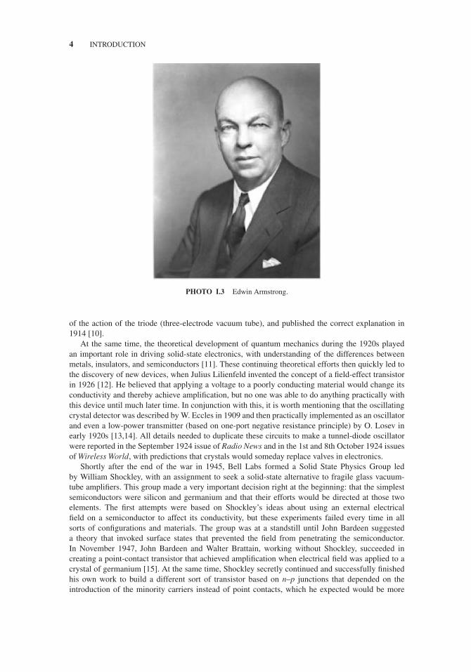
PHOTO I.3 Edwin Armstrong.
of the action of the triode (three-electrode vacuum tube), and published the correct explanation in1914 [10].
At the same time, the theoretical development of quantum mechanics during the 1920s playedan important role in driving solid-state electronics, with understanding of the differences betweenmetals, insulators, and semiconductors [11]. These continuing theoretical efforts then quickly led tothe discovery of new devices, when Julius Lilienfeld invented the concept of a field-effect transistorin 1926 [12]. He believed that applying a voltage to a poorly conducting material would change itsconductivity and thereby achieve amplification, but no one was able to do anything practically withthis device until much later time. In conjunction with this, it is worth mentioning that the oscillatingcrystal detector was described by W. Eccles in 1909 and then practically implemented as an oscillatorand even a low-power transmitter (based on one-port negative resistance principle) by O. Losev inearly 1920s [13,14]. All details needed to duplicate these circuits to make a tunnel-diode oscillatorwere reported in the September 1924 issue of Radio News and in the 1st and 8th October 1924 issuesof Wireless World, with predictions that crystals would someday replace valves in electronics.
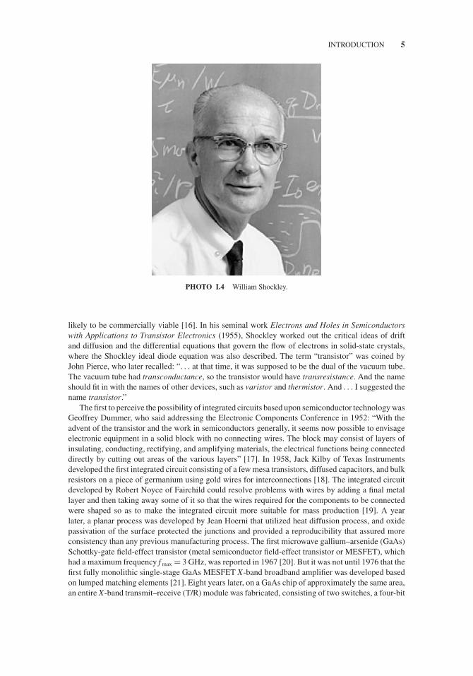
Shortly after the end of the war in 1945, Bell Labs formed a Solid State Physics Group ledby William Shockley, with an assignment to seek a solid-state alternative to fragile glass vacuum-tube amplifiers. This group made a very important decision right at the beginning: that the simplestsemiconductors were silicon and germanium and that their efforts would be directed at those twoelements. The first attempts were based on Shockley’s ideas about using an external electricalfield on a semiconductor to affect its conductivity, but these experiments failed every time in allsorts of configurations and materials. The group was at a standstill until John Bardeen suggesteda theory that invoked surface states that prevented the field from penetrating the semiconductor.In November 1947, John Bardeen and Walter Brattain, working without Shockley, succeeded increating a point-contact transistor that achieved amplification when electrical field was applied to acrystal of germanium [15]. At the same time, Shockley secretly continued and successfully finishedhis own work to build a different sort of transistor based on n–p junctions that depended on theintroduction of the minority carriers instead of point contacts, which he expected would be more
JWBS064-cintro JWBS064-Gerbennikov March 11, 2011 19:44 Printer Name: Yet to Come
INTRODUCTION 5
PHOTO I.4 William Shockley.
likely to be commercially viable [16]. In his seminal work Electrons and Holes in Semiconductorswith Applications to Transistor Electronics (1955), Shockley worked out the critical ideas of driftand diffusion and the differential equations that govern the flow of electrons in solid-state crystals,where the Shockley ideal diode equation was also described. The term “transistor” was coined byJohn Pierce, who later recalled: “. . . at that time, it was supposed to be the dual of the vacuum tube.The vacuum tube had transconductance, so the transistor would have transresistance. And the nameshould fit in with the names of other devices, such as varistor and thermistor. And . . . I suggested thename transistor.”
The first to perceive the possibility of integrated circuits based upon semiconductor technology wasGeoffrey Dummer, who said addressing the Electronic Components Conference in 1952: “With theadvent of the transistor and the work in semiconductors generally, it seems now possible to envisageelectronic equipment in a solid block with no connecting wires. The block may consist of layers ofinsulating, conducting, rectifying, and amplifying materials, the electrical functions being connecteddirectly by cutting out areas of the various layers” [17]. In 1958, Jack Kilby of Texas Instrumentsdeveloped the first integrated circuit consisting of a few mesa transistors, diffused capacitors, and bulkresistors on a piece of germanium using gold wires for interconnections [18]. The integrated circuitdeveloped by Robert Noyce of Fairchild could resolve problems with wires by adding a final metallayer and then taking away some of it so that the wires required for the components to be connectedwere shaped so as to make the integrated circuit more suitable for mass production [19]. A yearlater, a planar process was developed by Jean Hoerni that utilized heat diffusion process, and oxidepassivation of the surface protected the junctions and provided a reproducibility that assured moreconsistency than any previous manufacturing process. The first microwave gallium–arsenide (GaAs)Schottky-gate field-effect transistor (metal semiconductor field-effect transistor or MESFET), whichhad a maximum frequency f max = 3 GHz, was reported in 1967 [20]. But it was not until 1976 that thefirst fully monolithic single-stage GaAs MESFET X-band broadband amplifier was developed basedon lumped matching elements [21]. Eight years later, on a GaAs chip of approximately the same area,an entire X-band transmit–receive (T/R) module was fabricated, consisting of two switches, a four-bit

JWBS064-cintro JWBS064-Gerbennikov March 11, 2011 19:44 Printer Name: Yet to Come
6 INTRODUCTION
TABLE I.1 IEEE Standard Letter Designations for Frequency Bands.
Band Frequency Wavelength
HF (high frequency) 3–30 MHz 100–10 mVHF (very high frequency) 30–300 MHz 10–1.0 mUHF (ultra high frequency) 300–1000 MHz 1.0 m to 30 cmL 1–2 GHz 30–15 cmS 2–4 GHz 15 cm to 7.5 cmC 4–8 GHz 7.50–3.75 cmX 8–12 GHz 3.75–2.50 cmKu 12–18 GHz 2.50–1.67 cmK 18–27 GHz 1.67–1.11 cmKa 27–40 GHz 1.11 cm to 7.5 mmV 40–75 GHz 7.5–4.0 mmW 75–110 GHz 4.0–2.7 mmMillimeter wave 110–300 GHz 2.7–1.0 mm
phase shifter, a three-stage low-noise amplifier, and a four-stage power amplifier [22]. Generally, amonolithic microwave integrated circuit (MMIC) was defined as an active or passive microwave circuitformed in situ on a semiconductor substrate by a combination of deposition techniques includingdiffusion, evaporation, epitaxy, and other means [23].
Table I.1 shows the IEEE standard letter designations for frequency bands [24]. In military radarband designations, millimeter-wave bandwidth occupies the frequency range from 40 to 300 GHz.The letter designations (L, S, C, X, Ku, K, Ka) were meant to be used for radar, but have becomecommonly used for other microwave frequency applications. The K-band is the middle band (18–27GHz) that originated from the German word “Kurz”, which means short, while Ku-band is lower infrequency (Kurz-under), and Ka-band is higher in frequency (Kurz-above). The 1984 revision definedthe application of letters V and W to a portion of the millimeter-wave region each while retaining theprevious letter designators for frequencies.
REFERENCES
1. L. De Forest, “Space Telegraphy,” U.S. Patent 879,532, Feb. 1908 (filed Jan. 1907).
2. L. De Forest, “The Audion – Detector and Amplifier,” Proc. IRE, vol. 2, pp. 15–29, Mar. 1914.
3. “High-Frequency Oscillating Transmitter for Wireless Telephony,” Electrical World, p. 144, July 18, 1914.
4. T. H. White, United States Early Radio History, http://earlyradiohistory.us, sec. 11.
5. E. B. Craft and E. H. Colpitts, “Radio Telephony,” Trans. AIEE, vol. 38, pp. 305–343, Feb. 1919.
6. “Wireless-Telephone Set,” Electrical World, p. 487, Sept. 5, 1914.
7. J. E. Brittain, “Electrical Engineering Hall of Fame: Guglielmo Marconi,” Proc. IEEE, vol. 92, pp. 1501–1504,Sept. 2004.
8. A. Meissner, “The Development of Tube Transmitters by the Telefunken Company,” Proc. IRE, vol. 10,pp. 3–23, Jan. 1922.
9. V. Bashenoff, “Progress in Radio Engineering in Russia 1918–1922,” Proc. IRE, vol. 11, pp. 257–270, Mar.1923.
10. “Edwin Howard Armstrong,” Proc. IRE, vol. 31, p. 315, July 1943.
11. W. F. Brinkman, D. E. Haggan, and W. W. Troutman, “A History of the Invention of the Transistor and WhereIt Will Lead Us,” IEEE J. Solid-State Circuits, vol. SC-32, pp. 1858–1865, Dec. 1997.
12. J. E. Lilienfeld, “Method and Apparatus for Controlled Electric Currents,” U.S. Patent 1745175, Jan. 1930(filed Oct. 1926).

JWBS064-cintro JWBS064-Gerbennikov March 11, 2011 19:44 Printer Name: Yet to Come
REFERENCES 7
13. W. H. Eccles, “On an Oscillation Detector Actuated Solely by Resistance-Temperature Variations,” Proc.Phys. Society. London, vol. 22, pp. 360–368, Jan. 1909.
14. M. A. Novikov, “Oleg Vladimirovich Losev: Pioneer of Semiconductor Electronics,” Physics of the SolidState, vol. 46, pp. 1–4, Jan. 2004.
15. J. Bardin and W. H. Brattain, “Three-Electrode Circuit Element Utilizing Semiconductive Materials,” U.S.Patent 2524035, Oct. 1950 (filed June 17, 1948).
16. W. Shockley, “Circuit Element Utilizing Semiconductive Material,” U.S. Patent 2569347, Sept. 1951 (filedJune 26, 1948).
17. J. S. Kilby, “Invention of the Integrated Circuit,” IEEE Trans. Electron Devices, vol. ED-23, pp. 648–654,July 1976.
18. J. S. Kilby, “Miniaturized Electronic Circuits,” U.S. Patent 3138743, June 1964 (filed Feb. 1959).
19. R. N. Noyce, “Semiconductor Device-and-Lead Structure,” U.S. Patent 2981877, Apr. 1961 (filed July 1959).
20. D. N. McQuiddy, J. W. Wassel, J. Bradner LaGrange, and W. R. Wisseman, “Monolithic Microwave IntegratedCircuits: An Historical Perspective,” IEEE Trans. Microwave Theory Tech., vol. MTT-32, pp. 997–1008, Sept.1984.
21. R. S. Pengelly and J. A. Turner, “Monolithic Broadband GaAs F.E.T. Amplifiers,” Electronics Lett., vol. 12,pp. 251–252, May 1976.
22. E. C. Niehenke, R. A. Pucel, and I. J. Bahl, “Microwave and Millimeter-Wave Integrated Circuits,” IEEETrans. Microwave Theory Tech., vol. MTT-50, pp. 846–857, Mar. 2002.
23. R. A. Pucel, “Design Considerations for Monolithic Microwave Circuits,” IEEE Trans. Microwave TheoryTech., vol. MTT-29, pp. 513–534, June 1981.
24. IEEE Standard 521-2002, IEEE Standard Letter Designations for Radar-Frequency Bands, 2003.

JWBS064-cintro JWBS064-Gerbennikov March 11, 2011 19:44 Printer Name: Yet to Come
8
JWBS064-c01 JWBS064-Gerbennikov March 12, 2011 8:36 Printer Name: Yet to Come
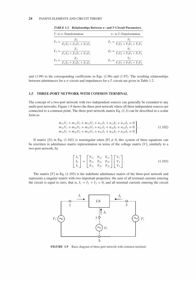
1 Passive Elements and Circuit Theory
The two-port equivalent circuits are widely used in radio frequency (RF) and microwave circuitdesign to describe the electrical behavior of both active devices and passive networks [1–4]. Thetwo-port network impedance Z-parameters, admittance Y-parameters, or hybrid H-parameters arevery important to characterize the nonlinear properties of the active devices, bipolar or field-effecttransistors. The transmission ABCD-parameters of a two-port network are very convenient for design-ing the distributed circuits like transmission lines or cascaded elements. The scattering S-parametersare useful to characterize linear circuits, and are required to simplify the measurement procedure.Transmission lines are widely used in matching circuits in power amplifiers, in resonant circuitsin the oscillators, filters, directional couplers, power combiners, and dividers. The design formulasand curves are presented for several types of transmission lines including stripline, microstrip line,slotline, and coplanar waveguide. Monolithic implementation of lumped inductors and capacitors isusually required at microwave frequencies and for portable devices. Knowledge of noise phenomena,such as the noise figure, additive white noise, low-frequency fluctuations, or flicker noise in activeor passive elements, is very important for the oscillator modeling in particular and entire transmitterdesign in general.
1.1 IMMITTANCE TWO-PORT NETWORK PARAMETERS
The basic diagram of a two-port nonautonomous transmission system can be represented by theequivalent circuit shown in Figure 1.1, where VS is the independent voltage source, ZS is the sourceimpedance, LN is the linear time-invariant two-port network without independent source, and ZL isthe load impedance. The two independent phasor currents I1 and I2 (flowing across input and outputterminals) and phasor voltages V1 and V2 characterize such a two-port network. For autonomousoscillator systems, in order to provide an appropriate analysis in the frequency domain of the two-port network in the negative one-port representation, it is sufficient to set the source impedance toinfinity. For a power amplifier or oscillator design, the elements of the matching or resonant circuits,which are assumed to be linear or appropriately linearized, can be found among the LN-networkelements, or additional two-port linear networks can be used to describe their frequency domainbehavior.
For a two-port network, the following equations can be considered to be imposed boundaryconditions:
V1 + ZS I1 = VS (1.1)
V2 + ZL I2 = VL . (1.2)
Suppose that it is possible to obtain a unique solution for the linear time-invariant circuit shown inFigure 1.1. Then the two linearly independent equations, which describe the general two-port network
RF and Microwave Transmitter Design, First Edition. Andrei Grebennikov.C© 2011 John Wiley & Sons, Inc. Published 2011 by John Wiley & Sons, Inc.
9

JWBS064-c01 JWBS064-Gerbennikov March 12, 2011 8:36 Printer Name: Yet to Come
10 PASSIVE ELEMENTS AND CIRCUIT THEORY
FIGURE 1.1 Basic diagram of two-port nonautonomous transmission system.
in terms of circuit variables V1, V2, I1, and I2, can be expressed in a matrix form as
[M] [V ] + [N ] [I ] = 0 (1.3)
or
m11V1 + m12V2 + n11 I1 + n12 I2 = 0
m21V1 + m22V2 + n21 I1 + n22 I2 = 0
}. (1.4)
The complex 2 × 2 matrices [M] and [N] in Eq. (1.3) are independent of the source and loadimpedances ZS and ZL and voltages VS and VL, respectively, and they depend only on the circuitelements inside the LN network.
If matrix [M] in Eq. (1.3) is nonsingular when |M| �= 0, then this matrix equation can be rewrittenin terms of [I] as
[V ] = − [M]−1 [N ] [I ] = [Z ] [I ] (1.5)
where [Z] is the open-circuit impedance two-port network matrix. In a scalar form, matrix Eq. (1.5)is given by
V1 = Z11 I1 + Z12 I2 (1.6)
V2 = Z21 I1 + Z22 I2 (1.7)
where Z11 and Z22 are the open-circuit driving-point impedances, and Z12 and Z21 are the open-circuittransfer impedances of the two-port network. The voltage components V1 and V2 due to the inputcurrent I1 can be found by setting I2 = 0 in Eqs. (1.6) and (1.7), resulting in an open-output terminal.Similarly, the same voltage components V1 and V2 are determined by setting I1 = 0 when the inputterminal becomes open-circuited. The resulting driving-point impedances can be written as
Z11 = V1
I1
∣∣∣∣I2=0
Z22 = V2
I2
∣∣∣∣I1=0
(1.8)
whereas the two transfer impedances are
Z21 = V2
I1
∣∣∣∣I2=0
Z12 = V1
I2
∣∣∣∣I1=0
. (1.9)
Dual analysis can be used to derive the short-circuit admittance matrix when the current compo-nents I1 and I2 are considered as outputs caused by V1 and V2. If matrix [N] in Eq. (1.3) is nonsingular

JWBS064-c01 JWBS064-Gerbennikov March 12, 2011 8:36 Printer Name: Yet to Come
IMMITTANCE TWO-PORT NETWORK PARAMETERS 11
when |N| �= 0, this matrix equation can be rewritten in terms of [V] as
[I ] = − [N ]−1 [M] [V ] = [Y ] [V ] (1.10)
where [Y] is the short-circuit admittance two-port network matrix. In a scalar form, matrix Eq. (1.10)is written as
I1 = Y11V1 + Y12V2 (1.11)
I2 = Y21V1 + Y22V2 (1.12)
where Y11 and Y22 are the short-circuit driving-point admittances, and Y12 and Y21 are the short-circuittransfer admittances of the two-port network. In this case, the current components I1 and I2 due to theinput voltage source V1 are determined by setting V2 = 0 in Eqs. (1.11) and (1.12), thus creating a shortoutput terminal. Similarly, the same current components I1 and I2 are determined by setting V1 = 0when input terminal becomes short-circuited. As a result, the two driving-point admittances are
Y11 = I1
V1
∣∣∣∣V2=0
Y22 = I2
V2
∣∣∣∣V1=0
(1.13)
whereas the two transfer admittances are
Y21 = I2
V1
∣∣∣∣V2=0
Y12 = I1
V2
∣∣∣∣V1=0
. (1.14)
In some cases, an equivalent two-port network representation can be redefined in order to expressthe voltage source V1 and output current I2 in terms of the input current I1 and output voltage V2. Ifthe submatrix
[m11 n12
m21 n22
]
given in Eq. (1.4) is nonsingular, then
[V1
I2
]= −
[m11 n12
m21 n22
]−1 [n11 m12
n21 m22
] [I1
V2
]= [H ]
[I1
V2
](1.15)
where [H] is the hybrid two-port network matrix. In a scalar form, it is best to represent matrix Eq.(1.15) as
V1 = h11 I1 + h12V2 (1.16)
I2 = h21 I1 + h22V2 (1.17)
where h11, h12, h21, and h22 are the hybrid H-parameters. The voltage source V1 and current componentI2 are determined by setting V2 = 0 for the short output terminal in Eqs. (1.16) and (1.17) as
h11 = V1
I1
∣∣∣∣V2=0
h21 = I2
I1
∣∣∣∣V2=0
(1.18)
where h11 is the driving-point input impedance and h21 is the forward current transfer function.Similarly, the input voltage source V1 and output current I2 are determined by setting I1 = 0 when

JWBS064-c01 JWBS064-Gerbennikov March 12, 2011 8:36 Printer Name: Yet to Come
12 PASSIVE ELEMENTS AND CIRCUIT THEORY
input terminal becomes open-circuited as
h12 = V1
V2
∣∣∣∣I1=0
h22 = I2
V2
∣∣∣∣I1=0
(1.19)
where h12 is the reverse voltage transfer function and h22 is the driving-point output admittance.The transmission parameters, often used for passive device analysis, are determined for the
independent input voltage source V1 and input current I1 in terms of the output voltage V2 and outputcurrent I2. In this case, if the submatrix
[m11 n11
m21 n21
]
given in Eq. (1.4) is nonsingular, we obtain
[V1
I1
]= −
[m11 n11
m21 n21
]−1 [m12 n12
m22 n22
] [V2
−I2
]= [ABCD]
[V2
−I2
](1.20)
where [ABCD] is the forward transmission two-port network matrix. In a scalar form, we can write
V1 = AV2 − B I2 (1.21)
I1 = CV2 − DI2 (1.22)
where A, B, C, and D are the transmission parameters. The voltage source V1 and current componentI1 are determined by setting I2 = 0 for the open output terminal in Eqs. (1.21) and (1.22) as
A = V1
V2
∣∣∣∣I2=0
C = I1
V2
∣∣∣∣I2=0
(1.23)
where A is the reverse voltage transfer function and C is the reverse transfer admittance. Similarly,the input independent variables V1 and I1 are determined by setting V2 = 0 when the output terminalis short-circuited as
B = V1
I2
∣∣∣∣V2=0
D = I1
I2
∣∣∣∣V2=0
(1.24)
where B is the reverse transfer impedance and D is the reverse current transfer function. The reason aminus sign is associated with I2 in Eqs. (1.20) to (1.22) is that historically, for transmission networks,the input signal is considered as flowing to the input port whereas the output current flowing to theload. The direction of the current –I2 entering the load is shown in Figure 1.2.
The parameters describing the same two-port network through different two-port matrices(impedance, admittance, hybrid, or transmission) can be cross-converted, and the elements of each
FIGURE 1.2 Basic diagram of loaded two-port transmission system.

JWBS064-c01 JWBS064-Gerbennikov March 12, 2011 8:36 Printer Name: Yet to Come
SCATTERING PARAMETERS 13
TABLE 1.1 Relationships Between Z-, Y-, H- and ABCD-Parameters.
[Z] [Y] [H] [ABCD]
[Z] Z11 Z12
Z21 Z22
Y22
�Y− Y12
�Y
− Y21
�Y
Y11
�Y
�H
h22
h12
h22
− h21
h22
1
h22
A
C
AD − BC
C
1
C
D
C
[Y] Z22
�Z− Z12
�Z
− Z21
�Z
Z11
�Z
Y11 Y12
Y21 Y22
1
h11− h12
h11
h21
h11
�H
h11
D
B− AD − BC
B
− 1
B
A
B
[H] �Z
Z22
Z12
Z22
− Z21
Z22
1
Z22
1
Y11− Y12
Y11
Y21
Y11
�Y
Y11
h11 h12
h21 h22
B
D
AD − BC
D
− 1
D
C
D
[ABCD] Z11
Z21
�Z
Z21
1
Z21
Z22
Z21
− Y22
Y21− 1
Y21
−�Y
Y21− Y11
Y21
−�H
h21− h11
h21
− h22
h21− 1
h21
A BC D
matrix can be expressed by the elements of other matrices. For example, Eqs. (1.11) and (1.12) forthe Y-parameters can be easily solved for the independent input voltage source V1 and input currentI1 as
V1 = −Y22
Y21V2 + 1
Y21I2 (1.25)
I1 = −Y11Y22 − Y12Y21
Y21V2 + Y11
Y21I2. (1.26)
By comparing the equivalent Eqs. (1.21) and (1.22) and Eqs. (1.25) and (1.26), the direct relation-ships between the elements of the transmission ABCD-matrix and admittance Y-matrix are writtenas
A = −Y22
Y21B = − 1
Y21(1.27)
C = −�Y
Y21D = −Y11
Y21(1.28)
where �Y = Y11Y22 − Y12Y21.A summary of the relationships between the impedance Z-parameters, admittance Y-parameters,
hybrid H-parameters, and transmission ABCD-parameters is shown in Table 1.1, where �Z =Z11 Z22 − Z12 Z21 and �H = h11h22 − h12h21.
1.2 SCATTERING PARAMETERS
The concept of incident and reflected voltage and current parameters can be illustrated by the one-portnetwork shown in Figure 1.3, where the network impedance Z is connected to the signal source VS

JWBS064-c01 JWBS064-Gerbennikov March 12, 2011 8:36 Printer Name: Yet to Come
14 PASSIVE ELEMENTS AND CIRCUIT THEORY
FIGURE 1.3 Incident and reflected voltages and currents.
with the internal impedance ZS. In a common case, the terminal current I and voltage V consistof incident and reflected components (assume their root mean square [rms] values). When the loadimpedance Z is equal to the conjugate of source impedance expressed as Z = Z∗
S, the terminal currentbecomes the incident current. It is calculated from
Ii = VS
Z∗S + ZS
= VS
2ReZS. (1.29)
The terminal voltage, defined as the incident voltage, can be determined from
Vi = Z∗S VS
Z∗S + ZS
= Z∗S VS
2ReZS. (1.30)
Consequently, the incident power, which is equal to the maximum available power from the source,can be obtained by
Pi = Re(Vi I
∗i
) = |VS|24ReZS
. (1.31)
The incident power can be presented in a normalized form using Eq. (1.30) as
Pi = |Vi|2 ReZS∣∣Z∗S
∣∣2 . (1.32)
This allows the normalized incident voltage wave a to be defined as the square root of the incidentpower Pi by
a =√
Pi = Vi√
ReZS
Z∗S
. (1.33)
Similarly, the normalized reflected voltage wave b, defined as the square root of the reflectedpower Pr, can be written as
b =√
Pr = Vr√
ReZS
ZS. (1.34)

JWBS064-c01 JWBS064-Gerbennikov March 12, 2011 8:36 Printer Name: Yet to Come
SCATTERING PARAMETERS 15
The incident power can be expressed by the incident current Ii and the reflected power can beexpressed by the reflected current Ir, respectively, as
Pi = |Ii|2 ReZS (1.35)
Pr = |Ir|2 ReZS. (1.36)
As a result, the normalized incident voltage wave a and reflected voltage wave b can be given by
a =√
Pi = Ii
√ReZS (1.37)
b =√
Pr = Ir
√ReZS. (1.38)
The parameters a and b can also be called the normalized incident and reflected current waves,or simply normalized incident and reflected waves, respectively, since the normalized current wavesand the normalized voltage waves represent the same parameters.
The voltage V and current I, related to the normalized incident and reflected waves a and b, canbe written as
V = Vi + Vr = Z∗S√
ReZSa + ZS√
ReZSb (1.39)
I = Ii − Ir = 1√ReZS
a − 1
1√
ReZSb (1.40)
where
a = V + ZS I
2√
ReZSb = V − Z∗
S I
2√
ReZS. (1.41)
The source impedance ZS is often purely real and, therefore, is used as the normalized impedance.In microwave design technique, the characteristic impedance of the passive two-port networks,including transmission lines and connectors, is considered as real and equal to 50 Ω. This is veryimportant for measuring S-parameters when all transmission lines, source, and load should have thesame real impedance. For ZS = Z∗
S = Z0, where Z0 is the characteristic impedance, the ratio ofthe normalized reflected wave and the normalized incident wave for a one-port network is called thereflection coefficient �, defined as
� = b
a= V − Z∗
S I
V + ZS I= V − ZS I
V + ZS I= Z − ZS
Z + ZS(1.42)
where Z = V/I .For a two-port network shown in Figure 1.4, the normalized reflected waves b1 and b2 can also be
represented by the normalized incident waves a1 and a2, respectively, as
b1 = S11a1 + S12a2 (1.43)
b2 = S21a1 + S22a2 (1.44)
or, in a matrix form,
[b1
b2
]=[
S11 S11
S21 S21
] [a1
a2
](1.45)

JWBS064-c01 JWBS064-Gerbennikov March 12, 2011 8:36 Printer Name: Yet to Come
16 PASSIVE ELEMENTS AND CIRCUIT THEORY
FIGURE 1.4 Basic diagram of S-parameter two-port network.
where the incident waves a1 and a2 and the reflected waves b1 and b2, for complex source and loadimpedances ZS and ZL, are given by
a1 = V1 + ZS I1
2√
ReZSa2 = V2 + ZL I2
2√
ReZL(1.46)
b1 = V1 − Z∗S I1
2√
ReZSb2 = V2 − Z ∗
L I2
2√
ReZL(1.47)
where S11, S12, S21, and S22 are the S-parameters of the two-port network.From Eq. (1.45) it follows that if a2 = 0, then
S11 = b1
a1
∣∣∣∣a2=0
S21 = b2
a1
∣∣∣∣a2=0
(1.48)
where S11 is the reflection coefficient and S21 is the transmission coefficient for ideal match-ing conditions at the output terminal when there is no incident power reflected from the load.Similarly,
S12 = b1
a2
∣∣∣∣a1=0
S22 = b2
a2
∣∣∣∣a1=0
(1.49)
where S12 is the transmission coefficient and S22 is the reflection coefficient for ideal matchingconditions at the input terminal.
To convert S-parameters to the admittance Y-parameters, it is convenient to represent Eqs. (1.46)and (1.47) as
I1 = (a1 − b1)1√Z0
I2 = (a2 − b2)1√Z0
(1.50)
V1 = (a1 + b1)√
Z0 V1 = (a2 + b2)√
Z0 (1.51)
where it is assumed that the source and load impedances are real and equal to ZS = ZL = Z0.Substituting Eqs. (1.50) and (1.51) to Eqs. (1.11) and (1.12) results in
a1 − b1√Z0
= Y11 (a1 + b1)√
Z0 + Y12 (a2 + b2)√
Z0 (1.52)
a2 − b2√Z0
= Y21 (a1 + b1)√
Z0 + Y22 (a2 + b2)√
Z0 (1.53)
JWBS064-c01 JWBS064-Gerbennikov March 12, 2011 8:36 Printer Name: Yet to Come
INTERCONNECTIONS OF TWO-PORT NETWORKS 17
which can then be respectively converted to
−b1 (1 + Y11 Z0) − b2Y12 Z0 = −a1 (1 − Y11 Z0) + a2Y12 Z0 (1.54)
−b1Y21 Z0 − b2 (1 + Y22 Z0) = a1Y21 Z0 − a2 (1 − Y22 Z0) . (1.55)
Eqs. (1.54) and (1.55) can be easily solved for the reflected waves b1 and b2 as
b1
[(1 + Y11 Z0) (1 + Y22 Z0) − Y12Y21 Z 2
0
] = a1
[(1 − Y11 Z0) (1 + Y22 Z0) + Y12Y21 Z 2
0
]− 2a2Y12 Z0
(1.56)
b2
[(1 + Y11 Z0) (1 + Y22 Z0) − Y12Y21 Z 2
0
] = −2a1Y21 Z0 + a2
[(1 + Y11 Z0) (1 − Y22 Z0) + Y12Y21 Z 2
0
](1.57)
Comparing equivalent Eqs. (1.43) and (1.44) and Eqs. (1.56) and (1.57) gives the followingrelationships between the scattering S-parameters and admittance Y-parameters:
S11 = (1 − Y11 Z0) (1 + Y22 Z0) + Y12Y21 Z 20
(1 + Y11 Z0) (1 + Y22 Z0) − Y12Y21 Z 20
(1.58)
S12 = −2Y12 Z0
(1 + Y11 Z0) (1 + Y22 Z0) − Y12Y21 Z 20
(1.59)
S21 = −2Y21 Z0
(1 + Y11 Z0) (1 + Y22 Z0) − Y12Y21 Z 20
(1.60)
S22 = (1 + Y11 Z0) (1 − Y22 Z0) + Y12Y21 Z 20
(1 + Y11 Z0) (1 + Y22 Z0) − Y12Y21 Z 20
. (1.61)
Similarly, the relationships of S-parameters with Z-, H-, and ABCD-parameters can be obtainedfor the simplified case when the source impedance ZS and the load impedance ZL are equal to thecharacteristic impedance Z0 [5].
1.3 INTERCONNECTIONS OF TWO-PORT NETWORKS
When analyzing the behavior of a particular electrical circuit in terms of the two-port networkparameters, it is often necessary to define the parameters of a combination of the two or more internaltwo-port networks. For example, the general feedback amplifier circuit consists of an active two-portnetwork representing the amplifier stage, which is connected in parallel with a passive feedbacktwo-port network. In general, the two-port networks can be interconnected using parallel, series,series–parallel, or cascade connections.
To characterize the resulting two-port networks, it is necessary to take into account which currentsand voltages are common for individual two-port networks. The most convenient set of parametersis one for which the common currents and voltages represent a simple linear combination of theindependent variables. For the interconnection shown in Figure 1.5(a), the two-port networks Za andZb are connected in series for both the input and output terminals. Therefore, the currents flowingthrough these terminals are equal when
I1 = I1a = I1b I2 = I2a = I2b (1.62)

JWBS064-c01 JWBS064-Gerbennikov March 12, 2011 8:36 Printer Name: Yet to Come
18 PASSIVE ELEMENTS AND CIRCUIT THEORY
FIGURE 1.5 Different interconnections of two-port networks.

JWBS064-c01 JWBS064-Gerbennikov March 12, 2011 8:36 Printer Name: Yet to Come
INTERCONNECTIONS OF TWO-PORT NETWORKS 19
or, in a matrix form,
[I ] = [Ia] = [Ib] . (1.63)
The terminal voltages of the resulting two-port network represent the corresponding sums of theterminal voltages of the individual two-port networks when
V1 = V1a + V1b V2 = V2a + V2b (1.64)
or, in a matrix form,
[V ] = [Va] + [Vb] . (1.65)
The currents are common components, both for the resulting and individual two-port networks.Consequently, to describe the properties of such a circuit, it is most convenient to use the impedancematrices. For each two-port network Za and Zb, we can write using Eq. (1.62), respectively,
[Va] = [Za] [Ia] = [Za] [I ] (1.66)
[Vb] = [Zb] [Ib] = [Zb] [I ] . (1.67)
Adding both sides of Eqs. (1.66) and (1.67) yields
[V ] = [Z ] [I ] (1.68)
where
[Z ] = [Za] + [Zb] =[
Z11a + Z11b Z12a + Z12b
Z21a + Z21b Z22a + Z22b
]. (1.69)
The circuit shown in Figure 1.5(b) is composed of the two-port networks Ya and Yb connectedin parallel, where the common components for both resulting and individual two-port networks areinput and output voltages, respectively,
V1 = V1a = V1b V2 = V2a = V2b (1.70)
or, in a matrix form,
[V ] = [Va] = [Vb] . (1.71)
Consequently, to describe the circuit properties in this case, it is convenient to use the admittancematrices that give the resulting matrix equation in the form
[I ] = [Y ] [V ] (1.72)
where
[Y ] = [Ya] + [Yb] =[
Y11a + Y11b Y12a + Y12b
Y21a + Y21b Y22a + Y22b
]. (1.73)
The series connection of the input terminals and parallel connection of the output terminals arecharacterized by the circuit in Figure 1.5(c), which shows a series–parallel connection of two-port
JWBS064-c01 JWBS064-Gerbennikov March 12, 2011 8:36 Printer Name: Yet to Come
20 PASSIVE ELEMENTS AND CIRCUIT THEORY
networks. The common components for this circuit are the input currents and the output voltages. Asa result, it is most convenient to analyze the circuit properties using hybrid matrices. The resultingtwo-port hybrid matrix is equal to the sum of the two individual hybrid matrices written as
[H ] = [Ha] + [Hb] =[
h11a + h11b h12a + h12b
h21a + h21b h22a + h22b
]. (1.74)
Figure 1.5(d) shows the cascade connection of the two individual two-port networks. For such anapproach using the one-by-one interconnection of the two-port networks, the output voltage and theoutput current of the first network is equal to the input voltage and the input current of the secondone, respectively, when
V1 = V1a I1 = I1a (1.75)
V2a = V1 − I2a = I1b (1.76)
V2b = V2 − I2b = −I2 (1.77)
In this case, it is convenient to use a system of ABCD-parameters given by Eqs. (1.21) and (1.22).As a result, for the first individual two-port network shown in Figure 1.5(d),
[V1a
I1a
]=[
Aa Ba
Ca Da
] [V2a
−I2a
](1.78)
or, using Eqs. (1.75) and (1.76),
[V1
I1
]=[
Aa Ba
Ca Da
] [V1b
I1b
]. (1.79)
Similarly, for the second individual two-port network,
[V1b
I1b
]=[
Ab Bb
Cb Db
] [V2b
−I2b
]=[
Ab Bb
Cb Db
] [V2
−I2
]. (1.80)
Then, substituting matrix Eq. (1.80) to matrix Eq. (1.79) yields
[V1
I1
]=[
Aa Ba
Ca Da
] [Ab Bb
Cb Db
] [V2
−I2
]=[
A BC D
] [V2
−I2
]. (1.81)
Consequently, the transmission matrix of the resulting two-port network obtained by the cascadeconnection of the two or more individual two-port networks is determined by multiplying the trans-mission matrices of the individual networks. This important property is widely used in the analysisand design of transmission networks and systems.
1.4 PRACTICAL TWO-PORT NETWORKS
1.4.1 Single-Element Networks
The simplest networks, which include only one element, can be constructed by a series-connectedadmittance Y , as shown in Figure 1.6(a), or by a parallel-connected impedance Z, as shown inFigure 1.6(b).

JWBS064-c01 JWBS064-Gerbennikov March 12, 2011 8:36 Printer Name: Yet to Come
PRACTICAL TWO-PORT NETWORKS 21
FIGURE 1.6 Single-element networks.
The two-port network consisting of the single series admittance Y can be described in a system ofY-parameters as
I1 = Y V1 − Y V2 (1.82)
I2 = −Y V1 + Y V2 (1.83)
or, in a matrix form,
[Y ] =[
Y −Y−Y Y
](1.84)
which means that Y11 = Y22 = Y and Y12 = Y21 = −Y . The resulting matrix is a singular matrix with|Y | = 0. Consequently, it is impossible to determine such a two-port network with the series admittanceY-parameters through a system of Z-parameters. However, by using H- and ABCD-parameters, it canbe described, respectively, by
[H ] =[
1/Y 1−1 0
][ABCD] =
[1 1/Y0 1
]. (1.85)
Similarly, for a two-port network with the single parallel impedance Z,
[Z ] =[
Z ZZ Z
](1.86)
which means that Z11 = Z12 = Z21 = Z22 = Z. The resulting matrix is a singular matrix with |Z| =0. In this case, it is impossible to determine such a two-port network with the parallel impedanceZ-parameters through a system of Y-parameters. By using H- and ABCD-parameters, this two-portnetwork can be described by
[H ] =[
0 1−1 1/Z
][ABCD] =
[1 0
1/Z 1
]. (1.87)
1.4.2 π- and T-Type Networks
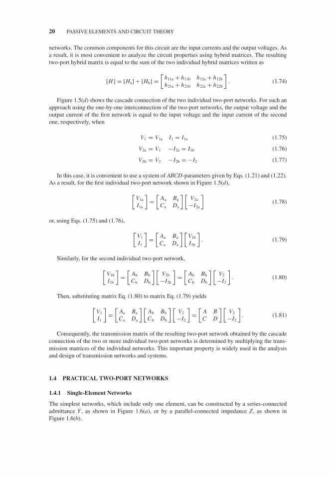
The basic configurations of a two-port network that usually describe the electrical properties of theactive devices can be represented in the form of a π -circuit shown in Figure 1.7(a) and in the formof a T-circuit shown in Figure 1.7(b). Here, the π -circuit includes the current source gmV1 and theT-circuit includes the voltage source rmI1.
JWBS064-c01 JWBS064-Gerbennikov March 12, 2011 8:36 Printer Name: Yet to Come
22 PASSIVE ELEMENTS AND CIRCUIT THEORY
FIGURE 1.7 Basic diagrams of π - and T-networks.
By writing the two loop equations using Kirchhoff’s current law or applying Eqs. (1.13) and (1.14)for the π -circuit, we obtain
I1 − (Y1 + Y3) V1 + Y3V2 = 0 (1.88)
I2 + (gm − Y3) V1 + (Y2 + Y3) V2 = 0. (1.89)
Eqs. (1.88) and (1.89) can be rewritten as matrix Eq. (1.3) with
[M] =[
1 00 1
]and [N ] =
[− (Y1 + Y3) Y3
−gm + Y3 − (Y2 + Y3)
].
Since matrix [M] is nonsingular, such a two-port network can be described by a system ofY-parameters as
[Y ] = − [M]−1 [N ] =[
Y1 + Y3 −Y3
gm − Y3 Y2 + Y3
]. (1.90)
Similarly, for a two-port network in the form of a T-circuit using Kirchhoff’s voltage law orapplying Eqs. (1.8) and (1.9), we obtain
[Z ] = − [M]−1 [N ] =[
Z1 + Z3 Z3
rm + Z3 Z2 + Z3
]. (1.91)
If gm = 0 for a π-circuit and rm = 0 for a T-circuit, their corresponding matrices in a system ofABCD-parameters can be written as, for π -circuit,
[ABCD] =
⎡⎢⎢⎣
1 + Y2
Y3
1
Y3
Y1 + Y2 + Y1Y2
Y31 + Y1
Y3
⎤⎥⎥⎦ (1.92)

JWBS064-c01 JWBS064-Gerbennikov March 12, 2011 8:36 Printer Name: Yet to Come
PRACTICAL TWO-PORT NETWORKS 23
FIGURE 1.8 Equivalence of π - and T-circuits.
for T-circuit,
[ABCD] =
⎡⎢⎢⎣
1 + Z2
Z3Z1 + Z2 + Z1 Z2
Z3
1
Z31 + Z1
Z3
⎤⎥⎥⎦ . (1.93)
For the appropriate relationships between impedances of a T-circuit and admittances of a π -circuit,these two circuits become equivalent with respect to the effect on any other two-port network. For aπ -circuit shown in Figure 1.8(a), we can write
I1 = Y1V13 + Y3V12 = Y1V13 + Y3 (V13 − V23) = (Y1 + Y3) V13 − Y3V23 (1.94)
I2 = Y2V23 − Y3V12 = Y2V23 − Y3 (V13 − V23) = −Y3V13 + (Y2 + Y3) V23. (1.95)
Solving Eqs. (1.94) and (1.95) for voltages V13 and V23 yields
V13 = Y2 + Y3
Y1Y2 + Y1Y2 + Y1Y2I1 + Y3
Y1Y2 + Y1Y2 + Y1Y2I2 (1.96)
V23 = Y3
Y1Y2 + Y1Y2 + Y1Y2I1 + Y1 + Y3
Y1Y2 + Y1Y2 + Y1Y2I2. (1.97)
Similarly, for a T-circuit shown in Figure 1.8(b),
V13 = Z1 I1 + Z3 I3 = Z1 I1 + Z3 (I1 + I2) = (Z1 + Z3) I1 + Z3 I2 (1.98)
V13 = Z1 I1 + Z3 I3 = Z1 I1 + Z3 (I1 + I2) = Z3 I1 + (Z2 + Z3) I2 (1.99)
and the equations for currents I1 and I2 can be obtained by
I1 = Z2 + Z3
Z1 Z2 + Z1 Z2 + Z1 Z2V13 − Z3
Z1 Z2 + Z1 Z2 + Z1 Z2V23 (1.100)
I2 = − Z3
Z1 Z2 + Z1 Z2 + Z1 Z2V13 + Z1 + Z3
Z1 Z2 + Z1 Z2 + Z1 Z2V23. (1.101)
To establish a T- to π-transformation, it is necessary to equate the coefficients for V13 and V23
in Eqs. (1.100) and (1.101) to the corresponding coefficients in Eqs. (1.94) and (1.95). Similarly, toestablish a π - to T-transformation, it is necessary to equate the coefficients for I1 and I2 in Eqs. (1.98)
JWBS064-c01 JWBS064-Gerbennikov March 12, 2011 8:36 Printer Name: Yet to Come
24 PASSIVE ELEMENTS AND CIRCUIT THEORY
TABLE 1.2 Relationships Between π- and T-Circuit Parameters.
T- to π -Transformation π- to T-Transformation
Y1 = Z2
Z1 Z2 + Z2 Z3 + Z1 Z3
Y2 = Z1
Z1 Z2 + Z2 Z3 + Z1 Z3
Y3 = Z3
Z1 Z2 + Z2 Z3 + Z1 Z3
Z1 = Y2
Y1Y2 + Y2Y3 + Y1Y3
Z2 = Y1
Y1Y2 + Y2Y3 + Y1Y3
Z3 = Y3
Y1Y2 + Y2Y3 + Y1Y3
and (1.99) to the corresponding coefficients in Eqs. (1.96) and (1.97). The resulting relationshipsbetween admittances for a π -circuit and impedances for a T-circuit are given in Table 1.2.
1.5 THREE-PORT NETWORK WITH COMMON TERMINAL
The concept of a two-port network with two independent sources can generally be extended to anymulti-port networks. Figure 1.9 shows the three-port network where all three independent sources areconnected to a common point. The three-port network matrix Eq. (1.3) can be described in a scalarform as
m11V1 + m12V2 + m13V3 + n11 I1 + n12 I2 + n13 I3 = 0m21V1 + m22V2 + m23V3 + n21 I1 + n22 I2 + n23 I3 = 0m31V1 + m32V2 + m33V3 + n31 I1 + n32 I2 + n33 I3 = 0
⎫⎬⎭ . (1.102)
If matrix [N] in Eq. (1.102) is nonsingular when |N| �= 0, this system of three equations canbe rewritten in admittance matrix representation in terms of the voltage matrix [V], similarly to atwo-port network, by
⎡⎣ I1
I2
I3
⎤⎦ =
⎡⎣Y11 Y12 Y13
Y21 Y22 Y23
Y31 Y32 Y33
⎤⎦⎡⎣ V1
V2
V3
⎤⎦ . (1.103)
The matrix [Y] in Eq. (1.103) is the indefinite admittance matrix of the three-port network andrepresents a singular matrix with two important properties: the sum of all terminal currents enteringthe circuit is equal to zero, that is, I1 + I2 + I3 = 0; and all terminal currents entering the circuit
FIGURE 1.9 Basic diagram of three-port network with common terminal.

JWBS064-c01 JWBS064-Gerbennikov March 12, 2011 8:36 Printer Name: Yet to Come
THREE-PORT NETWORK WITH COMMON TERMINAL 25
depend on the voltages between circuit terminals, which makes the sum of all terminal voltages equalto zero, that is, V13 + V32 + V21 = 0.
According to the first property, adding the left and right parts of matrix Eq. (1.103) results in
(Y11 + Y21 + Y31) V1 + (Y12 + Y22 + Y32) V2 + (Y13 + Y23 + Y33) V3 = 0. (1.104)
Since all terminal voltages (V1, V2, and V3) can be set independently from each other, Eq. (1.104)can be satisfied only if any column sum is identically zero,
Y11 + Y21 + Y31 = 0Y12 + Y22 + Y32 = 0Y13 + Y23 + Y33 = 0
⎫⎬⎭ . (1.105)
The neither terminal currents will neither decrease nor increase, with the simultaneous change ofall terminal voltages, by the same magnitude. Consequently, if all terminal voltages are equal to anonzero value when V1 = V2 = V3 = V0, a lack of the terminal currents occurs when I1 = I2 = I3
= 0. For example, from the first row of the matrix Eq. (1.103) it follows that I1 = Y11V1 + Y12V2 +Y13V3; then we can write
0 = (Y11 + Y12 + Y13) V0 (1.106)
which results due to the nonzero value V0 in
Y11 + Y12 + Y13 = 0. (1.107)
Applying the same approach to other two rows results in
Y11 + Y12 + Y13 = 0Y21 + Y22 + Y23 = 0Y31 + Y32 + Y33 = 0
⎫⎬⎭ . (1.108)
Consequently, by using Eqs. (1.105) through (1.108), the indefinite admittance Y-matrix of three-port network can be rewritten by
[Y ] =⎡⎣ Y11 Y12 − (Y11 + Y12)
Y21 Y22 − (Y21 + Y22)− (Y11 + Y21) − (Y12 + Y22) Y11 + Y12 + Y21 + Y22
⎤⎦ . (1.109)
By selecting successively terminal 1, 2, and 3 as the datum terminal, the corresponding threetwo-port admittance matrices of the initial three-port network can be obtained. In this case, theadmittance matrices will correspond to a common emitter configuration shown in Figure 1.10(a), acommon base configuration shown in Figure 1.10(b), and a common collector configuration of the
FIGURE 1.10 Bipolar transistors with different common terminals.

JWBS064-c01 JWBS064-Gerbennikov March 12, 2011 8:36 Printer Name: Yet to Come
26 PASSIVE ELEMENTS AND CIRCUIT THEORY
TABLE 1.3 Y- and Z-Parameters of Active Device with Different Common Terminal.
Y-Parameters Z-Parameters
Common emitter(source)
Y11 Y12
Y21 Y22
Z11 Z12
Z21 Z22
Common base (gate) Y11 + Y12 + Y21 + Y22 − (Y12 + Y22)− (Y21 + Y22) Y22
Z11 + Z12 + Z21 + Z22 − (Z12 + Z22)− (Z21 + Z22) Z22
Common collector(drain)
Y11 − (Y11 + Y12)− (Y11 + Y21) Y11 + Y12 + Y21 + Y22
Z11 − (Z11 + Z12)− (Z11 + Z21) Z11 + Z12 + Z21 + Z22
bipolar transistor shown in Figure 1.10(c), respectively. If the common emitter device is treated as atwo-port network characterized by four Y-parameters (Y11, Y12, Y21, and Y22), the two-port matrix ofthe common collector configuration with grounded collector terminal is simply obtained by deletingthe second row and the second column in matrix Eq. (1.109). For the common base configurationwith grounded base terminal, the first row and the first column should be deleted because the emitterterminal is considered the input terminal.
A similar approach can be applied to the indefinite three-port impedance network. This allows theZ-parameters of the impedance matrices of the common base and the common collector configurationsthrough known impedance Z-parameters of the common emitter configuration of the transistor to bedetermined. Parameters of the three-port network that can describe the electrical behavior of thethree-port bipolar or field-effect transistor configured with different common terminals are given inTable 1.3.
1.6 LUMPED ELEMENTS
Generally, passive RF and microwave lumped or integrated circuits are designed based on the lumpedelements, distributed elements, or combination of both types of elements. Distributed elements repre-sent any sections of the transmission lines of different lengths, types, and characteristic impedances.The basic lumped elements are inductors and capacitors that are small in size in comparison with thetransmission-line wavelength λ, and usually their linear dimensions are less than λ/10 or even λ/16.In applications where lumped elements are used, their basic advantages are small physical size andlow production cost. However, their main drawbacks are lower quality factor and power-handlingcapability compared with distributed elements.
1.6.1 Inductors
Inductors are lumped elements that store energy in a magnetic field. Lumped inductors can be realizedusing several different configurations, such as a short-section of a strip conductor or wire, a singleloop, or a spiral. The printed high-impedance microstrip-section inductor is usually used for lowinductance values, typically less than 2 nH, and often meandered to reduce the component size.The printed microstrip single-loop inductors are not very popular due to their limited inductance perunit area. The approximate expression for the microstrip short-section inductance in free space isgiven by
L (nH) = 0.2 × 10⁻³l
[ln
(l
W + t
)+ 1.193 + W + t
3l
]Kg (1.110)

JWBS064-c01 JWBS064-Gerbennikov March 12, 2011 8:36 Printer Name: Yet to Come
LUMPED ELEMENTS 27
FIGURE 1.11 Spiral inductor layouts.
where the conductor length l, conductor width W, and conductor thickness t are in microns, and theterm Kg accounts for the presence of a ground plane, defined as
Kg = 0.57 − 0.145 lnW
h, for
W
h> 0.05 (1.111)
where h is the spacing from ground plane [6,7].Spiral inductors can have a circular configuration, a rectangular (square) configuration shown in
Figure 1.11(a), or an octagonal configuration shown in Figure 1.11(b), if the technology allows 45◦
routing. The circular geometry is superior in electrical performance, whereas the rectangular shapesare easy to lay out and fabricate. Printed inductors are based on using thin-film or thick-film Si orGaAs fabrication processes, and the inner conductor is pulled out to connect with other circuitrythrough a bondwire, an air bridge, or by using multilevel crossover metal. The general expression forspiral inductor, which is also valid for its planar integration within accuracy of around 3%, is basedon Wheeler formula and can be obtained as
L (nH) = K1n2davg
1 + K2ρ(1.112)
where n is the number of turns, davg = (dout + din)/2 is the average diameter, ρ = (dout + din)/(dout –din) is the fill ratio, dout is the outer diameter in μm, din is the inner diameter in μm, and the coefficientsK1 and K2 are layout-dependent as follows: square—K1 = 2.34, K2 = 2.75; hexagonal—K1 = 2.33,K2 = 3.82; octagonal—K1 = 2.25, K2 = 3.55 [8,9].
In contrast to the capacitors, high-quality inductors cannot be readily available in a standardcomplementary metal-oxide-semiconductor (CMOS) technology. Therefore, it is necessary to usespecial techniques to improve the inductor electrical performance. By using a standard CMOS tech-nology with only two metal layers and a heavily doped substrate, the spiral inductor will have alarge series resistance, compared with three–four metal layer technologies, and the substrate lossesbecome a very important factor due to a relatively low resistivity of silicon. A major source ofsubstrate losses is the capacitive coupling when current is flowing not only through the metal strip,but also through the silicon substrate. Another important source of substrate losses is the inductivecoupling when, due to the planar inductor structure, the magnetic field penetrates deeply into thesilicon substrate, inducing current loops and related losses. However, the latter effects are partic-ularly important for large-area inductors and can be overcome by using silicon micromachiningtechniques [10].

JWBS064-c01 JWBS064-Gerbennikov March 12, 2011 8:36 Printer Name: Yet to Come
28 PASSIVE ELEMENTS AND CIRCUIT THEORY
FIGURE 1.12 Equivalent circuit of a square spiral inductor.
The simplified equivalent circuit for the CMOS spiral microstrip inductor is shown in Figure 1.12,where Ls models the self and mutual inductances, Rs is the series coil resistance, Cox is the parasiticoxide capacitance from the metal layer to the substrate, Rsi is the resistance of the conductive siliconsubstrate, Csi is the silicon substrate parasitic capacitance, and Cc is the parasitic coupling capacitance[11]. The parasitic silicon substrate capacitance Csi is sufficiently small, and in most cases it can beneglected. Such a model shows an accurate agreement between simulated and measured data within10% across a variety of inductor geometries and substrate dopings up to 20 GHz [12]. At frequencieswell below the inductor self-resonant frequency ωSRF, the coupling capacitance Cc between metalsegments due to fringing fields in both the dielectric and air regions can also be neglected since therelative dielectric constant of the oxide is small enough [13]. In this case, if one side of the inductoris grounded, the self-resonant frequency of the spiral inductor can approximately be calculated from
ωSRF = 1√L sCox
√L s − R2
s Cox
L s − R2siCox
. (1.113)
At frequencies higher than self-resonant frequency ωSRF, the inductor exhibits a capacitive behav-ior. The self-resonant frequency ωSRF is limited mainly by the parasitic oxide capacitance Cox, whichis inversely proportional to the oxide thickness between the metal layer and substrate. The frequencyat which the inductor quality factor Q is maximal can be obtained as
ωQ = 1√LsCox
√Rs
2Rsi
(√1 + 4Rsi
3Rs− 1
)0.5
. (1.114)
The inductor metal conductor series resistance Rs can be easily calculated at low frequenciesas the product of the sheet resistance and the number of squares of the metal trace. However, athigh frequencies, the skin effect and other magnetic field effects will cause a nonuniform currentdistribution in the inductor profile. In this case, a simple increase in the diameter of the inductor metalturn does not necessarily reduce correspondingly the inductor series resistance. For example, for thesame inductance value, the difference in resistance between the two inductors, when one of whichhas a two times wider metal strip, is only a factor of 1.35 [14]. Moreover, at very high frequencies,the largest contribution to the series resistance does not come from the longer outer turns, but fromthe inner turns. This phenomenon is a result of the generation of circular eddy currents in the innerconductors, whose direction is such that they oppose the original change in magnetic field. On the

JWBS064-c01 JWBS064-Gerbennikov March 12, 2011 8:36 Printer Name: Yet to Come
LUMPED ELEMENTS 29
inner side of the inner turn, coil current and eddy current flow in the same direction, so the currentdensity is larger than average. On the outer side, both currents cancel, and the current density issmaller than average. As a result, the current in the inner turn is pushed to the inside of the conductor.
In hybrid or monolithic applications, bondwires are used to interconnect different componentssuch as lumped elements, planar transmission lines, solid-state devices, and integrated circuits. Thesebondwires, which are usually made of gold or aluminium, have 0.5- to 1.0-mil diameters, and theirlengths are electrically shorter compared with the operating wavelength. To characterize the electricalbehavior of the bondwires, simple formulas in terms of their inductances and series resistancescan be used. As a first-order approximation, the parasitic capacitance associated with bondwirescan be neglected. When l � d, where l is the bondwire length in μm and d is the bondwire diameterin μm,
L (nH) = 0.2 × 10⁻³l
(ln
4l
d+ 0.5
d
l− 1 + C
)(1.115)
where C = 0.25 tanh (4δ/d) is the frequency-dependent correction factor, which is a function ofbondwire diameter and its material’s skin depth δ [8,15].
1.6.2 Capacitors
Capacitors are lumped elements that store energy due to an electric field between two electrodes (orplates) when a voltage is applied across them. In this case, charge of equal magnitude but oppositesign accumulates on the opposing capacitor plates. The capacitance depends on the area of the plates,separation, and dielectric material between them. The basic structure of a chip capacitor shown inFigure 1.13(a) consists of two parallel plates, each of area A = W × l and separated by a dielectricmaterial of thickness d and permittivity ε0εr, where ε0 is the free-space permittivity (8.85×10⁻¹²
farads/m) and εr is the relative dielectric constant.
FIGURE 1.13 Parallel capacitor topology and its equivalent circuit.
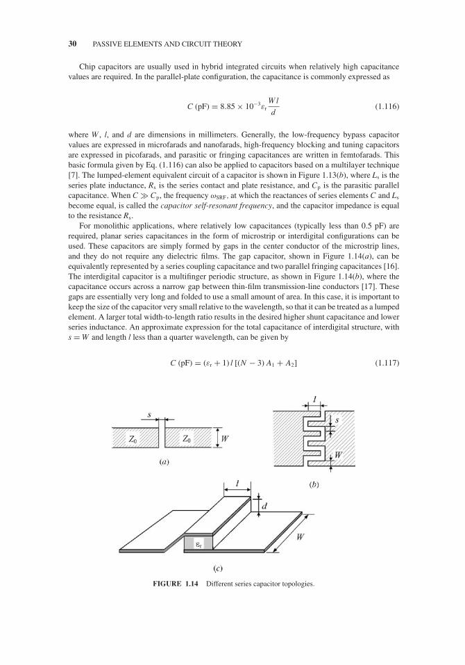
JWBS064-c01 JWBS064-Gerbennikov March 12, 2011 8:36 Printer Name: Yet to Come
30 PASSIVE ELEMENTS AND CIRCUIT THEORY
Chip capacitors are usually used in hybrid integrated circuits when relatively high capacitancevalues are required. In the parallel-plate configuration, the capacitance is commonly expressed as
C (pF) = 8.85 × 10⁻³εrWl
d(1.116)
where W , l, and d are dimensions in millimeters. Generally, the low-frequency bypass capacitorvalues are expressed in microfarads and nanofarads, high-frequency blocking and tuning capacitorsare expressed in picofarads, and parasitic or fringing capacitances are written in femtofarads. Thisbasic formula given by Eq. (1.116) can also be applied to capacitors based on a multilayer technique[7]. The lumped-element equivalent circuit of a capacitor is shown in Figure 1.13(b), where Ls is theseries plate inductance, Rs is the series contact and plate resistance, and Cp is the parasitic parallelcapacitance. When C � Cp, the frequency ωSRF, at which the reactances of series elements C and Ls
become equal, is called the capacitor self-resonant frequency, and the capacitor impedance is equalto the resistance Rs.
For monolithic applications, where relatively low capacitances (typically less than 0.5 pF) arerequired, planar series capacitances in the form of microstrip or interdigital configurations can beused. These capacitors are simply formed by gaps in the center conductor of the microstrip lines,and they do not require any dielectric films. The gap capacitor, shown in Figure 1.14(a), can beequivalently represented by a series coupling capacitance and two parallel fringing capacitances [16].The interdigital capacitor is a multifinger periodic structure, as shown in Figure 1.14(b), where thecapacitance occurs across a narrow gap between thin-film transmission-line conductors [17]. Thesegaps are essentially very long and folded to use a small amount of area. In this case, it is important tokeep the size of the capacitor very small relative to the wavelength, so that it can be treated as a lumpedelement. A larger total width-to-length ratio results in the desired higher shunt capacitance and lowerseries inductance. An approximate expression for the total capacitance of interdigital structure, withs = W and length l less than a quarter wavelength, can be given by
C (pF) = (εr + 1) l [(N − 3) A1 + A2] (1.117)
FIGURE 1.14 Different series capacitor topologies.

JWBS064-c01 JWBS064-Gerbennikov March 12, 2011 8:36 Printer Name: Yet to Come
TRANSMISSION LINE 31
where N is the number of fingers and
A1 (pF/μm) = 4.409 tanh
[0.55
(h
W
)0.45]
× 10−6 (1.118)
A2 (pF/μm) = 9.92 tanh
[0.52
(h
W
)0.5]
× 10−6 (1.119)
where h is the spacing from the ground plane.Series planar capacitors with larger values, which are called the metal-insulator-metal (MIM)
capacitors, can be realized by using an additional thin dielectric layer (typically less than 0.5 μm)between two metal plates, as shown in Figure 1.14(c) [7]. The bottom plate of the capacitor usesa thin unplated metal, and typically the dielectric material is silicon nitride (Si3N4) for integratedcircuits on GaAs and SiO2 for integrated circuits on Si. The top plate uses a thick-plated conductorto reduce the loss in the capacitor. These capacitors are used to achieve higher capacitance values insmall areas (10 pF and greater), with typical tolerances from 10% to 15%. The capacitance can becalculated according to Eq. (1.116).
1.7 TRANSMISSION LINE
Transmission lines are widely used in matching circuits in power amplifiers, in resonant and feedbackcircuits in the oscillators, filters, directional couplers, power combiners, and dividers. When thepropagated signal wavelength is compared to its physical dimension, the transmission line can beconsidered as a two-port network with distributed parameters, where the voltages and currents varyin magnitude and phase over length.
Schematically, a transmission line is often represented as a two-wire line, as shown in Figure1.15(a), where its electrical parameters are distributed along its length. The physical properties of atransmission line are determined by four basic parameters:
1. The series inductance L due to the self-inductive phenomena of two conductors.
2. The shunt capacitance C in view of the close proximity between two conductors.
3. The series resistance R due to the finite conductivity of the conductors.
4. The shunt conductance G that is related to the dielectric losses in the material.
As a result, a transmission line of length �x represents a lumped-element circuit shown inFigure 1.15(b), where �L, �C, �R, and �G are the series inductance, the shunt capacitance, theseries resistance, and the shunt conductance per unit length, respectively. If all these elements aredistributed uniformly along the transmission line, and their values do not depend on the chosenposition of �x, this transmission line is called the uniform transmission line. Any finite length of theuniform transmission line can be viewed as a cascade of section length �x.
To define the distribution of the voltages and currents along the uniform transmission line, it isnecessary to write the differential equations using Kirchhoff’s voltage law for instantaneous valuesof the voltages and currents in the line section of length �x, distant x from its beginning. For thesinusoidal steady-state condition, the telegrapher equations for V(x) and I(x) are given by
d2V (x)
dx2− γ 2V (x) = 0 (1.120)
d2 I (x)
dx2− γ 2 I (x) = 0 (1.121)

JWBS064-c01 JWBS064-Gerbennikov March 12, 2011 8:36 Printer Name: Yet to Come
32 PASSIVE ELEMENTS AND CIRCUIT THEORY
FIGURE 1.15 Transmission line schematics.
where γ = α + jβ = √(�R + jω�L) (�G + jω�C) is the complex propagation constant (which
is a function of frequency), α is the attenuation constant, and β is the phase constant. The generalsolutions of Eqs. (1.120) and (1.121) for voltage and current of the traveling wave in the transmissionline can be written as
V (x) = A1 exp (−γ x) + A2 exp (γ x) (1.122)
I (x) = A1
Z0exp (−γ x) − A2
Z0exp (γ x) (1.123)
where Z0 = √(�R + jω�L) / (�G + jω�C) is the characteristic impedance of the transmission
line, V i = A1exp(−γ x) and V r = A2exp(γ x) represent the incident voltage and the reflected voltage,respectively, and Ii = A1exp(−γ x)/Z0 and Ir = A2exp(γ x)/Z0 are the incident current and the reflectedcurrent, respectively. From Eqs. (1.122) and (1.123) it follows that the characteristic impedance of thetransmission line Z0 represents the ratio of the incident (reflected) voltage to the incident (reflected)current at any position on the line as
Z0 = Vi(x)
Ii(x)= Vr(x)
Ir(x). (1.124)
For a lossless transmission line, when R = G = 0 and the voltage and current do not changewith position, the attenuation constant α = 0, the propagation constant γ = jβ = jω
√�L�C , and
the phase constant β = ω√
�L�C . Consequently, the characteristic impedance is reduced to Z0 =√L/C and represents a real number. The wavelength is defined as λ = 2π /β = 2π/ω
√�L�C and
the phase velocity as vp = ω/β = 1/√
�L�C .Figure 1.16 represents a transmission line of characteristic impedance Z0 terminated with a load
ZL. In this case, the constants A1 and A2 are determined at the position x = l by
V (l) = A1 exp (−γ l) + A2 exp (γ l) (1.125)
I (l) = A1
Z0exp (−γ l) − A2
Z0exp (γ l) (1.126)
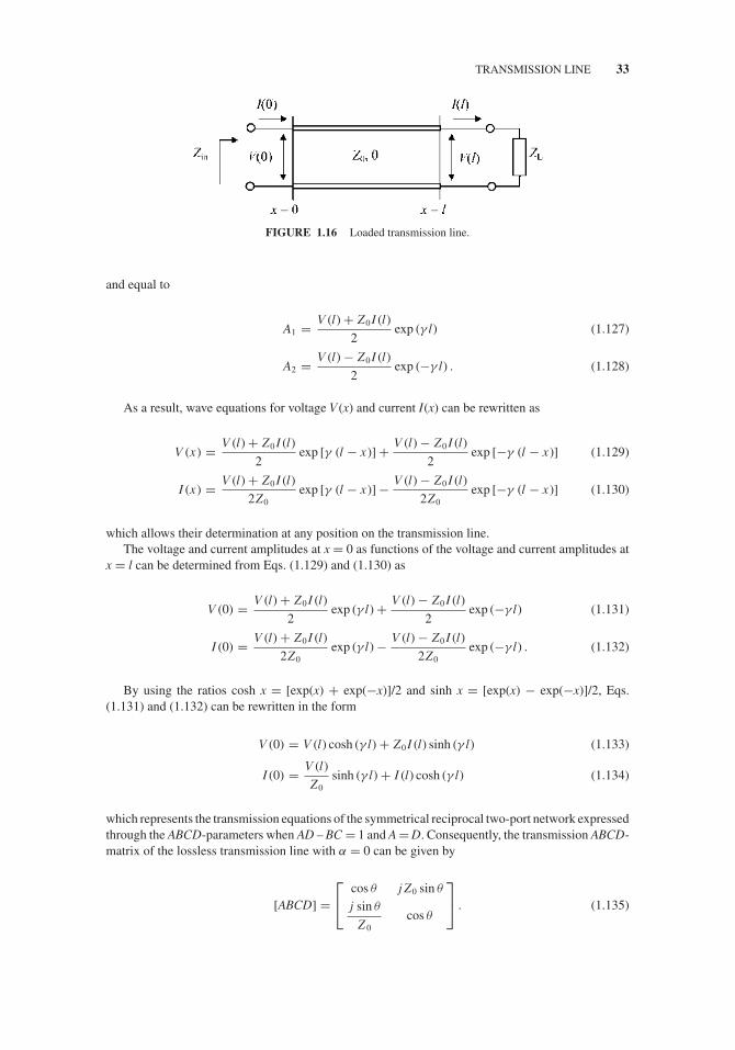
JWBS064-c01 JWBS064-Gerbennikov March 12, 2011 8:36 Printer Name: Yet to Come
TRANSMISSION LINE 33
FIGURE 1.16 Loaded transmission line.
and equal to
A1 = V (l) + Z0 I (l)
2exp (γ l) (1.127)
A2 = V (l) − Z0 I (l)
2exp (−γ l) . (1.128)
As a result, wave equations for voltage V(x) and current I(x) can be rewritten as
V (x) = V (l) + Z0 I (l)
2exp [γ (l − x)] + V (l) − Z0 I (l)
2exp [−γ (l − x)] (1.129)
I (x) = V (l) + Z0 I (l)
2Z0exp [γ (l − x)] − V (l) − Z0 I (l)
2Z0exp [−γ (l − x)] (1.130)
which allows their determination at any position on the transmission line.The voltage and current amplitudes at x = 0 as functions of the voltage and current amplitudes at
x = l can be determined from Eqs. (1.129) and (1.130) as
V (0) = V (l) + Z0 I (l)
2exp (γ l) + V (l) − Z0 I (l)
2exp (−γ l) (1.131)
I (0) = V (l) + Z0 I (l)
2Z0exp (γ l) − V (l) − Z0 I (l)
2Z0exp (−γ l) . (1.132)
By using the ratios cosh x = [exp(x) + exp(−x)]/2 and sinh x = [exp(x) − exp(−x)]/2, Eqs.(1.131) and (1.132) can be rewritten in the form
V (0) = V (l) cosh (γ l) + Z0 I (l) sinh (γ l) (1.133)
I (0) = V (l)
Z0sinh (γ l) + I (l) cosh (γ l) (1.134)
which represents the transmission equations of the symmetrical reciprocal two-port network expressedthrough the ABCD-parameters when AD – BC = 1 and A = D. Consequently, the transmission ABCD-matrix of the lossless transmission line with α = 0 can be given by
[ABCD] =⎡⎣ cos θ j Z0 sin θ
j sin θ
Z 0cos θ
⎤⎦ . (1.135)

JWBS064-c01 JWBS064-Gerbennikov March 12, 2011 8:36 Printer Name: Yet to Come
34 PASSIVE ELEMENTS AND CIRCUIT THEORY
Using the formulas to transform ABCD-parameters into S-parameters yields
[S] =[
0 exp (− jθ)exp (− jθ ) 0
](1.136)
where θ = βl is the electrical length of the transmission line.In the case of the loaded lossless transmission line, the reflection coefficient � is defined as the
ratio between the reflected voltage wave and the incident voltage wave, given at x as
�(x) = Vr
Vi= A2
A1exp (2 jβx) . (1.137)
By taking into account Eqs. (1.127) and (1.128), the reflection coefficient for x = l can be definedas
� = Z − Z0
Z + Z0(1.138)
where � represents the load reflection coefficient and Z = ZL = V(l)/I(l). If the load is mismatched,only part of the available power from the source is delivered to the load. This power loss is called thereturn loss (RL), and is calculated in decibels as
RL = −20log10 |�| . (1.139)
For a matched load when � = 0, a return loss is of ∞ dB. A total reflection with � = 1 means areturn loss of 0 dB when all incident power is reflected.
According to the general solution for voltage at a position x in the transmission line,
V (x) = Vi(x) + Vr(x) = Vi [1 + �(x)] . (1.140)
Hence, the maximum amplitude (when the incident and reflected waves are in phase) is
Vmax(x) = |Vi| [1 + |�(x)|] (1.141)
and the minimum amplitude (when these two waves are out of phase) is
Vmin(x) = |Vi| [1 − |�(x)|] . (1.142)
The ratio of Vmax to Vmin, which is a function of the reflection coefficient �, represents the voltagestanding wave ratio (VSWR). The VSWR is a measure of mismatch and can be written as
VSWR = Vmax
Vmin= 1 + |�|
1 − |�| (1.143)
which can change from 1 to ∞ (where VSWR = 1 implies a matched load). For a load impedancewith zero imaginary part when ZL = RL, the VSWR can be calculated using VSWR = RL/Z0 whenRL ≥ Z0 and VSWR = Z0/RL when Z0 ≥ RL.
From Eqs. (1.133) and (1.134) it follows that the input impedance of the loaded lossless transmis-sion line can be obtained as
Z in = V (0)
I (0)= Z0
ZL + j Z0 tan (θ)
Z0 + j ZL tan (θ)(1.144)
which gives an important dependence between the input impedance, the transmission-line parameters(electrical length and characteristic impedance), and the arbitrary load impedance.

JWBS064-c01 JWBS064-Gerbennikov March 12, 2011 8:36 Printer Name: Yet to Come
TYPES OF TRANSMISSION LINES 35
1.8 TYPES OF TRANSMISSION LINES
Several types of transmission lines are available when designing RF and microwave active and passivecircuits. Coaxial lines have very high bandwidth and high power-handling capability, and are widelyused for impedance transformers and power combiners. Planar transmission lines as an evolutionof the coaxial and parallel-wire lines are compact and readily adaptable to hybrid and monolithicintegrated circuit fabrication technologies at RF and microwave frequencies [18]. If coaxial line isdeformed in such a manner that both the center and outer conductors are square or rectangular incross-section, and then if side walls of the rectangular coaxial system are extended to infinity, theresultant flat-strip transmission system would have a form factor that is adaptable to the printed-circuittechnique. Similarly, if the parallel-wire line is replaced by its equivalent of a single wire and its imagein a conducting ground plane, and if this single wire is, in turn, progressively distorted into a flat strip,the resulting transmission system is again a planar structure. There is an important aspect that differflat-strip transmission lines from coaxial lines. In a coaxial line, an impedance discontinuity acts as ashunt capacitance, while a discontinuity in a flat strip has a series inductance in its equivalent circuit.Holes and gaps in center conductor strips also represent discontinuities that can be utilized in manyapplications to microwave circuitry.
1.8.1 Coaxial Line
A main type of wave propagated along a coaxial line shown in Figure 1.17 is the transverse electro-magnetic (TEM) wave. When the transverse fields of a TEM wave are the same as the static fields thatcan exist between the conductors, the electromagnetic properties of a coaxial line can be characterizedby the following parameters [19]: the shunt capacitance per unit length
C = 2πε0εr/ln(
b
a
)(1.145)
where a is the radius of inner conductor and b is the inner radius of outer conductor; the seriesinductance per unit length
L = μ0μr
2πln
(b
a
)(1.146)
FIGURE 1.17 Coaxial line structure.

JWBS064-c01 JWBS064-Gerbennikov March 12, 2011 8:36 Printer Name: Yet to Come
36 PASSIVE ELEMENTS AND CIRCUIT THEORY
where μ0 = 4π×10−7 H/m is the permeability of free space and μr is the relative magnetic constantor substrate permeability; the series resistance per unit length
R = Rs
2π
(1
b+ 1
a
)(1.147)
where Rs = ρ/�(f ) = √πμ0ρ f is the surface resistivity, ρ is the metallization electrical resistivity,
�(f ) is the penetration depth, and f is the frequency; the shunt conductance per unit length
G = 2πσ/ln
(b
a
)= 2πωεoεr tanδ/ln
(b
a
)(1.148)
where σ is the dielectric conductivity and tanδ is the dielectric loss tangent; the characteristicimpedance
Z0 = η
2πln
(b
a
)(1.149)
where η = √μ/ε is the wave impedance of the lossless coaxial line identical to the intrinsic impedance
of the medium.The conductor loss factor (in Np/m) can be written as
αc = R
2Z0(1.150)
whereas the dielectric loss factor (in Np/m) can be written as
αd = G Z0
2= ση
2= π
√εr
tanδ
λ(1.151)
where λ is the free-space wavelength.
1.8.2 Stripline
The geometry of a commonly used stripline is shown in Figure 1.18. The strip conductor of width Wis placed between two flat dielectric substrates with the same dielectric constant. The outer surfacesof these substrates are metallized and serve as a ground conductor. In practice, the strip conductoris etched on one of the dielectric substrates by photolithography process. Since the stripline has twoconductors and a homogeneous dielectric, it can support a pure TEM propagation mode, which is theusual mode of operation. The advantages of striplines are good electromagnetic shielding and lowattenuation losses, which make them suitable for high-Q and low-interference applications. However,striplines require strong symmetry that makes their tuning complicated due to difficult access tocenter conductor. As a result, the stripline structure is not convenient for incorporating chip elementsand associated bias circuitry.
The exact expression for the characteristic impedance of a lossless stripline of zero thickness isgiven by
Z0 = 30π√εr
K (k)
K (k ′)(1.152)

JWBS064-c01 JWBS064-Gerbennikov March 12, 2011 8:36 Printer Name: Yet to Come
TYPES OF TRANSMISSION LINES 37
FIGURE 1.18 Stripline structure.
where
K (k) =π/2∫0
dϕ√1 − k2sin2ϕ
(1.153)
is the complete elliptic integral of the first kind, k = sech (πW/2b), and k ′ = √1 − k2 [20,21].
An expression for the ratio K(k)/K(k′) can be simplified to
K (k)
K (k ′)=
⎧⎪⎪⎪⎪⎪⎨⎪⎪⎪⎪⎪⎩
π/ln
(2
1 + √k ′
1 − √k ′
)for 0 ≤ k ≤ 1√
2
1
πln
(2
1 + √k
1 − √k
)for
1√2
≤ k ≤ 1
(1.154)
which provides the relative error lower than 3 × 10⁻⁶ [22].In practice, it makes sense to use a sufficiently simple formula without complicated special
functions [23]. In this case, the formula for Z0 can be written within 1% of the exact results as
Z0 = 30π√εr
b
We + 0.441b(1.155)
where We is the effective width of the center conductor defined by
We
b= W
b−
⎧⎪⎪⎪⎨⎪⎪⎪⎩
0 forW
b> 0.35b
(0.35 − W
b
)2
forW
b< 0.35b
. (1.156)
For a stripline with a TEM propagation mode, the dielectric loss factor αd is the same as forcoaxial line, which is determined by Eq. (1.151). An approximation result for the conductor lossfactor αc (in Np/m) can be obtained by
αc =
⎧⎪⎪⎨⎪⎪⎩
A2.7 × 10−3 Rsεr Z0
30π (b − t)for Z0
√εr < 120
B0.16Rs
Z0bπfor Z0
√εr > 120
(1.157)
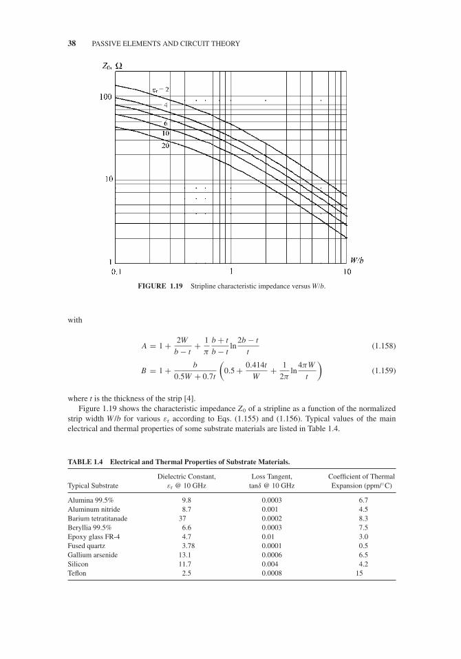
JWBS064-c01 JWBS064-Gerbennikov March 12, 2011 8:36 Printer Name: Yet to Come
38 PASSIVE ELEMENTS AND CIRCUIT THEORY
FIGURE 1.19 Stripline characteristic impedance versus W/b.
with
A = 1 + 2W
b − t+ 1
π
b + t
b − tln
2b − t
t(1.158)
B = 1 + b
0.5W + 0.7t
(0.5 + 0.414t
W+ 1
2πln
4πW
t
)(1.159)
where t is the thickness of the strip [4].Figure 1.19 shows the characteristic impedance Z0 of a stripline as a function of the normalized
strip width W/b for various εr according to Eqs. (1.155) and (1.156). Typical values of the mainelectrical and thermal properties of some substrate materials are listed in Table 1.4.
TABLE 1.4 Electrical and Thermal Properties of Substrate Materials.
Typical SubstrateDielectric Constant,
εr @ 10 GHzLoss Tangent,
tanδ @ 10 GHzCoefficient of ThermalExpansion (ppm/◦C)
Alumina 99.5% 9.8 0.0003 6.7Aluminum nitride 8.7 0.001 4.5Barium tetratitanade 37 0.0002 8.3Beryllia 99.5% 6.6 0.0003 7.5Epoxy glass FR-4 4.7 0.01 3.0Fused quartz 3.78 0.0001 0.5Gallium arsenide 13.1 0.0006 6.5Silicon 11.7 0.004 4.2Teflon 2.5 0.0008 15

JWBS064-c01 JWBS064-Gerbennikov March 12, 2011 8:36 Printer Name: Yet to Come
TYPES OF TRANSMISSION LINES 39
1.8.3 Microstrip Line
In a microstrip line, the grounded metallization surface covers only one side of dielectric substrate,as shown in Figure 1.20. Such a configuration is equivalent to a pair-wire system for the image of theconductor in the ground plane which produces the required symmetry [24]. In this case, the electricand magnetic field lines are located in both the dielectric region between the strip conductor andthe ground plane and in the air region above the substrate. As a result, the electromagnetic wavepropagated along a microstrip line is not a pure TEM, since the phase velocities in these two regionsare not the same. However, in a quasistatic approximation, which gives sufficiently accurate results aslong as the height of the dielectric substrate is very small compared with the wavelength, it is possibleto obtain the explicit analytical expressions for the electrical characteristics. Since microstrip line isan open structure, it has a major fabrication advantage over the stripline due to simplicity of practicalrealization, interconnection, and adjustments.
The exact expression for the characteristic impedance of a lossless microstrip line with finite stripthickness is given by [25,26]
Z0 =
⎧⎪⎪⎪⎨⎪⎪⎪⎩
60√εre
ln(
8h
We+ We
4h
)for
W
h≤ 1
120π√εre
[We
h+ 1.393 + 0.667 ln
(We
h+ 1.444
)]−1
forW
h≥ 1
(1.160)
where
We
h= W
h+ �W
h(1.161)
�W
h=
⎧⎪⎪⎪⎨⎪⎪⎪⎩
1.25
π
t
h
(1 + ln
4πW
t
)for
W
h≤ 1/2π
1.25
π
t
h
(1 + ln
2h
t
)for
W
h≥ 1/2π
(1.162)
εre = εr + 1
2+ εr − 1
2
1√1 + 12h/W
− εr − 1
4.6
t
h
√h
W. (1.163)
Figure 1.21 shows the characteristic impedance Z0 of a microstrip line with zero strip thicknessas a function of the normalized strip width W/h for various εr according to Eqs. (1.160) to (1.163).
FIGURE 1.20 Microstrip line structure.

JWBS064-c01 JWBS064-Gerbennikov March 12, 2011 8:36 Printer Name: Yet to Come
40 PASSIVE ELEMENTS AND CIRCUIT THEORY
FIGURE 1.21 Microstrip characteristic impedance versus W/h.
In practice, it is possible to use a sufficiently simple formula to estimate the characteristicimpedance Z0 of a microstrip line with zero strip thickness written as [27]
Z0 = 120π√εr
h
W
1
1 + 1.735ε−0.0724r (W/h)−0.836 . (1.164)
For a microstrip line in a quasi-TEM approximation, the conductor loss factor αc (in Np/m) as afunction of the microstrip-line geometry can be obtained by
αc =
⎧⎪⎪⎪⎨⎪⎪⎪⎩
1.38ARs
h Z0
32 − (We/h)2
32 + (We/h)2 forW
h≤ 1
6.1 · 10−5 ARs Z0εre
h
(We
h+ 0.667 We/h
1.444 + We/h
)for
W
h≥ 1
(1.165)
with
A = 1 + h
We
(1 + 1
πln
2B
t
)(1.166)
B =
⎧⎪⎪⎨⎪⎪⎩
2πW forW
h≤ 1/2π
h forW
h≥ 1/2π
(1.167)
where We/h is given by Eqs. (1.161) and (1.162) [28].The dielectric loss factor αd (in Np/m) can be calculated by
αd = 27.3εr
εr − 1
εre − 1√εre
tanδ
λ. (1.168)
Conductor loss is a result of several factors related to the metallic material composing the groundplane and walls, among which are conductivity, skin effect, and surface ruggedness. For most mi-crostrip lines (except some kinds of semiconductor substrate such as silicon), the conductor loss is

JWBS064-c01 JWBS064-Gerbennikov March 12, 2011 8:36 Printer Name: Yet to Come
TYPES OF TRANSMISSION LINES 41
TABLE 1.5 Electrical Resistivity of Conductor Materials.
Material SymbolElectrical Resistivity
(μ� cm) Material SymbolElectrical Resistivity
(μ� cm)
Aluminum Al 2.65 Palladium Pd 10.69Copper Cu 1.67 Platinum Pt 10.62Gold Au 2.44 Silver Ag 1.59Indium In 15.52 Tantalum Ta 15.52Iron Fe 9.66 Tin Sn 11.55Lead Pb 21.0 Titanium Ti 55.0Molybdenum Mo 5.69 Tungsten W 5.6Nickel Ni 8.71 Zinc Zn 5.68
much more significant than the dielectric loss. The conductor losses increase with increasing char-acteristic impedance due to greater resistance of narrow strips. The electrical resistivity of someconductor materials is given in Table 1.5.
1.8.4 Slotline
Slotlines are usually used when it is necessary to realize a high value of the characteristic impedanceZ0 [29,30]. A slotline is dual to a microstrip line and represents a narrow slot between two conductivesurfaces, one of which is grounded. Changing the width of the slot can easily change the characteristicimpedance of the slotline. The transverse electric H-mode wave propagates along the slotline. Threebasic types of slotlines are unilateral, antipodal, and bilateral. The geometry of a unilateral slotlineis shown in Figure 1.22, with a narrow gap in the conductive coating on one side of the dielectricsubstrate and being bare on the other side of substrate. Slotline can be used either alone or withmicrostrip line on the opposite side of substrate.
It is difficult to provide exact analytical expressions to calculate the slotline parameters. However,an equation for Z0 can be obtained for a quasi-TEM approximation with zero conductor thicknessand infinite width of the entire slotline system as
for 0.02 ≤ W/h ≤ 0.2
Z0 = 72.62 − 15.283 lnεr + 50(
1 − 0.02h
W
)(W
h− 0.1
)+ (19.23 − 3.693 lnεr) ln
(102 W
h
)
−(
11.4 − 2.636 lnεr − 102 h
λ
)2
×[
0.139 lnεr − 0.11 + W
h(0.465 lnεr + 1.44)
](1.169)
FIGURE 1.22 Slotline structure.

JWBS064-c01 JWBS064-Gerbennikov March 12, 2011 8:36 Printer Name: Yet to Come
42 PASSIVE ELEMENTS AND CIRCUIT THEORY
FIGURE 1.23 Slotline characteristic impedance versus W/h.
for 0.2 ≤ W/h ≤ 1.0
Z0 = 113.19 − 23.257 lnεr + 1.25W
h(114.59 − 22.531 lnεr) + 20
(1 − W
h
)(W
h− 0.2
)
−[
0.15 + 0.1 lnεr + W
h(0.899 lnεr − 0.79)
]
×[
10.25 − 2.171 lnεr + W
h(2.1 − 0.617 lnεr) − 102 h
λ
]2
(1.170)
where 0.01 ≤ h/λ ≤ 0.25/√
εr − 1 and λ is the free-space wavelength [31].Figure 1.23 shows the characteristic impedance Z0 of a slotline within the error of 2% as a function
of the normalized slot width W/h for h/λ = 0.02 and various εr = 9.7, 11, 12, . . . , 20 calculated byEqs. (1.169) and (1.170).
1.8.5 Coplanar Waveguide
A coplanar waveguide (CPW) is similar in structure to a slotline, the only difference being a thirdconductor centered in the slot region. The center strip conductor and two outer grounded conductorslie in the same plane on substrate surface, as shown in Figure 1.24 [32,33]. A coplanar configurationhas some advantages such as low dispersion, ease of attaching shunt and series circuit components, noneed for via holes, or simple realization of short-circuited ends, which makes a coplanar waveguidesuitable for hybrid and monolithic integrated circuits. In contrast to the microstrip and stripline, thecoplanar waveguide has shielding between adjacent lines that creates a better isolation between them.However, like microstrip and stripline, the coplanar waveguide can be also described by a quasi-TEM
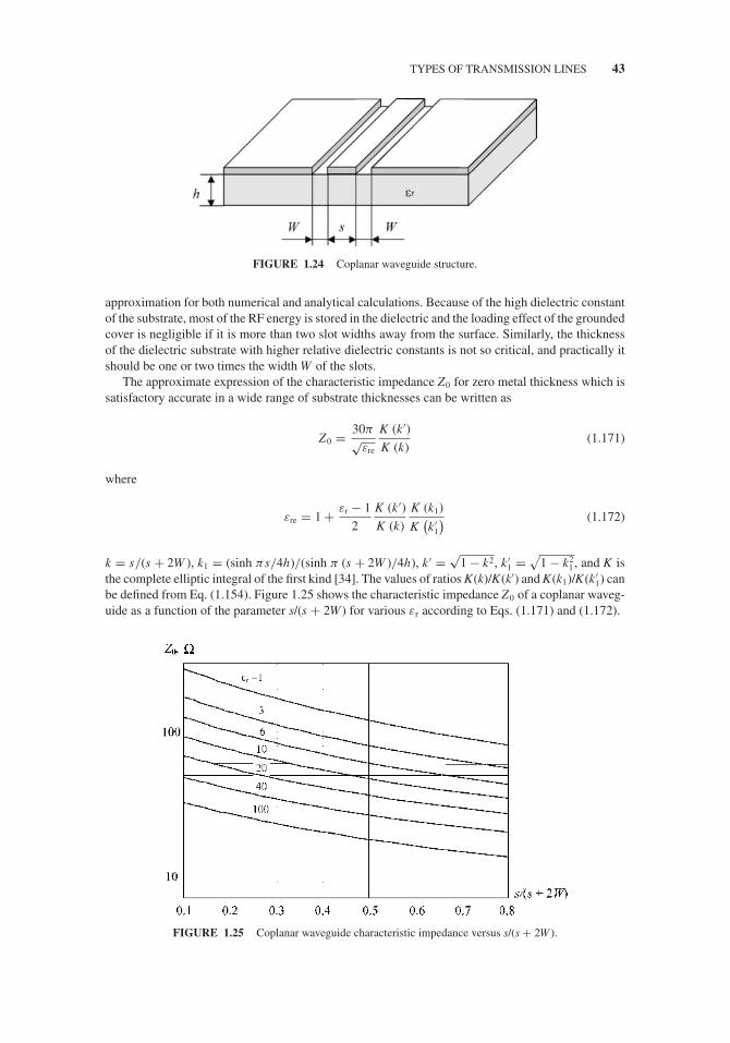
JWBS064-c01 JWBS064-Gerbennikov March 12, 2011 8:36 Printer Name: Yet to Come
TYPES OF TRANSMISSION LINES 43
FIGURE 1.24 Coplanar waveguide structure.
approximation for both numerical and analytical calculations. Because of the high dielectric constantof the substrate, most of the RF energy is stored in the dielectric and the loading effect of the groundedcover is negligible if it is more than two slot widths away from the surface. Similarly, the thicknessof the dielectric substrate with higher relative dielectric constants is not so critical, and practically itshould be one or two times the width W of the slots.
The approximate expression of the characteristic impedance Z0 for zero metal thickness which issatisfactory accurate in a wide range of substrate thicknesses can be written as
Z0 = 30π√εre
K (k ′)K (k)
(1.171)
where
εre = 1 + εr − 1
2
K (k ′)K (k)
K (k1)
K(k ′
1
) (1.172)
k = s/(s + 2W ), k1 = (sinh πs/4h)/(sinh π (s + 2W )/4h), k ′ = √1 − k2, k ′
1 =√
1 − k21 , and K is
the complete elliptic integral of the first kind [34]. The values of ratios K(k)/K(k′) and K(k1)/K(k ′1) can
be defined from Eq. (1.154). Figure 1.25 shows the characteristic impedance Z0 of a coplanar waveg-uide as a function of the parameter s/(s + 2W) for various εr according to Eqs. (1.171) and (1.172).
FIGURE 1.25 Coplanar waveguide characteristic impedance versus s/(s + 2W).

JWBS064-c01 JWBS064-Gerbennikov March 12, 2011 8:36 Printer Name: Yet to Come
44 PASSIVE ELEMENTS AND CIRCUIT THEORY
1.9 NOISE
The electrical performance of RF and microwave transmitters of different applications can be affectedby many factors, with the effect of noise as one of the most fundamental. In this case, it is necessaryto keep the ratio of average (or peak) signal power to average noise power so large that the noise ina transmitter path has no harmful effects on overall system performance. Several basic approachescan provide this where it is possible, such as powerful transmitters and high-gain antennas to developlarge signals at the receiver input, stabilized oscillators with minimum phase noise, power amplifierand mixer circuits so that they introduce a minimum amount of additional noise when processingsignals, and modulation and coding schemes that facilitate the separation of signal and noise.
1.9.1 Noise Sources
There are several primary noise sources in the electrical circuit. Thermal or white noise is created byrandom motion of charge carriers due to thermal excitation, being always found in any conductingmedium whose temperature is above absolute zero whatever the nature of the conduction process orthe nature of the mobile charge carriers [35]. This random motion of carriers creates a fluctuatingvoltage on the terminals of each resistive element which increases with temperature. However, ifthe average value of such a voltage is zero, then the noise power on its terminal is not zero beingproportional to the resistance of the conductor and to its absolute temperature. The resistor as athermal noise source can be represented by either of the noise sources shown in Figure 1.26. Thenoise voltage source and noise current source can be respectively described by Nyquist equationsthrough their mean-square noise voltage and noise current values as
e2n = 4kT R� f (1.173)
i2n = 4kT� f
R(1.174)
where k = 1.38 × 10⁻²³ J/K is the Boltzmann constant, T is the absolute temperature, and kT = 4 ×10⁻²¹ W/Hz = −174 dBm/Hz at ambient temperature T = 290 K. The thermal noise is proportionalto the frequency bandwidth �f , and it can be represented by the voltage source in series with resistorR, or by the current source in parallel to the resistor R. The maximum noise power can be delivered tothe load when R = RL, where RL is the load resistance, being equal to kT�f . Hence, the noise powerdensity when the noise power is normalized by �f is independent of frequency and is considered aswhite noise. The root-mean-square noise voltage and current are proportional to the square root ofthe frequency bandwidth �f .
Shot noise is associated with the carrier injection through the device p-n junction, being generatedby the movement of individual electrons within the current flow. In each forward biased junction,
FIGURE 1.26 Equivalent circuits to represent thermal noise sources.

JWBS064-c01 JWBS064-Gerbennikov March 12, 2011 8:36 Printer Name: Yet to Come
NOISE 45
there is a potential barrier that can be overcome by the carriers with higher thermal energy. Such aprocess is random and mean-square noise current can be given by
i 2n = 2q I� f (1.175)
where q is the electron charge and I is the direct current flowing through the p-n junction. The shotnoise depends on the thermal energy of the carriers near the potential barrier and its power densityis independent of frequency. It has essentially a flat spectral distribution and can be treated as thethermal or white type of noise with current source i 2
n connected in parallel to the small-signal junctionresistance. In a voltage noise representation, when the noise voltage source is connected in serieswith such a resistor, it can be written as
e2n = 2kT r� f (1.176)
where r = kT/qI is the junction resistance.Circuits containing more than one resistor can be analyzed by reducing their number to the only
one (Thevenin) equivalent resistance to obtain the mean-square noise voltage in the form of Eq.(1.173) [36]. As an example, the noise equivalent of a circuit shown in Figure 1.27(a), where asignal source VS is driving a hypothetical noise-free load resistor Rin (which can be considered aninput of the power amplifier) through three noise resistors R1, R2, and R3, is a noise voltage sourcee2
n = 2kT RT� f connected in series with an ideal (noise-free) resistor equal to the Thevenin resistanceRT, as shown in Figure 1.27(b).
Consider now a simple parallel RC circuit shown in Figure 1.28(a), where the thermal noise dueto the parallel resistor is represented by a parallel noise current source in. Nyquist has determined thethermal noise output of a two-port network containing both resistive and reactive elements, as shownin Figure 1.28(b). In this case, the mean-square thermal noise voltage is given by
e2n = 4kT
∫� f
R ( f ) d f (1.177)
FIGURE 1.27 Circuit with three resistors and its equivalent with noise voltage source.
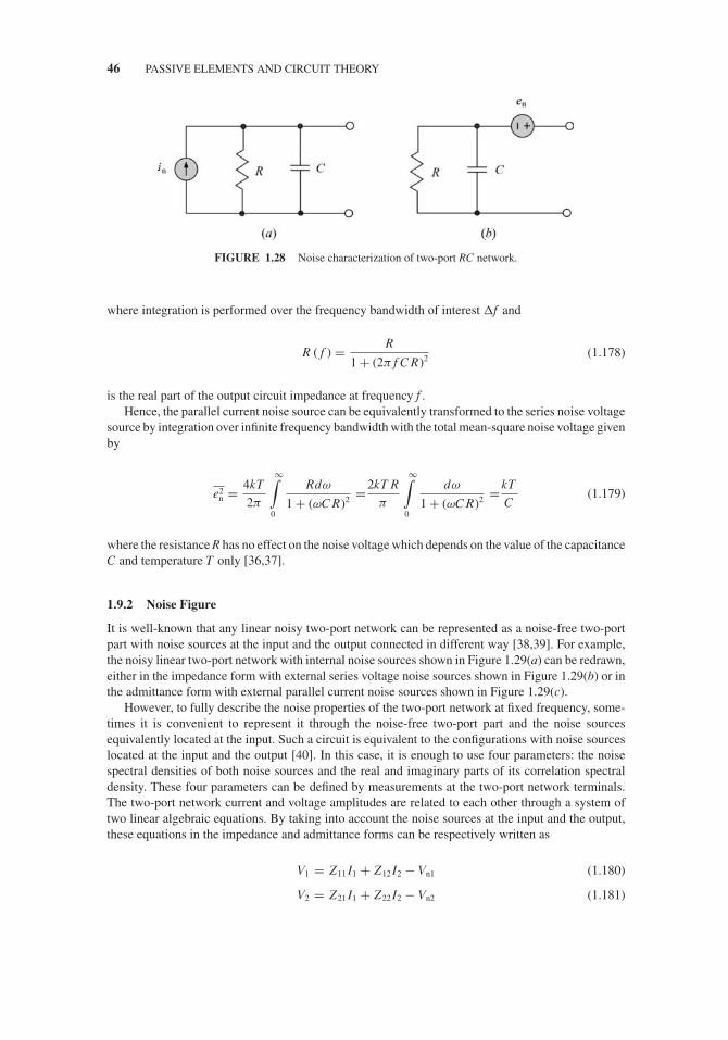
JWBS064-c01 JWBS064-Gerbennikov March 12, 2011 8:36 Printer Name: Yet to Come
46 PASSIVE ELEMENTS AND CIRCUIT THEORY
FIGURE 1.28 Noise characterization of two-port RC network.
where integration is performed over the frequency bandwidth of interest �f and
R ( f ) = R
1 + (2π f C R)2 (1.178)
is the real part of the output circuit impedance at frequency f .Hence, the parallel current noise source can be equivalently transformed to the series noise voltage
source by integration over infinite frequency bandwidth with the total mean-square noise voltage givenby
e2n = 4kT
2π
∞∫0
Rdω
1 + (ωC R)2 =2kT R
π
∞∫0
dω
1 + (ωC R)2 = kT
C(1.179)
where the resistance R has no effect on the noise voltage which depends on the value of the capacitanceC and temperature T only [36,37].
1.9.2 Noise Figure
It is well-known that any linear noisy two-port network can be represented as a noise-free two-portpart with noise sources at the input and the output connected in different way [38,39]. For example,the noisy linear two-port network with internal noise sources shown in Figure 1.29(a) can be redrawn,either in the impedance form with external series voltage noise sources shown in Figure 1.29(b) or inthe admittance form with external parallel current noise sources shown in Figure 1.29(c).
However, to fully describe the noise properties of the two-port network at fixed frequency, some-times it is convenient to represent it through the noise-free two-port part and the noise sourcesequivalently located at the input. Such a circuit is equivalent to the configurations with noise sourceslocated at the input and the output [40]. In this case, it is enough to use four parameters: the noisespectral densities of both noise sources and the real and imaginary parts of its correlation spectraldensity. These four parameters can be defined by measurements at the two-port network terminals.The two-port network current and voltage amplitudes are related to each other through a system oftwo linear algebraic equations. By taking into account the noise sources at the input and the output,these equations in the impedance and admittance forms can be respectively written as
V1 = Z11 I1 + Z12 I2 − Vn1 (1.180)
V2 = Z21 I1 + Z22 I2 − Vn2 (1.181)
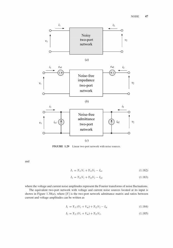
JWBS064-c01 JWBS064-Gerbennikov March 12, 2011 8:36 Printer Name: Yet to Come
NOISE 47
FIGURE 1.29 Linear two-port network with noise sources.
and
I1 = Y11V1 + Y12V2 − In1 (1.182)
I2 = Y21V1 + Y22V2 − In2 (1.183)
where the voltage and current noise amplitudes represent the Fourier transforms of noise fluctuations.The equivalent two-port network with voltage and current noise sources located at its input is
shown in Figure 1.30(a), where [Y] is the two-port network admittance matrix and ratios betweencurrent and voltage amplitudes can be written as
I1 = Y11 (V1 + Vni) + Y12V2 − Ini (1.184)
I2 = Y21 (V1 + Vni) + Y22V2. (1.185)

JWBS064-c01 JWBS064-Gerbennikov March 12, 2011 8:36 Printer Name: Yet to Come
48 PASSIVE ELEMENTS AND CIRCUIT THEORY
FIGURE 1.30 Linear two-port network with noise sources at input.
From comparison of Eqs. (1.182) and (1.183) with Eqs. (1.184) and (1.185) it follows that
Vni = − In2
Y21(1.186)
Ini = In1 − Y11
Y21In2 (1.187)
representing the relationships between the current noise sources at the input and the output corre-sponding to the circuit shown in Figure 1.29(c) and the voltage and current noise sources at the inputonly corresponding to the circuit shown in Figure 1.30(a). In this case, Eqs. (1.186) and (1.187)are valid only if Y21 �= 0 that always takes place in practice. Similar equations can be written forthe circuit with the series noise voltage source followed by a parallel noise current source shown inFigure 1.30(b) in terms of impedance Z-parameters to represent the relationships between the voltagenoise sources at the input and the output corresponding to the circuit shown in Figure 1.29(b). Theuse of voltage and current noise sources at the input enables the combination of all internal two-portnetwork noise sources.
To evaluate the quality of a two-port network, it is important to know the amount of noise addedto a signal passing through it. Usually, this can be done by introducing an important parameter suchas a noise figure or noise factor. The noise figure of the two-port network is intended as an indicationof its noisiness. The lower the noise figure, the less is the noise contributed by the two-port network.The noise figure is defined as
F = Sin/Nin
Sout/Nout(1.188)
where Sin/N in is the signal-to-noise ratio available at the input and Sout/Nout is the signal-to-noise ratioavailable at the output.

JWBS064-c01 JWBS064-Gerbennikov March 12, 2011 8:36 Printer Name: Yet to Come
NOISE 49
For a two-port network characterizing by the available power gain GA, the noise figure can berewritten as
F = Sin/Nin
GASin/GA(Nin + Nadd)= 1 + Nadd
Nin(1.189)
where Nadd is the additional noise power added by the two-port network referred to the input. FromEq. (1.189) it follows that the noise figure depends on the source impedance ZS shown in Figure1.31(a), but not on the circuit connected to the output of the two-port network.
Hence, if the two-port network is driven from the source with impedance ZS = RS + jXS, the noisefigure F of this two-port network in terms of the model shown in Figure 1.31(b) with input voltageand current noise sources and noise-free two-port network can be obtained by
F = 1 + |en + ZSin|24kT RS� f
= 1 + Rn + |ZS|2 Gn + 2√
RnGnRe (C ZS)
RS(1.190)
FIGURE 1.31 Linear two-port networks to calculate noise figure.
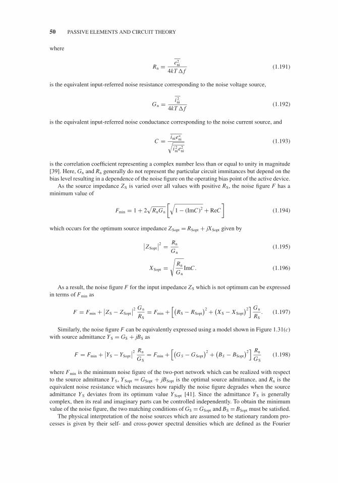
JWBS064-c01 JWBS064-Gerbennikov March 12, 2011 8:36 Printer Name: Yet to Come
50 PASSIVE ELEMENTS AND CIRCUIT THEORY
where
Rn = e2ni
4kT� f(1.191)
is the equivalent input-referred noise resistance corresponding to the noise voltage source,
Gn = i 2ni
4kT � f(1.192)
is the equivalent input-referred noise conductance corresponding to the noise current source, and
C = inie∗ni√
i 2nie
2ni
(1.193)
is the correlation coefficient representing a complex number less than or equal to unity in magnitude[39]. Here, Gn and Rn generally do not represent the particular circuit immitances but depend on thebias level resulting in a dependence of the noise figure on the operating bias point of the active device.
As the source impedance ZS is varied over all values with positive RS, the noise figure F has aminimum value of
Fmin = 1 + 2√
RnGn
[√1 − (ImC)2 + ReC
](1.194)
which occurs for the optimum source impedance ZSopt = RSopt + jXSopt given by
∣∣ZSopt
∣∣2 = Rn
Gn(1.195)
XSopt =√
Rn
GnImC. (1.196)
As a result, the noise figure F for the input impedance ZS which is not optimum can be expressedin terms of Fmin as
F = Fmin + ∣∣ZS − ZSopt
∣∣2 Gn
RS= Fmin +
[(RS − RSopt
)2 + (XS − XSopt
)2] Gn
RS. (1.197)
Similarly, the noise figure F can be equivalently expressed using a model shown in Figure 1.31(c)with source admittance YS = GS + jBS as
F = Fmin + ∣∣YS − YSopt
∣∣2 Rn
GS= Fmin +
[(GS − GSopt
)2 + (BS − BSopt
)2] Rn
GS(1.198)
where Fmin is the minimum noise figure of the two-port network which can be realized with respectto the source admittance YS, YSopt = GSopt + jBSopt is the optimal source admittance, and Rn is theequivalent noise resistance which measures how rapidly the noise figure degrades when the sourceadmittance YS deviates from its optimum value YSopt [41]. Since the admittance YS is generallycomplex, then its real and imaginary parts can be controlled independently. To obtain the minimumvalue of the noise figure, the two matching conditions of GS = GSopt and BS = BSopt must be satisfied.
The physical interpretation of the noise sources which are assumed to be stationary random pro-cesses is given by their self- and cross-power spectral densities which are defined as the Fourier
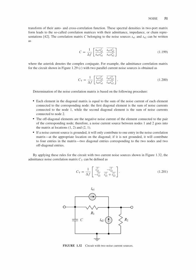
JWBS064-c01 JWBS064-Gerbennikov March 12, 2011 8:36 Printer Name: Yet to Come
NOISE 51
transform of their auto- and cross-correlation function. These spectral densities in two-port matrixform leads to the so-called correlation matrices with their admittance, impedance, or chain repre-sentations [42]. The correlation matrix C belonging to the noise sources sn1 and sn2 can be writtenas
C = 1
� f
[sn1s∗
n1 sn1s∗n2
sn2s∗n1 sn2s∗
n2
](1.199)
where the asterisk denotes the complex conjugate. For example, the admittance correlation matrixfor the circuit shown in Figure 1.29 (c) with two parallel current noise sources is obtained as
CY = 1
� f
[in1i∗
n1 in1i∗n2
in2i∗n1 in2i∗
n2
]. (1.200)
Determination of the noise correlation matrix is based on the following procedure:
� Each element in the diagonal matrix is equal to the sum of the noise current of each elementconnected to the corresponding node: the first diagonal element is the sum of noise currentsconnected to the node 1, while the second diagonal element is the sum of noise currentsconnected to node 2.
� The off-diagonal elements are the negative noise current of the element connected to the pairof the corresponding node; therefore, a noise current source between nodes 1 and 2 goes intothe matrix at locations (1, 2) and (2, 1).
� If a noise current source is grounded, it will only contribute to one entry in the noise correlationmatrix—at the appropriate location on the diagonal; if it is not grounded, it will contributeto four entries in the matrix—two diagonal entries corresponding to the two nodes and twooff-diagonal entries.
By applying these rules for the circuit with two current noise sources shown in Figure 1.32, theadmittance noise correlation matrix CY can be defined as
CY = 1
� f
[i 2n1 −i 2
n1
−i 2n1 i 2
n1 + i2n2
]. (1.201)
FIGURE 1.32 Circuit with two noise current sources.
JWBS064-c01 JWBS064-Gerbennikov March 12, 2011 8:36 Printer Name: Yet to Come
52 PASSIVE ELEMENTS AND CIRCUIT THEORY
To form the impedance noise correlation matrix with voltage noise sources, we can write
CZ = 1
� f
[en1e∗
n1 en1e∗n2
en2e∗n1 en2e∗
n2
]= [Z ] [CY] [Z ]T (1.202)
where [Z] is the impedance Z-matrix of the two-port network and T denotes the Hermitian ortransposed conjugation.
In the case where the correlation matrix cannot be theoretically derived, the measurements canbe used for its determination. Such measurements are usually done by defining the equivalent noiseresistance Rn, the optimal source admittance YSopt, and the minimum noise figure Fmin. As a result,the chain representation of the noise correlation matrix is obtained as
CA = 4kT
⎡⎢⎢⎣
RnFmin − 1
2− RnYSopt
Fmin − 1
2− RnY ∗
Sopt Rn
∣∣YSopt
∣∣2⎤⎥⎥⎦ (1.203)
where T is the absolute temperature [42]. If the correlation matrix has been determined, the noiseparameters can be calculated analytically from
Rn = CA11
4kT(1.204)
YSopt =√
CA22
CA11
− Im2
(CA
12
CA11
)− j Im
(CA
12
CA11
)(1.205)
Fmin = 1 + CA12 + CA
11YSopt
2kT. (1.206)
where CA11, CA
12, CA21, and CA
22 are the elements of the chain correlation matrix CA.In a multistage transmitter system, the input signal travels through a cascade of many different
components, each of which may degrade the signal-to-noise ratio to some degree. For a cascade oftwo stages having available gains GA1 and GA2 and noise figures F1 and F2, using Eq. (1.189) resultsin the output-to-input noise power ratio Nout/N in written as
Nout
Nin= GA2
[GA1
(1 + Nadd1
Nin
)+ Nadd2
Nin
]= GA1GA2
(F1 + F2 − 1
GA1
)(1.207)
where Nadd1 and Nadd2 are the additional noise powers added by the first and second stages, respectively.Consequently, an overall noise figure F1,2 for a two-stage system based on Eq. (1.188) can be givenby
F1,2 = F1 + 1
GA1(F2 − 1) . (1.208)
Eq. (1.208) can be generalized to a multistage transmitter system with n stages as
F1,n = F1 + F2 − 1
GA1+ · · · + Fn − 1
GA1GA2 . . . GA(n−1)(1.209)
which means that the noise figure of the first stage has the predominant effect on the overall noisefigure, unless GA1 is small or F2 is large [43].

JWBS064-c01 JWBS064-Gerbennikov March 12, 2011 8:36 Printer Name: Yet to Come
REFERENCES 53
1.9.3 Flicker Noise
The flicker or 1/f noise is a low-frequency noise associated with a fluctuation in the conductance witha power spectral density proportional to f −γ , where γ = 1.0 ± 0.1 in a wide frequency range, usuallymeasured from 1 Hz to 10 kHz [44]. Its spectrum cannot be exactly f −1 at offset frequencies fromf = 0 to f → ∞, since neither the integral over the power density nor the Fourier transform wouldbe able to have finite values. Unlike the thermal or shot noise sources, the origin of the 1/f noise isnot exactly clear and open to debate despite its predictable behavior. Generally, it is a result of bothsurface and bulk effects in the semiconductor material and is not generated by the current. In seriesexperiments it was shown that there is a type of 1/f noise that is a fluctuation in the carrier mobilitydue to lattice scattering.
Significant contribution to the low-frequency noise is made by the generation-recombination andburst noises [45]. The generation-recombination noise associated with the fluctuations in the numberof the carriers rather than their mobility is due to trap centers within the bandgap of a semiconductor.It may have any frequency behavior between f 0 and f −2. If not masked by thermal noise, the low-frequency noise generated from these trap centers becomes f −2 at very high frequencies. However,if the lifetime of the carriers in the semiconductor is finite, the noise spectral density reaches aplateau at very low frequencies. Burst noise (random telegraph noise) is a special kind of generation-recombination noise due to a single trap in the active device region. It is often observed in submicrondevices or in devices with very poor crystalline quality. In such devices, a trap level with certainenergy and at a specific location in the active device region (a single localized trap) traps and detrapsthe carriers causing an on-off time-dependent signal similar to a telegraph signal [46].
The physical origin of a low-frequency 1/f noise for any type of the metal-oxide-semiconductorfield-effect transistor (MOSFET) devices including CMOS transistors is based on two dominantprocesses: random fluctuation of the carriers in the channel due to fluctuations in the surface potentialcaused by trapping and releasing of the carriers by traps located near the Si–SiO2 interface, andmobility fluctuations due to carrier interactions with lattice fluctuations [47]. However, for a CMOStransistor depending on its type, one effect can prevail over the other. For example, flicker noisein n-channel devices is mostly attributed to carrier number fluctuations, while flicker noise in p-channel devices is often attributed to mobility fluctuations. It was observed that pMOS transistorshave significantly lower 1/f noise than nMOS transistors of the same size and fabricated with thesame CMOS process (by one order of magnitude or more). This is because, when an n+-polysilicongate layer is used for both the nMOS and pMOS devices, nMOS transistors have a surface channelwhile pMOS transistors have a buried channel [48].
REFERENCES
1. L. O. Chua, C. A. Desoer, and E. S. Kuh, Linear and Nonlinear Circuits, New York: McGraw-Hill, 1987.
2. D. R. Cunningham and J. A. Stuller, Circuit Analysis, New York: John Wiley & Sons, 1995.
3. G. D. Vendelin, A. M. Pavio, and U. L. Rohde, Microwave Circuit Design Using Linear and NonlinearTechniques, New York: John Wiley & Sons, 2005.
4. D. M. Pozar, Microwave Engineering, New York: John Wiley & Sons, 2004.
5. D. A. Frickey, “Conversions between S, Z, Y, h, ABCD, and T Parameters which are Valid for ComplexSource and Load Impedances,” IEEE Trans. Microwave Theory Tech., vol. MTT-42, pp. 205–211, Feb.1994.
6. E. F. Terman, Radio Engineer’s Handbook, New York: McGraw-Hill, 1945.
7. I. J. Bahl, Lumped Elements for RF and Microwave Circuits, Boston: Artech House, 2003.
8. H. A. Wheeler, “Simple Inductance Formulas for Radio Coils,” Proc. IRE, vol. 16, pp. 1398–1400, Oct.1928.
9. S. S. Mohan, M. del Mar Hershenson, S. P. Boyd, and T. H. Lee, “Simple Accurate Expressions for PlanarSpiral Inductances,” IEEE J. Solid-State Circuits, vol. SC-34, pp. 1419–1424, Oct. 1999.

JWBS064-c01 JWBS064-Gerbennikov March 12, 2011 8:36 Printer Name: Yet to Come
54 PASSIVE ELEMENTS AND CIRCUIT THEORY
10. J. M. Lopez-Villegas, J. Samitier, C. Cane, P. Losantos, and J. Bausells, “Improvement of the Quality Factorof RF Integrated Inductors by Layout Optimization,” IEEE Trans. Microwave Theory Tech., vol. MTT-48, pp.76–83, Jan. 2000.
11. J. R. Long and M. A. Copeland, “The Modeling, Characterization, and Design of Monolithic Inductors forSilicon RF IC’s,” IEEE J. Solid-State Circuits, vol. SC-32, pp. 357–369, Mar. 1997.
12. N. A. Talwalkar, C. P. Yue, and S. S. Wong, “Analysis and Synthesis of On-Chip Spiral Inductors,” IEEETrans. Electron Devices, vol. ED-52, pp. 176–182, Feb. 2005.
13. N. M. Nguyen and R. G. Meyer, “Si IC-Compatible Inductors and LC Passive Filters,” IEEE J. Solid-StateCircuits, vol. SC-25, pp. 1028–1031, Aug. 1990.
14. J. Craninckx and M. S. J. Steyaert, “A 1.8-GHz Low-Phase-Noise CMOS VCO Using Optimized HollowSpiral Inductors,” IEEE J. Solid-State Circuits, vol. SC-32, pp. 736–744, May 1997.
15. S. L. March, “Simple Equations Characterize Bond Wires,” Microwaves & RF, vol. 30, pp. 105–110, Nov.1991.
16. P. Benedek and P. Silvester, “Equivalent Capacitances of Microstrip Gaps and Steps,” IEEE Trans. MicrowaveTheory Tech., vol. MTT-20, pp. 729–733, Nov. 1972.
17. G. D. Alley, “Interdigital Capacitors and Their Applications in Lumped Element Microwave IntegratedCircuits,” IEEE Trans. Microwave Theory Tech., vol. MTT-18, pp. 1028–1033, Dec. 1970.
18. R. M. Barrett, “Microwave Printed Circuits – The Early Years,” IEEE Trans. Microwave Theory Tech., vol.MTT-32, pp. 983–990, Sept. 1984.
19. S. Ramo, J. R. Whinnery, and T. Van Duzer, Fields and Waves in Communication Electronics, New York:John Wiley & Sons, 1993.
20. S. B. Kohn, “Characteristic Impedance of the Shielded-Strip Transmission Line,” IRE Trans. MicrowaveTheory Tech., vol. MTT-2, pp. 52–55, July 1954.
21. H. Howe, Stripline Circuit Design, Dedham: Artech House, 1974.
22. W. Hilberg, “From Approximations to Exact Relations for Characteristic Impedances,” IEEE Trans. Mi-crowave Theory Tech., vol. MTT-17, pp. 259–265, May 1969.
23. I. J. Bahl and R. Garg, “A Designer’s Guide to Stripline Circuits,” Microwaves, vol. 17, pp. 90–96, Jan. 1978.
24. D. D. Grieg and H. F. Engelmann, “Microstrip – A New Transmission Technique for the KilomegacycleRange,” Proc. IRE, vol. 40, pp. 1644–1650, Dec. 1952.
25. E. O. Hammerstad, “Equations for Microstrip Circuit Design,” Proc. 5th Europ. Microwave Conf., pp.268–272, Sept. 1975.
26. I. J. Bahl and R. Garg, “Simple and Accurate Formulas for Microstrip with Finite Strip Thickness,” Proc.IEEE, vol. 65, pp. 1611–1612, Nov. 1977.
27. R. S. Carson, High-Frequency Amplifiers, New York: John Wiley & Sons, 1975.
28. K. C. Gupta, R. Garg, and R. Chadha, Computer-Aided Design of Microwave Circuits, Dedham: ArtechHouse, 1981.
29. S. B. Cohn, “Slot Line on a Dielectric Substrate,” IEEE Trans. Microwave Theory Tech., vol. MTT-17,pp. 768–778, Oct. 1969.
30. E. A. Mariani, C. P. Heinzman, J. P. Agrios, and S. B. Cohn, “Slot Line Characteristics,” IEEE Trans.Microwave Theory Tech., vol. MTT-17, pp. 1091–1096, Dec. 1969.
31. R. Garg and K. C. Gupta, “Expression for Wavelength and Impedance of a Slotline,” IEEE Trans. MicrowaveTheory Tech., vol. MTT-24, p. 532, Aug. 1976.
32. C. P. Weng, “Coplanar Waveguide: A Surface Strip Transmission Line Suitable for Nonreciprocal Gyro-magnetic Device Applications,” IEEE Trans. Microwave Theory Tech., vol. MTT-17, pp. 1087–1090, Dec.1969.
33. R. N. Simons, Coplanar Waveguide Circuits, Components, and Systems, New York: John Wiley & Sons,2001.
34. G. Ghione and C. Naldli, “Analytical Formulas for Coplanar Lines in Hybrid and Monolithic,” ElectronicsLett., vol. 20, pp. 179–181, Feb. 1984.
35. A. van der Ziel, Noise, Englewood Cliffs: Prentice-Hall, 1954.
36. H. L. Krauss, C. W. Bostian, and F. H. Raab, Solid State Radio Engineering, New York: John Wiley & Sons,1980.

JWBS064-c01 JWBS064-Gerbennikov March 12, 2011 8:36 Printer Name: Yet to Come
REFERENCES 55
37. B. L. Buckingham, Noise in Electronic Devices and Systems, New York: John Wiley & Sons, 1983.
38. H. C. Montgomery, “Transistor Noise in Circuit Applications,” Proc. IRE, vol. 40, pp. 1461–1471, 1952.
39. H. Rothe and W. Dahlke, “Theory of Noise Fourpoles,” Proc. IRE, vol. 44, pp. 811–818, June 1956.
40. A. G. T. Becking, H. Groendijk, and K. S. Knol, “The Noise Factor of Four-Terminal Networks,” Philips Res.Rep., vol. 10, pp. 349–357, 1955.
41. IRE Subcommittee 7.9 on Noise (H. A. Haus, Chairman), “Representation of Noise in Linear Twoports,”Proc. IRE, vol. 48, pp. 69–74, Jan. 1960.
42. H. Hillbrand and P. H. Russer, “An Efficient Method for Computer Aided Noise Analysis of Linear AmplifierNetworks,” IEEE Trans. Circuits and Systems, vol. CAS-23, pp. 235–238, Apr. 1976.
43. H. T. Friis, “Noise Figures of Radio Receivers,” Proc. IRE, vol. 32, pp. 419–422, July 1944.
44. F. N. Hooge, “1/f Noise Sources,” IEEE Trans. Electron Devices, vol. ED-41, pp. 1926–1934, Nov. 1996.
45. S. Mohammadi and D. Pavlidis, “A Nonfundamental Theory of Low-Frequency Noise in SemiconductorDevices,” IEEE Trans. Electron Devices, vol. ED-47, pp. 2009–2017, Nov. 2000.
46. X. N. Zhang, A. van der Ziel, K. H. Duh, and H. Morkoc, “Burst and Low-Frequency Generation-Recombination Noise in Double-Heterojunction Bipolar Transistors,” IEEE Trans. Electron Device Lett.,vol. 5, pp. 277–279, July 1984.
47. Y. P. Tsividis, Operation and Modeling of the MOS Transistor, New York: McGraw-Hill, 1987.
48. K. K. O, N. Park, and D.-J. Yang, “1/f Noise of NMOS and PMOS Transistors and Their Implications toDesign of Voltage Controlled Oscillators,” 2002 IEEE RFIC Symp. Dig., pp. 59–62, June 2002.

JWBS064-c01 JWBS064-Gerbennikov March 12, 2011 8:36 Printer Name: Yet to Come
56
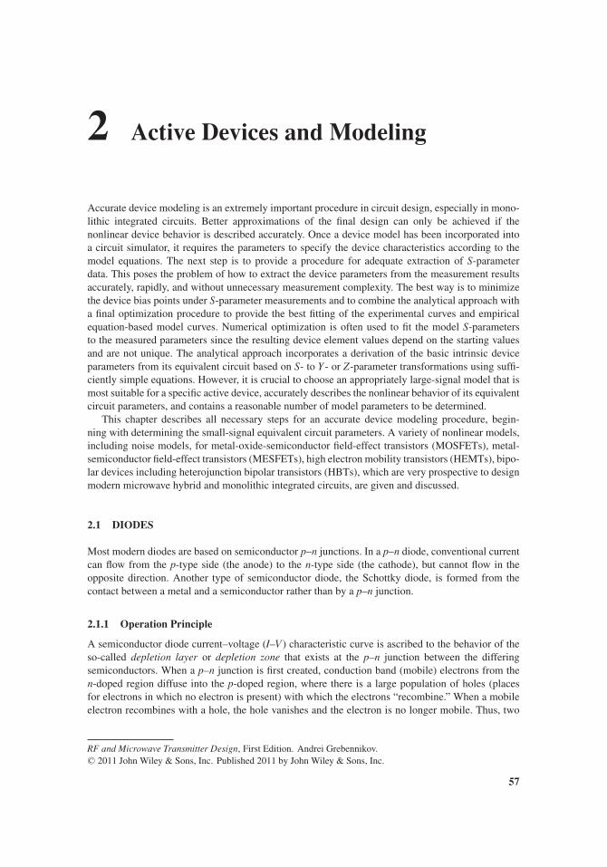
JWBS064-c02 JWBS064-Gerbennikov March 15, 2011 10:49 Printer Name: Yet to Come
2 Active Devices and Modeling
Accurate device modeling is an extremely important procedure in circuit design, especially in mono-lithic integrated circuits. Better approximations of the final design can only be achieved if thenonlinear device behavior is described accurately. Once a device model has been incorporated intoa circuit simulator, it requires the parameters to specify the device characteristics according to themodel equations. The next step is to provide a procedure for adequate extraction of S-parameterdata. This poses the problem of how to extract the device parameters from the measurement resultsaccurately, rapidly, and without unnecessary measurement complexity. The best way is to minimizethe device bias points under S-parameter measurements and to combine the analytical approach witha final optimization procedure to provide the best fitting of the experimental curves and empiricalequation-based model curves. Numerical optimization is often used to fit the model S-parametersto the measured parameters since the resulting device element values depend on the starting valuesand are not unique. The analytical approach incorporates a derivation of the basic intrinsic deviceparameters from its equivalent circuit based on S- to Y- or Z-parameter transformations using suffi-ciently simple equations. However, it is crucial to choose an appropriately large-signal model that ismost suitable for a specific active device, accurately describes the nonlinear behavior of its equivalentcircuit parameters, and contains a reasonable number of model parameters to be determined.
This chapter describes all necessary steps for an accurate device modeling procedure, begin-ning with determining the small-signal equivalent circuit parameters. A variety of nonlinear models,including noise models, for metal-oxide-semiconductor field-effect transistors (MOSFETs), metal-semiconductor field-effect transistors (MESFETs), high electron mobility transistors (HEMTs), bipo-lar devices including heterojunction bipolar transistors (HBTs), which are very prospective to designmodern microwave hybrid and monolithic integrated circuits, are given and discussed.
2.1 DIODES
Most modern diodes are based on semiconductor p–n junctions. In a p–n diode, conventional currentcan flow from the p-type side (the anode) to the n-type side (the cathode), but cannot flow in theopposite direction. Another type of semiconductor diode, the Schottky diode, is formed from thecontact between a metal and a semiconductor rather than by a p–n junction.
2.1.1 Operation Principle
A semiconductor diode current–voltage (I–V) characteristic curve is ascribed to the behavior of theso-called depletion layer or depletion zone that exists at the p–n junction between the differingsemiconductors. When a p–n junction is first created, conduction band (mobile) electrons from then-doped region diffuse into the p-doped region, where there is a large population of holes (placesfor electrons in which no electron is present) with which the electrons “recombine.” When a mobileelectron recombines with a hole, the hole vanishes and the electron is no longer mobile. Thus, two
RF and Microwave Transmitter Design, First Edition. Andrei Grebennikov.C© 2011 John Wiley & Sons, Inc. Published 2011 by John Wiley & Sons, Inc.
57

JWBS064-c02 JWBS064-Gerbennikov March 15, 2011 10:49 Printer Name: Yet to Come
58 ACTIVE DEVICES AND MODELING
charge carriers have vanished. The region around the p–n junction becomes depleted of charge carriersand thus behaves as an insulator.
However, the depletion width cannot grow without limit. For each electron–hole pair that recom-bines, a positively charged dopant ion is left behind in the n-doped region, and a negatively chargeddopant ion is left behind in the p-doped region. As recombination proceeds and more ions are created,an increasing electric field develops through the depletion zone that acts to slow and then finallystops recombination. At this point, there is a built-in potential across the depletion zone. This built-inpotential is positive because the n-side is at a higher potential than the p-side, which is proper toobtain a balance between drift and diffusion across the junction.
If an external voltage is placed across the diode with the same polarity as the built-in potential,the depletion zone continues to act as an insulator preventing a significant electric current. This isthe reverse bias phenomenon. However, if the polarity of the external voltage opposes the built-inpotential, recombination can once again proceed resulting in substantial electric current through thep–n junction. For silicon diodes, the built-in potential is approximately 0.6 V. Thus, if an externalcurrent is passed through the diode, about 0.6 V will be developed across the diode such that thep-doped region is positive with respect to the n-doped region and the diode is said to be “turned on”as it has a forward bias.
A diode I–V characteristic shown in Figure 2.1 can be approximated by two regions of operation.Below a certain difference in potential between the two leads, the depletion layer has significantwidth, and the diode can be thought of as an open (nonconductive) circuit. As the potential differenceis increased, at some stage the diode will become conductive and allow charges to flow, at whichpoint it can be thought of as a connection with zero (or at least very low) resistance. In a normalsilicon diode at rated currents, the voltage drop across a conducting diode is approximately 0.6 to0.7 V. In the reverse bias region for a normal p–n rectifier diode, the current through the device is
FIGURE 2.1 Diode current–voltage characteristic.

JWBS064-c02 JWBS064-Gerbennikov March 15, 2011 10:49 Printer Name: Yet to Come
DIODES 59
very low (in the μA range) for all reverse voltages up to a point called the peak inverse voltage (PIV).Beyond this point a process called reverse breakdown occurs that causes the device to be damagedalong with a large increase in current. For special purpose diodes like the avalanche or Zener diodes,the concept of PIV is not applicable since they have a deliberate breakdown beyond a known reversecurrent such that the reverse voltage is “clamped” to a known value (called the Zener voltage orbreakdown voltage). These devices however have a maximum limit to the current and power in theZener or avalanche region.
The Shockley ideal diode equation or the diode law is the current–voltage (I–V) characteristic ofan ideal diode in either forward or reverse bias (or no bias):
I = Isat
[exp
(V
nVT
)− 1
](2.1)
where I is the diode current, Isat is a scale factor called the reverse saturation current, V is thevoltage across the diode, VT is the thermal voltage, and n is the emission coefficient, also known asthe ideality factor. The term “saturation” indicates that the current I approaches an asymptote andbecomes independent of the voltage V .
It is derived with the assumption that the only processes giving rise to current in the diode aredrift (due to electrical field), diffusion, and thermal recombination–generation. It also assumes thatthe carrier recombination–generation current in the depletion region is insignificant. Additionally,it does not describe the “leveling off” of the I–V curve at high forward bias due to internal resis-tance, nor does it explain the practical deviation from the ideal at very low forward bias due torecombination–generation current in the depletion region.
The emission coefficient n varies from about 1 to 2 depending on the fabrication process andsemiconductor material and in many cases is assumed to be approximately equal to 1 (thus omitted).The thermal voltage VT is approximately 25.7 mV at room temperature 25◦C or 298 K defined by
VT = kT
q(2.2)
where q is the electronic charge (or elementary charge), k is Boltzmann constant, and T is the absolutetemperature of the p–n junction.
The diode small-signal electrical behavior can be described by the equivalent representation ofthe p–n junction with the differential resistance at the operating point
r = ∂V
∂ I
∣∣∣∣op
=[
Isat
nVTexp
(V
nVT
)]−1
(2.3)
and by two forms of charge storage: charge storage in the depletion region due to the dopantconcentrations and charge storage due to minority-carrier charges injected into the neutral p- andn-type regions resulting in the junction and diffusion capacitances, respectively [1]. There are severaltypes of semiconductor junction diodes, which either emphasizes a different physical aspects of adiode often by geometric scaling, doping level, choosing the right electrodes, or just an applicationof a diode in a special circuit.
2.1.2 Schottky Diodes
Schottky diodes are constructed from a structure made by forming a contact between a metal anda semiconductor defined as a metal–semiconductor junction. Each metal–semiconductor junctionis characterized by a potential barrier called the Schottky barrier, which depends only on the twomaterials and temperature, and it is not a function of the semiconductor doping. The Schottky barrierblocks the flow of electrons from the metal toward the semiconductor. Schottky diodes have a lower
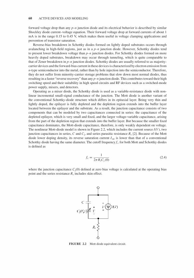
JWBS064-c02 JWBS064-Gerbennikov March 15, 2011 10:49 Printer Name: Yet to Come
60 ACTIVE DEVICES AND MODELING
forward voltage drop than any p–n junction diode and its electrical behavior is described by similarShockley diode current–voltage equation. Their forward voltage drop at forward currents of about 1mA is in the range 0.15 to 0.45 V, which makes them useful in voltage clamping applications andprevention of transistor saturation.
Reverse-bias breakdown in Schottky diodes formed on lightly doped substrates occurs throughavalanching in high-field regions, just as in a p–n junction diode. However, Schottky diodes tendto present lower breakdown voltage than p–n junction diodes. For Schottky diodes formed on moreheavily doped substrates, breakdown may occur through tunneling, which is quite comparable tothat of Zener breakdown in p–n junction diodes. Schottky diodes are usually referred to as majority-carrier devices and the forward-bias current in these devices is characterized by electron emission fromn-type semiconductor into the metal, rather than by hole injection into the semiconductor. Therefore,they do not suffer from minority-carrier storage problems that slow down most normal diodes, thusresulting in a faster “reverse recovery” than any p–n junction diode. This contributes toward their highswitching speed and their suitability in high speed circuits and RF devices such as a switched-modepower supply, mixers, and detectors.
Operating as a mixer diode, the Schottky diode is used as a variable-resistance diode with non-linear incremental small-signal conductance of the junction. The Mott diode is another variant ofthe conventional Schottky-diode structure which differs in its epitaxial layer. Being very thin andlightly doped, the epilayer is fully depleted and the depletion region extends into the buffer layerlocated between the epilayer and the substrate. As a result, the junction capacitance consists of twocomponents that can be modeled by two capacitances connected in series: the capacitance of thedepleted epilayer, which is very small and fixed, and the larger voltage-variable capacitance, arisingfrom the part of the depletion region that extends into the buffer layer. But because the smaller fixedcapacitance dominates, the Mott-diode capacitance, therefore, is only weakly dependent on voltage.The nonlinear Mott-diode model is shown in Figure 2.2, which includes the current source I(V), twojunction capacitances in series, C and Cj, and series parasitic resistance Rs [2]. Because of the Mottdiode lower doping density, its reverse saturation current Isat is lower than that of a conventionalSchottky diode having the same diameter. The cutoff frequency f c for both Mott and Schottky diodesis defined as
fc = 1
2π RsCj (0)(2.4)
where the junction capacitance Cj(0) defined at zero bias voltage is calculated at the operating biaspoint and the series resistance Rs includes skin effect.
FIGURE 2.2 Mott diode equivalent circuit.
JWBS064-c02 JWBS064-Gerbennikov March 15, 2011 10:49 Printer Name: Yet to Come
DIODES 61
The most important difference between p–n junction diode and Schottky diode is reverse recoverytime, when the diode switches from nonconducting to conducting state and vice versa. Where in p–njunction diode the reverse recovery time can be in the order of hundreds of nanoseconds, and lessthan 100 ns for fast diodes, Schottky diodes do not have a recovery time, because there is nothingto recover from. The switching time is of about 100 ps for the small signal diodes, up to tens ofnanoseconds for special high-capacity power diodes. With p–n junction switching, there is a reverserecovery current associated with it, which among other things with high-power semiconductors bringsincreased electromagnetic interference (EMI) noise. With Schottky diodes switching instantly withonly slight capacitive loading, this is of much lesser concern.
The most evident limitations of Schottky diodes are the relatively low reverse voltage rating forsilicon–metal Schottky diodes, 50 V and below, and a relatively high reverse leakage current. Thereverse leakage current, increasing with temperature, leads to a thermal instability issue. This oftenlimits the useful reverse voltage to well below the actual rating. Luckily, times are changing and thediodes are becoming better and better and the voltage ratings are now up at 200 V. The silicon carbideSchottky diodes have about 40 times lower reverse leakage current compared to silicon counterpartsand are made as 300-V, 600-V, and 1200-V variants. Silicon carbide has high thermal conductivityand temperature has little influence on switching and thermal characteristics, plus diodes have nothermal runaway. With special packing it is possible to have operating junction temperatures of over500 K, which allows passive radiation cooling in aerospace applications.
2.1.3 p–i–n Diodes
A p–i–n diode is a device that operates as a variable resistor at RF and microwave frequencies. Itis a silicon semiconductor diode in which a high-resistivity intrinsic i-layer is sandwiched betweenthe p-type and n-type layers. When a p–i–n diode is forward biased, holes and electrons from p-and n-layers are injected into the i-layer, respectively. These charges do not recombine immediately;instead, a finite quantity of charge always remains stored for an average time, called the carrierlife time τ , thus lowering the resistivity of the i-region. The quantity of stored charge Q is directlyproportional to the carrier life time (recombination time) τ and the forward bias current If as Q = Ifτ .The resistance Rs of the i-layer under forward bias condition is inversely proportional to Q and directlyproportional to W2, where W is the i-layer thickness. When the p–i–n diode is at zero or reverse bias,there is no stored charge in the i-layer and the diode appears as a junction capacitance Cj shuntedby a parallel resistance Rp. The p–i–n diode equivalent circuits for (a) forward bias and (b) zero orreverse modes are shown in Figure 2.3, where Ls is the parasitic series inductance [3]. By varying
RpCjRs
Ls
Ls
(b)(a)
FIGURE 2.3 p–i–n diode equivalent circuits.

JWBS064-c02 JWBS064-Gerbennikov March 15, 2011 10:49 Printer Name: Yet to Come
62 ACTIVE DEVICES AND MODELING
the i-layer thickness and diode area, it is possible to construct p–i–n diodes of different geometriesto result in the same Rs and Cj values. These devices may have similar small-signal characteristics.However, a diode with thicker i-layer would have a higher breakdown voltage and better distortionproperties. On the other hand, a diode with thinner i-layer would have faster switching speed.
At dc and very low frequencies being forward biased, the p–i–n diode behaves similar to a p–njunction diode and the diode resistance is described by the dynamic (or differential) resistance of thediode I–V characteristic at any forward bias point. The dc dynamic resistance point is not, however,valid for the p–i–n diodes at frequencies above which the period is shorter than the transit time of thei-region. The frequency at which this occurs is called the transit time frequency f T, and this lowestfrequency limit is primarily a function of the i-layer thickness W expressed by
fT = 1300
W 2MHz. (2.5)
At high frequencies when a p–i–n diode is at zero and reverse bias, it appears as a parallel platecapacitor, essentially independent of reverse voltage being a function of the junction capacitance andthickness of i-layer. However, at frequencies much lower than f T, the p–i–n diode acts as a varactor,and the junction capacitance Cj is determined by applying a sufficiently large reverse voltage, whichfully depletes the i-region of carriers. At low reverse bias voltages, the finite resistivity of the i-regionresults in a lossy junction capacitance. As the reverse voltage is increased, carriers are depleted fromthe i-layer, resulting in an essentially lossless silicon capacitor. Under reverse bias, the p–i–n diodeshould not be biased beyond its dc rating voltage VR. The diode avalanche or bulk breakdown voltageVBD is proportional to the i-layer thickness W and is always higher than VR. In a typical application,maximum negative voltage swing should never exceed VBD. An instantaneous excursion of the RFsignal into the positive bias direction generally does not cause the diode to go into conduction becauseof slow reverse-to-forward switching speed.
A step recovery diode (SRD) is a semiconductor junction diode having the ability to recoverextremely quickly from a strong forward-conduction state to a cutoff state. It is also called the snap-off diode or charge-storage diode, and has a variety of uses in microwave electronic devices as pulsegenerator or parametric amplifier. The SRD must have high charge storage in the forward direction,low capacitance in the reverse direction, low series resistance, and high reverse breakdown voltage forpower applications. Its switching time must be adequately short because switching speed establishesits high-frequency limit of operation. To meet these requirements, the SRD must have a relatively longcharge-storage time, and the charge that is injected into the junction while it is forward-biased mustnot travel so far that it cannot be removed during the reverse-bias interval. Also, the depletion regionmust not be too wide, otherwise transit-time effects will reduce the efficiency at high frequency.
The term “step recovery” relates to the form of the reverse recovery characteristic of these devices.After a forward current has been passing in an SRD and the current is interrupted or reversed, thereverse conduction will cease very abruptly (as in a step waveform). The SRD has the p–i–n structure,in which the i-region is a layer of undoped or intrinsic semiconductor or is very lightly doped [2].The i-region is formed by the overlap of the p- and n-layers, both of which have a steep dopingprofile. This profile gives a narrow depletion region in the p- and n-layers and a strong built-in electricfield, which opposes the diffusion of charge into the unction. During forward conduction, holes andelectrons are injected into the i-layer, where they recombine very slowly. The i-layer thus becomesa region in which charge is stored. When the SRD is reverse-biased, the i-layer is fully depleted,because of the wide depletion width, which includes the entire i-layer, resulting in a very low reversecapacitance. Under forward bias, the SRD can be modeled as a conventional p–n junction diode,however, when the SRD is reverse-biased, its capacitance is nearly constant and very low.
2.1.4 Zener Diodes
The effect when the p–n diodes can be made to conduct backward is called the Zener breakdown. Itoccurs at a precisely defined voltage, allowing the diode to be used as a precision voltage reference.

JWBS064-c02 JWBS064-Gerbennikov March 15, 2011 10:49 Printer Name: Yet to Come
VARACTORS 63
FIGURE 2.4 Circuit with Zener diode.
A conventional p–n diode will not let significant current flow if it is reverse-biased below its reversebreakdown voltage. By exceeding the reverse bias breakdown voltage, a conventional diode is subjectto high current flow due to avalanche breakdown. Unless this current is limited by external circuitry,the diode will be permanently damaged. A Zener diode exhibits almost the same properties, exceptthe device is specially designed so as to have a greatly reduced breakdown or Zener voltage. A Zenerdiode contains a heavily doped p–n junction allowing electrons to tunnel from the valence band ofthe p-type material to the conduction band of the n-type material. A reverse-biased Zener diode willexhibit a controlled breakdown and let the current flow to keep the voltage across the Zener diodeat the Zener voltage. For example, a diode with a Zener breakdown voltage of 3.2 V will exhibit avoltage drop of 3.2 V if reverse bias voltage applied across it is more than its Zener voltage. However,the current is not unlimited, so the Zener diode is typically used to generate a reference voltage for apower amplifier stage, or as a voltage stabilizer for low-current applications. The breakdown voltagecan be controlled quite accurately in the doping process. Tolerances to within 0.05% are available,though the most widely used tolerances are 5% and 10%.
Zener diodes are widely used to regulate the voltage across a circuit. When connected in parallelwith a variable voltage source so that it is reverse biased, a Zener diode conducts when the voltagereaches the diode reverse breakdown voltage. From that point it keeps the voltage at that value. In thecircuit shown in Figure 2.4, the bias resistor R provides the voltage drop between the input voltageV in and the output voltage Vout. The value of R must satisfy two conditions: it must be small enoughthat the current through diode keeps diode in reverse breakdown and it must be large enough thatthe current through diode does not destroy the device. A Zener diode used in this way is known as ashunt voltage regulator (shunt means connected in parallel, and voltage regulator is a class of circuitthat produces a stable voltage across any load).
2.2 VARACTORS
The term “varactor” comes from the phrase “variable reactor” and means a device whose reactancecan be varied in a controlled manner, in this case, with dc bias voltage [4]. The discovery of thecapacitance of a rectifying contact extends back to 1929 when the first comprehensive investigationof this phenomenon was made [5]. In 1949 Shockley published his classic paper on the theory of p–njunctions where not only the expressions for the current–voltage relationships in a diode are given,but the capacitance effect is considered as well [6]. The possibility of tuning diodes with exponentsgreater than one-half was firstly described in 1958, with the term “hyperabrupt” coined for suchsensitive devices [7].
2.2.1 Varactor Modeling
A simplified varactor equivalent circuit is shown in Figure 2.5, where Cv is the variable depletionlayer capacitance, Cp is the package capacitance, Rs is the series contact and bulk resistance, Ls is the

JWBS064-c02 JWBS064-Gerbennikov March 15, 2011 10:49 Printer Name: Yet to Come
64 ACTIVE DEVICES AND MODELING
FIGURE 2.5 Simplified varactor equivalent circuit.
series inductance incorporating package inductance, and VD is the diode junction [8,9]. The diode isnecessary to take into account because of the rectifying effect during a positive voltage swinging. Theseries resistance Rs is a function of applied voltage and operating frequency, although in most practicalcases it can be considered constant. Such a model neglects some parasitic linear components, whichshould be taken into account for microwave applications including distributed-line package modeland some capacitances due to the ground proximity. However, for most high frequency applicationsup to 2.5 GHz, these parasitics would not be significant unless higher order harmonics due to thevaractor nonlinearity affect VCO performance.
The varactor junction capacitance Cv as a function of the reverse dc bias voltage Vv can beexpressed by
Cv (Vv) = Cv0
(1 + Vv
ϕ
)−γ
(2.6)
where
γ = −dCv
Cv
/dVv
(Vv + ϕ)(2.7)
is the varactor junction sensitivity (γ = 0.5 for abrupt varactors, 1 ≤ γ ≤ 2 for hyperabrupt varactors),ϕ is the contact potential which value depends on a doping profile of varactor; and Cv0 = Cv(0) isthe varactor junction capacitance at Vv = 0. The voltage Vv is positive since it is assumed a reverseconnection of the varactor.
When the junction is reverse-biased, a large electric field exists in the depletion region. As the biasvoltage is increased, this field increases to a sufficiently high value where the thermally generatedcarriers traversing the depletion layer will generate additional hole–electron pairs by collision. Thesehole–electron pairs will in turn generate additional pairs, thus causing a multiplication effect oravalanche of carriers. The breakdown voltage at which avalanche occurs is the upper limit for thevaractor voltage-control range and determines the minimum varactor junction capacitance Cvmin. Thereverse breakdown voltage is relatively insensitive to temperature variations.
The doping concentration level in the varactor depletion region defines the difference between anabrupt junction varactor and a hyperabrupt junction one. For abrupt junction shown in Figure 2.6(a),the doping density is constant across the depletion region, whereas, for hyperabrupt junction shownin Figure 2.6(b), the doping density is a nonlinear function [10]. In the latter case, ion implantationor nonlinear epitaxial growing techniques can accomplish this. As a result, as the reverse voltage isincreased, the higher doping density contributes to a greater capacitance change in the hyperabruptvaractor than in the abrupt varactor with a constant doping density. However, the averaged dopingconcentration of the undepleted epitaxial region for abrupt varactor is higher approximately by afactor of two, which gives the higher value of the series resistance Rs for hyperabrupt varactor.

JWBS064-c02 JWBS064-Gerbennikov March 15, 2011 10:49 Printer Name: Yet to Come
VARACTORS 65
FIGURE 2.6 Doping density for abrupt and hyperabrupt varactors.
The quality factor of a varactor Qv (taken into account that the varactor junction capacitance Cv
is substantially higher than the package capacitance Cp) is defined as
Qv (Vv, ω) = 1
ωRsCv (Vv)(2.8)
being a function of operating frequency and applied voltage. Since with the increase of Rs thevaractor quality factor decreases, the Qv of the abrupt varactor is higher than that of the hyperabruptvaractor at low reverse bias voltage. However, at higher reverse bias voltages, the quality factor ofthe hyperabrupt varactor becomes higher due to the more rapid decrease in the hyperabrupt varactorcapacitance. As shown in Figure 2.7, usually over the linear tuning range for reverse bias voltageranging from 1 to 10 V, the Qv for hyperabrupt varactor is lower. As a result, the output power ofsuch a voltage-controlled oscillator (VCO) with hyperabrupt varactor should be lower due to higherpower losses in the varactor.
2.2.2 MOS Varactor
It is well known that an MOS transistor can be used as a variable capacitance due to the dependenceof its total charge (representing the charge on the gate, effective interface charge, and charge in the

JWBS064-c02 JWBS064-Gerbennikov March 15, 2011 10:49 Printer Name: Yet to Come
66 ACTIVE DEVICES AND MODELING
FIGURE 2.7 Varactor quality factor versus bias voltage.
semiconductor under the oxide) on the applied voltage between bulk and gate terminals [11]. In thecase of pMOS varactor with the source, drain, and bulk terminals together connected, an inversionchannel with mobile holes will be realized for gate–bulk voltages Vgb greater than the thresholdvoltage of the MOS transistor V th. Further increase in Vgb results in a strong inversion of the MOStransistor operation. On the other hand, for voltages Vgb lower than V th, an MOS transistor operatesin accumulation region, where the voltage at the interface between gate oxide and semiconductor ispositive and high enough to allow electrons to move freely.
Figure 2.8(a) shows the cross-section of the MOS transistor, where the movement behavior of themajority-charge carriers in the inversion, depletion, and accumulation regions is also shown [12]. Ametal oxide structure is build on the top of a lightly doped n-well diffusion layer with the gate andthe two n+ contacts inside n-well. The device bias-dependent capacitance C can be modeled as oxidecapacitance Cox in series with the parallel connection of the capacitance Cb owing to the depletionregion charge and Ci owing to the inversion layer charge at the gate–oxide interface. If Cb or Ci
dominates, the MOS transistor is operated in a depletion or strong-inversion region, respectively.Otherwise, if neither capacitance dominates, the MOS transistor is operated in a weak-inversionregion. The overall behavior of the MOS capacitance C versus gate–bulk voltage Vgb is qualitativelyshown in Figure 2.8(b), where the charge carrier movement in strong- and moderate-inversion regionsis indicated by solid lines shown in Figure 2.8(a).
When Vg approaches V th in the moderate-inversion region, the concentration of holes at theoxide interface decreases steadily, but Ci continues to be much larger than Cb. However, when theMOS transistor enters the weak-inversion region, modulation of the depletion region becomes ofthe same importance as hole injection when Ci ≈ Cb, being dominating effect in the depletionregion when Ci � Cb. Thus, both in the strong-inversion and accumulation region, the overall devicecapacitance C approaches the oxide capacitance Cox. Physically, an abundance of holes exists at highVgb immediately below the oxide and provides bottom plate of the oxide capacitor, just as abundanceof electrons provided that plate in the case of accumulation. In this case, the parasitic resistance isassociated with the resistive losses of electrons moving from the bulk contact to the interface betweenthe bulk and depletion regions, as shown in Figure 2.8(a) by dashed lines. Such a parasitic resistancecan be reduced by using scaled technology with shorter device gate length L [13]. With the technologyscaling, the oxide thickness is also reduced with correspondent increase in the oxide capacitance.Ideally, this should result not only in the better quality factor of a MOS varactor, but also in a widertuning range since a minimum depletion capacitance increases at a lower rate.
To obtain monotonic dependence for C, it is necessary to provide the device operation with-out entering the accumulation region for a very wide range of gate voltage values. This can be

JWBS064-c02 JWBS064-Gerbennikov March 15, 2011 10:49 Printer Name: Yet to Come
VARACTORS 67
FIGURE 2.8 MOS varactor and its voltage–capacitance dependence.
accomplished by removing the connection between drain and source with bulk, by connecting thebulk terminal to the supply voltage as the highest dc voltage in the circuit. Figure 2.9 shows thevoltage–capacitance dependence of such an inversion-mode MOS varactor operating in the strong-,moderate-, or weak-inversion regions only. However, a more attractive approach is to use the pMOSdevice in the depletion and accumulation regions only, resulting in a wider tuning range and betterquality factor due to lower parasitic resistance since the electrons have mobility approximately threetimes higher than holes [14].
The voltage–capacitance dependence of such an accumulation-mode MOS varactor operating inthe depletion and accumulation regions only is shown in Figure 2.10(a). To realize an accumulation-mode MOS varactor, the formation of the strong-, moderate-, and weak-inversion regions must beinhibited that requires the suppression of any injection of holes in the MOS channel. This can beaccomplished by removing the source and drain diffusion p+-doped layers and implementing thebulk n+-doped contacts instead of them, thus minimizing the parasitic-well resistance, as shown inFigure 2.10(b).
Since physical models describing the behavior of a MOS device in the accumulation and depletionregions are different, it normally comprises separate models for these regions, the integration of whichinto a common circuit simulator such as SPICE is complicated. Figure 2.11(a) shows the cross-sectionof an accumulation-mode MOS varactor, where bulk represents shorted n-well contacts. Its singleequivalent circuit is shown in Figure 2.11(b), where Cf represents the fringing capacitance mainlyassociated with sidewall of the gate; Lg and Rpoly are the parasitic inductance and resistance of the

JWBS064-c02 JWBS064-Gerbennikov March 15, 2011 10:49 Printer Name: Yet to Come
68 ACTIVE DEVICES AND MODELING
FIGURE 2.9 Inversion-mode MOS varactor tuning curve.
gate electrode, respectively [15]. The resistances Rwell, Rsub and capacitances Csub1, Csub2 are thesubstrate-related components. The resistance Rsd represents the source/drain regions. The channelresistance Rch is the only bias-dependent resistance. It can be modeled as Rch = Rs + Racc/Rp, where Rs
is the bias-independent n-well resistance between n+ contact and accumulation or depletion regionsunderneath the gate, Racc is the bias-dependent resistance of the accumulation layer, and Rp is theeffective resistance along the edge of the depletion region.
FIGURE 2.10 Accumulation-mode varactor and its tuning curve.

JWBS064-c02 JWBS064-Gerbennikov March 15, 2011 10:49 Printer Name: Yet to Come
VARACTORS 69
FIGURE 2.11 MOS varactor equivalent circuit.
In the accumulation region, Racc becomes much smaller than Rp, and Rch is approximately equalto Rs + Racc. In the depletion region, Racc can be considered infinite, and Rch approaches a constantvalue of Rs + Rp. The gate bias-dependence model of Racc based on the measurement results can beempirically given by
Racc(Vgb) = 1
Kacc
1
Vgb − Vdepfor Vgb > Vdep (2.9)
Racc(Vgb) = ∞ elsewhere (2.10)
where Kacc is the fitting parameter related to the device geometry and mobility of electrons in theaccumulation region, and Vdep is the fitting parameter related to the flat-band voltage in the depletionregion.
Accurate model of the MOS varactor capacitance C based on the description of its bias-dependentbehavior in two regions separately, available in SPICE simulator and valid under different bias
JWBS064-c02 JWBS064-Gerbennikov March 15, 2011 10:49 Printer Name: Yet to Come
70 ACTIVE DEVICES AND MODELING
conditions for a frequency range up to 10 GHz, is given by
C(Vg) = Cj
(1 − Vgb
Vj
)Mj
for Vgb ≤ FcVj (2.11)
C(Vg) = Cj
1 − Fc
(1 + Mj
)+ MjVgb
Vj
(1 − Fc)−1−Mjfor Vgb > FcVj (2.12)
where Cj, V j, Fc, and Mj are the model-fitting parameters [16].It should be noted that, due to the higher average doping beneath the gate and enhanced parasitic
interconnect capacitance in the device structure representing the more parallel connected segmentsfor the same gate area and smaller gate length L, the minimum capacitance will increase resultingin a lower capacitance ratio [17]. However, the minimum gate-length devices have the highestminimum quality factors since the polysilicon gate resistance at lower L dominates the overallparasitic resistance, which is several magnitudes smaller than the n-well resistance at large L. As aresult, there is a tradeoff between the quality factor and capacitance tuning ratio that can be achieved,for example, for medium 0.65-μm gate-length MOS varactors.
2.3 MOSFETs
Personal wireless communication services have been driving the development of silicon MOSFETworldwide to provide reliable low-cost and high-performance technology. For example, the laterallydiffused MOSFET (LDMOSFET) device structures have proven to be highly efficient, high gain,and linear for both high-power and low-voltage microwave and RF applications, including poweramplifiers, low-noise amplifiers, mixers, and voltage-controlled oscillators. To develop low-costsilicon integrated circuits using CMOS technology for higher speed and higher frequency integratedcircuits and subsystems within shorter design time, it is necessary to create accurate device models toallow efficient CAD simulation. Several well-known physically based MOSFET models can describethe device electrical behavior [1,18]. However, some of them such as Level 1, Level 2, or Level 3large-signal models are very simple and cannot describe the current–voltage and voltage–capacitancecharacteristics with acceptable accuracy. Other popular models, as the BSIM3v3 or higher versionmodels, are too much complicated and quite formal in general so that, for better learning of the devicebasic properties, it is useful to consider its intrinsic nonlinear core circuit only. Also, BSIM3v3 maynot be as accurate for RFIC simulation due to their derivative discontinuity. Moreover, microwaveparasitic effects in silicon MOSFET are not easy physically predictable. Table-based models, such asthe HP Root model, are only accurate for the characterized structures and measurement conditions.An empirical analytical modeling approach is an explicit and valid compromise between physicalmodels and data-based models.
2.3.1 Small-Signal Equivalent Circuit
To describe accurately the nonlinear properties of the large MOSFET devices, it is necessary to takeinto account the distributed nature of the gate capacitor, because the channel resistance is not equalto zero. In this case, the channel of such a device can be modeled as a bias-dependent RC distributedtransmission line along the channel length, as shown in Figure 2.12. This one-dimensional approachassumes a gradual channel approximation when the quantity of charge in the channel is controlledcompletely by the gate electrode, only fields in the vertical dimension influence the depletion region,and channel current is provided entirely by drift with a constant mobility. Despite some drawbacksrelated to short-channel devices, this approach allows a compromise between accuracy and simplicityof a model derivation.
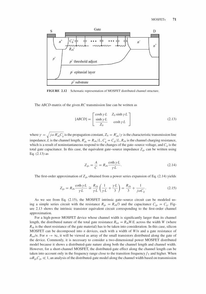
JWBS064-c02 JWBS064-Gerbennikov March 15, 2011 10:49 Printer Name: Yet to Come
MOSFETs 71
FIGURE 2.12 Schematic representation of MOSFET distributed channel structure.
The ABCD-matrix of the given RC transmission line can be written as
[ABCD] =⎡⎣ cosh γ L Z0 sinh γ L
sinh γ L
Z0cosh γ L
⎤⎦ (2.13)
where γ =√
jω R′chC ′
g is the propagation constant, Z0 = R′ch/γ is the characteristic transmission line
impedance, L is the channel length, R′ch = Rch/L , C ′
g = Cg/L , Rch is the channel charging resistance,which is a result of noninstantaneous respond to the changes of the gate–source voltage, and Cg is thetotal gate capacitance. In this case, the equivalent gate–source impedance Zgs can be written usingEq. (2.13) as
Zgs = A
C= Rch
coth γ L
γ L. (2.14)
The first-order approximation of Zgs obtained from a power series expansion of Eq. (2.14) yields
Zgs = Rchcoth γ L
γ L∼= Rch
γ L
(1
γ L+ γ L
3
)= Rch
3+ 1
jωCg. (2.15)
As we see from Eq. (2.15), the MOSFET intrinsic gate–source circuit can be modeled us-ing a simple series circuit with the resistance Rgs = Rch/3 and the capacitance Cgs = Cg. Fig-ure 2.13 shows the intrinsic transistor equivalent circuit corresponding to the first-order channelapproximation.
For a high-power MOSFET device whose channel width is significantly larger than its channellength, the distributed nature of the total gate resistance Rtot = RshW/L across the width W (whereRsh is the sheet resistance of the gate material) has to be taken into consideration. In this case, siliconMOSFET can be decomposed into n devices, each with a width of W/n and a gate resistance ofRtot/n. For n → ∞, it will be viewed as array of the small transistors distributed along the gate ofthe device. Commonly, it is necessary to consider a two-dimensional power MOSFET distributedmodel because it shows a distributed-gate nature along both the channel length and channel width.However, for a short-channel MOSFET, the distributed-gate effect along the channel length can betaken into account only in the frequency range close to the transition frequency f T and higher. WhenωRgsCgs � 1, an analysis of the distributed-gate model along the channel width based on transmission

JWBS064-c02 JWBS064-Gerbennikov March 15, 2011 10:49 Printer Name: Yet to Come
72 ACTIVE DEVICES AND MODELING
FIGURE 2.13 First-order approximation of intrinsic MOSFET equivalent circuit.
line theory shows that all transistor Y-parameters should be modified by the term tanh (γ W)/(γ W)[19]. However, a linear power series expansion of this term
tanh (γ W )
γ W= 1 − jωCg
Rtot
3∼= 1
1 + jωCgRtot
3
(2.16)
leads to only the additional use of a series lumped gate resistance Rtot/3 that does not alter the structureof the transistor equivalent circuit. Consequently, the overall gate resistance Rg can generally bedivided in two consecutive series resistances as Rg = Rge + Rgi, where Rge is the extrinsic contact andohmic gate electrode resistance and Rgi = Rtot/3 is the intrinsic gate resistance due to the distributed-gate structure of the power MOSFET.
The complete small-signal MOSFET equivalent circuit with the extrinsic parasitic elements isshown in Figure 2.14. Here, Rds is the differential channel resistance as a result of the channel lengthmodulation by the drain voltage, Cds is the drain–source capacitance, Lg is the gate lead inductance,Rs and Ls are the source bulk and ohmic resistance and lead inductance, Rd and Ld are the drain bulkand ohmic resistance and lead inductance, Cgp and Cdp are the gate and source pad capacitances,respectively.
FIGURE 2.14 Nonlinear MOSFET equivalent circuit with extrinsic linear elements.

JWBS064-c02 JWBS064-Gerbennikov March 15, 2011 10:49 Printer Name: Yet to Come
MOSFETs 73
To characterize the transistor nonlinear electrical properties, it is sufficient to use the grounded-source intrinsic Y-parameters. Their two-port admittance matrix is
Y =
⎡⎢⎢⎣
jωCgs
1 + jωτg+ jωCgd − jωCgd
gm exp (− jωτ )
1 + jωτg− jωCgd
1
Rds+ jω
(Cds + Cgd
)⎤⎥⎥⎦ (2.17)
where τ is the effective channel carrier transit time and τ g = RgsCgs. The intrinsic gate resistanceRgi can be considered an external gate element. In this case, the MOSFET intrinsic Y-matrix is thesame as for the MESFET or HEMT devices. Consequently, to determine the elements of the intrinsicMOSFET small-signal equivalent circuit, it is possible to use similar analytical approach, whichallows the determination of its elements through the real and imaginary parts of the device intrinsicadmittance Y-parameters.
2.3.2 Nonlinear I–V Models
An empirical approach to approximate the nonlinear behavior of the drain current source Ids (Vgs,Vds) of a JFET device is described in [20]. Instead of using separate equations for the triode andpinch-off regions, irrespective of the device geometry and material parameters, a general expressionbased on hyperbolic functions was proposed:
Ids = Idss
(1 − Vgs
Vp
)2
tanhα
∣∣∣∣ Vds
Vp − Vgs
∣∣∣∣ (2.18)
where Idss is the saturation drain current for Vgs = 0, α is the saturation voltage parameter, andVp is the pinch-off voltage. As a result, good agreement was obtained between the predicted andexperimental results, which showed a promising prospect of such a simple empirical model.
A similar and sufficiently simple nonlinear model using a hyperbolic function and incorporatingself-heating effect was later proposed to describe the I–V characteristics of a MOSFET device:
Ids = βeff VVG exp
gst (1 + λVds) tanh
(αVds
V SATexpgst
)(2.19)
where
βeff = β/(
1 + μcritVGMexp
gst
)
Vgst = Vst ln
[1 + exp
(Vgst1
Vst
)]
Vgst1 = Vgs − Vth0 − γ Vds
where GMexp, SATexp, and μcrit are the channel current parameters [21].An empirical nonlinear model, which is single-piece and continuously differentiable, developed
for silicon LDMOS transistors is given by
Ids = βV VG expgst (1 + λVds) tanh
(αVds
Vgst
) [1 + K1 exp (VBReff1)
]+ Iss exp
(Vds − VBR
VT
)(2.20)
JWBS064-c02 JWBS064-Gerbennikov March 15, 2011 10:49 Printer Name: Yet to Come
74 ACTIVE DEVICES AND MODELING
where
Vgst = Vst ln
[1 + exp
(Vgst2
Vst
)]
Vgst2 = Vgst1 − 1
2
(Vgst1 +
√(Vgst1 − VK
)2 + �2 −√
V 2K + �2
)
Vgst1 = Vgs − Vth0 − γ Vds
VBReff1 = Vds − VBReff
K2+ M3
Vds
VBReff
VBReff = VBR
2
[1 + tanh
(M1 − Vgst M2
)]
where λ is the drain current slope parameter, β is the transconductance parameter, V th0 is the forwardthreshold voltage, V st is the subthreshold slope coefficient, VT is the temperature voltage, Iss is theforward diode leakage current, VBR is the breakdown voltage, K1, K2, M1, M2, and M3 are thebreakdown parameters, VK, VGexp, �, and γ are the gate–source voltage parameters [22].
In many applications, it is necessary to take into consideration the MOSFET operation in theweak-inversion region when the gate–source voltage Vgs is smaller than the threshold voltage V th. Forexample, to improve the conversion gain of a mixer or reduce the intermodulation distortion (IMD) ofa class AB power amplifier when device is biased around the onset of the strong-inversion region fromthe weak-inversion region for low drain quiescent current. The drain current in the weak-inversionregion is mainly dominated by the diffusion component that increases exponentially with the gatevoltage [11]. On the other hand, in the strong-inversion saturation region when the gate–source voltageis greater than the threshold voltage, the drain current is proportional to the square of (Vgs – V th).
To obtain continuous behavior from weak-inversion region to strong-inversion region for the draincurrent and a compromise between accurate device modeling and ease of circuit analysis, we can use
Ids
(Vgs
) = A{ln[1 + exp
(B(Vgs − Vth
))]}2(2.21)
where A and B are the approximation parameters. In this case, the drain current is effectivelyproportional to the square of (Vgs – V th) when Vgs is larger than V th and exponentially decreases withthe gate–source voltage when Vgs is smaller than V th. The approximation parameters A and B aredefined from the following conditions:
Ids|Vgs=Vth= Ith
∂ Ids
∂Vgs
∣∣∣∣Vgs=Vth
= Sth (2.22)
where Ith is the threshold drain current, as shown in Figure 2.15, and Sth is a slope of the current–voltagetransfer characteristic in the threshold point. Then,
A = Ith
(ln2)2 B = Sth
Ithln 2. (2.23)
Consequently, the transfer characteristic can be defined in terms of only two physical parametersIth and Sth, which are easily calculated from the device measurements. By using similar analyticalapproach, the EKV MOST model has been successfully applied to low-voltage and low-current analogcircuit design and simulation, referring voltage Vg, Vd, and V s to the device local substrate [23].

JWBS064-c02 JWBS064-Gerbennikov March 15, 2011 10:49 Printer Name: Yet to Come
MOSFETs 75
FIGURE 2.15 Drain current versus gate–source voltage.
In view of the monotonous behavior of Ids−Vds curves, the entire drain current–voltage charac-teristics of a MOSFET device can be described as:
Ids
(Vgs, Vds
) = I0
/[1 +
(I0
Imax
)n] 1n
(2.24)
where
I0 = Ith
(ln2)2(1 − βVgs
) {ln
[1 + exp
(Sthln2
Ith
(Vgs − Vth
))]}2
Imax = Isat (1 + λVds) tanh (αVds)
where Isat is the saturated drain current, α is the saturation voltage parameter (which affects a slope ofthe Ids–Vds characteristics in the linear region), λ is the parameter that determines a slope of the samedrain characteristics in the saturation region, V th = V th0 − σVds, n and β are the fitting parametersthat determine a slope of the transfer characteristics under large values of Vgs, σ is the parameter thatexpresses empirically the dependence of the threshold voltage on Vds [24].
To verify that this model is applicable not only to high-power LDMOSFET devices but also tolow-voltage MOSFETs, the appropriate low-voltage MOSFET power device with a gate width of W =2 mm was selected [25]. Figure 2.16(a) shows the transistor theoretical and experimental drain currentcurves Ids(Vds). The resulting current mean-square error of a family of the output current–voltageIds–Vds characteristics is 0.42%. The transfer Ids–Vgs characteristics were compared with the samecharacteristics calculated from the BSIM3v3 model, which was developed for modeling of deepsubmicrometer devices. The results shown in Figure 2.16(b) demonstrate a good agreement with theexperimental curves and practically the same as in the case of the BSIM3v3 approximation.
2.3.3 Nonlinear C–V Models
The input capacitance Cgs normally influences the IMD level especially when the frequency increasesin the microwave region [26]. Generally, the calculation of the gate–source capacitance Cgs or thegate–drain capacitance Cgd from the charges corresponding to the strong-inversion model only resultsin a mathematically complicated expression [11]. Therefore, in most cases when it is necessary to

JWBS064-c02 JWBS064-Gerbennikov March 15, 2011 10:49 Printer Name: Yet to Come
76 ACTIVE DEVICES AND MODELING
FIGURE 2.16 Measured and modeled current–voltage characteristics of low voltage MOSFET.
predict efficiency, gain, or output power of the power amplifier or oscillator, the capacitances Cgs
and Cgd can be modeled as the fixed capacitances measured at the quiescent bias voltage, and thep–n junction diode capacitance model can be applied to the capacitance Cds [27]. The gate–draincapacitance Cgd can also be considered as the bias-dependent junction capacitance [28]. With theincrease in the drain bias voltage, a depletion region is formed under the oxide in the lightly doped drainregion. Therefore, the capacitance Cgd can be considered as a junction capacitance, which stronglydepends on the drain–source bias voltage Vds. According to the accurate charge model calculations,the gate–drain capacitance Cgd has a strong dependence on Vgs only in the moderate-inversion regionwhen Vgs – V th < 1 V [11]. In this region, the behavior of Cgd is similar to Cgs, and can be evaluatedusing the same hyperbolic tangent functions. However, for high-voltage LDMOSFET devices, sincethe dependence of Cgd on Vgs is quite small, it seems sufficient to limit the dependence to Vds only.

JWBS064-c02 JWBS064-Gerbennikov March 15, 2011 10:49 Printer Name: Yet to Come
MOSFETs 77
FIGURE 2.17 Gate–source capacitance versus gate–source voltage.
The drain–source capacitance Cds varies due to the change in the depletion region, which is mainlydetermined by the value of Vds.
The gate–source capacitance Cgs can be described as a function of the gate–source bias voltage.First, we consider an appropriate behavior of each of its main composite part: the intrinsic gate–sourcecapacitance Cgsi, including both the gate–source and the source–substrate charge fluctuations, andthe gate–substrate capacitance Cgbi. The gate–source voltage dependence of these components issubstantially different [11]. The intrinsic gate–substrate capacitance Cgbi is constant in the accumu-lation region where it is equal to the total intrinsic oxide capacitance Cox, slightly decreases in theweak-inversion region, significantly reduces in the moderate-inversion region, and becomes prac-tically constant in the strong-inversion or saturation region. The intrinsic gate–source capacitanceCgsi grows rapidly in the moderate-inversion region and equals 2Cox/3 in the saturation region. Thedependence of the total gate–source capacitance Cgs as a sum of its components Cgsi and Cgbi on Vgs
is shown in Figure 2.17.A hyperbolic tangent function can be used for each of two parts of the dependence Cgs(Vgs), where
the gate–source capacitance can be approximated by
Cgs = Cgsmin + Cs
{1 + tanh
[S
Cs
(Vgs − Vs
)]}(2.25)
where Cs = (Cgsmax − Cgsmin)/2, Cgsmax is the maximum gate–source capacitance, Cgsmin is theminimum gate–source capacitance, S = (S1, S2) is the slope of Cgs(Vgs) at each bend point Vgs =(V s1, V s2), as shown in Figure 2.17,
S1 = ∂Cgs
∂Vgs
∣∣Vgs=Vs1 S2 = ∂Cgs
∂Vgs
∣∣Vgs=Vs2. (2.26)
The total gate–source capacitance Cgs as a function of Vgs can be described by
Cgs = Cgsmax − Cgso
{1 + tanh
[S1
Cs
(Vgs − Vs1
)]}×{
1 + tanh
[S2
Cs
(Vgs − Vs2
)]}(2.27)
where Cgsmax = Cox and Cgso is the model fitting parameter [24].

JWBS064-c02 JWBS064-Gerbennikov March 15, 2011 10:49 Printer Name: Yet to Come
78 ACTIVE DEVICES AND MODELING
The approximation function for the gate–source capacitance Cgs as the dependence of Vgs can alsobe expressed by using the two components, both containing the hyperbolic functions:
Cgs = Cgs1 + Cgs2
{1 + tanh
[Cgs6
(Vgs + Cgs3
)]}+ Cgs4
[1 − tanh
(Cgs5Vgs
)](2.28)
where Cgs1, Cgs2, Cgs3, Cgs4, Cgs5, and Cgs6 are the approximation parameters [22].If we consider the dependence of the gate–source capacitance Cgs on Vds for submicrometer
MOSFET devices when Cgs slightly increases with the increase of Vds, the approximation expressionfor Cgs as a function of both Vgs and Vds can be written as
Cgs = Cgs0 + Cgs1
{As + Bstanh
[Cs
(Vgs − Vth
)]}× {Ds + Es
[1 + tanh
(Vgs − Vds
)]tanh
[FsVds − GsVgs
]}(2.29)
where Cgs0 is the bias-dependent capacitance, V th is the threshold voltage, Cgs1 is the scaling factor,and As, Bs, Cs, Ds, Es, Fs, and Gs are the model fitting parameters [29].
On the other hand, for high-voltage MOSFET devices, the dependencies of gate–drain capacitanceCgd and drain–source capacitance Cds on Vds can be accurately evaluated by the junction capacitancemodel as
Cgd(ds) = Cgdo(dso)
(ϕ + Vdso
ϕ + Vds
)m
(2.30)
where m (m1 for Cgd or m2 for Cds) is the junction sensitivity depending on a doping profile (m = 1/3for the linearly graded junction, m = 1/2 for the abrupt junction, and m > 1/2 for the hyperabruptjunction), ϕ is the contact potential, Cgdo and Cdso are the junction capacitances when Vds = Vdso. Forpractical profiles of the junction, which are neither exactly abrupt nor exactly linearly graded, oneoften chooses the parameters m and ϕ to obtain the best matching between the theoretical model andthe measurements.
For submicrometer MOSFET devices, to take into account the dependence of Cgd both on Vgs andVds, the approximation expression for the Cgd is written as
Cgd = Cgd0 + Cgd1
{Ad + Bd tanh
[Cd
(DdVgs − Vds
)− Vth
]}(2.31)
where Cgd0 is the bias-dependent capacitance, V th is the threshold voltage, Cgd1 is the scaling factor,while Ad, Bd, Cd, and Dd are the model fitting parameters [29].
2.3.4 Charge Conservation
To describe the small- and large-signal device models, it is necessary to satisfy the charge conservationcondition. For a three-terminal MOSFET device, the matrix equation for the small-signal chargingcircuit in frequency domain is given by
⎡⎢⎣
Ig
Id
Is
⎤⎥⎦ = jω
⎡⎢⎣
Cgg −Cgd −Cgs
−Cdg Cdd −Cds
−Csg −Csd Css
⎤⎥⎦⎡⎢⎣
Vg
Vd
Vs
⎤⎥⎦ (2.32)
where Ig, Id, and Is are the terminal current amplitudes, Vg, Vd, and V s are the terminal voltageamplitudes, and the capacitance between any two device terminals (k, l) is described as Ckl =∂Qk/∂V l [11]. To transform a three-terminal device into a two-port network with a common sourceterminal, the current and voltage terminal conditions of Ig = Igs, Id = Ids, Is = − (Igs + Ids),

JWBS064-c02 JWBS064-Gerbennikov March 15, 2011 10:49 Printer Name: Yet to Come
MOSFETs 79
Vg − V s = Vgs, and Vd − V s = Vds should be taken into account. In addition, the followingrelationships between the terminal capacitances for three-terminal devices are valid:
Cgg = Cgd + Cgs = Cdg + Csg
Cdd = Cdg + Cds = Cgd + Csd
Css = Csg + Csd = Cgs + Cds.
(2.33)
The admittance Yc-matrix for such a capacitive two-port network is
Yc =[
jω(Cgs + Cgd
) − jωCgd
− jω(Cgd + Cm
)jω(Cds + Cm + Cgd
)]
(2.34)
where Cm = Cdg − Cgd is the transcapacitance, Cgd represents the effect of the drain on the gate, andCdg represents the effect of the gate on the drain, and these effects are different [11]. Similarly to theI–V characteristics, there is no reason to expect that the effect of the drain voltage on the gate current,which is zero assuming no leakage current, is the same as the effect of the gate voltage on the draincurrent, which is significantly large.
Therefore, for power MOSFET devices, because the transcapacitance Cm is substantially less thanCgs, it can be translated to an additional delay time τc in a frequency range up to f T by its combiningwith the transconductance gm according to
gm − jωCm = gm
√1 +
(ω
ωT
Cm
Cgs
)2
exp
[− j tan−1
(ω
ωT
Cm
Cgs
)]∼= gm exp (− jωτc) (2.35)
where τ c = Cm/(ωTCgs). To satisfy the charge conservation condition, the total delay time τ , shownin the MOSFET equivalent circuit in Figure 2.14, represents both the ideal transit time and delaytime due to the transcapacitance. The transcapacitance Cm can be easily added to the drain–sourcecapacitance Cds under parameter extraction procedure.
2.3.5 Gate–Source Resistance
The gate–source resistance Rgs is determined by the effect of the channel inertia in responding torapid changes of the time varying gate–source voltage, and varies in such a manner that the chargingtime τ g = RgsCgs remains approximately constant. Thus, the increase of Rgs in the velocity satura-tion region (when the channel conductivity decreases) is partially compensated by the decrease ofCgs due to nonuniform channel charge distribution [30]. The effect of Rgs becomes significant athigher frequencies close to the transition frequency f T of the MOSFET and may not be taken intoaccount when designing RF circuits operating below 2 GHz, as used for commercial wireless appli-cations [25,31]. For example, for the MOSFET with the depletion region doping concentration valueNA = 1700 μm−3, the phase of the small-signal transconductance gm near f T reaches the value onlyof −15◦ [11].
2.3.6 Temperature Dependence
Silicon MOSFET devices are very sensitive to the operation temperature T and their characteristicsare strongly temperature dependent [11]. The main parameters responsible for this are the effectivecarrier mobility μ and the threshold voltage V th, resulting in the increase of the drain current throughV th(T) and the decrease of the drain current through μ (T ) with temperature. Increasing temperaturedecreases the slope of the Ids(Vgs) curves. A certain value of Vgs can be found, at which the draincurrent becomes practically temperature independent over a large temperature range. The variation

JWBS064-c02 JWBS064-Gerbennikov March 15, 2011 10:49 Printer Name: Yet to Come
80 ACTIVE DEVICES AND MODELING
of V th with temperature in a wide range from −50 to +200◦C represents a nonlinear function, whichis slowly decreased with temperature and can be approximated by
Vth (T ) = Vth (Tnom) + VT1�T + VT2�T 2 (2.36)
where �T = T − Tnom, Tnom = 300 K (27◦C), and VT1 and VT2 are the linear and quadratic temperaturecoefficients for threshold voltage [27].
The variation of μ with temperature can be taken into account by introducing the appropriatetemperature variation of Isat in Eq. (2.24). The temperature variation of Isat represents an almoststraight line, which decreases with temperature [27]. The temperature dependence Isat(T) can beapproximated by the linear function as
Isat (T ) = Isat (Tnom) + IT�T (2.37)
where IT is the linear temperature coefficient for the saturation current.The temperature dependencies of the MOSFET capacitances and series resistances can be de-
scribed by the following linear equations [1,32]:
C (T ) = C (Tnom) + CT�T (2.38)
R (T ) = R (Tnom) + RT�T (2.39)
where C = (Cgs, Cds, Cgd), R = (Rg, Rs, Rd), and RT and CT are the linear temperature coefficientsfor the capacitances and resistances, respectively.
At high value of Vgs and Vds under dc measurement, the slope of Ids – Vds curves can be negativethat occurs due to the self-heating effect in a highly dissipated power region. For the drain currentmodel given by Eq. (2.19), this effect can be taken into account by adding a linear componentdescribing the temperature dependence as
β (T ) = β (Tnom) + βT�Tj (2.40)
γ (T ) = γ (Tnom) + γT�Tj (2.41)
where �T j = RthPdis + �T , Rth(◦C/W) is the thermal resistance, Pdis is the dc power consumptionin watts caused by dc biasing, and βT and γ T are the linear temperature coefficients with negativevalues, respectively [21].
Another way of taking into account the effect of the negative conductance at high biasing is towrite the nonlinear Ids – Vds model as follows:
Ids (T , pT) = Ids (T )
1 + pTVd Ids (T )(2.42)
where the drain current source Ids(T) is given by Eq. (2.24), Vd = Vds/√
1 + (ωτth)2, pT is the self-heating temperature coefficient, Vds is the drain–source supply voltage, τ th = RthCth is the thermaltime constant, Rth is the thermal resistance, Cth is the thermal capacitance, and T j is the functionof ambient temperature T and pT. A thermal equivalent circuit can be added to the large-signalMOSFET model as a parallel RthCth circuit [22]. The thermal resistance Rth can be extracted from thetemperature measurement of the dc characteristics. Since the slope of the dc measured Ids(Vds) curveschanges its sign from positive to negative, the temperature coefficient pT can be evaluated under thecondition of
dIds (T, pT)
dVds= 0 (2.43)

JWBS064-c02 JWBS064-Gerbennikov March 15, 2011 10:49 Printer Name: Yet to Come
MOSFETs 81
As a result,
pT = 1
I 2ds (T )
dIds (T )
dVds(2.44)
where Ids(Vds) curves are determined by measurement of the pulsed Ids(Vds) curves at ambienttemperature T , and the value of Ids(T) is fixed the same as for zero slope of Ids(T, pT).
The thermal time constant τ th can be extracted by comparing pulsed Ids(Vds) curves calculatedunder different pulse widths and duty factors. A plot of Ids as a function of pulse width under thefixed gate–source and drain–source bias voltages gives an appropriate value of τ th.
2.3.7 Noise Model
The noise behavior of the MOSFET device can be described based on its equivalent circuit rep-resentation, which includes the main elements responsible for the device electrical behavior andnoise sources. The noise generated by a circuit element can be modeled as a result of a small-signalelectrical excitation. Each noise source is considered as statistically uncorrelated to the other noisesources in the circuit and the contribution of each noise source to the total noise is determined onthe individual basis. The total noise represents the root-mean-square sum of these individual noisecontributions. Since a device channel material is resistive, it exhibits thermal noise as a major sourceof noise, which can be represented by a noise current source i 2
nd connected between the drain andthe source in the MOSFET small-signal equivalent circuit shown in Figure 2.18(a), where the flicker
FIGURE 2.18 MOSFET equivalent circuits with noise sources.

JWBS064-c02 JWBS064-Gerbennikov March 15, 2011 10:49 Printer Name: Yet to Come
82 ACTIVE DEVICES AND MODELING
noise is also included. The induced gate current noise is modeled by the gate noise current source i 2ng
connected across the gate–source capacitance Cgs.The noise voltage and current sources can be given through their mean-square values as
e2ng = 4kTRg� f (2.45)
i2ng = 4kT η
(ωCgs
)2� f
gm(2.46)
i 2ns = 4kT� f
Rs(2.47)
e2nd = 4kTRd� f (2.48)
i2nd = 4kTγ
Rds0� f + KF
I AFd
Cox L2eff f
� f (2.49)
where η is the induced gate noise coefficient, gm is the device transconductance, Id is the drain biascurrent, AF is the flicker noise exponent, KF is the flicker noise coefficient, Cox is the oxide capacitanceper unit area, Leff is the effective channel length, Rds0 is the differential drain–source resistance atVds = 0, γ is the channel noise coefficient [1,33]. In the long-channel devices, Rds0 = 1/gm and γ =2/3, while both Rds0 and γ are complicated functions of the device parameters in the short-channelMOSFETs [34]. The equation for i 2
nd (with excluded flicker noise) valid for both short-channel andlong-channel devices expressed through the device parameters can be written in a simple form as
i 2nd = 4kTβ Id� f (2.50)
where
β = 1
Vdsat+ α2Vdsat
3(Vgs − Vth
)2Vdsat is the saturation drain–source voltage, and α is the bulk-charge effect coefficient [35].
The required minimum noise figure Fmin, noise resistance Rn, and optimum source admittanceYSopt using the noise correlation CA-matrix parameters as functions of the input-referred noise voltagev2
ni, noise current i 2ni, and the parameters of the simplified noise-free two-port network shown in
Figure 2.18(b) can be approximately estimated by
Rn = Rg + β Id
g2m
(2.51)
YSopt =√
β Id Rg
Rn
(f
fT
)(1 − j
1
gm
√β Id
Rg
)(2.52)
Fmin = 1 +(
f
fT
)√β Id Rg
[1 +
(f
fT
)√β Id Rg
](2.53)
where f is the operation frequency and f T = gm/2π (Cgs + Cgd) [35].There are two major theories to explain the physical origin of 1/f noise in MOSFET devices,
one is based on the carrier number fluctuation theory when the flicker noise is attributed to therandom trapping and detrapping processes of charges near the Si–SiO2 interface, the other is based onmobility fluctuation theory considering the flicker noise as a result of the fluctuations in bulk mobility

JWBS064-c02 JWBS064-Gerbennikov March 15, 2011 10:49 Printer Name: Yet to Come
MESFETs AND HEMTs 83
[36–38]. Assuming that the channel can exchange charges with the oxide traps through tunneling, thecharge fluctuation results in fluctuation of the surface potential, which in turn modulates the channelcarrier density. At the same time, it is considered that the fluctuation of bulk mobility is induced byfluctuations in phonon population through phonon scattering. Generally, the measured noise powerin MOSFET devices has a more complicated dependence on the gate bias and oxide thickness thandue to the predictions based on the number or bulk mobility fluctuation theory only. Also, the surfacemobility fluctuation mechanism should be taken into account attributed to the scattering effect offluctuating oxide charge [39]. The implementation of oxide and interface trapping noise into a partialdifferential equation-based semiconductor device simulator shows the correct prediction of 1/f noisespectral densities for submicrometer MOSFET devices operating in subthreshold and strong inversionin saturation [40].
The dependence of flicker noise power on gate bias and oxide thickness for n-channel MOSFETin terms of the equivalent gate noise power e2
ngcan be modeled by the following empirical expression:
e2ng = � f
LWf
[K1
(q
Cox
)m (Vgs − Vth
)+ K2
(q
Cox
)2]
(2.54)
where Vgs is the gate–source voltage, V th is the threshold voltage, L is the channel length, W is thechannel width, Cox is the gate–oxide capacitance per unit area, q is the electron charge, K1 and K2
are empirical constants, and m = 0.7–1.2 [38]. In this case, it was proposed that the term with K1
represents the contribution from the mobility fluctuation, whereas the term with K2 represents thecontribution from the number fluctuation.
Generally, the noise behavior of the n-channel and p-channel MOSFET devices is different, sincethe pMOS transistor being less noisy usually has a channel at a larger distance from the interface [41].Unlike MOSFET device, the flicker noise of its JFET counterpart is negligible. At low temperaturesthe noise spectrum of JFET indicates the presence of the several types of the generation–recombinationprocesses, but the 1/f noise component is absent [42]. However, the component related to 1/f noisecan appear at high temperatures more than 200 K [43]. Such a situation can be explained by thefact that the noise behavior of a JFET device having the p–n junction cannot be characterized by thesemiconductor–oxide surface effects since its channel is separated by the depletion region localizedalong the device channel.
2.4 MESFETs AND HEMTs
2.4.1 Small-Signal Equivalent Circuit
The small-signal equivalent circuit shown in Figure 2.19 proves to be an adequate representation forMESFETs and HEMTs in a frequency range up at least to 25 GHz. Here, the extrinsic elements Rg,Lg, Rd, Ld, Rs, and Ls are the bulk and ohmic resistances and lead inductances associated with thegate, drain, and source, while Cgp and Cdp are the gate and source pad capacitances, respectively.The capacitance Cdsd and resistance Rdsd model the dispersion of the MESFET or HEMT I–Vcharacteristics due to the trapping effect in the device channel, which leads to discrepancies betweendc measurement and S-parameter measurement at high frequencies [44–46]. The intrinsic model isdescribed by the channel charging resistance Rgs, which represents the resistive path for chargingof the gate–source capacitance Cgs, the feedback gate–drain capacitance Cgd, the output differentialresistance Rds, the drain–source capacitance Cds and the transconductance gm. The gate–sourcecapacitance Cgs and gate–drain capacitance Cgd represent the charge depletion region and are nonlinearfunctions. The influence of the drain–source capacitance Cds on the device behavior is insignificantand its value is practically bias independent. To model the transit time of electrons along the channel,the transconductance gm usually includes the time constant τ .

JWBS064-c02 JWBS064-Gerbennikov March 15, 2011 10:49 Printer Name: Yet to Come
84 ACTIVE DEVICES AND MODELING
FIGURE 2.19 Small-signal equivalent circuit of field-effect transistor.
To describe accurately the small-signal and large-signal device models, it is necessary to satisfycharge conservation condition. The models for the device gate–source capacitance Cgs and gate–draincapacitance Cgd should be derived from the charge model. There are commonly four partial derivativesof the two device terminal charges, the gate charge Qg and the drain charge Qd with regard to Vgs andVds, which appropriately represent totally four capacitances, as shown Figure 2.20(a) [45]. However,
FIGURE 2.20 Capacitance equivalent circuits consistent with charge conservation.

JWBS064-c02 JWBS064-Gerbennikov March 15, 2011 10:49 Printer Name: Yet to Come
MESFETs AND HEMTs 85
the intrinsic small-signal equivalent circuit contains only two capacitances. Consequently, in thiscase, they can be defined as
Cgs = ∂(Qg + Qd
)∂Vgs
Cgd = ∂(Qg + Qd
)∂Vgd
. (2.55)
The admittance Yc-matrix for such a capacitive two-port network is
Yc =[
jω(Cgs + Cgd
) − jωCgd
− jω(Cgs − Cm
)jωCgd
](2.56)
where Cm is an additional transcapacitance, which is determined by
Cm = ∂Qg
∂Vgd− ∂ Qd
∂Vgs. (2.57)
By adding the transcapacitance Cm, the capacitance equivalent circuit becomes consistent with thecharge conservation condition, as shown in Figure 2.20(b). Given that, for the MESFET devices, thetranscapacitance Cm is substantially less than the gate–source capacitance Cgs in a frequency rangewhere ω ≤ ωT, it can be translated to an additional delay time τ c by its combining with the small-signaltransconductance gm according to gm − jωCm ≈ gm exp(−jωτ c), where τ c = Cm/(ωTCgs).
2.4.2 Determination of Equivalent Circuit Elements
To characterize the nonlinear device electrical properties, first we consider the admittance Y-parameters derived from the intrinsic small-signal equivalent circuit as
Y11 = jωCgs
1 + jωCgs Rgs+ jωCgd (2.58)
Y12 = − jωCgd (2.59)
Y21 = gm exp (− jωτ )
1 + jωCgs Rgs+ jωCgd (2.60)
Y22 = 1
Rds+ jω
(Cds + Cgd
). (2.61)
By dividing these equations into their real and imaginary parts, the parameters of the small-signalequivalent circuit can be determined as [47]
Cgd = − Im Y12
ω(2.62)
Cgs = − Im Y11 − ωCgd
ω
[1 +
(ReY11
Im Y11 − ωCgd
)2]
(2.63)
Rgs = ReY11(Im Y11 − ωCgd
)2 + (ReY11)2(2.64)
gm =√
(ReY21)2 + (Im Y21 + ωCgd
)2√1 + (ωCgs Rgs
)2(2.65)
τ = 1
ωsin−1
(−ωCgd − ImY21 − ωCgs RgsReY21
gm
)(2.66)

JWBS064-c02 JWBS064-Gerbennikov March 15, 2011 10:49 Printer Name: Yet to Come
86 ACTIVE DEVICES AND MODELING
Cds = Im Y22 − ωCgd
ω(2.67)
Rds = 1
ReY22. (2.68)
Equations (2.62) to (2.68) are valid for the entire frequency range and for the drain voltages of Vds
> 0. If we assume that all extrinsic parasitic elements are already known, the only remaining problemis to determine the admittance Y-parameters of the intrinsic two-port network from experimental data.Consecutive stages shown in Figure 2.21 can represent such a determination procedure [48]:
� Measurement of the S-parameters of the extrinsic device.� Transformation of the S-parameters to the impedance Z-parameters with subtraction of the
series inductances Lg and Ld.� Transformation of the impedance Z-parameters to the admittance Y-parameters with subtraction
of the parallel capacitances Cgp and Cdp� Transformation of the admittance Y-parameters to the impedance Z-parameters with subtraction
of the series resistances Rg, Rs, Rd, and inductance Ls.� Transformation of the impedance Z-parameters to the admittance Y-parameters of the intrinsic
device two-port network.
The device extrinsic parasitic elements can be directly determined from measurements performedat Vds = 0. Figure 2.22 shows the distributed RC channel network under the device gate for zero drainbias condition, where �Cg is the distributed gate capacitance, �Rdiode is the distributed Schottkydiode resistance, and �Rc is the distributed channel resistance. For any gate bias voltages, by takinginto account the negligible influence of Cgp and Cdp, the extrinsic impedance Z-parameters are
Z11 = Rs + Rg + Rc
3+ nkT
q Ig+ jω
(L s + Lg
)(2.69)
Z12 = Z21 = Rs + Rc
2+ jωL s (2.70)
Z22 = Rs + Rd + Rc + jω (Ls + Ld) (2.71)
where Rc is the total channel resistance under the gate, nkT /qIg is the differential resistance of theSchottky diode, n is the ideality factor, k is the Boltzmann constant, T is the Kelvin temperature, qis the electron charge, and Ig is the dc gate current. As a result, if the parasitic inductance Ls can bedetermined directly from measured ImZ12, the parasitic inductances Lg and Ld are calculated frommeasured ImZ11 and ImZ22, respectively. The resistance Rc is the channel technological parameter,which is usually known. The measured real parts of Z-parameters yield the values of Rs, Rg, and Rd.
At zero drain bias and for the gate voltages lower than the pinch-off voltage Vp, the small-signalequivalent circuit can be simplified to the one shown in Figure 2.23. Here, the capacitance Cb
represents the fringing capacitance due to the depleted layer extension at each side of the gate. Forlow-frequency measurements usually up to a few gigahertz, when the extrinsic parasitic resistancesand inductances have no influence on the device behavior, the imaginary parts of the Y-parameterscan be written as
ImY11 = jω(Cgp + 2Cb
)(2.72)
ImY12 = ImY21 = − jωCb (2.73)
ImY22 = jω(Cb + Cdp
). (2.74)

JWBS064-c02 JWBS064-Gerbennikov March 15, 2011 10:49 Printer Name: Yet to Come
MESFETs AND HEMTs 87
FIGURE 2.21 Method for extracting device intrinsic Z-parameters.

JWBS064-c02 JWBS064-Gerbennikov March 15, 2011 10:49 Printer Name: Yet to Come
88 ACTIVE DEVICES AND MODELING
FIGURE 2.22 Distributed RC channel network schematic under device gate.
FIGURE 2.23 Small-signal FET circuit at zero drain bias voltage.
2.4.3 Curtice Quadratic Nonlinear Model
One of the first simple nonlinear intrinsic large-signal models for a MESFET device for use in thedesign of GaAs integrated circuits is shown in Figure 2.24 [49]. It consists of a voltage-controlledsource Ids(Vgs, Vds), the gate–source capacitance Cgs(Vgs), and a clamping diode between gate andsource. The gate–drain capacitance Cgd is assumed to be constant.
An analytical function proposed to describe the nonlinear current source behavior is
Ids = β(Vgs − Vp
)2(1 + λ Vds) tanh (α Vds) (2.75)
FIGURE 2.24 Curtice quadratic nonlinear intrinsic model.

JWBS064-c02 JWBS064-Gerbennikov March 15, 2011 10:49 Printer Name: Yet to Come
MESFETs AND HEMTs 89
where β is the transconductance parameter determined from experimental data, Vp is the pinch-offvoltage, and λ is the slope of the drain characteristic in the saturated region. Due to the finite valueof maximum charge velocity of about 107 cm/s during transient operation, change in the gate voltagedoes not cause an instantaneous change in the drain current. For example, it takes the order of 10ps to change the drain current after the gate voltage is changed in a 1-μm gate-length MESFET.Consequently, the most important result of this effect is a time delay between gate–source voltageand drain current. Therefore, the current source given by Eq. (2.75) as Ids[Vgs(t), Vds(t)] should bealtered to be Ids[Vgs(t − τ ), Vds(t)], where τ is equal to the transit time under the gate. To moreaccurate approximate the drain current behavior, a cubic nonlinear model can be used [50].
The time delay effect is not easily added to most circuit analysis program. Therefore, a simpleand sufficiently accurate way to solve this problem is to assume the current source to be of the form
Ids
(Vgs
)− τdIds
(Vgs
)dt
(2.76)
where the second term is considered the first term of the Taylor series expansion of Ids(t − τ ) in timewhen for small τ the error is quite small,
dIds
(Vgs
)dt
= dIds (V )
dVgs
∣∣∣∣Vgs
dVgs
dt.
The gate–source capacitance Cgs and gate–drain capacitance Cgd can be treated the voltage-dependent Schottky-barrier diode capacitances. For the negative gate–source and small drain–sourcevoltages, these capacitances are practically equal. However, when the drain–source voltage is in-creased beyond the current saturation point, the gate–drain capacitance Cgd is much more heavilyback-biased than the gate–source capacitance Cgs. Therefore, the gate–source capacitance Cgs is sig-nificantly more important and usually dominates the input impedance of the MESFET device. In thiscase, an analytical expression to approximate the gate–source capacitance Cgs is
Cgs = Cgs0/
√1 − Vgs
Vgsi(2.77)
where Cgs0 is the gate–source capacitance for Vgs = 0 and Vgsi is the built-in gate voltage. When Vgs
approaches Vgsi, the denominator in Eq. (2.77) must not be allowed to approach zero since Cgs willcontinue to increase as the depletion width reduces, so that a forward bias condition occurs, and thediffusion gate–source capacitance becomes of great importance. The built-in voltage Vgsi should beequal to the built-in voltage of the Schottky-barrier junction plus some part of the voltage drop alongthe channel under the gate.
2.4.4 Parker–Skellern Nonlinear Model
The comprehensive large-signal Parker–Skellern model, which intrinsic nonlinear part is shown inFigure 2.25, is a realistic description of measured characteristics of the MESFET device over allits operation regions [51]. The model maintains strict continuity in high-order derivatives, describessubthreshold and breakdown regions, self-heating effect, and frequency dependence of the outputconductance and transconductance. The model parameters provide independent fitting to all operationregions. Both the gate–source capacitance Cgs and the gate–drain capacitance Cgd are treated as thestandard voltage-dependent depletion capacitances with sensitivity γ = 0.5.

JWBS064-c02 JWBS064-Gerbennikov March 15, 2011 10:49 Printer Name: Yet to Come
90 ACTIVE DEVICES AND MODELING
FIGURE 2.25 Parker–Skellern nonlinear intrinsic model.
An analytical function to describe the nonlinear current source behavior is proposed as
Ids = βV QgT
1 + δX
[1 −
(1 − VdT
VgT
)Q]
(2.78)
where
X = βV QgTVds
[1 −
(1 − VdT
VgT
)Q]
− τdd X
dt(2.79)
with
VgT = VsT (1 + MVds) ln
[1 + exp
(VgsT
VsT
1
1 + MVds
)]
VgsT = Vgs − Vth − γ1Vgd − γ2
(Vgd − Vgd
)− γ3
(Vgs − Vgs
)Vgs = Vgs − τg
dVgs
dtVgd = Vgd − τg
dVgd
dt
VdT = 1
2
√(VdP
√1 + Z + Vsat
)2+ ZV2
sat − 1
2
√(VdP
√1 + Z − Vsat
)2+ ZV2
sat
VdP = VdsP
Q
(VgT
ϕ − Vth
)P−Q
Vsat = ξ (ϕ − Vth) VgT
ξ (ϕ − Vth) + VgT
where β is the linear-region transconductance scaling coefficient, δ is the thermal reduction coefficient,τ d is the relaxation time for thermal reduction, τ g is the relaxation time for gamma feedback, M isthe subthreshold modulation, P is the linear-region power-law exponent, Q is the saturated-regionpower-law exponent, V th is the threshold voltage, V sT is the subthreshold potential, Z is the knee

JWBS064-c02 JWBS064-Gerbennikov March 15, 2011 10:49 Printer Name: Yet to Come
MESFETs AND HEMTs 91
transition parameter, ϕ is the gate-junction potential, ξ is the saturation-knee potential factor, and γ 1,γ 2, and γ 3 are the fitting parameters.
The model must select V sat to be less than VgT and the velocity saturation potential that is setby the parameter ξ and the channel depletion potential ϕ − V th. For a 1-μm GaAs MESFET, ξ isapproximately 0.3. A single set of dual power-law model parameters P and Q can describe both thecontrolled-resistance and controlled-current regions. The drain conductance in a controlled-currentregion is fitted with parameter P, whereas the transconductance in a controlled-current region isfitted with parameter Q. To describe the frequency dispersion effects producing differences betweenthe drain conductance at dc and at high frequencies, the model determines the bias condition by acontinuous calculation of the average value of the thermal potentials Vgs and Vgd, where the averageis accumulated over a user-defined time constant τ g which is normally between 0.1 to 1 ms. Theaverage potential at time t is calculated by a weighted sum of the instantaneous potential at time tand previously calculated average at time (t − �t) as
V (t) = V (t) + [V (t − �t) − V (t)]
exp
(−�t
τ
)(2.80)
where V(t) is replaced by Vgs(t) or Vgd(t) and τ is replaced by τ g or τ d. At very low frequencies, theinstantaneous and average potentials are identical.
The gate junction current is implemented with identical gate–source and gate–drain diodes betweenthe intrinsic nodes. The term δ is a model parameter related to the product of the temperature coefficientof current reduction and the channel resistance. The model calculates average dissipated power ratherthan using instantaneous power over a time constant τ d using algorithm of Eq. (2.80).
2.4.5 Chalmers (Angelov) Nonlinear Model
A simple and accurate large-signal model for different submicrometer gate-length HEMT devicesand commercially available MESFETs, which is capable of modeling the drain current–voltage char-acteristics and its derivatives, as well as the gate–source and gate–drain capacitances, is shown inFigure 2.26 [52,53]. This model can be used not only for large-signal analysis of power amplifier andoscillators, but also for predicting the performance of multipliers and mixers including intermodula-tion simulation.
FIGURE 2.26 Angelov nonlinear intrinsic model.

JWBS064-c02 JWBS064-Gerbennikov March 15, 2011 10:49 Printer Name: Yet to Come
92 ACTIVE DEVICES AND MODELING
The drain current source is described by using the hyperbolic functions as
Ids = Ipk (1 + tanhψ) (1 + λVds) tanh (αVds) (2.81)
where Ipk is the drain current at maximum transconductance with the contribution from the outputconductance subtracted, λ is the channel length modulation parameter, and α = α0 + α1tanhψ is thesaturation voltage parameter, where α0 is the saturation voltage parameter at pinch-off and α1 is thesaturation voltage parameter at Vgs > 0.
The parameter ψ is a power series function centered at Vpk with the bias voltage Vgs as a variable,
ψ = P1
(Vgs − Vpk
)+ P2
(Vgs − Vpk
)2 + P3
(Vgs − Vpk
)3 + · · · (2.82)
where Vpk is the gate voltage for maximum transconductance gmpk. The model parameters as a firstapproximation can be easily obtained from the experimental Ids(Vgs, Vds) dependencies at a saturatedchannel condition when all higher terms in ψ are assumed to be zero, and λ is the slope of the Ids–Vds
curves.The intrinsic maximum transconductance gmpk is calculated from the measured maximum
transconductance gmpkm, by taking into account feedback effect due to the source resistance Rs,as
gmpk = gmpkm
1 − gmpkm Rs. (2.83)
To evaluate the gate voltage Vpk and parameter P1, it is necessary to define the derivatives of thedrain current. If higher order terms of ψ are neglected, the transconductance gm becomes equal to
gm = ∂ Ids
∂Vgs= Ipk P1 sech
[P1
(Vgs − Vpk
)]2(1 + λVds) tanh (αVds) . (2.84)
The gate voltage Vpk that depends on the drain voltage can be extracted by finding the gate voltagesfor maximum transconductance, at which the second derivative of the drain current is equal to zero.In this case, it is advisable to use the simplified expression
Vpk (Vds) = Vpk0 + (Vpks − Vpk0
)(1 + λVds) tanh (αVds) (2.85)
where Vpk0 is measured at Vds closely to zero and Vpks is measured at Vds in the saturation region.A good fitting of P1 and good results in harmonic balance simulations are obtained using
P1 = P1sat
[1 +
(P10
P1sat− 1)
1
cosh2 (BVds)
](2.86)
where P10 = gm0/Ipk0 at Vds close to zero and B is the fitting parameter (B ≈ 1.5α). The parameterP2 makes the derivative of the drain current asymmetric, whereas the parameter P3 changes the draincurrent values at voltages Vgs close to pinch-off voltage Vp. Three terms in Eq. (2.82) are usuallyenough to describe the behavior of the different MESFET or HEMT devices with acceptable accuracy.
The same hyperbolic functions can be used to model the intrinsic device capacitances. When5–10% accuracy is sufficient, the gate–source capacitance Cgs and gate–drain capacitance Cgd can bedescribed by
Cgs = Cgs0
[1 + tanh
(P1gsgVgs
)] [1 + tanh
(P1gsdVds
)](2.87)
Cgd = Cgd0
[1 + tanh
(P1gdgVgs
)] [1 − tanh
(P1gddVds + P1ccVgsVds
)](2.88)
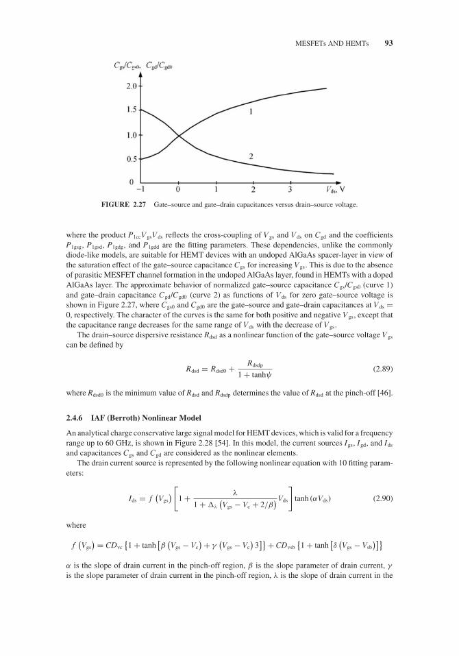
JWBS064-c02 JWBS064-Gerbennikov March 15, 2011 10:49 Printer Name: Yet to Come
MESFETs AND HEMTs 93
FIGURE 2.27 Gate–source and gate–drain capacitances versus drain–source voltage.
where the product P1ccVgsVds reflects the cross-coupling of Vgs and Vds on Cgd and the coefficientsP1gsg, P1gsd, P1gdg, and P1gdd are the fitting parameters. These dependencies, unlike the commonlydiode-like models, are suitable for HEMT devices with an undoped AlGaAs spacer-layer in view ofthe saturation effect of the gate–source capacitance Cgs for increasing Vgs. This is due to the absenceof parasitic MESFET channel formation in the undoped AlGaAs layer, found in HEMTs with a dopedAlGaAs layer. The approximate behavior of normalized gate–source capacitance Cgs/Cgs0 (curve 1)and gate–drain capacitance Cgd/Cgd0 (curve 2) as functions of Vds for zero gate–source voltage isshown in Figure 2.27, where Cgs0 and Cgd0 are the gate–source and gate–drain capacitances at Vds =0, respectively. The character of the curves is the same for both positive and negative Vgs, except thatthe capacitance range decreases for the same range of Vds with the decrease of Vgs.
The drain–source dispersive resistance Rdsd as a nonlinear function of the gate–source voltage Vgs
can be defined by
Rdsd = Rdsd0 + Rdsdp
1 + tanhψ(2.89)
where Rdsd0 is the minimum value of Rdsd and Rdsdp determines the value of Rdsd at the pinch-off [46].
2.4.6 IAF (Berroth) Nonlinear Model
An analytical charge conservative large signal model for HEMT devices, which is valid for a frequencyrange up to 60 GHz, is shown in Figure 2.28 [54]. In this model, the current sources Igs, Igd, and Ids
and capacitances Cgs and Cgd are considered as the nonlinear elements.The drain current source is represented by the following nonlinear equation with 10 fitting param-
eters:
Ids = f(Vgs
) [1 + λ
1 + �λ
(Vgs − Vc + 2/β
)Vds
]tanh (αVds) (2.90)
where
f(Vgs
) = CDvc
{1 + tanh
[β(Vgs − Vc
)+ γ(Vgs − Vc
)3]}+ CDvsb
{1 + tanh
[δ(Vgs − Vsb
)]}α is the slope of drain current in the pinch-off region, β is the slope parameter of drain current, γ
is the slope parameter of drain current in the pinch-off region, λ is the slope of drain current in the

JWBS064-c02 JWBS064-Gerbennikov March 15, 2011 10:49 Printer Name: Yet to Come
94 ACTIVE DEVICES AND MODELING
FIGURE 2.28 Berroth nonlinear intrinsic model.
saturation region, �λ is the gate voltage parameter for slope of drain current, δ is the drain currentslope parameter correction term, Vc is the gate voltage for maximum transconductance, V sb is thegate voltage for maximum transconductance correction term, CDvc is the drain current multiplicationfactor, and CDvsb is the drain current multiplication factor correction term.
To describe the Igs and Igd current sources, the diode model for both forward and reverse biasoperation modes was used in the form
Idiode = Idsat
[exp
(Vdiode
nVT
)− 1
](2.91)
where Idsat is the forward bias fitting parameter, VT is the temperature voltage, and n is the diodeideality factor.
The nonlinear capacitances Cgs and Cgd are calculated by differentiating the voltage-dependingcharge function Qg(Vgs, Vds) with respect to Vgs and Vds, which leads to the input capacitance C11 =Cgs + Cgd and transcapacitance C12 = −Cgd, respectively,
Qg
(Vgs,Vds
) = A f1 f2 + E(Vgs − 0.5Vds
)(2.92)
where
f1 = 1
Blncosh
{B[(
Vgs − V1
)− 0.5 tanh (CVds)]}+ (Vgs − V1
)− 0.5 tanh (CVds)
f2 = 1 + D lncosh (FVds)
V1 is the transition voltage, and A, B, C, D, E, and F are the model-fitting parameters.
2.4.7 Noise Model
The noise properties of a MESFET device can be described based on both its physical and equivalentcircuit models. The dominant intrinsic noise of a microwave GaAs MESFET device is the diffusionnoise introduced by electrons experiencing velocity saturation. In a device two-zone model, a portionof the channel near the source end is assumed to be in the constant mobility operation mode (zone I),while the remaining portion near the drain end is postulated to be in velocity saturation (zone II). Theposition of the boundary between these zones is a strong function of the source–drain bias with weakdependence on the gate–source bias. It is assumed that the noise in zone I is thermal enhanced by hotelectron effects [55,56]. However, zone II cannot be treated as an ohmic conductor. Its contributionmust be represented as a high-field diffusion noise, being dominant in microwave devices [57]. Thisdiffusion noise is proportional to the high-field diffusion coefficient and is linearly dependent on draincurrent. On the other hand, the thermal noise of zone I decreases with increasing drain current. As aresult, a strong correlation exists between the drain noise and the induced gate noise which leads toa high degree of cancellation in the noise output of the GaAs MESFET [58].

JWBS064-c02 JWBS064-Gerbennikov March 15, 2011 10:49 Printer Name: Yet to Come
MESFETs AND HEMTs 95
FIGURE 2.29 MESFET equivalent circuits with noise sources.
The noise equivalent circuit of the MESFET device with both intrinsic and extrinsic noise sourcesis shown in Figure 2.29(a) [55,58]. The noise source i 2
ng represents the noise induced on the gateelectrode by the passing thermal fluctuations in the drain current. The intrinsic drain noise sourcei2nd has a flat spectrum. The resistance Rgs represents the resistive charging path for the gate–source
capacitance Cgs, and noise associated with this resistor is imbedded in the gate noise source. Theseries gate, source and drain resistances are represented by the voltage thermal noise sources e2
ng, e2ns,
and e2nd, respectively.
The noise voltage and current sources can be given through their mean-square values as
e2ng = 4kTRg� f (2.93)
i2ng = 4kT
(ωCgs
)2R� f
gm(2.94)
e2ns = 4kTRs� f (2.95)
e2nd = 4kTRd� f (2.96)
i2nd = 4kTgm P� f (2.97)
JWBS064-c02 JWBS064-Gerbennikov March 15, 2011 10:49 Printer Name: Yet to Come
96 ACTIVE DEVICES AND MODELING
where R and P are the gate and drain noise model parameters depending upon the implementationtechnology and biasing conditions [59,60].
The cross-correlation between the gate–drain noise current sources i 2ng and i 2
nd can be written as
inding = 4kTωCgsC√
PR� f (2.98)
where C is the correlation coefficient. The quantities P, R, and C are the bias-dependent empiricalcorrection factors, which may be obtained by noise de-embedding techniques [61]. Their typicalvalues based on measurement and calculation of the noise figure for different devices can be chosenas P = 1, R = 0.5, and C = 0.9 [62]. It should be noted that i 2
nd and C increase in ohmic regionand tend to saturate at high drain voltage, while i2
ng increases with a near constant slope versus drainvoltage.
The noise current source i 2ngl is responsible for the effect of the gate leakage current, which should
be taken into account when using a submicrometer gate-length HEMT device. It can be written as ashot noise source in the form
i 2ngl = 2αq Igl� f (2.99)
where Igl is the gate leakage current and α is the fitting parameter [63,64].The admittance Y-parameters of the MESFET intrinsic small-signal equivalent circuit can be
written in matrix form
Y =
⎡⎢⎢⎣
jωCgs
1 + jωRgsCgs+ jωCgd − jωCgd
gm exp (− jωτ )
1 + jωRgsCgs− jωCgd
1
Rds+ jω
(Cds + Cgd
)⎤⎥⎥⎦ . (2.100)
The corresponding admittance noise correlation matrix to calculate the equivalent noise resistanceRn, optimal source admittance YSopt, and minimum noise figure Fmin is given by
CY = 4kT
⎡⎢⎣
α Igl
2VT+(ωCgs
)2R
gmjωCgsC
√PR
− jωCgsC√
PR gm P
⎤⎥⎦ (2.101)
where VT = kT/q is the thermal voltage. However, if the correlation matrix has been determined,the noise parameters can be analytically calculated by using the elements of the chain correlationmatrix [65]
CA11 = CY
22
|Y21|2(2.102)
CA12 = Y ∗
11CY22
|Y21|2− CY
12
Y12(2.103)
CA22 = CY
11 + |Y11|2 CY22
|Y21|2− Y11CY
21
Y21− Y ∗
11CY12
Y ∗21
. (2.104)
In a first approximation, the gate noise source i 2ng, feedback capacitance Cgd, and series drain re-
sistance Rd can be neglected. As a result, the simple approximate expressions based on measurements
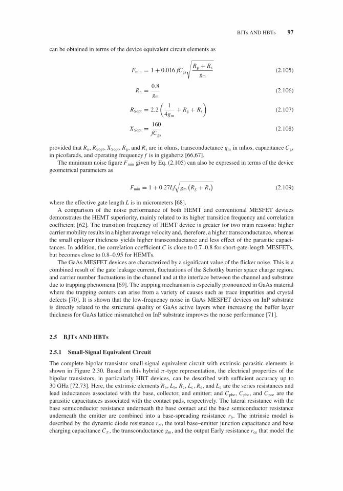
JWBS064-c02 JWBS064-Gerbennikov March 15, 2011 10:49 Printer Name: Yet to Come
BJTs AND HBTs 97
can be obtained in terms of the device equivalent circuit elements as
Fmin = 1 + 0.016 fCgs
√Rg + Rs
gm(2.105)
Rn = 0.8
gm(2.106)
RSopt = 2.2
(1
4gm+ Rg + Rs
)(2.107)
XSopt = 160
fCgs
(2.108)
provided that Rn, RSopt, XSopt, Rg, and Rs are in ohms, transconductance gm in mhos, capacitance Cgs
in picofarads, and operating frequency f is in gigahertz [66,67].The minimum noise figure Fmin given by Eq. (2.105) can also be expressed in terms of the device
geometrical parameters as
Fmin = 1 + 0.27Lf√
gm
(Rg + Rs
)(2.109)
where the effective gate length L is in micrometers [68].A comparison of the noise performance of both HEMT and conventional MESFET devices
demonstrates the HEMT superiority, mainly related to its higher transition frequency and correlationcoefficient [62]. The transition frequency of HEMT device is greater for two main reasons: highercarrier mobility results in a higher average velocity and, therefore, a higher transconductance, whereasthe small epilayer thickness yields higher transconductance and less effect of the parasitic capaci-tances. In addition, the correlation coefficient C is close to 0.7–0.8 for short-gate-length MESFETs,but becomes close to 0.8–0.95 for HEMTs.
The GaAs MESFET devices are characterized by a significant value of the flicker noise. This is acombined result of the gate leakage current, fluctuations of the Schottky barrier space charge region,and carrier number fluctuations in the channel and at the interface between the channel and substratedue to trapping phenomena [69]. The trapping mechanism is especially pronounced in GaAs materialwhere the trapping centers can arise from a variety of causes such as trace impurities and crystaldefects [70]. It is shown that the low-frequency noise in GaAs MESFET devices on InP substrateis directly related to the structural quality of GaAs active layers when increasing the buffer layerthickness for GaAs lattice mismatched on InP substrate improves the noise performance [71].
2.5 BJTs AND HBTs
2.5.1 Small-Signal Equivalent Circuit
The complete bipolar transistor small-signal equivalent circuit with extrinsic parasitic elements isshown in Figure 2.30. Based on this hybrid π -type representation, the electrical properties of thebipolar transistors, in particularly HBT devices, can be described with sufficient accuracy up to30 GHz [72,73]. Here, the extrinsic elements Rb, Lb, Rc, Lc, Re, and Le are the series resistances andlead inductances associated with the base, collector, and emitter; and Cpbe, Cpbc, and Cpce are theparasitic capacitances associated with the contact pads, respectively. The lateral resistance with thebase semiconductor resistance underneath the base contact and the base semiconductor resistanceunderneath the emitter are combined into a base-spreading resistance rb. The intrinsic model isdescribed by the dynamic diode resistance rπ , the total base–emitter junction capacitance and basecharging capacitance Cπ , the transconductance gm, and the output Early resistance rce that model the

JWBS064-c02 JWBS064-Gerbennikov March 15, 2011 10:49 Printer Name: Yet to Come
98 ACTIVE DEVICES AND MODELING
FIGURE 2.30 Small-signal equivalent circuit of bipolar device.
effect of base-width modulation on the transistor characteristics due to variations in the collector–basedepletion region. To increase the usable operating frequency range of the device up to 50 GHz, it isnecessary to properly include the collector-current delay time in the current source as gmexp(−jωτπ ),where τπ is the transit time [74].
2.5.2 Determination of Equivalent Circuit Elements
If all extrinsic parasitic elements of the device equivalent circuit shown in Figure 2.30 are known,the intrinsic two-port network parameters can be embedded with the following determination proce-dure [72]:
� Measurement of the S-parameters of the transistor with extrinsic elements.� Transformation of the S-parameters to the admittance Y-parameters with subtraction of the
parasitic shunt capacitances Cpbe, Cpbc, and Cpce.� Transformation of the new Y-parameters to the impedance Z-parameters with subtraction of the
parasitic series elements Lb, Rb, Le, Re, Lc, and Rc.� Transformation of the new Z-parameters to the Y-parameters with subtraction of the parasitic
shunt capacitance Cco.� Transformation of the new Y-parameters to the Z-parameters with subtraction of the parasitic
series resistance rb.� Transformation of the new Z-parameters to the Y-parameters of the intrinsic device two-port
network.
The bipolar transistor intrinsic Y-parameters can be written as
Y11 = 1
rπ
+ jω (Cπ + Cci) (2.110)
Y12 = − jωCci (2.111)
Y21 = gmexp (− jωτπ ) + jωCci (2.112)
Y22 = 1
rce+ jωCci. (2.113)

JWBS064-c02 JWBS064-Gerbennikov March 15, 2011 10:49 Printer Name: Yet to Come
BJTs AND HBTs 99
After separating Eqs. (2.110) to (2.113) into their real and imaginary parts, the elements of theintrinsic small-signal equivalent circuit can be determined analytically as
Cπ = Im (Y11 + Y12)
ω(2.114)
rπ = 1
ReY11(2.115)
Cci = − ImY12
ω(2.116)
gm =√
(ReY21)2 + (Im Y21 + ImY12)2 (2.117)
τπ = 1
ωcos−1 ReY21 + ReY12√
(ReY21)2 + (ImY21 + ImY12)2(2.118)
rce = 1
ReY22. (2.119)
The parasitic capacitances associated with the pads can be determined by the measurement of theopen test structure with the corresponding circuit model shown in Figure 2.31(a). When the values ofthese pad capacitances are known, it is easy to determine the values of the parasitic series inductancesby measuring the shorted test structure with corresponding circuit model shown in Figure 2.31(b).
The values of series parasitic resistances can be calculated on the basis of physical parameters ofthe device or by adding them to the intrinsic device parameters (with the appropriate solution of anonlinear system of eight equations with eight independent variables using iterative technique) [73].In the latter case, it is assumed that influence of the transit time τπ on the bipolar electrical propertiesin a frequency range up to 30 GHz is negligible.
The external parasitic parallel capacitance Cco, as well as the other device capacitances, can beestimated from the device behavior at low frequencies and cutoff operating conditions [75,76]. For
FIGURE 2.31 Models for parasitic (a) pad capacitances and (b) lead inductances.
JWBS064-c02 JWBS064-Gerbennikov March 15, 2011 10:49 Printer Name: Yet to Come
100 ACTIVE DEVICES AND MODELING
FIGURE 2.32 Small-signal model at low frequencies and cutoff operation mode.
such conditions, the device small-signal equivalent circuit is reduced to capacitive elements, as shownin Figure 2.32.
The device capacitances can be directly calculated from measured Y-parameters by
Cpbe + Cπ = Im (Y11 + Y12)
ω(2.120)
Cpce = Im (Y11 + Y12)
ω(2.121)
Cpbc + Cco + Cci = − ImY12
ω. (2.122)
Since Cpbc and Cco are the bias-independent capacitances and Cci is the base–collector junctioncapacitance, the extraction of Cpbc + Cco can be carried out by fitting the sum Cpbc + Cco + Cci
to the expression for junction capacitance at different base–collector voltages. If an approximationexpression for Cco is given by
Cco = Cjco/
√1 + Vbc
ϕc(2.123)
then the extraction of the parameters Cjco, ϕc, and Cci can be performed using the linear equation
⎛⎜⎝ Cjco
ImY12
ω+ Cpbc + Cci
⎞⎟⎠
2
= 1 + 1
ϕcVbc. (2.124)
As a result, linearizing this equation by choosing a proper value for Cci with known value of Cpbc
gives the values for remaining two parameters Cco and ϕc from the slope and intercept point of thefinal linearized dependence.
2.5.3 Equivalence of Intrinsic π - and T-Type Topologies
The small-signal equivalent circuit of a bipolar transistor can be represented by both π -type andT-type topologies. The T-type equivalent circuit representation is appealing because all the modelparameters can be directly tied to the physics of the device and an excellent fit between measuredand simulated S-parameters in the frequency range up to 30–40 GHz [74–77]. The HBT small-signalequivalent circuit with T-type topology is shown in Figure 2.33.

JWBS064-c02 JWBS064-Gerbennikov March 15, 2011 10:49 Printer Name: Yet to Come
BJTs AND HBTs 101
FIGURE 2.33 Small-signal T-model of bipolar device.
There is one-to-one correspondence between π -type and T-type device models. By comparingboth small-signal equivalent circuits shown in Figures 2.30 and 2.33, the difference, which can befound in the representation of both intrinsic device models, are just enclosed in dashed boxes. FromFigure 2.34 it follows that the admittances Ye = Ie/Vbe for π - and T-type models are defined by
Ye = 1
re+ jωCe = 1
rπ
+ jωCπ + gm exp (− jωτπ ) . (2.125)
The collector source currents for both models are the same,
α exp (− jωτtee) Ie = gm exp (− jωτπ ) Vπ (2.126)
where τ tee is the transit time for a T-type model, α = α0/(1 + jωτα), τ α = 1/(2π f α), f α is the alphacutoff frequency, and α0 is the low frequency collector-to-emitter current gain.
FIGURE 2.34 Intrinsic (a) π-type and (b) T-type device topologies.
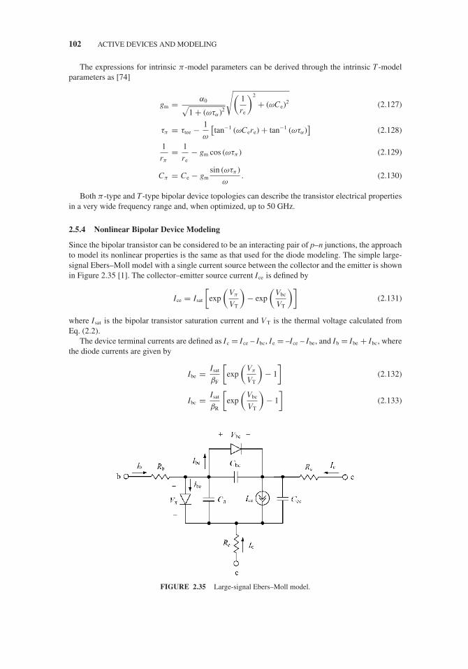
JWBS064-c02 JWBS064-Gerbennikov March 15, 2011 10:49 Printer Name: Yet to Come
102 ACTIVE DEVICES AND MODELING
The expressions for intrinsic π-model parameters can be derived through the intrinsic T-modelparameters as [74]
gm = α0√1 + (ωτα)2
√(1
re
)2
+ (ωCe)2 (2.127)
τπ = τtee − 1
ω
[tan−1 (ωCere) + tan−1 (ωτα)
](2.128)
1
rπ
= 1
re− gm cos (ωτπ ) (2.129)
Cπ = Ce − gmsin (ωτπ )
ω. (2.130)
Both π-type and T-type bipolar device topologies can describe the transistor electrical propertiesin a very wide frequency range and, when optimized, up to 50 GHz.
2.5.4 Nonlinear Bipolar Device Modeling
Since the bipolar transistor can be considered to be an interacting pair of p–n junctions, the approachto model its nonlinear properties is the same as that used for the diode modeling. The simple large-signal Ebers–Moll model with a single current source between the collector and the emitter is shownin Figure 2.35 [1]. The collector–emitter source current Ice is defined by
Ice = Isat
[exp
(Vπ
VT
)− exp
(Vbc
VT
)](2.131)
where Isat is the bipolar transistor saturation current and VT is the thermal voltage calculated fromEq. (2.2).
The device terminal currents are defined as Ic = Ice – Ibc, Ie = –Ice – Ibe, and Ib = Ibe + Ibc, wherethe diode currents are given by
Ibe = Isat
βF
[exp
(Vπ
VT
)− 1
](2.132)
Ibc = Isat
βR
[exp
(Vbc
VT
)− 1
](2.133)
FIGURE 2.35 Large-signal Ebers–Moll model.
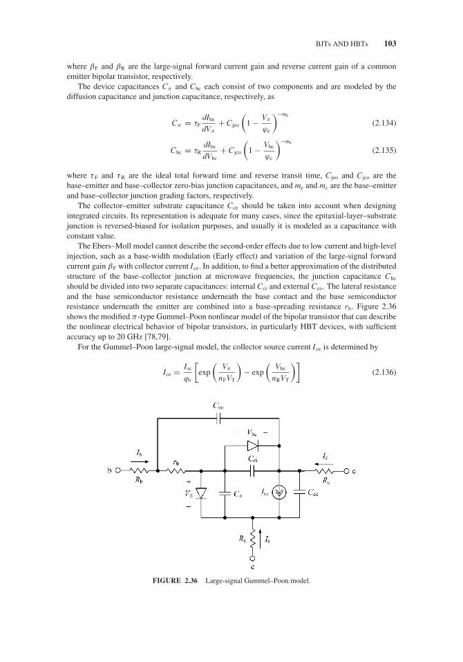
JWBS064-c02 JWBS064-Gerbennikov March 15, 2011 10:49 Printer Name: Yet to Come
BJTs AND HBTs 103
where βF and βR are the large-signal forward current gain and reverse current gain of a commonemitter bipolar transistor, respectively.
The device capacitances Cπ and Cbc each consist of two components and are modeled by thediffusion capacitance and junction capacitance, respectively, as
Cπ = τFdIbe
dVπ
+ Cjeo
(1 − Vπ
ϕe
)−me
(2.134)
Cbc = τRdIbc
dVbc+ Cjco
(1 − Vbc
ϕc
)−mc
(2.135)
where τ F and τR are the ideal total forward time and reverse transit time, Cjeo and Cjco are thebase–emitter and base–collector zero-bias junction capacitances, and me and mc are the base–emitterand base–collector junction grading factors, respectively.
The collector–emitter substrate capacitance Cce should be taken into account when designingintegrated circuits. Its representation is adequate for many cases, since the epitaxial-layer–substratejunction is reversed-biased for isolation purposes, and usually it is modeled as a capacitance withconstant value.
The Ebers–Moll model cannot describe the second-order effects due to low current and high-levelinjection, such as a base-width modulation (Early effect) and variation of the large-signal forwardcurrent gain βF with collector current Ice. In addition, to find a better approximation of the distributedstructure of the base–collector junction at microwave frequencies, the junction capacitance Cbc
should be divided into two separate capacitances: internal Cci and external Cco. The lateral resistanceand the base semiconductor resistance underneath the base contact and the base semiconductorresistance underneath the emitter are combined into a base-spreading resistance rb. Figure 2.36shows the modified π -type Gummel–Poon nonlinear model of the bipolar transistor that can describethe nonlinear electrical behavior of bipolar transistors, in particularly HBT devices, with sufficientaccuracy up to 20 GHz [78,79].
For the Gummel–Poon large-signal model, the collector source current Ice is determined by
Ice = Iss
qb
[exp
(Vπ
nFVT
)− exp
(Vbc
nRVT
)](2.136)
FIGURE 2.36 Large-signal Gummel–Poon model.

JWBS064-c02 JWBS064-Gerbennikov March 15, 2011 10:49 Printer Name: Yet to Come
104 ACTIVE DEVICES AND MODELING
where Iss is the BJT fundamental constant defined at zero-bias condition, nF is the forward currentemission coefficient, nR is the reverse current emission coefficient, and qb is the variable parameterdefined by
qb = q1
2+√(q1
2
)2+ q2 (2.137)
where
q1 = 1 + Vπ
VB+ Vbc
VA
q2 = Iss
IKF
[exp
(Vπ
nFVT
)− 1
]+ Iss
IKR
[exp
(Vbc
nRVT
)− 1
]
VA is the forward Early voltage, VB is the reverse Early voltage, IKF is the knee current for high-levelinjection in the normal active region, and IKR is the knee current for low-level injection in inverseregion [1].
The currents through model diodes are defined by
Ibe = Isat (0)
βFM (0)
[exp
(Vπ
nFVT
)− 1
]+ C2 Isat (0)
[exp
(Vπ
nELVT
)− 1
](2.138)
Ibc = Isat (0)
βRM (0)
[exp
(Vbc
nRVT
)− 1
]+ C4 Isat (0)
[exp
(Vbc
nCLVT
)− 1
](2.139)
where Isat(0) is the saturation current for Vbc = 0, βFM(0) and βRM(0) are the large-signal forward andreverse current gains of a common–emitter BJT in mid-current region for Vbc = 0, C2 and C4 are theforward and reverse low-current nonideal base current coefficients, respectively, nEL is the nonideallow-current base–emitter emission coefficient, and nCL is the nonideal low-current base–collectoremission coefficient.
The nonlinear behavior of the intrinsic base resistance rb can be described by
rb = rbm + 3 (rb0 − rbm)tan z − z
z tan2 z(2.140)
where
z =
√1 + 144
π2
Ib
Irb− 1
24
π 2
√Ib
Irb
rbm is the minimum base resistance that occurs at high-current level, rb0 is the base resistance at zerobias with small base current level, and Irb is the current where the base resistance falls halfway to itsminimum value [1].
The intrinsic device capacitances Cπ , Cci, and Cco are modeled by the diffusion capacitance andjunction capacitance, respectively, as
Cπ = d
dVπ
(τFF
Icc
qb
)+ Cjeo
(1 − Vπ
ϕe
)−me
(2.141)
Cci = τRdIbc
dVbc+ kcCjco
(1 − Vbc
ϕc
)−mc
(2.142)
Cco = Cjco (1 − kc)
(1 − Vbco
ϕc
)−mc
(2.143)

JWBS064-c02 JWBS064-Gerbennikov March 15, 2011 10:49 Printer Name: Yet to Come
BJTs AND HBTs 105
where kc is the fraction of the base–collector junction capacitance connected to the base resistancerb, Vbco is the voltage through the capacitance Cco, and τ FF is the modulated transit time defined by
τFF = τF
[1 + XτF
(Icc
Icc + IτF
)2
exp
(Vbc
1.44 VτF
)](2.144)
where XτF is the transit time bias dependence coefficient, IτF is the high-current parameter for effecton τ F, VτF is the value of Vbc where the exponential equals to 0.5, and
Icc = Iss
qb
[exp
(Vπ
nFVT
)− 1
]. (2.145)
As it follows from Eq. (2.141), the nonlinear behavior of capacitance Cπ strongly depends onthe effect of transit time modulation characterized by τ FF. This transit charge variation results insignificant changes of the transition frequency f T at various operation conditions. For example, atmedium currents, f T reaches its peak value and is practically constant. Here, the ideal transit time isdefined by τ F = 1/(2π f T) and the dominated base–emitter diffusion capacitance increases linearlywith collector current. At low currents, f T is dominated by the junction capacitance and increaseswith the increase in collector current. At high currents, the widening of the charge-neutral base regionand pushing of the entire space-charge region toward the heavily doped collector region (Kirk effect)degrades the frequency response of the transistor by increasing the transit time and decreasing f T. Inthis case, the transit time is modeled by τ FF.
The more complicated models, such as VBIC, HICUM, or MEXTRAM, include the effects ofself-heating of a bipolar transistor, take into account the parasitic p–n–p transistor formed by thebase, collector, and substrate regions, provide an improved description of depletion capacitances atlarge-forward bias, take into account avalanche and tunneling currents, and other nonlinear effectscorresponding to distributed high-frequency effects [80].
2.5.5 Noise Model
The noise in a bipolar transistor is assumed to arise from three basic sources: diffusion fluctuations,recombination fluctuations in the base region, and thermal noise in the base resistance [81]. The noisebehavior of the bipolar transistor can be described based on its equivalent circuit representation shownin Figure 2.37(a), which includes the main elements responsible for the device electrical behaviorand noise sources. Since the process of the carrier drifting into the collector–base depletion region isa random process, the collector current Ic demonstrates shot noise and is represented by a shot-noisecollector current source i 2
nc. The base current Ib is a result of the carrier injection from the baseto the emitter and generation–recombination effect in the base and base–emitter depletion regions.Because all these components are independent, representing a random process, the base current alsodemonstrates a shot-noise behavior and is represented by a shot-noise base current source i 2
nb. Flickernoise is represented by a current source across the internal base–emitter junction combined withthe base current source i 2
nb. The series base, emitter and collector resistances are represented by the
voltage and current thermal noise sources e2nb, i 2
ne, and e2nc, respectively.
The noise voltage and current sources can be given through their mean-square values as
e2nb = 4kTrb� f (2.146)
i 2ne = 4kT� f
re(2.147)
i 2nc = 2qIc� f (2.148)
e2nc = 4kTrc� f (2.149)
i2nb = 2qIb� f + KF
I AFb
f� f (2.150)

JWBS064-c02 JWBS064-Gerbennikov March 15, 2011 10:49 Printer Name: Yet to Come
106 ACTIVE DEVICES AND MODELING
FIGURE 2.37 Bipolar equivalent circuits with noise sources.
where q is the electron charge, AF is the flicker noise exponent, KF is the flicker noise coefficientcalculated as 2qf c, and f c is the flicker noise corner frequency [1,82].
The required minimum noise figure Fmin, noise resistance Rn, and optimum source admittanceYSopt using the noise correlation CA-matrix parameters as functions of the input-referred noise voltagev2
ni and noise current i2ni, as well as Y-parameters of the simplified noise-free two-port network shown
in Figure 2.37(b), can be calculated for a sufficiently high value of the low-frequency current gainβ = gmrπ from
Rn = rb
(1 + rb
2rπ
)+ rπ
2β+ r 2
b
2βrπ
(f
fT
)2
(2.151)
YSopt =√√√√ 1
2rπ Rn
[1 + 1
β
(f
fT
)2]
−(
1
2β Rn
f
fT
)2
− j1
2β Rn
f
fT(2.152)
Fmin = 1 + rb
rπ
[1 + 1
β
(f
fT
)2]
+√
2rb
rπ
(1 + rb
2rπ
)+ 2rb
βrπ
(1 + rb
rπ
)(f
fT
)2
(2.153)
where f is the operation frequency and f T = gm/(2πCπ ) is the bipolar transition frequency (the effectof the feedback collector capacitance Cc is not taken into account) [83]. It should be noted that if theoptimum noise conductance GSopt is insensitive to the collector capacitance Cc, then it can severely

JWBS064-c02 JWBS064-Gerbennikov March 15, 2011 10:49 Printer Name: Yet to Come
REFERENCES 107
affect the other noise parameters at microwave frequencies, mostly due to the reduction of the devicegain capability.
A noise model for HBT device operated at very high frequencies should include the contributionof both space-charge layers (at the emitter–base junction and the base–collector junction) to the shotnoise. These two noise sources related to the collector current Ic are the result of the same electrons,which are injected from the emitter into the base, cross this layer, and then reach the collector.Therefore, their correlation can be given by a time delay function exp(−jωτ ), where τ is the transittime through the base and the collector–base junction which is τπ for a π -type model [84–86]. Thus,to extend the HBT noise model valid up to its transition frequency, the base and collector noise currentsources are rewritten as
i 2nb = 2q
(Ib + |1 − exp (− jωτ )|2 Ic
)� f (2.154)
i2nc = 2q Ic� f (2.155)
inbi∗nc = 2q
[exp (− jωτ ) − 1
]Ic� f. (2.156)
Flicker noise in bipolar transistors is associated mainly with generation–recombination centers,which contribute to random trapping and release of free carriers [87,88]. This relatively slow processis always associated with flowing current by which mean-square value i 2
n as a function of the offsetfrequency f can be approximated
i 2n = KF I k � f
f(2.157)
where KF is the flicker noise coefficient and k is the flicker noise exponent. Both these coefficientsare device dependent. In conventional high-quality silicon bipolar devices, the low-frequency noiseis determined by 1/f noise in the base current due to carriers injected from the base into the emitter,since the emitter series resistance can be neglected, the base series resistance is low and the collectorcurrent has an ideality factor of 1. In downscaled polysilicon bipolar transistors with lower emitterarea, at low bias currents the 1/f noise in the base current is dominant, while at higher bias currents theinfluence of the series resistances on the noise becomes noticeable. In GaAs/AlGaAs HBT devices,the 1/f noise in the base current can be described by Eq. (2.157) with KF ≈ 10−10 A2−k and k ≈ 1.6,whereas, for the 1/f noise in the collector current, KF ≈ 10−12 A2−k and k ≈ 1.3 [89]. The contributionof the extrinsic base resistance noise becomes more important with scaling, especially for the devicewith very high transition frequency f T [90].
REFERENCES
1. G. Massobrio and P. Antognetti, Semiconductor Device Modeling with SPICE, New York: McGraw-Hill,1993.
2. S. A. Maas, Nonlinear Microwave Circuits, New York: IEEE Press, 1997.
3. Application Note 1002, “Design with PIN Diodes,” Skyworks Solutions, 2005.
4. M. H. Norwood and E. Shatz, “Voltage Variable Capacitor Tuning: A Review,” Proc. IEEE, vol. 56, pp.788–798, May 1968.
5. W. Schottky and W. Deutschmann, “Zum Mechanismus der Richtwirkung in Kupferoxydulgleichrichten,”Phys. Z., vol. 30, pp. 839–846, Nov. 1929.
6. W. Shockley, “The Theory of p–n Junctions in Semiconductors,” Bell Syst. Tech. J., vol. 28, pp. 435–450,July 1949.
7. M. E. McMahon and G. F. Straube, “Voltage-Sensitive Semiconductor Capacitor,” IRE WESCON Conv. Rec.,pt. 3, pp. 72–82, Aug. 1958.

JWBS064-c02 JWBS064-Gerbennikov March 15, 2011 10:49 Printer Name: Yet to Come
108 ACTIVE DEVICES AND MODELING
8. P. Penfield and R. P. Rafuse, Varactor Applications, Cambridge: The M.I.T Press, 1962.
9. Application Note 1004, “Varactor SPICE Models for RF VCO Applications,” Skyworks Solutions, 2005.
10. R. Beach, “High Speed Linear Oscillators,” Microwave J., vol. 21, pp. 59–65, Dec. 1978.
11. Y. P. Tsividis, Operation and Modeling of the MOS Transistor, New York: McGraw-Hill, 1987.
12. P. Andreani and S. Mattisson, “On the Use of MOS Varactors in RF VCO’s,” IEEE J. Solid-State Circuits,vol. SC-35, pp. 905–910, June 2000.
13. F. Svelto, P. Erratico, and R. Castello, “A Metal-Oxide-Semiconductor Varactor,” IEEE Electron Device Lett.,vol. 20, pp. 164–166, Apr. 1999.
14. A.-S. Porret, T. Melly, C. C. Enz, and E. A. Vittoz, “Design of High-Q Varactors for Low-Power WirelessApplications Using a Standard CMOS Process,” IEEE J. Solid-State Circuits, vol. SC-35, pp. 337–345, Mar.2000.
15. S.-S. Song and H. Shin, “An RF Model of the Accumulation-Mode MOS Varactor Valid in Both Accumulationand Depletion Regions,” IEEE Trans. Electron Devices, vol. ED-50, pp. 1997–1999, Sep. 2003.
16. B. Senapati, K. Ehwald, W. Winkler, and F. Furnhammer, “High Performance MOS Varactor SPICE Model,”Electronics Lett., vol. 38, pp. 1416–1417, Nov. 2002.
17. K. Molnar, G. Rappitsch, Z. Huszka, and E. Seebacher, “MOS Varactor Modeling With a Subcircuit Utilizingthe BSIM3v3 Model,” IEEE Trans. Electron Devices, vol. ED-49, pp. 1206–1211, July 2002.
18. Y. P. Tsividis and K. Suyama, “MOSFET Modeling for Analog Circuit CAD: Problems and Prospects,” IEEEJ. Solid-State Circuits, vol. SC-29, pp. 210–216, Mar. 1994.
19. E. Abou-Allam and T. Manku, “A Small-Signal MOSFET Model for Radio Frequency IC Applications,”IEEE Trans. Computer-Aided Design, vol. 16, pp. 437–447, May 1997.
20. T. Taki, “Approximation of Junction Field-Effect Transistor Characteristics by a Hyperbolic Function,” IEEEJ. Solid-State Circuits, vol. SC-13, pp. 724–726, Oct. 1978.
21. D. Heo, E. Chen, E. Gebara, S. Yoo, J. Lascar, and T. Anderson, “Temperature Dependent MOSFET RFLarge Signal Model Incorporating Self Heating Effects,” IEEE MTT-S Int. Microwave Symp. Dig., vol. 2, pp.415–418, June 1999.
22. W. R. Curtice, J. A. Pla, D. Bridges, T. Liang, and E. E. Shumate, “A New Dynamic Electro-ThermalNonlinear Model for Silicon RF LDMOS FETs,” IEEE MTT-S Int. Microwave Symp. Dig., vol. 2, pp. 419–422,1999.
23. C. C. Enz and E. A. Vittoz, Charge-Based MOS Transistor Modeling: The EKV Model for Low Power andRF IC Design, Chichester: John Wiley & Sons, Ltd. 2006.
24. A. V. Grebennikov and F. Lin, “An Efficient CAD-Oriented Large-Signal MOSFET Model,” IEEE Trans.Microwave Theory Tech., vol. MTT-48, pp. 1732–1742, Oct. 2000.
25. M. C. Ho, K. Green, R. Culbertson, J. Y. Yang, D. Ladwig, and P. Ehnis, “A Physical Large Signal Si MOSFETModel for RF Circuit Design,” IEEE MTT-S Int. Microwave Symp. Dig., vol. 2, pp. 391–394, June 1997.
26. J. Angel Garcia, A. Mediavilla, J. Carlos Pedro, N. B. Carvalho, A. Tazon, and J. L. Garcia, “Characterizingthe Gate to Source Nonlinear Capacitor Role on FET IMD Performance,” IEEE MTT-S Int. Microwave Symp.Dig., vol. 3, pp. 1635–1638, 1998.
27. P. Perugupalli, M. Trivedi, K. Shenai, and S. K. Leong, “Modeling and Characterization of an 80 V SiliconLDMOSFET for Emerging RFIC Applications,” IEEE Trans. Electron Devices, vol. ED-45, pp. 1468–1478,July 1998.
28. D. Moncoqut, D. Farenc, P. Rossel, G. Charitat, H. Tranduc, J. Victory, and I. Pages, “LDMOS Transistor forSmart Power Circuits: Modeling and Design,” Proc. IEEE Bipolar/BiCMOS Circuits and Technology Meeting(BCTM), pp. 216–219, Sept./Oct. 1996.
29. C. E. Biber, M. L. Schmatz, T. Morf, U. Lott, and W. Bachtold, “A Nonlinear Microwave MOSFET Modelfor SPICE Simulators,” IEEE Trans. Microwave Theory Tech., vol. MTT-46, pp. 604–610, May 1998.
30. R. Sung, P. Bendix, and M. B. Das, “Extraction of High-Frequency Equivalent Circuit Parameters of Submi-cron Gate-Length MOSFET’s,” IEEE Trans. Electron Devices, vol. ED-45, pp. 1769–1775, Aug. 1998.
31. B. J. Cheu and P. K. Ko, “Measurement and Modeling of Short-Channel MOS Transistor Gate Capacitances,”IEEE J. Solid-State Circuits, vol. SC-22, pp. 464–472, June 1987.
32. R. E. Anholt and S. E. Swirhun, “Experimental Investigations of the Temperature Dependence of GaAs FETEquivalent Circuits,” IEEE Trans. Electron Devices, vol. ED-39, pp. 2029–2036, Sept. 1992.

JWBS064-c02 JWBS064-Gerbennikov March 15, 2011 10:49 Printer Name: Yet to Come
REFERENCES 109
33. C. Enz, “An MOS Transistor Model for RF IC Design Valid in All Regions of Operation,” IEEE Trans.Microwave Theory Tech., vol. MTT-50, pp. 342–359, Jan. 2002.
34. S. Tedja, J. van der Spiegel, and H. H. Williams, “Analytical and Experimental Studies of Thermal Noise inMOSFETs,” IEEE Trans. Electron Devices, vol. ED-41, pp. 2069–2075, Nov. 1994.
35. S. Asgaran, M. J. Deen, and C.-H. Chen, “Analytical Modeling of MOSFET’s Channel Noise and NoiseParameters,” IEEE Trans. Electron Devices, vol. ED-51, pp. 2109–2114, Dec. 2004.
36. B. L. Buckingham, Noise in Electronic Devices and Systems, New York: John Wiley & Sons, 1983.
37. O. Jantsch, “Flicker (1/f ) Noise Generated by a Random Walk of Electrons in Interfaces,” IEEE Trans.Electron Devices, vol. ED-34, pp. 1100–1115, May 1987.
38. H. Mikoshiba, “1/f Noise in n-Channel Silicon-Gate MOS Transistors,” IEEE Trans. Electron Devices, vol.ED-29, pp. 965–969, June 1982.
39. K. K. Hung, P. K. Ko, C. Hu, and Y. C. Cheng, “A Unified Model for the Flicker Noise in Metal-Oxide-Semiconductor Field-Effect Transistors,” IEEE Trans. Electron Devices, vol. ED-37, pp. 654–664, Mar.1990.
40. F.-C. Hou, G. Bosman, and M. E. Law, “Simulation of Oxide Trapping Noise in Submicron n-ChannelMOSFETs,” IEEE Trans. Electron Devices, vol. ED-50, pp. 846–852, Mar. 2003.
41. L. K. J. Vandamme, X. Li, and D. Rigaud, “1/f Noise in MOS Devices, Mobility or Number Fluctuations?”IEEE Trans. Electron Devices, vol. ED-41, pp. 1936–1944, Nov. 1994.
42. C. F. Hiatt, A. van der Ziel, and K. M. van Viet, “Generation-Recombination Noise Produced in the Channelof JFETs,” IEEE Trans. Electron Devices, vol. ED-22, pp. 614–616, 1975.
43. F. M. Klaassen and J. R. Robinson, “Anomalous Noise Behaviour of the Junction Gate Field Effect Transistorat Low Temperatures,” IEEE Trans. Electron Devices, vol. ED-17, pp. 852–857, 1970.
44. F. Ellinger, J. Kucera, and W. Baechtold, “Improvements on a GaAs MESFET Model for Nonlinear RFSimulations,” IEEE MTT-S Int. Microwave Symp. Dig., vol. 3, pp. 1623–1626, June 1998.
45. C.-J. Wei, Y. Tkachenko, and D. Bartle, “An Accurate Large-Signal Model of GaAs MESFET Which Accountsfor Charge Conservation, Dispersion, and Self-Heating,” IEEE Trans. Microwave Theory Tech., vol. MTT-46,pp. 1638–1644, Nov. 1998.
46. I. Angelov, L. Bengtsson, and M. Garcia, “Extensions of the Chalmers Nonlinear HEMT and MESFETModel,” IEEE Trans. Microwave Theory Tech., vol. MTT-44, pp. 1664–1674, Oct. 1996.
47. M. Berroth and R. Bosch, “Broad-Band Determination of the FET Small-Signal Equivalent Circuit,” IEEETrans. Microwave Theory Tech., vol. MTT-38, pp. 891–895, July 1990.
48. G. Dambrine, A. Cappy, F. Heliodore, and E. Playez, “A New Method for Determining the FET Small-SignalEquivalent Circuit,” IEEE Trans. Microwave Theory Tech., vol. MTT-36, pp. 1151–1159, July 1988.
49. W. R. Curtice, “A MESFET Model for Use in the Design of GaAs Integrated Circuits,” IEEE Trans. MicrowaveTheory Tech., vol. MTT-25, pp. 448–456, May 1980.
50. W. R. Curtice and M. Ettenberg, “A Nonlinear GaAs FET Model for Use in the Design of Output Cir-cuits for Power Amplifiers,” IEEE Trans. Microwave Theory Tech., vol. MTT-33, pp. 1383–1394, Dec.1985.
51. A. E. Parker and D. J. Skellern, “A Realistic Large-Signal MESFET Model for SPICE,” IEEE Trans.Microwave Theory Tech., vol. MTT-45, pp. 1563–1571, Sept. 1997.
52. I. Angelov, H. Zirath, and N. Rorsman, “A New Empirical Nonlinear Model for HEMT and MESFETDevices,” IEEE Trans. Microwave Theory Tech., vol. MTT-40, pp. 2258–2266, Dec. 1992.
53. I. Angelov, H. Zirath, and N. Rorsman, “Validation of a Nonlinear Transistor Model by Power Spectrum Char-acteristics of HEMT’s and MESFET’s,” IEEE Trans. Microwave Theory Tech., vol. MTT-43, pp. 1046–1051,May 1995.
54. R. Osorio, M. Berroth, W. Marsetz, L. Verweyen, M. Demmler, H. Massler, M. Neumann, and M. Schlechtweg,“Analytical Charge Conservative Large Signal Model for MODFETs Validated up to MM-Wave Range,” IEEEMTT-S Int. Microwave Symp. Dig., vol. 2, pp. 595–598, June 1998.
55. H. Statz, H. A. Haus, and R. A. Pucel, “Noise Characteristics of Gallium Arsenide Field-Effect Transistors,”IEEE Trans. Electron Devices, vol. ED-21, pp. 549–562, Sept. 1974.
56. W. Baechtold, “Noise Behavior of GaAs Field-Effect Transistors with Short Gate Lengths,” IEEE Trans.Electron Devices, vol. ED-19, pp. 674–680, May 1972.

JWBS064-c02 JWBS064-Gerbennikov March 15, 2011 10:49 Printer Name: Yet to Come
110 ACTIVE DEVICES AND MODELING
57. A. van der Ziel, “Thermal Noise in the Hot Electron Regime in FET’s,” IEEE Trans. Electron Devices, vol.ED-18, p. 977, Oct. 1971.
58. R. A. Pucel, D. F. Masse, and C. F. Krumm, “Noise Performance of Gallium Arsenide Field-Effect Transistors,”IEEE Trans. Solid-State Circuits, vol. SC-11, pp. 243–255, Apr. 1976.
59. A. van der Ziel, “Thermal Noise in Field Effect Transistor,” Proc. IRE, vol. 50, pp. 1808–1812, Aug. 1962.
60. A. van der Ziel, “Gate Noise in Field Effect Transistors at Moderately High Frequencies,” Proc. IRE, vol. 51,pp. 461–467, Mar. 1963.
61. V. Rizzoli, F. Mastri, and C. Cecchetti, “Computer-Aided Noise Analysis of MESFET and HEMT Mixers,”IEEE Trans. Microwave Theory Tech., vol. MTT-37, pp. 1401–1410, Sept. 1989.
62. A. Cappy, “Noise Modeling and Measurement Techniques,” IEEE Trans. Microwave Theory Tech., vol.MTT-36, pp. 1–9, Jan. 1988.
63. P. Heymann and H. Prinzler, “Improved Noise Model for MESFETs and HEMTs in Lower GigahertzFrequency Range,” Electronics Lett., vol. 28, pp. 611–612, Mar. 1992.
64. D.-S. Shin, J. B. Lee, H. S. Min, J.-E. Oh, Y.-J. Park, W. Jung, and D. S. Ma, “Analytical Noise Model with theInfluence of Shot Noise Induced by the Gate Leakage Current for Submicrometer Gate-Length High-ElectronMobility Transistors,” IEEE Trans. Electron Devices, vol. ED-44, pp. 1883–1887, Nov. 1997.
65. J. Gao, C. L. Law, H. Wang, S. Aditya, and G. Boeck, “A New Method for pHEMT Noise-ParameterDetermination Based on 50-� Noise Measurement System,” IEEE Trans. Microwave Theory Tech., vol.MTT-51, pp. 2079–2089, Oct. 2003.
66. H. Fukui, “Design of Microwave GaAs MESFET’s for Broad-Band Low-Noise Amplifiers,” IEEE Trans.Microwave Theory Tech., vol. MTT-27, pp. 643–650, July 1979.
67. H. Fukui, “Addendum to Design of Microwave GaAs MESFET’s for Broad-Band Low-Noise Amplifiers,”IEEE Trans. Microwave Theory Tech., vol. MTT-29, p. 1119, Oct. 1981.
68. H. Fukui, “Optimal Noise Figure of Microwave GaAs MESFET’s,” IEEE Trans. Electron Devices, vol. ED-26,pp. 1032–1037, July 1979.
69. A. van der Ziel, “Flicker Noise in Electronic Devices,” Advances in Electronics and Electron Physics, vol.49, pp. 225–297, 1979.
70. R. A. Pucel, “The GaAs FET Oscillator – Its Signal and Noise Performance,” Proc. 40th Annual FrequencyControl Symp., pp. 385–391, 1986.
71. M. Chertouk and A. Chovet, “Origins and Characterization of Low-Frequency Noise in GaAs MESFET’sGrown on InP Substrates,” IEEE Trans. Electron Devices, vol. ED-43, pp. 123–129, 1996.
72. D. Costa, W. U. Liu, and J. S. Harris, “Direct Extraction of the AlGaAs/GaAs Heterojunction BipolarTransistor Small-Signal Equivalent Circuit,” IEEE Trans. Electron Devices, vol. ED-38, pp. 2018–2024, Sep.1991.
73. H. Ghaddab, F. M. Ghannouchi, and F. Bouallegue, “Small-Signal Modeling of HBT’s Using a HybridOptimization/Statistical Technique,” IEEE Trans. Microwave Theory Tech., vol. MTT-46, pp. 292–298, March1998.
74. D. A. Teeter and W. R. Curtice, “Comparison of Hybrid Pi and Tee HBT Circuit Topologies and TheirRelationship to Large Signal Modeling,” IEEE MTT-S Int. Microwave Symp. Dig., vol. 2, pp. 375–378, 1997.
75. A. Samelis and D. Pavlidis, “DC to High-Frequency HBT-Model Parameter Evaluation Using ImpedanceBlock Conditioned Optimization,” IEEE Trans. Microwave Theory Tech., vol. MTT-45, pp. 886–897, June1997.
76. B. Li, F. S. Prasad, L.-W. Yang, and S. C. Wang, “A Semianalytical Parameter-Extraction Procedure for HBTEquivalent Circuit,” IEEE Trans. Microwave Theory Tech., vol. MTT-46, pp. 1427–1435, Oct. 1998.
77. U. Schaper and B. Holzapfl, “Analytical Parameter Extraction of the HBT Equivalent Circuit with T-likeTopology from Measured S-parameters,” IEEE Trans. Microwave Theory Tech., vol. MTT-43, pp. 493–498,March 1995.
78. N. M. Rohringer and P. Kreuzgruber, “Parameter Extraction for Large-Signal Modeling of Bipolar JunctionTransistors,” Int. J. Microwave and Millimeter-Wave Computer-Aided Eng., vol. 5, pp. 161–272, Sept. 1995.
79. J. P. Fraysee, D. Floriot, P. Auxemery, M. Campovecchio, R. Quere, and J. Obregon, “A Non-Quasi-StaticModel of GaInP/AlGaAs HBT for Power Applications,” IEEE MTT-S Int. Microwave Symp. Dig., vol. 2, pp.377–382, June 1997.

JWBS064-c02 JWBS064-Gerbennikov March 15, 2011 10:49 Printer Name: Yet to Come
REFERENCES 111
80. M. Reisch, High-Frequency Bipolar Transistors, Berlin: Springer, 2003.
81. E. G. Nielsen, “Behavior of Noise Figure in Junction Transistors,” Proc. IRE, vol. 45, pp. 957–963, July1957.
82. H. Fukui, “The Noise Performance of Microwave Devices,” IEEE Trans. Electron Devices, vol. ED-13, pp.329–341, Mar. 1966.
83. L. Escotte, J.-P. Roux, R. Plana, J. Graffeuil, and A. Gruhle, “Noise Modeling of Microwave HeterojunctionBipolar Transistors,” IEEE Trans. Electron Devices, vol. ED-42, pp. 883–889, May 1995.
84. M. Rudolph, R. Doerner, L. Klapproth, and P. Heymann, “An HBT Noise Model Valid Up to TransitFrequency,” IEEE Electron Device Lett., vol. 20, pp. 24–26, Jan. 1999.
85. G. Niu, J. D. Cressler, S. Zhang, W. E. Ansley, C. S. Webster, and D. L. Harame, “A Unified Approach toRF and Microwave Noise Parameter Modeling in Bipolar Transistors,” IEEE Trans. Electron Devices, vol.ED-48, pp. 2568–2574, Nov. 2001.
86. J. Gao, X. Li, H. Wang, and G. Boeck, “Microwave Noise Modeling for InP-InGaAs HBTs,” IEEE Trans.Microwave Theory Tech., vol. MTT-52, pp. 1264–1272, Apr. 2004.
87. J. L. Plumb and E. R. Chenette, “Flicker Noise in Transistors,” IEEE Trans. Electron Devices, vol. ED-10,pp. 304–308, Sep. 1963.
88. R. C. Jaeger and A. J. Broderson, “Low-Frequency Noise Sources in Bipolar Junction Transistors,” IEEETrans. Electron Devices, vol. ED-17, pp. 128–134, Feb. 1970.
89. T. G. M. Kleinpenning, “Low-Frequency Noise in Modern Bipolar Transistors: Impact of Intrinsic Transistorand Parasitic Series Resistances,” IEEE Trans. Electron Devices, vol. ED-41, pp. 1981–1991, Nov. 1994.
90. G. Niu, J. Tang, Z. Feng, A. Joseph, and D. L. Harame, “SiGe HBT Scaling Implications on 1/f Noise andOscillator Phase Noise,” IEEE RFIC Symp. Dig., pp. 299–302, June 2004.

JWBS064-c02 JWBS064-Gerbennikov March 15, 2011 10:49 Printer Name: Yet to Come
112

JWBS064-c03 JWBS064-Gerbennikov March 15, 2011 10:57 Printer Name: Yet to Come
3 IMPEDANCE MATCHING
This chapter begins by describing the main principles and impedance matching tools. Generally, anoptimum solution depends on the circuit requirement, such as the simplicity in practical realization,the frequency bandwidth and minimum power ripple, design implementation and adjustability, stableoperation conditions, and sufficient harmonic suppression. As a result, many types of the matchingnetworks are available, including lumped elements and transmission lines. To simplify and visualizethe matching design procedure, an analytical approach, which allows calculation of the parameters ofthe matching circuits using simple equations, and Smith chart traces are discussed. In addition, severalexamples of the narrowband and broadband power amplifiers using bipolar or MOSFET devices aregiven, including successive and detailed design considerations and explanations.
3.1 MAIN PRINCIPLES
Impedance matching is necessary to provide maximum delivery to the load of the RF power availablefrom the source. This means that, when the electrical signal propagates in the circuit, a portion of thissignal will be reflected at the interface between the sections with different impedances. Therefore, it isnecessary to establish the conditions that allow to fully transmit the entire electrical signal without anyreflection. To determine an optimum value of the load impedance ZL, at which the power deliveredto the load is maximal, consider the equivalent circuit shown in Figure 3.1(a).
The power delivered to the load can be defined as
P = 1
2V 2
inRe
(1
ZL
)= 1
2V 2
S
∣∣∣∣ ZL
ZS + ZL
∣∣∣∣2
Re
(1
ZL
)(3.1)
where ZS = RS + jXS is the source impedance, ZL = RL + jXL is the load impedance, VS is the sourcevoltage amplitude, and V in is the load voltage amplitude. Substituting the real and imaginary parts ofthe source and load impedances ZS and ZL, into Eq. (3.1) yields
P = 1
2V 2
S
RL
(RS + RL)2 + (XS + XL)2 . (3.2)
Assume the source impedance ZS is fixed and it is necessary to vary the real and imaginary partsof the load impedance ZL until maximum power is delivered to the load. To maximize the outputpower, the following analytical conditions in the form of derivatives with respect to the output powerare written:
∂ P
∂ RL= 0
∂ P
∂ XL= 0. (3.3)
RF and Microwave Transmitter Design, First Edition. Andrei Grebennikov.C© 2011 John Wiley & Sons, Inc. Published 2011 by John Wiley & Sons, Inc.
113
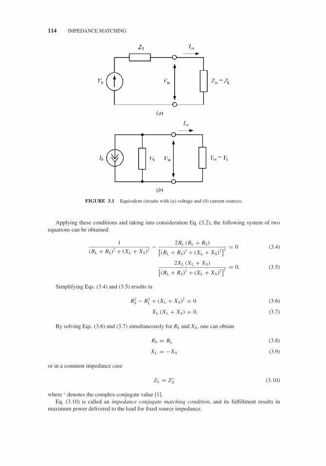
JWBS064-c03 JWBS064-Gerbennikov March 15, 2011 10:57 Printer Name: Yet to Come
114 IMPEDANCE MATCHING
FIGURE 3.1 Equivalent circuits with (a) voltage and (b) current sources.
Applying these conditions and taking into consideration Eq. (3.2), the following system of twoequations can be obtained:
1
(RL + RS)2 + (XL + XS)2 − 2RL (RL + RS)[(RL + RS)2 + (XL + XS)2
]2 = 0 (3.4)
2XL (XL + XS)[(RL + RS)2 + (XL + XS)2
]2 = 0. (3.5)
Simplifying Eqs. (3.4) and (3.5) results in
R2S − R2
L + (XL + XS)2 = 0 (3.6)
XL (XL + XS) = 0. (3.7)
By solving Eqs. (3.6) and (3.7) simultaneously for RS and XS, one can obtain
RS = RL (3.8)
XL = −XS (3.9)
or in a common impedance case
ZL = Z ∗S (3.10)
where * denotes the complex-conjugate value [1].Eq. (3.10) is called an impedance conjugate matching condition, and its fulfillment results in
maximum power delivered to the load for fixed source impedance.
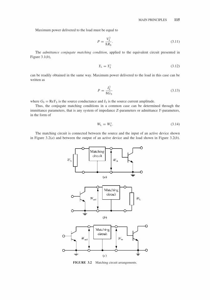
JWBS064-c03 JWBS064-Gerbennikov March 15, 2011 10:57 Printer Name: Yet to Come
MAIN PRINCIPLES 115
Maximum power delivered to the load must be equal to
P = V 2S
8RS. (3.11)
The admittance conjugate matching condition, applied to the equivalent circuit presented inFigure 3.1(b),
YL = Y ∗S (3.12)
can be readily obtained in the same way. Maximum power delivered to the load in this case can bewritten as
P = I 2S
8GS(3.13)
where GS = ReYS is the source conductance and IS is the source current amplitude.Thus, the conjugate matching conditions in a common case can be determined through the
immittance parameters, that is any system of impedance Z-parameters or admittance Y-parameters,in the form of
WL = W ∗S . (3.14)
The matching circuit is connected between the source and the input of an active device shownin Figure 3.2(a) and between the output of an active device and the load shown in Figure 3.2(b).
FIGURE 3.2 Matching circuit arrangements.
JWBS064-c03 JWBS064-Gerbennikov March 15, 2011 10:57 Printer Name: Yet to Come
116 IMPEDANCE MATCHING
For a multistage power amplifier, the load represents an input circuit of the next stage. Therefore,the matching circuit is connected between the output of the active device of the previous amplifierstage and the input of the active device of the subsequent stage of the power amplifier shown inFigure 3.2(c). The main objective is to properly transform the load immittance WL to the optimumdevice output immittance Wout, the value of which is properly determined by the supply voltage, theoutput power, the saturation voltage of the active device, and the selected class of the active deviceoperation to maximize the operating efficiency and output power of the power amplifier. It should benoted that Eq. (3.14) is given in a general immittance form without indication of whether it is used in asmall-signal or large-signal application. In the latter case, this only means that the device immittanceW-parameters are fundamentally averaged over large signal swing across the device equivalent circuitparameters and that the conjugate-matching principle is valid in both the small-signal application andthe large-signal application, where the optimum equivalent device output resistance (or conductance)is matched to the load resistance (or conductance) and the effect of the device output reactive elementsis eliminated by the conjugate reactance of the load network. In addition, the matching circuits shouldbe designed to provide the required voltage and current waveforms at the device output and thestability of operation conditions, and according to the requirements for the power amplifier amplitudeand phase characteristics. The losses in the matching circuits must be as small as possible to deliverthe output power to the load with maximum efficiency. Finally, it is desirable that the matching circuitbe easy to tune.
3.2 SMITH CHART
The hemisphere Smith chart is one of the tools most widely used to match circuit designs because itgives a clear and simple graphical representation of the consecutive matching design procedure [2,3].However, another hemisphere chart with a standing-wave indicator to measure the impedance ratioof a load on line where a grid of circular lines was marked with magnitude and angle of impedance,corresponding to latitude and longitude on a hemisphere, was simultaneously proposed by Carter[4,5]. The Smith chart can be applied for matching using both lumped elements and transmissionlines. The Smith chart is particularly useful for matching circuit designs that use the transmissionlines because analytical calculations in this case are very complicated. Also, when using the completeSmith chart, the circuit parameters such as voltage standing wave ratio (VSWR), reflection coefficient,return loss, or losses in the transmission line can be directly calculated. The Smith chart is a veryimportant tool, being a part of modern computer-aided design software and test equipment andproviding a useful visual way to understand the circuit behavior.
The Smith chart represents a relationship between the load impedance Z and the reflectioncoefficient � that can be written in the normalized form of
Z
Z0= 1 + �
1 − �(3.15)
where the normalized impedance Z/Z0 can also be written as
Z
Z0= R
Z0+ j
X
Z0(3.16)
and represents the reflection coefficient � through its real and imaginary parts as
� = �r + j�i. (3.17)

JWBS064-c03 JWBS064-Gerbennikov March 15, 2011 10:57 Printer Name: Yet to Come
SMITH CHART 117
Then, substituting Eqs. (3.16) and (3.17) into Eq. (3.15) results in
R
Z0+ j
X
Z0= 1 + �r + j�i
1 − �r − j�i. (3.18)
By equating the real and imaginary parts of Eq. (3.18), one can obtain
(�r − R
R + Z0
)2
+ �2i =
(Z0
R + Z0
)2
(3.19)
(�r − 1)2 +(
�i − Z0
X
)2
=(
Z0
X
)2
. (3.20)
As a result, in the �r–�i coordinate plane, Eq. (3.19) represents a family of circles centered atpoints �r = R/(R + Z0) and �i = 0 with radii of Z0/(R + Z0), which are called constant-(R/Z0) circles.Eq. (3.20) represents a family of circles at points �r = 1 and �i = Z0/X with radii of Z0/X, whichare called constant-(X/Z0) circles. These constant-(R/Z0) and constant-(X/Z0) circles with differentnormalized parameters are shown in Figure 3.3(a), where the points �r = −1 and �r = 1 are alsoindicated. The plot of such circles is called the impedance Smith chart or the Z Smith chart. The curvefrom the point A to the point C represents the impedance transformation from the pure resistance of25 � to the inductive impedance of (25 + j25) �, which can be provided by using the inductanceconnected in series with the resistance.
Eqs. (3.19) and (3.20) can be rewritten easily in the admittance form with the real part G andimaginary part B when a relationship between the impedance Y and the reflection coefficient � canbe written as
G
Y0+ j
B
Y0= 1 − �r − j�i
1 + �r + j�i(3.21)
where Y0 = 1/Z0. Then,
(�r + G
G + Y0
)2
+ �2i =
(Y0
G + Y0
)2
(3.22)
(�r + 1)2 +(
�i + Y0
B
)2
=(
Y0
B
)2
. (3.23)
From Eqs. (3.22) and (3.23) it follows that the constant-(G/Y0) circles are centered at �r =−G/(G + Y0) and �i = 0 with radii of Y0/(G + Y0). The constant-(B/Y0) circles are centered atpoints �r = −1 and �i = −Y0/B with radii of Y0/B, which is shown in Figure 3.3(b). These circlesare centered at antisymmetric points in contrast to the impedance Smith chart. The admittance Smithchart or the Y Smith chart, the admittances of which coincide with the appropriate impedancesplotted at the Z Smith chart, is the mirror-reflected impedance Smith chart as a result of its rotationby 180◦. The curve from the point C to the point D shows the admittance transformation from theinductive admittance of (20 − j20) mS to the pure conductance of 20 mS or resistance of 50 �,which can be provided by using the capacitance connected in parallel with the initial admittance. Theimpedances and admittances can be determined by any impedance or admittance Smith chart wherethe normalized parameters are indicated. As a general case, this diagram is called the immittanceSmith chart. However, in this case, the impedance point and its corresponding admittance value arelocated one against another at the same distance from center (1, 0).
Therefore, sometimes it is advisable to use the combined impedance–admittance Smith chartshown in Figure 3.3(c). This is the case when, for any point, we can read the normalized impedancefrom the Z Smith chart and normalized admittance from the Y Smith chart. This Z–Y Smith chart
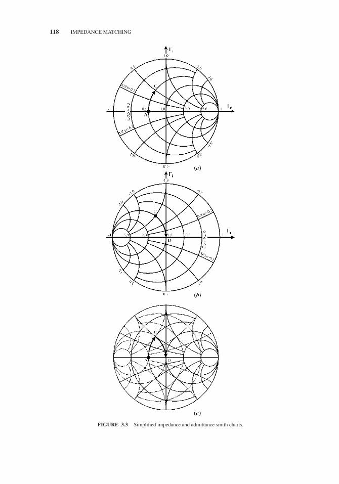
JWBS064-c03 JWBS064-Gerbennikov March 15, 2011 10:57 Printer Name: Yet to Come
118 IMPEDANCE MATCHING
FIGURE 3.3 Simplified impedance and admittance smith charts.
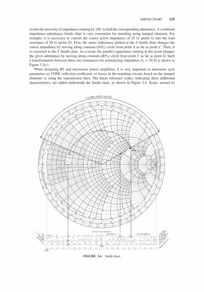
JWBS064-c03 JWBS064-Gerbennikov March 15, 2011 10:57 Printer Name: Yet to Come
SMITH CHART 119
avoids the necessity of impedance rotating by 180◦ to find the corresponding admittance. A combinedimpedance–admittance Smith chart is very convenient for matching using lumped elements. Forexample, it is necessary to convert the source active impedance of 25 � (point A) into the loadresistance of 50 � (point D). First, the series inductance plotted at the Z Smith chart changes thesource impedance by moving along constant-(X/Z0) circle from point A as far as point C. Then, itis converted to the Y Smith chart. As a result, the parallel capacitance starting at this point changesthe given admittance by moving along constant-(B/Y0) circle from point C as far as point D. Sucha transformation between these two resistances for normalizing impedance Z0 = 50 � is shown inFigure 3.3(c).
When designing RF and microwave power amplifiers, it is very important to determine suchparameters as VSWR, reflection coefficient, or losses in the matching circuits based on the lumpedelements or using the transmission lines. The linear reference scales, indicating these additionalcharacteristics, are added underneath the Smith chart, as shown in Figure 3.4. Scales around its
FIGURE 3.4 Smith chart.

JWBS064-c03 JWBS064-Gerbennikov March 15, 2011 10:57 Printer Name: Yet to Come
120 IMPEDANCE MATCHING
periphery show the calibrated electrical wavelength and the angles of the reflection coefficients.The Smith chart can be easily implemented for the graphical design using the transmission lines.Expression for the input impedance of the lossless transmission line can be written in terms of thereflection coefficient as
Z in
Z0= 1 + � exp (−2 jθ)
1 − � exp (−2 jθ). (3.24)
This equation differs from Eq. (3.15) by the added phase angle only. This means that the normalizedinput impedance, seen looking into the transmission line with electrical length θ , can be found byrotating this impedance point clockwise by 2θ about the center of the Smith chart with the sameradius |�|. By subtracting 2θ from the phase angle of the reflection coefficient, its value decreasesin the clockwise direction, according to the periphery scale. In this case, the half-wave transmissionline provides a clockwise rotation of 2π or 360◦ about the center, returning the point to its originalposition.
For example, a typical 50 � transmission line provides a transformation of load impedance fromZL = (12 + j10) � to a new impedance of Zin = (100 + j100) �. The normalized load impedanceis ZL/Z0 = (0.24 + j0.2) �, which is plotted on the Smith chart, as shown in Figure 3.4. By usinga compass to draw the circle from this point to the intersection point with a real axis, we obtain|�| = 0.61 at the reflection coefficient scale, RL = 4.3 dB at the return loss scale and VSWR = 4.2at the standing wave ratio (SWR) scale. To determine the angle of the reflection coefficient, it needsto draw a radial line through the load impedance point to the intersection of the periphery circle(an angle of 83◦ can be read). If a radial line is drawn through the point of the input impedanceat the outer wavelength scale, the difference between points of 0.209λ and 0.033λ gives the lengthof the transmission line as 0.176λ. However, in the case of the transmission line with losses of2 dB, the point obtained should be moved to the point of Zin = (90 + j40) �, according to theattenuation scale.
3.3 MATCHING WITH LUMPED ELEMENTS
3.3.1 Analytic Design Technique
Generally, there is a variety of configurations for matching networks that can be used to connect agenerating system efficiently to its useful load, but in order to obtain high transmission efficiency,any of these networks should be properly designed. The lumped matching circuits in the form of (a)L-transformer, (b) π -transformer, or (c) T-transformer shown in Figure 3.5 have proved for a longtime to be effective for power amplifier design [6]. The simplest and most popular matching circuitis the matching circuit in the form of the L-transformer. The transforming properties of this matchingcircuit can be analyzed by using the equivalent transformation of a parallel into a series representationof RX circuit [7].
Consider the parallel RX circuit shown in Figure 3.6(a), where R1 is the real (resistive) and X1
is the imaginary (reactive) parts of the circuit impedance. Z1 = j X1 R1/(R1 + j X1) and the seriesRX circuit shown in Figure 3.6(b), where R2 is the resistive and X2 is the reactive parts of the circuitimpedance Z2 = R2 + j X2. These two circuits, series and parallel, can be considered equivalent atsome frequency if Z1 = Z2 resulting in
R2 + j X2 = R1 X21
R21 + X 2
1
+ jR2
1 X1
R21 + X 2
1
. (3.25)

JWBS064-c03 JWBS064-Gerbennikov March 15, 2011 10:57 Printer Name: Yet to Come
MATCHING WITH LUMPED ELEMENTS 121
FIGURE 3.5 Matching circuits in the form of (a) L-, (b) π - and (c) T-transformers.
FIGURE 3.6 Impedance (a) parallel and (b) series equivalent circuits.
Eq. (3.25) can be rearranged by two separate equations for real and imaginary parts in the form of
R1 = R2
(1 + Q2
)(3.26)
X1 = X2
(1 + Q−2
)(3.27)
where Q = R1/|X1| = |X2|/R2 is the circuit quality factor, which is equal for both the series and parallelRX circuits.
Consequently, if the reactive impedance X1 = −X2
(1 + Q−2
)is connected in parallel to the series
circuit R2X2, it allows the reactive impedance (or reactance) of the series circuit to be compensated.In this case, the input impedance of such a two-port network shown in Figure 3.7 will be resistive
FIGURE 3.7 Input impedance of two-port network.

JWBS064-c03 JWBS064-Gerbennikov March 15, 2011 10:57 Printer Name: Yet to Come
122 IMPEDANCE MATCHING
FIGURE 3.8 L-type matching circuits and relevant equations.
only and equal to R1. Consequently, to transform the resistance R1 into the other resistance R2 at thegiven frequency, it is sufficient to connect between them a two-port L-transformer with the oppositesigns of the reactances X1 and X2, the parameters of which can be easily calculated from the followingsimple equations:
|X1| = R1
Q(3.28)
|X2| = R2 Q (3.29)
where
Q =√
R1
R2− 1 (3.30)
is the circuit quality factor expressed through the resistances to be matched. Thus, to design amatching circuit with fixed resistances to be matched, first we need to calculate the circuit qualityfactor Q according to Eq. (3.30) and then to define the reactive elements, according to Eqs. (3.28)and (3.29).
Due to the opposite signs of the reactances X1 and X2, the two possible circuit configurations (onein the form of a low-pass filter section and another in the form of a high-pass filter section) withthe same transforming properties can be realized, as shown in Figure 3.8 together with the designequations.
The lumped matching circuits in the form of the L-transformer loaded on the resistance R2 can alsobe considered as the parallel resonant circuit shown in Figure 3.9. In this case, the series inductance L2
and series resistance R2 transform to the parallel inductance L ′2 and parallel resistance R′
2, respectively,which become the frequency-dependent functions:
R1 = R′2 = R2
(1 + Q2
)(3.31)
L ′2 = L2
(1 + Q−2
)(3.32)

JWBS064-c03 JWBS064-Gerbennikov March 15, 2011 10:57 Printer Name: Yet to Come
MATCHING WITH LUMPED ELEMENTS 123
FIGURE 3.9 Parallel resonant circuit equivalent of loaded L-transformer.
where Q = ωL2/R2. The resonant frequency f 0 of such an equivalent parallel resonant circuit isdetermined from
ω0 = 2π f0 =√
1
L2C1−
(R2
L2
)2
. (3.33)
If this matching circuit has small values of Q, wider frequency bandwidth but poor out-of-bandsuppression can be achieved. However, with large values of Q, the frequency bandwidth is substantiallyreduced. For the case of R1/R2 ≥ 10, which corresponds to the condition of Q ≥ 3, the frequencybandwidth f and out-of-band suppression factor Fn of such an L-transformer can be approximatelyevaluated by the same formulas as for a parallel resonant circuit:
f ∼= f0
Q(3.34)
Fn∼= Q
(n2 − 1
)(3.35)
where f 0 is the operating frequency and n is the harmonic number [8]. The out-of-band suppressionfactor Fn of the matching circuit represents the ratio of the selected harmonic component in the input(collector) current to the same harmonic component in the output (load) current. Figure 3.10 showsthe frequency behavior of the input impedance magnitude |Zin| of the parallel resonant circuit.
FIGURE 3.10 Frequency plot of input impedance for parallel resonant circuit.

JWBS064-c03 JWBS064-Gerbennikov March 15, 2011 10:57 Printer Name: Yet to Come
124 IMPEDANCE MATCHING
The transformer efficiency ηT is determined by the ratio of PL/Pin, where Pin is the power at theinput of the transformer and PL is the load transformer power. The efficiency for the L-transformerwith negligible losses in the capacitor can be calculated from
ηT∼= 1
/ (1 + Q
Qind
)(3.36)
where Qind is the inductor quality factor. From Eq. (3.36) it follows that, with the increase of Q,the efficiency of the impedance transformer decreases. This means that, for the same R1 and seriesparasitic resistance of the circuit inductance, the lower resistance R2 provides the higher currentflowing through this inductance, which leads to an additional power dissipation. An analysis ofEqs. (3.28) and (3.29) shows that, for the given resistances R1 and R2, each element of the L-transformer can have only one value for a fixed frequency. Consequently, it is difficult to satisfysimultaneously such contradictory requirements as efficiency, frequency bandwidth and out-of-bandsuppression.
To avoid the parasitic low-frequency oscillations and to increase the level of the harmonic sup-pression, it may be necessary to connect an additional L0C0 series circuit, which resonant frequencyis equal to the operating frequency of the power amplifier, as shown in Figure 3.11. In this case, theout-of-band suppression factor Fn defined by Eq. (3.35) is written as
Fn∼= Q�
(n2 − 1
)(3.37)
where Q� = Q + Q0 and Q0 = ωL0/R2. Better harmonic suppression is achieved at the expense ofthe frequency bandwidth narrowing.
In practice, it makes sense to use the single two-port L-transformers in power amplifiers as theinterstage matching circuits, where the requirements for out-of-band suppression and efficiency arenot as high as for the output matching circuits. In this case, the main advantage of such an L-transformer is in its simplicity when the only two reactive elements with fast tuning are needed. Forlarger values of Q ≥ 10, it is possible to use a cascade connection of L-transformers, which allowswider frequency bandwidth and transformer efficiency to be realized.
The matching circuits in the form of (a) π -transformer and (b) T-transformer can be realized byappropriate connection of two L-transformers, as shown in Figure 3.12. For each L-transformer, theresistances R1 and the resistance R2 are transformed to some intermediate resistance R0 with the valueof R0 < (R1, R2) for a π-transformer and the value of R0 > (R1, R2) for a T-transformer. The valueof R0 is not fixed and can be chosen arbitrary depending on the frequency bandwidth. This meansthat, compared to the simple L-transformer with fixed parameters for the same ratio of R2/R1, theparameters of the π -transformer or T-transformer can be different. However, they provide narrowerfrequency bandwidths due to higher quality factors because the intermediate resistance R0 is eithergreater or smaller than each of the resistances R1 and R2. By taking into account the two possible
FIGURE 3.11 L-transformer with additional LC-filter.
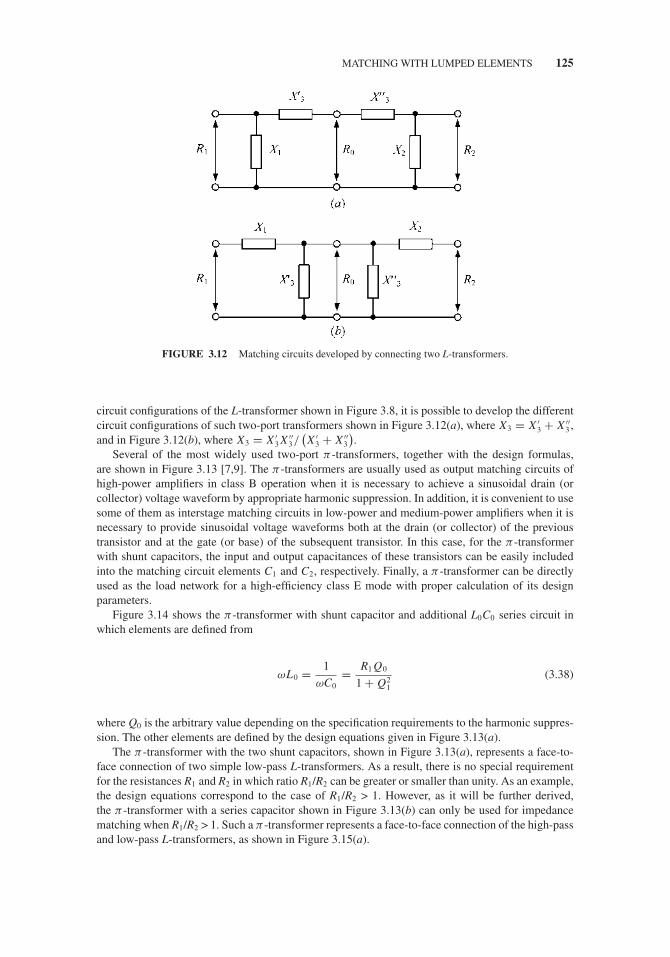
JWBS064-c03 JWBS064-Gerbennikov March 15, 2011 10:57 Printer Name: Yet to Come
MATCHING WITH LUMPED ELEMENTS 125
FIGURE 3.12 Matching circuits developed by connecting two L-transformers.
circuit configurations of the L-transformer shown in Figure 3.8, it is possible to develop the differentcircuit configurations of such two-port transformers shown in Figure 3.12(a), where X3 = X ′
3 + X ′′3 ,
and in Figure 3.12(b), where X3 = X ′3 X ′′
3/(X ′
3 + X ′′3
).
Several of the most widely used two-port π -transformers, together with the design formulas,are shown in Figure 3.13 [7,9]. The π -transformers are usually used as output matching circuits ofhigh-power amplifiers in class B operation when it is necessary to achieve a sinusoidal drain (orcollector) voltage waveform by appropriate harmonic suppression. In addition, it is convenient to usesome of them as interstage matching circuits in low-power and medium-power amplifiers when it isnecessary to provide sinusoidal voltage waveforms both at the drain (or collector) of the previoustransistor and at the gate (or base) of the subsequent transistor. In this case, for the π -transformerwith shunt capacitors, the input and output capacitances of these transistors can be easily includedinto the matching circuit elements C1 and C2, respectively. Finally, a π -transformer can be directlyused as the load network for a high-efficiency class E mode with proper calculation of its designparameters.
Figure 3.14 shows the π -transformer with shunt capacitor and additional L0C0 series circuit inwhich elements are defined from
ωL0 = 1
ωC0= R1 Q0
1 + Q21
(3.38)
where Q0 is the arbitrary value depending on the specification requirements to the harmonic suppres-sion. The other elements are defined by the design equations given in Figure 3.13(a).
The π -transformer with the two shunt capacitors, shown in Figure 3.13(a), represents a face-to-face connection of two simple low-pass L-transformers. As a result, there is no special requirementfor the resistances R1 and R2 in which ratio R1/R2 can be greater or smaller than unity. As an example,the design equations correspond to the case of R1/R2 > 1. However, as it will be further derived,the π -transformer with a series capacitor shown in Figure 3.13(b) can only be used for impedancematching when R1/R2 > 1. Such a π -transformer represents a face-to-face connection of the high-passand low-pass L-transformers, as shown in Figure 3.15(a).

JWBS064-c03 JWBS064-Gerbennikov March 15, 2011 10:57 Printer Name: Yet to Come
126 IMPEDANCE MATCHING
FIGURE 3.13 π -transformers and relevant equations.
FIGURE 3.14 π -transformer with additional LC-filter.

JWBS064-c03 JWBS064-Gerbennikov March 15, 2011 10:57 Printer Name: Yet to Come
MATCHING WITH LUMPED ELEMENTS 127
⇓C3
R1 L1 R2C2
′
R1 L1 R2C2
L3C3 ′
R0
(a)
(b)
FIGURE 3.15 π-transformer with series capacitor.
The design equations for a high-pass section are written using Eqs. (3.28) to (3.30) as
ωL1 = R1
Q1(3.39)
ωC ′3 = 1
Q1 R0(3.40)
Q21 = R1
R0− 1 (3.41)
where Q1 is the circuit quality factor and R0 is the intermediate resistance.Similarly, for a low-pass section,
ωC2 = Q2
R2(3.42)
ωL ′3 = Q2 R0 (3.43)
Q22 = R2
R0− 1. (3.44)
Since it is assumed that R1 > R2 > R0, from Eq. (3.41) it follows that the quality factor Q1 of ahigh-pass L-transformer can be chosen from the condition of
Q21 >
R1
R2− 1. (3.45)

JWBS064-c03 JWBS064-Gerbennikov March 15, 2011 10:57 Printer Name: Yet to Come
128 IMPEDANCE MATCHING
Substituting Eq. (3.41) into Eq. (3.44) results in
Q2 =√
R2
R1
(1 + Q2
1
) − 1. (3.46)
Combining the reactances of two series elements (capacitor C ′3 and inductor L ′
3) given by Eqs.(3.40) and (3.43) yields
ωL ′3 − 1
ωC ′3
= R0 (Q2 − Q1) = R2 (Q2 − Q1)(1 + Q2
2
) . (3.47)
As a result, since Q1 > Q2, the total series reactance is negative, which can be provided by a seriescapacitance C3, as shown in Eq. 3.15(b), with susceptance
ωC3 = 1 + Q22
R2 (Q1 − Q2). (3.48)
On the other hand, if Q2 > Q1 when R2 > R1 > R0, then the total series reactance is positive, whichcan be provided by a series inductance L3, and all matching circuit parameters can be calculatedaccording to the design equations given in Figure 3.13(c). In this case, it needs first to choose thevalue of Q2 for fixed resistances R1 and R2 to be matched, then to calculate the value of Q1, and finallythe values of the shunt inductance L1, shunt capacitance C2, and series inductance L3.
Some of the matching circuit configurations of two-port T-transformers, together with the designformulas, are shown in Figure 3.16 [7,9]. The T-transformers are usually used in the high-poweramplifiers as input, interstage, and output matching circuits, especially the matching circuit withshunt and series capacitors shown in Figure 3.16(b). In this case, if a high value of the inductanceL2 is chosen, then the current waveform at the input of the transistor with a small input resistivepart will be close to sinusoidal. By using such a T-transformer for the output matching of a poweramplifier, it is easy to realize a high-efficiency class F operation mode, because the series inductanceconnected to the drain (or collector) of the active device creates an open-circuit harmonic impedanceconditions.
The T-transformer with the two-series inductors, shown in Figure 3.16(a), represents a back-to-back connection of two simple low-pass L-transformers. In this case, the resistance ratio R1/R2 canbe greater or smaller than unity, similar to a π -transformer with the two shunt capacitors shown inFigure 3.13(a). As an example, the design equations correspond to the case of R1/R2 > 1. However,the T-transformer with series and shunt capacitors shown in Figure 3.16(b) can only be used forimpedance matching when R1/R2 > 1. Such a T-transformer represents a back-to-back connection ofthe high-pass and low-pass L-transformers, as shown in Figure 3.17(a).
The design equations for a high-pass section of such a T-transformer are written using Eqs. (3.28)to (3.30) as
ωC1 = 1
R1 Q1(3.49)
ωL ′3 = R0
Q1(3.50)
Q21 = R0
R1− 1 (3.51)
where Q1 is the circuit quality factor and R0 is the intermediate resistance.

JWBS064-c03 JWBS064-Gerbennikov March 15, 2011 10:57 Printer Name: Yet to Come
MATCHING WITH LUMPED ELEMENTS 129
FIGURE 3.16 T-transformers and relevant equations.
Similarly, for a low-pass section,
ωL2 = Q2 R2 (3.52)
ωC ′3 = Q2/R0 (3.53)
Q22 = R0
R2− 1. (3.54)
Since it is assumed that R0 > R1 > R2, from Eq. (3.54) it follows that the quality factor Q2 of alow-pass L-transformer can be chosen from the condition of
Q22 >
R1
R2− 1. (3.55)

JWBS064-c03 JWBS064-Gerbennikov March 15, 2011 10:57 Printer Name: Yet to Come
130 IMPEDANCE MATCHING
FIGURE 3.17 T-transformer with series and shunt capacitors.
Substituting Eq. (3.54) into Eq. (3.51) results in
Q1 =√
R2
R1
(1 + Q2
2
) − 1. (3.56)
Combining the susceptances of two shunt elements (inductor L ′3 and capacitor C ′
3) given by Eqs.(3.50) and (3.53) yields
ωC ′3 − 1
ωL ′3
= Q2 − Q1
R0= Q2 − Q1
R2
(1 + Q2
2
) . (3.57)
As a result, since Q2 > Q1, the total shunt susceptance is positive, which can be provided by ashunt capacitance C3, as shown in Figure 3.17(b), with susceptance
ωC3 = Q2 − Q1
R2
(1 + Q2
2
) . (3.58)
On the other hand, if Q1 > Q2 when R0 > R2 > R1, then the total shunt susceptance is negativethat can be provided by a shunt inductance L3, and all matching circuit parameters can be calculatedaccording to the design equations given in Figure 3.16(c). In this case, it needs first to choose thevalue of Q1 for fixed resistances R1 and R2 to be matched, then to calculate the value of Q2, and finallythe values of the series capacitance C1, series inductance L2, and shunt inductance L3.
If the elements of π - and T-transformers are chosen according to the condition X1 = X2 = −X3,then the input impedance Zin of the transformer loaded by the resistance RL (from any side) is equalto
Z in = Rin = X 2
RL(3.59)
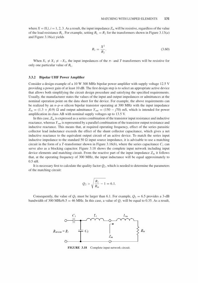
JWBS064-c03 JWBS064-Gerbennikov March 15, 2011 10:57 Printer Name: Yet to Come
MATCHING WITH LUMPED ELEMENTS 131
where X = |Xi|, i = 1, 2, 3. As a result, the input impedance Zin will be resistive, regardless of the valueof the load resistance RL. For example, setting RL = R2 for the transformers shown in Figure 3.13(a)and Figure 3.16(a) yields
R1 = X 2
R2. (3.60)
When X1 �= X2 �= −X3, the input impedances of the π - and T-transformers will be resistive foronly one particular value of RL.
3.3.2 Bipolar UHF Power Amplifier
Consider a design example of a 10 W 300 MHz bipolar power amplifier with supply voltage 12.5 Vproviding a power gain of at least 10 dB. The first design step is to select an appropriate active devicethat allows both simplifying the circuit design procedure and satisfying the specified requirements.Usually, the manufacturer states the values of the input and output impedances or admittances at thenominal operation point on the data sheet for the device. For example, the above requirements canbe realized by an n–p–n silicon bipolar transistor operating at 300 MHz with the input impedanceZ in = (1.3 + j0.9) � and output admittance Yout = (150 − j70) mS, which is intended for poweramplification in class AB with nominal supply voltages up to 13.5 V.
In this case, Z in is expressed as a series combination of the transistor input resistance and inductivereactance, whereas Yout is represented by a parallel combination of the transistor output resistance andinductive reactance. This means that, at required operating frequency, effect of the series parasiticcollector lead inductance exceeds the effect of the shunt collector capacitance, which gives a netinductive reactance to the equivalent output circuit of an active device. To match the series inputinductive impedance to the standard 50 � input source impedance, it is advisable to use a matchingcircuit in the form of a T-transformer shown in Figure 3.16(b), where the series capacitance C1 canserve also as a blocking capacitor. Figure 3.18 shows the complete input network including inputdevice elements and matching circuit. From the reactive part of the input impedance Zin it followsthat, at the operating frequency of 300 MHz, the input inductance will be equal approximately to0.5 nH.
It is necessary first to calculate the quality factor Q2, which is needed to determine the parametersof the matching circuit:
Q2 >
√R1
Rin− 1 = 6.1.
Consequently, the value of Q2 must be larger than 6.1. For example, Q2 = 6.5 provides a 3-dBbandwidth of 300 MHz/6.5 = 46 MHz. In this case, a value of Q1 will be equal to 0.35. As a result,
FIGURE 3.18 Complete input network circuit.
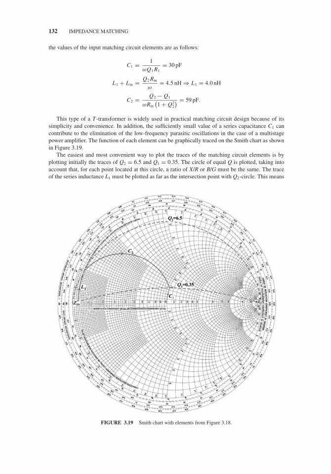
JWBS064-c03 JWBS064-Gerbennikov March 15, 2011 10:57 Printer Name: Yet to Come
132 IMPEDANCE MATCHING
the values of the input matching circuit elements are as follows:
C1 = 1
ωQ1 R1= 30 pF
L1 + L in = Q2 Rin
ω= 4.5 nH ⇒ L1 = 4.0 nH
C2 = Q2 − Q1
ωRin
(1 + Q2
2
) = 59 pF.
This type of a T-transformer is widely used in practical matching circuit design because of itssimplicity and convenience. In addition, the sufficiently small value of a series capacitance C1 cancontribute to the elimination of the low-frequency parasitic oscillations in the case of a multistagepower amplifier. The function of each element can be graphically traced on the Smith chart as shownin Figure 3.19.
The easiest and most convenient way to plot the traces of the matching circuit elements is byplotting initially the traces of Q2 = 6.5 and Q1 = 0.35. The circle of equal Q is plotted, taking intoaccount that, for each point located at this circle, a ratio of X/R or B/G must be the same. The traceof the series inductance L1 must be plotted as far as the intersection point with Q2-circle. This means
FIGURE 3.19 Smith chart with elements from Figure 3.18.

JWBS064-c03 JWBS064-Gerbennikov March 15, 2011 10:57 Printer Name: Yet to Come
MATCHING WITH LUMPED ELEMENTS 133
that, beginning at Zin, a curve of increasing inductive reactance must be plotted up to Q2-circle. Thevalue of L1 is determined from the normalized inductive impedance at this intersection point. Then,due to a normalization to 50 �, the chart value must be multiplied by factor 50.
The trace of the parallel capacitance C2 must be plotted using admittance circles. The previousimpedance point located at Q2-circle is converted to its appropriate admittance one. This point issymmetrical to the impedance point regarding the center point and is located on a straight line fromthe intersection point drawn through the center of the Smith chart into its lower half at the samedistance from the center point. A curve from this point with constant conductance and increasingcapacitive susceptance is plotted. These points are transformed to appropriate impedances using a linethrough the center point extended at equal distance on the other side and stop when the transformedcurve reaches the Q1 = 0.35 circle. In other words, it is necessary to transform mentally or to usea transparent admittance Smith chart (impedance Smith chart rotated on 180◦) to plot a curve forC2 on the upper half of the impedance Smith chart. The difference between the susceptances at thebeginning and the end of this curve determines the value of C2. Then, a curve of reducing inductivereactance is plotted down to the center point to determine a value of the series capacitance C1.
A similar design philosophy can be applied to the design of the output matching circuit shown inFigure 3.20. However, taking into account the presence of the output shunt inductance, it makes senseto use a matching circuit in the form of a π -transformer shown in Figure 3.13(c). The equivalentoutput resistance can be analytically evaluated by
Rout =[Vcc − Vcc(sat)
]2
2Pout
∼= (0.9 Vcc)2
2Pout
∼= 6.3 �
where Vcc is the supply voltage, Vcc(sat) is the saturation voltage, and Pout is the output power. Itsvalue is very close to the measurement value given by the real part of the device output admittancecalculated as Rout = 1/0.15 = 6.7 �. A value of Lout is approximately equal to 7.6 nH.
The quality factor Q2 can be chosen as
Q2 >
√R2
Rout− 1 = 2.5.
The calculated quality factor Q1 of the device output circuit is
Q1 = Rout
ωLout= 0.47.
This value of Lout allows the output device admittance to be matched to 50 � load using such aπ -transformer because
Q2 =√
R2
Rout
(1 + Q2
1
) − 1 = 2.8 > 2.5.
FIGURE 3.20 Complete output network circuit.

JWBS064-c03 JWBS064-Gerbennikov March 15, 2011 10:57 Printer Name: Yet to Come
134 IMPEDANCE MATCHING
As a result, the values of the other two elements of the output matching circuit are
C3 = Q2
ωR2= 31 pF
L2 = R2 (Q2 − Q1)
ω(1 + Q2
2
) = 6.8 nH.
A blocking capacitor that performs dc supply decoupling can be connected after the π -transformerwith sufficiently high value of its capacitance to avoid any negative influence on the matching circuit.Alternatively, it can be used in series with the inductor L2, in order to form a series resonant circuit, asshown in Figure 3.11. The design of the output circuit using the Smith chart is given in Figure 3.21.Initially, it is necessary to transform the output admittance Yout to the output impedance Zout using thestraight line of the Smith chart, putting the Zout point at the same distance from the center point as forthe Yout point. Then, the effect of increasing series inductance L2, by moving from the Zout point alongthe curve of the constant R and increasing X until intersection with the Q2 = 2.8 circle, is plotted.To determine the parallel capacitance C3, it is necessary to transform this point to the corresponding
FIGURE 3.21 Smith chart with elements from Figure 3.20.

JWBS064-c03 JWBS064-Gerbennikov March 15, 2011 10:57 Printer Name: Yet to Come
MATCHING WITH LUMPED ELEMENTS 135
admittance one and plot the curve of the constant G and increasing B, which must intersect the centerpoint of the Smith chart.
3.3.3 MOSFET VHF High-Power Amplifier
Now let us demonstrate lumped matching circuit technique to design a 150 W MOSFET poweramplifier with the supply voltage 50 V operating in a frequency bandwidth of 132 to 174 MHzand providing a power gain greater than 10 dB. These requirements can be satisfied using a siliconn-channel enhancement mode VDMOS transistor designed for power amplification in the VHFfrequency range. In this case, the center bandwidth frequency is equal to fc = √
132 · 174 = 152 MHz.For this frequency, the manufacturer states the following values of the input and output impedances:Z in = (0.9 − j1.2) � and Zout = (1.8 + j2.1) �. Both Zin and Zout represent the series combinationof an input or output resistance and a capacitive or inductive reactance, respectively. To cover therequired frequency bandwidth, the low-Q matching circuits should be used that allows reduction ofthe in-band amplitude ripple and improvement of the input VSWR. The value of a quality factor for3-dB bandwidth level must be less than Q = 152/(174 – 132) = 3.6. As a result, it is very convenient todesign the input and output matching circuits using the simple L-transformers in the form of low-passand high-pass filter sections with a constant value of Q [10].
To match input series capacitive impedance to the standard 50 � source impedance in a sufficientlywide frequency bandwidth, it is preferable to use three filter sections shown in Figure 3.22. From thenegative reactive part of the input impedance Z in it follows that the input capacitance at the operatingfrequency of 152 MHz is equal to approximately 873 pF. To compensate at the center bandwidthfrequency for this capacitive reactance, it is sufficient to connect in series to it an inductance of 1.3 nH.Now, when the device input capacitive reactance is compensated, the design of the input matchingcircuit can proceed. To simplify the matching design procedure, it is best to cascade L-transformerswith equal value of Q. Although equal Q values are not absolutely necessary, this provides a convenientguide for both analytical calculation of the matching circuit parameters and the Smith chart graphicaldesign.
In this case, the following ratio can be written for the input matching circuit:
R1
R2= R2
R3= R3
Rin(3.61)
resulting in R2 = 13 � and R3 = 3.5 � for Rsource = R1 = 50 � and Rin = 0.9 �. Consequently, aquality factor of each L-transformer is equal to Q = 1.7. The elements of the input matching circuitusing the formulas given in Figure 3.8 can be calculated as L1 = 31 nH, C1 = 47 pF, L2 = 6.2 nH,C2 = 137 pF, L3 = 1.6 nH, C3 = 509 pF.
This equal-Q approach significantly simplifies the matching circuit design using the Smith chart.When calculating a value of Q, it is necessary to plot a circle of equal Q values on the Smithchart. Then, each element of the input matching circuit can be readily determined, as it is shownin Figure 3.23. Each trace for the series inductance must be plotted until the intersection point with
FIGURE 3.22 Complete broadband input network circuit.

JWBS064-c03 JWBS064-Gerbennikov March 15, 2011 10:57 Printer Name: Yet to Come
136 IMPEDANCE MATCHING
FIGURE 3.23 Smith chart with elements from Figure 3.22.
Q-circle, whereas each trace for the parallel capacitance should be plotted until intersection withhorizontal real axis.
To match output series inductive impedance to the standard 50 � load impedance, it is sufficientto use only two filter sections, as shown in Figure 3.24. At the operating frequency of 152 MHz, thetransistor series output inductance is equal to approximately 2.2 nH. This inductance can be used asa part of L-transformer in the form of a low-pass filter section. For an output matching circuit, thecondition of equal-Q values gives the following ratio:
R2
R1= R1
Rout(3.62)
with the value of R1 = 9.5 � for Rload = R2 = 50 � and Rout = 1.8 �. Consequently, a quality factorof each L-transformer is equal to Q = 2.1, which is substantially smaller than a value of Q for 3-dBbandwidth level. Now it is necessary to check a value of a series inductance of the low-pass section,which must exceed the value of 2.2 nH for correct matching procedure. The appropriate calculation

JWBS064-c03 JWBS064-Gerbennikov March 15, 2011 10:57 Printer Name: Yet to Come
MATCHING WITH LUMPED ELEMENTS 137
FIGURE 3.24 Complete broadband output network circuit.
gives a value of total series inductance L4 + Lout of approximately 4 nH. As a result, the values of theoutput matching circuit elements are L4 = 1.8 nH, C4 = 231 pF, C5 = 52 pF, L5 = 25 nH.
The output matching circuit design using the Smith chart with constant Q-circle is shown inFigure 3.25. For the final high-pass section, a trace for the series capacitance C5 must be plotted untilthe intersection with Q = 2.1 circle, whereas a trace for the shunt inductance L5 should be plotteduntil the intersection with the center point of the Smith chart.
FIGURE 3.25 Smith chart with elements from Figure 3.24.
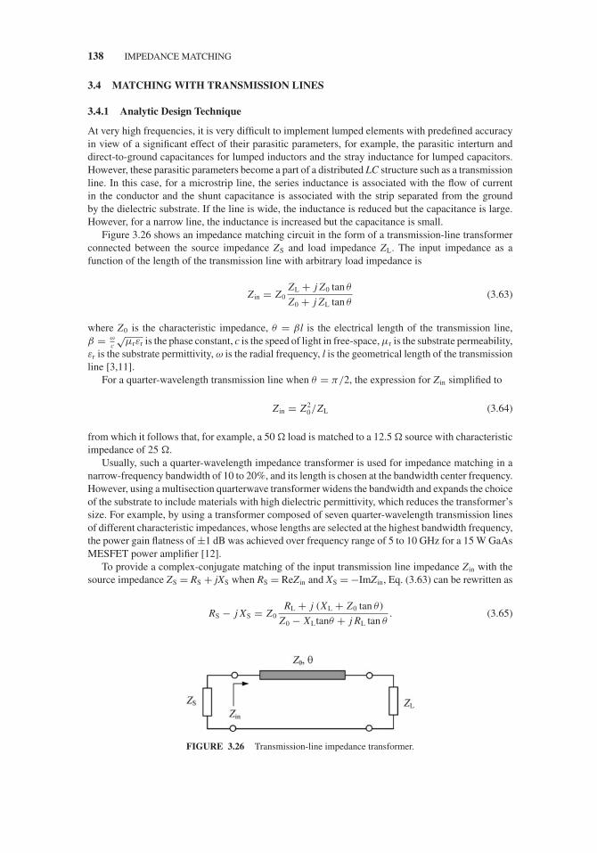
JWBS064-c03 JWBS064-Gerbennikov March 15, 2011 10:57 Printer Name: Yet to Come
138 IMPEDANCE MATCHING
3.4 MATCHING WITH TRANSMISSION LINES
3.4.1 Analytic Design Technique
At very high frequencies, it is very difficult to implement lumped elements with predefined accuracyin view of a significant effect of their parasitic parameters, for example, the parasitic interturn anddirect-to-ground capacitances for lumped inductors and the stray inductance for lumped capacitors.However, these parasitic parameters become a part of a distributed LC structure such as a transmissionline. In this case, for a microstrip line, the series inductance is associated with the flow of currentin the conductor and the shunt capacitance is associated with the strip separated from the groundby the dielectric substrate. If the line is wide, the inductance is reduced but the capacitance is large.However, for a narrow line, the inductance is increased but the capacitance is small.
Figure 3.26 shows an impedance matching circuit in the form of a transmission-line transformerconnected between the source impedance ZS and load impedance ZL. The input impedance as afunction of the length of the transmission line with arbitrary load impedance is
Z in = Z0ZL + j Z0 tan θ
Z0 + j ZL tan θ(3.63)
where Z0 is the characteristic impedance, θ = βl is the electrical length of the transmission line,β = ω
c
√μrεr is the phase constant, c is the speed of light in free-space, μr is the substrate permeability,
εr is the substrate permittivity, ω is the radial frequency, l is the geometrical length of the transmissionline [3,11].
For a quarter-wavelength transmission line when θ = π/2, the expression for Z in simplified to
Z in = Z 20/ZL (3.64)
from which it follows that, for example, a 50 � load is matched to a 12.5 � source with characteristicimpedance of 25 �.
Usually, such a quarter-wavelength impedance transformer is used for impedance matching in anarrow-frequency bandwidth of 10 to 20%, and its length is chosen at the bandwidth center frequency.However, using a multisection quarterwave transformer widens the bandwidth and expands the choiceof the substrate to include materials with high dielectric permittivity, which reduces the transformer’ssize. For example, by using a transformer composed of seven quarter-wavelength transmission linesof different characteristic impedances, whose lengths are selected at the highest bandwidth frequency,the power gain flatness of ±1 dB was achieved over frequency range of 5 to 10 GHz for a 15 W GaAsMESFET power amplifier [12].
To provide a complex-conjugate matching of the input transmission line impedance Zin with thesource impedance ZS = RS + jXS when RS = ReZ in and XS = −ImZ in, Eq. (3.63) can be rewritten as
RS − j XS = Z0RL + j (XL + Z0 tan θ)
Z0 − XLtanθ + j RL tan θ. (3.65)
FIGURE 3.26 Transmission-line impedance transformer.

JWBS064-c03 JWBS064-Gerbennikov March 15, 2011 10:57 Printer Name: Yet to Come
MATCHING WITH TRANSMISSION LINES 139
For a quarter-wavelength transformer, Eq. (3.65) can be divided into two separate equationsrepresenting the real and imaginary parts of the source impedance ZS as
RS = Z 20
RL
R2L + X 2
L
(3.66)
XS = −Z 20
XL
R2L + X 2
L
. (3.67)
For a pure real load impedance with XL = 0, a quarter-wavelength transmission line with thecharacteristic impedance Z0 can provide impedance matching for a purely active source and loadonly when
Z0 =√
RS RL. (3.68)
Generally, Eq. (3.65) can be divided into two equations representing the real and imaginary parts,
RS (Z0 − XL tan θ) − RL (Z0 − XS tan θ) = 0 (3.69)
XS (XL tan θ − Z0) − Z0 (XL + Z0 tan θ) + RS RL tan θ = 0. (3.70)
Solving Eqs. (3.69) and (3.70) for the two independent variables Z0 and θ yields
Z0 =√
RS
(R2
L + X 2L
) − RL
(R2
S + X 2S
)RL − RS
(3.71)
θ = tan−1
(Z0
RS − RL
RS XL − XS RL
). (3.72)
As a result, the transmission line with the characteristic impedance Z0 and electrical length θ ,determined by Eqs. (3.71) and (3.72), can match any source and load impedances when the impedanceratio gives a positive value inside the square root in Eq. (3.71).
For a particular case of a purely active source when ZS = RS, the ratio between the load andtransmission-line parameters can be expressed by
XL Z0
(1 − tan2 θ
) + (Z 2
0 − X 2L − R2
L
)tan θ = 0. (3.73)
Then, for the electrical length of the transmission line having θ = π /4, the expression for thecharacteristic impedance Z0 given by Eq. (3.71) can be simplified to
Z0 = |ZL| =√
R2L + X 2
L (3.74)
whereas the required real source impedance RS should be equal to
RS = RLZ0
Z0 − XL. (3.75)
Consequently, any load impedance can be transformed to a real source impedance defined byEq. (3.75) using a λ/8 transformer, the characteristic impedance of which is equal to the magnitudeof the load impedance [13].
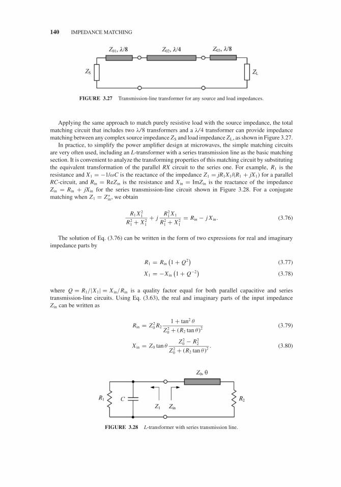
JWBS064-c03 JWBS064-Gerbennikov March 15, 2011 10:57 Printer Name: Yet to Come
140 IMPEDANCE MATCHING
FIGURE 3.27 Transmission-line transformer for any source and load impedances.
Applying the same approach to match purely resistive load with the source impedance, the totalmatching circuit that includes two λ/8 transformers and a λ/4 transformer can provide impedancematching between any complex source impedance ZS and load impedance ZL, as shown in Figure 3.27.
In practice, to simplify the power amplifier design at microwaves, the simple matching circuitsare very often used, including an L-transformer with a series transmission line as the basic matchingsection. It is convenient to analyze the transforming properties of this matching circuit by substitutingthe equivalent transformation of the parallel RX circuit to the series one. For example, R1 is theresistance and X1 = −1/ωC is the reactance of the impedance Z1 = jR1X1/(R1 + jX1) for a parallelRC-circuit, and Rin = ReZin is the resistance and Xin = ImZin is the reactance of the impedanceZin = Rin + jXin for the series transmission-line circuit shown in Figure 3.28. For a conjugatematching when Z1 = Z∗
in, we obtain
R1 X 21
R21 + X 2
1
+ jR2
1 X1
R21 + X 2
1
= Rin − j X in. (3.76)
The solution of Eq. (3.76) can be written in the form of two expressions for real and imaginaryimpedance parts by
R1 = Rin
(1 + Q2
)(3.77)
X1 = −X in
(1 + Q−2
)(3.78)
where Q = R1/|X1| = X in/Rin is a quality factor equal for both parallel capacitive and seriestransmission-line circuits. Using Eq. (3.63), the real and imaginary parts of the input impedanceZin can be written as
Rin = Z 20 R2
1 + tan2 θ
Z 20 + (R2 tan θ)2 (3.79)
X in = Z0 tan θZ 2
0 − R22
Z 20 + (R2 tan θ )2 . (3.80)
FIGURE 3.28 L-transformer with series transmission line.

JWBS064-c03 JWBS064-Gerbennikov March 15, 2011 10:57 Printer Name: Yet to Come
MATCHING WITH TRANSMISSION LINES 141
From Eq. (3.80) it follows that an inductive input impedance (necessary to compensate for thecapacitive parallel component) is provided when Z0 > R2 for θ < π /2 and Z0 < R2 for π /2 <
θ < π . As a result, to transform the resistance R1 into the other resistance R2 at the givenfrequency, it is necessary to connect a two-port L-transformer (including a parallel capacitanceand a series transmission line) between them. When one parameter (usually the characteristicimpedance Z0) is known, the matching circuit parameters can be calculated from the following twoequations:
C = Q
ωR1(3.81)
sin 2θ = 2QZ0
R2− R2
Z0
(3.82)
where
Q =√√√√ R1
R2
[cos2 θ +
(R2
Z0
)2
sin2 θ
]− 1 (3.83)
is the circuit quality factor defined as a function of the resistances R1 and R2 and the parameters ofthe transmission line, the characteristic impedance Z0 and electrical length θ .
It follows from Eqs. (3.82) and (3.83) that the electrical length θ can be calculated as a result ofthe numerical solution of a transcendental equation with one unknown parameter. However, it is moreconvenient to combine these two equations and to rewrite them in the implicit form of
R1
R2=
1 +(
Z0
R2− R2
Z0
)2
sin2 θ cos2 θ
cos2 θ +(
R2
Z0
)2
sin2 θ
. (3.84)
Figure 3.29 shows the resistance ratio of R1/R2 as a function of the normalized parameter Z0/R2 andelectrical length θ in the form of two nomographs: for the case of Z0/R2 > 0 shown in Figure 3.29(a) andfor the case of Z0/R2 < 0 shown in Figure 3.29(b). When the input resistance R1 and output resistanceR2 are known in advance, it is easy to evaluate the required value of θ for a fixed transmission-linecharacteristic impedance Z0 using these nomographs. The graphical results show that, in contrast to alumped L-transformer, a transmission-line L-transformer can match purely resistive source and loadimpedances with any ratio of R1/R2.
A π -transformer can be realized by back-to-back connection of the two L-transformers, as shownin Figure 3.30(a), where resistances R1 and R2 are transformed to some intermediate resistance R0.In this case, to minimize the length of a transmission line, the value of R0 should be smaller thanthat of both R1 and R2, that is, R0 < (R1, R2). The same procedure for a T-transformer shown inFigure 3.30(b) gives a value of R0 that is larger than that of both R1 and R2, that is R0 > (R1, R2).Then, for a T-transformer, two shunt adjacent capacitances are combined. For a π -transformer, twoadjacent series transmission lines are combined into a single transmission line with total electricallength.
For a π -transformer, the lengths of each part of the combined transmission line can be calculatedby equating the imaginary parts of the impedances from both sides at the reference plane A−A′ tozero, which means that the intermediate impedance R0 is real. This leads to two quadratic equations

JWBS064-c03 JWBS064-Gerbennikov March 15, 2011 10:57 Printer Name: Yet to Come
142 IMPEDANCE MATCHING
FIGURE 3.29 Nomographs for calculating transmission-line L-transformer.
FIGURE 3.30 π - and T-transformers with transmission lines.
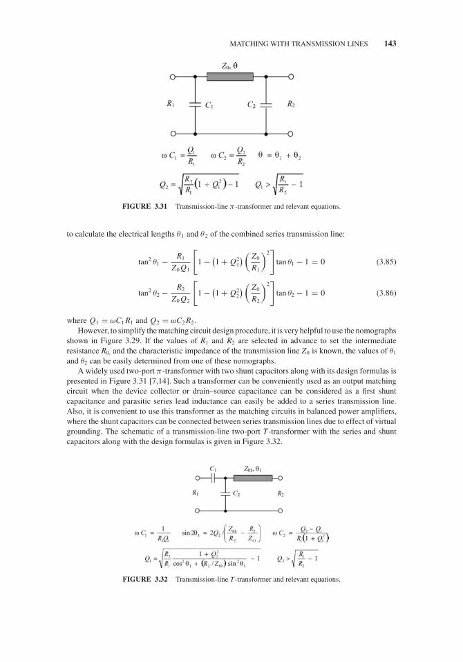
JWBS064-c03 JWBS064-Gerbennikov March 15, 2011 10:57 Printer Name: Yet to Come
MATCHING WITH TRANSMISSION LINES 143
FIGURE 3.31 Transmission-line π -transformer and relevant equations.
to calculate the electrical lengths θ1 and θ2 of the combined series transmission line:
tan2 θ1 − R1
Z0 Q1
[1 − (
1 + Q21
) (Z0
R1
)2]
tan θ1 − 1 = 0 (3.85)
tan2 θ2 − R2
Z0 Q2
[1 − (
1 + Q22
) (Z0
R2
)2]
tan θ2 − 1 = 0 (3.86)
where Q1 = ωC1 R1 and Q2 = ωC2 R2.However, to simplify the matching circuit design procedure, it is very helpful to use the nomographs
shown in Figure 3.29. If the values of R1 and R2 are selected in advance to set the intermediateresistance R0, and the characteristic impedance of the transmission line Z0 is known, the values of θ1
and θ2 can be easily determined from one of these nomographs.A widely used two-port π-transformer with two shunt capacitors along with its design formulas is
presented in Figure 3.31 [7,14]. Such a transformer can be conveniently used as an output matchingcircuit when the device collector or drain–source capacitance can be considered as a first shuntcapacitance and parasitic series lead inductance can easily be added to a series transmission line.Also, it is convenient to use this transformer as the matching circuits in balanced power amplifiers,where the shunt capacitors can be connected between series transmission lines due to effect of virtualgrounding. The schematic of a transmission-line two-port T-transformer with the series and shuntcapacitors along with the design formulas is given in Figure 3.32.
FIGURE 3.32 Transmission-line T-transformer and relevant equations.

JWBS064-c03 JWBS064-Gerbennikov March 15, 2011 10:57 Printer Name: Yet to Come
144 IMPEDANCE MATCHING
3.4.2 Equivalence Between Circuits with Lumped and Distributed Parameters
Generally, the input impedance of the transmission line at a particular frequency can be expressed asthat of a lumped element, the equivalence of which for a shunt inductor L is shown in Figure 3.33(a)and for a shunt capacitor C is shown in Figure 3.33(b). If load represents a short when ZL = 0, fromEq. (3.63) it follows that
Z in = j Z0 tan θ (3.87)
which corresponds to the inductive input impedance for θ < π /2. The equivalent inductance at thedesign frequency ω is calculated from
L = X in
ω= Z0 tan θ
ω(3.88)
where Xin = ImZin is the input reactance. This means that the network shunt inductor can equivalentlybe replaced with an open-circuited transmission line of characteristic impedance Z0 and electricallength θ .
Similarly, when ZL = ∞,
Z in = − j Z0 cot θ (3.89)
which corresponds to the capacitive input impedance for θ < π /2. The equivalent capacitance at thedesign frequency ω is determined from
C = − 1
ωX in= tan θ
ωZ0. (3.90)
These equivalences between lumped elements and transmission lines are exact only at the designfrequency. The reactance of the inductor increases linearly with increasing frequency, while thereactance of a shorted line increases as tanθ . For a short transmission line when θ � 90◦, the inputimpedance increases linearly with frequency since tanθ ≈ θ . Therefore, the short-circuit line behaveslike an inductor and open-circuit line behaves like a capacitor over a range of frequencies where theelectrical lengths of these transmission lines are much less than 90◦.
FIGURE 3.33 Equivalence between lumped element and transmission line.

JWBS064-c03 JWBS064-Gerbennikov March 15, 2011 10:57 Printer Name: Yet to Come
MATCHING WITH TRANSMISSION LINES 145
FIGURE 3.34 Lumped and transmission line matching-circuit equivalence.
To define the single-frequency equivalence between π -transformers using lumped and distributedelements, it is convenient to use two-port transmission ABCD-parameters. The transmission ABCD-matrices of these π -transformers shown in Figure 3.34(a) can respectively be given by
[ABCD]L =[
1 0jωC 1
] [1 jωL0 1
] [1 0
jωC 1
]=
[1 − ω2 LC jωL
jωC(2 − ω2 LC
)1 − ω2 LC
](3.91)
[ABCD]T =[
1 0jωC 1
]⎡⎣ cos θ j Z0 sin θ
jsin θ
Z0cos θ
⎤⎦[
1 0jωC 1
]
=⎡⎣ cosθ − ωCT Z0 sin θ j Z0 sin θ
j
Z0
(2ωCT Z0 cos θ + sin θ − ω2C2
T Z 20 sin θ
)cosθ − ωCT Z0 sin θ
⎤⎦ (3.92)
where θ is the electrical length of a transmission line at the design frequency ω.Since equivalent circuits must have equal matrix elements, then for AL = AT and BL = BT we can
write
1 − ω2 LC = cosθ − ωCT Z0 sin θ (3.93)
jωL = j Z0 sin θ. (3.94)

JWBS064-c03 JWBS064-Gerbennikov March 15, 2011 10:57 Printer Name: Yet to Come
146 IMPEDANCE MATCHING
As a result, the equivalent series inductance can be expressed through the parameters of thetransmission line as
L = Z0 sin θ
ω(3.95)
whereas the relationship between the shunt capacitances C from a lumped π -transformer and theshunt capacitance CT from a transmission-line π -transformer can be obtained by
CT = cos θ + ωC Z0sinθ − 1
ωZ0 sin θ. (3.96)
From Eq. (3.96) it follows that CT ≈ C for high values of the characteristic impedance Z0 whenωCZ0 � 1 or small values of the electrical length θ when cosθ ≈ 1. Consequently, the series lumpedinductor L can be replaced by a short transmission line, the parameters of which can be calculatedaccording to Eq. (3.95). The characteristic impedance of the series transmission line is chosen to besufficiently high to provide better accuracy.
Similarly, to define single-frequency equivalence between a lumped T-transformer and atransmission-line transformer shown in Figure 3.34(b), their transmission ABCD-matrices can re-spectively be given by
[ABCD]L =[
1 jωL0 1
] [1 0
jωC 1
] [1 jωL0 1
]=
[1 − ω2 LC jωL
(2 − ω2 LC
)jωC 1 − ω2 LC
](3.97)
[ABCD]T =[
1 jωLT
0 1
] ⎡⎣ cos θ j Z0 sin θ
jsin θ
Z0cos θ
⎤⎦[
1 jωLT
0 1
]
=
⎡⎢⎢⎣
cosθ − ωLT sin θ
Z0j Z0
(2ωLT
Z0cos θ + sin θ − ω2 L2
T
Z 20
sin θ
)
jsin θ
Z0cosθ − ωLT sin θ
Z0
⎤⎥⎥⎦ (3.98)
where θ is the electrical length of a transmission line at the design frequency ω.For equivalent matrix elements AL = AT and CL = CT,
1 − ω2LC = cosθ − ωLT
Z0sin θ (3.99)
jωC = jsin θ
Z0. (3.100)
As a result, the equivalent shunt capacitance can be expressed through the parameters of thetransmission line as
C = sin θ
ωZ0(3.101)
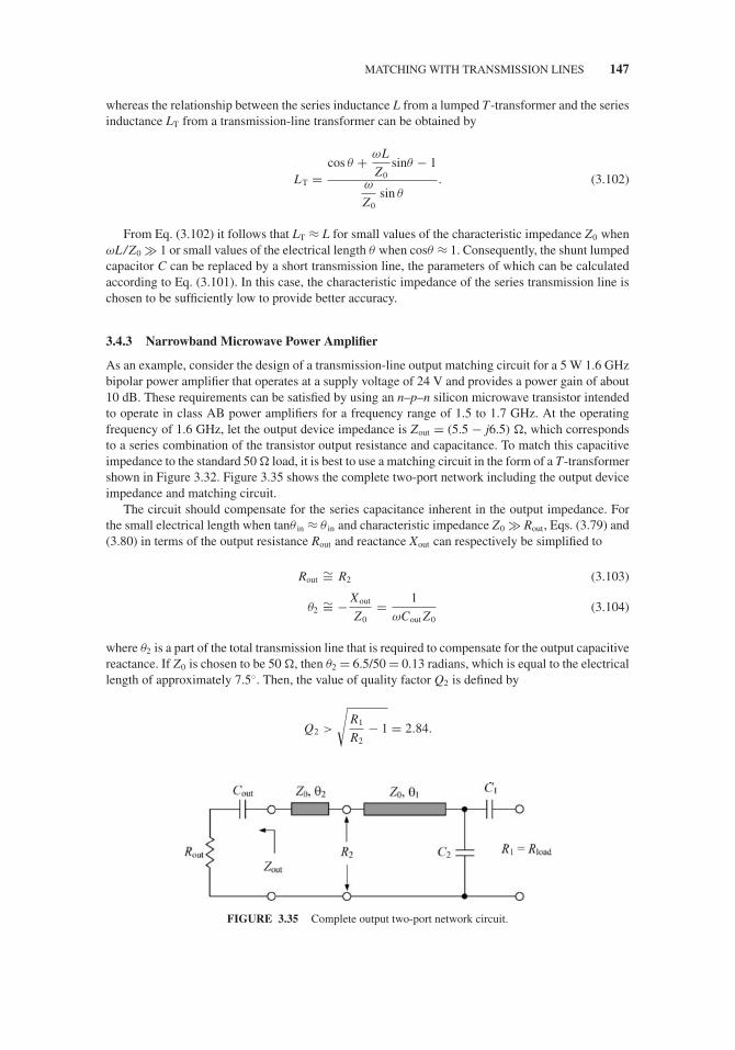
JWBS064-c03 JWBS064-Gerbennikov March 15, 2011 10:57 Printer Name: Yet to Come
MATCHING WITH TRANSMISSION LINES 147
whereas the relationship between the series inductance L from a lumped T-transformer and the seriesinductance LT from a transmission-line transformer can be obtained by
LT =cos θ + ωL
Z0sinθ − 1
ω
Z0sin θ
. (3.102)
From Eq. (3.102) it follows that LT ≈ L for small values of the characteristic impedance Z0 whenωL/Z0 � 1 or small values of the electrical length θ when cosθ ≈ 1. Consequently, the shunt lumpedcapacitor C can be replaced by a short transmission line, the parameters of which can be calculatedaccording to Eq. (3.101). In this case, the characteristic impedance of the series transmission line ischosen to be sufficiently low to provide better accuracy.
3.4.3 Narrowband Microwave Power Amplifier
As an example, consider the design of a transmission-line output matching circuit for a 5 W 1.6 GHzbipolar power amplifier that operates at a supply voltage of 24 V and provides a power gain of about10 dB. These requirements can be satisfied by using an n–p–n silicon microwave transistor intendedto operate in class AB power amplifiers for a frequency range of 1.5 to 1.7 GHz. At the operatingfrequency of 1.6 GHz, let the output device impedance is Zout = (5.5 − j6.5) �, which correspondsto a series combination of the transistor output resistance and capacitance. To match this capacitiveimpedance to the standard 50 � load, it is best to use a matching circuit in the form of a T-transformershown in Figure 3.32. Figure 3.35 shows the complete two-port network including the output deviceimpedance and matching circuit.
The circuit should compensate for the series capacitance inherent in the output impedance. Forthe small electrical length when tanθ in ≈ θ in and characteristic impedance Z0 � Rout, Eqs. (3.79) and(3.80) in terms of the output resistance Rout and reactance Xout can respectively be simplified to
Rout∼= R2 (3.103)
θ2∼= − Xout
Z0= 1
ωCout Z0(3.104)
where θ2 is a part of the total transmission line that is required to compensate for the output capacitivereactance. If Z0 is chosen to be 50 �, then θ2 = 6.5/50 = 0.13 radians, which is equal to the electricallength of approximately 7.5◦. Then, the value of quality factor Q2 is defined by
Q2 >
√R1
R2− 1 = 2.84.
FIGURE 3.35 Complete output two-port network circuit.

JWBS064-c03 JWBS064-Gerbennikov March 15, 2011 10:57 Printer Name: Yet to Come
148 IMPEDANCE MATCHING
Consequently, Q2 must be larger than 2.84. For example, a value of Q2 = 3 can be chosen to yielda 3-dB frequency bandwidth of 1.6 GHz/3 = 533 MHz. The values of the output matching circuitparameters are
θ1 = 1
2sin−1
[2Q2
/ (Z0
R2− R2
Z0
)]= 21◦
Q1 =√
R2
R1
1 + Q22
cos2 θ1 + (R2/Z0)2 sin2 θ1− 1 = 0.5
C2 = Q2 − Q1
ωR1
(1 + Q2
1
) = 4 pF
C1 = 1
ωQ1 R1= 4 pF.
The function of each element for visual effect can be traced on the Smith chart, as shown inFigure 3.36. The easiest and most convenient way to plot the traces of the matching circuit elementsis to first plot the traces of Q1 and Q2, then plot the trace of the series transmission line as far as theintersection point with Q2-circle, followed by the plot the trace of the shunt capacitance C2 as faras the intersection point with Q1-circle, and finally plot the trace of the series capacitance C1 to the
FIGURE 3.36 Smith chart with elements from Figure 3.35.
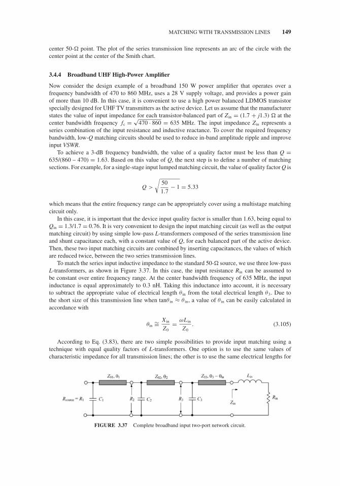
JWBS064-c03 JWBS064-Gerbennikov March 15, 2011 10:57 Printer Name: Yet to Come
MATCHING WITH TRANSMISSION LINES 149
center 50-� point. The plot of the series transmission line represents an arc of the circle with thecenter point at the center of the Smith chart.
3.4.4 Broadband UHF High-Power Amplifier
Now consider the design example of a broadband 150 W power amplifier that operates over afrequency bandwidth of 470 to 860 MHz, uses a 28 V supply voltage, and provides a power gainof more than 10 dB. In this case, it is convenient to use a high power balanced LDMOS transistorspecially designed for UHF TV transmitters as the active device. Let us assume that the manufacturerstates the value of input impedance for each transistor-balanced part of Zin = (1.7 + j1.3) � at thecenter bandwidth frequency fc = √
470 · 860 = 635 MHz. The input impedance Zin represents aseries combination of the input resistance and inductive reactance. To cover the required frequencybandwidth, low-Q matching circuits should be used to reduce in-band amplitude ripple and improveinput VSWR.
To achieve a 3-dB frequency bandwidth, the value of a quality factor must be less than Q =635/(860 – 470) = 1.63. Based on this value of Q, the next step is to define a number of matchingsections. For example, for a single-stage input lumped matching circuit, the value of quality factor Q is
Q >
√50
1.7− 1 = 5.33
which means that the entire frequency range can be appropriately cover using a multistage matchingcircuit only.
In this case, it is important that the device input quality factor is smaller than 1.63, being equal toQin = 1.3/1.7 = 0.76. It is very convenient to design the input matching circuit (as well as the outputmatching circuit) by using simple low-pass L-transformers composed of the series transmission lineand shunt capacitance each, with a constant value of Q, for each balanced part of the active device.Then, these two input matching circuits are combined by inserting capacitances, the values of whichare reduced twice, between the two series transmission lines.
To match the series input inductive impedance to the standard 50-� source, we use three low-passL-transformers, as shown in Figure 3.37. In this case, the input resistance Rin can be assumed tobe constant over entire frequency range. At the center bandwidth frequency of 635 MHz, the inputinductance is equal approximately to 0.3 nH. Taking this inductance into account, it is necessaryto subtract the appropriate value of electrical length θ in from the total electrical length θ3. Due tothe short size of this transmission line when tanθ in ≈ θ in, a value of θ in can be easily calculated inaccordance with
θin∼= X in
Z0= ωL in
Z0. (3.105)
According to Eq. (3.83), there are two simple possibilities to provide input matching using atechnique with equal quality factors of L-transformers. One option is to use the same values ofcharacteristic impedance for all transmission lines; the other is to use the same electrical lengths for
FIGURE 3.37 Complete broadband input two-port network circuit.

JWBS064-c03 JWBS064-Gerbennikov March 15, 2011 10:57 Printer Name: Yet to Come
150 IMPEDANCE MATCHING
all transmission lines. Consider the first approach, which also allows direct use of Smith chart, andchoose the value of the characteristic impedance Z0 = Z01 = Z02 = Z03 = 50 �. The ratio of inputand output resistances can be written as
R1
R2= R2
R3= R3
Rin(3.106)
which gives the values of R2 = 16.2 � and R3 = 5.25 � for Rsource = R1 = 50 � and Rin = 1.7 �.The values of electrical lengths are determined from the nomograph shown in Figure 3.29(a) as θ1 =30◦, θ 2 = 7.5◦, θ3 = 2.4◦.
To calculate the quality factor Q, equal for each L-transformer, from Eq. (3.83), it is enough toknow the electrical length θ1 of the first L-transformer. The remaining two electrical lengths can bedirectly obtained from Eq. (3.82). As a result, the quality factor of each L-transformer is equal to avalue of Q = 1.2. The values of the shunt capacitances using Eq. (3.81) are C1 = 6 pF, C2 = 19 pF,C3 = 57 pF.
For a constant Q, we can simplify significantly the design of the matching circuit by using theSmith chart. After calculating the value of Q, it is necessary to plot a constant Q-circle on the Smithchart. Figure 3.38 shows the input matching circuit design using the Smith chart with a constantQ-circle, where the curves for the series transmission lines represent the arcs of the circles with center
FIGURE 3.38 Smith chart with elements from Figure 3.37.

JWBS064-c03 JWBS064-Gerbennikov March 15, 2011 10:57 Printer Name: Yet to Come
MATCHING NETWORKS WITH MIXED LUMPED AND DISTRIBUTED ELEMENTS 151
point at the center of the Smith chart. The capacitive traces are moved along the circles with theincreasing susceptances and constant conductances.
Another approach assumes the same values of electrical lengths θ = θ1 = θ2 = θ3 and calculatesthe characteristic impedances of series transmission lines from Eq. (3.83) at equal ratios of the inputand output resistances according to Eq. (3.106). Such an approach is more convenient in practicaldesign, because, when using the transmission lines with standard characteristic impedance Z0 = 50 �,the electrical length of the transmission line adjacent to the active device input terminal is usuallytoo short. In this case, it makes sense to set the characteristic impedance of the first transmissionline to Z01 = 50 �. Then, the value of θ = 30◦ is determined directly from the nomograph shown inFigure 3.29(a). Further calculation of Q from Eq. (3.81) for fixed θ and Z0/R2 yields Q = 1.2. Thecharacteristic impedances of the remaining two transmission lines are then calculated easily fromEq. (3.81) or Eq. (3.83). Their values are Z02 = 15.7 � and Z03 = 5.1 � with the same values of theshunt capacitances.
3.5 MATCHING NETWORKS WITH MIXED LUMPED ANDDISTRIBUTED ELEMENTS
The matching circuits, which incorporate mixed lumped and transmission line elements, are widelyused both in hybrid and monolithic design technique. Such matching circuits are especially very con-venient when designing the push–pull power amplifiers where the shunt capacitances are simplyconnected between two series microstrip lines. In this case, the lumped matching circuits can beeasily transformed to the transmission-line matching circuits based on the single-frequency equiva-lence between lumped and distributed elements. First, consider a periodic LC-structure in the formof the low-pass ladder π-network which is used as a basis for the lumped matching prototype. Then,the lumped prototype should be split up into individual π -type sections with equal capacitances byconsecutive step-by-step process and replaced by their equivalent distributed network counterparts.Finally, the complete mixed matching structure is optimized to improve the overall performance byemploying standard nonlinear optimization routine on the element values. For the single frequencyequivalence between lumped and distributed elements, the low-pass lumped π -type ladder sectionwith equal shunt capacitances can be made equivalent to a symmetrically loaded transmission line atthe single frequency, as shown in Figure 3.39(a), where relationships between the circuit parametersare given by Eqs. (3.95) and (3.96).
To provide the design method using a single frequency equivalent technique, the following con-secutive design steps can be performed [15]:
� Designate the lumped π -type C1–L1–C2 section to be replaced.� From the chosen π-type C1–L1–C2 section, form the symmetrical with equal capacitances C
shown in Figure 3.39(b), the choice of which is arbitrary, however the values cannot exceed theminimum of (C1, C2).
� Calculate the parameters of the equivalent symmetrical CT–TL–CT section using the parametersof the lumped equivalent π -section by setting the transmission-line electrical length θ in accor-dance with Eqs. (3.95) and (3.96), assuming that the minimum of the capacitances C1 and C2
should be greater or equal than CT, so that CT can be readily embedded in the new CT–TL–CT
section.� Finally, replace the π -type C1–L1–C2 ladder section by the equivalent symmetrical CT–TL–CT
section and combine adjacent shunt capacitances, as shown in Figure 3.39(b), where the loadedparallel capacitances CA and CB are given as CA = C ′
1 + CT and CB = C ′2 + CT.
Figure 3.40(a) shows the electrical schematic of a broadband VHF high-power LDMOSFETamplifier. To provide an output power of about 15 W with a power gain of more than 10 dB in a

JWBS064-c03 JWBS064-Gerbennikov March 15, 2011 10:57 Printer Name: Yet to Come
152 IMPEDANCE MATCHING
FIGURE 3.39 Transforming design procedure for lumped and distributed matching circuits.
frequency range of 225 to 400 MHz, an LDMOSFET device with the gate geometry of 1.25 μm ×40 mm and a supply voltage of 28 V was chosen. In this case, the matching design technique isbased on the multisection low-pass networks with the series transmission line and shunt capacitances,two π -type sections for input matching circuit, and one π -type section for output matching circuit.The sections adjacent to the device input and output terminals incorporate the corresponding internalinput gate–source and output drain–source device capacitances. Since a difference between the deviceequivalent output resistance at the fundamental for several tens of watts of output power and the loadresistance of 50 � is not significant in this case, it is sufficient to be confined to only one section foroutput matching network.
Once a matching network structure is chosen, based on the requirements to the electrical perfor-mance and frequency bandwidth, the simplest and fastest way is to apply an optimization procedureusing CAD simulators to satisfy certain criteria over a wide frequency range. For such a broadbandpower amplifier, these criteria can be, for example, the minimum output power variation and inputreturn loss with the maximum power gain and efficiency. To minimize the overall dimensions of thepower amplifier board, the parallel microstrip line in the drain circuit can be treated as an element ofthe output matching circuit and its electrical length can be considered as a variable to be optimized aswell. Applying a nonlinear broadband CAD optimization technique implemented in any high-levelcircuit simulator and setting the ranges of electrical length of the transmission lines between 0 and90◦ and parallel capacitances from 0 to 100 pF, we obtain the parameters of the input and outputmatching circuits. The characteristic impedances of all transmission lines can be set to 50 � forsimplicity and convenience of the circuit implementation. However, to speed up this procedure, itis best to optimize circuit parameters separately for input and output matching circuits with thedevice equivalent input and output impedances: a series RC-circuit for the device input and a parallel

JWBS064-c03 JWBS064-Gerbennikov March 15, 2011 10:57 Printer Name: Yet to Come
REFERENCES 153
FIGURE 3.40 Circuit schematic and performance of broadband LDMOSFET power amplifier.
RC-circuit for the device output. It is sufficient to use a fast linear optimization process, which willtake only a few minutes to complete the matching circuit design. Then, the resulting optimized valuesare incorporated into the overall power amplifier circuit for each element and final optimization isperformed using a large-signal active device model. In this case, the optimization process is finalizedby choosing the nominal level of input power with optimizing elements in much narrower ranges oftheir values of about 10–20% from nominal for most critical elements. For practical convenience alltransmission lines might have the characteristic impedances of 50 �. Figure 3.40(b) illustrates thesimulated broadband power amplifier performance, where the output power is within the range of42.5 to 44.5 dBm with a power gain of 13.5 ± 1 dB in a frequency bandwidth of 225 to 400 MHz [7].
REFERENCES
1. S. Roberts, “Conjugate-Image Impedances,” Proc. IRE, vol. 34, pp. 198–204, Apr. 1946.
2. P. H. Smith, “Transmission Line Calculator,” Electronics, vol. 12, pp. 29–31, Jan. 1939.
3. P. H. Smith, Electronic Applications of the Smith Chart, New York: Noble Publishing, 2000.

JWBS064-c03 JWBS064-Gerbennikov March 15, 2011 10:57 Printer Name: Yet to Come
154 IMPEDANCE MATCHING
4. P. S. Carter, “Charts for Transmission-Line Measurements and Computations,” RCA Rev, vol. 3, pp. 355–368,Jan. 1939.
5. H. A. Wheeler, “Reflection Charts Relating to Impedance Matching,” IEEE Trans. Microwave Theory Tech,vol. MTT-32, pp. 1008–1021, Sept. 1984.
6. W. L. Everitt, “Output Networks for Radio-Frequency Power Amplifiers,” Proc. IRE, vol. 19, pp. 725–737,May. 1931.
7. A. Grebennikov, RF and Microwave Power Amplifier Design, New York: McGraw-Hill, 2004.
8. L. F. Gray and R. Graham, Radio Transmitters, New York: McGraw-Hill, 1961.
9. V. M. Bogachev and V. V. Nikiforov, Transistor Power Amplifiers (in Russian), Moskva: Energiya, 1978.
10. A. Tam, “Network Building Blocks Balance Power Amp Parameters,” Microwaves & RF, vol. 23, pp. 81–87,July. 1984.
11. D. M. Pozar, Microwave Engineering, New York: John Wiley & Sons, 2004.
12. Y. Ito, M. Mochizuki, M. Kohno, H. Masuno, T. Takagi, and Y. Mitsui, “A 5–10 GHz 15-W GaAs MESFETAmplifier with Flat Gain and Power Responses,” IEEE Microwave and Guided Wave Lett, vol. 5, pp. 454–456,Dec. 1995.
13. D. H. Steinbrecher, “An Interesting Impedance Matching Network,” IEEE Trans. Microwave Theory Tech,vol. MTT-15, p. 382, June. 1967.
14. A. V. Grebennikov, “Create Transmission-Line Matching Circuits for Power Amplifiers,” Microwaves & RF,vol. 39, pp. 113–122, Oct. 2000.
15. B. S. Yarman and A. Aksen, “An Integrated Design Tool to Construct Lossless Matching Networks withMixed Lumped and Distributed Elements,” IEEE Trans. Circuits and Systems – I: Fundamental Theory Appl,vol. CAS-I-39, pp. 713–723, Sep. 1992.

JWBS064-c04 JWBS064-Gerbennikov March 12, 2011 9:14 Printer Name: Yet to Come
4 Power Transformers, Combiners,and Couplers
It is critical, particularly at higher frequencies, that the special types of combiners and dividersare used to avoid insufficient power performance of the individual active devices. The methods ofconfiguration of the combiners or dividers differ depending on the operating frequency, frequencybandwidth, output power, and size requirements. Coaxial cable combiners with ferrite cores are usedto combine the output powers of power amplifiers intended for wideband applications. The deviceoutput impedance is usually sufficiently small for high power levels; so, to match this impedance witha standard 50-� load, coaxial-line transformers with specified impedance transformation are used.For narrow-band applications, the N-way Wilkinson combiners are widely used due to their simplepractical realization. For microwaves, the size of combiners should be very small and, therefore, thehybrid microstrip combiners (including different types of the microwaves hybrids and directionalcouplers) are commonly used to combine output powers of power amplifiers or oscillators. In thischapter, the basic properties of three-port and four-port networks are presented, as well as a varietyof different combiners, transformers, and directional couplers for application in RF and microwavetransmitters.
4.1 BASIC PROPERTIES
Basic three-port or four-port networks can be used to divide the output power of a single power sourceor combine the output powers of two or more power amplifiers or oscillators. Generally, the multiportnetwork required to combine the output powers of N identical power sources is based on these basicnetworks. In this case, it is very important to match the output impedances of all power amplifiersor oscillators with the load to provide the overall output power in N times larger than the outputpower of a single power amplifier or oscillator. Changes in the operation condition of one poweramplifier or oscillator should not affect the operation conditions of the remaining power amplifiersor oscillators. To satisfy this requirement, all input ports of the combiner should be decoupled ormutually independent. When one of the power sources is eliminated, the total output power mustdecrease by as small as possible, being within the limits of a maximum permissible level. In addition,the combiners can effectively be used for both narrowband and broadband transmitters.
4.1.1 Three-Port Networks
The simplest devices used for power division and combining are the three-port networks with oneinput and two outputs in the power divider, as shown in Figure 4.1(a), and two inputs and one outputin the power combiner, as shown in Figure. 4.1(b). The scattering S-matrix of an arbitrary three-port
RF and Microwave Transmitter Design, First Edition. Andrei Grebennikov.C© 2011 John Wiley & Sons, Inc. Published 2011 by John Wiley & Sons, Inc.
155

JWBS064-c04 JWBS064-Gerbennikov March 12, 2011 9:14 Printer Name: Yet to Come
156 POWER TRANSFORMERS, COMBINERS, AND COUPLERS
FIGURE 4.1 Schematic diagrams of (a) power divider and (b) power combiner.
network can be written by
[S] =⎡⎣ S11 S12 S13
S21 S22 S23
S31 S32 S33
⎤⎦ (4.1)
where Sij = Sji for the symmetric scattering S-matrix when all components are passive and reciprocal.In this case, if all ports are appropriately matched (when Sii = 0), the scattering S-matrix is reduced to
[S] =⎡⎣ 0 S12 S13
S12 0 S23
S13 S23 0
⎤⎦ . (4.2)
A lossless condition applied to a fully matched S-matrix given by Eq. (4.2) requires it to be aunitary matrix when
[S]∗ [S] = 1 (4.3)
where [S]∗ is the matrix, complex-conjugated to the original S-matrix [1,2].As a result of multiplying two matrices,
|S12|2 + |S13|2 = |S12|2 + |S23|2 = |S13|2 + |S23|2 = 1 (4.4)
S∗13S23 = S∗
23S12 = S∗12 S13 = 0. (4.5)
From Eq. (4.5) it follows that at least two of three available parameters S12, S13, and S23 should bezero, which is inconsistent with at least one condition given by Eq. (4.4). This means that a three-portnetwork cannot be lossless, reciprocal, and matched at all ports. However, if any one of these threeconditions is not fulfilled, a physically realizable device is possible for practical implementation. Alossless and reciprocal three-port network can be realized if only two of its ports are matched, or it islossy being reciprocal and fully matched at all three ports, as in the case of the resistive divider.
If a reciprocal three-port network represents the 3-dB power divider when, for a given input powerat the port 1, the output powers at the ports 2 and 3 are equal, then, according to Eq. (4.4),
|S12| = |S13| = 1√2. (4.6)
4.1.2 Four-Port Networks
The four-port networks are used for directional power coupling when, for a given input signal atthe port 1, the output signals are delivered to the ports 2 and 3, and no power is delivered to theport 4 (ideal case), as shown in Figure 4.2. The scattering S-matrix of a reciprocal four-port network

JWBS064-c04 JWBS064-Gerbennikov March 12, 2011 9:14 Printer Name: Yet to Come
BASIC PROPERTIES 157
FIGURE 4.2 Schematic diagram of directional coupler.
matched at all its ports is given by
[S] =
⎡⎢⎢⎣
0 S12 S13 S14
S12 0 S23 S24
S13 S23 0 S34
S14 S24 S34 0
⎤⎥⎥⎦ (4.7)
where Sij = Sji for the symmetric scattering S-matrix when all components are passive and reciprocal.In this case, the power supplied to the input port 1 is coupled to the coupled port 3 with couplingfactor |S13|2, whereas the remainder of the input power is delivered to the through port 2 with couplingfactor |S12|2.
For a lossless four-port network, the unitary condition of the fully matched S-matrix given by Eq.(4.7) results in
|S12|2 + |S13|2 = |S12|2 + |S24|2 = |S13|2 + |S34|2 = |S24|2 + |S34|2 = 1 (4.8)
which implies a full isolation between ports 2 and 3 and ports 1 and 4, respectively, when
S14 = S41 = S23 = S32 = 0 (4.9)
and that
|S13| = |S24| |S12| = |S34| . (4.10)
The scattering S-matrix of such a directional coupler, matched at all its ports with two decoupledtwo-port networks, reduces to
[S] =
⎡⎢⎢⎣
0 S12 S13 0S12 0 0 S24
S13 0 0 S34
0 S24 S34 0
⎤⎥⎥⎦ . (4.11)
The directional coupler can be classified according to the phase shift φ between two output ports2 and 3 as the in-phase coupler with φ = 0, quadrature coupler with φ = 90◦ or π /2, and out-of-phase coupler with φ = 180◦ or π . The following important quantities are used to characterize thedirectional coupler:
� The power-split ratio or power division ratio K2, which is calculated as the ratio of powers atthe output ports when all ports are nominally (reflectionless) terminated,
K 2 = P2
P3

JWBS064-c04 JWBS064-Gerbennikov March 12, 2011 9:14 Printer Name: Yet to Come
158 POWER TRANSFORMERS, COMBINERS, AND COUPLERS
� The insertion loss C12, which is calculated as the ratio of powers at the input port 1 relative theoutput port 2,
C12 = 10 log10
P1
P2= − 20 log10 |S12|
� The coupling C13, which is calculated as the ratio of powers at the input port 1 relative to theoutput port 3,
C13 = 10 log10
P1
P3= − 20 log10 |S13|
� The directivity C34, which is calculated as the ratio of powers at the output port 3 relative to theisolated port 4,
C34 = 10 log10
P3
P4= 20 log10
|S13||S14|
� The isolation C14 and C23, which are calculated as the ratios of powers at the input port 1 relativeto the isolated port 4 and between the two output ports (output port 2 is considered an inputport), respectively,
C14 = 10 log10
P1
P4= − 20 log10 |S14|
C23 = 10 log10
P2
P3= − 20 log10 |S23|
� The voltage standing wave ratio at each port or VSWRi, where i = 1, 2, 3, 4, calculated as
VSWRi = 1 + |Sii|1 − |Sii| .
In an ideal case, the directional coupler would have VSWRi = 1 at each ports, insertion lossC12 = 3 dB, coupling C13 = 3 dB, infinite isolation and directivity C14 = C23 = C34 = ∞.
4.2 TRANSMISSION-LINE TRANSFORMERS AND COMBINERS
The transmission-line transformers and combiners can provide very wide operating bandwidths andoperate up to frequencies of 3 GHz and higher [3,4]. They are widely used in matching networksfor antennas and power amplifiers in the HF and VHF bands, in mixer circuits, and their low lossesmake them especially useful in high-power circuits [5,6]. Typical structures for transmission-linetransformers consist of parallel wires, coaxial cables, or bifilar twisted wire pairs. In the latter case,the characteristic impedance can easily determined by the wire diameter, the insulation thickness,and, to some extent, the twisting pitch [7,8]. For coaxial cable transformers with correctly chosencharacteristic impedance, the theoretical high-frequency bandwidth limit is reached when the cablelength comes in order of a half wavelength, with the overall achievable bandwidth being about adecade. By introducing the low-loss high permeability ferrites alongside a good quality semirigidcoaxial or symmetrical strip cable, the low frequency limit can be significantly improved providingbandwidths of several or more decades.
The concept of a broadband impedance transformer consisted of a pair of interconnected trans-mission lines was first disclosed and described by Guanella [9,10]. Figure 4.3(a) shows a Guanella

JWBS064-c04 JWBS064-Gerbennikov March 12, 2011 9:14 Printer Name: Yet to Come
TRANSMISSION-LINE TRANSFORMERS AND COMBINERS 159
FIGURE 4.3 Schematic configurations of Guanella 1:1 and 4:1 transformers.
transformer system with transmission-line character achieved by an arrangement comprising onepair of cylindrical coils that are wound in the same sense and are spaced a certain distance apart byan intervening dielectric. In this case, one cylindrical coil is located inside the insulating cylinderand the other coil is located on the outside of this cylinder. For the currents flowing through bothwindings in opposite directions, the corresponding flux in the coil axis is negligibly small. However,for the currents flowing in the same direction through both coils, the latter may be assumed to beconnected in parallel, and a coil pair represents a considerable inductance for such currents and actslike a choke coil. With terminal 4 being grounded, such a 1:1 transformer provides matching of thebalanced source to unbalanced load and is called the balun (balanced-to-unbalanced transformers).In this case, if terminal 2 is grounded, it represents simply a delay line. In a particular case, whenterminals 2 and 3 are grounded, the transformer performs as a phase inverter.
A series-parallel connection of a plurality of coil pairs can produce a match between unequal sourceand load resistances. Figure 4.3(b) shows a 4:1 impedance (2:1 voltage) transmission-line transformerwhere the two pairs of cylindrical transmission line coils are connected in series at the input and inparallel at the output. For the characteristic impedance Z0 of each transmission line, this results inthe two times higher impedance 2Z0 at the input and two times lower impedance Z0/2 at the output.By grounding terminal 4, such a 4:1 impedance transformer provides impedance matching of thebalanced source to the unbalanced load. In this case, when terminal 2 is grounded, it performs as a 4:1unun (unbalanced-to-unbalanced transformer). With a series-parallel connection of n coil pairs withthe characteristic impedance Z0 each, the input impedance is equal to nZ0 and the output impedanceis equal to Z0/n. Since Guanella adds voltages that have equal delays through the transmission lines,such a technique results in the so called equal-delay transmission-line transformers.
The simplest transmission-line is a quarterwave transmission line whose characteristic impedanceis chosen to give the correct impedance transformation. However, this transformer provides a

JWBS064-c04 JWBS064-Gerbennikov March 12, 2011 9:14 Printer Name: Yet to Come
160 POWER TRANSFORMERS, COMBINERS, AND COUPLERS
narrowband performance valid only around frequencies for which the transmission line is odd mul-tiples of a quarter wavelength. If a ferrite sleeve is added to the transmission line, common-modecurrents flowing in both transmission line inner and outer conductors in phase and in the samedirection are suppressed and the load may be balanced and floating above ground [11,12]. If thecharacteristic impedance of the transmission line is equal to the terminating impedances, the trans-mission is inherently broadband. If not, there will be a dip in the response at the frequency at whichthe transmission line is a quarter-wavelength long.
A coaxial cable transformer, the physical configuration, and equivalent circuit representation ofwhich are shown in Figures 4.4(a) and 4.4(b), respectively, consists of the coaxial line arrangedinside the ferrite core or wound around the ferrite core. Due to its practical configuration, the coaxialcable transformer takes a position between the lumped and distributed systems. Therefore, at lowerfrequencies its equivalent circuit represents a conventional low-frequency transformer shown in Fig-ure 4.4(c), while at higher frequency it is a transmission line with the characteristic impedance Z0
shown in Figure 4.4(d). The advantage of such a transformer is that the parasitic interturn capaci-tance determines its characteristic impedance, whereas in the conventional wire-wound transformerwith discrete windings this parasitic capacitance negatively contributes to the transformer frequencyperformance.
When RS = RL = Z0, the transmission line can be considered a transformer with a 1:1 impedancetransformation. To avoid any resonant phenomena, especially for complex loads, which can contributeto the significant output power variations, as, a general rule, the length l of the transmission line iskept to no more than an eight of a wavelength λmin at the highest operating frequency,
l ≤ λmin
8(4.12)
where λmin is the minimum wavelength in the transmission line corresponding to the high operatingfrequency f max.
FIGURE 4.4 Schematic configurations of coaxial cable transformer.
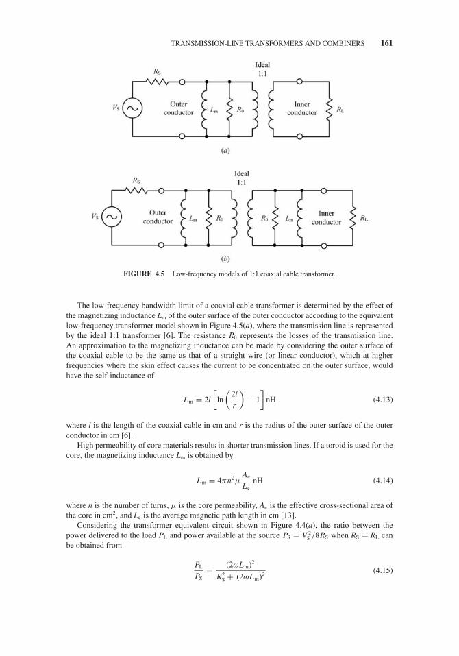
JWBS064-c04 JWBS064-Gerbennikov March 12, 2011 9:14 Printer Name: Yet to Come
TRANSMISSION-LINE TRANSFORMERS AND COMBINERS 161
FIGURE 4.5 Low-frequency models of 1:1 coaxial cable transformer.
The low-frequency bandwidth limit of a coaxial cable transformer is determined by the effect ofthe magnetizing inductance Lm of the outer surface of the outer conductor according to the equivalentlow-frequency transformer model shown in Figure 4.5(a), where the transmission line is representedby the ideal 1:1 transformer [6]. The resistance R0 represents the losses of the transmission line.An approximation to the magnetizing inductance can be made by considering the outer surface ofthe coaxial cable to be the same as that of a straight wire (or linear conductor), which at higherfrequencies where the skin effect causes the current to be concentrated on the outer surface, wouldhave the self-inductance of
Lm = 2l
[ln
(2l
r
)− 1
]nH (4.13)
where l is the length of the coaxial cable in cm and r is the radius of the outer surface of the outerconductor in cm [6].
High permeability of core materials results in shorter transmission lines. If a toroid is used for thecore, the magnetizing inductance Lm is obtained by
Lm = 4πn2μAe
LenH (4.14)
where n is the number of turns, μ is the core permeability, Ae is the effective cross-sectional area ofthe core in cm2, and Le is the average magnetic path length in cm [13].
Considering the transformer equivalent circuit shown in Figure 4.4(a), the ratio between thepower delivered to the load PL and power available at the source PS = V 2
S /8RS when RS = RL canbe obtained from
PL
PS= (2ωLm)2
R2S + (2ωLm)2 (4.15)

JWBS064-c04 JWBS064-Gerbennikov March 12, 2011 9:14 Printer Name: Yet to Come
162 POWER TRANSFORMERS, COMBINERS, AND COUPLERS
which gives the minimum operating frequency f min for a given magnetizing inductance Lm, takinginto account the maximum decrease of the output power by 3 dB, as
fmin ≥ RS
4π Lm. (4.16)
A similar low-frequency model for a coaxial cable transformer using twisted or parallel wires isshown in Figure 4.5(b) [6]. Here, the model is symmetrical as both conductors are exposed to anymagnetic material and therefore contribute identically to the losses and low-frequency performanceof the transformer.
An approach using a transmission line based on a single bifilar wound coil to realize a broadband1:4 impedance transformation was introduced by Ruthroff [14,15]. In this case, by using a core mate-rial of sufficiently high permeability, the number of turns can be significantly reduced. Figure 4.6(a)shows the circuit schematic of an unbalanced-to-unbalanced 1:4 transmission-line transformer whereterminal 4 is connected to the input terminal 1. As a result, for V = V1 = V2, the output voltage is twicethe input voltage, and the transformer has a 1:2 voltage step-up ratio. As the ratio of input voltageto input current is one-fourth the load voltage to load current, the transformer is fully matched formaximum power transfer when RL = 4RS, and the characteristic impedance of the transmission-lineZ0 is equal to the geometric mean of the source and load impedances:
Z0 =√
RS RL (4.17)
where RS is the source resistance and RL is the load resistance. Figure 4.6(b) shows an impedancetransformer acting as a phase inverter, where the load resistance is included between terminals 1 and4 to become a 1:4 balun. This technique is called the bootstrap effect, which does not have the samehigh-frequency response as Guanella equal-delay approach because it adds a delayed voltage to a
FIGURE 4.6 Schematic configurations of Ruthroff 1:4 impedance transformer.

JWBS064-c04 JWBS064-Gerbennikov March 12, 2011 9:14 Printer Name: Yet to Come
TRANSMISSION-LINE TRANSFORMERS AND COMBINERS 163
FIGURE 4.7 Schematic configurations of 4:1 coaxial cable transformer.
direct one [16]. The delay becomes excessive when the transmission line reach a significant fractionof a wavelength.
Figure 4.7(a) shows the physical implementation of the 4:1 impedance Ruthroff transformerusing a coaxial cable arranged inside the ferrite core. At lower frequencies, such a transformercan be considered an ordinary 2:1 voltage autotransformer. To improve the performance at higherfrequencies, it is necessary to add an additional phase-compensating line of the same length shown inFigure 4.7(b), resulting in a Guanella ferrite-based 4:1 impedance transformer. In this case, a ferritecore is necessary only for the upper line because the outer conductor of the lower line is grounded atboth ends, and no current is flowing through it. A current I driven into the inner conductor of the upperline produces a current I that flows in the outer conductor of the upper line, resulting in a current 2Iflowing into the load RL. Because the voltage 2V from the transformer input is divided in two equalparts between the coaxial line and the load, such a transformer provides impedance transformationfrom RS = 2Z0 into RL = Z0/2, where Z0 is the characteristic impedance of each coaxial line. Thebandwidth extension for the Ruthroff transformers can also be achieved by using transmission lineswith step-function and exponential changes in their characteristic impedances [17,18]. To adopt thistransmission-line transformer for microwave planar applications, the coaxial line can be replaced bya pair of stacked strip conductors or coupled microstrip lines [19,20].
Figure 4.8 shows similar arrangements for the 3:1 voltage coaxial cable transformers, whichproduce 9:1 impedance transformation. A current I driven into the inner conductor of the upper linein Figure 4.8(a) will cause a current I to flow in the outer conductor of the upper line. This currentthen produces a current I in the outer conductor of the lower line, resulting in a current 3I flowinginto the load RL. The lowest coaxial line can be removed, resulting in a 9:1 impedance coaxialcable transformer shown in Figure 4.8(b). The characteristic impedance of each transmission line isspecified by the voltage applied to the end of the line and the current flowing through the line and isequal to Z0.
By using the transmission-line baluns with different integer-transformation ratios in certain con-nection, it is possible to obtain the fractional-ratio baluns and ununs [4,21,22]. Figure 4.9 shows atransformer configuration for obtaining an impedance ratio of 2.25:1, which consists of a 1:1 Guanella

JWBS064-c04 JWBS064-Gerbennikov March 12, 2011 9:14 Printer Name: Yet to Come
164 POWER TRANSFORMERS, COMBINERS, AND COUPLERS
FIGURE 4.8 Schematic configurations of 9:1 coaxial cable transformer.
FIGURE 4.9 Schematic configuration of equal-delay 2.25:1 unun.

JWBS064-c04 JWBS064-Gerbennikov March 12, 2011 9:14 Printer Name: Yet to Come
TRANSMISSION-LINE TRANSFORMERS AND COMBINERS 165
balun on the top combined with a 1:4 Guanella balun where voltages on the left-hand side are inseries and on the right-hand side are in parallel [21]. In this case, the left-hand side has the higherimpedance. In a matched condition, this transformer should have a high frequency response similarto a single transmission line. By grounding the corresponding terminals (shown by dashed line), itbecomes a broadband unun. Different ratios can be obtained with other configurations. For example,using a 1:9 Guanella balun below the 1:1 unit results in a 1.78:1 impedance ratio, whereas, with a1:16 balun, the impedance ratio becomes 1.56:1.
On the other hand, the overall 1:1.5 voltage transformer configuration can be achieved by usingthe cascade connection of a 1:3 voltage transformer to increase the impedance by 9 times, and a2:1 voltage transformer to decrease the impedance by 4 times, which block schematic is shown inFigure 4.10(a) [22]. The practical configuration using coaxial cables and ferrite cores is shown inFigure 4.10(b). Here, the currents I/3 in the inner conductors of two lower lines cause an overallcurrent 2I/3 in the outer conductor of the upper line, resulting in a current 2I/3 flowing into the loadRL. A load voltage 3V/2 is out of phase with a longitudinal voltage V/2 along the upper line, resultingin a voltage V at the transformer input. The lowest line also can be eliminated with direct connectionof the points at both ends of its inner conductor, as in the case of the 2:1 and 3:1 Ruthroff voltage
FIGURE 4.10 Schematic configurations of fractional 1:2.25 impedance transformer.

JWBS064-c04 JWBS064-Gerbennikov March 12, 2011 9:14 Printer Name: Yet to Come
166 POWER TRANSFORMERS, COMBINERS, AND COUPLERS
FIGURE 4.11 Coaxial cable combiner.
transformers shown in Figures 4.7(a) and 4.8(b), respectively. If the source impedance is 50 �, thenthe characteristic impedance of all three transmission lines should be 75 �. In this case, the matchedcondition corresponds to a load impedance of 112.5 �.
By using the coaxial cable transformers, the output powers from two or more power sources canbe combined. Figure 4.11 shows an example of such a transformer, combining two in-phase signalswhen both signal are delivered to the load RL and no signal will be dissipated in the ballast resistorR0 if their amplitudes are equal [14]. The main advantage of this transformer is the zero longitudinalvoltage along the line for equal input powers; as a result, no losses occur in the ferrite core. When oneinput signal source (for example, power amplifier) defaults or disconnects, the longitudinal voltagebecomes equal to half a voltage of another input source. For this transformer, it is possible to combinetwo out-of-phase signals when the ballast resistor is considered the load, and the load resistor in turnis considered the ballast resistor.
The schematic of another hybrid coaxial cable transformer using as a combiner is shown inFigure 4.12. The advantage of this combiner is that both the load RL and the ballast resistor R0 aregrounded. These transformer-based combiners can also be used for the power division when theoutput power from single source is divided and delivered into two independent loads. In this case,the original load and the two signal sources should be switched. These hybrid transformer-basedcombiners can also be used for the power division when the output power from single source is
FIGURE 4.12 Two-cable hybrid combiner.
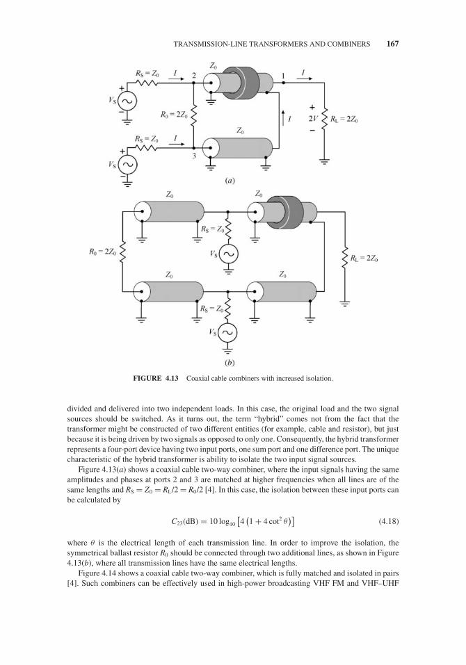
JWBS064-c04 JWBS064-Gerbennikov March 12, 2011 9:14 Printer Name: Yet to Come
TRANSMISSION-LINE TRANSFORMERS AND COMBINERS 167
FIGURE 4.13 Coaxial cable combiners with increased isolation.
divided and delivered into two independent loads. In this case, the original load and the two signalsources should be switched. As it turns out, the term “hybrid” comes not from the fact that thetransformer might be constructed of two different entities (for example, cable and resistor), but justbecause it is being driven by two signals as opposed to only one. Consequently, the hybrid transformerrepresents a four-port device having two input ports, one sum port and one difference port. The uniquecharacteristic of the hybrid transformer is ability to isolate the two input signal sources.
Figure 4.13(a) shows a coaxial cable two-way combiner, where the input signals having the sameamplitudes and phases at ports 2 and 3 are matched at higher frequencies when all lines are of thesame lengths and RS = Z0 = RL/2 = R0/2 [4]. In this case, the isolation between these input ports canbe calculated by
C23(dB) = 10 log10
[4
(1 + 4 cot2 θ
)](4.18)
where θ is the electrical length of each transmission line. In order to improve the isolation, thesymmetrical ballast resistor R0 should be connected through two additional lines, as shown in Figure4.13(b), where all transmission lines have the same electrical lengths.
Figure 4.14 shows a coaxial cable two-way combiner, which is fully matched and isolated in pairs[4]. Such combiners can be effectively used in high-power broadcasting VHF FM and VHF–UHF
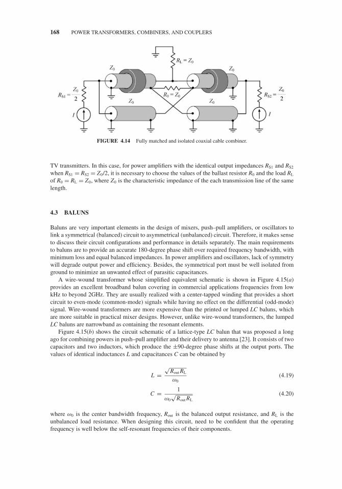
JWBS064-c04 JWBS064-Gerbennikov March 12, 2011 9:14 Printer Name: Yet to Come
168 POWER TRANSFORMERS, COMBINERS, AND COUPLERS
FIGURE 4.14 Fully matched and isolated coaxial cable combiner.
TV transmitters. In this case, for power amplifiers with the identical output impedances RS1 and RS2
when RS1 = RS2 = Z0/2, it is necessary to choose the values of the ballast resistor R0 and the load RL
of R0 = RL = Z0, where Z0 is the characteristic impedance of the each transmission line of the samelength.
4.3 BALUNS
Baluns are very important elements in the design of mixers, push–pull amplifiers, or oscillators tolink a symmetrical (balanced) circuit to asymmetrical (unbalanced) circuit. Therefore, it makes senseto discuss their circuit configurations and performance in details separately. The main requirementsto baluns are to provide an accurate 180-degree phase shift over required frequency bandwidth, withminimum loss and equal balanced impedances. In power amplifiers and oscillators, lack of symmetrywill degrade output power and efficiency. Besides, the symmetrical port must be well isolated fromground to minimize an unwanted effect of parasitic capacitances.
A wire-wound transformer whose simplified equivalent schematic is shown in Figure 4.15(a)provides an excellent broadband balun covering in commercial applications frequencies from lowkHz to beyond 2GHz. They are usually realized with a center-tapped winding that provides a shortcircuit to even-mode (common-mode) signals while having no effect on the differential (odd-mode)signal. Wire-wound transformers are more expensive than the printed or lumped LC baluns, whichare more suitable in practical mixer designs. However, unlike wire-wound transformers, the lumpedLC baluns are narrowband as containing the resonant elements.
Figure 4.15(b) shows the circuit schematic of a lattice-type LC balun that was proposed a longago for combining powers in push–pull amplifier and their delivery to antenna [23]. It consists of twocapacitors and two inductors, which produce the ±90-degree phase shifts at the output ports. Thevalues of identical inductances L and capacitances C can be obtained by
L =√
Rout RL
ω0(4.19)
C = 1
ω0√
Rout RL(4.20)
where ω0 is the center bandwidth frequency, Rout is the balanced output resistance, and RL is theunbalanced load resistance. When designing this circuit, need to be confident that the operatingfrequency is well below the self-resonant frequencies of their components.

JWBS064-c04 JWBS064-Gerbennikov March 12, 2011 9:14 Printer Name: Yet to Come
BALUNS 169
FIGURE 4.15 Different circuit configurations of 1:1 balun.
In monolithic microwave applications where the lumped inductances are usually replaced bytransmission lines, the designs with microstrip coupled lines, Lange couplers, or multilayer cou-pled structures are very popular. However, the electrical length of the transmission lines at centerbandwidth frequency is normally set to a quarter-wavelength, which is too large for applications inwireless communication systems. Therefore, it is very attractive to use the lumped-distributed balunstructures, which can significantly reduce the balun size and, at the same time, can satisfy the requiredelectrical characteristics. Figure 4.15(c) shows such a compact balun with lumped-distributed struc-ture consisting of the two coupled planar microstrip lines and two parallel capacitors, where the inputtransmission line is grounded at midpoint and the output transmission line is grounded at its one port[24]. Without these capacitors, it is necessary a very small spacing between quarterwave microstriplines to achieve a 3-dB coupling between them. However, by optimizing the balun elements aroundthe center bandwidth of 900 MHz, the planar structure of approximately one-sixteenth the size of theconventional quarter-wavelength structure was realized, with spacing S = 8 mils (note that 1 mil =0.0254 mm) using an FR4 board with substrate thickness of 300 mils.
Figure 4.16 shows the circuit arrangement with two coaxial-line transformers combined to pro-vide a push–pull operation of the power amplifier by creating a balanced-to-unbalanced impedance

JWBS064-c04 JWBS064-Gerbennikov March 12, 2011 9:14 Printer Name: Yet to Come
170 POWER TRANSFORMERS, COMBINERS, AND COUPLERS
FIGURE 4.16 Circuit arrangement with two cable transformers for push–pull operation.
transformation with higher spectral purity. Ideally, the out-of-phase RF signals from both activedevices will have pure half-sinusoidal waveforms, which contain (according to the Fourier seriesexpansion) only fundamental and even harmonic components. This implies a 180-degree shift be-tween fundamental components from both active devices and in-phase condition for remaining evenharmonic components. In this case, the transformer T1 representing a phase inverter is operated asa filter for even harmonics because currents flow through its inner and outer conductors in oppo-site directions. For each fundamental flowing through its inner and outer conductors in the samedirections, it works as an RF choke, the impedance of which depends on the core permeability.Consequently, since the transformer T2 represents a 1:1 balun, in order to provide maximum powerdelivery to the load RL, the output equivalent resistance of each active device should be two timessmaller.
For a simple 1:1 transmission-line balun realized with a twisted wire pair or coaxial cable,the balanced end is isolated from ground only at the center bandwidth frequency. To compensatefor the short-circuited line reactance over certain frequency bandwidth around center frequency, aseries open-circuited transmission line was introduced by Marchand, resulting in a compensatedbalun, the simplified schematic of which is shown in Figure 4.17(a) [25]. In this case, at centerbandwidth frequency when the electrical length of the compensated line is a quarter-wavelength,the load resistance RL is seen unchanged. When this structure is realized with coaxial cables, toeliminate unwanted current existing in the outer conductor and corresponding radiation, it is neces-sary to additionally provide the certain coupling between the coaxial cables forming a transmissionline with two outer conductors, as shown in Figure 4.17(b) [26]. Generally, the shunting reac-tance of this compensating line can reduce the overall balun reactance about center frequency orreverse it sign depending on the balanced load resistance, characteristic impedance of the com-pensating line, and coupling (characteristic impedance) between the outer conductors of two lines.Hence, a compensating line can create a complementary reactance to a balanced load and providean improved match over broader frequency range. At microwaves, wire-wound transformers areusually replaced by a pair of the coupled transmission lines shown in Figure 4.17(c), thus result-ing in a compact planar structure. It should be noted that generally the characteristic impedancesof the coaxial or coupled transmission lines can be different to optimize the frequency–bandwidthresponse.
Multilayer configurations make Marchand balun even more compact and can provide wide band-widths due to the tight coupling between coupled-line sections. Modeling and synthesis result of atwo-layer monolithic Marchand balun configuration with two-coupled lines, the basic structure ofwhich is shown in Figure 4.18(a), is discussed in [27]. In this configuration, the unbalanced terminalis connected to the microstrip line located at the upper metallization level, whereas the balanced loadis connected to the microstrip lines located at the lower metallization level. The transmission-linesections in different layers are not isolated from each other. It should be noted that, for a given set

JWBS064-c04 JWBS064-Gerbennikov March 12, 2011 9:14 Printer Name: Yet to Come
BALUNS 171
FIGURE 4.17 Schematic configurations of Marchand balun.
of the output balanced and load unbalanced resistances Rout and RL, the characteristic impedances ofthe outer and inner microstrip lines Z01 and Z02 are not unique, and they can be calculated from
C = 1
2
√Z02
Z01(4.21)
Z02 = 4Z01 − Rout RL
Z01(4.22)
FIGURE 4.18 Schematic configurations of coupled-line Marchand balun.

JWBS064-c04 JWBS064-Gerbennikov March 12, 2011 9:14 Printer Name: Yet to Come
172 POWER TRANSFORMERS, COMBINERS, AND COUPLERS
where C is the coupling factor [28]. However, a different choice of Z01 and Z02 leads to a differentfrequency bandwidth. For example, for Rout = 50 � and RL = 100 �, it was found that using thesymmetrical directional coupler with Z01 = Z02 = 40.825 � results in a frequency bandwidth of 48.4%with |S11| < −10 dB and amplitude imbalance within 0.91 dB, whereas the frequency bandwidth of20.9% with amplitude imbalance of less than 1.68 dB will be realized for the nonsymmetrical casewhen Z01 = 38 � and Z02 = 20.42 �.
The design of a three-line microstrip balun, the basic schematic of which is shown in Figure4.18(b), is based on the equivalence between a six-port section of three coupled lines and a six-portcombination of two couplers [28]. The results of circuit analysis and optimization show that thespacings between adjacent microstrip lines are so narrow that it is difficult to fabricate a single-layerthree-line balun. For a two-layer three-line balun with two coupled outer lines on the top metallizationlevel, the spacing between these lines is significantly wider than in a single-layer case. However, widerfrequency range can be achieved using a two-layer three-line balun with two coupled outer lines atthe lower metallization level. For example, the measurements results for this balun show that, beingfabricated on the Duroid RT5880 substrate, it can provide frequency range of 2.13 to 3.78 GHz withamplitude imbalance within 2.12 dB and phase error of less than 4.51◦.
To improve the performance of multilayer Marchand balun based on microstrip-line technologyover frequency range, a short transmission line can be included connecting the two couplers, as shownin Figure 4.19(a) [29]. This additional short microstrip line effectively compensates for the amplitudeand phase imbalance caused by the difference in even- and odd-mode phase velocities. Besides, tominimize the balun size, the transmission lines of the coupler can be implemented in meander formthat can give up to 90% reduction in size. As a result, the phase and amplitude differences of thecompensated balun were within 180 ± 10◦ and 0 ± 1 dB over the frequency range of 5 to 30 GHz. Thecompensation can also be implemented by employing capacitors at each end of the coupled lines, as
FIGURE 4.19 Schematic configurations of planar Marchand balun.

JWBS064-c04 JWBS064-Gerbennikov March 12, 2011 9:14 Printer Name: Yet to Come
BALUNS 173
shown in Figure 4.19(b) [30]. In this case, the capacitor will not affect the even-mode but effectivelyincreases odd-mode phase length, thus resulting in a minimum amplitude and phase imbalance overcertain frequency bandwidth. An exact synthesis technique that is widely used in filter design canbe applied to develop and analyze new classes of miniaturized mixed lumped-distributed planarMarchand baluns using microstrip lines and lumped capacitors [31]. As an alternative, by employingtwo additional inductors at each balanced output and optimum coupling between the grounded stripsshown in Figure 4.19(c), a frequency bandwidth of 53% centered around 6.2 GHz with size reductionof 64% over a conventional coupled-line Marchand balun is achieved [32]. A combined compensationtechnique uses a series capacitor at the unbalanced input port to improve the matching bandwidth andinductors at the ground connections to minimize amplitude and phase imbalance [33].
Figure 4.20(a) shows the broadband parallel-connected coaxial cable balun as an alternative to aseries-connected Marchand balun [34]. It consists of an unbalanced input coaxial cable connected toa dummy cable that maintains symmetry. On the opposite side of the balun, the output inner and outerconductors are connected in parallel to each other, while the input inner and outer conductors of coaxialcables are cross-connected. The right-hand portion of the balun forms a high impedance balancedload. By means of the cross connection, the high impedance is reduced to a low impedance showinga 4:1 impedance transformation ratio, for example, from a balanced load of 200 � to a single-ended50 �. The frequency bandwidth of the balun is limited by the shunting effect at lower frequencies andnear half-wave resonance. These parallel-connected baluns can provide approximately four times theoperating frequency bandwidth of their series-connected counterparts as covering in the experimentthe frequency range from 160 to 4000 MHz, a 25:1 bandwidth [35]. The parallel-connected balunmay be realized in a variety of configurations, some of which are shown in Figures 4.20(b) andFigure 4.20(c) [34,35].
FIGURE 4.20 Broadband parallel-connected cable 1:4 baluns.

JWBS064-c04 JWBS064-Gerbennikov March 12, 2011 9:14 Printer Name: Yet to Come
174 POWER TRANSFORMERS, COMBINERS, AND COUPLERS
4.4 WILKINSON POWER DIVIDERS/COMBINERS
The in-phase power combiners and dividers are the important components of the RF and microwavetransmitters when it is necessary to deliver a high level of the output power to antenna, especially inphased-array systems. In this case, it is required to provide a high degree of isolation between outputports over some frequency range for identical in-phase signals with equal amplitudes. Figure 4.21(a)shows a planar structure of the basic parallel beam N-way divider/combiner, which provides a com-bination of powers from the N signal sources. Here, the input impedance of the N transmission lines(connected in parallel) with the characteristic impedance of Z0 each is equal to Z0/N. Consequently,an additional quarterwave transmission line with the characteristic impedance Z0/
√N is required
to convert the input impedance Z0/N to standard impedance Z0. However, this N-way combinercannot provide sufficient isolation between input ports. The impedances are matched only when allinput signals have the same amplitudes and phases at any combiner input. The effect of any inputon the remaining ones becomes smaller for combiners with greater number of inputs. For example,if the input signal is delivered into the input port 2 and all other (N − 1) input ports and outputport 1 are matched, then the power dissipated at any load connected to the matched input ports willbe decreased by
(1 − 1/N 2
)/ (2N − 1) times and isolation between any two input ports expressed
through S-parameters is obtained by
Sij = − 10 log10
(1
N 2
N 2 − 1
2N − 1
)(4.23)
where N is a number of the input ports and i, j = 2, . . . , N + 1.
FIGURE 4.21 Circuit topologies of N-way in-phase combiners/dividers.

JWBS064-c04 JWBS064-Gerbennikov March 12, 2011 9:14 Printer Name: Yet to Come
WILKINSON POWER DIVIDERS/COMBINERS 175
In most cases, better isolation is required than obtained by Eq. (4.23). The simplest way toprovide full isolation between the input and output ports of the combiner is to connect the ferriteisolators (circulators) at the input ports 2, . . . , N + 1. In this case, the lengths of the transmission linesconnected between each ferrite isolator and a quarterwave transmission line should be equal. Althoughthe ferrite isolators increase the overall weight and dimensions of the combiner and contribute toadditional insertion losses, nevertheless they provide a very simple combiner realization and protectthe connected power amplifiers from the load variations. By using such a 12-way parallel beamcombiner, the continuous output power of 1 kW for the L-band transmitter was obtained at theoperating frequency of 1.25 GHz [36].
When one or more power amplifiers are destroyed for some reasons, the overall output power Pout
and efficiency ηc of the combiner can be calculated, respectively, by
Pout = (N − M)2
NP1 (4.24)
ηc = Pout
Pin= 1 − M
N(4.25)
where Pin = (N − M)P1, P1 is the output power from a single power amplifier, N is the number ofthe input ports, and M is the number of the destroyed power amplifiers. Part of the output power ofthe remaining power amplifiers will be dissipated within the ferrite isolators (in ballast resistors ofcirculators). For each ferrite isolator connected to the operating power amplifier, the dissipated powerPdo can be defined as
Pdo =(
M
N
)2
P1 (4.26)
whereas for each isolator connected to the destroyed power amplifier, the dissipated power Pdd canbe calculated from
Pdd =(
N − M
N
)2
P1. (4.27)
In this case, by adding the ballast resistors R0 = Z0, the right-hand side terminals of which arecombined together in a common junction as shown in Figure 4.21(b), matching of all ports, low lossand high isolation between input and output ports can be provided. Such kind of a simple N-wayhybrid power divider is known as a Wilkinson power divider [37]. However, it should be mentionedthat, historically, this divider/combiner was reported a little bit earlier [38–40]. Originally, a Wilkinsonpower divider was composed of a coaxial line in which the hollow inner conductor has been splitinto N splines of length λ/4, with shorting plate connecting the splines at the input end and resistorsconnected in a radial manner between each spline at the output end and a common junction. Thefrequency response of the voltage standing wave ratio at the divider input port, VSWRin, dependingon the number of the output ports N, is shown in Figure 4.22 [41].
The hybrid planar microstrip realization of the simplest two-way Wilkinson divider is shown inFigure 4.23(a). It consists of the two quarterwave microstrip lines connected in parallel at the inputend and the planar ballast resistor connected between the output ports of the microstrip lines. Despiteits small dimensions and simple construction, such a divider provides a sufficient isolation betweenoutput ports over sufficiently wide frequency bandwidth when equal power division is provided dueto a symmetrical configuration with R0 = 2Z0 and Z1 = Z0
√2. However, in practice, it is necessary
to take into account the distributed RC structure of the ballast resistor when its size is sufficientlylarge, as well as manufacturing tolerances and discontinuities. As a result, in a frequency bandwidth

JWBS064-c04 JWBS064-Gerbennikov March 12, 2011 9:14 Printer Name: Yet to Come
176 POWER TRANSFORMERS, COMBINERS, AND COUPLERS
FIGURE 4.22 Frequency performance of N-way Wilkinson divider.
of 30% with VSWRin ≤ 1.2 at input port 1 and VSWRout ≤ 1.03 at output ports 2 and 3, the isolationbetween the divider outputs can be better than 20 dB [42].
In millimeter-wave integrated circuits, in order to increase a self-resonant frequency of the ballastchip resistor, the overall MMIC dimensions must be very small. This means that the two branches ofthe power divider are very close to each other, which leads to strong mutual coupling between theoutput microstrip lines and, as a result, upsets the desired power-split ratio. A possible solution is touse the branches with the electrical lengths of 3λ/4 instead of λ/4 and to include the two additionalbranches into a semicircle, as shown in Figure 4.23(b) [43]. These additional branches should be ofthe half-wave electrical lengths with the characteristic impedances equal to Z0. In this case, isolationcan be better than 17 dB between all ports with the insertion loss of about 1.3 dB at the operatingfrequency of 30.4 GHz.
FIGURE 4.23 Microstrip realization of two-way Wilkinson dividers.

JWBS064-c04 JWBS064-Gerbennikov March 12, 2011 9:14 Printer Name: Yet to Come
WILKINSON POWER DIVIDERS/COMBINERS 177
However, the ballast resistors of the conventional N-way Wilkinson combiners/dividers cannot bedesigned to be a planar structure when their physical lengths and connecting wires are minimal toprovide sufficient isolation among output ports over the required frequency range. For example, theradial and fork N-way hybrids have reasonably wide frequency bandwidth, of about 20% and higher,but their match and isolation are not perfect even at the center bandwidth frequency [44]. Besides, dueto small size of the ballast resistor compared to the wavelength and its balanced structure, it is difficultto heat-sink it in the case of high power combining. In order to provide higher output power capability,it is possible to modify the N-way Wilkinson combiner/divider by replacing the ballast resistive starwith a combination of quarterwave transmission lines and shunt-connected resistors [45]. In thiscase, each ballast resistor is connected to corresponding output port through a transmission line. Atthe same time, all ballast resistors are connected to a common floating starpoint by the transmissionlines. Such a modification has an advantage of external isolation loads (high-power ballast resistors)and easy monitoring capability for imbalances at the output ports. For a two-way planar powercombiner/divider, the circuit topology of which is shown in Figure 4.24, the balanced 100-� ballastresistor is replaced by a transmission-line network and two 50-� resistors are connected to groundacting as the out-of-phase load, where Z1 = Z0
√2, Z2 = Z0/
√2, and Z0 = R0 = 50 � [46].
The cascade connection of two-way Wilkinson power combiners/dividers can provide a mul-tiway power division or power combining. The simplest practical realization is the binary powerdivider/combiner, composed of the n stages when each consecutive stage of which contains an in-creasing by 2N number of two-way dividers/combiners. For a single destroyed power amplifier, thepower dissipated in the ballast resistors is equal to
Pdb =(
1 − 1
N
)2
P1. (4.28)
The output power of P1/2 is dissipated in the ballast resistor adjacent to the destroyed poweramplifier; the output power of P1/4 is dissipated in the ballast resistor of the next stage, and so on.It should be mentioned that the power divider with a number of outputs multiple to 4N representsthe convenient case when the characteristic impedance of the transmission line are of the sameimpedance. Figure 4.25 shows the four-way microstrip Wilkinson divider/combiner fabricated onalumina substrate with six 50-� quarterwave microstrip lines and two 100 � and one 50-� thin-filmresistors. This microstrip Wilkinson power divider/combiner can provide the insertion loss of less
FIGURE 4.24 Gysel high-power in-phase planar combiner/divider.
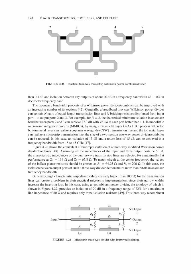
JWBS064-c04 JWBS064-Gerbennikov March 12, 2011 9:14 Printer Name: Yet to Come
178 POWER TRANSFORMERS, COMBINERS, AND COUPLERS
FIGURE 4.25 Practical four-way microstrip wilkinson power combiner/divider.
than 0.3 dB and isolation between any outputs of about 20 dB in a frequency bandwidth of ±10% indecimeter frequency band.
The frequency bandwidth property of a Wilkinson power divider/combiner can be improved withan increasing number of its sections [42]. Generally, a broadband two-way Wilkinson power dividercan contain N pairs of equal-length transmission lines and N bridging resistors distributed from inputport 1 to output ports 2 and 3. For example, for N = 2, the theoretical minimum isolation in an octaveband between ports 2 and 3 can achieve 27.3 dB with VSWR at each port better than 1.1. In monolithicmicrowave integrated circuits (MMICs), by using a two-metal layer GaAs HBT process when thebottom metal layer can realize a coplanar waveguide (CPW) transmission line and the top metal layercan realize a microstrip transmission line, the size of a two-section two-way power divider/combinercan be reduced. In this case, an isolation of 15 dB and a return loss of 15 dB can be achieved in afrequency bandwidth from 15 to 45 GHz [47].
Figure 4.26 shows the equivalent circuit representation of a three-way modified Wilkinson powerdivider/combiner [48]. Assuming all the impedances of the input and three output ports be 50 �,the characteristic impedances of the quarterwave transmission lines are selected for a maximally flatperformance as Z1 = 114 � and Z2 = 65.8 �. To match circuit at the center frequency, the valuesof the ballast planar resistors should be chosen as R1 = 64.95 � and R2 = 200 �. In this case, theisolation between output ports of such a three-way divider demonstrates more than 20 dB in an octavefrequency bandwidth.
Generally, high characteristic impedance values (usually higher than 100 �) for the transmissionlines can create a problem in their practical microstrip implementation, since their narrow widthsincrease the insertion loss. In this case, using a recombinant power divider, the topology of which isshown in Figure 4.27, provides an isolation of 20 dB in a frequency range of 72% for a maximumline impedance of 80 � and requires only three isolation resistors [49]. This three-way recombinant
FIGURE 4.26 Microstrip three-way divider with improved isolation.

JWBS064-c04 JWBS064-Gerbennikov March 12, 2011 9:14 Printer Name: Yet to Come
WILKINSON POWER DIVIDERS/COMBINERS 179
FIGURE 4.27 Microstrip three-way recombinant divider with improved isolation.
divider is characterized by the insertion loss of about 1 dB and return loss of more than 12 dB ina frequency range of 6 to 14 GHz, fabricated in 25-mil thick 99.6% alumina substrate. The designvalues for the quarterwave transmission lines were Z1 = 36 �, Z2 = Z3 = 40 �, Z4 = 80 �, and Z5 =Z6 = 40 � with the ballast resistors R1 = 50 � and R2 = 100 �, respectively. Over a 2:1 bandwidth,the center-to-side and side-to-side isolations exceed 20 dB.
The divider broadband properties can also be improved by using the more complicated phase-shifting circuit instead of a simple microstrip line. The phase shift between two output ports 2 and3 will be close to 90◦ in an octave frequency range if a Schiffman element based on the coupledmicrostrip lines is connected to one output port [50]. At the same time, an additional microstrip linewith the electrical length of 270◦ at the center bandwidth frequency should be connected to the secondoutput port.
In the design of a microwave distributed network, a power divider providing two equal-phaseoutputs with unequal power division is often required. The split-tee power divider is a simple compactand broadband device. It provides two isolated equal-phase unequal-amplitude outputs with a goodmatch at each port. Since a split-tee power divider is similar to the N-way equiphase equiamplitudepower divider, it can be developed from this N-way divider as follows: connect M of the output portstogether to form one port and the remaining (N − M) output ports together to form the other port,connect quarterwave transformers to the resulting output ports to adjust their impedance level, and apower divider with two equiphase outputs and power ratio of N/(N − M) is derived.
The basic schematic of a power divider with unequal output load impedances is shown in Fig-ure 4.28(a) [51]. This power divider is designed so that, when fed from input port 1, the perfectmatch will be achieved at the center bandwidth frequency when the output power at port 3 is K2
times the output power at port 2, and the voltage between port 2 and ground is equal to the voltagebetween port 3 and ground when measured at equal distances from port 1. To satisfy these con-ditions, the characteristic impedances Z1 and Z2 for unequal loads R2 = KZ0 and R3 = Z0/K arecalculated from
Z1 = KZ0
√K + 1
K(4.29)
Z2 = Z0
K
√K + 1
K(4.30)
where both transmission lines are of a quarter wavelength at the center bandwidth frequency.Since the voltages at port 2 and port 3 are equal with this design, a resistor may be placed between
these two ports without causing any power dissipation. However, isolation between output ports and agood match seen looking in at any ports is obtainable because of this resistor. Finally, to transform thetwo unequal output impedances to output impedance Z0 equal for each output port, the characteristic

JWBS064-c04 JWBS064-Gerbennikov March 12, 2011 9:14 Printer Name: Yet to Come
180 POWER TRANSFORMERS, COMBINERS, AND COUPLERS
FIGURE 4.28 Split-tee power divider.
impedances of additional quarterwave transformers Z3 and Z4 and ballast resistor R0 shown in Figure4.28(b) are determined from
Z3 = Z0
√K (4.31)
Z4 = Z0√K
(4.32)
R0 = Z0
(K + 1
K
). (4.33)
The three-way power divider with various output power ratios, which represents a planar structureand can be easily realized using microstrip lines with reasonable characteristic impedances, is shownin Figure 4.29 [52]. When port 1 is an input port, the input power is divided by a ratio of M:N:K atcorresponding output ports 2, 4, 6 with isolated ports 3 and 5. The electrical lengths of the transmissionlines must be 90◦ except for the half-wave middle horizontal line. The characteristic impedances ofthe transmission lines can be calculated from
Z1 = Z0
√1
2(4.34)
Z2 = Z0
√1
M(4.35)
Z3 = Z0 (4.36)
Z4 = Z0
√2
N(4.37)
Z5 = Z0
√2
K(4.38)
where 1 = M + N + K and 2 = N + K. For example, for a three-way divider with M = 3,N = 2 and K = 1, it follows that Z1 = Z2 = 1.41Z0, Z4 = 1.22Z0 and Z5 = 1.73Z0. The same

JWBS064-c04 JWBS064-Gerbennikov March 12, 2011 9:14 Printer Name: Yet to Come
WILKINSON POWER DIVIDERS/COMBINERS 181
FIGURE 4.29 New type of three-way power divider.
characteristic impedances are required for a 1:1:1 equal-power three-way divider, only the input portmust be changed to port 4 in this case.
Figure 4.30 shows the compact microstrip three-way Wilkinson power divider designed to operateover a frequency range of 1.7 to 2.1 GHz, with minimum combining efficiency of 93.8%, maximumamplitude imbalance of 0.35 dB, and isolation better than 15 dB [53]. To avoid any amplitude andphase imbalances between the divider 50 � output ports, the ballast resistor connected to its middlebranch should be split into two equal parallel resistors. To obtain an ideal floating node, these two
FIGURE 4.30 Compact microstrip three-way Wilkinson power divider.

JWBS064-c04 JWBS064-Gerbennikov March 12, 2011 9:14 Printer Name: Yet to Come
182 POWER TRANSFORMERS, COMBINERS, AND COUPLERS
resistors are connected together with narrow microstrip lines that are as short as possible. Finally, toconnect the resistors from both sides of the middle branch, a copper wire of 7-mil diameter is used.The most critical parameter is the isolation between port 2 and port 4, which can be improved byshortening the bondwire length.
4.5 MICROWAVE HYBRIDS
The branch-line couplers or hybrids were firstly described more than six decades ago; however, theproblem of their exact synthesis remained a puzzle for a number of years [54]. Initially, the branch-line hybrid was analyzed as a four-arm symmetrical network based on a superposition of the resultsobtained in the even and odd modes [55]. By writing the even- and odd-mode matrices together, thecharacteristic impedances of the branch lines and coupling into different ports can be obtained. Ageneral synthesis procedure that can be applied to any structure of a multibranch hybrid, based on aninvariance of the Richard’s variable S = jtanθ to the transformation of S → 1/S apart from a 180◦ phasechange, had become available a decade later [56]. As a result, with highly precise computer-designtechniques available for branch-line hybrids, it became possible to generate any coupling value inthe useful 0–15-dB coupling range. Their waveguide designs that have been used in large complexfeeds for phase-array radars are compact, highly predictable in amplitude and phase characteristics,and handle very high power. Coaxial, microstrip, or stripline implementations of branch-line hybridsprovide simple planar structures of moderate bandwidth capability, up to about 2/3 of an octave.
For a fully matched case with standard 50-� source and load impedances, when the characteristicimpedances of its transverse branches are 50 � and the characteristic impedances of its longitudinalmain lines are 50/
√2 = 35.4 �, the microstrip branch-line hybrid shown in Figure 4.31 represents
a 3-dB directional coupler, for which power in arm 1 divides evenly between arms 2 and 3 with thephase shift of 90◦. No power is delivered to arm 4, because the signal flowing through different paths(lengths of λ/4 and 3λ/4) have the same amplitude and opposite phases at this port. The branch-linehybrid does not depend on the load mismatch level for equal reflected coefficients from the outputswhen all reflected power is dissipated in the 50-� ballast resistor. However, in practice, due to thequarter-wavelength transmission-line requirement, the bandwidth of such a single-stage quadraturebranch-line hybrid is limited to 10–20%.
Figure 4.32 shows the calculated frequency bandwidth characteristics of a single-section branch-line hybrid matched at the center bandwidth frequency with the load impedance ZL = Z0 = 50 �
[57]. At millimeter-wave frequencies, the lengths of the microstrip lines can actually get shorter thanthe widths and the mutual coupling between the input lines and discontinuities at the input increasessignificantly. This has a direct effect on the input/output match, frequency bandwidth, and isolation.To minimize the effect of these problems, the branch-line hybrid can be designed as a two-section
FIGURE 4.31 Microstrip branch-line quadrature hybrid.

JWBS064-c04 JWBS064-Gerbennikov March 12, 2011 9:14 Printer Name: Yet to Come
MICROWAVE HYBRIDS 183
FIGURE 4.32 Bandwidth performance of single-section branch-line hybrid.
hybrid using three-quarterwave lines for the series main lines and quarterwave lines for the shuntbranch lines, with all inputs/outputs orthogonal to each other [58]. As a result, the return loss canachieve 10 dB or better over 90% of the band, the isolation was 10 dB or better over the whole band,and the difference in the coupling can be equal or less than 1 dB over about 75% of the frequencyband from 26 to 40 GHz.
If one pair of terminating resistors has different values compared to the other pair, the resultingbranch-line hybrid can operate as a directional coupler and an impedance transformer simultaneously[59]. Design values of the branch- and main-line characteristic impedances for a single-sectionbranch-line hybrid shown in Figure 4.33, related to the input source impedance Z0S and output loadimpedance Z0L, can be calculated by
Z1 = Z0S
K(4.39)
Z2 =√
Z0S Z0L
1 + K 2(4.40)
Z3 = Z1 Z0L
Z0S(4.41)
where K is the voltage-split ratio between output ports 2 and 3, and R0 = Z0S [60]. Such a hybridwith a 2-to-1 (50- to 25-�) impedance transformation ratio can provide approximately 20-percent
FIGURE 4.33 Microstrip branch-line quadrature impedance-transforming hybrid.
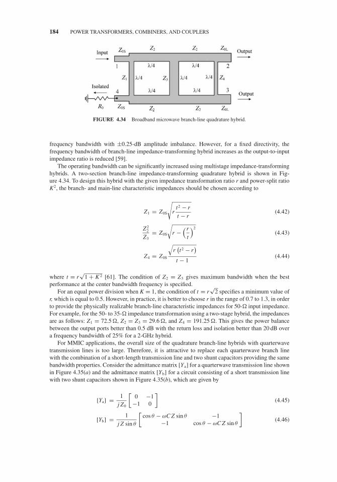
JWBS064-c04 JWBS064-Gerbennikov March 12, 2011 9:14 Printer Name: Yet to Come
184 POWER TRANSFORMERS, COMBINERS, AND COUPLERS
FIGURE 4.34 Broadband microwave branch-line quadrature hybrid.
frequency bandwidth with ±0.25-dB amplitude imbalance. However, for a fixed directivity, thefrequency bandwidth of branch-line impedance-transforming hybrid increases as the output-to-inputimpedance ratio is reduced [59].
The operating bandwidth can be significantly increased using multistage impedance-transforminghybrids. A two-section branch-line impedance-transforming quadrature hybrid is shown in Fig-ure 4.34. To design this hybrid with the given impedance transformation ratio r and power-split ratioK2, the branch- and main-line characteristic impedances should be chosen according to
Z1 = Z0S
√r
t2 − r
t − r(4.42)
Z 22
Z3= Z0S
√r −
(r
t
)2(4.43)
Z4 = Z0S
√r(t2 − r
)t − 1
(4.44)
where t = r√
1 + K 2 [61]. The condition of Z2 = Z3 gives maximum bandwidth when the bestperformance at the center bandwidth frequency is specified.
For an equal power division when K = 1, the condition of t = r√
2 specifies a minimum value ofr, which is equal to 0.5. However, in practice, it is better to choose r in the range of 0.7 to 1.3, in orderto provide the physically realizable branch-line characteristic impedances for 50-� input impedance.For example, for the 50- to 35-� impedance transformation using a two-stage hybrid, the impedancesare as follows: Z1 = 72.5 �, Z2 = Z3 = 29.6 �, and Z4 = 191.25 �. This gives the power balancebetween the output ports better than 0.5 dB with the return loss and isolation better than 20 dB overa frequency bandwidth of 25% for a 2-GHz hybrid.
For MMIC applications, the overall size of the quadrature branch-line hybrids with quarterwavetransmission lines is too large. Therefore, it is attractive to replace each quarterwave branch linewith the combination of a short-length transmission line and two shunt capacitors providing the samebandwidth properties. Consider the admittance matrix [Ya] for a quarterwave transmission line shownin Figure 4.35(a) and the admittance matrix [Yb] for a circuit consisting of a short transmission linewith two shunt capacitors shown in Figure 4.35(b), which are given by
[Ya] = 1
j Z0
[0 −1
−1 0
](4.45)
[Yb] = 1
j Z sin θ
[cos θ − ωC Z sin θ −1
−1 cos θ − ωC Z sin θ
](4.46)

JWBS064-c04 JWBS064-Gerbennikov March 12, 2011 9:14 Printer Name: Yet to Come
MICROWAVE HYBRIDS 185
FIGURE 4.35 Reduced-size branch-line quadrature hybrid.
where Z0 is the characteristic impedance of a quarterwave line, Z and θ are the characteristicimpedance and electrical length of a shortened line, and C is the shunt capacitance. By equating thecorresponding Y-parameters in Eqs. (4.45) and (4.46), the simple ratios between the circuit parameterscan be obtained in the form of
Z = Z0
sin θ(4.47)
C = 1
ωZ0 cos θ(4.48)
from which it follows that the lengths of the hybrid transmission lines can be made much shorter byincreasing their characteristic impedance Z. For example, when choosing the electrical length of θ =45◦, the characteristic impedance of the transmission line increases by a factor of
√2.
A circuit schematic of the reduced-size branch-line quadrature hybrid is shown in Figure 4.35(c)[62]. Compared to the conventional branch-line hybrid with the characteristic impedances of itsbranch- and main-lines of Z0 and Z0/
√2, respectively, the circuit parameters of the reduced-size
branch-line hybrid are obtained from
θ1 = sin−1
(Z0
Z
)(4.49)
θ2 = sin−1
(Z0
Z√
2
)(4.50)
ωC Z0 =√
1 −(
Z0
Z
)2
+√
2 −(
Z0
Z
)2
(4.51)
where θ1 and θ2 are the electrical lengths of the shunt branch-line and series main-line, respectively. Fora particular case of the standard characteristic impedance Z0 = 50 �, the characteristic impedance andelectrical lengths of the transmission lines are defined as Z = Z0
√2, θ1 = 45◦, and θ2 = 30◦, as shown
in Figure 4.35(c). Experimental results for a 25-GHz reduced-size branch-line quadrature hybrid showthat its bandwidth performance is slightly narrower than that of the conventional quarterwave hybrid,but its overall size is more than 80% smaller.
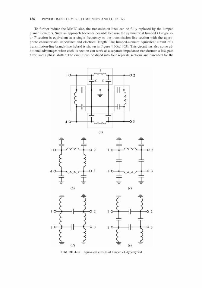
JWBS064-c04 JWBS064-Gerbennikov March 12, 2011 9:14 Printer Name: Yet to Come
186 POWER TRANSFORMERS, COMBINERS, AND COUPLERS
To further reduce the MMIC size, the transmission lines can be fully replaced by the lumpedplanar inductors. Such an approach becomes possible because the symmetrical lumped LC-type π-or T-section is equivalent at a single frequency to the transmission-line section with the appro-priate characteristic impedance and electrical length. The lumped-element equivalent circuit of atransmission-line branch-line hybrid is shown in Figure 4.36(a) [63]. This circuit has also some ad-ditional advantages when each its section can work as a separate impedance transformer, a low-passfilter, and a phase shifter. The circuit can be diced into four separate sections and cascaded for the
FIGURE 4.36 Equivalent circuits of lumped LC-type hybrid.

JWBS064-c04 JWBS064-Gerbennikov March 12, 2011 9:14 Printer Name: Yet to Come
MICROWAVE HYBRIDS 187
desired transmission characteristics. The circuit analysis indicates that various types of networksfulfill the conditions required for an ideal hybrid. Therefore, greater design flexibility in the choiceof the hybrid structure and performance is possible.
Several possible single-section two-branch hybrid options are shown in Figure 4.36 [64]. Inthis case, it should be noted that not only a low-pass section but also a high-pass section can berespectively used. In the latter case, the high-pass LC section is considered an equivalent single-frequency replacement for a 270-degree transmission line [65]. Figures 4.36(c) and 4.36(d) illustratethe use of both low-pass and high-pass sections simultaneously, while only high-pass sections composethe hybrid shown in Figure 4.36(e). The performances of the hybrids shown in Figures 4.36(b) and4.36(e) are very similar to that of the classical single-section branch-line hybrid. The bandwidthperformances of the hybrids shown in Figures 4.36(c) and 4.36(d) are narrower because the powerbalance between their output ports is much narrower. Broader bandwidth and lower output impedancescan be provided with a two-section three-branch lumped-element hybrid.
Figure 4.37(a) shows the equivalent circuit of a capacitively coupled lumped-element hybrid,which is used for monolithic design of variable phase shifters [66]. However, the power and phasebalance bandwidth at the output ports of this hybrid is very narrow, in the limits of a few percent. Analternative design of an inductively coupled lumped-element hybrid is shown in Figure 4.37(b) [67].As a basic element, it includes lumped multiturn mutually coupled spiral inductors with the couplingcoefficient, which can be realized using a bifilar (a sandwich of two multiturn spiral inductors withinner and outer windings) spiral transformer to achieve a coupling coefficient k = 0.707. In thiscase, this basic lumped-element configuration is completely equivalent to a transmission line in thevicinity of the center bandwidth frequency. The inductively coupled hybrid can provide a powerbalance within 0.2 dB and phase balance within 1◦ in a frequency bandwidth of ±10% in 2-GHzwireless applications. However, during the design procedure, some parasitic effects should be taken
FIGURE 4.37 Equivalent circuits of lumped hybrid with capacitive and inductive coupling.

JWBS064-c04 JWBS064-Gerbennikov March 12, 2011 9:14 Printer Name: Yet to Come
188 POWER TRANSFORMERS, COMBINERS, AND COUPLERS
into account. For example, the coupled inductor itself has a sufficient value of internal capacitance.Also, the finite value of the inductor quality factor results in a modest amplitude imbalance, butit leads to a significant phase deviation from ideal quadrature 90-degree difference. In this case, tocompensate for the resulting performance degradation, the electromagnetic simulation of the structureand optimization of the values of the added shunt capacitors on both sides of the circuit are required.Two of these inductively coupled hybrids can be cascaded in tandem to significantly extend thefrequency bandwidth. As a result, the phase shift of 93 ± 6◦, the insertion loss between 1 and 1.5 dB,the return loss better than 16 dB, and the isolation between the output ports better than 18 dB weremeasured over the frequency range from 2 to 6 GHz [67].
A hybrid-ring directional coupler or rat-race, which is one of the fundamental components used inmicrowave circuits was described and analyzed more than six decades ago [68]. Its operation principleis based on an assumption that the voltage at any point along the transmission line is a superpositionof the forward and backward propagating waves. Signal from the excitation source spreads out in thedriving point and propagates along the line. As the forward wave reaches the far-end termination, itreflects, propagates backward, reflects from the near-end termination, propagates forward again, andcontinues in a loop. According to this wave behavior, a pure standing wave is set up within the ringwhen there is no mechanism for dissipation other than the minor ohmic losses associated with wavetransmission. The point of voltage minimum (zero) corresponds to the case when the waves havephase shift of 180◦ with respect to each other. As a result, the standing wave within the ring can bemapped by marking off alternate voltage maxima and minima at quarterwave intervals. Consequently,if standing waves are set up in the main arm, the side arm receives maximum power when a voltageminimum of the standing-wave pattern coincides with the center of this arm and minimum powerwhen a voltage maximum located in this point.
The 3λ/2 ring hybrid, whose microstrip topology is shown in Figure 4.38(a), can be used to dividethe driving power or to combine the powers from two sources. In the case of power division, a signalapplied to the port 1 will be evenly split into two in-phase components at ports 2 and 3, and port 4 willbe isolated. If the input signal is applied at port 4, it will be equally split into two components with180-degree difference at ports 2 and 3, and port 1 will be isolated. When operated as a combiner, withinput signals applied at ports 2 and 3, the sum of the input signals will be delivered to port 1. Theirdifference will flow to port 4 and dissipated in corresponding ballast resistor R0. For equal signals andmatched ring hybrid with Z0 = R0, there is zero-power dissipation at port 4 [55]. The ideal rat-raceor ring hybrid has the bandwidth of approximately 27.6% at the tolerance limits of the deviation of0.43 dB for split and of 20 dB for the maximum return loss and isolation.
Generally, a hybrid-ring directional coupler can provide arbitrary power divisions when the power-split ratio is adjusted by varying the impedances between the arms [69]. Figure 4.38(b) shows theplanar microstrip topology of a ring hybrid where the characteristic impedances of four arms areequal to the standard characteristic impedance Z0. The variable parameters are the two characteristicimpedances Z1 and Z2, which determine the degree of coupling of the output arms and the impedancematching condition for the input arm. The analysis of this ring hybrid consists of the usual procedure ofreducing the four-terminal network to a two-terminal network by taking advantage of the symmetryabout the plane A–A′. For example, when two in-phase waves of equal amplitude are applied toterminals 1 and 3, the current is zero at the plane A–A′. As a result, the ring can be open-circuited atthis plane and only one-half of the circuit can be analyzed. This condition is called the even mode.On the other hand, the odd-mode condition is a result of applying the opposite-phase waves of equalamplitude to terminals 1 and 3 when the voltage at plane A–A′ is zero. In this case, the ring can beshort-circuited at this plane and only one half of the circuit can be analyzed. Once the scatteringmatrices for the even and odd modes are known, the reflected waves in each arm can be determined.Then, by superimposing the waves of the two modes, the resultant reflected waves in each arm and asingle incident wave in one arm is obtained. Thus, if arm 1 is input, the output voltage ratio betweenarm 2 and 3 is equal to Z1/Z2, and no power is delivered to the isolated port 4 where the ballast resistorR0 = Z0 is connected.

JWBS064-c04 JWBS064-Gerbennikov March 12, 2011 9:14 Printer Name: Yet to Come
MICROWAVE HYBRIDS 189
FIGURE 4.38 Microstrip rate-race ring hybrids.
Although usually considered a narrowband device, the rat-race hybrid can provide much broaderperformance if its three-quarter wavelength section (a main limiting factor in a conventional config-uration) is replaced by one having the same characteristic impedance, but whose electrical lengthis realized by a quarter wavelength of line exhibiting the characteristics of an ideal phase-reversingnetwork [70]. It may be a coaxial cable with a crossover of its inner and outer conductors at oneend, thus resulting in an isolation of more than 20 dB in a frequency bandwidth of 30% [57]. Asa compact planar alternative, a pair of equilateral broadside-coupled segments of strip transmissionlines having diametrically opposing ends short-circuited, as shown in Figure 4.39(a), approximates aphase-reversing network over a wide frequency range.
The characteristic impedance of the coupled section Zc is given by
Zc = 2Z0e Z0o sin θ√(Z0e − Z0o)2 − (Z0e + Z0o)2 cos2 θ
(4.52)
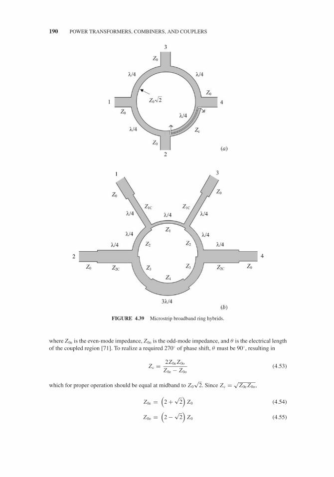
JWBS064-c04 JWBS064-Gerbennikov March 12, 2011 9:14 Printer Name: Yet to Come
190 POWER TRANSFORMERS, COMBINERS, AND COUPLERS
FIGURE 4.39 Microstrip broadband ring hybrids.
where Z0e is the even-mode impedance, Z0o is the odd-mode impedance, and θ is the electrical lengthof the coupled region [71]. To realize a required 270◦ of phase shift, θ must be 90◦, resulting in
Zc = 2Z0e Z0o
Z0e − Z0o(4.53)
which for proper operation should be equal at midband to Z0
√2. Since Zc = √
Z0e Z0o,
Z0e =(
2 +√
2)
Z0 (4.54)
Z0o =(
2 −√
2)
Z0 (4.55)

JWBS064-c04 JWBS064-Gerbennikov March 12, 2011 9:14 Printer Name: Yet to Come
MICROWAVE HYBRIDS 191
which means that, for a 50-� transmission system and a median 3-dB coupling, Z0e must be 170.7 �
and Z0o must be 29.3 �.To extend the frequency bandwidth and simplify fabrication process with a uniplanar structure,
the ring hybrid can represent a slotline ring with one slotline and three CPW arms [72]. The designtechnique substitutes one reverse-phase slotline T-junction for the conventional rat-race phase delaysection. Since the phase reverse of the slotline T-junction is frequency independent, the resulting slot-line ring hybrid provides a broad bandwidth. Experimental results show that this uniplanar crossoverring-hybrid coupler has a bandwidth from 2 to 4 GHz with ±0.4 dB power dividing balance and ±1◦
phase balance. By using a microcoplanar stripline ring with a broadband coplanar stripline phaseinverter and four CPW arms, the coupling between the output ports is within 3.5 ± 0.5 dB over thefrequency range from 1.43 to 2.95 GHz [73].
However, it is possible to increase the operating bandwidth of the conventional rat-race withouta quarterwave phase-reversing section by applying the concept of hypothetical ports and adding theproper quarterwave transformer to each port [74]. The bandwidth will be significantly broadened byreplacing a three-quarterwave equal-impedance section with symmetrical transmission-line structure,the middle quarterwave section of which has different characteristic impedance. To optimally realizethis, the numerical optimization procedure to minimize an objective evaluation function is required.In this case, to improve coupling, matching, and isolation, it is necessary to connect either the open-circuited compensating stubs at the hypothetical ports (connecting points of the quarterwave lineswith different characteristic impedances), or to add the quarterwave transformers (transmission lineswith different characteristic impedances) to the hybrid ports, as shown in Figure 4.39(b). As a result,the frequency bandwidth of the improved ring hybrid becomes 1.84 times as wide as the conventionalrat-race.
To significantly reduce the overall size of the conventional ring hybrid with the 90-degree and270-degree transmission line sections, which is crucial for MMIC design, the principle of the single-frequency equivalence between the circuits with the lumped and distributed parameters can be applied[65]. Let us compare the elements of the transmission matrix [ABCDa] for a 270-degree transmissionline and the transmission matrix [ABCDb] for a high-pass π -type lumped circuit, consisting of theseries capacitor and two shunt inductors, given by
[ABCDa] =
⎡⎢⎣
cos θ j Z0 sin θ
jsin θ
Z0cos θ
⎤⎥⎦
θ=3π/2
=⎡⎣ 0 − j Z0
− j
Z00
⎤⎦ (4.56)
[ABCDb] =[
1 0− j/ωL 1
] [1 − j/ωC0 1
] [1 0
− j/ωL 1
]=
⎡⎢⎢⎣
1 − 1
ω2 LC− j
1
ωC
− j1
ωL
(2 − 1
ω2 LC
)1 − 1
ω2 LC
⎤⎥⎥⎦ .
(4.57)
Equating the corresponding elements of both matrices yields the simple equations to determinethe circuit elements in the form of
Z0ωC = Z0
ωL= 1. (4.58)
Hence, to reduce the size of a ring hybrid, a 270-degree transmission line shown in Figure 4.40(a)is replaced by a high-pass lumped section. Then, the three quarterwave-line sections are replaced byshortened ones with two shunt capacitors, as shown in Figure 4.35(b) for a branch-line coupler. Finally,the characteristic impedance of the transmission line sections is chosen so that the shunt inductorsof the high-pass section shown in Figure 4.40(b) could resonant with the shunt capacitors of the

JWBS064-c04 JWBS064-Gerbennikov March 12, 2011 9:14 Printer Name: Yet to Come
192 POWER TRANSFORMERS, COMBINERS, AND COUPLERS
FIGURE 4.40 Reduced-size ring hybrid.
low-pass section at the center bandwidth frequency, in order to completely remove these components.Figure 4.40(c) shows the circuit diagram of the reduced-size ring hybrid with the characteristicimpedances of the transmission-line sections of 100 � and their electrical lengths of 45◦ [62]. Asa result, the overall reduced hybrid size is more than 80% smaller than that of the conventionalhybrid.
4.6 COUPLED-LINE DIRECTIONAL COUPLERS
The first directional couplers consisted of either a two-wire balanced line coupled to a second balancedline along a distance of quarter wavelength, or a pair of rods a quarter wavelength long between groundplanes [54]. Although the propagation of waves on systems of parallel conductors was investigatedmany decades ago in connection with the problem of crosstalk between open wire lines or cable pairsin order to eliminate the natural coupling rather than use it, the first exact design theory for transverseelectromagnetic (TEM) transmission-line couplers was introduced by Oliver [75]. In terms of theeven and odd electric-field modes describing a system of the coupled conductors, it can be statedthat the coupling is backward with coupled wave on the secondary line propagating in the directionopposite to the direction of the wave on the primary line, the directivity will be perfect with VSWRequal to unity if Z 2
0 = Z0e Z0o at all cross sections along the directional coupler, and the midbandvoltage coupling coefficient C of the directional coupler is defined as
C = Z0e − Z0o
Z0e + Z0o(4.59)
where C = 0 for zero coupling and C = 1 for completely superposed transmission lines.A coupled-line directional coupler, the stripline single-section topology of which is shown in
Figure 4.41(a), can be used for broadband power division or combining. Its electrical properties aredescribed using a concept of two types of excitations for the coupled lines in TEM approximation.In this case, for the even mode, the currents flowing in the strip conductors are equal in amplitudeand flow in the same direction. The electric field has even symmetry about the center line, and nocurrent flows between the two strip conductors. For the odd mode, the currents flowing in the stripconductors are equal in amplitude, but flow in opposite directions. The electric field lines have anodd symmetry about the center line, and a voltage null exists between these two strip conductors.
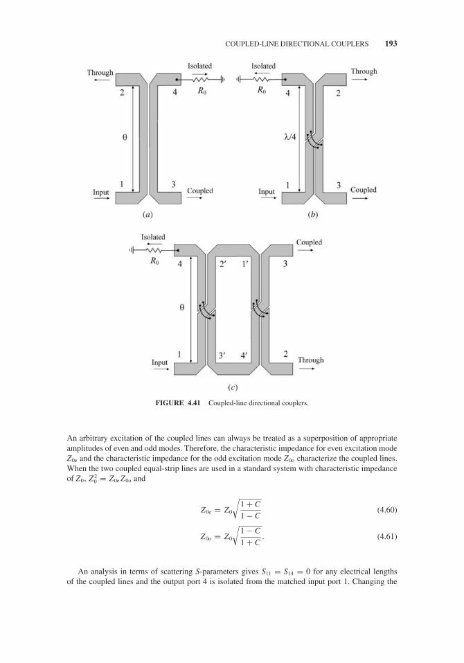
JWBS064-c04 JWBS064-Gerbennikov March 12, 2011 9:14 Printer Name: Yet to Come
COUPLED-LINE DIRECTIONAL COUPLERS 193
FIGURE 4.41 Coupled-line directional couplers.
An arbitrary excitation of the coupled lines can always be treated as a superposition of appropriateamplitudes of even and odd modes. Therefore, the characteristic impedance for even excitation modeZ0e and the characteristic impedance for the odd excitation mode Z0o characterize the coupled lines.When the two coupled equal-strip lines are used in a standard system with characteristic impedanceof Z0, Z 2
0 = Z0e Z0o and
Z0e = Z0
√1 + C
1 − C(4.60)
Z0o = Z0
√1 − C
1 + C. (4.61)
An analysis in terms of scattering S-parameters gives S11 = S14 = 0 for any electrical lengthsof the coupled lines and the output port 4 is isolated from the matched input port 1. Changing the

JWBS064-c04 JWBS064-Gerbennikov March 12, 2011 9:14 Printer Name: Yet to Come
194 POWER TRANSFORMERS, COMBINERS, AND COUPLERS
coupling between the lines and their widths can change the characteristic impedances Z0e and Z0o. Inthis case,
S12 =√
1 − C2
√1 − C2 cos θ + j sin θ
(4.62)
S13 = jC sin θ√1 − C2 cos θ + j sin θ
(4.63)
where θ is the electrical length of the coupled-line section.The voltage-split ratio K is defined as the ratio between voltages at port 2 and port 3 by
K =∣∣∣∣ S12
S13
∣∣∣∣ =√
1 − C2
C sin θ(4.64)
where K can be controlled by changing the coupling coefficient C and electrical length θ .For a quarter-wavelength-long coupler when θ = 90◦, Eqs. (4.62) and (4.63) reduce to
S12 = − j√
1 − C2 (4.65)
S13 = C (4.66)
from which it follows that equal voltage split between the output ports 2 and 3 can be provided withC = 1/
√2.
If it is necessary to provide the output ports 2 and 3 at one side, it is best to use a constructionof a microstrip directional coupler with crossed bondwires, as shown in Figure 4.41(b). The stripcrossover for a stripline directional coupler can be easily achieved with the three-layer sandwich. Themicrostrip 3-dB directional coupler fabricated on alumina substrate for idealized zero strip thicknessshould have the calculated strip spacing of less than 10 μm. Such a narrow value easily explainsthe great interest to the constructions of the directional couplers with larger spacing. The effectivesolution is to use a tandem connection of the two identical directional couplers, which alleviatesthe physical problem of tight coupling, since two individual couplers need only 8.34-dB couplingto achieve a 3-dB coupler [76,77]. The tandem coupler shown in Figure 4.41(c) has the electricalproperties of the individual coupler when the output ports 1, 4 and 2, 3 are isolated in pairs, and thephase difference between the output ports 2 and 3 is of 90◦.
From an analysis of the signal propagation from input port 1 to output ports 2 and 3 of thetandem coupler, when the signal from the input port 1 propagates to the output port 2 through thetraces 1-2′-1′-2 and 1-3′-4′-2 while the signal flowing through the traces 1-2′-1′-3 and 1-3′-4′-3 isdelivered to the output port 3, the ratio of the scattering parameters ST
12 and ST13 of a tandem coupler
can be expressed through the corresponding scattering parameters S12 and S13 of the individualcoupler as
ST12
ST13
= S212 + S2
13
2S12 S13= − j
1 − C2(1 + sin2 θ
)2C
√1 − C2sinθ
. (4.67)
As a result, the signal at the port 2 overtakes the signal at the port 3 by 90◦. In this case, for a 3-dBtandem coupler with θ = 90◦, the magnitude of Eq. (4.67) must be equal to unity. Consequently, therequired voltage coupling coefficient is calculated as
C = 0.5
√2 −
√2 = 0.3827
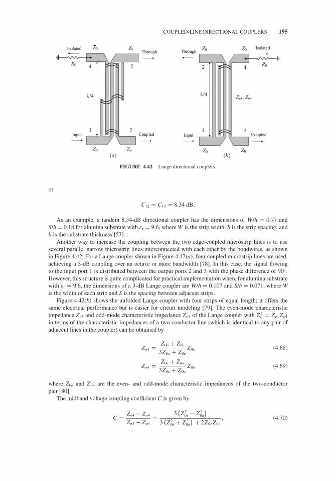
JWBS064-c04 JWBS064-Gerbennikov March 12, 2011 9:14 Printer Name: Yet to Come
COUPLED-LINE DIRECTIONAL COUPLERS 195
FIGURE 4.42 Lange directional couplers.
or
C12 = C13 = 8.34 dB.
As an example, a tandem 8.34-dB directional coupler has the dimensions of W/h = 0.77 andS/h = 0.18 for alumina substrate with εr = 9.6, where W is the strip width, S is the strip spacing, andh is the substrate thickness [57].
Another way to increase the coupling between the two edge-coupled microstrip lines is to useseveral parallel narrow microstrip lines interconnected with each other by the bondwires, as shownin Figure 4.42. For a Lange coupler shown in Figure 4.42(a), four coupled microstrip lines are used,achieving a 3-dB coupling over an octave or more bandwidth [78]. In this case, the signal flowingto the input port 1 is distributed between the output ports 2 and 3 with the phase difference of 90◦.However, this structure is quite complicated for practical implementation when, for alumina substratewith εr = 9.6, the dimensions of a 3-dB Lange coupler are W/h = 0.107 and S/h = 0.071, where Wis the width of each strip and S is the spacing between adjacent strips.
Figure 4.42(b) shows the unfolded Lange coupler with four strips of equal length; it offers thesame electrical performance but is easier for circuit modeling [79]. The even-mode characteristicimpedance Ze4 and odd-mode characteristic impedance Zo4 of the Lange coupler with Z 2
0 = Ze4 Zo4
in terms of the characteristic impedances of a two-conductor line (which is identical to any pair ofadjacent lines in the coupler) can be obtained by
Ze4 = Z0o + Z0e
3Z0o + Z0eZ0e (4.68)
Zo4 = Z0e + Z0o
3Z0e + Z0oZ0o (4.69)
where Z0e and Z0o are the even- and odd-mode characteristic impedances of the two-conductorpair [80].
The midband voltage coupling coefficient C is given by
C = Ze4 − Zo4
Ze4 + Zo4= 3
(Z 2
0e − Z 20o
)3(Z 2
0e + Z 20o
) + 2Z0e Z0o. (4.70)
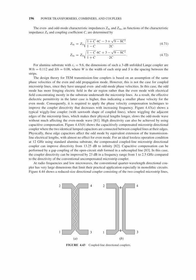
JWBS064-c04 JWBS064-Gerbennikov March 12, 2011 9:14 Printer Name: Yet to Come
196 POWER TRANSFORMERS, COMBINERS, AND COUPLERS
The even- and odd-mode characteristic impedances Z0e and Z0o, as functions of the characteristicimpedance Z0 and coupling coefficient C, are determined by
Z0e = Z0
√1 + C
1 − C
4C − 3 + √9 − 8C2
2C(4.71)
Z0o = Z0
√1 − C
1 + C
4C + 3 − √9 − 8C2
2C. (4.72)
For alumina substrate with εr = 9.6, the dimensions of such a 3-dB unfolded Lange coupler areW/h = 0.112 and S/h = 0.08, where W is the width of each strip and S is the spacing between thestrips.
The design theory for TEM transmission-line couplers is based on an assumption of the samephase velocities of the even and odd propagation mode. However, this is not the case for coupledmicrostrip lines, since they have unequal even- and odd-mode phase velocities. In this case, the oddmode has more fringing electric field in the air region rather than the even mode with electricalfield concentrating mostly in the substrate underneath the microstrip lines. As a result, the effectivedielectric permittivity in the latter case is higher, thus indicating a smaller phase velocity for theeven mode. Consequently, it is required to apply the phase velocity compensation techniques toimprove the coupler directivity that decreases with increasing frequency. Figure 4.43(a) shows atypical wiggly-line coupler (with sawtooth shape of coupled lines), where wiggling the adjacentedges of the microstrip lines, which makes their physical lengths longer, slows the odd-mode wavewithout much affecting the even-mode wave [81]. High directivity can also be achieved by usingcapacitive compensation. Figure 4.43(b) shows the capacitively compensated microstrip directionalcoupler where the two identical lumped capacitors are connected between coupled lines at their edges.Physically, these edge capacitors affect the odd mode by equivalent extension of the transmission-line electrical lengths, with almost no effect for even mode. For an ideal lossless operation conditionat 12 GHz using standard alumina substrate, the compensated coupled-line microstrip directionalcoupler can improve directivity from 13.25 dB to infinity [82]. Capacitive compensation can beperformed by a gap coupling of the open-circuit stub formed in a subcoupled line [83]. In this case,the coupler directivity can be improved by 23 dB in a frequency range from 1 to 2.5 GHz comparedto the directivity of the conventional uncompensated microstrip coupler.
At radio frequencies and low microwaves, the conventional quarter-wavelength directional cou-pler has very large dimensions that limit their practical application especially in monolithic circuits.Figure 4.44 shows a reduced-size directional coupler consisting of the two coupled microstrip lines,
FIGURE 4.43 Coupled-line directional couplers.
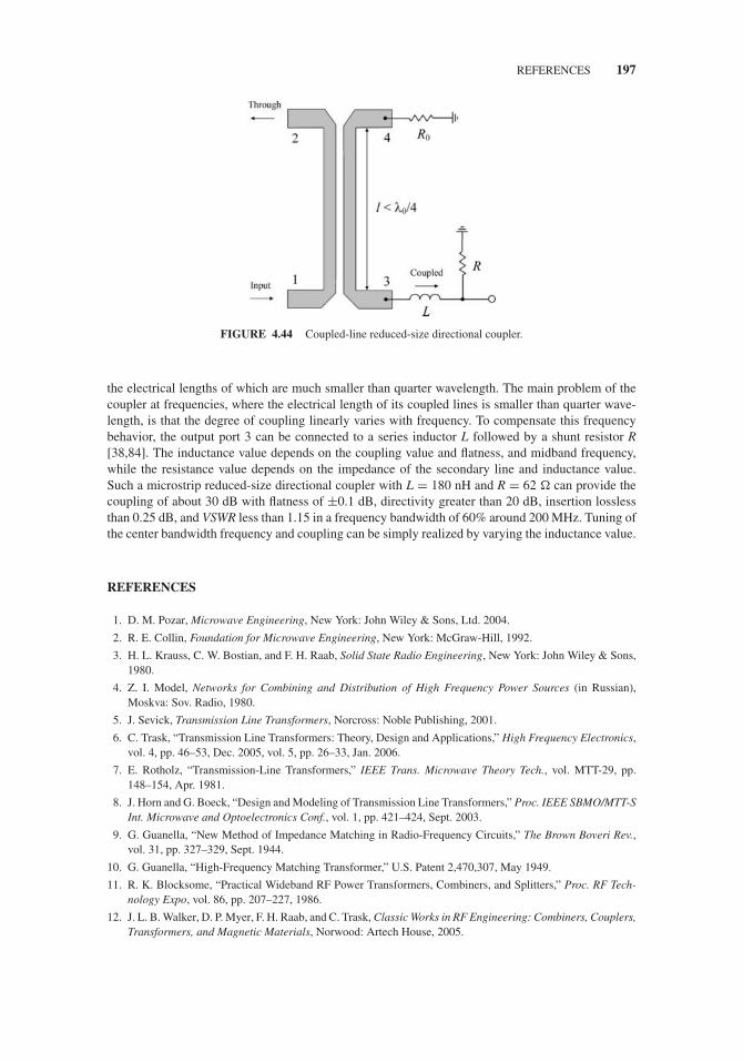
JWBS064-c04 JWBS064-Gerbennikov March 12, 2011 9:14 Printer Name: Yet to Come
REFERENCES 197
FIGURE 4.44 Coupled-line reduced-size directional coupler.
the electrical lengths of which are much smaller than quarter wavelength. The main problem of thecoupler at frequencies, where the electrical length of its coupled lines is smaller than quarter wave-length, is that the degree of coupling linearly varies with frequency. To compensate this frequencybehavior, the output port 3 can be connected to a series inductor L followed by a shunt resistor R[38,84]. The inductance value depends on the coupling value and flatness, and midband frequency,while the resistance value depends on the impedance of the secondary line and inductance value.Such a microstrip reduced-size directional coupler with L = 180 nH and R = 62 � can provide thecoupling of about 30 dB with flatness of ±0.1 dB, directivity greater than 20 dB, insertion losslessthan 0.25 dB, and VSWR less than 1.15 in a frequency bandwidth of 60% around 200 MHz. Tuning ofthe center bandwidth frequency and coupling can be simply realized by varying the inductance value.
REFERENCES
1. D. M. Pozar, Microwave Engineering, New York: John Wiley & Sons, Ltd. 2004.
2. R. E. Collin, Foundation for Microwave Engineering, New York: McGraw-Hill, 1992.
3. H. L. Krauss, C. W. Bostian, and F. H. Raab, Solid State Radio Engineering, New York: John Wiley & Sons,1980.
4. Z. I. Model, Networks for Combining and Distribution of High Frequency Power Sources (in Russian),Moskva: Sov. Radio, 1980.
5. J. Sevick, Transmission Line Transformers, Norcross: Noble Publishing, 2001.
6. C. Trask, “Transmission Line Transformers: Theory, Design and Applications,” High Frequency Electronics,vol. 4, pp. 46–53, Dec. 2005, vol. 5, pp. 26–33, Jan. 2006.
7. E. Rotholz, “Transmission-Line Transformers,” IEEE Trans. Microwave Theory Tech., vol. MTT-29, pp.148–154, Apr. 1981.
8. J. Horn and G. Boeck, “Design and Modeling of Transmission Line Transformers,” Proc. IEEE SBMO/MTT-SInt. Microwave and Optoelectronics Conf., vol. 1, pp. 421–424, Sept. 2003.
9. G. Guanella, “New Method of Impedance Matching in Radio-Frequency Circuits,” The Brown Boveri Rev.,vol. 31, pp. 327–329, Sept. 1944.
10. G. Guanella, “High-Frequency Matching Transformer,” U.S. Patent 2,470,307, May 1949.
11. R. K. Blocksome, “Practical Wideband RF Power Transformers, Combiners, and Splitters,” Proc. RF Tech-nology Expo, vol. 86, pp. 207–227, 1986.
12. J. L. B. Walker, D. P. Myer, F. H. Raab, and C. Trask, Classic Works in RF Engineering: Combiners, Couplers,Transformers, and Magnetic Materials, Norwood: Artech House, 2005.

JWBS064-c04 JWBS064-Gerbennikov March 12, 2011 9:14 Printer Name: Yet to Come
198 POWER TRANSFORMERS, COMBINERS, AND COUPLERS
13. J. Sevick, “Magnetic Materials for Broadband Transmission Line Transformers,” High Frequency Electronics,vol. 4, pp. 46–52, Jan. 2005.
14. C. L. Ruthroff, “Some Broad-Band Transformers,” Proc. IRE, vol. 47, pp. 1337–1342, Aug. 1959.
15. C. L. Ruthroff, “Broadband Transformers,” U.S. Patent 3,037,175, May 1962.
16. J. Sevick, “A Simplified Analysis of the Broadband Transmission Line Transformer,” High Frequency Elec-tronics, vol. 3, pp. 48–53, Feb. 2004.
17. R. T. Irish, “Method of Bandwidth Extension for the Ruthroff Transformer,” Electronics Lett., vol. 15, pp.790–791, Nov. 1979.
18. S. C. Dutta Roy, “Optimum Design of an Exponential Line Transformer for Wide-Band Matching at LowFrequencies,” Proc. IEEE, vol. 67, pp. 1563–1564, Nov. 1979.
19. M. Engels, M. R. Jansen, W. Daumann, R. M. Bertenburg, and F. J. Tegude, “Design Methodology, Measure-ment and Application of MMIC Transmission Line Transformers,” IEEE MTT-S Int. Microwave Symp. Dig.,vol. 3, pp. 1635–1638, May 1995.
20. S. P. Liu, “Planar Transmission Line Transformer Using Coupled Microstrip Lines,” IEEE MTT-S Int. Mi-crowave Symp. Dig., vol. 2, pp. 789–792, June 1998.
21. J. Sevick, “Design of Broadband Ununs with Impedance Ratios Less than 1:4,” High Frequency Electronics,vol. 3, pp. 44–50, Nov. 2004.
22. S. E. London and S. V. Tomashevich, “Line Transformers with Fractional Transformation Factor,” Telecom-munications and Radio Engineering, vol. 28/29, pp. 129–130, Apr. 1974.
23. C. Lorenz, “Schaltungsanordnung zum Ubergang von Einer symmetrischen, Elektrischen Anordnung zu EinerUnsymmetrischen, Insbesondere bei Hochfrequenzanordnungen,” German Patent DE603816, Sept. 1934.
24. B. P. Kumar and G. R. Branner, “Optimized Design of Unique Miniaturized Planar Baluns for WirelessApplications,” IEEE Microwave and Wireless Comp. Lett., vol. 13, pp. 134–136, Feb. 2003.
25. N. Marchand, “Transmission-Line Conversion Transformers,” Electronics, vol. 17, pp. 142–145, Dec.1944.
26. G. Oltman, “The Compensated Balun,” IEEE Trans. Microwave Theory Tech., vol. MTT-14, pp. 112–119,March. 1966.
27. C.-M. Tsai and K. C. Gupta, “A Generalized Model for Coupled Lines and its Applications to Two-LayerPlanar Circuits,” IEEE Trans. Microwave Theory Tech., vol. MTT-40, pp. 2190–2199, Dec. 1992.
28. C. Cho and K. C. Gupta, “A New Design Procedure for Single-Layer and Two-Layer Three-Line Baluns,”IEEE Trans. Microwave Theory Tech., vol. MTT-46, pp. 2514–2119, Dec. 1998.
29. K. Nishikawa, I. Toyoda, and T. Tokumitsu, “Compact and Broad-Band Three-Dimensional MMIC Balun,”IEEE Trans. Microwave Theory Tech., vol. MTT-47, pp. 96–98, Jan. 1999.
30. C. Y. Ng, M. Chongcheawchamnan, and I. D. Robertson, “Analysis and Design of a High-Performance PlanarMarchand Balun,” IEEE MTT-S Int. Microwave Symp. Dig., vol. 1, pp. 113–116, June 2002.
31. W. M. Fathelbab and M. B. Steer, “New Classes of Miniaturized Planar Marchand Baluns,” IEEE Trans.Microwave Theory Tech., vol. MTT-53, pp. 1211–1220, Apr. 2005.
32. V. Govind, W. Yun, S. Dalmia, V. Sundaram, G. White, and M. Swaminathan, “Analysis and Design ofCompact Wideband Baluns on Multilayer Liquid Crystalline Polymer (MLP) Based Structures,” IEEE MTT-SInt. Microwave Symp. Dig., pp. 1–4, June 2005.
33. R. Phromloungsri, S. Srisathit, M. Chongcheawchamnan, and I. D. Robertson, “Novel Technique for Perfor-mance Improvement in Impedance-Transforming Planar Marchand Baluns,” Proc. 35th Europ. MicrowaveConf., pp. 533–536, 2005.
34. H. Jasik, “Broad Band Balun Transformer,” U.S. Patent 2925566, Feb. 1960.
35. H. R. Phelan, “A Wide-Band Parallel-Connected Balun,” IEEE Trans. Microwave Theory Tech., vol. MTT-18,pp. 259–263, May 1970.
36. S. V. Bearse, “New Combining and Cooling Techniques Developed for 1 kW L-Band Transmitter,” Mi-crowaves, vol. 16, pp. 9–10, Sept. 1977.
37. E. J. Wilkinson, “An N-Way Hybrid Power Divider,” IRE Trans. Microwave Theory Tech., vol. MTT-8, pp.116–118, Jan. 1960.
38. L. G. Maloratsky, Passive RF & Microwave Integrated Circuits, New York: Elsevier, 2004.
39. V. M. Katushkina and Z. I. Model, “N-Way Power Combiner of VHF-UHF Transmitters (in Russian),”Elektrosvyaz, vol. 7, pp. 17–25, July 1959.

JWBS064-c04 JWBS064-Gerbennikov March 12, 2011 9:14 Printer Name: Yet to Come
REFERENCES 199
40. S. Y. London, “Independent Operation of High Power VHF Amplifiers on Common Load (in Russian),”Voprosy Radioelektroniki, Ser. X, Tekhnika Svyazi, vol. 6, pp. 87–96, June 1959.
41. J. J. Taub and G. P. Kurpis, “A More General N-Way Hybrid Power Divider,” IEEE Trans. Microwave TheoryTech., vol. MTT-17, pp. 406–408, July 1969.
42. S. B. Cohn, “A Class of Broad-Band Three-Port TEM-Mode Hybrids,” IEEE Trans. Microwave Theory Tech.,vol. MTT-16, pp. 110–116, Feb. 1968.
43. D. Antsos, R. Crist, and L. Sukamto, “A Novel Wilkinson Power Divider with Predictable Performance at Kand Ka-Band,” IEEE MTT-S Int. Microwave Symp. Dig., vol. 2, pp. 907–910, May 1994.
44. A. A. M. Saleh, “Planar Electrically Symmetric n-Way Hybrid Power Dividers/Combiners,” IEEE Trans.Microwave Theory Tech., vol. MTT-28, pp. 555–563, June 1980.
45. U. H. Gysel, “A New N-Way Power Divider/Combiner Suitable for High-Power Applications,” IEEE MTT-SInt. Microwave Symp. Dig., pp. 116–118, May 1975.
46. R. Knochel and B. Mayer, “Broadband Printed Circuit 0◦/180◦ Couplers and High Power Inphase PowerDividers,” IEEE MTT-S Int. Microwave Symp. Dig., vol. 1, pp. 471–474, May 1990.
47. Y. Sun and A. P. Freundorfer, “Broadband Folded Wilkinson Power Combiner/Splitter,” IEEE Microwaveand Wireless Components Lett., vol. 14, pp. 295–297, June 2004.
48. N. Nagai, E. Maekawa, and K. Ono, “New N-way Hybrid Power Dividers,” IEEE Trans. Microwave TheoryTech., vol. MTT-25, pp. 1008–1012, Dec. 1977.
49. M. E. Goldfarb, “A Recombinant, In-Phase Power Divider,” IEEE Trans. Microwave Theory Tech., vol.MTT-39, pp. 1438–1440, Aug. 1991.
50. B. M. Schiffman, “A New Class of Broad-Band Microwave 90-Degree Phase Shifter,” IRE Trans. MicrowaveTheory Tech., vol. MTT-6, pp. 232–237, Apr. 1958.
51. L. I. Parad and R. L. Moynihan, “Split-Tee Power Divider,” IEEE Trans. Microwave Theory Tech., vol.MTT-13, pp. 91–95, Jan. 1965.
52. J.-S. Lim and S.-Y. Eom, “A New 3-Way Power Divider with Various Output Power Ratios,” IEEE MTT-SInt. Microwave Symp. Dig., vol. 2 pp. 785–788, June 1996.
53. D. Maurin and K. Wu, “A Compact 1.7-2.1 GHz Three-Way Power Combiner Using Microstrip Technologywith Better Than 93.8% Combining Efficiency,” IEEE Microwave and Guided Wave Lett., vol. 6, pp. 106–108,Feb. 1996.
54. S. B. Cohn and R. Levy, “History of Microwave Passive Components with Particular Attention to DirectionalCouplers,” IEEE Trans. Microwave Theory Tech., vol. MTT-32, pp. 1046–1054, Sept. 1984.
55. J. Reed and G. J. Wheeler, “A Method of Analysis of Symmetrical Four-Port Networks,” IRE Trans. MicrowaveTheory Tech., vol. MTT-4, pp. 246–252, Oct. 1956.
56. R. Levy and L. Lind, “Synthesis of Symmetrical Branch-Guide Directional Couplers,” IEEE Trans. MicrowaveTheory Tech., vol. MTT-16, pp. 80–89, Feb. 1968.
57. A. Grebennikov, RF and Microwave Power Amplifier Design, New York: McGraw-Hill, 2004.
58. P. Meaney, “A Novel Branch-Line Coupler Design for Millimeter-Wave Applications,” IEEE MTT-S Int.Microwave Symp. Dig., vol. 1, pp. 585–588, May 1990.
59. L. F. Lind, “Synthesis of Asymmetrical Branch-Guide Directional Coupler-Impedance Transformers,” IEEETrans. Microwave Theory Tech., vol. MTT-17, pp. 45–48, Jan. 1969.
60. R. K. Gupta, S. E. Anderson, and W. J. Getsinger, “Impedance-Transforming 3-dB 90◦ Hybrids,” IEEE Trans.Microwave Theory Tech., vol. MTT-35, pp. 1303–1307, Dec. 1987.
61. S. Kumar, C. Tannous, and T. Danshin, “A Multisection Broadband Impedance Transforming Branch-LineHybrid,” IEEE Trans. Microwave Theory Tech., vol. MTT-43, pp. 2517–2523, Nov. 1995.
62. T. Hirota, A. Minakawa, and M. Muraguchi, “Reduced-Size Branch-Line and Rat-Race Hybrid for UniplanarMMIC’s,” IEEE Trans. Microwave Theory Tech., vol. MTT-38, pp. 270–275, March 1990.
63. M. Caulton, B. Hershenov, S.P. Knight, and R. E. DeBrecht, “Status of Lumped Elements in MicrowaveIntegrated Circuits − Present and Future,” IEEE Trans. Microwave Theory Tech., vol. MTT-19, pp. 588–599,July 1971.
64. R. W. Vogel, “Analysis and Design of Lumped- and Lumped-Distributed-Element Directional Couplers forMIC and MMIC Applications,” IEEE Trans. Microwave Theory Tech., vol. MTT-40, pp. 253–262, Feb. 1992.
65. S. J. Parisi, “180◦ Lumped Element Hybrid,” IEEE MTT-S Int. Microwave Symp. Dig., vol. 3, pp. 1243–1246,June 1989.

JWBS064-c04 JWBS064-Gerbennikov March 12, 2011 9:14 Printer Name: Yet to Come
200 POWER TRANSFORMERS, COMBINERS, AND COUPLERS
66. R. C. Frye, S. Kapur and R. C. Melville, “A 2-GHz Quadrature Hybrid Implemented in CMOS Technology,”IEEE J. Solid-State Circuits, vol. SC-38, pp. 550–555, March 2003.
67. F. Ali and A. Podell, “A Wide-Band GaAs Monolithic Spiral Quadrature Hybrid and its Circuit Applications,”IEEE J. Solid-State Circuits, vol. SC-26, pp. 1394–1398, Oct. 1991.
68. W. A. Tyrrell, “Hybrid Circuits for Microwaves,” Proc. IRE, vol. 35, pp. 1294–1306, Nov. 1947.
69. C. Y. Pon, “Hybrid-Ring Directional Coupler for Arbitrary Power Divisions,” IRE Trans. Microwave TheoryTech., vol. MTT-9, pp. 529–535, Nov. 1961.
70. S. March, “A Wideband Stripline Hybrid Ring,” IEEE Trans. Microwave Theory Tech., vol. MTT-16, pp. 361,June 1968.
71. G. L. Matthaei, E. M. T. Jones, and L. Young, Microwave Filters, Impedance-Matching Networks andCoupling Structures, New York: Artech House, 1980.
72. C.-H. Ho, L. Fan, and K. Chang, “Broad-Band Uniplanar Hybrid-Ring and Branch-Line Couplers,” IEEETrans. Microwave Theory Tech., vol. MTT-41, pp. 2116–2124, Dec. 1993.
73. T. Wang and K. Wu, “Size-Reduction and band-Broadening Design Technique of Uniplanar Hybrid RingCoupler Using Phase Inverter for M(H)MIC’s,” IEEE Trans. Microwave Theory Tech., vol. MTT-42, pp.198–206, Feb. 1999.
74. D. I. Kim and Y. Naito, “Broad-Band Design of Improved Hybrid-Ring 3-dB Directional Couplers,” IEEETrans. Microwave Theory Tech., vol. MTT-30, pp. 2040–2046, Nov. 1982.
75. B. M. Oliver, “Directional Electromagnetic Couplers,” Proc. IRE, vol. 42, pp. 1686–1692, Nov. 1954.
76. G. D. Monteath, “Coupled Transmission Lines as Symmetrical Directional Couplers,” IEE Proc., vol. 102,part B, pp. 383–392, May 1955.
77. T. P. Shelton and J. A. Mosko, “Synthesis and Design of Wide-Band Equal-Ripple TEM Directional Couplersand Fixed Phase Shifters,” IEEE Trans. Microwave Theory Tech., vol. MTT-14, pp. 462–473, Oct. 1966.
78. J. Lange, “Interdigitated Stripline Quadrature Hybrid,” IEEE Trans. Microwave Theory Tech., vol. MTT-17,pp. 1150–1151, Dec. 1969.
79. R. Waugh and D. LaCombe, “Unfolding the Lange Coupler,” IEEE Trans. Microwave Theory Tech., Vol.MTT-20, pp. 777–779, Nov. 1972.
80. W. P. Ou, “Design Equations for an Interdigitated Directional Coupler,” IEEE Trans. Microwave TheoryTech., vol. MTT-23, pp. 253–255, Feb. 1975.
81. A. Podell, “A High Directivity Microstrip Coupler Technique,” G-MTT Int. Microwave Symp. Dig., pp. 33–36,May 1970.
82. M. Dydyk, “Accurate Design of Microstrip Directional Couplers with Capacitive Compensation,” IEEEMTT-S Int. Microwave Symp. Dig., vol. 1, pp. 581–584, May 1990.
83. C.-S. Kim, J.-S. Lim, D.-J. Kim, and D. Ahn, “A Design of Single and Multi-Section Microstrip DirectionalCoupler with the High Directivity,” IEEE MTT-S Int. Microwave Symp. Dig., vol. 3, pp. 1895–1898, June2004.
84. L. Maloratsky, “Miniature Directional Coupler,” U.S. Patent 5424694, June 1995.

JWBS064-c05 JWBS064-Gerbennikov March 12, 2011 11:55 Printer Name: Yet to Come
5 Filters
Historically, an introduction of bandpass electrical filters invented independently by Karl W. Wagnerand George A. Campbell played a vital role in their successful development in high-frequency wirelesstelegraphy, wireless telephony, or multiplex wire telephony transmitting systems when a maximumnumber of channels could simultaneously operate on a given circuit with a minimum frequencyinterval between adjacent channels [1,2]. In addition to separating the various channels from eachother in multiplex line, it was found convenient from an operating standpoint to separate, within thetoll offices, the carrier frequencies as a group (using a high-pass filter) from the frequencies intendedfor ordinary telephony and telegraphy (using a low-pass filter), and transmit them by separate lines [3].
This chapter discusses the basic types of radio frequency (RF) and microwave filters based on thelow-pass or high-pass sections, and bandpass or bandstop transformation. Classical filter design ap-proaches, using image parameter and insertion loss methods, are given for low-pass and high-pass LCfilter implementations. The quarterwave-line and coupled-line section, which are the basic elementsof microwave transmission-line filters, are described and analyzed. Different examples of coupled-line filters including interdigital, combline, and hairpin bandpass filters are given. Special attentionis paid to microstrip filters with unequal phase velocities that can provide unexpected properties dueto different implementation technologies. Finally, the typical structures, implementation technology,operational principles, and band performance of the filters, based on surface and bulk acoustic waves,are presented.
5.1 TYPES OF FILTERS
The most general types of electrical filters in terms of the circuit configuration of the basic elementscan be represented by a ladder structure in the form of a T-network shown in Figure 5.1(a) and a π -network shown in Figure 5.1(b), or a lattice structure shown in Figure 5.1(c), where the correspondingreactive elements are represented schematically by conventional blocks [4]. A lattice network can berealized with any desired amplitude characteristic, and its characteristic impedance is independent ofits transmission properties. According to the classification in terms of the character of their elements,they can be considered as the LC filters, transmission-line filters, or resonator-type filters.
The low-pass filter (LPF) with the frequency response shown in Figure 5.2(a) passes the waveenergy in a passband region from zero frequency up to a determined cutoff frequency ideally withoutattenuation and rejects all energy beyond that limit in a stopband region, with a finite transition betweenpassband and stopband regions. The high-pass filter (HPF) with the frequency response shown inFigure 5.2(b) prevents the transmission of frequencies in a stopband region below a determined point(cutoff frequency) and appears to be electrically transparent to frequencies beyond this point ideallywithout attenuation, with a finite transition between stopband and passband regions.
The bandpass filter (BPF) with the frequency response shown in Figure 5.2(c) passes the waveenergy in a passband region from certain lower to upper frequency limits ideally without attenuationand stops all energy outside these two limits in the stopband regions. The band-reject filter (BRF)
RF and Microwave Transmitter Design, First Edition. Andrei Grebennikov.C© 2011 John Wiley & Sons, Inc. Published 2011 by John Wiley & Sons, Inc.
201
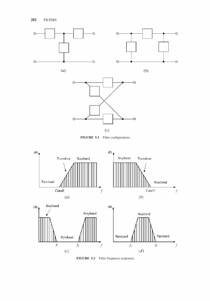
JWBS064-c05 JWBS064-Gerbennikov March 12, 2011 11:55 Printer Name: Yet to Come
202 FILTERS
FIGURE 5.1 Filter configurations.
FIGURE 5.2 Filter frequency responses.

JWBS064-c05 JWBS064-Gerbennikov March 12, 2011 11:55 Printer Name: Yet to Come
TYPES OF FILTERS 203
FIGURE 5.3 Voltage-driven two-port network terminated in its image impedance.
with the frequency response shown in Figure 5.2(d) is used when a certain unwanted frequency orband of frequencies has to be rejected. Outside of the rejection band or stopband, all frequencies willpass ideally without attenuation. All-pass filters pass all frequency components of the input signal, butintroduce a predictable phase shift for its different components. A short impulse on the input side ofsuch a filter is modified into a longer frequency-modulated signal at the output. As an example, an all-pass filter can be represented by a matched transmission line or LC lattice structure of a different order.
For an arbitrary voltage-driven two-port network specified by its transmission ABCD-parameters,as shown in Figure 5.3, the image impedance Z i1 is defined as the input impedance at input port1 when output port 2 is terminated with the image impedance Z i2, which is defined as the inputimpedance at output port 2 when port 1 is terminated with Zi1. Thus, both ports are matched whenterminated in their image impedances that can be expressed through the ABCD-parameters as
Z i1 =√
AB
CD(5.1)
Z i2 =√
BD
AC(5.2)
or Zi2 = DZi1/A, where the factor√
D/A can be interpreted as a transformer turns ratio [5]. If thenetwork is symmetric, then A = D and Zi2 = Z i1.
The propagation factor for the two-port network can be defined as
eγ =√
AD −√
BC (5.3)
where γ = α + jβ is the propagation constant, α is the attenuation constant, and β is the phaseconstant. Eq. (5.3) can be rewritten as
cosh γ = √AD. (5.4)
Table 5.1 lists the image impedances and propagation factors (along with other important param-eters) for the two-port T- and π -networks.
The basic network unit for realizing all-pass prototype filters is a lattice structure, as shown inFigure 5.4, where there is a conventional abbreviated representation on the right-hand side. Thislattice structure is not only symmetric with respect to the two ports, but also balanced with respectto ground. If the impedance of the series arm of the lattice is equal to Z1 and the impedance of theparallel arm is equal to Z2, the image impedance of the lattice structure is defined as
Z i =√
Z1 Z2 (5.5)

JWBS064-c05 JWBS064-Gerbennikov March 12, 2011 11:55 Printer Name: Yet to Come
204 FILTERS
TABLE 5.1 Image Parameters for T- and π-Networks.
T-Network π -Network
ABCD-parameters
A = 1 + Z1
2Z2
B = Z1 + Z21
4Z2
C = 1
Z2
D = 1 + Z1
2Z2
ABCD-parameters
A = 1 + Z1
2Z2
B = Z1
C = 1
Z2+ Z1
4Z22
D = 1 + Z1
2Z2
Z-parameters
Z11 = Z22 = Z2 + Z1
2Z12 = Z21 = Z2
Y-parameters
Y11 = Y22 = 1
Z1+ 1
2Z2
Y12 = Y21 = 1
Z1
Image impedance
Z iT = √Z1 Z2
√1 + Z1
4Z2
Image impedance
Z iπ =√
Z1 Z2√1 + Z1
4Z2
= Z1 Z2
ZiT
Propagation factor
eγ = 1 + Z1
2Z2+
√Z1
Z2+
(Z1
2Z2
)2
Propagation factor
eγ = 1 + Z1
2Z2+
√Z1
Z2+
(Z1
2Z2
)2
FIGURE 5.4 Lattice filter configuration.
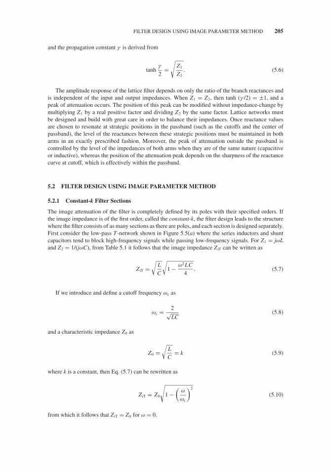
JWBS064-c05 JWBS064-Gerbennikov March 12, 2011 11:55 Printer Name: Yet to Come
FILTER DESIGN USING IMAGE PARAMETER METHOD 205
and the propagation constant γ is derived from
tanhγ
2=
√Z1
Z2. (5.6)
The amplitude response of the lattice filter depends on only the ratio of the branch reactances andis independent of the input and output impedances. When Z1 = Z2, then tanh (γ /2) = ±1, and apeak of attenuation occurs. The position of this peak can be modified without impedance-change bymultiplying Z1 by a real positive factor and dividing Z2 by the same factor. Lattice networks mustbe designed and build with great care in order to balance their impedances. Once reactance valuesare chosen to resonate at strategic positions in the passband (such as the cutoffs and the center ofpassband), the level of the reactances between these strategic positions must be maintained in botharms in an exactly prescribed fashion. Moreover, the peak of attenuation outside the passband iscontrolled by the level of the impedances of both arms when they are of the same nature (capacitiveor inductive), whereas the position of the attenuation peak depends on the sharpness of the reactancecurve at cutoff, which is effectively within the passband.
5.2 FILTER DESIGN USING IMAGE PARAMETER METHOD
5.2.1 Constant-k Filter Sections
The image attenuation of the filter is completely defined by its poles with their specified orders. Ifthe image impedance is of the first order, called the constant-k, the filter design leads to the structurewhere the filter consists of as many sections as there are poles, and each section is designed separately.First consider the low-pass T-network shown in Figure 5.5(a) where the series inductors and shuntcapacitors tend to block high-frequency signals while passing low-frequency signals. For Z1 = jωLand Z2 = 1/(jωC), from Table 5.1 it follows that the image impedance ZiT can be written as
Z iT =√
L
C
√1 − ω2 LC
4. (5.7)
If we introduce and define a cutoff frequency ωc as
ωc = 2√LC
(5.8)
and a characteristic impedance Z0 as
Z0 =√
L
C= k (5.9)
where k is a constant, then Eq. (5.7) can be rewritten as
Z iT = Z0
√1 −
(ω
ωc
)2
(5.10)
from which it follows that ZiT = Z0 for ω = 0.
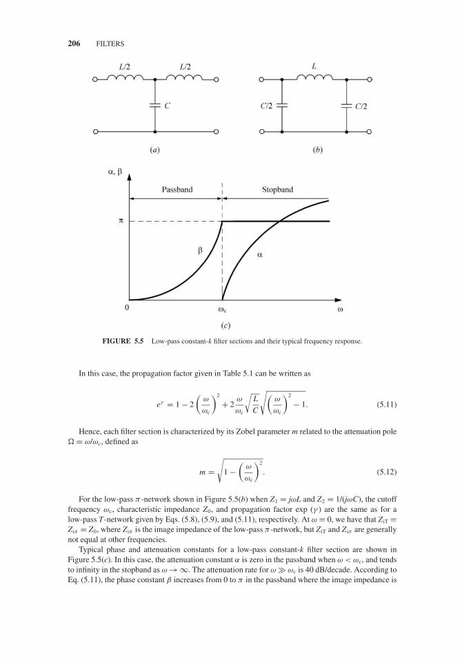
JWBS064-c05 JWBS064-Gerbennikov March 12, 2011 11:55 Printer Name: Yet to Come
206 FILTERS
FIGURE 5.5 Low-pass constant-k filter sections and their typical frequency response.
In this case, the propagation factor given in Table 5.1 can be written as
eγ = 1 − 2
(ω
ωc
)2
+ 2ω
ωc
√L
C
√(ω
ωc
)2
− 1. (5.11)
Hence, each filter section is characterized by its Zobel parameter m related to the attenuation pole� = ω/ωc, defined as
m =√
1 −(
ω
ωc
)2
. (5.12)
For the low-pass π -network shown in Figure 5.5(b) when Z1 = jωL and Z2 = 1/(jωC), the cutofffrequency ωc, characteristic impedance Z0, and propagation factor exp (γ ) are the same as for alow-pass T-network given by Eqs. (5.8), (5.9), and (5.11), respectively. At ω = 0, we have that Z iT =Ziπ = Z0, where Ziπ is the image impedance of the low-pass π -network, but ZiT and Ziπ are generallynot equal at other frequencies.
Typical phase and attenuation constants for a low-pass constant-k filter section are shown inFigure 5.5(c). In this case, the attenuation constant α is zero in the passband when ω < ωc, and tendsto infinity in the stopband as ω → ∞. The attenuation rate for ω � ωc is 40 dB/decade. According toEq. (5.11), the phase constant β increases from 0 to π in the passband where the image impedance is
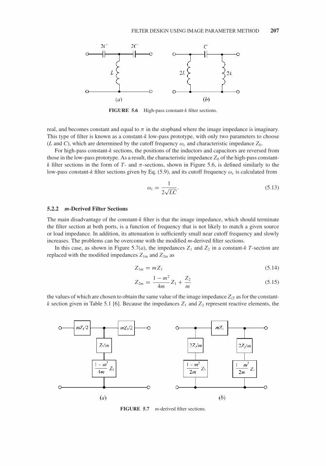
JWBS064-c05 JWBS064-Gerbennikov March 12, 2011 11:55 Printer Name: Yet to Come
FILTER DESIGN USING IMAGE PARAMETER METHOD 207
FIGURE 5.6 High-pass constant-k filter sections.
real, and becomes constant and equal to π in the stopband where the image impedance is imaginary.This type of filter is known as a constant-k low-pass prototype, with only two parameters to choose(L and C), which are determined by the cutoff frequency ωc and characteristic impedance Z0.
For high-pass constant-k sections, the positions of the inductors and capacitors are reversed fromthose in the low-pass prototype. As a result, the characteristic impedance Z0 of the high-pass constant-k filter sections in the form of T- and π-sections, shown in Figure 5.6, is defined similarly to thelow-pass constant-k filter sections given by Eq. (5.9), and its cutoff frequency ωc is calculated from
ωc = 1
2√
LC. (5.13)
5.2.2 m-Derived Filter Sections
The main disadvantage of the constant-k filter is that the image impedance, which should terminatethe filter section at both ports, is a function of frequency that is not likely to match a given sourceor load impedance. In addition, its attenuation is sufficiently small near cutoff frequency and slowlyincreases. The problems can be overcome with the modified m-derived filter sections.
In this case, as shown in Figure 5.7(a), the impedances Z1 and Z2 in a constant-k T-section arereplaced with the modified impedances Z1m and Z2m as
Z1m = m Z1 (5.14)
Z2m = 1 − m2
4mZ1 + Z2
m(5.15)
the values of which are chosen to obtain the same value of the image impedance Z iT as for the constant-k section given in Table 5.1 [6]. Because the impedances Z1 and Z2 represent reactive elements, the
FIGURE 5.7 m-derived filter sections.

JWBS064-c05 JWBS064-Gerbennikov March 12, 2011 11:55 Printer Name: Yet to Come
208 FILTERS
modified impedance Z2m represents two elements in series. Note that m = 1 reduces the m-derivedfilter section to the original constant-k- filter section.
For a low-pass T-section when Z1 = jωL and Z2 = 1/(jωC), the modified impedances Z1m andZ2m, given by Eqs. (5.14) and (5.15), can be rewritten as
Z1m = jmωL (5.16)
Z2m = j1 − m2
4mωL + 1
jmωC(5.17)
which results in the filter circuit of Figure 5.8(a). In this case, the propagation factor for the m-derivedsection can be written using Table 5.1 as
eγ = 1 + Z1m
2Z2m+
√Z1m
Z2m
(1 + Z1m
4Z2m
). (5.18)
For the low-pass m-derived T-section,
Z1m
Z2m= −
(2m
ω
ωc
)2
1 − (1 − m2
) (ω
ωc
) (5.19)
FIGURE 5.8 Low-pass and high-pass m-derived T-sections and frequency response.

JWBS064-c05 JWBS064-Gerbennikov March 12, 2011 11:55 Printer Name: Yet to Come
FILTER DESIGN USING IMAGE PARAMETER METHOD 209
where ωc = 2/√
LC as for the low-pass constant-k filter section, and
1 + Z1m
4Z2m=
1 −(
ω
ωc
)2
1 − (1 − m2
) (ω
ωc
) . (5.20)
Substituting Eqs. (5.19) and (5.20) into Eq. (5.18) shows that when 0 < m < 1, then the propagationfactor eγ is real and |eγ | > 1 for ω > ωc. Hence, the filter stopband begins at ω = ωc, similarly to theconstant-k section. However, when ω = ω∞ and the filter Zobel parameter m is defined as
m =√
1 −(
ωc
ω∞
)2
(5.21)
the denominators in both Eqs. (5.19) and (5.20) vanish and eγ becomes infinite, thus implying infiniteattenuation. Physically, this pole in the attenuation characteristic is caused by the resonance of theseries LC resonator at ω∞ in the shunt arm of the T-section. The infinite attenuation occurs after thecutoff frequency ωc, and the position of pole can be controlled with the value of m. The best resultwith minimum variation of the image impedance Z iT over the filter passband is achieved when m =0.6. The high-pass m-derived T-section is shown in Figure 5.8(b), for which ωc = 1/(2
√LC) as for
the high-pass constant-k filter section and
m =√
1 −(
ω∞ωc
)2
. (5.22)
The low-pass m-derived section shown in Figure 5.7(b) can be obtained from the correspondingtwo m-derived T-sections connected in cascade. In this case, the impedances Z1m and Z2m in theseries and shunt arms must be multiplied by a factor of 2. Figure 5.9 shows the (a) low-pass and(b) high-pass m-derived π -sections, where m for sharp cutoff is defined by Eqs. (5.21) and (5.22),respectively, and equals to 0.6 for optimum matching. The inductor L and capacitor C are the sameas for the corresponding low-pass and high-pass constant-k π-sections.
From Figure 5.8(c) it follows that the filter attenuation of the m-derived section decreases for ω >
ω∞. Since it is often desirable to have infinite attenuation as ω → ∞, the m-derived section canbe cascaded with a constant-k section to give the composite attenuation response. By combining incascade the constant-k T-section, the m-derived sharp-cutoff T-section, and the m-derived bisected-π matching sections at the filter input and output, the four-stage composite filter with desired
FIGURE 5.9 Low-pass and high-pass m-derived π-sections.

JWBS064-c05 JWBS064-Gerbennikov March 12, 2011 11:55 Printer Name: Yet to Come
210 FILTERS
attenuation and matching properties can be realized [5]. The sharp-cutoff section with m < 0.6 placesan attenuation pole near the cutoff frequency to provide a sharp attenuation response, whereas theconstant-k section provides high attenuation further into the stopband. The bisected-π sections at theends of the filter match the nominal source and load impedance Z0 to the internal image impedancesZiT of the constant-k and m-derived sections.
5.3 FILTER DESIGN USING INSERTION LOSS METHOD
Unlike the image parameter method, the insertion loss method allows a high degree of the filterperformance control over the passband and stopband when the desired amplitude and phase charac-teristic can be synthesized with a systematic way. For example, if a minimum insertion loss is mostimportant, a binomial filter response could be used. However, a requirement for the sharpest cutoffcan be satisfied with a Chebyshev filter response, or better phase response can be obtained by usinga linear phase filter design. In all cases, the insertion loss method allows filter performance to beimproved in a straightforward manner, at the expense of a higher order filter.
In the insertion loss method, a filter response is defined by its attenuation A (or insertion loss indecibels equal to 10 log10 A), which is defined as the ratio of power available from the source PS topower delivered to the load PL,
A = PS
PL= 1
1 − |� (ω)|2 (5.23)
where �(ω) is the reflection coefficient. For the input impedance Zin(ω) = Rin(ω) + jXin(ω), thereflection coefficient �(ω) can be written as
� (ω) = Z in (ω) − Z0
Z in (ω) + Z0= Rin (ω) − Z0 + j X in (ω)
Rin (ω) + Z0 + j X in (ω)(5.24)
where Z0 is the characteristic impedance. From Eq. (5.24) it follows that the magnitude of thereflection coefficient is even function of ω because
|� (ω)|2 = |� (−ω)|2 (5.25)
and it can be expressed as a polynomial of ω2. As a result, Eq. (5.23) can be rewritten as
A = 1 + M(ω2
)N
(ω2
) . (5.26)
5.3.1 Maximally Flat Low-Pass Filter
The low-pass binomial or Butterworth response of the filter (named in honor of S. Butterworth whodescribed this response in 1930), which is completely defined by its poles, is specified as
A = 1 + k2
(ω
ωc
)2n
(5.27)
where n is the order of the filter, which corresponds to the number of required reactive elements, andωc is the cutoff frequency. The insertion-loss function of this filter in the passband has the flattestpossible shape in the passband (maximally flat), having the maximum number of (2n − 1) zeroderivatives at ω = 0, and is a monotonically increasing function. The passband extends from ω = 0

JWBS064-c05 JWBS064-Gerbennikov March 12, 2011 11:55 Printer Name: Yet to Come
FILTER DESIGN USING INSERTION LOSS METHOD 211
FIGURE 5.10 Maximally flat responses and low-pass filter prototype.
to ω = ωc, with the power loss ratio of (1 + k2) at the band edge and k = 1 for a commonly usedmaximum passband attenuation of 3 dB. Above the cutoff frequency, the attenuation increases almostlinearly that gives a rate of 6n dB/octave on a logarithmic frequency scale. The attenuation functionsof the low-pass Butterworth filter are sketched in Figure 5.10(a) for small (n = 2) and large (n =5) filter orders. It is clearly seen that the larger order provides a better approximation to the ideallow-pass response.
As a design example, consider the two-element low-pass filter prototype shown in Figure 5.10(b)and derive the normalized element values of an inductor L1 and a capacitor C2 for a maximally flatresponse, assuming a source impedance RS = Z0 = 1 � and a cutoff frequency ωc = 1 radian/s. Forn = 2, the input impedance of this filter can be written as
Z in = jωL1 + 1 − jωC2 RL
1 + (ωC2 RL)2 RL. (5.28)
Then, substituting Eq. (5.28) to Eq. (5.23), and using Eq. (5.24), results in
A = 1 + (1 − RL)2 + (R2
LC22 + L2
1 − 2L1C2 R2L
)ω2 + (L1C2 RL)2 ω4
4RL(5.29)

JWBS064-c05 JWBS064-Gerbennikov March 12, 2011 11:55 Printer Name: Yet to Come
212 FILTERS
FIGURE 5.11 Ladder circuits for low-pass filter prototypes.
which represents a polynomial of ω2. Comparing to Eq. (5.27) for k = 1 and n = 2 shows that RL =1 �, since A = 1 for ω = 0. In this case, the coefficient of ω2 must be equal to zero, which results inL1 = C2. Then, for the coefficient of ω4 to be unity, L1 = C2 = √
2.In principle, this design procedure can be extended to find the element values for filters with an
arbitrary numbers of elements, but analytically it becomes too complicated. Generally, by constructingthe rational transfer function from Eq. (5.27), the values of elements (normalized capacitors andinductors) shown in Figure 5.11 are calculated from
g0 = 1.0
gi = 2sin
(2i − 1
2nπ
)for i = 1, . . . , n
gn+1 = 1.0
(5.30)
which are given in numerical form in Table 5.2 [7,8]. For convenience, the element values formaximally flat low-pass filter prototypes are given for n = 1 to 8, and these data can be used with
TABLE 5.2 Element Values for Maximally Flat Low-Pass Filter Prototypes.
n g1 g2 g3 g4 g5 g5 g7 g8 g9
1 2.0000 1.00002 1.4142 1.4142 1.00003 1.0000 2.0000 1.0000 1.00004 0.7654 1.8478 1.8478 0.7654 1.00005 0.6180 0.6180 2.0000 0.6180 0.6180 1.00006 0.5176 1.4142 1.9318 1.9318 1.4142 0.5176 1.00007 0.4450 1.2470 1.8019 2.0000 1.8019 1.2470 0.4450 1.00008 0.3902 1.1111 1.6629 1.9615 1.9615 1.6629 1.1111 0.3902 1.0000
JWBS064-c05 JWBS064-Gerbennikov March 12, 2011 11:55 Printer Name: Yet to Come
FILTER DESIGN USING INSERTION LOSS METHOD 213
either of the ladder circuits of Figure 5.11, where RS = R0 and GS = G0. The two-port Butterworthfilters considered here represent the symmetrical network structure when g0 = gn+1, g1 = gn, and soon. If a termination resistance higher than 1 � is desired, the reactances are multiplied accordingly.The reactances are then scaled so that they have the same value at the new desired cutoff frequency ωc.
The elements alternate between series and shunt connections, and g0 and gn+1 represent the sourceand load resistances for a network in Figure 5.11(a) and the source and load conductances for anetwork in Figure 5.11(b); the reactive components are calculated from
Ci = gi
ωc R0L i = gi R0
ωc(5.31)
and both low-pass ladder circuits of Figure 5.11 give the same frequency response.The degree of a Butterworth low-pass filter prototype defined by a minimum stopband attenuation
Amin at ω = ωs and a maximum passband attenuation Amax at ω = ωc can be derived from Eq. (5.27)in the form
n ≥log10
Amin − 1
Amax − 1
2 log10
ωs
ωc
. (5.32)
For example, if a minimum attenuation in the stopband Amin = 104 (or 40 dB) at ωs/ωc = 2 forAmax = 2 (or 3 dB) is required, then n ≥ 6.644, and a 7-pole (n = 7) Butterworth prototype should bechosen.
In the high-pass ladder filters, which are dual of the low-pass ladder filters, the series inductors arereplaced with series capacitors, while shunt capacitors are replaced by shunt inductors. The reactancesare the same at the normalized cutoff frequency ωc = 1 radian/s and R0 = 1 �. The Butterworthhigh-pass filter prototype is described by the following denormalization of the normalized low-passdata from Table 5.2:
Ci = 1
giωc R0L i = R0
giωc. (5.33)
The Butterworth approximation is useful for many applications; however, its main advantage isits mathematical simplicity. The low-pass Butterworth response was derived on the assumption thatbehavior at zero frequency was far more important than behavior at any other frequency. This leads toa class of filters with good phase response and tolerably good amplitude response but with very poorcharacteristics around the cutoff frequency. The Butterworth function is unsuitable for applicationsthat require uniform transmission of frequencies in the passband and sharp rise at cutoff.
5.3.2 Equal-Ripple Low-Pass Filter
By changing the approximation conditions, it is possible to obtain much better characteristics nearcutoff frequency. Besides, it may be required that all frequencies in the passband are equally important,and that it is desirable to minimize the maximum deviation from the ideal response. The Chebyshevapproximation can exhibit the equal-ripple passband and maximally flat stopband when the attenuationof the low-pass filter is written as
A = 1 + k2T 2n
(ω
ωc
)(5.34)
JWBS064-c05 JWBS064-Gerbennikov March 12, 2011 11:55 Printer Name: Yet to Come
214 FILTERS
where k is the ripple constant and Tn(ω/ωc) is the a Chebyshev function of the first kind of order n,which is defined as
Tn
(ω
ωc
)=
⎧⎪⎪⎪⎨⎪⎪⎪⎩
cos
(n cos−1 ω
ωc
)for
ω
ωc≤ 1
cosh
(n cosh−1 ω
ωc
)for
ω
ωc≥ 1
. (5.35)
From Eq. (5.35) is not clear that Tn(ω/ωc) is actually the nth-order polynomial. However, byapplying simple trigonometric identities, the first four Chebyshev polynomials are written as
T1(x) = x (5.36)
T2(x) = 2x2 − 1 (5.37)
T3(x) = 4x3 − 3x (5.38)
T4(x) = 8x4 − 8x2 + 1 (5.39)
with higher order polynomials found using general recurrence relation,
Tn(x) = 2xTn−1 (x) − Tn−2 (x) (5.40)
where x = ω/ωc.Since the Chebyshev polynomials have the property that Tn(0) = 0 for odd n and Tn(0) = 1 for
even n, from Eq. (5.34) it follows that the equally-ripple low-pass filter have a unity attenuation atω = 0 for odd n, but an attenuation of (1 + k2) at ω = 0 for even n. In the passband, the attenuationresponse varies between the values of zero and Amax = 1 + k2, as seen from Figure 5.12(a) forn = 2, 3. Above the cutoff frequency ωc, the attenuation curve rises monotonically. The rate ofincrease depends not only upon the number of poles or resonators but also upon such a designparameter as the height of the ripples: the attenuation rate is higher for larger passband ripples.
For the two-element low-pass filter prototype, shown in Figure 5.12(b) with a source impedanceRS = R0 = 1 � and a cutoff frequency ωc = 1 radian/s, equating Eq. (5.34) to Eq. (5.29) and usingEq. (5.37) result in
1 + k2(4ω4 − 4ω2 + 1
) = 1 + (1 − RL)2 + (R2
LC22 + L2
1 − 2L1C2 R2L
)ω2 + (L1C2 RL)2 ω4
4RL
(5.41)
which can be solved to define RL, L1, and C2 if the ripple determined by k2 is known. Since k2 =(1 − RL)2/(4RL) at ω = 0, then equating coefficients of ω2 and ω4 yields the additional equations,
4k2 = (L1C2 RL)2
4RL(5.42)
−4k2 = (C2 RL)2 + L21 − 2L1C2 R2
L
4RL(5.43)
which are necessary to find L1 and C2. Note that a value for RL is not unity for even n, thus resultingin an impedance mismatch if the load represents a unity normalized impedance.
Because it is too complicated to find analytically element values for filters with arbitrary numbersof elements, by constructing the rational transfer function from Eq. (5.34), the values of elements

JWBS064-c05 JWBS064-Gerbennikov March 12, 2011 11:55 Printer Name: Yet to Come
FILTER DESIGN USING INSERTION LOSS METHOD 215
FIGURE 5.12 Equal-ripple responses and low-pass filter prototype.
(normalized capacitors and inductors) shown in Figure 5.11 can be calculated from
g0 = 1.0
g1 = 2
γsin
( π
2n
)
gi = 1
gi−1
4 sin
(2i − 1
2nπ
)sin
(2i − 3
2nπ
)γ 2
for i = 2, 3, . . . , n
gn+1 = 1.0 for odd n and gn+1 = coth2 β
4for even n
(5.44)
with
γ = sinhβ
2nβ = ln
[coth
A (dB)
17.3718
]
where A(dB) is the passband ripple in decibels [7]. Some typical element values for such filters aregiven in numerical form in Table 5.3 for various passband ripples A(dB) and for the filter degree ofn = 1 to 7.
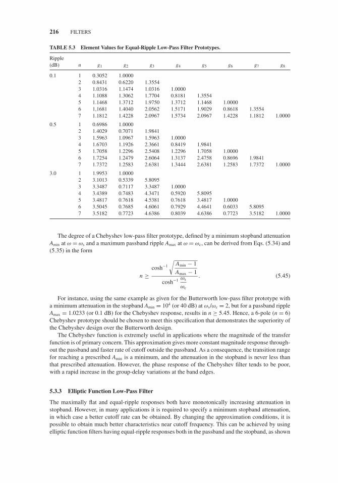
JWBS064-c05 JWBS064-Gerbennikov March 12, 2011 11:55 Printer Name: Yet to Come
216 FILTERS
TABLE 5.3 Element Values for Equal-Ripple Low-Pass Filter Prototypes.
Ripple(dB) n g1 g2 g3 g4 g5 g6 g7 g8
0.1 1 0.3052 1.00002 0.8431 0.6220 1.35543 1.0316 1.1474 1.0316 1.00004 1.1088 1.3062 1.7704 0.8181 1.35545 1.1468 1.3712 1.9750 1.3712 1.1468 1.00006 1,1681 1.4040 2.0562 1.5171 1.9029 0.8618 1.35547 1.1812 1.4228 2.0967 1.5734 2.0967 1.4228 1.1812 1.0000
0.5 1 0.6986 1.00002 1.4029 0.7071 1.98413 1.5963 1.0967 1.5963 1.00004 1.6703 1.1926 2.3661 0.8419 1.98415 1.7058 1.2296 2.5408 1.2296 1.7058 1.00006 1.7254 1.2479 2.6064 1.3137 2.4758 0.8696 1.98417 1.7372 1.2583 2.6381 1.3444 2.6381 1.2583 1.7372 1.0000
3.0 1 1.9953 1.00002 3.1013 0.5339 5.80953 3.3487 0.7117 3.3487 1.00004 3.4389 0.7483 4.3471 0.5920 5.80955 3.4817 0.7618 4.5381 0.7618 3.4817 1.00006 3.5045 0.7685 4.6061 0.7929 4.4641 0.6033 5.80957 3.5182 0.7723 4.6386 0.8039 4.6386 0.7723 3.5182 1.0000
The degree of a Chebyshev low-pass filter prototype, defined by a minimum stopband attenuationAmin at ω = ωs and a maximum passband ripple Amax at ω = ωc, can be derived from Eqs. (5.34) and(5.35) in the form
n ≥cosh−1
√Amin − 1
Amax − 1
cosh−1 ωs
ωc
. (5.45)
For instance, using the same example as given for the Butterworth low-pass filter prototype witha minimum attenuation in the stopband Amin = 104 (or 40 dB) at ωs/ωc = 2, but for a passband rippleAmax = 1.0233 (or 0.1 dB) for the Chebyshev response, results in n ≥ 5.45. Hence, a 6-pole (n = 6)Chebyshev prototype should be chosen to meet this specification that demonstrates the superiority ofthe Chebyshev design over the Butterworth design.
The Chebyshev function is extremely useful in applications where the magnitude of the transferfunction is of primary concern. This approximation gives more constant magnitude response through-out the passband and faster rate of cutoff outside the passband. As a consequence, the transition rangefor reaching a prescribed Amin is a minimum, and the attenuation in the stopband is never less thanthat prescribed attenuation. However, the phase response of the Chebyshev filter tends to be poor,with a rapid increase in the group-delay variations at the band edges.
5.3.3 Elliptic Function Low-Pass Filter
The maximally flat and equal-ripple responses both have monotonically increasing attenuation instopband. However, in many applications it is required to specify a minimum stopband attenuation,in which case a better cutoff rate can be obtained. By changing the approximation conditions, it ispossible to obtain much better characteristics near cutoff frequency. This can be achieved by usingelliptic function filters having equal-ripple responses both in the passband and the stopband, as shown
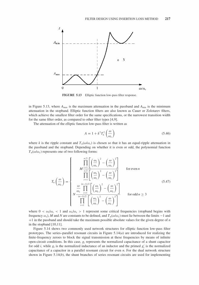
JWBS064-c05 JWBS064-Gerbennikov March 12, 2011 11:55 Printer Name: Yet to Come
FILTER DESIGN USING INSERTION LOSS METHOD 217
FIGURE 5.13 Elliptic function low-pass filter response.
in Figure 5.13, where Amax is the maximum attenuation in the passband and Amin is the minimumattenuation in the stopband. Elliptic function filters are also known as Cauer or Zolotarev filters,which achieve the smallest filter order for the same specifications, or the narrowest transition widthfor the same filter order, as compared to other filter types [4,9].
The attenuation of the elliptic function low-pass filter is written as
A = 1 + k2T 2n
(ω
ωc
)(5.46)
where k is the ripple constant and Tn(ω/ωc) is chosen so that it has an equal-ripple attenuation inthe passband and the stopband. Depending on whether it is even or odd, the polynomial functionTn(ω/ωc) represents one of two following forms:
Tn
(ω
ωc
)=
⎧⎪⎪⎪⎪⎪⎪⎪⎪⎪⎪⎪⎪⎪⎪⎪⎪⎪⎨⎪⎪⎪⎪⎪⎪⎪⎪⎪⎪⎪⎪⎪⎪⎪⎪⎪⎩
M
n/2∏i=1
[(ωi
ωc
)2
−(
ω
ωc
)2]
n/2∏i=1
[(ωs
ωi
)2
−(
ω
ωc
)2] for even n
N
ω
ωc
(n−1)/2∏i=1
[(ωi
ωc
)2
−(
ω
ωc
)2]
(n−1)/2∏i=1
[ (ωs
ωi
)2
−(
ω
ωc
)2] for odd n ≥ 3
(5.47)
where 0 < ωi/ωc < 1 and ωs/ωc > 1 represent some critical frequencies (stopband begins withfrequency ωs), M and N are constants to be defined, and Tn(ω/ωc) must lie between the limits −1 and+1 in the passband and should take the maximum possible absolute values for the given degree of nin the stopband [10,11].
Figure 5.14 shows two commonly used network structures for elliptic function low-pass filterprototypes. The series–parallel resonant circuits in Figure 5.14(a) are introduced for realizing thefinite-frequency zeroes to block the signal transmission at these frequencies by means of infiniteopen-circuit conditions. In this case, gi represents the normalized capacitance of a shunt capacitorfor odd i, while gi is the normalized inductance of an inductor and the primed g′
i is the normalizedcapacitance of a capacitor in a parallel resonant circuit for even n. For the dual network structureshown in Figure 5.14(b), the shunt branches of series resonant circuits are used for implementing
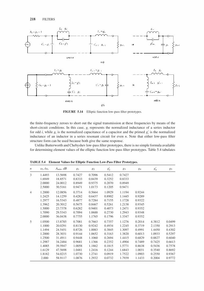
JWBS064-c05 JWBS064-Gerbennikov March 12, 2011 11:55 Printer Name: Yet to Come
218 FILTERS
FIGURE 5.14 Elliptic function low-pass filter prototypes.
the finite-frequency zeroes to short out the signal transmission at these frequencies by means of theshort-circuit conditions. In this case, gi represents the normalized inductance of a series inductorfor odd i, while gi is the normalized capacitance of a capacitor and the primed g′
i is the normalizedinductance of an inductor in a series resonant circuit for even n. Note that either low-pass filterstructure form can be used because both give the same response.
Unlike Butterworth and Chebyshev low-pass filter prototypes, there is no simple formula availablefor determining element values of the elliptic function low-pass filter prototypes. Table 5.4 tabulates
TABLE 5.4 Element Values for Elliptic Function Low-Pass Filter Prototypes.
n ωs /ωc Amin, dB g1 g2 g′2 g3 g4 g′
4 g5
3 1.4493 13.5698 0.7427 0.7096 0.5412 0.74271.6949 18.8571 0.8333 0.8439 0.3252 0.83332.0000 24.0012 0.8949 0.9375 0.2070 0.89492.5000 30.5161 0.9471 1.0173 0.1205 0.9471
4 1.2000 12.0856 0.3714 0.5664 1.0929 1.1194 0.92441.2425 14.1259 0.4282 0.6437 0.8902 1.1445 0.92891.2977 16.5343 0.4877 0.7284 0.7155 1.1728 0.93221.3962 20.3012 0.5675 0.8467 0.5261 1.2138 0.93451.5000 23.7378 0.6282 0.9401 0.4073 1.2471 0.93521.7090 29.5343 0.7094 1.0688 0.2730 1.2943 0.93482.0000 36.0438 0.7755 1.1765 0.1796 1.3347 0.9352
5 1.0500 13.8785 0.7081 0.7663 0.7357 1.1276 0.2014 4.3812 0.04991.1000 20.0291 0.8130 0.9242 0.4934 1.2245 0.3719 2.1350 0.29131.1494 24.5451 0.8726 1.0083 0.3845 1.3097 0.4991 1.4450 0.43021.2000 28.3031 0.9144 1.0652 0.3163 1.3820 0.6013 1.0933 0.52971.2500 31.4911 0.9448 1.1060 0.2694 1.4415 0.6829 0.8827 0.60401.2987 34.2484 0.9681 1.1366 0.2352 1.4904 0.7489 0.7425 0.66131.4085 39.5947 1.0058 1.1862 0.1815 1.5771 0.8638 0.5436 0.75781.6129 47.5698 1.0481 1.2416 0.1244 1.6843 1.0031 0.3540 0.86921.8182 54.0215 1.0730 1.2741 0.0919 1.7522 1.0903 0.2550 0.93672.000 58.9117 1.0876 1.2932 0.0732 1.7939 1.1433 0.2004 0.9772

JWBS064-c05 JWBS064-Gerbennikov March 12, 2011 11:55 Printer Name: Yet to Come
FILTER DESIGN USING INSERTION LOSS METHOD 219
some useful design data for equally terminated (g0 = gn+1 = 1) elliptic function low-pass filterprototypes representing two equivalent structures shown in Figure 5.14, where normalized elementvalues are given for various ωs/ωc and minimum stopband attenuation Amin for a maximum passbandripple Amax = 0.1 dB [12]. In this case, a smaller ωs/ωc means a higher selectivity of the filter at theexpense of reducing stopband rejection.
Considering the same example as used for the Butterworth and Chebyshev low-pass filter pro-totypes with a minimum attenuation in the stopband Amin = 40 dB at ωs/ωc = 2 and a maximumpassband ripple Amax = 0.1 dB, from Table 5.4 it follows that a 5-pole (n = 5) elliptic functionfilter prototype should be chosen that demonstrates its superiority over both the Butterworth andChebyshev designs for this type of specification. Note that the even-degree Zolotarev low-pass filterhas a mismatch at zero frequency and is realizable as an impedance-transforming LC ladder networkwith unequal terminations [13].
5.3.4 Maximally Flat Group-Delay Low-Pass Filter
A maximally flat group-delay low-pass filter prototype is characterized by its transfer (or gain)function G(jω/ωc) that is written in the form
G
(j
ω
ωc
)= a0
n∑k=0
ak
(j
ω
ωc
)k(5.48)
where
ak = (2n − k) !
2n−kk! (n − k) !(5.49)
represents the coefficients of the reverse Bessel polynomials and ωc is a frequency chosen to givethe desired cutoff frequency. This transfer function results in better responses in the time domain andapproaches the ideal Gaussian curve as the degree of approximation is increased (n → ∞). It alsocontributes to a group delay that has maximum possible number of zero derivatives with respect to ω
at ω = 0, resulting in a maximally flat group delay around ω = 0, and is in a sense complementaryto the Butterworth response, which has a maximally flat amplitude. This maximally flat group-delayapproximation was originally derived by W. E. Thompson, and for these reasons the filter prototypesof this type are also called Bessel–Thompson filters [14]. The first four Bessel polynomials withrespect to a loss function H(jω/ωc) = 1/G(jω/ωc) are written as
H (s) =
⎧⎪⎪⎨⎪⎪⎩
s + 1 for n = 1s2 + 3s + 1 for n = 2s3 + 6s2 + 15s + 15 for n = 3s4 + 10s3 + 45s2 + 105s + 105 for n = 4
(5.50)
where s = jω/ωc is the normalized complex frequency variable.Figure 5.15 shows the typical maximally flat group-delay responses in terms of attenuation
and group delay for n = 3 and n = 5 that are properly obtained from Eq. (5.48). In general, theBessel–Thompson filters have a poor selectivity, as can be seen from the attenuation curves inFigure 5.15(a). However, its selectivity improves according to
A(dB) = 10 log10 exp
[1
2n − 1
(ω
ωc
)2]
(5.51)
with increasing order n of the filter [15]. From Eq. (5.51), the 3-dB frequency bandwidth can bedetermined as
ω3dB
ωc=
√(2n − 1) ln 2 (5.52)

JWBS064-c05 JWBS064-Gerbennikov March 12, 2011 11:55 Printer Name: Yet to Come
220 FILTERS
FIGURE 5.15 Maximally flat group-delay response.
approximation of which is sufficiently accurate for n ≥ 3. Hence, unlike the Butterworth response,the 3-dB bandwidth of a Bessel–Thompson filter is a function of the filter order when the higher thefilter order, the wider the 3-dB bandwidth.
However, the Bessel–Thompson filters have a quite flat group delay in the passband, as shown inFigure 5.15(b) for a normalized group delay τ g/τ 0, where τ 0 is the delay at zero frequency, and thisnormalized group delay is inversely proportional to the bandwidth of the passband. With increasingthe filter order n, the group delay is flat over a wider frequency range. Therefore, a high-orderBessel–Thompson filter is usually used for achieving a flat group delay over a large passband.
As an example, consider the gain function G(s) for a third-order Bessel–Thompson low-pass filterprototype derived from Eq. (5.48) as
G(s) = 15
s3 + 6s2 + 15s + 15. (5.53)
In this case, the attenuation A = |H (s)|2 = 1/ |G (s)|2 can be written by assuming ωc = 1 radian/sas
A = 1 + ω2
5+ ω4
75+ ω6
225(5.54)
and the phase φ = arg[G(s)] as
φ (ω) = − tan−1
(15ω − ω3
15 − 6ω2
). (5.55)
The group delay, which is a measure of the transit time of a signal through a particular transmittingstructure versus frequency, is then
τg = −φ (ω)
ω= 6ω4 + 45ω2 + 225
ω6 + 6ω4 + 45ω2 + 225. (5.56)
Finally, the Taylor series expansion of the group delay is
τg = 1 − ω6
225+ ω8
1125+ · · · (5.57)

JWBS064-c05 JWBS064-Gerbennikov March 12, 2011 11:55 Printer Name: Yet to Come
FILTER DESIGN USING INSERTION LOSS METHOD 221
TABLE 5.5 Element Values for Maximally Flat Group-Delay Low-Pass Filter Prototypes.
n g1 g2 g3 g4 g5 g5 g7 g8 g9
1 2.0000 1.00002 1.5774 0.4226 1.00003 1.2550 0.5528 0.1922 1.00004 1.0598 0.5116 0.3181 0.1104 1.00005 0.9303 0.4577 0.3312 0.2090 0.0718 1.00006 0.8377 0.4116 0.3158 0.2364 0.1480 0.0505 1.00007 0.7677 0.3744 0.2944 0.2378 0.1778 0.1104 0.0375 1.00008 0.7125 0.3446 0.2735 0.2297 0.1867 0.1387 0.0855 0.0289 1.0000
where the two terms in ω2 and ω4 are zero, resulting in a very flat group delay at ω = 0. This isthe greatest number of terms that can be set to zero, since there are a total of four coefficients in thethird-order Bessel polynomial, requiring four equations in order to be defined. One equation specifiesthat the gain be unity at ω = 0 and a second equation specifies that the gain be zero at ω = ∞, leavingtwo equations to specify two terms in the series expansion to be zero. This is a general property of thegroup delay for a Bessel–Thompson filter of order n: the first (n − 1) terms in the series expansion ofthe group delay will be zero, thus maximizing the flatness of the group delay at ω = 0.
Design element values for maximally flat group-delay low-pass filter prototypes with g0 = 1derived for the ladder circuits of Figure 5.11 for different values of n = 1 to 8 are given in Table 5.5.
Figure 5.16 shows the frequency transfer characteristics of the Butterworth, Chebyshev, andBessel–Thompson low-pass filter prototypes based on the ladder circuit shown in Figure 5.11(a)and the elliptic low-pass filter prototype based on the circuit structure of Figure 5.14(a). Each filterconfiguration was chosen to have an order of n = 5, with a passband ripple of 0.5 dB for the Chebyshev
FIGURE 5.16 Filter transfer frequency responses for n = 5.
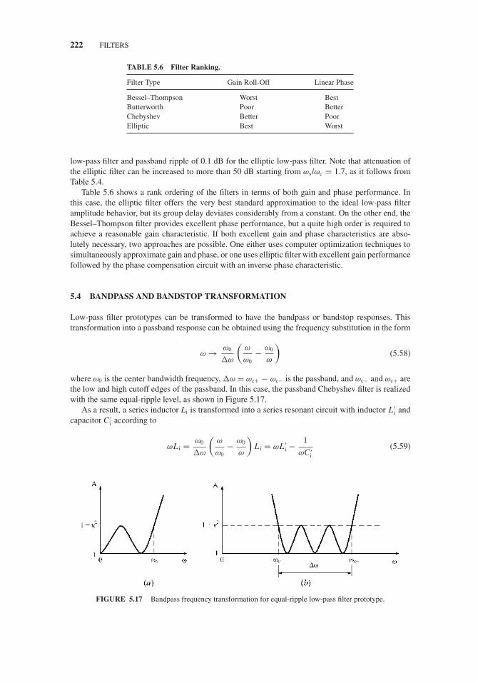
JWBS064-c05 JWBS064-Gerbennikov March 12, 2011 11:55 Printer Name: Yet to Come
222 FILTERS
TABLE 5.6 Filter Ranking.
Filter Type Gain Roll-Off Linear Phase
Bessel–Thompson Worst BestButterworth Poor BetterChebyshev Better PoorElliptic Best Worst
low-pass filter and passband ripple of 0.1 dB for the elliptic low-pass filter. Note that attenuation ofthe elliptic filter can be increased to more than 50 dB starting from ωs/ωc = 1.7, as it follows fromTable 5.4.
Table 5.6 shows a rank ordering of the filters in terms of both gain and phase performance. Inthis case, the elliptic filter offers the very best standard approximation to the ideal low-pass filteramplitude behavior, but its group delay deviates considerably from a constant. On the other end, theBessel–Thompson filter provides excellent phase performance, but a quite high order is required toachieve a reasonable gain characteristic. If both excellent gain and phase characteristics are abso-lutely necessary, two approaches are possible. One either uses computer optimization techniques tosimultaneously approximate gain and phase, or one uses elliptic filter with excellent gain performancefollowed by the phase compensation circuit with an inverse phase characteristic.
5.4 BANDPASS AND BANDSTOP TRANSFORMATION
Low-pass filter prototypes can be transformed to have the bandpass or bandstop responses. Thistransformation into a passband response can be obtained using the frequency substitution in the form
ω → ω0
�ω
(ω
ω0− ω0
ω
)(5.58)
where ω0 is the center bandwidth frequency, �ω = ωc+ − ωc− is the passband, and ωc− and ωc+ arethe low and high cutoff edges of the passband. In this case, the passband Chebyshev filter is realizedwith the same equal-ripple level, as shown in Figure 5.17.
As a result, a series inductor Li is transformed into a series resonant circuit with inductor L ′i and
capacitor C ′i according to
ωL i = ω0
�ω
(ω
ω0− ω0
ω
)L i = ωL ′
i −1
ωC ′i
(5.59)
FIGURE 5.17 Bandpass frequency transformation for equal-ripple low-pass filter prototype.
JWBS064-c05 JWBS064-Gerbennikov March 12, 2011 11:55 Printer Name: Yet to Come
BANDPASS AND BANDSTOP TRANSFORMATION 223
where
L ′i = L i
�ωC ′
i = �ω
ω20 L i
. (5.60)
Similarly, a shunt capacitor Ci is transformed into a shunt resonant circuit with inductor L ′i and
capacitor C ′i as
ωCi = ω0
�ω
(ω
ω0− ω0
ω
)Ci = ωC ′
i − 1
ωL ′i
(5.61)
where
C ′i = Ci
�ωL ′
i = �ω
ω20Ci
. (5.62)
The low-pass filter prototype will be transformed to the bandpass filter when all its series elementsare replaced by the series resonant circuits and all its parallel elements are replaced by the parallelresonant circuits, where each of them are tuned to the center bandwidth frequency ω0. In this case,the elements in the series resonant circuit of a bandpass filter can be calculated from Eq. (5.60) withimpedance scaling as
L ′i = gi R0
�ωC ′
i = �ω
ω20gi R0
(5.63)
whereas the elements in the shunt resonant circuit of a bandpass filter can be calculated from Eq.(5.62) with impedance scaling as
C ′i = gi
�ωR0L ′
i = �ωR0
ω20gi
(5.64)
where i is an element serial number for low-pass prototype filter and gi is the appropriate coefficientgiven by Table 5.2 for maximally flat low-pass filter prototype or Table 5.3 for equal-ripple low-passfilter prototype.
As an example, let us design a third-order (n = 3) bandpass filter with the center frequency of 2GHz and bandwidth of 20%, having a 0.5-dB equal-ripple response and an impedance R0 = 50 �.From Table 5.3, the element values for the low-pass prototype circuit shown in Figure 5.18(a) aregiven by
g1 = 1.5963 g2 = 1.0967
g3 = 1.5963 g4 = 1.0000.
Then, the impedance-scaled and frequency-transformed element values for the passband filtercircuit shown in Figure 5.18(b) using Eqs. (5.63) and (5.64) are
L ′1 = L ′
3 = 3.76 nH C ′1 = C ′
3 = 0.1994 pF
L ′2 = 0.7256 nH C ′
2 = 8.727 pF.
Finally, the resulting amplitude response of the Chebyshev passband filter in a frequency domainis shown in Figure 5.18(c) where the out-of-band suppression of 40 dB is achieved below 1.3 GHzand above 3.0 GHz.
The inverse transformation that can be applied to obtain a bandstop response is written as
ω → �ω
ω0
(ω
ω0− ω0
ω
)−1
(5.65)

JWBS064-c05 JWBS064-Gerbennikov March 12, 2011 11:55 Printer Name: Yet to Come
224 FILTERS
FIGURE 5.18 Bandpass filter circuit and its amplitude response.
where ω0 and �ω have the same definition as in Eq. (5.58). In this case, a series inductor Li of thelow-pass filter prototype is transformed into a parallel resonant circuit with inductor L ′
i and capacitorC ′
i according to
L ′i = �ωL i
ω20
C ′i = 1
�ωL i(5.66)
and a shunt capacitor Ci of the low-pass filter prototype is transformed into a series resonant circuitwith inductor L ′
i and capacitor C ′i as
C ′i = �ωCi
ω20
L ′i = 1
�ωCi(5.67)
with further denormalization similar to that given by Eqs. (5.63) and (5.64) for a passband filter.

JWBS064-c05 JWBS064-Gerbennikov March 12, 2011 11:55 Printer Name: Yet to Come
TRANSMISSION-LINE LOW-PASS FILTER IMPLEMENTATION 225
5.5 TRANSMISSION-LINE LOW-PASS FILTER IMPLEMENTATION
The design approaches for the filters with lumped elements generally work well at sufficiently lowfrequencies or in small-size monolithic integrated circuits. However, the lumped elements such as in-ductors and capacitors are difficult to implement at microwave frequencies where they can be treated asdistributed elements, and distances between the filter components are not negligible. The other prob-lem is that the quality factors for inductors are sufficiently small, thus contributing to additional losses.
5.5.1 Richards’s Transformation
Generally, the design of a practical distributed filter is based on some approximate equivalence be-tween lumped and distributed elements, which can be established by applying a Richards’s transforma-tion [16]. This implies that the distributed circuits composed of equal-length open- and short-circuitedtransmission lines can be treated as lumped elements under the transformation
s = j tanπω
2ω0(5.68)
where s = jω/ωc is the conventional normalized complex frequency variable and ω0 is the radianfrequency for which the transmission lines are a quarter wavelength [12].
As a result, the one-port impedance of a short-circuited transmission line corresponds to thereactive impedance of a lumped inductor ZL as
ZL = sL = jωL = j L tanπω
2ω0. (5.69)
Similarly, the one-port admittance of an open-circuited transmission line corresponds to thereactive admittance of a lumped capacitor YC as
YC = sC = jωC = jC tanπω
2ω0. (5.70)
The results given in Eqs. (5.69) and (5.70) show that an inductor can be replaced with a short-circuited stub of electrical length θ = πω/(2ω0) and characteristic impedance Z0 = L, while a capacitorcan be replaced with an open-circuited stub of electrical length θ = πω/(2ω0) and characteristicimpedance Z0 = 1/C when a unity filter characteristic impedance is assumed.
From Eq. (5.68) it follows that, for a low-pass filter prototype, the cutoff occurs when ω = ωc,resulting in
tanπωc
2ω0= 1 (5.71)
that gives a stub length θ = 45◦ (or π /4) with ωc = ω0/2. Hence, the inductors and capacitors ofa lumped-element filter can be replaced with short-circuited and open-circuited stubs, as shown inFigure 5.19. Since the lengths of all stubs are the same and equal to λ/8 at the cutoff frequency ωc,these lines are called the commensurate lines. At the frequency ω = ω0, the transmission lines willbe a quarter-wavelength long, resulting in an attenuation pole. However, at any frequency away fromωc, the impedance of each stub will no longer match the original lumped-element impedances, andthe filter response will differ from the desired filter prototype response. Note that the response willbe periodic in frequency, repeating every 4ωc.
Since the transmission line generally represents a four-port network, it is very convenient to usea matrix technique for a filter design. In the case of cascade of several networks, the rule is that theoverall matrix of the new network is simply the matrix product of the matrices for the individual

JWBS064-c05 JWBS064-Gerbennikov March 12, 2011 11:55 Printer Name: Yet to Come
226 FILTERS
FIGURE 5.19 Equivalence between lumped elements and transmission lines.
networks taken in the order of connection [17]. In terms of a Richards’s variable, an ABCD-matrixfor a transmission line with the characteristic impedance Z0 can be written as
[A BC D
]= 1√
1 − s2
[1 s Z0s
Z01
](5.72)
representing a unit element which has a half-order transmission zero at s = ±1. The matrix of the unitelement is the same as that of a transmission line of electrical length θ and characteristic impedanceZ0. Unit elements are usually introduced to separate the circuit elements in transmission-line filters,which are otherwise located at the same physical point.
5.5.2 Kuroda Identities
The application of a Richards’s transformation provides a sequence of short-circuited and open-circuited stubs, which are then converted to a more practical circuit implementation. This can bedone based on a series of equivalent circuits known as Kuroda identities, which allows these stubsto be physically separated, transforming the series stub into the shunt and changing impracticalcharacteristic impedances into more realizable impedances [18]. The Kuroda identities use the unitelements, and these unit elements are thus commensurate with the stubs used to implement inductorsand the capacitors of the prototype design. Connecting the unit element with characteristic impedanceZ0 to the same load impedance Z0 does not change the input impedance. The four Kuroda identities areillustrated in Figure 5.20, where the combinations of unit elements with the characteristic impedanceZ0 and electrical length θ = 45◦, the reactive elements, and the relationships between them are given.
To prove the equivalence, consider two circuits of identity at the first row in Figure 5.20 whenABCD-matrix for the entire left-hand circuit can be written as
[A BC D
]L
= 1√1 − s2
[1 0
sC 1
] [1 s Z1s
Z11
]= 1√
1 − s2
⎡⎣ 1 s Z1
s
(C + 1
Z1
)1 + s2 Z1C
⎤⎦(5.73)
where Z1 is the characteristic impedance of the left-hand unit element.

JWBS064-c05 JWBS064-Gerbennikov March 12, 2011 11:55 Printer Name: Yet to Come
TRANSMISSION-LINE LOW-PASS FILTER IMPLEMENTATION 227
FIGURE 5.20 Four Kuroda identities.
Similarly, for the right-hand circuit,
[A BC D
]R
= 1√1 − s2
[1 s Z2s
Z21
][1 sL0 1
]= 1√
1 − s2
⎡⎣ 1 s (Z2 + L)
s
Z21 + s2L
Z2
⎤⎦ (5.74)
where Z2 is the characteristic impedance of the right-hand unit element.The results in Eqs. (5.73) and (5.74) are identical if
Z1 = Z2 + L1
Z1+ C = 1
Z2
L
Z2= Z1C
or
Z2 = Z1
nL = n − 1
nZ1 (5.75)
where n = 1 + Z1C.
JWBS064-c05 JWBS064-Gerbennikov March 12, 2011 11:55 Printer Name: Yet to Come
228 FILTERS
5.5.3 Design Example
To design a low-pass microwave filter based on the transmission lines, let us choose a lumped third-order low-pass Chebyshev filter prototype shown in Figure 5.18(a) with the cutoff frequency f c =ωc/(2π ) = 2 GHz, having a 0.5-dB equal-ripple response and an impedance R0 = 50 �. For unitelement with R0 = Z0 = 1 and normalized inductance L3 = g3 = 1.5963,
n = 1 + L/Z0 = 2.5963.
Using Table 5.3 and Eq. (5.31) results in the denormalized circuit parameters given by
L1 = g1 R0
ωc= L3 = 6.375 nH
C2 = g2
ωc R0= 1.745 pF.
Figure 5.21 shows the design transformation of a lumped low-pass filter prototype to atransmission-line filter using the Kuroda identities. The first step shown in Figure 5.21(a) is toadd a unit element at the right end of the circuit and convert a series inductor into a shunt capacitorusing the second Kuroda identity, as shown in Figure 5.21(b), resulting in the shunt capacitor havinga normalized value of (n − 1)/n = 0.6148. Then, adding another unit element at the left end ofthe circuit and applying the first Kuroda identity lead to the same result for the symmetrical filterstructure, as shown in Figure 5.21(c) with resulting two unit elements and three shunt capacitors. Tokeep the same physical dimensions during the calculation of the circuit parameters, the inductanceshould be taken in nanohenri. The capacitance is measured in nanofarad if the cutoff frequency ismeasured in gigahertz.
Finally, a Richards’s transformation is used to convert the shunt capacitors to open-circuitedstubs. In this case, the normalized characteristic impedance of an open-circuited stub equal to 1/Ci
is necessary to be multiplied by Z0 = 50 �. Thus, the series transmission-line stubs have thecharacteristic impedance of 2.5963 × 50 = 129.3 �, the left- and right-hand side open-circuitedstubs have the characteristic impedance of 50/0.6148 = 81.3 � each, and the centre open-circuitedstub has the characteristic impedance of 50/1.0967 = 45.6 �.
Figure 5.21(d) shows the transmission-line structure of the final low-pass Chebyshev filter. Thelengths of the series and shunt open-circuited stubs are λ/8 at 2 GHz. The simulated amplituderesponse of the designed transmission-line low-pass filter is shown in Figure 5.21(e), along with theresponse of its lumped-circuit prototype. It is clearly seen that the passband characteristics are verysimilar; however, the transmission-line filter has a sharper cutoff transition and its response repeatsevery 8 GHz as a result of the periodic nature of a Richards’s transformation.
5.6 COUPLED-LINE FILTERS
The filter design can also be based on the parallel coupled transmission lines that can be easilyimplemented in microstrip or stripline form. First, let us consider the basic properties of a quarterwaveline and a coupled-line section and then describe the most popular designs of the passband andstopband filter configurations.
5.6.1 Impedance and Admittance Inverters
The impedance and admittance inverters are useful to transform series-connected elements to shunt-connected elements, or vice versa. An ideal impedance inverter represents a two-port network shownin Figure 5.22(a) having a unique property at all frequencies which means that, if it is terminated in

JWBS064-c05 JWBS064-Gerbennikov March 12, 2011 11:55 Printer Name: Yet to Come
COUPLED-LINE FILTERS 229
FIGURE 5.21 Transmission-line low-pass filter design using Kuroda identities.

JWBS064-c05 JWBS064-Gerbennikov March 12, 2011 11:55 Printer Name: Yet to Come
230 FILTERS
FIGURE 5.22 Impedance and admittance inverters.
an impedance ZL on one port considered a load, the input impedance Zin seen looking into the otherport is
Z in = K 2
ZL(5.76)
where K is a constant image impedance of the inverter known as a K-inverter [19]. In this case, ifZL is capacitive (or inductive), then Z in will become inductive (or capacitive), and hence the inverterhas a phase shift of ±90◦ or its odd multiple. The ABCD-matrix of the ideal impedance inverters cangenerally be written as
[A BC D
]=
⎡⎣ 0 ∓ j K
± 1
j K0
⎤⎦ . (5.77)
Similarly, an idealized admittance inverter is a two-port network shown in Figure 5.22(b) thatexhibits such a unique property at all frequencies that, if an impedance YL is connected at on one portconsidered a load, the input admittance Y in seen looking into the other port is
Yin = J 2
YL(5.78)
where J is real and defined as the characteristic admittance of the inverter known as a J-inverter. In thiscase, the admittance inverter has a phase shift of ±90◦ or its odd multiple as well. The ABCD-matrixof the ideal admittance inverters can generally be written as
[A BC D
]=
⎡⎣ 0 ± 1
j J
∓ j J 0
⎤⎦ . (5.79)
In its simplest form, a K- or J-inverter can be implemented using a quarterwave transformer ofthe appropriate characteristic impedance, as shown in Figure 5.22(c). In this case, the ABCD-matrixof the inverter can be easily determined from the ABCD-parameters of the transmission line.

JWBS064-c05 JWBS064-Gerbennikov March 12, 2011 11:55 Printer Name: Yet to Come
COUPLED-LINE FILTERS 231
5.6.2 Coupled-Line Section
A parallel-coupled stripline section representing a four-port network with port voltages and currents isshown in Figure 5.23(a). It is well known that the even (symmetric) and odd (antisymmetric) excitationmodes exist in a system of the two-coupled transmission lines. The transverse electromagnetic (TEM)even- and odd-mode electric field distributions in a homogeneous dielectric medium are shown inFigures 5.23(b) and 5.23(c), respectively. In this case, stronger coupling between the transmissionlines takes place at an odd excitation mode, and Z0e > Z0 > Z0o, where the characteristic impedanceZ0e corresponds to even mode, the characteristic impedance Z0o corresponds to odd mode, andZ0 = √
Z0e Z0o is the characteristic impedance of a single transmission line.The four-port impedance Z-matrix for a lossless parallel coupled-line section is derived based on
a superposition of the results at both types of excitation in a homogeneous medium, which can bewritten as ⎡
⎢⎢⎣V1
V2
V3
V4
⎤⎥⎥⎦ =
⎡⎢⎢⎣
Z11 Z12 Z13 Z14
Z21 Z22 Z23 Z24
Z31 Z32 Z33 Z34
Z41 Z42 Z43 Z44
⎤⎥⎥⎦
⎡⎢⎢⎣
I1
I2
I3
I4
⎤⎥⎥⎦ (5.80)
where
Z11 = Z22 = Z33 = Z44 = − j (Z0e + Z0o)cot θ
2
Z12 = Z21 = Z34 = Z43 = − j (Z0e − Z0o)cot θ
2
Z13 = Z31 = Z24 = Z42 = − j (Z0e − Z0o)csc θ
2
Z14 = Z41 = Z23 = Z32 = − j (Z0e + Z0o)csc θ
2
FIGURE 5.23 Parallel-coupled stripline four-port network, even- and odd-mode electric fields.

JWBS064-c05 JWBS064-Gerbennikov March 12, 2011 11:55 Printer Name: Yet to Come
232 FILTERS
FIGURE 5.24 Equivalent circuits of coupled-line sections.
where θ is the electrical length of the transmission lines [20]. Equation (5.80) holds for a simplestcase when both striplines have equal widths. However, by using unequal strip widths, an additionaldegree of freedom can be obtained as required in many practical cases [21].
Any two-port network with different boundary conditions can be built from the coupled-linesection by terminating two of the four ports in either open or short circuits. In this case, the variouscircuits have different frequency responses, including low-pass, bandpass, all-pass, and all-stop. Themost popular configuration of a bandpass filter can be realized with open-circuited conditions whenI2 = I4 = 0, as open circuits are easier to fabricate than short circuits. From Table 5.1, the imageimpedance for the coupled-line section in terms of Z-parameters shown in the left-hand side ofFigure 5.24(a) is
Z i =√
Z 211 − Z11 Z 2
13
Z33=
√(Z0e − Z0o)2 − (Z0e + Z0o)2 cos2 θ
2 sin θ. (5.81)
When an electrical length of the coupled-line section is θ = π /2 (or it is λ/4 long), the imageimpedance reduces to
Z i = Z0e − Z0o
2(5.82)
which is real and positive since Z0e > Z0o. However, when θ → 0 or π , then Zi → ∞, thus indicatinga stopband, and the passband cutoff frequencies can be obtained from Eq. (5.81) when Zi = 0 as
cos θc = ± Z0e − Z0o
Z0e + Z0o. (5.83)
The propagation constant can be defined using the results of Table 5.1 as
cos β =√
Z11 Z33
Z 213
= Z0e + Z0o
Z0e − Z0ocos θ (5.84)
which shows that β is real for θ c− < θ < θ c+ = π − θ c−, where θ c− and θ c+ correspond to the lowand high cutoff edges of the passband, respectively, and cosθ c− = (Z0e − Z0o)/(Z0e + Z0o) [20].

JWBS064-c05 JWBS064-Gerbennikov March 12, 2011 11:55 Printer Name: Yet to Come
COUPLED-LINE FILTERS 233
The design procedure for a transmission-line passband filter is based on an equivalence of a singlecoupled-line section and an equivalent circuit that includes an ideal impedance inverter with a phaseshift of −90◦, as shown in Figure 5.24(a). The ABCD-matrix of the entire equivalent circuit canbe obtained from the multiplication of the ABCD-matrices of the ideal transmission lines and theimpedance inverter as
[A B
C D
]=
⎡⎣ cos θ j Z0 sin θ
jsin θ
Z0cos θ
⎤⎦
⎡⎣ 0 − j K
− j1
K0
⎤⎦
⎡⎣ cos θ j Z0 sin θ
jsin θ
Z0cos θ
⎤⎦
=
⎡⎢⎢⎢⎣
(K
Z0− Z0
K
)sin θ cos θ j
(Z 2
0
Ksin2 θ − K cos2 θ
)
j
(K
Z 20
sin2 θ − cos2 θ
K
) (K
Z0− Z0
K
)sin θ cos θ
⎤⎥⎥⎥⎦ . (5.85)
Then, the image impedance of the equivalent circuit can be found using Eq. (5.1) as
Z i =√
B
C= Z0
√√√√√√√Z0
Ksin2 θ − K
Z0cos2 θ
K
Z0sin2 θ − Z0
Kcos2 θ
(5.86)
while the propagation constant can be calculated from Eq. (5.4) as
cos β = A =(
K
Z0− Z0
K
)sinθ cos θ. (5.87)
By equating Eqs. (5.81) and (5.86) for the image impedances, Eqs. (5.84) and (5.87) for thepropagation constants, and setting the electrical length of the coupled-line section to θ = 90◦, whichcorresponds to the center frequency of the bandpass response and for which a single-frequency equiv-alence is fully established, the separate equations for even- and odd-mode characteristic impedancescan be derived as
Z0e
Z0= 1 + Z0
K+
(Z0
K
)2
(5.88)
Z0o
Z0= 1 − Z0
K+
(Z0
K
)2
. (5.89)
Similarly, the equivalence between the coupled-line section with open-circuited and short-circuitedconditions for a coupled line and the cascade of a unit element and a series inductor shown in Fig-ure 5.24(b) can be established [22]. In this case, the transmission-line low-pass filter can be fabricatedusing coupled-line sections with such a configuration where even- and odd-mode characteristicimpedances can be derived as
Z0e = Z0 + L +√
L (Z0 + L) (5.90)
Z0o = Z0e
1 + 2L
Z0+ 2
Z0
√L (Z0 + L)
(5.91)
JWBS064-c05 JWBS064-Gerbennikov March 12, 2011 11:55 Printer Name: Yet to Come
234 FILTERS
where L is the series inductance of the equivalent circuit after application of Kuroda identities to thelow-pass filter-prototype. Generally, there are ten possible combinations of boundary conditions fora coupled-line section [22].
In a practical implementation of the symmetric coupled stripline structure shown in Figure 5.23(d),the required strip widths and spacing for a given set of the characteristic impedances Z0e and Z0o andthe dielectric constant εr for an idealized case of t = 0 can be calculated from
Z0e = 94.15
√εr
[ln 2
π+ W
b+ 1
πln
(1 + tanh
π S
2b
)] (5.92)
Z0o = 94.15
√εr
[ln 2
π+ W
b+ 1
πln
(1 + coth
π S
2b
)] (5.93)
where W is the strip width, S is the strip spacing, and b is the distance between ground conductors[23]. Sufficiently accurate closed-form expressions for the effective dielectric constants and thecharacteristic impedances of coupled microstrip lines can be found in [24].
5.6.3 Parallel-Coupled Bandpass Filters Using Half-Wavelength Resonators
Narrowband bandpass filters can be designed using the cascaded coupled-line sections with open ends,as shown in Figure 5.25(a). In this case, the sections are of equal length (one-quarter wavelengthat the center frequency), and their electrical design is completely specified by the even- and odd-mode characteristic impedances Z0e and Z0o, respectively. The total filter structure always will besymmetrical for maximally flat or equal-ripple response. In the design of a parallel-coupled withhalf-wavelength resonators, it is necessary first to select the type of response function and the numberof resonators that will yield the desired transfer or attenuation function in the pass and stop bands.Then, the even- and odd-mode characteristic impedances for each coupled-line section are calculatedbased on Eqs. (5.88) and (5.89), respectively, from
Z0ei = Z0
[1 + Z0
K i+
(Z0
K i
)2]
(5.94)
Z0oi = Z0
[1 − Z0
K i+
(Z0
K i
)2]
(5.95)
where
Z0
K1=
√�ω
2ω0
π
g1
Z0
Ki= �ω
2ω0
π√gi−1gi
Z0
Kn+1=
√�ω
2ω0
π
gngn+1
for i = 2, 3, . . . , n (5.96)
g1, g2, . . . , gn+1 are the normalized values for the ladder-type low-pass prototype elements fromTables 5.2 and 5.3, and ω0 = (ωc+ + ωc−)/2 is the center bandwidth frequency [8,19]. Finally, thetransmission-line physical dimensions in each section should be designed to yield these characteristicimpedances. In general, the strip widths and spacing will differ from section to section, and hencethe width of the resonators will not be constant. The design equations have excellent accuracy for

JWBS064-c05 JWBS064-Gerbennikov March 12, 2011 11:55 Printer Name: Yet to Come
COUPLED-LINE FILTERS 235
FIGURE 5.25 Coupled-line bandpass filter and its response.
bandwidths up to 20% in the case of maximally flat response and 30% in the case of equal-rippleresponse.
As an example, let us design a third-order (n = 3) coupled-line bandpass filter with the centerfrequency of 10 GHz and bandwidth of 20%, having a 0.5-dB equal-ripple response and a characteristicimpedance Z0 = 50 �. From Table 5.3, the element values for the low-pass prototype circuit aregiven by
g1 = 1.5963 g2 = 1.0967
g3 = 1.5963 g4 = 1.0000.
Then, the expressions from Eq. (5.96) are used to determine the normalized impedance inverterconstants in the form of Z0/K i and finally the even- and odd-mode characteristic impedances Z0e andZ0o can be calculated from Eq. (5.94) and (5.95), respectively, as
Zoe = 82.02 � Z0o = 37.66 � for i = 1, 4
Zoe = 64.69 � Z0o = 40.95 � for i = 2, 3.
The resulting amplitude response of the designed microwave third-order coupled-line passbandfilter in a frequency domain is shown in Figure 5.25(b), where the out-of-band suppression of40 dB is achieved below 6 GHz and above 14 GHz with a minimum suppression at 20 GHz. Note

JWBS064-c05 JWBS064-Gerbennikov March 12, 2011 11:55 Printer Name: Yet to Come
236 FILTERS
that passbands also occur at higher frequencies, having the center bandwidth frequencies of 30 GHz,50 GHz, and so on.
5.6.4 Interdigital, Combline, and Hairpin Bandpass Filters
An interdigital bandpass filter represents an array of coupled-line resonators where each resonatorelement is a quarter-wavelength long at the midband frequency and is short-circuited at one endand open-circuited at the other end. A typical interdigital filter construction is realized by striplinesuspending resonators in an air-filled metal case, and generally the physical dimensions of theseresonators can be different. Coupling is achieved by way of the fields fringing between adjacentresonator elements. Coupled-stripline self- and mutual capacitances provide the starting point forthe determination of the resonator width and spacing [25,26]. The mutual coupling between theresonators causes the resonator width to be less than the width of uncoupled lines.
Figure 5.26(a) shows the interdigital bandpass filter structure with short-circuited lines at theends where each element serves as a resonator, except for the input and output lines which have
FIGURE 5.26 Interdigital passband filter structures.

JWBS064-c05 JWBS064-Gerbennikov March 12, 2011 11:55 Printer Name: Yet to Come
COUPLED-LINE FILTERS 237
an impedance-matching function. This type of design is most practical for filters having narrowor moderate bandwidths. The main drawback in applying the design procedure to filters of widerbandwidths is that the gaps between lines 0 and 1 and between lines n and n + 1 tend to becomeinconveniently small when the bandwidth is large, and the thickness of lines 1 and n tend to becomevery small. The other interdigital filter structure is shown in Figure 5.26(b) where the terminatinglines are open-circuited that gives filter structural dimensions most suitable for moderate and widebandwidths. In this case, all of the line elements serve as resonators. The main drawback of this filterstructure for a narrowband design is that lines 1 and n will attain extremely high impedance.
Interdigital passband filters have a number of attractive features: they are compact; the manu-facturing tolerances are relatively relaxed due to the relatively large spacing; the second passbandis centered at three times the center frequency of the first passband, and there is no possibility ofspurious responses in between; the rates of cutoff and the strength of the stopbands are enhancedby multiple-order poles of attenuation at dc and even multiples of the center frequency of the firstpassband [25]. In microstrip implementation, the interdigital filter is superior to the parallel coupledbandpass filter based on half-wavelength resonators because the microstrip interdigital filter occupiesless space at the expense of shorts through the substrate [27]. However, its microstrip implementationsuffers from severe asymmetry of the filter response due to effect of coupling between nonadjacentresonators.
Figure 5.27 shows the tapped combline bandpass filter which consists of an array of coupledresonators that are short-circuited at one end and loaded by a grounded lumped capacitance Ci
at the other end. In this case, the resonator lines will be less than a quarter-wavelength long atresonance each, and the coupling between resonators is predominantly magnetic [28]. However, ifthe capacitors Ci were not present, the resonator lines would be a full λ0/4 long at resonance, and thestructure would have no passband. Without some kind of reactive loading at the ends of the resonatorlines, the magnetic and electric coupling effects would cancel each other, and the combline structurewould become an all-stop structure. The larger the loading capacitances, the shorter the resonatorlines, which result in a more compact filter structure with a wider stopband between the first desiredpassband and the second unwanted passband. For example, when resonator length is equal to l =λ0/8, then the second passband will appear at over four times the midband frequency, and when l =λ0/16, the second passband will be located at over eight times the midband frequency [29].
In practice, the minimum resonator line length is limited by the decrease of unloaded quality factorof resonator and a requirement of heavy capacitive loading. The bandwidth of combline filters is afunction of the ground-plane spacing b and spacing S between resonators when the greater bandwidthis achieved for greater b and S. The spacing b determines the resonator impedance and length, as wellas the maximum power rating and quality factor. The loading capacitance for each resonator can be
FIGURE 5.27 Structure of tapped combline passband filter.
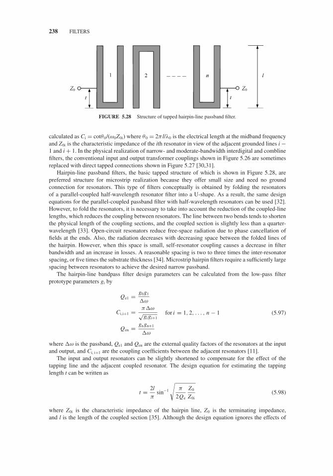
JWBS064-c05 JWBS064-Gerbennikov March 12, 2011 11:55 Printer Name: Yet to Come
238 FILTERS
FIGURE 5.28 Structure of tapped hairpin-line passband filter.
calculated as Ci = cotθ0/(ω0Z0i) where θ0 = 2π l/λ0 is the electrical length at the midband frequencyand Z0i is the characteristic impedance of the ith resonator in view of the adjacent grounded lines i −1 and i + 1. In the physical realization of narrow- and moderate-bandwidth interdigital and comblinefilters, the conventional input and output transformer couplings shown in Figure 5.26 are sometimesreplaced with direct tapped connections shown in Figure 5.27 [30,31].
Hairpin-line passband filters, the basic tapped structure of which is shown in Figure 5.28, arepreferred structure for microstrip realization because they offer small size and need no groundconnection for resonators. This type of filters conceptually is obtained by folding the resonatorsof a parallel-coupled half-wavelength resonator filter into a U-shape. As a result, the same designequations for the parallel-coupled passband filter with half-wavelength resonators can be used [32].However, to fold the resonators, it is necessary to take into account the reduction of the coupled-linelengths, which reduces the coupling between resonators. The line between two bends tends to shortenthe physical length of the coupling sections, and the coupled section is slightly less than a quarter-wavelength [33]. Open-circuit resonators reduce free-space radiation due to phase cancellation offields at the ends. Also, the radiation decreases with decreasing space between the folded lines ofthe hairpin. However, when this space is small, self-resonator coupling causes a decrease in filterbandwidth and an increase in losses. A reasonable spacing is two to three times the inter-resonatorspacing, or five times the substrate thickness [34]. Microstrip hairpin filters require a sufficiently largespacing between resonators to achieve the desired narrow passband.
The hairpin-line bandpass filter design parameters can be calculated from the low-pass filterprototype parameters gi by
Qe1 = g0g1
�ω
Ci,i+1 = π�ω√gigi+1
Qen = gngn+1
�ω
for i = 1, 2, . . . , n − 1 (5.97)
where �ω is the passband, Qe1 and Qen are the external quality factors of the resonators at the inputand output, and Ci, i+1 are the coupling coefficients between the adjacent resonators [11].
The input and output resonators can be slightly shortened to compensate for the effect of thetapping line and the adjacent coupled resonator. The design equation for estimating the tappinglength t can be written as
t = 2l
πsin−1
√π
2Qe
Z0
Z0i(5.98)
where Z0i is the characteristic impedance of the hairpin line, Z0 is the terminating impedance,and l is the length of the coupled section [35]. Although the design equation ignores the effects of
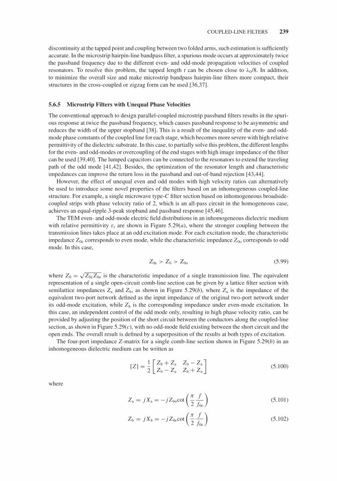
JWBS064-c05 JWBS064-Gerbennikov March 12, 2011 11:55 Printer Name: Yet to Come
COUPLED-LINE FILTERS 239
discontinuity at the tapped point and coupling between two folded arms, such estimation is sufficientlyaccurate. In the microstrip hairpin-line bandpass filter, a spurious mode occurs at approximately twicethe passband frequency due to the different even- and odd-mode propagation velocities of coupledresonators. To resolve this problem, the tapped length t can be chosen close to λ0/8. In addition,to minimize the overall size and make microstrip bandpass hairpin-line filters more compact, theirstructures in the cross-coupled or zigzag form can be used [36,37].
5.6.5 Microstrip Filters with Unequal Phase Velocities
The conventional approach to design parallel-coupled microstrip passband filters results in the spuri-ous response at twice the passband frequency, which causes passband response to be asymmetric andreduces the width of the upper stopband [38]. This is a result of the inequality of the even- and odd-mode phase constants of the coupled line for each stage, which becomes more severe with high relativepermittivity of the dielectric substrate. In this case, to partially solve this problem, the different lengthsfor the even- and odd-modes or overcoupling of the end stages with high image impedance of the filtercan be used [39,40]. The lumped capacitors can be connected to the resonators to extend the travelingpath of the odd mode [41,42]. Besides, the optimization of the resonator length and characteristicimpedances can improve the return loss in the passband and out-of-band rejection [43,44].
However, the effect of unequal even and odd modes with high velocity ratios can alternativelybe used to introduce some novel properties of the filters based on an inhomogeneous coupled-linestructure. For example, a single microwave type-C filter section based on inhomogeneous broadside-coupled strips with phase velocity ratio of 2, which is an all-pass circuit in the homogeneous case,achieves an equal-ripple 3-peak stopband and passband response [45,46].
The TEM even- and odd-mode electric field distributions in an inhomogeneous dielectric mediumwith relative permittivity εr are shown in Figure 5.29(a), where the stronger coupling between thetransmission lines takes place at an odd excitation mode. For each excitation mode, the characteristicimpedance Z0e corresponds to even mode, while the characteristic impedance Z0o corresponds to oddmode. In this case,
Z0e > Z0 > Z0o (5.99)
where Z0 = √Z0e Z0o is the characteristic impedance of a single transmission line. The equivalent
representation of a single open-circuit comb-line section can be given by a lattice filter section withsemilattice impedances Za and Zb, as shown in Figure 5.29(b), where Za is the impedance of theequivalent two-port network defined as the input impedance of the original two-port network underits odd-mode excitation, while Zb is the corresponding impedance under even-mode excitation. Inthis case, an independent control of the odd mode only, resulting in high phase velocity ratio, can beprovided by adjusting the position of the short circuit between the conductors along the coupled-linesection, as shown in Figure 5.29(c), with no odd-mode field existing between the short circuit and theopen ends. The overall result is defined by a superposition of the results at both types of excitation.
The four-port impedance Z-matrix for a single comb-line section shown in Figure 5.29(b) in aninhomogeneous dielectric medium can be written as
[Z ] = 1
2
[Zb + Za Zb − Za
Zb − Za Zb + Za
](5.100)
where
Za = j Xa = − j Z0ocot
(π
2
f
f0o
)(5.101)
Zb = j Xb = − j Z0ecot
(π
2
f
f0e
)(5.102)
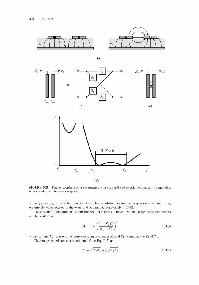
JWBS064-c05 JWBS064-Gerbennikov March 12, 2011 11:55 Printer Name: Yet to Come
240 FILTERS
FIGURE 5.29 Parallel-coupled microstrip structure with even and odd electric field modes, its equivalentrepresentation, and frequency response.
where f 0e and f 0o are the frequencies at which a comb-line section are a quarter-wavelength longelectrically when excited in the even- and odd mode, respectively [47,48].
The effective attenuation of a comb-line section in terms of the equivalent lattice circuit parameterscan be written as
A = 1 +(
1 + X ′a X ′
b
X ′a − X ′
b
)2
(5.103)
where X ′a and X ′
b represent the corresponding reactances Xa and Xb normalized to Z0 [4,7].The image impedance can be obtained from Eq. (5.5) as
Z i =√
Za Zb = j√
Xa Xb (5.104)
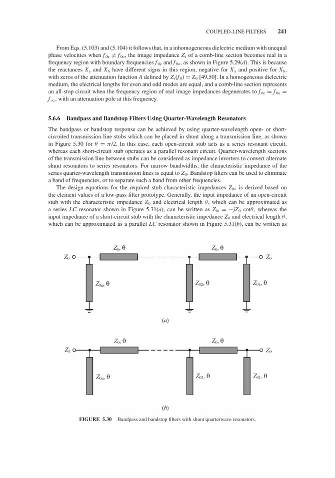
JWBS064-c05 JWBS064-Gerbennikov March 12, 2011 11:55 Printer Name: Yet to Come
COUPLED-LINE FILTERS 241
From Eqs. (5.103) and (5.104) it follows that, in a inhomogeneous dielectric medium with unequalphase velocities when f 0e �= f 0o, the image impedance Zi of a comb-line section becomes real in afrequency region with boundary frequencies f 0e and f 0o, as shown in Figure 5.29(d). This is becausethe reactances Xa and Xb have different signs in this region, negative for Xa and positive for Xb,with zeros of the attenuation function A defined by Zi(f 0) = Z0 [49,50]. In a homogeneous dielectricmedium, the electrical lengths for even and odd modes are equal, and a comb-line section representsan all-stop circuit when the frequency region of real image impedances degenerates to f 0e = f 0o =f ∞, with an attenuation pole at this frequency.
5.6.6 Bandpass and Bandstop Filters Using Quarter-Wavelength Resonators
The bandpass or bandstop response can be achieved by using quarter-wavelength open- or short-circuited transmission-line stubs which can be placed in shunt along a transmission line, as shownin Figure 5.30 for θ = π /2. In this case, each open-circuit stub acts as a series resonant circuit,whereas each short-circuit stub operates as a parallel resonant circuit. Quarter-wavelength sectionsof the transmission line between stubs can be considered as impedance inverters to convert alternateshunt resonators to series resonators. For narrow bandwidths, the characteristic impedance of theseries quarter-wavelength transmission lines is equal to Z0. Bandstop filters can be used to eliminatea band of frequencies, or to separate such a band from other frequencies.
The design equations for the required stub characteristic impedances Z0n is derived based onthe element values of a low-pass filter prototype. Generally, the input impedance of an open-circuitstub with the characteristic impedance Z0 and electrical length θ , which can be approximated asa series LC resonator shown in Figure 5.31(a), can be written as Zin = −jZ0 cotθ , whereas theinput impedance of a short-circuit stub with the characteristic impedance Z0 and electrical length θ ,which can be approximated as a parallel LC resonator shown in Figure 5.31(b), can be written as
FIGURE 5.30 Bandpass and bandstop filters with shunt quarterwave resonators.

JWBS064-c05 JWBS064-Gerbennikov March 12, 2011 11:55 Printer Name: Yet to Come
242 FILTERS
FIGURE 5.31 Third-order bandstop filter with quarterwave resonators and its response.
Zin = jZ0 tanθ . As a result, the characteristic impedance Z0i of each open-circuit transmission-linestub used in the n-order bandstop filters is calculated from
Z0i = 4Z0ω0
πgi�ω(5.105)
whereas the characteristic impedance Z0i of each short-circuit transmission-line stub is determinedby
Z0i = π Z0�ω
4giω0(5.106)
where gi are the element values for maximally flat or equal-ripple low-pass filters prototypes, �ω isthe frequency bandwidth, and ω0 is the center bandwidth frequency, i = 1, 2, . . . , n [5,51]. Note thatthese results can only be applied to filters having input and output impedances of Z0, and cannot beused for equal-ripple designs with even n.
As an example, let us design a third-order (n = 3) coupled-line bandstop filter with the centerfrequency of 4 GHz and bandwidth of 25%, having a 0.5 dB equal-ripple response and a characteristicimpedance Z0 = 50 �. For the corresponding element value of the low-pass prototype circuit tabulatedin Table 5.3, the characteristic impedance Z0i is calculated as
g1 = 1.5963 Z01 = 159.5 � for i = 1
g2 = 1.0967 Z02 = 232.2 � for i = 2
g3 = 1.5963 Z03 = 159.5 � for i = 3
resulting in the transmission-line filter topology shown in Figure 5.31(c) and amplitude responseshown in Figure 5.31(d). In this case, the ripple in the passband is somewhat greater than expected,which is the result of a narrowband assumption corresponding to the stop-band bandwidths up to afew percent.

JWBS064-c05 JWBS064-Gerbennikov March 12, 2011 11:55 Printer Name: Yet to Come
SAW AND BAW FILTERS 243
For better accuracy over wider bandwidths, the characteristic impedances of the interconnectingquarter-wavelength lines must be variable calculated according to the corresponding design equations[8,52]. These distributed microwave bandstop filters are characterized by their second harmonicresponse centered at no more than three times the fundamental bandstop center frequency. However,such a limitation can be removed by the use of compound stub resonators, each composed ofa pair of transmission lines with different characteristic impedances with each line being of thecommensurate length when the first upper stopband center frequency becomes as high as six timesthe fundamental bandstop center frequency [53]. By providing a parallel association of two differentbandstop structures, the narrow bandpass filters with short- and open-circuit stubs of different lengthsand characteristic impedances can be realized which allow an independent control of each attenuatedband on either side of one bandpass [54].
5.7 SAW AND BAW FILTERS
Serious interest in surface acoustic wave (SAW) technology commenced in 1967 with the develop-ment of the interdigital electrode transducer (IDT), which permitted efficient transduction betweenelectromagnetic acoustic energy [55]. The IDT consists of a set of interleaved metal electrodes andis fabricated by photoetching a deposited metal film. In the simplest form, the width and spacingof electrodes is equal and uniform throughout the pattern. In this case, electrical excitation of thetransducer with a sinusoidal voltage produces a periodic electrical field which penetrates into thepiezoelectric substrate. In this case, suitable choice of substrate orientation produces two surfaceacoustic wave beams propagating normal to the IDT electrodes. As a result, peak output occursat the synchronous frequency f 0 = v/l, where v is the SAW velocity and l is the transducer peri-odic length. Under this condition of acoustic synchronism, the stress contributions of all electrodesadd in phase.
The lower SAW filter frequency limit is set by practical size limits on piezoelectric substratesand the range of velocities of available surface wave materials. At the high-frequency end, the limitis set by the resolution capabilities of state-of-the-art patterning techniques, substrate velocities, andfrequency-dependent loss mechanisms. The essential feature in changing the operating frequency ofsurface-wave filters is simply a matter of changing the interdigital electrode spacing. In this case,the width of acoustic beam is set by electrode stripe length w which can be adjusted to obtain aconvenient impedance level. With increasing frequency, however, electrode thickness must decreaseto avoid larger distortion from reflections due to increased parasitic resistive loss. Several filterapplications were found at both ends of available surface-wave frequency range, from the frequencymodulated (FM) radio filters at 10.7 MHz with a 200-kHz signal bandwidth to the 800-MHz filtersfor mobile telephone transceivers and L-band radar and satellite transponder filters operating at 1.5GHz and higher [56–58]. To achieve higher SAW operating frequency, it is necessary either to usesubstrate with higher velocities than can be achieved in quartz and lithium niobate, or to develophigher resolution fabrication. An important relationship in SAW filter design is that between fractionalbandwidth (�f /f 0) and insertion loss, with benefit of lithium niobate substrate over quartz substratedue to stronger piezoelectric coupling despite its moderate temperature sensitivity. The out-of-bandrejection better than 60 dB over a wide range of bandwidths is available with weighting techniquessuch as finger overlap, finger withdrawal, phase weighting, and multistrip couplers. Principle obstaclesto achieve or improve such a performance include diffraction and spurious responses.
Figure 5.32 shows the equivalent electric circuit for IDT, where G represents the radiation con-ductance, CT represents the capacitance between transducer fingers, and B represents the acousticsusceptance due to vibration [59]. This circuit corresponds to a shunt representation for transducerinput immittance in a “crossed-field” model configuration when the applied electric field is normal tothe acoustic propagation vector. However, it can equivalently be illustrated by a series representationfor transducer input immittance in an “in-line” model configuration characterized by parallel electricfield and propagation vectors. For a given piezoelectric with given cut and orientation, the choice

JWBS064-c05 JWBS064-Gerbennikov March 12, 2011 11:55 Printer Name: Yet to Come
244 FILTERS
FIGURE 5.32 Equivalent electric circuit for IDT.
between these models is made by evaluating the contribution to Rayleigh wave (RW) excitation ofthe perpendicular and parallel to the surface electric field components.
From computer simulation and practical experiments, it was found that the input impedance(or admittance) of an IDT with quarter-wavelength-solid fingers can be classified into three types,depending on the number of finger pairs N and electromechanical coupling coefficient defined ask2 = 2�v/v, where �v is the perturbation of phase velocity due to nonidentical field distributions forinterdigital and metal-coated configurations [60]. In this case, for an optimized N = 1.5/k2, a widefrequency range can be achieved. The total susceptance (ωCT + B) becomes very small over thisrange due to the cancellation of electric and acoustic susceptance components, being capacitive forsmaller N and inductive for larger N.
Figure 5.33 shows the configuration with sharp cutoff frequency response representing an image-impedance connection where one pair of electrically connected interdigital transducers with anoptimum number of finger pairs is introduced. Input and output transducers with a broader frequencyresponse are arranged on both sides where SAW reflectors are also placed [61]. With this nonweightingconfiguration, a sharp cutoff response is achieved because, in the passband where the susceptance iscancelled, the current from an upper image-impedance IDT flows into a lower one without reflection.If the frequency is outside passband, almost all current is reflected at the image-impedance connectedpoint because the susceptance component is larger than the conductance component. In this case,an insertion loss of as low as 3.5–4.0 dB is achieved for the ultra high frequency (UHF) filter, and1.7–2.0 dB for the very high frequency (VHF) filter.
The loss mechanism in a UHF SAW filter is basically defined by the leakage (bidirectionality),weighting, and thin Al electrode conductivity losses. Since bidirectionality loss is the largest inconventional transversal SAW filters, an introduction of the resonant structure with lateral repetitionsin addition to reflectors can minimize this loss. To reduce weighting loss, a new phase weighting,which excites SAW structure with uniform wavefront distribution in the passband, can be included.Figure 5.34 shows the new repetition structure for interdigital transducers with a tapering number offinger pairs where one pair of input and output transducers is laterally repeated [61]. Since there is alarger number of finger pairs in the center of the filter and a smaller number at both sides, thus theenergy of acoustic vibrations is confined within the filter. As a result, six repetitions are enough toachieve 0.7 dB of insertion loss using a simple taper in the number of finger pairs (half the numberof finger pairs at both sides). To reduce the conductivity loss, the filter aperture should be small andthe impedance of each repeated IDT must be increased.
The device will usually be hermetically packaged to protect the sensitive surface from contam-ination. Often, one or two reactive components must be added at each end, outside the package.An inductor may be needed because the interdigital transducers have capacitive reactance which
JWBS064-c05 JWBS064-Gerbennikov March 12, 2011 11:55 Printer Name: Yet to Come
SAW AND BAW FILTERS 245
FIGURE 5.33 SAW filter with sharp cutoff frequency response.
FIGURE 5.34 SAW filter with tapered number of finger pairs.

JWBS064-c05 JWBS064-Gerbennikov March 12, 2011 11:55 Printer Name: Yet to Come
246 FILTERS
FIGURE 5.35 Typical SAW filter response.
may need to be tuned out. Also, lumped LC circuits are often used to transform the source or loadimpedance (usually 50 �) to an impedance more suitable for the SAW device. Typical SAW filterresponse for an 800-MHz mobile telephone transceiver is shown in Figure 5.35. To improve itspower capability, insertion loss, and out-of-band rejection satisfying the requirements for a miniatureantenna duplexer, the transmitter SAW filter can be realized in a ladder-type configuration with addi-tional shunt capacitors between electrode fingers and ground [62]. Extremely low-loss and ultra-steepcutoff SAW filters used in a 1.9-GHz antenna duplexer can be achieved with IDT metallization ratioless than 50% and optimized ladder-type structure with a reduction in the coupling coefficient k2 foronly selected series resonators [63,64]. To minimize SAW filter size for multimode mobile phoneapplications, a chip-sized SAW package, which is flip-chip mounted onto a chip carrier serving asbottom of the package with electrical connections to the chip provided by solder bumps, represents akey packaging technology [65].
The traditional SAW filter technology demonstrates good selectivity and very small size, butoperation frequencies of SAW filters is limited below 3 GHz due to their high insertion losses athigh input power levels of above 1 W. On the other hand, despite the recent advances in ceramicmaterial technology which have made dielectric filters very largely employed as duplexers since theycan handle high power levels and demonstrate high selectivity, their large dimensions limit theirapplication in mobile RF front-end modules. At the same time, the radio-frequency bulk acousticwave (BAW) filters and duplexers based on film bulk acoustic resonator (FBAR) filters or solidlymounted resonator (SMR) technologies are expected to replace these traditional RF filter technologiesdue to their lower insertion loss, better selectivity, higher power handling, higher operation frequency.Besides, they can be directly integrated with active circuits, making possible of fully-integrated RFfront-ends at very competitive costs.
The core element for both BAW and SAW filters technologies is the resonator which is char-acterized by high quality factor due to low propagation loss and small size due to much shorteracoustic wavelength than that of the electromagnetic wave. Besides, acoustic waves can be easily andefficiently excited and converted back to electrical signal by using transducers and the piezoelectricproperty of the SAW and BAW materials. Though the impedance responses of these filters are similar,the resonances are realized quite differently in SAW and BAW filter technologies. In the former case,a surface acoustic wave is an elastic wave that travels along the surface of a crystal substrate, however

JWBS064-c05 JWBS064-Gerbennikov March 12, 2011 11:55 Printer Name: Yet to Come
SAW AND BAW FILTERS 247
FIGURE 5.36 BAW resonator structure, its equivalent circuit, and frequency response.
in the latter case, a bulk acoustic wave represents an elastic wave that travels inside solid material. In aSAW resonator, the wave amplitude decays rapidly with depth, with 90% or more energy of acousticenergy being within one wavelength of the surface material. In a BAW resonator whose structureis shown in Figure 5.36(a) together with a signal source, the acoustic wave which is called thelongitudinal wave propagates in a vertical direction between top and bottom metal electrodes [66,67].
Generally, the equivalent circuits of BAW and SAW resonators valid near the fundamental reso-nance are the same and are shown in Figure 5.36(b), where C0 is the static (or plate) capacitance, Cm isthe motional (or acoustic) capacitance which is much smaller than C0, Lm is the motional inductance,Rm is the motional resistance, and the resistance Rs and R0 characterize the electrode ohmic loss andundesired acoustic wave loss, respectively [68,69]. Being a second-order circuit, it has both a zerowhich defines the series resonant frequency f s and pole which defines the parallel resonant frequencyf p, as shown in Figure 5.36(c). In this case, the motional inductance Lm forms a series resonance withCm and, at a slightly higher frequency, a parallel resonance with C0, with the inductive impedance inbetween f s and f p.
The most important characteristic of a BAW resonator is the strength of the piezoelectric couplingwhich depends on the piezoelectric and electrode materials and the resonator structure. With a single

JWBS064-c05 JWBS064-Gerbennikov March 12, 2011 11:55 Printer Name: Yet to Come
248 FILTERS
piezoelectric plate without any layers, the coupling coefficient can be determined from the series andparallel resonance frequencies as
k2 = π
2
fs
fptan
(π
2
fp − fs
fp
)(5.107)
However, in a real FBAR resonator, there are other layers and, then, the effective piezoelectriccoupling coefficient is defined by
k2eff = 1 −
(fs
fp
)2
= Cm
Cm + C0≈ 8
π2k2 (5.108)
which means that one must bear in mind that k = 1.1keff when comparing these coupling coefficients[70]. For a BAW resonator, the only piezoelectric thin-film material that has been established as thebest balance of performance and manufacturability is aluminum nitride (AIN). With the best layerstack design and with optimized AIN thin-film deposition system, the maximum achievable resonatorrelative bandwidth BW = (f p − f s)/f p and k2
eff are 2.8% and 6.9%, respectively [66].The BAW (or SAW) resonator filters can be generally divided in two basic topologies: ladder shown
in Figure 5.37(a) and lattice shown in Figure 5.37(b), or the combination of them [71,72]. Ladder-typeBAW filters have a very steep rejection response at passband ends followed by a lower rejection atfurther frequencies. On the other hand, lattice-type BAW filters demonstrate slower roll-off coefficientand higher rejection at both stopbands which are more effective to for rejecting undesired frequencybands. As a result, a combined ladder-lattice BAW filters can provide high in-band selectivity andimproved out-of-band isolation simultaneously. Using FBAR technology with acoustic loading layer,
FIGURE 5.37 Ladder and lattice BAW filter configurations.
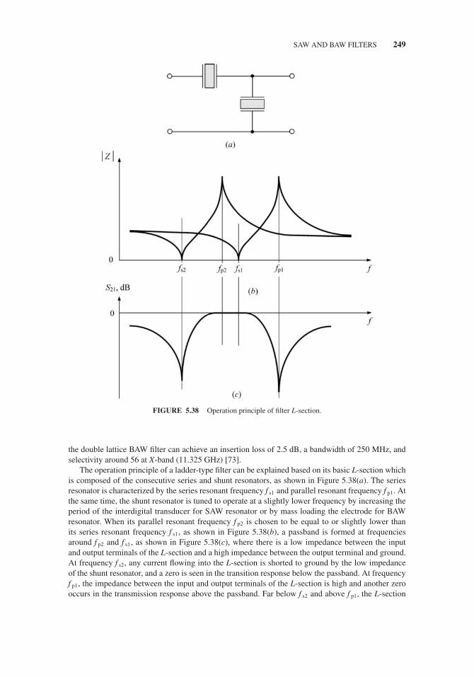
JWBS064-c05 JWBS064-Gerbennikov March 12, 2011 11:55 Printer Name: Yet to Come
SAW AND BAW FILTERS 249
FIGURE 5.38 Operation principle of filter L-section.
the double lattice BAW filter can achieve an insertion loss of 2.5 dB, a bandwidth of 250 MHz, andselectivity around 56 at X-band (11.325 GHz) [73].
The operation principle of a ladder-type filter can be explained based on its basic L-section whichis composed of the consecutive series and shunt resonators, as shown in Figure 5.38(a). The seriesresonator is characterized by the series resonant frequency f s1 and parallel resonant frequency f p1. Atthe same time, the shunt resonator is tuned to operate at a slightly lower frequency by increasing theperiod of the interdigital transducer for SAW resonator or by mass loading the electrode for BAWresonator. When its parallel resonant frequency f p2 is chosen to be equal to or slightly lower thanits series resonant frequency f s1, as shown in Figure 5.38(b), a passband is formed at frequenciesaround f p2 and f s1, as shown in Figure 5.38(c), where there is a low impedance between the inputand output terminals of the L-section and a high impedance between the output terminal and ground.At frequency f s2, any current flowing into the L-section is shorted to ground by the low impedanceof the shunt resonator, and a zero is seen in the transition response below the passband. At frequencyf p1, the impedance between the input and output terminals of the L-section is high and another zerooccurs in the transmission response above the passband. Far below f s2 and above f p1, the L-section
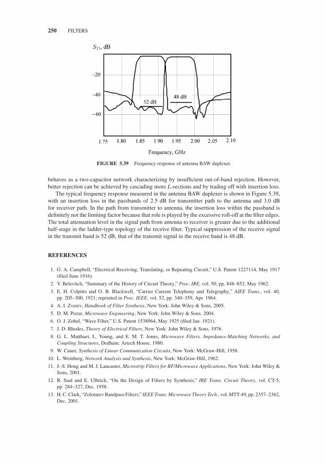
JWBS064-c05 JWBS064-Gerbennikov March 12, 2011 11:55 Printer Name: Yet to Come
250 FILTERS
FIGURE 5.39 Frequency response of antenna BAW duplexer.
behaves as a two-capacitor network characterizing by insufficient out-of-band rejection. However,better rejection can be achieved by cascading more L-sections and by trading off with insertion loss.
The typical frequency response measured in the antenna BAW duplexer is shown in Figure 5.39,with an insertion loss in the passbands of 2.5 dB for transmitter path to the antenna and 3.0 dBfor receiver path. In the path from transmitter to antenna, the insertion loss within the passband isdefinitely not the limiting factor because that role is played by the excessive roll-off at the filter edges.The total attenuation level in the signal path from antenna to receiver is greater due to the additionalhalf-stage in the ladder-type topology of the receive filter. Typical suppression of the receive signalin the transmit band is 52 dB, that of the transmit signal in the receive band is 48 dB.
REFERENCES
1. G. A. Campbell, “Electrical Receiving, Translating, or Repeating Circuit,” U.S. Patent 1227114, May 1917(filed June 1916).
2. V. Belevitch, “Summary of the History of Circuit Theory,” Proc. IRE, vol. 50, pp. 848–852, May 1962.
3. E. H. Colpitts and O. B. Blackwell, “Carrier Current Telephony and Telegraphy,” AIEE Trans., vol. 40,pp. 205–300, 1921; reprinted in Proc. IEEE, vol. 52, pp. 340–359, Apr. 1964.
4. A. I. Zverev, Handbook of Filter Synthesis, New York: John Wiley & Sons, 2005.
5. D. M. Pozar, Microwave Engineering, New York: John Wiley & Sons. 2004.
6. O. J. Zobel, “Wave Filter,” U.S. Patent 1538964, May 1925 (filed Jan. 1921).
7. J. D. Rhodes, Theory of Electrical Filters, New York: John Wiley & Sons, 1976.
8. G. L. Matthaei, L. Young, and E. M. T. Jones, Microwave Filters, Impedance-Matching Networks, andCoupling Structures, Dedham: Artech House, 1980.
9. W. Cauer, Synthesis of Linear Communication Circuits, New York: McGraw-Hill, 1958.
10. L. Weinberg, Network Analysis and Synthesis, New York: McGraw-Hill, 1962.
11. J.-S. Hong and M. J. Lancaster, Microstrip Filters for RF/Microwave Applications, New York: John Wiley &Sons, 2001.
12. R. Saal and E. Ulbrich, “On the Design of Filters by Synthesis,” IRE Trans. Circuit Theory, vol. CT-5,pp. 284–327, Dec. 1958.
13. H. C. Clark, “Zolotarev Bandpass Filters,” IEEE Trans. Microwave Theory Tech., vol. MTT-49, pp. 2357–2362,Dec. 2001.

JWBS064-c05 JWBS064-Gerbennikov March 12, 2011 11:55 Printer Name: Yet to Come
REFERENCES 251
14. W. E. Thomson, “Delay Network Having Maximally Flat Frequency Characteristics,” Proc. IEE, pt. 3, vol.96, pp. 487–490, Nov. 1949.
15. G. C. Temes and S. K. Mitra, Modern Filter Theory and Design, New York: John Wiley & Sons, Ltd. 1973.
16. P. I. Richards, “Resistor-Transmission-Line Circuits,” Proc. IRE, vol. 36, pp. 217–220, Feb. 1948.
17. P. I. Richards, “Applications of Matrix Algebra to Filter Theory,” Proc. IRE, vol. 34, pp. 145–150, Mar.1946.
18. H. Ozaki and J. Ishii, “Synthesis of Transmission-Line Networks and the Design of UHF Filters,” IRE Trans.Circuit Theory, vol. CT-2, pp. 325–336, Dec. 1955.
19. S. B. Cohn, “Parallel-Coupled Transmission-Line-Resonator Filters,” IRE Trans. Microwave Theory Tech.,vol. MTT-6, pp. 145–153, Apr. 1958.
20. E. M. T. Jones and J. T. Bolljahn, “Coupled-Strip-Transmission-Line Filters and Directional Couplers,” IRETrans. Microwave Theory Tech., vol. MTT-4, pp. 75–81, Apr. 1956.
21. H. Ozaki and J. Ishii, “Synthesis of a Class of Strip-Line Filters,” IRE Trans. Circuit Theory, vol. CT-5,pp. 104–109, June 1958.
22. R. J. Wenzel, “Exact Design of TEM Microwave Networks Using Quarter-Wave Lines,” IEEE Trans. Mi-crowave Theory Tech., vol. MTT-12, pp. 94–111, Jan. 1964.
23. S. B. Cohn, “Shielded Coupled-Strip Transmission Line,” IRE Trans. Microwave Theory Tech., vol. MTT-3,pp. 29–38, Oct. 1955.
24. M. Kirschning and R. H. Jansen, “Accurate Wide-Range Design Equations for Parallel Coupled MicrostripLines,” IEEE Trans. Microwave Theory Tech., vol. MTT-32, pp. 83–90, Jan. 1984; vol. MTT-33, p. 288, Mar.1985.
25. G. L. Matthaei, “Interdigital Band-Pass Filters,” IRE Trans. Microwave Theory Tech., vol. MTT-10,pp. 479–491, Nov. 1962.
26. R. J. Wenzel, “Exact Theory of Interdigital Bandpass Filters and Related Structures,” IEEE Trans. MicrowaveTheory Tech., vol. MTT-13, pp. 559–575, Sept. 1965.
27. T. A. Milligan, “Dimensions of Microstrip Coupled Lines and Interdigital Structures,” IEEE Trans. MicrowaveTheory Tech., vol. MTT-25, pp. 405–410, May 1977.
28. G. L. Matthaei, “Combline Band-Pass Filters of Narrow or Moderate Bandwidth,” Microwave J., vol. 6,pp. 82–91, Aug. 1963.
29. R. J. Wenzel, “Synthesis of Combline and Capacitively Loaded Interdigital Filters of Arbitrary Bandwidth,”IEEE Trans. Microwave Theory Tech., vol. MTT-19, pp. 678–686, Aug. 1971.
30. E. G. Cristal, “Tapped-Line Coupled Transmission Lines with Applications to Interdigital and ComblineFilters,” IEEE Trans. Microwave Theory Tech., vol. MTT-23, pp. 1007–1113, Dec. 1975.
31. S. Caspi and J. Adelman, “Design of Combline and Interdigital Filters with Tapped-Line Input,” IEEE Trans.Microwave Theory Tech., vol. MTT-36, pp. 759–763, Apr. 1988.
32. E. G. Cristal and S. Frankel, “Design of Hairpin-Line and Hybrid Hairpin-Parallel-Coupled-Line Filters,”IEEE Trans. Microwave Theory Tech., vol. MTT-20, pp. 719–728, Nov. 1972.
33. U. H. Gysel, “New Theory and Design for Hairpin-Line Filters,” IEEE Trans. Microwave Theory Tech., vol.MTT-22, pp. 523–531, May 1974.
34. L. G. Maloratsky, Passive RF & Microwave Integrated Circuits, New York: Newnes, 2004.
35. J. S. Wong, “Microstrip Tapped-Line Filter Design,” IEEE Trans. Microwave Theory Tech., vol. MTT-27,pp. 44–50, Jan. 1979.
36. J.-S. Hong and M. J. Lancaster, “Cross-Coupled Microstrip Hairpin-Resonator Filters,” IEEE Trans. Mi-crowave Theory Tech., vol. MTT-46, pp. 118–122, Jan. 1998.
37. G. L. Matthaei, “Narrow-Band, Fixed-Tuned, and Tunable Bandpass Filters with Zig-Zag Hairpin-CombResonators,” IEEE Trans. Microwave Theory Tech., vol. MTT-51, pp. 1214–1219, Apr. 2003.
38. C.-Y. Chang and T. Itoh, “A Modified Parallel-Coupled Filter Structure That Improves the Upper Stop-band and Response Symmetry,” IEEE Trans. Microwave Theory Tech., vol. MTT-39, pp. 310–314, Feb.1991.
39. A. Riddle, “High Performance Parallel Coupled Microstrip Filters,” IEEE MTT-S Int. Microwave Symp. Dig.,vol. 1, pp. 427–430, May 1988.

JWBS064-c05 JWBS064-Gerbennikov March 12, 2011 11:55 Printer Name: Yet to Come
252 FILTERS
40. J.-T. Kuo, S.-P. Chen, and M. Jiang, “Parallel-Coupled Microstrip Filters with Over-Coupled End Stages forSuppression of Spurious Responses,” IEEE Microwave and Wireless Components Lett., vol. 13, pp. 440–442,Oct. 2003.
41. S. L. March, “Phase Velocity Compensation in Parallel-Coupled Microstrip,” IEEE MTT-S Int. MicrowaveSymp. Dig., pp. 410–412, June 1982.
42. I. J. Bahl, “Capacitively Compensated High Performance Parallel Coupled Microstrip Filters,” IEEE MTT-SInt. Microwave Symp. Dig., vol. 2, pp. 679–682, June 1989.
43. D. Kajfez and S. Govind, “Effect of Difference in Odd- and Even-Mode Wavelengths on a Parallel-CoupledBandpass Filter,” Electronics Lett., vol. 11, pp. 117–118, Mar. 1975.
44. H.-M. Lee and C.-M. Tsai, “Improved Coupled-Microstrip Filter Design Using Effective Even-Mode andOdd-Mode Characteristic Impedances,” IEEE Trans. Microwave Theory Tech., vol. MTT-53, pp. 2812–2818,Sept. 2005.
45. G. I. Zysman and A. Matsumoto, “Properties of Microwave C-Sections,” IRE Trans. Circuit Theory, vol.CT-12, pp. 74–82, Mar. 1965.
46. J. L. Allen, “Inhomogeneous Coupled-Line Filters with Large Mode-Velocity Ratios,” IEEE Trans. MicrowaveTheory Tech., vol. MTT-22, pp. 1182–1186, Dec. 1974.
47. G. Zysman and A. Johnson, “Coupled Transmission Line Networks in an Inhomogeneous Dielectric Medium,”IEEE Trans. Microwave Theory Tech., vol. MTT-17, pp. 753–759, Oct. 1969.
48. G. M. Aristarkhov and Y. P. Vershinin, “Analysis of Coupled-Line Filters with Unequal Phase Velocities(in Russian),” Radiotekhnika i Elektronika, vol. 28, pp. 1714–1724, Sept. 1983.
49. G. M. Aristarkhov and V. P. Chernyshev, “Equivalent Mode Representation of Microstrip Filters Based onMulticonductor Transmission Lines with Unequal Phase Velocities (in Russian),” Radiotekhnika i Elektronika,vol. 30, pp. 2289–2297, Dec. 1985.
50. G. M. Aristarkhov, A. N. Alekseev, P. S. Mikhnevich, and V. P. Chernyshev, “Functional Possibilities ofStructures Based on Slotlines and Coupled Microstrip Lines (in Russian),” Radiotekhnika i Elektronika, vol.33, pp. 7–13, Jan. 1989.
51. L. Young, G. L. Matthaei, and E. M. T. Jones, “Microwave Band-Stop Filters with Narrow Stop Bands,” IRETrans. Microwave Theory Tech., vol. MTT-10, pp. 416–427, Nov. 1962.
52. B. M. Schiffman and G. L. Matthaei, “Exact Design of Band-Stop Microwave Filters,” IEEE Trans. MicrowaveTheory Tech., vol. MTT-12, pp. 6–15, Jan. 1964.
53. R. Levy, R. V. Snyder, and S. Shin, “Bandstop Filters with Extended Upper Passbands,” IEEE Trans.Microwave Theory Tech., vol. MTT-54, pp. 2503–2515, June 2006.
54. C. Quendo, E. Rius, and C. Person, “Narrow Bandpass Filters Using Dual-Behavior Resonators Based onStepped-Impedance Stubs and Different-Length Stubs,” IEEE Trans. Microwave Theory Tech., vol. MTT-52,pp. 1034–1044, Mar. 2004.
55. P. M. Grant, J. D. Adam, and J. H. Collins, “Surface Wave Device Applications in Microwave CommunicationSystems,” IEEE Trans. Commun., vol. COM-22, pp. 1410–1419, Sept. 1974.
56. R. D. Hays and C. S. Hartmann, “Surface-Acoustic-Wave Devices for Communications,” Proc. IEEE, vol.64, pp. 652–671, May 1976.
57. Y. Kinoshita, M. Hikita, M. Toya, T. Toyama, and Y. Fujiwara, “Low Loss and High Performance SAW Filtersfor 800 MHz Mobile Telephone Transceiver,” IEEE Trans. Vehicular Technol., vol. VT-32, pp. 225–229, Aug.1983.
58. H. Shinonaga and Y. Ito, “Microwave SAW Bandpass Filters for Spacecraft Applications,” IEEE Trans.Microwave Theory Tech., vol. MTT-40, pp. 1110–1116, June 1992.
59. W. R. Smith, H. M. Gerard, J. H. Collins, T. M. Reeder, and H. J. Shaw, “Analysis of Interdigital Surface WaveTransducers by Use of an Equivalent Circuit Model,” IEEE Trans. Microwave Theory Tech., vol. MTT-17,pp. 856–864, Nov. 1969.
60. M. Hikita, H. Kojima, T. Tabuchi, and Y. Kinoshita, “800-MHz High-Performance SAW Filter UsingNew Resonant Configuration,” IEEE Trans. Microwave Theory Tech., vol. MTT-33, pp. 510–518, June1985.
61. M. Hikita, T. Tabuchi, and A. Sumioka, “Miniaturized SAW Devices for Radio Communication Transceivers,”IEEE Trans. Vehicular Technol., vol. VT-38, pp. 2–8, Feb. 1989.

JWBS064-c05 JWBS064-Gerbennikov March 12, 2011 11:55 Printer Name: Yet to Come
REFERENCES 253
62. M. Hikita, Y. Ishida, T. Tabuchi, and K. Kurosawa, “Miniature SAW Antenna Duplexer for 800-MHzPortable Telephone Used in Cellular Radio Systems,” IEEE Trans. Microwave Theory Tech., vol. MTT-36,pp. 1047–1056, June 1988.
63. J. Tsutsumi, S. Inoue, Y. Iwamoto, T. Matsuda, M. Miura, Y. Satoh, M. Ueda, and O. Ikata, “ExtremelyLow-Loss SAW Filter and Its Application to Antenna Duplexer for the 1.9 GHz PCS Full-Band,” Proc. IEEEInt. Frequency Control Symp., pp. 861–867, May 2003.
64. S. Inoue, J. Tsutsumi, T. Matsuda, M. Ueda, O. Ikata, and Y. Satoh, “Ultra-Steep Cut-Off Double Mode SAWFilter and Its Application to a PCS Duplexer,” IEEE Trans. Ultrasonic Ferroelectric Frequency Control, vol.54, pp. 1882–1887, Sept. 2007.
65. H. Meier, T. Baier, and G. Riha, “Miniaturization and Advanced Functionalities of SAW Devices,” IEEETrans. Microwave Theory Tech., vol. MTT-49, pp. 743–748, Apr. 2001.
66. F. Z. Bi and B. P. Barber, “Bulk Acoustic Wave RF Technology,” IEEE Microwave Mag., vol. 9, pp. 65–80,Oct. 2008.
67. M. Ueda, M. Iwaki, T. Nishihara, Y. Satoh, and K. Hashimoto, “A Circuit Model for Nonlinear Simulationof Radio-Frequency Filters Using Bulk Acoustic Wave Resonators,” IEEE Trans. Ultrason. FerroelectricFrequency Control, vol. 55, pp. 849–856, Apr. 2008.
68. J. F. Rosenbaum, Bulk Acoustic Wave Theory and Devices, London: Artech House, 1988.
69. M. Ylilammi, J. Ella, M. Partanen, and J. Kaitila, “Thin Film Bulk Acoustic Wave Filter,” IEEE Trans.Ultrasonic Ferroelectric Frequency Control, vol. 49, pp. 535–539, Apr. 2002.
70. H. Jaffe and D. A. Berlincourt, “Piezoelectric transducer materials,” Proc. IEEE, vol. 53, pp. 1372–1386, Oct.1965.
71. G. G. Fattinger, J. Kaitila, R. Aigner, and W. Nessler, “Thin Film Bulk Acoustic Wave Devices for Applicationsat 5.2 GHz,” Proc. IEEE Ultrasonic Symp., vol. 1, pp. 174–177, Oct. 2003.
72. A. A. Shirakawa, J.-M. Pham, P. Jarry, E. Kerherve, F. Dumont, J.-B. David, and A. Cathelin, “A High Isolationand High Selectivity Ladder-Lattice BAW-SMR Filter,” Proc. 36th Europ. Microwave Conf., pp. 905–908,Sept. 2006.
73. A. A. Shirakawa, J.-M. Pham, P. Jarry, and E. Kerherve, “Design of FBAR Filters at High Frequency Bands,”Int. J. RF and Microwave Computer-Aided Eng., vol. 17, pp. 115–122, Jan. 2007.

JWBS064-c05 JWBS064-Gerbennikov March 12, 2011 11:55 Printer Name: Yet to Come
254

JWBS064-c06 JWBS064-Gerbennikov March 12, 2011 9:39 Printer Name: Yet to Come
6 Modulation and Modulators
Modulation is the process that allows the information content of an audio, video, or data signal tobe transferred to a region of higher frequencies where the transmission can be effective. In this case,the spectrum bandwidth of the modulating signal must be much smaller compared to the carrierfrequency being modulated. During the modulation process, one or several parameters of the carriersignal such as amplitude, frequency, or phase vary according to the modulating signal when themodulator changes the signal into a form suitable for transmission over the proper radio channel.More complex modulation process includes digitization and encoding of the modulating signals.Depending on the communication systems with corresponding requirements on transmitting power,signal quality, frequency bandwidth, power consumption, system complexity, or cost, different typesof the modulation scheme can be used based on analog and digital modulation techniques.
This chapter discusses the basic features of different types of analog modulation including ampli-tude, single-sideband, frequency, and phase modulation and basic types of digital modulation suchas amplitude shift keying, frequency shift keying, phase shift keying, or pulse code modulation andtheir variations. The principle of operations and various schematics of the modulators for differentmodulation schemes including Class-S modulator for pulse-width modulation are described. Finally,the concept of time and frequency division multiplexing is introduced, as well as brief description ofdifferent multiple access techniques is given.
6.1 AMPLITUDE MODULATION
The amplitude modulation (AM) concept invented in 1902 by Reginald Fessenden and followed byhis audio radio broadcast demonstrations in 1906 by means of the alternator–transmitter became theoriginal method used for audio radio transmissions [1]. The basic design idea was to produce a steadyradio signal when connected to an aerial by simply placing a carbon microphone in the transmissionline, and the strength of the radio signal could be varied in order to add sounds to the transmission.This means that AM would be used to impress audio on the radio frequency carrier wave. However,it would take many years of expensive development before even a prototype alternator–transmitterwould be ready, and a few more years beyond that for high-power versions to become available. Laterin 1920s, audio radio broadcasting became widespread by using the vacuum-tube transmitters ratherthan the alternator.
6.1.1 Basic Principle
The basic single-frequency carrier signal v = Vcos(ω0t + φ0) is characterized by the constantamplitude V , carrier frequency ω0, and initial phase φ0 that can be set to zero. Such a signal doesnot contain any information since it repeats over and over again with the same parameters. However,when this signal is modulated, either in amplitude or frequency, it is no longer a simple sine wave, butis instead a mixture of several waves of slightly different frequencies, superimposed upon each other.
RF and Microwave Transmitter Design, First Edition. Andrei Grebennikov.C© 2011 John Wiley & Sons, Inc. Published 2011 by John Wiley & Sons, Inc.
255

JWBS064-c06 JWBS064-Gerbennikov March 12, 2011 9:39 Printer Name: Yet to Come
256 MODULATION AND MODULATORS
Thus, in the common case of modulating signal vm, the AM signal with time-varying amplitude V =V0 + vm(t) can be written as
v(t) = [V0 + vm(t)] cos ω0t (6.1)
where V0 represents the carrier amplitude without modulation. Generally, such a transmitting signalmay represent any periodical and non-periodical processes, the spectral components of which occupyvery wide frequency range. However, the main signal energy is concentrated in a sufficiently narrowfrequency bandwidth that gives an opportunity to make the communication channel bandwidth muchnarrower to transmit signal with required quality characterized by acceptable distortion level.
In a simple case of a sinusoidal modulating signal vm(t) = Vmcos�t, where Vm is the modulatingamplitude and � is the modulating frequency, Eq. (6.1) can be rewritten as
v(t) = V0 [1 + m cos �t] cos ω0t (6.2)
where m is the modulation index or modulation factor defined as
m = Vm
V0(6.3)
In this case, the maximum and minimum values of the AM signal amplitude is obtained fromEq. (6.2) as Vmax = V0(1 + m) and Vmin = V0(1 − m), respectively, and modulation factor can becharacterized through the relative amplitude variation as
m = Vmax − Vmin
Vmax + Vmin(6.4)
as shown in Figure 6.1(a).Equation (6.2) can be rearranged by employing a trigonometric identity into the form
v(t) = V0cosω0t + mV0
2cos (ω0 + �) t + mV0
2cos (ω0 − �) t (6.5)
where the first term is called the carrier, which is unaffected by modulation process and the amplitudeof which is equal to V0. The other terms at frequencies ω0 + � and ω0 − � are called the upperand lower sideband frequencies, respectively. Their amplitudes are proportional to the modulationfactor and their frequencies differ from the carrier frequency by an amount equal to the modulatingfrequency. Figure 6.1(b) shows the frequency spectrum of such a single-frequency AM signal witha bandwidth of 2�. The relative phase relationships of these three components are illustrated inFigure 6.1(c), with the vector of the carrier frequency rotating counterclockwise in a circle withangular velocity ω0 and the side-frequency vectors rotating with angular velocities ω0 + � andω0 − �, respectively. Thus, the side-frequency vectors are rotating in opposite directions relativelyto the carrier vector with the angular velocity �, and their vector sum will always lie along the carriervector, indicating amplitude variation but no frequency deviation. This means that, in the complexplane, both the carrier and the sum of the side-frequency phasors are always located on the realhorizontal axis. Hence, in AM, carrier and modulation vectors are in phase [2]. Consequently, theresulting AM-signal vector is rotating with the constant angular velocity ω0, and its length variesperiodically with the angular velocity �.
Figure 6.2 shows the time-domain behavior of the AM signal for fixed values of carrier andmodulating frequencies and different modulation factors: (a) m = 50%, (b) m = 100%, and (c) m =150%. In this case, for m < 1, the carrier time-varying amplitude or envelope of the modulated wavevaries in proportion to the time-varying modulating signal vm(t) = Vmcos�t. However, for m > 1,the modulation symmetry is violated since the negative peaks of vm when Vm > V0 reduce the total

JWBS064-c06 JWBS064-Gerbennikov March 12, 2011 9:39 Printer Name: Yet to Come
AMPLITUDE MODULATION 257
FIGURE 6.1 Time-domain, frequency-domain, and vector representations of AM wave.
voltage to the points less than zero. In this case, the resulting AM signal envelope do not correspondsanymore to the modulating signal waveform. This condition is called the overmodulation, resultingin a significant nonlinear distortion for the transmitting signal.
In a common case of the complicated modulating signal shown in Figure 6.3, the upper andlower frequency sidebands appear, each of which corresponds to the modulating signal spectrum. If�max is the highest modulating angular frequency present and ω0 is the carrier angular frequency,the complete spectrum of the amplitude-modulated waveform extends from the bottom of the lowersideband at ω0 − �max to the top of the upper sideband ω0 + �max, with a total bandwidth of (ω0 +�max) − (ω0 − �max) = 2�max.
FIGURE 6.2 AM waveforms with different modulation factors.

JWBS064-c06 JWBS064-Gerbennikov March 12, 2011 9:39 Printer Name: Yet to Come
258 MODULATION AND MODULATORS
FIGURE 6.3 Amplitude modulation spectrum representation.
The carrier power without modulation can be written as
P0 = V 20
2RL(6.6)
where RL is the load resistance. At the same time, the maximum power Pmax corresponding to themaximum AM signal amplitude Vmax is defined as
Pmax = V 2max
2RL= V 2
0 (1 + m)2
2RL= P0 (1 + m)2 (6.7)
which is also called the peak envelope power (PEP).From Eq. (6.7) it follows that, for m = 1 when maximum possible linear transmission mode
without overmodulation can be realized, the maximum power Pmax (or peak envelope power PPEP)is four times greater than the carrier power P0, that is, Pmax = 4P0. The average power Pavr overcomplete cycle of the modulating signal can be found as
Pavr = 1
2π
2π∫0
P0 (1 + m cos �t)2 d (�t) = P0
(1 + m2
2
)(6.8)
where the total sideband power is equal to Psb = (m2/2)P0. In this case, the bandwidth of the outputresonant circuit tuned to the carrier frequency must be much wider than the modulating frequencybandwidth to present purely RL for complete AM signal. Thus, the useful information within thecomplete AM signal, which is represented by Psb, defined as a ratio to the maximum possibletransmitting power Pmax, is a function of the modulation factor m according to
Psb
Pmax= m2
2 (1 + m)2 (6.9)
being equal to Psb = 0.125Pmax for modulation factor m = 1. This means that the total sideband powercontaining all of the information does not exceed 12.5% in a maximum total AM-signal power thatcan be potentially transmitted. According to Eq. (6.8), each of two sideband components contains one-fourth as much power as does the carrier, so that the power required to transmit the carrier-frequencysignal is at least twice greater than the useful power corresponding to the sidebands. Moreover, forcomplicated AM signals, the long-time average modulating factor is usually significantly smallerthan its maximum short-time value, thus resulting in a significant reduction of the sideband power inan overall transmitting AM-signal power. Therefore, despite the simplicity of the AM approach, the
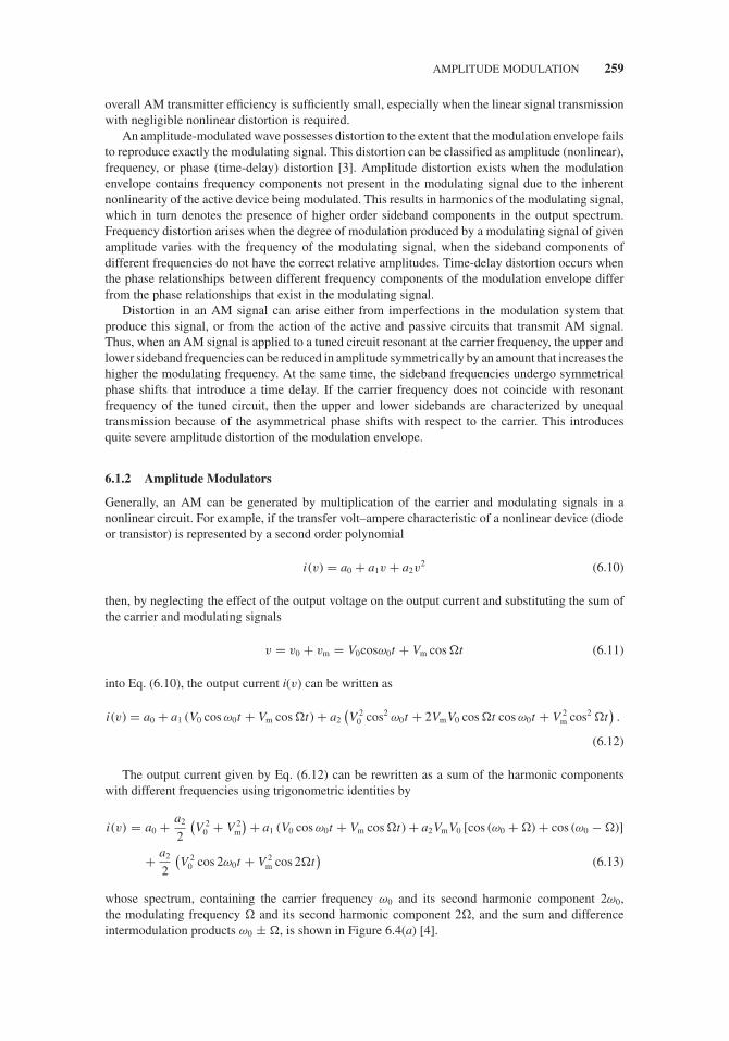
JWBS064-c06 JWBS064-Gerbennikov March 12, 2011 9:39 Printer Name: Yet to Come
AMPLITUDE MODULATION 259
overall AM transmitter efficiency is sufficiently small, especially when the linear signal transmissionwith negligible nonlinear distortion is required.
An amplitude-modulated wave possesses distortion to the extent that the modulation envelope failsto reproduce exactly the modulating signal. This distortion can be classified as amplitude (nonlinear),frequency, or phase (time-delay) distortion [3]. Amplitude distortion exists when the modulationenvelope contains frequency components not present in the modulating signal due to the inherentnonlinearity of the active device being modulated. This results in harmonics of the modulating signal,which in turn denotes the presence of higher order sideband components in the output spectrum.Frequency distortion arises when the degree of modulation produced by a modulating signal of givenamplitude varies with the frequency of the modulating signal, when the sideband components ofdifferent frequencies do not have the correct relative amplitudes. Time-delay distortion occurs whenthe phase relationships between different frequency components of the modulation envelope differfrom the phase relationships that exist in the modulating signal.
Distortion in an AM signal can arise either from imperfections in the modulation system thatproduce this signal, or from the action of the active and passive circuits that transmit AM signal.Thus, when an AM signal is applied to a tuned circuit resonant at the carrier frequency, the upper andlower sideband frequencies can be reduced in amplitude symmetrically by an amount that increases thehigher the modulating frequency. At the same time, the sideband frequencies undergo symmetricalphase shifts that introduce a time delay. If the carrier frequency does not coincide with resonantfrequency of the tuned circuit, then the upper and lower sidebands are characterized by unequaltransmission because of the asymmetrical phase shifts with respect to the carrier. This introducesquite severe amplitude distortion of the modulation envelope.
6.1.2 Amplitude Modulators
Generally, an AM can be generated by multiplication of the carrier and modulating signals in anonlinear circuit. For example, if the transfer volt–ampere characteristic of a nonlinear device (diodeor transistor) is represented by a second order polynomial
i (v) = a0 + a1v + a2v2 (6.10)
then, by neglecting the effect of the output voltage on the output current and substituting the sum ofthe carrier and modulating signals
v = v0 + vm = V0cosω0t + Vm cos �t (6.11)
into Eq. (6.10), the output current i(v) can be written as
i (v) = a0 + a1 (V0 cos ω0t + Vm cos �t) + a2
(V 2
0 cos2 ω0t + 2VmV0 cos �t cos ω0t + V 2m cos2 �t
).
(6.12)
The output current given by Eq. (6.12) can be rewritten as a sum of the harmonic componentswith different frequencies using trigonometric identities by
i (v) = a0 + a2
2
(V 2
0 + V 2m
) + a1 (V0 cos ω0t + Vm cos �t) + a2VmV0 [cos (ω0 + �) + cos (ω0 − �)]
+ a2
2
(V 2
0 cos 2ω0t + V 2m cos 2�t
)(6.13)
whose spectrum, containing the carrier frequency ω0 and its second harmonic component 2ω0,the modulating frequency � and its second harmonic component 2�, and the sum and differenceintermodulation products ω0 ± �, is shown in Figure 6.4(a) [4].

JWBS064-c06 JWBS064-Gerbennikov March 12, 2011 9:39 Printer Name: Yet to Come
260 MODULATION AND MODULATORS
FIGURE 6.4 Output AM current spectra.
In order to obtain the required AM signal, it is necessary to represent only the frequency compo-nents ω0, ω0 + �, and ω0 − � from the whole spectrum. This can be achieved by using a resonantcircuit tuned to the carrier frequency ω0 with a certain frequency bandwidth (BW) when the portionof the output current flowing to the load can be obtained from Eq. (6.12) as
iL = a1V0 cos ω0t + 2a2VmV0 cos �t cos ω0t . (6.14)
As a result, if the bandwidth of the resonant circuit is such that the load is seen as pure resistanceRL for frequencies ω0, ω0 + �, and ω0 − � and is zero for the rest frequency components, then theAM voltage across the resonant circuit is defined by
vAML = a1 RLV0
(1 + 2a2Vm
a1cos �t
)cos ω0t (6.15)
which can be simply rewritten as
vAML = VL (1 + m cos �t) cos ω0t (6.16)
where VL = a1RLV0 is the carrier amplitude and m = 2(a2/a1)Vm is the modulation factor. In thiscase, larger values of the modulation factor m correspond to stronger device nonlinearity defined bya2 and greater modulating amplitude Vm. Since the modulation factor m is directly proportional tothe modulating-signal amplitude Vm, then ideally the modulation process is distortion free.
However, if the transfer volt–ampere characteristic of a nonlinear device is represented by athird-order polynomial i(v) = a0 + a1v + a2v
2 + a3v3, then the output current spectrum will
contain the three harmonic components of the carrier and modulating frequency, ω0 and �, and theintermodulation components of the second and third orders, ω0 ± �, ω0 ± 2�, and 2ω0 ± �, asshown in Figure 6.4(b). To achieve a distortion-free AM signal, it is necessary to be confined only tothe frequency components ω0 and ω0 ± �. However, in this case the bandwidth of the resonant circuit

JWBS064-c06 JWBS064-Gerbennikov March 12, 2011 9:39 Printer Name: Yet to Come
AMPLITUDE MODULATION 261
is not narrow enough to suppress the second order intermodulation products ω0 ± 2�, resulting in aparasitic AM of the carrier frequency by the second harmonic of the modulating frequency 2�.
An AM can be easily realized by variation of the base- or gate-bias voltage of the transistor, whichproduces a corresponding variation in the amplitude of the transistor output voltage in accordancewith the modulating voltage. However, despite the simplicity of implementation, some distortion (5%to 10%) of the envelope is inherent with this method because of the nonlinearities of the device inputcapacitance and transconductance as nonlinear functions of a bias voltage [5]. In addition, it is diffi-cult to provide a sufficient isolation between the carrier and modulating signal paths, especially if thespectrum of the modulating frequencies is wide enough, which is the case for modern telecommunica-tion modulation formats. To improve the linearity performance of the AM transmitting signal withoutadditional linearization envelope feedback loops, it is best to apply an AM at low power levels usingeither cascode or differential-pair transistor stage, followed then by a linear power AM amplifier.
Figure 6.5(a) shows the circuit schematic of an amplitude modulator based on a cascode where thebottom transistor in a common emitter configuration is used for carrier signal and the top transistor in a
FIGURE 6.5 Collector modulation using cascode.

JWBS064-c06 JWBS064-Gerbennikov March 12, 2011 9:39 Printer Name: Yet to Come
262 MODULATION AND MODULATORS
FIGURE 6.6 Collector modulation using differential pair.
common base configuration is used for modulating signal. Such a cascode amplifier can operate as anamplitude modulator with linear modulation range of about 15–20 dB, because of the collector–biasvoltage variation of the bottom transistor when the cascode amplitude characteristic Vout(Vmod) islinear over a significant range of the modulating amplitudes applied to the base of the top transistor,as shown in Figure 6.5(b). The significant isolation of the modulating and carrier paths can be easilyachieved by using a proper RC low-pass filter connected to the base of the top transistor. As analternative, the carrier frequency path can be connected to the top transistor, while the modulatingsignal is applied to the bottom device, providing a linear emitter modulation of the carrier signal.However, due to a sufficiently high collector–base device capacitance, the significant feedthroughcarrier power flows to the load in this case. Similar or even better linearity of the output AM signalcan be achieved using a differential-pair transistor stage where the carrier signal is applied to thecurrent–source device, as shown in Figure 6.6. In this case, the modulating signal can be applied toone transistor of the differential pair, while the load for the resulting AM signal can be connected tothe collector of the other differential-pair transistor. The modulating signal can also be applied to bothdifferential-pair devices to obtain the differential output AM signals at the outputs of the transistorsrelatively to each other. The voltage range of the modulating amplitudes is set by a series resistor inthe modulating signal path.
6.2 SINGLE-SIDEBAND MODULATION
The single-sideband (SSB) method of signal transmission was proposed by John Carson in 1915 asa result of pure mathematical studies related to modulation of a continuous-wave carrier by meansof vacuum tubes. He was the first to recognize that the suppression of the carrier either without orwith suppression of one sideband would uniquely define the transmitting message that eventually ledto the development of the double-sideband amplitude modulation (DSB-AM) and single-sidebandamplitude modulation (SSB-AM), respectively [6,7].
6.2.1 Double-Sideband Modulation
The usual method of suppressing the carrier component of an amplitude-modulated signal is to employa balanced modulator, which can provide carrier compensation when combining two AM waves in
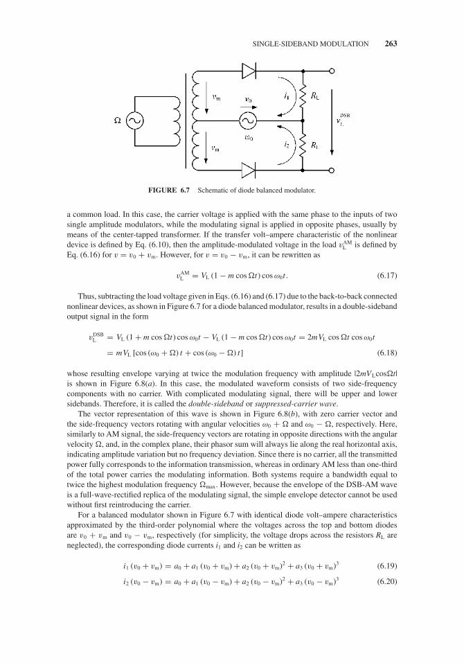
JWBS064-c06 JWBS064-Gerbennikov March 12, 2011 9:39 Printer Name: Yet to Come
SINGLE-SIDEBAND MODULATION 263
FIGURE 6.7 Schematic of diode balanced modulator.
a common load. In this case, the carrier voltage is applied with the same phase to the inputs of twosingle amplitude modulators, while the modulating signal is applied in opposite phases, usually bymeans of the center-tapped transformer. If the transfer volt–ampere characteristic of the nonlineardevice is defined by Eq. (6.10), then the amplitude-modulated voltage in the load vAM
L is defined byEq. (6.16) for v = v0 + vm. However, for v = v0 − vm, it can be rewritten as
vAML = VL (1 − m cos �t) cos ω0t. (6.17)
Thus, subtracting the load voltage given in Eqs. (6.16) and (6.17) due to the back-to-back connectednonlinear devices, as shown in Figure 6.7 for a diode balanced modulator, results in a double-sidebandoutput signal in the form
vDSBL = VL (1 + m cos �t) cos ω0t − VL (1 − m cos �t) cos ω0t = 2mVL cos �t cos ω0t
= mVL [cos (ω0 + �) t + cos (ω0 − �) t] (6.18)
whose resulting envelope varying at twice the modulation frequency with amplitude |2mVLcos�t|is shown in Figure 6.8(a). In this case, the modulated waveform consists of two side-frequencycomponents with no carrier. With complicated modulating signal, there will be upper and lowersidebands. Therefore, it is called the double-sideband or suppressed-carrier wave.
The vector representation of this wave is shown in Figure 6.8(b), with zero carrier vector andthe side-frequency vectors rotating with angular velocities ω0 + � and ω0 − �, respectively. Here,similarly to AM signal, the side-frequency vectors are rotating in opposite directions with the angularvelocity �, and, in the complex plane, their phasor sum will always lie along the real horizontal axis,indicating amplitude variation but no frequency deviation. Since there is no carrier, all the transmittedpower fully corresponds to the information transmission, whereas in ordinary AM less than one-thirdof the total power carries the modulating information. Both systems require a bandwidth equal totwice the highest modulation frequency �max. However, because the envelope of the DSB-AM waveis a full-wave-rectified replica of the modulating signal, the simple envelope detector cannot be usedwithout first reintroducing the carrier.
For a balanced modulator shown in Figure 6.7 with identical diode volt–ampere characteristicsapproximated by the third-order polynomial where the voltages across the top and bottom diodesare v0 + vm and v0 − vm, respectively (for simplicity, the voltage drops across the resistors RL areneglected), the corresponding diode currents i1 and i2 can be written as
i1 (v0 + vm) = a0 + a1 (v0 + vm) + a2 (v0 + vm)2 + a3 (v0 + vm)3 (6.19)
i2 (v0 − vm) = a0 + a1 (v0 − vm) + a2 (v0 − vm)2 + a3 (v0 − vm)3 (6.20)

JWBS064-c06 JWBS064-Gerbennikov March 12, 2011 9:39 Printer Name: Yet to Come
264 MODULATION AND MODULATORS
FIGURE 6.8 Time-domain, frequency-domain, and vector representation of DSB-AM wave.
resulting in an output voltage
vDSBL = RL [i1 (v0 + vm) − i2 (v0 − vm)] = 2RL
(a1vm + 2a2v0vm + 3a3v
20vm + a3v
3m
). (6.21)
From Eq. (6.21) it follows that the output voltage spectrum obtained by using trigonometricidentities will contain much less frequency components than that of a single-diode modulator. Forexample, the dc, second modulating (2�) and third carrier (3ω0) harmonic components will besuppressed, as well as the intermodulation components of the second order ω0 ± 2�, as shown inFigure 6.8(c), compared to the output AM spectrum shown in Figure 6.4(b). In this case, the double-sideband signal can be easily filtered by the output resonant circuits connected in parallel to eachload resistor RL.
Moreover, the further and significantly better harmonic suppression can be achieved by adding twoadditional diodes, thus resulting in a double-balanced diode modulator shown in Figure 6.9. In thiscase, the currents i1(v0 + vm) and i2(v0 − vm) are defined by Eqs. (6.19) and (6.20), while the currentsi3(−v0 − vm) and i4(−v0 + vm) differ from the currents i1 and i2 by opposite signs of the voltages v0
and vm, respectively. Hence, the resulting output voltage at the output of a double-balanced modulatorby adding the two output voltages, one caused by current i1 and i2 defined by Eq. (6.21) and anothercaused by currents i3 and i4 defined by Eq. (6.21) with opposite signs for voltages v0 and vm, can bewritten as
vDSBL = RL (i1 − i2) + RL (i3 − i4) = 2RL
(a1vm + 2a2v0vm + 3a3v
20vm + a3v
3m
)+ 2RL
(−a1vm + 2a2v0vm − 3a3v20vm − a3v
3m
) = 8RLa2v0vm (6.22)
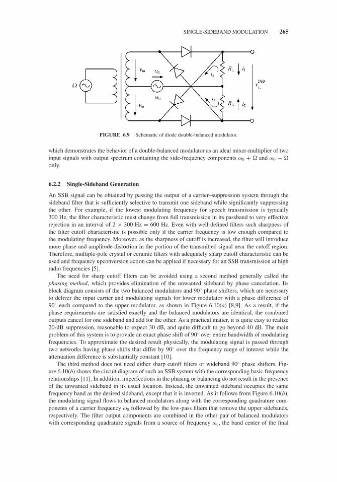
JWBS064-c06 JWBS064-Gerbennikov March 12, 2011 9:39 Printer Name: Yet to Come
SINGLE-SIDEBAND MODULATION 265
FIGURE 6.9 Schematic of diode double-balanced modulator.
which demonstrates the behavior of a double-balanced modulator as an ideal mixer-multiplier of twoinput signals with output spectrum containing the side-frequency components ω0 + � and ω0 − �
only.
6.2.2 Single-Sideband Generation
An SSB signal can be obtained by passing the output of a carrier–suppression system through thesideband filter that is sufficiently selective to transmit one sideband while significantly suppressingthe other. For example, if the lowest modulating frequency for speech transmission is typically300 Hz, the filter characteristic must change from full transmission in its passband to very effectiverejection in an interval of 2 × 300 Hz = 600 Hz. Even with well-defined filters such sharpness ofthe filter cutoff characteristic is possible only if the carrier frequency is low enough compared tothe modulating frequency. Moreover, as the sharpness of cutoff is increased, the filter will introducemore phase and amplitude distortion in the portion of the transmitted signal near the cutoff region.Therefore, multiple-pole crystal or ceramic filters with adequately sharp cutoff characteristic can beused and frequency upconversion action can be applied if necessary for an SSB transmission at highradio frequencies [5].
The need for sharp cutoff filters can be avoided using a second method generally called thephasing method, which provides elimination of the unwanted sideband by phase cancelation. Itsblock diagram consists of the two balanced modulators and 90◦ phase shifters, which are necessaryto deliver the input carrier and modulating signals for lower modulator with a phase difference of90◦ each compared to the upper modulator, as shown in Figure 6.10(a) [8,9]. As a result, if thephase requirements are satisfied exactly and the balanced modulators are identical, the combinedoutputs cancel for one sideband and add for the other. As a practical matter, it is quite easy to realize20-dB suppression, reasonable to expect 30 dB, and quite difficult to go beyond 40 dB. The mainproblem of this system is to provide an exact phase shift of 90◦ over entire bandwidth of modulatingfrequencies. To approximate the desired result physically, the modulating signal is passed throughtwo networks having phase shifts that differ by 90◦ over the frequency range of interest while theattenuation difference is substantially constant [10].
The third method does not need either sharp cutoff filters or wideband 90◦ phase shifters. Fig-ure 6.10(b) shows the circuit diagram of such an SSB system with the corresponding basic frequencyrelationships [11]. In addition, imperfections in the phasing or balancing do not result in the presenceof the unwanted sideband in its usual location. Instead, the unwanted sideband occupies the samefrequency band as the desired sideband, except that it is inverted. As it follows from Figure 6.10(b),the modulating signal flows to balanced modulators along with the corresponding quadrature com-ponents of a carrier frequency ω0 followed by the low-pass filters that remove the upper sidebands,respectively. The filter output components are combined in the other pair of balanced modulatorswith corresponding quadrature signals from a source of frequency ωc, the band center of the final

JWBS064-c06 JWBS064-Gerbennikov March 12, 2011 9:39 Printer Name: Yet to Come
266 MODULATION AND MODULATORS
FIGURE 6.10 Methods of single-sideband modulation.
SSB frequency. As a result, the combined outputs from these balanced modulators cancel one pairof sideband components and add the other pair of sideband components to produce the desired SSBsignal. As the entire circuit is bilateral, it can be used in demodulation as well as in generation of theSSB signals.
6.2.3 Single-Sideband Modulator
SSB modulators have numerous applications in a variety of existing and new communication systemsincluding optical and millimeter waves. Basically, a practical SSB modulator represents an upcon-verter that generates an SSB suppressed-carrier (SSB/SC) output signal without the use of filters.Figure 6.11(a) shows the block diagram of a typical high-frequency SSB modulator where either thelower sideband or the upper sideband can be selected by exchanging the in-phase (I) and quadrature(Q) modulating inputs [12]. Generally, the system should include two balanced modulators, an I/Qgenerator to generate output quadrature modulating signals, a 90◦ branch-line hybrid combiner toinput the carrier signals, and an in-phase Wilkinson combiner for summing the two output modulatorsignals. As an alternative, the upper sideband can be achieved by using an out-of-phase rat-race 180◦
subtracter at the output instead of a Wilkinson combiner. In microwave monolithic implementation,both the transmission-line branch-line coupler and Wilkinson combiner can be replaced by theirlumped low-pass and high-pass filter equivalents based on monolithic spiral inductors and MIMcapacitors [13]. To further minimize size and phase imbalance between modulator paths, the GaAsMESFETs or HEMTs as nonlinear elements rather than diodes can be used.
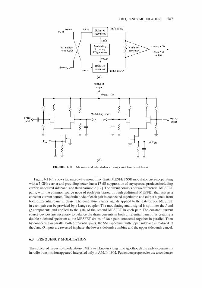
JWBS064-c06 JWBS064-Gerbennikov March 12, 2011 9:39 Printer Name: Yet to Come
FREQUENCY MODULATION 267
FIGURE 6.11 Microwave double-balanced single-sideband modulators.
Figure 6.11(b) shows the microwave monolithic GaAs MESFET SSB modulator circuit, operatingwith a 7-GHz carrier and providing better than a 17-dB suppression of any spectral products includingcarrier, undesired sideband, and third harmonic [12]. The circuit consists of two differential MESFETpairs, with the common source node of each pair biased through additional MESFET that acts as aconstant current source. The drain node of each pair is connected together to add output signals fromboth differential pairs in phase. The quadrature carrier signals applied to the gate of one MESFETin each pair can be provided by a Lange coupler. The modulating audio signal is split into the I andQ components and applied to the gate of the second MESFET in each pair. The constant currentsource devices are necessary to balance the drain currents in both differential pairs, thus creating adouble-sideband spectrum at the MESFET drains of each pair, connected together in parallel. Thenby connecting in parallel both differential pairs, the SSB spectrum with upper sideband is realized. Ifthe I and Q inputs are reversed in phase, the lower sidebands combine and the upper sidebands cancel.
6.3 FREQUENCY MODULATION
The subject of frequency modulation (FM) is well known a long time ago, though the early experimentsin radio transmission appeared interested only in AM. In 1902, Fessenden proposed to use a condenser
JWBS064-c06 JWBS064-Gerbennikov March 12, 2011 9:39 Printer Name: Yet to Come
268 MODULATION AND MODULATORS
type of microphone in circuits that appear to produce FM, but in his publication remarks about testshe seemed interested in using the frequency variation to produce amplitude variation by throwing thefrequency in and out of resonance with the antenna or other tuned circuit to modulate the amplitude[14]. Moreover, in 1922, Carson published his famous paper pointing out that FM would not providea narrower band than AM, and that it inherently produces distortion in the signal, and hence, the FMsystem is inferior to the AM system [15]. And only one and half decades later, Armstrong theoreticallyexplained and experimentally demonstrated that, if one widened the swing in FM much beyond thebandwidth used in AM and used an effective limiter in the receiver, noise lower than the carrier couldbe substantially eliminated, thus proving a significant superiority of the FM broadcasting system overits AM counterpart [16].
6.3.1 Basic Principle
Generally, the modulated signal can be written in the form
v(t) = V (t) cos φ(t) (6.23)
which is fully described by a time-varying amplitude V(t) and a time-varying phase angle φ(t). If inAM the carrier envelope V(t) is varied while φ(t) remains constant, then in angle modulation V(t) =V0 is fixed and the modulating signal varies φ(t). Angular modulation can be either FM or phasemodulation (PM), depending upon the exact relationship between φ(t) and the modulating signal.The instantaneous angular velocity ω(t) can be written in a common case as
ω(t) = 2π f (t) = dφ(t)
dt(6.24)
from which the instantaneous phase can be found by integrating according to
φ(t) =t∫
0
ω(t)dt + φ0 (6.25)
where φ0 is the initial phase at t = 0.A frequency-modulated signal with cosine modulation when the instantaneous modulating signal
varies in accordance with vm(t) = Vmcos�t represents by definition a signal in which the instantaneousangular velocity is varied according to
ω(t) = ω0 + vm(t)
Vm�ω = ω0 + 2π � f cos�t (6.26)
where ω0 is the carrier or average radian frequency, � = 2π f m is the modulating radian frequency,and �f is the maximum deviation of instantaneous frequency from average obtained at time momentswhen vm = Vm. A fundamental characteristic of a frequency-modulated signal is that the maximumfrequency deviation �f is proportional to the peak amplitude of the modulating signal Vm and isindependent of the modulating frequency. Integrating Eq. (6.26) gives
φ(t) = ω0t + � f
fmsin�t + φ0 (6.27)
where for simplicity it can be assumed that φ0 = 0.Consequently, substituting Eq. (6.27) in Eq. (6.23) results in
v(t) = V0cos
(ω0t + � f
fmsin�t
)(6.28)

JWBS064-c06 JWBS064-Gerbennikov March 12, 2011 9:39 Printer Name: Yet to Come
FREQUENCY MODULATION 269
which is commonly written for FM as
v(t) = V0cos (ω0t + msin�t) (6.29)
where
m = kVm
fm= � f
fm(6.30)
is called the modulation index for frequency modulation, where k is the factor of proportionality[4]. Note that, for a given frequency deviation �f , the modulation index m varies inversely asthe modulating frequency f m. Time-domain representation of the FM process with a sinusoidalmodulating wave is shown in Figure 6.12. As the modulating signal swings positive, the carrierfrequency is increased, reaching its highest frequency at the positive peak of the modulating signal.When the signal swings in the negative direction, the carrier frequency is lowered, reaching a minimumwhen the signal passes through its peak negative value.
Equation (6.29) can be rewritten through trigonometric expansion as
v(t) = V0 cos (msin�t) cos ω0t − V0 sin (msin�t) sin ω0t (6.31)
which represents a sum of two quadrature signals with a carrier frequency ω0, each of which isamplitude-modulated with a modulating frequency �. Generally, two different classes of FM signalscan be distinguished, depending on the values of the modulation index m [17]. For m ≤ 0.5, it is
FIGURE 6.12 Frequency modulation process in time domain.

JWBS064-c06 JWBS064-Gerbennikov March 12, 2011 9:39 Printer Name: Yet to Come
270 MODULATION AND MODULATORS
called the narrowband frequency modulation, and Eq. (6.31) can be approximated as
v(t) ∼= V0 cos ω0t − mV0sin�t sin ω0t = V0 cos ω0t + mV0
2cos (ω0 + �) t − mV0
2cos (ω0 − �) t
(6.32)
since cos(m sin�t) ∼= 1 and sin(m sin�t) ∼= m sin�t. Hence, the bandwidth of a narrowband FM isapproximately 2�, which is the same as for AM signal containing the carrier frequency ω0 and twosideband frequencies ω0 + � and ω0 − �. In this case, the amplitudes of the sideband frequenciesare defined by a modulation index m. However, the narrowband FM spectrum differs from the AMspectrum due to opposite sign in the second term, resulting in its phase shift by 180◦.
For m > 0.5, the frequency-modulated process is called the wideband frequency modulation, whichis the type of FM most often used in analog communication systems. To determine its bandwidthrequirements, it is necessary to expand the terms cos(m sin�t) and sin(m sin�t) in Eq. (6.31) as theeven and odd periodic functions in a Fourier series according to
cos (msin�t) = J0 (m) + 2J2 (m) cos (2�t) + 2J4 (m) cos (4�t) + · · · (6.33)
sin (msin�t) = 2J1 (m) sin (�t) + 2J3 (m) sin (3�t) + · · · (6.34)
where Jn(m) are the Bessel functions of the first kind.Substituting Eqs. (6.33) and (6.34) into Eq. (6.31) and using trigonometric identities result in
v(t) = V0 {J0 (m) cos ω0t + J1 (m) [cos (ω0 + �) t − cos (ω0 − �) t]
+ J2 (m) [cos (ω0 + 2�) t + cos (ω0 − 2�) t]
+ J3 (m) [cos (ω0 + 3�) t − cos (ω0 − 3�) t] + · · ·}
= V0
{J0 (m) cos ω0t +
∞∑n=1
Jn (m)J1 (m)[cos (ω0 + n�) t + (−1)n cos (ω0 − n�) t
]}(6.35)
from which it follows that the FM signal spectrum is discrete, symmetrical relatively to the carrierfrequency ω0, and contains an infinite number of sideband frequencies spaced at radian frequencies± �, ± 2�, . . . , about the carrier with amplitudes Vn = V0Jn(m). The plots and numbers of therelative carrier and sideband-frequency amplitudes for different modulation indexes m are shown inFigure 6.13. It is clearly seen that, as the modulation index varies, a carrier frequency or a sideband-frequency pair may vanish entirely. This phenomenon can be used to set the frequency deviation ofan FM transmitter, for example, by choosing the modulating frequency f m for a specified frequencydeviation �f so that J0(m) = 0.
The characters of the frequency spectra obtained under different conditions with FM are shownin Figure 6.14 (fixed f m with increasing m) and Figure 6.15 (fixed �f with decreasing f m). Althoughthe bandwidth occupied by the frequency-modulated signal is theoretically infinite, in reality theamplitudes of higher order sideband frequencies decrease rapidly. When the modulation index is lessthan 0.5, the second-order sideband frequencies are relatively small, and the frequency bandwidth(BW) required to accommodate the essential part of the signal is the same as in AM when BW = 2f m.Besides, the amplitude of the first-order sideband frequencies is almost exactly proportional to themodulation index. On the other hand, when the modulation index exceeds unity, there are importanthigher order sideband components contained in the FM signal, and, for very large m, the approximate

JWBS064-c06 JWBS064-Gerbennikov March 12, 2011 9:39 Printer Name: Yet to Come
FREQUENCY MODULATION 271
FIGURE 6.13 Carrier and sideband amplitudes for FM signals.
bandwidth requirements can be defined as BW = 2mf m = 2�f . Figure 6.16 illustrates the analyzerdisplay of an FM signal with m = 95 when it is required to use the entire spectrum width.
Thus, a general rule of thumb for the approximate bandwidth of a frequency-modulated signal forany m is
BW = 2 (� f + fm) = 2 fm (m + 1) (6.36)
which is called the Carson’s bandwidth rule. In other words, any frequency-modulated signal willhave an infinite number of sidebands but in practice all significant sideband power (98% or more) isconcentrated within the bandwidth defined by Eq. (6.36). However, setting the arbitrary definition ofoccupied bandwidth at 98% of the total power still means that the power outside the band is only by10 × log10(0.02/0.98) = 16.9 dB less than the in-band power. For voice communications a higher

JWBS064-c06 JWBS064-Gerbennikov March 12, 2011 9:39 Printer Name: Yet to Come
272 MODULATION AND MODULATORS
FIGURE 6.14 Frequency spectra of FM signal with fixed modulating frequency.
FIGURE 6.15 Frequency spectra of FM signal with fixed frequency deviation.

JWBS064-c06 JWBS064-Gerbennikov March 12, 2011 9:39 Printer Name: Yet to Come
FREQUENCY MODULATION 273
RL: – 31.3 dBm
CNF: 1999.999 4 MHz SPF:5 MHz RB1 KHz VB1 KHz
10 dBm/ AT 0 dB ST 15 s D:PK
FIGURE 6.16 Analyzer display of FM signal with m = 95.
degree of distortion can be tolerated, and it is possible to ignore all sidebands with less than 10% ofthe carrier voltage. In broadcast FM, where �f is restricted to be 75 kHz and maximum f m should beless than or equal to 15 kHz, the smallest modulation index is m = 75 kHz/15 kHz = 5. As a result,from Eq. (6.36) it follows that BW = 180 kHz, which is safely within the total bandwidth of 200 kHzallocated to each FM station.
More accurate approximation of the frequency-modulated signal bandwidth for m = 0 to 24 canbe calculated for sinusoidal modulation as
BW = 2 fm
(m + √
m + 1)
(6.37)
and for square-wave modulation as
BW = 2 fm
√200
πm + m2 (6.38)
with amplitudes less than 1% of the non-modulated carrier amplitude [18].Generally, the relative carrier and sideband frequency amplitudes in a frequency-modulated signal
will vary with amplitude and frequency of the modulating signal, but the total power contained in themodulated waveform remains constant. This is in contrast to AM, where the sideband amplitudes andthe total power are controlled by the modulation, but the carrier amplitude is not. Besides, contrary tothe situation in AM when each frequency component in the modulating signal produces a single pairof sideband frequencies, the superposition principle does not hold in a frequency-modulated signalfor complex modulating signal, resulting in asymmetrical arrays of sideband frequencies, even withharmonically related modulating signals [4].
6.3.2 Frequency Modulators
Generally, there are two basic methods to provide an FM process: direct method by varying the reactiveelement of the frequency oscillator and indirect method by proper phase varying in the phase modulatoraccording to Eq. (6.27), which follows the fixed-frequency oscillator. Usually, varactor whose junctioncapacitance varies in accordance with applied reverse bias voltage is used as a frequency-tuningelement in the oscillators. By providing a proper reverse bias voltage and low-frequency modulating

JWBS064-c06 JWBS064-Gerbennikov March 12, 2011 9:39 Printer Name: Yet to Come
274 MODULATION AND MODULATORS
FIGURE 6.17 Schematic of varactor-tuned transformer-coupled oscillator.
signal to the varactor that is a part of entire oscillator resonant circuit, the frequency-modulated signalat the output port of the oscillator is achieved. To evaluate the quality of such a frequency-modulatedsignal, it is very important to know the behavior of the varactor voltage–capacitance characteristic andits influence on the oscillator modulation characteristic, representing a dependence of the oscillationfrequency on a slowly varying varactor bias voltage. Figure 6.17 shows the simplified transformer-coupled MOSFET oscillator circuit where the modulating signal vm = Vmcos�t is applied to thevaractor included into the oscillator resonant circuit.
The voltage–capacitance characteristic of the abrupt-junction varactor can be written as
Cv (Vv) = Cv0√1 + Vv
ϕ
(6.39)
where Vv is the fixed bias voltage, Cv0 is the varactor capacitance when Vv = 0, and ϕ is the contactpotential. Substituting the voltage increment v = Vv + �v instead of Vv into Eq. (6.39) gives
�Cv
Cv= 1√
1 + ξ− 1 (6.40)
where ξ = �v/(ϕ + Vv). Equation (6.40) can be expanded into a Taylor series as
x = −ξ
2+ 3ξ 2
8− 5ξ 3
16+ · · · (6.41)
where x = �Cv/Cv. By assuming that the normalized voltage increment ξ represents the value of themodulating voltage as ξ = �v/(ϕ + Vv) = Vmcos�t, then Eq. (6.41) can be rewritten as
�Cv
Cv= −3V 2
m
16− Vm
2cos�t − 3V 2
m
16cos2�t − · · · . (6.42)
For a single resonant circuit oscillator with the radian frequency deviation �ω around the oscil-lation frequency ω0 when varactor represents the only circuit capacitance,
�ω = 1√L (Cv + �Cv)
− 1√LCv
= ω0
[(1 + �Cv
Cv
)−1/2
− 1
](6.43)

JWBS064-c06 JWBS064-Gerbennikov March 12, 2011 9:39 Printer Name: Yet to Come
FREQUENCY MODULATION 275
where ω0 = 1/√
LCv. As a result, from Eq. (6.43) it follows that
� f
f0= 1√
1 + x− 1 = − x
2+ 3x2
8− · · · . (6.44)
Substituting Eq. (6.41) with two first factors only into Eq. (6.44) results in
� f
f0= ξ
4− 3ξ 2
32+ · · · (6.45)
which represents a nonlinear dependence of the frequency deviation �f versus voltage variation �v
on the varactor. Then, substituting ξ = Vmcos�t into Eq. (6.45) gives
� f
f0= −3V 2
m
64+ Vm
4cos�t − 3V 2
m
64cos2�t + · · · (6.46)
with the frequency deviation
� f = Vm
4f0 (6.47)
the second-harmonic nonlinear coefficient
k2 = 3Vm
16= 3
4
� f
f0(6.48)
and the relative shift of the average frequency
� favr
f0= 3V 2
m
64= 3
4
(� f
f0
)2
. (6.49)
Generally, the function x(ξ ) in Eq. (6.41) depends on the voltage–capacitance characteristic ofthe particular varactor, whereas the function �f (x) is characterized by the particular type of thevaractor connection to the oscillator resonant circuit. Figure 6.18(a) shows the general case of thepartial varactor connection to the oscillator resonant circuit. When C1 � C2 + Cv, it can represent aparallel resonant circuit with variable capacitance Cv, as shown in Figure 6.18(b). When C2 Cv,the oscillator can be represented by a series resonant circuit with variable capacitance Cv, as shownin Figure 6.18(c).
FIGURE 6.18 Varactor connection to resonant circuit.

JWBS064-c06 JWBS064-Gerbennikov March 12, 2011 9:39 Printer Name: Yet to Come
276 MODULATION AND MODULATORS
For a parallel resonant circuit with C0 = C2 + Cv and varactor capacitance variation �Cv due to�v,
y = �C
C0= C2 + Cv + �Cv
C2 + Cv− 1 = Cv
C2 + Cv
�Cv
Cv= px (6.50)
where the total capacitance variation �C corresponds to the varactor voltage variation �v andp = Cv/(C2 + Cv) is the coefficient of partial varactor connection into the parallel oscillator resonantcircuit.
For a series resonant circuit with C0 = CvC1/(Cv + C1),
y = �C
C0= (1 + x) (C1 + Cv)
C1 + Cv (1 + x)− 1 = px
1 + (1 − p) x= px − p (1 − p) x2 + · · · (6.51)
where p = C1/(C1 + Cv) is the coefficient of partial varactor connection into the series oscillatorresonant circuit.
The general-type resonant circuit shown in Figure 6.18(a) represents a combination of the seriesand parallel resonant circuits. The relative deviation y1 of the capacitance C ′
v = C2 + Cv can bedefined from Eq. (6.50) as
x1 = �C ′v
C ′v
= p1x (6.52)
where p1 = Cv/(C2 + Cv). In this case, the capacitance C ′v is the variable capacitance for the circuit
including the capacitance C1 and inductance L. Therefore, using Eq. (6.51),
y (x) = p2x1 − p2 (1 − p2) x21 + · · · (6.53)
where p2 = C1/(C1 + C ′v) = C1/(C1 + C2 + Cv). Substituting Eq. (6.52) into Eq. (6.53) and
representing Eq. (6.53) as y(x) = a1x + a2x 2 + · · · allow the first two coefficients to be determinedas a1 = p1 p2 and a2 = −p2
1 p2 (1 − p2).As a result, by choosing the coefficients p1 and p2 with proper values of C1, C2, and, Cv, the
behavior of the oscillator modulation characteristic can be optimized for linear frequency tuning forthe particular varactor voltage–capacitance characteristic [19].
Generally, the voltage vv across the varactor shown in Figure 6.19 consists of the dc bias voltage Vv,low-frequency modulating component vm with amplitude Vm, and high-frequency carrier componentv0 with amplitude V0, which can be written as
vv = Vv + Vm cos �t + V0 cos ω0t (6.54)
where � is the modulating frequency and ω0 is the carrier frequency. The bias voltage Vv is usuallychosen at the center point of the varactor voltage–capacitance characteristic to maximize the frequencytuning bandwidth without performance degradation due to the forward conduction of the active deviceor its breakdown. Under these assumptions, the borders of voltage variations across the varactorjunction should satisfy the condition Vm + V0 = 0.5Vvmax.
Figure 6.20 shows the schematic of the linearized direct frequency modulator based on a crystaltransistor oscillator with audio-frequency input port, which is intended to use in the land mobileradio of low VHF band [20]. Assuming that the crystal fundamental frequency may be selected on acost–size basis only, a multiplier ratio of 3 will require a crystal fundamental frequency of 10 to 17MHz to cover the 30 to 50 MHz VHF band. To provide a 5 kHz deviation with a multiplication ratioof 3, the varactor-tuned crystal oscillator must be capable of a ±1.7 kHz deviation at the fundamental.In this case, the bias voltage must be large enough to insure the varactor diode remains reverse biased.

JWBS064-c06 JWBS064-Gerbennikov March 12, 2011 9:39 Printer Name: Yet to Come
FREQUENCY MODULATION 277
FIGURE 6.19 Varactor capacitance and frequency modulation.
FIGURE 6.20 Schematic of linearized direct frequency modulator.
JWBS064-c06 JWBS064-Gerbennikov March 12, 2011 9:39 Printer Name: Yet to Come
278 MODULATION AND MODULATORS
The tank circuit in the collector is tuned to the third harmonic of the fundamental crystal frequency,which is then amplified without further multiplication straight through antenna. The linearizationof the modulation characteristic can be achieved by optimizing the value of the variable inductorconnected in parallel to the varactor diode. The value of the shunt capacitor at the audio input ischosen to look like an RF short to the inductor but still have relatively high reactance over theaudio band up to 3000 Hz. By proper choice of both the inductance and the varactor capacitance,the undesirable modulation nonlinearity can be considerably reduced. The linearizing network for amicrowave frequency modulator based on the varactor-tuned cavity or dielectric resonator transistoroscillator can include the optimized combination of a shunt variable capacitor and the high-impedanceand low-impedance transmission lines [21].
6.4 PHASE MODULATION
In order to introduce the PM principle, first consider the carrier cycle as the projection of a pointrotating counterclockwise in a circle where the phase at any given point is the angle between the startpoint and the point on the waveform, as shown in Figure 6.21. This is called the vector representation,which can also be plotted as the amplitude against the number of degrees of the point rotation. Foreach cycle of the carrier, the point rotates in one complete circle, or period of 360◦: starting from 0◦,rotating through 180◦, and coming back to 0◦, where the next cycle begins. The position of the pointat any instant can be indicated by a vector drawn from the center of the circle, showing the particularcase of 45◦ in Figure 6.21. Note that this vector is rotating at the carrier frequency ω0.
A phase-modulated signal with cosine modulation (instantaneous modulating signal varies inaccordance with cos�t) will represent by definition a signal in which the instantaneous phase isvaried according to
φ(t) = ω0t + vm(t)
Vm�φ + φ0 = ω0t + �φ cos�t + φ0 (6.55)
where ω0 is the carrier or average radian frequency, � = 2π f m is the modulating radian frequency, φ0
is the initial phase, and �φ is the maximum deviation of instantaneous phase from its average value.Similarly to a frequency-modulated signal represented by Eq. (6.27), Eq. (6.55) for a phase-modulatedsignal can be rewritten as
φ(t) = ω0t + m cos�t + φ0 (6.56)
where m = kVm = �φ is called the modulation index for phase modulation [4].
FIGURE 6.21 Projection of circulating vector point to form sine-wave cycle.
JWBS064-c06 JWBS064-Gerbennikov March 12, 2011 9:39 Printer Name: Yet to Come
PHASE MODULATION 279
Substituting Eq. (6.56) into Eq. (6.23) with constant carrier amplitude V0 results in a phase-modulated signal with cosine modulation written as
v(t) = V0cos (ω0t + mcos�t) (6.57)
where it is assumed that φ0 = 0 for the sake of simplicity. A comparison of Eqs. (6.29) and (6.57)shows that the phase-modulated signal contains similar sideband components as does the frequency-modulated signal, and if the modulation indexes in these two cases are the same, the relative amplitudesof their corresponding components will also be the same. The frequency of the phase-modulated signalobtained from Eq. (6.56) varies according to
ω = dφ(t)
dt= ω0 − m�sin�t. (6.58)
As a result, from a comparison of Eqs. (6.56) and (6.58) it follows that the cosine varying of thesignal phase causes the sinusoidal varying of the signal frequency. In this case, the phase modulationwith maximum phase deviation �φ is accompanied by the frequency modulation with maximumfrequency deviation �f = f m�φ. At the same time, as it follows from a comparison of Eqs. (6.26)and (6.27), the FM with maximum deviation �f is equivalent to the PM with maximum phasedeviation �φ as
�φ = � f
fm. (6.59)
Consequently, varying the modulating frequency f m affects differently the frequency spectra ofFM and PM signals. For example, the modulation index of FM signal increases by reducing themodulating frequency, as shown in Figure 6.15; however, the spectrum bandwidth remains almostthe same. On the contrary, the spectrum bandwidth of FM signal reduces with increasing modulatingfrequency, as shown in Figure 6.22 where the modulating frequency f m becomes three times smaller,
FIGURE 6.22 Frequency spectra of PM signal with fixed modulation index.
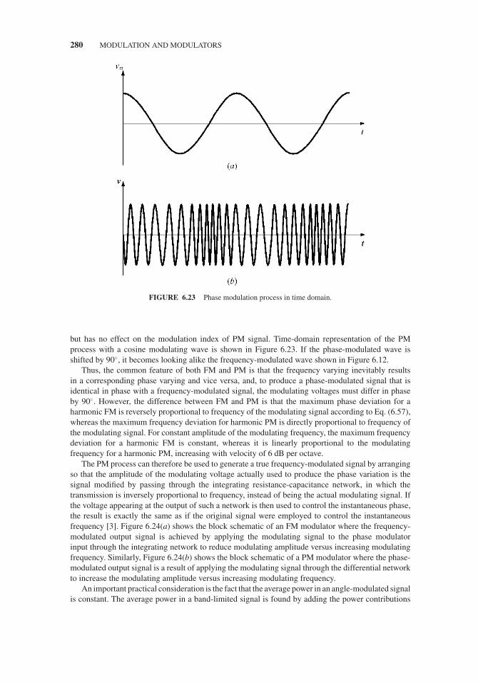
JWBS064-c06 JWBS064-Gerbennikov March 12, 2011 9:39 Printer Name: Yet to Come
280 MODULATION AND MODULATORS
FIGURE 6.23 Phase modulation process in time domain.
but has no effect on the modulation index of PM signal. Time-domain representation of the PMprocess with a cosine modulating wave is shown in Figure 6.23. If the phase-modulated wave isshifted by 90◦, it becomes looking alike the frequency-modulated wave shown in Figure 6.12.
Thus, the common feature of both FM and PM is that the frequency varying inevitably resultsin a corresponding phase varying and vice versa, and, to produce a phase-modulated signal that isidentical in phase with a frequency-modulated signal, the modulating voltages must differ in phaseby 90◦. However, the difference between FM and PM is that the maximum phase deviation for aharmonic FM is reversely proportional to frequency of the modulating signal according to Eq. (6.57),whereas the maximum frequency deviation for harmonic PM is directly proportional to frequency ofthe modulating signal. For constant amplitude of the modulating frequency, the maximum frequencydeviation for a harmonic FM is constant, whereas it is linearly proportional to the modulatingfrequency for a harmonic PM, increasing with velocity of 6 dB per octave.
The PM process can therefore be used to generate a true frequency-modulated signal by arrangingso that the amplitude of the modulating voltage actually used to produce the phase variation is thesignal modified by passing through the integrating resistance-capacitance network, in which thetransmission is inversely proportional to frequency, instead of being the actual modulating signal. Ifthe voltage appearing at the output of such a network is then used to control the instantaneous phase,the result is exactly the same as if the original signal were employed to control the instantaneousfrequency [3]. Figure 6.24(a) shows the block schematic of an FM modulator where the frequency-modulated output signal is achieved by applying the modulating signal to the phase modulatorinput through the integrating network to reduce modulating amplitude versus increasing modulatingfrequency. Similarly, Figure 6.24(b) shows the block schematic of a PM modulator where the phase-modulated output signal is a result of applying the modulating signal through the differential networkto increase the modulating amplitude versus increasing modulating frequency.
An important practical consideration is the fact that the average power in an angle-modulated signalis constant. The average power in a band-limited signal is found by adding the power contributions

JWBS064-c06 JWBS064-Gerbennikov March 12, 2011 9:39 Printer Name: Yet to Come
PHASE MODULATION 281
FIGURE 6.24 Indirect methods of frequency and phase modulations.
of the various frequency components delivered to the load resistance RL as
P = V 20
2RL
∞∑n=0
J 2n (m) (6.60)
by using Parseval’s theorem according to which the average power is proportional to the sum of thesquares of the individual Fourier components of the modulated wave.
Figure 6.25(a) shows the circuit schematic of the phase modulator based on a three-section low-pass filter having identical resonant circuits, each tuned by the varactor. For a proper tuning, sucha phase modulator can provide the phase deviation up to 30◦ for each section when the parasiticAM is negligible and nonlinear distortions are sufficiently small [22]. The phase modulator, whosebasic reactive elements compose a second-order phase-shifting four-pole network, is shown in Figure6.25(b). Here, the low-frequency modulating voltage applied directly to the varactors changes theircapacitances so that, for a proper dc biasing and sufficiently small capacitance variation, the amplitudevariations are negligible with the phase deviation up to 70◦.
Figure 6.26 shows the simplified schematics of the reflection-type varactor-tuned phase modulatorusing either (a) quadrature branch-line hybrid or (b) 3-dB coupled-line directional coupler. In bothcases, the input carrier signal divides equally between the two opposite ports of the hybrid or coupler,each of which is connected to the varactor. The varactor diodes are both biased in the same forwardor reverse biased state, so that the resulting modulated waves reflected from these two reactiveterminations will add in phase at the output port, which originally represents the isolated port. Toisolate the high-frequency carrier and low-frequency modulating paths, the quarterwave transmission

JWBS064-c06 JWBS064-Gerbennikov March 12, 2011 9:39 Printer Name: Yet to Come
282 MODULATION AND MODULATORS
FIGURE 6.25 Schematics of varactor-tuned phase modulators.
lines can be used instead of lumped LC circuits. To improve the modulation linearity, a pair ofvaractors that are reversely biased with different voltages and separated by microstrip lines withoptimized lengths to maximize reflection can be configured instead of a single varactor [23]. Inthis case, the phase deviation of 90◦ with linearity of 5% had been achieved within the frequencybandwidth of 0.8 to 1.2 GHz [24]. Much broader bandwidth can be achieved by using a 3-dB tandemor multisection Lange-type coupler. Three cascaded sections (with tapered varactor size), each ofwhich is based on the lumped reflection-type quadrature hybrid and two varactors, could provide anX-band phase modulation with peak phase deviation of 300◦ and linearity of ±2◦ [25].
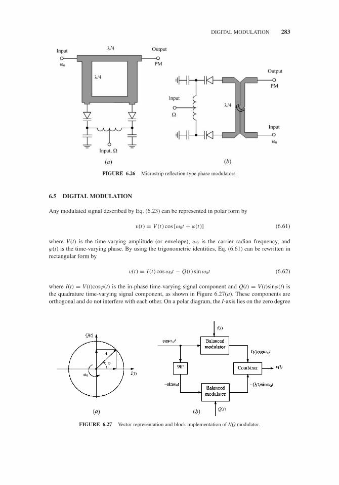
JWBS064-c06 JWBS064-Gerbennikov March 12, 2011 9:39 Printer Name: Yet to Come
DIGITAL MODULATION 283
FIGURE 6.26 Microstrip reflection-type phase modulators.
6.5 DIGITAL MODULATION
Any modulated signal described by Eq. (6.23) can be represented in polar form by
v(t) = V (t) cos [ω0t + ϕ(t)] (6.61)
where V(t) is the time-varying amplitude (or envelope), ω0 is the carrier radian frequency, andϕ(t) is the time-varying phase. By using the trigonometric identities, Eq. (6.61) can be rewritten inrectangular form by
v(t) = I (t) cos ω0t − Q(t) sin ω0t (6.62)
where I(t) = V(t)cosϕ(t) is the in-phase time-varying signal component and Q(t) = V(t)sinϕ(t) isthe quadrature time-varying signal component, as shown in Figure 6.27(a). These components areorthogonal and do not interfere with each other. On a polar diagram, the I-axis lies on the zero degree
FIGURE 6.27 Vector representation and block implementation of I/Q modulator.

JWBS064-c06 JWBS064-Gerbennikov March 12, 2011 9:39 Printer Name: Yet to Come
284 MODULATION AND MODULATORS
phase reference, and the Q-axis is rotated by 90 degrees. The signal vector projection onto the I-axisis its in-phase (I) component, while the projection onto the Q-axis is its quadrature (Q) component.In this case, the corresponding signal magnitude is defined as
A =√
I 2 + Q2 (6.63)
whereas the signal phase is obtained by
ϕ = tan−1 Q
I. (6.64)
Since two baseband signals I(t) and Q(t) modulate two exactly 90◦ out-of-phase carriers cosω0t and−sinω0t, respectively, then the system operating according to Eq. (6.62) is called the I/Q modulator.The operating principle of an I/Q modulator, the block schematic of which is shown in Figure 6.27(b),is based on the splitting of the carrier signal into two equal signals when one flows directly to thebalanced modulator to form the I-channel and the other flows into the other balanced modulatorvia 90◦ phase shifter to form the Q-channel. The baseband I(t) and Q(t) signals (either analog ordigital) modulate appropriately the carrier to produce the I (in-phase) and Q (quadrature) frequencycomponents, which are finally combined to produce the desired radio transmitting signal. Since anyRF signal can be represented in the I/Q form, any modulation scheme can be implemented by an I/Qmodulator. Digital modulation is easy to accomplish with the I/Q modulators because most digitalmodulation schemes map the data to a number of discrete points on the I/Q plane, resulting in asimultaneous amplitude and phase modulation.
To compare different modulation format efficiencies, it is necessary to first introduce the terms“bit” and “symbol,” and then to understand the difference between bit rate and symbol rate. A bitis a binary digit as a basic unit of information capacity, taking a value of either 0 or 1. A symbolis a state or significant condition of the communication channel that persists for a fixed period oftime. A sending device places symbols on the channel at a fixed and known symbol rate, which ismeasured in baud (Bd) or symbols per second. The baud unit is named in honor of Emile Baudot,the inventor of the Baudot code for telegraphy. If the transmitted pulses take on only two possiblelevels, each pulse represents 1 bit, and the bit rate = symbol rate = 1/τ bits/s, where τ is the widthof rectangular pulse. However, when raised cosine pulses are used for data transmission, then thepulse rate or symbol rate = 1/τ symbols/s. Generally, the basic difference is that the signal bandwidthneeded for the communication channel depends on the symbol rate, and not on the bit rate. The bitrate is the frequency of a system bit stream. The symbol rate is the bit rate divided by the number ofbits transmitted with each symbol. If one bit is transmitted per symbol, then the symbol rate would bethe same as the bit rate. However, if two bits are transmitted per symbol, then the symbol rate wouldbe half of the bit rate. If more bits can be sent with each symbol, then the same amount of data canbe sent in a narrower spectral bandwidth. This is why modulation formats that are more complex anduse higher number of states can send the same information over a narrower frequency bandwidth.For example, for 8-state phase-shift keying modulation, there are eight possible states that the signalcan transmit at any time. Since 8 = 23, there are three bits per symbol, which means that the symbolrate is one-third of the bit rate.
6.5.1 Amplitude Shift Keying
Amplitude shift keying (ASK) is a form of digital modulation that represents digital data as pulsedvariations in the amplitude of a carrier wave. The amplitude of an analog sinusoidal carrier signal variesin accordance with the bit stream (modulating signal), keeping frequency and phase constant. In themodulated signal, logic 0 is represented by the absence of a carrier, while logic 1 is represented by somecarrier amplitude, thus giving on-off keying operation. The ASK technique is also commonly used

JWBS064-c06 JWBS064-Gerbennikov March 12, 2011 9:39 Printer Name: Yet to Come
DIGITAL MODULATION 285
FIGURE 6.28 Binary modulating signal, OOK signal and spectrum.
to transmit digital data over optical fiber. For the fiber optic LED (light-emitting diode) transmitters,binary 1 is represented by a short pulse of light and binary 0 by the absence of light. On-off keying(OOK) is the simplest type of ASK modulation representing digital data as the presence (peak value)or absence (zero value) of a carrier wave. OOK is most commonly used to transmit Morse code overradio frequencies; the term “keying” is a historical remnant of telegraph transmission days. Whenmore than two-level pulses are used, called the m-ary transmission for m-level signals, the modulationprocess is usually called the m-ary amplitude shift keying (MASK).
Figure 6.28(a) shows the binary sequence 10010 that generates the OOK signal in the form of anRF pulse train. The OOK modulation can be considered as a modulation of the carrier by the periodicrectangular pulses with the symbol rate f m = 1/(2τ ) = 0.5 Bd, where τ is the symbol (bit) durationtime. Figure 6.28(b) shows the OOK frequency spectrum where its spectral components are definedusing a Fourier transform of the OOK signal with unit carrier amplitude as
a0 = 0.5, an = 1
nπsin
nπ
2, n = 1, 3, 5, . . . .
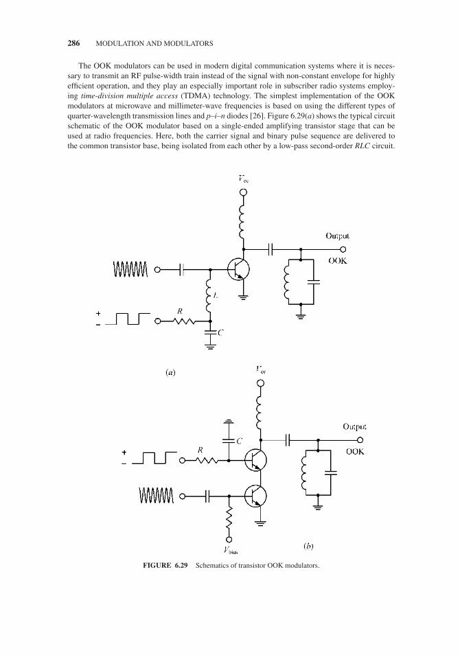
JWBS064-c06 JWBS064-Gerbennikov March 12, 2011 9:39 Printer Name: Yet to Come
286 MODULATION AND MODULATORS
The OOK modulators can be used in modern digital communication systems where it is neces-sary to transmit an RF pulse-width train instead of the signal with non-constant envelope for highlyefficient operation, and they play an especially important role in subscriber radio systems employ-ing time-division multiple access (TDMA) technology. The simplest implementation of the OOKmodulators at microwave and millimeter-wave frequencies is based on using the different types ofquarter-wavelength transmission lines and p–i–n diodes [26]. Figure 6.29(a) shows the typical circuitschematic of the OOK modulator based on a single-ended amplifying transistor stage that can beused at radio frequencies. Here, both the carrier signal and binary pulse sequence are delivered tothe common transistor base, being isolated from each other by a low-pass second-order RLC circuit.
FIGURE 6.29 Schematics of transistor OOK modulators.

JWBS064-c06 JWBS064-Gerbennikov March 12, 2011 9:39 Printer Name: Yet to Come
DIGITAL MODULATION 287
FIGURE 6.30 Binary sequence and 4ASK modulation.
In this case, it is necessary to optimally choose its elements to minimize the overall circuit transientresponse caused by the finite pulse fall and rise times and periodic damped oscillation process. A veryconvenient practical implementation, especially for monolithic circuits, can be based on a cascodecircuit shown in Figure 6.29(b) where the bottom transistor in a common emitter configuration isused for carrier signal and the top transistor in a common base configuration is used for binary pulsesequence. The significant isolation of the pulse-modulating and carrier paths can be easily achievedby using an optimized low-pass RC filter connected to the base of the top transistor.
Figure 6.30 shows the binary sequence, 4-ary digital signal, and 4ASK signal with the amplitudesthat are defined as V i = V0[2i − (m − 1)] for i = 0, 1, 2, . . . , m and m ≥ 4. It is interesting to note thatsimply by observing the resulting 4ASK signal alone, it is difficult to directly distinguish this signalfrom the conventional binary ASK (BASK) signal with a modulation index m = 0.5. However, eachRF pulse of the 4ASK signal, corresponding to a particular binary code, is characterized by differentinitial phase compared to the RF pulse with the same amplitude in a conventional binary case.
6.5.2 Frequency Shift Keying
Frequency shift keying (FSK) is an FM scheme in which digital information is transmitted throughdiscrete frequency changes of a carrier wave. The simplest FSK is a binary frequency shift keying
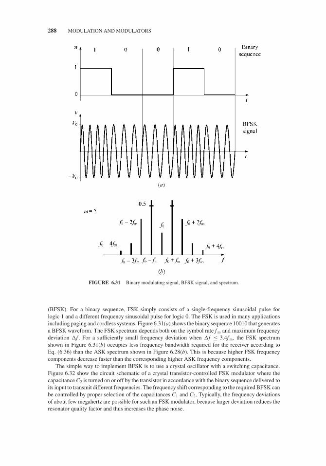
JWBS064-c06 JWBS064-Gerbennikov March 12, 2011 9:39 Printer Name: Yet to Come
288 MODULATION AND MODULATORS
FIGURE 6.31 Binary modulating signal, BFSK signal, and spectrum.
(BFSK). For a binary sequence, FSK simply consists of a single-frequency sinusoidal pulse forlogic 1 and a different frequency sinusoidal pulse for logic 0. The FSK is used in many applicationsincluding paging and cordless systems. Figure 6.31(a) shows the binary sequence 10010 that generatesa BFSK waveform. The FSK spectrum depends both on the symbol rate f m and maximum frequencydeviation �f . For a sufficiently small frequency deviation when �f ≤ 3.4f m, the FSK spectrumshown in Figure 6.31(b) occupies less frequency bandwidth required for the receiver according toEq. (6.36) than the ASK spectrum shown in Figure 6.28(b). This is because higher FSK frequencycomponents decrease faster than the corresponding higher ASK frequency components.
The simple way to implement BFSK is to use a crystal oscillator with a switching capacitance.Figure 6.32 show the circuit schematic of a crystal transistor-controlled FSK modulator where thecapacitance C2 is turned on or off by the transistor in accordance with the binary sequence delivered toits input to transmit different frequencies. The frequency shift corresponding to the required BFSK canbe controlled by proper selection of the capacitances C1 and C2. Typically, the frequency deviationsof about few megahertz are possible for such an FSK modulator, because larger deviation reduces theresonator quality factor and thus increases the phase noise.

JWBS064-c06 JWBS064-Gerbennikov March 12, 2011 9:39 Printer Name: Yet to Come
DIGITAL MODULATION 289
FIGURE 6.32 Schematic of binary FSK modulator.
The BFSK signal can be represented as a sum of two OOK signals generated by two binarysequences n1 and n2, as shown in Figure 6.33. In this case, logics 1 and 0 for binary sequences shouldalternate with each other when logic 1 for binary sequence n1 corresponds to logic 0 for binarysequence n2 and vice versa. The BFSK can be provided using an I/Q modulator with quadraturecomponents of the carrier frequency f 0 when the I and Q inputs are driven by a low-frequencyoscillator, set at the frequency offset f m. The output of the oscillator is split into quadrature componentsand applied to the modulator, thus generating an SSB output at the frequency f 0 − f m (or f 0 + f m,depending on the phase relationships of I and Q inputs). The low-frequency oscillator can be on-to-off keyed by a binary sequence to toggle between the fixed frequency f 0 representing a carrierfeedthrough mode and the modulated frequency f 0 − f m representing an SSB mode.
In m-ary frequency shift keying (MFSK), n bits are combined into a symbol before transmission,and each symbol is represented by a separate frequency of the signal. There can be a total of mdifferent frequencies, with each change in frequency occurring every symbol period equal to n-bitperiods. For example, in quaternary or 4FSK, the data is transmitted in symbols of two bits, as shownin Figure 6.34, where each symbol is represented by a different frequency of the transmitted signal.The signal can have any of four frequencies depending on the type of symbol (00, 01, 10, or 11). Thefrequencies are spaced equidistant from each other and the spacing generally is even multiples of thesymbol frequency f s. The MFSK signal requires less bandwidth compared to BFSK; however, moreresolution is required in the receiver.
6.5.3 Phase Shift Keying
Phase shift keying (PSK) modulation scheme is used to transmit digital information by shifting thephase of a carrier among several discrete values. When a binary sequence is to be transmitted, thephase is usually switched between 0◦ and 180◦, and the binary phase shift keying (BPSK) signal canbe defined as
v(t) ={
V0 cos (ω0t + φ0) for logic 1
−V0 cos (ω0t + φ0) for logic 0(6.65)
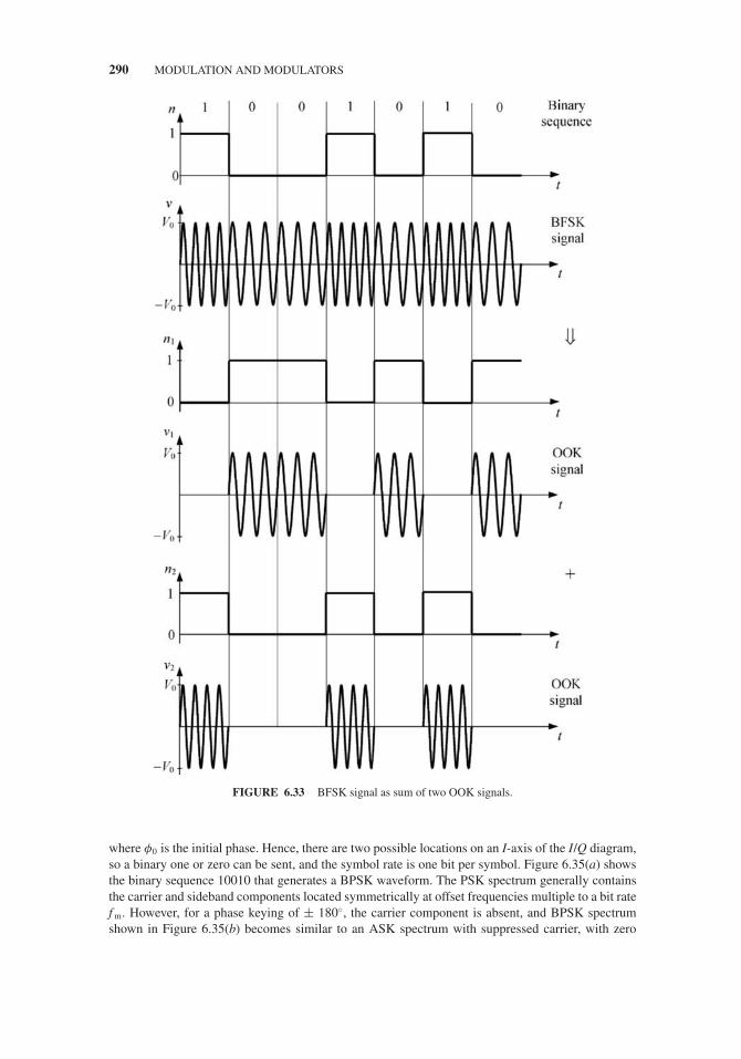
JWBS064-c06 JWBS064-Gerbennikov March 12, 2011 9:39 Printer Name: Yet to Come
290 MODULATION AND MODULATORS
FIGURE 6.33 BFSK signal as sum of two OOK signals.
where φ0 is the initial phase. Hence, there are two possible locations on an I-axis of the I/Q diagram,so a binary one or zero can be sent, and the symbol rate is one bit per symbol. Figure 6.35(a) showsthe binary sequence 10010 that generates a BPSK waveform. The PSK spectrum generally containsthe carrier and sideband components located symmetrically at offset frequencies multiple to a bit ratef m. However, for a phase keying of ± 180◦, the carrier component is absent, and BPSK spectrumshown in Figure 6.35(b) becomes similar to an ASK spectrum with suppressed carrier, with zero

JWBS064-c06 JWBS064-Gerbennikov March 12, 2011 9:39 Printer Name: Yet to Come
DIGITAL MODULATION 291
FIGURE 6.34 Binary sequence and 4FSK modulation.
FIGURE 6.35 Binary modulating signal, BPSK signal, and spectrum.

JWBS064-c06 JWBS064-Gerbennikov March 12, 2011 9:39 Printer Name: Yet to Come
292 MODULATION AND MODULATORS
crossing corresponding to the even-order sidebands and increased level of the odd-order sidebandcomponents, both having approximately the same bandwidths.
An m-ary phase shift keying (MPSK) signal can be defined as
v(t) = V0 cos(
ω0t + 2πi
m+ φ0
)(6.66)
where i = 1, 2, . . . , m. In MPSK, n bits are combined and transmitted as a symbol, with a total ofm = 2n different symbols, and each symbol is a different combination of n bits. Each transmittedsymbol is represented by a different phase of the signal. Therefore, the signal can have up to m phasechanges occurring every symbol period. The transmitted signal in Eq. (6.66) can be rewritten usinga trigonometric identity as
v(t) = V0 cos
(2π
i
m
)cos (ω0t + φ0) − V0 sin
(2π
i
m
)sin (ω0t + φ0) . (6.67)
Since PSK requires coherent demodulation with phase reference, differential phase shift keying(DPSK) avoids the requirement for an accurate local oscillator phase by using the phase during theimmediately preceding symbol interval as the phase reference [17]. As long as the preceding phaseis received correctly, the phase reference is accurate. There are a variety of encoding techniques forimplanting a DPSK system. One technique, which can be used for one-bit-at-a-time transmission,is to obtain a differential binary sequence from the input binary sequence and then assign phases tothe bits in the differential sequence. The differential binary sequence is generated by repeating thepreceding bit in the differential sequence if the message bit corresponds to logic 1 or by changing tothe opposite bit if the message bit corresponds to logic 0. Phases are then assigned to the differentialbinary sequence by transmitting 0◦ for logic 1 and 180◦ for logic 0. Another common DPSK encodingscheme is to group bits into singles, pairs (dibits), or triples (tribits), and then associate a particularphase change with each group.
In quadrature phase shift keying (QPSK) or 4PSK with n = 2 and m = 4, two bits are combinedto form a symbol before transmission when each symbol is represented by a different phase of thetransmitted signal and phase change occurs every symbol period. The phases are usually spacedequally so that the transmitted phases for 4PSK signal are 90◦ apart. Figure 6.36 shows the binary
FIGURE 6.36 Binary sequence and 4PSK modulation.

JWBS064-c06 JWBS064-Gerbennikov March 12, 2011 9:39 Printer Name: Yet to Come
DIGITAL MODULATION 293
sequence and 4PSK modulation according to Eq. (6.67) with φ0 = − 90◦. Any sudden phase changeresults in non-constant envelope. The more abrupt the phase change, the more envelope changes andthe wider the spectrum is, with the worst case of a 180◦ phase change. To minimize the power inspectral adjacent channels, pulse shaping is usually applied. In 8PSK, there are eight states of pointsspaced equally with 45◦, 16PSK corresponds to the signal with equal phase spacing of 22.5◦, andso forth.
It is convenient to represent a PSK signal, as well as some other types of the modulated signal,in the form of a phasor or constellation diagram. Using this scheme, the phase of the signal isrepresented by the angle around the circle, and the amplitude by the distance from the origin or centerof the circle. In this way, the signal can be resolved into quadrature components representing thesine for in-phase (I) component and the cosine for the quadrature (Q) component. Most PSK systemsuse constant amplitude, and therefore, points appear on one circle with constant amplitude and thechanges in state being represented by movement around the circle. For a BPSK using phase reversals,the constellation diagram represents two points appearing at opposite points on the I axis, as shownin Figure 6.37(a). Other forms of PSK may use different points on the circle, and there can be morepoints on the circle. The constellation diagram for a QPSK signal with initial phase started at 45◦ isshown in Figure 6.37(b). Since a rotation of this constellation diagram has no effect on modulationperformance, it can also start at zero phase, as shown in Figure 6.37(c). Figure 6.37(d) shows thetrajectories for an 8PSK signal, where the bits are mapped to possible phases according to the Graycoding. In this case, the bits are numbered such that each adjacent phase means just bit difference sothat when a phase mistake is made and the most likely one is the nearest phase, then only one bit isdecoded incorrectly. Using a constellation view of the signal enables quick fault-finding in a system.
FIGURE 6.37 Trajectories for (a) BPSK, (b) QPSK, (c) shifted QPSK, (d) 8PSK.
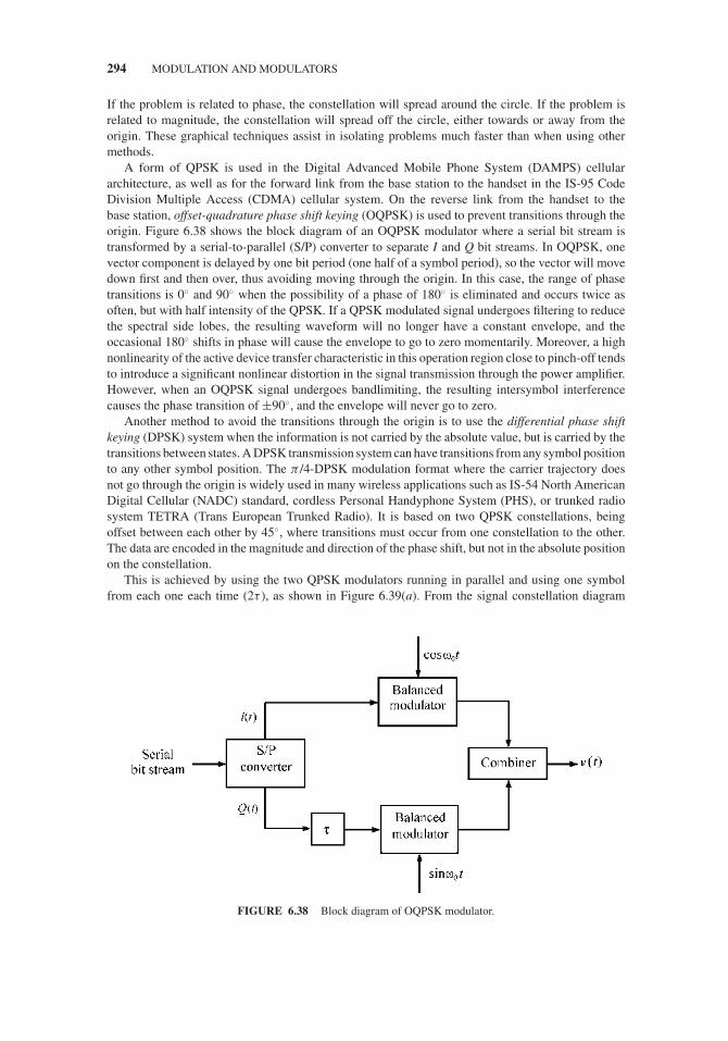
JWBS064-c06 JWBS064-Gerbennikov March 12, 2011 9:39 Printer Name: Yet to Come
294 MODULATION AND MODULATORS
If the problem is related to phase, the constellation will spread around the circle. If the problem isrelated to magnitude, the constellation will spread off the circle, either towards or away from theorigin. These graphical techniques assist in isolating problems much faster than when using othermethods.
A form of QPSK is used in the Digital Advanced Mobile Phone System (DAMPS) cellulararchitecture, as well as for the forward link from the base station to the handset in the IS-95 CodeDivision Multiple Access (CDMA) cellular system. On the reverse link from the handset to thebase station, offset-quadrature phase shift keying (OQPSK) is used to prevent transitions through theorigin. Figure 6.38 shows the block diagram of an OQPSK modulator where a serial bit stream istransformed by a serial-to-parallel (S/P) converter to separate I and Q bit streams. In OQPSK, onevector component is delayed by one bit period (one half of a symbol period), so the vector will movedown first and then over, thus avoiding moving through the origin. In this case, the range of phasetransitions is 0◦ and 90◦ when the possibility of a phase of 180◦ is eliminated and occurs twice asoften, but with half intensity of the QPSK. If a QPSK modulated signal undergoes filtering to reducethe spectral side lobes, the resulting waveform will no longer have a constant envelope, and theoccasional 180◦ shifts in phase will cause the envelope to go to zero momentarily. Moreover, a highnonlinearity of the active device transfer characteristic in this operation region close to pinch-off tendsto introduce a significant nonlinear distortion in the signal transmission through the power amplifier.However, when an OQPSK signal undergoes bandlimiting, the resulting intersymbol interferencecauses the phase transition of ±90◦, and the envelope will never go to zero.
Another method to avoid the transitions through the origin is to use the differential phase shiftkeying (DPSK) system when the information is not carried by the absolute value, but is carried by thetransitions between states. A DPSK transmission system can have transitions from any symbol positionto any other symbol position. The π /4-DPSK modulation format where the carrier trajectory doesnot go through the origin is widely used in many wireless applications such as IS-54 North AmericanDigital Cellular (NADC) standard, cordless Personal Handyphone System (PHS), or trunked radiosystem TETRA (Trans European Trunked Radio). It is based on two QPSK constellations, beingoffset between each other by 45◦, where transitions must occur from one constellation to the other.The data are encoded in the magnitude and direction of the phase shift, but not in the absolute positionon the constellation.
This is achieved by using the two QPSK modulators running in parallel and using one symbolfrom each one each time (2τ ), as shown in Figure 6.39(a). From the signal constellation diagram
FIGURE 6.38 Block diagram of OQPSK modulator.
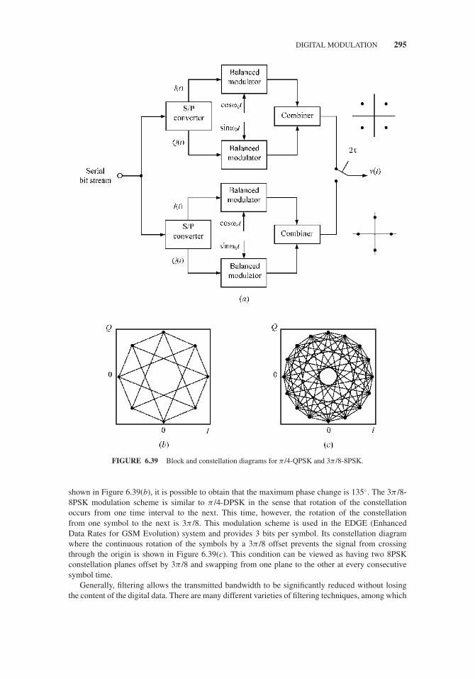
JWBS064-c06 JWBS064-Gerbennikov March 12, 2011 9:39 Printer Name: Yet to Come
DIGITAL MODULATION 295
FIGURE 6.39 Block and constellation diagrams for π /4-QPSK and 3π /8-8PSK.
shown in Figure 6.39(b), it is possible to obtain that the maximum phase change is 135◦. The 3π /8-8PSK modulation scheme is similar to π /4-DPSK in the sense that rotation of the constellationoccurs from one time interval to the next. This time, however, the rotation of the constellationfrom one symbol to the next is 3π /8. This modulation scheme is used in the EDGE (EnhancedData Rates for GSM Evolution) system and provides 3 bits per symbol. Its constellation diagramwhere the continuous rotation of the symbols by a 3π /8 offset prevents the signal from crossingthrough the origin is shown in Figure 6.39(c). This condition can be viewed as having two 8PSKconstellation planes offset by 3π /8 and swapping from one plane to the other at every consecutivesymbol time.
Generally, filtering allows the transmitted bandwidth to be significantly reduced without losingthe content of the digital data. There are many different varieties of filtering techniques, among which
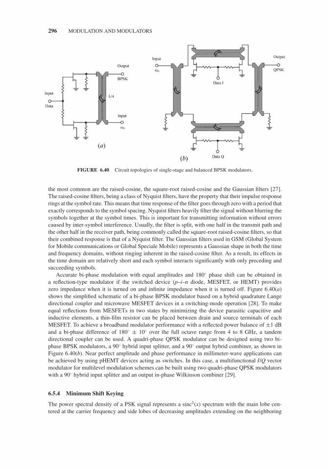
JWBS064-c06 JWBS064-Gerbennikov March 12, 2011 9:39 Printer Name: Yet to Come
296 MODULATION AND MODULATORS
FIGURE 6.40 Circuit topologies of single-stage and balanced BPSK modulators.
the most common are the raised-cosine, the square-root raised-cosine and the Gaussian filters [27].The raised-cosine filters, being a class of Nyquist filters, have the property that their impulse responserings at the symbol rate. This means that time response of the filter goes through zero with a period thatexactly corresponds to the symbol spacing. Nyquist filters heavily filter the signal without blurring thesymbols together at the symbol times. This is important for transmitting information without errorscaused by inter-symbol interference. Usually, the filter is split, with one half in the transmit path andthe other half in the receiver path, being commonly called the square-root raised-cosine filters, so thattheir combined response is that of a Nyquist filter. The Gaussian filters used in GSM (Global Systemfor Mobile communications or Global Speciale Mobile) represents a Gaussian shape in both the timeand frequency domains, without ringing inherent in the raised-cosine filter. As a result, its effects inthe time domain are relatively short and each symbol interacts significantly with only preceding andsucceeding symbols.
Accurate bi-phase modulation with equal amplitudes and 180◦ phase shift can be obtained ina reflection-type modulator if the switched device (p–i–n diode, MESFET, or HEMT) provideszero impedance when it is turned on and infinite impedance when it is turned off. Figure 6.40(a)shows the simplified schematic of a bi-phase BPSK modulator based on a hybrid quadrature Langedirectional coupler and microwave MESFET devices in a switching-mode operation [28]. To makeequal reflections from MESFETs in two states by minimizing the device parasitic capacitive andinductive elements, a thin-film resistor can be placed between drain and source terminals of eachMESFET. To achieve a broadband modulator performance with a reflected power balance of ±1 dBand a bi-phase difference of 180◦ ± 10◦ over the full octave range from 4 to 8 GHz, a tandemdirectional coupler can be used. A quadri-phase QPSK modulator can be designed using two bi-phase BPSK modulators, a 90◦ hybrid input splitter, and a 90◦ output hybrid combiner, as shown inFigure 6.40(b). Near perfect amplitude and phase performance in millimeter-wave applications canbe achieved by using pHEMT devices acting as switches. In this case, a multifunctional I/Q vectormodulator for multilevel modulation schemes can be built using two quadri-phase QPSK modulatorswith a 90◦ hybrid input splitter and an output in-phase Wilkinson combiner [29].
6.5.4 Minimum Shift Keying
The power spectral density of a PSK signal represents a sinc2(x) spectrum with the main lobe cen-tered at the carrier frequency and side lobes of decreasing amplitudes extending on the neighboring
JWBS064-c06 JWBS064-Gerbennikov March 12, 2011 9:39 Printer Name: Yet to Come
DIGITAL MODULATION 297
channels, the most important of which are adjacent and alternate, creating interference with thesechannels, which is called the spectral regrowth. Spectral regrowth can be reduced by using a modu-lation format called the minimum shift keying (MSK), which occurs when the phase changes of thetransmitted signal are smooth as opposed to instantaneous changes in QPSK. Smooth phase changesin MSK are provided by filtering the digital data before modulation, thus resulting in the side lobesmuch lower in amplitude compared to BPSK or QPSK. However, the addition of a filter in the datapath creates symbol distortion, and therefore, the choice of filtering must take into consideration thetradeoff between symbol distortion and side lobe suppression [30].
MSK can be mathematically understood as an OQPSK with a special pulse shaping in such away that the transitions between symbols are smoothed and there are no abrupt changes in phase orfrequency. If sinusoidal pulses are employed instead of rectangular shapes, the modified signal canbe defined as MSK and equals to
v(t) = aI(t)V0 cos( π
2τt)
cos ω0t + aQ(t)V0 sin( π
2τt)
sin ω0t (6.68)
where aI and aQ are two data streams consisting of even and odd bits, being separated from the binaryinput bit stream arriving at a rate of 1/τ baud. Figure 6.41(a) shows the modified in-phase bit streamwaveform with the corresponding amplitudes ± 1 shown inside waveforms. The in-phase carrier,representing by the first term in Eq. (6.68), is obtained by multiplying the waveform in Figure 6.41(a)by cosω0t, as shown in Figure 6.41(b). Similarly, the sinusoidally shaped odd-bit stream and thequadrature carrier, multiplied by sinω0t, are shown in Figures 6.41(c) and 6.41(d), respectively. Thecomposite MSK signal v(t), the addition of Figures 6.41(b) and 6.41(d), is shown in Figure 6.41(e).
To better understand the waveform shown in Figure 6.41(e), Eq. 6.68 can be rewritten using awell-known trigonometric identity as
v(t) = V0 cos[ω0t + bk(t)
π
2τt + φk
](6.69)
where bk is equal to +1 when aI and aQ have opposite signs and bk is equal to −1 when aI and aQ
have the same sign, and φk is equal to 0 or π corresponding to aI = +1 or −1, respectively. Note thatbk(t) can also be written as −aI(t)aQ(t).
From Eq. (6.69) and Figure 6.41(e), the following basic properties of MSK can be derived:
1. It has constant envelope.
2. There is phase continuity in the RF carrier at the bit transition instants.
3. The signal represents an FSK signal with signaling frequencies f + = f 0 + 1/(4τ ) and f − =f 0 − 1/(4τ ), where f 0 = ω0/(2π ), with the frequency deviation equals to half the bit rate, thatis, �f = f + − f − = 1/(2τ ). This is the minimum frequency spacing that allows the two FSKsignals to be coherently orthogonal. Since the frequency spacing is only half as much as theconventional 1/τ spacing used in noncoherent detection of FSK signals, MSK is also referredto as the fast frequency shift keying (FFSK).
4. The excess phase of the MSK signal, referenced to the carrier phase, is given by the term
ϕ(t) = bk(t)π
2τt = ± π
2τt
in Eq. (6.69), which increases or decreases linearly during each bit period of τ seconds. A bit bk
of +1 corresponds to an increase of the carrier phase by 90◦ and corresponds to an FSK signalat the higher frequency f +. Similarly, bk = −1 implies a linear decrease of phase by 90◦ overτ seconds, corresponding to the lower frequency f −. In order to make the phase continuous atbit transitions, the carrier frequency f 0 should be chosen such that f 0 is an integral multiple of1/(4τ ), one-fourth the bit rate.
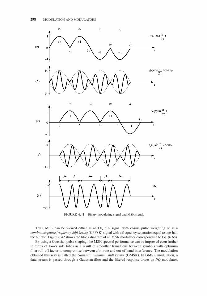
JWBS064-c06 JWBS064-Gerbennikov March 12, 2011 9:39 Printer Name: Yet to Come
298 MODULATION AND MODULATORS
FIGURE 6.41 Binary modulating signal and MSK signal.
Thus, MSK can be viewed either as an OQPSK signal with cosine pulse weighting or as acontinuous phase frequency shift keying (CPFSK) signal with a frequency separation equal to one-halfthe bit rate. Figure 6.42 shows the block diagram of an MSK modulator corresponding to Eq. (6.68).
By using a Gaussian pulse shaping, the MSK spectral performance can be improved even furtherin terms of lower side lobes as a result of smoother transitions between symbols with optimumfilter roll-off factor to compromise between a bit rate and out-of-band interference. The modulationobtained this way is called the Gaussian minimum shift keying (GMSK). In GMSK modulation, adata stream is passed through a Gaussian filter and the filtered response drives an I/Q modulator,
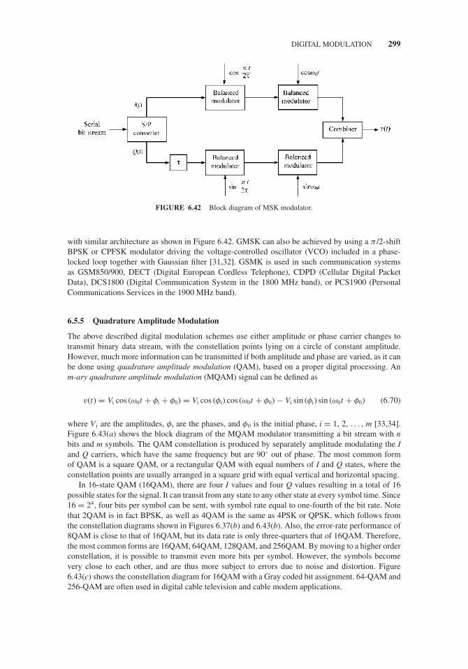
JWBS064-c06 JWBS064-Gerbennikov March 12, 2011 9:39 Printer Name: Yet to Come
DIGITAL MODULATION 299
FIGURE 6.42 Block diagram of MSK modulator.
with similar architecture as shown in Figure 6.42. GMSK can also be achieved by using a π /2-shiftBPSK or CPFSK modulator driving the voltage-controlled oscillator (VCO) included in a phase-locked loop together with Gaussian filter [31,32]. GSMK is used in such communication systemsas GSM850/900, DECT (Digital European Cordless Telephone), CDPD (Cellular Digital PacketData), DCS1800 (Digital Communication System in the 1800 MHz band), or PCS1900 (PersonalCommunications Services in the 1900 MHz band).
6.5.5 Quadrature Amplitude Modulation
The above described digital modulation schemes use either amplitude or phase carrier changes totransmit binary data stream, with the constellation points lying on a circle of constant amplitude.However, much more information can be transmitted if both amplitude and phase are varied, as it canbe done using quadrature amplitude modulation (QAM), based on a proper digital processing. Anm-ary quadrature amplitude modulation (MQAM) signal can be defined as
v(t) = Vi cos (ω0t + φi + φ0) = Vi cos (φi) cos (ω0t + φ0) − Vi sin (φi) sin (ω0t + φ0) (6.70)
where V i are the amplitudes, φi are the phases, and φ0 is the initial phase, i = 1, 2, . . . , m [33,34].Figure 6.43(a) shows the block diagram of the MQAM modulator transmitting a bit stream with nbits and m symbols. The QAM constellation is produced by separately amplitude modulating the Iand Q carriers, which have the same frequency but are 90◦ out of phase. The most common formof QAM is a square QAM, or a rectangular QAM with equal numbers of I and Q states, where theconstellation points are usually arranged in a square grid with equal vertical and horizontal spacing.
In 16-state QAM (16QAM), there are four I values and four Q values resulting in a total of 16possible states for the signal. It can transit from any state to any other state at every symbol time. Since16 = 24, four bits per symbol can be sent, with symbol rate equal to one-fourth of the bit rate. Notethat 2QAM is in fact BPSK, as well as 4QAM is the same as 4PSK or QPSK, which follows fromthe constellation diagrams shown in Figures 6.37(b) and 6.43(b). Also, the error-rate performance of8QAM is close to that of 16QAM, but its data rate is only three-quarters that of 16QAM. Therefore,the most common forms are 16QAM, 64QAM, 128QAM, and 256QAM. By moving to a higher orderconstellation, it is possible to transmit even more bits per symbol. However, the symbols becomevery close to each other, and are thus more subject to errors due to noise and distortion. Figure6.43(c) shows the constellation diagram for 16QAM with a Gray coded bit assignment. 64-QAM and256-QAM are often used in digital cable television and cable modem applications.

JWBS064-c06 JWBS064-Gerbennikov March 12, 2011 9:39 Printer Name: Yet to Come
300 MODULATION AND MODULATORS
FIGURE 6.43 Block diagram of QAM modulator and constellation diagrams.
6.5.6 Pulse Code Modulation
Pulse code modulation (PCM) was originally developed in 1939 by Alec Reeves for voice com-munication as a method for transmitting digital signals over analog communications channels [35].This is generally a method of transmitting continuous signals in which the amplitude of the signal issampled regularly at uniform intervals and then quantized to a series of symbols in a numeric (usuallybinary) code. Pulse-code modulation is very popular because of many advantages it offers such asinexpensive digital circuitry required in the system, all-digital transmission, possible encryption withfurther digital processing, or error minimization by appropriate coding of the signals. PCM variantsare based on different mathematical techniques for quantization, including linear, logarithmic, andadaptive. Quantization is the process of converting a continuous amplitude into one of a finite numberof discrete amplitudes.
Figure 6.44 shows how an analog signal in the form of a sine wave is converted (sampled) into16 amplitude levels with equal spacing by a 16-level quantizer. For each sample, one of the availablevalues shown on the Y-axis is chosen by some algorithm (in this case, the floor function is used whenfloor(x) is the largest integer not greater than x). This produces a fully discrete representation of theinput signal (shaded area) that can be easily encoded as digital data for storage or manipulation. Forthis sine wave signal, we can verify that the quantized values at the sampling moments are 7, 9, 11,12, 13, 14, 14, 15, 15, 15, 14, and so on. Encoding these values as binary numbers would result in thefollowing set of nibbles (or half-octets): 0111, 1001, 1011, 1100, 1101, 1110, 1110, 1111, 1111, 1111,1110, and so on. These digital values could then be further processed or analyzed by a purpose-specificdigital signal processor or general purpose central processing unit (CPU). Several PCM data streams

JWBS064-c06 JWBS064-Gerbennikov March 12, 2011 9:39 Printer Name: Yet to Come
DIGITAL MODULATION 301
FIGURE 6.44 Signal sampling and quantization for 4-bit PCM.
could also be multiplexed into a larger aggregate data stream, generally for transmission of multiplestreams over a single physical link. There are many ways to implement a real device that performsthis task. In real systems, such a device is commonly implemented on a single integrated circuit thatlacks only the clock necessary for sampling, and is generally referred to as an ADC (analog-to-digitalconverter). These devices will produce on their output a binary representation of the input wheneverthey are triggered by a clock signal, which would then be read by a processor of some sort.
Generally, quantization reduces the degree of accuracy of representation of the sampled signal,which is characterized by a quantization error or noise. To evaluate the quantizer performance,one commonly used measure is the quantizer signal-to-noise ratio (SQNR). Assuming a uniformdistribution of input signal values, the quantization noise is a uniformly-distributed random signalwith peak-to-peak amplitude of one quantization level, making the amplitude ratio 2n/1. Then, if theinput to the quantizer is a full-scale sine wave signal (that is, the quantizer is designed such that it hasthe same minimum and maximum values as the input signal), the quantization noise approximates asawtooth wave with peak-to-peak amplitude of one quantization level and uniform distribution [17].As a result, for a n-bit quantizer,
SQNR (dB) = 20n log10 2 + 1.76 = 6.02n + 1.76 (6.71)
Thus, for an 8-bit quantizer, the SQNR for a full-scaled sine wave is about 50 dB, and each extraquantization bit increases the SQNR by roughly 6 dB. In practical digital telephone systems, 256 =28 levels are used to keep quantization error to an acceptable level, whereas 65,536 = 216 levels areused for the CD digital system.
If the quantized samples are transmitted directly over a channel, such a process is simply called thepulse amplitude modulation (PAM) process in the transmission system. In PCM system, the quantizedsignal is coded into a block of digits for transmission. The decimal-to-binary conversion can be donein various ways, for example, using two simple coding rules based on the natural binary and Graycodes, as shown in Figure 6.44 for a 16-level sample into 4 binary digits. In the Gray coding, adjacentlevels differ by only a single bit, and hence, for equally likely bit errors in each position, a singlechannel bit error is more likely to produce an adjacent output level than in other codes.
Some forms of PCM combine signal processing with coding. Differential pulse code modulation(DPCM) encodes the PCM values as differences between the current value and the predicted value.

JWBS064-c06 JWBS064-Gerbennikov March 12, 2011 9:39 Printer Name: Yet to Come
302 MODULATION AND MODULATORS
An algorithm predicts the next sample based on the previous samples, and the encoder stores onlythe difference between this prediction and the actual value. If the prediction is reasonable, fewer bitscan be used to represent the same information. For audio signals, this type of encoding reduces thenumber of bits required per sample by about 25% compared to PCM. Adaptive differential pulsecode modulation (ADPCM) is a variant of DPCM that varies the size of the quantization step, toallow further reduction of the required bandwidth for a given SQNR. Delta modulation (DM or �-modulation), another variant, is the simplest form of DPCM where the difference between successivesamples is encoded into n-bit data streams, and the transmitted data is reduced to a 1-bit data stream.
6.6 CLASS-S MODULATOR
A class-S modulator is a high-efficiency low-frequency power amplifier based on pulse-width mod-ulation (PWM), and its output is a baseband envelope signal including a dc component [5,36].Pulse-width modulation (or pulse-duration modulation) uses a square-wave signal whose pulse widthis modulated resulting in the variation of the average value of the waveform. Such a modulatorproduces only positive output current and, therefore, requires only a single transistor and a singlediode that is required to provide a suitable reverse-direction path, as shown in Figure 6.45. The outputvoltage can have any value between nearly zero voltage and the supply voltage Vcc. The low-passfilter (LPF) should have high impedance to the switching (sampling, or clock) frequency and itsharmonics to provide a high level of spectral purity of the output RF signal. Usually, it is preferableto use a first-order LPF, since further increasing the number of its elements improves the modulatorperformance insignificantly, but significantly increases size and complexity of a Class-S modulator.When the transistor is turned on, the supply voltage Vcc is connected to the input of the LPF, and theload current flows through the device. However, when transistor is turned off, the load current flowsthrough the diode, and the voltage at the LPF input is equal to the voltage across the diode.
In an ideal operation mode, the active device never experiences simultaneous nonzero voltage andnonzero current resulting in 100% efficiency. However, in practical implementation, the losses in thediode and transistor degrade efficiency due to the finite values of their on-resistances and finite riseand fall times, especially at higher operation frequencies. To minimize the intermodulation distortionof the envelope signal, it is necessary to choose correctly the LPF parameters for a maximally flatfrequency response, which can be calculated from
L = 0.7RL
π fcC = 1
2.8π fc RL(6.72)
where f c is the cutoff frequency of the low-pass filter.
FIGURE 6.45 Schematic of Class-S modulator.

JWBS064-c06 JWBS064-Gerbennikov March 12, 2011 9:39 Printer Name: Yet to Come
CLASS-S MODULATOR 303
FIGURE 6.46 Waveforms of pulse-width modulation of envelope signal.
Generally, the PWM signal can be accomplished by several techniques, the most popular ofwhich is a comparator method shown in Figure 6.45. In this case, a comparison of the envelopeinput to a triangular reference wave shown in Figure 6.46(b) by a comparator produces a PWMswitching signal, the width of which varies with envelope amplitude, as shown in Figure 6.46(c).The comparator produces maximum output when the input signal is larger than the triangular waveand zero output when the input signal is smaller than the triangular wave. The triangular wave canbe supplied directly from a function-generator circuit or obtained by integration of the output of aswitching generator with rectangular-wave signal, which is shown in Figure 6.46(a). The maximummodulation frequency depends strongly on the switching frequency required for a PWM process. Tokeep the spurious products in the output spectrum at least 30–40 dB below the carrier, the switchingfrequency must four or five times exceed the highest modulation frequency. In practice, to restore theinput envelope with minimum level of intermodulation components using an LPF, as shown in Figure6.46(d), it is better to use a factor of 10. An efficiency of about 90% can be achieved for a Class-Smodulator with an envelope bandwidth up to 150 kHz [36,37]. However, a PWM is an inherentlynonlinear process that generates intermodulation components with as higher level as wider RF signalbandwidth [38].
JWBS064-c06 JWBS064-Gerbennikov March 12, 2011 9:39 Printer Name: Yet to Come
304 MODULATION AND MODULATORS
Therefore, for the envelope-varying systems with wider bandwidths and stronger requirements forthe intermodulation distortion levels, it is preferable to use a Class-S modulator based on a low-passdelta–sigma modulation (�-modulation or DSM) scheme. For the same switching frequency (oroversampling ratio), a system based on DSM can provide wider bandwidth and lower distortionthan a PWM system. The signal in a delta–sigma modulator is digitized by a quantizer (single-bitcomparator), the output of which is subtracted from the input signal through a digital feedback loopacting as a discrete-time sharp low-pass filter and quantization noise is forced outside of the bandof interest [39,40]. The degree of suppression of the quantization noise depends on an oversamplingratio, which is the ratio of a sampling frequency to twice the bandwidth or highest frequency of thesignal being sampled.
6.7 MULTIPLE ACCESS TECHNIQUES
6.7.1 Time and Frequency Division Multiplexing
In the history of electrical communications, the earliest reason for sampling a signal was to interlacesamples from different telegraphy sources, and transmit them over a single telegraph cable. Theelectrical engineer W. Miner used an electromechanical commutator for time-division multiplex ofmultiple telegraph signals in 1903, and also applied this technology to telephony where he obtainedintelligible speech from channels sampled at a rate above 3500–4300 Hz by means of a pulse-amplitude modulation rather than PCM. Thus, time division multiplexing (TDM) is alternate processin which a number of signals or bit streams are transmitted simultaneously in one communicationchannel by letting the signals occupy the same frequency band on a time-sharing basis. In suchsystems the transmitter is switched or commutated to each signal channel sequentially. In this case,the time domain is divided into several recurrent timeslots of fixed length, one for each subchannel,when a sample byte or data block of subchannel 1 is transmitted during timeslot 1, subchannel 2during timeslot 2, and so on. The receiving system must then be switched in synchronism with thetransmitter to separate the various signals prior to final demodulation. In circuit switched networkssuch as the Public Switched Telephone Network (PSTN) there exists the need to transmit multiplesubscribers’ calls along the same transmission medium, and to accomplish this, network designersmake use of TDM that allows switches to create channels within a transmission stream.
Frequency division multiplexing (FDM) is a form of signal multiplexing that involves assigningnon-overlapping frequency ranges to different signals. Since the portion of the spectrum to be utilizedis determined by the carrier frequency, different signals can modulate carriers of different frequenciesand all of them can be transmitted simultaneously. The receiver can choose the desired signal band bymeans of selective filters. FDM can be also used to combine multiple signals before final modulationonto a carrier wave. In this case, the carrier signals are referred to as subcarriers. For example, instereo FM transmission, a 38-kHz subcarrier is used to separate the left–right difference signal fromthe central left–right sum channel, prior to the frequency modulation of the composite signal. Atelevision channel is divided into subcarrier frequencies for video, color, and audio. Digital SubscribeLine (DSL) uses different frequencies for voice and for upstream and downstream data transmissionon the same conductors.
Orthogonal frequency division multiplexing (OFDM) represents an FDM scheme utilized as adigital multicarrier modulation method where a large number of closely-spaced orthogonal subcarriersare used for data transmission [41]. In this case, the data is divided into several parallel data streamsor channels, one for each subcarrier, and the subcarrier is modulated with a conventional modulationscheme such as QAM or PSK at a low symbol rate, maintaining total data rates similar to conventionalsingle-carrier modulation schemes in the same bandwidth. OFDM has developed into a popularscheme for wideband digital communication used in applications such as digital television and audiobroadcasting, wireless networking and broadband internet access. In OFDM, the subcarriers arechosen so that they are orthogonal to each other, meaning that cross-talk between the subchannels is

JWBS064-c06 JWBS064-Gerbennikov March 12, 2011 9:39 Printer Name: Yet to Come
MULTIPLE ACCESS TECHNIQUES 305
eliminated and intercarrier guard bands are not required. This greatly simplifies the design of both thetransmitter and the receiver when a separate filter for each subchannel is not required. As a result, anOFDM carrier signal is the sum of a number of orthogonal subcarriers, with baseband data on eachsubcarrier being independently modulated commonly using some type of QAM or PSK.
6.7.2 Frequency Division Multiple Access
When FDM is used as to allow multiple users to share a physical communication channel, it iscalled the frequency division multiple access (FDMA), which is the traditional way of separatingradio signals from different transmitters. FDMA gives users an individual allocation of one or severalfrequency bands, allowing them to utilize the allocated radio spectrum without interfering with eachother and coordinate access between multiple users. In FDMA, a predetermined frequency band isavailable for the entire period of communication, with stream data that may not be packetized. Inthe commercial radio broadcast bands, 535–1705 kHz for AM and 88–108 MHz for FM, each localbroadcast station (user) is assigned to a specific slice of spectrum within the frequency band allocatedfor that purpose. As long as the station broadcasts, no other radio station in the same area can use thatradio frequency bandwidth to send a signal. Another broadcast station can use that same bandwidthonly when the distance between the stations is sufficient to reduce the risk of interference. Therefore,FDMA requires high-performing filters in the radio systems. In addition, because adjacent channelinterference is an important factor in channel quality, frequency planning is a key consideration whenselecting fixed or base station locations.
It is important to distinguish between FDMA and frequency division duplexing (FDD). WhileFDMA allows multiple users simultaneous access to a certain system, FDD refers to how the radiochannel is shared between the uplink and downlink (for instance, the traffic going back and forthbetween a mobile phone and a base station). Similarly, FDM should not be confused with FDMA. Theformer is a physical layer technique that combines and transmits low-bandwidth channels through ahigh-bandwidth channel. FDMA, on the other hand, is an access method in the data link layer. FDMAalso supports demand assignment in addition to fixed assignment. Demand assignment allows all usersapparently continuous access of the radio spectrum by assigning carrier frequencies on a temporarybasis using a statistical assignment process.
Orthogonal frequency division multiple access (OFDMA) is a multi-user version of the OFDMdigital modulation scheme. Multiple access is achieved in OFDMA by assigning subsets of subcarriersto individual users. This allows simultaneous low data rate transmission from several users.
6.7.3 Time Division Multiple Access
Time division multiple access (TDMA) represents a channel access method for shared radio networks.TDMA systems can improve spectrum efficiency compared to FDMA because they allow not onlyassigning users into an available pair of channels, but also allowing several users to share the samefrequency channel by dividing into different timeslots. The users transmit in rapid succession, oneafter the other, each using own timeslot. This allows multiple stations to share the same radio channel,while using only a part of its channel capacity. However, the user can only send or receive informationat that time, regardless of the availability of other timeslots. Information flow is not continuous for anyuser, but rather is sent and received in bursts that are then reassembled at the receiving end and appearto provide continuous signal due to fast process. TDMA is used in the digital cellular systems suchas GSM or DECT (Digital Enhanced Cordless Telecommunications) standard for portable phones, aswell as in the satellite systems. Figure 6.47 shows the TDMA frame structure based on a data streamdivided into frames with those frames divided into timeslots.
TDMA is a type of TDM when multiple transmitters are used instead of a single transmitterconnected to a single receiver. Because TDMA systems also split an allotted portion of the frequencyspectrum into smaller slots (channels), they require the same level of frequency planning as FDMAsystems. Generally, FDMA can provide extended battery life and talk time, more efficient use by

JWBS064-c06 JWBS064-Gerbennikov March 12, 2011 9:39 Printer Name: Yet to Come
306 MODULATION AND MODULATORS
FIGURE 6.47 TDMA frame structure.
accommodating more users in the same spectrum space, efficient utilization of hierarchical cellstructures from macrocells to picocells and can efficiently handle video and audio data. However,in TDMA systems, the network and spectrum planning are intensive; they create interference ata frequency that is directly connected to the timeslot length; the frequency guard bands limit thepotential bandwidth of a TDMA channel; and dropped calls are possible when users switch in andout of different cells. Handsets that are moving will need to constantly adjust their timings to ensuretheir transmission is received at precisely the right time, because as they move further from the basestation, their signal will take longer to arrive, which also means that the major TDMA systems havehard limits on cell sizes in terms of range.
In the GSM system, the synchronization of the mobile phones is achieved by sending timingadvance commands from the base station that instructs the mobile phone to transmit earlier and byhow much. The mobile phone is not allowed to transmit for its entire timeslot, but there is a guardinterval at the end of each timeslot. As the transmission moves into the guard period, the mobilenetwork adjusts the timing advance to synchronize the transmission.
6.7.4 Code Division Multiple Access
Code division multiple access (CDMA) is a class of modulation that uses specialized codes toprovide multiple communication channels in a designated frequency range [42]. It is based on aspread spectrum technique used to increase spectrum efficiency over current FDMA and TDMAsystems. In this case, CDMA spreads the information contained in a signal over the entire availablebandwidth and not simply through one frequency. Due to the wide bandwidth of a spread-spectrumsignal, it is very difficult to cause jamming, difficult to interfere with, and difficult to identify. CDMAsystems are widely used in military and cellular applications.
The use of CDMA for terrestrial cellular communications was first conceived in 1985 and wasthen standardized as IS-95 to become the first commercialized CDMA system. In North Americancellular system, CDMA starts with a basic rate of 9600 b/s, and then it spreads to a transmitted bitrate, or chip rate, of 1.2288 MHz [43]. Spreading consists of applying digital codes to the data bitsthat increase the data rate while adding redundancy to the system. The chips (transmitted bits) aretransmitted using a form of a QPSK modulation that is filtered to limit the bandwidth of the signal.When the signal is received, the coding is removed from the desired signal, returning it to a rateof 9600 b/s. The ratio of transmitted bits or chips to data bits is the coding gain, which is equal to

JWBS064-c06 JWBS064-Gerbennikov March 12, 2011 9:39 Printer Name: Yet to Come
MULTIPLE ACCESS TECHNIQUES 307
128 or 21 dB and because of which an interference of up to 18 dB above the signal level (3 dB belowthe signal strength after coding gain) can be tolerated. The CDMA codes are designed to have verylow cross-correlation.
The basic differences of CDMA communication systems from the others are:
1. Multiple users share one frequency. In a fully loaded CDMA system, there are about 35users on each carrier frequency. (Note that there are actually two carrier frequencies perchannel, 45 MHz away from each other. One is for the base-mobile link, when it is calledthe forward direction, while the other is for the mobile-base link, which is called the reversedirection).
2. The channel is defined by a code. There is a carrier frequency assignment, with a frequencybandwidth of 1.25 MHz.
3. The capacity limit is soft. Additional users add more interference to the system, which cancause a higher data error rate for all users, but this limit is not set by the number of physicalchannels.
CDMA makes use of multiple forms of diversity such as spatial, frequency, and time diversities.The traditional form of spatial diversity, using multiple antennas, is used for the cell site receiver.Another form of spatial diversity called the soft handoff is used during the process of handling off a callfrom one cell to the next. Soft handoffs allow the mobile telephone to communicate simultaneouslywith two or more cells, and the best signal quality is selected until the handoff is complete. Frequencydiversity is provided in the bandwidth of the transmitted signal. With time diversity for multipathsignals, the multiple correlative receiver elements can be assigned to different time-delayed copiesof the same signal when the time-diverse signals are combined in optimal manner. One importantaspect of CDMA is the use of Walsh codes based on the Walsh matrix, which is a square matrix withbinary elements that always has a dimension that is power of two.
Each user in a CDMA system uses a different code to modulate their signal. Choosing the codesused to modulate the signal is very important in the performance of CDMA systems. The bestperformance will occur when there is good separation between the signal of a desired user and thesignals of other users. The separation of the signals is made by correlating the received signal withthe locally generated code of the desired user. If the signal matches the desired user’s code, then thecorrelation function will be high, and the system can extract that signal. If the desired user’s codehas nothing in common with the signal, the correlation should be as close to zero as possible (thuseliminating the signal), which is referred to as cross-correlation. If the code is correlated with thesignal at any time offset other than zero, the correlation should be as close to zero as possible. Thisis referred to as auto-correlation and is used to reject multipath interference.
In general, CDMA belongs to two basic categories: synchronous (orthogonal codes) and asyn-chronous (pseudorandom codes). Most modulation schemes try to minimize the bandwidth of thetransmitted signal since bandwidth is a limited resource. However, spread-spectrum techniques use atransmission bandwidth that is several orders of magnitude greater than the minimum required signalbandwidth. One of the initial reasons for doing this was military applications, including guidanceand communication systems. These systems were designed using spread spectrum because of itssecurity and resistance to jamming. Asynchronous CDMA has some level of privacy built in becausethe signal is spread using a pseudorandom code; this code makes the spread-spectrum signals appearrandom or have noise-like properties. CDMA can also effectively reject narrowband interference.Since narrowband interference affects only a small portion of the spread-spectrum signal, it caneasily be removed through notch filtering without much loss of information. Convolution encodingand interleaving can be used to assist in recovering this lost data. CDMA signals are also resistant tomultipath fading. Since the spread-spectrum signal occupies a large bandwidth, only a small portionof this will undergo fading due to multipath at any given time. Like the narrowband interference, thiswill result in only a small loss of data and can be overcome.
JWBS064-c06 JWBS064-Gerbennikov March 12, 2011 9:39 Printer Name: Yet to Come
308 MODULATION AND MODULATORS
Frequency reuse is the ability to reuse the same radio channel frequency at other cell sites within acellular system. In the FDMA and TDMA systems, frequency planning is an important consideration.The frequencies used in different cells need to be planned carefully in order to ensure that the signalsfrom different cells do not interfere with each other. In a CDMA system, the same frequency can beused in every cell because channelization is done using the pseudorandom codes. Reusing the samefrequency in every cell eliminates the need for frequency planning in a CDMA system; however,planning of the different pseudorandom sequences must be done to ensure that the received signalfrom one cell does not correlate with the signal from a nearby cell.
WCDMA (Wideband Code Division Multiple Access) is a wideband spread-spectrum channelaccess method providing higher speeds and support more users compared to CDMA and TDMAschemes and represents an air interface implemented in 3G (Third Generation) mobile telecommuni-cations networks [44]. The structures of the WCDMA physical channels, as well as the modulationand spreading techniques, differs in some respects from that of IS-95 CDMA. In WCDMA sys-tems, the QPSK nodulation is employed, with baseband filters representing the root raised-cosinefilters having a roll-off factor of 0.22. WCDMA standards define a wide variety of data and chiprates. In this case, data rates for the traffic channels are between 32 and 1024 kSymbols/s. Chiprate of 3.84 MChips/s is chosen for a channel bandwidth of 5 MHz, with frame length of 10 msand each frame is divided into 15 slots. A strong difference in the WCDMA structure with respectto IS-95 is the use of a pilot signal. This is a special data pattern that is identical for all codechannels and is transmitted every 0.625 ms. WCDMA traffic channel structure is based on a singlecode transmission for small data rates and multicode for higher data rates. WCDMA supports FDDand TDD modes, using one carrier frequency for uplink and one for downlink and fifteen slots perradio frame in UMTS (Universal Mobile Telecommunications System) for time division. Multiuserdetection and smart antennas can be used to increase capacity and coverage. Modulation schemessuch as OQPSK or GMSK do not prevent zero-crossing for multiple channels at different ampli-tude levels with complex scrambling in 3G spread-spectrum systems. In this case, HPSK (HybridPhased Shift Keying), representing a complex spreading modulation technique that is based on Walshcoding and specific orthogonal spreading functions, can minimize zero-crossing and 0◦ phase shifttransitions, thus improving the peak-to-average power ratio of the signal by approximately 1.0 to1.5 dB [45].
REFERENCES
1. R. A. Fessenden, “Apparatus for Signaling by Electromagnetic Waves,” U.S. Patent 706,747, Aug. 1902 (filedSept. 1901).
2. H. Roder, “Amplitude, Phase, and Frequency Modulation,” Proc. IRE, vol. 19, pp. 2145–2176, Dec. 1931.
3. F. E. Terman, Electronic and Radio Engineering, New York: McGraw-Hill, 1955.
4. H. S. Black, Modulation Theory, New York: Van Nostrand, 1953.
5. H. L. Krauss, C. W. Bostian, and F. H. Raab, Solid State Radio Engineering, New York: John Wiley & Sons,1980.
6. J. R. Carson, “Method and Means for Signaling with High Frequency Waves,” U.S. Patent 1,449,382, Mar.1923 (filed Dec. 1915).
7. A. A. Oswald, “Early History of Single-Sideband Transmission,” Proc. IRE, vol. 44, pp. 1676–1679, Dec.1956.
8. R. V. L. Hartley, “Modulation System,” U.S. Patent 1,666,206, Apr. 1928 (filed Jan. 1925).
9. O. G. Villard, “A High-Level Single-Sideband Transmitter,” Proc. IRE, vol. 36, pp. 1419–1425, Nov. 1948.
10. S. D. Bedrosian, “Normalized Design of 90 Degree Phase Difference Networks,” IEEE Trans. Circuit Theory,vol. CT-7, pp. 128–136, June 1960.
11. D. K. Weaver, “A Third Method of Generation and Detection of Single-Sideband Signals,” Proc. IRE, vol.44, pp. 1703–1705, Dec. 1956.

JWBS064-c06 JWBS064-Gerbennikov March 12, 2011 9:39 Printer Name: Yet to Come
REFERENCES 309
12. S. D. Thompson and A. M. Pavio, “A Monolithic Double Balanced Single Sideband Modulator,” 1987 IEEEMTT-S Int. Microwave Symp. Dig., vol. 2, pp. 899–902.
13. S. J. Parisi, “Monolithic, Lumped Element, Single Sideband Modulator,” 1992 IEEE MTT-S Int. MicrowaveSymp. Dig., vol. 2, pp. 1047–1050.
14. R. A. Heising, “Modulation Methods,” Proc. IRE, vol. 50, pp. 896–901, May 1962.
15. J. R. Carson, “Notes on the Theory of Modulation,” Proc. IRE, vol. 10, pp. 57–67, Feb. 1922; reprinted inProc. IEEE, vol. 51, pp. 893–896, June 1963.
16. E. H. Armstrong, “A Method of Reducing Disturbances in Radio Signaling by a System of FrequencyModulation,” Proc. IRE, vol. 24, pp. 689–740, May 1936; reprinted in Proc. IEEE, vol. 52, pp. 1042–1062,Aug. 1964.
17. J. D. Gibson, Principles of Digital and Analog Communications, New York: Prentice Hall, 1993.
18. E. I. Manaev, “About Bandwidth to Receive Frequency-Modulated Signals without Nonlinear Distortions (inRussian),” Radiotekhnika, vol. 3, pp. 54–61, May 1948.
19. A. Grebennikov, RF and Microwave Transistor Oscillator Design, London: John Wiley & Sons, 2007.
20. S. J. Lipoff, “Linearization of Direct FM Frequency Modulators,” IEEE Trans. Vehicular Technol., vol. VT-27,pp. 7–17, Feb. 1978.
21. E. Marazzi and V. Rizzoli, “The Design of Linearizing Networks for High-Power Varactor-Tuned FrequencyModulators,” IEEE Trans. Microwave Theory Tech., vol. MTT-28, pp. 767–773, July 1980.
22. K. I. Kukk and V. G. Sokolinsky, Transmitter Devices of Multichannel Radio Relay Systems (in Russian),Moskva: Svyaz, 1968.
23. R. V. Garver, “360◦ Varactor Linear Phase Modulator,” IEEE Trans. Microwave Theory Tech., vol. MTT-17,pp. 137–147, Mar. 1969.
24. T. Morawaki, J. Zborowska, and P. Miazga, “Multi-Octave Phase Modulators,” 1984 IEEE MTT-S Int.Microwave Symp. Dig., pp. 378–380.
25. F. Ali and N. Mysoor, “An Analog MMIC Phase Modulator for X-Band Satellite Transponder Applications,”IEEE Microwave and Guided Wave Lett., vol. 2, pp. 445–446, Nov. 1992.
26. Y. Tarusawa, H. Ogawa, and T. Hirota, “A New Constant-Resistance ASK Modulator Using Double-SidedMIC,” IEEE Trans. Microwave Theory Tech., vol. MTT-35, pp. 819–822, Sept. 1987.
27. Application Note 1298, Digital Modulation in Communication Systems – An Introduction, Agilent Technolo-gies, 2001.
28. B. E. Dobratz, N. J. Ho, G. E. Lee, and H. T. Suyematsu, “Microwave Analog and Digital Processors,” 1979IEEE Int. Solid-State Conf. Dig., pp. 76–77.
29. A. E. Ashtiani, S.-I. Nam, A. d’Espona, S. Lucyszyn, and I. D. Robertson, “Direct Multilevel CarrierModulation Using Millimeter-Wave Balanced Vector Modulators,” IEEE Trans. Microwave Theory Tech.,vol. MTT-46, pp. 2611–2619, Dec. 1998.
30. S. Pasupathy, “Minimum Shift Keying: A Spectrally Efficient Modulation,” IEEE Commun. Mag., vol. 17,pp. 14–22, July 1979.
31. K. Murota and K. Hirade, “GMSK Modulation for Digital Radio Telephony,” IEEE Trans. Commun., vol.COM-29, pp. 1044–1050, July 1981.
32. D. M. Klymyshyn, S. Kumar, and A. Mohammadi, “Direct GMSK Modulation with a Phased-Locked PowerOscillator,” IEEE Trans. Vehicular Technol., vol. VT-48, pp. 1616–1625, Sept. 1999.
33. T. Noguchi, Y. Daido, and J. A. Nossek, “Modulation Techniques for Microwave Digital Radio,” IEEECommun. Mag., vol. 24, pp. 21–30, Oct. 1986.
34. F. Xiong, Digital Modulation Techniques, Norwood: Artech House, 2006.
35. W. M. Waggener, Pulse Code Modulation Techniques, Cambridge: Springer, 2007.
36. F. H. Raab and D. J. Rupp, “Class-S High-Efficiency Amplitude Modulator,” RF Design, vol. 17, pp. 3–11,May 1994.
37. F. H. Raab, B. E. Sigmon, R. G. Myers, and R. M. Jackson, “L-Band Transmitter Using Kahn EER Technique,”IEEE Trans. Microwave Theory Tech., vol. MTT-46, pp. 2220–2225, Dec. 1996.
38. F. H. Raab, “Intermodulation Distortion in Kahn-Technique Transmitters,” IEEE Trans. Microwave TheoryTech., vol. MTT-44, pp. 2273–2278, Dec. 1996.

JWBS064-c06 JWBS064-Gerbennikov March 12, 2011 9:39 Printer Name: Yet to Come
310 MODULATION AND MODULATORS
39. I. Galton, “Delta-Sigma Data Conversion in Wireless Transceivers,” IEEE Trans. Microwave Theory Tech.,vol. MTT-50, pp. 302–315, Jan. 2002.
40. J. Choi, J. Yim, J. Yang, J. Kim, J. Cha, D. Kang, D. Kim, and B. Kim, “A �-Digitized Polar RF Transmitter,”IEEE Trans. Microwave Theory Tech., vol. MTT-55, pp. 2679–2690, Dec. 2007.
41. L. Litwin and M. Pugel, “The Principles of OFDM,” RF Design, vol. 24, pp. 30–48, Jan. 2001.
42. A. J. Viterbi, CDMA: Principles of Spread Spectrum Communication, Boston: Addison-Wesley, 1995.
43. D. P. Whipple, “The CDMA Standard,” Applied Microw. & Wireless, vol. 6, pp. 24–37, Winter/Spring 1994.
44. K.-D. Tiepermann, “Understand the Basics of WCDMA Signal Generation,” Microwaves & RF, vol. 37, pp.83–86, Dec. 1998.
45. Application Note 1335, HPSK Spreading for 3G, Agilent Technologies, 2000.

JWBS064-c07 JWBS064-Gerbennikov March 15, 2011 11:12 Printer Name: Yet to Come
7 Mixers and Multipliers
This chapter begins with a basic theory describing the operational principles of frequency conversionin receivers and transmitters. The different types of mixers, from the simplest based on a singlediode to a balanced and double-balanced type based on both diodes and transistors, are described andanalyzed. The special case is a mixer based on a dual-gate transistor that provides better isolationbetween signal paths and simple implementation. The frequency multipliers that historically were avery important part of the vacuum-tube transmitters can extend the operating frequency range.
7.1 BASIC THEORY
In wireless transmitters, it is generally required to convert a low-frequency baseband informationsignal to high frequency or frequencies at which the resulting signal can be effectively transmitted viaantenna by electromagnetic propagation to the desired destination. This can be done either by a directmodulation of the high-frequency signal source or using a frequency converter traditionally calledthe mixer. Generally, any device (diode, vacuum tube, or transistor) that exhibits amplitude-nonlinearbehavior can serve as a mixer, as nonlinear distortion results in the production of frequencies notpresent in the input. However, mixer as itself is fundamentally a linear device, which is shifting a signalfrom one frequency to another, keeping the properties of the initial signal (amplitude and phase),thus generally providing a linear operation. At the same time, mixers have relatively high levels ofintermodulation distortion, spurious responses, and other undesirable nonlinear phenomena. Althoughmixers are equally important in wireless transmission and reception, traditional mixer terminologyfavors the receiving case because mixing was first applied as such in receiving applications [1,2].
The basic characteristic of a frequency-converter stage is its conversion transconductance, whichis determined by the device transconductance of the input-electrode voltage to the output-electrodecurrent. The general analysis of a frequency converter or mixer is applicable to all types of mixers nomatter how or to what electrodes the oscillator and signal voltages are applied. Under assumption thatthe signal voltage is very small and the local oscillator (LO) voltage is large, the transconductancegm of the three-element device (or conductance g of the two-element device) may be considered asa periodically varying function of the oscillator sinusoidal voltage only, which can be written as aFourier series
gm = a0 +∞∑
n=1
an cos nω0t (7.1)
where ω0 is the angular frequency of the LO, n is the harmonic number,
a0 = 1
2π
2π∫0
gmd (ω0t) (7.2)
RF and Microwave Transmitter Design, First Edition. Andrei Grebennikov.C© 2011 John Wiley & Sons, Inc. Published 2011 by John Wiley & Sons, Inc.
311

JWBS064-c07 JWBS064-Gerbennikov March 15, 2011 11:12 Printer Name: Yet to Come
312 MIXERS AND MULTIPLIERS
an = 1
π
2π∫0
gm cos nω0t d (ω0t). (7.3)
Use of the cosine series implies that the device transconductance is a single-valued function of theoscillator voltage that varies as cosω0t. When a small signal vs = Vs sinωst is applied to the deviceinput, the resulting output current i in a first-order approximation with the oscillator-frequency termsonly may be written as
i = gmVs sin ω0t = a0Vs sin ωst + Vs
∞∑n=1
an sin ωst cos nω0t = a0Vs sin ωst
+ Vs
2
∞∑n=1
an sin (ωs + nω0) t + Vs
2
∞∑n=1
an sin (ωs − nω0) t . (7.4)
Examination of Eq. (7.4) shows that the output current contains a component having a sumfrequency (ωs + ω0) and a magnitude a1V s/2. The term a1/2 is called the conversion transconductancegc. It is analogous to the device transconductance gm representing the factor that, when multiplied bythe amplitude of the applied signal, will give the amplitude of the sum-frequency component of theoutput current. The conversion transconductance gc for the sum frequency is seen from Eq. (7.3) tohave the value
gc = 1
2π
2π∫0
gm cos ω0t d (ω0t). (7.5)
In a common case, if a circuit tuned to the intermediate frequency (ωs − nω0) is inserted in theoutput port, then the mixer operates as a downconverter converting the incoming signal frequencyto a lower intermediate frequency. However, if a circuit inserted in the output port is tuned tothe intermediate frequency (ωs + nω0), then the mixer operates as an upconverter converting theincoming signal frequency to a higher intermediate frequency. For a given small-signal frequency ωs,an ideal mixer with a perfect LO with no harmonics and no noise sidebands would produce only twointermediate-frequency outputs: one at the sum frequency (ωs + ω0) and another at the frequencydifference (ωs − ω0). Filtering can be used to select the desired intermediate-frequency product andreject the unwanted one, which is sometimes referred to as the intermediate-frequency (IF) image.Since n is an integer, it is evident that the intermediate frequency, in general, may be chosen tobe the difference between the signal frequency and any integral multiple of the LO frequency. Theconversion transconductance at the nth harmonic of the LO is given by
gcn = Iωs±nω0
Vs= an
2(7.6)
where Iωs±nω0 is the amplitude of the intermediate-frequency output current component (ωs ± nω0).All mixers are multipliers in the sense that the various new output components they produce
can be described mathematically as the multiplicative products of their input frequencies. Mixing isachieved by the application of two signals to a nonlinear device whose transfer characteristic maydiffer depending upon the particular device. An active device with square-law transfer characteristicis ideal for mixer performance, since the least number of undesired frequencies is produced. In thiscase, if a device has the transfer characteristic
i(t) = a0v(t) + a1v2(t) (7.7)

JWBS064-c07 JWBS064-Gerbennikov March 15, 2011 11:12 Printer Name: Yet to Come
SINGLE-DIODE MIXERS 313
then, with a two-tone input signal
v(t) = V1 cos ω1t + V2 cos ω2t (7.8)
the output current becomes
i (t) = a0V1 cos ω1t + a0V2 cos ω2t + a1V 21 cos2ω1t + a1V 2
2 cos2 ω2t + 2a1V1V2cosω1t cosω2t
(7.9)
where the first two terms are not necessary for mixer performance and must be filtered out in practicalcircuit. By the use of the trigonometric identity when
a1V 21 cos2 ω1t = a1
2a1V 2
1 (1 + cos2ω1t) (7.10)
the third and fourth terms are seen to represent a dc component and second harmonics of the inputfrequencies. Consequently, the final term in Eq. (7.9), which is called the product term, representsthe desired output spectral components derived as
2a1V1V2 cos ω1t cos ω2t = a1V1V2 [cos (ω1 − ω2) + cos (ω1 + ω2)] (7.11)
where the amplitudes of the sum- and difference-frequency components are proportional to theproduct V1V2 of the input-signal amplitudes. The sum and difference frequencies generated by thesquared term in Eq. (7.7) are called the second-order intermodulation products, whereas the spectralfrequency components generated by the cubed term such as 2ω1 − ω2 and 2ω2 − ω1 are called thethird-order intermodulation products.
In a heterodyne receiver application, a low-level RF signal and an RF LO signal are mixed togetherto produce an intermediate difference frequency f IF = f RF − f LO (low-side conversion) or f IF = f LO −f RF (high-side conversion) and a much higher sum frequency f RF + f LO that is filtered out, as shownin Figure 7.1(a). In a particular transmitter operation, an RF LO signal and IF signal can be mixedtogether to produce an output RF signal f RF = f LO + f IF (sum mixer) or f RF = f LO − f IF (differencemixer) with corresponding filtering, as shown in Figure 7.1(b). A single LO can provide the mixingfunction in the transmitter (upconversion) and receiver (downconversion), when both are used inradar or transceiver system.
7.2 SINGLE-DIODE MIXERS
The simplest mixer type that was for many years a key element in receiving systems was a diode mixer.Although other semiconductor junctions, such as the p–n junction, also exhibit nonlinear behavior, themetal–semiconductor Schottky-barrier diodes are widely used in modern mixers because of inherentlylow junction capacitance and high switching speed. As a result, Schottky diodes operate well intothe millimeter-wave frequency with cutoff frequencies exceeding 200 GHz due to their much highercarrier mobility. Despite the fact that GaAs diodes are more expensive than those in silicon, they canprovide better conversion loss and noise performance, especially at high frequencies. Besides, GaAsdevices generally have higher breakdown voltages than silicon ones and better resistance to ionizingradiation. However, their advantage at lower frequencies is minimal and their cost is much greater.
At low frequencies, the relationship between the current i and voltage v across the mixer diodecan generally be written as
i = Isat
[exp
(v
nVT
)− 1
](7.12)

JWBS064-c07 JWBS064-Gerbennikov March 15, 2011 11:12 Printer Name: Yet to Come
314 MIXERS AND MULTIPLIERS
FIGURE 7.1 Frequency conversion in receiver and transmitter.
where Isat is the reverse saturation current, VT is the thermal voltage, and n is the ideality factor. Thediode differential conductance at the operating point is therefore given by
g = di
dv= Isat
nVTexp
(v
nVT
)= i + Isat
nVT
∼= i
nVTi � Isat (7.13)
If a cosine oscillator voltage is assumed to apply to the mixer diode,
v = V0 + V cos ω0t (7.14)
where V0 is the dc bias voltage, then its substitution into Eq. (7.12) allows us to rewrite the diodeconductance g as a time-varying function by
g(t) = Isat
nVTexp
(V0
nVT
)exp
(V cos ω0t
nVT
)= Isat
nVTexp
(V0
nVT
) ∞∑k=0
Ik
(V
nVT
)cos kω0t (7.15)
where Ik[V/(nVT)] are the modified Bessel functions of the first kind of order k with argumentV/(nVT) [3].
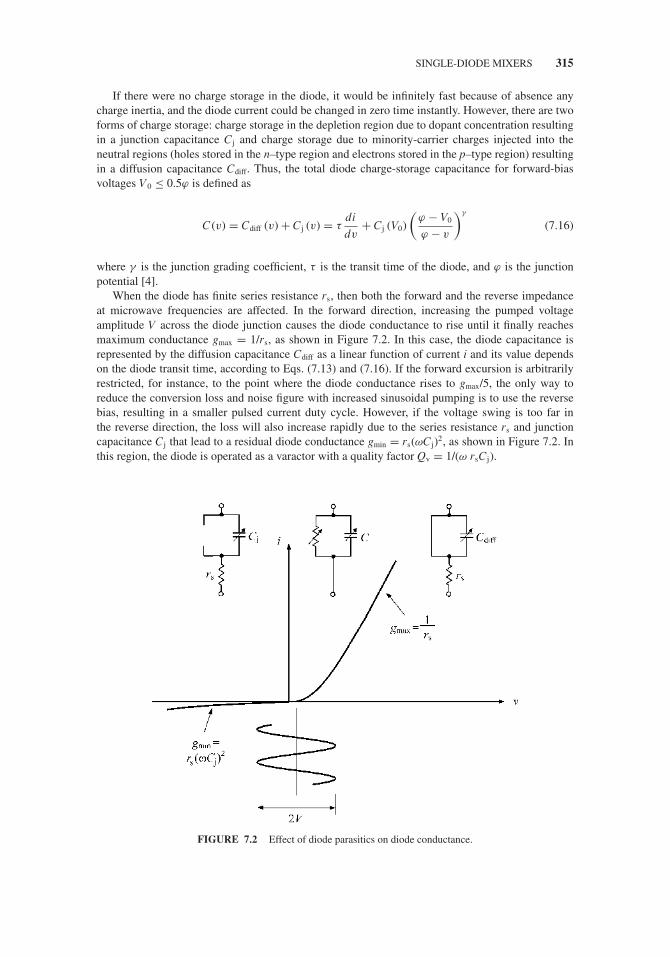
JWBS064-c07 JWBS064-Gerbennikov March 15, 2011 11:12 Printer Name: Yet to Come
SINGLE-DIODE MIXERS 315
If there were no charge storage in the diode, it would be infinitely fast because of absence anycharge inertia, and the diode current could be changed in zero time instantly. However, there are twoforms of charge storage: charge storage in the depletion region due to dopant concentration resultingin a junction capacitance Cj and charge storage due to minority-carrier charges injected into theneutral regions (holes stored in the n–type region and electrons stored in the p–type region) resultingin a diffusion capacitance Cdiff. Thus, the total diode charge-storage capacitance for forward-biasvoltages V0 ≤ 0.5ϕ is defined as
C(v) = Cdiff (v) + Cj (v) = τdi
dv+ Cj (V0)
(ϕ − V0
ϕ − v
)γ
(7.16)
where γ is the junction grading coefficient, τ is the transit time of the diode, and ϕ is the junctionpotential [4].
When the diode has finite series resistance rs, then both the forward and the reverse impedanceat microwave frequencies are affected. In the forward direction, increasing the pumped voltageamplitude V across the diode junction causes the diode conductance to rise until it finally reachesmaximum conductance gmax = 1/rs, as shown in Figure 7.2. In this case, the diode capacitance isrepresented by the diffusion capacitance Cdiff as a linear function of current i and its value dependson the diode transit time, according to Eqs. (7.13) and (7.16). If the forward excursion is arbitrarilyrestricted, for instance, to the point where the diode conductance rises to gmax/5, the only way toreduce the conversion loss and noise figure with increased sinusoidal pumping is to use the reversebias, resulting in a smaller pulsed current duty cycle. However, if the voltage swing is too far inthe reverse direction, the loss will also increase rapidly due to the series resistance rs and junctioncapacitance Cj that lead to a residual diode conductance gmin = rs(ωCj)2, as shown in Figure 7.2. Inthis region, the diode is operated as a varactor with a quality factor Qv = 1/(ω rsCj).
FIGURE 7.2 Effect of diode parasitics on diode conductance.

JWBS064-c07 JWBS064-Gerbennikov March 15, 2011 11:12 Printer Name: Yet to Come
316 MIXERS AND MULTIPLIERS
In the past, it was common to use varactor frequency converters to generate moderate to highlevels of RF power. Their major advantage as the reactive devices over other types of the frequencyconverters was a little noise. The general relations between the real powers at all mixing frequencies,which were derived by Manley and Rowe, apply to any nonlinear reactance, including varactor asa nonlinear capacitor, driven by one or two incommensurable frequencies. Generally, if a nonlinearcapacitor is excited by two frequencies f 1 and f 2, the sideband frequencies of the form mf 1 + nf 2 aregenerated because of the varactor nonlinearity, resulting in the following two equations:
∞∑m=0
∞∑n=−∞
m Pmn
m f1 + n f2= 0 (7.17)
∞∑n=0
∞∑m=−∞
n Pmn
m f1 + n f2= 0 (7.18)
where Pmn is the real power produced in the circuit at the frequency mf 1 + nf 2 [5,6]. These equationsimply that the nonlinear capacitor is lossless and can be applied to parametric amplifiers, frequencyupconverters and multipliers.
In a frequency multiplier, there is only a single excitation signal with frequency f 1 when f 2 = 0,and n can be set to zero. Consequently, the summation over n in Eq. (7.17) can be omitted, all termsin Eq. (7.18) become zero, and Eq. (7.17) is simplified to
∞∑m=0
Pm = 0 (7.19)
where Pm represents the power at the frequency mf 1. Equation (7.19) states that applying the inputsignal with power P1 and frequency f 1 to a lossless nonlinear capacitor must be converted to theoutput powers at the harmonics of f 1. In particular, for mth-harmonic multiplier, the highest possiblevalue of Pm occurs when only P1 and Pm are not zero, and the input power flowing to the capacitoris equal to the output power flowing from the capacitor, resulting in a multiplier efficiency of 100%.To achieve such an idealized condition, it is necessary to provide the varactor termination by purereactances at all other harmonics.
However, varactor mixers and multipliers are narrowband and very sensitive to slight mistuning thatmakes difficult their performance optimization. In addition, they can generate parasitic parametricoscillations due to capacitor nonlinearity depending on how strong varactor is pumped. Also, thesmall variation of pumping level results in a significant variation of the desired output power becausethe average varactor capacitance strongly depends on the voltage amplitude across the varactorjunction. Thermal noise of the varactor series capacitance provides a fundamental limit on the noiseperformance obtainable from the frequency converters. The upper-sideband (USB) upconverter isgenerally stable, but its gain is limited, and for high-frequency signals no gain is possible. At thesame time, the lower-sideband (LSB) upconverter is potentially unstable, and can have negative inputand output resistances [6]. Therefore, the resistive diode mixers based on Schottky-barrier diodes arewidely used in modern designs due to the circuit simplicity, performance stability and predictability,broadband design capability, and applicability up to millimeter-wave frequencies [7].
Figure 7.3(a) shows the microwave upconversion single-diode mixer (SDM) schematic where thesignal from the LO flows through the directional coupler to the mixing diode connected in parallel,and the low-pass and bandpass filters are included into the IF and RF signal paths, respectively. Inthis case, conversion gain (loss) is the ratio of the output (RF) signal power to the input (IF) signalpower. Isolation represents the amount of “leakage” or “feedthrough” between the mixing ports.Dynamic range is the amplitude range over which the mixer can operate without performance degra-dation. Harmonic intermodulation distortion results from the mixing of mixer-generated harmonicsof the input signals having frequencies mf LO ± nf IF, where m and n represent the harmonic order.

JWBS064-c07 JWBS064-Gerbennikov March 15, 2011 11:12 Printer Name: Yet to Come
SINGLE-DIODE MIXERS 317
FIGURE 7.3 Single-diode upconversion mixer and its spectrum.
Cross-modulation distortion is the amount of modulation transferred from a modulated input signalto an unmodulated input signal when both signals are applied to the IF port.
In upconversion mixers, the signal that is necessary to transfer to higher frequency band is appliedto the IF port, the power level of the LO signal is increased, and then the high-side RF signal is filteredout, as shown in Figure 7.3(b). In this case, when both the LO and IF signals may have comparablyhigh power levels, the spectrum of the output RF signal is rich with intermodulation products. Forinstance, if voltage applied to the mixing diode with exponential characteristic given by Eq. (7.12)represents the sum of two voltages,
v = V0 + V1 cos ω1t + V2 cos ω2t (7.20)
where V0 is the dc bias voltage, then the currents corresponding to any intermodulation product in adiode mixer can be written as
ikl = Isat exp(
V0
nVT
)Ik
(V1
nVT
)Il
(V2
nVT
)cos (kω1t ± lω2t ) (7.21)
where Ik[V1/(nVT)] and Il[V2/(nVT)] are the modified Bessel functions of the first kind of orders k andl with argument V1/(nVT) and V2/(nVT), respectively [8]. Here, the quantities k and l designate thecurrent harmonic components produced in the diode mixer. As a result, the conversion loss of the SDMis sufficiently high, of about 10 dB. However, some improvement of 1–2 dB in the RF output powerlevel can be achieved if to provide an optimum impedance for the second LO harmonic (2f LO) at theRF output when its combining with a low-side RF frequency creates an intermodulation product ofthe secondary conversion f RF = 2f LO − (f LO − f IF) which is in phase with the correspondent productof the primary upconversion f RF = f LO + f IF, similarly to that kind of process in a downconvertedimage-rejection diode mixer having optimum image-frequency impedance [9].

JWBS064-c07 JWBS064-Gerbennikov March 15, 2011 11:12 Printer Name: Yet to Come
318 MIXERS AND MULTIPLIERS
7.3 BALANCED DIODE MIXERS
Balanced mixers are generally divided into two classes, called the single-balanced mixers and thedouble-balanced mixers, which combine two or more identical single-diode mixers. The advantageof balanced upconversion mixers over single-diode mixers includes both the rejection of spuriousresponses and intermodulation products and significantly better LO-to-RF, RF-to-IF, and LO-to-IFisolation. The level of rejection is dependent on the amplitude and phase balance of the baluns,providing the balanced drive and the matching between the diodes.
7.3.1 Single-Balanced Mixers
In a single-balanced mixer (SBM) circuit shown in Figure 7.4 where the two diodes as nonlin-ear elements are excited in phase by one signal and 180◦ out of phase by the other signal, nointermodulation outputs that include even-order harmonics of the out-of-phase signal exist [10].In a general case when the transfer characteristic of the nonlinear element can be described as apolynomial
i =∞∑
n=0
Anvn (7.22)
the current in the upper nonlinear element can be calculated as
i1 =∞∑
n=0
An (V2 cos ω2t + V1 cos ω1t)n =∞∑
n=0
Bn cosn ω2t+∞∑
n=0
Cm cosm ω1t
+⎛⎝ ∞∑
p=1
Dp cosp ω2t
⎞⎠
⎛⎝ ∞∑
q=1
Eq cosq ω1t
⎞⎠ =
( ∞∑r=0
Fr cosr ω2t
) ( ∞∑s=0
Gs coss ω1t
).
(7.23)
By expanding each term into the Fourier series, Eq. (7.23) can be equivalently rewritten infrequency domain with harmonic representation as
i1 =( ∞∑
r=0
Hr cos rω2t
) ( ∞∑s=0
Is cos sω1t
). (7.24)
FIGURE 7.4 Single-balanced diode mixer diagram.

JWBS064-c07 JWBS064-Gerbennikov March 15, 2011 11:12 Printer Name: Yet to Come
BALANCED DIODE MIXERS 319
FIGURE 7.5 Microstrip reflection-type branch-line diode mixer.
Since both nonlinear elements are assumed to be fully identical, the current in the lower nonlinearelement excited by the same input signal but with a 180◦ out-of-phase shift can be written as
i2 =[ ∞∑
r=0
Hr cos r (ω2t + 180o)
] ( ∞∑s=0
Is cos sω1t
). (7.25)
As a result, the total current iT that flows through the load is equal to
iT = i1 − i2 =( ∞∑
s=0
Is cos sω1t
)×
{( ∞∑r=0
Hr cos rω2t
)−
[ ∞∑r=0
Hr cos r (ω2t + 180o)
]}. (7.26)
From Eq. (7.26) it follows that, for all r where r is an even integer, the current iT becomes equalto zero. Therefore, all intermodulation products defined by frequencies of the form
ωIM = |±sω1 ± rω2| (7.27)
exist for all s but only for odd r.The circuit for a microwave balanced upconversion mixer based on a branch-line hybrid is shown
in Figure 7.5. Although not shown, generally any single-diode mixer (SDM) requires matchingand bias circuits. Hybrid microwave combiners become practical for upconversion mixers when IFfrequency is much smaller than both LO and RF frequencies, and both LO and RF frequencies differinsignificantly from each other to fit the hybrid operating bandwidth. For a fully symmetrical SBMcircuit, the resulting current iRF corresponding to the USB RF frequency f RF = f LO + f IF can bewritten as
iRF = −iRF1 − iRF2 = −IRF
{cos
[(ωLOt − π
2
)+ ωIFt + π
]+ cos
(ωLOt + ωIFt + π
2
)}= 2IRF sin (ωLO + ωIF) t. (7.28)
where ωIF = 2π f IF and ωLO = 2π f LO.Instead of a branch-line hybrid combiner, the rate-race ring hybrid combiner or coupled-line 3-dB
coupler can be used [11,12]. The hybrid ring is more easily fabricated and controlled, but it is largerthan the hybrid coupler and its operating frequency bandwidth is nowhere as good. Due to suppressionof the even LO harmonics, the SBM provides less level of the intermodulation components in thetransmitted RF signal spectrum than the SDM. When one mixing diode of an SBM fails, the circuitcontinues to operate, although the RF output power level drops by about 3 dB.
To increase the operating frequency, a subharmonic mixer can be used that provides an abilityto operate with halved LO frequency, thus avoiding signal leakage problems inherent with higherfrequency LO sources. Figure 7.6(a) shows the simplified schematic of a subharmonic mixer with an
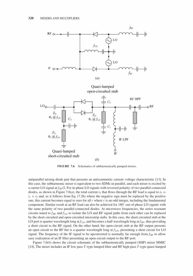
JWBS064-c07 JWBS064-Gerbennikov March 15, 2011 11:12 Printer Name: Yet to Come
320 MIXERS AND MULTIPLIERS
FIGURE 7.6 Schematics of subharmonically pumped mixers.
antiparallel mixing diode pair that presents an antisymmetric current–voltage characteristic [13]. Inthis case, the subharmonic mixer is equivalent to two SDMs in parallel, and each mixer is excited bya carrier LO signal at f RF/2. For in-phase LO signals with reversed polarity of two parallel-connecteddiodes, as shown in Figure 7.6(a), the total current iT that flows through the RF load is equal to iT =i1 + i2 and, as it follows from Eq. (7.26) where the negative sign must be replaced by the positiveone, this current becomes equal to zero for all r where r is an odd integer, including the fundamentalcomponent. Similar result at an RF load can also be achieved for 180◦ out-of-phase LO signals withthe same polarity of two parallel-connected diodes. At microwave frequencies, the series resonantcircuits tuned to f RF and f LO to isolate the LO and RF signal paths from each other can be replacedby the short-circuited and open-circuited microstrip stubs. In this case, the short-circuited stub at theLO port is quarter wavelength long at f LO, and becomes a half wavelength long at f RF, thus providinga short circuit to the RF signal. On the other hand, the open-circuit stub at the RF output presentsan open circuit to the RF but is a quarter wavelength long at f LO, presenting a short circuit for LOsignal. The frequency of the IF signal to be upconverted is normally far enough from f RF to alloweasy realization of an IF filter presenting an open-circuit output to the RF port.
Figure 7.6(b) shows the circuit schematic of the subharmonically pumped (SHP) mixer MMIC[14]. The mixer includes an IF low-pass T-type lumped filter and RF high-pass T-type quasi-lumped

JWBS064-c07 JWBS064-Gerbennikov March 15, 2011 11:12 Printer Name: Yet to Come
BALANCED DIODE MIXERS 321
filter to isolate RF and IF ports. To isolate RF and LO ports, the quasi-lumped open-circuited andshort-circuited stubs are used. The former stub provides a short circuit at f LO with an open circuitat f RF, whereas the latter stub introduces a short circuit at f RF, providing an open circuit at f LO. Thecapacitances C1 and C2 of the quasi-lumped open-circuited stub are defined as
C1 = 1
ωLO Z1 tan θ1. (7.29)
C2 = C1
3 + tan2θ1. (7.30)
where Z1 is the characteristic impedance and θ1 (0 < θ 1 < 90◦) is the electrical length of the stubat f LO. To effectively convert the IF signal to the RF, the quasi-lumped short-circuited stub shouldbe grounded at IF frequency. In this case, the shunt capacitance C3 and electrical length θ 3 can becalculated from
tan θ3 = Z3
Z2
1 + 3 tan2 θ2
2tanθ2−
√(Z3
Z2
)2 (1 + 3 tan2 θ2
2tanθ2
)2
− 3. (7.31)
C3 = 1
ωLO Z3
(1
tan θ3− Z3
Z2tan θ2
). (7.32)
where the electrical lengths θ 2 and θ 3, which are set at f LO, must vary within the range of 0 < (θ 2,θ 3) < 45◦ to short RF signal at the input of the short-circuited stub.
7.3.2 Double-Balanced Mixers
A double-balanced mixer (DBM) normally makes use of four diodes, which can be connected indifferent configurations, with both LO and RF signal paths being balanced. In this case, all ports ofthe mixer are inherently isolated from each other, and isolation is achieved by means of center-tappedtransformers. The advantages of a double-balanced design over a single-balanced scheme are theincreased linearity, improved suppression of spurious products, and inherent isolation between allports. However, they require a higher level LO drive to pump the diodes and two additional baluns.The DBMs have higher conversion loss and lower limit in maximum frequency, but they providebroader bandwidth.
Figure 7.7(a) shows the bridge double-balanced diode upconversion mixer schematic with twocenter-tapped transformers to provide isolation between three ports: LO, IF, and RF [15]. The LOvoltage is assumed to be large enough to properly control on/off cycle of the diodes. The RF currentsi1 and i3, which are shown in Figure 7.7(b), flow through the diodes D1 and D3, respectively, duringthe time when voltage vLO makes point a positive with respect to point b and voltage vIF makes point cpositive with respect to point d. Diodes D1 and D3 are turned on by vLO, and current iLO flows aroundthe loop a-c-b-a. In this case, diodes D2 and D4 are turned off because they are reverse-biased. The RFcurrents i1 and i3 add in the load resistance RL to produce the RF voltage with indicated polarity. Notethat iLO does not flow through the IF path between the center points of the transformers because thesepoints have the same potential at f LO if the diodes and the LO transformer are perfectly balanced.The polarity of vIF in Figure 7.7(c) is the same as in Figure 7.7(b), but the polarity of vLO is reversed,thus making point b positive with respect to point a. In this case, diodes D2 and D4 are turned on,while diodes D1 and D3 are turned off. As a result, the RF currents i2 and i4 flows into the RF load,producing the RF voltage of opposite polarity to that in Figure 7.7(b). The LO current flows throughthe loop involving diodes D2 and D4, but not in the RF transformer. This type of mixer can operateover a wide frequency range determined primarily by the design of transformers. If toroidal-coredtransmission-line transformers are used, bandwidths of 1000:1 can be achieved. The balance of the

JWBS064-c07 JWBS064-Gerbennikov March 15, 2011 11:12 Printer Name: Yet to Come
322 MIXERS AND MULTIPLIERS
FIGURE 7.7 Equivalent schematics of diode double-balanced mixer.
mixer and isolation between ports is determined by the accuracy of the transformer windings andcareful matching of the diode characteristics.
Generally, the two most common types of DBMs are the ring mixer (RM) and the star mixer [7].The RM is more relevant to low-frequency applications, in which wire-wound or transmission-lineferrite transformers can be used. The star mixer is used primarily in microwave applications, as itis more amenable to operate with microwave baluns. However, there is no significant difference intheir performances. Figure 7.8(a) shows the classical diode RM circuit where the secondary windingsof the transformers are connected to the nodes of the diode ring composed by four diodes. The LOsignal alternately turns the top diode pair D1 and D2 and bottom diode pair D3 and D4 on and offin anti-phase, thus providing the corresponding closed loops for IF currents through the diodes andthe grounded center tap of the LO transformer in opposite directions. In this case, if the diodes areidentical, the points b and d represent virtual grounding to the RF signal, hence no RF voltage appearsacross the secondary winding of the LO transformer. Similarly, the points a and c are virtual groundto the LO signal, thus no LO voltage appears across the secondary winding of the RF transformer. Ifdiode ring is fabricated on a single chip, the isolation between LO and RF ports in microwave mixerscan be achieved from 30 to 40 dB. The IF signal can also be delivered through the center tap of the LOtransformer rather than through the center tap of the RF transformer. The RM concept can be extendedto include double-ring mixer topologies that have the added advantage of allowing the IF frequencyresponse to overlap the RF and LO frequency bands, thus making easier the process of frequencyselection [16]. In this case, to reduce the conversion loss and to extend the frequency upconversionto higher operating frequencies, the broadband active center-tapped balun can be implemented inmicrowave monolithic design.
The upper-frequency limit of the DBMs using tapered baluns and low parasitic diode packages canalso be extended if a balun structure is formed by two coupled transmission-line pairs, each havinga quarter wavelength at the center bandwidth frequency, as shown in Figure 7.8(b) [17]. Without

JWBS064-c07 JWBS064-Gerbennikov March 15, 2011 11:12 Printer Name: Yet to Come
BALANCED DIODE MIXERS 323
FIGURE 7.8 Schematics of diode ring double-balanced mixers.
any frequency compensation, this structure can exhibit greater than octave of bandwidth and canbe realized in a variety of media, such as coaxial cable, microstrip, or coplanar waveguide. As aresult, the upper-frequency limit of such a DBM occurs when the total length of the balun becomes360◦. To minimize the overall mixer size for monolithic microwave applications above 10 GHz, themixer architecture for frequency upconversion can include a miniature spiral balun for IF path anda 180◦ hybrid formed with an interdigitated Lange microstrip coupler with two (+45◦ and −45◦)phase shifters. This allows us to split an LO incoming signal into two paths with equal amplitudesand 180◦ relative phase difference and to provide an output port for the RF extraction of upconverterapplication [18].
In a star DBM architecture shown in Figure 7.9, one terminal of each four diodes is connected toa common node used as the IF terminal [7,19]. Similarly to the RM, this mixer operates as a polarity-reversing switch. For the LO transformer T2, when the dotted sides of its secondary windings T2a
and T2b are positive, diodes D1 and D2 are turned on, diodes D3 and D4 are turned off, and the dotted

JWBS064-c07 JWBS064-Gerbennikov March 15, 2011 11:12 Printer Name: Yet to Come
324 MIXERS AND MULTIPLIERS
FIGURE 7.9 Schematic of diode double-balanced star mixer.
sides of the secondary windings T1a and T1b of the RF transformer T1 are connected to the IF port.The RF port is thus connected to the IF port through the RF transformer T1 and the diodes. However,when the LO polarity reverses, diodes D1 and D2 are turned off, diodes D3 and D4 are turned on,and then the undotted sides of both secondary windings T1a and T1b are connected to the IF port.In this case, the RF port is again connected to the IF port, but with reversed polarity. As a result,the RF polarity is therefore always applied to the IF port, but its polarity is reversed periodically atthe LO frequency. Because generally the operational principles of the star and RMs are the same, itshould expect similar spurious-response properties, and the only difference may be defined by theconvenience and complexity of the implementation in a particular design and technology.
Single-sideband (SSB) mixer architectures are useful in discriminating and removing the LSBand USB generated during frequency upconversion, especially when sidebands are very close infrequency and attenuation of one of the sidebands cannot be achieved with filtering. ConventionalSSB mixers generally include a Wilkinson divider to provide two LO signals, well balanced both inamplitude and phase, a 90◦ phase shifter to provide quadrature IF signals, and a quadrature hybridcoupler to combine the extracted RF signal at USB, as shown in Figure 7.10(a). Unlike the low-noisereceiver downconverter, the transmitter upconverter operates with sufficiently high power levels (inlimits of 5 to 10 dBm) at both IF and LO inputs, and therefore, the sidebands are rich with IFharmonics. However, since the even IF harmonics and their intermodulation components are wellsuppressed in each SBM, only the sidebands with the odd-order components such as f LO ± (f IF, 3f IF,5f IF, . . .) are delivered to the output quadrature coupler of the DBM. The carrier LO frequency is alsosuppressed in the SBMs, typically by about 20 dB, due to the corresponding isolation of their outputhybrids.
Consider the propagation paths of the main signal components ωLO ± ωIF from both SSB mixersthrough the output quadrature coupler–combiner in Figure 7.10(a), by assuming that the phase delayin directions 1–3 and 2–4 is equal to 90◦ and there is no phase delay in diagonal directions. As a

JWBS064-c07 JWBS064-Gerbennikov March 15, 2011 11:12 Printer Name: Yet to Come
BALANCED DIODE MIXERS 325
FIGURE 7.10 Block diagrams of single-sideband mixer-upconverters.
result, for an USB RF signal at port 3, the phase delay from the top mixer is equal to φ1,3 = φLO +φIF + 90◦, whereas the phase delay from the bottom mixer is equal φ2,3 = φLO + (φIF + 90◦) + 0◦,which are in phase, and the USB RF signal f LO + f IF flows to the RF load. At the same time, for aLSB RF signal, the in-phase condition is achieved at port 4, when the phase delay from the top mixeris equal to φ1,4 = φLO − φIF + 0◦, whereas the phase delay from the bottom mixer is equal φ2,4 =φLO − (φIF + 90◦) + 90◦. As a result, the LSB RF signal f LO − f IF is fully dissipated in the ballastresistor and does not appear in the RF load.
The suppression level of an unwanted sideband strongly depends on a circuit symmetry level(equality of pumped LO signals, identity of voltage–ampere diode characteristics, equality of phaseshifts to nominal values, etc.). For instance, if two RF signals having equal amplitudes and beingorthogonal in phase flow from both top and bottom SSB mixer outputs, then their suppression levelat the output of the non-ideal quadrature coupler–combiner can be evaluated according to
L = 1 + 2A cos φ + A2
1 − 2A cos φ + A2(7.33)
where A is the ratio of amplitudes and φ is the phase difference produced by the coupler.Consequently, in order to achieve the suppression level of an unwanted sideband of more than 20dB, it is necessary to provide A and φ to be better than ±0.2 dB and 10◦, respectively. As anexample, in a microwave SSB diode mixer operated as a frequency upconverter with IF power PIF =5 dBm and LO power PLO = 10 dBm, an upconversion of the modulated IF to RF can occur with theconversion loss of 6 dB and LO suppression of 9 dB, relatively to the USB f RF = f LO + f IF [20].

JWBS064-c07 JWBS064-Gerbennikov March 15, 2011 11:12 Printer Name: Yet to Come
326 MIXERS AND MULTIPLIERS
TABLE 7.1 Intermodulation Components in RF Spectrum for Different Mixer Types.
Harmonics LO
Harmonics IF 1 2 3 4 5 6 Mixer Type
1 + + + + + + SDM+ − + − + − SBM+ − + − + − DBM, RM
2 + + + + + + SDM+ − + − + − SBM− − − − − − DBM, RM
3 + + + + + + SDM+ − + − + − SBM+ − + − + − DBM, RM
4 + + + + + + SDM+ − + − + − SBM− − − − − − DBM, RM
5 + + + + + + SDM+ − + − + − SBM+ − + − + − DBM, RM
6 + + + + + + SDM+ − + − + − SBM− − − − − − DBM, RM
To simplify filtering problem by mixing with a harmonic of a lower frequency LO signal, which isvery important when IF frequency is not so high, and to increase an operating frequency bandwidthfor RF signal towards millimeter waves, an SSB upconverter based on subharmonically pumpedmixers with antiparallel pair of diodes can be used [14,21]. Figure 7.10(b) shows the block schematicof the wideband SSB SHP upconversion mixer consisting of two SHP mixers, an LO power dividerwith a phase shift of 45◦, and an RF in-phase power combiner. In this case, the IF signals are fed intoeach SHP mixers having the phase difference of 90◦, the LO signal is divided into two signals withthe phase difference of 45◦, and then the SHP mixers generate the USBs and LSBs of the upconvertedsignal 2f LO ± f IF. Since upconverted USB signals 2f LO + f IF are in phase with each other at the inputof the Wilkinson combiner, hence the desired upconverted USB resulting signal appears at the RFoutput, while out-of-phase LSB resulting signal is canceled.
To compare different diode mixer architectures, the presence or absence of various intermodulationcomponent in an RF spectrum due to IF and LO harmonic components (from fundamental to sixth) isshown in Table 7.1, where the harmonic availability is marked by the “+” symbol. Thus, the spectrumof an SDM contains all possible harmonic components, unlike an SBM, where the even-order LOharmonics are suppressed. However, in a DBM or RM, the number of intermodulation componentsreduces even more, in total by four times, due to the corresponding suppression of both IF and LOeven harmonics.
7.4 TRANSISTOR MIXERS
Transistor mixers can be built based on both bipolar transistor and FET device; however, GaAs FETsare commonly used at microwave frequencies due to their superior noise and gain performance. For abipolar mixer, it was found that the frequency conversion, which is strongly dependent on the forwardcollector–emitter current gain of the device in a common base configuration in the low-frequencyfrequency range, primarily depends on the base resistance in the medium-frequency range, and is

JWBS064-c07 JWBS064-Gerbennikov March 15, 2011 11:12 Printer Name: Yet to Come
TRANSISTOR MIXERS 327
mainly dependent on the base–emitter capacitance [22]. Due to its highly nonlinear characteristic,the FET device turns out to be a very efficient mixer, and its conversion transconductance exhibits aflat maximum as a function of the gate bias voltage. In this case, an optimum voltage range can beobtained where the ratio between mixing current and distortion product currents is most favorable.Generally, FET mixers exhibit smaller transconductance than mixer stages with bipolar transistors[23]. However, the FET input impedance is higher and thus does allow the use of better and moreselective input resonance circuits. The more effective mixer performance can be achieved with lowergate capacitance and bulk resistances at higher frequencies where FET devices are preferred overbipolar transistors as having less intermodulation and cross-modulation distortion and their lowerfeedback capacitance provides better circuit stability.
In a general case, if a device has the transfer characteristic
i (t) = a0v(t) + a1v2(t) + a2v
3(t) (7.34)
then applying a two-tone input signal
v(t) = V1 cos ω1t + V2 cos ω2t (7.35)
results in the following components of the output current provided correspondingly by first-orderterm
a0V1 cos ω1t + a0V2 cos ω2t (7.36)
second-order term
a1
2
(V 2
1 + V 22
) + a1
2V 2
1 cos 2ω1t + a1
2V 2
2 cos 2ω2t + a1V1V2 [cos (ω1 + ω2) t + cos (ω1 − ω2) t]
(7.37)
and third-order term(3a2
4V 3
1 + 3a2
2V1V 2
2
)cos ω1t +
(3a2
4V 3
2 + 3a2
2V 2
1 V2
)cos ω2t + a2
4V 3
1 cos 3ω1t
+ a2
4V 3
2 cos 3ω2t + 3a2
4V 2
1 V2 [cos (2ω1 + ω2) t + cos (2ω1 − ω2) t]
+ 3a2
4V1V 2
2 [cos (2ω2 + ω1) t + cos (2ω2 − ω1) t ] (7.38)
where the term a0v represents linear mixer action, reproducing the input signals at the output, theterm a1v
2 gives rise to a dc component and second harmonics of the input signals as well as theproduct terms at frequencies f 1 ± f 2, and the term a2v
3 produces components at frequencies f 1, f 2,3f 1, 3f 2, 2f 1 ± f 2, and 2f 2 ± f 1 [15].
The basic block schematic of a single FET mixer, where an active device is treated as a three-portnetwork, is shown in Figure 7.11(a), with each port generally intended to be connected to LO, IF,or RF signal path, respectively. However, conventional FET mixers usually employ a gate mixingto produce a desired frequency component when LO signal shares the same gate terminal with IFmodulated signal. In this case, independent matching for each signal is impossible, and, to achieve asufficiently high isolation between both LO and IF signals, it is necessary to use hybrid circuits suchas Lange couplers, power dividers, or baluns that increase the mixer circuit complexity.
Figure 7.11(b) shows the circuit schematic of a monolithic upconversion heterojunction FET mixerMMIC based on coplanar waveguides (CPW) as the transmission lines that can be used in microwave

JWBS064-c07 JWBS064-Gerbennikov March 15, 2011 11:12 Printer Name: Yet to Come
328 MIXERS AND MULTIPLIERS
andand
and
FIGURE 7.11 Block diagram and circuit schematic of source-injection FET mixer.
and millimeter-wave applications [24,25]. In this case, a source injection concept was introduced inwhich the IF signal with a frequency f IF is applied to the gate terminal through the IF filtering andmatching network, the LO signal with a frequency f LO is applied to the source terminal through theLO filtering and matching network, and the resultant USB RF signal having a frequency f RF = f IF +f LO is extracted from the drain terminal, after passing through the RF matching circuit and outputfilter. The RF output filter consists of two T-type networks connected in parallel for suppressing theLSB frequency f IF − f LO and LO frequency f LO, but passing the USB frequency f IF + f LO. The LOmatching network is essentially responsible to provide an unconditionally stable operation for theupconverter, both in presence and absence of an LO signal. In this structure, since the LO signalis directly applied to the source terminal, it has the largest effect on the device transconductancemodulation and, consequently, on nonlinear mixing enhancement, which facilitates a low LO poweroperation. As a result, the upconverter can operate with an LO power level as low as −16 dBm for IFsignals in 1.5–2.5 GHz band, and LO signals in 20–23 GHz band. In this case, LO suppression at IFand RF ports is better than 20 dB, whereas IF suppression at RF port is better than 35 dB.
Figure 7.12 shows the circuit schematic of a monolithic gate-injection HEMT mixer that shifts asignal in the 16 GHz band up to the V-band using a 48 GHz LO signal [26]. Such a mixer topologywas chosen because it is simple in implementation and can achieve high conversion gain for low LOpower levels. The network at the gate side of the mixer was designed to provide 50- matching atboth IF (16 GHz) and LO (48 GHz) frequencies. However, since two signals are applied to the sameport, the external diplexer is required. The gate bias network also includes a small (5 ) resistor,which is needed to ensure unconditional stability in the circuit. The network at the drain side of
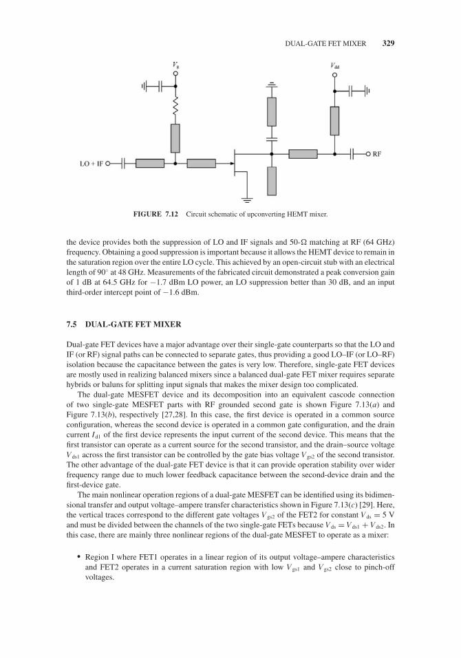
JWBS064-c07 JWBS064-Gerbennikov March 15, 2011 11:12 Printer Name: Yet to Come
DUAL-GATE FET MIXER 329
FIGURE 7.12 Circuit schematic of upconverting HEMT mixer.
the device provides both the suppression of LO and IF signals and 50- matching at RF (64 GHz)frequency. Obtaining a good suppression is important because it allows the HEMT device to remain inthe saturation region over the entire LO cycle. This achieved by an open-circuit stub with an electricallength of 90◦ at 48 GHz. Measurements of the fabricated circuit demonstrated a peak conversion gainof 1 dB at 64.5 GHz for −1.7 dBm LO power, an LO suppression better than 30 dB, and an inputthird-order intercept point of −1.6 dBm.
7.5 DUAL-GATE FET MIXER
Dual-gate FET devices have a major advantage over their single-gate counterparts so that the LO andIF (or RF) signal paths can be connected to separate gates, thus providing a good LO–IF (or LO–RF)isolation because the capacitance between the gates is very low. Therefore, single-gate FET devicesare mostly used in realizing balanced mixers since a balanced dual-gate FET mixer requires separatehybrids or baluns for splitting input signals that makes the mixer design too complicated.
The dual-gate MESFET device and its decomposition into an equivalent cascode connectionof two single-gate MESFET parts with RF grounded second gate is shown Figure 7.13(a) andFigure 7.13(b), respectively [27,28]. In this case, the first device is operated in a common sourceconfiguration, whereas the second device is operated in a common gate configuration, and the draincurrent Id1 of the first device represents the input current of the second device. This means that thefirst transistor can operate as a current source for the second transistor, and the drain–source voltageVds1 across the first transistor can be controlled by the gate bias voltage Vgs2 of the second transistor.The other advantage of the dual-gate FET device is that it can provide operation stability over widerfrequency range due to much lower feedback capacitance between the second-device drain and thefirst-device gate.
The main nonlinear operation regions of a dual-gate MESFET can be identified using its bidimen-sional transfer and output voltage–ampere transfer characteristics shown in Figure 7.13(c) [29]. Here,the vertical traces correspond to the different gate voltages Vgs2 of the FET2 for constant Vds = 5 Vand must be divided between the channels of the two single-gate FETs because Vds = Vds1 + Vds2. Inthis case, there are mainly three nonlinear regions of the dual-gate MESFET to operate as a mixer:
� Region I where FET1 operates in a linear region of its output voltage–ampere characteristicsand FET2 operates in a current saturation region with low Vgs1 and Vgs2 close to pinch-offvoltages.

JWBS064-c07 JWBS064-Gerbennikov March 15, 2011 11:12 Printer Name: Yet to Come
330 MIXERS AND MULTIPLIERS
FIGURE 7.13 Dual-gate MESFET, its equivalent cascode representation, and voltage-ampere characteristics.
� Region II where the FET1 operates in a linear region close to saturation and the FET2 operatesin a current saturation for high Vgs1 and Vgs2 far from pinch-off voltages.
� Region III where the FET1 operates in a saturation region and the FET2 operates in a linearregion with high Vgs1 and Vgs2 far from pinch-off voltages.
Figure 7.14 shows the equivalent circuit of a dual-gate MESFET showing the elements responsiblefor nonlinear operation in different bias regions. It is obvious that in bias regions I and II, mixingtakes place inside of FET1, while FET2 acts as a linear amplifier. In this case, if the mixing in regionI is mainly provided at low drain current by the nonlinearity of the device transconductance gm1 andoutput differential resistance Rds1 as the functions of Vgs1, then, in region II, the nonlinear effect ofthe gate–source capacitance Cgs1 at high drain current becomes significant as well. Due to the lowdrain current, the mixer operating in region I requires smaller LO power and provides low-noiseperformance. However, if the dual-gate MESFET operates as a mixer in region III, the nonlinearitiesare located in FET2, and FET1 acts now as a linear amplifier.
Figure 7.15 shows the block schematic of a microwave upconversion mixer based on a dual-gateGaAs MESFET operating at X-band with an IF input signal varying over 700 ± 250 MHz appliedto the second gate [30]. Such an upconverter pumping by the LO signal at 7.4 GHz can offer the

JWBS064-c07 JWBS064-Gerbennikov March 15, 2011 11:12 Printer Name: Yet to Come
BALANCED TRANSISTOR MIXERS 331
FIGURE 7.14 Nonlinear equivalent circuit of dual-gate MESFET.
conversion gains up to 15 dB, noise figure of 3.2 dB and saturated RF output power up to 12 dBm.For a particular case of the saturated output power of 9 dBm with the LO level set at 12 dBm, thethird-order intermodulation product at the 1-dB compression point was −22 dBc. The isolation fromthe input LO port to the input IF port was measured to be 28 dB, whereas the isolation from the outputRF port to either of the input ports was greater than 20 dB.
7.6 BALANCED TRANSISTOR MIXERS
7.6.1 Single-Balanced Mixers
A pair of single-gate MESFET mixers can be combined into a single-balanced MESFET mixer usingdifferent hybrid combiners or simply parallel connection at the output. In this case, the propertiesof balanced MESFET mixers with regard to intermodulation products and isolation of input andoutput ports are essentially the same as in balanced diode mixers. Figure 7.16 shows the typical blockschematic of a balanced MESFET mixer where the LO signals being 180◦ out of phase are mixed withIF signals fed from a 180◦ hybrid [31]. As a result, the output upconverted signals are combined atthe RF port as being in phase, while the LO signals are canceled as being out of phase. In the practicallayout of such a 20-GHz balanced upconversion mixer, a 180◦ phase difference between the LOsignals can be obtained through the slotline Y-junction formed on the other side of substrate. The
FIGURE 7.15 Dual-gate MESFET upconverter configuration.
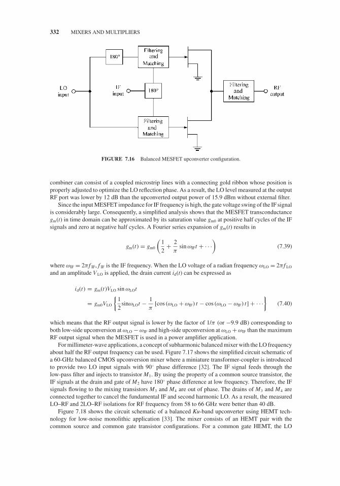
JWBS064-c07 JWBS064-Gerbennikov March 15, 2011 11:12 Printer Name: Yet to Come
332 MIXERS AND MULTIPLIERS
FIGURE 7.16 Balanced MESFET upconverter configuration.
combiner can consist of a coupled microstrip lines with a connecting gold ribbon whose position isproperly adjusted to optimize the LO reflection phase. As a result, the LO level measured at the outputRF port was lower by 12 dB than the upconverted output power of 15.9 dBm without external filter.
Since the input MESFET impedance for IF frequency is high, the gate voltage swing of the IF signalis considerably large. Consequently, a simplified analysis shows that the MESFET transconductancegm(t) in time domain can be approximated by its saturation value gm0 at positive half cycles of the IFsignals and zero at negative half cycles. A Fourier series expansion of gm(t) results in
gm(t) = gm0
(1
2+ 2
πsin ωIFt + · · ·
)(7.39)
where ωIF = 2π f IF, f IF is the IF frequency. When the LO voltage of a radian frequency ωLO = 2π f LO
and an amplitude VLO is applied, the drain current id(t) can be expressed as
id(t) = gm(t)VLO sin ωLOt
= gm0VLO
{1
2sinωLOt − 1
π[cos (ωLO + ωIF) t − cos (ωLO − ωIF) t] + · · ·
}(7.40)
which means that the RF output signal is lower by the factor of 1/π (or −9.9 dB) corresponding toboth low-side upconversion at ωLO − ωIF and high-side upconversion at ωLO + ωIF than the maximumRF output signal when the MESFET is used in a power amplifier application.
For millimeter-wave applications, a concept of subharmonic balanced mixer with the LO frequencyabout half the RF output frequency can be used. Figure 7.17 shows the simplified circuit schematic ofa 60-GHz balanced CMOS upconversion mixer where a miniature transformer-coupler is introducedto provide two LO input signals with 90◦ phase difference [32]. The IF signal feeds through thelow-pass filter and injects to transistor M1. By using the property of a common source transistor, theIF signals at the drain and gate of M2 have 180◦ phase difference at low frequency. Therefore, the IFsignals flowing to the mixing transistors M3 and M4 are out of phase. The drains of M3 and M4 areconnected together to cancel the fundamental IF and second harmonic LO. As a result, the measuredLO–RF and 2LO–RF isolations for RF frequency from 58 to 66 GHz were better than 40 dB.
Figure 7.18 shows the circuit schematic of a balanced Ku-band upconverter using HEMT tech-nology for low-noise monolithic application [33]. The mixer consists of an HEMT pair with thecommon source and common gate transistor configurations. For a common gate HEMT, the LO
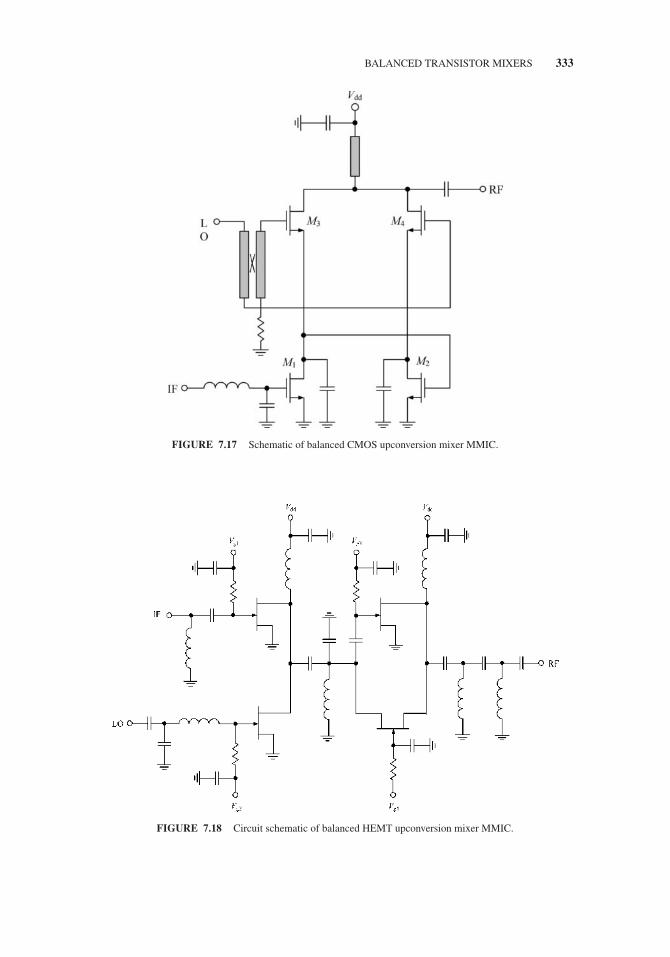
JWBS064-c07 JWBS064-Gerbennikov March 15, 2011 11:12 Printer Name: Yet to Come
BALANCED TRANSISTOR MIXERS 333
FIGURE 7.17 Schematic of balanced CMOS upconversion mixer MMIC.
FIGURE 7.18 Circuit schematic of balanced HEMT upconversion mixer MMIC.

JWBS064-c07 JWBS064-Gerbennikov March 15, 2011 11:12 Printer Name: Yet to Come
334 MIXERS AND MULTIPLIERS
signal is injected between the gate and source ports. In both configurations, the time-varying devicetransconductance gm(t) is the dominant contributor to frequency conversion, and the effect of othernonlinearities is minimal. By properly selecting the gate width of the common source transistor, it ispossible to have the same gain in both devices. As a result, the IF and LO signals will be canceled atthe output of the parallel-connected transistors due to the phase shift (ideally 180◦) in the commonsource transistor. To combine the LO and IF signals, two active circuits based on the single-stageamplifying stages were used, as well as a high-pass filter at the RF output was included to improveisolation. As a result, a conversion gain over 4.2 dB at RF frequency of 14 GHz (IF = 1.885 GHz)was achieved with 3 dBm of LO power and isolation between any ports over 27 dB.
7.6.2 Double-Balanced Mixers
The double-balanced transistor mixers have essentially the same characteristics as the double-balanceddiode mixers in terms of isolation, spurious responses, or bandwidth but substantially higher con-version gain and they do not require hybrids or baluns that make them very attractive for compactmonolithic implementation. The DBM in the form of a pair of the transistorized differential amplifierswas originally invented by Howard Jones to use as a dual output synchronous detector [34]. However,Alberto Bilotti was the first who described and analyzed the fully balanced arrangement of the threedifferential pairs shown in Figure 7.19 with regard to its different monolithic applications such asbalanced product mixer (downconverter or upconverter) and suppressed carrier modulator [35]. Inthis case, a DBM requires low-level operation at both inputs, whereas suppressed carrier modula-tion is obtained by low-level modulating signal v1(t) and high-level carrier signal v2(t). In the lattercase, carrier high-level operation provides a modulated output independent from the carrier level andshould be preferred unless the harmonic spectral response is acceptable. Note that the amount ofcarrier suppression is a function of the matching accuracy of the differential pairs.
FIGURE 7.19 Monolithic double-balanced mixer configuration.
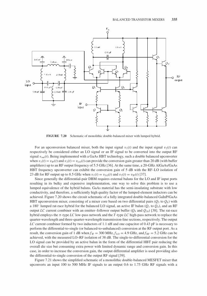
JWBS064-c07 JWBS064-Gerbennikov March 15, 2011 11:12 Printer Name: Yet to Come
BALANCED TRANSISTOR MIXERS 335
FIGURE 7.20 Schematic of monolithic double-balanced mixer with lumped hybrid.
For an upconversion balanced mixer, both the input signal v1(t) and the input signal v2(t) canrespectively be considered either an LO signal or an IF signal to be converted into the output RFsignal vout(t). Being implemented with a GaAs HBT technology, such a double balanced upconverterwhen v1(t) = vIF(t) and v2(t) = vLO(t) can provide the conversion gain greater than 20 dB (with bufferamplifiers) up to an RF output frequency of 5.5 GHz [36]. At the same time, a 20-GHz AlGaAs/GaAsHBT frequency upconverter can exhibit the conversion gain of 5 dB with the RF–LO isolation of23 dB for RF output up to 8.5 GHz when v1(t) = vLO(t) and v2(t) = vIF(t) [37].
Since generally the differential-pair DBM requires external baluns for the LO and IF input portsresulting in its bulky and expensive implementation, one way to solve this problem is to use alumped equivalence of the hybrid baluns. GaAs material has the semi-insulating substrate with lowconductivity, and therefore, a sufficiently high quality factor of the lumped-element inductors can beachieved. Figure 7.20 shows the circuit schematic of a fully integrated double-balanced GaInP/GaAsHBT upconversion mixer, consisting of a mixer core based on two differential pairs (Q5 to Q8) witha 180◦ lumped rat-race hybrid for the balanced LO signal, an active IF balun (Q1 to Q4), and an RFoutput LC current combiner with an emitter–follower output buffer (Q9 and Q10) [38]. The rat-racehybrid employs the π-type LC low-pass network and the T-type LC high-pass network to replace thequarter-wavelength and three-quarter-wavelength transmission-line sections, respectively. The outputLC current combiner formed by two inductors of 1.1 nH and one capacitor of 0.43 pF is necessary toperform the differential-to-single (or balanced-to-unbalanced) conversion at the RF output port. As aresult, the conversion gain of 1 dB when f IF = 300 MHz, f LO = 4.9 GHz, and f RF = 5.2 GHz can beachieved, with the measured LO–RF isolation of 38 dB. The single-to-differential conversion for theLO signal can be provided by an active balun in the form of the differential HBT pair reducing theoverall die size but consuming extra power with limited dynamic range and conversion gain. In thiscase, in order to increase the conversion gain, the output differential amplifier is used providing alsothe differential-to-single conversion of the output RF signal [39].
Figure 7.21 shows the simplified schematic of a monolithic double-balanced MESFET mixer thatupconverts an input 100 to 500 MHz IF signals to an output 0.6 to 1.75 GHz RF signals with a

JWBS064-c07 JWBS064-Gerbennikov March 15, 2011 11:12 Printer Name: Yet to Come
336 MIXERS AND MULTIPLIERS
FIGURE 7.21 Simplified schematic of double-balanced MESFET mixer.
conversion gain of 8 dB [40]. The circuit consists of two mixers stages that are excited by IF and LOsignals that are 0◦ and 180◦ out of phase with respect to one another. The outputs of the two mixersare then combined and amplified to produce an RF output, with the conversion gain depending on theLO level. Mixing action is accomplished by alternating amplification of the two 180◦ out-of-phaseIF signals at the LO frequency. When the LO transistor is turned on, ideally an ac ground is createdacross it, which makes an effective common-source amplifier for the IF signal. Conversely, when theLO transistor is turned off, no amplification of the IF signal occurs at the output. Therefore, the LOsignal alternately turns each side of the mixer into an IF amplifier, thus creating an output RF signalthat is a combination of the two signals. To achieve the proper mixing action, the dc components ofthe LO and IF transistors must be identical to ensure in the quiescent state that the drain-to-sourcevoltages of the devices Q3 and Q4 are zero, thereby preventing any LO feedthrough in the absence ofan IF signal.
For low supply voltage and low power consumption requirements, RF CMOS technology can beused in the high microwave range in phased-array radars, wireless local networks, local multipointdistribution services (LMDS), and other industrial-scientific-medical (ISM) band applications. Al-though passive mixers have the inherent advantage of better frequency and linearity response, theyhave conversion loss and also require a high LO drive level. A typical circuit schematic of the double-balanced CMOS mixer based on a pair of differential amplifiers is shown in Figure 7.22(a) wherethe gate and source degeneration inductors are used to match LO and IF inputs and RF output tostandard 50 [41]. Having source degeneration inductors also helps to improve the linearity at some

JWBS064-c07 JWBS064-Gerbennikov March 15, 2011 11:12 Printer Name: Yet to Come
BALANCED TRANSISTOR MIXERS 337
FIGURE 7.22 Simplified schematics of double-balanced CMOS mixer.

JWBS064-c07 JWBS064-Gerbennikov March 15, 2011 11:12 Printer Name: Yet to Come
338 MIXERS AND MULTIPLIERS
expense of conversion gain. To improve conversion gain of the upconversion mixer that is intendedto operate in a superheterodyne 60-GHz transmitter, the transmission-line stubs in the output circuitand between each differential pair and current-source transistors can be used [42].
However, even lower available LO drive can be achieved in a dual-gate DBM, the simplifiedcircuit schematic of which is shown in Figure 7.22(b) [41]. In a dual-gate mixer, a finite LO signalmust be presented at the drains of lower devices (M1 to M4), which causes the devices to operatebetween linear and saturation regions, thus resulting in the modulated transconductance of thesedevices. This is because the lower devices are operated in linear region during most part of the LOcycle, unlike a conventional double-differential mixer where switching action of the LO transistorpair occurs between the cutoff and saturation regions. As a result, the conversion gain of a dual-gatemixer is slightly lower, but its linearity performance is moderately better. The mixer can achieve aconversion gain of 1.7 dB and an output 1-dB compression point of −3.4 dBm at a supply voltage of1.2 V with a current consumption of 9 mA when f IF = 2,3 GHz and f RF = 23 GHz.
7.7 FREQUENCY MULTIPLIERS
The frequency multipliers historically were the very important part of the vacuum-tube transmittersto achieve a high-frequency transmission of a stable modulated signal. In this case, a high-frequencytransmitter chain was comprised of a crystal-controlled vacuum-tube circuit, oscillating on the crystalfrequency, and a non-oscillating power amplifier or several power amplifiers, the output resonantcircuit of which is tuned to a small integral multiple of the crystal frequency [43,44]. It was foundthat, for any given excitation voltage, there is a fairly critical adjustment of negative grid voltagecorresponding to Class C mode for maximum efficiency and another critical adjustment for maximumoutput harmonic power. As the order of multiplication is increased, these adjustments become morecritical and the points of the maximum harmonic efficiency and power more nearly coincide. However,both higher efficiency and greater output power is obtained for higher values of excitation voltage.
For a piecewise-linear approximation of the device transfer characteristic shown in Figure 7.23with cosine driving voltage, an effect of the duty cycle (or conduction angle) of the pulsed outputcurrent on the operation mode of a frequency multiplier can be readily understood based on the ratioof the nth-harmonic current amplitude In and maximum amplitude Imax of the output current, whichcan written as
αn = In
Imax(7.41)
where maximum current amplitude Imax as a function of a half-conduction angle θ is equal to
Imax = I (1 − cosθ) (7.42)
where I is the pulsed current amplitude, and I = Imax when θ = 90◦, which corresponds to 50%duty cycle. The amplitude In of nth current harmonic is defined as In = γ n(θ)I, where γ n(θ ) is then-harmonic current coefficient defined as
γn (θ) = 1
π
[sin (n − 1) θ
n (n − 1)− sin (n + 1) θ
n (n + 1)
]. (7.43)
As a result,
αn = γn (θ )
1 − cosθ(7.44)

JWBS064-c07 JWBS064-Gerbennikov March 15, 2011 11:12 Printer Name: Yet to Come
FREQUENCY MULTIPLIERS 339
FIGURE 7.23 Piecewise-linear approximation and pulsed output current waveform.
which shows that, for each harmonic component, there is a particular angle of current flow, for whichαn is a maximum, and hence where the maximum harmonic output is obtainable. In this case, themaximum value of αn(θ) is achieved when θ = 120◦/n, where n is the harmonic order. The bestangle of current flow is almost exactly inversely proportional to the order of the harmonic and differsslightly for the piecewise-linear and square-law cases [45].
The possibility of a frequency multiplication in the transistor amplifiers can be explained on thebasis of two physical principles. The first principle is based on the transistor operation with a certainconduction angle that results in the harmonic generation at the device output. In this case, it is enough toemploy idler circuit at the collector of the bipolar transistor tuned to the selected harmonic component,as shown in Figure 7.24(a), where the tank idler circuit tuned to the nth harmonic is used to providelow impedance conditions at the collector for the rest harmonic components including fundamental.Such a circuit configuration of the transistor frequency multiplier is usually used for low orders offrequency multiplication and high-power levels [46]. The second multiplication principle is based onthe nonlinearity of the device collector-junction capacitance that is used in the varactor parametricmultipliers [6]. In this case, due to the load-network configuration with series idler harmonically-tuned circuits with finite loaded quality factors, as shown in Figure 7.24(b), the collector currentalso flows through the feedback collector abrupt-junction capacitance, thus resulting in a frequencymultiplication due to parametric effect. The parametric frequency multiplication is a very effectiveapproach when it is necessary to achieve the output frequency exceeding the transistor transitionfrequency f T by 2–3 times. In addition, for lower power transistors and higher order multiplication,the idler circuit can be placed at the base of the transistor that exhibits the abrupt change of base-spreading resistance as the input voltage increases that may result in an additional improvement ofthe multiplier conversion gain [47].
With introduction of GaAs MESFET devices operated as frequency multipliers, the high conver-sion gain and good isolation between the input and output ports due to significantly lower feedbackgate-drain capacitance can be achieved. Besides, the MESFET frequency multiplier provides highconversion efficiency and circuit stability, requires low driving power, and the lack of an idler circuitat the input makes it reasonable broadband [48]. Generally, the major nonlinearities in the MESFETcausing harmonic generation are the nonlinear gate-source and gate-drain capacitances, the draincurrent clipping due to the gate-source Schottky diode, and the nonlinear transconductance and out-put differential resistance due to the drain current source operation in the pinch-off and saturationregions. However, the largest contributor to the MESFET frequency doubler is the drain-currentclipping effect when the device is biased near close to 0 V, just below the forward conduction point
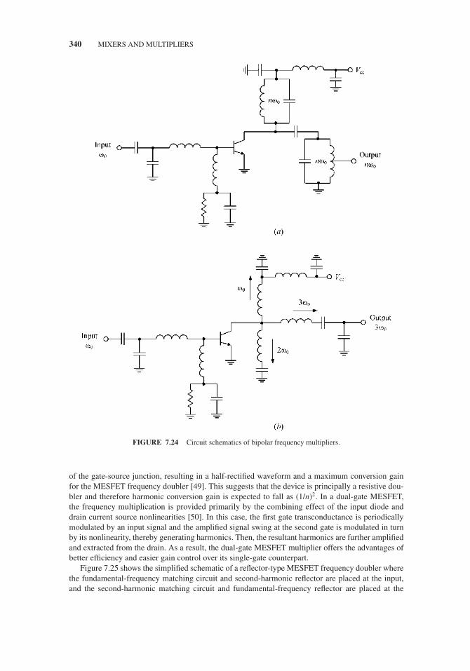
JWBS064-c07 JWBS064-Gerbennikov March 15, 2011 11:12 Printer Name: Yet to Come
340 MIXERS AND MULTIPLIERS
FIGURE 7.24 Circuit schematics of bipolar frequency multipliers.
of the gate-source junction, resulting in a half-rectified waveform and a maximum conversion gainfor the MESFET frequency doubler [49]. This suggests that the device is principally a resistive dou-bler and therefore harmonic conversion gain is expected to fall as (1/n)2. In a dual-gate MESFET,the frequency multiplication is provided primarily by the combining effect of the input diode anddrain current source nonlinearities [50]. In this case, the first gate transconductance is periodicallymodulated by an input signal and the amplified signal swing at the second gate is modulated in turnby its nonlinearity, thereby generating harmonics. Then, the resultant harmonics are further amplifiedand extracted from the drain. As a result, the dual-gate MESFET multiplier offers the advantages ofbetter efficiency and easier gain control over its single-gate counterpart.
Figure 7.25 shows the simplified schematic of a reflector-type MESFET frequency doubler wherethe fundamental-frequency matching circuit and second-harmonic reflector are placed at the input,and the second-harmonic matching circuit and fundamental-frequency reflector are placed at the

JWBS064-c07 JWBS064-Gerbennikov March 15, 2011 11:12 Printer Name: Yet to Come
FREQUENCY MULTIPLIERS 341
FIGURE 7.25 Schematic of reflector-type MESFET frequency doubler.
output [51,52]. The open-circuit stub with an electrical length of 45◦ is located inside the inputreflector to provide the short-circuit condition for the second harmonic, while the open-circuit stubwith an electrical length of 90◦ and series stub with an electrical length of 180◦ represent the outputreflector to provide the short-circuit condition for the fundamental at the device drain. As a result, aconversion gain of 6 dB for the MESFET frequency doubler was achieved at an output frequency of24 GHz. Using the separate fundamental-frequency rejection network at the device drain when it canbe adjusted independently from the frequency-selective load network can improve significantly theconversion gain for the 11.5 to 34.5 GHz HEMT frequency tripler [53]. The fundamental-frequencytermination at the device output is especially useful for a millimeter-wave HEMT multiplier whenthe frequency ranges from 180 to 220 GHz for a doubler and from 130 to 150 GHz for a tripler withacceptable conversion gain can be achieved [54].
To provide high spectral purity and broadband operation, the balanced frequency-doubler config-urations are preferred because they provide efficient rejection of the fundamental and odd-harmoniccomponents. In this case, the bandwidth of the doubler is mainly limited by the phase and amplitudeimbalance of the hybrid that increases with frequency. To overcome this limitation, it is necessary toapply broadband MMIC approaches for combining scheme or hybrid implementation. Figure 7.26(a)shows the miniaturized broadband balanced frequency doubler MMIC that consists of a common-gateand common-source MESFETs connected in parallel electrically and in series by electrode configura-tion such as source-gate-drain-gate-source [55]. Here, the gate of a common-gate device is groundedthrough a capacitor, and the source of a common-gate device and the gate of a common-source deviceare connected in phase at the input port through the phase shifter and dc-blocking capacitor, respec-tively. The phase shifter compensates for a phase error between the device outputs, and the outputmatching circuit is required for load matching at the second harmonic. The doubler operates near thegate-source pinch-off voltage, and the amplitudes of the output signals from both MESFETs are madeequal by adjusting each gate bias. Due to different device configurations, their fundamental compo-nents are 180◦ out of phase, whereas the second-harmonic components are in phase, thus resulting in acancelation of the fundamental frequency signals and an in-phase combining of the second-harmonicsignals. The conversion gain from −8 to −10 dB was achieved with fundamental-signal suppressionbetter than 17 dB from 6 to 16 GHz.
Figure 7.26(b) shows the basic configuration of a balanced frequency doubler consisting of the twoidentical MESFETs and a 180◦ hybrid divider [56]. Since a practical rat-race hybrid was characterizedby amplitude imbalance of about 1.1 dB and phase imbalance of about 2◦ from 28.8 to 39.4 GHz, thebias compensation approach when each transistor is biased differently to compensate for the hybridasymmetry was applied. As a result, the fundamental-frequency rejection achieved was better than35 dB over second-harmonic output frequency bandwidth of 31.5 to 37.5 GHz. A planar Marchandbalun is very effective to divide the incoming signal into two equal parts with 180◦ phase differencein millimeter-wave applications to provide a conversion gain of −10 dB for a balanced HEMTdoubler covering the frequency range from 150 to 220 GHz [57]. To achieve frequency doubling overan octave bandwidth, good conversion gain and fundamental-frequency rejection, the microwaveMESFET frequency doubler can be built based on a balanced structure with Lange couplers followed
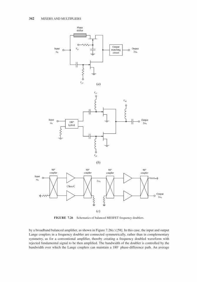
JWBS064-c07 JWBS064-Gerbennikov March 15, 2011 11:12 Printer Name: Yet to Come
342 MIXERS AND MULTIPLIERS
FIGURE 7.26 Schematics of balanced MESFET frequency doublers.
by a broadband balanced amplifier, as shown in Figure 7.26(c) [58]. In this case, the input and outputLange couplers in a frequency doubler are connected symmetrically, rather than in complementarysymmetry, as for a conventional amplifier, thereby creating a frequency doubled waveform withrejected fundamental signal to be then amplified. The bandwidth of the doubler is controlled by thebandwidth over which the Lange couplers can maintain a 180◦ phase-difference path. An average
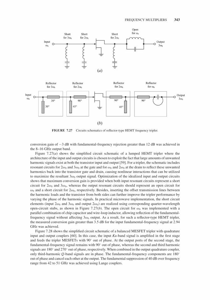
JWBS064-c07 JWBS064-Gerbennikov March 15, 2011 11:12 Printer Name: Yet to Come
FREQUENCY MULTIPLIERS 343
FIGURE 7.27 Circuits schematics of reflector-type HEMT frequency tripler.
conversion gain of −3 dB with fundamental-frequency rejection greater than 12 dB was achieved inthe 8–16 GHz output band.
Figure 7.27(a) shows the simplified circuit schematic of a lumped HEMT tripler where thearchitecture of the input and output circuits is chosen to exploit the fact that large amounts of unwantedharmonic signals exist at both the transistor input and output [59]. For a tripler, the schematic includesresonant circuits for 2ω0 and 3ω0 at the gate and for ω0 and 2ω0 at the drain to reflect these unwantedharmonics back into the transistor gate and drain, causing nonlinear interactions that can be utilizedto maximize the resultant 3ω0 output signal. Optimization of the idealized input and output circuitsshows that maximum conversion gain is provided when both input resonant circuits represent a shortcircuit for 2ω0 and 3ω0, whereas the output resonant circuits should represent an open circuit forω0 and a short circuit for 2ω0, respectively. Besides, inserting the offset transmission lines betweenthe harmonic loads and the transistor from both sides can further improve the tripler performance byvarying the phase of the harmonic signals. In practical microwave implementation, the short circuitelements (input 2ω0 and 3ω0 and output 2ω0) are realized using corresponding quarter-wavelengthopen-circuit stubs, as shown in Figure 7.27(b). The open circuit for ω0 was implemented with aparallel combination of chip capacitor and wire-loop inductor, allowing reflection of the fundamental-frequency signal without affecting 3ω0 output. As a result, for such a reflector-type HEMT tripler,the measured conversion gain greater than 3.5 dB for the input fundamental-frequency signal at 2.94GHz was achieved.
Figure 7.28 shows the simplified circuit schematic of a balanced MESFET tripler with quadratureinput and output couplers [60]. In this case, the input Ku-band signal is amplified in the first stageand feeds the tripler MESFETs with 90◦ out of phase. At the output ports of the second stage, thefundamental-frequency signal remains with 90◦ out of phase, whereas the second and third harmonicsignals are 180◦ and 270◦ out of phase, respectively. When combined in the output quadrature coupler,only third-harmonic Q-band signals are in phase. The fundamental-frequency components are 180◦
out of phase and cancel each other at the output. The fundamental suppression of 40 dB over frequencyrange from 42 to 51 GHz was achieved using Lange couplers.

JWBS064-c07 JWBS064-Gerbennikov March 15, 2011 11:12 Printer Name: Yet to Come
344 MIXERS AND MULTIPLIERS
FIGURE 7.28 Schematic of balanced MESFET frequency tripler.
REFERENCES
1. E. W. Herold, “The Operation of Frequency Converters and Mixers for Superheterodyne Reception,” Proc.IRE., vol. 30, pp. 84–103, Feb. 1942.
2. E. W. Herold and L. Matter, “Some Aspects of Radio Reception at Ultra-High Frequencies,” Proc. IRE., vol.31, pp. 575–582, Oct. 1943.
3. M. R. Barber, “Noise Figure and Conversion Loss of the Schottky Barrier Mixer Diode,” IEEE Trans.Microwave Theory Tech., vol. MTT-15, pp. 629–635, Nov. 1967.
4. P. R. Gray and R. G. Meyer, Analysis and Design of Analog Integrated Circuits, New York: John Wiley &Sons, 1977.
5. J. M. Manley and H. E. Rowe, “Some General Properties of Nonlinear Elements,” Proc. IRE., vol. 44, pp.904–913, July 1956.
6. P. Penfield and R. P. Rafuse, Varactor Applications, Cambridge: The M.I. T Press, 1962.
7. S. A. Maas, Nonlinear Microwave Circuits, New York: IEEE Press, 1997.
8. L. M. Orloff, “Intermodulation Analysis of Crystal Mixer,” Proc. IEEE., vol. 52, pp. 173–179, Feb. 1964.
9. E. W. Herold, R. R. Bush, and W. R. Ferris, “Conversion Loss of Diode Mixers Having Image-FrequencyImpedance,” Proc. IRE., vol. 33, pp. 603–609, Sept. 1945.
10. D. Kaye, “Derivation of Intermodulation Outputs of a Pair of General Nonlinear Elements in a BalancedMixer Array,” Proc. IEEE., vol. 53, pp. 1783–1784, Nov. 1965.
11. C. M. Howell, “Integrated Balanced Mixers for S- and X-Band,” 1966 IEEE G-MTT Int. Microwave Symp.Dig., pp. 151–155.
12. D. M. Pozar, Microwave Engineering, New York: John Wiley & Sons, 2004.
13. F. L. Di Alessio, A. D’Orazio, and R. Lavolpe, “Even-Harmonic C-Band Modulator,” IEEE Trans. MicrowaveTheory Tech., vol. MTT-53, pp. 1203–1210, Apr. 2005.
14. H. Okazaki and Y. Yamaguchi, “Wide-Band SSB Subharmonically Pumped Mixer MMIC,” IEEE Trans.Microwave Theory Tech., vol. MTT-45, pp. 2375–2379, Dec. 1997.
15. H. L. Krauss, C. W. Bostian, and F. H. Raab, Solid State Radio Engineering, New York: John Wiley & Sons,1980.
16. A. M. Pavio, R. H. Halladay, S. D. Bingham, and C. Sapashe, “Double Balanced Mixers Using Active andPassive Techniques,” IEEE Trans. Microwave Theory Tech., vol. MTT-36, pp. 1948–1957, Dec. 1988.
17. G. D. Vendelin, A. M. Pavio, and U. L. Rohde, Microwave Circuit Design Using Linear and NonlinearTechniques, New York: John Wiley & Sons, 1990.
18. C.-M. Lin, H.-K. Lin, C.-F. Lin, Y.-A. Lai, C.-H. Lin, and Y.-H. Wang, “A 16–44 GHz Compact DoublyBalanced Monolithic Ring Mixer,” IEEE Microwave and Wireless Components Lett., vol. 18, pp. 620–622,Sept. 2008.

JWBS064-c07 JWBS064-Gerbennikov March 15, 2011 11:12 Printer Name: Yet to Come
REFERENCES 345
19. R. B. Mouw, “A Broad-Band Hybrid Junction and Application to the Star Modulator,” IEEE Trans. MicrowaveTheory Tech., vol. MTT-16, pp. 911–918, Nov. 1968.
20. D. Neuf and S. Spohrer, “Conventional and New Applications for the Quadrature IF Microwave Mixer,”Microwave J., vol. 26, pp. 99–109, Jan. 1983.
21. K. Hettak, G. A. Morin, and M. G. Stubbs, “Size Reduction of a MMIC Direct Up-Converter at 44 GHz inMultilayer CPW Technology Using Thin-Film Microstrip Stubs Loading,” IEEE Trans. Microwave TheoryTech., vol. MTT-54, pp. 3453–3461, Sept. 2006.
22. J. Zawels, “The Transistor as a Mixer,” Proc. IRE, vol. 42, pp. 542–548, Mar. 1954.
23. J. S. Vogel, “Nonlinear Distortion and Mixing Processes in Field-Effect Transistors,” Proc. IEEE., vol. 55,pp. 2109–2116, Dec. 1967.
24. M. Madihian, L. Desclos, K. Maruhashi, K. Onda, and M. Kuzuhara, “A Monolithic AlGaAs/InGaAs Up-converter IC for K-Band Wireless Networks,” IEEE Trans. Microwave Theory Tech., vol. MTT-43, pp.2773–2777, Dec. 1995.
25. M. Madihian, L. Desclos, K. Maruhashi, K. Onda, and M. Kuzuhara, “60-GHz Monolithic Down- and Up-Converters Utilizing a Source-Injection Concept,” IEEE Trans. Microwave Theory Tech., vol. MTT-46, pp.1003–1006, July 1998.
26. A. Orzati, F. Robin, H. Meier, H. Benedikter, and W. Bachtold, “A V-Band Up-Converting InP HEMT ActiveMixer with Low LO-Power Requirements,” IEEE Microwave and Wireless Components Lett., vol. 13, pp.202–204, June 2003.
27. S. Asai, F. Murai, and H. Kodera, “GaAs Dual-Gate Schottky-Barrier FET’s for Microwave Frequencies,”IEEE Trans. Electron Devices, vol. ED-22, pp. 897–904, Oct. 1975.
28. C. A. Liechti, “Performance of Dual-Gate GaAs MESFET’s as Gain-Controlled Low-Noise Amplifiers andHigh-Speed Modulators,” IEEE Trans. Microwave Theory Tech., vol. MTT-23, pp. 461–469, June 1975.
29. C. Tsironis, R. Meierer, and R. Stahlmann, “Dual-Gate MESFET Mixers,” IEEE Trans. Microwave TheoryTech., vol. MTT-32, pp. 248–255, Mar. 1984.
30. W. S. Tsai, S. F. Paik, and B. S. Hewitt, “An X-Band Dual-Gate FET Up-Converter,” 1979 IEEE MTT-S Int.Microwave Symp. Dig., pp. 495–497.
31. T. Hirota and H. Ogawa, “A Novel K-Band Balanced FET Up-Converter,” IEEE Trans. Microwave TheoryTech., vol. MTT-32, pp. 679–683, July 1984.
32. P.-S. Wu, C.-H. Wang, C.-S. Lin, K.-Y. Lin, and H. Wang, “A Compact 60 GHz Integrated Up-Converter UsingMiniature Transformer Couplers with 5 dB Conversion Gain,” IEEE Microwave and Wireless ComponentsLett., vol. 18, pp. 641–643, Sept. 2008.
33. M. L. de la Fuente, J. Portilla, J. P. Pascual, and E. Artal, “Low-Noise Ku-Band MMIC Balanced P-HEMTUpconverter,” IEEE J. Solid-State Circuits, vol. SC-34, pp. 259–263, Feb. 1999.
34. H. E. Jones, “Dual Output Synchronous Detector Utilizing Transistorized Differential Amplifiers,” U.S. Patent3,241,078, Mar. 1966 (filed June 1963).
35. A. Bilotti, “Applications of a Monolithic Analog Multiplier,” IEEE J. Solid-State Circuits, vol. SC-3, pp.373–380, Dec. 1968.
36. A. Y. Umeda, C. T. Matsuno, A. K. Oki, G. S. Dow, K. W. Kobayashi, D. K. Umemoto, and M. E. Kim,“A Monolithic GAAs HBT Upconverter,” 1990 IEEE Microwave and Millimeter-Wave Monolithic CircuitsSymp. Dig., pp. 77–80.
37. K. Osafune and Y. Yamauchi, “20-GHz 5-dB-Gain Analog Multipliers with AlGaAs/GaAs HBT’s,” IEEETrans. Microwave Theory Tech., vol. MTT-42, pp. 518–520, Mar. 1994.
38. C. Meng, T.-H. Wu, and M. Lin, “Compact 5.2-GHz GaInP/GaAs HBT Gilbert Upconverter Using LumpedRat-Race Hybrid and Current Combiner,” IEEE Microwave and Wireless Components Lett., vol. 15, pp.688–690, Oct. 2005.
39. K. W. Kobayashi, L. T. Tran, S. Bui, A. K. Oki, D. C. Streit, and M. Rosen, “InAlAs/InGaAs HBT X-BandDouble-Balanced Upconverter,” IEEE J. Solid-State Circuits, vol. SC-29, pp. 1238–1243, Oct. 1994.
40. M. West and M. Kumar, “Monolithic Integrated Blanking Up-Converter,” IEEE Trans. Microwave TheoryTech., vol. MTT-38, pp. 1227–1231, Sept. 1990.
41. A. Verma, K. K. O, and J. Lin, “A Low-Power Up-Conversion CMOS Mixer for 22–29-GHz Ultra-WidebandApplications,” IEEE Trans. Microwave Theory Tech., vol. MTT-54, pp. 3295–3300, Aug. 2006.

JWBS064-c07 JWBS064-Gerbennikov March 15, 2011 11:12 Printer Name: Yet to Come
346 MIXERS AND MULTIPLIERS
42. A. Valdes-Garcia, S. Reynolds, and J.-O. Plouchart, “60 GHz Transmitter Circuits in 65 nm CMOS,” Proc.2008 IEEE RFIC Symp., pp. 641–644.
43. R. S. Ohl, “High Frequency Oscillation Generator,” U.S. Patent 1,756,131, Apr. 1930 (filed Aug. 1925).
44. R. M. Page, “An Investigation of the Phenomena of Frequency Multiplication as Used in Tube Transmitters,”Proc. IRE, vol. 17, pp. 1649–1655, Sept. 1929.
45. F. E. Terman and J. H. Ferns, “The Calculation of Class C Amplifier and Harmonic Generator Performanceof Screen-Grid and Similar Tubes,” Proc. IRE, vol. 22, pp. 359–373, Mar. 1934.
46. H. C. Lee and R. Minton, “Designing Transistor Multipliers,” Microwaves, vol. 4, pp. 18–28, Nov. 1965.
47. G. D. O’Clock and R. J. Dauphinee, “High-Gain Transistor Frequency Multiplier,” Proc. IEEE, vol. 58, pp.1363–1365, Sept. 1970.
48. J. J. Pan, “Wideband MESFET Microwave Frequency Multiplier,” 1978 IEEE MTT-S Int. Microwave Symp.Dig., pp. 306–308.
49. A. Gopinath and J. B. Rankin, “Single-Gate MESFET Frequency Doublers,” IEEE Trans. Microwave TheoryTech., vol. MTT-30, pp. 869–875, June 1982.
50. P. T. Chen, C.-T. Li, and P. H. Wang, “Dual-Gate GaAs FET as a Frequency Multiplier at Ku-Band,” 1978IEEE MTT-S Int. Microwave Symp. Dig., pp. 309–311.
51. C. Rauscher, “High-Frequency Doubler Operation of GaAs Field-Effect Transistors,” IEEE Trans. MicrowaveTheory Tech., vol. MTT-31, pp. 462–473, June 1983.
52. Y. Iyama, A. Iida, T. Takagi, and S. Urasaki, “Second-Harmonic Reflector Type High-Gain FET FrequencyDoubler Operating in K-Band,” 1989 IEEE MTT-S Int. Microwave Symp. Dig., pp. 1291–1294.
53. G. Zhang, R. D. Pollard, and C. M. Snowden, “A Novel Technique for HEMT Tripler Design,” 1996 IEEEMTT-S Int. Microwave Symp. Dig., pp. 663–666.
54. Y. Campos-Roca, C. Schworer, A. Leuther, and M. Seelmann-Eggebert, “G-Band Metamorphic HEMT-Based Frequency Multipliers,” IEEE Trans. Microwave Theory Tech., vol. MTT-54, pp. 2983–2992, July2006.
55. T. Hiraoka, T. Tokumitsu, and M. Akaike, “A Miniaturized Broad-Band MMIC Frequency Doubler,” IEEETrans. Microwave Theory Tech., vol. MTT-38, pp. 1932–1937, Dec. 1990.
56. B. Piernas, K. Nishikawa, T. Nakagawa, H. Hayashi, and K. Araki, “Analysis of Balanced Active Doublerfor Broad-Band Operation – The Frequency-Tuning Concept,” IEEE Trans. Microwave Theory Tech., vol.MTT-50, pp. 1120–1126, Apr. 2002.
57. C. Schworer, Y. Campos-Roca, A. Leuther, A. Tessmann, M. Seelmann-Eggebert, H. Massler, M.Schlechtweg, and G. Weimann, “A 150 to 220 GHz Balanced Doubler MMIC Using a 50 nm Metamor-phic HEMT Technology,” Proc. 35th Europ. Microwave Conf., vol. 3, pp. 1–4, 2005.
58. R. Gilmore, “Octave-Bandwidth Microwave FET Doubler,” Electronics Lett., vol. 21, pp. 532–533, June1985.
59. J. E. Johnson, G. R. Branner, and J.-P. Mima, “Design and Optimization of Large Conversion Gain ActiveMicrowave Frequency Triplers,” IEEE Microwave and Wireless Components Lett., vol. 15, pp. 457–459, July2005.
60. H. Fudem and E. C. Niehenke, “Novel Millimeter Wave Active MMIC Triplers,” 1998 IEEE MTT-S Int.Microwave Symp. Dig., pp. 387–390.
JWBS064-c08 JWBS064-Gerbennikov March 15, 2011 11:17 Printer Name: Yet to Come
8 Oscillators
This chapter presents the principles of oscillator design, including start-up and steady-stateoperation conditions, noise and stability of oscillations, basic oscillator configurations using lumpedand transmission-line elements, and simplified equation-based oscillator analyses and optimum de-sign techniques. An immittance design approach is introduced and applied to the series and parallelfeedback oscillators, including circuit design and simulation aspects. Voltage-controlled oscillators(VCOs) and their varactor tuning range and linearity for different oscillator configurations are dis-cussed. Finally, the basic circuits and operation principles of crystal and dielectric resonator oscillatorsare given.
8.1 OSCILLATOR OPERATION PRINCIPLES
8.1.1 Steady-State Operation Mode
A simple feedback oscillator model is shown in Figure 8.1(a) where an oscillator circuit is decomposedinto a forward nonlinear network and a feedback linear network, both of which are two-port networks.Figure 8.1(b) shows an example of a transformer-coupled metal-oxide-semiconductor field-effecttransistor (MOSFET) oscillator without bias circuit to illustrate common features of the feedbackoscillator. Because an oscillator is an autonomous circuit, electronic noise in the active device orpower supply turn-on transient leads to the self-excitation of the oscillations. This provides the initialoscillation build-up. As the oscillation amplitude grows, the active device displays larger nonlinearityand then limits the amplitude increase.
In a steady-state operation mode, the following complex equation also known as the Barkhausencriterion can be written for the parallel feedback oscillator:
T (Vin, ω) = A (Vin, jω) β ( jω) = 1 (8.1)
where A = Iout/Vin is the forward transfer function and β = Vin/Iout is the feedback transfer function.This equation means that the oscillator complex loop gain is equal to unity [1,2]. The feedbacktransfer function can be represented as
β ( jω) = K ( jω) Z ( jω) (8.2)
where K = Vin/Vout is the voltage feedback coefficient and Z = Vout/Iout is the oscillator resonantcircuit impedance. Presenting each of these complex quantities in the form of A = Aexp(jφA), K =Kexp(jφK), and Z = Zexp(jφZ), the following equations for magnitudes and phases directly resultfrom Eq. (8.1):
A (Vin, ω) K (ω) Z (ω) = 1 (8.3)
φA + φK + φZ = 0, 2π, . . . . (8.4)
RF and Microwave Transmitter Design, First Edition. Andrei Grebennikov.C© 2011 John Wiley & Sons, Inc. Published 2011 by John Wiley & Sons, Inc.
347

JWBS064-c08 JWBS064-Gerbennikov March 15, 2011 11:17 Printer Name: Yet to Come
348 OSCILLATORS
FIGURE 8.1 Schematics of (a) parallel feedback oscillator and (b) transformer-coupled MOSFET oscillator.
Equation (8.3), which is called the amplitude balance condition, means that the oscillator loopgain is equal to unity in the steady-state stationary operation mode. In this equation, it is assumed thattwo quantities, K and Z, depend on frequency only. Consequently, the amplitude balance condition issatisfied only under the appropriate value of input voltage amplitude V in. To define the value of thisamplitude, let us rewrite Eq. (8.3) in the form
A (Vin, ω) = 1
K (ω) Z (ω). (8.5)
In Figure 8.2, the amplitude dependence A(V in) and feedback straight line 1/KZ are plotted. Theintersection point of these dependencies determines the steady-state oscillation amplitude V o
in.Equation (8.4), which is called the phase balance condition, means that the sum of all oscillator
loop phase shifts must be equal to zero or 2πn, where n = 1, 2, . . . . This equation defines the value ofthe oscillation frequency f osc. In the simple case when φK = 0 (transistor input admittance is equal tozero and feedback magnitude K depends only on a mutual-coupling coefficient M between primaryand secondary inductances), and the active device does not produce the phase shift, that is φA = 0,then φZ = 0, and the oscillation frequency f osc is equal to parallel resonant circuit frequency f 0 =ω0/(2π ), where ω0 = 1/
√LC . If φA �= 0, the oscillation frequency f osc will differ from f 0 in order to
fully compensate for the available phase shift φZ according to
φZ = −tan−1
(2Q
�ω
ω0
)= −φA (8.6)
where Q = 1/(ωCR) is a quality factor of the oscillator resonant circuit, �ω = 2π (f osc − f 0) [2].
FIGURE 8.2 Graphic balance amplitude condition.

JWBS064-c08 JWBS064-Gerbennikov March 15, 2011 11:17 Printer Name: Yet to Come
OSCILLATOR OPERATION PRINCIPLES 349
FIGURE 8.3 Deviation of oscillation frequency f osc from resonant frequency f 0.
Equation (8.6) can be rewritten in the form
�ω
ω0= tan φA
2Q(8.7)
which determines the deviation of the oscillation frequency f osc from resonant frequency f 0 as afunction of the phase of the forward transfer function of the active device and oscillator quality factor.
From graphical representation of Eq. (8.6) shown in Figure 8.3(a), it follows that the oscillationfrequency f osc is smaller than the resonant frequency f 0. Furthermore, the lower the quality factorQ the smaller oscillation frequency f osc, as shown in Figure 8.3(b), where the deviation �ω2 fromradian resonant frequency ω0 becomes greater for the case of Q2 < Q1.
8.1.2 Start-Up Conditions
The start-up conditions can be illustrated on the plane of the transfer function iout = f (vin), as shownin Figure 8.4. Let us choose the bias voltage V ′
g corresponding to the maximum small-signal transferfunction when ∂iout/∂vin = 0. Such a condition is adequate to the maximum forward transfer functionA(V in = 0) shown in Figure 8.2. According to Figure 8.2, the amplitude V in of the oscillations growsmonotonically, whereas the transfer function A decreases. The amplitude of the output current iout
is trying to reach its maximum value corresponding to the stable steady-state operation mode whenV in = V o
in. Such a behavior of the transfer function A means that the start-up oscillation conditionscan be defined as
A(ω) K (ω) Z (ω) > 1 (8.8)
φA + φK + φZ = 0,2π, . . . . (8.9)
Let the bias voltage V ′′g be chosen close to the device threshold voltage, as shown in Figure 7.4.
Such a bias condition corresponds to the small initial value of transfer function A(V in = 0), whichis not enough to establish the stable steady-state stationary oscillations because A < 1/KZ. Thisis demonstrated by curve II in Figure 8.5(a). Therefore, the oscillation system with such a biascondition requires an impulse to initiate self-oscillations, as it cannot oscillate by itself. The resultof this impulse should be output current amplitude resulting in a condition of A > 1/KZ. Hence, thesystem has hard operating conditions and the process of the oscillation establishment is called the
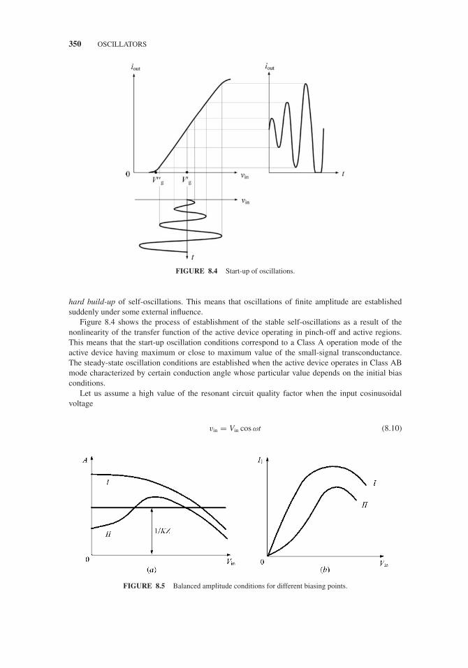
JWBS064-c08 JWBS064-Gerbennikov March 15, 2011 11:17 Printer Name: Yet to Come
350 OSCILLATORS
FIGURE 8.4 Start-up of oscillations.
hard build-up of self-oscillations. This means that oscillations of finite amplitude are establishedsuddenly under some external influence.
Figure 8.4 shows the process of establishment of the stable self-oscillations as a result of thenonlinearity of the transfer function of the active device operating in pinch-off and active regions.This means that the start-up oscillation conditions correspond to a Class A operation mode of theactive device having maximum or close to maximum value of the small-signal transconductance.The steady-state oscillation conditions are established when the active device operates in Class ABmode characterized by certain conduction angle whose particular value depends on the initial biasconditions.
Let us assume a high value of the resonant circuit quality factor when the input cosinusoidalvoltage
vin = Vin cos ωt (8.10)
FIGURE 8.5 Balanced amplitude conditions for different biasing points.
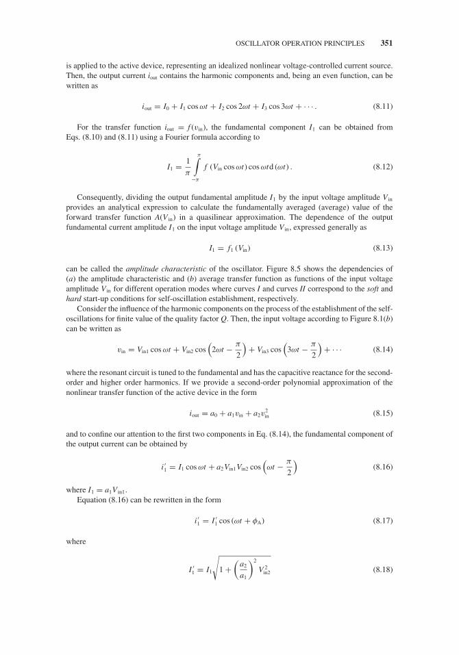
JWBS064-c08 JWBS064-Gerbennikov March 15, 2011 11:17 Printer Name: Yet to Come
OSCILLATOR OPERATION PRINCIPLES 351
is applied to the active device, representing an idealized nonlinear voltage-controlled current source.Then, the output current iout contains the harmonic components and, being an even function, can bewritten as
iout = I0 + I1 cos ωt + I2 cos 2ωt + I3 cos 3ωt + · · · . (8.11)
For the transfer function iout = f (vin), the fundamental component I1 can be obtained fromEqs. (8.10) and (8.11) using a Fourier formula according to
I1 = 1
π
π∫−π
f (Vin cos ωt) cos ωtd (ωt) . (8.12)
Consequently, dividing the output fundamental amplitude I1 by the input voltage amplitude V in
provides an analytical expression to calculate the fundamentally averaged (average) value of theforward transfer function A(V in) in a quasilinear approximation. The dependence of the outputfundamental current amplitude I1 on the input voltage amplitude V in, expressed generally as
I1 = f1 (Vin) (8.13)
can be called the amplitude characteristic of the oscillator. Figure 8.5 shows the dependencies of(a) the amplitude characteristic and (b) average transfer function as functions of the input voltageamplitude V in for different operation modes where curves I and curves II correspond to the soft andhard start-up conditions for self-oscillation establishment, respectively.
Consider the influence of the harmonic components on the process of the establishment of the self-oscillations for finite value of the quality factor Q. Then, the input voltage according to Figure 8.1(b)can be written as
vin = Vin1 cos ωt + Vin2 cos(
2ωt − π
2
)+ Vin3 cos
(3ωt − π
2
)+ · · · (8.14)
where the resonant circuit is tuned to the fundamental and has the capacitive reactance for the second-order and higher order harmonics. If we provide a second-order polynomial approximation of thenonlinear transfer function of the active device in the form
iout = a0 + a1vin + a2v2in (8.15)
and to confine our attention to the first two components in Eq. (8.14), the fundamental component ofthe output current can be obtained by
i ′1 = I1 cos ωt + a2Vin1Vin2 cos
(ωt − π
2
)(8.16)
where I1 = a1V in1.Equation (8.16) can be rewritten in the form
i ′1 = I ′
1 cos (ωt + φA) (8.17)
where
I ′1 = I1
√1 +
(a2
a1
)2
V 2in2 (8.18)
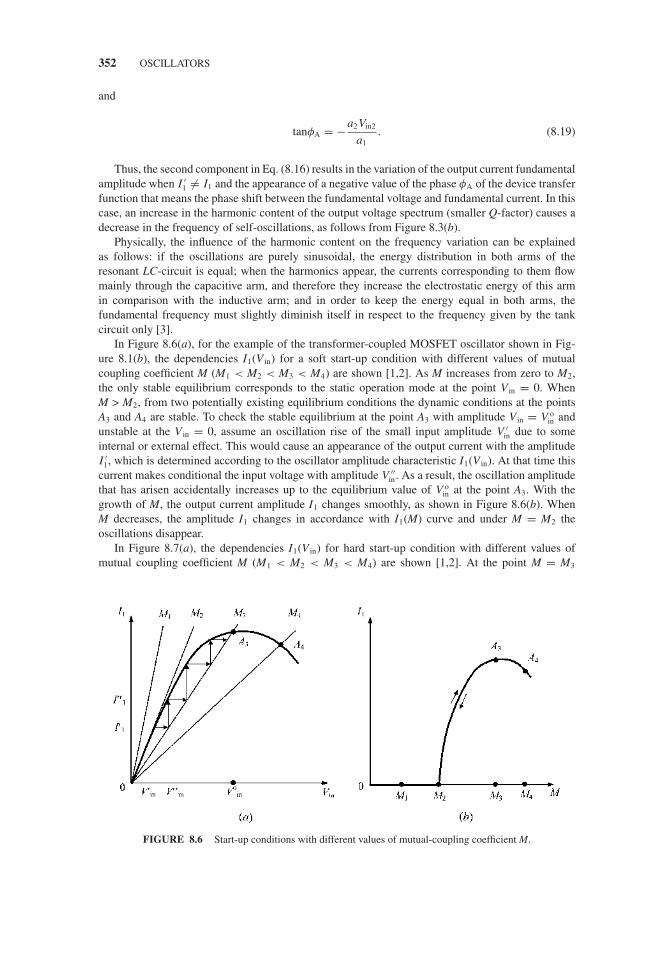
JWBS064-c08 JWBS064-Gerbennikov March 15, 2011 11:17 Printer Name: Yet to Come
352 OSCILLATORS
and
tanφA = −a2Vin2
a1. (8.19)
Thus, the second component in Eq. (8.16) results in the variation of the output current fundamentalamplitude when I ′
1 �= I1 and the appearance of a negative value of the phase φA of the device transferfunction that means the phase shift between the fundamental voltage and fundamental current. In thiscase, an increase in the harmonic content of the output voltage spectrum (smaller Q-factor) causes adecrease in the frequency of self-oscillations, as follows from Figure 8.3(b).
Physically, the influence of the harmonic content on the frequency variation can be explainedas follows: if the oscillations are purely sinusoidal, the energy distribution in both arms of theresonant LC-circuit is equal; when the harmonics appear, the currents corresponding to them flowmainly through the capacitive arm, and therefore they increase the electrostatic energy of this armin comparison with the inductive arm; and in order to keep the energy equal in both arms, thefundamental frequency must slightly diminish itself in respect to the frequency given by the tankcircuit only [3].
In Figure 8.6(a), for the example of the transformer-coupled MOSFET oscillator shown in Fig-ure 8.1(b), the dependencies I1(V in) for a soft start-up condition with different values of mutualcoupling coefficient M (M1 < M2 < M3 < M4) are shown [1,2]. As M increases from zero to M2,the only stable equilibrium corresponds to the static operation mode at the point V in = 0. WhenM > M2, from two potentially existing equilibrium conditions the dynamic conditions at the pointsA3 and A4 are stable. To check the stable equilibrium at the point A3 with amplitude V in = V o
in andunstable at the V in = 0, assume an oscillation rise of the small input amplitude V ′
in due to someinternal or external effect. This would cause an appearance of the output current with the amplitudeI ′
1, which is determined according to the oscillator amplitude characteristic I1(V in). At that time thiscurrent makes conditional the input voltage with amplitude V ′′
in. As a result, the oscillation amplitudethat has arisen accidentally increases up to the equilibrium value of V o
in at the point A3. With thegrowth of M, the output current amplitude I1 changes smoothly, as shown in Figure 8.6(b). WhenM decreases, the amplitude I1 changes in accordance with I1(M) curve and under M = M2 theoscillations disappear.
In Figure 8.7(a), the dependencies I1(V in) for hard start-up condition with different values ofmutual coupling coefficient M (M1 < M2 < M3 < M4) are shown [1,2]. At the point M = M3
FIGURE 8.6 Start-up conditions with different values of mutual-coupling coefficient M.
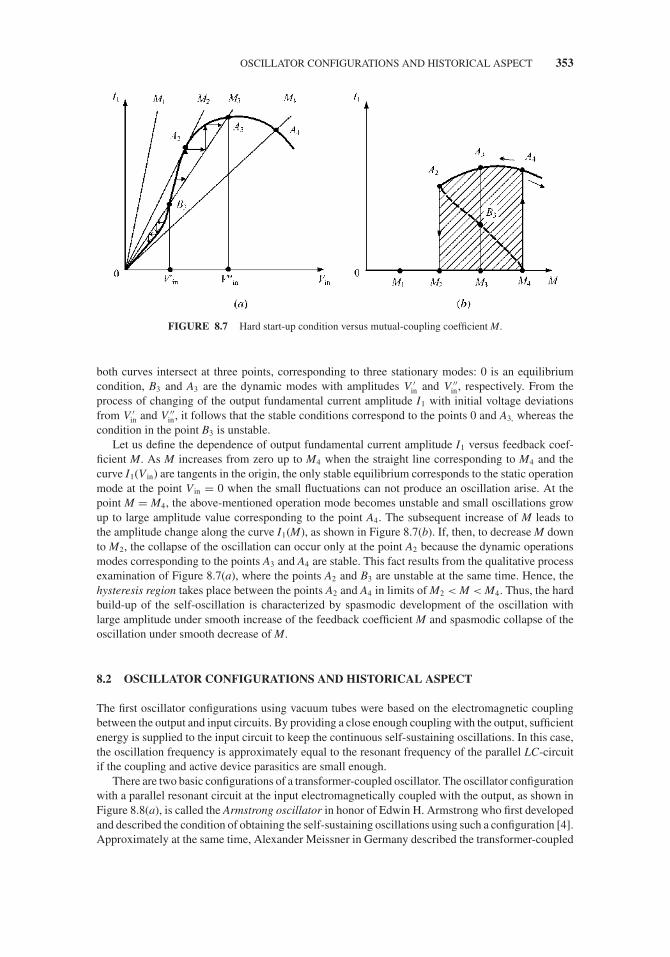
JWBS064-c08 JWBS064-Gerbennikov March 15, 2011 11:17 Printer Name: Yet to Come
OSCILLATOR CONFIGURATIONS AND HISTORICAL ASPECT 353
FIGURE 8.7 Hard start-up condition versus mutual-coupling coefficient M.
both curves intersect at three points, corresponding to three stationary modes: 0 is an equilibriumcondition, B3 and A3 are the dynamic modes with amplitudes V ′
in and V ′′in, respectively. From the
process of changing of the output fundamental current amplitude I1 with initial voltage deviationsfrom V ′
in and V ′′in, it follows that the stable conditions correspond to the points 0 and A3, whereas the
condition in the point B3 is unstable.Let us define the dependence of output fundamental current amplitude I1 versus feedback coef-
ficient M. As M increases from zero up to M4 when the straight line corresponding to M4 and thecurve I1(V in) are tangents in the origin, the only stable equilibrium corresponds to the static operationmode at the point V in = 0 when the small fluctuations can not produce an oscillation arise. At thepoint M = M4, the above-mentioned operation mode becomes unstable and small oscillations growup to large amplitude value corresponding to the point A4. The subsequent increase of M leads tothe amplitude change along the curve I1(M), as shown in Figure 8.7(b). If, then, to decrease M downto M2, the collapse of the oscillation can occur only at the point A2 because the dynamic operationsmodes corresponding to the points A3 and A4 are stable. This fact results from the qualitative processexamination of Figure 8.7(a), where the points A2 and B3 are unstable at the same time. Hence, thehysteresis region takes place between the points A2 and A4 in limits of M2 < M < M4. Thus, the hardbuild-up of the self-oscillation is characterized by spasmodic development of the oscillation withlarge amplitude under smooth increase of the feedback coefficient M and spasmodic collapse of theoscillation under smooth decrease of M.
8.2 OSCILLATOR CONFIGURATIONS AND HISTORICAL ASPECT
The first oscillator configurations using vacuum tubes were based on the electromagnetic couplingbetween the output and input circuits. By providing a close enough coupling with the output, sufficientenergy is supplied to the input circuit to keep the continuous self-sustaining oscillations. In this case,the oscillation frequency is approximately equal to the resonant frequency of the parallel LC-circuitif the coupling and active device parasitics are small enough.
There are two basic configurations of a transformer-coupled oscillator. The oscillator configurationwith a parallel resonant circuit at the input electromagnetically coupled with the output, as shown inFigure 8.8(a), is called the Armstrong oscillator in honor of Edwin H. Armstrong who first developedand described the condition of obtaining the self-sustaining oscillations using such a configuration [4].Approximately at the same time, Alexander Meissner in Germany described the transformer-coupled

JWBS064-c08 JWBS064-Gerbennikov March 15, 2011 11:17 Printer Name: Yet to Come
354 OSCILLATORS
FIGURE 8.8 Schematics of (a) Armstrong and (b) Meissner oscillators.
oscillator with a parallel resonant circuit at the output electromagnetically coupled with the input, asshown in Figure 8.8(b), which is called the Meissner oscillator [5]. High-purity stable oscillationscan be obtained by a fully balanced version of Meissner oscillator with a three-turn link providingan excellent isolation of the resonant circuit when very little energy is taken from the resonator toprovide the voltages to drive the input and sustain the oscillations [6].
To satisfy a phase balance condition in the transformer-coupled oscillator, the transformer shouldprovide a phase shift of 180◦. If the primary and secondary windings of the transformer have thesame direction of wind, it is necessary to connect the secondary winding in the opposite directionrelatively the primary one, that is, to connect the end of the secondary winding where the voltage isin-phase with the anode (drain or collector) voltage to the ground. The coupling coefficient of thetransformer is chosen to provide a soft start-up oscillation mode.
The schematic of the Hartley oscillator is very close to the schematic of the Meissner oscillator [7].The difference is that the tank inductor L having an additional output replaces the transformer, as shownin Figure 8.9(a). The inductance ratio determines the feedback coefficient. The Hartley oscillator canbe represented by a well-known inductive three-point configuration shown in Figure 8.9(b), where thefeedback element from the output to the input is the capacitor C. The inductors L1 and L2 representthe output and input circuits, respectively.
Unlike the Hartley oscillator with electromagnetic coupling, the schematic of a Colpitts oscillator isbased on electrostatic coupling using the capacitive divider, the capacitance ratio of which determinesthe feedback coefficient, as shown in Figure 8.10(a) [8]. The Colpitts oscillator can be representedby a well-known capacitive three-point configuration shown in Figure 8.10(b), where the feedbackelement from the output to the input is the inductor L [9]. The capacitors C1 and C2 represent theoutput and input circuits, respectively.
FIGURE 8.9 Schematics of Hartley oscillators.

JWBS064-c08 JWBS064-Gerbennikov March 15, 2011 11:17 Printer Name: Yet to Come
OSCILLATOR CONFIGURATIONS AND HISTORICAL ASPECT 355
FIGURE 8.10 Schematics of Colpitts oscillators.
Depending on which electrode of the active device is grounded, we can distinguish three basicconfigurations representing a Colpitts family of oscillators based on the MOSFET devices, as shownin Figure 8.11. The Colpitts oscillator with grounded (common) source is shown in Figure 8.11(a), theColpitts oscillator with grounded (common) drain is shown in Figure 8.11(b), and the Colpitts oscil-lators with grounded (common) gate is shown in Figure 8.11(c, d). The connection of the appropriateelectrode of the tube (or transistor) to the ground have important effects upon the following:
� The manner in which the dc power is fed to the oscillator and the corresponding loading effectson the resonant circuit.
� The manner in which the output power is fed to the external load.� The distribution of the stray elements to the ground plane, which has important effects, partic-
ularly at microwaves.
Calculating the output impedance Zout for a common source oscillator shown in Figure 8.11(a)and a common drain oscillator shown in Figure 8.11(b), which are identical, shows that groundingof any terminal of the oscillator circuit does not change its electrical performance, provided thereare no changes in the connection of the feedback elements and load to the active device. Therefore,the schematic with a common gate shown in Figure 8.11(c) is characterized by the same electricalbehavior as the oscillator circuits with common source and common drain. However, in such aconfiguration there is no connection of any load terminal to the ground that makes its practicalimplementation more complicated. Figure 8.11(d) shows a common gate oscillator schematic withthe load connected in parallel to the inductance L, that is, between the drain and gate terminals.However, the other load connection, such as this with one grounded port, results in different electricalproperties of the oscillator compared with common source or common drain configuration.
The Gouriet–Clapp oscillator is a variation of the Colpitts oscillator with a tank inductor replacedby the series combination of an inductor L and a variable capacitor Cv, as shown in Figure 8.12(a).In this case, frequency stability is improved because the reactance of such a series circuit variesmore rapidly with frequency than that of a single inductor. However, the possibility to improve theoscillator stability by connecting a capacitor in series to one or each circuit inductor was first foundbased on a Hartley type of the oscillator [10]. In modern practical oscillator design, the Gouriet–Clapposcillator configuration is called the Clapp oscillator, although G. Gouriet and J. Clapp had devel-oped it independently [11]. A parallel counterpart of the Clapp oscillator shown in Figure 8.12(b)was described by E. Seiler and, therefore, is called the Seiler oscillator [11]. Such an oscillatorconfiguration is useful for wideband frequency tuning when the capacitance Cv in the parallel circuitis variable.
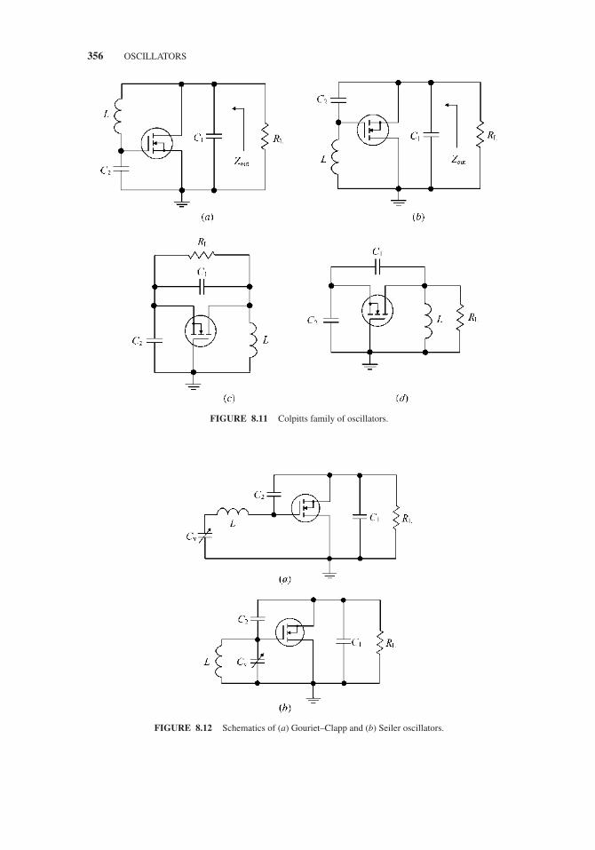
JWBS064-c08 JWBS064-Gerbennikov March 15, 2011 11:17 Printer Name: Yet to Come
356 OSCILLATORS
FIGURE 8.11 Colpitts family of oscillators.
FIGURE 8.12 Schematics of (a) Gouriet–Clapp and (b) Seiler oscillators.
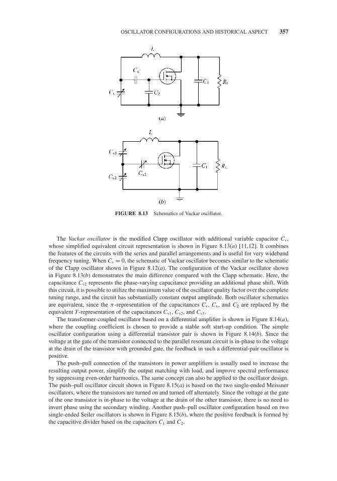
JWBS064-c08 JWBS064-Gerbennikov March 15, 2011 11:17 Printer Name: Yet to Come
OSCILLATOR CONFIGURATIONS AND HISTORICAL ASPECT 357
FIGURE 8.13 Schematics of Vackar oscillator.
The Vackar oscillator is the modified Clapp oscillator with additional variable capacitor Cv,whose simplified equivalent circuit representation is shown in Figure 8.13(a) [11,12]. It combinesthe features of the circuits with the series and parallel arrangements and is useful for very widebandfrequency tuning. When Cv = 0, the schematic of Vackar oscillator becomes similar to the schematicof the Clapp oscillator shown in Figure 8.12(a). The configuration of the Vackar oscillator shownin Figure 8.13(b) demonstrates the main difference compared with the Clapp schematic. Here, thecapacitance Cv2 represents the phase-varying capacitance providing an additional phase shift. Withthis circuit, it is possible to utilize the maximum value of the oscillator quality factor over the completetuning range, and the circuit has substantially constant output amplitude. Both oscillator schematicsare equivalent, since the π -representation of the capacitances Cv, Cx, and C2 are replaced by theequivalent T-representation of the capacitances Cv1, Cv2, and Cv3.
The transformer-coupled oscillator based on a differential amplifier is shown in Figure 8.14(a),where the coupling coefficient is chosen to provide a stable soft start-up condition. The simpleoscillator configuration using a differential transistor pair is shown in Figure 8.14(b). Since thevoltage at the gate of the transistor connected to the parallel resonant circuit is in-phase to the voltageat the drain of the transistor with grounded gate, the feedback in such a differential-pair oscillator ispositive.
The push–pull connection of the transistors in power amplifiers is usually used to increase theresulting output power, simplify the output matching with load, and improve spectral performanceby suppressing even-order harmonics. The same concept can also be applied to the oscillator design.The push–pull oscillator circuit shown in Figure 8.15(a) is based on the two single-ended Meissneroscillators, where the transistors are turned on and turned off alternately. Since the voltage at the gateof the one transistor is in-phase to the voltage at the drain of the other transistor, there is no need toinvert phase using the secondary winding. Another push–pull oscillator configuration based on twosingle-ended Seiler oscillators is shown in Figure 8.15(b), where the positive feedback is formed bythe capacitive divider based on the capacitors C1 and C2.
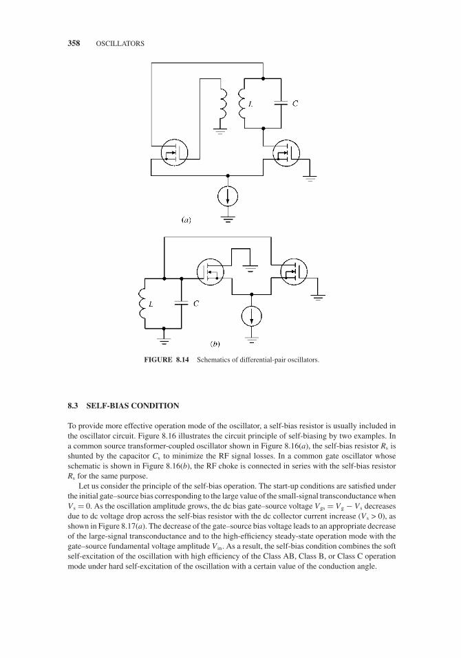
JWBS064-c08 JWBS064-Gerbennikov March 15, 2011 11:17 Printer Name: Yet to Come
358 OSCILLATORS
FIGURE 8.14 Schematics of differential-pair oscillators.
8.3 SELF-BIAS CONDITION
To provide more effective operation mode of the oscillator, a self-bias resistor is usually included inthe oscillator circuit. Figure 8.16 illustrates the circuit principle of self-biasing by two examples. Ina common source transformer-coupled oscillator shown in Figure 8.16(a), the self-bias resistor Rs isshunted by the capacitor Cs to minimize the RF signal losses. In a common gate oscillator whoseschematic is shown in Figure 8.16(b), the RF choke is connected in series with the self-bias resistorRs for the same purpose.
Let us consider the principle of the self-bias operation. The start-up conditions are satisfied underthe initial gate–source bias corresponding to the large value of the small-signal transconductance whenV s = 0. As the oscillation amplitude grows, the dc bias gate–source voltage Vgs = Vg − V s decreasesdue to dc voltage drop across the self-bias resistor with the dc collector current increase (V s > 0), asshown in Figure 8.17(a). The decrease of the gate–source bias voltage leads to an appropriate decreaseof the large-signal transconductance and to the high-efficiency steady-state operation mode with thegate–source fundamental voltage amplitude V in. As a result, the self-bias condition combines the softself-excitation of the oscillation with high efficiency of the Class AB, Class B, or Class C operationmode under hard self-excitation of the oscillation with a certain value of the conduction angle.

JWBS064-c08 JWBS064-Gerbennikov March 15, 2011 11:17 Printer Name: Yet to Come
SELF-BIAS CONDITION 359
FIGURE 8.15 Schematics of push–pull oscillators.
Using a piecewise-linear approximation of the device transfer characteristic, the dc drain currentI0 as a function of the input gate voltage amplitude V in can be determined by means of the conductionangle as
I0 = gmVinγ0 (θ) (8.20)
where gm is the device small-signal transconductance, γ 0(θ ) is the dc current coefficient, and
cos θ = − Vgs − Vp
Vin(8.21)
where 2θ is the conduction angle and Vp is the device pinch-off voltage.Substituting Eq. (8.21) into Eq. (8.20) allows us to obtain the relationship between gate–source
bias voltage Vgs and dc drain current I0 in the form
Vgs = Vp − I0
gm
cos θ
γ0 (θ). (8.22)

JWBS064-c08 JWBS064-Gerbennikov March 15, 2011 11:17 Printer Name: Yet to Come
360 OSCILLATORS
FIGURE 8.16 MOSFET oscillators with self-bias resistors.
On the other hand, a similar relationship can be written by
Vgs = Vg − I0 Rs. (8.23)
Figure 8.17(b) shows the graphical solution of a system of these two equations, where Eq. (8.22)with the conduction angle of 2θ = 360◦ is plotted by curve 1, Eq. (8.22) with the conduction angle of2θ < 180◦ is plotted by curve 2, and Eq. (8.23) is plotted by curve 3. The intersection of curve 3 withcurve 1 at the point A corresponds to the start-up oscillation mode, whereas the point B correspondsto the steady-state oscillation mode with constant amplitude. During the oscillation build-up, the dcdrain current increases by the value of �I0.
Consequently, during the process of self-oscillations build-up, the two separate processes occursimultaneously: the increase of the oscillation amplitude across the resonant circuit and the decreaseof the bias gate–source voltage due to the presence of the self-bias resistor Rs. Generally, both theseprocesses are interdependent. The velocity of the first process is defined by the time constant of theresonant circuit given by
T = Q
ω0(8.24)
where Q = ω0CRL is the oscillator quality factor at the resonant frequency ω0. The velocity of thesecond process is defined by the time constant of the self-bias circuit as
Ts = RsCs . (8.25)

JWBS064-c08 JWBS064-Gerbennikov March 15, 2011 11:17 Printer Name: Yet to Come
SELF-BIAS CONDITION 361
FIGURE 8.17 Self-bias operation.
If T s � T , the self-oscillations grow very rapidly, corresponding to the soft start-up condition forthe bias voltage of Vg − V s = Vg (V s = 0). The intersection of the oscillator amplitude characteristicI1(V in) with V s = 0 and feedback line provides the voltage amplitude across the resonant circuitcorresponding to point 1 shown in Figure 8.18(a). The dc drain current grows with the same velocity,resulting in the slow growth of the self-bias voltage Vs due to the slow transient response of the self-bias circuit. This process contributes to the gradual transition to the points 2 and then 3, characterized
FIGURE 8.18 Self-pulse modulation and self-modulation phenomena.
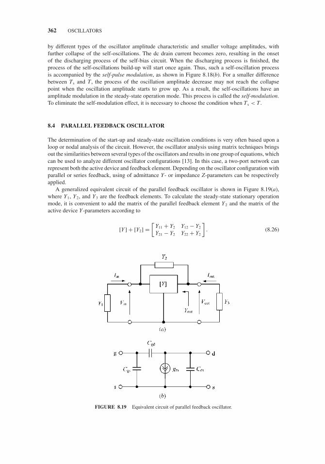
JWBS064-c08 JWBS064-Gerbennikov March 15, 2011 11:17 Printer Name: Yet to Come
362 OSCILLATORS
by different types of the oscillator amplitude characteristic and smaller voltage amplitudes, withfurther collapse of the self-oscillations. The dc drain current becomes zero, resulting in the onsetof the discharging process of the self-bias circuit. When the discharging process is finished, theprocess of the self-oscillations build-up will start once again. Thus, such a self-oscillation processis accompanied by the self-pulse modulation, as shown in Figure 8.18(b). For a smaller differencebetween T s and T , the process of the oscillation amplitude decrease may not reach the collapsepoint when the oscillation amplitude starts to grow up. As a result, the self-oscillations have anamplitude modulation in the steady-state operation mode. This process is called the self-modulation.To eliminate the self-modulation effect, it is necessary to choose the condition when T s < T .
8.4 PARALLEL FEEDBACK OSCILLATOR
The determination of the start-up and steady-state oscillation conditions is very often based upon aloop or nodal analysis of the circuit. However, the oscillator analysis using matrix techniques bringsout the similarities between several types of the oscillators and results in one group of equations, whichcan be used to analyze different oscillator configurations [13]. In this case, a two-port network canrepresent both the active device and feedback element. Depending on the oscillator configuration withparallel or series feedback, using of admittance Y- or impedance Z-parameters can be respectivelyapplied.
A generalized equivalent circuit of the parallel feedback oscillator is shown in Figure 8.19(a),where Y1, Y2, and Y3 are the feedback elements. To calculate the steady-state stationary operationmode, it is convenient to add the matrix of the parallel feedback element Y2 and the matrix of theactive device Y-parameters according to
[Y ] + [Y2] =[
Y11 + Y2 Y12 − Y2
Y21 − Y2 Y22 + Y2
]. (8.26)
FIGURE 8.19 Equivalent circuit of parallel feedback oscillator.
JWBS064-c08 JWBS064-Gerbennikov March 15, 2011 11:17 Printer Name: Yet to Come
PARALLEL FEEDBACK OSCILLATOR 363
In this case, a system of two equations for the two-port network input current I in, output currentIout, input voltage V in, and output voltage Vout can be written as
Iin = (Y12 + Y2) Vin + (Y12 − Y2) Vout (8.27)
Iout = (Y21 − Y2) Vin + (Y22 + Y2) Vout. (8.28)
Since, for the oscillator shown in Figure 8.19(a), the boundary conditions are obtained in the form
Iin = −Y1Vin (8.29)
Iout = −Y3Vout (8.30)
the following matrix equation can be written as
[Y11 + Y1 + Y2 Y12 − Y2
Y21 − Y2 Y22 + Y2 + Y3
] [Vin
Vout
]= 0. (8.31)
Thus, the steady-state stationary condition can be derived by equating determinant to zero,
∣∣∣∣ Y11 + Y1 + Y2 Y12 − Y2
Y21 − Y2 Y22 + Y2 + Y3
∣∣∣∣ = 0. (8.32)
After some simplification, Eq. (8.32) can be rewritten by
Y22 + Y2 + Y3 − (Y12 − Y2) (Y21 − Y2)
Y11 + Y1 + Y2= 0 (8.33)
As a result, the steady-state oscillation condition for the parallel feedback oscillator representedas a one-port negative conductance oscillator can be written as
Yout + YL = 0 (8.34)
where Y3 = YL, and
Yout = Y22 + Y2 − (Y12 − Y2) (Y21 − Y2)
Y11 + Y1 + Y2. (8.35)
Consequently, the separate equations for real and imaginary parts of the admittances for a negativeconductance oscillator, which are similar to Eqs. (8.3) and (8.4) for magnitude and phase of the loopgain of a parallel feedback oscillator corresponding to the steady-state oscillation process, can beobtained as
ReYout + ReYL = 0 (8.36)
ImYout + ImYL = 0. (8.37)
Similarly, the start-up conditions for the parallel feedback oscillator given by Eqs. (8.8) and (8.9)can be rewritten as
ReYout + ReYL < 0 (8.38)
ImYout + ImYL = 0. (8.39)
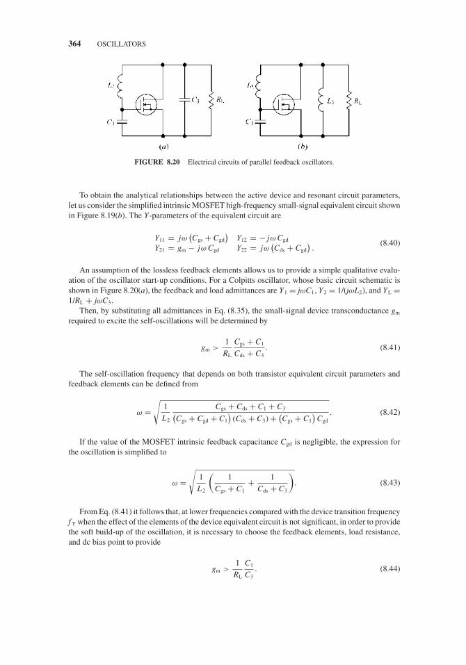
JWBS064-c08 JWBS064-Gerbennikov March 15, 2011 11:17 Printer Name: Yet to Come
364 OSCILLATORS
FIGURE 8.20 Electrical circuits of parallel feedback oscillators.
To obtain the analytical relationships between the active device and resonant circuit parameters,let us consider the simplified intrinsic MOSFET high-frequency small-signal equivalent circuit shownin Figure 8.19(b). The Y-parameters of the equivalent circuit are
Y11 = jω(Cgs + Cgd
)Y12 = − jω Cgd
Y21 = gm − jω Cgd Y22 = jω(Cds + Cgd
).
(8.40)
An assumption of the lossless feedback elements allows us to provide a simple qualitative evalu-ation of the oscillator start-up conditions. For a Colpitts oscillator, whose basic circuit schematic isshown in Figure 8.20(a), the feedback and load admittances are Y1 = jωC1, Y2 = 1/(jωL2), and YL =1/RL + jωC3.
Then, by substituting all admittances in Eq. (8.35), the small-signal device transconductance gm
required to excite the self-oscillations will be determined by
gm >1
RL
Cgs + C1
Cds + C3. (8.41)
The self-oscillation frequency that depends on both transistor equivalent circuit parameters andfeedback elements can be defined from
ω =√
1
L2
Cgs + Cds + C1 + C3(Cgs + Cgd + C1
)(Cds + C3) + (
Cgs + C1
)Cgd
. (8.42)
If the value of the MOSFET intrinsic feedback capacitance Cgd is negligible, the expression forthe oscillation is simplified to
ω =√
1
L2
(1
Cgs + C1+ 1
Cds + C3
). (8.43)
From Eq. (8.41) it follows that, at lower frequencies compared with the device transition frequencyf T when the effect of the elements of the device equivalent circuit is not significant, in order to providethe soft build-up of the oscillation, it is necessary to choose the feedback elements, load resistance,and dc bias point to provide
gm >1
RL
C1
C3. (8.44)

JWBS064-c08 JWBS064-Gerbennikov March 15, 2011 11:17 Printer Name: Yet to Come
SERIES FEEDBACK OSCILLATOR 365
Because it was assumed that the value of the feedback susceptance B3 = ImY3 is positive,consequently, to satisfy the start-up and steady-state oscillation conditions, it is necessary to use thecapacitance C3. By rewriting Eq. (8.43) as
B3 = ω
(Cgs + C1
ω2L2
(Cgs + C1
) − 1− Cds
)(8.45)
it is easy to show that when
L2 <1
ω2(Cgs + C1
) (8.46)
then the value of B3 becomes negative. This means that such an oscillator feedback element must beinductive with the value of L3 = −1/(ωB3). The circuit configuration for this oscillator is shown inFigure 8.20(b).
8.5 SERIES FEEDBACK OSCILLATOR
A generalized equivalent circuit of the series feedback oscillator is shown in Figure 8.21(a), where Z1,Z2, and Z3 are the feedback elements. To calculate the steady-state operation mode, it is convenientto add the matrix of the series feedback element Z2 and the matrix of the active device Z-parametersaccording to
[Z ] + [Z2] =[
Z11 + Z2 Z12 + Z2
Z21 + Z2 Z22 + Z2
]. (8.47)
FIGURE 8.21 Equivalent circuits of series feedback oscillator.

JWBS064-c08 JWBS064-Gerbennikov March 15, 2011 11:17 Printer Name: Yet to Come
366 OSCILLATORS
In this case, a system of two equations for the two-port network input current Iin, output currentIout, input voltage V in, and output voltage Vout can be written as
Vin = (Z12 + Z2) Iin + (Z12 + Z2) Iout (8.48)
Vout = (Z21 + Z2) Iin + (Z22 + Z2) Iout. (8.49)
Since, for the oscillator shown in Figure 8.21(a), the boundary conditions are obtained in the form
Vin = −Z1 Iin (8.50)
Vout = −Z3 Iout (8.51)
the following matrix equation can be written as
[Z11 + Z1 + Z2 Z12 + Z2
Z21 + Z2 Z22 + Z2 + Z3
] [Iin
Iout
]= 0. (8.52)
Thus, the steady-state oscillation condition can be expressed by
∣∣∣∣ Z11 + Z1 + Z2 Z12 + Z2
Z21 + Z2 Z22 + Z2 + Z3
∣∣∣∣ = 0. (8.53)
After some simplifications, Eq. (8.53) can be rewritten as
Z22 + Z2 + Z3 − (Z12 + Z2) (Z21 + Z2)
Z11 + Z1 + Z2= 0. (8.54)
As a result, the steady-state oscillation condition for the series feedback oscillator represented asa one-port negative resistance oscillator can be written as
Zout + ZL = 0 (8.55)
where Z3 = ZL, and
Zout = Z22 + Z2 − (Z12 + Z2) (Z21 + Z2)
Z11 + Z1 + Z2. (8.56)
Consequently, the separate equations for real and imaginary parts of the negative resistanceoscillator, which are similar to Eqs. (8.36) and (8.37) for the parallel feedback oscillator correspondingto the steady-state oscillation process, can be obtained by
ReZout + ReZL = 0 (8.57)
ImZout + ImZL = 0. (8.58)
Similarly, the start-up conditions for the series feedback oscillator can be rewritten as
ReZout + ReZL < 0 (8.59)
ImZout + ImZL = 0. (8.60)
Let us obtain the analytical relationships between the active device and resonant circuit parametersof the oscillator based on the MOSFET device, the admittance Y-parameters of the equivalent circuit

JWBS064-c08 JWBS064-Gerbennikov March 15, 2011 11:17 Printer Name: Yet to Come
SERIES FEEDBACK OSCILLATOR 367
of which are given by Eq. (8.40). The ratios between admittance Y-parameters and impedanceZ-parameters can be expressed in the form
Z11 = Y22
�YZ12 = − Y12
�YZ21 = − Y21
�YZ22 = Y11
�Y. (8.61)
Then, the steady-state condition for the series feedback oscillator can be written as
1 + Z2 (Y11 + Y12 + Y21 + Y22) + Z1 (Y11 + Z2�Y )
Y22 + (Z1 + Z2) �Y+ Z3 = 0 (8.62)
where �Y = 1/�Z and �Y = Y11Y22 − Y12Y21. For a simple oscillator circuit configuration withexternal gate inductance shown in Figure 8.21(b), the feedback elements including load are definedas Z1 = jωL1, Z2 = 1/jωC2, and Z3 = RL.
Usually, in a wide frequency range up to 0.3f T, it is possible to neglect the intrinsic gate–draincapacitance Cgd without the substantial loss of accuracy. Then, the small-signal transconductance gm
corresponding to the soft start-up condition and the frequency of the self-oscillations can be evaluated,respectively, by
gm > Cgs RL(ωCds)
2
Cds + C2(8.63)
ω =√
1
L1
(1
Cgs+ 1
Cds + C2
). (8.64)
From Eq. (8.63) it follows that the oscillation build-up can be easily provided by choosing theMOSFET device with the smaller drain–source capacitance Cds and using a sufficiently large valueof the feedback capacitance C2.
In a common case, different sets of two-port network parameters can be used for oscillator designincluding impedance Z-parameters, admittance Y-parameters, or scattering S-parameters. The choiceof any type of these parameters depends on the operating frequency, required design accuracy andimplementation technique, availability of the small- or large-signal active device parameters, or thepossibility of using proper measurement and simulation tools. For example, in terms of one-portnegative resistance approach, the conditions for self-oscillations expressed through the small-signalS-parameters can be written as
K = 1 + |�|2 − |S11|2 − |S22|22 |S12 S21| < 1 (8.65)
inS = 1 (8.66)
outL = 1 (8.67)
where K is the stability factor, � = S11S22 − S12S21, in and S are the input and source reflectioncoefficients, out and L are the output and load reflection coefficients, respectively [14]. The stabilityfactor should be less than unity for any possibility of self-oscillations. The passive terminations S
and L must be added to resonate input and output ports at the oscillation frequency. It should benoted that the conditions described by Eqs. (8.66) and (8.67) are inter-related, and if one conditionis satisfied, then the other condition should be satisfied as well. The large-signal S-parameters of thetransistor optimized for maximum output power can be measured by varying the input drive level andload impedance, or injecting signal into the output port [15]. By using the measured S-parameters,the required ratios of terminal voltages and currents can be calculated.
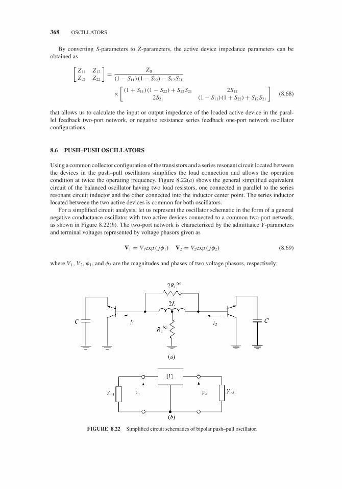
JWBS064-c08 JWBS064-Gerbennikov March 15, 2011 11:17 Printer Name: Yet to Come
368 OSCILLATORS
By converting S-parameters to Z-parameters, the active device impedance parameters can beobtained as
[Z11 Z12
Z21 Z22
]= Z0
(1 − S11) (1 − S22) − S12S21
×[
(1 + S11) (1 − S22) + S12S21 2S12
2S21 (1 − S11) (1 + S22) + S12S21
](8.68)
that allows us to calculate the input or output impedance of the loaded active device in the paral-lel feedback two-port network, or negative resistance series feedback one-port network oscillatorconfigurations.
8.6 PUSH–PUSH OSCILLATORS
Using a common collector configuration of the transistors and a series resonant circuit located betweenthe devices in the push–pull oscillators simplifies the load connection and allows the operationcondition at twice the operating frequency. Figure 8.22(a) shows the general simplified equivalentcircuit of the balanced oscillator having two load resistors, one connected in parallel to the seriesresonant circuit inductor and the other connected into the inductor center point. The series inductorlocated between the two active devices is common for both oscillators.
For a simplified circuit analysis, let us represent the oscillator schematic in the form of a generalnegative conductance oscillator with two active devices connected to a common two-port network,as shown in Figure 8.22(b). The two-port network is characterized by the admittance Y-parametersand terminal voltages represented by voltage phasors given as
V1 = V1exp ( jφ1) V2 = V2exp ( jφ2) (8.69)
where V1, V2, φ1, and φ2 are the magnitudes and phases of two voltage phasors, respectively.
FIGURE 8.22 Simplified circuit schematics of bipolar push–pull oscillator.

JWBS064-c08 JWBS064-Gerbennikov March 15, 2011 11:17 Printer Name: Yet to Come
PUSH–PUSH OSCILLATORS 369
The relationships between the circuit currents and voltages in a steady-state operation modethrough the admittance parameters in a matrix form can be written by[ −Yin1 V1
−Yin2 V2
]=
[Y11 Y12
Y21 Y22
] [V1
V2
](8.70)
where Y in1 and Y in2 represent the input admittances of the negative conductance devices.Since the oscillator consists of two identical nonlinear active halves when V1 = V2 = V and V in1 =
V in2 = V in and symmetrical passive linear two-port network when Y11 = Y22 and Y12 = Y21, matrixEq. (8.70) can be rewritten in the form of two equations as
−Yin = Y11 + Y12 exp ( jφ) (8.71)
−Yin = Y12 exp (− jφ) + Y11 (8.72)
where φ = φ2 − φ1 is the phase difference between voltage phasors.Simplified analysis of the steady-state operation modes shows that, in such a balanced oscillator,
there may exist two modes with equal amplitudes [2,16]:
� odd mode with
φ = (2k + 1)π where k = 0, 1, 2, . . .
� even mode with
φ = 2 kπ where k = 0, 1, 2, . . . .
The frequency and amplitude of each of the two oscillation modes can be determined by solvingthe following equation:
Yin (V ,ω) + Y11 (ω) ± Y12 (ω) = 0. (8.73)
In a time domain, assuming symmetrical current waveforms flowing into the base of both transis-tors, their Fourier series expansions in a common case can be written by
i1 = I (1)1 cos ωt + I (1)
2 cos 2ωt + I (1)3 cos 3ωt + · · · + I (1)
n cos nωt (8.74)
i2 = I 2)1 cos (ωt + φ) + I (2)
2 cos 2 (ωt + φ) + I (2)3 cos 3 (ωt + φ) + · · · + I (2)
n cos n (ωt + φ)
(8.75)
where n is the harmonic number.Consequently, in the odd mode, the currents are flowing in opposite directions providing a
push–pull operation of both transistors having 180◦ out-of-phase base–emitter voltages. In this case,the circuit becomes antimetric and, at its center point, a virtual ground will be formed at the funda-mental frequency f 0 with zero fundamental voltage at this point. The output current flowing into theload 2R(o)
L is a result of the out-of-phase summation of currents given by Eqs. (8.74) and (8.75) as
i (o) = 2I1 cos ωt + 2I3 cos 3ωt + · · · + 2I2k+1 cos (2k + 1) ωt (8.76)
which contains only odd current components, and there are no odd components flowing into theload RL
(e). At the same time, the output current flowing into the load RL(e) is a result of the in-phase
summation of currents as
i (e) = 2I2 cos 2ωt + 2I4 cos 4ωt + · · · + 2I2k cos 2kωt (8.77)
which contains only even current components.

JWBS064-c08 JWBS064-Gerbennikov March 15, 2011 11:17 Printer Name: Yet to Come
370 OSCILLATORS
FIGURE 8.23 Equivalent oscillator circuits with (a) odd and (b) even modes.
In the even mode, the currents are flowing in the same direction providing a push–push operationof both transistors having in-phase base–emitter voltages. In this case, the circuit becomes symmetricwith a load resistor R(e)
L at the center of symmetry. For such an operation, the odd current componentsobtained by Eq. (8.76) will flow to this load, whereas the even components obtained by Eq. (8.77)will be dissipated at the load 2R(o)
L .The equivalent circuits of the oscillator under odd and even operation modes are shown in
Figure 8.23. For oscillations to occur in the odd mode, the negative conductance generated by theoscillator, whose schematic is shown in Figure 8.23(a), should exceed the resistive losses in theresonant circuit, that is
ReYin + ReY (o)L < 0. (8.78)
For oscillations to occur in the even mode, the negative resistance generated by the oscillator,whose schematic is shown in Figure 8.23(b), should exceed the resistive losses in such a resonantcircuit according to
ReZ in + ReZ (e)L < 0. (8.79)
Generally, both odd and even operation modes can exist in the oscillator simultaneously dependingon the values of the load resistances R(o)
L and R(e)L . Under a start-up condition given by Eq. (8.78), the
even mode will be stable for the case of R(o)L = ∞ corresponding to the situation of the summation of
the output powers of individual oscillators with resistive coupling [17]. A simplified criterion of theodd mode stable operation for the oscillator circuit shown in Figure 8.22(a) can be obtained as
R(o)L <
2R(e)L
1 +(
ωL
2R(e)L
)2 (8.80)

JWBS064-c08 JWBS064-Gerbennikov March 15, 2011 11:17 Printer Name: Yet to Come
PUSH–PUSH OSCILLATORS 371
FIGURE 8.24 Simplified circuit schematics of bipolar push–push oscillator.
when the odd components will flow into the load 2R(o)L , while the even components will dissipate at
the load R(e)L . To improve stability of the odd operation mode, it is necessary to inhibit the oscillation
condition given by Eq. (8.79).Such a balanced oscillator configuration with a series resonant circuit creates a simple opportunity
to double the oscillation frequency when each half-circuit oscillates at the resonant frequency f 0,while the output signal at the load oscillates at the frequency 2f 0. In this case, it is necessary toprovide stable operation in the odd mode and to inhibit the oscillations in the even mode by removingthe load resistor R(o)
L . This results in the oscillator circuit configuration shown in Figure 8.24, wherethe variable capacitors Cv can be used for frequency tuning. For a lossless tank inductor L, the start-upamplitude oscillation conditions can be rewritten as
ReZ in < 0 (8.81)
ReZ in + 2RL > 0 (8.82)
when the even harmonic components dissipate at the load RL. A significant margin in negativeresistance can be achieved compared with an equivalent single-ended oscillator, even at very highfrequencies [18]. The outputs for the out-of-phase odd components can be connected to the deviceemitters. Because, for the even output current components, the transistors are operated in phase, it iscalled the push–push operation mode. A push–push operation is the inverse to a push–pull operation,in that the load is either conductively or capacitively coupled to the center point of inductor ortransmission line located between the bases (gates) of the active devices [19,20]. In this case, thecurrents flow into the load in the same direction during both half periods or 180◦ phases of the active

JWBS064-c08 JWBS064-Gerbennikov March 15, 2011 11:17 Printer Name: Yet to Come
372 OSCILLATORS
FIGURE 8.25 Push–push and balanced microstrip oscillator configurations.
device operation. Since there are two 180◦ phases during each cycle, the circuit acts as a frequencydoubler. Such a push–push oscillator is a result of its odd operation mode with virtual ground;therefore, ideally this design is independent of the output load pulling compared to a fundamentaloscillator approach.
At microwaves, the resonant circuits usually incorporate the transmission lines as inductive el-ements or resonators. Figure 8.25 shows the push–push oscillator using half wavelength or λ/2microstrip resonator [21]. For the fundamental frequency f 0, this resonator has a null point at thecenter of microstrip line, being a point of the oscillator symmetry, which is considered as a virtualground or short-circuited point. In this case, the resonance voltage has maximum values at bothends of the resonator with a phase difference of 180◦, and the resonance voltage is zero at the centerof the resonator. For the desired second-harmonic frequency 2f 0, such a point could be consideredas an open-circuited point. The null point is an ideal output port to combine the second-harmonicsignals from both active devices effectively. To compromise the maximum second-harmonic outputsignal and significant harmonic suppression, a sufficiently small series capacitor is usually used. Theoperating bias points with zero gate voltages can provide nonlinear operation of the used high electronmobility transistor (HEMT) devices generating a high-power second-harmonic signal. The impedanceof half-wavelength microstrip open-circuited resonator is optimized to make the impedance of theoutput port close to 50 �. For such a microwave push–push oscillator using two Fujitsu FHX35LGdevices, a maximum power of 8.4 dBm at the second-harmonic frequency of 21.68 GHz with thefundamental frequency suppression of 26 dB was achieved.
8.7 STABILITY OF SELF-OSCILLATIONS
Applying dc bias to the active device does not generally result in the negative resistance or properfeedback condition. This condition has to be induced in these devices, and it is determined by thephysical mechanism in the device and chosen circuit topology. The transistor in the oscillator circuitsis mostly represented as the active two-port network, whose operation principle is reflected throughits equivalent circuit. The influence of the circuit and transistor parameters can result in the hysteresiseffect or oscillation instability in practical design. In high-frequency practical implementation, thepresence of the parasitic device and circuit elements can contribute to the multiresonant circuits.
A steady-state free-running oscillation build-up is provided with the velocity due to dissipationfactor δ = [Rout(I) + RL]/L for a single series resonant circuit with an inductance L and δ = [Gout(V) +
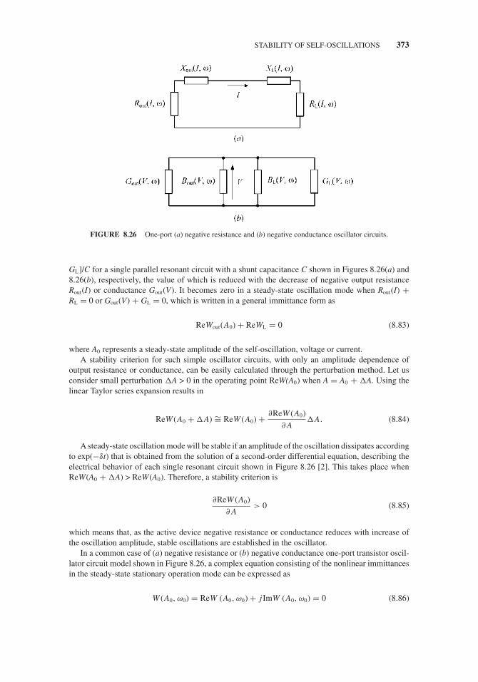
JWBS064-c08 JWBS064-Gerbennikov March 15, 2011 11:17 Printer Name: Yet to Come
STABILITY OF SELF-OSCILLATIONS 373
FIGURE 8.26 One-port (a) negative resistance and (b) negative conductance oscillator circuits.
GL]/C for a single parallel resonant circuit with a shunt capacitance C shown in Figures 8.26(a) and8.26(b), respectively, the value of which is reduced with the decrease of negative output resistanceRout(I) or conductance Gout(V). It becomes zero in a steady-state oscillation mode when Rout(I) +RL = 0 or Gout(V) + GL = 0, which is written in a general immittance form as
ReWout(A0) + ReWL = 0 (8.83)
where A0 represents a steady-state amplitude of the self-oscillation, voltage or current.A stability criterion for such simple oscillator circuits, with only an amplitude dependence of
output resistance or conductance, can be easily calculated through the perturbation method. Let usconsider small perturbation �A > 0 in the operating point ReW(A0) when A = A0 + �A. Using thelinear Taylor series expansion results in
ReW (A0 + �A) ∼= ReW (A0) + ∂ReW (A0)
∂ A�A. (8.84)
A steady-state oscillation mode will be stable if an amplitude of the oscillation dissipates accordingto exp(−δt) that is obtained from the solution of a second-order differential equation, describing theelectrical behavior of each single resonant circuit shown in Figure 8.26 [2]. This takes place whenReW(A0 + �A) > ReW(A0). Therefore, a stability criterion is
∂ReW (A0)
∂ A> 0 (8.85)
which means that, as the active device negative resistance or conductance reduces with increase ofthe oscillation amplitude, stable oscillations are established in the oscillator.
In a common case of (a) negative resistance or (b) negative conductance one-port transistor oscil-lator circuit model shown in Figure 8.26, a complex equation consisting of the nonlinear immittancesin the steady-state stationary operation mode can be expressed as
W (A0, ω0) = ReW (A0, ω0) + j ImW (A0, ω0) = 0 (8.86)

JWBS064-c08 JWBS064-Gerbennikov March 15, 2011 11:17 Printer Name: Yet to Come
374 OSCILLATORS
where
ReW (A0, ω0) = ReWout (A0, ω0) + ReWL (A0, ω0) (8.87)
ImW (A0, ω0) = ImWout (A0, ω0) + ImWL (A0, ω0) . (8.88)
Assuming a solution of Eq. (8.86) as a(t) = A0 cosω0 t or a(t) = A0Re[exp(jω0 t)], one can findthe amplitude A0 and frequency ω0 of free-running oscillations. Then, consider the small perturbationfrom the steady-state stationary mode when the amplitude and frequency of the oscillation are turnedout to be A = A0 + �A and ω = ω0 + �ω, respectively, where �A A0 and �ω ω0. Underconditions of small perturbations from the steady-state mode, a nonlinear system behaves as linear,and amplitude of the oscillation dissipates exponentially. Therefore, the expected solution can bewritten as
a(t) = (A0 + �A) exp (−�δt) cos (ω0 + �ω) t (8.89)
or
a(t) = (A0 + �A) Re[exp j (ω0 + �ω + j�δ) t
]. (8.90)
According to Eq. (8.90), the steady-state oscillation condition in the form of Eq. (8.86) can berewritten as
ReW (A0 + �A, ω0 + �ω + j�δ) + j ImW (A0 + �A, ω0 + �ω + j�δ) = 0. (8.91)
By applying the linear Taylor series expansion of Eq. (8.91) by degrees of the small parameters�A, �ω, and �δ for each components and replacing one complex equation with two equations forreal and imaginary parts, the following system of two equations in consideration of Eq. (8.86) can bewritten:
∂ReW
∂ A�A + ∂ReW
∂ω�ω + ∂ReW
∂δ�δ = 0 (8.92)
∂ImW
∂ A�A + ∂ImW
∂ω�ω + ∂ImW
∂δ�δ = 0. (8.93)
It is known that for analytic function W(ω + j�δ) = ReW(ω, �δ) + jImW(ω, �δ), theCauchy–Riemann equations can be written as
∂ReW
∂ω= ∂ImW
∂δ(8.94)
∂ReW
∂δ= −∂ImW
∂ω. (8.95)
Then, excluding �ω from Eqs. (8.92) and (8.93) and using Eqs. (8.94) and (8.95) result in
�δ
�A=
∂ReW
∂ A
∂ImW
∂ω− ∂ImW
∂ A
∂ReW
∂ω(∂ReW
∂ω
)2
+(
∂ImW
∂ω
)2 . (8.96)

JWBS064-c08 JWBS064-Gerbennikov March 15, 2011 11:17 Printer Name: Yet to Come
STABILITY OF SELF-OSCILLATIONS 375
FIGURE 8.27 Parallel feedback (a) electrical and (b) equivalent oscillator circuits.
The steady-state stationary mode will be stable if a small perturbation of the oscillation amplitude�A dissipates in time and the values �A and �δ have the same signs. Thus, the stable oscillationsare established in the oscillator if
∂ReW
∂ A
∂ImW
∂ω− ∂ImW
∂ A
∂ReW
∂ω> 0 (8.97)
which corresponds in terms of immittance parameters to a general form of a stability conditionobtained by Kurokawa [22].
Figure 8.27 shows (a) the electrical and (b) the equivalent circuits of the parallel feedback negativeresistance oscillator with a common collector. In this case, a transistor has been configured and biasedso that the output resistance is negative. The capacitors C1 and C2 are used to increase a regenerationfactor and to provide steady-state oscillation conditions of the amplitude and phase.
In this series circuit configuration with the negative imaginary part of output transistor impedance,the load is constant and the negative output resistance Rout = ReZout(I, ω) decreases with increase ofthe oscillation frequency. As a result,
∂ X
∂ω= ∂
∂ω
(ωL − 1
ωCout
)= L + 1
ω2Cout> 0 (8.98)
and
∂ R
∂ω= ∂
∂ω(Rout + RL) = ∂ Rout
∂ω> 0. (8.99)
Consequently, by taking into account Eq. (8.97), to obtain stable oscillations in a steady-stateoperation mode, it is required to satisfy the following sufficient conditions for the series resonantcircuit negative resistance oscillator with constant load:
∂ Rout
∂ I> 0
∂ Xout
∂ I< 0. (8.100)

JWBS064-c08 JWBS064-Gerbennikov March 15, 2011 11:17 Printer Name: Yet to Come
376 OSCILLATORS
8.8 OPTIMUM DESIGN TECHNIQUES
8.8.1 Empirical Approach
For optimum oscillator design with maximum output power, generally it is required extensive small-and large-signal measurements. The small-signal S-parameter measurements can be made at severalfrequencies, along with estimated device equivalent circuit parameters, including package para-sitics. Then, a computer optimization program is used to match the measured S-parameters to theS-parameters computed for the active device from its equivalent circuit. The next step is to varythose elements of the equivalent circuit, which can vary under large signals. By varying the activedevice nonlinear equivalent circuit parameters, the set of large-signal S-parameters can be obtainedcorresponding to the saturation condition where maximum oscillator output power can be achieved.
The simplified design approach assumes that all of the S-parameters except the magnitude ofS21 are constant under large signals. For example, for a metal-semiconductor field-effect transistor(MESFET) device up to saturation with small limitation in accuracy, it is possible to derive the large-signal behavior of the main device nonlinear elements as functions of the device transconductance gm
[23]. Consequently, the S-parameters become functions of gm only and, at each incremental reductionof gm, are recomputed and optimized along with power gain. If one were interested in the 1-dBcompression point, the S-parameters used would be those at that point.
For a common source (emitter) power oscillator, it is helpful to characterize the maximum powerthrough the saturated output power Psat and small-signal transducer power gain GT of the correspond-ing power amplifier. An empirical expression for output power of a common source MESFET poweramplifier can be written by
Pout = Psat
[1 − exp
(− GT Pin
Psat
)](8.101)
where Pin is the input power [23].The objective is to maximize the oscillator output power Posc = Pout − Pin by providing a condition
dPosc
dPin= d (Pout − Pin)
dPin= 0. (8.102)
Substituting Eq. (8.101) into Eq. (8.102) yields
dPout
dPin= GTexp
(− GT Pin
Psat
)= 1. (8.103)
From Eq. (8.103) it follows that
exp
(GT Pin
Psat
)= GT (8.104)
or
Pin
Psat= ln GT
GT. (8.105)
As a result,
Pout = Psat
(1 − 1
GT
)(8.106)

JWBS064-c08 JWBS064-Gerbennikov March 15, 2011 11:17 Printer Name: Yet to Come
OPTIMUM DESIGN TECHNIQUES 377
and the maximum output power of the oscillator can be approximated by
Posc = Psat
(1 − 1
GT− ln GT
GT
). (8.107)
Consequently, the oscillator maximum power can be predicted from the saturated power andsmall-signal transducer power gain of a common source power amplifier. From Eq. (8.107) it followsthat the oscillator output power Posc will approach Psat at low frequencies where the small-signaltransducer power gain GT is large. As the transducer power gain approaches unity, the oscillatoroutput power approaches zero.
In this case, the maximum efficiency power gain GME can be calculated from
GME = GT − 1
ln GT. (8.108)
For example, a MESFET device, which is characterized by the small-signal transducer power gainGT = 7.5 dB and saturated amplifier output power of 1 W, would be capable of a maximum oscillatorpower of 515 mW. The maximum efficiency power gain at this point calculated from Eq. (8.108) isequal to GME = 4.3 dB. The expression for maximum efficiency power gain GME given by Eq. (8.108)can be used to determine at what gain level the large-signal S-parameters were to be used for optimumoscillator design.
A quasilinear design approach based on the measured small-signal S-parameters and static outputvoltage–ampere device characteristic can be used to predict the oscillator output power [24]. However,this method assumes that the significant nonlinear effects in GaAs MESFET represent the rapidincrease in the gate–source conductance due to the forward-biasing effect of the gate–source Schottkydiode and output drain–source conductance [25]. To maximize the output power of a series feedbackMESFET oscillator, an analytic procedure was derived using the input and output fundamentalvoltages as independent variables. The systematic approach to oscillator design using large-signalS-parameters, which may be measured under high drive conditions or obtained through the use of anactive device nonlinear model, represents an alternative method [26]. The device can be modeled in aquasilinear approximation by its large-signal S-parameters, each assumed to be a function of a singlevariable when S11 and S21 are the functions of the input fundamental voltage amplitude, whereas S12
and S22 are the functions of the output fundamental voltage amplitude. As a result, the set of fourequations describes the oscillation condition that requires standard computer-based nonlinear root-finding methods to determine the optimum feedback parameters providing a delivery of maximumoutput power into the load.
A technique for the design of microwave transistor oscillator, in which measurements made on anexperimentally optimized power amplifier, has been presented in [15]. Generally, the transistor poweramplifier is easily analyzed and optimized than the corresponding oscillator because, in quasilinearapproximation at a given frequency and bias point, only two parameters need to be varied: the inputRF drive level and the output load impedance. Once these parameters are experimentally optimized,measuring the input impedance and constructing an input matching circuit complete the design. In thecase of the transistor oscillator, however, there are a multitude of possible oscillator configurationsand a large number of interacting circuit elements, which must be varied to optimize an oscillatorfor maximum power. But since we know that a transistor operates under the same set of RF voltagesand currents when delivering its maximum output power, it is possible to take information obtainedfrom an easily optimized power amplifier and use this information to calculate optimum oscillatorconfigurations.
The first step in this procedure is to experimentally optimize the large-signal behavior of thetransistor by varying the load impedance and drive level for the maximum output power delivered

JWBS064-c08 JWBS064-Gerbennikov March 15, 2011 11:17 Printer Name: Yet to Come
378 OSCILLATORS
into the load. The incident and reflected waves a1, b1, a2, and b2 shown in Figure 8.28 can be measuredwith calculation of the output power delivered into the load according to
PL = |b2|2(
1 − 1∣∣S′22
∣∣2 − 1 − ∣∣S′11
∣∣2∣∣S′21
∣∣2
)(8.109)
where
S′11 = b1
a1S′
22 = b2
a2S′
21 = b2
a1
S′11 is the input reflection coefficient 1 and S′
22 is the output reflection coefficient 2 [14].Using these three measured parameters S′
11,S′21, and S′
22, it is then possible to calculate the requiredratios of the transistor terminal voltages and currents
V2
V1=
S′21
(1
S′22
+ 1
)1 + S′
11
(8.110)
I2
I1=
S′21
(1
S′22
− 1
)1 − S′
11
(8.111)
V1
I1= RS
1 + S′11
1 − S′11
(8.112)
V2
I1= RS
S′21
(1
S′22
+ 1
)1 − S′
11
(8.113)
I2
V1= 1
RS
S′21
(1
S′22
− 1
)1 + S′
11
(8.114)
where V1 and I1 are the transistor input port voltage and current, V2 and I2 are the transistor outputport voltage and current, and RS is the source resistance considered as the characteristic impedanceof the measuring system, as shown in Figure 8.28.
FIGURE 8.28 Power amplifier schematic to be experimentally optimized.

JWBS064-c08 JWBS064-Gerbennikov March 15, 2011 11:17 Printer Name: Yet to Come
OPTIMUM DESIGN TECHNIQUES 379
8.8.2 Analytic Approach
Depending on a type of the transistor used, operating frequencies, required output power and spectralcharacteristics, most of the oscillator schematics can be reduced to the two basic arrangements withexternal positive parallel or series feedback shown in Figures 8.29(a) and 8.29(b), respectively. Onemodel may be preferred over another, depending on the oscillator configuration and characteristics.The two-port network representing an active device can be generally characterized by a system ofimmittance W-parameters. This describes parameter systems of a two-port network, such as a systemof admittance Y-parameters for parallel feedback or a system of impedance Z-parameters for seriesfeedback oscillator circuits, respectively. The oscillator circuit and the output load are characterizedby immittances W1, W2, and W3 = WL, respectively.
Then, the steady-state oscillation condition for a single frequency of oscillation can be expressed as
Wout + WL = 0 (8.115)
where the active two-port network, together with the feedback elements W1 and W2, will beconsidered as a one-port negative resistance oscillator circuit.
To optimize the oscillator circuit in terms of the maximum value of the negative real part of theequivalent one-port network output immittance, the expression for output immittance Wout should bewritten as
Wout = W22 + W2 − (W12 ∓ W2) (W21 ∓ W2)
W11 + W1 + W2(8.116)
where the minus signs in the factors correspond to output admittance of the circuit shown in Fig-ure 8.29(a) and the plus signs correspond to the output impedance of the circuit shown inFigure 8.29(b). Such an optimization approach was first applied to a bipolar transformer-coupledoscillator to define maximum output power [27]. Later it was used to determine optimum feedbackelements with reference to a series feedback MESFET oscillator using a simplified device equivalentcircuit without the intrinsic feedback gate–drain capacitance [28].
It is convenient to represent this optimum approach in a general form regardless of the type of theactive device, for commonly used parallel and series feedback oscillators [2,29]. The first step in thedesign is to determine the optimum combination of the values of the feedback reactive elements ImW1
and ImW2, which maximize the absolute value of the real part of the output immittance ReWout atthe desired frequency of oscillation. Such a condition will permit to obtain self-sustained oscillationswith the largest amplitude that implies maximum output power delivered to the load [30]. Analyzing
FIGURE 8.29 Two-port oscillator circuits with (a) parallel and (b) series feedback.
JWBS064-c08 JWBS064-Gerbennikov March 15, 2011 11:17 Printer Name: Yet to Come
380 OSCILLATORS
Eq. (8.116) in extremum, we can find the optimum values ImW o1 and ImW o
2 , at which the negativevalue ReWout is maximal, by solving
∂ ReWout
∂ ImW1= 0
∂ ReWout
∂ ImW2= 0. (8.117)
As a result, the optimum values ImW o1 and ImW o
2 depend on the immittance parameters of theactive device two-port network according to
ImW o1 = ∓Re (W21 − W12)
Im (W21 − W12)
[Re (W12 + W21)
2± Re (W11 + W1)
]− ImW11 ∓ Im (W12 + W21)
2
(8.118)
ImW o2 = ±Re (W21 + W12 ∓ 2W2) Re (W21 − W12)
2Im (W21 − W12)± Im (W12 + W21)
2. (8.119)
The next step is to determine the optimum load immittance WL in a steady-state operation modedefined by Eq. (8.115). By substituting expressions for ImW o
1 and ImW o2 into Eq. (8.116), the optimum
real and imaginary parts of the output immittance W oout will be respectively defined by
ReW oout = ReW22 + ReW2 − Re2 (W12 + W21 ∓ 2W1) + Im2 (W21 − W12)
4Re (W11 + W1 + W2)(8.120)
ImW oout = ImW22 + ImW o
2 − Re (W21 − W12)
Im (W21 − W12)Re
(W o
out − W22 − W2
). (8.121)
In a large-signal operation mode, all immittance parameters generally become the functions of thevoltage amplitudes across the elements of the device equivalent circuit. For the negative resistance(conductance) one-port oscillators shown in Figure 8.29, the output power can be written as Pout =V 2Gout(V)/2 in terms of Y-parameters or Pout = I2Rout(I)/2 in terms of Z-parameters, where V isvoltage amplitude across the load resistance and I is the amplitude of the output current flowing intothe load. Since, for the same output voltage or current amplitude, the combination of the optimumfeedback parameters obtained by Eqs. (8.118) and (8.119) provides a maximum negative real partof the output immittance according Eq. (8.120), then the maximum power will be delivered to theload. Thus, such an analytic approach presumes that, once the nonlinear model of the active device isdeveloped, the elements of the optimum feedback parameters and the load can be easily and explicitlycalculated under both the small-signal and large-signal conditions corresponding to the start-up andsteady-state operation modes, respectively.
An analytical evaluation of the start-up and steady-state oscillation conditions for a bipolaroscillator can be done using a simplified transistor equivalent circuit shown in Figure 8.30 [2]. In thiscase, the parasitic lead inductances and resistances can be considered amongst the external feedbackcircuit. The typical condition rπ � 1/(ωCπ ) simplifies the analytical calculations substantially withouta significant decrease in accuracy at high frequencies. Let us consider the transistor parasitic leadinductances Lb, Le, and Lc among the external feedback elements Z1, Z2, and ZL, respectively. Inaddition, loss in the feedback elements should be taken into account in elements rb and re.
As a result, the optimum values of imaginary parts of the feedback elements X o1 and X o
2 , expressedthrough the parameters of the bipolar transistor equivalent circuit, can be calculated from
X o1 = 1
2ωCc− rb
ω
ωT(8.122)
X o2 = − 1
2ωC c− re
ω
ωT. (8.123)
where ωT = gm/Cπ is the radian transition frequency.

JWBS064-c08 JWBS064-Gerbennikov March 15, 2011 11:17 Printer Name: Yet to Come
OPTIMUM DESIGN TECHNIQUES 381
FIGURE 8.30 Simplified series feedback bipolar oscillator circuit.
The real and imaginary parts of the optimum output impedance Z oout = Ro
out+ jX oout, including the
collector series resistor rc and lead inductance Lc, are given by
Roout = rc + 1
rb + re + R11
[rb
(re + R11 + 1
aωTCc
)− 1
a
(1
2ωCc
)2]
(8.124)
X oout = ωLc − 1
2ωC c+ (
Roout − rc
) ω
ωT(8.125)
where R11 = a/gm and
a = 1
1 +(
ω
ωT
)2 .
From Eq. (8.124) it follows that, as frequency increases, the absolute value of the negativeresistance Ro
out reduces and becomes zero at maximum oscillation frequency f max. Without accountingfor the parasitic parameters of the bipolar transistor equivalent circuit, the expression for f max is
fmax =√
fT
8πrbCc. (8.126)
This coincides with the well-known expression for a maximum oscillation frequency f max of thebipolar transistor, on which a maximum available power gain becomes equal to unity and a steady-state oscillation condition can be established only for lossless feedback elements. Such a conditioncorresponds to the three-terminal mode of the transistor operation. However, the circuit may becapable of oscillating at frequencies greater than the f max obtained by Eq. (8.126), when it is operatedin a two-terminal mode, by making Z1 an open circuit. In this configuration, no RF current is flowinginto the base terminal to produce negative resistance (though the base terminal can still be used forbiasing purposes). The transistor is now behaving as a two-terminal negative resistance, and the baseresistance does not directly affect the maximum oscillation frequency, which will be determined bythe parasitic resistances in the emitter and collector circuits [31].

JWBS064-c08 JWBS064-Gerbennikov March 15, 2011 11:17 Printer Name: Yet to Come
382 OSCILLATORS
TABLE 8.1 Microwave Bipolar Transistor Equivalent Circuit Parameters.
Cc, pF rπ , � Cπ , pF Le, nH Lb, nH Lc, nH re, � rb, � rc, � f T, GHz
0.5 30 40 0.3 0.3 0.5 0.3 4.0 1.75 6.0
The oscillator simulations were performed using a harmonic balance technique implemented in aMicrowave Harmonica that is a part of the computer circuit simulator Ansoft Software, consideringthe oscillation frequency as an additional optimization variable [32]. The transistor equivalent circuitparameters are listed in Table 8.1. Accuracy of an analytic approach was verified based on a seriesfeedback microwave bipolar oscillator shown in Figure 8.31. For a preliminary chosen oscillationfrequency f = 4 GHz, the optimum oscillator feedback parameters according to the theoreticalpredictions given by Eqs. (8.122) and (8.123) must be equal to L = 1.2 nH and C = 0.8 pF.
Figure 8.32 shows the oscillation frequency and output power in a steady-state mode for variousvalues of the emitter bias resistor Re. In spite of the preliminary simplification, the simulation resultsobtained indicate minimum discrepancy between the chosen oscillation frequency and simulatedoscillation frequency using an analytic calculation of the oscillator feedback parameters (taking
FIGURE 8.31 Simulated series feedback bipolar oscillator equivalent circuit.
FIGURE 8.32 Output power and oscillation frequency versus emitter bias resistance.

JWBS064-c08 JWBS064-Gerbennikov March 15, 2011 11:17 Printer Name: Yet to Come
OPTIMUM DESIGN TECHNIQUES 383
into account the standard load resistance RL = 50 �). An exact value of the oscillation frequencyf = 4 GHz in a steady-state mode is realized for Re = 28 �, when the output power Pout is close tothe maximum value. Moreover, the output power Pout = 21.5 dBm is very close to a maximum valueof 21.9 dBm for optimum load Ro
L = 45 �.A common gate MESFET oscillator circuit with a series feedback between the gate and the ground
is shown in Figure 8.33. Such a circuit configuration was selected because of its inherent broadbandnegative resistance. If the correct feedback reactance is added, oscillations can occur from very lowfrequencies to approximately maximum oscillation frequency f max. Figure 8.33 also shows the small-signal MESFET equivalent circuit, which characterizes with good accuracy the device performanceup to 50 GHz [33].
The results of microwave bipolar oscillator analytic design based on a quasilinear approachshow the attractiveness and high effectiveness of preliminary analytical calculations of the oscillatorfeedback parameters according to the simple optimum analytical expressions. Therefore, one canassume that, to speedup the design process for microwave MESFET oscillators, a simplificationof the analytical expressions for its feedback elements is possible [34]. For example, influence ofthe gate–drain capacitance Cgd and transit time τ can be ignored, and the transistor parasitic leadinductances Lg, Ls, and Ld can be considered among the external feedback elements Z1, Z2, and ZL,respectively. Then, the optimum values of imaginary parts of the lossless feedback elements X o
1 , X o2,
and output reactance X oout can be given by
X 01 = 1
ωCgs+ Rds
[−ωCds
(Rgs + Rg
) + gm
2ωCgs
](8.127)
X 02 = −Rds
(ωCds Rs + gm
2ωCgs
)(8.128)
X 0out = −Rds
[ωCds Ro
out + gm
2ωCgs
]. (8.129)
As a result, for an optimum series feedback MESFET oscillator, according to Eqs. (8.127)and (8.128), the optimum values of the reactances X o
1 and X o2 should be inductive and capacitive,
FIGURE 8.33 Series feedback microwave MESFET oscillator circuit.
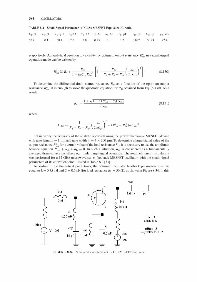
JWBS064-c08 JWBS064-Gerbennikov March 15, 2011 11:17 Printer Name: Yet to Come
384 OSCILLATORS
TABLE 8.2 Small-Signal Parameters of GaAs MESFET Equivalent Circuit.
Lg, pH Ls, pH Ld, pH Rg, � Rgs, � Rs, � Rd, � Cgs, pF Cgd, pF Cds, pF gm, mS
50.4 0.1 60.1 2.0 2.0 0.93 1.1 1.2 0.087 0.199 97.4
respectively. An analytical equation to calculate the optimum output resistance Roout in a small-signal
operation mode can be written by
R0out
∼= Rs + Rds
1 + (ωCds Rds)2
[1 − Rds
Rg + Rs + Rgs
(gm
2ωCgs
)2]
. (8.130)
To determine the differential drain–source resistance Rds as a function of the optimum outputresistance Ro
out, it is enough to solve the quadratic equation for Rds obtained from Eq. (8.130). As aresult,
Rds = 1 + √1 − 4 (Ro
out − Rs) Gdso
2Gdso(8.131)
where
Gdso = 1
Rg + Rs + Rgs
(gm
2ωCgs
)2
+ (Ro
out − Rs
)(ωCds)
2 .
Let us verify the accuracy of the analytic approach using the power microwave MESFET devicewith gate length l = 1 μm and gate width w = 4 × 200 μm. To determine a large-signal value of theoutput resistance Ro
out for a certain value of the load resistance RL, it is necessary to use the amplitudebalance equation Ro
out + Rd + RL = 0. In such a situation, Rds is considered as a fundamentallyaveraged drain–source resistance Rds1 under large-signal operation. The nonlinear circuit simulationwas performed for a 12 GHz microwave series feedback MESFET oscillator, with the small-signalparameters of its equivalent circuit listed in Table 8.2 [33].
According to the theoretical predictions, the optimum oscillator feedback parameters must beequal to L = 0.35 nH and C = 0.5 pF (for load resistance RL = 50 �), as shown in Figure 8.34. In this
FIGURE 8.34 Simulated series feedback 12 GHz MESFET oscillator.
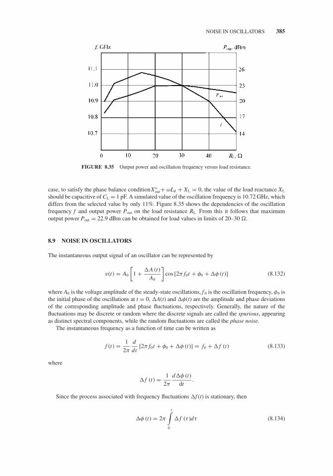
JWBS064-c08 JWBS064-Gerbennikov March 15, 2011 11:17 Printer Name: Yet to Come
NOISE IN OSCILLATORS 385
FIGURE 8.35 Output power and oscillation frequency versus load resistance.
case, to satisfy the phase balance conditionX oout+ ωLd + XL = 0, the value of the load reactance XL
should be capacitive of CL = 1 pF. A simulated value of the oscillation frequency is 10.72 GHz, whichdiffers from the selected value by only 11%. Figure 8.35 shows the dependencies of the oscillationfrequency f and output power Pout on the load resistance RL. From this it follows that maximumoutput power Pout = 22.9 dBm can be obtained for load values in limits of 20–30 �.
8.9 NOISE IN OSCILLATORS
The instantaneous output signal of an oscillator can be represented by
v(t) = A0
[1 + �A (t)
A0
]cos [2π f0t + φ0 + �φ (t)] (8.132)
where A0 is the voltage amplitude of the steady-state oscillations, f 0 is the oscillation frequency, φ0 isthe initial phase of the oscillations at t = 0, �A(t) and �φ(t) are the amplitude and phase deviationsof the corresponding amplitude and phase fluctuations, respectively. Generally, the nature of thefluctuations may be discrete or random where the discrete signals are called the spurious, appearingas distinct spectral components, while the random fluctuations are called the phase noise.
The instantaneous frequency as a function of time can be written as
f (t) = 1
2π
d
dt[2π f0t + φ0 + �φ (t)] = f0 + � f (t) (8.133)
where
� f (t) = 1
2π
d�φ (t)
dt.
Since the process associated with frequency fluctuations �f (t) is stationary, then
�φ (t) = 2π
t∫0
� f (τ )dτ (8.134)

JWBS064-c08 JWBS064-Gerbennikov March 15, 2011 11:17 Printer Name: Yet to Come
386 OSCILLATORS
which is in general a nonstationary process. However, as the phase fluctuation process is sufficientlyslow during the natural period of the oscillations, the stationary model to describe the phase noiseperformance of free-running oscillators can be used. It should be noted that an autonomous free-running oscillator does not have a reference plane and the initial phase φ0 in an autonomous systemcan be chosen arbitrary, for example, of zero value.
8.9.1 Parallel Feedback Oscillator
It is very important for the oscillator noise model to express a clear relationship between the oscillatorspectral noise power density, resonant circuit, and active device parameters. The simple Leeson linearmodel for a feedback oscillator, which was derived empirically, is based on the expectations that thereal oscillator has two basic components [35]. The first component is caused by the phase fluctuationsdue to the additive white noise at frequency offsets close to the carrier, as well as due to the noisehaving a mixing nature resulting from the circuit nonlinearities. The second component is a result ofthe low-frequency fluctuations or flicker noise upconverted to the carrier region because of the activedevice nonlinear effects.
The phase noise at the input of the power amplifier is added to a signal as the sum of everybandwidth �f = 1 Hz, each producing an available noise power at the input of the noise-freeamplifier, as shown in Figure 8.36(a). Maximum power delivery can be achieved when the sourceinternal impedance is conjugate-matched to the input impedance of the amplifier. As a result, onlyone-half of the root-mean-square noise voltage en appears across the amplifier input and is equal to
ein = en
2=
√4FkTR
2=
√FkTR (8.135)
where F is the noise figure, k is the Boltzmann constant, T is the absolute temperature, and Ris the equivalent resistance, which can be represented as the input resistance for the input root-mean-square noise voltage [36]. The input phase noise produces a root-mean-square phase deviation�φrms = �φ/
√2 at each offset frequency ±f m from the carrier f 0, as shown in Figure 8.36(b), for
which a total power-wise sum can be written for a small phase perturbation as
�φ = �φrms
√2 = ein
√2
Vin=
√FkT
Pin(8.136)
where Vin = √2Pin R is the signal voltage amplitude at the power amplifier input.
FIGURE 8.36 Simplified feedback oscillator noise model.

JWBS064-c08 JWBS064-Gerbennikov March 15, 2011 11:17 Printer Name: Yet to Come
NOISE IN OSCILLATORS 387
FIGURE 8.37 Equivalent model of parallel feedback oscillator.
As a result, the double-sideband spectral power density of the thermal phase noise in a frequencybandwidth �f = 1 Hz can be written as
S�φ = �φ2 = FkT
Pin. (8.137)
The Leeson model consists of an amplifier with a noise figure F and a resonator (or filter) in thefeedback loop, as shown in Figure 8.37(a) [36]. The oscillator phase noise is modeled by assuming anoise-free power amplifier and adding a phase modulator to its input. Based on empirical predictions,the phase noise level of the oscillator at an offset frequency f m from the carrier f 0 can be described by
Sφ ( fm) = S�φ ( fm)(
f0
2QL fm
)2
for fm <f0
2QL(8.138)
Sφ ( fm) = S�φ ( fm) for fm >f0
2QL(8.139)
where S�φ (f m) is determined using Eq. (8.137) as
S�φ ( fm) = FkT
Pin
(1 + fc
fm
)(8.140)
taking into the effect of the signal purity degradation due to the low-frequency flicker noise effectclose to the carrier, described empirically by the corner frequency f c. It should be noted that theempirical Leeson equation for S�φ (f m) contains a multiplication factor of two in the numerator.Moreover, accurate agreement was achieved between the model and experiment results when thepower density S�φ (f m) was expressed in terms of the compressed (or large-signal) power gain G andoutput power Pout as S�φ (f m) = 2GFkT/Pout [37].
The parameter F in Eq. (8.140) is associated with the active device noise figure and can becalled an effective noise factor because, generally, it should represent the effects of the active devicenoise sources and the cyclostationary noise resulting from periodically varying processes in practicaloscillators. Due to the inherent nonlinear nature of the active device, the effects of intermodulationbetween the wideband white noise and various harmonics of fundamental frequency (for example,nonlinear transformation of the noise near the third harmonic downconverted to the near carrier regiondue to mixing effect with second harmonic) must be included [35]. Also, the effect of low-frequencynoise modulation of the current, resulting in the reactance modulation of the input impedance ofthe circuit (for example, variation of the phase angle of the device forward transfer function versusemitter current), cannot be neglected [38]. Hence, it is impossible to calculate F accurately withouttaking into account the effect of the oscillator resonant circuit. Therefore, for such a linear model,the effective noise factor F as well as the corner frequency f c can be considered more like fittingparameters, based on measured data.

JWBS064-c08 JWBS064-Gerbennikov March 15, 2011 11:17 Printer Name: Yet to Come
388 OSCILLATORS
The corresponding combined expression to calculate the normalized double-sideband phase noisepower spectral density or the double-sideband noise-to-carrier ratio at the input of the feedbackoscillator can be obtained from
Sφ ( fm) = FkT
Pin
(1 + fc
fm
)[1 +
(f0
2QL fm
)2]
(8.141)
which gives an asymptotic model showing generally the noise reduction of 9 dB/octave in the offsetregion with predominant low-frequency 1/f noise, 6 dB/octave in the offset region due to feedbackloop and 0 dB/octave representing the thermal or white noise spectrum.
The single-sideband noise-to-carrier ratio at the input of the feedback oscillator can be described by
L ( fm) = 1
2
FkT
Pin
(1 + fc
fm
)[1 +
(f0
2QL fm
)2]
(8.142)
whose idealized sideband spectral behavior for different values of the loaded quality factors isillustrated in Figure 8.38. For the low-QL case, there are regions with 1/ f 3
m and 1/ f 2m dependencies
for spectral power density close to carrier, as shown in Figure 8.38(a). For the moderate-QL case,Figure 8.38(b) demonstrates only 1/ f 3
m dependence as far as intersection with thermal noise floor.For the high-QL case, the regions with 1/ f 3
m and 1/ fm dependencies are observed near the carrier,as shown in Figure 8.38(c). Closest to the carrier, 1/ f 3
m phase noise behavior is a result of randomfrequency modulation of the oscillator by low frequency 1/f noise. In the region of 1/ f 2
m phase noisebehavior, the white noise causes random frequency modulation. The 1/ fm dependence is due to themixing up of the 1/f noise with the oscillation frequency. Finally, the phase noise becomes constant,which is a result of the mixing up of white noise around the oscillation frequency.
To calculate the same phase noise power spectral density at the oscillator output, it is necessaryto replace the input power Pin by the power available at the output Pout and to multiply the numeratorof Eq. (8.142) by the power gain G. As a result, neglecting the effect of flicker noise and consideringthe case of f m f 0, one can obtain
L ( fm) = GFkT
8Q2L Pout
(f0
fm
)2
(8.143)
where
G = 1(1 − QL
Q0
)2 (8.144)
is considered the transducer power gain and Q0 is the unloaded quality factor [39]. From Eqs. (8.142)and (8.143) it follows that, to minimize the oscillator phase noise, it is necessary to reduce the noisefigure F and to increase the input power Pin (or the output power Pout for a fixed power gain G ofthe amplifier) as much as possible. In addition, for frequency offsets inside the resonator bandwidth,it is desirable to maximize the oscillator loaded quality factor QL. However, the resonator insertionloss and loaded QL are inter-related, and one cannot arbitrarily increase QL without increasing theinsertion loss, otherwise a larger power gain G is needed. The two competing effects result in anoptimum loaded QL of approximately one-half the unloaded Q0 and insertion loss of about 6 dB[40,41]. Thus, the minimum noise occurs when QL/Q0 = 0.5 resulting in
L ( fm) = 2FkT
Pout
(f0
2QL fm
)2
. (8.145)
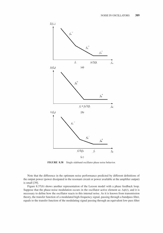
JWBS064-c08 JWBS064-Gerbennikov March 15, 2011 11:17 Printer Name: Yet to Come
NOISE IN OSCILLATORS 389
FIGURE 8.38 Single sideband oscillator phase noise behavior.
Note that the difference in the optimum noise performance predicted by different definitions ofthe output power (power dissipated in the resonant circuit or power available at the amplifier output)is small [39].
Figure 8.37(b) shows another representation of the Leeson model with a phase feedback loop.Suppose that the phase-noise modulation occurs in the oscillator active element as �φ(t), and it isnecessary to define how the oscillator reacts to this internal noise. As it is known from transmissiontheory, the transfer function of a modulated high-frequency signal, passing through a bandpass filter,equals to the transfer function of the modulating signal passing through an equivalent low-pass filter

JWBS064-c08 JWBS064-Gerbennikov March 15, 2011 11:17 Printer Name: Yet to Come
390 OSCILLATORS
prototype. Thus, the phase relationship resulting from the null-phase condition on the loop and fromthe filtering of φ(t) by the selective filter can be written as
ψ (t) + �φ (t) = φ (t) (8.146)
where
ψ (t) =+∞∫
−∞
φ (t) h (τ − t) dτ = φ (t) × h (t) (8.147)
h(t) is the impulse response of the equivalent low-pass filter, and the asterisk denotes a convolutionproduct. The integral in Eq. (8.147) converges for nearly all samples of φ(t) provided that the filter islinear and time invariant, and that the stationary random process φ(t) possesses a finite second-ordermoment.
In this case, the Leeson formula for the double-sideband phase noise power spectral density of thefeedback oscillator given by Eq. (8.141) can be expressed in a more general form
Sφ (ωm) = S�φ (ωm)
[H ( jωm) − 1] [H ∗ ( jωm) − 1](8.148)
where H(jωm) is the equivalent low-pass transfer function and asterisk denotes the complex-conjugatevalue [42].
Thus, by representing the transfer function of the first order low-pass filter as
H ( jωm) = α
α + jωm(8.149)
where α = ω0/2QL is the half-bandwidth of the resonator and ωm = 2π f m, Eq. (8.148) can be rewrittenas
Sφ (ωm) = S�φ (ωm)
[1 +
(α
ωm
)2]
(8.150)
which is similar to Eq. (8.141).Now consider a case of the second-order low-pass filter based on the two coupled resonators
having the transfer function
H ( jωm) = α1
α1 + jωm
α2
α2 + jωm= 1
1 −(ωm
α
)2+ j2ωmδ
(8.151)
where α = √α1α2 and δ = (α1 + α2) /2
√α1α2 [43]. In this case, Eq. (8.148) can be rewritten as
Sφ (ωm) = S�φ (ωm)
⎡⎢⎣1 +
1 − 2(ωm
α
)2
(ωm
α
)2+ 4δ2
(α
ωm
)2
⎤⎥⎦ (8.152)
which shows the substantially better phase noise performance in the near vicinity of the carrierfrequency for the case of loosely coupled resonators when δ > 1. However, since the available outputpower becomes low, it is necessary to provide post low-noise output signal amplification.

JWBS064-c08 JWBS064-Gerbennikov March 15, 2011 11:17 Printer Name: Yet to Come
NOISE IN OSCILLATORS 391
Let us quantitatively compare both cases of the Leeson phase noise models using the first-and second-order low-pass filters in the oscillator feedback loop for the same arbitrary chosentechnical data:
� Oscillation (carrier) frequency f 0 = 2 GHz.� Offset frequency f m = 10 kHz.� Oscillator resonant circuit loaded quality factor QL = 10.� Noise figure of the active device F = 6 dB.� Input power delivered to the device Pin = 10 mW.� Corner frequency for flicker noise f c = 3 kHz.
Substituting these parameters into Eq. (8.142) for a single-sideband phase noise spectral densityof the oscillator with the first-order low-pass filter results in
L( fm) = 10 log(1.05128 × 10⁻¹⁰) = −99.78 dBc/Hz.
For the case of the oscillator with two coupled resonators, let us assume that the loaded QL of thesecond resonator is five times as much as the first one, that is α1 = 6.283 × 10⁸ and α2 = 1.2566 ×10⁸. Then,
L( fm) = 10 log(2.918 × 10⁻¹²) = −115.35 dBc/Hz
which clearly shows the significant phase noise improvement compared to the oscillator having thefirst-order low-pass filter in a feedback loop.
Figure 8.39 shows the typical oscillator output power spectrum. The noise distribution on eachside of the oscillator signal is subdivided into a large number of strips of width �f located at thedistance f m away from signal. It should be noted that, generally, the spectrum of the output signalconsists of the amplitude and phase noise components. Hence, to measure the phase noise close to thecarrier frequency, one needs to make sure that any contributions of parasitic amplitude modulation tothe oscillator output noise spectrum are negligible compared with those from frequency modulation.The single-sideband phase noise L(f m) usually given logarithmically is defined as the ratio of a signal
FIGURE 8.39 Oscillator output power spectrum.

JWBS064-c08 JWBS064-Gerbennikov March 15, 2011 11:17 Printer Name: Yet to Come
392 OSCILLATORS
power Pss�f in one-phase modulation sideband per bandwidth �f = 1 Hz, at an offset f m away fromthe carrier, to the total signal power Ps.
Despite some limitations of the linear Leeson model when device is operated in a conductionangle large-signal mode and output signal is not purely sinusoidal, which have an effect on the activedevice noise factor and low-frequency flicker noise upconversion, such an approach gives a sense ofthe phase noise performance for oscillators with different resonant circuits. This applies especially,if the theoretical results can be supported by sufficiently accurate measurements of a loaded qualityfactor of the oscillator resonant circuit and simulations of the effective noise figure based on themodeled active device parameters and operation conditions.
In addition, such a simple model indicates the basic factors and provides the design rules that arenecessary to follow in order to minimize the oscillator phase noise:
� Choose the resonator with maximum unloaded quality factor Q0 and optimize the loaded qualityfactor QL of the oscillator resonant circuit by proper load coupling.
� Maximize the output power PL delivered to the load by maximizing the RF voltage amplitudeacross the resonant circuit with limitations due to active device breakdown voltage and operationin the saturation mode.
� Choose a device with the lowest noise figure F and corner frequency f c for low-frequencyflicker noise.
8.9.2 Negative Resistance Oscillator
Now consider the equivalent circuit of a simple single-resonant negative resistance oscillator shown inFigure 8.40, where the available noise power is assumed to be totally from the active device. Here, Rn
is the equivalent noise resistance associated with active device noise sources, the negative resistanceRout, and the equivalent output capacitance Cout represent the device negative output impedance, L isthe tank inductance, and RL is the load resistance. The derivation of the power spectral density willbe based on the fact that the available noise power in the active device is amplified in a frequencyselective way, resulting at resonance in the output power PL being dissipated in the load resistanceRL [44]. This will happen in a steady-state condition when the values of the negative resistance andthe load resistance are close to each other.
Then, assuming that RL + �R = −Rout and defining the magnitude of the mean-square noisecurrent flowing into load from the mean-square noise voltage source, we can write
i 2n = e2
n
(�R)2 +(
ωL − 1
ωCout
)2 . (8.153)
FIGURE 8.40 Simplified negative resistance oscillator noise model.

JWBS064-c08 JWBS064-Gerbennikov March 15, 2011 11:17 Printer Name: Yet to Come
NOISE IN OSCILLATORS 393
Equation (8.153) can be rewritten in the normalized general form as
i 2n = 1(
�R
RL
)2
+ Q2L
(ω
ω0− ω0
ω
)2
e2n
R2L
(8.154)
where ω0 is the radian resonant frequency and QL is the oscillator loaded quality factor at the resonantfrequency.
By normalizing to the power PL dissipated in the load resistor RL, Eq. (8.154) can be rewrittenthrough the spectral power densities by
Sφ = S�φ(�R
RL
)2
+ Q2L
(ω
ω0− ω0
ω
)2 (8.155)
where S�φ = 4kTRn/(RLPL), Sφ = i 2n RL/PL is the power spectral density of the noise current across
the load resistor RL and �f = 1 Hz.Since at small offset frequencies ωm = ω − ω0 close to the resonant frequency,
ω
ω0− ω0
ω∼= 2ωm
ω0
then Eq. (8.155) can be rewritten as
Sφ = S�φ(�R
RL
)2
+(
2QLωm
ω0
)2 (8.156)
which is similar to the power spectral density at frequency offsets close to the resonant frequency forthe parallel feedback oscillator. Equation (8.156) represents a Lorentz function corresponding to anexponential decay of the autocorrelation function in the time domain [45].
Since the total output power delivered to the load is equal to PL,
1
2π
∞∫0
Sφ (ω)dω =(
ω0
2QL
)2 S�φ
2�ωn= 1 (8.157)
where
�ωn = �R
RL
ω0
2QL
is the Lorentzian linewidth (half-width at half-maximum), which is an oscillator spectrum linewidthcharacterized by the natural phase fluctuations due to the thermal and shot noises of the oscillator.However, in a common case, due to the variation of the oscillator resonant circuit parameters, flickernoise, pushing or pulling effects, the effective spectrum linewidth widens, especially close to theresonant frequency.
By using a widely used definition of the loaded quality factor of the passive resonator in the form
QL = ω0
�ω3dB(8.158)

JWBS064-c08 JWBS064-Gerbennikov March 15, 2011 11:17 Printer Name: Yet to Come
394 OSCILLATORS
where �ω3dB is the full linewidth at half-maximum level, one can write
2�ωn = S�φ
4�ω2
3dB = kTRn
RL
�ω23dB
PL. (8.159)
As a result, there is a complete analogy between Lorentzian linewidth defined by Eq. (8.159) andthe expression for semiconductor laser homogeneous linewidth [46]. In this case, the characteristicenergy kT corresponds to the photon energy, the oscillator output power PL corresponds to thelaser output power, and the oscillator noise-gain ratio Rn/RL corresponds to the inversion factorrepresenting the ratio between spontaneous emission rate and the optical gain rate. The widening ofthe oscillator spectral line due to the low-frequency fluctuations is similar to an inhomogeneous laserline broadening due to the Doppler effect.
The normalized power spectral density can be expressed through the Lorentzian linewidth as
Sφ (ωm) = 2�ωn
�ω2n + ω2
m
∼= 2�ωn
ω2m
(8.160)
showing a simple linear relationship between Lorentzian linewidth and oscillator phase noise spectrumat offset frequencies ωm � �ωn. Substituting Eq. (8.159) into Eq. (8.160) and taking into accountthat F = Rn/RL result in the single-sideband noise-to-carrier ratio
L ( fm) = kTF
2PL
(f0
QL fm
)2
(8.161)
which is similar to the Edson noise formula [44,47].
8.9.3 Colpitts Oscillator
As an example, let us define the linear phase noise model for a popular Colpitts oscillator, thesimplified circuit schematic of which is shown in Figure 8.41(a). The power loss in the tank inductorL is included in the load resistance RL. The transistor equivalent circuit with voltage and current noisesources in shown in Figure 8.41(b), where the resonator noise is modeled by a noise current inR. Thenoise voltage and current sources can be given through their mean-square values as
i2nR = 4kT � f
RL(8.162)
v2nb = 4kT rb� f (8.163)
i2nb = 2q Ic� f
β(8.164)
i 2nc = 2q Ic� f. (8.165)
where the input noise current source i 2nb is related to shot noise at the emitter–base junction due to
electrons that recombine with holes inside the neutral base and i2nc represents the shot noise generated
at the collector–base junction due to collector electrons. The mean-square values of these noisesources in a bandwidth �f are given by
i 2nb = 2q Ib� f = 2kT nbgπ� f (8.166)
i2nc = 2q Ic� f = 2kT ncgm� f. (8.167)
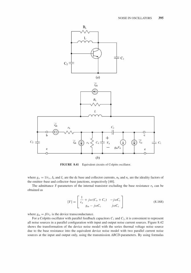
JWBS064-c08 JWBS064-Gerbennikov March 15, 2011 11:17 Printer Name: Yet to Come
NOISE IN OSCILLATORS 395
FIGURE 8.41 Equivalent circuits of Colpitts oscillator.
where gπ = 1/rπ , Ib and Ic are the dc base and collector currents, nb and nc are the ideality factors ofthe emitter–base and collector–base junctions, respectively [48].
The admittance Y-parameters of the internal transistor excluding the base resistance rb can beobtained as
[Y ] =⎡⎣ 1
rπ
+ jω (Cπ + Cc) − jωCc
gm − jωCc jωCc
⎤⎦ (8.168)
where gm = β/rπ is the device transconductance.For a Colpitts oscillator with parallel feedback capacitors C1 and C2, it is convenient to represent
all noise sources in a parallel configuration with input and output noise current sources. Figure 8.42shows the transformation of the device noise model with the series thermal voltage noise sourcedue to the base resistance into the equivalent device noise model with two parallel current noisesources at the input and output only, using the transmission ABCD-parameters. By using formulas

JWBS064-c08 JWBS064-Gerbennikov March 15, 2011 11:17 Printer Name: Yet to Come
396 OSCILLATORS
FIGURE 8.42 Transformation of base resistance thermal voltage noise.
of the transformation from the admittance Y-parameters to the transmission ABCD-parameters, onecan write
1
B= −Y21 = −(gm − jωCc). (8.169)
D
B= Y11 = 1
rπ
+ jω(Cπ + Cc). (8.170)
Let us simplify the analytical calculations by taking into account that, as it follows fromEqs. (8.169) and (8.170), the contribution of the collector capacitance Cc is not significant. As aresult, the mean-square input current source i 2
ni and output current source i 2no can be written as
i 2ni = 2q Ic� f
β+ 4kT � f
rb
(rb
rπ
)2 (1 + β2 f 2
f 2T
)(8.171)
i 2n0 = 2q Ic� f + 4kT� f
rb
(βrb
rπ
)2
(8.172)
where f is the operating frequency, f T = gm/(2πCπ ) is the transition frequency, and it is assumed thatthe dc and small-signal values of the current gain β are equal.
To calculate the noise figure of the oscillator, the noise current sources i2ni and i 2
no should be
transformed in parallel with i 2nR. By using Eqs. (8.166) and (8.167) for the case of ideal junctions
when nb = nc = 1, the total equivalent noise source i 2n� connected in parallel to the resonator and
load can now be obtained as
i2n� = 4kT � f
RL+ 4kT � f
2rπ
[1 + 2rb
rπ
(1 + β2 f 2
f 2T
)] (C1
C1 + C2
)2
+ 4kTβ� f
2rπ
(1 + 2βrb
rπ
)(C2
C1 + C2
)2
.
(8.173)

JWBS064-c08 JWBS064-Gerbennikov March 15, 2011 11:17 Printer Name: Yet to Come
NOISE IN OSCILLATORS 397
The noise figure F of the oscillator is defined as the ratio of the total noise power due to all noisecurrent sources and the noise power from the loaded resonator due to the noise source i2
nR. As a result,
F = 1 + RL
2rπ
[1 + 2rb
rπ
(1 + β2 f 2
f 2T
)] (C1
C1 + C2
)2
+ RL
2rπ
(1 + 2βrb
rπ
) (C2
C1 + C2
)2
. (8.174)
In most cases, the contribution of the collector shot noise dominates over the contribution of theshot noise caused by the base current. Consequently, for rb rπ and f f T, the expression for theoscillator noise figure is simplified to
F = 1 + RL
2rπ
(1 + 2βrb
rπ
) (C2
C1 + C2
)2
. (8.175)
Finally, the single-sideband noise-to-carrier ratio at the output of the Colpitts oscillator in a linearconsideration, using Eq. (8.161), can be defined by
L ( fm) = kT
2PL
(f0
QL fm
)2[
1 + RL
2rπ
(1 + 2βrb
rπ
) (C2
C1 + C2
)2]
. (8.176)
8.9.4 Impulse Response Model
The behavior of autonomous second-order weakly nonlinear oscillation systems with low damp-ing factor close to linear conservative systems and small time-varying external force f (t) can bedescribed by
d2x
dτ 2+ x = n (t) (8.177)
where x is the time-dependent variable, voltage or current, and τ = ω0 t is the time normalized bythe angular resonant frequency ω0.
The phase plane method is one of the theoretical approaches that allows one to analyze qualitativelyand quantitatively the dynamics of the oscillation systems described by the second-order differentialequations such as Eq. (8.177) [1]. By setting the small external force equal to zero, the solution ofthe linear second-order differential equation takes the form
x = Acos (τ + φ) = A cos ψ (8.178)
dx
dτ= −Asin (τ + φ) = −A sin ψ (8.179)
where A is the amplitude of the oscillations and φ is the phase of the oscillation. The phase portraitshown in Figure 8.43(a) represents the family of circular trajectories enclosing each other with radiir = A (limit cycles) depending on energy stored in the system.
Let us define the variations of the amplitude A(t) and phase φ(t) under the effect of the externalforce applied to the oscillation system [2,49]. Assuming that the effect of the external force is smalland these variations are slow, the amplitude and phase can be considered constant during a naturalperiod of the oscillation. Then, Eq. (8.177) can be rewritten in the form of two first-order equations by
dx
dτ= y (8.180)
dy
dτ= −x + n (t) . (8.181)

JWBS064-c08 JWBS064-Gerbennikov March 15, 2011 11:17 Printer Name: Yet to Come
398 OSCILLATORS
FIGURE 8.43 Phase portrait of second-order oscillation system and effect of injected impulse.
From Eqs. (8.180) and (8.181) it follows that the instantaneous change of the ordinate y by avalue of dny = ndτ will occur, due to the small external force injected to the oscillation system. Thiscorresponds to a step change of the representative point M0 from the position K to the position L,thus resulting in the amplitude and phase changes shown in Figure 8.43(b). These changes can bedetermined from the consideration of a triangle KLN as
d A = −dn y sin ψ = −n sin ψdτ (8.182)
dφ = −dn y
Acos ψ = − n
Acos ψdτ. (8.183)
Thus, separate first-order differential equations for the time-varying amplitude and phase can beobtained from Eqs. (8.182) and (8.183) as
d A
dτ= −n sin ψ (8.184)
dφ
dτ= − n
Acos ψ. (8.185)
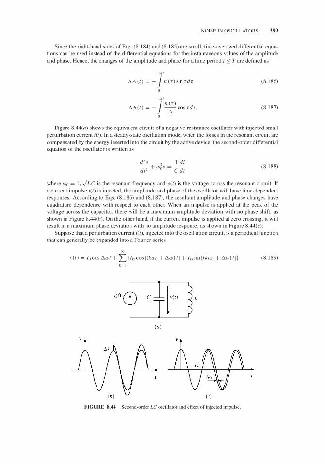
JWBS064-c08 JWBS064-Gerbennikov March 15, 2011 11:17 Printer Name: Yet to Come
NOISE IN OSCILLATORS 399
Since the right-hand sides of Eqs. (8.184) and (8.185) are small, time-averaged differential equa-tions can be used instead of the differential equations for the instantaneous values of the amplitudeand phase. Hence, the changes of the amplitude and phase for a time period t ≤ T are defined as
�A (t) = −ω0 t∫0
n (τ ) sin τdτ (8.186)
�φ (t) = −ω0 t∫0
n (τ )
Acos τdτ . (8.187)
Figure 8.44(a) shows the equivalent circuit of a negative resistance oscillator with injected smallperturbation current i(t). In a steady-state oscillation mode, when the losses in the resonant circuit arecompensated by the energy inserted into the circuit by the active device, the second-order differentialequation of the oscillator is written as
d2v
dt2+ ω2
0v = 1
C
di
dt(8.188)
where ω0 = 1/√
LC is the resonant frequency and v(t) is the voltage across the resonant circuit. Ifa current impulse i(t) is injected, the amplitude and phase of the oscillator will have time-dependentresponses. According to Eqs. (8.186) and (8.187), the resultant amplitude and phase changes havequadrature dependence with respect to each other. When an impulse is applied at the peak of thevoltage across the capacitor, there will be a maximum amplitude deviation with no phase shift, asshown in Figure 8.44(b). On the other hand, if the current impulse is applied at zero crossing, it willresult in a maximum phase deviation with no amplitude response, as shown in Figure 8.44(c).
Suppose that a perturbation current i(t), injected into the oscillation circuit, is a periodical functionthat can generally be expanded into a Fourier series
i (t ) = I0 cos �ωt +∞∑
k=1
{Ikccos [(kω0 + �ω) t] + Ikssin [(kω0 + �ω) t]} (8.189)
FIGURE 8.44 Second-order LC oscillator and effect of injected impulse.

JWBS064-c08 JWBS064-Gerbennikov March 15, 2011 11:17 Printer Name: Yet to Come
400 OSCILLATORS
where I0 is the dc current, Ikc is the kth cosine current harmonic amplitude, Iks is the kth sinusoidalcurrent harmonic amplitude, and �ω ω0. In this case, the small external force can be redefined as
n = 1
ω0C
di
dτ= L
di
dt. (8.190)
Consequently, substituting Eq. (8.189) into Eqs. (8.186) and (8.187) and taking into account thatω0 + �ω ∼= ω0 result in
�V (t) = − I1s
2C
cos (�ωt) − 1
�ω(8.191)
�φ(t) = − I1c
2CV
sin (�ωt)
�ω(8.192)
where V is the voltage amplitude across the capacitor C. In this case, only the fundamental compo-nents in the injected current i(t) can contribute to the amplitude (sine amplitude) and phase (cosineamplitude) fluctuations given by Eqs. (8.191) and (8.192), because for the dc and kth-order cur-rent components, the arguments for all their integrals in Eqs. (8.186) and (8.187) are significantlyattenuated by the averaging over integration period.
The output voltage of an ideal cosine oscillator with constant amplitude V and phase fluctuations�φ can be written as
v(t) = V cos [ω0t + �φ (t)] = V cos [�φ (t )] cos ω0t − V sin [�φ (t)] sin ω0t (8.193)
resulting in an output spectrum of the oscillator with sidebands close to the oscillation frequencyω0. Since, for a narrowband phase modulation with small phase fluctuations, sin[�φ(t)] ∼= �φ(t)and cos[�φ(t)] ∼= 1, the phase modulation spectrum given by Eq. (8.193) can be rewritten usingEq. (8.192) as
v(t) = V cos ω0t + I1c
4C�ωcos [(ω0t − �ω) t] − I1c
4C�ωcos [(ω0t + �ω) t] (8.194)
which is similar to the single-tone amplitude modulation spectrum containing the spectral componentscorresponding to the carrier frequency ω0 and two close sideband frequencies ω0 − �ω and ω0 + �ω.
The injection of the current
i (t) = I0 cos �ω0t +∞∑
k=1
{Ikccos [(kω0 − �ω) t] + Ikssin [(kω0 − �ω) t]} (8.195)
has similar effect, resulting in twice the noise power at the sidebands. Therefore, an injected totalcurrent i(t) results in a pair of equal sidebands at ω0 ± �ω with a sideband power Psb relative to thecarrier power Pc given by
Psb (ω0 ± �ω)
Pc (ω0)= 2
(I1c
4CV �ω
)2
. (8.196)
Now let us assume that a stationary thermal noise current with a white power spectral densityi 2n is injected into the oscillator circuit close to carrier. Then, by making a replacement between the
amplitude and root-mean-square current values when I 21c/2 = i 2
n , the single sideband power spectral

JWBS064-c08 JWBS064-Gerbennikov March 15, 2011 11:17 Printer Name: Yet to Come
NOISE IN OSCILLATORS 401
density for the phase fluctuations at �ω offset from the carrier ω0 in 1/f 2 region can be written usingEq. (8.196) as
L ( fm) = i2n
4C2V 2�ω2. (8.197)
Finally, taking into account that i 2n = 4FkT/RL for �f = 1 Hz, QL = ω0CRL, and PL = V2/2RL,
where RL is the tank parallel or load resistance, Eq. (8.197) can be rewritten as
L ( fm) = 2FkT
PL
(ω0
2QL�ω
)2
. (8.198)
which is similar to Eq. (8.161) for the negative resistance oscillator.Consideration of both cosine current and cosine voltage across the device output terminals implies
the device operation in a linear active region only when the establishment of the oscillations canbe achieved by using a separate diode as a nonlinear element. Therefore, the mixing effect from thenonlinear behavior of the active device is not taken into account. For a general case of the activedevice described by a two-port network equivalent circuit, in order to evaluate the output port noisevoltage generator, it is necessary to provide a transformation of the noise source from the input portto the output port of the device.
As an example, consider an oscillator with a nonlinear output resistance dependent on the applieddc bias voltage and on the amplitude of the self-sustained oscillations. The basic oscillator circuit withthe nonlinear negative output resistance Rout, capacitance C, inductance L, load resistance RL, andnoise current in(t) is shown in Figure 8.45(a). The electrical behavior of such an oscillator, in termsof voltage v(t) across the capacitance, can be represented by a second-order nonlinear differentialequation
LCd2v
dt2+ L
RL
dv
dt+ v + L
di
dt= en (t) (8.199)
where
en (t) = Ldin (t)
dt(8.200)
is the equivalent noise voltage and
i = I0 + v
Rout+
∞∑k=2
Gkvk (8.201)
represents a power series expansion where I0 is the dc current and Gk are the small coefficients.
FIGURE 8.45 Second-order nonlinear oscillation systems.
JWBS064-c08 JWBS064-Gerbennikov March 15, 2011 11:17 Printer Name: Yet to Come
402 OSCILLATORS
In a steady-state operation mode, when the active device compensates for the losses in the loadresistance according to Rout + RL = 0, Eq. (8.199) can be rewritten as
LCd2v
dt2+ v + L
d
dt
( ∞∑k=2
Gkvk
)= en (t) (8.202)
Seeking the general solution of the inhomogeneous differential equation as the superposition of ageneral solution of the homogeneous (noise-free) and specific solutions of Eq. (8.202) as
v(t) = V (t)cos [ω0t + φ (t)] + en (t) (8.203)
and applying a van der Pol approach for the slowly time-varying amplitude V(t) and phase φ(t) allowus to rewrite Eq. (8.202) in the form
2ω0dV
dtsin (ω0t + φ) + 2ω0V
dφ
dtcos (ω0t + φ) = 1
C
d
dt
( ∞∑k=2
Gkvk
)(8.204)
where ω0 = 1/√
LC . It is assumed that en(t) is a small slowly time-varying low-frequency noisevoltage, for which
LCd2en (t)
dt2 en (t ) .
As a result, substituting Eq. (8.203) into the right-hand side of Eq. (8.204) and using trigonometricidentities yield
dφ
dt= 0 (8.205)
which means that the nonlinear output resistance has no impact on the phase fluctuations. How-ever, the amplitude fluctuations are not equal to zero because all factors on the right-hand side ofEq. (8.204) have the first-order sine components. Thus, the resistive type of nonlinearities alone wouldcause amplitude noise only, since the reactive elements determining the oscillation frequency remainconstant. However, if the high-frequency noise current is injected close to the carrier frequency ω0
(for example, at small offset �ω), it will cause the phase fluctuations according to Eqs. (8.192)and (8.204).
Now consider a varactor-controlled oscillator with the varactor as a nonlinear element, whosecapacitance depends not only on the applied dc bias voltage, but also on the amplitude of the self-sustained oscillations. The basic VCO circuit consists of the varactor with a nonlinear capacitanceC, an inductance L, and a noise voltage en(t), as shown in Figure 8.45(b) [50]. The voltage en(t)can represent all the noise coming from both inside and outside the circuit, including any thermalnoise from the resistors, flicker noise from the active device, and noise from the power supply. Theelectrical behavior of the oscillator can be described by
v + Ldi
dt= en (t) (8.206)
i =(
C + vdC
dv
)dv
dt(8.207)
where the nonlinear term vdC/dv is included in Eq. (8.207).
JWBS064-c08 JWBS064-Gerbennikov March 15, 2011 11:17 Printer Name: Yet to Come
NOISE IN OSCILLATORS 403
By expanding a nonlinear capacitance C into a power series
C = C0 +∞∑
k=1
Ckvk (8.208)
with the small coefficients Ck, substituting Eq. (8.207) into Eq. (8.206) and applying an asymptoticperturbation procedure with decomposition of the perturbed and unperturbed equations, the first-order differential equation for phase fluctuations with the slowly time-varying noise voltage en canbe derived as
dφ
dt= −ω0
C0
[C1en + C2
(3
4V 2 + 3e2
n
)+ C3en
(3V 2 + 4e2
n
) + · · ·]
(8.209)
where V is the voltage amplitude across the varactor [51]. Note that a nonlinear capacitance has noimpact on the amplitude noise of the oscillator.
From Eq. (8.209) it follows that
� the first-order capacitance nonlinearity described by the coefficient C1 contributes to the up-conversion of the low-frequency noise en(t) to the sideband noise near carrier ω0;
� the second-order nonlinearity described by the coefficient C2 generates a phase noise, due toboth amplitude-to-phase conversion and low-frequency noise upconversion;
� the higher order nonlinearities described by the coefficients Ck, k = 3, 4, 5, . . . , cause a morecomplicated noise behavior of the oscillator based on hybrid upconversion and amplitude-to-phase conversion due to the cross-terms of V and en.
In the case of a single-frequency LC oscillator, the main contributor to the phase noise is thenonlinear collector capacitance of the bipolar device or the gate–source capacitance of the field-effecttransistor (FET) device. However, in a general case, the equivalent circuit of the active device is verycomplicated, including both nonlinear intrinsic and linear parasitic external elements. This meansthat it is difficult to evaluate analytically the impact of each nonlinear element on the upconversionmechanism. Moreover, the joint effect of different nonlinear circuit elements will result in both ampli-tude and phase fluctuations. For example, the phase noise can be significantly reduced by linearizingboth the transconductance gm and the gate–source capacitance Cgs, since both nonlinearities areimportant contributors to the phase noise [51]. The amplitude noise also depends on the capacitanceand transconductance nonlinearities. However, the capacitance nonlinearity will not affect the outputcurrent if the series gate resistance Rg is set to zero. The nonlinearities of the gate–drain capacitanceCgd and drain–source resistance Rds have negligible effect on the amplitude and phase noise.
Generally, the transition from soft start-up oscillation conditions to steady-state self-sustainedoscillations is provided as a result of the degradation of the device transconductance in a large-signalmode, when the active device is operated in both pinch-off and active regions. As a result, for thecosine voltage across the resonant circuit, the output collector (or drain) current i(t) represents aFourier series expansion
i (t) = I0 +∞∑
n=1
In cos (nω0t) (8.210)
where I0 is the dc current and In is the amplitude of the nth harmonic component.If the oscillation frequency is equal to the resonant circuit frequency, which means that the active
device has no effect on the oscillation frequency, then the fundamental component of the collectorvoltage will be in phase with the fundamental component of the collector current. However, for allhigher order voltage harmonics, the impedance of the resonant circuit will be capacitive since the

JWBS064-c08 JWBS064-Gerbennikov March 15, 2011 11:17 Printer Name: Yet to Come
404 OSCILLATORS
FIGURE 8.46 Schematic of parallel feedback oscillator.
collector current harmonics are mostly flowing through the shunt capacitance. Therefore, for theMeissner oscillator circuit shown in Figure 8.46, the voltage at the input of the active device can bewritten as
vin (t) = Vin1 cos ω0t +∞∑
k=2
Vink cos(
kω0t − π
2
)(8.211)
where V ink V in1 for a high value of the oscillator loaded quality factor.As a result, when the device transfer characteristic is approximated by a polynomial, the presence
of higher order voltage harmonic contributes, first, to the changes in the fundamental amplitude and,secondly, to the appearance of the phase shift between the fundamental voltage and the fundamentalcurrent. In a general form, the frequency deviation �ω caused by the presence of the second-orderand higher order harmonic components of the voltage v on the resonant circuit can be obtained from
�ω
ω0= −1
2
∞∑k=2
(k2 − 1
)m2
k (8.212)
where k is the order of the harmonic component and mk = Vk/V1 is the ratio of the harmonic voltagecomponent to the fundamental voltage amplitude [3].
In view of the multiharmonic representation of the oscillator output spectrum due to the deviceand resonant circuit nonlinearities, the total phase fluctuations can be represented by a superpositionintegral as a result of each harmonic contribution. This is similar to the Fourier harmonic expansionin a frequency domain of the voltage waveform, when the phase trajectory on the phase plane is aresult of the phase trajectories with different radii and velocities corresponding to the dc shift andharmonic amplitudes. In this case, Eq. (8.187) can take a general form
�φ (t) = − 1
A
ω0 t∫0
n (τ ) (τ ) dτ (8.213)
where
(t) = c0
2+
∞∑n=1
cn cos (nω0t + φn) (8.214)
is a dimensionless periodic function characterizing the shape of the limit cycle or phase trajectorycorresponding to the oscillation waveform and depending on the oscillator topology. It is called the
JWBS064-c08 JWBS064-Gerbennikov March 15, 2011 11:17 Printer Name: Yet to Come
NOISE IN OSCILLATORS 405
impulse sensitivity function (ISF) for an approximate model for the oscillator phase behavior [52] andserves a similar role as the perturbation projection vector (PPV) for the exact model [53]. The initialphase φn in Eq. (8.214) is not important for random noise sources and can be neglected. For an idealcase of a purely sinusoidal oscillator, c1 = 1 and (t) = cosω0 t.
Now if any stationary noise current with a white power spectral density i 2n/� f is injected into
the oscillator circuit close to any harmonic nω0 + �ω or nω0 − �ω, it will result in a pair ofequal sidebands at ω0 ± �ω. Then, the total single-sideband power spectral density for the phasefluctuations in a bandwidth �f = 1 Hz can be written, based on Eq. (8.197), as
L ( fm) =i 2n
∞∑n=0
c2n
4C2V 2�ω2= i2
n2rms
2C2V 2�ω2(8.215)
where rms is the root-mean-square value of (t) [54]. Thus, the total noise power near the carrierfrequency of the oscillator is a result of the upconverted 1/f noise near dc, weighted by coefficientc0, the noise near the carrier weighted by coefficient c1, and the downconverted white noise near thesecond-order and higher order harmonics weighted by coefficients cn, n = 2, 3, . . . . The convertedphase noise due to the conversion from one sideband to another can be of the order of 6 dB higherthan the additive noise in the oscillator [55].
From Eq. (8.215) it follows that the effect of the converted phase noise can be reduced by minimiz-ing the dc coefficient c0 and the higher order harmonic coefficients cn of the (t) approximating thecosine waveform of the injected node voltage. For a symmetrical flattened drain voltage waveformcorresponding to a Class F operation mode, the ratio between the voltage fundamental and thirdharmonic should be equal to V1/V3 = 9 with the significantly suppressed even harmonic components.On the other hand, for a half-cosine drain voltage waveform corresponding to an inverse Class Foperation mode, the ratio between the voltage fundamental and second harmonic should be equalto V1/V2 = 4 with the significantly suppressed odd harmonic components. Note that, in Class Eoperation with nonsymmetrical voltage waveform, the effect of the second-order and higher orderharmonics is significant resulting in a high value of the voltage peak factor. The importance of thesymmetry is necessary also to minimize the coefficient c0 responsible for the low noise upconversionand amplitude-to-phase conversion [52]. As it is seen from Eq. (8.209), the phase noise improvementcan be achieved by reducing the effect of the device and circuit nonlinear capacitances. Due to theamplitude-to-phase conversion, the phase for each higher order harmonic component changes withamplitude resulting in a generally asymmetric voltage waveform.
Equation (8.213) describes an approximate phase noise behavior, compared with the accurateequation where the phase φ(t) also appears in its right-hand side [53]. Such a simplified phase noisemodel is valid for the case of stationary noise sources such as white noise. However, when the noisesources are no longer stationary, it can be accurate only in the limits of an assumption of the smallphase shifts for which cos�φ is close to unity. This implies that the approximate model is not accurateenough to analyze neither the injection-locking phenomenon nor the related issues such as behaviorof phase differences of coupled oscillators [56].
The noise sources in an oscillator generally cannot be only modeled as purely stationary sincethe statistical properties of some of them may change with time in a periodic manner. Such types ofnoise sources are referred to as cyclostationary. If the thermal noise of the resistor has a stationarynature, then the collector shot noise of the transistor is an example of cyclostationary noise due to thetime-varying nature of the collector current. The most important issue is that the collector shot noiseis dominant, compared to the noise from base resistance or tank losses, and can achieve about 70%of total phase noise of the oscillator [57].
Figure 8.47(a) shows a simplified single-ended common gate complementary metal-oxide semi-conductor (CMOS) Colpitts oscillator configuration where the required regeneration factor for thestart-up oscillation conditions is chosen using a proper ratio of the feedback capacitances C1 and C2.
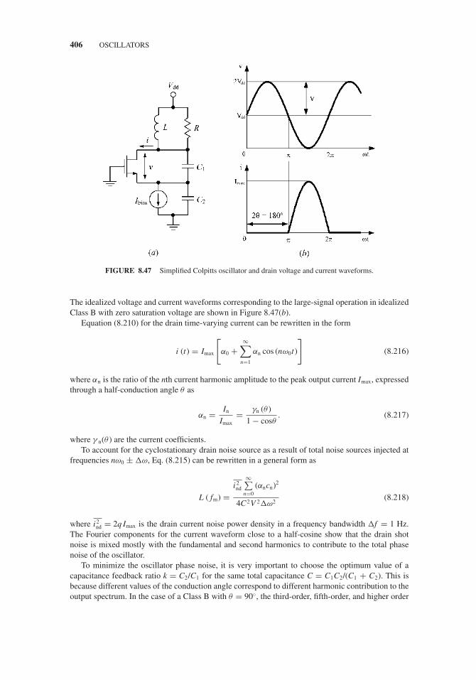
JWBS064-c08 JWBS064-Gerbennikov March 15, 2011 11:17 Printer Name: Yet to Come
406 OSCILLATORS
FIGURE 8.47 Simplified Colpitts oscillator and drain voltage and current waveforms.
The idealized voltage and current waveforms corresponding to the large-signal operation in idealizedClass B with zero saturation voltage are shown in Figure 8.47(b).
Equation (8.210) for the drain time-varying current can be rewritten in the form
i (t) = Imax
[α0 +
∞∑n=1
αn cos (nω0t)
](8.216)
where αn is the ratio of the nth current harmonic amplitude to the peak output current Imax, expressedthrough a half-conduction angle θ as
αn = In
Imax= γn (θ )
1 − cosθ. (8.217)
where γ n(θ ) are the current coefficients.To account for the cyclostationary drain noise source as a result of total noise sources injected at
frequencies nω0 ± �ω, Eq. (8.215) can be rewritten in a general form as
L ( fm) =i 2nd
∞∑n=0
(αncn)2
4C2V 2�ω2(8.218)
where i2nd = 2q Imax is the drain current noise power density in a frequency bandwidth �f = 1 Hz.
The Fourier components for the current waveform close to a half-cosine show that the drain shotnoise is mixed mostly with the fundamental and second harmonics to contribute to the total phasenoise of the oscillator.
To minimize the oscillator phase noise, it is very important to choose the optimum value of acapacitance feedback ratio k = C2/C1 for the same total capacitance C = C1C2/(C1 + C2). This isbecause different values of the conduction angle correspond to different harmonic contribution to theoutput spectrum. In the case of a Class B with θ = 90◦, the third-order, fifth-order, and higher order

JWBS064-c08 JWBS064-Gerbennikov March 15, 2011 11:17 Printer Name: Yet to Come
VOLTAGE-CONTROLLED OSCILLATORS 407
harmonics can be eliminated since their current coefficients γ n (for n = 3, 5, . . .) become equal tozero. As a rule-of-thumb, the optimum capacitance feedback ratio for a Colpitts oscillator can bechosen to be approximately k = 3.5–4 [52,57].
8.10 VOLTAGE-CONTROLLED OSCILLATORS
The VCOs are key components in many applications, especially in wireless communication systems,measurement equipment, or military applications. A growing market of wireless applications requireshighly integrated circuit solutions, where both high-performance transistors and passive elements withhigh-quality factors can be used. To analyze the tuning linearity of the VCO circuit, a general approachdescribing the oscillation circuit in terms of natural frequencies of a lossless two-port network whenone of its ports is short circuited can be used [58]. Figure 8.48 shows the block diagram of the generalVCO equivalent circuit, where a linear lossless network can incorporate one or several resonantcircuits including active device reactive elements, the baseband modulation signal is brought to thevaractor using port 3–3′, and the load is connected to the port 4–4′. Such a block representationenables the description of the VCO modulated curve in terms of poles and zeros, irrespective of anyparticular circuit diagram.
The oscillation frequency can be found form the phase balance condition of
X in (ω0) = −Xv (ω0) (8.219)
where Xin(ω0) is the reactance seen by the varactor, Xv(ω0) is the reactance of the varactor, and ω0 =2π f 0 is the radian oscillation frequency. The reactance seen by the active device is equal to zero atthe oscillation frequency.
Generally, the reactance Xin can be expressed in terms of poles and zeros. For instance, for thecase shown in Figure 8.49 where the poles occur at the origin and ω2 while the zeros occur at ω1 andω3, the reactance Xin is written as
X in (ω) = K
(ω2 − ω2
1
) (ω2 − ω2
3
)ω
(ω2 − ω2
2
) . (8.220)
The reactance due to the varactor junction capacitance can be written using Eq. (2.6) in Chapter 2in the form
Xv = − (vv + ϕ)γ
ωCvoϕγ(8.221)
where the voltage vv on the varactor consists of the dc bias voltage Vv and of the modulation voltage vm.The modulation voltage can be represented in the normalized form
v = vm
Vv + ϕ. (8.222)
FIGURE 8.48 Block diagram of VCO with linear circuit.

JWBS064-c08 JWBS064-Gerbennikov March 15, 2011 11:17 Printer Name: Yet to Come
408 OSCILLATORS
FIGURE 8.49 Reactance of lossless network.
For the initial conditions of ω = ω0, v is equal to zero. This leads to
1 + v =[(
ω2 − ω21
) (ω2
0 − ω22
) (ω2 − ω2
3
)(ω2
0 − ω21
) (ω2 − ω2
2
) (ω2
0 − ω23
)]1/γ
. (8.223)
Introducing the frequency normalization in the form of
ωi
ω0= �i for i = 1, 2, 3 (8.224)
and taking into account that, in the vicinity of the operating point
ω
ω0= 1 + η (8.225)
where η = (ω − ω0)/ω0 is the normalized frequency change representing a very small number, themodulation curve can be rewritten by
1 + v =[
(1 + η)2 − �21
1 − �21
1 − �22
(1 + η)2 − �22
(1 + η)2 − �23
1 − �23
]1/γ
. (8.226)
When the linear lossless circuit between the varactor and the active device has more than threefinite natural frequencies, Eq. (8.226) can be appropriately expanded to include any additional zerosand poles.
The simplest two-port network between the varactor and the active device is a single series resonantcircuit shown in Figure 8.50(a). The modulation curve for such a resonant circuit can be obtainedfrom Eq. (8.226) as
1 + v =[
1 + A1η + A1
2η2
]1/γ
(8.227)

JWBS064-c08 JWBS064-Gerbennikov March 15, 2011 11:17 Printer Name: Yet to Come
VOLTAGE-CONTROLLED OSCILLATORS 409
FIGURE 8.50 Schematics of two-port networks.
where
A1 = 2
1 − �21
.
Since η is a small number, it is convenient to use the binomial expansion to obtain first two termsof the Taylor series for voltage v by
v = C1η + C2η2 (8.228)
where
C1 = A1
γ
C2 = A1
2γ
[1 +
(1
γ− 1
)A1
].
The slope coefficient C1 is the inverse of the normalized circuit sensitivity Sn equal to
Sn = dη
dv
∣∣∣∣ω0
= SVv + ϕ
f0(8.229)
where S is the slope of the actual circuit sensitivity (or modulation curve) in hertz per volt. As aresult, for the series resonant circuit shown in Figure 8.50(a), the normalized sensitivity must satisfythe condition of
Sn = γ
2
(1 − �2
1
). (8.230)
The modulation curve is linearized by requesting C2 = 0 resulting in
γ = 2
1 + �21
. (8.231)
From Eq. (8.231) it follows that the varactor junction sensitivity γ must be larger than unitybecause �1 < 1. Consequently, the only possibility to linearize the modulation curve for a seriesresonant circuit is to use a hyperabrupt varactor. However, such a resonant circuit for a fixed operatingpoint does not provide enough flexibility to accommodate small variations in γ .
The inductively coupled pair of lumped resonant circuits shown in Figure 8.50(b) offers moredegree of freedom to linearize the modulation curve, having the position of natural frequencies ω1,ω2, and ω3 (when port 2–2′ is short-circuited), as shown in Figure 8.49. To achieve resonance with

JWBS064-c08 JWBS064-Gerbennikov March 15, 2011 11:17 Printer Name: Yet to Come
410 OSCILLATORS
the varactor capacitance, reactance Xin must be positive with oscillation frequency ω0 located abovethe zero ω3.
The linearity of the modulation curve of the resonant circuit with two coupled resonators can bedefined by expanding Eq. (8.226) in a three-term Taylor series
v = C1η + C2η2 + C3η
3 (8.232)
where
C1 = 1
γ(A1 − A2 + A3)
C2 = 1
2
[C1 + C2
1 − 1
γ
(A2
1 − A22 + A2
3
)]
C3 = −C31
3− C2
1
2− C1
2+ C2
(1
2+ C1
)+ 1
3γ
(A3
1 − A32 + A3
3
)
where
Ai = 2
1 − �2i
for i = 1, 2, 3.
Since the normalized sensitivity Sn0 at the center frequency ω0 can be written as Sn0 = 1/C1, andthe linearity of the modulation curve requires C2 = C3 = 0, then the three nonlinear equations can beobtained as
A1 − A2 + A3 = γ
Sn0(8.233)
A21 − A2
2 + A23 = γ
Sn0
(1 + γ
Sn0
)(8.234)
A31 − A3
2 + A33 = γ
Sn0
[3
2+ 1
Sn0
(3
2+ 1
Sn0
)](8.235)
which should be solved numerically to find the optimum position of natural frequencies forcingelimination of both the second and third coefficients in Eq. (8.232).
The calculated values �1, �2, and �3 are substituted in Eq. (8.226), and the relative frequency η
is gradually varied so that normalized modulation curve v(η) is evaluated [58]. The higher the chosenvalue of Sn0, the wider bandwidth within which the deviation from linearity stays within prescribedlimits. For example, by using an abrupt varactor with γ = 0.5, for 1% deviation from linearity, thesensitivity Sn0 = 0.02 results in the relative bandwidth of 0.0214, while the relative bandwidth is0.0319 for Sn0 = 0.03. To provide oscillation stability, the following approximate condition shouldbe satisfied:
�22 ≥ �2
r
(1 + k Qv�r
2�2v
)(8.236)
where �r = ωr/ω0 is the normalized resonant frequency associated with the varactor side,
ωr =√
C2 + Cv
L2C2Cv
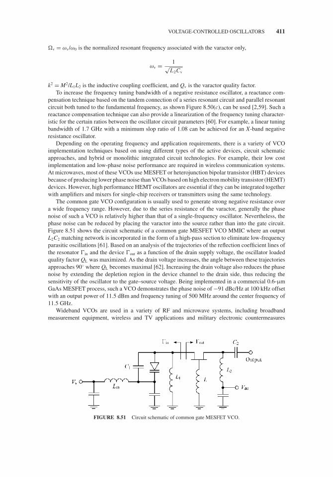
JWBS064-c08 JWBS064-Gerbennikov March 15, 2011 11:17 Printer Name: Yet to Come
VOLTAGE-CONTROLLED OSCILLATORS 411
�v = ωv/ω0 is the normalized resonant frequency associated with the varactor only,
ωv = 1√L2Cv
k2 = M2/L1L2 is the inductive coupling coefficient, and Qv is the varactor quality factor.To increase the frequency tuning bandwidth of a negative resistance oscillator, a reactance com-
pensation technique based on the tandem connection of a series resonant circuit and parallel resonantcircuit both tuned to the fundamental frequency, as shown Figure 8.50(c), can be used [2,59]. Such areactance compensation technique can also provide a linearization of the frequency tuning character-istic for the certain ratios between the oscillator circuit parameters [60]. For example, a linear tuningbandwidth of 1.7 GHz with a minimum slop ratio of 1.08 can be achieved for an X-band negativeresistance oscillator.
Depending on the operating frequency and application requirements, there is a variety of VCOimplementation techniques based on using different types of the active devices, circuit schematicapproaches, and hybrid or monolithic integrated circuit technologies. For example, their low costimplementation and low-phase noise performance are required in wireless communication systems.At microwaves, most of these VCOs use MESFET or heterojunction bipolar transistor (HBT) devicesbecause of producing lower phase noise than VCOs based on high electron mobility transistor (HEMT)devices. However, high performance HEMT oscillators are essential if they can be integrated togetherwith amplifiers and mixers for single-chip receivers or transmitters using the same technology.
The common gate VCO configuration is usually used to generate strong negative resistance overa wide frequency range. However, due to the series resistance of the varactor, generally the phasenoise of such a VCO is relatively higher than that of a single-frequency oscillator. Nevertheless, thephase noise can be reduced by placing the varactor into the source rather than into the gate circuit.Figure 8.51 shows the circuit schematic of a common gate MESFET VCO MMIC where an outputL2C2 matching network is incorporated in the form of a high-pass section to eliminate low-frequencyparasitic oscillations [61]. Based on an analysis of the trajectories of the reflection coefficient lines ofthe resonator in and the device out as a function of the drain supply voltage, the oscillator loadedquality factor QL was maximized. As the drain voltage increases, the angle between these trajectoriesapproaches 90◦ where QL becomes maximal [62]. Increasing the drain voltage also reduces the phasenoise by extending the depletion region in the device channel to the drain side, thus reducing thesensitivity of the oscillator to the gate–source voltage. Being implemented in a commercial 0.6-μmGaAs MESFET process, such a VCO demonstrates the phase noise of −91 dBc/Hz at 100 kHz offsetwith an output power of 11.5 dBm and frequency tuning of 500 MHz around the center frequency of11.5 GHz.
Wideband VCOs are used in a variety of RF and microwave systems, including broadbandmeasurement equipment, wireless and TV applications and military electronic countermeasures
FIGURE 8.51 Circuit schematic of common gate MESFET VCO.
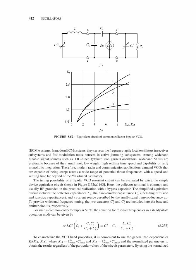
JWBS064-c08 JWBS064-Gerbennikov March 15, 2011 11:17 Printer Name: Yet to Come
412 OSCILLATORS
FIGURE 8.52 Equivalent circuit of common collector bipolar VCO.
(ECM) systems. In modern ECM systems, they serve as the frequency-agile local oscillators in receiversubsystems and fast-modulation noise sources in active jamming subsystems. Among widebandtunable signal sources such as YIG-tuned (yttrium iron garnet) oscillators, wideband VCOs arepreferable because of their small size, low weight, high settling time speed and capability of fullymonolithic integration. Therefore, modern radar and communication applications demand VCOs thatare capable of being swept across a wide range of potential threat frequencies with a speed andsettling time far beyond of the YIG-tuned oscillators.
The tuning possibility of a bipolar VCO resonant circuit can be evaluated by using the simpledevice equivalent circuit shown in Figure 8.52(a) [63]. Here, the collector terminal is common andusually RF grounded in the practical realization with a bypass capacitor. The simplified equivalentcircuit includes the collector capacitance Cc, the base–emitter capacitance Cπ (including diffusionand junction capacitances), and a current source described by the small-signal transconductance gm.To provide wideband frequency tuning, the two varactors Cb
v and C ev are included into the base and
emitter circuits, respectively.For such a common collector bipolar VCO, the equation for resonant frequencies in a steady-state
operation mode can be given by
ω2 LCbv
(Cc + CπC e
v
Cπ + C ev
)= Cb
v + Cc + Cπ Cev
Cπ + C ev
. (8.237)
To characterize the VCO band properties, it is convenient to use the generalized dependenciesKf(Kc1, Kc2), where Kc1 = Cb
vmax/Cbvmin and Kc2 = Ce
vmax/Cevmin, and the normalized parameters to
obtain the results regardless of the particular values of the circuit parameters. By using the normalized
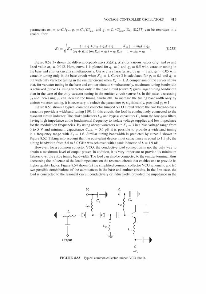
JWBS064-c08 JWBS064-Gerbennikov March 15, 2011 11:17 Printer Name: Yet to Come
VOLTAGE-CONTROLLED OSCILLATORS 413
parameters m0 = ωTCc/gm, q1 = Cc/Cbvmin, and q2 = Cc/Ce
vmin, Eq. (8.237) can be rewritten in ageneral form
Kf =√
Kc1(1 + q1) (m0 + q2) + q1
(q1 + Kc1) (m0 Kc2 + q2) + q1 Kc2
Kc2 (1 + m0) + q2
1 + m0 + q2. (8.238)
Figure 8.52(b) shows the different dependencies Kf(Kc1, Kc2) for various values of q1 and q2 andfixed value m0 = 0.012. Here, curve 1 is plotted for q1 = 1 and q2 = 0.5 with varactor tuning inthe base and emitter circuits simultaneously. Curve 2 is characterized by q1 = 1 and q2 = 0.05 withvaractor tuning only in the base circuit when Kc2 = 1. Curve 3 is calculated for q1 = 0.1 and q2 =0.5 with only varactor tuning in the emitter circuit when Kc1 = 1. A comparison of the curves showsthat, for varactor tuning in the base and emitter circuits simultaneously, maximum tuning bandwidthis achieved (curve 1). Using varactors only in the base circuit (curve 2) gives larger tuning bandwidththan in the case of the only varactor tuning in the emitter circuit (curve 3). In this case, decreasingq2 and increasing q1 can increase the tuning bandwidth. To increase the tuning bandwidth only byemitter varactor tuning, it is necessary to reduce the parameter q1 significantly, provided q2 = 1.
Figure 8.53 shows a typical common collector lumped VCO circuit where the two back-to-backvaractors provide a wideband tuning [19]. In this circuit, the load is conductively connected to theresonant circuit inductor. The choke inductors Lch and bypass capacitors Cb form the low-pass filtershaving high impedance at the fundamental frequency to isolate voltage supplies and low impedancefor the modulation frequencies. By using abrupt varactors with Kc = 3 in a bias voltage range from0 to 5 V and minimum capacitance Cvmin = 0.6 pF, it is possible to provide a wideband tuningin a frequency range with Kf = 1.6. Similar tuning bandwidth is predicted by curve 2 shown inFigure 8.52. Taking into account that the equivalent device input capacitance is equal to 1.5 pF, thetuning bandwidth from 5.5 to 8.0 GHz was achieved with a tank inductor of L = 1.9 nH.
However, for a common collector VCO, the conductive load connection is not the only way toobtain a maximum level of output power. In addition, it is very important to provide its minimumflatness over the entire tuning bandwidth. The load can also be connected to the emitter terminal, thusdecreasing the influence of the load impedance on the resonant circuit that enables one to provide itshigher quality factor. Figure 8.54 shows (a) the simplified common collector VCO schematic and (b)two possible combinations of the admittances in the base and emitter circuits. In the first case, theload is connected to the resonant circuit conductively or inductively, provided the impedance in the
FIGURE 8.53 Typical common collector lumped VCO circuit.
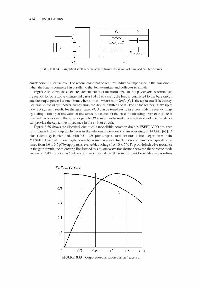
JWBS064-c08 JWBS064-Gerbennikov March 15, 2011 11:17 Printer Name: Yet to Come
414 OSCILLATORS
FIGURE 8.54 Simplified VCO schematic with two combinations of base and emitter circuits.
emitter circuit is capacitive. The second combination requires inductive impedance in the base circuitwhen the load is connected in parallel to the device emitter and collector terminals.
Figure 8.55 shows the calculated dependencies of the normalized output power versus normalizedfrequency for both above-mentioned cases [64]. For case 1, the load is connected to the base circuitand the output power has maximum when ω = ωα , where ωα = 2π f α , f α is the alpha cutoff frequency.For case 2, the output power comes from the device emitter and its level changes negligibly up toω = 0.5 ωα . As a result, for the latter case, VCO can be tuned easily in a very wide frequency rangeby a simple tuning of the value of the series inductance in the base circuit using a varactor diode inreverse bias operation. The series or parallel RC-circuit with constant capacitance and load resistancecan provide the capacitive impedance in the emitter circuit.
Figure 8.56 shows the electrical circuit of a monolithic common drain MESFET VCO designedfor a phase-locked loop application in the telecommunication system operating at 14 GHz [65]. Aplanar Schottky-barrier diode with 0.5 × 280 μm2 stripe suitable for monolithic integration with theMESFET device of the same gate geometry is used as a varactor. The varactor junction capacitance istuned from 1.0 to 0.5 pF by applying a reverse bias voltage from 0 to 5 V. To provide inductive reactancein the gate circuit, the microstrip line is used as a quarterwave transformer between the varactor diodeand the MESFET device. A 50-� resistor was inserted into the source circuit for self-biasing resulting
FIGURE 8.55 Output power versus oscillation frequency.

JWBS064-c08 JWBS064-Gerbennikov March 15, 2011 11:17 Printer Name: Yet to Come
VOLTAGE-CONTROLLED OSCILLATORS 415
Ω
FIGURE 8.56 Schematics of microwave MESFET VCO.
in a drain current stabilization. Another 50-� resistor was connected to the microstrip impedance trans-former to provide a gate zero bias point. These resistors are necessary to prevent low-frequency oscilla-tions by contributing to the significant decrease of the loaded quality factor at frequencies much loweror higher than resonant frequency. An output series capacitance is small enough to reduce the pullingeffect, compromising the output power. The frequency tuning bandwidth from 11.3 to 14.3 GHzwas achieved by varactor tuning in a bias range from 0 to 7 V with an output power of −4 dBm.
Figure 8.57 shows the wideband VCO circuit that was used to design and fabricate four GaAsmonolithic VCO chips that cover 2–4 GHz, 4–7 GHz, 7–12 GHz, and 12–18 GHz frequency ranges,respectively [66]. Each monolithic chip includes the MESFET device, two varactors, gate inductor Lg,source inductor Ls, and two bypass capacitors Cb. The varactor diode represents a single implantedstructure into semi-insulating material and is formed with the same active region as for the MESFETdevice. Its capacitance ratio is typically of 8:1 or greater. The common gate VCO configurationusing the gate inductor as a regenerative feedback element exhibits negative impedance at the sourceterminal across the entire tuning bandwidth for the equivalent load resistance connected to the drain
Ω
FIGURE 8.57 Microwave monolithic wideband VCO circuit schematic.

JWBS064-c08 JWBS064-Gerbennikov March 15, 2011 11:17 Printer Name: Yet to Come
416 OSCILLATORS
terminal of approximately 15 �. To provide the output matching with standard load of 50 �, theL-type matching circuit with a series inductor L1 and a shunt capacitor C1 is used. Due to the requiredadditional area, the output matching circuit was not included on the chip.
The VCO performance in terms of phase noise and tuning range determines the basic characteristicsof a whole transceiver. However, a limited frequency-tuning range is usually a serious problem forVCO fully based on CMOS technology. There are four basic candidate differential topologies shownin Figure 8.58 [67]. Figure 8.58(a) shows an nMOS differential VCO topology with tail current
FIGURE 8.58 Single differential topologies of CMOS VCO.
JWBS064-c08 JWBS064-Gerbennikov March 15, 2011 11:17 Printer Name: Yet to Come
CRYSTAL OSCILLATORS 417
source, while Figure 8.58(b) shows an nMOS differential topology with top current source. ThepMOS differential topologies with tail and top current sources are shown Figures 8.58(c) and 8.58(d),respectively. As regards tuning range capability, topologies shown in Figures 8.58(b) and 8.58(c) arepreferable. This is because the anode varactor bias voltage is fixed to Vdd for an nMOS oscillator withtail current source, and the anode varactor bias voltage is fixed to zero for a pMOS oscillator with topcurrent source.
Since using pMOS devices results in a lower phase noise due to inherently smaller low-frequency1/f noise, the pMOS differential topology with tail current source shown in Figure 8.58(c) representsthe best choice for a low-noise wideband tuning. Being implemented in a 0.25-μm standard CMOSprocess, such a differential VCO with a Q-factor of the tank inductor of 7.5 provides the phase noiseof −109 and −123 dBc/Hz at 100 and 500 kHz offset from carrier frequency of 1.3 GHz, respectively.The tuning range was 13.3% for Vdd = 1.4 V and 20.1% for Vdd = 2.0 V.
Using a proper configuration of the accumulation MOS varactors can significantly improve thetuning range. Such a varactor with high quality factor fabricated using the 0.13-μm CMOS silicon-on-insulator (SOI) technology demonstrates the capacitance ratio of 5 with ± 1 V voltage tuningthat provides over 50% frequency-tuning range [68]. However, a high capacitance ratio implies ahigh varactor sensitivity or KVCO, which makes the oscillator phase noise worse. A band switchingsolution can reduce the varactor sensitivity, but requires extra control circuitry. A simple and effectivesolution can be provided by differential varactor tuning to avoid the effect of high KVCO.
8.11 CRYSTAL OSCILLATORS
The traditional and most common type of a piezoelectric resonator used in electronics is the quartzcrystal. Its operation is based on a piezoelectric effect that converts the electrical signal applying tothe opposite sides of the crystal to mechanical motion and reconverts the vibratory motion of thecrystal back into an electrical signal at the resonator terminals. The amount of motion varies over wideextremes depending on how closely the applied signal frequency approaches a natural mechanicalresonance of the crystal. In a properly designed resonator these regions of high-amplitude mechanicalvibration are very narrow in frequency and are ideally suited for oscillator stabilization. Therefore, theoscillator circuits using a quartz crystal are called the crystal oscillators. The first crystal-controlledoscillator, using a crystal of Rochelle salt, was first built by Alexander M. Nicolson and the resultswere filed in the form of a patent application in 1918 [69]. In 1919, Walter G. Cady used the quartzto control the frequency of an oscillator and described the use of quartz bars and plates as frequencystandards and wave filters [70]. Since then, it is generally accepted that Cady was the first to use thequartz to control the frequency of an oscillator circuit. However, subsequent litigation resulted in alegal decision in favor of Nicolson who is therefore considered to be the inventor of the piezoelectricoscillator.
The quartz crystal represents one of forms of silicone dioxide (SiO2) that is found in nature and isideal for use as a frequency-determining device because of its predictable thermal, mechanical, andelectrical characteristics with a high quality factor. The quartz properties are primarily determined bythe orientation angle at which the quartz wafers are cut, being dependent on the reference directionswithin the crystal that are referred to as axes. There are three axes in quartz, forwarded along the X, Y,and Z directions. Ideal quartz would consist of a hexagonal prism with six facets at each end, with across section shown in Figure 8.59 [71]. The Z-axis is known as the optical axis, repeating its physicalproperties every 120◦ as the crystal is rotated about the Z-axis. This axis is not anisotropic to light;therefore light passes readily. The X-axis called the electrical axis is parallel to a line bisecting theangles between adjacent prism faces. Electrical polarization occurs in this direction when mechanicalpressure is applied. The Y-axis, which is called the mechanical axis, runs at right angles through theface of the prism, and at right angles to the X-axis.
The AT cut is the most popular of the Y-axis group because of its excellent temperature character-istic, and it is produced by cutting the quartz bar at an angle of approximately 35◦15′ from Z-axis. The
JWBS064-c08 JWBS064-Gerbennikov March 15, 2011 11:17 Printer Name: Yet to Come
418 OSCILLATORS
Z1
Z1
Z1
49 35
AT
CT
CutY
CutX
Z
52DT
FT
BT
57 38
X
Y
Y
X
FIGURE 8.59 Typical crystal cuts from a doubly terminated quartz crystal.
crystal resonator is usually represents a round disc and its fundamental mode measured in megahertzis defined as
f = N
d(8.239)
where d is the disc thickness in millimeters and N is the frequency constant for particular cut, forexample, equal to 1.661 MHz/mm for AT cut, 1.797 MHz/mm for SC cut, or 2.536 MHz/mm forBT cut [72]. Because the frequency of the crystal is related to its thickness, there is a limitation inthe manufacturing of high-frequency fundamental crystals. For example, a 100 MHz AT-cut crystalresonator has a thickness of only 16.61 microns. In this case, the higher the frequency, the thinnershould be the crystal plate. Such a thin wafer is not only somewhat fragile but also impracticalto fabricate by conventional means, which are normally limited to thicknesses of 30–35 microns(approximately 50 MHz for AT-cut resonators). However, by introducing chemical polishing methodsusing fluorides and composite double inverted mesa blank structures with air-gapped electrode haveresulted in AT-cut crystal resonators with fundamental frequencies up to 1.6 GHz, corresponding toa resonator plate thickness of just less than 1 micron [73,74]. The measured quality factors of theseunits ranged from 73,000 at 100 MHz and 32,000 at 250 MHz to 5,000 at 950 MHz.
JWBS064-c08 JWBS064-Gerbennikov March 15, 2011 11:17 Printer Name: Yet to Come
CRYSTAL OSCILLATORS 419
FIGURE 8.60 Simplified equivalent circuit of crystal resonator.
Figure 8.60(a) shows the symbol for a crystal resonator that should generally be treated as atwo-port device together with its metallic enclosure, leads and supports. However, in some practicalcases, especially at lower frequencies, the complete equivalent circuit of a crystal resonator canbe simplified, as shown in Figure 8.60(b), where the crystal vibration portion is represented in thevicinity of a series resonance by dynamic parameters such as an inductance L1, a capacitance C1
and a resistance R1, whereas C0 is the static capacitance associated with the crystal and its adherentelectrodes plus the stray capacitances internal to the crystal enclosure [74]. The impedance of a crystalresonator (between point 1−1′) can be written as
Z ( jω) = 1
jωC0
ω2s + jω
R1
L1− ω2
ω2p + jω
R1
L1− ω2
. (8.240)
where
ωs = 1√L1C1
(8.241)
is the series resonant frequency in radians per second and, for C0 � C1,
ωp =√
C1 + C0
L1C1C0= ωs
√1 + C1
C0
∼= ωs
(1 + C1
2C0
)(8.242)
is the parallel resonant frequency in radians per second.The simplified model of a crystal resonator shown in Figure 8.60(b) can be represented by an
equivalent general network, as shown in Figure 8.60(c), with the impedance expressed as
Z ( jω) = Re (ω) + j Xe (ω) (8.243)
where
Re (ω) = R1
(1 − ab)2 + b2(8.244)
Xe (ω) = R1a (1 − ab) − b
(1 − ab)2 + b2(8.245)
where a = (ωsL1/R1)(ω/ωs − ωs/ω) and b = ωC0R1.
JWBS064-c08 JWBS064-Gerbennikov March 15, 2011 11:17 Printer Name: Yet to Come
420 OSCILLATORS
FIGURE 8.61 Resistive and reactive parts of crystal resonator network.
The equivalent-circuit resistance Re and reactance Xe given by Eqs. (8.244) and (8.245), re-spectively, are plotted in Figure 8.61 as functions of frequency over its wide range. It is seen thatreactance Xe is zero at two values of frequency where the lower frequency is just slightly above theseries resonant frequency ωs and upper frequency corresponds to a nearly maximum resistance Re.Equation (8.245) can be simplified to
Xe (ω) ≈ 2
ωC1
� f
f(8.246)
which is used as a measure of the slope of the curve at the operating frequency f . The slope of Xe
versus frequency is a measure of crystal resonator stiffness [72]. The resonator quality factor Qx isdefined as
Qx = 1
ωC1 R1(8.247)
the inverse value of which is a measure of loss in the resonator. Therefore, the resonator (or unloaded)quality factor is always higher than the oscillator (or loaded) quality factor.
Generally, the crystal oscillators can be divided into two basic groups. In the first group, thecrystal resonator represents an inductive reactance, whereas, in the second group, it is used as a seriesresonant circuit included into the feedback loop. The basic and most widely used crystal oscillatorcircuit corresponding to the first group is shown in Figure 8.62(a), where the crystal resonator isincluded between collector and base terminals. It is called the Pierce oscillator in the honor ofGeorge W. Pierce, whose modified and simplified single-stage crystal oscillator circuit became thetouchstone of the radio communication art. It is also possible to include crystal oscillator betweenthe base and emitter terminals, as shown in Figure 8.62(b), and between the collector and emitterterminals, as shown in Figure 8.62(c). In both latter cases, the crystal oscillator represents an inductivethree-point circuit, which is a crystal analog of a Hartley LC oscillator, unlike of a Colpitts LC analog

JWBS064-c08 JWBS064-Gerbennikov March 15, 2011 11:17 Printer Name: Yet to Come
CRYSTAL OSCILLATORS 421
FIGURE 8.62 Simplified oscillator circuits with crystal resonator.
of a crystal Pierce oscillator. Adding additional capacitance across the crystal will cause the parallelresonance to shift downward. This can be used to adjust the frequency at which a crystal oscillatoroscillates.
For an ideal Pierce oscillator shown in Figure 8.62(a) when the active device is regarded as anideal and loss in crystal is neglected, the phase balance condition can be written as
X1 (ωosc) + X2 (ωosc) + Xe (ωosc) = 0 (8.248)
where ωosc is the oscillation frequency, X1 = 1/(ωoscC1), X2 = 1/(ωoscC2), and Xe(ωosc) is defined byEq. (8.245). The graphical solution of Eq. (8.248) is shown in Figure 8.61, where there are two points,in which a curve −(X1 + X2) intersects a curve Xe. In this case, point A corresponds to the oscillationfrequency ωosc with a low resistance Re, whereas point B corresponds to the frequency with a highresistance Re where the amplitude balance condition is not satisfied and build-up of self-oscillationscan never happen. An analytical solution of Eq. (8.248) determines the frequency of self-oscillationequal to
ωosc = ωs
[1 + 1
2
C1
C0 + C2C3/ (C2 + C3)
]. (8.249)
Most types of the quartz vibration may be used on different overtones or harmonics. Among them,the most popular by far are the thickness vibrations of plates such as AT- and BT-cut of quartz, wherethe thickness determines the fundamental frequency according to Eq. (8.239). Odd overtones of thefundamental frequency may be excited in resonator, and Figure 8.63(a) represents the equivalentcircuit of a family of overtones associated with the fundamental, where CN = C1/N 2, LN = L1, andRN = R1 N 2, N = 1, 3, 5, . . . is the overtone number [72]. It should be noted that overtones areused because the smaller CN values lead to greater frequency stability due to increasing reactanceslope with increasing N. In order to operate at one of the crystal overtones, the oscillator schematicshould be slightly changed. In this case, an additional inductor L can be connected in parallel to acapacitor C1, as shown in Figure 8.63(b). The resonant frequency of LC1 circuit is chosen to be lowerthan the required operating frequency but higher than the nearest overtone. As a result, this circuitrepresents a capacitive reactance at the operating frequency, providing a conventional capacitive three-point oscillator configuration. However, at lower frequencies, the LC1 circuit represents an inductivereactance when the phase balance condition is not satisfied. When the crystal is connected as thetransistor emitter load impedance, such a harmonic emitter-coupled crystal oscillator can providevery good short-term frequency stability [75,76].
To design crystal oscillator at higher frequencies, it is necessary to maximize its regenerationfactor, which can be increased by minimizing the effect of the internal transistor feedback collector-base capacitance, thus resulting in a higher device maximum oscillation frequency. This can bedone by using a cascode crystal oscillator configuration, simplified schematic of which is shown in
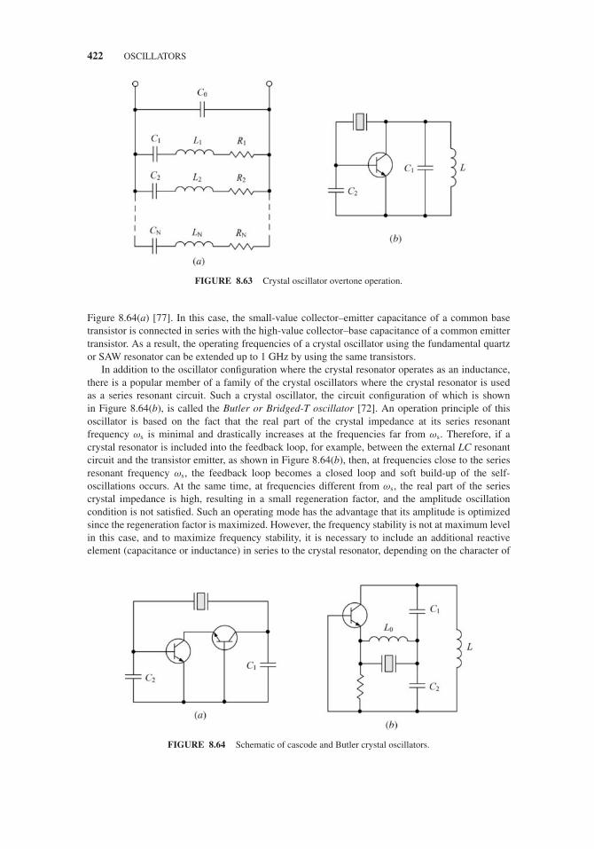
JWBS064-c08 JWBS064-Gerbennikov March 15, 2011 11:17 Printer Name: Yet to Come
422 OSCILLATORS
FIGURE 8.63 Crystal oscillator overtone operation.
Figure 8.64(a) [77]. In this case, the small-value collector–emitter capacitance of a common basetransistor is connected in series with the high-value collector–base capacitance of a common emittertransistor. As a result, the operating frequencies of a crystal oscillator using the fundamental quartzor SAW resonator can be extended up to 1 GHz by using the same transistors.
In addition to the oscillator configuration where the crystal resonator operates as an inductance,there is a popular member of a family of the crystal oscillators where the crystal resonator is usedas a series resonant circuit. Such a crystal oscillator, the circuit configuration of which is shownin Figure 8.64(b), is called the Butler or Bridged-T oscillator [72]. An operation principle of thisoscillator is based on the fact that the real part of the crystal impedance at its series resonantfrequency ωs is minimal and drastically increases at the frequencies far from ωs. Therefore, if acrystal resonator is included into the feedback loop, for example, between the external LC resonantcircuit and the transistor emitter, as shown in Figure 8.64(b), then, at frequencies close to the seriesresonant frequency ωs, the feedback loop becomes a closed loop and soft build-up of the self-oscillations occurs. At the same time, at frequencies different from ωs, the real part of the seriescrystal impedance is high, resulting in a small regeneration factor, and the amplitude oscillationcondition is not satisfied. Such an operating mode has the advantage that its amplitude is optimizedsince the regeneration factor is maximized. However, the frequency stability is not at maximum levelin this case, and to maximize frequency stability, it is necessary to include an additional reactiveelement (capacitance or inductance) in series to the crystal resonator, depending on the character of
FIGURE 8.64 Schematic of cascode and Butler crystal oscillators.

JWBS064-c08 JWBS064-Gerbennikov March 15, 2011 11:17 Printer Name: Yet to Come
DIELECTRIC RESONATOR OSCILLATORS 423
FIGURE 8.65 Schematics of negative resistance crystal oscillator.
the loading reactance of the external resonant circuit. It should be noted that the parasitic oscillationscan be arisen at frequencies significantly higher than ωs due to the crystal static capacitance C0, whosereactance is small at these high frequencies and can result in a significant feedback with potentialestablishing of self-oscillations. To prevent this parasitic phenomenon, it is necessary to include anexternal neutralizing inductance L0 in parallel to C0, in order to form the parallel resonant circuit atvery high frequencies.
The negative resistance approach to design a crystal oscillator can also be attractive, based ona common base transistor configuration with a series feedback inductor at the base, as shown inFigure 8.65(a) [78]. In this case, the parasitic capacitances of the transistor, together with the seriesinductive feedback obtained by a short-circuited stub, and a properly designed terminating networkprovides the negative resistance required at the input port, connected to the resonant network, to satisfythe oscillation conditions in a wide frequency range. Figure 8.65(b) shows the complete schematicof a microwave crystal oscillator operating at the fundamental resonance of the crystal resonator of842.911 MHz. The oscillator was built using a substrate with relative dielectric constant of 4.8 andthickness of 1.5 mm. The experimental results showed that the negative resistance approach to designthe crystal oscillator is well suited for its potential low-noise microwave application.
8.12 DIELECTRIC RESONATOR OSCILLATORS
It is known yet from 1930s that the dielectric object with free-space boundaries can resonate invarious modes [79]. If the relative dielectric constant is high, the electric and magnetic fields ofa given resonant mode will be confined in and near the resonator and will attenuate to negligiblevalues at a distance small compared to free-space wavelength. Therefore, radiation loss is very small,

JWBS064-c08 JWBS064-Gerbennikov March 15, 2011 11:17 Printer Name: Yet to Come
424 OSCILLATORS
and the unloaded Q of the resonance is limited mainly by losses inside the dielectric body. Sincethe magnetic permeability of the dielectric material used is unity, then magnetic losses are zero.Electrical losses occur as a result of the finite loss tangent (tanδ) of the dielectric material. Typicaltanδ values for dielectric materials used as resonators are about 0.0001–0.0002, thus resulting inthe values of unloaded Q of about 5000–10,000 and even higher for high-purity TiO2 disks [80].For the fundamental-mode resonance, the dimensions of a dielectric resonator are on the order ofone wavelength in the dielectric material. As a result, for the material with high relative dielectricconstant, the size of the dielectric resonator can be very small. For example, for a polycrystalline TiO2
ceramic with a relative dielectric constant εr of about 100, the effective wavelength in the dielectricwill be one-tenth of the wavelength in air only. However, the disadvantage of dielectric resonators issignificant variation of dielectric constant with temperature. For TiO2 material, the relative change ofdielectric constant εr is about 1000 ppm/◦C. Higher dielectric-constant materials such as strontiumtitanate (εr > 250) have much greater temperature sensitivities. Therefore, materials with dielectricconstants 10 ≤ εr ≤ 100 are generally used, such as barium tetratitanate and titanium dioxide.
The most practical shape of a dielectric resonator is a cylindrical disk whose length (thickness)L is less than its diameter D. With this shape, the lowest frequency resonant mode has a circularelectric field distribution, whereas the magnetic field is strongest on the axis of the disk and at asufficient distance outside the disk the field resembles that of an axial magnetic dipole, as shown inFigure 8.66 [81]. The axial-dipole mode offers the best separation from other resonances when thedielectric optimum ratio of L/D is about 0.4 [80]. The resonant frequency of the dielectric resonatordepends on its shape, being a function of the relative dielectric constant εr, diameter D, and thicknessL for a cylindrical resonator configuration [82].
In practical microwave resonant circuits, the dielectric resonator is placed on the alumina substrateand is confined within a metal case. In this case, the resonant circuit has a tripled-layered structure ofalumina substrate, cylindrical dielectric resonator, and air gap. As a result, the resonant frequenciesof such tripled-layered structures are higher than the values predicted theoretically based on thesimplified assumptions. For example, the resonant frequency decreases with increasing resonatordiameter and alumina substrate thickness for a fixed optimum ratio L/D = 0.4 [83]. Fine adjustmentof resonant frequency is possible by changing air gap thickness between the resonator and themetal disk.
When a dielectric resonator is placed in the vicinity of a microstrip line on the alumina substrate,as shown in Figure 8.67(a), magnetic coupling between the resonator and microstrip line is caused,increasing if the distance l between the resonator edge and microstrip-line edge decreases [84]. In thiscase, the dielectric resonator operates like a reaction cavity that reflects the radiofrequency energy at
DR
TransmissionLines
Substrate
Ground plane To gate #1 To gate #2
ig2
ig1
εr= 46
εr= 3.9
L
DR
H fieldE field
FIGURE 8.66 DR-microstrip coupling and electromagnetic fields.

JWBS064-c08 JWBS064-Gerbennikov March 15, 2011 11:17 Printer Name: Yet to Come
DIELECTRIC RESONATOR OSCILLATORS 425
FIGURE 8.67 DR-microstrip coupling and equivalent circuit.
the resonant frequency, which is similar to an open circuit with a voltage maximum at the referenceplane at the resonant frequency. Because coupling is via the magnetic filed, the dielectric resonatorappears as a series load on the microstrip line, as shown in the equivalent circuit of Figure 8.67(b).The resonator is modeled as a parallel RLC circuit, and the coupling to the line is represented by theturns ratio of the equivalent transformer. Since the input impedance Zin of a parallel RLC circuit canbe written as
Z in = R
1 + 2jQ�ω
ω0
(8.250)
where Q = R/(ω0L) = ω0CR is the unloaded quality factor of the resonator, ω0 = 1/√
LC is theresonant frequency, and �ω = ω − ω0, then the equivalent series impedance Z seen by the microstripline is expressed as
Z = N 2 R
1 + 2jQ�ω
ω0
(8.251)
where N is the turns ratio of the equivalent transformer [85].The coupling factor g between the resonator and the feedline represents the ratio of the unloaded
Q to external Qe, and can be written as
g = Q
Qe= R
ω0 L/
RL
N 2ω0 L= N 2 R
2Z0(8.252)
where RL = 2Z0 is the load resistance for a feedline with source and termination resistances Z0
[86,87]. In some cases, the feedline is terminated with an open-circuit quarterwave line from theresonator to maximize the magnetic field at that point, thus resulting in RL = Z0, and the couplingfactor is twice the value given in Eq. (8.252).
The reflection coefficient seen by the source on the terminated microstrip line toward the resonatorcan be written as
=(Z0 + N 2 R
) − Z0(Z0 + N 2 R
) + Z0= N 2 R
2Z0 + N 2 R= g
1 + g(8.253)
which can be used to determine the coupling coefficient from the direct measurements as
g = 1 −
. (8.254)
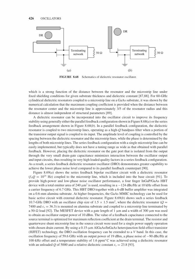
JWBS064-c08 JWBS064-Gerbennikov March 15, 2011 11:17 Printer Name: Yet to Come
426 OSCILLATORS
FIGURE 8.68 Schematics of dielectric resonator oscillator.
which is a strong function of the distance between the resonator and the microstrip line underfixed shielding conditions for given substrate thickness and dielectric constant [87,88]. For 60-GHzcylindrical dielectric resonators coupled to a microstrip line on a GaAs substrate, it was shown by thenumerical calculation that the maximum coupling coefficient is provided when the distance betweenthe resonator center and the microstrip line is approximately 3/5 of the resonator radius and thisdistance is almost independent of structural parameters [89].
A dielectric resonator can be incorporated into the oscillator circuit to improve its frequencystability using generally either the parallel feedback configuration shown in Figure 8.68(a) or the seriesfeedback arrangement shown in Figure 8.68(b). In a parallel feedback configuration, the dielectricresonator is coupled to two microstrip lines, operating as a high-Q bandpass filter when a portion ofthe transistor output signal is coupled to its input. The amplitude level of coupling is controlled by thespacing between the dielectric resonator and the microstrip lines, while the phase is determined by thelengths of both microstrip lines. The series feedback configuration with a single microstrip line can beeasily implemented, but typically does not have a tuning range as wide as that obtained with parallelfeedback. However, placing the dielectric resonator on the gate port that is isolated from the outputthrough the very small drain-gate capacitance minimizes interaction between the oscillator outputand input circuits, thus resulting in very high loaded quality factors in a series feedback configuration.As a result, a series feedback dielectric resonator oscillator (DRO) demonstrates greater capability toachieve the lower phase noise level compared to its parallel feedback counterpart [90].
Figure 8.69(a) shows the series feedback bipolar oscillator circuit with a dielectric resonator(f 0Q = 1014 Hz) coupled to the microstrip line, which is included into the base circuit [91]. Toprovide high-power and low-phase noise oscillator performance, a four finger InGaP/GaAs HBTdevice with a total emitter area of 240 μm2 is used, resulting in a −124 dBc/Hz at 10 kHz offset froma carrier frequency of 6.7 GHz. This HBT DRO together with a 6-dB buffer amplifier was integratedon a 0.6-mm alumina substrate. At higher frequencies, the GaAs MMIC technology can be used forbasic active circuit with external dielectric resonator. Figure 8.69(b) shows such a series feedback10.7-GHz DRO with an oscillator chip size of 1.5 × 1.5 mm2, where the dielectric resonator (Q =7400 and εr = 36.3) is mounted on alumina substrate and coupled to a microstrip line terminated bya 50-� load [92]. The MESFET device with a gate length of 1 μm and a width of 300 μm was usedto obtain an oscillator output power of 10 dBm. The value of a feedback capacitance connected to thesource terminal is optimized for maximum reflection coefficient at the drain terminal. The resistor andquarterwave shunt microstrip line in the source circuit were used for a single power supply operationwith chosen drain current. By using a 0.15-μm AlGaAs/InGaAs heterojunction field-effect transistor(HJFET) technology, the DRO oscillation frequency can be extended to a V band. In this case, theoscillation frequency of 59.6 GHz with an output power of 19 dBm, a phase noise of −90 dBc/Hz at100-kHz offset and a temperature stability of 1.6 ppm/◦C was achieved using a dielectric resonatorwith an unloaded Q of 5000 and a relative dielectric constant εr = 23.8 [93].

JWBS064-c08 JWBS064-Gerbennikov March 15, 2011 11:17 Printer Name: Yet to Come
DIELECTRIC RESONATOR OSCILLATORS 427
FIGURE 8.69 Schematics of series feedback dielectric resonator oscillator.
However, at high microwave frequencies, it is very difficult to effectively manufacture accuratehigh-Q dielectric resonators, as well as their physical handling, since a 2-GHz resonator is in theorder of 1 mm in diameter. Also, at Ka-band frequencies and higher, the gain of the transistorsfor the same output power becomes marginal, and resonator coupling would need to be excessive,thus destroying the inherent Q and spectral purity of the oscillator. These problems can be partiallyeliminated by employing a push-push oscillator design approach. Figure 8.70 shows the push–pushDRO configuration, where outputs from both transistors are combined in parallel using ordinarymicrostrip technique. In this case, each microstrip line has a characteristic impedance of 100 � andis of a half-wavelength at fundamental frequency f 0, in order to provide a parallel connection of thetransistors with the output impedances of 100 � [94]. Since the gate circuits of each MESFET are onopposite sides of the resonator, the currents coupled at each gate will be exactly antiphased, as shownin Figure 8.66. Under these conditions, each MESFET is phase locked to the other, with their second-harmonic power combined in phase at the output of the oscillator and delivered to the 50-� load. Apositive feedback by using a capacitive open-circuit stub is added to each device source. The level ofthe fundamental power at the load is usually of −25 dBc and less, relatively to the second-harmonicpower, which can be maximized when MESFET is biased near pinch-off or forward conduction.The dielectric resonator must be located at the distance of θ = 180◦ from the gates, however inputdevice reactances should be taken into account, since they provides the effective transmission-lineelectrical length extension. The 50-� resistors at the ends of the gate transmission lines are necessary
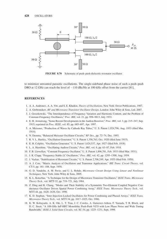
JWBS064-c08 JWBS064-Gerbennikov March 15, 2011 11:17 Printer Name: Yet to Come
428 OSCILLATORS
FIGURE 8.70 Schematic of push–push dielectric resonator oscillator.
to minimize unwanted parasitic oscillations. The single-sideband phase noise of such a push–pushDRO at 12 GHz can reach the level of −110 dBc/Hz at 100-kHz offset from the carrier [81].
REFERENCES
1. A. A. Andronov, A. A. Vitt, and S. E. Khaikin, Theory of Oscillations, New York: Dover Publications, 1987.
2. A. Grebennikov, RF and Microwave Transistor Oscillator Design, London: John Wiley & Sons, Ltd. 2007.
3. J. Groszkowski, “The Interdependence of Frequency Variation and Harmonic Content, and the Problem ofConstant-Frequency Oscillators,” Proc. IRE, vol. 21, pp. 958–9813, July 1933.
4. E. H. Armstrong, “Some Recent Developments in the Audion Receiver,” Proc. IRE, vol. 3, pp. 215–247, Sep.1915; reprinted in Proc. IEEE, vol. 85, pp. 685–697, Apr. 1997.
5. A. Meissner, “Production of Waves by Cathode Ray Tubes,” U. S. Patent 1,924,796, Aug. 1933 (filed Mar.1914).
6. N. Demma, “Balanced Meissner Oscillator Circuits,” RF Des., pp. 72–74, Dec. 1993.
7. R. V. L. Hartley, “Oscillation Generator,” U. S. Patent 1,356,763, Oct. 1920 (filed June 1915).
8. E. H. Colpitts, “Oscillation Generator,” U. S. Patent 1,624,537, Apr. 1927 (filed Feb. 1918).
9. L. A. Hazeltine, “Oscillating Audion Circuits,” Proc. IRE, vol. 6, pp. 63–97, Feb. 1918.
10. F. B. Llewellyn, “Constant Frequency Oscillator,” U. S. Patent 1,896,781, Feb. 1933 (filed Mar. 1931).
11. J. K. Clapp, “Frequency Stable LC Oscillators,” Proc. IRE, vol. 42, pp. 1295–1300, Aug. 1954.
12. J. Vackar, “Stabilization of Resonant Circuits,” U. S. Patent 2,706,249, Apr. 1955 (filed Feb. 1950).
13. A. J. Cote, “Matrix Analysis of Oscillators and Transistor Applications,” IRE Trans. Circuit Theory, vol.CT-5, pp. 181–188, Sept. 1958.
14. G. D. Vendelin, A. M. Pavio, and U. L. Rohde, Microwave Circuit Design Using Linear and NonlinearTechniques, New York: John Wiley & Sons, 2005.
15. K. L. Kotzebue, “A Technique for the Design of Microwave Transistor Oscillators,” IEEE Trans. MicrowaveTheory Tech., vol. MTT-32, pp. 719–721, July 1984.
16. Z. Ding and K. Chang, “Modes and Their Stability of a Symmetric Two-Element Coupled Negative Con-ductance Oscillator Driven Spatial Power Combining Array,” IEEE Trans. Microwave Theory Tech., vol.MTT-44, pp. 1628–1636, Oct. 1996.
17. K. D. Stephan, “Inter-Injection-Locked Oscillators for Power Combining and Phased Arrays,” IEEE Trans.Microwave Theory Tech., vol. MTT-34, pp. 1017–1025, Oct. 1986.
18. K. W. Kobayashi, A. K. Oki, L. T. Tran, J. C. Cowles, A. Gutierrez-Aitken, F. Yamada, T. R. Block, andD. C. Streit, “A 108-GHz InP-HBT Monolithic Push-Push VCO with Low Phase Noise and Wide TuningBandwidth,” IEEE J. Solid-State Circuits, vol. SC-34, pp. 1225–1231, Sept. 1999.

JWBS064-c08 JWBS064-Gerbennikov March 15, 2011 11:17 Printer Name: Yet to Come
REFERENCES 429
19. A. Shipow, “Linearity in Solid State Microwave Voltage Tuned Oscillators,” Microwave J., vol. 26, pp.130–137, Feb. 1983.
20. J. R. Bender and C. Wong, “Push-Push Design Extends Bipolar Frequency Range,” Microwave & RF, vol.22, pp. 91–98, Oct. 1983.
21. H. Xiao, T. Tanaka, and M. Aikawa, “Push-Push Oscillator Using λg/2 Microstrip Resonator,” IEICE Trans.Electron., vol. E86-C, pp. 1438–1443, Aug. 2003.
22. K. Kurokawa, “Some Basic Characteristics of Broadband Negative Resistance Oscillator Circuits,” Bell Syst.Tech. J., vol. 48, pp. 1937–1955, July 1969.
23. K. M. Johnson, “Large Signal GaAs MESFET Oscillator Design,” IEEE Trans. Microwave Theory Tech., vol.MTT-27, pp. 217–227, Mar. 1979.
24. H. Abe, “A GaAs MESFET Oscillator Using Quasi-Linear Design Method,” IEEE Trans. Microwave TheoryTech., vol. MTT-34, pp. 19–25, Jan. 1986.
25. Y. Tajima, B. Wrona, and K. Mishima, “GaAs FET Large-Signal Model and Its Application to Circuit Design,”IEEE Trans. Electron Devices, vol. ED-28, pp. 171–175, Feb. 1981.
26. R. J. Gilmore and F. J. Rosenbaum, “An Analytic Approach to Optimum Oscillator Design UsingS-Parameters,” IEEE Trans. Microwave Theory Tech., vol. MTT-31, pp. 633–639, Aug. 1983.
27. D. F. Page, “A Design Basis for Junction Transistor Oscillator Circuits,” Proc. IRE, vol. 46, pp. 1271–1280,Nov. 1958.
28. M. Madihian and T. Noguchi, “An Analytical Approach to Microwave GaAs FET Oscillator Design,” NECRes. Dev., no. 82, pp. 49–56, July 1986.
29. A. V. Grebennikov and V. V. Nikiforov, “An Analytic Method of Microwave Transistor Oscillator Design,”Int. J. Electron., vol. 83, pp. 849–858, Dec. 1997.
30. M. Maeda, K. Kimura, and H. Kodera, “Design and Performance of X-Band Oscillators with GaAs Schottky-Gate Field-Effect Transistors,” IEEE Trans. Microwave Theory Tech., vol. MTT-23, pp. 661–667, Aug. 1975.
31. J. F. Gibbons, “An Analysis of the Modes of Operation of a Simple Transistor Oscillator,” Proc. IRE, vol. 49,pp. 1383–1390, Sep. 1961.
32. A. V. Grebennikov, “Microwave Transistor Oscillators: Analytic Approach to Simplify Computer-AidedDesign,” Microwave J., vol. 42, pp. 292–300, May 1999.
33. J.-M. Dortu, J.-E. Muller, M. Pirola, and G. Ghione, “Accurate Large-Signal GaAs MESFET and HEMTModeling for Power MMIC Amplifier Design,” Int. J. Microw. Millimet. Wave Computer-Aided Eng., vol. 5,pp. 195–209, May 1995.
34. A. V. Grebennikov, “Microwave FET Oscillators: Analytic Approach to Simplify Computer-Aided Design,”Microwave J., vol. 43, pp. 100–110, Jan. 2000.
35. D. B. Leeson, “A Simple Model of Feedback Oscillator Noise Spectrum,” Proc. IEEE, vol. 54, pp. 329–330,Feb. 1966.
36. D. Scherer, “Today’s Lesson − Learn about Low-Noise Design,” Microwaves, vol. 18, pp. 116–122, Apr.1979.
37. T. E. Parker, “Characteristics and Sources of Phase Noise in Stable Oscillators,” Proc. 41st Annu. Freq.Control Symp., pp. 99–110, 1987.
38. D. J. Healy III, “Flicker of Frequency and Phase and White Frequency and Phase Fluctuations in FrequencySources,” Proc. 26th Annu. Freq. Control Symp., pp. 43–49, 1972.
39. J. K. A. Everard, “A Review of Low Noise Oscillator: Theory and Design,” Proc. IEEE Int. Frequency ControlSymp., pp. 909–918, 1997.
40. T. E. Parker, “Current Developments in SAW Oscillator Stability,” Proc. 31st Annu. Freq. Control Symp., pp.359–364, 1977.
41. H. J. Siweris and B. Schiek, “Analysis of Noise Upconversion in Microwave FET Oscillators,” IEEE Trans.Microwave Theory Tech., vol. MTT-33, pp. 223–242, Mar. 1985.
42. G. Sauvage, “Phase Noise in Oscillators: A Mathematical Analysis of Leeson’s Model,” IEEE Trans. Instrum.Meas., vol. IM-26, pp. 408–410, Dec. 1977.
43. T. Hajder, “Higher Order Loops Improve Phase Noise of Feedback Oscillators,” Appl. Microwave Wireless,vol. 14, pp. 24–31, Oct. 2002.
44. S. Hamilton, “FM and AM Noise in Microwave Oscillators,” Microwave J., vol. 21, pp. 105–109, June 1978.

JWBS064-c08 JWBS064-Gerbennikov March 15, 2011 11:17 Printer Name: Yet to Come
430 OSCILLATORS
45. F. Herzel, “An Analytical Model for the Power Spectral Density of a Voltage-Controlled Oscillator and ItsAnalogy to the Laser Linewidth Theory,” IEEE Trans. Circuits Syst.−I: Fund. Theor. Appl., vol. CAS-I-45,pp. 904–908, Sept. 1998.
46. F. Herzel, K. Hennenberger, and W. Vogel, “The Semiconductor Laser Linewidth: A Green’s FunctionApproach,” IEEE J. Quantum Electron., vol. QE-29, pp. 2891–2897, Dec. 1993.
47. W. A. Edson, “Noise in Oscillators,” Proc. IRE, vol. 48, pp. 1454–1466, Aug. 1960.
48. A. van der Ziel, “Noise in Solid-State Devices and Lasers,” Proc. IEEE, vol. 58, pp. 1178–1206, Aug. 1970.
49. K. A. Samoylo, Method of Analysis of Second-Order Oscillation Systems (in Russian), Moskva: Sov. Radio,1976.
50. T. Ohira, “Higher-Order Analysis on Phase Noise Generation in Varactor-Tuned Oscillators − BasebandNoise Upconversion in GaAs MESFET Oscillators,” IEICE Trans. Electron., vol. E76-C, pp. 1851–1854,Dec. 1993.
51. S. Lee and K. J. Webb, “The Influence of Transistor Nonlinearities on Noise Properties,” IEEE Trans.Microwave Theory Tech., vol. MTT-53, pp. 1314–1321, Apr. 2005.
52. A. Hajimiri and T. H. Lee, “A General Theory of Phase Noise in Electrical Oscillators,” IEEE J. Solid-StateCircuits, vol. SC-33, pp. 179–194, Feb. 1998.
53. A. Demir, A. Mehrotra, and J. Roychowdhury, “Phase Noise in Oscillators: A Unifying Theory and Numer-ical Methods for Characterization,” IEEE Trans. Circuits Syst.−I: Fund. Theory Appl., vol. CAS-I-47, pp.655–673, Apr. 2000.
54. T. H. Lee and A. Hajimiri, “Oscillator Phase Noise: A Tutorial,” IEEE J. Solid-State Circuits, vol. SC-35, pp.326–336, Mar. 2000.
55. J.-C. Nallatamby, M. Prigent, and J. Obregon, “On the Role of the Additive and Converted Noise in theGeneration of Phase Noise in Nonlinear Oscillators,” IEEE Trans. Microwave Theory Tech., vol. MTT-53,pp. 901–906, Mar. 2005.
56. P. Vanassche, G. Gielen, and W. Sansen, “On the Difference between Two Widely Publicized Methods forAnalyzing Oscillator Phase Behavior,” Proc. IEEE/ACM Int. Conf. Comput. Aided Des., pp. 229–233, 2002.
57. M. A. Margarit, J. L. Tham, R. G. Meyer, and M. J. Deen, “A Low-Noise, Low-Power VCO with AutomaticAmplitude Control for Wireless Applications,” IEEE J. Solid-State Circuits, vol. SC-34, pp. 761–771, June1999.
58. D. Kajfez and E. J. Hwan, “Linearity Limits of the Varactor-Controlled Osc-Mod Circuits,” IEEE Trans.Microwave Theory Tech., vol. MTT-33, pp. 620–625, July 1985.
59. C. S. Aitchison and R. V. Gelsthorpe, “A Circuit Technique for Broadbanding the Electronic Tuning Rangeof Gunn Oscillators,” IEEE J. Solid-State Circuits, vol. SC-12, pp. 21–28, Feb. 1977.
60. W. H. Lockyear, “Linearize VCOs by Reactance Compensation,” Microwave J., vol. 23, pp. 60–68, Feb.1980.
61. C.-H. Lee, S. Han, B. Matinpour, and J. Laskar, “A Low Phase Noise X-band MMIC GaAs MESFET VCO,”IEEE Microwave Guided Wave Lett., vol. 10, pp. 325–327, Aug. 2000.
62. M. J. Howes and D. V. Morgan, Microwave Devices, New York: John Wiley & Sons, 1976.
63. A. V. Grebennikov, “Wideband VCO Designs Are Independent of Circuit Parameters,” Microwaves & RF,vol. 40, pp. 147–155, Aug. 2001.
64. H.-N. Toussaint and P. Olfs, “Transistor Power Oscillator, Electronically Tunable from 250 to 500 MHz,”Proc. IEEE, vol. 56, pp. 226–227, Feb. 1968.
65. T. Ohira, T. Hiraoka, and H. Kato, “MMIC 14-GHz VCO and Miller Frequency Divider for Low-Noise LocalOscillators,” IEEE Trans. Microwave Theory Tech., vol. MTT-35, pp. 657–661, July 1987.
66. B. N. Scott, M. Wurtele, and B. B. Creiger, “A Family of Four Monolithic VCO MIC’s Covering 2–18 GHz,”1984 IEEE Microwave and Millimeter-Wave Monolithic Circuits Symp. Dig., pp. 58–61.
67. N. Itoh, “Low Voltage Low Phase Noise CMOS VCO and Its Flicker Noise Influence,” IEICE Trans. Electron.,vol. E86-C, pp. 1062–1068, June 2003.
68. N. H. W. Fong, J.-O. Plouchart, N. Zamdmer, D. Liu, L. F. Wagner, C. Plett, and G. Tarr, “A Low-VoltageMulti-GHz VCO with 58% Tuning Range in SOI CMOS,” Proc. 2002 IEEE Custom Integrated CircuitsConf., pp. 423–426.
69. A. M. Nicolson, “Piezophony,” U. S. Patent 1,495,429, May 1924 (filed 1918).

JWBS064-c08 JWBS064-Gerbennikov March 15, 2011 11:17 Printer Name: Yet to Come
REFERENCES 431
70. W. G. Cady, “Piezo Electric Resonator,” U. S. Patent 1,450,246, Apr. 1923 (filed 1920).
71. Application Note 200–2, Fundamentals of Quartz Oscillators, Hewlett-Packard, 1997.
72. B. Parzen, Design of Crystal and Other Harmonic Oscillators, New York: John Wiley & Sons, 1983.
73. J. R. Hunt and R. C. Smythe, “Chemically Milled VHF and UHF AT-Cut Resonators,” Proc. 39th Annu. Freq.Control Symp., pp. 292–300, 1985.
74. M. Umeki, T. Sato, H. Uehara, and M. Okazaki, “622 MHz High Frequency Fundamental Composite CrystalResonator with an Air-Gapped Electrode,” Proc. IEEE Int. Frequency Control Symp., pp. 365–368, 2004.
75. M. M. Driscoll, “Two-Stage Self-Limiting Series Mode Quartz-Crystal Oscillator Exhibiting Improved Short-Term Frequency Stability,” IEEE Trans. Instrum. Meas., vol. IM-22, pp. 130–138, June 1973.
76. R. J. Matthys, Crystal Oscillator Circuits, Malabar, FL: Krieger Publishing, 1992.
77. N. Nomura, Y. Aoyagi, C.-K. Chang, K. Asano, and Y. Sekine, “A Colpitts-Type Crystal Oscillator forGigahertz Frequency,” Proc. IEEE Int. Freq. Control Symp., pp. 233–236, 2006.
78. G. Gonzalez and B. Avanic, “Design of Crystal Oscillators with Fundamental Frequencies in the UHF andMicrowave Regions,” Electron. Lett., vol. 23, pp. 1379–1381, Dec. 1987.
79. R. D. Richtmeyer, “Dielectric Resonators,” J. Appl. Phys., vol. 10, pp. 391–398, June 1939.
80. S. B. Cohn, “Microwave Bandpass Filters Containing High-Q Dielectric Resonators,” IEEE Trans. MicrowaveTheory Tech., vol. MTT-16, pp. 218–227, Apr. 1968.
81. J.-F. Gravel and J. S. Wight, “On the Conception and Analysis of a 12-GHz Push-Push Phase-Locked DRO,”IEEE Trans. Microwave Theory Tech., vol. MTT-54, pp. 153–159, Jan. 2006.
82. J. C. Sethares and S. J. Naumann, “Design of Microwave Dielectric Resonators,” IEEE Trans. MicrowaveTheory Tech., vol. MTT-14, pp. 2–7, Jan. 1966.
83. H. Abe, Y. Takayama, A. Higashisaka, and H. Takamizawa, “A Highly Stabilized Low-Noise GaAs FETIntegrated Oscillator with a Dielectric Resonators in the C Band,” IEEE Trans. Microwave Theory Tech.,vol. MTT-26, pp. 156–162, Mar. 1978.
84. J. K. Plourde and C. L. Ren, “Applications of Dielectric Resonators in Microwave Components,” IEEE Trans.Microwave Theory Tech., vol. MTT-29, pp. 754–770, Aug. 1981.
85. Y. Komatsu and Y. Murakami, “Coupling Coefficient between Microstrip Line and Dielectric Resonator,”IEEE Trans. Microwave Theory Tech., vol. MTT-31, pp. 34–40, Jan. 1983.
86. D. Kajfez and P. Guillon, Dielectric Resonators, New York: Artech House, 1986.
87. D. M. Pozar, Microwave Engineering, New York: John Wiley & Sons, 2004.
88. A. Khanna and Y. Garault, “Determination of Loaded, Unloaded, and External Quality Factors of a DielectricResonator Coupled to a Microstrip Line,” IEEE Trans. Microwave Theory Tech., vol. MTT-31, pp. 261–264,Mar. 1983.
89. K. Hosoya, T. Inoue, M. Funabashi, and K. Ohata, “Systematic Evaluation and Analysis for 60-GHz DielectricResonators Coupled to a Microstrip Line on a GaAs Substrate,” IEEE Trans. Microwave Theory Tech., vol.MTT-46, pp. 352–358, Apr. 1998.
90. M. Regis, O. Llopis, and J. Graffeuil, “Nonlinear Modeling and Design of Bipolar Transistors Ultra-Low Phase-Noise Dielectric-Resonator Oscillators,” IEEE Trans. Microwave Theory Tech., vol. MTT-46,pp. 1589–1593, Oct. 1998.
91. S. Perez, D. Floriot, P. Maurin, P. M. Gutierrez, J. Obregon, and S. L. Delage, “Extremely Low NoiseInGaP/GaAs HBT Oscillator at C-band,” Electron. Lett., vol. 34, pp. 813–814, Apr. 1998.
92. S. Hori, K. Kamei, K. Shibata, M. Tatematsu, K. Mishima, and S. Okano, “GaAs Monolithic MIC’s for DirectBroadcast Satellite Receivers,” IEEE Trans. Microwave Theory Tech., vol. MTT-31, pp. 1089–1096, Dec.1983.
93. K. Hosoya, K. Ohata, M. Funabashi, T. Inoue, and M. Kuzuhara, “V-Band HJFET MMIC DROs with LowPhase Noise, High Power, and Excellent Temperature Stability,” IEEE Trans. Microwave Theory Tech., vol.MTT-51, pp. 2250–2258, Nov. 2003.
94. A. M. Pavio and M. A. Smith, “A 20–40-GHz Push–Push Dielectric Resonator Oscillator,” IEEE Trans.Microwave Theory Tech., vol. MTT-33, pp. 1346–1349, Dec. 1985.

JWBS064-c08 JWBS064-Gerbennikov March 15, 2011 11:17 Printer Name: Yet to Come
432
JWBS064-c09 JWBS064-Gerbennikov March 11, 2011 20:2 Printer Name: Yet to Come
9 Phase-Locked Loops
This chapter begins with introduction of the basic phase-locked loop concept. Then, the basic perfor-mance and structures of the analog, charge-pump, and digital phase-locked loops are analyzed. Thebasic loop components such as phase detector, loop filter, frequency divider, and voltage-controlledoscillator are discussed, as well as loop dynamic parameters. The possibility and particular realizationsof the phase modulation using phase-locked loops are presented. Finally, general classes of frequencysynthesizer techniques such as direct analog synthesis, indirect synthesis, and direct digital synthesisare discussed. The proper choice of the synthesizer type is based on the number of frequencies,frequency spacing, frequency switching time, noise, spurious level, particular technology, and cost.
9.1 BASIC LOOP STRUCTURE
The basic phase-locked loop (PLL) concept has been well known and widely used since it wasproposed and described by Appleton and later analyzed by Bellescize [1,2]. Starting with the rapiddevelopment of integrated circuits in the 1970s, the PLL had become an important part of moderncommunication systems, improving their performance and reliability. A PLL circuit responds to boththe frequency and the phase of the input signal, automatically raising or lowering the frequencyof a voltage-controlled oscillator until it is synchronized with the reference in both frequency andphase. In other words, the PLL controls the phase of its RF output signal in such a way that thephase error between output phase and reference phase reduces to a minimum. The basic structureof a PLL is shown in Figure 9.1, which consists of a phase detector (PD), a loop filter (LF), and avoltage-controlled oscillator (VCO). The PD compares the phase of the input reference signal withthat of the VCO, and its output voltage is filtered and applied to the VCO whose output frequencymoves in the direction so as to reduce the phase difference of both input and output signals. As aresult, when the frequency is locked, the frequency of the VCO is exactly equal to the frequency ofthe reference oscillator.
To describe the general electrical behavior of the PLL, consider the input reference signal vin andoutput signal vout expressed as
vin(t) = Vin cos(ωint + θin) (9.1)
vout(t) = Vout cos(ωoutt + φout) (9.2)
where V in and Vout are the amplitudes, ωin and ωout are the angular frequencies, and θ in and φout arethe phase constants of the input reference and output VCO signals, respectively [3,4]. If the loop isinitially unlocked and the PD operating as a signal multiplier has a sinusoidal transfer characteristic,the error signal ve at its output is written as
ve(t) = Kd {cos [(ωin − ωout) t +(θin − φout)] + cos [(ωin + ωout) t +(θin + φout)]} (9.3)
RF and Microwave Transmitter Design, First Edition. Andrei Grebennikov.C© 2011 John Wiley & Sons, Inc. Published 2011 by John Wiley & Sons, Inc.
433

JWBS064-c09 JWBS064-Gerbennikov March 11, 2011 20:2 Printer Name: Yet to Come
434 PHASE-LOCKED LOOPS
FIGURE 9.1 Basic structure of phase-locked loop.
where Kd = V inVout/2 is the gain factor of the PD. Since the higher frequency component ωin + ωout
is eliminated by the ideal loop low-pass filter (LPF) used, the signal vc at the LPF output can begiven by
vc(t) = Kd cos [(ωin − ωout) t +(θin − φout)] . (9.4)
When the loop is locked after a period of time sufficiently long for transient, the VCO signal vout
becomes synchronous with the input reference signal vin, and it can be written as
vout(t) = Vout cos(ωint + ϕout) (9.5)
where ϕout is the initial phase. Comparing Eqs. (9.2) and (9.5) shows that the phase φout in Eq. (9.2)is a linear function of time expressed by
φout = (ωin − ωout) t + ϕout (9.6)
and the LPF output signal vc becomes a dc signal given by
vc(t) = Kd cos(θin − ϕout) . (9.7)
The instantaneous angular frequency ωosc of the VCO operating as a frequency-modulated oscil-lator represents a linear function of the control signal vc around the center angular frequency ωout
according to
ωosc = d
dt(ωoutt + φout) = ωout + KVCOvc(t ) (9.8)
and
dφout
dt= KVCOvc(t) (9.9)
where KVCO is the VCO sensitivity measured in radian per second per volt and ωout is the frequencythat occurs when the PD is in the center of its output transfer characteristic or the frequency midwaybetween the frequencies that occur at the edges of the PD range.
From Eqs. (9.6), (9.7), and (9.9) it follows that
ωin − ωout = Kd KVCO cos(θin − ϕout) (9.10)
resulting in
ϕout = θin − cos−1 ωin − ωout
Kd KVCO. (9.11)

JWBS064-c09 JWBS064-Gerbennikov March 11, 2011 20:2 Printer Name: Yet to Come
ANALOG PHASE-LOCKED LOOPS 435
Substituting Eq. (9.11) into Eq. (9.7) yields
vc = ωin − ωout
KVCO(9.12)
which clearly shows that it is the dc signal vc that changes the VCO frequency from its central valueωout to the input signal angular frequency ωin according to
ωosc = ωout + KVCOvc = ωin. (9.13)
If the angular frequency difference ωin − ωout is much lower than the loop gain K = KdKVCO,Eq. (9.11) is simplified to θ in − ϕout ≈ π /2, thus indicating that the VCO output signal is almost inphase quadrature with the input reference signal when the loop is locked, where the phase quadraturecondition corresponds to ωin = ωout. In this case, by letting θout = ϕout + π /2, Eq. (9.7) can berewritten as
vc(t) = Kd sin(θin − θout) (9.14)
where θ e = θ in − θ out is the phase error between the two signals, which becomes zero when theinitial frequency offset equals to zero. It should be noted that Eq. (9.14) takes into account the phaseshift of 180◦ around the loop. For a sufficiently small phase difference θ e = θ in − θ out, the followingapproximation can be used
vc(t ) ≈ Kd(θin − θout) (9.15)
with the PD gain factor Kd measured in volt per radian. When the difference |ωin − ωout| exceeds theloop gain K in a PD with sinusoidal transfer characteristic, synchronization can no longer maintainaccording to Eq. (9.11), and the loop falls out of lock.
As one of the first practical implementations, the PLL structure was used to stabilize the operatingfrequency of a power ultra-high-frequency (UHF) VCO developed as part of a solid-state microwaveradio relay system [5]. In this case, in order to increase the reference frequency provided by a crystaloscillator, the frequency doubler and tripler with buffer amplifiers were used. Integrated PLLs arenow well developed and widely used in a variety of applications such as a reference source, signalmodulator, frequency-selective demodulator, or frequency synthesizer.
9.2 ANALOG PHASE-LOCKED LOOPS
The basic analog PLL structure also includes a frequency divider (DIV) between the oscillator and thePD to match the frequency of the reference signal, as shown in Figure 9.2(a), since it creates enoughflexibility in designing of both reference oscillator and VCO with improved performance. When thesystem is phased-lock, the VCO is N times that of the reference frequency, where N is the frequencydivision ratio. Changing the value of the divider will cause the PD to sense a frequency error. In thiscase, the feedback will respond with a correcting voltage. The operating range is set by the maximumfrequency of the divider, the division ratio of the divider, and the VCO tuning range. The PD, LF,and VCO compose the feedforward path with the feedback path containing the DIV. Removal of theDIV produces unity gain in the feedback path for N = 1, and the VCO output frequency is equal tothe PD input frequency.
An analog PLL is generally a nonlinear system since its PD is described by a nonlinear transfercharacteristic in a common case. However, when its loop is locked, a PLL can be accurately ap-proximated by a linear model when the phase error θ e is small and analyzed using the concepts andterminology of feedback control systems based on Laplace transform. In this case, each component

JWBS064-c09 JWBS064-Gerbennikov March 11, 2011 20:2 Printer Name: Yet to Come
436 PHASE-LOCKED LOOPS
FIGURE 9.2 Typical structure of analog phase-locked loop.
of the PLL can be described by a linear transfer function. When the loop is closed, the response ofany component and entire system can be expressed as the ratio of phases at corresponding outputand input points. Figure 9.2(b) shows the typical structure of a linearized analog PLL where the PDis assumed to be sinusoidal, operating linearly over a phase range of ±1 rad and represented by thefrequency multiplier with separate gain block, F(s) is the filter transfer function, and s = jω is thecomplex frequency (Laplace) variable. The VCO is usually modeled by an integrator, since phase isthe integral of instantaneous frequency with KVCO.
According to feedback control system analogy, the system forward gain is written as
G(s) = Kd KVCO F(s)
s(9.16)
with the open-loop transfer function or open-loop gain GH(s) = G(s)/N, whereas the closed-looptransfer function H(s), which is a measure of the loop response to changes in the input phase orfrequency, is obtained by
H (s) = θ ′out(s)
θin(s)= G(s)
1 + G(s) /N= Kd KVCO F(s)
s + Kd(KVCO/N ) F(s). (9.17)
where the roots of 1 + G(s)/N are the poles of the system function, determining the transient behaviorof the loop. This affects the ability of the loop to follow rapid changes in input frequency and phase.
By considering the change in output frequency produced by introducing a test frequency at variouspoint in the PLL, all transfer functions from these points to output can be derived, which are shownin Table 9.1 [6,7]. Note that the transfer function of the LF is a major factor in loop performance.As the filter bandwidth is reduced, its response time is increased. This helps to keep the loop in lockthrough momentary losses of input signal, and minimizes the noise transmitted through the loop atthe expense of a reduction in the capture range. In this case, the phase error function is written as
θe(s) = θin(s) − θout(s) = sθin(s)
s + Kd KVCO F(s)/N. (9.18)

JWBS064-c09 JWBS064-Gerbennikov March 11, 2011 20:2 Printer Name: Yet to Come
ANALOG PHASE-LOCKED LOOPS 437
TABLE 9.1 Transfer Functions for Various Analog PLL Ports.
Source to Output Transfer Function
Reference oscillatorG(s)
1 + G(s)/N
N dividerG(s)
1 + G(s)/N
Phase detector1
Kd
G(s)
1 + G(s)/N
Loop filterKVCO
s
1
1 + G(s)/N
VCO1
1 + G(s)/N
The order of the loop equals the number of poles in the open-loop transfer function GH(s) definedby the highest power of s in its denominator [8]. Therefore, a PLL without LF when F(s) = 1 is calledthe first-order PLL, because the highest power of s in the denominator of G(s) is 1. In this case, theopen-loop gain of a first-order PLL is defined by the forward gain and equals to Kd(KVCO/N)/s, whereK = KdKVCO/N represents a dc loop gain referred to the PD. This is a type 1 system when the phaseerror function is simplified to
θe(s) = sθin(s)
s + Kd KVCO/N(9.19)
where the dc loop gain is defined according to Figure 9.1 by taking into account Eqs. (9.12) and(9.15) as
K = ve
θe
�ω
ve= �ω
θe. (9.20)
Equation (9.17), which can simply be rewritten as H(s) = 1/(1 + s/K) for N = 1, represents an LPFcharacteristic with a cutoff (−3 dB) frequency of ω = K. Equation (9.18), rewritten for θ e(s)/θ in(s)as s/(s + K) for N = 1, shows that the relative error phase is characterized by a high-pass filtercharacteristic.
The steady-state phase error resulting from a step change of input phase of magnitude �θ in whenθ in(s) = �θ in/s is derived in a stable feedback control system according to
�θe(s) = lims→0
sθe(s) = lims→0
s�θin
s + Kd KVCO/N= 0 (9.21)
and the steady-state error resulting from a ramp input phase, or from a step change in referencefrequency of magnitude �ω when θ in(s) = �ω/s2 is equal to
�θe(s) = lims→0
sθe(s) = lims→0
�ω
s + Kd KVCO/N= �ωN
Kd KVCO(9.22)
which is a constant [6]. In addition, it is important to know the first-order PLL response to a rampchange in frequency with time at a rate of d�ω/dt when θ in(s) = (1/s3) d�ω/dt. As a result,
�θe(s) = lims→0
d�ω/dt
s2 + sKd KVCO/N= ∞ (9.23)

JWBS064-c09 JWBS064-Gerbennikov March 11, 2011 20:2 Printer Name: Yet to Come
438 PHASE-LOCKED LOOPS
which means that above some critical value of change rate of reference frequency the loop will nolonger stay locked or, conversely, if VCO frequency is linearly swept at a rate above a critical valueto achieve locking, the latter will not occur.
These results indicate that a first-order PLL will eventually track out any step change in inputphase that is within the system hold-in range and will follow a step frequency change with a phaseerror that is proportional to the magnitude of the frequency step and inversely proportional to the dcloop gain. The loop will behave in the same manner with respect to a phase or frequency change of theVCO signal. The time response of a first-order PLL to a step change in reference phase or frequencydoes not have overshoot. For example, it is associated with the exponential rise of the output phasedue to a step change in the input phase with time constant equal to K. A high dc loop gain results ina fast loop response. Besides, the first-order PLL behaves as an LPF with respect to the phase noiseof the reference signal and as a high-pass filter with respect to VCO noise. It should be noted thatthe basic first-order loop is unconditionally stable for all values of dc loop gain [3]. However, thissimplified form of PLL is rarely used in frequency synthesis as having limited lock range. For narrowbandwidth, a second-order loop is most common, since a third-order loop is complicated and canlead to instability if not properly controlled [9].
To overcome some problems inherent with the second-order PLLs such as increasing the hold-inrange without changing acquisition dynamics, aided acquisition loops can be used as an alternative,as shown in Figure 9.3(a) [10]. The basic principle here is to combine two feedback loops in sucha way that only the frequency detector (FD) loop provides the error signal when input and outputfrequencies are different. If these two frequencies are sufficiently close, the PD loop begins to work,providing the required dc input to the VCO so that θ in = θout. Then, the FD loop gradually completesthe acquisition and becomes inactive as the PD becomes activated. The exact dynamics of this
FIGURE 9.3 Phase-locked loops with aided acquisition loops.

JWBS064-c09 JWBS064-Gerbennikov March 11, 2011 20:2 Printer Name: Yet to Come
CHARGE-PUMP PHASE-LOCKED LOOPS 439
process will be dependent on the actual implementation of detectors and LFs. However, since a PDimplicitly contains the frequency information, a possible FD can be considered as a PD followed by adifferentiator. Then, integration by the VCO and the differentiation operation cancel out, comprisingthe scaling factor that results in a PLL with an aided acquisition loop shown in Figure 9.3(b), wherethe LF1 and LF2 are LPFs, and only a conventional PD is used [11]. In this case, a second-order PLLwith an aided acquisition loop can be seen as the equivalent to a third-order PLL.
9.3 CHARGE-PUMP PHASE-LOCKED LOOPS
Charge-pump PLLs based on sequential-logic phase frequency detectors are very popular due to theirextended tracking range, frequency-aided acquisition, and low cost. The purpose of using chargepump (CP), which follows the phase and frequency detector (PFD), is to convert the logic states ofthe PFD into analog signals suitable for controlling the VCO. A CP simply represents a three-positionelectronic switch that is controlled by the three states of the PFD—it is either open or delivers positiveand negative pump voltages or currents [12,13]. The current CP followed by a passive filter representsa convenient practical configuration that is easier to analyze. In this case, the low power performanceand high integration level at microwave and millimeter-wave frequencies make complementary metal-oxide-semiconductor (CMOS) technology attractive in ultra-fast PLL designs. For example, a fullyintegrated PLL circuit in 90-nm CMOS technology can be designed for the 77-GHz automotiveradars using a multistage DIV, a cross-coupled VCO, and a PFD based on the single-sideband mixerto suppress the reference feedthrough [14].
Figure 9.4(a) shows a typical block diagram of the charge-pump PLL with DIV in the feedbackpath. Here, the PFD compares the phase difference between the reference signal with phase θ in andthe VCO output signal (divided by DIV division ratio N) with phase θ out, as shown in Figure 9.4(b).The PFD output signal represents a series of pulses whose duty cycle is proportional to this phasedifference θ in − θ out, and the CP converts the voltage pulses into current pulses with a predeterminedamplitude Ip. The LF converts in turn the current pulses into a low-pass filtered voltage signal thatcontrols the frequency of the VCO. In this case, if the feedback is negative, the phase differenceθ in − θout gradually becomes smaller and smaller approaching zero value until θ in = θ out, when theloop is referred to be locked. Once the loop is locked, the frequency of the VCO output signal is equalto the frequency of the reference signal multiplied by the feedback division factor N.
FIGURE 9.4 Charge-pump PLL block diagrams.

JWBS064-c09 JWBS064-Gerbennikov March 11, 2011 20:2 Printer Name: Yet to Come
440 PHASE-LOCKED LOOPS
Since the operation of the PFD and CP is performed in the discrete-time domain, the completetransfer function of the loop becomes complicated due to the z-transform representation. A moreintuitive equation can be obtained by assuming that the phase error is small when the PFD and CPcan be modeled together by a simple combined gain block Ip/2π , as shown in Figure 9.4(b). As aresult, the forward gain of a charge-pump PLL can be written in a linear approximation as
G(s) = Ip ZF(s)
2π
KVCO
s(9.24)
where ZF(s) is the filter transimpedance transfer function defined as a ratio of the filter output voltageto its input current, while the closed-loop transfer function H(s) is obtained by
H (s) = θ ′out(s)
θin(s)= G(s)
1 + G(s) /N= Ip ZF(s) KVCO
2πs + Ip ZF(s)(KVCO/N )(9.25)
and the roots of 1 + G(s)/N are the poles of the system function, determining the transient behaviorof the loop.
Considering the change in output frequency produced by introducing a test frequency at variouspoints in the PLL results in the transfer function from these points to output, which are shown inTable 9.2. In this case, the phase error function is written as
θe(s) = θin(s) − θout(s) = sθin(s)
s +(Ip ZF/2π
)(KVCO/N )
(9.26)
so that, by taking into account the analog PLL analogy, the steady-state phase error (or loop stress) forthe charge-pump PLL, resulting from a step change of input phase of magnitude �θ in, is defined by
�θe(s) = lims→0
s�θin
s + Ip ZF(s) KVCO
2π N
= 0 (9.27)
TABLE 9.2 Transfer Functions for VariousCharge-Pump PLL Ports.
Source to Output Transfer Function
Reference oscillatorG(s)
1 + G(s)/N
N dividerG(s)
1 + G(s)/N
Charge pump2π
Ip
G(s)
1 + G(s)/N
Loop filterKVCO
s
1
1 + G(s)/N
VCO1
1 + G(s)/N

JWBS064-c09 JWBS064-Gerbennikov March 11, 2011 20:2 Printer Name: Yet to Come
DIGITAL PHASE-LOCKED LOOPS 441
FIGURE 9.5 Charge-pump PLL with calibration circuit.
and the steady-state phase error resulting from a step change in reference frequency of magnitude�ω when θ in(s) = �ω/s2 is equal to
�θe(s) = lims→0
�ω
s + Id ZF(s) KVCO
2π N
= 2π�ωN
Ip ZF(0) KVCO(9.28)
having the same form as obtained for a conventional analog PLL [3,12]. The step response of theclosed-loop transfer function shows the locking transient, with settling time performance determinedfrom the transient waveform.
For a typical charge-pump PLL with high integration level, the process and temperature variationscan alter its dynamic parameters away from the desired values. In this case, an analog time-constantcalibration circuit can be used to precisely control the time constant of the LF, whereas the variablecapacitance multiplier is introduced to adjust the equivalent capacitance in the LF. Figure 9.5 showsthe charge-pump PLL block schematic that includes a time-constant calibration circuit (TCCC),LF with variable capacitance multiplier (LF-VCM), and a lock detector (LD) [15]. When the lockdetector is turned off, the capacitance in the LF is not multiplied that equivalently enlarges the PLLloop bandwidth. However, when the lock detector is turned on, the LF capacitance is multiplied,thus resulting in a small loop bandwidth with low jitter performance. In this case, the lock time forphase acquisition can be reduced by about four times. As a result, the time constant of the LF andthe dynamic parameters of the charge-pump PLL can effectively be tracked with the period of thereference clock, and a fast locking acquisition for a PLL is achieved.
9.4 DIGITAL PHASE-LOCKED LOOPS
In the early development of the PLL, the work was primarily on analog PLLs. However, withincreasing emphasis on digital circuitry because of decreasing cost, increased reliability, and smallersize, significant efforts have been done to develop analog–digital (hybrid) PLL, discrete PLL, andfinally digital PLL [9]. The hybrid PLL is a variation of analog PLL where one or more, but not allelements in the loop, are digital. A digital PLL is realized from analog PLL where all the analogcomponents are replaced by digital devices. The first all-digital PLL with a second-order LF, in whichall components were clocked synchronously by a common 1.097-MHz reference, was built and testedin 1967 [16]. The basic block diagram for a digital PLL is shown in Figure 9.6(a). Here, the inputsignal is sampled and compared with a reconstructed reference to produce digitized error samples that
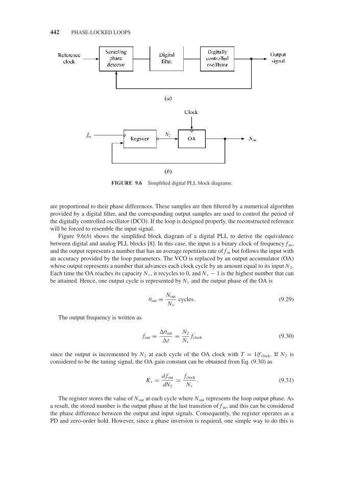
JWBS064-c09 JWBS064-Gerbennikov March 11, 2011 20:2 Printer Name: Yet to Come
442 PHASE-LOCKED LOOPS
FIGURE 9.6 Simplified digital PLL block diagrams.
are proportional to their phase differences. These samples are then filtered by a numerical algorithmprovided by a digital filter, and the corresponding output samples are used to control the period ofthe digitally controlled oscillator (DCO). If the loop is designed properly, the reconstructed referencewill be forced to resemble the input signal.
Figure 9.6(b) shows the simplified block diagram of a digital PLL to derive the equivalencebetween digital and analog PLL blocks [8]. In this case, the input is a binary clock of frequency f in,and the output represents a number that has an average repetition rate of f in but follows the input withan accuracy provided by the loop parameters. The VCO is replaced by an output accumulator (OA)whose output represents a number that advances each clock cycle by an amount equal to its input N2.Each time the OA reaches its capacity Nv, it recycles to 0, and Nv − 1 is the highest number that canbe attained. Hence, one output cycle is represented by Nv and the output phase of the OA is
θout = Nout
Nvcycles. (9.29)
The output frequency is written as
fout = �θout
�t= N2
Nvfclock (9.30)
since the output is incremented by N2 at each cycle of the OA clock with T = 1/f clock. If N2 isconsidered to be the tuning signal, the OA gain constant can be obtained from Eq. (9.30) as
Kv = d fout
dN2= fclock
Nv. (9.31)
The register stores the value of Nout at each cycle where Nout represents the loop output phase. Asa result, the stored number is the output phase at the last transition of f in, and this can be consideredthe phase difference between the output and input signals. Consequently, the register operates as aPD and zero-order hold. However, since a phase inversion is required, one simple way to do this is
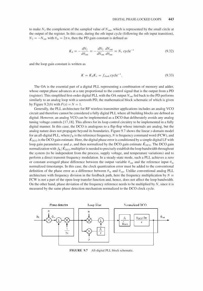
JWBS064-c09 JWBS064-Gerbennikov March 11, 2011 20:2 Printer Name: Yet to Come
DIGITAL PHASE-LOCKED LOOPS 443
to make N2 the complement of the sampled value of Nout, which is represented by the small circle atthe output of the register. In this case, during the nth input cycle (following the nth input transition),N2 = −Nout with θ in = 2πn, then the PD gain constant is defined as
Kd = − dN2
dθout= − dN2
dNout
dNout
dθout= Nv cycle−1 (9.32)
and the loop gain constant is written as
K = Kd Kv = fclock cycle−1. (9.33)
The OA is the essential part of a digital PLL representing a combination of memory and adder,whose output phase advances at a rate proportional to the control signal that is the output from a PD(register). This simplified first-order digital PLL with the OA output Nout fed back to the PD performssimilarly to an analog loop with a sawtooth PD, the mathematical block schematic of which is givenby Figure 9.2(b) with F(s) = N = 1.
Generally, the PLL architecture for RF wireless transmitter applications includes an analog VCOcircuit and therefore cannot be considered a fully digital PLL where all building blocks are defined asdigital. However, an analog VCO can be implemented as a DCO that deliberately avoids any analogtuning voltage controls [17,18]. This allows for its loop control circuitry to be implemented in a fullydigital manner. In this case, the DCO is analogous to a flip-flop whose internals are analog, but theanalog nature does not propagate beyond its boundaries. Figure 9.7 shows the linear s-domain modelfor an all-digital PLL, where f R is the reference frequency, N is frequency command word (FCW), andKDCO is the DCO gain estimate. Here, the digital phase error is conditioned by a simple digital LF withloop gain parameters α and ρ, and then normalized by the DCO gain estimate KDCO. The DCO gainnormalization with fR/KDCO multiplier is needed to precisely establish the loop bandwidth throughoutthe system (to be independent from the process, supply voltage, and temperature variations) and toperform a direct transmit frequency modulation. In a steady-state mode, such a PLL achieves a zeroor constant averaged phase difference between the output variable θout and the reference input θ in
normalized timestamps. In this case, the clock quantization error must be added to the conventionaldefinition of the phase error as a difference between θ in and θout. Unlike conventional analog PLLarchitecture with frequency division in the feedback path, here the frequency multiplication by N ≡FCW is not a part of the open-loop transfer function and, hence, does not affect the loop bandwidth.On the other hand, phase deviation of the frequency reference needs to be multiplied by N, since it ismeasured by the same phase detection mechanism normalized to the DCO clock cycle.
FIGURE 9.7 All-digital PLL block schematic.

JWBS064-c09 JWBS064-Gerbennikov March 11, 2011 20:2 Printer Name: Yet to Come
444 PHASE-LOCKED LOOPS
9.5 LOOP COMPONENTS
9.5.1 Phase Detector
In the commonly used PDs, its output voltage ve can be a sinusoidal, triangular, or sawtoothed functionof the phase angle θ e, where θ e is shifted by π /2 from the VCO output phase according to Eq. (9.14)for the sinusoidal and triangular types, and by π for the sawtoothed type. As a result, it is convenient toprovide a direct comparison between these three types of the PD transfer characteristics when the out-put voltage ve is equal to zero for θ e = 0 in all cases, as shown in Figure 9.8. With the loop in lock, thephase angle θ e stays within the limits ±π /2 for sinusoidal and triangular types, and ±π for sawtoothedtype. If the angular excursion is greater than this, the loop goes out of lock by skipping the cycles.
In a useful region where the phase excursions are sufficiently small compared with limiting values,the corresponding characteristic for each type of the PD can be written as
sinusoidal: ve = Ve sin θe
triangular: ve = 2
πVeθe
sawtooth: ve = 1
πVeθe
where Ve is the maximum output voltage. For the sinusoidal PD, a reasonable linear approximationof its characteristic for loop performance calculations with the loop in lock will be for θ e ≤ 0.2 radwhen sinθ e ≈ θ e.
FIGURE 9.8 Three types of phase detector transfer characteristics.

JWBS064-c09 JWBS064-Gerbennikov March 11, 2011 20:2 Printer Name: Yet to Come
LOOP COMPONENTS 445
FIGURE 9.9 Double-balanced phase detector schematic.
The double-balanced PD circuit schematic based on bipolar transistors, which is widely usedin a variety of analog PLLs, is shown in Figure 9.9, where IE is a constant-current source for thedifferential amplifier on transistors Q1 and Q2 [19]. In this case, a change �I1 in the collector currentof Q1 is accompanied by a corresponding change �I2 = −�I1 in the collector current of Q2, since thetotal current I1 + I2 is equal to the constant current IE. Hence, for the positive increment �vin of theinput reference voltage vin, the current in Q1 increases while the current in Q2 decreases. Then, inthe case of the positive increment �vout of the output VCO voltage vout when this signal is assumedto be a square wave of sufficient amplitude, the transistors Q3 and Q6 are turned completely on(saturation mode), and the collector current I2 flows through transistor Q6 and resistor RC2. However,for the negative increment �vout, the transistors Q4 and Q5 are turned on, and the collector currentI1 flows through transistor Q4 and resistor RC2. Since the incremental components of the collectorcurrents I1 and I2 due to �vin are of opposite phase and VCO output acts as a reversing switch onthe amplified version of vin that appears across RC2, the output voltage ve becomes the product of vin
times a square-wave switching function produced by vout.The time-domain voltage diagrams in Figure 9.10 illustrate the PD behavior for several combina-
tions of vin and vout, both of which are assumed to be square waves. In Figure 9.10(a), the voltagesvin and vout are 90◦ out of phase between each other, and the resulting ve represents equal positiveand negative areas around VE, resulting in its average zero value. In Figure 9.10(b), the phase ofvout is shifted relative to that in Figure 9.10(a), resulting in a positive average value (dc component)due to longer positive areas. In this case, the polarity of ve indicates the direction of phase shift, andits amplitude is proportional to the phase displacement, thus yielding the triangular PD function ofFigure 9.8(b).
Such a double-balanced multiplier circuit will also operate as a PD even though the two inputsignals are not square waves, as long as one or both of them are large enough to cause the transistor

JWBS064-c09 JWBS064-Gerbennikov March 11, 2011 20:2 Printer Name: Yet to Come
446 PHASE-LOCKED LOOPS
FIGURE 9.10 Phase detector voltage waveforms.
transfer function to be nonlinear. In this case, the resulting PD transfer function may be sinusoidalrather than triangular, especially for sine-wave inputs. The phase error signal amplitude Ve at the PDoutput versus its phase θ e can be written as
Ve = 1
2π
θe+π∫θe
sin θdθ = cos θe − cos(θe + π)
2π= 1
πcos θe (9.34)
showing that, for θ e = 90◦, the amplitude Ve of the resulting signal is equal to zero.Figure 9.11(a) shows the operation of a flip-flop PD and symbol for a set-reset (SR) flip-flop. It
should be mentioned that the term “flip-flop” was derived long ago from the sound produced on aspeaker connected to one of the back-coupled amplifiers’ outputs during the trigger process withinthe circuit. The output state Q changes in response to state change at either S or R input, resultingin Q = 1 state when S is pulsed high, and then stays high even after S returns low. Similarly, if R ispulsed high while S is held low, then Q = 0, and stays low even after R returns low. When both inputsare high (S = R = 1), the output state is undefined, so the input waveforms are shown as very narrowpulses to avoid overlap of high states at the two inputs. The duration of the Q = 1 state, and thusthe average output voltage, is proportional to the time difference between inputs, and hence to theirphase difference, the average value of which represents the useful PD output. The average voltagehas a sawtooth-shaped characteristic versus phase, as shown in Figure 9.8(c), where the phase varieslinearly within the range of 2π radians.
The operation of the exclusive-OR (XOR) gate PD and its symbol are shown in Figure 9.11(b).The XOR gate is a digital logic gate that implements exclusive disjunction and behaves accordingto the truth table where a high output (1) results if one, and only one, of the inputs to the gate ishigh (1). If both inputs are low (0) or both are high (1), a low output (0) results. Since the part ofthe time when both inputs are the same (or different) indicates their relative phase, the XOR can be
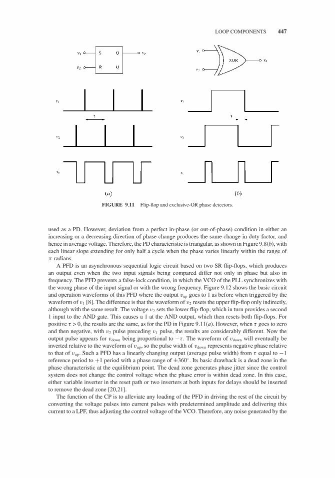
JWBS064-c09 JWBS064-Gerbennikov March 11, 2011 20:2 Printer Name: Yet to Come
LOOP COMPONENTS 447
FIGURE 9.11 Flip-flop and exclusive-OR phase detectors.
used as a PD. However, deviation from a perfect in-phase (or out-of-phase) condition in either anincreasing or a decreasing direction of phase change produces the same change in duty factor, andhence in average voltage. Therefore, the PD characteristic is triangular, as shown in Figure 9.8(b), witheach linear slope extending for only half a cycle when the phase varies linearly within the range ofπ radians.
A PFD is an asynchronous sequential logic circuit based on two SR flip-flops, which producesan output even when the two input signals being compared differ not only in phase but also infrequency. The PFD prevents a false-lock condition, in which the VCO of the PLL synchronizes withthe wrong phase of the input signal or with the wrong frequency. Figure 9.12 shows the basic circuitand operation waveforms of this PFD where the output vup goes to 1 as before when triggered by thewaveform of v1 [8]. The difference is that the waveform of v2 resets the upper flip-flop only indirectly,although with the same result. The voltage v2 sets the lower flip-flop, which in turn provides a second1 input to the AND gate. This causes a 1 at the AND output, which then resets both flip-flops. Forpositive τ > 0, the results are the same, as for the PD in Figure 9.11(a). However, when τ goes to zeroand then negative, with v2 pulse preceding v1 pulse, the results are considerably different. Now theoutput pulse appears for vdown being proportional to −τ . The waveform of vdown will eventually beinverted relative to the waveform of vup, so the pulse width of vdown represents negative phase relativeto that of vup. Such a PFD has a linearly changing output (average pulse width) from τ equal to −1reference period to +1 period with a phase range of ±360◦. Its basic drawback is a dead zone in thephase characteristic at the equilibrium point. The dead zone generates phase jitter since the controlsystem does not change the control voltage when the phase error is within dead zone. In this case,either variable inverter in the reset path or two inverters at both inputs for delays should be insertedto remove the dead zone [20,21].
The function of the CP is to alleviate any loading of the PFD in driving the rest of the circuit byconverting the voltage pulses into current pulses with predetermined amplitude and delivering thiscurrent to a LPF, thus adjusting the control voltage of the VCO. Therefore, any noise generated by the
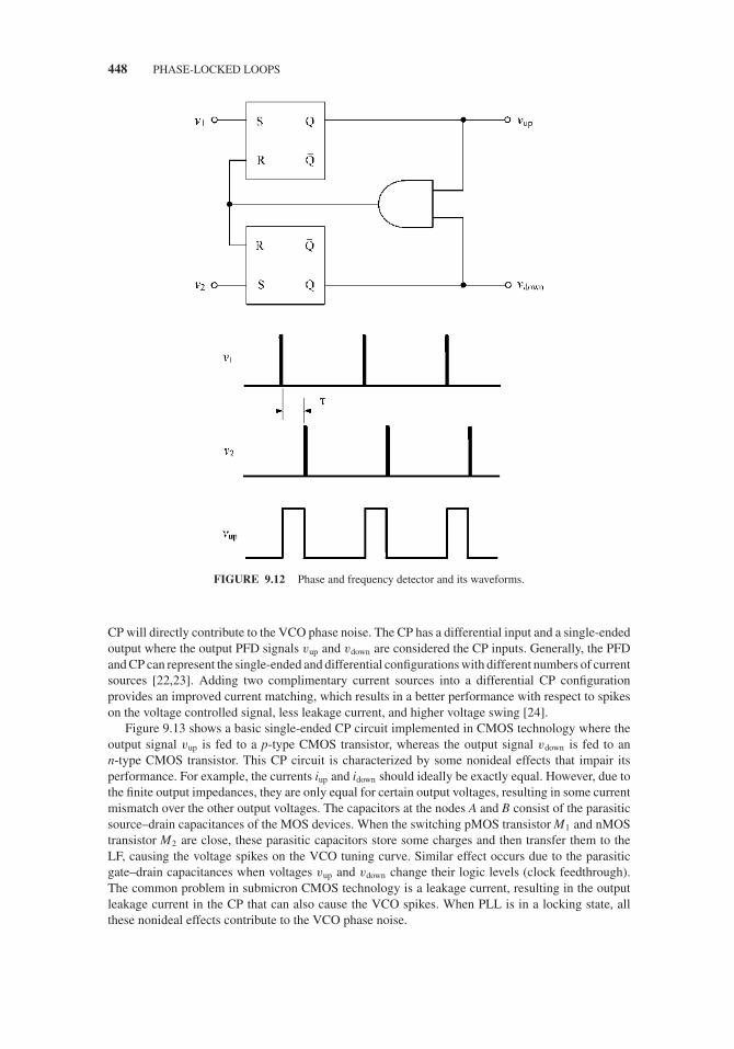
JWBS064-c09 JWBS064-Gerbennikov March 11, 2011 20:2 Printer Name: Yet to Come
448 PHASE-LOCKED LOOPS
FIGURE 9.12 Phase and frequency detector and its waveforms.
CP will directly contribute to the VCO phase noise. The CP has a differential input and a single-endedoutput where the output PFD signals vup and vdown are considered the CP inputs. Generally, the PFDand CP can represent the single-ended and differential configurations with different numbers of currentsources [22,23]. Adding two complimentary current sources into a differential CP configurationprovides an improved current matching, which results in a better performance with respect to spikeson the voltage controlled signal, less leakage current, and higher voltage swing [24].
Figure 9.13 shows a basic single-ended CP circuit implemented in CMOS technology where theoutput signal vup is fed to a p-type CMOS transistor, whereas the output signal vdown is fed to ann-type CMOS transistor. This CP circuit is characterized by some nonideal effects that impair itsperformance. For example, the currents iup and idown should ideally be exactly equal. However, due tothe finite output impedances, they are only equal for certain output voltages, resulting in some currentmismatch over the other output voltages. The capacitors at the nodes A and B consist of the parasiticsource–drain capacitances of the MOS devices. When the switching pMOS transistor M1 and nMOStransistor M2 are close, these parasitic capacitors store some charges and then transfer them to theLF, causing the voltage spikes on the VCO tuning curve. Similar effect occurs due to the parasiticgate–drain capacitances when voltages vup and vdown change their logic levels (clock feedthrough).The common problem in submicron CMOS technology is a leakage current, resulting in the outputleakage current in the CP that can also cause the VCO spikes. When PLL is in a locking state, allthese nonideal effects contribute to the VCO phase noise.

JWBS064-c09 JWBS064-Gerbennikov March 11, 2011 20:2 Printer Name: Yet to Come
LOOP COMPONENTS 449
FIGURE 9.13 Schematic of basic single-ended CP CMOS circuit.
9.5.2 Loop Filter
The design of a PLL loop filter is a big challenge because it determines lock time, noise, stability,or reference spurious products, and is a biggest contributor to the chip area in monolithic integratedcircuits. For example, fast lock times are possible with wide LF bandwidth, although this will leadto higher reference spurious products. A narrow LF bandwidth can reduce reference spurs, butleads to increased lock time and decreased stability. Therefore, the desired loop characteristics canbe controlled by inserting the corresponding types of LFs. The simplest configuration is a passiveone-pole low-pass RC circuit shown in Figure 9.14(a). The filter first-order transfer function that isproduced by a series resistor R and a shunt capacitor C is derived as
F(s) = 1
1 + s RC(9.35)
where s = jω. The filter amplitude and phase response is shown in Figure 9.14(b), where ωc = 1/RCis the cutoff frequency corresponding to the amplitude of 1/
√2 and phase shift of −45◦.
From Eq. (9.17) for N = 1, the loop response becomes
θout
θin(s) =
Kd KVCO
RC
s2 + s
RC+ Kd KVCO
RC
(9.36)
with the second-order denominator that can be written similarly to the second-order oscillator circuit as
s2 + 2sςωn + ω2n

JWBS064-c09 JWBS064-Gerbennikov March 11, 2011 20:2 Printer Name: Yet to Come
450 PHASE-LOCKED LOOPS
FIGURE 9.14 Passive first-order RC filter and its frequency response.
where
ς = 1
2√
Kd KVCO RC(9.37)
is the damping ratio (or factor) and
ωn =√
Kd KVCO
RC(9.38)
is the undamped natural frequency.The loop undamped natural frequency is a measure of the response time of the loop, and the
damping ratio is a measure of the overshoot and ringing. Ideally, the natural frequency should be highand the damping ratio should be near 0.707 (critical damping). However, with a single-pole filter, itis not possible to control the loop frequency and damping ratio independently.
The slightly more effective first-order RC filters in the form of proportional plus integral controlnetworks with two resistors and one capacitor, the transfer functions of which include one pole andone zero, are shown in Figure 9.15 [25]. The loop frequency response for these types of filters is
θout
θin( jω) =
1 + j2ςω
ωn
(1 − ωn
2ς Kd KVCO
)
1 + j2ςω
ωn−
(ω
ωn
)2 (9.39)

JWBS064-c09 JWBS064-Gerbennikov March 11, 2011 20:2 Printer Name: Yet to Come
LOOP COMPONENTS 451
FIGURE 9.15 Passive low-pass filters for second-order loop.
showing that the cutoff frequency of the system for ζ = 0.5 is approximately defined as ωc∼= ωn. The
bandwidth and the gain constant of the system can be adjusted independently if a double time-constantcontrol network is employed.
In the charge-pump PLL, the resistor in a single-pole RC LF introduces a stabilizing zero toimprove the loop transient response. However, this resistor causes a ripple due to charge-pump outputcurrent Ip, which modulates the VCO frequency and introduces excessive jitter in the output. In orderto suppress the ripple-induced jitter, a small shunt capacitor is added, resulting in a typical second-order filter circuit shown in Figure 9.16(a). However, this shunt capacitor introduces an additionalpole, thus increasing the order of the system to three. Therefore, the phase degradation due to thispole has to be accounted for by a proper choice of the other loop parameters.
The transimpedance function of the second-order LF based on linear analysis can be written as
ZF(s) = 1 + sτ1
s(C1 + C2)(1 + sτ2)(9.40)
where the time constants τ 1 = R1C1 and
τ2 = R1
(1
C1+ 1
C2
)−1
determine the pole and zero frequencies of the filter transfer function and depend on the specifiedloop bandwidth and phase margin.
In this case, the third-order charge-pump PLL open-loop gain, using Eqs. (9.24) and (9.40), isobtained as
GH(s) = Ip KVCO
2π N
1 + sτ1
s2(C1 + C2)(1 + sτ2)(9.41)
where KVCO is the VCO sensitivity, Ip is the charge-pump current, and N is the frequency divisionratio.
This third-order loop with Bode plot shown in Figure 9.16 is described by a zero and three poles.The phase margin degradation due to the third pole can be expressed by
φm(ωc) = tan−1(ωcτ1) + tan−1(ωcτ2) (9.42)

JWBS064-c09 JWBS064-Gerbennikov March 11, 2011 20:2 Printer Name: Yet to Come
452 PHASE-LOCKED LOOPS
FIGURE 9.16 Passive filter for third-order loop and Bode plot.
where ω1 = 1/τ 1 and ω2 = 1/τ 2 [26,27]. The maximum phase margin φm can be analytically derivedby setting the phase of the open-loop gain as derivative with respect to frequency at the cross-overfrequency ωc to zero when
1
1 +(ωcτ1)2 + 1
1 +(ωcτ2)2 = 0 (9.43)
which results in the values of the time constants τ 1 and τ 2 given by
τ1 = 1
ω2cτ2
τ2 = 1 − sin φm
ωccosφm. (9.44)
As a result, the maximum phase margin occurs when
ωc = 1
τ1
√C1
C2+ 1 (9.45)

JWBS064-c09 JWBS064-Gerbennikov March 11, 2011 20:2 Printer Name: Yet to Come
LOOP COMPONENTS 453
and the relationship between the two filter capacitances and maximum phase margin, by substitutingEq. (9.45) into Eq. (9.43), is described by
C1 = 2C2 tan φm
(tan φm +
√tan2 φm + 1
)(9.46)
where the choice of the basic loop parameters, such as loop bandwidth and phase margin, depends ona particular application. For example, in the case of clock generators with a poor phase noise VCOand a pure low-frequency reference, a relatively high bandwidth is required. However, it is necessaryto choose a low loop bandwidth and a large phase margin if it is required to avoid any jitter peaking.
The cross-over frequency ωc can also be approximated as a function of the loop parameters as
ωc ≈ Ip KVCO R1
2π N
C1
C1 + C2≈ Ip KVCO R1
2π N(9.47)
resulting in the simple design equations for the filter parameters
R1 = 2π N
Ip KVCOωc (9.48)
C1 = α
R1ωc= Ip KVCO
2π N
α
ω2c
(9.49)
C2 = 1
β R1ωc= Ip KVCO
2π N
1
βω2c
(9.50)
where α = ωc/ω1 and β = ω2/ωc [28]. The factors α and β are typically equal to 4 each, which givesa capacitance ratio C1/C2 = 16, according to Eqs. (9.49) and (9.50), and results to a phase margin ofapproximately 60◦, as it follows from Eq. (9.46).
An active LF employs an operational amplifier in its configuration, as shown in Figure 9.17(a)for a typical filter circuit. The transimpedance function of such a second-order active LF driven by avoltage, which is related to the passive lag–lead LF shown in Figure 9.15(a), is written as
ZF(s) = 1 + sτ1
sτ2(9.51)
with the time constants τ 1 = R1C1 and τ 2 = R2C1, assuming an ideal operational amplifier withinfinite gain. The response has a pole at the origin and a zero in the left half plane. The zero is vital inpreserving system stability and in controlling the step response. It should be noted that the integrator,which is realized when R1 = 0 for an active LF of Figure 9.17(a), is not a practical LF because thereis no frequency at which it does not have a transfer of −90◦ that would inevitably put the loop on theverge of instability [8]. Also, the series capacitance at the filter input should be avoided.
If the active LF is driven by current, as it happens in a charge-pump PLL, there is no need forthe series resistor R2. The second-order passive LF shown in Figure 9.16(a) has some limitations;for example, one of them due to significant contribution of the filter resistance to the system outputphase noise. In this case, a very low value of R1 is needed, but it leads to extremely large capacitancevalues that are not feasible for integration. In addition, a small offset at the input of the PFD causingspurs in the output spectrum can occur due to the finite output impedance of the charge-pump currentsources when the VCO input control voltage must vary over a wide range to use the full tuning rangeof the VCO. As a result, an extra pole must be inserted in the frequency response of the LF shown inFigure 9.17(b), which is placed on top of ω2 by making τ 2 = R3C3. To keep the phase margin highenough, the factor β must be increased from 4 to 6. Since the loop transfer function now falls off ata 60 dB/decade for frequencies beyond ω2, the noise of the CP and the LF resistor R1 will have adependency on the offset frequency of ω−6
m . However, this solution leads to a total capacitance that
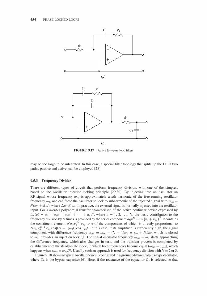
JWBS064-c09 JWBS064-Gerbennikov March 11, 2011 20:2 Printer Name: Yet to Come
454 PHASE-LOCKED LOOPS
FIGURE 9.17 Active low-pass loop filters.
may be too large to be integrated. In this case, a special filter topology that splits up the LF in twopaths, passive and active, can be employed [28].
9.5.3 Frequency Divider
There are different types of circuit that perform frequency division, with one of the simplestbased on the oscillator injection-locking principle [29,30]. By injecting into an oscillator anRF signal whose frequency ωinj is approximately a nth harmonic of the free-running oscillatorfrequency ω0, one can force the oscillator to lock to subharmonic of the injected signal with ωinj =N(ω0 + �ω), where �ω � ω0. In practice, the external signal is normally injected into the oscillatorinput. For a n-order polynomial transfer characteristic of the active nonlinear device expressed byiout(v) = a0 + a1v + a2v
2 + · · · + anvn, where n = 1, 2, . . . , N, the basic contribution to the
frequency division by N times is provided by the series component aNvN = aN
(v0 + vinj
)N. It contains
the constituent element NaNvN−10 vinj, one of the components of which is directly proportional to
NaNV N−10 Vinj cos[(N − 1)ω0t] cos ωinjt . In this case, if its amplitude is sufficiently high, the signal
component with difference frequency ωdiff = ωinj − (N − 1)ω0 = ω0 + N�ω, which is closedto ω0, provides an injection locking. The initial oscillator frequency ωosc = ω0 starts approachingthe difference frequency, which also changes in turn, and the transient process is completed byestablishment of the steady-state mode, in which both frequencies become equal (ωdiff = ωosc), whichhappens when ωosc = ωinj/N. Usually such an approach is used for frequency division with N = 2 or 3.
Figure 9.18 shows a typical oscillator circuit configured in a grounded-base Colpitts-type oscillator,where Cb is the bypass capacitor [6]. Here, if the reactance of the capacitor C3 is selected so that

JWBS064-c09 JWBS064-Gerbennikov March 11, 2011 20:2 Printer Name: Yet to Come
LOOP COMPONENTS 455
FIGURE 9.18 Locked-oscillator frequency divider circuit.
the capacitor no longer provides a good RF short from the base of the transistor to ground, and ifan external signal whose frequency is harmonically related to the oscillator frequency is injectedinto the transistor base, the oscillator will lock in frequency to the injected signal. To increase thelocking range, a load resistor R1 is inserted across the oscillator-tuned L1C1 circuit, which effectivelyincreases the bandwidth of the tuned circuit. In this case, the required frequency shift can be written as
�ω = ω0
2QL
Iinj
Iosc(9.52)
where QL is the oscillator quality factor, Iinj is the injected current amplitude, and Iosc is the oscillatorfundamental current amplitude [30,31].
The injection-locking approach for frequency division is characterized by relatively low cost andhas no lower or upper limit because, theoretically, an oscillator operating at any frequency can belocked to a signal source by injection locking. The circuit operates over a narrow frequency band(12–15%), though electronic tuning can be easily implemented. The major problem of the DIV basedon the injection-locking principle is the presence of an output RF signal even if driving circuitry failsto generate an injection signal.
In the locked-oscillator dividers, the frequency division occurs due to availability of the differencefrequency component ωdiff = ωinj − (N − 1)ωosc, the appearance of which can be considered as aresult of two consecutive operations: multiplication of ωosc by (N − 1) times resulting in a frequencyω′ = (N − 1)ωosc, and then the frequency transformation by separating the component ωdiff =ωinj − ω′. Besides, signal amplification occurs due to the active device. As a result, the regenerativeDIVs can be considered as modified locked-oscillator DIVs in which any from the above-mentionedoperations (or some of them) is fulfilled by separate stages that allows the required characteristicsof each stage to be independently controlled. As a result, the overall system performance can beimproved. A regenerative DIV, also known as a Miller DIV, simplified block schematic of whichis shown in Figure 9.19, provides mixing of the input injected signal with the feedback signaldelivered from the output through the multiplier and bandpass filter [6,32]. For the oscillations tobe sustained, the loop gain should be greater than unity, and the total phase shift must also be aninteger multiple of 2π . To operate properly with correct frequency division, the multiplier has to behard-driven and minimum required input power should be provided [33]. The advantage of using
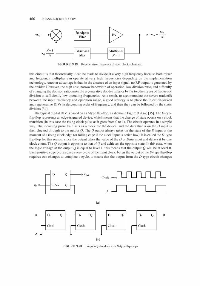
JWBS064-c09 JWBS064-Gerbennikov March 11, 2011 20:2 Printer Name: Yet to Come
456 PHASE-LOCKED LOOPS
FIGURE 9.19 Regenerative frequency divider block schematic.
this circuit is that theoretically it can be made to divide at a very high frequency because both mixerand frequency multiplier can operate at very high frequencies depending on the implementationtechnology. Another advantage is that, in the absence of an input signal, no RF output is generated bythe divider. However, the high cost, narrow bandwidth of operation, low division ratio, and difficultyof changing the division ratio make the regenerative divider inferior by far to other types of frequencydivision at sufficiently low operating frequencies. As a result, to accommodate the severe tradeoffsbetween the input frequency and operation range, a good strategy is to place the injection-lockedand regenerative DIVs in descending order of frequency, and then they can be followed by the staticdividers [34].
The typical digital DIV is based on a D-type flip-flop, as shown in Figure 9.20(a) [35]. The D-typeflip-flop represents an edge-triggered device, which means that the change of state occurs on a clocktransition (in this case the rising clock pulse as it goes from 0 to 1). The circuit operates in a simpleway. The incoming pulse train acts as a clock for the device, and the data that is on the D input isthen clocked through to the output Q. The Q output always takes on the state of the D input at themoment of a rising clock edge (or falling edge if the clock input is active low). It is called the D-typeflip-flop for this reason, since the output takes the value of the D or Data input and delays it by oneclock count. The Q output is opposite to that of Q and achieves the opposite state. In this case, whenthe logic voltage at the output Q is equal to level 1, this means that the output Q will be at level 0.Each positive edge occurs once every cycle of the input clock, but as the output of the D-type flip-floprequires two changes to complete a cycle, it means that the output from the D-type circuit changes
FIGURE 9.20 Frequency dividers with D-type flip-flops.

JWBS064-c09 JWBS064-Gerbennikov March 11, 2011 20:2 Printer Name: Yet to Come
LOOP COMPONENTS 457
at half the rate of the incoming pulse train, thus representing a divide-by-2 circuit according to thetiming diagram. It should be noted that the pulse train should have sharp edges. If the rising edges areinsufficiently sharp, then there may be problems with the proper circuit operation. However, placingan inverter before the clock input has the effect of sharpening the edges on the incoming signal. Thekey building block in such a digital DIV is the bistable circuit based on a differential amplifier and across-coupled oscillator, although the other circuit configurations are also possible [36].
An arbitrary number of DIVs may be cascaded to produce very low frequencies. In this case,the input clock signal must be of the proper voltage level and must usually have a reasonably fasttransition to ensure that the flip-flop is properly triggered. In cascade, a later flip-flop may be clockedby either the Q or Q output of the preceding stage because it does not matter which output is used ifit is necessary to provide the frequency division by 2n. Figure 9.20(b) shows the DIV based on a shiftregister, where a four-bit shift register is built from four cascaded D-type flip-flops [35]. With eachclock pulse, the information at the input D of each flip-flop is transferred to the corresponding outputQ. Assume that a logical 1 is applied to the input, and that initially all Q values are zero. When thefirst clock pulse arrives, Q1 will be 1 while the rest remain zero. After the second clock pulse, Q2 is1 as well. Finally, after the fourth clock pulse, a logical 1 appears at the output. This may be used totrigger a one-shot multivibrator to reset all of the flip-flops. The result is a divide-by-4 circuit, and thedivision number corresponds to the number of stages in the register. Due to the propagation delay ofseveral stages, uncertainty or jitter in the delay will lead to unwanted phase modulation of the outputsignal. This can be eliminated through the application of a D-type flip-flop at the output of a largedivider chain.
In a differential CMOS implementation, a DIV is typically represented as an asynchronouscascade of divide-by-2 circuits, where each stage is clocked by the previous one. Figure 9.21(a)shows a common topology for a digital DIV with N = 2, where two D-latches are connected inmaster/slave configuration and the output Q of the second latch is fed back to the input D of the firstlatch [37]. The same clock is used to drive both D-latches with opposite logic, and either master orslave D-latch is activated in each clock, but not both at the same time. On the next cycle, invertedoutput is fed back to the input again, which causes the output to toggle. The same event repeats forevery two input clocks. The jitter at the output of this DIV is not affected by the noise of the first latch,since the latter has no control on the output switching. Therefore, the noise sources of the secondlatch only need to be taken into account in the evaluation of the output jitter. The differential topologyof the latch stage is shown in Figure 9.21(b), where the pMOS transistors biased in the triode regionact as load resistors. The pairs of nMOS transistors are alternatively switched on and off.
9.5.4 Voltage-Controlled Oscillator
The VCO is considered as the heart of a phase-locked system generally determining its performancequality. For example, for a low phase noise VCO, it may be controlled with a narrow bandwidth loopwith no compromise in overall noise performance. At low frequencies when it is possible, insteadof the VCO in a PLL system some designs are used a current-controlled oscillator, representing amultivibrator with a square-wave output because it is desirable for proper operation of the PD andis compatible with logic circuitry. In this case, linear variation of frequency with control voltage(or current) is easier to obtain with a multivibrator than with a sine-wave LC oscillator. For high-frequency operation with better stability and spectral purity, or if sinusoidal waveform is required,a varactor–tuned LC oscillator is preferable. The VCO will convert the applied tuning voltage to anoutput frequency, and its sensitivity can vary drastically over its full frequency range. In general, thelower the tuning sensitivity of the VCO, the better the VCO phase noise will be.
Generally, different circuit topologies based on a Colpitts core circuit and including one or severalvaractors as the frequency-tuning elements can be used. The varactor diode is operated with a reversebias on the junction, and its capacitance is a function of the reverse bias voltage. Figure 9.22(a) shows
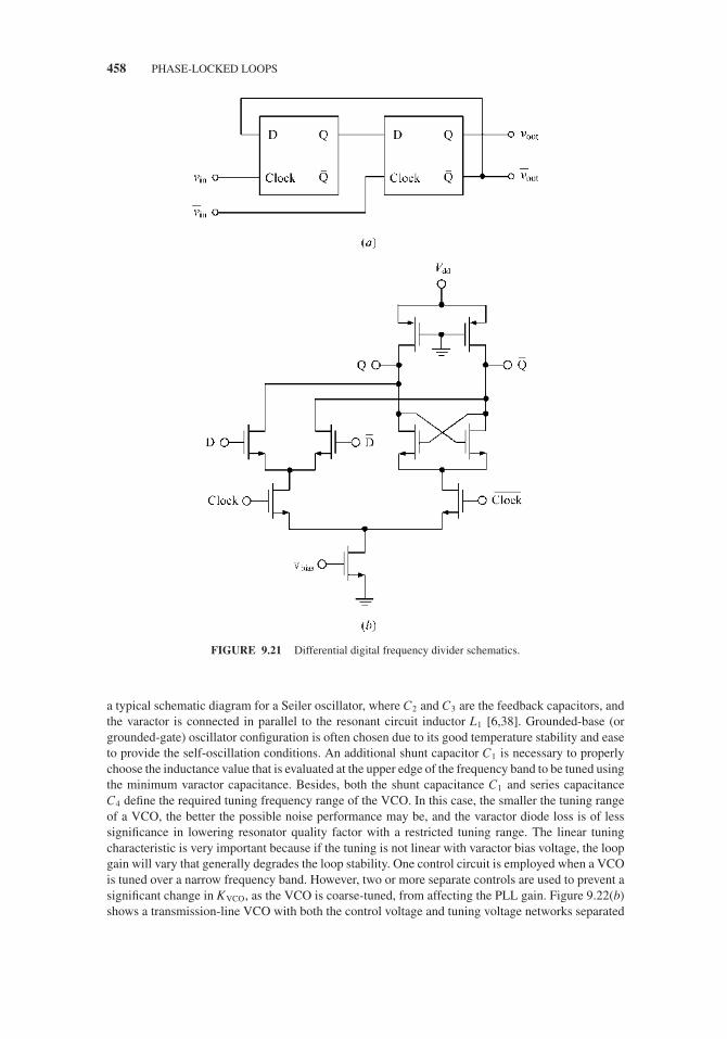
JWBS064-c09 JWBS064-Gerbennikov March 11, 2011 20:2 Printer Name: Yet to Come
458 PHASE-LOCKED LOOPS
FIGURE 9.21 Differential digital frequency divider schematics.
a typical schematic diagram for a Seiler oscillator, where C2 and C3 are the feedback capacitors, andthe varactor is connected in parallel to the resonant circuit inductor L1 [6,38]. Grounded-base (orgrounded-gate) oscillator configuration is often chosen due to its good temperature stability and easeto provide the self-oscillation conditions. An additional shunt capacitor C1 is necessary to properlychoose the inductance value that is evaluated at the upper edge of the frequency band to be tuned usingthe minimum varactor capacitance. Besides, both the shunt capacitance C1 and series capacitanceC4 define the required tuning frequency range of the VCO. In this case, the smaller the tuning rangeof a VCO, the better the possible noise performance may be, and the varactor diode loss is of lesssignificance in lowering resonator quality factor with a restricted tuning range. The linear tuningcharacteristic is very important because if the tuning is not linear with varactor bias voltage, the loopgain will vary that generally degrades the loop stability. One control circuit is employed when a VCOis tuned over a narrow frequency band. However, two or more separate controls are used to prevent asignificant change in KVCO, as the VCO is coarse-tuned, from affecting the PLL gain. Figure 9.22(b)shows a transmission-line VCO with both the control voltage and tuning voltage networks separated

JWBS064-c09 JWBS064-Gerbennikov March 11, 2011 20:2 Printer Name: Yet to Come
LOOP COMPONENTS 459
FIGURE 9.22 Schematics of bipolar LC voltage-controlled oscillators.
by a quarter-wavelength transmission line. The control voltage varactor is reversed-biased at a dcvoltage that is generated by the phase detector (or phase comparator) of the PLL. It provides thefine-tuning control necessary to keep the VCO frequency-locked to a reference source, whereas thetuning voltage varactor coarse-tunes the VCO to within the PLL capture range. The overall lineartuning range can be expanded by using switching reactances into the circuit where capacitors can beswitched with p–i–n diodes [6,35].
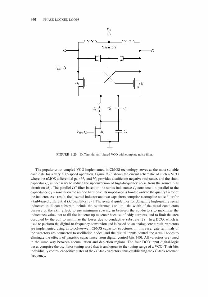
JWBS064-c09 JWBS064-Gerbennikov March 11, 2011 20:2 Printer Name: Yet to Come
460 PHASE-LOCKED LOOPS
FIGURE 9.23 Differential tail-biased VCO with complete noise filter.
The popular cross-coupled VCO implemented in CMOS technology serves as the most suitablecandidate for a very high-speed operation. Figure 9.23 shows the circuit schematic of such a VCOwhere the nMOS differential pair M1 and M2 provides a sufficient negative resistance, and the shuntcapacitor Cs is necessary to reduce the upconversion of high-frequency noise from the source biascircuit on M3. The parallel LC filter based on the series inductance Lf connected in parallel to thecapacitance Cf resonates on the second harmonic. Its impedance is limited only to the quality factor ofthe inductor. As a result, the inserted inductor and two capacitors comprise a complete noise filter fora tail-biased differential LC oscillator [39]. The general guidelines for designing high-quality spiralinductors in silicon substrate include the requirements to limit the width of the metal conductorsbecause of the skin effect, to use minimum spacing in between the conductors to maximize theinductance value, not to fill the inductor up to center because of eddy currents, and to limit the areaoccupied by the coil to minimize the losses due to conductive substrate [28]. In a DCO, which isused to perform the digital-to-frequency conversion and is based on an analog core circuit, varactorsare implemented using an n-poly/n-well CMOS capacitor structures. In this case, gate terminals ofthe varactors are connected to oscillation nodes, and the digital inputs control the n-well nodes toeliminate the effects of parasitic capacitance from digital control bits [40]. All varactors are tunedin the same way between accumulation and depletion regions. The four DCO input digital-logicbuses comprise the oscillator tuning word that is analogous to the tuning range of a VCO. Their bitsindividually control capacitive states of the LC-tank varactors, thus establishing the LC-tank resonantfrequency.

JWBS064-c09 JWBS064-Gerbennikov March 11, 2011 20:2 Printer Name: Yet to Come
LOOP PARAMETERS 461
9.6 LOOP PARAMETERS
9.6.1 Lock Range
The steady-state phase error resulting from a step change in reference frequency in a first-order PLLwith sinusoidal PD, whose transfer characteristic is shown Figure 9.8(a), is defined by Eqs. (9.12)and (9.14), where �ω is the difference between the free-running and the locked VCO frequencies.As a result, the maximum VCO frequency error approaching ±π /2 rad that can be compensated forby a first-order PLL, which is called the hold-in, lock, or synchronization range, is equal to the dcloop gain, or
�ωhold-in = K (9.53)
where K = KdF(0)KVCO for an analog PLL and K = (Ip/2π )ZF(0)KVCO for a charge-pump PLL.However, the hold-in range �ωhold-in, which is referred to the PD, should be divided by N. For thetriangular and sawtooth PDs whose linear transfer characteristics are shown in Figures 9.8(b) and9.8(c), respectively, the hold-in range is obtained by taking into account Eq. (9.20) as
�ωhold-in = K θe,max (9.54)
where θ e, max is equal to π for the triangular and 2π for the sawtooth detector characteristic.If the input reference frequency is sufficiently close to the VCO free-running frequency, a PLL
locks up with just a phase transient, without slipping cycle prior to lock. The frequency range overwhich the loop acquires phase to lock without slips is called the seize or lock-in range of the PLL. Ina first-order loop, the lock-in range is equal to the hold-in range, however for the second and higherorder loops the lock-in range is always less than the hold-in-range, which is defined by Eqs. (9.53) or(9.54). As an example for the second-order loop with a lag–lead filter shown in Figure 9.15(a), if thedifference between the free-running and the locked VCO frequencies is less than 3-dB bandwidth ofthe closed-loop transfer function H(s), the loop will lock up without slipping cycles and the maximumlock-in range can be written as
�ωlock-in = K τ1
τ1 + τ2(9.55)
or, in terms of the LF damping factor ζ and natural frequency ωn,
�ωlock-in ≈ 2ςωn (9.56)
where
ς = ωn
2
(τ1 + 1
K
)(9.57)
ωn =√
K
τ1 + τ2. (9.58)
However, there is a frequency interval, smaller than the hold-in range and larger than the lock-inrange, which is called the pull-in or acquisition range, over which the loop will acquire lock afterslipping cycles for a while. The relationship between the hold-in range, lock-in range, and pull-inrange is shown in Figure 9.24. The equalities in this apply to the first-order loops and highly dampedsecond-order loops, which act like first-order loops. For the second-order PLL with a lag–lead filter,

JWBS064-c09 JWBS064-Gerbennikov March 11, 2011 20:2 Printer Name: Yet to Come
462 PHASE-LOCKED LOOPS
FIGURE 9.24 Ranges of dynamic limits of phase-locked loop.
locking is still possible with some cycles of VCO frequency skipped as long as �ω < �ωpull-in, wherethe pull-in range is estimated as
�ωpull-in ≈√
2√
2ςωn K − ω2n (9.59)
which is valid for K/ωn > 2.5 [6]. Once the loop is in lock, small loop bandwidth is desirable tominimize noise transmission. On the other hand, large bandwidth is desirable to aid initial capture.These incompatible requirements are sometimes met by reducing the bandwidth after lock is acquiredor using small bandwidth but sweeping the VCO frequency until lock is acquired [3].
9.6.2 Stability
As in any feedback system, stability is one of the most important aspects of the PLL design since thecondition for phase locking does not assure loop stability. A PLL can oscillate if at some frequencyits open-loop gain is greater than unity and phase shift exceeds 180◦. All PLLs have −90◦ phaseshift due to the 1/s term, so excess phase is 90◦ even before any effect from the LF is considered.Therefore, the basic first-order PLL is stable unless the filtering provided in the forward and feedbackpath introduces a large amount of phase shift. Whether a loop will oscillate when its gain exceedsunity at 180◦ can be seen from the Nyquist plot, root locus plot, or Bode plot [8]. Since a Bode plot isa graph of the logarithm of the system transfer function versus frequency, open-loop gain and phaseare plotted with a log-frequency axis, and the gain and phase margins can be seen from this plot. Inthis case, tangential approximations for gain and phase are often used. A Nyquist plot is representedby a graph in polar coordinates, in which the gain and phase of a frequency response are plotted.The plot of these phasor quantities shows the phase as the angle and the magnitude as the distancefrom the origin. This plot combines the two types of Bode plot—magnitude and phase—on a singlegraph, with frequency as a parameter along the curve. In this case, if the locus does not surroundthe point −1 + j0, so poles of H(s) are in the left half of the s-plane and that corresponds to the stableregion. In the root locus technique, which determines the position of system poles and zeros in thes-plane, the graph or plot illustrates how the closed loop poles (roots of the characteristic equation)vary with loop gain and at what value of the loop gain they enter the right half of the s-plane. Therelationship of the system poles and zeros determines the degree of stability. The root locus contourcan be determined by using special set of rules [41,42].
There are two sources for stability limit in a charge-pump PLL [12,43]. First, it has a criticalstability limitation due to the discrete nature of the PFD and CP output. As a sampled system, thecharge-pump PLL will become unstable if the loop gain is made so large that the bandwidth becomes

JWBS064-c09 JWBS064-Gerbennikov March 11, 2011 20:2 Printer Name: Yet to Come
LOOP PARAMETERS 463
comparable to the sampling frequency. Limited loop gain sets upper boundary of the loop bandwidthobtainable for a given input reference frequency ωref. Stability limit requires that
ω2n <
ω2ref
π
(π + ωref
ω1
) (9.60)
where ωn is the natural frequency and ω1 = 1/τ 1 is shown in Figure 9.16. The relationship betweenωn and loop bandwidth defined by ωc is approximately obtained by
ωc ≈ ω2n
ω1(9.61)
for critically damped and overdamped system. Substituting Eq. (9.61) into Eq. (9.60) results in
ωc <ωref
π
(1 + πω1
ωref
) (9.62)
which indicates that the loop bandwidth has to be significantly lower than the frequency of the inputreference signal. Commonly, ωc is chosen below one-tenth of ωref to guarantee stability.
The second stability limit comes from the open-loop transfer function. As it is seen from Eq. (9.41),the open-loop transfer function of a third-order charge-pump PLL has two poles at the origin, whichmakes the loop inherently unstable. A zero should be placed at a lower frequency than the crossoverfrequency to make the phase margin large enough (>45◦). Since the zero reduces the slope of themagnitude response, an additional pole at a higher frequency than the crossover frequency is alsorequired to maintain adequate spurious signal rejection. When a zero is located at 1/4 of the crossoverfrequency and a pole is placed at 4 times of ωc, the loop is critically damped with a damping ratioof 1 and a phase margin of 63◦ can be achieved. Normally, a critically damped loop works best for atypical PLL design.
9.6.3 Transient Response
One important aspect of the PLL performance is the manner in which it responds to a change to inputfrequency or phase, and one of the most important measures is its response to a step change of theinput. The step error response of the PLL in the time domain represents the phase error in response toa unit phase step at the input or the frequency error in response to a unit frequency step at the input. Inthis case, the transient response will be characterized by the rise time tr (the time for transient curveto first reach the value that will eventually be steady-state value), the peaking time tp (the time fortransient curve to reach the first peak), the settling time ts (the time for the envelope of the responseto reach and remain less than a specified fraction of the final steady-state value, for example, within10%), and the peak-overshoot ratio POR (the ratio of the maximum value of the transient curve to itssteady-state value), as shown in Figure 9.25 [41].
In the slow-acquisition PLL, the transient response of the VCO does not affect acquisition time.However, in the high-speed PLL, the transient response of the VCO does affect PLL acquisitionperformance because the time constants of the LF are set close to those of the VCO [44]. In thiscase, minimum settling time for a third-order charge-pump PLL can be provided by placing the threeclosed-loop poles given by the root locus at equal distances from the origin of the axis in the s-plane[45]. When the bandwidth is less than 1/20th of the input reference frequency, a good estimation ofthe settling time ts can be defined as
ts = 1
ςωcln
(�ωout
�ωe
)(9.63)

JWBS064-c09 JWBS064-Gerbennikov March 11, 2011 20:2 Printer Name: Yet to Come
464 PHASE-LOCKED LOOPS
FIGURE 9.25 Transient response to step input change.
where �ωout is the frequency step and �ωe is the required frequency accuracy. As the loop bandwidthfrequency ωc increases, the settling time ts gets shorter if the damping ratio ζ is fixed.
The effect of the damping ratio on settling time for a third-order charge-pump PLL is plottedin Figure 9.26, which shows that the settling time is fastest when the loop is critically damped,and further underdamping does not improve the settling time [43]. However, underdamping is notdesirable, since it increases overshoot in transient response, which can be limited within the dynamicrange of the charge-pump PLL. The overshoot in transient response also translates into the gainpeaking in the frequency domain, which amplifies the phase noise of the reference signal at the PLLoutput. An overdamped condition can be recommended to use for better stability with narrow loopbandwidth. Generally, loop bandwidth and damping ratio have to be determined carefully, dependingon the system requirements, since they improve some aspects of the performance, but deteriorateothers at the same time.
FIGURE 9.26 Transient responses of third-order PLL.
JWBS064-c09 JWBS064-Gerbennikov March 11, 2011 20:2 Printer Name: Yet to Come
LOOP PARAMETERS 465
9.6.4 Noise
In general, the system noise bandwidth can be defined as the bandwidth Bn of a rectangular filter thathas that nominal power gain (or unity in particular cases) within the passband and zero gain outsidethe passband and passes the same total power as does the actual filter when they are both excited bya uniformly distributed power density. As a result,
Bn = 1
2π
∞∫0
|H ( jω)|2dω (9.64)
where H(jω) is the closed-loop transfer function.For a first-order PLL,
Bn = 1
2π
∞∫0
∣∣∣∣ K/jω
1 + K/jω
∣∣∣∣2
dω = K
4(9.65)
which means that the equivalent noise bandwidth extends beyond the 3-dB bandwidth by almost 60%for the single-pole response of the first-order loop since the ratio between the dc loop gain K andcutoff frequency ωc is written as ωc = 2π f c = K.
For the second-order PLL with a lag–lead filter, the noise bandwidth is calculated from
Bn = ωn
2
(ς + 1
4ς
)(9.66)
where ωn and ζ are determined by Eqs. (9.57) and (9.58) [6].For a first-order PLL, no LF exists and the PD is usually implemented using an analog multiplier or
an XOR gate. Assuming no DIV and ideal PD, the phase noise at the PLL output will be representedby a combination of the input reference noise and VCO noise. As a result, the fundamental propertyof the PLL states that its phase noise is dominated by the input source noise at frequency offsetsbelow the loop bandwidth and by the VCO noise at frequency offsets above the loop bandwidth.This is because the PLL is unable to react fast enough to fast random changes in the VCO output,but compensates the slow random variations produced by the VCO by adjusting its control voltage.Therefore, the PLL having a noisy VCO and a clean reference input should be designed to have alarge loop bandwidth. Since the loop bandwidth is inversely related to the PLL settling time, such aPLL takes little time for locking and has a large noise reduction of the VCO noise. However, if theloop bandwidth is small, the PLL takes longer time for locking and leaves much of the VCO noiseunsuppressed.
Higher order PLL employs the PFD, CP, and LF to ensure zero static phase error. The majorinternal noise sources of the charge-pump PLL include the DIV noise, charge-pump noise, LF noise,and VCO noise. In addition, additive noise, predominantly thermal, within the PFD gives rise totiming jitter in the edges of the output pulses, which is translated to equivalent phase jitter, thusinjecting this noise into the system [46]. The LF and VCO are subject to high-pass filtering by loopaction and are thus significant sources of out-of-band phase noise, whereas the DIV and CP aresubject to low filtering by loop action and are thus significant sources of in-band phase noise. Theexcess noise of the DIV and CP can be modeled by an additive 1/f noise, whereas the VCO noiseand low-pass LF noise can be mainly represented by 1/f 2 noise characteristic. If the loop bandwidthis large, the PLL has a large reduction in 1/f 2 noise, but cannot provide a sufficient suppression of1/f noise. However, if the loop bandwidth is small, the charge-pump PLL provides a large 1/f noisereduction, but leaves much of the 1/f 2 noise unsuppressed. Since the transfer functions of the DIV

JWBS064-c09 JWBS064-Gerbennikov March 11, 2011 20:2 Printer Name: Yet to Come
466 PHASE-LOCKED LOOPS
and CP noise sources to the output represent the low-pass characteristics and the transfer functionsof the VCO and LF to the output are described by the high-pass characteristics, an optimum phasenoise spectrum of the system can be achieved for the 3-dB bandwidth for low- and high-pass transferfunctions when power spectrum densities for both 1/f and 1/f 2 noises sources intersect [47].
Consequently, the main contributors to the output phase noise response at offsets lower than theloop bandwidth or in-band noise sources are the reference oscillator noise, DIV noise, and CP noise.In this case, by using a clean reference oscillator (such as a crystal or dielectric resonator oscillator),a large CP gain, and a low frequency division ratio the phase noise and jitter at the PLL output can bereduced at low frequency offsets. However, an increased CP gain may affect the VCO control voltagedue to a small net current injection in a locked condition causing a shift in VCO frequency. This inturn produces a phase error at the charge-pump input due to the feedback loop that tends CP to injecta corrective current pulse to bring the VCO frequency back to its previous value. As a result, the VCOfrequency toggles between two values under the locked condition. In a frequency domain, this effectwill produce spurs at the reference frequency or multiples of the reference frequency. The magnitudeof these spurs is directly proportional to the ripple in the control voltage and hence the charge-pumpgain. Reference spurs should be at least 50 dB below the PLL output frequency to ensure a cleanspectrum. At frequency offsets larger the loop bandwidth, the main contributor is the VCO noise. Inthis case, a low KVCO is required for a low phase noise PLL. However, reducing KVCO will make theloop dynamics slower, and the PLL will take a long time to correct abrupt changes in frequency andrequire a large time to lock during start-up. In addition, the effect of the thermal noise of the resistorin the LF should be minimized, for example, by optimizing the physical dimensions of the filter MOScapacitors or in conjunction with op-amp noise [48].
9.7 PHASE MODULATION USING PHASE-LOCKED LOOPS
By recognizing the loop transfer function properties, the VCO can be used as a phase or frequencymodulator. The VCO control port varies the VCO frequency, so the VCO can be used as boththe carrier generator and the modulator. If the modulating signal is inserted into the circuit infront of the LF, the result is a VCO phase-modulated signal, provided that the signal bandwidth isbelow the cutoff frequency of the LPF transfer function. If the modulating signal is inserted afterthe LF, then the transfer function to the VCO output represents a high-pass response. In this case,frequency modulation is generated, and the modulating signal bandwidth must not extend below theloop cutoff frequency. Thus, no frequency offset can be applied, because the rejection at dc is infinite.A VCO with a linear tuning characteristic is required in this latter case, and highly suggested in theformer one. However, this type of the VCO tuning characteristic requires a more complicated andcarefully designed oscillator circuit.
When a PLL is operated as an open-loop modulator, modulation is disabled just prior to amodulating signal transmission burst in order to allow the PLL circuit to stabilize. Once the PLL isstabilized, modulation is applied for a short time period. Therefore, the open-loop modulators operateonly in short bursts between tuning cycles. As a result, the open-loop nature of the modulator results ina PLL free-running during bursts, thus increasing its phase noise. In addition, the PLL conventionallyrequires precise calibration to ensure proper operation when used in an open-loop configuration. In aclosed-loop modulator scheme, the output of a VCO is fed back for minimizing the phase differencebetween the VCO output and a reference signal input. In this case, frequency modulation can beperformed by directly modulating the input of a VCO with a narrowband modulating signal whenthe bandwidth of the modulating signal is less than the closed-loop bandwidth of the VCO. Theclosed-loop dynamics of a PLL do not appreciably distort modulation present in the VCO feedbacksignal as long as the modulation bandwidth is less than the closed-loop bandwidth of the PLL. Signaldistortion occurs when a wideband modulation signal is directly applied to a VCO, the output ofwhich is fed back to an input of a closed-loop PLL. The closed-loop dynamics of a PLL, in particularthe limited bandwidth of the LF, result in attenuation of the high frequency components of a wideband

JWBS064-c09 JWBS064-Gerbennikov March 11, 2011 20:2 Printer Name: Yet to Come
PHASE MODULATION USING PHASE-LOCKED LOOPS 467
FIGURE 9.27 Schematics of phase modulation PLL circuit.
modulating signal and distort the group delay of the modulating signal. One possibility for achievingwideband modulation using a closed-loop PLL involves injecting some components of a widebandmodulating signal into one part of the PLL and other components into a different part of the PLL.For example, the high-frequency components can directly modulate the input of a VCO, while thelow-frequency components alter the instantaneous division ratio of the PLL feedback path. However,equalization is needed in this case to cancel overlap between the high and low frequency componentsin order to prevent the growth of signal distortion.
Figure 9.27(a) shows the schematic of a PLL with phase modulation where the modulating signalis applied to the VCO through the modulation circuit inserted between the LF and the VCO and thePLL is used only for frequency stabilization [49]. When the modulating signal, whose frequency ismuch higher than the loop bandwidth, is introduced to modulate the VCO, the loop does not respondto this modulating signal. The schematic of the modulation circuit is shown in Figure 9.27(b), wherethe modulating signal is capacitively coupled to the VCO input, converting the modulating squarewave signal into pulse signal. The modulating signal and error voltage from the LF are added togetherand applied to the VCO. The phase change due to the pulse modulation can be written as
�θ =t∫
0
�ω(t) dt (9.67)
where �ω(t) is the frequency change due to the modulating signal.By assuming that the oscillation frequency of the VCO changes instantly with the tuning voltage,
the frequency change can be represented in terms of an exponential function as
�ω(t) = KVCO�V (t) = ±KVCOVp exp
(− t
RC
)(9.68)

JWBS064-c09 JWBS064-Gerbennikov March 11, 2011 20:2 Printer Name: Yet to Come
468 PHASE-LOCKED LOOPS
where R = R ′1 + R′
2, Vp =(R′
2/R)(
R′1/R1
)Vin, R′
1 = R1R2/(R1 + R2), and R′2 = R3R4/(R3 + R4).
Substituting Eq. (9.68) into Eq. (9.67) and using the conditions that the time constant RC is muchsmaller than the period of the modulating signal and that the modulating frequency is much higherthan the loop bandwidth, the phase shift due to the modulating signal can be simplified to
�θ (t) = ±KVCOVp RC (9.69)
from which it follows that the modulated phase is determined by the frequency tuning sensitivity ofthe VCO, modulating signal amplitude, and time constant of the modulation circuit. In this case, theinput data stream is restricted to have a zero mean value; otherwise any nonzero mean value wouldcause the loop to pull back the desired phase shift due to the modulation.
The block diagram of an open-loop modulation shown in Figure 9.28(a) is used in DECT (DigitalEuropean Cordless Telephone) system. Its output carrier frequency range is from 1.88 to 1.90 GHzwith Gaussian frequency-shift keying (GFSK) modulation and high data rate of 1.152 Mb/s. In thiscase, the loop is initially closed to the RF output to provide f out = Nf ref. By putting the CP outputinto high-impedance mode, the loop is opened and the modulation data is fed to the Gaussian filter.The modulating voltage then appears at the VCO input where it is multiplied by KVCO. When the databurst finishes, the loop is returned to the closed-loop mode of operation. It should be noted that thevoltage drift, and hence the system frequency drift, is directly dependent on the leakage current of theCP, when CP is in the high-impedance mode. The block schematic of the direct Gaussian minimumshift keying (GMSK) modulator is shown in Figure 9.28(b), where a low-power MSK-modulatedcarrier signal is generated as a reference signal for the PLL at the desired output microwave transmitfrequency [50]. The PLL allows the VCO to frequency track the stable MSK-modulated input signal,while providing Gaussian filtering to convert the input minimum shift keying (MSK) signal spectrumto the GMSK signal spectrum at the VCO output. To realize Gaussian filtering, the loop responsemust approximate the Gaussian LPF response. Since MSK is equivalent to CPFSK (continuous phasefrequency-shift keying) with a modulation index of 0.5, a CPFSK modulator, which is realized byintegrating the baseband binary information signal, can be used to phase modulate the carrier. TheCPFSK modulator is capable of providing full 360◦ linear control of the signal phase.
FIGURE 9.28 Block diagrams of phase-modulated PLL.
JWBS064-c09 JWBS064-Gerbennikov March 11, 2011 20:2 Printer Name: Yet to Come
FREQUENCY SYNTHESIZERS 469
9.8 FREQUENCY SYNTHESIZERS
Frequency synthesizer techniques can be separated into three general classes: direct analog synthesis,indirect synthesis, and direct digital synthesis [51]. A direct analog synthesizer is based on frequencymixing, multiplication, and switching with appropriate filtering to achieve the desired output per-formance when the frequency of the reference oscillator or oscillators is translated directly. Indirectsynthesizers utilize PLLs with VCOs. In direct digital synthesizers (DDS), the output waveformis directly synthesized digitally from the reference oscillator that is used as a clock for the digitaloperation. The proper choice of the synthesizer type is based on such parameters as the number of fre-quencies, frequency spacing, frequency switching time, noise, spurious level, particular technology,and cost.
9.8.1 Direct Analog Synthesizers
This direct analog synthesizer creates its output frequency by mixing two or more signals to producesum or difference frequency followed by frequency multiplication, division, or phase locking [6,52].The output signals can be extracted from low-frequency (with crystal or SAW resonators) or high-frequency oscillators (with dielectric, cavity, or sapphire resonators) by frequency multiplication,division, or phase locking. The key advantages of direct frequency synthesizers are fast frequencyswitching and capability to generate signals with very low phase noise. This low-noise performanceis achieved by the selection of topologies and components such that the additive phase noise of allthe components is considerably smaller than the multiplied phase noise of the reference oscillatorsthat determine the output phase noise of the synthesizer. The drawbacks of direct synthesizers arethat they are hardware intensive and tend to generate an excessive number of spurious signals.
Figure 9.29(a) shows the simplest type of the direct analog synthesizer, where two crystal oscil-lators are applied to a mixer and the resulting output is then filtered to produce the desired frequency[35]. Each oscillator has a number of crystals that are closely spaced in frequency. For example, ifoscillator f 1 has 10 crystals in the range of 20.000–20.450 MHz, each frequency differs from the otherby 50 kHz. Similarly assume that the other oscillator f 2 has 10 crystals at 5-kHz spacings in the rangeof 25.000–25.045 MHz. By choosing appropriate combinations, 100 output frequencies are availablein the range of 45.000–45.495 MHz, each separated by 5 kHz. The bandpass filter selects only thesum frequency, and it should offer good suppression of the 5-MHz image as well as harmonics of thetwo oscillators.
Figure 9.29(b) shows the block diagram of a direct analog synthesizer that consists of a set of theseparate reference oscillators that are used twice to generate the output signal with desired frequency[52,53]. In this case, when one reference oscillator is selected, its signal is sent simultaneouslyto a mixer directly and through the frequency multiplier with multiplication factor N. The outputsignal represents any sum or difference frequency f out = Nf i ± f j, where 1 ≤ i, j ≤ 4, yielding 16frequencies at the output for a set of four reference oscillators. Variations on this concept wouldinclude the use of more than one multiplier and the use of multipliers in the direct path. An equivalentarchitecture could use DIVs such that the direct and divided paths to mixer would produce thesame result, provided the reference frequencies were appropriately higher. This technique is oftenused to synthesize frequencies with spacings that are smaller than the reference frequency spacings.Frequency filtering requires the use of narrow-band filters to reduce spurs and harmonic components.However, this can introduce several problems when the output frequency range is restricted to thefilter passband, the settling time is inversely proportional to the filter passband, and large group delaysare provided by narrow-band filters.
9.8.2 Integer-N Synthesizers Using PLL
The most popular technique of frequency synthesis is based on the use of a PLL offering smallerstep size, reduced spurious levels, and lower complexity in comparison with direct analog schemes
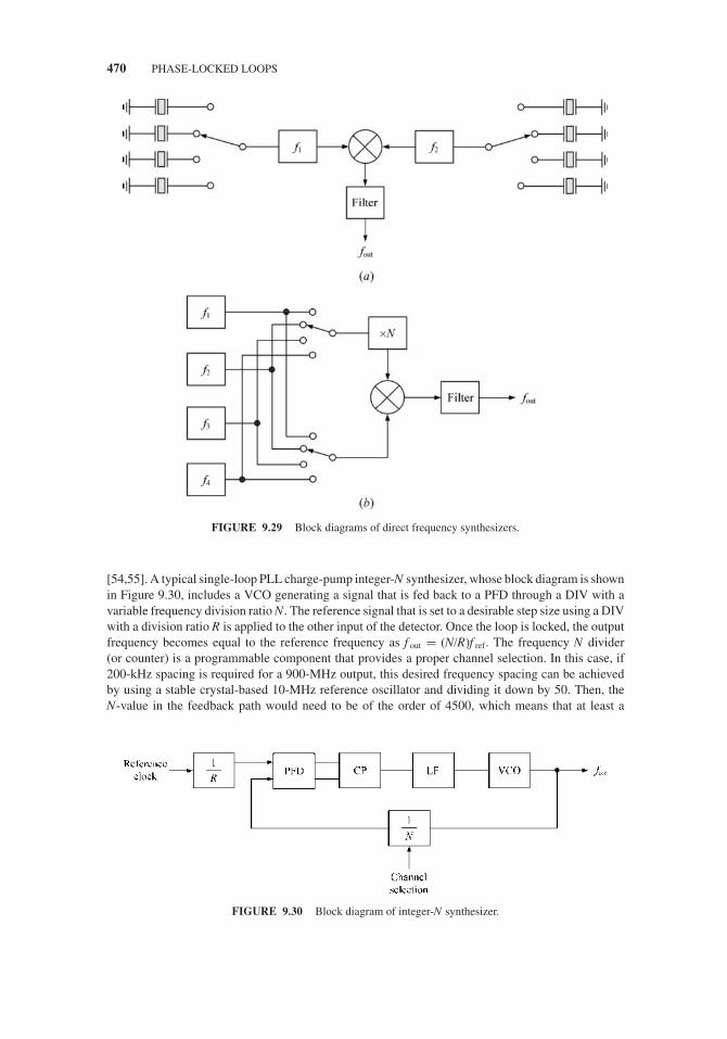
JWBS064-c09 JWBS064-Gerbennikov March 11, 2011 20:2 Printer Name: Yet to Come
470 PHASE-LOCKED LOOPS
FIGURE 9.29 Block diagrams of direct frequency synthesizers.
[54,55]. A typical single-loop PLL charge-pump integer-N synthesizer, whose block diagram is shownin Figure 9.30, includes a VCO generating a signal that is fed back to a PFD through a DIV with avariable frequency division ratio N. The reference signal that is set to a desirable step size using a DIVwith a division ratio R is applied to the other input of the detector. Once the loop is locked, the outputfrequency becomes equal to the reference frequency as f out = (N/R)f ref. The frequency N divider(or counter) is a programmable component that provides a proper channel selection. In this case, if200-kHz spacing is required for a 900-MHz output, this desired frequency spacing can be achievedby using a stable crystal-based 10-MHz reference oscillator and dividing it down by 50. Then, theN-value in the feedback path would need to be of the order of 4500, which means that at least a
FIGURE 9.30 Block diagram of integer-N synthesizer.
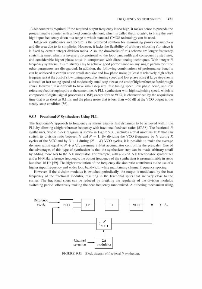
JWBS064-c09 JWBS064-Gerbennikov March 11, 2011 20:2 Printer Name: Yet to Come
FREQUENCY SYNTHESIZERS 471
13-bit counter is required. If the required output frequency is too high, it makes sense to precede theprogrammable counter with a fixed counter element, which is called the prescaler, to bring the veryhigh input frequency down to a range at which standard CMOS technology can be used.
Integer-N synthesizer architecture is the preferred solution for minimizing power consumptionand die area due to its simplicity. However, it lacks the flexibility of arbitrary choosing f ref, since itis fixed by certain integer division ratios. Also, the drawbacks of this scheme are longer frequencyswitching time, which is inversely proportional to the loop bandwidth and consequently step size,and considerable higher phase noise in comparison with direct analog techniques. With integer-Nfrequency synthesis, it is relatively easy to achieve good performance on any single parameter if theother parameters are disregarded. In addition, the following combinations of performance benefitscan be achieved at certain costs: small step size and low phase noise (at least at relatively high offsetfrequencies) at the cost of slow tuning speed; fast tuning speed and low phase noise if large step size isallowed; or fast tuning speed and moderately small step size at the cost of high reference feedthroughspurs. However, it is difficult to have small step size, fast tuning speed, low phase noise, and lowreference feedthrough spurs at the same time. A PLL synthesizer with high switching speed, which iscomposed of digital signal processing (DSP) except for the VCO, is characterized by the acquisitiontime that is as short as 0.1 ms and the phase noise that is less than −60 dB at the VCO output in thesteady-state condition [56].
9.8.3 Fractional-N Synthesizers Using PLL
The fractional-N approach to frequency synthesis enables fast dynamics to be achieved within thePLL by allowing a high reference frequency with fractional feedback ratios [57,58]. The fractional-Nsynthesizer, whose block diagram is shown in Figure 9.31, includes a dual modulus DIV that canswitch its division ratio between N and N + 1. By dividing the VCO frequency by N during Kcycles of the VCO and by N + 1 during (2k − K) VCO cycles, it is possible to make the averagedivision ration equal to N + K/2k, assuming a k-bit accumulator controlling the prescaler. One ofthe advantages of this type of synthesizer is that the synthesizer step can be made arbitrary smallby adding more bits to the �� modulator. For example, with a 20-bit �� fractional-N synthesizerand a 16-MHz reference frequency, the output frequency of the synthesizer is programmable in stepsless than 16 Hz [59]. The higher resolution of the frequency division ratio contributes to the use of ahigher input frequency and wider loop bandwidth while maintaining channel frequency spacing.
However, if the division modulus is switched periodically, the output is modulated by the beatfrequency of the fractional modulus, resulting in the fractional spurs that are very close to thecarrier. The fractional spurs can be reduced by breaking the regularity of the division modulusswitching period, effectively making the beat frequency randomized. A dithering mechanism using
FIGURE 9.31 Block diagram of fractional-N synthesizer.

JWBS064-c09 JWBS064-Gerbennikov March 11, 2011 20:2 Printer Name: Yet to Come
472 PHASE-LOCKED LOOPS
�� modulator can not only randomize the beat frequency, but shape the noise spectrum so that it hasmore power at higher frequency. The high-frequency quantization noise is filtered by the LF of thePLL. A combination of the order of the �� modulator, its sampling rate, and LF order can reduce thehigh-frequency quantization noise at levels that make the effect of the noise negligible [43]. A highsampling rate for the �� modulator results in the quantization noise that is distributed over a widefrequency range. Note that the quantization noise for an nth-order �� modulator only exhibits ann − 1 order of noise-shaping characteristic because the quantization phase error is a time-integratedversion of the modulator output [60]. The quantization noise in a �� fractional-N synthesizer canbe significantly reduced using an all-digital quantization noise cancellation technique when excellentin-band and out-of-band phase noise performance can be achieved [61]. In the digital synthesistechnique, the quantized phase error word is sent to a digital LF, which processes the error word andoutputs a VCO control word to a digital-to-analog converter (DAC), which then turns this control wordinto a control voltage for the VCO. Generally, the PLLs for �� fractional-N synthesizer can be fullyintegrated using both bipolar junction transistor (BJT) and CMOS technologies [28,62]. The radiotransmitter can be realized using this fractional-N approach that performs phase/frequency modulationin a continuous manner such as GMSK or GFSK by direct modulation of the synthesizer [63].
Offset PLLs offer another method of frequency synthesis [52,53]. Figure 9.32 shows a blockdiagram of a single-offset analog synthesizer where the VCO frequency is heterodyned to a lowerfrequency using the signal of an offset generator. The offset signal can be produced using an additionalPLL or a chain of frequency multipliers. Frequency agility can be achieved with a multifrequencyoffset generator in conjunction with a fixed-frequency or a multifrequency reference. An arbitraryfrequency resolution can be realized by successively heterodyning the VCO frequency with severalmultifrequency offset generators with successively finer frequency resolution. One of the problemsassociated with any frequency-mixing scheme is a possible false lock due to undesired mixingproducts. This type of failure requires a sufficiently accurate coarse-tuning mechanism. In this case,a digital-to-analog converter may be included to coarse-tune the VCO, the tuning characteristic ofwhich should be linear over operating temperature range. Besides, it is required to provide sufficientisolation between the mixer ports and the synthesizer output.
Figure 9.33 shows the block schematic of a dual-loop synthesizer where the variable offset signalcan be generated with another PLL. In this case, assuming a 1 MHz-step synthesizer operatingbetween 9 and 10 GHz, the first loop provides 9–10 GHz frequency coverage with a 100 MHz stepsize by varying the division ratio N1 between 90 and 100. At the same time, the output of the firstPLL is used as an offset signal for the second loop to keep the mixer output below 100 MHz. Thus,for the desired 1 MHz step size, the maximum division ratio for the second loop does not exceed100 as well. The phase noise degradation for both loops, which is set by the maximum division ratio,will not exceed 40 dB compared to 80 dB for the single-loop case. Therefore, splitting the design
FIGURE 9.32 Single-offset analog synthesizer architecture.
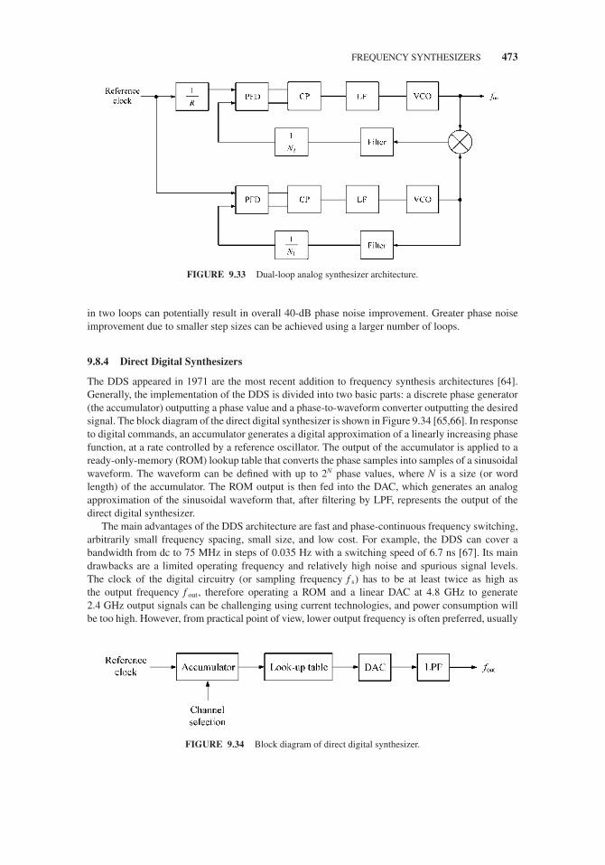
JWBS064-c09 JWBS064-Gerbennikov March 11, 2011 20:2 Printer Name: Yet to Come
FREQUENCY SYNTHESIZERS 473
FIGURE 9.33 Dual-loop analog synthesizer architecture.
in two loops can potentially result in overall 40-dB phase noise improvement. Greater phase noiseimprovement due to smaller step sizes can be achieved using a larger number of loops.
9.8.4 Direct Digital Synthesizers
The DDS appeared in 1971 are the most recent addition to frequency synthesis architectures [64].Generally, the implementation of the DDS is divided into two basic parts: a discrete phase generator(the accumulator) outputting a phase value and a phase-to-waveform converter outputting the desiredsignal. The block diagram of the direct digital synthesizer is shown in Figure 9.34 [65,66]. In responseto digital commands, an accumulator generates a digital approximation of a linearly increasing phasefunction, at a rate controlled by a reference oscillator. The output of the accumulator is applied to aready-only-memory (ROM) lookup table that converts the phase samples into samples of a sinusoidalwaveform. The waveform can be defined with up to 2N phase values, where N is a size (or wordlength) of the accumulator. The ROM output is then fed into the DAC, which generates an analogapproximation of the sinusoidal waveform that, after filtering by LPF, represents the output of thedirect digital synthesizer.
The main advantages of the DDS architecture are fast and phase-continuous frequency switching,arbitrarily small frequency spacing, small size, and low cost. For example, the DDS can cover abandwidth from dc to 75 MHz in steps of 0.035 Hz with a switching speed of 6.7 ns [67]. Its maindrawbacks are a limited operating frequency and relatively high noise and spurious signal levels.The clock of the digital circuitry (or sampling frequency f s) has to be at least twice as high asthe output frequency f out, therefore operating a ROM and a linear DAC at 4.8 GHz to generate2.4 GHz output signals can be challenging using current technologies, and power consumption willbe too high. However, from practical point of view, lower output frequency is often preferred, usually
FIGURE 9.34 Block diagram of direct digital synthesizer.

JWBS064-c09 JWBS064-Gerbennikov March 11, 2011 20:2 Printer Name: Yet to Come
474 PHASE-LOCKED LOOPS
f out(max) = f s/4, for easier analog signal reconstruction. At the same time, the minimum outputfrequency that can be generated by DDS is defined as f out(min) = f s/2N. Large quantization noise andharmonic distortion of a high-speed DAC can significantly degrade the spectral purity of the outputsignal. The DDS power dissipation can be reduced if a nonlinear DAC is used in place of the ROMlookup table and linear DAC [68]. In this case, the function of the nonlinear DAC is to convert thedigital phase information from the phase accumulator directly into analog sine output signal. As aresult, with 8-bit phase accumulator and sine-weighted DAC, the DDS is capable to operate up to a32-GHz clock frequency for all frequency control words and synthesize sine-wave outputs from 125MHz to 16 GHz in 125-MHz steps [69]. By using a 11-bit pipeline phase accumulator, a 10-bit sine-weighted DAC segmented in a 6-bit coarse and eight 3-bit fine DACs, a low-power ultrahigh-speedand high-resolution DDS implemented in a 0.13-μm SiGe BiCMOS technology with f max = 250GHz achieves a maximum clock frequency of 8.6 GHz and a spurious-free dynamic range (SFDR)of approximately 45 dBc with a 4.2958-GHz output [70].
REFERENCES
1. E. V. Appleton, “Automatic Synchronization of Triode Oscillators,” Proc. Camb. Phil. Soc., vol. 21, pt. III,p. 231, 1922–1923.
2. H. de Bellescize, “La Reception Synchrone,” L’Onde Electrique, vol. 11, pp. 230–240, June 1932.
3. F. M. Gardner, Phaselock Techniques, New York: John Wiley & Sons, 2005.
4. G.-C. Hsieh and J. C. Hung, “Phase-Locked Loop Techniques − A Survey,” IEEE Trans. Ind. Electron., vol.IE-43, pp. 609–615, Dec. 1996.
5. J. Frank, A. Newton, and L. Pugliese, “Solid State, Phase-Locked, Tunable UHF Power Oscillators,” IEEETrans. Aerospace Navigational Electron., pp. 3.3.2/1–3.3.2/8, Oct. 1963.
6. V. Manassewitsch, Frequency Synthesizers: Theory and Design, New York: John Wiley & Sons, 1976.
7. D. Banerjee, PLL Performance, Simulation and Design, National Semiconductor, 2006.
8. W. F. Egan, Phase-Lock Basics, New York: John Wiley & Sons, 2008.
9. S. C. Gupta, “Phase-Locked Loops,” Proc. IEEE, vol. 63, pp. 291–306, Feb. 1975.
10. B. Razavi, Monolithic Phase-Locked Loops and Clock Recovery Circuits: Theory and Design, New York:Wiley-IEEE Press, 2008.
11. A. Carlosena and A. Manuel-Lazaro, “Design of High-Order Phase-Locked Loops,” IEEE Trans. Circuitsand Systems−II: Express Briefs, vol. CAS-II-54, pp. 9–13, Jan. 2007.
12. F. M. Gardner, “Charge-Pump Phase-Locked Loops,” IEEE Trans. Commun., vol. COM-28, pp. 1849–1858,Nov. 1980.
13. Z. Wang, “An Analysis of Charge-Pump Phase-Locked Loops,” IEEE Trans. Circuits and Systems−I: RegularPapers, vol. CAS-I-52, pp. 2128–2138, Oct. 2005.
14. J. Lee, M. Liu, and H. Wang, “A 75-GHz Phase-Locked Loop in 90-nm CMOS Technology,” IEEE J.Solid-State Circuits, vol. SC-43, pp. 1414–1426, June 2008.
15. S.-R. Han, C.-N. Chuang, and S.-I. Liu, “A Time-Constant Calibrated Phase-Locked Loop with a Fast-LockedTime,” IEEE Trans. Circuits and Systems−II: Express Briefs, vol. CAS-II-54, pp. 34–37, Jan. 2007.
16. W. C. Lindsey and C. M. Chie, “A Survey of Digital Phase-Locked Loops,” Proc. IEEE, vol. 69, pp. 410–431,Apr. 1981.
17. R. B. Staszewski and P. T. Balsara, “Phase-Domain All-Digital Phase-Locked Loop,” IEEE Trans. Circuitsand Systems−II: Express Briefs, vol. CAS-II-52, pp. 159–163, Mar. 2005.
18. R. B. Staszewski, J. I. Wallberg, S. Rezeq, C.-M. Hung, O. E. Eliezer, S. K. Vemulapalli, C. Fernando, K.Maggio, R. Staszewski, N. Barton, M.-C. Lee, P. Cruise, M. Entezari, K. Muhammad, and D. Leipold, “All-Digital PLL and Transmitter for Mobile Phones,” IEEE J. Solid-State Circuits, vol. SC-40, pp. 2469–2482,Dec. 2005.
19. H. L. Krauss, C. W. Bostian, and F. H. Raab, Solid State Radio Engineering, New York: John Wiley & Sons,1980.

JWBS064-c09 JWBS064-Gerbennikov March 11, 2011 20:2 Printer Name: Yet to Come
REFERENCES 475
20. H. O. Johansson, “A Simple Precharged CMOS Phase Frequency Detector,” IEEE J. Solid-State Circuits,vol. SC-33, pp. 295–299, Feb. 1998.
21. C. T. Charles and D. J. Allstot, “A Calibrated Phase/Frequency Detector for Reference Spur Reduction inCharge-Pump PLLs,” IEEE Trans. Circuits and Systems−II: Express Briefs, vol. CAS-II-53, pp. 822–826,Sept. 2006.
22. J. Rogers, C. Plett, and F. Dai, Integrated Circuit Design for High-Speed Frequency Synthesis, Norwood,MA: Artech House, 2006.
23. S. Milicevic and L. MacEachern, “A Phase-Frequency Detector and a Charge Pump Design for PLL Appli-cations,” 2008 IEEE Int. Symp. Circuits and Systems Dig., pp. 1532–1535.
24. W. Rhee, “Design of High-Performance CMOS Charge Pumps in Phase-Locked Loops,” 1999 IEEE Int.Symp. Circuits and Systems Dig., vol. II, pp. 545–548.
25. W. J. Gruen, “Theory of AFC Synchronization,” Proc. IRE, vol. 41, pp. 1043–1048, Aug. 1953.
26. D. Byrd, C. Davis, and W. O. Keese, A Fast Locking Scheme for PLL Frequency Synthesizers, NationalSemiconductor, AN1000, 1995.
27. P. K. Hanumolu, M. Brownlee, K. Mayaram, and U.-K. Moon, “Analysis of Charge-Pump Phase-LockedLoops,” IEEE Trans. Circuits and Systems−I: Regular Papers, vol. CAS-I-51, pp. 1665–1674, Sept. 2004.
28. J. Craninckx and M. S. J. Steyaert, “A Fully Integrated CMOS DCS-1800 Frequency Synthesizer,” IEEE J.Solid-State Circuits, vol. SC-33, pp. 2054–2065, Dec. 1998.
29. D. G. Tucker, “The Synchronization of Oscillators,” Electronic Engineer, vol. 15, pp. 412–418, Mar. 1943,pp. 457–461, Apr. 1943, vol. 16, pp. 26–30, June 1943.
30. R. Adler, “A Study of Locking Phenomena in Oscillators,” Proc. IRE, vol. 34, pp. 351–357, June 1946.
31. B. Razavi, “A Study of Injection Locking and Pulling in Oscillators,” IEEE J. Solid-State Circuits, vol. SC-39,pp. 1415–1424, Sept. 2004.
32. R. L. Miller, “Fractional-Frequency Generators Utilizing Regenerative Modulation,” Proc. IRE, vol. 27,pp. 446–457, July 1939.
33. A. Safarian, S. Anand, and P. Heydari, “On the Dynamics of Regenerative Frequency Dividers,” IEEE Trans.Circuits and Systems−II: Express Briefs, vol. CAS-II-53, pp. 1413–1417, Dec. 2006.
34. C. Kromer, G. von Buren, G. Sialm, T. Morf, F. Ellinger, and H. Jackel, “A 40-GHz Static Frequency Dividerwith Quadrature Outputs in 80-nm CMOS,” IEEE Microwave and Wireless Components Lett., vol. 16,pp. 564–566, Oct. 2006.
35. W. Hayward, Introduction to Radio Frequency Design, Newington, CT: ARRL, 1995.
36. L. F. Fei, “Frequency Divider Design Strategies,” RF Design, pp. 18–26, Mar. 2005.
37. S. Levantino, L. Romano, S. Pellerano, C. Samori, and A. L. Lacaita, “Phase Noise in Digital FrequencyDividers,” IEEE J. Solid-State Circuits, vol. SC-39, pp. 775–784, May 2004.
38. A. Grebennikov, RF and Microwave Transistor Oscillator Design, London: John Wiley & Sons, 2007.
39. E. Hegazi, H. Sjoland, and A. A. Abidi, “A Filtering Technique to Lower LC Oscillator Phase Noise,” IEEEJ. Solid-State Circuits, vol. SC-36, pp. 1921–1930, Dec. 2001.
40. R. B. Staszewski, C.-M. Hung, N. Barton, M.-C. Lee, and D. Leipold, “A Digitally Controlled Oscillator in a90 nm Digital CMOS Process for Mobile Phones,” IEEE J. Solid-State Circuits, vol. SC-40, pp. 2203–2211,Nov. 2005.
41. C. S. Weaver, “A New Approach to the Linear Design and Analysis of Phase-Locked Loops,” IEEE Trans.Space Electron. Telemetry, vol. SET-5, pp. 166–178, Dec. 1959.
42. G. Nash, Phase-Locked Loop Design Fundamentals, Freescale Semiconductor, AN535, 2006.
43. S. T. Moon, A. Y. Valero-Lopez, and H. Sanchez-Sinencio, “Fully Integrated Frequency Synthesizers: ATutorial,” Int. J. High Speed Electron. Syst., vol. 15, pp. 353–375, June 2005.
44. A. Shibutani, T. Saba, S. Moro, and S. Mori, “Transient Response of Colpitts-VCO and Its Effect onPerformance of PLL System,” IEEE Trans. Circuits and Systems−I: Fundamental Theory Appl., vol.CAS-I-45, pp. 717–725, July 1999.
45. S. Levantino, M. Milani, C. Samori, and A. L. Lacaita, “Fast-Switching Analog PLL with Finite-ImpulseResponse,” IEEE Trans. Circuits Syst.−I: Fundam. Theory Appl., vol. CAS-I-51, pp. 1697–1701, Sept. 2004.
46. I. Thompson and P. V. Brennan, “Phase Noise Contribution of the Phase/Frequency Detector in a Digital PLLFrequency Synthesizer,” IEE Proc. Circuits Devices Syst., vol. 150, pp. 1–5, Feb. 2003.

JWBS064-c09 JWBS064-Gerbennikov March 11, 2011 20:2 Printer Name: Yet to Come
476 PHASE-LOCKED LOOPS
47. B. Chuang, Z. Zhenyu, and Z. Minxuan, “A Low-Noise PLL Design Achieved by Optimizing the LoopBandwidth,” J. Semiconduct., vol. 30, pp. 085011/1–085011/4, Aug. 2009.
48. L. Lascari, “Accurate Phase Noise Prediction in PLL Synthesizers,” Appl. Microwave Wireless, vol. 12,pp. 30–38, Apr. 2000, pp. 90–96, May 2000.
49. W. Wang and L. W. Pearson, “Phase Modulation of a Loop Phase-Locked Grid Oscillator Array,” IEEEMicrowave Wireless Components Lett., vol. 11, pp. 441–443, Nov. 2001.
50. D. M. Klymyshyn, S. Kumar, and A. Mohammadi, “Direct GMSK Modulation with a Phase-Locked PowerOscillator,” IEEE Trans. Vehicular Technol., vol. VT-48, pp. 1616–1625, Sept. 1999.
51. V. Reinhardt, K. Gould, K. McNab, and M. Bustamante, “A Short Survey of Frequency Synthesizer Tech-niques,” Proc. 40th Annual Frequency Control Symp., pp. 355–365, 1986.
52. Z. Galani and R. A. Campbell, “An Overview of Frequency Synthesizers for Radars,” IEEE Trans. MicrowaveTheory Tech., vol. MTT-39, pp. 782–790, May 1991.
53. A. Chenakin, “Building a Microwave Frequency Synthesizer,” High Frequency Electronics, vol. 7, pp. 58–67,May, pp. 18–26, June, pp. 18–26, July, pp.44–51, Aug., pp. 50–58, Sept. 2008.
54. U. L. Rohde, Microwave and Wireless Synthesizers: Theory and Design, New York: John Wiley & Sons,1997.
55. V. Kroupa, Phase Lock Loops and Frequency Synthesis, New York: John Wiley & Sons, 2003.
56. A. Kajiwara and M. Nakagawa, “A New PLL Frequency Synthesizer with High Switching Speed,” IEEETrans. Vehicular Technol., vol. VT-41, pp. 407–413, Nov. 1992.
57. T. A. D. Riley, M. A. Copeland, and T. A. Kwasniewski, “Delta-Sigma Modulation in Fractional-N FrequencySynthesis,” IEEE J. Solid-State Circuits, vol. SC-28, pp. 553–559, May 1993.
58. U. L. Rohde, Synthesizer Design for Microwave Applications, Synergy Microwave Corporation, 1999.
59. T. Riley and J. Kostamovaara, “A Hybrid �� Fractional-N Frequency Synthesizer,” IEEE Trans. Circuitsand Systems−II: Analog and Digital Processing, vol. CAS-II-50, pp. 176–180, Apr. 2003.
60. Basics of Dual Fractional-N Synthesizers/PLLs, Skyworks Solutions, 101463A, 2001.
61. C.-M. Hsu, M. Z. Straayer, and M. H. Perrott, “A Low-Noise Wide-BW 3.6-GHz Digital �� Fractional-NFrequency Synthesizer with a Noise-Shaping Time-to-Digital Converter and Quantization Noise Cancella-tion,” IEEE J. Solid-State Circuits, vol. SC-43, pp. 2776–2786, Dec. 2008.
62. W.-Z. Chen and J.-T. Wu, “A 2-V, 1.8-GHz BJT Phase-Locked Loop,” IEEE J. Solid-State Circuits, vol.SC-34, pp. 784–789, June 1999.
63. M. H. Perrott, T. L. Tewksbury III, and C. G. Sodini, “A 27-mW CMOS Fractional-N Synthesizer Using DigitalCompensation for 2.5-Mb/s GFSK Modulation,” IEEE J. Solid-State Circuits, vol. SC-32, pp. 2048–2060,Dec. 1997.
64. J. Tierney, C. Rader, and B. Gold, “A Digital Frequency Synthesizer,” IEEE Trans. Audio Electroacous.,vol. AE-19, pp. 48–57, Mar. 1971.
65. V. Kroupa, Direct Digital Frequency Synthesizers, New York: John Wiley & Sons, 1998.
66. L. Cordesses, “Direct Digital Synthesis: A Tool for Periodic Wave Generation,” IEEE Signal Process. Mag.,vol. 21, pp. 50–54, July 2004.
67. H. T. Nicholas III and H. Samueli, “A 150-MHz Direct Digital Frequency Synthesizer in 1.25-μm CMOSwith −90-dBc Spurious Performance,” IEEE J. Solid-State Circuits, vol. SC-26, pp. 1959–1969, Dec. 1991.
68. S. Mortezapour and E. F. Lee, “Design of Low-Power ROM-less Direct Digital Frequency Synthesizer UsingNonlinear Digital-to-Analog Converter,” IEEE J. Solid-State Circuits, vol. SC-34, pp. 1350–1359, Oct. 1999.
69. S. E. Turner and D. E. Kotecki, “Direct Digital Synthesizer with Sine-weighted DAC at 32-GHz ClockFrequency in InP DHBT Technology,” IEEE J. Solid-State Circuits, vol. SC-41, pp. 2284–2290, Oct. 2006.
70. X. Geng, F. F. Dai, J. D. Irwin, and R. C. Jaeger, “An 11-Bit 8.6 GHz Direct Digital Synthesizer MMIC with10-Bit Segmented Sine-Weighted DAC,” IEEE J. Solid-State Circuits, vol. SC-45, pp. 300–313, Feb. 2010.

JWBS064-c10 JWBS064-Gerbennikov March 15, 2011 14:3 Printer Name: Yet to Come
10 Power AmplifierDesign Fundamentals
Generally, the power amplifier design requires accurate active device modeling, impedance match-ing depending on the technical requirements and operation conditions, stability in operation, andsimplicity in practical implementation. The quality of the power amplifier design is evaluated byrealized maximum power gain under stable operation condition with minimum amplifier stages, andthe requirement of linearity or high efficiency can be considered where it is needed. For a stableoperation, it is necessary to evaluate the operating frequency domains where the active device maybe potentially unstable. To avoid the parasitic oscillations, the stabilization circuit technique for dif-ferent frequency domains (from low frequencies up to high frequencies close to the device transitionfrequency) is discussed. The key parameter of the power amplifier is its linearity, which is very im-portant for many wireless communication applications. The relationships between the output power,1-dB gain compression point, third-order intercept point, and intermodulation distortions of the thirdand higher orders are given and illustrated for different active devices. The device bias conditionsthat are generally different for linearity or efficiency improvement depend on the power amplifieroperation class and the type of the active device. The bias circuits for the voltage-controlled metal-oxide-semiconductor field-effect transistor (MOSFET) devices are simple due to its voltage control,because the gate dc current is equal to the gate leakage current. However, for the current-controlledbipolar devices, they differ substantially, depending on the device base current and class of operation.The basic Classes A, AB, B, and C of the power amplifier operation are introduced, analyzed, andillustrated. The principles and design of the push–pull amplifiers using balanced transistors, as well asbroadband and distributed power amplifiers are discussed. Harmonic-control techniques for designingmicrowave power amplifiers are given with description of a systematic procedure of multiharmonicload–pull simulation using the harmonic balance method and active load–pull measurement system.Finally, the concept of thermal resistance is introduced and heatsink design issues are discussed.
10.1 POWER GAIN AND STABILITY
Power amplifier design aims for maximum power gain and efficiency for a given value of outputpower with a predictable degree of stability. Instability of the power amplifier will lead to undesiredparasitic oscillations and, as a result, to the distortion of the output signal. One of the main reasonsfor amplifier instability is a positive feedback from the device output to its input through the internalfeedback capacitance, inductance of a common grounded device electrode, and external circuitelements. Consequently, a stability analysis is crucial to any power amplifier design, especially athigh frequencies.
Figure 10.1 shows the basic block schematic of the single-stage power amplifier circuit, whichincludes an active device, an input matching circuit to match with the source impedance, and anoutput matching circuit to match with the load impedance. Generally, the two-port active device
RF and Microwave Transmitter Design, First Edition. Andrei Grebennikov.C© 2011 John Wiley & Sons, Inc. Published 2011 by John Wiley & Sons, Inc.
477
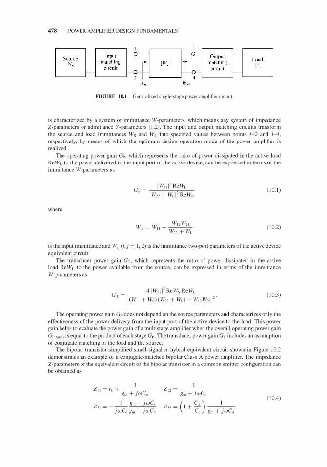
JWBS064-c10 JWBS064-Gerbennikov March 15, 2011 14:3 Printer Name: Yet to Come
478 POWER AMPLIFIER DESIGN FUNDAMENTALS
FIGURE 10.1 Generalized single-stage power amplifier circuit.
is characterized by a system of immittance W-parameters, which means any system of impedanceZ-parameters or admittance Y-parameters [1,2]. The input and output matching circuits transformthe source and load immittances WS and WL into specified values between points 1–2 and 3–4,respectively, by means of which the optimum design operation mode of the power amplifier isrealized.
The operating power gain GP, which represents the ratio of power dissipated in the active loadReWL to the power delivered to the input port of the active device, can be expressed in terms of theimmittance W-parameters as
GP = |W21|2 ReWL
|W22 + WL|2 ReWin(10.1)
where
Win = W11 − W12W21
W22 + WL(10.2)
is the input immittance and W ij (i, j = 1, 2) is the immittance two-port parameters of the active deviceequivalent circuit.
The transducer power gain GT, which represents the ratio of power dissipated in the activeload ReWL to the power available from the source, can be expressed in terms of the immittanceW-parameters as
GT = 4 |W21|2 ReWS ReWL
|(W11 + WS) (W22 + WL) − W12W21|2. (10.3)
The operating power gain GP does not depend on the source parameters and characterizes only theeffectiveness of the power delivery from the input port of the active device to the load. This powergain helps to evaluate the power gain of a multistage amplifier when the overall operating power gainGP(total) is equal to the product of each stage GP. The transducer power gain GT includes an assumptionof conjugate matching of the load and the source.
The bipolar transistor simplified small-signal π-hybrid equivalent circuit shown in Figure 10.2demonstrates an example of a conjugate-matched bipolar Class A power amplifier. The impedanceZ-parameters of the equivalent circuit of the bipolar transistor in a common emitter configuration canbe obtained as
Z11 = rb + 1
gm + jωCπ
Z12 = 1
gm + jωCπ
Z21 = − 1
jωCc
gm − jωCc
gm + jωCπ
Z22 =(
1 + Cπ
Cc
)1
gm + jωCπ
(10.4)

JWBS064-c10 JWBS064-Gerbennikov March 15, 2011 14:3 Printer Name: Yet to Come
POWER GAIN AND STABILITY 479
FIGURE 10.2 Simplified equivalent circuit of matched bipolar power amplifier.
where gm is the device transconductance, rb is the series base resistance, Cπ is the base–emittercapacitance including both diffusion and junction components, and Cc is the feedback collectorcapacitance.
By setting the device feedback impedance Z12 to zero and complex-conjugate matching conditionsof RS = ReZ in and Lin = −ImZin/ω at the input and of RL = ReZout and Lout = −ImZout/ω at theoutput, the small-signal transducer power gain GT can be calculated from
GT =(
fT
f
)2 1
8π fTrbCc(10.5)
where f T = gm/(2πCπ ) is the device transition frequency.Figure 10.3 shows an example of a conjugate-matched field-effect transistor (FET) power amplifier.
The admittance Y-parameters of the small-signal equivalent circuit of any FET device in a commonsource configuration can be obtained by
Y11 = jωCgs
1 + jωCgs Rgs+ jωCgd Y12 = − jωCgd
Y21 = gm
1 + jωCgs Rgs− jωCgd Y22 = 1
Rds+ jω
(Cds + Cgd
) (10.6)
where gm is the device transconductance, Rgs is the gate–source resistance, Cgs is the gate–sourcecapacitance, Cgd is the feedback gate–drain capacitance, Cds is the drain–source capacitance, and Rds
is the differential drain–source resistance.Since the value of the gate–drain capacitance Cgd is normally relatively small, the effect of the
feedback admittance Y12 can be neglected in a simplified case. Then, it is necessary to set RS = Rgs
FIGURE 10.3 Simplified equivalent circuit of matched FET power amplifier.

JWBS064-c10 JWBS064-Gerbennikov March 15, 2011 14:3 Printer Name: Yet to Come
480 POWER AMPLIFIER DESIGN FUNDAMENTALS
and Lin = 1/ω2Cgs for input matching, whereas RL = Rds and Lout = 1/ω2Cds for output matching.Hence, the transducer power gain GT can approximately be calculated from
GT
(Cgd = 0
) = MAG =(
fT
f
)2 Rds
4Rgs(10.7)
where f T = gm/(2πCgs) is the device transition frequency and MAG is the maximum available gainrepresenting a theoretical limit on the power gain that can be achieved under complex-conjugatematching conditions.
From Eqs. (10.5) and (10.7) it follows that the small-signal power gain of a conjugate-matchedpower amplifier for any type of the active device drops off as 1/f 2 or 6 dB per octave. Therefore,GT(f ) can readily be predicted at a certain frequency f , if its value is known at the transition frequencyf T, by
GT ( f ) = GT ( fT)(
fT
f
)2
. (10.8)
It should be noted that previous analysis is based on the linear small-signal consideration whengenerally nonlinear device current source as a function of both the input and output voltages canbe characterized by the linear transconductance gm as a function of the input voltage and the outputdifferential resistance Rds as a function of the output voltage. This is a result of a Taylor seriesexpansion of the output current as a function of the input and output voltages with maintainingonly the dc and linear components. Such an approach helps to understand and derive the maximumachievable power-amplifier parameters in a linear approximation. In this case, an active deviceis operated in a Class A mode when one half of a dc power is dissipated in the device, whilethe other half is transformed to the fundamental-frequency output power, resulting in a maximumideal collector efficiency of 50%. The device output resistance Rout remains constant and can becalculated as a ratio of the dc supply voltage to the dc current flowing through the active device. Ina common case, for a complex-conjugate matching procedure, the device output immittance underlarge-signal consideration should be calculated using Fourier analysis of the output current andvoltage fundamental components. This means that, unlike a linear Class A mode, an active device isoperated in a its linear region only for part of the entire period, and its output resistance is definedas a ratio of the fundamental-frequency output voltage to the fundamental-frequency output current.This is not a physical resistance resulting in a corresponding power loss inside the device, but anequivalent resistance required to use for a conjugate matching procedure. In this case, the complex-conjugate matching is valid and required, firstly, to compensate for the reactive part of the deviceoutput impedance and, secondly, to provide a proper load resistance resulting in a maximum powergain for a given supply voltage and required output power delivered to the load. Note that this is notthe maximum available small-signal power gain that can be achieved in a linear operation mode, buta maximum achievable large-signal power gain that can be achieved for a particular operation modewith a certain conduction angle. Of course, the maximum large-signal power gain is smaller than thesmall-signal power gain for the same input power, since the output power in a nonlinear operationmode also includes the powers at the harmonic components of the fundamental frequency.
According to the immittance approach to the stability analysis of the active two-port network, itis necessary and sufficient for its unconditional stability if the following system of equations can besatisfied for the given active device with both open-circuit input and output ports:
{Re [WS (ω) + Win (ω)] > 0
Im [WS (ω) + Win (ω)] = 0(10.9)

JWBS064-c10 JWBS064-Gerbennikov March 15, 2011 14:3 Printer Name: Yet to Come
POWER GAIN AND STABILITY 481
or
{Re [WL (ω) + Wout (ω)] > 0
Im [WL (ω) + Wout (ω)] = 0.(10.10)
In the case of the opposite signs in Eqs. (10.9) and (10.10), the active two-port network can betreated as unstable or potentially unstable.
Analyzing Eq. (10.9) or Eq. (10.10) on the extremum results in a special relationship between thedevice immittance parameters called the device stability factor
K = 2ReW11ReW22 − Re (W12W21)
|W12W21| (10.11)
which shows a stability margin indicating how far from zero value are the real parts in Eqs. (10.9)and (10.10) being positive [3]. An active device is unconditionally stable if K > 1 and potentiallyunstable if K < 1.
When the device is potentially unstable, an improvement of the power amplifier stability can beprovided with the appropriate choice of the source and load immittances WS and WL. The circuitstability factor KT in this case is defined in the same way as the device stability factor K, but bytaking into account ReWS and ReWL along with the device W-parameters. The circuit stability factoris given by
KT = 2Re (W11 + WS) Re (W22 + WL) − Re (W12W21)|W12W21| . (10.12)
If the circuit stability factor KT > 1, the power amplifier is unconditionally stable. However, thepower amplifier becomes potentially unstable if KT < 1. The value of KT = 1 corresponds to theborder of the circuit unconditional stability. The values of the circuit stability factor KT and devicestability factor K become equal if ReWS = ReWL = 0.
When the device stability factor K > 1, the operating power gain GP has to be maximized. Byanalyzing Eq. (10.1) on extremum, it is possible to find optimum values ReW o
L and ImW oL when the
operating power gain GP is maximal [3,4]. As a result,
GPmax = |W21/W12|K + √
K 2 − 1. (10.13)
The power amplifier with an unconditionally stable active device provides a maximum power gainoperation only if the input and output of the active device are conjugate-matched with the sourceand load impedances, respectively. For the lossless input matching circuit when the power availableat the source is equal to the power delivered to the input port of the active device, that is PS = Pin,the maximum operating power gain is equal to the maximum transducer power gain, that is, GPmax =GTmax.
Domains of the device potential instability include the operating frequency ranges where the activedevice stability factor is equal to K < 1. Within the bandwidth of such a frequency domain, parasiticoscillations can occur, defined by internal positive feedback and operating conditions of the activedevice. The instabilities may also be induced by the RF drive power and remain on its removal. Oneof the most serious cases of the power amplifier instability can occur when there is a variation of theload impedance. Under these conditions, the transistor may be destroyed almost instantaneously. Buteven if it is not destroyed, the instability can result in an increased level of the spurious emissions in
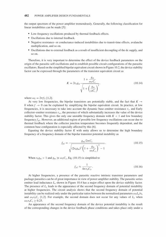
JWBS064-c10 JWBS064-Gerbennikov March 15, 2011 14:3 Printer Name: Yet to Come
482 POWER AMPLIFIER DESIGN FUNDAMENTALS
the output spectrum of the power amplifier tremendously. Generally, the following classification forlinear instabilities can be made [5]:
� Low-frequency oscillations produced by thermal feedback effects.� Oscillations due to internal feedback.� Negative resistance- or conductance-induced instabilities due to transit-time effects, avalanche
multiplication, and so on.� Oscillations due to external feedback as a result of insufficient decoupling of the dc supply, and
so on.
Therefore, it is very important to determine the effect of the device feedback parameters on theorigin of the parasitic self-oscillations and to establish possible circuit configurations of the parasiticoscillators. Based on the simplified bipolar equivalent circuit shown in Figure 10.2, the device stabilityfactor can be expressed through the parameters of the transistor equivalent circuit as
K = 2rbgm
1 + gm
ωT Cc√1 +
(gm
ωCc
)2. (10.14)
where ωT = 2π f T [1,2].At very low frequencies, the bipolar transistors are potentially stable, and the fact that K →
0 when f → 0 can be explained by simplifying the bipolar equivalent circuit. In practice, at lowfrequencies, it is necessary to take into account the dynamic base–emitter resistance rπ and Earlycollector–emitter resistance rce, the presence of which substantially increases the value of the devicestability factor. This gives the only one unstable frequency domain with K < 1 and low boundaryfrequency f p1. However, an additional region of possible low frequency oscillations can occur due tothermal feedback where the collector junction temperature becomes frequently dependent, and thecommon base configuration is especially affected by this [6].
Equating the device stability factor K with unity allows us to determine the high boundaryfrequency of a frequency domain of the bipolar transistor potential instability as
fp2 = gm/2πCc√(2rbgm)2
(1 + gm
ωTCc
)2
− 1
. (10.15)
When rbgm > 1 and gm � ωTCc, Eq. (10.15) is simplified to
f p2 ≈ 1
4πrbCπ
. (10.16)
At higher frequencies, a presence of the parasitic reactive intrinsic transistor parameters andpackage parasitics can be of great importance in view of power amplifier stability. The parasitic seriesemitter lead inductance Le shown in Figure 10.4 has a major effect upon the device stability factor.The presence of Le leads to the appearance of the second frequency domain of potential instabilityat higher frequencies. The circuit analysis shows that the second frequency domain of potentialinstability can be realized only under the particular ratios between the normalized parameters ωTLe/rb
and ωTrbCc [1,2]. For example, the second domain does not occur for any values of Le whenωTrbCc ≥ 0.25.
An appearance of the second frequency domain of the device potential instability is the resultof the corresponding changes in the device feedback phase conditions and takes place only under a
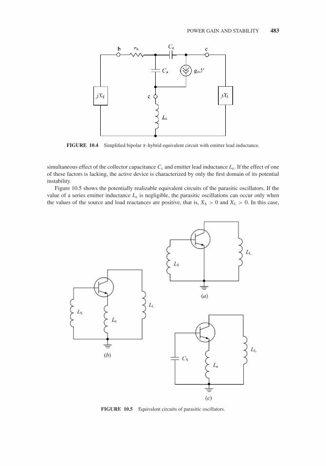
JWBS064-c10 JWBS064-Gerbennikov March 15, 2011 14:3 Printer Name: Yet to Come
POWER GAIN AND STABILITY 483
FIGURE 10.4 Simplified bipolar π-hybrid equivalent circuit with emitter lead inductance.
simultaneous effect of the collector capacitance Cc and emitter lead inductance Le. If the effect of oneof these factors is lacking, the active device is characterized by only the first domain of its potentialinstability.
Figure 10.5 shows the potentially realizable equivalent circuits of the parasitic oscillators. If thevalue of a series emitter inductance Le is negligible, the parasitic oscillations can occur only whenthe values of the source and load reactances are positive, that is, XS > 0 and XL > 0. In this case,
FIGURE 10.5 Equivalent circuits of parasitic oscillators.
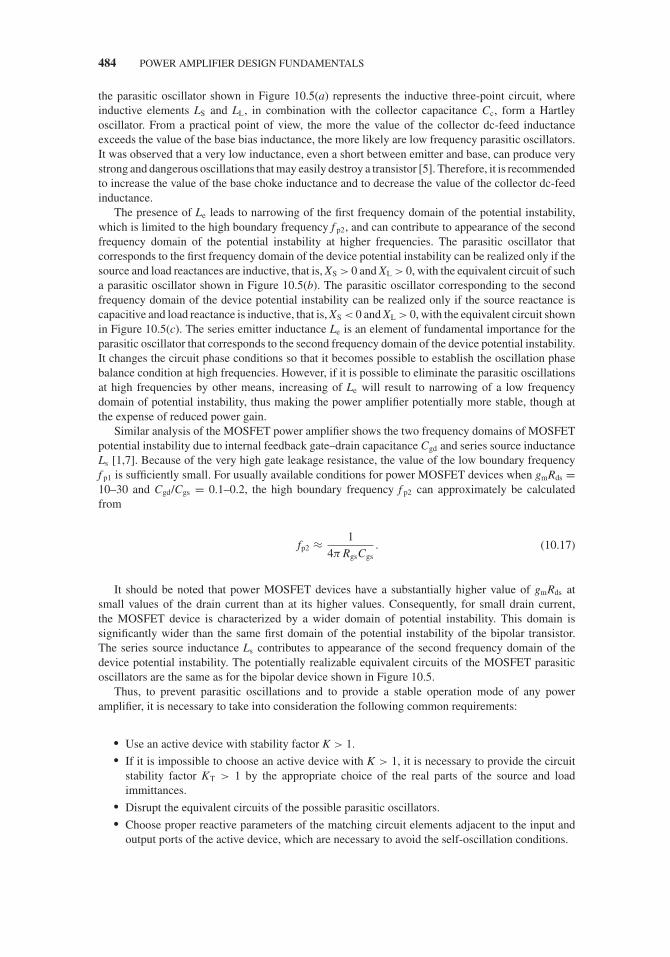
JWBS064-c10 JWBS064-Gerbennikov March 15, 2011 14:3 Printer Name: Yet to Come
484 POWER AMPLIFIER DESIGN FUNDAMENTALS
the parasitic oscillator shown in Figure 10.5(a) represents the inductive three-point circuit, whereinductive elements LS and LL, in combination with the collector capacitance Cc, form a Hartleyoscillator. From a practical point of view, the more the value of the collector dc-feed inductanceexceeds the value of the base bias inductance, the more likely are low frequency parasitic oscillators.It was observed that a very low inductance, even a short between emitter and base, can produce verystrong and dangerous oscillations that may easily destroy a transistor [5]. Therefore, it is recommendedto increase the value of the base choke inductance and to decrease the value of the collector dc-feedinductance.
The presence of Le leads to narrowing of the first frequency domain of the potential instability,which is limited to the high boundary frequency f p2, and can contribute to appearance of the secondfrequency domain of the potential instability at higher frequencies. The parasitic oscillator thatcorresponds to the first frequency domain of the device potential instability can be realized only if thesource and load reactances are inductive, that is, XS > 0 and XL > 0, with the equivalent circuit of sucha parasitic oscillator shown in Figure 10.5(b). The parasitic oscillator corresponding to the secondfrequency domain of the device potential instability can be realized only if the source reactance iscapacitive and load reactance is inductive, that is, XS < 0 and XL > 0, with the equivalent circuit shownin Figure 10.5(c). The series emitter inductance Le is an element of fundamental importance for theparasitic oscillator that corresponds to the second frequency domain of the device potential instability.It changes the circuit phase conditions so that it becomes possible to establish the oscillation phasebalance condition at high frequencies. However, if it is possible to eliminate the parasitic oscillationsat high frequencies by other means, increasing of Le will result to narrowing of a low frequencydomain of potential instability, thus making the power amplifier potentially more stable, though atthe expense of reduced power gain.
Similar analysis of the MOSFET power amplifier shows the two frequency domains of MOSFETpotential instability due to internal feedback gate–drain capacitance Cgd and series source inductanceLs [1,7]. Because of the very high gate leakage resistance, the value of the low boundary frequencyf p1 is sufficiently small. For usually available conditions for power MOSFET devices when gmRds =10–30 and Cgd/Cgs = 0.1–0.2, the high boundary frequency f p2 can approximately be calculatedfrom
fp2 ≈ 1
4π RgsCgs. (10.17)
It should be noted that power MOSFET devices have a substantially higher value of gmRds atsmall values of the drain current than at its higher values. Consequently, for small drain current,the MOSFET device is characterized by a wider domain of potential instability. This domain issignificantly wider than the same first domain of the potential instability of the bipolar transistor.The series source inductance Ls contributes to appearance of the second frequency domain of thedevice potential instability. The potentially realizable equivalent circuits of the MOSFET parasiticoscillators are the same as for the bipolar device shown in Figure 10.5.
Thus, to prevent parasitic oscillations and to provide a stable operation mode of any poweramplifier, it is necessary to take into consideration the following common requirements:
� Use an active device with stability factor K > 1.� If it is impossible to choose an active device with K > 1, it is necessary to provide the circuit
stability factor KT > 1 by the appropriate choice of the real parts of the source and loadimmittances.
� Disrupt the equivalent circuits of the possible parasitic oscillators.� Choose proper reactive parameters of the matching circuit elements adjacent to the input and
output ports of the active device, which are necessary to avoid the self-oscillation conditions.
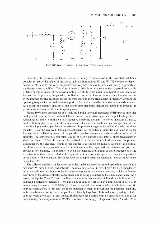
JWBS064-c10 JWBS064-Gerbennikov March 15, 2011 14:3 Printer Name: Yet to Come
POWER GAIN AND STABILITY 485
FIGURE 10.6 Stabilized bipolar Class C VHF power amplifier.
Generally, the parasitic oscillations can arise on any frequency within the potential instabilitydomains for particular values of the source and load immittances WS and WL. The frequency depen-dencies of WS and WL are very complicated and very often cannot be predicted exactly, especially inmultistage power amplifiers. Therefore, it is very difficult to propose a unified approach to providea stable operation mode of the power amplifiers with different circuit configuration and operationfrequencies. In practice, the parasitic oscillations can arise close to the operating frequencies dueto the internal positive feedback inside the transistor and at the frequencies sufficiently far from theoperating frequencies due to the external positive feedback created by the surface-mounted elements.As a result, the stability analysis of the power amplifier must include the methods to prevent theparasitic oscillations in different frequency ranges.
Figure 10.6 shows an example of a stabilized bipolar very high frequency (VHF) power amplifierconfigured to operate in a zero-bias Class C mode. Conductive input and output loading due toresistances R1 and R2 eliminate a low-frequency instability domain. The series inductors L3 and L4
contribute to higher power gain if the resistance values are too small, and can compensate for thecapacitive input and output device impedances. To provide a negative-bias Class C mode, the shuntinductor L2 can be removed. The equivalent circuit of the potential parasitic oscillator at higherfrequencies is realized by means of the parasitic reactive parameters of the transistor and externalcircuitry. The only possible equivalent circuit of such a parasitic oscillator at these frequencies isshown in Figure 10.5(c). It can only be realized if the series emitter lead inductance is present.Consequently, the electrical length of the emitter lead should be reduced as much as possible,or, alternatively, the appropriate reactive immittances at the input and output transistor ports areprovided. For example, it is possible to avoid the parasitic oscillations at these frequencies if theinductive immittance is provided at the input of the transistor and capacitive reactance is providedat the output of the transistor. This is realized by an input series inductance L1 and an output shuntcapacitance C5.
The collector efficiency of the power amplifier can be increased by removing the shunt capacitanceand series RL circuit in the load network. The remaining series LC circuit provides high impedancesat the second-order and higher order harmonic components of the output current, which are flowingnow through the device collector capacitance unlike being grounded by the shunt capacitance. As aresult, the bipolar Class C power amplifier, the circuit schematic of which is shown in Figure 10.7,achieved a collector efficiency of 73% and a power gain of 9 dB with an output power of 13.8 W atan operating frequency of 160 MHz [8]. However, special care must be taken to eliminate parasiticspurious oscillations. In this case, the most important element in preventing the potential instabilityis the base bias resistor Rb. For example, for a relatively large base choke inductor Lb and Rb = 1 k�,spurious oscillations exist at any tuning. Tuning becomes possible with no parasitic oscillations foroutput voltage standing wave ratio (VSWR) less than 1.3 or supply voltage more than 22 V when Rb is

JWBS064-c10 JWBS064-Gerbennikov March 15, 2011 14:3 Printer Name: Yet to Come
486 POWER AMPLIFIER DESIGN FUNDAMENTALS
FIGURE 10.7 High efficiency bipolar Class C VHF power amplifier.
reduced to 470 �. However, a very small reduction in input drive power causes spurious oscillations.Further reduction of Rb to 47 � provides a stable operation for output VSWR ≤ 7 and supply voltagesdown to 7 V. Finally, no spurious oscillations occur at any load, supply voltage and drive power levelfor Rb = 26 �.
Since the transistor using as an active device in power amplifiers is characterized by a sub-stantially nonlinear behavior, this can result in nonlinear instabilities, which generally provide theparametric generation of both harmonic and subharmonic components. The subharmonics can beexplained by parametric varactor-junction action of the collector-to-base voltage-dependent capaci-tance when the large-signal driving acts like pumping a varactor diode, as in a parametric amplifier[9,10]. Such an amplifier exhibits negative resistance under certain conditions when a circuit startsoscillating at subharmonics or rational fractions of the operating frequency [11]. Generally, theparametric oscillations are the result of the external force impact on the element of the oscillationsystem by varying its parameter. Understanding of the physical origin of this parametric effect isvery important in order to disrupt any potentially realizable parametric oscillator circuits. Espe-cially, it is a serious concern for high-efficiency power amplifiers, in general, and Class E poweramplifiers, in particular, with very high voltage peak factor and voltage swing across the devicenonlinear output capacitance, since the transistor is operated in pinch-off, active and saturationregions.
Figure 10.8 shows the simplified large-signal equivalent circuit of the (a) MOSFET or (b) bipolardevice with a nonlinear current source i(t), respectively. The most nonlinear capacitances are thebipolar collector capacitance Cc and the MOSFET gate–drain capacitance Cgd and drain–source ca-pacitance Cds, which can be modeled as junction capacitances with different sensitivities γ . However,since the drain–source capacitance Cds is normally greater by 8–10 times than the gate–drain capaci-tance Cgd, the parametric effect due to Cds causes a major effect on potential parametric oscillationsin a MOSFET power amplifier. The value of the collector capacitance Cc is by the order smaller thanthe value of the base–emitter capacitance Cπ in active mode. In this case, the circuit of a potentialparametric oscillator represents a system with one degree of freedom as shown in Figure 10.8(c),where Vcc is the supply voltage applied to the varying output capacitance Cout (Cout ≈ Cc for a bipolardevice and Cout ≈ Cds for a MOSFET device), while the capacitor C0 and inductor L0 represent theseries high-Q resonant circuit tuned to the fundamental frequency and having high impedances at thesecond-order and higher order harmonics [12].

JWBS064-c10 JWBS064-Gerbennikov March 15, 2011 14:3 Printer Name: Yet to Come
BASIC CLASSES OF OPERATION: A, AB, B, AND C 487
FIGURE 10.8 Simplified nonlinear transistor models and output amplifier circuit.
The most probable parametric oscillations in the nonlinear power amplifier can occur at a subhar-monic frequency ω1/2 = ω0/2, where ω0 is the operating frequency varying the device capacitance.To eliminate such a parasitic subharmonic parametric oscillation, it is necessary to provide the circuitdesign solution when the device output can see very high impedance at a subharmonic frequencyω1/2. Alternatively, an additional lossy element in the subharmonic circuit with its proper isolationfrom the fundamental circuit can be incorporated. In other words, it is necessary to break out any pos-sible resonant conditions at the subharmonic frequency component, which can cause the parametricoscillations.
10.2 BASIC CLASSES OF OPERATION: A, AB, B, AND C
To determine the operation classes of the power amplifier, consider a simple resistive stage shown inFigure 10.9, where Lch is the ideal choke inductor with zero series resistance and infinite reactance atthe operating frequency, Cb is the dc-blocking capacitance with infinite value having zero reactance
JWBS064-c10 JWBS064-Gerbennikov March 15, 2011 14:3 Printer Name: Yet to Come
488 POWER AMPLIFIER DESIGN FUNDAMENTALS
FIGURE 10.9 Voltage and current waveforms in Class A operation.
at the operating frequency, and R is the load resistance. The dc supply voltage Vcc is applied to bothplates of the dc-blocking capacitor, being constant during the entire signal period. The active devicebehaves as an ideal voltage-controlled current source having zero saturation resistance.
Let us assume the input signal to be in a cosine form of
vin = Vbias + Vincosωt (10.18)
where Vbias is the input dc bias voltage. The operating point must be fixed at the middle point ofthe linear part of the device transfer characteristic with V in ≤ Vbias − Vp, where Vp is the devicepinch-off voltage. Normally, to simplify an analysis of the power amplifier operation, the devicetransfer characteristic is represented by a piecewise-linear approximation. As a result, the outputcurrent is cosinusoidal,
i = Iq + I cosωt (10.19)
with the quiescent current Iq greater or equal to the collector current amplitude I. In this case, theoutput collector current contains only two components—dc and cosine—and the averaged currentmagnitude is equal to a quiescent current or dc component Iq.
JWBS064-c10 JWBS064-Gerbennikov March 15, 2011 14:3 Printer Name: Yet to Come
BASIC CLASSES OF OPERATION: A, AB, B, AND C 489
The output voltage v across the device collector represents a sum of the dc supply voltage Vcc
and cosine voltage vR across the load resistance R. Consequently, the greater the output current i,the greater the voltage vR across the load resistance R and smaller the output voltage v. Thus, for apurely real load impedance when ZL = R, the collector voltage v is shifted by 180◦ relative to theinput voltage vin and can be written as
v = Vcc + V cos (ωt + 180◦) = Vcc − V cosωt (10.20)
where V is the output voltage amplitude.Substituting Eq. (10.19) into Eq. (10.20) yields
v = Vcc − (i − Iq
)R. (10.21)
Equation (10.21) can be rewritten in the form of
i =(
Iq + Vcc
R
)− v
R(10.22)
which determines a linear dependence of the collector current versus collector voltage. Such acombination of the cosine collector voltage and current waveforms is known as a Class A operationmode. In real practice, because of the device nonlinearities, it is necessary to connect a parallel LCcircuit with resonant frequency equal to the operating frequency to suppress any possible harmoniccomponents.
Circuit theory prescribes that the collector efficiency η can be written as
η = P
P0= 1
2
I
Iq
V
Vcc= 1
2
I
Iqξ (10.23)
where
P0 = IqVcc (10.24)
is the dc output power,
P = I V
2(10.25)
is the power delivered to the load resistance R at the fundamental frequency f 0, and
ξ = V
Vcc(10.26)
is the collector voltage peak factor.Then, by assuming the ideal conditions of zero saturation voltage when ξ = 1 and maximum
output current amplitude when I/Iq = 1, from Eq. (10.23) it follows that the maximum collectorefficiency in a Class A operation mode is equal to
η = 50%. (10.27)
However, as it follows from Eq. (10.23), increasing the value of I/Iq can further increase thecollector efficiency. This leads to a step-by-step nonlinear transformation of the current cosinewaveform to its pulsed waveform when the amplitude of the collector current exceeds zero value
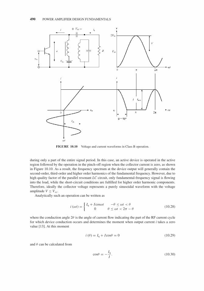
JWBS064-c10 JWBS064-Gerbennikov March 15, 2011 14:3 Printer Name: Yet to Come
490 POWER AMPLIFIER DESIGN FUNDAMENTALS
FIGURE 10.10 Voltage and current waveforms in Class B operation.
during only a part of the entire signal period. In this case, an active device is operated in the activeregion followed by the operation in the pinch-off region when the collector current is zero, as shownin Figure 10.10. As a result, the frequency spectrum at the device output will generally contain thesecond-order, third-order and higher order harmonics of the fundamental frequency. However, due tohigh quality factor of the parallel resonant LC circuit, only fundamental-frequency signal is flowinginto the load, while the short-circuit conditions are fulfilled for higher order harmonic components.Therefore, ideally the collector voltage represents a purely sinusoidal waveform with the voltageamplitude V ≤ Vcc.
Analytically such an operation can be written as
i (ωt) ={
Iq + Icosωt −θ ≤ ωt < θ
0 θ ≤ ωt < 2π − θ(10.28)
where the conduction angle 2θ is the angle of current flow indicating the part of the RF current cyclefor which device conduction occurs and determines the moment when output current i takes a zerovalue [13]. At this moment
i (θ) = Iq + I cosθ = 0 (10.29)
and θ can be calculated from
cosθ = − Iq
I. (10.30)
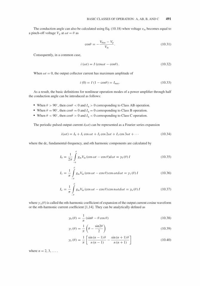
JWBS064-c10 JWBS064-Gerbennikov March 15, 2011 14:3 Printer Name: Yet to Come
BASIC CLASSES OF OPERATION: A, AB, B, AND C 491
The conduction angle can also be calculated using Eq. (10.18) when voltage vin becomes equal toa pinch-off voltage Vp at ωt = θ as
cosθ = − Vbias − Vp
Vin. (10.31)
Consequently, in a common case,
i (ωt) = I (cosωt − cosθ) . (10.32)
When ωt = 0, the output collector current has maximum amplitude of
i (0) = I (1 − cosθ ) = Imax. (10.33)
As a result, the basic definitions for nonlinear operation modes of a power amplifier through halfthe conduction angle can be introduced as follows:
� When θ > 90◦, then cosθ < 0 and Iq > 0 corresponding to Class AB operation.� When θ = 90◦, then cosθ = 0 and Iq = 0 corresponding to Class B operation.� When θ < 90◦, then cosθ > 0 and Iq < 0 corresponding to Class C operation.
The periodic pulsed output current i(ωt) can be represented as a Fourier series expansion
i(ωt) = I0 + I1 cos ωt + I2 cos 2ωt + I3 cos 3ωt + · · · (10.34)
where the dc, fundamental-frequency, and nth harmonic components are calculated by
I0 = 1
2π
θ∫−θ
gmVin (cos ωt − cos θ )dωt = γ0 (θ ) I (10.35)
I1 = 1
π
θ∫−θ
gmVin (cos ωt − cos θ) cos ωtdωt = γ1 (θ ) I (10.36)
In = 1
π
θ∫−θ
gmVin (cos ωt − cos θ) cos nωtdωt = γn (θ ) I (10.37)
where γ n(θ) is called the nth-harmonic coefficient of expansion of the output current cosine waveformor the nth-harmonic current coefficient [1,14]. They can be analytically defined as
γ0 (θ) = 1
π(sinθ − θ cos θ) (10.38)
γ1 (θ) = 1
π
(θ − sin2θ
2
)(10.39)
γn (θ) = 1
π
[sin (n − 1) θ
n (n − 1)− sin (n + 1) θ
n (n + 1)
](10.40)
where n = 2, 3, . . . .

JWBS064-c10 JWBS064-Gerbennikov March 15, 2011 14:3 Printer Name: Yet to Come
492 POWER AMPLIFIER DESIGN FUNDAMENTALS
FIGURE 10.11 Dependencies of γ n (θ ) for dc, fundamental and higher order current components.
The dependencies of γ n (θ) for the dc, fundamental-frequency, second-order and higher ordercurrent components are shown in Figure 10.11. The maximum value of γ n(θ) is achieved when θ =180◦/n. Special case is θ = 90◦, when odd current coefficients are equal to zero, that is, γ 3(θ) =γ 5(θ) = · · · = 0. The ratio between the fundamental-frequency and dc components γ 1(θ)/γ 0(θ ) variesfrom 1 to 2 for any values of the conduction angle, with a minimum value of 1 for θ = 180◦ anda maximum value of 2 for θ = 0◦. It is necessary to pay attention to the fact that, for example, thecurrent coefficient γ 3(θ ) becomes negative within the interval of 90◦ < θ < 180◦. This implies theproper phase changes of the third current harmonic component when its values are negative and itbecomes out of phase relative to the fundamental. Consequently, if the harmonic components, forwhich γ n(θ) > 0, achieve positive maximum values at the time moments corresponding to the middlepoints of the current waveform, the harmonic components, for which γ n(θ ) < 0, can achieve negative
JWBS064-c10 JWBS064-Gerbennikov March 15, 2011 14:3 Printer Name: Yet to Come
BASIC CLASSES OF OPERATION: A, AB, B, AND C 493
maximum values at these time moments. As a result, combination of different harmonic componentswith proper loading will result to flattening of the current or voltage waveforms, thus improvingefficiency of the power amplifier. The amplitude of corresponding current harmonic component canbe obtained by
In = γn (θ ) I = γn (θ) gmVin. (10.41)
From Eq. (10.35) it follows that the dc current component is a function of θ in the operation modeswith θ < 180◦, in contrast to a Class A operation mode where θ = 180◦ and the dc current is equalto the quiescent current during the entire period.
The collector efficiency of a resonant power amplifier biased to operate in the nonlinear mode canbe obtained from
η = P1
P0= 1
2
I1
I0ξ = 1
2
γ1
γ0ξ. (10.42)
where
P0 = Vcc I0 = Vcc Iγ0 (θ ) (10.43)
is the dc output power and
P1 = VI1
2= VIγ1 (θ )
2(10.44)
is the fundamental-frequency output power delivered to the load P1 = PL.If ξ = 1 and θ = π /2 or 90◦, then from Eqs. (10.38) and (10.39) it follows that the maximum
collector efficiency in a Class B operation mode is equal to
η = π
4∼= 78.5%. (10.45)
Equation (10.42) shows that the collector efficiency of a nonlinear power amplifier with pulsed col-lector current waveform depends on the conduction angle, where θ corresponds to half the conductionangle. This means that reduction in θ results in lower γ 1, and to increase the fundamental-frequencypower P1, it is necessary to increase the current amplitude I. Since the current amplitude I is de-termined by the input voltage amplitude V in, the input power Pin must be increased. The collectorefficiency also increases with reduced value of θ and becomes maximum when θ = 0◦ where a ratioγ 1/γ 0 is maximal, as follows from Figure 10.11(a). For example, the collector efficiency η increasesfrom 78.5% to 92% when θ reduces from 90◦ to 60◦. However, it requires the input voltage amplitudeV in to be increased by 2.5 times, resulting in lower values of the power-added efficiency (PAE), whichis defined as
PAE = P1 − Pin
P0= P1
P0
(1 − 1
GP
)(10.46)
where
GP = P1
Pin
is the operating power gain.Consequently, to obtain an acceptable tradeoff between high power gain and high PAE, the con-
duction angle should be chosen within the range of 120◦ ≤ 2θ ≤ 190◦. If it is required to provide high

JWBS064-c10 JWBS064-Gerbennikov March 15, 2011 14:3 Printer Name: Yet to Come
494 POWER AMPLIFIER DESIGN FUNDAMENTALS
collector efficiency of the active device having high gain capability, it is necessary to choose a ClassC operation mode with θ close to 60◦. However, when the input power is limited and power gain is notsufficient, a Class AB operation mode with small quiescent current when θ is slightly greater than 90◦
is recommended. In the latter case, the linearity of the power amplifier can be significantly improved.Since the parallel LC circuit is tuned to the fundamental frequency, the voltage across the load
resistor R can be considered cosinusoidal. By using Eqs. (10.20), (10.28), and (10.30), the relationshipbetween the collector current i and collector voltage v during a time period of −θ ≤ ωt < θ can beexpressed by
i =(
Iq + Vcc
γ1 R
)− v
γ1 R(10.47)
where the fundamental current coefficient γ 1 as a function of θ is determined by Eq. (10.39) andthe load resistance is determined as R = V/I1, where I1 is the fundamental current amplitude.Equation (10.47) representing the dependence of the collector current on the collector voltage forany values of conduction angle in the form of a straight line function is called the load line of theactive device. For a Class A operation mode with θ = 180◦ when γ 1 = 1, Eq. (10.47) is identical toEq. (10.22).
Figure 10.12 shows the idealized active device output I–V curves and load lines for differentconduction angles according to Eq. (10.47) with the corresponding collector and current waveforms.From Figure 10.12 it follows that the maximum collector current amplitude Imax corresponds to theminimum collector voltage V sat when ωt = 0, and is the same for any conduction angle. The slope ofthe load line defined by its slope angle β is different for the different conduction angles and values ofthe load resistance, and it can be obtained by
tan β = I
V (1 − cos θ)= 1
γ1 R(10.48)
from which it follows that greater the slope angle β of the load line, smaller is the value of the loadresistance R for the same θ .
In general, the entire load line represents a broken line PK including a horizontal part, as shownin Figure 10.12. Figure 10.12(a) represents a load line PNK corresponding to a Class AB mode withθ > 90◦, Iq > 0, and I < Imax. Such a load line moves from point K, corresponding to the maximumoutput current amplitude Imax at ωt = 0 and determining the device saturation voltage V sat throughthe point N located at the horizontal axis v where i = 0 and ωt = θ . For a Class AB operation,the conduction angle for the output current pulse between points N′ and N ′′ is greater than 180◦.Figure 10.12(b) represents a load line PMK corresponding to a Class C mode with θ < 90◦, Iq < 0,and I > Imax. For a Class C operation, the load line intersects a horizontal axis v in a point M, andthe conduction angle for the output current pulse between points M′ and M′′ is smaller than 180◦.Hence, generally the load line represents a broken line with the first section having a slope angle β
and another horizontal section with zero current i. In a Class B mode, the collector current representshalf-cosine pulses with the conduction angle of 2θ = 180◦ and Iq = 0.
Now let us consider a Class B operation with increased amplitude of the cosine collector voltage.In this case, as follows from Figure 10.13, an active device is operated in the saturation, active, andpinch-off regions, and the load line represents a broken line LKMP with three linear sections (LK, KM,and MP). The new section KL corresponds to the voltage saturation region resulting in the half-cosineoutput current waveform with a depression in the top part. With further increase of the output voltageamplitude, the output current pulse can be split into two symmetrical pulses containing a significantlevel of the higher order harmonic components. The same result can be achieved by increasing avalue of the load resistance R when the load line is characterized by smaller slope angle β.
The collector current waveform becomes asymmetrical for the complex load, the impedance ofwhich represents the load resistance and capacitive or inductive reactances. In this case, the Fourier

JWBS064-c10 JWBS064-Gerbennikov March 15, 2011 14:3 Printer Name: Yet to Come
BASIC CLASSES OF OPERATION: A, AB, B, AND C 495
FIGURE 10.12 Collector voltage and current waveforms in Class AB and Class C operations.
expansion of the output current given by Eq. (10.34) includes a particular phase for each harmoniccomponent. Then, the output voltage at the device collector is written by
v = Vcc −∞∑
n=1
In |Zn | cos (nωt + φn) (10.49)
where In is the amplitude of nth output current harmonic component, |Zn| is the magnitude of theload network impedance at nth output current harmonic component, and φn is the phase of nthoutput current harmonic component. Assuming that Zn is zero for n = 2, 3, . . . , which is possiblefor a resonant load network having negligible impedance at any harmonic component except thefundamental, Eq. (10.49) can be rewritten as
v = Vcc − I1 |Z1| cos (ωt + φ1) . (10.50)

JWBS064-c10 JWBS064-Gerbennikov March 15, 2011 14:3 Printer Name: Yet to Come
496 POWER AMPLIFIER DESIGN FUNDAMENTALS
FIGURE 10.13 Collector voltage and current waveforms for the device operating in saturation, active andpinch-off regions.
As a result, for the inductive load impedance, the depression in the collector current waveformreduces and moves to the left side of the waveform, whereas the capacitive load impedance causesthe depression to deepen and shift to the right side of the collector current waveform [15]. This effectcan simply be explained by the different phase conditions for fundamental and higher order harmoniccomponents in general composing the collector current waveform, and is illustrated by the differentload lines for (a) inductive and (b) capacitive load impedances shown in Figure 10.14. Note that nowthe load line represents a two-dimensional curve with a complicated behavior.
10.3 LINEARITY
To evaluate the nonlinear properties of the power amplifier, first it is necessary to consider the transferfunction of the active device in the form of
i (ωt) = f [v (ωt )] (10.51)
where i(ωt) is the output collector or drain current and v(ωt) is the input gate–source or base–emittervoltage. It is convenient to apply a power-series analysis, which is relatively easy to use and whichgives a good intuitive sense of the nonlinear behavior of the active device. Assume that the nonlinearityis weak enough so that a power series converges. Then, the transfer function f (v) can be approximatedby its expanding around a dc voltage V0 in a Taylor series as
f (v) = f (V0) +∞∑
n=1
1
n!
∂ (n) f (v)
∂vn
∣∣∣∣v=Vo
(v − V0)n . (10.52)
The nonlinear properties are usually determined by a two-tone excitation test signal with individualcomponents separated slightly in frequency, which can be represented in a common case of unequalamplitudes as
v = V0 + V1cosω1t + V2cosω2t. (10.53)

JWBS064-c10 JWBS064-Gerbennikov March 15, 2011 14:3 Printer Name: Yet to Come
LINEARITY 497
FIGURE 10.14 Load lines for (a) inductive and (b) capacitive load impedances.
For first three derivatives, the output signal can be represented by a Taylor series expansion withthe appropriate equating of the frequency component terms by
i = f (V0) + 1
4
∂2 f (v)
∂v2
∣∣∣∣v=Vo
(V 2
1 + V 22
)
+[
∂ f (v)
∂v
∣∣∣∣v=Vo
+ 1
4
∂3 f (v)
∂v3
∣∣∣∣v=Vo
(1
2V 2
1 + V 22
)]V1cosω1t
+[
∂ f (v)
∂v
∣∣∣∣v=Vo
+ 1
4
(V 2
1 + 1
2V 2
2
)]V2cosω2t
+ 1
4
∂2 f (v)
∂v2
∣∣∣∣v=Vo
(V 2
1 cos2ω1t + V 22 cos2ω2t
)
+ 1
24
∂3 f (v)
∂v3
∣∣∣∣v=Vo
(V 3
1 cos3ω1t + V 32 cos3ω2t
)
+ 1
2
∂2 f (v)
∂v2
∣∣∣∣v=Vo
V1V2cos (ω1 ± ω2) t
+ 1
8
∂3 f (v)
∂v3
∣∣∣∣v=Vo
[V 2
1 V2cos (2ω1 ± ω2) t + V1V 22 cos (ω1 ± 2ω2) t
] · · · (10.54)

JWBS064-c10 JWBS064-Gerbennikov March 15, 2011 14:3 Printer Name: Yet to Come
498 POWER AMPLIFIER DESIGN FUNDAMENTALS
The following conclusions can be drawn from the above Taylor series expansion of the activedevice transfer function:
� Variation of the device bias point is directly proportional to the second derivative (in a commoncase, even derivatives) of the transfer function.
� Device transfer function will be linear only if the third derivative (in a common case, oddderivatives) is equal to zero.
� Even harmonic components are the result of even derivatives of the device transfer function,whereas odd harmonic components are the result of odd derivatives of the device transferfunction.
� First-order mixing products (total and differential) are provided by even derivatives of the devicetransfer function.
� Mixing products of the third order and more are mainly determined by the odd derivatives ofthe device transfer function.
� Distortions, which are determined by the second derivative (second amplitude degree) or by thethird derivative (third amplitude degree) of the device transfer function, are called the second-order intermodulation distortions or the third-order intermodulation distortions, respectively.
From Eq. (10.54) it follows that the output current amplitude of the fundamental, second, and thirdharmonic or intermodulation components depends on the first, second, and third degree of the inputvoltage amplitude, respectively. Consequently, the output power levels of the linear, second-order,and third-order frequency components show a straight-line behavior and vary by 1 dB, 2 dB, and 3 dB,respectively, with an input power level of 1 dB variation. Further analysis of Eq. (10.54) would showthat n-order components also vary by n dB with an input power level of 1 dB variation. As a result,these straight lines in terms of dBm intersect at the proper intercept points. Each point is differentfor each order of intermodulation products. Consequently, if the intercept point is determined, forexample, experimentally for a given type of the transistor, it is easy to evaluate the harmonic andn-order intermodulation output power levels at the arbitrary level of input power. Figure 10.15 showsthe straight-line dependencies for the fundamental, second harmonic and third-order intermodulation(IM3) components with the corresponding intercept points IP2 and IP3, respectively.
For any straight line, we can write the following equation:
PIMn = n Pin + Pn0 dBm (10.55)
where Pn0 is a constant that will be evaluated.The linear fundamental-frequency output power is equal to
Pω1 = 10 log10
(Gp Pin
) = Pin + Gp dBm. (10.56)
Equation (10.55) can be rewritten as
PIMn = n Pω1 + Pn0 − nGp dBm. (10.57)
At the intercept point IPn,
PIMn = Pω1 = IPn (10.58)
which yields a ratio
(1 − n) IPn = Pno − nGp dBm. (10.59)
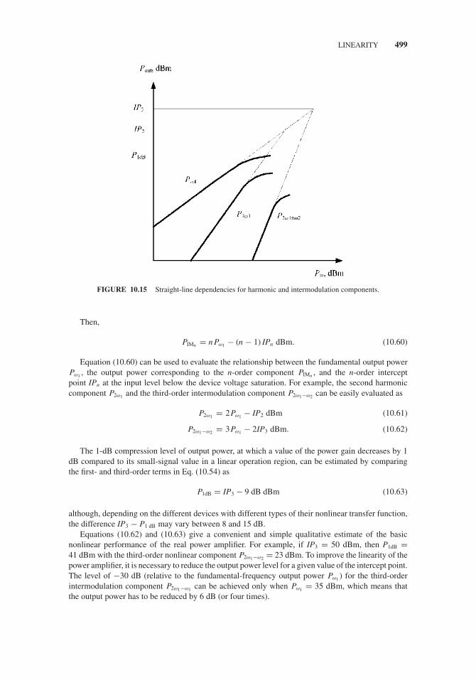
JWBS064-c10 JWBS064-Gerbennikov March 15, 2011 14:3 Printer Name: Yet to Come
LINEARITY 499
FIGURE 10.15 Straight-line dependencies for harmonic and intermodulation components.
Then,
PIMn = n Pω1 − (n − 1) IPn dBm. (10.60)
Equation (10.60) can be used to evaluate the relationship between the fundamental output powerPω1 , the output power corresponding to the n-order component PIMn , and the n-order interceptpoint IPn at the input level below the device voltage saturation. For example, the second harmoniccomponent P2ω1 and the third-order intermodulation component P2ω1−ω2 can be easily evaluated as
P2ω1 = 2Pω1 − IP2 dBm (10.61)
P2ω1−ω2 = 3Pω1 − 2IP3 dBm. (10.62)
The 1-dB compression level of output power, at which a value of the power gain decreases by 1dB compared to its small-signal value in a linear operation region, can be estimated by comparingthe first- and third-order terms in Eq. (10.54) as
P1dB = IP3 − 9 dB dBm (10.63)
although, depending on the different devices with different types of their nonlinear transfer function,the difference IP3 − P1 dB may vary between 8 and 15 dB.
Equations (10.62) and (10.63) give a convenient and simple qualitative estimate of the basicnonlinear performance of the real power amplifier. For example, if IP3 = 50 dBm, then P1dB =41 dBm with the third-order nonlinear component P2ω1−ω2 = 23 dBm. To improve the linearity of thepower amplifier, it is necessary to reduce the output power level for a given value of the intercept point.The level of −30 dB (relative to the fundamental-frequency output power Pω1 ) for the third-orderintermodulation component P2ω1−ω1 can be achieved only when Pω1 = 35 dBm, which means thatthe output power has to be reduced by 6 dB (or four times).

JWBS064-c10 JWBS064-Gerbennikov March 15, 2011 14:3 Printer Name: Yet to Come
500 POWER AMPLIFIER DESIGN FUNDAMENTALS
FIGURE 10.16 MESFET power amplifier intermodulation distortions for different quiescent currents.
It is well known that setting the dc drain current of a GaAs metal–semiconductor field-effecttransistor (MESFET) device to approximately 0.5Idss maximizes not only its gain but also intermod-ulation intercept points. First, the transfer Ids(Vgs) curve is clearly more linear near sweet spot of0.5Idss where its slope, that is, the device transconductance, is maximal, and thus mainly influences thefirst-degree coefficient of its Taylor series expansion. Secondly, the nonlinearity of the Cgs(Vgs) curvesignificantly decreases with the bias point shifted toward higher values. To provide the high-efficiencyoperation mode of the MESFET power amplifier, it is necessary to use a value of the gate–source biasvoltage quite close to the pinch-off voltage, with the appropriate worsening of its linear properties.However, in this case it is possible to choose the bias point with the drain quiescent current Iq inlimits of 0.1–0.15Idss, when the carrier-to-third-order intermodulation ratio IM3 can be minimized atsufficiently high output power, as shown in Figure 10.16. First of all, this is a result of the quadraticdependence of drain current Ids on gate voltage Vgs near the pinch-off point. Besides, given a certainvalue of the gate–source bias voltage, the third-order and the intermodulation components, which arethe results of an interaction of the second harmonics 2ω1 and 2ω2 and differential component ω2 −ω1 with the fundamental components ω1 and ω2, cancel each other. Since this cancelation dependson the load and source impedances at the frequencies far from the operating frequency bandwidth,it is necessary to provide an additional tuning of the input and output matching circuits to minimizeintermodulation distortion.
Figure 10.17 shows an output power spectrum containing only n-order intermodulation compo-nents, which are the result of the effect of two-tone input excitation. The amplitude of the higherorder intermodulation components decreases significantly when frequency increases. To evaluate thelinear behavior of the transistor, it is sufficient to measure the amplitudes of the largest intermodula-tion components, that is, their third-order and the fifth-order components. The carrier-to-third-orderintermodulation ratio or the third-order intermodulation coefficient IM3, as well as the fifth-orderintermodulation coefficient IM5, are defined as
IM3 = 10 log10
(P2ω1−ω2
P
)= P2ω1−ω2 − P dBc (10.64)
IM5 = 10 log10
(P3ω1−2ω2
P
)= P3ω1−2ω2 − P dBc (10.65)
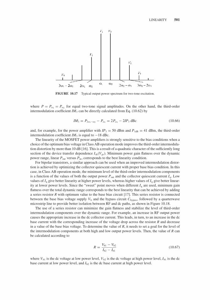
JWBS064-c10 JWBS064-Gerbennikov March 15, 2011 14:3 Printer Name: Yet to Come
LINEARITY 501
FIGURE 10.17 Typical output power spectrum for two-tone excitation.
where P = Pω1 = Pω2 for equal two-tone signal amplitudes. On the other hand, the third-orderintermodulation coefficient IM3 can be directly calculated from Eq. (10.62) by
IM3 = P2ω1−ω2 − Pω1 = 2Pω1 − 2IP3 dBc (10.66)
and, for example, for the power amplifier with IP3 = 50 dBm and P1dB = 41 dBm, the third-orderintermodulation coefficient IM3 is equal to −18 dBc.
The linearity of the MOSFET power amplifiers is strongly sensitive to the bias conditions when achoice of the optimum bias voltage in Class AB operation mode improves the third-order intermodula-tion distortion by more than 10 dB [16]. This is a result of a quadratic character of the sufficiently longsection of the device transfer dependence Ids(Vgs). Minimum power gain flatness over the dynamicpower range, linear Pout versus Pin, corresponds to the best linearity condition.
For bipolar transistors, a similar approach can be used when an improved intermodulation distor-tion is achieved by optimizing the collector quiescent current with proper base bias condition. In thiscase, in Class AB operation mode, the minimum level of the third-order intermodulation componentsis a function of the values of both the output power Pout and the collector quiescent current Iq. Lowvalues of Iq give better linearity at higher power levels, whereas higher values of Iq give better linear-ity at lower power levels. Since the “sweet” point moves when different Iq are used, minimum gainflatness over the total dynamic range corresponds to the best linearity that can be achieved by addinga series resistor R with optimum value to the base bias circuit [17]. This series resistor is connectedbetween the base bias voltage supply Vb and the bypass circuit Cbypass, followed by a quarterwavemicrostrip line to provide better isolation between RF and dc paths, as shown in Figure 10.18.
The use of a series resistor can minimize the gain flatness and stabilize the level of third-orderintermodulation components over the dynamic range. For example, an increase in RF output powercauses the appropriate increase in the dc collector current. This leads, in turn, to an increase in the dcbase current with the corresponding increase of the voltage drop across the resistor R and decreasein a value of the base bias voltage. To determine the value of R, it needs to set a goal for the level ofthe intermodulation components at both high and low output power levels. Then, the value of R canbe calculated according to
R = Vb1 − Vb2
Ib2 − Ib1(10.67)
where Vb1 is the dc voltage at low power level, Vb2 is the dc voltage at high power level, Ib1 is the dcbase current at low power level, and Ib2 is the dc base current at high power level.

JWBS064-c10 JWBS064-Gerbennikov March 15, 2011 14:3 Printer Name: Yet to Come
502 POWER AMPLIFIER DESIGN FUNDAMENTALS
FIGURE 10.18 Bipolar power amplifier with linearizing bias resistor.
In practice, the level of n-order intermodulation component is usually given relative to the peakenvelope power PPEP calculated from two-tone excitation signal measurements. In this case, thewaveform of the signal dissipated in the load will be significantly different from the sine wave, andthe signal voltage can be written for a two-tone signal of equal amplitudes V1 = V2 = V as
vL = V1sinω1t + V2sinω2t = 2V cos �t sin ωt (10.68)
where ω = (ω1 + ω2)/2 is the center RF signal frequency and � = (ω2 − ω1)/2 is the low intercarrierfrequency or pulse envelope.
The waveform of such a two-tone driving signal with equal amplitudes is shown in Figure 10.19,where T = 2π /� is the period of envelope. The peak envelope power PPEP that corresponds to theoutput power with maximum amplitude 2V is equal to
PPEP = (2V )2
2RL(10.69)
where RL is the load resistance. The total output power provided by each sinusoidal tone of a two-toneexcitation signal with equal amplitudes is
Pout = Pω1 + Pω2 = V 2
RL. (10.70)
Comparing Eqs. (10.69) and (10.70) yields
PPEP = 2Pout = 4P (10.71)
where P = Pω1 = Pω2.If the output amplitude and/or phase of the two- or multi-tone test signal are affected by the
tone difference, the power amplifier exhibits the so-called memory effect. Memory is caused by thestorage of energy because of storage elements (capacitors and indictors) that has to be charged ordischarged. Smooth memory effects (usually at low frequencies) do not usually affect the linearity ofthe power amplifier itself. A phase rotation of 10◦–20◦ or an amplitude change of less than 0.5 dB, as a

JWBS064-c10 JWBS064-Gerbennikov March 15, 2011 14:3 Printer Name: Yet to Come
NONLINEAR EFFECT OF COLLECTOR CAPACITANCE 503
FIGURE 10.19 Two-tone driving signal.
function of modulation frequency, has no dramatic effect on the linearity of the device. There are twomemory effects: electrical and thermal. Electrical memory effects are produced by nonconstant nodeimpedances within different frequency ranges corresponding to the dc, fundamental, and its higherorder harmonic components. Most of these effects are generated by frequency-dependent envelopeimpedance, and those close to the dc are the most harmful. Also, the greater the difference betweenthe tones, the more the effect on higher frequency tone can be caused by the device transit time.Thermal memory effects are generated by the junction temperature that is modulated by the appliedsignal, and are much more prominent in a slow envelope sweep.
10.4 NONLINEAR EFFECT OF COLLECTOR CAPACITANCE
Generally, the dependence of the collector capacitance on the output voltage represents a nonlinearfunction. To evaluate the influence of the nonlinear collector capacitance on electrical behavior ofthe power amplifier, let us consider the load network including a series resonant L0C0 circuit tunedto the fundamental frequency that provides open-circuit conditions for the second-order and higherorder harmonic components of the output current and an L-type matching circuit with series inductorL and shunt capacitor C, as shown in Figure 10.20(a). The matching circuit is required to matchthe equivalent output resistance R, corresponding to the required output power at the fundamentalfrequency, with the standard load resistance RL. Figure 10.20(b) shows the simplified output equivalentcircuit of the bipolar power amplifier.
The total output current flowing through the device collector can be written as
i = I0 +∞∑
n=1
Incos (nωt + φn) (10.72)
where In and φn are the amplitude and phase of the nth harmonic component, respectively.

JWBS064-c10 JWBS064-Gerbennikov March 15, 2011 14:3 Printer Name: Yet to Come
504 POWER AMPLIFIER DESIGN FUNDAMENTALS
FIGURE 10.20 Resonant power amplifier circuit schematics.
An assumption of a high quality factor of the series resonant circuit allows the only fundamental-frequency current component to flow into the load. The current flowing through the nonlinear collectorcapacitance Cc, shown in Figure 10.20(a) outside of the transistor, consists of the fundamental-frequency and higher order harmonic components,
iC = ICcos (ωt + φ1) +∞∑
n=2
Incos (nωt + φn) (10.73)
where IC is the fundamental-frequency capacitor current amplitude.The nonlinear behavior of the collector junction capacitance is described by
Cc (v) = C0
(ϕ + Vcc
ϕ + v
)γ
(10.74)
where C0 is the collector capacitance at v = Vcc, Vcc is the supply voltage, ϕ is the contact potential,and γ is the junction sensitivity, being equal to 0.5 for abrupt junction.
As a result, the expression for charge flowing through the collector capacitance can be obtainedby
q =v∫
0
C(v)dv =v∫
0
C0 (ϕ + Vcc)γ
(ϕ + v)γdv. (10.75)

JWBS064-c10 JWBS064-Gerbennikov March 15, 2011 14:3 Printer Name: Yet to Come
NONLINEAR EFFECT OF COLLECTOR CAPACITANCE 505
When v = Vcc, then
q0 = C0 (ϕ + Vcc)
1 − γ
[1 −
(ϕ
ϕ + Vcc
)1−γ]
. (10.76)
Although the dc charge component q0 is a function of the voltage amplitude, its deviation atmaximum voltage amplitude from the small-signal value normally does not exceed 20% for γ =0.5. Then, assuming q0 is determined by Eq. (10.76) as a constant component, the total charge qof the nonlinear capacitance Cc can be represented by the dc component q0 and ac component qwritten as
q = q0 + q = q0
(1 + q
q0
)= q0
(ϕ + v)1−γ − ϕ1−γ
(ϕ + Vcc)1−γ − ϕ1−γ
. (10.77)
Since usually Vcc � ϕ, then from Eq. (10.77) it follows that
v
Vcc=
(1 + q
q0
) 1
1 − γ (10.78)
where q0∼= C0Vcc/(1 − γ ).
On the other hand, the linear charge component q can be written using Eq. (10.73) as
q =∫
iC (t) dt = IC
ωsin (ωt + φ1) +
∞∑n=2
In
nωsin (nωt + φn). (10.79)
As a result, substituting Eq. (10.79) into Eq. (10.78) yields
v
Vcc=
[1 + IC (1 − γ )
ωC0Vccsin (ωt + φ1) +
∞∑n=2
In (1 − γ )
nωC0Vccsin (nωt + φn)
] 1
1 − γ. (10.80)
After applying a Taylor series expansion to Eq. (10.80), it is sufficient to be limited to its first threeterms to reveal the parametric effect. Then, equating the fundamental-frequency collector voltagecomponents gives
v1
Vcc= IC
ωC0Vccsin (ωt + φ1) + IC I2γ
(2ωC0Vcc)2 cos (ωt + φ2 − φ1) + I2 I3γ
12 (ωC0Vcc)2 cos (ωt + φ3 − φ2) .
(10.81)
Consequently, by taking into account that v1 = V1sin(ωt + φ1), the fundamental voltage amplitudeV1 can be obtained from Eq. (10.81) by
V1
Vcc= IC
ωC0Vcc
[1 + I2γ
4ωC0Vcccos (90◦ + φ2 − 2φ1) + I2 I3γ
12ωC0Vcc ICcos (90◦ + φ3 − φ2 − φ1)
].
(10.82)
Since a large-signal value of the abrupt-junction collector capacitance usually doesn’t exceed20%, the fundamental-frequency capacitor current amplitude IC as a first order approximation canbe written as IC
∼= ωC0V1. As a result, from Eq. (10.82) it follows that, because of the parametric
JWBS064-c10 JWBS064-Gerbennikov March 15, 2011 14:3 Printer Name: Yet to Come
506 POWER AMPLIFIER DESIGN FUNDAMENTALS
transformation due to the collector capacitance nonlinearity, the fundamental-frequency collectorvoltage amplitude increases by σ p times according to
σp = 1 + I2γ
4ωC0Vcccos (90◦ + φ2 − 2φ1) + I2 I3γ
12 (ωC0)2 V1Vcccos (90◦ + φ3 − φ2 − φ1) (10.83)
where σ p = ξ p/ξ and ξ p is the collector voltage peak factor with parametric effect [1,15].From Eq. (10.83) it follows that, to maximize the collector voltage peak factor and, consequently,
the collector efficiency for a given value of the supply voltage Vcc, it is necessary to provide thefollowing phase conditions:
φ2 = 2φ1 − 90◦ (10.84)
φ3 = 3φ1 − 180◦. (10.85)
Then, for γ = 0.5,
σp = 1 + I2
8 ωC0Vcc+ I2 I3
24 (ωC0)2 V1Vcc
. (10.86)
Equation (10.86) demonstrates the theoretical possibility to increase the collector voltage peakfactor by 1.1–1.2 times, thus achieving collector efficiency of 85% to 90%. Physically, the improvedefficiency can be explained by the transformation of powers corresponding to the second-order andhigher order harmonic components into the fundamental-frequency output power because of thenonlinearity of the collector capacitance. However, this becomes effective only in the case of the loadnetwork with a series resonant circuit, since it ideally provides infinite impedance at the second-orderand higher order harmonic components, unlike the load network with a parallel resonant circuit havingideally zero impedance at these harmonics.
10.5 DC BIASING
The simplest way to provide a proper dc biasing for power MOSFET device in Class A or ClassAB operation, is to use the potentiometer-type voltage divider for gate bias and choke inductance inthe drain circuit, as shown in Figure 10.21(a). However, in this case, any variation of the ambienttemperature or bias voltage in a wide range leads to the variations of the quiescent current and, asa result, to appropriate variations of the output power, linearity, efficiency and gain of the poweramplifier. The threshold voltage of the MOSFET transistor V th varies with temperature T linearlywith the approximate speed of V th/ T ∼= 2 mV/◦C. But simple adding a diode in series to thevariable resistor allows the quiescent current variation to be reduced substantially over temperature.A bias circuit corresponding to this stabilizing condition is shown in Figure 10.21(b). For a high valueof V th, several diodes can be connected in series. The reason to use such a simple bias circuit forpower MOSFET biasing is that its dc gate current is extremely small being equal to the gate–sourceleakage current only.
In contrast to MOSFET devices, where it can be possible to choose the optimum operating pointwith practically zero temperature coefficient or to be limited to just an additional diode only, thebipolar transistors require the more complicated approach of dc biasing depending on a class ofoperation. For example, in a Class A operation mode, to obtain maximum linear power gain in high-power amplifiers with minimum variations in a wide temperature range, the bias circuit shown inFigure 10.22 can be designed [18]. Here, due to the large negative feedback due to the resistor R3,the operating point of the RF power bipolar transistor is extremely stabilized for wide variations inambient temperature. For instance, if the dc collector current of the RF power transistor rises, due

JWBS064-c10 JWBS064-Gerbennikov March 15, 2011 14:3 Printer Name: Yet to Come
DC BIASING 507
FIGURE 10.21 Typical MOSFET bias circuits.
to an increase in ambient temperature, the collector voltage of this transistor will fall in accordancewith the voltage drop across the feedback resistor R3 causing in turn an appropriate decrease inthe transistor collector current. The diode is used to compensate for the temperature coefficient ofthe base–emitter junction voltage of the p–n–p transistor. The variable resistor R1 in series with thisdiode serves to adjust the dc collector current of RF transistor in its operating point at the desiredvalue. The resistor R5 is necessary to reduce the variation in collector current of the p–n–p transistor,whereas the resistor R4 is included to protect the RF power transistor and to reduce the dissipationin the p–n–p transistor. The parameters of this bias circuit are given for the collector current of RFpower transistor of 0.9 A providing a collector voltage of 25 V for a supply voltage of 28 V.
FIGURE 10.22 Typical bipolar bias circuit for Class A operation.

JWBS064-c10 JWBS064-Gerbennikov March 15, 2011 14:3 Printer Name: Yet to Come
508 POWER AMPLIFIER DESIGN FUNDAMENTALS
FIGURE 10.23 Simple bipolar bias circuits for Class AB operation.
In a Class AB operation, the bias circuit has to deliver a dc voltage, slightly adjustable approxi-mately in limits of 0.7–0.8 V with a wide range of the current values to stabilize the base current of theRF bipolar transistor. Besides, it is necessary to provide an operation mode of the power amplifier withtemperature compensation (collector current stabilization over temperature) and minimum possiblereference current (dc current from the reference dc voltage supply). One of the simplest versions ofsuch a bias circuit with silicon diode temperature compensation is shown in Figure 10.23(a). By usingthe emitter follower based on the n–p–n transistor, it is possible to increase the base current of the RFpower transistor for high power operation. In this bias circuit, each silicon diode can be replaced bythe n–p–n diode-connected transistor, the collector and the base of which are directly connected toeach other, as shown in Figure 10.23(b). A better temperature-compensating result can be achievedusing similar devices for RF and dc paths, only with reduced area sizes for the bias circuit devices.Such an approach is usually used in monolithic integrated circuit design when the same transistorcells with different area size are used for both RF power device and bias circuit transistors.
Figure 10.24 shows a more complicated bias circuit that is commonly used for biasing of thehigh-power RF transistors to provide their temperature-stable and reliable operation mode [18]. Thetemperature stabilization is provided with the parallel connection of the base–emitter diode junctionof the transistor VT1, whereas high value of the bias drive current for the RF power transistor isdelivered by the transistor VT2. If the dc collector current of an RF power transistor is 5 A and a valueof its βF is approximately equal to 10, then the maximum base current of the RF power transistor canbe 0.5 A. In this bias circuit, the resistor R5 is used to reduce the base current variations. At Vb =0.7 V, for a current of 15 mA, the value of R5 should be equal to 0.7 V/15 mA = 47 �. Suppose thata value of the collector current of VT1 is 30 mA. As a result, if the base–emitter junction voltage ofVT2 is equal to 0.8 V with a voltage across the resistor R2 of 28 − 1.5 = 26.5 V, its value is 26.5 V/30 mA∼= 820 �. The variable resistor R3 serves to adjust the output voltage in limits of 0.1 V. Tolimit the maximum collector current of VT2 by a value of 0.5 A, it is best to use the resistor R4. SinceVT2 has a value of the saturation voltage of 0.8 V, it follows that the maximum value of R4 is 26.5 V/0.5 A = 53 �. It is sufficient to use its value of 47 � with a power dissipation of (0.5 A)2 × 47 � =11.75 W. Such a bias circuit can produce the parasitic oscillations near 1 MHz with highly capacitive

JWBS064-c10 JWBS064-Gerbennikov March 15, 2011 14:3 Printer Name: Yet to Come
DC BIASING 509
FIGURE 10.24 Typical bipolar bias circuit for Class AB operation.
loads. Therefore, to prevent these oscillations, it is necessary to connect the RC circuit between thecollector of VT1 and ground.
In most wireless communication systems, it is preferred that the power amplifier operates withhigh efficiency, maintaining an acceptable linearity over the desired supply voltage and output powerranges. However, there is a tradeoff between efficiency and linearity, with improvement in one comingat the expense of another. This means that it is necessary to provide an optimum stable fixed or adaptivebias point over wide temperature range and process variations. As a current-controlled device, thebipolar transistor in RF operation requires the dc base driving current, the value of which dependson the output power and device parameters. Because technologically the bipolar device represents aparallel connection of the basic cells, it is important to use the ballast series resistors to avoid currentimbalance and possible device collapse at higher current density levels. Another important aspectis to keep the dc base–emitter bias point constant (or properly variable) over any RF input powervariations to prevent the linearity worsening at maximum output power for power amplifiers withvariable envelope signal (such as EDGE, WCDMA, LTE, or CDMA2000).
The typical temperature-compensation current-mirror bias circuit with one reference transistor Q1
and one driving transistor Q2 is shown in Figure 10.25(a). This circuit keeps the quiescent currentfor RF device Q0 sufficiently constant over temperature variations, and the current flowing throughresistor R2 is sufficiently small. It is very important to provide the proper ratio between ballastresistors R1 and R0, equal to the reverse ratio of the device areas Q0/Q1. This can minimize the overallperformance variation with temperature as well as stabilize the dc bias point. The latter case is veryimportant for the variable envelope signals, as the dc bias voltage Vbe0 establishes the conductionangle and operation class for the RF device. If the dc base–emitter bias voltage reduces with theincrease of RF input power, the Class AB mode required for linear operation changes to a nonlinearClass C operation.
Figure 10.25(b) shows the dependence of the dc base–emitter bias voltage Vbe0 versus RF inputpower Pin for the second stage of a wideband code-division multiple access (WCDMA) InGaP/GaAsheterojunction bipolar transistor (HBT) power amplifier for different cases, with ballast resistor R1 = 0(curve 1) and optimum ballast resistor R1 (curve 2). From Figure 10.25(b) it follows that including ofthe ballast resistor with optimum value results in a more constant base–emitter dc bias voltage over awider range of input powers, thus improving the linearity performance of the power amplifier at high

JWBS064-c10 JWBS064-Gerbennikov March 15, 2011 14:3 Printer Name: Yet to Come
510 POWER AMPLIFIER DESIGN FUNDAMENTALS
FIGURE 10.25 Current-mirror bipolar bias circuit and its performance.
power levels. In addition, it is best to use a shunt capacitance C1 connected to the base of the deviceQ1 to form a low-pass RC filter, which provides better isolation of the bias circuit from RF signal,with a yet more constant base–emitter dc bias voltage (curve 3).
Figure 10.26 shows the emitter follower bias circuit that provides temperature compensationand minimizing reference current requirements [19]. The emitter follower bias circuit requires onlyseveral tens of microamperes of reference current, whereas the current mirror bias circuit requires afew milliamperes of reference current. Both the current mirror and emitter follower bias circuits havesimilar current-voltage behavior but, for the same circuit parameters (R0, R1, and R2) and devicesareas for Q0, Q1, and Q2, the emitter follower circuit is less sensitive to the reference voltage variationscompared with current mirror bias circuit. Variations of the collector supply voltage Vcc in limitsof 3.0–5.0 V have no effect on the quiescent current set by the reference voltage V ref. However, forsimilar temperature performance, the emitter follower bias circuit may supply more dc current fromdc power supply.
Figure 10.27 shows the bias circuit configuration stabilizing the quiescent current in some rangeof variations of the reference voltage V ref [20,21]. This bias circuit incorporates a feedback loop

JWBS064-c10 JWBS064-Gerbennikov March 15, 2011 14:3 Printer Name: Yet to Come
DC BIASING 511
FIGURE 10.26 Bipolar power amplifier stage with emitter follower bias circuit.
in the form of differential amplifier, which stabilizes the dc operating point. The dc base currentrequired for RF device Q0 is fed by the driver transistor Q2. For better temperature compensation,the ratio between resistors R1 and R0 should be equal to the reverse device area ratio Q0/Q1. Thebase nodes of the transistors Q3 and Q4 forming a differential amplifier are at the same potentialVb1 = Vb2. The voltage difference V ref − Vb2 across the resistor R5 sets the reference current, whichis a mirror current for a quiescent current. In this case, if, for some reason, the temperature of the
FIGURE 10.27 Bipolar power amplifier stage with feedback loop bias circuit.

JWBS064-c10 JWBS064-Gerbennikov March 15, 2011 14:3 Printer Name: Yet to Come
512 POWER AMPLIFIER DESIGN FUNDAMENTALS
FIGURE 10.28 Quiescent current versus temperature for current mirror and feedback loop bias circuits.
RF power device rises causing the proper increase in a quiescent current, the collector current of atransistor Q1 increases proportionally causing the decrease of the base voltage Vb2 due to the increaseof voltage drop across the resistor R5. As a result, as the base voltage of the differential amplifier Vb2
decreases while the base voltage Vb1 remains constant, their difference contributes to the decrease ofthe differential amplifier output voltage resulting in the decrease of base current flowing through thedriver transistor Q2.
Figure 10.28 shows the measured quiescent current Iq of the current mirror and feedback loopbias circuits versus temperature of a wireless handset power amplifier at a supply voltage Vcc = 3.5 V[21]. The current mirror bias circuit shown in Figure 10.25 demonstrates a significant variation of 36mA for a quiescent current over whole temperature range from −25 to +85◦C (curve 1). At the sametime, the variation of a quiescent current for the feedback loop bias circuit is negligible (curve 2).However, the feedback loop bias circuit has a tendency to be potentially unstable. To prevent thepossible instability, it is necessary to provide a proper choice of feedback elements Rf and Cf actingas a low-pass filter section. In addition, a value of the capacitance Cf may be sufficiently large thatincreases the die size and cost, which are very important specification parameters for wireless mobilehandsets.
To overcome stability problem and to keep similar insensitivity of the bias operating point over thesame temperature range, process and reference voltage variations, the bias circuit schematic shown inFigure 10.29(a) can be used. This bias circuit includes a differential amplifier based on two transistorsQ3 and Q4, located between the diode-connected reference transistor Q1 and driving transistor Q2. Avalue of the resistance R1 is chosen to minimize the sensitivity to the temperature variations, and itsvalue is scaled with ballast resistor R0 depending on the device areas. In addition to minimizing thetemperature variations, the proper choice of a value of the resistance R2 contributes to minimizingthe sensitivity of the quiescent current to the reference voltage changes. For instance, if, for somereason, a value of the reference voltage V ref increases, then this results in an appropriate increase ofthe base–emitter voltage of the transistor Q3. As the base potential of the transistor Q4 is fixed usingdiode-connected transistor Q1, the difference in base–emitter voltages of the differential amplifiertransistors Q3 and Q4 causes an increase of the collector current of the transistor Q3 and an increase ofthe voltage drop across the resistor R2. As a result, voltage at the base of the transistor Q2 reduces tokeep the same value of a quiescent current of the power device Q0. In addition, the diode-connectedreference transistor Q1 tracks the changes in the base–emitter voltage variations of the power deviceover temperature. As shown in Figure 10.29(b), the quiescent current Iq varies only in limits of 10%over a reference voltage range of 2.6–2.9 V. At the same time, the reference current Iref is sufficiently

JWBS064-c10 JWBS064-Gerbennikov March 15, 2011 14:3 Printer Name: Yet to Come
DC BIASING 513
FIGURE 10.29 Bipolar power amplifier stage with differential amplifier bias circuit.
small, in limits of 2–4 mA. The quiescent current is very sensitive to variations of the values of theresistors R3 and R4 for both differential amplifier bias circuits shown in Figures 10.27 and 10.29(a).To eliminate this sensitivity, it is the best to replace these resistors partly using diode-connectedtransistors with small areas.
To provide an efficient linear power amplifier operation, it is necessary to minimize the quiescentcurrent at backoff output powers since maximum of the power density function for CDMA2000 orWCDMA standards with nonconstant envelope occurs at the output powers of about 25–30 dB belowthe saturation output power. As a current controlled device, the bipolar transistor at RF operationrequires the dc base driving current, the value of which depends on the output power and deviceparameters. Unlike the current mirror and emitter follower bias circuits, together with the temperature

JWBS064-c10 JWBS064-Gerbennikov March 15, 2011 14:3 Printer Name: Yet to Come
514 POWER AMPLIFIER DESIGN FUNDAMENTALS
compensation over wide range of ambient temperatures, the adaptive bias circuit can control dc powerconsumption as the output power varies by greatly improving a PAE when the output power is lowand maintaining a high linearity of the power amplifier when its output power is high [22].
Figure 10.30(a) shows the schematic of the adaptive bias circuit where the value of the ballastresistance R1 is chosen to minimize the sensitivity to the base bias current variations and its value isscaled with ballasting resistor R2 to the ratio of reverse device areas Q2/Q1 [23]. The bypass capacitoris needed to isolate dc bias circuit from the RF path. Since the RF transistor Q1 is biased to a ClassAB with a small quiescent current and its collector current is a function of the input power, thecollector current of the current mirror device Q2 increases with input power. This increased currentdecreases the base voltage of the device Q3, thus decreasing its collector current. Then, this decreasedcollector current increases the base voltage of the device Q4 due to a smaller voltage drop across the
FIGURE 10.30 Adaptive bias circuit and its performance.

JWBS064-c10 JWBS064-Gerbennikov March 15, 2011 14:3 Printer Name: Yet to Come
PUSH–PULL POWER AMPLIFIERS 515
resistor R4 forcing its emitter current and the collector current of the RF device Q1 to increase. Thus,the quiescent current of the adaptive bias circuit is an increasing function of the input power. Thisprovides high quiescent current at high output powers when high linearity with tradeoff efficiency isachieved and low quiescent current at low output powers when high linearity and increased efficiencyare obtained. As an example shown in Figure 10.30(b), the quiescent current Iq varies from 110 mAat a maximum Pout = 33 dBm to 12 mA for low output powers. The minimum value of a quiescentcurrent is defined by the values of resistors R4 and R5.
10.6 PUSH–PULL POWER AMPLIFIERS
Generally, if it is necessary to increase the overall output power of the power amplifier, severalactive devices can be used in parallel or push–pull configurations. In a parallel configuration, theactive devices are not isolated from each other that requires a very good circuit symmetry and outputimpedance becomes too small in the case of high output power. The latter drawback can be eliminatedin a push–pull configuration, which provides increased values of the input and output impedances.In this case, for the same output power level, the input impedance Z in and output impedance Zout areapproximately four times as high as that of in a parallel connection of the active devices. At the sametime, the loaded quality factors of the input and output matching circuits remain unchanged becauseboth the real and reactive parts of these impedances are increased by the factor of four. Very goodcircuit symmetry can be provided using the balanced active devices with common emitters in a singlepackage. The basic concept of a push–pull operation can be analyzed by using the equivalent circuitshown in Figure 10.31 [24].
It is most convenient to consider an ideal Class B operation, which means that each transistorconducts exactly half a 180◦ cycle with zero quiescent current. Let us also assume that the number ofturns of both primary and secondary windings of the output transformer T2 is equal when n1 = n2,and the collector current of each transistor can be represented in the following half-sinusoidal form:
for the first transistor
ic1 ={+Icsinωt 0 ≤ ωt < π
0 π ≤ ωt < 2π(10.87)
for the second transistor
ic2 ={
0 0 ≤ ωt < π
−Icsinωt π ≤ ωt < 2π(10.88)
where Ic is the output current amplitude.Being transformed through the output transformer T2 with the appropriate out-of-phase conditions,
the total current flowing across the load RL is obtained by
iR (ωt) = ic1 (ωt) − ic2 (ωt) = Icsinωt. (10.89)
The current flowing into the center tap of the primary windings of the output transformer T2 is thesum of the collector currents resulting in
icc (ωt) = ic1 (ωt) + ic2 (ωt) = Ic |sinωt| . (10.90)
Ideally, even-order harmonics being in phase are canceled out and should not appear at the load. Inpractice, a level of the second harmonic component of 30–40 dB below the fundamental is allowable.However, it is necessary to connect a bypass capacitor to the center tap of the primary winding to

JWBS064-c10 JWBS064-Gerbennikov March 15, 2011 14:3 Printer Name: Yet to Come
516 POWER AMPLIFIER DESIGN FUNDAMENTALS
FIGURE 10.31 Basic concept of push–pull operation.
exclude power losses due to even-order harmonics. The current iR(ωt) produces the load voltagevR(ωt) onto the load RL as
vR (ωt) = Ic RLsin (ωt) = VRsin (ωt) (10.91)
where VR is the load voltage amplitude.The total dc collector current is defined as the average value of icc(ωt), which yields
I0 = 1
2π
2π∫0
icc (ωt) d (ωt) = 2
πIc. (10.92)
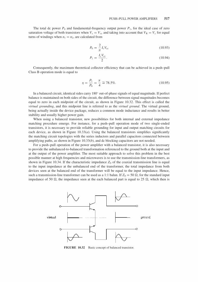
JWBS064-c10 JWBS064-Gerbennikov March 15, 2011 14:3 Printer Name: Yet to Come
PUSH–PULL POWER AMPLIFIERS 517
The total dc power P0 and fundamental-frequency output power P1, for the ideal case of zerosaturation voltage of both transistors when Vc = Vcc and taking into account that VR = Vc for equalturns of windings when n1 = n2, are calculated from
P0 = 2
πIcVcc (10.93)
P1 = IcVcc
2. (10.94)
Consequently, the maximum theoretical collector efficiency that can be achieved in a push–pullClass B operation mode is equal to
η = P1
P0= π
4∼= 78.5%. (10.95)
In a balanced circuit, identical sides carry 180◦ out-of-phase signals of equal magnitude. If perfectbalance is maintained on both sides of the circuit, the difference between signal magnitudes becomesequal to zero in each midpoint of the circuit, as shown in Figure 10.32. This effect is called thevirtual grounding, and this midpoint line is referred to as the virtual ground. The virtual ground,being actually inside the device package, reduces a common mode inductance and results in betterstability and usually higher power gain.
When using a balanced transistor, new possibilities for both internal and external impedancematching procedure emerge. For instance, for a push–pull operation mode of two single-endedtransistors, it is necessary to provide reliable grounding for input and output matching circuits foreach device, as shown in Figure 10.33(a). Using the balanced transistors simplifies significantlythe matching circuit topologies with the series inductors and parallel capacitors connected betweenamplifying paths, as shown in Figure 10.33(b), and dc blocking capacitors are not needed.
For a push–pull operation of the power amplifier with a balanced transistor, it is also necessaryto provide the unbalanced-to-balanced transformation referenced to the ground both at the input andat the output of the power amplifier. The most suitable approach to solve this problem in the bestpossible manner at high frequencies and microwaves is to use the transmission-line transformers, asshown in Figure 10.34. If the characteristic impedance Z0 of the coaxial transmission line is equalto the input impedance at the unbalanced end of the transformer, the total impedance from bothdevices seen at the balanced end of the transformer will be equal to the input impedance. Hence,such a transmission-line transformer can be used as a 1:1 balun. If Z0 = 50 �, for the standard inputimpedance of 50 �, the impedance seen at the each balanced part is equal to 25 �, which then is
FIGURE 10.32 Basic concept of balanced transistor.
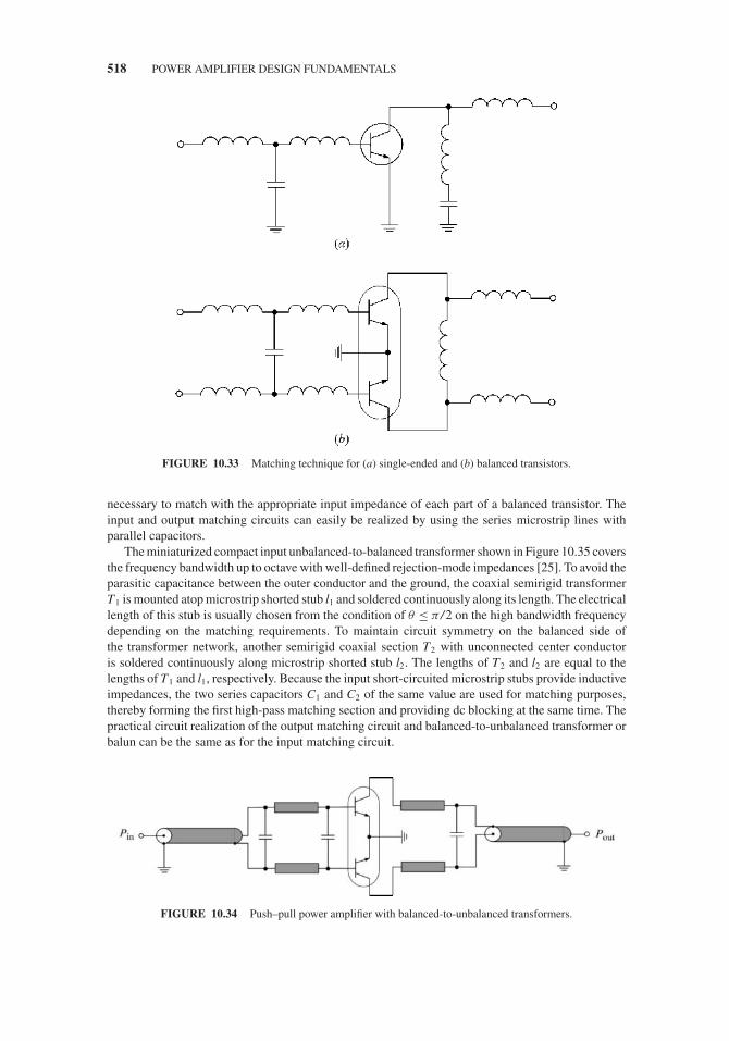
JWBS064-c10 JWBS064-Gerbennikov March 15, 2011 14:3 Printer Name: Yet to Come
518 POWER AMPLIFIER DESIGN FUNDAMENTALS
FIGURE 10.33 Matching technique for (a) single-ended and (b) balanced transistors.
necessary to match with the appropriate input impedance of each part of a balanced transistor. Theinput and output matching circuits can easily be realized by using the series microstrip lines withparallel capacitors.
The miniaturized compact input unbalanced-to-balanced transformer shown in Figure 10.35 coversthe frequency bandwidth up to octave with well-defined rejection-mode impedances [25]. To avoid theparasitic capacitance between the outer conductor and the ground, the coaxial semirigid transformerT1 is mounted atop microstrip shorted stub l1 and soldered continuously along its length. The electricallength of this stub is usually chosen from the condition of θ ≤ π /2 on the high bandwidth frequencydepending on the matching requirements. To maintain circuit symmetry on the balanced side ofthe transformer network, another semirigid coaxial section T2 with unconnected center conductoris soldered continuously along microstrip shorted stub l2. The lengths of T2 and l2 are equal to thelengths of T1 and l1, respectively. Because the input short-circuited microstrip stubs provide inductiveimpedances, the two series capacitors C1 and C2 of the same value are used for matching purposes,thereby forming the first high-pass matching section and providing dc blocking at the same time. Thepractical circuit realization of the output matching circuit and balanced-to-unbalanced transformer orbalun can be the same as for the input matching circuit.
FIGURE 10.34 Push–pull power amplifier with balanced-to-unbalanced transformers.

JWBS064-c10 JWBS064-Gerbennikov March 15, 2011 14:3 Printer Name: Yet to Come
PUSH–PULL POWER AMPLIFIERS 519
FIGURE 10.35 Push–pull power amplifier with compact balanced-to-unbalanced transformers.
Instead of a passive balun at the input, the active-balun circuit can be used to provide the out-of-phase input signals so that the push–pull power amplifier can be driven from a single unbalancedtransmission line, which is very important for a very broadband operation or in a monolithic design.In the former case, the low boundary frequency of operation depends on the values of the dcblocking capacitors only. The simplest active balun or power splitter is a single-stage amplifyingstage with two outputs connected to the drain and source separated from the dc voltage supplyand the ground by the RF chokes, respectively, as shown in Figure 10.36(a). By using a MOSFETdevice, a broadband operation up to 0.1f T can be easily provided, though the power gain is usuallynegligible and amplitude and phase accuracy at high frequencies is not sufficiently high. To improvethe performance over broader frequency bandwidth, a differential amplifier with identical outputpaths, which schematic is shown in Figure 10.36(b), can be used. The advantage of using a MOSFETdevice compare to its bipolar counterpart is its high device input impedance so that no need to use thecomplicated input matching circuit and it is easy to provide symmetry of operation over very widefrequency range.
Figure 10.37(a) shows a schematic diagram of an active power splitter or paraphase amplifierbased on the differential amplifier with a current source using MESFET devices [26]. The unbalancedinput is applied to one of the gates while the other gate is RF shorted to ground by means of abypass capacitor. For X-band operation, a capacitance of 8 pF or greater (reactance at 10 GHz isapproximately equal to 2 �) is desirable. The output tuning is identical to that used in the firststage of the push–pull amplifier. The series and shunt inductors at the input are used for impedancematching with standard 50-� input transmission line. The transistor that functions as a current sourceis realized by 1.5 times larger device. To provide high impedance at the common source connectionto the differential pair, the gate of the current source transistor is RF shorted to ground, and a shuntRF grounded inductor is used at the drain to parallel resonate the device drain–source capacitance.As a result, in a frequency range from 8.4 to 8.65 GHz, the amplitudes were within 1 dB and thephase difference was between 140◦ and 180◦.
Figure 10.37(b) shows the circuit schematic of an active power splitter using both the common gateand common source GaAs FETs which can be used as separate devices or in a dual-gate configuration[27,28]. One gate is grounded through a bypass capacitor for a common gate device, while one sourceis directly grounded for a common source device. The source of a common gate device and the gateof a common source device are connected in phase at the input port through a phase shift circuitrepresenting a short transmission line and a dc blocking capacitor, respectively. A short transmission
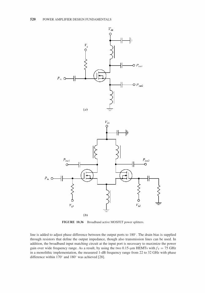
JWBS064-c10 JWBS064-Gerbennikov March 15, 2011 14:3 Printer Name: Yet to Come
520 POWER AMPLIFIER DESIGN FUNDAMENTALS
FIGURE 10.36 Broadband active MOSFET power splitters.
line is added to adjust phase difference between the output ports to 180◦. The drain bias is suppliedthrough resistors that define the output impedance, though also transmission lines can be used. Inaddition, the broadband input matching circuit at the input port is necessary to maximize the powergain over wide frequency range. As a result, by using the two 0.15-μm HEMTs with f T = 75 GHzin a monolithic implementation, the measured 1-dB frequency range from 22 to 32 GHz with phasedifference within 170◦ and 180◦ was achieved [28].
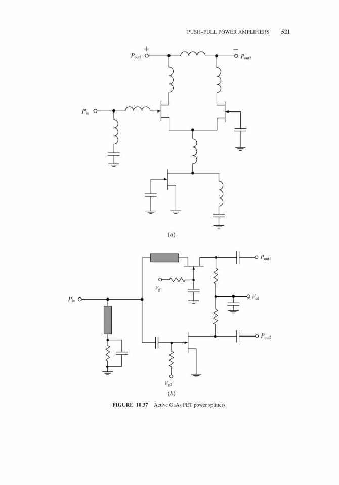
JWBS064-c10 JWBS064-Gerbennikov March 15, 2011 14:3 Printer Name: Yet to Come
PUSH–PULL POWER AMPLIFIERS 521
FIGURE 10.37 Active GaAs FET power splitters.

JWBS064-c10 JWBS064-Gerbennikov March 15, 2011 14:3 Printer Name: Yet to Come
522 POWER AMPLIFIER DESIGN FUNDAMENTALS
10.7 BROADBAND POWER AMPLIFIERS
Generally, the design for a broadband matching circuit, as a main aspect of the broadband poweramplifier design procedure, should solve a problem with contradictory requirements when widermatching bandwidth is required with minimum reflection coefficient, or how to minimize the numberof the matching network sections for a given wideband specification. The necessary requirements aredetermined by the Bode–Fano criterion that gives, for certain canonical types of load impedances,a theoretical limit on the minimum reflection coefficient magnitude that can be obtained with anarbitrary matching network [29,30].
For the lossless matching networks with s parallel RC load impedance shown in Figure 10.38(a)and with series LR load impedance shown in Figure 10.38(b), the Bode-Fano criterion states that
∞∫0
ln1
|� (ω)|dω ≤ π
τ(10.96)
where � (ω) is the reflection coefficient seen looking into the arbitrary lossless matching network andτ = RC = L/R.
For the lossless matching networks with a series RC load impedance shown in Figure 10.38(c)and with parallel LR load impedance shown in Figure 10.38(d), the Bode-Fano integral is written as
∞∫0
1
ω2ln
1
|� (ω)|dω ≤ πτ. (10.97)
The mathematical relationships expressed by Eqs. (10.96) and (10.97) reflect the flat responsesof an ideal filter over the required frequency bandwidth shown in Figure 10.39 for two differentcases. For the same load, both plots illustrate the important tradeoff: the wider the matching network
FIGURE 10.38 Loaded lossless matching circuits.

JWBS064-c10 JWBS064-Gerbennikov March 15, 2011 14:3 Printer Name: Yet to Come
BROADBAND POWER AMPLIFIERS 523
FIGURE 10.39 Ideal filter flat responses.
bandwidth, the worse the reflection coefficient magnitude. From Eq. (10.96) it follows that, when |�|is constant within the frequency bandwidth and |�| = 1 otherwise,
∞∫0
ln1
|� (ω)|dω =ω2∫
ω1
ln1
|� (ω)|dω = ω ln1
|�| ≤ π
τ. (10.98)
Then,
|�|min = exp
( −π
ωτ
)(10.99)
where ω = ω2 − ω1.Similarly, for the lossless network with a series RC load impedance and with a parallel LR load
impedance,
|�|min = exp
(−πω20τ
ω
)(10.100)
where ω0 = √ω1ω2 is the center bandwidth frequency. It should be noted that theoretical bandwidth
limits can be realized only with an infinite number of matching network sections. The frequencybandwidth with minimum reflection coefficient magnitude is determined by a loaded quality factorQL = ω0τ for the series RL or parallel RC circuit and QL = 1/(ω0τ ) for the parallel RL or series RCcircuit, respectively. The Chebyshev matching transformer with a finite number of sections can beconsidered as a close approximation to the ideal passband network when the ripple of the Chebyshevresponse is made equal to |�|min.
Generally, Eqs. (10.99) and (10.100) can be rewritten in a simplified form of
|�|min = exp
(−π
Q0
QL
)(10.101)
where Q0 = ω0/ ω.To correctly design the broadband matching circuits for power amplifiers, it is necessary to
transform and match the device complex impedances with the source and load impedances, whichare usually resistive and equal to 50 �. For high-power or low-supply voltage cases, the deviceimpedances may be sufficiently small, therefore it needs to include an ideal transformer IT togetherwith a matching circuit, as shown in Figure 10.40. Such an ideal transformer provides only a required

JWBS064-c10 JWBS064-Gerbennikov March 15, 2011 14:3 Printer Name: Yet to Come
524 POWER AMPLIFIER DESIGN FUNDAMENTALS
FIGURE 10.40 Matching circuit with ideal transformer.
transformation between the source resistance RS and input impedance of the matching circuit, and itdoes not affect the circuit frequency characteristics.
To implement such an ideal transformer to the impedance-transforming circuit design, it is usefulto operate with the Norton transform. As a result, an ideal transformer with two capacitors C1 and C2
shown in Figure 10.41(a) is replaced by three capacitances CI, CII and CIII connected in the form ofa π -transformer, as shown in Figure 10.41(b). Their values are determined by
CI = nT (nT − 1) C1 (10.102)
CII = nTC1 (10.103)
CIII = C2 − (nT − 1) C1 (10.104)
where nT is the transformation coefficient. In this case, all of the parameters of these two-port networksare identical at any frequency. However, such a replacement is possible only if the capacitance CIII
obtained by Eq. (10.104) is positive and, consequently, physically realizable.Similarly, an ideal transformer with two inductors L1 and L2 shown in Figure 10.42(a) can be
replaced by three inductors LI, LII and LIII connected in the form of a T-transformer in Figure 10.42(b),with values determined by
L I = nT (nT − 1) L2 (10.105)
L II = nT L2 (10.106)
L III = L1 − (nT − 1) L2. (10.107)
FIGURE 10.41 Capacitive impedance-transforming circuits.
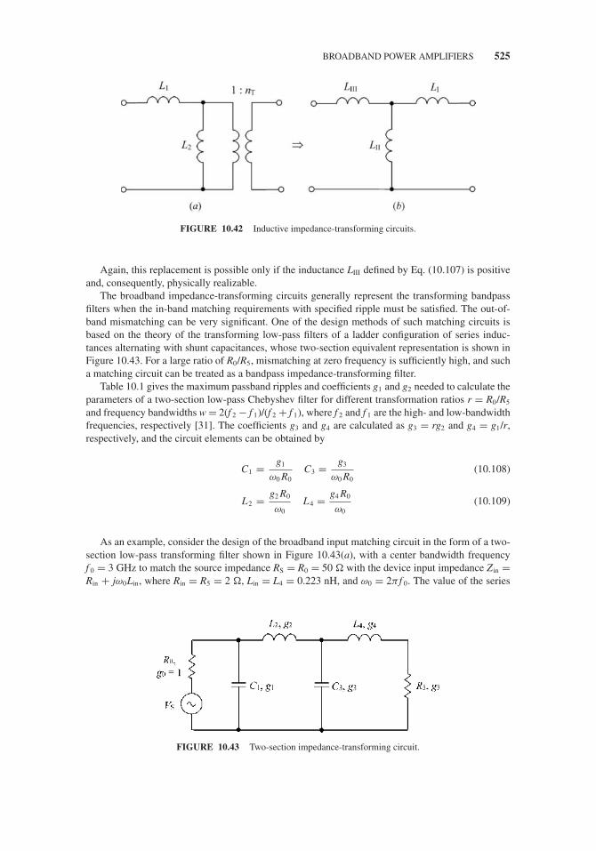
JWBS064-c10 JWBS064-Gerbennikov March 15, 2011 14:3 Printer Name: Yet to Come
BROADBAND POWER AMPLIFIERS 525
FIGURE 10.42 Inductive impedance-transforming circuits.
Again, this replacement is possible only if the inductance LIII defined by Eq. (10.107) is positiveand, consequently, physically realizable.
The broadband impedance-transforming circuits generally represent the transforming bandpassfilters when the in-band matching requirements with specified ripple must be satisfied. The out-of-band mismatching can be very significant. One of the design methods of such matching circuits isbased on the theory of the transforming low-pass filters of a ladder configuration of series induc-tances alternating with shunt capacitances, whose two-section equivalent representation is shown inFigure 10.43. For a large ratio of R0/R5, mismatching at zero frequency is sufficiently high, and sucha matching circuit can be treated as a bandpass impedance-transforming filter.
Table 10.1 gives the maximum passband ripples and coefficients g1 and g2 needed to calculate theparameters of a two-section low-pass Chebyshev filter for different transformation ratios r = R0/R5
and frequency bandwidths w = 2(f 2 − f 1)/(f 2 + f 1), where f 2 and f 1 are the high- and low-bandwidthfrequencies, respectively [31]. The coefficients g3 and g4 are calculated as g3 = rg2 and g4 = g1/r,respectively, and the circuit elements can be obtained by
C1 = g1
ω0 R0C3 = g3
ω0 R0(10.108)
L2 = g2 R0
ω0L4 = g4 R0
ω0(10.109)
As an example, consider the design of the broadband input matching circuit in the form of a two-section low-pass transforming filter shown in Figure 10.43(a), with a center bandwidth frequencyf 0 = 3 GHz to match the source impedance RS = R0 = 50 � with the device input impedance Z in =Rin + jω0Lin, where Rin = R5 = 2 �, Lin = L4 = 0.223 nH, and ω0 = 2π f 0. The value of the series
FIGURE 10.43 Two-section impedance-transforming circuit.
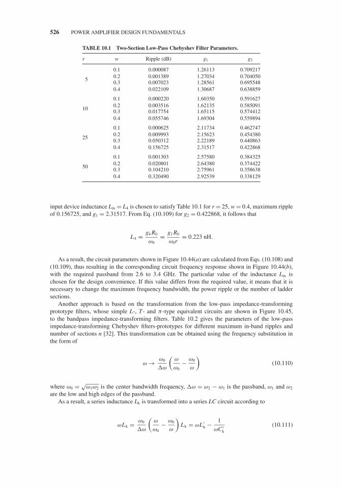
JWBS064-c10 JWBS064-Gerbennikov March 15, 2011 14:3 Printer Name: Yet to Come
526 POWER AMPLIFIER DESIGN FUNDAMENTALS
TABLE 10.1 Two-Section Low-Pass Chebyshev Filter Parameters.
r w Ripple (dB) g1 g2
0.1 0.000087 1.26113 0.7092170.2 0.001389 1.27034 0.704050
50.3 0.007023 1.28561 0.6955480.4 0.022109 1.30687 0.638859
0.1 0.000220 1.60350 0.5916270.2 0.003516 1.62135 0.585091
10 0.3 0.017754 1.65115 0.5744120.4 0.055746 1.69304 0.559894
0.1 0.000625 2.11734 0.4627470.2 0.009993 2.15623 0.454380
250.3 0.050312 2.22189 0.4408630.4 0.156725 2.31517 0.422868
0.1 0.001303 2.57580 0.3843250.2 0.020801 2.64380 0.374422
500.3 0.104210 2.75961 0.3586380.4 0.320490 2.92539 0.338129
input device inductance Lin = L4 is chosen to satisfy Table 10.1 for r = 25, w = 0.4, maximum rippleof 0.156725, and g1 = 2.31517. From Eq. (10.109) for g2 = 0.422868, it follows that
L4 = g4 R0
ω0= g1 R0
ω0r= 0.223 nH.
As a result, the circuit parameters shown in Figure 10.44(a) are calculated from Eqs. (10.108) and(10.109), thus resulting in the corresponding circuit frequency response shown in Figure 10.44(b),with the required passband from 2.6 to 3.4 GHz. The particular value of the inductance Lin ischosen for the design convenience. If this value differs from the required value, it means that it isnecessary to change the maximum frequency bandwidth, the power ripple or the number of laddersections.
Another approach is based on the transformation from the low-pass impedance-transformingprototype filters, whose simple L-, T- and π -type equivalent circuits are shown in Figure 10.45,to the bandpass impedance-transforming filters. Table 10.2 gives the parameters of the low-passimpedance-transforming Chebyshev filters-prototypes for different maximum in-band ripples andnumber of sections n [32]. This transformation can be obtained using the frequency substitution inthe form of
ω → ω0
ω
(ω
ω0− ω0
ω
)(10.110)
where ω0 = √ω1ω2 is the center bandwidth frequency, ω = ω2 − ω1 is the passband, ω1 and ω2
are the low and high edges of the passband.As a result, a series inductance Lk is transformed into a series LC circuit according to
ωLk = ω0
ω
(ω
ω0− ω0
ω
)Lk = ωL ′
k − 1
ωC ′k
(10.111)

JWBS064-c10 JWBS064-Gerbennikov March 15, 2011 14:3 Printer Name: Yet to Come
BROADBAND POWER AMPLIFIERS 527
FIGURE 10.44 Two-section broadband low-pass matching circuit and its frequency response.
FIGURE 10.45 Lumped L-, π- and T-type impedance-transforming circuits.

JWBS064-c10 JWBS064-Gerbennikov March 15, 2011 14:3 Printer Name: Yet to Come
528 POWER AMPLIFIER DESIGN FUNDAMENTALS
TABLE 10.2 Parameters of Low-Pass Chebyshev Filters-Prototypes.
Ripple (dB) n g1 g2 g3 g4
1 0.0960 1.00000.01 2 0.4488 0.4077 1.1007
3 0.6291 0.9702 0.6291 1.0000
1 0.3052 1.00000.1 2 0.8430 0.6220 1.3554
3 1.0315 1.1474 1.0315 1.0000
1 0.4342 1.00000.2 2 1.0378 0.6745 1.5386
3 1.2275 1.1525 1.2275 1.0000
1 0.6986 1.00000.5 2 1.4029 0.7071 1.9841
3 1.5963 1.0967 1.5963 1.0000
where
L ′k = Lk
ωC ′
k = ω
ω20 Lk
. (10.112)
Similarly, a shunt capacitance Ck is transformed into a shunt LC-circuit
ωCk = ω0
ω
(ω
ω0− ω0
ω
)Ck = ωC ′
k − 1
ωL ′k
(10.113)
where
C ′k = Ck
ωL ′
k = ω
ω20Ck
. (10.114)
The low-pass impedance-transforming prototype filter will be transformed to the bandpassimpedance-transforming filter when all its series elements are replaced by the series resonant circuitsand all its parallel elements are replaced by the parallel resonant circuits, where each of them aretuned to the center bandwidth frequency ω0. The bandpass filter elements can be calculated from
ωCk = gk
R(10.115)
ωLk = gk R (10.116)
where k is an element serial number for low-pass prototype filter, gk are the appropriate coefficientsgiven by Table 10.2.
Generally, the low-pass prototype filters and obtained on their basis bandpass filters do not performan impedance transformation. The input and output resistances are either equal for the symmetric T-or π-type filters shown in Figure 10.45(a, b) where g4 = 1 or their ratio is too small for L-type filtersas those shown in Figure 10.45(c, d) where g3 < 2. Therefore, in this case, it is necessary to use anideal transformer concept. This approach is based on using the existing data tables from which theparameters of such impedance-transforming networks can be easily calculated for a given qualityfactor of the device input or output circuit. However, they can also be very easy verified or optimizedby using a computer-aided design (CAD) optimization procedure incorporating in any comprehensivecircuit simulator.
Consider the design example of the broadband interstage impedance-transforming filter with thecenter bandwidth frequency of 1 GHz to match the output driver-stage circuit with the input final-stage

JWBS064-c10 JWBS064-Gerbennikov March 15, 2011 14:3 Printer Name: Yet to Come
BROADBAND POWER AMPLIFIERS 529
FIGURE 10.46 Impedance-transformer design procedure using low-pass filter-prototype.
circuit of the power amplifier, as shown in Figure 10.46(a) [1]. In this case, it is convenient initiallyto convert the parallel connection of the device output resistance Rout and capacitance Cout into theappropriate series connection at the center bandwidth frequency ω0 according to
R′out = Rout
1 + (ω0 RoutCout)2 (10.117)
C ′out = 1 + (ω0 RoutCout)
2
(ω0 Rout)2 Cout
(10.118)
as shown in Figure 10.46(b).

JWBS064-c10 JWBS064-Gerbennikov March 15, 2011 14:3 Printer Name: Yet to Come
530 POWER AMPLIFIER DESIGN FUNDAMENTALS
For the three-section low-pass impedance-transforming prototype filter shown in Figure 10.45(a)with a maximum in-band ripple of 0.1 dB, we then can obtain g1 = g3 = 1.0315, g2 = 1.1474, g4 = 1for n = 3 from Table 10.2. According to Eq. (10.116), the relative frequency bandwidth in this caseis defined as
ω
ω0= g1 Rin
ω0 L in= 16.5%
based on a value of which the shunt capacitor C2 can be calculated using Eq. (10.115) providing acapacitive reactance equal to 0.215 �. The inductive reactance corresponding to a series inductanceLin is equal to 9.42 �.
To convert the low-pass filter to its bandpass prototype, it is necessary to connect the capacitancein series to the input inductance and inductance in parallel to shunt capacitance for and calculatewith the same reactances to resonate at the center bandwidth frequency ω0, as shown in Figure10.46(c) where an ideal transformer IT with transformation coefficient nT = √
9.8/1.5 = 2.556 isincluded. Here, the reactances for each series element are equal to 9.42 �, whereas the reactancesfor each parallel element are equal to 0.215 �. Then, in order to apply a Norton transform, movethe corresponding elements with transformed parameters (each inductive and capacitive reactanceis multiplied by n2
T) to the left-hand side of IT , as shown in Figure 10.46(d) where the requiredseries elements with reactances of 9.42n2
T are realized by existing device output capacitance C ′out and
inductance Lout and additional elements L′ and C′. Finally, by using a Norton transform shown inFigure 10.41 with the ideal transformer IT and two capacitances, the resulting impedance matchingbandpass filter is obtained, as shown in Figure 10.47(a). The frequency response of the filter withminimum in-band ripple and significant out-of-band suppression is shown in Figure 10.47(b). In the
FIGURE 10.47 Impedance-transforming bandpass filter and its frequency response.

JWBS064-c10 JWBS064-Gerbennikov March 15, 2011 14:3 Printer Name: Yet to Come
BROADBAND POWER AMPLIFIERS 531
case of serious difficulties with practical implementation of very low inductance of 0.22 nH or veryhigh capacitance of 109 pF, it is possible to design a multi-section low-pass impedance-transformingcircuit.
An alternative impedance matching technique depends on using the multisection impedance-matching transformers consisting of the stepped transmission-line sections with different charac-teristic impedances. These transmission-line transformers, in contrast to the continuously taperedtransmission-line transformers are significantly shorter and find broader performance. For example,a stepped transmission-line transformer, which consists of a cascaded connection of five uniformsections of equal lengths l = λ0/4, where λ0 is the wavelength corresponding to the central bandwidthfrequency f 0, can provide a maximum VSWR of 1.021 in an octave frequency bandwidth having atotal characteristic impedance change ratio of 8:1 [33]. Such a transformer can be constructed usingany type of transmission lines. Such a stepped transmission-line transformer represents an antimetricstructure, for which the relationship between the characteristic impedances of its sections may bewritten in the general form of
Zi Zn+1−i = ZS ZL (10.119)
where i = 1, 2, . . . , n and n is the number of sections, ZS is the source impedance and ZL is the loadimpedance [34].
The main drawback of such transformers is their significant total length of L = nλ0/4. However,it is possible to reduce the overall transformer length by applying other profiles of its structure. Thestepped transformers using n cascaded uniform transmission-line sections of various lengths withalternating impedances are shorter by 1.5–2. In this case, a number of sections n is always an evennumber and the section impedances may be equal to the source and load impedances to be matched.The total length of such a stepped transmission-line transformer, which four-section structure isshown in Figure 10.48(a), can be further reduced by using the structure representing the cascadeconnection of n transmission line sections of the same length l < λ0/4 with
Z1 < Z3 < · · · < Zn−1
Z2 < Z4 < · · · < Zn(10.120)
where n is an even number and Z1 > Zn when ZS < ZL [35]. In this case, the total transformer lengthis shorter by three times compared to the basic structure with the quarterwave sections, and an octavepassband from 2 to 4 GHz shown in Figure 10.48(b) for the lossless ideal transmission-line sectionsis provided with input return loss better than 25 dB.
To reduce the high impedance ratio of the stepped transformers with a short total length, theiroptimized structures can be used with the section length li = ln+1−i, where i = 1, 2, . . . , n/2, and thesame characteristic impedances for odd and even sections according to
Z1 = Z3 = · · · = Zn−1
Z2 = Z4 = · · · = Zn(10.121)
where Z1Z2 = ZSZL, Zn < ZS, Zn−1 > ZL [36]. In particular situations of high impedance-matchingratio at microwave frequencies when it is necessary to match the standard source load impedance of50 � with the device input and output impedance of 1 � and smaller, both the length and width of themicrostrip-line sections can be optimized. For example, with the use of a multisection transformerwith seven quarter-wavelength microstrip lines of different characteristic impedances, a power gainof 9 ± 1 dB and a PAE of 37.5 ± 7.5% over a frequency range of 5–10 GHz was achieved for a 15-WGaAs MESFET power amplifier [37].
The dissipative or lossy gain compensation matching circuits can achieve the important tradeoffsbetween the power gain, reflection coefficient and frequency bandwidth. Moreover, the resistive natureof such a matching circuit may also improve power amplifier stability and reduce its size and cost

JWBS064-c10 JWBS064-Gerbennikov March 15, 2011 14:3 Printer Name: Yet to Come
532 POWER AMPLIFIER DESIGN FUNDAMENTALS
FIGURE 10.48 Stepped transmission-line transformer with equal-length sections.
because it represents a simple lossy matching circuit structure. In many practical cases, to providebroadband matching with minimum gain flatness and input reflection coefficient, it is sufficient touse the resistive shunt element at the transistor input. An additional matching improvement at highbandwidth frequencies can be achieved by employing inductive reactive elements in series to theresistor [1].
Figure 10.49 shows the circuit schematics of the input, interstage, and output networks intendedfor microwave broadband power amplifiers. The constant-resistance input network shown in Figure10.49(a) enables the input device impedance to be purely resistive and equal to Zin = Rin, when
R1 = Rin (10.122)
L1 = Cgs R2in (10.123)
C1 = Lg
R2in
(10.124)
that makes broadband transformation of the input resistance to the source resistance much easier. In theoutput network shown in Figure 10.49(b), a value of the drain inductance is chosen to compensate forthe capacitive device output reactance at the center bandwidth frequency. Then, a resonant frequencyof the parallel resonant circuit is set to be equal to the same center bandwidth frequency. In this case,for the frequencies where the device drain impedance Zd is capacitive, the impedance of the parallelresonant circuit is inductive. On the other hand, for the frequencies where the drain impedance Zd
is inductive, the impedance of the parallel resonant circuit is capacitive. As a result, the broadband

JWBS064-c10 JWBS064-Gerbennikov March 15, 2011 14:3 Printer Name: Yet to Come
BROADBAND POWER AMPLIFIERS 533
FIGURE 10.49 Schematics of (a) input, (b) output and (c) interstage broadband matching circuits.
FIGURE 10.50 Microstrip two-stage lossy match MESFET power amplifier.
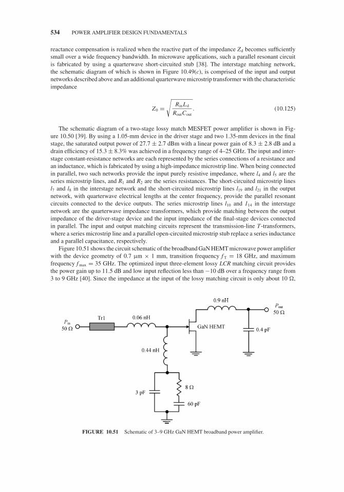
JWBS064-c10 JWBS064-Gerbennikov March 15, 2011 14:3 Printer Name: Yet to Come
534 POWER AMPLIFIER DESIGN FUNDAMENTALS
reactance compensation is realized when the reactive part of the impedance Zd becomes sufficientlysmall over a wide frequency bandwidth. In microwave applications, such a parallel resonant circuitis fabricated by using a quarterwave short-circuited stub [38]. The interstage matching network,the schematic diagram of which is shown in Figure 10.49(c), is comprised of the input and outputnetworks described above and an additional quarterwave microstrip transformer with the characteristicimpedance
Z0 =√
Rin Ld
RoutCout. (10.125)
The schematic diagram of a two-stage lossy match MESFET power amplifier is shown in Fig-ure 10.50 [39]. By using a 1.05-mm device in the driver stage and two 1.35-mm devices in the finalstage, the saturated output power of 27.7 ± 2.7 dBm with a linear power gain of 8.3 ± 2.8 dB and adrain efficiency of 15.3 ± 8.3% was achieved in a frequency range of 4–25 GHz. The input and inter-stage constant-resistance networks are each represented by the series connections of a resistance andan inductance, which is fabricated by using a high-impedance microstrip line. When being connectedin parallel, two such networks provide the input purely resistive impedance, where l4 and l5 are theseries microstrip lines, and R1 and R2 are the series resistances. The short-circuited microstrip linesl7 and l8 in the interstage network and the short-circuited microstrip lines l19 and l21 in the outputnetwork, with quarterwave electrical lengths at the center frequency, provide the parallel resonantcircuits connected to the device outputs. The series microstrip lines l10 and 114 in the interstagenetwork are the quarterwave impedance transformers, which provide matching between the outputimpedance of the driver-stage device and the input impedance of the final-stage devices connectedin parallel. The input and output matching circuits represent the transmission-line T-transformers,where a series microstrip line and a parallel open-circuited microstrip stub replace a series inductanceand a parallel capacitance, respectively.
Figure 10.51 shows the circuit schematic of the broadband GaN HEMT microwave power amplifierwith the device geometry of 0.7 μm × 1 mm, transition frequency f T = 18 GHz, and maximumfrequency f max = 35 GHz. The optimized input three-element lossy LCR matching circuit providesthe power gain up to 11.5 dB and low input reflection less than −10 dB over a frequency range from3 to 9 GHz [40]. Since the impedance at the input of the lossy matching circuit is only about 10 �,
FIGURE 10.51 Schematic of 3–9 GHz GaN HEMT broadband power amplifier.

JWBS064-c10 JWBS064-Gerbennikov March 15, 2011 14:3 Printer Name: Yet to Come
BROADBAND POWER AMPLIFIERS 535
this necessitates an additional broadband impedance transformation (Tr1) from 50 to 10 �, whichwas realized using a few sections of the quarterwave coplanar transmission lines with decreasingimpedance. The output network incorporates an LC circuit to compensate for the output devicecapacitance such that the intrinsic device sees approximately a real load within frequency bandwidth.Because the optimum load for this 1-mm device with supply voltage of 20 V is of about 50 �,consequently no output impedance transformation is needed. The output power was of about 1.6 Wwith the PAE ranging from 14 to 24% in a frequency bandwidth from 4 to 8 GHz.
A very broadband power amplifier operation with high power gain can be achieved by using asimple RL gain-compensating matching circuit at the input and a compensating series inductor Lout
at the output of each stage in a multistage power amplifier, which simplified schematic (withoutbias circuits) is shown in Figure 10.52(a). The combination of these compensating elements ininterstage matching circuit shown in Figure 10.52(b) is necessary to compensate first for the inputdevice reactance due to the gate source capacitance Cgs when its input impedance will become purelyactive equal to R when R = Rgs and L = CgsR2 and, secondly, to compensate for the device outputdrain–source capacitance Cds when the output inductance can be calculated as Lout = CdsR2. By usingthis compensating inductor, the power gain can be increased at high bandwidth frequencies when theeffect of the drain–source capacitance Cds becomes significant. The effect of the feedback gate–draincapacitance Cgd is neglected because its value is sufficiently small compared with Cgs and Cds. Fora wider operating bandwidth, it is better to use the transistors of the same gate geometry, thoughdifferent sizes are also possible. In this case, it is necessary to choose the different parameters ofinterstage matching circuits and optimize them for maximum bandwidth (the resistance R at the inputcan be set to 50 � if the source impedance is 50 �). Then, the overall operating power gain can beestimated from
GP(dB) = 20n log10 (gm R) (10.126)
where n is the number of stages. As a result, by using the GaAs MESFET devices with transconduc-tances gm = 55 mS in a similar four-stage power amplifier structure, the output power of 10 ± 1 dBm
FIGURE 10.52 Schematic of 1–10 GHz four-stage broadband power amplifier.

JWBS064-c10 JWBS064-Gerbennikov March 15, 2011 14:3 Printer Name: Yet to Come
536 POWER AMPLIFIER DESIGN FUNDAMENTALS
for the input power of −28 dBm was achieved across the frequency bandwidth from 1 to 10 GHz atthe supply voltage of 2 V [41].
Figure 10.53(a) shows the circuit schematic of a broadband laterally diffused metal-oxide semi-conductor field-effect transistor (LDMOSFET) high power amplifier with the device geometry of1.25 μm × 40 mm [1]. The optimized input three-element lossy matching circuit allows a verybroadband operation to be provided with the minimum power gain flatness. The using of a 1:2 outputtransformer contributes to an increase in the output power level. The capacitance of 20 pF connectedin parallel with the resistance of 27 � provides an additional increase of a power gain at higher band-width frequencies. The simulation results are plotted in Figure 10.53(b), where the output powers of22–25 W with a power gain of 13.7 ± 0.3 dB in a frequency range of 5–300 MHz can be achieved(curve 1). In this case, input return loss is greater than 8 dB up to 225 MHz (curve 2). The directconnection of the standard 50-� load to the device drain through the blocking capacitor provides anoutput power level within the range of 6–7 W.
FIGURE 10.53 Circuit schematic of broadband LDMOSFET high power amplifier.
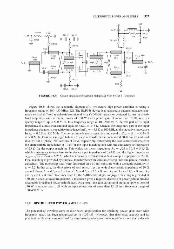
JWBS064-c10 JWBS064-Gerbennikov March 15, 2011 14:3 Printer Name: Yet to Come
DISTRIBUTED POWER AMPLIFIERS 537
FIGURE 10.54 Circuit diagram of broadband high power VHF MOSFET amplifier.
Figure 10.54 shows the schematic diagram of a two-octave high-power amplifier covering afrequency range of 100–450 MHz [42]. The BLF548 device is a balanced n-channel enhancement-mode vertical diffused metal-oxide-semiconductor (VDMOS) transistor designed for use in broad-band amplifiers with an output power of 150 W and a power gain of more than 10 dB in a fre-quency range of up to 500 MHz. In a frequency range of 100–500 MHz, the real part of its inputimpedance is almost constant and equal to ReZ in = 0.43 �, whereas the imaginary part of the inputimpedance changes its capacitive impedance ImZ in = −4.1 � at 100 MHz to the inductive impedanceImZin = 0.5 � at 500 MHz. The output impedance is capacitive and equal to Zout = (1.1 − j0.8) �
at 500 MHz. Coaxial semirigid baluns are used to transform the unbalanced 50-� source and loadinto two out-of-phase 180◦ sections of 25 �, respectively, followed by the coaxial transformers, withthe characteristic impedance of 10 � for the input matching and with the characteristic impedanceof 25 � for the output matching. This yields the lower impedance Rin = √
25 × 10/4 = 3.95 �,which is necessary to transform to the device input impedance of 0.43 �, and the higher impedanceRout = √
25 × 25/4 = 6.25 �, which is necessary to transform to device output impedance of 2.8 �.Final matching is provided by simple L-transformers with series microstrip lines and parallel variablecapacitors. The microstrip lines were fabricated on a 30-mil substrate with a dielectric permittivityεr = 2.2. In this case, the dimensions of each microstrip line with characteristic impedance of 20 �
are as follows: L1 and L3 are 5 × 8 mm2, L2 and L4 are 2.5 × 8 mm2, L5 and L7 are 11.5 × 8 mm2, L6
and L8 are 4 × 8 mm2. To compensate for the 6-dB/octave slope, conjugate matching is provided at450 MHz since, at lower frequencies, a mismatch gives a required decrease of power gain to provideacceptable broadband power gain flatness. As a result, the gain variation of an output power level of150 W is smaller than 1 dB with an input return loss of more than 12 dB in a frequency range of100–450 MHz.
10.8 DISTRIBUTED POWER AMPLIFIERS
The potential of traveling-wave or distributed amplification for obtaining power gains over widefrequency bands has been recognized yet in 1937 [43]. However, first theoretical analysis and itspractical verification were obtained for very broadband electron-tube amplifiers more than a decade

JWBS064-c10 JWBS064-Gerbennikov March 15, 2011 14:3 Printer Name: Yet to Come
538 POWER AMPLIFIER DESIGN FUNDAMENTALS
FIGURE 10.55 Schematic representation of four-stage FET traveling-wave amplifier.
later [44,45]. The basic concept was based on the idea to combine the interelectrode capacitances of theelectron tubes with series inductors to form two lumped-element artificial transmission lines coupledby the active device transconductances. As a result, it became possible to provide amplification overmuch wider bandwidths than was achievable with conventional power amplifiers.
In actual circuits, however, the extreme bandwidths predicted by a first-order theory are modifiedby several factors, such as capacitive and inductive couplings, loading of the lumped-element trans-mission lines due to grid and coil losses, lead inductance, and parasitic capacitances associated withthe coil inductance. Therefore, it is only recently, with the availability of good-quality microwaveGaAs FETs, the distributed power amplifiers has again become popular at microwave frequencies. Inthis case, GaAs FETs are used as the active devices, and the input and output lines are periodicallyloaded microstrip transmission lines. With such an arrangement, the factors mentioned above asdegrading the expected performance are either completely eliminated or their effect is included in thedesign. In addition, the resultant amplifiers exhibit very low sensitivities to process variations and arerelatively easy to design and simulate.
The simplified schematic representation of a four-stage FET traveling-wave amplifier is shownin Figure 10.55, where microstrip lines are periodically loaded with the complex gate and drainimpedances of the devices, thus forming lossy transmission-line structures of different characteristicimpedance and propagation constant [46]. An RF signal applied at the input end of the gate linetravels down the line to the other end, where it is absorbed by the terminating impedance connectingat the end of the gate line and including the resistor R1. However, a significant portion of the signal isproportionally dissipated by the gate circuits of the individual FETs along the way. The input signalsampled by the gate circuits at different phases (and generally at different amplitudes) is transferred tothe drain line through the FET transconductances. If the phase velocity of the signal at the drain line isidentical to the phase velocity of the gate line, then the signals on the drain line add. The addition willbe in phase only for the forward-traveling signal. Any signal which travels backward, and is not fullycanceled by the out-of-phase additions, will be absorbed by the terminating impedance connecting atthe end of the drain line and including the resistor R2.
In conventional power amplifiers, it is impossible to increase the gain-bandwidth product byjust paralleling the FETs because the resulting increase in transconductance gm is compensated forby the corresponding increase in the input and output capacitances. The distributed power amplifierovercomes this problem by adding the individual device transconductances without adding their inputand output capacitances, which are now the parts of the artificial gate and drain transmission lines,respectively. If the spacing between FETs is small compared to the wavelength, the characteristicimpedances of the gate and drain lines shown in Figures 10.56(a) and 10.56(b), respectively, can beapproximated as
ZG =√√√√√ Lg
Cg + Cgs
lg
(10.127)
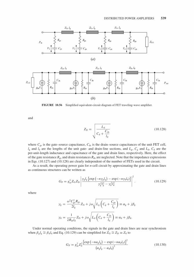
JWBS064-c10 JWBS064-Gerbennikov March 15, 2011 14:3 Printer Name: Yet to Come
DISTRIBUTED POWER AMPLIFIERS 539
FIGURE 10.56 Simplified equivalent-circuit diagram of FET traveling-wave amplifier.
and
ZD =√√√√√ Ld
Cd + Cds
ld
(10.128)
where Cgs is the gate–source capacitance, Cds is the drain–source capacitances of the unit FET cell,lg and ld are the lengths of the unit gate- and drain-line sections, and Lg, Cg and Ld, Cd are theper-unit-length inductance and capacitance of the gate and drain lines, respectively. Here, the effectof the gate resistance Rgs and drain resistances Rds are neglected. Note that the impedance expressionsin Eqs. (10.127) and (10.128) are clearly independent of the number of FETs used in the circuit.
As a result, the operating power gain for n-cell circuit by approximating the gate and drain linesas continuous structures can be written as
GP = g2m ZG ZD
∣∣∣∣∣γglg
[exp
(−nγglg
) − exp (−nγdld)]
γ 2g l2
g − γ 2d l2
d
∣∣∣∣∣2
. (10.129)
where
γg = ω2C2gs Rgs
2lgZG + jω
√Lg
(Cg + Cgs
lg
)≡ αg + jβg
γd = 1
2RdsldZD + jω
√Ld
(Cd + Cds
ld
)≡ αd + jβd.
Under normal operating conditions, the signals in the gate and drain lines are near synchronismwhen βglg
∼= βdld and Eq. (10.129) can be simplified for ZG∼= ZD ≡ Z0 to
GP = g2m Z 2
0
[exp
(−nαglg
) − exp (−nαdld)]2
(αglg − αdld
)2 (10.130)

JWBS064-c10 JWBS064-Gerbennikov March 15, 2011 14:3 Printer Name: Yet to Come
540 POWER AMPLIFIER DESIGN FUNDAMENTALS
from which it follows that, as the number of unit cells n is increased, the power gain does not increasemonotonically and approaches zero in limit as n gets large.
For values of nαglg ≤ 1 and when the drain-line losses are negligible compared to the gate-linelosses, Eq. (10.130) can be rewritten as
GP∼= n2g2
m Z 20
4
(1 − nαglg
2− n2α2
gl2g
6
)2
(10.131)
which means that, in this operating conditions, the power gain can be made proportional to n2. In thiscase, by using the expression for the gate-line attenuation constant αg,
nZ0 Rgsω2C2
gs ≤ 2 (10.132)
that defines the upper limit to the total gate periphery that can be used in practical traveling-wavepower amplifier or the maximum number of unit cells for a given FET device. Similar results can beobtained by applying a theoretical analysis based on matrix technique by employing a finite numberof active and passive circuit elements [47].
Figure 10.57 shows the frequency dependence of a power gain for different numbers of FET unitcells or stages [46]. As we can see, there is an optimum number n which provides maximum frequencybandwidth with minimum gain variations and reasonable power gain. For example, a power gain of9 ± 1 dB over a bandwidth of 1–13 GHz obtained for a four-stage traveling-wave amplifier withtotal GaAs FET gate periphery of 4 × 300 μm. It should be mentioned that the resistive part of gateloading typically results in 3-dB gain reduction. Effect of drain loading is not so significant, howeverthe power gain can be increased by about 1 dB for increased values of the drain loading resistance.
FIGURE 10.57 Power gain versus frequency for different numbers of cells.

JWBS064-c10 JWBS064-Gerbennikov March 15, 2011 14:3 Printer Name: Yet to Come
DISTRIBUTED POWER AMPLIFIERS 541
FIGURE 10.58 Simplified equivalent-circuit diagram of FET distributed amplifier with lumped inductors.
The equivalent gate and drain transmission lines based on lumped inductors and capacitors areshown in Figures 10.58(a) and 10.58(b), respectively [48]. If the gate circuit cutoff frequency isdefined as ωg = 1/RgsCgs and drain circuit cutoff frequency is defined as ωd = 1/RdsCds, the propagationcharacteristics of the transmission-line sections with constant characteristic impedance are known.By requiring the phase shift between each gate-line and drain-line section to be equal, the cutofffrequency ωc for both transmission lines must also be equal. As a result, the power gain of the lumpedtraveling-wave amplifier can be written as
GP =g2
m Z01 Z02 sinh2[n
2
(αd − αg
)]exp
[−n(αd + αg
)]4
[1 +
(ω
ωg
)2][
1 −(
ω
ωc
)2]
sinh2
[1
2
(αd − αg
)] (10.133)
where
ωc = 2√LgCgs
= 2√LdCds
and
Z01 =√
Lg
CgsZ02 =
√Ld
Cds
are the characteristic impedances of the gate and drain lines, respectively.By maximizing Eq. (10.133) at a given frequency, the optimum number of unit cells n = Nopt can
be shown to be
Nopt = 1
αd − αgln
(αd
αg
). (10.134)

JWBS064-c10 JWBS064-Gerbennikov March 15, 2011 14:3 Printer Name: Yet to Come
542 POWER AMPLIFIER DESIGN FUNDAMENTALS
The maximum gain-bandwidth product of the distributed power amplifier can be estimated by
√GP0 f1dB ≈ 0.8 fmax (10.135)
where GP0 is the power gain of the amplifier in the low-frequency limit, f 1dB is the frequency atwhich the power gain of the amplifier falls below GP0 by 1 dB, and f max is the maximum frequencyof oscillation of the FET given by
fmax = gm
4πCgs
√Rds
Rgs. (10.136)
The attenuation of the gate line αg increases rapidly with frequency, resulting in a lower powergain at high bandwidth frequencies. In addition, at a given frequency the number of devices is limited.In this case, if the gate-line attenuation can be made very small, the input signal is nearly evenlyapplied to all FETs in the amplifier and the power gain will remain constant over a wide frequencyband. However, since the gate-line attenuation is directly proportional to the gate–source capacitanceCgs, then it is possible to reduce its effect by adding a series capacitance C = qCgs connected to eachgate, as shown in Figure 10.59 [49]. As a result, since the effective gate capacitance is reduced bya factor of q/(1 + q), the gate-line attenuation αg decreases by a factor of q/(1 + q) and the gatecircuit cutoff frequency ωg is increased by a factor of (1 + q)/q at a fixed frequency. The gate voltage,however, divides between C and Cgs. The FET can now be considered as a modified device having aneffective gate–source capacitance of C ′
g = qCgs/(1 + q) and an effective transconductance of g′m =
qgm/(1 + q).By using a cascode connection of transistors, it is possible to significantly improve the isolation
between the input and output artificial transmission lines. Figure 10.60(a) shows the circuit schematicof a three-stage cascode distributed amplifier based on bipolar devices [50]. The emitter degenerationresistor increases the device input impedance and helps to reduce the output distortion. Instead ofa line section consisting of a series lumped inductor L and a shunt capacitor C with the frequency-independent characteristic impedance Z0 = √
L/C shown in Figure 10.60(b), the m-derived T-sectionshown in Figure 10.60(c) can be used by adding a parallel inductor to provide an additional degree offreedom [51]. Both sections still maintain the same input and output impedances, but the m-derivedT-section has an LC series resonance in its shunt arm. This resonance provides the ability to modifythe passband attenuation. As a result, the m-derived T-section has a flatter passband and a better inputreflection coefficient than its corresponding T-section with constant Z0. Being implemented in SiGe(refers to integration of bipolar junction transistors and CMOS technology) or HBT technology, sucha cascode distributed power amplifier can achieve a measured passband from 100 MHz to 50 GHzwith a 1-dB compression power gain varying from 6 to 8.5 dB with output power of 4.2 ± 2 dBm [50].
For a typical distributed amplifier with the drain-line termination, there is a serious limitation inefficiency, which is lower by about 25% compared to a conventional single-ended power amplifier [52].
FIGURE 10.59 Schematic of distributed amplifier with series capacitors at FET gates.

JWBS064-c10 JWBS064-Gerbennikov March 15, 2011 14:3 Printer Name: Yet to Come
HARMONIC TUNING USING LOAD–PULL TECHNIQUES 543
FIGURE 10.60 Schematic of three-stage bipolar cascode distributed amplifier.
However, the effects of this drain-line termination can be mitigated when the resistive terminationis neglected and, by tapering the drain-line characteristic impedance, the optimum load can bepresented to each active device. In this case, the efficiency can be nearly as twice as high for the samemulti-octave frequency bandwidth. The output power and efficiency over wide range of microwavefrequencies can also be increased by using a 0.25-μm GaN on SiC device technology [53].
10.9 HARMONIC TUNING USING LOAD–PULL TECHNIQUES
Generally, the transistor is operated as a nonlinear active device under large-signal conditions, re-sulting in a significant amount of harmonic components. Since the second harmonic is the largestharmonic component, it was found experimentally that just providing the proper source and loadsecond-harmonic-terminating impedances at the input and output ports of the transistor can sig-nificantly improve the power amplifier efficiency At microwave frequencies, the special networkbased on three coupled bars positioned between two ground planes can be used to realize a widerange of impedance matching at the fundamental frequency, while simultaneously presenting reactiveimpedance at the second-harmonic component, thus decoupling the second-harmonic signal from50-� load [54].
To maximize the amplifier efficiency, the proper harmonic impedances must be provided at thetransistor output port. At microwave frequencies, those impedances must be measured or simulatedaccurately, taking into account the transistor parasitic elements and defining accurately the values ofthe device equivalent-circuit parameters under large-signal operation. Since it is necessary to realizezero or infinite harmonic impedance conditions seen by the internal device current source requiredfor ideal conventional Class F or inverse Class F modes, the corresponding optimum reactances atthe harmonics must be presented at the device external output port which can then be translated to
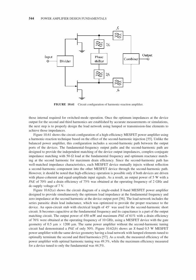
JWBS064-c10 JWBS064-Gerbennikov March 15, 2011 14:3 Printer Name: Yet to Come
544 POWER AMPLIFIER DESIGN FUNDAMENTALS
FIGURE 10.61 Circuit configuration of harmonic-reaction amplifier.
those internal required for switched-mode operation. Once the optimum impedances at the deviceoutput for the second and third harmonics are established by accurate measurements or simulations,the next step is to properly design the load network using lumped or transmission-line elements toachieve those impedances.
Figure 10.61 shows the circuit configuration of a high-efficiency MESFET power amplifier usinga harmonic-reaction technique based on the effect of the second-harmonic injection [55]. Unlike thebalanced power amplifier, this configuration includes a second-harmonic path between the outputports of the devices. The fundamental-frequency output paths and the second-harmonic path aredesigned to provide the independent matching of the device output impedances, complex-conjugateimpedance matching with 50-� load at the fundamental frequency and optimum reactance match-ing at the second harmonic for maximum drain efficiency. Since the second-harmonic path haswell-matched impedance characteristics, each MESFET device mutually injects without reflectiona second-harmonic component into the other MESFET device through the second-harmonic path.However, it should be noted that high-efficiency operation is possible only if both devices are drivenwith phase-coherent and equal-amplitude input signals. As a result, an output power of 5 W with aPAE of 70% and a drain efficiency of 75% was obtained at the operating frequency of 2 GHz anddc-supply voltage of 7 V.
Figure 10.62(a) shows the circuit diagram of a single-ended X-band MESFET power amplifierdesigned to provide simultaneously the optimum load impedance at the fundamental frequency andzero impedance at the second harmonic at the device output port [56]. The load network includes theseries parasitic drain lead inductance, which was optimized to provide the proper reactance to thedevice. An open-circuit stub with electrical length of 45◦ was used for the second-harmonic shortcircuit. It becomes capacitive at the fundamental frequency and its capacitance is a part of the outputmatching circuit. The output power of 450 mW and maximum PAE of 61% with a drain efficiencyof 76% were obtained at the operating frequency of 10 GHz, using a MESFET device with the gategeometry of 0.5 μm × 1200 μm. The same power amplifier without the second-harmonic tuningcircuit had demonstrated a PAE of only 50%. Figure 10.62(b) shows an X-band 0.5 W MESFETpower amplifier with the same device geometry having a load network with lumped elements tuned tooptimally terminate the second and third harmonics [57]. As a result, the measured efficiency of thepower amplifier with optimal harmonic tuning was 49.3%, while the maximum efficiency measuredfor a device tuned to only the fundamental was 44.5%.
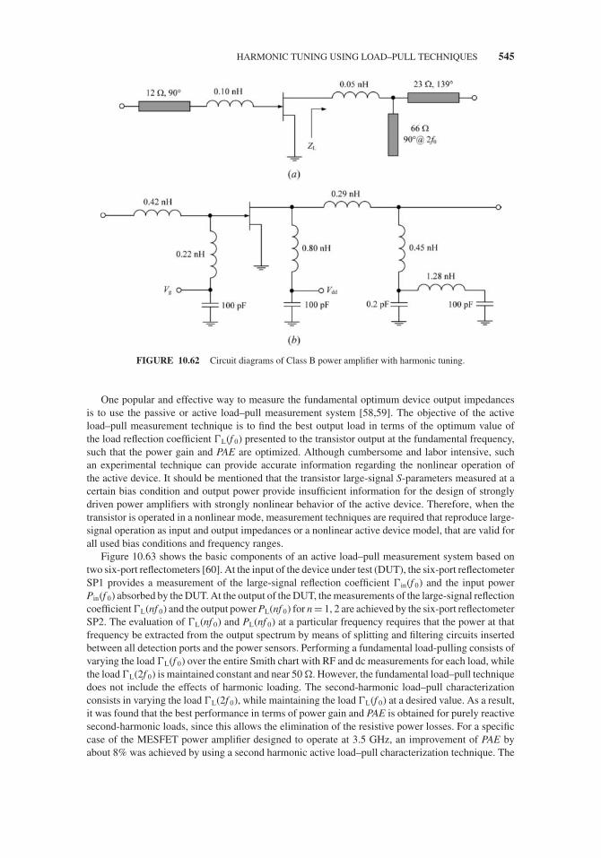
JWBS064-c10 JWBS064-Gerbennikov March 15, 2011 14:3 Printer Name: Yet to Come
HARMONIC TUNING USING LOAD–PULL TECHNIQUES 545
FIGURE 10.62 Circuit diagrams of Class B power amplifier with harmonic tuning.
One popular and effective way to measure the fundamental optimum device output impedancesis to use the passive or active load–pull measurement system [58,59]. The objective of the activeload–pull measurement technique is to find the best output load in terms of the optimum value ofthe load reflection coefficient �L(f 0) presented to the transistor output at the fundamental frequency,such that the power gain and PAE are optimized. Although cumbersome and labor intensive, suchan experimental technique can provide accurate information regarding the nonlinear operation ofthe active device. It should be mentioned that the transistor large-signal S-parameters measured at acertain bias condition and output power provide insufficient information for the design of stronglydriven power amplifiers with strongly nonlinear behavior of the active device. Therefore, when thetransistor is operated in a nonlinear mode, measurement techniques are required that reproduce large-signal operation as input and output impedances or a nonlinear active device model, that are valid forall used bias conditions and frequency ranges.
Figure 10.63 shows the basic components of an active load–pull measurement system based ontwo six-port reflectometers [60]. At the input of the device under test (DUT), the six-port reflectometerSP1 provides a measurement of the large-signal reflection coefficient �in(f 0) and the input powerPin(f 0) absorbed by the DUT. At the output of the DUT, the measurements of the large-signal reflectioncoefficient �L(nf 0) and the output power PL(nf 0) for n = 1, 2 are achieved by the six-port reflectometerSP2. The evaluation of �L(nf 0) and PL(nf 0) at a particular frequency requires that the power at thatfrequency be extracted from the output spectrum by means of splitting and filtering circuits insertedbetween all detection ports and the power sensors. Performing a fundamental load-pulling consists ofvarying the load �L(f 0) over the entire Smith chart with RF and dc measurements for each load, whilethe load �L(2f 0) is maintained constant and near 50 �. However, the fundamental load–pull techniquedoes not include the effects of harmonic loading. The second-harmonic load–pull characterizationconsists in varying the load �L(2f 0), while maintaining the load �L(f 0) at a desired value. As a result,it was found that the best performance in terms of power gain and PAE is obtained for purely reactivesecond-harmonic loads, since this allows the elimination of the resistive power losses. For a specificcase of the MESFET power amplifier designed to operate at 3.5 GHz, an improvement of PAE byabout 8% was achieved by using a second harmonic active load–pull characterization technique. The

JWBS064-c10 JWBS064-Gerbennikov March 15, 2011 14:3 Printer Name: Yet to Come
546 POWER AMPLIFIER DESIGN FUNDAMENTALS
FIGURE 10.63 Harmonic active load–pull measurement system schematic.
active load–pull system based on a six-port reflectometer can also be used to optimize both linearityand output power or PAE for modulated signal [61].
In addition to harmonic loading at the device output, the harmonic tuning at the device input canalso be effective. For Class AB power amplifiers, both the linearity and overall efficiency can beimproved by the suppression of even-order harmonic components at the device input. Figure 10.64shows an example of the circuit schematic of a microwave MESFET power amplifier with sourcesecond-harmonic tuning designed to operate in a Class AB mode [62]. To terminate even harmonicsat the device input, a quarterwave transmission line at the fundamental frequency was short-circuitedat its far end using a large-value capacitance C2. The series transmission line with varying electricallength θ is necessary to provide a symmetrical gate-voltage waveform by compensating for the phaseof the second-harmonic termination, taking into account the device input shunt capacitance andparasitic series gate inductance. The results of nonlinear circuit simulations show a linear (at 1 dBgain compression point) output power of 37.4 dBm at an operating frequency of 6 GHz with a PAEimproved by 7% by using source harmonic tuning. It should be noted that changes in the sourcesecond-harmonic impedance can vary PAE significantly, from 30 to 80% for a 5 GHz 28.4-dBmMESFET power amplifier [63].
FIGURE 10.64 Circuit schematic of Class AB power amplifier with source harmonic tuning.

JWBS064-c10 JWBS064-Gerbennikov March 15, 2011 14:3 Printer Name: Yet to Come
HARMONIC TUNING USING LOAD–PULL TECHNIQUES 547
FIGURE 10.65 Circuit topologies for multi-harmonic load–pull design procedure.
A systematic procedure of multi-harmonic load–pull simulation using the harmonic-balancemethod includes two basic steps: finding the optimal loading at each harmonic component, andchecking the power levels of higher harmonics [64]. An impedance-sampling method can be used tofind the optimal harmonic loading. Generally, only one impedance component Zi(kω0) at kth harmonicand ith external port is sampled at the defined impedance plane, while the others are kept constant ateach step. For a specific case of a MESFET power amplifier with input and output tuners, as shownin Figure 10.65(a), the design procedure steps are as follows:
1. Start load–pull simulation by sampling the impedance at the fundamental frequency Zi(ω0)and find the optimal load Ziopt(ω0).
2. Fix Zi(ω0) at Ziopt(ω0) and check the output spectrum to observe the effects of higher harmonicloads on the power amplifier response.
3. Perform load–pull simulation by sampling the kth harmonic impedance Zi(kω0) and find theoptimal load Z iopt(kω0).
4. Fix Zi(kω0) at Ziopt(kω0) and check the output spectrum to observe the effects of higher harmonicloads on the power amplifier response.
It should be noted that, if checking the output power spectrum shows that the power at higherharmonics is sufficiently small, the design procedure is stopped.
For a 900 MHz power amplifier using a GaAs MESFET device with a gate periphery of 0.7 μm ×600 μm biased at 3 V with a quiescent current of approximately 10% of total dc drain current, itwas shown that, with sinusoidal driving signal, the best power-added efficiencies are achieved at loadphase angles close to ±180◦ for the second harmonic, corresponding to short-circuit condition, andat load phase angles close to zero at the third harmonic, corresponding to open-circuit condition,

JWBS064-c10 JWBS064-Gerbennikov March 15, 2011 14:3 Printer Name: Yet to Come
548 POWER AMPLIFIER DESIGN FUNDAMENTALS
approximating a conventional Class F mode [65]. The simulation results demonstrated a strongdependence of efficiency on the second harmonic termination, while the effect of the third harmonicwas much weaker. The effect of the fourth- and fifth-harmonic terminations, stronger in the formercase and weaker in the latter case, results in efficiency variation of approximately 2.5%. It is necessaryto minimize the resistive losses in the harmonic terminations, intended to be purely reactive, that couldbe changed from reactive to resistive if the harmonic terminations are excessively lossy.
The properly phased input and output voltage harmonic components using a multi-harmonicterminating scheme shown in Figure 10.65(b) can be achieved by choosing the optimum impedancesfor each harmonic component [66,67]. For example, in a Class F mode these output impedances canbe purely resistive (low at even harmonics and high at odd harmonics), since the drain (collector)current second harmonic is always in-phase and the drain (collector) current third harmonic is alwaysout-of-phase with respect to the fundamental component for conduction angles ranging from 180◦
(Class B biasing) to 0◦ (Class C biasing). Under slightly overdriven device operation when the draincurrent waveform represents a truncated half-sinusoid, the third harmonic becomes out-of-phase alsofor Class AB biasing with conduction angles greater than 180◦. The same result can be obtainedby using a driver stage in a Class F mode. However, in an inverse Class F mode, the drain currentsecond harmonic must be out of phase with respect to the fundamental-frequency component, whichcan be realized by reactive input termination of the second harmonic providing the required phaseshift. Fortunately, the main contribution to the harmonic-generating mechanism at the device input isprovided by its nonlinear input gate–source capacitor by generating the second and third harmoniccomponents with proper phasing. As a result, optimum half-sinusoidal drain voltage waveformcorresponding to an inverse Class F mode is achieved by optimizing the input and output impedancesat the second and third harmonics simultaneously.
Generally, it is very difficult to provide accurate source- and load–pull measurements at very highmicrowave frequencies where de-embedding of waveguide transitions and parasitic discontinuitiesleads to significant measurement errors. It can be done accurately enough by using on-wafer mea-surements for an active device with limited output power capability at the fundamental frequency.At the same time, the S-parameters of tuner structures can be accurately predicted using both linearand electromagnetic circuit simulators. The determination of the optimum impedances at the secondharmonic can be done by computer source- and load–pull analysis. In this case, there is no prob-lem to isolate the fundamental and second-harmonic paths to determine their optimum impedances.Figure 10.66 shows the schematic of the source- and load–pull simulation setup for a V-band InPHEMT power amplifier, where the ideal output duplexer separates the fundamental-frequency fromthe second-harmonic components [68]. By changing the ideal transformer turns ratio and the reactivecomponent values, the output power, PAE, power gain, and stability circle contours can be simulatedfor various bias voltages and operating frequencies around a center bandwidth frequency of 60 GHz.
FIGURE 10.66 Schematic of source- and load–pull simulation setup.

JWBS064-c10 JWBS064-Gerbennikov March 15, 2011 14:3 Printer Name: Yet to Come
THERMAL CHARACTERISTICS 549
FIGURE 10.67 Circuit topologies for multi-harmonic load–pull design procedure.
The optimum second-harmonic termination resulted in a theoretical 6% improvement in PAE at the3 dB gain-compression point under Class AB bias. However, in practice, a smaller improvement isexpected because low-loss reactive harmonic loading at 120 GHz is difficult to physically implementwithout degrading the fundamental-frequency load match at 60 GHz.
Three basic methods of harmonic tuning have been offered commercially for load pull system withpassive automated tuners [69]. The triplexer tuning method uses filters to separate the fundamentaland harmonic signals so they may be tuned separately. The block diagram corresponding to thismethod is shown in Figure 10.67(a) where a triplexer includes a low-pass filter for the fundamentalfrequency f 0, a bandpass filter for the second harmonic 2f 0, and a bandpass or high-pass filter for thethird harmonic 3f 0. The stub resonator method is based on using open-circuit stubs with quarterwavelengths at the second and third harmonic components, respectively, connected to the center conductorwith a sliding contact according to the block diagram shown in Figure 10.67(b). The cascaded tunermethod uses the two cascaded tuners shown in Figure 10.67(c) with 625 states each, producing nearly400,000 available impedance states at the fundamental frequency with a variety of the impedances atthe second harmonic. This allows the possibility to optimize the impedance at 2f 0 with approximatelyconstant impedance at f 0. Each method has its own advantages and disadvantages. For example,the triplexer method is the only approach with high tuning isolation, however with slightly morepower loss at harmonic frequency, especially at the third harmonic, compared to the stub resonatormethod. At the same time, the stub resonator method with dual stubs is operated over a very narrowbandwidth. The cascaded tuner method has an advantage here, because no hardware needs to bechanged; however, its tuning isolation is very poor. Thus, the triplexer method looks the best choicebecause of the major advantages over the other methods, with typical return-loss isolation over 100 dBand insertion loss of 0.2–0.3 dB.
10.10 THERMAL CHARACTERISTICS
The reliability of such active semiconductor components as transistors and diodes decreases withincreasing their junction temperature. Since RF power transistors very often dissipate a significant

JWBS064-c10 JWBS064-Gerbennikov March 15, 2011 14:3 Printer Name: Yet to Come
550 POWER AMPLIFIER DESIGN FUNDAMENTALS
amount of power, it is important to provide them with heatsinks to dispose of the unwanted heat.Usually, the data sheets specify a maximum junction temperature that should not be exceeded, and itis desirable to maintain as low a junction temperature as possible (compromising with size, weight,and cost of entire system) because many of the semiconductor failure mechanisms are temperature-dependent.
The heat flow P which is transferred through a medium composed of dissimilar materials, asshown in Figure 10.68(a), can be modeled by the thermal model given in Figure 10.68(b) through theanalogy to an electrical circuit shown in Figure 10.68(c) where heat flow is represented by current,temperatures are represented by voltages, heat sources are represented by constant current sources,thermal resistances are represented by resistors, and thermal capacitances by capacitors. Thermalcapacitors can also be added to model time constants due to heat storage [24]. The property of variouselements to transfer the heat is characterized by the thermal resistance
Rth = T
P(10.137)
where P is the heat flow through the surface of the element, T = T1 − T2 is the temperaturedifference, T1 and T2 are the surface temperatures at the beginning and end of the element, respectively.Thermal resistance is defined as the temperature difference across a structure when a unit of heatenergy flows through it in unit time. Similar to electrical circuits, the thermal model can include both
FIGURE 10.68 Thermal resistance model and its electrical equivalent.

JWBS064-c10 JWBS064-Gerbennikov March 15, 2011 14:3 Printer Name: Yet to Come
THERMAL CHARACTERISTICS 551
FIGURE 10.69 Model of heat transfer from transistor to ambient.
series and parallel connections of the thermal resistances. In a thermal model shown in Figure 10.68(b),the thermal resistances are connected in series, hence its total resistance is equal to
Rth,� =n∑
i=1
Rth,i .
The model of heat transfer from junction to ambient is shown in Figure 10.69 where the heatgenerated in the power transistor chip flows from junction with a temperature T j to the mountingbase, which is in close contact with the case characterized by a temperature Tc, then it flows viacontact pressure to heatsink with a temperature Th, and finally the heatsink dissipates heat to ambientwith a temperature Ta by conduction, convection, and radiation [15]. In high-power applications,forced air cooling by fans or forced water cooling may be provided. The total thermal resistance Rth, ja
between junction and ambient is given by
Rth, ja = Rth, jc + Rth, ch + Rth, ha (10.138)
where Rth, jc is the thermal resistance between junction and case, Rth, ch is the thermal resistancebetween case and heatsink, and Rth, ha is the thermal resistance between heatsink and ambient.
According to the heat transfer model shown in Figure 10.69, the junction temperature T j can bedefined as
Tj = Ta + Tjc + Tch + Tha (10.139)
where Ta is the ambient temperature and T th, jc, T th, ch and T th, ha are the temperatures differ-ences between junction and case, case and heatsink, and heatsink and ambient, respectively. FromEqs. (10.137)–(10.139) it follows that
Tj = Ta + Pdiss
(Rth, jc + Rth, ch + Rth, ha
)(10.140)
where Pdiss is the power dissipated by the semiconductor device [70].

JWBS064-c10 JWBS064-Gerbennikov March 15, 2011 14:3 Printer Name: Yet to Come
552 POWER AMPLIFIER DESIGN FUNDAMENTALS
When several transistors and diodes with the total dissipated power Pdiss, � are attached to thesame heatsink, Eq. (10.140) can be rewritten as
Tj = Ta + Pdiss
(Rth, jc + Rth, ch
) + Pdiss,� Rth, ha
K th(10.141)
where Kth = 0.7–1.0 is the temperature coefficient taking into account the uneven nature of theheatsink temperature. Similarly, the case temperature can be written as
Tc = Ta + Pdiss Rth, ch + Pdiss,� Rth, ha
K th. (10.142)
When any significant amount of power is being dissipated, something must be done to fill the airvoids between mating surfaces in the thermal path. Otherwise, the interface thermal resistance will beunnecessarily high and quite dependent upon the surface finishes. In this case, the thermal compoundsbased on silicone oil or other synthetic base fluids with conductive particles or dry conductive padscan be used [70]. The part of the heatsink that is in contact with the heat source must be perfectly flatthat allows a thinner layer of thermal compound to be used, which will reduce the thermal resistancebetween heatsink and heat source. Heatsinks must be designed in a way that air can easily and quicklyfloat through the cooler, and reach all cooling fins. Especially heatsinks having a very large amount offine fins, with small distances between the fins may not allow good air flow. A compromise betweenhigh surface (many fins with small gaps between them) and good aerodynamics must be found. Thisalso depends on the fan the heatsink is used with. A powerful fan can force air even through a heatsinkwith lots of fine fins with only small gaps for air flow, whereas there should be fewer cooling fins withmore space between them on a passive heatsink. Large cooling fins are pointless if the heat cannotreach them, so the heatsink must be designed to allow good thermal transfer from the heat source tothe fins. Thicker fins have better thermal conductivity, which means that a compromise between highsurface (many thin fins) and good thermal transfer (thicker fins) must be found.
To design a heatsink, first it is necessary to define the powers dissipated by each transistor anddiode and to know the maximum value (worst case) for the ambient temperature Ta. Then, by settingthe heatsink overheating temperature Tha = 10–25◦ relatively to the ambient temperature, therequired value for the thermal resistance Rth, ha between heatsink and ambient is calculated accordingto Eqs. (10.139) and (10.141) as Rth, ha = ThaK th/Pdiss, � . Finally, the junction temperature T j or casetemperature Tc is calculated for each component from Eq. (10.141) or Eq. (10.142), respectively,based on the value for Rth, jc obtained from data sheets and the value for Rth, ch estimated for particularmounting details. Check that the values for T j or Tc do not exceed the absolute maximum rating forthe components. Then, choose an appropriately sized heatsink for the calculated Rth, ha using heatsinknomograms provided by manufacturers.
REFERENCES
1. A. Grebennikov, RF and Microwave Power Amplifier Design, New York: McGraw-Hill, 2004.
2. V. M. Bogachev and V. V. Nikiforov, Transistor Power Amplifiers (in Russian), Moskva: Energiya, 1978.
3. J. M. Rollett, “Stability and Power Gain Invariants of Linear Two-Ports,” IRE Trans. Circuit Theory, vol. CT-9,pp. 29–32, Jan. 1962.
4. J. G. Linvill and L. G. Schimpf, “The Design of Tetrode Transistor Amplifiers,” Bell Syst. Technol. J., vol. 35,pp. 813–840, Apr. 1956.
5. O. Muller and W. G. Figel, “Stability Problems in Transistor Power Amplifiers,” Proc. IEEE, vol. 55,pp. 1458–1466, Aug. 1967.
6. O. Muller, “Internal Thermal Feedback in Fourpoles, Especially in Transistors,” Proc. IEEE, vol. 52,pp. 924–930, Aug. 1964.

JWBS064-c10 JWBS064-Gerbennikov March 15, 2011 14:3 Printer Name: Yet to Come
REFERENCES 553
7. V. V. Nikiforov, E. P. Stroganova, and I. V. Shevnin, “An Influence of Parasitic Lead Inductances on Stabilityof Power MOSFET Amplifiers (in Russian),” Radiotekhnika, vol. 45, pp. 100–102, May 1990.
8. J. Vidkjaer, “Instabilities in RF-Power Amplifiers Caused by a Self-Oscillation in the Transistor Bias Net-work,” IEEE J. Solid-State Circuits, vol. SC-11, pp. 703–712, Oct. 1976.
9. D. R. Lohrmann, “Parametric Oscillations in VHF Transistor Power Amplifiers,” Proc. IEEE, vol. 54,pp. 409–410, Mar. 1966.
10. D. R. Lohrmann, “Amplifiers Has 85% Efficiency while Providing up to 10 Watts Power over a WideFrequency Band,” Electron. Des., vol. 14, pp. 38–43, Mar. 1966.
11. P. Penfield and R. P. Rafuse, Varactor Applications, Cambridge: The MIT Press, 1962.
12. A. Grebennikov and N. O. Sokal, Switchmode RF Power Amplifiers, New York: Newnes, 2007.
13. F. E. Terman and J. H. Ferns, “The Calculation of Class C Amplifier and Harmonic Generator Performanceof Screen-Grid and Similar Tubes,” Proc. IRE, vol. 22, pp. 359–373, Mar. 1934.
14. A. I. Berg, Theory and Design of Vacuum-Tube Generators (in Russian), Moskva: Gosenergoizdat, 1932.
15. V. I. Kaganov, Transistor Radio Transmitters (in Russian), Moskva: Energiya, 1976.
16. A. Wood, “LDMOS Transistor Powers PCS Base-Station Amplifiers,” Microw. RF, vol. 37, pp. 69–80, Mar.1998.
17. K. Vennema, “Two-Tone Linearity in a 900 MHz Silicon Bipolar Class AB Amplifier,” Microwave J., vol.39, pp. 88–93, Feb. 1996.
18. RF Transmitting Transistor and Power Amplifier Fundamentals, Philips Semiconductors, 1998.
19. T. Sato and C. Grigorean, “Design Advantages of CDMA Power Amplifiers Built with MOSFET Technology,”Microwave J., vol. 45, pp. 64–78, Oct. 2002.
20. E. Jarvinen, “Radio Frequency Amplifiers,” U.S. Patent 6,052,032, Apr. 18, 2000.
21. E. Jarvinen, S. Kalajo, and M. Matilainen, “Bias Circuits for GaAs HBT Power Amplifiers,” 2001 IEEEMTT-S Int. Microwave Symp. Dig., vol. 1, pp. 507–510.
22. Y. S. Noh and C. S. Park, “An Intelligent Power Amplifier MMIC Using a New Adaptive Bias Control Circuitfor W-CDMA Applications,” IEEE J. Solid-State Circuits, vol. SC-39, pp. 967–970, June 2004.
23. A. Grebennikov, B. Zogl, H. Hermann, C. Roth, and W. Thomann, “High-Efficiency Balanced Switch-PathMonolithic SiGe HBT Power Amplifiers for Wireless Applications,” Proc. 37th Europ. Microwave Conf.,2007, pp. 1189–1192.
24. H. L. Krauss, C. W. Bostian, and F. H. Raab, Solid State Radio Engineering, New York: John Wiley & Sons,1980.
25. B. M. Lee, “Apply Wideband Techniques to Balanced Amplifiers,” Microwaves, vol. 19, pp. 83–88, Apr.1980.
26. V. Sokolov and R. E. Williams, “Development of GaAs Monolithic Power Amplifiers in X-Band,” IEEETrans. Electron Dev., vol. ED-27, pp. 1164–1171, June 1980.
27. T. Hiraoka, T. Tokumitsu, and M. Akaike, “A Miniaturized Broad-Band MMIC Frequency Doubler,” IEEETrans. Microwave Theory Tech., vol. MTT-38, pp. 1932–1937, Dec. 1990.
28. T. Tokumitsu, A. Oya, K. Sakai, and Y. Hasegawa, “A K-Band Bi-Phase Modulator MMIC for UWBApplication,” IEEE Microwave Wireless Compon. Lett., vol. 15, pp. 159–161, Mar. 2005.
29. H. W. Bode, Network Analysis and Feedback Amplifier Design, New York: Van Nostrand, 1945.
30. R. M. Fano, “Theoretical Limitations on the Broad-Band Matching of Arbitrary Impedances,” J. FranklinInst., vol. 249, pp. 57–83, Jan. 1950, pp. 139–154, Feb. 1950.
31. G. L. Matthaei, “Tables of Chebyshev Impedance-Transforming Networks of Low-Pass Filter Form,” Proc.IEEE, vol. 52, pp. 939–963, Aug. 1964.
32. G. L. Matthaei, L. Young, and E. M. T. Jones, Microwave Filters, Impedance-Matching Networks, andCoupling Structures, New York: Artech House, 1980.
33. S. B. Cohn, “Optimum Design of Stepped Transmission-Line Transformers,” IRE Trans. Microwave TheoryTech., vol. MTT-3, pp. 16–21, Apr. 1955.
34. H. J. Riblet, “General Synthesis of Quarter-Wave Impedance Transformers,” IRE Trans. Microwave TheoryTech., vol. MTT-5, pp. 36–43, Apr. 1957.
35. G. L. Matthaei, “Short-Step Chebyshev Impedance Transformers,” IEEE Trans. Microwave Theory Tech.,vol. MTT-14, pp. 372–383, Aug. 1966.

JWBS064-c10 JWBS064-Gerbennikov March 15, 2011 14:3 Printer Name: Yet to Come
554 POWER AMPLIFIER DESIGN FUNDAMENTALS
36. V. P. Meschanov, I. A. Rasukova, and V. D. Tupikin, “Stepped Transformers on TEM-Transmission Lines,”IEEE Trans. Microwave Theory Tech., vol. MTT-44, pp. 793–798, June 1996.
37. Y. Ito, M. Mochizuki, M. Kohno, H. Masuno, T. Takagi, and Y. Mitsui, “A 5-10 GHz 15-W GaAs MESFETAmplifier with Flat Gain and Power Responses,” IEEE Microwave Guided Wave Lett., vol. 5, pp. 454–456,Dec. 1995.
38. K. B. Niclas, “On Design and Performance of Lossy Match GaAs MESFET Amplifiers,” IEEE Trans.Microwave Theory Tech., vol. MTT-30, pp. 1900–1906, Nov. 1982.
39. Y. Ito, M. Nii, Y. Kohno, M. Mochizuki, and T. Takagi, “A 4 to 25 GHz 0.5 W Monolithic Lossy MatchAmplifier,” 1994 IEEE MTT-S Int. Microwave Symp. Dig., pp. 257–260.
40. Y.-F. Wu, R. A. York, S. Keller, B. P. Keller, and U. K. Mishra, “3-9 GHz GaN-Based Microwave PowerAmplifiers with L-C-R Broad-Band Matching,” IEEE Microwave Guided Wave Lett., vol. 9, pp. 314–316,Aug. 1999.
41. B. Y. Banyamin and M. Berwick, “Analysis of the Performance of Four-Cascaded Single-Stage DistributedAmplifiers,” IEEE Trans. Microwave Theory Tech., vol. MTT-48, pp. 2657–2663, Dec. 2000.
42. Application Note AN98021, 100-450 MHz 250 W Power Amplifier with the BLF548 MOSFET , PhilipsSemiconductors, March 1998.
43. W. S. Percival, “Thermionic Valve Circuits,” British Patent 460562, Jan. 1937.
44. E. L. Ginzton, W. R. Hewlett, J. H. Jasberg, and J. D. Noe, “Distributed Amplification,” Proc. IRE, vol. 36,pp. 956–969, Aug. 1948.
45. W. H. Horton, J. H. Jasberg, and J. D. Noe, “Distributed Amplifiers: Practical Considerations and ExperimentalResults,” Proc. IRE, vol. 38, pp. 748–753, July 1950.
46. Y. Ayasli, R. L. Mozzi, J. L. Vorhaus, L. D. Reynolds, and R. A. Pucel, “A Monolithic GaAs 1-13 GHzTraveling-Wave Amplifier,” IEEE Trans. Microwave Theory Tech., vol. MTT-30, pp. 976–981, July 1982.
47. K. B. Niclas, W. T. Wilser, T. R. Kritzer, and R. R. Pereira, “On Theory and Performance of Solid-StateMicrowave Distributed Amplifiers,” IEEE Trans. Microwave Theory Tech., vol. MTT-31, pp. 447–456, June1983.
48. J. B. Beyer, S. N. Prasad, R. C. Becker, J. E. Nordman, and G. K. Hohenwarter, “MESFET DistributedAmplifier Design Guidelines,” IEEE Trans. Microwave Theory Tech., vol. MTT-32, pp. 268–275, Mar. 1984.
49. S. N. Prasad, J. B. Beyer, and I.-K. Chang, “Power-Bandwidth Considerations in the Design of MESFETDistributed Amplifiers,” IEEE Trans. Microwave Theory Tech., vol. MTT-36, pp. 1117–1123, July 1988.
50. J. Aguirre and C. Plett, “50-GHz SiGe HBT Distributed Amplifiers Employing Constant-k and m-DerivedFilter Sections,” IEEE Trans. Microwave Theory Tech., vol. MTT-52, pp. 1573–1579, May 2004.
51. Y. Chen, J. B. Beyer, V. Sokolov, and J. P. Culp, “A 11 GHz Hybrid Paraphase Amplifier,” 1986 IEEE Int.Solid-State Circuits Conf. Dig., pp. 236–237.
52. L. Zhao, A. Pavio, B. Stengel, and B. Thompson, “A 6 Watt LDMOS Broadband High Efficiency DistributedPower Amplifier Fabricated Using LTCC Technology,” 2002 IEEE MTT-S Int. Microwave Symp. Dig.,pp. 897–900.
53. C. Campbell, C. Lee, V. Williams, M.-Y. Kao, H.-Q. Tserng, P. Saunier, and T. Balisteri, “A WidebandPower Amplifier MMIC Utilizing GaN on SiC HEMT Technology,” IEEE J. Solid-State Circuits, vol. SC-44,pp. 2640–2647, Oct. 2009.
54. S. R. Mazumder, A. Azizi, and F. E. Gardiol, “Improvement of a Class-C Transistor Power Amplifier bySecond-Harmonic Tuning,” IEEE Trans. Microwave Theory Tech., vol. MTT-27, pp. 430–433, May 1979.
55. T. Nojima and S. Nishiki, “High Efficiency Microwave Harmonic Reaction Amplifier,” 1988 IEEE MTT-SInt. Microwave Symp. Dig., pp. 1007–1010.
56. M. A. Khatibzadeh and H. Q. Tserng, “Harmonic Tuning of Power FETs at X-Band,” 1990 IEEE MTT-S Int.Microwave Symp. Dig., pp. 989–992.
57. B. Kopp and D. D. Heston, “High-Efficiency 5-Watt Power Amplifier with Harmonic Tuning,” 1988 IEEEMTT-S Int. Microwave Symp. Dig., pp. 839–842.
58. J. M. Cusak, S. M. Perlow, and B. S. Perlman, “Automatic Load Contour Mapping for Microwave PowerTransistors,” IEEE Trans. Microwave Theory Tech., vol. MTT-22, pp. 1146–1152, Dec. 1974.
59. Y. Takayama, “A New Load-Pull Characterization Method for Microwave Power Transistors,” 1976 IEEEMTT-S Int. Microwave Symp. Dig., pp. 218–220.

JWBS064-c10 JWBS064-Gerbennikov March 15, 2011 14:3 Printer Name: Yet to Come
REFERENCES 555
60. P. Berini, M. Desgagne, F. M. Ghannouchi, and R. G. Bosisio, “An Experimental Study of the Effects ofHarmonic Loading on Microwave MESFET Oscillators and Amplifiers,” IEEE Trans. Microwave TheoryTech., vol. MTT-42, pp. 943–950, June 1994.
61. S. Bensmida, E. Bergeault, G. I. Abib, and B. Huyart, “Power Amplifier Characterization: An Active Load-Pull System Based on Six-Port Reflectometer using Complex Modulated Carrier,” IEEE Trans. MicrowaveTheory Tech., vol. MTT-54, pp. 2707–2712, June 2006.
62. S. Watanabe, S. Takatsuka, K. Takagi, H. Kuroda, and Y. Oda, “Effect of Source Harmonic Tuning onLinearity of Power GaAs FET under Class AB Operation,” IEICE Trans. Electron., vol. E79-C, pp. 611–616,May 1996.
63. L. C. Hall and R. J. Trew, “Maximum Efficiency Tuning of Microwave Amplifiers,” 1991 IEEE MTT-S Int.Microwave Symp. Dig., pp. 123–126.
64. Q. Cai, J. Herber, and S. Peng, “A Systematic Scheme for Power Amplifier Design Using a Multi-HarmonicLoadpull Simulation Technique,” 1998 IEEE MTT-S Int. Microwave Symp. Dig., pp. 161–165.
65. J. Staudinger, “Multiharmonic Load Termination Effects on GaAs MESFET Power Amplifiers,” MicrowaveJ., vol. 39, pp. 60–77, Apr. 1996.
66. P. Colantonio, F. Giannini, G. Leuzzi, and E. Limiti, “Multiharmonic Manipulation for Highly EfficientMicrowave Power Amplifiers,” Int. J. RF Microwave Computer-Aided Eng., vol. 11, pp. 366–384, Nov.2001.
67. P. Colantonio, F. Giannini, E. Limiti, and V. Teppati, “An Approach to Harmonic Load- and Source-Pull Mea-surements for High-Efficiency PA Design,” IEEE Trans. Microwave Theory Tech., vol. MTT-52, pp. 191–198,Jan. 2005.
68. O. S. A. Tang, S. M. J. Liu, P. C. Chao, W. M. T. Kong, K. C. Hwang, K. Nichols, and J. Heaton, “Designand Fabrication of a Wideband 56- to 63-GHz Monolithic Power Amplifier with Very High Power-AddedEfficiency,” IEEE J. Solid-State Circuits, vol. SC-35, pp. 1298–1306, Sept. 2000.
69. G. Simpson, “A Comparison of Harmonic Tuning Methods for Load Pull Systems,” Maury Microw. Corp.,2004.
70. Application Note 1040, Mounting Considerations for Power Semiconductors, Freescale Semiconductor, 1993.

JWBS064-c10 JWBS064-Gerbennikov March 15, 2011 14:3 Printer Name: Yet to Come
556

JWBS064-c11 JWBS064-Gerbennikov March 12, 2011 10:45 Printer Name: Yet to Come
11 High-Efficiency Power Amplifiers
High efficiency of the power amplifier can be obtained by using Class D, Class F, or Class Eoperation modes and their subclasses, depending on the technical requirements. In all cases, anefficiency improvement in practical implementation is achieved by providing the nonlinear operationconditions when an active device can simultaneously operate in pinch-off, active, and saturationregions resulting in nonsinusoidal collector current and voltage waveforms, symmetrical for Class Dand Class F and asymmetrical for Class E (DE, FE) operation modes. In Class F amplifiers analyzedin frequency domain, the fundamental-frequency and harmonic load impedances are optimized byshort-circuit termination and open-circuit peaking to control the voltage and current waveforms atthe device output to obtain maximum efficiency. In Class E amplifiers analyzed in time domain, anefficiency improvement is achieved by realizing the on/off active device switching operation (thepinch-off and saturation modes) with special current and voltage waveforms so that high voltage andhigh current do not concur at the same time.
11.1 CLASS D
The efficiency of a power amplifier can be maximized if the active device is ideally operated asa switch. When the transistor is turned on, the voltage is nearly zero and high current is flowingthrough the device; that is, the transistor acts as a low resistance (closed switch) during this part ofa period. When the transistor is turned off, the current is zero and there is high voltage across thedevice; that is, the transistor acts as an open switch during the other part of a period. Conceptually, aClass D power amplifier employs a pair of active devices operating in a push–pull mode and a tunedoutput circuit [1,2]. The switched-mode power amplifiers with output filter tuned to the fundamentalfrequency transform ideally the total dc power into a fundamental-frequency power delivered to theload without power losses at the harmonics. The output circuit is tuned to the switching frequency andremoves ideally its all harmonic components resulting in a purely sinusoidal signal delivered to theload. Consequently, the theoretical efficiency of an idealized Class D power amplifier achieves 100%.Let us consider the basic principles, circuit schematics, and voltage/current waveforms correspondingto the different types of a Class D power amplifier with output filter [3–5].
11.1.1 Voltage-Switching Configurations
Figure 11.1(a) shows the simplified circuit schematic of a complementary voltage-switching ClassD bipolar power amplifier consisting of the same type of the active devices, fundamentally tunedseries L0C0 filter, and load resistance RL. The large-value bypass capacitor Cb is necessary to isolatethe dc power supply by bypassing all radio frequency (RF) signals to ground. The input transformercauses both active devices to be driven with currents that are 180◦ out of phase by reversing onesecondary winding on the transformer. However, there is no need in phase reversing if the transistorsare true-complementary with different base or channel majority-carrier type that simplifies the circuit
RF and Microwave Transmitter Design, First Edition. Andrei Grebennikov.C© 2011 John Wiley & Sons, Inc. Published 2011 by John Wiley & Sons, Inc.
557

JWBS064-c11 JWBS064-Gerbennikov March 12, 2011 10:45 Printer Name: Yet to Come
558 HIGH-EFFICIENCY POWER AMPLIFIERS
FIGURE 11.1 Complementary voltage-switching configuration with series filter.
schematic. Note that any type of the vacuum tubes, bipolar, and MOSFET transistors can be used inthis circuit if suitable drive is applied. Due to the grounding effect of a bypass capacitor Cb, the RFconnection of the transistor outputs is parallel, thus resulting in an equivalent load resistance equalto 2RL for each device.
To determine the collector voltage and current waveform and to calculate the output power andcollector efficiency, the following assumptions are taken into account:
� Power loss due to flow of leakage current during transistor pinch-off is negligible.� Power loss due to nonideal tuning is negligible.� Power loss during switching transitions is negligible.
In this case, each active device is considered a switch with the saturation resistance rsat shownin Figure 11.1(b) that is driven in such a way in order to provide an alternating switching betweenthe on- and off-state operation conditions of the transistor under an assumption of a 50% dutycycle. The alternating half-period device switching between its pinch-off mode and saturation mode

JWBS064-c11 JWBS064-Gerbennikov March 12, 2011 10:45 Printer Name: Yet to Come
CLASS D 559
results in rectangular collector voltage pulses with a maximum amplitude of 2Vcc, as shown inFigure 11.1(c). The collector–voltage pulses, which contain the odd harmonic components only, areapplied to the series L0C0 filter with high-loaded quality factor QL = ωL0/RL � 1 tuned to thefundamental frequency ω0 = 1/
√L0C0. This results in the fundamental-frequency sinusoidal current
iR = −IR sinωt flowing to the load RL, where IR is the load current amplitude. The half waves of thiscurrent flow in turn through the transistors representing the half-sinusoidal collector–current pulsesthat contain the fundamental-frequency, second-order and higher order even-harmonic componentsonly. The shape of the saturation voltage with maximum amplitude V sat is fully determined by thecollector–current waveform when i(ωt) > 0 according to vsat(ωt) = rsati(ωt), where i(ωt) = i1(ωt) ori2(ωt) for a symmetrical circuit with identical transistors. The collector voltage peak factor is equalto v/Vcc = 2.
It should be noted that for an operation with conduction angles less than 180◦, when both activedevices are turned on for duty cycles less than 50%, there is a time period when both active devicesare turned off simultaneously. Therefore, in order that the load current iR(ωt) could flow continuously,it is necessary to include a diode in parallel to each device, as shown in Figure 11.1(b). The operationconditions with conduction angles greater than 180◦ are unacceptable, since both dc power suppliesare connected to each other through the small saturation resistances of the identical transistors equalto 2rsat, thus resulting in the significant efficiency reduction due to an increased total current flowingthrough both transistors.
Now let us determine the voltage v(ωt) = v1(ωt) − Vcc at the input of a series L0C0 circuit andcollector current i1(ωt) for the first transistor operating as a switch with a saturation resistance rsat.When switch is turned on for 0 ≤ ωt ≤ π ,
v (ωt) = −Vcc + rsat IR sin ωt (11.1)
i1 (ωt) = IR sin ωt . (11.2)
When switch is turned off for π ≤ ωt ≤ 2π ,
v (ωt) = Vcc + rsat IR sin ωt (11.3)
i1 (ωt) = 0. (11.4)
The fundamental-frequency voltage amplitude V of the voltage v(ωt) can be calculated by applyinga Fourier transform to Eqs. (11.1) and (11.2) from
V = − 1
π
2π∫0
v (ωt) sin ωt dωt = 4
πVcc − rsat IR. (11.5)
Similarly, the dc current I0 can be obtained from Eq. (11.2) by
I0 = 1
2π
π∫0
i1 (ωt) dωt = IR
π. (11.6)
Taking into account that IR = V/RL and the fact that the sinusoidal output current flows througheither one or another transistor depending on which device is turned on and having a half-sinusoidalwaveform, using Eq. (11.5) will result in
IR = Imax = 4
π
Vcc
RL
1
1 + rsat
RL
. (11.7)

JWBS064-c11 JWBS064-Gerbennikov March 12, 2011 10:45 Printer Name: Yet to Come
560 HIGH-EFFICIENCY POWER AMPLIFIERS
The dc power P0 and fundamental-frequency output power P can be obtained using Eqs. (11.5)and (11.6), respectively, by
P0 = 2Vcc I0 = 8
π 2
V 2cc
RL
1
1 + rsat
RL
(11.8)
P = 1
2I 2
R RL = 8
π2
V 2cc
RL
1(1 + rsat
RL
)2 . (11.9)
As a result, the collector efficiency η of a complementary voltage-switching push–pull poweramplifier with a series filter can be written as
η = P
P0= 1
1 + rsat
RL
. (11.10)
From Eq. (11.10), it follows that the collector efficiency is equal to 100% for an idealized case ofthe lossless active devices with zero saturation resistance. It should be mentioned that the dc currentdrawn from the power supply represents the form of a half-sinusoidal pulse train. Therefore, it isvery important to provide the proper RF bypassing circuit representing either a single large-valuecapacitor or an additional filter with a low cutoff frequency in the power supply line. In addition,the loaded quality factor for a simple series-tuned L0C0 circuit must be chosen greater than five toprovide a good compromise between the prevention of harmonic current and coil losses. Additionalharmonic suppression can be obtained by inserting standard filters between the series-tuned circuitand the load. Note that the collector efficiency degrades with increasing operating frequency wherethe switching transitions become an appreciable fraction of the signal period. In practice, it was foundthat high efficiency of a Class D power amplifier can be maintained to frequencies of the order of0.1f T for low-power transistors and to 0.01f T for high-power transistors rated at greater than 10 W,where f T is the device transition frequency [6].
The broadband center-tapped and balanced-to-unbalanced transformers can also be used involtage-switching Class D power amplifiers in much the same manner as they are used in conventionalClass B push–pull power amplifiers. In this case, such a configuration is called the transformer-coupledvoltage-switching Class D power amplifier. Figure 11.2 shows the simplified circuit schematicof a transformer-coupled voltage-switching Class D bipolar power amplifier including an output
FIGURE 11.2 Transformer-coupled voltage-switching push–pull configuration with series filter.
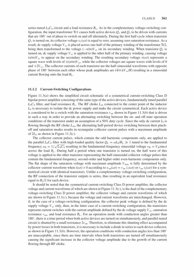
JWBS064-c11 JWBS064-Gerbennikov March 12, 2011 10:45 Printer Name: Yet to Come
CLASS D 561
series-tuned L0C0 circuit and a load resistance RL. As in the complementary voltage-switching con-figuration, the input transformer Tr1 causes both active devices Q1 and Q2 to be driven with currentsthat are 180◦ out of phase to switch on and off alternately. During the first half-cycle when transistorQ1 is turned on, its collector voltage v1(ωt) is equal to zero, assuming zero saturation resistance. As aresult, dc supply voltage Vcc is placed across one-half of the primary winding of the transformer Tr2,being then transformed to the voltage (−n/m)Vcc on its secondary winding. When transistor Q2 isturned on, dc supply voltage Vcc is applied to the other half of the primary winding, causing voltage(n/m)Vcc to appear on the secondary winding. The resulting secondary voltage v(ωt) represents asquare wave with levels of ±(n/m)Vcc, while the collector voltages are square waves with levels of 0and +2Vcc. The collector currents of each transistor are the half-sinusoidal waveforms with oppositephase of 180◦ between each other whose peak amplitudes are (4/π)(Vcc/R) resulting in a sinusoidalcurrent flowing onto the load RL.
11.1.2 Current-Switching Configurations
Figure 11.3(a) shows the simplified circuit schematic of a symmetrical current-switching Class Dbipolar power amplifier consisting of the same type of the active devices, fundamentally tuned parallelL0C0 filter, and load resistance RL. The RF choke Lch connected to the center point of the inductorL0 is necessary to isolate the dc power supply and make the circuit symmetrical. Each active deviceis considered to be a switch with the saturation resistance rsat shown in Figure 11.3(b) that is drivenin such a way in order to provide an alternating switching between the on- and off-state operationconditions of the transistor under an assumption of a 50% duty cycle. Since the only dc current I0 isflowing through the RF choke Lch, the alternating half-period device switching between their pinch-off and saturation modes results in rectangular collector current pulses with a maximum amplitudeof 2I0, as shown in Figure 11.3(c).
The collector current pulses, which contain the odd harmonic components only, are applied tothe parallel L0C0 filter with high-loaded quality factor QL = ωL0/RL � 1 tuned to the fundamentalfrequency ω0 = 1/
√L0C0 resulting in the fundamental-frequency sinusoidal voltage vR = VRsinωt
across the load RL. During half a period when one transistor is turned on, the half wave of thisvoltage is applied to the other transistor representing the half-sinusoidal collector voltage pulses thatcontain the fundamental-frequency, second-order and higher order even-harmonic components only.The flat shape of the saturation voltage with maximum amplitude Vmax is fully determined by thecollector–current waveform when i(ωt) > 0 according to vsat(ωt) = rsat i1(ωt) or rsat i2(ωt) for a sym-metrical circuit with identical transistors. Unlike a complementary voltage-switching configuration,the RF connection of the transistor outputs is series, thus resulting in an equivalent load resistanceequal to RL/2 for each device.
It should be noted that the symmetrical current-switching Class D power amplifier, the collectorvoltage and current waveforms of which are shown in Figure 11.3(c), is the dual of the complementaryvoltage-switching Class D power amplifier, the collector voltage and current waveforms of whichare shown in Figure 11.1(c), because the voltage and current waveforms are interchanged. However,if, in the case of a voltage-switching configuration, the collector peak voltage is defined by the dcsupply voltage Vcc only, then, in the latter case of a current-switching configuration, the transistorsrepresent current switches with the current amplitude defined by the dc voltage supply Vcc, saturationresistance rsat, and load resistance RL. For an operation mode with conduction angles greater than180◦, there is a time period when both active devices are turned on simultaneously, and parallel-tunedcircuit is shunted by a small resistance 2rsat. Therefore, to eliminate this shunting effect accompaniedby power losses in both transistors, it is necessary to include a diode in series to each device collector,as shown in Figure 11.3(b). However, the operation conditions with conduction angles less than 180◦
are unacceptable, since there are time intervals when both transistors are turned off simultaneouslycausing the significant increase in the collector voltage amplitude due to the growth of the currentflowing through RF choke.

JWBS064-c11 JWBS064-Gerbennikov March 12, 2011 10:45 Printer Name: Yet to Come
562 HIGH-EFFICIENCY POWER AMPLIFIERS
FIGURE 11.3 Symmetrical current-switching configuration with parallel filter.
Now let us determine the current i(ωt) = i1(ωt) − I0 in a parallel L0C0 circuit and collector voltagev1(ωt) for the first transistor operating as a current switch with a saturation resistance rsat. When firstswitch is turned on for 0 ≤ ωt ≤ π , i1(ωt) = 2I0 resulting in
i (ωt) = I0 (11.11)
v1 (ωt) = Vsat = 2rsat I0 (11.12)
where I0 is the dc supply current of each device.When first switch is turned off for π ≤ ωt ≤ 2π , i1(ωt) = 0 resulting in
i (ωt) = −I0 (11.13)
v1 (ωt) = − (Vmax − 2rsat I0) sin ωt + 2rsat I0 (11.14)
where Vmax is the collector peak voltage.

JWBS064-c11 JWBS064-Gerbennikov March 12, 2011 10:45 Printer Name: Yet to Come
CLASS D 563
The fundamental-frequency current amplitude I of the current i(ωt) can be calculated by applyinga Fourier transform to Eqs. (11.11) and (11.13) from
I = 1
π
2π∫0
i (ωt) sin ωtdωt = 4
πI0. (11.15)
Similarly, the dc supply voltage Vcc can be written from Eqs. (11.12) and (11.14) by
Vcc = 1
2π
π∫0
v1 (ωt) dωt = 1
π(Vmax − 2rsat I0) . (11.16)
Taking into account that V1 = Vmax − 2rsatI0 = IRL, the dc current I0 and fundamental-frequencycollector voltage V1 can be obtained by
I0 =(π
2
)2(
1 + π 2
2
rsat
RL
)−1Vcc
RL(11.17)
V1 = π
(1 + π2
2
rsat
RL
)−1
Vcc. (11.18)
The dc power P0 and fundamental-frequency output power P and can be obtained usingEqs. (11.17) and (11.18) and taking into account that V1 = VR by
P0 = 2Vcc I0 = π 2
2
V 2cc
RL
1
1 + π 2
2
rsat
RL
(11.19)
P = 1
2
V 2R
RL= π2
2
V 2cc
RL
1(1 + π 2
2
rsat
RL
)2 . (11.20)
As a result, the collector efficiency η of a symmetrical current-switching push–pull power amplifierwith parallel filter can be written as
η = P
P0= 1
1 + π 2
2
rsat
RL
. (11.21)
Figure 11.4 shows the circuit schematic of a current-switching Class D power amplifier, where theoutput balanced-to-unbalanced transformer is used to connect to a standard load. In this case, such aconfiguration is called the transformer-coupled current-switching Class D power amplifier, which isthe dual of the transformer-coupled voltage-switching Class D power amplifier because the collectorvoltage and current waveforms are interchanged. As in the transformer-coupled voltage-switchingconfiguration, the input transformer Tr1 is necessary to drive both active devices with currents havingopposite phases for the on-to-off alternate device switching. The output transformer Tr2 is consideredas ideal, having m turns in each half of the primary winding and n turns in the secondary winding.However, the dc current supply is connected to the center tap of the transformer primary windingthrough the RF choke. The load network of the transformer-coupled current-switching configurationrequires a parallel fundamentally tuned resonant L0C0 circuit connected in parallel to the load RL,instead of a series fundamentally tuned resonant L0C0 circuit required for the transformer-coupled
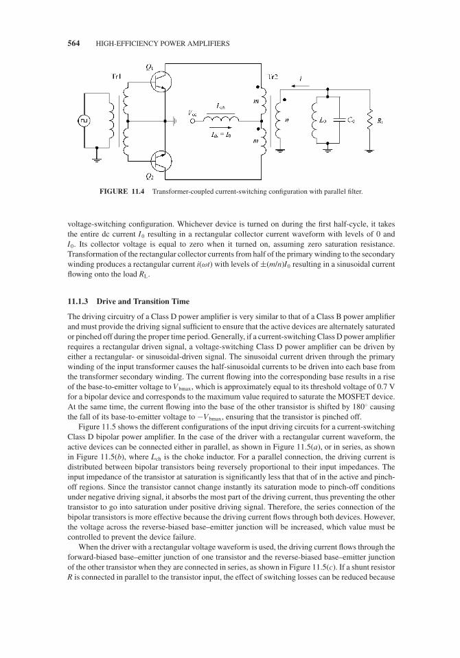
JWBS064-c11 JWBS064-Gerbennikov March 12, 2011 10:45 Printer Name: Yet to Come
564 HIGH-EFFICIENCY POWER AMPLIFIERS
FIGURE 11.4 Transformer-coupled current-switching configuration with parallel filter.
voltage-switching configuration. Whichever device is turned on during the first half-cycle, it takesthe entire dc current I0 resulting in a rectangular collector current waveform with levels of 0 andI0. Its collector voltage is equal to zero when it turned on, assuming zero saturation resistance.Transformation of the rectangular collector currents from half of the primary winding to the secondarywinding produces a rectangular current i(ωt) with levels of ±(m/n)I0 resulting in a sinusoidal currentflowing onto the load RL.
11.1.3 Drive and Transition Time
The driving circuitry of a Class D power amplifier is very similar to that of a Class B power amplifierand must provide the driving signal sufficient to ensure that the active devices are alternately saturatedor pinched off during the proper time period. Generally, if a current-switching Class D power amplifierrequires a rectangular driven signal, a voltage-switching Class D power amplifier can be driven byeither a rectangular- or sinusoidal-driven signal. The sinusoidal current driven through the primarywinding of the input transformer causes the half-sinusoidal currents to be driven into each base fromthe transformer secondary winding. The current flowing into the corresponding base results in a riseof the base-to-emitter voltage to Vbmax, which is approximately equal to its threshold voltage of 0.7 Vfor a bipolar device and corresponds to the maximum value required to saturate the MOSFET device.At the same time, the current flowing into the base of the other transistor is shifted by 180◦ causingthe fall of its base-to-emitter voltage to −Vbmax, ensuring that the transistor is pinched off.
Figure 11.5 shows the different configurations of the input driving circuits for a current-switchingClass D bipolar power amplifier. In the case of the driver with a rectangular current waveform, theactive devices can be connected either in parallel, as shown in Figure 11.5(a), or in series, as shownin Figure 11.5(b), where Lch is the choke inductor. For a parallel connection, the driving current isdistributed between bipolar transistors being reversely proportional to their input impedances. Theinput impedance of the transistor at saturation is significantly less that that of in the active and pinch-off regions. Since the transistor cannot change instantly its saturation mode to pinch-off conditionsunder negative driving signal, it absorbs the most part of the driving current, thus preventing the othertransistor to go into saturation under positive driving signal. Therefore, the series connection of thebipolar transistors is more effective because the driving current flows through both devices. However,the voltage across the reverse-biased base–emitter junction will be increased, which value must becontrolled to prevent the device failure.
When the driver with a rectangular voltage waveform is used, the driving current flows through theforward-biased base–emitter junction of one transistor and the reverse-biased base–emitter junctionof the other transistor when they are connected in series, as shown in Figure 11.5(c). If a shunt resistorR is connected in parallel to the transistor input, the effect of switching losses can be reduced because

JWBS064-c11 JWBS064-Gerbennikov March 12, 2011 10:45 Printer Name: Yet to Come
CLASS D 565
FIGURE 11.5 Input driving circuits.
the device input capacitance is faster discharged through this resistor. A similar correction effect canbe achieved by using a parallel RC circuit connected in series to each transistor when both transistorsare connected in parallel, as shown in Figure 11.5(d). However, an increased current is required fromthe driver to saturate the transistor.
Generally, the input circuit of the transistor, either bipolar or MOSFET, can be represented as apurely capacitance only at low frequencies. In switching applications, however, the finite rise andfall times are the result of the effect of the much higher frequency components than the fundamental.For example, if, at 30-MHz carrier, the switching time of 4 ns can be tolerated at amplitude of80% that represents roughly a 100-MHz sine wave [7]. Besides, the input capacitance is usuallynonlinear and varies over bias conditions. For example, the MOSFET gate–source capacitance varieswith gate and drain voltages. At increased gate voltage, it goes down to its lowest value, just beforereaching the threshold voltage, and then goes up to be constant at saturation. At the same time,when the MOSFET device begins to draw drain current, the drain voltage is lowered resulting ina reduction of the depletion area and causing an overlap between the gate and bulk material. Thisin turn increases the value of the gate–drain capacitance, which takes maximum value at zero drainvoltage and positive gate voltage corresponding to the maximum device transconductance. In bipolartransistors, the base–emitter nonlinear capacitance represents the large diffusion capacitance in theactive and saturation regions and much lower junction capacitance in the pinch-off region.
However, at higher frequencies, the device equivalent input circuit must include also a seriesresistance, which is the base ohmic resistance for bipolar transistor or effective gate resistanceconsisting of the distributed channel and gate electrode resistances for MOSFET device. In this case,the power losses occur due to the finite voltage rise time τ r and fall time τ f as a function of the
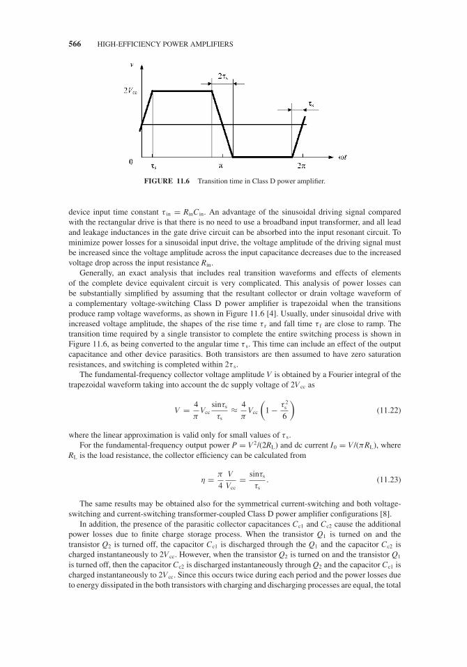
JWBS064-c11 JWBS064-Gerbennikov March 12, 2011 10:45 Printer Name: Yet to Come
566 HIGH-EFFICIENCY POWER AMPLIFIERS
FIGURE 11.6 Transition time in Class D power amplifier.
device input time constant τ in = RinCin. An advantage of the sinusoidal driving signal comparedwith the rectangular drive is that there is no need to use a broadband input transformer, and all leadand leakage inductances in the gate drive circuit can be absorbed into the input resonant circuit. Tominimize power losses for a sinusoidal input drive, the voltage amplitude of the driving signal mustbe increased since the voltage amplitude across the input capacitance decreases due to the increasedvoltage drop across the input resistance Rin.
Generally, an exact analysis that includes real transition waveforms and effects of elementsof the complete device equivalent circuit is very complicated. This analysis of power losses canbe substantially simplified by assuming that the resultant collector or drain voltage waveform ofa complementary voltage-switching Class D power amplifier is trapezoidal when the transitionsproduce ramp voltage waveforms, as shown in Figure 11.6 [4]. Usually, under sinusoidal drive withincreased voltage amplitude, the shapes of the rise time τ r and fall time τ f are close to ramp. Thetransition time required by a single transistor to complete the entire switching process is shown inFigure 11.6, as being converted to the angular time τ s. This time can include an effect of the outputcapacitance and other device parasitics. Both transistors are then assumed to have zero saturationresistances, and switching is completed within 2τ s.
The fundamental-frequency collector voltage amplitude V is obtained by a Fourier integral of thetrapezoidal waveform taking into account the dc supply voltage of 2Vcc as
V = 4
πVcc
sinτs
τs≈ 4
πVcc
(1 − τ 2
s
6
)(11.22)
where the linear approximation is valid only for small values of τ s.For the fundamental-frequency output power P = V2/(2RL) and dc current I0 = V/(πRL), where
RL is the load resistance, the collector efficiency can be calculated from
η = π
4
V
Vcc= sinτs
τs. (11.23)
The same results may be obtained also for the symmetrical current-switching and both voltage-switching and current-switching transformer-coupled Class D power amplifier configurations [8].
In addition, the presence of the parasitic collector capacitances Cc1 and Cc2 cause the additionalpower losses due to finite charge storage process. When the transistor Q1 is turned on and thetransistor Q2 is turned off, the capacitor Cc1 is discharged through the Q1 and the capacitor Cc2 ischarged instantaneously to 2Vcc. However, when the transistor Q2 is turned on and the transistor Q1
is turned off, then the capacitor Cc2 is discharged instantaneously through Q2 and the capacitor Cc1 ischarged instantaneously to 2Vcc. Since this occurs twice during each period and the power losses dueto energy dissipated in the both transistors with charging and discharging processes are equal, the total

JWBS064-c11 JWBS064-Gerbennikov March 12, 2011 10:45 Printer Name: Yet to Come
CLASS F 567
power losses due to parasitic collector capacitances for a complementary voltage-switching Class Dpower amplifier with supply voltage of 2Vcc and zero saturation resistance rsat can be written as
Ps = (Cc1 + Cc2) (2Vcc)2 f0 = 4CcV 2
cc f0 (11.24)
where Cc = Cc1 + Cc2 and f 0 is the operating frequency. The total switching power losses describedby Eq. (11.24) can also characterize the transformer-coupled voltage-switching Class D poweramplifier with a supply voltage of Vcc, in which the parasitic collector capacitances Cc1 and Cc2 arecharged and discharged between 0 and 2Vcc.
In the current-switching Class D power amplifier, the parasitic capacitances do not providecharging and discharging losses since the collector currents flowing through the transistor havefixed constant values (either zero or Ids). However, there is another mechanism of power lossesassociated with parasitic inductances Lc1 and Lc2 (due to finite lead length and leakage inductancein transformer) connected in series with the transistor collectors. In this case, the currents flowingthrough the active devices jump when switching occurs, since they must be changed from zero tomaximum instantaneously, twice during each period. Therefore, the total power losses due to theparasitic collector series inductances for a current-switching Class D power amplifier with zerosaturation resistance can be written as
Ps = Lc I 2dc f0 (11.25)
where Lc = Lc1 + Lc2.
11.2 CLASS F
The possibility to improve efficiency by approximating the anode voltage waveform to square waveto minimize the value of the saturation voltage compared to the supply voltage over half an entireinterval 0 ≤ ωt ≤ 2π was discussed yet in the early 1920s. As a practical solution it was proposedto use a load network with a third-harmonic trap in series to the anode, as shown in Figure 11.7(a)[9,10]. However, the effect of the inclusion of a third-harmonic resonator was described and analyzed
FIGURE 11.7 Polyharmonic power amplifiers.

JWBS064-c11 JWBS064-Gerbennikov March 12, 2011 10:45 Printer Name: Yet to Come
568 HIGH-EFFICIENCY POWER AMPLIFIERS
in detail 1.5 decade later [11,12]. It was shown that the symmetrical anode voltage waveform andlevel of its depression can be provided with opposite phase conditions between the fundamental andthird harmonic and optimum value of the ratio between their voltage amplitudes. In addition, it wasnoted that high operation efficiency can be achieved even when impedance of the third-harmonicresonator is equal or slightly greater than impedance of the fundamental tank. To maximize efficiencyof the vacuum-tube amplifier with better approximating a square voltage anode waveform, it was alsosuggested to use an additional resonator tuned to the fifth harmonic, as shown in Figure 11.7(b) [13].
Figure 11.8 shows that the shapes of the voltage and current waveforms can be significantlychanged with increasing fundamental voltage amplitude by adding even one additional harmoniccomponent being properly phased. For example, the combination of the fundamental and third-harmonic components being out of phase at center point results in a flattened voltage waveform withdepression in its center. It is clearly seen from Figure 11.8(a) that the proper ratio between the ampli-tudes of the fundamental and third-harmonic components can provide the flattened voltage waveformwith minimum depression and maximum difference between its peak amplitude and amplitude ofthe fundamental component. Similarly, the combination of the fundamental-frequency and second-harmonic components being in-phase at the center point flattens the current waveform corresponding
v
i
n = 1, 3
n = 1, 2
(a)
0 2π ωtπ
Vcc
I0
(b)
0 2π ωtπ
FIGURE 11.8 Fourier voltage and current waveforms with third and second harmonics.

JWBS064-c11 JWBS064-Gerbennikov March 12, 2011 10:45 Printer Name: Yet to Come
CLASS F 569
to the maximum values of the voltage waveform and sharpens the current waveform correspond-ing to the minimum values of the voltage waveform, as shown in Figure 11.8(b). The optimum ratiobetween the amplitudes of the fundamental-frequency and second current harmonic components canmaximize a peak value of the current waveform with its minimized value determined by the devicesaturation resistance in a practical circuit. Thus, power loss due to the active device can be minimizedsince the results of the integration over period when minimum voltage corresponds to maximumcurrent will give small value compared with the power delivered to the load.
11.2.1 Idealized Class F Mode
Generally, an infinite number of odd-harmonic tank resonators can maintain a square collector voltagewaveform, also providing a half-sinusoidal current waveform. Figure 11.9(a) shows such a Class Fpower amplifier with a multiple-resonator output filter to control the harmonic content of its collector(anode or drain) voltage and current waveforms, thereby shaping them to reduce dissipation and toincrease efficiency [4,14].
To simplify an analysis of a Class F power amplifier, a simple equivalent circuit of which is shownin Figure 11.9(b), the following several assumptions are introduced:
� Transistor has zero saturation voltage, zero saturation resistance, infinite off-resistance, and itsswitching action is instantaneous and lossless.
� RF choke allows only a dc current and has no resistance.� Quality factors of all parallel resonant circuits have infinite impedance at the corresponding
harmonic and zero impedance at other harmonics.� There are no losses in the circuit except only into the load RL.� Operation mode with a 50% duty cycle.
To determine the idealized collector voltage and current waveforms, let us consider the distributionof voltages and currents in the load network assuming the sinusoidal fundamental current flowinginto the load as iR(ωt) = IRsin(ωt), where IR is its amplitude. The voltage v(ωt) across the switchcan be represented as a sum of the dc voltage Vcc, fundamental voltage vR = iRRL across the loadresistor, and voltage vodd across the odd-harmonic resonators,
v(ωt) = Vcc + vodd[(2n + 1)ωt] + vR(ωt ). (11.26)
FIGURE 11.9 Basic circuits of Class F power amplifier with parallel resonant circuits.

JWBS064-c11 JWBS064-Gerbennikov March 12, 2011 10:45 Printer Name: Yet to Come
570 HIGH-EFFICIENCY POWER AMPLIFIERS
Since the time moment t was chosen arbitrarily, by introducing a phase shift of π , Eq. (11.26) canbe rewritten for periodical sinusoidal functions as
v(ωt + π ) = Vcc − vodd[(2n + 1)ωt] − vR(ωt). (11.27)
Then, the summation of Eqs. (11.26) and (11.27) yields
v(ωt) = 2Vcc − v(ωt + π ). (11.28)
From Eq. (11.28), it follows that maximum value of the collector voltage cannot exceed a value of2Vcc and the time duration with maximum voltage of v = 2Vcc coincides with the time duration withminimum voltage of v = 0. Since the collector voltage is zero when the switch is closed, the onlypossible waveform for the collector voltage is a square wave composing of only dc, fundamental-frequency, and odd-harmonic components.
During the interval 0 < ωt ≤ π when the switch is closed, the current i(ωt) flowing through theswitch can be written as
i(ωt) = I0 + ieven(2nωt) + iR(ωt) (11.29)
whereas during the interval π < ωt ≤ 2π when the switch is open, the current i(ωt + π ) is equal tozero resulting in
0 = I0 + ieven(2nωt) − iR(ωt). (11.30)
Then, by substituting Eq. (11.30) into Eq. (11.29), we can rewrite Eq. (11.29) as
i (ωt) = 2iR(ωt) = 2IR sin(ωt) (11.31)
from which it follows that the amplitude of the current flowing through the switch during interval0 < ωt ≤ π is two times greater than the amplitude of the fundamental current. Thus, in a generalcase of entire interval, Eq. (11.29) can be rewritten as
i (ωt) = IR(sin ωt + | sin ωt |) (11.32)
which means that the switch current represents half-sinusoidal pulses with the amplitude equal todouble load current amplitude.
Consequently, for a purely sinusoidal current flowing into the load as shown in Figure 11.10(a),the ideal collector voltage and current waveforms can be represented by the appropriate normalizedwaveforms shown in Figures 11.10(b) and 11.10(c), respectively. Here, a sum of the fundamentaland odd harmonics approximates a square voltage waveform, and a sum of the fundamental and evenharmonics approximates a half-sinusoidal collector current waveform. As a result, the shapes of thecollector current and voltage waveforms provide a condition when the current and voltage do notoverlap simultaneously. Such a condition, with symmetrical collector voltage and current waveforms,corresponds to an idealized Class F operation mode with 100% collector efficiency.
A Fourier analysis of the current and voltage waveforms allows us to obtain the equations forthe dc current, fundamental voltage and current components in the collector voltage and currentwaveforms, as explained in the following.
The dc current I0 can be calculated from Eq. (11.32) as
I0 = 1
2π
π∫0
2IR sin ωt dωt = 2IR
π(11.33)

JWBS064-c11 JWBS064-Gerbennikov March 12, 2011 10:45 Printer Name: Yet to Come
CLASS F 571
FIGURE 11.10 Ideal waveforms of Class F power amplifier.
the fundamental current component can be calculated from Eq. (11.32) as
I1 = 1
π
π∫0
2IR sin2 ωt dωt = IR (11.34)
the fundamental voltage component can be calculated using Eq. (11.28) as
V1 = VR = 1
π
2π∫π
2Vcc sin (ωt + π ) dωt = 4Vcc
π(11.35)
where VR = IRRL is the fundamental voltage amplitude across the load resistor RL.Then, the dc power and output power at the fundamental frequency are calculated from
P0 = Vcc I0 = 2Vcc IR
π(11.36)

JWBS064-c11 JWBS064-Gerbennikov March 12, 2011 10:45 Printer Name: Yet to Come
572 HIGH-EFFICIENCY POWER AMPLIFIERS
and
P1 = V1 I1
2= 2Vcc IR
π(11.37)
resulting in a theoretical collector efficiency with maximum value of
η = P1
P0= 100%. (11.38)
In this case, the impedance conditions seen by the device collector for an idealized Class F modemust be equal to
Z1 = R1 = 8
π 2
Vcc
I0(11.39)
Z2n = 0 for even harmonics (11.40)
Z2n+1 = ∞ for odd harmonics (11.41)
which are similar to that of derived from the limiting case of the optimum efficiency Class B mode [15].
11.2.2 Class F with Quarterwave Transmission Line
Ideally, a control of an infinite number of the harmonics maintaining a square voltage waveformand a half-sinusoidal current waveform at the drain can be provided by using a serious quarterwavetransmission line and a parallel-tuned resonant circuit, as shown in Figure 11.11. Such type of a ClassF power amplifier was initially proposed to use at very high frequencies where implementation of theload networks with lumped elements only is difficult and the parasitic device output (lead or package)inductor is sufficiently small [4]. In this case, the quarterwave transmission line transforms the loadimpedance according to
R = Z 20
RL(11.42)
where Z0 is the characteristic impedance of a transmission line [16]. For even harmonics, the shortcircuit on the load side of the transmission line is repeated, thus producing a short circuit at the drain.However, the short circuit at the load produces an open circuit at the drain for odd harmonics withresistive load at the fundamental.
FIGURE 11.11 Class F power amplifier with series quarterwave transmission line.

JWBS064-c11 JWBS064-Gerbennikov March 12, 2011 10:45 Printer Name: Yet to Come
CLASS F 573
Generally, at low drive level, the active device acts as a current source (voltage-controlled in thecase of the MOSFETs or MESFETs and current-controlled in the case of bipolar transistors). Asdrive input increases, the active device enters voltage saturation resulting in a harmonic-generationprocess. Since the transmission line presents the high impedance conditions to all odd harmonics,all odd harmonics provide a proper contribution to the output voltage waveform. As a result, at highdrive level, the output voltage waveform becomes a complete square wave and the active deviceis voltage-saturated for a full half-cycle. In this case, the transistor acts as a switch rather than asaturating current source.
An alternative configuration of the Class F power amplifier with a shunt transmission line located inbetween the dc power supply and device collector is shown in Figure 11.12(a). In this case, there is noneed to use an RF choke and a series blocking capacitor because a series fundamentally tuned resonantL0C0 circuit is used instead of a parallel fundamentally tuned resonant circuit. However, unlike thecase with a series quarterwave transmission line, such a Class F load network configuration with ashunt quarterwave transmission line does not provide an impedance transformation. Therefore, theload resistance R, which is equal to the equivalent active device output resistance at the fundamentalfrequency, must then be transformed to the standard load resistance RL. Let us now derive analyticallysome basic fundamental properties of a quarterwave transmission line. The transmission line in timedomain can be represented as an element with finite delay time depending on its electrical length.Consider a simple load network of the Class F power amplifier shown in Figure 11.12(b) consistingof a parallel quarterwave transmission line grounded at the end through power supply, a series
FIGURE 11.12 Class F power amplifier with shunt quarterwave transmission line.

JWBS064-c11 JWBS064-Gerbennikov March 12, 2011 10:45 Printer Name: Yet to Come
574 HIGH-EFFICIENCY POWER AMPLIFIERS
fundamentally tuned L0C0 circuit, and a load resistance R. In an idealized case, the intrinsic deviceoutput capacitance is assumed to be negligible to affect the power amplifier RF performance. Theloaded quality factor QL of the series resonant L0C0 circuit is high enough to provide the sinusoidaloutput current iR flowing into the load R.
To define the collector voltage and current waveforms, consider the electrical behavior of ahomogeneous lossless quarterwave transmission line connected to the dc voltage supply with RFgrounding [3,17]. In this case, the voltage v(t, x) in any cross section of such a transmission line canbe represented as a sum of the incident and reflected voltages vinc(ωt−2πx/λ) and vrefl (ωt+2πx/λ),generally with an arbitrary waveform. When x = 0, the voltage v(t, x) is equal to the collector voltage
v(ωt) = v(t, 0) = vinc(ωt) + vrefl(ωt). (11.43)
At the same time, at another end of the transmission line when x = λ/4, the voltage is constantand equal to
Vcc = v(t, π/2) = vinc(ωt − π/2) + vrefl(ωt + π/2). (11.44)
Since the time moment t was chosen arbitrarily, let us rewrite Eq. (11.44) using a phase shift ofπ /2 for each voltage as
vinc(ωt) = Vcc − vrefl(ωt + π ). (11.45)
Substituting Eq. (11.45) into Eq. (11.43) yields
v(ωt) = vrefl(ωt) − vrefl(ωt + π) + Vcc. (11.46)
Consequently, for the phase shift of π , the collector voltage can be obtained by
v(ωt + π ) = vrefl(ωt + π ) − vrefl(ωt + 2π) + Vcc. (11.47)
For an idealized operation condition with a 50% duty cycle when during half a period the transistoris turned on and during another half a period the transistor is turned off with overall period of 2π , thevoltage vrefl(ωt) can be considered the periodical function with a period of 2π ,
vrefl(ωt) = vrefl(ωt + 2π ). (11.48)
As a result, the summation of Eqs. (11.46) and (11.47) results in the basic expression for collectorvoltage in the form of
v(ωt) = 2Vcc − v(ωt + π ). (11.49)
From Eq. (11.49), which is similar to Eq. (11.28), it follows that the maximum value of thecollector voltage cannot exceed a value of 2Vcc and the time duration with maximum voltage of v =2Vcc coincides with the time duration with minimum voltage of v = 0.
Similarly, an equation for the current iT flowing into the quarterwave transmission line can beobtained as
iT(ωt) = iT(ωt + π ) (11.50)
which means that the period of a signal flowing into the quarterwave transmission line is equal to π
because it contains only even harmonics, since a shorted quarterwave transmission line has an infiniteimpedance at odd harmonics at its input.

JWBS064-c11 JWBS064-Gerbennikov March 12, 2011 10:45 Printer Name: Yet to Come
CLASS F 575
FIGURE 11.13 Ideal current waveform in quarterwave transmission line.
Let the transistor operates as an ideal switch: it is closed during the interval 0 < ωt ≤ π wherev = 0 and open during the interval π < ωt ≤ 2π , where v = 2Vcc according to Eq. (11.49). Duringthe interval π < ωt ≤ 2π when switch is open, the load is directly connected to the transmission lineand iT = −iR = −IR sinωt. Consequently, during the interval 0 < ωt ≤ π when switch is closed,iT = IR sinωt according to Eq. (11.50). Hence, the current flowing into the quarterwave transmissionline at any ωt can be represented by
iT(ωt) = IR| sin ωt | (11.51)
where IR is the amplitude of current flowing into the load.Since the collector current is defined as i = iT + iR, then
i (ωt) = IR(sin ωt + | sin ωt |) (11.52)
which means that the collector current represents half-sinusoidal pulses with the amplitude equal todouble load current amplitude.
Consequently, for a purely sinusoidal current flowing into the load due to infinite loaded qualityfactor of the series fundamentally tuned L0C0 circuit shown in Figure 11.10(a), the ideal collectorvoltage and current waveforms can be represented by the corresponding normalized square andhalf-sinusoidal waveforms shown in Figures 11.10(b) and 11.10(c), respectively, where I0 is the dccurrent. Here, a sum of the fundamental and odd harmonics approximates a square voltage waveformand a sum of the fundamental and even harmonics approximates a half-sinusoidal collector currentwaveform. The waveform corresponding to the normalized current flowing into the quarterwavetransmission line, which is shown in Figure 11.13, represents a sum of even harmonics only. As aresult, the shapes of the collector current and voltage waveforms provide a condition when the currentand voltage do not overlap simultaneously.
11.2.3 Effect of Saturation Resistance
In a real transistor, the saturation or on-resistance rsat is not equal to zero, and transistor dissipatessome amount of power due to the collector current flowing through this resistance when the transistoris turned on. The simplified equivalent circuit of a Class F power amplifier with a quarterwavetransmission line where the transistor is represented by a nonideal switch with saturation resistancersat and parasitic output capacitance Cout is shown in Figure 11.14. During the interval 0 < ωt ≤ π
when the switch is closed, the saturation voltage vsat due to the current i(ωt) flowing through theswitch can be written as
vsat(ωt) = Vsat sin ωt = 2IRrsat sin ωt (11.53)
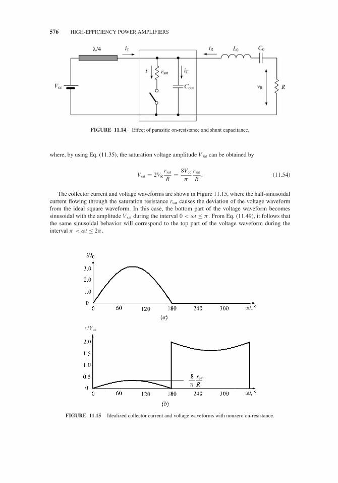
JWBS064-c11 JWBS064-Gerbennikov March 12, 2011 10:45 Printer Name: Yet to Come
576 HIGH-EFFICIENCY POWER AMPLIFIERS
FIGURE 11.14 Effect of parasitic on-resistance and shunt capacitance.
where, by using Eq. (11.35), the saturation voltage amplitude V sat can be obtained by
Vsat = 2VRrsat
R= 8Vcc
π
rsat
R. (11.54)
The collector current and voltage waveforms are shown in Figure 11.15, where the half-sinusoidalcurrent flowing through the saturation resistance rsat causes the deviation of the voltage waveformfrom the ideal square waveform. In this case, the bottom part of the voltage waveform becomessinusoidal with the amplitude V sat during the interval 0 < ωt ≤ π . From Eq. (11.49), it follows thatthe same sinusoidal behavior will correspond to the top part of the voltage waveform during theinterval π < ωt ≤ 2π .
FIGURE 11.15 Idealized collector current and voltage waveforms with nonzero on-resistance.

JWBS064-c11 JWBS064-Gerbennikov March 12, 2011 10:45 Printer Name: Yet to Come
CLASS F 577
Now let us evaluate the power losses and collector efficiency due to presence of the saturationresistance rsat. Using Eqs. (11.31), (11.33), and (11.35) results in
Psat
P0= 1
2π
2π∫0
i 2 (ωt) rsat
I0Vccdωt = rsat
2π I0Vcc
2π∫0
(2IR)2 sin2 ωt dωt = rsat IR
Vcc
IR
I0= rsat
R
IR
I0
VR
Vcc= 2rsat
R.
(11.55)
Hence, the collector efficiency can be calculated from
η = 1 − Psat
P0= 1 − 2rsat
R. (11.56)
In practice, the idealized collector voltage and current waveforms can be realized at low fre-quencies when effect of the device output capacitance is negligible. At higher frequencies, theeffect of the output capacitance contributes to a nonzero switching time resulting in the time pe-riods when the collector voltage and collector current exist at the same time when simultaneouslyv > 0 and i > 0. Consequently, such a load network with shunt capacitance cannot provide theswitched-mode operation with an instantaneous transition from the device pinch-off to saturationmode. Therefore, during a nonzero time interval, the device operates in active region as a nonlinearcurrent source.
11.2.4 Load Networks with Lumped and Distributed Parameters
Theoretical results show that the proper control of the second and third harmonics only can sig-nificantly increase the collector efficiency of the power amplifier by flattening the output voltagewaveform. Since practical realization of a multielement high-order LC resonant circuit can causea serious implementation problem, especially at higher frequencies, it is sufficient to be confinedto a three- or four-element resonant circuit composing the load network of the power amplifier. Inaddition, it is necessary to take into account that, in practice, both extrinsic and intrinsic transistoroutput capacitance has a substantial effect on the efficiency. The output capacitance Cout can repre-sent the collector capacitance Cc in the case of the bipolar transistor or drain–source capacitance plusgate–drain capacitance Cds + Cgd in the case of the FET device.
For a lumped-circuit amplifier, a special three-element load network can be used to approximateto ideal Class F by providing both high impedance at the fundamental and third harmonics and zeroimpedance at the second harmonic at the collector (or drain) by compensating for the influence ofCout. Examples of such load networks with additional parallel and series resonant circuits locatedbetween the dc power supply and device output are shown in Figure 11.16 [18,19]. Here, the outputcircuit of the active device is represented by a multiharmonic current source, and Rout is the equivalentoutput resistance at the fundamental frequency defined as a ratio of the fundamental voltage at thedevice output to the fundamental current flowing into the device.
The reactive part of the output admittance or susceptance Bnet = Im(Ynet) of the load network withparallel resonant tank shown in Figure 11.16(b) including the device output capacitance Cout can bewritten by
Bnet = ωCout − 1 − ω2 L2C2
ωL1
(1 − ω2L2C2
) + ωL2. (11.57)
By applying three-harmonic impedance conditions at the device collector (or drain), open-circuitedfor fundamental-frequency and third harmonic when Bnet(ω0) = Bnet(3ω0) = 0 and short-circuited for

JWBS064-c11 JWBS064-Gerbennikov March 12, 2011 10:45 Printer Name: Yet to Come
578 HIGH-EFFICIENCY POWER AMPLIFIERS
FIGURE 11.16 Load networks with parallel and series resonant circuits.
second harmonic when Bnet(2ω0) = ∞, the values of elements of this impedance-peaking circuit canbe derived as
L1 = 1
6ω2oCout
L2 = 5
3L1 C2 = 12
5Cout (11.58)
where the sum of the reactance of the parallel resonant tank, consisting of an inductor L2 and acapacitor C2, and inductor L1 creates resonances at the fundamental and third-harmonic components,and the series capacitance of the tank circuit in series with L1 creates a low-impedance series resonanceat the second-harmonic component [18].
Applying the same conditions for the load network with series resonant circuit shown in Fig-ure 11.16(c) results in the ratios between elements given by
L1 = 4
9ω20Cout
L2 = 9
15L1 C2 = 15
16Cout (11.59)
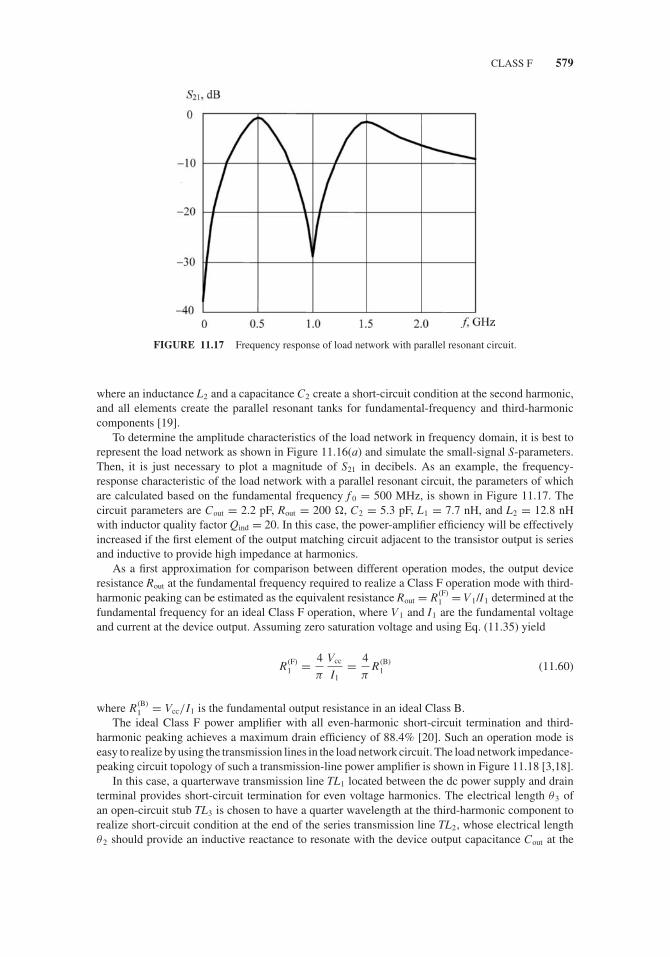
JWBS064-c11 JWBS064-Gerbennikov March 12, 2011 10:45 Printer Name: Yet to Come
CLASS F 579
FIGURE 11.17 Frequency response of load network with parallel resonant circuit.
where an inductance L2 and a capacitance C2 create a short-circuit condition at the second harmonic,and all elements create the parallel resonant tanks for fundamental-frequency and third-harmoniccomponents [19].
To determine the amplitude characteristics of the load network in frequency domain, it is best torepresent the load network as shown in Figure 11.16(a) and simulate the small-signal S-parameters.Then, it is just necessary to plot a magnitude of S21 in decibels. As an example, the frequency-response characteristic of the load network with a parallel resonant circuit, the parameters of whichare calculated based on the fundamental frequency f 0 = 500 MHz, is shown in Figure 11.17. Thecircuit parameters are Cout = 2.2 pF, Rout = 200 �, C2 = 5.3 pF, L1 = 7.7 nH, and L2 = 12.8 nHwith inductor quality factor Qind = 20. In this case, the power-amplifier efficiency will be effectivelyincreased if the first element of the output matching circuit adjacent to the transistor output is seriesand inductive to provide high impedance at harmonics.
As a first approximation for comparison between different operation modes, the output deviceresistance Rout at the fundamental frequency required to realize a Class F operation mode with third-harmonic peaking can be estimated as the equivalent resistance Rout = R(F)
1 = V1/I1 determined at thefundamental frequency for an ideal Class F operation, where V1 and I1 are the fundamental voltageand current at the device output. Assuming zero saturation voltage and using Eq. (11.35) yield
R(F)1 = 4
π
Vcc
I1= 4
πR(B)
1 (11.60)
where R(B)1 = Vcc/I1 is the fundamental output resistance in an ideal Class B.
The ideal Class F power amplifier with all even-harmonic short-circuit termination and third-harmonic peaking achieves a maximum drain efficiency of 88.4% [20]. Such an operation mode iseasy to realize by using the transmission lines in the load network circuit. The load network impedance-peaking circuit topology of such a transmission-line power amplifier is shown in Figure 11.18 [3,18].
In this case, a quarterwave transmission line TL1 located between the dc power supply and drainterminal provides short-circuit termination for even voltage harmonics. The electrical length θ3 ofan open-circuit stub TL3 is chosen to have a quarter wavelength at the third-harmonic component torealize short-circuit condition at the end of the series transmission line TL2, whose electrical lengthθ 2 should provide an inductive reactance to resonate with the device output capacitance Cout at the

JWBS064-c11 JWBS064-Gerbennikov March 12, 2011 10:45 Printer Name: Yet to Come
580 HIGH-EFFICIENCY POWER AMPLIFIERS
FIGURE 11.18 Transmission-line impedance-peaking circuit.
third voltage harmonic. As a result, the electrical lengths of the transmission lines on fundamentalfrequency can be obtained from
θ1 = π
2θ2 = 1
3tan−1
(1
3Z0ω0Cout
)θ3 = π
6(11.61)
where Z0 is the characteristic impedance of the series transmission line TL2 and ω0 is the radialoperating frequency. Figure 11.19 shows an example of the frequency-response characteristic of themicrostrip impedance-peaking circuit using alumina substrate for the device output resistance Rout =50 � and output capacitance Cout = 2.2 pF, characteristic impedance of microstrip lines Z0 = 50 �
and electrical length θ2 = 15◦. From Figure 11.19, it follows that, for short-circuited conditions forall even harmonics and third-harmonic peaking, an additional output impedance matching at the
FIGURE 11.19 Frequency response of microstrip impedance-peaking circuit.

JWBS064-c11 JWBS064-Gerbennikov March 12, 2011 10:45 Printer Name: Yet to Come
INVERSE CLASS F 581
operating fundamental frequency f 0 = 500 MHz is required to compensate for the reactive part andto match the real part of the realized output impedance with the standard load impedance of 50 �.
11.3 INVERSE CLASS F
The effect of the inclusion of the second-harmonic resonator in series to the anode, as shown inFigure 11.20(a), was described and analyzed yet in the early 1940s [12,21]. It was shown that thesymmetrical anode current waveform and level of its depression can be provided with the oppositephase conditions between the fundamental-frequency and second-harmonic components and an opti-mum value of the ratio between their voltage amplitudes. It was noted that high operation efficiencycould be achieved even when impedance of the parallel circuit to second harmonic was equal orslightly greater than impedance of the tank circuit to fundamental frequency. In practical vacuum-tube power amplifiers intended for operation at very high frequencies, the peak output power andanode efficiency can be increased by 1.15–1.2 times [22]. In addition, it was later suggested to use anadditional resonator, tuned to the fourth harmonic and connected in series with the second-harmonicresonator, as shown in Figure 11.20(b), to maximize efficiency of the vacuum-tube amplifier withapproximate square voltage driving waveform [23].
The simple solution to realize out-of-phase conditions between the voltage fundamental-frequencyand second-harmonic components at the device output is to use a second-harmonic parallel resonatorconnected in series to the device input [3,20]. Such an approach gives a possibility to flatten the anodevoltage waveform in active region avoiding the device saturation mode. In this case, the driver stage isloaded by the nonlinear diode-type input grid impedance of the final-stage device providing a flattenedgrid voltage waveform, which includes the fundamental-frequency and second-harmonic components.The presence of the strong second-harmonic component results in a second-harmonic voltage dropacross the resonator. The loaded quality factor of the second-harmonic resonator must be highenough to neglect the voltage drop at the fundamental frequency. As a result, the second-harmonicresonator has no effect on the voltage fundamental-frequency component, however it provides aphase shift of 180◦ for the second-harmonic component, since increasing of the voltage drop across
FIGURE 11.20 Polyharmonic power amplifiers.
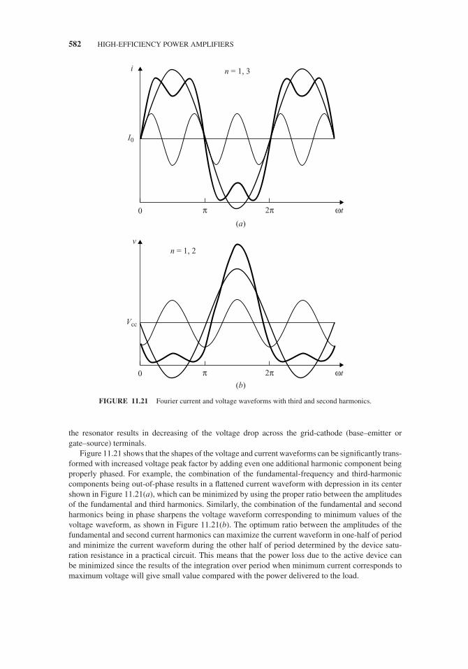
JWBS064-c11 JWBS064-Gerbennikov March 12, 2011 10:45 Printer Name: Yet to Come
582 HIGH-EFFICIENCY POWER AMPLIFIERS
i
v
n = 1, 3
n = 1, 2
(a)
0 2π ωtπ
I0
Vcc
(b)
0 2π ωtπ
FIGURE 11.21 Fourier current and voltage waveforms with third and second harmonics.
the resonator results in decreasing of the voltage drop across the grid-cathode (base–emitter orgate–source) terminals.
Figure 11.21 shows that the shapes of the voltage and current waveforms can be significantly trans-formed with increased voltage peak factor by adding even one additional harmonic component beingproperly phased. For example, the combination of the fundamental-frequency and third-harmoniccomponents being out-of-phase results in a flattened current waveform with depression in its centershown in Figure 11.21(a), which can be minimized by using the proper ratio between the amplitudesof the fundamental and third harmonics. Similarly, the combination of the fundamental and secondharmonics being in phase sharpens the voltage waveform corresponding to minimum values of thevoltage waveform, as shown in Figure 11.21(b). The optimum ratio between the amplitudes of thefundamental and second current harmonics can maximize the current waveform in one-half of periodand minimize the current waveform during the other half of period determined by the device satu-ration resistance in a practical circuit. This means that the power loss due to the active device canbe minimized since the results of the integration over period when minimum current corresponds tomaximum voltage will give small value compared with the power delivered to the load.
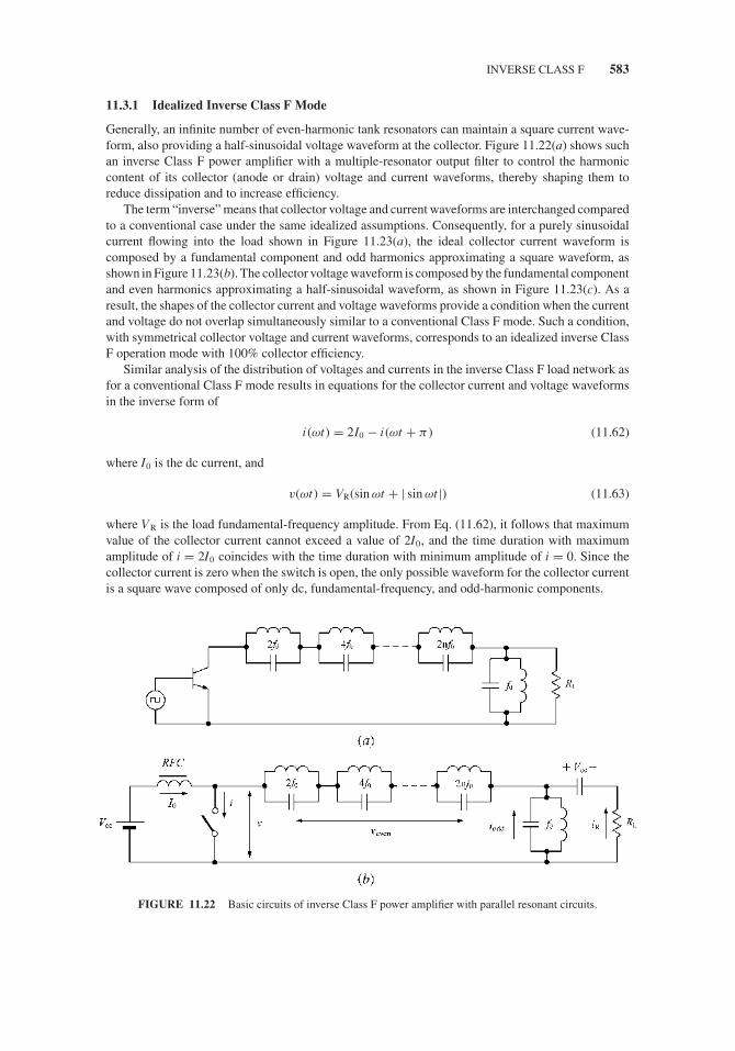
JWBS064-c11 JWBS064-Gerbennikov March 12, 2011 10:45 Printer Name: Yet to Come
INVERSE CLASS F 583
11.3.1 Idealized Inverse Class F Mode
Generally, an infinite number of even-harmonic tank resonators can maintain a square current wave-form, also providing a half-sinusoidal voltage waveform at the collector. Figure 11.22(a) shows suchan inverse Class F power amplifier with a multiple-resonator output filter to control the harmoniccontent of its collector (anode or drain) voltage and current waveforms, thereby shaping them toreduce dissipation and to increase efficiency.
The term “inverse” means that collector voltage and current waveforms are interchanged comparedto a conventional case under the same idealized assumptions. Consequently, for a purely sinusoidalcurrent flowing into the load shown in Figure 11.23(a), the ideal collector current waveform iscomposed by a fundamental component and odd harmonics approximating a square waveform, asshown in Figure 11.23(b). The collector voltage waveform is composed by the fundamental componentand even harmonics approximating a half-sinusoidal waveform, as shown in Figure 11.23(c). As aresult, the shapes of the collector current and voltage waveforms provide a condition when the currentand voltage do not overlap simultaneously similar to a conventional Class F mode. Such a condition,with symmetrical collector voltage and current waveforms, corresponds to an idealized inverse ClassF operation mode with 100% collector efficiency.
Similar analysis of the distribution of voltages and currents in the inverse Class F load network asfor a conventional Class F mode results in equations for the collector current and voltage waveformsin the inverse form of
i (ωt) = 2I0 − i (ωt + π ) (11.62)
where I0 is the dc current, and
v(ωt) = VR(sin ωt + | sin ωt |) (11.63)
where VR is the load fundamental-frequency amplitude. From Eq. (11.62), it follows that maximumvalue of the collector current cannot exceed a value of 2I0, and the time duration with maximumamplitude of i = 2I0 coincides with the time duration with minimum amplitude of i = 0. Since thecollector current is zero when the switch is open, the only possible waveform for the collector currentis a square wave composed of only dc, fundamental-frequency, and odd-harmonic components.
FIGURE 11.22 Basic circuits of inverse Class F power amplifier with parallel resonant circuits.

JWBS064-c11 JWBS064-Gerbennikov March 12, 2011 10:45 Printer Name: Yet to Come
584 HIGH-EFFICIENCY POWER AMPLIFIERS
FIGURE 11.23 Ideal waveforms of inverse Class F power amplifier.
By using a Fourier analysis of the current and voltage waveforms, the following equations forthe dc voltage, fundamental voltage, and current components in the collector voltage and currentwaveforms can be obtained:
The fundamental current component can be calculated using Eq. (11.62) as
I1 = IR = 1
π
2π∫π
2I0 sin (ωt + π ) dωt = 4I0
π(11.64)
the dc voltage Vcc can be calculated from Eq. (11.63) as
Vcc = 1
2π
π∫0
2VR sin ωt dωt = 2VR
π(11.65)
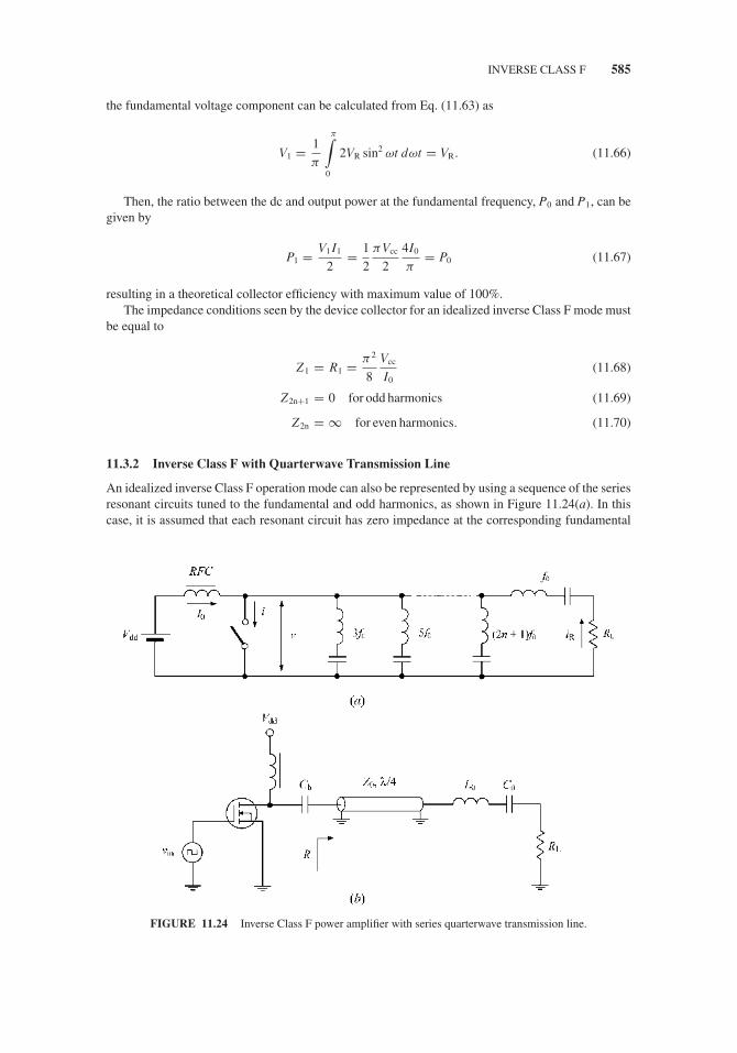
JWBS064-c11 JWBS064-Gerbennikov March 12, 2011 10:45 Printer Name: Yet to Come
INVERSE CLASS F 585
the fundamental voltage component can be calculated from Eq. (11.63) as
V1 = 1
π
π∫0
2VR sin2 ωt dωt = VR. (11.66)
Then, the ratio between the dc and output power at the fundamental frequency, P0 and P1, can begiven by
P1 = V1 I1
2= 1
2
πVcc
2
4I0
π= P0 (11.67)
resulting in a theoretical collector efficiency with maximum value of 100%.The impedance conditions seen by the device collector for an idealized inverse Class F mode must
be equal to
Z1 = R1 = π 2
8
Vcc
I0(11.68)
Z2n+1 = 0 for odd harmonics (11.69)
Z2n = ∞ for even harmonics. (11.70)
11.3.2 Inverse Class F with Quarterwave Transmission Line
An idealized inverse Class F operation mode can also be represented by using a sequence of the seriesresonant circuits tuned to the fundamental and odd harmonics, as shown in Figure 11.24(a). In thiscase, it is assumed that each resonant circuit has zero impedance at the corresponding fundamental
FIGURE 11.24 Inverse Class F power amplifier with series quarterwave transmission line.
JWBS064-c11 JWBS064-Gerbennikov March 12, 2011 10:45 Printer Name: Yet to Come
586 HIGH-EFFICIENCY POWER AMPLIFIERS
frequency f 0 and its odd-harmonic components (2n + 1)f 0 and infinite impedance at even harmonics2nf 0 realizing the idealized inverse Class F square current and half-sinusoidal voltage waveforms atthe device output terminal. As a result, the active device that is driven to operate as a switch sees theload resistance RL at the fundamental frequency, while the odd harmonics are shorted by the seriesresonant circuits.
An infinite set of the series resonant circuits tuned to the odd harmonics can be effectively replacedby a quarterwave transmission line with the same operating capability. Such a circuit representationof an inverse Class F power amplifier with a series quarterwave transmission line loaded by the seriesresonant circuit tuned to the fundamental is shown in Figure 11.24(b) [13,24]. The series-tuned outputcircuit presents to the transmission line a load resistance at the frequency of operation. At the sametime, the quarterwave transmission line transforms the load impedance according to
R = Z 20
RL(11.71)
where Z0 is the characteristic impedance of a transmission line. For even harmonics, the open circuiton the load side of the transmission line is repeated, thus producing an open circuit at the drain.However, the quarterwave transmission line converts the open circuit at the load to a short circuit atthe drain for odd harmonics with resistive load at the fundamental.
Consequently, for a purely sinusoidal current flowing into the load due to infinite loaded qualityfactor of the series fundamentally tuned circuit, the ideal drain current and voltage waveforms can berepresented by the corresponding normalized square and half-sinusoidal waveforms shown in Figures11.23(b) and 11.23(c), respectively. Here, a sum of the fundamental and odd harmonics approximatesa square current waveform and a sum of the fundamental and even harmonics approximates a half-sinusoidal drain voltage waveform. As a result, the shapes of the drain current and voltage waveformsprovide a condition when the current and voltage do not overlap simultaneously. The quarterwavetransmission line causes the output voltage across the load resistor RL to be phase-shifted by 90◦
relative to the fundamental-frequency components of the drain voltage and current.
11.3.3 Load Networks with Lumped and Distributed Parameters
Theoretical results show that the proper control of the second harmonic can significantly increasethe collector efficiency of the power amplifier by flattening of the output current waveform andminimizing the product of integration of the voltage and current waveforms. Practical realization of amultielement high-order LC resonant circuit can cause a serious implementation problem, especiallyat higher frequencies and in monolithic integrated circuits, when only three-harmonic componentscan be effectively controlled. Therefore, it is sufficient to be confined to the three- or four-elementresonant circuit composing the load network of the power amplifier. In this case, the operation with asecond-harmonic open circuit and third-harmonic short circuit is a promising concept for low voltagepower amplifiers [25].
In addition, it is necessary to take into account that, in practice, both extrinsic and intrinsictransistor parasitic elements like output shunt capacitance or serious inductance have a substantialeffect on the efficiency. The output capacitance Cout can represent the collector capacitance Cc inthe case of the bipolar transistor or drain–source capacitance plus gate–drain capacitance Cds +Cgd in the case of the FET device. The output inductance Lout is generally composed of the bond-wire and lead inductances for a packaged transistor, effect of which becomes significant at higherfrequencies.
The equivalent circuit of the second-harmonic impedance-peaking circuit is shown in Figure 11.25.Here, the series circuit consisting of an inductor L1 and a capacitor C1 creates a resonance at thesecond harmonic. Since the device output inductor Lout and capacitor Cout are tuned to create anopen-circuited condition at the second harmonic, the device collector sees resultant high impedanceat the second harmonic. To achieve a second harmonic high impedance, an external inductance may

JWBS064-c11 JWBS064-Gerbennikov March 12, 2011 10:45 Printer Name: Yet to Come
INVERSE CLASS F 587
FIGURE 11.25 Second-harmonic impedance-peaking circuit.
be added to interconnect the device output inductance Lout directly at the output terminal (collectoror drain) if its value is not accurate enough. As a result, the values of the network parameters are
Lout = 1
4ω20Cout
L1 = 1
4ω20C1
. (11.72)
As a first approximation for numerical calculation, the output device resistance Rout at the fun-damental frequency required to realize an inverse Class F operation mode with second-harmonicpeaking can be estimated as an equivalent resistance Rout = R(invF)
1 = V1/I1 determined at the funda-mental frequency for an ideal inverse Class F operation. Assuming zero saturation voltage and usingEq. (11.65) yield
R(invF)1 = π
2
Vcc
I1= π2
8R(F)
1 = π
2R(B)
1 (11.73)
where R(F)1 is the fundamental output resistance in a conventional Class F mode and R(B)
1 = Vcc/I1 isthe fundamental output resistance in an ideal Class B.
The ideal inverse class F power amplifier with all voltage third-order and higher order odd-harmonic short-circuit termination cannot be provided by using a single parallel transmission line thatcan be easily realized by a quarterwave transmission line for even harmonics in the conventional classF power amplifier. In this case, with a sufficiently simple circuit schematic convenient for practicalrealization, applying the current second-harmonic peaking and voltage third-harmonic terminationcan result in a maximum drain efficiency of more than 80% [3,26]. The output impedance-peakingload network of such a microstrip power amplifier is shown in Figure 11.26, and its circuit structureis similar to the one used to provide a conventional Class F operation mode.
As it follows from Eq. (11.73), the equivalent output resistance for an ideal inverse Class Fmode is higher by more than 1.5 times compared to a conventional Class B operation. Therefore,using an inverse Class F operation mode simplifies the subsequent output matching circuit design byminimizing the impedance transformation ratio. This is very important for high output power levelwhen the output resistance is sufficiently small. However, maximum amplitude of the output voltagewaveform can exceed the supply voltage by about three times. In practice, it is required to increasethe device breakdown voltage or to reduce the supply voltage. The latter is not desirable because ofa decrease in power gain and efficiency.
For such an inverse Class F microstrip power amplifier, it is necessary to provide the followingelectrical lengths for the transmission lines at the fundamental frequency:
θ1 = π
3θ2 = 1
2tan−1
[(2Z0ω0Cout + 1√
3
)−1]
θ3 = π
4(11.74)

JWBS064-c11 JWBS064-Gerbennikov March 12, 2011 10:45 Printer Name: Yet to Come
588 HIGH-EFFICIENCY POWER AMPLIFIERS
FIGURE 11.26 Transmission-line impedance-peaking circuit.
where Z0 is the characteristic impedance of the microstrip lines. The transmission line TL1 withelectrical length θ1 = 60◦ provides a short-circuited condition for the third harmonic and introducesa capacitive reactance at the second harmonic. The open-circuit stub TL3 with electrical length θ 3 =45◦ creates a short-circuited condition at the end of the transmission line TL2 at the second harmonic.Thus, the transmission line TL2 should provide an inductive reactance at the second harmonic tocompensate for the capacitive reactances of the transmission line TL1 and device output capacitanceCout to create a second-harmonic tank.
As an example, Figure 11.27 shows the frequency-response characteristic of the microstripimpedance-peaking circuit using an alumina substrate for the device output resistance Rout = 50 �
and output capacitance Cout = 2.2 pF, characteristic impedance of microstrip lines Z0 = 50 �
and electrical length θ2 = 19◦. From Figure 11.27, it follows that, for the second-harmonic peak-ing and third-harmonic short-circuit termination, an additional output matching at the fundamental
FIGURE 11.27 Frequency response of the microstrip impedance-peaking circuit.
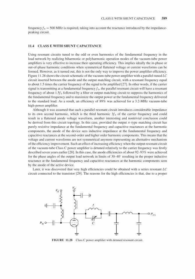
JWBS064-c11 JWBS064-Gerbennikov March 12, 2011 10:45 Printer Name: Yet to Come
CLASS E WITH SHUNT CAPACITANCE 589
frequency f 0 = 500 MHz is required, taking into account the reactance introduced by the impedance-peaking circuit.
11.4 CLASS E WITH SHUNT CAPACITANCE
Using resonant circuits tuned to the odd or even harmonics of the fundamental frequency in theload network by realizing biharmonic or polyharmonic operation modes of the vacuum-tube poweramplifiers is very effective to increase their operating efficiency. This implies ideally the in-phase orout-of-phase harmonic conditions when symmetrical flattened voltage or current waveforms can beformed. However, as it turned out, this is not the only way to improve the power amplifier efficiency.Figure 11.28 shows the circuit schematic of the vacuum-tube power amplifier with a parallel-tuned LCcircuit inserted between the anode and the output matching circuit, with a resonant frequency equalto about 1.5 times the carrier frequency of the signal to be amplified [27]. In other words, if the carriersignal is transmitting at a fundamental frequency f 0, the parallel resonant circuit will have a resonantfrequency of about 1.5f 0 followed by a filter or output matching circuit to suppress the harmonics ofthe fundamental frequency and to maximize the output power at the fundamental frequency deliveredto the standard load. As a result, an efficiency of 89% was achieved for a 3.2-MHz vacuum-tubehigh-power amplifier.
Although it was assumed that such a parallel resonant circuit introduces considerable impedanceto its own second harmonic, which is the third harmonic 3f 0 of the carrier frequency and couldresult in a flattened anode voltage waveform, another interesting and nontrivial conclusion couldbe derived from this circuit topology. In this case, provided the output π -type matching circuit haspurely resistive impedance at the fundamental frequency and capacitive reactances at the harmoniccomponents, the anode of the device sees inductive impedance at the fundamental frequency andcapacitive reactances at the second-order and higher order harmonic components. This means that thevoltage and current waveforms are not symmetrical anymore representing an alternative mechanismof the efficiency improvement. Such an effect of increasing efficiency when the output resonant circuitof the vacuum-tube Class C power amplifier is detuned relatively to the carrier frequency was firstlydescribed seven years earlier [28]. In this case, the anode efficiencies of about 92–93% were achievedfor the phase angles of the output load network in limits of 30–40◦ resulting in the proper inductivereactance at the fundamental frequency and capacitive reactances at the harmonic components seenby the anode of the active device.
Later, it was discovered that very high efficiencies could be obtained with a series resonant LCcircuit connected to the transistor [29]. The reasons for the high efficiencies is that, due to a proper
FIGURE 11.28 Class C power amplifier with detuned resonant circuit.
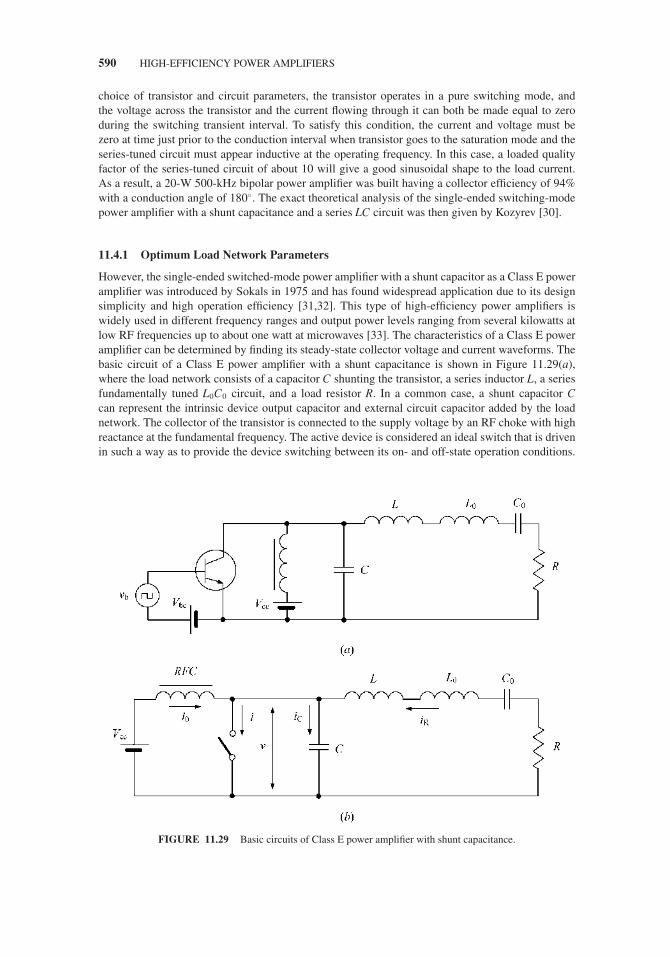
JWBS064-c11 JWBS064-Gerbennikov March 12, 2011 10:45 Printer Name: Yet to Come
590 HIGH-EFFICIENCY POWER AMPLIFIERS
choice of transistor and circuit parameters, the transistor operates in a pure switching mode, andthe voltage across the transistor and the current flowing through it can both be made equal to zeroduring the switching transient interval. To satisfy this condition, the current and voltage must bezero at time just prior to the conduction interval when transistor goes to the saturation mode and theseries-tuned circuit must appear inductive at the operating frequency. In this case, a loaded qualityfactor of the series-tuned circuit of about 10 will give a good sinusoidal shape to the load current.As a result, a 20-W 500-kHz bipolar power amplifier was built having a collector efficiency of 94%with a conduction angle of 180◦. The exact theoretical analysis of the single-ended switching-modepower amplifier with a shunt capacitance and a series LC circuit was then given by Kozyrev [30].
11.4.1 Optimum Load Network Parameters
However, the single-ended switched-mode power amplifier with a shunt capacitor as a Class E poweramplifier was introduced by Sokals in 1975 and has found widespread application due to its designsimplicity and high operation efficiency [31,32]. This type of high-efficiency power amplifiers iswidely used in different frequency ranges and output power levels ranging from several kilowatts atlow RF frequencies up to about one watt at microwaves [33]. The characteristics of a Class E poweramplifier can be determined by finding its steady-state collector voltage and current waveforms. Thebasic circuit of a Class E power amplifier with a shunt capacitance is shown in Figure 11.29(a),where the load network consists of a capacitor C shunting the transistor, a series inductor L, a seriesfundamentally tuned L0C0 circuit, and a load resistor R. In a common case, a shunt capacitor Ccan represent the intrinsic device output capacitor and external circuit capacitor added by the loadnetwork. The collector of the transistor is connected to the supply voltage by an RF choke with highreactance at the fundamental frequency. The active device is considered an ideal switch that is drivenin such a way as to provide the device switching between its on- and off-state operation conditions.
FIGURE 11.29 Basic circuits of Class E power amplifier with shunt capacitance.

JWBS064-c11 JWBS064-Gerbennikov March 12, 2011 10:45 Printer Name: Yet to Come
CLASS E WITH SHUNT CAPACITANCE 591
As a result, the collector voltage waveform is determined by the switch when it is turned on and bythe transient response of the load network when the switch is turned off.
To simplify an analysis of a Class E power amplifier, a simple equivalent circuit of which is shownin Figure 11.29(b), the following several assumptions are introduced:
� The transistor has zero saturation voltage, zero saturation resistance, infinite off-resistance, andits switching action is instantaneous and lossless.
� The total shunt capacitance is independent of the collector and is assumed linear.� The RF choke allows only a constant dc current and has no resistance.� The loaded quality factor QL = ωL0/R = 1/ωC0R of the series resonant L0C0 circuit tuned to the
fundamental frequency is high enough for the output current to be sinusoidal at the switchingfrequency.
� There are no losses in the circuit except only in the load R.� For an optimum operation mode, a 50% duty cycle is used.
For a lossless operation mode, it is necessary to provide the following optimum conditions forvoltage across the switch just prior to the start of switch on at the moment ωt = 2π , when transistoris saturated:
v (ωt)|ωt=2π = 0 (11.75)
dv (ωt)
dωt
∣∣∣∣ωt=2π
= 0 (11.76)
where v(ωt) is the voltage across the switch.The detailed theoretical analysis of a Class E power amplifier with shunt capacitance for any duty
cycle is given in [34], where the load current is assumed to be sinusoidal,
iR(ωt) = IR sin (ωt + ϕ) (11.77)
where ϕ is the initial phase shift.When the switch is turned on for 0 ≤ ωt < π , the current through the capacitance
iC (ωt) = ωCdv (ωt)
dωt= 0 (11.78)
and, consequently,
i(ωt) = I0 + IR sin (ωt + ϕ) (11.79)
under the initial on-state condition i (0) = 0. Hence, the dc current can be defined as
I0 = −IR sin ϕ (11.80)
and the current through the switch can be rewritten by
i (ωt) = IR [sin (ωt + ϕ) − sinϕ] . (11.81)
When the switch is turned off for π ≤ ωt < 2π , the current through the switch i (ωt) = 0, and thecurrent flowing through the capacitor C can be written as
iC(ωt) = I0 + IR sin (ωt + ϕ) (11.82)

JWBS064-c11 JWBS064-Gerbennikov March 12, 2011 10:45 Printer Name: Yet to Come
592 HIGH-EFFICIENCY POWER AMPLIFIERS
producing the voltage across the switch by the charging of this capacitor according to
v (ωt) = 1
ωC
ωt∫π
iC(ωt)dωt = − IR
ωC[cos (ωt + ϕ) + cos ϕ + (ωt − π ) sin ϕ] . (11.83)
Applying the first optimum condition given by Eq. (11.75) enables the phase angle ϕ to bedetermined as
ϕ = tan−1
(− 2
π
)= −32.482◦. (11.84)
Consideration of trigonometric relationships shows that
sin ϕ = −2√π 2 + 4
cos ϕ = π√π 2 + 4
. (11.85)
By using Fourier-series expansion and Eqs. (11.80) and (11.85), the expression to determine thesupply voltage Vcc can be written as
Vcc = 1
2π
2π∫0
v (ωt)dωt = I0
πωC. (11.86)
As a result, the normalized steady-state collector voltage waveform for π ≤ ωt < 2π and currentwaveform for period of 0 ≤ ωt < π are
v (ωt)
Vcc= π
(ωt − 3π
2− π
2cos ωt − sinωt
)(11.87)
i (ωt)
I0= π
2sin ωt − cosωt + 1. (11.88)
Figure 11.30 shows the normalized (a) load current, (b) collector voltage waveform, and (c) collec-tor current waveforms for an idealized optimum Class E with shunt capacitance. From collector volt-age and current waveforms it follows that, when the transistor is turned on, there is no voltage acrossthe switch and the current i(ωt) consisting of the load sinusoidal current and dc current flows throughthe device. However, when the transistor is turned off, this current flows through the shunt capacitanceC. The jump in the collector current waveform at the instant of switching off is necessary to obtainnonzero output power at the fundamental frequency delivered to the load, which can be defined as anintegration of the product of the collector voltage and current derivatives over the entire period [35].
As a result, there is no nonzero voltage and current simultaneously, which means a lack of thepower losses and gives an idealized collector efficiency of 100%. This implies that the dc power andfundamental-frequency output power delivered to the load are equal,
I0Vcc = I 2R
2R. (11.89)
Consequently, the value of dc supply current I0 can be determined using Eqs. (11.80) and (11.85)by
I0 = Vcc
R
8
π2 + 4= 0.577
Vcc
R. (11.90)

JWBS064-c11 JWBS064-Gerbennikov March 12, 2011 10:45 Printer Name: Yet to Come
CLASS E WITH SHUNT CAPACITANCE 593
FIGURE 11.30 Normalized (a) load current and collector (b) voltage and (c) current waveforms for idealizedoptimum Class E with shunt capacitance.
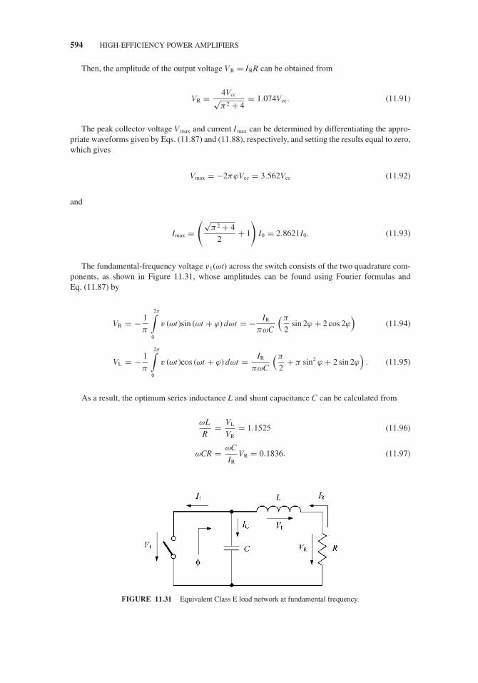
JWBS064-c11 JWBS064-Gerbennikov March 12, 2011 10:45 Printer Name: Yet to Come
594 HIGH-EFFICIENCY POWER AMPLIFIERS
Then, the amplitude of the output voltage VR = IRR can be obtained from
VR = 4Vcc√π 2 + 4
= 1.074Vcc. (11.91)
The peak collector voltage Vmax and current Imax can be determined by differentiating the appro-priate waveforms given by Eqs. (11.87) and (11.88), respectively, and setting the results equal to zero,which gives
Vmax = −2πϕVcc = 3.562Vcc (11.92)
and
Imax =(√
π 2 + 4
2+ 1
)I0 = 2.8621I0. (11.93)
The fundamental-frequency voltage v1(ωt) across the switch consists of the two quadrature com-ponents, as shown in Figure 11.31, whose amplitudes can be found using Fourier formulas andEq. (11.87) by
VR = − 1
π
2π∫0
v (ωt)sin (ωt + ϕ) dωt = − IR
πωC
(π
2sin 2ϕ + 2 cos 2ϕ
)(11.94)
VL = − 1
π
2π∫0
v (ωt)cos (ωt + ϕ) dωt = IR
πωC
(π
2+ π sin2 ϕ + 2 sin 2ϕ
). (11.95)
As a result, the optimum series inductance L and shunt capacitance C can be calculated from
ωL
R= VL
VR= 1.1525 (11.96)
ωCR = ωC
IRVR = 0.1836. (11.97)
FIGURE 11.31 Equivalent Class E load network at fundamental frequency.

JWBS064-c11 JWBS064-Gerbennikov March 12, 2011 10:45 Printer Name: Yet to Come
CLASS E WITH SHUNT CAPACITANCE 595
The optimum load resistance R can be obtained using Eqs. (11.89) and (11.91) for the supplyvoltage Vcc and fundamental-frequency output power Pout delivered to the load as
R = 8
π 2 + 4
V 2cc
Pout= 0.5768
V 2cc
Pout. (11.98)
Finally, the phase angle of the load network seen by the switch at the fundamental and requiredfor an idealized optimum Class E with shunt capacitance can be determined through the load networkparameters using Eqs. (11.96) and (11.97) by
φ = tan−1
(ωL
R
)− tan−1
⎛⎜⎝ ωC R
1 − ωL
RωC R
⎞⎟⎠= 35.945◦. (11.99)
When realizing an optimum Class E operation mode, it is very important to know up to whichmaximum frequency such an idealized efficient operation mode can be extended. In this case, it ispossible to establish a relationship between a maximum frequency f max, a parallel shunt capacitanceC, and a supply voltage Vcc by using Eqs. (11.86) and (11.93) when
fmax = 1
π 2
1√π 2 + 4 + 2
Imax
CoutVcc= Imax
56.5CoutVcc(11.100)
where C = Cout is the device output capacitance limiting the maximum operation frequency of anideal Class E circuit [36].
The high-QL assumption for the series resonant L0C0 circuit can lead to considerable errors if itsvalue is substantially small in real circuits [37]. For example, for a 50% duty cycle, the values of thecircuit parameters for the loaded quality factor less than unity can differ by several tens of percents.At the same time, for QL ≥ 7, the errors are found to be less than 10% and become less than 5% forQL ≥ 10. To match the optimum Class E load network resistance R with standard load impedanceRL = 50 �, the series resonant L0C0 circuit should be followed or fully replaced by the matchingcircuit, in which the first element must represent the series inductor to provide high impedance atharmonics [3].
11.4.2 Saturation Resistance and Switching Time
In practical power amplifier design, especially when a value of the supply voltage is sufficiently small,it is very important to predict the overall degradation of power amplifier efficiency due to the finitevalue of the transistor saturation resistance. Figure 11.32 shows the simplified equivalent circuit of aClass E power amplifier with shunt capacitance including the on-resistance or saturation resistancersat connected in series to the ideal switch. To obtain a quantitative estimate of the power losses due tothe contribution of rsat, the saturated output power Psat can be obtained with a simple approximation
FIGURE 11.32 Equivalent Class E load network with saturation resistance.
JWBS064-c11 JWBS064-Gerbennikov March 12, 2011 10:45 Printer Name: Yet to Come
596 HIGH-EFFICIENCY POWER AMPLIFIERS
when the current i(ωt) flowing through the saturation resistance rsat is determined in an ideal case byEq. (11.88).
An analytical expression to calculate the power losses due to the saturation resistance rsat, whosevalue is assumed constant, can be represented in the normalized form according to
Psat
P0= rsat
2π I0Vcc
π∫0
i2 (ωt) dωt (11.101)
where P0 = I0Vcc is the dc power.By taking into account that
π∫0
(π
2sin ωt − cos ωt + 1
)2dωt =π
8
(π 2 + 28
)I 2
0 (11.102)
Eq. (11.101) can be rewritten using Eq. (11.90) as
Psat
P0= rsat
2π
I0
Vcc
π
8
(π 2 + 28
) = rsat
2R
π 2 + 28
π2 + 4= 1.365
rsat
R. (11.103)
The collector efficiency η can be calculated from
η = Pout
P0= P0 − Psat
P0= 1 − Psat
P0. (11.104)
Consequently, the presence of the saturation resistance results in the finite value of the saturationvoltage V sat, which can be defined from
Vsat
Vcc= 1 − 1
1 + 1.365rsat
R
(11.105)
being normalized to the dc supply voltage Vcc [38].More detailed theoretical analysis of the time-dependent behavior of the collector voltage and
current waveforms shows that, for a finite value of the saturation resistance rsat, the optimum conditionsfor idealized operation mode given by Eqs. (11.75) and (11.76) do not correspond anymore to theminimum dissipated power losses, and there are optimum nonzero values of the collector voltageand its derivative at switching time instant corresponding to minimum overall power losses [39]. Forexample, even for small losses with the normalized loss parameter ωCrsat = 0.1 for a duty cycle of 50%,the optimum series inductance L is almost two times greater, while the optimum shunt capacitanceC is of about 20% greater than those obtained under optimum conditions given by Eqs. (11.75)and (11.76). However, for collector efficiencies of 90% and greater, both the optimum inductanceand optimum capacitance differ by less than 20% from their optimum values for rsat = 0 [40]. Thus,generally the switching conditions given by Eqs. (11.75) and (11.76) can be considered optimum onlyfor an idealized case of a Class E load network with zero saturation resistance providing the switched-mode transistor operation when it operates in pinch-off and saturation regions only. However, theycan be considered as a sufficiently accurate initial guess for further design and optimization of thereal high-efficiency power amplifier circuits.
For an ideal active device without any memory effects due to intrinsic phase delays, the switchingtime is equal to zero when the rectangular input drive results in a rectangular output response. Suchan ideal case assumes zero device feedback capacitance and zero device input resistance. However, in

JWBS064-c11 JWBS064-Gerbennikov March 12, 2011 10:45 Printer Name: Yet to Come
CLASS E WITH SHUNT CAPACITANCE 597
a real situation, especially at higher frequencies, it is very difficult to realize the driving signal closeto the rectangular form as it leads to the significant circuit complexity. Fortunately, to realize high-efficiency operation conditions, it is sufficient to drive the power amplifier simply with a sinusoidalsignal. The finite-time transition from the saturation mode to the pinch-off mode through the deviceactive mode takes place at the point of the intersection of the curve corresponding to the base (orchannel) charge process (curve 1) and the curve corresponding to the required ideal collector currentwaveform provided by the load network (curve 2), as shown in Figure 11.33(a). To minimize theswitching time interval, it is sufficient to slightly overdrive the active device with signal amplitudeby 20–30% higher than it is required for a conventional Class B power amplifier, as shown inFigure 11.33(b) [3]. As an alternative, the second-harmonic component (approximation of a half-sinusoidal waveform) or third-harmonic component (approximation of a rectangular waveform withclose to trapezoidal waveform) with proper phasing can be added to the input driving signal. In bothcases, the overall driving waveform will be steeper compared with simply sinusoidal driving signal,thus resulting in a faster switching operation time.
FIGURE 11.33 Collector current waveforms due to finite switching time.

JWBS064-c11 JWBS064-Gerbennikov March 12, 2011 10:45 Printer Name: Yet to Come
598 HIGH-EFFICIENCY POWER AMPLIFIERS
The power dissipated during this on-to-off transition can be calculated assuming zero on-resistanceas
Ps = 1
2π
π∫θs
i (ωt) v (ωt) dωt (11.106)
where the collector voltage during the transition time τ s = π − θ s is given by
v (θs) = 1
ωC
π∫θs
iC (ωt) dωt . (11.107)
The short duration of the switching time and the proper behavior of the resulting collector (ordrain) waveform allows us to make an additional assumption of a linearly decreasing collector currentduring fall time τ s = π − θ s starting at i(θ s) at time θ s and decaying to zero at time π , which can bewritten by
i (ωt ) = i (θs)(
1 − ωt − θs
τs
)(11.108)
where i(θ s) corresponds to the peak collector current shown in Figure 11.33(a) [38,40]. In this case,the capacitor-charging current iC(ωt) = i(θ s) − i(ωt), being zero during saturation mode, varieslinearly between zero and i(θ s) during on-to-off transition according to
iC (ωt) = i (θs)ωt − θs
τs. (11.109)
The collector voltage produces a parabolic voltage waveform during the switching interval ac-cording to Eq. (11.107) given by
v (ωt) = i (θs)
2ωCτs(ωt − θs)
2 . (11.110)
As a result, the power dissipated during transition according to Eq. (11.106) is then
Ps = i2 (θs) τ 2s
48πωC. (11.111)
For an optimum power amplifier by assuming that, in view of a short transition time, i(θ s) = i(π ),from Eq. (11.88) it follows that i(π ) = 2I0, hence
Ps = I 20 τ 2
s
12πωC. (11.112)
Taking into account Eq. (11.86), the switching loss power Ps normalized to the dc power P0 canbe obtained from
Ps
P0= I0τ
2s
12πωCVcc= τ 2
s
12. (11.113)

JWBS064-c11 JWBS064-Gerbennikov March 12, 2011 10:45 Printer Name: Yet to Come
CLASS E WITH SHUNT CAPACITANCE 599
The collector efficiency η can be estimated as
η = 1 − Ps
P0= 1 − τ 2
s
12. (11.114)
As follows from Eq. (11.113), the power losses due to the finite switching time are sufficientlysmall and, for example, for τs = 0.35 or 20◦ they are only about 1%, whereas for τs = 60◦ theyare approximately equal to 10%. A more exact analysis assuming a linear variation of the collectorcurrent during on-to-off transition results in similar results when efficiency degrades to 97.72% forτs = 30◦ and to 90.76% for τs = 60◦ [41]. Considering an exponential collector current decay ratherthan linear during the fall time shows the similar result for τs = 30◦ when η = 96.8%, but the collectorefficiency degrades more significantly at longer fall times when, for example, η = 86.6% for τs =60◦ [42].
11.4.3 Load Network with Transmission Lines
The transmission lines are often preferred over lumped inductors at microwave frequencies becauseof the convenience of their practical implementation, more predictable performance, less insertionloss, and less effect of the parasitic elements. For example, the matching circuit can be composedwith any types of the transmission lines including open-circuit or short-circuit stubs to provide therequired matching and harmonic-suppression conditions. In this case, to approximate the idealizedClass E operation mode of the microwave power amplifier or oscillator, it is necessary to designthe transmission-line load network satisfying the required idealized optimum impedances at thefundamental-frequency and harmonic components. The device output capacitance can fully representthe required shunt capacitance whose optimum value is defined by Eq. (11.97). Consequently, themain problem is to satisfy the optimum requirements on the fundamental-frequency impedance ZL(ω0)shown in Figure 11.34(a) and harmonic-component impedances ZL(nω0) shown in Figure 11.34(b),which can be written using Eq. (11.96) at fundamental frequency f 0 as
ZL (ω0) = R + jωL = R
(1 + j
ωL
R
)= R
(1 + j tan 49.052◦) (11.115)
and at harmonic components nf 0, where n = 2, 3, . . . , ∞, as
ZL (nω0) = ∞. (11.116)
Generally, it is practically impossible to realize these conditions for infinite number of the harmoniccomponents by using a finite number of the transmission lines only. However, as it turned out fromthe Fourier-series analysis, a good approximation to Class E mode may be obtained with the dc,fundamental-frequency, and second-harmonic components of the voltage waveform across the switch[36,43]. Figure 11.34(c) shows the collector (drain) voltage waveform containing these two-harmoniccomponents (dotted line) plotted along with an ideal voltage waveform (solid line). In this case, theClass E load network designed for microwave applications will include the series microstrip line l1
and open-circuit stub l2, as shown in Figure 11.35(a). The electrical lengths of lines l1 and l2 arechosen to be of about 45◦ at the fundamental frequency to provide an open-circuit condition seen fromthe device output at the second harmonic according to Eq. (11.116). Their characteristic impedancesare calculated to satisfy the required inductive impedance condition at the fundamental frequencygiven by Eq. (11.115). In the case of a packaged active device, its output lead inductance can beaccounted for by shortening the length of l1.
In some case, a value of the device output capacitance exceeds the required optimum value fora Class E mode with shunt capacitance. In this situation, it is possible to approximate Class Emode with high efficiency by setting an adequate optimum load at the fundamental frequency and
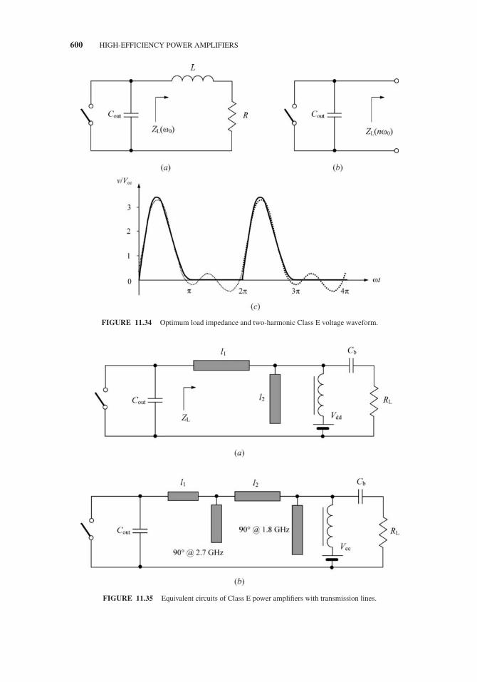
JWBS064-c11 JWBS064-Gerbennikov March 12, 2011 10:45 Printer Name: Yet to Come
600 HIGH-EFFICIENCY POWER AMPLIFIERS
FIGURE 11.34 Optimum load impedance and two-harmonic Class E voltage waveform.
FIGURE 11.35 Equivalent circuits of Class E power amplifiers with transmission lines.
JWBS064-c11 JWBS064-Gerbennikov March 12, 2011 10:45 Printer Name: Yet to Come
CLASS E WITH FINITE DC-FEED INDUCTANCE 601
strong reactive load at the second- and third-harmonic components [44]. Such a harmonic controlnetwork consists of the open-circuit quarterwave stubs at the second- and third-harmonic componentsseparately, as shown in Figure 11.35(b), where the third-harmonic quarterwave stub is located beforethe second-harmonic quarterwave stub. As a result, very high collector efficiency can be achievedeven with values of the device output capacitance higher than it is conventionally required at theexpense of lower output power, keeping the load at the second and third harmonics strictly inductive.The maximum collector efficiency over 90% with the output power of 1.5 W for a test power amplifierusing the commercial bipolar transistor MRF557 was measured at a carrier frequency of 900 MHz.
An analysis of an optimum Class E mode in frequency domain shows that the combined effectof the saturation resistance rsat and second-harmonic loading is characterized by a shift of theoptimum load fundamental-frequency impedance [45]. Besides, parasitic effects due to packagingand microstrip junction discontinuities may upset the transmission-line open-circuit requirement.Therefore, it is practically important to predict the power amplifier performance due to nonidealharmonic terminations. For example, the voltage peak factor increases when the second-harmonicload varies from capacitive to inductive, and the excessive current flow can be realized under capacitiveload reactance. It appears that, while a capacitive second-harmonic load achieves higher output power,an inductive second-harmonic load provides better efficiency. In this case, to approximate a switched-mode Class E operation mode, the maximum collector efficiency with lower output power is achievedfor nonzero collector voltage and negative collector voltage-derivative conditions [46]. Generally, byproviding the open-circuit termination of the second- and third-harmonic components, the collectorefficiency can be increased by 10% [47].
11.5 CLASS E WITH FINITE DC-FEED INDUCTANCE
In real practice, it is impossible to realize an RF choke with infinite impedance at the fundamentalfrequency and its harmonic components. Moreover, using a finite dc-feed inductance has an advantageof minimizing size, cost, and complexity of the overall circuit. The detailed approach to analyze theeffect of a finite dc-feed inductance on the idealized Class E mode with shunt capacitance and seriesfilter was firstly described in [48]. It was based on Laplace-transform technique to solve a second-order differential equation describing the behavior of a Class E load network with finite dc-feedinductance. Later this approach was extended to the load network with finite QL-factor of the seriesfilter and finite device saturation resistance [49,50]. However, since the results of excessive analyticaland numerical calculations are given only for a few particular cases, it is difficult to figure out the basicbehavior of the load network elements and define simple equations for their parameters. Generally,based on the composing of the circuit equations in the form of a system of the first-order differentialequations for currents and voltages and setting the design specifications, the optimum Class E loadnetwork parameters can be numerically calculated taking into account the finite dc-feed inductance,drain current fall time, finite QL-factor, nonzero device saturation resistance, and nonlinear operationof any passive element simultaneously [51]. Also, it was analytically shown for a duty cycle of 50%based on the Class E optimum conditions that the series excessive reactance can be either inductiveor capacitive depending on the values of the dc-feed inductance and shunt capacitance [52,53]. Basedon the certain numbers of cases, a Lagrange polynomial interpolation was used to obtain explicit anddirectly usable design equations for an idealized Class E with finite dc-feed inductance and seriesinductive reactance [54].
11.5.1 General Analysis and Optimum Circuit Parameters
The generalized second-order load network of a switched-mode Class E power amplifier with finite dc-feed inductance is shown in Figure 11.36(a) [3,55]. The load network consists of a shunt capacitance C,a parallel inductance L, a series reactance X, a series resonant L0C0 circuit tuned to the fundamentalfrequency, and a load resistance R. In a common case, a shunt capacitance C can represent the
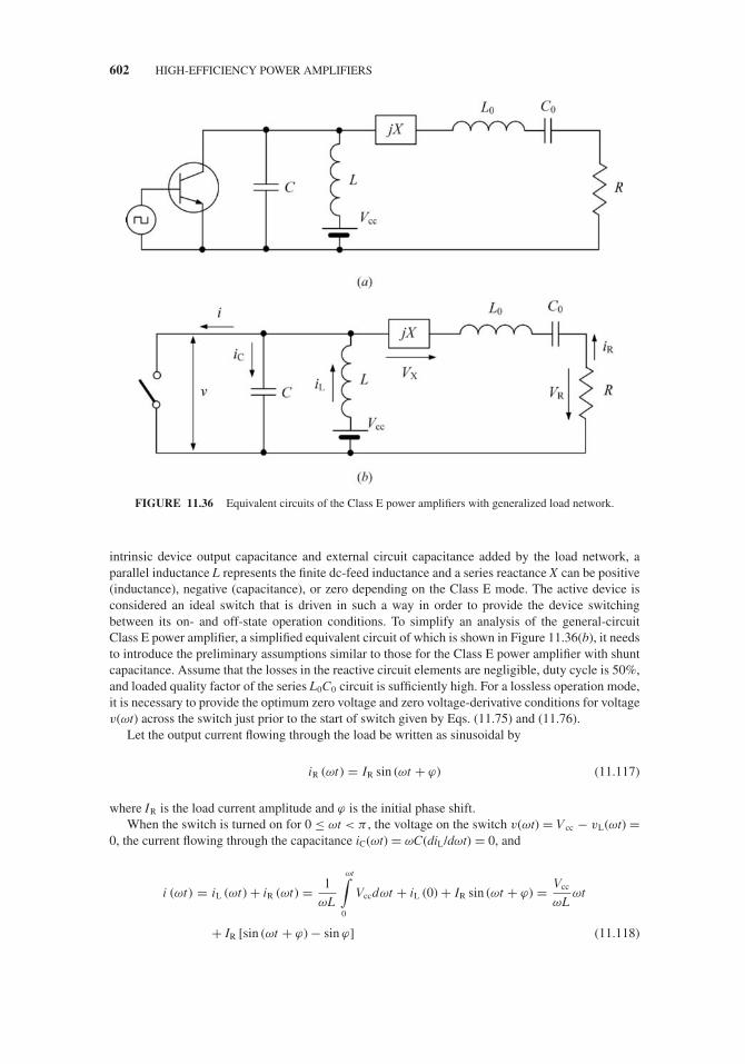
JWBS064-c11 JWBS064-Gerbennikov March 12, 2011 10:45 Printer Name: Yet to Come
602 HIGH-EFFICIENCY POWER AMPLIFIERS
FIGURE 11.36 Equivalent circuits of the Class E power amplifiers with generalized load network.
intrinsic device output capacitance and external circuit capacitance added by the load network, aparallel inductance L represents the finite dc-feed inductance and a series reactance X can be positive(inductance), negative (capacitance), or zero depending on the Class E mode. The active device isconsidered an ideal switch that is driven in such a way in order to provide the device switchingbetween its on- and off-state operation conditions. To simplify an analysis of the general-circuitClass E power amplifier, a simplified equivalent circuit of which is shown in Figure 11.36(b), it needsto introduce the preliminary assumptions similar to those for the Class E power amplifier with shuntcapacitance. Assume that the losses in the reactive circuit elements are negligible, duty cycle is 50%,and loaded quality factor of the series L0C0 circuit is sufficiently high. For a lossless operation mode,it is necessary to provide the optimum zero voltage and zero voltage-derivative conditions for voltagev(ωt) across the switch just prior to the start of switch given by Eqs. (11.75) and (11.76).
Let the output current flowing through the load be written as sinusoidal by
iR (ωt) = IR sin (ωt + ϕ) (11.117)
where IR is the load current amplitude and ϕ is the initial phase shift.When the switch is turned on for 0 ≤ ωt < π , the voltage on the switch v(ωt) = Vcc − vL(ωt) =
0, the current flowing through the capacitance iC(ωt) = ωC(diL/dωt) = 0, and
i (ωt) = iL (ωt) + iR (ωt) = 1
ωL
ωt∫0
Vccdωt + iL (0) + IR sin (ωt + ϕ) = Vcc
ωLωt
+ IR [sin (ωt + ϕ) − sin ϕ] (11.118)
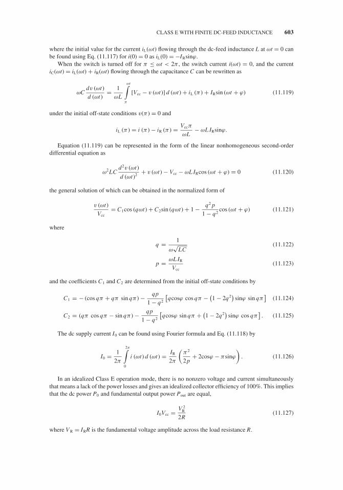
JWBS064-c11 JWBS064-Gerbennikov March 12, 2011 10:45 Printer Name: Yet to Come
CLASS E WITH FINITE DC-FEED INDUCTANCE 603
where the initial value for the current iL(ωt) flowing through the dc-feed inductance L at ωt = 0 canbe found using Eq. (11.117) for i(0) = 0 as iL(0) = −IRsinϕ.
When the switch is turned off for π ≤ ωt < 2π , the switch current i(ωt) = 0, and the currentiC(ωt) = iL(ωt) + iR(ωt) flowing through the capacitance C can be rewritten as
ωCdv (ωt)
d (ωt)= 1
ωL
ωt∫π
[Vcc − v (ωt)] d (ωt) + iL (π ) + IRsin (ωt + ϕ) (11.119)
under the initial off-state conditions v(π) = 0 and
iL (π ) = i (π) − iR (π ) = Vccπ
ωL− ωL IRsinϕ.
Equation (11.119) can be represented in the form of the linear nonhomogeneous second-orderdifferential equation as
ω2 LCd2v (ωt)
d (ωt)2 + v (ωt) − Vcc − ωL IRcos (ωt + ϕ) = 0 (11.120)
the general solution of which can be obtained in the normalized form of
v (ωt)
Vcc= C1cos (qωt) + C2sin (qωt) + 1 − q2 p
1 − q2cos (ωt + ϕ) (11.121)
where
q = 1
ω√
LC(11.122)
p = ωL IR
Vcc(11.123)
and the coefficients C1 and C2 are determined from the initial off-state conditions by
C1 = − (cos qπ + qπ sin qπ) − qp
1 − q2
[qcosϕ cos qπ − (
1 − 2q2)
sinϕ sin qπ]
(11.124)
C2 = (qπ cos qπ − sin qπ) − qp
1 − q2
[qcosϕ sin qπ + (
1 − 2q2)
sinϕ cos qπ]. (11.125)
The dc supply current I0 can be found using Fourier formula and Eq. (11.118) by
I0 = 1
2π
2π∫0
i (ωt) d (ωt) = IR
2π
(π 2
2p+ 2cosϕ − πsinϕ
). (11.126)
In an idealized Class E operation mode, there is no nonzero voltage and current simultaneouslythat means a lack of the power losses and gives an idealized collector efficiency of 100%. This impliesthat the dc power P0 and fundamental output power Pout are equal,
I0Vcc = V 2R
2R(11.127)
where VR = IRR is the fundamental voltage amplitude across the load resistance R.
JWBS064-c11 JWBS064-Gerbennikov March 12, 2011 10:45 Printer Name: Yet to Come
604 HIGH-EFFICIENCY POWER AMPLIFIERS
As a result, by using Eqs. (11.126) and (11.127) and taking into account that R = V 2R /2Pout, the
optimum load resistance R for the specified values of a supply voltage Vcc and a fundamental outputpower Pout can be obtained by
R = 1
2
(VR
Vcc
)2 V 2cc
Pout(11.128)
where
VR
Vcc= 1
π
(π 2
2p+ 2cosϕ − πsinϕ
). (11.129)
The normalized load network inductance L and capacitance C can be appropriately defined usingEqs. (11.122), (11.123), and (11.126) by
ωL
R= p
/ (π
2p+ 2
πcosϕ − sinϕ
)(11.130)
ωCR = 1
/ (q2 ωL
R
). (11.131)
The series reactance X, which may generally have an inductive, capacitive, or zero reactance,depending on the load network parameters, can be calculated using the two quadrature fundamental-frequency voltage Fourier components of
VR = − 1
π
2π∫0
v (ωt) sin (ωt + ϕ) dωt (11.132)
VX = − 1
π
2π∫0
v (ωt) cos (ωt + ϕ) dωt . (11.133)
The fundamental-frequency current flowing through the switch consists of the two quadraturecomponents, the amplitudes of which can be found using Fourier formulas and Eq. (11.118) by
IR = 1
π
2π∫0
i (ωt) sin (ωt + ϕ) dωt = IR
π
[πcosϕ − 2sinϕ
p+ π
2− sin2ϕ
]
IX = − 1
π
2π∫0
i (ωt)cos (ωt + ϕ) dωt = IR
π
[πsinϕ + 2cosϕ
p− 2sin2ϕ
].
Generally, Eq. (11.121) for a normalized collector voltage contains the three unknown parametersq, p, and ϕ, which must be analytically or numerically determined. In a common case, the parameter qcan be considered a variable, and the other two parameters p and ϕ are calculated from a system of thetwo equations resulting from applying of the two optimum zero voltage and zero voltage-derivativeconditions given by Eqs. (11.75) and (11.76) to Eq. (11.121). Figure 11.37 shows the dependenciesof the optimum parameters p and ϕ versus q for a Class E with finite dc-feed inductance.
Based on the calculated optimum parameters p and ϕ as the functions of q, the optimum loadnetwork parameters of the Class E load network with a finite dc-feed inductance can be determined

JWBS064-c11 JWBS064-Gerbennikov March 12, 2011 10:45 Printer Name: Yet to Come
CLASS E WITH FINITE DC-FEED INDUCTANCE 605
FIGURE 11.37 Optimum Class E parameters p and ϕ versus q.
using Eqs. (11.128) to (11.131). The series reactance X can be calculated through the ratio of the twoquadrature fundamental-frequency voltage Fourier components given in Eqs. (11.132) and (11.133) as
X
R= VX
VR. (11.134)
The dependences of the normalized optimum dc-feed inductance ωL/R and series reactance X/R areshown in Figure 11.38(a), while the dependences of the normalized optimum shunt capacitance ωCRand load resistance RPout/V 2
cc are plotted in Figure 11.38(b). Here, we can see that the subharmoniccase of q = 0.5 is very close to a Class E mode with shunt capacitance, since the value of thenormalized inductance ωL/R is sufficiently high and the variations of normalized values of ωCRand RPout/V 2
cc are insignificant. The value of the series reactance X changes its sign from positiveto negative, which means that the inductive reactance is followed by the capacitive reactance. As aresult, there is special case of a load network with a parallel circuit and a load resistance only whenX = 0 at q = 1.412. In this case, the maximum value of the optimum load resistance R is providedfor the same supply voltage and output power, thus simplifying the matching with the standard loadof 50 �. Also, the values of a dc-feed inductance L become sufficiently small, thus making Class Every attractive for monolithic applications. The maximum operation frequency f max is realized at q =1.468 where the normalized optimum shunt capacitance ωCR reaches its maximum.
The graphical solutions for the optimum load network parameters can be replaced by the analyticaldesign equations represented in terms of the simple second- and third-order polynomial functionsgiven by Tables 11.1 and 11.2 for different ranges of the parameter q [56]. The maximum differencebetween the polynomial approximations and exact numerical solutions given in the graphic form isof about 2%.
11.5.2 Parallel-Circuit Class E
The theoretical analysis of a switched-mode parallel-circuit Class E power amplifier using a seriesfilter, which basic circuit is shown in Figure 11.39(a), was done firstly by Kozyrev with the calculation

JWBS064-c11 JWBS064-Gerbennikov March 12, 2011 10:45 Printer Name: Yet to Come
606 HIGH-EFFICIENCY POWER AMPLIFIERS
FIGURE 11.38 Normalized optimum Class E load network parameters.
TABLE 11.1 Load Network Parameters for 0.6 < q < 1.0.
Parameter Design Equation
ωL
R44.93q2 − 94.32q + 52.46
ωC R 0.426q2 − 0.379q + 0.3
X
R−0.73 q2 + 0.411 q + 1.03
Pout R
V 2cc
0.74q2 − 0.6q + 0.76
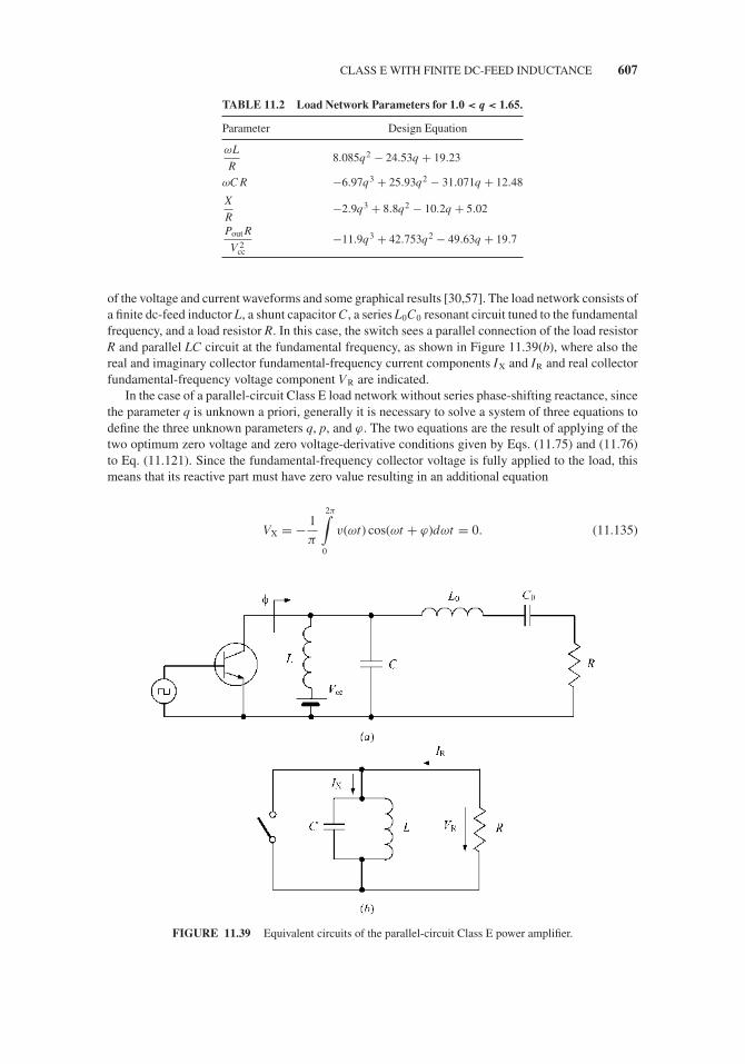
JWBS064-c11 JWBS064-Gerbennikov March 12, 2011 10:45 Printer Name: Yet to Come
CLASS E WITH FINITE DC-FEED INDUCTANCE 607
TABLE 11.2 Load Network Parameters for 1.0 < q < 1.65.
Parameter Design Equation
ωL
R8.085q2 − 24.53q + 19.23
ωC R −6.97q3 + 25.93q2 − 31.071q + 12.48
X
R−2.9q3 + 8.8q2 − 10.2q + 5.02
Pout R
V 2cc
−11.9q3 + 42.753q2 − 49.63q + 19.7
of the voltage and current waveforms and some graphical results [30,57]. The load network consists ofa finite dc-feed inductor L, a shunt capacitor C, a series L0C0 resonant circuit tuned to the fundamentalfrequency, and a load resistor R. In this case, the switch sees a parallel connection of the load resistorR and parallel LC circuit at the fundamental frequency, as shown in Figure 11.39(b), where also thereal and imaginary collector fundamental-frequency current components IX and IR and real collectorfundamental-frequency voltage component VR are indicated.
In the case of a parallel-circuit Class E load network without series phase-shifting reactance, sincethe parameter q is unknown a priori, generally it is necessary to solve a system of three equations todefine the three unknown parameters q, p, and ϕ. The two equations are the result of applying of thetwo optimum zero voltage and zero voltage-derivative conditions given by Eqs. (11.75) and (11.76)to Eq. (11.121). Since the fundamental-frequency collector voltage is fully applied to the load, thismeans that its reactive part must have zero value resulting in an additional equation
VX = − 1
π
2π∫0
v(ωt) cos(ωt + ϕ)dωt = 0. (11.135)
FIGURE 11.39 Equivalent circuits of the parallel-circuit Class E power amplifier.

JWBS064-c11 JWBS064-Gerbennikov March 12, 2011 10:45 Printer Name: Yet to Come
608 HIGH-EFFICIENCY POWER AMPLIFIERS
Solving the system of three equations with three unknown parameters numerically gives thefollowing values [3,58,59]:
q = 1.412 (11.136)
p = 1.210 (11.137)
ϕ = 15.155◦. (11.138)
Figure 11.40 shows the normalized (a) load current and collector (b) voltage, and (c) currentwaveforms for an idealized optimum parallel-circuit Class E operation. From collector voltage andcurrent waveforms it follows that there is no nonzero voltage and current simultaneously. When thishappens, there no power loss occurs and an idealized collector efficiency of 100% is achieved.
By using Eqs. (11.128) to (11.131), the optimum load resistance R, parallel inductance L, andparallel capacitance C can be appropriately obtained by
R = 1.365V 2
cc
Pout(11.139)
L = 0.732R
ω(11.140)
C = 0.685
ωR. (11.141)
The dc supply current I0 can be calculated from Eq. (11.126) as
I0 = 0.826IR. (11.142)
The phase angle φ seen from the device collector at the fundamental frequency can be representedeither through the two quadrature fundamental-frequency current Fourier components IX and IR oras a function of load network elements by
φ = tan−1
(R
ωL− ωRC
)= 34.244◦. (11.143)
If the calculated value of the optimum Class E resistance R is too small or differs significantlyfrom the required load impedance, it is necessary to use an additional matching circuit to delivermaximum output power to the load. It should be noted that, among a family of the Class E loadnetworks, a parallel-circuit Class E load network offers the largest value of R, thus simplifying thefinal matching design procedure. In this case, the first series element of such matching circuits shouldbe the inductor to provide high impedance conditions for harmonics, as shown in Figure 11.41.
The peak collector current Imax and peak collector voltage Vmax can be determined fromEqs. (11.118), (11.121), and (11.142) as
Imax = 2.647I0 (11.144)
Vmax = 3.647Vcc. (11.145)
The maximum frequency f max can be calculated using Eqs. (11.139) and (11.141) when C = Cout,where Cout is the device output capacitance, as
fmax = 0.0798Pout
CoutV 2cc
(11.146)

JWBS064-c11 JWBS064-Gerbennikov March 12, 2011 10:45 Printer Name: Yet to Come
CLASS E WITH FINITE DC-FEED INDUCTANCE 609
FIGURE 11.40 Normalized (a) load current and collector (b) voltage and (c) current waveforms for idealizedoptimum parallel-circuit Class E.
FIGURE 11.41 Parallel-circuit class E power amplifier with lumped matching circuit.

JWBS064-c11 JWBS064-Gerbennikov March 12, 2011 10:45 Printer Name: Yet to Come
610 HIGH-EFFICIENCY POWER AMPLIFIERS
which is 1.4 times higher than maximum operation frequency for an optimum Class E power amplifierwith shunt capacitance [60].
At microwave frequencies, the parallel inductance L can be replaced by a short-length short-circuited transmission line TL according to
Z0tanθ = ωL (11.147)
where Z0 and θ are the characteristic impedance and electrical length of such a transmission line,respectively [61]. By using Eq. (11.140) defining the optimum parallel inductance L for a parallel-circuit Class E mode, Eq. (11.147) can be rewritten as
tanθ = 0.732R
Z0. (11.148)
11.5.3 Broadband Class E
The conventional design of a high-efficiency switched-mode tuned Class E power amplifier requires ahigh QL-factor to satisfy the necessary harmonic impedance conditions at the output device terminal.However, if a sufficiently small value of the loaded quality factor QL is chosen, a high-efficiencybroadband operation of the Class E power amplifier can be realized. For example, a simple networkconsisting of a series resonant LC circuit tuned to the fundamental frequency and a parallel inductorprovides a constant load phase angle of 50◦ in a frequency range of about 50% [62]. For the firsttime, such a reactance compensation technique using a single-resonant circuit had been applied tothe varactor tuned Gunn oscillator and parametric amplifier [63]. Moreover, it became possible toincrease the tuning range of an oscillator by adding more stages of reactance compensation. Forinstance, for a resonant circuit having a 50-� load, an improvement of 4% in the tuning range cantheoretically be achieved as a result of applying a double-resonant circuit reactance compensation,whereas, for a resonant circuit operating into 100-� load, an increase in the tuning range is 17% [64].
To describe reactance compensation circuit technique, let us consider the simplified equivalentload network with a series resonant L0C0 circuit tuned to the fundamental frequency and a shunt LCcircuit providing a constant load phase angle seen by the device output, as shown in Figure 11.42(a).The reactances of the series and shunt resonant circuits vary with frequency, increasing in the case ofa series resonant circuit and reducing in the case of a loaded parallel resonant circuit near the radialresonant frequency ω0, as shown in Figure 11.42(b) by curve 1 and curve 2, respectively. Near theresonant frequency ω0 of the series circuit with positive slope of its reactance, the slope of a shuntcircuit reactance is negative. This reduces the overall reactance slope of the load network (curve 3).With a proper choice of the circuit elements, a constant load angle over a wide frequency bandwidthis established.
This technique can be directly applied to the parallel-circuit Class E power amplifier becauseits load-network configuration has an exactly the same structure [65,66]. The parallel-circuit con-figuration exactly matches the broadband operation conditions, unlike the Class E mode with shuntcapacitance. In this case, the optimum load resistance R and phase angle φ of the load network canbe obtained from Eqs. (11.139) and (11.143), respectively.
The load network input admittance Y in = 1/Zin can be written by
Yin (ω) =(
jωC + 1
jωL+ 1
R + jω′L0
)(11.149)
where
ω′ = ω
(1 − ω2
0
ω2
)(11.150)
and ω0 = 1/√
L0C0 is the resonant frequency.
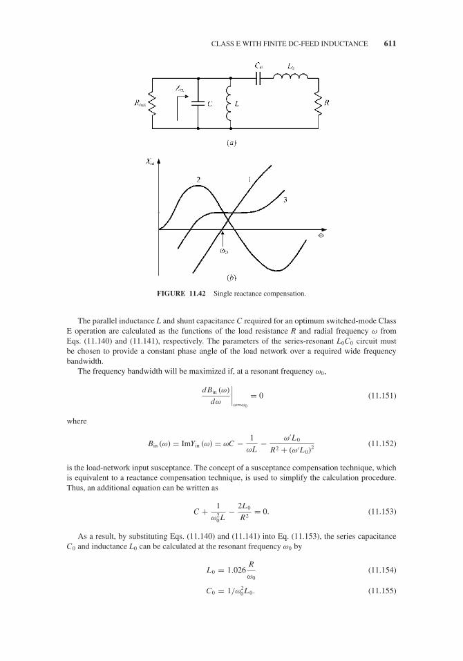
JWBS064-c11 JWBS064-Gerbennikov March 12, 2011 10:45 Printer Name: Yet to Come
CLASS E WITH FINITE DC-FEED INDUCTANCE 611
FIGURE 11.42 Single reactance compensation.
The parallel inductance L and shunt capacitance C required for an optimum switched-mode ClassE operation are calculated as the functions of the load resistance R and radial frequency ω fromEqs. (11.140) and (11.141), respectively. The parameters of the series-resonant L0C0 circuit mustbe chosen to provide a constant phase angle of the load network over a required wide frequencybandwidth.
The frequency bandwidth will be maximized if, at a resonant frequency ω0,
d Bin (ω)
dω
∣∣∣∣ω=ω0
= 0 (11.151)
where
Bin (ω) = ImYin (ω) = ωC − 1
ωL− ω′ L0
R2 + (ω′L0)2 (11.152)
is the load-network input susceptance. The concept of a susceptance compensation technique, whichis equivalent to a reactance compensation technique, is used to simplify the calculation procedure.Thus, an additional equation can be written as
C + 1
ω20 L
− 2L0
R2= 0. (11.153)
As a result, by substituting Eqs. (11.140) and (11.141) into Eq. (11.153), the series capacitanceC0 and inductance L0 can be calculated at the resonant frequency ω0 by
L0 = 1.026R
ω0(11.154)
C0 = 1/ω20 L0. (11.155)

JWBS064-c11 JWBS064-Gerbennikov March 12, 2011 10:45 Printer Name: Yet to Come
612 HIGH-EFFICIENCY POWER AMPLIFIERS
FIGURE 11.43 Double reactance compensation circuit.
Wider frequency bandwidth can be achieved using a double-resonant reactance compensationcircuit shown in Figure 11.43, where L0C0 and L1C1 are the series and parallel resonant cir-cuits, respectively. In this case, a system of the two additional equations can be used and solvedaccording to
d Bin (ω)
dω
∣∣∣∣ω=ω0
= d3 Bin (ω)
dω3
∣∣∣∣ω=ω0
= 0 (11.156)
as the second derivative cannot provide an appropriate analytical expression.To determine the load-network parameters for a double-resonant circuit reactance compensation
with the input load network susceptance Bin = ImY in given by
Bin (ω) = ωC − 1
ωL+ ω′ C1 R2
[1 − (ω′)2 L0C1
] − L0
R2[1 − (ω′)2 L0C1
]2 + (ω′L0)2(11.157)
it is necessary to solve simultaneously two following equations at a resonant frequency ω0,
C + 1
ω20 L
− 2C1 R2 − L0
R2= 0 (11.158)
1
ω20 L
+ C1 R2 − L0
R2− 8ω2
0 L0
[C2
1 +(C1 R2 − L0
) (L0 − 2C1 R2
)R4
]= 0. (11.159)
As a result, the parameters of the series and shunt resonant circuits with the corresponding loadedquality factors Q0 = ω0L0/R and Q1 = ω0C1R close to unity and greater – as a starting point forcircuit optimization – can be calculated from
L0 = R
ω0
2√5 − 1
C0 = 1
ω20 L0
(11.160)
C1 = L0
R2
3 − √5
2L1 = 1
ω20C1
. (11.161)
The circuit simulations for these two types of reactance compensation load networks were per-formed at a resonant frequency f 0 = 150 MHz for a standard load resistance R = 50 �. Figure 11.44shows the frequency dependencies of the load network phase angle φ for the single-reactance (curve 1)and double-reactance (curve 2) compensation circuits. It is apparent that the reactance-compensationtechnique provides very broadband operation conditions. Using just a single reactance load networkyields a significant widening of the operating frequency bandwidth with minimum deviations of themagnitude and phase of the load-network input impedance. A double-reactance compensation load
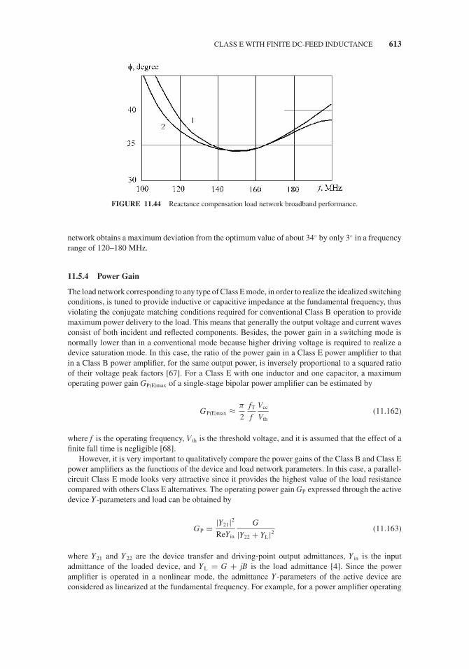
JWBS064-c11 JWBS064-Gerbennikov March 12, 2011 10:45 Printer Name: Yet to Come
CLASS E WITH FINITE DC-FEED INDUCTANCE 613
FIGURE 11.44 Reactance compensation load network broadband performance.
network obtains a maximum deviation from the optimum value of about 34◦ by only 3◦ in a frequencyrange of 120–180 MHz.
11.5.4 Power Gain
The load network corresponding to any type of Class E mode, in order to realize the idealized switchingconditions, is tuned to provide inductive or capacitive impedance at the fundamental frequency, thusviolating the conjugate matching conditions required for conventional Class B operation to providemaximum power delivery to the load. This means that generally the output voltage and current wavesconsist of both incident and reflected components. Besides, the power gain in a switching mode isnormally lower than in a conventional mode because higher driving voltage is required to realize adevice saturation mode. In this case, the ratio of the power gain in a Class E power amplifier to thatin a Class B power amplifier, for the same output power, is inversely proportional to a squared ratioof their voltage peak factors [67]. For a Class E with one inductor and one capacitor, a maximumoperating power gain GP(E)max of a single-stage bipolar power amplifier can be estimated by
GP(E)max ≈ π
2
fT
f
Vcc
Vth(11.162)
where f is the operating frequency, V th is the threshold voltage, and it is assumed that the effect of afinite fall time is negligible [68].
However, it is very important to qualitatively compare the power gains of the Class B and Class Epower amplifiers as the functions of the device and load network parameters. In this case, a parallel-circuit Class E mode looks very attractive since it provides the highest value of the load resistancecompared with others Class E alternatives. The operating power gain GP expressed through the activedevice Y-parameters and load can be obtained by
GP = |Y21|2ReYin
G
|Y22 + YL|2 (11.163)
where Y21 and Y22 are the device transfer and driving-point output admittances, Y in is the inputadmittance of the loaded device, and YL = G + jB is the load admittance [4]. Since the poweramplifier is operated in a nonlinear mode, the admittance Y-parameters of the active device areconsidered as linearized at the fundamental frequency. For example, for a power amplifier operating
JWBS064-c11 JWBS064-Gerbennikov March 12, 2011 10:45 Printer Name: Yet to Come
614 HIGH-EFFICIENCY POWER AMPLIFIERS
at the same conduction angle over various bias and drive conditions, these Y-parameters remainconstant and operating power gain becomes a function of only the load admittance.
Equation (11.163) can be rewritten as
GP = |Y21|2ReYin
R(1 + G22
G
)2
+(
B22 + B
G
)2 (11.164)
where G22 = ReY22, B22 = ImY22, and R = 1/G is the load resistance. Without significant loss ofaccuracy, the output conjugate-matching condition between imaginary parts of the device outputadmittance and the load admittance can be replaced by a simple condition of B22 + B = 0, whichmeans a resonance tuning of the load network including the device output susceptance B22. Also,normally the device output conductance G22 is significantly smaller than the load conductance Gfor both MOSFET and bipolar transistors, especially at frequencies well below the device transitionfrequency f T.
Consequently, the simplified ratio between the operating power gain GP(E) of a parallel-circuitClass E power amplifier and the operating power gain GP(B) of a conventional Class B power amplifierwith conjugate-matched load can be written by
GP(E)
GP(B)= 1
1 + (B22 + B)2 R2(E)
R(E)
R(B)(11.165)
where R(E) is the load resistance of a Class E power amplifier and R(B) is the load resistance of a ClassB power amplifier.
For an ideal optimum Class E operation mode with 100% collector efficiency, from Eqs. (11.128)and (11.139) it follows that
VR(E) = 1.652Vcc. (11.166)
For the same output power Pout and taking into account that VR(B) = Vcc in a conventional ClassB with zero saturation voltage, we can write
R(E)
R(B)= V 2
R(E)
V 2R(B)
= 2.729 (11.167)
that shows the significantly higher value for the load resistance in an optimum parallel-circuit ClassE operation mode.
As a result, the power gain ratio given by Eq. (11.165) can be rewritten in the form of
GP(E)
GP(B)= 2.729
1 + tan2φ= 1.865 (11.168)
where φ = 34.244◦ is the phase angle between the fundamental-frequency voltage and currentcomponents at the device output required for the optimum parallel-circuit Class E mode.
The result given by Eq. (11.168) means that, ideally, the operating power gain for a switched-modeparallel-circuit Class E mode compared to a conventional Class B mode is almost the same, and evenslightly greater despite the mistuning of the load network. This can be explained by the larger valueof the load resistance required for the optimum parallel-circuit Class E load network. For example,for a Class E with shunt capacitance, the operating power gain is smaller compared to a Class Bpower amplifier because its optimum Class E load resistance is about 2.4 times smaller than that ofa parallel-circuit Class E mode [69]. The idealized conditions for a switched-mode operation can

JWBS064-c11 JWBS064-Gerbennikov March 12, 2011 10:45 Printer Name: Yet to Come
CLASS E WITH QUARTERWAVE TRANSMISSION LINE 615
be achieved with instant on/off active device switching, which requires the rectangular input drivingsignal compared with sinusoidal driving signal for a conventional Class B mode. However, the powerlosses due to the finite switching time are sufficiently small and, for example, for switching time ofτ s = 0.35 or 20◦ are only of about 1% [59]. Consequently, a slight overdrive of the active device isneeded when the input power should be increased by 1–2 dB to minimize the switching time andmaximize the collector efficiency of a switched-mode parallel-circuit Class E power amplifier. As aresult, its resulting operating power gain becomes approximately equal to the operating power gainof a conventional Class B power amplifier.
11.6 CLASS E WITH QUARTERWAVE TRANSMISSION LINE
The ideal Class F load network with a quarterwave transmission line and a series L0C0 filter tunedto the fundamental frequency can provide a collector efficiency of 100% when the open-circuitconditions for odd-harmonic components and short-circuit conditions for even-harmonic componentsare realized. However, in practice, the idealized collector rectangular voltage and half-sinusoidalcurrent waveforms cannot be realized at sufficiently high frequencies when an effect of the deviceoutput shunt capacitance Cout and series output inductance Lout, which can generally include the leadand bondwire device inductances, is significant. In this case, the device is operated during a finite timeinterval in active region as a current source, and the required optimum conditions can be providedonly for the fundamental frequency and several higher order harmonic components. Fortunately, asit will be further demonstrated, the collector efficiency can be increased and effect of the outputcapacitance can be compensated with a proper value of this output series inductance realizing theswitching Class E operation conditions. The obvious advantage of such a load network shown inFigure 11.45 is a combination of the high-operating efficiency corresponding to a Class E mode andan even-harmonic suppression due to a quarterwave transmission line used in a Class F mode.
11.6.1 General Analysis and Optimum Circuit Parameters
Figure 11.46 shows a Class E load network consisting of a shunt capacitor C, a series inductor L,a quarterwave transmission line, a series reactance X, a series resonant L0C0 circuit tuned to thefundamental frequency, and a load resistor R. The bottom end of a quarterwave transmission line isconnected between a series inductor L and a series reactance X, while its top end is connected to adc power supply being RF grounded through the bypass capacitor [3]. In a common case, a shuntcapacitance C can represent the intrinsic device output capacitance and external circuit capacitanceadded by the load network. The series reactance X generally can be positive (inductance), negative(capacitance) or zero depending on the values of the shunt capacitance C and series inductance L. Theactive device is considered an ideal switch that is driven in such a way to provide the device switchingbetween its on- and off-state operation conditions. To simplify an analysis of a Class E power amplifier
FIGURE 11.45 Class F load network with parasitic shunt capacitance and bondwire inductance.

JWBS064-c11 JWBS064-Gerbennikov March 12, 2011 10:45 Printer Name: Yet to Come
616 HIGH-EFFICIENCY POWER AMPLIFIERS
FIGURE 11.46 Equivalent circuit of Class E power amplifier with quarterwave transmission line.
with a quarterwave transmission line, it needs to introduce the preliminary assumptions similar tothose for the Class E power amplifier with shunt capacitance. Assume that the losses in the reactivecircuit elements are negligible, duty cycle is 50%, and loaded quality factor of the series L0C0 circuitis sufficiently high. For a lossless operation mode, it is necessary to provide the optimum zero voltageand zero voltage-derivative conditions for voltage v(ωt) across the switch just prior to the start ofswitch given by Eqs. (11.75) and (11.76).
Let the output current flowing into the load be sinusoidal as
iR (ωt) = IR sin (ωt + ϕ) (11.169)
where ϕ is the initial phase shift due to the shunt capacitance and series inductance.When the switch is turned on for 0 ≤ ωt < π , the current flowing through the shunt capacitance
iC(ωt) = 0 and, consequently,
i (ωt) = iL (ωt) = iT (ωt) + iR (ωt) . (11.170)
When the switch is turned off for π ≤ ωt < 2π , there is no current flowing through the switchwhen i(ωt + π ) = 0, and the current flowing through the shunt capacitance C is
iC (ωt + π ) = iL (ωt + π) = iT (ωt + π ) + iR (ωt + π ) . (11.171)
To link up both Eqs. (11.170) and (11.171), each corresponding to one-half a period, it is necessaryto use a basic equation for the current flowing into the quarterwave transmission line given byEq. (11.50) as
iT (ωt) = iT (ωt + π ) (11.172)
which means that the period of a signal flowing into the quarterwave transmission line is equal to π
because it contains only even harmonics.

JWBS064-c11 JWBS064-Gerbennikov March 12, 2011 10:45 Printer Name: Yet to Come
CLASS E WITH QUARTERWAVE TRANSMISSION LINE 617
Then,
iL (ωt) = iT (ωt + π) + iR (ωt) = iL (ωt + π) + iR (ωt) − iR (ωt + π ) (11.173)
resulting in
iL (ωt) − iL (ωt + π ) = 2iR (ωt) . (11.174)
The current iL(ωt + π ) = iC(ωt + π ) can be expressed through the voltages vT(ωt + π ) and
vL (ωt + π ) = ωLdiL (ωt + π)
dωt(11.175)
as
iL (ωt + π ) = ωCdv (ωt + π )
dωt= ωC
d
dωt
[vT (ωt + π ) − ωL
diL (ωt + π )
dωt
]. (11.176)
Now we can use the equation for a voltage at the input of the quarterwave transmission linecorresponding to each of a period given by Eq. (11.49) as
vT (ωt) = 2Vcc − vT (ωt + π ) . (11.177)
Hence, when the switch is turned on resulting in vT(ωt) = vL(ωt),
vT (ωt + π ) = 2Vcc − ωLdiL (ωt)
dωt. (11.178)
Substituting Eq. (11.178) into Eq. (11.176) and using Eqs. (11.179) and (11.174) yield a second-order nonhomogeneous differential equation corresponding to half a period of π ≤ ωt < 2π wheniL(ωt + π ) = iC(ωt + π ) in the form of
d2iC (ωt + π )
d (ωt)2 + q2
2iC (ωt + π ) − IRsin (ωt + ϕ) = 0 (11.179)
or
d2iC (ωt)
d (ωt)2 + q2
2iC (ωt) + IRsin (ωt + ϕ) = 0 (11.180)
where
q = 1
ω√
LC. (11.181)
The general solution of Eq. (11.180) in the normalized form can be written by
iC (ωt)
IR= C1cos
(qωt√
2
)+ C2sin
(qωt√
2
)+ 2
2 − q2sin (ωt + ϕ) (11.182)
where the coefficients C1 and C2 are determined from the initial off-state conditions.The first initial condition is obtained from Eq. (11.174) as
iC (ωt)|ωt=π = 2iR (π ) (11.183)
taking into account that iL(π ) = iC(π ) and iL(2π ) = iC(2π ) = 0.

JWBS064-c11 JWBS064-Gerbennikov March 12, 2011 10:45 Printer Name: Yet to Come
618 HIGH-EFFICIENCY POWER AMPLIFIERS
To obtain a second initial condition, let us substitute Eq. (11.175) in Eq. (11.178) and useEq. (11.174). As a result,
ωLdiL (ωt + π)
dωt= 2Vcc − ωL
diL (ωt)
dωt= 2Vcc − ωL
diL (ωt + π )
dωt− 2ωL
diR (ωt)
dωt. (11.184)
Then, by taking into account that iL(π) = iC(π ), we can write
diC (ωt)
dωt
∣∣∣∣ωt=π
= Vcc
ωL− IR cos ϕ. (11.185)
As a result, applying the initial conditions given by Eqs. (11.183) and (11.185) to Eq. (11.182)yields
C1 = −√
2
qpsin
(qπ√
2
)− q
√2
2 − q2sin
(qπ√
2
)cosϕ − 2
1 − q2
2 − q2cos
(qπ√
2
)sinϕ (11.186)
C2 =√
2
qpcos
(qπ√
2
)+ q
√2
2 − q2cos
(qπ√
2
)cosϕ − 2
1 − q2
2 − q2sin
(qπ√
2
)sinϕ (11.187)
where
p = ωL IR
Vcc. (11.188)
The dc supply current I0 can be written using the Fourier formula and Eqs. (11.171) and (11.172)by
I0 = 1
2π
2π∫0
iT (ωt) dωt = 1
π
π∫0
iT (ωt + π) dωt = 1
π
π∫0
[iC (ωt + π ) − iR (ωt + π )] dωt .
(11.189)
Then, substituting Eqs. (11.169) and (11.182) into Eq. (11.189) results in
I0 = IR
π
{C1
√2
q
[sin
(qπ
√2)
− sin
(qπ√
2
)]−C2
√2
q
[cos
(qπ
√2)
− cos
(qπ√
2
)]− 2q2
2 − q2cos ϕ
}.
(11.190)
The voltage v(ωt) across the switch is produced by charging of the shunt capacitor C by the currentgiven by Eq. (11.182) according to
v (ωt) = 1
ωC
ωt∫π
iC (ωt) dωt = IR
√2
qωC
{C1
[sin
(qωt√
2
)− sin
(qπ√
2
)]
− C2
[cos
(qωt√
2
)− cos
(qπ√
2
)]− q
√2
2 − q2[cos (ωt + ϕ) + cos ϕ]
}. (11.191)
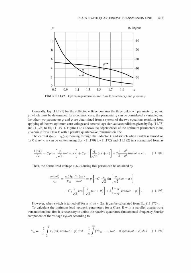
JWBS064-c11 JWBS064-Gerbennikov March 12, 2011 10:45 Printer Name: Yet to Come
CLASS E WITH QUARTERWAVE TRANSMISSION LINE 619
FIGURE 11.47 Optimum quarterwave-line Class E parameters p and ϕ versus q.
Generally, Eq. (11.191) for the collector voltage contains the three unknown parameter q, p, andϕ, which must be determined. In a common case, the parameter q can be considered a variable, andthe other two parameters p and ϕ are determined from a system of the two equations resulting fromapplying of the two optimum zero voltage and zero voltage-derivative conditions given by Eq. (11.75)and (11.76) to Eq. (11.191). Figure 11.47 shows the dependences of the optimum parameters p andϕ versus q for a Class E with a parallel quarterwave transmission line.
The current i(ωt) = iL(ωt) flowing through the inductor L and switch when switch is turned onfor 0 ≤ ωt < π can be written using Eqs. (11.170) to (11.172) and (11.182) in a normalized form as
i (ωt)
IR= C1cos
[q√2
(ωt + π )
]+ C2sin
[q√2
(ωt + π )
]+ 2
1 − q2
2 − q2sin (ωt + ϕ) . (11.192)
Then, the normalized voltage vT(ωt) during this period can be obtained by
vT (ωt)
Vcc= ωL IR
Vcc
diL (ωt)
dωt= p
{−C1
q√2
sin
[q√2
(ωt + π )
]
+ C2q√2
cos[
q√2
(ωt + π)]
+ 21 − q2
2 − q2cos (ωt + ϕ)
}. (11.193)
However, when switch is turned off for π ≤ ωt < 2π , it can be calculated from Eq. (11.177).To calculate the optimum load network parameters for a Class E with a parallel quarterwave
transmission line, first it is necessary to define the reactive quadrature fundamental-frequency Fouriercomponent of the voltage vT(ωt) according to
VX = − 1
π
π∫0
vT (ωt) cos (ωt + ϕ) dωt − 1
π
2π∫π
[2Vcc − vT (ωt − π )] cos (ωt + ϕ) dωt. (11.194)

JWBS064-c11 JWBS064-Gerbennikov March 12, 2011 10:45 Printer Name: Yet to Come
620 HIGH-EFFICIENCY POWER AMPLIFIERS
FIGURE 11.48 Equivalent quarterwave-line Class E load network at fundamental frequency.
Then, the two active and reactive quadrature fundamental-frequency Fourier components of thecollector voltage v(ωt) are defined from
VR = − 1
π
2π∫0
v(ωt) sin (ωt + ϕ) dωt (11.195)
VL+X = − 1
π
2π∫0
v(ωt) cos (ωt + ϕ) dωt. (11.196)
Finally, as it follows from Figure 11.48, the optimum normalized series reactance X, seriesinductance L, and shunt capacitance C can be calculated from
X
R= VX
VR(11.197)
ωL
R= VL+X
VR− X
R(11.198)
ωCR = 1
q2ωL
R
. (11.199)
By taking into account that R = V 2R/2Pout, the optimum load resistance R for the specified values
of a supply voltage Vcc and an output power Pout delivered to the load can be obtained by
R = 1
2
(VR
Vcc
)2 V 2cc
Pout(11.200)
or, using Eq. (11.188), by
R = 1
2
( p
l
)2 V 2cc
Pout(11.201)
where l = ωL/R.The dependences of the normalized optimum series inductance ωL/R and series reactance X/R
are shown in Figure 11.49(a), while the dependences of the normalized optimum shunt capacitanceωCR and load resistance RPout/V 2
cc are plotted in Figure 11.49(b). Here, we can see that the greatervalues of the normalized series inductance ωL/R can be achieved for the lower values of q. Tocompensate for such an increased inductive value, the reactance X should have a negative capacitive

JWBS064-c11 JWBS064-Gerbennikov March 12, 2011 10:45 Printer Name: Yet to Come
CLASS E WITH QUARTERWAVE TRANSMISSION LINE 621
FIGURE 11.49 Normalized optimum quarterwave-line Class E load network parameters.
value. Generally, the value of the series reactance X changes its sign from negative to positive, whichmeans that the capacitive reactance is followed by the inductive reactance, and it is required to addan additional inductance at higher values of q. As a result, there is special case of a load network withX = 0 when there is no need for additional phase compensation. The variations of normalized valuesof ωCR and RPout/V 2
cc versus q are not so significant.Figure 11.50 shows the circuit schematics of the Class E power amplifiers with a parallel quar-
terwave transmission lines corresponding to the different values of the optimum parameter q. Theinclusion of a series capacitance Cx is necessary to compensate for the excessive inductive reactanceat the fundamental frequency when the series reactance X is negative, as shown in Figure 11.50(a).
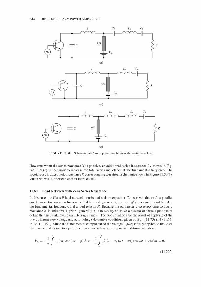
JWBS064-c11 JWBS064-Gerbennikov March 12, 2011 10:45 Printer Name: Yet to Come
622 HIGH-EFFICIENCY POWER AMPLIFIERS
FIGURE 11.50 Schematic of Class E power amplifiers with quarterwave line.
However, when the series reactance X is positive, an additional series inductance LX shown in Fig-ure 11.50(c) is necessary to increase the total series inductance at the fundamental frequency. Thespecial case is a zero series reactance X corresponding to a circuit schematic shown in Figure 11.50(b),which we will further consider in more detail.
11.6.2 Load Network with Zero Series Reactance
In this case, the Class E load network consists of a shunt capacitor C, a series inductor L, a parallelquarterwave transmission line connected to a voltage supply, a series L0C0 resonant circuit tuned tothe fundamental frequency, and a load resistor R. Because the parameter q corresponding to a zeroreactance X is unknown a priori, generally it is necessary to solve a system of three equations todefine the three unknown parameters q, p, and ϕ. The two equations are the result of applying of thetwo optimum zero voltage and zero voltage-derivative conditions given by Eqs. (11.75) and (11.76)to Eq. (11.191). Since the fundamental component of the voltage vT(ωt) is fully applied to the load,this means that its reactive part must have zero value resulting in an additional equation
VX = − 1
π
π∫0
vT (ωt) cos (ωt + ϕ) dωt − 1
π
2π∫π
[2Vcc − vT (ωt − π )] cos (ωt + ϕ) dωt = 0.
(11.202)
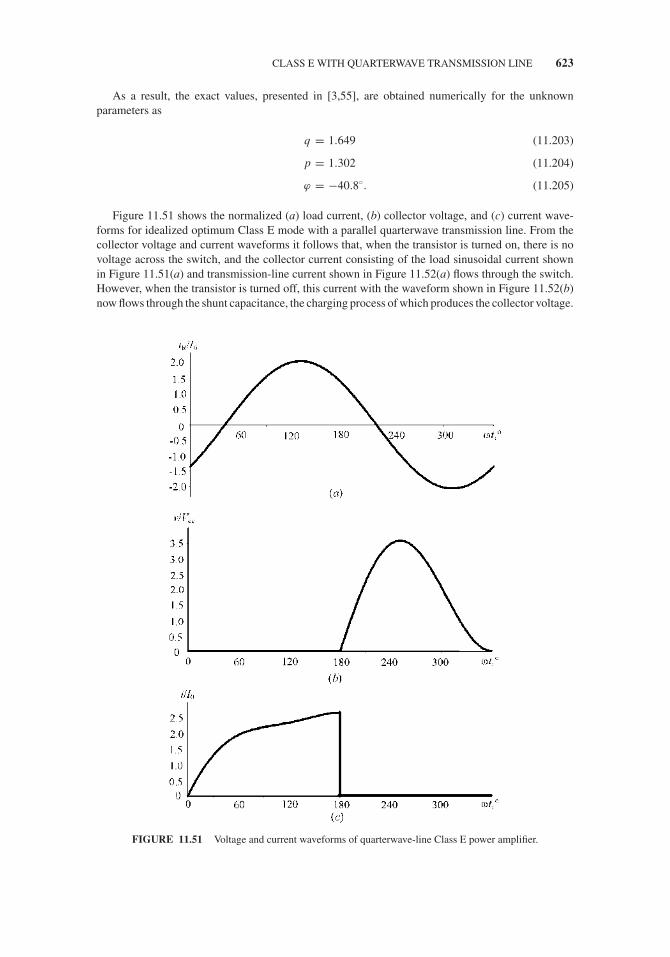
JWBS064-c11 JWBS064-Gerbennikov March 12, 2011 10:45 Printer Name: Yet to Come
CLASS E WITH QUARTERWAVE TRANSMISSION LINE 623
As a result, the exact values, presented in [3,55], are obtained numerically for the unknownparameters as
q = 1.649 (11.203)
p = 1.302 (11.204)
ϕ = −40.8◦. (11.205)
Figure 11.51 shows the normalized (a) load current, (b) collector voltage, and (c) current wave-forms for idealized optimum Class E mode with a parallel quarterwave transmission line. From thecollector voltage and current waveforms it follows that, when the transistor is turned on, there is novoltage across the switch, and the collector current consisting of the load sinusoidal current shownin Figure 11.51(a) and transmission-line current shown in Figure 11.52(a) flows through the switch.However, when the transistor is turned off, this current with the waveform shown in Figure 11.52(b)now flows through the shunt capacitance, the charging process of which produces the collector voltage.
FIGURE 11.51 Voltage and current waveforms of quarterwave-line Class E power amplifier.
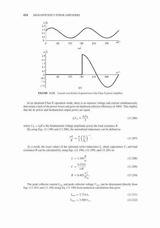
JWBS064-c11 JWBS064-Gerbennikov March 12, 2011 10:45 Printer Name: Yet to Come
624 HIGH-EFFICIENCY POWER AMPLIFIERS
FIGURE 11.52 Current waveforms of quarterwave-line Class E power amplifier.
In an idealized Class E operation mode, there is no nonzero voltage and current simultaneouslythat means a lack of the power losses and gives an idealized collector efficiency of 100%. This impliesthat the dc power and fundamental output power are equal,
I0Vcc = IRVR
2(11.206)
where VR = IRR is the fundamental voltage amplitude across the load resistance R.By using Eqs. (11.188) and (11.206), the normalized inductance can be defined as
ωL
R= p
2
(I0
IR
)−1
. (11.207)
As a result, the exact values of the optimum series inductance L, shunt capacitance C, and loadresistance R can be calculated by using Eqs. (11.190), (11.199), and (11.201) as
L = 1.349R
ω(11.208)
C = 0.2725
ωR(11.209)
R = 0.465V 2
cc
Pout. (11.210)
The peak collector current Imax and peak collector voltage Vmax can be determined directly fromEqs. (11.191) and (11.192) using Eq. (11.190) from numerical calculations that gives
Imax = 2.714 I0 (11.211)
Vmax = 3.589 Vcc. (11.212)

JWBS064-c11 JWBS064-Gerbennikov March 12, 2011 10:45 Printer Name: Yet to Come
CLASS E WITH QUARTERWAVE TRANSMISSION LINE 625
TABLE 11.3 Optimum Impedances at Fundamental and Harmonics for Different Class E LoadNetworks.
Class E load networkf 0
(Fundamental)2nf 0
(Even Harmonics)(2n + 1)f 0
(Odd Harmonics)
Class E with shuntcapacitance
C
L
R C C
Class E with parallelcircuit
C L R C L C L
Class E withquarterwavetransmission line
C
L
RC L
C
Using Eqs. (11.209) and (11.210) with C = Cout, where Cout is the device output capacitance,gives the value of a maximum operation frequency f max of
fmax = 0.093Pout
CoutV 2cc
(11.213)
which is 1.63 times higher than the maximum operation frequency for an optimum Class E modewith shunt capacitance [60].
In Table 11.3, the optimum impedances seen by the device collector at the fundamental-frequencyand higher order harmonic components are illustrated by the appropriate circuit configurations. It canbe seen that Class E mode with a quarterwave transmission line shows different impedance propertiesat even and odd harmonics. At odd harmonics, the optimum impedances can be established by the shuntcapacitance that is required for all harmonic components in Class E with a shunt capacitance At evenharmonics, the optimum impedances are realized by using a parallel LC circuit that is required for allharmonic components in Class E with a parallel circuit, which is a subclass of a Class E with finite dc-feed inductance. Thus, the frequency properties of a grounded parallel quarterwave transmission linewith its open-circuit conditions at odd harmonics and short-circuit conditions at even harmonics enableClass E with a quarterwave transmission line to combine simultaneously the harmonic impedanceconditions typical for both Class E with a shunt capacitance and Class E with a parallel circuit.
11.6.3 Matching Circuits with Lumped and Distributed Parameters
The theoretical results obtained for the Class E power amplifier with a quarterwave transmission lineshow that it is enough to use a very simple load network to realize the optimum impedance conditionseven for four harmonics. As follows from Figure 11.52(a), the current flowing into the quarterwavetransmission line is very close to the sinusoidal second-harmonic current, which means that the level offourth-order and higher order harmonic components is negligible because of the significant shuntingeffect of the capacitance C. In this case, as the shunt capacitor C and series inductor L both provide

JWBS064-c11 JWBS064-Gerbennikov March 12, 2011 10:45 Printer Name: Yet to Come
626 HIGH-EFFICIENCY POWER AMPLIFIERS
FIGURE 11.53 Schematic of quarterwave-line Class E power amplifier with lumped matching circuit.
optimum inductive impedance at the fundamental frequency and the quarterwave transmission linerealizes the shorting of even harmonics, it is only required to provide an open-circuit condition at thethird-harmonic component. Consequently, when the ideal series L0C0 circuit is replaced by the outputmatching circuit, the optimum impedance conditions for Class E load network with a quarterwavetransmission line can be practically fully realized by simply providing an open-circuit condition atthe third-harmonic component.
Figure 11.53 shows the circuit schematic of a lumped Class E power amplifier with a parallelquarterwave transmission line, where the parallel resonant L1C1 circuit is tuned to the third-harmoniccomponent and Cb represents the blocking or bypass capacitor. Since the reactance of the parallelthird-harmonic tank circuit is inductive at the fundamental, it is enough to use the shunt capacitance C2
composing the L-type low-pass matching circuit to provide the required impedance matching of theoptimum Class E load resistance R with the standard load impedance of RL = 50 �. In this case, it isassumed that R < RL, which is normally the case for the high-power or low-voltage power amplifiers.
To calculate the parameters of the matching-circuit elements, it is convenient to consider theloaded quality factor QL = ωC2RL, which can also be expressed through the resistances R and RL as
QL =√(
RL
R
)− 1. (11.214)
As a result, the matching circuit parameters can be calculated at the radial fundamental frequencyω0 from
C2 = QL
ω0 RL(11.215)
L1 = 8
9
QL R
ω0(11.216)
C1 = 1
9ω20 L1
. (11.217)
At microwaves, the series lumped inductor L can be replaced by the short-length series transmissionline. In this case, when the shunt capacitance C represents a fully internal active device output

JWBS064-c11 JWBS064-Gerbennikov March 12, 2011 10:45 Printer Name: Yet to Come
CLASS E WITH QUARTERWAVE TRANSMISSION LINE 627
FIGURE 11.54 Schematic of transmission-line Class E power amplifier.
capacitance, the bondwire and lead inductances can be taken into account because they provide aninductive reactance and make the series transmission line shorter. Figure 11.54 shows the circuitschematic of a transmission-line Class E power amplifier with a parallel quarterwave transmissionline. The output matching circuit represents the L-type low-pass matching circuit consisting of a seriestransmission line with a short electrical length θ1, which provides an inductive reactance, and a shuntopen-circuit stub with an electrical length θ 2 of less than 90◦, which provides a capacitive reactance.
Usually, the characteristic impedance Z0 of a transmission line (in most practical cases equal to50 �) is much higher than the required optimum Class E load network resistance R. Consequently,the input impedance Zin of the loaded series transmission line with the characteristic impedanceZ0 and electrical length θ0 under the condition of (R/Z0)tanθ0 � 1 when the electrical length of atransmission line is less than 45◦ at the fundamental is determined by
Z in = Z0R + jZ0 tan θ0
Z0 + jR tan θ0= Z0
R
Z0+ j tan θ0
1 + jR
Z0tan θ0
∼= R + jZ0 tan θ0. (11.218)
As a result, the required optimum value of θ0 for Class E mode with a quarterwave transmissionline using Eqs. (11.208) and (11.218) can be obtained from
θ0 = tan−1
(1.349
R
Z0
). (11.219)
The output matching circuit is necessary to match the required optimum Class E resistance Rcalculated in accordance with Eq. (11.210) to a standard load resistance of 50 �. In addition, it isrequired to provide an open-circuit condition at the third-harmonic component. This can be easily doneusing the output matching topology in the form of an L-type transformer with the series transmissionline and open-circuit stub. In this case, the electrical lengths of the series transmission line andopen-circuit stub should be chosen to be 30◦ each. The load impedance ZL seen by a quarterwavetransmission line can be written by
ZL = Z1RL
(Z2 − Z1 tan2 θ
) + jZ1 Z2 tan θ
Z1 Z2 + j (Z1 + Z2) RL tan θ(11.220)

JWBS064-c11 JWBS064-Gerbennikov March 12, 2011 10:45 Printer Name: Yet to Come
628 HIGH-EFFICIENCY POWER AMPLIFIERS
where Z1 and θ 1 are the characteristic impedance and electrical length of the series transmission line,and Z2 and θ2 are the characteristic impedance and electrical length of the open-circuit stub, and θ =θ1 = θ2 = 30◦.
Hence, the complex-conjugate matching with the load can be provided by proper choice of thecharacteristic impedances Z1 and Z2. Separating Eq. (11.220) into real and imaginary parts and takinginto account that ReZL = R and ImZL = 0, the following system of two equations with two unknownparameters is obtained:
Z 21 Z 2
2 − R2L (Z1 + Z2)
(Z2 − Z1 tan2 θ
) = 0 (11.221)
(Z1 + Z2)2 R2L R tan2 θ − Z 2
1 Z 22
[RL
(1 + tan2 θ
) − R] = 0 (11.222)
which enables the characteristic impedances Z1 and Z2 to be properly calculated.This system of two equations can be explicitly solved as a function of the parameter r = RL/R
resulting in
Z1
RL=
√4r − 3
r(11.223)
Z1
Z2= 3
(r − 1
r
). (11.224)
Consequently, for the specified value of the parameter r with the required Class E optimumload resistance R and standard load RL = 50 �, the characteristic impedance Z1 is calculated fromEq. (11.223) and then the characteristic impedance Z2 is calculated from Eq. (11.224). For example, ifthe required Class E optimum load resistance R is equal to 12.5 � resulting in r = 4, the characteristicimpedance of the series transmission line Z1 is equal to 45 � and the characteristic impedance of theopen-circuit stub Z2 is equal to 20 �.
Unlike the transmission-line Class E load network approximations with two-harmonic control[43] and with three-harmonic control [44], the Class E load network with a quarterwave transmissionline, which can provide the optimum impedance conditions for at least four-harmonic components, isvery simple in circuit implementation and does not require an additional lumped RF choke element. Inaddition, there is no need to use the special computer simulation tools which are generally required tocalculate the parameters of the Class E transmission-line load-network topologies, since all parametersof the Class E load network with a quarterwave transmission line and the output matching circuitparameters are easily calculated explicitly from simple analytical equations. Besides, such a Class Eload network with a quarterwave transmission line is very useful in practical design by providing asignificant higher order harmonic suppression.
11.7 CLASS FE
In practice, the idealized collector voltage and current waveforms corresponding to Class F mode canbe realized at sufficiently low frequencies when effect of the device collector capacitance is negligible.At higher frequencies, the effect of the collector capacitance contributes to a finite switching timeresulting in the time periods when the collector voltage and collector current exist at the same time,that is, simultaneously v > 0 and i > 0. As a result, such a load network with shunt capacitance cannotprovide the switched-mode operation with an instantaneous transition from the device pinch-off tosaturation mode. Therefore, during a finite time interval the device operates in active region as anonlinear current source with the reverse-biased collector–base junction and the collector current isprovided by this current source.
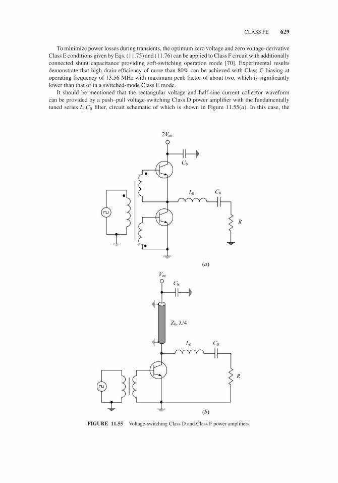
JWBS064-c11 JWBS064-Gerbennikov March 12, 2011 10:45 Printer Name: Yet to Come
CLASS FE 629
To minimize power losses during transients, the optimum zero voltage and zero voltage-derivativeClass E conditions given by Eqs. (11.75) and (11.76) can be applied to Class F circuit with additionallyconnected shunt capacitance providing soft-switching operation mode [70]. Experimental resultsdemonstrate that high drain efficiency of more than 80% can be achieved with Class C biasing atoperating frequency of 13.56 MHz with maximum peak factor of about two, which is significantlylower than that of in a switched-mode Class E mode.
It should be mentioned that the rectangular voltage and half-sine current collector waveformcan be provided by a push–pull voltage-switching Class D power amplifier with the fundamentallytuned series L0C0 filter, circuit schematic of which is shown in Figure 11.55(a). In this case, the
FIGURE 11.55 Voltage-switching Class D and Class F power amplifiers.

JWBS064-c11 JWBS064-Gerbennikov March 12, 2011 10:45 Printer Name: Yet to Come
630 HIGH-EFFICIENCY POWER AMPLIFIERS
bipolar transistors must be driven in such a way as to provide an alternate voltage switching betweenthe on- and off-state modes. However, in a single-ended power amplifier with a parallel quarterwavetransmission line shown in Figure 11.55(b), the symmetrizing action of the transmission-line behaviorcan easily provide a function of the voltage inverter resulting in the same collector waveforms withvoltage peak factor of two. In this case, the quarterwave line stores the voltage waveform in atraveling wave along its length, which returns delayed by one-half fundamental period and inverted,because of power-reflection condition at the short-circuit termination. However, the presence ofparasitic collector capacitances degrades the performances of both power amplifiers due to finitetime of the charging and discharging processes. As a result, the frequency limitations of both poweramplifiers are provided by the device parasitic collector shunt capacitances, resulting in the increasedswitching transition times due to the capacitor charging and discharging processes, and the fact thattransistor switches charge and discharge the shunt capacitance, dissipating power in the charging anddischarging processes.
A possible way to eliminate these power losses and to extend the voltage-switching class D modeto higher frequencies is to introduce a dead time during the period when one device has already turnedoff but the other has not turned on yet, and the inductive load network is used to charge and dischargethe shunt capacitances. This can be done by introducing the Class E switching conditions when theswitching loss during off-to-on transition is reduced to zero by the operating requirements of zerovoltage at zero voltage slope at the end of period. Since the shunt capacitor must be discharged atthat time instant, an additional series inductor L with optimum value should be included into the loadnetwork, as shown in Figure 11.56(a). As a result, the switching current and voltage waveforms havethe characteristics of both Class D and Class E operation modes, and such an operation mode is calledClass DE. Such a Class DE power amplifier was firstly described by Zhukov and Kozyrev and hasfound some particular applications due to its high operation efficiency at higher operating frequenciesfor driving signals with duty cycles D < 0.5 [3,71]. Similarly, a quarterwave transmission line can beused as a voltage inverter resulting in a single-ended Class FE (or Class EF) power amplifier, whichcombines a class F operating mode with Class E switching conditions.
The optimum parameters of a Class FE power amplifier can be determined based on its steady-state collector voltage and current waveforms [72]. Figure 11.57 shows the two equivalent ClassFE switching circuits that occur during a switching cycle, the load network of which consists of agrounded parallel quarterwave transmission line, a shunt capacitance C, a series inductor L, a seriesfundamentally tuned L0C0 circuit, and a load resistor R. An active device is considered an ideal switchthat is driven in such a way as to provide the device switching between its on- and off-state operationconditions.
To simplify the analysis of a Class FE power amplifier, the following assumptions are introduced:
� The transistor has zero saturation voltage, zero saturation resistance, infinite off-resistance, andits switching is instantaneous and lossless.
� The shunt capacitance is assumed to be linear.� The loaded quality factor QL = ωL0/R = 1/ωC0R of the series resonant L0C0 circuit tuned to the
fundamental frequency is high enough for the output current to be sinusoidal at the switchingfrequency.
� There are no losses in the circuit except only into the load R.
The Class E switching conditions for the transistor switch can be written as
v (ωt)|ωt=2π = 0 (11.225)
dv (ωt)
dωt
∣∣∣∣ωt=2π
= 0 (11.226)
where v is the voltage across the switch.

JWBS064-c11 JWBS064-Gerbennikov March 12, 2011 10:45 Printer Name: Yet to Come
CLASS FE 631
FIGURE 11.56 Voltage-switching Class DE and Class FE power amplifiers.
Let the output current flowing through the load be written as sinusoidal,
iR(ωt) = IR sin (ωt + ϕ) (11.227)
where IR is the current amplitude and ϕ is the initial phase shift.The basic Kirchhoff equations characterizing the electrical behavior of the equivalent circuits of
a Class FE power amplifier are
i (ωt) + iC (ωt) = iT (ωt) + iR (ωt) (11.228)
iC(ωt) = ωCdv (ωt)
dωt. (11.229)
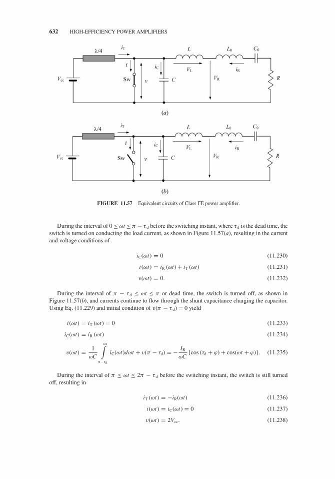
JWBS064-c11 JWBS064-Gerbennikov March 12, 2011 10:45 Printer Name: Yet to Come
632 HIGH-EFFICIENCY POWER AMPLIFIERS
FIGURE 11.57 Equivalent circuits of Class FE power amplifier.
During the interval of 0 ≤ ωt ≤ π − τ d before the switching instant, where τ d is the dead time, theswitch is turned on conducting the load current, as shown in Figure 11.57(a), resulting in the currentand voltage conditions of
iC(ωt) = 0 (11.230)
i (ωt) = iR (ωt) + iT (ωt) (11.231)
v(ωt) = 0. (11.232)
During the interval of π − τ d ≤ ωt ≤ π or dead time, the switch is turned off, as shown inFigure 11.57(b), and currents continue to flow through the shunt capacitance charging the capacitor.Using Eq. (11.229) and initial condition of v(π − τ d) = 0 yield
i (ωt) = iT (ωt) = 0 (11.233)
iC(ωt) = iR (ωt) (11.234)
v(ωt) = 1
ωC
ωt∫π−τd
iC(ωt)dωt + v(π − τd) = − IR
ωC[cos (τd + ϕ) + cos(ωt + ϕ)] . (11.235)
During the interval of π ≤ ωt ≤ 2π − τ d before the switching instant, the switch is still turnedoff, resulting in
iT (ωt) = −iR(ωt) (11.236)
i(ωt) = iC(ωt) = 0 (11.237)
v(ωt) = 2Vcc. (11.238)

JWBS064-c11 JWBS064-Gerbennikov March 12, 2011 10:45 Printer Name: Yet to Come
CLASS FE 633
During the interval of 2π − τ d ≤ ωt ≤ 2π or dead time, the switch is turned off, and currents flowthrough the shunt capacitance discharging the capacitor. Using Eq. (11.229) and initial condition ofv(2π − τ d) = 2Vcc yield
i(ωt) = iT (ωt) = 0 (11.239)
iC(ωt) = iR (ωt) (11.240)
v(ωt) = 1
ωC
ωt∫2π−τd
iC(ωt)dωt + v(2π − τd) = IR
ωC(cos τd − cos ωt) + 2Vcc. (11.241)
Equation (11.240) can also be written in a differential form using Eqs. (11.237) and (11.239) as
dv(ωt)
dωt= IR
ωCsin (ωt + ϕ) . (11.242)
Applying the switching condition given in Eq. (11.236) to Eq. (11.242) results in
sin (2π + ϕ) = 0 (11.243)
from which it follows that the initial phase ϕ can be set to zero,
ϕ = 0. (11.244)
Figure 11.58 shows the ideal current and voltage waveforms of a Class FE power amplifier inan idealized optimum operation mode during the whole interval 0 ≤ ωt ≤ 2π corresponding toits equivalent circuits shown in Figure 11.57. The quarterwave transmission line has a half-wavesymmetry, which means that the line attempts to do the same work in the first and second halves ofthe cycle. Therefore, the transmission-line half-repeating current must necessarily instantaneouslyfall to zero at π − τ d and 2π − τ d, being zero during both collector voltage edges. Note that, for thesinusoidal driving signals, the transistor must be biased in Class C mode to provide duty cycle D lessthan 50% (D < 0.5) because the period of time when the device is turned off must exceed the periodof time when the device is turned on.
From the boundary condition v(π ) = 2Vcc or v(2π ) = 0 by using the corresponding Eq. (11.235)or (11.241), we can write
ωCVcc
IR= 1 − cos τd
2. (11.245)
The fundamental-frequency component of the voltage v(ωt) across the switch can be representedby the two quadrature components as shown in Figure 11.57, the amplitudes of which can be foundusing Fourier formulas by
VR = − 1
π
2π∫0
v (ωt) sinωtdωt = 2 (1 + cos τd)
πVcc = IR R (11.246)
VL = − 1
π
2π∫0
v (ωt) cosωtdωt = τd − sinτd cos τd
π
IR
ωC. (11.247)
In an idealized Class FE operation mode, there is no nonzero voltage and current simultaneouslythat gives an idealized collector efficiency of 100% when the dc power P0 and fundamental output
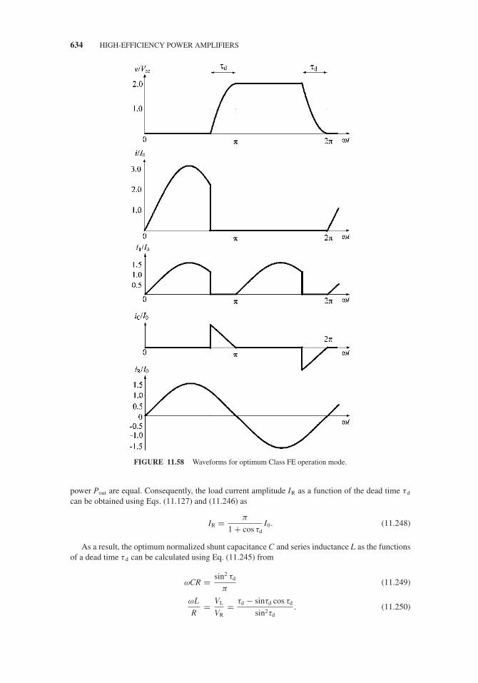
JWBS064-c11 JWBS064-Gerbennikov March 12, 2011 10:45 Printer Name: Yet to Come
634 HIGH-EFFICIENCY POWER AMPLIFIERS
FIGURE 11.58 Waveforms for optimum Class FE operation mode.
power Pout are equal. Consequently, the load current amplitude IR as a function of the dead time τ d
can be obtained using Eqs. (11.127) and (11.246) as
IR = π
1 + cos τdI0. (11.248)
As a result, the optimum normalized shunt capacitance C and series inductance L as the functionsof a dead time τ d can be calculated using Eq. (11.245) from
ωCR = sin2 τd
π(11.249)
ωL
R= VL
VR= τd − sinτd cos τd
sin2τd. (11.250)

JWBS064-c11 JWBS064-Gerbennikov March 12, 2011 10:45 Printer Name: Yet to Come
CLASS FE 635
The optimum load resistance R can be obtained using Eq. (11.246) for the constant dc supplyvoltage Vcc and fundamental-frequency output power Pout delivered to the load as
R = 1
2
V 2R
Pout= 2 (1 + cosτd)2
π 2
V 2cc
Pout. (11.251)
The maximum fundamental-frequency output power Pout delivered to the load as the functions ofthe dead time τ d and capacitance C can be obtained from Eqs. (11.249) and (11.251) for the supplyvoltage Vcc as
Pout = 2
π
(1 + cosτd
sin τd
)2
ωCV 2cc. (11.252)
The maximum operating frequency f max in an optimum Class FE mode is limited by the deviceoutput (collector or drain–source) capacitance Cout. From Eq. (11.252) it follows that
fmax = 0.25
(sin τd
1 + cosτd
)2 Pout
CoutV 2cc
. (11.253)
Figure 11.59 shows the dependence of the normalized maximum operating frequency(fmaxCoutV 2
cc
)/Pout on the dead time τ d. From Eq. (11.253) and Figure 11.59, it follows that the
maximum operating frequency increases with smaller dead times, and, for a τ d = 45◦,
fmax = 0.043Pout
CoutV 2cc
(11.254)
which is the same as for a Class DE and close to the maximum operating frequency of a Class Ewith 50% duty cycle [60]. However, for a saturation period of π − τ d = (180 − 45)◦ = 135◦ whenthe transistor is turned on, the maximum operating frequency f max of a Class E power amplifier ismore than three times greater [30,73]. At the same time, for a saturation period of 135◦, the collectorvoltage peak of a Class E power amplifier is three times larger than the applied supply voltage Vcc [74].
FIGURE 11.59 Normalized maximum operating frequency versus dead time.
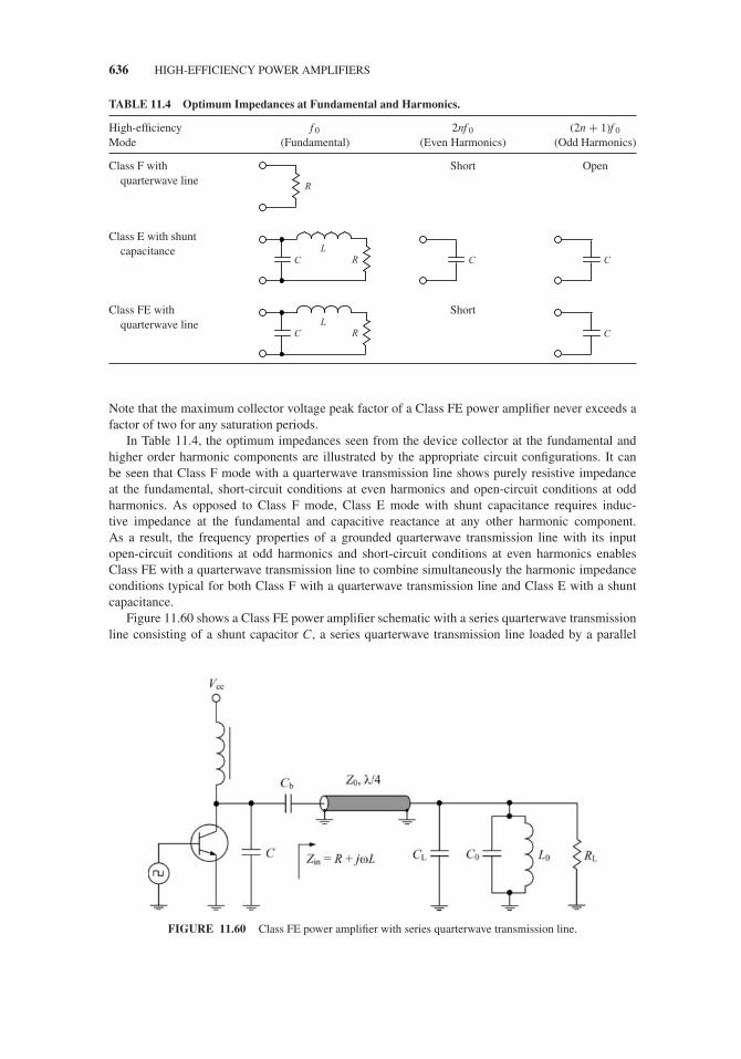
JWBS064-c11 JWBS064-Gerbennikov March 12, 2011 10:45 Printer Name: Yet to Come
636 HIGH-EFFICIENCY POWER AMPLIFIERS
TABLE 11.4 Optimum Impedances at Fundamental and Harmonics.
High-efficiencyMode
f 0
(Fundamental)2nf 0
(Even Harmonics)(2n + 1)f 0
(Odd Harmonics)
Class F withquarterwave line
Short Open
R
Class E with shuntcapacitance
CL
R C C
Class FE withquarterwave line
Short
CL
R C
Note that the maximum collector voltage peak factor of a Class FE power amplifier never exceeds afactor of two for any saturation periods.
In Table 11.4, the optimum impedances seen from the device collector at the fundamental andhigher order harmonic components are illustrated by the appropriate circuit configurations. It canbe seen that Class F mode with a quarterwave transmission line shows purely resistive impedanceat the fundamental, short-circuit conditions at even harmonics and open-circuit conditions at oddharmonics. As opposed to Class F mode, Class E mode with shunt capacitance requires induc-tive impedance at the fundamental and capacitive reactance at any other harmonic component.As a result, the frequency properties of a grounded quarterwave transmission line with its inputopen-circuit conditions at odd harmonics and short-circuit conditions at even harmonics enablesClass FE with a quarterwave transmission line to combine simultaneously the harmonic impedanceconditions typical for both Class F with a quarterwave transmission line and Class E with a shuntcapacitance.
Figure 11.60 shows a Class FE power amplifier schematic with a series quarterwave transmissionline consisting of a shunt capacitor C, a series quarterwave transmission line loaded by a parallel
FIGURE 11.60 Class FE power amplifier with series quarterwave transmission line.
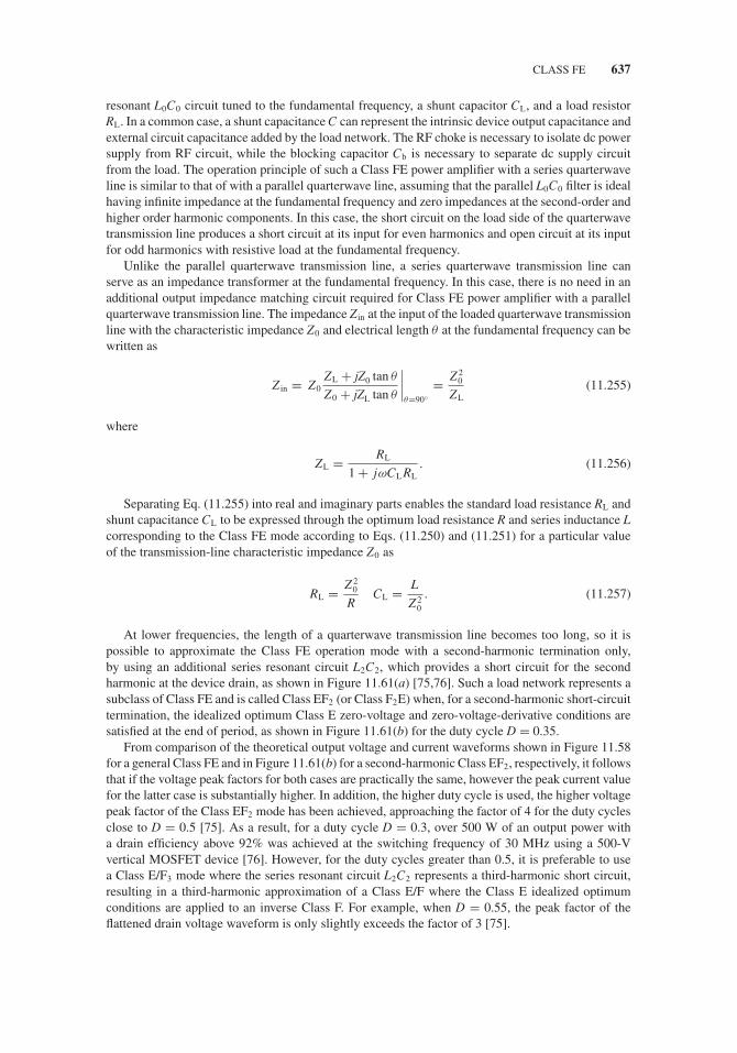
JWBS064-c11 JWBS064-Gerbennikov March 12, 2011 10:45 Printer Name: Yet to Come
CLASS FE 637
resonant L0C0 circuit tuned to the fundamental frequency, a shunt capacitor CL, and a load resistorRL. In a common case, a shunt capacitance C can represent the intrinsic device output capacitance andexternal circuit capacitance added by the load network. The RF choke is necessary to isolate dc powersupply from RF circuit, while the blocking capacitor Cb is necessary to separate dc supply circuitfrom the load. The operation principle of such a Class FE power amplifier with a series quarterwaveline is similar to that of with a parallel quarterwave line, assuming that the parallel L0C0 filter is idealhaving infinite impedance at the fundamental frequency and zero impedances at the second-order andhigher order harmonic components. In this case, the short circuit on the load side of the quarterwavetransmission line produces a short circuit at its input for even harmonics and open circuit at its inputfor odd harmonics with resistive load at the fundamental frequency.
Unlike the parallel quarterwave transmission line, a series quarterwave transmission line canserve as an impedance transformer at the fundamental frequency. In this case, there is no need in anadditional output impedance matching circuit required for Class FE power amplifier with a parallelquarterwave transmission line. The impedance Zin at the input of the loaded quarterwave transmissionline with the characteristic impedance Z0 and electrical length θ at the fundamental frequency can bewritten as
Z in = Z0ZL + jZ0 tan θ
Z0 + jZL tan θ
∣∣∣∣θ=90◦
= Z 20
ZL(11.255)
where
ZL = RL
1 + jωCL RL. (11.256)
Separating Eq. (11.255) into real and imaginary parts enables the standard load resistance RL andshunt capacitance CL to be expressed through the optimum load resistance R and series inductance Lcorresponding to the Class FE mode according to Eqs. (11.250) and (11.251) for a particular valueof the transmission-line characteristic impedance Z0 as
RL = Z 20
RCL = L
Z 20
. (11.257)
At lower frequencies, the length of a quarterwave transmission line becomes too long, so it ispossible to approximate the Class FE operation mode with a second-harmonic termination only,by using an additional series resonant circuit L2C2, which provides a short circuit for the secondharmonic at the device drain, as shown in Figure 11.61(a) [75,76]. Such a load network represents asubclass of Class FE and is called Class EF2 (or Class F2E) when, for a second-harmonic short-circuittermination, the idealized optimum Class E zero-voltage and zero-voltage-derivative conditions aresatisfied at the end of period, as shown in Figure 11.61(b) for the duty cycle D = 0.35.
From comparison of the theoretical output voltage and current waveforms shown in Figure 11.58for a general Class FE and in Figure 11.61(b) for a second-harmonic Class EF2, respectively, it followsthat if the voltage peak factors for both cases are practically the same, however the peak current valuefor the latter case is substantially higher. In addition, the higher duty cycle is used, the higher voltagepeak factor of the Class EF2 mode has been achieved, approaching the factor of 4 for the duty cyclesclose to D = 0.5 [75]. As a result, for a duty cycle D = 0.3, over 500 W of an output power witha drain efficiency above 92% was achieved at the switching frequency of 30 MHz using a 500-Vvertical MOSFET device [76]. However, for the duty cycles greater than 0.5, it is preferable to usea Class E/F3 mode where the series resonant circuit L2C2 represents a third-harmonic short circuit,resulting in a third-harmonic approximation of a Class E/F where the Class E idealized optimumconditions are applied to an inverse Class F. For example, when D = 0.55, the peak factor of theflattened drain voltage waveform is only slightly exceeds the factor of 3 [75].

JWBS064-c11 JWBS064-Gerbennikov March 12, 2011 10:45 Printer Name: Yet to Come
638 HIGH-EFFICIENCY POWER AMPLIFIERS
FIGURE 11.61 Class EF2 power amplifier and corresponding optimum drain waveforms.
11.8 CAD DESIGN EXAMPLE: 1.75 GHZ HBT CLASS E MMIC POWER AMPLIFIER
Generally, the high-efficiency power amplifier design procedure should include the following ba-sic steps:
� The proper selection of the active device, accurate measurements of its small-signal S-parametersunder different bias conditions in a wide frequency range, and then transformation of themeasured S-parameters to the impedance Z- and admittance Y-parameters to describe thedevice electrical behavior through the nonlinear model in the form of its equivalent circuit withgenerally nonlinear parameters.
� The analytical calculation of the optimum parameters of the proper load network in a high-efficiency mode for given output power, supply voltage, and device output capacitance to providethe maximum collector/drain efficiency and required level of harmonic suppression.
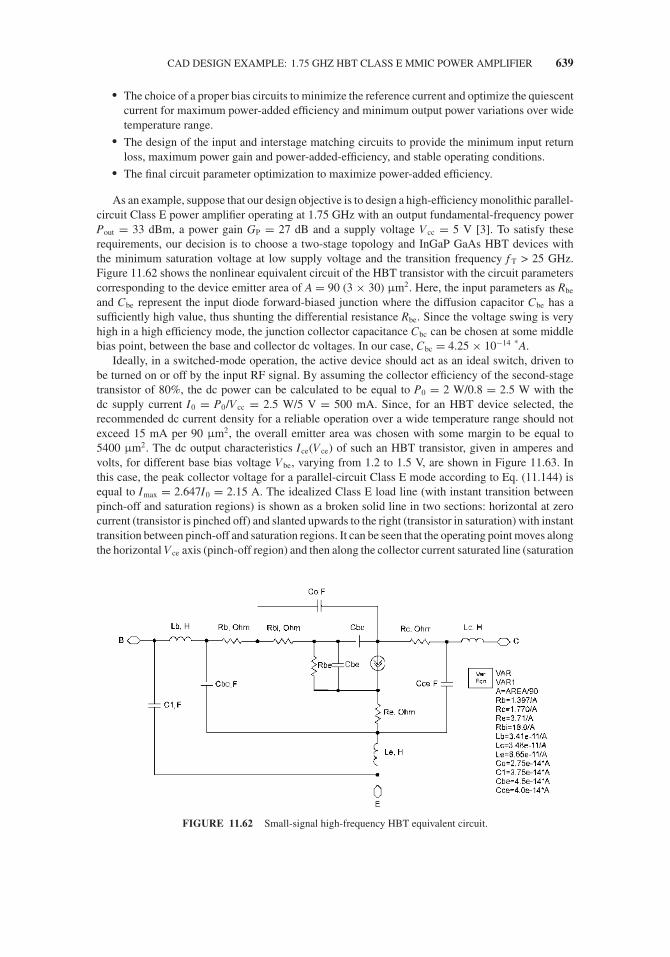
JWBS064-c11 JWBS064-Gerbennikov March 12, 2011 10:45 Printer Name: Yet to Come
CAD DESIGN EXAMPLE: 1.75 GHZ HBT CLASS E MMIC POWER AMPLIFIER 639
� The choice of a proper bias circuits to minimize the reference current and optimize the quiescentcurrent for maximum power-added efficiency and minimum output power variations over widetemperature range.
� The design of the input and interstage matching circuits to provide the minimum input returnloss, maximum power gain and power-added-efficiency, and stable operating conditions.
� The final circuit parameter optimization to maximize power-added efficiency.
As an example, suppose that our design objective is to design a high-efficiency monolithic parallel-circuit Class E power amplifier operating at 1.75 GHz with an output fundamental-frequency powerPout = 33 dBm, a power gain GP = 27 dB and a supply voltage Vcc = 5 V [3]. To satisfy theserequirements, our decision is to choose a two-stage topology and InGaP GaAs HBT devices withthe minimum saturation voltage at low supply voltage and the transition frequency f T > 25 GHz.Figure 11.62 shows the nonlinear equivalent circuit of the HBT transistor with the circuit parameterscorresponding to the device emitter area of A = 90 (3 × 30) μm2. Here, the input parameters as Rbe
and Cbe represent the input diode forward-biased junction where the diffusion capacitor Cbe has asufficiently high value, thus shunting the differential resistance Rbe. Since the voltage swing is veryhigh in a high efficiency mode, the junction collector capacitance Cbc can be chosen at some middlebias point, between the base and collector dc voltages. In our case, Cbc = 4.25 × 10⁻¹⁴ *A.
Ideally, in a switched-mode operation, the active device should act as an ideal switch, driven tobe turned on or off by the input RF signal. By assuming the collector efficiency of the second-stagetransistor of 80%, the dc power can be calculated to be equal to P0 = 2 W/0.8 = 2.5 W with thedc supply current I0 = P0/Vcc = 2.5 W/5 V = 500 mA. Since, for an HBT device selected, therecommended dc current density for a reliable operation over a wide temperature range should notexceed 15 mA per 90 μm2, the overall emitter area was chosen with some margin to be equal to5400 μm2. The dc output characteristics Ice(Vce) of such an HBT transistor, given in amperes andvolts, for different base bias voltage Vbe, varying from 1.2 to 1.5 V, are shown in Figure 11.63. Inthis case, the peak collector voltage for a parallel-circuit Class E mode according to Eq. (11.144) isequal to Imax = 2.647I0 = 2.15 A. The idealized Class E load line (with instant transition betweenpinch-off and saturation regions) is shown as a broken solid line in two sections: horizontal at zerocurrent (transistor is pinched off) and slanted upwards to the right (transistor in saturation) with instanttransition between pinch-off and saturation regions. It can be seen that the operating point moves alongthe horizontal Vce axis (pinch-off region) and then along the collector current saturated line (saturation
FIGURE 11.62 Small-signal high-frequency HBT equivalent circuit.

JWBS064-c11 JWBS064-Gerbennikov March 12, 2011 10:45 Printer Name: Yet to Come
640 HIGH-EFFICIENCY POWER AMPLIFIERS
FIGURE 11.63 Device output current-voltage characteristics and load line.
region) until Ice = 2.15 A. At this final point, the saturation voltage can be found as equal to V sat =0.3 V. This means that the power loss due to the finite device saturation resistance can be calculatedas Psat = I0V sat = 150 mW with degradation in the collector efficiency of (1 − Psat/P0) = 0.06 or 6%.
First, we shall design the second stage for a maximum collector efficiency with some interme-diate value of the source resistance much less than 50 �. The idealized optimum parameters of aparallel-circuit Class E load network can be calculated using Eqs. (11.139) to (11.141), by taking intoaccount the saturation voltage Vsat, as
R = 1.365(Vcc − Vsat)
2
Pout= 15 �
L = 0.732R
ω= 1.0 nH
C = 0.685
ωR= 3.9 pF.
It should be noted that, in view of a saturation voltage, the calculated parameters of the ClassE load network generally cannot be considered optimum unlike the ideal case of zero saturationvoltage. However, they can be considered as a sufficiently accurate initial guess for final design andoptimization when efficiency is sufficiently high. In addition, the collector capacitance can be largerthan required, especially at higher frequencies and for the transistor with large emitter area requiredfor high output power. In our case, the total output capacitance can be estimated as Cout = Cce +C0 + Cbc = 6.6 pF for total emitter area of 5400 μm2, which is 1.5 times greater than required forthe optimum parallel-circuit Class E mode. The excessive output capacitance of (6.6 − 3.9) = 2.7 pFis responsible for additional switching losses which occur during the transitions from the saturationto pinch-off modes of the device operation. To compensate for this capacitance at the fundamentalfrequency, it is necessary to connect the corresponding inductance in parallel, which value is equalto 3 nH. Hence, the parallel connection of the two inductors with values of 1 nH and 3 nH results ina final value of (1 × 3)/(1 + 3) = 0.75 nH.
Assuming the quality factor of the series filter of QL = 10, the series capacitance C0 and inductanceL0 are calculated as
C0 = 1
ωRQL= 0.6 pF
L0 = 1
ω2C0= 13.8 nH.

JWBS064-c11 JWBS064-Gerbennikov March 12, 2011 10:45 Printer Name: Yet to Come
CAD DESIGN EXAMPLE: 1.75 GHZ HBT CLASS E MMIC POWER AMPLIFIER 641
Since the input device impedance is sufficiently low, the intermediate source resistance is chosento be equal to 5 �. In this case, it will be enough to use only one input matching section. The inputmatching circuit can be composed in the form of a high-pass L-type section with a shunt inductor anda series capacitor. The parameters of this matching circuit can finally be optimized in a large-signalmode to minimize input return loss as a criterion by using Smith chart tuning procedure.
Figure 11.64 shows the simulation setup of the second-power amplifier stage designed to operatein a parallel-circuit Class E mode. To simulate the electrical characteristics and waveforms, thecorresponding current probes and voltage wire labels are incorporated into the circuit. As a current-controlled device, the bipolar transistor requires the dc base driving current, the value of whichdepends on the input power and device parameters. Because technologically the bipolar devicerepresents a parallel connection of the basic cells (fingers), the important issue is to use the ballastingseries resistors to avoid the current imbalance and possible device collapse at higher current densitylevels. Generally, different types of the current-mirror bias circuits can be effectively used to bias atransistor. In our case, the emitter follower bias circuit that provides the temperature compensationand minimizes the reference current is used. It is very important to provide the proper ratio betweenthe ballasting resistors R34 and R33, which preferably should be equal to the ratio of the correspondingdevice areas of 5400/270 = 20. The emitter follower bias circuit normally requires only several tensof microamperes of reference current.
Figure 11.65 shows the measurement equations required to plot the small- and large-signal poweramplifier characteristics. The small-signal frequency dependence of the stability factor K is shownin Figure 11.66(a) demonstrating the stable conditions over entire frequency range with K > 1.However, it is not enough to just simulate the small-signal performance. It is important also to verifythe potential instability that can occur in the form of injection-locking effect at large-signal modenear operating frequency. The dependencies of the real parts of the device impedance at the base andthe input impedance seen by the source are shown in Figure 11.66(b). It is seen that the real partof the base impedance is slightly negative. In order to compensate for this negative resistance, it isnecessary to connect the resistance of 0.35 � in series to the base compromising the stable operationand sufficient power gain. The real part of the input impedance seen by the source is close to therequired 5 � at nominal large-signal operation.
As a result, the second-power amplifier stage exhibits a linear power gain of about 13 dB andsaturated output power of 33.1 dBm, which dependencies are shown in Figure 11.67(a), with amaximum collector efficiency of 85.3% and a maximum power-added efficiency of 60.5%, whichdependencies are shown in Figure 11.67(b). It is seen that the collector efficiency improvement isachieved at the expense of the significant power gain reduction. However, the maximum power-addedefficiency occurs when the power gain is reduced by about 3 dB, which is a result of the contributionof the driving power.
Figure 11.68 shows the collector and base voltage waveform corresponding to a Class E approx-imation. The collector voltage waveform with a peak factor of about 18/5 = 3.6 was achieved for amaximum collector efficiency with the base voltage waveform having a flattened top part and causingthe device to operate in a switching mode with minimum switching loss.
To match the Class E load resistance R = 15 � with a standard load resistance RL = 50 �, itis necessary to use a matching circuit with the series inductor as a first element to provide highimpedance at the harmonics. Since the ratio of impedances is not so high, we can use the low-passL-type matching section with design equations, resulting in
QL =√
50
15− 1 ∼= 1.5
L = QL R
ω= 2.1 nH
C = QL
ωRL= 2.9 pF.

JWBS064-c11 JWBS064-Gerbennikov March 12, 2011 10:45 Printer Name: Yet to Come
R R33
R=
3.5
Ohm
R R34
R=
70 O
hm
S-P
AR
AM
ET
ER
S
HA
RM
ON
IC B
ALA
NC
E
Har
mon
icB
alan
ceH
B1
Fre
q[1]
=fr
eque
ncy
Ord
er[1
]=7
Max
Shr
inka
ge=
1.0e
-5S
wee
pVar
=“P
in”
Sta
rt=
0S
top=
30S
tep=
0.1
VA
Ram
p_va
rsfr
eque
ncy=
1.75
GH
zP
in =
0V
cc =
5 V
Var
Eqn
I_P
robe
I_R
ef
I_P
robe
I_b
I_P
robe
I_V
cc0
V_D
CS
RC
3V
dc=
2.6
V
V_D
CS
RC
7V
dc=
Vcc
V_D
CS
RC
1V
dc=
Vcc
iHB
T_E
EB
JT2
X18
AR
EA
=27
0
iHB
T_E
EB
JT2
X3
AR
EA
=54
00
R R39
R=
0.35
Ohm
C C60
C=
7 pF
C C59
C=
40 p
FC C
58C
=0.
6 pF
L L3 L=0.
22 n
HR
=1.
2 O
hm
L L2 L=0.
75 n
HR
=
L L1 L=13
.8 n
HR
=
I_P
robe
I_in
I_P
robe
I_c
I_P
robe
I_D
C
I_P
robe
I_lo
ad
Vin
P_n
Har
mR
F_s
ourc
eN
um=
1Z
=5
Ohm
Fre
q=fr
eque
ncy
P[1
]=db
mto
w(P
in)
Vb
Vc
+ –
+ –
Vcc
iHB
T_E
EB
JT2
X4
AR
EA
=27
0
Vlo
ad Term
Term
2N
um=
2Z
=15
Ohm
S_P
aram
SP
1S
tart
=0.
5 G
Hz
Sto
p=5.
0 G
Hz
Ste
p=10
MH
z
FIG
UR
E11
.64
Sim
ulat
ion
setu
pfo
rC
lass
Ese
cond
stag
e.
642

JWBS064-c11 JWBS064-Gerbennikov March 12, 2011 10:45 Printer Name: Yet to Come
CAD DESIGN EXAMPLE: 1.75 GHZ HBT CLASS E MMIC POWER AMPLIFIER 643
FIGURE 11.65 Measurement equations.
Figure 11.69 shows the simulation setup of the Class E second stage with output matching circuit.Since the loaded quality facto QL is sufficiently small, the conditions at the fundamental-frequencyand harmonic components will be slightly different compared to the ideal case. In this case, theeasiest and fastest way to maximize collector efficiency is to tune manually the parameters of thebasic elements such as the parallel inductor. The maximum collector efficiency of 84.8% and powergain of about 13 dB were achieved, as shown in Figure 11.70, by tuning the value of the parallel
1.0 1.5 2.0 2.5 3.0 3.5 4.0 4.50.5 5.0
2
3
4
1
5
freq, GHz
K
5 10 15 200 25
-0.20
-0.15
-0.10
-0.25
-0.05
4.4
4.6
4.8
5.0
5.2
5.4
4.2
5.6
Pin
real
(Vb[
::,1]
/I_b.
i[::,1
])real(V
in[::,1]/I_in.i[::,1])
(a)
(b)
FIGURE 11.66 Input impedance and stability.

JWBS064-c11 JWBS064-Gerbennikov March 12, 2011 10:45 Printer Name: Yet to Come
644 HIGH-EFFICIENCY POWER AMPLIFIERS
FIGURE 11.67 Power gain, output power and efficiency.
inductor from 0.75–1.0 nH. This inductor is shown in Figure 11.69 inside the circle. However, a singlelow-pass matching section can provide a second-harmonic suppression of about 20 dB. Consequently,to improve the spectral performance, it is necessary to use two or more low-pass sections in succession,better with equal quality factors to provide a wider frequency bandwidth.
Figure 11.71 shows the simulation setup of the first power amplifier stage designed to operate ina Class AB mode. Since it is sufficient to provide an output power from the first stage of not more
FIGURE 11.68 Collector and base voltage waveforms.
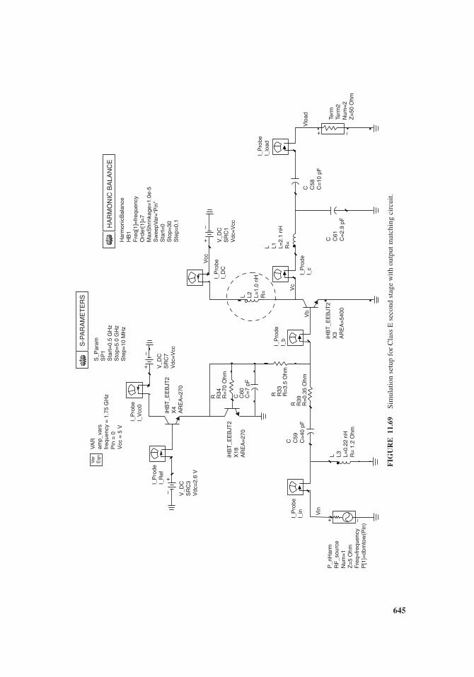
JWBS064-c11 JWBS064-Gerbennikov March 12, 2011 10:45 Printer Name: Yet to Come
VA
Ram
p_va
rsfr
eque
ncy
= 1
.75
GH
zP
in =
0V
cc =
5 V
Var
Eqn
S_P
aram
SP
1S
tart
=0.
5 G
Hz
Sto
p=5.
0 G
Hz
Ste
p=10
MH
zH
arm
onic
Bal
ance
HB
1F
req[
1]=
freq
uenc
yO
rder
[1]=
7M
axS
hrin
kage
=1.
0e-5
Sw
eepV
ar=
“Pin
”S
tart
=0
Sto
p=30
Ste
p=0.
1
I_P
rode
I_R
ef+
+
–
–
+
+
–
–
+ –
I_P
robe
I_V
cc0
I_P
robe
I_D
C
I_P
robe
I_lo
ad
Vlo
adC C
58C
=10
pF
C C61
C=
2.9
pF
Term
Term
2N
um=
2Z
=50
Ohm
iHB
T_E
EB
JT2
X3
AR
EA
=54
00
I_P
rode
I_c
L L2 L=1.
0 nH
R=
I_P
rode
I_b
I_P
robe
I_in
C C59
C=
40 p
F
V_D
CS
RC
3V
dc=
2.6
V
iHB
T_E
EB
JT2
X4
AR
EA
=27
0
iHB
T_E
EB
JT2
X18
AR
EA
=27
0
R R34
R=
70 O
hm
R R33
R=
3.5
Ohm
R R39
R=
0.35
Ohm
C C60
C=
7 pF
V_D
CS
RC
7V
dc=
Vcc
V_D
CS
RC
1V
dc=
Vcc
L L1 L=2.
1 nH
R=
L L3 L=0.
22 n
HR
= 1
.2 O
hm
P_n
Har
mR
F_s
ourc
eN
um=
1Z
=5
Ohm
Fre
q=fr
eque
ncy
P[1
]=db
mto
w(P
in)
Vin
Vcc
Vc
Vb
S-P
AR
AM
ET
ER
S
HA
RM
ON
IC B
ALA
NC
E
FIG
UR
E11
.69
Sim
ulat
ion
setu
pfo
rC
lass
Ese
cond
stag
ew
ithou
tput
mat
chin
gci
rcui
t.
645
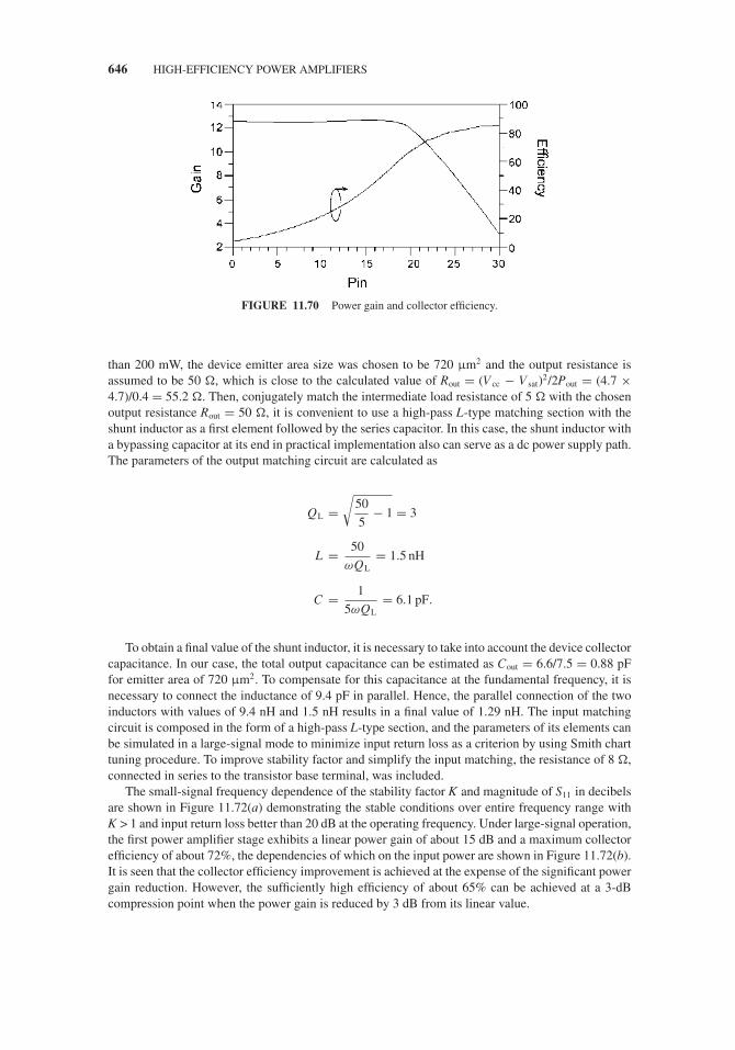
JWBS064-c11 JWBS064-Gerbennikov March 12, 2011 10:45 Printer Name: Yet to Come
646 HIGH-EFFICIENCY POWER AMPLIFIERS
FIGURE 11.70 Power gain and collector efficiency.
than 200 mW, the device emitter area size was chosen to be 720 μm2 and the output resistance isassumed to be 50 �, which is close to the calculated value of Rout = (Vcc − V sat)2/2Pout = (4.7 ×4.7)/0.4 = 55.2 �. Then, conjugately match the intermediate load resistance of 5 � with the chosenoutput resistance Rout = 50 �, it is convenient to use a high-pass L-type matching section with theshunt inductor as a first element followed by the series capacitor. In this case, the shunt inductor witha bypassing capacitor at its end in practical implementation also can serve as a dc power supply path.The parameters of the output matching circuit are calculated as
QL =√
50
5− 1 = 3
L = 50
ωQL= 1.5 nH
C = 1
5ωQL= 6.1 pF.
To obtain a final value of the shunt inductor, it is necessary to take into account the device collectorcapacitance. In our case, the total output capacitance can be estimated as Cout = 6.6/7.5 = 0.88 pFfor emitter area of 720 μm2. To compensate for this capacitance at the fundamental frequency, it isnecessary to connect the inductance of 9.4 pF in parallel. Hence, the parallel connection of the twoinductors with values of 9.4 nH and 1.5 nH results in a final value of 1.29 nH. The input matchingcircuit is composed in the form of a high-pass L-type section, and the parameters of its elements canbe simulated in a large-signal mode to minimize input return loss as a criterion by using Smith charttuning procedure. To improve stability factor and simplify the input matching, the resistance of 8 �,connected in series to the transistor base terminal, was included.
The small-signal frequency dependence of the stability factor K and magnitude of S11 in decibelsare shown in Figure 11.72(a) demonstrating the stable conditions over entire frequency range withK > 1 and input return loss better than 20 dB at the operating frequency. Under large-signal operation,the first power amplifier stage exhibits a linear power gain of about 15 dB and a maximum collectorefficiency of about 72%, the dependencies of which on the input power are shown in Figure 11.72(b).It is seen that the collector efficiency improvement is achieved at the expense of the significant powergain reduction. However, the sufficiently high efficiency of about 65% can be achieved at a 3-dBcompression point when the power gain is reduced by 3 dB from its linear value.
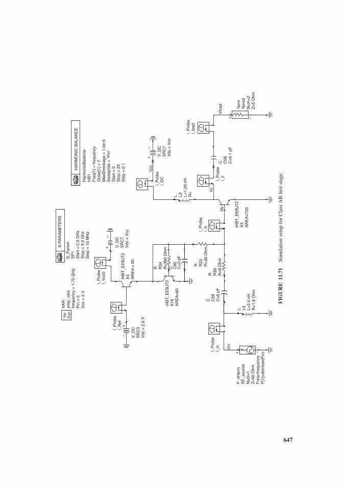
JWBS064-c11 JWBS064-Gerbennikov March 12, 2011 10:45 Printer Name: Yet to Come
Var
Eqn
VA
Ram
p_va
rsfr
eque
ncy
= 1
.75
GH
zP
in =
0V
cc =
5 V
S_P
aram
SP
1S
tart
= 0
.5 G
Hz
Sto
p =
5.0
Ghz
Ste
p =
10
MH
z
l_P
robe
l_V
cc0
l_P
robe
l_D
C
l_P
robe
l_b
l_P
robe
l_in Vin
P_n
Har
mR
F_s
ourc
eN
um=
1Z
=50
Ohm
Fre
q=fr
eque
ncy
P[1
]=db
mto
w(P
in)
Vb
l_P
robe
l_lo
ad
Vlo
ad Term
Term
2N
um=
2Z
=5
Ohm
l_P
robe
l_c
L L2 L=1.
29 n
HR
=
L L3 L=2.
4 nH
R=
1.8
Ohm
C C58
C=
6.1
pF
Vcc
Vc
l_P
robe
l_R
efiH
BT
_EE
BJT
2X
4A
RE
A =
90
V_D
CS
RC
3V
dc =
2.6
V
iHB
T_E
EB
JT2
X3
AR
EA
=72
0
iHB
T_E
EB
JT2
X18
AR
EA
=60
R R34
R=
360
Ohm
R R33
R=
30 O
hmR R
39R
=8
Ohm
C C60
C=
2 pF
C C59
C=
6 pF
V_D
CS
RC
7V
dc =
Vcc
+
+
+
–
–
+
+
–
–
–
V_D
CS
RC
1V
dc =
Vcc
Har
mon
icB
alan
ceH
B1
Fre
q[1]
= fr
eque
ncy
Ord
er[1
] = 7
Max
Shr
inka
ge =
1.0
e-5
Sw
eepV
ar =
“P
in”
Sta
rt =
0S
top
= 2
5S
tep
= 0
.1
S-P
AR
AM
ET
ER
S
HA
RM
ON
IC B
ALA
NC
E
FIG
UR
E11
.71
Sim
ulat
ion
setu
pfo
rC
lass
AB
first
stag
e.
647
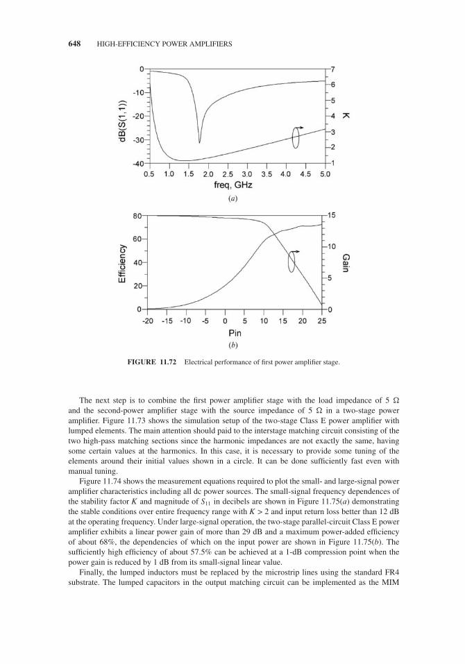
JWBS064-c11 JWBS064-Gerbennikov March 12, 2011 10:45 Printer Name: Yet to Come
648 HIGH-EFFICIENCY POWER AMPLIFIERS
FIGURE 11.72 Electrical performance of first power amplifier stage.
The next step is to combine the first power amplifier stage with the load impedance of 5 �
and the second-power amplifier stage with the source impedance of 5 � in a two-stage poweramplifier. Figure 11.73 shows the simulation setup of the two-stage Class E power amplifier withlumped elements. The main attention should paid to the interstage matching circuit consisting of thetwo high-pass matching sections since the harmonic impedances are not exactly the same, havingsome certain values at the harmonics. In this case, it is necessary to provide some tuning of theelements around their initial values shown in a circle. It can be done sufficiently fast even withmanual tuning.
Figure 11.74 shows the measurement equations required to plot the small- and large-signal poweramplifier characteristics including all dc power sources. The small-signal frequency dependences ofthe stability factor K and magnitude of S11 in decibels are shown in Figure 11.75(a) demonstratingthe stable conditions over entire frequency range with K > 2 and input return loss better than 12 dBat the operating frequency. Under large-signal operation, the two-stage parallel-circuit Class E poweramplifier exhibits a linear power gain of more than 29 dB and a maximum power-added efficiencyof about 68%, the dependencies of which on the input power are shown in Figure 11.75(b). Thesufficiently high efficiency of about 57.5% can be achieved at a 1-dB compression point when thepower gain is reduced by 1 dB from its small-signal linear value.
Finally, the lumped inductors must be replaced by the microstrip lines using the standard FR4substrate. The lumped capacitors in the output matching circuit can be implemented as the MIM
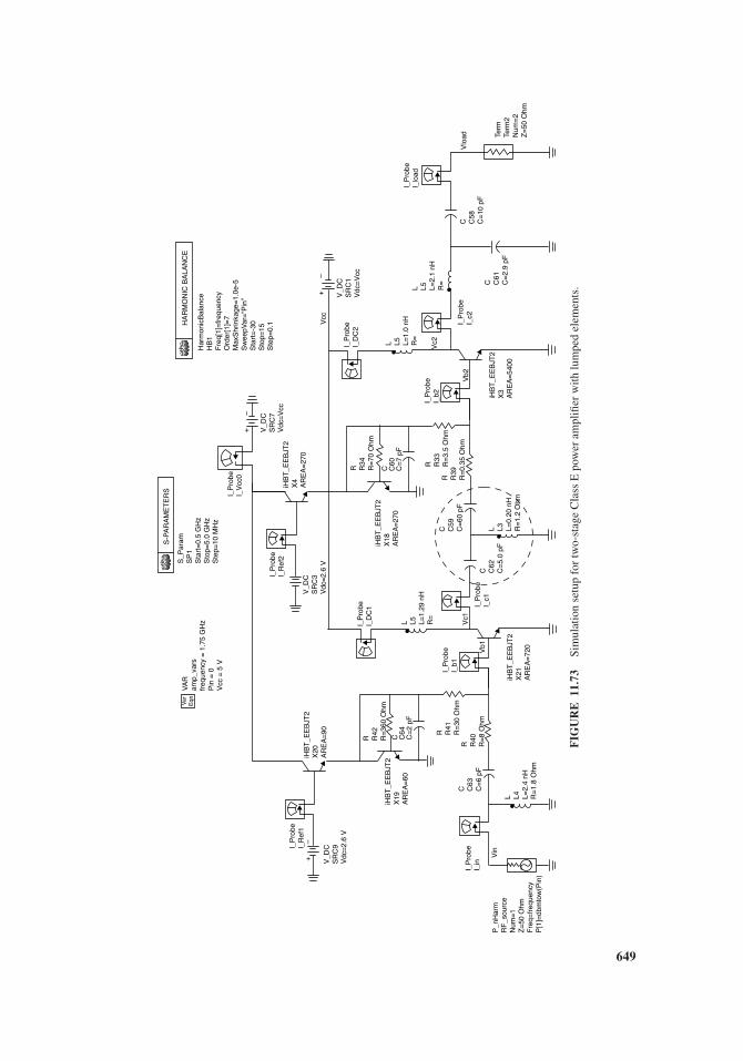
JWBS064-c11 JWBS064-Gerbennikov March 12, 2011 10:45 Printer Name: Yet to Come
S_P
aram
SP
1S
tart
=0.
5 G
Hz
Sto
p=5.
0 G
Hz
Ste
p=10
MH
z
Har
mon
icB
alan
ceH
B1
Fre
q[1]
=fr
eque
ncy
Ord
er[1
]=7
Max
Shr
inka
ge=
1.0e
-5S
wee
pVar
=“P
in”
Sta
rt=
-30
Sto
p=15
Ste
p=0.
1I_
Pro
beI_
Ref
2
I_P
robe
I_V
cc0
I_P
robe
I_D
C2
I_P
robe
I_lo
ad
Vlo
adC C
58C
=10
pF
C C61
C=
2.9
pFTe
rmTe
rm2
Num
=2
Z=
50 O
hm
iHB
T_E
EB
JT2
X3
AR
EA
=54
00
I_P
robe
I_c2
I_P
robe
I_b2
I_P
robe
I_D
C1
I_P
robe
I_R
ef1
I_P
robe
I_in
I_P
robe
I_b1
I_P
robe
I_c1
C C64
C=
2 pF
C C63
C=
6 pF
C C60
C=
7 pF
C C59
C=
60 p
F
C C62
C=
5.0
pF
R R42
R=
360
Ohm
R R40
R=
8 O
hm
R R41
R=
30 O
hm
R R39
R=
0.35
Ohm
R R33
R=
3.5
Ohm
R R34
R=
70 O
hm
V_D
CS
RC
3V
dc=
2.6
VV
_DC
SR
C9
Vdc
=2.
6 V
iHB
T_E
EB
JT2
X4
AR
EA
=27
0
iHB
T_E
EB
JT2
X19
AR
EA
=60
iHB
T_E
EB
JT2
X18
AR
EA
=27
0
iHB
T_E
EB
JT2
X21
AR
EA
=72
0
iHB
T_E
EB
JT2
X20
AR
EA
=90
V_D
CS
RC
7V
dc=
Vcc
+–
+–
+–
V_D
CS
RC
1V
dc=
Vcc
L L5 L=1.
29 n
HR
=
L L5 L=2.
1 nH
R=
L L5 L=1.
0 nH
R=
L L4 L=2.
4 nH
R=
1.8
Ohm
L L3 L=0.
20 n
HR
=1.
2 O
hm
P_n
Har
mR
F_s
ourc
eN
um=
1Z
=50
Ohm
Fre
q=fr
eque
ncy
P[1
]=db
mto
w(P
in)
Vin
Vcc
Vb2
Vb1
Vc1
Vc2
S-P
AR
AM
ET
ER
S
VA
Ram
p_va
rsfr
eque
ncy
= 1
.75
GH
zP
in =
0V
cc =
5 V
HA
RM
ON
IC B
ALA
NC
E
FIG
UR
E11
.73
Sim
ulat
ion
setu
pfo
rtw
o-st
age
Cla
ssE
pow
eram
plifi
erw
ithlu
mpe
del
emen
ts.
649
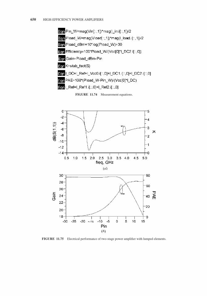
JWBS064-c11 JWBS064-Gerbennikov March 12, 2011 10:45 Printer Name: Yet to Come
650 HIGH-EFFICIENCY POWER AMPLIFIERS
FIGURE 11.74 Measurement equations.
FIGURE 11.75 Electrical performance of two-stage power amplifier with lumped elements.

JWBS064-c11 JWBS064-Gerbennikov March 12, 2011 10:45 Printer Name: Yet to Come
S_P
aram
SP
1S
tart
=0.
5 G
Hz
Sto
p=5.
0 G
Hz
Ste
p=10
MH
z
Har
mon
icB
alan
ceH
B1
Fre
q[1]
=fr
eque
ncy
Ord
er[1
]=7
Max
Shr
inka
ge=
1.0e
-5S
wee
pVar
=“P
in”
Sta
rt=
-30
Sto
p=15
Ste
p=0.
1M
SU
BF
R4
H=
16 m
ilE
r=4.
7M
ur=
1C
ond=
5.1E
+7
T=
10 u
mTa
nD=
0.02
I_P
robe
I_R
ef2
I_P
robe
I_V
cc0
I_P
robe
I_D
C2
I_P
robe
I_lo
ad
Vlo
adC C
58C
=10
pF
C C61
C=
2.9
pFTe
rmTe
rm2
Num
=2
Z=
50 O
hm
iHB
T_E
EB
JT2
X3
AR
EA
=54
00
I_P
robe
I_c2
I_P
robe
I_b2
I_P
robe
I_D
C1
I_P
robe
I_R
ef1
I_P
robe
I_in
I_P
robe
I_b1
I_P
robe
I_c1
C C64
C=
2 pF
C C63
C=
6 pF
C C60
C=
7 pF
C C59
C=
60 p
F
C C62
C=
5.0
pF
R R42
R=
360
Ohm
R R40
R=
8 O
hm
R R41
R=
30 O
hm
R R39
R=
0.35
Ohm
R R33
R=
3.5
Ohm
R R34
R=
70 O
hm
V_D
CS
RC
3V
dc=
2.6V
V_D
CS
RC
9V
dc=
2.6
V
iHB
T_E
EB
JT2
X4
AR
EA
=27
0
iHB
T_E
EB
JT2
X19
AR
EA
=60
iHB
T_E
EB
JT2
X18
AR
EA
=27
0
iHB
T_E
EB
JT2
X21
AR
EA
=72
0
iHB
T_E
EB
JT2
X20
AR
EA
=90
V_D
CS
RC
7V
dc=
Vcc
+–
+–
+
+
–
–
+
+
–
–
V_D
CS
RC
1V
dc=
Vcc
MLI
NT
L4S
ubst
=“F
R4”
W=
29 m
ilL=
4.0
mm
MLI
NT
L5S
ubst
=“F
R4”
W=
29 m
ilL=
3.1
mm
MLI
NT
L6S
ubst
=“F
R4”
W=
29 m
ilL=
6.3
mm
L L4 L=2.
4 nH
R=
1.8
Ohm
L L3 L=0.
20 n
HR
=1.
2 O
hm
P_n
Har
mR
F_s
ourc
eN
um=
1Z
=50
Ohm
Fre
q=fr
eque
ncy
P[1
]=db
mto
w(P
in)
Vin
Vcc
Vb2
Vb1
Vc1
Vc2
S-P
AR
AM
ET
ER
SV
AR
amp_
vars
freq
uenc
y =
1.7
5 G
Hz
Pin
= 0
Vcc
= 5
V
HA
RM
ON
IC B
ALA
NC
E
MS
ub
FIG
UR
E11
.76
Sim
ulat
ion
setu
pfo
rtw
o-st
age
Cla
ssE
pow
eram
plifi
erw
ithm
icro
stri
plin
es.
651
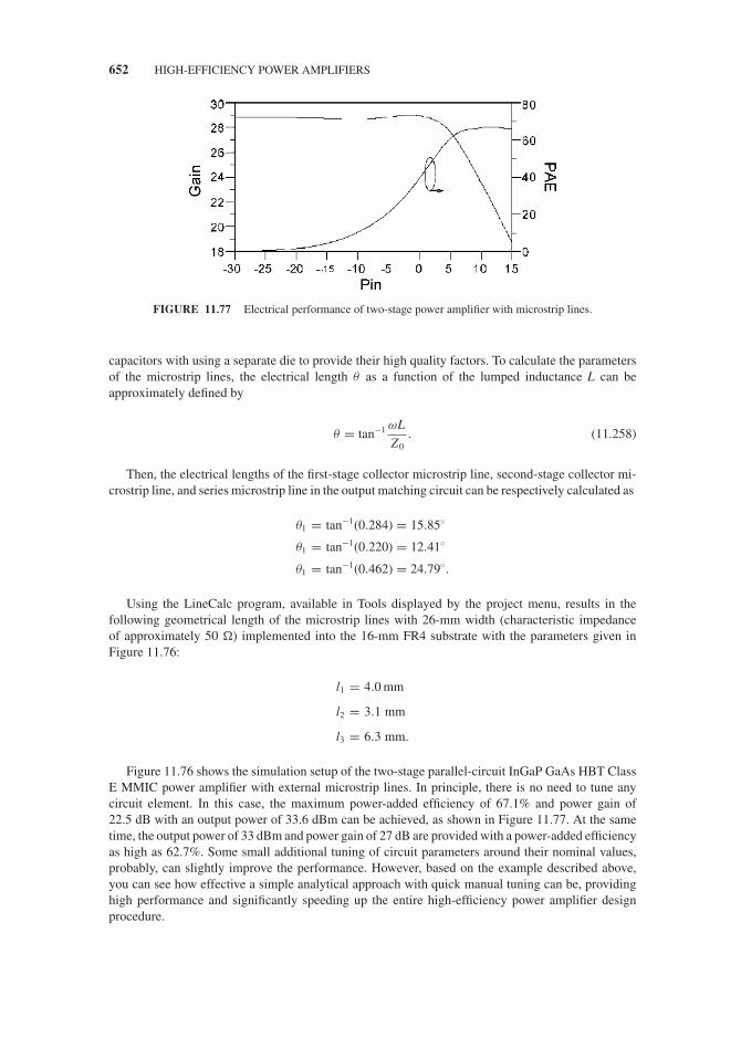
JWBS064-c11 JWBS064-Gerbennikov March 12, 2011 10:45 Printer Name: Yet to Come
652 HIGH-EFFICIENCY POWER AMPLIFIERS
FIGURE 11.77 Electrical performance of two-stage power amplifier with microstrip lines.
capacitors with using a separate die to provide their high quality factors. To calculate the parametersof the microstrip lines, the electrical length θ as a function of the lumped inductance L can beapproximately defined by
θ = tan−1 ωL
Z0. (11.258)
Then, the electrical lengths of the first-stage collector microstrip line, second-stage collector mi-crostrip line, and series microstrip line in the output matching circuit can be respectively calculated as
θ1 = tan−1(0.284) = 15.85◦
θ1 = tan−1(0.220) = 12.41◦
θ1 = tan−1(0.462) = 24.79◦.
Using the LineCalc program, available in Tools displayed by the project menu, results in thefollowing geometrical length of the microstrip lines with 26-mm width (characteristic impedanceof approximately 50 �) implemented into the 16-mm FR4 substrate with the parameters given inFigure 11.76:
l1 = 4.0 mm
l2 = 3.1 mm
l3 = 6.3 mm.
Figure 11.76 shows the simulation setup of the two-stage parallel-circuit InGaP GaAs HBT ClassE MMIC power amplifier with external microstrip lines. In principle, there is no need to tune anycircuit element. In this case, the maximum power-added efficiency of 67.1% and power gain of22.5 dB with an output power of 33.6 dBm can be achieved, as shown in Figure 11.77. At the sametime, the output power of 33 dBm and power gain of 27 dB are provided with a power-added efficiencyas high as 62.7%. Some small additional tuning of circuit parameters around their nominal values,probably, can slightly improve the performance. However, based on the example described above,you can see how effective a simple analytical approach with quick manual tuning can be, providinghigh performance and significantly speeding up the entire high-efficiency power amplifier designprocedure.

JWBS064-c11 JWBS064-Gerbennikov March 12, 2011 10:45 Printer Name: Yet to Come
REFERENCES 653
REFERENCES
1. M. R. Osborne, “Design of Tuned Transistor Power Amplifiers,” Electronic Eng., vol. 40, pp. 436–443, Aug.1968.
2. P. J. Baxandall, “Transistor Sine Wave LC Oscillators, Some General Considerations and New Developments,”IEE Proc. Electric Power Appl., vol. 106, pp. 748–758, May 1959.
3. A. Grebennikov and N. O. Sokal, Switchmode RF Power Amplifiers, New York: Newnes, 2007.
4. H. L. Krauss, C. W. Bostian, and F. H. Raab, Solid State Radio Engineering, New York: John Wiley & Sons,1980.
5. A. D. Artym, Class D Power Amplifiers and Switching Generators in Radio Communication and Broadcasting(in Russian), Moskva: Svyaz, 1980.
6. W. J. Chudobiak and D. F. Page, “Frequency Limitations of Class-D Transistor Amplifiers,” IEEE J. Solid-State Circuits, vol. SC-4, pp. 25–37, Feb. 1969.
7. H. O. Granberg, “Applying Power MOSFETs in Class D/E RF Power Amplifier Design,” RF Design, vol. 8,pp. 42–47, June 1985.
8. T.-P. Hung, A. G. Metzger, P. J. Zampardi, M. Iwamoto, and P. M. Asbeck, “Design of High-Efficiency Current-Mode Class-D Amplifiers for Wireless Applications,” IEEE Trans. Microwave Theory Tech., vol. MTT-53,pp. 144–151, Jan. 2005.
9. D. C. Prince, “Vacuum Tubes as Power Oscillators, Part III,” Proc. IRE, vol. 11, pp. 527–550, Sept. 1923.
10. J. Zenneck and H. Rukop, Lehrbuch der Drahtlosen Telegraphie, Stuttgart: Ferdinand Enke, 1925.
11. I. N. Fomichev, “A New Method to Increase Efficiency of the Radio Broadcasting Station (in Russian),”Elektrosvyaz, pp. 58–66, June 1938.
12. R. I. Sarbacher, “Power-Tube Performance in Class C Amplifiers and Frequency Multipliers as Influenced byHarmonic Voltage,” Proc. IRE, vol. 31, pp. 607–625, Nov. 1943.
13. H. J. Round, “Wireless Telegraph and Telephone Transmission,” U.S. Patent 1,564,627, Dec. 1925.
14. F. H. Raab, “An Introduction to Class-F Power Amplifiers,” RF Design, vol. 19, pp. 79–84, July 1996.
15. D. M. Snider, “A Theoretical Analysis and Experimental Confirmation of the Optimally Loaded and Over-driven RF Power Amplifier,” IEEE Trans. Electron Devices, vol. ED-14, pp. 851–857, Dec. 1967.
16. F. H. Raab, “FET Power Amplifier Boosts Transmitter Efficiency,” Electronics, vol. 49, pp. 122–126, June1976.
17. V. A. Borisov and V. V. Voronovich, “Analysis of Switched-Mode Transistor Amplifier with Parallel FormingTransmission Line (in Russian),” Radiotekhnika i Elektronika, vol. 31, pp. 1590–1597, Aug. 1986.
18. A. V. Grebennikov, “Circuit Design Technique for High Efficiency Class F Amplifiers,” IEEE MTT-S Int.Microwave Symp. Dig., vol. 2, pp. 771–774, 2000.
19. C. Trask, “Class-F Amplifier Loading Networks: A Unified Design Approach,” IEEE MTT-S Int. MicrowaveSymp. Dig., vol. 1, pp. 351–354, 1999.
20. F. H. Raab, “Class-F Power Amplifiers with Maximally Flat Waveforms,” IEEE Trans. Microwave TheoryTech., vol. MTT-45, pp. 2007–2012, Nov. 1997.
21. A. I. Kolesnikov, “A New Method to Improve Efficiency and to Increase Power of the Transmitter (inRussian),” Master Svyazi, pp. 27–41, June 1940.
22. E. S. Glazman, L. B. Kalinin, and Y. I. Mikhailov, “Improving VHF Transmitter Efficiency by Using theBiharmonic Mode,” Telecommunications and Radio Engineering, Part 1, vol. 30, pp. 46–51, July 1975.
23. V. J. Tyler, “A New High-Efficiency High-Power Amplifier,” Marconi Review, vol. 21, pp. 96–109, 1958.
24. M. K. Kazimierczuk, “A New Concept of Class F Tuned Power Amplifier,” Proc. 27th Midwest Circuits andSystems Symp., pp. 425–428, 1984.
25. P. Heymann, R. Doerner, and M. Rudolph, “Harmonic Tuning of Power Transistors by Active Load–PullMeasurement,” Microwave J., vol. 43, pp. 22–37, June 2000.
26. C. J. Wei, P. DiCarlo, Y. A. Tkachenko, R. McMorrow, and D. Bartle, “Analysis and Experimental WaveformStudy on Inverse Class-F Mode of Microwave Power FETs,” IEEE MTT-S Int. Microwave Symp. Dig., vol. 1,pp. 525–528, 2000.
27. J. W. Wood, “High Efficiency Class C Amplifier,” U.S. Patent 3,430,157, Feb. 1969.

JWBS064-c11 JWBS064-Gerbennikov March 12, 2011 10:45 Printer Name: Yet to Come
654 HIGH-EFFICIENCY POWER AMPLIFIERS
28. E. P. Khmelnitsky, Operation of Vacuum-Tube Generator on Detuned Resonant Circuit (in Russian), Moskva:Svyazizdat, 1962.
29. G. D. Ewing, High-Efficiency Radio-Frequency Power Amplifiers, Ph.D. Dissertation, Oregon State Univer-sity, June 1964.
30. V. B. Kozyrev, “Single-Ended Switching-Mode Tuned Power Amplifier with Filtering Resonant Circuit (inRussian),” Poluprovodnikovye Pribory v Tekhnike Svyazi, vol. 6, pp. 152–166, 1971.
31. N. O. Sokal and A. D. Sokal, “Class E − A New Class of High-Efficiency Tuned Single-Ended SwitchingPower Amplifiers,” IEEE J. Solid-State Circuits, vol. SC-10, pp. 168–176, June 1975.
32. N. O. Sokal and A. D. Sokal, “High-Efficiency Tuned Switching Power Amplifier,” U.S. Patent 3,919,656,Nov. 1975.
33. N. O. Sokal, “Class E High-Efficiency Power Amplifiers, from HF to Microwave,” IEEE MTT-S Int. MicrowaveSym. Dig., vol. 2, pp. 1109–1112, June 1998.
34. F. H. Raab, “Idealized Operation of the Class E Tuned Power Amplifier,” IEEE Trans. Circuits and Systems,vol. CAS-24, pp. 725–735, Dec. 1977.
35. B. Molnar, “Basic Limitations on Waveforms Achievable in Single-Ended Switching-Mode Tuned (Class E)Power Amplifiers,” IEEE J. Solid-State Circuits, vol. SC-19, pp. 144–146, Feb. 1984.
36. T. B. Mader, E. W. Bryerton, M. Marcovic, M. Forman, and Z. Popovic, “Switched-Mode High-EfficiencyMicrowave Power Amplifiers in a Free-Space Power-Combiner Array,” IEEE Trans. Microwave Theory Tech.,vol. MTT-46, pp. 1391–1398, Oct. 1998.
37. M. Kazimierczuk and K. Puczko, “Exact Analysis of Class E Tuned Power Amplifier at any Q and SwitchDuty Cycle,” IEEE Trans. Circuits and Systems, vol. CAS-34, pp. 149–158, Feb. 1987.
38. F. H. Raab and N. O. Sokal, “Transistor Power Losses in the Class E Tuned Power Amplifier,” IEEE J.Solid-State Circuits, vol. SC-13, pp. 912–914, Dec. 1978.
39. A. N. Bruevich, “About Optimum Parameters of Switching-Mode Tuned Power Amplifier with FilteringResonant Circuit (in Russian),” Poluprovodnikovaya Elektronika v Tekhnike Svyazi, vol. 18, pp. 43–48, 1977.
40. I. A. Popov (Ed.), Transistor Generators of Harmonic Oscillations in Switching Mode (in Russian), Moskva:Radio i Svyaz, 1985.
41. M. Kazimierczuk, “Effect of the Collector Current Fall Time on the Class E Tuned Power Amplifier,” IEEEJ. Solid-State Circuits, vol. SC-18, pp. 181–193, Apr. 1983.
42. J. A. Blanchard and J. S. Yuan, “Effect of Collector Current Exponential Decay on Power Efficiency for ClassE Tuned Power Amplifier,” IEEE Trans. Circuits and Systems−I: Fundamental Theory Appl., vol. CAS-I-41,pp. 69–72, Jan. 1994.
43. T. B. Mader and Z. B. Popovic, “The Transmission-Line High-Efficiency Class-E Amplifier,” IEEE Microwaveand Guided Wave Lett., vol. 5, pp. 290–292, Sept. 1995.
44. F. J. Ortega-Gonzalez, J. L. Jimenez-Martin, A. Asensio-Lopez, and G. Torregrosa-Penalva, “High-EfficiencyLoad–Pull Harmonic Controlled Class-E Power Amplifier,” IEEE Microwave and Guided Wave Lett., vol. 8,pp. 348–350, Oct. 1998.
45. Y.-B. Choi and K.-K. M. Cheng, “Generalised Frequency-Domain Analysis of Microwave Class-E PowerAmplifiers,” IEE Proc. Microwave Antennas Propag., vol. 148, pp. 403–409, Dec. 2001.
46. P. Watson, R. Neidhard, L. Kehias, R. Welch, T. Quach, R. Worley, M. Pacer, R. Pappaterra, R. Schweller,and T. Jenkins, “Ultra-High Efficiency Operation Based on an Alternative Class-E Mode,” IEEE GaAs ICSymp. Dig., pp. 53–56, 2000.
47. T. K. Quach, P. M. Watson, W. Okamura, E. N. Kaneshiro, A. Gutierrez-Aitken, T. R. Block, J. W. Eldredge,T. J. Jenkins, L. T. Kehias, A. K. Oki, D. Sawdai, R. J. Welch, and R. D. Worley, “Ultra-High EfficiencyPower Amplifier for Space Radar Applications,” IEEE J. Solid-State Circuits, vol. SC-37, pp. 1126–1134,Sep. 2002.
48. R. E. Zulinski and J. W. Steadman, “Class E Power Amplifiers and Frequency Multipliers with Finite DC-FeedInductance,” IEEE Trans. Circuits and Systems, vol. CAS-34, pp. 1074–1087, Sept. 1987.
49. C. P. Avratoglou, N. C. Voulgaris, and F. I. Ioannidou, “Analysis and Design of a Generalized Class E TunedPower Amplifier,” IEEE Trans. Circuits and Systems, vol. CAS-36, pp. 1068–1079, Aug. 1989.
50. G. H. Smith and R. E. Zulinski, “An Exact Analysis of Class E Power Amplifiers with Finite DC-FeedInductance at Any Output Q,” IEEE Trans. Circuits and Systems, vol. CAS-37, pp. 530–534, Apr. 1990.

JWBS064-c11 JWBS064-Gerbennikov March 12, 2011 10:45 Printer Name: Yet to Come
REFERENCES 655
51. H. Sekiya, I. Sasase, and S. Mori, “Computation of Design Values for Class E Amplifiers without UsingWaveform Equations,” IEEE Trans. Circuits and Systems−I: Fundamental Theory Appl., vol. CAS-I-49,pp. 966–978, July 2002.
52. C.-H. Li and Y.-O. Yam, “Maximum Frequency and Optimum Performance of Class E Power Amplifiers,”IEE Proc. Circuits Devices Syst., vol. 141, pp. 174–184, June 1994.
53. C. K. Ho, H. Wong, and S. W. Ma, “Approximation of Non-Zero Transistor ON Resistance in Class-EAmplifiers,” Proc. 5th IEEE Int. Caracas Conf. Devices Circuits Syst., vol. 1, pp. 90–93, Nov. 2004.
54. D. Milosevic, J. van der Tang, and A. van Roermund, “Explicit Design Equations for Class-E Power Amplifierswith Small DC-Feed Inductance,” Proc. 2005 Europ. Conf. Circuit Theory and Design, vol. 3, pp. 101–104,Aug./Sept. 2005.
55. A. Grebennikov, “Load Network Design Techniques for Class E RF and Microwave Amplifiers,” HighFrequency Electronics, vol. 3, pp. 18–32, July 2004.
56. M. Acar, A. J. Annema, and B. Nauta, “Generalized Design Equations for Class-E Power Amplifiers withFinite DC Feed Inductance,” Proc. 36th Europ. Microwave Conf., pp. 1308–1311, 2006.
57. A. Grebennikov, “Class E High-Efficiency Power Amplifiers: Historical Aspect and Future Prospect,” AppliedMicrowave & Wireless, vol. 14, pp. 64–71, July 2002, pp. 64–72, Aug. 2002.
58. A. V. Grebennikov and H. Jaeger, “Class E with Parallel Circuit – A New Challenge for High-EfficiencyRF and Microwave Power Amplifiers,” IEEE MTT-S Int. Microwave Sym. Dig., vol. 3, pp. 1627–1630,2002.
59. A. Grebennikov, “Switched-Mode RF and Microwave Parallel-Circuit Class E Power Amplifiers,” Int. J. RFand Microwave Computer-Aided Eng., vol. 14, pp. 21–35, Jan. 2004.
60. M. K. Kazimierczuk and W. A. Tabisz, “Class C-E High-Efficiency Tuned Power Amplifier,” IEEE Trans.Circuits and Systems, vol. CAS-36, pp. 421–428, Mar. 1989.
61. A. V. Grebennikov and H. Jaeger, “High Efficiency Transmission Line Tuned Power Amplifier,” U.S. Patent6,552,610, April 2003.
62. J. K. A. Everard and A. J. King, “Broadband Power Efficient Class E Amplifiers with a Non-Linear CADModel of the Active MOS Device,” J. IERE, vol. 57, pp. 52–58, Mar. 1987.
63. C. S. Aitchison and R. V. Gelsthorpe, “A Circuit Technique for Broadbanding the Electronic Tuning Rangeof Gunn Oscillators,” IEEE J. Solid-State Circuits, vol. SC-12, pp. 21–28, Feb. 1977.
64. R. V. Gelsthorpe and C. S. Aitchison, “Analytical Evaluation of the Components Necessary for DoubleReactance Compensation of an Oscillator,” Electronics Lett., vol. 12, pp. 485–486, Sept. 1976.
65. H. Jaeger, A. V. Grebennikov, E. P. Heaney, and R. Weigel, “Broadband High-Efficiency Monolithic InGaP/GaAs HBT Power Amplifiers for 3G Handset Applications,” IEEE MTT-S Int. Microwave Symp. Dig., vol. 2,pp. 1035–1038, 2002.
66. H. Jaeger, A. Grebennikov, E. Heaney, and R. Weigel, “Broadband High-Efficiency Monolithic InGaP/GaAsHBT Power Amplifiers for Wireless Applications,” Int. J. RF and Microwave Computer-Aided Eng., vol. 13,pp. 496–510, Nov./Dec. 2003.
67. I. A. Popov, “Switching Mode of Single-Ended Transistor Power Amplifier (in Russian),” PoluprovodnikovyePribory v Tekhnike Svyazi, vol. 5, pp. 15–35, 1970.
68. M. Kazimierczuk, “Charge-Control Analysis of Class E Tuned Power Amplifier with Only One Inductor andOne Capacitor in Load Network,” IEEE Trans. Electron Devices, vol. ED-31, pp. 366–373, Mar. 1984.
69. J. Modzelewski, “Power Gain of Class E and Class B VHF Tuned Power Amplifiers,” Proc. 15th Int. Conf.Microwaves Radar Wireless Commun., vol. 1, pp. 41–44, 2004.
70. J. W. Phinney, D. J. Perreault, and J. H. Lang, “Radio-Frequency Inverters with Transmission-Line InputNetworks,” IEEE Trans. Power Electronics, vol. PE-22, pp. 1154–1161, July 2007.
71. S. A. Zhukov and V. B. Kozyrev, “Push–Pull Switching-Mode Tuned Power Amplifier without Commu-tation Losses (in Russian),” Poluprovodnikovye Pribory v Tekhnike Elektrosvyazi, vol. 15, pp. 95–106,1975.
72. A. Grebennikov, “High-Efficiency Class FE Tuned Power Amplifiers,” IEEE Trans. Circuits and Systems−I:Regular Papers, vol. CAS-I-55, pp. 3284–3292, Nov. 2008.
73. M. Albulet, “An Exact Analysis of Class DE Amplifier at Any Output Q,” IEEE Trans. Circuits and Systems−I:Fundamental Theory Appl., vol. CAS-I-46, pp. 1228–1239, Oct. 1999.

JWBS064-c11 JWBS064-Gerbennikov March 12, 2011 10:45 Printer Name: Yet to Come
656 HIGH-EFFICIENCY POWER AMPLIFIERS
74. D. J. Kessler and M. K. Kazimierczuk, “Power Losses and Efficiency of Class-E Power Amplifier at AnyDuty Ratio,” IEEE Trans. Circuits and Systems−I: Regular Papers, vol. CAS-I-51, pp. 1675–1689, Sept.2004.
75. Z. Kaczmarczyk, “High-Efficiency Class E, EF2, and E/F3 Inverters,” IEEE Trans. Industrial Electronics,vol. IE-53, pp. 1584–1593, Oct. 2006.
76. J. M. Rivas, Y. Han, O. Leitermann, A. D. Sagneri, and D. J. Perreault, “A High-Frequency Resonant InverterTopology with Low-Voltage Stress,” IEEE Trans. Power Electronics, vol. PE-23, pp. 1759–1771, July 2008.

JWBS064-c12 JWBS064-Gerbennikov March 15, 2011 11:28 Printer Name: Yet to Come
12 Linearization and EfficiencyEnhancement Techniques
In modern wireless communication systems, it is very important to realize simultaneously high-efficiency and linear operation of the power amplifiers. This chapter describes a variety of techniquesand approaches that can improve the power amplifier performance. To increase efficiency over powerbackoff range, the Doherty, outphasing, and envelope-tracking power amplifier architectures, as wellas switched multipath power amplifier configurations are discussed and analyzed. There are severallinearization techniques that provide linearization of both entire transmitter system and individualpower amplifier. Feedforward, cross cancellation, or reflect forward linearization techniques areavailable technologies for satellite and cellular base station applications with achieving very highlinearity levels. The practical realization of these techniques is quite complicated and very sensitiveto both the feedback loop imbalance and the parameters of its individual components. Analogpredistortion linearization technique is the simplest form of power amplifier linearization and canbe used for handset application, although significant linearity improvement is difficult to realize.Different types of the feedback linearization approaches together with digital linearization techniquesare potentially attractive to be used in handset or base station transmitters. The choice of a properhigh-efficiency approach or linearity correction scheme depends on performance tradeoffs as well asmanufacturing capabilities. Finally, the potential semidigital and digital amplification approaches arediscussed with their architectural advantages and problems in practical implementation.
12.1 FEEDFORWARD AMPLIFIER ARCHITECTURE
In the middle of 1920s, H. S. Black firstly proposed the method of suppressing even- and odd-orderdistortion components produced in nonlinear transmitting system [1]. However, interest in this in-vention was limited at that time due to success of the competitive feedback approach invented laterby him as well, due to the simplicity and effectiveness of the latter. Only almost three decades laterW. D. Lewis extended this approach to microwave frequencies by using the wave-guide sectionsfor delay lines, branch-line hybrid junctions and directional couplers [2]. Since then, the interest offeedforward correction in RF and microwave applications had become significant to satisfy simulta-neously strong requirements in high output powers, extremely high degrees of linearity, good timestability and broad bandwidths. H. Seidel described in detail the application of a feedforward com-pensated circuit in which the amplified signal is compared with a time-shifted reference signal [3]. Inthis case, the error component, which includes both noise and distortion components introduced bythe main amplifier, is then amplified by means of a high-quality linear subsidiary amplifier and addedto the time-shifted amplified signal in such a phase as to minimize the error in the output signal. Tominimize errors due to impedance mismatch in the amplifier circuit, hybrid-coupler power dividerscan be used. At the same time, to minimize noise in the output signal due to the subsidiary amplifier,the portion of input signal coupled to the subsidiary amplifier must be larger than that of coupled to
RF and Microwave Transmitter Design, First Edition. Andrei Grebennikov.C© 2011 John Wiley & Sons, Inc. Published 2011 by John Wiley & Sons, Inc.
657
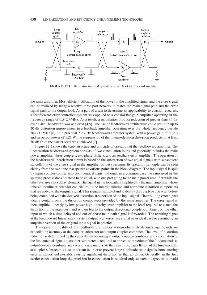
JWBS064-c12 JWBS064-Gerbennikov March 15, 2011 11:28 Printer Name: Yet to Come
658 LINEARIZATION AND EFFICIENCY ENHANCEMENT TECHNIQUES
FIGURE 12.1 Basic structure and operation principle of feedforward amplifier.
the main amplifier. Most efficient utilization of the power in the amplified signal and the error signalcan be realized by using a reactive three-port network to match the main signal path and the errorsignal path to the output load. As a part of a test to determine its applicability to coaxial repeaters,a feedforward error-controlled system was applied to a coaxial flat-gain amplifier operating in thefrequency range of 0.5–20 MHz. As a result, a modulation product reduction of greater than 35 dBover a 40:1 bandwidth was achieved [4,5]. The use of feedforward architecture could result in up to20 dB distortion improvement in a feedback amplifier operating over the whole frequency decade30–300 MHz [6]. In a practical 2.2 GHz feedforward amplifier system with a power gain of 30 dBand an output power of 1.25 W, the suppression of the intermodulation distortion products of at least50 dB from the carrier level was achieved [7].
Figure 12.1 shows the basic structure and principle of operation of the feedforward amplifier. Thelinearization feedforward system consists of two cancellation loops and generally includes the mainpower amplifier, three couplers, two phase shifters, and an auxiliary error amplifier. The operation ofthe feedforward linearization circuit is based on the subtraction of two equal signals with subsequentcancellation of the error signal in the amplifier output spectrum. Its operation principle can be seenclearly from the two-tone test spectra at various points in the block diagram. The input signal is splitby input coupler-splitter into two identical parts, although in a common case the ratio used in thesplitting process does not need to be equal, with one part going to the main power amplifier while theother part goes to a delay element. The signal in the top path is amplified by the main amplifier whoseinherent nonlinear behavior contributes to the intermodulation and harmonic distortion componentsthat are added to the original signal. This signal is sampled and scaled by the coupler-subtracter beforebeing combined with the delayed distortion-free portion of the input signal. The resulting error signalideally contains only the distortion components provided by the main amplifier. The error signal isthen amplified linearly by low-power high-linearity error amplifier to the level required to cancel thedistortion in the main part, and is then fed to the output directional coupler-combiner, on the otherinput of which a time-delayed and out-of-phase main-path signal is forwarded. The resulting signalat the feedforward linearization system output is an error-free signal in an ideal case or essentially anamplified version of the original input signal in practice.
The operation quality of the feedforward amplifier system obviously depends significantly oncancellation accuracy at the coupler-subtracter and output coupler-combiner. The level of distortionreduction is determined by the cancellation occurring at output coupler-combiner, and cancellation ofthe fundamental signals at coupler-subtracter is required to prevent subtraction of the fundamentals atoutput coupler-combiner and consequent gain loss. At the same time, cancellation of the fundamentalsat coupler-subtracter is also important in order to prevent large amplitude error signals from enteringerror amplifier and possibly causing significant distortion in that amplifier. Generally, in the firstcarrier-cancellation loop the precision in cancellation is required only to such a degree as to avoid

JWBS064-c12 JWBS064-Gerbennikov March 15, 2011 11:28 Printer Name: Yet to Come
FEEDFORWARD AMPLIFIER ARCHITECTURE 659
any substantial degradation of linearity in the error amplifier [5]. On the other hand, since the seconddistortion-cancellation loop controls the entire linearity improvement of the feedforward system, thedegree of its balance should always be at the highest level [7].
To analyze the effect of imperfect magnitude and phase equalization in the amplifier and delayline paths at any particular frequency, consider the signal in each upper and lower paths of the firstcancellation loop to be cosinusoidal in the form of
v1 = V cos ωt (12.1)
v2 = (V ± �V ) cos (ωt ± θ) (12.2)
where �V is the amplitude imbalance and θ is the phase imbalance.After subtraction of these signals in a coupler-subtracter, we have in a normalized form
�v
V= cos ωt −
(1 ± �V
V
)cos (ωt ± θ) = (1 − αcosθ) cos ωt ± α sin θ sin ωt (12.3)
where �v = v1 − v2 and
α = 1 ± �V
V. (12.4)
As a result, for a total imbalance magnitude,
|�v|V
=√
(1 − αcosθ)2 + (α sin θ)2. (12.5)
Since cancellation achieved by the second loop can be analyzed ideally in a similar way, thecancellation result achieved by the first and second loops independently can be rewritten in thecorresponding forms of
CANC1(dB) = 10 log10
(1 + α2
1 − 2α1 cos θ1
)(12.6)
CANC2(dB) = 10 log10
(1 + α2
2 − 2α2 cos θ2
)(12.7)
where α1 and θ1 are the amplitude and phase imbalance in the first loop, and α2 and θ2 are theamplitude and phase imbalance in the second loop, respectively [8].
Figure 12.2 shows the distortion cancellation as a function of amplitude and phase imbalance.From these curves it follows that, to obtain a high degree of cancellation accuracy, it is necessaryto maintain extremely small amounts of amplitude imbalance. For example, a 40 dB of cancellationwould require a phase imbalance of less than 1◦ and an amplitude imbalance of less than 0.1 dB.However, a demand for a high degree of linearity improvement will cause the system to becomesensitive to circuit parameter variations due to temperature change. To achieve temperature stabilityin a practical system, the degree of linearity improvement should be kept at a reasonably low level.For example, a 30 dB of cancellation would require only an amplitude imbalance of 0.25 dB and aphase imbalance of 1.8◦. To improve the temperature stability characteristic, it is better to realize bothmain and error amplifiers using the same technology, similar components and assembly techniques.However, if a higher degree of balance is to be maintained at all times, an automatic adaptive controlsystem must be employed. Besides, an additional transmission-line delay mismatch can be takeninto account when using transmission lines in high-frequency feedforward linearization systems. Forexample, if the difference in wavelength between the transmission lines in upper and lower paths atthe center bandwidth frequency f 0 is equal to 0.1f 0, then, in order to obtain a 30 dB of cancellation

JWBS064-c12 JWBS064-Gerbennikov March 15, 2011 11:28 Printer Name: Yet to Come
660 LINEARIZATION AND EFFICIENCY ENHANCEMENT TECHNIQUES
FIGURE 12.2 Cancellation as function of amplitude and phase imbalance.
with 30 MHz bandwidth at 800 MHz for α = 0.1 dB, the phase imbalance should be maintainedwithin approximately 1.0◦ [9].
It is of great importance for telecommunication system to minimize its nonlinear distortion level,and the main factor of its linearity is a level of the third-order intermodulation products at the systemoutput. In this case, consider the cancellation provided by both fist and second loop through theparameters of the feedforward system [10]. At the output of the coupler-subtracter with suppressedcarrier Psupp, the cancellation of the first loop is defined as
CANC1 = Psupp
C2 Pmain(12.8)
where C2 is the coupling coefficient of the second coupler-subtracter and Pmain is the carrier powerlevel of the main amplifier. On the other hand, the cancellation achieved in the second loop is
CANC2 = PIM3supp
PIM3main
1
T2 L2T3(12.9)
where PIM3main is the power level of the third-order intermodulation component, PIM3supp is the powerlevel of the third-order intermodulation component of the main amplifier suppressed at the linearizeroutput due to the corrective action of the second loop, L2 is the delay-line loss in the second loop, T2
and T3 are the transmission losses in the coupler-subtracter and output coupler-combiner, respectively.The effective cancellation of the overall feedforward linearization system is the ratio of the power
level of all intermodulation components at the feedforward system output over the power levelof the intermodulation products for open-loop configuration. As a result, for in-phase addition ofthe intermodulation components of the main and error amplifiers, the effective cancellation can beexpressed by
CANCeff (dB) = 20 log10
⎡⎣√
CANC2 +√
CANC31
(I P3main
I P3error
)2 T 22 L2
2
α32
(T3
C3
)2⎤⎦ (12.10)

JWBS064-c12 JWBS064-Gerbennikov March 15, 2011 11:28 Printer Name: Yet to Come
FEEDFORWARD AMPLIFIER ARCHITECTURE 661
where the amplitude imbalance α2 is defined as the ratio of the power gains of the two paths
α2 = T2 L2T3
C2G2C3(12.11)
where G2 is the power gain of the error amplifier, C3 is the coupling coefficient of the outputcoupler-combiner, and IP3main and IP3error are the third-order intercept points of the main and erroramplifiers, respectively. The first term in Eq. (12.10) depends on the balance level achieved in thesecond loop, whereas the second term defines the possible imbalance created by the first loop andsome other feedforward circuit parameters. In particularly, an error amplifier with sufficiently lowpower capabilities having too small value of IP3error or too big coupling coefficient C3 of the outputcoupler-combiner and loss (T2L2T3) through the main path increases the effect of the amplitude andphase imbalance.
The relationship between the overall feedforward system efficiency η and the efficiencies of thetwo amplifiers, ηmain for main amplifier and ηerror for error amplifier, when the losses (T2L2T3) throughthe main path are considered negligible, can be written as
η = ηmainηerrorC3 (1 − C3)
ηerrorC3 + ηmain fmain (1 − C3)(12.12)
where log10 fmain = −(C/I )main/10, (C/I)main is the ratio of carrier to third-order intermodulationproduct of the main amplifier [11,12]. Provided the optimum value of C3, which maximizes the overallefficiency η when the other system parameters are fixed, the maximum ηmax can be obtained by
ηmax = ηmain/
(1 +
√ηmain
ηerrorfmain
)2
(12.13)
which shows the efficiency degradation due to the linearization system [13]. For example, for atypical 10 dB coupling ratio of the output coupler-combiner, only 10% of the power from the erroramplifier reaches the load, which means that the error amplifier must produce ten times the power ofthe distortion in the main amplifier. In this case, it should operate in an inefficient linear mode in ordernot to disturb the error signal. As a result, the dc power consumed by the error amplifier can representa significant part of that of the main amplifier. In addition, it needs to take into account the factthat, despite its excellent distortion cancellation property, generally the feedforward amplifier systemrequires well-equalized circuitry and is characterized by substantially increased complexity and cost.
The efficiency of the conventional feedforward linearization system using a balanced configurationof the main amplifier shown in Figure 12.3(a) can be improved by providing some restructuring ofthe system. As a result, the modified feedforward system consists of three major loops shown inFigure 12.3(b): carrier cancelation loop, balanced power amplifier loop, and error-injection loop[14]. In this case, the carrier cancelation loop extracts the error signal from the amplified signal atthe output of the top power amplifier, whereas the error-injection loop provides an injection of theamplitude-adjusted and properly phased distortion into the output of the bottom power amplifier.Finally, the amplified signals in balanced paths are combined in the output hybrid combiner withcorresponding distortion cancellation. Unlike the conventional feedforward system, in its balancedversion each power amplifier sees only one coupler, either coupler-subtracter or output coupler-combiner, which means that there is no additional insertion loss due to output coupler-combiner as inthe conventional feedforward system. As a result, for the four-carrier wideband code division multipleaccess (WCDMA) signal with peak-to-average ratio of 10 dB, an efficiency improvement by 2% at anaverage output power of 40 dBm with an improvement in adjacent channel leakage power ratio (ACLR)(5 MHz offset) of about 18.6 dB by cancellation at the center bandwidth frequency of 2.14 GHz.
However, it is a serious problem for the conventional feedforward linearization system to maintainthe great accuracy in amplitude and phase balance over time, temperature, supply voltage, or inputsource and load variations. In practice, some forms of the gain and phase adjustments are essential to

JWBS064-c12 JWBS064-Gerbennikov March 15, 2011 11:28 Printer Name: Yet to Come
662 LINEARIZATION AND EFFICIENCY ENHANCEMENT TECHNIQUES
FIGURE 12.3 Balanced feedforward amplifier topologies.
achieve acceptably low level of intermodulation distortion. Figure 12.4(a) shows a block schematic ofthe analog adaptive feedforward linearization system that includes a feedback network for adaptivelyadjusting the performance of the overall feedforward system to compensate for uncontrolled variationsof its component parameters [15]. The feedback network provides a control of the carrier and distortioncancellation loops by comparing the signals sampled at their inputs and outputs and adaptivelyadjusts the corresponding vector modulators to minimize the amplitude and phase imbalance whenit is necessary. Different adaptation algorithms using optimization techniques can be implemented toimprove the cancellation results for an analog adaptive feedforward linearization system [16].
Using a digital signal processing (DSP) creates a good opportunity to provide a correction inthe amplitude and phase imbalance in the feedforward linearization system at baseband level, thusmaking this procedure more predictable and fast and overcoming the problems with mixer dc offsetand masking of strong signals by weaker ones than can compromise analog adaptive implementations[17]. To compensate for the component frequency response and the nonadaptive nature of the delaylines, a hybrid of the conventional feedforward linearizer and a digital signal processor can be used, asshown in Figure 12.4(b), where both the amplifier input signal and the reference signal are generatedby DSP [18]. The reference signal is then used to cancel the linearly amplified component of thedistorted amplifier output signals, leaving an error signal containing only the main amplifier distortion.By generating the reference signal in the DSP, rather than using an analog splitter, some of the analoghardware can be moved into a simpler digital implementation, with independent control of the mainamplifier and reference signals by using equalizers. In this case, the amplitude and reference equalizerscorrect the phase shift, time delay and nonideal response of the analog components to achieve theproper distortion cancellation. By improving the cancellation of the first loop, a more accurate errorsignal is generated that consists only of the distortion from the main amplifier. Generally, the use of
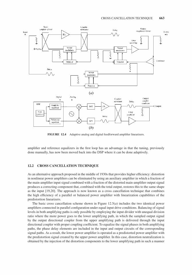
JWBS064-c12 JWBS064-Gerbennikov March 15, 2011 11:28 Printer Name: Yet to Come
CROSS CANCELLATION TECHNIQUE 663
FIGURE 12.4 Adaptive analog and digital feedforward amplifier linearizers.
amplifier and reference equalizers in the first loop has an advantage in that the tuning, previouslydone manually, has now been moved back into the DSP where it can be done adaptively.
12.2 CROSS CANCELLATION TECHNIQUE
As an alternative approach proposed in the middle of 1930s that provides higher efficiency: distortionin nonlinear power amplifiers can be eliminated by using an auxiliary amplifier in which a fraction ofthe main-amplifier input signal combined with a fraction of the distorted main-amplifier output signalproduces a correcting component that, combined with the total output, restores this to the same shapeas the input [19,20]. The approach is now known as a cross cancellation technique that combinesthe high efficiency of a parallel or balanced power amplifier with linearization capabilities of thepredistortion linearizers.
The basic cross cancellation scheme shown in Figure 12.5(a) includes the two identical poweramplifiers connected in parallel configuration under equal input drive conditions. Balancing of signallevels in both amplifying paths is only possible by employing the input divider with unequal divisionratio where the more power goes to the lower amplifying path, in which the sampled output signalby the output directional coupler from the upper amplifying path is delivered through the inputdirectional coupler with proper coupling coefficient. To equalize the signal phases in both amplifyingpaths, the phase delay elements are included in the input and output circuits of the correspondingsignal paths. As a result, the lower power amplifier is operated as a predistorted power amplifier withthe predistortion signal created by the upper power amplifier. In this case, distortion neutralization isobtained by the injection of the distortion components to the lower amplifying path in such a manner

JWBS064-c12 JWBS064-Gerbennikov March 15, 2011 11:28 Printer Name: Yet to Come
664 LINEARIZATION AND EFFICIENCY ENHANCEMENT TECHNIQUES
FIGURE 12.5 Cross cancellation linearizer diagrams.
that they will be 180◦ out of phase with those being created by the upper power amplifier at the inputof the output combiner.
To derive some analytical relationships between parameters of the cross cancellation linearizationsystem shown in Figure 12.5(a), consider an idealized approach where the system parameters arenormalized to the input power and power ratio of the input unequal divider is equal to 1:N. Then,the output powers of lower and upper amplifying paths at the corresponding inputs of the outputcombiner can be written as
GP (1 − C31) + IM = [N (1 − C31) − (GP + IM) C2
31
]GP + IM
= [N (1 − C31) − GPC2
31
]GP + (
1 − GPC231
)IM (12.14)
where GP is the power gain of each power amplifier (PA), IM is the intermodulation distortionintroduced by each PA, and C31 is the coupling factor of each directional coupler calculated as theratio of power at the output port 3 relative to the input port 1 equal to the coupling factor C24 of theinput directional coupler when its port 4 becomes an input port. From comparison between the left-and right-hand sides of Eq. (12.14) it follows that the out-of-phase conditions for intermodulationcomponents at the corresponding inputs of the output in-phase combiner can be obtained when
GPC231 = 2 (12.15)
resulting in
N = 3 − C31
1 − C31. (12.16)

JWBS064-c12 JWBS064-Gerbennikov March 15, 2011 11:28 Printer Name: Yet to Come
REFLECT FORWARD LINEARIZATION AMPLIFIER 665
As an example, if the power gain of each PA is GP = 200 or 23 dB, then from Eq. (12.15) itfollows that it is necessary to choose the input and output directional couplers with coupling factorC31 = 0.1 or −10 dB and the input power divider with N = 3.2 (about 5 dB) resulting then fromEq. (12.16). In this case, the power gain of the overall system reduces to 19.5 dB. However, it wasfound that the linearity improvement is not as high as in a feedforward linearizer where the distortionsare subtracted at its output. This is because the amplifying paths are not really identical. To makethe cross cancellation system more symmetrical, it is necessary to equalize the insertion losses in theoutput circuits of both amplifying paths by introducing a required attenuation in a lower path, whichin turn results in reduced system efficiency. Generally, in practical applications, with varying inputdrive levels and temperature, it is necessary to use phase shifters and variable attenuators that arecontrolled by a power-minimization loop controller that serves to minimize the distortion componentsin a composite output signal [21].
Figure 12.5(b) show the cross cancellation technique based on a balanced power amplifier config-uration where the distortion generated in one balanced path, which is identical to the other path, areused to cancel the distortions generated by the whole balanced power amplifier [22]. This approachprovides a control of the error signal separately, as in the feedforward technique. However, the maindifference between these two techniques is that the error signal is added to the input of the amplifyingpath, not to the output, thus improving the system efficiency. In this case, samples of the signal anddistortion from lower amplifying path are combined with a portion of the reference signal deliveredfrom the input splitter such that the linear components of these two signals are cancel each otherleaving the distortion components only from the sampled path of the balanced power amplifier. Thegain and phase of the distortion are then adjusted using variable attenuator, phase shifter and linearerror amplifier so that, when it is coupled into the input of the other path of the balanced poweramplifier, the distortions generated by both paths of the balanced power amplifier are cancelled.
12.3 REFLECT FORWARD LINEARIZATION AMPLIFIER
The reflect forward adaptive linearizer (RFAL) technique uses the input reflected signal from onepower amplifier to develop an intermodulation-correcting signal forwarded to the input of the otherpower amplifier, which are connected in parallel or balanced configuration [23,24]. Figure 12.6 shows
FIGURE 12.6 Block schematic of reflect forward linearization amplifier.

JWBS064-c12 JWBS064-Gerbennikov March 15, 2011 11:28 Printer Name: Yet to Come
666 LINEARIZATION AND EFFICIENCY ENHANCEMENT TECHNIQUES
a block diagram of the RFAL amplifier that includes the two identical power amplifiers, low-distortionbooster amplifier, forward and reflected paths with two directional couplers at the input, and delayline and in-phase combiner at the output. With RFAL technique, the power combining efficiency ofthe two power amplifiers approaches that of the conventional parallel power amplifier configuration,while the intermodulation products can be improved from 20 to 30 dBc at the center bandwidthfrequency.
The basic principle of RFAL operation can be described as follows: when the two-tone forwardfundamental signal is reflected from the transistor input of upper power amplifier, the resultingreflected two-tone fundamental signal is out-of-phase relative to the input forward signal and is in-phase relative to the output signal. In this case, the intermodulation components appeared at the upperpower amplifier input as a result of its active device nonlinearity are in-phase relative to the outputintermodulation components. The input reflected composite signal containing the fundamental and in-termodulation components is used as a correcting signal for the lower power amplifier. This correctingsignal, when properly amplified and phased in the reflected path, cancels the output intermodulationdistortions produced by the lower power amplifier when it is combined with the input signal flowingthrough the forward path. The booster amplifier in a lower path is necessary to equalize the drivesignal levels for both upper and lower power amplifiers. In this case, the signals from the upper andlower amplifying paths have the in-phase fundamental and out-of-phase intermodulation componentsat the corresponding inputs of the output in-phase combiner, thus resulting in a distortion cancella-tion in the combined signal flowing into the load. The laterally diffused metal-oxide-semiconductor(LDMOS) RFAL amplifier with output power of 43 dBm achieves an improvement of the third-orderintermodulation products by over 15 dB and a total efficiency of more than 20% over the frequencyrange from 865 to 895 MHz [25]. For very high cancelation requirements over wide temperatureand drive conditions an adaptive feedback network can be used to monitor the relative amplitudeand phase at the outputs of the power amplifiers and drive the voltage variable attenuators and phaseshifters to maintain the optimum conditions.
12.4 PREDISTORTION LINEARIZATION
To achieve simultaneously high-efficiency and low-distortion operation conditions of the power am-plifier when the linearity requirements are not extremely high, it is possible to use a predistortionlinearizer that provides the positive amplitude and negative phase deviations for input RF signalto compensate for the active device nonlinearity whose nonlinear behavior (when a power ampli-fier is operated close to saturation) usually represents the opposite behavior of its amplitude andphase characteristics. Historically, the initial idea to compensate for the third-order intermodulationproducts arising in vacuum-tube amplifier was to use the linearization scheme where the nonlinearamplifier having a compressing characteristic is followed by a nonlinear element having an expandingcharacteristic and producing the third-order distortion of opposite sign to that of the amplifier [26].
The block diagram of a linearized power amplifier system with a predistortion linearizer withindication of the appropriate amplitude and phase dependences at each stage of the system is shownin Figure 12.7, where also a variable attenuator for adjusting the amplitude level of the input signalis included. At microwaves, a linearized power amplifier usually includes two isolators for stableoperation conditions. The conventional predistortion linearizer circuits generally use either diodes ortransistors as sources of intermodulation [27,28].
As an interesting fact, yet at the beginning of 1920s it was claimed that, by using similar vacuumtubes in both stages of a two-stage power amplifier with similar signals at their inputs, the evenharmonics generated by the first amplification are neutralized by the even harmonics generated by thesecond amplification because they are similar in amplitude and opposite in phase at the output of thesecond vacuum tube [29]. Indeed, as it turned out with regard to modern transistor power amplifiersusing GaAs pseudomorphic high electron mobility transistor (pHEMT) devices, it is enough toproper choose a bias point of a driver-stage device in a two-stage amplifier to provide a negativephase deviation to compensate for the positive phase deviation of the final stage [30]. In this case, the

JWBS064-c12 JWBS064-Gerbennikov March 15, 2011 11:28 Printer Name: Yet to Come
PREDISTORTION LINEARIZATION 667
FIGURE 12.7 Block diagram of power amplifier with predistortion linearizer.
quiescent current of the driver-stage device, whose size is three times smaller than that of a final-stagedevice, is sufficiently small. As a result, for a quiescent current equal to 1.25% of the device dcsaturated current, an improvement of more than 5 dB in ACLR of a whole high-efficiency two-stagecellular-phone WCDMA power amplifier operating at 1.95 GHz can be achieved at backoff outputpowers close to the saturation power.
Figure 12.8(a) shows the schematic of a simple diode linearizer composed of a series Schottkydiode and a parallel capacitor with two RF chokes for dc feed and two blocking capacitors, whichprovides positive amplitude and negative phase deviations when input power increases [31]. Theequivalent circuit of the series diode is shown in Figure 12.8(b), where R is the diode equivalentresistance and Cj is the junction capacitance. With the increase of an incident input signal power, theforward diode current increases that leads to the decrease of the diode resistance R. In this case, thepositive amplitude and negative phase deviations can be achieved under low forward-bias conditionswhen the diode current ranges from 0.1 to 1.0 mA, and, in the latter case, the phase deviation canreach a value of −30◦. Applying such a linearizer to a 1.9 GHz monolithic microwave integratedcircuit (MMIC) power amplifier with saturated power of 22.5 dBm, an improvement of adjacentchannel power ratio (ACPR) of 5 dB can be achieved for the quadrature phase shift keying (QPSK)modulated signal when output powers are less than 15 dBm.
FIGURE 12.8 Simple diode-based predistortion linearizers.

JWBS064-c12 JWBS064-Gerbennikov March 15, 2011 11:28 Printer Name: Yet to Come
668 LINEARIZATION AND EFFICIENCY ENHANCEMENT TECHNIQUES
A similar improvement of ACPR can be achieved by using a linearizer based on a parallel Schottkydiode with the bias feed resistor Rb, which is shown in Figure 12.8(c) [32]. With the increase of inputpower, the bias point of a diode changes due to the voltage drop across the resistor Rb caused inturn by the increased diode forward current. As a result, due to the decreased diode resistance R, thelinearizer achieves positive gain and negative phase deviations. By applying such a linearizer to a2.7 GHz power amplifier, a maximum improvement of 5 dB was achieved for low quiescent currentconditions at output power of 34 dBm.
Positive amplitude deviation with negative phase deviation can also be achieved using a series-feedback GaAs metal semiconductor field-effect transistor (MESFET) amplifier with a large sourceinductance Ls, a block diagram of which (including matching circuits) is shown in Figure 12.9(a) [33].The required amplitude and phase deviations are due to nonlinearities of the device transconductancegm, gate–source capacitance Cgs, and differential drain–source resistance Rds. For the device with agate width of 1.2 mm, a nonlinearity of gm contributes to the positive amplitude deviation when Ls =20 nH. At the same time, nonlinearities of both gm and Rds contribute to the negative phase deviationwhen Ls ≥ 3 nH. A nonlinearity of Cgs has a negligibly small effect on both the amplitude and phasedeviations. As a result, for a linearizer with Ls = 16 nH at an operating frequency of 1.9 GHz, thepositive amplitude and negative phase deviations were obtained across the input power dynamic rangefrom 5 to 18 dBm, with amplitude deviation of 2.5 dB and phase deviation of 30◦ at 18 dBm inputpower. The GaAs MESFET device was biased in Class AB mode with a drain–source supply voltageof 2 V providing a quiescent current of 78 mA. By applying this linearizing technique to a 1.9 GHzMMIC power amplifier with 1-dB compressed power of 17 dBm, an improvement of ACPR up to 7dB was achieved for a π /4-shifted QPSK signal.
As an alternative, it is also possible to achieve positive amplitude and negative phase deviationsusing a source-grounded MESFET device with zero drain–source supply voltage [34]. The schematicdiagram of such a linearizer is shown in Figure 12.9(b). In this case, for the device with a gate widthof 240 μm at the saturation power of 20 mW under the gate bias condition of Vg = −0.4 V, the
FIGURE 12.9 Transistor-based linearizers.

JWBS064-c12 JWBS064-Gerbennikov March 15, 2011 11:28 Printer Name: Yet to Come
PREDISTORTION LINEARIZATION 669
3-dB increased power gain and of about 30-degree negative phase were achieved due to the varyingdrain–source resistance. Because of its simplicity, such a linearizer can operate from 2 to 12 GHzwith good thermal stability. When it was implemented into a 50 W solid-state power amplifier systemat operating frequency of 7 GHz, the system noise power ratio was improved over 15-dB dynamicrange, in particular by 2 dB at the 3-dB output power backoff point.
More advanced configurations of the predistortion linearizer is based on the splitting of theinput signal into nonlinear and linear paths using a directional coupler or a hybrid divider withsubsequent subtraction of resulting signals in the output coupler-subtracter. The block diagram ofsuch a predistortion linearizer that employs two power amplifiers in a balanced configuration usingtwo 90-degree hybrids is shown in Figure 12.10(a) [28]. In this case, the upper power amplifier isoperated in a linear Class A mode while the lower power amplifier is biased in a nonlinear Class ABor B mode to generate the proper intermodulation products by controlling the input power and devicebias conditions. The phase shifter in a lower amplifying path is necessary to optimize the level of thefundamental components in the resulting output spectrum. Since both devices present approximatelythe same input impedances, a low input return loss is provided because the most of the reflected powerflows into the isolated port. Figure 12.10(b) shows the practical microwave microstrip implementationof a two-path predistortion linearizer with an input 90-degree branch-line hybrid coupler, a nonlinearpower amplifier in a lower path and an output directional coupler [35]. The microstrip transmissionline in a lower amplifying path having a required electrical length compensates for the additionalphase shift provided by the active device, whereas the required amplitude conditions are realizedwith the coupling coefficient of an output coupler-subtracter to be chosen. As a result, for a Ku-bandmulticarrier 4.5-W power amplifier, the phase deviation of a 12-dBm signal at the linearizer outputup to −10◦ was achieved with a 22-dBm signal at the linearizer input.
Figure 12.11 shows the modified three-path predistortion linearizer structure, where a balancedconfiguration with a nonlinear power amplifier is adjusted for suppression of the fundamental com-ponents with the resulting error signal. Then, the amplitude-adjusted and properly phased error signalis amplified by an error amplifier and added to the linear component in the upper path, which is a
FIGURE 12.10 Block diagrams of power amplifier linearizers with input power splitting.
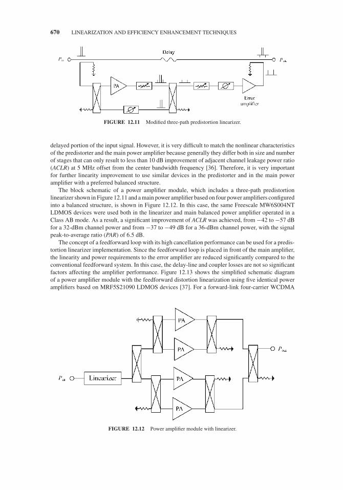
JWBS064-c12 JWBS064-Gerbennikov March 15, 2011 11:28 Printer Name: Yet to Come
670 LINEARIZATION AND EFFICIENCY ENHANCEMENT TECHNIQUES
FIGURE 12.11 Modified three-path predistortion linearizer.
delayed portion of the input signal. However, it is very difficult to match the nonlinear characteristicsof the predistorter and the main power amplifier because generally they differ both in size and numberof stages that can only result to less than 10 dB improvement of adjacent channel leakage power ratio(ACLR) at 5 MHz offset from the center bandwidth frequency [36]. Therefore, it is very importantfor further linearity improvement to use similar devices in the predistorter and in the main poweramplifier with a preferred balanced structure.
The block schematic of a power amplifier module, which includes a three-path predistortionlinearizer shown in Figure 12.11 and a main power amplifier based on four power amplifiers configuredinto a balanced structure, is shown in Figure 12.12. In this case, the same Freescale MW6S004NTLDMOS devices were used both in the linearizer and main balanced power amplifier operated in aClass AB mode. As a result, a significant improvement of ACLR was achieved, from −42 to −57 dBfor a 32-dBm channel power and from −37 to −49 dB for a 36-dBm channel power, with the signalpeak-to-average ratio (PAR) of 6.5 dB.
The concept of a feedforward loop with its high cancellation performance can be used for a predis-tortion linearizer implementation. Since the feedforward loop is placed in front of the main amplifier,the linearity and power requirements to the error amplifier are reduced significantly compared to theconventional feedforward system. In this case, the delay-line and coupler losses are not so significantfactors affecting the amplifier performance. Figure 12.13 shows the simplified schematic diagramof a power amplifier module with the feedforward distortion linearization using five identical poweramplifiers based on MRF5S21090 LDMOS devices [37]. For a forward-link four-carrier WCDMA
FIGURE 12.12 Power amplifier module with linearizer.
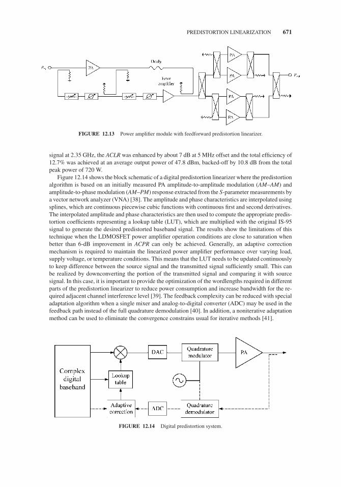
JWBS064-c12 JWBS064-Gerbennikov March 15, 2011 11:28 Printer Name: Yet to Come
PREDISTORTION LINEARIZATION 671
FIGURE 12.13 Power amplifier module with feedforward predistortion linearizer.
signal at 2.35 GHz, the ACLR was enhanced by about 7 dB at 5 MHz offset and the total efficiency of12.7% was achieved at an average output power of 47.8 dBm, backed-off by 10.8 dB from the totalpeak power of 720 W.
Figure 12.14 shows the block schematic of a digital predistortion linearizer where the predistortionalgorithm is based on an initially measured PA amplitude-to-amplitude modulation (AM–AM) andamplitude-to-phase modulation (AM–PM) response extracted from the S-parameter measurements bya vector network analyzer (VNA) [38]. The amplitude and phase characteristics are interpolated usingsplines, which are continuous piecewise cubic functions with continuous first and second derivatives.The interpolated amplitude and phase characteristics are then used to compute the appropriate predis-tortion coefficients representing a lookup table (LUT), which are multiplied with the original IS-95signal to generate the desired predistorted baseband signal. The results show the limitations of thistechnique when the LDMOSFET power amplifier operation conditions are close to saturation whenbetter than 6-dB improvement in ACPR can only be achieved. Generally, an adaptive correctionmechanism is required to maintain the linearized power amplifier performance over varying load,supply voltage, or temperature conditions. This means that the LUT needs to be updated continuouslyto keep difference between the source signal and the transmitted signal sufficiently small. This canbe realized by downconverting the portion of the transmitted signal and comparing it with sourcesignal. In this case, it is important to provide the optimization of the wordlengths required in differentparts of the predistortion linearizer to reduce power consumption and increase bandwidth for the re-quired adjacent channel interference level [39]. The feedback complexity can be reduced with specialadaptation algorithm when a single mixer and analog-to-digital converter (ADC) may be used in thefeedback path instead of the full quadrature demodulation [40]. In addition, a noniterative adaptationmethod can be used to eliminate the convergence constrains usual for iterative methods [41].
FIGURE 12.14 Digital predistortion system.
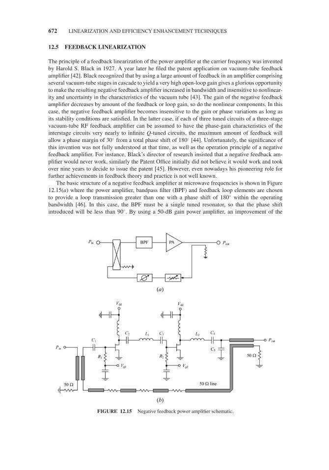
JWBS064-c12 JWBS064-Gerbennikov March 15, 2011 11:28 Printer Name: Yet to Come
672 LINEARIZATION AND EFFICIENCY ENHANCEMENT TECHNIQUES
12.5 FEEDBACK LINEARIZATION
The principle of a feedback linearization of the power amplifier at the carrier frequency was inventedby Harold S. Black in 1927. A year later he filed the patent application on vacuum-tube feedbackamplifier [42]. Black recognized that by using a large amount of feedback in an amplifier comprisingseveral vacuum-tube stages in cascade to yield a very high open-loop gain gives a glorious opportunityto make the resulting negative feedback amplifier increased in bandwidth and insensitive to nonlinear-ity and uncertainty in the characteristics of the vacuum tube [43]. The gain of the negative feedbackamplifier decreases by amount of the feedback or loop gain, so do the nonlinear components. In thiscase, the negative feedback amplifier becomes insensitive to the gain or phase variations as long asits stability conditions are satisfied. In the latter case, if each of three tuned circuits of a three-stagevacuum-tube RF feedback amplifier can be assumed to have the phase-gain characteristics of theinterstage circuits very nearly to infinite Q-tuned circuits, the maximum amount of feedback willallow a phase margin of 30◦ from a total phase shift of 180◦ [44]. Unfortunately, the significance ofthis invention was not fully understood at that time, as well as the operation principle of a negativefeedback amplifier. For instance, Black’s director of research insisted that a negative feedback am-plifier would never work, similarly the Patent Office initially did not believe it would work and tookover nine years to decide to issue the patent [45]. However, even nowadays his pioneering role forfurther achievements in feedback theory and practice is not well known.
The basic structure of a negative feedback amplifier at microwave frequencies is shown in Figure12.15(a) where the power amplifier, bandpass filter (BPF) and feedback loop elements are chosento provide a loop transmission greater than one with a phase shift of 180◦ within the operatingbandwidth [46]. In this case, the BPF must be a single tuned resonator, so that the phase shiftintroduced will be less than 90◦. By using a 50-dB gain power amplifier, an improvement of the
FIGURE 12.15 Negative feedback power amplifier schematic.
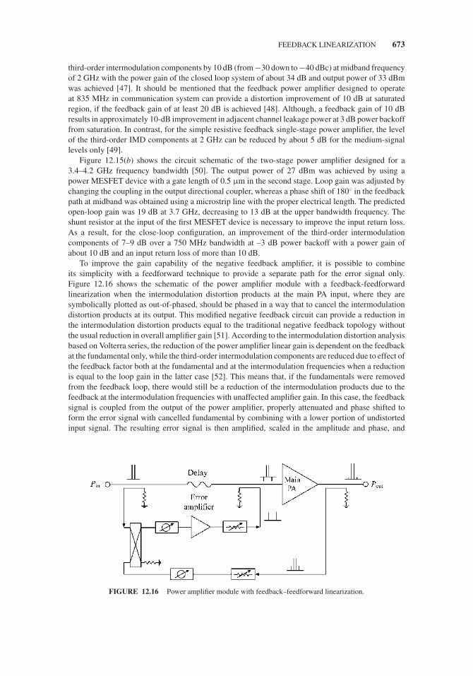
JWBS064-c12 JWBS064-Gerbennikov March 15, 2011 11:28 Printer Name: Yet to Come
FEEDBACK LINEARIZATION 673
third-order intermodulation components by 10 dB (from −30 down to −40 dBc) at midband frequencyof 2 GHz with the power gain of the closed loop system of about 34 dB and output power of 33 dBmwas achieved [47]. It should be mentioned that the feedback power amplifier designed to operateat 835 MHz in communication system can provide a distortion improvement of 10 dB at saturatedregion, if the feedback gain of at least 20 dB is achieved [48]. Although, a feedback gain of 10 dBresults in approximately 10-dB improvement in adjacent channel leakage power at 3 dB power backofffrom saturation. In contrast, for the simple resistive feedback single-stage power amplifier, the levelof the third-order IMD components at 2 GHz can be reduced by about 5 dB for the medium-signallevels only [49].
Figure 12.15(b) shows the circuit schematic of the two-stage power amplifier designed for a3.4–4.2 GHz frequency bandwidth [50]. The output power of 27 dBm was achieved by using apower MESFET device with a gate length of 0.5 μm in the second stage. Loop gain was adjusted bychanging the coupling in the output directional coupler, whereas a phase shift of 180◦ in the feedbackpath at midband was obtained using a microstrip line with the proper electrical length. The predictedopen-loop gain was 19 dB at 3.7 GHz, decreasing to 13 dB at the upper bandwidth frequency. Theshunt resistor at the input of the first MESFET device is necessary to improve the input return loss.As a result, for the close-loop configuration, an improvement of the third-order intermodulationcomponents of 7–9 dB over a 750 MHz bandwidth at –3 dB power backoff with a power gain ofabout 10 dB and an input return loss of more than 10 dB.
To improve the gain capability of the negative feedback amplifier, it is possible to combineits simplicity with a feedforward technique to provide a separate path for the error signal only.Figure 12.16 shows the schematic of the power amplifier module with a feedback-feedforwardlinearization when the intermodulation distortion products at the main PA input, where they aresymbolically plotted as out-of-phased, should be phased in a way that to cancel the intermodulationdistortion products at its output. This modified negative feedback circuit can provide a reduction inthe intermodulation distortion products equal to the traditional negative feedback topology withoutthe usual reduction in overall amplifier gain [51]. According to the intermodulation distortion analysisbased on Volterra series, the reduction of the power amplifier linear gain is dependent on the feedbackat the fundamental only, while the third-order intermodulation components are reduced due to effect ofthe feedback factor both at the fundamental and at the intermodulation frequencies when a reductionis equal to the loop gain in the latter case [52]. This means that, if the fundamentals were removedfrom the feedback loop, there would still be a reduction of the intermodulation products due to thefeedback at the intermodulation frequencies with unaffected amplifier gain. In this case, the feedbacksignal is coupled from the output of the power amplifier, properly attenuated and phase shifted toform the error signal with cancelled fundamental by combining with a lower portion of undistortedinput signal. The resulting error signal is then amplified, scaled in the amplitude and phase, and
FIGURE 12.16 Power amplifier module with feedback–feedforward linearization.

JWBS064-c12 JWBS064-Gerbennikov March 15, 2011 11:28 Printer Name: Yet to Come
674 LINEARIZATION AND EFFICIENCY ENHANCEMENT TECHNIQUES
FIGURE 12.17 Measured spectrum of WCDMA 3GPP FWD output signal (a) before and (b) after feedback–feedforward linearization.
finally combined with a delayed upper portion of the undistorted signal to form the composite signalat the amplifier input with out-of-phased distortion products required to cancel the intermodulationproducts at the amplifier output. The stability analysis shows that, for narrow-band amplifiers withminimum loop delay, the reduction of third-order intermodulation products can exceed 20 dB [51].
In this case, when four Freescale MW6S004NT LDMOS devices operated in Class AB modeare used in the main PA that represents a balanced configuration of the four amplifying stagessimilar to shown in Figure 12.12, a 7-dB improvement of ACLR from −38 to −47 dB for a 35-dBmchannel power with the signal peak-to-average ratio of 6.5 dB was achieved, as shown in Figure12.17. The power amplifier gain was 17 dB and coupling coefficient of the microstrip output couplerwas 10 dB. This indicates that the effect of the negative feedback on the intermodulation productsis independent of the cancellation of the fundamentals in the loop, and circuit can successfullyreduce the intermodulation distortion without affecting the gain of the power amplifier. For furtherintermodulation reduction, it is necessary to use a multistage power amplifier with overall high powergain to increase the loop gain.
The feedback linearization technique can also be implemented reversely to a feedforward scheme,as shown in Figure 12.18, where the linearizing circuit consists of the feedback, canceling andfeeding blocks [53]. At the canceling block, the amplitude-corrected and phase-shifted feedbacksignal is combined with the sampled input signal to form the error signal, which is then amplified andadded with proper amplitude and phase to the input undistorted signal within the feeding block. As aresult, for a 38-dB main amplifier gain, the cancellation of the third-order intermodulation productsfrom −22 to −42 dBc were achieved at the output power P1dB = 27 dBm and operating frequency

JWBS064-c12 JWBS064-Gerbennikov March 15, 2011 11:28 Printer Name: Yet to Come
FEEDBACK LINEARIZATION 675
FIGURE 12.18 Power amplifier with feedback predistortion linearization.
of 1.85 GHz. However, the critical problems of this analog feedback predistortion scheme are theoperation at bandwidth limitation caused by the loop delay and an oscillation tendency caused by thefeedback nature. By employing a digital LUT technique, these limitations can be overcome, whilemaintaining the advantages of the feedback circuit [54]. As a result, the distortion is corrected in adigital domain and further enhanced by the feedback linearization. In this case, the structure of adigital feedback linearizer is the same as the analog feedback counterpart, except that the feedbacksignal in the cancellation loop constructs a LUT in the digital domain, and the gain factors of thesignal canceling and feedback paths are adjusted by the DSP instead of using the variable attenuatorsand phase shifters. The predistortion signal is extracted directly from the LUT, which has beenupdated using the error signal extracted at the signal cancellation loop beforehand. Thus, the timedelay through the loop is eliminated, and the bandwidth limitation does not exist anymore. At thesame time, the oscillation tendency of the feedback circuit can be suppressed easily by digital controlof the feedback loop parameters. Compared to the conventional digital predistortion technique, lessnumber of iterations is required for convergence with simpler algorithm.
The envelope-feedback linearization is a simple and popular technique to improve the distortionassociated with the amplitude nonlinearity of the power amplifier [44,55]. The basis of this technique,the block diagram of which is shown in Figure 12.19(a), is to compare the envelopes of the inputand output signals, and to control the instantaneous gain of the power amplifier so as to minimizethe difference between them. In this case, the RF input and output signals are sampled by thecorresponding input and output couplers and then each fed to the proper input of the differentialamplifier. The difference signal, representing the error between the input and output envelopes, isused to drive a variable gain amplifier to modify the envelope of the input signal that drives thepower amplifier. The linearization effect depends on the nonlinearity of the detectors, especially atlow signal levels, the bandwidth, time delay, and phase-gain characteristic of the feedback loop andthe sensitivity of the variable gain amplifier. Therefore, where the AM–AM distortion is dominant,the two-tone intermodulation products are typically reduced by up to 10 dB. To provide a significantimprovement in the nonlinear distortion cancellation, both RF feedback and envelope feedbackmethods can be combined [44].
Figure 12.19(b) shows the envelope-feedback power amplifier module with a digital adaptivepredistortion developed for code division multiple access (CDMA) handset application in a frequencyrange of 887–925 MHz [56]. The block diagram of the power amplifier module includes additionallya surface acoustic wave (SAW) filter, a phase-controlling block and a CMOS integrated circuitincorporating two LUTs to linearize AM–AM and AM–PM characteristics. The variable gain amplifieris based on a dual-gate MOSFET to linearize AM–AM characteristic, which can easily vary the powergain by controlling its second-gate bias voltage in a range of more than 10 dB. In the phase-controlling block, a varactor diode was used with the phase range of more than 10◦. By producingappropriate AM–PM predistortion data including phase characteristics of the dual-gate MOSFETand the following PA block, the total AM–PM can be linearized. Because the variations of phasewith supply voltage and temperature according to the measurement results were insignificant, it wasenough to use the LUT with modified initial data to minimize phase variations versus input power

JWBS064-c12 JWBS064-Gerbennikov March 15, 2011 11:28 Printer Name: Yet to Come
676 LINEARIZATION AND EFFICIENCY ENHANCEMENT TECHNIQUES
FIGURE 12.19 Block diagrams of power amplifier with adaptive predistortion.
that were predictable in advance. To linearize AM–AM characteristic, the adaptive predistortion wasused by modifying the data in LUT during linearization process. It was found that the allowabletime delay must be less than 40 ns for CDMA signal. As a result, by using a digital adaptivepredistortion mechanism for only AM–AM characteristic, the PAE was increased up to 48% for theoutput power of 27.5 dBm and ACPR of −49 dBc. The complementary metal-oxide-semiconductor(CMOS) integrated circuit, whose size is 2.5×2.5 mm2, consumed of about 15 mA.
The AM–AM linearization can also be achieved by dynamically varying the gate bias voltage ofthe final-stage transistor. In such an adaptive double-envelope feedback two-stage MESFET poweramplifier the gain variations are detected directly while the phase variations are detected through a90◦ branch-line coupler [57]. This is possible since when the gate goes more negative, the MESFETis closer to pinch-off and its gain is reduced. On the other hand, as the gate goes more positive, theMESFET will approach Class A, where its gain is maximal. The dynamic bias on the gate of theMESFET resulted in an increase in P1dB by 1 dB, which improved the PAE by 5%.
To overcome the limitation of the envelope-feedback technique to correct for AM–PM distortion,the polar-loop technique can be used where a phased-lock loop is added to the envelope feedbacksystem resulting in a polar-loop feedback [58]. However, the key disadvantage of a polar feedbackoccurs in the generally different bandwidths required for the amplitude and phase feedback paths, aswell as locking capability of the phased-lock loop is limited at low signal level in the presence ofinterference coupled to the transmitter output from antenna that leads to a poorer overall performance.The Cartesian-feedback technique can solve at some extent the problems associated with the widebandwidth of the signal phase by applying modulation feedback in the in-phase (I) and quadrature(Q) Cartesian baseband components. Figure 12.20(a) shows the basic block diagram of the Cartesian

JWBS064-c12 JWBS064-Gerbennikov March 15, 2011 11:28 Printer Name: Yet to Come
FEEDBACK LINEARIZATION 677
FIGURE 12.20 Digital predistortion system.
loop transmitter with two identical feedback loops for I and Q channels [12,59]. In this case, thesampled output signal is quadrature downconverted and demodulated to Cartesian co-ordinate signals,amplified and then subtracted from the corresponding input signals to form a distorted error signalthat is complementary to the distortion signal at the PA output after being filtered and upconverted.The amount of the distortion reduction is equal to the loop gain and is high inside the passband ofthe loop filters. The phase shifter is necessary to control the phase delays that cause rotation of thesignal constellation. The bandwidth of the Cartesian components is narrower than that of the RFsignal, however errors in the feedback loop are not corrected and feedback components must be aslinear as the desired loop linearity. The Cartesian feedback can be used to linearize multicarrier poweramplifiers, improving output spectrum by 10–30 dB [60].
Further linearity improvement can be achieved by using a combined Cartesian loop and adaptivebaseband predistortion linearization techniques using DSP, as shown in Figure 12.20(b) [61]. Adaptivepredistortion provides a continuous adjusting of the loop time delays and updating of the predistorterLUT with information of the PA nonlinearity, which changes with supply voltage, temperature, loadvoltage standing wave ratio (VSWR), output power, and other environmental effects. For example, byusing the predistorter implemented in DSP with 5-bit effective resolution digital-to-analog convertersat its output and optimized using a direct search algorithm, a further 11-dB reduction of the third-orderintermodulation components was achieved when a predistorted component has been added to the errorsignal [62]. However, as the bandwidth of transmitting signal gets wider, the feedback loop delaymismatch becomes increasingly detrimental to the convergence of LUT adaptation algorithm. In thiscase, the analog Cartesian feedback, which is separated from LUT, can be used only for LUT training,
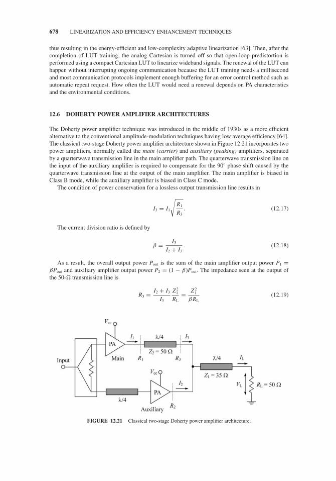
JWBS064-c12 JWBS064-Gerbennikov March 15, 2011 11:28 Printer Name: Yet to Come
678 LINEARIZATION AND EFFICIENCY ENHANCEMENT TECHNIQUES
thus resulting in the energy-efficient and low-complexity adaptive linearization [63]. Then, after thecompletion of LUT training, the analog Cartesian is turned off so that open-loop predistortion isperformed using a compact Cartesian LUT to linearize wideband signals. The renewal of the LUT canhappen without interrupting ongoing communication because the LUT training needs a millisecondand most communication protocols implement enough buffering for an error control method such asautomatic repeat request. How often the LUT would need a renewal depends on PA characteristicsand the environmental conditions.
12.6 DOHERTY POWER AMPLIFIER ARCHITECTURES
The Doherty power amplifier technique was introduced in the middle of 1930s as a more efficientalternative to the conventional amplitude-modulation techniques having low average efficiency [64].The classical two-stage Doherty power amplifier architecture shown in Figure 12.21 incorporates twopower amplifiers, normally called the main (carrier) and auxiliary (peaking) amplifiers, separatedby a quarterwave transmission line in the main amplifier path. The quarterwave transmission line onthe input of the auxiliary amplifier is required to compensate for the 90◦ phase shift caused by thequarterwave transmission line at the output of the main amplifier. The main amplifier is biased inClass B mode, while the auxiliary amplifier is biased in Class C mode.
The condition of power conservation for a lossless output transmission line results in
I3 = I1
√R1
R3. (12.17)
The current division ratio is defined by
β = I3
I2 + I3. (12.18)
As a result, the overall output power Pout is the sum of the main amplifier output power P1 =βPout and auxiliary amplifier output power P2 = (1 − β)Pout. The impedance seen at the output ofthe 50- transmission line is
R3 = I2 + I3
I3
Z 21
RL= Z 2
1
β RL(12.19)
FIGURE 12.21 Classical two-stage Doherty power amplifier architecture.

JWBS064-c12 JWBS064-Gerbennikov March 15, 2011 11:28 Printer Name: Yet to Come
DOHERTY POWER AMPLIFIER ARCHITECTURES 679
FIGURE 12.22 Ideal voltage and current behavior of Doherty amplifier.
whereas the impedance seen by the auxiliary power amplifier is
R2 = I2 + I3
I2
Z 21
RL= Z 2
1
(1 − β) RL. (12.20)
The basic operation principle of the Doherty power amplifier architecture can be analyzed for low,medium and peak output power regions separately [65]. Figure 12.22 shows the current and voltagebehavior for ideal transistors and lossless matching circuits where VL is the load voltage and IL isthe load current. At peak output power PPEP when both main and auxiliary amplifiers are saturated,the resultant collector efficiency is equal to the maximum achievable efficiency of η = π /4 for anideal Class B operation. For the classical Doherty power amplifier architecture shown in Figure 12.21with the current and power division ratios of β = α = 0.5 when both main and auxiliary amplifiersproduce equal output powers, their load impedances are equal to R1 = R3 = R2 = Z2 = 2Z 2
1/RL. Ifthe characteristic impedance of the output transmission line is chosen equal to Z1 = 35 , then R1 =R3 = R2 = Z2 = RL = 50 .
At lower power levels in a low-drive region, the auxiliary (peaking) amplifier is turned off becausethe instantaneous amplitude of the input signal is insufficient to overcome the negative Class C biasand appears as an open circuit, whereas the main (carrier) amplifier operates in active region. In thiscase, the load impedance seen by the main amplifier is
R1 =(
Z2
Z1
)2
RL (12.21)
resulting in R1 = 2RL = 100 when Z1 = 35 and Z2 = RL = 50 . Because the output powerof the main amplifier in saturation is four times less than the peak output power PPEP, the collectorefficiency of the main amplifier in an ideal Class B mode will be twice than that of a conventionalClass B power amplifier, achieving maximum of 78.5% at backoff power level of −6 dB, as shownin Figure 12.23.
At medium power levels in a load-modulation region, the main amplifier is saturated whereas theauxiliary amplifier is turned on and operates in the active region. Since the output voltage of the mainamplifier V1 = I1R1 is constant under saturation conditions, from Eq. (12.17) it follows that currentI3 is constant in the medium power region as well. The collector efficiency of the main amplifierremains at its maximum value, whereas the collector efficiency of the auxiliary amplifier increasesup to its maximum value for Class B operation at peak output power PPEP. As a result, the Doherty

JWBS064-c12 JWBS064-Gerbennikov March 15, 2011 11:28 Printer Name: Yet to Come
680 LINEARIZATION AND EFFICIENCY ENHANCEMENT TECHNIQUES
FIGURE 12.23 Collector efficiencies of ideal two-stage Doherty architecture and Class B power amplifier.
power amplifier architecture achieves maximum efficiency at both the transition −6 dB backoff pointand the peak output power, and remains relatively high in between, as seen from Figure 12.23.
There is a possibility to extend the collector efficiency over a wider range of output powers ifwe choose the main and auxiliary amplifiers with different output power capabilities, smaller for thecarrier (main) amplifier and larger for the peaking (auxiliary) amplifier. For instance, for a powerratio α = 0.25, the transition point with maximum collector efficiency corresponds to the backoffpower level of −12 dB from peak output power [65]. At peak output power when the carrier andpeaking amplifiers are saturated, from consideration of their output powers it follows that R1 = Z2
= R3 = 3R2. As a result, I2 = 3I3 and β = 0.25. The output impedances R2 and R3 as functionsof the load resistance RL and characteristic impedance Z1 can be obtained from Eqs. (12.19) and(12.20). For example, if we choose the characteristic impedance of the output transmission line andload resistance equal to Z1 = 15 and RL = 50 , respectively, then the characteristic impedanceof the quarterwave transformer and output impedance of the main amplifier are Z2 = R1 = 18 ,whereas the output impedance of the peaking amplifier is equal to R2 = R1/3 = 6 .
Since from Eqs. (12.19) and (12.20) it follows that
R1 = Z 22
β R3(12.22)
hence, at lower power levels when the peaking amplifier is turned off, the output impedance R1
is four times higher than that at peak output power where R1 = Z2 = R3. The scaling ratio of4:1 was used for InGaP/GaAs HBT devices with total emitter areas of 3360 and 840 μm2 for thepeaking and carrier amplifiers, respectively, to implement the extended Doherty technique into themonolithic power amplifier developed for CDMA handset applications As a result, the power-addedefficiencies of 45% and 23% was measured at the highest output power of 25 dBm and at 10-dBbackoff level, respectively [66]. Note that the conventional Class AB power amplifiers designed forthe same application normally have the power-added efficiency of about four times lower at thisbackoff power. For the packaged devices when it is difficult to choose the proper power ratio betweenthe devices, it is convenient to use the identical power amplifiers that can compose ideally the N-wayDoherty architecture where one carrier power amplifier is in parallel with N − 1 numbers of thepeaking amplifiers. This is the simplest hybrid approach to acquire an N − 1 times larger-sizedpeaking amplifier compared with the carrier amplifier [67].

JWBS064-c12 JWBS064-Gerbennikov March 15, 2011 11:28 Printer Name: Yet to Come
DOHERTY POWER AMPLIFIER ARCHITECTURES 681
The loss due to effect of the noninfinite impedance of the peaking power amplifier when it isturned off depends on the impedance seen from its output end, especially at microwaves. Therefore,to increase this output impedance by rotating the phase, the output matching circuit, which is requiredto transform the device output impedance at maximum power to 50 when it is turned on, shouldbe followed by a particular section of a transmission line with the characteristic impedance of 50
[68]. From the other hand, in order to avoid an increase in size that is very important for monolithicdesign, the proper structure of the output matching circuit can be selected depending on the outputpower [69].
An asymmetrical Doherty architecture exhibits a significant drop in efficiency in the regionbetween the power at the transition backoff point and peak output power. However, it is possible touse more than two power amplifiers in order to maintain the efficiency without significant droppingat the backoff output power levels. The basic multistage Doherty power amplifier architecture shownin Figure 12.24(a) uses more than one peaking amplifiers, with quarterwave transmission linesto combine their output powers [70]. The characteristic impedances of each output quarterwavetransmission line depend on the levels of backoff and can be calculated from
Z0i = RL
i∏j=1
γj (12.23)
(i+k)/2∏j=k
γ(2 j−k) = 10(Bi/20) (12.24)
FIGURE 12.24 Multistage Doherty power amplifier architectures.
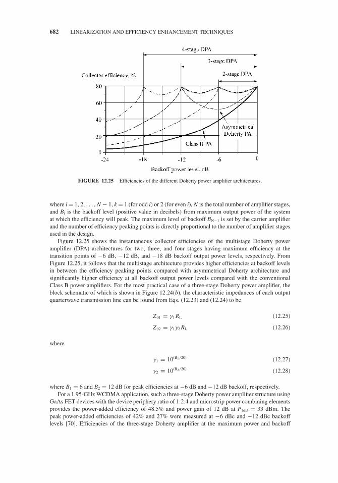
JWBS064-c12 JWBS064-Gerbennikov March 15, 2011 11:28 Printer Name: Yet to Come
682 LINEARIZATION AND EFFICIENCY ENHANCEMENT TECHNIQUES
FIGURE 12.25 Efficiencies of the different Doherty power amplifier architectures.
where i = 1, 2, . . . , N − 1, k = 1 (for odd i) or 2 (for even i), N is the total number of amplifier stages,and Bi is the backoff level (positive value in decibels) from maximum output power of the systemat which the efficiency will peak. The maximum level of backoff BN−1 is set by the carrier amplifierand the number of efficiency peaking points is directly proportional to the number of amplifier stagesused in the design.
Figure 12.25 shows the instantaneous collector efficiencies of the multistage Doherty poweramplifier (DPA) architectures for two, three, and four stages having maximum efficiency at thetransition points of −6 dB, −12 dB, and −18 dB backoff output power levels, respectively. FromFigure 12.25, it follows that the multistage architecture provides higher efficiencies at backoff levelsin between the efficiency peaking points compared with asymmetrical Doherty architecture andsignificantly higher efficiency at all backoff output power levels compared with the conventionalClass B power amplifiers. For the most practical case of a three-stage Doherty power amplifier, theblock schematic of which is shown in Figure 12.24(b), the characteristic impedances of each outputquarterwave transmission line can be found from Eqs. (12.23) and (12.24) to be
Z01 = γ1 RL (12.25)
Z02 = γ1γ2 RL (12.26)
where
γ1 = 10(B1/20) (12.27)
γ2 = 10(B2/20) (12.28)
where B1 = 6 and B2 = 12 dB for peak efficiencies at −6 dB and −12 dB backoff, respectively.For a 1.95-GHz WCDMA application, such a three-stage Doherty power amplifier structure using
GaAs FET devices with the device periphery ratio of 1:2:4 and microstrip power combining elementsprovides the power-added efficiency of 48.5% and power gain of 12 dB at P1dB = 33 dBm. Thepeak power-added efficiencies of 42% and 27% were measured at −6 dBc and −12 dBc backofflevels [70]. Efficiencies of the three-stage Doherty amplifier at the maximum power and backoff

JWBS064-c12 JWBS064-Gerbennikov March 15, 2011 11:28 Printer Name: Yet to Come
DOHERTY POWER AMPLIFIER ARCHITECTURES 683
transition points, in particular at −12 dB backoff power, can be significantly increased up to morethan 60% by using the highly effective GaN HEMT devices and apply digital predistortion techniquefor linearization [71].
It is difficult to apply directly the Doherty technique to the design of the power amplifier integratedcircuits with high level of integration, since the physical size of the quarterwave transmission linesis too large. For example, for a FR-4 substrate with effective dielectric permittivity of εr = 3.48,the geometrical lengths of the quarterwave transmission lines are 48 mm, 19 mm, and 8.7 mm atthe operating frequencies of 900 MHz, 2.4 GHz, and 5.2 GHz, respectively [72]. Therefore, the bestsolution in this situation is to replace the quarterwave transmission lines by the lumped elementsusing the single-frequency equivalence between the circuits with lumped elements and a quarterwavetransmission line.
Consider the transmission matrix [ABCD]L for a quarterwave transmission line shown in Fig-ure 12.26(a) and transmission matrix [ABCD]T for a π -type low-pass lumped circuit, consisting ofthe series inductance and two shunt capacitances shown in Figure 12.26(b) given respectively by
[ABC D]T =⎡⎣ cos θ j Z0 sin θ
jsin θ
Z0cos θ
⎤⎦
∣∣∣∣∣∣θ=π/2
=⎡⎣ 0 j Z0
j
Z00
⎤⎦ (12.29)
[ABC D]L =[
1 0jωC 1
] [1 jωL0 1
] [1 0
jωC 1
]=
⎡⎣ 1 − ω2 LC jωL
jωL
(2 − 1
ω2 LC
)1 − ω2 LC
⎤⎦ .
(12.30)
Equating the corresponding elements of both matrices in Eqs. (12.29) and (12.30) yields thefollowing relationships between the circuit elements:
Z0ωC = Z0
ωL= 1. (12.31)
The same relationships can be established between the characteristic impedance of the three-quarterwave transmission line and π -type high-pass lumped circuit consisting of the series capacitanceand two shunt inductances shown in Figure 12.26(c). Similarly, the input branch-line hybrid coupler or
FIGURE 12.26 Quarterwave transmission line and its single-frequency lumped equivalent circuits.
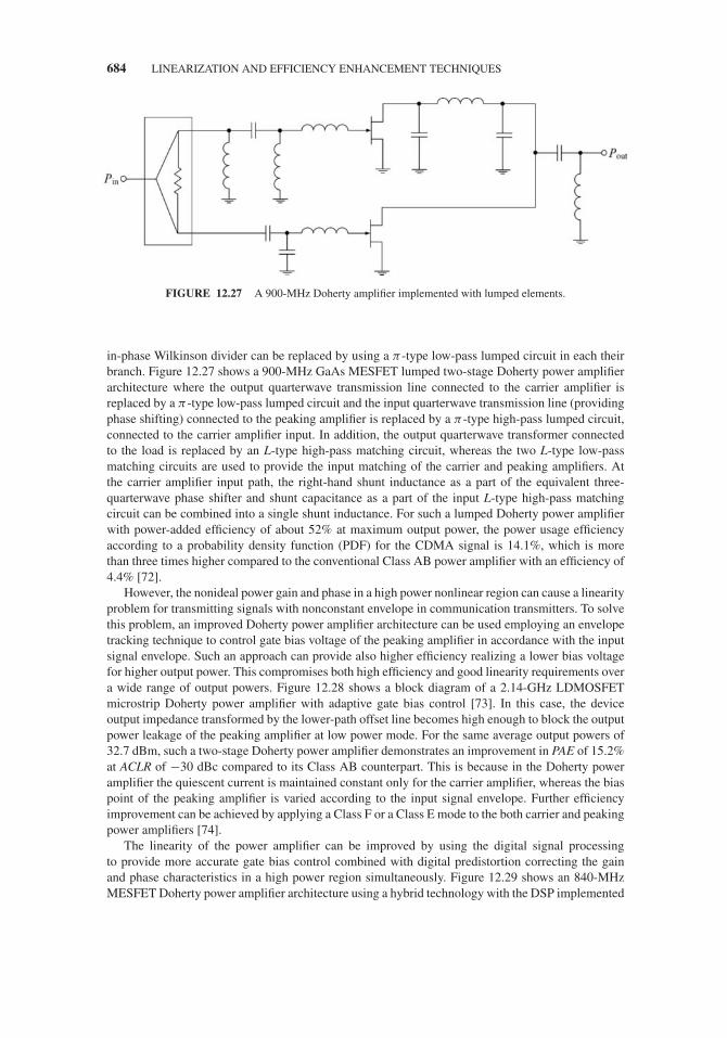
JWBS064-c12 JWBS064-Gerbennikov March 15, 2011 11:28 Printer Name: Yet to Come
684 LINEARIZATION AND EFFICIENCY ENHANCEMENT TECHNIQUES
FIGURE 12.27 A 900-MHz Doherty amplifier implemented with lumped elements.
in-phase Wilkinson divider can be replaced by using a π -type low-pass lumped circuit in each theirbranch. Figure 12.27 shows a 900-MHz GaAs MESFET lumped two-stage Doherty power amplifierarchitecture where the output quarterwave transmission line connected to the carrier amplifier isreplaced by a π -type low-pass lumped circuit and the input quarterwave transmission line (providingphase shifting) connected to the peaking amplifier is replaced by a π-type high-pass lumped circuit,connected to the carrier amplifier input. In addition, the output quarterwave transformer connectedto the load is replaced by an L-type high-pass matching circuit, whereas the two L-type low-passmatching circuits are used to provide the input matching of the carrier and peaking amplifiers. Atthe carrier amplifier input path, the right-hand shunt inductance as a part of the equivalent three-quarterwave phase shifter and shunt capacitance as a part of the input L-type high-pass matchingcircuit can be combined into a single shunt inductance. For such a lumped Doherty power amplifierwith power-added efficiency of about 52% at maximum output power, the power usage efficiencyaccording to a probability density function (PDF) for the CDMA signal is 14.1%, which is morethan three times higher compared to the conventional Class AB power amplifier with an efficiency of4.4% [72].
However, the nonideal power gain and phase in a high power nonlinear region can cause a linearityproblem for transmitting signals with nonconstant envelope in communication transmitters. To solvethis problem, an improved Doherty power amplifier architecture can be used employing an envelopetracking technique to control gate bias voltage of the peaking amplifier in accordance with the inputsignal envelope. Such an approach can provide also higher efficiency realizing a lower bias voltagefor higher output power. This compromises both high efficiency and good linearity requirements overa wide range of output powers. Figure 12.28 shows a block diagram of a 2.14-GHz LDMOSFETmicrostrip Doherty power amplifier with adaptive gate bias control [73]. In this case, the deviceoutput impedance transformed by the lower-path offset line becomes high enough to block the outputpower leakage of the peaking amplifier at low power mode. For the same average output powers of32.7 dBm, such a two-stage Doherty power amplifier demonstrates an improvement in PAE of 15.2%at ACLR of −30 dBc compared to its Class AB counterpart. This is because in the Doherty poweramplifier the quiescent current is maintained constant only for the carrier amplifier, whereas the biaspoint of the peaking amplifier is varied according to the input signal envelope. Further efficiencyimprovement can be achieved by applying a Class F or a Class E mode to the both carrier and peakingpower amplifiers [74].
The linearity of the power amplifier can be improved by using the digital signal processingto provide more accurate gate bias control combined with digital predistortion correcting the gainand phase characteristics in a high power region simultaneously. Figure 12.29 shows an 840-MHzMESFET Doherty power amplifier architecture using a hybrid technology with the DSP implemented

JWBS064-c12 JWBS064-Gerbennikov March 15, 2011 11:28 Printer Name: Yet to Come
OUTPHASING POWER AMPLIFIERS 685
ΩΩ
FIGURE 12.28 Block diagram of LDMOSFET microstrip Doherty power amplifier with adaptive gatebias control.
externally on a board controlled by a personal computer [75]. In this case, the DSP generates both thebaseband I and Q signals, which are then upconverted to an RF signal using the quadrature modulator,and the voltage signal Vg2, which is applied to the peaking amplifier as the gate bias. This resultsin an efficiency improvement by the dynamic gate biasing of the peaking amplifier according to theinstantaneous envelope of the input signal. At the same time, the phase performance is corrected bythe phase predistortion at baseband level based on the dynamic gate bias-voltage values from the gaincorrection, thus resulting in a linearity improvement. An overall improvement of PAE of 3–5% andACPR of about 10 dB at an average output power of 23 dBm can be achieved by utilizing such a DSPtechnique [72,75]. Significant linearity improvement can also be achieved by using a digital feedbackpredistortion linearization technique [76].
12.7 OUTPHASING POWER AMPLIFIERS
The outphasing modulation technique was invented in the middle of 1930s in order to improveboth the efficiency and linearity of AM-broadcast transmitters [77]. Substantially later in 1970s, its
FIGURE 12.29 Doherty power amplifier architecture with DSP control.

JWBS064-c12 JWBS064-Gerbennikov March 15, 2011 11:28 Printer Name: Yet to Come
686 LINEARIZATION AND EFFICIENCY ENHANCEMENT TECHNIQUES
application was extended up to microwave frequencies under the name LINC (linear amplificationusing nonlinear components) [78]. An outphasing transmitter operates as a linear power amplifiersystem for amplitude-modulated signal having a linear transfer function over a wide range of the inputsignal levels by combining the outputs of two nonlinear power amplifiers that are driven with signals ofconstant amplitude but different time-varying phases corresponding to the envelope of the input signal.
A simple outphasing power amplifier system is shown in Figure 12.30(a) [79]. The signal com-ponent separator (SCS) generates from the input amplitude-modulated signal two sinewave signalsof constant envelopes with different phases +φ(t) and −φ(t). These two signals are then separatelyamplified by the identical nonlinear power amplifiers each and combined to produce the outputamplitude-modulated signal. The peak output power is obtained with φ = 90◦ when currents frompower amplifiers with equal amplitudes IL = I1 = I2 are added in phase, similar to a push–pulloperation. Zero output power corresponds to the signal with φ = 0◦ when equal currents from poweramplifiers cancel each other resulting in IL = 0. Intermediate values of phase in between 0◦ < φ <
90◦ produce intermediate values of the output voltage amplitude. As shown in Figure 12.30(b), thetime-varying phase φ can be written using the vector sum of the output voltages V1 and V2 by
φ = sin−1
(VL
VLPEP
)(12.32)
FIGURE 12.30 Simple outphasing power amplifier system.
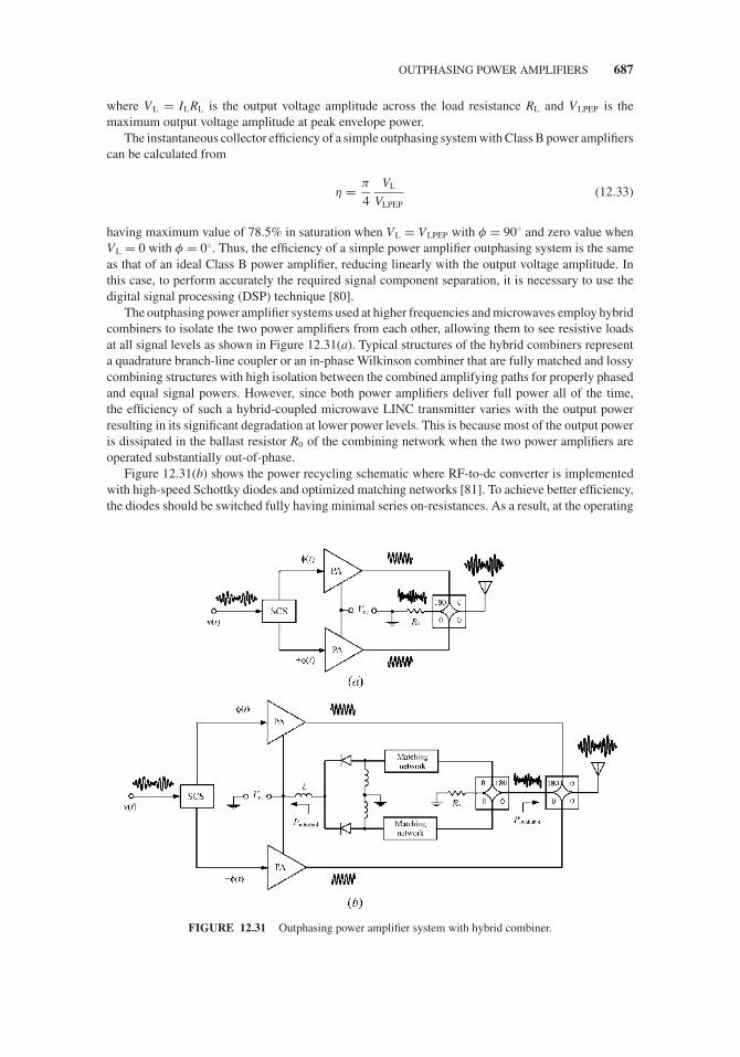
JWBS064-c12 JWBS064-Gerbennikov March 15, 2011 11:28 Printer Name: Yet to Come
OUTPHASING POWER AMPLIFIERS 687
where VL = ILRL is the output voltage amplitude across the load resistance RL and VLPEP is themaximum output voltage amplitude at peak envelope power.
The instantaneous collector efficiency of a simple outphasing system with Class B power amplifierscan be calculated from
η = π
4
VL
VLPEP(12.33)
having maximum value of 78.5% in saturation when VL = VLPEP with φ = 90◦ and zero value whenVL = 0 with φ = 0◦. Thus, the efficiency of a simple power amplifier outphasing system is the sameas that of an ideal Class B power amplifier, reducing linearly with the output voltage amplitude. Inthis case, to perform accurately the required signal component separation, it is necessary to use thedigital signal processing (DSP) technique [80].
The outphasing power amplifier systems used at higher frequencies and microwaves employ hybridcombiners to isolate the two power amplifiers from each other, allowing them to see resistive loadsat all signal levels as shown in Figure 12.31(a). Typical structures of the hybrid combiners representa quadrature branch-line coupler or an in-phase Wilkinson combiner that are fully matched and lossycombining structures with high isolation between the combined amplifying paths for properly phasedand equal signal powers. However, since both power amplifiers deliver full power all of the time,the efficiency of such a hybrid-coupled microwave LINC transmitter varies with the output powerresulting in its significant degradation at lower power levels. This is because most of the output poweris dissipated in the ballast resistor R0 of the combining network when the two power amplifiers areoperated substantially out-of-phase.
Figure 12.31(b) shows the power recycling schematic where RF-to-dc converter is implementedwith high-speed Schottky diodes and optimized matching networks [81]. To achieve better efficiency,the diodes should be switched fully having minimal series on-resistances. As a result, at the operating
FIGURE 12.31 Outphasing power amplifier system with hybrid combiner.
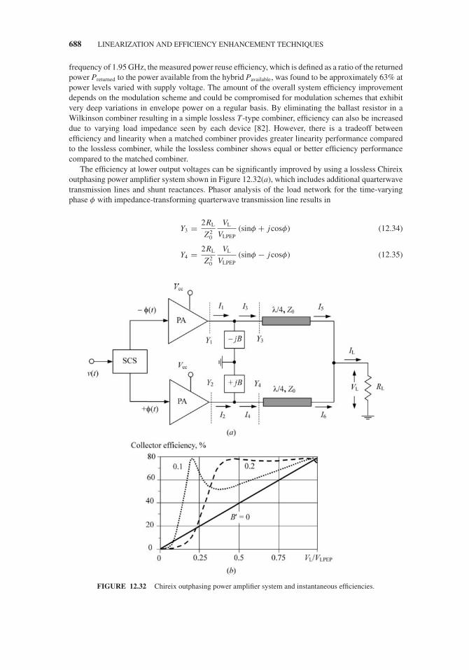
JWBS064-c12 JWBS064-Gerbennikov March 15, 2011 11:28 Printer Name: Yet to Come
688 LINEARIZATION AND EFFICIENCY ENHANCEMENT TECHNIQUES
frequency of 1.95 GHz, the measured power reuse efficiency, which is defined as a ratio of the returnedpower Preturned to the power available from the hybrid Pavailable, was found to be approximately 63% atpower levels varied with supply voltage. The amount of the overall system efficiency improvementdepends on the modulation scheme and could be compromised for modulation schemes that exhibitvery deep variations in envelope power on a regular basis. By eliminating the ballast resistor in aWilkinson combiner resulting in a simple lossless T-type combiner, efficiency can also be increaseddue to varying load impedance seen by each device [82]. However, there is a tradeoff betweenefficiency and linearity when a matched combiner provides greater linearity performance comparedto the lossless combiner, while the lossless combiner shows equal or better efficiency performancecompared to the matched combiner.
The efficiency at lower output voltages can be significantly improved by using a lossless Chireixoutphasing power amplifier system shown in Figure 12.32(a), which includes additional quarterwavetransmission lines and shunt reactances. Phasor analysis of the load network for the time-varyingphase φ with impedance-transforming quarterwave transmission line results in
Y3 = 2RL
Z 20
VL
VLPEP(sinφ + jcosφ) (12.34)
Y4 = 2RL
Z 20
VL
VLPEP(sinφ − jcosφ) (12.35)
FIGURE 12.32 Chireix outphasing power amplifier system and instantaneous efficiencies.

JWBS064-c12 JWBS064-Gerbennikov March 15, 2011 11:28 Printer Name: Yet to Come
OUTPHASING POWER AMPLIFIERS 689
where Z0 is the characteristic impedance of the transmission lines [79]. From Eqs. (12.34) and(12.35) it follows that the admittances Y3 and Y4 are purely resistive only for φ = 90◦ correspondingto the case of in-phase output currents. However, for most values of phase φ, the power amplifiershave highly reactive loads that become completely reactive when φ = 0◦ with out-of-phase outputcurrents. The effect of the reactive loads can be partially compensated by adding the correspondingshunt susceptances −B and +B, respectively. In this case, the reactive parts of the admittances Y1 =Y3 − jB and Y2 = Y4 + jB can be zeroed at one specific output voltage amplitude by setting
B = 2RL
Z 20
VL
VLPEP
√1 −
(VL
VLPEP
)2
(12.36)
which can be obtained by substituting Eq. (12.32) into Eqs. (12.34) and (12.35). As a result, for thecase of a purely resistive load, the instantaneous collector efficiency of a Chireix outphasing systemwith ideal Class B power amplifiers can reach the maximum value of
η = π
4. (12.37)
The instantaneous efficiencies of the Chireix outphasing system for different values of the normal-ized shunt susceptance B ′ = B Z 2
0/2RL are shown in Figure 12.32(b), from which it follows that theselection of a proper value of B increases efficiency at a specified medium level of the output voltageamplitude, however it is degraded at low and high amplitudes. Using a value of B′ = 0.2 can providehigh efficiency over the upper 6 dB of the output voltage range. The case of B′ = 0 corresponds tothe collector efficiency variations of an ideal Class B power amplifier. An improvement in the averageefficiency calculated over a wide range of output voltages for various amplitude-modulated signalsof up to a factor of two over that of an ideal Class B power amplifier can be achieved by properlyselecting the shunt susceptances in outphasing power amplifier system. On the whole, to design suchan outphasing system, it is necessary to consider simultaneously such factors as a complexity of theSCS circuit and sensitivity of the power amplifiers to the wide range of load impedances.
Further efficiency improvement can potentially be achieved by using the push–pull voltage-switching Class D, transmission-line Class F, or switching-mode Class E power amplifiers [83,84].Using a push–pull configuration for each saturated Class B power amplifier based on pHEMT devicesin a Chireix outphasing system had contributed to the increased efficiency of 42.2% at −7 dB backoff,which is more that two times improvement over the Wilkinson combiner system [85]. The widebandefficient operation of a LINC transmitter over frequency range from 30 to 450 MHz can be achievedby using the push–pull resistive-load Class D power amplifiers with harmonic filter bank [86]. Atmicrowave frequencies, it can be realized by replacing the single quarterwave transmission linesin Class F power amplifiers with either lumped low-pass LC ladder networks or cascades of thequarterwave transmission lines, having a smaller transformation ratio for each line [87].
In a practical LINC transmitter there are three main mechanisms that degrade the overall per-formance: The power gain and phase imbalance between two RF amplifying paths and the differentnonlinear characteristics of both power amplifiers [88]. For example, if the gain imbalance betweenpaths is about 1%, the output rejection may reduce to 45 dB and even further to 28 dB only dependingon the relative level of the input modulating signal amplitude. On the other hand, a phase errorbetween amplifying paths as low as 2◦ diminishes the undesired response rejection to only 33 dBfor the best case. At the same time, effect of the imbalance of the power amplifier nonlinearities isless meaningful. In terms of the Chireix power amplifier parameters, it is very important to minimizethe combiner impedance mismatching, especially at microwave frequencies where the Chireix out-phasing combiner should consist of two shunt stubs of equal and opposite reactances and two seriesquarterwave transmission lines [89].
Therefore, the practical implementation of the entire LINC or Chireix outphasing power amplifiersystem is very difficult because of its inherent strong sensitivity to the amplitude and phase errors
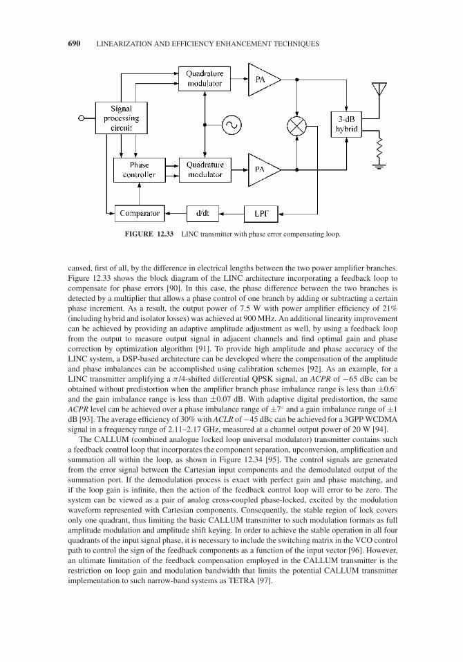
JWBS064-c12 JWBS064-Gerbennikov March 15, 2011 11:28 Printer Name: Yet to Come
690 LINEARIZATION AND EFFICIENCY ENHANCEMENT TECHNIQUES
FIGURE 12.33 LINC transmitter with phase error compensating loop.
caused, first of all, by the difference in electrical lengths between the two power amplifier branches.Figure 12.33 shows the block diagram of the LINC architecture incorporating a feedback loop tocompensate for phase errors [90]. In this case, the phase difference between the two branches isdetected by a multiplier that allows a phase control of one branch by adding or subtracting a certainphase increment. As a result, the output power of 7.5 W with power amplifier efficiency of 21%(including hybrid and isolator losses) was achieved at 900 MHz. An additional linearity improvementcan be achieved by providing an adaptive amplitude adjustment as well, by using a feedback loopfrom the output to measure output signal in adjacent channels and find optimal gain and phasecorrection by optimization algorithm [91]. To provide high amplitude and phase accuracy of theLINC system, a DSP-based architecture can be developed where the compensation of the amplitudeand phase imbalances can be accomplished using calibration schemes [92]. As an example, for aLINC transmitter amplifying a π /4-shifted differential QPSK signal, an ACPR of −65 dBc can beobtained without predistortion when the amplifier branch phase imbalance range is less than ±0.6◦
and the gain imbalance range is less than ±0.07 dB. With adaptive digital predistortion, the sameACPR level can be achieved over a phase imbalance range of ±7◦ and a gain imbalance range of ±1dB [93]. The average efficiency of 30% with ACLR of −45 dBc can be achieved for a 3GPP WCDMAsignal in a frequency range of 2.11–2.17 GHz, measured at a channel output power of 20 W [94].
The CALLUM (combined analogue locked loop universal modulator) transmitter contains sucha feedback control loop that incorporates the component separation, upconversion, amplification andsummation all within the loop, as shown in Figure 12.34 [95]. The control signals are generatedfrom the error signal between the Cartesian input components and the demodulated output of thesummation port. If the demodulation process is exact with perfect gain and phase matching, andif the loop gain is infinite, then the action of the feedback control loop will error to be zero. Thesystem can be viewed as a pair of analog cross-coupled phase-locked, excited by the modulationwaveform represented with Cartesian components. Consequently, the stable region of lock coversonly one quadrant, thus limiting the basic CALLUM transmitter to such modulation formats as fullamplitude modulation and amplitude shift keying. In order to achieve the stable operation in all fourquadrants of the input signal phase, it is necessary to include the switching matrix in the VCO controlpath to control the sign of the feedback components as a function of the input vector [96]. However,an ultimate limitation of the feedback compensation employed in the CALLUM transmitter is therestriction on loop gain and modulation bandwidth that limits the potential CALLUM transmitterimplementation to such narrow-band systems as TETRA [97].
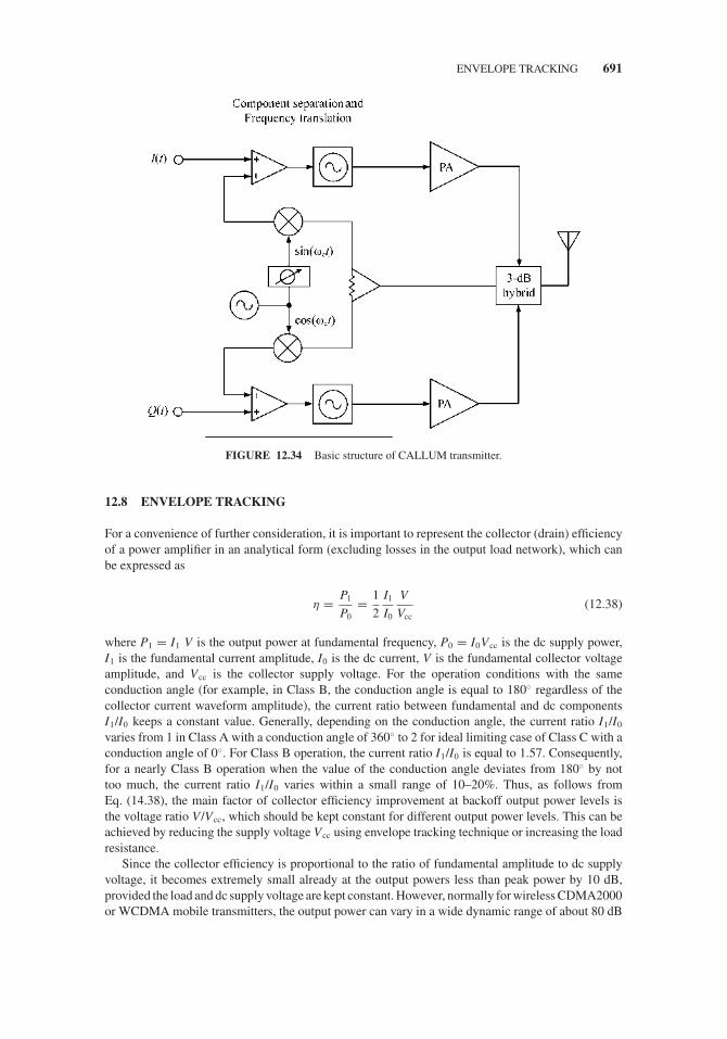
JWBS064-c12 JWBS064-Gerbennikov March 15, 2011 11:28 Printer Name: Yet to Come
ENVELOPE TRACKING 691
FIGURE 12.34 Basic structure of CALLUM transmitter.
12.8 ENVELOPE TRACKING
For a convenience of further consideration, it is important to represent the collector (drain) efficiencyof a power amplifier in an analytical form (excluding losses in the output load network), which canbe expressed as
η = P1
P0= 1
2
I1
I0
V
Vcc(12.38)
where P1 = I1 V is the output power at fundamental frequency, P0 = I0Vcc is the dc supply power,I1 is the fundamental current amplitude, I0 is the dc current, V is the fundamental collector voltageamplitude, and Vcc is the collector supply voltage. For the operation conditions with the sameconduction angle (for example, in Class B, the conduction angle is equal to 180◦ regardless of thecollector current waveform amplitude), the current ratio between fundamental and dc componentsI1/I0 keeps a constant value. Generally, depending on the conduction angle, the current ratio I1/I0
varies from 1 in Class A with a conduction angle of 360◦ to 2 for ideal limiting case of Class C with aconduction angle of 0◦. For Class B operation, the current ratio I1/I0 is equal to 1.57. Consequently,for a nearly Class B operation when the value of the conduction angle deviates from 180◦ by nottoo much, the current ratio I1/I0 varies within a small range of 10–20%. Thus, as follows fromEq. (14.38), the main factor of collector efficiency improvement at backoff output power levels isthe voltage ratio V/Vcc, which should be kept constant for different output power levels. This can beachieved by reducing the supply voltage Vcc using envelope tracking technique or increasing the loadresistance.
Since the collector efficiency is proportional to the ratio of fundamental amplitude to dc supplyvoltage, it becomes extremely small already at the output powers less than peak power by 10 dB,provided the load and dc supply voltage are kept constant. However, normally for wireless CDMA2000or WCDMA mobile transmitters, the output power can vary in a wide dynamic range of about 80 dB

JWBS064-c12 JWBS064-Gerbennikov March 15, 2011 11:28 Printer Name: Yet to Come
692 LINEARIZATION AND EFFICIENCY ENHANCEMENT TECHNIQUES
FIGURE 12.35 Envelope-tracking power amplifier architecture with analog control.
with maximum statistically averaged transmitting power required to deliver signal to the base station ofabout 15–30 dB less than the peak output power. Therefore, the average envelope-tracking techniquecan be very useful to increase power amplifier efficiency in a wide range of output powers of mobiletransmitters by varying the dc supply voltage according to the RF signal envelope. When the supplyvoltage tracks the instantaneous output envelope, it is known as a wideband envelope or envelope-follower tracking. However, when the supply voltage tracks the long-term average of the outputenvelope, it is known as an average envelope or power tracking. The envelope-follower tracking isnecessary to increase efficiency at fixed output power, while the power tracking is required to increaseefficiency at backoff powers.
Figure 12.35 shows the envelope-tracking power amplifier architecture with analog control wherethe envelope detector is included at the input to detect the input signal envelope [98,99]. Here, a dc–dcconverter is used to provide the dynamically controlled supply voltage to a linear power amplifier.While both buck (step-down) or boost (step-up) dc–dc converters can be used, the latter allowsoperation of the power amplifier from a supply voltage higher than the dc-supply voltage. Sucha dc–dc boost converter implemented using AlGaAs/GaAs HBT process with 10 MHz switching(clock) frequency can provide the efficiency of 74% at maximum dc power [98]. The ripple in thedc–dc converter output results in the spurious in the output signal spectrum of approximately 60 dBlower than the fundamental spectral component. The delay line is necessary to compensate for thephase misalignment between the envelope and RF signal paths.
The linearity of a power amplifier with envelope tracking is usually worse than that of the poweramplifier with fixed supply voltage because of the gain and phase variations with supply voltage. Inthis case, it is possible to use a fixed analog predistortion or digital control to minimize the increasednonlinearity to a considerable extent. Figure 12.36 shows the envelope-tracking power amplifierarchitecture with a digital control [100]. In addition to providing a proper control voltage for thedc–dc converter according to the signal envelope, the DSP system also computes a predistorted inputsignal for both the in-phase (I) and quadrature (Q) channels using amplifier amplitude and phasecharacteristics. The practical results show that, in this case, the ACPR of the IS-95 CDMA inputsignal can be improved by 8 dB at an output power of 28 dBm. However, the ACPR is quite sensitiveto the timing relationships between the varying supply voltage and the input signal. For a GaAsMESFET power amplifier with boost converter operated at 950 MHz with maximum output powerof 1 W, the power usage efficiency calculated in accordance with probability distribution function(PDF) of its output power is 1.64 times higher than the one for just battery operation [99]. However,to meet CDMA IS-95 specifications for ACPR, a fast feedback loop regulation scheme and dynamicgate biasing are needed to reduce the intermodulation distortions caused by the gain variation (dueto the significant variation of the device transconductance with the supply voltage) and parasitic
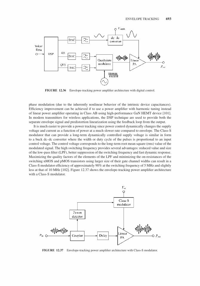
JWBS064-c12 JWBS064-Gerbennikov March 15, 2011 11:28 Printer Name: Yet to Come
ENVELOPE TRACKING 693
FIGURE 12.36 Envelope-tracking power amplifier architecture with digital control.
phase modulation (due to the inherently nonlinear behavior of the intrinsic device capacitances).Efficiency improvement can be achieved if to use a power amplifier with harmonic tuning insteadof linear power amplifier operating in Class AB using high-performance GaN HEMT device [101].In modern transmitters for wireless applications, the DSP technique are used to provide both theseparate envelope signal and predistortion linearization using the feedback loop from the output.
It is much easier to provide a power tracking since power control dynamically changes the supplyvoltage and current as a function of power at a much slower rate compared to envelope. The Class-Smodulator that can provide a long-term dynamically controlled supply voltage is similar in formto a buck dc–dc converter where the width or duty cycle of the pulses is proportional to an inputcontrol voltage. The control voltage corresponds to the long-term root mean square (rms) value of themodulated signal. The high switching frequency provides several advantages: reduced value and sizeof the low-pass filter (LPF), better suppression of the switching frequency and fast dynamic response.Maximizing the quality factors of the elements of the LPF and minimizing the on-resistances of theswitching nMOS and pMOS transistors using larger size of their gate channel widths can result in aClass-S modulator efficiency of approximately 90% at the switching frequency of 5 MHz and slightlyless at that of 10 MHz [102]. Figure 12.37 shows the envelope-tracking power amplifier architecturewith a Class-S modulator.
FIGURE 12.37 Envelope-tracking power amplifier architecture with Class-S modulator.
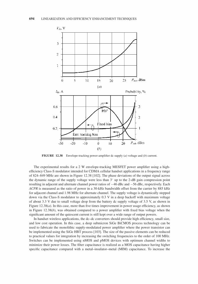
JWBS064-c12 JWBS064-Gerbennikov March 15, 2011 11:28 Printer Name: Yet to Come
694 LINEARIZATION AND EFFICIENCY ENHANCEMENT TECHNIQUES
FIGURE 12.38 Envelope-tracking power-amplifier dc supply (a) voltage and (b) current.
The experimental results for a 2 W envelope-tracking MESFET power amplifier using a high-efficiency Class-S modulator intended for CDMA cellular handset applications in a frequency rangeof 824–849 MHz are shown in Figure 12.38 [102]. The phase deviations of the output signal acrossthe dynamic range of the supply voltage were less than 3◦ up to the 2-dB gain compression pointresulting in adjacent and alternate channel power ratios of −46 dBc and −56 dBc, respectively. EachACPR is measured as the ratio of power in a 30-kHz bandwidth offset from the carrier by 885 kHzfor adjacent channel and 1.98 MHz for alternate channel. The supply voltage is dynamically steppeddown via the Class-S modulator to approximately 0.3 V in a deep backoff with maximum voltageof about 3.3 V due to small voltage drop from the battery dc supply voltage of 3.5 V, as shown inFigure 12.38(a). In this case, more than five times improvement in power usage efficiency, as shownin Figure 12.38(b), was obtained compared to a power amplifier with fixed bias voltage when thesignificant amount of the quiescent current is still kept over a wide range of output powers.
In handset wireless applications, the dc–dc converters should provide high efficiency, small size,and low cost operation. In this case, a deep submicron SiGe BiCMOS process technology can beused to fabricate the monolithic supply-modulated power amplifier where the power transistor canbe implemented using the SiGe HBT process [103]. The size of the passive elements can be reducedto practical values for integration by increasing the switching frequencies to the order of 100 MHz.Switches can be implemented using nMOS and pMOS devices with optimum channel widths tominimize their power losses. The filter capacitance is realized as a MOS capacitance having higherspecific capacitance compared with a metal–insulator–metal (MIM) capacitance. To increase the

JWBS064-c12 JWBS064-Gerbennikov March 15, 2011 11:28 Printer Name: Yet to Come
SWITCHED MULTIPATH POWER AMPLIFIERS 695
quality factor of the filter inductance, it is implemented using a thick last metal layer far above thesubstrate. Such a monolithic 900 MHz power amplifier with a high speed synchronous buck dc–dcconverter can provide substantially higher efficiency compared with the similar power amplifier usingconstant voltage supply at lower power levels. By using a buck-boost converter with high efficiencyover a wide loading range, the system efficiency can be further improved [104].
However, the system efficiency is slightly lower at high power than that of the conventional poweramplifier with constant supply voltage due to certain effect of the dc–dc converter. For an 802.11 gOFDM application at 2.4 GHz, the overall efficiency of the complete wideband envelope-trackingsystem with SiGe HBT power amplifier is achieved 28% with an EVM (error vector magnitude)of 5% at an output power of 20 dBm [105]. Since the wideband envelope-tracking system has asignificant nonlinearity associated with the collector modulation, as well as the intrinsic nonlinearityof the power amplifier, off-chip baseband digital predistortion with a LUT scheme was implementedto improve the system linearity, in particular EVM.
12.9 SWITCHED MULTIPATH POWER AMPLIFIERS
The power amplifiers in wireless communications systems operating in WCDMA or CDMA2000standards are required to cover linearly a dynamic range of the transmitting output powers up to80 dB. As a result, being designed for the highest power level with maximum achievable efficiency,the power amplifier tends to operate less efficiently at lower power levels, which leads to shorteningthe life of a battery. Figure 12.39(a) shows the transmitter architecture including a variable gainamplifier, a power amplifier to provide a high output power level, a bypass line for bypassing thesmaller output power level, and a two-pole switch between two signal paths [106]. Normally, thepower amplifiers for wireless handset transmitters are designed to achieve the power gain of about25–30 dB. Therefore, it is very important to provide an efficient operation condition for the maximumprobable transmitting power required to deliver signal to the base station, which is of about 12–15 dBless than the maximum peak power. The output power of the widely used variable gain amplifiersis usually less than 10 dBm, otherwise it is difficult to realize their linear operation. Besides, thevariable gain amplifiers usually have a sufficiently high value for their noise figure. This contributesto the degradation in nonlinear distortion and excessive noise level in receiver bandwidth, whichcan only be improved by additional filtering, which increases the cost and size of the transmitter.A possible solution to improve the performance of the wireless handset transmitter is to use two
FIGURE 12.39 Transmitter architectures with dual-path power amplifier.

JWBS064-c12 JWBS064-Gerbennikov March 15, 2011 11:28 Printer Name: Yet to Come
696 LINEARIZATION AND EFFICIENCY ENHANCEMENT TECHNIQUES
power amplifier paths with different output power levels. This can result in a significant reductionof power consumption, because the low-power amplifier provides higher efficiency at output powerlevel corresponding to maximum PDF. The block schematic of the dual-path transmitter architectureis shown in Figure 12.39(b). When it is required to transmit the signal with an output power betweenthe maximum level Pmax and the statistically averaged power Pavg, the low-power amplifier is turnedoff. When it is enough to transmit the signal with output power equal or less than Pavg, the high poweramplifier is turned off. So, at any moment the only one power amplifier is switched on. To furtherimprove the efficiency of the transmitter, it may need to provide more than two power amplifier pathswith different output power levels connected in parallel to the multipole switch.
In another approach, a mechanism for switching the output path between two or several powerdevices is used [107]. In this switchable-path power amplifier circuit shown in Figure 12.40, acombining network with a Schottky diode is used to switch the output path between the first activedevice, designed for maximum output power level, and the second active device, designed for thespecified output power level with increased efficiency. As a result, the combining network is operablesuch that either the first power device Q1 or the second power device Q2 drives the power amplifieroutput.
An efficiency improvement can also be achieved by bypassing the power amplifier stages. Forexample, the power amplifier topology shown Figure 12.41(a) provides the possibility of bypassingthe second stage [108]. At lower output power levels, the signal amplification can be achieved usingonly the first stage PA1 with switch S1 being turned on, whereas the maximum output power levelis achieved using the two-stage power amplifier configuration with switches S2 and S3 being turnedon. To eliminate any additional impedance matching, both stages should be designed to operate ina 50- environment at the input and output. An improvement in average efficiency of greater thanfour times at backoff output power levels, compared with the conventional two-stage architecture, is
FIGURE 12.40 Switchable path power amplifier circuit.
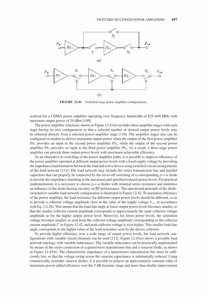
JWBS064-c12 JWBS064-Gerbennikov March 15, 2011 11:28 Printer Name: Yet to Come
SWITCHED MULTIPATH POWER AMPLIFIERS 697
FIGURE 12.41 Switched-stage power amplifier configurations.
realized for a CDMA power amplifier operating over frequency bandwidth of 825–849 MHz withmaximum output power of 29 dBm [109].
The power amplifier schematic shown in Figure 12.41(b) includes three amplifier stages with eachstage having its own configuration so that a selected number of desired output power levels maybe obtained directly from a selected power amplifier stage [110]. The amplifier stages also can beconfigured in tandem to deliver maximum output power when the output of the first power amplifierPA1 provides an input to the second power amplifier PA2, while the output of the second poweramplifier PA2 provides an input to the third power amplifier PA3. As a result, a three-stage poweramplifier can provide three output power levels with maximum achievable efficiency.
As an alternative to switching of the power amplifier paths, it is possible to improve efficiency ofthe power amplifier operated at different output power levels with a fixed supply voltage by providingthe impedance transformation between the load and active device using switched-circuit arrangementsof the load network [111]. The load network may include the series transmission line and parallelcapacitors that can properly be connected by the on-to-off switching of a corresponding p–i–n diodeto provide the impedance matching at the maximum and specified reduced power levels. For practicalimplementation, it is necessary to choose p–i–n diodes with minimal series resistance and minimizean influence of the diode biasing circuitry on RF performance. The operational principle of the diode-switched or variable load network configuration is illustrated in Figure 12.42. To maximize efficiencyof the power amplifier, the load resistance for different output power levels should be different, so asto provide a collector voltage amplitude close to the value of the supply voltage Vcc, in accordancewith Eq. (12.38). This means that the load-line angle at lower output power levels becomes smaller, sothat the smaller collector current amplitude corresponds to approximately the same collector voltageamplitude as for the higher output power level. Moreover, for lower power levels, the saturationvoltage becomes smaller, as seen from the collector voltage amplitude corresponding to the collectorcurrent amplitude I′ ′ in Figure 12.42, and peak collector voltage is even higher. This smaller load-lineangle corresponds to the higher value of the load resistance seen by the device collector.
To provide higher efficiency over a wide range of output power levels, the load network con-figurations with variable circuit elements can be used [112]. Figure 12.43(a) shows a possible loadnetwork topology with variable inductances. The variable inductance can be practically implementedby means of the series connection of a quarterwave transmission line and a varactor diode, as shownin Figure 12.43(b). The characteristic impedance of a quarterwave transmission line must be suffi-ciently low, so that the voltage swing across the varactor capacitance is substantially reduced. Usingcommercially available varactor diodes, it is possible to achieve an approximately constant value ofmaximum power-added efficiency over the 5 dB dynamic range and more than double improvement
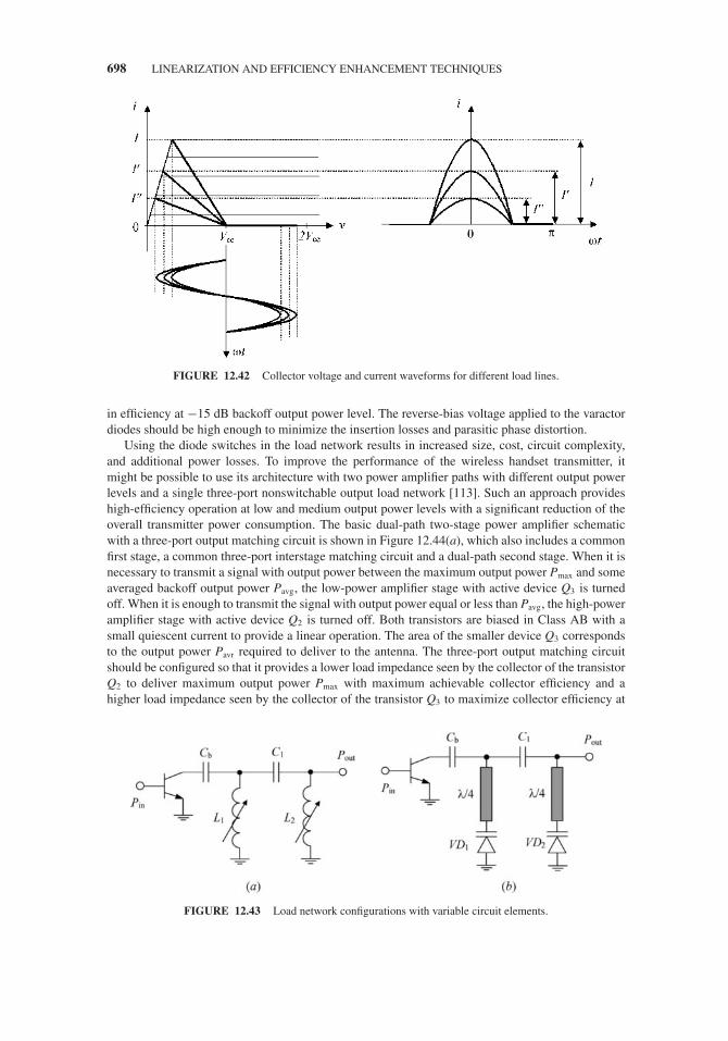
JWBS064-c12 JWBS064-Gerbennikov March 15, 2011 11:28 Printer Name: Yet to Come
698 LINEARIZATION AND EFFICIENCY ENHANCEMENT TECHNIQUES
FIGURE 12.42 Collector voltage and current waveforms for different load lines.
in efficiency at −15 dB backoff output power level. The reverse-bias voltage applied to the varactordiodes should be high enough to minimize the insertion losses and parasitic phase distortion.
Using the diode switches in the load network results in increased size, cost, circuit complexity,and additional power losses. To improve the performance of the wireless handset transmitter, itmight be possible to use its architecture with two power amplifier paths with different output powerlevels and a single three-port nonswitchable output load network [113]. Such an approach provideshigh-efficiency operation at low and medium output power levels with a significant reduction of theoverall transmitter power consumption. The basic dual-path two-stage power amplifier schematicwith a three-port output matching circuit is shown in Figure 12.44(a), which also includes a commonfirst stage, a common three-port interstage matching circuit and a dual-path second stage. When it isnecessary to transmit a signal with output power between the maximum output power Pmax and someaveraged backoff output power Pavg, the low-power amplifier stage with active device Q3 is turnedoff. When it is enough to transmit the signal with output power equal or less than Pavg, the high-poweramplifier stage with active device Q2 is turned off. Both transistors are biased in Class AB with asmall quiescent current to provide a linear operation. The area of the smaller device Q3 correspondsto the output power Pavr required to deliver to the antenna. The three-port output matching circuitshould be configured so that it provides a lower load impedance seen by the collector of the transistorQ2 to deliver maximum output power Pmax with maximum achievable collector efficiency and ahigher load impedance seen by the collector of the transistor Q3 to maximize collector efficiency at
FIGURE 12.43 Load network configurations with variable circuit elements.
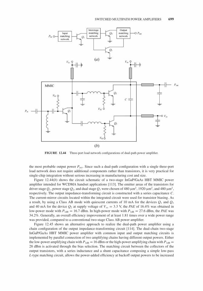
JWBS064-c12 JWBS064-Gerbennikov March 15, 2011 11:28 Printer Name: Yet to Come
SWITCHED MULTIPATH POWER AMPLIFIERS 699
FIGURE 12.44 Three-port load network configurations of dual-path power amplifier.
the most probable output power Pavr. Since such a dual-path configuration with a single three-portload network does not require additional components rather than transistors, it is very practical forsingle-chip integration without serious increasing in manufacturing cost and size.
Figure 12.44(b) shows the circuit schematic of a two-stage InGaP/GaAs HBT MMIC poweramplifier intended for WCDMA handset applications [113]. The emitter areas of the transistors fordriver stage Q1, power stage Q2, and dual stage Q3 were chosen of 480 μm2, 1920 μm2, and 480 μm2,respectively. The output impedance-transforming circuit is constructed with a series capacitance C.The current-mirror circuits located within the integrated circuit were used for transistor biasing. Asa result, by using a Class AB mode with quiescent currents of 10 mA for the devices Q1 and Q3
and 40 mA for the device Q2 at supply voltage of Vcc = 3.3 V, the PAE of 16.4% was obtained inlow-power mode with P1dB = 16.7 dBm. In high-power mode with P1dB = 27.6 dBm, the PAE was34.2%. Generally, an overall efficiency improvement of at least 1.81 times over a wide power rangewas provided, compared to a conventional two-stage Class AB power amplifier.
Figure 12.45 shows an alternative approach to realize the dual-path power amplifier using achain configuration of the output impedance-transforming circuit [114]. The dual-chain two-stageInGaP/GaAs HBT MMIC power amplifier with common input and output matching circuits isimplemented by parallel connection of two amplifying chains having different output powers. Eitherthe low-power amplifying chain with P1dB = 16 dBm or the high-power amplifying chain with P1dB =28 dBm is activated through the bias selection. The matching circuit between the collectors of theoutput transistors, with a series inductance and a shunt capacitance composing a simple low-passL-type matching circuit, allows the power-added efficiency at backoff output powers to be increased

JWBS064-c12 JWBS064-Gerbennikov March 15, 2011 11:28 Printer Name: Yet to Come
700 LINEARIZATION AND EFFICIENCY ENHANCEMENT TECHNIQUES
FIGURE 12.45 Schematic of dual-chain MMIC power amplifier.
by more accurate impedance matching of the higher output impedance of the low-power device to the50- load. Using such a chain power amplifier configuration, it is possible to obtain the PAE of 21%at P1dB = 16 dBm in a low-power mode and PAE of 40% at P1dB = 28 dBm in a high-power mode.
Figure 12.46(a) shows the block diagram of the power amplifier with high efficiency at differentoutput power levels, which incorporates an additional separate low-power amplifying path connectedbetween the isolated ports of a quadrature input hybrid power divider and a quadrature output hybridpower combiner [115]. In a high power mode, the bias control unit provides proper biasing of thetransistors in both balanced paths and switches off the biasing in a low-power path 4-to-4′. In this case,the output powers from both high-power balanced paths 2-to-2′ and 3-to-3′ are combined in the outputhybrid combiner and the low-power path is isolated from them, thus providing a high efficiency athigh output power. When all ports of a hybrid branch-line combiner are matched, power entering inputport 1 is divided between the output ports 2 and 3 with a phase shift of 90◦ between these outputs andno power is delivered to the isolated port 4. In a low power mode, the bias control unit switches off thebiasing of transistors in both balanced paths and provides proper biasing for a low power amplifyingpath. A quadrature hybrid has an important advantage compared to the in-phase dividers that, at equalvalues of reflection coefficients from loads connected to the output ports 2 and 3, the reflection waveis lacking at the input port 1 and, consequently, input VSWR of a quadrature hybrid does not dependon the equal-load mismatch level. In this case, all reflected power in a quadrature divider is dissipatedin a 50- ballast resistor connected to the isolated port 4. Similarly, for a quadrature combiner, thereflection waves from two inputs will combine and flow to the load. As a result, the isolated port ofthe input hybrid becomes the input for a low-power amplifying path, while the isolated port of theoutput hybrid operates as its output 50- port. Hence, the high efficiency at lower output power levels
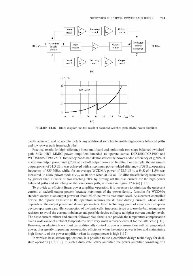
JWBS064-c12 JWBS064-Gerbennikov March 15, 2011 11:28 Printer Name: Yet to Come
SWITCHED MULTIPATH POWER AMPLIFIERS 701
FIGURE 12.46 Block diagram and test result of balanced switched-path MMIC power amplifier.
can be achieved, and no need to include any additional switches to isolate high-power balanced pathsand low-power path from each other.
Practical results for high-efficiency linear multiband and multimode two-stage balanced switched-path SiGe HBT MMIC power amplifiers intended to operate across DCS1800/PCS1900 andWCDMA850/1900/2100 frequency bands had demonstrated the power-added efficiency of ≥50% atmaximum output power and ≥20% at backoff output power of 16 dBm. For example, the maximumoutput power of 31.5 dBm was achieved with a maximum power-added efficiency of 58% at operatingfrequency of 835 MHz, while, for an average WCDMA power of 28.5 dBm, a PAE of 41.5% wasmeasured. In a low-power mode at Pout = 16 dBm when ACLR = −34 dBc, the efficiency is increasedby greater than a factor of two reaching 20% by turning off the bias current for the high-powerbalanced paths and switching on the low-power path, as shown in Figure 12.46(b) [115].
To provide an efficient linear power amplifier operation, it is necessary to minimize the quiescentcurrent at backoff output powers because maximum of the power density function for WCDMAstandard occurs at an output power of about 25 dB below its maximum level. As a current-controlleddevice, the bipolar transistor at RF operation requires the dc base driving current, whose valuedepends on the output power and device parameters. From technology point of view, since a bipolardevice represents a parallel connection of the basic cells, important issue is to use the ballasting seriesresistors to avoid the current imbalance and possible device collapse at higher current density levels.The basic current-mirror and emitter-follower bias circuits can provide the temperature compensationover a wide range of ambient temperatures, with very small reference current for the latter case [116].However, an adaptive bias circuit can additionally control dc power consumption with varying outputpower, thus greatly improving power-added efficiency when the output power is low and maintaininghigh linearity of the power amplifier when its output power is high [117].
In wireless base-station applications, it is possible to use a combiner design technology for dual-state operation [118,119]. In such a dual-state power amplifier, the power amplifier consisting of a
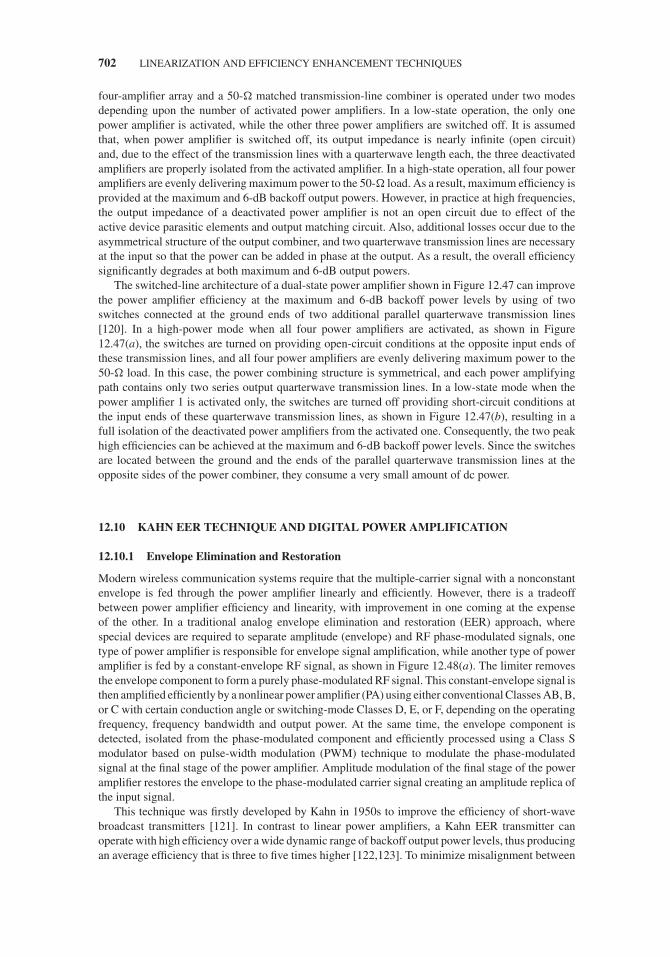
JWBS064-c12 JWBS064-Gerbennikov March 15, 2011 11:28 Printer Name: Yet to Come
702 LINEARIZATION AND EFFICIENCY ENHANCEMENT TECHNIQUES
four-amplifier array and a 50- matched transmission-line combiner is operated under two modesdepending upon the number of activated power amplifiers. In a low-state operation, the only onepower amplifier is activated, while the other three power amplifiers are switched off. It is assumedthat, when power amplifier is switched off, its output impedance is nearly infinite (open circuit)and, due to the effect of the transmission lines with a quarterwave length each, the three deactivatedamplifiers are properly isolated from the activated amplifier. In a high-state operation, all four poweramplifiers are evenly delivering maximum power to the 50- load. As a result, maximum efficiency isprovided at the maximum and 6-dB backoff output powers. However, in practice at high frequencies,the output impedance of a deactivated power amplifier is not an open circuit due to effect of theactive device parasitic elements and output matching circuit. Also, additional losses occur due to theasymmetrical structure of the output combiner, and two quarterwave transmission lines are necessaryat the input so that the power can be added in phase at the output. As a result, the overall efficiencysignificantly degrades at both maximum and 6-dB output powers.
The switched-line architecture of a dual-state power amplifier shown in Figure 12.47 can improvethe power amplifier efficiency at the maximum and 6-dB backoff power levels by using of twoswitches connected at the ground ends of two additional parallel quarterwave transmission lines[120]. In a high-power mode when all four power amplifiers are activated, as shown in Figure12.47(a), the switches are turned on providing open-circuit conditions at the opposite input ends ofthese transmission lines, and all four power amplifiers are evenly delivering maximum power to the50- load. In this case, the power combining structure is symmetrical, and each power amplifyingpath contains only two series output quarterwave transmission lines. In a low-state mode when thepower amplifier 1 is activated only, the switches are turned off providing short-circuit conditions atthe input ends of these quarterwave transmission lines, as shown in Figure 12.47(b), resulting in afull isolation of the deactivated power amplifiers from the activated one. Consequently, the two peakhigh efficiencies can be achieved at the maximum and 6-dB backoff power levels. Since the switchesare located between the ground and the ends of the parallel quarterwave transmission lines at theopposite sides of the power combiner, they consume a very small amount of dc power.
12.10 KAHN EER TECHNIQUE AND DIGITAL POWER AMPLIFICATION
12.10.1 Envelope Elimination and Restoration
Modern wireless communication systems require that the multiple-carrier signal with a nonconstantenvelope is fed through the power amplifier linearly and efficiently. However, there is a tradeoffbetween power amplifier efficiency and linearity, with improvement in one coming at the expenseof the other. In a traditional analog envelope elimination and restoration (EER) approach, wherespecial devices are required to separate amplitude (envelope) and RF phase-modulated signals, onetype of power amplifier is responsible for envelope signal amplification, while another type of poweramplifier is fed by a constant-envelope RF signal, as shown in Figure 12.48(a). The limiter removesthe envelope component to form a purely phase-modulated RF signal. This constant-envelope signal isthen amplified efficiently by a nonlinear power amplifier (PA) using either conventional Classes AB, B,or C with certain conduction angle or switching-mode Classes D, E, or F, depending on the operatingfrequency, frequency bandwidth and output power. At the same time, the envelope component isdetected, isolated from the phase-modulated component and efficiently processed using a Class Smodulator based on pulse-width modulation (PWM) technique to modulate the phase-modulatedsignal at the final stage of the power amplifier. Amplitude modulation of the final stage of the poweramplifier restores the envelope to the phase-modulated carrier signal creating an amplitude replica ofthe input signal.
This technique was firstly developed by Kahn in 1950s to improve the efficiency of short-wavebroadcast transmitters [121]. In contrast to linear power amplifiers, a Kahn EER transmitter canoperate with high efficiency over a wide dynamic range of backoff output power levels, thus producingan average efficiency that is three to five times higher [122,123]. To minimize misalignment between

JWBS064-c12 JWBS064-Gerbennikov March 15, 2011 11:28 Printer Name: Yet to Come
KAHN EER TECHNIQUE AND DIGITAL POWER AMPLIFICATION 703
FIGURE 12.47 Schematic of switched-line dual-state power amplifier architecture.
phase and amplitude, the delay line is required. Adding the output envelope feedback circuit withenvelope detector allows the intermodulation distortion to be reduced [124]. In modern transmittersfor wireless applications, the both envelope and phase-modulated signals can be easily generatedseparately using DSP technique, resulting in a system architecture shown in Figure 12.48(b). In thiscase, the phase-modulated signal with constant envelope is upconverted to the desired output RFfrequency using a direct or double conversion scheme. For a direct conversion scheme, the basebandsignal containing the phase information directly modulates the RF carrier. The experimental resultsfor mobile RF polar transmitters with CDMA IS-95 signals show that the overall system efficiencymore than 30% can be achieved at moderate average output power levels satisfying the correspondinglinearity requirements [125,126].

JWBS064-c12 JWBS064-Gerbennikov March 15, 2011 11:28 Printer Name: Yet to Come
704 LINEARIZATION AND EFFICIENCY ENHANCEMENT TECHNIQUES
FIGURE 12.48 Block diagrams of Kahn EER transmitters.
Nevertheless, there are several serious limitations of a traditional Kahn EER architecture forpractical implementation. The output voltage characteristic of the RF power transistor should belinear enough to restore accurately the input envelope. However, in practice this is not the case,especially for high power devices. Besides, the size of a Class-S modulator is sufficiently largefor MMIC implementation, and it becomes too inefficient at high frequencies. In addition, a highdegree of amplitude and phase tracking accuracy is required to achieve a high depth of modulation. Forinstance, a combination of 0.2 dB of amplitude and 3◦ of phase tracking error will result in a maximummodulation dynamic range of 20 dB. To obtain the level of the third-order intermodulation componentsbetter than −30 dBc, the differential time delay (�t) between the envelope and phase-modulated pathsdefined as �t ≤ 0.1/BRF, where BRF is the bandwidth of the RF signal, must be sufficiently small[127]. Finally, there should be a tradeoff between the switching frequency in the Class-S modulatorand the order of the low-pass filter in order to minimize the intermodulation distortion.
12.10.2 Pulse-Width Carrier Modulation
Figure 12.49(a) shows the transmitter architecture with pulse-width carrier modulation, which is analternative to a conventional Kahn EER technique [128]. In this case, similarly to the Kahn EERtechnique, the phase-modulated input signal with a nonconstant envelope is split by a coupler intoseparate envelope and phase-modulated components by means of the envelope detector and limiter,respectively. The envelope is converted to duty factor variations of pulse train, typically at a samplingrate at least an order of magnitude higher in frequency than the maximum frequency of the envelope.

JWBS064-c12 JWBS064-Gerbennikov March 15, 2011 11:28 Printer Name: Yet to Come
KAHN EER TECHNIQUE AND DIGITAL POWER AMPLIFICATION 705
FIGURE 12.49 Transmitter architecture with pulse-width carrier modulation.
However, the pulse train is then applied as pulse-width modulation onto a low-power carrier phase-modulated signal using a pulse modulator. The combined signal is transmitted to a high-efficiencybroadband nonlinear power amplifier. Unwanted sidebands caused by the sampling process are thenrejected by a bandpass filter (BPF) at the amplifier output to pass only the carrier and its modulatedsignal bandwidth and hence recover a linear replica of the original source signal. Pulse modulationsource can operate using Cartesian coordinate I and Q baseband data determining the phase valuesand duty ratios for modulating the pulsed envelope signal, as shown in Figure 12.49(b) [129,130].Using a LUT in the envelope-to-pulse modulation circuitry is important to maximize the envelopedynamic range by proper adjustment of the pulse width and the sampling period. The feedback loopwith a quadrature demodulator reproducing the baseband in-phase and quadrature feedback signalsmay be necessary to correct the nonlinearity effects introduces by components within the circuit andimprove linearity [129].
Generally, the both envelope and phase-modulated signals can also be generated separately usingDSP technique, and digitization of the envelope signal can be provided by a delta-sigma modulatorwith a sampling rate of ten times of the RF bandwidth [131,132]. The main disadvantage of suchtransmitter architectures is a sufficiently high level of insertion loss of the narrowband BPF, the qualityfactor of which should be very high to minimize the switching frequency sidebands. Nevertheless,in some particular cases, it is possible to realize a compromise solution between BPF insertion lossand switching frequency, thus resulting in a higher average efficiency for signals with nonconstantenvelope than can be achieved by the systems at backoff output power levels using linear poweramplifiers. For example, by using a second-order delta-sigma modulator with 200 MHz switchingfrequency and a Class E power amplifier, an output power of 18 dBm with a power-added efficiency of
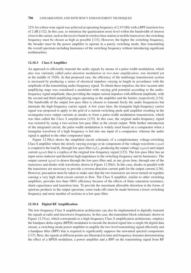
JWBS064-c12 JWBS064-Gerbennikov March 15, 2011 11:28 Printer Name: Yet to Come
706 LINEARIZATION AND EFFICIENCY ENHANCEMENT TECHNIQUES
32% for a three-tone signal was achieved at operating frequency of 2.47 GHz with a BPF insertion lossof 2 dB [132]. In this case, to minimize the quantization noise level within the bandwidth of interestclose to the carrier, such as the receive band in wireless base station or mobile transceiver, the switchingfrequency must be chosen as high as possible [133]. However, the higher the switching frequency,the broader must be the power amplifier to operate in a purely switching mode, thus transmittingthe overall spectrum including harmonics of the switching frequency without introducing significantnonlinearities.
12.10.3 Class S Amplifier
An approach to efficiently transmit the audio signals by means of a pulse-width modulation, whichalso was variously called pulse-duration modulation or two-state amplification, was invented yetin the middle of 1920s. In that proposed case, the efficiency of the multistage transmission systemis increased by producing a series of electrical impulses varying in length in accordance with theamplitude of the transmitting audio-frequency signal. To obtain these impulses, the first vacuum-tubeamplifying stage was considered a modulator with varying grid potential according to the audio-frequency signal amplitude, thus providing the output current impulses with different amplitude, withthe second and third amplifying stages operating as the amplifier and the limiter, respectively [134].The bandwidth of the output low-pass filter is chosen to transmit freely the audio frequencies butattenuate the high-frequency carrier signal. A few years later, the triangular high-frequency carriersignal was proposed to apply to the grid of a current-switching push–pull amplifier resulting in therectangular-wave output currents at anodes to form a pulse-width modulation transmission, whichwas then called the Class S amplification [135]. In this case, the original audio-frequency signalwas restored by using a two-section low-pass filter at the circuit output. With further introductionof the integrated circuit, the pulse-width modulation is widely used based on a comparator when atriangular waveform of a high frequency is fed into one input of a comparator, whereas the audiosignal is applied to the other comparator input.
Figure 12.50(a) shows the simplified circuit schematic of a complementary voltage-switchingClass S amplifier where the slowly varying average or dc component of the voltage waveform v2(ωt)is coupled to the load RL through low-pass filter L0C0, producing the output voltage vR(ωt) and outputcurrent iR(ωt) that is a replica of the original low-frequency signal [123]. The low-pass filter has aninput series inductor and therefore high impedance to the switching frequency and its harmonics. Theoutput current iR(ωt) is drawn through the low-pass filter and, at any given time, through one of thetransistors and diodes with waveforms shown in Figure 12.50(b). In this case, diodes in parallel withthe transistors are necessary to provide a reverse-direction current path for the output current [136].However, precaution must be taken to make sure that the two transistors are never turned on togethercausing a very high short-circuit current to flow. The Class S amplifier, similar to other switchingamplifiers, provides less than 100% efficiency because of the effects of finite saturation resistance,shunt capacitance and transition time. To provide the maximum allowable distortion in the forms ofspurious products in the output spectrum, some trade-offs must be made between a lower switchingfrequency and more number of sections in a low-pass filter.
12.10.4 Digital RF Amplification
The low-frequency Class S amplification architecture can also be implemented to digitally transmitthe signals at radio and microwave frequencies. In this case, the transmitter block schematic shown inFigure 12.51(a), which corresponds to a high-frequency Class S amplification architecture, employsthe bandpass delta-sigma (BPDS) modulator to encode the desired signal into a single-bit digital datastream, a switching-mode power amplifier to amplify the two-level transmitting signal efficiently anda bandpass filter (BPF) that is required to significantly suppress the unwanted spectral components[137]. Here, the signals at different points are illustrated in time and frequency domains demonstratingthe effect of a BPDS modulator, a power amplifier and a BPF on the transmitting signal from RF
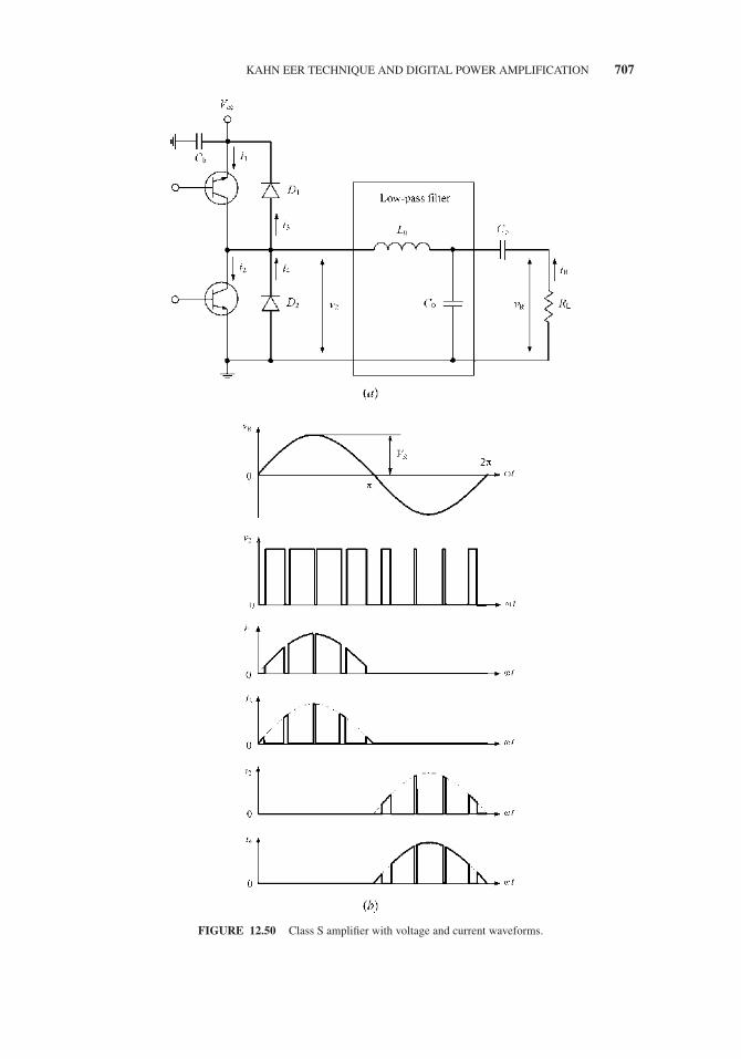
JWBS064-c12 JWBS064-Gerbennikov March 15, 2011 11:28 Printer Name: Yet to Come
KAHN EER TECHNIQUE AND DIGITAL POWER AMPLIFICATION 707
FIGURE 12.50 Class S amplifier with voltage and current waveforms.
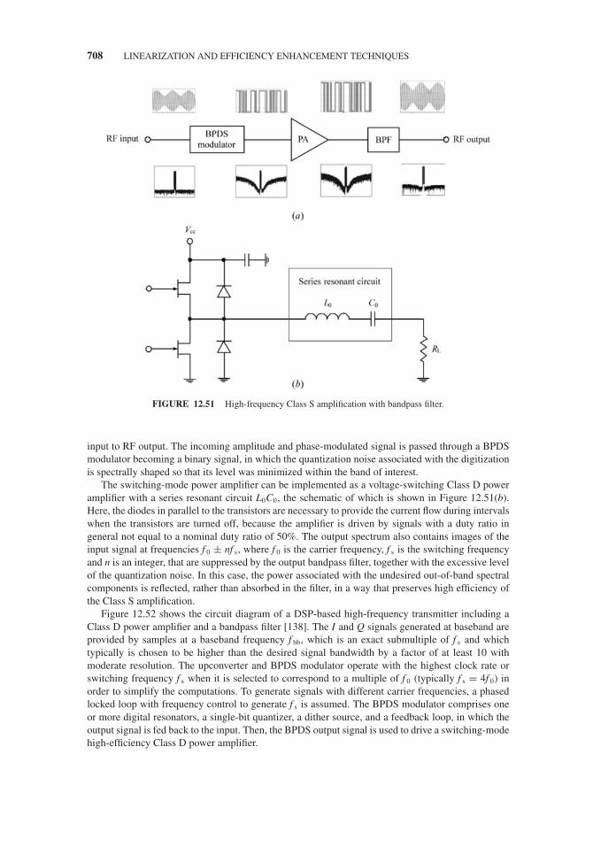
JWBS064-c12 JWBS064-Gerbennikov March 15, 2011 11:28 Printer Name: Yet to Come
708 LINEARIZATION AND EFFICIENCY ENHANCEMENT TECHNIQUES
FIGURE 12.51 High-frequency Class S amplification with bandpass filter.
input to RF output. The incoming amplitude and phase-modulated signal is passed through a BPDSmodulator becoming a binary signal, in which the quantization noise associated with the digitizationis spectrally shaped so that its level was minimized within the band of interest.
The switching-mode power amplifier can be implemented as a voltage-switching Class D poweramplifier with a series resonant circuit L0C0, the schematic of which is shown in Figure 12.51(b).Here, the diodes in parallel to the transistors are necessary to provide the current flow during intervalswhen the transistors are turned off, because the amplifier is driven by signals with a duty ratio ingeneral not equal to a nominal duty ratio of 50%. The output spectrum also contains images of theinput signal at frequencies f 0 ± nf s, where f 0 is the carrier frequency, f s is the switching frequencyand n is an integer, that are suppressed by the output bandpass filter, together with the excessive levelof the quantization noise. In this case, the power associated with the undesired out-of-band spectralcomponents is reflected, rather than absorbed in the filter, in a way that preserves high efficiency ofthe Class S amplification.
Figure 12.52 shows the circuit diagram of a DSP-based high-frequency transmitter including aClass D power amplifier and a bandpass filter [138]. The I and Q signals generated at baseband areprovided by samples at a baseband frequency f bb, which is an exact submultiple of f s and whichtypically is chosen to be higher than the desired signal bandwidth by a factor of at least 10 withmoderate resolution. The upconverter and BPDS modulator operate with the highest clock rate orswitching frequency f s when it is selected to correspond to a multiple of f 0 (typically f s = 4f 0) inorder to simplify the computations. To generate signals with different carrier frequencies, a phasedlocked loop with frequency control to generate f s is assumed. The BPDS modulator comprises oneor more digital resonators, a single-bit quantizer, a dither source, and a feedback loop, in which theoutput signal is fed back to the input. Then, the BPDS output signal is used to drive a switching-modehigh-efficiency Class D power amplifier.

JWBS064-c12 JWBS064-Gerbennikov March 15, 2011 11:28 Printer Name: Yet to Come
REFERENCES 709
FIGURE 12.52 DSP-based Class S transmitter architecture.
The performance of the BPDS modulator depends mainly on two parameters: the order of themodulator and the oversampling ratio (OSR) of the input signal. The OSR is defined as a ratio ofsampling (switching) frequency to two times the input signal bandwidth. The higher the order is, thebetter the quantization noise is filtered at the output bandwidth, but the modulator structure becomesmore complicated. For example, for a 2.14-GHz WCDMA carrier, the switching frequency must beequal to f s = 4f 0 = 8.56 GHz, which means that, for a 60 MHz bandwidth, the OSR = 8.56 GHz/(2× 60 MHz) = 71.33, resulting in the ACLR of at least −50 dBc [139]. However, the sampling rateof 8.56 GHz is definitely too high for modern technology, especially in implementation of a high-efficiency high-power switching-mode amplifier, the active devices of which must be characterizedby a transition frequency f T much higher than f s, of at least three times to include its third harmoniccomponent in the transmitting spectrum for increased efficiency and linearity. For a CDMA IS-95signal with a bandwidth of 1.23 MHz and a PAR of 5.5 dB at a carrier frequency of 800 MHz, adrain efficiency of 31% was achieved for a voltage-switching CMOS Class D power amplifier with anoutput power of 15 dBm and an ACPR of −43 dBc using a clock rate for a two-level BPSD of 3.2 GHz[140]. However, to calculate a power-added efficiency of the high-frequency Class S amplificationpath, it is necessary to operate with a coding efficiency that represents a ratio of the in-band power tothe total pulse train power [141]. In this case, a high level of out-of-band spectral power is wastefuland reduces the utility of the pulse train to generate a load in-band power may significantly affect theoverall system efficiency. Although out-of-band spectral components do not dissipate any power in theload network of an ideal Class-D power amplifier, however they are dissipated in its input circuit andrequire the excessive dc power for a driver amplifier, thus significantly reduces the operating powergain and, as a result, the power-added efficiency, compared to the linear amplification architecture.Therefore, in practice it is necessary to choose the active devices such as a pHEMT or a GaN HEMTwith the minimum saturation resistances, high gain capability and maximum transition frequency.
REFERENCES
1. H. S. Black, “Translating System,” U.S. Patent 1,686,792, Oct. 1928.
2. W. D. Lewis, “Self-Correcting Amplifier,” U.S. Patent 2,592,716, Apr. 1952.
3. H. Seidel, “Feed-Forward Amplifier,” U.S. Patent 3,471,798, Oct. 1969.
4. H. Seidel, “A Feedforward Experiment Applied to an L-4 Carrier System Amplifier,” IEEE Trans. Commun.Technol., vol. COM-19, pp. 320–325, June 1971.
5. H. Seidel, “A Microwave Feedforward Experiment,” Bell System Tech. J., vol. 50, pp. 2879–2916, Nov.1971.
6. R. G. Meyer, R. Eschenbach, and W. M. Edgerley, “A Wide-Band Feedforward Amplifier,” IEEE J. Solid-State Circuits, vol. SC-9, pp. 422–428, Dec. 1974.
7. C.-C. Hsieh and S.-P. Chan, “A Feedforward S-Band MIC Amplifier System,” IEEE J. Solid-State Circuits,vol. SC-11, pp. 271–278, Apr. 1976.

JWBS064-c12 JWBS064-Gerbennikov March 15, 2011 11:28 Printer Name: Yet to Come
710 LINEARIZATION AND EFFICIENCY ENHANCEMENT TECHNIQUES
8. R. J. Wilkinson and P. B. Kenington, “Specification of Error Amplifiers for Use in Feedforward Transmitters,”IEE Proc.-G, vol. 139, pp. 447–480, Aug. 1992.
9. S.-G. Kang and I.-K. Lee, “Cancellation Performance of a Linearisation Loop of a Feedforward Amplifier,”Electronics Lett., vol. 33, pp. 444–446, Mar. 1997.
10. K. Konstantinou and D. K. Paul, “Analysis and Design of Broadband High Efficiency Feedforward Ampli-fiers,” IEEE MTT-S Int. Microwave Symp. Dig., vol. 2, pp. 867–870, 1996.
11. P. B. Kenington, “Efficiency of Feedforward Amplifiers,” IEE Proc.-G, vol. 139, pp. 591–593, Oct. 1992.
12. P. B. Kenington, High Linearity RF Amplifier Design, Boston: Artech House, 2000.
13. E. E. Eid, F. M. Ghannouchi, and F. Beauregard, “Optimal Feedforward Linearization System Design,”Microwave J., vol. 38, pp. 78–86, Nov. 1995.
14. H. Choi, Y. Jeong, J. S. Kenney, and C. D. Kim, “Cross Cancellation Technique Employing an ErrorAmplifier,” IEEE Microwave and Wireless Components Lett., vol. 18, pp. 488–490, July 2008.
15. R. M. Bauman, “Adaptive Feed-Forward System,” U.S. Patent 4,389,618, June 1983.
16. B. Shi, W. Shan, and L. Sundstrom, “An Analog Adaptive Feedforward Amplifier Linearizer,” Proc. 34thEuropean Microwave Conf., pp. 1065–1068, 2004.
17. S. J. Grant, J. K. Cavers, and P. A. Goud, “A DSP Controlled Adaptive Feedforward Amplifier Linearizer,”5th IEEE Int. Conf. Record. Universal Personal Commun., pp. 788–792, 1996.
18. S. G. Randall, J. G. McRory, and R. H. Johnston, “Broadband DSP Based Feedforward Amplifier Linearizer,”Electronics Lett., vol. 38, pp. 1470–1471, Nov. 2002.
19. W. W. Macalpine, “Distortionless Transmission System,” U.S. Patent 2,043,587, June 1936.
20. P. O. Pedersen, “A Distortion-Free Amplifier,” Proc. IRE, vol. 28, pp. 59–66, Feb. 1940.
21. L. T. Mucenieks, C. S. Robertson, B. L. Irvine, and N. Salvador, “RF Power Amplifier Linearization UsingParallel RF Power Amplifiers Having Intermod-Complementing Predistortion Paths,” U.S. Patent 6,111,462,Aug. 2000.
22. M. Billsberry, “Balanced Distortion Reduction Circuit,” U.S. Patent 6,734,726, May 2004.
23. R. Gutierrez, “Reflect Forward Adaptive Linearizer Amplifier,” U.S. Patent 6,573,793, June 2003.
24. R. Gutierrez, “The RFAL Technique for Cancellation of Distortion in Power Amplifiers,” High FrequencyElectronics, vol. 4, pp. 18–28, June 2004.
25. R. Gutierrez, “High-Efficiency Linearized LDMOS Amplifiers Utilize the RFAL Architecture,” High Fre-quency Electronics, vol. 6, pp. 22–28, Feb. 2006.
26. E. Peterson, “Control of Distortion,” U.S. Patent 2,233,061, Feb. 1941.
27. T. Nojima and T. Kohno, “Cuber Predistortion Linearizer for Relay Equipment in 800 MHz Band LandMobile Telephone System,” IEEE Trans. Vehicular Technol., vol. VT-34, pp. 169–177, Nov. 1985.
28. R. C. Tupynamba and E. Camargo, “MESFET Nonlinearities Applied to Predistortion Linearizer Design,”IEEE MTT-S Int. Microwave Symp. Dig., pp. 955–958, 1992.
29. H. S. Read, “Electric Circuits,” U.S. Patent 1,464,111, Aug. 1923.
30. Y. Ikeda, K. Mori, S. Shinjo, F. Kitabayashi, A. Ohta, T. Takagi, and O. Ishida, “An L-Band High Efficiencyand Low Distortion Multi-Stage Amplifier Using Self Phase Distortion Compensation Technique,” IEICETrans. Electron., vol. E85-C, pp. 1967–1972, Dec. 2002.
31. K. Yamauchi, K. Mori, M. Nakayama, Y. Itoh, Y. Mitsui, and O. Ishida, “A Novel Series Diode Lin-earizer for Mobile Radio Power Amplifiers,” IEEE MTT-S Int. Microwave Symp. Dig., vol. 2, pp. 831–834,1996.
32. K. Yamauchi, K. Mori, M. Nakayama, Y. Mitsui, and T. Takagi, “A Microwave Miniaturized LinearizerUsing a Parallel Diode with a Bias Feed Resistance,” IEEE Trans. Microwave Theory Tech., vol. MTT-45,pp. 2431–2435, Dec. 1997.
33. M. Nakayama, K. Mori, K. Yamauchi, Y. Itoh, and Y. Mitsui, “An Amplitude and Phase LinearizingTechnique for Linear Power Amplifiers,” Microwave J., vol. 39, pp. 96–104, Mar. 1996.
34. S. Ogura, K. Seino, T. Ono, A. Kamikokura, and H. Hirose, “Development of a Compact Broadband FETLinearizer for Satellite Use,” IEEE MTT-S Int. Microwave Symp. Dig., vol. 3, pp. 1195–1198, 1997.
35. J. Boix, “Ku-Band Solid State Power Amplifiers for the New European Satellites,” Proc. 23rd Europ.Microwave Conf., pp. 11–14, 1993.

JWBS064-c12 JWBS064-Gerbennikov March 15, 2011 11:28 Printer Name: Yet to Come
REFERENCES 711
36. J. Yi, Y. Yang, M. Park, W. Kang, and B. Kim, “Analog Predistortion Linearizer for High-Power RFAmplifiers,” IEEE Trans. Microwave Theory Tech., vol. 48, pp. 2709–2713, Dec. 2000.
37. I. Kim, J. Cha, S. Hong, Y. Y. Woo, J. Kim, and B. Kim, “Predistortion Power Amplifier for Base-StationUsing a Feedforward Loop Linearizer,” Proc. 36th Europ. Microwave Conf., pp. 141–144, 2006.
38. F. Zavosh, D. Runton, and C. Thron, “Digital Predistortion Linearizes CDMA LDMOS Amps,” Microwaves& RF, vol. 39, pp. 55–61, Mar. 2000.
39. L. Sundstrom, M. Faulkner, and M. Johansson, “Quantization Analysis and Design of a Digital PredistortionLinearizer for RF Power Amplifiers,” IEEE Trans. Vehicular Technol., vol. VT-45, pp. 707–719, Nov.1996.
40. A. R. Mansell and A. Bateman, “Adaptive Predistortion with Reduced Feedback Complexity,” ElectronicsLett., vol. 32, pp. 1153–1154, June 1996.
41. N. Nascas and Y. Papananos, “A New Non-Iterative, Adaptive Baseband Predistortion Method for HighPower RF Amplifiers,” IEEE Circuits and Systems Symp. Dig., vol. I, pp. 413–416, 2003.
42. H. S. Black, “Wave Translation System,” U.S. Patent 2,003,282, June 1935 (filed Aug. 1923).
43. H. S. Black, “Stabilized Feed-Back Amplifiers,” Proc. IEEE, vol. 87, pp. 379–385, Feb. 1999; reprintedfrom Electronic Engineering, vol. 53, pp. 114–120, Jan. 1934.
44. W. B. Bruene, “Distortion Reducing Means for Single-Sideband Transmitters,” Proc. IRE, vol. 44,pp. 1760–1765, Dec. 1956.
45. H. S. Black, “Inventing the Negative Feedback Amplifier,” IEEE Spectrum, vol. 14, pp. 55–60, Dec. 1977.
46. H. A. Rosen and A. T. Owens, “Power Amplifier Linearity Studies for SSB Transmissions,” IEEE Trans.Commun. Syst., vol. CS-12, pp. 150–159, June 1964.
47. C.-C. Hsieh and E. Strid, “A S-Band High Power Feedback Amplifier,” IEEE MTT-S Int. Microwave Symp.Dig., pp. 182–184, June 1977.
48. K. Oosaki and Y. Akaiwa, “Nonlinearity Compensation of Linear Power Amplifier for Mobile Communi-cation,” 4th IEEE Int. Conf. Record. Universal Personal Commun., pp. 302–305, Nov. 1995.
49. R. J. Gilmore, R. Kiehne, and F. J. Rosenbaum, “Circuit Design to Reduce 3rd Order IntermodulationDistortion in FET Amplifiers,” IEEE MTT-S Int. Microwave Symp. Dig., pp. 413–416, June 1985.
50. A. K. Ezzeddine, H.-L. Hung, and H. C. Huang, “An MMIC C-Band FET Feedback Power Amplifier,”IEEE Trans. Microwave Theory Tech., vol. MTT-38, pp. 350–357, Apr. 1990.
51. J. G. McRory and R. H. Johnston, “An RF Amplifier for Low Intermodulation Distortion,” IEEE MTT-S Int.Microwave Symp. Dig., vol. 3, pp. 1741–1744, 1994.
52. S. Narayanan, “Application of Volterra Series to Intermodulation Distortion Analysis of Transistor FeedbackAmplifiers,” IEEE Trans. Circuit Theory, vol. CT-17, pp. 518–527, Nov. 1970.
53. Y. Kim, Y. Yang, S. Kang, and B. Kim, “Linearization of 1.85 GHz Amplifier Using Feedback PredistortionLoop,” IEEE MTT-S Int. Microwave Symp. Dig., vol. 3, pp. 1675–1678, 1998.
54. Y. Y. Woo, J. Kim, J. Yi, S. Hong, I. Kim, J. Moon, and B. Kim, “Adaptive Digital Feedback Predistor-tion Technique for Linearizing Power Amplifiers,” IEEE Trans. Microwave Theory Tech., vol. MTT-55,pp. 932–940, May 2007.
55. T. Arthanayake and H. B. Wood, “Linear Amplification Using Envelope Feedback,” Electronics Lett.,vol. 7, pp. 145–146, Apr. 1971.
56. S. Kusunoki, K. Yamamoto, T. Hatsugai, H. Nagaoka, K. Tagami, N. Tominaga, K. Osawa, K. Tanabe,S. Sakurai, and T. Iida, “Power-Amplifier Module with Digital Adaptive Predistortion for Cellular Phones,”IEEE Trans. Microwave Theory Tech., vol. MTT-50, pp. 2979–2986, Dec. 2002.
57. J.-S. Cardinal and F. Ghannouchi, “A New Adaptive Double Envelope Feedback (ADEF) Linearizer forSolid State Power Amplifiers,” IEEE Trans. Microwave Theory Tech., vol. MTT-43, pp. 1508–1515, July1995.
58. V. Petrovic and W. Gosling, “Polar-Loop Transmitter,” Electronics Lett., vol. 15, pp. 286–288, May1979.
59. V. Petrovic, “Reduction of Spurious Emission from Radio Transmitters by Means of Modulation Feedback,”Proc. IEE Conf. Radio Spectrum Conservation Technol., pp. 44–49, 1983.
60. M. Johansson and L. Sundstrom, “Linearisation of RF Multicarrier Amplifiers Using Cartesian Feedback,”Electronics Lett., vol. 30, pp. 1110–1112, July 1994.

JWBS064-c12 JWBS064-Gerbennikov March 15, 2011 11:28 Printer Name: Yet to Come
712 LINEARIZATION AND EFFICIENCY ENHANCEMENT TECHNIQUES
61. Y. Nagata, “Linear Amplification Technique for Digital Mobile Communications,” Proc. 39th IEEE VehicularTechnol. Conf., pp. 159–164, 1989.
62. A. R. Mansell and A. Bateman, “Transmitter Linearisation Using Composite Modulation Feedback,” Elec-tronics Lett., vol. 32, pp. 2120–2121, Nov. 1996.
63. S. W. Chung, J. W. Holloway, and J. L. Dawson, “Energy-Efficient Digital Predistortion with LookupTable Training Using Analog Cartesian Feedback,” IEEE Trans. Microwave Theory Tech., vol. MTT-56,pp. 2248–2258, Oct. 2008.
64. W. H. Doherty, “A New High Efficiency Power Amplifier for Modulated Waves,” Proc. IRE, vol. 24,pp. 1163–1182, Sept. 1936.
65. F. H. Raab, “Efficiency of Doherty RF Power-Amplifier Systems,” IEEE Trans. Broadcast., vol. BC-33,pp. 77–83, Sept. 1987.
66. M. Iwamoto, A. Williams, P -F. Chen, A. G. Metzger, L. E. Larsson, and P. M. Asbeck, “An ExtendedDoherty Amplifier with High Efficiency Over a Wide Power Range,” IEEE Trans. Microwave Theory Tech.,vol. MTT-49, pp. 2472–2479, Dec. 2001.
67. Y. Yang, J. Cha, B. Shin, and B. Kim, “A Fully Matched N-Way Doherty Amplifier with OptimizedLinearity,” IEEE Trans. Microwave Theory Tech., vol. MTT-51, pp. 986–993, Mar. 2003.
68. Y. Yang, J. Yi, Y. Y. Woo, and B. Kim, “Optimum Design for Linearity and Efficiency of a Mi-crowave Doherty Amplifier Using a New Load matching Technique,” Microwave J., vol. 44, pp. 20–36,Dec. 2001.
69. Y. Takayama, T. Harada, T. Fujita, and K. Maenaka, “Design Method of Microwave Doherty Power Ampli-fiers and Its Application to Si Power MOSFET Amplifiers,” Electronics and Communications in Japan, part2, vol. 88, pp. 9–17, Apr. 2005.
70. N. Srirattana, A. Raghavan, D. Heo, P. E. Allen, and J. Laskar, “Analysis and Design of a High-EfficiencyMultistage Doherty Power Amplifier for Wireless Communications,” IEEE Trans. Microwave Theory Tech.,vol. MTT-53, pp. 852–860, Mar. 2005.
71. M. J. Pelk, W. C. E. Neo, J. R. Gajadharsing, R. S. Pengelly, and L. C. N. de Vreede, “A High-Efficiency100-W GaN Three-Way Doherty Amplifier for Base-Station Applications,” IEEE Trans. Microwave TheoryTech., vol. MTT-56, pp. 1582–1591, July 2008.
72. Y. Zhao, M. Iwamoto, D. Kimball, L. E. Larsson, and P. M. Asbeck, “A 900 MHz Doherty AmplifierImplemented with Lumped Elements,” IEEE Topical Workshop on Power Amplifiers for Wireless Commun.,San Diego, 2003.
73. Y. Yang, J. Cha, B. Shin, and B. Kim, “A Microwave Doherty Amplifier Employing Envelope TrackingTechnique for High Efficiency and Linearity,” IEEE Microwave and Wireless Components Lett., vol. 13, pp.370–372, Sept. 2003.
74. Y.-S. Lee, M.-W. Lee, and Y.-H. Jeong, “Highly Efficient Doherty Amplifier Based on Class-E topologyfor WCDMA Applications,” IEEE Microwave and Wireless Components Lett., vol. 18, pp. 608–610, Sept.2008.
75. Y. Zhao, M. Iwamoto, L. E. Larsson, and P. M. Asbeck, “Doherty Amplifier with DSP Control to Improveperformance in CDMA Operation,” IEEE MTT-S Int. Microwave Symp. Dig., vol. 2, pp. 687–690, 2003.
76. J. Moon, Ja. Kim, I. Kim, Ju. Kim, and B. Kim, “Highly efficiency Three-Way Saturated Doherty Amplifierwith Digital Feedback Predistortion,” IEEE Microwave and Wireless Components Lett., vol. 18, pp. 539–541,Aug. 2008.
77. H. Chireix, “High Power Outphasing Modulation,” Proc. IRE, Vol. 23, pp. 1370–1392, Nov. 1935.
78. D. C. Cox, “Linear Amplification with Nonlinear Components,” IEEE Trans. Commun., vol. COM-22,pp. 1942–1945, Dec. 1974.
79. F. H. Raab, “Average Efficiency of Outphasing Power-Amplifier Systems,” IEEE Trans. Commun.,vol. COM-33, pp. 1094–1099, Oct. 1985.
80. S. A. Hetzel, A. Bateman, and J. P. McGeehan, “A LINC Transmitter,” Proc. 41st IEEE Vehicular Technol.Conf., pp. 133–137, 1991.
81. R. Langridge, T. Thornton, P. M. Asbeck, and L. E. Larson, “A Power Re-Use Technique for ImprovedEfficiency of Outphasing Microwave Power Amplifiers,” IEEE Trans. Microwave Theory Tech., vol. MTT-47,pp. 1467–1470, Aug. 1999.

JWBS064-c12 JWBS064-Gerbennikov March 15, 2011 11:28 Printer Name: Yet to Come
REFERENCES 713
82. C. P. Conradi, R. H. Johnston, and J. G. McRory, “Evaluation of a Lossless Combiner in a LINC Transmitter,”Proc. 1999 IEEE Canadian Conf. Electrical and Computer Eng., vol. 1, pp. 105–110, May 1999.
83. B. Shi and L. Sundstrom, “Investigation of a Highly Efficient LINC Amplifier Topology,” Proc. 54th IEEEVehicular Technol. Conf., pp. 1215–1219, 2001.
84. K. Tom, V. Bassoo, M. Faulkner, and T. Lejon, “Load-Pull Analysis of Outphasing Class-E Power Amplifier,”Proc. 2nd Int. Conf. Wireless Broadband and Ultra Wideband Commun., pp. 52–55, 2007.
85. I. Hakala, D. K. Choi, L. Gharavi, N. Kajakine, J. Koskela, and R. Kaunisto, “A 2.14-GHz Chireix OutphasingTransmitter,” IEEE Trans. Microwave Theory Tech., vol. MTT-53, pp. 2129–2138, June 2005.
86. G. Hegazi, T. Chu, S. Heibel, J. Jordan, and H. Sasmazer, “Linear Wideband VHF/UHF Quad LINCTransmitter System,” Proc. 2007 IEEE Military Commun. Conf., pp. 1–6, Oct. 2007.
87. S. Hamedi-Hagh and C. A. T. Salama, “Wideband CMOS Integrated RF Combiner for LINC Transmitters,”IEEE MTT-S Int. Microwave Symp. Dig., vol. 1, pp. 41–43, 2003.
88. F. Casadevall and J. J. Olmos, “On the Behavior of the LINC Transmitter,” Proc. 40th IEEE VehicularTechnol. Conf., pp. 29–34, May 1990.
89. A. Birafane and A. B. Kouki, “On the Linearity and Efficiency of Outphasing Microwave Amplifiers,” IEEETrans. Microwave Theory Tech., vol. MTT-52, pp. 1702–1708, July 2004.
90. S. Tomisato, K. Chiba, and K. Murota, “Phase Error Free LINC Modulator,” Electronics Lett., vol. 25,pp. 576–577, Apr. 1989.
91. L. Sundstrom, “Automatic Adjustment of Gain and Phase Imbalances in LINC Transmitters,” ElectronicsLett., vol. 31, pp. 155–156, Feb. 1995.
92. X. Zhang, L. E. Larson, P. M. Asbeck, and P.Nanawa, “Gain/Phase Imbalance-Minimization Tech-niques for LINC Transmitters,” IEEE Trans. Microwave Theory Tech., vol. MTT-49, pp. 2507–2515, Dec.2001.
93. C. P. Conradi and J. G. McRory, “Predistorted LINC Transmitter,” Electronics Lett., vol. 38, pp. 301–302,Mar. 2002.
94. A. Huttunen and R. Kaunisto, “A 20-W Chireix Outphasing Transmitter for WCDMA Base Stations,” IEEETrans. Microwave Theory Tech., vol. MTT-55, pp. 2709–2718, Dec. 2007.
95. A. Bateman, “The Combined Analogue Locked Loop Universal Modulator (CALLUM),” Proc. 42nd IEEEVehicular Technol. Conf., pp. 759–763, 1992.
96. A. Bateman, M. Li, and K. Chan, “Implementation of the LINC Transmitter Using the Combined AnalogueLocked Loop Universal Modulator (CALLUM),” Proc. 7th IEE Europ. Conf. Mobile and Personal Commun.,pp. 31–37, 1993.
97. D. J. Jennings and J. P. McGeehan, “A High-Efficiency RF Transmitter Using VCO-Derived Synthesis:CALLUM,” IEEE Trans. Microwave Theory Tech., vol. MTT-47, pp. 715–721, June 1999.
98. G. Hannigton, P.-F. Chen, V. Radisic, T. Itoh, and P. M. Asbeck, “Microwave Power Amplifier Effi-ciency Improvement with a 10 MHz HBT DC-DC Converter,” IEEE MTT-S Int. Microwave Symp. Dig.,pp. 313–316, 1998.
99. G. Hannigton, P.-F. Chen, P. M. Asbeck, and L. E. Larson, “High-Efficiency Power Amplifier Using DynamicPower-Supply Voltage for CDMA Applications,” IEEE Trans. Microwave Theory Tech., vol. MTT-47,pp. 1471–1476, Aug. 1999.
100. M. Ranjan, K. H. Koo, G. Hannigton, C. Fallesen, and P. M. Asbeck, “Microwave Power Amplifiers withDigitally-Controlled Power Supply Voltage for High Efficiency and High Linearity,” IEEE MTT-S Int.Microwave Symp. Dig., vol. 1, pp. 493–496, 2000.
101. D. F. Kimball, J. Jeong, C. Hsia, P. Draxler, S. Lanfranco, W. Nagy, K. Linthicum, L. E. Larson, and M.Asbeck, “High-Efficiency Envelope-Tracking W-CDMA Base-Station Amplifier Using GaN HFETs,” IEEETrans. Microwave Theory Tech., vol. MTT-54, pp. 3848–3856, Nov. 2006.
102. J. Staudinger, B. Gilsdorf, D. Newman, G. Norris, G. Sadowniczak, R. Sherman, and T. Quach, “HighEfficiency CDMA RF Power Amplifier Using Dynamic Envelope Tracking Technique,” IEEE MTT-S Int.Microwave Symp. Dig., vol. 2, pp. 873–876, 2000.
103. S. Abedinpour, I. Deligoz, J. Desai, M. Figiel, and S. Kiaei, “Monolithic Supply Modulated RF PowerAmplifier and DC–DC Power Converter IC,” IEEE MTT-S Int. Microwave Symp. Dig., vol. 1, pp. 89–92,2003.

JWBS064-c12 JWBS064-Gerbennikov March 15, 2011 11:28 Printer Name: Yet to Come
714 LINEARIZATION AND EFFICIENCY ENHANCEMENT TECHNIQUES
104. B. Sahu and G. A. Rincon-Mora, “A High-Efficiency Linear RF Power Amplifier with a Power-Tracking Dy-namically Adaptive Buck-Boost Supply,” IEEE Trans. Microwave Theory Tech., vol. MTT-52, pp. 112–120,Jan. 2004.
105. F. Wang, D. F. Kimball, D. Y. Lie, P. M. Asbeck, and L. E. Larsson, “A Monolithic High-Efficiency 2.4-GHz 20-dBm SiGe BiCMOS Envelope-Tracking OFDM Power Amplifier,” IEEE J. Solid-State Circuits,vol. SC-42, pp. 1271–1281, June 2007.
106. Y. Aihara, “Transmitter Power Varying Device Having a Bypass Line for a Power Amplifier,” U.S. Patent5,909,643, June 1999.
107. J. R. King and G. A. Olsen, “Switchable Path Power with Schottky Diode Combining Network,” U.S. Patent6,181,208, Jan. 2001.
108. S. Brozovich, “High Efficiency Multiple Power Level Amplifier Circuit,” U.S. Patent 5,661,434, Aug. 1997.
109. J. Staudinger, “Applying Switched Gain Stage Concepts to Improve Efficiency and Linearity of MobileCDMA Power Amplification,” Microwave J., vol. 43, pp. 152–162, Sept. 2000.
110. H. X. Wu, “High-Efficient Configurable Power Amplifier for Use in a Portable Unit,” U.S. Patent 5,758,269,May 1998.
111. A. V. Grebennikov, H. Jaeger, and E. P. Heaney, “High-Efficiency Cellular Phone Transmitters with ReducedPower Consumption,” Proc. 2002 European Conf. Wireless Technol., pp. 115–118.
112. G. Leuzzi and C. Micheli, “Variable-Load Constant-Efficiency Power Amplifier for Mobile CommunicationsApplications,” Proc. 11th European GAAS Symp., pp. 481–484, 2003.
113. H.-M. Park, S.-H. Cheon, J.-W. Park, and S. Hong, “Demonstration of On-Chip Appended Power Amplifierfor Improved Efficiency at Low Power Region,” IEEE MTT-S Int. Microwave Symp. Dig., vol. 2, pp. 691–694,2003.
114. J. H. Kim, J. H. Kim, Y. S. Noh, and C. S. Park, “An InGaP-GaAs HBT MMIC Smart Power Amplifier forW-CDMA Mobile Handsets,” IEEE J. Solid-State Circuits, vol. SC-38, pp. 905–910, June 2003.
115. A. Grebennikov, B. Zogl, H. Hermann, C. Roth, and W. Thomann, “High-Efficiency Balanced Switched-Path Monolithic SiGe HBT Power Amplifiers for Wireless Applications,” Proc. 37th Europ. MicrowaveConf., pp. 1189–1192, 2007.
116. T. Sato and C. Grigorean, “Design Advantages of CDMA Power Amplifiers Built with MOSFET Technol-ogy,” Microwave J., vol. 45, pp. 64–78, Oct. 2002.
117. Y. S. Noh and C. S. Park, “An Intelligent Power Amplifier MMIC Using a New Adaptive Bias Con-trol Circuit for W-CDMA Applications,” IEEE J. Solid-State Circuits, vol. SC-39, pp. 967–970, June2004.
118. C. Y. Hang, Y. Wang, and T. Itoh, “A New Amplifier Power Combining Scheme with Optimum Efficiencyunder Variable Outputs,” IEEE MTT-S Int. Microwave Symp. Dig., vol. 2, pp. 913–916, 2002.
119. Y. Chung, J. Jeong, Y. Wang, D. Ahn, and T. Itoh, “Power Level-Dependent Dual-Operating Mode LDMOSPower Amplifier for CDMA Wireless Base-Station Applications,” IEEE Trans. Microwave Theory Tech.,vol. MTT-53, pp. 739–746, Feb. 2005.
120. A. Grebennikov, “High-Efficiency Dual-State Power Amplifier,” Europ. Patent Appl. EP 2,169,825, Mar.2010.
121. L. R. Kahn, “Single Sideband Transmission by Envelope Elimination and Restoration,” Proc. IRE, vol. 40,pp. 803–806, July 1952.
122. F. H. Raab, “High Efficiency Amplification Techniques,” IEEE Circuits and Systems J., vol. 7, pp. 3–11,Dec. 1975.
123. H. L. Krauss, C. W. Bostian, and F. H.Raab, Solid State Radio Engineering, New York: John Wiley & Sons,Ltd. 1980.
124. F. H. Raab and D. J. Rupp, “Class-S High-Efficiency Amplitude Modulator,” RF Design, vol. 17, pp. 3–11,May 1994.
125. D. K. Su and W. J. McFarland, “An IC for Linearizing RF Power Amplifiers Using Envelope Eliminationand Restoration,” IEEE J. Solid-State Circuits, vol. SC-33, pp. 2252–2258, Dec. 1998.
126. J. Choi, J. Yim, J. Yang, J. Kim, J. Cha, D. Kang, D. Kim, and B. Kim, “A � -Digitized Polar RFTransmitter,” IEEE Trans. Microwave Theory Tech., vol. MTT-55, pp. 2679–2690, Dec. 2007.

JWBS064-c12 JWBS064-Gerbennikov March 15, 2011 11:28 Printer Name: Yet to Come
REFERENCES 715
127. F. H. Raab, “Intermodulation Distortion in Kahn-Technique Transmitters,” IEEE Trans. Microwave TheoryTech., vol. MTT-44, pp. 2273–2278, Dec. 1996.
128. R. Posner and Z. Regev, “Transmission of Multiple Carrier Signals in a Nonlinear System,” U.S. Patent5,249,201, Sept. 1993.
129. P. Midya, R. M. Jackson, and D. Anderson, “Method and Apparatus for Generating a Modulated Signal,”U.S. Patent 5,838,210, Nov. 1998.
130. P. Wagh and P. Midya, “High-Efficiency Switched-Mode RF Power Amplifier,” Proc. 42nd Midwest Symp.Circuits and Systems, vol. 2, pp. 1044–1047, 1999.
131. Y. Wang, “An Improved Kahn Transmitter Architecture Based on Delta-Sigma Modulation,” IEEE MTT-SInt. Microwave Symp. Dig., vol. 3, pp. 1327–1300, 2003.
132. A. Dupuy and Y. E. Wang, “High Efficiency Power Transmitter Based on Envelope Delta-Sigma Modulation(EDSM),” Proc. 60th IEEE Vehicular Technol. Conf., pp. 2092–2095, 2004.
133. C. Berland, I. Hibon, J. F. Bercher, M. Villegas, D. Belot, D. Pache, and V. Le Goascoz, “A TransmitterArchitecture for Nonconstant Envelope Modulation,” IEEE Trans. Circuits and Systems–II: Express Briefs,vol. CAS-II-53, pp. 13–17, Jan. 2006.
134. R. A. Heising, “Transmission System,” U.S. Patent 1,655,543, Jan. 1928.
135. B. D. Bedford, “Electric Amplifying Circuits,” U.S. Patent 1,874,159, Aug. 1932.
136. H. R. Camenzind, “Modulated Pulse Audio Power Amplifiers for Integrated Circuits,” IEEE Trans. Audioand Electroacoustics, vol. AU-14, pp. 136–140, Sept. 1966.
137. A. Jayaraman, P. F. Chen, G. Hanington, L. Larson, and P. Asbeck, “Linear High-Efficiency MicrowavePower Amplifiers Using Bandpass Delta-Sigma Modulators,” IEEE Microwave and Guided Wave Lett., vol.8, pp. 121–123, Mar. 1998.
138. J. Keyzer, J. Hinrichs, A. Metzger, M. Iwamoto, I. Galton, and P. Asbeck, “Digital Generation of RF Signalsfor Wireless Communications with Band-Pass Delta-Sigma Modulation,” IEEE MTT-S Int. Microwave Symp.Dig., vol. 3, pp. 2127–2130, 2001.
139. J. Ketola, J. Sommarek, J. Vankka, and K. Halonen, “Transmitter Utilizing Bandpass Delta-Sigma Modulatorand Switching Mode RF Power Amplifier,” IEEE Int. Sym. Circuits and Systems Dig., vol. 1, pp. 633–636,2004.
140. T.-P. Hung, J. Rode, L. E. Larson, and P. M. Asbeck, “Design of H-Bridge Class-D Power Ampli-fiers for Digital Pulse Modulation Transmitters,” IEEE Trans. Microwave Theory Technol., vol. MTT-55,pp. 2845–2855, Dec. 2007.
141. T. Johnson and S. P. Stapleton, “RF Class-D Amplification with Bandpass Sigma-Delta Modulator DriveSignals,” IEEE Trans. Circuits and Systems–I: Regular Papers, vol. CAS-I-53, pp. 2507–2520, Dec. 2006.

JWBS064-c12 JWBS064-Gerbennikov March 15, 2011 11:28 Printer Name: Yet to Come
716

JWBS064-c13 JWBS064-Gerbennikov March 12, 2011 7:54 Printer Name: Yet to Come
13 Control Circuits
This chapter discusses the circuit schematics and main properties of the semiconductor control circuitsthat are usually characterized by small size, low power consumption, high-speed performance, andoperating life. Generally, they can be built based on the p–i–n diodes, silicon MOSFET, or GaAsMESFET transistors and can be divided into two basic parts: amplitude and phase control circuits.The control circuits are necessary to protect high power devices from excessive peak voltage ordc current conditions. They also used as switching elements for directing signal between differenttransmitting paths, as variable gain amplifiers to stabilize transmitter output power, as attenuators andphase shifters to changing the amplitude and phase of the transmitting signal paths in array systems,or as limiters to protect power-sensitive components.
13.1 POWER DETECTOR AND VSWR PROTECTION
In wireless communication systems based on GSM/EDGE, CDMA2000, WCDMA, or OFDM stan-dards with nonconstant envelope signals, it is required that the power amplifier could operate withhigh power, high efficiency, high linearity, and high spectral purity simultaneously under significantload variation where the values of the load voltage standing wave ratio (VSWR) may be very high.For conventional power amplifiers, the performance degrades significantly with high VSWR when theentire active device sees the high impedance conditions corresponding to the device operation in ahighly nonlinear saturation mode. At the same time, when the entire device sees the low impedanceconditions corresponding to the device operation in an active linear mode that is far from satura-tion, efficiency degrades significantly. In addition, reactive loads can lead to high second-breakdownstresses and increased dissipation in the transistors, both of which lead to reduced reliability [1].Protection against low-impedance loads can be achieved by placing a current-limiting regulator inthe dc feed to the final power amplifier stage. However, protection against load variations in generalrequires more complicated circuitry.
For a load impedance ZL = RL + jXL, the VSWR will vary according to
VSWR = 1 + |�|1 − |�| (13.1)
where the magnitude of the reflection coefficient � is written as
|�| =√
(RL − Z0)2 + X 2L
(RL + Z0)2 + X 2L
(13.2)
and Z0 is nominal load resistance. In this case, the condition VSWR = 1 corresponds to a perfectlymatched condition, while VSWR = ∞ corresponds to a complete mismatch. The same value of
RF and Microwave Transmitter Design, First Edition. Andrei Grebennikov.C© 2011 John Wiley & Sons, Inc. Published 2011 by John Wiley & Sons, Inc.
717
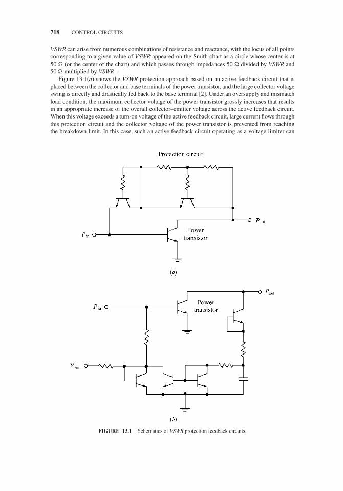
JWBS064-c13 JWBS064-Gerbennikov March 12, 2011 7:54 Printer Name: Yet to Come
718 CONTROL CIRCUITS
VSWR can arise from numerous combinations of resistance and reactance, with the locus of all pointscorresponding to a given value of VSWR appeared on the Smith chart as a circle whose center is at50 � (or the center of the chart) and which passes through impedances 50 � divided by VSWR and50 � multiplied by VSWR.
Figure 13.1(a) shows the VSWR protection approach based on an active feedback circuit that isplaced between the collector and base terminals of the power transistor, and the large collector voltageswing is directly and drastically fed back to the base terminal [2]. Under an oversupply and mismatchload condition, the maximum collector voltage of the power transistor grossly increases that resultsin an appropriate increase of the overall collector–emitter voltage across the active feedback circuit.When this voltage exceeds a turn-on voltage of the active feedback circuit, large current flows throughthis protection circuit and the collector voltage of the power transistor is prevented from reachingthe breakdown limit. In this case, such an active feedback circuit operating as a voltage limiter can
FIGURE 13.1 Schematics of VSWR protection feedback circuits.
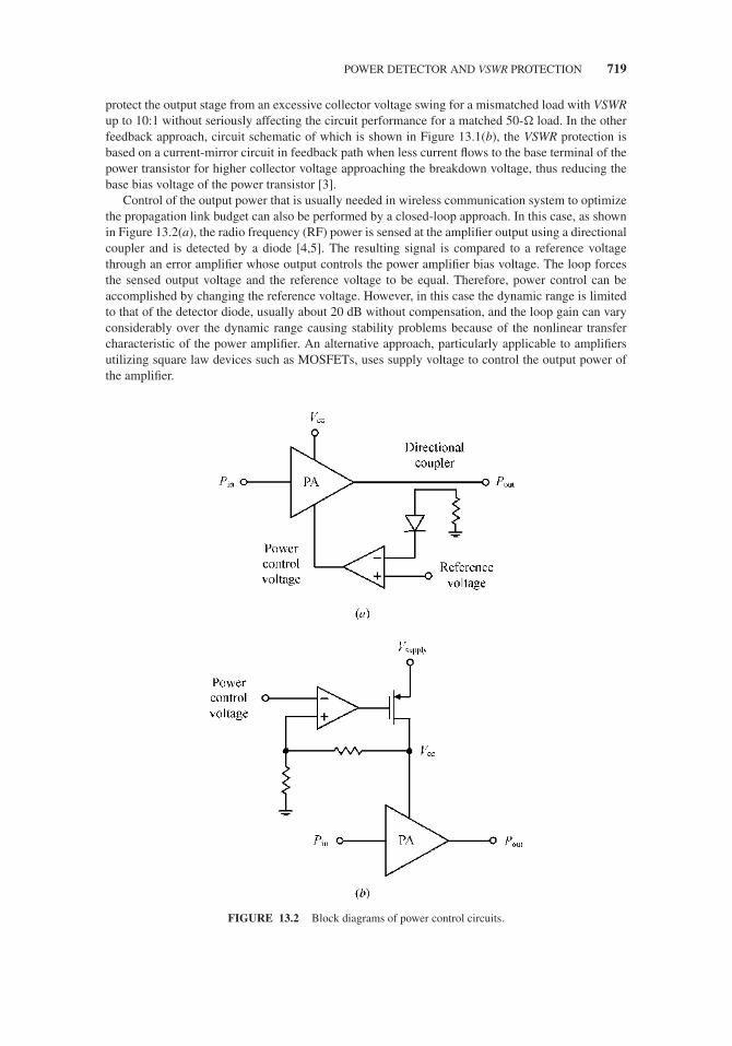
JWBS064-c13 JWBS064-Gerbennikov March 12, 2011 7:54 Printer Name: Yet to Come
POWER DETECTOR AND VSWR PROTECTION 719
protect the output stage from an excessive collector voltage swing for a mismatched load with VSWRup to 10:1 without seriously affecting the circuit performance for a matched 50-� load. In the otherfeedback approach, circuit schematic of which is shown in Figure 13.1(b), the VSWR protection isbased on a current-mirror circuit in feedback path when less current flows to the base terminal of thepower transistor for higher collector voltage approaching the breakdown voltage, thus reducing thebase bias voltage of the power transistor [3].
Control of the output power that is usually needed in wireless communication system to optimizethe propagation link budget can also be performed by a closed-loop approach. In this case, as shownin Figure 13.2(a), the radio frequency (RF) power is sensed at the amplifier output using a directionalcoupler and is detected by a diode [4,5]. The resulting signal is compared to a reference voltagethrough an error amplifier whose output controls the power amplifier bias voltage. The loop forcesthe sensed output voltage and the reference voltage to be equal. Therefore, power control can beaccomplished by changing the reference voltage. However, in this case the dynamic range is limitedto that of the detector diode, usually about 20 dB without compensation, and the loop gain can varyconsiderably over the dynamic range causing stability problems because of the nonlinear transfercharacteristic of the power amplifier. An alternative approach, particularly applicable to amplifiersutilizing square law devices such as MOSFETs, uses supply voltage to control the output power ofthe amplifier.
FIGURE 13.2 Block diagrams of power control circuits.

JWBS064-c13 JWBS064-Gerbennikov March 12, 2011 7:54 Printer Name: Yet to Come
720 CONTROL CIRCUITS
By using a simple linear regulator that is implemented through a power pMOS transistor and anoperational amplifier, as shown in Figure 13.2(b), the collector (or drain) voltage can be varied linearlyover wide range of supply voltages. Reducing the collector voltage effectively limits the output voltageswing and, hence, limits the output power with very fast response time [6]. In this case, output poweris predictable after a simple calibration and burst shaping with associate switching transients can beeasily controlled. However, a very low saturation resistance is needed for the pMOS transistor topreserve the overall efficiency under maximum output power levels. The transistor protection circuitcan be generally based on an adaptive output power control that includes sensing of both dc currentand output voltage swing under severe load mismatched conditions [7].
Two topologies for capacitively-coupled power detectors are shown in Figure 13.3 [8]. In Figure13.3(a), the value of the coupled capacitor is usually adjusted so that the sampled power is 15–20 dBbelow the output power, while the value of the shunt resistor is selected to obtain the largest possibledetected voltage and bandwidth. The capacitive-type sampling has a larger bandwidth potential thanresistive or inductive. When the shunt resistor is replaced by a diode, as shown in Figure 13.3(b), theinput power can be significantly reduced to obtain the same detected voltage.
For a nonconstant envelope RF signal, an envelope detector can be used that takes a high-frequencysignal as input, and provides an output that ideally should be an envelope of the original signal. Theshunt capacitor in the circuit stores up charge on the rising edge, and releases it slowly throughthe resistor when the signal falls. The diode in series rectifies the incoming signal, allowing currentflow only when the positive input terminal is at a higher potential than the negative input terminal.Filtering is then used to smooth the final result. The simple low-pass filtering is often not sufficientsince some ripple is likely to remain on the detected envelope. More complicated filter circuit givesa smoother result, but decreases the responsiveness of the design, so practical solutions are usuallya compromise. The simplest form of envelope detector is the diode that is located between the inputand output of a circuit, connected to a resistor and capacitor in parallel from the output of the circuitto the ground. If the resistor and capacitor are correctly chosen, the output of this circuit shouldapproximate a voltage-shifted version of the original (baseband) signal.
The systems described that sense voltage or current associated with the power output only accountfor the amplitude of the output voltage or current. However, for accurate power detection, it needsto account for both amplitude and phase. The system that senses incident power only may fail toaccurately sense the transmitting or true output power because it does not account for any reflectedpower if there is an impedance mismatch at the load. In addition, the control of reflected power isrequired to exactly measure the load VSWR because the reflection coefficient � is a ratio betweenthe reflected (V r) and incident (V i) voltages. Figure 13.4 shows the power amplifier architecture withVSWR detection and protection mechanism based on the transmission-line directional couplers andvariable-gain amplifier (VGA). To protect from high VSWR condition, the power amplifier can alsobe powered down into a safe operating mode using bias or dc supply current control of the powertransistor [9,10].
When the output signal traveling along the transmission line encounters a load with impedanceZL equal to the transmission-line characteristic impedance Z0, all of the available signal power is
FIGURE 13.3 Schematics of capacitively-coupled voltage detectors.
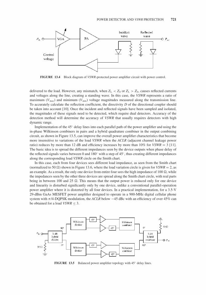
JWBS064-c13 JWBS064-Gerbennikov March 12, 2011 7:54 Printer Name: Yet to Come
POWER DETECTOR AND VSWR PROTECTION 721
FIGURE 13.4 Block diagram of VSWR-protected power amplifier circuit with power control.
delivered to the load. However, any mismatch, when ZL < Z0 or ZL > Z0, causes reflected currentsand voltages along the line, creating a standing wave. In this case, the VSWR represents a ratio ofmaximum (Vmax) and minimum (Vmin) voltage magnitudes measured along the transmission line.To accurately calculate the reflection coefficient, the directivity D of the directional coupler shouldbe taken into account [10]. Once the incident and reflected signals have been sampled and isolated,the magnitudes of these signals need to be detected, which require dual detectors. Accuracy of thedetection method will determine the accuracy of VSWR that usually requires detectors with highdynamic range.
Implementation of the 45◦ delay lines into each parallel path of the power amplifier and using thein-phase Wilkinson combiners in pairs and a hybrid quadrature combiner in the output combiningcircuit, as shown in Figure 13.5, can improve the overall power amplifier characteristics that becomemore insensitive to variations of the load VSWR when the ACLR (adjacent channel leakage powerratio) reduces by more than 12 dB and efficiency increases by more than 10% for VSWR = 3 [11].The basic idea is to spread the different impedances seen by the device outputs when phase delay ofthe reflected signals varies between 0 and 180◦ with a step of 45◦, thus creating different impedancesalong the corresponding load VSWR circle on the Smith chart.
In this case, each from four devices sees different load impedance, as seen from the Smith chart(normalized to 50 �) shown in Figure 13.6, where the load variation circle is given for VSWR = 2, asan example. As a result, the only one device from entire four sees the high impedance of 100 �, whilethe impedances seen by the other three devices are spread along the Smith chart circle, with real partsbeing in between 100 and 25 �. This means that the output power is reduced only for one deviceand linearity is disturbed significantly only by one device, unlike a conventional parallel-operationpower amplifier where it is distorted by all four devices. In a practical implementation, for a 3.5-V29-dBm GaAs MESFET power amplifier designed to operate in a 900-MHz digital cellular phonesystem with π /4-DQPSK modulation, the ACLR below −45 dBc with an efficiency of over 45% canbe obtained for a load VSWR ≤ 3.
FIGURE 13.5 Balanced power amplifier topology with 45◦ delay lines.

JWBS064-c13 JWBS064-Gerbennikov March 12, 2011 7:54 Printer Name: Yet to Come
722 CONTROL CIRCUITS
FIGURE 13.6 Smith-chart impedances for VSWR = 2.
13.2 SWITCHES
Semiconductor diodes have been extensively used for many years as RF and microwave switchingelements for directing signal or power flow between different ports [12,13]. In these applications, theRF impedance may be switched from one value (usually small) in a forward-biased or conductingstate to another (usually large) in a reverse-biased or nonconducting state. The impedance changes areprovided by changing the dc bias from a high forward current to a small back current that is appliedthrough leads, which are isolated from the transmitting signal by RF chokes and bypass capacitors.A large forward bias will decrease the diode resistance and results in high effective impedance thatwill absorb little power. On the other hand, a large reverse bias will result in low impedance that bothabsorbs power and causes high reflection.
Generally, diodes are inherently nonlinear and some care must be taken in establishing the limits oncurrent, voltage, and dissipation to prevent significant harmonic generation and diode damage at highpower levels. The diode operating performance can be described by a simple equivalent circuit thatconsists of the series inductance L, which is usually assumed to be constant, the junction capacitanceCj, which is variable and represents a derivative of the stored charge with respect to voltage, the seriesspreading resistance Rs, which is a function of the conductivity of the semiconductor and the contactarea, being approximately constant for reverse-bias voltages, and the junction nonlinear differentialresistance Rj that varies with amplitude and polarity of the applied dc bias. In a reverse-bias modewhen switch is closed, it can be represented by a series combination of the inductance L, capacitanceCj, and reverse series Rs. In a forward-bias mode when switch is open, the junction resistance Rj issmall, thereby shunting the junction capacitance Cj, and the switch can be equivalently representedby a series combination of the inductance L and resistance Rs.
The p–i–n diodes are commonly used as switching elements to control RF or microwave signalsbecause they are characterized by high breakdown voltages, are capable of high-speed operation, andcan be easily integrated with planar technology. A p–i–n diode can be used in either a series or a shuntconfiguration to form a single-pole single-through (SPST) RF switch. In the series configuration
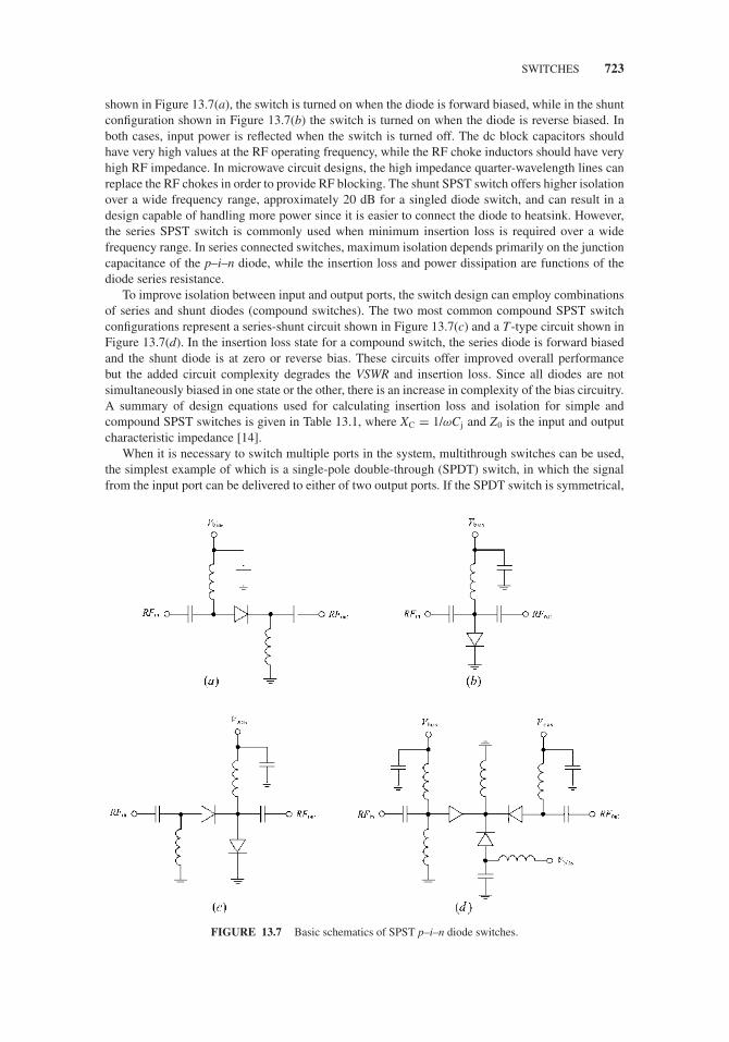
JWBS064-c13 JWBS064-Gerbennikov March 12, 2011 7:54 Printer Name: Yet to Come
SWITCHES 723
shown in Figure 13.7(a), the switch is turned on when the diode is forward biased, while in the shuntconfiguration shown in Figure 13.7(b) the switch is turned on when the diode is reverse biased. Inboth cases, input power is reflected when the switch is turned off. The dc block capacitors shouldhave very high values at the RF operating frequency, while the RF choke inductors should have veryhigh RF impedance. In microwave circuit designs, the high impedance quarter-wavelength lines canreplace the RF chokes in order to provide RF blocking. The shunt SPST switch offers higher isolationover a wide frequency range, approximately 20 dB for a singled diode switch, and can result in adesign capable of handling more power since it is easier to connect the diode to heatsink. However,the series SPST switch is commonly used when minimum insertion loss is required over a widefrequency range. In series connected switches, maximum isolation depends primarily on the junctioncapacitance of the p–i–n diode, while the insertion loss and power dissipation are functions of thediode series resistance.
To improve isolation between input and output ports, the switch design can employ combinationsof series and shunt diodes (compound switches). The two most common compound SPST switchconfigurations represent a series-shunt circuit shown in Figure 13.7(c) and a T-type circuit shown inFigure 13.7(d). In the insertion loss state for a compound switch, the series diode is forward biasedand the shunt diode is at zero or reverse bias. These circuits offer improved overall performancebut the added circuit complexity degrades the VSWR and insertion loss. Since all diodes are notsimultaneously biased in one state or the other, there is an increase in complexity of the bias circuitry.A summary of design equations used for calculating insertion loss and isolation for simple andcompound SPST switches is given in Table 13.1, where XC = 1/ωCj and Z0 is the input and outputcharacteristic impedance [14].
When it is necessary to switch multiple ports in the system, multithrough switches can be used,the simplest example of which is a single-pole double-through (SPDT) switch, in which the signalfrom the input port can be delivered to either of two output ports. If the SPDT switch is symmetrical,
FIGURE 13.7 Basic schematics of SPST p–i–n diode switches.
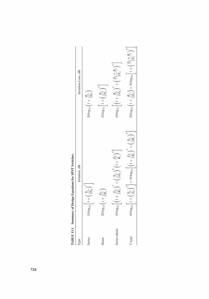
JWBS064-c13 JWBS064-Gerbennikov March 12, 2011 7:54 Printer Name: Yet to Come
TA
BL
E13
.1Su
mm
ary
ofD
esig
nE
quat
ions
for
SPST
Swit
ches
.
Type
Isol
atio
n,dB
Inse
rtio
nL
oss,
dB
Seri
es10
log 1
0
[ 1+
( Xc
2Z0
) 2]20
log 1
0
( 1+
Rc
2Z0
)
Shun
t20
log 1
0
( 1+
Z0
2R
s
)10
log 1
0
[ 1+
( Z0
2X
c
) 2]
Seri
es-s
hunt
10lo
g 10
[ ( 1+
Z0
2R
s
) 2 +( X
c
2Z
0
) 2(1
+Z
0
Rs
) 2]10
log 1
0
[ ( 1+
Rs
2Z
0
) 2 +( Z
0+
Rs
2X
c
) 2]
T-t
ype
10lo
g 10
[ 1+
( Xc
Z0
) 2] +10
log 1
0
[ ( 1+
Z0
2R
s
) 2 +( X
c
2R
s
) 2]20
log 1
0
( 1+
Rs
2Z
0
) +10
log 1
0
[ 1+
( Z0+
Rs
2X
c
) 2]
724

JWBS064-c13 JWBS064-Gerbennikov March 12, 2011 7:54 Printer Name: Yet to Come
SWITCHES 725
each switch branch performs like the SPST equivalent, but the isolation of a double-through switchis increased by 6 dB. This effect occurs because the branch with turned-off diode is shunted by thebranch with turned-on diode and its 50-� termination, causing the RF voltage across the turned-offdiode to be 50% less than would be the case for the equivalent SPST switch.
Figure 13.8 shows the three basic circuit configurations for the SPDT switches [15,16]. Thecircuit schematic of a shunt SPDT p–i–n diode switch is shown in Figure 13.8(a), where the
FIGURE 13.8 Basic schematics of SPDT p–i–n diode switches.

JWBS064-c13 JWBS064-Gerbennikov March 12, 2011 7:54 Printer Name: Yet to Come
726 CONTROL CIRCUITS
quarter-wavelength transmission lines are used between common junction (input port) and eachshunt diode. When diode D1 is forward biased and diode D2 is zero or reverse biased, the RF powerwill flow from the input port RFin to the output port RFout2, and the output port RFout1 will be isolated.In this case, the quarterwave line will transform the short circuit at diode D1 into an open circuit at thecommon junction, thus eliminating any reactive loading of the closed port and improving isolationbetween the output ports. However, as the frequency is changed from the center bandwidth frequencyf 0, the transmission lines will change in electrical length, creating a mismatch at the common junction.For example, the VSWR of this structure will be 1.43:1 when the frequency ratio f /f 0 or f 0/f is equalto 1.2 (40% bandwidth).
The series SPDT diode switch, the circuit schematic of which is shown in Figure 13.8(b), iscapable of very large (multioctave) bandwidth, limited only by the parameters of the bias inductors,blocking capacitors, and length of any transmission line between the diode and common junction.This structure can be easily fabricated with beam-lead diodes on alumina substrate. However, parasiticcapacitances can result in poor isolation at microwave frequencies, with a 6 dB per octave roll-offas a function of frequency. Better isolation can be achieved with a series-shunt SPDT diode switchshown in Figure 13.8(c). In this case, when diodes D2 and D3 are forward biased into a low-resistancestate, while diodes D1 and D4 are reverse biased into a high-resistance state, RF power flows from theinput port RFin to the output port RFout1. Diode D4 acts as an open circuit to isolate the short circuitat diode D2 from the common junction. However, it is complicated to properly implement such aswitch in practice because it is difficult to mount the D3 and D4 diode junctions electrically close tothe common point.
The bandwidth of the shunt SPDT diode switch can be improved by the simple impedancematching technique. In this case, a third quarterwave transmission line is placed between the commonjunction and input port RFin, as shown in Figure 13.9 [16]. The specific value of the transmission-line characteristic impedances will determine the VSWR and bandwidth of the switch. For example,setting the characteristic impedance Z0 of all three transmission lines to 35 � will result in a 1.43:1VSWR frequency bandwidth of 100% (3:1). Additional bandwidth improvement can be achieved ifthe characteristic impedance of the quarterwave line connected to the input port RFin is selected tobe slightly different from that for the other lines. The quarter-wavelength transmission lines can alsobe used as RF chokes in the bias network of each p–i–n diode arm [17]. Higher isolation over widerange at microwave frequencies can be achieved by using additional shunt diodes and transmission-line sections [18]. The ladder lumped resonance circuits in parallel to the p–i–n diodes can be usedto simplify the SPDT diode switch configurations, minimize their size, and reduce cost [19].
Different types of SPDT diode switches can be used to separately connect the transmitting andreceiving paths to antenna in radio communication system. When p–i–n diodes are used as elements in
FIGURE 13.9 Basic schematic of broadband shunt SPDT switch.
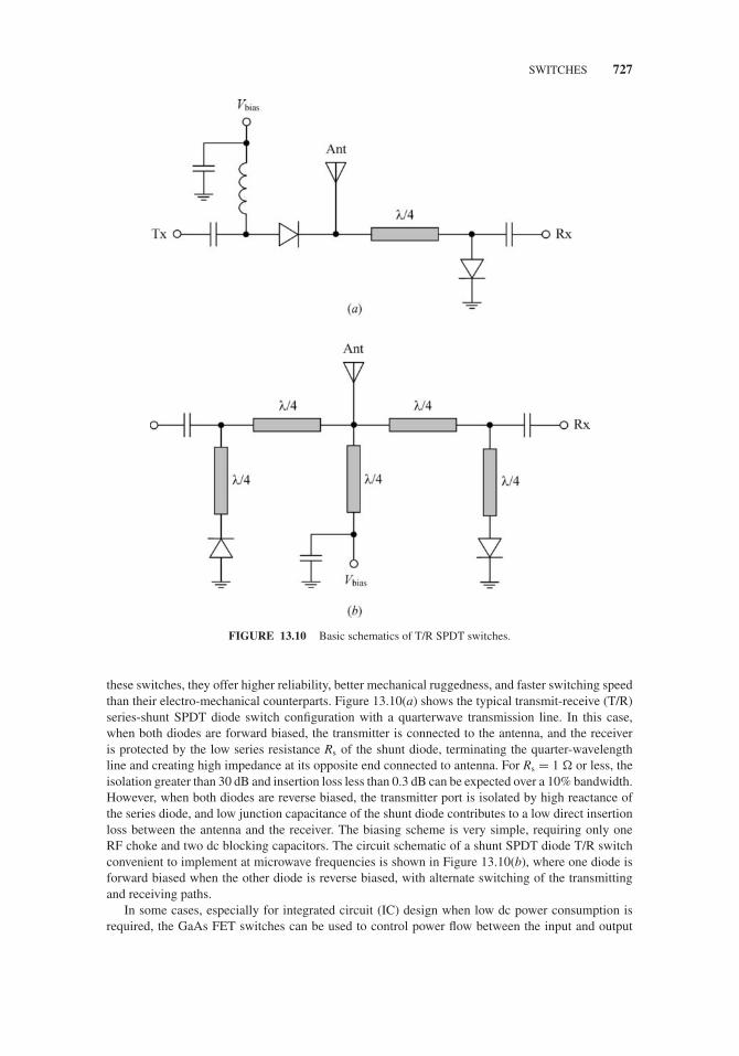
JWBS064-c13 JWBS064-Gerbennikov March 12, 2011 7:54 Printer Name: Yet to Come
SWITCHES 727
FIGURE 13.10 Basic schematics of T/R SPDT switches.
these switches, they offer higher reliability, better mechanical ruggedness, and faster switching speedthan their electro-mechanical counterparts. Figure 13.10(a) shows the typical transmit-receive (T/R)series-shunt SPDT diode switch configuration with a quarterwave transmission line. In this case,when both diodes are forward biased, the transmitter is connected to the antenna, and the receiveris protected by the low series resistance Rs of the shunt diode, terminating the quarter-wavelengthline and creating high impedance at its opposite end connected to antenna. For Rs = 1 � or less, theisolation greater than 30 dB and insertion loss less than 0.3 dB can be expected over a 10% bandwidth.However, when both diodes are reverse biased, the transmitter port is isolated by high reactance ofthe series diode, and low junction capacitance of the shunt diode contributes to a low direct insertionloss between the antenna and the receiver. The biasing scheme is very simple, requiring only oneRF choke and two dc blocking capacitors. The circuit schematic of a shunt SPDT diode T/R switchconvenient to implement at microwave frequencies is shown in Figure 13.10(b), where one diode isforward biased when the other diode is reverse biased, with alternate switching of the transmittingand receiving paths.
In some cases, especially for integrated circuit (IC) design when low dc power consumption isrequired, the GaAs FET switches can be used to control power flow between the input and output
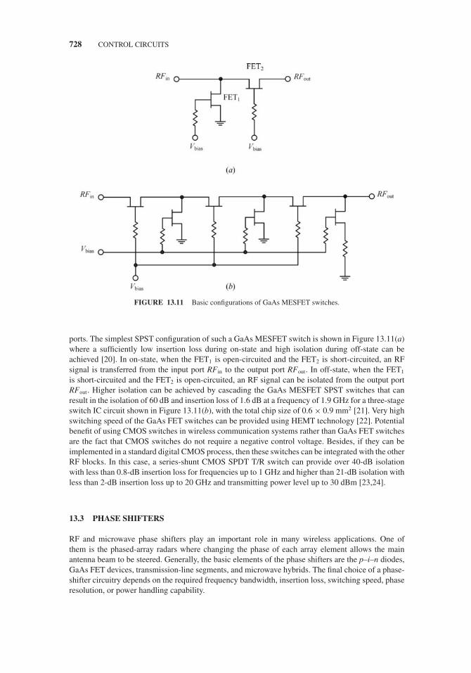
JWBS064-c13 JWBS064-Gerbennikov March 12, 2011 7:54 Printer Name: Yet to Come
728 CONTROL CIRCUITS
FIGURE 13.11 Basic configurations of GaAs MESFET switches.
ports. The simplest SPST configuration of such a GaAs MESFET switch is shown in Figure 13.11(a)where a sufficiently low insertion loss during on-state and high isolation during off-state can beachieved [20]. In on-state, when the FET1 is open-circuited and the FET2 is short-circuited, an RFsignal is transferred from the input port RFin to the output port RFout. In off-state, when the FET1
is short-circuited and the FET2 is open-circuited, an RF signal can be isolated from the output portRFout. Higher isolation can be achieved by cascading the GaAs MESFET SPST switches that canresult in the isolation of 60 dB and insertion loss of 1.6 dB at a frequency of 1.9 GHz for a three-stageswitch IC circuit shown in Figure 13.11(b), with the total chip size of 0.6 × 0.9 mm2 [21]. Very highswitching speed of the GaAs FET switches can be provided using HEMT technology [22]. Potentialbenefit of using CMOS switches in wireless communication systems rather than GaAs FET switchesare the fact that CMOS switches do not require a negative control voltage. Besides, if they can beimplemented in a standard digital CMOS process, then these switches can be integrated with the otherRF blocks. In this case, a series-shunt CMOS SPDT T/R switch can provide over 40-dB isolationwith less than 0.8-dB insertion loss for frequencies up to 1 GHz and higher than 21-dB isolation withless than 2-dB insertion loss up to 20 GHz and transmitting power level up to 30 dBm [23,24].
13.3 PHASE SHIFTERS
RF and microwave phase shifters play an important role in many wireless applications. One ofthem is the phased-array radars where changing the phase of each array element allows the mainantenna beam to be steered. Generally, the basic elements of the phase shifters are the p–i–n diodes,GaAs FET devices, transmission-line segments, and microwave hybrids. The final choice of a phase-shifter circuitry depends on the required frequency bandwidth, insertion loss, switching speed, phaseresolution, or power handling capability.
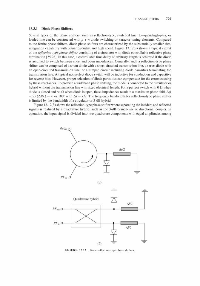
JWBS064-c13 JWBS064-Gerbennikov March 12, 2011 7:54 Printer Name: Yet to Come
PHASE SHIFTERS 729
13.3.1 Diode Phase Shifters
Several types of the phase shifters, such as reflection-type, switched line, low-pass/high-pass, orloaded-line can be constructed with p–i–n diode switching or varactor tuning elements. Comparedto the ferrite phase shifters, diode phase shifters are characterized by the substantially smaller size,integration capability with planar circuitry, and high speed. Figure 13.12(a) shows a typical circuitof the reflection-type phase shifter consisting of a circulator with diode controllable reflective phasetermination [25,26]. In this case, a controllable time delay of arbitrary length is achieved if the diodeis assumed to switch between short and open impedances. Generally, such a reflection-type phaseshifter can be composed of a shunt diode with a short-circuited transmission line, a series diode withan open-circuited transmission line, or a lumped circuit including diode parasitics terminating thetransmission line. A typical nonperfect diode switch will be inductive for conduction and capacitivefor reverse bias. However, proper selection of diode parasitics can compensate for the errors causingby these reactances. To provide a wideband phase shifting, the diode is connected to the circulator orhybrid without the transmission line with fixed electrical length. For a perfect switch with 0 � whendiode is closed and ∞ � when diode is open, these impedances result in a maximum phase shift �φ
= 2π (�l/λ) = π or 180◦ with �l = λ/2. The frequency bandwidth for reflection-type phase shifteris limited by the bandwidth of a circulator or 3-dB hybrid.
Figure 13.12(b) shows the reflection-type phase shifter where separating the incident and reflectedsignals is realized by a quadrature hybrid, such as the 3-dB branch-line or directional coupler. Inoperation, the input signal is divided into two quadrature components with equal amplitudes among
FIGURE 13.12 Basic reflection-type phase shifters.
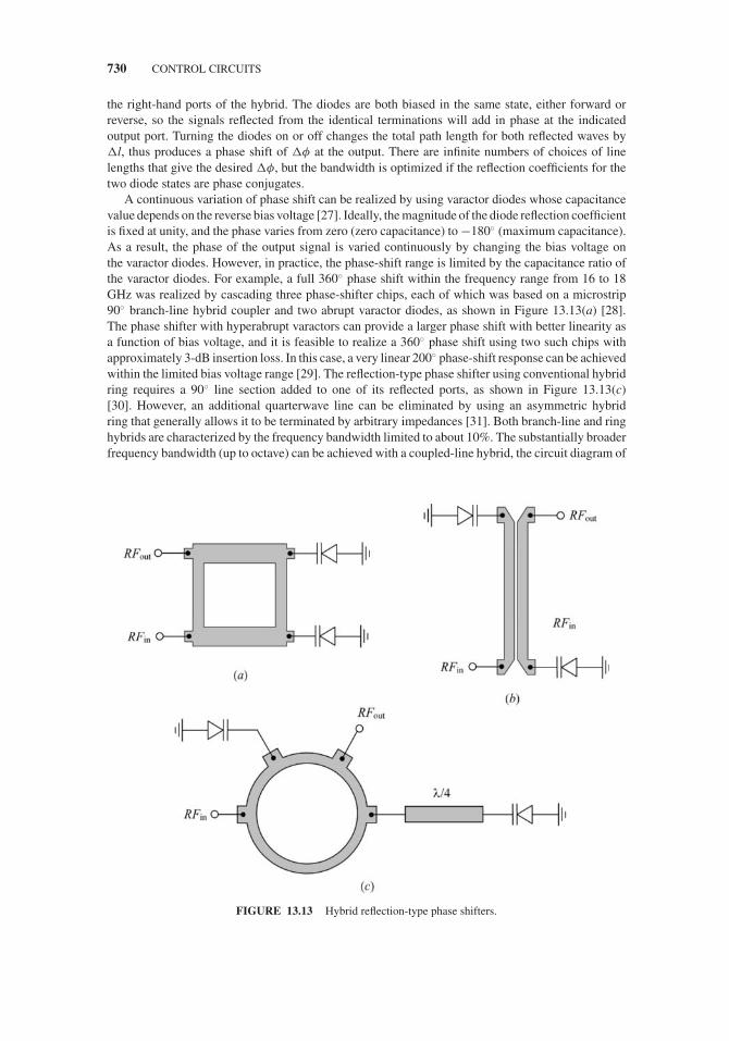
JWBS064-c13 JWBS064-Gerbennikov March 12, 2011 7:54 Printer Name: Yet to Come
730 CONTROL CIRCUITS
the right-hand ports of the hybrid. The diodes are both biased in the same state, either forward orreverse, so the signals reflected from the identical terminations will add in phase at the indicatedoutput port. Turning the diodes on or off changes the total path length for both reflected waves by�l, thus produces a phase shift of �φ at the output. There are infinite numbers of choices of linelengths that give the desired �φ, but the bandwidth is optimized if the reflection coefficients for thetwo diode states are phase conjugates.
A continuous variation of phase shift can be realized by using varactor diodes whose capacitancevalue depends on the reverse bias voltage [27]. Ideally, the magnitude of the diode reflection coefficientis fixed at unity, and the phase varies from zero (zero capacitance) to −180◦ (maximum capacitance).As a result, the phase of the output signal is varied continuously by changing the bias voltage onthe varactor diodes. However, in practice, the phase-shift range is limited by the capacitance ratio ofthe varactor diodes. For example, a full 360◦ phase shift within the frequency range from 16 to 18GHz was realized by cascading three phase-shifter chips, each of which was based on a microstrip90◦ branch-line hybrid coupler and two abrupt varactor diodes, as shown in Figure 13.13(a) [28].The phase shifter with hyperabrupt varactors can provide a larger phase shift with better linearity asa function of bias voltage, and it is feasible to realize a 360◦ phase shift using two such chips withapproximately 3-dB insertion loss. In this case, a very linear 200◦ phase-shift response can be achievedwithin the limited bias voltage range [29]. The reflection-type phase shifter using conventional hybridring requires a 90◦ line section added to one of its reflected ports, as shown in Figure 13.13(c)[30]. However, an additional quarterwave line can be eliminated by using an asymmetric hybridring that generally allows it to be terminated by arbitrary impedances [31]. Both branch-line and ringhybrids are characterized by the frequency bandwidth limited to about 10%. The substantially broaderfrequency bandwidth (up to octave) can be achieved with a coupled-line hybrid, the circuit diagram of
FIGURE 13.13 Hybrid reflection-type phase shifters.

JWBS064-c13 JWBS064-Gerbennikov March 12, 2011 7:54 Printer Name: Yet to Come
PHASE SHIFTERS 731
which is shown in Figure 13.13(b). For the two cascaded 3-dB multilayer folded directional couplerswith abrupt varactors, the phase shift up to 98◦ was measured over two octaves, from 4.4 to 16.1 GHz[32].
Hyperabrupt varactor diodes have a nonlinear doping profile that facilitates a larger capacitanceas the reverse bias voltage is increased and a larger tuning ratio occurs. Therefore, these diodeshave better capacitance-voltage linearity and tunability. However, the maximum linear power froma single varactor is limited due to the second- and third-order nonlinear distortions. In this case, toeliminate the second-order and other even-order distortions, two varactor diodes can be connectedin an antiseries configuration. As a result, the branch-line reflection-type phase shifter with parallelresonant circuits, each of which is comprised of an antiseries varactor pair and an inductor andconnected to the corresponding reflected port of the branch-line hybrid, as shown in Figure 13.14(a),significantly improves the maximum linear output power and provides a continuous phase shift of180◦ at an operating frequency of 1.88 GHz [33]. For a given varactor or varactor pair with a limitedcapacitance tuning ratio, the phase-shift range can be increased by using an impedance-transformingbranch-line coupler that also provides an impedance transformation between the varactor loads andthe input and output ports, thus making the entire circuit more compact [34]. A full 360◦ phase shiftwith a silicon varactor of a 1.4-to-8-pF capacitance ratio can be obtained at an operating frequency of2 GHz when each reflection load for an impedance-transforming branch-line coupler consists of twovaractors interconnected with a quarter-wavelength transmission line, as shown in Figure 13.14(b)[35].
The loaded-line phase shifter is very useful for obtaining small phase shifts up to approximately45◦ due to its simplicity and low insertion loss [25,36]. The circuit consists of two equal two-stateswitchable admittances Y i (i = 1, 2) connected in shunt with a transmission-line section, and thetransition between two admittance states produces a certain change �φ in the phase of the transmission
FIGURE 13.14 Hybrid reflection-type phase shifters.

JWBS064-c13 JWBS064-Gerbennikov March 12, 2011 7:54 Printer Name: Yet to Come
732 CONTROL CIRCUITS
scattering coefficient S21. The scattering S-matrix can directly be obtained by transformation fromthe ABCD-matrix that can be derived in the idealized lossless case as
[ABCD] =[
1 0jBi 1
] ⎡⎣ cos θ jZT sin θ
jsin θ
ZTcos θ
⎤⎦ [
1 0j Bi 1
]
=⎡⎣ cosθ − Bi ZT sin θ jZT sin θ
j
ZT
[2Bi ZT cos θ + (
1 − B2i Z 2
T
)sin θ
]cosθ − Bi ZT sin θ
⎤⎦ (13.3)
where Bi = ImY i is the shunt susceptance, ZT is the characteristic impedance, and θ is the electricallength of the transmission-line section [26,37]. The transformation to the scattering matrix for areciprocal, symmetrical two-port network is given by
S11 = S22 = BY0 − C Z0
2A + BY0 + C Z0(13.4)
S21 = S12 = 2
2A + BY0 + C Z0(13.5)
where Z0 = 1/Y0 is the characteristic impedance of the circuit into which the phase shifter is connected.The required phase shift �φ corresponds to the change in the argument φi of S21(Bi) when the
shunt elements make the transition from reactive admittances jB1 to jB2 by switching the p–i–n diodes,as shown in Figure 13.15(a) with lumped inductors and capacitors. In this case, the elimination ofreflected waves from the input of the phase shifter by input matching reduces the return loss andremoves possibility of phase errors that can be caused by interaction of the reflected waves withadjacent cascaded stages. The condition of the input match is specified by requiring S11 = 0 in Eq.(13.4). As a result,
BY0 = C Z0 (13.6)
FIGURE 13.15 Basic circuits of loaded-line phase shifters.

JWBS064-c13 JWBS064-Gerbennikov March 12, 2011 7:54 Printer Name: Yet to Come
PHASE SHIFTERS 733
and the transmission scattering element S21 becomes
S21 = 1
A + BY0= 1
(cos θ − Bi ZT sin θ ) + j ZTY0 sin θ. (13.7)
Since the magnitude of S21 is equal to unity in the input-matched lossless case, from Eq. (13.7) itfollows that
cos φ = cosθ − Bi ZT sin θ (13.8)
sin φ = − ZTY0 sin θ (13.9)
where φ is the phase angle of S21. It can be seen from Eq. (13.9) that sinφ remains constant duringload switching, while cosφ in Eq. (13.8) assumes two values with two loading admittance states.Consequently, the phase shift �φ due to the switching between the susceptance values B1 and B2 canbe written from Eq. (13.8) as
�φ = cos−1 (cos θ − B1 ZT sin θ ) − cos−1 (cos θ − B2 ZT sin θ) . (13.10)
The spacing between diodes of λ/4 when the electrical length of the transmission line is equal to90◦ provides the widest frequency bandwidth and is mostly used in practice. However, a phase shiftgreater than 45◦ is difficult to achieve without causing excessively high VSWR [26]. In this case, thephase is switched symmetrically about 90◦ by increments of ±�φ/2 by the line loading. Substitutingφ = (90◦ ± �φ/2) into Eqs. (13.8) and (13.9) results in
ZT = Z0cos (�φ/2) (13.11)
Bi Z0 = ± tan (�φ/2) (13.12)
representing the design equations for the lossless loaded-line phase shifter with �φ. Hence, the phaseshift �φ can be properly set by switching between two susceptances B1 and B2 as
�φ = 2tan−1 B1 − B2
2Y0. (13.13)
From Eq. (13.8), it follows that dφ/dBi is positive for θ ≤ 90◦. Therefore, the addition of capacitivesusceptance loading increases the phase angle φ. For complex-conjugate loading when B1 = −B2,
�φ = 2tan−1 B1
Y0= 2tan−1
(− B2
Y0
)(13.14)
where B1 = ωC and B2 = −1/ωL corresponding to Figure 13.15(a) or B1 = Y s and B2 = −Y s, whereZs = 1/Y s is the stub characteristic impedance, corresponding to Figure 13.15(b) [37,38].
The phase shift can be substantially extended using a transmission line that is periodically loadedwith varactor diodes, as shown in Figure 13.15(c) [39]. In this case, the maximum possible phaseshift is defined by �φ = nθi
(√1 + x/θi − √
1 + xy/θi
), where n is the number of sections, θ i is the
electrical length of the transmission-line section measured in radians, x = ZiωCvmax, y = Cvmin/Cvmax,Cvmin and Cvmax are the minimum and maximum varactor capacitances, and the transmission-linecharacteristic impedance Zi is calculated from Z i = Z0
√1 + x/θi, where Z0 is the loaded character-
istic impedance usually equal to 50 �. As a result, the variable phase shift up to 360◦ can be achievedat 20 GHz with the maximum insertion loss of 4.2 dB and return loss better than −12 dB for such adistributed phase shifter based on a coplanar-waveguide line.
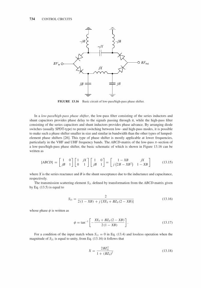
JWBS064-c13 JWBS064-Gerbennikov March 12, 2011 7:54 Printer Name: Yet to Come
734 CONTROL CIRCUITS
FIGURE 13.16 Basic circuit of low-pass/high-pass phase shifter.
In a low-pass/high-pass phase shifter, the low-pass filter consisting of the series inductors andshunt capacitors provides phase delay to the signals passing through it, while the high-pass filterconsisting of the series capacitors and shunt inductors provides phase advance. By arranging diodeswitches (usually SPDT-type) to permit switching between low- and high-pass modes, it is possibleto make such a phase shifter smaller in size and similar in bandwidth than the other types of lumped-element phase shifters [26]. This type of phase shifter is mostly applicable at lower frequencies,particularly in the VHF and UHF frequency bands. The ABCD-matrix of the low-pass π -section ofa low-pass/high-pass phase shifter, the basic schematic of which is shown in Figure 13.16 can bewritten as
[ABCD] =[
1 0jB 1
] [1 jX0 1
] [1 0jB 1
]=
[1 − XB jX
j(2B − XB2
)1 − XB
](13.15)
where X is the series reactance and B is the shunt susceptance due to the inductance and capacitance,respectively.
The transmission scattering element S21 defined by transformation from the ABCD-matrix givenby Eq. (13.5) is equal to
S21 = 2
2 (1 − XB) + j [XY0 + BZ0 (2 − XB)](13.16)
whose phase φ is written as
φ = tan−1
[− XY0 + BZ0 (2 − XB)
2 (1 − XB)
]. (13.17)
For a condition of the input match when S11 = 0 in Eq. (13.4) and lossless operation when themagnitude of S21 is equal to unity, from Eq. (13.16) it follows that
X = 2BZ 20
1 + (BZ0)2 (13.18)

JWBS064-c13 JWBS064-Gerbennikov March 12, 2011 7:54 Printer Name: Yet to Come
PHASE SHIFTERS 735
and substitution of Eq. (13.18) into Eq. (13.17) results in
φ = tan−1
[− 2BZ0
1 − (BZ0)2
]. (13.19)
When both B and X change signs that corresponds to the high-pass π -section, the phase remainsthe same but changes sign. Therefore, the phase shift �φ caused by switching between low- andhigh-pass sections is twice the value of the phase φ in Eq. (13.19),
�φ = 2tan−1
[− 2BZ0
1 − (BZ0)2
]. (13.20)
Consequently, the susceptance B and reactance X of a low-pass/high-pass phase shifter can beexpressed in terms of the phase shift �φ from Eqs. (13.20) and (13.18), respectively, as
B = Y0tan(
�φ
4
)(13.21)
X = Z0sin(
�φ
2
). (13.22)
For a T-section filter instead of a π -section, it is necessary to exchange B and X given in Eqs.(13.21) and (13.22). Each T-section or π-section phase shifter configuration can provide a phase shiftof 90◦±2◦ over almost an octave, while the smaller phase shifts are available over more than octave.However, the amplitude difference varies with frequency, since the band-edge slopes of the two filtersare rolling in opposite directions.
The switched-line phase shifter, the basic schematic of which is shown in Figure 13.17(a), isbased on a very simple principle when two transmission lines of different lengths are switched bytwo SPDT p–i–n diode switches to route the signal flow [26,40]. When the p–i–n diodes D1 and D2
are turned on while the p–i–n diodes D3 and D4 are turned off, the reference lower-path transmissionline is connected into the circuit. However, when the p–i–n diodes D1 and D2 are turned off while thep–i–n diodes D3 and D4 are turned on, the upper-path transmission line is connected into the circuit.By switching a signal between two lines of different lengths, it is possible to provide a specific phaseshift. The difference in physical length �l between these two transmission-line paths results in thephase shift �φ defined by
�φ = β (l2 − l1) = 2β�l
2= 2π
�l
λ(13.23)
where β is the propagation constant of the transmission line, λ = 2π /β is the transmission-linewavelength, �l = l2 − l1, l2 is the length of the upper-path line and l1 is the length of the lower-pathline. Because the phase shift in the switched-line configuration is well defined by difference in thetransmission-line lengths only, such a phase shifter does not need any additional adjustment and isvery stable over time and temperature.
Switched-line digital phase shifters providing a certain phase increment can be made by a cascadeconnection of individual binary switched-line phase shifters [41]. For a switched-line phase shiftercomprised of the nth consecutive stages, the smallest phase increment is defined by
�φ = �φmax
2n(13.24)
where �φmax is the maximum phase shift. Generally, multibit switched-line phase shifters can varythe phase shift up to 360◦. Figure 13.17(b) shows the basic circuit schematics of the 4-bit microstrip

JWBS064-c13 JWBS064-Gerbennikov March 12, 2011 7:54 Printer Name: Yet to Come
736 CONTROL CIRCUITS
FIGURE 13.17 Schematics of switched-line phase shifters.
switched-line p–i–n diode phase shifter consisting of four binary phase shifters and covering 180◦
in nominal steps of 22.5◦. The main problem with multibit phase shifters is a large variation in thereturn loss across the phase states that can limit their phase resolution and accuracy.
13.3.2 Schiffman 90◦ Phase Shifter
The basic differential Schiffman 90◦ phase shifter consists of two separate sections, one of whichis a reference uncoupled transmission line while the other is a single C-section representing a pairof parallel coupled transmission lines directly connected to each other at one end, as shown inFigure 13.18(a) [42].
The phase shift φ1 of the coupled-line section is defined as
φ1 = cos−1
⎛⎜⎜⎝
Z0e
Z0o− tan2 θ
Z0e
Z0o+ tan2 θ
⎞⎟⎟⎠ (13.25)
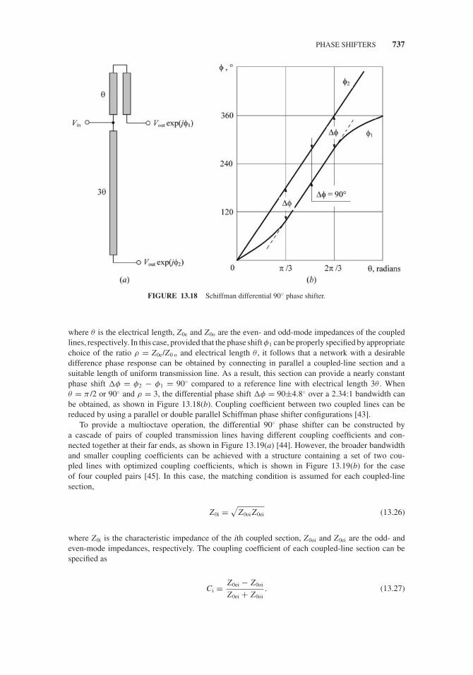
JWBS064-c13 JWBS064-Gerbennikov March 12, 2011 7:54 Printer Name: Yet to Come
PHASE SHIFTERS 737
FIGURE 13.18 Schiffman differential 90◦ phase shifter.
where θ is the electrical length, Z0e and Z0o are the even- and odd-mode impedances of the coupledlines, respectively. In this case, provided that the phase shift φ1 can be properly specified by appropriatechoice of the ratio ρ = Z0e/Z0 o and electrical length θ , it follows that a network with a desirabledifference phase response can be obtained by connecting in parallel a coupled-line section and asuitable length of uniform transmission line. As a result, this section can provide a nearly constantphase shift �φ = φ2 − φ1 = 90◦ compared to a reference line with electrical length 3θ . Whenθ = π /2 or 90◦ and ρ = 3, the differential phase shift �φ = 90±4.8◦ over a 2.34:1 bandwidth canbe obtained, as shown in Figure 13.18(b). Coupling coefficient between two coupled lines can bereduced by using a parallel or double parallel Schiffman phase shifter configurations [43].
To provide a multioctave operation, the differential 90◦ phase shifter can be constructed bya cascade of pairs of coupled transmission lines having different coupling coefficients and con-nected together at their far ends, as shown in Figure 13.19(a) [44]. However, the broader bandwidthand smaller coupling coefficients can be achieved with a structure containing a set of two cou-pled lines with optimized coupling coefficients, which is shown in Figure 13.19(b) for the caseof four coupled pairs [45]. In this case, the matching condition is assumed for each coupled-linesection,
Z0i =√
Z0oi Z0ei (13.26)
where Z0i is the characteristic impedance of the ith coupled section, Z0oi and Z0ei are the odd- andeven-mode impedances, respectively. The coupling coefficient of each coupled-line section can bespecified as
Ci = Z0ei − Z0oi
Z0ei + Z0oi. (13.27)

JWBS064-c13 JWBS064-Gerbennikov March 12, 2011 7:54 Printer Name: Yet to Come
738 CONTROL CIRCUITS
FIGURE 13.19 Structures of multioctave differential 90◦ phase shifters.
resulting in the differential phase shift �φ = 90±1.2◦ over a 6:1 bandwidth for lr = 4.0006λ,C1 = 0.815 and l1 = 0.167λ, C2 = 0.63 and l2 = 0.349λ, C3 = 0.266 and l3 = 0.627λ, C4 = 0.121and l4 = 0.78λ, where λ is the line wavelength corresponding to the center operating frequency.
Schiffman phase shifters can be very useful to achieve the sufficiently flat 90◦ relative-phasedifferences between two output ports. Ideally, it can be done for equal even- and odd-mode charac-teristics, corresponding to stripline realization in a homogeneous substrate. Therefore, since even-and odd-mode phase velocities in the coupled-line section are not equal in the microstrip Schiffmanphase shifter, it is necessary to apply special techniques to equalize phase velocities correspondingto these two modes.
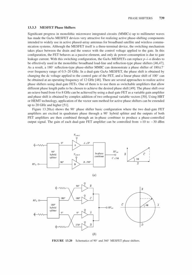
JWBS064-c13 JWBS064-Gerbennikov March 12, 2011 7:54 Printer Name: Yet to Come
PHASE SHIFTERS 739
13.3.3 MESFET Phase Shifters
Significant progress in monolithic microwave integrated circuits (MMICs) up to millimeter waveshas made the GaAs MESFET devices very attractive for realizing active phase-shifting componentsintended to widely use in active phased-array antennas for broadband satellite and wireless commu-nication systems. Although the MESFET itself is a three-terminal device, the switching mechanismtakes place between the drain and the source with the control voltage applied to the gate. In thisconfiguration, the FET behaves as a passive element, and only dc power consumption is due to gateleakage current. With this switching configuration, the GaAs MESFETs can replace p–i–n diodes tobe effectively used in the monolithic broadband load-line and reflection-type phase shifters [46,47].As a result, a 180◦ reflection-type phase-shifter MMIC can demonstrate a phase shifter of 180±7◦
over frequency range of 0.5–20 GHz. In a dual-gate GaAs MESFET, the phase shift is obtained bychanging the dc voltage applied to the control gate of the FET, and a linear phase shift of 100◦ canbe obtained at an operating frequency of 12 GHz [48]. There are several approaches to realize activephase shifters using dual-gate FETs. One of them is to use them as switchable amplifiers that allowdifferent phase length paths to be chosen to achieve the desired phase shift [49]. The phase shift overan octave band from 4 to 8 GHz can be achieved by using a dual-gate FET as a variable gain amplifierand phase shift is obtained by complex addition of two orthogonal variable vectors [50]. Using HBTor HEMT technology, application of the vector sum method for active phase shifters can be extendedup to 20 GHz and higher [51].
Figure 13.20(a) shows the 90◦ phase shifter basic configuration where the two dual-gate FETamplifiers are excited in quadrature phase through a 90◦ hybrid splitter and the outputs of bothFET amplifiers are then combined through an in-phase combiner to produce a phase-controlledoutput signal. The gain of each dual-gate FET amplifier can be controlled from +10 to −30 dBm
FIGURE 13.20 Schematics of 90◦ and 360◦ MESFET phase shifters.
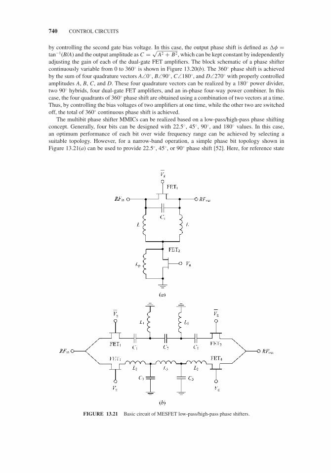
JWBS064-c13 JWBS064-Gerbennikov March 12, 2011 7:54 Printer Name: Yet to Come
740 CONTROL CIRCUITS
by controlling the second gate bias voltage. In this case, the output phase shift is defined as �φ =tan−1(B/A) and the output amplitude as C = √
A2 + B2, which can be kept constant by independentlyadjusting the gain of each of the dual-gate FET amplifiers. The block schematic of a phase shiftercontinuously variable from 0 to 360◦ is shown in Figure 13.20(b). The 360◦ phase shift is achievedby the sum of four quadrature vectors A∠0◦, B∠90◦, C∠180◦, and D∠270◦ with properly controlledamplitudes A, B, C, and D. These four quadrature vectors can be realized by a 180◦ power divider,two 90◦ hybrids, four dual-gate FET amplifiers, and an in-phase four-way power combiner. In thiscase, the four quadrants of 360◦ phase shift are obtained using a combination of two vectors at a time.Thus, by controlling the bias voltages of two amplifiers at one time, while the other two are switchedoff, the total of 360◦ continuous phase shift is achieved.
The multibit phase shifter MMICs can be realized based on a low-pass/high-pass phase shiftingconcept. Generally, four bits can be designed with 22.5◦, 45◦, 90◦, and 180◦ values. In this case,an optimum performance of each bit over wide frequency range can be achieved by selecting asuitable topology. However, for a narrow-band operation, a simple phase bit topology shown inFigure 13.21(a) can be used to provide 22.5◦, 45◦, or 90◦ phase shift [52]. Here, for reference state
FIGURE 13.21 Basic circuit of MESFET low-pass/high-pass phase shifters.

JWBS064-c13 JWBS064-Gerbennikov March 12, 2011 7:54 Printer Name: Yet to Come
ATTENUATORS 741
operation, FET1 is switched on and FET2 is switched off. The inductor Lp is sized to parallel resonatethe drain–source capacitance of FET2 that contributes to a series combination of inductances L inparallel with the on-state resistance of FET1. To activate the phase shift state, FET1 is switched offand FET2 is switched on, resulting in the approximate equivalent high-pass π-network, where theseries capacitance C is represented by the parallel combination of Cs and drain–source capacitanceof FET1.
The transmission ABCD-matrix of the high-pass LC-type π -section can be written as
[ABCD] =
⎡⎢⎢⎣
1 − 1
ω2 LC
1
jωC
2
jωL− 1
jω3 L2C1 − 1
ω2 LC
⎤⎥⎥⎦ (13.28)
that results in design equations for L and C as a function of the phase shift �φ in a matched conditionwith S11 = S22 = 0 given by
L = Z0
ω tan (�φ/2)(13.29)
C = 1
ωZ0 sin �φ(13.30)
where Z0 is the loaded characteristic impedance.The 180◦ phase shifter can be designed by switching of the low- and high-pass filters, as shown
in Figure 13.21(b) [53]. In this case, to switch the signal between these filters, the FET-based SPDTswitches are used. As a result, the phase error less than 3◦ can be achieved across the operatingfrequency bands of 1.4–2.4 GHz and 2.3–3.8 GHz. Generally, the low-pass/high pass phase shifterconfiguration is very useful when wider bandwidth and compact size are required. Here, the phaseshift is realized by using the phase lag characteristics of the low- and high-pass sections that areconnected between two SPDT switches. However, this topology has relatively higher insertion loss.
13.4 ATTENUATORS
Analog and digital attenuators that are capable of a large attenuation range with low insertion lossand VSWR can be designed using p–i–n diodes where a p–i–n diode is operated as an electronicallyvariable resistor controlled by dc current [54]. In a switching p–i–n diode operation, to provide lowphase shift and high dynamic step attenuation range up to 70 dB, several two-path resistive attenuatorsections can be cascaded by means of a couple of SPDT p–i–n diode switches [55]. Monolithicintegration of a p–i–n attenuator can reduce the size, complexity, and overall system cost. Generally,to select the p–i–n diode for an attenuator application, it is necessary to be aware of the range ofits resistance that will define the dynamic range of the attenuation, and nonlinear behavior, since itsoperating bias point often occurs at a low value of forward bias current.
Figure 13.22 shows the basic circuits of the bridged-T and π -type p–i–n diode attenuators [14]. Inthe bridged-T attenuator shown in Figure 13.22(a), the required attenuation is provided by absorbingRF power in the p–i–n diodes D1 and D2 and can be defined in decibels as
A (dB) = 20log10
(1 + Z0
Rs1
)(13.31)
where Z0 = √Rs1 Rs2 is the loaded characteristic impedance, Rs1 and Rs2 are the series resistances of
the forward-biased p–i–n diodes D1 and D2, respectively.
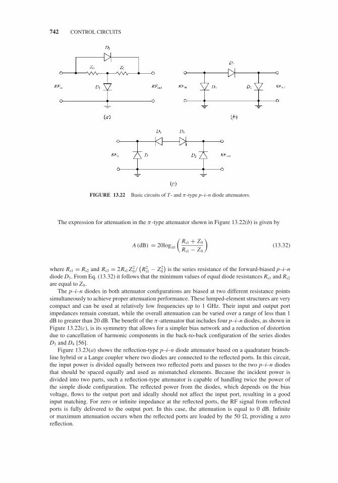
JWBS064-c13 JWBS064-Gerbennikov March 12, 2011 7:54 Printer Name: Yet to Come
742 CONTROL CIRCUITS
FIGURE 13.22 Basic circuits of T- and π -type p–i–n diode attenuators.
The expression for attenuation in the π -type attenuator shown in Figure 13.22(b) is given by
A (dB) = 20log10
(Rs1 + Z0
Rs1 − Z0
)(13.32)
where Rs1 = Rs2 and Rs3 = 2Rs1 Z 20/
(R2
s1 − Z 20
)is the series resistance of the forward-biased p–i–n
diode D3. From Eq. (13.32) it follows that the minimum values of equal diode resistances Rs1 and Rs2
are equal to Z0.The p–i–n diodes in both attenuator configurations are biased at two different resistance points
simultaneously to achieve proper attenuation performance. These lumped-element structures are verycompact and can be used at relatively low frequencies up to 1 GHz. Their input and output portimpedances remain constant, while the overall attenuation can be varied over a range of less than 1dB to greater than 20 dB. The benefit of the π -attenuator that includes four p–i–n diodes, as shown inFigure 13.22(c), is its symmetry that allows for a simpler bias network and a reduction of distortiondue to cancellation of harmonic components in the back-to-back configuration of the series diodesD3 and D4 [56].
Figure 13.23(a) shows the reflection-type p–i–n diode attenuator based on a quadrature branch-line hybrid or a Lange coupler where two diodes are connected to the reflected ports. In this circuit,the input power is divided equally between two reflected ports and passes to the two p–i–n diodesthat should be spaced equally and used as mismatched elements. Because the incident power isdivided into two parts, such a reflection-type attenuator is capable of handling twice the power ofthe simple diode configuration. The reflected power from the diodes, which depends on the biasvoltage, flows to the output port and ideally should not affect the input port, resulting in a goodinput matching. For zero or infinite impedance at the reflected ports, the RF signal from reflectedports is fully delivered to the output port. In this case, the attenuation is equal to 0 dB. Infiniteor maximum attenuation occurs when the reflected ports are loaded by the 50 �, providing a zeroreflection.

JWBS064-c13 JWBS064-Gerbennikov March 12, 2011 7:54 Printer Name: Yet to Come
ATTENUATORS 743
FIGURE 13.23 Reflection-type low-phase shift diode attenuators.
At any p–i–n diode bias condition, the phase characteristic of the reflection-type attenuator shownin Figure 13.23(a) can be written as
�φ = tan−1
⎛⎜⎜⎜⎝
ωL s − ωR2pCj
1 + ω2 R2pC2
j
− Z0
tan θ
Rs − Z0 + Rp
1 + ω2 R2pC2
j
⎞⎟⎟⎟⎠ − tan−1
⎛⎜⎜⎜⎝
ωL s − ωR2pCj
1 + ω2 R2pC2
j
− Z0
tan θ
Rs + Z0 + Rp
1 + ω2 R2pC2
j
⎞⎟⎟⎟⎠ (13.33)
where Ls is the parasitic series inductance, Rs is the series i-layer resistance, Cj is the diode junctioncapacitance shunted by a parallel resistance Rp, Z0 and θ are the characteristic impedance and electricallength of the open-circuit stub, respectively [57]. In this case, a low phase shift attenuator can berealized by adjusting the value of θ to minimize the effects of the parasitic series inductance Ls andvarying resistance Rj. As a result, at a center bandwidth frequency of 1855 MHz, this reflection-typeattenuator can achieve less than 3◦ phase shift with up to 30 dB attenuation and return loss below 17dB at both input and output ports.

JWBS064-c13 JWBS064-Gerbennikov March 12, 2011 7:54 Printer Name: Yet to Come
744 CONTROL CIRCUITS
The frequency bandwidth of a reflection-type variable attenuator is defined by the bandwidthproperties of the quadrature hybrid. The microstrip 3-dB branch-line coupler in conjunction withtwo varactor diodes instead of p–i–n diodes can vary the attenuation from 2.2 to 17 dB over a 40%bandwidth from 2.8 to 4.2 GHz [58]. To minimize the variation of attenuation with frequency andimprove return loss, two or more quadrature hybrids can be used. For example, by cascading twobalanced bi-phase modulators with opposite phase where each balanced modulator consists of a pairof reflection-type attenuators connected by means of input and output quadrature directional couplers,as shown in Figure 13.23(b), the phase error less than 5◦ over a 32 dB attenuation range in a frequencyrange from 6 to 18 GHz was achieved [59].
The performance of the variable attenuators can be improved in terms of frequency bandwidth,linearity, power handling, and integration level by using MOSFET, MESFET, or HEMT technology.The basic mechanism of the circuit is the change in the low-field drain–source resistance of a zero-biased field-effect transistor controlled by the gate–source voltage [60]. In this case, the variableattenuator operating as a controlled resistor represents a passive component and does not dissipateany dc power. The value of resistance can generally vary from the open-gate resistance to infinitewhen the gate voltage is changed from the built-in voltage (positive) of the gate barrier to the pinch-offvoltage (negative). The attenuator nonlinear distortion can be reduced by connecting two FETs inantiparallel (or antiseries) configuration or using a single FET with negative feedback [61].
The classic bridged-T attenuator shown in Figure 13.24(a) becomes a continuously variableattenuators when the series resistance R1 and the shunt resistance R2 are allowed to vary accordingto Z0 = √
R1 R2, where Z0 is the desired characteristic impedance. As a result, the attenuation in a
FIGURE 13.24 Resistive and MESFET variable attenuators.
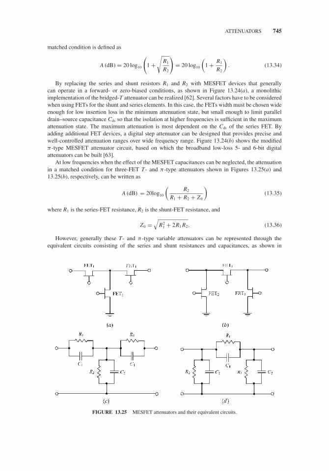
JWBS064-c13 JWBS064-Gerbennikov March 12, 2011 7:54 Printer Name: Yet to Come
ATTENUATORS 745
matched condition is defined as
A (dB) = 20 log10
(1 +
√R1
R2
)= 20 log10
(1 + R1
R2
). (13.34)
By replacing the series and shunt resistors R1 and R2 with MESFET devices that generallycan operate in a forward- or zero-biased conditions, as shown in Figure 13.24(a), a monolithicimplementation of the bridged-T attenuator can be realized [62]. Several factors have to be consideredwhen using FETs for the shunt and series elements. In this case, the FETs width must be chosen wideenough for low insertion loss in the minimum attenuation state, but small enough to limit paralleldrain–source capacitance Cds so that the isolation at higher frequencies is sufficient in the maximumattenuation state. The maximum attenuation is most dependent on the Cds of the series FET. Byadding additional FET devices, a digital step attenuator can be designed that provides precise andwell-controlled attenuation ranges over wide frequency range. Figure 13.24(b) shows the modifiedπ -type MESFET attenuator circuit, based on which the broadband low-loss 5- and 6-bit digitalattenuators can be built [63].
At low frequencies when the effect of the MESFET capacitances can be neglected, the attenuationin a matched condition for three-FET T- and π -type attenuators shown in Figures 13.25(a) and13.25(b), respectively, can be written as
A (dB) = 20log10
(R2
R1 + R2 + Z0
)(13.35)
where R1 is the series-FET resistance, R2 is the shunt-FET resistance, and
Z0 =√
R21 + 2R1 R2. (13.36)
However, generally these T- and π -type variable attenuators can be represented through theequivalent circuits consisting of the series and shunt resistances and capacitances, as shown in
FIGURE 13.25 MESFET attenuators and their equivalent circuits.

JWBS064-c13 JWBS064-Gerbennikov March 12, 2011 7:54 Printer Name: Yet to Come
746 CONTROL CIRCUITS
FIGURE 13.26 Schematics of MESFET bandpass attenuators.
Figures 13.25(c) and 13.25(d), respectively [64]. For the same R1, the π -type circuit is characterizedby less insertion loss than the T-type circuit. The value of R1 can be reduced by increasing thenumber of gate fingers, although the parasitic capacitance C1 will also increase limiting the dynamicrange of attenuation at high frequencies. In terms of the dynamic range, T-type attenuators becomeadvantageous over π -type attenuators. Besides, the T-network is more linear than the π -network,especially at higher attenuation settings [65]. Since power-handling capability is limited by theperformance of the shunt FET, dual-gate devices can be used for the shunt FET to increase its kneeand breakdown voltages. To achieve better linearity, the two nonidentical cascaded T-type stages thatare activated consecutively can be used [66].
In order to absorb the device parasitic capacitances C1 and C2 representing the device drain–sourcecapacitances Cds (or generally equivalent output capacitances Cout) and eliminate their effect on atten-uator performance, a bandpass filter topology can be superimposed onto the π -type MMIC variableattenuator, as shown in Figure 13.26(a) [67]. In this case, the bandpass filter parameters are deter-mined as L1 = Z 2
0C1 and L2 = 1/(2ω1ω2C2), where Z0 = √L1/2C2 = √
L2/C1 is the filter imageimpedance corresponding to the loaded characteristic impedance equal to 50 �, ω1 and ω2 are thelower and upper cutoff frequencies in radians with the center bandwidth frequency ω0 = √
ω1ω2,respectively. Figure 13.26(b) shows the T-type MMIC variable attenuator where a shunt FET isdistributed into four cells interconnected by high-impedance transmission-line sections [68]. At aminimum attenuation setting when the shunt FETs are equivalently represented as capacitances, thedistributed structure absorbs the FET capacitances into an artificial 50-� transmission line. At a max-imum attenuation setting with the shunt FETs effectively operated as low resistances, the distributedLR structure yields an increased attenuation with frequency, thus compensating for degraded isolationdue to parasitic capacitances of the series FETs. Moreover, a 50-� resistor connected in parallel witheach series FET minimizes the parasitic capacitances at the maximum attenuation setting by allowingthe series FETs to be biased well below their pinch-off voltage. As a result, a 30-dB dynamic rangeof attenuation in a frequency range from dc up to 50 GHz with a minimum insertion loss of 1.8 dBat 26.5 GHz and 2.6 dB at 40 GHz was achieved.
13.5 VARIABLE GAIN AMPLIFIERS
For mobile phone or satellite communication transmitters with power control schemes, a variablegain amplifier with wide dB-linear gain control and high transmission linearity is required. To achieve
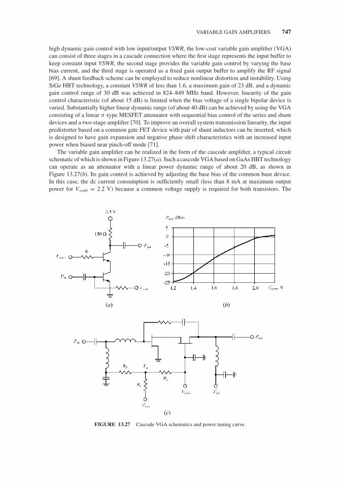
JWBS064-c13 JWBS064-Gerbennikov March 12, 2011 7:54 Printer Name: Yet to Come
VARIABLE GAIN AMPLIFIERS 747
high dynamic gain control with low input/output VSWR, the low-cost variable gain amplifier (VGA)can consist of three stages in a cascade connection where the first stage represents the input buffer tokeep constant input VSWR, the second stage provides the variable gain control by varying the basebias current, and the third stage is operated as a fixed gain output buffer to amplify the RF signal[69]. A shunt feedback scheme can be employed to reduce nonlinear distortion and instability. UsingSiGe HBT technology, a constant VSWR of less than 1.6, a maximum gain of 23 dB, and a dynamicgain control range of 30 dB was achieved in 824–849 MHz band. However, linearity of the gaincontrol characteristic (of about 15 dB) is limited when the bias voltage of a single bipolar device isvaried. Substantially higher linear dynamic range (of about 40 dB) can be achieved by using the VGAconsisting of a linear π -type MESFET attenuator with sequential bias control of the series and shuntdevices and a two-stage amplifier [70]. To improve an overall system transmission linearity, the inputpredistorter based on a common gate FET device with pair of shunt inductors can be inserted, whichis designed to have gain expansion and negative phase shift characteristics with an increased inputpower when biased near pinch-off mode [71].
The variable gain amplifier can be realized in the form of the cascode amplifier, a typical circuitschematic of which is shown in Figure 13.27(a). Such a cascode VGA based on GaAs HBT technologycan operate as an attenuator with a linear power dynamic range of about 20 dB, as shown inFigure 13.27(b). Its gain control is achieved by adjusting the base bias of the common base device.In this case, the dc current consumption is sufficiently small (less than 8 mA at maximum outputpower for Vcontr = 2.2 V) because a common voltage supply is required for both transistors. The
FIGURE 13.27 Cascode VGA schematics and power tuning curve.
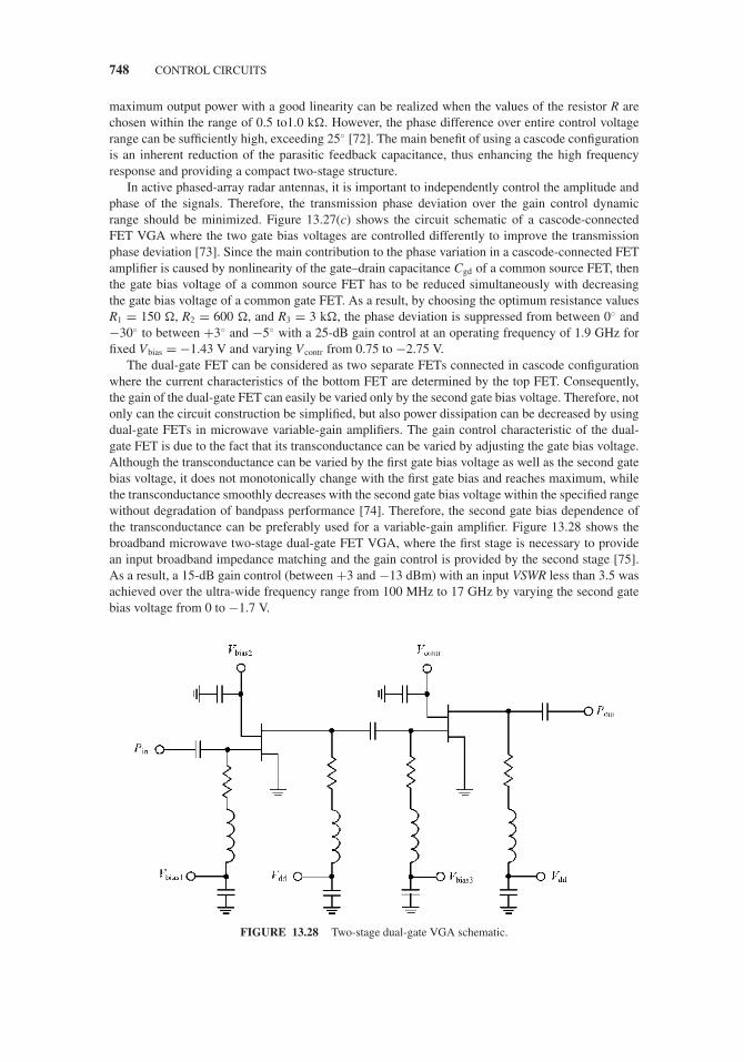
JWBS064-c13 JWBS064-Gerbennikov March 12, 2011 7:54 Printer Name: Yet to Come
748 CONTROL CIRCUITS
maximum output power with a good linearity can be realized when the values of the resistor R arechosen within the range of 0.5 to1.0 k�. However, the phase difference over entire control voltagerange can be sufficiently high, exceeding 25◦ [72]. The main benefit of using a cascode configurationis an inherent reduction of the parasitic feedback capacitance, thus enhancing the high frequencyresponse and providing a compact two-stage structure.
In active phased-array radar antennas, it is important to independently control the amplitude andphase of the signals. Therefore, the transmission phase deviation over the gain control dynamicrange should be minimized. Figure 13.27(c) shows the circuit schematic of a cascode-connectedFET VGA where the two gate bias voltages are controlled differently to improve the transmissionphase deviation [73]. Since the main contribution to the phase variation in a cascode-connected FETamplifier is caused by nonlinearity of the gate–drain capacitance Cgd of a common source FET, thenthe gate bias voltage of a common source FET has to be reduced simultaneously with decreasingthe gate bias voltage of a common gate FET. As a result, by choosing the optimum resistance valuesR1 = 150 �, R2 = 600 �, and R3 = 3 k�, the phase deviation is suppressed from between 0◦ and−30◦ to between +3◦ and −5◦ with a 25-dB gain control at an operating frequency of 1.9 GHz forfixed Vbias = −1.43 V and varying Vcontr from 0.75 to −2.75 V.
The dual-gate FET can be considered as two separate FETs connected in cascode configurationwhere the current characteristics of the bottom FET are determined by the top FET. Consequently,the gain of the dual-gate FET can easily be varied only by the second gate bias voltage. Therefore, notonly can the circuit construction be simplified, but also power dissipation can be decreased by usingdual-gate FETs in microwave variable-gain amplifiers. The gain control characteristic of the dual-gate FET is due to the fact that its transconductance can be varied by adjusting the gate bias voltage.Although the transconductance can be varied by the first gate bias voltage as well as the second gatebias voltage, it does not monotonically change with the first gate bias and reaches maximum, whilethe transconductance smoothly decreases with the second gate bias voltage within the specified rangewithout degradation of bandpass performance [74]. Therefore, the second gate bias dependence ofthe transconductance can be preferably used for a variable-gain amplifier. Figure 13.28 shows thebroadband microwave two-stage dual-gate FET VGA, where the first stage is necessary to providean input broadband impedance matching and the gain control is provided by the second stage [75].As a result, a 15-dB gain control (between +3 and −13 dBm) with an input VSWR less than 3.5 wasachieved over the ultra-wide frequency range from 100 MHz to 17 GHz by varying the second gatebias voltage from 0 to −1.7 V.
FIGURE 13.28 Two-stage dual-gate VGA schematic.

JWBS064-c13 JWBS064-Gerbennikov March 12, 2011 7:54 Printer Name: Yet to Come
VARIABLE GAIN AMPLIFIERS 749
FIGURE 13.29 Simplified schematics of differential VGA and gain tuning curves.
Figure 13.29(a) shows the conventional differential amplifier where the signal current from acommon emitter tail transistor Q1 is split between the two top transistors Q2 and Q3 with the collectorcurrent from Q2 being used as the output and the collector current from Q3 being shunted to a supply,and a voltage Vcontr between the bases of the transistors determines the attenuation of the transmittingsignal [76]. The gain-control characteristic can be found by solving for the current ratio I2/I1, wherethe current In corresponds to the transistor Qn, n = 1, 2, . . . . A linear change in the difference betweenthe base–emitter voltages of bipolar transistors changes the ratio of their current exponentially as
I2
I3= exp
(Vcontr
VT
)(13.37)
where VT is the thermal voltage. Solving for the gain-control characteristic by determining the currentratio I2/I1 results in
I2
I1= 1
1 + exp
(− Vcontr
VT
) . (13.38)

JWBS064-c13 JWBS064-Gerbennikov March 12, 2011 7:54 Printer Name: Yet to Come
750 CONTROL CIRCUITS
Figure 13.29(b) shows the curves that are plotted from Eqs. (13.37) and (13.38), respectively.Here, it can be seen that when the control voltage Vcontr is applied as a voltage across the bases oftransistors Q2 and Q3, the gain-control characteristic is fairly linear-in-dB at high attenuation levels,but the error increases at higher gains so that the maximum gain is expected at a 6-dB loss. The trueexponential characteristic for the current ratio I2/I1 can be achieved based on the circuit schematicshown in Figure 13.29(c), where all corresponding bipolar and pMOS transistors are assumed tobe identical. In this case, a transconductance buffer amplifier B1 is used to supply current to thetransistors Q6 and Q7 such that the current I7 is equal to the reference current Iref1. The current I6,which is a function of the current I7 and the control voltage Vcontr, is mirrored by the two pMOSdevices. The current I5 is forced to be equal to the current I7 by a buffer B2 that controls the voltagebetween the bases of the transistors Q4 and Q5, and the same voltage is applied between the transistorsQ2 and Q3. This sets the current ratio I5/Iref2 equal to the current ratio I2/I1, and the reference currentIref2 is chosen to be equal to the reference current Iref1. Consequently,
I2
I1= I5
Iref2= I6
I7= exp
(Vcontr
VT
)(13.39)
which demonstrates the most desirable linear-in-dB gain-control characteristic. As a result, the gain-control range can be measured of about 50 dB for 900-MHz applications using a BiCMOS process.It should be noted that the equivalence between the dc and RF performances can be achieved if thedevice transconductance is constant over the entire bias range and there is no effect of the deviceoutput impedance. Therefore, the measured gain-control curve slightly deviates from the ideal linearcharacteristic.
It is well known that a fully balanced (or double differential) multiplier is based on the threedifferential transistor pairs where the modulating (or control) signal is applied to the inputs of thetwo top transistor pairs and the carrier signal is applied to the tail transistor pair [77]. In this case,using a silicon bipolar technology with f T = 10 GHz results in a 50-dB gain control range with 24 dBof maximum gain and input/output VSWR better than 2:1 at all gain levels over the frequency rangefrom 100 MHz to 4 GHz by controlling the base bias voltages of the top transistor differential pairs[78]. Similar gain control range with 24-dBm maximum output power and efficiency greater than27% at an operating frequency of 1.95 GHz for mobile WCDMA applications can be achieved usinga GaAs HBT technology [79].
13.6 LIMITERS
Generally, limiter represents a two-port network that limits the output power level to a constant valueat high input power levels to protect power-sensitive components. A typical single-stage limiter circuitshown in Figure 13.30(a) uses the limiter diode, which is a special type of a p–i–n diode [80,81].For incoming signals that are below the threshold level in amplitude, the diode acts as an ordinaryunbiased p–i–n diode. In this case, the electrical field of the incoming signal is not large enough toforce carriers into the diode i-layer so its resistance remains high and it appears to be a capacitor ofrelatively small value. When the incident signal exceeds the threshold power level, the diode i-layeris flooded with carriers during the positive half-cycle of the incoming RF signal. The dc currentbegins to flow in the loop formed by the limiter diode and RF choke, and the limiter diode biasesitself to a low resistance value in a matter of nanoseconds, thus shorting out the signal transmissionat high power levels. In this case, the limiter circuit operates as a reflective switch, reflecting thelarge signal back to its source and protecting the subsequent circuitry. When the large amplitude ofthe incoming signal reduces to the level below the threshold voltage, the carriers in the diode i-layerrapidly recombine, and the diode junction resistance becomes very high, allowing small signals topass. The inductance of the RF choke is chosen to have a sufficiently high reactance and out-of-bandseries resonance so that it also produces negligible in-band reflection loss.

JWBS064-c13 JWBS064-Gerbennikov March 12, 2011 7:54 Printer Name: Yet to Come
LIMITERS 751
FIGURE 13.30 Basic circuits of p–i–n diode limiters.
There are three basic types of a power limiter circuit, usually based on the diode shunt con-figurations [41]. In a passive (or self-bias) limiter, lumped and transmission-line configurations ofwhich are shown in Figures 13.30(a) and 13.30(b), respectively, the limited output power dependson the variable diode resistance under zero-bias condition. Since the limiter diodes are turned onby the incoming RF signal itself, a passive limiter is a self-activating switch that is activated by ahigh-level incident power. When the self-rectified bias is increasing with increasing input power, thediode impedance is decreasing, and speed of this process depends on the diode lifetime (20–200 ns).This relatively slow process leads to a high dissipation power on the diode, causing spike leakagepower nearly equal to the incident power level. The maximum incoming RF power that a limiterdiode can handle is limited by either diode breakdown voltage or its power-dissipation capability. Thequasi-active limiter shown in Figure 13.30(c) includes a high-power Schottky-barrier diode detectorthat supplies dc current to the limiter diode. The Schottky diode rectification process is much fasterthan the limiter diode self-bias. In this case, the limiter diode is turned on primarily by the externalbias current from the Schottky detector diode that is sensitive to the incident power. The active limitershown in Figure 13.30(d) operates using a separate dc current source, and it is used in the sensitivetime control systems.
The single-stage limiter can typically produce 20–30 dB of isolation, depending on the inputsignal frequency and the characteristics of the diode. However, much more isolation can be requiredto protect sensitive components. Figure 13.31 shows the basic circuit of a two-stage p–i–n diode

JWBS064-c13 JWBS064-Gerbennikov March 12, 2011 7:54 Printer Name: Yet to Come
752 CONTROL CIRCUITS
FIGURE 13.31 Basic circuit of two-stage p–i–n diode limiter.
FIGURE 13.32 Schematics of MESFET limiters.
JWBS064-c13 JWBS064-Gerbennikov March 12, 2011 7:54 Printer Name: Yet to Come
REFERENCES 753
microwave power limiter with limiter diodes D1 and D2 and two Schottky detector diodes D3 andD4, where the Schottky diodes D3 and D4 are coupled with the main 50-Ω transmitting path throughhigh-impedance quarterwave transmission lines [41]. These Schottky diodes detect the incident powerand rapidly apply self-rectified current to the limiter diodes D1 and D2, causing a rapid increase inattenuation. The first high-power limiter diode D1 is used as a prelimiter of the high-incident power,while the second low-power limiter diode D2 provides protection during the initial stages of pulse risetime as having a faster response. Ideally, the electrical spacing between two limiter diodes should beof a one-quarter wavelength or an odd multiple of a one-quarter wavelength. The parasitic reactancesof the limiter diodes can be compensated for by choosing the optimum spacing and characteristicimpedance of the transmission line between them. If the limiter is required to handle very largeinput signals, a third stage can be added at the limiter input, spaced another one-quarter wavelengthfrom the second diode, which now becomes the intermediate limiter stage. The double-stackeddiode configurations can be used to handle about 6 dB more of the input power and to reduce theparasitic diode shunt capacitance by a factor of 2 [82,83]. Variable attenuation levels are achievedthrough biasing of the limiter diodes since the diode impedance is current-dependent and results in acontinuously variable attenuation [84].
Instead of the p–i–n diode limiter, a GaAs MESFET limiter can be used where the device isoperated beyond its compression point so that the RF level at its output cannot exceed the saturationlevel, irrespective of the incoming signal amplitude. In this case, to reduce the phase shift that dependson the amplitude of the RF signal and mainly caused by the device input gate–source capacitancevariations occurring during a fraction of the RF cycle when the gate becomes forward biased, anadditional series resistor with optimum value is included into the gate bias circuit to create the voltagedrop that results in the increased reverse gate–source voltage [85]. As a result, for a given input power,the fraction of the RF cycle corresponding to a forward-biased gate is smaller and the variations ofthe gate–source capacitance also diminish. Figure 13.32(a) shows the circuit schematic of a 8-GHz12-dBm MMIC MESFET limiter that incorporates a special gate biasing scheme with optimizedseries resistor and makes use of appropriate load conditions resulting in a phase variations less than8◦ over a 22-dB input power range [86]. The hybrid topology of a microwave MESFET limiter witha single bias circuit shown in Figure 13.32(b) is based on the microstrip-line design and provides lowphase distortions [87]. The dual-gate MESFET can be used as an excellent wideband limiter becauseit offers the design advantages of lower power output limiting, a sharper saturation knee, and theability to set the output power level by changing the dc bias point [88].
REFERENCES
1. H. L. Krauss, C. W. Bostian, and F. H. Raab, Solid State Radio Engineering, New York: John Wiley & Sons,1980.
2. K. Yamamoto, S. Suzuki, K. Mori, T. Asada, T. Okuda, A. Inoue, T. Miura, K. Chomei, R. Hattori, M.Yamanouchi, and T. Shimura, “A 3.2-V Operation Single-Chip Dual-Band AlGaAs/GaAs HBT MMICPower Amplifier with Active Feedback Circuit Technique,” IEEE J. Solid-State Circuits, vol. SC-35,pp. 1109–1120, Aug. 2000.
3. D. Dening and K. Muhonen, “Power Amplifier Protection Circuit,” U. S. Patent 6,720,831, Apr. 2004.
4. Ang. Scuderi, L. La Paglia, Ant. Scuderi, F. Carrara, and G. Palmisano, “A VSWR-Protected Silicon BipolarRF Power Amplifier with Soft-Slope Power Control,” IEEE J. Solid-State Circuits, vol. SC-40, pp. 611–621,Mar. 2005.
5. F. Carrara, C. D. Presti, Ant. Scuderi, C. Santagati, and G. Palmisano, “A Methodology for Fast VSWRProtection Implemented in a Monolithic 3-W 55% PAE RF CMOS Power Amplifier,” IEEE J. Solid-StateCircuits, vol. SC-43, pp. 2057–2066, Sept. 2008.
6. Application Note 1599, Power Control with the MRFIC0913 GaAs IPA and MC33169 Support IC, FreescaleSemiconductor, 2000.

JWBS064-c13 JWBS064-Gerbennikov March 12, 2011 7:54 Printer Name: Yet to Come
754 CONTROL CIRCUITS
7. A. van Bezooijen, F. van Straten, R. Mahmoudi, and A. H. M. van Roermund, “Avalanche BreakdownProtection by Adaptive Output Power Control,” IEEE Radio and Wireless Symp. Dig., pp. 519–522,2006.
8. I. J. Bahl, “Broadband Power Detectors,” IEEE Microwave Mag., vol. 8, pp. 82–86, June 2007.
9. D. W. Bowman, “Circuit to Protect RF Output Amplifier Against Mismatch Damage,” U. S. Patent 3,852,669,Dec. 1974.
10. A. Rachakonda and L. Hawkins, “Log Amps and Directional Couplers Enable VSWR Detection,” RF Design,pp. 28–34, Jan. 2007.
11. H. Ikeda, H. Kosugi, and T. Uwano, “A Low Distortion and High Efficiency Parallel-Operation PowerAmplifier Combined in Different Phases in Wide Range of Load Impedances,” IEEE MTT-S Int. MicrowaveSymp. Dig., pp. 535–538, 1996.
12. M. R. Millet, “Microwave Switching by Crystal Diodes,” IEEE Trans. Microwave Theory Tech.,vol. MTT-6, pp. 284–290, July 1958.
13. M. E. Hines, “Fundamental Limitations in RF Switching and Phase Shifting Using Semiconductor Diodes,”Proc. IEEE, vol. 52, pp. 697–708, June 1964.
14. Application Note, Design with PIN Diodes, Skyworks Solutions, Apr. 2009.
15. Application Note 922, Applications of PIN Diodes, Agilent Technologies, 1999.
16. Application Note 957–1, Broadbanding the Shunt PIN Diode SPDT Switch, Agilent Technologies, 1996.
17. K. W. Kobayashi, A. K. Oki, D. K. Umemoto, S. K. Z. Claxton, and D. C. Streit, “Monolithic GaAs HBTp–i–n Diode Variable Gain Amplifiers, Attenuators, and Switches,” IEEE Trans. Microwave Theory Tech.,vol. MTT-41, p. 2295–2302, Dec. 1993.
18. J.-L. Lee, D. Zych, E. Reese, and D. M. Drury, “Monolithic 2–18 GHz Low Loss, On-Chip Biased PIN DiodeSwitches,” IEEE Trans. Microwave Theory Tech., vol. MTT-43, pp. 250–256, Feb. 1995.
19. S. Tanaka, S. Horiuchi, T. Kimura, and Y. Atsumi, “Design and Fabrication of Multiband p–i–n DiodeSwitches with Ladder Circuits,” IEEE Trans. Microwave Theory Tech., vol. MTT-54, pp. 1561–1568, Apr.2006.
20. K. Miyatsuji and D. Ueda, “A GaAs High Power RF Single Pole Dual Throw Switch IC for Digital MobileCommunication System,” IEEE J. Solid-State Circuits, vol. SC-30, pp. 979–983, Sept. 1995.
21. Y. Ota, M. Sakakura, K. Fujimoto, S. Yamamoto, and H. Fujimoto, “High Isolation and Low Insertion LossSwitch IC Using GaAs MESFET’s,” IEEE Trans. Microwave Theory Tech., vol. MTT-43, pp. 2175–2177,Sept. 1995.
22. J. Frounchi and S. Harrold, “Very Fast GaAs HEMT Analogue Switch,” Electronics Lett., vol. 33,pp. 1499–1501, Aug. 1997.
23. K. F.-J. Huang O, “A 0.5-μm CMOS T/R Switch for 900-MHz Wireless Applications,” IEEE J. Solid-StateCircuits, vol. SC-36, pp. 486–492, Mar. 2001.
24. Q. Li and Y. P. Zhang, “CMOS T/R Switch Design: Towards Ultra-Wideband and Higher Frequency,” IEEEJ. Solid-State Circuits, vol. SC-42, pp. 563–570, Mar. 2007.
25. J. F. White, “High-Power, p–i–n Diode Controlled, Microwave Transmission Phase Shifters,” IEEE Trans.Microwave Theory Tech., vol. MTT-13, pp. 233–242, Mar. 1965.
26. R. V. Carver, “Broad-Band Diode Phase Shifters,” IEEE Trans. Microwave Theory Tech., vol. MTT-20, pp.314–323, May 1972.
27. R. H. Hardin, E. J. Downey, and J. Munushian, “Electronically-Variable Phase Shifters Utilizing VariableCapacitance Diodes,” Proc. IRE, vol. 48, pp. 944–945, May 1960.
28. C.-L. Chen, W. E. Courtney, L. J. Mahoney, M. J. Manfra, A. Chu, and H. A. Atwater, “A Low-Loss Ku-BandMonolithic Analog Phase Shifter,” IEEE Trans. Microwave Theory Tech., vol. MTT-35, pp. 315–320, Mar.1987.
29. E. C. Niehenke, V. V. DiMarco, and A. Friedberg, “Linear Analog Hyperabrupt Varactor Diode Phase Shifter,”IEEE MTT-S Int. Microwave Symp. Dig., pp. 657–660, 1985.
30. J. F. White, “Diode Phase Shifters for Array Antennas,” IEEE Trans. Microwave Theory Tech.,vol. MTT-22, pp. 658–674, June 1974.
31. H.-R. Ahn and I. Wolff, “Asymmetric Ring-Hybrid Phase Shifters and Attenuators,” IEEE Trans. MicrowaveTheory Tech., vol. MTT-50, pp. 1146–1155, Apr. 2002.

JWBS064-c13 JWBS064-Gerbennikov March 12, 2011 7:54 Printer Name: Yet to Come
REFERENCES 755
32. S. Lucyszyn and I. D. Robertson, “Two-Octave Bandwidth Monolithic Analog Phase Shifter,” IEEE Mi-crowave and Guided Wave Lett., vol. 2, pp. 343–345, Aug. 1992.
33. A. Keerti, J. Xiang, and A.-V. Pham, “High Power Linearized RF Phase Shifter Using Anti-Series Diodes,”IEEE Microwave and Wireless Components Lett., vol. 16, pp. 200–202, Apr. 2006.
34. C.-S. Lin, S.-F. Chang, C.-C. Chang, and Y.-H. Shu, “Design of a Reflection-Type Phase Shifter with WideRelative Phase Shift and Constant Insertion Loss,” IEEE Trans. Microwave Theory Tech., vol. MTT-55, pp.1862–1868, Sept. 2007.
35. C.-S. Lin, S.-F. Chang, and W.-C. Hsiao, “A Full-360◦ Reflection-Type Phase Shifter with Constant InsertionLoss,” IEEE Microwave and Wireless Components Lett., vol. 18, pp. 106–108, Feb. 2008.
36. W. A. Davis, “Design Equations and Bandwidth of Loaded-Line Phase Shifters,” IEEE Trans. MicrowaveTheory Tech., vol. MTT-22, pp. 561–563, May 1974.
37. H. A. Atwater, “Circuit Design of the Loaded-Line Phase Shifter,” IEEE Trans. Microwave Theory Tech.,vol. MTT-33, pp. 626–634, July 1985.
38. I. J. Bahl and K. C. Gupta, “Design of Loaded-Line p–i–n Diode Phase Shifter Circuit,” IEEE Trans.Microwave Theory Tech., vol. MTT-28, pp. 219–224, Mar. 1980.
39. A. S. Nagra and R. A. York, “Distributed Analog Phase Shifters with Low Insertion Loss,” IEEE Trans.Microwave Theory Tech., vol. MTT-47, pp. 1705–1711, Sept. 1999.
40. G. D. Lynes, G. E. Johnson, B. E. Huckleberry, and N. H. Forrest, “Design of a Broad-Band 4-Bit LoadedSwitched-Line Phase Shifter,” IEEE Trans. Microwave Theory Tech., vol. MTT-22, pp. 693–697, June1974.
41. L. G. Maloratsky, Passive RF & Microwave Integrated Circuits, New York: Newnes, 2004.
42. B. M. Schiffman, “A New Class of Broad-Band Microwave 90-Degree Phase Shifters,” IEEE Trans. Mi-crowave Theory Tech., vol. MTT-6, pp. 232–237, Apr. 1958.
43. J. L. R. Quirarte and J. P. Starski, “Novel Schiffman Phase Shifters,” IEEE Trans. Microwave Theory Tech.,vol. MTT-41, pp. 9–14, Jan. 1993.
44. B. M. Schiffman, “Multisection Microwave Phase-Shift Networks,” IEEE Trans. Microwave Theory Tech.,vol. MTT-14, p. 209, Apr. 1966.
45. V. P. Meschanov, I. V. Metelnikova, V. D. Tupikin, and G. G. Chumaevskaya, “A New Structure of Mi-crowave Ultrawide-Band Differential Phase Shifter,” IEEE Trans. Microwave Theory Tech., vol. MTT-42,pp. 762–765, May 1994.
46. C. Andricos, I. J. Bahl, and E. L. Griffin, “C-Band 6-Bit GaAs Monolithic Phase Shifter,” IEEE Trans.Microwave Theory Tech., vol. MTT-33, pp. 1591–1596, Dec. 1985.
47. K. Miyaguchi, M. Hieda, K. Nakahara, H. Kurusu, M. Nii, M. Kasahara, T. Takagi, and S. Urasaki, “AnUltra-Broad-Band Reflection-Type Phase-Shifter MMIC with Series and Parallel LC Circuits,” IEEE Trans.Microwave Theory Tech., vol. MTT-49, pp. 2446–2452, Dec. 2001.
48. C. Tsironis and P. Harrop, “Dual-Gate MESFET Phase Shifter with Gain at 12 GHz,” Electronics Lett.,vol. 16, pp. 553–554, July 1980.
49. J. L. Vorhaus, R. A. Pucel, and Y. Tajima, “Monolithic Dual-Gate GaAs FET Digital Phase Shifter,” IEEETrans. Microwave Theory Tech., vol. MTT-30, pp. 982–992, July 1982.
50. M. Kumar, R. J. Menna, and H.-C. Huang, “Broad-Band Active Phase Shifter Using Dual-Gate MESFET,”IEEE Trans. Microwave Theory Tech., vol. MTT-29, pp. 1098–1102, Oct. 1981.
51. P.-Y. Chen, T.-W. Huang, H. Wang, Y.-C. Wang, C.-H. Chen, and P.-C. Chao, “K-Band HBT and HEMTMonolithic Active Phase-Shifters Using Vector Sum Method,” IEEE Trans. Microwave Theory Tech.,vol. MTT-52, pp. 1414–1424, May 2004.
52. C. F. Campbell and S. A. Brown, “A Compact 5-Bit Phase-Shifter MMIC for K-Band Satellite CommunicationSystems,” IEEE Trans. Microwave Theory Tech., vol. MTT-48, pp. 2652–2656, Dec. 2000.
53. I. J. Bahl and D. Conway, “L- and S-Band Compact Octave Bandwidth 4-Bit MMIC Phase Shifters,” IEEETrans. Microwave Theory Tech., vol. MTT-56, pp. 293–299, Feb. 2008.
54. J. K. Hunton and A. G. Ryals, “Microwave Variable Attenuators and Modulators Using PIN Diodes,” IEEETrans. Microwave Theory Tech., vol. MTT-10, pp. 262–273, July 1962.
55. F. G. Atanasso, “A Low Phase Shift Step Attenuator Using p–i–n Diodes Switches,” IEEE Trans. MicrowaveTheory Tech., vol. MTT-28, pp. 774–776, July 1980.

JWBS064-c13 JWBS064-Gerbennikov March 12, 2011 7:54 Printer Name: Yet to Come
756 CONTROL CIRCUITS
56. Application Note 1003, A Wideband General Purpose PIN Diode Attenuator, Skyworks Solutions, 2005.
57. W.-T. Kang, I.-S. Chang, and M.-S Kang, “Reflection-Type Low-Phase-Shift Attenuators,” IEEE Trans.Microwave Theory Tech., vol. MTT-46, pp. 1019–1021, July 1998.
58. C. R. Trent and T. M. Weller, “S-Band Reflection Type Variable Attenuator,” IEEE Microwave and WirelessComponents Lett., vol. 12, pp. 243–245, July 2002.
59. D. Adler and P. Mariato, “Broadband Phase Invariant Attenuator,” IEEE MTT-S Int. Microwave Symp. Dig.,pp. 673–676, 1988.
60. W. Gosling, “Voltage Controlled Attenuation Using Field Effect Transistors,” IEEE Trans. Audio, vol. AU-13,pp. 112–120, Sept. 1965.
61. H. P. von Ow, “Reducing Distortion in Controlled Attenuators Using FET,” Proc. IEEE, vol. 56,pp. 1718–1719, Oct. 1968.
62. G. S. Barta, K. E. Jones, G. C. Herrick, and E. W. Strid, “Surface-Mounted GaAs Active Splittersand Attenuator MMIC’s Used in a 1−10-GHz Leveling Loop,” IEEE Trans. Microwave Theory Tech.,vol. MTT-34, pp. 1569–1575, Dec. 1986.
63. D. Krafcsik, F. Ali, and S. Bishop, “Broadband, Low-Loss 5- and 6-Bit Digital Attenuators,” IEEE MTT-SInt. Microwave Symp. Dig., pp. 673–676, 1988.
64. Y. Tajima, T. Tsukii, R. Mozzi, E. Tong, L. Hanes, and B. Wrona, “GaAs Monolithic Wideband (2–18 GHz)Variable Attenuators,” IEEE MTT-S Int. Microwave Symp. Dig., pp. 479–481, 1982.
65. H. Dogan and R. G. Meyer, “Intermodulation Distortion in CMOS Attenuators and Switches,” IEEE J.Solid-State Circuits, vol. SC-42, pp. 529–539, Mar. 2007.
66. H. Dogan, R. G. Meyer, and A. M. Niknejad, “Analysis and Design of RF CMOS Attenuators,” IEEE J.Solid-State Circuits, vol. SC-43, pp. 2269–2283, Oct. 2008.
67. S. M. Daoud and P. N. Shastry, “A Novel Wideband MMIC Voltage Controlled Attenuator with a BandpassFilter Topology,” IEEE Trans. Microwave Theory Tech., vol. MTT-54, pp. 2576–2583, June 2006.
68. H. Kondoh, “DC-50 GHz MMIC Variable Attenuator with a 30dB Dynamic Range,” IEEE MTT-S Int.Microwave Symp. Dig., pp. 499–502, 1988.
69. C.-W. Kim and Y.-G. Kim, “A 2.7-V SiGe HBT Variable Gain Amplifier for CDMA Applications,” IEEEMicrowave and Wireless Components Lett., vol. 13, pp. 502–504, Dec. 2003.
70. M. Inamori, K. Motoyoshi, T. Kitazawa, K. Tara, and M. Hagio, “A New GaAs Variable-Gain AmplifierMMIC with a Wide-Dynamic-Range and Low-Voltage-Operation Linear Attenuation Circuit,” IEEE Trans.Microwave Theory Tech., vol. MTT-48, pp. 182–186, Feb. 2000.
71. G. Hau, T. B. Nishimura, and N. Iwata, “High Efficiency, Wide Dynamic Range Variable Gain and PowerAmplifier MMICs for Wide-Band CDMA Handsets,” IEEE Microwave and Wireless Components Lett.,vol. 11, pp. 13–15, Jan. 2001.
72. Q. Chaudhry, R. Alidio, G. Sakamoto, and T. Cisco, “A SiGe MMIC Variable Gain Cascode Amplifier,”IEEE Microwave and Wireless Components Lett., vol. 12, pp. 424–425, Nov. 2002.
73. H. Hayashi and M. Muragushi, “An MMIC Variable-Gain Amplifier Using a Cascode-Connected FET withConstant Phase Deviation,” IEICE Trans. Electron., vol. E81-C1, pp. 70–77, Jan. 1998.
74. M. Maeda and Y. Minai, “Microwave Variable-Gain Amplifier with Dual-Gate GaAs FET,” IEEE Trans.Microwave Theory Tech., vol. MTT-22, pp. 1226–1230, Dec. 1974.
75. N. Mamodaly, P. Quentin, P. Dueme, and J. Obregon, “100 MHz to 17 GHz Dual-Gate Variable-GainAmplifier,” IEEE Trans. Microwave Theory Tech., vol. MTT-30, pp. 918–919, June 1982.
76. D. Coffing, E. Main, M. Randol, and G. Szklarz, “A Variable Gain Amplifier with 50-dB Control Range for900-MHz Applications,” IEEE J. Solid-State Circuits, vol. SC-37, pp. 1169–1175, Sept. 2002.
77. A. Bilotti, “Applications of a Monolithic Analog Multipliers,” IEEE J. Solid-State Circuits, vol. SC-3,pp. 373–380, Dec. 1968.
78. I. Kipnis, J. F. Kukielka, J. Wholey, and C. P. Snapp, “Silicon Bipolar Fixed and Variable Gain AmplifierMMICs for Microwave and Lightwave Applications up to 6 GHz,” IEEE MTT-S Int. Microwave Symp. Dig.,pp. 109–112, 1989.
79. V. T. S. Vintola, M. J. Matilainen, S. J. K. Kalajo, and E. A. Jarvinen, “Variable-Gain Power Amplifier forMobile WCDMA Applications,” IEEE Trans. Microwave Theory Tech., vol. MTT-49, pp. 2464–2471, Dec.2001.

JWBS064-c13 JWBS064-Gerbennikov March 12, 2011 7:54 Printer Name: Yet to Come
REFERENCES 757
80. Application Note, PIN Limiter Diodes in Receiver Protectors, Skyworks Solutions, Aug. 2008.
81. Application Note 1959, Low Cost Surface Mount Power Limiters, Agilent Technologies, 1999.
82. D. J. Seymour, D. D. Heston, and R. E. Lehmann, “X-Band and Ka-Band Monolithic GaAs PIN DiodeVariable Attenuation Limiters,” IEEE MTT-S Int. Microwave Symp. Dig., pp. 255–258, 1988.
83. D. G. Smith, D. D. Heston, and D. L. Allen, “Designing High-Power Limiter Circuits with GaAs PIN Diodes,”IEEE MTT-S Int. Microwave Symp. Dig., pp. 329–332, 1999.
84. D. G. Smith, D. D. Heston, J. Heston, B. Heimer, and K. Decker, “Designing Reliable High-Power LimiterCircuits with GaAs PIN Diodes,” IEEE MTT-S Int. Microwave Symp. Dig., vol. 3, pp. 1245–1247, 2002.
85. T. Parra, M. Gayral, O. Llopis, M. Pouysegur, J. Sautereau, and J. Graffeuil, “Design of a Low Phase DistortionGaAs FET Power Limiter,” IEEE Trans. Microwave Theory Tech., vol. MTT-39, pp. 1059–1062, June 1991.
86. T. Parra, J. Dienor, M. Gayral, M. Pouysegur, J. Sautereau, and J. Graffeuil, “X-Band Low Phase DistortionMMIC Power Limiter,” IEEE Trans. Microwave Theory Tech., vol. MTT-41, pp. 876–879, May 1993.
87. S. Fukuda, M. Kitamura, Y. Ara, and I. Haga, “A New Microwave Amplitude Limiter Using GaAs FieldEffect Transistor,” IEEE MTT-S Int. Microwave Symp. Dig., pp. 240–242, 1977.
88. R. J. Hamilton, “Wide Band, Dual-Gate GaAs F.E. T. Output Limiters,” IEEE MTT-S Int. Microwave Symp.Dig., pp. 256–258, 1979.

JWBS064-c13 JWBS064-Gerbennikov March 12, 2011 7:54 Printer Name: Yet to Come
758

JWBS064-c14 JWBS064-Gerbennikov March 12, 2011 8:44 Printer Name: Yet to Come
14 Transmitter Architectures
This chapter describes the different types of radio transmitter architectures, history of radio commu-nication, conventional types of radio transmission, and modern communication systems. Amplitude-modulated transmitters representing the oldest technique for radio communication are based on high-or low-level modulation methods, with the particular case of an amplitude keying. Single-sidebandtransmitters as the next-generation transmitters could provide higher efficiency because of the trans-mission of a single sideband only. Frequency-modulated transmitters then became a revolutionarystep to improve the quality of a broadcast transmission. TV transmitters include different modulationtechniques for transmitting audio and video information, both analog and digital. Wireless commu-nication transmitters as a part of the cellular technologies provide a worldwide wireless radio access.Radar transmitters are required for many commercial and military applications such as phased-arrayradars, automotive radars, or electronic warfare systems. Satellite transmission systems contributeto worldwide transmission of any communication signals through satellite transponders and offercommunication for areas with any population density and location. Ultra-wideband transmission isvery attractive for its low-cost and low-power communication applications, occupying a very widefrequency range.
14.1 AMPLITUDE-MODULATED TRANSMITTERS
Amplitude-modulated transmitters whose extensive development began in about 1927 based onvacuum tubes for generating radio-frequency signals are used in high-frequency communication,broadcasting, aircraft, and navigation systems. Early continuous-wave vacuum-tube transmittersused a power oscillator as the generator of the RF power. However, the requirements for betterfrequency stability soon caused a significant change in the transmitter configuration because ofsuccess in the development in crystal stability when the requirements for piezoelectric crystal controlof frequency began establishing in 1929 [1]. Currently, amplitude-modulated radio transmissionsare used worldwide at medium frequencies (530–1700 kHz) and high-frequency bands (3–26 MHz)where the carrier signals are amplitude modulated with audio bandwidths of 5 kHz [2]. In short-wavebroadcasting, transmitters use both solid-state (5-kW modules) or vacuum-tube RF power amplifiers(PAs), with power levels ranging from 10 kW to 2 MW. Full-carrier double-sideband amplitudemodulation can be accomplished by several techniques, including high-level modulation by variationof the final RF PA supply voltage by transformer coupling and low-level modulation by controllingthe gate bias voltage. An advantage of the high-level modulation is that only the final stage needs to bemodulated when all preliminary stages can be driven at a constant RF level. In low-level modulation,a small audio stage is used to modulate a low-power RF carrier stage, the output of which is thenamplified using a linear RF PA. However, the serious disadvantage of this system is that the amplifierchain is less efficient because it has to be linear to preserve modulation. In order to use Class-C PAas a final stage, the feedback linearization scheme is required.
RF and Microwave Transmitter Design, First Edition. Andrei Grebennikov.C© 2011 John Wiley & Sons, Inc. Published 2011 by John Wiley & Sons, Inc.
759

JWBS064-c14 JWBS064-Gerbennikov March 12, 2011 8:44 Printer Name: Yet to Come
760 TRANSMITTER ARCHITECTURES
14.1.1 Collector Modulation
The traditional method of accomplishing high-quality amplitude modulation (AM) uses a transformer-coupled push–pull Class B audio-frequency (AF) amplifier to vary the supply collector (drain) voltageof a Class RF PA designed in a conventional (with shunt resonant circuit) or mixed-mode (with seriesresonant circuit) configuration, as shown in Figure 14.1(a) [3]. When efficiency is not a criticalparameter, a Class A audio amplifier can be used. In this case, all components in a modulating path,namely the transformer, AF amplifier, and AF drivers if required, are collectively called the modulator.The linearity of high-level modulation technique depends on the linearity of the modulator and themodulation characteristic of the RF PA. In the latter case, the nonlinear capacitive coupling between
FIGURE 14.1 Basic transmitter structure and operation waveforms for collector modulation.

JWBS064-c14 JWBS064-Gerbennikov March 12, 2011 8:44 Printer Name: Yet to Come
AMPLITUDE-MODULATED TRANSMITTERS 761
gate and drain of the field-effect transistor (or between base and collector of the bipolar device)produces a minimum output or feedthrough signal that is present even when Vdd = 0, resulting inboth amplitude and phase modulation (PM) nonlinearity at low signal level. Consequently, too muchdrive results in nonlinearity at low outputs, while too little drive results in nonlinearity at high outputswhen device saturation does not occur at high values of Vdd.
An analysis of waveforms shown in Figure 14.1(b) shows that the drain (or collector) supplyvoltage of the final RF power amplifying stage swings above and below the unmodulated carrierlevel, which is equal to Vdd. In this case, the final RF power amplifying stage must deliver the peakenvelope power when its supply voltage is equal to 2Vdd. Since the drain dc and fundamental currentamplitudes change almost linearly with the supply voltage, the final RF amplifying stage representsapproximately constant resistive load and efficiency close to the saturated efficiency in Class B. Asa result, the low-level nonlinear distortions and high overall efficiency can generally be achieved.The overall efficiency of the transformer-coupled collector modulation by a single sinusoid can becalculated (assuming that only the final RF PA is modulated and the power required by the AF andRF drivers is ignored) as
η = ηRFηAF
1 + m2
2
ηAF + m2
2
(14.1)
where m is the modulation index, ηRF is the efficiency of the final RF PA, and ηAF is the efficiencyof the final audio amplifier. If both the AF and RF final amplifiers had 78.5% efficiency of an idealClass B mode, the overall efficiency η of the two final amplifiers would be 72% for m = 1. If the finalAF amplifier operates in Class A with 50% efficiency, the overall efficiency is 58.9%.
To minimize the amplitude nonlinear distortions at low voltages at the device collector when thebase–collector junction can be forward biased resulting in low junction impedance and feedthroughsignal, an additional collector modulation of the driver stage (with modulation index m < 1) byusing the modulating signal coupled with the AF amplifier output transformer can be implemented,as shown in Figure 14.2. This provides the lower signal power at the input of the final RF amplifyingstage at low voltages at the device collector, thus minimizing the feedthrough signal through it and
FIGURE 14.2 Basic transmitter structure for dual collector modulation.
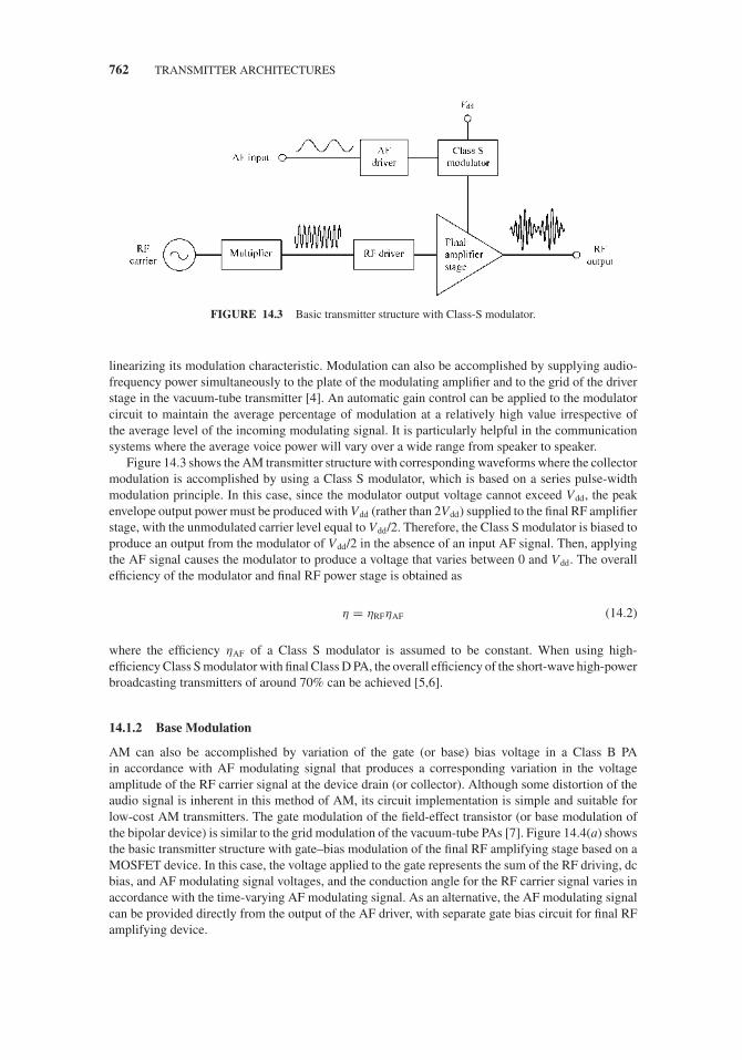
JWBS064-c14 JWBS064-Gerbennikov March 12, 2011 8:44 Printer Name: Yet to Come
762 TRANSMITTER ARCHITECTURES
FIGURE 14.3 Basic transmitter structure with Class-S modulator.
linearizing its modulation characteristic. Modulation can also be accomplished by supplying audio-frequency power simultaneously to the plate of the modulating amplifier and to the grid of the driverstage in the vacuum-tube transmitter [4]. An automatic gain control can be applied to the modulatorcircuit to maintain the average percentage of modulation at a relatively high value irrespective ofthe average level of the incoming modulating signal. It is particularly helpful in the communicationsystems where the average voice power will vary over a wide range from speaker to speaker.
Figure 14.3 shows the AM transmitter structure with corresponding waveforms where the collectormodulation is accomplished by using a Class S modulator, which is based on a series pulse-widthmodulation principle. In this case, since the modulator output voltage cannot exceed Vdd, the peakenvelope output power must be produced with Vdd (rather than 2Vdd) supplied to the final RF amplifierstage, with the unmodulated carrier level equal to Vdd/2. Therefore, the Class S modulator is biased toproduce an output from the modulator of Vdd/2 in the absence of an input AF signal. Then, applyingthe AF signal causes the modulator to produce a voltage that varies between 0 and Vdd. The overallefficiency of the modulator and final RF power stage is obtained as
η = ηRFηAF (14.2)
where the efficiency ηAF of a Class S modulator is assumed to be constant. When using high-efficiency Class S modulator with final Class D PA, the overall efficiency of the short-wave high-powerbroadcasting transmitters of around 70% can be achieved [5,6].
14.1.2 Base Modulation
AM can also be accomplished by variation of the gate (or base) bias voltage in a Class B PAin accordance with AF modulating signal that produces a corresponding variation in the voltageamplitude of the RF carrier signal at the device drain (or collector). Although some distortion of theaudio signal is inherent in this method of AM, its circuit implementation is simple and suitable forlow-cost AM transmitters. The gate modulation of the field-effect transistor (or base modulation ofthe bipolar device) is similar to the grid modulation of the vacuum-tube PAs [7]. Figure 14.4(a) showsthe basic transmitter structure with gate–bias modulation of the final RF amplifying stage based on aMOSFET device. In this case, the voltage applied to the gate represents the sum of the RF driving, dcbias, and AF modulating signal voltages, and the conduction angle for the RF carrier signal varies inaccordance with the time-varying AF modulating signal. As an alternative, the AF modulating signalcan be provided directly from the output of the AF driver, with separate gate bias circuit for final RFamplifying device.

JWBS064-c14 JWBS064-Gerbennikov March 12, 2011 8:44 Printer Name: Yet to Come
AMPLITUDE-MODULATED TRANSMITTERS 763
FIGURE 14.4 Basic transmitter structure and operation waveforms for base modulation.
The amplitude-modulated RF output signal is shown in Figure 14.4(b), where the dc bias andthe modulating signal are chosen to produce a Class B operation at positive modulation peaksand a zero conduction angle at negative modulation peaks, based on the sufficiently linear devicetransfer characteristic. The simple overall efficiency approximation assumes a linear variation of theinstantaneous time-varying efficiency from zero value with vdrain = 0 to maximum (peak-envelope)value ηmax with vdrain = Vdd, where Vdd is the drain supply voltage. As a result, the efficiency for

JWBS064-c14 JWBS064-Gerbennikov March 12, 2011 8:44 Printer Name: Yet to Come
764 TRANSMITTER ARCHITECTURES
an unmodulated carrier signal is ηmax/2 and the average efficiency for 100% modulation by a singlesinusoid is 3ηmax/4. However, due to significant nonlinearity of the device transfer characteristic closeto cutoff and saturation regions, the modulation index is usually chosen to be less than 70–80%to minimize amplitude (AM–AM) distortions. At the same time, nonlinearity of the input devicenonlinear capacitance, which can be modeled as a junction capacitance, can cause the unwantedphase (AM–PM) distortions of the transmitting amplitude-modulated signal if its phase characteristicis considered an important parameter.
14.1.3 Low-Level Modulation
The block diagram of a typical amplitude-modulated transmitter, in which an amplitude modulatoris followed by a linear PA, is shown in Figure 14.5 with corresponding waveforms. This is a low-level modulation system where the modulation takes place at a power level less than transmitteroutput, and the linear amplification of the amplitude-modulated signals is often used in low-powerbroadcasting and communication transmitters. In this case, to minimize nonlinear distortions of thetransmitting signal, the input level of the amplitude-modulated signal and the gate (or base) biascondition with constant conduction angle must be chosen so that only the linear part of the transfercharacteristic of the linear PA can be used, thus providing its active (linear current source) mode andavoiding saturated mode. Since existing bipolar or field-effect power transistors operated in Class Bdo not change abruptly from a cutoff mode to an active mode that would result to so-called crossoverdistortion, the active device must be biased in a Class AB with small quiescent current in the collectoror drain. The amount of a quiescent current required for minimum distortion is usually determined
FIGURE 14.5 Basic transmitter structure and operation waveforms for low-level modulation.

JWBS064-c14 JWBS064-Gerbennikov March 12, 2011 8:44 Printer Name: Yet to Come
AMPLITUDE-MODULATED TRANSMITTERS 765
by simulation or measurement (typically, in between 1% and 10% of the collector or drain dc currentunder nominal operation), since theoretical prediction is quite complicated.
For a sinusoidal full-carrier AM with m = 1 in a Class B PA, the dc input current is proportional tothe RF output current (or voltage) amplitude. Consequently, the average dc power for an AM signalis the same as the dc power for the carrier without modulation, with an unmodulated carrier levelequal to Vdd/2. The average RF output power is equal to Pavr = P0 (1 + m2/2) = (3/2)P0, where P0 isthe unmodulated carrier power that is four times less than the peak envelope power PPEP. As a result,the average drain efficiency can be written as
η = (3/2) (PPEP/4)
(1/2) (4/π ) PPEP= 3π
16(14.3)
which is approximately equal to 58.9% [3].
14.1.4 Amplitude Keying
The continuous-wave radio transmitters are often operated in an amplitude-shift-keying (ASK) moderequired in remote control circuits, security systems, wireless data transmission, or in accordance todots and dashes to produce radio telegraph signals in a simple case of on-off keying. This amplitudekeying is usually performed at a low or moderate power level, and the required transmitter poweris then obtained by the high-power amplifying stage with a fixed bias. The block diagram of a sim-ple amplitude-keyed transmitter is shown in Figure 14.6(a), where the gate of the active device isturned on and off in accordance with the rectangular modulating signal delivered directly throughthe gate bias circuit. In a 60-GHz high data rate transmitter, the ASK modulator block consists of a60-GHz fundamental-mode oscillator, a buffer, and a switch (using a 0.1-μm GaAs HEMT technol-ogy) followed by the driver, bandpass filter (BPF), PA, and antenna fabricated with a low-temperatureco-fired ceramic (LTCC) [8].
FIGURE 14.6 Basic transmitter structure and operation waveforms for amplitude keying.

JWBS064-c14 JWBS064-Gerbennikov March 12, 2011 8:44 Printer Name: Yet to Come
766 TRANSMITTER ARCHITECTURES
The optional inclusion of a frequency multiplier improves stability by allowing the frequencies ofthe oscillator and high-power amplifiers (HPAs) to be different. In amplitude keying, the RF pulsesshould have rounded edges, as shown in Figure 14.6(b). Otherwise, if the voltage rises and falls veryrapidly, the abrupt changes in amplitude will introduce high-order sidebands, at frequencies differingsignificantly from the carrier frequency. However, when the rise and fall times are too long, thiswill lead to the nonlinear distortions of the transmitted signal that may significantly complicate itsidentification after detection. In this case, it is necessary to choose the active devices with low inputtime constant and high transition frequency. In addition, it needs to carefully design the bias circuit inorder to maximize isolation between modulating signal path and the carrier signal path and minimizelow-frequency transient response shown in Figure 14.6(c).
14.2 SINGLE-SIDEBAND TRANSMITTERS
In mid-1915, during the radio–telephone experiments conducted with a powerful vacuum-tube trans-mitter in Arlington, Virginia, it was recognized by Harold Arnold that the antenna could be tuned toone side of the carrier frequency that contained all the signal elements necessary to reproduce theoriginal speech [9]. In addition to suppressing one sideband, John Carson proposed suppression ofthe carrier as well [10]. As a result, a transatlantic reliable one-way speech transmission was demon-strated in January 1923 using a powerful experimental single-sideband (SSB) transmitter, operatingat a mid-band frequency of 57 kHz [11]. The first short-wave SSB equipment provided only a singlespeech channel on one side of the carrier, but it was quickly determined that a common PA couldbe made sufficiently linear to permit adding a second channel on the opposite of the carrier [12]. Inthis case, two frequency tones of equal amplitudes were then used for testing the transmitting signalquality, each frequency tone being half the peak sideband amplitude. With introduction of automotivetuning capability of the output resonant circuit and high-power wideband ferrite balun at the end of1950s, the broadband operation of a short-wave vacuum-tube SSB transmitter was extended to covera frequency range from 2 to 25 MHz. One of the first solid-state transmitters that used eight widebandRF modules in a hybrid arrangement to produce an output power of 1 kW was introduced in the early1970s [13]. Modern SSB transmitters are widely used in long-range military, marine, aircraft, andamateur communication systems where frequency of operation can vary over several octaves.
An SSB can be obtained by passing the output of a carrier-suppression system through filtercircuits that are sufficiently selective to transmit one sideband while suppressing the other. However,the requirements that filter must meet are sufficiently strong, especially if the carrier frequency is toohigh. For example, the standard frequency band of the telephone channel is from 300 to 3400 Hz,which means that very effective rejection can be done for the lowest offset frequency of 2 × 300Hz. Even with well-designed filters such sharpness of discrimination is possible only if the carrierfrequency is low enough so that 600 Hz is not too small a percentage of the carrier frequency. As aresult, the filter method is suitable only for obtaining SSBs corresponding to low or moderate carrierfrequencies. If the sideband must be located in a high-frequency part of spectrum, then it must betranslated in frequency by heterodyne or superheterodyne action, resulting generally to multiple-conversion transmitter architectures mostly based on the discrete-band and broadband methods.
The discrete-band frequency translation technique has evolved from vacuum-tube transmittersand is well suited for operation in several small assigned bands. Figure 14.7(a) shows the discrete-band SSB transmitter architecture with two balanced modulators. For such an SSB communicationtransmitter, the SSB signal at intermediate frequency can be achieved using a balanced modulatorand a BPF (which can represent a quartz or electromechanical filter) for fixed intermediate carrierfrequency f 1 in range of 100 to 500 kHz. In this case, the modulating signal with frequencies from f 1
+ 300 Hz to f 1 + 3400 Hz applies to the second balanced modulator, and filter must suppress one ofthe sidebands separated by 2(f 1 + 300 Hz), or more by about 1 MHz for f 1 = 500 kHz than withoutfrequency upconversion. After filtering, which can be done with simple multisection LC filters, theresulting SSB signal then translated to the assigned small frequency band within the high frequency

JWBS064-c14 JWBS064-Gerbennikov March 12, 2011 8:44 Printer Name: Yet to Come
SINGLE-SIDEBAND TRANSMITTERS 767
FIGURE 14.7 Basic structures of multiple-conversion SSB transmitters.
range from 1.6 to 30 MHz intended for HF communication service. The BPF generally represents abank of switched BPFs, and band selection is provided by activating the corresponding filter. Someapplications, particularly military communications, require transmitters capable of operating on anyfrequency in the HF band. In this case, the second carrier source (f 2) in Figure 14.7(a) will representa frequency synthesizer followed by a low-pass filter (LPF) and a broadband power [3]. The SSBtransmitter can generally provide a capability of multichannel transmission. Its two-channel structureis shown in Figure 14.7(b), where N1 and N2 are the audio modulating signals of the first and secondchannels, respectively. At the output of the first balanced modulators, the high sideband is selected byone filter and the low sideband is selected by another filter. Then, both these sidebands are combinedand translated to higher frequencies by the second balanced modulator followed by the filter whosepassband must include both telephone channels.
The direct-conversion SSB transmitters, the basic structure of which is shown in Figure 14.8(a),are intended for use on a single band of frequencies in low-cost applications. SSB modulation using aphasing method to provide the direct conversion is based on two balanced modulators arranged withRF inputs that differ in phase by 90◦, and with AF modulating inputs that are likewise identical exceptthat each frequency component of the modulating voltage applied to the second balanced modulatordiffers in phase by 90◦ from the phase of the corresponding component of the modulating voltageapplied to the first balanced modulator. As an example, the simplified circuit of the transformer-coupled MOSFET balanced modulator is shown in Figure 14.8(b). When the outputs of these twobalanced modulators are added, one of the sidebands is canceled out, resulting (together with thefact that the carrier is suppressed by the balanced modulators) in an output that contains only asingle sideband. The first practical implementation of this principle described in 1948 included abalanced-modulator system using screen-grid-modulated Class C amplifiers [14]. The quadraturesignals at the carrier frequency f 0 can be obtained by digital frequency division of the output of avoltage-controlled oscillator (VCO) operating at 4f 0. As shown in Figure 14.8(a), the signal at 4f 0
is divided by a flip-flop whose outputs are at frequency 2f 0 and 180◦ out of phase. The subsequentdivision of each of these signals by a pair of flip-flops then produces the corresponding outputs atfrequency f 0 that differ in phase by 90◦.

JWBS064-c14 JWBS064-Gerbennikov March 12, 2011 8:44 Printer Name: Yet to Come
768 TRANSMITTER ARCHITECTURES
FIGURE 14.8 Basic structure of direct-conversion SSB transmitter.
For a two-tone signal with equal amplitudes commonly used to test an SSB transmitter, the averageRF output power is equal to Pavr = PPEP/2, because each of the tone with half of the peak envelopeamplitude would dissipate PPEP/4. The dc input current (and dc power) will vary with the outputcurrent, forming a full-wave rectified shape whose peak value is the current required by an amplifierdelivering PPEP. The average dc input current is therefore 2/π times the peak dc input current. As aresult, the average drain efficiency of the PA can be written as
η = (1/2)PPEP
(2/π ) (4/π ) PPEP= π 2
16(14.4)
which is approximately equal to 61.7% [15].
14.3 FREQUENCY-MODULATED TRANSMITTERS
Despite the fact that the subject of frequency modulation (FM) is very old and was proposed beforethe introduction of the vacuum-tube oscillators, Edwin Armstrong was the first who developed andinstalled a working frequency-modulated transmitter and began regular broadcasts in 1939 [16]. Afew years later, to provide the center frequency stability of a high-order for wideband frequency-modulation systems, direct crystal control of the center frequency was proposed as an ideal solution[17]. Since then frequency-modulated transmitters have found extensive use at frequencies above

JWBS064-c14 JWBS064-Gerbennikov March 12, 2011 8:44 Printer Name: Yet to Come
FREQUENCY-MODULATED TRANSMITTERS 769
FIGURE 14.9 Basic structures of FM transmitters.
40 MHz in such applications as frequency-modulated broadcasting, television sound transmission,mobile radio, or radio-relay systems. For example, frequency-modulated broadcasting is now usedworldwide in the 88–108 MHz band and offers greatly reduced noise and interference with lower dis-tortion and larger audio bandwidth. The first frequency-modulated transmitter utilizing GaAs powerMESFETs for a 7-GHz frequency-modulated radio-relay equipment was developed in mid-1970s [18].
Generally, FM can be accomplished at low-power level either directly by variation of the frequencyof an oscillator by the audio input signal, or indirectly by PM of the RF signal by the time-integratedaudio input signal. Figure 14.9(a) shows the block schematic of a frequency-modulated transmitterwith direct FM where the audio signal is applied to the varactor included to the resonant circuit ofa crystal oscillator. To achieve high linearity, most frequency modulators operate at a lower thanrequired operating frequency producing a small modulation index or frequency deviation. To achievethe required operating frequency and to increase the frequency deviation, one or several multiplierstages with multiplication factor N are used, then followed by a PA and a BPF. High stabilityof the operating frequency can be achieved by using a crystal varactor-controlled oscillator or aphase-locked loop with local crystal oscillator (LO), as shown in Figure 14.9(b). In this case, thefrequency-modulated signal is coupled to pass through the frequency divider to reduce the modulationindex and to increase the amplitude of the average frequency compared to sideband amplitudes. Then,it is delivered to the phase detector (PD) to compare with the frequency of the highly stable referenceLO signal. When the average frequency of a frequency-modulated signal is not equal to the frequencyof the LO signal, then the PD output signal represents a low-frequency error voltage, the frequencyand phase of which is defined by the difference of the divided average frequency-modulated andreference LO signals. This voltage is applied to the varactor through the LPF, which has a bandwidthto pass the dc voltage and very low frequencies but to remove the modulating-frequency feedback. Asa result, the loop responds to the injected error voltage by adjusting the VCO to produce the specifiedphase shift between its output and the reference signal.
For higher operating frequencies, frequency-modulated transmitter configuration with direct mod-ulation can include mixer to provide frequency upconversion, as shown in Figure 14.10(a). In thiscase, unlike frequency multiplication, frequency upconversion changes neither the modulation index
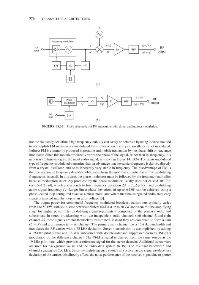
JWBS064-c14 JWBS064-Gerbennikov March 12, 2011 8:44 Printer Name: Yet to Come
770 TRANSMITTER ARCHITECTURES
FIGURE 14.10 Block schematics of FM transmitter with direct and indirect modulation.
nor the frequency deviation. High frequency stability can easily be achieved by using indirect methodto accomplish FM in frequency-modulated transmitter where the crystal oscillator is not modulated.Indirect FM is commonly produced in portable and mobile transmitter by the phase-shift or reactancemodulator. Since this modulator directly varies the phase of the signal, rather than its frequency, it isnecessary to time-integrate the input audio signal, as shown in Figure 14.10(b). The phase-modulatedtype of frequency-modulated transmitter has an advantage that the carrier frequency is derived directlyfrom a crystal oscillator, and so is inherently very stable in frequency. The disadvantage of PM isthat the maximum frequency deviation obtainable from the modulator, particular at low modulatingfrequencies, is small. In this case, the phase modulator must be followed by the frequency multiplierbecause modulation index �φ produced by the phase modulator usually does not exceed 30◦–70◦
(or 0.5–1.2 rad), which corresponds to low frequency deviation �f = f m�φ for fixed modulatingaudio-signal frequency f m. Larger linear phase deviations of up to ±180◦ can be achieved using aphase-locked loop configured to act as a phase modulator where the time-integrated audio-frequencysignal is injected into the loop as an error voltage [3].
The output power for commercial frequency-modulated broadcast transmitters typically variesfrom 1 to 50 kW, with solid-state power amplifiers (SSPAs) up to 20 kW and vacuum-tube amplifyingstage for higher power. The modulating signal represents a composite of the primary audio andsubcarriers. In stereo broadcasting with two independent audio channels (left channel L and rightchannel R), these signals are not themselves transmitted. Instead they are combined to form a sum(L + R) and a difference (L − R) channel. The primary sum channel has a 15-kHz bandwidth andmodulates the RF carrier with a 75-kHz deviation. Stereo transmission is accomplished by addinga 19-kHz pilot signal and 38-kHz subcarrier with double-sideband suppressed-carrier (DSB/SC)modulation by the difference channel. The 38-kHz signal is derived from the same source as the19-kHz pilot tone, which provides a reference signal for the stereo decoder. Additional subcarriersare used for background music and the radio data system (RDS). The resultant bandwidth andchannel spacing are 200 kHz. Since the high-frequency sounds in a typical audio signal produce lessdeviation of the carrier, this directly affects the noise performance of the received signal due to poorer

JWBS064-c14 JWBS064-Gerbennikov March 12, 2011 8:44 Printer Name: Yet to Come
FREQUENCY-MODULATED TRANSMITTERS 771
noise immunity at these frequencies. To avoid this effect, high frequencies are boosted before beingtransmitted by pre-emphasis.
Since audio signal transmission in an analog form results in unnecessary expense and degradationin signal quality, the modern frequency-modulated broadcast systems provide a capability of digitalaudio transmission and distribution. The advantages of digital audio distribution include transparentaudio quality, noise immunity, and the ability to diversely route the signal through a multi-nodenetwork. Figure 14.11(a) shows a typical 1-kW digital VHF/FM transmitter block schematic withan integrated digital exciter (including control unit, signal processor, and digital synthesizer), anupconverter, and an HPA module where each of four PAs provides a 300 W output power. Transmitterswith higher output power up to 20 kW can be developed by parallel combining of the basic 1-kWPA modules. Figure 14.11(b) shows the circuit schematic of a 300-W MOSFET PA operating overthe frequency range of 88 to 108 MHz and providing a power gain of more than 19 dB with a drainefficiency of more than 70% at a supply voltage of 50 V using the balanced RF MOSFET SD2932device [19]. The input matching network to transform the unbalanced standard 50 � to the balanced(gate-to-gate) device input impedance of 5.56 � consists of a 1:1 balun based on a 50-� coaxial cable
FIGURE 14.11 Schematics of high-power VHF/FM transmitter.
JWBS064-c14 JWBS064-Gerbennikov March 12, 2011 8:44 Printer Name: Yet to Come
772 TRANSMITTER ARCHITECTURES
and a 9:1 balanced impedance transformer based on 25-� flexible coaxial cables with ferrite core.The output matching network to transform the balanced (drain-to-drain) equivalent output deviceresistance of about 12 � (calculated in Class B for each part as Rout = (0.85Vdd)2/2Pout = (0.85 ×50 V)2/(2 × 150 W) = 6.02 �) to the standard 50-� load impedance consists of a 4:1 balancedimpedance transformer based on 25-� flexible coaxial cables and a 1:1 balun based on a 50-�coaxial cable. A 10-nH inductor is connected between two gates to compensate for the device inputcapacitive reactance, whereas a 40-nH inductor connected between two drains is used to compensatefor the device output capacitance over whole frequency range.
14.4 TELEVISION TRANSMITTERS
The history of electronic television (TV) transmission is originated from pioneering works of PhiloFarnsworth who invented an electronic scanning system (image dissector) and Vladimir Zworykinwho introduced an iconoscope camera tube and a kinescope picture tube that together formed the firstelectronic television system and replaced the cumbersome mechanical system of whirling perforateddiscs that had dominated the early development of television [20,21]. Zworykin studied at the St.Petersburg Institute of Technology, Russia, being a student of Prof. Boris Rosing, who had filedhis first patent on a television system in 1907 [22]. In May 1911, Rosing exhibited a televisionsystem, using a mechanical scanner in the transmitter and the electronic Braun tube in the receiver,which was among the first demonstrations of TV of any kind. Fully electronic television broadcastingsystems were introduced in Europe, USA, and Japan at the end of 1930s, and then after World War IIbecame commercially available worldwide. A microwave point-to-point radio system for TV channeltransmission intended to supplement local wire distribution of television was tested in 1946 [23].TV broadcasting uses both VHF (in various regions between 48 to 100 MHz and 174 to 230 MHz)and UHF (470–890 MHz) frequency bands. VHF and lower power UHF television transmitters aremostly based on SSPAs, while high-power UHF transmitters employ vacuum tubes.
There are three basic analog television standards with their own history used in different coun-tries such as North American NTSC (National Television System Committee), SECAM (SequentielCouleur Avec Memoire), originating in France, and PAL (Phase Alternation Line), developed inGermany. An NTSC television channel occupies a total bandwidth of 6 MHz in the frequency spec-trum, as shown in Figure 14.12(a). The sound that accompanies the picture is transmitted via afrequency-modulated carrier with a 25-kHz deviation located 4.5 MHz above the picture carrier.The picture carrier (brightness signal) is amplitude-modulated by the composite video signal repre-senting a vestigial-sideband (VSB) transmission that is DSB/SC with the lower sideband removedby filtering before transmission in order to save bandwidth. The seven elements of the compositevideo signal include horizontal line sync pulse, color reference burst, reference black level, pictureluminance information, color saturation information, color hue information, and vertical sync pulse.Since the image is divided into 525 lines (in a picture with a width-to-height ratio of 4:3) thatare scanned in an interlaced fashion at 30 Hz, the nominal bandwidth becomes equal to 4.2 MHz[3]. The color subcarrier is 3.579545 MHz above the video carrier, and the I and Q signals ofthe color information that correspond roughly to the difference between brightness and the red-orange and blue-green components of the image are transmitted by DSB/SC modulation of thecolor subcarrier.
According to the SECAM standard with a total channel bandwidth of 8 MHz, the image isdivided into 625 lines that are scanned in an interlaced fashion at 25 Hz with the nominal bandwidthof 6.0 MHz, and is similar to PAL in these respects. To transmit the two-color information, twodifferent subcarrier frequencies are used (4.25 and 4.406 MHz), as shown in Figure 14.12(b), thatrequires a one-line delay in the receiver to recombine the color information. These two subcarriersare frequency-modulated, instead of AM of a color subcarrier occurring at approximately 3.58 MHzfor NTSC and at approximately 4.43 MHz for PAL. The sound carrier is located 6.5 MHz above thepicture carrier and frequency modulated with a 25-kHz deviation.

JWBS064-c14 JWBS064-Gerbennikov March 12, 2011 8:44 Printer Name: Yet to Come
TELEVISION TRANSMITTERS 773
FIGURE 14.12 Spectra of composite TV signals in different analog standards.
Digital television (DTV) supports many different picture formats defined by the combination ofsize, aspect ratio (width-to-height ratio), and interlacing, and transmitted on radio frequencies thatare similar to standard analog television, with the primary difference being the use of multiplextransmitters to allow reception of multiple channels on a single frequency range. In the USA, high-definition television is based on MPEG-2 (Moving Pictures Experts Group) video coding and DolbyAC-3 audio coding as specified by the Advanced Television Systems Committee (ATSC) [24,25].The image is composed of 1080 lines with 1920 pixels per line, resulting in a data rate of 19.39Mb/s, which expands to 30.28 Mb/s with the addition of error-correction coding and other overheads.The 8VSB-transmitted signal is based on eight-level DSB/SC modulation followed by filtering toremove most of the lower sideband, allowing it to fit into existing 6-MHz television channels. Inthe United Kingdom, digital video broadcasting (DVB) is based on MPEG encoding and OFDMusing 16 or 64 QAM. The data at rates up to 31.7 Mb/s are distributed among 1704 carriers with1.1-kHz spacing or 6816 carriers with 4.5-kHz spacing. DTV has several advantages over analogTV, the most significant being that digital channels take up less bandwidth, and the bandwidth needsare continuously variable, at a corresponding reduction in image quality depending on the level ofcompression as well as the resolution of the transmitted image. This means that digital broadcasterscan provide more digital channels in the same space, provide high-definition television (HDTV)

JWBS064-c14 JWBS064-Gerbennikov March 12, 2011 8:44 Printer Name: Yet to Come
774 TRANSMITTER ARCHITECTURES
service, or provide other non-television services such as multimedia or interactivity. By bringingDTV content to mobile terminals, mobile TV promises to extend, enhance, and enrich conventionalTV user experience by allowing consumers not only to watch TV on the move, but also to have accessto personalized, time-shifted, and on-demand TV content [26].
The first practical all-solid-state TV transmitter having an output power of 30 kW was developedin Japan in 1985 [27]. This transmitter comprises of a main/stand-by exciter system, two separatesolid-state transmitters (each having half the capacity of the rated output power) that are operatedin parallel so that each transmitter can be separately released for required maintenance, and outputcoaxial circuitry for combining and switching the outputs of two transmitters. The transmitter modulardesign provides high redundancy, while jet air cooling with high efficiency contributes to size andweight reduction. The basic 6-kW UHF PA representing a functional block consists of eight 800-WPA modules, four 28-V power supplies, one 8-way divider at the input, and one 8-way combinerat the output, each employing a suspended substrate stripline that provides an insertion loss of lessthan 0.15 dB. A total of twelve internally matched 110-W bipolar 2SC2660 A devices operating in apush–pull mode up to 860 MHz are used in parallel in each 800-W PA module, which has no heatsinkby adopting jet air cooling. A circulator is employed in each module to achieve its stable operationover load variations. The high temperature protection, reflection detection, and abnormal displaylatch functions are provided to enhance self-protection function and improve the maintainability.
Figure 14.13 shows the block schematic of a solid-state VHF TV transmitter providing a 30-kWpeak visual output power with high reliability, broadband operation, and minimum maintenancerequirements [28]. The exciter includes video and IF correction circuitry with sound intercarrierfrequency phase locked to the video signal, automatic gain control, SAW filter, and possibility to lockthe carrier frequency to an external precision frequency source. The basic 5-kW frame fed from twoseparate power supplies consists of eight PA modules, fans, and a monitor and control module. Thefour PAs in each module are first combined using a 3-dB hybrid to obtain 850 W output per moduleand then the output of two frames are combined by a 16-way full isolation coupling system to obtain10 kW power. The basic PA uses a balanced bipolar transistor operating in a push–pull Class ABmode. The bipolar transistor is rated at 240 W peak of sync output at the 1-dB gain compression point.With 192 transistors in use, the total capability is approximately 46 kW that provides comfortablelinear operation below the compression point.
By using the silicon laterally diffused MOSFET technology, solid-state transmitters based onthe LDMOSFET devices become reliable and economically viable alternatives to the traditional
FIGURE 14.13 Block schematic of 30 kW VHF TV transmitter.
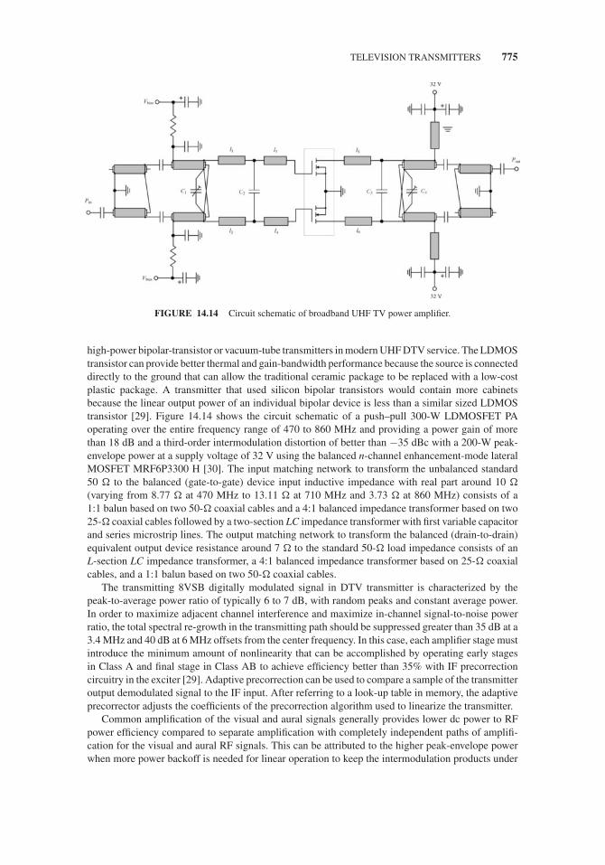
JWBS064-c14 JWBS064-Gerbennikov March 12, 2011 8:44 Printer Name: Yet to Come
TELEVISION TRANSMITTERS 775
FIGURE 14.14 Circuit schematic of broadband UHF TV power amplifier.
high-power bipolar-transistor or vacuum-tube transmitters in modern UHF DTV service. The LDMOStransistor can provide better thermal and gain-bandwidth performance because the source is connecteddirectly to the ground that can allow the traditional ceramic package to be replaced with a low-costplastic package. A transmitter that used silicon bipolar transistors would contain more cabinetsbecause the linear output power of an individual bipolar device is less than a similar sized LDMOStransistor [29]. Figure 14.14 shows the circuit schematic of a push–pull 300-W LDMOSFET PAoperating over the entire frequency range of 470 to 860 MHz and providing a power gain of morethan 18 dB and a third-order intermodulation distortion of better than −35 dBc with a 200-W peak-envelope power at a supply voltage of 32 V using the balanced n-channel enhancement-mode lateralMOSFET MRF6P3300 H [30]. The input matching network to transform the unbalanced standard50 � to the balanced (gate-to-gate) device input inductive impedance with real part around 10 �
(varying from 8.77 � at 470 MHz to 13.11 � at 710 MHz and 3.73 � at 860 MHz) consists of a1:1 balun based on two 50-� coaxial cables and a 4:1 balanced impedance transformer based on two25-� coaxial cables followed by a two-section LC impedance transformer with first variable capacitorand series microstrip lines. The output matching network to transform the balanced (drain-to-drain)equivalent output device resistance around 7 � to the standard 50-� load impedance consists of anL-section LC impedance transformer, a 4:1 balanced impedance transformer based on 25-� coaxialcables, and a 1:1 balun based on two 50-� coaxial cables.
The transmitting 8VSB digitally modulated signal in DTV transmitter is characterized by thepeak-to-average power ratio of typically 6 to 7 dB, with random peaks and constant average power.In order to maximize adjacent channel interference and maximize in-channel signal-to-noise powerratio, the total spectral re-growth in the transmitting path should be suppressed greater than 35 dB at a3.4 MHz and 40 dB at 6 MHz offsets from the center frequency. In this case, each amplifier stage mustintroduce the minimum amount of nonlinearity that can be accomplished by operating early stagesin Class A and final stage in Class AB to achieve efficiency better than 35% with IF precorrectioncircuitry in the exciter [29]. Adaptive precorrection can be used to compare a sample of the transmitteroutput demodulated signal to the IF input. After referring to a look-up table in memory, the adaptiveprecorrector adjusts the coefficients of the precorrection algorithm used to linearize the transmitter.
Common amplification of the visual and aural signals generally provides lower dc power to RFpower efficiency compared to separate amplification with completely independent paths of amplifi-cation for the visual and aural RF signals. This can be attributed to the higher peak-envelope powerwhen more power backoff is needed for linear operation to keep the intermodulation products under

JWBS064-c14 JWBS064-Gerbennikov March 12, 2011 8:44 Printer Name: Yet to Come
776 TRANSMITTER ARCHITECTURES
FIGURE 14.15 Block schematics of UHF TV transmitters with common amplification.
control. However, modern digital precorrection techniques allow very linear transmitter performanceand freedom from visual-to-aural cross modulation. As a result, the difference between two systemsin terms of efficiency becomes very small [31]. In this case, common amplification provides an ex-tremely attractive alternative to external diplexing when it comes to upgrade an analog TV transmitterfor digital operation. Figure 14.15(a) shows the block diagram for the analog transmitter configu-ration, including the digital signal modulator that processes the video and audio analog basebandand digital I/Q precorrector. To modify the transmitter system for DTV service, the only significanthardware change required is the replacement of the digital signal modulator with the coded OFDM(COFDM) encoder, as shown in Figure 14.15(b). All other items remain the same as for the analogTV transmitter. A BPF that is placed on the output of a DTV transmitter will slightly degrade theTV output signal by introducing group delay in the transmit chain. The group delay will becomesubstantial if the slope of the bandpass skirts is very steep. In order to minimize group delay, the BPFshould be designed with the minimum amount of required attenuation to provide a trade-off betweenPA linearity and BPF skirt requirements.
14.5 WIRELESS COMMUNICATION TRANSMITTERS
Decades before the cellular technologies began to provide a worldwide wireless radio access, thetwo-way radio systems met the need for mobile communication. In 1927, a number of bands inthe frequency range of 1.5 to 6.0 MHz were allocated to mobile aircraft two-way communicationsystems [32]. The first two-way municipal police duplex radio communication systems operatingbetween 30 to 42 MHz were introduced in 1930s [33]. The system transmitter that was capableof 100% modulation either by voice or by a 1-kHz calling tone included a vacuum-tube crystaloscillator, several frequency multipliers, an intermediate PA as a driver, and a final push–pull PAmodule. Microwave radio communication system using a pulse-position modulation that provideseight duplex voice channels through time division multiplexing and operating at 4.5 GHz wasdeveloped in mid-1940s [34]. The applications for modern mobile radio include land, marine, and

JWBS064-c14 JWBS064-Gerbennikov March 12, 2011 8:44 Printer Name: Yet to Come
WIRELESS COMMUNICATION TRANSMITTERS 777
airborne use for both civilian and military organizations. Analog systems use AM or FM and include acontrol channel for digital information. Each service is assigned to a specific set of frequencies in theVHF and UHF bands. For example, terrestrial trunked radio (TETRA) as a digital land-mobile radiobased on time division multiple access is commonly developed to use in different frequency bands,mainly between 350 and 470 MHz, marine communications using narrowband FM is provided in the156–174 MHz band, civilian aeronautical communications uses AM in the 108–137 MHz band, andmilitary airborne communications uses the frequency range from 225 to 400 MHz [2]. The multimediamillimeter-wave wireless communication service with high-speed modulation capability is providedat 60 GHz and can be based on an ultra-miniature monolithic FM/FSK transmitter/receiver moduleutilizing a complete MMIC chip set that includes a DR-stabilized fundamental-frequency oscillatorand based on a 0.15-μm double heterojunction GaAs FET technology [35].
The first commercial mobile telephone service operated on six channels in the 152–162 MHz bandwith 60-kHz channel spacing was developed in the USA in 1946 [36]. In 1960, the world’s first partlyautomatic car phone system was launched in Sweden. The first commercially automated cellular 1G(first generation) network was introduced in Japan in 1979. The initial launch network covered the fullmetropolitan area of Tokyo’s over 20 million inhabitants with a cellular network of 23 base stations.Within 5 years, this network had been expanded to cover the whole population of Japan and becamethe first nation-wide 2G (second generation) network. The second launch of the 1G networks was thesimultaneous deployment in Scandinavian countries in 1981 of the Nordic Mobile Telephone (NMT)system, which was the first mobile phone network featuring international roaming. The first networktechnology on digital 2G cellular technology was introduced in 1991 in Finland on the basis of theGSM standard. In 2001, the first commercial launch of 3G (third generation) system was developedin Japan based on the WCDMA standard. The next evolution to offer broadband wireless accesswith higher data transfer speeds and capacity represents the 4G (fourth generation) systems based on3GPP LTE (Long Term Evolution) cellular standard, which can offer peak bit rates of 326.4 Mb/s.
Several architectures can be proposed for wireless communication mobile transmitters dependingon the performance requirements [37,38]. In a Cartesian-type transmitter, the quadrature I and Qbaseband components are mixed with a quadrature LO signals. In this case, the baseband componentsare usually generated in the digital domain followed by the digital-to-analog converters (DAC) andLPF to provide delivery of the analog baseband signals to low-frequency inputs of the mixers. Theupconversion can be done in one or two steps. Figure 14.16(a) shows the superheterodyne transmitterwith two-step upconversion where the modulation is done at IF frequency and then subsequentlyupconverted to the transmitting frequency by an RF mixer. This architecture requires a significantamount of circuitry, which usually includes both the low-pass IF and bandpass RF filters to properlysuppress noise and spurious components. In addition, to provide a significant dynamic range ofoutput powers up to 80 dB depending on the communication standard, it is necessary to apply thevariable power control scheme directly at RF prior to the PA. The direct-conversion architectureshown in Figure 14.16(b) minimizes the number of circuit blocks providing the best compromise ofperformance versus power consumption and circuit complexity [39]. However, it may require an RFSAW filter to suppress noise floor in the receiver band before feeding the signal into the PA. Also,direct-conversion transmitters suffer from any mismatch in the phase and amplitude of the basebandsignals, and any dc offset in the baseband signal can result in LO leakage to the output, thus degradingthe transmit signal quality. In both architectures, the PA requires a good linearity, compromising theoverall transmitter efficiency and complicating output power control.
Despite various shielding techniques that attempt to isolate the LO in a direct-conversion trans-mitter, the noisy PA output can still corrupt the oscillator spectrum through injection-pulling (orinjection-locking) effect, tending the LO frequency ω0 to shift towards the frequency of an externalstimulus. If the frequency of the injected noise is close to the oscillator natural frequency, then the LOoutput is disturbed increasingly as the noise magnitude rises, eventually locking to the noise frequency.In practice, noise level as low as 40 dB below the oscillation level may create tremendous disturbance.This unwanted phenomenon can be alleviated if the PA output spectrum is sufficiently higher or lowerthan the LO frequency. For example, the LO frequency can be offset by subtracting or adding the

JWBS064-c14 JWBS064-Gerbennikov March 12, 2011 8:44 Printer Name: Yet to Come
778 TRANSMITTER ARCHITECTURES
FIGURE 14.16 Double-conversion and direct-conversion transmitter architectures.
output frequency of another LO with subsequent bandpass filtering, as shown in Figure 14.17 [40].In this case, the BPF selectivity should provide a significantly low level of intermodulation frequencycomponents mω1 ± nω2 resulting from the nonlinearities in the offset mixer.
The easiest way to transmit a constant-envelope signal is to use the direct modulation of a VCO withbaseband data, as shown in Figure 14.18(a), which has appeared in designs for DECT communicationstandard [41]. Here, initially the VCO is operated with the phase-locked loop (PLL) to accuratelyset the carrier frequency and then disconnected so that modulation can be fed into the control inputof the VCO unperturbed by its dynamics. Since the VCO performs both frequency translation andmodulation, this approach allows a significant reduction in components (with no mixers and onlyone DAC to produce modulation signal) and low power consumption. However, because the loopis inactive during modulation, the nominal frequency setting of the VCO tends to drift, resulting ina perturbation of the output frequency, which can also be seriously affected by turn-on transients.In addition, the isolation requirements between VCO and PA exclude the possibility of a one-chipsolution that limits high integration capability of this approach. The offset-PLL architecture is shown
FIGURE 14.17 Direct-conversion transmitter architecture with offset VCO.
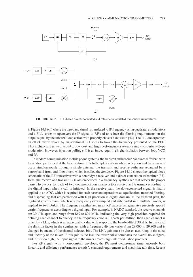
JWBS064-c14 JWBS064-Gerbennikov March 12, 2011 8:44 Printer Name: Yet to Come
WIRELESS COMMUNICATION TRANSMITTERS 779
FIGURE 14.18 PLL-based direct-modulated and reference-modulated transmitter architectures.
in Figure 14.18(b) where the baseband signal is translated to IF frequency using quadrature modulatorsand a PLL serves to upconvert the IF signal to RF and to reduce the filtering requirements on theoutput signal by the inherent loop action with properly chosen bandwidth [42]. The PLL incorporatesan offset mixer driven by an additional LO so as to lower the frequency presented to the PFD.This architecture is well suited to low-cost and high-performance systems using constant-envelopemodulation. However, injection pulling still is an issue, requiring higher isolation between loop VCOand PA.
In modern communication mobile phone systems, the transmit and receive bands are different, withtranslation performed at the base station. In a full-duplex system where reception and transmissionoccur simultaneously through a single antenna, the transmit and receive paths are separated by anarrowband front-end filter block, which is called the duplexer. Figure 14.19 shows the typical blockschematic of the RF transceiver with a heterodyne receiver and a direct-conversion transmitter [37].Here, the receive and transmit LOs are embedded in a frequency synthesizer that selects the propercarrier frequency for each of two communication channels (for receive and transmit) according tothe digital input when a call is initiated. In the receive path, the downconverted signal is finallyapplied to an ADC, which is required for such baseband operations as equalization, matched filtering,and dispreading that are performed with high precision in digital domain. In the transmit path, thedigitized voice stream, which is subsequently oversampled and subdivided into multi-bit words, isapplied to two DACs. The frequency synthesizer in an RF transceiver generates precisely spacedcarrier frequencies according to a digital input. For example, in NADC standard, the receive channelsare 30 kHz apart and range from 869 to 894 MHz, indicating the very high precision required fordefining each channel frequency. If the frequency error is 10 parts per million, then each channel isoffset by 9 kHz, which is an appreciable value with respect to the bandwidth of 30 kHz. In this case,the division factor in the synthesizer with a frequency divider varies from 29,000 to 29,800 and ischanged by means of the channel-selected bits. The LNA gain must be chosen according to the noiseand linearity of the mixer. If this gain is too low, the mixer noise dominates the overall noise figure,and if it is too high, the input signal to the mixer creates high intermodulation products.
For RF signals with a non-constant envelope, the PA must compromise simultaneously bothlinearity and efficiency performance to satisfy standard requirements and maximize talk time. Recent

JWBS064-c14 JWBS064-Gerbennikov March 12, 2011 8:44 Printer Name: Yet to Come
780 TRANSMITTER ARCHITECTURES
FIGURE 14.19 RF transceiver architecture.
trends in the integration of entire communication system require the development of homodyneradios with direct-conversion transmit and receive paths [39]. The PLL-based or translational looparchitecture, where sampled output of the VCO is fed back to the I/Q modulator included in the loopand which is well-suited for constant-envelope signals, can eliminate the need for RF SAW filter at thePA input. In this case, a single-chip quad-band GSM direct-conversion transceiver can be developedusing a BiCMOS technology where the only required external elements (excluding the impedancematching and loop filter components) are the receive-band SAW filters, a switchplexer, and a PA [43].
Polar transmitter architecture was chosen to minimize the dc power consumption and numberof external RF filters [44]. In this type of transmitter the modulated signal A(t) cos[ω0 t + φ(t)] isdecomposed into its amplitude and phase polar components. As a result, the PM can be first appliedusing a PLL-based phase modulator to generate a constant-envelope signal A0 cos[ω0 t + φ(t)].Then, the AM can be added by modulating the envelope of the RF signal using a variable gainamplifier (VGA) whose output amplitude is a function of A(t). Figure 14.20(a) shows the simplifiedblock diagram of a GSM/EDGE transmitter where an I/Q modulator generates the modulated IFoutput from the baseband inputs that contain both AM and PM information [45]. The PM path limitsthe IF signal to remove AM envelope, and this limited signal is then used as the reference inputto a translational loop PLL. The PLL locks the VCO to the transmit carrier frequency, transfersthe PM of the reference input onto the VCO, operating as a tunable high-Q filter for input noisecontributors in the transmitter. The AM signal is extracted from the IF signal using an AM detectorfollowed by the LPF and then directly applied to the VGA where both AM and PM signals arefinally recombined.
In GSM mode with constant envelope, the AM path is disabled and the transmitter reverts to aconventional nonlinear offset-PLL transmitter. In order to reconstruct the modulated signal correctly,the AM and PM signals need to be aligned. For example, a delay mismatch of about 80 ns canincrease the output spectrum mask at 400 kHz offset to about −54 dBc, which is a minimum levelrequired by the standard. To minimize this misalignment in practice, either a feedback loop or aprecision calibration scheme can be used. When AM signal is combined with PM signal, AM-to-PMconversion due to PA nonlinearity can corrupt the signal quality, degrading both spectral mask anderror vector magnitude (EVM). Therefore, as an alternative, either polar modulation can be appliedto the low-power linearized VGA prior to the high-power PA, or feedback control of both phase andamplitude of the transmitted signal from the output of PA is necessary to correct its nonlinearitiesunder large-signal operation [46].

JWBS064-c14 JWBS064-Gerbennikov March 12, 2011 8:44 Printer Name: Yet to Come
WIRELESS COMMUNICATION TRANSMITTERS 781
FIGURE 14.20 Polar transmitter architectures.
Figure 14.20(b) shows the simplified digital polar transmitter architecture that can be incorporatedin a fully integrated single-chip GSM/EDGE radio together with the receiver using a low-costsubmicron CMOS technology [44]. The GMSK transmitter is based on the fractional-N approach tofrequency synthesis, which enables fast dynamics to be achieved within the PLL by allowing a highreference frequency, and low spurious noise can be obtained by using a high-order �� modulator toperform high resolution [41]. The binary PM data stream is first convolved with a digital finite impulseresponse (FIR) filter that has a Gaussian shape and fed into the input of a �� modulator, the outputof which controls the instantaneous division value of the PLL. The nominal division value sets thecarrier frequency, and its variation causes the output frequency to be modulated according to the inputdata. Sufficient reduction of the ��-modulator quantization noise can be accomplished through theproper choice of the sample rate, which is usually assumed to be equal to the reference frequency, andthe PLL transfer function. To support EDGE functionality, the digital modulator creates a separateAM path that directly modulates the amplitude of RF VGA. By adding a frequency divider by two tocreate an additional transmitting path, the low-frequency band including 824–849 MHz and 880–915MHz and high-frequency band ranging from 1850 to 1910 MHz for PCS standard and from 1710 to1785 MHz for DCS standard can be provided.
Next generation wireless networks will support a wide range of data rates over multiple frequencybands and require adaptive and programmable system resources. Low-cost and low-power designsat the circuit, architectural, and overall system levels implementing in high data rate programmableOFDM multiple-input/multiple-output (MIMO) radio transceivers will cover different frequencybands, support multiple standard, and enable longer battery life for mobile devices [47]. In this case,the architecture and frequency planning must be optimized to avoid coupling in a multistandardMIMO transceiver that may arise from existing or harmonic frequencies of the different standards

JWBS064-c14 JWBS064-Gerbennikov March 12, 2011 8:44 Printer Name: Yet to Come
782 TRANSMITTER ARCHITECTURES
FIGURE 14.21 A 2 × 3 matrix MIMO radio.
and to optimize the cost of the radio by sharing the maximum number of blocks to avoid the needfor separate full radio blocks for each standard. For example, the frequency synthesizer and clockgenerator would generate clocks for all frequency bandwidths (such as 2.4 GHz and 5.5 GHz forWLAN). Once LO signals are generated from the LO generator, they must be routed to differentradios at different frequencies, and, in most case, they are routed differentially for noise immunityand in pairs for image rejection. In wireless communications, multiple transmitter and receiver pathsare subject to reflections from the surrounding environment. Once a signal is transmitted, the receivermay see several different versions of this signal due to the reflections from walls and elsewhere. Toovercome these problems through MIMO support, multiple transmitters and receivers can be used, asshown in Figure 14.21 for two transmitters and three receivers. In this case, multiple streams of dataare transmitted simultaneously on the multiple slices of each transmitter. By optimally combiningthe multiple-received channels at the digital baseband, a higher throughout, a longer communicationrange, and immunity to fading and interference are all achieved.
14.6 RADAR TRANSMITTERS
Radar is used in many commercial and military applications and represents an object detectionsystem that uses electromagnetic waves to identify the range, altitude, direction, or speed of bothmoving and fixed objects such as aircraft, ships, motor vehicles, weather formations, and terrain [48].The first person to use radio waves to detect “the presence of distant metallic objects” was ChristianHuelsmeyer, who in 1904 demonstrated the feasibility of detecting the presence of a ship in dense fog,but not its distance. In August 1917, Nikola Tesla first established principles regarding frequency andpower level for the first primitive radar units stating that by electromagnetic waves “we may determinethe relative position or course of a moving object, such as a vessel at sea, the distance traversed bythe same, or its speed.” Before the World War II, developments by the British, German, French,Russian, and American scientists led to the modern version of radar. However, Robert Watson-Watt
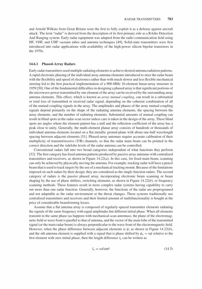
JWBS064-c14 JWBS064-Gerbennikov March 12, 2011 8:44 Printer Name: Yet to Come
RADAR TRANSMITTERS 783
and Arnold Wilkins from Great Britain were the first to fully exploit it as a defense against aircraftattack. The term “radar” is derived from the description of its first primary role as a RAdio DetectionAnd Ranging system. Early radar equipment was adapted from the radio communication field usingHF, VHF, and UHF vacuum tubes and antenna techniques [49]. Solid-state transmitters were firstintroduced into radar applications with availability of the high-power silicon bipolar transistors inthe 1970s.
14.6.1 Phased-Array Radars
Early radar transmitters used multiple radiating elements to achieve desired antenna radiation patterns.A rapid electronic phasing of the individual array antenna elements introduced to steer the radar beamwith the flexibility and speed of electronics rather than with much slower and less flexible mechanicalsteering led to the first practical implementation of a 900-MHz 16-element linear-array structure in1959 [50]. One of the fundamental difficulties in designing a phased array is that significant portions ofthe microwave power transmitted by one element of the array can be received by the surrounding arrayantenna elements. This effect, which is known as array mutual coupling, can result in a substantialor total loss of transmitted or received radar signal, depending on the coherent combination of allof the mutual-coupling signals in the array. The amplitudes and phases of the array mutual-couplingsignals depend primarily on the shape of the radiating antenna elements, the spacing between thearray elements, and the number of radiating elements. Substantial amounts of mutual coupling canresult in blind spots in the radar-scan sector unless care is taken in the design of the array. These blindspots are angles where the element pattern has a null and the reflection coefficient of the array has apeak close to unity. Generally, the multi-element planar array consists of hundreds or thousands ofindividual antenna elements located on a flat metallic ground-plane with about one-half wavelengthspacing between adjacent elements [51]. Phased-array antennas require accurate calibration of theirmultiplicity of transmit/receive (T/R) channels, so that the radar main beam can be pointed in thecorrect direction and the sidelobe levels of the radar antenna can be controlled.
Conventional radars fall into two broad categories independent of what functions they perform[52]. The first category has fixed antenna patterns produced by passive array antennas with centralizedtransmitters and receivers, as shown in Figure 14.22(a). In this case, for fixed main beam, scanningcan only be achieved by physically moving the antenna. For example, tracking radar will have a pencilbeam that is used to track targets by the use of a mechanical tracking mount. Because of the limitationsimposed on such radars by their design, they are considered as the single-function radars. The secondcategory of radars is the passive phased array, incorporating electronic beam scanning or beamshaping by the use of phase shifters, switching elements, as shown in Figure 14.22(b), or frequencyscanning methods. These features result in more complex radar systems having capability to carryout more than one radar function. Generally, however, the functions of the radar are preprogramedand not adaptable as the radar environment or the threat changes. These systems traditionally usecentralized transmitters and receivers and their limited amount of multifunctionality is bought at theprice of considerable beamforming losses.
Assume that a flat antenna array is composed of regularly-spaced transmitter elements radiatingthe signals of the same frequency with equal amplitudes but different initial phase. When all elementstransmit in the same phase (as happens with mechanical-scan antennas), the plane of the electromag-netic field or wave front is parallel to that of antenna, and the vector of the main lobe of the transmittedsignal (or the main radar beam) is always perpendicular to the wave front of the electromagnetic field.However, when the phase difference between adjacent elements is φ, as shown in Figure 14.22(b),and the nth antenna element is supplied with a signal that is phase shifted by φn = nφ relative to thefirst element with zero initial phase, then the length difference ln can be written as
ln = ndsinθ (14.5)
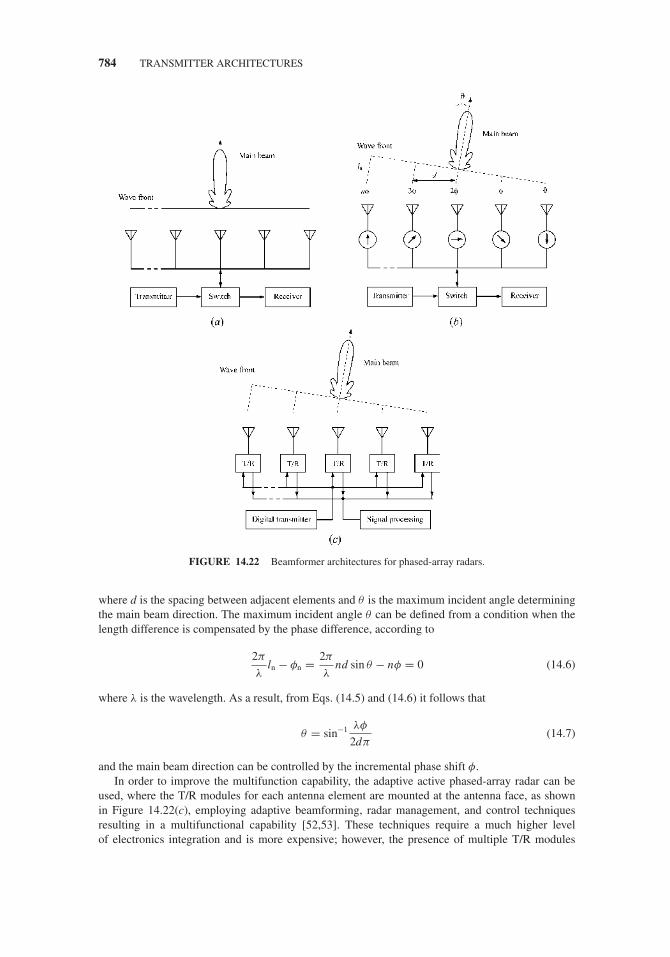
JWBS064-c14 JWBS064-Gerbennikov March 12, 2011 8:44 Printer Name: Yet to Come
784 TRANSMITTER ARCHITECTURES
FIGURE 14.22 Beamformer architectures for phased-array radars.
where d is the spacing between adjacent elements and θ is the maximum incident angle determiningthe main beam direction. The maximum incident angle θ can be defined from a condition when thelength difference is compensated by the phase difference, according to
2π
λln − φn = 2π
λnd sin θ − nφ = 0 (14.6)
where λ is the wavelength. As a result, from Eqs. (14.5) and (14.6) it follows that
θ = sin−1 λφ
2dπ(14.7)
and the main beam direction can be controlled by the incremental phase shift φ.In order to improve the multifunction capability, the adaptive active phased-array radar can be
used, where the T/R modules for each antenna element are mounted at the antenna face, as shownin Figure 14.22(c), employing adaptive beamforming, radar management, and control techniquesresulting in a multifunctional capability [52,53]. These techniques require a much higher levelof electronics integration and is more expensive; however, the presence of multiple T/R modules
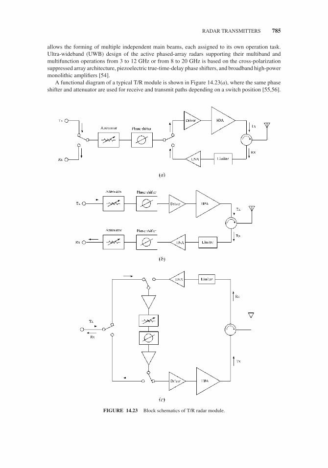
JWBS064-c14 JWBS064-Gerbennikov March 12, 2011 8:44 Printer Name: Yet to Come
RADAR TRANSMITTERS 785
allows the forming of multiple independent main beams, each assigned to its own operation task.Ultra-wideband (UWB) design of the active phased-array radars supporting their multiband andmultifunction operations from 3 to 12 GHz or from 8 to 20 GHz is based on the cross-polarizationsuppressed array architecture, piezoelectric true-time-delay phase shifters, and broadband high-powermonolithic amplifiers [54].
A functional diagram of a typical T/R module is shown in Figure 14.23(a), where the same phaseshifter and attenuator are used for receive and transmit paths depending on a switch position [55,56].
FIGURE 14.23 Block schematics of T/R radar module.

JWBS064-c14 JWBS064-Gerbennikov March 12, 2011 8:44 Printer Name: Yet to Come
786 TRANSMITTER ARCHITECTURES
In transmit mode, an RF signal is phase-shifted and amplitude adjusted at each module to producethe desired radiated beam. This signal is then amplified by approximately 50 dB by driver and HPAand finally routed through circulator operating as a duplexer to the radiating antenna element. Toimprove efficiency of an L-band T/R module, an HPA can be designed based on a high-efficiencyswitched-mode Class E or Class F mode [57]. The circulator provides isolation for the receiver, aswell as VSWR protection for the PA. Alternative T/R module architectures result from the possibilityto improve either cost or performance of the module. Figure 14.23(b) shows the configuration wherethe transmitter and receiver are totally isolated except through the duplexer. Since there are noT/R switches, the dead time required to switch between transmit and receive paths is minimized,with a resulting improvement in radar efficiency. However, separate phase shifter and attenuator fortransmit and receive paths are required, thus making such a T/R module configuration more expensive.Figure 14.23(c) shows another configuration with reduced number of components where the phaseshifter and attenuator are shared between the transmit path and the receive path. However, in thisconfiguration, since the transmit and receive signals flow in the same direction through the phaseshifter and attenuator, it becomes possible to use common amplifying stages, thus further reducingthe overall number of components. Some disadvantage of this architecture is an increased number ofswitches, timing complexity, and the potential for oscillations caused by signal leakage.
The packaging technology for a high-power X-band T/R module can be based on either lowtemperature co-fired ceramic (LTCC) or multi-chip-module (MCM) structure [58,59]. For example, a6-bit phase shifter and a 5-bit attenuator using p—i–n diodes and implemented in a SiGe technologycan represent separate MMICs [60]. The single-chip phase shifter with six digital bits of 180◦, 90◦,45◦, 22.5◦, 11.25◦, and 5.625◦, cascaded in a linear arrangement, provides 64 phase states between0 and 360◦ in increments of 5.625◦. A 5-bit two-chip attenuator consists of 1-, 2-, 4-, 8-, and16-dB attenuation bits and is divided into two cascadable designs, when a 3-bit attenuator and a 2-bitattenuator to be used are interdispersed between amplifier gain stages.
Figure 14.24 shows the circuit solution for an X-band radar GaAs MMIC chipset based on amultifunction-self-aligned-gate (MSAG) MESFET process that provides an output power of about10 W in a frequency range from 8 to 11 GHz [61]. In this process, which does not use air bridges andprovides multilevel plating capability, the active devices use 0.4-μm gates deposited by employinglow-cost optical lithography. The digital 5-bit attenuator (32 steps with 0.75 dB), 6-bit phase shifter(64 steps with 5.6◦), and buffer amplifier are incorporated in a single chip and fully matched to 50 �
on both the input and the output. High power-added efficiency of the PA over 40% can be achievedusing a 0.35-μm pHEMT or 0.25-μm GaN HEMT technology [62,63]. Typically, the HPA consists oftwo amplifying stages where the first stage is composed of 4 unit cells and the final stage is composedof 8 or 16 unit cells that are matched and connected in parallel in pairs using quarter-wavelengthmicrostrip lines. The broadband Ka-band GaN HEMT MMIC PA can provide an output power ofmore than 2 W with a power gain of 13 ± 1 dB across the bandwidth from 26 to 36 GHz [64]. At35 GHz, the measured saturated output power was 36 dBm with a power-added efficiency of 23%.
14.6.2 Automotive Radars
Automotive radars have found a great interest for comfort and safety applications in car industry.Long-range radars for applications including adaptive cruise control (ACC), collision avoidance,and pedestrian detection use the frequency band from 76 to 77 GHz, while the frequency bandfrom 77 to 81 GHz has been allocated for short-range applications such as blind spot monitoring,lane departure warning, and parking aid [65,66]. Recent advances in a SiGe HBT technology (withdevice f max of over 300 GHz, good noise figure, and high breakdown voltage) enable the realization of77-GHz radar systems using silicon technology. At the same time, popular CMOS technology is beingadvanced rapidly and its applications are now expanding into the millimeter-wave region allowingthe transceiver chip for 77-GHz automotive radar to be designed in 90-nm CMOS [67]. As a result,the reduced semiconductor cost, together with packaging and system optimization, will ultimatelyallow deployment of these systems in economy car models.

JWBS064-c14 JWBS064-Gerbennikov March 12, 2011 8:44 Printer Name: Yet to Come
RADAR TRANSMITTERS 787
X-Band Radar GaAs MMIC Chipset
MASWGM0002-DIE
Non-reflective SPDTTTL/CMOS control
LNA
Limiter
HPA Driver Amp
Digitalattenuator
Digital controlSerial to parallel converter
Phaseshifter
6-bit phasor5-bit attenuator
18 dB max. gain
Tx in
Rx out
MA03501D
MA01502D
MA08509D
MAAPGM0034-DIE
MAAPGM0039-DIE10 W @ 10 V
1 W, 15 dB gain
0.5 W, 15 dB gain
MA01503D
14 dB gain
20 dB gain
2.5 dB NF10 W CW integrated limiter
MA03503D
FIGURE 14.24 X-band radar GaAs MMIC chipset (courtesy of Inder Bahl, Cobham) [61].
Generally, the basic radar module for a single-beam configuration that can be adapted to multiple-beam operation represents either the monostatic configuration with duplexing between T/R signalsat the single antenna, as shown in Figure 14.25(a) [68,69], or the bistatic configuration with separateantennas for transmitter and receiver, as shown in Figure 14.25(b) [67,70]. If the target has a velocitycomponent along the line-of-site of the radar, the returned signal will be shifted in frequency relativeto the transmitted frequency due to the Doppler effect. If the transmitted frequency is f 0 and the targetvelocity is v, then the shift in frequency, or Doppler frequency, will be f D = 2vf 0/c, where c is thevelocity of light. In this case, the received frequency is then f 0 ± f D, where the plus sign correspondsto an approaching target and the minus sign corresponds to a receiving target.
In terms of integration, a 77-GHz four-element phased-array transceiver system, in which abeamforming capability is achieved by varying the relative phase shifts in each element, can beimplemented in a single chip with on-chip antennas [71]. To effectively linearize the VCO tuningcharacteristic and significantly reduce the VCO phase noise, the PLL can be used to obtain linear FMramp required to achieve fine target resolution [70,72]. A reconfigurable single-chip T/R structurecan be used as the basic building block for a complete four-channel T/R chip, which allows theimplementation of the MIMO radar [73]. Its main difference compared to the conventional radar isthe capability of transmitting different signals on multiple Tx antennas while keeping these signalsseparable at reception. In this case, the target can be illuminated from different directions and thenumber of resolvable targets can be increased in the same direction by improving angular resolution.
Typical monostatic automotive radar front-end module including an oscillator, a frequency di-vider, a PA, and a differential (or quadrature) hybrid combiner, whose block schematic is shown in

JWBS064-c14 JWBS064-Gerbennikov March 12, 2011 8:44 Printer Name: Yet to Come
788 TRANSMITTER ARCHITECTURES
FIGURE 14.25 Block schematic of monostatic and bistatic radar front-ends.
Figure 14.25(a), uses a single antenna to reduce the overall size of the radar system. However, thelarge leakage signal from transmitter due to the low isolation of the antenna circulator (or hybridcoupler) or the reflection from the antenna can significantly reduce the sensitivity of the receiver,and even saturate the receiver components, so that the dynamic range of the receiver is reduced. Forexample, the isolation of the branch-line hybrid coupler at these frequencies is about 20 dB. To cancelTx leakage due to poor isolation between antenna and isolated ports of the hybrid, the balanced radartopology can be used that includes an out-of-phase divider and a PA to supply the two Lange couplerswith two equal-amplitude and anti-phase signals, as shown in Figure 14.26 [74]. The coupled port ofthe first Lange coupler is connected to the antenna that is matched to 50 �; however, the coupled portof the second Lange coupler is terminated with 50-� load. The isolated ports of both Lange couplersare combined with an in-phase Wilkinson combiner. As a result, Tx leakage signals are canceledout at the output of the Wilkinson combiner because they are balanced and 180◦ out of phase at itsinput ports.
However, such an automotive radar system is not very efficient since only half an output powerflows to the antenna, whereas the other half flows to the ballast resistor of the output hybrid. Besides,half of the received signal power is dissipated too. In this case, a Tx leakage canceller can beintroduced using four branch-line hybrid couplers, a 90◦ microstrip delay line, and a Wilkinson divider[75,76]. Highly efficient differential radar system, whose block schematic is shown in Figure 14.27,incorporates three differential couplers (rat-race hybrids) with three antennas for transmit and receivesignals and two mixers [77]. The two transmitting 180◦ out-of-phase signals initially flow to theleft-hand side and right-hand side rat-races where they split into two equal-amplitude signals, onehalves flowing to the corresponding left-line and right-line antennas, respectively, and the other halvesflowing to the central rat-race from the corresponding output ports of side hybrids, thus resultingin a two times greater power transmission to the central antenna, which is responsible for the frontline. No power is flowing to the ballast resistor of the central rat-race hybrid. Generally, there is nopower loss in such a radar system except due to certain insertion losses of the hybrids. The receivingsignals from the left-line and right-line antennas flow to left-hand side and right-hand side hybridsand mixers, respectively, but not to the central rat-race. The corresponding mixer provides signal

JWBS064-c14 JWBS064-Gerbennikov March 12, 2011 8:44 Printer Name: Yet to Come
RADAR TRANSMITTERS 789
FIGURE 14.26 Balanced automotive radar topology.
detection from the corresponding side. However, the receiving signal flowing to the central rat-raceis divided into two parts flowing to the left-side and right-side rat-races, respectively. This means thatfor a front-line signal, both mixers provide the signal detection simultaneously.
An offset-loop architecture for a frequency modulated continuous wave (FMCW) radar transmitteroptimized for low-phase noise and high-sweep bandwidth is shown in Figure 14.28, where a down-converter is based on a dielectric resonator oscillator (DRO) in conjunction with low division factorand a direct digital synthesizer (DDS) acting as a reference clock is used to generate the frequencyramp [78]. In this case, the overall division value is composed of the divider ratio N = 4 between theVCO and downconverter and N = 16 after the downconverter, thus providing wideband frequencysweeps using only quite a narrow frequency range generated from DDS, where spurious levels at theDDS output are sufficiently low. With a fully integrated dual-band PLL-based frequency synthesizer,the operation in the 22–29 GHz and 77–81 GHz short-range automotive radar bands can be provided[79]. Such a synthesizer consists of two VCOs, one for each radar band, whose outputs are multi-plexed into the input of an injection-locked circuit that acts as a divide-by-three circuit for higherband and as a tuned buffer for lower band. The 79-GHz VCO represents the modified differentialColpitts oscillator, with an LC degeneration technique, and the 24-GHz VCO is a cross-coupled LCoscillator with the tank formed by a spiral inductor and MOS varactors.
One of the important issues in a millimeter-wave PA design is to achieve its high operatingefficiency at maximum output power, since generally it is difficult to achieve high efficiency at thesefrequencies taking into account significant effect of grounding parasitics and component losses. Forexample, by using a 0.12-μm SiGe BiCMOS process with f max = 200 GHz, the single-ended PAachieves an output power of 17.5 dBm with a power-added efficiency (PAE) of 12.8% at 77 GHz [80].In this case, four stages in a common emitter configuration are biased in Class AB mode where the last
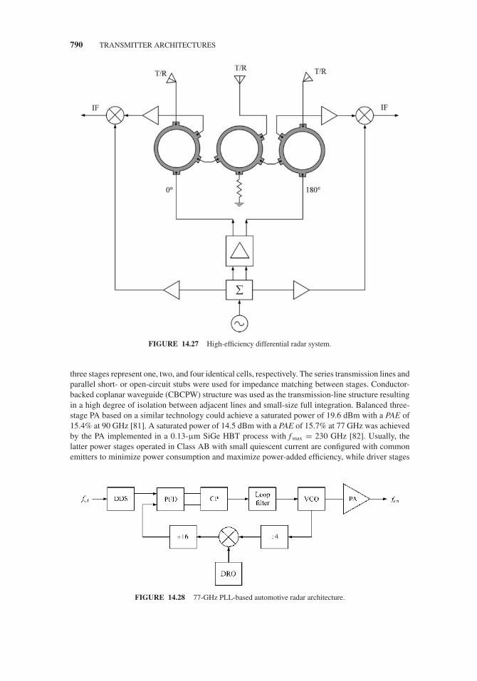
JWBS064-c14 JWBS064-Gerbennikov March 12, 2011 8:44 Printer Name: Yet to Come
790 TRANSMITTER ARCHITECTURES
FIGURE 14.27 High-efficiency differential radar system.
three stages represent one, two, and four identical cells, respectively. The series transmission lines andparallel short- or open-circuit stubs were used for impedance matching between stages. Conductor-backed coplanar waveguide (CBCPW) structure was used as the transmission-line structure resultingin a high degree of isolation between adjacent lines and small-size full integration. Balanced three-stage PA based on a similar technology could achieve a saturated power of 19.6 dBm with a PAE of15.4% at 90 GHz [81]. A saturated power of 14.5 dBm with a PAE of 15.7% at 77 GHz was achievedby the PA implemented in a 0.13-μm SiGe HBT process with f max = 230 GHz [82]. Usually, thelatter power stages operated in Class AB with small quiescent current are configured with commonemitters to minimize power consumption and maximize power-added efficiency, while driver stages
FIGURE 14.28 77-GHz PLL-based automotive radar architecture.

JWBS064-c14 JWBS064-Gerbennikov March 12, 2011 8:44 Printer Name: Yet to Come
RADAR TRANSMITTERS 791
can be designed in a cascode configuration. High breakdown voltage of over 50 V to design a reliable76-GHz PA can be realized with a 0.15-μm GaN FET process having f max = 160 GHz [83].
14.6.3 Electronic Warfare
Electronic warfare (EW) techniques were initiated during the World War II as radio countermeasureswhen signal analysis was used to identify the frequencies of enemy systems such as communication,radar, and airborne navigation equipments, which were subsequently disabled with passive counter-measures such as chaff or active noise jamming techniques [84]. Passive countermeasures representmethods to reduce the probability that a target will be detected by the radar, or to present false targetsto the radar, and do not involve the emission of any targets and noise. Active countermeasures arebased on the radiation of a signal to confuse or deceive the radar or communication system, andgenerally take the form of jammers. A noise jammer radiates a relatively large power in the operatingband of the radar to mask the true target return, or to overload the receiver front-end. There are threebasic subsets of the overall discipline of EW such as electronic support measures (ESM), electroniccountermeasures (ECM), and electronic counter-countermeasures (ECCM). ESM is based on the useof intercept or warning receivers when actions are taken to search for, intercept, locate, and analyzeradiated electromagnetic energy. ECM includes passive and active techniques such as jamming anddeception, when actions are taken to prevent or reduce the enemy’s use of the electromagnetic spec-trum, overload or saturate the data processing of threat systems, and introduce false deceptive data intohostile electronic systems. Since a jamming transmitter may be vulnerable to lethal countermeasures,prudent ECM operational procedures require detection and identification of a target signal before ajamming signal is transmitted. ECCM includes a coding technique that spreads the signal energy overa wide bandwidth to minimize the effect of enemy jamming and interference.
The most common techniques for spreading the signal spectrum are to employ frequency-agiletransmissions, either in discrete steps, frequency hopping (FH), or to use a continuously swept FMor phase-shift keying (PSK) of the carrier oscillator. FM is employed in pulsed radar where a linearswept chirp waveform is transmitted and a weighted matched filter is incorporated into the receiver todetect the return echo. FH and PSK, both under control of a pseudo-noise (PN) code, represent twobasic modulation techniques for generating the spread-spectrum waveform. Direct-sequence spreadspectrum is widely used in satellite communication and navigation systems, where a continuous PNspreading code is modulo-two added with data prior to keying the carrier. FH offers a much flattertransmitted spectrum than PSK or MSK and, for a given RF bandwidth, the FH dwell time is muchlonger than the equivalent PSK interval. This reduces the PN-code rate with a potential easing ofsynchronization acquisition in the FH systems. A key advantage of FH is that multiple-access signalsin other frequency slots are theoretically non-interfering, regardless of the relative signal strength.
Many EW systems require a high performance front-end covering all or part of the 2–18 GHzband with stringent requirements on the size, weight, power consumption, and reliability. An effectivemethod of meeting all these requirements is to make extensive use of MMICs to allow packagingof major sections of the front-end using a small number of MMIC modules [85]. In this case, theexcellent balance and reduced parasitics can minimize the level of spurious products and LO leakage inmixers. In the development of high-frequency VCOs, wider tuning bandwidths can be achieved usingMMIC technology due to the elimination of critical bondwire parasitics. In modern ECM systems,VCOs serve as the frequency-agile local oscillators in receiver subsystems and fast-modulation noisesources in active jamming subsystems. Among wideband tunable signal sources such as YIG-tunedoscillators, wideband VCOs using hyperabrupt varactors are preferable because of their small size,low weight, high settling time speed, and capability of fully monolithic integration. Figure 14.29(a)illustrates the use of a hyperabrupt VCO as a local oscillator in the receiver system, while a blockdiagram of an active jamming system using a hyperabrupt VCO as the microwave power source isshown in Figure 14.29(b) [86]. In both system applications, the hyperabrupt VCO must exhibit thelinear voltage-frequency characteristic, minimum tuning slope variation, low post-tuning drift, fastsettling time, and low voltage bias range to allow direct integration with high-speed digital-to-analog
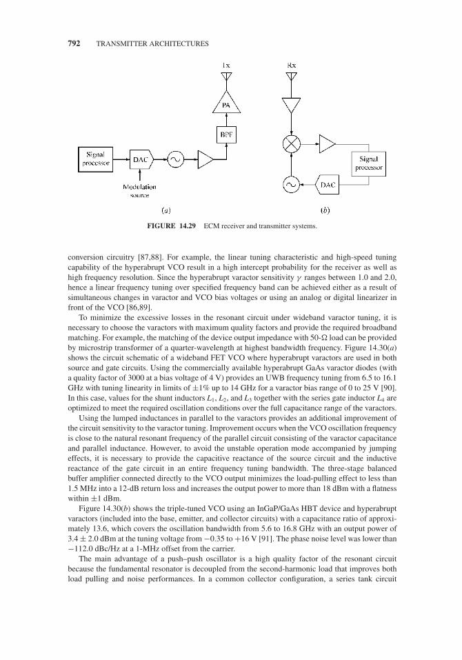
JWBS064-c14 JWBS064-Gerbennikov March 12, 2011 8:44 Printer Name: Yet to Come
792 TRANSMITTER ARCHITECTURES
FIGURE 14.29 ECM receiver and transmitter systems.
conversion circuitry [87,88]. For example, the linear tuning characteristic and high-speed tuningcapability of the hyperabrupt VCO result in a high intercept probability for the receiver as well ashigh frequency resolution. Since the hyperabrupt varactor sensitivity γ ranges between 1.0 and 2.0,hence a linear frequency tuning over specified frequency band can be achieved either as a result ofsimultaneous changes in varactor and VCO bias voltages or using an analog or digital linearizer infront of the VCO [86,89].
To minimize the excessive losses in the resonant circuit under wideband varactor tuning, it isnecessary to choose the varactors with maximum quality factors and provide the required broadbandmatching. For example, the matching of the device output impedance with 50-� load can be providedby microstrip transformer of a quarter-wavelength at highest bandwidth frequency. Figure 14.30(a)shows the circuit schematic of a wideband FET VCO where hyperabrupt varactors are used in bothsource and gate circuits. Using the commercially available hyperabrupt GaAs varactor diodes (witha quality factor of 3000 at a bias voltage of 4 V) provides an UWB frequency tuning from 6.5 to 16.1GHz with tuning linearity in limits of ±1% up to 14 GHz for a varactor bias range of 0 to 25 V [90].In this case, values for the shunt inductors L1, L2, and L3 together with the series gate inductor L4 areoptimized to meet the required oscillation conditions over the full capacitance range of the varactors.
Using the lumped inductances in parallel to the varactors provides an additional improvement ofthe circuit sensitivity to the varactor tuning. Improvement occurs when the VCO oscillation frequencyis close to the natural resonant frequency of the parallel circuit consisting of the varactor capacitanceand parallel inductance. However, to avoid the unstable operation mode accompanied by jumpingeffects, it is necessary to provide the capacitive reactance of the source circuit and the inductivereactance of the gate circuit in an entire frequency tuning bandwidth. The three-stage balancedbuffer amplifier connected directly to the VCO output minimizes the load-pulling effect to less than1.5 MHz into a 12-dB return loss and increases the output power to more than 18 dBm with a flatnesswithin ±1 dBm.
Figure 14.30(b) shows the triple-tuned VCO using an InGaP/GaAs HBT device and hyperabruptvaractors (included into the base, emitter, and collector circuits) with a capacitance ratio of approxi-mately 13.6, which covers the oscillation bandwidth from 5.6 to 16.8 GHz with an output power of3.4 ± 2.0 dBm at the tuning voltage from −0.35 to +16 V [91]. The phase noise level was lower than−112.0 dBc/Hz at a 1-MHz offset from the carrier.
The main advantage of a push–push oscillator is a high quality factor of the resonant circuitbecause the fundamental resonator is decoupled from the second-harmonic load that improves bothload pulling and noise performances. In a common collector configuration, a series tank circuit

JWBS064-c14 JWBS064-Gerbennikov March 12, 2011 8:44 Printer Name: Yet to Come
RADAR TRANSMITTERS 793
FIGURE 14.30 Microwave monolithic very wideband VCO circuits.
connected between the device bases can be used. The overall resonant circuit includes also transistorcollector–base capacitances, varactor capacitances, and bond wire inductances. In this case, the loadcan be connected conductively to the center point of the resonant-circuit inductor, as shown inFigure 14.31, where odd-harmonic cancelation can be provided. For symmetrical parts in the oddoperation mode, this center point becomes a virtual ground. Such a push–push VCO enables to providevery wideband varactor tuning over a frequency range from 6.94 to 19.22 GHz with the fundamental
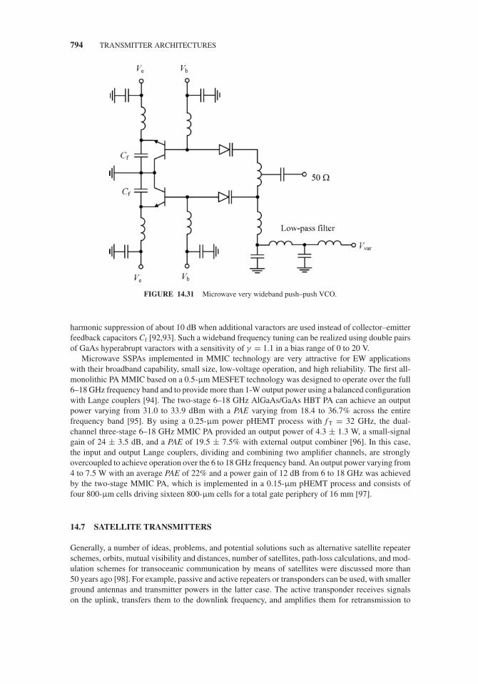
JWBS064-c14 JWBS064-Gerbennikov March 12, 2011 8:44 Printer Name: Yet to Come
794 TRANSMITTER ARCHITECTURES
FIGURE 14.31 Microwave very wideband push–push VCO.
harmonic suppression of about 10 dB when additional varactors are used instead of collector–emitterfeedback capacitors Cf [92,93]. Such a wideband frequency tuning can be realized using double pairsof GaAs hyperabrupt varactors with a sensitivity of γ = 1.1 in a bias range of 0 to 20 V.
Microwave SSPAs implemented in MMIC technology are very attractive for EW applicationswith their broadband capability, small size, low-voltage operation, and high reliability. The first all-monolithic PA MMIC based on a 0.5-μm MESFET technology was designed to operate over the full6–18 GHz frequency band and to provide more than 1-W output power using a balanced configurationwith Lange couplers [94]. The two-stage 6–18 GHz AlGaAs/GaAs HBT PA can achieve an outputpower varying from 31.0 to 33.9 dBm with a PAE varying from 18.4 to 36.7% across the entirefrequency band [95]. By using a 0.25-μm power pHEMT process with f T = 32 GHz, the dual-channel three-stage 6–18 GHz MMIC PA provided an output power of 4.3 ± 1.3 W, a small-signalgain of 24 ± 3.5 dB, and a PAE of 19.5 ± 7.5% with external output combiner [96]. In this case,the input and output Lange couplers, dividing and combining two amplifier channels, are stronglyovercoupled to achieve operation over the 6 to 18 GHz frequency band. An output power varying from4 to 7.5 W with an average PAE of 22% and a power gain of 12 dB from 6 to 18 GHz was achievedby the two-stage MMIC PA, which is implemented in a 0.15-μm pHEMT process and consists offour 800-μm cells driving sixteen 800-μm cells for a total gate periphery of 16 mm [97].
14.7 SATELLITE TRANSMITTERS
Generally, a number of ideas, problems, and potential solutions such as alternative satellite repeaterschemes, orbits, mutual visibility and distances, number of satellites, path-loss calculations, and mod-ulation schemes for transoceanic communication by means of satellites were discussed more than50 years ago [98]. For example, passive and active repeaters or transponders can be used, with smallerground antennas and transmitter powers in the latter case. The active transponder receives signalson the uplink, transfers them to the downlink frequency, and amplifies them for retransmission to

JWBS064-c14 JWBS064-Gerbennikov March 12, 2011 8:44 Printer Name: Yet to Come
SATELLITE TRANSMITTERS 795
earth. In July 1962, the orbiting Telstar active satellite having a 6-GHz uplink and a 4-GHz downlinkwith transmitter power of 2.25 W was used for TV transmission, as well as for demonstrations oftelephony between American and European cities [99]. Due to demand in wider frequency range andmore information capacity, satellite communications have moved from C-band (6/4 GHz) to Ku-band(14/11 GHz) and then to Ka-band (30/20 GHz) frequencies [100]. The potential market for mobilecommunications provided by satellite systems has resulted in the development of a range of opera-tional systems and conceptual designs, from conventional geosynchronous orbit (GEO) systems tothe low earth orbit (LEO) systems [101]. To further improve the performance of high data-rate com-munication links, millimeter-wave frequencies were considered to use for wireless communicationsthrough satellites. However, such effects as atmospheric attenuation and rain absorption increase thechannel noise temperature and limit the channel capacity. In this case, the phased-array techniquerepresents a practical solution to compensate for these propagation impairments, since a highly di-rective antenna array improves the signal-to-noise ratio significantly, thus correspondingly increasingchannel capacity. For example, a 16-element phased-array transmitter in a standard 0.18-μm SiGeBiCMOS technology based on 4-bit active phase shifters results in a 12.5 dB of average power gainper channel at 42.5 GHz [102].
Efficient use of communication channels can be achieved through multiple access techniques suchas FDMA, which allows more than one earth station to share the bandwidth of a satellite transponderwhen each earth station is assigned to a specific carrier or set of carriers for signal transmission over acertain frequency bandwidth; TDMA, which is used to provide more than one earth station with accessto the same carrier by dividing the transmitting signal into different time slots; and CDMA as a spread-spectrum access technique, in which every earth station may transmit at the same frequency and at thesame time when each earth station uses a unique identifying code modulated with the communicationsignal. In TDMA system, the satellite transponder can operate at saturation, while output backoffof the satellite transponder in an SCPC (single channel per carrier) FDMA system is necessary toreduce intermodulation distortion [103]. The advantage of using FDMA in a wideband frequencytransponder is that it allows the simplest ground station configuration requiring no timing by the user,whereas TDMA requires that the earth station complex be synchronized to a high degree of precisionand be capable of high peak power transmission. The TDMA modulation equipment can providea transmission rate of 60 Mb/s and overall capacity of 19 full-duplex 1.544-Mb/s signal channelsper transponder, or the equivalent of 456 full-duplex voice-grade channels [104]. CDMA is usuallydivided into two subclasses: frequency hopping and direct sequence. In the former, a user imposesa preselected frequency hopping sequence on his normal transmission so that mutual interferencebetween two such users occurs only when they are hopped to the same frequency at the same time.In the latter, the transmission is characterized by a phase-modulated carrier with a total bandwidthoccupancy much wider than the information bandwidth. The data are added to the multiple-accesscarrier as either frequency or phase modulation. A PN code is used to spread the spectrum and istypically a maximal length shift register code [105]. The degree of mutual interference between twosuch users is determined by the cross correlation between the PN codes of two users.
The first completely solid-state transmitter intended for missile and satellite applications to operateas a PPM (pulse position modulation) telemetry transmitter was based on transistor PA stages witha varactor tripler and provided a peak power of 30 W at 234 MHz [106]. Further advances in com-munications satellite technology have led to the development of different systems that can transmitvarious kinds of communication signals. In a domestic satellite communications system accommo-dating numerous small earth stations, it is important that the small earth station equipment remainsinexpensive in order to make the system economical. In this case, each station uses a high power FETamplifier, whose output peak power is about 2 W per voice channel, and a low-noise FET amplifier,whose noise temperature is less than 90 K [103]. When more than two voice channels are transmitted,signals are multiplexed using orthogonal carriers in order to keep the transmitting peak power low.These carriers are modulated by different PN codes and amplified simultaneously by a high PA.
Figure 14.32(a) shows the typical block schematic of a 6/4 GHz satellite transponder performingthe function of a low-noise amplification of the 6-GHz receiving signal, its upconversion to 4-GHz

JWBS064-c14 JWBS064-Gerbennikov March 12, 2011 8:44 Printer Name: Yet to Come
796 TRANSMITTER ARCHITECTURES
FIGURE 14.32 Block schematics of satellite transponder.
band, and further channel power amplification (with channel bandwidth up to 35–40 MHz) and outputfiltering. Channelization of communication frequencies after receiver processing and recombinationof channels after high-power amplification are provided by input and output multiplexers, respec-tively. Both input and output multiplexers employ a multiplicity of high-selectivity channel BPFsin combination with an input distribution network and output manifold. Significant achievementsin dielectric resonator technology, resulting in dielectric materials of superior stability and reducedloss, have produced filter designs of reduced size, volume, and weight. Due to frequency bandwidthand filter selectivity limitations, the Ka-band 30/20 GHz satellite transponders can be designed using30–12 GHz downconverter and 12–20 GHz upconverter when the intermediate channel amplificationis provided in a 12-GHz band [107]. The block schematic of a channel PA is shown in Figure 14.32(b),where the amplitude and phase corrector is necessary to linearize the signal amplitude characteristicand to make the signal phase independent of its amplitude. To provide transmitter stable operationwith an HPA and sufficient isolation from the other transmitting channel, the circulator operating asan isolator is included at the output of the PA. The output directional coupler is used to measure thelevels of incident and reflected powers.
The development of SSPA technology in the late 1970s and early 1980s created a viable alternativeto the traveling-wave tube amplifiers (TWTA) to design a channel PA for most C-band applications.SSPA designs have utilized power GaAs FETs that became available and space-qualified during thatperiod. As a result, a C-band GaAs FET PA could deliver a high output power of 70 W with a highefficiency of more than 50% under 10-V operation at 3.8 GHz, representing a packaged internallymatched amplifier with four 35-mm-gate-width heterostructure FETs [108]. A Ku-Band GaAs FETSSPA, consisting of four 8-W internally matched power FETs and using a spatial power combiner,demonstrated a 30-W output power across the band of 14.0 to 14.5 GHz with 11% efficiency [109].By using a 0.35-μm GaAs pHEMT process, a monolithic two-stage SSPA is capable to deliver up to10 W of output power with a PAE of 47% at 11.7 GHz [110]. The MMIC layout, whose dimensionsare 4.7 × 4.0 mm2, is composed of eight power cells in the final amplifying stage and microstripcombining network.

JWBS064-c14 JWBS064-Gerbennikov March 12, 2011 8:44 Printer Name: Yet to Come
ULTRA-WIDEBAND COMMUNICATION TRANSMITTERS 797
FIGURE 14.33 Block diagram of microwave solid-state high-power amplifier.
Recently, the GaN HEMTs have demonstrated superior microwave power performance over GaAswith output powers of 4 W/mm, which is approximately four times higher compared to the GaAspHEMTs at Ku-band [111]. To achieve a very high output power level, the individual PAs are usuallycombined in a packaged hybrid module using Wilkinson dividers/combiners [112,113]. Figure 14.33shows the block diagram of a C-band PA with over 340-W output power at 4.8 GHz using 0.8-μm GaNHEMTS and an X-band PA with over 100-W output power at 9.8 GHz using 0.25-μm GaN HEMTsobtained under the pulsed condition of 10-μs pulse width and 10% duty cycles [113]. In both casesbased on two internally matched GaN HEMT chips and microstrip Wilkinson dividers/combiners,PAE exceed 50%.
14.8 ULTRA-WIDEBAND COMMUNICATION TRANSMITTERS
UWB technology was first proposed for communication systems a long ago [114]. Since then it wasmainly used for radar-based applications because of the wideband nature of the signal that resultsin very accurate timing information. By the early 1970s, the system concept and basic componentssuch as pulse train generators and modulators, detection receivers and wideband antennas wereavailable [115]. However, due to recent developments in high-speed switching and narrowband pulsegeneration technology, UWB has become more attractive for low-cost communications applications,representing now any wireless transmission scheme that occupies a transmission frequency bandwidthof more than 20% of a center frequency, or more than 500 MHz [116]. Such large bandwidths areachieved by using very narrow time-duration baseband pulses of appropriate shape and duration,including the family of Gaussian shaped pulses and their derivatives. Larger transmission bandwidthsare preferred to achieve higher data rates without the need to increase transmitting power, resultingin the ability for increasingly fine resolution for multipath arrivals, which leads to reduced fading perresolved path since the impulsive nature of the transmitted waveforms prevents significant overlapand, hence, reduces possibility of destructive combining. A key advantage of UWB designs is thathighly linear PAs are generally not required because the UWB pulse generator need only to producea peak-to-peak voltage swing on the order of 100 mV to meet spectral mask requirements that can

JWBS064-c14 JWBS064-Gerbennikov March 12, 2011 8:44 Printer Name: Yet to Come
798 TRANSMITTER ARCHITECTURES
be achieved by a suitable UWB waveform choice. The UWB systems are being currently designedfor 110 Mb/s at a 10-m range with four collocated clusters that project to spatial capacity of about1.3 Mb/s/m2. Thus, UWB represents a tradeoff between lower spectral efficiency for increased powerefficiency to achieve a given rate/range operating point with limited transmit power.
In view of UWB pulsed nature with a very sharp rise and fall time for signal transmission, theUWB emissions can potentially interfere with other licensed frequency bands. Therefore, the allowedtransmit power spectral density (PSD) is limited to −41.25 dBm/MHz that corresponds to a theoreticalmaximum total power of −13.9 dBm for a 550-MHz bandwidth signal [117]. The transmitting signalin UWB system can be generally modulated by turning the pulse on and off (OOK), by providingthe binary phase-shift keying (BPSK), or by dithering the pulse position modulation (PPM), or thepulse amplitude modulation (PAM). The pulse may have duration on the order of 200 ps and itsshape can be designed to concentrate energy over the broad frequency range from 2 to 6 GHz,for example. In this case, a BPF is necessary to use before the antenna to constrain the emissionswithin this desired frequency band when the filter would have a bandwidth on the order of 4 GHz.UWB systems can also be designed using spread-spectrum codes, which offer better coexistencewith other UWB systems. The generation of spread-spectrum UWB signals can be achieved usingtime hopping or direct sequence methods. In multiband UWB systems when UWB band from 3.1to 10.6 GHz is divided into 14 subbands with a bandwidth of 528 MHz each, signal transmissionsare staggered in time across the constituent subbands, and one of several (typically 3–10) subbandsare used sequentially for transmission. The requirement for maximum total power consumption of aUWB transceiver set by specification at 110 Mb/s and 200 Mb/s is 100 mW and 250 mW, respectively.
Generally, low-rate and high-rate pulsed UWB transmitters are based on one of two basic tech-niques to synthesize pulses in the 3.1–10.6 GHz band [118]. The upconversion pulse (or directconversion) synthesis technique involves generating a pulse at baseband and upconverting it to centerfrequency in the UWB band by mixing with a local oscillator, whose output can be either enabledor disabled by a simple switch, thus effectively mixing the RF signal with a rectangular basebandpulse. The carrier-less pulse synthesis involves generating pulses that directly fall in the UWB bandwithout requiring frequency translation where the pulse width is usually defined by delay elementsthat may be tunable or fixed. In this case, a baseband impulse may excite a filter that shapes the pulseor the pulse may be directly synthesized at RF with no additional filtering required. An advantage ofcarrier-less techniques over traditional mixed-based architectures is that the carrier frequency genera-tion is inherently duty cycled when RF power is only generated when it is required. However, its maindisadvantage is that an integrated downconverting receiver typically cannot share the RF generationcircuits, and therefore, must have its own local oscillator. Pulse-based transmitters can additionally becategorized in terms of how pulses are delivered to an antenna, either by analog power amplificationor digital buffering. However, in the latter case, linear AM and pulse shaping are more difficult toachieve. Since the direct-conversion UWB transceiver is usually characterized by the large LO leak-age to the RF front-end and to antenna because the local oscillator is operated at the same frequencyas the RF carrier, the dual-conversion zero-IF transceiver architecture with two-step upconversioncan be a suitable alternative [119]. In this case, to reduce the image-rejection problem, which existsin the first conversion, either both local oscillators for channel selection can be variable or an I/Qlocal oscillator is properly fixed at desired frequency according to careful frequency planning.
Figure 14.34(a) shows the generic UWB pulse-based transmitter architecture with a pulse gen-erator followed by a modulator, both driven by a digital baseband. The modulator is then directlyfollowed by a PA to achieve the required power level, a BPF to reduce spurious emission, and a wide-band antenna to radiate pulsed signal. A UWB pulse can be generated by multiplying a sinusoidalsignal with an envelope close to zero-order Gaussian shape with a standard deviation of 341 ps andcentered in 4.1 GHz to spread energy over a 2-GHz bandwidth [120]. The UWB transmitter basedon a 0.18-μm CMOS technology can achieve highest pulse repetition rate of 750 Mb/s with bi-phasemodulated pulses of 500-ps duration and 8-GHz center frequency, operating over the band of 6 to 10GHz and complying with the standard spectrum mask [121]. For a short-range non-coherent com-munication, the transmitter can use an all-digital architecture and calibration technique to synthesizepulses with programmable width and center frequency using a 90-nm CMOS process [122].

JWBS064-c14 JWBS064-Gerbennikov March 12, 2011 8:44 Printer Name: Yet to Come
ULTRA-WIDEBAND COMMUNICATION TRANSMITTERS 799
FIGURE 14.34 UWB transmitter architectures.
Figure 14.34(b) shows a low-power, low-complexity carrier-based multiband UWB transmitterwhere OOK modulation is used for low data rate (∼100 kb/s) applications [123]. The pulse generatorblock is capable of generating triangular-enveloped pulses over three 528-MHz subbands in a 3–5 GHzband using a subband selection function. The modulator consists of the NAND and inverter logiccomponents where one input of a NAND block is the baseband data while the other input is thesquare pulse clock. The clock is provided by the baseband processor with predetermined duration tocontrol the output pulse width to ensure 528-MHz bandwidth for each subband. The input data andclock are combined and the resultant edge-combined square pulse signal drives the pulse generator.As a result, with pulse duration of 3.5 ns, an output pulse spectrum with more than 20 dB of sideloberejection can be achieved satisfying spectral mask without additional filtering. This transmitter beingimplemented in a 0.18-μm CMOS process was designed to operate in a burst mode and dissipatesonly 18 pJ of energy consumption per pulse. For higher amplitudes of transmitted triangular pulses(for example, with a peak voltage of about 2.8 V under a supply voltage of 3.3 V), in order to satisfythe spectral mask limit, especially in the frequency range from 0.96 to 1.61 GHz assigned for GPSsystems, the separate BPF that can represent a single-section coupled-line filter (half-wavelengthtransmission-line resonator) with a tapered stub can be used [124]. With sufficiently low inductancevalues, a third-order Bessel bandpass LC filter structure can be designed on-chip [125].
The new-generation UWB transmitters, whose typical block schematic is shown in Figure 14.34(c),are intended to operate in the 3.1–10.6 GHz band with 100 Mb/s data rate at a link distance of 10 m

JWBS064-c14 JWBS064-Gerbennikov March 12, 2011 8:44 Printer Name: Yet to Come
800 TRANSMITTER ARCHITECTURES
using BPSK modulated pulses at a maximum pulse repetition frequency of 100 MHz [117]. Thetransmitter implemented in a 0.18-μm SiGe BiCMOS process uses a direct-conversion architectureto upconvert a shaped baseband pulse train to one of 14 subbands in the UWB band by modulating thebias current of the differential pair with a carrier frequency. The baseband UWB signal is generatedusing either a programmable arbitrary waveform generator (AWG) or a dedicated discrete pulsegenerator. Using an AWG enables a large amount of flexibility in the shape of the transmitted pulses,modulation scheme, and duration of transmission. The carrier frequency can be generated either byon-chip VCO or from external LO. In the latter case with a 0.13-μm CMOS technology, the frequencyof the external differential input signal from 6 to 22 GHz is divided by the on-chip 2:1 frequencydivider to obtain quadrature LO signals from 3 to 11 GHz to cover 14 bands of the UWB systemat the same time [126]. With the LO input power of 0 dBm, the quadrature upconversion mixer andbalanced PA provide the conversion gain of 1.1 ± 1 dB and power gain of 12.4 ± 2 dB over thefrequency range from 3 to 11 GHz, respectively.
A pulse generation principle for a multiband OOK UWB transmitter with on/off switching of aCMOS oscillator, whose circuit schematic is shown in Figure 14.35, can be based on the switched
FIGURE 14.35 Schematic of three-band OOK UWB pulse generator.
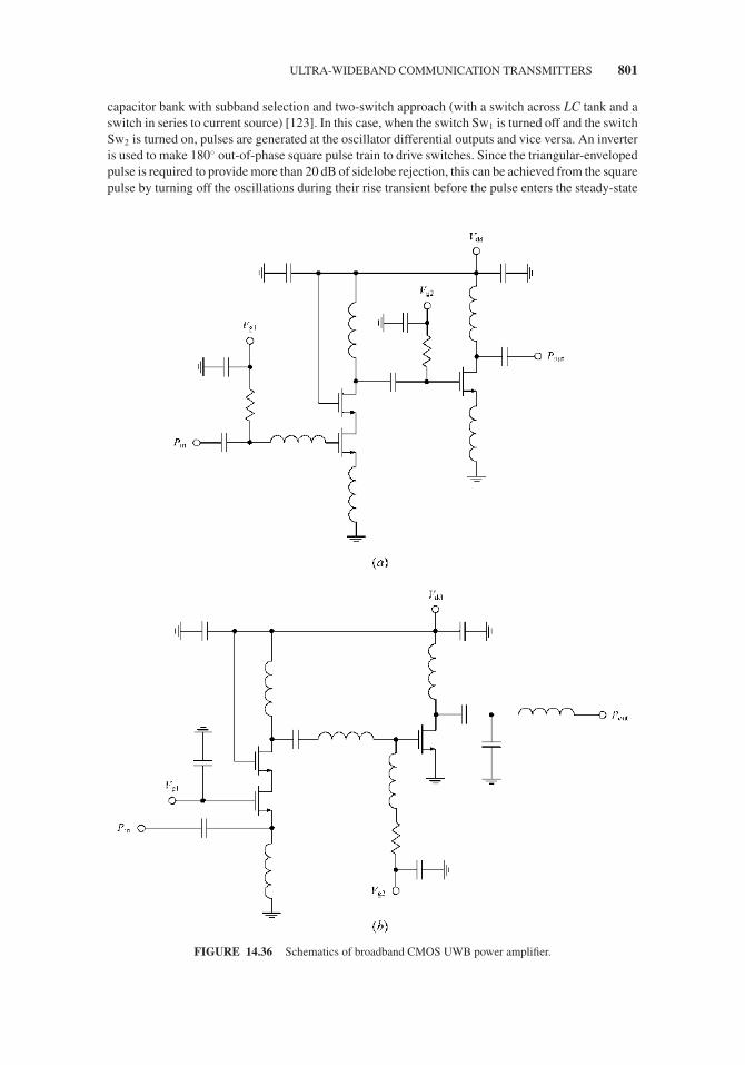
JWBS064-c14 JWBS064-Gerbennikov March 12, 2011 8:44 Printer Name: Yet to Come
ULTRA-WIDEBAND COMMUNICATION TRANSMITTERS 801
capacitor bank with subband selection and two-switch approach (with a switch across LC tank and aswitch in series to current source) [123]. In this case, when the switch Sw1 is turned off and the switchSw2 is turned on, pulses are generated at the oscillator differential outputs and vice versa. An inverteris used to make 180◦ out-of-phase square pulse train to drive switches. Since the triangular-envelopedpulse is required to provide more than 20 dB of sidelobe rejection, this can be achieved from the squarepulse by turning off the oscillations during their rise transient before the pulse enters the steady-state
FIGURE 14.36 Schematics of broadband CMOS UWB power amplifier.

JWBS064-c14 JWBS064-Gerbennikov March 12, 2011 8:44 Printer Name: Yet to Come
802 TRANSMITTER ARCHITECTURES
mode. By changing the capacitor bank values, the pulse center frequency is shifted, and the threesubbands with 528 MHz are centered at 3.2, 3.8, and 4.4 GHz, respectively. In a 0.18-μm SiGeBiCMOS UWB transmitter designed for wireless sensor networks, the VCO switched tank circuitwith three capacitor banks controlled by CMOS switches can provide three 500-MHz subbands atcenter frequencies of 4.6, 6.4, and 8.0 GHz, respectively [127].
The PA in UWB systems should meet several stringent requirements simultaneously such asbroadband matching, high power gain, sufficient output power, and reasonable efficiency for low-power operation. By using the lossy input and output RLC matching networks and two-stage cascodeconfiguration, it is possible to cover a full UWB band from 3.1 to 10.6 GHz with a power gain above6 dB and an output power of around 0 dBm using a 0.18-μm CMOS technology [128]. The outputpower can be increased to more than 5 dBm over a full UWB band using twice as many transistorsin a distributed configuration with a wideband bandpass artificial transmission-line topology [129].Unfortunately, in both cases the efficiency is too low and the power consumption is too high to satisfysuch broadband requirements. However, the PAE can potentially be increased to more than 30% withproper external broadband output matching for a 0.18-μm CMOS PA, whose circuit schematic isshown in Figure 14.36(a) and which is operated in a narrower frequency band from 3 to 5 GHz withan output power over 10 dBm [130]. Here, the source degeneration inductor in the first cascode stageis added for linearity and stability improvement.
Figure 14.36(b) shows the circuit schematic of a 0.18-μm CMOS PA with interstage RLC broad-band impedance matching (including the gate–drain capacitance of the common-gate device and thegate–source capacitance of the common-source device) to provide a flat power gain over a frequencyband from 6 to 10 GHz [131]. In this case, a PAE of about 15% over most of the bandwidth and apower consumption of only 18 mW can be achieved with an output power of about 5 dBm at a supplyvoltage of 1.5 V. To simplify the input matching and provide significant interstage isolation, bothfirst-stage nMOS devices are configured with a common gate.
REFERENCES
1. J. O. Weldon, “Transmitters,” Proc. IRE, vol. 50, pp. 901–906, May 1962.
2. F. H. Raab, R. Caverly, R. Campbell, M. Eron, J. B. Hecht, A. Mediano, D. P. Myer, and J. L. B. Walker, “HF,VHF, and UHF Systems and Technology,” IEEE Trans. Microw. Theory Technol., vol. MTT-50, pp. 888–899,Mar. 2002.
3. H. L. Krauss, C. W. Bostian, and F. H. Raab, Solid State Radio Engineering, New York: John Wiley & Sons,1980.
4. N. F. Schlaack and F. A. Polkinghorn, “An Unattended Ultra-Short-Wave Radiotelephone System,” Proc.IRE, vol. 23, pp. 1275–1285, Nov. 1935.
5. A. Mina, J. O. Weldon, and G. Hulsey, “An Improved High Efficiency 500 Kilowatt Short Wave BroadcastTransmitter with Novel Features,” IEEE Trans. Broadcast., vol. BC-34, pp. 134–136, June 1988.
6. M. Yamazoe, K. Haeiwa, S. Hirose, and K. Wakai, “Considerations for Developing a Highly Efficient,High-Power Shortwave AM Transmitter,” Proc. 1996 IEEE Power Conversion Conf., pp. 1035–1042.
7. F. E. Terman, Electronic and Radio Engineering, New York: McGraw-Hill, 1955.
8. D. Y. Jung, W. I. Chang, and C. S. Park, “A System-on-Package Integration of 60 GHz ASK Transmitter,”Proc. 2006 IEEE Radio and Wireless Conf., pp. 151–154.
9. A. A. Oswald, “Early History of Single-Sideband Transmission,” Proc. IRE, vol. 44, pp. 1672–1679, Dec.1956.
10. J. R. Carson, “Method and Means for Signaling with High Frequency Waves,” U.S. Patent 1,449,382, Mar.1923 (filed Dec. 1915).
11. H. D. Arnold and L. Espenschied, “Transatlantic Radio Telephony,” Trans. AIEE, vol. 42, pp. 718–729,Aug. 1923.
12. A. A. Oswald, “A Short-Wave Single-Side-Band Radiotelephone System,” Proc. IRE, vol. 26, pp. 1431–1454,Dec. 1938.

JWBS064-c14 JWBS064-Gerbennikov March 12, 2011 8:44 Printer Name: Yet to Come
REFERENCES 803
13. J. Wood, “Developments in the Design and Performance of HF Transmitters,” Electronics & Power, vol. 33,pp. 392–396, June 1987.
14. O. G. Willard, “A High-Level Single-Sideband Transmitter,” Proc. IRE, vol. 36, pp. 1419–1425, Nov.1948.
15. L. R. Kahn, “Comparison of Linear Single-Sideband Transmitters with Envelope Elimination and RestorationSingle-Sideband Transmitters,” Proc. IRE, vol. 44, pp. 1706–1712, Dec. 1956.
16. E. H. Armstrong, “A Method of Reducing Disturbances in Radio Signaling by a System of FrequencyModulation,” Proc. IRE, vol. 24, pp. 689–740, May 1936.
17. R. J. Pieracci, “A Stabilized Frequency-Modulation System,” Proc. IRE, vol. 30, pp. 76–80, Feb. 1942.
18. H. Komizo, Y. Arai, and T. Saito, “A 7 GHz FM Transmitter Utilizing GaAs Power MESFETs,” 1977 IEEEMTT-S Int. Microwave Symp. Dig., pp. 243–245.
19. Application Note 1229, SD2932 RF MOSFET for 300 W FM Amplifier, STMicroelectronics, 2007.
20. V. K. Zworykin, “Television System,” U.S. Patent 2,141,059, Dec. 1938 (filed Dec. 1923).
21. P. T. Farnsworth, “Television System,” U.S. Patent 1,773,980, Aug. 1930 (filed Jan. 1927).
22. J. E. Brittain, “Zworykin on an Electronic Television System,” Proc. IEEE, vol. 72, p. 723, June 1984.
23. J. F. Wentz and K. D. Smith, “A New Microwave Television System,” Trans. AIEE, vol. 66, pp. 465–470,Jan. 1947.
24. B. Bhatt, D. Birks, and D. Hermreck, “Digital Television: Making It Work,” IEEE Spectrum, vol. 34,pp. 19–28, Oct. 1997.
25. G. A. Jones, J. M. Defilippis, H. Hoffmann, and E. A. Williams, “Digital Television Station and NetworkImplementation,” Proc. IEEE, vol. 94, pp. 22–36, Jan. 2006.
26. J. Zhou, Z. Ou, M. Rautiainen, T. Koskela, and M. Ylianttila, “Digital Television for Mobile Devices,” IEEEMultimedia, vol. 16, pp. 60–70, Jan.–Mar. 2009.
27. T. Ikegami, “A Newly Designed UHF Solid-State Television Transmitter,” IEE Colloq. Advances in SolidState Technol. for Broadcast Transmitters, pp. 2/1–2/17, 1988.
28. P. Corbel, “New Developments in Transistorized TV Transmitters,” IEE Colloq. Advances in Solid StateTechnol. for Broadcast Transmitters, pp. 7/1–7/4, 1988.
29. C. Davis, J. Hawkins, and C. Einolf Jr, “Solid State DTV Transmitters,” IEEE Trans. Broadcast., vol. BC-43,pp. 252–260, Sept. 1997.
30. Technical Data, RF Power Field Effect Transistor MRF6P3300 H, Freescale Semiconductor, 2005.
31. M. J. Horspool, Analog-to-Digital Upgradeable Transmitters for the Worldwide Market, Harris Corporation,2003.
32. R. L. Jones and F. M. Ryan, “Air Transport Communication,” Trans. AIEE, vol. 49, pp. 187–197, Jan. 1930.
33. S. Becker and L. M. Leeds, “A Modern Two-Way Radio System,” Proc. IRE, vol. 24, pp. 1183–1206, Sept.1936.
34. H. S. Black, J. W. Beyer, T. J. Grieser, and F. A. Polkinghorn, “A Multichannel Microwave Radio RelaySystem,” Trans. AIEE, vol. 65, pp. 798–805, Dec. 1946.
35. K. Ohata, T. Inoue, M. Funabashi, A. Inoue, Y. Takimoto, T. Kuwabara, S. Shinozaki, K. Maruhashi,K. Hosaya, and H. Nagai, “Sixty-GHz-Band Ultra-Miniature Monolithic T/R Modules for MultimediaWireless Communication Systems,” IEEE Trans. Microwave Theory Tech., vol. MTT-44, pp. 2354–2360,Dec. 1996.
36. H. I. Romnes and R. R. O’Connor, “General Mobile Telephone System,” Trans. AIEE, vol. 66, pp. 1658–1666,Jan. 1947.
37. B. Razavi, “Challenges in Portable RF Transceiver Design,” IEEE Circuits & Devices Mag., vol. 12,pp. 12–25, Sept. 1996.
38. B. Razavi, “RF Transmitter Architectures and Circuits,” Proc. 1999 IEEE Custom Integrated Circuits Conf.,pp. 197–204.
39. A. Loke and F. Ali, “Direct Conversion Radio for Digital Mobile Phones − Design Issues, Status, andTrends,” IEEE Trans. Microwave Theory Tech., vol. MTT-50, pp. 2422–2435, Nov. 2002.
40. T. D. Stetzler, I. G. Post, J. H. Havens, and M. Koyama, “A 2.7–4.5 V Single Chip GSM Transceiver RFIntegrated Circuit,” IEEE J. Solid-State Circuits, vol. SC-30, pp. 1421–1429, Dec. 1995.

JWBS064-c14 JWBS064-Gerbennikov March 12, 2011 8:44 Printer Name: Yet to Come
804 TRANSMITTER ARCHITECTURES
41. M. H. Perrott, T. L. Tewksbury III, and C. G. Sodini, “A 27-mW CMOS Fractional-N Synthesizer Us-ing Digital Compensation for 2.56-Mb/s GFSK Modulation,” IEEE J. Solid-State Circuits, vol. SC-32,pp. 2048–2060, Dec. 1997.
42. T. Yamawaki, M. Kokubo, K. Irie, H. Matsui, K. Hori, T. Endou, H. Hagisawa, T. Furiya, Y. Shimizu,M. Katagishi, and J. R. Hildersley, “A 2.7-V GSM RF Transceiver IC,” IEEE J. Solid-State Circuits,vol. SC-32, pp. 2089–2096, Dec. 1997.
43. R. Magoon, A. Molnar, J. Zachan, G. Hatcher, and W. Rhee, “A Single-Chip Quad-Band (850/900/1800/1900MHz) Direct Conversion GSM/GPRS RF Transceiver with Integrated VCOs and Fractional-N Synthesizer,”IEEE J. Solid-State Circuits, vol. SC-37, pp. 1710–1720, Dec. 2002.
44. A. Zolfaghari, H. Darabi, H. Jensen, J. Leete, B. Mohammadi, J. Chiu, Q. Li, Z. Zhou, P. Lettieri, Y. Chang,A. Hadji-Abdolhamid, P. Chang, M. Nariman, I. Bhatti, A. Medi, L. Serrano, J. Welz, K. Shoarinejad, S.Hasan, J. Castaneda, J. Kim, H. Tran, P. Kilcoyne, R. Chen, B. lee, B. Zhao, B. Ibrahim, M. Rofougaran,and A. Rofourgaran, “Transmitter Development for Cellular Integrated Circuits,” IEEE Commun. Mag., vol.46, pp. 146–152, Sept. 2008.
45. M. R. Elliott, T. Montalvo, B. P. Jeffries, F. Murden, J. Strange, A. Hill, S. Nandipaku, and J. Harrebek, “APolar Modulator Transmitter for GSM/EDGE,” IEEE J. Solid-State Circuits, vol. SC-39, pp. 2190–2199,Dec. 2004.
46. T. Sowlati, D. Rozenblit, R. Pullela, M. Damgaard, E. McCarthy, D. Koh, D. Ripley, F. Balteanu, andG. Gheorghe, “Quad-Band GSM/GPRS/EDGE Polar Loop Transmitter,” IEEE J. Solid-State Circuits, vol.SC-39, pp. 2179–2189, Dec. 2004.
47. A. Rofougaran, M. Rofourgaran, and A. Behzad, “Radios for Next-Generation Wireless Networks,” IEEEMicrowave Mag., vol. 6, pp. 38–43, May 2005.
48. M. Skolnik, Radar Handbook, New York: McGraw-Hill, 2008.
49. D. K. Barton, “A Half Century of Radar,” IEEE Trans. Microwave Theory Tech., vol. MTT-32, pp. 1161–1170,Sept. 1984.
50. A. J. Fenn, D. H. Temme, W. R. Delaney, and W. E. Courtney, “The Development of Phased-Array RadarTechnology,” Lincoln Lab. J., vol. 12, pp. 321–339, No. 2, 2000.
51. K. F. Molz, “Phased Array Radar Systems,” The Radio and Electronic Eng., vol. 28, pp. 331–339, Nov.1964.
52. J. Holloway, “Design Considerations for Adaptive Active Phased-Array ‘Multifunction’ Radars,” Electronics& Commun. Eng. J., vol. 13, pp. 277–288, Dec. 2001.
53. A. K. Agrawal and E. L. Holzman, “Beamformer Architectures for Active Phased-Array Radar Antennas,”IEEE Trans. Antennas and Propagation, vol. AP-47, pp. 432–442, Mar. 1999.
54. C. T. Rodenbeck, S. G. Kim, W. H. Tu, M. R. Coutant, S. Hing, M. Li, and K. Chang, “Ultra-WidebandLow-Cost Phased-Array Radars,” IEEE Trans. Microwave Theory Tech., vol. MTT-53, pp. 3697–3703, Dec.2005.
55. D. N. McQuiddy Jr, R. L. Gassner, P. Hull, J. S. Mason, and J. M. Bedinger, “Transmit/Receive ModuleTechnology for X-Band Active Array Radar,” Proc. IRE, vol. 79, pp. 308–341, Mar. 1991.
56. B. A. Kopp, M. Borkowski, and G. Jerinic, “Transmit/Receive Modules,” IEEE Trans. Microwave TheoryTech., vol. MTT-50, pp. 827–834, Mar. 2002.
57. W. N. Edelstein, C. Andricos, and A. Moussessian, “High-Efficiency L-Band Transmit/Receive Module forSynthetic Aperture Radar,” Proc. 2003 IEEE Radar Conf., pp. 238–243.
58. B. A. Kopp, “S- and X-Band Radar Transmit/Receive Module Overview,” Proc. 2007 IEEE Radar Conf.,pp. 948–953.
59. S. K. Yeo, C. H. Kim, J. H. Ahn, J. H. Chun, and Y. S. Kwon, “A Compact High Power T/R Module forX-Band Phased Array Radar Applications Using an Anodized Aluminum Substrate,” Proc. 39th Europ.Microwave Conf., pp. 1365–1368, 2009.
60. R. Tayrani, M. A. Teshiba, G. M. Sakamoto, Q. Chaudhry, R. Alidio, Y. Kang, I. S. Ahmad, T. C. Cisco, andM. Hauhe, “Broad-Band SiGe MMICs for Phased-Array Radar Applications,” IEEE J. Solid-State Circuits,vol. SC-38, pp. 1462–1470, Sept. 2003.
61. I. J. Bahl, Fundamentals of RF and Microwave Transistor Amplifiers, New York: John Wiley & Sons,2009.

JWBS064-c14 JWBS064-Gerbennikov March 12, 2011 8:44 Printer Name: Yet to Come
REFERENCES 805
62. C. K. Chu, H. K. Huang, H. Z. Liu, C. H. Lin, C. H. Chang, C. L. Wu, C. S. Chang, and Y. H. Wang, “AnX-Band High-Power and High-PAE PHEMT MMIC Power Amplifier for Pulse and CW Operation,” IEEEMicrowave and Wireless Components Lett., vol. 18, pp. 707–709, Oct. 2008.
63. J. Kuehn, F. van Raay, R. Quay, R. Kiefer, T. Maier, R. Stibal, M. Mikulla, M. Seelman-Eggebert,W. Bronner, M. Schlechtweg, O. Ambacher, and M. Thumm, “Design of Highly-Efficient GaN X-Band-Power-Amplifier MMICs,” 2009 IEEE MTT-S Int. Microwave Symp. Dig., pp. 661–664.
64. A. M. Darwish, K. Boutros, B. Luo, B. Huebschman, E. Viveiros, and H. A. Hung, “4-Watt Ka-BandAlGaN/GaN Power Amplifier MMIC,” 2006 IEEE MTT-S Int. Microwave Symp. Dig., pp. 730–733.
65. H. Knapp, B. Dehlink, H.-P. Forstner, E. Kolmhofer, K. Aufinger, J. Boeck, and T. F. Meister, “SiGe Circuitsfor Automotive Radar,” Proc. 2007 IEEE Topical Meeting Silicon Monolithic Integrated Circuits in RF Syst.,pp. 231–236.
66. W. M. Huang, J. P. John, S. Braithwaite, J. Kirchgessner, I. S. Lim, D. Morgan, Y. B. Park, S. Shams,I. To, P. Welch, R. Reuter, H. Li, A. Ghazinour, P. Wennekers, and Y. Yin, “SiGe 77GHz Automotive RadarTechnology,” 2007 IEEE Int. Circuits and Syst. Symp. Dig., pp. 1967–1970.
67. Y. Kawano, T. Suzuki, M. Sato, T. Hirose, and K. Joshin, “A 77GHz Transceiver in 90 nm CMOS,” Proc.2009 IEEE Int. Solid-State Circuits Conf., pp. 310–311.
68. I. Gresham, N. Jain, T. Budka, A. Alexanian, N. Kinayman, B. Ziegner, S. Brown, and P. Staecker, “ACompact Manufacturable 76−77-GHz Radar Module for Commercial ACC Applications,” IEEE Trans.Microwave Theory Tech., vol. MTT-49, pp. 44–58, Jan. 2001.
69. C. Wagner, A. Stelzer, and H. Jaeger, “A Phased-Array Radar Transmitter Based on 77-GHz CascadableTransceivers,” 2009 IEEE MTT-S Int. Microwave Symp. Dig., pp. 73–76.
70. T. V. Kerssenbrock, T. Musch, B. Shiek, and P. Heide, “Novel 77 GHz Low-Cost Automotive Radar Modulewith Fractional-PLL Frequency Linearizer,” Proc. 29th Europ. Microwave Conf., pp. 5–8, 1999.
71. A. Natarajan, A. Komijani, X. Guan, A. Babakhani, and A. Hajimiri, “A 77-GHz Phased-Array Transceiverwith On-Chip Antennas in Silicon: Transmitter and Local LO-Path Phase Shifting,” IEEE J. Solid-StateCircuits, vol. SC-41, pp. 2807–2819, Dec. 2006.
72. D. Salle, C. Landez, P. Savary, G. Montoriol, R. Gach, H. Li, and A. Ghazinour, “A Fully Integrated 77GHzFMCW Radar Transmitter Using a Fractional-N frequency Synthesizer,” Proc. 6th Europ. Radar Conf.,pp. 149–152, 2009.
73. R. Feger, C. Wagner, S. Schuster, S. Scheiblhofer, H. Jaeger, and A. Stelzer, “A 77-GHz FMCW MIMORadar Based on an SiGe Single-Chip Transceiver,” IEEE Trans. Microwave Theory Tech., vol. MTT-57,pp. 1020–1035, May 2009.
74. J. G. Kim, S. Ko, S. Jeon, J. W. Park, and S. Hong, “Balanced Topology to Cancel Tx Leakage in CWRadar,” IEEE Microwave and Wireless Components Lett., vol. 14, pp. 443–445, Sept. 2004.
75. C.Y. Kim, J. G. Kim, J. H. Oum, J. R. Yang, D.K. Kim, J. H. Choi, S.W. Kwon, S.H. Jeon, J.W. Park, andS. Hong, “Tx Leakage Cancellers for 24 GHz and 77 GHz Vehicular Radar Applications,” 2006 IEEE MTT-SInt. Microwave Symp. Dig., pp. 1402–1405.
76. C.-Y. Kim, J.-G. Kim, and S. Hong, “A Quadrature Radar Topology with Tx Leakage Canceller for 24-GHzRadar Applications,” IEEE Trans. Microwave Theory Tech., vol. MTT-55, pp. 1438–1444, July 2007.
77. A. Grebennikov and G. Haider, “High-Efficiency Differential Radar System,” U.S. Patent 7,511,658,Mar. 2009.
78. C. Wagner, A. Stelzer, and H. Jaeger, “PLL Architecture for 77-GHz FMCW Radar Systems with Highly-Linear Ultra-Wideband Frequency Sweeps,” 2006 IEEE MTT-S Int. Microwave Symp. Dig., pp. 399–402.
79. V. Jain, F. Tzeng, L. Zhou, and P. Heydari, “A Single-Chip Dual-Band 22−29-GHz/77−81-GHz BiCMOSTransceiver for Automotive Radars,” IEEE J. Solid-State Circuits, vol. SC-44, pp. 3469–3485, Dec. 2009.
80. A. Komijani, and A. Hajimiri, “A Wideband 77-GHz, 17.5-dBm Fully Integrated Power Amplifier inSilicon,” IEEE J. Solid-State Circuits, vol. SC-41, pp. 1749–1756, Aug. 2006.
81. M. Chang and G. M. Rebeiz, “A Wideband High-Efficiency 79–97 GHz SiGe Linear Power Amplifier with>90 mW Output,” Proc. 2008 IEEE Bipolar/BiCMOS Circuits and Tech. Meeting, pp. 69–72.
82. S. Nicolson, K. H. K. Yau, S. Pruvost, V. Danelon, P. Chevalier, P. Garcia, A. Chantre, B. Sautreuil, and S. P.Voinigescu, “A Low-Voltage SiGe BiCMOS 77-GHz Automotive Radar Chipset,” IEEE Trans. MicrowaveTheory Tech., vol. MTT-56, pp. 1092–1104, May 2008.

JWBS064-c14 JWBS064-Gerbennikov March 12, 2011 8:44 Printer Name: Yet to Come
806 TRANSMITTER ARCHITECTURES
83. S. Yoshida, M. Tanomura, Y. Murase, K. Yamanoguchi, K. Ota, K. Matsunaga, and H. Shimawaki, “A 76GHz GaN-on-Silicon Power Amplifier for Automotive Radar Systems,” 2009 IEEE MTT-S Int. MicrowaveSymp. Dig., pp. 665–668.
84. P. M. Grant and J. H. Collins, “Introduction to Electronic Warfare,” IEE Proc. Commun. Radar & SignalProcess., vol. 129, pp. 113–132, June 1982.
85. G. Garbe, R. Becker, M. Patel, W. Guthrie, S. Moghe, R. Williams, and G. Giacomino, “A 6.8–10.7 GHzEW Module Using 72 MMICs,” 1993 IEEE MTT-S Int. Microwave Symp. Dig., pp. 1329–1332.
86. R. Beach, “High Speed Linear Oscillators,” Microwave J., vol. 21, pp. 59–65, Dec. 1978.
87. D. A. Boyd, “Design Considerations for Post-Tuning Drift (PTD) Reduction in Modern VCO Subsystems,”Microwave J., vol. 29, pp. 121–130, Dec. 1986.
88. D. A. Boyd, “VCO Techniques for EW Systems,” Microwave J., vol. 31, pp. 129–138, Feb. 1988.
89. R. N. Buswell, “Behind the Design of VCO Linearizers,” Microwaves, vol. 15, pp. 36–40, Sept. 1976.
90. K. Adams and C. Oxley, “Broadband FET VCO Design,” Electronic Eng., vol. 61, pp. S25–S30, Feb. 1989.
91. M. Tsuru, K. Kawakami, K. Tajima, K. Miyamoto, M. Nakane, K. Itoh, M. Miyazaki, and Y. Isota, “ATriple-Tuned Ultra-Wideband VCO,” IEEE Trans. Microwave Theory Tech., vol. MTT-56, pp. 346–354,Feb. 2008.
92. R. G. Winch, “Very Broadband Bipolar VCO,” Electronics Lett., vol. 17, pp. 871–873, Nov. 1981.
93. R. G. Winch, “Wide-Band Varactor-Tuned Oscillators,” IEEE J. Solid-State Circuits, vol. SC-17,pp. 1214–1219, Dec. 1982.
94. A. Platzker, K. T. Hetzler, and J. B. Cole, “Development of Highly Dense Four-Stage Flat-Gain 1-W6−18-GHz MMIC Power Amplifier Chip,” IEEE J. Solid-State Circuits, vol. SC-27, pp. 1405–1412, Oct.1992.
95. M. Salib, A. Gupta, F. Ali, and D. Dawson, “A 1.8-W, 6–18 GHz HBT MMIC Power Amplifier with 10-dBGain and 37% Peak Power-Added Efficiency,” IEEE Microwave and Guided Wave Lett., vol. 3, pp. 325–326,Sept. 1993.
96. A. R. Barnes, M. T. Moore, and M. B. Allenson, “A 6–18 GHz Broadband High Power MMIC for EWApplications,” 1997 IEEE MTT-S Int. Microwave Symp. Dig., pp. 1429–1432.
97. J. J. Komiak, W. Kong, and K. Nichols, “High Efficiency Wideband 6 to 18 GHz PHEMT Power AmplifierMMIC,” 2002 IEEE MTT-S Int. Microwave Symp. Dig., pp. 905–907.
98. J. R. Pierce and R. Kompfner, “Transoceanic Communication by Means of Satellite,” Proc. IRE, vol. 47,pp. 372–380, Mar. 1959; reprinted in Proc. IEEE, vol. 85, pp. 1011–1019, June 1997.
99. H. Sobol, “Microwave Communications − An Historical Perspective,” IEEE Trans. Microwave TheoryTech., vol. MTT-32, pp. 1170–1181, Sept. 1984.
100. J. E. Keigler and C. E. Profera, “Domestic and Regional Satellite Systems,” Proc. IEEE, vol. 59, pp. 238–252,Feb. 1971.
101. W. W. Wu, “Satellite Communications,” Proc. IEEE, vol. 85, pp. 998–1010, June 1997.
102. K.-J. Koh, J. W. May, and G. M. Rebeiz, “A Millimeter-Wave (40–45 GHz) 16-Element Phased-Array Trans-mitter in 0.18-μm SiGe BiCMOS Technology,” IEEE J. Solid-State Circuits, vol. SC-44, pp. 1498–1509,May 2009.
103. T. Masamura and T. Inoue, “Satellite Communication System Using TDMA and SSMA,” IEEE Trans.Aerospace Electron. Syst., vol. AES-19, pp. 906–914, Nov. 1983.
104. K. A. Miller and A. Schoen, “A Digital Satellite Communications System for Corporate Telecommunica-tions,” IEEE J. Selected Areas Commun., vol. SAC-2, pp. 403–413, May 1984.
105. R. Y. Huang and P. Hooten, “Communication Satellite Processing Repeaters,” Proc. IEEE, vol. 59,pp. 238–252, Feb. 1971.
106. R. J. Bauer and R. Baker, “A Solid State 30 Watt PPM Telemetry Transmitter,” IEEE Trans. AerospaceNavigation. Electron., pp. 2.3.1–1−2.3.1–15, 1963.
107. D. Cummings, K. J. Sweeney, and N. F. Kington, “The Development of a British Prototype Ks-Band SatelliteTransponder,” J. IERE, vol. 58, pp. 149–157, May 1988.
108. A. Wakejima, T. Asano, T. Hirano, M. Funabashi, and K. Matsunaga, “C-Band GaAs FET Power Amplifierswith 70-W Output Power and 50% PAE for Satellite Communication,” IEEE J. Solid-State Circuits, vol.SC-40, pp. 2054–2060, Oct. 2005.

JWBS064-c14 JWBS064-Gerbennikov March 12, 2011 8:44 Printer Name: Yet to Come
REFERENCES 807
109. R. Mallavarpu and M. P. Puri, “High Power 14 GHz SSPA for SATCOM Applications,” 1993 IEEE MTT-SInt. Microwave Symp. Dig., pp. 1217–1220.
110. F. Scappaviva, R. Cignani, C. Florian, G. Vannini, and M. Feudale, “10 Watt High Efficiency GaAsMMIC Power Amplifier for Space Applications,” Proc. 38th Europ. Microwave Conf., pp. 1429–1432,2008.
111. M. C. Smith and L. P. Dunleavy, “Comparison of Solid State, MPM, and TWT Based Transmitters forSpaceborne Applications,” Proc. 1998 IEEE Southeastcon, pp. 256–259.
112. S. D. Seymour, “Development of Spacecraft Solid-State High-Power L-Band Amplifiers,” IEE Proc. Com-mun. Radar & Signal Processing, vol. 133, pp. 326–338, July 1986.
113. H. Shigematsu, Y. Inoue, A. Akasegawa, M. Yamada, S. Masuda, Y. Kamada, A. Yamada, M. Kanamura,T. Ohki, K. Makiyama, N. Okamoto, K. Imanishi, T. Kikkawa, K. Joshin, and N. Hara, “C-Band 340-W andX-band 100-W GaN Power Amplifiers with over 50% PAE,” 2009 IEEE MTT-S Int. Microwave Symp. Dig.,pp. 1265–1268.
114. C. H. Hoeppner, “Pulse Communication System,” U.S. Patent 2,999,128, Sept. 1961 (filed Nov. 1945).
115. G. F. Ross, “Transmission and Reception System for Generating and Receiving Base-Band Duration PulseSignals without Distortion for Short Base-Band Pulse Communication System,” U.S. Patent 3,728,632, Apr.1973 (filed May 1971).
116. S. Roy, J. R. Foerster, V. S. Somayazulu, and D. G. Leeper, “Ultrawideband Radio Design: The Promise ofHigh-Speed, Short-Range Wireless Connectivity,” Proc. IEEE, vol. 92, pp. 295–311, Feb. 2004.
117. D. D. Wentzloff, R. Blazquez, F. S. Lee, B. P. Ginsburg, J. Powell, and A. P. Chandrakasan, “System DesignConsiderations for Ultra-Wideband Communication,” IEEE Commun. Mag., vol. 43, pp. 114–121, Aug.2005.
118. A. P. Chandrakasan, F. S. Lee, D. D. Wentzloff, V. Sze, B. P. Ginsburg, P. P. Mercier, D. C. Daly, andR. Blazquez, “Low-Power Impulse UWB Architectures and Circuits,” Proc. IEEE, vol. 97, pp. 332–352,Feb. 2009.
119. H. Zheng, S. Lou, D. Lu, C. Shen, T. Chan, and H. S. Luong, “A 3.1 GHz − 8.0 GHz Single-Chip Transceiverfor MB-OFDM UWB in 0.18-μm CMOS Process,” IEEE J. Solid-State Circuits, vol. SC-44, pp. 414–426,Feb. 2009.
120. D. Marchaland, M. Villegas, G. Baudoin, C. Tinella, and D. Belot, “System Concepts Dedicated to UWBTransmitter,” Proc. 2005 Europ. Wireless Tech. Conf., pp. 141–144.
121. V. V. Kulkarni, M. Muqsith, K. Niitsu, H. Ishikuro, and T. Kuroda, “A 750 Mb/s, 12 pJ/b, 6-to-10 GHzCMOS IR-UWB Transmitter with Embedded On-Chip Antenna,” IEEE J. Solid-State Circuits, vol. SC-44,pp. 394–403, Feb. 2009.
122. D. D. Wentzloff, F. S. Lee, D. C. Daly, M. Bhardwaj, P. P. Mercier, and A. P. Chandrakasan, “EnergyEfficient Pulsed-UWB CMOS Circuits and Systems,” Proc. 2007 IEEE Int. Ultra-Wideband Conf., pp. 282–287.
123. T.-A. Phan, J. Lee, V. Krizhanovskii, S.-K. Han, and S.-G. Lee, “A 18-pJ/Pulse OOK CMOS Transmitter forMultiband UWB Impulse Radio,” IEEE Microwave and Wireless Components Lett., vol. 17, pp. 688–690,Sept. 2007.
124. J. Lee, Y. J. Park, M. Kim, C. Yoon, J. Kim, and K. H. Kim, “System-On-Package Ultra-Wideband TransmitterUsing CMOS Impulse Generator,” IEEE Trans. Microwave Theory Tech., vol. MTT-54, pp. 1667–1674, Apr.2006.
125. S. Bourdel, Y. Bachelet, J. Gaubert, R. Vauche, O. Fourquin, N. Dehaese, and H. Barthelemy, “A 9-pJ/Pulse1.42-Vpp OOK CMOS UWB Pulse Generator for the 3.1−10.6-GHz FCC Band,” IEEE Trans. MicrowaveTheory Tech., vol. MTT-58, pp. 65–73, Jan. 2010.
126. W.C. Wang, C.P. Liao, Y.K. Lo, Z.D. Huang, F. R. Shahroury, and C.Y. Wu, “The Design of Integrated3-GHz to 11-GHz CMOS Transmitter for Full-Band Ultra-Wideband (UWB) Applications,” 2008 IEEE Int.Circuits and Syst. Symp. Dig., pp. 2709–2712.
127. J. Zhao, C. Maxey, A. Narayanan, and S. Raman, “A SiGe BiCMOS Ultra Wide Band RFIC TransmitterDesign for Wireless Sensor Networks,” Proc. 2004 IEEE Radio and Wireless Conf., pp. 215–218.
128. H. C. Hsu, Z. W. Wang, and G. K. Ma, “A Low Power CMOS Full-Band UWB Power AmplifierUsing Wideband RLC Matching Method,” Proc. 2005 IEEE Electron Devices and Solid-State Conf.,pp. 233–236.

JWBS064-c14 JWBS064-Gerbennikov March 12, 2011 8:44 Printer Name: Yet to Come
808 TRANSMITTER ARCHITECTURES
129. C. Lu, A.V. Pham, and M. Shaw, “A CMOS Power Amplifier for Full-Band UWB Transmitters,” 2006 IEEERFIC Symp. Dig., pp. 397–400.
130. S. K. Wong, S. Maisurah, M. N. Osman, F. Kung, and J. H. See, “High Efficiency CMOS Power Ampli-fier for 3 to 5 GHz Ultra-Wideband (UWB) Application,” IEEE Trans. Consumer Electron., vol. CE-55,pp. 1546–1550, Aug. 2009.
131. H. W. Chung, C. Y. Hsu, C. Y. Yang, K. F. Wei, and H. R. Chuang, “A 6–10-GHz CMOS Power Amplifierwith an Interstage Wideband Impedance Transformer for UWB Transmitters,” Proc. 38th Europ. MicrowaveConf., pp. 305–308, 2008.

JWBS064-bind JWBS064-Gerbennikov March 15, 2011 2:43 Printer Name: Yet to Come
INDEX
ABCD matrix, 12of lossless transmission line, 33of RC transmission line, 71table for conversions, 13cascade connection, 20π - and T -type matrices, 22–23
Admittance matrix, 11table for conversions, 13of intrinsic BJT, 98, 395, 479of intrinsic MESFET, 85, 96of intrinsic MOSFET, 73parallel connection, 19, 362–363π -type network, 22–24three-port network, 24–26
table for different common terminal, 26Amplitude balance condition, 348Amplitude-modulated transmitter, 759–766
amplitude keying, 765–766base modulation, 762–764collector modulation, 760–762low-level modulation, 764–765
Amplitude modulation, 255–259modulation index, 256overmodulation, 257peak envelope power (PEP), 258, 502
Amplitude shift keying (ASK), 284–2874-ary ASK (4ASK), 287m-ary ASK (MASK), 285on-off keying (OOK), 285
Armstrong E. H., 3–4Armstrong oscillator, 353Attenuators
diode-based, 741–743transistor-based, 744–746
BAW (bulk acoustic wave) filters, 246configurations, 248–249piezoelectric coupling coefficient, 248resonator structure, 247
Bandpass filterscoupled-line, 231–241lumped element, 222–224quarter-wavelength resonators, 241
Bandstop filters, 241–243Bessel functions, 317BJTs (bipolar junction transistors)
Ebers-Moll model, 102–103intrinsic Z -parameters, 478Gummel-Poon model, 103–104noise model, 105–107π - and T -type topologies, 100–102small-signal equivalent circuit, 97–98transition frequency, 479
Bode-Fano criterion, 522Bode plot, 452Broadband Class E
double reactance compensation, 612–613single reactance compensation, 610–611,
613Butler oscillator, 422
Carsons’s bandwidth rule, 271Chalmers (Angelov) model, 91–93Characteristic impedance
coaxial line, 36coplanar waveguide, 43even-mode, 195–196, 233–234lossless transmission line, 32odd-mode, 195–196, 233–234stripline, 36–37microstrip line, 39–40slotline, 41–42
Chebyshevfilter response, 215, 527, 530function, 214, 216polynomials, 214
Clapp oscillator, 355–356Class A, 488–489
RF and Microwave Transmitter Design, First Edition. Andrei Grebennikov.C© 2011 John Wiley & Sons, Inc. Published 2011 by John Wiley & Sons, Inc.
809

JWBS064-bind JWBS064-Gerbennikov March 15, 2011 2:43 Printer Name: Yet to Come
810 INDEX
Class AB, 490–495Class B, 490–495Class C, 490–495Class D
current-switching, 561–564driving circuits, 564–565transition time, 566voltage-switching, 557–561
Class Ewith finite dc-feed inductance, 601–615with quarterwave line, 615–628with shunt capacitance, 589–601
Class E with finite dc-feed inductancebroadband (see Broadband Class E)optimum parameters, 601–605parallel circuit (see Parallel-circuit Class E)power gain, 613–615
Class E with quarterwave linegeneral analysis, 615–621load network with zero series reactance,
622–623maximum operating frequency, 625optimum parameters, 624waveforms, 623–624
matching circuits, 625–628lumped parameters, 625–626transmission lines, 626–628
Class E with shunt capacitancemaximum operating frequency, 595optimum (nominal) conditions, 591optimum parameters, 590–594saturation resistance, 595–596switching time, 597–598transmission-line load networks, 599–601waveforms, 593
Class Feffect of saturation resistance, 575–577harmonic resonators, 567–569impedance conditions, 572, 579inverse (see Inverse Class F)lumped parameters, 577–579transmission-line load network,
579–581waveforms, 568, 571with quarterwave line, 572–575
Class FEClass EF2, 637–638dead time, 632–635duty cycle, 637–638equivalent circuits, 632maximum operating frequency, 635switching conditions, 630
optimum parameters, 633–635waveforms, 636with series quarterwave line, 636–637
Class S modulator, 302–304low-pass filter, 302pulse-width modulation (PWM), 303,
704–705Class S amplifier, 706–709Colpitts oscillator, 354–356, 394–397Conduction angle, 338, 490–496Conjugate matching, 114–115, 478–480Coupled lines
characteristic impedances, 195–196,233–234, 737
couplers, 192–197filters, 229–241TEM waves, 231
Coupling, 158coefficient, 192, 195, 737
Cross cancellation technique, 663–665Crystal oscillators, 417–423
crystal fundamental mode, 418quartz crystal, 417–418overtone operation, 421–422negative resistance, 423
Curtice quadratic model, 88–89
De Forest L., 1–2Dead time, 632–635Dielectric resonator oscillators, 423–428
cylindrical dielectric resonator, 424magnetic coupling, 424–426push-push schematic, 427–428
Digital modulationamplitude shift keying (ASK), 284–287bit rate, 284frequency shift keying (FSK), 287–289minimum shift keying (MSK), 296–298phase shift keying (PSK), 289–294pulse code (PCM), 300–302quadrature amplitude modulation (QAM),
299–300signal (I /Q) components, 283symbol rate, 284
Diode mixerssingle-balanced, 318–321double-balanced, 321–326
Diodescurrent-voltage characteristic, 58–59detectors, 719–721p-i-n diodes, 61–62step recovery diodes, 62

JWBS064-bind JWBS064-Gerbennikov March 15, 2011 2:43 Printer Name: Yet to Come
INDEX 811
Schottky diodes, 59–61Zener diodes, 62–63
Directional couplersbranch-line hybrid, 182–187coupled-line, 192–197ring hybrid, 188–192Lange, 195
Directivity, 158Doherty amplifier, 678–685
bias control, 685digital control, 685multistage, 680–683offset lines, 684–685two-stage, 678–680with lumped elements, 683–684
Duplexer, 779–780Duty cycle (or ratio), 559, 591, 602, 637–638
Ebers-Moll model, 102–103Efficiency
collector (drain), 489, 493, 506, 517, 560,563, 566, 577, 599, 691
power-added (PAE), 493Envelope elimination and restoration (EER),
703–704Envelope tracking, 691–695
analog control, 692digital control, 692–693with Class-S modulator, 693
Feedback linearizationenvelope-feedback, 675–676digital, 676–678feedback-feedforward, 673–674negative feedback, 672–673predistortion, 674–675
Feedforward amplifier, 657–663Filters
all-pass, 203bandpass, 201–202, 222–224, 234–243bandstop, 202, 241–243bulk acoustic wave (BAW)combline, 237–238composite response, 208constant-k, 205–207elliptic (Cauer or Zolotarev), 216–219,
221–222equal-ripple (Chebyshev), 213–216,
221–222hairpin-line, 238–239high-pass, 201–202interdigital, 236–237
lattice configuration, 204low-pass, 201, 205–221, 230m-derived, 207–210maximally flat (Butterworth), 210–213,
221–222maximally flat group-delay
(Bessel-Thompson), 219–222parallel-coupled with half-wavelength
resonators, 234–236surface acoustic wave (SAW), 243–246transformations, 222–224with unequal phase velocities, 239–241Zobel parameter, 206, 209
Flicker noise, 53of BJT device, 107of MESFET device, 97of MOSFET device, 82–83
Frequency dividers, 454–457digital, 456–457injection-locking approach, 455regenerative schematic, 456
Frequency-modulated transmitters, 768–772Frequency modulation, 267–273
Carsons’s bandwidth rule, 271indirect method of frequency modulation,
281modulation index, 269wideband modulation, 270
Frequency shift keying (FSK), 287–289binary FSK (BFSK), 287–288m-ary FSK (MFSK), 289
Frequency synthesizersdirect analog, 469–470direct digital, 473–474integer-N , 469–471fractional-N , 471–473
dual-loop, 472–473single-offset, 472
Guanella transformers, 158–159Gummel-Poon model, 103–104Gysel power divider, 177
H-parameters (see Hybrid matrix)Hartley oscillator, 354HBTs (hetero-junction bipolar transistors),
97–107HEMTs (high-electron mobility transistors),
83–97High-pass filters
constant-k, 207m-derived, 208–210

JWBS064-bind JWBS064-Gerbennikov March 15, 2011 2:43 Printer Name: Yet to Come
812 INDEX
Hybrid matrix, 11table for conversions, 13series-parallel connection, 19
IAF (Berroth) model, 93–94Image impedance, 203–205, 233Image parameter method for filter design,
205–210Immittance parameters, 9, 115, 379, 478Impedance matching
Bode-Fano criterion, 522broadband network, 135–137, 149–151conjugate matching condition, 114–115,
478–480L-transformer, 121–124, 140–142, 527lossy matching circuit, 532–536π -transformer, 121, 125–128, 142–143,
527quarterwave transformer, 138–140Smith chart, 116–120, 132–137, 148–150T-transformer, 121, 125, 128–130, 142–143,
527Impedance matrix, 10
for extrinsic MESFET parameters, 86for four-port lossless coupled-line section,
231for intrinsic BJT parameters, 478series connection, 19, 365–366table for conversions, 13T-type network, 22–24
Impulse response model, 397–407impulse sensitivity function (ISF),
404–405phase portrait, 398second-order system, 401–403
Insertion loss, 158Interdigital electrode transducer (IDT),
243–245Intermodulation distortions, 316, 498–501
intercept point, 498–499third-order component, 498–500
Insertion loss method for filter design,210–222
Inverse Class Fharmonic resonators, 581–583impedance conditions, 585, 587lumped parameters, 586–587transmission-line load network, 587–589waveforms, 582, 584with quarterwave line, 585–586
Inverters, admittance, impedance, 228–229Isolation, 158, 167, 174, 316
Kahn technique (see Envelope elimination andrestoration)
Kuroda identities, 226–227
LDMOSFET (see MOSFETs)Leeson model, 386–388Limiters, 750–753Linearity, 496–503
intermodulation distortions, 498–501Taylor series expansion, 497two-tone signal, 503
Linearizationcross cancellation, 663–665feedback, 672–678feedforward, 657–663predistortion, 666–671reflect forward, 665–666
Load line, 494–496Load-pull system
active, 545–546passive, 547–549
Load-pull technique, 543–549harmonic reaction, 544harmonic tuning, 544–549
Loop filter, 449–454Bode plot, 452damping, 450loop response, 450phase margin, 452–453undamped natural frequency, 450
Low-pass filtersconstant-k, 205–206coupled-line, 229–241insertion loss method, 210–222m-derived, 207–210
Manley-Rowe relations, 316Marchand balun, 170–173Maximum oscillation frequency, 542Meissner A., 3Meissner oscillator, 354MESFETs (metal-semiconductor field-effect
transistors)Chalmers (Angelov) model, 91–93charge conservation, 84–85Curtice quadratic model, 88–89IAF (Berroth) model, 93–94intrinsic Y -parameters, 479noise model, 94–97Parker-Skellern model, 89–91small-signal equivalent circuit, 83–85transition frequency, 480

JWBS064-bind JWBS064-Gerbennikov March 15, 2011 2:43 Printer Name: Yet to Come
INDEX 813
Microwave hybridsbranch-line quadrature, 182–188
impedance-transforming, 183–184broadband, 184reduced-size, 185LC-type, 186–188
coupled-line, 192–197Lange, 195tandem, 193–195reduced-size, 196–197
ring (rat-race), 188–192broadband, 189–191reduced-size, 191–192
MIMO (multiple-input/multiple-output),781–782
Minimum shift keying (MSK), 296–298continuous phase MSK (CPFSK), 298Gaussian MSK (GMFSK), 298
Mixers, 311–338conversion
gain, 316transconductance, 312
diodesingle-balanced, 318–321double-balanced, 321–326
distortioncross-modulation, 317intermodulation, 316
downconverter, 312isolation, 316single-diode, 313–317single-sideband, 324–326subharmonically pumped, 319–321transistor mixers
dual-gate FET, 329–331single-balanced, 331–334double-balanced, 334–338
upconverter, 312MMIC (microwave monolithic integrated
circuit), 341Modulation
amplitude, 255–259digital, 283–302single-sideband, 262–266frequency, 267–273phase, 278–281
Modulatorsamplitude, 259–262balanced BPSK, 296binary FSK, 288–289Class-S, 302–304differential PSK (DPSK), 294–295
frequency, 273–278minimum shift keying (MSK), 298–299offset-quadrature PSK (OQPSK), 294on-off keying (OOK), 286phase, 281–283quadrature I /Q, 283–284quadrature amplitude (QAM), 300single-sideband, 266–267
MOSFETs (metal-oxide silicon field-effecttransistors)
C-V models, 75–78charge conservation, 78–79flicker noise, 83I-V models, 73–75small-signal equivalent circuit, 70–73noise model, 81–83temperature dependence, 79–81transition frequency, 82
Multiple access techniquescode division multiple access (CDMA),
306–308frequency division multiple access (FDMA),
305frequency division multiplexing (FDM),
304orthogonal frequency division multiplexing
(OFDM), 304time division multiple access (TDMA),
305–306time division multiplexing (TDM), 304wideband CDMA (WCDMA), 308
Multipliers, 338–344conduction angle, 338balanced MESFET
doublers, 341–342tripler, 343
reflection-type HEMT tripler, 343reflection-type MESFET doubler, 341
Negative resistance oscillator, 392–394Noise, 44–53
correlation matrix, 51figure, 46–52flicker, 53single sideband phase, 388–389, 401, 405sources, 44–46
Noise figure, 46–52minimum value, 50of BJT device, 105–107of cascade, 52of Colpitts oscillator, 397of MESFET device, 97

JWBS064-bind JWBS064-Gerbennikov March 15, 2011 2:43 Printer Name: Yet to Come
814 INDEX
Noise figure (Continued )of MOSFET device, 82of two-port network, 49
Nonlinear collector capacitance, 503–506Norton transform, 524
Oscillatorscrystal, 417–423dielectric resonator, 423–428differential-pair, 358negative resistance, 392–394noise, 385–392parallel feedback, 362–365push-pull, 357, 359, 368–370push-push, 371–372, 427–428series feedback, 365–368stability, 372–375voltage-controlled, 407–417
Oscillator operation principlesself-bias condition, 358–362
self-modulation, 360–362self-pulse modulation, 360–362
start-up conditions, 349–353, 363–364,366–367
steady-state mode, 347–349, 363–364,366–367, 379
Oscillator optimum designanalytic approach, 379–385empirical approach, 376–378
Outphasing power amplifiers, 686–691CALLUM transmitter, 690–691with compensation loop, 690
Parallel feedback oscillator, 362–365Parallel-circuit Class E
lumped matching circuit, 609maximum operating frequency, 608MMIC design example, 639–652optimum parameters, 608waveforms, 609
Parasitic oscillators, 482–484Parker-Skellern model, 89–91Phase balance condition, 348Phase and frequency detector (PFD), 447–449
charge pump, 447–449flip-flop, 447–448
Phase detector (PD), 444–447double-balanced, 445exclusive-OR, 446–447flip-flop, 446–447sawtooth, 444
sinusoidal, 444triangular, 444
Phase-locked loops (PLLs)analog PLLs, 435–439basic structure, 433–435charge-pump PLLs, 439–441digital PLLs, 441–444frequency divider, 436gain factor, 434loop filter, 434lock range
hold-in, 461–462lock-in, 461–462pull-in, 461–462
noise, 465–466phase detector, 434–436phase and frequency detector, 439–441stability, 462–463transient response, 463–465voltage-controlled oscillator, 457–460
Phase modulation, 278–281indirect method of phase modulation, 281modulation index, 278phase deviation, 279wideband modulation, 270
Phase shift keying (PSK), 289–294binary PSK (BPSK), 289–291differential PSK (DPSK), 292, 294m-ary PSK (MPSK), 292offset-quadrature PSK (OQPSK), 294quadrature PSK (QPSK), 292–293using PLLs, 466–468
Phase shifters, 728–741loaded-line, 731–733low-pass/high-pass, 734–735MESFET, 739–741reflection-type, 729–731Schiffman, 736–738switched-line, 735–736
Piecewise-linear approximation, 339Pierce oscillator, 420–421p-i-n diodes, 61–62Power gain
maximum available, 480operating, 478, 481, 535, 539–541transducer, 478–480
Power amplifiersbroadband, 522–537dc biasing, 506–515distributed, 537–543harmonic tuning, 543–549linearity, 496–503

JWBS064-bind JWBS064-Gerbennikov March 15, 2011 2:43 Printer Name: Yet to Come
INDEX 815
load line, 494–496parasitic oscillators, 482–484push-pull, 515–521thermal characteristics, 549–552zero-bias Class C, 485–486
Power detectors, 717–721Predistortion linearization, 666–671
digital, 671diode-based, 667–668feedforward, 671input power splitting, 669–670transistor-based, 668–669
Propagation constant, 203–205, 232Power-split ratio, 157Pulse code modulation (PCM), 300–302
quantizer signal-to-noise ratio (SQNR), 301pulse amplitude modulation (PAM), 289
Pulse-width carrier modulation, 704–705Push-pull amplifiers, 515–521
active splitters, 519–521balanced transistors, 51–519balun, 518–519virtual ground, 517–518
Quadrature amplitude modulation (QAM),299–300
m-ary QAM (MQAM), 299Quiescent current, 510–514
Radar transmittersautomotive, 786–791electronic warfare (EW), 791–794phased-array, 783–787
Reactance compensation, 610–613Reflect forward linearization, 665–666Reflection coefficient, 15, 120, 210, 425,
522–523Return loss, 34Richards’s transformation, 225–226Ruthroff transformers, 162–163
S-parameters (see Scattering matrix)Satellite transmitters, 794–797
high-power amplifier, 797transponder, 795–796
Saturation resistance, 559–560, 562–563,575–577, 595–596
SAW (surface acoustic wave) filters, 243–246Scattering matrix, 15
conversion to Z -parameters, 368of four-port network, 156–157of lossless transmission line, 34
of three-port network, 155–156relationships with Y -parameters, 17
Schiffman phase shifters, 736–738Schottky diodes, 59–61Seiler oscillator, 355–356Shockley W., 4–5Single-sideband (SSB) modulation, 262–266
diode balanced, 262–264diode double-balanced, 264–265single-sideband generation, 265suppressed-carrier wave, 263
Single-sideband transmittersdirect conversion, 767–768multiple-conversion, 766–767
Smith chart, 116–120, 132–137, 148–150Stability factor, 367, 481–482Step recovery diode (SRD), 62Switched multipath power amplifiers
dual-chain, 699dual-path, 695–696, 699dual-state, 702–703switched-path, 700–701switched-stage, 697variable load network, 698
Switchesdiode-based, 722–727transistor-based, 727–728
Television transmitterscomposite TV signal, 772–773digital TV, 773–776power amplifiers, 774–775
Transistor mixers, 326–329dual-gate FET, 329–331single-balanced, 331–334double-balanced, 334–338
Transmission-line transformersbalanced-to-unbalanced (balun), 159,
168–173, 518–519Marchand balun, 170–173
coaxial cable transformers, 160–168Guanella transformers, 158–159Ruthroff transformers, 162–163
Transmission linescoaxial, 35–36coplanar waveguide, 42–43microstrip, 39–41slotline, 41–42stripline, 36–38
Transmittersamplitude-modulated (AM), 759–766frequency-modulated (FM), 768–772

JWBS064-bind JWBS064-Gerbennikov March 15, 2011 2:43 Printer Name: Yet to Come
816 INDEX
Transmitters (Continued )radar, 782–794satellite, 794–797single-sideband (SSB), 766–768television (TV), 772–776ultra-wideband (UWB), 797–802wireless communication, 776–782
Ultra-wideband transmitters, 797–802
Vackar oscillator, 357Varactors
abrupt, 64–66hyperabrupt, 64–66modeling, 63–64MOS varactor, 65–69
inversion mode, 67–68accumulation mode, 67–69
quality factor, 65tuning sensitivity, 64
Variable gain amplifiers (VGA), 746–750Virtual ground, 371–372, 517–518Voltage-split ratio, 194Voltage-controlled oscillators (VCOs),
407–417common collector, 412–414common gate, 411
differential CMOS, 416–417microwave push-push, 793–794modulation curve, 408–409monolithic wideband, 415–416triple-tuned, 792–793tuning sensitivity, 409–410
Voltage standing wave ratio (VSWR), 34, 158,717
W-parameters (see Immittance parameters)Wilkinson power divider, 174–182
four-way, 178N-way, 174–176split-tee, 179–180three-way, 178–181two-way, 175–176
Wireless communication transmitters, 776–782direct-conversion, 777–778double-conversion, 777–778MIMO radio, 781782PLL-based, 778–779polar, 780–781
Y-parameters (see Admittance matrix)
Z-parameters (see Impedance matrix)Zener diodes, 62–63

JWBS064-BM JWBS064-Gerbennikov March 15, 2011 18:37 Printer Name: Yet to Come
WILEY SERIES IN MICROWAVE AND OPTICAL ENGINEERING
KAI CHANG, EditorTexas A&M University
FIBER-OPTIC COMMUNICATION SYSTEMS, Fourth Edition � Gavind P. Agrawal
ASYMMETRIC PASSIVE COMPONENTS IN MICROWAVE INTEGRATED CIRCUITS �
Hee-Ran Ahn
COHERENT OPTICAL COMMUNICATIONS SYSTEMS � Silvello Betti, Giancarlo De Marchis, andEugenio Iannone
PHASED ARRAY ANTENNAS: FLOQUET ANALYSIS, SYNTHESIS, BFNs, AND ACTIVE ARRAYSYSTEMS � Arun K. Bhattacharyya
HIGH-FREQUENCY ELECTROMAGNETIC TECHNIQUES: RECENT ADVANCES ANDAPPLICATIONS � Asoke K. Bhattacharyya
RADIO PROPAGATION AND ADAPTIVE ANTENNAS FOR WIRELESS COMMUNICATION LINKS:TERRESTRIAL, ATMOSPHERIC, AND IONOSPHERIC � Nathan Blaunstein and Christos G.Christodoulou
COMPUTATIONAL METHODS FOR ELECTROMAGNETICS AND MICROWAVES �
Richard C. Booton, Jr.
ELECTROMAGNETIC SHIELDING � Salvatore Celozzi, Rodolfo Araneo, and Giampiero Lovat
MICROWAVE RING CIRCUITS AND ANTENNAS � Kai Chang
MICROWAVE SOLID-STATE CIRCUITS AND APPLICATIONS � Kai Chang
RF AND MICROWAVE WIRELESS SYSTEMS � Kai Chang
RF AND MICROWAVE CIRCUIT AND COMPONENT DESIGN FOR WIRELESS SYSTEMS �
Kai Chang, Inder Bahl, and Vijay Nair
MICROWAVE RING CIRCUITS AND RELATED STRUCTURES, Second Edition � Kai Chang andLung-Hwa Hsieh
MULTIRESOLUTION TIME DOMAIN SCHEME FOR ELECTROMAGNETIC ENGINEERING �
Yinchao Chen, Qunsheng Cao, and Raj Mittra
DIODE LASERS AND PHOTONIC INTEGRATED CIRCUITS � Larry Coldren and Scott Corzine
EM DETECTION OF CONCEALED TARGETS � David J. Daniels
RADIO FREQUENCY CIRCUIT DESIGN � W. Alan Davis and Krishna Agarwal
RADIO FREQUENCY CIRCUIT DESIGN, Second Edition � W. Alan Davis
MULTICONDUCTOR TRANSMISSION-LINE STRUCTURES: MODAL ANALYSIS TECHNIQUES �
J. A. Brandao Faria
PHASED ARRAY-BASED SYSTEMS AND APPLICATIONS � Nick Fourikis
SOLAR CELLS AND THEIR APPLICATIONS, Second Edition � Lewis M. Fraas and Larry D. Partain
FUNDAMENTALS OF MICROWAVE TRANSMISSION LINES � Jon C. Freeman
OPTICAL SEMICONDUCTOR DEVICES � Mitsuo Fukuda
MICROSTRIP CIRCUITS � Fred Gardiol
HIGH-SPEED VLSI INTERCONNECTIONS, Second Edition � Ashok K. Goel
FUNDAMENTALS OF WAVELETS: THEORY, ALGORITHMS, AND APPLICATIONS,Second Edition � Jaideva C. Goswami and Andrew K. Chan
817

JWBS064-BM JWBS064-Gerbennikov March 15, 2011 18:37 Printer Name: Yet to Come
HIGH-FREQUENCY ANALOG INTEGRATED CIRCUIT DESIGN � Ravender Goyal (ed.)
RF AND MICROWAVE TRANSMITTER DESIGN � Andrei Grebennikov
ANALYSIS AND DESIGN OF INTEGRATED CIRCUIT ANTENNA MODULES �
K. C. Gupta and Peter S. Hall
PHASED ARRAY ANTENNAS, Second Edition � R. C. Hansen
STRIPLINE CIRCULATORS � Joseph Helszajn
THE STRIPLINE CIRCULATOR: THEORY AND PRACTICE � Joseph Helszajn
LOCALIZED WAVES � Hugo E. Hernandez-Figueroa, Michel Zamboni-Rached, andErasmo Recami (eds.)
MICROSTRIP FILTERS FOR RF/MICROWAVE APPLICATIONS, Second Edition � Jia-Sheng Hong
MICROWAVE APPROACH TO HIGHLY IRREGULAR FIBER OPTICS � Huang Hung-Chia
NONLINEAR OPTICAL COMMUNICATION NETWORKS � Eugenio Iannone, Francesco Matera,Antonio Mecozzi, and Marina Settembre
FINITE ELEMENT SOFTWARE FOR MICROWAVE ENGINEERING � Tatsuo Itoh, Giuseppe Pelosi,and Peter P. Silvester (eds.)
INFRARED TECHNOLOGY: APPLICATIONS TO ELECTROOPTICS, PHOTONIC DEVICES, ANDSENSORS � A. R. Jha
SUPERCONDUCTOR TECHNOLOGY: APPLICATIONS TO MICROWAVE, ELECTRO-OPTICS,ELECTRICAL MACHINES, AND PROPULSION SYSTEMS � A. R. Jha
TIME AND FREQUENCY DOMAIN SOLUTIONS OF EM PROBLEMS USING INTEGTRALEQUATIONS AND A HYBRID METHODOLOGY � B. H. Jung, T. K. Sarkar, S. W. Ting, Y. Zhang,Z. Mei, Z. Ji, M. Yuan, A. De, M. Salazar-Palma, and S. M. Rao
OPTICAL COMPUTING: AN INTRODUCTION � M. A. Karim and A. S. S. Awwal
INTRODUCTION TO ELECTROMAGNETIC AND MICROWAVE ENGINEERING � Paul R. Karmel,Gabriel D. Colef, and Raymond L. Camisa
MILLIMETER WAVE OPTICAL DIELECTRIC INTEGRATED GUIDES AND CIRCUITS �
Shiban K. Koul
ADVANCED INTEGRATED COMMUNICATION MICROSYSTEMS � Joy Laskar, SudiptoChakraborty, Manos Tentzeris, Franklin Bien, and Anh-Vu Pham
MICROWAVE DEVICES, CIRCUITS AND THEIR INTERACTION � Charles A. Lee andG. Conrad Dalman
ADVANCES IN MICROSTRIP AND PRINTED ANTENNAS � Kai-Fong Lee and Wei Chen (eds.)
SPHEROIDAL WAVE FUNCTIONS IN ELECTROMAGNETIC THEORY � Le-Wei Li, Xiao-Kang Kang,and Mook-Seng Leong
ARITHMETIC AND LOGIC IN COMPUTER SYSTEMS � Mi Lu
OPTICAL FILTER DESIGN AND ANALYSIS: A SIGNAL PROCESSING APPROACH �
Christi K. Madsen and Jian H. Zhao
THEORY AND PRACTICE OF INFRARED TECHNOLOGY FOR NONDESTRUCTIVE TESTING �
Xavier P. V. Maldague
METAMATERIALS WITH NEGATIVE PARAMETERS: THEORY, DESIGN, AND MICROWAVEAPPLICATIONS � Ricardo Marques, Ferran Martın, and Mario Sorolla
OPTOELECTRONIC PACKAGING � A. R. Mickelson, N. R. Basavanhally, and Y. C. Lee (eds.)
OPTICAL CHARACTER RECOGNITION � Shunji Mori, Hirobumi Nishida, and Hiromitsu Yamada
ANTENNAS FOR RADAR AND COMMUNICATIONS: A POLARIMETRIC APPROACH �
Harold Mott
INTEGRATED ACTIVE ANTENNAS AND SPATIAL POWER COMBINING � Julio A. Navarro andKai Chang
818

JWBS064-BM JWBS064-Gerbennikov March 15, 2011 18:37 Printer Name: Yet to Come
ANALYSIS METHODS FOR RF, MICROWAVE, AND MILLIMETER-WAVE PLANARTRANSMISSION LINE STRUCTURES � Cam Nguyen
LASER DIODES AND THEIR APPLICATIONS TO COMMUNICATIONS AND INFORMATIONPROCESSING � Takahiro Numai
FREQUENCY CONTROL OF SEMICONDUCTOR LASERS � Motoichi Ohtsu (ed.)
WAVELETS IN ELECTROMAGNETICS AND DEVICE MODELING � George W. Pan
OPTICAL SWITCHING � Georgios Papadimitriou, Chrisoula Papazoglou, andAndreas S. Pomportsis
MICROWAVE IMAGING � Matteo Pastorino
ANALYSIS OF MULTICONDUCTOR TRANSMISSION LINES � Clayton R. Paul
INTRODUCTION TO ELECTROMAGNETIC COMPATIBILITY, Second Edition � Clayton R. Paul
ADAPTIVE OPTICS FOR VISION SCIENCE: PRINCIPLES, PRACTICES, DESIGN ANDAPPLICATIONS � Jason Porter, Hope Queener, Julianna Lin, Karen Thorn, and Abdul Awwal (eds.)
ELECTROMAGNETIC OPTIMIZATION BY GENETIC ALGORITHMS � Yahya Rahmat-Samii andEric Michielssen (eds.)
INTRODUCTION TO HIGH-SPEED ELECTRONICS AND OPTOELECTRONICS �
Leonard M. Riaziat
NEW FRONTIERS IN MEDICAL DEVICE TECHNOLOGY � Arye Rosen and Harel Rosen (eds.)
ELECTROMAGNETIC PROPAGATION IN MULTI-MODE RANDOM MEDIA �
Harrison E. Rowe
ELECTROMAGNETIC PROPAGATION IN ONE-DIMENSIONAL RANDOM MEDIA � Harrison E. Rowe
HISTORY OF WIRELESS � Tapan K. Sarkar, Robert J. Mailloux, Arthur A. Oliner, MagdalenaSalazar-Palma, and Dipak L. Sengupta
PHYSICS OF MULTIANTENNA SYSTEMS AND BROADBAND PROCESSING � Tapan K. Sarkar,Magdalena Salazar-Palma, and Eric L. Mokole
SMART ANTENNAS � Tapan K. Sarkar, Michael C. Wicks, Magdalena Salazar-Palma,and Robert J. Bonneau
NONLINEAR OPTICS � E. G. Sauter
APPLIED ELECTROMAGNETICS AND ELECTROMAGNETIC COMPATIBILITY � Dipak L. Senguptaand Valdis V. Liepa
COPLANAR WAVEGUIDE CIRCUITS, COMPONENTS, AND SYSTEMS � Rainee N. Simons
ELECTROMAGNETIC FIELDS IN UNCONVENTIONAL MATERIALS AND STRUCTURES �
Onkar N. Singh and Akhlesh Lakhtakia (eds.)
ANALYSIS AND DESIGN OF AUTONOMOUS MICROWAVE CIRCUITS � Almudena Suarez
ELECTRON BEAMS AND MICROWAVE VACUUM ELECTRONICS � Shulim E. Tsimring
FUNDAMENTALS OF GLOBAL POSITIONING SYSTEM RECEIVERS: A SOFTWAREAPPROACH, Second Edition � James Bao-yen Tsui
RF/MICROWAVE INTERACTION WITH BIOLOGICAL TISSUES � Andre Vander Vorst, Arye Rosen,and Youji Kotsuka
InP-BASED MATERIALS AND DEVICES: PHYSICS AND TECHNOLOGY � Osamu Wadaand Hideki Hasegawa (eds.)
COMPACT AND BROADBAND MICROSTRIP ANTENNAS � Kin-Lu Wong
DESIGN OF NONPLANAR MICROSTRIP ANTENNAS AND TRANSMISSION LINES �
Kin-Lu Wong
PLANAR ANTENNAS FOR WIRELESS COMMUNICATIONS � Kin-Lu Wong
FREQUENCY SELECTIVE SURFACE AND GRID ARRAY � T. K. Wu (ed.)
819

JWBS064-BM JWBS064-Gerbennikov March 15, 2011 18:37 Printer Name: Yet to Come
ACTIVE AND QUASI-OPTICAL ARRAYS FOR SOLID-STATE POWER COMBINING �
Robert A. York and Zoya B. Popovic (eds.)
OPTICAL SIGNAL PROCESSING, COMPUTING AND NEURAL NETWORKS � Francis T. S. Yu andSuganda Jutamulia
ELECTROMAGNETIC SIMULATION TECHNIQUES BASED ON THE FDTD METHOD �
Wenhua Yu, Xiaoling Yang, Yongjun Liu, and Raj Mittra
SiGe, GaAs, AND InP HETEROJUNCTION BIPOLAR TRANSISTORS � Jiann Yuan
PARALLEL SOLUTION OF INTEGRAL EQUATION-BASED EM PROBLEMS � Yu Zhang andTapan K. Sarkar
ELECTRODYNAMICS OF SOLIDS AND MICROWAVE SUPERCONDUCTIVITY � Shu-Ang Zhou
820