1 watt fm transmitter
47
1 CHAPTER ONE 1.10 INTRODUCTION Generally, the signals heard on AM and FM radio, as well as the signals seen on a television set receiving broadcasts from an antenna are carried by waves. Radio transmitter is used mostly as a public medium, sending commercial broadcasts from a transmitter to anyone with a radio receiver within its range, so it is known as a point-to-multipoint medium. However, radio can also be used for private point-to-point transmissions. Transmitters are said to be electronic units that accepts the information signal to be transmitted and converts it into Radio Frequency signal capable of being transmitted over long distances. Every transmitter has three basic functions. First, the transmitter must generate a signal of the correct frequency at a desired point in the spectrum. Second, it must provide some form of modulation that causes the information signal to modify the carrier signal. Third, it must provide sufficient power amplification to ensure that the signal level is high enough to carry over the desired distance. Personal radio communication is generally limited to short distances usually a few kilometres, but powerful transmitters can send broadcast radio signals hundreds of kilometres. The FM system was developed as an alternative to AM as a system that would have a better quality than the AM transmitter due to its benefits as; it has noise immunity, it rejects interfering signals because of the capture effect and provides better transmitter efficiency. Though, it has its disadvantage as it uses excessive amount of spectrum space. In FM, the carrier amplitude remains constant, while the carrier frequency is change by modulating signal. Most Frequency Modulated transmitters are used in the very high frequency and ultra high frequency range, and crystals are not available to generate those frequencies directly. As a result, the carrier is usually generated at a frequency
-
Upload
independent -
Category
Documents
-
view
0 -
download
0
Transcript of 1 watt fm transmitter
1
CHAPTER ONE
1.10 INTRODUCTION
Generally, the signals heard on AM and FM radio, as well as the signals seen on
a television set receiving broadcasts from an antenna are carried by waves.
Radio transmitter is used mostly as a public medium, sending commercial
broadcasts from a transmitter to anyone with a radio receiver within its range, so
it is known as a point-to-multipoint medium. However, radio can also be used
for private point-to-point transmissions. Transmitters are said to be electronic
units that accepts the information signal to be transmitted and converts it into
Radio Frequency signal capable of being transmitted over long distances. Every
transmitter has three basic functions. First, the transmitter must generate a
signal of the correct frequency at a desired point in the spectrum. Second, it
must provide some form of modulation that causes the information signal to
modify the carrier signal. Third, it must provide sufficient power amplification
to ensure that the signal level is high enough to carry over the desired distance.
Personal radio communication is generally limited to short distances usually a
few kilometres, but powerful transmitters can send broadcast radio signals
hundreds of kilometres. The FM system was developed as an alternative to AM
as a system that would have a better quality than the AM transmitter due to its
benefits as; it has noise immunity, it rejects interfering signals because of the
capture effect and provides better transmitter efficiency. Though, it has its
disadvantage as it uses excessive amount of spectrum space. In FM, the carrier
amplitude remains constant, while the carrier frequency is change by
modulating signal.
Most Frequency Modulated transmitters are used in the very high frequency and
ultra high frequency range, and crystals are not available to generate those
frequencies directly. As a result, the carrier is usually generated at a frequency
2
considerably lower than the final output frequency. A technique called
modulation was introduced to ensure the transmission of signals over long
distance also; the conversion of the audio signal information to a high frequency
information signal is by modulation.
1.11 AIM AND OBJECTIVES
The aim of this project is to design and construct a handheld 1watt FM
transmitter for short distance communication which is capable of transmitting
any audio signal from any audio source within the range of 100meters to a
location also capable of accepting the audio signals simultaneously of the
frequency ranges of about 102MHz to 105MHz.the intension is to design a
locally made system. This is because such systems sold in the market are
imported so it is nice to be designed in the course of producing this system.
1.12 FACTORS TO BE CONSIDERED
Several FM communications transmitters operate at relatively low power
levels, typically less than 100 watts. All the circuits use transistors even in the
very high and ultra high frequencies range. The final stages of amplification in
FM broadcast transmitters typically use large vacuum tube class C amplifiers.
However, the proposed 1 watt FM transmitter circuit is made up of four radio
frequency stages: a VHF oscillator, a pre-amplifier, a driver and a power
amplifier stage. Signals are finally fed to the class-C RF power amplifier, which
is to deliver RF power of about 9 volts dc to a proposed 1.75ft single pole
antenna. It is required to generate a frequency within a range of 102MHz-
105MHz to cover within a distance of about 100meters; a condenser
microphone is to be connected at the input of the oscillator.
3
1.13 METHODS COMMONLY USED TO ACHIEVE THIS PROJECT
The basic requirement of a frequency modulating system is an output frequency
which varies with instantaneous amplitude of the modulating voltage. The other
requirement is that the un-modulated frequency should be of a constant value
and the frequency deviation should be independent of the modulating
frequency.
There are methods of frequency modulation as follows,
First, the Indirect-method of FM generation involves the use of a stable crystal
oscillator to generate the carrier signal and the use of a buffer amplifier to
isolate it from the remainder of the circuitry. This carrier signal is then applied
to a phase modulator. It is obvious that FM here is generated indirectly through
phase modulation PM. While it is not possible to vary the frequency of a crystal
oscillator directly, it is possible to vary its phase. The resulting PM signal as the
output of the modulator is the desired FM signal. Here the voice input is
amplified and processed to limit the frequency range and prevent over
deviation. The Armstrong modulator is used in this method such that an audio
signal is passed through pre-emphasis network and then an integrator of the
input signal.
Second, the Direct-method; in this method crystals are not available to generate
those frequencies directly; as a result of this the carrier is usually generated at a
frequency considerably lower than the final output frequency. To achieve the
desired output frequency, one or more frequency multiplier stages are used.
Another method of direct FM generation is the use of a reactance modulator.
This modulator is a circuit in which a transistor is made to act like a variable
reactance. The reactance modulator is placed across the LC circuit of the
oscillator and as the modulator’s reactance varies in response to an applied
audio signal, the oscillator frequency varies as well.
4
However, the third technique is to use a voltage controlled oscillator. The output
frequency of the voltage controlled oscillator is proportional to the voltage of
the input signal; i.e. if audio signal is applied to the input of a voltage controlled
oscillator, the output is an FM signal.
1.14 SCOPE OF WORK
This project is limited to the construction of an FM transmitter from educational
design perspective utilizing basic discrete components and doesn’t interfere
with government regulation in bandwidth and other transmissions. Hence it is
limited to 1 watt. It is intended to be received within a distance of 100meters
and a DC battery is used to make it a very portable.
1.15 REALIZATION OF OBJECT IN BLOCK DIAGRAM
FIGURE 1.0 BLOCK DIAGRAM OF THE PROPOSED 1 WATT FM
TRANSMITTER
The FM transmitter block diagram represents the information signal in audio
form which it is transuded into electrical signals and the corresponding
processing signal is later undergone before being sent to the transmitter. The
audio input sources block represents the audio signals coming into microphones
OSCILLATOR
PRE-AMPLIFIER MICROPHONE
ANTENNA
AUDIO INPUT
SOURCES
POWER AMPLIFIER
5
from the radio players, cassette players and any audio signal source that one
would like to transmit at any point in time. The next stage is the pre-
amplification stage. This pre-amplifier amplifies the input signals and does pre-
emphasis by also integrating a high-pass filter to satisfy lower frequencies of the
audio signals. For a satisfactory reproduction of music and speech for
entertainment, the frequency ranges of 102MHz to 105 MHz are recommended.
After pre-amplification, the power amplifier boosts signals efficiency and its
rate of transmission then signal is connected to the oscillator to modulate it. The
oscillator is to generate the carrier frequency within the range of 102MHz to
105MHz and this will be modulated. The carrier is coupled to the antenna.
1.16 MOTIVATION
Though this project was the initiative of my supervisor i embraced it with great
seriousness. However, the idea behind this project is to enhance my exposure to
the field of telecommunication as a communication Engineer and to help
promote effective communication in the institution due to the fact that
inadequate network is the order of the day. Also the idea is to be informed about
the activities going on both inside and outside the institution; as it is known that
information is supremacy.

6
CHAPTER TWO
2.10 LITERATURE REVIEW
This chapter presents and highlights the design tends to offer in terms of
flexibility of usage as against previous and existing designs. It also discusses the
various theories employed in realizing the design and operational principles of
the components used in the design.
2.11 ELECTROACOUSTIC TRANSDUCERS (MICROPHONES)
A transducer is a device that converts energy from one form to another form.
Transducers in terms of electro acoustic converts sound wave energy to
electrical signal energy and vice versa. Transducer that converts changes in air
pressure into corresponding changes in electrical signals is called microphone.
Several varieties of microphones exist which may be classified according to the
basic principle of operation. These include its resistance, moving coil induction,
and capacitance and piezoelectric effect property.
2.11.1 Variable Resistance Microphones
An example of this class of microphone is the carbon granules microphone
which is mainly used in telephone handsets and portable radio systems. The
electrical resistance of the granules varies with pressure and results to varying
circuit current. It is characterized by a limited frequency response. If the
movement of the diaphragm takes place sinusoidal at a frequency F, then the
resistance of the granules at any given time t is given by:
Where Ro is the Resistance of granules when there is no pressure on the
diaphragm, Rt is the total resistance under signal conditions and r is the
maximum change in resistance due to sound pressure.

7
However, the carbon granules microphone is small and relatively cheap, very
rugged and produces a relatively high output.
2.11.2 Capacitor Microphones
These have an excellent frequency response and frequently reduced as standard
against which others are calibrated. They are quite delicate because of the
narrow separation between the diaphragm and the back plate and the thin
diaphragm needed. An elect ret microphone is an example of such, as it is the
electrostatic equivalent of a permanent magnet and can store electrostatic
charges almost indefinitely. When an elect ret is placed between two metal
plates it forms a special kind of a changed capacitor, with charge held by the
elect ret permanently. One of the plates is used as microphone diaphragm and
made to vibrate with sound waves. Thus sound waves are converted to audio
frequency (AF) voltage signals very small and needs to be amplified. The
microphone has high internal impedance and does not require a polarizing
voltage. A field effect transistor (FET) is always included inside the microphone
capsule and used as a source follower to provide matching between the high
impedance microphones to the low impedance of the amplifier circuit. They
require high voltage supply and must be used with a signal amplifier.
2.11.3 Magnetic Microphones
The variables reluctance and moving coil induction microphones are grouped.
Both types of microphones do not require bias current for their operation but
have low signal output levels. The variable reluctance microphone are not
common as their diaphragm has to be of a magnetic material and which is
difficult to construct as it not being too rigid and having interfering mechanical
resonance. It has high source impedance. The moving coil induction
microphones or dynamic microphone as it is commonly known has the same
structure as the moving coil loudspeaker. Its diaphragm is light and has a

8
characteristic very linear frequency response. It is used mainly for music
recording and broadcasting.
2.11.4 Piezoelectric Microphones
These are also known as crystal microphones. They are self generating
microphones and quite rugged and provide reasonable good frequency response.
Recently the crystal has been replaced with ceramics materials and at time are
called ceramic crystal microphones.
2.12 PRE-AMPLIFIER
This is better described as the audio amplifier. It is sometimes called a low
frequency amplifier. It is basically designed to amplify electrical signals of
about 20Hzto20KHz. The two principal types of audio amplifiers are the
voltage and the power amplifiers. Primarily, a voltage amplifier is designed to
produce large output voltage with respect to the input voltage. A power
amplifier develops, primarily, a large signal current in the output circuit.
Schematically, there is no way to distinguish between the two types of the audio
amplifier except their types of load. In this project design the pre-amplifier
circuit was employed since the audio signal from the microphone is quite weak
and requires amplification. Also by definition the pre-amplifier following the
microphone is called microphone amplifier.
2.13 POWER AMPLIFIER
It is also known as the radio frequency (RF) amplifier. It is used in radio
transmitters to amplify the carrier frequency to the desired power output level.
RF power amplifier is operated under either class-B or class-C conditions.
Amplifiers are classified into various classes depending on the position of their
operating point in its output characteristic. This is dependent on the biasing of
the amplifier.
9
2.13.1 Class-A Amplifiers
This are weak signals amplifiers, such as the kind used in a microphone pre-
amplifier, they are always Class-A amplifiers. They are linear meaning that the
shape of the output wave is a faithful, but magnified, reproduction of the shape
of the input wave. To obtain a class-A operation with a bipolar transistor, the
bias must be such that, with no signal input, the device operates near the middle
of the straight-line portion of the collector current (IC)versus base current (IB)
curve. This is usually for an NPN transistor. For PNP reverse the polarity signs
with a JFET and MOSFET, the bias must be such that, with no signal input, the
device is near the middle of the straight-line part of the drain current (ID) versus
gate voltage (EG) curve. This is usually for an N-channel device. For P-channel,
reverse the polarity signs.
2.13.2 Class-AB Amplifiers
The operation of class-AB amplifier occurs when a bipolar transistor is biased
slightly above the point where the no-signal base current becomes zero (cut-
off), or when an FET is biased slightly above the point where the no-signal gate
current becomes zero(pinch off), the input signal drives the device into the non-
linear part of the operating curve. In class-AB amplifiers, the input signal might
cause the device to go into cut-off or pinch-off for a small part of the cycle.
Whether or not this happens depends on the actual bias point and the strength of
the input signal. If the bipolar transistor or FET is never driven into cut-
off/pinch-off during any part of the signal cycle, the circuit is class-AB1
amplifier. If the device goes into cut-off/ pinch-off for any part of the cycle, the
circuit is a class-AB2 amplifier. In any class-AB amplifier the output waveform
differs in shape from the input waveform. If the signals are modulated, such as
in a voice radio transmitter, the data impressed on the signal will emerge
10
undistorted anyway. Class-AB operation is commonly used in RF power
amplifier systems.
2.13.3 Class-B Amplifiers
When a bipolar transistor is biased exactly at cut-off, or when a FET is biased
exactly at pinch-off, an amplifier is said to be working in class-B. Here there are
no collector or drain current when there is no signal, as a result of this the
energy is saved compared to the class-A and class-AB circuits. When there is an
input signal, current flows in the device during exactly half the cycle.
Sometimes two bipolar transistors or FETs are used in a class-AB or class-B
circuit, one for the positive half of the cycle and the other for the negative half.
In this way distortion is eliminated. This is a push-pull amplifier and is
commonly used in audio applications. The class-B scheme can be used for RF
power amplification. The output wave has a shape that is much different from
that of the input wave and this produces harmonics in addition to the signals at
the fundamental frequency. This can be a problem, but it can be overcome by a
resonant circuit in the output. If the signal is modulated, the modulation
envelope is not distorted.
2.13.4 Class-C Amplifiers
A class-C amplifier comes to operation when a bipolar or FET can be biased by
past cut-off or pinch-off and it can work as a power amplifier if the drive is
sufficient to overcome the bias and cause the device to conduct during part of
the cycle. A class-C RF power amplifier is a non-linear for signal envelopes in
which the amplitude varies over a continuous range. An example is the standard
amplitude modulation (AM) signal. The class-C circuit will work ;properly only
for a signal whose amplitude is constant, or else has only two states called
on/off, high/low, mark/space. Continuous wave (CW) radio telegraphy, radio
teletype (RTTY) and frequency modulation (FM) are examples of such signals.
11
A class-C RF power amplifier needs substantial driving power in order to
overcome the cut-off or pinch-off bias that is applied to its base or gate when
properly operated, however, it can work with high efficiency and is still used in
some broadcast transmitters.
2.14 OSCILLATORS
An electric oscillator may be defined as one of the following;
(i) An unstable amplifier
(ii) A circuit that produces an output which varies its input with time
(iii) A circuit which converts DC energy to AC energy at very high
frequency
These definitions exclude electromagnetic alternators which convert mechanical
or heat energy into electrical energy. An oscillator differs from an amplifier in
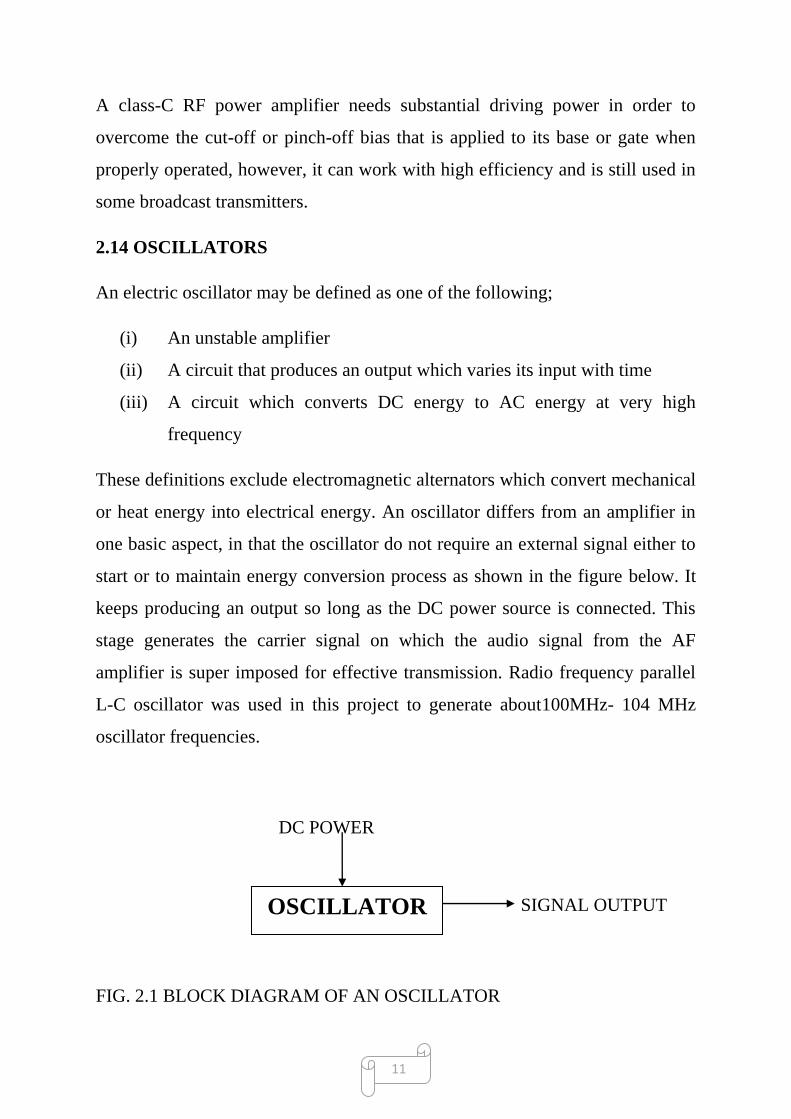
one basic aspect, in that the oscillator do not require an external signal either to
start or to maintain energy conversion process as shown in the figure below. It
keeps producing an output so long as the DC power source is connected. This
stage generates the carrier signal on which the audio signal from the AF
amplifier is super imposed for effective transmission. Radio frequency parallel
L-C oscillator was used in this project to generate about100MHz- 104 MHz
oscillator frequencies.
DC POWER
SIGNAL OUTPUT
FIG. 2.1 BLOCK DIAGRAM OF AN OSCILLATOR
OSCILLATOR
12
Moreover, the frequency of the output is determined by the passive components
used in the oscillator and can be varied at will. Electronic oscillators may be
broadly divided into two groups namely: sinusoidal and non-sinusoidal
oscillators.
2.14.1 Sinusoidal or Harmonic Oscillators
These are oscillators which can produce an output having sine wave forms and
produce any of the following oscillations; damped or un-damped oscillations.
2.14.2 Non-Sinusoidal or Relaxation Oscillators
These are oscillators which produce an output which has square, rectangular or
saw-tooth wave form.
Oscillations whose amplitudes keeps decreasing or decaying with time are
called damped oscillations. Ultimately, the amplitude of the oscillations decays
to zero when there is not enough to supply circuit losses. However, the
frequency or time-period remains constant because it is determined by the
circuit parameters. Sinusoidal oscillators serve a variety connection in
telecommunications and in electronics. Its most important application in
telecommunication is the use of sine waves as carrier in both radio and cable
transmission.
Oscillations whose amplitude remains constant that is those that do not change
with time are called un-damped oscillations. They are produced by those
oscillators circuit which have no losses or if they have, there is provision for
compensating them, the constant amplitude and constant frequency sinusoidal
waves.
In addition, oscillators can be described also as an electronic circuit whose
function is to produce an alternating electromotive force (EMF) of a particular
13
frequency and wave. Its purpose in the design is the generation of sinusoidal
carrier signal.
The basic types of oscillators are Phase oscillator, Hartley oscillator, and
colpitts oscillator. etc. For the purpose of this project the colpitts oscillator is
used.
Capacitors and inductors are the two components found in an RF oscillator or
tank circuit. These two components are used together to form an L-C circuit
which provide selectivity that we need in a radio receiver. When used together
we refer to them as tuned circuits or resonant circuit.
In practice, we have both series and parallel tuned circuits. This two behave
quite differently. In the case of series tuned circuit and assuming that both of the
components are “perfect”, the impedance of the circuit will be zero at the
resonant frequency this circuit is thus sometimes referred to as an acceptor
circuit, in other words, it will accept signal at other frequency. In the case of the
parallel L-C circuit and assuming that both of the components are perfect, the
impedance of the circuit will be infinite, at resonant frequency this circuits is
thus sometimes referred to as a rejecter circuit, in other words it will reject
signals at resonant frequency. In the case of both the series and parallel circuit
the frequency of resonance can be calculated.
2.15 RESISTOR:
For a resistor, according to ohm’s law, the voltage dropped across it is
proportional to the amount of current flowing through it. ie.
Where voltage across the resistor
Current flowing through the resistor and
14
Resistance of the resistor
Any current waveform across the resistor will produce the same voltage
waveform across the resistor. Resistors are essential to the functions of almost
every electronic circuit and provide means of controlling the circuit and/or
voltage present. There are almost as many types as their applications. Resistors
are used in amplifiers as loads for active devices in bias networks and as
feedback element. In combination with capacitors they establish time constant
and acts as filters, they are used to set operating currents and signal levels.
Resistors are used in power to measure currents and to discharge capacitor after
moving power source. They are used in precision circuit to establish currents to
provide accurate voltage ratio and to set precise gain values.
2.16 INDUCTOR:
The voltage across an inductor leads the current through it by 90degress. This is
due to the fact that the voltage across an inductor depends on the rate of change
of current entering the inductor. The impedance of an inductor is (
) which reflects the fact that the voltage leads the current.
Given the dimensions of an inductor coil such as average radius of coil(r) in
inches, number of turns of the coil(N), length of the coil(L) in inches, the
inductance in Micro Henrys( ) can be computed using this relationship.
⁄
2.17 CAPACITOR:
A capacitor temporarily stores charge or electricity in form of electrostatics.
This is not to be confused with the function of a battery, which chemically
generate electricity. A capacitor is said to be like a water storage tank while the
battery is like the central heating pump. i.e pumping the water round the

15
radiator. Capacitor like resistor are so widely used that books are written about
them. So capacitors are used in storing small amount of electrical energy, they
are used in smoothing i.e decoupling power supplies, removing of voltage
spikes from supplies etc.
2.18 TRANSISTOR:
A transistor is defined as a semiconductor device obtained by sand witching a P
or N type semiconductor material between a pair of the same type of
semiconductor materials. We have two types according to
(i) P-N-P is obtained by sand witching an N-type material between two
P-type materials.
(ii) N-P-N transistor is obtained by sand witching a P-type material
between two N-type materials.
Transistors have three regions or terminal as follows.
(i) Emitter (E):
It emits (supplies) electrons if it is an N-type region and holes, if it is a
P-type region. The electrons or holes emitted constitute emitter
current ( ). The emitter-base junction is always forward biased.
When grounded it is called common emitter.
(ii) Collector(C):
It collects electrons (or holes emitted by the emitter. It constitutes a
current called collector current( ), which flows through the load. The
collector base junction is always reversed biased. When grounded, it is
known as common collector.
(iii) Base (B):
The region between emitter and collector is the Base. The base
provides the path for blow of electrons or holes from emitter to
16
collector. In the case of an N-P-N transistor, when electrons from
emitter (N) enter into base (P), they recombine with holes in the base
region similarly, in case of a P-N-P transistor holes entering from (P)
into the base (N), try to recombine with electrons of the base region.
Thus, in both the transistor a current is constituted called base current
( ), which is however, very small. When grounded is termed
common base.
2.19 DETERMINATION OF RESONANT FREQUENCY
A resonant circuit comprises an inductor and a capacitor in parallel or in series
XL
XC ⁄
Where:
Capacitor
XL
XC
Resonance occurs when
XL=XC 2.3
At resonance,
2 ⁄
Making f the subject of formula, i have;
17
⁄
√ √ ⁄
√ ⁄
This is the resonant carrier frequency of a colpitts oscillator. The tank or
resonant circuit has three main specifications, namely: Bandwidth, Quality
factor or Q-factor, Insertion loss. These parameters define the pass band, shape
and loss of the tank circuit response.
2.20 MODULATION
Modulation is a process of superimposing information contained in a lower
frequency electronic signal into higher frequency signal. The higher frequency
is called the carrier signal. In the process of modulation, some characteristics
are varied in accordance with the instantaneous value of modulating signal such
as sine wave which may be represented by the following equation.
( )
Where:
The instantaneous value of the sine wave called the carrier
The maximum amplitude
The angular velocity
The phase relation is with respect to some reference value. Any of this last
three characteristics or parameters (e, ) of the carrier may be varied by

18
the modulating signal, giving rise to amplitude, frequency or phase modulation
respectively in this project, frequency modulation is considered.
2.20.1 NEED FOR MODULATION
However, it is needed due to the following reason.
(i) For efficient radiation and reception of radio waves. The transmitting
and receiving antenna must have height will be too long to be realized.
(ii) Signals of low frequencies cannot travel far hence, it is of importance
to superimpose it on a signal of higher frequencies for a wider
coverage, on the other hand an un-modulated carrier cannot be used to
convey information.
(iii) By standard, the bandwidth for commercial quality speech is 30Hz to
3400Hz. To allow for discrimination, each individual signal is
modulated by different carriers through the process called Frequency
Division Multiplexing (FDM). By this method, a telephone cable is
capable of carrying up hundreds of channels.
2.21 TYPES OF MODULATION TECHNIQUES
Basically, there are two types of modulation namely Amplitude Modulation and
Angle Modulation. Angle Modulation is further divided into frequency and
phase modulation. They are each briefly discussed below.
2.21.1AMPLITUDE MODULATION
A signal is said to be amplitude modulated when the amplitude of the carrier
wave is varied in proportion to the instantaneous amplitude of the information
signal or RF signal.
Obviously, the amplitude and intensity of the carrier waves is changed while the
frequency remains constant remains constant.
19
2.21.1.1 LIMITATIONS OF AMPLITUDE MODULATION
Although theoretically highly effective, Amplitude Modulation suffers from the
following draw backs;
(i) Noisy Reception: In an AM wave, the signal is in the amplitude
variations of the carrier practically all the natural and manmade noises
consists of electrical amplitude disturbances. As a radio receiver
cannot distinguish between amplitude variations that represent noise
and those that contain the desired signal, therefore reception is
generally noisy.
(ii) Low Efficiency: In amplitude modulation, useful power is in the side
bands as they contain the signal.
(iii) Small Operating Range: Due to low efficiency of the amplitude
modulation, transmitters employing this method have a small
operating range. i.e message cannot be transmitted over large
distances.
(iv) Lack of Audio Quality: This is a distinct disadvantage of amplitude
modulation. In order to attain high-fidelity reception all audio
frequencies up to 15 KHz must be reproduced. This necessitates band
width of 30 KHz since both sidebands must be reproduced. But FM
broadcasting stations are assigned bandwidth of only 10 KHz to
minimize the interference from adjacent broadcasting station. This
means that the highest modulation frequency can be 5 KHz which is
hardly sufficient to reproduce the music properly.
2.21.2 PHASE MODULATION
Here, the phase of the sinusoidal carrier is made to vary with the instantaneous
value of the modulating audio signal or the information signal changes the
20
phase of the waves with the frequency and the amplitude kept constant.
However; phase modulation varies with the modulating frequency.
2.21.3 FREQUENCY MODULATION
In this case the frequency of the carrier wave is varied in proportion to the
modulating signal. During modulation only the frequency of the carrier varies as
it increases positively with increase in modulating voltage.
The carrier amplitude is kept constant and thus the associated power of the
modulated wave is constant and this is a vital advantage over amplitude
modulation.
2.22 DEMODULATION
The process of recovering the audio signal from the modulated wave is known
as demodulation or detection.
At the broadcasting station, modulation is done to transmit the signal over a
large distance to the receiver when the modulated wave is picked up by the
radio receiver. It is necessary to recover the audio signal from it. This process is
accomplished in the radio receiver and is called demodulation.
2.22.1 NECESSITY FOR DEMODULATION
It was noted previously that amplitude modulated wave consists of carrier and
sideband frequency. The audio signal is contained in the sideband frequencies
which are audio frequencies. If the modulated wave after amplification is
directly fed to the speaker no sound will be heard. It is because diaphragm of
the speaker is not all able to respond to such high frequencies. Before the
diaphragm is able to move in one direction, the rapid reversal of current tends to
move it in the opposite direction i.e diaphragm will not move at all.
Consequently no sound will be heard.

21
Receiver antenna loud speaker (no sound)
FIG. 2.2 BLOCK DIAGRAM OF DEMODULATION PROCESSES.
From the above discussion, it follows that the audio signal must be separated
from the carrier at a suitable stage in receiver. The recovered audio signal is
then amplified and fed to the speaker for conversion into sound.
2.23 THEORY OF FREQUENCY AND PHASE MODULATION
Frequency Modulation is a system of modulation in which the amplitude of the
modulated carrier is kept constant, while its frequency and rate of change are
varied by the modulating signal. The most direct way to get FM is to apply the
audio signal to a varactor in a tuned oscillator an example is known as reactance
modulation. The varying voltage across the varactor causes its capacitance to
change in accordance with the audio wave form. The changing capacitance
results in variation of the resonant frequency of the induction-capacitance (LC)
tuned circuit, causing a swing in the frequency generated by the oscillator.
A direct way to get FM is to modulate the phase of the oscillator signal. Any
change in the instantaneous phase of a sine-wave RF carrier causes a change in
its instantaneous frequency. The first practical system was put forward in 1936
as an alternative to A.M in an effort to make radio transmissions more resistant
to noise.
Phase Modulation is a similar system in which the phase of the carrier is varied
instead of the frequency: as in FM, the amplitude of the carrier remains
constant. When the phase modulation is used, the audio signal must be
Station
selection
RF
Amplifier
22
processed, adjusting the amplitude-versus-frequency response of the audio
amplifiers; otherwise, the signal sounds unnatural when it is heard at the output
of an FM receiver.
2.23.1 FREQUENCY DEVIATION
Assuming the moment that the carrier of the transmitter is at its resting
frequency ie state of no modulation of 100MHz and we apply a modulating
signal. The amplitude of the modulating signal will cause the carrier to shift
from this resting frequency by a certain amount. If we increase the amplitude of
the modulating signal we will increase the deviation. A maximum of 75 KHz is
allowed as specified by the Federal Communication Council. If we remove the
modulation, the carrier frequency shifts back to its initial resting frequency
100MHz. However, the deviation of the carrier is proportional to the amplitude
of the modulating voltage. The deviation in comparison to the amplitude of the
modulating voltage is called the Deviation Ratio.
For most FM voice transmitters, the deviation is standardized at 5 KHz for
commercial broadcast. The deviation obtainable by means of direct FM is
greater, for a given oscillator frequency than the deviation that can be obtained
using phase modulation. Deviation can be increased by a frequency multiplier.
When an FM signal is passed through a frequency multiplier, the deviation is
multiplied along with the carrier frequency. In FM High-Fidelity music
broadcasting and in some other applications the deviation is much greater than
5 KHz. This is called wide band FM, as opposed to narrowband FM discussed
above. To obtain the optimum fidelity the deviation for an FM signal should be
at least equal to the highest modulating audio frequency. ie the rate at which the
carrier shifts from its resting point to a non-resting point is determined by the
frequency of the modulating signal. Thus for voice signals 5 KHz is more than
enough. For music, a deviation of at least 15 KHz to 20 KHz is needed. The
23
ratio of the frequency deviation to the highest modulating audio frequency is
called the Modulating Index. Ideally, the ratio should be between 11 and 21.If
it is less than11, the signal sounds muffled, and the efficiency sacrificed, but
increasing it beyond 21broadens the bandwidth without providing much
improvement in the signal quality.
Frequency Modulation can also be described as a process of changing a
particular property of the carrier wave in sympathy with the instantaneous
voltage or current which is the signal. The most commonly used methods of
modulation are the Amplitude Modulation (AM) and the Frequency Modulation
(FM) in the former case, the carrier amplitude; its peak voltage varies according
to the voltage at any instant of the Modulation signal in the latter case, the
carrier frequency is varied in accordance with voltage, at any instant of the
modulating signal.
2.23.2 DESCRIPTION OF MODULATION SYSTEMS
The general equation of an un-modulated wave or carrier may be written as
( ).................................................................................2.6
Where Instantaneous value (of voltage or current)
Maximum Amplitude
Angular Velocity in radians per seconds (rads/sec).
Phase Angle in radians.
It is noted that the represents the angle in radians.
If any one of these parameters is varied in accordance with another signal,
normally of a lower frequency, then the second signal is called the modulation
and the first is said to be modulated by the second.

24
Amplitude Modulation is achieved when the amplitude is varied.
Phase Modulation is obtained altering the phase angle .
Frequency Modulation is achieved by varying the frequency of the carrier.
It is assumed that the modulating signal is sinusoidal. This signal has two
important parameters which must be represented by modulation process without
distortion, specifically, its amplitude and frequency. By the definition of
frequency modulation, the amount by which the carrier frequency is varied from
its un modulated value, called the deviation, is made proportional to the
instantaneous amplitude of the modulating voltage. The rate at which the
frequency variation; or changes takes place is equal to the modulating
frequency. All signals having the same amplitude will deviate the carrier
frequency by the same amount, consequently, all signals of the same frequency
will deviate the carrier at the same rate no matter what their individual
amplitudes are. The amplitude of the frequency modulated wave remains
constant at all times. This is the greatest single advantage of FM. The effect of
frequency modulation on a sinusoidal carrier is shown below noting that the
modulating signal is in this case also sinusoidal. In practice many more cycles
of RF carrier would occur in the time span of one cycle of the modulating
signal.

25
FIG. 2.3 A MODULATING SIGNAL
FIG. 2.4 FREQUENCY MODULATED SIGNAL
The modulating or audio signal is described as
Where represents the maximum amplitude,
Represent the frequency of the audio signal,

26
Represent time and
Represent the instantaneous value of the modulating signal voltage.
The carrier frequency F, will vary around a resting FC (carrier frequency) thus
The frequency modulated wave will have the following description.
( )
In this frequency modulated situation, is the maximum change in frequency
the modulated wave undergoes. It is called the frequency deviation, and the total
variation in frequency from the lowest to the highest is referred to as a carrier
swing. Therefore, for a modulated signal which has equal positive and negative
peaks; such as pure sign wave, the carrier swing is equal to two times the
frequency deviation.
Frequency deviation
Carrier swing frequency deviation
It can be proven that the equation for the frequency modulated wave can be
transformed into:
( ⁄ )
It is noted that in the above equation (2.12), the cosine term is the preceded by
the ⁄ . This quantity is called the modulation index and is indicated or
represented as “MF”.
Modulation
Index ⁄
27
2.23.3 ADVANTAGES OF FREQUENCY MODULATION
(i) The efficiency of transmission is very high
(ii) It gives high fidelity reception
(iii) It gives noiseless reception as discussed before, noise is said to be a
form of amplitude variations and a FM receiver will reject such
signals.
(iv) The operating range is quite large.
2.23.4 APPLICATIONS OF FREQUENCY MODULATION
The five major categories in which FM is used are as follows:
(i) Non-commercial broadcast at 88MHz to 90MHz
(ii) Commercial broadcast with 200 KHz channel bandwidth at 90MHz to
108MHz.
(iii) Television audio signals with 50 KHz channel bandwidth at 54MHz to
88MHz, 174MHz to 216MHz and 470 MHz to 806MHz.
(iv) Narrow band public service channels from 108 MHz to 174MHz and
in excess of 806MHz.
(v) Narrow band amateur radio channel at 29.6MHz, 52MHz to 53MHz,
144MHz to 147.99MHz, 440MHz to 450MHz and in excess of
902MHz.
(vi) Digital-FSK: Frequency Shift Keying (FSK) is used on HF for low
speed telegraphy or data transmission, eg. RTTY at speeds of 45.45 or
50 band. FSK is also used on VHF for data transmission at 4800bps
using the Direct Frequency Modulation (DFM) technique, or G3RUH
Modulation at 9600bps.
(vii) Digital-AFSK: Audio Frequency Shift Keying (AFSK) is the use of a
frequency shift keyed audio tone to modulate a FM or SSB
transmitter. This is commonly used for speeds of 300bps on HF and

28
1200bps on VHF/UHF. On VHF/UHF, the AFSK signal is fed into the
microphone input of the transmitter to pick up pre-emphasis, and de-
emphasised audio is used for the demodulation.
2.24 NOISE AND FREQUENCY MODULATION
There are several other forms of modulation particularly associated with digital
communications like pulse code modulation, pulse width modulation etc.
Frequency Modulation is much more immune to noise than Amplitude
Modulation and is significantly more immune than Phase Modulation.
A signal-noise frequency will affect the output of a receiver only if it falls
within its band pass. The carrier and the noise voltages will mix, and if the
difference is audible, it will naturally interfere with reception of wanted signals.
Noise rejection is obtained only when the signal is at least twice the noise peak
amplitude. Other forms of interference found in receivers include:
(i) Adjacent channel interference: FM offers not only an improvement in
the signal to noise ratio but also better discrimination against other
interfering signals, no matter what their source is. Also wideband FM
broadcasting channel occupies 200 KHz of which only 180 KHz is
used and the remaining 20 KHz guard band goes a long way towards
reducing adjacent channel interference even further.
(ii) Co-channel interference-capture effect: FM receivers incorporate the
use of amplitude limiters, which work on the principle of passing the
signal and eliminating the weaker. This was the reason for mentioning
earlier that rejection is obtained only when the signal is at least twice
the noise peak amplitude. A relatively weak interfering signal from
another transmitter will also be attenuated in this manner, as much as
any other forms of interference. This applies even if the other
transmitter operates at the same frequency as the desired transmitter.
29
2.25 PRE-EMPHASIS AND DE-EMPHASIS
Noise has a greater effect on higher modulating frequencies than on the lower
ones. Thus, if the higher frequencies were artificially boosted at the transmitter
and correspondingly cut at the receiver, an improvement in noise immunity
could be expected, thereby increasing the signal-to-noise ratio. This boosting of
the higher modulating frequencies, in accordance with a pre-arranged curve, is
termed pre-emphasis, and the compensation at the receiver is called de-
emphasis. The standard unit for defining emphasis is microseconds. A 75 pre-
emphasis in FM gives a noise rejection of at least 24db better than AM.
30
CHAPTER THREE
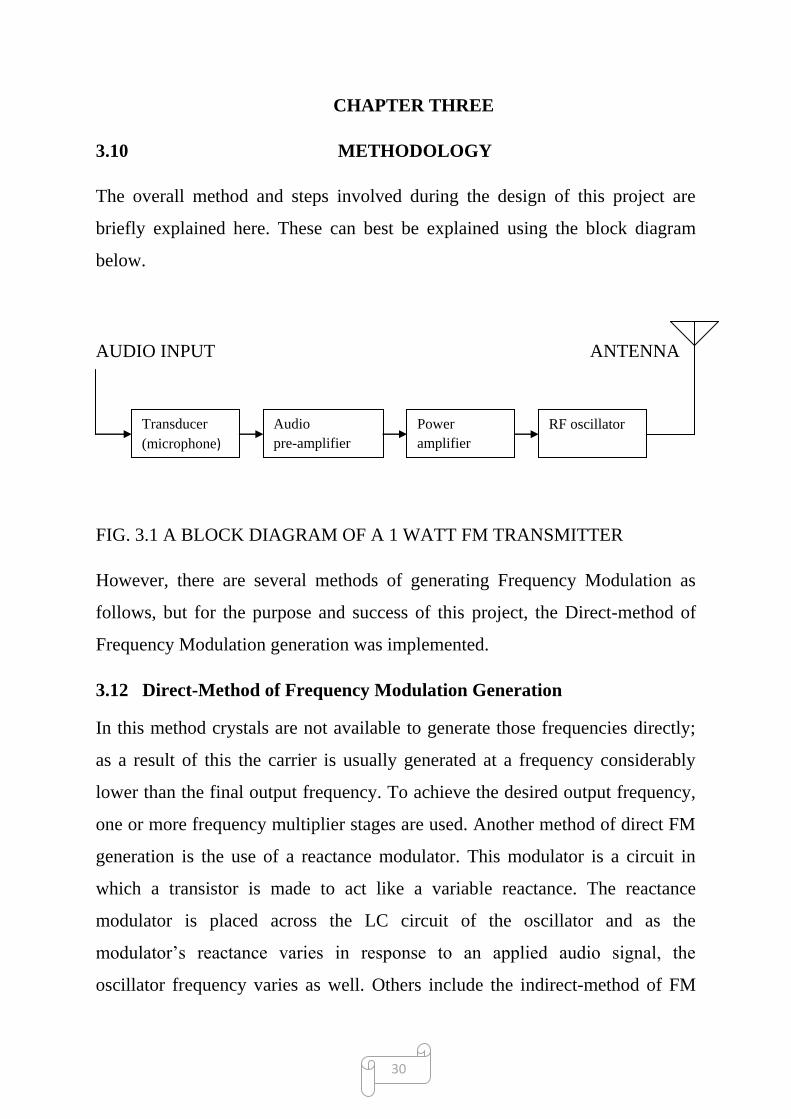
3.10 METHODOLOGY
The overall method and steps involved during the design of this project are
briefly explained here. These can best be explained using the block diagram
below.
AUDIO INPUT ANTENNA
FIG. 3.1 A BLOCK DIAGRAM OF A 1 WATT FM TRANSMITTER
However, there are several methods of generating Frequency Modulation as
follows, but for the purpose and success of this project, the Direct-method of
Frequency Modulation generation was implemented.
3.12 Direct-Method of Frequency Modulation Generation
In this method crystals are not available to generate those frequencies directly;
as a result of this the carrier is usually generated at a frequency considerably
lower than the final output frequency. To achieve the desired output frequency,
one or more frequency multiplier stages are used. Another method of direct FM
generation is the use of a reactance modulator. This modulator is a circuit in
which a transistor is made to act like a variable reactance. The reactance
modulator is placed across the LC circuit of the oscillator and as the
modulator’s reactance varies in response to an applied audio signal, the
oscillator frequency varies as well. Others include the indirect-method of FM
Transducer
(microphone)
Audio
pre-amplifier
Power
amplifier
RF oscillator
31
generation which involves the use of a stable crystal oscillator to generate the
carrier signal and the use of a buffer amplifier to isolate it from the remainder of
the circuitry. And the use of voltage controlled oscillator. The output frequency
of the voltage controlled oscillator is proportional to the voltage of the input
signal; i.e. if audio signal is applied to the input of a voltage controlled
oscillator, the output is an FM signal.
The various components used in the construction of this project include:
resistors, transistors, capacitors, potentiometer and inductors.
The major sections that constitute this design are:
(i) The power supply unit
(ii) The audio pre-amplification unit
(iii) The power amplification unit
(iv) The RF oscillator unit
(v) The antenna
(vi) The indicator
3.12 THE POWER SUPPLY UNIT:
This unit consists of a 9 volts DC battery .The power supply ensures the circuit
functions effectively. To an extent, it determines the carrier frequency of the
oscillator circuit.
3.13 THE AUDIO PRE-AMPLIFIER UNIT:
The function of this stage is to pre-amplify the audio signal from the
microphone which is very weak so that it can be set for modulation. This stage
consists of NPN transistor, common emitter configuration, with collector
feedback biasing, biasing resistors and capacitors. The input to this state is from
the base of the transistor while the output is from the collector. The capacitors at

32
this unit serve as a coupling unit filter networks and frequency determination of
input signal.
3.14 THE POWER AMPLIFIER UNIT:
The function of this stage is to amplify the carrier frequency or signal from the
pre-amplification stage to the desired power output level. It serves as a boost of
signal coming into it or as a driver. This stage consists of NPN transistor,
common emitter configuration with voltage divider biasing, biasing resistors.
The input to this stage is from the base of the transistor, while the output is from
the collector, which goes to the parallel resonant circuit or tank circuit.
3.15 RF OSCILLATOR UNIT:
This unit consists of a parallel resonant circuit or tank which is responsible for
producing the carrier wave upon which the intelligence signal is to be
superimposed for modulation.
3.16 THE ANTENNA UNIT:
The antenna is responsible for the transmission of the modulated signal through
space. For this project, the antenna is 1.75ft. Single pole antenna, It should be
noted that extending the length of the antenna consequently extends the range of
signal transmission as observed during testing.
3.17 THE INDICATOR:
This section consists only of a Light Emitting Diode whose function is to
indicate power supply to the rest of the component in the circuit.
For the design and construction of this project, some fundamental components
were used. An insight into their properties and their characteristic behaviour
relevant to the design under consideration are discussed below.

33
CHAPTER FOUR
4.10 DESIGN AND CONSRUCTION OF MODULE
FIG.4.1 CIRCUIT DIAGRAM OF SYSTEM
4.11 DESIGN SPECIFICATION
The design specification is a detailed description of the expected characteristics
of the designed FM transmitter.
(1) MODULATION TYPE: FM
(2) FREQUENCY OF OPERATION: 104.7 MHz
mic 25k4.7
220k
4.7k 1nF
10k
2-15pF
3.3pF
100
2N2219A
10k1nFBC547C
ANTENNA
4.7
5-30v
1k
VR1C1
R1
Q1 C4R5
R6
Q1
C6
0.2C5R4
C3R2
R3
C2
34
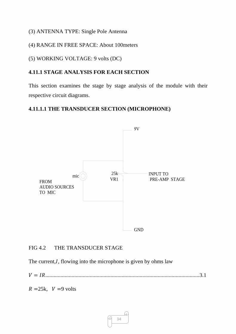
(3) ANTENNA TYPE: Single Pole Antenna
(4) RANGE IN FREE SPACE: About 100meters
(5) WORKING VOLTAGE: 9 volts (DC)
4.11.1 STAGE ANALYSIS FOR EACH SECTION
This section examines the stage by stage analysis of the module with their
respective circuit diagrams.
4.11.1.1 THE TRANSDUCER SECTION (MICROPHONE)
FIG 4.2 THE TRANSDUCER STAGE
The current, , flowing into the microphone is given by ohms law
...............................................................................................................3.1
25k, 9 volts
mic25k
GND
INPUT TO PRE-AMP STAGE
FROMAUDIO SOURCESTO MIC
VR1
35
⁄
⁄
⁄
4.11.1.2 THE AUDIO PRE-AMPLIFIER SECTION
FIG. 4.3 THE AUDIO PRE-AMPLIFIER STAGE
From the circuit diagram above,
, , , E ,
4.7
220k
4.7k
BC547C
GND
9V
INPUT TOPOWER AMP STAGE
INPUT FROM
TRANSDUCER (MIC)C1
R1
R2
Q1

36
Where is the collector current and is the base current.
From the equation for the collector feedback biased transistor,
( ) 4.1
Making the subject of formula, we obtain
( ⁄ ) ⁄
( ⁄ )
Now from this relationship,
E ⁄
Substituting the values of and E
⁄
⁄
37
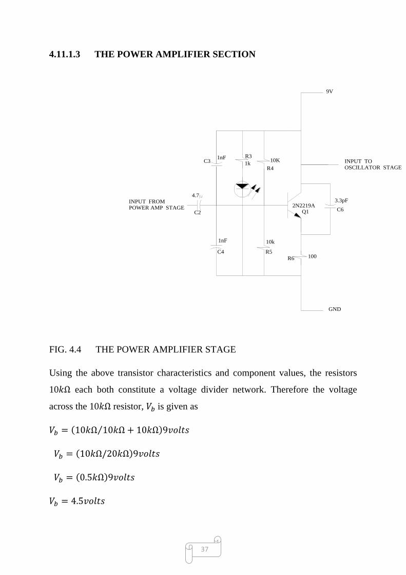
4.11.1.3 THE POWER AMPLIFIER SECTION
FIG. 4.4 THE POWER AMPLIFIER STAGE
Using the above transistor characteristics and component values, the resistors
10 each both constitute a voltage divider network. Therefore the voltage
across the 10 resistor, is given as
( ⁄ )
( )
( )
1nF10K
100
2N2219A
1nF
4.7
10k
9V
GND
INPUT TOOSCILLATOR STAGE
INPUT FROMPOWER AMP STAGE
3.3pF
1k
C2
C3R3
R4
C4 R5
R6
Q1 C6
38
From the fundamental transistor equation, we know that
Where for a 2N2219A N-P-N transistor and silicon transistor
by standard
( )
Where is the voltage across the emitter, the current, across the emitter is
given as
⁄
However, noting that approximately,
Therefore, using equation and noting
39
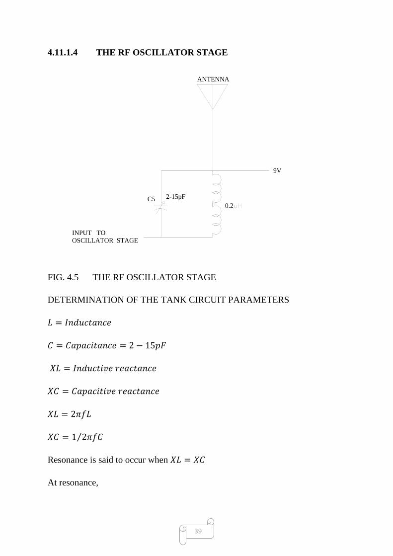
4.11.1.4 THE RF OSCILLATOR STAGE
FIG. 4.5 THE RF OSCILLATOR STAGE
DETERMINATION OF THE TANK CIRCUIT PARAMETERS
⁄
Resonance is said to occur when
At resonance,
2-15pF
ANTENNA
9V
INPUT TOOSCILLATOR STAGE
C50.2

40
⁄ From equation
Making the subject of the formula, we obtain
√ ⁄ as in equation . This is the resonant carrier frequency of a
Colpitt Oscillator.
From equation
( )
⁄
Obtaining the dimensions of the inductor coil to be as follows,
Number of turns
Average radius of coil
Length of coil
Substituting these values into the expression, we obtain
⁄
⁄ = ⁄
.
41
From equation in the previous page, substituting for the values of and
we obtain, the resonant frequency to be
√ ⁄
√ ⁄
√ ⁄
⁄
⁄
MHz. this is thus the carrier frequency of the parallel - network.
4.12 COMPONENT JUSTIFICATION
This section describes the importance of using each of the electronic
components that constitutes the circuit diagram.
For the transducer section, the electrets microphone was used as the input
transducer because of its high sensitivity. The 25k potentiometer limits the
amount of current entering the electrets microphone. This consequently
stabilizes the gain of the microphone and maintains good stability of the
sensitivity.
In the pre-amplifier, power amplifier circuit and oscillator stages, the BC547C
and 2N2219A respectively were used utilized because of its high frequency
response characteristics. The capacitors were used as coupling filter networks to
the various stages of the circuitry. The parallel L-C tank oscillator was chosen
due to its ability to generate a stable sine wave at the carrier frequency, a better

42
performance at high frequency generation of signal and its availability in the
market.
A single pole antenna was used as the antenna due to the miniature nature of the
circuit and under impedance matching considerations was seen to be the best
suit for this project work.
A 9 volt DC battery was used as the power supply for this circuitry because of
its ability to produce a steady current and its ready availability.

43
4.13 BILL OF ENGINEERING MEASUREMENT
S/N ITEM SPECIFICATION QUANTITY UNIT
COST
TOTAL
COST
1 N-P-N TRANSISTORS
BC547C; h E
2N2219A; h E
1
1
₦10
₦150
₦10
₦150
2 RESISTORS(fixed wire wound)
220kΩ,4.7kΩ,10kΩ,10kΩ,100Ω,1kΩ
6
₦5
₦30
3 POTENTIOMETER
25kΩ
1
₦20
₦20
4 CAPACITORS
4.7 F( Electrolytic)
1nF,1nF,3.3pF(Ceramics)
2-15pF(Variable Capacitor)
2
3
1
₦20
₦20
₦300
₦40
₦60
₦300
5 ELECTRET MICROPHONE 1 ₦100 ₦100
6 SWITCH 1 ₦50 ₦50
7 VERO BOARD(DOTTED) 1 ₦50 ₦50
8 9 VOLTS DC BATTERY 2 ₦50 ₦100
9 SINGLE POLE ANTENNA 1 ₦50 ₦50
10 PLASTIC CASING 1 ₦100 ₦100
11 BATTERY CONNECTOR 1 ₦50 ₦50
12 INDICATOR 1 ₦5 ₦5
13 CONNECTING WIRE 2 ₦20 ₦40
14 MIC PORT 1 ₦50 ₦50
15 MISCELLANEOUS - - ₦3000
TOTAL COST
₦4,205
44
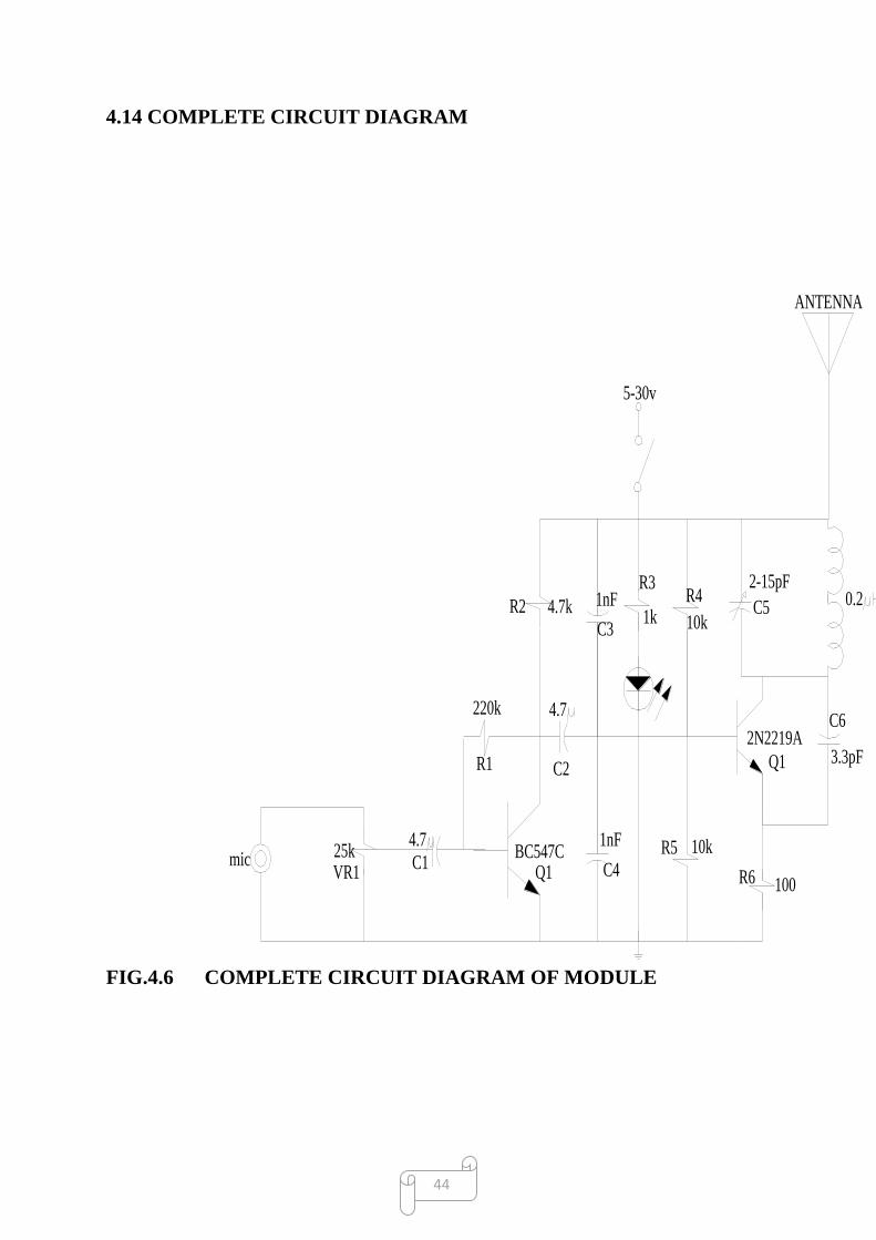
4.14 COMPLETE CIRCUIT DIAGRAM
FIG.4.6 COMPLETE CIRCUIT DIAGRAM OF MODULE
mic 25k4.7
220k
4.7k 1nF
10k
2-15pF
3.3pF
100
2N2219A
10k1nFBC547C
ANTENNA
4.7
5-30v
1k
VR1C1
R1
Q1 C4R5
R6
Q1
C6
0.2C5R4
C3R2
R3
C2
45
CHAPTER FIVE
5.10 TEST AND OBSERVATION
It was observed that during the testing of this project with a radio receiver that
the transmitted signal produced a large squeal, an external microphone port was
improvised for the microphone due to imbalance biasing, which gave better
performance. Also observed during testing that the transmitter frequency was at
104.7 MHz contrary to the anticipated and calculated 102.7MHz.This situation
resulted from variable capacitor the variations made to the inductor wire during
construction which affected the inductance and consequently the carrier
frequency. Also on maximum power the power transistor heats up at power
amplifier stage, to solve this issue a heat sink is needed for the transistor, worth
mentioning is the observation that touching of the inductor coil caused the
frequency to drift by a reasonable amount. In addition, the main area of
instability is the oscillator part. Shielding the oscillator helps in part to counter
this and an extension of the antenna length increased the range of signal
propagation. The use of a voltmeter was used to test for voltages at various
points also an oscilloscope was used to test for frequencies of oscillations and
also the range was put in to consideration.
46
CHAPTER SIX
6.10 CONCLUSION
The simple FM transmitter was designed with a view which includes using the
basic concepts and theories of FM transmission in the propagation of
information. Attempts were made to put in a simple and straight forward design.
This design was tested and found to reach about 100 meters of range and its
frequency of operation of about 104.7 MHz in agreement with my objective.
The design and construction procedures involved in the organization of this
system and the casing was also presented. I have attempted to use minimum
components to achieve optimum transmission range and portability. The
selection of the modified electronic circuitry components was carefully done
considering these factors; their ability to perform their required function without
interruption during the operational life and their economic ability. However, this
project is a success due to these satisfactions and the tests carried out.
6.11 RECOMMENDATION
The design used for this project is essentially quite a simple one and it is this
simplicity which partly brings it down when it comes to the overall reliable
performance. The project has succeeded to a great extent, in exposing the very
basic principles involved in FM transmission and reception.
The following recommendation was made based on the experience in doing the
project and the problem encountered in the course of the work.
Modular design should be used, for analysis of each module should be done
cautiously, accurate measurement should be done to determine the values of
capacitor and wire wound inductor. Every variable capacitor and inductor
should be aligned properly to produce the required threshold voltage above the
system noise in the RF section.
47
6.12 REFERENCES
1. A Textbook of Electrical Technology by B.L Theraja, A.K Theraja,
S.Chand publishers India (24th
Edition)
2. Electronic Communications: modulation and transmission, Schoebeck,
Robert, Tata McGraw Hill, 2002, New York
3. Electronic Communications System, Kennedy and Davies Fourth Edition,
Tata McGraw Hill
4. Electronic Principles Devices & Circuits M.L.ANAND S.CHAND First
Edition, 2000
5. Fundamentals of Reliable Circuit Design, Alexander Mel, Longman
Press, 2001, Texas
6. Mastering Electronics, Whitehead R.J “” McGraw Hill, New York, 1988,
3rd
Edition chapter 9 &10.
7. Modern Communications, Miller Gary M, Tata McGraw Hill, New York
(2nd
Edition)
8. Radio Communication Concepts: Analogue, Carson, John Wiley & Sons,
Inc; 1990
9. RF Circuit Design, Boswick, SAMS, 1982.
10. Solid State Radio Engineering, Krauss, Bo stain, Raab, John Wiley&
Sons, Inc; 1980.
11. The ARRL Handbook, The American Radio Relay League, Inc., 1994.