TYPE 816R-5C FM TRANSMITTER 35 kW, 88-108 MHz
245
816R-5C TECHNICAL MANUAL OPERATION AND MAINTENANCE INSTRUCTIONS TYPE 816R-5C FM TRANSMITTER 35 kW, 88-108 MHz (PIN 180298-2) Serial No. 89 and Above (214) 381-7161 COPYRIGHTED© 2005 BY CONTINENTAL ELECTRONICS 4212 S. BUCKNER BLVD. DALLAS, TEXAS 75227 Web Address: [email protected] FAX: (214) 381-4949 ISSUED - 6 SEPTEMBER 1995 CHANGE 4 - 30 JUNE 2005
-
Upload
khangminh22 -
Category
Documents
-
view
0 -
download
0
Transcript of TYPE 816R-5C FM TRANSMITTER 35 kW, 88-108 MHz

816R-5C
TECHNICAL MANUALOPERATION AND MAINTENANCE INSTRUCTIONS
TYPE 816R-5C FM TRANSMITTER
35 kW, 88-108 MHz
(PIN 180298-2)
Serial No. 89 and Above
(214) 381-7161
COPYRIGHTED© 2005 BYCONTINENTAL ELECTRONICS
4212 S. BUCKNER BLVD.DALLAS, TEXAS 75227
Web Address: [email protected] FAX: (214) 381-4949
ISSUED - 6 SEPTEMBER 1995CHANGE 4 - 30 JUNE 2005


816R-5C
PREFACE
This Operation and Maintenance manual gives the physical and functional description, installation, operation, theory ofoperation, maintenance, parts lists, and diagrams for the identified equipment. Operator and service personnel shouldbecome familiar with the manual contents before attempting to install, operate, or maintain the equipment. In addition to theSafety Summary which follows the Table of Contents, specific WARNINGS, CAUTIONS and NOTES are locatedthroughout this manual where they apply. Continental Electronics (CE) manufactured this equipment to conform with Icurrent electrical, radiation, and safety codes of the United States to the extent that they apply. It is the user's responsibilityto comply ,vith all local and national codes during installation and operation of the equipment.
CE reserves the right to make any changes, without notice, to this or any of CE's products to improve reliability,perfonnance, function, or design.
I
CE does not assume any liability resulting from the application or use of any product or circuit described herein; nor does CEIconvey any license under its patent rights or the rights of others.
The information in this document has been carefully checked and is believed to be entirely reliable. While all reasonableefforts to ensure accuracy have been taken in the preparation of this manual, CE assumes no responsibility resulting fromomissions or errors in this manual, or from the use of information contained herein.
These instructions do not purport to cover all details or variations in equipment nor to provide for every possible contingencythat might be met during installation, operation, or maintenance. Should further infonnation be desired or should particularproblems arise which are not covered sufficiently for the user's purpose, the matter should be referred to CEo I
All Rights Reserved
This document contains proprietary information ofContinental Electronics and shall not be duplicated,nor its contents used for any purpose, unless expresswritten permission is obtained from ContinentalElectronics.
CUSTOMER SERVICE
I
I
Continental Electronics customer service is available for assistance at any time, 24 hours a day, weekends and holidays Iincluded. Call anytime day or night:
Parts ServicesEngineering ServicesMain OfficesWeb Address
(214) 388-3737(214) 388-5800(214) 381-7161 (8:00 am - 5:00 pm CT)
You may write to any of these services at 4212 S. Buckner Blvd. Dallas, Texas 75227, or FAX (214) 381-4949.
Change 3

816R-5C
INSERT LATEST CHANGE PAGES. DESTROY SUPERSEDED PAGES.
ILIST OF EFFECTIVE PAGES I NOTE: The portion of text affected by the changes isindicated by a change number located in the footer ofeach changed page.
Dates of original and change pages are:OriginaL 0 19 August 1995Change 1 9 July 1996Change 2 .. ~ 21 May 1998Change 3 24 January 2003Change 4 30 June 2005
TOTAL NUMBER OF PAGES IN THIS PUBLICATION IS 247 CONSISTING OF THE FOLLOWING:
Page No. *Change Page No *Change Page No *Change
Title...................... 4Preface 3A......................... 4i 2ii " " '" . .. .. . . . . . . . 3iii - vii. . . . . . . . . . . . . . . . . . . . . 2viii Blank . . . . . . . . . . . . . . . . . . 2ix - xiii. ... . .... . . . . . . .. .. . 0xiv Blank' . . . . . . . . . . . . . . . . . . 01-1 - 1-2 .. :-................ 31-3 - 1-4 02-1 32-2 - 2-3 02-4 Blank. . . . . . . . . . . . . . . . . . 02-5 - 2-9 02-10 22-11 - 2-12 32-13 - 2-18 03-1 - 3-2 33-3 - 3-8 03-9 23-10 03-11-3-12 13-13 - 3-15 03-16-3-17 13-18-3-19 03-20 Blank. . . . . . . . . . . . . . . . . 04-1 34-2 24-3 - 4-4 34-5-4-10 24-11 34-12 24-13 - 4-14 34-15 24-16 - 4-21 34-22 Blank. . . . . . . . . . . . . . . . . 25-1 35-2 05-3 35-4 05-5 15-6 - 5-7 05-8 - 5-10 35-11 - 5-20 05-21 3
. 5-22 - 5-23 0. 5-24 Blank . . . . . . . . . . . . . . . . . 0
6-1 36-2 46-3 - 6-5 36-6 Blank. . . . . . . . . . . . . . . . . . 26-7 - 6-18 . . . . . . . . . . . . . . . . . . 26-19 36-20 '. . . 26-21 - 6-24 36-25 Blank . . . . . . . . . . . . . 26-26 26-27 - 6-29 36-30 - 6-36 26-37 - 6-39 36-40 26-41 36-42 26-43 36-44 26-45 36-46 - 6-49 26-50 - 6-51 36-52 26-53 36-54 - 6-60 26-61 Blank . . . . . . . . . . . . 26-62 26-63 - 6-64 36-65 Blank . . . . . . . . . . . . . . . . . 26-66 - 6-70 26-71 Blank . . . . . 26-72 26-73 46-74 26-75 36-76-6-78 26-79 36-80 - 6-82 26-83 36-84 - 6-86 26-87 36-88 Blank . . . . . . . . . . . . . 26-89 36-90 26-91 - 6-92 36-93 Blank . . . . . . . . . . . . . . 2
*Zero in the column indicates an original page.
6-94 0 ••
6-95 .6-96 .6-97 - 6-98 .6-99 Blank .6-100 .6-101 .6-102 - 6-104 .6-105 .6-106 Blank .7-1 .7-2 Blank .7-3 .7-4 Blank .7-5 .7-6 Blank .7-7 .7-8 Blank .7-9 .7-10 Blank .7-11 .7-12 Blank .7-13 .7-14 Blank .7-15 .7-16 Blank .7-17 .7-18 Blank .7-19 .7-20 Blank .7-21 .7-22 Blank .7-23 .7-24 Blank .7-25 .7-26 Blank .7-27 .7-28 Blank .7-29 .7-30 Blank .7-31 .7-32 Blank .7-33 .7-34 Blank .7-35 .7-36 Blank .
2323223232322222222222222222323222222222222232
A Change 4

816R-5C
Paragraph
Table of Contents
Title
SECTION 1 - GENERAL
TABLE OF CONTENTS
Page
1-1. Introduction 1-11-2. Functional Description . . . . . . . . . . . . . . . . . . . . . . . . . . . . . . . . . . . . . . . . . . . . . . . . . . . . . . . . . . . . . . . 1-11-3. Physical Description. . . . . . . . . . . . . . . . . . . . . . . . . . . . . . . . . . . . . . . . . . . . . . . . . . . . . . . . . . . . . . . . . 1-11-4. Technical Characteristics 1-1
SECTION 2 - INSTALLATION
2-1.2-1.12-1.22-1.32-1.3.12-1.3.22-1.3.32-2.2-2.12-2.22-3.2-3.12-3.22-3.32-3.4
3-1.3-2.3-3.3-4.3-5.3-6.3-7.3-8.
Pre-Installation Information .AC Power .RF Output Power .Transmitter Cooling .Exhaust Fans .Positive Pressure ~ . ~ ..Transmitter Exhaust Duct .Unpacking and Inspecting .Domestic Shipments .International Shipments .Assembly .Equipment Locatioin .Connect Plate Transformer .Connect Primary AC Power .Install Remaining Assemblies .
SECTION 3 - OPERATION
General .Controls and Indicators .Initial Tum-On Procedure .Remote Operation .2nd Power Level (Low Pwr) Adjustment .Automatic Recycle Resetting .Normal Tum-Off (Local) .Emergency Tum-Off .
SECTION 4 - THEORY OF OPERATION
2-12-12-12-12-12-22-62-62-62-62-72-72-72-72-10
3-13-13-13-153-153-153-153-15
4-1.4-2.4-3.4-3.14-3.24-3.2.14-3.2.24-3.2.3.14-3.2.3.2
Change 2
General . . . . . . . . . . . . . . . . . . . . . . . . . . . . . . . . . . . . . . . . . . . . . . . . . . . . . . . . . . . . . . . . . . . . . . . . . . . 4-1Functional Description . . . . . . . . . . . . . . . . . . . . . . . . . . . . . . . . . . . . . . . . . . . . . . . . . . . . . . . . . . . . . . . 4-1RF Circuits .. . . . . . . . . . . . . . . . . . . . . . . . . . . . . . . . . . . . . . . . . . . . . . . . . . . . . . . . . . . . . . . . . . . . . . . 4-1Exciter, A4. 4-1IPA, A3. 4-1IPA Metering, AI. 4-1Amplifier Assembly, A3A3 4-1RF Amplifier 4-2Control Assembly. . . . . . . . . . . . . . . . . . . . . . . . . . . . . . . . . . . . . . . . . . . . . . . . . . . . . . . . . . . . . . . . . . . 4-2

TABLE OF CONTENTS
Table of Contents - Continued
816R-SC
Paragraph
4-3.34-3.44-3.54-4.4-4.14-4.24-4.34-4.44-4.54-4.64-4.74-4.84-4.94-4.1 04-5.4-5.14-5.24-5.34-5.44-5.4.14-5.4.24-5.54-5.64-5.74-5.84-5.94-5.1 0
Title
SECTION 4 - THEORY OF OPERATION - Continued
RF Power Amplifier, A12 .Low-Pass Filter, A7 .Directional Coupler, DCI .Power Supplies and Power Control Circuits .General .24 Vdc Power Supply, PIO A10 .Power Amplifier Bias Power Supply, PIO Al O .PA Plate Supply .Power Control Unit, A9 .Power Control Regulator, PIO A2A6 .PA Screen Power Supply .Driver Power Supply, PIO A5 .Filament Voltage Regulator, A2A4 .Filament Voltage Distribution. . .Primary Power Distribution Control and Overload Circuits .Primary Power Distribution .Transmitter Tum-On. . .Exciter Power Control Override. . .FWDIREFL Calibrate and Auto Power Control Unit, A2A6. . .Functions .Theory of Operation. . .Overload Protection .Overload and Recycle Board, A2A5 .Power Failure Recycle Board, A8A 1. . .Auto-Manual Power Control Latching Relay and Transmitter Status Indicators. . .Power Control Relays, PIO A10A2 .Remote Relays, PIO AI0A2 .
SECTION 5 - MAINTENANCE
Page
4-24-34-34-34-34-3 I4-34-34-34-114-114-114-114-144-144-144-144-144-144-144-174-174-174-184-184-194-19
5-1.5-2.5-2.15-2.25-2.35-3.5-4.5-5.5-5.15-5.25-6.5-6.1
ii
Routine Maintenance 5-1Cleaning 5-1General Cleaning Procedures. 5-1Air Filter. 5-1Tube Cleaning. . . . . . . . . . . . . . . . . . . . . 5-1Inspection . . . . . . . . . . . . . . . . . . . . . . . . . . . . . . . . . . . . . . . . . . . . . . . . . . . . . . 5-1Lubrication . . . . . . . . . . . . . . . . . . . . . . . . . . . . . . . . . . . . . . . . . . . . . . . . . . . . . 5-1Parts Replacement 5-1P.A Tube, VI. 5-2Fuse Replacement. 5-2Troubleshooting 5-2Access Panel Interlock Switch. 5-2
Change 3

816R-5C TABLE OF CONTENTS
Table of Contents - Continued
Paragraph
5-6.25-7.25-7.35-7.3.15-7.3.25-7.45-7.55-7.65-7.6.15-7.6.25-7.6.35-7.75-7.7.15-7.7.25-7.7.35-7.7.45-7.85-8.5-9.5-9.15-9.1.15-9.1.25-9.1.35-9.1.45-9.1.55-9.1.65-9.1.75-9.1.85-9.1.95-9.1.105-9.25-9.3
Title
SECTION 5 - MAINTENANCE - Continued
Test Equipment. . .Filament Voltage Adjustment. .DC Overload Adjustment. .PA Plate Overload Adjustment. .PA Screen Overload Adjustment. .PA Grid Current. . .High Voltage Power Supply Static Check (no drive) .IPA Metering Board Calibration. . .General Information .Setup Procedures. . .Calibration Procedures. . .FWD/REFL CAL and Power Control Card, A2A6. . .Offset Nulls .Forward Power Calibration ~ .Reflected Power and VSWR Protection Calibration .VSWR Foldback Adjustment. . .Phase Monitor Adjustment. .Changing Power .Changing Frequency .Frequency Change Adjustments. . .Shorting Plane .PA Neutralization .PA Grid Tuning Slider .PA Grid Swamping Capacitor. .Cathode Return Capacitor. .Efficiency Capacitor. .Coupling Capacitor. .PA Bias .IPA to PA Cable Length. . .PA Grid Circuit. . .PA Tuning and Loading. . .PA Neutralization. . .
SECTION 6 - PARTS LISTS
Page
5-25-35-65-65-65-75-75-75-75-75-85-95-95-105-105-105-115-115-115-115-115-125-125-125-125-125-125-125-215-215-225-23
6-1.6-2.6-3.6-4.6-5.6-6.
Introduction 6-1Reference Designations (Ref Des) . . . . . . . . . . . . . . . . . . . . . . . . . . . . . . . . . . . . . . . . . . . . . . . 6-1Description. . . . . . . . . . . . . . . . . . . . . . . . . . . . . . . . . . . . . . . . . . . . . . . . . . . . . . . . . . . . . . . . . 6-1Part Number . . . . . . . . . . . . . . . . . . . . . . . . . . . . . . . . . . . . . . . . . . . . . . . . . . . . . . . . . . . . . . . . 6-1Illustrations. . . . . . . . . . . . . . . . . . . . . . . . . . . . . . . . . . . . . . . . . . . . . . . . . . . . . . . . . . . . . . . . . 6-1Index of Parts Lists . . . . . . . . . . . . . . . . . . . . . . . . . . . . . . . . . . . . . . . . . . . . . . . . . . . . . . . . . . . 6-1
SECTION 7 - DIAGRAMS
7-1.
Change 2
Introduction 7-1
iii

TABLE OF CONTENTS
LIST OF ILLUSTRATIONS
816R-SC
Figure
1-1.
Title
SECTION 1 - GENERAL
816R-5C FM Transmitter.
SECTION 2 - INSTALLATION
Page
1-2
2-1.2-2.2-3.2-4.2-5.2-6.2-7.2-8.2-9.2-10.
3-1.3-2.3-2.3-3.3-4.3-5.3-6.3-7.3-8.
4-1.4-2.4-3.4-4.4-5.4-6.4-7.4-8.4-9.4-10.
FM Transmitter Outline and Installation Drawing .FM Transmitter Nominal Heat Balance .Plate Transformer Assembly, A14 .Transmitter AC Power Connections .Remote Control Connections .Transmitter Controller (377D-1 or -2) Connections .Remote Plate Current Sample Circuit .Transformer Connection Schedule .IPA Transformer (T3) Connection .Secondary Tap Configuration, T2 .
SECTION 3 - OPERATION
Transmitter Control Panels. . .Control Panel, A1, Controls (Sheet 1 of 2). . .Control Panel, A 1, Status Indicators (Sheet 2 of 2) .Card Cage Assembly, A2, Controls and Indicators .
IPA, A3, Controls and Indicators .Circuit Breaker Panel, A6, Controls and Indicators .PA Tuning and Loading .Amplifier Efficiency vs. Frequency and Po .Power to VSWR Conversion Graph .
SECTION 4 - THEORY OF OPERATION
FM Transmitter 816R-5C, Block Diagram .RF Drive Path. . .IPA Block Diagram, A3 .SCR Power Control, Simplified Diagram .Power Amplifier DC Bias Circuitry Simplified Schematic .PA Cavity, A12 .PA Tuning Circuit, Simplified .Power Control Circuits, Simplified Diagram. . .Filament Voltage Distribution .AC Power Distribution. . .
2-32-52-82-92-112-122-132-152~16
2-18
3-23-33-43-83-83-103-143-183-19
4-44-54-64-74-84-94-104-134-154-16
iv Change 2

816R-5C TABLE OF CONTENTS
LIST OF ILLUSTRATIONS - Continued
Figure
4-11.4-12.
5-1.5-2.5-3.5-4.5-5.5-6.5-7.5-8.5-9.5-10.
6-1.6-1.6-2.6-3.6-4.6-5.6-6.6-7.6-8.6-9.6-10.6-11.6-12.6-13.6-146-156-166-176-18.6-19.6-20.6-21.6-22.6-23.6-24.
Change 2
Title
SECTION 4 - THEORY OF OPERATION - Continued
Latching Relay Simplified Schematic .Power Control Relays Simplified Schematic. . .
SECTION 5 - MAINTENANCE
Primary AC Wiring, Power Control. .PA Plate Tuning Cavity Slider, Coarse Adjustment. .PA Neutralizing Adjustment. .Graph for Coarse Setting of PA Grid Tuning Inductors. . .Power Amplifier Tube Socket (Bottom View), A12A3 .PA Grid Swamping Capacitor. .PA Socket, Cathode Return Capacitors .Adjustment of Cathode Return Capacitors. . .Cathode Return Capacitor Position vs. Frequency. . .IPA to PA Cable Length. . .
SECTION 6 - PARTS LISTS
816R-5C FM Transmitter (Sheet 1 of 2) .816R-5C FM Transmitter (Sheet 2 of2) .Control Panel, AI .Control Panel Circuit Card Assembly, AlAI .Card Cage, A2 .Filament Regulator Circuit Card Assembly, A2A4. . .Overload/Recycle Circuit Card Assembly, A2AS .Power Monitor/Control Circuit Card Assembly, A2A6. . .Card Cage Component Circuit Card Assembly, A2A7 .Backplane Circuit Card Assembly, A2A8. . .Power Control Assembly, A2A9 .Intermediate Power Amplifier Assembly, A3 .IPA Metering Circuit Card Assembly, A3Al .LED Assembly, A3A2. . .Amplifier Assembly, A3A3 .Amplifier Module, A3A3AI-A2 .RF Circuit Card Assembly, A3A3AI-A2Al .Control Circuit Card Assembly, A3A3AI-A2A2 .Component Shelf Assembly, AS .Plate Current Metering Circuit Card Assembly, A5A 1 .Circuit Breaker Assembly, A6. . .Low Pass Filter Assembly, A7. . .Component Panel Assembly, A8. . .Power Failure Recycle Circuit Card Assembly, A8A 1 .Variac Driver Assembly, A8A2 .
Page
4-204-21
5-45-135-145-155-165-175-185-195-205-21
6-36-46-86-106-186-206-266-306-366-406-426-446-466-506-526-546-566-586-626-666-686-726-746-766-78
v

TABLE OF CONTENTS
LIST OF ILLUSTRATIONS - Continued
816R-5C
Figure
6-25.6-26.6-27.6-28.6-29.6-29.6-30.6-31.6-32.6-33.6-34.
7-1.7-1.7-2.7-3.7-4.7-5.7-6.7-6.7-7.7-8.7-9.7-107-117-127-137-147-15
vi
Title
SECTION 6 - PARTS LISTS - Continued
SCR Assembly, A9 .Power Supply Assembly, AID .Bias Component Circuit Card Assembly, AIDA 1 .Remote Control Circuit Card Assembly, Al OA2. . .PA Cavity Assembly (Front View), A12. (Sheet 1 of2) .PA Cavity Assembly (Rear View), A12. (Sheet 2 of 2) .Metering Multiplier Circuit Card Assembly, A12A1. . .Metering Multiplier Circuit Card Assembly, A12A2 .PA Tube Socket Assembly, A12A3. . .Bleeder Resistor Assembly, A13 .Plate Transformer Assembly, A 14 .
SECTION 7 - DIAGRAMS
Control Panel (Sht. 1 of 2) .Control Panel (Sht. 2 of 2) .Filament Regulator Schematic Diagram. . .Overload/Recycle Schematic Diagram. . .Power Monitor/Control Schematic Diagram. . .Card Cage Components .Backplane Schematic Diagram (Sheet 1 of 2) .Backplane Schematic Diagram (Sheet 2 of 2) .Intermediate Power Amplifier (IPA) 816R Schematic Diagram .Driver Metering Schematic Diagram .IPA Status Schematic Diagram. . .Amplifier Module Assembly Schematic Diagram .RF Circuit Card Assembly Schematic Diagram .Control Circuit Card Assembly Schematic Diagram .IPA Metering Circuit Card Assembly Schematic Diagram .Bias Component Circuit Card Assembly Schematic Diagram .Remote Control Circuit Card Assembly Schematic Diagram .
Page
6-806-826-846-866-896-906-946-966-1006-1026-104
7-37-57-77-97-117-137-157-177-197-217-237-257-277-297-317-337-35
Change 2

816R-SC TABLE OF CONTENTS
LIST OF TABLES
Table
1-1.
Title
SECTION 1 - GENERAL
Technical Characteristics
SECTION 2 - INSTALLATION
Page
1-3
2-1.
3-1.3-2.3-3.3-4.3-5.3-6.
5-1.
6-1.
7-1.
Change 2
Screen Voltage Transformer Tap Schedule 2-17
SECTION 3 - OPERATION
Control Panel, AI, Controls and Indicators . . . . . . . . . . . . . . . . . . . . . . . . . . .. 3-5Card Cage Assembly, A2, Controls and Indicators. . . . . . . . . . . . . . . . . . . . . . . . . . . . . . . . . 3-9IPA, A3, Controls and Indicators 3-9
Circuit Breaker Panel, A6, Controls and Indicators . . . . . . . . . . . . . . . . . . . . . . . . . . . . . . 3-11Nominal Operating Parameters vs. Power Levels 3-16Nominal Operating Parameters vs. Frequency. . . . . . . . . . . . . . . . . . . . . . . . . . . . . . . . . . . .. 3-17
SECTION 4 -THEORY OF OPERATION
(No Tables In This Section)
SECTION 5 -MAINTENANCE
Required Test Equipment 5-2
SECTION 6 -PARTS LISTS
Index of Parts Lists . . . . . . . . . . . . . . . . . . . . . . . . . . . . . . . . . . . . . . . . . . . . . . . . . . . . . . . . .. 6-1
SECTION 7 -DIAGRAMS
Index of Schematic Diagrams 7-1
vii

TABLE OF CONTENTS
viii
(This Page Intentionally Left Blank)
816R-SC
Change 2

816R-SC
I GENERAL
SAFETY INFORMATION
SAFETY SUMMARY
This safety summary is intended for trained and qualifiedpersonnel who are aware of the dangers inherent in handlingpotentially hazardous electrical circuits. It is not intended asa complete or authoritative medical treatment course, butshould serve as a reminded of accepted emergencytechniques. The equipment documentation must bereviewed for familiarization with safety markings andinstructions before operation or maintenance activities areattempted. Know where and how to turn off main electricalpower to the equipment. User personnel should havetraining in first aid and cardiopulmonary resuscitation(CPR) techniques. Emergency medical, fire, and ambulancetelephone numbers should be posted in clear view adjacentto each telephone. Make a note if 911 service is available.
II ELECTRICAL SHOCK TREATMENT
In case of an electrical shock the A-B-Cs of basic lifesupport treatment may be used while medical assistance isbeing summoned.
WARNINGHIGH VOLTAGEfRF HAZARD
WHEN A VICTIM IS IN CONTACT WITHHIGH VOLTAGE OR RF, ENSURE SOURCEPOTENTIAL IS REMOVED AND CIRCUITGROUNDED BEFORE ATTEMPTINGARTIFICIAL RESPIRATION. FAILURE TOCOMPLY MAY RESULT IN PERSONALINJURY OR DEATH.
10 If the victim is not responsive follow the A-B-Cs ofbasic life support. Place victim face-up on a flat hardsurface. Three critical areas (Airway, Breathing, andCirculation) need immediate attention:
WARNINGBITE HAZARD
USE CAUTION WHEN PLACINGFINGERS IN VICTIMS MOUTH, MUSCLESPASMS CAN CAUSE THE MOUTH TOCLOSE WITH FORCE SUFFICIENT TOSEVER YOUR FINGERS. FAILURE TOCOMPLY MAY RESULT IN LOSS OFFINGERS.
a. Airway - If victim is unconscious, open airwayby lifting up the neck while pushing back on thevictims forehead. Refer to Figure 1A. Clearmouth of obstructions and observe for breathing.
WARNINGRESCUER KEEP CALM
EXCESSIVELY DEEP AND RAPIDBREATHING BY THE RESCUER MAYRESULT IN RESCUER BECOMINGFAINT, TO TINGLE, AND EVEN LOSECONSCIOUSNESS. BREATHING SHOULDBE NORMAL IN RATE WITH ONLYMODERATE INCREASE IN VOLUME.FAILURE TO COMPLY MAY RESULT INRESCUE BEING PREMATURELYSTOPPED DUE TO FATIGUE.
b. Breathing - If victim is not breathing beginartificial breathing. Tilt head, pinch nostrils,make airtight seal with your mouth, and blow 4quick full breaths into the victims lungs. Refer toFigure lB.
c. Circulation - If victim does not have a pulse, seeFigure 1C, begin artificial circulation. Depresssternum 1V2 to 2 inches then release. Refer toFigures ID and IE. WITH ONE rescuer:Perform 15 compressions and 2 quick breaths atthe rate of 80 per minute. WITH TWO rescuers:Perform 5 compressions and 1 breath at the rateof 60 per minuteo
Ix

SAFETY SUMMARY 816R-SC
94G0309
®
®
®
Figure 1. Artificial Breathing and Circulation.
2. If the victim is responsive treat for shock in thefollowing way:
a. Keep victim wann.
1. In case of extensive electrical burns and broken skin:
a. Cover area with clean sheet or cloth. (Cleanestavailable cloth article.)
b. Keep victim as quite as possible.
c. Loosen victims clothing.
b. Do Not break blisters, remove tissue, removeadhered particles of clothing, or apply any salveor ointment.
d. Place victim in a reclining position if possible. c. Treat victim for shock as follows: Keep victimwarm, quite, reclined, and loosen clothing.
III FIRST-AID
Users of this equipment are urged to become familiar withfirst-aid theory and practices. The following information isintended for reference only. It is important that all personnelusing this equipment be prepared to give adequateEmergency First-Aid to fellow users.
d. Arrange transportation to a hospital as quickly aspossible.
x

816R-5C SAFETY SUMMARY
III
2.
FIRST-AID - Continued
e. If arms or legs are affected keep them elevated.
NOTE
If medical help will not be available within anhour and the victim is conscious and notvomiting, give him a weak solution of salt andsoda: 1 level teaspoon of salt and 1/2 levelteaspoon of baking soda to each quart ofwater (neither hot nor cold). Allow victim tosip slowly about 4 ounces (a half glass) over aperiod of 15 minutes. Discontinue fluid ifvomiting occurs. (Do Not give alcohol.)
In case of less severe electrical burns (1 st. or 2nd.degree) with no broken skin:
a. Apply cool (not ice cold) compresses using thecleanest available cloth article.
b. Do Not break blisters, remove tissue, removeadhered particles of clothing, or apply any salveor ointment.
c. Apply clean dry dressing if necessary.
d. Treat victim for shock as follows: Keep victimwarm, quite, reclined, and loosen clothing.
e. Arrange transportation to a hospital as quickly aspossible.
f. If arms or legs are affected keep them elevated.
CAUTION
The CAUTION sign as shown above, denotesan equipment hazard. It calls attention to anoperating procedure, practice, or the like, which,if not correctly performed or adhered to, mayresult in damage to or destruction of part or all ofthe equipment. Do not proceed beyond aCAUTION sign until the indicated conditionsare fully understood and met.
V SAFETY PRECAUTIONS
Follow the safety precautions listed below in addition to anysite safety precautions when servicing this equipment.Failure to observe these safety precautions may result inserious injury or death.
WARNING
DEATH OR SERIOUS INJURY MAYRESULT IF PERSONNEL FAIL TOOBSERVE THE FOLLOWING SAFETYPRECAUTIONS.
1. Never work on electronic equipment unless there isanother person present who is familiar with theoperation and hazards of the equipment and who iscompetent in administering first aid. When theengineer or technician is aided by operators, he mustwarn them about dangerous areas.
2. Do not contact high voltage or current connectionswhen power is applied to this equipment.
IV SAFETY SYMBOLS
Safety symbols shown below are typical of those used in theoperation and maintenance manual:
WARNING
The WARNING sign as shown above, denotes apersonal hazard. It calls attention to a procedure,practice, or the like, which, if not correctlyperformed or adhered to, may result in personalinjury. Do not proceed beyond a WARNINGsign until the indicated conditions are fullyunderstood and met.
3. Whenever the nature of the procedure permits, keepone hand away from the equipment to reduce thehazard of current flowing through vital organs of thebody.
xl

SAFETY SUMMARY
V SAFETY PRECAUTIONS - Continued
4. Make sure that all rings, watches, necklaces, metallicear-rings, and other similar items are removed beforeworking with this equipment.
5. Whenever possible, the power supply to theequipment must be turned-off and tagged or lockedbefore beginning work on the equipment.
6. Extremely high current, low voltage, dc is used inportions of the equipment. Do not be misled by thelow voltage rating (5 to 30 V dc) of the currentsources. Severe injury to personnel and damage to theequipment can occur if the voltage sources are shorted(directly connected) to ground or ground returns bytools or test equipment.
VI VOLTAGE, CURRENT, and LIGHTNINGHAZARDS
The voltage, current, and lightning hazards listed in 1through 3.15elow exist for the equipment. For hazardsassociated with vendor equipment, refer to appropriatemanuals furnished with the item.
1. The dc voltage hazards consist of potentials of 5 V dcto 10kV dc between power supply lines within theequipment.
2. High voltage, high current, 50/60 Hz ac power issupplied to the equipment.
3. Antenna systems acting as an attracting devicepresents a lightning hazard to personnel perfonningmaintenance on the equipment. No maintenanceshould be performed on the unit when thunderstormsare imminent or in progress, while the antenna isconnected.
VII RF RADIATION HAZARDS
The rf radiation hazards listed in 1 and 2 below exist for theequipment. For hazards associated with vendor equipment,refer to appropriate manuals furnished with the item.
816R-5C
a. Proper precautions shall be taken to protectcardiac pacemaker users.
b. Ensure that radiation restrictions for nearbyequipment or other high power rf radiationsources are observed before performingmaintenance on this equipment.
c. Prior to and during operation and maintenance,observe all radiation restrictions in effect at thesite.
d. If personnel are suspected or known to havebeen exposed to rf radiation in excess of rfradiation protection guidelines, consult medicalpersonnel immediately.
VIII TOXIC MATERIAL/ENVIRONMENTALHAZARDS
The hazards listed in 1 and 2 below may exist whenperforming maintenance of the equipment. For hazardsassociated with vendor equipment, refer to appropriatemanuals furnished with the item.
1. Toxic or flammable solvents and corrosive chemicalsused in cleaning operations may involve the use ofcaustic or acid solutions, skin irritants, and organicsolvents that are flammable and/or toxic. Thefollowing precautions, as a minimum, must beobserved by personnel using such materials.
a. Work only in well ventilated areas.
b. Wear organic vapor respirators when usingorganic solvents or corrosive chemicals.
c. Wear chemical safety goggles, gloves andaprons when using corrosive chemicals.
d. Do not use flammable chemicals near or insidethe equipment while power is applied to thesystem.
e. Maintain a fully stocked first aid cabinet nearbyfor emergency treatment of scalds, burns, etc.
2. Benzene, Carbon Tetrachloride, Freon~ andTrichloroethane based Solvents should only be used inwell ventilated areas. The fumes are toxic and may behazardous to your health or can cause death bysuffocation.
1. RF radiation from the equipment could present apotential hazard to personnel wearing cardiacpacemakers.
2. The following rf radiation hazard precautions shall beobserved when operating or performing maintenanceon the equipment:
xli
f. Flush away coolant or cleaning solventcontamination from any part of the body.

816R-5C
IX MAJOR EMPLACEMENT ANDMAINTENANCE HAZARDS
The precautions given in 1 and 2 below must be observed toprevent injury or death to personnel:
1. Installation and assembly hazards associated with theequipment are as follows:
a. After performing maintenance ensure the doorsand covers are installed prior to attempting toreturn the equipment to service.
b. On all electrolytic capacitors, make sure terminalpolarity markings [positive (+) and negative (-)]are observed when connecting capacitors to ± dcbuses.
2. While performing maintenance on the equipment,observe the following precautions:
SAFETY SUMMARY
2. Electrostatic handling of MaS devices is of primeimportance. Static electricity is always present in anywork environment. It is generated when ever twodifferent materials are rubbed together. A personwalking across the floor can generate a charge ofthousands of volts. A person working at a bench,sliding around on a stool, or rubbing his arms on thework bench can develop a high static potential. Forpreventing damage to devices due to ESD, use thefollowing precautions:
a. Table tops or work areas should be covered withgrounded conductive tops. Test areas shouldhave conductive floor mats.
b. Tools and test equipment used in protected workareas shall be properly grounded. Ensure thatsoldering-iron tips are grounded. If plastichandled tools must be used, they shall be treatedwith a topical antistat.
STATIC SENSITIVE DEVICES
b. When performing maintenance on the equipmentmake sure all ac power to the unit is removed. d. Use a conductive wrist strap when removing a
circuit card containing MaS/CMOS devicesfrom a card cage or when removing a devicefrom a circuit card.X
a. Maintenance of equipment shall not beperformed when thunderstorms and lightning areimminent or in progress.
c. Devices, or circuit cards with devices, should notbe inserted into or removed from circuits withthe power on because transient voltages maycause permanent damage.
There are some circuits throughout the equipment usingmetal-oxide-semiconductor (MaS) and complementaryMOS (CMOS) integrated circuits. This requires stringentattention to handling techniques due to the sensitivity tostatic electricity. The following paragraphs outline theprocedures to use when handling MaS or CMOS devices.
1. Electrostatic discharge hazards in MaS/CMOSdevices are prevalent. Such damage can be producedby Electrostatic Discharge (ESD) due to improperhandling or installation. All MaS/CMOS devices aresusceptible to damage by the discharge of electrostaticenergy between any two pins. This sensitivity to staticcharge is due to the fact that gate input capacitance (5picofarads typical) in parallel with an extremely highinput resistance (1012 ohms typical) lends itself to ahigh input impedance and hence readily builds up theelectrostatic charges.
3.
e. The devices are to be stored or transported instatic shielding bags, anti-static rails, orconductive foam.
ESD grounding is critical to safe handling of ESDsensitive devices. Earth ground rods for ESDprotection shall be solid copper or copper jacketedsteel and shall be driven six to eight feet into the earthbeyond the work area floor slab with approximatelysix inches exposed for making connection. Dry soilconditions may require a copper sulfate drip.Electrical grounds shall be isolated from staticgrounds.
Water pipes offer convenient grounds; however, theymay not be connected to earth ground. Thesetechniques are for minimizing the difference ofpotential between separate grounds, and not forreducing the ohmic resistance to earth.
xiii

SAFETY SUMMARY
xlv
(This Page Intentionally Left Blank)
816R-SC

816R-5C
WARNING
SECTION 1 - GENERAL INFORMATION
GENERAL INFORMATION
DISCONNECT PRIMARY POWER BEFORESERVICING THIS TRANSMITTER. SHORTALL CAPACITORS AND POWER SUPPLIESWITH GROUNDING STICK. VOLTAGES INTHIS TRANSMITTER ARE DEADLY TOHUMAN LIFE.
1-1. INTRODUCTION
The 816R-5C transmitter operates in the FM broadcastrange (88-108 1;lHz) with an RF output power of 35 kW.Reduced power is available by tap changes of the plate andscreen transformer to meet customer requirements. Whenthe exciter receives input from the optional stereo generatorand SCA generator, the transmitter provides continuousmonaural, stereophonic, and SCA (subsidiarycommunication authorization) frequency-modulatedprograms.
1-2. FUNCTIONAL DESCRIPTION
The transmitter consists of an exciter, a solid-state driver,and a power amplifier. The output of the exciter is appliedto the driver. The driver consists of two 400-watt modulescombined. The input to the driver is amplified to
I approximately 500 watts and applied to the power amplifierthat contains one
Change 3
4CX20,000E tube operated class C. The output of the poweramplifier is applied to a 50-ohm unbalanced load. Powercontrol circuits monitor the RF output power level. When achange in output power is detected, these circuits change theplate voltage to compensate. Other control circuits withinthe transmitter monitor reflected power, forward power,operating voltage, air pressure and exhaust air temperaturewithin the power amplifier section. They protect thetransmitter by removing power when excessive currents,VSWR, loss of air pressure, or excessive air exhausttemperature occur.
1-3. PHYSICAL DESCRIPTION
The transmitter is housed in a unistrut cabinet that containsall transmitter components, except the plate transformerassembly, A14. The plate transformer is in a separateenclosure. Refer to Figure 1-1. The transmitter containsthree sections. The section on the left in Figure 1-1 containsthe power amplifier. The center section houses the controlpanel, control circuits, exciter, and driver circuits. Thesection on the right contains the power supplies, the circuitbreakers, and fuse panel.
1-4. TECHNICAL CHARACTERISTICS
Table 1-1 contains the mechanical, environmental, andelectrical specifications for the 816R-5C Transmitter.
1-1

GENERAL INFORMATION
Jr'l~r~ll!J. • lLtJo
J
o
~~~~~o«:JCJCJCJ4[)«)CJ 0
CJC)«) CJ4I)CJCJ
816R-5C
1-2
Figure 1-10 816R-SC FM Transmitter.
Change 3

816R-SC
Function
Weight - Transmitter:
- Plate Transformer:
GENERAL DESCRIPTION
Table 1-1. Technical Characteristics.
Characteristic
MECHANICAL
1,657 lbs (752 kg)
901 lbs (409 kg)
Size
Finish:
- Transmitter:
- Plate Transformer:
Height: 73 in (188 em) with directional couplerWidth: 70.7 in (180 em)Depth: 28 in (71 em)
Height 46 in (117 em)Width: 35 in (89 em)Depth: 24 in (61 em)
Front Panel: GreyCabinet: Black
ENVIRONMENTAL
Ventilation:
Ambient Temperature Range:
Relative Humidity Range:
Altitude:
Shock and Vibration:
Frequency Range:
Output Power:
Output Impedance:
Standing Wave Ratio:
Power Source:
Squirrel cage type blower mounted under the cavity. Axial fan in the rightsection that provides positive air pressure within the entire cabinet
-4 of to + 122 of operating(-.20 °C to +50 °C)
oto 95 % relative humidity
Up to 7,500 ft (2,285 m) at 95 of (+35 °C)Up to 10,000 ft (3,046 m) at 104 of (+40 °C) with optional high altitudeblower
Normal handling & transportation
ELECTRICAL
88 to 108 MHz
15,000 watts to 35,000 watts
50 ohms, unbalanced
2: 1 Maximum (Refer to Figure 3-8)
200 to 250 volts, 60 Hz, 3-phase.Available voltage taps on plate & screen transformers: 200, 210, 220, 230~240, and 250. (50 Hz operation available on special order)
1-3

GENERAL DESCRIPTION
Table 1-1. Technical Characteristics. - Continued
816R-SC
Function
Power Line Variations:
Radiation:
Modulation-Characteristics:
Input Power Requirements:(at 35 kW output)
Excitation Source:
Output Impedance:
Carrier Frequency Stability:
Modulation Input:
Audio Frequency Response:
Audio Frequency Distortion:
FM Noise Level:
AM Noise Level:
1-4
Characteristic
ELECTRICAL - Continued
±5 % overall power line variations; in addition, the phase angle and voltageunbalance shall be within 5 % of the average of all three phasesHarmonicand SpuriousAny emission appearing on a frequency removed from thecarrier by
between 120 kHz and 240 kHz inclusive is attenuated at least 25 dB belowthe level of the unmodulated carrier.
Any emission appearing on a frequency removed from the carrier by morethan 240 kHz and up to and including 600 kHz is attenuated at least 35 dBbelow the level of the unmodulated carrier.
Any emission appearing on a frequency removed from the carrier by morethan 600 kHz is attenuated at least 80 dB below the level of theunmodulated carrier.
Wideband direct FM
54.0 kW at 0.93 Power Factor
Continental 802B Exciter
50 Ohms, unbalanced
Frequency will not vary more than ±250 Hz for an ambient temperaturerange of +32 OF to + 131°F (0 to +55 DC).
Monaural - 600 Ohms, balanced, +10 dBm ±2 dB, for ±75 kHz deviation
Composite - 5,000 Ohms, switchable balanced or unbalanced, 1.25 Vrms,for ±75 kHz deviation
SCA: 3 adjustable, 15,000 Ohms, unbalanced, 1.25 Vrms, for 10 0/0injection
Monaural - ±0.5 dB; flat, 25, 50, 75 microsecond pre-emphasis, 20 Hz to 15kHz.
Monaural - Not more than 0.08 0/0,20 Hz to 15 kHz (Measured withspectrum analyzer)
75 dB below 100 % modulation (±75 kHz)
Asynchronous - 55 dB below equivalent 100 % AM modulation
Synchronous - 50 dB below equivalent 100 % AM modulation

816R-5C
SECTION 2 - INSTALLATION
INSTALLATION
2-1. PRE-INSTALLATION INFORMATION
The transmitter requires three phase 200 to 250 volts, 50 or60 Hz, AC primary power of either Wye or closed Deltaconfiguration. Line-to-line balance must be within fivepercent both for voltage and phase.
Refer to Figure 2-1 for location of air ports, wire ports, andcabinet dimensions. The transmitter should be located toallow access to front and rear.
2-1.1 AC Power.
Figure 2-1 shows the location of the openings in the top andfloor of the transmitter that can be used to bring the powercables into the transmitter. Power cables may be broughtthrough either a two-inch (5 cm) knockout in the top of thecabinet or through a two-inch round opening in the floor ofthe transmitter. The size of the power wiring is determinedby local electrical code and good engineering practice. In noca~e should the wiring be smaller than number #3/0 AWGwire where the wire length is up to 100 feet (31 m). Thedisconnect fuses should be 200 ampere slo-blow. Thetransmitter has a 200 ampere primary power disconnectbreaker.
The plate transformer and its associated rectifier are housedin a separate enclosure that can be located up to 20 feet fromthe transmitter. Nine wires are used fro interconnection, sixof these wires supply the plate transformer primary, twowires return the high voltage dc from the rectifiers to thetransmitter. The remaining wire is a safety ground thatconnects between the transformer chassis and the transmitterchassis. The six primary wires and the safety ground \vireare to be enclosed in the same two inch conduit. The two dchigh voltage wires are to be enclosed in a separate conduit.Holes are provided in the tops of the transmitter andtransformer enclosures for attaching the conduits.
AC line transient suppressors are suggested for the primaryI lines. For recommendation of suppressors, call CE Field
Service.
2-1.2 RF Output Power.
The RF output power termination is a 3-1/8" EIA flangelocated at the top of the directional coupler just above thePA cavity.
2-1.3 Transmitter Cooling.
In many locations ventilating a building is preferred over airconditioning. Air conditioning equipment is mechanical andcan break down, is initially expensive, and is expensive tomaintain and operate. The 816R-5C transmitter can operatein a room environment where temperatures can be as low as
Change 3
-4 degrees F to as high as 122 degrees F. There are severaldifferent ways to ventilate a room that \vill be discussed infollowing paragraphs. Refer to Figure 2-2 for nominal heatbalance values.
2-1.3.1 Exhaust Fans. There are times when exhaust fansare the best means of ventilating a transmitter space. If theroom is large and it is not possible to locate the transmitter
near an outside wall, exhaust fans may be the onlyreasonable way to ventilate a room. It is better in thissituation to vent the transmitter directly to the room orthrough a short duct to the attic and use exhaust fans in theroom or the attic. It is important to arrange the transmitterexhaust so that there is no chance of recirculation of exhaustair back into the transmitter.
There are many good ways to make an installation utilizingexhaust fans and one method will be described here. If theroom has a high ceiling (more than 10 feet), install a dropceiling about eight feet from the floor. Vent the transmitterexhaust directly into the space above the drop ceiling. Letthe transmitter take air from the room. At the four comers ofthe drop ceiling install air registers that will allow air fromthe room to escape into the area above the drop ceiling.Install an exhaust fan that will evacuate the area above thedrop ceiling. This method will not have the exhaust fancompeting with the transmitter fan and blower, will preventrecirculation (providing exhaust fan does not fail), and willprovide ventilation for the transmitter space. There arevariations of this scheme that will allow recirculation(controlled by a thermostat) in the winter to heat thetransmitter space. Although exhaust fans and blowers are themost common method of ventilating transmitter spaces theyare not the best in some cases. The three cautions listedbelow are some reasons for choosing another method whenthere is a choice.
1. An exhaust fan allows unfiltered air into the transmitterby expelling air from the room or building and pullingair into the room through any and all openings in theroom. The transmitter space should be as clean and dustfree as possible. It is not likely that the transmitter spacecan be air tight except for the filtered air intake. Theunfiltered openings will allow dust and dirt into thetransmitter space.
2. An exhaust fan results in dead air spaces since it doesnot "stir" the air in a room which makes "dead airspaces" possible. There is usually only one intended airinlet to a transmitter space and the air movement is fromthat inlet directly to the exhaust fan.
2-1

INSTALLATION
2-1.3.1 Exhaust Fans. - Continued
3. In installations where the transmitter is ducted to theoutside and takes air from the room, the exhaust fan iscompeting with the transmitter cabinet fan and cavityblower for air through the same room air inlet. In thissituation, the greater capacity of the exhaust fan willreduce the transmitter cooling if the room air inlet is notlarge in size. Where exhaust fans or blowers are used,the room air intake must be large enough so that theroom in not under negative pressure. Negative pressureat the transmitter air inlet has the same detrimental effectas back pressure of the same amount at the transmitterair exhaust.
2-1.3.2 Positive Pressure. Positive pressure ventilationforces air into the room and the air escapes throughopenings in the room. The air may be forced into the roomwith propeller type fans or with centrifugal blowers.Propeller type fans move more air with smaller motors thanwill centrifugal blowers. A 30 or 36 inch fan is quiet andcan move more than 3000 cfin of air into a room and useonly a 1/4HP motor. Some of the advantages of positivepressure ventilation are:
1. All the air entering the room comes through one openingwhich can be easily filtered. When doors or windows areopened, air moves out through the opening.
2. A fan blowing air into a room will "stir" the room airreducing the risk of dead air space. Deflectors at the fancan be used to direct air into areas that might nototherwise have moving air.
3. All fans aid each other. The fan that is forcing air into aroom is aiding the transmitter fans in cooling thetransmitter. All the fans, the room fan, the transmittercabinet fan, and the power amplifier cavity blower aremoving the air in the same direction through thetransmitter.
4. Like the exhaust system, the pressure system will alsoventilate the room. The transmitter will exhaust about500 cu-ft/min. of air to the outside. If the room fan iscapable of moving three or four thousand cu-ft/min. ofair into the room, another opening in the room must beprovided for room ventilation.
An example of positive room ventilation will be describedhere. This is intended only as an example and can bemodified to meet your particular requirements.
Locate the left end or the rear of the transmitter near anoutside wall in order to keep the exhaust ductwork as short
2-2
816R-5C
as possible. Position the transmitter so that the exhaust duct\vill not interfere with the coaxial RF output line. If the totalduct run is eight feet or less and there are no more than twoelbows, 16 inch round or the equivalent square duct can beconnected directly over the transmitter exhaust output usingsheet metal screws. (Use care when drilling holes for sheetmetal screws so as to avoid metal shavings falling into thetransmitter.) The duct will have to be turned down at theoutside to prevent rain and snow from getting into it. A belltype transition should be used at the end of the duct toreduce turbulence.
The duct above the transmitter will have two dampers andan opening to the room. The dampers will be motorcontrolled and mechanically linked together so that theopening to the room will be closed off at the same time thatthe air from the transmitter will be directed to the outside.With the dampers in the second position, the air from thetransmitter will be directed to the room instead of outside.The mechanical linkage is necessary to prevent thepossibility of both dampers being closed at the same time.This arrangement will allow the transmitter to exhaust to theoutside in the summer and recirculate to the inside in thewinter.
A fan that has enough capacity to change the room air atleast once each minute is installed in the wall. This fan pullsfiltered air into the room through motor controlled louvers.A 3000 cfm fan will change the air once a minute in a15X20 foot room having a 10 foot ceiling.
An opening with motor controlled louvers is provided in thesame wall where the fan is mounted. The reason for intakefan and room air outlet being on the same wall is tominimize the effects of wind on the ventilation system. Ifboth inlet and outlet are on the same wall, the effects ofwind, regardless of direction, is neutralized since the windpressure is the same on both. The transmitter air exhaustshould be on this wall also. The transmitter exhaust shouldnot be positioned so that there is a risk of recirculation.
With motor control on inlet and outlet louvers andtransmitter duct dampers, it is possible to control theoperation of louvers, dampers, and the ventilation fan withthermostats. Set the thermostats, based on environmentalconditions, to maintain the required equipment operatingtemperature at all times. Three conditions are describedbelow that will give different results:

816R-5C INSTALLATION
r- 4906
2.00 TYP
SLOT rORGROUND~
1/4-20 GND HOL£S.
6 PLACES
++
FLOOR OF TRANSMITIER
++".00
t=2703 1
•4Oe-l I1..i--r-1r------.-+--f------r------+-~
flL1£RED AIR INTAKE
Rt~ THtS pmEl rOR ACCESS TO R(YOT(
AND PO'N(R TER\lINAl BOARD CONNECTIONS
0 0000 0
~3- 1/8 FlANGED OVTPVT TRANSutSSJON LINE CONNEClION
r 7.00· DIA TUBE ExHAUST
NOTL my DUCT WORK },luST NOT REPRtsonUORE THAN D. ,. WATER BACk PRESSURE
I~-+--+------®
9.000
::0.375
~12.656r---l4.031
TOP VIEW OF TRANSMITTERSEE: [)[TAIL A fOR ()JYEN$JONS
~ ~ ~ ~ ~2 2 ~ ~ :!
4620
I~ 11.06 (SIDE PANEL)
rT----...I.--L.------------------- ~
Ir----t-t--+--+--+--+----+-~---.---.;-- D.
-+--+--~-- 4) 12
r--;-k-------~--4--+-- 662S
I 062 DlA.. 3 HOt£S 2.37S ~ .2 HOLES
CIRCVTT BREMER ASsY"-------------J--4--+-_ 23.141
DETAIL A
CONTROl PA),jEl A.$$T
1-2.375 ~ HOLE1-1.062 [)lA HOI.!
~.875
(XCJrrR
PLATE TRANSFORMERHOUSING
SlOCP~S~
tOR ACctSS TO (OUJP.
r---------------- 70.687 (W'ITlt $JD( PAH£lS) ---------- ~
FRONT VIE"'" OF TRANSMITIER Fi!,rure 2-1. FM Transmitter Outline and Installation Drawing.
2-3/(2-4 Blank)

816R-5C
CABINETAIR
LEAKAGE(CAL)
CFM
HEAT
~AIR-IN
17. RFOUTPUT1POWER
TRANSMITIER
INPUTPOWER
INSTALLATION
4800 BTU MAX(CONVECTION)
tPLATE
TRANSFORMER
CABINETHEAT
~ RADIATION(CHR)
STRAY HEAT TO ROOM
~ (CAL) + (CHR)
Power and Cooling 816R-5C
Pwr Out Pwr In Input Stack Stack Stray RoomkW kW kVa ° Heat, BTUHeat, BTU *Temp, F
35.0 54.7 58.3 53925 100 1331030.0 47.6 50.7 48123 86 1194525.0 39.4 41.8 39591 70 955620.0 33.2 35.4 34471 65 1058015.0 26.1 29.2 29352 53 8532
95G0432
* Rise Above AmbientAir Input at Cabinet Fan 815 cfmStack Air Output 500 cfmOptimum Ambient Temperature 72 ofMaximum Ambient Temperature 122 of
Figure 2-2. FM Transmitter Nominal Heat Balance.
2-5

INSTALLATION
2-1.3.2 Positive Pressure. - Continued
1. A condition of maximum ventilation and couling willresult during the hottest periods. The transmitter will beducted to the outside and the intake fan will be running.The outlet wall louvers will also be opened to permitroom ventilation.
2. A condition of minimum ventilation will exist at timeswhen it is not necessary to run the room intake fan, butthe transmitter should be vented to the oUf-,ide. Underthese conditions the transmitter exhaust dampers willdirect the transmitter exhaust to the outside, the outletwall louvers will be closed, the fan will be off, and theinlet fan louvers will be open to allow fresh filtered airinto the room and transmitter.
3. A condition of recirculation for heating will exist duringcold periods. The transmitter exhaust dampers will bepositioned to allow transmitter exhaust air into the roomand all outside outlets and inlets will be closed.
The system described will require two heating typethermostats and control relays. One will be set toapproximately 65 of and the second will be set toapproximately 85 of.
At temperatures above 85 of, the first condition describedabove will exist.
For temperatures between 65 OF and 85 OF the secondcondition described above will exist.
For temperatures below 65 of the third condition describedabove will exist.
The thermostats should be mounted approximately sevenfeet off the floor and in an area of the room where thetemperature is not influenced by heat radiated by thetransmitter or by direct air flow from the room intake fan.
The transmitter space should also be provided with athermostatically controlled heater that can be set toapproximately 50 of. This will provide heat duringmaintenance periods or during times that the transmitter isoff-the-air, if not a 24 hour operation.
2-1.3.3 Transmitter Exhaust Duct. Regardless which airsystem is used, careful consideration must be given tolocation of transmitter, air intake, and air outlet vent whenusing outside air for cooling room and equipment. First,consider where to place the transmitter. The transmitterexhaust will be vented to the outside and transmitter willtake air from the room. Since the transmitter will exhaust to
2-6
816R-5C
the outside, the exhaust vent on the transmitter should beplaced as close as possible to an outside wall. Although it ishighly undesirable, it is possible to exhaust through the roofbut extreme care must be used to weatherproof and leakproof the ductwork above the transmitter. Since water thatmay leak at the ductwork will likely get into the transmitter,it is absolutely necessary to check for leak proofing often. Inany case the ducts must be kept as short as possible tominimize back pressure at the transmitter outlet. Rememberthat elbows, vent caps, and hoods all add extra resistance toair flow through the transmitter. In most installations, thetransmitter can be placed so that no more than eight feet ofexhaust duct is needed. If this is possible, 16 inch roundduct or the equivalent rectangular duct will be acceptable.Do not use more than two elbows. It is not a good practiceto connect more than one transmitter to the same exhaustduct. Let each transmitter have its own individual exhaustduct.
Where possible use large ductwork instead of duct fans.Duct fans may be required if the duct run is long but ductfans increase air resistance if they fail ~ therefore, somemethod of monitoring and interlocking to the transmittermust be used if there is no alternative to the use of duct fans.
2-2. UNPACKING AND INSPECTING
2-2.1 Domestic Shipments.
The uncrated transmitter cabinet is shipped on a shippingskid. The transmitter is attached to the skid by shippingbands. Inspect for loose screws and fasteners. Ensure allcontrols operate freely. Examine the cabinet for dents orscratches. Ensure cable and wiring connections are tight andsituated clear of obstructions.
If any item is freight damaged, the customer should acceptthe equipment, note the damage on the shipping documentsand immediately file a freight claim. All boxes and packingmaterial should be retained for the freight inspector. Refusalto accept delivery of damaged equipment removes theevidence and makes freight damage reimbursementcomplicated or impossible.
2-2.2 International Shipments.
The transmitter is shipped in a skid type crate withunpacking instructions stenciled on the side. Heavy ironcomponents are crated separately, bolted down to a 2-inch

816R-SC
2-2.2 International Shipments. - Continued
(5 cm) solid base. Uncrate the transmitter carefully to avoiddamage. Inspect for loose screws and fasteners. Ensure thatall controls operate freely. Examine the cabinet for dents orscratches. Ensure cable and wiring connections are tight,and situated clear of obstructions.
File any damage claims properly with the transportationcompany. Retain all packing material if a claim is filed.
2-3. ASSEMBLY
The transmitter has been tested and prepared for shipment atthe factory. Perform the following steps to reduceinstallation time.
2-3.1 Equipment Location.
Plan the placement of the transmitter and its external wiringcarefully before beginning installation. Refer to Figure 2-1.Six knockout holes are located on the top of the transmittersection that contains the power supplies. The holesaccommodate cabling for 3-phase input voltage and theremote control wiring. A 2-inch (5 cm) conduit entry is alsoprovided in the floor of the power supply section. Refer toFigure 2-1.
2-3.2 Connect Plate Transformer.
Wire the plate transformer to the transmitter using thefollowing procedure, refer to Figure 2-3 and 2-4.
1. Remove the transmitter right end panel by removing twohex head bolts from the floor end of the panel. Pull thepanel out at the bottom and lift up to remove the panelfrom two post at the top corners.
2. Install the two high voltage dc wires, type LE-9, in a 1"conduit and terminate each end as follows:
NOTE
Remove only the cap nut and one lock washerbefore installing the lugged end of each wire inthe following steps. After installing wire lugs,replace the lock washers and tighten the cap nuts.
a. At the transmitter connect the wires to two highvoltage cones located on the upper left wall of theright most section of the transmitter. The insulatorsare marked +HV and -HV corresponding to similarmarkings on the transformer.
INSTALLATION
b. At the transformer connect the high voltage dc wiresto terminal posts marked +HV and -HVcorresponding to similar markings on thetransmitter. Terminals are located on the rectifierstack nearest to the primary ac terminal block.
3. Install the transformer ac ground and primary ac wiringconsisting of one 6-gauge wire and six 2-gauge wiresinstalled in a 2" conduit and terminate each end asfollows:
a. At the transmitter route the wires from the top orbottom conduit openings outside the rack crossbraces and up or down the side to a position abovethe terminal block.
b. Connect the one 6-gauge wire to the ground lugadjacent to the power terminal block, in thetransmitter, and tighten.
c. Connect the six 2-gauge wires to term"inals Athrough F, located on the right side of the right mostsection of the transmitter cabinet, and tighten.
CAUTION
ENSURE THAT THE WIRES ARECONNECTED TERMINAL TO TERMINALBETWEEN THE TRANSMITTER ANDTRANSFORMER. A TO A, B TO B, ETC.
d. Connect the one 6-gauge wire to the ground lugbeneath the power terminal block, in the transformercabinet, and tighten.
e. Connect the six 2-gauge wires to terminals Athrough F, located on the right side near the top ofthe transformer cabinet, and tighten.
4. Connect the transmitter to the station ground systemusing 4-inch copper strap. Holes are provided for thispurpose in the floor of the transmitter.
2-3.3 Connect Primary AC Power.
WARNING
ALWAYS CONNECT THE TRANSMITTERTO STATION GROUND PRIOR TOCONNECTING AC VOLTAGE TO THE UNIT.FAILURE TO COMPLY WITH THISWARNING MAY RESULT IN PERSONNELINJURY.
2-7

INSTALLATION 816R-5C
2
3
2
3
D
E
F
A
B
C
GROUNDSTRAP
TRANSFORMERPRIMARYTERMINALBLOCKS
TB1
TB2
AC PWR GNDTO MAIN CABINET
95G0429
Z1BZ1AC1
'--_--- WIRE TOTRANSMITIER
-HV
R1
WIRE TOADJACENTRECTIFIER~
Figure 2-3. Plate Transformer Assembly, A14.
2-8

816R-5C INSTALLATION
HIGH VOLTAGEINTERCONNECTCONE INSULATORS
g::: cu:o L:J] I~'~:
II "----.,L._JII
AC POWER GROUND TOTRANSFORMER CABINET
o
CJTB2} AC POWER TO
PLATETB1 TRANSFORMER
95G0430
Figure 2-4. Transmitter AC Power Connections.
2-9

INSTALLATION
2-3.3 Connect Primary AC Power. - Continued
Perform the following procedure to connect prime ac powerto the transmitter from the customer supplied disconnectbreaker box:
1. Connect the input power wiring from the customersupplied fuse or circuit breaker panel with a 200 ampererating. Using a #3/0 AWG cable, (follow local"Electrical Code" to determine wire size for a 200ampere fused service) connect 3-phase power totransmitter terminal board A8TB 1. Connect the powerAC GND to the GND terminal adjacent to A8TBI. Donot turn on power at this time.
2. Install the transmitter right end panel by hanging thepanel on the two post at the top corners of the cabinetand pushing the panel down on an in at the floor end ofthe panel. Tighten the two hex head bolts at the bottomend of the end panel.
816R-SC
4. If remote control is used, run the external wiring fromthe remote unit into the transmitter and connect it asshown on Figures 2-5 and 2-6.
NOTE
The positive plate current sample, AIOTB2-9must be connected to the ground side of theremote metering circuits if one side of the remotemetering is grounded. The negative plate currentsample AI0TB2-8 will then be connected to theremote metering input. The open circuit voltageat AI0TB2-8, -9 will be approximately 7.2 Vdcwhen plate current is 3.0 amperes. An externalvoltage divider may be required to obtain asample that is within allowable limits for theremote control. Refer to Figure 2-7.
CAUTION
I
I
2-3.4 Install Remaining Assemblies.
Install the following assemblies which were removed forshipment:
1. Install the 802B Exciter by performing the followingsteps:
a. If the 802B Exciter was not factory installed, mountit in the area provided in the transmitter centersection. Connect an rf cable from the exciter outputto the driver input (A3Jl). Attach the MUTEvoltage leads to A4TB 1-9. Connect the 117 Vacpower cable to the exciter. Refer to the 802B Exciterinstruction book for installation of audio inputcables.
b. If the 802B Exciter is to be mounted separately fromthe transmitter, make sure the voltage sourcematches the voltage on the voltage selector card atthe rear of the exciter. Refer to the 802B Excitermanual for ac power installation. The exciter mutevoltage must also be connected to the 802B ExciterTB 1-9. The RF output from J3 of the 802B Exciterwill be connected to the Driver RF input (A3JI)using RG-223 cable or equivalent.
2. Transformers TI and T2, filter inductors LI and L2, andfilter capacitor C1 may have been removed to facilitateshipping. Install these components if they were shippedseparately.
3. Install the PA tube using the procedure outlined inparagraph 5-5.1
2-10
ENSURE THAT THE TRANSMISSION LINEAND ANTENNA PRESENT A 50 OHMIMPEDANCE AND A VSWR NOT GREATERTHAN 2:1 TO THE TRANSMITTER AT THEOPERATING FREQUENCY. DAMAGE MAYRESULT FROM AN IMPROPER IMPEDANCEMATCH BETWEEN THE TRANSMITTERAND THE RF SWITCH, TEST LOAD, ORTRANSMISSION LINE.
5. Connect the customer-supplied, 50-ohm transmissionline to the RF output connector mounted on top of thetransmitter cabinet.
CAUTION
FOR 60 HZ OPERATION ONLY, THETRANSFORMER PRIMARY TAPS MUSTNOT BE SET MORE THAN TWO TAPSLOWER THAN THE HIGHEST LINEVOLTAGE EXPECTED. FOR EXAMPLE, IFLINE VOLTAGE IS 245 VOLTS, THESCREEN TRANSFORMER PRIMARY TAPSCAN BE SET TO THE 230, 240, OR 250 VOLTTAPS. IF LINE VOLTAGE IS 240 VOLTS,THE SCREEN TRANSFORMER COULD BESET TO THE 220 VOLT TAPS IFNECESSARY TO INCREASE TRANSMITTERPOWER. TRANSFORMER TAPS SHALL NOTBE SET TO LOWER TAPS THAN THEHIGHEST EXPECTED LINE VOLTAGEWHERE 50 HZ PRIMARY POWER SOURCEIS USED. FAILURE TO COMPLY MAYRESULT IN DAMAGE TO EQUIPMENT.
Change 2

816R-5C
CUSTOMERFURNISHED
CUSTOMERFURNISHED
INSTALLATION
REMOTE CONTROL CABLE
~~~~ACLOSED TO MAINTAIN
SECOND POWER LEVEL
REMOTE PANELCONNECTIONSFOR LAMP MAY
BE RELAYCIRCUITS
RMTMETERING
TRANSMITTER
A10TB2
2nd PWR LVL
FIL ON INO
FIL OFF INO
RMT INTLK
RMT INTLK
6 PLT ON IND
7 RMT COM
PA Ip (-)
9 PA Ip(+)
10 PA Ep (-)
11 PA Ep(+)
12 REFL PWR
13 FWD PWR
14 GND
15 GND
16 +24
L....----117 +24
A10A2TB1
PLT OFF
PLT ON
FIL OFF
4 FIL ON
GNO
6 +24
FAILSAFE
MAN. PWR R
9 MAN. PWR L
-------------------------110 AUTO PWR CO NT
-------:-------------------1 11 MAN. PWR CONT
12 NOT USED
CONTROL METERCHANNEL FUNCTIONFUNCTION
1 FIL OFF/ON
2 PLATE OFF/ON PLATE VOLTS
3 MANUAL/AUTO PLATE CURRENT
4 PWR RAISE/LOWER FWDPWR
5 REFL PWR
93G0281A
TYPICAL REMOTE CONTROL CHANNEL ASSIGNMENT
Figure 2-5. Remote Control Connections.
Change 3 2-11

INSTALLATION
CUSTOMERFURNISHED
CABLETRANSMITTER
816R-5C
TB3* A10TB1
3770-1
3770-2
*
1, 11 1... ,.
2, 12 23, 13 34, 14 45, 15 56, 16 67, 17 ..
7...L.8, 18 -- 89, 19 910,20 10
} PLATE ON
} EXT INTLK
PL ON TALLY
PL OFF TALLY
GNO+24V
} PL OFF
93G0239
2-12
TERMINALS 1 - 10 ARE FOR TRANSMITTER NO.1TERMINALS 11 -20 ARE FOR TRANSMITTER NO.2
Figure 2-6. Transmitter Controller (377D-l or -2) Connections.
Change 3

816R-SC
REMOTECONTROLMETERING
*6.8K
*CUSTOMER SUPPLIED
A10TB2
- 8
9
+
0.25 OHM10W
A5A1R9
INSTALLATION
93G0283
Figure 2-7. Remote Plate Current Sample Circuit.
--- 1-"IJ

INSTALLATION
2-3.4 Install Remaining Assemblies. - Continued
6. The transmitter is shipped with all transformers on thehighest voltage taps unless specific instructions aregiven regarding source line voltage. This is done toprevent damage where line voltage may be higher thantransformers are tapped for and power is appliedwithout changing taps.
The broad range of allowable voltage sources (200 to250 volts) is made possible by the availability ofdifferent primary tap connections of power transformersA14Tl, T2, T3, and AIOT1. Figures 2-8 and 2-9, and
2-14
816R-SC
Table 2-1 show the details of the proper primary lineconnections for various source line voltages. Figures2-10 shows the proper T2 secondary line connectionsfor various input line voltages.
In addition to the primary taps, the screen transformer(T2) has three sets of secondary taps. These secondarytaps are identified as 100 %, 85 0/0, and 70 0/0. The dcscreen voltage will be 800 volts when the primary tapsmatch the source line voltage and the secondary leadsare connected to the 100 % taps. For example if thesecondary leads are moved to the 70 % taps the dcscreen voltage will be lowered to 560 volts.

816R-5C INSTALLATION
A8TB1
3
A6CB6
-Vv---\--------------------,3 6
T2
2
5
) P/O CB5
~02
AC3
A14T1
T2
A14T1
T2
21
2
AC1
1
'~~CB5
P/OCB5
r 1A
~
P/O CB4/4
/~,,0
1
PoWER
PRIMARY
PHASE
3
2JV'vO---------------------:
2 5
LINE A14T1,T2 T4 TERM. A10T1 TERM.
VOLTAGE TERMINALS CONNECTION CONNECTION
200V 2-3,7-8,12-13 1 &2 1&2
210V 2-4,7-9,12-14 1 &3 1 & 2
220V 2-5,7-10,12-15 1 &4 1&2
230V 1-3,6-8,11-13 1 &5 1&3
240V 1-4,6-9,11-14 1 &6 1 & 3
250V 1-5,6-10,11-15 1 &7 1 & 3
95G0433A14T1 PLATE TRANSFORMER
T2 SCREEN TRANSFORMER
A10T1 PA BIAS SUPPLY
Figure 2-8. Transformer Connection Schedule.
2-15

INSTALLATION
--6T0----~6T'~1: 4 1 ~ 4 1:
9
~ ~ y-0 ~ O~----O :~: .&
3~ 6 2 ~5 2 ~~ 10
~ A y-0 ~ 0-----0 : O-----O--~ ..2~ 5 3 ~6 3 ~
A6CB6 A6CB3' 11
AC LINE DRIVER
POWER IAS"K1 ISUPPLY
T3
93G0285
816R-5C
Figure 2-9. Driver Transformer (T3) Connection.
2-16

816R-SC INSTALLATION
Table 2-1. Screen Voltage Transformer Tap Schedule.
Primary Line VoltageConfiguration Taps 200 210 220 230 240 250
DC SCREEN VOLTAGE
100% WYE 200 800 840 880210 762 800 838 876220 727 764 800 836 873230 696 730 765 800 835 870240 667 700 733 767 800 833250 640 672 704 736 768 800
85% WYE 200 680 714 748210 648 680 712 745220 618 649 680 711 742 _230 591 621 650 680 710 739240 567 595 623 652 680 708250 544 571 598 625 653 680
70% WYE 200 560 588 616210 533 560 587 613220 509 535 560 585 611230 487 511 536 560 584 609240 467 490 513 537 560 583250 448 470 493 515 538 560
100% DELTA 200 462 485 508210 440 462 484 506220 420 441 462 483 504230 402 422 442 462 482 502240 385 404 424 443 462 481250 370 388 407 425 444 462
2-17

INSTALLATION
TO SCREEN RECTIFIER
816R-5C
,'0, I', I ,
, I ,, I ,
, I ,
", " ~, I ,, , ,
, I ,, , ,
G)GG1000k 85% 700/0
,'0, I', I ,, , ,
, I ,, , ," I ,, I ,, , ,, , ,, , ,
800100% 85% 70%
JUMPER
,,0, ", I', I ,
, I ,
" , ,, , ,, I ,
, I ,, I ," , ,, , ,
00G100% 85% 70%
JUMPER
SCREEN SECONDARY WYE CONNECTION
TO SCREEN RECTIFIER
1 __
100% 85% 700/0
C008 41\ . ,\ . ,\ • I\ . ,\ . ,\ . ,\ . ,, . ', . '"."" ,
1000/0 85% 70%
~0p 33
, . ", . ,\ • I\ • I
\, : ",. '
100% 850/0 70%
~0~ 37
\ . "\ . ,\ I I\ I I\ I ,
\\ : "\ I,'
o
SCREEN SECONDARY DELTA CONNECTION
95G0242
Figure 2-10. Secondary Tap Configuration, T2.
2-18

816R-5C
SECTION 3 - OPERATION
OPERATION
3-1. GENERAL
The transmitter may be operated from the local controlpanel or by remote control. Once the transmitter has beeninstalled and properly tuned, it is only necessary to monitormeter indications and to make periodic minor tuning andloading adjustments. Instructions for the 802B Exciter arefound in the Exciter Instruction Manual.
3-2. CONTROLS AND INDICATORS
Refer to the following figures and tables for a generaldescription of the operating controls found on the frontpanels of the transmitter. Figure 3-1 shows the location ofthe control and indicator panels. Figures 3-2 through 3-5show details of each panel. Tables 3-1 through 3-4supplement Figures 3-2 through 3-5.
The PA grid tuning control is part of Power AmplifierCavity A12. The control shaft extends through a hole in astructural panel. The control knob is shown in Figure 3-1.This control allows adjustment of PA grid circuit resonance.
3-3. INITIAL TURN-ON PROCEDURE
WARNING
DISCONNECT PRIMARY POWER BEFORESERVICING THIS TRANSMITTER. SHORTALL CAPACITORS AND POWER SUPPLIESWITH GROUNDING STICK. VOLTAGES INTHIS TRANSMITTER ARE DEADLY.
1. Ensure transmitter has been assembled and connectedaccording to instructions in Paragraphs 2-1 through 2-3.
2. Remove access panel of Card Cage Assembly foraccess to the control circuit cards. Check the circuitcards for proper installation.
3. Install Card Cage access panel and ensure all doors andpanels are properly closed or installed.
4. Ensure all transmitter circuit breakers on A6 panel areOFF.
5. Connect primary power to transmitter and set AC LINEcircuit breaker to ON.
Change 3
6. Set the 24 VDC POWER SUPPLY and BLOWERS Icircuit breakers to ON. Check the PHASE LOSSindicator on the A 1 Control Panel (see Figure 3-2). Ifthis indicator is not on, set AC LINE circuit breaker toOFF. Remove the right front bay access panel. LocateA8K5 (the phase loss/phase rotation monitor) and tumits control to minimum (full counterclockwise). Installthe access panel and restore primary power. If thePHASE LOSS indicator is still not on, shut off primarypower and disconnect power from power input lines.Interchange any two primary input leads at A8TB 1(Figure 6-15). Restore primary power and checkindicator.
7. Adjust the Phase Monitor A8K5 phase loss threshold.
WARNING
HIGH VOLTAGES ARE EXPOSED WHENCABINET DOORS OR ACCESS PANELS AREOPENED. DEATH ON CONTACT MAYOCCUR. BE CAREFUL WHENPERFORMING THE FOLLOWINGPROCEDURES.
a. Set AC LINE circuit breaker to OFF and removethe right front bay access panel.
b. Block the interlock grounding switch, on the rightfront bay access panel, in the open position.
NOTE
The phase loss/phase rotation monitor will shutthe transmitter off when phase loss or incorrectsequence is detected. A phase loss will bedetected if the line voltage drops below thethreshold voltage level which is set by turningthe control on K5. The threshold voltage range is190-270V and it must be set below the lowestexpected line voltage. To accomplish this, theline voltage should be at the lowest expectedlevel when performing the following adjustment.
Continued on Page 3-12.
3-1

OPERATION
CONTROLPANEL, A1
FIG. 3-2
816R-5C
CIRCUITBREAKER
CARD CAGE, A2 PANEL, A6FIG. 3-3 FIG 3-5
/
I
I
II
IPA GRID TUNINGPIO PA CAVITY,
A12C2
3-2
IPA, A3
FIG. 3-4
Figure 3-1. Transmitter Control Panels.
/
--
\
\
\EXCITER, A4
(REF 802B)
/o
o
93G0286
Change 3

816R-SC OPERATION
2 3 4
C) C)
MULTiMETER PUUE VOLTAGE PLATE CURRENT POWER OUTPUT
C)
0- UMrr-O
- POWER-
5
o-uMIID
RAISE LOWER
POWER ADJUST
DD DO
DD
RAISE LOWER RAISE LOWER
- TUNING - - LOADING -
FWD
2312
-- POWER --
1314151617
10
22
o PASCREENVOlTAGEllOOVl'B
o PABIAS
o PA~~EN CURRENT
o 28VSUPPLY40VRl
o PA GRID CURRENT400WAF8
C)
11
21
18
6
9
93G0287
19 20 8 7
Figure 3-2. Control Panel, AI, Controls (Sheet I of 2).
3-3

OPERATION
o~~~~o
( ~2 9_~ ~_~ ]g 0 :u:
816R-5C
o
OP-A::'Q1/Jf1fWr
OrA.=\llCl:r.... 0_ 0 .......- 0-_ 0_0- o~_ 0___ 0_0....... 0.,........ o~
o-LJiI1'""0 O-lMrO
DD DO- ...- - ~--- -~- 0
STATUS
o PA GRID DOOR INTLK 0 C FRONT PNL INTLK 0 PA PLATE OVlD
o R REAR DOOR INTLK 0 PA SCRN OVLD
o C REAR DOOR INTLK 0 FAILSAFE INTlK
( 0 LOCAL CONTROL 0 REMOTE CONTROL)
o PHASE lOSS
o CARD CAGE INTLK
o AIRINTlK
o TEMP INTLK
o READY
o RMT PlT OFF INTLK
o PA DOOR INTLK
o l REAR DOOR INTlK
o R FRONT PNllNTLK
o REMOTE INTLK
OVSWROVLD
OVLD DSTATUSRESET
93G0288A
Figure 3-2. Control Panel, AI, Status Indicators (Sheet 2 of 2).
3-4

816R-5C OPERATION
Table 3-1. Control Panel, AI, Controls and Indicators.
IndexNo.
2
3
4
5
6
7_
8
9
10
11
12
13
14
Control orIndicator
TEST METER AIMI
PLATE VOLTAGE AIM2
PLATE CURRENT meter AIM3
POWER OUTPUT meter AIM4
POWER FWD-REFLswitch AIAlS9
LOADING LOWER LIMITindicator AIAIDS29
LOADING RAISE LIMITindicator AIAIDS28
LOADING RAISEswitch AIAIS12
LOADING LOWER switchAIAlS13
POWER ADJUST RAISEswitch A1A1S7
POWER ADJUST LOWERswitch A1AlS8
PLATE ON switch AIA1S6
PLATE OFF switch A1A1S5
FILAMENT ON switch A1AlS4
Function
Displays voltages and currents selected by meter select switches.
Displays power amplifier plate voltage.
Displays power amplifier plate current.
Displays power amplifier forward or reflected power as selected byPOWER switch.
Allows selection of power amplifier forward power at 120% full scaleor reflected power at 120/0 full scale for display on POWER OUTPUTmeter.
Lights when lower limit is reached with LOADINGLOWER switch being held.
Lights when upper limit is reached with LOADING RAISEswitch being held.
Pushbutton momentary switch that allows the variable PAloading capacitance to be raised.
Pushbutton momentary switch that allows the variable PAloading capacitance to be lowered.
Pushbutton momentary switch that allows the power amplifier outputto be raised.
Pushbutton momentary switch that allows the power amplifier outputto be lowered.
Pushbutton switch-indicator for application of plate voltage to poweramplifier.
Pushbutton switch-indicator for removal of plate voltage from poweramplifier.
Pushbutton switch-indicator for application of filament voltage topower amplifier.
15 FILAMENT OFF switch AlA1S3 Pushbutton switch-indicator for removal of filament voltage from poweramplifier.
16 POWER CONTROL MANswitch A1AlS2
Pushbutton switch-indicator that allows selection of manualpower amplifier output control.
3-5

OPERATION 816R-SC
Table 3-1. Control Panel, AI, Controls and Indicators. - Continued
Index Control orNo. Indicator
17 POWER CONTROL AUTOswitch AIA1S1
18 TUNING RAISEswitch AIAlS10
19 TUNING LOWERswitch AIAlSll
20 TUNING LOWER LIMITindicator AIAIDS27
21 TUNING UPPER LIMITindicator A 1Al DS26
22 METER SELECTswitches AIAlS14 & S15
23 RESET switch AIAISl6
STATUS Indicators:
PHASE LOSS, AIAIDS6
Function
Pushbutton switch-indicator that allows selection of automaticpower amplifier output control.
Pushbutton momentary switch that allows the variable PAtuning capacitance to be raised.
Pushbutton momentary switch that allows the variable PAtuning capacitance to be lowered.
Lights when lower limit is reached with TUNING LOWERswitch being held.
Lights when upper limit is reached with TUNING RAISEswitch being held.
Allows selection of voltages and currents to be displayed on TESTMETER. Value listed below each selection is full scale value.
Pushbutton momentary switch that resets fault indicators.
(See Figure 3-2, Sheet 2 for close-up of status section of panel)
NOTE: During normal operating conditions "OVLD" indicatorsare OFF. READY, PHASE LOSS, and all INTLKindicators are ON.
Lights when all phases, phase sequence, and phase balance is correct.
CA~D CAGE INTLK, AIAIDS7 Lights when interlock circuit is normal.
3-6
AIR INTLK, AIAIDS8
TEMP INTLK, AIAIDS9
READY, AIAIDSIO
RMT PLT OFF INTLK,AIAIDS11
PA GRID DOOR INTLK,AIAIDS12
PA DOOR INTLK, AIAIDS13
L REAR DOOR INTLK,AIAIDS14
Lights when there is adequate air pressure.
Goes out when exhaust temperature is too hot.
Lights to indicate completion of PA filament warmup time delay.
Remote plate off relay indicator.
PA grid door interlock indicator.
PA door interlock indicator.
Left rear door interlock indicator.

816R-5C
Table 3-1. Control Panel, AI, Controls and Indicators. - Continued
OPERATION
IndexNo.
Control orIndicator Function
C REAR DOOR INTLK, Center rear door interlock indicator.AIAIDSl5
R REAR DOOR INTLK, Right rear door interlock indicator.AIAIDS17
C FRONT PNL INTLK, Center front panel interlock indicator.AIAIDS18
R FRONT PNL INTLK, Right front panel interlock indicator.AIAIDS19
REMOTE INTLK, AIDS20 Remote interlock indicator.
FAILSAFE INTLK, AIAIDS21 Remote failsafe relay interlock indicator.
PA SCRN OVLD, AIAIDS23 PA screen fault indicator.
PA PLATE OVLD, AIAIDS24 PA plate fault indicator.
VSWR OVLD, AIAIDS25 VSWR fault indicator.
LOCAL CONTROL, AIAIDSl6 A2S2local control position indicator.
MANUALPWRCONTROLAIAIDS22
A2S 1 Remote control position indicator.
3-7

OPERATION
1~ ~ \ \ 5\
~OF0u ~ ~ ~C)OA-B
0o B-C METER LOCAL REMOTEOC-A
SELECT
AC VOLTMETER FILAMENT HOURS
l tJ LJ J lJ J LnJ lnJ IJ ~ IJ J LJ J
[VC) C)
111 J1 P 1 rul rul P ~ P ~ r ,
816R-5C
6
Figure 3-3. Card Cage Assembly, A2, Controls and Indicators.
93G0288
2 3 4 5 6 7
POWER
Ee Ie FWD REFL60 30 1200 1200
VFS AFS WFS WFS
C)
3-8
Figure 3-4. IPA, A3, Controls and Indicators.
93G0289A
Change 3

816R-5C OPERATION
Table 3-2. Card Cage Assembly, A2, Controls and Indicators.
IndexNo.
2
3
4
5
6
Control orIndicator
AC VOLTS meter A2Ml
AC volt meter switch A2A7S3
LOCAL switch A2A7S2
REMOTE switch A2A7S1
HOURS meter A2M2
Door Interlock SwitchA2S2
Function
Display voltage selected by AC VOLTMETER switch.
Selects line voltage or filament voltage displayed on AC volt meter.
Allows selection of local control of power amplifier operations.
Allows selection of remote control of power amplifier operation.
Transmitter operation elapse time recorder.
Indicates the card cage door is open and prevents application offilament voltage to the tube stage.
Table 3-3. IPA, A3, Controls and Indicators.
Index Control orNo. Indicator Function
VSWR indicator A3A2DS2 Lights to show high reflected power on IPA. I
2 POWER indicator A3A2DS 1 Lights to show that IPA is on.
3 Meter function selector switch Pushbutton switch allows selection of IPA collector voltageplo A3AlSl to be displayed on panel meter A3Ml.
4 Meter function selector switch Pushbutton switch allows selection of IPA collector currentplo A3AlSl to be displayed on panel meter A3Ml.
5 Meter function selector switch Pushbutton switch allows selection ofIPA FWD powerplo A3AlSl to be displayed on panel meter A3Ml.
6 Meter function selector switch Pushbutton switch allows selection of IPA REFL powerplo A3AlSl to be displayed on panel meter A3Ml.
7 Multiple display meter Displays voltage, current, or power selected at panel's selectorA3Ml switch.
Change 3 3-9

OPERATION 816R-5C
20
3 o o
2
4
C)AC LINE
5
PA PLATEPOWER SUPPLY
DRIVER PA SCREENBLOWERS POWER SUPPLY POWER SUPPLY e (!)
e e e e e e
8EBe $
C) C)
6
PA BIAS PA BIASFAN FAN POWER SUPPLY POWER SUPPLY FILAMENTS
(0) ((J) (0)F7 F1
7
C)
19
18 17 16 15 14 13 12 11 10 9 8
Figure 3-5. Circuit Breaker Panel, A6, Controls and Indicators.
3-10

816R-5C OPERATION
Table 3-4. Circuit Breaker Panel, A6, Controls and Indicators.
IndexNo.
2
3
4
5
6
7
8
Control orIndicator
28 VDC POWER SUPPLYcircuit breaker A6CB 1
BLOWER circuit breakerA6CB2
DRIVER POWER SUPPLYcircuit breaker A6CB3
PA SCREEN POWER SUPPLYcircuit breaker A6CB4
PA PLATE POWER SUPPLYcircuit breaker A6CBS
FILAMENTS fuse A6Fl
CONTROLS fuse A6FI4
FILAMENTS fuse A6F3
Function
ON/OFF control and protection for 24 Vdc po\ver supply.
ON/OFF control and protection for transmitter cavity blowerand cabinet fan.
ON/OFF control and protection for driver (IPA) power supply.
ON/OFF control and protection for power amplifier screen powersupply.
ON/OFF control and protection for power an1plifier plate powersupply.
Power amplifier filament circuit protector.
Control motors circuit protector.
Power amplifier filament circuit protector.
9
10
11
12
13
14
15
16
17
18
19
20
Change 3
FILAMENT METER fuse A6F13 Power amplifier filament current metering circuit protector.
PA BIAS POWER SUPPLY Power amplifier grid bias power supply circuit protector.fuse A6F5
EXCITER fuse A6F2 Exciter power circuit protector.
EXCITER fuse A6Fll Exciter power circuit protector.
PA BIAS POWER SUPPLY Power amplifier grid bias power supply circuit protector.fuse A6F4
POWER CONTROL Protection for primary circuit of A2Tl, T2, and T3.AMPLIFIER fuse A6FI0
FAN fuse A6F12 Protection for cabinet fan AC power circuit.
POWER CONTROL Protection for primary circuit of A2Tl, T2, and T3.AMPLIFIER fuse A6F6
FAN fuse A6F9 Protection for cabinet fan AC power circuit.
POWER CONTROL Protection for primary circuit of A2Tl, T2, and T3.AMPLIFIER fuse A6F8
FAN fuse A6F7 Protection for cabinet fan AC power circuit.
AC LINE circuit breaker A6CB6 ON/OFF control for AC input power to transmitter.
3-11

OPERATION 816R-5C
3-3. INITIAL TURN-ON PROCEDURE - Continued 11. Set all circuit breakers to ON and apply primary power.from Page 3-1 Press FILAMENT ON switch.
c. Restore primary power. 12. Set the METER SELECT switches, AIAlS14 & S15,to 24V SUPPLY (40V SCALE). The test meter will Id. Increase the phase loss threshold voltage by indicate 24 ±2.0 Vdc.
turning the control on A8K5 clockwise until theLED on K5 goes out. Turn the control 13. Set the METER SELECT switch, A2A7S3, to FIL. Thecounterclockwise slightly past the point where the test meter should indicate 6.3 ±O.1 volts. AdjustLED comes back on. filament voltage if it is not correct. Use procedure in
Paragraph 5-7.2. These adjustments are required to bee. Remove primary power. made at customer's normal line voltage.
f. Remove block from interlock grounding switch. NOTE
g. Install access panel. Refer to 802B Exciter Instruction Manual forexciter details.
WARNING 14. Verify that the exciter is on.
HIGH VOLTAGES ARE EXPOSED WHEN NOTECABINET DOORS ARE OPENED ORACCESS PANELS ARE REMOVED. DEATH The transmitter is adjusted and pre-tuned atON CONTACT MAY OCCUR. BE CAREFUL the factory for specific customer power outputWHEN PERFORMING THE FOLLOWING and frequency requirements. In normalPROCEDURES. applications, the fine-tuning and adjustment
procedures provided in Steps 14 through 27 are8. Loosen the two retaining bolts at the bottom of the left adequate to ensure proper transmitter
cabinet side panel. Grip the panel securely and lift it operation. However, if the transmitter is to beoff. operated at a frequency or power output
different from the frequency or power output9. Apply primary power and press FILAMENT ON designated in the factory test data supplied
switch on PA Power Control Panel. with the transmitter, perform the complete RFtuning and power adjustment procedures listed
10. Remove primary power and observe direction of in Paragraphs 5-8 and 5-9.rotation of the PA cavity blower and the cabinet fan asthey come to a stop. Cabinet fan rotation may be 15. Press the POWER CONTROL switch MANUAL forobserved by lifting the foam filter from the top right manual power control operation.side of the cabinet. PA cavity blower rotation should becounterclockwise when viewed from the shaft end. 16. Press the POWER switch to FORWARD.Cabinet fan rotation should be counterclockwise whenviewed from the top. Install cabinet side panel. 17. Press the LOCAL switch, A2A7S2. The LOCAL
CONTROL LED will light.CAUTION
18. Press the PLATE ON switch. The PLATE ON switchDO NOT PERFORM THE REMAINDER OF lamp will light.THIS PROCEDURE IF THE TRANS-MITTER IS NOT CONNECTED TO AN 19. Adjust PA GRID TUNING for minimum IPA reflectedANTENNA WITH A 50-OHM IMPEDANCE power.OR A DUMMY LOAD CAPABLE OFDISSIPATING AT LEAST THE RATED RFOUTPUT OF THE TRANSMITTER.
3-12 Change 3

816R-5C
20. Slightly adjust the PA LOADING and PA TUNINGcontrols until maximum power output is displayed onthe POWER OUTPUT meter.
21. As the transmitter warms up, the IPA reflected po\verwill rise. Re-tune the PA GRID TUNING as needed tokeep the reflected power below 75 watts (final value isless than 20 watts). Once the IPA reflected powerappears stabilized, repeat Steps 19 and 20. The finalsetting should be established after the transmitter hasbeen on for at least 30 minutes. Do not re-tune the gridafter the fmal setting has been established.
NOTE
Operating parameters will become stablewithin 15-20 minutes. All fine tuning andrecording of operating parameters should beperformed only after the transmitter hasstabilized.
22. RAISE or LOWER the POWER ADJUST control until- the POWER OUTPUT meter displays the station's
authorized power level. If specified by the customer,the meter was calibrated at the factory to indicate 100%at this power.
23. Compare meter readings with those listed in the factorytest data located at the back of this manual. Ifadditional tuning or transformer tap adjustment isrequired, refer to the adjustment procedures listed inParagraph 5-7.
24. Set POWER CONTROL switch to AUTOMATIC.Adjust the power monitor/control card A2A6R8,located in the card cage, for 100% output power ifnecessary.
25. PA TUNING AND LOADING (For best efficiency).There is not likely to be a plate current dip within thenormal range of tuning control. There are, however,three indicators to be observed for proper PA TUNE.Power output and screen current will be maximum. PAplate current will change as the tuning is changed. Platecurrent will increase when the tuning control is held inthe raise position. When the shorting plane ispositioned correctly, the PA screen current and poweroutput will go through a peak. Refer to Figure 3-6 foran indication of what to expect as the tuning control isrun through its total mechanical range, from one limitto the other. Notice that power output is the same atpoint A and point B, but that plate current is greater atpoint B. The proper tuning point is at point A whichresults in maximum output and also the least amount ofplate current (not plate current dip). The loadingcontrol is adjusted for maximum RF output. PA screencurrent decreases when loading is raised and increases
Change 1
OPERATION
when loading is lowered. Normally, screen current isbetween 300 - 600 mAo The screen current is Idependent upon loading, power output requirements,plate and screen voltage, and individual tubecharacteristics. When the PA tube is replaced, screenvoltage may have to be changed in order to obtain thedesired power output.
26. MAXIMUM POWER OUTPUT ADJUSTMENT.
NOTE
This procedure is intended to maintainauthorized station maximum po,ver output withline voltage variations.
a. Press the RAISE switch of the POWER ADJUSTcontrol until maximum power output is displayedon the POWER OUTPUT METER.
b. If the maximum power output is not more than 50/0above the authorized station maximum output,skip to Step h. If the maximum power output ismore than 5% above the authorized stationmaximum output, proceed to Step c.
c. Press the PLATE OFF and FILAMENT OFFswitches on control panel AI.
d. Tum off primary power to the transmitter.
e. Refer to Figure 2-5 and Table 2-1, and changewires to the screen transformer terminals todecrease screen voltage.
f. Reapply primary power and press the FILAMENTON and PLATE ON switches on control panel AI.
g. Repeat Steps c through funtil the maximumtransmitter output is approximately 5% above theauthorized station maximum output.
h. Compare the PLATE VOLTAGE reading with theplate voltage listed in Tables 3-5 and 3-6 for theauthorized station maximum power output.(Linear interpolation of tabulated values may benecessary.) If the compared voltages differ bymore than 10%, proceed to Step i. If the comparedvoltages differ by less than 10%, skip to Step n.
3-13

OPERATION 816R-SC
A B~::)(L~::)
0a:wS0(L
LOWER PA TUNING RAISE
~
A Bzwa:a:::)
0zwwa:0Cf)
«(L
LOWER PA TUNING RAISE
~
zwa:a:::)ow~
:5(L
«(L
LOWER PA TUNING RAISE
93G0291
Figure 3-6. PA Tuning and Loading.
3-14

816R-5C
3-3.. INITIAL TURN-ON PROCEDURE - Continued
1. Press the PLATE OFF and FILAMENT OFFswitches on control panel A 1.
J. Tum off primary power to the transmitter.
k. Refer to Figure 2-5. If the transmitter plate voltageexceeds the tabulated voltage, change wires ontransfonner T1 to the tenninals listed for the nexthigher line voltage. If the tabulated voltageexceeds the transmitter plate voltage, change wireson transfonner T1 to the tenninals listed for thenext lower line voltage.
L Repeat Steps h through k until the transmitter andthe tabulated plate voltages differ by less than100/0.
m. Repeat Step a.
<- n. Adjust the POWER ADJUST controls until thePOWER OUTPUT meter displays the authorizedstation maximum power output.
NOTEUse curves and equations in Figure 3-7 forindirect power output determination.
27. ANTENNA SYSTEM VSWR CHECK. The POWEROUTPUT meter and the graph in Figure 3-8 can beused for this purpose if other means are not available.Typically, VSWR is less than 1.1: 1 and it must notexceed 2:1.
3-4. REMOTE OPERATION
Press the REMOTE switch of A2 to begin remote operation.The REMOTE CONTROL LED on Al will light. Whenoperating at the transmitter, the LOCAL switch on A2 mustbe pressed.
3-5. 2nd POWER LEVEL (low pwr) ADJUSTMENT
NOTE
Perform this step only if using a second powerlevel.
OPERATION
1. Switch transmitter to AUTO POWER CONTROLmode.
2. Apply 24 Vdc to Al OTB2-1, Remote Control, toactivate relay A2A6Kl.
3. Adjust Power Monitor (Control Card) A2A6R7 for thedesired power level.
3-6. AUTOMATIC RECYCLE RESETTING
Automatic transmitter shutdown occurs when PA Screen,PA Plate, or VSWR is overloaded. An overload indicator,AIAIDS23 through AIAIDS25, illuminates on ControlPanel A1. The automatic recycling circuits, when enabled,restart the transmitter. The indicator lamp remains on untilthe transmitter operator presses the FAULT RESET switchon the main control panel. The fault indicator lamp cannotbe RESET from Remote Control location.
The fault recycling circuits may be tested by using switchA2A5S1 or disabled by switching the AUTO RECYCLEswitch A2A5S2 to OFF.
3-7. NORMAL TURN-OFF (Local)
1. Press the PLATE OFF pushbutton and allow a fewseconds for the voltage to decrease.
2. Press the FILAMENT OFF pushbutton.
3-8. EMERGENCY TURN-OFF
In the event of an emergency, remove power in any of thefollowing ways:
1. Press the FILAMENT OFF pushbutton.
2. Tum 28V POWER SUPPLY circuit breaker CB1 OFF.
3. Tum AC LINE circuit breaker A6CB6 OFF.
4. Open the Primary Disconnect switch.
Change 3
Table 3-5. Nominal Operating Parameters vs. Power Levels.
3-15
skrone
Rectangle

OPERATION
(100.1 MHz)
Operating Parameters RF Operating Power - kW15 20 25 30 35
Plate Voltage (kV) 9.78 9.81 9.78 9.75 9.80Plate Current (Amps) 2.29 2.80 3.40 4.00 4.51Screen Voltage (V) 419 500 580 670 735Screen Current (rnA) 195 290 295 380 430Grid Bias Voltage (V) -560 -560 -560 -560 -550Grid Current (rnA) 112 112 112 112 111Forward Power (%) 43.0 61.0 73.0 89.0 100.0Reflected Power (0/0) <0.2 <0.2 <0.2 <0.2 <0.2Filament Voltage (VRMS) 6.3 6.3 6.3 6.3 6.3
I PA Efficiency Factor F (%) 68.5 72.3 73.3 77.9 80.3
IPA
IPA Voltage (Volts) 44 44 44 44 44IPA Current (Amps) 17 17 17 17 17FWD Power (watts) 500 500 500 500 500RFL Power (watts) <10 <10 <10 <10 <10
3-16
816R-5C
Change 1
skrone
Text Box
skrone
Text Box
Table 3-5. Nominal Operating Parameters vs. Power Levels.
skrone
Text Box

816R-5C OPERATION
Table 3-6. Nominal Operating Parameters vs. Frequency.(35 kW)
Operating Parameters Frequency (MHz)88.1 92.1 96.1 102.1 107.9
Plate Voltage (kV) 9.75 9.80 9.80 9.80 9.80Plate Current (Amps) 4.59 4.57 4.52 4.43 4.54Screen Voltage (V) 730 735 730 735 735Screen Current (rnA) 395 420 360 370 250Grid Bias Voltage (V) -430 -431 -446 -549 -338Grid Current (rnA) 88 89 79 95 61Forward Power (%) 105.8 104.9 103.2 101.2 102.3Reflected Power (%) <0.2 <0.2 <0.2 <0.2 <0.2Filament Voltage (VRMS) 6.3 6.3 6.3 6.3 6.3 I
Power Output (KW) 35.0 35.0 35.0 35.0 35.0PA Efficiency Factor "F" (%) 81.3 80.4 80.1 80.4 79.1
I£A
-IPA Voltage (V) 44 44 44 44 44IPA Current (A) 17 17 17 17 17FWD Power (W) 500 500 500 500 500RFL Power (W) <10 <10 <10 <10 <10
Change 1 3-17
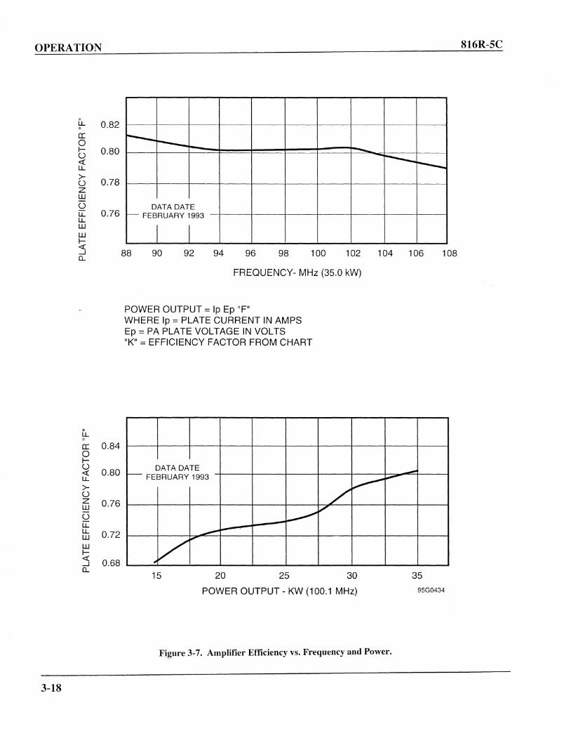
............... ...............~ ............... ..........r------.... ...............
DATA DATE~ FEBRUARY 1993
I I
OPERATION
LL 0.82a:0I- 0.80()«LL
>- 0.78()zw()
u: 0.76LLwWI-«-JCL
88 90 92 94 96 98 100 102 104 106 108
816R-SC
FREQUENCY- MHz (35.0 kW)
POWER OUTPUT = Ip Ep "F"WHERE Ip = PLATE CURRENT IN AMPSEp =PA PLATE VOLTAGE IN VOLTS"K" = EFFICIENCY FACTOR FROM CHART
DATA DATE ----~ FEBRUARY 1993~
~
/'~
',,;'
~
~~
~V""
u..a: 0.840I-()
0.80«LL
>-()z 0.76w()
u:LL 0.72wwI-« 0.68-J0...
15 20 25 30
POWER OUTPUT - KW (100.1 MHz)
35
95G0434
3-18
Figure 3-7. Amplifier Efficiency vs. Frequency and Power.
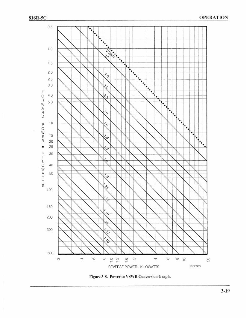
816R-5C
0.5
1.0
1.5
2.0
2.5
3.0
F0 4.0R 5.0WAR0
P 10
0WE 15R 20
• 25
K 30IL0 40WA 50TTS
100
150
200
300
500
OPERATION
~~.
~•
~ ••~ •~~~ '"
.~.
" ••",-'",,""- "~ £,~ • I
"•'"/'"."z.,~••
'" ~ ", '\ F •••"" ~ "\," '" ••
'" '" ", '" " ......
""'~ ~ ")?
"~.
",0 ••
~ , ", ~" ..."', """••......,,- ~ "', ~ '"
, ~......,""" '" "-, " '" '" •..... '" •
"'" "'" " "-~t.t)' " '" "'"•
'" " '" "'" '\.. r'\. '\.. •
~~I'" '" " " ~
""•
~ " •~
""•••
~ ~~O ",~ ••
~ ~~ ""- ~ " "",-'" '".
"•
r'-. " l'\.. •~ /', •
"~
"" '" K "", ~
""" '" "", •, •,~ '\.. ••
'" '" ~ "~..cI I~ "'" '" '" "', '" •••I'-. '" '" i"\.. ~ '" ", '\
" " ~~ ......
'" ~ " '" " " r'\.. '" " '" " •:T '\.. •
\. "" ", "", "Z '" " ""- "" '" '" "," '\.. ~ ~
~ "" " "/' "'- " ~ ""- "" "" "', ""'" "'" '" 'Z " " '" '" ", " "",
'" " ", " ", "', " "', ", "" " " " " ,"'" "'" "
,'" "\.. "'" "'" " "< J " \..
"'" " "'", ,
"'"0 ""~ ~ " ~ '"
" "- " "~ '" '"l'
'" " ~ "~ '" "~ " '" "'- ", \.. ,,,~ '""" "" '"~ " ~"~ '" '" ""- ", , ~~. " , " " "~~~ ~ '" "" '" I'" '" "
'" '" ~ "", ", '" , l'\ " "~'" i"\.. "'- "r\.. "l7 '" "-" '" '" ~ " '" ",+/',..
~ '" ",,,,,- "I'-. ", " '" ~ '" '"
,'" '\ ~I\..
"'''' '" '" '" ~~-", '" '" ", "r\.. I': "- ",,~",-" " "" I)''" '" "i'\. ""- "" '" ""'\ '", i"\.. r'-. '" " " " "" ~'"
'\
" i"\.. "r<~ " " '" '" '" " ~ ",r'\.
" '" '" '" ", i"-~7~~ '"~ " '" '" '" '",
I'"
'" '" '" '" ", I'( " ", ", "I'-. '" " ~ " "'" ""
~
~"" " '\
",,,,,-"" '" ", ", '\, , , i"\.. ~ I\.. "o
(\J
REVERSE POWER - KILOWATIS
Figure 3-8. Power to VSWR Conversion Graph.
93G0373
3-19

OPERATION
3-20
(This Page Intentionally Left Blank)
816R-SC
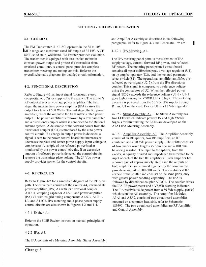
816R-5C THEORY OF OPERATION
SECTION 4 - THEORY OF OPERATION
4-3.2.1 IPA Metering, AI.
4-3.2.2 Status Assembly, A2. The Status Assembly hastwo LEDs which indicate power ON and high VSWR.Signals for illuminating the LEDs are developed on theA3A1 IPA Metering Assembly.
The IPA metering panel permits measurement of IPAsupply voltage, current, forward RF power, and reflectedRF power. The metering panel printed circuit boardcontains all meter calibration pots, a voltage regulator (U1),an op amp/comparator (U2), and the metered parameterselect switch (S 1). The operational amplifier amplifies thereflected power signal (V2-5) from the IPA directionalcoupler. This signal is compared to a reference voltageusing the comparator ofU2. When the reflected powersignal (U2-3) exceeds the reference voltage (U2-2), V2-1goes high, causing the VSWR LED to light. The meteringcircuitry is powered from the 50 Vdc IPA supply throughRl and VI on the card. Device VI is a 12 Vdc regulator.
4-3.2.3 Amplifier Assembly, A3. The Amplifier Assemblyconsist of an RF splitter, two RF amplifiers, an RFcombiner, and a 50 Vdc power supply. The splitter consistsof two quarter wave lengths 75 ohm line and a 100 ohmbalancing resistor. The input to the splitter, from theexciter, is equally divided and impedance transformed to theinput of each of the two RF amplifiers. Each amplifier hasa power gain of approximately 16 dB and the outputs ofboth amplifiers are summed together by the combiner toprovide an output of 500-600 watts. The combiner is thereverse of the splitter and consists of the same parts, onlywith greater power handling capability. The IPA isfollowed by directional coupler A3DC 1. The coupler drivesthe IPA RF power meter and a VSWR warning indicator.The IPA receives its dc power from a 50 Vdc supply, part ofwhich is on the A5 assembly. The Amplifier Modules,A3Al and A3A2, consist of two circuit card assembliesmounted on a common heat sink, refer to Schematic189397. The two circuit card assemblies are RF Amplifierand Control Assembly.
Iand Amplifier Assembly as described in the followingparagraphs. Refer to Figure 4-3 and Schematic 195125.
4-1. GENERAL
4-3. RF CIRCUITS
Refer to Figure 4-2 for a simplified diagram of the RF drivepath. The drive path consists of the exciter A4, intermediatepower amplifier (IPA) A3 with its directional couplerA3DCl, coupling capacitor AI2Cl, and power amplifier(PA) VI with its grid tuning components AI2C3, AI2LlL3, and A 12C2. IPA metering and 3-phase power supplycontrol circuits are also shown in Figures 4-2 and 4-4.
4-3.1 Exciter, A4.
4-2. FUNCTIONAL DESCRIPTION
The FM Transmitter, 816R-5C, operates in the 88 to 108IMHz range at a maximum rated RF output of 35 kW. A CE802B solid state, wideband, FM Exciter provides excitation.The transmitter is equipped with circuits that maintainconstant power output and protect the transmitter fromoverload conditions. A control panel provides completetransmitter metering and tuning controls. Refer to theoverall schematic diagrams for detailed circuit information.
Refer to Figure 4-1, an input signal (monaural, stereocomposite, or SCA) is supplied to the exciter. The exciter'sRF output drives a two stage power amplifier. The firststage, the intermediate power amplifier (IPA), raises theoutput to a level of 500 Watts. The last stage, the RF poweramplifier, raises the output to the transmitter's rated poweroutput. The power amplifier is followed by a low pass filterand a directional coupler which is connected to the station'santenna system. A dc sample of the forward power from thedirectional coupler (DC 1) is monitored by the auto powercontrol circuit. If a change in output power is detected, asignal is sent to the power control board that increases ordecreases the plate and screen power supply input voltage tocompensate. A sample of the reflected power is alsomonitored by the power control circuits. If an excessiveamount of reflected power is detected, the control circuits
I remove the transmitter plate voltage. The 24 Vdc powersupply provides power for the control circuits.
Refer to the 802B 'Exciter instruction manual, principles ofoperation.
4-3.2 IPA, A3.
The IPA consists of a Metering Assembly, Status Assembly,
Change 3 4-1

THEORY OF OPERATION
4-3.2.3.1 RF Amplifier. The RF Amplifiers use a systemof lumped coaxial lines to match the drain-to-drainimpedance of 12.5 Ohn1s, balanced, to 50 Ohms, balanced.See Schematic 189214. Transmission lines TL 1OlandTL 102, which have a characteristic impedance of 25 Ohms,are seriesed at their output connection to TL 103 (for 50Ohms) and are paralleled at their input connection to theamplifier transistor, Ql, to present a 12.5 Ohm impedance.The balanced 50 Ohm output impedance at the junction ofTL 101 and 102 must be converted to a unbalanced outputsignal for coaxial transmission. This is accomplished byTL 103. The length of this line is just long enough topresent a large impedance to the unbalance current in itsshield. This type of current balun results is excellentbalance to the transistor drains.
The amplifier module is untuned. The operation of thetransformers and the balun serve to limit the operating rangeto 80-120 MHz. The input of the amplifier is similarlybroadband. Capacitor C 101 is adjusted to insure thatvariations iI} such things as the gate capacity of theamplifier FET transistor and the leakage reactance of theinput transformer are balanced out to provide a good inputmatch to drive the Splitter over the operating range.
The output transistors of the PA Modules operate insaturated push-pull, Class BC, with an operating angle ofapproximately 150 degrees and a drive level, at full output,of up to 20 Watts. This results in a conversion efficiency inexcess of 750/0. The bias adjustment for the RF transistor,R220, is adjusted to give an operating bias of + 1.5 to 3.5Vdc. This bias adjustment also serves as a gain control.During final testing, slight adjustment of the bias control ismade to insure that the gain of both RF amplifiers are equaL
There is an optimum drive level for the PA Modules. Asthe amplifiers are under-driven, they go into a linear modeand conversion efficiency drops. Over driving theamplifiers results in excessive harmonic content at theamplifier drains which also causes a drop in conversionefficiency. Drive level is adjusted by varying the exciteroutput to obtain the desired drive power to the finalamplifier tube.
4-3.2.3.2 Control Assembly. The Amplifier ModuleControl Assembly is an on-board protection system toprotect the module from over-current and over-temperature.The Schematic Diagram, 189211, shows that the operatingvolt..ge for the protection circuitry, + 15 Vdc, can be derivedfrom either the +24 Vdc Control Power Supply of thetransmitter or from the +50 Vdc supply through theisolation diodes, CR201 and CR202. Voltage for the RFtransistor flows through the over-current shunt, R209, andthe ON/OFF switch, Q203. Switching transistor Q203 is
4-2
816R-5C
either ON or OFF in this circuit. The voltage on either sideof the over-current shunt, R209, is reduced to +8 Vdc by thebridge circuit. As the current flow, the over-current shuntcauses a voltage drop, 0.5 Vdc when the current is 10amperes. The voltage differential is amplified by a bufferamplifier so that the output of buffer, U201A is 6.4 Vdc,when the current through the amplifier is 10 amperes. Thisvoltage appears on 11-2 and is used to monitor the current ineach module. This current-related voltage is also bufferedand divided and feeds the non-inverting input ofU201B. Apreset reference voltage of +4 Vdc is applied to theinverting input ofU20 lB. When the current through theamplifier exceeds 12.5 amperes, the output ofU201 goeshigh and fires the SCR, Q202. This, in turn, pulls the baseof the switch driver, Q201 low. This turns Q201 ON whichcauses the gate voltage of Q203 to rise to input voltagevalue. Unless the gate ofQ201 is low, the switch turns OFFand removes voltage from the amplifier. Each RF Module isalso protected with a 12 ampere fast-acting fuse.
Over-temperature operation is detected by the thermalswitch, S1, on the amplifier assembly. This switch ismounted in contact with heat sink close to the attachmentpoint of the amplifier transistor. Closure of the switch dueto over-temperature (80 degrees C.) causes current to flowin the opto-isolator U202. This causes the voltage across theopto-isolator output transistor to fall to zero. Again, theswitch, Q203 opens and removes voltage from theamplifier. Operation of the thermal switch is throughresistor R223.
4-3.3 RF Power Amplifier, A12.
The RF power amplifier is driven by the IPA through amatching network consisting of the COUPLING control(CI), the PA GRID TUNE control (C2), and Ll, 2, 3 (SeeFigure 4-2). Capacitor C3 and resistor Rl swamps thepower amplifier grid circuit and provide a more uniformimpedance to the IPA under varying drive conditions.Inductor L 14 and the distributed capacity of resistor R75couple R75 to the cavity, forming a suppressor thatdampens the higher order cavity resonances that can occurnear the third harmonic of the output frequency. Cathodetuning (or peaking) capacitor C39 improves the bypassaction at the operating frequency. Inductor L5 is the poweramplifier grid bias feed choke.
The power amplifier is a plate tuned 4CX 15 ,OOGA tube thatis operated as Class C. The tube screen is grounded and thecathode is placed 750 Volts (nominal) below ground toprovide screen voltage, as shown in Figure 4-5. A fixed biasfrom the power amplifier bias power supply is applied to thecontrol grid through terminal A5E12, resistor A5R13, andterminal A5E13. When an input signal is present, grid
Change 2

816R-5C
current flows and develops grid leak bias across resistorsR35 and R36. The increased negative potential on the gridcauses the diode in the power amplifier bias supply toreverse bias, preventing grid current flow through thesupply. Hall effect probe A5Z 1 monitors the amount of gridcurrent for control panel metering.
The power amplifier plate circuit is coarse-tuned from 88 to108 MHz by resonating adjustable coaxial resonators,Figure 4-6. The resonators are in the area between the tubeshelf and the sliding shorting plane. Two motor-drivencapacitors permit more precise tuning (capacitor C51) andloading (capacitor C50). RAISE or LOWER switches S10or Sll (PA TUNING) and SI2 or S13 (PA LOADING) oncontrol panel A 1AI, control the capacitor drive motors. Thedc blocking capacitor C2 is located between the top ofpower amplifier tube and input to the air chimney. Figure4-7 shows the electrical equivalence of the plate tuningcircuit.
4-3.4 Low-Pass Filter, A7.
Low Pass filter A7 (Figures 6-1, sheet 2) consists of twocoaxial filters in tandem. The first filter has a cutofffrequency of 130 MHz, while the second has a cutofffrequency of 300 MHz.
4-3.5 Directional Coupler, DCI.
The directional coupler provides a proportional dc voltageto both the forward and reflected circuits of A2A6. Theoutput of each is then routed to, and can be displayed on,the Forward! Reflected Meter (AIM4).
4-4. POWER SUPPLIES AND POWER CONTROLCIRCUITS
4-4.1 General.
Refer to transmitter schematic 189632 for the followingdiscussion. There are five separate power supplies in thetransmitter. Three of the five, the plate, screen and poweramplifier bias power supplies provide voltages to the poweramplifier. The Driver supply, furnishes voltage to the IPA
Istage. The 24 Vdc power supply provides power to thecontroI circuits 0
Change 3
THEORY OF OPERATION
4-4.2 24 Vdc Power Supply, PIO A10. IThe 24 Vdc supply is a fully self-contained power supply. IA parts list and schematic diagram is included in thismanual.
4-4.3 Power Amplifier Bias Power Supply, PIO Al O.
The power amplifier bias power supply provides the poweramplifier with fixed grid bias that holds the tube near cutoffwhen no signal is present on the grid. Single-phase primarypower is applied through contactor A8K} and step-uptransformer T} to a bridge rectifier network. An L-sectionfilter is formed by inductor L 1 and capacitor C2.
The power supply output is applied to the grid of the poweramplifier through diode CR5. Diode CR5 blocks gridcurrent flow through the supply when the grid leak biasexceeds the fixed bias. A sample of the bias voltage isapplied through resistor R3 to front panel meter AIMI formonitoring.
4-4.4 PA Plate Power Supply.
The power amplifier plate power supply provides platevoltage to the power amplifier. Primary components of thesupply are transformer AI4TI, 3-phase bridge rectifierassembly A14ZIA, ZIB, ZIC, filter choke Ll, and filtercapacitor C1. A meter multiplier board, A12A1, samplesplate voltage and allows constant monitoring. Input powerto transformer A14TI is controlled by SCR(silicon-controlled rectifier) power control unit A9. Thisunit, connected as a closed loop regulator, maintainsconstant power output to offset conditions of varying linevoltage.
4-4.5 Power Control Unit, A9.
Power control unit A9 regulates the 3-phase ac power inputto the power amplifier plate and the power amplifier screentransformer. SCR assembly Z 1 has three SCR pairs; onepair in series with each primary winding of the 3-phasepower transformers. Each pair is connected within the deltacircuit of the transformer primaries. Three control cards arelocated within the A2 card cage. Each control card controlsthe firing (tum-on) point of one SCR pair (Refer to Figures4-4 and 4-8).
A common dc control signal from power control regulatorA2A6 is fed simultaneously to each control card. Thiscontrol signal governs the firing of the SCR pairs thatregulate the input power applied to the power supplies.Upon receipt of a PLATE OFF control signal, a ground isplaced across the inputs of each card.
4-3

THEORY OF OPERATION
MONAURAL,STEREO
COMPOSITE,SCA
:A3
FORWARDPOWERSAMPLE
816R-5C
27.5 kW88 TO 108 MHz .
DIRECTIONAL~ :COUPLER .... ,
DC1
REFLECTEDPOWERSAMPLE
3 rAPOWER
PHASE / CONTROLLINE I B--.--+-., UNIT
VOLTAGE lC A9
t24VDC
CONTROLSUPPLY
A10PS1
CONTROL VOLTAGE
VSWRCALIBRATE
ANDAUTO POWER
CONTROLCIRCUITS
A2A6
* INPUT TO PLATE AND SCREENPOWER SUPPLIES IS 3-PHASECONTROLLED VOLTAGE.
Figure 4-1. FM Transmitter 816R-5C, Block Diagram"
4-4
95G0196d
Change 3

816R-SC
A4
EXCITER
A3
IPAMETERING
A3A3A3DC1
COUPLINGIPA
FWD REFL
A12C1
THEORY OF OPERATION
Vi
PAGRIDTUNE
AS
A3R4
A3R3
A3R1
....---------(T a---..3 PH ---:-
POWER i a---.L...-_s_UP_P_L_Y----aI--------< 1a---.
TODRIVERSUPPLYCIRCUIT
BREAKER
Change 2
Figure 4-2. RF Drive Path.
TOPLATE-ONCIRCUITRY
98G0093
4-5
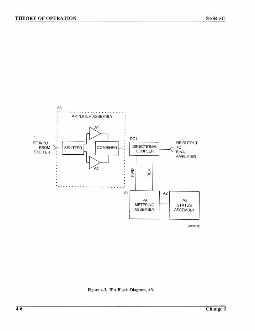
AMPLIFIER ASSEMBLY
THEORY OF OPERATION
A3It' • G .., ...
A1
816R-SC
RF INPUTFROM
EXCITERSPLITIER
• DC1
DIRECTIONALCOUPLER
o >~ wu.. a:
RF OUTPUTTOFINALAMPLIFIER
••• e ••••••• 0 lIP ••• lID .
A1
IPAMETERINGASSEMBLY
A2
IPASTATUS
ASSEMBLY
98G0092
4-6
Figure 4-3. IPA Block Diagram, A3.
Change 2

816R-SC
ACVOLTAGEAPPLIED TOPLATE ANDSCREENTRANSFORMERS
seR's
~
~
~
THEORY OF OPERATION
FULLPOWER
REDUCEDPOWER
GREATLYREDUCEDPOWER
240 VACINPUT ONEOF THREEPHASES
GATINGCARD
CTRL SIG. 0-5 VDC
ONE OF THREEPLATETRANSFORMERSECTIONS
ONE OF THREESCREENTRANSFORMERSECTIONS
DIRECTIONAL
COUPLER
POWER
CONTROLCARD
P/O A2A6
PLATE14------- ON/OFF
CONTROL
CONTROLCARD
P/O A2A6
A10A2K~MAN.
'-----{~
AUTO.
MOTORDRIVENMANUALPOWERCONTROL
93G0296
Change 2
Figure 4-4. SCR Power Control, Simplified Diagramo
4-7

THEORY OF OPERATION 816R-5C
A12L6
SCREENOVLDA5K2
PLATECURRENT
A12 L54.7 uH n
A12T1
A5R51{l
Figure 4-5. Power Amplifier DC Bias Circuitry Simplified Schematic.
4-8 Change 2

816R-5C
C92
TUBECHIMNEY
P5, J5
PATUNING
(C51)
R75
TUBESHELF
C82
C83
C52
S15
" I /-0-
THEORY OF OPERATION
C49
C48
C84C85
S7
P4,J4
SLIDERDECK
BLOCKINGCAPACITOR
C2 (REF)
PA LOADING(C50)
TUBE
A3
93G0340A
86
Change 2
Figure 4-6. PA Cavity, A12.
4-9

THEORY OF OPERATION 816R-SC
r ---- -- -- - -- - - - - - - --- - - - -- --- - - - - -- - - - - - - - - - - - - -- - - - -- - - - -- - - - - - - - - ---
LOWPASSFILTER
C50
LR r···········
~ (-L1L-1-2V~i...--s:H<+---+-.a:: J2 MONITOR
LOADING .::L- ~ ~ SAMPLEB3 -- •
I···II·
C51
........eTUNING
B2
PLATE TANK CIRCUIT
PIO A12
(l1 0 fr-K MONITOR
~3~ r J6SAMPLE
I·I··I··_________________________ • _. .. ., eII • •
C2
V1
A12L6
A12IC49
NOTE:C2 IS THE CAPACITANCE BETWEEN TUBE ANODE AND THE CAVITY CENTER CONDUCTORA12C50 IS THE CAPACITANCE BETWEEN MOVABLE PLATE 1 AND THE TUBE ANODEA12C51 IS THE CAPACITANCE BETWEEN MOVABLE PLATE 2 AND THE TUBE ANODELR IS THE LUMPED CONSTANT EQUIVALENT OF THE SHORTENED 1/4 WAVE RESONATOR
93G0299A
Figure 4-7. PA Tuning Circuit, Simplified.
4-10 Change 2

816R-5C
4-4.6 Power Control Regulator, PIO A2A6.
The po\ver control regulator located on A2A6 provides thenecessary control signals to operate power SCR control unitA9. Assembly A2A6 supplies a soft-start power amplifierplate supply tum-on signal, a negative voltage for manualpower control, and amplifier mixer functions for automaticpower control.
IWhen the PLATE ON switch is pressed, 24 Vdc is suppliedto A2A611-30. The 24 Vdc activates transistor Q1 to turnon relay A8K6. Relay A8K6 in tum supplies 3-phase accontrol power to A2Tl-3. An RC time delay circuit formedby resistor R41 and capacitor C12 maintains A8K6 closedfor a short interval after the PLATE OFF switch is pressed.
I Transistors Q2, Q3, and Q4, also energized by the 24 Vdc,provide the dc turn-on signal to the gate cards. ResistorsR34 and R35, and capacitor C11 modify this signal tosoft-start the high voltage power amplifier plate powersupply. Zener regulator VR4 provides -10 Vdc toMANUAL power adjust resistor A2A9R1. Transistors Q4and Q5 amplify the control signal and apply the signal tothe gating cards. Capacitor C5 and resistor R36 phasecompensate the power control servo loop.
4-4.7 PA Screen Power Supply.
The 3-phase regulated voltage from the power control unitis applied through transformer T2 to a silicon 3-phasefull-wave bridge rectifier assembly A5CR1 in the poweramplifier screen power supply. The output of A5CRI isfiltered and applied to the cathode circuit of the poweramplifier at the secondary center tap of filament transformerA12Tl.
4-4.8 Driver Power Supply, PIO A5.
The driver power supply is a 3-phase, full-wave, type usinga single section choke input filter. It nominally delivers 45Vdc at 25 amperes to its load. The supply's primary poweris switched through relay A5Kl which is operated by thePLATE ON circuitry. The supply is protected throughcircuit breaker A6CB3.
4-4.9 Filament Voltage Regulator, A2A4.
When the Filament Regulator Card is in the automaticmode, the filament voltage regulator detects andcompensates for sustained fluctuations in the input acvoltage (Refer to Schematic Diagram Figure 7-2). Thefluctuations are detected by a true rms detection circuitwhich in conjunction with associated circuitry, includingmotor control circuits, adjusts the setting of variabletransformer A8A2T 1. The output voltage of the variabletransformer is then applied to the primary of power
Change 3
THEORY OF OPERATION
amplifier filament transformer A 12T1. The variabletransformer voltage is also applied to the primary ofdetector circuit transformer A2T4.
Voltage for the power supply circuits on the filamentregulator board is derived from sampling transformer A2T4.This ac voltage is rectified and applied to voltage droppingresistor R33. Capacitor C24 provides filtering. Athree-terminal 15 Vdc regulator U9 supplies voltage to the15 Vdc circuits with additional stabilization provided bycapacitors C27 and C28. Voltage dropping resistor R34feeds three-terminal 5 Vdc regulator U 10 while capacitorsC29 and C30 provide additional voltage stabilization. LEDDS5 indicates voltage present on the 5 Vdc line whichimplies that the 15 Vdc circuits are also powered.
Negative supply voltage is provided via diodes CRI andCR2 via resistor R3 and capacitor C24 to card edgeconnection 38 for distribution to other circuit cards in thetransmitter.
A sample of the voltage feeding the power amplifier tubefilament transformer is applied via transformer A2T4. Thisac signal is applied to RF filtering components inductor L 1and capacitor C14. Inductor L I has a 4.7 J1-h parallelresonance which falls in the FM broadcast band providing ahigh impedance path for frequency modulated RF signals.Capacitor C14 is a 100 pf capacitor whose series resonancefalls in the FM broadcast band providing a low impedanceshunt path for frequency modulated RF signals. Thesefiltering components are used in several locations in thefilament regulator card, and provide the same filteringfunctions as described here.
The filament voltage sample signal is then applied to theRMS-to-dc converter circuit via voltage divider resistors RIand R2, and through capacitor CI5. This RMS-to-dcconverter circuit is based around U7, a true rms-to-dcconverter integrated circuit. The converter directlycomputes the true RMS of any complex input waveformcontaining ac components. It has crest factor compensationwhich allows very accurate measurements up to 300 kHz.The crest factor of a waveform is the ratio of the peak signalswing to the RMS value. Components C17, R17, RI8, C18,RI9, and C20 provide time constant and filtering functionsfor the converter.
4-11

THEORY OF OPERATION
Test point 3 (TP3) provides easy access to the dc voltagerepresentation of the filament RMS voltage. During nonna}operation of the filament voltage regulator, resistor R2 isadjusted so the output of the RMS-to-dc converter circuit is5.00 Vde when the filament voltage has been preset to thenominal value by the operator. The output voltage is thenfed to window comparator composed of U8 and relateddevices. The voltage references for the window comparatorare provided by U 11, a very high precision 10-Voltregulator, and voltage divider components R20, R21, R22,and R23. In nonnal operation, resistor R20 is adjusted toprovide 5.00 Vdc at TP2. The corrected reference voltagesare then applied to their respective comparators. Pin 5 of U8has 5.05 Vdc applied, and pin 10 ofU8 has 4.95 Voltsapplied. These voltages will be correct if resistor R20 hasbeen properly adjusted for 5.00 Vdc on TP2. The 50 mVvoltage drops are provided by voltage divider resistors R21and R22. This 100 mV total window provides a total ± 10/0window for the voltage comparator, and hence for thevoltage regulator circuitry.
If the voltage from the RMS-to-dc converter circuit iswithin the 4.95 to 5.05 Vdc window, the outputs of thecomparators will both be high and the output of AND gateU4C will go high illuminating green LED DS4 indicatingproper filament voltage is present. If the voltage from theRMS-to-dc converter is not within the 4.95 - 5.05 Vdcwindow, the circuit will then operate to make the necessarycorrections if switch S2 is in the AUTO position.
Assuming that switch S2 is in the AUTO position, if thefilament voltage rises above +1% of the nominal valuesetting, the following actions are taken. The output of the5.05 Vdc comparator will go low at U8-2 causing the outputofU4 to go low and DS4, the LOCK LED, will extinguish.Device U8-1I will go high bringing the input of U 1-13high. When either of the comparators goes low, indicating acorrection is necessary, U2B, U2D, and U2C incombination act as an OR gate forcing U 1-1 0 high which intum triggers timer, U6. When U6 is timing, the output pin 3goes high illuminating yellow LED DS 1. At the same time,UI-3 output goes low which takes the input ofU4-I low.This output is fed through switch SIA to inputs UI-9, Ul12 and U2-1 bringing them all low. Hence, while the timeris in its timing state, the outputs of U 1C, U 1D, and U2A areall high, inhibiting the actuation of relays Kl, K2, and K3respectively. Once the timer U6 has timed out, the inputs ofUIC, UID, and U2A fed from switch SIA are broughthigh. At this point if the filament voltage is still above the+ I% nominal value, both inputs ofUI will be high,enabling actuation of relay Kl and the clutch assembly onthe filament voltage adjust variac motor. Simultaneously,both inputs of U 1D will go high forcing its output pin 11 togo low. The LOWER LED (DS2) will be illuminated andrelay K2 will be activated which in tum actuates the lowerwinding in the motor driving the filament voltage controlvariac. Once the variac brings the filament voltage backinside the range of nominal operation, the comparator
4-12
816R-5C
output ofU8-2 will go high, and the above logic actions arereversed removing power from the filament voltageregulator variac motor.
The raise function operates just as the lower functiondescribed above, but instead activates the raise circuits. Itmay be noted that if future adjustments by the operator arerequired in the automatic mode, resistor R2 may be used asa simple filament voltage adjustment control.
The timing period of timer U6 is provided to guard againstconstantly correcting momentary excursions in the filamentvoltage. This delay timing period is adjustable from 0 to 12seconds with resistor R7.
If automatic operation of the filament voltage regulatorcircuit is not desired, switch S1 can be put in the MAN(manual) position. This effectively takes the regulator out ofthe circuit, but the green LED lock indicator will still showif the filament voltage is within nominal range.
While in the manual mode, momentary switches S2 and 83can be used to manually activate the clutch and raise orlower circuits respectively. Other than the timer not beingactive in this mode, these switches simulate the output ofthe comparators per the operator's command, thus manuallyraising or lowering the filament voltage. This provides aconvenient way to determine if most of the digital logic andthe solid state relay are functioning properly should aproblem occur. Devices U3A and U3B are provided toinsure that the raise and lower functions are not activatedsimultaneously by circuit failure or accidentally by theoperator using the manual control.
While in the manual mode, the operator may depress boththe raise and lower switches simultaneously and the onlyaction to take place is the timing ofU6 as noticed by theillumination of yellow LED DS 1. This allows the operator aconvenient way to set the time delay ofU6 withoutaffecting the other circuits.
Solid state relays K I, K2 and K3 provide a return for the acvoltages already on the windings of the clutch, and thelower and raise circuits of the variac drive motor. Relays K2and K3 also have the return path for the ac voltages routedthrough micro-switches SI and S2 on the variac assembly.This provides a secondary measure against operating thefilament voltage regulator outside of the prescribed rangeprovided by the mechanical stops on the variac drive motor.
Change 2

816R-5C THEORY OF OPERATION
FORWARD
POWERDIRECTIONAL
COUPLERDC1
POWER CONTROLA1A1S1 PS
IAUTO 1~32) I
HMANUAL J NO-
1~3S>------'A1A1S2
1- - - - - - - - --I1 +10V 1
I 1
~ I 05 I- 10 - - - - - - - i I 04 2N2222A 1
1 V R48 J1 I - - - - . I 2N2222A ~ II +U4 6 38 )- K2 I I 1- R22 II ILRESET I ~-R24 4.7K,
1 1 .-------<12~U +24 I 47 22
I I I, 1 1 C6 I
I ----""-24) < . L-: ~14)-<261 T 0.1 I~ ---+--- 13~. I" I C7-=
I 1 I: I I T O.1 -10V 1LP/OA2A~ - - - - _I I 0-'SET 1 1P/OA2A6-= ~ 1
--<1i~ +24 I L ~.----'
~OA10A2_y~ , .•.•......•....••..~f:
120VAC FROM
A6XF14-2
"A14T1,T2
IPRIMARIES1/ (2 PLACES)
A
C
I
N
P
U
T
P
0A9Z1-B W
ER
J93G0300
88
8 2A3 A9Z1-A
14~
8,04
08 f---~----:
88A214
28 f----+------~"--~
POWER ADJUSTA1A1S7 PI6J0-73S>---------+--------e--r
>.,/\./\. ,....4
RAISE I I~34)
LOWER 10736)-";"'!-+----+-~II-r-__4It__---JA1A1S8
P4 -~-l---------- 6-- 51
6 <1::9 ~ /..9•••~~1 T:8 (1~ tJ I
I P4
\. I___---t---~3 /
I
(16~ I1K~••.••• ~ ••• / .9../311 i
L__~o"TO K2 / 1/ I
1 17)--i-- P5-3S(A1A1J1-3S)
LP/0 A.2.?~ I
+24
POWERLOWER
POWERRAISE
Figure 4-8. Power Control Circuits, Simplified Diagram"
Change 3 4-13

THEORY OF OPERATION
4-4.10 Filament Voltage Distribution.
The filament voltage distribution is shown in Figure 4-9.Filament voltage regulator A2A4 maintains a constant rmsvoltage on the filaments as discussed in Paragraph 4-4.9.
4-5. PRIMARY POWER DISTRIBUTION CONTROLAND OVERLOAD CIRCUITS
4-5.1 Primary Power Distribution.
The 60 Hz, 3-phase primary power is distributed to thevarious circuits of the transmitter via circuit breakers andfuses mounted on circuit breaker panel A6. Refer to Figure4-10. Circuit breaker A6CB5 is connected inside the deltaof plate transformer A14T1. It also serves to interruptprimary power to the PA screen transformer T2 throughassociated circuit breaker A6CB4. Circuit breaker A6CB3controls power to driver power supply (IPA) transformerT3. AC line voltage metering is provided by ac meterA2Ml. In addition to the three phase-to-phase voltages,A2MI can monitor the power amplifier filament voltage.BLOWERS circuit breaker A6CB2 controls application ofprimary power to cavity blower Bland FAN fuses A6F7,F9, and F12 through filament-on relay A8K2. Relay A8K2is energized when the filament switch (S2) is turned on.Application of primary power to the filament circuits, theexciter, the power amplifier bias power supply, and thepower amplifier tuning and loading motors is relaycontrolled. Filament-on relay A8KI and blower-on relayA8K2 control application of power to the regulated filamentcircuit through auto-transformer A8A2TI. Relay A8Kl alsocontrols application of power to 802B Exciter A4, to poweramplifier bias power supply, PIO A10, and to the poweramplifier tuning and loading motors B2 and B3respectively. Power to the exciter and the motors is throughisolation transformer T4. Time totalizing meter A2M2 isplaced across the load side of filament-on relay A8KI.
The filament, exciter, and power amplifier bias supply inputpower circuits are protected by associated fuses. Thesecircuits receive power from the blowers circuit breaker,A6CB2.
4-5.2 Transmitter Tum-On.
The transmitter is energized by pressing FILAMENT ONswitch AlA 1S4 on the A 1 control panel. Relay A8K2 isenergized and is applied to the blower motors. Aftersufficient air pressure is created in the power amplifiercabinet, air switch AI2S1 is closed and relay A8K1 isenergiz~d.
4-14
816R-5C
After a 30-second delay, relay A8K4 is energized. ThePLATE ON switch is pressed energizing relay A8K3 whichapplies 24 Vdc to the base of transistor A2A6Q3. This turns Ion the control amplifier, which applies input voltage to theplate and power supplies.
The transmitter may also be energized by pressing thePLATE ON switch \vhich latches relay A8K3, andenergizes relay A8K2 through contacts 8 and 5. Pressingthis single switch (PLATE ON) enables the transmitter togo through the above sequence of blower, filament, timedelay and plate on.
4-5.3 Exciter Power Control Override.
An output override voltage is supplied to the 802B Exciterwhen the plate voltage is turned OFF. This mutes the outputof the exciter while the power amplifier plate voltage isturned OFF (Figure 4-11). The voltage is applied from the24 Vdc power supply through contacts 3 and 9 of relay IA8K4 to the 802B Exciter power supply regulator.
4-5.4 FWDIREFL Calibrate and Auto Power Control Unit,A2A6.
4-5.4.1 Functions. The FWD/REFL CALIBRATE ANDAUTO POWER CONTROL portion of the A2A6 cardperforms these functions (Refer to Schematic 180162):
1. The forward power signal from the directional coupleris buffered and amplified to provide a panel powermeter reading of 1000/0 at the customer's specifiedtransmitter power output (TPO). Full scale meterindication is 1200/0 in the FORWARD POWERposition.
2. The forward power signal from the directional coupleris compared against either of two internal, adjustablevoltages for automatic power control. Two discretelevels of power control are remotely selectable andmaintain the desired power to within 10/0.
3. The reflected power signal from the directional coupleris buffered and amplified to provide a full scale readingof 12% of the customer's specified TPO on the panelpower meter in the REFLECTED POWER position.
4. The reflected power signal from the directional coupleris compared against an internal limit to smoothly foldthe forward power level back when a slowly risingVSWR level is detected. Forward power is reduced tokeep the reflected power at 5 to 60/0 of the customer'sspecified TPO.
Change 3

816R-5C THEORY OF OPERATION
A2T4
A2A4FILAMENTVOLTAGE
REGULATOR
GRNVIO
13 <I
25 <
L v -- v -- V -- V -- V46 2 42 1 6
V V V
ORG BLU~
I29 <
I
WHT
~
115VAC
0
RED'·
WHT BLK
FILAMENTS
2
~~6i 2i1;~... .. 4 ~12 C5\ 1 3
~.~~_FI~E~ ~~~~:::~_1!-2~-2JII~1V 3f~-p3 A8A2 I' A12 C56 A12T1
-~-T 0 0 T1 A6F13: ~ --~-~ A8K2B A8K1 P7 - I---~
~ r 3 J1 :
R209.09K
R199.09K
R175K
PIO A2A7
CARD CAGE COMPo ASSY : 93G0301
Figure 4-ge Filament Voltage Distribution..
Change 2 4-15

THEORY OF OPERATION 816R-5C
: T1 PRI WINDINGS
~-------------------___l
~...----- ----------------------j
REGULATED DCOPERATING/CONT
VOLTAGE FROMREGULATOR A2A8
POWERCONTROL
A2A8
F6 ---.t:B~ :
F8 ---.t-:C~_:
~ ~10 .:A)----O~ .
24VDC DON RELAY
A8K6A6CB5~
r------- -------------------~
200-250 VAC60 Hz 3 PHASE
A8TB1
m(-(- -( A6CB6
A6CB4 : T2 PRI WINDINGS
~--------------------iII"-----_""---:--'" ~-~------~.--+---------------------4IIt--+----~~-..--.-
a---+---+-----------------tIIIl--+--+------=---------...~L--___,.---------lDRIVER ~ - - . '
24 I P_W_~_~ : dJ----------J-~_=:::::=.._=:::::=..~ VDC-=--=--=--=--=--==.-------...-----,-0 0b,'---_-.D1
IPAA5K1
I PHASE t
iMONITOR
A6CB2
......-;--..,.-~~-+
~--""-'I--+-
B)----------f--+-+-
A DB C BL~~~RS
A6F1 ON RELAY
CAVITYBLOWER
B1
VARIAC DRIVEMOTORA8A2 B1 ---F-IL-AM-E-N-T--'
_ VOLTAGEREGA2A4
AC LINEVOLTMETER
A2A7 SWITCH
FILAMENT
A6F13
I--A_2A_9_B_1_...~
?MANUALPOWER
CONTROLADJUST
93G0372
LOWERA1A1S8
RAISEA1A1S7
DK6 DK4 ~REMOTERELAYS
:P/OA10A2
}
TO PAFILAMENT
....-----..----,
PALOADINGMOTOR
A12B3
A6F11
PA BIASPOWERSUPPLY
P/OA10
o~)----a~-.r..-4--------+-------__--+---
DFIL ONRELAY
A8K1
B>--~--::=V-~_-__~A6F2 __----l-----f.------l
c>--~~~-------.A6F3 '
A~Tro-------.A6F4
Figure 4-10. AC Power Distribution.
4-16 Change 3

816R-5C
4-5.4.1 Functions. - Continued
5. A reflected power signal from the directional couplercan remove power from the transmitter and light theVSWR tally LED when a rapidly rising reflected powerlevel greater than I00/0 of the customer's specified TPOis detected.
4-5.4.2 Theory of Operation.
The forward power signal from the directional coupler,DC 1, is amplified and buffered by V4. Resistor R9 is anoffset null adjusted for zero output at TP 1 when no inputsignal is present. Resistor RIO is adjusted to provide a100% forward power indication on the panel power meter(AIM4) at the customer's specified TPO.
The output ofV4 is also present on terminal boardAIOTB2-13, through a 2.2K ohm isolation resistor, R53, toprovide remote metering of forward power.
The positive output ofV4 is coupled through diode CR1land compared at the inverting input ofU3 against thenegative voltage from either resistor R8 (Normal Power) orresistor R7 (Second Power) in the automatic mode. Theoutput of U3 is used to raise or lower the transmitter platevoltage, as necessary, to maintain the selected power level.The input to V3 is switched from resistor R8 to resistor R7
I by relay K 1 which is activated by applying +24 Vdc to relayKl coil through terminal board AI0TB2-1. Normally,resistor R8 sets the normal operating TPO reference whileresistor R7 is adjusted for some lower value, perhapsnecessary during emergency operation with a generatorunable to supply the full power load.
The reflected power signal from directional coupler DC 1 isamplified and buffered by VI. Resistor Rl is an offset nulladjustment for zero output at TP2 when no input signal ispresent. Resistor R2 is adjusted to cause a 10% reflectedpower indication on the panel power meter AIM4 when thereflected power reaches 10% of the customer's specifiedTPO. Resistor R3 is adjusted to simulate that 100/0 reflectedpower level when the TEST switch S1 is depressed. Thisallows testing of the VSWR protection and meteringcircuits. The output of VI is fed through resistor R43 to thegate of the VSWR overload SCR A2A5Q4 when theVSWR protect is in the enable position. Resistor R4 isadjusted to fire SCR A2A5Q4 when the reflected powerreaches 100/0 of the customer's specified TPO. When SCRQ4 fires, VSWR overload relay A11K9 activates, removingpower from the transmitter and illuminating the VSWROVERLOAD LED.
The output ofV1 is also present on terminal boardAIOTB2-12 through 2.2K ohm resistor R46 to provide
Change 3
THEORY OF OPERATION
remote metering of reflected power.
Devices U2 and U3 form the VSWR foldback circuit. Asample of the buffered reflected power signal from U 1 isfed to U2 through resistor R5. Resistor R6 is the offset nulladjustment for U2 and is adjusted to give zero output at U26 \vhen no input signal is present. The output of U2 iscoupled through diode CR6 to the automatic powercomparator, U3. Resistor R5 sets the level so that the outputvoltage ofU2 will exceed that ofU4, causing the power tobe reduced, when the reflected power exceeds 5-60/0 of thenormal TPO. The VSWR foldback circuit is defeated by thecircuitry of the ten second timer U5. The timer is triggeredby sampling the anode voltage ofVSWR overload SCRA2A5Q4. The response time of the VSWR foldback circuitis relatively slow. A sudden significant increase in VSWR,as in an arc, would cause the VSWR overload SCR to fire.Power to the transmitter is removed, the VSWROVERLOAD LED is illuminated and the VSWR foldbackcircuit is disabled for ten seconds. The VSWR foldbackcircuit is disabled to allow the VSWR overload circuit tosample the VSWR at full power thereby preventingoperation into a dangerously deficient load.
4-5.5 Overload Protection.
Relays A5K2, A5K3, and A5K4 are adjusted to energizeand remove power from the transmitter when an overloadoccurs in the plate or screen supply or when the VSWRexceeds a preset level. Screen current through resistor A5R8produces a voltage that is applied to relay A5K2 throughresistor A5R15. The plate current through resistor A5R7produces a voltage that is applied to relay A5K3 throughresistor A5R16. When SCR A2A2QS is gated on, a groundis applied and relay A5K4 is energized. Each relay isadjusted to trip at a factory preset current level. The relaycontacts are in series with plate control relay A8K3. If anoverload occurs, the corresponding relay trips andde-energizes relay A8K3, removing plate power from thetransmitter.
4-5.6 Overload and Recycle Board, A2A5.
Overload and recycle board A2AS contains circuits thatprovide overload indication and memory, automatic poweron recycling, and filament control circuit interlock status(Refer to Schematic 180167).
4-17

THEORY OF OPERATION
When an overload occurs in the PA plate, PA screen, orI VSWR circuits, a 24 Vdc pulse is supplied to the
appropriate SCR Q4, Q7, or Q8. The SCR latches and lightsits associated LED indicator on the A 1 panel to indicatewhich overload has occurred. All indicators that have beenlighted by an overload function remain lighted until OVLDFAULT RESET switch AIAISl6 on the main control panelis pressed. Plate voltage is removed by overload relays
IA5K2, A5K3, or A5K4. The 24 Vdc pulse that triggers theSCR is simultaneously routed to the recycle circuit viadiodes CR9, CR11, or CR12 to be used to automaticallyrestart the transmitter.
The automatic recycle circuit provides a timed restart pulsefor up to four overload occurrences within a 30-secondperiod. The card as shipped will allow only two restartpulses in a 30-second period. However, it may bereconfigured to allow four restart pulses in a 30-secondperiod by removing the jumper between terminals A and Bon the card and replacing it between A and C.
IThe auto recycle begins when the 24 Vdc pulse is applied tothe base of transistor Q2 causing it to conduct. The outputof Q2 is fed to timers Uland U4. Timer U 1 provides aO.5-second delay, then triggers timer U3 which generates aO.5-second output pulse. This pulse is fed through gate U2Ato inverter Q3 which causes Q6 to conduct and chargecapacitor C22. The charging current of capacitor C22momentarily energizes relay K 1 which closes the PLATEON circuit through switch S2. The charging current ofcapacitor C22 also flows through RECYCLE PULSEindicator LED CR6 giving an indication of the recyclecircuit operation.
Gate U2D conducts the output pulse from timer U 1 tocounter U5. Counter U5 counts the number of recyclepulses and provides a logic 1 output at terminal C when fourpulses have been received. Depending on which terminalhas been strapped to terminal A, two or four recycleattempts in a 30-second period will close gates U2A, U2B,U2C, and U2D and prevent any further attempts by the cardto restart the transmitter. RECYCLE LOCKOUT indicatorLED CR2 will light to indicate this condition. When the30-second period of time has elapsed, a pulse is generated,inverted by transistor Q 1, and applied to U5 to reset it tozero. This clears the memory and allows another sequenceto begin. If the maximum count of two or four pulses hasnot been received in the 30-second period, the timer willalso reset the counter automatically.
4-18
816R-5C
AUTO-RECYCLE switch S2 may be used to disable theauto recycle card when desired. This is usually done duringtune-up or maintenance procedures. RECYCLE TESTswitch S1 may be used to test the automatic recycle circuitduring maintenance procedures by simulating an overloadpulse at the input to the recycle circuit.
4-5.7 Power Failure Recycle Board, A8Al.
In the event of momentary loss of primary power, the powerfailure recycle circuit restores the transmitter to operationalstatus. Capacitor C3 maintains current flow through timedelay relay A8K4 keeping the time delay circuit active forshort term power outages and a separate circuit provides amomentary ground at pin 10 when power is restored. Themomentary ground is applied to capacitor A2A5C22 and thecharging current of this capacitor pulls relay A2A5K8 inand initiates the power ON command.
4-5.8 Auto-Manual Power Control Latching Relay andTransmitter Status Indicators.
The latching relay permits local or remote selection ofmanual or automatic power control (Refer to Figure 4-11and Status and Interlock Simplified Schematic, 189579, inpouch at rear of manual).
The latching relay is connected to the remote control panelthrough terminal board A 1OA2. A 24 Vde signal applied by Imanual control switch AIAlS2 or through remote controlinterface board will latch relay A1OA2K2 in one of twostable states. AUTO PWR CONTROL switch LEDA1A 1S1 indicates automatic power control is selected andMAN PWR CONTROL switch LED A1AIS2 indicatesmanual power control is selected.
Visual indication of TRANSMITTER CONTROLREMOTEILOCAL switches A2A7S 1 or A2A7S2 are givenby status indicator LEDs AIAIDS22 and A1AIDS16.
Plate control circuit interlock status indicators are providedon the Control Panel A 1. RMT PLT OFF INTLK indicatorLED A1AIDSll is lighted when remote relay A10A2K8 isde-energized. PA GRID DOOR INTLK indicator LEDAIAIDSl2 is lighted when the PA grid compartment dooris closed. PA DOOR INTLK indicator LED A1A1DS13 islighted when the power amplifier plate compartment door isclosed. L REAR DOOR INTLK indicator LED A1AIDS 14,C REAR DOOR INTLK indicator LED A 1A 1DS 15, RREAR DOOR INTLK indicator LED AIA1DS17, C FRPNL INTLK indicator LED A1AIDS18, and R FR PNLINTLK indicator LED AIAIDS19 are panel interlock statusindicators that are lighted when the respective panels are in
Change 3

816R-5C
place. Panel designations refer to the three bays of thetransmitter cabinet (left, center and right) as viewed fromthe front of the transmitter. REMOTE INTLK indicatorLED A1A1DS20 is lighted when continuity exists betweenremote control interface terminal board Al OTB 1-3 and -4.FAILSAFE INTLK indicator LED A 1A 1DS29 is lightedwhen remote relay Al OA2K8 is energized. Indicator LEDsA1A1DSl1 through A1AIDS21, except for AIA1DS16,are in series and in sequence as they are connected in thecircuit. Therefore, an interlock must be satisfied before itsstatus indicator LED will light.
4-5.9 Power Control Relays, PIO A10A2.
Assembly Al OA2 provides remote manual power lower andraise control. When power is decreased at the remotecontrol panel, relay K4 is energized (see Figures 4-8 and4-12). Closed contacts provide 115 Vac to motor A2A9Bl
Change 3
THEORY OF OPERATION
which adjusts the resistance of A2A9Rl to decrease thetransmitter power output. When the power is increased atthe remote control panel, relay K6 is energized and closedcontacts provide 115 Vac to motor A2A9B 1 which adjuststhe resistance of A2A9R1 to increase the transmitter poweroutput.
4-5.10 Remote Relays, PIO A10A2.
Remote relays in Al OA2 parallel the front panel controloperations. Failsafe relay K8 is energized only \vhen 24 IVdc is present in the control circuit. If the 24 Vdc is lost,the relay de-energizes and removes plate power from thetransmitter. Second power level (low power) relay K7 mustalso be energized continuously (24 Vdc) to maintain this Ifunction.
4-19

THEORY OF OPERATION 816R-5C
RELAY SHOWN IN MANUAL(SET) POSITION
RESET AUTOA1A1S1
---.L-
O~
11POWERMON/CTRL -7--(14 ~--+---~
A2A6 13
MAN. PWR.A2A9R1
9
15 >-+1 AUTO. PWR.A2A6
r-==-----I----~16
11<17hi.
6
4
8 IIAUTO IPIO A1A1S1
+24V
'--------if----~18
IMANUAL IPIO A1A1S2
I
94G0028
--L-t-------+--4---~19)>--------'0 ~
MANUAL mA1A1S2
16
SET
: PIO A10A2K2 PIO TB1
{
O. ";U'T·Q·· , ·", , ·", · .""· ·"", , · , '\" . "I" "", , , ·
MAN.
FROMREMOTE
CONTROL
Figure 4-11 .. Latching Relay Simplified Schematic..
4-20 Change 3

816R-5C THEORY OF OPERATION
POWER CONTROL
RESISTOR
PIO•••• !II It D ••••• a •• ••- •••••••
POWER ADJUST A 1A1J2A1A1S7 I R2 : 0.01 uf
1~35
I~
RAISE 2 ,. 100 C 1
~34 81
IC2 9
1~36 : 0.1 uf -LOWER
P/O A2A9 :A1A1S8 •••••••••••••••• III " It ..... T
120VAC FROMA6XF11-2
•••• II. II II II •••••••••• ". 6 8 5 8 u
+24
POWERRAISE
6
POWERLOWER
------+----~3
9 I--+----<
TO K2
'-------~7>-- A1A1J1-35
· PIO A10A2• II•••• iI •••••• It" • liD D • D ••••••••••••••••••••••
93G0304
Change 3
Figure 4-12 .. Power Control Relays Simplified Schematic..
4-21

THEORY OF OPERATION
4-22
(This Page Intentionally Left Blank)
816R-5C
Change 2

816R-5C
5-1. ROUTINE MAINTENANCE
MAINTENANCE
SECTION 5 - MAINTENANCE
1. Remove the cross-wire brace that holds the filter in place.
The transmitter is carefully inspected and adjusted at thefactory to reduce maintenance to a minimum. To ensurepeak performance, adhere to a regular schedule of periodicchecks and maintenance procedures. Refer to the parts lists,Section 6, for component location in the transmitter.
WARNING
HIGH VOLTAGES ARE EXPOSED WHENCABINET DOORS OR ACCESS PANELS AREOPENED. WHEN WORKING INSIDE THEEQUIPMENT, BE SURE THAT ALL CIRCUITBREAKERS ARE OFF AND THAT PRIMARYPOWER IS DISABLED AT THE WALL_DISCONNECT OR CIRCUIT BREAKERUNLESS OTHERWISE DIRECTED. ALWAYSSHORT ALL HIGH VOLTAGE TERMINALS TOGROUND WITH THE GROUNDING STICKPROVIDED. FAILURE TO COMPLY MAYRESULT IN DEATH ON CONTRACT.
5-2. CLEANING
Clean the transmitter when dust accumulation occursanywhere inside the equipment. A solvent oftrichlorethylene may be used as a cleaning material.
5-2.1 General Cleaning Procedures.
1. Remove dust from chassis, panels, and components witha soft-bristled brush.
2. Remove foreign matter from flat surfaces and accessibleareas with a lintless cloth moistened with solvent. Drywith a clean, dry, lintless cloth.
3. Wash switch and relay contacts with relay contactcleaner. Wash less accessible areas with solvent lightlyapplied with a small soft-bristled brush.
5-2.2 Air Filter.
The air filter should be cleaned whenever a perceptiblequantity of dust and dirt accumulates on the filter element.Remove and clean the filter as follows:
2. Remove the filter.
3. Use a vacuum cleaner to remove heavy dustaccumulation from the filter.
4. Blow a stream of air through the filter in a directionopposite to normal air flow.
5. Wash the filter in a solution of hot water and detergent.
6. Reinstall the filter when dry.
5-2.3 Tube Cleaning.
The power amplifier tube should be cleaned when a visiblequantity of dust accumulates on the cooling fins of the tube.Carefully remove the tube from the socket and clean with adry, oil free jet of air.
5-3. INSPECTION
Inspect the transmitter at least once a week. Check all metalparts for corrosion and general deterioration. Examinewiring and components for signs of overheating. Ensurethat all controls are operating smoothly. Inspect allconnections and tighten any loose nuts, screws, or bolts.Examine the blower and cabinet fans for normal operation.
5-4. LUBRICATION
The tuning and loading motor and the manual powerincrease/ decrease motor are sealed and do not requirelubrication. The cabinet inlet fan motor (B2) and the PAcavity blower motor (B 1) bearings should be lubricatedwith SAE 10 oil as necessary or if required.
5-5. PARTS REPLACEMENT
The following paragraphs present general descriptions forthe removal and replacement of certain component parts.
I
Change 3 5-1

MAINTENANCE
5-5.1 PA Tube, VI.
816R-5C
Table 5-1. Required Test Equipment.
1. Remove air guides (tube chimney) between the PAblocker and the cabinet base. Loosen the two bands(top and bottom only, never loosen the center band) onPA blocking capacitor and slide it down over the PAtube.
2. Remove the anode lead.
Name
Volt-ohmmilliammeter
AC Voltmeter
Power Supply
Description
Test Meter
oto 10 volts, 1% to 1
oto 28 volts DC, 6 amps
Manufacturerand Model
Fluke 77
Weston 433(true RMS)
Any
CAUTION
BE CAREFUL TO NOT BEND OR BREAKTHE SOCKET'S FINGER CONTACTS.FAILURE TO COMPLY MAY RESULT INDAMAGE TO THE TUBE SOCKET.
RF Wattmeter
ThrulineWattmeter
DC Voltmeter
2.5 kW and 25 kW elements~ Bird Thruline50 to 125 MHz (or equivalent)
0-1 kW element, 0-100 W Bird 43 (orequivalent)
o to 10 kV, 1% to 1 any
3. Carefully lift the tube (4CX20,OOOE), and PAblocking capacitor, out of its socket.
DC Ammeter oto 5 amperes, 1% to I any
4. Reverse the procedure to install the replacement.
5-5.2 Fuse Replacement.
Turn AC line breaker off before removing or installingfuses.
5-6. TROUBLESHOOTING
If the transmitter fails to operate properly, check eachcircuit in the order that it is made operative. Use thesimplified schematics and the overall schematic in Section 4when needed. Normal control panel meter readings areprovided in Tables 3-5 and 3-6. Efficiency graphs areprovided in Figure 3-7.
5-6.1 Access Panel Interlock Switch.
The access panel interlock switches must be blocked opento perform certain adjustment procedures. To block thepanel switch to open, push in on the plunger and insert twoinsulated blocks between the switch contactors. Remove theinsulated blocks before reinstalling the panel.
5-6.2 Test Equipment.
Table 5-1 lists the test equipment necessary to maintain thetransmitter.
5-2
5-6.3 Troubleshooting the Power Controller.
1. Remove primary power from the transmitter and groundhigh voltage components (Refer to Figure 5-1).
WARNINGVOLTAGE HAZARD
USE CARE WHEN SERVICING GATINGCARDS A2AI, A2, AND A3. 250 VAC ISPRESENT ON CARDS WHEN MAIN CIRCUITBREAKER A6CB6 IS ON. FAILURE TOCOMPLY MAY RESULT IN SERIOUSPERSONAL INJURY.
2. Remove two of the three gating cards from the A2assembly.
3. Restore the primary power to the transmitter and turnFIL ON.
4. Place the transmitter in MANUAL POWER CONTROLand after the time delay has expired, turn PLATES ON.

816R-5C
NOTE
The transmitter plate and screen power supplieswill be operating with only one power phaseapplied in the following tests. The plate voltage,screen voltage, and RF po,ver output will be lowerthan usual. Exact voltages in these tests areunimportant.
5. Operate POWER CONTROL ADJUST and observe thatthe plate voltage, plate current, and RF power outputchange smoothly. Note the maximum plate voltage. Ifthe power controller phase under test is good, thereshould be no breaker trips, no unusual noise from thepower transformers and no building lights blinking.
CAUTION
REMOVE PRIMARY POWER FROM THE_TRANSMITTER EACH TIME A GATINGCARD IS REMOVED. FAILURE TO COMPLYMAY RESULT IN CARD DAMAGE.
If none of the cards operate properly in the selected powercontroller receptacle, use a different card receptacle andrepeat the test. Perform the same test with each of theremaining gating cards in the same power controller cardreceptacle. The results should be the same for each card ifthe card is good. If all the cards operated properly, use oneof the cards to test each of the two remaining receptacles.This will check the other two power controller phases.
If all cards operate properly in one or two receptacles butnot in another, it can safely be assumed that the cards aregood but either an A2 control transformer or one of theSCR banks are defective. Experience indicates that theSCRs are least likely to fail.
5-7. ADJUSTMENTS
All transmitters are factory adjusted and pre-tuned tospecific customer requirements. No adjustments arerequired by the customer unless a broken part is replaced, aspecific assembly does not display meter readings withinallowable tolerances, or the transmitter is operated at afrequency or power output different from the frequency orpower output specified in the production test data suppliedwith the transmitter.
Change 3
MAINTENANCE
NOTE
The 24 Vdc power supply is ON when both the28V supply breaker and ac line breaker are ON.Unless otherwise indicated, the POWERCONTROL switch is set to MANUAL, thePOWER switch is set to FORWARD, the AUTORECYCLE switch is set to OFF, and all circuitbreakers are set to ON during adjustmentprocedures.
5-7.1 Switch Adjustments.
5-7.1.1 Air Interlock Switch, A12S 1.
1. Press the PLATE OFF and FILAMENT ON switches oncontrol panel AI.
2. Remove the rear panel behind the PA cavity.
3. Adjust the tension bolt on switch A12S1 so that thegreen filament light goes out when the PA gridcompartment door is opened approximately one inch.
5-7.1.2 Tuning Motor Limit Switches, A12S11-S14.
1. Press the PLATE OFF and FILAMENT OFF switcheson control panel AI.
2. Remove the rear panel behind the PA cavity, or the sidepanel next to the cavity.
3. Loosen the mounting screws on the limit switch.
4. Position the limit switch so that the peg mounted to therack gear causes the switch to trip before the peg runsinto either end-stop. The tuning and loading paddlesmust never be closer than 5/8 inch from the blockingcapacitor.
5-7.2 Filament Voltage Adjustment.
1. Press the PLATE OFF and FILAMENT OFF switcheson the control panel AI.
5-3

MAINTENANCE 816R-5C
3 PHASEACINPUT
F10
*A6CB2*A6CB3
*REAR VIEW OFBREAKERS SHOWN
*A6CB4
Z1C
TRANSMITTER
POWER ENTRY BLOCK
*A6CB5
*A6CB6
Z1BZ1A:A9
. AC1
A2E1-1
A2E1-2
POWERTRANSFORMERTAPS SHOWNFOR 210 VAC
2 7PA PLATE
TRANSFORMER
4 9
12
14
T1
2 7PA SCREEN
TRANSFORMER
4 9
12
14
T2
93G0305A
Figure 5-1. Primary AC Wiring, Power Control.
5-4
816R-5C MAINTENANCE
5-7.2 Filament Voltage Adjustment. - Continued 7. With S1 of the filament regulator card A2A4 inMANUAL position, depress RAISE switch, A2A4S3,and run variable transformer drive motor until limit
WARNING switch actuator arm is against the upper clockwiseVOLTAGE HAZARD (CW) limit switch.
HIGH VOLTAGES ARE EXPOSED WHEN 8. Adjust variable transformer A8A2Tl with an insulatedCABINET DOORS OR ACCESS PANELS rod for an indication of7.0 V ac. Note the filamentARE OPENED. THE SHAFT OF VARIABLE meter reading. If filament meter does not agree withTRANSFORMER A8A2Tl HAS calibration meter, adjust filament meter calibrationHAZARDOUS VOLTAGE TO GROUND A2A7Rl until it does.WHEN FILAMENT CONTACTOR ISENERGIZED. USE CARE WHEN 9. Press FILAMENT OFF switch on control panel AI.PERFORMING THE FOLLOWING Tum OFF main circuit Breaker A6CB6.PROCEDURES. FAILURE TO COMPLYMAY RESULT IN PERSONAL INJURY. 10. Tighten set screws on variable transformer end of
motor coupling.
2. Open the power amplifier grid compartment and 11. Place switch A2A4S 1 on the filament regulator card inconnect a 0 to 10 volt, true RMS ac, one percent MANUAL position.meter, to the power amplifier filament rings on the
- tube socket. 12. Tum main breaker A6CB6 back on. PressFILAMENT ON switch on control panel AI.
3. Run the meter leads through the comer of thecompartment and close the power amplifier 13. Use the RAISE or LOWER switches, A2A4S2 and S3,compartment door. on the filament regulator card to adjust the filament
voltage to the desired voltage, 6.3 V ac rms is the I4. Remove the cover from the control circuits card cage recommended operating voltage for 48 hours, as
and pull the plunger on the card cage interlock all the indicated on the true rms voltmeter.way out. Turn main circuit breaker A6CB6 OFF.
14. Check the comparator window voltage on the filamentregulator card. It should be preset to 5.00 volts. If it isnot, adjust resistor R20 observing the voltage on
WARNING BLUE test point 2 (TP2) and adjust for 5.00 volts.VOLTAGE HAZARD Once this voltage is set, it should not need to be reset
unless a component change is made.GROUND VARIABLE TRANSFORMER(A8A2Tl) SHAFT AND CONTACT BRUSH 15. Adjust resistor R2 for 5.00 volts by observing theASSEMBLY BEFORE TOUCHING ANY voltage on RED test point 3 (TP3). At this point thePART OF VARIABLE TRANSFORMER. green LOCK LED DS4 should illuminate.REPEAT THIS PROCEDURE EACH TIMEPOWER IS REMOVED. FAILURE TO 16. To adjust the timer, while still in the MANUALCOMPLY MAY RESULT IN PERSONAL position of switch S1, push both RAISE and LOWERINJURY. switches (S3 and S2) simultaneously and time how
long the timer yellow indicator, DS 1, stays on. Thisdelay is normally set for 5 seconds at the factory to
5. Loosen motor coupling set screws on variable prevent momentary changes in the power line voltagetransformer A8A2T1 (Right side panel) end of from constantly effecting a correction. To increasecoupling, and tum the main circuit breaker ON. time delay adjust resistor R7 counter clockwise
(CCW); to decrease time delay adjust resistor R7 CWo6. Press FILAMENT ON switch on control panel AI. Repeating the above will verify your action. The time
delay range is approximately 0 to 12 seconds.
Change 1 5-5

MAINTENANCE
17. Once the above adjustments are made, activate theautomatic mode of filament voltage regulation byplacing switch 51 in the AUTO position. RAISE andLOWER switches 53 and S2 only operate in the MAN(manual) mode of operation.
18. The life of the PA tube can be greatly enhanced bycorrectly adjusting the filament voltage required toproduce the emission needed for your rated outputpower. To obtain the optimum tube life you shouldadopt the following procedure.
19. First stabilize a new tube's emission by operating it atthe recommended filament voltage for 48 hours.
20. Place the transmitter power control in the MANUALposition. Also place the filament voltage regulator inthe MANUAL position.
21. Raise the transmitter output power to 105% of normalrated power.
22. Carefully lower the filament voltage in 0.2 volt steps,pausing about 30 seconds after each step, look for agreater than 20/0, change in output power or platecurrent. This is the filament emission knee. Now raisethe filament voltage 0.2 volts above this voltage. Thisis the correct filament voltage for your output power.
WARNING
REMOVE ALL POWER FROM THETRANSFORMER BEFORE WORKING ONTHE VARIABLE TRANSFORMER LIMITSWITCHES. FAILURE TO COMPLY MAYRESULT IN PERSONAL INJURY.
23. It may be necessary to adjust the lower limit of thefilament voltage variable transformer to find the kneeand/or operate at the correct filament voltage.
24. After the correct voltage for desired operating powerhas been established, repeat Steps 13 through 17 andreset the "desired voltage" to the correct level.
25. Check for a change in the filament voltage knee oneweek later. Keep the operating voltage 0.2 volts abovethe emission knee. Repeat this check monthlythroughout the life of the tube.
5-6
816R-5C
26. After the filament voltage has been set, return thetransmitter output power control to the AUTO position.Ensure that the filament voltage regulator is also inAUTO.
5-7.3 DC Overload Adjustment.
1. Press the PLATE OFF and FILAMENT OFF switcheson control panel A 1. Turn DRIVER POWER SUPPLY,PA SCREEN POWER SUPPLY and PA PLATEPOWER SUPPLY circuit breakers OFF.
2. Remove the lower front center panel.
5-7.3.1 PA Plate Overload Adjustment.
1. Connect an ammeter from the positive terminal of anadjustable 28 Vde power supply to resistor A5R8-1.
2. Connect the negative terminal of the de power supply toresistor A5R5.
3. Raise the dc power supply current to 5.8 amperes.
NOTEThe plate supply current is rated at 5.0 amperes.This measurement point is the sum of the plateand screen supplies and 5.8 amperes allows forthe 0.8 ampere screen supply.
4. If overload does not occur, then adjust PA PLATEOVLD ADJ resistor A5R16 to trip relay A5K3 at thiscurrent. (The PA PLATE OIL fault indicator on theoverload/recycle board lights when the relay trips.) Ifoverload trip occurs at less than 5.8 A, adjust resistorA5R16 to raise trip point to 5.8 amperes.
5. Disconnect the ammeter and remove the jumper fromthe dc power supply to resistor A5R5.
5-7.3.2 PA Screen Overload Adjustment.
1. Connect a milliammeter from the positive terminal of anadjustable 28 V de power supply to terminal 3 ofA5R15.
2. Connect the negative terminal of the de power supply toterminal! of A5R15.

816R-5C
3. Raise the power supply current to 600 rnA.
4. If overload does not occur, then adjust PA SCREENOVLD AD] resistor A5R15 to trip relay A5K2 at thiscurrent. The PA SCRN OIL fault indicator LED on Allights when the relay trips. If overload trip occurs at lessthan 600 rnA, adjust resistor A5R15 to raise trip pointto 600 rnA.
5. Disconnect the milliammeter and remove the jumpersfrom the dc power supply to A5R15.
6. Press the FAULT RESET switch on control panel AI.
5-7.4 PA Grid Current Meter Calibration.
1. Press PLATE OFF and FILAMENT OFF switches oncontrol panel A 1. Tum DRIVER POWER SUPPLY,PA SCREEN POWER SUPPLY and PA PLATEPOWER SUPPLY circuit breakers OFF.
2. - Remove the front panel beneath the PA gridcompartment door.
3. Connect the negative terminal of an adjustable 28 V dcpower supply to A5E 13 and the positive terminal toA5E12.
4. Adjust the dc power supply current to 100 rnA.
5. Set the TEST METER selector switch to PA GRID 400rnA.
6. Adjust PA GRID MTRG CAL CONTROL resistorA5R18 for a 100 rnA reading on the test meter.
7. Remove the dc power supply test leads.
5-7.5 High Voltage Power Supply Static Check (no drive).
WARNING
HIGH VOLTAGES ARE EXPOSED WHENCABINET DOORS OR ACCESS PANELS AREOPENED OR REMOVED. FAILURE TOCOMPLY MAY RESULT IN PERSONALINJURY.
MAINTENANCE
1. Remove the lower front panel belo\v the exciter andblock open the interlock switch.
2. MUTE the exciter.
3. Press the FILAMENT ON and PLATE ON switches oncontrol panel AI.
4. Raise or lower the POWER ADJUST control untilapproximately 10,000 volts is indicated on the PLATEVOLTAGE meter.
5. Set TEST METER select switch to PA SCREEN 800 v.Observe that approximately 750 Volts is indicated onthe TEST METER.
6. Press the PLATE OFF and FILAMENT OFF switcheson control panel A 1 and Mute on the exciter.
7. Replace all panels and close all compartment doors.
5-7.6 IPA Metering Board Calibration.
5-7.6.1 General Information. Necessary equipment for thiscalibration includes: Bird Thruline Wattmeter with500-Watt and 100-Watt elements, ammeter with 0 to 30 Adc rating and inductive sensor, digital voltmeter, Bird500-Watt dummy load, 50-ohm coaxial cable with Type Ncable connector and adapters: male-to-male andfemale-to- female.
WARNING
TURN TRANSMITTER POWER OFF ORDISCONNECT IT WHEN CONNECTING ORREMOVING TEST EQUIPMENT ANDOTHER TEST COMPONENTS. HIGHVOLTAGES AND HIGH POWER RFSIGNALS ARE PRESENT. FAILURE TOCOMPLY MAY RESULT IN PERSONALINJURY.
5-7.6.2 Setup Procedures.
1. Refer to FM Broadcast Exciter 802B InstructionManual and adjust exciter power output to 15 watts.
2. Set PA SCREEN and PA PLATE POWER SUPPLYcircuit breakers on Circuit Breaker Panel (Figure 3-5) toOFF.
5-7

MAINTENANCE
5-7.6.2 Setup Procedures. - Continued
3. Set AC LINE circuit breaker on circuit breaker panel(Figure 3-5) to OFF.
4. Remove lower front access panel of center cabinet.Block interlock switch for the panel so that it isbypassed.
5. Remove four retaining screws and slide the IPA drawerand attached cables out from front of cabinet.
6. Set IPA metering assembly controls (Figure 6-11) asfollows:
R22 VSWR THRESHOLD INDICATOR Fully CWR27 COLLECTOR CURRENT CAL Fully CCWR32 COLLECTOR VOLTAGE CAL Fully CCWR23 FORWARD POWER CAL Fully CCWR14 REFLECTED POWER CAL Fully CCW
7. Disconnect coaxial cable from output of the IPA.
NOTE
In the following step, the DC coupler (A3DCl) isto remain in place at the IPA output.
8. Connect input of Thruline wattmeter with 500 Welement to IPA. Use appropriate coaxial adapter(s) and50 ohm cable. Connect input of Bird 500 W dummy loadto output of Wattmeter with appropriate adapter(s) andcable.
5-7.6.3 Calibration Procedures.
1. Set AC LINE circuit breaker Figure 3-5 to ON.
2. Set BLOWERS circuit breaker, and 28 V de andDRIVER POWER SUPPLY circuit breakers, on circuitbreaker panel (Figure 3-5) to ON.
3. Press POWER CONTROL MAN and FILAMENT ONswitch/indicators on control panel (Figure 3-2).
4. When READY indicator on PA control panelilluminates, set PA SCREEN and PA PLATE POWERSUPPLY circuit breakers on circuit breaker panel toON.
5. Press PLATE ON switch-indicator on control panel to
5-8
816R-5C
ON (lighted) condition.
WARNING
HIGH VOLTAGE MAY BE PRESENT ONEXPOSED ELECTRICAL TERMINALS ORCONDUCTORS OF THE TRANSMITTER.USE CAUTION WHEN WORKING NEAREXPOSED TERMINALS OR CONDUCTORS.FAILURE TO COMPLY MAY RESULT INPERSONAL INJURY.
6. Use digital voltmeter to measure voltage at A3RI-2.Record measurement.
7. Press Ec 60 VFS switch on IPA metering board A3A 1.
8. Adjust A3AIR32 on IPA metering board so that v-oltagelshown on meter matches that measured in step 6 above.
9. Slowly adjust exciter output so that power output ofIPA as shown on Thruline Wattmeter is 500 W.
10. Press FWD 1,200 WFS switch on IPA metering boardA3Al.
11. Adjust A3A 1R23 on the IPA metering board so that Ipower output shown on the meter is 500 W (forwardpower meter scale is 0 to 1,200 W).
WARNING
DANGEROUS VOLTAGES AND RF SIGNALSARE PRESENT IN THE TRANSMITTER.AVOID CONTACT WITH TERMINALS ORCONDUCTORS. FAILURE TO COMPLYMAY RESULT IN PERSONAL INJURY.
12. Press Ie 30 AFS switch on the IPA metering board.
13. Position inductive sensor of 0 to 30 ampere ammeteraround the wire attached to terminal A3RI-2. Recordthis measurement.
14. Adjust A3AIR27 on IPA metering board (Figure 6-28) Iso that current measurement shown on the metermatches that recorded in Step 13 above.
Change 3

816R-5C
15. Adjust exciter output until a measurement of 100 wattsin shown on Thruline Wattmeter.
16. Press PLATE OFF switch on PA control panel (Figure3-2). Press FILAMENT OFF switch.
17. Set PA PLATE, PA SCREEN, DRIVER, and 28 V dePOWER SUPPLY circuit breakers on circuit breakerpanel (Figure 3-5) to OFF.
18. Disconnect cable and adapter from IPA.
19. Disconnect directional coupler A3DC 1 from the IPA.Reverse coupler and use appropriate adapter to reinstallit in the reverse mode.
20. Reconnect Thruline Wattmeter cable and adapter to theIPA.
21. Perform Steps 2 through 5, above, to re-power thetransmitter.
22. Verify that output of IPA is still 100 Watts asestablished in Step 15 above.
23. Press REFL 1,200 WFS switch on IPA metering board.
124. Adjust A3A1R14 on IPA metering assembly (Figure6-28) until a measurement of 100 watts is shown on themeter.
25. Press FWD 1,200 WFS switch on IPA metering board.
126. Adjust A3A1R22 on IPA metering board CCW until theVSWR light on the IPA metering board just comes on.
27. Perform Steps 16 through 21 above.
28. Adjust exciter output (Figure 6-28) until the TrulineWattmeter indicates 500 watts.
29. Perform Steps 16 and 17 above.
30. Disconnect Thruline Wattmeter and dummy load fromoutput ofIPA.
31. Reconnect coaxial cable so that grid input circuit ofpower amplifier is connected to output of driver. Besure directional coupler A3DC 1 is still in configuration
Change 3
MAINTENANCE
established in Step 28 above. Directional coupler is tobe in its normal forward configuration.
32. Perform Steps 2 through 5 above.
33. Verify that output ofIPA as shown on meter ofIPAmetering board (Figure 3-6) is 500 ±50 watts. Slightadjustments may be made to the exciter output ifnecessary.
34. Perform Steps 16 and 17 above. Then set AC LINEcircuit breaker on the circuit breaker panel (Figure 3-5)to OFF.
WARNING
GROUND ALL CAPACITORS ANDCONDUCTORS IN THE TRANSMITTERBEFORE PERFORMING THE FOLL"OWINGSTEPS. FAILURE TO COMPLY MAYRESULT IN PERSONAL INJURY.
35. Slide the IPA drawer (Figure 3-1) into transmitter.Attach with four screws.
36. Unblock interlock switch for access panel of lowercompartment of transmitter center cabinet. Install accesspanel.
5-7.7 FWDIREFL CAL and Power Control Card, A2A6.
NOTE
Maintenance is required only if major partdamage has occurred. Adequate test equipmentis required for proper, accurate alignment.
5-7.7.1 Offset Nulls.
WARNING
USE CARE WHEN SERVICING GATINGCARDS A2Al, A2, AND A3. 250 VAC ISPRESENT ON CARDS WHEN MAINCIRCUIT BREAKER A6CB6 IS ON. FAILURETO COMPLY MAY RESULT IN SERIOUSPERSONAL INJURY.
5-9

MAINTENANCE
5-7.7.1 Offset Nulls. - Continued
1. Place the A2A6 card on the extender board. Tum ONonly the transmitter filaments and allow the componentsto temperature stabilize for at least 15 Ininutes.
2. Use a high impedance dc voltmeter to measure thevoltage at test point TP 1. Adjust resistor R9, FWDOFFSET, set for zero voltage at test point TPI.
3. Use a high impedance dc voltmeter to measure thevoltage at test point TP2. Adjust resistor Rl, REFLOFFSET, for zero voltage at test point TP2.
4. Use a high impedance dc voltmeter to measure thevoltage at U2-6, most easily accessible at either end ofresistor R27. Adjust resistor R6, OFFSET ADJUST, forzero voltage at U2-6.
5-7.7.2 Forward Power Calibration.
1. Adjustthe transmitter to normal power output using themanual power control. An indirect power calculationmay be used if an external power meter is not available.
2. Adjust resistor RIO, FWD CAL, to indicate 100% onthe OUTPUT POWER meter AIM4. DO NOTADJUST THIS CONTROL AGAIN. Increase thepower control to maximum output power. Refer to thetest data for proper plate screen and driver transformertaps if the maximum power output exceeds 1050/0. Themaximum power should not exceed 1050/0 unlessunusual circumstances exist.
3. Switch to AUTO power control and adjust resistor R8,PWR CNTRL ADJ, for 1000/0 power in the AUTOmode.
14. Apply 24 V dc to terminal board A IOTB2-1 to activaterelay AI0A2K7.
5. Adjust resistor R7, LP ADJUST, to the desired secondpower level.
5-7.7.3 Reflected Power and VSWR Protection Calibration.
1. Use the manual power control to reduce the poweroutput to 10% of the desired operating TPO.
2. Pull the VSWR PROT jumper OFF and reverse thedirection of the top element in the directional coupler,DCI.
5-10
816R-5C
NOTE
Reflected Power (VSWR) trip point is factoryadjusted to 10% of rated transmitter power or10% of TPO if factory is advised of TPO. Thislevel may not be desired and must be set bystation engineer to the desired safe level.
3. Adjust resistor R2, REFL CAL, to indicate 100/0reflected power. Full scale is 12% when reflected poweris selected. DO NOT ADJUST THIS CONTROLAGAIN.
4. With plates OFF, depress TEST switch, S1, and adjustresistor R3, REFL ADJ, for desired reflected (VSWR)level indication on panel power meter Al M4. Full scaleis 120/0. Nuisance trips may occur if the trip level is setfor less than 50/0.
5. Place VSWR PROT jumper ON and adjust resistor R4VSWR PROT CAL until a VSWR Overload occurs.
6. Remove all voltage, return the top element and VSWRPROT switch to normal.
5-7.7.4 VSWR Foldback Adjustment.
NOTE
The Foldback Circuit is not enabled when thetransmitter is shipped from our factory. Thereis the possibility of additional damage to apreviously damaged antenna system where theFoldback circuit is in use. The Foldback levelshould be set to the fully CCW position unlessantenna icing conditions are likely.
1. Pull VSWR PROT jumper OFF. Switch to AUTOpower control, and depress the REFL switch.
2. Remove the low power element from the top, reflectedpower position of the directional coupler, DC 1.
3. Remove the high power element from the bottom,forward power position of the directional coupler, DCI,and install it in the reflected power position with theelement arrow pointing toward the load.
Change 3

816R-5C
4. Turn the plate voltage ON, and in AUTO power mode,adjust R5 VSWR FOLDBACK LEVEL to the desiredfoldback level. Read the reflected power on the 12%scale. Disregard the fact that the forward element is notcalibrated for the reflected power meter. This test onlyrequires a voltage that is controlled by the powercontroller and represents some amount of reflectedpower. Foldback level must be approximately halfVSWR trip level or less.
5. Remove plate voltage, return the high power and lowpower directional coupler elements to their propersockets and direction. Return the VSWR PROT jumperto ON and resume normal transmitter operation.
5-7.8 Phase Monitor Adjustment.
WARNING
HIGH VOLTAGES ARE EXPOSED WHENCABINET DOORS OR ACCESS PANELS AREOPENED. USE EXTREME CARE WHENPERFORMING THE FOLLOWINGPROCEDURES. FAILURE TO COMPLYMAY RESULT IN PERSONAL INJURY.
10 Remove primary power and the right front bay accesspanels. Locate phase loss relay A8K5.
2. The phase loss/phase rotation monitor will shut off thetransmitter when phase loss or incorrect sequence isdetected. A phase loss will be detected if the linevoltage drops below the threshold voltage level whichis set by turning the control on relay K5. The thresholdvoltage range is 190 to 270 volts. Set control to 190volts, full counterclockwise (CCW).
3. Replace primary power and right front access panels.
5-8. CHANGING POWER
The power output is adjusted by changing taps on the screentransformer T2. The PA plate voltage is maintained high(9.5 to 9.8 kV) to keep efficiency high. Use the followingdata supplied in Sections 2 and 3 as a guide: Tables 2-1, 3-5and 3-6, and Figure 2-5. Adjust the screen voltage to obtainthe desired output power. To complete the power change,refer to Paragraphs 5-7.7,5-9.3, and 3.3, Step 25.
MAINTENANCE
5-9. CHANGING FREQUENCY
NOTE
If power and frequency are to be changed, referto Power Change, Paragraph 5-8, and changetransformer taps as directed, then return to thisparagraph to complete the frequency changeprocedure. Major RF tuning is required onlywhen components in the RF circuit are replacedor when the operating frequency is changed.Refer to the initial turn-on procedures(Paragraph 3-3 Steps 19 through 27) for minortuning instructions.
The following paragraphs provide procedures for major RFtuning of the transmitter. If the operating frequency is thesame as the frequency specified in the production test datasupplied with the transmitter, perform the procedures inParagraphs 5-9.2, Steps 1 through 10. If the operatingfrequency is different from the frequency specified in theproduction test data supplied with the transmitter, performthe procedures in Paragraphs 5-9.1 through 5-9.3.
NOTE
The data presented in the graphs (Figures 5-2,5-3 and 5-4) is approximate and is intended onlyto get the transmitter tuning close.
5-9.1 Frequency Change Adjustments.
NOTE
These adjustments are not necessary if therelated components have not been replaced andthe operating frequency is the same as thefrequency specified in the production test datasupplied with the transmitter.
5-9.1.1 Shorting Plane.
1. Press the PLATE OFF and FILAMENT OFF switcheson control panel AI.
2. Open the plate cavity doors.
3. Adjust the plate cavity slider deck (Figure 4-7) to thedesired frequency in accordance with the graph inFigure 5-2.
5-11

MAINTENANCE
5-9.1.2 PA Neutralization. Adjust the PA neutralizationbars to the desired frequency in accordance with the graphin Figure 5-3.
5-9.1.3 PA Grid Tuning Slider.
1. Open the PA grid compartment door.
2. Adjust the PA grid tuning sliders (Figures 5-4 and 5-5,Ll, 2, 3) in accordance with the graph shown in Figure5-4 for the desired frequency.
5-9.1.4 PA Grid Swamping Capacitor.
1. Swamping capacitor A 12C3 consists of two aluminumplates separated by some distance. The position of theplate nearest the front of the transmitter is adjustable,thus making it possible to set the distance between thetwo plates. Referring to Figure 5-6, loosen the screw onthe adjustable plate and position it to obtain the plate toplate sp_acing indicated in Figure 5-6 for the desiredoperating frequency. The spacing may be checked byusing a drill bit or a similar device inserted between theplates.
5-12
816R-5C
2. Tighten the screw on the adjustable plate.
5-9.1.5 Cathode Return Capacitor. Cathode capacitor slotposition definition: There are seven capacitor positionsdefined for each side of the four cathode return capacitors.The seven positions are chosen to be easily identified byeye. The positions are described below and in Figures 5-7,5-8, and 5-9.
Initially set the capacitor to the nearest whole positionindicated above. The final position of the capacitor may befine adjusted for improved efficiency after the transmitter isoperating.
5-9.1.6 Efficiency Capacitor. Preset the efficiencycapacitor A12A3C39 for minimum capacitance. Thecapacitor plates should be completely unmeshed.
5-9.1.7 Coupling Capacitor. Preset the coupling capacitor(Cl) for minimum capacitance. The capacitor plate shouldbe completely unmeshed. Close the grid compartment door.
5-9.1.8 PA Bias. Preset the bias resistor (R35), locatedbehind the power amplifier cavity, to the middle of its range.
(Continued on Page 5-21)

816R-SC MAINTENANCE
18
17
~ '-.~
'-.~
'-"''-"''-
"''-"'", "',
~,"'~DATA DATE
DECEMBER 1993
88 90 92 94 96 98 100
FREQUENCY IN MHz
102 104 106
93G0306
TUBE SHELF
SLIDER DECK
!/
"I IV
/
1(X)
j
Figure 5-2. PA Plate Tuning Cavity Slider, Coarse Adjustment.
5-13

MAINTENANCE
SCREEN RING
PA CAVITY FLOOR
o
o
o
TUBE SOCKETNEUTRALIZING CLAMPS
816R-SC
en 3UJI()
~ 2
~UJ()z«Ien(5
DATA DATE~
DECEMBER 1993
o88 90 92 94 96 98 100
FREQUENCY (MHz)
102 104 106 108
93G0307
5-14
Figure 5-3. PA Neutralizing Adjustment.

~ ......-....r---..~ ...... ......-.... ......-.... --...........~ ......-.... ......-.... .......
...............-.... ......-.... -............ ........... ......-.... ......-..................r---.. r---..
DATA DATEDECEMBER 1993
I I I I
816R-5C
3
Cf)wI2ozz
8-woz~1(f)
o
o88 90 92 94 96 98 100
FREQUENCY IN MHz
C7, 8, 9
102 104 106
MAINTENANCE
108
C4, 5, 6 r-- --+-_-+--~---------__,C10, 11 7 12
i(0)
1
i(0)
1
93G0308
Figure 5-4.. Graph for Coarse Setting of PA Grid Tuning Inductors..
5-15

MAINTENANCE
C7
C8
L2
C9
C59
CG C5
C10 L3 C11
L1 C4
C12
FILAMENTLEAD
93G0309
816R-5C
FILAMENTLEAD
CGO
5-16
Figure 5-5. Power Amplifier Tube Socket (Bottom View), A12A3.

816R-5C
0.6
0.5
Cii 0.4wI0z
0.30
0.2
0.1
~~
~",
~
/~
DATA DATEDECEMBER 1993
MAINTENANCE
o85 90 95 100
FREQ MHz
105 110
o
o
93G0310
Figure 5-6. PA Grid Swamping Capacitor.
5-17

MAINTENANCE 816R-SC
PA SOCKETBOTTOM VIEWSIMPLIFIED
CGO
C58D
oC59
C53
QFRONT OF TRANSMITTER 93G0311
Figure 5-7. PA Socket, Cathode Return Capacitors.
5-18

816R-5C MAINTENANCE
SCRE HEAD
OUTSIDESLOT ______
o
C53, C58, C59, C60DOOR KNOB TYPECATHODE BYPASS
CAPACITORS
~INSIDESLOT CENTER
OF SOCKET
93G0312
Figure 5-8. Adjustment of Cathode Return Capacitors.
5-19

MAINTENANCE 816R-5C
7
6
poS 5ITI 4oN
N 3UMB 2ER
"~
~00~
'~/'00<:-
"~ INSIDE-----------_. ------
~~/'&0<:-
------- DATA DATEDECEMBER 1993
I85 90 95 100 105
FREQUENCY MHz
TOP (INSIDE)
110
93G0313
2 3
BODOM (OUTSIDE)
POSITION NUMBER
4 5 6 7
93G0314
5-20
Figure 5-9. Cathode Return Capacitor Position vs. Frequency.

816R-5C
5-9.1.9 IPA to PA Cable Length. The length of the coaxialcable between the IPA directional coupler (A3DC1) and thePA cavity input connector shall be cut to a specific lengthbased on the desired operating frequency. The cable must betype RG-142. It can be obtained from CEC by ordering partnUlnber M17/60-RG 142. Use the illustration and equationin Figure 5-10 to calculate the cable length.
MAINTENANCE
procedure allows you to tune the grid circuit using theoutput of the exciter.
1. Use a coax cable and BNC to Type-N adapter toconnect the exciter RF output directly to the grid inputcircuit. This bypasses the IPA.
2. Tum the transmitter plate breaker CB5 OFF.45
40
35
30
25
20
I IPA COAX LENGTH II 816R-5C & 6C II(DUAL 400W MODULES) I
~'-
"" '-~
"'"'" ~
"',,-~
"-
",f"'
" ~
~"-~
3. Tum filament and plate control ON. After the filamenttime delay, there will be IPA collector voltage but noIPA collector current. There will be no PA platevoltage or screen voltage since the plate breaker isOFF.
4. Set the exciter RF output level to approximately 15watts.
5. Adjust the PA grid TUNING and COUPLINGcontrols for minimum indication on the exciterreflected power meter.
6. Increase the exciter RF output to approximately 40watts and repeat Step 5.
o85 90 95 100
FREQUENCY (MHz)105 110
7. Turn plate and filament control OFF and removeprimary power from the transmitter. Restore theexciter and IPA to original configuration. Tum platebreaker CB5 ON.
Figure 5-10. IPA to PA Cable Length.
5-9.1.10 PA Grid Circuit. There are several reasons foradjustment of the PA grid tuning and coupling circuits, forexample:
A. When the IPA module fails and is replaced.
B. When the tube is replaced.
C. If there is any reason to suspect that there may be abad load on the IPA or if changes have been made inthe PA grid circuit.
When the IPA internal VSWR protection circuits are active,the IPA output power will be reduced and the fault lampilluminated. This can make grid tuning difficult if the grid isfar out of tune. The 802B Exciter can be used to adjust thegrid circuit to approximately correct tuning and couplingpositions. The 802B Exciter has a reflected power foldbackcircuit that limits the reflected power to a safe level for theexciter regardless of the VSWR presentcd to the exciter bythe PA grid circuit. The first six steps of the following
Change 3
NOTE
The PA tube input impedance decreases asthe grid input power is increased. The gridtuning and coupling must be readjusted whenthe IPA is reconnected and the IPA outputpower is increased to normal.
The following steps shall be perfonned starting with lowIPA output power and zero or minimum plate voltage.Adjust grid tuning and coupling as drive power is slowlyincreased until nonnal drive power is reached and thenslowly increase plate voltage while adjusting the grid tuningand coupling until normal operating plate voltage isreached. Keep the IPA reflected power to a minimum whilemaking adjustments to IPA power output and plate voltage.
8. Restore primary power to the transmitter and turn thefilament control ON.
9. Set the exciter power output adjustment fully CCW.
5-21

MAINTENANCE
5-9.1.10 PA Grid Circuit. - Continued
10. Mute the exciter. Turn ON the plate control andreduce the plate voltage to zero or nlinimum \vith themanual power control.
11. Unmute the exciter. Slowly increase the exciter outputwhile watching the IPA reflected power. Do not let theIPA reflected power exceed 60 watts.
12. Adjust the PA grid tuning and coupling for minimumIPA reflected power as the exciter output is increasedto nonnal. DO NOT exceed 35 watts of output powerfrom the exciter. The nonnal range of IPA collectorcurrent is 15 to 20 amperes.
816R-5C
3. Open the plate cavity access door and observe PAtuning and loading capacitors A12C51 and A12C50.(See Figure 4-7.) Adjust the PA TUNING control onthe control panel until the capacitor is positionedapproximately mid-range. Close the plate cavity door.
NOTE
An easier way to determine position ofcapacitors A12C51 and A12C50 is to look atthe capacitor motor drive units. Each has alimit switch actuator bar that travels with thecapacitor plate. When it is in the middle of itsrange so are the capacitors. Left side andcenter rear covers must be removed.
CAUTION
DO NOT EXCEED THE FOLLOWINGMAXIMUM RATINGS, FAILURE TOCOMPLY MAY RESULT IN DAMAGE TOTHE TRANSMITTER:
13. Slowly increase the plate voltage with the manualpower control. Notice that the IPA reflected powerwill increase as the plate voltage is increased. Adjustthe grid tuning and coupling to keep the IPA reflectedpower at minimum and IPA forward power atmaximum as the plate voltage is increased towardmaximum.
14. This completes the adjustment procedure. Restore thetransmitter to normal configuration.
PA SCREEN CURRENT:PA PLATE CURRENT:
600 rnA5.0A
5-9.2 PA Tuning and Loading.
1. Press PLATE OFF and FILAMENT OFF switches oncontrol panel AI.
2. Ifpossible, connect the transmitter to an RFWattmeter/dummy load combination or a calorimetercapable of measuring and dissipating 35 kW at 88 to108 MHz. If these devices are unavailable, refer to theRF OUTPUT on the control panel for measurement.
CAUTION
DO NOT PERFORM THE REMAINDER OFTHIS PROCEDURE IF THETRANSMITTER IS NOT CONNECTED TOAN ANTENNA WITH A 50-OHMIMPEDANCE OR A DUMMY LOADCAPABLE OF DISSIPATING AT LEAST 35KILOWATTS. FAILURE TO COMPLYMAY RESULT IN DAMAGE TO THETRANSMITTER.
5-22
4. Place power control in MANUAL mode.
5. Press the FILAMENT ON and PLATE ON switcheson control panel AI.
CAUTION
MAXIMUM PA TUBE PLATEDISSIPATION IS 15 KW. PROLONGEDTRANSMITTER OPERATION WITH THEPLATE IMPROPERLY TUNED MAYDAMAGE THE POWER AMPLIFIER.CALCULATE THE PLATE DISSIPATIONUSING THE FORMULA BELOW. FAILURETO COMPLY MAY RESULT IN POWERAMPLIFIER DAMAGE.
Where: Dpis plate dissipation in WattsIpis DC plate current in amperesEpis DC plate voltage in voltsOp is RF output power in Watts

816R-5C MAINTENANCE
6. Alternately adjust the PA GRID TUNING (AI2C2)and COUPLING (AI2Cl) capacitors for minimumreflected IPA reflected power. The power amplifiergrid current should be at least 80 rnA.
a.
b.
REGENERATIVE (Positive Feedback)
PERFECTLY NEUTRALIZED (NoFeedback)
NOTE
The state of neutralization can be identified by observingthe control grid current while raising the plate tuning.
Experience has shown that it is best to adjust theneutralization slightly beyond the point of perfectneutralization into the region of degeneration. Moving theneutralization bars out slightly, 1/16" to 1/8", from the pointof perfect neutralization will place the PA into thedegenerative region.
DEGENERATIVE (Negative Feedback)
RegenerativePerfectDegenerative
State Of Neutralization
c.
RisesDoesn't changeDrops
If Grid Current
NOTE
NOTE
Because of the relatively high output capacityof the tube and the resulting low cavityinductance, no plate current dip will be notedat higher power levels. Tuning and loadingshould be adjusted in steps for maximumoutput power. Perform procedure inParagraph 3-3, Step 25, for best efficiency.
9. Check for power amplifier neutralization. Refer toParagraph 5-9.3.
8. Repeat Steps 6 and 7 until maximum output power isobtained. If the PA TUNING control encounters anend-stop while in the LOWER position, lower theshorting plane and retune. If an end-stop isencountered in the RAISE position, raise the shortingplane and retune.
7. Adjust the PA TUNING and PA LOADING controlsfor a maximum output power indication.
Compare the transmitter operatingparameters with those in Tables 3-5 and 3-6.Some fine tuning of the previously presetadjustments may be needed to bring operatingparameters into agreement with those found inthe data. If efficiency needs improvement,adjustment of the efficiency capacitor(A12A3C39) may be needed.
10. Press the PLATE OFF and FILAMENT OFF switcheson control panel AI.
11. Determine if plate tuning capacitor A12C50 isapproximately halfway between its limits.
12. If plate tuning capacitor A 12C50 is not approximatelyhalf way between its limits, adjust the PA plate cavityshorting plane (Paragraph 5-9.1, Step 1) and repeatSteps 3 through 12 of this paragraph.
5-9.3 PA Neutralization.
Check the transmitter for proper neutralization.If neutralization is correct, do not perform thisprocedure.
1. Press the PLATE OFF and FILAMENT OFF switcheson control panel AI.
2. Open the PA cavity door. Short all high voltageterminals with grounding stick.
3. Remove front half of tube air guide to gain access toscreen sliders.
4. Refer to Figure 5-3 and adjust the screen sliders LN1 andLN2 • The sliders should not require an adjustmentgreater than ±1/4 inch from the initial setting. (A settingon the plus side is preferred.)
5. Install the tube air guide.
The power amplifier of the transmitter can be found in oneof three possible states of neutralization (neut). These are:
6. Close the cavity door and apply power to thetransmitter.
7. Check for proper neutralization again. If incorrect,repeat Steps 2 through 6.
5-23

MAINTENANCE
5-24
(This Page Intentionally Left Blank)
816R-SC

816R-5C
6-1. INTRODUCTION
SECTION 6 - PARTS LISTS
6-4. PART NUIVIBER
PARTS LISTS
This section contains a list of repairable/replaceableelectrical, and selected mechanical parts for the 816R-5C,FM Transmitter. Paragraphs 6-2 through 6-4 describe thethree columns in the parts lists.
6-2. REFERENCE DESIGNATIONS (REF DES)
This column contains the electrical reference designators ofparts that have been assigned on schematics or wiringdiagrams, and/or index numbers for parts which have notbeen assigned reference designators. When a referencedesignator within a series of designators has not beenassigned a part number~ the unassigned reference designator\\Till be omitted from the list.
6-3~ _DESCRIPTION
The identifying noun or item name followed by a briefdescription such as size, color, rating or specialcharacteristics will be listed in this column. Thedescription for electricaVelectronic parts includes theapplication ratings and tolerances.
Continental Electronics (CE) specification or drawingcontrol numbers for each item in the parts listings, arereflected in this column.
6-5. ILLUSTRATIONS
Parts listed in the REF DES column are located oncorresponding illustrations. The illustration always precedesthe parts list. More than one illustration may be required toidentify all items in an assembly. When a replaceable itemis hidden from view by structural parts or wiring, a dottedleader line is used to show the items location on theillustration.
6-6. INDEX OF PARTS LISTS
Table 6-1 is an index of major subassemblies used in thetype 816R-5C Transmitter. The subassemblies aresequentially listed. The rust parts list will cover items notincluded in a specific subassembly.
I
Table 6-1. Index of Parts Lists.
Ref. Des. Description/Title Part No. Rev. Page
Transmitter, 816R-5C, 35 kW FM 180298-2 S 6-5Main Cable 180328-1 B 6-7
Al Control Panel 189638-2 6-9AlAI Control Panel Circuit Card Assembly 189668-1 D 6-11A2 Card Cage Assembly 180299-2 F 6-19A2A4 Filament Regulator Circuit Card Assembly 182901-1 E 6-21A2A5 Overload/Recycle Circuit Card Assembly 180166-1 G 6-27A2A6 Power Monitor/Control Circuit Card Assembly 180161-1 G 6-31A2A7 Card Cage Component Circuit Card Assembly 189620-1 E 6-37A2A8 Backplane Circuit Card Assembly 180194-1 G 6-41A2A9 Power Control Assembly 172715-1 B 6-43A3 Intermediate Power Amplifier Assembly. 180302-2 G 6-45A3Al IPA Metering Circuit Card Assembly 195079-1 A 6-47A3A2 IFA Status Assembly 189625-1 A 6-51A3A3 Amplifier Assembly 193773-1 H 6-53A3A3A1-A2 Amplifier Module 189215-1 D 6-55
Change 3 6-1

PARTS LISTS 816R-5C
Table 6-1. Index of Parts Lists.- Continued
Ref. Des. Descrip tionlTitle Part No. Rev. Page
A3A3A1-A2Al RF Circuit Card Assembly 189213-1 E 6-57A3A3A1-A2A2 Control Circuit Card Assembly 189210-1 C 6-59A4 (See 802B FM Exciter Manual)A5 Component Shelf Assembly 180317-4 K 6-63A5A1 IPA Metering Circuit Card Assembly 180386-1 A 6-67A6 Circuit Breaker Assembly 180303-2 6-69A7 Low Pass Filter Assembly 786-3451-003 F 6-73A8 Component Panel Assembly 180320-1 E 6-75A8Al Power Failure Recycle Circuit Card Assembly 640-3466-001 B 6-77A8A2 Variac Driver Assembly 648-8104-001 E 6-79A9 SCR Assembly 180304-1 6-81A10 Power Supply Assembly 180318-1 H 6-83AI0Al Bias Component Circuit Card Assembly 180383-1 A 6-85A10A2 Remote Control Circuit Card Assembly 180310-3 A 6-87All NOT-USEDA12 PA Cavity Assembly 786-3335-006 AK 6-91A12Al Metering Multiplier Circuit Card Assembly 643-7445-001 C 6-95A12A2 Metering Multiplier Circuit Card Assembly 643-7446-001 B 6-97A12A3 PA Tube Socket Assembly 786-3686-003 G 6-101A13 Bleeder Resistor Assembly 180394-1 6-103A14 Plate Transformer Assembly 172087-1 E 6-105
6-2 Change 4

816R-5C PARTS LISTS
81
A6
A10(REF)
ASA4
C1-B
DC1-A (DIODE P/N3S3-S376-010)
P
DC1
BEB BEB 8BB 8BB0
C2 A80 0 0 0 0 0 0F7 F~ Fl2 F4 F5 F3 Fl
V1·. 0 0 0 0 0 0 0 0 0Fe Fe FlO Fl1 F2 F13 F14
A12
B1(REF)
T4 C1(REF)
L2 82 T2(REF)
L1
Figure 6-1. 816R-5C FM Transmitter (Sheet 1 of 2).
Change 3 6-3

PARTS LISTS 816R-5C
FAN BLADE PIN: 009-3118-030DC1(REF)
B1
83
T3
84
\\\\\ A13 A9 - A7'"\ / /
\\ \ / /
"'" ~\/
/-0 / 0 -0 f""""l
""'-, ( ~ )
C~ ~_I""'- \
~O ~D ~O-< :::>-
j
~ /""'-~~" x a_I
A............" '~ ii
I I...........
~g D~V
I I~ 0 E~
0c:==J
0
II I§~,
~1&1EIllIc:::J
4E00 ~
~,;00
~~ 0 ~00
vV'bo 00
1QLDIIIillll.!!lli'lllipo 00
~po 00 Ii liiil!! I Ii!00 00 ------.. ""--'
ac Ot~
!2.2 ~ .,/ .,/v~~ ~
0 0 l.---
~~ l------.----nnrn nnrn rnnn
mln n Ilr~------
~~,....
~ ~I lorn D ./
~ VV
~1 __ - I
~//\~ =-- - ..... .=..=:- ....
~~~
~----=-~
)~~~\\
'\, ~---;;;~---;;;
~ I I\ L - \ -""-\...lm-I ,~ 1\\ \ \. "\.\ \ \. "\.
\ \ \ ~ ~-
\
\ \ \ '" '"
82
Z1
A1
Z1
Z1
L1(REF)
T2 85 L2 C1
(REF)
95G0439
Figure 6-1. 816R-5C FM Transmitter (Sheet 2 of 2).
6-4 Change 3

· 816R-5C
PL180298-2 TRANSMITTER, 35 KW FM, 816R-5C
PARTS LISTS
Rev. S
Ref. Des. Part No.
Al *189638-2A2 *180299-2A3 *180302-2A4 NOT-USEDA5 *180317-4A6 *180303-2A7 *786-3451-003A8 *180320-1A9 *180304-1A10 *180318-1A12 *786-3335-006A13 *180394-1A14 *172087-1Bl 009-0167-010
Cl 930-0781-040
C2 *159422-1DC1 277-5052-010
Ll 668-0199-030L2 668-0200-030
Sl *627-9743-004S2 *627-9743-004S3 *627-9743-008S4 *627-9743-008S5 *627-9743-008T1 NOT-USEDT2 664-5003-010T3 662-6024-010T4 662-6270-010
TB1 367-1188-020TB2 367-1188-020VI 256-5057-010
Change 3
Description
CONTROL PANEL ASSEMBLYCARD CAGE ASSYIPA ASSY
COMPONENT SHELF ASSYCIRCUIT BREAKER ASSYASSEMBLY,LOW PASS FILTERCOMPONENT PANEL ASSYSCRASSYPOWER SUPPLY ASSYPOWER AMPLIFIER ASSEMBLYBLEEDER RESISTOR ASSYPLATE TRANSFORMER ASSYFAN~CENTRIFUGAL:800CFM@4"SP,220/440V,50/60HZ,lHP3PH,3450RPMMOTOR,DlRECT DRIVECAPACITOR,FIXED,PAPER:20 UF,+-10%,10K WVDC OIL FILLED,I/2-13TERMINALSCAP,BLOCKINGCOUPLER,DlRECTIONAL:W/CRYSTAL DETECTORS&RF MONITOR PORT,IKWTO 35KW,1:05:1 VSWRMAXREACTOR:4 HENRIES MIN @ 5.25 ADC,400 VRMS RIPPLE 300-360 HZREACTOR: 1.0 HENRIES MIN.@ 6.0 ADC,38VRMS/2500 V, WITHSTANDING,400HZSWITCH ASSEMBLY,SHORTINGSWITCH ASSEMBLY,SHORTINGSWITCH ASSEMBLY,SHORTINGSWITCH ASSEMBLY,SHORTINGSWITCH ASSEMBLY,SHORTING
TRANSFORMER,POWER:STEP-UP,250 V/800 VDCTRANSFORMER,POWER:STEP-DOWN,250 VOLT/45 VOLT,3 PHTRANSFORMER,POWER:STEP-DN,PRI=230/460V,50/60HZ,lPHSEC=115V,2.17AMP,250VA,OPEN,DRY TYPE CONTROL XFMRTERMINAL BOARD,ELECTRICAL:HEAVY DUTY 3 CONDUCTORTERMINAL BOARD,ELECTRICAL:HEAVY DUTY 3 CONDUCTORELECTRON TUBE:TETRODE,BEAM POWER
6-5

PARTS LISTS
6-6
(This Page Intentionally Left Blank)
816R-5C
Change 2

CONNECTOR BODY, PLUG, ELECTRICAL: 60 POSITIONS, 2 ROW, INDENTLATCHING, 0.100 X 0.100 CENTERSCONNECTOR BODY, PLUG, ELECTRICAL: 60 POSITIONS, 2 ROW, INDENTLATCHING, 0.100 X 0.100 CENTERSCONNECTOR BODY, PLUG, ELECTRICAL: 20 POSITIONS, PLZD 1 ROWCONTACT HOUSING, 0.1 "CENTERS, WIDETENT LATCHCONNECTOR BODY, PLUG, ELECTRICAL: 20 POSITIONS, PLZD 1 ROWCONTACT HOUSING, 0.1 "CENTERS, W/DETENT LATCHCONNECTOR BODY, PLUG, ELECTRICAL: 40 CAVITY, 2 ROW DETENTLATCHING, WIO STRAIN RELIEF, .1 "X.1 "CENTERSCONNECTOR BODY, PLUG, ELECTRICAL: 40 CAVITY, 2 ROW DETENTLATCHING, W10 STRAIN RELIEF, .1 "X.1"CENTERSCONNECTOR BODY, PLUG, ELECTRICAL: 20 POSITIONS, PLZD 1 ROWCONTACT HOUSING, O. 1"CENTERS, W/DETENT LATCH
816R-SC
PL180328-1
Ref. Des. Part No.
PI 372-9755-010
P2 372-9755-010
P3 372-9766-020
P4 372-9766-020
P5 372-9761-030
P6 372-9761-030
P7 372-9766-020
MAIN CABLE
Description
PARTS LISTS
Rev.B
Change 2 6-7

PARTS LISTS816R-SC
M1, C1 M2, C2, R2 M3, C3, R1 M4,C4
o
MULTIMETER PLATE VOLTAGE PLATE CURRENT POWER OlTTPUT
o 28VSUPPLY4O'o'Rl DD 00 DO D D REFLUFWD
o PA SCREEN CURRENTIOOWA
AUTO MAN.
POWER CONTROl
OFF ON
- FILAMENT-
OFF ON
- PlATE-
RAISE LOWER
POWER ADJUST - POWER-
O-UMrF-QQ-UMrr-D
DD DOOPAlIO'lNCMD
o PAflLATECMD
o RRfiMDOORIHTlJ(
OCRlCI«TPlLHI\J(
STATUS
ORllfflLTOR'HI\J(
o PAQflI)DOORIHTlJ(
o PA SCREEN VOLTAGE1OO'o'Rl
o PA GRID CURRENT4llOa,w:e
o PABIAS o Mt HI\J( 0 PADOOR IHTlJ( 0 RRlCI«TPlL HI\J( 0 VlIWRCMD RAISE LOWER RAISE LOWER
~ METER SB.ECT 0 Tal'HI\J( 0 LR£ARDOORHI\J( 0 REYOT'EIHTlJ( - TUNING - - LOADING - 0
l OOUP 0- oc_~_ ~==- =0 1I ( Ol.OCALlXlN'TflCt. I
:. -- -- -- -- --------- ---- ------------------ --- --------- ---- ---- ------ --- -- --------- --------- ------ -- -- ---- ----_.. ----- --- --- ------ ---- -- --j
95G0440
A1
Figure 6-2. Control Panel, AI.
6-8Change 2

CCA, CONTROL PANELCAPACITOR, FIXED, MICA: 100 pF, ±5%, 500 WVDCCAPACITOR, FIXED, MICA: 100 pF, ±5%, 500 WVDCCAPACITOR, FIXED, MICA: 100 pF, ±5%, 500 WVDCCAPACITOR, FIXED, MICA: 100 pF, ±5%, 500 WVDCMETER, ARBITRARY SCALE: 1MADC SENS, 0-8/0-4 SCALES 100 OHM INT RES,3-1/2" RECT, PANEL MT, PVT AND JWLVOLTMETER: DC, 2MADC SENS, 0-12 DC KILOVOLTS SCALE 1000 OHM INTRES, 3-1/2" RECT, PANEL MT, PVT AND JWLAMMETER: DC, 1MADC SENS, 0-6 DC AMPERES SCALE 1250 OHM INT RES,3-1/2" RECT, PANEL MT, PVT AND JWLMETER, SPECIAL SCALE: DC, 100UADC SENS, 0-1200/0/0-12% SCALE, 1750OHM INT RES, 3-1/2"RECT, PANEL MT, PVT AND JWLRESISTOR, VARIABLE, WIRE WOUND: 500 OHM, ±5%, 2 WATT LINEARTAPER, 10 TURN, PRECISION, BUSHING MOUNTRESISTOR, VARIABLE, WIRE WOUND: 10K OHM, ±50/0, 2 WATT LIN'EARTAPER, 10 TURN, PRECISION, BUSHING MOUNT
816R-5C
PL189638-2
Ref. Des. Part No.
Al *189668-1C1 CM05FD101J03C2 CM05FD101J03C3 CM05FD101J03C4 CM05FD101J03MI 458-5005-060
M2 458-5005-390
M3 458-5005-380
M4 458-5005-100
R1 381-1648-010
R2 381-1648-030
CONTROL PANEL ASSEMBLY
Description
PARTS LISTS
Rev. -
Change 2 6-9

PARTS LISTS 816R-SC
0 [J][O [J][O [0][0] [0] [0 [] 0CJ OS1
S1 S2 83
0S4 S5 S6 S7 S8 S9
CJ OS2
CJ 083 OS26 OS27 OS28 OS29
0 0 0 0OOS4 OODS6 OOS11 o OS17 o OS23 0[0 [0 [0] [D]
OOS7 OOS12 CJ OS18 o OS24CJ OS5
CJOS8 CJ OS13 o OS19 o OS25 S10 811 S12 813
Dos9 Dos14 o OS20
BB Dos1o Dos15 o OS21 BDOS16 o OS22
0 S14 S15 S16 0
FRONT VIEW
C5C7
/R8R7
C4 .cR1
VR1 I
C6c:J
c8~ +o
R9 C»
~Eb ~~~
8888
~O ~O ~O
L:Jr J2 =,r L:J :1J4
R37 -e:=J- 0-e=r R30R38 -e:=J- ;0 -e=r R31
R39 -e=J- ~() () -e=:J- R32
~ ¢~ ~ -to- -r==J R33
n ...P" nCR5 -r==J R34
~ -e=rR35VR3
~O ~o
r c::J
J1
r c::J
J3
R24 --[=:J-
R25 --[=:J-
R26 -c=J-
R27-e=J-
R28-c=J-
R29 -c=J-
R57R48R47R45R46
6-10
REAR VIEW
Figure 6-3. Control Panel Circuit Card Assembly, AlAI.
95G0180
Change 2

CAPACITOR, FIXED, ELECTROLYTIC: 1 uF, ±10%, 35 WVDC DIPPEDTANTALUMCAPACITOR, FIXED, CERAMIC: 0.1 uF, ±10%, 50 WVDCCAPACITOR, FIXED, CERAMIC: 0.1 uF, ±10%, 50 WVDCCAPACITOR, FIXED, CERAMIC: 0.1 uF, ±10%, 50 WVDCCAPACITOR, FIXED, ELECTROLYTIC: 1 uF, ±10%, 35 WVDC DIPPEDTANTALUMCAPACITOR, FIXED, CERAMIC: 0.1 uF, ±10O/o, 50 WVDCCAPACITOR, FIXED, CERAMIC: 10,000 pF, ±5%, 50 WVDCCAPACITOR, FIXED, ELECTROLYTIC: 100 uF, ±10%, 6.3 WVDCCAPACITOR, FIXED, CERAMIC: 0.1 uF, ±10%, 50 WVDCCAPACITOR, FIXED, CERAMIC: 0.1 uF, ±lO%, 50 WVDCCAPACITOR, FIXED, CERAMIC: 0.1 uF, ±10%, 50 WVDCCAPACITOR, FIXED, ELECTROLYTIC: 4.7 uF, ±10%, 35 WVDC DIPPEDTANTALUMCAPACITOR, FIXED, CERAMIC: 0.1 uF, ±lOO/o, 50 WVDCCAPACITOR, FIXED, CERAMIC: 0.1 uF, ±10%, 50 WVDCCAPACITOR, FIXED, ELECTROLYTIC: 4.7 uF, ±10%, 35 WVDC DIPPEDTANTALUMCAPACITOR, FIXED, CERAMIC: 1000 pF, ±10%, 200 WVDC FR=1.0%/1000 HRCAPACITOR, FIXED, CERAMIC: 1000 pF, ±10%, 200 WVDC FR=1.0%/1000 HRCAPACITOR, FIXED, ELECTROLYTIC: 4.7 uF, ±10%, 35 WVDC DIPPEDTANTALUMCAPACITOR, FIXED, ELECTROLYTIC: 4.7 uF, ±10%, 35 WVDC DIPPEDTANTALUMCAPACITOR, FIXED, CERAMIC: 0.1 uF, ±10%, 50 WVDCCAPACITOR, FIXED, CERAMIC: 0.1 uF, ±10%, 50 WVDCCAPACITOR, FIXED, FILM: 1.0 uF, ±10%, 200 WVDCCAPACITOR, FIXED, FILM: 1.0 uF, ±10%, 200 WVDCCAPACITOR, FIXED, FILM: 1.0 uF, ±10%, 200 WVDCCAPACITOR, FIXED, FILM: 1.0 uF, ±10%, 200 WVDCCAPACITOR, FIXED, CERAMIC: 0.1 uF, ±10%, 50 WVDCCAPACITOR, FIXED, CERAMIC: 0.1 uF, ±10%, 50 WVDCCAPACITOR, FIXED, CERAMIC: 0.1 uF, ±10%, 50 WVDCCAPACITOR, FIXED, ELECTROLYTIC: 10 uF, ±10%, 25 WVDC DIPPEDTANTALUMCAPACITOR, FIXED, ELECTROLYTIC: 10 uF, ±10%, 25 WVDC DIPPEDTANTALUMCAPACITOR, FIXED, CERAMIC: 0.1 uF, ±10%, 50 WVDCCAPACITOR, FIXED, CERAMIC: 0.1 uF, ±10%, 50 WVDCCAPACITOR, FIXED, CERAMIC: 0.1 uF, ±lO%, 50 WVDCCAPACITOR, FIXED, CERAMIC: 0.1 uF, ±10%, 50 WVDCCAPACITOR, FIXED, CERAMIC: 0.1 uF, ±10%, 50 WVDCSEMICONDUCTOR DEVICE, DIODE: SILICON, 100V PIV, 300MA FASTRECOVERY, DO-35 PKG (TYPE 1N4148)SEMICONDUCTOR DEVICE, DIODE: SILICON, 150MA, 75V PIV 500MILLIWATTS, AXIAL LEADS, DO-35 PKG (IN4454-1)SEMICONDUCTOR DEVICE, DIODE: SILICON, 150MA, 75V PIV 500MILLIWATTS, AXIAL LEADS, DO-35 PKG (lN4454-1)
816R-SC
PL189668-1
Ref. Des. Part No.
C1 183-5018-070
C2 CK05BX104KC3 CK05BX104KC4 CK05BX104KC5 183-5018-070
C6 CK05BX104KC7 913-7016-510C8 184-9612-010C9 CK05BX104KC10 CK05BX104KC11 CK05BX104KC12 183-5018-110
C13 CK05BX104KC14 CK05BX104KCI-5 183-5018-110
C16 M39014/01-1237C17 M39014/01-1237C18 183-5018-110
C19 183-5018-110
C20 CK05BX104KC21 CK05BX104KC22 933-1059-050C23 933-1059-050C24 933-1059-050C25 933-1059-050C26 CK05BX104KC27 CK05BX104KC28 CK05BXI04KC29 183-5017-070
C30 183-5017-070
C31 CK05BXI04KC32 CK05BXI04KC33 CK05BX104KC34 CK05BX104KC35 CK05BX104KCR1 353-3763-010
CR2 353-3644-010
CR3 353-3644-010
CCA, CONTROL PANEL
Description
PARTS LISTS
Rev.D
Change 2 6-11

SEMICONDUCTOR DEVICE, DIODE: SILICON, 150MA, 75V PIV 500MILLIWATTS, AXIAL LEADS, DO-35 PKG (lN4454-1)SEMICONDUCTOR DEVICE, DIODE: SILICON, lAMP, 1000V PRY DO-41 EPOXYPKG, AXIAL LEADS (lN4007)SEMICONDUCTOR DEVICE, DIODE: SILICON, lAMP, lOOOV PRY DO-41 EPOXYPKG, AXIAL LEADS (lN4007)SEMICONDUCTOR DEVICE, DIODE: SILICON, lAMP, 1000V PRY DO-41 EPOXYPKG, AXIAL LEADS (lN4007)SEMICONDUCTOR DEVICE, DIODE: SILICON, lAMP, 1000V PRY DO-41 EPOXYPKG, AXIAL LEADS (lN4007)SEMICONDUCTOR DEVICE, DIODE: SILICON, lAMP, 1000V PRY DO-41 EPOXYPKG, AXIAL LEADS (lN4007)DISPLAY, OPTOELECTRONIC: LED, GREEN, .5"X.25"LIGHTED AREA, 4.5MCDINTENSITY) RECT, PC MOUNT, DUAL-IN-LINEDISPLAY, OPTOELECTRONIC: LED, GREEN, .5"X.25"LIGHTED AREA, 4.5MCDINTENSITY, RECT, PC MOUNT, DUAL-IN-LINEDISPLAY, OPTOELECTRONIC: LED, GREEN, .5"X.25"LIGHTED AREA, 4.5MCDINTENSITY, RECT, PC MOUNT, DUAL-IN-LINEDISPLAY, OPTOELECTRONIC: LED, GREEN, .5"X.25"LIGHTED AREA, 4.5MCDINTENSITY, RECT, PC MOUNT, DUAL-IN-LINEDISPLAY, OPTOELECTRONIC: LED, GREEN, .5"X.25"LIGHTED AREA, 4.5MCDINTENSITY, RECT, PC MOUNT, DUAL-IN-LINEDISPLAY, OPTOELECTRONIC: LED, GREEN, .5"X.25"LIGHTED AREA, 4.5MCDINTENSITY, RECT, PC MOUNT, DUAL-IN-LINEDISPLAY, OPTOELECTRONIC: LED, GREEN, .5"X.25"LIGHTED AREA, 4.5MCDINTENSITY, RECT, PC MOUNT, DUAL-IN-LINEDISPLAY, OPTOELECTRONIC: LED, GREEN, .5"X.25"LIGHTED AREA, 4.5MCDINTENSITY, RECT, PC MOUNT, DUAL-IN-LINEDISPLAY, OPTOELECTRONIC: LED, GREEN, .5"X.25"LIGHTED AREA, 4.5MCDINTENSITY, RECT, PC MOUNT, DUAL-IN-LINEDISPLAY, OPTOELECTRONIC: LED, GREEN, .5"X.25"LIGHTED AREA, 4.5MCDINTENSITY, RECT, PC MOUNT, DUAL-IN-LINEDISPLAY, OPTOELECTRONIC: LED, GREEN, .5"X.25"LIGHTED AREA, 4.5MCDINTENSITY, RECT, PC MOUNT, DUAL-IN-LINEDISPLAY, OPTOELECTRONIC: LED, GREEN, .5"X.25"LIGHTED AREA, 4.5MCDINTENSITY, RECT, PC MOUNT, DUAL-IN-LINEDISPLAY, OPTOELECTRONIC: LED, GREEN, .5 I X.25"LIGHTED AREA, 4.5MCDINTENSITY, RECT, PC MOUNT, DUAL-IN-LINEDISPLAY, OPTOELECTRONIC: LED, GREEN, .5"X.25"LIGHTED AREA, 4.5MCDINTENSITY, RECT, PC MOUNT, DUAL-IN-LINEDISPLAY, OPTOELECTRONIC: LED, GREEN, .5"X.25"LIGHTED AREA, 4.5MCDINTENSITY, RECT, PC MOUNT, DUAL-IN-LINEDISPLAY, OPTOELECTRONIC: LED, GREEN, .5"X.25"LIGHTED AREA, 4.5MCDINTENSITY, RECT, PC MOUNT, DUAL-IN-LINEDISPLAY, OPTOELECTRONIC: LED, GREEN, .5"X.25"LIGHTED AREA, 4.5MCDINTENSITY, RECT, PC MOUNT, DUAL-IN-LINEDISPLAY, OPTOELECTRONIC: LED, GREEN, .5"X.25"LIGHTED AREA, 4.5MCDINTENSITY, RECT, PC MOUNT, DUAL-IN-LINEDISPLAY, OPTOELECTRONIC: LED, GREEN, .5 t1X.25"LIGHTED AREA, 4.5MCDINTENSITY, RECT, PC MOUNT, DUAL-IN-LINE
PARTS LISTS
PL189668-1
Ref. Des~ Part No.
CR4 353-3644-010
CR5 353-6442-070
CR6 353-6442-070
CR7 353-6442-070
CR8 353-6442-070
CR9 353-6442-070
DS1 419-0089-010
DS2 419-0089-010
DS3 419-0089-010
DS4 419-0089-010
DS5 419-0089-010
DS6 419-0089-010
DS7 419-0089-010
DS8 419-0089-010
DS9 419-0089-010
DS10 419-0089-010
DS11 419-0089-010
DS12 419-0089-010
DS13 419-0089-010
DS14 419-0089-010
DS15 419-0089-010
DS16 419-0089-010
DS17 419-0089-010
DS18 419-0089-010
DS19 419-0089-010
CCA, CONTROL PANEL - Continued
Description
816R-SC
Rev.D
6-12 Change 2

DISPLAY, OPTOELECTRONIC: LED, GREEN, .5"X.25"LIGHTED AREA, 4.5MCDINTENSITY, RECT, PC MOUNT, DUAL-IN-LINEDISPLAY, OPTOELECTRONIC: LED, GREEN, .5"X.25"LIGHTED AREA, 4.5MCDINTENSITY, RECT, PC MOUNT, DUAL-IN-LINEDISPLAY, OPTOELECTRONIC: LED, GREEN, .5 "X.25"LIGHTED AREA, 4.5MCDINTENSITY, RECT, PC MOUNT, DUAL-IN-LINEDISPLAY, OPTOELECTRONIC: LED, RED, .5"X.25"LIGHTED AREA, 4.5MCDINTENSITY, RECT, PC MOUNT, DUAL-IN-LINEDISPLAY, OPTOELECTRONIC: LED, RED, .5"X.25"LIGHTED AREA, 4.5MCDINTENSITY, RECT, PC MOUNT, DUAL-IN-LINEDISPLAY, OPTOELECTRONIC: LED, RED, .5"X.25"LIGHTED AREA, 4.5MCDINTENSITY, RECT, PC MOUNT, DUAL-IN-LINEDISPLAY, OPTOELECTRONIC: LED, RED, .5"X.25"LIGHTED AREA, 4.5MCDINTENSITY, RECT, PC MOUNT, DUAL-IN-LINEDISPLAY, OPTOELECTRONIC: LED, RED, .5"X.25"LIGHTED AREA, 4.5MCDINTENSITY, RECT, PC MOUNT, DUAL-IN-LINEDISPLAY, OPTOELECTRONIC: LED, RED, .5"X.25"LIGHTED AREA, 4.5MCDINTENSITY, RECT, PC MOUNT, DUAL-IN-LINEDISPLAY, OPTOELECTRONIC: LED, RED, .5"X.25"LIGHTED AREA, 4.5MCDINTENSITY, RECT, PC MOUNT, DUAL-IN-LINECONNECTOR, RECEPTACLE, ELECTRICAL: HEADER, 40 PINS 2 ROW,STRAIGHT, 0.100"CTRS, SHROUDED, 0.066"END DIMCONNECTOR, RECEPTACLE, ELECTRICAL: HEADER, 40 PINS 2 ROW,STRAIGHT, 0.100"CTRS, SHROUDED, 0.066"END DIMCONNECTOR, RECEPTACLE, ELECTRICAL: HEADER, 40 PINS 2 ROW,STRAIGHT, O.lOO"CTRS, SHROUDED, 0.066"END DIMCONNECTOR, RECEPTACLE, ELECTRICAL: HEADER, 40 PINS 2 ROW,STRAIGHT, O.lOO"CTRS, SHROUDED, 0.066"END DIMRESISTOR, FIXED, FILM: 82.5KOHM, ±1 0/0, 1/4WATT@70C METAL FILM,TC=lOOPPMIDEGC, COLOR BANDEDRESISTOR, FIXED, FILM: 1200 OHM, ±50/0, 2 WATT @ 70C METAL FILM,TC=250PPMIDEGC, COLOR BANDEDRESISTOR, FIXED, FILM: 12100HM, ±1%, 1/4WATT@70CMETALFILM,TC=lOOPPM/DEGC, COLOR BANDEDRESISTOR, FIXED, FILM: 12100HM, ±1 0/0, 1/4WATT@70C METAL FILM,TC=100PPMIDEGC, COLOR BANDEDRESISTOR, FIXED, FILM: 12100HM, ±1%, 1/4WATT@70C METAL FILM,TC=lOOPPMIDEGC, COLOR BANDEDRESISTOR, FIXED, FILM: 12100HM, ±10/0, 1/4WATT@70C METAL FILM,TC=100PPM/DEGC, COLOR BANDEDRESISTOR, FIXED, FILM: 82.5KOHM, ±l %, 1/4WATT@70C METAL FILM,TC=lOOPPMIDEGC, COLOR BANDEDRESISTOR, FIXED, FILM: 75KOHM, ±l %, 1/4WATT@70C METAL FILM,TC=lOOPPMJDEGC, COLOR BANDEDRESISTOR, FIXED, FILM: lOOOOHM, ±1%, 1/4WATT@70C METAL FILM,TC=lOOPPMJDEGC, COLOR BANDEDRESISTOR, FIXED, FILM: 47.5KOHM, ±1 0/0, 1/4WATT@70C METAL FILM,TC=lOOPPMIDEGC, COLOR BANDEDRESISTOR, FIXED, FILM: 4750HM, ±15, 1/4WATT@70C METAL FILM,TC=100PPM/DEGC, COLOR BANDED
816R-5C
PL189668-1
Ref. Des. Part No.
DS20 419-0089-010
DS21 419-0089-010
DS22 419-0089-010
DS23 419-0089-020
DS24 419-0089-020
DS25 419-0089-020
DS26 419-0089-020
DS27 419-0089-020
DS28 419-0089-020
DS29 419-0089-020
Jl 372-9754-040
J2 372-9754-040
J3 372-9754-040
14 372-9754-040
R1 724-5052-780
R2 724-5055-380
R3 724-5052-410
R4 724-5052-410
R5 724-5052-410
R6 724-5052-410
R7 724-5052-780
R8 724-5052-775
R9 724-5052-400
RIO 724-5052-740
Rll 724-5052-285
CCA, CONTROL PANEL - Continued
Description
PARTS LISTS
Rev.D
Change 2 6-13

RESISTOR, FIXED, FILM: 4750HM, ±15, 1/4WATT@70C METAL FILM,TC=100PPMIDEGC, COLOR BANDEDRESISTOR, FIXED, FILM: 47500HM, ±10/0, 1/4WATT@70C METAL FILM,TC=100PPMIDEGC, COLOR BANDEDRESISTOR, FIXED, FILM: 47500HM, ±1 0/0, 1/4WATT@70C METAL FILM,TC=100PPMlDEGC, COLOR BANDEDRESISTOR, FIXED, FILM: 20K OHM, ±1 0/0, 1/4 WATT @ 70C METAL FILM,TC=100PPMIDEGC, COLOR BANDEDRESISTOR, FIXED, FILM: 20K OHM, ±10/0, 1/4 WATT @ 70C METAL FILM,TC=100PPM/DEGC, COLOR BANDEDRESISTOR, FIXED, FILM: 22.10HM, ±1%, 1/4WATT@70C METAL FILM,TC=100PPMlDEGC, COLOR BANDEDRESISTOR, FIXED, FILM: 22.10HM, ±1 0/0, 1/4WATT@70C METAL FILM,TC=100PPMlDEGC, COLOR BANDEDRESISTOR, FIXED, FILM: 1200 OHM, ±5%, 2 WATT @ 70C METAL FILM,TC=250PPM/DEGC, COLOR BANDEDRESISTOR, FIXED, FILM: 1200 OHM, ±5%, 2 WATT @ 70C METAL FILM,TC=250PPMlDEGC, COLOR BANDEDRESISTOR, FIXED, FILM: 1200 OHM, ±5%, 2 WATT @ 70C METAL FILM,TC=250PPMIDEGC, COLOR BANDEDRESISTOR, FIXED, FILM: 1200 OHM, ±5%, 2 WATT @ 70C METAL FILM,TC=250PPMIDEGC, COLOR BANDEDRESISTOR, FIXED, FILM: 1200 OHM, ±50/0, 2 WATT @ 70C METAL FILM,TC=250PPMIDEGC, COLOR BANDEDRESISTOR, FIXED, FILM: 1200 OHM, ±50/0, 2 WATT @ 70C METAL FILM,TC=250PPM/DEGC, COLOR BANDEDRESISTOR, FIXED, FILM: 1200 OHM, ±50/0, 2 WATT @ 70C METAL FILM,TC=250PPM/DEGC, COLOR BANDEDRESISTOR, FIXED, FILM: 1200 OHM, ±50/0, 2 WATT @ 70C METAL FILM,TC=250PPMIDEGC, COLOR BANDEDRESISTOR, FIXED, FILM: 1200 OHM, ±5%, 2 WATT @ 70C METAL FILM,TC=250PPMIDEGC, COLOR BANDEDRESISTOR, FIXED, FILM: 1200 OHM, ±50/0, 2 WATT @ 70C METAL FILM,TC=250PPM/DEGC, COLOR BANDEDRESISTOR, FIXED, FILM: 1200 OHM, ±50/0, 2 WATT @ 70C METAL FILM,TC=250PPMIDEGC, COLOR BANDEDRESISTOR, FIXED, FILM: 1200 OHM, ±5%, 2 WATT @ 70C METAL FILM,TC=250PPMlDEGC, COLOR BANDEDRESISTOR, FIXED, FILM: 1200 OHM, ±5%, 2 WATT @ 70C METAL FILM,TC=250PPMIDEGC, COLOR BANDEDRESISTOR, FIXED, FILM: 1200 OHM, ±50/0, 2 WATT @ 70C METAL FILM,TC=250PPMlDEGC, COLOR BANDEDRESISTOR, FIXED, FILM: 1200 OHM, ±5%, 2 WATT @ 70C METAL FILM,TC=250PPMIDEGC, COLOR BANDEDRESISTOR, FIXED, FILM: 1200 OHM, ±50/0, 2 WATT @ 70C METAL FILM,TC=250PPMIDEGC, COLOR BANDEDRESISTOR, FIXED, FILM: 1200 OHM, ±5%, 2 WATT @ 70C METAL FILM,TC=250PPMIDEGC, COLOR BANDEDRESISTOR, FIXED, WIRE WOUND: 33 OHMS, ±5%, 6.5 WATT
PARTS LISTS
PL189668-1
Ref. Des~ Part No.
R12 724-5052-285
R13 724-5052-520
R14 724-5052-520
R15 724-5052-660
R16 724-5052-660
R17 724-5052-050
R18 724-5052-050
R19 724-5055-380
R20 724-5055-380
R21 724-5055-380
R22 724-5055-380
R23 724-5055-380
R24 724-5055-380
R25 724-5055-380
R26 724-5055-380
R27 724-5055-380
R28 724-5055-380
R29 724-5055-380
R30 724-5055-380
R31 724-5055-380
R32 724-5055-380
R33 724-5055-380
R34 724-5055-380
R35 724-5055-380
R36 747-5491-000
CCA, CONTROL PANEL - Continued
Description
816R-SC
Rev.D
6-14 Change 2

RESISTOR, VARIABLE, NONWIRE WOUND: 20K OHMS, ±10% 1/2 WATT,CERMETRESISTOR, FIXED, COMPOSITION: 1.2M OHM, ±50/0, 1/4 WATTRESISTOR, FIXED, FILM: 10KOHM, ±10/0, 1/4WATT@70C METAL FILM,TC=100PPMIDEGC, COLOR BANDEDRESISTOR, FIXED, FILM: 10KOHM, ±1 0/0, 1/4WATT@70C METAL FILM,TC=100PPMIDEGC, COLOR BANDEDRESISTOR, VARIABLE, NONWIRE WOUND: 10K OHMS, ±100/0 1/2 WATT,CERMETRESISTOR, FIXED, FILM: 47.5KOHM, ±1 %, 1/4WATT@70C METAL FILM,TC=100PPMIDEGC, COLOR BANDEDRESISTOR, FIXED, FILM: 100KOHM, ±1 0/0, 1/4WATT@70C METAL FILM,TC=100PPMIDEGC, COLOR BANDEDRESISTOR, FIXED, FILM: 1000HM, ±10/0, 1/4WATT@70C METAL FILM,TC=100PPMIDEGC, COLOR BANDEDSWITCH, PUSH: SPDT, ON-MOM ON, 5AMP, 125/250VAC CONTACTILLUMINATED, YELLOW LED, YELLOW LENS/CAP, PC MOUNTSWITCH, PUSH: SPDT, ON-MOM ON, 5AMP, 125/250VAC CONTACTILLUMINATED, YELLOW LED, YELLOW LENS/CAP, PC MOUNTSWITCH, PUSH: SPDT, ON-MOM ON, 5AMP, 125/250VAC CONTACTILLUMINATED, GREEN LED, GREEN LENS/CAP, PC MOUNTSWITCH, PUSH: SPDT, ON-MOM ON, 5AMP, 125/250VAC CONTACTILLUMINATED, RED LED, RED LENS/CAP, PC MOUNT
RESISTOR, FIXED, FILM: 1200 OHM, ±50/0, 2 WATT @ 70C METAL FILM,TC=250PPMIDEGC, COLOR BANDEDRESISTOR, FIXED, FILM: 1200 OHM, ±5%, 2 WATT @ 70C METAL FILM,TC=250PPMIDEGC, COLOR BANDEDRESISTOR, FIXED, FILM: 1200 OHM, ±50/0, 2 WATT @ 70C METAL FILM,TC=250PPMIDEGC, COLOR BANDEDRESISTOR, FIXED, FILM: 1200 OHM, ±5%, 2 WATT @ 70C METAL FILM,TC=250PPMIDEGC, COLOR BANDEDRESISTOR, FIXED, FILM: 1200 OHM, ±5%, 2 WATT @ 70C METAL FILM,TC=250PPMIDEGC, COLOR BANDEDRESISTOR, FIXED, FILM: 1200 OHM, ±50/0, 2 WATT @ 70C METAL FILM,TC=250PPM/DEGC, COLOR BANDEDRESISTOR, FIXED, FILM: 1200 OHM, ±5%, 2 WATT @ 70C METAL FILM,TC=250PPM/DEGC, COLOR BANDEDRESISTOR, FIXED, FILM: 1500HM, ±10/0, 1/4WATT@70C METAL FILM,TC=100PPM/DEGC, COLOR BANDEDRESISTOR, FIXED, FILM: 10000HM, ±1%, 1/4WATT@70CMETALFILM,TC=100PPMIDEGC, COLOR BANDEDRESISTOR, VARIABLE, NONWIRE WOUND: 20K OHMS, ±100/0 1/2 WATT,CERMETRESISTOR, FIXED, FILM: 68100HM, ±1%, 1/4WATT@70C METAL FILM,TC=100PPM/DEGC, COLOR BANDEDRESISTOR, FIXED, FILM: 10000HM, ±1 0/0, 1/4WATT@70C METAL FILM,TC=100PPMlDEGC, COLOR BANDED
816R-5C
PL189668-1
Ref. Des. Part No.
R37 724-5055-380
R38 724-5055-380
R39 724-5055-380
R40 724-5055-380
R41 724-5055-380
R42 724-5055-380
R43 724-5055-380
R44 724-5052-225
R45 724-5052-400
R46 382-1405-080
R47 724-5052-545
R48 724-5052-400
R49 NOT-USEDR50 NOT-USEDR51 382-1405-080
R52 RCR07G 125JSR53 724-5052-600
R54 724-5052-600
R55 382-1405-070
R56 724-5052-740
R57 724-5052-800
R58 724-5052-200
SI 266-9981-020
S2 266-9981-020
S3 266-9981-030
S4 266-9981-010
CCA, CONTROL PANEL - Continued
Description
PARTS LISTS
Rev.D
Change 2 6-15

SWITCH, PUSH: SPDT, ON-MOM ON, 5AMP, 125/250VAC CONTACTILLUMINATED, GREEN LED, GREEN LENS/CAP, PC MOUNTSWITCH, PUSH: SPDT, ON-MOM ON, 5AMP, 125/250VAC CONTACTILLUMINATED, RED LED, RED LENS/CAP, PC MOUNTSWITCH, PUSH: SPDT, ON-MOM ON, 5AMP, 125/250VAC CONTACTILLUMINATED, YELLOW LED, YELLOW LENS/CAP, PC MOUNTSWITCH, PUSH: SPDT, ON-MOM ON, 5AMP, 125/250VAC CONTACTILLUMINATED, YELLOW LED, YELLOW LENS/CAP, PC MOUNTSWITCH, PUSH: SPDT, MOMENTARY, BLACK KEYCAP, W/GRN LEDS 60 VDC,10 MADC MAX, GOLD PLATED CONTACTSSWITCH, PUSH: DPDT, ON-MOM ON, 5AMP, 125/250VAC CONTACTILLUMINATED, YELLOW LED, YELLOW LENS/CAP, PC MOUNTSWITCH, PUSH: DPDT, ON-MOM ON, 5AMP, 125/250VAC CONTACTILLUMINATED, YELLOW LED, YELLOW LENS/CAP, PC MOUNTSWITCH, PUSH: DPDT, ON-MOM ON, 5AMP, 125/250VAC CONTACTILLUMINATED, YELLOW LED, YELLOW LENS/CAP, PC MOUNTSWITCH, PUSH: DPDT, ON-MOM ON, 5AMP, 125/250VAC CONTACTILLUMINATED, YELLOW LED, YELLOW L,ENS/CAP, PC MOUNTSWITCH, PUSH: SPDT, MOMENTARY, BLACK KEYCAP, 60 VDC MAX, 10MADCMAXSWITCH, PUSH: SPDT, MOMENTARY, BLACK KEYCAP, 60 VDC MAX, 10MADCMAXSWITCH, PUSH: SPDT, MOMENTARY, BLACK KEYCAP, 60 VDC MAX, 10MADCMAXTERMINAL BOARD: 8 POLES, 2 PINSJPOLE, 0.2" PITCH 26-14 AWG WIRE SIZE,PWB MOUNTING, BLUE, 300V, lOA RTGMICROCIRCUIT, LINEAR: TRANSISTOR ARRAY, HIGH VOLTAGE, HIGH CUR,DARLINGTON PAIRS, 7 CKT, 16 PIN PLASTIC DIPMICROCIRCUIT, LINEAR: QUAD SPDT JFET ANALOG SWITCH NORMALLYOPEN, 16 PIN DIPMICROCIRCUIT, LINEAR: QUAD SPDT JFET ANALOG SWITCH NORMALLYOPEN, 16 PIN DIPMICROCIRCUIT, DIGITAL: LOW POWER SCHOTTKY, DIVIDE BY 12COUNTER, 14 PIN DIP, PLASTIC PACKAGEMICROCIRCUIT, LINEAR: DUAL TIMER, +16 V, 600 MWRESISTOR NETWORK: 8 RESISTORS, 47 OHM, ±2% 1/4 WATT/RESISTOR, 16PIN DIP PACKAGE, 2.4 WATTJPKGMICROCIRCUIT, DIGITAL: DECODER, 3 LINE TO 8 LINE, TTL, LOW POWERSCHOTTKY, 16 PIN PLASTIC DIP PKGMICROCIRCUIT, DIGITAL: LOGIC GATEMICROCIRCUIT, DIGITAL: TTL/MSI, 4 BIT BINARY UPJDOWN COUNTER,DUAL CLOCK W/CLEAR, 16 PIN PLASTIC DIP PKGMICROCIRCUIT, DIGITAL: LSTTL, QUAD 2-INPUT NAND GATE SCHMITTTRIGGER INPUT, 14 PIN PLASTIC DIP PKGMICROCIRCUIT, LINEAR: QUAD OP AMP, DIFF INPUTS 14 PIN PLASTIC DIPPKG, 0-70DEG CMICROCIRCUIT, LINEAR: CMOS, VOLTAGE CONVERTER, +5VDC TO +/-5VDC,8 PIN PLASTIC DIP PKG, 0-70CSEMICONDUCTOR DEVICE, DIODE: ZENER, 5.1 V, ±5%, 1WATT AXIAL LEADS,MOLDED BODY
PARTS LISTS
PL189668-1
Ref. Des. Part No.
S5 266-9981-030
S6 266-9981-010
S7 266-9981-020
S8 266-9981-020
S9 266-9952-070
S10 266-9981-040
S11 266-9981-040
S12 266-9981-040
S13 266-9981-040
S14 266-9952-020
S15 266-9952-020
S16 266-9952-020
TBI 306-3051-010
Ul 351-4864-010
U2 351-5298-010
U3 351-5298-010
U4 351-5305-010
U5 351-4706-010U6 736-7026-040
U7 351-4750-010
U8 351-7630-010U9 351-9005-020
U10 351-1728-020
Ul1 351-4768-010
U12 351-5367-010
VRI 353-6481-110
CCA, CONTROL PANEL - Continued
Description
816R-SC
Rev.D
6-16 Change 2

SEMICONDUCTOR DEVICE, DIODE: SILICON, 1 WATT, 5.6 VOLTMICROCIRCUIT, LINEAR: +5 V @ 1 A VOLTAGE REGULATOR TO-220PLASTIC PACKAGESOCKET, PLUG-IN ELECTRONIC COMPONENT: 16 CONTACTS OPEN FRAME,0.3" WIDE PIN SPACINGSOCKET, PLUG-IN ELECTRONIC COMPONENT: 16 CONTACTS OPEN FRAME,0.3" WIDE PIN SPACINGSOCKET, PLUG-IN ELECTRONIC COMPONENT: 16 CONTACTS OPEN FRAME,0.3" WIDE PIN SPACINGSOCKET, PLUG-IN ELECTRONIC COMPONENT: 14 CONTACTS OPEN FRAME,0.3" WIDE PIN SPACINGSOCKET, PLUG-IN ELECTRONIC COMPONENT: 14 CONTACTS OPEN FRAIVIE,0.3" WIDE PIN SPACINGSOCKET, PLUG-IN ELECTRONIC COMPONENT: 16 CONTACTS OPEN FRAME,0.3" WIDE PIN SPACINGSOCKET, PLUG-IN ELECTRONIC COMPONENT: 16 CONTACTS OPEN FRAME,0.3" WIDE PIN SPACINGSOCKET, PLUG-IN ELECTRONIC COMPONENT: 14 CONTACTS OPEN FRAME,0.3" WIDE PIN SPACINGSOCKET, PLUG-IN ELECTRONIC COMPONENT: 16 CONTACTS OPEN FRAME,0.3" WIDE PIN SPACINGSOCKET, PLUG-IN ELECTRONIC COMPONENT: 14 CONTACTS OPEN FRAME,0.3" WIDE PIN SPACINGSOCKET, PLUG-IN ELECTRONIC COMPONENT: 14 CONTACTS OPEN FRAME,0.3" WIDE PIN SPACINGSOCKET, PLUG-IN ELECTRONIC COMPONENT: 8 CONTACTS OPEN FRAME,0.3" WIDE PIN SPACING
816R-SC
PL189668-1
Ref. Des. Part No.
VR2 353-6481-130VR3 351-1120-010
XUl 220-6017-040
XU2 220-6017-040
XU3 220-6017-040
XU4 220-6017-030
XU5 220-6017-030
XU6 220-6017-040
XU7 220-6017-040
XtT8 220-6017-030
XU9 220-6017-040
XUI0 220-6017-030
XUll 220-6017-030
XU12 220-6017-020
CCA, CONTROL PANEL - Continued
Description
PARTS LISTS
Rev.D
Change 2 6-17
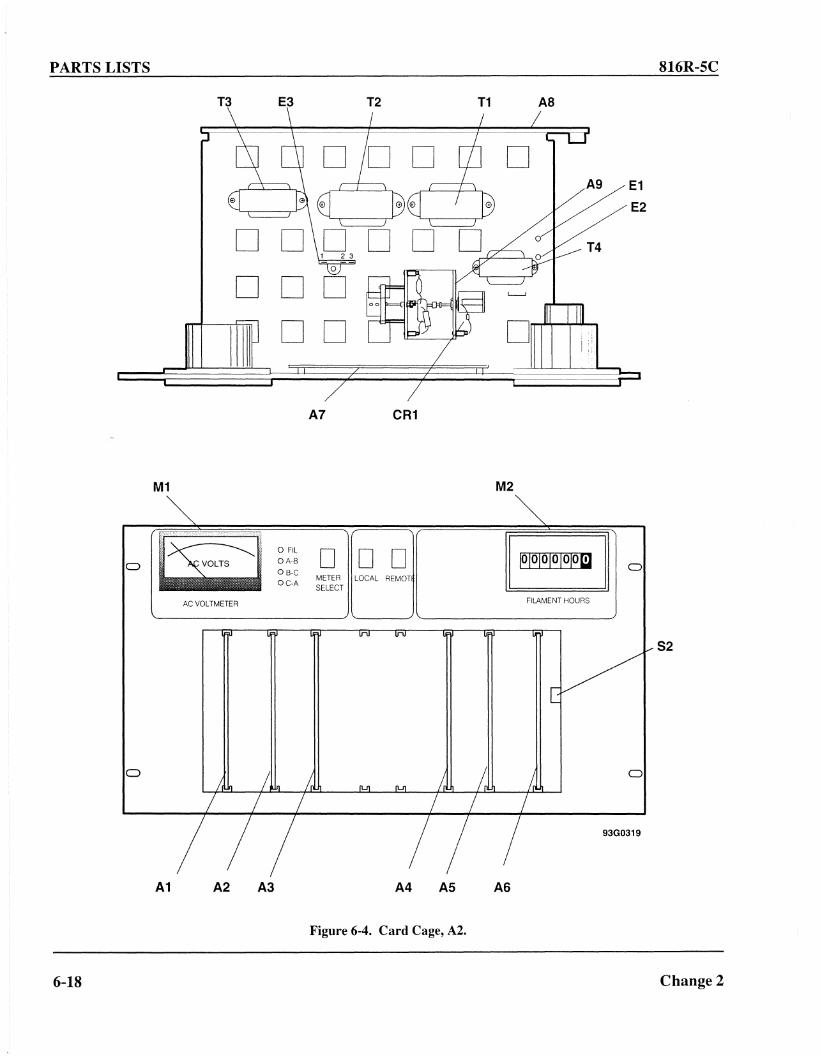
PARTS LISTS
T3
D
D
IIII
E3
A7
T2
CR1
T1
D
A8
A9 E1
E2
aT4
816R-5C
M1 M2
C)
a FILOA-B
OB-C
OC-A
D D DMETER LOCAL REMOTSELECT
o
AC VOLTMETER FILAMENT HOURS
o o
93G0319
52
A1 A2 A3 A4 AS A6
6-18
Figure 6-4. Card Cage, A2.
Change 2

816R-5C
PL180299-2 CARD CAGE ASSEMBLY
PARTS LISTS
Rev.F
Ref. Des. Part No.
Al 270-3253-010
A2 270-3253-010
A3 270-3253-010
A4 *182901-1A5 *180166-1A6 *180161-1A7 *189620-1A8 *180194-1A9 *172715-1CR1 353-6442-070
E1 306-0234-000
E2 306-0234-000
E3-
306-2230-000
£4 306-0234-000
E5 306-0234-000
E6 306-0234-000
M1 458-5006-020
M2 458-5007-010
RV1 714-3258-250
Sl 266-8000-000
T1 270-0313-020
T2 270-0313-020
T3 270-0313-020
T4 662-0898-010
Change 3
Description
CIRCUIT CARD ASSEMBLY: GATING, 3 PHASE, FULL WAVE HARD FIRING,PLUG IN, USING AMP 534204-1 CONNECTORCIRCUIT CARD ASSEMBLY: GATING, 3 PHASE, FULL WAVE HARD FIRING,PLUG IN, USING AMP 534204-1 CONNECTORCIRCUIT CARD ASSEMBLY: GATING, 3 PHASE, FULL WAVE HARD FIRING,PLUG IN, USING AMP 534204-1 CONNECTORCCA, FILAMENT REGULATORCCA,OVERLOADffiECYCLECCA, POWER MONITOR/CONTROLCCA, CARD CAGE COMPONENTCCA, BACKPLANEPOWER CONTROL ASSEMBLYSEMICONDUCTOR DEVICE, DIODE: SILICON, lAMP, 1000V PRV DO-41 EPOXYPKG~ AXIAL LEADS (lN4007)POST, ELECTRICALIMECHANICAL EQUIPMENT: 4-40 THREADS, 0.625LENGTH, 6500 VOLTS AC-RMSPOST, ELECTRICALIMECHANICAL EQUIPMENT: 4-40 THREADS, 0.625LENGTH, 6500 VOLTS AC-RMSTERMINAL BOARD: 3 TERMINAL, SOLDER LUG, SNGL MTG FOOT PHENOLICBASEPOST, ELECTRICALIMECHANICAL EQUIPMENT: 4-40 THREADS, 0.625LENGTH, 6500 VOLTS AC-RMSPOST, ELECTRICALIMECHANICAL EQUIPMENT: 4-40 THREADS, 0.625LENGTH, 6500 VOLTS AC-RMSPOST, ELECTRICALIMEClIANICAL EQUIPMENT: 4-40 THREADS, 0.625LENGTH, 6500 VOLTS AC-RMSAMMETER, AC: 10 MA, SENS, 0-9, 0-300 SCALES VOLTS AC, 3-1/2"RECTANGLE, PIVOT & JEWEL MOVEMENT, IRON VANEMETER, TIME TOTALIZING: 99999.9 HR, 0.1 HR, INCREMENTS 230 VOLT, 60HZ, 3-1/2" RECT BEZEL, NO RESETRESISTOR, VOLTAGE DEPENDENT: 2000 AMPS, 0.6 WATT 500 PF, METALOXIDE VARISTORSWITCH ASSEMBLY, INTERLOCK: SPDT, 5 AMP @ 28 VDC, PULL TOMAINTAIN CONNECTIONTRANSFORMER, POWER: STEP-DOWN, PRI=230/460V, 50/60HZ 1PH,SEC#1=24VCT@40MA, SEC#2&3=18V@400MA, OPEN, DRYTRANSFORMER, POWER: STEP-DOWN, PRI=230/460V, 50/60HZ 1PH,SEC#I=24VCT@40MA, SEC#2&3=18V@400MA, OPEN, DRYTRANSFORMER, POWER: STEP-DOWN, PRI=230/460V, 50/60HZ 1PH,SEC#1=24VCT@40MA, SEC#2&3=18V@400MA, OPEN, DRYTRANSFORMER, POWER: STEP-DOWN, 166 VRMS/24-56 VRMS
6-19

PARTS LISTS 816R-5C
7, XU7
L§jS4
o2 L§jS2 S3 L§jS3 0
o B8~DO [J
DOJo8
I U4,XU4 <[fD DO 0 08, XU8
I_U3_'XU3 ------lilliJ DOD 00
I U2,XU2) 00~ :~:: :. j WD Q 00I-U1.XU~1<
I R34
L4
EJ EJ (]
L§jS5 000[jL§jso
08 0 EJOD
@]8
R33
~ WQ]
~ [£] [Bill IJ~ 8°~.-----K1,-XK1I 811 ® C16 +
sz sz I L3 I (. I-C-14-----,'D0 c: RV4 =::>c: RV3 =::> I L2 I I I
c: RV2 ::::>, ~ L1
EJ
oD
P1
93G0320
Figure 6-5. Filament Regulator Circuit Card Assembly, A2A4.
6-20 Change 2

816R-5C
PL182901-1 CCA, FILAMENT REGULATOR
PARTS LISTS
Rev.E
Ref. Des. Part No.
C1 NOT-USEDC2 NOT-USEDC3 NOT-USEDC4 184-9102-110
C5 CK05BX104KC6 CK05BX104KC7 CK05BX104KC8 CK05BX104KC9 CK05BX104KC10 CK05BX104KCII CM05FD101J03C12 CM05FD101J03C13 CM05FD101J03C14 CM05FD101J03C15 913-3279-270C16 183-5016-070
C17 184-9102-370
C18 184-9102-370
C19 CK05BX104KC20 CK05BX104KC21 CK05BX104KC22 CK05BX104KC23 CK05BX104KC24 183-5031-030
C25 NOT-USEDC26 CK05BX104KC27 CK05BX104KC28 184-9102-200
C29 CK05BX104KC30 184-9102-100
C31 CM05FD101J03C32 CM05FD101J03CR1 353-6442-070
CR2 353-6442-070
DS1 419-0095-020
DS2 419-0095-030
DS3 419-0095-030
Change 3
Description
CAPACITOR, FIXED, ELECTROLYTIC: 220 UF, ±20%, 10 WVDC DIPPEDTANTALUMCAPACITOR, FIXED, CERAMIC: 0.1 UF, ±10%, 50 WVDCCAPACITOR, FIXED, CERAMIC: 0.1 UF, ±10%, 50 WVDCCAPACITOR, FIXED, CERAMIC: 0.1 UF, ±10%, 50 WVDCCAPACITOR, FIXED, CERAMIC: 0.1 UF, ±10%, 50 WVDCCAPACITOR, FIXED, CERAMIC: 0.1 UF, ±10%, 50 WVDCCAPACITOR, FIXED, CERAMIC: 0.1 UF, ±10%, 50 WVDCCAPACITOR, FIXED, MICA: 100 PF, ±5%, 500 WVDCCAPACITOR, FIXED, MICA: 100 PF, ±5%, 500 WVDCCAPACITOR, FIXED, MICA: 100 PF, ±5%, 500 WVDCCAPACITOR, FIXED, MICA: 100 PF, ±5%, 500 WVDCCAPACITOR, FIXED, CERAMIC: 1 UF, ±20%, 50 WVDCCAPACITOR, FIXED, ELECTROLYTIC: 33 UF, ±10%, 20 WVDC DIPPEDTANTALUMCAPACITOR, FIXED, ELECTROLYTIC: 2.2 UF, ±20%, 35 WVDC DIPPEDTANTALUMCAPACITOR, FIXED, ELECTROLYTIC: 2.2 UF, ±20%, 35 WVDC DIPPEDTANTALUMCAPACITOR, FIXED, CERAMIC: 0.1 UF, ±lO%, 50 WVDCCAPACITOR, FIXED, CERAMIC: 0.1 UF, ±10%, 50 WVDCCAPACITOR, FIXED, CERAMIC: 0.1 UF, ±10%, 50 WVDCCAPACITOR, FIXED, CERAMIC: 0.1 UF, ±10%, 50 WVDCCAPACITOR, FIXED, CERAMIC: 0.1 UF, ±10%, 50 WVDCCAPACITOR, FIXED, ELECTROLYTIC: 100 UF, ±20%, 63 WVDC WITHINSULATING SLEEVE
CAPACITOR, FIXED, CERAMIC: 0.1 UF, ±10%, 50 WVDCCAPACITOR, FIXED, CERAMIC: 0.1 UF, ±10%, 50 WVDCCAPACITOR, FIXED, ELECTROLYTIC: 100 UF, ±20%, 20 WVDC DIPPEDTANTALUMCAPACITOR, FIXED, CERAMIC: 0.1 UF, ±10%, 50 WVDCCAPACITOR, FIXED, ELECTROLYTIC: 100 UF, ±20%, 10 WVDC DIPPEDTANTALUMCAPACITOR, FIXED, MICA: 100 PF, ±5%, 500 WVDCCAPACITOR, FIXED, MICA: 100 PF, ±5%, 500 WVDCSEMICONDUCTOR DEVICE, DIODE: SILICON, lAMP, lOOOV PRY DO-41 EPOXYPKG, AXIAL LEADS (lN4007)SEMICONDUCTOR DEVICE, DIODE: SILICON, lAMP, 1000V PRY DO-41 EPOXYPKG, AXIAL LEADS (lN4007)LIGHT EMITTING DIODE: YELLOW DIFFUSED, BLOCK FORM RT ANGLE,WITHOUT RESISTOR, 3 VDC MAX, 30 MALIGHT EMITTING DIODE: RED DIFFUSED, BLOCK FORM RT ANGLE,WITHOUT RESISTOR, 2 VDC MAX, 50 MALIGHT EMITTING DIODE: RED DIFFUSED, BLOCK FOJa,1 RT ANGLE,WITHOUT RESISTOR, 2 VDC MAX, 50 MA
6-21

PARTS LISTS
PL182901-1 CCA, FILAMENT REGULATOR - Continued
816R-5C
Rev.E
Ref. Des. Part No.
DS4 419-0095-010
DS5 419-0095-020
K1 410-6009-010
K2 41 0-6009-01 0
K3 41 0-6009-0 10
Ll MS91189-21
L2 MS91189-21
L3 MS91189-21
L4 MS91189-21
PI 372-9739-010
Rl 724-5053-440
R2 382-1405-210
R3 724-5054-310
R4 724-5052-265
R5 724-5052-400
R6 724-5052-520
R7 382-1405-250
R8 724-5052-400
R9 724-5052-265
RIO 724-5052-275
Rll 724-5052-275
R12 724-5052-265
R13 724-5052-265
R14 724-5052-265
R15 724-5052-265
6-22
Description
LIGHT EMITTING DIODE: GREEN DIFFUSED, BLOCK FORM RT ANGLE,WITHOUT RESISTOR, 3 VDC MAX, 60 MALIGHT EMITTING DIODE: YELLOW DIFFUSED, BLOCK FORM RT ANGLE,WITHOUT RESISTOR, 3 VDC MAX, 30 MARELAY, SOLID STATE: VOLTAGE 20-140 VAC, 1.0 AMP LOAD CURRENT AT 40DEG C, 3.5 VDC ACTUATINGRELAY, SOLID STATE: VOLTAGE 20-140 VAC, 1.0 AMP LOAD CURRENT AT 40DEG C, 3.5 VDC ACTUATINGRELAY, SOLID STATE: VOLTAGE 20-140 VAC, 1.0 AMP LOAD CURRENT AT 40DEG C, 3.5 VDC ACTUATINGCOIL, RADIO FREQUENCY: 4.7 UH, ±10%, 860 DCMA, Q==60MIN 90 MHZ SELFRESONANT FREQ, 0.560 DCR MAXCOIL, RADIO FREQUENCY: 4.7 UH, ±10%, 860 DCMA, Q==60MIN 90 MHZ SELFRESONANT FREQ, 0.560 DCR MAXCOIL, RADIO FREQUENCY: 4.7 UH, ±10%, 860 DCMA, Q==60MIN 90 MHZ SELFRESONANT FREQ, 0.560 DCR MAXCOIL, RADIO FREQUENCY: 4.7 UH, ±10%, 860 DCMA, Q==60MIN 90 MHZ SELFRESONANT FREQ, 0.560 DCR MAXCONNECTOR, RECEPTACLE, ELECTRICAL: 2 ROW CLOSED ENTRY BOARDMTD, 50 POSN, 0.100"CTR, W/BD RETENTION POSTSRESICTOR, FIXED, FILM: 22100HM, ±1%, 1/2WATT@70C METAL FILM,TC==1OOPPMIDEGC, COLOR BANDEDRESISTOR, VARIABLE, NONWlRE WOUND: 5000 OHMS, ±10% 1/2 WATT,CERMETRESISTOR, FIXED, FILM: 330 OHM, ±5%, 1 WATT @ 70C METAL FILM,TC==250PPMIDEGC, COLOR BANDEDRESISTOR, FIXED, FILM: 3320HM, ±l%, 1/4WATT@70C METAL FILM,TC==100PPMlDEGC, COLOR BANDEDRESISTOR, FIXED, FILM: 10000HM, ±l%, 1/4WATT@70C METAL FILM,TC==lOOPPMIDEGC, COLOR BANDEDRESISTOR, FIXED, FILM: 47500HM, ±l%, 1/4WATT@70C METAL FILM,TC== 1OOPPMlDEGC, COLOR BANDEDRESISTOR, VARIABLE, NONWIRE WOUND: 50K OHMS, ±10% 1/2 WATT,CERMETRESISTOR, FIXED, FILM: 10000HM, ±1%, 1/4WATT@70C METAL FILM,TC==100PPMlDEGC, COLOR BANDEDRESISTOR, FIXED, FILM: 3320HM, ±1%, 1/4WATT@70C METAL FILM,TC==100PPMIDEGC, COLOR BANDEDRESISTOR, FIXED, FILM: 3920HM, ±l%, 1/4WATT@70C METAL FILM,TC==1OOPPMIDEGC, COLOR BANDEDRESISTOR, FIXED, FILM: 3920HM, ±l%, 1/4WATT@70C METAL FILM,TC==100PPMIDEGC, COLOR BANDEDRESISTOR, FIXED, FILM: 3320HM, ±l%, 1/4WATT@70C METAL FILM,TC==100PPMIDEGC, COLOR BANDEDRESISTOR, FIXED, FILM: 3320HM, ±1%, 1/4WATT@70C METAL FILM,TC==100PPMIDEGC, COLOR BANDEDRESISTOR, FIXED, FILM: 3320HM, ±l%, 1/4WATT@70C METAL FILM,TC==100PPMIDEGC, COLOR BANDEDRESISTOR, FIXED, FILM: 3320HM, ±l%, 1/4WATT@70C METAL FILM,TC== 1OOPPMIDEGC, COLOR BANDED
Change 3

816R-5C
PL182901-1 CCA, FILAMENT REGULATOR - Continued
PARTS LISTS
Rev.E
Ref. Des. Part No.
R16 724-5052-265
R17 724-5052-665
R18 724-5052-660
R19 724-5052-600
R20 382-1405-250
R21 724-5052-200
R22 724-5052-200
R23 724-5052-600
R24 724-5052-600
RI5 724-5052-600
R26 724-5052-600
R27 724-5052-600
R28 RLR07C2204GSR29 RLR07C2204GSR30 724-5052-400
R31 724-5052-400
R32 724-5052-265
R33 724-5055-230
R34 724-5054-230
RV1 714-7015-010
RV2 714-7008-010
RV3 714-7008-010
RV4 714-7008-010
Sl 266-5415-670
82 266-5404-190
83 266-5404-190
Change 3
Description
RESISTOR, FIXED, FILM: 3320HM, ±10/0, 1/4WATT@70C METAL FILM,TC= 1OOPPMIDEGC, COLOR BANDEDRESISTOR, FIXED, FILM: 22.1KOHM, ±10/0, 1/4WATT@70C METAL FILM,TC=100PPM/DEGC, COLOR BANDEDRESISTOR, FIXED, FILM: 20K OHM, ±10/0, 1/4 WATT @ 70C METAL FILM,TC=100PPMIDEGC, COLOR BANDEDRESISTOR, FIXED, FILM: 10KOHM, ±10/0, 1/4WATT@70C METAL FILM,TC=100PPM/DEGC, COLOR BANDEDRESISTOR, VARIABLE, NONWIRE WOUND: 50K OHMS, ±10% 1/2 WATT,CERMETRESISTOR, FIXED, FILM: 1000HM, ±10/0, 1/4WATT@70C METAL FILM,TC=100PPMIDEGC, COLOR BANDEDRESISTOR, FIXED, FILM: 1000HM, ±10/0, 1/4WATT@70C METAL FILM,TC=1OOPPMlDEGC, COLOR BANDEDRESISTOR, FIXED, FILM: 10KOHM, ±10/0, 1/4WATT@70C METAL FILM,TC=100PPMlDEGC, COLOR BANDEDRESISTOR, FIXED, FILM: 1OKOHM, ±1 0/0, 1/4WATT@70C METAL FILM,TC=100PPMIDEGC, COLOR BANDEDRESISTOR, FIXED, FILM: 10KOHM, ±10/0, 1/4WATT@70C METAL FILM,TC=100PPMIDEGC, COLOR BANDEDRESISTOR, FIXED, FILM: 10KOHM, ±10/0, 1/4WATT@70C METAL FILM,TC=100PPMIDEGC, COLOR BANDEDRESISTOR, FIXED, FILM: 10KOHM, ±10/0, 1/4WATT@70C METAL FILM,TC=100PPMIDEGC, COLOR BANDEDRESISTOR, FIXED, FILM: 2.2M OHM, ±20/0, 1/4 WATT FR=.OOl %/1 OOOHRRESISTOR, FIXED, FILM: 2.2M OHM, ±20/0, 1/4 WATT FR=.001%/1000HRRESISTOR, FIXED, FILM: 10000HM, ±1%, 1/4WATT@70C METAL FILM,TC=1OOPPMlDEGC, COLOR BANDEDRESISTOR, FIXED, FILM: 10000HM, ±10/0, 1/4WATT@70C METAL FILM,TC=1OOPPMIDEGC, COLOR BANDEDRESISTOR, FIXED, FILM: 3320HM, ±1%, 1/4WATT@70C METAL FILM,TC=100PPMIDEGC, COLOR BANDEDRESISTOR, FIXED, FILM: 68 OHM, ±50/0, 2 WATT 2 70C METAL FILM,TC=250PPMIDEGC, COLOR BANDEDRESISTOR, FIXED, FILM: 68 OHM, ±5%, 1 WATT @ 70C METAL FILM,TC=250PPMIDEGC, COLOR BANDEDRESISTOR, VOLTAGE SENSITIVE: 1000 AMPS, 0.50 WATT 3500 PF, METALOXIDE VARISTORRESISTOR, VOLTAGE SENSITIVE: 4000 AMPS, 0.85 WATT 1000 PF, METALOXIDE VARISTORRESISTOR, VOLTAGE SENSITIVE: 4000 AMPS, 0.85 WATT 1000 PF, METALOXIDE VARISTORRESISTOR, VOLTAGE SENSITIVE: 4000 AMPS, 0.85 WATT 1000 PF, METALOXIDE VARISTORSWITCH, TOGGLE: 3PDT, 5 AMP @ 28VDC/120 VAC ON-NONE-ON ACTION,RIGHT ANGLE, PC MOUNTSWITCH, PUSH: SPDT-MOM, lAMP, 28VDC/120VAC CONT RATING BUTTONCOLOR-NONE, EDGE MT, RT ANGLE PC TERMINATIONSSWITCH, PUSH: SPDT-MOM, lAMP, 28VDC/120VAC CONT RATING BUTTONCOLOR-NONE, EDGE MT, RT ANGLE PC TERMINATIONS
6-23

PARTS LISTS
PL182901-1 CCA, FILAMENT REGULATOR - Continued
816R-5C
Rev.E
Ref. Des. Part No.
TPI 360-0495-010TP2 360-0495-070TP3 360-0495-030Ul 351-7629-010
U2 351-7629-010
U3 351-7629-010
U4 351-7634-010
U5 NOT-USEDU6 351-1 137-020U7 351-4714-020U8 351-1122-010
U9 351-1120-050
UI0 - 351-1120-010
Ul1 351-4801-010
XKl 220-6017-040
XK2 220-6017-040
XK3 220-6017-040
XUl 220-6017-030
XU2 220-6017-030
XU3 220-6017-030
XU4 220-6017-030
XU5 NOT-USEDXU6 220-6017-020
XU7 220-6017-030
XU8 220-6017-030
6-24
Description
JACK, 'TIP: BLACK, NYLON INSULATED, PWB MOUNTING HIGH PROFILEJACK, TIP: BLUE, NYLON INSULATED TIP, PWB MOUNTING HIGH PROFILEJACK, TIP: RED, NYLON INSULATED, PWB MOUNTING I-IIGH PROFILEMICROCIRCUIT, DIGITAL: QUAD 2 INPUT NAND GATE, TTL, 14 PIN DIP,PLASTIC PACKAGEMICROCIRCUIT, DIGITAL: QUAD 2 INPUT NAND GATE, TTL, 14 PIN DIP,PLASTIC PACKAGEMICROCIRCUIT, DIGITAL: QUAD 2 INPUT NAND GATE, TTL, 14 PIN DIP,PLASTIC PACKAGEMICROCIRCUIT, DIGITAL: TTL, QUAD 2 INPUT AND GATE 14 PIN PLASTICDIP PKG
MICROCIRCUIT, LINEAR: TIMER, + 18V, 600 MWMICROCIRCUIT, LINEAR: 30 VOLT, 1000 OHMS IMPEDANCEMICROCIRCUIT, LINEAR: QUAD COMPARATOR, LOW OFFSET LOW POWER,14 PIN PLASTIC DIP PKGMICROCIRCUIT, LINEAR: 15V POSITIVE VOLTAGE REGULATOR 1.5AMP,TO-220 PLASTIC PACKAGEMICROCIRCUIT, LINEAR: +5 V @ 1 A VOLTAGE REGULATOR TO-220PLASTIC PACKAGEMICROCIRCUIT, LINEAR: PRECISION BCD BUFFERED REFERENCE, TO-5PACKAGESOCKET, PLUG-IN ELECTRONIC COMPONENT: 16 CONTACTS OPEN FRAME,0.3" WIDE PIN SPACINGSOCKET, PLUG-IN ELECTRONIC COMPONENT: 16 CONTACTS OPEN FRAME,0.3" WIDE PIN SPACINGSOCKET, PLUG-IN ELECTRONIC COMPONENT: 16 CONTACTS OPEN FRAME,0.3" WIDE PIN SPACINGSOCKET, PLUG-IN ELECTRONIC COMPONENT: 14 CONTACTS OPEN FRAME,0.3" WIDE PIN SPACINGSOCKET, PLUG-IN ELECTRONIC COMPONENT: 14 CONTACTS OPEN FRAME,0.3" WIDE PIN SPACINGSOCKET, PLUG-IN ELECTRONIC COMPONENT: 14 CONTACTS OPEN FRAME,0.3" WIDE PIN SPACINGSOCKET, PLUG-IN ELECTRONIC COMPONENT: 14 CONTACTS OPEN FRAME,0.3" WIDE PIN SPACING
SOCKET, PLUG-IN ELECTRONIC COMPONENT: 8 CONTACTS OPEN FRAME,0.3" WIDE PIN SPACINGSOCKET, PLUG-IN ELECTRONIC COMPONENT: 14 CONTACTS OPEN FRAME,0.3" WIDE PIN SPACINGSOCKET, PLUG-IN ELECTRONIC COMPONENT: 14 CONTACTS OPEN FRAME,0.3" WIDE PIN SPACING
Change 3

816R-SC
Change 2
(This Page Intentionally Left Blank)
PARTS LISTS
6-25

PARTS LISTS 816R-5C
o
-o-VR1
-0- CR4
DCi0
S~DblC6
c=J-i R6 ~DC?
DC8
@+
~
C1
D CR1--rr::::J-
-i Ri ~
-i R2 ~
~0D~C3
c=J-1 R3 ~
bO~
I I I
<:DI\:>
~~
--c=J- R7
DCi2
+o~~CR6
G--1 R11 ~
.~ R12
~
Oe~I c 5c..n
E2E3[[I]E1
--c=J- R9
DCi4
-c:nCRS
~0D~
C20
o
o--[lliil-~CR9--D-
DC2i
~~~~
~~
DCi7
®®CRi0
--CJJ-
@D2Q-DCi9
--[§J-
~CR? -c:n-
~CR8 --rr::::J-
C23
D
G~
~CRii--D-
DC24o--G2ZJ-
en~ ~
~o~' --rc=J-m» :' ."'" CRi2me: !
~g \. ~/J~zoz
o ~I FRONT ~ I:coL...----------------
o
93G0321
Figure 6-6. OverloadfRecycle Circuit Card Assembly, A2AS.
6-26 Change 2

816R-5C
PL180166-1 CCA,OVERLOADIRECYCLE
PARTS LISTS
Rev.G
Ref. Des. Part No.
CI CK05BXI04KC2 CK05BXI03KC3 CK06BX105KC4 CK05BX104KC5 CK05BX103KC6 CK06BX105KC7 CK05BX104KC8 CK05BX104KC9 184-9102-370
C10 CK05BX104KC11 184-9102-410
C12 CK05BX104KC13 CK05BX103KC14 CK05BX104KC15 CK05BXI03KC16 183-5018-110
C17 CK05BX104KC18 184-9102-410
C19 CK05BX104KC20 CK05BX104KC21 CK05BX104KC22 183-5103-050
C23 CK05BX104KC24 CK05BX104KCR1 353-3763-010
CR2 353-0293-020CR3 353-3763-010
CR4 353-6442-040
CR5 353-3763-010
CR6 353-0293-020CR7 353-3763-010
CR8 353-3763-010
CR9 353-6442-040
CR10 353-6442-040
CR11 353-6442-040
Change 3
Description
CAPACITOR, FIXED, CERAMIC: 0.1 UF, ±10%, 50 WVDCCAPACITOR, FIXED, CERAMIC: 0.01 UF, ±10%, 100 WVDCCAPACITOR, FIXED, CERAMIC: 1 UF, ±10%, 50 WVDCCAPACITOR, FIXED, CERAMIC: 0.1 UF, ±10%, 50 WVDCCAPACITOR, FIXED, CERAMIC: 0.01 UF, ±10%, 100 WVDCCAPACITOR, FIXED, CERAMIC: 1 UF, ±10%, 50 WVDCCAPACITOR, FIXED, CERAMIC: 0.1 UF, ±10%, 50 WVDCCAPACITOR, FIXED, CERAMIC: 0.1 UF, ±10%, 50 WVDCCAPACITOR, FIXED, ELECTROLYTIC: 2.2 UF, ±20%, 35 WVDC DIPPEDTANTALUMCAPACITOR, FIXED, CERAMIC: 0.1 UF, ±lO%, 50 WVDCCAPACITOR, FIXED, ELECTROLYTIC: 10 UF, ±20%, 35 WVDC DIPPEDTANTALUMCAPACITOR, FIXED, CERAMIC: 0.1 UF, ±lO%, 50 WVDCCAPACITOR, FIXED, CERAMIC: 0.01 UF, ±10%, 100 WVDCCAPACITOR, FIXED, CERAMIC: 0.1 UF, ±10%, 50 WVDCCAPACITOR, FIXED, CERAMIC: 0.01 UF, ±10%, 100 WVDCCAPACITOR, FIXED, ELECTROLYTIC: 4.7 UF, ±10%, 35 WVDC DIPPEDTANTALUMCAPACITOR, FIXED, CERAMIC: 0.1 UF, ±10%, 50 WVDCCAPACITOR, FIXED, ELECTROLYTIC: 10 UF, ±20%, 35 WVDC DIPPEDTANTALUMCAPACITOR, FIXED, CERAMIC: 0.1 UF, ±IO%, 50 WVDCCAPACITOR, FIXED, CERAMIC: 0.1 UF, ±IO%, 50 WVDCCAPACITOR, FIXED, CERAMIC: 0.1 UF, ±10%, 50 WVDCCAPACITOR, FIXED, ELECTROLYTIC: 330 UF, ±20%, 50 WVDC ALUMINUM,SINGLE ENDEDCAPACITOR, FIXED, CERAMIC: 0.1 UF, ±10%, 50 WVDCCAPACITOR, FIXED, CERAMIC: 0.1 UF, ±10%, 50 WVDCSEMICONDUCTOR DEVICE, DIODE: SILICON, 100V PIV, 300MA FASTRECOVERY, DO-35 PKG (TYPE IN4l48)SEMICONDUCTOR DEVICE, ASSEMBLY: LED, YELLOWSEMICONDUCTOR DEVICE, DIODE: SILICON, 100V PIV, 300MA FASTRECOVERY, DO-35 PKG (TYPE lN4l48)SEMICONDUCTOR DEVICE, DIODE: SILICON, lAMP, 400V PRY DO-41 EPOXYPKG, AXIAL LEADS (IN4004)SEMICONDUCTOR DEVICE, DIODE: SILICON, 100V PIV, 300MA FASTRECOVERY, DO-35 PKG (TYPE IN4148)SEMICONDUCTOR DEVICE, ASSEMBLY: LED, YELLOWSEMICONDUCTOR DEVICE, DIODE: SILICON, 100V PIV, 300MA FASTRECOVERY, DO-35 PKG (TYPE 1N4148)SEMICONDUCTOR DEVICE, DIODE: SILICON, 100V PIV, 300MA FASTRECOVERY, DO-35 PKG (TYPE 1N4148)SEMICONDUCTOR DEVICE, DIODE: SILICON, lAMP, 400V PRV DO-41 EPOXYPKG, AXIAL LEADS (IN4004)SEMICONDUCTOR DEVICE, DIODE: SILICON, lAMP, 400V PRV DO-41 EPOXYPKG, AXIAL LEADS (lN4004)SEMICONDUCTOR DEVICE, DIODE: SILICON, lAMP, 400V PRY DO-41 EPOXYPKG, AXIAL LEADS (IN4004)
6-27

PARTS LISTS
PL180166-1 CCA, OVERLOADIRECYCLE - Continued
816R-5C
Rev.G
Ref. Des. Part No.
CR12 353-6442-040
Jl 372-9739-010
Kl 410-0572-010
Ll MS75089-11Ql 352-0661-020Q2 352-0661-020Q3 352-0661-020Q4 353-6468-060Q5 353-6468-060Q6 352-1104-010
Q7 353-6468-060Q8 353-6468-060Rl 724-5052-460
R2 - 724-5052-460
R3 724-5052-905
R4 724-5052-285
R5 724-5053-485
R6 724-5052-905
R7 RLR07C2204GSR8 724-5052-400
R9 RLR07C2204GSRIO 724-5052-905
Rl1 724-5054-420
R12 747-5498-000R13 724-5052-600
R14 724-5052-400
R15 724-5053-485
R16 724-5052-600
RI7 724-5053-485
RI8 724-5052-400
6-28
Description
SEMICONDUCTOR DEVICE, DIODE: SILICON, lAMP, 400V PRY DO-41 EPOXYPKG, AXIAL LEADS (lN4004)CONNECTOR, RECEPTACLE, ELECTRICAL: 2 ROW CLOSED ENTRY BOARDMTD, 50 POSN, 0.100"CTR, W/BD RETENTION POSTSRELAY, REED: SPDT, 0.25AMP, 4 WATT, 100VDC CONTACT RTG 24VDC, 2200OHM COIL, PC MOUNT, DUAL-IN-LINE PKGCOIL, RADIO FREQUENCY: 100.0UH, 160MADC, 3.12 OHMSTRANSISTOR: NPN, SILICON, 800MA, 70V, 500MW DISS TO-18 PKG (2N2222A)TRANSISTOR: NPN, SILICON, 800MA, 70V, 500MW DISS TO-18 PKG (2N2222A)TRANSISTOR: NPN, SILICON, 800MA, 70V, 500MW DISS TO-18 PKG (2N2222A)SEMICONDUCTOR DEVICE, THYRISTOR: 1.6AMP, 400V, SCR TO-5 PKGSEMICONDUCTOR DEVICE, THYRISTOR: 1.6AMP, 400V, SCR TO-5 PKGTRANSISTOR: NPN, SILICON, 4AMP, 100V, 1.5 WATT DISS PLASTIC PKG,CHASSIS MT, (MJE243)SEMICONDUCTOR DEVICE, THYRISTOR: 1.6AMP, 400V, SCR TO-5 PKGSEMICONDUCTOR DEVICE, THYRISTOR: 1.6AMP, 400V, SCR TO-5 PKGRESISTOR, FIXED, FILM: 22100HM, ±l%, 1/4WATT@70C METAL FILM,TC==1OOPPMIDEGC, COLOR BANDEDRESISTOR, FIXED, FILM: 22100HM, ±l%, 1/4WATT@70C METAL FILM,TC==lOOPPMIDEGC, COLOR BANDEDRESISTOR, FIXED, FILM: 475KOHM, ±l%, 1/4WATT@70C METAL FILM,TC==1OOPPMIDEGC, COLOR BANDEDRESISTOR, FIXED, FILM: 4750HM, ±15, 1/4WATT@70C METAL FILM,TC==1OOPPMIDEGC, COLOR BANDEDRESISTOR, FIXED, FILM: 47500HM, ±l%, 1/2WATT@70C METAL FILM,TC==100PPMIDEG C, COLOR BANDEDRESISTOR, FIXED, FILM: 475KOHM, ±l%, 1/4WATT@70C METAL FILM,TC==1OOPPMIDEGC, COLOR BANDEDRESISTOR, FIXED, FILM: 2.2M OHM, ±2%, 1/4 WATT FR==.00I%/1000HRRESISTOR, FIXED, FILM: 10000HM, ±l%, 1/4WATT@70C METAL FILM,TC==lOOPPMIDEGC, COLOR BANDEDRESISTOR, FIXED, FILM: 2.2M OHM, ±2%, 1/4 WATT FR==.001%/1000HRRESISTOR, FIXED, FILM: 475KOHM, ±1 %, 1/4WATT@70C METAL FILM,TC==100PPMIDEGC, COLOR BANDEDRESISTOR, FIXED, FILM: 2700 OHM, ±5%, 1 WATT @ 70C METAL FILM,TC==250PPMIDEGC, COLOR BANDEDRESISTOR, FIXED, WIRE WOUND: 150 OHMS, ±5%, 6.5 WATTRESISTOR, FIXED, FILM: 10KOHM, ±1%, 1/4WATT@70C METAL FILM,TC==1OOPPMIDEGC, COLOR BANDEDRESISTOR, FIXED, FILM: 10000HM, ±l%, 1/4WATT@70C METAL FILM,TC==100PPM/DEGC, COLOR BANDEDRESISTOR, FIXED, FILM: 47500HM, ±1%, 1/2WATT@70C METAL FILM,TC==100PPMIDEG C, COLOR BANDEDRESISTOR, FIXED, FILM: 10KOHM, ±l%, 1/4WATT@70C METAL FILM,TC== 1OOPPMIDEGC, COLOR BANDEDRESISTOR, FIXED, FILM: 47500HM, ±l%, 1/2WATT@70C METAL FILM,TC==100PPMIDEG C, COLOR BANDEDRESISTOR, FIXED, FILM: 10000HM, ±l%, 1/4WATT@70C METAL FILM,TC==100PPMIDEGC, COLOR BANDED
Change 3

816R-5C
PL180166-1 CCA, OVERLOADIRECYCLE - Continued
PARTS LISTS
Rev.G
Ref. Des. Part No.
R19 724-5053-240
R20 724-5053-485
R21 724-5053-010
R22 724-5053-600
R23 724-5053-600
R24 747-5455-000R25 724-5053-240
R26 724-5053-485
R27 724-5053-240
R28 724-5053-485
SI 266-5404-190
S2 266-5321-980Ul 351-1137-020U2 351-7629-010
U3 351-1137-020U4 351-1137-020U5 351-5305-010
U6 35 1-1137-020VR1 353-6481-470VR2 351-1120-010
XK1 220-0049-010XUl 220-0049-100XU2 220-0049-010XU3 220-0049-100XU4 220-0049-100XU5 220-0049-010XU6 220-0049-100
Change 3
Description
RESISTOR, FIXED, FILM: 2210HM, ±10/0, 1/2WATT@70C METAL FILM,TC=100PPM/DEGC, COLOR BANDEDRESISTOR, FIXED, FILM: 47500HM, ±10/0, 1/2WATT@70C METAL FILM,TC= 1OOPPMIDEG C, COLOR BANDEDRESISTOR, FIXED, FILM: 100HM, ±10/0, 1/2WATT@70C METAL FILM,TC=100PPM/DEGC, COLOR BANDEDRESISTOR, FIXED, FILM: 10KOHM, ±10/0, 1/2WATT@70C METAL FILM,TC=100PPMIDEGC, COLOR BANDEDRESISTOR, FIXED, FILM: 10KOHM, ±10/0, 1/2WATT@70C METAL FILM,TC=1OOPPMIDEGC, COLOR BANDEDRESISTOR, FIXED, WIRE WOUND: 560 OHMS, ±50/0, 6.5 WATTRESISTOR, FIXED, FILM: 2210HM, ±10/0, 1/2WATT@70C METAL FILM,TC=1OOPPMIDEGC, COLOR BANDEDRESISTOR, FIXED, FILM: 47500HM, ±10/0, 1/2WATT@70C METAL FILM,TC= 1OOPPMIDEG C, COLOR BANDEDRESISTOR, FIXED, FILM: 2210HM, ±10/0, 1/2WATT@70C METAL FILM,TC=100PPMIDEGC, COLOR BANDEDRESISTOR, FIXED, FILM: 47500HM, ±1 0/0, 1/2WATT@70C METAL FILM,TC=100PPMlDEG C, COLOR BANDEDSWITCH, PUSH: SPDT-MOM, lAMP, 28VDC/120VAC CONT RATING BUTTONCOLOR-NONE, EDGE MT, RT ANGLE PC TERMINATIONSSWITCH, TOGGLE: SPDT, ON-NONE-ON, 5 AMP CONTACT RATINGMICROCIRCUIT, LINEAR: TIMER, +18V, 600 MWMICROCIRCUIT, DIGITAL: QUAD 2 INPUT NAND GATE, TTL, 14 PIN DIP,PLASTIC PACKAGEMICROCIRCUIT, LINEAR: TIMER, +18V, 600 MWMICROCIRCUIT, LINEAR: TIMER, +18V, 600 MWMICROCIRCUIT, DIGITAL: LOW POWER SCHOTTKY, DIVIDE BY 12COUNTER, 14 PIN DIP, PLASTIC PACKAGEMICROCIRCUIT, LINEAR: TIMER, +18V, 600 MWSEMICONDUCTOR DEVICE, DIODE: SILICON, 1 WATT, 30 VOLTMICROCIRCUIT, LINEAR: +5 V @ 1 A VOLTAGE REGULATOR TO-220PLASTIC PACKAGESOCKET, INTEGRATED CIRCUIT: DUAL IN-LINE, 14 POSTSSOCKET, INTEGRATED CIRCUIT: DUAL IN-LINE, 8 POSTSSOCKET, INTEGRATED CIRCUIT: DUAL IN-LINE, 14 POSTSSOCKET, INTEGRATED CIRCUIT: DUAL IN-LINE, 8 POSTSSOCKET, INTEGRATED CIRCUIT: DUAL IN-LINE, 8 POSTSSOCKET, INTEGRATED CIRCUIT: DUAL IN-LINE, 14 POSTSSOCKET, INTEGRATED CIRCUIT: DUAL IN-LINE, 8 POSTS
6-29

PARTS LISTS 816R-5C
49
J1
2
~
Ct1CAUTION
SENSI T1 vt ELECTRONl CDEY ICES
CR11 ~--rr=J- R48
XU4~ C16~ DC17
~~~~
~c=J
XU10 C13
C14 C15
~ c=Jc=J~~~
~~~
00 C10
rn~XU3CR8
-CJ}--~-to-
CR9
e VR1
~ -to~ -1-R-37---'~
~ ~~ ¢o-[@J-~~(3 ~~ G~ ® -@QJ- v \D@)
CR4-CJ}-- -CJ}-- CR10-CJ}-- I®I VR3~ --1""----[@J- CR5 @ v:g; R57 L~ C12 ~ r-~ + ~ 8eo
o ® C3 o~cO 81 F=D~ ~o ~~ ~D ~~~ ~ C4 --sm-0~~~~~~~
6G XK1p K1
CR2
~ -CJ}--
OE3ITJJE1
R7 E2
~
~ f0-D-fR9l 8~~~a
TP1 ITP2 ITP3 ITP4 ITP5 I
93G0322
Figure 6-7. Power Monitor/Control Circuit Card Assembly, A2A6.
6-30 Change 2

CAPACITOR, FIXED, ELECTROLYTIC: 10 uF, ±20%, 35 WVDC DIPPEDTANTALUMCAPACITOR, FIXED, CERAMIC: 0.1 uF, ±10%, 50 WVDCCAPACITOR, FIXED, CERAMIC: 0.1 uF, ±10%, 50 WVDCCAPACITOR, FIXED, CERAMIC: 0.1 uF, ±10%, 50 WVDCCAPACITOR, FIXED, ELECTROLYTIC: 47 uF, ±100/0, 20 WVDC DIPPEDTANTALUMCAPACITOR, FIXED, CERAMIC: 0.1 uF, +_20%, 50 WVDCCAPACITOR, FIXED, CERAMIC: 0.1 uF, +_200/0,50 WVDCCAPACITOR, FIXED, CERAMIC: 1 uF, ±100/0, 50 WVDCCAPACITOR, FIXED, CERAMIC: 1 uF, ±10%, 50 WVDCCAPACITOR, FIXED, CERAMIC: 1 uF, ±100/0, 50 WVDCCAPACITOR, FIXED, ELECTROLYTIC: 220 uF, ±20%, 35 WVDC ALUMINUM,RADIAL LEADSCAPACITOR, FIXED, ELECTROLYTIC: 100 uF, ±200/0, 50 WVDC RADIAL LEADSCAPACITOR, FIXED, CERAMIC: 1 uF, ±100/0, 50 WVDCCAPACITOR, FIXED, CERAMIC: 1 uF, ±lO%, 50 WVDCCAPACITOR, FIXED, CERAMIC: 1 uF, ±10%, 50 WVDCCAPACITOR, FIXED, CERAMIC: 1 uF, ±IO%, 50 WVDCCAPACITOR, FIXED, CERAMIC: 0.1 uF, ±10%, 50 WVDCCAPACITOR, FIXED, ELECTROLYTIC: 4.7 uF, ±10%, 35 WVDC DIPPEDTANTALUMCAPACITOR, FIXED, ELECTROLYTIC: 10 uF, ±20%, 35 WVDC DIPPEDTANTALUMCAPACITOR, FIXED, ELECTROLYTIC: 150 uF, ±200/o, 15 WVDC DIPPEDTANTALUMCAPACITOR, FIXED, ELECTROLYTIC: 100 uF, ±20%, 20 WVDC DIPPEDTANTALUMCAPACITOR, FIXED, ELECTROLYTIC: 100 uF, ±200/o, 20 WVDC DIPPEDTANTALUMSEMICONDUCTOR DEVICE, DIODE: SILICON, HOT CARRIER 70V, 250MW, 2pFNOM, GLASS PKG, AXIAL LEADS (lN5711)SEMICONDUCTOR DEVICE, DIODE: SILICON, lAMP, 1000V PRY DO-41 EPOXYPKG, AXIAL LEADS (lN4007)SEMICONDUCTOR DEVICE, DIODE: SILICON, lAMP, 1000V PRY DO-4l EPOXYPKG, AXIAL LEADS (lN4007)SEMICONDUCTOR DEVICE, DIODE: SILICON, lAMP, 1000V PRY DO-41 EPOXYPKG, AXIAL LEADS (lN4007)SEMICONDUCTOR DEVICE, DIODE: SILICON, lAMP, 1000V PRY DO-41 EPOXYPKG, AXIAL LEADS (lN4007)SEMICONDUCTOR DEVICE, DIODE: SILICON, HOT CARRIER 70V, 250MW, 2pFNOM, GLASS PKG, AXIAL LEADS (IN57ll)SEMICONDUCTOR DEVICE, DIODE: SILICON, lAMP, 1000V PRY DO-41 EPOXYPKG, AXIAL LEADS (lN4007)SEMICONDUCTOR DEVICE, DIODE: SILICON, lAMP, lOOOV PRY DO-41 EPOXYPKG, AXIAL LEADS (IN4007)SEMICONDUCTOR DEVICE, DIODE: SILICON, lAMP, looav PRY DO-41 EPOXYPKG, AXIAL LEADS (lN4007)SEMICONDUCTOR DEVICE, DIODE: SILICON, lAMP, 1000V PRY DO-41 EPOXYPKG, AXIAL LEADS (lN4007)
816R-5C
PL180161-1
Ref. Des. Part No.
C1 184-9102-410
C2 CK05BX104KC3 CK05BX104KC4 CK05BX104KC5 183-5016-080
C6 913-3813-000C7 913-3813-000C8 CK06BX105KC9 CK06BX105KC10 CK06BX105KC11 183-5111-080
C12 183-5031-080C13 CK06BXI05KC14 CK06BX105KCl-5 CK06BX105KC16 CK06BX105KC17 CK05BXI04KC18 183-5018-110
C19 184-9102-410
C20 184-9102-160
C21 184-9102-200
C22 184-9102-200
CR1 353-3691-010
CR2 353-6442-070
CR3 353-6442-070
CR4 353-6442-070
CR5 353-6442-070
CR6 353-3691-010
CR7 353-6442-070
eR8 353-6442-070
CR9 353-6442-070
CR10 353-6442-070
CCA, POWER MONITOR/CONTROL
Description
PARTS LISTS
Rev.G
Change 2 6-31

SEMICONDUCTOR DEVICE, DIODE: SILICON, HOT CARRIER 70V, 250MW, 2pFNOM, GLASS PKG, AXIAL LEADS (IN5711)CONNECTOR, RECEPTACLE, ELECTRICAL: 2 ROW CLOSED ENTRY BOARDMTD, 50 POSN, 0.100"CTR, W/BD RETENTION POSTSRELAY, REED: SPDT, 0.25AMP, 4 WATT, 100VDC CONTACT RTG 24VDC, 2200OHM COIL, PC MOUNT, DUAL-IN-LINE PKGTRANSISTOR: NPN, SILICON, VCEO=40 VDC, IC=0.7 AMP 5 WATT, TO-5PACKAGETRANSISTOR: NPN, SILICON, VCEO=40 VDC, IC=0.7 AMP 5 WATT, TO-5PACKAGETRANSISTOR: NPN, SILICON, 800MA, 70V, 500MW DISS TO-I8 PKG (2N2222A)TRANSISTOR: NPN, SILICON, 800MA, 70V, 500MW DISS TO-I8 PKG (2N2222A)TRANSISTOR: NPN, SILICON, 800MA, 70V, 500MW DISS TO-I8 PKG (2N2222A)RESISTOR, \lARIABLE, NONWIRE WOUND: 10K OHMS, ±100/0 1/2 WATT,CERMETRESISTOR, VARIABLE, NONWIRE WOUND: SOK OHMS, ±100/0 1/2 WATT,CERMETRESISTOR, VARIABLE, NONWIRE WOUND: 20K OHM, ±1 0%, 1/2 WATT,CERMET, 25 TURNRESISTOR, VARIABLE, NONWIRE WOUND: 10K OHMS, ±100/0 1/2 WATT,CERMETRESISTOR, VARIABLE, NONWIRE WOUND: 20K OHM, ±10%, 1/2 WATT,CERMET, 25 TURNRESISTOR, VARIABLE, NONWIRE WOUND: 10K OHMS, ±100/0 1/2 WATT,CERMETRESISTOR, VARIABLE, NONWIRE WOUND: 10K OHMS, ±100/0 1/2 WATT,CERMETRESISTOR, VARIABLE, NONWIRE WOUND: 10K OHMS, ±100/0 1/2 WATT,CERMETRESISTOR, VARIABLE, NONWIRE WOUND: 10K OHMS, ±100/0 1/2 WATT,CERMETRESISTOR, VARIABLE, NONWIRE WOUND: 50K OHMS, ±100/0 1/2 WATT,CERMETRESISTOR, FIXED, FILM: 3320HM, ±1 %, 1/4Wi\TT@70C METAL FILM,TC=100PPMIDEGC, COLOR BANDEDRESISTOR, FIXED, FILM: 10000HM, ±10/0, 1/4WATT@70C METAL FILM,TC=100PPMIDEGC, COLOR BANDEDRESISTOR, FIXED, FILM: 1000HM, ±10/0, 1/4WATT@70C METAL FILM~
TC=lOOPPMIDEGC, COLOR BANDEDRESISTOR, FIXED, FILM: 30.1 KOHM, ±10/0, 1/4WATT@70C METAL FILM,TC=100PPMIDEGC, COLOR BANDEDRESISTOR, FIXED, FILM: 100HM, ±1 0/0, 1/4WATT@70C METAL FILM,TC=100PPMIDEGC, COLOR BANDEDRESISTOR, FIXED, FILM: 3320HM, ±1 %, 1/4WATT@70C METAL FILM,TC=100PPMIDEGC, COLOR BANDEDRESISTOR, FIXED, FILM: 30.1 KOHM, ±10/0, 1/4WATT@70C METAL FILM,TC=100PPMIDEGC, COLOR BANDEDRESISTOR, FIXED, FILM: 68100HM, ±10/0, 1/4WATT@70C METAL FILM,TC=100PPMIDEGC, COLOR BANDED
PARTS LISTS
PL180161-1
Ref. Des. Part No.
CRll 353-3691-010
11 372-9739-010
Kl 410-0572-010
Ql 352-0613-010
Q2 352-0613-010
Q3 352-0661-020Q4 352-0661-020Q5 352-0661-020Rl 382-1405-220
R2 382-1405-250
R3 - 382-1405-230
R4 382-1405-220
R5 382-1405-230
R6 382-1405-220
R7 382-1405-220
R8 382-1405-220
R9 382-1405-220
RIO 382-1405-250
Rl1 724-5052-265
R12 724-5052-400
R13 724-5052-200
R14 724-5052-695
R15 724-5052-010
R16 724-5052-265
R17 724-5052-695
R18 724-5052-545
CCA, POWER MONITOR/CONTROL - Continued
Description
816R-5C
Rev.G
6-32 Change 2

RESISTOR, FIXED, FILM: 22100HM, ±1%, 1/4WATT@70C METAL FILM,TC=100PPMIDEGC, COLOR BANDEDRESISTOR, FIXED, FILM: 10000HM, ±1%, I/4WATT@70C METAL FILM,TC=100PPM/DEGC, COLOR BANDEDRESISTOR, FIXED, FILM: 27400HM, ±I %, I/2WATT@70C METAL FILM,TC=100PPMIDEGC, COLOR BANDEDRESISTOR, FIXED, FILM: 47500HM, ±I%, 1/2WATT@70C METAL FILM,TC=100PPM/DEG C, COLOR BANDEDRESISTOR, FIXED, FILM: 27400HM, ±1%, 1/2WATT@70C METAL FILM,TC=100PPMIDEGC, COLOR BANDEDRESISTOR, FIXED, FILM: 47.50HM, ±1%, 1/2WATT@70C METAL FILM,TC=lOOPPMIDEGC, COLOR BANDEDRESISTOR, FIXED, FILM: IMEGOHM, ±l 0/0, 1/4WATT@70C METAL FILM,TC=lOOPPM/DEGC, COLOR BANDEDRESISTOR, FIXED, FILM: 162KOHM, ±1 0/0, 1/4WATT@70C METAL FILM,TC=100PPM/DEGC, COLOR BANDEDRESISTOR, FIXED, FILM: 2000HM, ±l %, I/4WATT@70C METAL FILM,TC=100PPMIDEGC, COLOR BANDEDRESISTOR, FIXED, FILM: 30.1KOHM, ±I 0/0, 1/4WATT@70C METAL FILM,TC=lOOPPM/DEGC, COLOR BANDEDRESISTOR, FIXED, FILM: 15KOHM, ±1 %, 1/4WATT@70C METAL FILM,TC=1OOPPM/DEGC, COLOR BANDEDRESISTOR, FIXED, FILM: 10KOHM, ±10/0, 1/4WATT@70CMETAL FILM,TC=100PPMIDEGC, COLOR BANDEDRESISTOR, FIXED, FILM: 15KOHM, ±1%, 1/4WATT@70C METAL FILM,TC=100PPMIDEGC, COLOR BANDEDRESISTOR, FIXED, FILM: 475KOHM, ±1 0/0, I/4WATT@70C METAL FILM,TC=lOOPPMIDEGC, COLOR BANDEDRESISTOR, FIXED, FILM: 68100HM, ±l%, 1/4WATT@70C METAL FILM,TC=100PPMIDEGC, COLOR BANDEDRESISTOR, FIXED, FILM: 47.50HM, ±l 0/0, 1/2WATT@70C METAL FILM,TC=100PPM/DEGC, COLOR BANDEDRESISTOR, FIXED, FILM: 22.1KOHM, ±1%, 1/2WATT@70CMETALFILM,TC=100PPM/DEGC, COLOR BANDEDRESISTOR, FIXED, FILM: 15KOHM, ±1 %, 1/2WATT@70C METAL FILM,TC=100PPMIDEGC, COLOR BANDEDRESISTOR, FIXED, FILM: 820 OHM, ±5%, 1 WATT @70CC METAL FILM,TC=250PPM/DEGC, COLOR BANDEDRESISTOR, FIXED, FILM: 47500HM, ±l%, 1/2WATT@70C METAL FILM,TC=100PPM/DEG C, COLOR BANDEDRESISTOR, FIXED, FILM: lOOOOHM, ±1%, 1/2WATT@70C METAL FILM,TC=100PPMlDEGC, COLOR BANDEDRESISTOR, FIXED, FILM: 22.1KOHM, ±l %, 1/2WATT@70C METAL FILM9
TC=lOOPPMIDEGC, COLOR BANDEDRESISTOR, FIXED, FILM: lOOOOHM, ±1 %, 1/2WATT@70C METAL FILM,TC=100PPMIDEGC, COLOR BANDEDRESISTOR, FIXED, FILM: 15KOHM, ±10/0, 1/2WATT@70C METAL FILM,TC=100PPMlDEGC, COLOR BANDEDRESISTOR, FIXED, FILM: 2000HM, ±10/0, 1/4WATT@70C METAL FILM,TC=100PPMIDEGC, COLOR BANDED
816R-5C
PL180161-1
Ref. Des. Part No.
RI9 724-5052-460
R20 724-5052-400
R2I 724-5053-450
R22 724-5053-485
R23 724-5053-450
R24 724-5053-090
R25 724-5052-995
R26 724-5052-840
R27 724-5052-240
R28 724-5052-695
R29 724-5052-645
R30 724-5052-600
R3I 724-5052-645
R32 724-5052-905
R33 724-5052-545
R34 724-5053-090
R35 724-5053-650
R36 724-5053-630
R37 724-5054-360
R38 724-5053-485
R39 724-5053-400
R40 724-5053-650
R4I 724-5053-400
R42 724-5053-630
R43 724-5052-240
CCA, POWER MONITOR/CONTROL - Continued
Description
PARTS LISTS
Rev.G
Change 2 6-33

RESISTOR, FIXED, FILM: 162KOHM, ±l 0/0, l/4WATT@70C METAL FILM,TC=100PPMlDEGC, COLOR BANDEDRESISTOR, FIXED, FILM: 43200HM, ±10/0, 1/4WATT@70C METAL FILM,TC=lOOPPMlDEGC, COLOR BANDEDRESISTOR, FIXED, FILM: 22100HM, ±l%, 1/4WATT@70C METAL FILM,TC=100PPMlDEGC, COLOR BANDEDRESISTOR, FIXED, FILM: 20K OHM, ±1 %, 1/4 WATT @ 70C METAL FILM,TC=100PPMlDEGC, COLOR BANDEDRESISTOR, FIXED, FILM: 2000HM, ±1 0/0, 1/4WATT@70C METAL FILM,TC=100PPMlDEGC, COLOR BANDEDRESISTOR, FIXED, FILM: 15KOHM, ±1%, 1/4WATT@70C METAL FILM,TC=lOOPPMlDEGC, COLOR BANDEDRESISTOR, FIXED, FILM: 162KOHM, ±10/0, 1/4WATT@70C METAL FILM,TC=100PPM/DEGC, COLOR BANDEDRESISTOR, FIXED, FILM: 20K OHM, ±1 0/0, 1/4 WATT @ 70C METAL FILM, _TC=100PPMlDEGC, COLOR BANDEDRESISTOR, FIXED, FILM: 15KOHM, ±1%, 1/4WATT@70C METAL FILM,TC=100PPMIDEGC, COLOR BANDEDRESISTOR, FIXED, FILM: 22100HM, ±1%, 1/4WATT@70C METAL FILM,TC=100PPMlDEGC, COLOR BANDEDRESISTOR, FIXED, FILM: 100 OHM, ±50/0, 1 WATT @ 70C METAL FILM,TC=250PPMIDEGC, COLOR BANDEDRESISTOR, FIXED, FILM: 82500HM, ±1%, 1/2WATT@70C METAL FILM,TC=100PPMlDEGC, COLOR BANDEDRESISTOR, FIXED, FILM: 1200 OHM, ±5%, 1 WATT @ 70C METAL FILM,TC=250PPMlDEGC, COLOR BANDEDRESISTOR, FIXED, FILM: 470 OHM, ±5%, 1 WATT @ 70C METAL FILM,TC=250PPMIDEGC, COLOR BANDEDSWITCH, PUSH: SPDT-MOM, lAMP, 28VDC/120VAC CONT RATING BUTTONCOLOR-NONE, EDGE MT, RT ANGLE PC TERMINATIONSJACK, TIP: RED, NYLON INSULATED TIP, PWB MOUNTING LOW PROFILEJACK, TIP: ORANGE, NYLON INSULATED TIP, PWB MOUNTING LOWPROFILEJACK, TIP: YELLOW, NYLON INSULATED TIP, PWB MOUNTING LOWPROFILEJACK, TIP: BROWN, NYLON INSULATED TIP, PWB MOUNTING LOW PROFILEJACK, TIP: BLACK, NYLON INSULATED TIP, PWB MOUNTING LOW PROFILEMICROCIRCUIT, LINEAR: OPERATIONAL AMPLIFIER, ±18 VOLTS SUPPLY, 8LEAD PLASTIC DUAL IN-LINE PKGMICROCIRCUIT, LINEAR: OPERATIONAL AMPLIFIER, ±18 VOLTS SUPPLY, 8LEAD PLASTIC DUAL IN-LINE PKGMICROCIRCUIT, LINEAR: OPERATIONAL AMPLIFIER, ±18 VOLTS SUPPLY, 8LEAD PLASTIC DUAL IN-LINE PKGMICROCIRCUIT, LINEAR: OPERATIONAL AMPLIFIER, ±18 VOLTS SUPPLY, 8LEAD PLASTIC DUAL IN-LINE PKGMICROCIRCUIT, LINEAR: TIMER, +18V, 600 MWSEMICONDUCTOR DEVICE, DIODE: SILICON, 1 WATT, 10 VOLTMICROCIRCUIT, LINEAR: VOLTAGE REGULATOR -12 INPUT -35 VOLTS,TO-220PKG
PARTS LISTS
PL180161-1
Ref. Des. Part No.
R44 724-5052-840
R45 724-5052-515
R46 724-5052-460
R47 724-5052-660
R48 724-5052-240
R49 724-5052-645
R50 724-5052-840
R51 724-5052-660
R52 724-5052-645
R53 724-5052-460
R54 724-5054-250
R55 724-5053-515
R56 724-5054-380
R57 724-5054-330
S1 266-5404-190
TP1 360-0495-130TP2 360-0495-140
TP3 360-0495-150
TP4 360-0495-120TP5 360-0495-110U1 351-1110-020
U2 351-1110-020
U3 351-1110-020
U4 351-111 0-020
U5 351-1137-020VR1 353-6481-260VR2 351-1124-130
CCA, POWER MONITOR/CONTROL - Continued
Description
816R-SC
Rev.G
6-34 Change 2

816R-SC
PL180161-1
Ref. Des. Part No.
CCA, POWER MONITOR/CONTROL - Continued
Description
PARTS LISTS
Rev.G
VR3 351-1120-040
VR4 353-6481-260XKI 220-0049-010XU1 220-0049-100XU2 220-0049-100XU3 220-0049-100XU4 220-0049-100XU5 220-0049-100
Change 2
MICROCIRCUIT, LINEAR: +12 V @ 1 A VOLTAGE REGULATOR TO-220PLASTIC PACKAGESEMICONDUCTOR DEVICE, DIODE: SILICON, 1 WATT, 10 VOLTSOCKET, INTEGRATED CIRCUIT: DUAL IN-LINE, 14 POSTSSOCKET, INTEGRATED CIRCUIT: DUAL IN-LINE, 8 POSTSSOCKET, INTEGRATED CIRCUIT: DUAL IN-LINE, 8 POSTSSOCKET, INTEGRATED CIRCUIT: DUAL IN-LINE, 8 POSTSSOCKET, INTEGRATED CIRCUIT: DUAL IN-LINE, 8 POSTSSOCKET, INTEGRATED CIRCUIT: DUAL IN-LINE, 8 POSTS
6-35

82
o
c=J DS1 I::Jc=J DS2 Uc=J DS3 S3
c=J DS4
B B81
FRONT VIEW
~ EFJEJ EJBGfB ~~ VR1 ~8~~~~; Go 5U~$D C10 C11
Q4
REAR VIEW
hI AlA7.· C rd Assem y,t CircuIt aC PonenCard Cage omFigure 6-8.
9580182
6-36 Change 2

816R-5C
PL189620-1 CCA, CARD CAGE COMPONENT
PARTS LISTS
Rev.E
Ref. Des. Part No.
Cl CK05BX104KC2 CK05BX104KC3 913-7016-510C4 184-9612-010C5 183-5018-070
C6 CK05BX104KC7 CK05BX104KC8 183-5018-070
C9 CK05BX104KC10 CK05BX104KC11 CK05BX104KC12 CK05BX104KCR1 353-6442-070
CR2 353-6442-070
CR7 353-6442-070
CR8 353-3763-010
CR9 353-6442-070
DS1 419-0089-010
DS2 419-0089-010
DS3 419-0089-010
DS4 419-0089-010
11 372-9765-020
Kl 410-6009-010
K2 41 0-6009-01 0
K3 410-6204-030
K4 410-6009-010
K5 410-6009-010
K6 41 0-6009-0 10
K7 41 0-6009-01 0
R1 747-0998-950
Change 3
Description
CAPACITOR, FIXED, CERAMIC: 0.1 UF, ±10%, 50 WVDCCAPACITOR, FIXED, CERAMIC: 0.1 UF, ±10%, 50 WVDCCAPACITOR, FIXED, CERAMIC: 10,000 PF, ±5%, 50 WVDCCAPACITOR, FIXED, ELECTROLYTIC: 100 UF, ±10%, 6.3 WVDCCAPACITOR, FIXED, ELECTROLYTIC: 1 UF, ±10%, 35 WVDC DIPPEDTANTALUMCAPACITOR, FIXED, CERAMIC: 0.1 UF, ±10%, 50 WVDCCAPACITOR, FIXED, CERAMIC: 0.1 UF, ±lO%, 50 WVDCCAPACITOR, FIXED, ELECTROLYTIC: 1 UF, ±10%, 35 WVDC DIPPEDTANTALUMCAPACITOR, FIXED, CERAMIC: 0.1 UF, ±10%, 50 WVDCCAPACITOR, FIXED, CERAMIC: 0.1 UF, ±10%, 50 WVDCCAPACITOR, FIXED, CERAMIC: 0.1 UP, ±10%, 50 WVDCCAPACITOR, FIXED, CERAMIC: 0.1 UF, ±10%, 50 WVDCSEMICONDUCTOR DEVICE, DIODE: SILICON, lAMP, 1000V PRY DO-41 EPOXYPKG, AXIAL LEADS (lN4007)SEMICONDUCTOR DEVICE, DIODE: SILICON, lAMP, 1000V PRY DO-41 EPOXYPKG, AXIAL LEADS (lN4007)SEMICONDUCTOR DEVICE, DIODE: SILICON, lAMP, 1000V PRY DO-41 EPOXYPKG, AXIAL LEADS (lN4007)SEMICONDUCTOR DEVICE, DIODE: SILICON, 100V PIV, 300MA FASTRECOVERY, DO-35 PKG (TYPE 1N4148)SEMICONDUCTOR DEVICE, DIODE: SILICON, lAMP, 1000V PRY DO-41 EPOXYPKG, AXIAL LEADS (lN4007)DISPLAY, OPTOELECTRONIC: LED, GREEN, .5"X.25"LIGHTED AREA, 4.5MCDINTENSITY, RECT, PC MOUNT, DUAL-IN-LINEDISPLAY, OPTOELECTRONIC: LED, GREEN, .5"X.25"LIGHTED AREA, 4.5MCDINTENSITY, RECT, PC MOUNT, DUAL-IN-LINEDISPLAY, OPTOELECTRONIC: LED, GREEN, .5"X.25"LIGHTED AREA, 4.5MCDINTENSITY, RECT, PC MOUNT, DUAL-IN-LINEDISPLAY, OPTOELECTRONIC: LED, GREEN, .5"X.25"LIGHTED AREA, 4.5MCDINTENSITY, RECT, PC MOUNT, DUAL-IN-LINECONNECTOR, RECEPTACLE, ELECTRICAL: 20 POSITIONS SINGLE ROW,SHROUDED HEADER, SQ STRAIGHT POSTRELAY, SOLID STATE: VOLTAGE 20-140 VAC, 1.0 AMP LOAD CURRENT AT 40DEG C, 3.5 VDC ACTUATINGRELAY, SOLID STATE: VOLTAGE 20-140 VAC, 1.0 AMP LOAD CURRENT AT 40DEG C, 3.5 VDC ACTUATINGRELAY, ELECTROMAGNETIC: 4PDT, 2AMP, 28VDC/120VAC CONT 24VDCCOILS, DUAL COIL LATCHING, PC MOUNTRELAY, SOLID STATE: VOLTAGE 20-140 VAC, 1.0 AMP LOAD CURRENT AT 40DEG C, 3.5 VDC ACTUATINGRELAY, SOLID STATE: VOLTAGE 20-140 VAC, 1.0 AMP LOAD CURRENT AT 40DEG C, 3.5 VDC ACTUATINGRELAY, SOLID STATE: VOLTAGE 20-140 VAC, 1.0 AMP LOAD CURRENT AT 40DEG C, 3.5 VDC ACTUATINGRELAY, SOLID STATE: VOLTAGE 20-140 VAC, 1.0 AMP LOAD CURRENT AT 40DEG C, 3.5 VDC ACTUATINGRESISTOR, FIXED, WIRE WOUND: 8870 OHM, ±1%, 3 WATT INDUCTIVEWOUND, SILICONE-CERAMIC COATING
6-37

PARTS LISTS
PL189620-1 CCA, CARD CAGE COMPONENT - Continued
816R-5C
Rev.E
Ref. Des. Part No.
R2 747-0998-800
R3 724-5070-010
R4 382-1405-210
R5 747-0998-950
R6 747-5491-000R7 747-0998-800
R8 747-0998-800
R9 724-5070-010
RIO 724-5070-010
R11 724-5052-775
R12 724-5052-400
R13 724-5052-780
R14 724-5052-780
S1 266-9952-020
S2 266-9952-020
S3 266-9952-020
Ul 351-4706-010U2 351-5305-010
U3 35 1-4750-01 0
U4 351-7630-010U5 736-7026-040
U6 351-4864-010
U7 351-7740-010
VR1 351-1120-010
VR2 353-6481-130VR3 353-6481-11 0
XK1 220-6017-040
6-38
Description
RESISTOR, FIXED, WIREWOUND: 6190 OHMS, ±10/0, 3 WATT INDUCTIVEWOlJND, SILICONE-CERAMIC COATINGRESISTOR, FIXED, FILM: 6200 OHM, ±50/o, 1 WATT, 350 WVDC METAL FILMOXIDERESISTOR, VARIABLE, NONWIRE WOUND: 5000 OHMS, ±10% 1/2 WATT,CERMETRESISTOR, FIXED, WIRE WOUND: 8870 OHM, ±1%, 3 WATT INDUCTIVEWOUND, SILICONE-CERAMIC COATINGRESISTOR, FIXED, WIRE WOUND: 33 OHMS, ±5%, 6.5 WATTRESISTOR, FIXED, WIREWOUND: 6190 OHMS, ± 10/0, 3 WATT INDUCTIVEWOUND, SILICONE-CERAMIC COATINGRESISTOR, FIXED, WIREWOUND: 6190 OHMS, ±1%, 3 WATT INDUCTIVEWOUND, SILICONE-CERAMIC COATINGRESISTOR, FIXED, FILM: 6200 OHM, ±5%, 1 WATT, 350 WVDC METAL FILMOXIDERESISTOR, FIXED, FILM: 6200 OHM, ±5%, 1 WATT, 350 WVDC METAL FILMOXIDERESISTOR, FIXED, FILM: 75KOHM, ±10/o, 1/4WATT@70C METAL FILM,TC==100PPMlDEGC, COLOR BANDEDRESISTOR, FIXED, FILM: 10000HM, ±1%, 1/4WATT@70C METAL FILM,TC==100PPMlDEGC, COLOR BANDEDRESISTOR, FIXED, FILM: 82.5KOHM, ±10/0, 1/4WATT@70C METAL FILM,TC==100PPMlDEGC, COLOR BANDEDRESISTOR, FIXED, FILM: 82.5KOHM, ±1%, 1/4WATT@70C METAL FILM,TC==lOOPPMIDEGC, COLOR BANDEDSWITCH, PUSH: SPDT, MOMENTARY, BLACK KEYCAP, 60 VDC MAX, 10MADCMAXSWITCH, PUSH: SPDT, MOMENTARY, BLACKKEYCAP, 60 VDC MAX, 10MADCMAXSWITCH, PUSH: SPDT, MOMENTARY, BLACK KEYCAP, 60 VDC MAX, 10MADCMAXMICROCIRCUIT, LINEAR: DUAL TIMER, +16 V, 600 MWMICROCIRCUIT, DIGITAL: LOW POWER SCHOTTKY, DIVIDE BY 12COUNTER, 14 PIN DIP, PLASTIC PACKAGEMICROCIRCUIT, DIGITAL: DECODER, 3 LINE TO 8 LINE, TTL, LOW POWERSCHOTTKY, 16 PIN PLASTIC DIP PKGMICROCIRCUIT, DIGITAL: LOGIC GATERESISTOR NETWORK: 8 RESISTORS, 47 OHM, ±20/0 1/4 WATTIRESISTOR, 16PIN DIP PACKAGE, 2.4 WATT/PKGMICROCIRCUIT, LINEAR: TRANSISTOR ARRAY, HIGH VOLTAGE, HIGH CUR,DARLINGTON PAIRS, 7 CKT, 16 PIN PLASTIC DIPMICROCIRCUIT, DIGITAL: TTL QUAD 2 INPUT OR GATE, 14 LEAD PLASTICDUAL IN-LINE PACKAGEMICROCIRCUIT, LINEAR: +5 V @ 1 A VOLTAGE REGULATOR TO-220PLASTIC PACKAGESEMICONDUCTOR DEVICE, DIODE: SILICON, 1 WATT, 5.6 VOLTSEMICONDUCTOR DEVICE, DIODE: ZENER, 5.1V, ±5%, 1WATT AXIAL LEADS,MOLDED BODYSOCKET, PLUG-IN ELECTRONIC COMPONENT: 16 CONTACTS OPEN FRAME,0.3" WIDE PIN SPACING
Change 3

816R-5C
PL189620-1 CCA, CARD CAGE COMPONENT - Continued
PARTS LISTS
Rev.E
Ref. Des. Part No.
XK2 220-6017-040
XK3 220-6017-160
XK4 220-6017-040
XK5 220-6017-040
XK6 220-6017-040
XK7 220-6017-040
XUl 220-6017-030
XU2 220-6017-030
XU3 220-6017-040
XU4 220-6017-030
XU5 220-6017-040
XU6 220-6017-040
XU7 220-6017-030
Change 3
Description
SOCKET, PLUG-IN ELECTRONIC COMPONENT: 16 CONTACTS OPEN FRAME,0.3" WIDE PIN SPACINGSOCKET, PLUG-IN ELECTRONIC COMPONENT: 28 CONTACTS OPEN FRAME,0.3" WIDE PIN SPACINGSOCKET, PLUG-IN ELECTRONIC COMPONENT: 16 CONTACTS OPEN FRAME,0.3" WIDE PIN SPACINGSOCKET, PLUG-IN ELECTRONIC COMPONENT: 16 CONTACTS OPEN FRAME,0.3" WIDE PIN SPACINGSOCKET, PLUG-IN ELECTRONIC COMPONENT: 16 CONTACTS OPEN FRAME,0.3" WIDE PIN SPACINGSOCKET, PLUG-IN ELECTRONIC COMPONENT: 16 CONTACTS OPEN FRAME,0.3" WIDE PIN SPACINGSOCKET, PLUG-IN ELECTRONIC COMPONENT: 14 CONTACTS OPEN FRAME,0.3" WIDE PIN SPACINGSOCKET, PLUG-IN ELECTRONIC COMPONENT: 14 CONTACTS OPEN FRAME,0.3" WIDE PIN SPACINGSOCKET, PLUG-IN ELECTRONIC COMPONENT: 16 CONTACTS OPEN FRAME,0.3" WIDE PIN SPACINGSOCKET, PLUG-IN ELECTRONIC COMPONENT: 14 CONTACTS OPEN FRAME,0.3" WIDE PIN SPACINGSOCKET, PLUG-IN ELECTRONIC COMPONENT: 16 CONTACTS OPEN FRAME,0.3" WIDE PIN SPACINGSOCKET, PLUG-IN ELECTRONIC COMPONENT: 16 CONTACTS OPEN FRAME,0.3" WIDE PIN SPACINGSOCKET, PLUG-IN ELECTRONIC COMPONENT: 14 CONTACTS OPEN FRAME,0.3" WIDE PIN SPACING
6-39

PARTS LISTS 816R-5C
J9
--c=J-R6
J13 1 J12 60
1( ¢¢11.115 :: 16J8 J7 J6 J3 15 - -16 J2
8 0C4J10
00 0-e::J- R8
49 49 49 49 ~R550
60
8 T85 1 8 T84 1 8 T83 1 8 T82 1 8 T81 1"T11-'-'-'-' "TII-,-,-r-, r,TII-'-i-r-, "TII-'-I-rl ,rTIII-,-rlI I I I I I I I II I I I I I I I II I I I I I I I II I I I I I J I II I I I I I I I III 1 I I I II II I I 1 I I I I II11 I I I I I II I I I I I I I II I I I I 1 I I IL L 1. J. .J -.J _1_ L -.J L L 1. J. .J -.J _1_ L -.J L L 1. J. .J -.J _1_ L -I L L .L J. .J -.J _1_ L -I L L .L .l.J -1_1_ L -I16 9 16 9 16 9 16 9 16 9
93G0324
JUMPERS LOCATED AT: J11 5 TO 69 TO 10
13 TO 1415 TO 16
J127T089 TO 10
J133T045 TO 67 TO 8
Figure 6-9. Backplane Circuit Card Assembly, A2A8.
6-40 Change 2

816R-5C
PL180194-1 CCA, BACKPLANE
Ref. Des. Part No.
C1 183-1281-080
C2 183-1281-080
CR1 353-6442-030
CR2 353-6442-030
J1 372-9753-010
J2 372-9753-010
J3 372-9753-010
J6 372-9753-010
J7 372-9753-010
J8 372-9753-010
J9 372-9754-010
JI0 372-9754-010
Jll 372-9756-010
J12 372-9756-010
J13 372-9756-010
R5 724-5052-665
R6 724-5053-280
R7 724-5053-280
R8 724-5052-200
R9 724-5053-260
RIO 724-5053-250
TB1 306-3051-010
TB2 306-3051-010
TB3 306-3051-010
TB4 306-3051-010
TB5 306-3051-010
Change 3
PARTS LISTS
Rev.G
Description
CAPACITOR, FIXED, ELECTROLYTIC: 100 UF, +85-100/0, 50WVDC ALUMINUM,INSULATED, AXIAL LEADS, .385" D, 1.536" LCAPACITOR, FIXED, ELECTROLYTIC: 100 UF, +85-100/0, 50WVDC ALUMINUM,INSULATED, AXIAL LEADS, .385" D, 1.536" LSEMICONDUCTOR DEVICE, DIODE: SILICON, lAMP, 200V PRV DO-41 EPOXYPKG, AXIAL LEADS (IN4003)SEMICONDUCTOR DEVICE, DIODE: SILICON, lAMP, 200V PRV DO-41 EPOXYPKG, AXIAL LEADS (IN4003)CONNECTOR, RECEPTACLE, ELECTRICAL: HEADER, 50 PINS, 2 ROW,STRAIGHT, 0.100 CENTERSCONNECTOR, RECEPTACLE, ELECTRICAL: HEADER, 50 PINS, 2 RO\V,STRAIGHT, 0.100 CENTERSCONNECTOR, RECEPTACLE, ELECTRICAL: HEADER, 50 PINS, 2 ROW,STRAIGHT, 0.100 CENTERSCONNECTOR, RECEPTACLE, ELECTRICAL: HEADER, 50 PINS, 2 ROW,STRAIGHT, 0.100 CENTERSCONNECTOR, RECEPTACLE, ELECTRICAL: HEADER, 50 PINS, 2 ROW,STRAIGHT, 0.100 CENTERSCONNECTOR, RECEPTACLE, ELECTRICAL: HEADER, 50 PINS, 2 ROW,STRAIGHT, 0.100 CENTERSCONNECTOR, RECEPTACLE, ELECTRICAL: HEADER, 60 PINS, 2 ROW, RTANGLE, 0.100 CTRS, SHROUDED, 0.150 END DIMCONNECTOR, RECEPTACLE, ELECTRICAL: HEADER, 60 PINS, 2 ROW, RTANGLE, 0.100 CTRS, SHROUDED, 0.150 END DIMCONNECTOR, RECEPTACLE, ELECTRICAL: HEADER, 16 PINS, 2 ROW,STRAIGHT, 0.100 X 0.100 CENTERS, UNSHROUDEDCONNECTOR, RECEPTACLE, ELECTRICAL: HEADER, 16 PINS, 2 ROW,STRAIGHT, 0.100 X 0.100 CENTERS, UNSHROUDEDCONNECTOR, RECEPTACLE, ELECTRICAL: HEADER, 16 PINS, 2 ROW,STRAIGHT, 0.100 X 0.100 CENTERS, UNSHROUDEDRESISTOR, FIXED, FILM: 22. 1KOHM, ±l%, 1/4WATT@70C METAL FILM,TC=100PPMIDEGC, COLOR BANDEDRESISTOR, FIXED, FILM: 4750HM, ±1%, 1/2WATT@70C METAL FILM,TC=100PPMlDEGC, COLOR BANDEDRESISTOR, FIXED, FILM: 4750HM, ±l%, 1/2WATT@70C METAL FILM,TC=100PPMIDEGC, COLOR BANDEDRESISTOR, FIXED, FILM: 1000HM, ±1%, 1/4WATT@70C METAL FILM,TC=1OOPPMIDEGC, COLOR BANDEDRESISTOR, FIXED, FILM: 3320HM, ±1%, 1/2WATT@70C METAL FILM,TC=1OOPPMIDEGC, COLOR BANDEDRESISTOR, FIXED, FILM: 2740HM, ±l%, 1/2WATT@70C METAL FILM,TC=100PPMlDEGC, COLOR BANDEDTERMINAL BOARD: 8 POLES, 2 PINS/POLE, 0.2" PITCH 26-14 AWG WIRE SIZE,PWB MOUNTING, BLUE, 300V, lOA RTGTERMINAL BOARD: 8 POLES, 2 PINS/POLE, 0.2" PITCH 26-14 AWG WIRE SIZE,PWB MOUNTING, BLUE, 300V, lOA RTGTERMINAL BOARD: 8 POLES, 2 PINS/POLE, 0.2" PITCH 26-14 AWG WIRE SIZE,PWB MOUNTING, BLUE, 300V, lOA RTGTERMINAL BOARD: 8 POLES, 2 PINS/POLE, 0.2" PITCH 26-14 AWG WIRE SIZE,PWB MOUNTING, BLUE, 300V, lOA RTGTERMINAL BOARD: 8 POLES, 2 PINS/POLE, 0.2" PITCH 26-14 AWG WIRE SIZE,PWB MOUNTING, BLUE, 300V, lOA RTG
6-41

PARTS LISTS 816R-5C
81
00
C1 E3
R2
93G0325
R1
6-42
Figure 6-10. Power Controi Assembly, A2A9.
Change 2

816R-5C
PL172715-1 POWER CONTROL ASSEMBLY
PARTS LISTS
Rev.B
Ref. Des. Part No.
B1 230-5006-010
C1 CK63AWI03MC2 933-5005-010
CR1 353-6442-070
E1 306-0234-000
E2 306-0234-000
E3 306-0234-000
E4 306-0234-000
Rl 381-1648-020
R2 724-5054-250
Change 3
Description
GEARCASE-MOTOR: 10RPM, 5 OZ-IN OUTPUT TORQUE, 120V 60HZ,REVERSIBLE, 30: 1 GEAR RATIO, BRASS GEARSCAPACITOR, FIXED, CERAMIC: 0.01 MicroF, ±20%, 500 WVDCCAPACITOR, FIXED, FILM: 0.1 MicroF, ± 10%, 600 WVDC POLYPROPYLENEFILM, RADIAL LEADS, 0.75"DIA, 1.30"LGSEMICONDUCTOR DEVICE,DIODE:SILICON,lAMP,1000V PRV DO-41 EPOXYPKG,AXIAL LEADS (lN4007)POST, ELECTRICALIMECHANICAL EQUIPMENT: 4-40 THREADS, 0.625LENGTH, 6500 VOLTS AC-RMSPOST, ELECTRICALIMECHANICAL EQUIPMENT: 4-40 THREADS, 0.625LENGTH, 6500 VOLTS AC-RMSPOST, ELECTRICALIMECHANICAL EQUIPMENT: 4-40 THREADS, 0.625LENGTH, 6500 VOLTS AC-RMSPOST, ELECTRICALIMECHANICAL EQUIPMENT: 4-40 THREADS, 0.625LENGTH, 6500 VOLTS AC-RMSRESISTOR, VARIABLE, WIRE WOUND: 5000 OHM, ±5%, 2 WATT LINEARTAPER, 10 TURN, PRECISION, BUSHING MOUNTRESISTOR, FIXED, FILM: 100 OHM, ±5%, 1 WATT @ 70C METAL FILM,TC=250PPMIDEGC, COLOR BANDED
6-43

PARTS LISTS 816R-5C
R5F1
o XF1
R3DC1
0
+
R2r;.-A3 ~
0
C1~<±>
V
T81 €11
a a
~ + ~ @ @
<±> @:laae!) <±>E1 E2
DO
DO
o
oo
C2
A2 81 A1 M198G0090
Figure 6-11. Intermediate Power Amplifier Assembly, A3.
6-44 Change 2

816R-5C
PL180302-2 IPA ASSEMBLY
Ref. Des. Part No.
Al *195079-1A2 *189625-1A3 *193773-1B1 009-5057-010
C1 183-1278-660
C2 CM05FD10IJ03C3 CK63AWI03MDC1 277-3039-010
El 306-0234-000
E2 306-0234-000
Fl 264-5209-010M1 450-8023-010
Rl *159682-1R]- 716-0060-080
R4 724-5054-370
TBI 367-0926-000
XFl 265-9514-020
Change 3
PARTS LISTS
Rev.G
Description
CCA, METERING CARDIPA STATUS BOARDAMPLIFIER ASSYFAN, CENTRIFUGAL: DOUBLE, 185 CFM, 230 VAC, 60 HZ, UL/CLA BALLBEARING MOTORCAPACITOR, FIXED, ELECTROLYTIC: 120000 UF, +75-100/0,60 WVDC,ALUMINUM DIELECTRIC, 1/4-28 TERMINALSCAPACITOR, FIXED, MICA: 100 PF, ±5%, 500 WVDCCAPACITOR, FIXED, CERAMIC: 0.01 UF, ±20%, 500 WVDCCOUPLER, DIRECTIONAL: 88-108 MHZ, 1.20: 1 VSWR MAX POWER 1000WATTS MAX, DIRECTIVITY 30 DB MIN, CUSTOMPOST, ELECTRICALIMECHANICAL EQUIPMENT: 4-40 THREADS, 0.625LENGTH, 6500 VOLTS AC-RMSPOST, ELECTRICALIMECHANICAL EQUIPMENT: 4-40 THREADS, 0.625LENGTH, 6500 VOLTS AC-RMSFUSE: 30 AMPS, 125 VOLTSPOWER METER, RF: 3-1/2", RECTANGULAR, FLANGE, PANEL MOUNT,RANGE-0-1200/0, 0-3 AMPSSHUNT ASSEMBLYRESISTOR, ADJUSTABLE, WIRE WOUND: 50 OHM, ±100/0, 100 WATT, 1.41 MAXAMPRESISTOR, FIXED, FILM: 1000 OHM, ±5%, 1 WATT @ 70C METAL FILM,TC==250PPMIDEGC, COLOR BANDEDTERMINAL BOARD: 20 TERMINALS, 20 AMP, 3000 VOLTS, #6-32 X 1/4 BRASS,NP SCREWS, 16-14 AWG, PHENOLICFUSEHOLDER, BLOCK: 30 AMP, SCREW TERMINALS, RATED @ 600 VOLTS, 1POSITION
6-45

PARTS LISTS 816R-5C
o o81
~
I-
VR1
R33
VR2
I I I
G~--c:=IJ- CR1
8~
R23 ~
~
~
~
~
~~
~J2
~J1
Gc-:I~
~
~G( ]~ R14 C3
~ ----oE1
E2
o
R3
-
20
Pi
OOG0002
Figure 6-12. IPA Metering Circuit Card Assembly, A3A1.
6-46 Change 3

816R-5C
PL195079-1 CCA, METERING CARD
PARTS LISTS
Rev. A
Ref. Des. Part No.
C1 913-3279-200C2 913-3279-200C3 CM05FD101103C4 CM05FD101103C5 CM05FD 101103C6 913-3279-200C7 913-3279-200CR1 353-6442-070
11 372-9643-040
12 372-9643-040
PI 372-9754-260
Q1 352-0661-020Q2 352-0661-020R1 724-5052-400
RL 724-5053-650
R3 724-5053-510
R4 724-5052-400
R5 724-5052-400
R6 724-5052-510
R7 724-5052-400
R8 724-5052-200
R9 724-5052-460
RIO 724-5052-460
R11 724-5052-200
R12 724-5052-400
R13 724-5052-490
R14 382-1405-080
R15 724-5052-520
R16 724-5052-520
R17 724-5052-400
Change 3
Description
CAPACITOR, FIXED, CERAMIC: 0.1 UF, ±200/o, 50 WVDCCAPACITOR, FIXED, CERAMIC: 0.1 UF, ±20%, 50 WVDCCAPACITOR, FIXED, MICA: 100 PF, ±50/o, 500 WVDCCAPACITOR, FIXED, MICA: 100 PF, ±50/o, 500 WVDCCAPACITOR, FIXED, MICA: 100 PF, ±50/0, 500 WVDCCAPACITOR, FIXED, CERAMIC: 0.1 UF, ±200/o, 50 WVDCCAPACITOR, FIXED, CERAMIC: 0.1 UF, ±20~o, 50 WVDCSEMICONDUCTOR DEVICE, DIODE: SILICON, lAMP, 1000V PRY DO-4lEPOXY PKG, AXIAL LEADS (lN4007)CONNECTOR, RECEPTACLE, ELECTRICAL: PWB MOUNT, 3 PIN, SINGLEROW, STRAIGHT, 0.100 CENTER, GOLD PLATEDCONNECTOR, RECEPTACLE, ELECTRICAL: PWB MOUNT, 3 PIN, SINGLEROW, STRAIGHT, 0.100 CENTER, GOLD PLATEDCONNECTOR, RECEPTACLE, ELECTRICAL: HEADER, 20 PINS 1 ROW, RTANGLE, 0.1" CENTERS, SHROUDED PROFILETRANSISTOR: NPN, SILICON, 800MA, 70V, 500MW DISS TO-18 PKG (2N2222A)TRANSISTOR: NPN, SILICON, 800MA, 70V, 500MW DISS TO-18 PKG.(2N2222A)RESISTOR, FIXED, FILM: 10000HM, ±10/0, 1/4WATT@70C METAL FILM,TC= 1OOPPMIDEGC, COLOR BANDEDRESISTOR, FIXED, FILM: 22.1KOHM, ±10/0, 1/2WATT@70C METAL FILM,TC=1OOPPMIDEGC, COLOR BANDEDRESISTOR, FIXED, FILM: 75000HM, ±10/0, 1/2WATT@70C METAL FILM,TC=100PPMlDEGC, COLOR BANDEDRESISTOR, FIXED, FILM: 10000HM, ±l%, 1/4WATT@70C METAL FILM,TC=100PPMIDEGC, COLOR BANDEDRESISTOR, FIXED, FILM: 10000HM, ±l%, 1/4WATT@70C METAL FILM,TC= 1OOPPMIDEGC, COLOR BANDEDRESISTOR, FIXED, FILM: 39200HM, ±10/0, 1/4WATT@70C METAL FILM,TC=1OOPPMIDEGC, COLOR BANDEDRESISTOR, FIXED, FILM: 10000HM, ±l%, 1/4WATT@70C METAL FILM,TC=100PPMIDEGC, COLOR BANDEDRESISTOR, FIXED, FILM: 1000HM, ±1 0/0, 1/4WATT@70C METAL FILM,TC=100PPMIDEGC, COLOR BANDEDRESISTOR, FIXED, FILM: 22100HM, ±10/0, 1/4WATT@70C METAL FILM,TC=100PPMIDEGC, COLOR BANDEDRESISTOR, FIXED, FILM: 22100HM, ±l%, 1/4WATT@70C METAL FILM,TC=100PPMlDEGC, COLOR BANDEDRESISTOR, FIXED, FILM: 1000HM, ±l%, 1/4WATT@70C METAL FILM,TC= 1OOPPMIDEGC, COLOR BANDEDRESISTOR, FIXED, FILM: 10000HM, ±10/0, 1/4WATT@70C METAL FILM,TC=1OOPPMIDEGC, COLOR BANDEDRESISTOR, FIXED, FILM: 33200HM, ±10/0, 1/4WATT@70C METAL FILM,TC=100PPMIDEGC, COLOR BANDEDRESISTOR, VARIABLE, NONWIRE WOUND: 20K OHMS, ±1 00/0 1/2 WATT,CERMETRESISTOR, FIXED, FILM: 47500HM, ±1%, 1/4WATT@70C METAL FILM,TC=1OOPPMIDEGC, COLOR BANDEDRESISTOR, FIXED, FILM: 47500HM, ±10/0, 1/4WATT@70C METAL FILM,TC=100PPMlDEGC, COLOR BANDEDRESISTOR, FIXED, FILM: 10000HM, ±l%, 1/4WATT@70CMETAL FILM,TC= 1OOPPMIDEGC, COLOR BANDED
6-47

PARTS LISTS
PL195079-1 CCA, METERING CARD - Continued
816R-5C
Rev. A
Ref. Des. Part No.
RI8 724-5052-510
R19 724-5052-510
R20 724-5052-740
R21 724-5052-400
R22 382-1405-080
R23 382-1405-080
R24 724-5052-400
R25 724-5052-800
R26 724-5052-400
R27 382-1405-050
R28 724-5052-400
R29 724-5052-400
R30 724-5052-800
R31 724-5052-735
R32 382-1405-100
R33 724-5055-370
SI 266-9731-010
U1 351-1211-040U2 351-1211-040VR1 351-1120-040
VR2 353-6481-330XU1 220-6017-020
XU2 220-6017-020
6-48
Description
RESISTOR, FIXED, FILM: 39200HM, ±l%, I/4WATT@70C METAL FILM,TC=IOOPPMIDEGC, COLOR BANDEDRESISTOR, FIXED, FILM: 39200HM, ±I%, 1/4WATT@70C METAL FILM,TC=1OOPPMIDEGC, COLOR BANDEDRESISTOR, FIXED, FILM: 47.5KOHM, ±I%, 1/4WATT@70C METAL FILM,TC=100PPMIDEGC, COLOR BANDEDRESISTOR, FIXED, FILM: IOOOOHM, ±l%, I/4WATT@70C METAL FILM,TC=100PPMlDEGC, COLOR BANDEDRESISTOR, VARIABLE, NONWIRE WOUND: 20K OHMS, ±10% 1/2 WATT,CERMETRESISTOR, VARIABLE, NONWIRE WOUND: 20K OHMS, ±10% 1/2 WATT,CERMETRESISTOR, FIXED, FILM: 10000HM, ±l%, 1/4WATT@70C METAL FILM,TC=lOOPPMIDEGC, COLOR BANDEDRESISTOR, FIXED, FILM: IOOKOHM, ±l%, 1/4WATT@70C METAL FILM,TC= 1OOPPMIDEGC, COLOR BANDEDRESISTOR, FIXED, FILM: IOOOOHM, ±l%, I/4WATT@70C METAL FILM,TC=lOOPPMIDEGC, COLOR BANDEDRESISTOR, VARIABLE, NONWIRE WOUND: 2000 OHMS, ±10% 1/2 WATT,CE.RMETRESISTOR, FIXED, FILM: IOOOOHM, ±1%, 1/4WATT@70C METAL FILM,TC=100PPMlDEGC, COLOR BANDEDRESISTOR, FIXED, FILM: 10000HM, ±l%, 1/4WATT@70C METAL FILM,TC=1OOPPMIDEGC, COLOR BANDEDRESISTOR, FIXED, FILM: 100KOHM, ±1%, 1/4WATT@70C METAL FILM,TC=100PPMlDEGC, COLOR BANDEDRESISTOR, FIXED, FILM: 46.4K OHM, ±l%, 1/4 WATT @ 70C METAL FILM,TC=100PPMIDEGC, COLOR BANDEDRESISTOR, VARIABLE, NONWIRE WOUND: 50K OHMS, ±10% 1/2 WATT,CERMETRESISTOR, FIXED, FILM: 1000 OHM, ±5%, 2 WATT @ 70C METAL FILM,TC=250PPMIDEGC, COLOR BANDEDSWITCH ASSEMBLY, PUSHBUTTON: 4 PDT, 4 POSITION, 12 CONTACTS,INTERLOCKMICROCIRCUIT, LINEAR: DUAL OP-AMP 8 PIN PLASTIC DIP PKGMICROCIRCUIT, LINEAR: DUAL OP-AMP 8 PIN PLASTIC DIP PKGMICROCIRCUIT, LINEAR: +12 V @ 1 A VOLTAGE REGULATOR TO-220PLASTIC PACKAGESEMICONDUCTOR DEVICE, DIODE: ZENER, 15 VDC, 1 WATT, COMMERCIALSOCKET, PLUG-IN ELECTRONIC COMPONENT: 8 CONTACTS OPEN FRAME,0.3" WIDE PIN SPACINGSOCKET, PLUG-IN ELECTRONIC COMPONENT: 8 CONTACTS OPEN FRAME,0.3" WIDE PIN SPACING
Change 3

816R-5C
Change 3
(This Page Intentionally Left Blank)
PARTS LISTS
6-49

PARTS LISTS
6-50
o
(l II DS1
U II DS2
o
0080003
Figure 6-13. LED Assembly, A3A2.
816R-5C
Change 3

816R-5C
PL189625-1 IPA STATUS BOARD
PARTS LISTS
Rev. A
Ref. Des. Part No.
DS 1 419-0089-010
DS2 419-0089-020
Change 3
Description
DISPLAY, OPTOELECTRONIC: LED, GREEN, .5"X.25"LIGHTED AREA, 4.5MCDINTENSITY, RECT, PC MOUNT, DUAL-IN-LINEDISPLAY, OPTOELECTRONIC: LED, RED, .5"X.25"LIGHTED AREA, 4.5MCDINTENSITY, RECT, PC MOUNT, DUAL-IN-LINE
6-51

PARTS LISTS 816R-5C
F1 <±> <±>XF
F2XF2
P1J2
J1
P2
<±> <±>
R2
A 1 -.+-----t-t+---
o o
A2
R1
TP2
6-52
98G0088
Figure 6-14. Amplifier Assembly, A3A3.
TP1
Change 2

816R-5C
PL193773-1 AMPLIFIER ASSEMBLY
PARTS LISTS
Rev.H
Ref. Des. Part No.
Al *189215-1A2 *189215-1CR1 353-6442-070
CR2 353-6442-070
F1 264-5224-040
F2 264-5224-040
PI 361-5028-060
P2 361-5028-060
Rl 714-7039-070
R2 714-7051-020
TB1 367-0910-000
TPI 306-0976-000TP2 306-0976-000WI *195442-1W2 *195443-1W3 *195443-1W4 *195444-1W5 *195444-1W6 *195445-1W7 *195445-1W8 *195446-1W9 *195446-1WI0 *195447-1Wll *195373-1W12 *195373-1XFl 265-9534-010XF2 265-9534-010
Change 3
Description
AMPLIFIER MODULEAMPLIFIER MODULESEMICONDUCTOR DEVICE,DIODE:SILICON,lAMP,1000V PRY DO-41 EPOXYPKG,AXIAL LEADS (IN4007)SEMICONDUCTOR DEVICE,DIODE:SILICON,lAMP,1000V PRY DO-41 EPOXYPKG,AXIAL LEADS (IN4007)FUSE,CARTRlDGE:12AMP,60V,CERAMIC BODY,I/4"X1-1/4" VERY FASTACTING,SEMICONDUCTOR PROTECTIONFUSE,CARTRlDGE:12AMP,60V,CERAMIC BODY,1/4"X1-1/4" VERY FASTACTING,SEMICONDUCTOR PROTECTIONCONNECTOR,PLUG,ELECTRICAL:5 #20 SOCKET & 2 #8 CAVITIES,"D"SUBTYPE, 15 CONT SHELL SZ,SOLDER TERMCONNECTOR,PLUG,ELECTRICAL:5 #20 SOCKET & 2 #8 CAVITIES,"D"SUBTYPE, 15 CONT SHELL SZ,SOLDER TERMRESISTOR,FIXED,FILM: 100 OHM,+-5%,40 WATT CHIP TYPE,DOUBLE FLANGEMOUNTRESISTOR,FIXED,FILM: 100 OHM,+-5%,250 WATT CHIP TYPE,DOUBLE FLANGEMOUNTTERMINAL BOARD:4 TERMINALS,20 AMP,3K VRMS, #6-32 X 1/4 BRASS,NPSCREWS,16-14 AWG,PHENOLICTERMINAL,STUD:6K VOLT,5/8 X 4-40UNC-2B THDTERMINAL,STUD:6K VOLT,5/8 X 4-40UNC-2B THDCABLE,INLETCABLE ASSEMBLYCABLE ASSEMBLYCABLE ASSEMBLYCABLE ASSEMBLYCABLE ASSEMBLYCABLE ASSEMBLYCABLE ASSEMBLYCABLE ASSEMBLYCABLE ASSEMBLYBUS CABLE ASSEMBLYBUS CABLE ASSEMBLYFUSEHOLDER:SINGLE POLE,FOR 1/4 X 1-1/4 FUSESFUSEHOLDER:SINGLE POLE,FOR 1/4 X 1-1/4 FUSES
6-53

PARTS LISTS 816R-5C
p S1
A1 A2
I0 I~
J2 IJ1 0 I
II 0 I10 0
II. .•. IC1 .00
0
C2 o ' •~·O
0 I~R2 000.
f... 0 0 IR3 .. - I
96G0264
Figure 6-15. Amplifier Module, A3A3AI-A2 ..
6-54 Change 2

RESISTOR, FIXED, FILM: 100HM, ±1 %, 1/4WATT@70C METAL FILM,TC=100PPMIDEGC, COLOR BANDEDRESISTOR, FIXED, FILM: 100HM, ±1 %, 1/4WATT@70C METAL FILM,TC=100PPM/DEGC, COLOR BANDEDSWITCH, THERMOSTATIC: 80C, ±5DEG, CLOSE ON TEMP RISE BIMETALLIC,SNAP ACTION, TO-220 TYPE PKG
CCA,RFCCA, CONTROLCAPACITOR, FIXED, CERAMIC: 0.01 uF, ±10%, 100 WVDCCAPACITOR, FIXED, CERAMIC: 0.01 uF, ±10%, 100 WVDCCONNECTOR, RECEPTACLE, ELECTRICAL: 5 #20 PINS AND 2 #8 CAVITIES,"D"SUB TYPE, 15 CONT SHELL SZ, SOLDER TERMCONNECTOR, RECEPTACLE, ELECTRICAL: BNC, BULKHEAD JACKSHIELDING BEAD, ELECTRONIC: FERRITE, 5-30MHZ OPER FRE 0.385"OD,0.193"ID, 0, 410"LG, Z=80 OHM@100MHZ@25CTRANSISTOR: FET, DUAL, RF, 300W, 2-175 MHZ, N CHANNEL TAB LEADS,CHASSIS MOUNT
816R-SC
PL189215-1
~ef. Des. Part No.
Al *189213-1A2 *189210-1Cl CK05BXI03KC2 CK05BX103K11 361-5028-050
J2 361-5065-010Ll 288-4029-020
Ql 352-5134-010
Rl NOT-USEDR2 724-5052-010
R3 724-5052-010
Sl 267-5022-010
AMPLIFIER MODULE
Description
PARTS LISTS
Rev.D
Change 2 6-55

PARTS LISTS
96G0500
816R-SC
6-56
Figure 6-16. CCA, RF A3A3A1-A2A1.
Change 2

CAPACITOR, VARIABLE, CERAMIC: 8-50pF, 250WVDC STRIPLINE LEADS,TC=-1500±900PPMlDEGCCAPACITOR, FIXED, CERAMIC: 120 pF, ±100/0, 50 WVDC, CHIP TYPE, COGTEMP CHAR, WRPRND TERM, SURF MT, EIA SZ 1206CAPACITOR, FIXED, CERAMIC: 0.01 uF, ±10%, 50 WVDC, CHIP TYPE, X7RTEMP CHAR, WRPRND TERM, SURF MT, EIA SZ 1206CAPACITOR, FIXED, CERAMIC: 1 uF, ±100/0, 50 WVDCCAPACITOR, FIXED, CERAMIC: 0.1 uF, ±10%, 100 WVDCCAPACITOR, FIXED, CERAMIC: 0.1 uF, ±10%, 100 WVDCCAPACITOR, FIXED, CERAMIC: 1000pF, ±50/0, 50WVDC, CHIP TYPE SURFACEMT, TC=P90±30PPMIDEGC, CASE SIZE BCAPACITOR, FIXED, CERAMIC: 1000pF, ±5%, 50WVDC, CHIP TYPE SURFACEMT, TC=P90±30PPMIDEGC, CASE SIZE BCAPACITOR, FIXED, CERAMIC: 0.01 uF, ±100/0, 50 WVDC, CHIP TYPE, X7RTEMP CHAR, WRPRND TERM, SURF MT, EIA SZ 1206CAPACITOR, FIXED, ELECTROLYTIC: 10uF, +75-100/0, 150WVDC ALUMINUM,INSULATED, AXIAL LEADS, +105C, LONG LIFESHIELDING BEAD, ELECTRONIC: FERRITE, 5-30MHZ OPER FRE 0.385"OD,0.193"ID, 0, 410"LG, Z=80 OHM@100MHZ@25CSHIELDING BEAD, ELECTRONIC: FERRITE, 5-30MHZ OPER FRE 0.385"OD,0.193"ID, 0, 410"LG, Z=80 OHM@100MHZ@25CRESISTOR, FIXED, FILM: 330 OHM, ±50/0, 1 WATT @ 70C METAL FILM,TC=250PPMIDEGC, COLOR BANDEDRESISTOR, FIXED, FILM: 22 OHM, ±5%, 2 WATT @ 70C METAL FILM,TC=250PPMIDEGC, COLOR BANDEDRESISTOR, FIXED, FILM: 22 OHM, ±50/0, 2 WATT @ 70C I\-1ETAL FILM,TC=250PPMIDEGC, COLOR BANDEDRESISTOR, FIXED, FILM: 22 OHM, ±50/0, 2 WATT @ 70C METAL FILM,TC=250PPMIDEGC, COLOR BANDEDRESISTOR, FIXED, FILM: 22 OHM, ±50/0, 2 WATT @ 70C METAL FILM,TC=250PPM/DEGC, COLOR BANDEDRESISTOR, FIXED, FILM: 7.5 OHM, ±1 0/0, 20 WATT @ 25C TO-220 TYPE PKG,METAL TAB, NON-INDUCTIVERESISTOR, FIXED, FILM: 39200HM, ±10/0, 1/2WATT@70C METAL FILM,TC=100PPMIDEGC, COLOR BANDEDRESISTOR, FIXED, FILM: 39200HM, ±10/0, 1/2WATT@70C METAL FILM,TC=lOOPPM/DEGC, COLOR BANDEDRESISTOR, VARIABLE, NONWIRE WOUND: 5000 OHMS, ±100/0 1/2 WATT,CERMETRESISTOR, FIXED, FILM: 15000HM, ±1 %, 1/22WATT@70C METAL FILM,TC=100PPMlDEGC, COLOR BANDEDRESISTOR, FIXED, FILM: 330 OHM, ±5%, 1 WATT @ 70C METAL FILM,TC=250PPMIDEGC, COLOR BANDEDRESISTOR, FIXED, FILM: 10 OHM, ±50/o, 2 WATT @ 70C METAL FILM,TC=250PPMIDEGC, COLOR BANDEDCORE, ELECTROMAGNET: BALUN, TWO HOLE, 125MHZ MAX FREQ FERRITE,0.295"THK, 0.525"W, 0.565"LG
816R-5C
PL189213-1
Ref. Des. Part No.
C101 917-2006-010
C102 913-7144-510
CI03 913-7143-650
CI04 CK06BX105Kel05 CK06BX104KC106 CK06BX104KCI07 913-7135-030
CI08 913-7135-030
CI09 913-7143-650
ClIO 183-5106-040
L102 288-4029-020
LI03 288-4029-020
R101 724-5054-310
RI02 724-5055-170
RI03 724-5055-170
R104 724-5055-170
RI05 724-5055-170
R106 714-7059-030
RI07 724-5053-475
RI08 724-5053-475
RI09 382-1405-060
RI10 724-5053-420
RIll 724-5054-310
R112 724-5055-130
TIOI 288-4020-020
CCA,RF
Description
PARTS LISTS
Rev.E
Change 2 6-57

PARTS LISTS 816R-5C
o
<:0I\)
~
R204 r-----~ ----{'t' __ --I
I--I
() --E)l-----~ R201 0
C204R202
~o
o
----------- ......
OJJ-~,
~ L_-'o Im I
~ P= ,..I~-.,
L_r--___________ --1
Dc2~R223
[liD ~ 8-Rm 0(jl~. 0
~D ~ '-J~\J CR203 ru
DG-R224
R~
~ g ~ 8R21 7. r--l C20900 00 ~ L-..J
~ ~ ~ ~~~
o ~O~~ (~O
96G0311
Figure 6-17. Control Circuit Card Assembly, A3A3A1-A2A2.
6-58 Change 2

CAPACITOR, FIXED, CERAMIC: 0.01 uF, ±10%, 100 WVDCCAPACITOR, FIXED, CERAMIC: 0.022 uF, ±100/0, 50 VOLTSEMICONDUCTOR DEVICE, DIODE: SILICON, lAMP, 400V PRY DO-41 EPOXYPKG, AXIAL LEADS (lN4004)SEMICONDUCTOR DEVICE, DIODE: SILICON, lAMP, 400V PRY DO-41 EPOXYPKG, AXIAL LEADS (lN4004)SEMICONDUCTOR DEVICE, DIODE: SILICON, lAMP, 400V PRY DO-41 EPOXYPKG, AXIAL LEADS (lN4004)
CAPACITOR, FIXED, CERAMIC: O.luF, ±100/0, 50WVDC, CHIP TYPE, SURF MT,X7R TEMP CHAR, WRPRND TERM, EIA SZ 1206CAPACITOR, FIXED, CERAMIC: 0.01 uF, ±10%, 100 WVDCCAPACITOR, FIXED, CERAMIC: O.luF, ±100/0, 50WVDC, CHIP TYPE, SURF MT,X7R TEMP CHAR, WRPRND TERM, EIA SZ 1206CAPACITOR, FIXED, CERAMIC: .010 uF, ±10%, 100WVDC, CHIP TYPE, SURFMT, X7R TEMP CHAR, WRPRND TERM, EIA SZ 1206CAPACITOR, FIXED, CERAMIC: 0.1 uF, ±100/0, 100 WVDCCAPACITOR, FIXED, CERAMIC: 0.1 uF, ±10%, 100 WVDC
TRANSISTOR: SILICON, PNP, 200MADC, 40V C-E, 350 M\V 250MHZ, TO-92PLASTIC PKGSEMICONDUCTOR DEVICE, THYRISTOR: SCR, 100V PRY, 0.8AMP TO-226AAPLASTIC PKGTRANSISTOR: POWER MOSFET, P-CHANNEL, -100 VOLTS VDS RDS=0.20HM,ID=21AMP, PD=150WATTS, TO-247AC(TO-3P)PKGRESISTOR, FIXED, FILM: 100HM, ±1 0/0, 1/4WATT@70C METAL FILM,TC=100PPMlDEGC, COLOR BANDEDRESISTOR, FIXED, FILM: 100HM, ±l 0/0, 1/4WATT@70C METAL FILM,TC=100PPM/DEGC, COLOR BANDEDRESISTOR, VARIABLE, NONWIRE WOUND: 2000 OHMS, ±100/0 1/2 WATT,CERMETRESISTOR, FIXED, FILM: 1620HM, ±1%, 1/4WATT@70C METAL FILM,TC=100PPMIDEGC, COLOR BANDEDRESISTOR, FIXED, FILM: 1100 OHM, ±1%, 1/4 WATT @ 70C METAL FILM,TC=lOOPPMIDEGC, COLOR BANDEDRESISTOR, FIXED, FILM: 10KOHM, ±l%, 1/2WATT@70CMETALFILM,TC=100PPMIDEGC, COLOR BANDEDRESISTOR, FIXED, FILM: 10KOHM, ±1 %, 1/4WATT@70C METAL FILM,TC=lOOPPMIDEGC, COLOR BANDEDRESISTOR, FIXED, FILM: 32.4KOHM, ±1 %, 1/4WATT@70C METAL FILM,TC=100PPM/DEGC, COLOR BANDEDRESISTOR, FIXED, FILM: 0.05 OHM, ±l%, 20 WATT @ 25C TO-220 TYPE PKG,METAL TAB, NON-INDUCTIVE
816R-5C
PL189210-1
Ref. Des. Part No.
C201 913-7143-770
C202 CK05BX103KC203 913-7143-770
C204 913-7145-210
C205 CK06BX104KC206 CK06BX104KC207 NOT-USEDC208 CK05BX103KC209 CK05BX223KCR201 353-6442-040
CR202 353-6442-040
CR203 353-6442-040
E1- REFERENCEE2 REFERENCEE3 REFERENCEE4 REFERENCEE5 REFERENCEE6 REFERENCEE7 REFERENCEQ201 352-5104-010
Q202 353-5356-010
Q203 352-5188-010
R201 724-5052-010
R202 724-5052-010
R203 382-1405-050
R204 724-5052-230
R205 724-5052-405
R206 724-5053-600
R207 724-5052-600
R208 724-5052-595
R209 714-7059-040
CCA, CONTROL
Description
PARTS LISTS
Rev.C
Change 2 6-59

RESISTOR, FIXED, FILM: 24.9K OHM, ±1 %, 1/4 WATT @ 70C METAL FILM,TC=100PPMIDEGC, COLOR BANDEDRESISTOR, FIXED, FILM: 24.9K OHM, ±1 0/0, 1/4 WATT @ 70C METAL FILM,TC=100PPMlDEGC, COLOR BANDEDRESISTOR, FIXED, FILM: 47500HM, ±1 %, 1/4WATT@70C METAL FILM,TC=100PPMIDEGC, COLOR BANDEDRESISTOR, FIXED, FILM: 51100HM, ±1 0/0, 1/4WATT@70C METAL FILM,TC=100PPMIDEGC, COLOR BANDEDRESISTOR, VARIABLE, NONWIRE WOUND: 500 OHMS, ±100/0 1/2 WATT,CERMETRESISTOR, FIXED, FILM: 332KOHM, ±1%, 1/4WATT@70C METAL FILM,TC=100PPMlDEGC, COLOR BANDEDRESISTOR, FIXED, FILM: 2000HM, ±1%, 1/4WATT@70C METAL FILM,TC=100PPMlDEGC, COLOR BANDEDRESISTOR, FIXED, FILM: 10KOHM, ±1 0/0, 1/4WATT@70C METAL FILM,TC=1OOPPMIDEGC, COLOR BANDEDRESISTOR, FIXED, FILM: 332KOHM, ±1 %, 1/4WATT@70C METAL FILM,TC=100PPMIDEGC, COLOR BANDEDRESISTOR, FIXED, FILM: 10KOHM, ±1%, 1/4WATT@70C METAL FILM,TC=100PPMIDEGC, COLOR BANDEDRESISTOR, VARIABLE, NONWIRE WOUND: 5000 OHMS, ±10% 1/2 WATT,CERMETRESISTOR, FIXED, FILM: 10KOHM, ±1%, 1/4WATT@70C METAL FILM,TC=100PPMIDEGC, COLOR BANDEDRESISTOR, FIXED, FILM: 1100 OHM, ±10/0, 1/4 WATT @ 70C METAL FILM,TC=100PPMlDEGC, COLOR BANDEDRESISTOR, FIXED, FILM: 3010HM, ±l 0/0, 1/4WATT@70C METAL FILM,TC=100PPM/DEGC, COLOR BANDEDRESISTOR, FIXED, FILM: 6810HM, ±10/0, 1/4WATT@70C METAL FILM,TC=100PPMIDEGC, COLOR BANDEDRESISTOR, FIXED, FILM: 4750HM, ±15, 1/4WATT@70C METAL FILM,TC=100PPMIDEGC, COLOR BANDEDRESISTOR, FIXED, FILM: 100HM, ±l%, 1/4WATT@70C METAL FILM,TC=100PPMIDEGC, COLOR BANDEDRESISTOR, FIXED, FILM: 100KOHM, ±l 0/0, 1/4WATT@70C METAL FILM,TC=100PPMlDEGC, COLOR BANDEDMICROCIRCUIT, LINEAR: DUAL OP AMPS, WIDE BAND, 5 MHZ SINGLESUPPLY, 8 PIN PLASTIC DIP PKGCOUPLER, OPTOELECTRONIC: SNGL CHANNEL, NPN TRANSISTOR OUT,VCE=70V MIN, LED IN, STD 6 PIN PLASTIC DIP PKGMICROCIRCUIT, LINEAR: VOLTAGE REGULATOR, ADJ, POS OUT 1.2-57V,1.5AMP, 3 TERMINAL, TO-220 PLASTIC PKGSOCKET, PLUG-IN ELECTRONIC COMPONENT: 8 CONTACTS OPEN FRAME,0.3" WIDE PIN SPACINGSOCKET, PLUG-IN ELECTRONIC COMPONENT: 6 CONTACTS, OPEN FRAME,O.3"WIDE PIN SPACING, 0.4"WIDE BODY
PARTS LISTS
PL189210-1
Ref. Des. Part No.
R210 724-5052-675
R211 724-5052-675
R212 724-5052-520
R213 724-5052-530
R214 382-1405-030
R215 724-5052-880
R216 724-5052-240
R217 724-5052-600
R218 724-5052-880
R219 724-5052-600
R220 382-1405-060
R221 724-5052-600
R222 724-5052-405
R223 724-5052-260
R224 724-5052-310
R225 724-5052-285
R226 724-5052-010
R227 724-5052-800
U201 351-5402-010
U202 419-0121-010
VR201 351-5403-010
XU201 220-6017-020
XU202 220-6017-010
CCA, CONTROL - Continued
Description
816R-5C
Rev.C
6-60 Change 2

816R-5C
Change 2
(This Page Intentionally Left Blank)
PARTS LISTS
6-61

PARTS LISTS 816R-5C
C4 R12 CR2 VR2 C6 CR3 R10 C1
R1
51(REF)
55(REF)
/C3R9
R11
R4
R3
R13
C5
93G0329R7 52 R5 R6
(REF)R8
54(REF)
R15 R16 R18 A1
T3(REF)
R14
R17
53(REF)
Figure 6-18. Component Shelf Assembly, AS.
6-62 Change 2

816R-5C
PL180317-4 COMPONENT SHELF ASSEMBLY
PARTS LISTS
Rev.K
Ref. Des. Part No.
22 970-3520-010Al *180386-1Cl NOT-USEDC2 930-5040-010
C3 933-5016-010C4 951-0118-000C5 913-1186-000C6 913-3152-000
CR1 353-5281-010
CR2 353-5281-010
CR3 353-6442-070
CR4 353-5224-010CR5 353-5224-010K1 970-2426-070
K2 970-3508-010
K3 970-3508-010
K4 970-3508-010
L1 240-4007-020
Rl 705-1493-050R2 705-1493-050R3 705-1493-050R4 705-1493-050R5 71 0-5076-01 0R6 710-5076-030
R7 710-5076-060
R8 710-5076-060
R9 746-6070-000RIO NOT-USEDR11 RCR32G473JSR12 724-5055-210
R13 747-5320-000R14 746-6145-000R15 377-0619-000R16 377-0619-000
Change 3
Description
SPRING,RETAINING:RELAY,HOLD DOWN FOR 2 POLE,RIO SPRING STEELCCA,IP METERING ASSEMBLY
CAPACITOR,FIXED,PAPER:25 UF,+-100/0,1500 WVDC, METAL CAN,WITHTERMINALS,CUSTOMCAPACITOR,FIXED,PAPER:0.05 UF,+-1 00/0,2000 WVDCCAPACITOR,FIXED,PAPER:0.68 UF,+-200/0,200 WVDCCAPACITOR,FIXED,CERAMIC:I000 PF,+-200/0,1000 WVDC DISC TYPECAPACITOR,FIXED,CERAMIC:O.1 UF,+80 -200/0,500 WVDC DISC TYPE,Z5UTEMP COEFFICIENTRECTIFIER,SEMICONDUCTOR DEVICE:OUTPUT CURRENT 30A FORWARDVOLTAGE 1.30 VOLTS MAX,3 AC INPUTRECTIFIER,SEMICONDUCTOR DEVICE:OUTPUT CURRENT 30A FORWARDVOLTAGE 1.30 VOLTS MAX,3 AC INPUTSEMICONDUCTOR DEVICE,DIODE:SILICON,IAMP,1000V PRY DO-41 EPOXYPKG,AXIAL LEADS (IN4007)SEMICONDUCTOR DEVICE,DIODE:6 AMP,1000 VOLTSEMICONDUCTOR DEVICE,DIODE:6 AMP,1000 VOLTRELAY,ELECTROMAGNETIC:24 VDC COIL,20 VDC PULL-IN, 15 VDCDROP-OUT, 132 OHMS,+-150/0,COIL RESISTANCERELAY,ELECTROMAGNETIC:SPDT,2AMP@28VDC CONTACT RTGSENSITIVE,3VDC-20MW COIL,PLASTIC ENCLOSURE,SKT MTRELAY,ELECTROMAGNETIC:SPDT,2AMP@28VDC CONTACT RTGSENSITIVE,3VDC-20MW COIL,PLASTIC ENCLOSURE,SKT MTRELAY,ELECTROMAGNETIC:SPDT,2AMP@28VDC CONTACT RTGSENSITIVE,3VDC-20MW COIL,PLASTIC ENCLOSURE,SKT MTREACTOR:5 MH,25 AMP DC,DCR=0.025 OHM, 100-360 HZ OPEN FRAME,DRYCONSTRUCTION,CHASSIS MOUNTRESISTOR,FIXED,FILM:200K OHMS,+-1 0/0,3 WATTRESISTOR,FIXED,FILM:200K OHMS,+-10/0,3 WATTRESISTOR,FIXED,FILM:200K OHMS,+-1 0/0,3 WATTRESISTOR,FIXED,FILM:200K OHMS,+-1 0/0,3 WATTRESISTOR,FIXED,WIRE WOUND: 1 OHMS,+-10/0,36 WATTRESISTOR,FIXED,WIRE WOUND:0.50HM,+-1 0%,35WATT MIN EDGEWOUNDCORRUGATED RIBBON,RESISTOR,FIXED,WIRE WOUND:4 OHMS,+-100/0,100 WATT WITH ADJUSTABLETAPRESISTOR,FIXED,WIRE WOUND:4 OHMS,+-IO%,IOO WATT WITH ADJUSTABLETAPRESISTOR,FIXED,WIREWOUND:300 OHM,+-5%.12 WATT
RESISTOR,FIXED,COMPOSITION:47K OHMS,+-50/0, 1 WATTRESISTOR,FIXED,FILM:47 OHM,+-5%,2 WATT @ 70C METALFILM,TC=250PPMIDEGC,COLOR BANDEDRESISTOR,FIXED,WIRE WOUND: 10 OHMS,+-50/0,3 WATTRESISTOR,FIXED,WIRE WOUND:150 OHMS,+-5%,12 WATTRESISTOR,VARIABLE,WIRE WOUND:50 OHM,+-100/0,2 WATT, LINEARRESISTOR,VARIABLE,WIRE WOUND:50 OHM,+-10%,2 WATT, LINEAR
6-63

PARTS LISTS
PL180317-4 COMPONENT SHELF ASSEMBLY - Continued
816R-5C
Rev.K
Ref. Des. Part No.
R17 RER75F60R4R
R18 377-0716-040VR1 353-6230-000
XK2 220-9037-010
XK3 220-9037-010
XK4 220-9037-010
Zl 270-0080-040
6-64
Description
RESISTOR,FIXED,WIRE WOUND:60.4 OHM,+-10/0,30 WATT, CHASSIS MT,10WFREE AIR,FR+0.01 0/0/1 OOOHR,INDRESISTOR,VARIABLE,WIRE WOUND:50 OHMS,+-100/0,4 WATT LINEAR TAPERSEMICONDUCTOR DEVICE,DIODE:SILICON,MEDIUM POWER VOLTAGEREGULATORSOCKET,PLUG-IN ELECTRONIC COMPONENT:I0 CONTACT SCREWTERMINALS,FOR 2 POLE RIO RELAY,TRACK MOUNTSOCKET,PLUG-IN ELECTRONIC COMPONENT: 10 CONTACT SCREWTERMINALS,FOR 2 POLE RIO RELAY,TRACK MOUNTSOCKET,PLUG-IN ELECTRONIC COMPONENT: 10 CONTACT SCREWTERMINALS,FOR 2 POLE RIO RELAY,TRACK MOUNTMAGNETIC CIRCUIT,HALLTRON:250MA,20 OHMS,360MH IN 250MV@2 OHMSOUT,[email protected] OHMS CONTROL
Change 3

816R-SC
Change 2
(This Page Intentionally Left Blank)
PARTS LISTS
6-65

PARTS LISTS
o
816R-5C
~
a:>
C\J.,--a::
0)
a:
95G0188
6-66
Figure 6-19. Plate Current Metering Circuit Card Assembly, A5A1.
Change 2

CAPACITOR, FIXED, CERAMIC: 0.01 uF, ±20%, 500 WVDCRESISTOR, FIXED, WIRE WOUND: 0.25 OHMS, ±1%, 10 WATTRESISTOR, FIXED, FILM: 1200 OHM, ±5%, 1 WATT @ 70C METAL FILM,TC=250PPM/DEGC, COLOR BANDEDRESISTOR, FIXED, FILM: 3600 OHM, ±5%, 1 WATT @ 70C METAL FILM,TC=250PPMIDEGC, COLOR BANDEDRESISTOR, FIXED, FILM: 1200 OHM, ±5%, 1 WATT @ 70C METAL FILM,TC=250PPMIDEGC, COLOR BANDEDTERMINAL BOARD: 12 POLES, 2 PINS/POLE, 0.2" PITCH 26-14 AWG WIRESIZE, PWB MOUNTING, BLUE, 300V, lOA RTGSEMICONDUCTOR DEVICE, DIODE: ZENER, 6.8V, ±5%, 1 WATT SILICON,VOLTAGE REGULATOR, AXIAL LEADSSEMICONDUCTOR DEVICE, DIODE: ZENER, 6.8V, ±5%, 1 WATT SILICON,VOLTAGE REGULATOR, AXIAL LEADS
816R-SC
PL.180386-1
Ref. Des. Part No.
C5 CK63AWl03MR9 747-9451-000Rll 724-5054-380
R12 724-5054-435
R13 724-5054-380
TB1 306-3051-020
VR3 353-3121-000
VR4 353-3121-000
CCA, IP METERING ASSEMBLY
Description
PARTS LISTS
Rev. A
Change 2 6-67

PARTS LISTS 816R-5C
CB6
o o
CB3
0 ACLINE0
CB2CB4
CB1
PA PLATE CBS28VDC BLOWERS DRIVER PASCREEN
POWER SUPPLYe (f)
POWER SUPPLY POWER SUPPLY POWER SUPPLYe e 0 e e 0 e 0
8E8 BB8ct I) et e a et I) f)
0 0
PASIAS PASIASFAN FAN FAN POWER SUPPLY POWER SUPPLY FILAMENTS FILAMENTS
0 0 0 0 0 0 0- -
F7 F9 F12 F4 F5 F3 F1
-- POWER CONTROL AMPLIFIER --
000oFB F6 FlO
EXCITER EXCITER FILAMENT METER CONTROLS
0 0 0 0- -
0
Fll F2 F13 F14
93G0330
Figure 6-20. Circuit Breaker Assembly, A6
6-68 Change 2

CIRCUIT BREAKER: 3 POLE, 5 AMP, 250 VAC, 50/60 HZ STD INRUSH, SHORTDELAY, CURVE 3CIRCUIT BREAKER: 3 POLE, 15 AMP, 240 VAC, 50/60 HZ HIGH INRUSH, LONGDELAY, CURVE 10CIRCUIT BREAKER: 3 POLE, 10 AMP, 240 VAC, 50/60 HZ NORM INRUSH,MEDIUM DELAY, CURVE 2CIRCUIT BREAKER: 3 POLE, 15 AMP, 240 VAC, 50/60 HZ NORM INRUSH,MEDIUM DELAY, CURVE 2CIRCUIT BREAKER: 3 POLE, 100 AMP, 480 VAC, 50/60 HZ HIGH INRUSH,SHORT DELAY, CURVE 3CIRCUIT BREAKER: 3 POLE, 200 AMP, CURVE 1, SERIES TRIP MAGNETIC,PRESSURE TERMINALSFUSE, CARTRIDGE: 250 VOLT, 15 AMP, SMALL, CERAMIC TUBE SLOWBLOWINGFUSE, CARTRIDGE: 3 AMPS, 250V, GLASSFUSE, CARTRIDGE: 250 VOLT, 15 AMP, SMALL, CERAMIC TUBE SLOWBLOWINGFUSE, CARTRIDGE: 1/4AMP, 250V, SLO-BLO TYPE, GLASS 1/4" X 1-1/4", DUALELEMENT TIME DELAY, HIGH INRUSHFUSE, CARTRIDGE: 1/4AMP, 250V, SLO-BLO TYPE, GLASS 1/4" X 1-1/4", DUALELEMENT TIME DELAY, HIGH INRUSHFUSE, CARTRIDGE: 1 AMP, 250 VOLT, HIGH TIME LAGFUSE, CARTRIDGE: 2 AMPS, 250V, GLASSFUSE, CARTRIDGE: 1 AMP, 250 VOLT, HIGH TIME LAGFUSE, CARTRIDGE: 2 AMPS, 250V, GLASSFUSE, CARTRIDGE: 1 AMP, 250 VOLT, HIGH TIME LAGFUSE, CARTRIDGE: 3 AMPS, 250V, GLASSFUSE, CARTRIDGE: 2 AMPS, 250V, GLASSFUSE, CARTRIDGE: 2 AMPS, 250V, GLASSFUSE, CARTRIDGE: 2 AMPS, 250V, GLASSFUSEHOLDER: LAMP EXTRACTOR, POST TYPE, 1-1/4" X 1/4" FUSE, 90-250VOLT, BLACK, 470K OHMS, KNOB CLEAR, NEONFUSEHOLDER: LAMP EXTRACTOR, POST TYPE, 1-1/4" X 1/4" FUSE, 90-250VOLT, BLACK, 470K OHMS, KNOB CLEAR, NEONFUSEHOLDER: LAMP EXTRACTOR, POST TYPE, 1-1/4" X 1/4" FUSE, 90-250VOLT, BLACK, 470K OHMS, KNOB CLEAR, NEONFUSEHOLDER: LAMP EXTRACTOR, POST TYPE, 1-1/4" X 1/4" FUSE, 90-250VOLT, BLACK, 470K OHMS, KNOB CLEAR, NEONFUSEHOLDER: LAMP EXTRACTOR, POST TYPE, 1-1/4" X 1/4" FUSE, 90-250VOLT, BLACK, 470K OHMS, KNOB CLEAR, NEONFUSEHOLDER: LAMP EXTRACTOR, POST TYPE, 1-1/4" X 1/4" FUSE, 90-250VOLT, BLACK, 470K OHMS, KNOB CLEAR, NEONFUSEHOLDER: LAMP EXTRACTOR, POST TYPE, 1-1/4" X 1/4" FUSE, 90-250VOLT, BLACK, 470K OHMS, KNOB CLEAR, NEONFUSEHOLDER: LAMP EXTRACTOR, POST TYPE, 1-1/4" X 1/4" FUSE, 90-250VOLT, BLACK, 470K OHMS, KNOB CLEAR, NEONFUSEHOLDER: LAMP EXTRACTOR, POST TYPE, 1-1/4" X 1/4" FUSE, 90-250VOLT, BLACK, 470K OHMS, KNOB CLEAR, NEON
816R-5C
PL180303-2
Ref. Des. Part No.
CB1 260-5043-040
CB2 260-5071-010
CB3 260-4011-320
CB4 260-5076-010
CB5 260-5073-010
CB6 260-4060-140
F1 264-0912-340
F2 264-0009-000F3 264-0912-340
F4· 264-0291-000
-F5 264-0291-000
F6 264-0295-000F7 264-0008-000F8 264-0295-000F9 264-0008-000FlO 264-0295-000F11 264-0009-000F12 264-0008-000F13 264-0008-000F14 264-0008-000XF1 265-1241-090
XF2 265-1241-090
XF3 265-1241-090
XF4 265-1241-090
XF5 265-1241-090
XF6 265-1241-090
XF7 265-1241-090
XF8 265-1241-090
XF9 265-1241-090
CIRCUIT BREAKER ASSEMBLY
Description
PARTS LISTS
Rev. -
Change 2 6-69

FUSEHOLDER: LAMP EXTRACTOR, POST TYPE, 1-1/4" X 1/4" FUSE, 90-250VOLT, BLACK, 470K OHMS, KNOB CLEAR, NEONFUSEHOLDER: LAMP EXTRACTOR, POST TYPE, 1-1/4" X 1/4" FUSE, 90-250VOLT, BLACK, 470K OHMS, KNOB CLEAR, NEONFUSEHOLDER: LAMP EXTRACTOR, POST TYPE, 1-1/4" X 1/4" FUSE, 90-250VOLT, BLACK, 470K OHMS, KNOB CLEAR, NEONFUSEHOLDER: LAMP EXTRACTOR, POST TYPE, 1-1/4" X 1/4" FUSE, 90-250VOLT, BLACK, 470K OHMS, KNOB CLEAR, NEONFUSEHOLDER: LAMP EXTRACTOR, POST TYPE, 1-1/4" X 1/4" FUSE, 90-250VOLT, BLACK, 470K OHMS, KNOB CLEAR, NEON
PARTS LISTS
PL180303-2
Ref. Des. Part No.
XF10 265-1241-090
XF11 265-1241-090
XF12 265-1241-090
XF13 265-1241-090
XF14 265-1241-090
CIRCUIT BREAKER ASSEMBLY - Continued
Description
Rev. -
816R-5C
6-70 Change 2

816R-SC
Change 2
(This Page Intentionally Left Blank)
PARTS LISTS
6-71

PARTS LISTS
12 23,,,,,,
",
22
, 81",
21
816R-5C
6-72
16
14
4
15
2
13
I _1.--&--- 11
_____________ --- ...-------7 (COIL ASSY-NO.3)J...-~_-L----I..-_--.-~
25 (4 PLACES)
10
-·-···-6 (COIL ASSY-NO.2)
9
, ..17......, ..............
5
8
....... - ...19
81
20....'\================~:::=:':--I ........
.......... 3........93G0331 ..........T81
18
Figure 6-21. Low Pass Filter Assembly, A7.
Change 2

COVER,LP FILTERFILTER,BLOWER TNTAKEBOX,LP FILTERCOIL ASSY-NO 1COIL ASSY-NO 2COIL ASSY-NO 3CAPACITOR-NO 1: ALUMINUM,6061-T651,1 THICKCAPACITOR-NO 2: ALUMINUM,6061-T6 ROD,6.500 DIACAPACITOR-NO 3: ALUMINUM,6061-T6 ROD,6.500 DIACAPACITOR-NO 4: ALUMINUM,6061-T6 ROD,6.500 DIARECEPTACLE,BULLETSPACER-NO 1:TEFLON,1.000 OD X 0.750,ID TIJBE 1.663 INCHSPACER-NO 2:TEFLON,I.000 OD X 0.750 ID TUBE 3.125 INCHSPACER-NO 3:TEFLON,I.000 OD X 0.750 ill TUBE 2.725 INCHSPACER-NO 4:TEFLON,1.000 OD X.0.750 ID TUBE 3.025 INCHROD,CAPACITOR:SILICON GSG-7,0.750 OD X 1/8 WALLPLATE,BASE:ALU1v1INUM,6061-T6,0.75 THICKINLETCONDUCTOR,OUTERCAPACITOR NO.5SUPPORT,INNER CONDUCTOR-TV 1 FILTER: 1/2 THICK, TYPE GEE-7,FIBERGLASS
FLANGE,TVI FILTER:ALUMINUM,6061-T6,0.500 THICKINSULATOR DISC:TEFLON SH,0.250 THICKSPACER,CAPACITOR: 1/2 DIA ROD,TEFLON PLASTICFAN,CENTRlFUGAL:148 CFM FREE AIR,3160 RPM FREE AIR 1 PHASE,115 VAC,50/60 HZ,DlRECT DRIVE
S\V1TCH,THERMOSTATIC:BI-METALLIC,SNAP ACTION,175DEG F,OPEN ONTEMP RISE,15DEG F DIFF,15AMP/120VAC CONT
TEIUv1INAL BOARD:2 TERMINALS,20 ANIPS,3000V Rl'!1S, #6-32 X 1/4 BRASS,NPSCREWS,16-14 AWG,PHENOLIC
816R-5C
PL786-3451-003
Ref. Des. Part No.
'"' 172139-1L
3 172170-14 *172171-15 *786-3367-0016 *786-3369-0017 *786-3371-0018 786-3372-0019 786-3373-00110 786-3374-00111 786-3375-00112 *786-3379-00113 786-3388-00114 786-3388-00215 786-3388-003'16 786-3388-00417 786-3435-00118 786-3437-00119 *786-3443-00120 *786-3445-00221 *786-3448-00122 786-3449-001
23 786-3468-00124 786-3469-00125 786-3535-001BI 009-5014-010
Sl 267-5023-010
TBI 367-0908-000
ASSElVIBLY, LO\V PASS FILTER
Description
PARTS LISTS
Rev. F
Change 4 6-73

PARTS LISTS 816R-5C
R2
R1
R3
CR3
93G0332
o
E6 P1 A1
TB1
.bK3
~
~~O~ K6
00 000 K7
K4
K5@
lID @ @ @~GND @ @ @
3 2 1
A2 K2A K2B K1AK18
Figure 6-22. Component Panel Assembly, AS.
6-74 Change 2

816R-5C
PL180320-1 COMPONENT PANEL ASSEMBLY
PARTS LISTS
Rev.E
Ref. Des. Part No.
Al *640-3466-001A2 *648-8104-001CRI 353-2607-000CR2 353-2607-000CR3 353-3718-040CR4 353-2607-000CR5 353-2607-000CR6 353-2607-000CR7 353-2607-000CR8 353-6442-070
El 306-0234-000
E2 306-0234-000
E3 306-0234-000
E4 306-0234-000
E5- 304-7015-010Jl 372-971 7-010
KIA 410-6144-010KIB 410-6144-020
K2A 410-6216-010
K2B 401-5040-020
K3 970-0007-180
K4 410-6173-010
K5 403-0038-010
K6 970-0007-180
K7 970-0007-180
Rl 724-5055-360
R2 724-5055-360
R3 710-5076-050TBI 367-5600-010XK3 220-0010-010XK4 220-6036-080
XK5 220-6036-060
XK6 220-0010-010XK7 220-0010-010
Change 3
Description
CCA,POWER FAILURE RECYCLEVARIAC DRIVER ASSYSEMICONDUCTOR DEVICE,DIODE:SILICON GLASS DIODESEMICONDUCTOR DEVICE,DIODE:SILICON GLASS DIODESEMICONDUCTOR DEVICE,DIODE:HIGH CURRENTSEMICONDUCTOR DEVICE,DIODE:SILICON GLASS DIODESEMICONDUCTOR DEVICE,DIODE:SILICON GLASS DIODESEMICONDUCTOR DEVICE,DIODE:SILICON GLASS DIODESEMICONDUCTOR DEVICE,DIODE:SILICON GLASS DIODESEMICONDUCTOR DEVICE,DIODE:SILICON,IAMP,1000V PRY DO-41 EPOXYPKG,AXIAL LEADS (IN4007)POST,ELECTRICALIMECHANICAL EQUIPMENT:4-40 THREADS, 0.625LENGTH,6500 VOLTS AC-RMSPOST,ELECTRICALIMECHANICAL EQUIPMENT:4-40 THREADS, 0.625LENGTH,6500 VOLTS AC-RMSPOST,ELECTRICALIMECHANICAL EQUIPMENT:4-40 THREADS, 0.625LENGTH,6500 VOLTS AC-RMSPOST,ELECTRICALIMECHANICAL EQUIPMENT:4-40 THREADS, 0.625LENGTH,6500 VOLTS AC-RMSTERMINAL LUG:SINGLE CABLE,#14 SOLID-I/O STRANDEDCONNECTOR,RECEPTACLE,ELECTRICAL: 10 CONTACTS,DOUBLEROW,EDGEBOARD,SINGLE READOUT,.200 ROW,EYELETRELAY,ELECTROMAGNETIC:4P,NO,10 AMP,17 VOLT CONTACT 24 VDC COILRELAY,ELECTROMAGNETIC:AUXILIARY CONTACT,2 POLES, 1 NO,l NC,6AMP,17 VOLT CONTACT,24 VDC COILRELAY,ELECTROMAGNETIC:DPDT,30AMP@277VAC CONTACTS 24VDCCOIL,PANEL MT,PLASTIC DUST COVERCONTACTOR,MAGNETIC:4P-NO,CONTACTS RATED 30A@600VACCOIL-220VAC,50HZ,OPEN STYLE,PRESSURE CONTACTSRELAY,ELECTROMAGNETIC:3PDT,5AMP@28VDC/240VAC CONT 24VDCCOIL,PLAIN PLASTIC CASE,SOCKET MOUNTTIMER,SEQUENTIAL:PROGRAMMABLE,8 FUNCTIONS, 24-240V ACIDCINPUT,O.l SEC TO 100 MIN RANGERELAY,ELECTROMAGNETIC:PHASE MONITOR, LOW VOLTAGEIPHASEREVERSALRELAY,ELECTROMAGNETIC:3PDT,5AMP@28VDC/240VAC CONT 24VDCCOIL,PLAIN PLASTIC CASE,SOCKET MOUNTRELAY,ELECTROMAGNETIC:3PDT,5AMP@28VDC/240VAC CONT 24VDCCOIL,PLAIN PLASTIC CASE,SOCKET MOUNTRESISTOR,FIXED,FILM:820 OHM,+-5%,2 WATT @ 70C METALFILM,TC=250PPMIDEGC,COLOR BANDEDRESISTOR,FIXED,FILM:820 OHM,+-5%,2 WATT @ 70C METALFILM,TC=250PPMIDEGC,COLOR BANDEDRESISTOR,FIXED,WlRE WOUND:0.5 OHMS,+-1 00/0,1 00 WATTTERMINAL BLOCK,ELECTRICAL:3 POLE,600 VOLT,31 0 AMPS PER POLESOCKET,RELAY:CHASSIS MTD FOR WIRED ASSEMBLYSOCKET,PLUG-IN ELECTRONIC COMPONENT:11 CONTACT,STD 11 PIN TUBESKT,PHENOLIC,W/GROUND LUGS,W/O SHIELDSOCKET,PLUG-IN ELECTRONIC COMPONENT:8 CONTACT,STD OCTAL TUBESKT,PHENOLIC,W/GROUND LUGS,W/O SHIELDSOCKET,RELAY:CHASSIS MTD FOR WIRED ASSEMBLYSOCKET,RELAY:CHASSIS MTD FOR WIRED ASSEMBLY
6-75

PARTS LISTS 816R-5C
C3
+
C1
Q1~
0o-@D-0 6
XK1K1
G-I R3
G-I R5
XK2K2
~ + C2
+
93G0333
Figure 6-23. Power Failure Recycle Card Assembly, A8At.
6-76 Change 2

CAPACITOR, FIXED, ELECTROLYTIC: 68 uF, ±20%, 40 WVDCCAPACITOR, FIXED, ELECTROLYTIC: 100 uF, +85-100/0, 50WVDC ALUMINUM,INSULATED, AXIAL LEADS, .385" D, 1.536" LCAPACITOR, FIXED, ELECTROLYTIC: 5500 uF, +100-10%, 40 WVDC,ALUMINUM DIELECTRICSEMICONDUCTOR DEVICE, DIODE: SILICON, lAMP, 1000V PRY DO-41 EPOXYPKG, AXIAL LEADS (lN4007)SEMICONDUCTOR DEVICE, DIODE: SILICON, lAMP, 1000V PRY DO-41 EPOXYPKG, AXIAL LEADS (lN4007)SEMICONDUCTOR DEVICE, DIODE: SILICON, lAMP, lOOOV PRY DO-41 EPOXYPKG, AXIAL LEADS (lN4007)SEMICONDUCTOR DEVICE, DIODE: SILICON, lAMP, 1000V PRV DO-41 EPOXYPKG, AXIAL LEADS (lN4007)SEMICONDUCTOR DEVICE, DIODE: SILICON, lAMP, 1000V PRV DO-41 EPOXYPKG, AXIAL LEADS (lN4007)SEMICONDUCTOR DEVICE, DIODE: SILICON, lAMP, 1000V PRV DO-41 EPOXYPKG, AXIAL LEADS (lN4007)RELAY, ELECTROMAGNETIC: 4PDT, 3AMP, 30VDC CONTACT RTG 24VDCCOIL, PLASTIC ENCLOSURE, SOLDER TERMSRELAY, ELECTROMAGNETIC: 4PDT, 3AMP, 30VDC CONTACT RTG 24VDCCOIL, PLASTIC ENCLOSURE, SOLDER TERMSTRANSISTOR: NPN, SILICON, 4AMP, 100V, 1.5 WATT DISS PLASTIC PKG,CHASSIS MT, (MJE243)TRANSISTOR: NPN, SILICON, 4AMP, 100V, 1.5 WATT DISS PLASTIC PKG,CHASSIS MT, (MJE243)RESISTOR, FIXED, FILM: 2210HM, ±1 %, 1/2WATT@70C METAL FILM,TC=100PPMIDEGC, COLOR BANDEDRESISTOR, FIXED, FILM: 100KOHM, ±1%, 1/2WATT@70C METAL FILM,TC=100PPM/DEGC, COLOR BANDEDRESICTOR, FIXED, FILM: 22100HM, ±10/0, 1/2WATT@70C METAL FILM,TC=100PPMlDEGC, COLOR BANDEDRESICTOR, FIXED, FILM: 22100HM, ±10/0, 1/2WATT@70CMETAL FILM,TC=100PPMIDEGC, COLOR BANDEDRESICTOR, FIXED, FILM: 22100HM, ±1%, 1/2WATT@70CMETALFILM,TC=100PPM/DEGC, COLOR BANDEDRESISTOR, FIXED, FILM: IOKOHM, ±10/0, 1/2WATT@70C METAL FILM,TC=100PPM/DEGC, COLOR BANDEDRESICTOR, FIXED, FILM: 22100HM, ±10/0, 1/2WATT@70C METAL FILM,TC=100PPMlDEGC, COLOR BANDEDRESICTOR, FIXED, FILM: 22100HM, ±l%, 1/2WATT@70C METAL FILM,TC=100PPMlDEGC, COLOR BANDEDSEMICONDUCTOR DEVICE, DIODE: SILICON, 1 WATT, 6.2 VOLTSEMICONDUCTOR DEVICE, DIODE: TRANSIENT SUPPRESSOR, 34.2-37.8VOLTAGE BREAKDOWNSEMICONDUCTOR DEVICE, DIODE: TRANSIENT SUPPRESSOR, 34.2-37.8VOLTAGE BREAKDOWNSOCKET,RELAY: 14CONTACTSOCKET,RELAY: 14CONTACT
816R-5C
PL640-3466-001
Ref. Des. Part No.
C1 184-6330-360C2 183-1281-080
C3 183-1278-180
CRI 353-6442-070
CR2 353-6442-070
CR3 353-6442-070
CR4 353-6442-070
CR5 353-6442-070
CR6 353-6442-070
K1 970-0002-030
-K2 970-0002-030
Ql 352-1104-010
Q2 352-1104-010
R1 724-5053-240
R2 724-5053-800
R3 724-5053-440
R4 724-5053-440
R5 724-5053-440
R6 724-5053-600
R7 724-5053-440
R8 724-5053-440
VR1 353-6481-160VR2 353-0221-360
VR3 353-0221-360
XK1 220-1582-010XK2 220-1582-010
CCA, POWER FAILURE RECYCLE
Description
PARTS LISTS
Rev.B
Change 2 6-77

PARTS LISTS 816R-5C
* (FURNISHED WITH 81) GEG # 933-5053-010
51
T1
81
....~
52 E1 C3
E2
C2
C1 T81
* C4
6-78
Figure 6-24. Variac Driver Assembly, A8A2.
Change 2

MOTOR, ALTERNATING CURRENT: 1RPM OUT, 1000Z-IN TORQUE115V-60HZ-1PH, REVERSIBLE, W/CLUTCH, BRAKE AND CAPACITORCAPACITOR, FIXED, CERAMIC: 0.1 uF, +80 -200/0,500 WVDC DISC TYPE, Z5UTEMP COEFFICIENTCAPACITOR, FIXED, CERAMIC: 0.1 uF, +80 -200/0,500 WVDC DISC TYPE, Z5UTEMP COEFFICIENTCAPACITOR, FIXED, CERAMIC: 0.1 uF, +80 -200/0,500 WVDC DISC TYPE, Z5UTEMP COEFFICIENTPOST, ELECTRICAL/MECHANICAL EQUIPMENT: 4-40 THREADS, 0.625LENGTH, 6500 VOLTS AC-RMSPOST, ELECTRICAL/MECHANICAL EQUIPMENT: 4-40 THREADS, 0.625LENGTH, 6500 VOLTS AC-RMSSWITCH, SENSITIVE: SUBMINIATURE, SPDTSWITCH, SENSITIVE: SUBMINIATURE, SPDTTRANSFORMER, POWER: VARIABLE, INPUT=240V, 50/60HZ, IPHOUTPUT=0-280V, 7.5AMP, 2.1KVA, MANUAL, OPEN FRAMETERMINAL, BOARD: 8 TERMINALS, 20 AMP, 3000 VRMS, #6-32 X 1/4 BRASS,NP SCREWS, 16-14 AWG, PHENOLIC
816R-5C
PL648-8104-001
Ref. Des. Part No.
B1 230-0581-010
C1 913-3152-000
C2 913-3152-000
C3 913-3152-000
El 306-0234-000
E2 306-0234-000
Sl 260-2293-000S2 260-2293-000Tl 664-4010-020
TB1 367-0914-000
VARIACDRIVER ASSEMBLY
Description
PARTS LISTS
Rev.E
Change 3 6-79

PARTS LISTS 816R-5C
AC1
o
L1 AC2 L2 AC3 L3Q5 (REF)
o
Q1 (REF)
Q3 (REF)
Q4 (REF)
Q2 (REF)
Z1A
oL4
Z18
L5
Z1C
L6
o
95G0098
6-80
Figure 6-25. SCR Assembly, A9.
Change 2

816R-SC
PL180304-1
Ref. Des. Part No.
SCR ASSEMBLY
Description
PARTS LISTS
Rev. -
ZlA 353-6551-010
Z1B 353-6551-010
Zl C 353-6551-010
Change 2
SEMICONDUCTOR DEVICE, SCR ASSEMBLY: 3 PHASE, FULL-WAVERECTIFIERSEMICONDUCTOR DEVICE, SCR ASSEMBLY: 3 PHASE, FULL-WAVERECTIFIERSEMICONDUCTOR DEVICE, SCR ASSEMBLY: 3 PHASE, FULL-WAVERECTIFIER
6-81

PARTS LISTS 816R-5C
T1(BACK SIDE)
A2 A1 R2 R1
C1
o
o
("----- ..
'-. ./
10 0 01
o
o
o--. --------_.-------------- -_ ...
po L..-_--I_~~----~---a.-------------'
o ("-----.... 0
TB2(BACK SIDE)
TB1(BACK SIDE)
Figure 6-26. Power Supply Assembly, AIO.
6-82 Change 2

816R-5C
PL180318-1 POWER SUPPLY ASSEMBLY
PARTS LISTS
Rev.H
Ref. Des. Part No.
Al *180383-1A2 *18031 0-3Cl 930-0038-000PSI 270-3177-010
R1 746-61 72-000R2 747-1686-000Tl 662-0218-010TB1 367-0924-000
TB2 367-0924-000
Change 3
Description
CCA, BIAS COMPONENTCCA, REMOTE CONTROLCAPACITOR, FIXED, PAPER: 10 MicroF, ±100/0, 1000 WVDCPOWER SUPPLY: DC, 1 OUTPUT, 28V, 7 AMP@50C, 200 WATT 207-250V,50-420HZ IN, LINEAR, REG=.O 1% LINE, .10/0 LOADRESISTOR, FIXED, WIREWOUND: 10K OHM, ±50/0, 12 WATTRESISTOR, FIXED, WIRE WOUND: 1000 OHMS, ±50/0, 26 WATTTRANSFORMER, POWER: STEP-UP, 208-230 VRMS/300 VOLTTERMINAL BOARD: 18 TERMINALS, 20 AMP, 3000 VRMS, #6-32 X 1/4 BRASS,NP SCREWS, 16-14 AWG, PHENOLICTERMINAL BOARD: 18 TERMINALS, 20 AMP, 3000 VRMS, #6-32 X 1/4 BRASS,NP SCREWS, 16-14 AWG, PHENOLIC
6-83

PARTS LISTS
o • 0~ .
6-84
o
oTB1
1 8
Figure 6-27. Bias Component Circuit Card Assembly, AIOAI.
93G0337
816R-5C
Change 2

CAPACITOR, FIXED, PAPER DIELECTRIC: 0.047 uF, ±20%, 600 WVDCSEMICONDUCTOR DEVICE, DIODE: SILICON, lAMP, 1000V PIV GLASS PKG,HERMETICALLY SEALED, AXIAL LEADS (IN4586)SEMICONDUCTOR DEVICE, DIODE: SILICON, lAMP, 1000V PIV GLASS PKG,HERMETICALLY SEALED, AXIAL LEADS (lN4586)SEMICONDUCTOR DEVICE, DIODE: SILICON, lAMP, 1000V PIV GLASS PKG,HERMETICALLY SEALED, AXIAL LEADS (lN4586)SEMICONDUCTOR DEVICE, DIODE: SILICON, lAMP, lOOOV PIV GLASS PKG,HERMETICALLY SEALED, AXIAL LEADS (lN4586)SEMICONDUCTOR DEVICE, DIODE: SILICON, lAMP, 1000V PlY GLASS PKG,HERMETICALLY SEALED, AXIAL LEADS (lN4586)RESISTOR, FIXED, FILM: 330 OHM, ±5%, 1 WATT @ 70C METAL FILM,TC=250PPM/DEGC, COLOR BANDEDRESISTOR, FIXED, FILM: 1 MEGOHM, ±l%, 3 WATTRESISTOR, VARIABLE, WIRE WOUND: 2000 OHM, ±5%, 1 WATT SINGLETURN, 310 DEG, PC PINS, TOP ADJTERMINAL BOARD: 8 POLES, 2 PINS/POLE, 0.2" PITCH 26-14 AWG WIRE SIZE,PWB MOUNTING, BLUE, 300V, lOA RTG
816R-5C
PL180383-1
Ref. Des. Part No.
C1 931-8592-000CR1 353-6467-050
CR2 353-6467-050
CR3 353-6467-050
CR4 353-6467-050
CR5 353-6467-050
R1 724-5054-310
R3 705-4254-000R4 377-5034-010
TB1 306-3051-010
CCA, BIAS COMPONENT
Description
PARTS LISTS
Rev. A
Change 2 6-85

PARTS LISTS
6-86
o
12
TB1
¢5 K2K1, XK2XK1
l 1 C1c=J C2 c=J10 8 0 20b
¢gC;;0co
K3 K4,-
>-XK3 XK4 (j)(j)<{
J1 u:; J2,-
C4c=J C5 c=J C\JL()
K5 ¢g~
K6XK5 XK6
20J
C6c=J C7 c=J
K7 ¢¢5 K8XK7 XK8
~
a:()
1cac=J C9c=J
93G0338
Figure 6-28. Remote Control Circiut Card Assembly, AIOA2.
816R-5C
Change 2

816R-5C
PL180310-3 CCA, REMOTE CONTROL
PARTS LISTS
Rev. A
Ref. Des. Part No.
C1 CK06BX104KC2 CK06BX104KC3 CK06BX104KC4 CK06BXl04KC5 CK06BX104KC6 CK06BX104KC7 CK06BX104KC8 CK06BX104KC9 CK06BX104KCR1 353-6442-070
CR2 353-6442-070
CR3 353-6442-070
CR4 353-6442-070
CR5 353-6442-070
J1 372-9765-020
J2 372-9765-020
Kl 410-6098-010
K2 410-6109-030
K3 410-6098-010
K4 410-6098-010
K5 410-6098-010
K6 410-6098-010
K7 410-6098-010
K8 410-6098-010
Rl RCR20G330JSR2 RCR20G330JSTBI 367-5566-110
XK1 220-0049-020XK2 220-0049-020XK3 220-0049-020XK4 220-0049-020XK5 220-0049-020XK6 220-0049-020XK7 220-0049-020XK8 220-0049-020
Change 3
Description
CAPACITOR, FIXED, CERAMIC: 0.1 MicroF, ±lO%, 100 WVDCCAPACITOR, FIXED, CERAMIC: 0.1 MicroF, ±lO%, 100 WVDCCAPACITOR, FIXED, CERAMIC: 0.1 MicroF, ±10%, 100 WVDCCAPACITOR, FIXED, CERAMIC: 0.1 MicroF, ±10%, 100 WVDCCAPACITOR, FIXED, CERAMIC: 0.1 MicroF, ±10%, 100 WVDCCAPACITOR, FIXED, CERAMIC: 0.1 MicroF, ±10%, 100 WVDCCAPACITOR, FIXED, CERAMIC: 0.1 MicroF, ±10%, 100 WVDCCAPACITOR, FIXED, CERAMIC: 0.1 MicroF, ±10%, 100 WVDCCAPACITOR, FIXED, CERAMIC: 0.1 MicroF, ±10%, 100 WVDCSEMICONDUCTOR DEVICE, DIODE: SILICON, lAMP, 1000V PRY DO-41 EPOXYPKG, AXIAL LEADS (lN4007)SEMICONDUCTOR DEVICE, DIODE: SILICON, lAMP, 1000V PRY DO-41 EPOXYPKG, AXIAL LEADS (lN4007)SEMICONDUCTOR DEVICE, DIODE: SILICON, lAMP, 1000V PRY DO-41 EPOXYPKG, AXIAL LEADS (lN4007)SEMICONDUCTOR DEVICE, DIODE: SILICON, lAMP, 1000V PRY DO-41 EPOXYPKG, AXIAL LEADS (lN4007)SEMICONDUCTOR DEVICE, DIODE: SILICON, lAMP, 1000V PRY DO-41 EPOXYPKG, AXIAL LEADS (lN4007)CONNECTOR, RECEPTACLE, ELECTRICAL: 20 POSITIONS SINGLE ROW,SHROUDED HEADER, SQ STRAIGHT POSTCONNECTOR, RECEPTACLE, ELECTRICAL: 20 POSITIONS SINGLE ROW,SHROUDED HEADER, SQ STRAIGHT POSTRELAY, ELECTROMAGNETIC: DPDT, 2AMP@28VDC CONTACT RTG 24VDCCOIL, PLSTC ENCL, SEALED, PWB MTRELAY, ELECTROMAGNETIC: DPDT, 2AMP@28VDC CONTACT RTG 24VDCCOIL, DUAL COIL LATCH, PLSTC ENCL, SEALED, DILRELAY, ELECTROMAGNETIC: DPDT, 2AMP@28VDC CONTACT RTG 24VDCCOIL, PLSTC ENCL, SEALED, PWB MTRELAY, ELECTROMAGNETIC: DPDT, 2AMP@28VDC CONTACT RTG 24VDCCOIL, PLSTC ENCL, SEALED, PWB MTRELAY, ELECTROMAGNETIC: DPDT, 2AMP@28VDC CONTACT RTG 24VDCCOIL, PLSTC ENCL, SEALED, PWB MTRELAY, ELECTROMAGNETIC: DPDT, 2AMP@28VDC CONTACT RTG 24VDCCOIL, PLSTC ENCL, SEALED, PWB MTRELAY, ELECTROMAGNETIC: DPDT, 2AMP@28VDC CONTACT RTG 24VDCCOIL, PLSTC ENCL, SEALED, PWB MTRELAY, ELECTROMAGNETIC: DPDT, 2AMP@28VDC CONTACT RTG 24VDCCOIL, PLSTC ENCL, SEALED, PWB MTF£SISTOR, FIXED, COMPOSITION: 33 OHMS, ±5%, 1/2 WATTRESISTOR, FIXED, COMPOSITION: 33 OHMS, ±5%, 1/2 WATTTERMINAL BOARD: 12 POSITIONS, 20 AMPS, 300 VOLTS, #3-48 UNC, 12-22AWGSOCKET, INTEGRATED CIRCUIT: DUAL IN-LINE, 16 POSTSSOCKET, INTEGRATED CIRCUIT: DUAL IN-LINE, 16 POSTSSOCKET, INTEGRATED CIRCUIT: DUAL IN-LINE, 16 POSTSSOCKET, INTEGRATED CIRCUIT: DUAL IN-LINE, 16 POSTSSOCKET, INTEGRATED CIRCUIT: DUAL IN-LINE, 16 POSTSSOCKET, INTEGRATED CIRCUIT: DUAL IN-LINE, 16 POSTSSOCKET, INTEGRATED CIRCUIT: DUAL IN-LINE, 16 POSTSSOCKET, INTEGRATED CIRCUIT: DUAL IN-LINE, 16 POSTS
6-87

PARTS LISTS
6-88
(This Page Intentionally Left Blank)
816R-5C
Change 2

816R-5C
J6 J2 L6 C49
PARTS LISTS
TUBE
CHIMNEY
PS
786-3029-001FINGER CONTACT
PATUNING
(CS1)
786-3029-002
FINGER CONTAC
R7S
L14
TUBESHELF
.... ~
G
"'-------- -----~--:v-" I /
-0-
C48
87
P4
786-3029-002
FINGER CONTACT
SLIDERDECKFINGER STOCK180028-(4PCS)
BLOCKINGCAPACITOR
C2 (REF)
786-3029-001FINGER CONTACT
PA LOADING
(CSO)
TUBE
C2786-3032-001
FINGER CONTACT03G105
Change 3
Figure 6-29. PA Cavity Assembly (Front View), A12. (Sheet 1 of 2)
6-89

PARTS LISTS 816R-5C
A2 A1C41 (CEC # 933-5053-010FURNISHED WITH 83)
C42 (CEC # 933-5053-010FURNISHED WITH 82)
T1
C86
82
S14
S13
C55
C90/91
o
o-0
830 0
0 0
0 0
0 0
8120 0 0 0 0
811 R36 ~C46 e
C8~-"I~ I
@)I~ I
@]o 0
C89 0 0 0 0 . ' . .' .. ' .. ' .C32 . ' . .' .
0
C54
®R35 0
81
C88
C56
93G0341
(REAR VIEW)
Figure 6-29. PA Cavity Assembly (Rear View), A12. (Sheet 2 of 2)
6-90 Change 2

CCA,METERING MULTIPLIERCCA,METERING MULTIPLIERSOCKET ASSEMBLY,ELECTRON TUBEMOTOR,ALTERNATING CURRENT: 1RPM OUT,1000Z-IN TORQUE115V-60HZ-1PH,REVERSIBLE,W/CLUTCH,BRAKE&CAPACITORMOTOR,ALTERNATING CURRENT: 1RPM OUT, 1OOOZ-IN TORQUE115V-60HZ-1 PH,REVERSIBLE,W/CLUTCH,BRAKE&CAPACITORCAPACITOR,VARIABLE,AIR:5.5-1 0.2 PF,3 PLATES,CAPACITOR MODIFICATIONFILTER,RADIO FREQUENCY INTERFERENCE: 1500PF MIN 2500WVDC,PI TYPEFEEDTHRU,W-3/8-32 MTG HARDWARECAPACITOR,FIXED,CERAMIC:310PF,+-50/0,2500WVDC TRANSMITTINGTYPE,6-32 THD TERM,1.8AMP@lMHZCAPACITOR,FIXED,PAPER:10 UF,+-l 00/0, 1000 WVDCCAPACITOR,FIXED,CERAMIC:500 PF,+80-200/0,20K WVDC WITHOUT ADAPTERCAPACITOR,FIXED,CERAMIC:500 PF,+80-200/0,20K WVDC WITHOUT ADAPTERCAPACITOR,FIXED,CERAMIC:100 PF,+-100/0,15K WVDCFILTER,RADIO FREQUENCY INTERFERENCE: 1500PF MIN 2500WVDC,PI TYPEFEEDTHRU,W-3/8-32 MTG HARDWARECAPACITOR,FIXED,PAPER:O.l UF,+-10%,600 WVDCCAPACITOR,FIXED,PAPER:O.l UF,+-10%,600 WVDCCAPACITOR,FIXED,CERAMIC: 1000 PF,+-20%,500 WVDC FEEDTHRUTYPE,WIRE LEADSCAPACITOR,FIXED,CERAMIC:1000 PF,+-20%,500 WVDC FEEDTHRUTYPE,WIRE LEADSCAPACITOR,FIXED,CERAMIC:I000 PF,+-20%,500 WVDC FEEDTHRUTYPE,WIRE LEADSCAPACITOR,FIXED,CERAMIC:1000 PF,+-200/0,500 WVDC FEEDTHRUTYPE,WIRE LEADSCAPACITOR,FIXED,CERAMIC:O.l UF,+80 -200/0,500 WVDC DISC TYPE,Z5UTEMP COEFFICIENTCAPACITOR,FIXED,CERAMIC:0.1 UF,+80 -20%,500 WVDC DISC TYPE,Z5UTEMP COEFFICIENTCAPACITOR,FIXED,CERAMIC:O.l UF,+80 -200/0,500 WVDC DISC TYPE,Z5UTEMP COEFFICIENTCAPACITOR,FIXED,CERAMIC:O.l UF,+80 -200/0,500 WVDC DISC TYPE,Z5UTEMP COEFFICIENTCAPACITOR,FIXED,CERAMIC:O.l UF,+80 -20%,500 WVDC DISC TYPE,Z5UTEMP COEFFICIENTCAPACITOR,FIXED,CERAMIC:0.1 UF,+80 -20%,500 WVDC DISC TYPE,Z5UTEMP COEFFICIENTCAPACITOR,FIXED,CERAMIC:1000 PF,+-20%,500 WVDC FEEDTHRUTYPE,WIRE LEADSCAPACITOR,FIXED,CERAMIC:IOOO PF,+-20%,500 WVDC FEEDTHRUTYPE,WIRE LEADSCONNECTOR,RECEPTACLE,ELECTRlCAL:SERIES N, TEFLONDIELECTRIC,PANEL MOUNTCONNECTOR,RECEPTACLE,ELECTRlCAL:BNC BULKHEAD TYPE (TYPEUG909/U)
816R-5C
PL786-3335-006
Ref. Des. Part No.
Al *643-7445-001A2 *643-7446-001A3 *786-3686-003B2 230-0581-010
B3 230-0581-010
C1 922-8011-010C2 *180322-1C32 241-1031-010
C40 913-0845-000
C46 930-0038-000C48 913-7150-010C49 913-7150-010C52 913-5113-050C54 241-1031-010
CSS 241-0090-000C56 241-0090-000C82 CK70AW102M
C83 CK70AWI02M
C84 CK70AWI02M
C85 CK70AWI02M
C86 913-3152-000
C87 913-3152-000
C88 913-3152-000
C89 913-3152-000
C90 913-3152-000
C91 913-3152-000
C92 CK70AW102M
C93 CK70AW102M
J1 M39012/04-0002
J2 M39012/19-0101
POWER AMPLIFIER ASSEMBLY
Description
PARTS LISTS
Rev. AK
Change 3 6-91

CONNECTOR,RECEPTACLE,ELECTRICAL:BNC,FEMALE JAM NUT MOUNTED(OLD UG-625BIU)CON~ECTOR,RECEPTACLE,ELECTRICAL:BNC,FEMALEJAM NUT MOUNTED(OLD UG-625BIU)CONNECTOR,RECEPTACLE,ELECTRICAL:BNC BULKHEAD TYPE (TYPEUG9091U)COIL,RADIO FREQUENCY:4.7 UH,+-10%,860 DCMA,Q=60MIN 90 MHZ SELFRESONANT FREQ,0.560 DCR MAXCHOKERFCONNECTOR,PLUG,ELECTRICAL:BNC,COAXIAL,PIN CONTACT (TYPEUG-88EIU)CONNECTOR,PLUG,ELECTRICAL:BNC,COAXIAL,PIN CONTACT (TYPEUG-88EIU)RESISTOR,FIXED,COMPOSITION:50 OHMS,+-20%,100 WATT @40 DEG C,4KVPEAK,NON-INDUCTIVE,1 "OD,6"LONGRESISTOR,VARIABLE,WIRE WOUND:2500 OHM,+-10,50 WATT 0.14 MAXAMPERES,7/8" LONG SHAFT,SLOTTEDRESISTOR,FIXED,WIRE WOUND:3000 OHM,+-5%, 100 WATT VITREOUSENAMEL COATING,RADIAL LUG TERMINALSRESISTOR,FIXED,COMPOSITION:22 OHMS,+-5%,2 WATTSRESISTOR,FIXED,COMPOSITION:50 OHMS,+-20%,60 WATTSWITCH,FLOW:SPDT AIR SWITCH ADJUSTABLE FROM 0.05" TO 12" WCSWITCH ASSEMBLY,SHORTINGSWITCH ASSEMBLY,SHORTINGSWITCH,SENSITIVE:SINGLE POLE,DOUBLE THROW SNAP SOLDER LUGTERMINAL,MAX OPER FORCE,6SWITCH,SENSITIVE:SINGLE POLE,DOUBLE THROW SNAP SOLDER LUGTERMINAL,MAX OPER FORCE,6SWITCH,SENSITIVE:SINGLE POLE,DOUBLE THROW SNAP SOLDER LUGTERMINAL,MAX OPER FORCE,6SWITCH,SENSITIVE:SINGLE POLE,DOUBLE THROW SNAP SOLDER LUGTERMINAL,MAX OPER FORCE,6SWITCH,THERMOSTATIC:200+-10 DEG CLOSING TEMP, 240+-10 DEGOPENING TEMP,SPST SWITCHTRANSFORMER,POWER:STEP-DOWN,208 VRMS/7.5 VRMS
PARTS LISTS
PL786-3335-006
Ref. Des. Part No.
J4 M390 12/21-0001
J5 M390 12/21-0001
J6 M39012/19-0 101
L5 MS91189-21
L6 *786-3548-001P4 M39012/16-0101
P5 M39012/16-0101
Rl 745-8013-010
R35 749-1028-000
R36 710-9294-000
R55 - RCR42G220JSR75 712-0070-000SI 266-9960-010S6 *627-9743-004S7 *627-9743-004S11 266-3081-000
S12 266-3081-000
S13 266-3081-000
S14 266-3081-000
S15 267-0243-100
Tl 662-0410-020
POWER AMPLIFIER ASSEMBLY - Continued
Description
816R-5C
Rev.AK
6-92 Change 3

816R-5C
Change 2
(This Page Intentionally Left Blank)
PARTS LISTS
6-93

PARTS LISTS 816R-5C
12
0
B2
83
84
85
86
B7B8
R9R10
811
B12
R13
R14
815816
B17
R18
R19R20
821R22
823
R24
C138
37 VR1
R27C2
43 R29
VR345
93G0342
Figure 6-30. Metering Multiplier Circuit Card Assembly, A12Al.
6-94 Change 2

CAPACITOR, FIXED, CERAMIC: 0.01 MicroF, ±200/0, 500 WVDCCAPACITOR, FIXED, CERAMIC: 0.01 MicroF, ±200/0, 500 WVDCRESISTOR, FIXED, FILM: 750K OHMS, ±1%, 3 WATTRESISTOR, FIXED, FILM: 750K OHMS, ±10/0, 3 WATTRESISTOR, FIXED, FILM: 750K OHMS, ±10/0, 3 WATTRESISTOR, FIXED, FILM: 750K OHMS, ±10/0, 3 WATTRESISTOR, FIXED, FILM: 750K OHMS, ±10/0, 3 WATTRESISTOR, FIXED, FILM: 750K OHMS, ±10/0, 3 WATTRESISTOR, FIXED, FILM: 750K OHMS, ±10/0, 3 WATTRESISTOR, FIXED, FILM: 750K OHMS, ±10/0, 3 WATTRESISTOR, FIXED, FILM: 750K OHMS, ±10/0, 3 WATTRESISTOR, FIXED, FILM: 750K OHMS, ±10/0, 3 WATTRESISTOR, FIXED, FILM: 750K OHMS, ±1%, 3 WATTRESISTOR, FIXED, FILM: 750K OHMS, ±10/0, 3 WATTRESISTOR, FIXED, FILM: 750K OHMS, ±10/0, 3 WATTRESISTOR, FIXED, FILM: 750K OHMS, ±10/0, 3 WATTRESISTOR, FIXED, FILM: 750K OHMS, ±10/0, 3 WATTRESISTOR, FIXED, FILM: 750K OHMS, ±1 0/0, 3 WATTRESISTOR, FIXED, FILM: 750K OHMS, ±1%, 3 WATTRESISTOR, FIXED, FILM: 750K OHMS, ±10/0, 3 WATTRESISTOR, FIXED, FILM: 750K OHMS, ±10/0, 3 WATTRESISTOR, FIXED, FILM: 750K OHMS, ±1%, 3 WATTRESISTOR, FIXED, FILM: 750K OHMS, ±1 0/0, 3 WATTRESISTOR, FIXED, FILM: 750K OHMS, ±1%, 3 WATTRESISTOR, FIXED, FILM: 750K OHMS, ±10/0, 3 WATTRESISTOR, FIXED, FILM: 750K OHMS, ±10/0, 3 WATTRESISTOR, FIXED, FILM: 180K OHM, ±50/0, 2 WATT @ 70C METAL FILM,TC==250PPMIDEGC, COLOR BANDEDRESISTOR, FIXED, FILM: 51100HM, ±10/0, 1/2WATT@70C METAL FILM,TC==100PPMIDEGC, COLOR BANDEDRESISTOR, FIXED, FILM: 1 MEGOHM, ±l%, 3 WATTRESISTOR, FIXED, FILM: 1 MEGOHM, ±10/0, 3 WATTSEMICONDUCTOR DEVICE, DIODE: ZENER, 100V, ±5%, 1 WATT METALCASE, AXIAL LEADSSEMICONDUCTOR DEVICE, DIODE: ZENER, IOOV, ±50/0, 1 WATT METALCASE, AXIAL LEADS
816R-5C
PL643-7445-001
Ref. Des. Part No.
C1 CK63AW103MC2 CK63AWI03MRl 705-1493-020R2 705-1493-020R3 705-1493-020R4 705-1493-020R5 705-1493-020R6 705-1493-020R7 705-1493-020R8 705-1493-020R9 705-1493-020RIO 705-1493-020Rl1 705-1493-020R12 705-1493-020R13 705-1493-020R14 705-1493-020R15 705-1493-020R16 705-1493-020R17 705-1493-020Rl-8 705-1493-020R19 705-1493-020R20 705-1493-020R21 705-1493-020R22 705-1493-020R23 705-1493-020R24 705-1493-020R27 724-5055-640
R29 724-5053-490
R30 705-4254-000R31 705-4254-000VR1 353-1339-000
VR3 353-1339-000
CCA, METERING MULTIPLIER
Description
PARTS LISTS
Rev.C
Change 3 6-95

PARTS LISTS
c
c
o
o
93G0343
VR1
R27
R32
VR3
816R-5C
6-96
Figure 6-31. Metering Multiplier Circuit Card Assembly, A12A2.
Change 2

CAPACITOR, FIXED, CERAMIC: 0.01 NlicroF, ±20%, 500 WVDCCAPACITOR, FIXED, CERAMIC: 0.01 MicroF, ±20%, 500 WVDCRESISTOR, FIXED, FILM: 180K OHM, ±5%, 2 WATT @ 70C METAL FILM,TC=250PPM/DEGC, COLOR BANDEDRESISTOR, FIXED, FILM: 180K OHM, ±5%, 2 WATT @ 70C METAL FILM,TC=250PPM/DEGC, COLOR BANDEDRESISTOR, FIXED, FILM: 180K OHM, ±5%, 2 WATT @ 70C METAL FILM,TC=250PPMIDEGC, COLOR BANDEDRESISTOR, FIXED, FILM: 180K OHM, ±5%, 2 WATT @ 70C METAL FILM,TC=250PPMIDEGC, COLOR BANDEDRESISTOR, FIXED, FILM: 180K OHM, ±5%, 2 WATT @ 70C METAL FILM,TC=250PPMIDEGC, COLOR BANDEDRESISTOR, FIXED, FILM: 180K OHM, ±5%, 2 WATT @ 70C METAL FILM,TC=250PPMIDEGC, COLOR BANDEDRESISTOR, FIXED, FILM: 180K OHM, ±5%, 2 WATT @ 70C METAL FILM,TC=250PPMIDEGC, COLOR BANDEDRESISTOR, FIXED, FILM: 180K OHM, ±5%, 2 WATT @ 70C METAL FILM,TC=250PPMlDEGC, COLOR BANDEDRESISTOR, FIXED, FILM: 180K OHM, ±5%, 2 WATT @ 70C METAL FILM,TC=250PPMlDEGC, COLOR BANDEDRESISTOR, FIXED, FILM: 180K OHM, ±5%, 2 WATT @ 70C METAL FILM,TC=250PPMlDEGC, COLOR BANDEDRESISTOR, FIXED, FILM: 180K OHM, ±5%, 2 WATT @ 70C METAL FILM,TC=250PPMIDEGC, COLOR BANDEDRESISTOR, FIXED, FILM: 180K OHM, ±5%, 2 WATT @ 70C METAL FILM,TC=250PPMIDEGC, COLOR BANDEDRESISTOR, FIXED, FILM: 180K OHM, ±5%, 2 WATT @ 70C METAL FILM,TC=250PPMIDEGC, COLOR BANDEDRESISTOR, FIXED, FILM: 180K OHM, ±5%, 2 WATT @ 70C METAL FILM,TC=250PPMlDEGC, COLOR BANDEDRESISTOR, FIXED, FILM: 180K OHM, ±5%, 2 WATT @ 70C METAL FILM,TC=250PPMIDEGC, COLOR BANDEDRESISTOR, FIXED, FILM: 180K OHM, ±5%, 2 WATT @ 70C METAL FILM,TC=250PPMlDEGC, COLOR BANDEDRESISTOR, FIXED, FILM: 180K OHM, ±5%, 2 WATT @ 70C METAL FILM,TC=250PPMIDEGC, COLOR BANDEDRESISTOR, FIXED, FILM: 180K OHM, ±5%, 2 WATT @ 70C METAL FILM,TC=250PPMIDEGC, COLOR BANDEDRESISTOR, FIXED, FILM: 180K OHM, ±5%, 2 WATT @ 70C MET.AL FILM,TC=250PPMIDEGC, COLOR BANDEDRESISTOR, FIXED, FILM: 180K OHM, ±5%, 2 WATT @ 70C METAL FILM,TC=250PPMIDEGC, COLOR BANDEDRESISTOR, FIXED, FILM: 180K OHM, ±5%, 2 WATT @ 70C METAL FILM,TC=250PPMIDEGC, COLOR BANDEDRESISTOR, FIXED, FILM: 180K OHM, ±5~;Q, 2 WATT @ 70C METAL FILM,TC=250PPMIDEGC, COLOR BANDEDRESISTOR, FIXED, FILM: 180K OHM, ±5%, 2 WATT @ 70C METAL FILM,TC=250PPMIDEGC, COLOR BANDEDRESISTOR, FIXED, FILM: 180K OHM, ±5%, 2 WATT @ 70C METAL FILM,TC=250PPMIDEGC, COLOR BANDED
816R-5C
PL643-7446-001
Ref. Des. Part No.
C1 CK63AW103MC2 CK63AWI03MRl 724-5055-640
R2 724-5055-640
R3 724-5055-640
R4 724-5055-640
R5 724-5055-640
R6 724-5055-640
R7 724-5055-640
R8 724-5055-640
R9 724-5055-640
RIO 724-5055-640
Rll 724-5055-640
R12 724-5055-640
R13 724-5055-640
R14 724-5055-640
R15 724-5055-640
R16 724-5055-640
R17 724-5055-640
R18 724-5055-640
R19 724-5055-640
R20 724-5055-640
R21 724-5055-640
R22 724-5055-640
R23 724-5055-640
R24 724-5055-640
CCA, METERING MULTIPLIER
Description
PARTS LISTS
Rev.B
Change 3 6-97

PARTS LISTS
PL643-7446-001 CCA, METERING MULTIPLIER - Continued
816R-5C
Rev.B
Ref. Des.
R27
R32
VRI
VR3
6-98
Part No.
724-5055-400
724-5054-490
353-1339-000
353-3121-000
Description
RESISTOR, FIXED, FILM: 1800 OHM, ±5%, 2 WATT @ 70C METAL FILM,TC=250PPM/DEGC, COLOR BANDEDRESISTOR, FIXED, FILM: 10K OHM, ±5%, 1 WATT @ 70C METAL FILM,TC=250PPMIDEGC, COLOR BANDEDSEMICONDUCTOR DEVICE, DIODE: ZENER, 100V, ±5%, 1 WATT METALCASE, AXIAL LEADSSEMICONDUCTOR DEVICE, DIODE: ZENER, 6.8V, ±5%, 1 WATT SILICON,VOLTAGE REGULATOR, AXIAL LEADS
Change 3

816R-SC
Change 2
(This Page Intentionally Left Blank)
PARTS LISTS
6-99

PARTS LISTS 816R-SC
NEUTRALIZATION CLAMPS (2)CONSISTING OF CEC #786-3236-001 AND CEC #786-3237-001
*'C12 C11 L3 C10 C59 C13
C39
A12R1 (REF)
A12C1 (REF)
*' A12C3 (REF)
A12J1 (REF)
C7
C53
C8C9A12C2 (REF)
*'A12T1 (REF) C38 C58 C4 L1 C5 C6
*" MECHANICAL ASSEMBLIES
FILAMENTLEAD
XV1
A12R55 (REF)
CGO
A12L5 (REF)
A12C40 (REF)
LIST OF REPLACEABLE PARTS OF XV1
C43
C44
220-1500-000
SAME AS C43220-1494-000220-1495-000
220-1497-000
220-1496-000
220-1498-000
220-1500-000
220-1502-000
220-1506-000
FILAMENT BYPASS CAPACITOR (BUILT INTO TUBE SOCKET)
OUTER FILAMENT COLLETINNER FILAMENT COLLET
INSULATOR POST (8 REQUIRED)
CONTROL GRID COLLET
INSULATOR SLEEVE (8 REQUIRED)
SCREEN GRID COLLET
INSULATOR WASHER, SPACER FOR SCREWS THAT GOTHRU FILAMENT COLLETS (14 REQUIRED)SCREEN COLLET SPRING
BRASS SCREWS (14 REQUIRED) 93G0344
Figure 6-32. PA Tube Socket Assembly, A12A3.
6-100 Change 2

CAPACITOR,FIXED,CERAMIC: 1OOPF,+-l O%,5000WVDC TRANSMITTINGTYPE,6-32 THD TERM,1.8AMP@lMHZCAPACITOR,FIXED,CERAMIC: 1OOPF,+-l O%,5000WVDC TRANSMITTINGTYPE,6-32 THD TERM,1.8AMP@lMHZCAPACITOR,FIXED,CERAMIC: 1OOPF,+-l O%,5000WVDC TRANSMITTINGTYPE,6-32 THD TERM,1.8AMP@lMHZCAPACITOR,FIXED,CERAMIC: 1OOPF,+-l 0%,5000WVDC TRANSMITTINGTYPE,6-32 THD TERM,1.8AMP@lMHZCAPACITOR,FIXED,CERAMIC:IOOPF,+-10%,5000WVDC TRANSMITTINGTYPE,6-32 THD TERM,l.8AMP@lMHZCAPACITOR,FIXED,CERAMIC: 1OOPF,+-1 0%,5000WVDC TRANSMITTINGTYPE,6-32 THD TERM,1.8AMP@lMHZCAPACITOR,FIXED,CERAMIC:IOOPF,+-10%,5000WVDC TRANSMITTINGTYPE,6-32 THD TERM,1.8AMP@lMHZCAPACITOR,FIXED,CERAMIC: 1OOPF,+-l O%,5000WVDC TRANSMITTINGTYPE,6-32 THD TERM,1.8AMP@lMHZCAPACITOR,FIXED,CERAMIC:100PF,+-10%,5000WVDC TRANSMITTINGTYPE,6-32 THD TERM,I.8AMP@lMHZCAPACITOR,FIXED,CERAMIC:500 PF,+-20%,5000 WVDCCAPACITOR,FIXED,CERAMIC: 1000PF,-20+40%,3500V PKWKG PLATECAPACITOR,CONTOURED RIM,CLASS 2 CERAMICCAPACITOR,VARIABLE,AIR:5.5-20 PF,7 PLATES CERAMIC INSULATIONCAPACITOR,FIXED,CERAMIC:67PF,+-5%,4000WVDC TRANSMITTINGTYPE,6-32 THD TERM,2AMP@lMHZCAPACITOR,FIXED,CERAMIC:67PF,+-5%,4000WVDC TRANSMITTINGTYPE,6-32 THD TERM,2AMP@lMHZCAPACITOR,FIXED,CERAMIC:67PF,+-5%,4000WVDC TRANSMITTINGTYPE,6-32 THD TERM,2AMP@lMHZCAPACITOR,FIXED,CERAMIC:67PF,+-5%,4000WVDC TRANSMITTINGTYPE,6-32 THD TERM,2AMP@lMHZSOCKET,ELECTRON TUBE:4CX5000 AND 4CX15000
816R-5C
PL786-3686-003
Ref. Des. Part No.
C4 913-0821-000
C5 913-0821-000
C6 913-0821-000
C7 913-0821-000
C8 913-0821-000
C9 913-0821-000
C10 913-0821-000
C11 913-0821-000
C12 913-0821-000
C13 913-5113-250C3.8 913-7096-020
C39 922-8023-010C53 913-0829-000
C58 913-0829-000
C59 913-0829-000
C60 913-0829-000
XVI 220-1491-000
SOCKET ASSEMBLY, ELECTRON TUBE
Description
PARTS LISTS
Rev.G
Change 3 6-101

PARTS LISTS
R
R
E1
o
o
o93G0345
816R-5C
R3
R4
6-102
Figure 6-33. Bleeder Resistor Assembly, At3.
Change 2

ARRESTER, LIGHTNING: 150-300 OPERATING VDC, GREENRESISTOR, FIXED, WIRE WOUND: 18 OHMS, ±5%, 21 0 WATT SILICONECOATED, 3/8"TAB TERM, TIN PLTDRESISTOR, FIXED, WIRE WOUND: lOOK OHM, ±5%, 21 0 WATT SILICONECOATED, 3/8" TAB TERM, TIN PLTDRESISTOR, FIXED, WIRE WOUND: lOOK OHM, ±5%, 210 WATT SILICONECOATED, 3/8" TAB TERM, TIN PLTDRESISTOR, FIXED, WIRE WOUND: 5100 OHM, ±5%, 210 WATT SILICONECOATED, 3/8" TAB TERM, TIN PLTD
816R-5C
PL180394-1
Ref. Des. Part No.
E1 013-1332-020R1 746-6662-000
R2 746-6737-000
R3 746-6737-000
R4 746-6817-000
BLEEDER RESISTOR ASSEMBLY
Description
PARTS LISTS
Rev.-
Change 2 6-103

PARTS LISTS
R1 C1
816R-5C
Z1AZ1B
Z1C
T81
~~~1~J--_--r-- TB2
AC PWR GNDTO MAIN CABINET
T1
GROUNDSTRAP
95G0442
6-104
Figure 6-34. Plate Transformer Assembly, A14.
Change 2

816R-5C
PL172087-1 PLATE TRANSFORMER ASSEMBLY
PARTS LISTS
Rev.E
Ref. Des. Part No.
C1 930-0614-000E1 304-7015-010R1 716-5014-010T1 664-5004-010
TB1 367-1188-020TB2 367-1188-020ZlA 353-6596-030
ZlB 353-6596-030
ZlC 353-6596-030
Change 3
Description
CAPACITOR,FIXED,PAPER:0.03 UF,+-10%,15K WVDCTERMINAL LUG:SINGLE CABLE,#14 SOLID-I/O STRANDEDRESISTOR,FIXED,WIRE WOUND:300 OHM,+-5%,25 WATTTRANSFORMER,POWER:STEP-UP,PRI=230V,50/60HZ,3PH,[email protected],WYE,52KVA,OPEN FRAME,DRY TYPETERMINAL BOARD,ELECTRICAL:HEAVY DUTY 3 CONDUCTORTERMINAL BOARD,ELECTRICAL:HEAVY DUTY 3 CONDUCTORRECTIFIER,SEMICONDUCTOR DEVICE:SILICON,HIGH VLTG DOUBLERASSY,16KV PRV,4AMP EACH LEGRECTIFIER,SEMICONDUCTOR DEVICE:SILICON,HIGH VLTG DOUBLERASSY,16KV PRV,4AMP EACH LEGRECTIFIER,SEMICONDUCTOR DEVICE:SILICON,HIGH VLTG DOUBLERASSY,16KV PRV,4AMP EACH LEG
6-105

PARTS LISTS
6-106
(This Page Intentionally Left Blank)
816R-5C
Change 2

816R-5C DIAGRAMS
Change 3 7-1
SECTION 7 - DIAGRAMS
7-1. INTRODUCTION
This section of the Operation and Maintenance manualcontains schematic diagrams for the 816R-5C, FMTransmitter. Drawings have been reduced from large formatengineering drawings.
Schematics are arranged in ascending reference designator(Ref. Des.) number order. An index of schematics isprovided in Table 7-1, the table is in Ref. Des. order.
Table 7-1. Index of Schematic Diagrams.
Schematic Ref. Page No. Rev. Description Des. No.
*193795 C Transmitter 816R-5C Ref. -
*189579 B Status and Interlock Simplified Diagram Ref. -
189667 B Control Panel A1A1 7-3
182902 - Filament Regulator A2A4 7-7
180167 - Overload/Recycle A2A5 7-9
180162 A Power Monitor/Control A2A6 7-11
189621 C Card Cage Components A2A7 7-13
180196 A Backplane A2A8 7-15
195125 - IPA Assembly A3 7-19
195080 E Driver Metering A3A1 7-21
189626 - IPA Status A3A2 7-23
189397 A Amplifier Module Assembly A3A3A1-A2 7-25
189214 B RF Circuit Card Assembly A3A3A1-A2A1 7-27
189211 C Control Circuit Card Assembly A3A3A1-A2A2 7-29
180387 - IPA Metering CCA A5A1 7-31
180384 - Bias Component CCA A10A1 7-33
194874 - Remote Control CCA A10A2 7-35
* Located in envelope at rear of manual.

DIAGRAMS 816R-5C
Change 27-2
(This Page Intentionally Left Blank)


IREffiTt: I i ~AIL SAFE IINTU< INTLK
1R£~Tt:~CONTRa.. .IpA ~I jPAGRiDl~ I LOCAL IINTU< ~~ CCNTROL
816R-5C DIAGRAMS
~ ~ro') N
\()
ex>
~~ ~Q et> ~ tn
~ ~III
i ¥
~ ~ ~~
:;: :;: ex> :;: 0: ~ u; :{
;:: ;:: 2 ;:: 2 2 2 2 2 2
I :JHASE IlOSS I
>CJ:)
R2'--------------..-----------VV'..---.+2S'11.2-<
UN:T It-DICATo:<$
~ ~ .J4-~-------l!If-----.-------+-.------
1M
I4I.0071----..--=::..Q:-=-=38=-<TC A12$ i24\C
1::24 rna .J4-39..--.j1f--------+---~--+-------I-l-<1M.007--+---=..Q:-~J=-=-<9·Ie AJ2S: ! -NO
~~
C23 rK7 .J4-19...----------1 L----------1-+l\4.007f----....-J2-::=::-7'.:19~TO A12S14-NC
!!. ::::l. c..
:: 2
77 NN
~% ~~>-,..,,..,I J
tn-:>~
"")--,-:> -:>..,
51 S2
J2-10 ~ TO AI~
J4-10,
r---r---__---+---<,..-.~J2-48~~, TO AI2S12-c
J4-40
>If)
S10
IOVLD FAQT IR£~
r-+------~--+_-----~+_...:~~:~:. TO AI2S14-c
R36
336.5\1
';;756
1.2:K
I
{ 777777 1 ...,.., ~..,...,~~~~I'
~~~..,~~-...,-,-,. ..,-,
It) N\L'
~CD
:x:cr·
2Co
ss
> I ~~ I > I ~L Iex>
('; N. S3 LxS4
IR3 'l 4 'l 4l...-.
: .21K 1.21K
I RAISE I I RAISE I
j~~
SI!~ &
r-. CD r Sl
~i "")
I \()
~ ;~ a: :x: a: 0: :1- ~CDXC1?
2 < -< 2 2 2 2:( 2 2 22 2
t
Lv~I'v---=-+-~~----"1.21K
Co.
C
n~i'~'I I
..,-,
!'.OTES: IN...ESS OT1-£RWlSE SPECIF:ED
I. PAAiIAl~OCSIGNAT~ ARE SH)'./N. ~I)( \lIT'"!\..NIT tU13ER CR SUBASS8"f3Ly OCSIGNATlCt-l CR BOTH =-CRCO"F'LETE OCSIGNATICN.
>10
...
>I.')
::. ALLRESIST:R VALUES ARE IN CHiS. ALL CAPACITCR 'r'ALU:SARE IN Hla~ARAOS.
;. I'IJT PART r:r CIRCUIT BOAro•
AlAI 189667 Rev. BFigure 7-1. Control Panel (Sht.l of 2)•.
Change 2 7-3/(7-4 Blank)

816R-SC DIAGRAMS
R56 U3-A
C31 47.51< LF13202
r., 2::ll
R58u
~ 100
~
R4S
C32~ lK
r.1R4S
C33 lK
~~lIJ2-A
RS2 LF!3202
C34~---'\IV
21.2M
r.l >t{)
R53
R54
C35~ It')<
I ~LY Ir.l6 U6-F":!
47
>
~N~~
VQTAG(
JO") ~ g ~- t\I 10 g ~ IS) ~ 7 l&-G 10Ci
~Ci i ~ ~
]~ 47L&-A7404
~I~IPA ~ID I
L&S C'lRRENT7404
4 I,.&{) 13
~ 47
'It"15
Ip~1Ci
\J6-H ~
47
~T~ G,rt7
5~47
SI4
R15
2.21\
JI-33
GRID~T J3-21TO A5E!5
JI-21
SI5
~.~
/;71 'HER sa.EC I ,,1~a:: N
::JBlas vo_ TAGE J3-22,0 AI0AITBl-7
~~o~~-----------'--------------------------------------+---~----Q.
JI-B
TOA5£15~
.---------,I POWER CUTPIJT II II II I
TBI-Cl I3 I
IIII
L JSEt I'()TE 3
Figure 7-1. Control Panel (Sht. 2 of2).
>
t~ -
>It>
IN4733At U&-A 16
47
\PLATEl~r-------,
I II II I
~OTBI I ITBl-tl I
TO AI2Al-3S~-=:--"~ 5 .. IIIIIIII ....J
SEE NOTE 3
I~Ir-------,I II II II I
TBl-G1 !TO ASA 1R9-: r-;-"'=--.....--I 7 -+ I
II1IIII ....J
SEE NJTE 3
Change 2 7-5/(7-6 Blank)

816R-5C DIAGRAMS
+5VOC
L24.7pH P/o PI
--- 't'---t 13
'4
330
KSJ XK3 I+ R/IO J
I 16 +5VOL12 15 330
.3 14 J11/ 13
L45 /'26 II 4.7.iAH a7 /.0
8 9 30C/31 RV4IOOPF
AC'GNOU-
L---------------;18
K/) XKI----+ R/2
-----4 I /6 t----v'~-_..
2 /53 144 /35 /26 II7 /0 t----.........8 9
ACGNO
C11tIOOPFm
1<2,XK2 ACG/YO+ R/4
"------. I 16 t-----w'~__l J.j.SVlJC2 /5 3303 144. ~
5 12 LfJ'II 4.7A.lf{7 10 ......-.--411~ ......~~~ 25
8 9 Z~
CI21IOOPFrh
U2 7400
II
UI7400
8 CLUTCH
U//2
11/3 0
DS?REO
+5VOC
At/TO MA/</
-f5VOC 7 C 9 S/A
RIO
3.902
R/5 v~
.330 '0RII ~
390
U2
+5VOC
2
R30IK
+5VOC
(j8XU8
+15VOC
+C291 t C~OO·/pF rtOOPF C7 +5VDC
+SVOC +SVOC ~,lIF/
+15VOC
OUT3 ('23
R20 M50K rhO./,/IF
I Y2W
R2/ 1?2·4 5 .3+
100 /OKA10/0
4R2510K
-f15VOC
G,8,/w+ C28C271 1/00p~
O.l,uF -f5VOC
+5VOC R8II(
3
I /42 /3 C203 n RIB
20k4 II O./~F
5 10
b 9RI9/01(
7 8 TP2•
C21RI7
22K o./~F
C.!J/TP3 CICl
• + 2.2pF IOOpF
652W
R0C54.7K lIb,XlJ6
I O./JlF R5 R98 IK .330+15VOC +15VOC 2 7
CIG 1+3 6 OSI
C/9 4 5 YElLowt/7)XU7
IjJF A0536A O./'uF 555CIS
/IJF
U9 WOMC7815CT MC7805CT
r----.JRv3V'\3 ..-_I • ....2_--+-........--.JR
v3
V"4---t, ~2~_-..- .-~rvv'----t;..-t-...,
C3? R22IOOpF /00 R28
·190 2. 2MR26 10
IOJ( /,3R23
II10K1?27101(
04
f& 1?29
22M
CRJIN4-O:)7
50~---...
2
4q ~---....
.R335
330IC24 /w
I/OO.J1~+eRz.
I lNW0742
34-
LI RI0
2.2KV2W
3Cf4
I /OONIR2 2
5K'j-l,W I
I AC GNlJ
II TPII •I
plo PI
4-0 ~I --,
Figure·7-2. Filament Regulator Schematic Diagram.
NO~S; UNLESS OTHERWISE: SPE-CIFIE.D
J. PItRTJI1l- /(EFERSNCE OESJ6NATIONS liKE SHOW,.).
P1:EFIX WITH UNlr NUMBER OK SLlS/1SSEMBLY t'J$.$J6N/fTION
OR 80TH F()~ COHP/..ETE OESI6/Y19TlbN.
f..ALL I?6'SISTO!? VI'1LUl;S 1f~E' IIV OHMS, Y4W,~ ..A2A4 182902 Rev...
Change 2 7-7/(7-8 Blank)


816R-5C DIAGRAMS
~
~
~
.:ll.::.U..7~
~
~
~
~
~
~
YR2LH320T-12
SPARE GATES
~
~
~
~
~
~
~
~
~
~
~
'------.----+---.......- ...-12v
.....----.----+---.......--++ :2V
100
RS4
TPS
JJ -40
tD :.::
Cl: 10 052N2222A
>N
~
RI7 C4
I ll-?fl;:30K .1
-12v
rOLDBACK IT> lSIlSI
OfF'SE'T a:: N
R26 N
160K
co x U) -+N lSI Cl: It)
"f 3I~l'Cl: U Z a:: If)u z
rt7
CR3
IN4007
~..:>+---~
FOLDBACKLEVEL
TP2.
R37
221<
820
R40
R38
4.71<
VR37S12eT
Ril
CRI0
1N4007
Cl: ::
20K
R46
R47
Rl2
470
R57
_r----::..l
DISABLE w9 ~t ;:; ....E_NA_BL_E _+<- - lSI SilR
YS'JR PROTECT ~ - PROTCAL
JI-8
JI-6
JI-46
SI
R42
!5K
JI-50
JI-16
JI-IS
JI -20
JI-36
JI-32
JI-34
( JI-44
f--..:::.J1:..--..=.3=-0-+---. ~30S3
+12v...-20 IKREFlTEST
NOTES' UNLESS OTHERWISE SPECIF'IEo
I. PARTIAL REF"ERENCE DESIGNATIONS ARE SHO'llN. PREF'IX WITHUNIT NUI'1BER OR SUBASSEMBl.Y DESIGNATION OR BOTH F"ORCOMPLETE DES I GNATI ON.
2. ALL RESISTOR VALUES ARE IN OHMS. ALL CAPACITOR VALUESARE IN HICROF"ARAOS.
>N
>N
-;-
F>\IR~-t-~<..lSl CONTROL
- AD-J
~-
~;)------...<~: 4 r-->-
~~N~~(S)&
"T
10K
R30
15K
R31
C9
U31741
CR7
1N4007R32
4701<
CS
It--;J,
CI0
R29
15K
TPI.
-lZV
JI-38
JI-4S R56 VR4
: ';D ~ 1IN4740
JI-45
8.21<
JI-14R16
lSI
ex
JI-12RS3
2200
Jl-10RSt
l'
u
A2A6 180162 Rev. AFigure 7-4. Power Monitor/Control Schematic Diagram.
Change 2 7-11/{7-12 Blank)

816R-5C DIAGRAMS
..11-2JI-5JI-9Jl-1
PA FIL
...-- +--__------+--.-.----------::J::..:.I-::::.!.7~<A2t9J (_)
R4
F1~ >:,J::..:.I...;-l~--aAy~'V~\r--...::::CW=:tv"5KI/'--. -+-------------------------------+--I-~ .......
~b-~ rJ::..:.l::::-J~--6'V~Va9(V--.--,)62S9""R9'1'v--------------------------------t------+~--,,----~~
~~ rJ::..:.I~-G~--6'V~Vl~..........~-J6:22itIV'R3I/'v--------------------------------J----~~4_-----------__4
...... -.. • --:::.:.Jl:...-2S=-« Aait<+)
L1U~~ )~,J~l-B~-_...A~-----------__-._----_-----------..J_----_H~-----4-~./r~ 6.13< S2M
~2.q
~l41
~J
'"8 U5-H,~
18962"1 Rev. C
t-()1ES: tN..£.SS OTKRWISE SPECIfIED
i. PARTIAL RE:f'EREl'a oe::sJ~~ Ji£~. PREFIX vtlHlJ'flT tuUR ~ Sl.eAsseu-v t£SIliNATI~ CR 90TH F'CRCt'tf'l.El£ lESI~lI,".
2. AlL RESI~ VALlES APE. IN CH1S. All. CAPACIl<R VAL.lESW. IN MICRCFARA.OO.
A2A7
CR7
Figure 7-5& Card Cage Components.
Change3 7-13/(7-14Blank)-

816R-5C DIAGRAMS
J9 1CFJl 1-I
- "-) JI-2 I J9-31 <) Jl-3 I T J13-16 <> Jl-4 T /
> Jl-6 CG J9-32> Jl-8 CH J9-2 <
> Jl-10 C1 J9-33 <Ji-12 CvI J9-3 <
> Jl-14 CK J9-4 <
> Jl-18 CL J9-5 <) Jl-22 CM J9-6 <> JI-24 CN J9-36> JI-25 co J9-7> JI-30 CP J9-8> Ji-34 co J9-9> J)-36 CR J9-39 <
> Ji -38 CS J9-10 <> J!-42 CT J9-11 <> Jl-44 CU J9-41 <
I JJ3-14 <J13-6 T J2-10 <
> Ji -481 J J0-42 <> JI-50 CV J9-43 <
> JJ-45 C'vI J9-42 <
5
J9 13
BJ
BV
JI 39
J4 14- -> J4-16 BW J9-15 <> J4-18 BX J10-31' <> J4-20 BY J10-32> J4-22 BZ J10-33> J4-4 CC J12-14> J4-6 CD J13-15) J4-12 ..' CE J12-16 <
/
- JII-l> JI-49 BK J 11-13 <
Jl-17 BL J4-30Jl-21 BM J4-8JI-33 BN J4-2 <
) JI-31 80 J4-26 <
JI-23 8P J4-24 <
JI-35 BO J4-10JI-47 BR J4-23 <
) vl13-13 8S J5-15> JI-43 8T J5-5> Jl-41 8U J5-3 <
J5-2 AB J10-34J5-4 AC J10-35 <
> J5-6 AD J 10-36 <J5-8 AE J10-37 <J5-10 AF J 10-38 <
> J5-14 AG JI0-40 <> J5-16 AH J10-41 <> J5-18 AI J10-1 <
J5-20 AJ J10-2 <J5-22 AK J10-3 <
J5-24 AL J10-4 <
J5-26 AM J10-5> J5-28 AN J10-6> J5-30 AO J10-7 <
> J5-32 AP J10-8J5-34 AQ J10-9 <
> J5-36 AR J10-10> J5-38 AS J10-11> J5-40 AT J10-12> J5-42 AU J10-13> J5-44 AV JI0-14> J5-46 AW J10-15> J5-48 AX J10-16> J5-49 AY J10- J 8 <> J5-50 AZ JI0-17 <
J5-13 <
T J10-39 <
J9-47 <
J9-20 <
J9-19 <J9-50 <
J9-48 <J5-9 <
J9-49 "
J9-15 <
Jll-16 <
J9-46 <
J9-·17 <
TJll-10 <J9-51 <
T J9-22 <Jl1-14 <
_ J9-21 <
_ J5-11 <
I J12-15 <
TJ12-t3 <
J9-14I J9-44
.. J9-52 <
.. J9-18 <
H
R
N
A
p
M
F
K
s
I
Q
B
l
crD
Q
J2-22
J2-27
J2-23
J2-4
J2-26J2-24
J2-20
> J2-5
> J2-16> J2-17> J2-18
) J2-14) J2 - I2) J2-8
> J2-35
> J2-29
> J2-2 T
"
> J2-33
/ J2-28
"/ J2-31
T83 688J7 44- -) J7-40 BC T83-3 <) J7-32 110VAC T T82-3 <
> J7-28 110VACY T82-4 <J7-t8 110VAC-R T82-1 <
> J7-}4 110VAC-S T82-2> J7-8 BH T83-4) J7-2 81 T83-5
/ J8-44 T T84-7> J8-40 V T84-3
J8-32 110VAC_J T81-7 <
> J8-28 110VACJC T81-8J8-18 110VAC....M T81-5 <
> J8-14 110VAC-N T81-6> J8-8 Z T84-5 <
> J8-2 AA T84-6
NOTES: UNLESS OTHERWISE SPECIFIED
1. PARTIAL REFERENCE DESIGNATIONS ARE SHOwN. PREFIX WITHUNIT NUMBER OR SUBASSEMBLY DESIGNATION OR BOTH FORCOMPLETE DESIGNATION.
2. ALL RESISTOR VALUES ARE IN OHMS, ALL CAPACITOR VALUESARE IN MICROFARADS.
180196 Rev. AFigure 7-6. Backplane Schematic Diagram (Sheet 1 of 2).
Change 2 7-15/(7-16 Blank)

816R-SC DIAGRAMS
T82 7
J8-10
T83-7
J7-10
T85-7
T83-2
T85-2
T84-2
T85-6 "T85-3 <
J10-29 )
184-4
C-E
DT
DODR
R9
270
J5 32
J5-48 .....
J6-40
> J7 -481J8-48 TJ5-44
- 110VA -> J5-28 110VACS T82-8 <) J6-18 1 10VAC G T82-5 <
> J6-14 110VACJ1 T82-6 <
> J5-8 DY T85-4 <
> J6-2 DZ T85-5 <
> T85-8 EE J10-23 <
( J10-19
J12-7
J9-23 )
J 13-8 ~
IN4003
IN4003
CR2
OL
O:vl
( Jl-32 ON JII-5 ~T J9-38
( Jl1-5
Nl&U/I~
~ Jll-9 DO J 1-20 )• J9-35 T
( J 1 -28
( J 13-4
( J9-34~ J 1-161 R6/\r- --;.lC.RJ-l__..::::..J...w12=----::9::::-.-~
~0Ui~
T J9-3~
JI-46 R8~ --Y'./'v --=J..=;.9_-...:...:12==--4)
100K
J9 24CJ3 1/ -I
x -> J3-2 T J9-54
> J3-5 T CY J9-25
'" L I J9-55T T81-1 <
J3 -25 .... 110VAC-A J9-26> J3-26 T T J9-56> J3-18 110VAC-3 J9-27> J3-34 DE .- J9-28
T J 13-3 <
J3-29 ... 110VAC-C ..... J9-30> J3 -30 T T J9-50 <> J3-22 OG J9-58 <> J3-49 ..... J13-1 <> J3 -50 T I J9-29 <
T T81-4 <J3-13 110VAC-O J9-59 <
> J3-14 T T81-3 <
> J3-45 01 1 J 12-8 <J3-42 OJ : J12-10
T T81-2 <
/ J3-38 OK ..... J12-12 <"-
GI J9-57 <
T J 13-5..... Jl-40T J9-40
470
MOUNTING HOLES
Figure 7-6. Backplane Schematic Diagram (Sheet 2 of2).
Change 2 7-17/(7-18 Blank)

816R-SC DIAGRAMS
.Ai
r ~ETEm-: IASS( 195079- t
71 SCHEM 195080
I6 REVERSE INPUT
5 GROUND I7 fORWARD INPUT
3 GROUND I20 POWER lED
I18 VSWR lED I1(2 METER + III METER- II GROUND
8 CURRENT - I... POWER INPUT I
I9 CURRENT +
J--
E2
[,
oc,
~~lJ2 IN OUTI
]~~REV
II
A2
~ --FA SlAWS .
ASS( 189625-1SCHEM J89626
L I~I-. --J
F2XF2
12Afl
XFI
12A
-""""-.----AI
r ~~215-~PI JI-AI SCHat 189397 J2
r-t--+--+--+-+----+-4-------f---I--) IN
III
A2 --1 Ir -;;;Uf1ER- -, I
AS$'( 189215-1 fP2 J I-A I SCHOtA '8939! J2 ~
'--+--+---+-,H IN out--<~---f-~~I-7. I
_____...,..-....--__--I--+------~J~J~_-t RESET
~~WfJER I I1------------+.--1----7. JI4+24 I
JI-A2 I+50
). JI-3 IJ I
II~
3
P/OTBI
A3
IL_ ....................
III
BIOWER
RF' tNPUTfROMEXCITER
2
P!olB.
REMOTE 19RESET
RESET 20 ......-.......-----fINPUT
23CNSO/60Hz
+2<WeN
GROUND(fROU RECTlFlER)
+5t:N aN(FRON CHOKE) R2
'OOW50
NOTES: UNLESS OTHERWISE SPECIFIED
I. PARTIAL REFERENCE DESIGNATORS ARE··.SHOWN.PREAX WITH UNIT NUMBER OR SUBASSEMBLYDESIGNATION OR BOlli FOR COMPLETE DESIGNATION..
2. ALL RESISTOR VALUES ARE IN OHMS.ALL CAPACITOR VALUES ARE IN MICROFARADS.
"" A3 ;.195125 Rev. - '.Figure 7-7. Intermediate P~werAmplifier (lPA) Schema"tic Diagrnm.·
Change 3

816R-5C DIAGRAMS
>N
>N
U2-AlM358N
.>-"-1_-....__.--'\IR5\f\r -'P-=.I_-1=-<5< RITLECTID SAJ"PlE anIK
lK
R24
l.-.- ~P~l_-1~9( "'VS'w'R- LED
R8
100
r-.JRVIV\l.- . ~P~I_'-J~7< VSiiR STATU:; CUT
100
RIS
RI5
4.75K
UI-ALM358N
IPI--6REFl..ECTED 1N
~-_..--__._.J\,RI\17/\r_-------------t------_-.--------..:-P~I--'-'J6~< rORYAffi SAI'f'LE ruTIK
IKrcmmu IN ) Pl-7
~CRI
PO'.CR l~ Pl-4 R33~IN IK
PI-19 va...TAGE SAI'PLE WI
PI-14~ SA.'PLE
Do PI-Ie (
[20 PI-13 (
PI-12/'£TI:R ~
PI-IIl'£TER -
:lC
2 'i:;..0
N VOLTAG[ eN....,0::
~
R27CW 2K
lK
RI2
C91GR ...uf>(R -.11-1 TO JI-2}eFt J..t'PER JI-2 10 JI-3}
lK
R2135A : 35 HILUVQTSPl-2
FR01 9.PPLY" )>-!-P~I-9~------------------a
(8IGR Ct.RRENT .. ) J )" 7:; :; ::;
Figure 7-8. Driver Metering Schematic Diagram.
rRCJ"\ EU'PLy _ )>o-=-P...:,.l-9...e::-. -
(BI6R~-) ~ r,77~ ~ ~
(SISR ...u'f'ER ..12-J TO ..12-2)(F 1 J.J'f'ER "2-2 TO -.12-3)
-oMl-0112
A3A1 195080 Rev. E
Change 3 7-21/(7-22 Blank)

Figure 7-9. IPA Status Schematic Diagram.
NOTES: UNLESS OTHERWISE SPECIFIED
1. PARTIAL REFERENCE DESIGNATORS ARE SHOWN. PREFIX WITHUNIT NUMBER OR SUBASSEMBLY DESIGNATION OR BOTH FORCOMPLETE DESIGNATION.
816R-5C
El
E2
E3
E4A3ARITBl-2
E5TO A3 CHASSIS - ...------l
Change 2
POWER
MV54173
DSI-B4~ 3
VSWR
MV57173
DS2-B4~ 3
IPAFAULT
MV57173
DS3-B4~ 3
A3A2
DIAGRAMS
189626 Rev., -
7-23/(7-24 Blank)

2
Al
VIew or J I ::-ROMOUTSIDE OF AMPLIFIER
A2
816R-5C
~.... ....
J..o ::J ::>::J~ 0.. 0..
~ ::J ~zz~ ~ 3: a
::J 0.. (/) lIJa::::J z0 ~ ti::J O::wo. ~ ~ ::>
t]~ O:: .... l- 0l.A. l.A. :::>lIJ::J \.'1 N a::0:: 0:: a:::(/) U:::i:O + + <::>
~~ 11I
I ::;
DIAGRAMS
I__ )1_SWITCHED t:2
OUTFl/T
I
I
0203IRFP9I40
S D
CONTROLASSY 1892/0- rSCHEM 1892 f i
APPRJX 0 VIF SCR FIREDOR OVERTEMP
1
~<=t'-
~(!l
t'-l$) QC\J - C\J G
~I~Cl::
Q201Cl::
2N3906
)(!l
~HIGH IF SHUT OFF
l$l LOW = NORMALC\J ~Cl::
(l) ~CR203 0
[\J NQ: !"")
lN4e04
6
().fn---......--....----+----------.~15v
VR201LM317HV
re
IG
u .
APPROX +15V 1.11<:IF OVER-CURRENT
U20J-BCP283
7 R222
332<
R218
+
~09
J~.05
~ t' ~
~I~N:S"; ('J
~a:::
1
N 0:: N
U201-A ~ roCf>2B3 a::: <.0
+6VIF SCR
R22SFIRED
R215 t-)
==475
('J
332K 0::
5
R216
CR202
301
CURRENTOVERLOADTRIP A[AI
METE~JNG
OVTPJT
----------------------------
I R219+ 15V.-.....-.J\f\I\r-~~--f___=6:..._.f
10K
1+52V
IIIL
IIIII
.J
A2-, rI IE5 R202
1+24V J0
II
EIOi I
EI031
- I
+50 VOLTS I
IITlI03sc ')HM (RG-30':}
BALLN I
50 OHMil104
THERMOSTAT(C LOSE @ +80C)
$!
~
22
22
RIOS
RIOi RIIO~ +-----co.....-o---'\33f\1'~r-------------------------------<>-----,
R 109 0 ~ - 01 ,.-5K a::;;.) 01-cv/
A
CIO:?
RFASS) '892;.35CHEM i 59214
~~l!"ITI I i~ I'- -...,.--~l------------t---'
IIII
L _
~O7!':; ~NU:SS OTHERWISE SPEC FlED
:>~L REFERENCE DESIGNATORS AR~ SHOWN.:>P.EF1x frlTH I,,;N T NUMBER 01< SUBASS.EMeLy:)(SiGNATON OR 80TH FOR COtolPL£T'E DESIGNATION
.: A!.;' RESISTOR VALuES .~E IN OHMS.AlL CAPACITOR \/AlIJES ARE .It-: MICROFARADS.
A3A3Al - A2 189397 Rev. AFigure 7-10. Amplifier Module Assembly.
Change 2 7-25/(7-26 Blank)

816R-5C DIAGRAMS
SIoEIOI TO El~----C g;I-RI02
22 U1Q
RI03
22CI07CI02
EI02 TO E2+50 VOLTSto
0
U1'lJ...to LI020..
0 0 00 0 0CI05- L() n n
0 I Ct: n et: n 0::: .n TLI03nco 0
50 OHM J2-0
RG-303 CBNC)BALUNBLF278RI04 MRF 151 G .00 I
22
RIDS
22
RI07 RIIOoEI03 TO E3 +15V
REFVALUE
CW
TLI04c+- J I-AI50 OHM
RG-316
Figure 7-11. RF Circuit Card Assembly.
NOTES: UNLESS OTHERWISE SPECIFIED
I. PARTIAL REFERENCE DESIGNATORS. ARE SHOWN.PREFIX WITH UNIT NUMBER OR SUBASSEMBLYDESIGNATION OR BOTH FOR COMPLETE DESIGNATION.
2. ALL RESISTOR VALUES ARE IN OHMS.ALL CAPACITOR VALUES ARE IN MICROFARADS.
3. TL I 04, Q I AND S I ARE FOR REFERENCE ONLY.A3A3AI-A2Al 189214 Rev. B
Change 2 7-27/(7-28 Blank)

816R-5C DIAGRAMS
VR201LM317HV
!--~--""f----"----------'+15V
MOUNTINGHOlES
HI
02012N3906
vW&If)ZN
1
>to
+
(\J ~'¢I.D (j)
~t' N co(\J N ~ IS)n::: ~ .0::: W Nc:r
ro ~
R225 CR203 ($) ~N N'¢ c:r "0
N IV) :=: 47SIN4004n::: IS)
&u?I.D
~U
R222
1.1K
332K
U201-BOP2B3
7
R218
+
0) (\J
reI~c.:> •
IJ')t'~
N1V() .
U20~-AOP 83 3
1 +2
R215
332K
5
+ 15V~--.--.JR2vv19v___.--_+-6__t10K
R216E6 v---.......-----'\/\I'\r---+---.;...--<
200
E7v---e--------,----r------ ~~
E3v-----.
RESET &STATUS
R2rer--------~I--l'l~.0~5y--r------t---------,..----t---.---.-~~~~J?-----1~----oE2SWITCHED OUTPUT
CURRENTMETERING
OUTPUT
OVERTEMP E1 v-- ..nR22,1\1\3,----J301
NOTES: UNLESS OTHERWISE SPECIFIED
1. PARTIAL REFERENCE DESIGNATORS ARE "SHOWN. PREFIX WITHUNIT NUMBER OR SLeASS813LY DESIGNATION OR BOTH FORCOMPLETE DESIGNATION.
2. ALL RESISTOR VALLES ARE IN OH1S p ALL CAPACITOR VALUESARE IN MICROFARADS.
3. E1 Tl-RU E7 ARE FOR REFERENCE Oti..Y•
189211 Rev. CA3A3AI-A2A2Figure 7-12. Control Circuit Card Assembly.
Change 2 7-29/(7-30 Blank)

816R-SC DIAGRAMS
VR3
IN30158N ~
to l(). U{S}
0:: fY)
VR4
IN3015BfV) ~
C\J0
cr::~
C\J
0:::A5R7- 2 5 .----------'
T81A 1'1T82- 8 1J-------1II...--~-- ----~ -____.
A 10 TB2- 9 3I---------i~- - --~-~I__----.J
7 J--- -------_
A1T83-4 8~-
OJcr:
l()
C\JIf
NOTES: UNLESS OTHERWISE SPECIFIED
A5R10-1A1TB3-3"
11t------,
12...--------------"
1. PARTIAL REFERENCE DESIGNATIONS ARE SHOWN.PREFIX WITH UNIT NUMBER OR SUBASSEMBLYDESIGNATION OR BOTH FOR COMPLETE DESIGNATION.
2469
10
2. ALL RESISTOR VALUES ARE IN OHMS, ALLCAPACITOR VALUES ARE IN MICROFARADS.
A5Al 180387 Rev. -Figure 7-13. IPA Metering CCA.
Change 2 7-31/(7-32 Blank}

816R-5C DIAGRAMS
enr-
~ LD C\1 OJ ['-., 0I , I I Z
~ C\1 I I 0l- f- 0::: -l 0::: CO NtSl & In t'S2 Q CD CO 0
<{ l- f- f-<t: « <t. «
0 «0 0 I- 0 a «l- t- l- f- a
0 l-I-
NOTES: UNLESS OTHERWISE SPECIFIED
1. PARTIAL REFERENCE DESIGNATIONS ARE SHOWN. PREFIX WITHUNIT NUMBER OR SUBASSEMBLY DESIGNATION OR BOTH FORCOMPLETE DESIGNATION.
2. ALL RESISTOR VALUES ARE IN OHMS, ALL CAPACITOR VALUESARE IN MICROFARADS. AIOAI 180384 Rev. -
Figure 7-14. Bias Component CCA.
Change 2 7-33/(7-34 Blank)

816R-SC- DIAGRAMS
ED
oos AA£~. PR£FIX VITHt:£SIGNATla4 CR 001H r~
JI-17Jl-18Jl-19
t ..-t t • 1.0 ~<O'i~H~",~m'i~ -~.
RI ~J~
.±br ~ 33/
/JI-l I ~2_'\.)JI-2 TH l S T J2-J_<....
~I I Lpr kLll/Jl-3 I~ I 8)~I~
,.... 1
~~ ~O1 ~~
" W~ -fW16 16
.1 1 I .1
/JI-5 It~)Jt-G ItJ,/l 13 J2-5,
)JI-7 r f 9 f I S '-"2-6~....
CR2 IL:±7t k-1 /
1~J2:-7_"-.
8 1 I . 8_ ...t2-8_{Jl-a ",.
:6 ~~ ~O1 J2-~_{
" Wt '4W/
IS
.1 I r .1
lt7r ~/Jl-9 13 J2-lrlb.)JI-Ie T 9 I - , 9 /
" au IL1:7r ~l~ 8 I I 8
/JI-ll ....
:6 ~a ~Ot J2-1t '\.
....
~~ rt--l "16
.1 1 1 .1
m:o~-------, .Q-J2,"- lele: CtL~ I h I
/
/JI-12T ±b-)JI-13 LO_I=-__~_J......
~J2-13CR4 b f'-. It J2-1~
1~ _8 I~ ~
il J2-J5/~I-I-1-
.... 1 9 ..12-16...... 'W C~ " 6 J2-17
16 l .. ..12-18
1 08
.1 16
f3~I l .1 J2-19_....
/
~",.
. ~--1N4007
/Jl-16 N:JTES: .'.H...ESS OTI£R'WIOC SPECIFI......
1. PARn~~ OCSIGNAT~~ LNIT f'.UGR CR~y
O::WLETE OCSIGNAlICN.
/ Jt-29 2. U I£SISTOO Y.ALl£S M£. IN.... Jl-1S
AIOA2 194874 Rev. - "Figure 7-15. Remote Control CCA.
7-35/(7-36" Blank)


PRODUCT SERVICE BULLETIN
EIMAC 4CX15000A, 4CX20000E, 4CX25000C AND 4CW30000A TUBES JUNE 22, 2007
EIMAC has learned more about the best way to operate these tubes with regard to filament management. These operating instructions can be found in EIMAC Application Bulletin AB-18. Specifically, you should lower the filament voltage after the first 200 hours of operation. After operating a new tube for 200 hours, the filament voltage should be reduced to the power emission knee required for your output power.
WARNING
HIGH VOLTAGE IS USED IN HIGH POWER EQUIPMENT. HIGH VOLTAGE CAN CAUSE SEVERE INJURY OR DEATH. INSURE THAT ALL CIRCUIT BREAKERS
ARE OFF AND PRIMARY POWER IS DISABLED WHEN MAKNG ADJUSTMENTS INSIDE THE TRANSMITTER.
DISCHARD ALL POWER SUPPLIES BEFORE MAKING ANY ADJUSTMENTS.
INSTRUCTIONS First, stabilize the new tube emission by operating it a rated filament voltage for a minimum of 200 hours. With the transmitter in manual power control at 100% power, carefully lower the filament voltage in 0.2 volts steps, pausing for at least 30 seconds after each decrement, until you see a significant (greater than 2%) change in power output or plate current. This is the filament emission knee. Now raise the filament voltage 0.2 volts above the knee voltage. This is the correct filament operating voltage for your power output. Operation at this reduced filament voltage insures maximum possible tube life. Recheck the filament knee voltage again after 24 hours to determine if the emission is stable. If not repeatable, repeat the derating procedure again.
Please contact Continental Electronics Field Service with any questions or comments.
214-388-5800