Fundamentals of Nanoscale Film Analysis
349
-
Upload
khangminh22 -
Category
Documents
-
view
7 -
download
0
Transcript of Fundamentals of Nanoscale Film Analysis


Fundamentals of NanoscaleFilm Analysis

Fundamentals of NanoscaleFilm Analysis
Terry L. AlfordArizona State UniversityTempe, AZ, USA
Leonard C. FeldmanVanderbilt UniversityNashville, TN, USA
James W. MayerArizona State UniversityTempe, AZ, USA
Terry L. AlfordArizona State UniversityTempe, AZ, USA
Leonard C. FeldmanVanderbilt UniversityNashville, TN, USA
James W. MayerArizona State UniversityTempe, AZ, USA
Fundamentals of Nanoscale Film Analysis
Library of Congress Control Number: 2005933265
ISBN 10: 0-387-29260-8ISBN 13: 978-0-387-29260-1ISBN 10: 0-387-29261-6 (e-book)
Printed on acid-free paper.
C© 2007 Springer Science+Business Media, Inc.All rights reserved. This work may not be translated or copied in whole or in part without the writtenpermission of the publisher (Springer Science+Business Media, Inc., 233 Spring Street, New York, NY 10013,USA), except for brief excerpts in connection with reviews or scholarly analysis. Use in connection withany form of information storage and retrieval, electronic adaptation, computer software, or by similar ordissimilar methodology now known or hereafter developed is forbidden.The use in this publication of trade names, trademarks, service marks and similar terms, even if they arenot identified as such, is not to be taken as an expression of opinion as to whether or not they are subject toproprietary rights.
Printed in the United States of America.
9 8 7 6 5 4 3 2 1 SPIN 11502913
springer.com

To our wives and children,Katherine and Dylan,
Betty, Greg, and Dana,and
Betty, Jim, John, Frank, Helen, and Bill
Contents
Preface ......................................................................................... xiii
1. An Overview: Concepts, Units, and the Bohr Atom ............................. 11.1 Introduction ..................................................................... 11.2 Nomenclature ................................................................... 21.3 Energies, Units, and Particles ................................................ 61.4 Particle–Wave Duality and Lattice Spacing ............................... 81.5 The Bohr Model ................................................................ 9Problems.................................................................................. 10
2. Atomic Collisions and Backscattering Spectrometry ............................ 122.1 Introduction ..................................................................... 122.2 Kinematics of Elastic Collisions ............................................ 132.3 Rutherford Backscattering Spectrometry .................................. 162.4 Scattering Cross Section and Impact Parameter .......................... 172.5 Central Force Scattering ...................................................... 182.6 Scattering Cross Section: Two-Body ....................................... 212.7 Deviations from Rutherford Scattering at Low and High Energy ..... 232.8 Low-Energy Ion Scattering................................................... 242.9 Forward Recoil Spectrometry................................................ 282.10 Center of Mass to Laboratory Transformation............................ 28Problems.................................................................................. 31
3. Energy Loss of Light Ions and Backscattering Depth Profiles ................. 343.1 Introduction ..................................................................... 343.2 General Picture of Energy Loss and Units of Energy Loss............. 343.3 Energy Loss of MeV Light Ions in Solids ................................. 353.4 Energy Loss in Compounds—Bragg’s Rule............................... 403.5 The Energy Width in Backscattering ....................................... 403.6 The Shape of the Backscattering Spectrum ............................... 433.7 Depth Profiles with Rutherford Scattering................................. 453.8 Depth Resolution and Energy-Loss Straggling ........................... 47
viii Contents
3.9 Hydrogen and Deuterium Depth Profiles .................................. 503.10 Ranges of H and He Ions ..................................................... 523.11 Sputtering and Limits to Sensitivity ........................................ 543.12 Summary of Scattering Relations ........................................... 55Problems.................................................................................. 55
4. Sputter Depth Profiles and Secondary Ion Mass Spectroscopy ................ 594.1 Introduction ..................................................................... 594.2 Sputtering by Ion Bombardment—General Concepts................... 604.3 Nuclear Energy Loss .......................................................... 634.4 Sputtering Yield ................................................................ 674.5 Secondary Ion Mass Spectroscopy (SIMS)................................ 694.6 Secondary Neutral Mass Spectroscopy (SNMS) ......................... 734.7 Preferential Sputtering and Depth Profiles ................................ 754.8 Interface Broadening and Ion Mixing ...................................... 774.9 Thomas–Fermi Statistical Model of the Atom............................ 80Problems.................................................................................. 81
5. Ion Channeling .......................................................................... 845.1 Introduction ..................................................................... 845.2 Channeling in Single Crystals ............................................... 845.3 Lattice Location of Impurities in Crystals ................................. 885.4 Channeling Flux Distributions............................................... 895.5 Surface Interaction via a Two-Atom Model............................... 925.6 The Surface Peak............................................................... 955.7 Substrate Shadowing: Epitaxial Au on Ag(111).......................... 975.8 Epitaxial Growth ............................................................... 995.9 Thin Film Analysis............................................................. 101Problems.................................................................................. 103
6. Electron–Electron Interactions and the Depth Sensitivity ofElectron Spectroscopies ............................................................... 1056.1 Introduction ..................................................................... 1056.2 Electron Spectroscopies: Energy Analysis ................................ 1056.3 Escape Depth and Detected Volume........................................ 1066.4 Inelastic Electron–Electron Collisions ..................................... 1096.5 Electron Impact Ionization Cross Section ................................. 1106.6 Plasmons......................................................................... 1116.7 The Electron Mean Free Path ................................................ 1136.8 Influence of Thin Film Morphology on Electron Attenuation ......... 1146.9 Range of Electrons in Solids ................................................. 1186.10 Electron Energy Loss Spectroscopy (EELS).............................. 1206.11 Bremsstrahlung ................................................................. 124Problems.................................................................................. 126
Dr.Masdaralomur
Highlight
Contents ix
7. X-ray Diffraction........................................................................ 1297.1 Introduction ..................................................................... 1297.2 Bragg’s Law in Real Space................................................... 1307.3 Coefficient of Thermal Expansion Measurements ....................... 1337.4 Texture Measurements in Polycrystalline Thin Films ................... 1357.5 Strain Measurements in Epitaxial Layers.................................. 1377.6 Crystalline Structure........................................................... 1417.7 Allowed Reflections and Relative Intensities ............................. 143Problems.................................................................................. 149
8. Electron Diffraction .................................................................... 1528.1 Introduction ..................................................................... 1528.2 Reciprocal Space ............................................................... 1538.3 Laue Equations ................................................................. 1578.4 Bragg’s Law..................................................................... 1588.5 Ewald Sphere Synthesis....................................................... 1598.6 The Electron Microscope ..................................................... 1608.7 Indexing Diffraction Patterns ................................................ 166Problems.................................................................................. 172
9. Photon Absorption in Solids and EXAFS.......................................... 1749.1 Introduction ..................................................................... 1749.2 The Schrodinger Equation.................................................... 1749.3 Wave Functions................................................................. 1769.4 Quantum Numbers, Electron Configuration,
and Notation..................................................................... 1799.5 Transition Probability ......................................................... 1809.6 Photoelectric Effect—Square-Well Approximation ..................... 1819.7 Photoelectric Transition Probability for
a Hydrogenic Atom............................................................ 1849.8 X-ray Absorption............................................................... 1859.9 Extended X-ray Absorption Fine Structure (EXAFS)................... 1899.10 Time-Dependent Perturbation Theory...................................... 192Problems.................................................................................. 197
10. X-ray Photoelectron Spectroscopy .................................................. 19910.1 Introduction ..................................................................... 19910.2 Experimental Considerations ................................................ 19910.3 Kinetic Energy of Photoelectrons ........................................... 20310.4 Photoelectron Energy Spectrum............................................. 20410.5 Binding Energy and Final-State Effects.................................... 20610.6 Binding Energy Shifts—Chemical Shifts.................................. 20810.7 Quantitative Analysis.......................................................... 210Problems.................................................................................. 211
Dr.Masdaralomur
Highlight
Dr.Masdaralomur
Highlight
x Contents
11. Radiative Transitions and the Electron Microprobe.............................. 21411.1 Introduction ..................................................................... 21411.2 Nomenclature in X-Ray Spectroscopy ..................................... 21511.3 Dipole Selection Rules ........................................................ 21511.4 Electron Microprobe........................................................... 21611.5 Transition Rate for Spontaneous Emission ................................ 22011.6 Transition Rate for Kα Emission in Ni ..................................... 22011.7 Electron Microprobe: Quantitative Analysis .............................. 22211.8 Particle-Induced X-Ray Emission (PIXE)................................. 22611.9 Evaluation of the Transition Probability for Radiative Transitions ... 22711.10 Calculation of the Kβ/Kα Ratio.............................................. 230Problems.................................................................................. 231
12. Nonradiative Transitions and Auger Electron Spectroscopy.................... 23412.1 Introduction ..................................................................... 23412.2 Auger Transitions .............................................................. 23412.3 Yield of Auger Electrons and Fluorescence Yield ....................... 24112.4 Atomic Level Width and Lifetimes ......................................... 24312.5 Auger Electron Spectroscopy ................................................ 24412.6 Quantitative Analysis.......................................................... 24812.7 Auger Depth Profiles .......................................................... 249Problems.................................................................................. 252
13. Nuclear Techniques: Activation Analysis and Prompt Radiation Analysis .. 25513.1 Introduction ..................................................................... 25513.2 Q Values and Kinetic Energies .............................................. 25913.3 Radioactive Decay ............................................................. 26213.4 Radioactive Decay Law....................................................... 26513.5 Radionuclide Production...................................................... 26613.6 Activation Analysis ............................................................ 26613.7 Prompt Radiation Analysis ................................................... 267Problems.................................................................................. 274
14. Scanning Probe Microscopy .......................................................... 27714.1 Introduction ..................................................................... 27714.2 Scanning Tunneling Microscopy ............................................ 27914.3 Atomic Force Microscopy.................................................... 284
Appendix 1. KM for 4He+ as Projectile and Integer Target Mass................. 291Appendix 2. Rutherford Scattering Cross Section of the Elements
for 1 MeV 4He+ ............................................................ 294Appendix 3. 4He+ Stopping Cross Sections .......................................... 296Appendix 4. Electron Configurations and Ionization Potentials of Atoms ...... 299Appendix 5. Atomic Scattering Factors ............................................... 302Appendix 6. Electron Binding Energies ............................................... 305
Dr.Masdaralomur
Highlight
Dr.Masdaralomur
Highlight
Dr.Masdaralomur
Highlight

Contents xi
Appendix 7. X-Ray Wavelengths (nm) ................................................ 309Appendix 8. Mass Absorption Coefficient and Densities........................... 312Appendix 9. KLL Auger Energies (eV) ................................................ 316Appendix 10. Table of the Elements..................................................... 319Appendix 11. Table of Fluoresence Yields for K, L, and M Shells................. 325Appendix 12. Physical Constants, Conversions, and Useful Combinations ...... 327Appendix 13. Acronyms ................................................................... 328
Index............................................................................................ 330
Preface
A major feature in the evolution of modern technologies is the important role of surfacesand near surfaces on the properties of materials. This is especially true at the nanometerscale. In this book, we focus on the fundamental physics underlying the techniquesused to analyze surfaces and near surfaces. New analytical techniques are emerging tomeet the technological requirements, and all are based on a few processes that governthe interactions of particles and radiation with matter. Ion implantation and pulsedelectron beams and lasers are used to modify composition and structure. Thin films aredeposited from a variety of sources. Epitaxial layers are grown from molecular beamsand physical and chemical vapor techniques. Oxidation and catalytic reactions arestudied under controlled conditions. The key to these methods has been the widespreadavailability of analytical techniques that are sensitive to the composition and structureof solids on the nanometer scale.
This book focuses on the physics underlying the techniques used to analyze the sur-face region of materials. This book also addresses the fundamentals of these processes.From an understanding of processes that determine the energies and intensities of theemitted energetic particles and/or photons, the application to materials analysis followsdirectly.
Modern materials analysis techniques are based on the interaction of solids withinterrogating beams of energetic particles or electromagnetic radiation. These inter-actions and their resulting radiation/particles are based upon on fundamental physics.Detection of emergent radiation and energetic particles provides information about thesolid’s composition and structure. Identification of elements is based on the energyof the emergent radiation/particle; atomic concentration is based on the intensity ofthe emergent radiation. We discuss in detail the relevant analytical techniques used touncover this information. Coulomb scattering from atoms (Rutherford backscatteringspectrometry), the formation of inner shell vacancies in the electronic structure (X-rayphotoelectron spectroscopy), transitions between levels (electron microprobe andAuger electron spectroscopies), and coherent scattering (X-ray and electron diffracto-metry) are fundamental to materials analysis. Composition depth profiles are obtainedwith heavy-ion sputtering in combination with surface-sensitive techniques (electronspectroscopies and secondary ion mass spectrometry). Depth profiles are also foundfrom energy loss of light ions (Rutherford backscattering and prompt nuclear analy-ses). Structures of surface layers are characterized using diffraction (X-ray, electron,
xiv Preface
and low-energy electron diffraction), elastic scattering (ion channeling), and scanningprobes (tunneling and atomic force microscopies).
Because this book focuses on the fundamentals of modern surface analysis atthe nanometer scale, we have provided derivations of the basic parameters—energyand cross section or transition probability. The book is organized so that we startwith the classical concepts of atomic collisions as applied to Rutherford scattering(Chapter 2), energy loss (Chapter 3), sputtering (Chapter 4), channeling (Chapter 5),and electron interactions (Chapter 6). An overview is given of diffraction techniques inboth real space (X-ray diffraction, Chapter 7) and reciprocal space (electron diffraction,Chapter 8) for structural analysis. Wave mechanics is required for an understanding ofphotoelectric cross sections and fluorescence yields; we review the wave equation andperturbation theory in Chapter 9. We use these relations to discuss photoelectron spec-troscopy (Chapter 10), radiative transitions (Chapter 11), and nonradiative transitions(Chapter 12). Chapter 13 discusses the application of nuclear techniques to thin filmanalysis. Finally, Chapter 14 presents a discussion of scanning probe microscopy.
The current volume is a significant expansion of the previous work, Fundamentals ofThin Films Analysis, by Feldman and Mayer. New chapters have been added reflectingthe progress that has been made in analysis of ultra thin films and nanoscale structures.
All the authors have been engaged heavily in research programs centered on materialsanalysis; we realize the need for a comprehensive treatment of the analytical techniquesused in nanoscale surface and thin film analysis. We find that a basic understanding ofthe processes is important in a field that is rapidly changing. Instruments may change,but the fundamental processes will remain the same.
This book is written for materials scientists and engineers interested in the use ofspectroscopies and/or spectometries for sample characterization; for materials analystswho need information on techniques that are available outside their laboratory; andparticularly for seniors and graduate students who will use this new generation ofanalytical techniques in their research.
We have used the material in this book in senior/graduate-level courses at CornellUniversity, Vanderbilt University, and Arizona State University, as well as in shortcourses for scientists and engineers in industry around the world. We wish to thankDr. N. David Theodore for his review of Chapters 7 and 8. We also thank TimothyPennycook for proofreading the manuscript. We thank Jane Jorgensen and Ali Avcisoyfor their drawings and artwork.

1An Overview: Concepts, Units,and the Bohr Atom
1.1 Introduction
Our understanding of the structure of atoms and atomic nuclei is based on scatter-ing experiments. Such experiments determine the interaction of a beam of elemen-tary particles—photons, electrons, neutrons, ions, etc.—with the atom or nucleus ofa known element. (In this context, we consider all incident radiation as particles,including photons.) The classical example is Rutherford scattering, in which the scat-tering of incident alpha particles from a thin solid foil confirmed the picture of anatom as composed of a small positively charged nucleus surrounded by electrons incircular orbits. As these fundamental interactions became understood, the scientificcommunity recognized the importance of the inverse process—namely, measuring theinteraction of radiation with targets of unknown elements to determine atomic compo-sition. Such determinations are called materials analysis. For example, alpha particlesscatter from different nuclei in a distinct and well-understood manner. Measurementsof the intensity and energy of the scattered particles provides a direct measure ofelemental composition. The emphasis in this book is twofold: (1) to describe in aquantitative fashion those fundamental interactions that are used in modern materialsanalysis and (2) to illustrate the use of this understanding in practical materials analysisproblems.
The emphasis in modern materials analysis is generally directed toward the struc-ture and composition of the surface and outer few tens to hundred nanometers of thematerials. The emphasis comes from the realization that the surface and near-surfaceregions control many of the mechanical and chemical properties of solids: corrosion,friction, wear, adhesion, and fracture. In addition, one can tailor the composition andstructure of the outer layers by directed energy processes utilizing lasers or electron andion beams, as well as by more conventional techniques such as oxidation and diffusion.
In modern materials analysis, one is concerned with the source beam (also referredto as the incident beam or the probe beam or primary beam) of radiation; the beamof particles—photons, electrons, neutrons, or ions; the interaction cross section; theemergent radiation; and the detection system. The primary interest of this book is theinteraction of the beam with the material to be analyzed, with emphasis on the energiesand intensities of emitted radiation. As we will show, the energy of the emitted particlesprovides the signature or identification of the atom, and the intensity tells the amount
2 1. An Overview: Concepts, Units, and the Bohr Atom
of atoms (i.e., sample composition). The radiation source and the detection system areimportant topics in their own right; however, the main emphasis in this book is on theability to conduct quantitative materials analysis that depends upon interactions withinthe target.
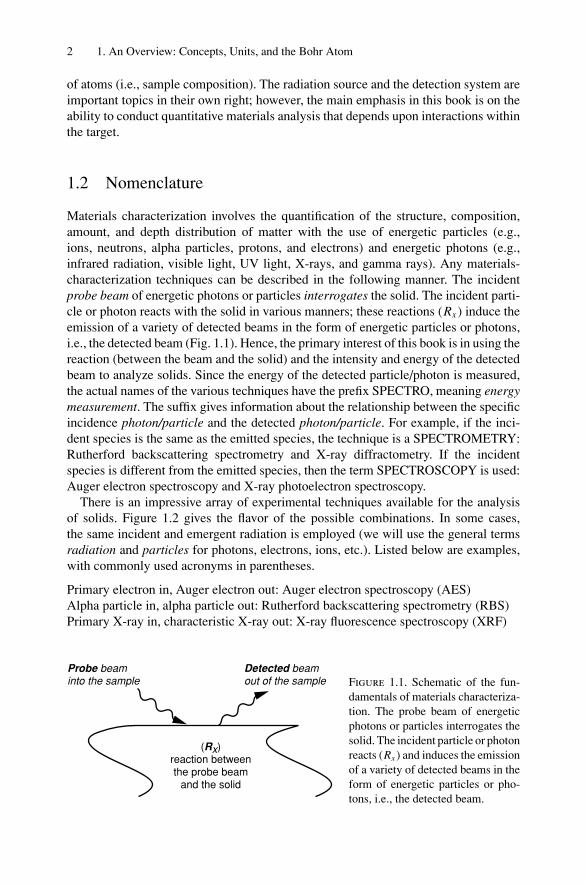
1.2 Nomenclature
Materials characterization involves the quantification of the structure, composition,amount, and depth distribution of matter with the use of energetic particles (e.g.,ions, neutrons, alpha particles, protons, and electrons) and energetic photons (e.g.,infrared radiation, visible light, UV light, X-rays, and gamma rays). Any materials-characterization techniques can be described in the following manner. The incidentprobe beam of energetic photons or particles interrogates the solid. The incident parti-cle or photon reacts with the solid in various manners; these reactions (Rx ) induce theemission of a variety of detected beams in the form of energetic particles or photons,i.e., the detected beam (Fig. 1.1). Hence, the primary interest of this book is in using thereaction (between the beam and the solid) and the intensity and energy of the detectedbeam to analyze solids. Since the energy of the detected particle/photon is measured,the actual names of the various techniques have the prefix SPECTRO, meaning energymeasurement. The suffix gives information about the relationship between the specificincidence photon/particle and the detected photon/particle. For example, if the inci-dent species is the same as the emitted species, the technique is a SPECTROMETRY:Rutherford backscattering spectrometry and X-ray diffractometry. If the incidentspecies is different from the emitted species, then the term SPECTROSCOPY is used:Auger electron spectroscopy and X-ray photoelectron spectroscopy.
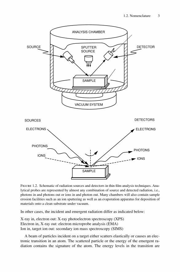
There is an impressive array of experimental techniques available for the analysisof solids. Figure 1.2 gives the flavor of the possible combinations. In some cases,the same incident and emergent radiation is employed (we will use the general termsradiation and particles for photons, electrons, ions, etc.). Listed below are examples,with commonly used acronyms in parentheses.
Primary electron in, Auger electron out: Auger electron spectroscopy (AES)Alpha particle in, alpha particle out: Rutherford backscattering spectrometry (RBS)Primary X-ray in, characteristic X-ray out: X-ray fluorescence spectroscopy (XRF)
Detected beamout of the sample
Probe beaminto the sample
(Rx)reaction betweenthe probe beam
and the solid
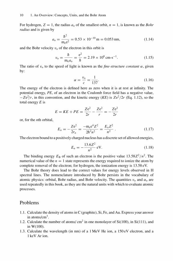
Figure 1.1. Schematic of the fun-damentals of materials characteriza-tion. The probe beam of energeticphotons or particles interrogates thesolid. The incident particle or photonreacts (Rx ) and induces the emissionof a variety of detected beams in theform of energetic particles or pho-tons, i.e., the detected beam.
1.2. Nomenclature 3
IONSIONS
DETECTORS
ELECTRONS
PHOTONSPHOTONS
SOURCES
SOURCE
ELECTRONS
VACUUM SYSTEM
SAMPLE
SAMPLE
DETECTORSPUTTERSOURCE
ANALYSIS CHAMBER
Figure 1.2. Schematic of radiation sources and detectors in thin film analysis techniques. Ana-lytical probes are represented by almost any combination of source and detected radiation, i.e.,photons in and photons out or ions in and photon out. Many chambers will also contain sampleerosion facilities such as an ion sputtering as well as an evaporation apparatus for deposition ofmaterials onto a clean substrate under vacuum.
In other cases, the incident and emergent radiation differ as indicated below:
X-ray in, electron out: X-ray photoelectron spectroscopy (XPS)Electron in, X-ray out: electron microprobe analysis (EMA)Ion in, target ion out: secondary ion mass spectroscopy (SIMS)
A beam of particles incident on a target either scatters elastically or causes an elec-tronic transition in an atom. The scattered particle or the energy of the emergent ra-diation contains the signature of the atom. The energy levels in the transition are
4 1. An Overview: Concepts, Units, and the Bohr Atom
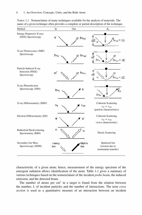
Table 1.1. Nomenclature of many techniques available for the analysis of materials. Thename of a given technique often provides a complete or partial description of the technique.
Method In Out Rx
Energy Dispersive X-rays(EDX) Spectroscopy
X-ray Fluorescence (XRF)Spectroscopy
Particle Induced X-rayEmission (PIXE)Spectroscopy
X-ray PhotoelectronSpectroscopy (XPS)
X-ray Diffractometry (XRD) Coherent Scatteringνin = νout
(particle characteristics)
Electron Diffractometry (ED) Coherent Scatteringνin = νout
(wave characteristic)
Rutherford BackscatteringSpectrometry (RBS) Elastic Scattering
Secondary Ion MassSpectroscopy (SIMS)
Sputtered Ion(erosion due to
momentum transfer)
characteristic of a given atom; hence, measurement of the energy spectrum of theemergent radiation allows identification of the atom. Table 1.1 gives a summary ofvarious techniques based on the nomenclature of the incident probe beam, the inducedemission, and the detected beam.
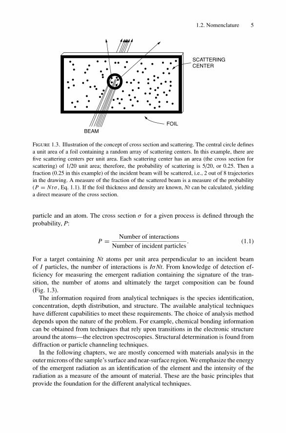
The number of atoms per cm2 in a target is found from the relation betweenthe number, I, of incident particles and the number of interactions. The term crosssection is used as a quantitative measure of an interaction between an incident
1.2. Nomenclature 5
BEAMFOIL
SCATTERINGCENTER
Figure 1.3. Illustration of the concept of cross section and scattering. The central circle definesa unit area of a foil containing a random array of scattering centers. In this example, there arefive scattering centers per unit area. Each scattering center has an area (the cross section forscattering) of 1/20 unit area; therefore, the probability of scattering is 5/20, or 0.25. Then afraction (0.25 in this example) of the incident beam will be scattered, i.e., 2 out of 8 trajectoriesin the drawing. A measure of the fraction of the scattered beam is a measure of the probability(P = Ntσ , Eq. 1.1). If the foil thickness and density are known, Nt can be calculated, yieldinga direct measure of the cross section.
particle and an atom. The cross section σ for a given process is defined through theprobability, P:
P = Number of interactions
Number of incident particles. (1.1)
For a target containing Nt atoms per unit area perpendicular to an incident beamof I particles, the number of interactions is IσNt. From knowledge of detection ef-ficiency for measuring the emergent radiation containing the signature of the tran-sition, the number of atoms and ultimately the target composition can be found(Fig. 1.3).
The information required from analytical techniques is the species identification,concentration, depth distribution, and structure. The available analytical techniqueshave different capabilities to meet these requirements. The choice of analysis methoddepends upon the nature of the problem. For example, chemical bonding informationcan be obtained from techniques that rely upon transitions in the electronic structurearound the atoms—the electron spectroscopies. Structural determination is found fromdiffraction or particle channeling techniques.
In the following chapters, we are mostly concerned with materials analysis in theouter microns of the sample’s surface and near-surface region. We emphasize the energyof the emergent radiation as an identification of the element and the intensity of theradiation as a measure of the amount of material. These are the basic principles thatprovide the foundation for the different analytical techniques.
6 1. An Overview: Concepts, Units, and the Bohr Atom
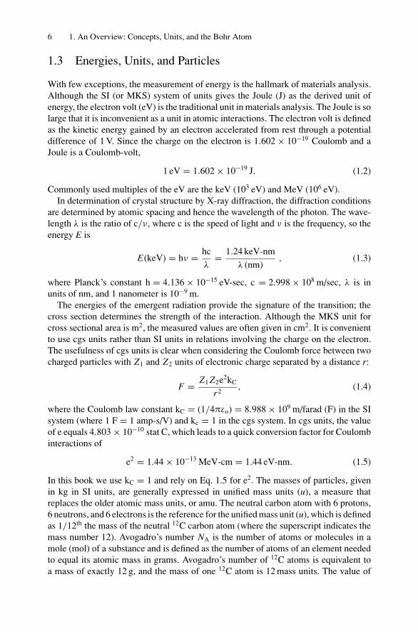
1.3 Energies, Units, and Particles
With few exceptions, the measurement of energy is the hallmark of materials analysis.Although the SI (or MKS) system of units gives the Joule (J) as the derived unit ofenergy, the electron volt (eV) is the traditional unit in materials analysis. The Joule is solarge that it is inconvenient as a unit in atomic interactions. The electron volt is definedas the kinetic energy gained by an electron accelerated from rest through a potentialdifference of 1 V. Since the charge on the electron is 1.602 × 10⁻¹⁹ Coulomb and aJoule is a Coulomb-volt,
1 eV = 1.602 × 10⁻¹⁹ J. (1.2)
Commonly used multiples of the eV are the keV (103 eV) and MeV (106 eV).In determination of crystal structure by X-ray diffraction, the diffraction conditions
are determined by atomic spacing and hence the wavelength of the photon. The wave-length λ is the ratio of c/ν, where c is the speed of light and ν is the frequency, so theenergy E is
E(keV) = hν = hc
λ= 1.24 keV-nm
λ (nm), (1.3)
where Planck’s constant h = 4.136 × 10⁻¹⁵ eV-sec, c = 2.998 × 10⁸ m/sec, λ is inunits of nm, and 1 nanometer is 10−9 m.
The energies of the emergent radiation provide the signature of the transition; thecross section determines the strength of the interaction. Although the MKS unit forcross sectional area is m2, the measured values are often given in cm2. It is convenientto use cgs units rather than SI units in relations involving the charge on the electron.The usefulness of cgs units is clear when considering the Coulomb force between twocharged particles with Z1 and Z2 units of electronic charge separated by a distance r:
F = Z1 Z2e2kC
r2, (1.4)
where the Coulomb law constant kC = (1/4πεo) = 8.988 × 10⁹ m/farad (F) in the SIsystem (where 1 F = 1 amp-s/V) and kc = 1 in the cgs system. In cgs units, the valueof e equals 4.803 × 10⁻¹⁰ stat C, which leads to a quick conversion factor for Coulombinteractions of
e2 = 1.44 × 10⁻¹³ MeV-cm = 1.44 eV-nm. (1.5)
In this book we use kC = 1 and rely on Eq. 1.5 for e2. The masses of particles, givenin kg in SI units, are generally expressed in unified mass units (u), a measure thatreplaces the older atomic mass units, or amu. The neutral carbon atom with 6 protons,6 neutrons, and 6 electrons is the reference for the unified mass unit (u), which is definedas 1/12th the mass of the neutral 12C carbon atom (where the superscript indicates themass number 12). Avogadro’s number NA is the number of atoms or molecules in amole (mol) of a substance and is defined as the number of atoms of an element neededto equal its atomic mass in grams. Avogadro’s number of 12C atoms is equivalent toa mass of exactly 12 g, and the mass of one 12C atom is 12 mass units. The value of
1.3. Energies, Units, and Particles 7
Avogadro’s number, the number of atoms/mol, is
NA = 6.0220 × 10²³, (1.6)
and the unified mass unit u, the reciprocal of NA, is
u = 1
NA= 1g
6.023 × 1023= 1.661 × 10⁻²⁴g . (1.7)
A large part of this book is devoted to the extraction of depth profiles—the atomiccomposition or impurity concentration as a function of depth below the surface. Interms of length measurement, the natural unit is the nanometer (nm), where
1 nm = 10−9 m .
For example, the separation between atoms in a solid is about 0.3 nm. The measurementtechniques give depth scales in terms of areal density, the number Nt of atoms per cm2,where t is the thickness and N is the atomic density. For elemental solids, the atomicdensity and the mass density ρ in g/cm3 are related by
N = NA ρ/A, (1.8)
where A is the atomic mass number and NA is Avogadro’s number. Another unit ofthickness is the mass absorption coefficient, usually expressed as g/cm2, the productof the mass density and linear thickness.
Each nucleus is characterized by a definite atomic number Z and mass number A.The atomic number Z is the number of protons and hence the number of electronsin the neutral atom; it reflects the atomic properties of the atom. The mass numbergives the number of nucleons, protons, and neutrons; isotopes are nuclei (often callednuclides) with the same Z and different A. The current practice is to represent eachnucleus by the chemical name with the mass number as a superscript, i.e., 12C. Thechemical atomic weight (or atomic mass) of elements as listed in the periodic tablegives the average atomic mass, i.e., the average of the stable isotopes weighted by theirabundance. Carbon, for example, has an atomic weight of 12.011, which reflects the1.1% abundance of 13C. Appendix 10 lists the elements and their relative abundance,atomic weight, atomic density, and specific gravity.
The masses of particles may be expressed in terms of energy through the Einsteinrelation
E = mc2 , (1.9)
which associates 1 J of energy with 1/c2 kg of mass. The mass of an electron is 9.11 ×10⁻³¹ kg, which is equivalent to an energy
E = (9.11 × 10⁻³¹ kg)(2.998 × 10⁸ m/s)2
= 8.188 × 10⁻¹⁴J = 0.511 MeV . (1.10)
In materials analysis, the incident radiation is usually photons, electrons, neutrons,or low-mass ions (neutral atoms stripped of one or more electrons). For example, theproton is an ionized hydrogen atom, and the alpha particle is a helium atom with one ortwo electrons removed. The notation 4He+ and 4He++ is often used to denote a heliumatom with one or two electrons removed, respectively. The deuteron, 2H+, is a neutron
8 1. An Overview: Concepts, Units, and the Bohr Atom
Table 1.2. Mass energies of particles and light nuclei.
Mass energyParticle Symbol (MeV)
Electron e or e− 0.511Proton p 938.3Neutron n 939.6Deuteron d or 2H+ 1875.6Alpha α or 4He++ 3727.4
and proton bound together. The mass energies of some of these particles are given inTable 1.2. In analytical applications, the velocities of these particles are generally wellbelow 107 m/sec; hence, relativistic effects do not enter, and the masses are independentof velocity.
1.4 Particle–Wave Duality and Lattice Spacing
In materials analysis, one tends to view the incident beam and emergent radiationas discrete particles—photons, electrons, neutrons, and ions. On the other hand, theinteractions of radiation with matter and, in particular, the cross section for a transitionis often based on the wave aspect of the radiation.
This wave–particle duality was of major concern in the early development of modernphysics. The photon and the electron provide examples of the wave and particle natureof matter. For example, in the photoelectric effect, light behaves as if it were particle-like, that each photon interacting with an atom to give up its energy, E = hν, to anelectron that can escape from the solid. The diffraction of X-rays from planes of atoms,on the other hand, satisfies wave interference conditions.
Electrons and their diffraction from crystal surfaces constitute a sensitive probe ofsurface structure. The classical, particle behavior of electrons, on the other hand, isillustrated in their deflection in electric and magnetic fields. One can associate botha wavelength λ and a momentum p with the motion of an electron. The De Broglierelation gives their connection:
λ = h/p , (1.11)
where h is Planck’s constant. Distances between lattice planes are on the order of atenth of a nanometer (0.1 nm). For diffraction, the wavelengths of electrons are of com-parable magnitude. The electron velocity, v = p/m, corresponding to a wavelength of0.1 nm is
v = h
mλ= 6.6 × 10⁻³⁴
9.1 × 10−31 × 10−10= 7.25 × 10⁶ m-sec−1 ,
where MKS units are used with h = 6.6 × 10⁻³⁴ J s. The energy is
E = 1
2mv2 = 9.1 × 10⁻³¹(7.25 × 10⁶)2
2= 2.39 × 10⁻¹⁷J = 150 eV .
1.5. The Bohr Model 9
Electron diffraction studies of surfaces use electrons with low energies, between 40 eVand 150 eV, giving rise to the acronym LEED—low-energy electron diffraction.
Energies of 1.0–2.0 MeV He+ are commonly used in materials analysis; here thewavelengths are orders of magnitude smaller than the lattice spacing, and the inter-actions of helium ions with solids are described on the basis of particle rather thanwave behavior. For helium atoms, an energy of 2 MeV corresponds to a wavelengthof 10−5 nm; whereas, distances between nearest-neighbor atoms in a solid are on theorder of 0.2–0.5 nm.
The distances between atoms and atomic planes can be calculated from a knownlattice constant and crystal structure. Aluminum, for example, contains ∼6 × 10²²
atoms/cm3, has a lattice constant of 0.404 nm, and has a face-centered cubic (fcc)crystal structure. One monolayer of atoms on the (100) surface then contains an arealatom density of 2 atoms/(0.404 nm)2 or 1.2 × 10¹⁵ atoms/cm2. Almost all solids havemonolayer density values of 5 × 10¹⁴/cm2 to 2 × 10¹⁵/cm2 on major crystallographicsurfaces. In a loose way, a monolayer is usually thought of as 1015 atoms/cm2. Thespectroscopic sensitivity of various surfaces is often measured in units of monolayersor atoms/cm2; bulk impurity determinations are usually given in atoms/cm3.
1.5 The Bohr Model
The identification of atomic species from the energies of emitted radiation was devel-oped from the concepts of the Bohr model of the hydrogen atom. Particle scatteringexperiments established that the atom could be treated as a positively charged nucleussurrounded by a cloud of electrons. Bohr assumed that the electrons could move instable circular orbits called stationary states and would emit radiation only in the tran-sition from one stable orbit to another. The energies of the orbits were derived from thepostulate that the angular momentum of the electron around the nucleus is an integralmultiple of h/2π (h/2π is written as h). In this section, we give a brief review of theBohr atom, which provides useful relations for simple estimates of atomic parameters.
For a single electron of mass me in a circular orbit of radius r about a fixed nucleusof charge Ze, the balance between the Coulomb and centripetal forces leads to
Ze2
r2= me
v2
r. (1.12)
Bohr assumed that the angular momentum, mevr , has values given by an integer ntimes h,
mevr = n h .
From the above equations, we have
v2 = n2h2e2
m2er2
= Ze2
mer,
which can be rewritten to give the radii rn of allowed orbits:
rn = h2n2
me Ze2. (1.13)
10 1. An Overview: Concepts, Units, and the Bohr Atom
For hydrogen, Z = 1, the radius ao of the smallest orbit, n = 1, is known as the Bohrradius and is given by
ao = h2
mee2= 0.53 × 10⁻¹⁰ m = 0.053 nm, (1.14)
and the Bohr velocity vo of the electron in this orbit is
vo = h
meao= e2
h= 2.19 × 108 cm-s−1. (1.15)
The ratio of vo to the speed of light is known as the fine-structure constant α, givenby:
α = vo
c= 1
137. (1.16)
The energy of the electron is defined here as zero when it is at rest at infinity. Thepotential energy, PE, of an electron in the Coulomb force field has a negative value,−Ze2/r , in this convention, and the kinetic energy (KE) is Ze2/2r (Eq. 1.12), so thetotal energy E is
E = KE + PE = Ze2
2r− Ze2
r= − Ze2
2ror, for the nth orbital,
En = − Ze2
2rn= −mee4 Z2
2h2n2= Eo Z2
n2. (1.17)
The electron bound to a positively charged nucleus has a discrete set of allowed energies,
En = −13.6Z2
n2eV. (1.18)
The binding energy EB of such an electron is the positive value 13.58Z2/n2. Thenumerical value of the n = 1 state represents the energy required to ionize the atom bycomplete removal of the electron; for hydrogen, the ionization energy is 13.58 eV.
The Bohr theory does lead to the correct values for energy levels observed in Hspectral lines. The nomenclature introduced by Bohr persists in the vocabulary ofatomic physics: orbital, Bohr radius, and Bohr velocity. The quantities vo and αo areused repeatedly in this book, as they are the natural units with which to evaluate atomicprocesses.
Problems
1.1. Calculate the density of atoms in C (graphite), Si, Fe, and Au. Express your answerin atoms/cm3.
1.2. Calculate the number of atoms/ cm2 in one monolayer of Si(100), in Si(111), andin W(100).
1.3. Calculate the wavelength (in nm) of a 1 MeV He ion, a 150 eV electron, and a1 keV Ar ion.
Problems 11
1.4. Show that e2 = 1.44 eV-nm.1.5. Find the ratio of velocity of a 1 MeV ion to the Bohr velocity.1.6. Use the literature and notes to state the incoming radiation (particles) in the fol-
lowing spectroscopies, and in each case, state the nature of the atomic transitioninvolved:
AES – Auger electron spectroscopyRBS – Rutherford backscattering spectrometrySIMS – secondary ion mass spectroscopyXPS – X-ray photoelectron spectroscopyXRF – X-ray fluorescence spectroscopySEM – scanning electron µ probeNRA – nuclear reaction analysis
1.7. In this book we repeatedly make estimates using the Bohr model of the atom.Test the validity of this approximation by calculating the K-shell binding energy,EK(n = 1); the L-shell binding energy, EL(n = 2); the wavelength at the K-shellabsorption edge, (hω = EK), and the K X-ray energy (EK − EL) for Si, Ni, andW. Compare with the accurate values given in the appendices.
1.8. The Auger process, discussed in Chapter 12, corresponds to an electron transitioninvolving the emission of an Auger electron with the energy (EK − EL − EL),where K is for n = 1 and L is for n = 2. Show that, in the Bohr model, aok = 1/
√2,
where ao is the K-shell radius ao/Z and hk is the momentum of the outgoingelectron.
1.9. An incident photon of sufficient energy can eject an electron from an inner shellorbit. Such an excited atom may relax by rearranging the outer electrons to fill thevacancy. This is said to occur in a time equivalent to the orbital time. Calculate thischaracteristic atomic time for Ni. In later chapters, we will show that the inverseof this time may be thought of as the rate for the Auger process.
References
1. L.C. Feldman and J.W. Mayer, Fundamentals of Surface and Thin Film Analysis (North-Holland, New York 1986).
2. J. D. McGervey, Introduction to Modern Physics (Academic Press New York, 1971).3. F. K. Richtmyer, E. H. Kennard, and J. N. Cooper, Introduction to Modern Physics, 6th ed.
(McGraw-Hill, New York, 1969).4. R. L. Sproull and W. A. Phillips, Modern Physics, 3rd ed. (John Wiley and Sons, New York
1980).5. P. A. Tipler, Modern Physics (Worth Publishers, New York, 1978).6. R. T. Weidner and R. L. Sells, Elementary Modern Physics, 3rd ed. (Allyn and Bacon,
Boston, MA, 1980).7. J. C. Willmott, Atomic Physics (John Wiley and Sons, New York, 1975).8. John Taylor, Chris Zafiratos, and Michael A. Dubson, Modern Physics for Scientists and
Engineers, 2nd ed. (Prentice-Hall, New York, 2003).9. D.C. Giancoli, Physics for Scientists and Engineers with Modern Physics, 3rd ed. (Prentice-
Hall, New York, 2001).
2Atomic Collisions andBackscattering Spectrometry
2.1 Introduction
The model of the atom is that of a cloud of electrons surrounding a positivelycharged central core—the nucleus—that contains Z protons and A − Z neutrons,where Z is the atomic number and A the mass number. Single-collision, large-anglescattering of alpha particles by the positively charged nucleus not only establishedthis model but also forms the basis for one modern analytical technique, Ruther-ford backscattering spectrometry. In this chapter, we will develop the physical con-cepts underlying Coulomb scattering of a fast light ion by a more massive stationaryatom.
Of all the analytical techniques, Rutherford backscattering spectrometry is perhapsthe easiest to understand and to apply because it is based on classical scattering in acentral-force field. Aside from the accelerator, which provides a collimated beam ofMeV particles (usually 4He+ ions), the instrumentation is simple (Fig. 2.1a). Semicon-ductor nuclear particle detectors are used that have an output voltage pulse proportionalto the energy of the particles scattered from the sample into the detector. The techniqueis also the most quantitative, as MeV He ions undergo close-impact scattering colli-sions that are governed by the well-known Coulomb repulsion between the positivelycharged nuclei of the projectile and target atom. The kinematics of the collision andthe scattering cross section are independent of chemical bonding, and hence backscat-tering measurements are insensitive to electronic configuration or chemical bondingwith the target. To obtain information on the electronic configuration, one must employanalytical techniques such as photoelectron spectroscopy that rely on transitions in theelectron shells.
In this chapter, we treat scattering between two positively charged bodies of atomicnumbers Z1 and Z2. The convention is to use the subscript 1 to denote the incidentparticle and the subscript 2 to denote the target atom. We first consider energy transfersduring collisions, as they provide the identity of the target atom. Then we calculatethe scattering cross section, which is the basis of the quantitative aspect of Rutherfordbackscattering. Here we are concerned with scattering from atoms on the sample surfaceor from thin layers. In Chapter 3, we discuss depth profiles.
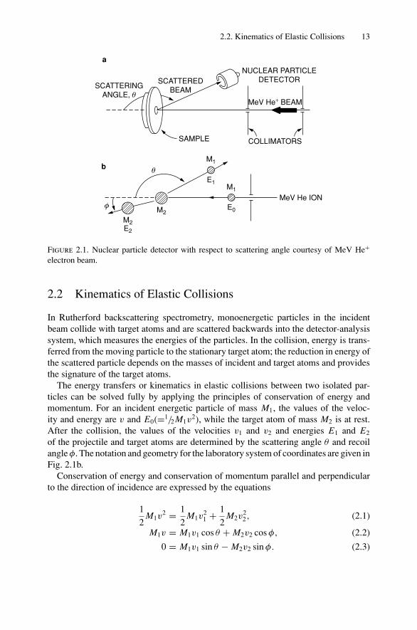
2.2. Kinematics of Elastic Collisions 13
φ
M2
M2
M1
M1
E2
E0
E1
b θ
MeV He ION
SAMPLE COLLIMATORS
MeV He+ BEAM
NUCLEAR PARTICLEDETECTORSCATTERED
BEAMSCATTERINGANGLE, θ
a
Figure 2.1. Nuclear particle detector with respect to scattering angle courtesy of MeV He+
electron beam.
2.2 Kinematics of Elastic Collisions
In Rutherford backscattering spectrometry, monoenergetic particles in the incidentbeam collide with target atoms and are scattered backwards into the detector-analysissystem, which measures the energies of the particles. In the collision, energy is trans-ferred from the moving particle to the stationary target atom; the reduction in energy ofthe scattered particle depends on the masses of incident and target atoms and providesthe signature of the target atoms.
The energy transfers or kinematics in elastic collisions between two isolated par-ticles can be solved fully by applying the principles of conservation of energy andmomentum. For an incident energetic particle of mass M1, the values of the veloc-ity and energy are v and E0(=1/2 M1v
2), while the target atom of mass M2 is at rest.After the collision, the values of the velocities v1 and v2 and energies E1 and E2
of the projectile and target atoms are determined by the scattering angle θ and recoilangle φ. The notation and geometry for the laboratory system of coordinates are given inFig. 2.1b.
Conservation of energy and conservation of momentum parallel and perpendicularto the direction of incidence are expressed by the equations
1
2M1v
2 = 1
2M1v
21 + 1
2M2v
22, (2.1)
M1v = M1v1 cos θ + M2v2 cos φ, (2.2)
0 = M1v1 sin θ − M2v2 sin φ. (2.3)
14 2. Atomic Collisions and Backscattering Spectrometry
00
0.1
0.2
0.3
0.4
0.5
0.6
0.7
0.8
0.9
1.0
KM
4He
20Ne
40Ar
M2
12C
50 100 150 200
H
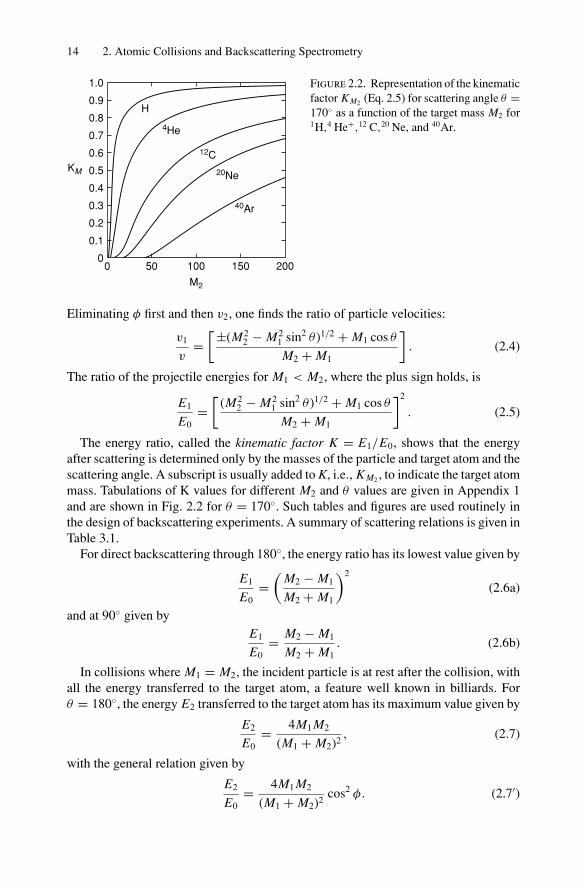
Figure 2.2. Representation of the kinematicfactor KM2 (Eq. 2.5) for scattering angle θ =170 as a function of the target mass M2 for1H,4 He+,12 C,20 Ne, and 40Ar.
Eliminating φ first and then v2, one finds the ratio of particle velocities:
v1
v=[±(M2
2 − M21 sin2 θ )1/2 + M1 cos θ
M2 + M1
]. (2.4)
The ratio of the projectile energies for M1 < M2, where the plus sign holds, is
E1
E0=[
(M22 − M2
1 sin2 θ )1/2 + M1 cos θ
M2 + M1
]2
. (2.5)
The energy ratio, called the kinematic factor K = E1/E0, shows that the energyafter scattering is determined only by the masses of the particle and target atom and thescattering angle. A subscript is usually added to K, i.e., KM2 , to indicate the target atommass. Tabulations of K values for different M2 and θ values are given in Appendix 1and are shown in Fig. 2.2 for θ = 170. Such tables and figures are used routinely inthe design of backscattering experiments. A summary of scattering relations is given inTable 3.1.
For direct backscattering through 180, the energy ratio has its lowest value given by
E1
E0=(
M2 − M1
M2 + M1
)2
(2.6a)
and at 90 given byE1
E0= M2 − M1
M2 + M1. (2.6b)
In collisions where M1 = M2, the incident particle is at rest after the collision, withall the energy transferred to the target atom, a feature well known in billiards. Forθ = 180, the energy E2 transferred to the target atom has its maximum value given by
E2
E0= 4M1 M2
(M1 + M2)2, (2.7)
with the general relation given by
E2
E0= 4M1 M2
(M1 + M2)2cos2 φ. (2.7′)
2.2. Kinematics of Elastic Collisions 15
In practice, when a target contains two types of atoms that differ in their massesby a small amount M2, the experimental geometry is adjusted to produce as large achange E1 as possible in the measured energy E1 of the projectile after the collision.A change of M2 (for fixed M1 < M2) gives the largest change of K when θ = 180.Thus θ = 180 is the preferred location for the detector (θ ∼= 170 in practice becauseof detector size), an experimental arrangement that has given the method its name ofbackscattering spectrometry.
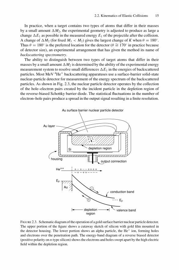
The ability to distinguish between two types of target atoms that differ in theirmasses by a small amount M2 is determined by the ability of the experimental energymeasurement system to resolve small differences E1 in the energies of backscatteredparticles. Most MeV 4He+ backscattering apparatuses use a surface-barrier solid-statenuclear-particle detector for measurement of the energy spectrum of the backscatteredparticles. As shown in Fig. 2.3, the nuclear particle detector operates by the collectionof the hole–electron pairs created by the incident particle in the depletion region ofthe reverse-biased Schottky barrier diode. The statistical fluctuations in the number ofelectron–hole pairs produce a spread in the output signal resulting in a finite resolution.
Au
+ − + − − + + + +− + − + + − − − −
−
+
He++
EF
EF
housing
valence band
conduction band
depletionregion
output connection
depletion regionSi
Au layer
+++
+−− −−
Au surface barrier nuclear particle detector
Figure 2.3. Schematic diagram of the operation of a gold surface barrier nuclear particle detector.The upper portion of the figure shows a cutaway sketch of silicon with gold film mounted inthe detector housing. The lower portion shows an alpha particle, the He+ ion, forming holesand electrons over the penetration path. The energy-band diagram of a reverse biased detector(positive polarity on n-type silicon) shows the electrons and holes swept apart by the high electricfield within the depletion region.
16 2. Atomic Collisions and Backscattering Spectrometry
Energy resolution values of 10–20 keV, full width at half maximum (FWHM), forMeV 4He+ ions can be obtained with conventional electronic systems. For example,backscattering analysis with 2.0 MeV 4He+ particles can resolve isotopes up to aboutmass 40 (the chlorine isotopes, for example). Around target masses close to 200, themass resolution is about 20, which means that one cannot distinguish among atomsbetween 181Ta and 201Hg.
In backscattering measurements, the signals from the semiconductor detector elec-tronic system are in the form of voltage pulses. The heights of the pulses are proportionalto the incident energy of the particles. The pulse height analyzer stores pulses of a givenheight in a given voltage bin or channel (hence the alternate description, multichannelanalyzer). The channel numbers are calibrated in terms of the pulse height, and hencethere is a direct relationship between channel number and energy.
2.3 Rutherford Backscattering Spectrometry
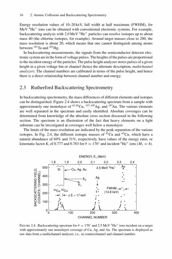
In backscattering spectrometry, the mass differences of different elements and isotopescan be distinguished. Figure 2.4 shows a backscattering spectrum from a sample withapproximately one monolayer of 63,65Cu, 107,109Ag, and 197Au. The various elementsare well separated in the spectrum and easily identified. Absolute coverages can bedetermined from knowledge of the absolute cross section discussed in the followingsection. The spectrum is an illustration of the fact that heavy elements on a lightsubstrate can be investigated at coverages well below a monolayer.
The limits of the mass resolution are indicated by the peak separation of the variousisotopes. In Fig. 2.4, the different isotopic masses of 63Cu and 65Cu, which have anatural abundance of 69% and 31%, respectively, have values of the energy ratio, orkinematic factor K, of 0.777 and 0.783 for θ = 170 and incident 4He+ ions (M1 = 4).
0
1.8
0100 200 300 400
100
200
300
400
500
1.9 2.0 2.1 2.2 2.3 2.4
ENERGY, E1 (MeV)
CHANNEL NUMBER
BA
CK
SC
ATT
ER
ING
YIE
LD,
(CO
UN
TS
/ C
HA
NN
EL)
Au
FWHM(14.8 keV)
Ag
Cu, Ag, Au 2.5 MeV 4He+
E0
E1
63Cu 65Cu
∆ E = 17 keV
Si
Figure 2.4. Backscattering spectrum for θ = 170 and 2.5 MeV 4He+ ions incident on a targetwith approximately one monolayer coverage of Cu, Ag, and Au. The spectrum is displayed asraw data from a multichannel analyzer, i.e., in counts/channel and channel number.
2.4. Scattering Cross Section and Impact Parameter 17
For incident energies of 2.5 MeV, the energy difference of particles from the two massesis 17 keV, an energy value close to the energy resolution (FWHM = 14.8 keV) of thesemiconductor particle-detector system. Consequently, the signals from the two iso-topes overlap to produce the peak and shoulder shown in the figure. Particles scatteredfrom the two Ag isotopes, 107Ag and 109Ag, have too small an energy difference, 6 keV,and hence the signal from Ag appears as a single peak.
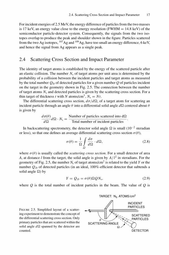
2.4 Scattering Cross Section and Impact Parameter
The identity of target atoms is established by the energy of the scattered particle afteran elastic collision. The number Ns of target atoms per unit area is determined by theprobability of a collision between the incident particles and target atoms as measuredby the total number QD of detected particles for a given number Q of particles incidenton the target in the geometry shown in Fig. 2.5. The connection between the numberof target atoms Ns and detected particles is given by the scattering cross section. For athin target of thickness t with N atoms/cm3, Ns = Nt .
The differential scattering cross section, dσ/d, of a target atom for scattering anincident particle through an angle θ into a differential solid angle d centered about θ
is given by
dσ(θ )
dd · Ns = Number of particles scattered into d
Total number of incident particles.
In backscattering spectrometry, the detector solid angle is small (10−2 steradianor less), so that one defines an average differential scattering cross section σ (θ),
σ (θ ) = 1
∫Ω
dσ
d· d, (2.8)
where σ (θ ) is usually called the scattering cross section. For a small detector of areaA, at distance l from the target, the solid angle is given by A/ l2 in steradians. For thegeometry of Fig. 2.5, the number Ns of target atoms/cm2 is related to the yield Y or thenumber Q D of detected particles (in an ideal, 100%-efficient detector that subtends asolid angle ) by
Y = Q D = σ (θ)QNs, (2.9)
where Q is the total number of incident particles in the beam. The value of Q is
TARGET: NS ATOMS/cm2
INCIDENTPARTICLES
SCATTEREDPARTICLES
DETECTORΩ
SCATTERING ANGLEθ
Figure 2.5. Simplified layout of a scatter-ing experiment to demonstrate the concept ofthe differential scattering cross section. Onlyprimary particles that are scattered within thesolid angle d spanned by the detector arecounted.
18 2. Atomic Collisions and Backscattering Spectrometry
NUCLEUSz
db
b θdθ
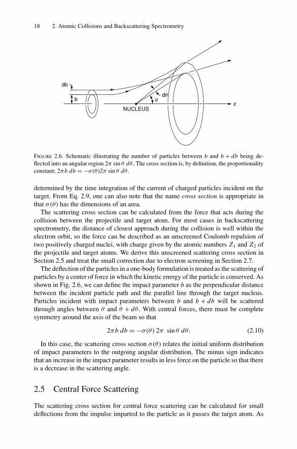
Figure 2.6. Schematic illustrating the number of particles between b and b + db being de-flected into an angular region 2π sin θ dθ . The cross section is, by definition, the proportionalityconstant; 2πb db = −σ (θ )2π sin θ dθ .
determined by the time integration of the current of charged particles incident on thetarget. From Eq. 2.9, one can also note that the name cross section is appropriate inthat σ (θ ) has the dimensions of an area.
The scattering cross section can be calculated from the force that acts during thecollision between the projectile and target atom. For most cases in backscatteringspectrometry, the distance of closest approach during the collision is well within theelectron orbit, so the force can be described as an unscreened Coulomb repulsion oftwo positively charged nuclei, with charge given by the atomic numbers Z1 and Z2 ofthe projectile and target atoms. We derive this unscreened scattering cross section inSection 2.5 and treat the small correction due to electron screening in Section 2.7.
The deflection of the particles in a one-body formulation is treated as the scattering ofparticles by a center of force in which the kinetic energy of the particle is conserved. Asshown in Fig. 2.6, we can define the impact parameter b as the perpendicular distancebetween the incident particle path and the parallel line through the target nucleus.Particles incident with impact parameters between b and b + db will be scatteredthrough angles between θ and θ + dθ . With central forces, there must be completesymmetry around the axis of the beam so that
2πb db = −σ (θ) 2π sin θ dθ. (2.10)
In this case, the scattering cross section σ (θ ) relates the initial uniform distributionof impact parameters to the outgoing angular distribution. The minus sign indicatesthat an increase in the impact parameter results in less force on the particle so that thereis a decrease in the scattering angle.
2.5 Central Force Scattering
The scattering cross section for central force scattering can be calculated for smalldeflections from the impulse imparted to the particle as it passes the target atom. As
2.5. Central Force Scattering 19
b
b
O AC
B
vM1
F
M1
v
θr
z′
φφ0
φ0
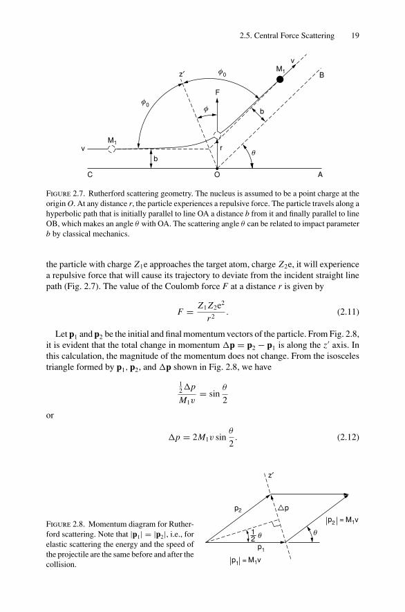
Figure 2.7. Rutherford scattering geometry. The nucleus is assumed to be a point charge at theorigin O. At any distance r, the particle experiences a repulsive force. The particle travels along ahyperbolic path that is initially parallel to line OA a distance b from it and finally parallel to lineOB, which makes an angle θ with OA. The scattering angle θ can be related to impact parameterb by classical mechanics.
the particle with charge Z1e approaches the target atom, charge Z2e, it will experiencea repulsive force that will cause its trajectory to deviate from the incident straight linepath (Fig. 2.7). The value of the Coulomb force F at a distance r is given by
F = Z1 Z2e2
r2. (2.11)
Let p1 and p2 be the initial and final momentum vectors of the particle. From Fig. 2.8,it is evident that the total change in momentum p = p2 − p1 is along the z′ axis. Inthis calculation, the magnitude of the momentum does not change. From the isoscelestriangle formed by p1, p2, and p shown in Fig. 2.8, we have
12p
M1v= sin
θ
2
or
p = 2M1v sinθ
2. (2.12)
θ θ12
p1
p2 p
p1 M1v =
p2 M1v =
z′
Figure 2.8. Momentum diagram for Ruther-ford scattering. Note that |p1| = |p2|, i.e., forelastic scattering the energy and the speed ofthe projectile are the same before and after thecollision.
20 2. Atomic Collisions and Backscattering Spectrometry
We now write Newton’s law for the particle, F = dp/dt , or
dp = F dt.
The force F is given by Coulomb’s law and is in the radial direction. Taking com-ponents along the z′ direction, and integrating to obtain p, we have
p =∫
(dp)z′ =∫
F cos φ dt =∫
F cos φdt
dφdφ, (2.13)
where we have changed the variable of integration from t to the angle φ. We canrelate dt/dφ to the angular momentum of the particle about the origin. Since theforce is central (i.e., acts along the line joining the particle and the nucleus at theorigin), there is no torque about the origin, and the angular momentum of the particle isconserved. Initially, the angular momentum has the magnitude M1vb. At a later time,it is M1r2 dφ/dt . Conservation of angular momentum thus gives
M1r2 dφ
dt= M1vb
or
dt
dφ= r2
vb.
Substituting this result and Eq. 2.11 for the force in Eq. 2.13, we obtain
p = Z1 Z2e2
r2
∫cos φ
r2
vbdφ = Z1 Z2e2
vb
∫cos φ dφ
or
p = Z1 Z2e2
vb(sin φ2 − sin φ1). (2.14)
From Fig. 2.7, φ1 = −φ0 and φ2 = +φ0, where 2φ0 + θ = 180. Then sin φ2 −sin φ1 = 2 sin(90 − 1/2θ ). Combining Eqs. 2.12 and 2.14 for p, we have
p = 2M1v sinθ
2= Z1 Z2e2
vb2 cos
θ
2. (2.15a)
This gives the relationship between the impact parameter b and the scattering angle:
b = Z1 Z2e2
M1v2cot
θ
2= Z1 Z2e2
2Ecot
θ
2. (2.15b)
From Eq. 2.10, the scattering cross section can be expressed as
σ (θ ) = −b
sin θ
db
dθ, (2.16)
and from the geometrical relations sinθ = 2 sin(θ/2) cos(θ/2) and d cot(θ/2) =− 1
2 dθ/ sin2(θ/2),
σ (θ) =(
Z1 Z2e2
4E
)21
sin4 θ/2. (2.17)
2.6. Scattering Cross Section: Two-Body 21
This is the scattering cross section originally derived by Rutherford. The experimentsby Geiger and Marsden in 1911–1913 verified the predictions that the amount ofscattering was proportional to (sin4 θ/2)−1 and E−2. In addition, they found that thenumber of elementary charges in the center of the atom is equal to roughly half theatomic weight. This observation introduced the concept of the atomic number of anelement, which describes the positive charge carried by the nucleus of the atom. Thevery experiments that gave rise to the picture of an atom as a positively charged nucleussurrounded by orbiting electrons has now evolved into an important materials analysistechnique.
For Coulomb scattering, the distance of closest approach, d, of the projectile to thescattering atom is given by equating the incident kinetic energy, E, to the potentialenergy at d:
d = Z1 Z2e2
E. (2.18)
The scattering cross section can be written as σ (θ) = (d/4)2/ sin4 θ/2, which for180 scattering gives σ (180) = (d/4)2. For 2 MeV He+ ions (Z1 = 2) incident on Ag(Z2 = 47),
d = (2)(47) · (1.44 eV nm)
2 × 10⁶ eV= 6.8 × 10⁻⁵ nm,
a value much smaller than the Bohr radius a0 = h2/mee2 = 0.053 nm and the K-shellradius of Ag, a0/47 ∼= 10−3 nm. Thus the use of an unscreened cross section is justified.The cross section for scattering to 180 is
σ (θ) = (6.8 × 10⁻⁵ nm)2/16 = 2.89 × 10⁻¹⁰ nm2,
a value of 2.89 × 10⁻²⁴ cm2 or 2.89 barns, where the barn = 10−24 cm2.
2.6 Scattering Cross Section: Two-Body
In the previous section, we used central forces in which the energy of the incidentparticle was unchanged through its trajectory. From the kinematics (Section 2.2), weknow that the target atom recoils from its initial position, and hence the incident particleloses energy in the collision. The scattering is elastic in that the total kinetic energyof the particles is conserved. Therefore, the change in energy of the scattered particlecan be appreciable; for θ = 180 and 4He+(M1 = 4) scattering from Si (M2 = 28),the kinematic factor K = (24/32)2 = 0.56 indicates that nearly one-half the energy islost by the incident particle. In this section, we evaluate the scattering cross sectionwhile including this recoil effect. The derivation of the center of mass to laboratorytransformation is given in Section 2.10.
The scattering cross section (Eq. 2.17) was based on the one-body problem of thescattering of a particle by a fixed center of force. However, the second particle is notfixed but recoils from its initial position as a result of the scattering. In general, thetwo-body central force problem can be reduced to a one-body problem by replacing
22 2. Atomic Collisions and Backscattering Spectrometry
θCθ
r
M1
M2
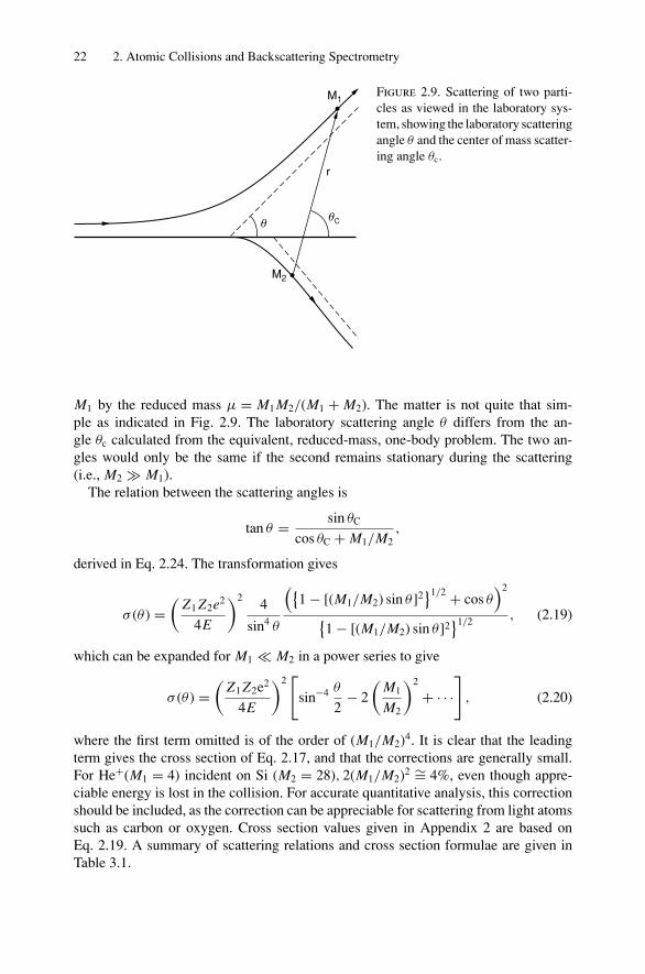
Figure 2.9. Scattering of two parti-cles as viewed in the laboratory sys-tem, showing the laboratory scatteringangle θ and the center of mass scatter-ing angle θc.
M1 by the reduced mass µ = M1 M2/(M1 + M2). The matter is not quite that sim-ple as indicated in Fig. 2.9. The laboratory scattering angle θ differs from the an-gle θc calculated from the equivalent, reduced-mass, one-body problem. The two an-gles would only be the same if the second remains stationary during the scattering(i.e., M2 M1).
The relation between the scattering angles is
tan θ = sin θC
cos θC + M1/M2,
derived in Eq. 2.24. The transformation gives
σ (θ ) =(
Z1 Z2e2
4E
)24
sin4 θ
(1 − [(M1/M2) sin θ ]2
1/2 + cos θ)2
1 − [(M1/M2) sin θ ]2
1/2 , (2.19)
which can be expanded for M1 M2 in a power series to give
σ (θ) =(
Z1 Z2e2
4E
)2[
sin−4 θ
2− 2
(M1
M2
)2
+ · · ·]
, (2.20)
where the first term omitted is of the order of (M1/M2)4. It is clear that the leadingterm gives the cross section of Eq. 2.17, and that the corrections are generally small.For He+(M1 = 4) incident on Si (M2 = 28), 2(M1/M2)2 ∼= 4%, even though appre-ciable energy is lost in the collision. For accurate quantitative analysis, this correctionshould be included, as the correction can be appreciable for scattering from light atomssuch as carbon or oxygen. Cross section values given in Appendix 2 are based onEq. 2.19. A summary of scattering relations and cross section formulae are given inTable 3.1.
2.7. Deviations from Rutherford Scattering at Low and High Energy 23
2.7 Deviations from Rutherford Scatteringat Low and High Energy
The derivation of the Rutherford scattering cross section is based on a Coulomb inter-action potential V (r ) between the particle Z1 and target atom Z2. This assumes that theparticle velocity is sufficiently large so that the particle penetrates well inside the or-bitals of the atomic electrons. Then scattering is due to the repulsion of two positivelycharged nuclei of atomic number Z1 and Z2. At larger impact parameters found insmall-angle scattering of MeV He ions or low-energy, heavy ion collisions (discussedin Chapter 4), the incident particle does not completely penetrate through the electronshells, and hence the innermost electrons screen the charge of the target atom.
We can estimate the energy where these electron screening effects become important.For the Coulomb potential to be valid for backscattering, we require that the distance ofclosest approach d be smaller than the K-shell electron radius, which can be estimatedas a0/Z2, where a0 = 0.053 nm, the Bohr radius. Using Eq. 2.18 for the distance ofclosest approach d, the requirement for d less than the radius sets a lower limit on theenergy of the analysis beam and requires that
E > Z1 Z22
e2
a0.
This energy value corresponds to ∼ 10 keV for He+ scattering from silicon and ∼ 340keV for He+ scattering from Au (Z2 = 79). However, deviations from the Rutherfordscattering cross section occur at energies greater than the screening limit estimate givenabove, as part of the trajectory is always outside of the electron cloud.
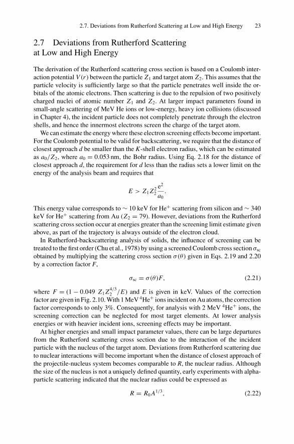
In Rutherford-backscattering analysis of solids, the influence of screening can betreated to the first order (Chu et al., 1978) by using a screened Coulomb cross section σsc
obtained by multiplying the scattering cross section σ (θ) given in Eqs. 2.19 and 2.20by a correction factor F,
σsc = σ (θ)F, (2.21)
where F = (1 − 0.049 Z1 Z4/32 /E) and E is given in keV. Values of the correction
factor are given in Fig. 2.10. With 1 MeV 4He+ ions incident on Au atoms, the correctionfactor corresponds to only 3%. Consequently, for analysis with 2 MeV 4He+ ions, thescreening correction can be neglected for most target elements. At lower analysisenergies or with heavier incident ions, screening effects may be important.
At higher energies and small impact parameter values, there can be large departuresfrom the Rutherford scattering cross section due to the interaction of the incidentparticle with the nucleus of the target atom. Deviations from Rutherford scattering dueto nuclear interactions will become important when the distance of closest approach ofthe projectile-nucleus system becomes comparable to R, the nuclear radius. Althoughthe size of the nucleus is not a uniquely defined quantity, early experiments with alpha-particle scattering indicated that the nuclear radius could be expressed as
R = R0 A1/3, (2.22)
24 2. Atomic Collisions and Backscattering Spectrometry
CO
RR
EC
TIO
N F
AC
TOR
F
0.860 10 20 30 40 50 60 70 80 90
0.30.5
MeV
Z2
1.01.5
2.0
0.88
0.90
0.92
0.94
0.96
0.98
1.00
Figure 2.10. Correction factor F, which describes the deviation from pure Rutherford scatteringdue to electron screening for He+ scattering from the atoms Z2, at a variety of incident kineticenergies. [Courtesy of John Davies]
where A is the mass number and R0∼= 1.4 × 10⁻¹³ cm. The radius has values from a
few times 10−13 cm in light nuclei to about 10−12 cm in heavy nuclei. When the distanceof closest approach d becomes comparable with the nuclear radius, one should expectdeviations from the Rutherford scattering. From Eqs. 2.18 and 2.22, the energy whereR = d is
E = Z1 Z2e2
R0 A1/3.
For 4He+ ions incident on silicon, this energy is about 9.6 MeV. Consequently, nuclearreactions and strong deviations from Rutherford scattering should not play a role inbackscattering analyses at energies of a few MeV.
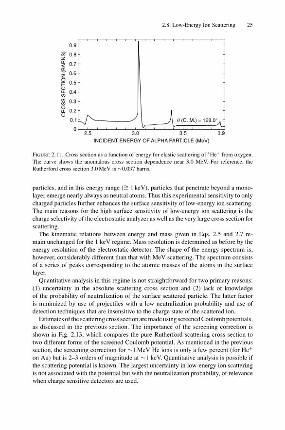
One of the exceptions to the estimate given above is the strong increase (resonance)in the scattering cross section at 3.04 MeV for 4He+ ions incident on 16O, as shownin Fig. 2.11. This reaction can be used to increase the sensitivity for the detection ofoxygen. Indeed, many nuclear reactions are useful for element detection, as describedin Chapter 13.
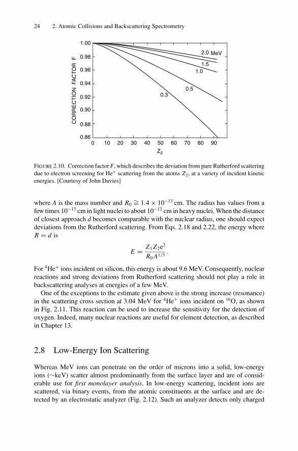
2.8 Low-Energy Ion Scattering
Whereas MeV ions can penetrate on the order of microns into a solid, low-energyions (∼keV) scatter almost predominantly from the surface layer and are of consid-erable use for first monolayer analysis. In low-energy scattering, incident ions arescattered, via binary events, from the atomic constituents at the surface and are de-tected by an electrostatic analyzer (Fig. 2.12). Such an analyzer detects only charged
2.8. Low-Energy Ion Scattering 25
2.50
0.1
0.2
0.3
0.4
0.5
0.6
0.7
0.8
0.9
3.0 3.5 3.9
INCIDENT ENERGY OF ALPHA PARTICLE (MeV)
θ (C. M.) = 168.0°
CR
OS
S S
EC
TIO
N (
BA
RN
S)
Figure 2.11. Cross section as a function of energy for elastic scattering of 4He+ from oxygen.The curve shows the anomalous cross section dependence near 3.0 MeV. For reference, theRutherford cross section 3.0 MeV is ∼0.037 barns.
particles, and in this energy range (∼= 1 keV), particles that penetrate beyond a mono-layer emerge nearly always as neutral atoms. Thus this experimental sensitivity to onlycharged particles further enhances the surface sensitivity of low-energy ion scattering.The main reasons for the high surface sensitivity of low-energy ion scattering is thecharge selectivity of the electrostatic analyzer as well as the very large cross section forscattering.
The kinematic relations between energy and mass given in Eqs. 2.5 and 2.7 re-main unchanged for the 1 keV regime. Mass resolution is determined as before by theenergy resolution of the electrostatic detector. The shape of the energy spectrum is,however, considerably different than that with MeV scattering. The spectrum consistsof a series of peaks corresponding to the atomic masses of the atoms in the surfacelayer.
Quantitative analysis in this regime is not straightforward for two primary reasons:(1) uncertainty in the absolute scattering cross section and (2) lack of knowledgeof the probability of neutralization of the surface scattered particle. The latter factoris minimized by use of projectiles with a low neutralization probability and use ofdetection techniques that are insensitive to the charge state of the scattered ion.
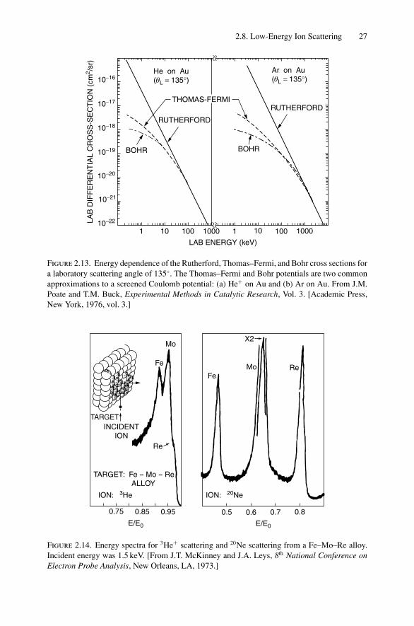
Estimates of the scattering cross section are made using screened Coulomb potentials,as discussed in the previous section. The importance of the screening correction isshown in Fig. 2.13, which compares the pure Rutherford scattering cross section totwo different forms of the screened Coulomb potential. As mentioned in the previoussection, the screening correction for ∼1 MeV He ions is only a few percent (for He+
on Au) but is 2–3 orders of magnitude at ∼1 keV. Quantitative analysis is possible ifthe scattering potential is known. The largest uncertainty in low-energy ion scatteringis not associated with the potential but with the neutralization probability, of relevancewhen charge sensitive detectors are used.
26 2. Atomic Collisions and Backscattering Spectrometry
TARGET
INCIDENTION
SCATTERED ION
MULTIPLETARGETASSEMBLY POSITIVE ION
TRAJECTORY
127° ENERGYANALYZER
CHANNELELECTRONMULTIPLIER
ION GUN
+
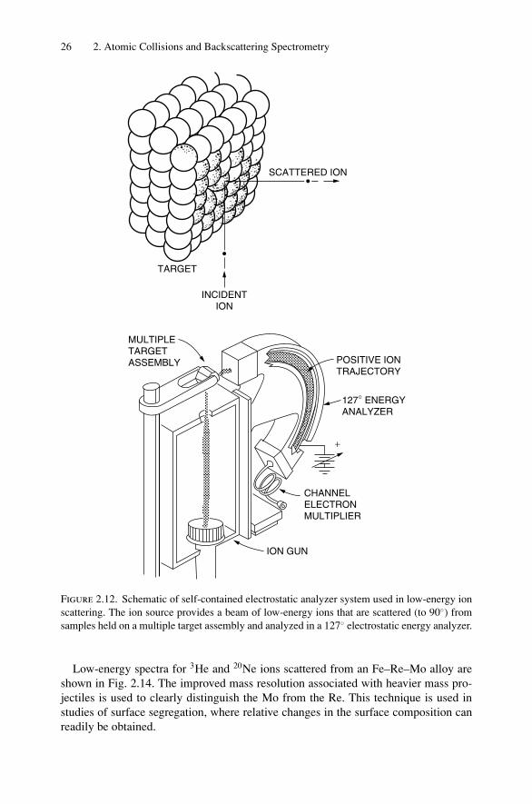
Figure 2.12. Schematic of self-contained electrostatic analyzer system used in low-energy ionscattering. The ion source provides a beam of low-energy ions that are scattered (to 90) fromsamples held on a multiple target assembly and analyzed in a 127 electrostatic energy analyzer.
Low-energy spectra for 3He and 20Ne ions scattered from an Fe–Re–Mo alloy areshown in Fig. 2.14. The improved mass resolution associated with heavier mass pro-jectiles is used to clearly distinguish the Mo from the Re. This technique is used instudies of surface segregation, where relative changes in the surface composition canreadily be obtained.
2.8. Low-Energy Ion Scattering 27
10−16
10−17
10−18
10−19
10−20
10−21
10−22
1 10 10100 1001000 10001
BOHR BOHR
RUTHERFORD
RUTHERFORDTHOMAS-FERMI
He on Au(θL = 135°)
Ar on Au(θL = 135°)
LAB ENERGY (keV)
LAB
DIF
FE
RE
NT
IAL
CR
OS
S-S
EC
TIO
N (
cm2 /
sr)
Figure 2.13. Energy dependence of the Rutherford, Thomas–Fermi, and Bohr cross sections fora laboratory scattering angle of 135. The Thomas–Fermi and Bohr potentials are two commonapproximations to a screened Coulomb potential: (a) He+ on Au and (b) Ar on Au. From J.M.Poate and T.M. Buck, Experimental Methods in Catalytic Research, Vol. 3. [Academic Press,New York, 1976, vol. 3.]
Mo
Fe
TARGETINCIDENT
IONRe
TARGET: Fe -- Mo -- Re ALLOY
ION: 3He
0.75 0.85 0.95
X2
FeMo Re
ION: 20Ne
0.5 0.6 0.7 0.8
E/E0 E/E0
Figure 2.14. Energy spectra for 3He+ scattering and 20Ne scattering from a Fe–Mo–Re alloy.Incident energy was 1.5 keV. [From J.T. McKinney and J.A. Leys, 8th National Conference onElectron Probe Analysis, New Orleans, LA, 1973.]
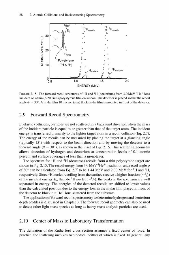
28 2. Atomic Collisions and Backscattering Spectrometry
Si
Erecoil
Polystyrene(1H & 2H)
E0
30
20
NO
RM
ALI
ZE
D Y
IELD
10
00.5 1.0
ENERGY (MeV)
1.5 2.0
2Hsurface1Hsurface
2Hrecoils1Hrecoils
4He++
Figure 2.15. The forward recoil structures of 1H and 2H (deuterium) from 3.0 MeV 4He+ ionsincident on a thin (≈200 nm) polystyrene film on silicon. The detector is placed so that the recoilangle φ = 30. A mylar film 10 micron (µm) thick mylar film is mounted in front of the detector.
2.9 Forward Recoil Spectrometry
In elastic collisions, particles are not scattered in a backward direction when the massof the incident particle is equal to or greater than that of the target atom. The incidentenergy is transferred primarily to the lighter target atom in a recoil collision (Eq. 2.7).The energy of the recoils can be measured by placing the target at a glancing angle(typically 15) with respect to the beam direction and by moving the detector to aforward angle (θ = 30), as shown in the inset of Fig. 2.15. This scattering geometryallows detection of hydrogen and deuterium at concentration levels of 0.1 atomicpercent and surface coverages of less than a monolayer.
The spectrum for 1H and 2H (deuteron) recoils from a thin polystyrene target areshown in Fig. 2.15. The recoil energy from 3.0 MeV 4He+ irradiation and recoil angle φ
of 30 can be calculated from Eq. 2.7′ to be 1.44 MeV and 2.00 MeV for 1H and 2H,respectively. Since 2H nuclei recoiling from the surface receive a higher fraction (∼2/3)of the incident energy Eo than do 1H nuclei (∼1/2), the peaks in the spectrum are wellseparated in energy. The energies of the detected recoils are shifted to lower valuesthan the calculated position due to the energy loss in the mylar film placed in front ofthe detector to block out He+ ions scattered from the substrate.
The application of forward recoil spectrometry to determine hydrogen and deuteriumdepth profiles is discussed in Chapter 3. The forward recoil geometry can also be usedto detect other light-mass species as long as heavy-mass analysis particles are used.
2.10 Center of Mass to Laboratory Transformation
The derivation of the Rutherford cross section assumes a fixed center of force. Inpractice, the scattering involves two bodies, neither of which is fixed. In general, any
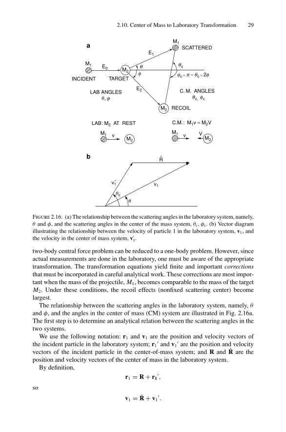
2.10. Center of Mass to Laboratory Transformation 29
E0
E1
E2
q qcM1
M1 M1
M1
C. M. ANGLESqc, fc
SCATTERED
INCIDENT TARGET
LAB: M2 AT REST C.M.: M1v = M2V
RECOIL
LAB ANGLESθ, φ
M2
M2 M2
M2
f fc = p − qc = 2f
v v V
θc
θ
v1v1'
R
a
b
Figure 2.16. (a) The relationship between the scattering angles in the laboratory system, namely,θ and φ, and the scattering angles in the center of the mass system, θc, φc. (b) Vector diagramillustrating the relationship between the velocity of particle 1 in the laboratory system, v1, andthe velocity in the center of mass system, v′
1.
two-body central force problem can be reduced to a one-body problem. However, sinceactual measurements are done in the laboratory, one must be aware of the appropriatetransformation. The transformation equations yield finite and important correctionsthat must be incorporated in careful analytical work. These corrections are most impor-tant when the mass of the projectile, M1, becomes comparable to the mass of the targetM2. Under these conditions, the recoil effects (nonfixed scattering center) becomelargest.
The relationship between the scattering angles in the laboratory system, namely, θ
and φ, and the angles in the center of mass (CM) system are illustrated in Fig. 2.16a.The first step is to determine an analytical relation between the scattering angles in thetwo systems.
We use the following notation: r1 and v1 are the position and velocity vectors ofthe incident particle in the laboratory system; r1
′ and v1′ are the position and velocity
vectors of the incident particle in the center-of-mass system; and R and R are theposition and velocity vectors of the center of mass in the laboratory system.
By definition,
r1 = R + r1′,
so
v1 = R + v1′.
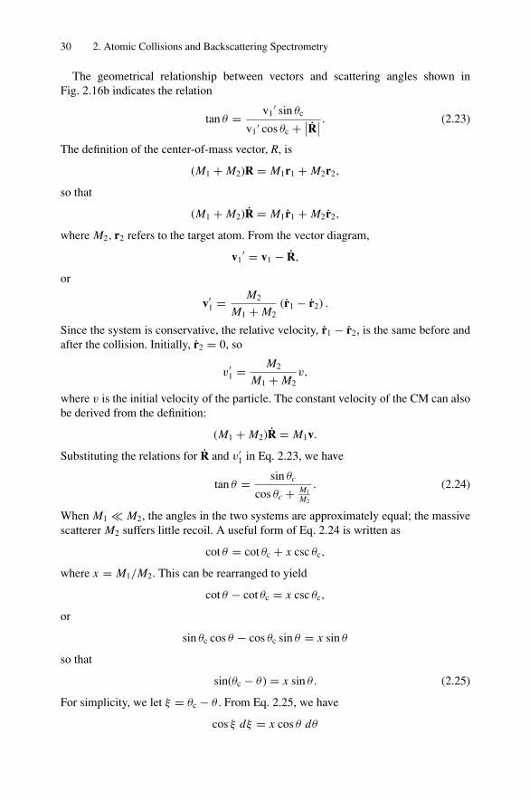
30 2. Atomic Collisions and Backscattering Spectrometry
The geometrical relationship between vectors and scattering angles shown inFig. 2.16b indicates the relation
tan θ = v1′ sin θc
v1′ cos θc + ∣∣R∣∣ . (2.23)
The definition of the center-of-mass vector, R, is
(M1 + M2)R = M1r1 + M2r2,
so that
(M1 + M2)R = M1r1 + M2r2,
where M2, r2 refers to the target atom. From the vector diagram,
v1′ = v1 − R,
or
v′1 = M2
M1 + M2(r1 − r2) .
Since the system is conservative, the relative velocity, r1 − r2, is the same before andafter the collision. Initially, r2 = 0, so
v′1 = M2
M1 + M2v,
where v is the initial velocity of the particle. The constant velocity of the CM can alsobe derived from the definition:
(M1 + M2)R = M1v.
Substituting the relations for R and v′1 in Eq. 2.23, we have
tan θ = sin θc
cos θc + M1M2
. (2.24)
When M1 M2, the angles in the two systems are approximately equal; the massivescatterer M2 suffers little recoil. A useful form of Eq. 2.24 is written as
cot θ = cot θc + x csc θc,
where x = M1/M2. This can be rearranged to yield
cot θ − cot θc = x csc θc,
or
sin θc cos θ − cos θc sin θ = x sin θ
so that
sin(θc − θ) = x sin θ. (2.25)
For simplicity, we let ξ = θc − θ . From Eq. 2.25, we have
cos ξ dξ = x cos θ dθ
Problems 31
anddξ
dθ= dθc
dθ− 1 = x cos θ
cos ξ,
ordθc
dθ= sin θc
sin θ cos ξ.
Then
dσ
d=(
Z1 Z2e2
2E
)2 [(1 + x) sin θc
2 sin θ sin2 θc/2
]2/cos ξ,
where E, the energy in lab coordinates, is given by
E = Ec(1 + x).
It is useful to derive an expression for the cross section simply in terms of θ and x. Wemake use of the fact that
1 + x = (sin ξ + sin θ )/ sin θ,
sin(θc
/2)
sin2(θc
/2)
= cot(θc
/2)
,
sin θ + sin ξ
cos θ + cos ξ= tan
θc
2,
so that(1 + x) sin ξc
2 sin2(θc
/2)
,= cos θ + cos ξ
sin θ
and
dσ
d=(
Z1 Z2e2
2E
)2(cos θ + cos ξ )2
sin4 θ cos ξ.
Noting that cos ξ = (1 − sin2 ξ )1/2 = (1 − x2 sin2 θ )1/2, we obtain
dσ
d=(
Z1 Z2e2
2E
)2 [cos θ + (1 − x2 sin2 θ )1/2]2
sin4 θ (1 − x2 sin2 θ )1/2, (2.26)
which is the form given in Eq. 2.19.
Problems
2.1. 4He++ particles are scattered from a thin foil of an elemental material with atomicnumber Z1, mass density ρ1, number A1, and thickness t1, and are observed atsome fixed angle θ . The first foil is replaced with a second one (Z2, ρ2, A2, t2).What is the ratio of the number of particles observed at θ for the first and secondfoils?
2.2. A beam of 2 MeV helium ions is incident on a silver foil 10−6 cm thick andundergoes Coulomb scattering in accordance with the Rutherford formula.
32 2. Atomic Collisions and Backscattering Spectrometry
(a) What is the distance of closest approach?(b) Find the impact parameter for He+ ions scattered through 90.(c) What fraction of the incident 2 MeV He+ ions will be backscattered (i.e.,
θ > 90)?
The density of silver is 10.50 g/cm3, and its atomic weight is 107.88 g mol.[Hint: The integrated cross section for scattering through angles 0 to 90 is∫ π/2
0 dσ.]2.3. An α particle, 4He+, makes a head-on collision with (a) a gold nucleus, (b) a
carbon nucleus, (c) an α particle, and (d) an electron, each initially at rest. Whatfraction of the α particle’s initial kinetic energy is transferred to the struck particlein each instance?
2.4. (a) Using the formula for the Rutherford scattering cross section in center-of-masscoordinates (CM) and the relations for the recoil energy (Eq. 2.7), and notingthat φ = π/2 − θc/2 (Fig. 2.16), calculate an expression for dσ/dE2, the crosssection for transferring an energy E2 to a nucleus. Hint:
dσ
dθc
dθc
d E2= dσ
d E2.
(b) Using the result of part (a), integrate dσ/d E2 from Emin to Emax to find thetotal cross section for transferring an energy greater than Emin.
(c) Evaluate the result of part (b) in cm2 for the case of 1.0 MeV He ions bom-barding Si. Use Emin = 14 eV, the displacement energy of a Si atom bound inan Si lattice. Compare this cross section to σRuth(θ = 180).
(d) Use the result of (c) to calculate the fraction of atoms displaced (i.e., undergoingan energy transfer greater than 14 eV) for 1 µC of He+ ions incident on a targetwhere the He+ beam diameter = 1 mm. This result is only a lower limit to thedisplacements, since we have ignored displacements due to recoiling Si atoms.
2.5. A carbon film is known to contain surface contaminants of Au, Ag, and Si. Sketchthe backscattering spectrum, indicating the energies of the various peaks and theirrelative heights.
2.6. An accelerator produces an He+ ion current of 50 nA at 1.0 MeV. Using a 1 cm2
detector 5 cm from the target at a scattering angle of 170, determine the smallestamount of Au (atoms/cm2) that can be detected. Detectability is arbitrarily definedas 100 counts in 1 hr. Under similar conditions, what is the detection limit foroxygen? Compare these limits with the number of atoms/cm2 in a monolayer(∼=1015 atoms/cm2).
2.7. Derive the expression for E2 (Eq. 2.7′), the energy transferred to the target atomusing conservation of energy and momentum relations. Give the expression forE2/E0 for θ = 90.
2.8. Use the small angle approximation (sin θ = θ ) to show that the scattering crosssection can be expressed as σ (θ ) = (Z1 Z2e2/E)2(θ)−4. Derive this expressionusing the impulse approximation in which the force of Z1 Z2e2/b2 acts on theparticle for an effective time t = l/v, where l = 2b. [Hint: An intermediate stepin the derivation is to show that b = Z1 Z2e2/Eθ.]

References 33
References
1. W. K. Chu, J. W. Mayer, and M.-A. Nicolet, Backscattering Spectrometry (Academic Press,New York, 1978).
2. H. Goldstein, Classical Mechanics (Addison-Wesley, Reading, MA, 1959).3. J. W. Mayer and E. Rimini, Ion Beam Handbook for Material Analysis (Academic Press, New
York, 1977).4. F. K. Richtmyer, E. H. Kennard, and T. N. Cooper, Introduction to Modern Physics, 6th ed.
(McGraw-Hill, New York, 1969).5. P. A. Tipler, Modern Physics (Worth Publishers, New York, 1978).
3Energy Loss of Light Ions andBackscattering Depth Profiles
3.1 Introduction
In the previous chapter, it was tacitly assumed that the atoms to be identified were atthe surface of the materials. In this chapter, we consider composition depth profilesthat can be obtained from Rutherford backscattering spectrometry (RBS) and nuclearreaction analysis. In this case, the depth scale is established by the energy loss d E/dxof light (H+, d+, and He+) ions at high energies (0.5–5 MeV) during their passagethrough the solid (Fig. 3.1). The energy lost in penetration is directly proportionalto the thickness of material traversed, so a depth scale can be assigned directly andquantitatively to the energy spectra of detected particles. The yield of backscatteredparticles or reaction products is proportional to the scattering or reaction cross sections,so the composition depth profile can be found from knowledge of energy loss and crosssections.
3.2 General Picture of Energy Loss and Units of Energy Loss
For light ions such as 4He+ penetrating a solid, the energetic particles lose energy pri-marily through excitation and ionization in inelastic collisions with atomic electrons—termed electronic-energy loss. Microscopically, energy loss due to excitation and ion-ization is a discrete process. Macroscopically, however, it is a good assumption that themoving ions lose energy continuously. All we are concerned with here is the averageenergy loss during the penetration of ions into a given material.
To measure energy loss, we must determine two quantities: the distance t that theions traverse in the target, and the energy loss E in this distance. The mass densityρ or the atomic density N are frequently combined with the distance, in the form ρtor Nt , to express the amount of material per unit area or the number of atoms perunit area that the projectiles have traversed in losing energy E to the target material.Energy loss can be expressed in several different ways. Some frequently used units are
d E/dx : eV/nm,
(1/ρ) d E/dx : eV/(µg/cm2),
ε = (1/N ) d E/dx : eV/(atoms/cm2), eV-cm2.
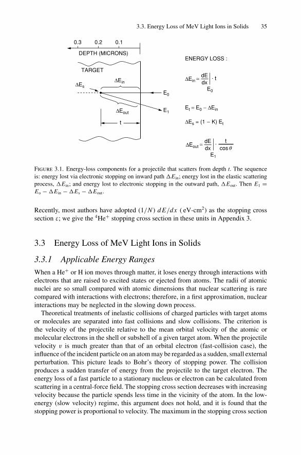
3.3. Energy Loss of MeV Light Ions in Solids 35
0.3 0.2
DEPTH (MICRONS)ENERGY LOSS :
∆Es = (1 − K) Et
Et = E0 − ∆Ein
TARGET
t
∆Es∆Ein
E0
E1∆Eout
0.1
E0
∆Ein. tdE
dx
E1
∆EoutdEdx
tcos θ
.
Figure 3.1. Energy-loss components for a projectile that scatters from depth t. The sequenceis: energy lost via electronic stopping on inward path Ein; energy lost in the elastic scatteringprocess, Ein; and energy lost to electronic stopping in the outward path, Eout. Then E1 =Eo − Ein − Es − Eout.
Recently, most authors have adopted (1/N ) d E/dx ( eV-cm2) as the stopping crosssection ε; we give the 4He+ stopping cross section in these units in Appendix 3.
3.3 Energy Loss of MeV Light Ions in Solids
3.3.1 Applicable Energy Ranges
When a He+ or H ion moves through matter, it loses energy through interactions withelectrons that are raised to excited states or ejected from atoms. The radii of atomicnuclei are so small compared with atomic dimensions that nuclear scattering is rarecompared with interactions with electrons; therefore, in a first approximation, nuclearinteractions may be neglected in the slowing down process.
Theoretical treatments of inelastic collisions of charged particles with target atomsor molecules are separated into fast collisions and slow collisions. The criterion isthe velocity of the projectile relative to the mean orbital velocity of the atomic ormolecular electrons in the shell or subshell of a given target atom. When the projectilevelocity v is much greater than that of an orbital electron (fast-collision case), theinfluence of the incident particle on an atom may be regarded as a sudden, small externalperturbation. This picture leads to Bohr’s theory of stopping power. The collisionproduces a sudden transfer of energy from the projectile to the target electron. Theenergy loss of a fast particle to a stationary nucleus or electron can be calculated fromscattering in a central-force field. The stopping cross section decreases with increasingvelocity because the particle spends less time in the vicinity of the atom. In the low-energy (slow velocity) regime, this argument does not hold, and it is found that thestopping power is proportional to velocity. The maximum in the stopping cross section
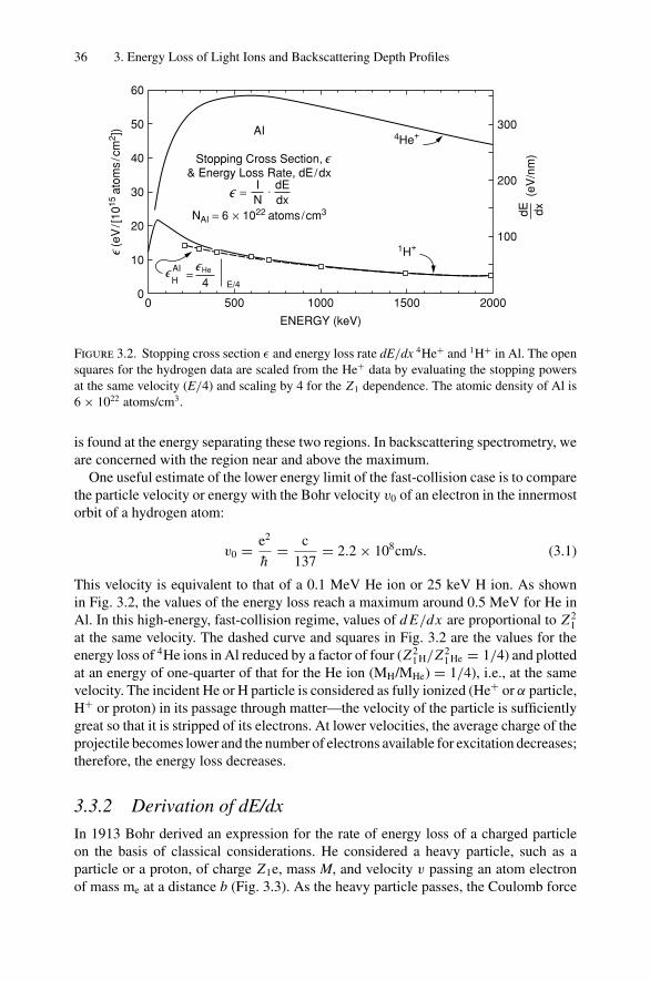
36 3. Energy Loss of Light Ions and Backscattering Depth Profiles
50
NAI = 6 × 10²² atoms/cm3
Stopping Cross Section,& Energy Loss Rate, dE/dx
00
10
20
30
40
60
500
E/4
AI 4He+
1H+
1000
ENERGY (keV)
(eV
/[10
15at
oms
/cm
2 ])
1500 2000
300
200
100
(eV
/nm
)dE dx
AIH = He
4
IN
= dEdx
.
'
''
'
'
Figure 3.2. Stopping cross section ε and energy loss rate dE/dx 4He+ and 1H+ in Al. The opensquares for the hydrogen data are scaled from the He+ data by evaluating the stopping powersat the same velocity (E/4) and scaling by 4 for the Z1 dependence. The atomic density of Al is6 × 1022 atoms/cm3.
is found at the energy separating these two regions. In backscattering spectrometry, weare concerned with the region near and above the maximum.
One useful estimate of the lower energy limit of the fast-collision case is to comparethe particle velocity or energy with the Bohr velocity v0 of an electron in the innermostorbit of a hydrogen atom:
v0 = e2
h= c
137= 2.2 × 108cm/s. (3.1)
This velocity is equivalent to that of a 0.1 MeV He ion or 25 keV H ion. As shownin Fig. 3.2, the values of the energy loss reach a maximum around 0.5 MeV for He inAl. In this high-energy, fast-collision regime, values of d E/dx are proportional to Z2
1at the same velocity. The dashed curve and squares in Fig. 3.2 are the values for theenergy loss of 4He ions in Al reduced by a factor of four (Z2
1 H/Z21 He = 1/4) and plotted
at an energy of one-quarter of that for the He ion (MH/MHe) = 1/4), i.e., at the samevelocity. The incident He or H particle is considered as fully ionized (He+ or α particle,H+ or proton) in its passage through matter—the velocity of the particle is sufficientlygreat so that it is stripped of its electrons. At lower velocities, the average charge of theprojectile becomes lower and the number of electrons available for excitation decreases;therefore, the energy loss decreases.
3.3.2 Derivation of dE/dx
In 1913 Bohr derived an expression for the rate of energy loss of a charged particleon the basis of classical considerations. He considered a heavy particle, such as aparticle or a proton, of charge Z1e, mass M, and velocity v passing an atom electronof mass me at a distance b (Fig. 3.3). As the heavy particle passes, the Coulomb force
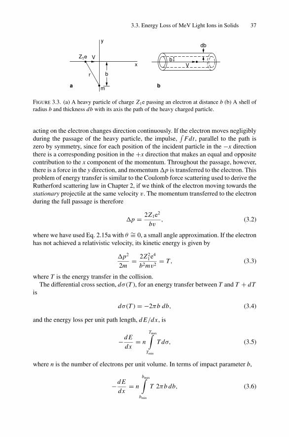
3.3. Energy Loss of MeV Light Ions in Solids 37
b
a m
br
Z1e
y
xV
db
V
b
Figure 3.3. (a) A heavy particle of charge Z1e passing an electron at distance b (b) A shell ofradius b and thickness db with its axis the path of the heavy charged particle.
acting on the electron changes direction continuously. If the electron moves negligiblyduring the passage of the heavy particle, the impulse,
∫Fdt , parallel to the path is
zero by symmetry, since for each position of the incident particle in the −x directionthere is a corresponding position in the +x direction that makes an equal and oppositecontribution to the x component of the momentum. Throughout the passage, however,there is a force in the y direction, and momentum p is transferred to the electron. Thisproblem of energy transfer is similar to the Coulomb force scattering used to derive theRutherford scattering law in Chapter 2, if we think of the electron moving towards thestationary projectile at the same velocity v. The momentum transferred to the electronduring the full passage is therefore
p = 2Z1e2
bv, (3.2)
where we have used Eq. 2.15a with θ ∼= 0, a small angle approximation. If the electronhas not achieved a relativistic velocity, its kinetic energy is given by
p2
2m= 2Z2
1e4
b2mv2= T, (3.3)
where T is the energy transfer in the collision.The differential cross section, dσ (T ), for an energy transfer between T and T + dT
is
dσ (T ) = −2πb db, (3.4)
and the energy loss per unit path length, d E/dx , is
−d E
dx= n
Tmax∫Tmin
T dσ, (3.5)
where n is the number of electrons per unit volume. In terms of impact parameter b,
−d E
dx= n
bmax∫bmin
T 2πb db, (3.6)
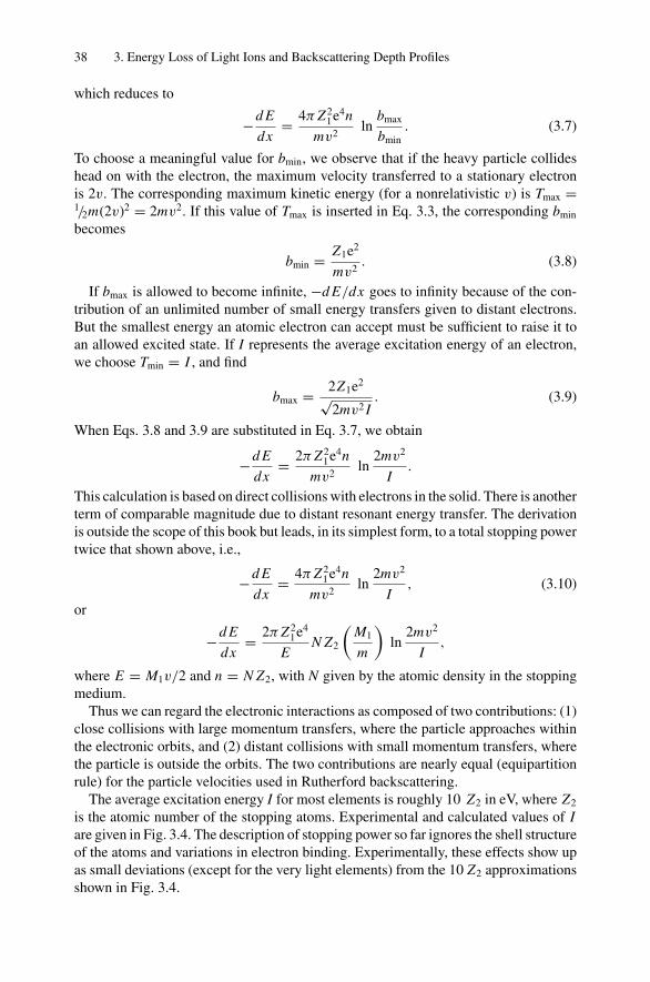
38 3. Energy Loss of Light Ions and Backscattering Depth Profiles
which reduces to
−d E
dx= 4π Z2
1e4n
mv2ln
bmax
bmin. (3.7)
To choose a meaningful value for bmin, we observe that if the heavy particle collideshead on with the electron, the maximum velocity transferred to a stationary electronis 2v. The corresponding maximum kinetic energy (for a nonrelativistic v) is Tmax =1/2m(2v)2 = 2mv2. If this value of Tmax is inserted in Eq. 3.3, the corresponding bmin
becomes
bmin = Z1e2
mv2. (3.8)
If bmax is allowed to become infinite, −d E/dx goes to infinity because of the con-tribution of an unlimited number of small energy transfers given to distant electrons.But the smallest energy an atomic electron can accept must be sufficient to raise it toan allowed excited state. If I represents the average excitation energy of an electron,we choose Tmin = I , and find
bmax = 2Z1e2
√2mv2 I
. (3.9)
When Eqs. 3.8 and 3.9 are substituted in Eq. 3.7, we obtain
−d E
dx= 2π Z2
1e4n
mv2ln
2mv2
I.
This calculation is based on direct collisions with electrons in the solid. There is anotherterm of comparable magnitude due to distant resonant energy transfer. The derivationis outside the scope of this book but leads, in its simplest form, to a total stopping powertwice that shown above, i.e.,
−d E
dx= 4π Z2
1e4n
mv2ln
2mv2
I, (3.10)
or
−d E
dx= 2π Z2
1e4
EN Z2
(M1
m
)ln
2mv2
I,
where E = M1v/2 and n = N Z2, with N given by the atomic density in the stoppingmedium.
Thus we can regard the electronic interactions as composed of two contributions: (1)close collisions with large momentum transfers, where the particle approaches withinthe electronic orbits, and (2) distant collisions with small momentum transfers, wherethe particle is outside the orbits. The two contributions are nearly equal (equipartitionrule) for the particle velocities used in Rutherford backscattering.
The average excitation energy I for most elements is roughly 10 Z2 in eV, where Z2
is the atomic number of the stopping atoms. Experimental and calculated values of Iare given in Fig. 3.4. The description of stopping power so far ignores the shell structureof the atoms and variations in electron binding. Experimentally, these effects show upas small deviations (except for the very light elements) from the 10 Z2 approximationsshown in Fig. 3.4.

3.3. Energy Loss of MeV Light Ions in Solids 39
242322212019181716151413121110
98
0 10 20 30 40 50 60
ATOMIC NUMBER Z
I/Z
(eV
)
70
CALCULATION : and
EXPERIMENT:
80 90 100
Figure 3.4. Calculation of mean excitation energy by Lindhard and Scharff’s theory with aHartree–Fock–Slater charge distribution. The calculation 1/Z vs. atomic number Z reveals struc-ture, as has been observed in many experimental measurements. [From W.K. Chu and D. Powers,Phys. Lett. 40A, 23 (1972), with permission from Elsevier.]
The complete energy loss formula (often referred to as the Bethe formula) containscorrections that include relativistic terms at high velocities and corrections for thenonparticipation of the strongly bound inner-shell electrons. For helium ions in theenergy regime of a few MeV, relativistic effects are negligible and nearly all the targetelectrons participate (n = N Z2) in the stopping process. Consequently, Eq. 3.10 canbe used to estimate values of d E/dx . In analysis, it is preferable to use tabulated ornumerical values such as those listed in Appendix 3.
For example, the electronic energy loss of 2 MeV 4He+ ions in Al has a value(calculated from Eq. 3.10) of 315 eV/nm using values of n = N Z2 = 780/nm3 andI = 10Z2 = 130 eV. The value given in Appendix 3 is ε = 44.25 eV/(1015 atoms/cm2)or a value of d E/dx = 266 eV/nm (d E/dx = εN ). Thus the first-order treatment givesvalues to within 20% of the experimental values.
3.3.3 Comparison of Energy Loss to Electrons and to Nuclei
A penetrating He ion can also transfer energy to the nuclei of the solid through small-angle scattering events. This component to the total energy loss of an energetic ionis termed nuclear energy loss. Nuclear energy loss is much smaller than the elec-tronic loss. If the derivation of Eq. 3.7 is repeated for collisions with target atoms, wefind
−d E
dx
∣∣∣∣n
= 4π Z22 Z2
1e4 N
M2v2ln
bmax
bmin, (3.11)
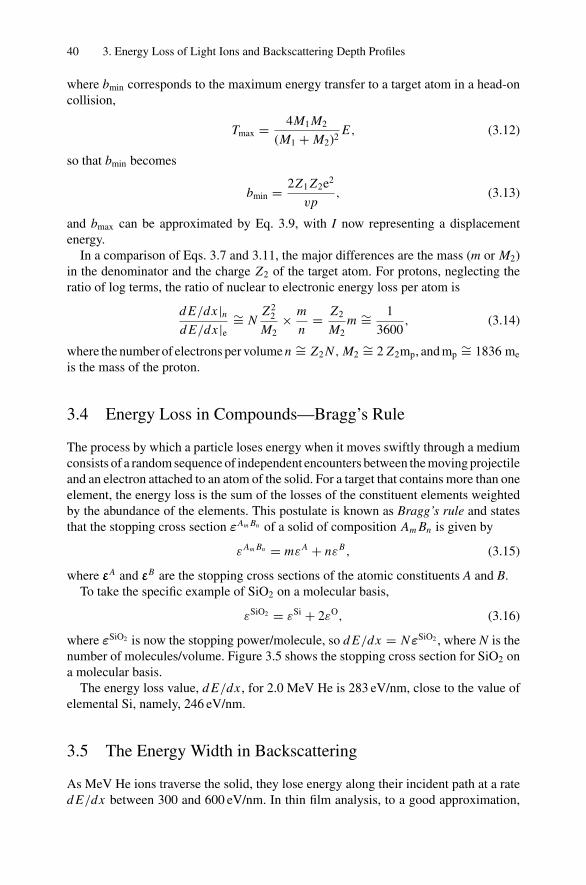
40 3. Energy Loss of Light Ions and Backscattering Depth Profiles
where bmin corresponds to the maximum energy transfer to a target atom in a head-oncollision,
Tmax = 4M1 M2
(M1 + M2)2E, (3.12)
so that bmin becomes
bmin = 2Z1 Z2e2
vp, (3.13)
and bmax can be approximated by Eq. 3.9, with I now representing a displacementenergy.
In a comparison of Eqs. 3.7 and 3.11, the major differences are the mass (m or M2)in the denominator and the charge Z2 of the target atom. For protons, neglecting theratio of log terms, the ratio of nuclear to electronic energy loss per atom is
d E/dx |nd E/dx |e
∼= NZ2
2
M2× m
n= Z2
M2m ∼= 1
3600, (3.14)
where the number of electrons per volume n ∼= Z2 N , M2∼= 2 Z2mp, and mp
∼= 1836 me
is the mass of the proton.
3.4 Energy Loss in Compounds—Bragg’s Rule
The process by which a particle loses energy when it moves swiftly through a mediumconsists of a random sequence of independent encounters between the moving projectileand an electron attached to an atom of the solid. For a target that contains more than oneelement, the energy loss is the sum of the losses of the constituent elements weightedby the abundance of the elements. This postulate is known as Bragg’s rule and statesthat the stopping cross section εAm Bn of a solid of composition Am Bn is given by
εAm Bn = mεA + nεB, (3.15)
where εεεA and εεεB are the stopping cross sections of the atomic constituents A and B.To take the specific example of SiO2 on a molecular basis,
εSiO2 = εSi + 2εO, (3.16)
where εSiO2 is now the stopping power/molecule, so d E/dx = NεSiO2 , where N is thenumber of molecules/volume. Figure 3.5 shows the stopping cross section for SiO2 ona molecular basis.
The energy loss value, d E/dx , for 2.0 MeV He is 283 eV/nm, close to the value ofelemental Si, namely, 246 eV/nm.
3.5 The Energy Width in Backscattering
As MeV He ions traverse the solid, they lose energy along their incident path at a rated E/dx between 300 and 600 eV/nm. In thin film analysis, to a good approximation,
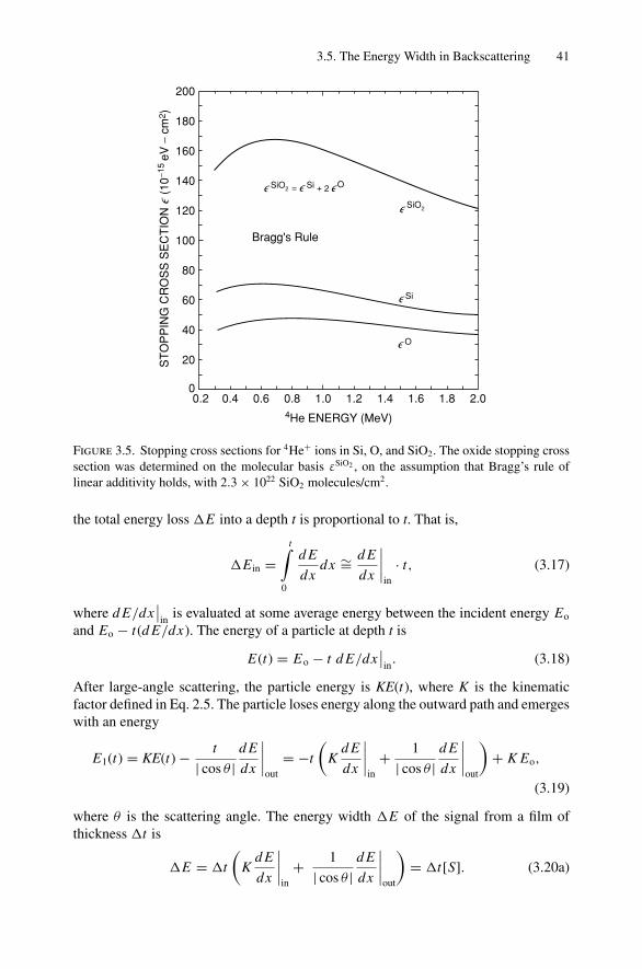
3.5. The Energy Width in Backscattering 41
SiO2 = Si + 2
SiO2
Si
O
Bragg's Rule
0.2
200
180
160
140
120
100
80
60
40
20
00.4 0.6 0.8 1.0 1.2 1.4 1.6 1.8 2.0
4He ENERGY (MeV)
ST
OP
PIN
G C
RO
SS
SE
CT
ION
(
10−1
5eV
− cm
2 )
∋ ∋
∋
∋
∋
∋
∋
O
Figure 3.5. Stopping cross sections for 4He+ ions in Si, O, and SiO2. The oxide stopping crosssection was determined on the molecular basis εSiO2 , on the assumption that Bragg’s rule oflinear additivity holds, with 2.3 × 10²² SiO2 molecules/cm2.
the total energy loss E into a depth t is proportional to t. That is,
Ein =t∫
0
d E
dxdx ∼= d E
dx
∣∣∣∣in
· t, (3.17)
where d E/dx∣∣in is evaluated at some average energy between the incident energy Eo
and Eo − t(d E/dx). The energy of a particle at depth t is
E(t) = Eo − t d E/dx∣∣in. (3.18)
After large-angle scattering, the particle energy is KE(t), where K is the kinematicfactor defined in Eq. 2.5. The particle loses energy along the outward path and emergeswith an energy
E1(t) = KE(t) − t
| cos θ |d E
dx
∣∣∣∣out
= −t
(K
d E
dx
∣∣∣∣in
+ 1
| cos θ |d E
dx
∣∣∣∣out
)+ K Eo,
(3.19)
where θ is the scattering angle. The energy width E of the signal from a film ofthickness t is
E = t
(K
d E
dx
∣∣∣∣in
+ 1
| cos θ |d E
dx
∣∣∣∣out
)= t[S]. (3.20a)
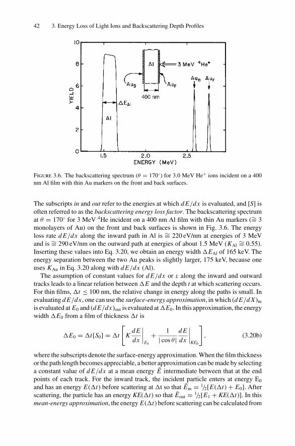
42 3. Energy Loss of Light Ions and Backscattering Depth Profiles
Figure 3.6. The backscattering spectrum (θ = 170) for 3.0 MeV He+ ions incident on a 400nm Al film with thin Au markers on the front and back surfaces.
The subscripts in and out refer to the energies at which d E/dx is evaluated, and [S] isoften referred to as the backscattering energy loss factor. The backscattering spectrumat θ = 170 for 3 MeV 4He incident on a 400 nm Al film with thin Au markers (∼= 3monolayers of Au) on the front and back surfaces is shown in Fig. 3.6. The energyloss rate d E/dx along the inward path in Al is ∼= 220 eV/nm at energies of 3 MeVand is ∼= 290 eV/nm on the outward path at energies of about 1.5 MeV (KAl
∼= 0.55).Inserting these values into Eq. 3.20, we obtain an energy width EAl of 165 keV. Theenergy separation between the two Au peaks is slightly larger, 175 keV, because oneuses KAu in Eq. 3.20 along with d E/dx (Al).
The assumption of constant values for d E/dx or ε along the inward and outwardtracks leads to a linear relation between E and the depth t at which scattering occurs.For thin films, t ≤ 100 nm, the relative change in energy along the paths is small. Inevaluating d E/dx , one can use the surface-energy approximation, in which (d E/d X )in
is evaluated at E0 and (d E/dx)out is evaluated at E0. In this approximation, the energywidth E0 from a film of thickness t is
E0 = t[S0] = t
[K
d E
dx
∣∣∣∣E0
+ 1
| cos θ |d E
dx
∣∣∣∣KE0
], (3.20b)
where the subscripts denote the surface-energy approximation. When the film thicknessor the path length becomes appreciable, a better approximation can be made by selectinga constant value of d E/dx at a mean energy E intermediate between that at the endpoints of each track. For the inward track, the incident particle enters at energy E0
and has an energy E(t) before scattering at t so that Ein = 1/2[E(t) + E0]. Afterscattering, the particle has an energy KE(t) so that Eout = 1/2[E1 + KE(t)]. In thismean-energy approximation, the energy E(t) before scattering can be calculated from
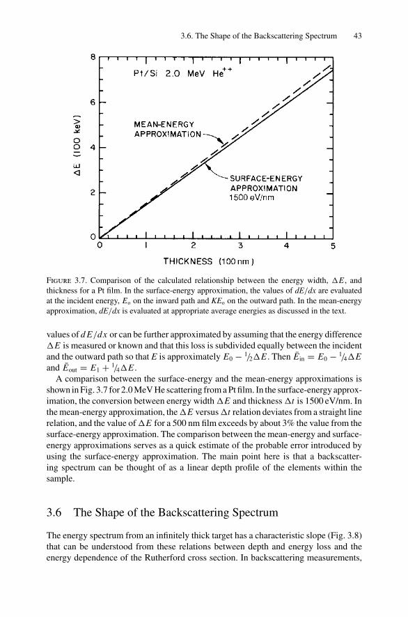
3.6. The Shape of the Backscattering Spectrum 43
Figure 3.7. Comparison of the calculated relationship between the energy width, E , andthickness for a Pt film. In the surface-energy approximation, the values of dE/dx are evaluatedat the incident energy, Eo on the inward path and KEo on the outward path. In the mean-energyapproximation, dE/dx is evaluated at appropriate average energies as discussed in the text.
values of d E/dx or can be further approximated by assuming that the energy differenceE is measured or known and that this loss is subdivided equally between the incidentand the outward path so that E is approximately E0 − 1/2E . Then Ein = E0 − 1/4Eand Eout = E1 + 1/4E .
A comparison between the surface-energy and the mean-energy approximations isshown in Fig. 3.7 for 2.0 MeV He scattering from a Pt film. In the surface-energy approx-imation, the conversion between energy width E and thickness t is 1500 eV/nm. Inthe mean-energy approximation, the E versus t relation deviates from a straight linerelation, and the value of E for a 500 nm film exceeds by about 3% the value from thesurface-energy approximation. The comparison between the mean-energy and surface-energy approximations serves as a quick estimate of the probable error introduced byusing the surface-energy approximation. The main point here is that a backscatter-ing spectrum can be thought of as a linear depth profile of the elements within thesample.
3.6 The Shape of the Backscattering Spectrum
The energy spectrum from an infinitely thick target has a characteristic slope (Fig. 3.8)that can be understood from these relations between depth and energy loss and theenergy dependence of the Rutherford cross section. In backscattering measurements,
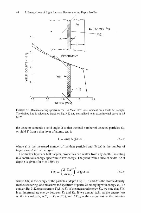
44 3. Energy Loss of Light Ions and Backscattering Depth Profiles
ENERGY (MeV)
YIE
LD (
CO
UN
TS
× 1
0−3)
0.60
2
4
Y(t)
E1(t)
6
EXPERIMENT
∆t
t
Au
E0 = 1.4 MeV 4He
E1(t)8
0.8 1.0 1.2 1.4
Figure 3.8. Backscattering spectrum for 1.4 MeV He+ ions incident on a thick Au sample.The dashed line is calculated based on Eq. 3.25 and normalized to an experimental curve at 1.3MeV.
the detector subtends a solid angle so that the total number of detected particles QD
or yield Y from a thin layer of atoms, t , is
Y = σ (θ) QNt, (3.21)
where Q is the measured number of incident particles and (Nt) is the number oftarget atoms/cm2 in the layer.
For thicker layers or bulk targets, projectiles can scatter from any depth t, resultingin a continuous energy spectrum to low energy. The yield from a slice of width t atdepth t is given (for θ = 180) by
Y (t) =(
Z1 Z2e2
4E(t)
)2
N Q t, (3.22)
where E(t) is the energy of the particle at depth t Eq. 3.18 and N is the atomic density.In backscattering, one measures the spectrum of particles emerging with energy E1. Toconvert Eq. 3.22 to a spectrum Y (E1)d E1 of the measured energy E1, we note that E(t)is an intermediate energy between E0 and E1. If we denote Ein as the energy loston the inward path, Ein = E0 − E(t), and Eout as the energy lost on the outgoing
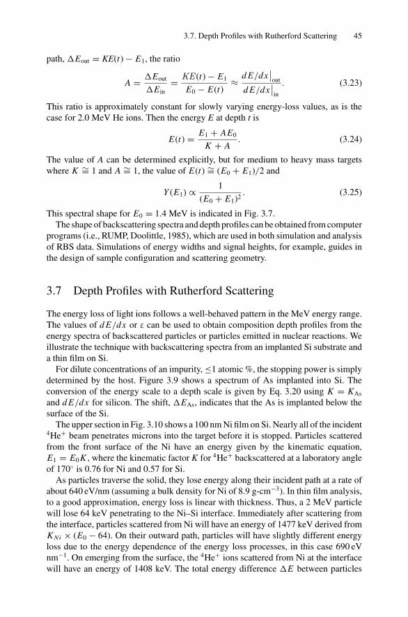
3.7. Depth Profiles with Rutherford Scattering 45
path, Eout = KE(t) − E1, the ratio
A = Eout
Ein= KE (t) − E1
E0 − E(t)≈ d E/dx
∣∣out
d E/dx∣∣in
. (3.23)
This ratio is approximately constant for slowly varying energy-loss values, as is thecase for 2.0 MeV He ions. Then the energy E at depth t is
E(t) = E1 + AE0
K + A. (3.24)
The value of A can be determined explicitly, but for medium to heavy mass targetswhere K ∼= 1 and A ∼= 1, the value of E(t) ∼= (E0 + E1)/2 and
Y (E1) ∝ 1
(E0 + E1)2. (3.25)
This spectral shape for E0 = 1.4 MeV is indicated in Fig. 3.7.The shape of backscattering spectra and depth profiles can be obtained from computer
programs (i.e., RUMP, Doolittle, 1985), which are used in both simulation and analysisof RBS data. Simulations of energy widths and signal heights, for example, guides inthe design of sample configuration and scattering geometry.
3.7 Depth Profiles with Rutherford Scattering
The energy loss of light ions follows a well-behaved pattern in the MeV energy range.The values of d E/dx or ε can be used to obtain composition depth profiles from theenergy spectra of backscattered particles or particles emitted in nuclear reactions. Weillustrate the technique with backscattering spectra from an implanted Si substrate anda thin film on Si.
For dilute concentrations of an impurity, ≤1 atomic %, the stopping power is simplydetermined by the host. Figure 3.9 shows a spectrum of As implanted into Si. Theconversion of the energy scale to a depth scale is given by Eq. 3.20 using K = KAs
and d E/dx for silicon. The shift, EAs, indicates that the As is implanted below thesurface of the Si.
The upper section in Fig. 3.10 shows a 100 nm Ni film on Si. Nearly all of the incident4He+ beam penetrates microns into the target before it is stopped. Particles scatteredfrom the front surface of the Ni have an energy given by the kinematic equation,E1 = E0 K , where the kinematic factor K for 4He+ backscattered at a laboratory angleof 170 is 0.76 for Ni and 0.57 for Si.
As particles traverse the solid, they lose energy along their incident path at a rate ofabout 640 eV/nm (assuming a bulk density for Ni of 8.9 g-cm−3). In thin film analysis,to a good approximation, energy loss is linear with thickness. Thus, a 2 MeV particlewill lose 64 keV penetrating to the Ni–Si interface. Immediately after scattering fromthe interface, particles scattered from Ni will have an energy of 1477 keV derived fromKNi × (E0 − 64). On their outward path, particles will have slightly different energyloss due to the energy dependence of the energy loss processes, in this case 690 eVnm−1. On emerging from the surface, the 4He+ ions scattered from Ni at the interfacewill have an energy of 1408 keV. The total energy difference E between particles
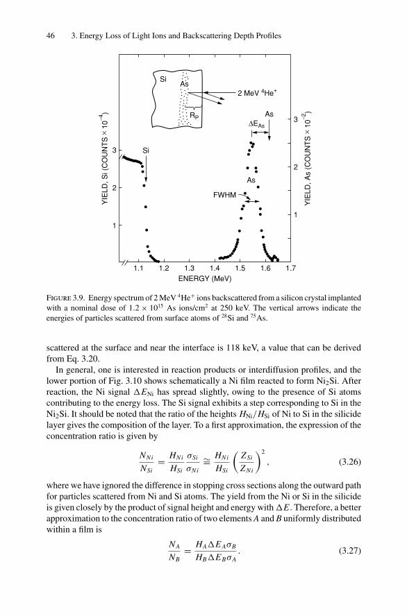
46 3. Energy Loss of Light Ions and Backscattering Depth Profiles
Si
Si
As
RP
FWHM
ENERGY (MeV)
YIE
LD, S
i (C
OU
NT
S ×
10−4
)
YIE
LD, A
s (C
OU
NT
S ×
10−2
)
1.1
1
2
3
1.2 1.3 1.4 1.5 1.6 1.7
3
2
1
As
As
∆EAs
2 MeV 4He+
Figure 3.9. Energy spectrum of 2 MeV 4He+ ions backscattered from a silicon crystal implantedwith a nominal dose of 1.2 × 10¹⁵ As ions/cm2 at 250 keV. The vertical arrows indicate theenergies of particles scattered from surface atoms of 28Si and 75As.
scattered at the surface and near the interface is 118 keV, a value that can be derivedfrom Eq. 3.20.
In general, one is interested in reaction products or interdiffusion profiles, and thelower portion of Fig. 3.10 shows schematically a Ni film reacted to form Ni2Si. Afterreaction, the Ni signal ENi has spread slightly, owing to the presence of Si atomscontributing to the energy loss. The Si signal exhibits a step corresponding to Si in theNi2Si. It should be noted that the ratio of the heights HNi/HSi of Ni to Si in the silicidelayer gives the composition of the layer. To a first approximation, the expression of theconcentration ratio is given by
NNi
NSi= HNi
HSi
σSi
σNi
∼= HNi
HSi
(ZSi
Z Ni
)2
, (3.26)
where we have ignored the difference in stopping cross sections along the outward pathfor particles scattered from Ni and Si atoms. The yield from the Ni or Si in the silicideis given closely by the product of signal height and energy with E . Therefore, a betterapproximation to the concentration ratio of two elements A and B uniformly distributedwithin a film is
NA
NB= HAE AσB
HBEBσA. (3.27)
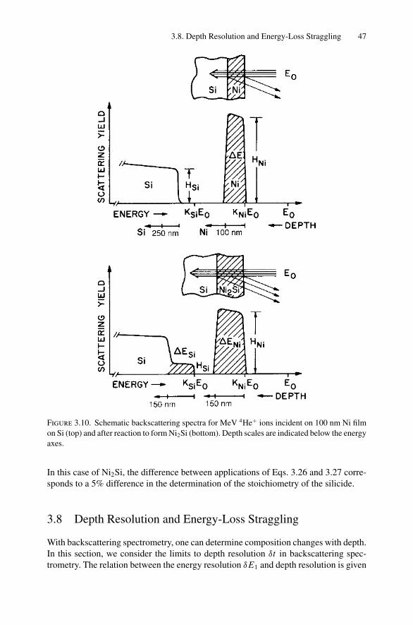
3.8. Depth Resolution and Energy-Loss Straggling 47
Figure 3.10. Schematic backscattering spectra for MeV 4He+ ions incident on 100 nm Ni filmon Si (top) and after reaction to form Ni2Si (bottom). Depth scales are indicated below the energyaxes.
In this case of Ni2Si, the difference between applications of Eqs. 3.26 and 3.27 corre-sponds to a 5% difference in the determination of the stoichiometry of the silicide.
3.8 Depth Resolution and Energy-Loss Straggling
With backscattering spectrometry, one can determine composition changes with depth.In this section, we consider the limits to depth resolution δt in backscattering spec-trometry. The relation between the energy resolution δE1 and depth resolution is given
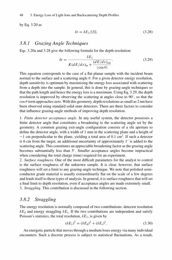
48 3. Energy Loss of Light Ions and Backscattering Depth Profiles
by Eq. 3.20 as
δt = δE1/[S]. (3.28)
3.8.1 Grazing Angle Techniques
Eqs. 3.20a and 3.28 give the following formula for the depth resolution:
δt = δE1
K (d E/dx)in + (d E/dx)out
| cos θ |. (3.29)
This equation corresponds to the case of a flat planar sample with the incident beamnormal to the surface and a scattering angle θ . For a given detector energy resolution,depth sensitivity is optimum by maximizing the energy loss associated with scatteringfrom a depth into the sample. In general, this is done by grazing-angle techniques sothat the path length and hence the energy loss is a maximum. Using Eq. 3.29, the depthresolution is improved by observing the scattering at angles close to 90, so that thecos θ term approaches zero. With this geometry, depth resolutions as small as 2 nm havebeen observed using standard solid-state detectors. There are three factors to considerthat influence grazing-angle methods of improving depth resolution.
1. Finite detector acceptance angle. In any useful system, the detector possesses afinite detector angle that constitutes a broadening to the scattering angle set by thegeometry. A common grazing exit-angle configuration consists of a slit aperture todefine the detector angle, with a width of 1 mm in the scattering plane and a height of∼1 cm perpendicular to the plane, yielding a total area of 0.1 cm2. If such a detectoris 6 cm from the target, an additional uncertainty of approximately 1 is added to thescattering angle. This constitutes an appreciable broadening factor as the grazing anglebecomes substantially less than 5. Smaller acceptance angles become impracticalwhen considering the total charge (time) required for an experiment.2. Surface roughness. One of the most difficult parameters for the analyst to controlis the surface roughness of the unknown sample. It is clear, however, that surfaceroughness will set a limit to any grazing-angle technique. We note that polished semi-conductor grade material is usually extraordinarily flat on the scale of a few degreesand lends itself to these types of analysis. In general, it is surface roughness that will seta final limit to depth resolution, even if acceptance angles are made extremely small.3. Straggling. This contribution is discussed in the following section.
3.8.2 Straggling
The energy resolution is normally composed of two contributions: detector resolutionδEd and energy straggling δEs. If the two contributions are independent and satisfyPoisson’s statistics, the total resolution, δE1, is given by
(δE1)2 = (δEd)2 + (δEs)2. (3.30)
An energetic particle that moves through a medium loses energy via many individualencounters. Such a discrete process is subject to statistical fluctuations. As a result,
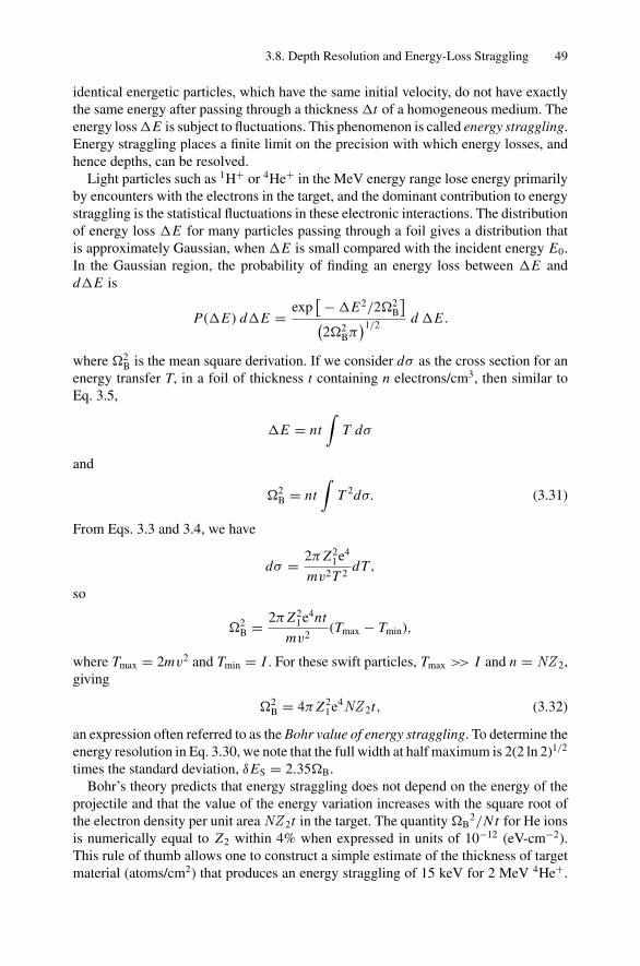
3.8. Depth Resolution and Energy-Loss Straggling 49
identical energetic particles, which have the same initial velocity, do not have exactlythe same energy after passing through a thickness t of a homogeneous medium. Theenergy loss E is subject to fluctuations. This phenomenon is called energy straggling.Energy straggling places a finite limit on the precision with which energy losses, andhence depths, can be resolved.
Light particles such as 1H+ or 4He+ in the MeV energy range lose energy primarilyby encounters with the electrons in the target, and the dominant contribution to energystraggling is the statistical fluctuations in these electronic interactions. The distributionof energy loss E for many particles passing through a foil gives a distribution thatis approximately Gaussian, when E is small compared with the incident energy E0.In the Gaussian region, the probability of finding an energy loss between E anddE is
P(E) dE = exp[− E2/22
B
](22
Bπ)1/2 d E .
where 2B is the mean square derivation. If we consider dσ as the cross section for an
energy transfer T, in a foil of thickness t containing n electrons/cm3, then similar toEq. 3.5,
E = nt∫
T dσ
and
2B = nt
∫T 2dσ. (3.31)
From Eqs. 3.3 and 3.4, we have
dσ = 2π Z21e4
mv2T 2dT,
so
2B = 2π Z2
1e4nt
mv2(Tmax − Tmin),
where Tmax = 2mv2 and Tmin = I . For these swift particles, Tmax >> I and n = NZ 2,giving
2B = 4π Z2
1e4NZ 2t, (3.32)
an expression often referred to as the Bohr value of energy straggling. To determine theenergy resolution in Eq. 3.30, we note that the full width at half maximum is 2(2 ln 2)1/2
times the standard deviation, δES = 2.35B.Bohr’s theory predicts that energy straggling does not depend on the energy of the
projectile and that the value of the energy variation increases with the square root ofthe electron density per unit area NZ 2t in the target. The quantity B
2/Nt for He ionsis numerically equal to Z2 within 4% when expressed in units of 10−12 (eV-cm−2).This rule of thumb allows one to construct a simple estimate of the thickness of targetmaterial (atoms/cm2) that produces an energy straggling of 15 keV for 2 MeV 4He+.
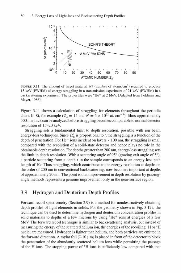
50 3. Energy Loss of Light Ions and Backscattering Depth Profiles
1019
1018
1017
6
6
4
4
2
2
0 10 20 30 40 50 60 70 80 90
BOHR'S THEORY
ATOMIC NUMBER Z2
Nt (
atom
s/cm
2 )
2 MeV 4He IONS
Nt
Figure 3.11. The amount of target material Nt (number of atoms/cm2) required to produce15 keV (FWHM) of energy straggling in a transmission experiment of 21 keV (FWHM) in abackscattering experiment. The projectiles were 4He+ at 2 MeV. [Adapted from Feldman andMayer, 1986].
Figure 3.11 shows a calculation of straggling for elements throughout the periodicchart. In Si, for example (Z2 = 14 and N = 5 × 10²² at. cm−3), films approximately500 nm thick can be analyzed before straggling becomes comparable to normal detectorresolution of 15–20 keV.
Straggling sets a fundamental limit to depth resolution, possible with ion beamenergy-loss techniques. Since 2
B is proportional to t, the straggling is a function of thedepth of penetration. For He+ ions incident on layers <100 nm, the straggling is smallcompared with the resolution of a solid-state detector and hence plays no role in theobtainable depth resolution. For depths greater than 200 nm, energy-loss straggling setsthe limit in depth resolution. With a scattering angle of 95 (grazing exit angle of 5),a particle scattering from a depth t in the sample corresponds to an energy-loss pathlength of 10t. Thus straggling, which contributes to the energy resolution at depths onthe order of 200 nm in conventional backscattering, now becomes important at depthsof approximately 20 nm. The point is that improvement in depth resolution by grazing-angle methods represents a genuine improvement only in the near-surface region.
3.9 Hydrogen and Deuterium Depth Profiles
Forward recoil spectrometry (Section 2.9) is a method for nondestructively obtainingdepth profiles of light elements in solids. For the geometry shown in Fig. 3.12a, thetechnique can be used to determine hydrogen and deuterium concentration profiles insolid materials to depths of a few microns by using 4He+ ions at energies of a fewMeV. The forward recoil technique is similar to backscattering analysis, but instead ofmeasuring the energy of the scattered helium ion, the energies of the recoiling 1H or 2Hnuclei are measured. Hydrogen is lighter than helium, and both particles are emitted inthe forward direction. A mylar foil (∼=10 µm) is placed in front of the detector to blockthe penetration of the abundantly scattered helium ions while permitting the passageof the H ions. The stopping power of 1H ions is sufficiently low compared with that
3.9. Hydrogen and Deuterium Depth Profiles 51
POLYSTYRENE
ENERGYSENSITIVEDETECTOR
4He++ ION BEAM
E0, 3.0 MeV α
FORWARD SCATTERED4He++ IONS
2H (DEUTERIUM)
2α RECOILING1H and 2HNUCLEI
E1
E
10 µm THICKMYLARSTOPPER FOIL
DEUTERIUM (2H) DIFFUSION INPOLYSTYRENE
DEPOSITED
DIFFUSED
ENERGY (MeV)
NO
RM
ALI
ZE
D Y
IELD
1Hsurface2Hsurface
6
4
2
01.0 1.2 1.4 1.6
a
b
+
+
+
+
+
+++++++++++++++++++++++++++++++++++++++++++++
+++++++++++++
++++++++++++++
+++
+++
Figure 3.12. (a) Experimental geometry for forward recoil spectrometry experiments to deter-mine depth profiles of 1H and 2H in solids. (b) Recoil spectrum of 2H diffused in a sample ofpolystyrene for 1 hr at 170 C. The sample consisted of a bilayer film consisting of 12 nm ofdeuterated polystyrene on a large-molecular-weight (Mw = 2 × 10⁷) film of polystyrene.
of He ions (Fig. 3.2), so a 1.6 MeV 1H ion only loses 300 keV in penetrating a filmthat completely stops 3 MeV 4He+ ions. The mylar absorber does introduce energystraggling that combined with the energy resolution of the detector, results in an energyresolution at the sample surface of about 40 keV.
Depth profiles are determined by the energy loss of the incident He+ ion alongthe inward path and the energy loss of the recoil 1H or 2H ion along the outwardpath. The diffusion of deuterium (2H) in polystyrene can be determined from spectrasuch as those shown in Fig. 3.12b. In that case, a 2H ion detected at an energy of 1.4MeV corresponds to a collision that originated a 2H recoil from a depth about 400 nmbelow the surface. The use of forward recoil spectrometry allows the determination ofhydrogen and deuterium diffusion coefficients in the range of 10−12–10−14 cm2/sec, arange that is difficult to determine by conventional techniques.
As an example of depth measurement, consider a layer of hydrocarbon on bothsides of a self-supported 400 nm Al film (instead of the Au markers shown in Fig.3.6). We will use a symmetrical scattering geometry with the sample inclined at an
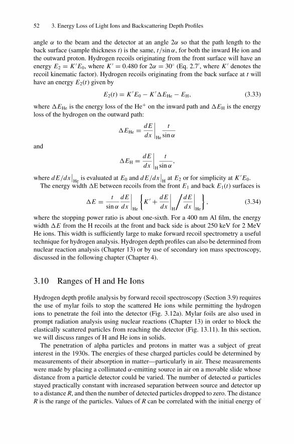
52 3. Energy Loss of Light Ions and Backscattering Depth Profiles
angle α to the beam and the detector at an angle 2α so that the path length to theback surface (sample thickness t) is the same, t/sin α, for both the inward He ion andthe outward proton. Hydrogen recoils originating from the front surface will have anenergy E2 = K ′E0, where K ′ = 0.480 for 2α = 30 (Eq. 2.7′, where K ′ denotes therecoil kinematic factor). Hydrogen recoils originating from the back surface at t willhave an energy E2(t) given by
E2(t) = K ′E0 − K ′EHe − EH, (3.33)
where EHe is the energy loss of the He+ on the inward path and EH is the energyloss of the hydrogen on the outward path:
EHe = d E
dx
∣∣∣∣He
t
sin α
and
EH = d E
dx
∣∣∣∣H
t
sin α,
where d E/dx∣∣He is evaluated at E0 and d E/dx
∣∣H at E2 or for simplicity at K ′E0.
The energy width E between recoils from the front E1 and back E1(t) surfaces is
E = t
sin α
d E
dx
∣∣∣∣He
K ′ + d E
dx
∣∣∣∣H
/d E
dx
∣∣∣∣He
, (3.34)
where the stopping power ratio is about one-sixth. For a 400 nm Al film, the energywidth E from the H recoils at the front and back side is about 250 keV for 2 MeVHe ions. This width is sufficiently large to make forward recoil spectrometry a usefultechnique for hydrogen analysis. Hydrogen depth profiles can also be determined fromnuclear reaction analysis (Chapter 13) or by use of secondary ion mass spectroscopy,discussed in the following chapter (Chapter 4).
3.10 Ranges of H and He Ions
Hydrogen depth profile analysis by forward recoil spectroscopy (Section 3.9) requiresthe use of mylar foils to stop the scattered He ions while permitting the hydrogenions to penetrate the foil into the detector (Fig. 3.12a). Mylar foils are also used inprompt radiation analysis using nuclear reactions (Chapter 13) in order to block theelastically scattered particles from reaching the detector (Fig. 13.11). In this section,we will discuss ranges of H and He ions in solids.
The penetration of alpha particles and protons in matter was a subject of greatinterest in the 1930s. The energies of these charged particles could be determined bymeasurements of their absorption in matter—particularly in air. These measurementswere made by placing a collimated α-emitting source in air on a movable slide whosedistance from a particle detector could be varied. The number of detected α particlesstayed practically constant with increased separation between source and detector upto a distance R, and then the number of detected particles dropped to zero. The distanceR is the range of the particles. Values of R can be correlated with the initial energy of
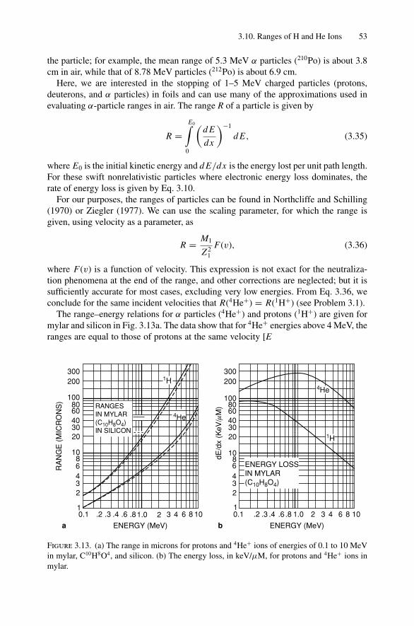
3.10. Ranges of H and He Ions 53
the particle; for example, the mean range of 5.3 MeV α particles (210Po) is about 3.8cm in air, while that of 8.78 MeV particles (212Po) is about 6.9 cm.
Here, we are interested in the stopping of 1–5 MeV charged particles (protons,deuterons, and α particles) in foils and can use many of the approximations used inevaluating α-particle ranges in air. The range R of a particle is given by
R =E0∫
0
(d E
dx
)−1
d E, (3.35)
where E0 is the initial kinetic energy and d E/dx is the energy lost per unit path length.For these swift nonrelativistic particles where electronic energy loss dominates, therate of energy loss is given by Eq. 3.10.
For our purposes, the ranges of particles can be found in Northcliffe and Schilling(1970) or Ziegler (1977). We can use the scaling parameter, for which the range isgiven, using velocity as a parameter, as
R = M1
Z21
F(v), (3.36)
where F(v) is a function of velocity. This expression is not exact for the neutraliza-tion phenomena at the end of the range, and other corrections are neglected; but it issufficiently accurate for most cases, excluding very low energies. From Eq. 3.36, weconclude for the same incident velocities that R(4He+) = R(1H+) (see Problem 3.1).
The range–energy relations for α particles (4He+) and protons (1H+) are given formylar and silicon in Fig. 3.13a. The data show that for 4He+ energies above 4 MeV, theranges are equal to those of protons at the same velocity [E(He)/4]. The scaling only
300200
1008060403020
1086432
10.1 .2 .3 .4 .6 .81.0 2 3 4 6 8 10
ENERGY (MeV)
RA
NG
E (
MIC
RO
NS
)
RANGESIN MYLAR(C10H8O4)IN SILICON
1H
4He
300200
1008060403020
1086432
10.1 .2 .3 .4 .6 .8 1.0 2 3 4 6 8 10
ENERGY (MeV)
4He
1H
ENERGY LOSSIN MYLAR(C10H8O4)
dE/d
x (K
eV/µ
M)
a b
Figure 3.13. (a) The range in microns for protons and 4He+ ions of energies of 0.1 to 10 MeVin mylar, C10H8O4, and silicon. (b) The energy loss, in keV/µM, for protons and 4He+ ions inmylar.
54 3. Energy Loss of Light Ions and Backscattering Depth Profiles
holds at energies above the maximum in the d E/dx curves shown in Figure 3.13b.In these curves, d E/dx values at the same velocity scale as Z2
1, so the 1H values areone-fourth of the 4He+ values.
A 10 µm mylar film is sufficient to stop a 2.5 MeV He ion. The energy loss of a 2.5Me V proton in the film can be estimated from the range–energy relation. The range ofa 2.5 MeV proton in mylar is 80 µm, and a 70 µm film has a thickness equivalent to therange of a 2.3 MeV proton; hence, the energy lost by a 2.5 MeV proton in traversingthe film is about 0.2 MeV. This loss could also be estimated from the d E/dx curve inFig. 3.13b by noting that a 2.5 MeV proton loses 18 keV/µm in mylar.
3.11 Sputtering and Limits to Sensitivity
The Z2 dependence of the Rutherford scattering cross section clearly indicates a largesensitivity to heavy elements. It is of interest to ask for the ultimate sensitivity, i.e., thesmallest amount of material detectable by this technique.
The limit for the ion scattering technique is set by sputtering. Sputtering is a processin which an energetic ion impinging on a solid creates a collision cascade due tosmall angle nuclear events. Some fraction of the secondary ions acquire the correctmomentum to escape the solid, giving rise to an erosion process. This erosion techniqueis an important process in surface analysis and is described completely in Chapter 4. Inthe case of Rutherford scattering, this erosion process is an undesirable phenomenonand sets the limit on sensitivity. The basic question is under what conditions will theerosion of the material will occur before a measurement is complete. Sputtering isdefined in terms of a sputtering yield Y, which is the number of atoms ejected from thesolid per incident ion. In the following, we calculate the limit to sensitivity set by thesputtering process.
We consider a thin layer of material (possibly submonolayer) containing NS atoms/cm2. The yield of scattered ions, QD, is given by the usual equation in a Rutherfordbackscattering measurement:
QD = σ (θ)QNS,
where σ (θ ) is the differential cross section, is the solid angle of the detector, and Qis the number of incident ions.
For the same number of incident ions, the loss of atoms from the layer, NS, due tosputtering by the incident ions is
NS = YQ/a, (3.37)
where a is the area of the probing beam spot. We require that the amount of erosion beless than the original film thickness, i.e.,
NS < NS, (3.38)
Problems 55
which can be expressed as a limit on the value of Q given by
Q <
(QDa
Yσ (θ)
)1/2
, (3.39)
and a corresponding minimum value of NS given by
NS >
(Q DY
σ (θ )a
)1/2
. (3.40)
In evaluating this quantity, we use the following standard numbers for the case of a layerof gold (Z = 79): σ (θ), the cross section for He scattering at 2 MeV to 170, is 10−23
cm2/steradian; , the solid angle of the detector corresponding to a 1 cm2 detector 5cm from the target, is 4 × 10⁻² steradians; Y, the sputtering yield, is 10−3 (see Chapter4); Q, the area of the probing beam, is 10−2 cm2; and Q D is arbitrarily taken as 102,the minimum number of counts required for a statistically significant measurement.With these values, we find a minimum layer thickness of 5 × 10¹² Au atoms/cm2 orclose to 1/1000 of a monolayer. Using these expressions, we see that the scatteringparameters and geometry could be optimized in a number of ways to further increasethe sensitivity. Experience suggests that the absolute best sensitivity realizable for thisfavorable case of a heavy scatterer is 5 × 10¹¹ atoms/cm2. Note that the incident chargerequired is not prohibitive. Equation 3.39 corresponds to an incident particle dose of5 × 1013 ions or about 10 µ Coulombs.
3.12 Summary of Scattering Relations
Throughout this book, and particularly in Chapters 2 and 3, we have developedand used a number of kinematic relations and cross sections and the backscatteringfactor. For the reader’s convenience, we have collected these scattering relations inTable 3.1 on page 57.
Problems
3.1. Derive
R = M1
Z21
F(v)
(Eq. 3.36), using dE = Mv dv and dx = mv2 dE (4π Z21e4n ln(2mv2/I ))−1, and
estimate the range of 1.0 MeV deuterons in Si using Eq. 3.36 and Fig. 3.13.3.2. Using Eq. 3.10:
(a) Evaluate dE/dx in eV/nm for 1 MeV He in Si.(b) Convert to units of eV (1015 atoms/cm2) and compare your answer with
Appendix 3.(c) Determine dE/dx in eV/nm for 4 MeV C ions in silicon.
56 3. Energy Loss of Light Ions and Backscattering Depth Profiles
3.3. Show that the maximum in the stopping power is given by
E = MZ 2 I0
4me,
where e is 2.718 and I0 = 10 eV. Evaluate for He in Si.3.4. Draw the backscattering spectrum (θ = 180) for 2.0 MeV He+ expected for
(a) a sample of Si containing a uniform 1% Au impurity;(b) a sample of Au containing a uniform 1% Si impurity;(c) a sample of Si covered with a 100 nm Pt film; and(d) a sample of Si with a 100 nm PtSi film on Si.
In all spectra, show specific energies for the leading edge (and trailing edge in thinfilm cases) of the spectral features, and indicate the relative heights.
3.5. For the scattering geometry in Fig. 3.12a, what is the energy width of the recoilinghydrogen atoms for a 200-nm-thick mylar target? Use the energy loss values inmylar given in Fig. 3.13 and ignore the influence of the stopper foil in front of thedetector.
3.6. Determine the backscattering energy loss factor (S) (as in Eq. 3.20) for the case ofnonnormal incidence: incident beam at angle θ1 with respect to the sample normaland scattering angle θ2.
3.7. Consider an experiment involving 2.0 MeV ions backscattered to 180 from a 200nm SiO2 target.
(a) Sketch the backscattering spectrum indicating the energies of the features inthe spectrum.
(b) Assuming that the stopping power is energy independent, show that the ratioof the energy widths of scattering from oxygen and Si can be written as
(KSi + 1)/(K0 + 1),
where K denotes the kinematic factor.(c) Recognizing that energy loss is not energy independent, derive a precise form
for the ratio of the energy widths from the two elements. Evaluate the ratioand compare this to the expression given in part (b).
(d) Using the stopping powers, the stoichiometry, and the cross section, derive anequation for the heights of the Si and oxygen peaks and evaluate.
(e) Assume the oxide is of unknown stoichiometry, Six Oy . Derive an expressionfor the ratio of the heights in terms of the scattering cross section, the elementalstopping powers, and x/y. [Hint: Express the stopping power in terms of xand y using Bragg’s rule.]
3.8. Assume in backscattering measurements that energy straggling is given by2
tot = (KB|in)2 + (KB|out)2. Calculate the amount of energy straggling in anRBS signal from a thin Cr layer underneath an Al film 400 nm thick with ananalysis beam of 2 MeV 4He ions (θ = 180). What is the total signal width(FWHM) if the detector resolution is 15 keV? To what thickness of Al does thiscorrespond?
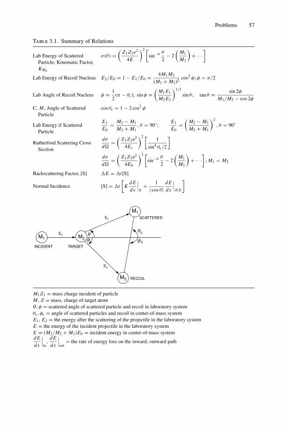
Problems 57
Table 3.1. Summary of Relations
Lab Energy of ScatteredParticle; Kinematic Factor,KM2
σ (θ ) =(
Z1 Z2e2
4E
)2 [sin−4 θ
2− 2
(M1
M2
)+ · · ·
]
Lab Energy of Recoil Nucleus E2/E0 = 1 − E1/E0 = 4M1 M2
(M1 + M2)2cos2 φ; φ < π/2
Lab Angle of Recoil Nucleus φ = 1
2(π − θc); sin φ =
(M1 E1
M2 E2
)1/2
sin θ ; tan θ = sin 2φ
M1/M2 − cos 2φ
C, M , Angle of ScatteredParticle
cos θc = 1 − 2 cos2 φ
Lab Energy if ScatteredParticle
E1
E0= M2 − M1
M2 + M1, θ = 90;
E1
E0=(
M2 − M1
M2 + M1
)2
, θ = 90
Rutherford Scattering CrossSection
dσ
d=(
Z1 Z2e2
4Ec
)2 [1
sin4 θc/2
]
dσ
d=(
Z1 Z2e2
4E0
)2 [sin−4 θ
2− 2
(M1
M2
)+ · · ·
]; M1 < M2
Backscattering Factor, [S] E = t[S]
Normal Incidence [S] = t
[K
d E
dx
∣∣∣E
+ 1
| cos θ |d E
dx
∣∣∣KE
]
M1
M1
M2
M2 RECOIL
SCATTERED
TARGETINCIDENT
E0
E1
E2
θφ
θc
φc
M1 Z1 = mass charge incident of particleM, Z = mass, charge of target atomθ, φ = scattered angle of scattered particle and recoil in laboratory systemθc, φc = angle of scattered particles and recoil in center-of-mass systemE1, E2 = the energy after the scattering of the projectile in the laboratory systemE = the energy of the incident projectile in the laboratory systemE = (M2/M2 + M1)E0 = incident energy in center-of-mass systemd E
dx
∣∣∣in,
d E
dx
∣∣∣out
= the rate of energy loss on the inward, outward path
58 3. Energy Loss of Light Ions and Backscattering Depth Profiles
References
1. H. H. Anderson and J. F. Ziegler, Hydrogen Stopping Power and Ranges in All Elements(Pergamon Press, New York, 1977).
2. W. K. Chu, J. W. Mayer, and M. A. Nicolet, Backscattering Spectrometry (Academic Press,New York, 1978).
3. R. D. Evans, The Atomic Nucleus (McGraw-Hill Book Co., New York, 1955).4. I. Kaplan, Nuclear Physics (Addison-Wesley, Reading, MA, 1964).5. R. B. Leighton, Principles of Modern Physics (McGraw-Hill Book Co., New York, 1959).6. L. C. Northcliffe and R. F. Schilling, “Range and Stopping Power Tables for Heavy Ions,”
Nucl. Data Tables 7(3–4), 733 (1970).7. F. K. Richtmyer, E. H. Kennard, and J. N. Cooper, Introduction to Modern Physics, 6th ed.
(McGraw-Hill Book Co., New York, 1978).8. J. F. Ziegler, Helium Stopping Powers and Ranges in All Elements (Pergamon Press, New
York, 1977).9. L. R. Doolittle, Nucl. Intr. and Meth., B9, 349 (1985).10. L. C. Feldman and J. W. Mayer, Fundaments of Surface and Thin Film Analysis (Prentice
Hall, NJ, 1986).
4Sputter Depth Profiles and Secondary IonMass Spectroscopy
4.1 Introduction
This chapter deals with the erosion of the sample by energetic particle bombardment.In this process, called sputtering, surface atoms are removed by collisions betweenthe incoming particles and the atoms in the near-surface layers of a solid. Sputteringprovides the basis for composition depth profiling with surface analysis techniques,either by analysis of the remaining surface with electron spectroscopies or by analysis ofthe sputtered material. Here we describe the most widely used of these latter techniques,secondary ion mass spectroscopy (SIMS).
In previous chapters, we have been concerned with the energies and yields of parti-cles scattered from the target material under analysis. With Rutherford backscatteringspectrometery (RBS) using MeV He+ ions, the energy loss along the inward andoutward paths provides the depth information (Fig. 4.1). In other analytical techniques,the atoms to be identified must lie at the surface of the materials. For example,the observation depth in X-ray photoelectron spectroscopy and Auger-electronspectroscopy (XPS and AES) can be as small as 1.0–2.0 nm. In order to use XPS andAES to determine depth profiles, it is necessary to remove controlled thicknesses ofthe surface layer. This surface layer removal is carried out in materials analysis bybombarding the surface with low-energy (0.5–20 keV) heavy ions, such as O+ or Ar+,which eject or sputter target atoms from the surface. The yield of sputtered atoms,the number of sputtered atoms per incident ion, lies in the range of 0.5–20 dependingupon ion species, ion energy, and target material. Surface-sensitive techniques canthen be used after each layer is removed in order to determine the composition of thenew surface and hence deduce the depth profile of the atomic composition. It is alsopossible to analyze the sputtered atoms, generally the ionized species, to determinethe composition of the sputter-removed materials. This technique of secondary ionmass spectroscopy, or SIMS, has been used extensively in depth profiling. One canalso measure the characteristic radiation emitted from excited sputtered ions or atomsto determine the composition of the sputter-removed material.
For sputtering, it is the energy lost in elastic collisions with the atomic cores—termednuclear energy loss—that determines the energy transfer to and eventual ejection ofsurface atoms. For backscattering or nuclear analysis, the energetic particles lose energyprimarily through electron excitation and ionization in inelastic collisions with atomic
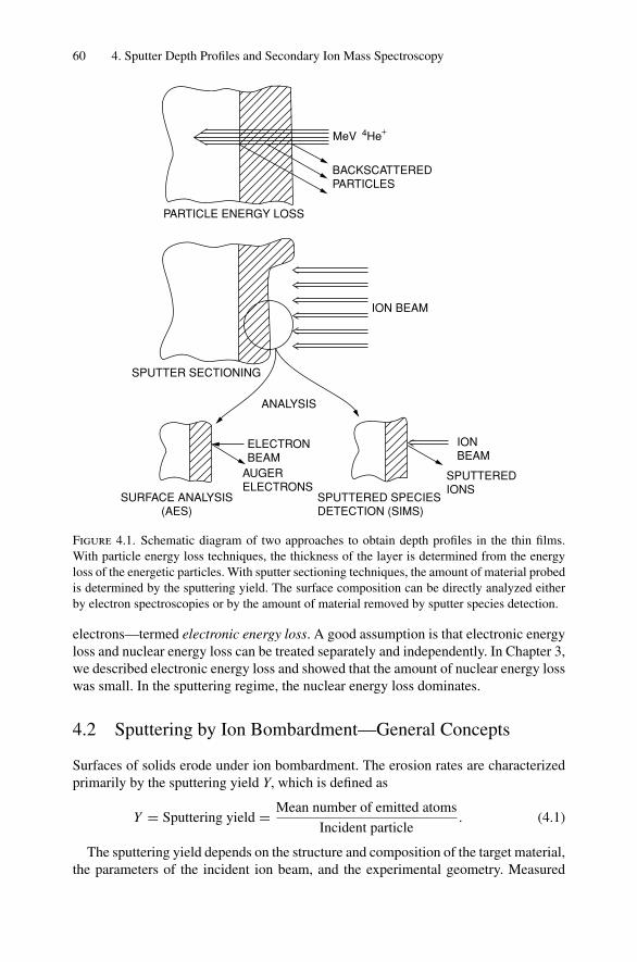
60 4. Sputter Depth Profiles and Secondary Ion Mass Spectroscopy
BACKSCATTEREDPARTICLES
MeV 4He+
PARTICLE ENERGY LOSS
ION BEAM
SPUTTER SECTIONING
ANALYSIS
IONBEAM
SPUTTEREDIONS
SPUTTERED SPECIESDETECTION (SIMS)
ELECTRONBEAM
AUGERELECTRONS
SURFACE ANALYSIS(AES)
Figure 4.1. Schematic diagram of two approaches to obtain depth profiles in the thin films.With particle energy loss techniques, the thickness of the layer is determined from the energyloss of the energetic particles. With sputter sectioning techniques, the amount of material probedis determined by the sputtering yield. The surface composition can be directly analyzed eitherby electron spectroscopies or by the amount of material removed by sputter species detection.
electrons—termed electronic energy loss. A good assumption is that electronic energyloss and nuclear energy loss can be treated separately and independently. In Chapter 3,we described electronic energy loss and showed that the amount of nuclear energy losswas small. In the sputtering regime, the nuclear energy loss dominates.
4.2 Sputtering by Ion Bombardment—General Concepts
Surfaces of solids erode under ion bombardment. The erosion rates are characterizedprimarily by the sputtering yield Y, which is defined as
Y = Sputtering yield = Mean number of emitted atoms
Incident particle. (4.1)
The sputtering yield depends on the structure and composition of the target material,the parameters of the incident ion beam, and the experimental geometry. Measured
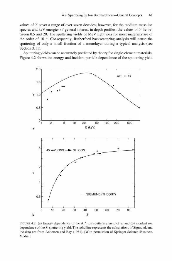
4.2. Sputtering by Ion Bombardment—General Concepts 61
values of Y cover a range of over seven decades; however, for the medium-mass ionspecies and keV energies of general interest in depth profiles, the values of Y lie be-tween 0.5 and 20. The sputtering yields of MeV light ions for most materials are ofthe order of 10−3. Consequently, Rutherford backscattering analysis will cause thesputtering of only a small fraction of a monolayer during a typical analysis (seeSection 3.11).
Sputtering yields can be accurately predicted by theory for single-element materials.Figure 4.2 shows the energy and incident particle dependence of the sputtering yield
2.0
1.5
0.5
1.0
01 2 5 10 20 50 100 200 500
Y
E (keV)
5
2
0.5
1
0 10 20 30 40 50 60 70 80
Y
Z1
SIGMUND (THEORY)
45 keV IONS SILICON
Ar+ Si
b
a
Figure 4.2. (a) Energy dependence of the Ar+ ion sputtering yield of Si and (b) incident iondependence of the Si sputtering yield. The solid line represents the calculations of Sigmund, andthe data are from Andersen and Bay (1981). [With permission of Springer Science+BusinessMedia.]
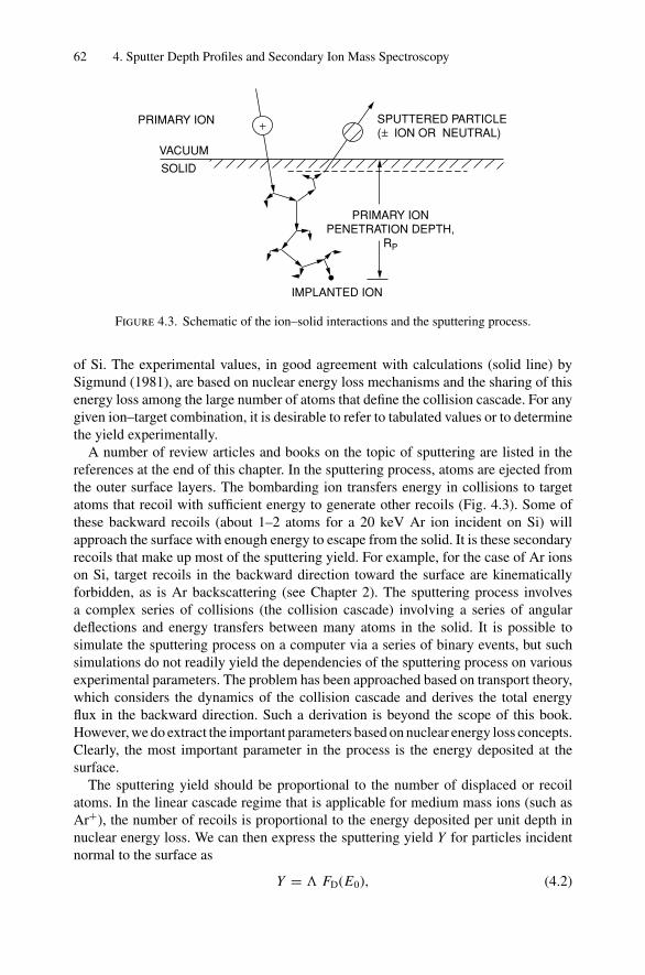
62 4. Sputter Depth Profiles and Secondary Ion Mass Spectroscopy
+ SPUTTERED PARTICLE( ION OR NEUTRAL)+−
PRIMARY ION
VACUUM
SOLID
PRIMARY IONPENETRATION DEPTH,
RP
IMPLANTED ION
Figure 4.3. Schematic of the ion–solid interactions and the sputtering process.
of Si. The experimental values, in good agreement with calculations (solid line) bySigmund (1981), are based on nuclear energy loss mechanisms and the sharing of thisenergy loss among the large number of atoms that define the collision cascade. For anygiven ion–target combination, it is desirable to refer to tabulated values or to determinethe yield experimentally.
A number of review articles and books on the topic of sputtering are listed in thereferences at the end of this chapter. In the sputtering process, atoms are ejected fromthe outer surface layers. The bombarding ion transfers energy in collisions to targetatoms that recoil with sufficient energy to generate other recoils (Fig. 4.3). Some ofthese backward recoils (about 1–2 atoms for a 20 keV Ar ion incident on Si) willapproach the surface with enough energy to escape from the solid. It is these secondaryrecoils that make up most of the sputtering yield. For example, for the case of Ar ionson Si, target recoils in the backward direction toward the surface are kinematicallyforbidden, as is Ar backscattering (see Chapter 2). The sputtering process involvesa complex series of collisions (the collision cascade) involving a series of angulardeflections and energy transfers between many atoms in the solid. It is possible tosimulate the sputtering process on a computer via a series of binary events, but suchsimulations do not readily yield the dependencies of the sputtering process on variousexperimental parameters. The problem has been approached based on transport theory,which considers the dynamics of the collision cascade and derives the total energyflux in the backward direction. Such a derivation is beyond the scope of this book.However, we do extract the important parameters based on nuclear energy loss concepts.Clearly, the most important parameter in the process is the energy deposited at thesurface.
The sputtering yield should be proportional to the number of displaced or recoilatoms. In the linear cascade regime that is applicable for medium mass ions (such asAr+), the number of recoils is proportional to the energy deposited per unit depth innuclear energy loss. We can then express the sputtering yield Y for particles incidentnormal to the surface as
Y = FD(E0), (4.2)
4.3. Nuclear Energy Loss 63
where contains all the material properties such as surface binding energies, andFD(E0) is the density of deposited energy at the surface and depends on the type,energy, and direction of the incident ion and the target parameters Z2, M2, and N.
The deposited energy at the surface can be expressed as
FD(E0) = αN Sn(E0), (4.3)
where N is the atomic density of target atoms, Sn(E) is the nuclear stopping crosssection, and NSn(E) = dE dx|n is the nuclear energy loss. In this equation, α is acorrection factor that takes into account the angle of incidence of the beam to thesurface and contributions due to large-angle scattering events that are not included inthe development. The sputtering yield is calculated in Section 4.4.
The evaluation of Sn(E) rests on the collision cross section for energy transfer to asubstrate atom. In the keV sputtering regime where the particle velocity is much lessthan the Bohr velocity, screening of the nuclear charge by the electrons must be includedin the description of the collisions. The procedure to obtain the sputtering yield is tofirst treat a screened potential from a description of the Thomas–Fermi approximations(Section 4.9), and then derive the collision cross section based on a screened potentialto obtain the nuclear stopping cross section (Section 4.3).
4.3 Nuclear Energy Loss
A charged particle penetrating a solid loses energy through two processes: (1) energytransfer to electrons (electronic energy loss); and (2) energy transfer to the atoms ofthe solid (nuclear energy loss). In both cases, the interaction is basically of a Coulombtype; for the electronic case, it is pure Coulomb (see Chapter 3), while in the nuclearcase, it is a form of screened Coulomb potential. The two mechanisms have differentenergy dependencies—in the electronic case, there is a peak in the cross section atprojectile energies of the order of 0.1–1.0 MeV for light projectiles; in the nuclearcase, the peak in the loss cross section is at much lower energy, of the order of 0.1–10 keV. In penetration theory, the electronic and nuclear energy losses are treatedas uncorrelated and simply summed. In many cases, one or the other contribution isnegligible and is simply ignored. Sputtering is governed by the energy deposited vianuclear energy loss at the surface of a solid. This mechanism transfers momentum andenergy to the atoms of the solid, resulting in energetic secondaries and sputtering. Inthis section, we give a simple description of nuclear energy loss and compare it to themore sophisticated treatments. As in other sections of this text, our aim is to providea simple mathematical description of the process in order to provide some insight intothe quantitative understanding of the physics.
The derivation of nuclear energy loss uses two main assumptions: (1) a simplescreened Coulomb potential and (2) the impulse approximation.
The interaction potential between two atoms Z1 and Z2 can be written in the formof a screened Coulomb potential (Section 4.9), using χ as the screening function:
V (r ) = Z1 Z2e2
rχ( r
a
), (4.4)
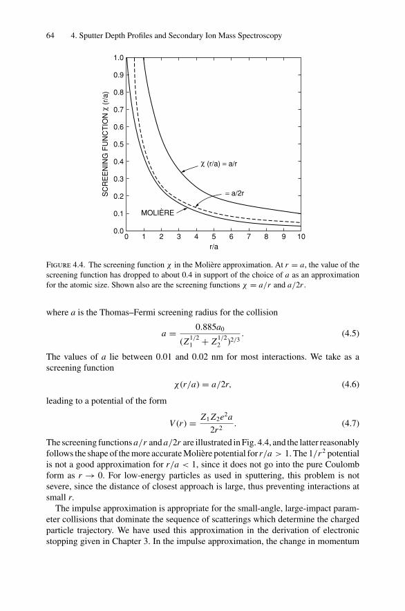
64 4. Sputter Depth Profiles and Secondary Ion Mass Spectroscopy
0 1 2 3 4 5 6 7 8 9 10r/a
MOLIÈRE
SC
RE
EN
ING
FU
NC
TIO
N χ
(r/
a)
0.0
0.1
0.2
0.3
0.4
0.5
0.6
0.7
0.8
0.9
1.0
χ (r/a) = a/r
= a/2r
Figure 4.4. The screening function χ in the Moliere approximation. At r = a, the value of thescreening function has dropped to about 0.4 in support of the choice of a as an approximationfor the atomic size. Shown also are the screening functions χ = a/r and a/2r .
where a is the Thomas–Fermi screening radius for the collision
a = 0.885a0
(Z1/21 + Z1/2
2 )2/3. (4.5)
The values of a lie between 0.01 and 0.02 nm for most interactions. We take as ascreening function
χ (r/a) = a/2r, (4.6)
leading to a potential of the form
V (r ) = Z1 Z2e2a
2r2. (4.7)
The screening functions a/r and a/2r are illustrated in Fig. 4.4, and the latter reasonablyfollows the shape of the more accurate Moliere potential for r/a > 1. The 1/r2 potentialis not a good approximation for r/a < 1, since it does not go into the pure Coulombform as r → 0. For low-energy particles as used in sputtering, this problem is notsevere, since the distance of closest approach is large, thus preventing interactions atsmall r.
The impulse approximation is appropriate for the small-angle, large-impact param-eter collisions that dominate the sequence of scatterings which determine the chargedparticle trajectory. We have used this approximation in the derivation of electronicstopping given in Chapter 3. In the impulse approximation, the change in momentum
4.3. Nuclear Energy Loss 65
is given by
p =∞∫
−∞F⊥ dt, (4.8)
or
p = 1
v
∞∫−∞
F⊥ dx, (4.9)
where F⊥ is the component of the force acting on the ion perpendicular to its incident di-rection. By using the geometry of Fig. 3.3, the force may be written with r = √
x2 + b2
as
F⊥ = ∂V (r )
∂y= −
∂V(√
x2 + b2)
∂b. (4.10)
Then
p = 1
v
∂
∂b
∞∫−∞
V(√
x2 + b2)
dx, (4.11)
or, using Eq. 4.7,
p = 1
v
∂
∂b
∞∫0
Z1 Z2e2a
(x2 + b2)dx, (4.12)
which reduces to
p = π Z1 Z2e2a
2vb2. (4.13)
The energy transferred, T, to the recoiling nucleus is
T = p2
2M2,
T = π2 Z21 Z2
2e4a2
8M2v2b4. (4.14)
The cross section dσ (T ) for transfer of energy between T and T + dT is
dσ = −2πb db,
or
dσ = − π2 Z1 Z2e2a
8√
(M2/M1)ET −3/2 dT, (4.15)
66 4. Sputter Depth Profiles and Secondary Ion Mass Spectroscopy
where E = M1v2/2. It is convenient to express this result in terms of the maximum
energy transfer Tmax, where
Tmax = 4M1 M2
(M1 + M2)2E .
Then
dσ = −π2 Z1 Z2e2a
4T 1/2max
M1
(M1 + M2)T −3/2 dT . (4.16)
The nuclear stopping cross section Sn is given by
Sn = −∫
T dσ,
or
Sn = π2 Z1 Z2e2a
2T 1/2max
(M1
M1 + M2
)T 1/2
∣∣∣∣Tmax
0
.
Sn = π2 Z1 Z2e2aM1
2(M1 + M2), (4.17)
The nuclear energy loss is given by
dE
dx
∣∣∣n
= NSn, (4.18)
where N is the number of atoms/volume in the solid. Note that, in this approximation,dE/dx|n is independent of energy, i.e.,
dE
dx
∣∣∣n
= Nπ2
2Z1 Z2e2a
M1
M1 + M2. (4.19)
Figure 4.5 compares this energy-independent value to the values of the nuclear energyloss using the Thomas–Fermi potential, and follows the description of Lindhard inwhich the nuclear energy loss is expressed in terms of a reduced energy ε′. This energyis given by the ratio of the Thomas screening distance to the distance of closest approach,
ε′ = M2
M1 + M2E
a
Z1 Z2e2, (4.20a)
and a reduced length ρ based on a cross section πa2 and an energy ratio Tmax/E ,
ρ = x N M24πa2 M1/(M1 + M2)2. (4.20b)
This form is generally useful in that the stopping power for any combination of projectileand target at any energy can be found. In this formalism, dε′/dρ = Sn(ε′), so if we useEqs. 4.20a and 4.20b,
dE
dx
∣∣∣n
= 4πaN Z1 Z2e2 M1
M1 + M2Sn(ε′), (4.21)
where Sn(ε′) depends on the form of V (r ). In terms of the value of (dE/dx)n derived inEq. 4.19, the energy-independent value of the nuclear energy loss in reduced units ofenergy and length is 0.393. This value is slightly different than that given by Lindhard
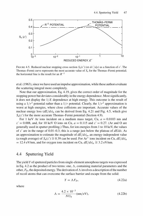
4.4. Sputtering Yield 67
REDUCED ENERGY, ′
THOMAS–FERMIPOTENTIALR−2 POTENTIAL
Sn ( ′)
10−3 10−2 10−1 1 100
0.1
0.2
0.3
0.4
0.5
e
e
Figure 4.5. Reduced nuclear stopping cross section Sn(ε ′) (or dε ′/dρ) as a function of ε ′. TheThomas–Fermi curve represents the most accurate value of Sn for the Thomas–Fermi potential;the horizontal line is the result for an R−2 potential [Eq. (4.17)].
et al. (1963), since we have used an impulse approximation, while these authors evaluatethe scattering integral more completely.
Note that our approximation, Eq. 4.19, gives the correct order of magnitude for thestopping power but deviates considerably in the energy dependence. Most significantly,it does not display the 1/E dependence at high energy. This outcome is the result ofusing a 1/r2 potential rather than a 1/r potential. Clearly, the 1/r2 approximation isworst at high energies, where close collisions are important. Accurate values of thenuclear energy loss (dE/dx)n can be derived from Eq. 4.21 and Fig. 4.5, which giveSn(ε′) for the more accurate Thomas–Fermi potential (Section 4.9).
For 1 keV Ar ions incident on a medium mass target, Cu, a = 0.0103 nm andε′ = 0.008, and, for 10 keV O ions on Cu, a = 0.115 and ε′ = 0.27. (Ar and O aregenerally used in sputter profiling.) Thus, for ion energies from 1 to 10 keV, the valuesof ε′ are in the range of 0.01–0.3; this is a range just below the plateau of dE/dx. Asan approximation to estimate the magnitude of dE/dx|n, an energy-independent value(a rough average) of Sn(ε′) ∼= 0.39 can be used. For Ar+ ions incident on Cu, dE/dx|n= 12.4 eV/nm, and for oxygen ions incident on Cu, dE/dx|n ∼= 3.2 eV/nm.
4.4 Sputtering Yield
The yield Y of sputtered particles from single-element amorphous targets was expressedin Eq. 4.2 as the product of two terms: one, , containing material parameters and theother, FD, the deposited energy. The derivation of involves a description of the numberof recoil atoms that can overcome the surface barrier and escape from the solid:
Y = FD, (4.22a)
where
= 4.2 × 10⁻³
NU0(nm/eV), (4.22b)
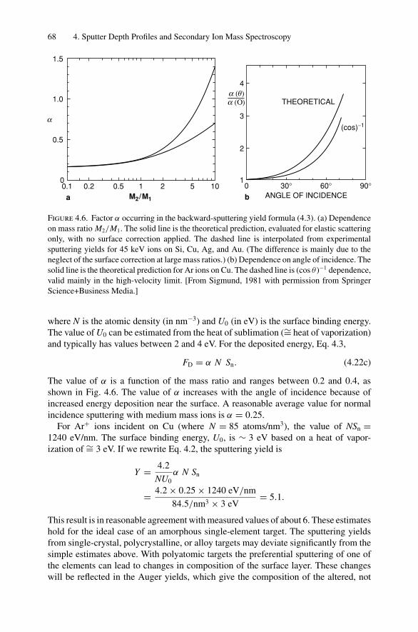
68 4. Sputter Depth Profiles and Secondary Ion Mass Spectroscopy
1.5
1.0
0.5
0.1 0.2 0.50
1 2 5 10
a
a M2/M1
4
3
2
1
THEORETICAL
(cos)−1
ANGLE OF INCIDENCE90°60°30°0
b
a (θ)a (Ο)
Figure 4.6. Factor α occurring in the backward-sputtering yield formula (4.3). (a) Dependenceon mass ratio M2/M1. The solid line is the theoretical prediction, evaluated for elastic scatteringonly, with no surface correction applied. The dashed line is interpolated from experimentalsputtering yields for 45 keV ions on Si, Cu, Ag, and Au. (The difference is mainly due to theneglect of the surface correction at large mass ratios.) (b) Dependence on angle of incidence. Thesolid line is the theoretical prediction for Ar ions on Cu. The dashed line is (cos θ)−1 dependence,valid mainly in the high-velocity limit. [From Sigmund, 1981 with permission from SpringerScience+Business Media.]
where N is the atomic density (in nm−3) and U0 (in eV) is the surface binding energy.The value of U0 can be estimated from the heat of sublimation (∼= heat of vaporization)and typically has values between 2 and 4 eV. For the deposited energy, Eq. 4.3,
FD = α N Sn. (4.22c)
The value of α is a function of the mass ratio and ranges between 0.2 and 0.4, asshown in Fig. 4.6. The value of α increases with the angle of incidence because ofincreased energy deposition near the surface. A reasonable average value for normalincidence sputtering with medium mass ions is α = 0.25.
For Ar+ ions incident on Cu (where N = 85 atoms/nm3), the value of NSn =1240 eV/nm. The surface binding energy, U0, is ∼ 3 eV based on a heat of vapor-ization of ∼= 3 eV. If we rewrite Eq. 4.2, the sputtering yield is
Y = 4.2
NU0α N Sn
= 4.2 × 0.25 × 1240 eV/nm
84.5/nm3 × 3 eV= 5.1.
This result is in reasonable agreement with measured values of about 6. These estimateshold for the ideal case of an amorphous single-element target. The sputtering yieldsfrom single-crystal, polycrystalline, or alloy targets may deviate significantly from thesimple estimates above. With polyatomic targets the preferential sputtering of one ofthe elements can lead to changes in composition of the surface layer. These changeswill be reflected in the Auger yields, which give the composition of the altered, not
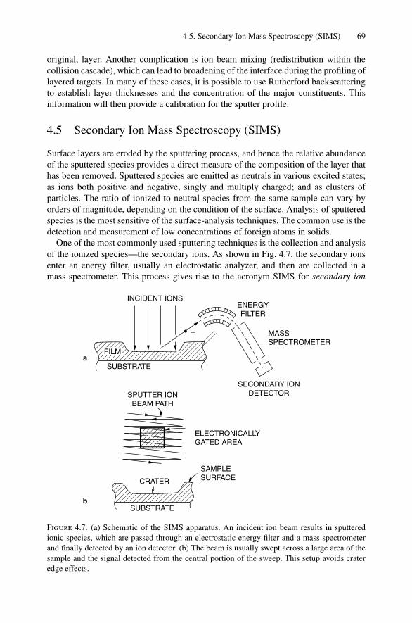
4.5. Secondary Ion Mass Spectroscopy (SIMS) 69
original, layer. Another complication is ion beam mixing (redistribution within thecollision cascade), which can lead to broadening of the interface during the profiling oflayered targets. In many of these cases, it is possible to use Rutherford backscatteringto establish layer thicknesses and the concentration of the major constituents. Thisinformation will then provide a calibration for the sputter profile.
4.5 Secondary Ion Mass Spectroscopy (SIMS)
Surface layers are eroded by the sputtering process, and hence the relative abundanceof the sputtered species provides a direct measure of the composition of the layer thathas been removed. Sputtered species are emitted as neutrals in various excited states;as ions both positive and negative, singly and multiply charged; and as clusters ofparticles. The ratio of ionized to neutral species from the same sample can vary byorders of magnitude, depending on the condition of the surface. Analysis of sputteredspecies is the most sensitive of the surface-analysis techniques. The common use is thedetection and measurement of low concentrations of foreign atoms in solids.
One of the most commonly used sputtering techniques is the collection and analysisof the ionized species—the secondary ions. As shown in Fig. 4.7, the secondary ionsenter an energy filter, usually an electrostatic analyzer, and then are collected in amass spectrometer. This process gives rise to the acronym SIMS for secondary ion
+
a
b
SECONDARY IONDETECTOR
ELECTRONICALLYGATED AREA
SPUTTER IONBEAM PATH
SUBSTRATE
INCIDENT IONSENERGYFILTER
MASSSPECTROMETER
SAMPLESURFACECRATER
SUBSTRATE
FILM
Figure 4.7. (a) Schematic of the SIMS apparatus. An incident ion beam results in sputteredionic species, which are passed through an electrostatic energy filter and a mass spectrometerand finally detected by an ion detector. (b) The beam is usually swept across a large area of thesample and the signal detected from the central portion of the sweep. This setup avoids crateredge effects.
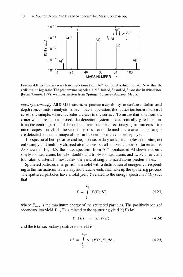
70 4. Sputter Depth Profiles and Secondary Ion Mass Spectroscopy
MASS NUMBER
ION
YIE
LD
10−10
10−11
10−12
10−13
10−140 20 40 60 80 100
AI3
AI2AI2
AI3
AI4
AI+AI+
AI
Ar+
+
++
+
+
Figure 4.8. Secondary ion cluster spectrum from Ar+ ion bombardment of Al. Note that theordinate is a log scale. The predominant species is Al+, but Al2
+: and Al3+: are also in abundance.
[From Werner, 1978, with permission from Springer Science+Business Media.]
mass spectroscopy. All SIMS instruments possess a capability for surface and elementaldepth concentration analysis. In one mode of operation, the sputter ion beam is rasteredacross the sample, where it erodes a crater in the surface. To insure that ions from thecrater walls are not monitored, the detection system is electronically gated for ionsfrom the central portion of the crater. There are also direct imaging instruments—ionmicroscopes—in which the secondary ions from a defined micro-area of the sampleare detected so that an image of the surface composition can be displayed.
The spectra of both positive and negative secondary ions are complex, exhibiting notonly singly and multiply charged atomic ions but all ionized clusters of target atoms.As shown in Fig. 4.8, the mass spectrum from Ar+-bombarded Al shows not onlysingly ionized atoms but also doubly and triply ionized atoms and two-, three-, andfour-atom clusters. In most cases, the yield of singly ionized atoms predominates.
Sputtered particles emerge from the solid with a distribution of energies correspond-ing to the fluctuations in the many individual events that make up the sputtering process.The sputtered particles have a total yield Y related to the energy spectrum Y (E) suchthat
Y =Emax∫0
Y (E) dE, (4.23)
where Emax is the maximum energy of the sputtered particles. The positively ionizedsecondary ion yield Y +(E) is related to the sputtering yield Y (E) by
Y +(E) = α+(E)Y (E), (4.24)
and the total secondary positive ion yield is
Y + =Emax∫0
α+(E)Y (E) dE, (4.25)
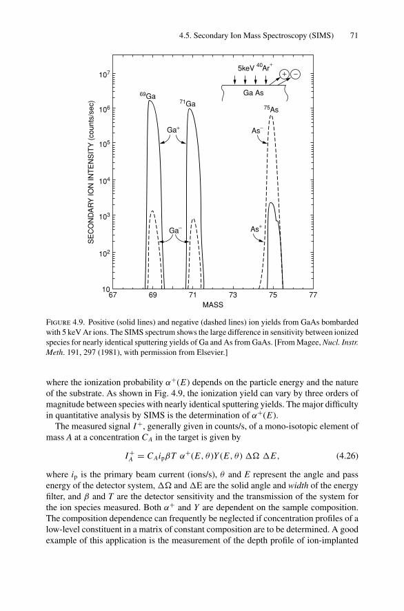
4.5. Secondary Ion Mass Spectroscopy (SIMS) 71
107
106
105
104
103
102
10
SE
CO
ND
AR
Y IO
N IN
TE
NS
ITY
(co
unts
/sec
)
MASS67 69 71 73 75 77
As+
Ar+
Ga−
As−Ga+
Ga As69Ga71Ga 75As
5keV 40
+ −
Figure 4.9. Positive (solid lines) and negative (dashed lines) ion yields from GaAs bombardedwith 5 keV Ar ions. The SIMS spectrum shows the large difference in sensitivity between ionizedspecies for nearly identical sputtering yields of Ga and As from GaAs. [From Magee, Nucl. Instr.Meth. 191, 297 (1981), with permission from Elsevier.]
where the ionization probability α+(E) depends on the particle energy and the natureof the substrate. As shown in Fig. 4.9, the ionization yield can vary by three orders ofmagnitude between species with nearly identical sputtering yields. The major difficultyin quantitative analysis by SIMS is the determination of α+(E).
The measured signal I +, generally given in counts/s, of a mono-isotopic element ofmass A at a concentration CA in the target is given by
I +A = CAipβT α+(E, θ )Y (E, θ ) E, (4.26)
where ip is the primary beam current (ions/s), θ and E represent the angle and passenergy of the detector system, and E are the solid angle and width of the energyfilter, and β and T are the detector sensitivity and the transmission of the system forthe ion species measured. Both α+ and Y are dependent on the sample composition.The composition dependence can frequently be neglected if concentration profiles of alow-level constituent in a matrix of constant composition are to be determined. A goodexample of this application is the measurement of the depth profile of ion-implanted
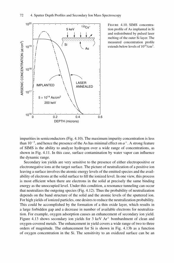
72 4. Sputter Depth Profiles and Secondary Ion Mass Spectroscopy
0 0.2 0.4 0.6DEPTH (microns)
AR
SE
NIC
CO
NC
EN
TR
ATIO
N (
at/c
m3 )
1016
1017
1018
1019
1020
IMPLANTEDLASERANNEALED
5 × 10¹⁴ As/cm2
200 keV
5 keV133Cs+
SiAs
Figure 4.10. SIMS concentra-tion profile of As implanted in Siand redistributed by pulsed lasermelting of the outer Si layer. Themeasured concentration profileextends below levels of 1018/cm3.
impurities in semiconductors (Fig. 4.10). The maximum impurity concentration is lessthan 10−3, and hence the presence of the As has minimal effect on α+. A strong featureof SIMS is the ability to analyze hydrogen over a wide range of concentrations, asshown in Fig. 4.11. In this case, surface contamination by water vapor can influencethe dynamic range.
Secondary ion yields are very sensitive to the presence of either electropositive orelectronegative ions at the target surface. The picture of neutralization of a positive ionleaving a surface involves the atomic energy levels of the emitted species and the avail-ability of electrons at the solid surface to fill the ionized level. In one view, this processis most efficient when there are electrons in the solid at precisely the same bindingenergy as the unoccupied level. Under this condition, a resonance tunneling can occurthat neutralizes the outgoing species (Fig. 4.12). Thus the probability of neutralizationdepends on the band structure of the solid and the atomic levels of the sputtered ion.For high yields of ionized particles, one desires to reduce the neutralization probability.This could be accomplished by the formation of a thin oxide layer, which results ina large forbidden gap and a decrease in number of available electrons for neutraliza-tion. For example, oxygen adsorption causes an enhancement of secondary ion yield.Figure 4.13 shows secondary ion yields for 3 keV Ar+ bombardment of clean andoxygen-covered metals. The enhancement in yield covers a wide range of two to threeorders of magnitude. The enhancement for Si is shown in Fig. 4.13b as a functionof oxygen concentration in the Si. The sensitivity to an oxidized surface can be an
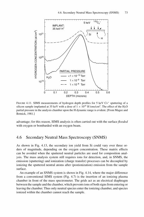
4.6. Secondary Neutral Mass Spectroscopy (SNMS) 73
PARTIAL PRESSURE
<1 × 10⁻¹⁰ Torr
1 × 10⁻⁹ Torr
1 × 10⁻⁸ Torr
0 0.20.1 0.3 0.4 0.5 0.6DEPTH (microns)
1019
1020
1021
5 keV133Cs
+
SiH
YD
RO
GE
N C
ON
CE
NT
RAT
ION
(at
/cm
3 )
IMPLANT:35 keV H+
H
H2O
Figure 4.11. SIMS measurements of hydrogen depth profiles for 5 keV Cs+ sputtering of asilicon sample implanted at 35 keV with a dose of 1 × 10¹⁸ H ions/cm2. The effect of the H2Opartial pressure in the analysis chamber upon the H dynamic range is evident. [From Magee andBotnick, 1981.]
advantage; for this reason, SIMS analysis is often carried out with the surface floodedwith oxygen or bombarded with an oxygen beam.
4.6 Secondary Neutral Mass Spectroscopy (SNMS)
As shown in Fig. 4.13, the secondary ion yield from Si could vary over three or-ders of magnitude, depending on the oxygen concentration. These matrix effectscan be avoided when the sputtered neutral particles are used for composition anal-ysis. The mass analysis system still requires ions for detection, and, in SNMS, theemission (sputtering) and ionization (charge transfer) processes can be decoupled byionizing the sputtered neutral atoms after (postionization) emission from the samplesurface.
An example of an SNMS system is shown in Fig. 4.14, where the major differencefrom a conventional SIMS system (Fig. 4.7) is the insertion of an ionizing plasmachamber in front of the mass spectrometer. The grids act as an electrical diaphragmbetween the sample and the chamber, which prevents ions of both signs from entering orleaving the chamber. Thus only neutral species enter the ionizing chamber, and speciesionized within the chamber cannot reach the sample.
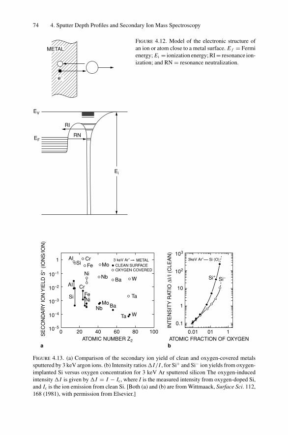
74 4. Sputter Depth Profiles and Secondary Ion Mass Spectroscopy
EV
EF
Ei
RI
RN
e−
METAL
Figure 4.12. Model of the electronic structure ofan ion or atom close to a metal surface. E f = Fermienergy; Ei = ionization energy; RI = resonance ion-ization; and RN = resonance neutralization.
ATOMIC NUMBER Z2
SE
CO
ND
AR
Y IO
N Y
IELD
S+
(IO
NS
/ION
)
0 20 40 60 80 10010−5
10−4
10−3
10−2
10−1
1 AI
AI
Si
Si
Ni
Ni
Cr
Cr
Fe
Fe
Nb
Nb
Ba
Ba
Mo
MoTa
Ta
W
W
CLEAN SURFACEOXYGEN COVERED
METAL3 keV Ar+
Si+ Si−
0.01 01
0.1
1
1
103
102
10
INT
EN
SIT
Y R
ATIO
∆I/
I (C
LEA
N)
ATOMIC FRACTION OF OXYGEN
3keV Ar+ Si (O)
a b
Figure 4.13. (a) Comparison of the secondary ion yield of clean and oxygen-covered metalssputtered by 3 keV argon ions. (b) Intensity ratios I/I , for Si+ and Si− ion yields from oxygen-implanted Si versus oxygen concentration for 3 keV Ar sputtered silicon The oxygen-inducedintensity I is given by I = I − Ic, where I is the measured intensity from oxygen-doped Si,and Ic is the ion emission from clean Si. [Both (a) and (b) are from Wittmaack, Surface Sci. 112,168 (1981), with permission from Elsevier.]
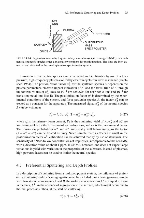
4.7. Preferential Sputtering and Depth Profiles 75
GRIDS
SAMPLE
IONGUN
DETECTOR
QUADRUPOLEMASSSPECTROMETER
PLASMA
Figure 4.14. Apparatus for conducting secondary neutral mass spectroscopy (SNMS), in whichneutral sputtered species enter a plasma environment for postionization. The ions are then ex-tracted and detected in the quadruple mass spectrometer system.
Ionization of the neutral species can be achieved in the chamber by use of a low-pressure, high-frequency plasma excited by electron cyclotron wave resonance (Oech-sner, 1984). The postionization factor α0
A for the sputtered species A depends on theplasma parameters, electron impact ionization of A, and the travel time of A throughthe ionizer. Values of α0
A close to 10−1 are achieved for near noble ions and 10−2 fortransition metal ions like Ta. The postionization factor α0 is determined by the exper-imental conditions of the system, and for a particular species A, the factor α0
A can betreated as a constant for the apparatus. The measured signal α0
A of the neutral speciesA can be written as
I 0A = ip YA α0
A (1 − α+A − α−
A ) η0A, (4.27)
where ip is the primary beam current, YA is the sputtering yield of A, α+A and α−
A areionization yields for the formation of secondary ions, and ηA is the instrumental factor.The ionization probabilities α+ and α− are usually well below unity, so the factor(1 − α+ − α−) can be treated as unity. Since sample matrix effects are small in thepostionization factor α0, calibration can be achieved readily by use of standards. Thesensitivity of SNMS to low concentrations of impurities is comparable to that of SIMS,with a detection value of about 1 ppm. In SNMS, however, one does not expect largevariations in yield with variation in the properties of the substrate. Instead of plasmas,high-powered lasers can be used to ionize the neutral species.
4.7 Preferential Sputtering and Depth Profiles
In a description of sputtering from a multicomponent system, the influence of prefer-ential sputtering and surface segregation must be included. For a homogeneous samplewith two atomic components A and B, the surface concentrations C s are equal to thosein the bulk, Cb, in the absence of segregation to the surface, which might occur due tothermal processes. Then, at the start of sputtering,
C sA/C s
B = CbA/Cb
B . (4.28)
76 4. Sputter Depth Profiles and Secondary Ion Mass Spectroscopy
The partial yield of atomic species A and B is defined as in Eq. 4.1 by
YA,B = Number of elected atoms A, B
Incident particle, (4.29)
where the partial sputtering yield YA of species A is proportional to the surface concen-tration C s
A, and similarly, YB is proportional to CsB . The ratio of partial yields is given
by
YA
YB= f AB
C sA
C sB
, (4.30)
where the sputtering factor f AB takes into account differences in surface binding ener-gies, sputter escape depths, and energy transfers within the cascade. Measured valuesof f AB generally are in the range between 0.5 and 2.
In the case where f AB is unity, YA/YB = C sA/C s
B , and the yield of sputtered particlesis a direct measure of the bulk concentration ratio. In the case where f AB = 1, the surfaceconcentrations and yields will change from their initial values, C s
A(0) and YA(0), to theirvalues Y s
A(∞) and YA(∞) at long times when steady state is achieved.At the start of sputtering, t = 0,
YA(0)
YB(0)= f AB
C sA(0)
C sB(0)
= f ABCb
A
CbB
. (4.31)
At long times, when steady-state conditions have been achieved, conservation of massrequires that the ratios of partial yields equal the bulk concentration ratio,
YA(∞)
YB(∞)= Cb
A
CbB
. (4.32)
For example, if there is preferential sputtering where f AB > 1, the sputtering yield ofA is greater than that of B, and the surface will be enriched in B. This enrichment of thesurface produces an increase in the sputtering yield of B (more B atoms) and a decreasein the sputtering yield of A (less A atoms). As the process continues with macroscopicamounts (greater than 10 nm) of material removed, the increased concentration of Bjust balances out the preferential sputtering of A. Therefore, at steady state, the surfaceconcentration ratio will differ from that of the bulk when fAB = 1:
CA(∞)
CB(∞)= 1
f AB· Cb
A
CbB
. (4.33)
That is, the surface composition is rearranged so that the total sputtering yield givesthe bulk composition in spite of differences in yields of the individual atomic species.Analysis of the composition of the remaining surface layer at this point would show adifference from that of the bulk composition.
An example of the change in composition of a silicide layer is shown in Fig. 4.15for PtSi that was sputtered with 20 keV argon ions and then analyzed with 2 MeV4He+ ions. The Rutherford backscattering spectrum shows an enrichment of the Ptconcentration in the surface region. The ratio of Pt/Si increased from the value of unityassociated with that of the bulk values to a value near two in the surface region. Theincrease in the Pt concentration is due to the fact that the partial sputtering yield of Si is
4.8. Interface Broadening and Ion Mixing 77
0.8
1.6
3.2
4.8
6.4
8.0
9.6
1.00 1.25 1.50 1.75ENERGY (MeV)
BA
CK
SC
ATT
ER
ING
YIE
LD (
CO
UN
TS
× 1
0−3)
PtSi
PtSiSi
PtSi
Ar
4He
Pt ENRICHMENT
20 keV Ar SPUTTERING OF PtSi
Figure 4.15. RBS spectrum of a PtSi film after sputtering with 20 keV Ar ions. The shadedportion in this Pt signal indicates an increase in the concentration of Pt in the near-surface regionas a result of the enhanced Si sputtering. [From Liau et al., J. Appl. Phys. 49, 5295 (1978).Copyright 1978 by the American Physical Society.]
greater than that of Pt, YSi > YPt. Figure 4.16 shows the partial yields as a function ofargon ion dose. As one would expect, at low bombardment doses the sputtering yieldof Si is significantly greater than that of Pt. At the onset of sputtering, the yield ratioYSi(0)/YPt(0) = 2.4. As the bombardment proceeds, the partial sputtering yields mergeinto the same value. The equality of the Si and Pt yields merely reflects the fact thatthe yield ratio, after steady state has been reached, is equal to the bulk concentrationratio, which for PtSi is unity.
4.8 Interface Broadening and Ion Mixing
One of the applications of sputtering is the removal of deposited or grown layers in thinfilm structures in order to analyze the composition at the interface between the filmand substrate. In these applications, the penetration of the ions used in the sputteringbeam can induce an intermixing between the film and substrate due to the strong atomicdisplacements and diffusion that occurs within the collision cascade around the trackof the ion used in sputtering. This intermixing leads to an artificial broadening of theconcentration depth profiles at the interface.
Sputtering requires bombardment of the surface with primary ions of appreciableenergy (typically 1–20 keV) whose range far exceeds the escape depth of the sputteredions and often exceeds the observation depth in electron spectroscopies. Therefore,due to the ion-induced intermixing in the collision cascade, a zone of altered mate-rial precedes the analytical zone during layer removal. Ion mixing is illustrated inFig. 4.17 for SIMS analysis of a Pt film deposited on Si and sputtered by argon ions.
78 4. Sputter Depth Profiles and Secondary Ion Mass Spectroscopy
0 0.5 1.0ARGON FLUENCE
(1017 ions/cm2)
PAR
TIA
LS
PU
TT
ER
ING
YIE
LD
1
2
3
YSi
YPt
Pt Si
40 keV Ar+
Figure 4.16. Dose dependence of the partial sputtering yields of Si and Pt emitted from PtSifor 40 keV Ar bombardment, where fluence denotes dose. [From Liau and Mayer, 1980.]
When the argon ions penetrate through the Pt/Si interface, some of the Si atoms inthe substrate will be transported to the top surface of the Pt film, where they can besputtered. Thus a silicon signal will appear before the Pt film is sputtered away. Plat-inum is also intermixed with the Si, and, consequently, a Pt signal will persist in theSIMS spectrum at depths well beyond the thickness of the original deposited layerof Pt.
An estimate of the interfacial broadening in such systems can be made by setting therange R of the sputtering ion equal to the half-width of the broadened signal. The ion
INCREASED SPUTTERING TIME
Ar+
Ar+
Ar+
Si
SiSiSi
Si
Si
Pt
Pt
Pt
Ptin
PtPt
Figure 4.17. Schematic diagram of Ar+ ion sputtering of a 100 nm Pt layer on Si at threedifferent times in the sputtering process. When the Ar range is less than the Pt film thickness,only Pt ions are sputtered. When the Ar ion penetrates through the Pt/Si interface, ion-inducedintermixing occurs, and a Si signal is found in the sputtering yield. After the initial Pt film hasbeen removed, a Pt signal is still observed due to mixing of Pt into the substrate Si. [From Liauet al., J. Vac. Sci. Technol. 16, 121 (1979).]
4.8. Interface Broadening and Ion Mixing 79
range is given by
R =0∫
E0
1
dE/dxdE, (4.34)
which can be approximated for medium mass ions in the keV energy range by assumingthat nuclear energy loss dominates and has an energy-independent value,
R = E0/(dE/dx)n, (4.35)
where (dE/dx)n is given by Eq. 4.19. The value of (dE/dx)n for Ar+ ions in Cu is about1000 eV/nm, which is the basis for the rule of thumb that the altered layer extends1 nm/keV.
The amount of interface broadening can be minimized by proper choice of ion ener-gies and incident angles during sputter profiling. In many cases, sputter depth profilescan have a better depth resolution than that obtained with backscattering spectrometry.
When possible, it is advantageous to use two or more analytical techniques that pro-vide complementary data. Figure 4.18 shows the analysis of a tungsten silicide film onpolycrystalline silicon (poly-Si). Secondary ion mass spectroscopy (Fig. 4.18a) is usedto determine the phosphorus concentration in polycrystalline Si and to detect oxygencontamination at the interface. Backscattering spectrometry (Fig. 4.18b) provides thedepth scale and the composition of the sputter-deposited silicide—in this case, 183 nmof WSi2.7. In the SIMS data, the phosphorus concentration in poly-Si was calibratedfrom a standard obtained by implanting phosphorus into a silicon sample.
The ratio of W to Si signals in SIMS data (Fig. 4.18a) does not reflect the silicidecomposition, and there is an order-of-magnitude increase in the Si signal going fromthe silicide into the Si. These effects are due to the influence of the matrix on theyield of secondary ions. The peak in the W signal at the silicide/Si interface is dueto the enhancement of the W ion yield because of oxygen at the interface (note alsothe enhancement of the phosphorus yield at the Si/SiO2 interface). The RBS spectrum
SIMS
Si
SiO2
P
'O
W
POLY SiW Six
O (arb. units)
Si(arb. units)
W (arb. units)
SPUTTER TIME (seconds)0
1018
1019
1020
1021
200 400 600 800 1000 1200 1400
PH
OS
. CO
NC
. (at
oms/
cm3 )
a b800 1000 1200 1400 1600 1800
ENERGY (MeV)
RB
S Y
IELD
(co
unts
)
RBS (4He)
TUNGSTEN INTUNGSTEN SILICIDE
POLYCRYSTALLINE SILICONSILICON INTUNGSTEN SILICIDE
SILICIDE: 183 nmPOLY Si = 215 nmWSix = WSi2.7
Figure 4.18. (a) Secondary ion mass spectroscopy (SIMS) and (b) Rutherford backscatteringspectrometry (RBS) analysis of a tungsten silicide layer sputter deposited on a phosphorus-dopedpolycrystalline silicon layer on a layer of SiO2 on silicon.
80 4. Sputter Depth Profiles and Secondary Ion Mass Spectroscopy
(Fig. 4.18b) shows that there is no peak in the W distribution at the interface and that thecomposition of the silicide is WSi2.7. The increase in the Si signal around 950 keV isdue to the increase in Si concentration going from silicide to Si, and the decrease around800 keV is due to the presence of a layer of SiO2 70 nm thick at the interface betweenthe poly-Si layer and substrate Si. The signal from the 1 atomic % of phosphorus inthe poly-Si cannot be detected in the RBS spectrum but is easily detected in the SIMSdata. The amount of interface broadening is minimal in the depth profile of the SIMSdata, and the concentration of light mass elements (oxygen and phosphorus) can easilybe detected. The strong influence of the matrix on the ion yield does not allow anaccurate determination of the relative concentration of the major constituents (tungstenand silicon). These quantities are found along with layer thickness from the Rutherfordbackscattering spectrum. By the use of two complementary analytical techniques (RBSand SIMS), a rather accurate picture of the composition of the sample can be obtained.
4.9 Thomas–Fermi Statistical Model of the Atom
In low-velocity collisions, the impact parameter is sufficiently large such that the nu-clear charge is screened by the electrons. This leads to a modification of the scatteringpotential from that of the unscreened Coulomb potential, V = Z1 Z2e2/r . The modi-fied potential is found from the Thomas–Fermi description, which treats all atoms asidentical aside from scaling factors.
The Thomas–Fermi model assumes that the electrons can then be treated by statisticalmechanics, Fermi–Dirac statistics, in which they behave as an ideal gas of particlesthat fills the potential well around the positively charged core. The density of states,n(E), of a free electron gas is obtained by applying periodic boundary conditions andbox normalization to a cell of length L to give
n(E) = L3
2π2h--3(2m)3/2 E1/2. (4.36)
The energy of the gas increases as the number of electrons increases. For a collectionof electrons, the number at a point r, Z (r ), is given by
Z (r ) =EF(r )∫0
n(E) dE = L3(2m)3/2
2π2h--3
EF(r )∫0
E1/2dE = L3(2m)3/2
3π2h--3EF(r )3/2, (4.37)
where EF(r ) is associated with the maximum energy of the ensemble of electrons at r.The Fermi energy is simply the energy of the highest filled state. In the many-electronatom that we are considering, the total energy Er of an electron is Er = EK + V (r ),where EK is the kinetic energy. For a bound electron, Er ≤ 0, which requires that forthe maximum kinetic energy electron, EF = −V (r ). From Eq. 4.37,
ρ(r ) = Z (r )
L3= (2m)3/2
3π2h--3[−V (r )]3/2. (4.38)
The self-consistency condition is that the potential due to the electron density in Eq.4.38, as well as that due to the nuclear charge, properly reproduces the potential
Problems 81
energy, −V (r ). Consequently, the charge density, −eρ, and the electrostatic poten-tial, −[V (r )/e], must satisfy Poisson’s equation
−1
e∇2V = − 4π (−eρ),
or
∇2V = 1
r2
d
dr
(r2 dV
dr
)= 4πe2ρ = 4e2[−2mV (r )]3/2
3πh--3. (4.39)
Equations 4.38 and 4.39 may be solved simultaneously for ρ and V, with boundaryconditions as follows: As r → 0, the leading term in the potential energy must be dueto the nucleus, so that V (r ) → −Ze2/r , and as r → ∞, there must be no net chargeinside the sphere of radius r, so that V falls off more rapidly than 1/r, and r V (r ) → 0.Equation 4.39 and the boundary conditions given above are conveniently expressed ina dimensionless form in which Z , E, m, and h appear only in scale factors. We put
V (r ) = − Ze2
rχ, r = ax,
and
a = 1
2
(3π
4
)2/3 h--2
me2 Z1/3= 0.885a0
Z1/3, (4.40)
where a0 = h--2/me2, the Bohr radius. Eq. 4.8 indicates that the scaling parameter todescribe the size of an atom is inversely proportional to the cube root of the atomicnumber. (For electron spectroscopies where transitions are between core levels, the 1sradius is approximated by a0/Z .) With these substitutions, Eq. 4.39 becomes
x1/2 d2χ
dx2= χ3/2. (4.41)
In this dimensionless Thomas–Fermi (TF) equation, the potential behaves like asimple Coulomb interaction in the extreme case as r → 0. The accurate solution ofEq. 4.41 is done numerically, and there are also analytical approximations representedin series expansions or exponentials. The Moliere approximation to the Thomas–Fermiscreening function shown in Fig. 4.4 is most often used in computer simulations andis given by
χ (x) = 0.35e−0.3x + 0.55e−1.2x + 0.10e−6.0x, (4.42)
where x = r/a.
Problems
4.1. The maximum value of the nuclear energy loss occurs at the reduced energyvalue of 0.3 for the Thomas–Fermi potential. What energy in keV does ε′ = 0.3correspond to for Ar+ ion incident on Si?
4.2. Assuming nuclear energy loss dominates and the stopping cross section is energyindependent, what is the range of 10 keV Ar ions incident on Cu?
82 4. Sputter Depth Profiles and Secondary Ion Mass Spectroscopy
4.3. For a screened Coulomb collision with χ = a/2r , use the impulse approximationto show that b, the impact parameter, is proportional to (a/Eθ)1/2, and derive σ (θ),the cross section.
4.4. Calculate the ratio of the unscreened to screened nuclear cross section dσ/dT forthe following cases: 2.0 MeV He+ on Au, 0.1 MeV He+ on Au, and 1 keV Ar+
on Cu.4.5. For a scattering potential V (r ) ∝ r−3, what is the energy dependence of the
energy loss dE/dx?4.6. Calculate the sputtering yield for 45 keV Ar ions incident on Si (U0 = 4.5 eV)
using a screened potential. Compare your answer with the data given in Figure 4.2.4.7. If the sputtering yield of species A is twice that of species B in a matrix AB, what
is the ratio A to B of the flux of sputtered species at (a) the initial time and (b) thesteady-state time, and what is the ratio A to B of surface composition at (c) theinitial time and (d) the steady-state time?
4.8. Determine the time in seconds required to sputter 50 nm of Si using a 10 µA/cm2
beam of 45 keV ions of (a) Ne, (b) Kr, and (c) Xe. (Use data given by the solidline in Fig. 4.2.)
References
1. E. E. Anderson, Modern Physics and Quantum Mechanics (W. B. Saunders Co., Philadelphia,1971).
2. H. H. Anderson and H. L. Bay, “Sputtering Yield Measurements,” in Sputtering by ParticleBombardment I, R. Behrisch, Ed. (Springer-Verlag, New York, 1981), Chapter 4.
3. R. Behrisch, Ed., Sputtering by Particle Bombardment I and II (Springer-Verlag, New York,1981 and 1983).
4. G. Carter and J. S. Colligon, Ion Bombardment of Solids (Elsevier Science Publishing Co.,New York, 1968).
5. G. Carter, B. Narvinsek, and J. L. Whitton, “Heavy Ion Sputtering Induced Surface Topog-raphy Development,” in Sputtering by Particle Bombardment II, R. Behrisch, Ed. (Springer-Verlag, New York, 1983).
6. W. K. Chu, “Energy Loss of High Velocity Ions in Matter,” in Atomic Physics, P. Richard,Ed., Methods of Experimental Physics, Vol. 17 (Academic Press, New York, 1980),Chapter 2.
7. Z. L. Liau and J. W. Mayer, “Ion Bombardment Effects on Material Composition,” in IonImplantation, J. K. Hirvonen, Ed., Treatise on Materials Science and Technology, Vol. 18,N. Herman, Ed. (Academic Press, New York, 1980), Chapter 2.
8. J. Lindhard, M. Scharff, and H. E. Schiott, “Range Concepts and Heavy Ion Ranges (Noteson Atomic Collision, II),” Mat. Fys. Medd. Dan. Vid. Selsk. 33(14) (1963).
9. C. Magee and E. M. Botnick, J. Vac. Sci. Technol. 19(47) (1981).10. J. A. McHugh, “Secondary Ion Mass Spectrometry,” in Methods of Surface Analysis, A. W.
Czanderna, Ed. (Elsevier Science Publishing Co., New York, 1975), Chapter 6.11. J. M. McCrea, “Mass Spectrometry,” in Characterization of Solid Surfaces, P. F. Kane and
G. B. Larrabee, Eds. (Plenum Press, New York, 1974), Chapter 2.12. H. Oechsner, Ed., Thin Film and Depth Profile Analysis (Springer-Verlag, New York,
1984).13. P. Sigmund, “Sputtering Processes: Collision Cascades and Spikes,” in Inelastic Ion-Surface
Collisions, N. Tolk et al., Eds. (Academic Press, New York, 1977), pp. 121–152.

References 83
14. P. Sigmund, “Sputtering by Ion Bombardment; Theoretical Concepts,” in Sputtering byParticle Bombardment I, R. Behrisch, Ed. (Springer-Verlag, New York, 1981), Chapter 2.
15. I. M. Torrens, Interatomic Potentials (Academic Press, New York, 1972).16. P. D. Townsend, J. C. Kelley, and N. E. W. Hartley, Ion Implantation, Sputtering and Their
Applications (Academic Press, New York, 1976).17. H. W. Werner, “Introduction to Secondary Ion Mass Spectrometry (SIMS),” in Electron and
Ion Spectroscopy of Solids, L. F. Ermans et al., Eds. (Plenum Press, New York, 1978).
5Ion Channeling
5.1 Introduction
The arrangement of atoms in a solid determines the properties of a material and, insingle crystals, determines the magnitude of incident ion–target-atom interactions. Theinfluence of the crystal lattice on the trajectories of ions penetrating into the crystalis known as channeling—a term that visualizes the atomic rows and planes as guidesthat steer energetic ions along the channels between rows and planes. The steeringaction is effective and can lead to hundredfold reductions in the yield of backscatteredparticles. In this chapter, we describe channeling of high-energy ions in single crys-tals and show how use of this technique can improve the depth resolution of the ionscattering technique and improve its sensitivity to light impurities. The combinationof Rutherford backscattering and channeling plays an important role in the materialsanalysis of a variety of thin film/single-crystal problems. Single crystals are not rarein modern-day technology, as all electronic components are based on single-crystalsemiconductors.
5.2 Channeling in Single Crystals
Channeling of energetic ions occurs when the beam is carefully aligned with a ma-jor symmetry direction of a single crystal (Lindhard, 1965). By a major symmetrydirection, we mean one of the open directions as viewed down a row of atoms ina single crystal. Figure 5.1 shows a side view of this process in which most of theion beam is steered (channeled) through the channels formed by the string of atoms.Channeled particles cannot get close enough to the atomic nuclei to undergo large-angle Rutherford scattering; hence, scattering from the substrate is drastically reducedby a factor of ∼100. This improves the ion scattering sensitivity to light impuri-ties on the surface. There is always a full interaction with the first monolayers ofthe solid. This surface interaction results in an improved depth resolution in theseexperiments.
The trajectory of a channeled ion is such that the ion makes a glancing angle impactwith the axes (axial channeling) or planes (planar channeling) of the crystal and issteered by small-angle scattering collisions at distances greater than 0.01 nm from the
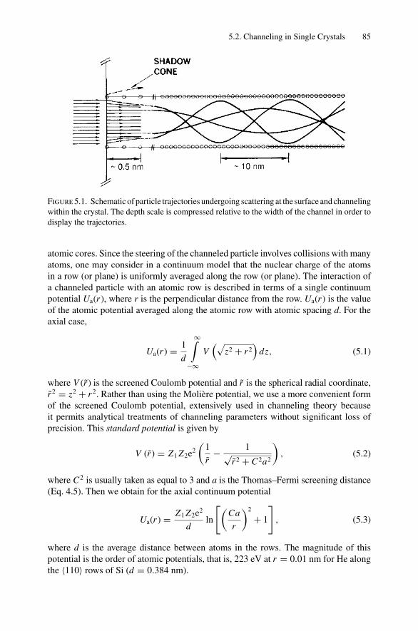
5.2. Channeling in Single Crystals 85
Figure 5.1. Schematic of particle trajectories undergoing scattering at the surface and channelingwithin the crystal. The depth scale is compressed relative to the width of the channel in order todisplay the trajectories.
atomic cores. Since the steering of the channeled particle involves collisions with manyatoms, one may consider in a continuum model that the nuclear charge of the atomsin a row (or plane) is uniformly averaged along the row (or plane). The interaction ofa channeled particle with an atomic row is described in terms of a single continuumpotential Ua(r ), where r is the perpendicular distance from the row. Ua(r ) is the valueof the atomic potential averaged along the atomic row with atomic spacing d. For theaxial case,
Ua(r ) = 1
d
∞∫−∞
V(√
z2 + r2)
dz, (5.1)
where V (r ) is the screened Coulomb potential and r is the spherical radial coordinate,r2 = z2 + r2. Rather than using the Moliere potential, we use a more convenient formof the screened Coulomb potential, extensively used in channeling theory becauseit permits analytical treatments of channeling parameters without significant loss ofprecision. This standard potential is given by
V (r ) = Z1 Z2e2
(1
r− 1√
r2 + C2a2
), (5.2)
where C2 is usually taken as equal to 3 and a is the Thomas–Fermi screening distance(Eq. 4.5). Then we obtain for the axial continuum potential
Ua(r ) = Z1 Z2e2
dln
[(Ca
r
)2
+ 1
], (5.3)
where d is the average distance between atoms in the rows. The magnitude of thispotential is the order of atomic potentials, that is, 223 eV at r = 0.01 nm for He alongthe 〈110〉 rows of Si (d = 0.384 nm).
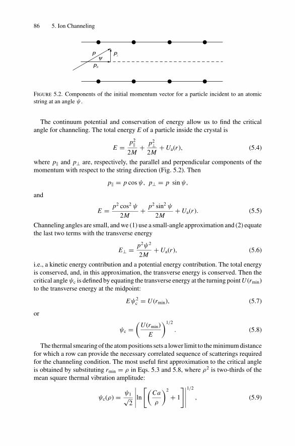
86 5. Ion Channeling
PII
P Py ^
Figure 5.2. Components of the initial momentum vector for a particle incident to an atomicstring at an angle ψ .
The continuum potential and conservation of energy allow us to find the criticalangle for channeling. The total energy E of a particle inside the crystal is
E = p2‖
2M+ p2
⊥2M
+ Ua(r ), (5.4)
where p‖ and p⊥ are, respectively, the parallel and perpendicular components of themomentum with respect to the string direction (Fig. 5.2). Then
p‖ = p cos ψ, p⊥ = p sin ψ,
and
E = p2 cos2 ψ
2M+ p2 sin2 ψ
2M+ Ua(r ). (5.5)
Channeling angles are small, and we (1) use a small-angle approximation and (2) equatethe last two terms with the transverse energy
E⊥ = p2ψ2
2M+ Ua(r ), (5.6)
i.e., a kinetic energy contribution and a potential energy contribution. The total energyis conserved, and, in this approximation, the transverse energy is conserved. Then thecritical angle ψc is defined by equating the transverse energy at the turning point U (rmin)to the transverse energy at the midpoint:
Eψ2c = U (rmin), (5.7)
or
ψc =(
U (rmin)
E
)1/2
. (5.8)
The thermal smearing of the atom positions sets a lower limit to the minimum distancefor which a row can provide the necessary correlated sequence of scatterings requiredfor the channeling condition. The most useful first approximation to the critical angleis obtained by substituting rmin = ρ in Eqs. 5.3 and 5.8, where ρ2 is two-thirds of themean square thermal vibration amplitude:
ψc(ρ) = ψ1√2
∣∣∣∣∣ln[(
Ca
ρ
)2
+ 1
]∣∣∣∣∣1/2
, (5.9)
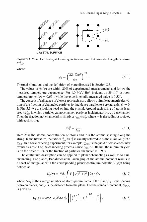
5.2. Channeling in Single Crystals 87
CRYSTAL SURFACE
pr2min
pr20
Figure 5.3. View of an ideal crystal showing continuous rows of atoms and defining the area/row,πr 2
min.
where
ψ1 =(
2Z1 Z2e2
Ed
)1/2
. (5.10)
Thermal vibrations and the definition of ρ are discussed in Section 8.3.The values of ψc(ρ) are within 20% of experimental measurements and follow the
measured temperature dependence. For 1.0 MeV He+ incident on Si〈110〉 at roomtemperature, ψc(ρ) = 0.65, while the experimentally measured value is 0.55.
The concept of a distance of closest approach, rmin, allows a simple geometric deriva-tion of the fraction of channeled particles for incidence parallel to a crystal axis, ψ = 0.In Fig. 5.3, we are looking head-on into the crystal. Around each string of atoms is anarea πr2
min in which particles cannot channel; particles incident at r > rmin can channel.Then the fraction not channeled is simply πr2
min/πr20 , where r0 is the radius associated
with each string:
πr20 = 1
Nd. (5.11)
Here N is the atomic concentration of atoms and d is the atomic spacing along thestring. In the literature, the ratio πr2
min/πr20 is usually referred to as the minimum yield,
χmin. In a backscattering experiment, for example, χmin is the yield of close-encounterevents as a result of the channeling process. Since rmin ∼0.01 nm, the minimum yieldis on the order of 1% or the fraction of particles channeled is ∼99%.
The continuum description can be applied to planar channeling as well as to axialchanneling. For planes, two-dimensional averaging of the atomic potential results ina sheet of charge, as with the corresponding planar continuum potential Up(y) beingdefined as
Up(y) = Ndp
∫V(√
y2 + r2)
2πr dr, (5.12)
where Ndp is the average number of atoms per unit area in the plane, dp is the spacingbetween planes, and y is the distance from the plane. For the standard potential, Up(y)is given by
Up(y) = 2π Z1 Z2e2aNdp
[( y
a
)2+ C2
]1/2
− y
a
. (5.13)
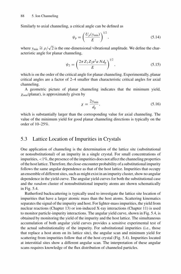
88 5. Ion Channeling
Similarly to axial channeling, a critical angle can be defined as
ψp =(
Up(ymin)
E
)1/2
, (5.14)
where ymin∼= ρ/
√2 is the one-dimensional vibrational amplitude. We define the char-
acteristic angle for planar channeling,
ψ2 =(
2π Z1 Z2e2a Ndp
E
)1/2
, (5.15)
which is on the order of the critical angle for planar channeling. Experimentally, planarcritical angles are a factor of 2–4 smaller than characteristic critical angles for axialchanneling.
A geometric picture of planar channeling indicates that the minimum yield,χmin(planar), is approximately given by
χ = 2ymin
dp, (5.16)
which is substantially larger than the corresponding value for axial channeling. Thevalue of the minimum yield for good planar channeling directions is typically on theorder of 10–25%.
5.3 Lattice Location of Impurities in Crystals
One application of channeling is the determination of the lattice site (substitutionalor nonsubstitutional) of an impurity in a single crystal. For small concentrations ofimpurities,<1%, the presence of the impurities does not affect the channeling propertiesof the host lattice. Therefore, the close-encounter probability of a substitutional impurityfollows the same angular dependence as that of the host lattice. Impurities that occupyan ensemble of different sites, such as might exist in an impurity cluster, show no angulardependence in the yield curve. The angular yield curves for both the substitutional caseand the random cluster of nonsubstitutional impurity atoms are shown schematicallyin Fig. 5.4.
Rutherford backscattering is typically used to investigate the lattice site location ofimpurities that have a larger atomic mass than the host atoms. Scattering kinematicsseparates the signal of the impurity and host. For lighter-mass impurities, the yield fromnuclear reactions (Chapter 13) or ion-induced X-ray interactions (Chapter 11) is usedto monitor particle-impurity interactions. The angular yield curve, shown in Fig. 5.4, isobtained by monitoring the yield of the impurity and the host lattice. The simultaneousaccumulation of both angular yield curves provides a sensitive experimental test ofthe actual substitutionality of the impurity. For substitutional impurities (i.e., thosethat replace a host atom on its lattice site), the angular scan and minimum yield forscattering from impurities follow that of the host crystal (Fig. 5.4). Impurities locatedat interstitial sites show a different angular scan. The interpretation of these angularscans requires knowledge of the flux distribution of channeled particles.
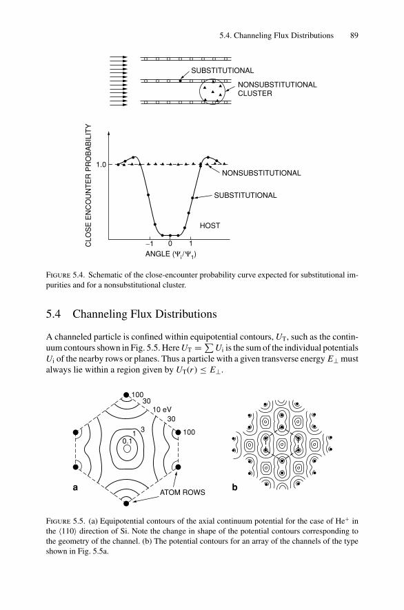
5.4. Channeling Flux Distributions 89
NONSUBSTITUTIONAL
NONSUBSTITUTIONALCLUSTER
SUBSTITUTIONAL
CLO
SE
EN
CO
UN
TE
R P
RO
BA
BIL
ITY
SUBSTITUTIONAL
HOST
−1
1.0
10ANGLE (Ψi /Ψ1)
Figure 5.4. Schematic of the close-encounter probability curve expected for substitutional im-purities and for a nonsubstitutional cluster.
5.4 Channeling Flux Distributions
A channeled particle is confined within equipotential contours, UT, such as the contin-uum contours shown in Fig. 5.5. Here UT =∑Ui is the sum of the individual potentialsUi of the nearby rows or planes. Thus a particle with a given transverse energy E⊥ mustalways lie within a region given by UT(r ) ≤ E⊥.
ATOM ROWSa b
0.11 3
30
30
100
100
10 eV
Figure 5.5. (a) Equipotential contours of the axial continuum potential for the case of He+ inthe 〈110〉 direction of Si. Note the change in shape of the potential contours corresponding tothe geometry of the channel. (b) The potential contours for an array of the channels of the typeshown in Fig. 5.5a.
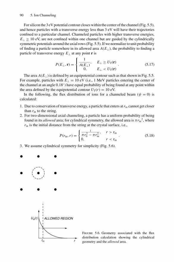
90 5. Ion Channeling
For silicon the 3 eV potential contour closes within the center of the channel (Fig. 5.5),and hence particles with a transverse energy less than 3 eV will have their trajectoriesconfined to a particular channel. Channeled particles with higher transverse energies,E⊥ ≥ 10 eV, are not confined within one channel but are guided by the cylindricallysymmetric potentials around the axial rows (Fig. 5.5). If we normalize to unit probabilityof finding a particle somewhere in its allowed area A(E⊥), the probability to finding aparticle of transverse energy E⊥ at any point r is
P(E⊥, r) =⎧⎨⎩
1
A(E⊥), E⊥ ≥ UT(r)
0, E⊥ < UT(r). (5.17)
The area A(E⊥) is defined by an equipotential contour such as that shown in Fig. 5.5.For example, particles with E⊥ = 10 eV (i.e., 1 MeV particles entering the center ofthe channel at an angle 0.18) have equal probability of being found at any point withinthe area defined by the equipotential contour UT(r ) = 10 eV.
In the following, the flux distribution of ions for a channeled beam (ψ = 0) iscalculated:
1. Due to conservation of transverse energy, a particle that enters at rin cannot get closerthan rin to the string.
2. For two-dimensional axial channeling, a particle has a uniform probability of beingfound in its allowed area; for cylindrical symmetry, the allowed area is πrin
2, whererin is the initial distance from the string at the crystal surface, i.e.,
P(rin, r ) =
1
πr20 − πr2
in, r > rin
0, r < rin
. (5.18)
3. We assume cylindrical symmetry for simplicity (Fig. 5.6).
ALLOWED REGIONUa(r)
rrin
Figure 5.6. Geometry associated with the fluxdistribution calculation showing the cylindricalgeometry and the allowed area.

5.4. Channeling Flux Distributions 91
0
1
2
0.2 0.4 0.6 0.8 1.0
ROW CHANNEL CENTER
DISTANCE FROM ROW (r/r0)
NONCHANNELED
LEVEL
AXIAL CHANNELING(y = 0)
(r/r0)2
FLU
X
Figure 5.7. Flux distribution of the channeled beam as a function of distance from the row forthe case of the parallel incidence. ψ = 0, and assuming statistical equilibrium and cylindricalsymmetry. The small r/r0 approximation (Eq. 5.20) is shown for comparison.
The flux distribution inside the crystal, f (r ), then corresponds to integrating over allinitial impact parameters:
f (r ) =r0∫
0
P(rin, r )2πrin drin
=r0∫
0
1
πr20 − πr2
in
2πrin drin
= lnr2
0
r20 − r2
. (5.19)
The effect of channeling is to transform a spatially uniform distribution to the peakeddistribution shown in Fig. 5.7. This flux distribution displays the most prominent featureof channeling, namely, that the flux intensity and hence the close-encounter probabilityapproaches zero near the atomic rows (as r → 0). Expansion f (r ) for small r, near theatom rows, gives
f (r ) ≈ r2
r20
, (5.20)
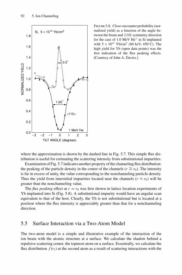
92 5. Ion Channeling
−3 −2 −1 00.0
0.2
0.4
0.6
0.8
1.0
1.2
1.4
1.6
1.8
1 2 3
TILT ANGLE (degrees)
NO
RM
ALI
ZE
D Y
IELD
1 MeV He
<110>
1.65°
0.5°
Si, 5 × 10¹⁴ Yb/cm2
Figure 5.8. Close-encounter probability (nor-malized yield) as a function of the angle be-tween the beam and 〈110〉 symmetry directionfor the case of 1.0 MeV He+ in Si implantedwith 5 × 10¹⁴ Yb/cm2 (60 keV, 450C). Thehigh yield for Yb (open data points) was thefirst indication of the flux peaking effects.[Courtesy of John A. Davies.]
where the approximation is shown by the dashed line in Fig. 5.7. This simple flux dis-tribution is useful for estimating the scattering intensity from substitutional impurities.
Examination of Fig. 5.7 indicates another property of the channeling flux distribution:the peaking of the particle density in the center of the channels (r ∼= r0). The intensityis far in excess of unity, the value corresponding to the nonchanneling particle density.Thus the yield from interstitial impurities located near the channels (r ≈ r0) will begreater than the nonchanneling value.
The flux peaking effect at r = r0 was first shown in lattice location experiments ofYb implanted into Si (Fig. 5.8). A substitutional impurity would have an angular scanequivalent to that of the host. Clearly, the Yb is not substitutional but is located at aposition where the flux intensity is appreciably greater than that for a nonchannelingdirection.
5.5 Surface Interaction via a Two-Atom Model
The two-atom model is a simple and illustrative example of the interaction of theion beam with the atomic structure at a surface. We calculate the shadow behind arepulsive scattering center, the topmost atom on a surface. Essentially, we calculate theflux distribution f (r2) at the second atom as a result of scattering interactions with the
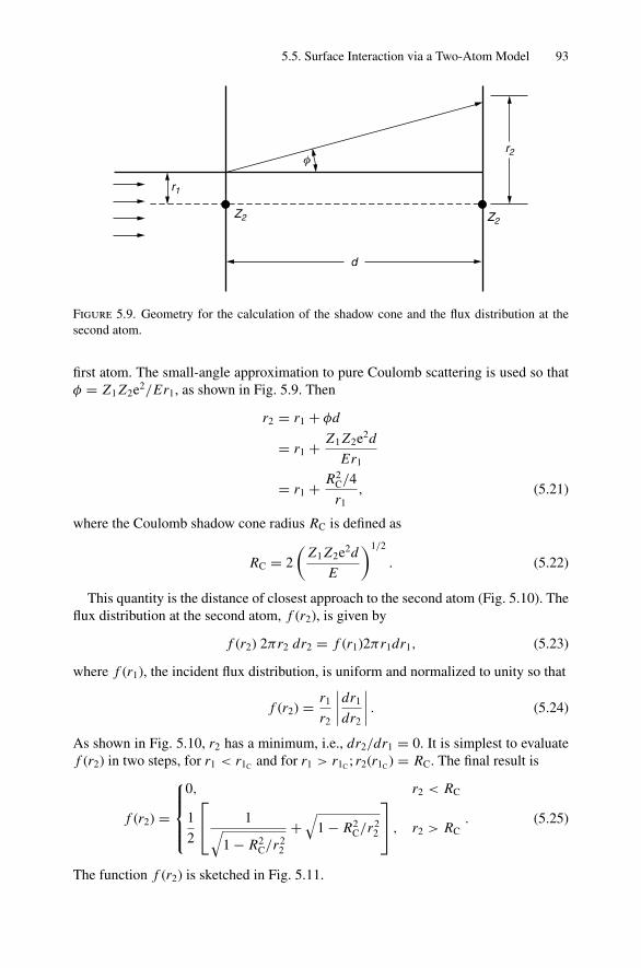
5.5. Surface Interaction via a Two-Atom Model 93
d
Z2 Z2
r2
r1
φ
Figure 5.9. Geometry for the calculation of the shadow cone and the flux distribution at thesecond atom.
first atom. The small-angle approximation to pure Coulomb scattering is used so thatφ = Z1 Z2e2/Er1, as shown in Fig. 5.9. Then
r2 = r1 + φd
= r1 + Z1 Z2e2d
Er1
= r1 + R2C/4
r1, (5.21)
where the Coulomb shadow cone radius RC is defined as
RC = 2
(Z1 Z2e2d
E
)1/2
. (5.22)
This quantity is the distance of closest approach to the second atom (Fig. 5.10). Theflux distribution at the second atom, f (r2), is given by
f (r2) 2πr2 dr2 = f (r1)2πr1dr1, (5.23)
where f (r1), the incident flux distribution, is uniform and normalized to unity so that
f (r2) = r1
r2
∣∣∣∣dr1
dr2
∣∣∣∣ . (5.24)
As shown in Fig. 5.10, r2 has a minimum, i.e., dr2/dr1 = 0. It is simplest to evaluatef (r2) in two steps, for r1 < r1C and for r1 > r1C ; r2(r1C ) = RC. The final result is
f (r2) =
⎧⎪⎪⎨⎪⎪⎩
0, r2 < RC
1
2
⎡⎣ 1√
1 − R2C/r2
2
+√
1 − R2C/r2
2
⎤⎦ , r2 > RC
. (5.25)
The function f (r2) is sketched in Fig. 5.11.
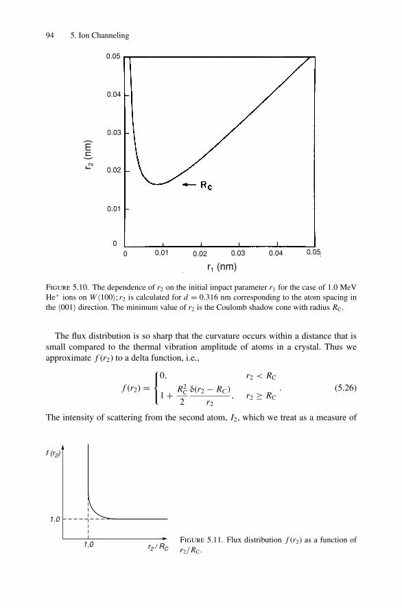
94 5. Ion Channeling
r1 (nm)
r 2 (
nm)
0.01
0.01
0.02
0.02
0.03
0.03
0.04
0.04 0.05
0.05
00
Figure 5.10. The dependence of r2 on the initial impact parameter r1 for the case of 1.0 MeVHe+ ions on W 〈100〉; r2 is calculated for d = 0.316 nm corresponding to the atom spacing inthe 〈001〉 direction. The minimum value of r2 is the Coulomb shadow cone with radius RC.
The flux distribution is so sharp that the curvature occurs within a distance that issmall compared to the thermal vibration amplitude of atoms in a crystal. Thus weapproximate f (r2) to a delta function, i.e.,
f (r2) =⎧⎨⎩
0, r2 < RC
1 + R2C
2
δ(r2 − RC )
r2, r2 ≥ RC
. (5.26)
The intensity of scattering from the second atom, I2, which we treat as a measure of
1.0
1.0
r2 / RC
f (r2)
Figure 5.11. Flux distribution f (r2) as a function ofr2/RC.
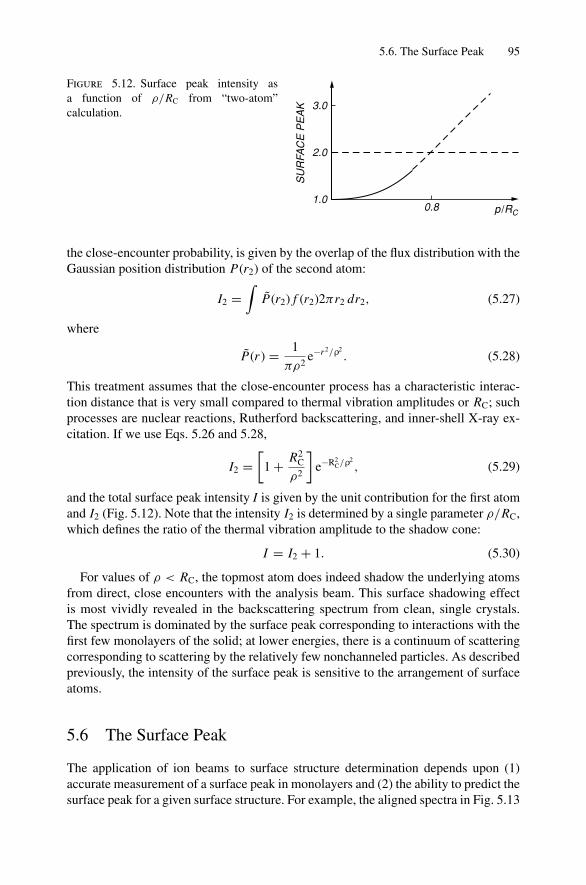
5.6. The Surface Peak 95
1.0
2.0
3.0
0.8 p/RC
SU
RFA
CE
PE
AK
Figure 5.12. Surface peak intensity asa function of ρ/RC from “two-atom”calculation.
the close-encounter probability, is given by the overlap of the flux distribution with theGaussian position distribution P(r2) of the second atom:
I2 =∫
P(r2) f (r2)2πr2 dr2, (5.27)
where
P(r ) = 1
πρ2e−r2/ρ2
. (5.28)
This treatment assumes that the close-encounter process has a characteristic interac-tion distance that is very small compared to thermal vibration amplitudes or RC; suchprocesses are nuclear reactions, Rutherford backscattering, and inner-shell X-ray ex-citation. If we use Eqs. 5.26 and 5.28,
I2 =[
1 + R2C
ρ2
]e−R2
C/ρ2, (5.29)
and the total surface peak intensity I is given by the unit contribution for the first atomand I2 (Fig. 5.12). Note that the intensity I2 is determined by a single parameter ρ/RC,which defines the ratio of the thermal vibration amplitude to the shadow cone:
I = I2 + 1. (5.30)
For values of ρ < RC, the topmost atom does indeed shadow the underlying atomsfrom direct, close encounters with the analysis beam. This surface shadowing effectis most vividly revealed in the backscattering spectrum from clean, single crystals.The spectrum is dominated by the surface peak corresponding to interactions with thefirst few monolayers of the solid; at lower energies, there is a continuum of scatteringcorresponding to scattering by the relatively few nonchanneled particles. As describedpreviously, the intensity of the surface peak is sensitive to the arrangement of surfaceatoms.
5.6 The Surface Peak
The application of ion beams to surface structure determination depends upon (1)accurate measurement of a surface peak in monolayers and (2) the ability to predict thesurface peak for a given surface structure. For example, the aligned spectra in Fig. 5.13

96 5. Ion Channeling
ENERGY
BA
CK
SC
ATT
ER
ING
YIE
LDRECONSTRUCTEDSURFACE PEAK
IDEAL SURFACEPEAK
Figure 5.13. Channeling spectrum showing the surface peak for an ideal surface and areconstructed surface.
differ in their surface peak intensity for different surface structures. The reconstructedsurface shows a higher yield than the ideal surface due to surface displacements.
More sophisticated treatments of the surface peak take into account that more thantwo atoms may contribute to the surface peak, and the governing potential is not apure Coulomb description but a screened potential, for example, the Moliere potential.The intensity of the surface peak is established by numerical techniques. The resultsof many calculations demonstrate that the surface peak scaling still holds; the scalingparameter is ρ/RM, where RM is the shadow cone radius associated with the Molierepotential, roughly RM
∼= RC.The values of the surface peak in terms of atoms/row have been calculated for a
broad range of cases in which an ideal surface with a bulklike structure is assumed.The results are plotted in Fig. 5.14, as a universal curve for the intensity of the surfacepeak as a function of ρ/RM, where ρ is the two-dimensional vibrational amplitude.
Four simple cases of surface structure are shown with their corresponding surfacepeak spectra in Fig. 5.15. The dashed spectra represent the scattering yield from a crystalwith an ideal surface for the case where the thermal vibration amplitude ρ is much lessthan the shadow cone radius RM. This condition assures that the surface peak intensitycorresponds to one atom/row in this ideal case. The crystal with a reconstructed surfacewhere the surface atoms are displaced in the plane of the surface (Fig. 5.15b) representsa situation where the second atom is not shadowed. The surface peak intensity in thiscase is twice that of the ideal crystal. To test for relaxation where the surface atoms aredisplaced normal to the surface plane (Fig. 5.15c), one must use nonnormal incidenceso that the shadow cone established by the surface atoms is not aligned with the atomicrows in the bulk. Here, normal incidence would yield a surface peak intensity equivalentto one monolayer. These two measurements, then, at normal and oblique incidencereveal the presence of relaxation. A surface adsorbate atom can shadow the atomsof the substrate if Radsorbate > ρsubstrate. The atomic mass sensitivity of ion scatteringpermits discrimination between substrate and adsorbate. In Fig. 5.15d, the adsorbateis positioned exactly over the surface atoms and hence reduces the substrate surfacepeak.
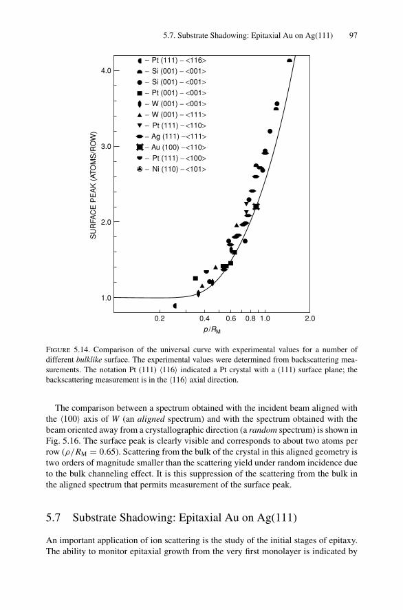
5.7. Substrate Shadowing: Epitaxial Au on Ag(111) 97
Pt (111) − <116>Si (001) − <001>Si (001) − <001>Pt (001) − <001>
Pt (111) − <110>
Pt (111) − <100>Ni (110) − <101>
Ag (111) −<111>Au (100) −<110>
W (001) − <001>W (001) − <111>
−−−−−−−−−−−
2.01.0
1.0
2.0
3.0
4.0
0.80.60.40.2p /RM
SU
RFA
CE
PE
AK
(AT
OM
S/R
OW
)
Figure 5.14. Comparison of the universal curve with experimental values for a number ofdifferent bulklike surface. The experimental values were determined from backscattering mea-surements. The notation Pt (111) 〈116〉 indicated a Pt crystal with a (111) surface plane; thebackscattering measurement is in the 〈116〉 axial direction.
The comparison between a spectrum obtained with the incident beam aligned withthe 〈100〉 axis of W (an aligned spectrum) and with the spectrum obtained with thebeam oriented away from a crystallographic direction (a random spectrum) is shown inFig. 5.16. The surface peak is clearly visible and corresponds to about two atoms perrow (ρ/RM = 0.65). Scattering from the bulk of the crystal in this aligned geometry istwo orders of magnitude smaller than the scattering yield under random incidence dueto the bulk channeling effect. It is this suppression of the scattering from the bulk inthe aligned spectrum that permits measurement of the surface peak.
5.7 Substrate Shadowing: Epitaxial Au on Ag(111)
An important application of ion scattering is the study of the initial stages of epitaxy.The ability to monitor epitaxial growth from the very first monolayer is indicated by
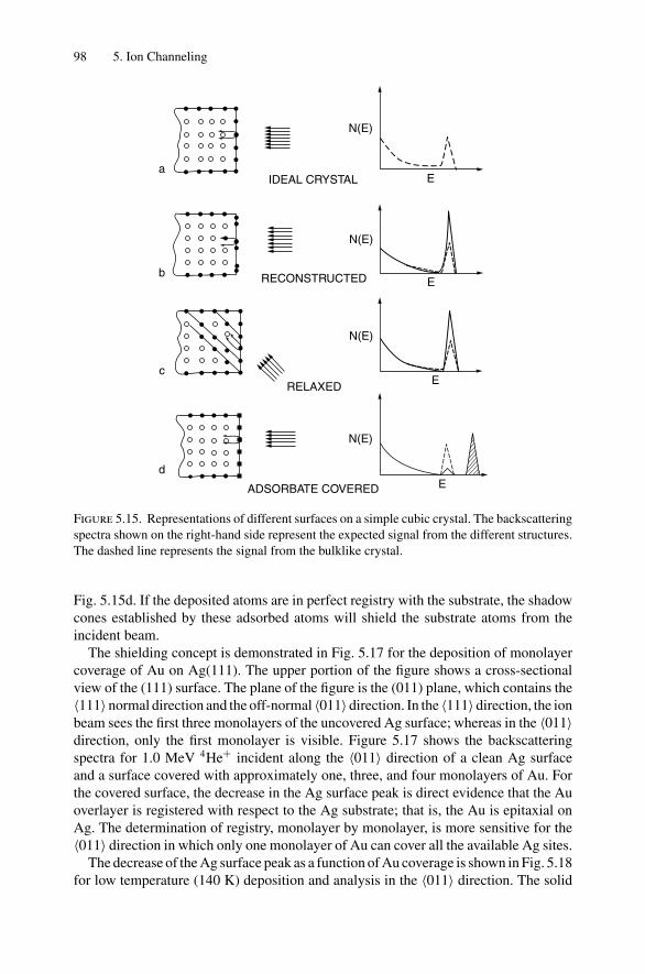
98 5. Ion Channeling
a
b
c
d
IDEAL CRYSTAL
RECONSTRUCTED
RELAXED
N(E)
E
E
E
E
N(E)
N(E)
N(E)
ADSORBATE COVERED
Figure 5.15. Representations of different surfaces on a simple cubic crystal. The backscatteringspectra shown on the right-hand side represent the expected signal from the different structures.The dashed line represents the signal from the bulklike crystal.
Fig. 5.15d. If the deposited atoms are in perfect registry with the substrate, the shadowcones established by these adsorbed atoms will shield the substrate atoms from theincident beam.
The shielding concept is demonstrated in Fig. 5.17 for the deposition of monolayercoverage of Au on Ag(111). The upper portion of the figure shows a cross-sectionalview of the (111) surface. The plane of the figure is the (011) plane, which contains the〈111〉 normal direction and the off-normal 〈011〉 direction. In the 〈111〉 direction, the ionbeam sees the first three monolayers of the uncovered Ag surface; whereas in the 〈011〉direction, only the first monolayer is visible. Figure 5.17 shows the backscatteringspectra for 1.0 MeV 4He+ incident along the 〈011〉 direction of a clean Ag surfaceand a surface covered with approximately one, three, and four monolayers of Au. Forthe covered surface, the decrease in the Ag surface peak is direct evidence that the Auoverlayer is registered with respect to the Ag substrate; that is, the Au is epitaxial onAg. The determination of registry, monolayer by monolayer, is more sensitive for the〈011〉 direction in which only one monolayer of Au can cover all the available Ag sites.
The decrease of the Ag surface peak as a function of Au coverage is shown in Fig. 5.18for low temperature (140 K) deposition and analysis in the 〈011〉 direction. The solid

5.8. Epitaxial Growth 99
1.60
<100>
<R> ÷ 10
1.52
100
200
YIE
LD
300
400
500
600
7002.0 MeV Heon W
800
900
1000
1100
1.68
ENERGY (MeV)
1.76 1.84
Figure 5.16. Backscattering spectra from 2.0 MeV He+ incident on a clean W(001) surface forthe beam aligned with the 〈100〉 axis () and for the beam aligned away from any major crys-tallographic direction (•). Note that the nonchanneling spectrum 〈R〉, termed random incidence,has been reduced by a factor of 10.
line is the result of computer simulations, which assume that Au atoms form uniformcoverage monolayer by monolayer. The agreement between the data and calculatedcurve shows that the Au has good epitaxy and uniform coverage.
The registration of the first monolayer of Au with the Ag substrate can be monitoredthrough the reduction of the Ag surface peak. The registration of subsequent Au layerswith the initial Au layer can be monitored with the Au–Au shadowing effect. Theratio of the Au signal for 〈011〉 incidence to random incidence—χmin (Au)—exhibitsa break at one monolayer coverage and a pronounced decrease at higher coverage(Fig. 5.18). The dashed curve is a computer simulation. The agreement between thecalculated curve and the data shows that the Au is indeed epitaxial. The decrease ofthe Ag surface peak with Au coverage measures the registry of the epitaxial layer tothe substrate; the decrease of χmin (Au) measures the quality of the epitaxial film.
5.8 Epitaxial Growth
The Au/Ag case is a good example of the growth of a high-quality epitaxial film. Thiscombination of materials satisfies the most important criterion for epitaxy, namely, a
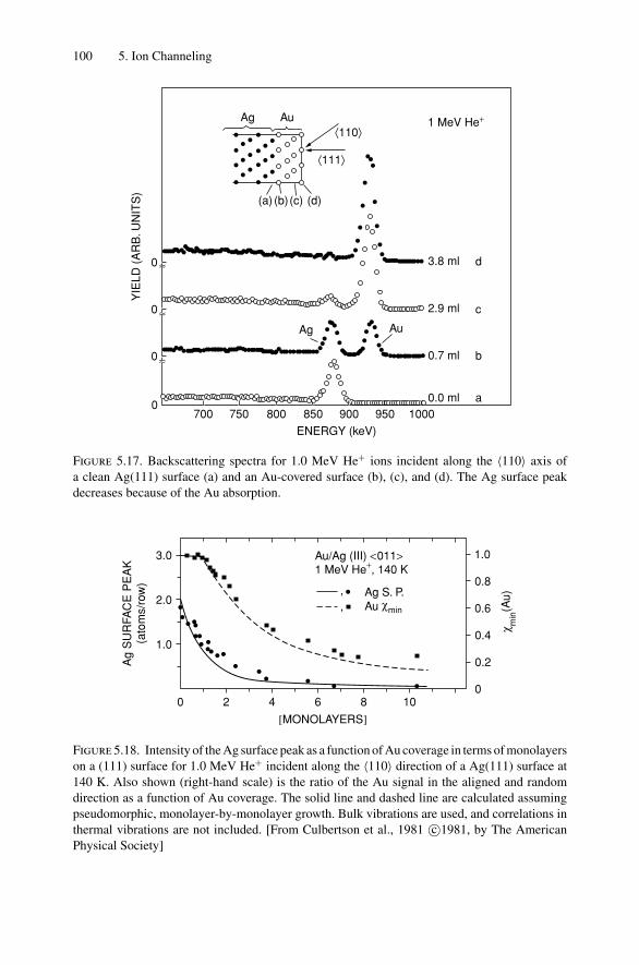
100 5. Ion Channeling
700
ENERGY (keV)
YIE
LD (
AR
B. U
NIT
S)
0
0
0
0
750 800 850 900 950 10000.0 ml a
b
c
d
0.7 ml
2.9 ml
3.8 ml
Au⟨110⟩
⟨111⟩
Ag
(a) (b) (c) (d)
AuAg
1 MeV He+
≈
≈
≈
Figure 5.17. Backscattering spectra for 1.0 MeV He+ ions incident along the 〈110〉 axis ofa clean Ag(111) surface (a) and an Au-covered surface (b), (c), and (d). The Ag surface peakdecreases because of the Au absorption.
00
1.0
2.0
3.0
2 4 6 8 10
0.2
0.4
0.6
0.8
1.0
[MONOLAYERS]
,,
Au/Ag (III) <011>1 MeV He+, 140 K
Ag S. P.Au χmin
χ min
(Au)
Ag
SU
RFA
CE
PE
AK
(ato
ms/
row
)
Figure 5.18. Intensity of the Ag surface peak as a function of Au coverage in terms of monolayerson a (111) surface for 1.0 MeV He+ incident along the 〈110〉 direction of a Ag(111) surface at140 K. Also shown (right-hand scale) is the ratio of the Au signal in the aligned and randomdirection as a function of Au coverage. The solid line and dashed line are calculated assumingpseudomorphic, monolayer-by-monolayer growth. Bulk vibrations are used, and correlations inthermal vibrations are not included. [From Culbertson et al., 1981 c©1981, by The AmericanPhysical Society]
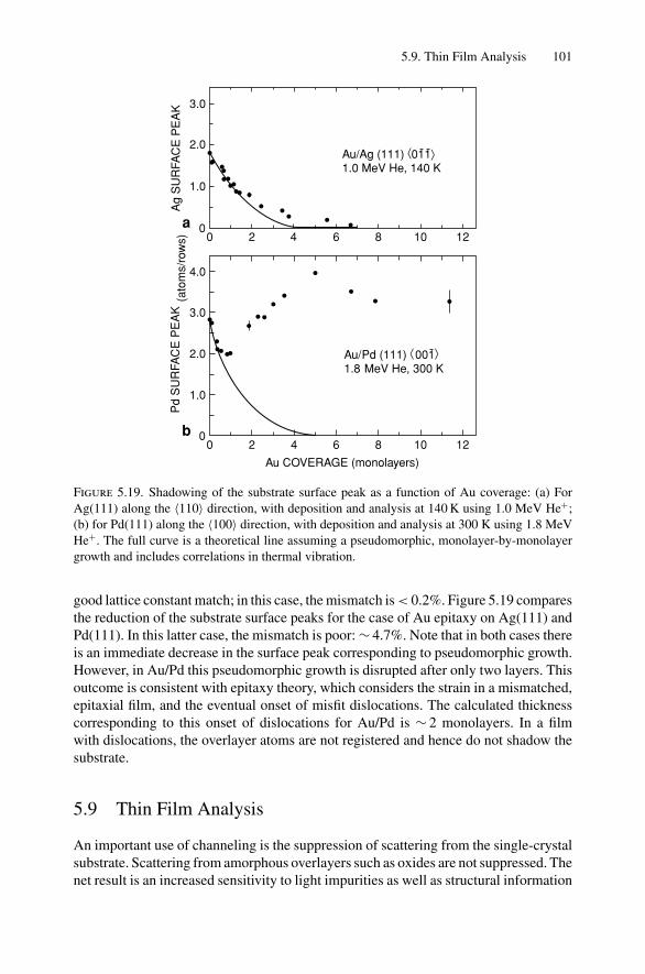
5.9. Thin Film Analysis 101
00
1.0
2.0
3.0
0
1.0
2.0
3.0
4.0
2 4 6 8 10 12
0 2 4 6 8 10 12
Ag
SU
RFA
CE
PE
AK
Au/Ag (111) ⟨011⟩1.0 MeV He, 140 K
Au/Pd (111) ⟨001⟩1.8 MeV He, 300 K
Au COVERAGE (monolayers)
Pd
SU
RFA
CE
PE
AK
(ato
ms/
row
s)
a
b
Figure 5.19. Shadowing of the substrate surface peak as a function of Au coverage: (a) ForAg(111) along the 〈110〉 direction, with deposition and analysis at 140 K using 1.0 MeV He+;(b) for Pd(111) along the 〈100〉 direction, with deposition and analysis at 300 K using 1.8 MeVHe+. The full curve is a theoretical line assuming a pseudomorphic, monolayer-by-monolayergrowth and includes correlations in thermal vibration.
good lattice constant match; in this case, the mismatch is < 0.2%. Figure 5.19 comparesthe reduction of the substrate surface peaks for the case of Au epitaxy on Ag(111) andPd(111). In this latter case, the mismatch is poor: ∼ 4.7%. Note that in both cases thereis an immediate decrease in the surface peak corresponding to pseudomorphic growth.However, in Au/Pd this pseudomorphic growth is disrupted after only two layers. Thisoutcome is consistent with epitaxy theory, which considers the strain in a mismatched,epitaxial film, and the eventual onset of misfit dislocations. The calculated thicknesscorresponding to this onset of dislocations for Au/Pd is ∼ 2 monolayers. In a filmwith dislocations, the overlayer atoms are not registered and hence do not shadow thesubstrate.
5.9 Thin Film Analysis
An important use of channeling is the suppression of scattering from the single-crystalsubstrate. Scattering from amorphous overlayers such as oxides are not suppressed. Thenet result is an increased sensitivity to light impurities as well as structural information
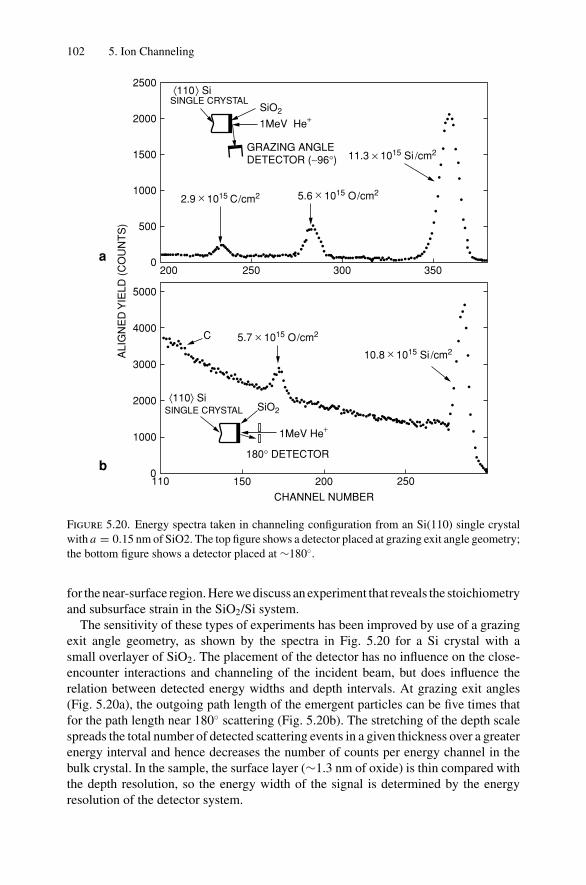
102 5. Ion Channeling
2500
a
b
2000
1500
1000
5000
4000
3000
2000
1000
0
500
0200 250 300 350
⟨110⟩ SiSINGLE CRYSTAL
SiO2
1MeV He+
GRAZING ANGLEDETECTOR (∼96°) 11.3 × 10¹⁵ Si /cm2
5.6 × 10¹⁵ O/cm22.9 × 1015 C/cm2
110 150 200 250
CHANNEL NUMBER
ALI
GN
ED
YIE
LD (
CO
UN
TS
)
⟨110⟩ SiSINGLE CRYSTAL SiO2
1MeV He+
180° DETECTOR
C
10.8 × 10¹⁵ Si /cm2
5.7 1015 O/cm2×
Figure 5.20. Energy spectra taken in channeling configuration from an Si(110) single crystalwith a = 0.15 nm of SiO2. The top figure shows a detector placed at grazing exit angle geometry;the bottom figure shows a detector placed at ∼180.
for the near-surface region. Here we discuss an experiment that reveals the stoichiometryand subsurface strain in the SiO2/Si system.
The sensitivity of these types of experiments has been improved by use of a grazingexit angle geometry, as shown by the spectra in Fig. 5.20 for a Si crystal with asmall overlayer of SiO2. The placement of the detector has no influence on the close-encounter interactions and channeling of the incident beam, but does influence therelation between detected energy widths and depth intervals. At grazing exit angles(Fig. 5.20a), the outgoing path length of the emergent particles can be five times thatfor the path length near 180 scattering (Fig. 5.20b). The stretching of the depth scalespreads the total number of detected scattering events in a given thickness over a greaterenergy interval and hence decreases the number of counts per energy channel in thebulk crystal. In the sample, the surface layer (∼1.3 nm of oxide) is thin compared withthe depth resolution, so the energy width of the signal is determined by the energyresolution of the detector system.
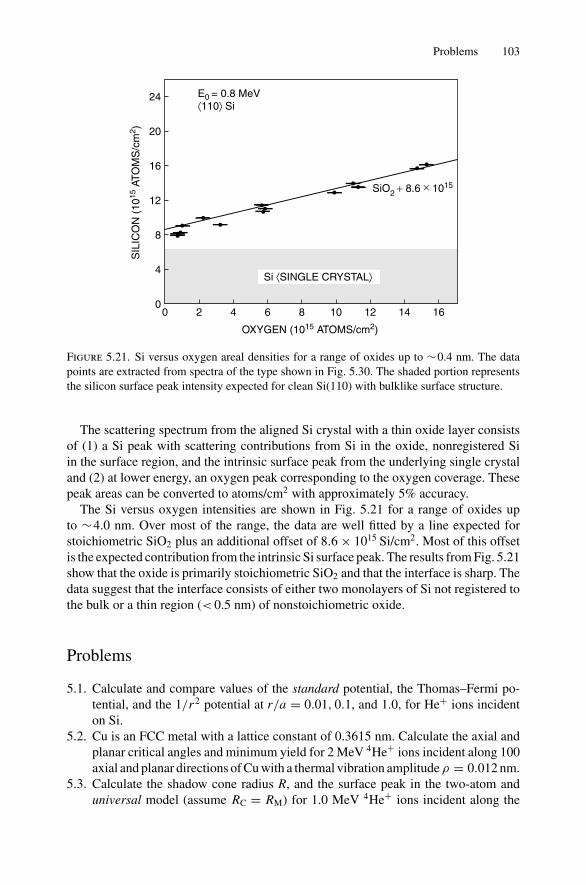
Problems 103
24
20
16
12
8
4
00 2 4 6 8 10 12 14 16
E0 = 0.8 MeV⟨110⟩ Si
SiO2 + 8.6 × 10¹⁵
OXYGEN (1015 ATOMS/cm2)
SIL
ICO
N (
1015
ATO
MS
/cm
2 )
Si ⟨SINGLE CRYSTAL⟩
Figure 5.21. Si versus oxygen areal densities for a range of oxides up to ∼0.4 nm. The datapoints are extracted from spectra of the type shown in Fig. 5.30. The shaded portion representsthe silicon surface peak intensity expected for clean Si(110) with bulklike surface structure.
The scattering spectrum from the aligned Si crystal with a thin oxide layer consistsof (1) a Si peak with scattering contributions from Si in the oxide, nonregistered Siin the surface region, and the intrinsic surface peak from the underlying single crystaland (2) at lower energy, an oxygen peak corresponding to the oxygen coverage. Thesepeak areas can be converted to atoms/cm2 with approximately 5% accuracy.
The Si versus oxygen intensities are shown in Fig. 5.21 for a range of oxides upto ∼4.0 nm. Over most of the range, the data are well fitted by a line expected forstoichiometric SiO2 plus an additional offset of 8.6 × 10¹⁵ Si/cm2. Most of this offsetis the expected contribution from the intrinsic Si surface peak. The results from Fig. 5.21show that the oxide is primarily stoichiometric SiO2 and that the interface is sharp. Thedata suggest that the interface consists of either two monolayers of Si not registered tothe bulk or a thin region (< 0.5 nm) of nonstoichiometric oxide.
Problems
5.1. Calculate and compare values of the standard potential, the Thomas–Fermi po-tential, and the 1/r2 potential at r/a = 0.01, 0.1, and 1.0, for He+ ions incidenton Si.
5.2. Cu is an FCC metal with a lattice constant of 0.3615 nm. Calculate the axial andplanar critical angles and minimum yield for 2 MeV 4He+ ions incident along 100axial and planar directions of Cu with a thermal vibration amplitude ρ = 0.012 nm.
5.3. Calculate the shadow cone radius R, and the surface peak in the two-atom anduniversal model (assume RC = RM) for 1.0 MeV 4He+ ions incident along the
104 5. Ion Channeling
100 axis of Al (lattice constant = 0.405 nm and ρ = 0.014 nm). What energy isrequired for a unity surface peak intensity (ρ/RM = 0.4)?
5.4. Use the r2/r20 approximation to the flux distribution (Eq. 5.20), and calculate the
minimum yield of an impurity displaced 0.01, 0.03, and 0.05 nm from the atomicrow. Take the vibration amplitude as 0.01 nm and use an r0 value appropriate tothe Si 〈010〉 channeling direction.
5.5. Channeling occurs not only along the strings of atoms but also between the sheetsof atoms that make up atomic planes. In this case, the potential governing thetransverse notion can be described by a parabolic potential of the form
V (y) = 1
2ky2, 0 ≤ |y| ≤ dp/2,
where dp is the planar spacing and y is the distance to the planar wall measuredfrom the midpoint. Using the concept of motion in a harmonic potential, derivea formula for the wavelength of the oscillatory motion. Evaluate this wavelengthfor 1.0 MeV ions channeling along the W(100) planes. The spring constant k canbe estimated by noting that V (dp/2) = Up(0) from Eq. 5.13.
References
1. J. U. Anderson, O. Andreason, J. A. Davies, and E. Uggerhøj, Rad. Eff. 7, 25 (1971).2. B. R. Appelton and G. Foti, “Channeling,” in Ion Beam Handbook for Material Analysis, J.
W. Mayer and E. Rimini, Eds. (Academic Press, New York, 1977).3. W. K. Chu, J. W. Mayer, and M.-A. Nicolet, Backscattering Spectrometry (Academic Press,
New York, 1978).4. G. Dearnaley, J. H. Freeman, R. S. Nelson, and J. Stephen, Ion Implantation (North-Holland,
Amsterdam, 1973).5. L. C. Feldman, J. W. Mayer, and S. T. Picraux, Materials Analysis by Ion Channeling
(Academic Press, New York, 1982).6. D. S. Gemmell, “Channeling and Related Effects in the Motion of Charged Particles Through
Crystals,” Rev. Mod. Phys. 46(1), 129–227 (1974).7. J. Lindhard, Mat. Fys. Medd. Dan. Vid. Selsk. 34(14), 1 (1965).8. D. V. Morgan, Ed., Channeling (John Wiley and Sons, New York, 1973).9. R. S. Nelson, The Observation of Atomic Collisions in Crystalline Solids (North-Holland,
Amsterdam, 1968).10. P. D. Townsend, J. C. Kelly, and N. E. W. Hartley, Ion Implantation, Sputtering and Their
Applications (Academic Press, New York, 1976).11. R. J. Culbertson, L. C. Feldman, and P. J. Silverman, Phys. Rev. Lett. 47, 657 (1981).
6Electron–Electron Interactionsand the Depth Sensitivity ofElectron Spectroscopies
6.1 Introduction
Detection of an element from the near-surface region of a solid often involves themeasurement of an electron energy characteristic of a particular atom. The depth res-olution of these techniques is then determined by the thickness of the material thatan emitted electron can traverse without undergoing an inelastic event and thus al-tering the electron energy. We consider these inelastic electron processes in order toobtain a quantitative understanding of the thickness of the analyzed layer. An under-standing of these phenomena is particularly useful in the design of surface studies, asan experimenter can often choose the electron energy and thus determine the depthprobed. In this chapter, we use the particle-scattering concepts developed in Chapters 2and 3 to derive classical relations for electron–electron collisions. These provide aguide for useful approximations for electron escape depths and impact ionization crosssections.
6.2 Electron Spectroscopies: Energy Analysis
The surface analytical tools, photoelectron and Auger electron spectroscopy, discussedin the following chapters use photons or electrons to excite electrons that escape fromthe solid with sharply defined energies. Emitted electrons in the 100 eV range haveescape depths on the order of 1.0 nm. By choosing the appropriate incident beamparameters and detection systems, these electron spectroscopies become extremelysurface sensitive. Electron spectroscopies have found their widest application in sur-face analysis for a number of reasons. Electrons are easily focused into beams, areefficiently detected and counted, and may be analyzed with respect to angular andenergy distribution using electrostatic lenses and deflection systems.
The electron spectroscopies are based on an analysis of the energy distribution ofelectrons emitted from the surface. The different features of the emission spectra andthe requirements imposed by the analytical technique have led to the developmentof a variety of analyzers for measuring the electron energy distributions (see alsoChapter 10). In the cylindrical mirror analyzer (CMA) (Fig. 6.1), the emitted electronsare focused electrostatically in such a way that only those electrons with energies within
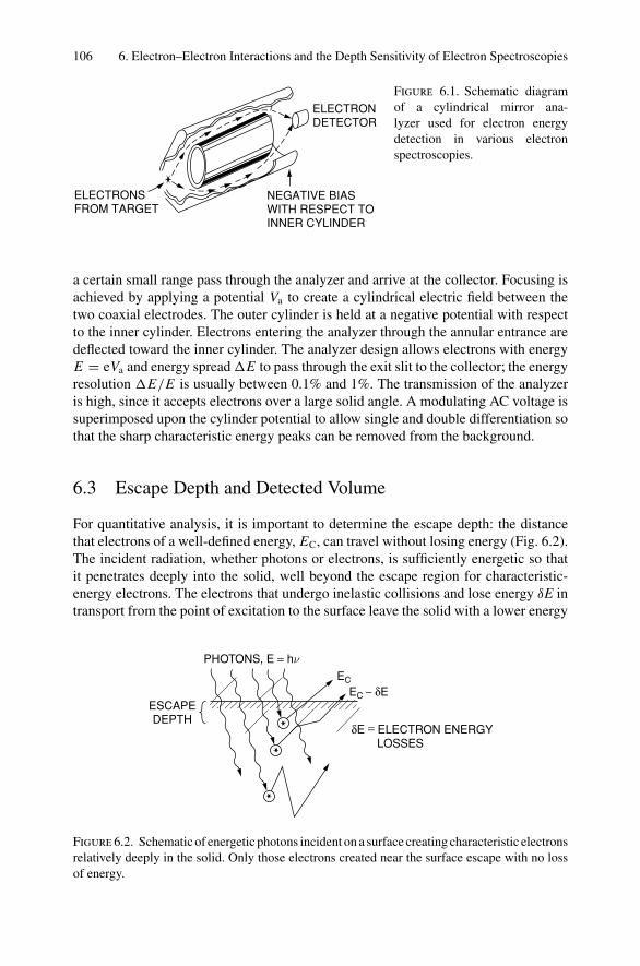
106 6. Electron–Electron Interactions and the Depth Sensitivity of Electron Spectroscopies
ELECTRONSFROM TARGET
NEGATIVE BIASWITH RESPECT TOINNER CYLINDER
ELECTRONDETECTOR
Figure 6.1. Schematic diagramof a cylindrical mirror ana-lyzer used for electron energydetection in various electronspectroscopies.
a certain small range pass through the analyzer and arrive at the collector. Focusing isachieved by applying a potential Va to create a cylindrical electric field between thetwo coaxial electrodes. The outer cylinder is held at a negative potential with respectto the inner cylinder. Electrons entering the analyzer through the annular entrance aredeflected toward the inner cylinder. The analyzer design allows electrons with energyE = eVa and energy spread E to pass through the exit slit to the collector; the energyresolution E/E is usually between 0.1% and 1%. The transmission of the analyzeris high, since it accepts electrons over a large solid angle. A modulating AC voltage issuperimposed upon the cylinder potential to allow single and double differentiation sothat the sharp characteristic energy peaks can be removed from the background.
6.3 Escape Depth and Detected Volume
For quantitative analysis, it is important to determine the escape depth: the distancethat electrons of a well-defined energy, EC, can travel without losing energy (Fig. 6.2).The incident radiation, whether photons or electrons, is sufficiently energetic so thatit penetrates deeply into the solid, well beyond the escape region for characteristic-energy electrons. The electrons that undergo inelastic collisions and lose energy δE intransport from the point of excitation to the surface leave the solid with a lower energy
ESCAPEDEPTH
PHOTONS, E = hν
EC
EC − δE
δE = ELECTRON ENERGY LOSSES
Figure 6.2. Schematic of energetic photons incident on a surface creating characteristic electronsrelatively deeply in the solid. Only those electrons created near the surface escape with no lossof energy.
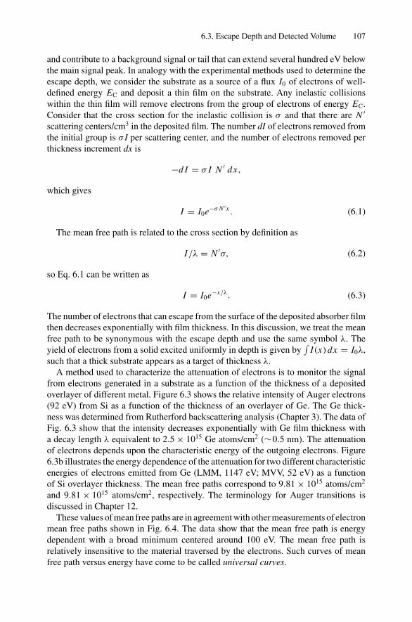
6.3. Escape Depth and Detected Volume 107
and contribute to a background signal or tail that can extend several hundred eV belowthe main signal peak. In analogy with the experimental methods used to determine theescape depth, we consider the substrate as a source of a flux I0 of electrons of well-defined energy EC and deposit a thin film on the substrate. Any inelastic collisionswithin the thin film will remove electrons from the group of electrons of energy EC.Consider that the cross section for the inelastic collision is σ and that there are N ′
scattering centers/cm3 in the deposited film. The number dI of electrons removed fromthe initial group is σ I per scattering center, and the number of electrons removed perthickness increment dx is
−d I = σ I N ′ dx,
which gives
I = I0e−σ N ′x . (6.1)
The mean free path is related to the cross section by definition as
I/λ = N ′σ, (6.2)
so Eq. 6.1 can be written as
I = I0e−x/λ. (6.3)
The number of electrons that can escape from the surface of the deposited absorber filmthen decreases exponentially with film thickness. In this discussion, we treat the meanfree path to be synonymous with the escape depth and use the same symbol λ. Theyield of electrons from a solid excited uniformly in depth is given by
∫I (x) dx = I0λ,
such that a thick substrate appears as a target of thickness λ.A method used to characterize the attenuation of electrons is to monitor the signal
from electrons generated in a substrate as a function of the thickness of a depositedoverlayer of different metal. Figure 6.3 shows the relative intensity of Auger electrons(92 eV) from Si as a function of the thickness of an overlayer of Ge. The Ge thick-ness was determined from Rutherford backscattering analysis (Chapter 3). The data ofFig. 6.3 show that the intensity decreases exponentially with Ge film thickness witha decay length λ equivalent to 2.5 × 10¹⁵ Ge atoms/cm2 (∼0.5 nm). The attenuationof electrons depends upon the characteristic energy of the outgoing electrons. Figure6.3b illustrates the energy dependence of the attenuation for two different characteristicenergies of electrons emitted from Ge (LMM, 1147 eV; MVV, 52 eV) as a functionof Si overlayer thickness. The mean free paths correspond to 9.81 × 10¹⁵ atoms/cm2
and 9.81 × 10¹⁵ atoms/cm2, respectively. The terminology for Auger transitions isdiscussed in Chapter 12.
These values of mean free paths are in agreement with other measurements of electronmean free paths shown in Fig. 6.4. The data show that the mean free path is energydependent with a broad minimum centered around 100 eV. The mean free path isrelatively insensitive to the material traversed by the electrons. Such curves of meanfree path versus energy have come to be called universal curves.
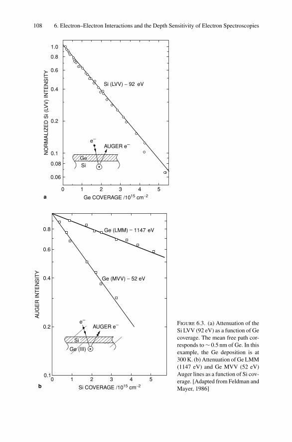
108 6. Electron–Electron Interactions and the Depth Sensitivity of Electron Spectroscopies
0 1 2 3 4 5
0.06
0.08
0.1
0.2
0.4
0.6
0.8
1.0
Ge COVERAGE /1015 cm−2a
NO
RM
ALI
ZE
D S
i (LV
V)
INT
EN
SIT
Y
Si (LVV) − 92 eV
e−AUGER e−
GeSi
e−AUGER e−
Ge (III)
Si
Si COVERAGE /1015 cm−2
0 1 2 3 4 50.1
0.2
0.4
0.6
0.8
AU
GE
R IN
TE
NS
ITY
b
Ge (LMM) − 1147 eV
Ge (MVV) − 52 eV
Figure 6.3. (a) Attenuation of theSi LVV (92 eV) as a function of Gecoverage. The mean free path cor-responds to ∼ 0.5 nm of Ge. In thisexample, the Ge deposition is at300 K. (b) Attenuation of Ge LMM(1147 eV) and Ge MVV (52 eV)Auger lines as a function of Si cov-erage. [Adapted from Feldman andMayer, 1986]
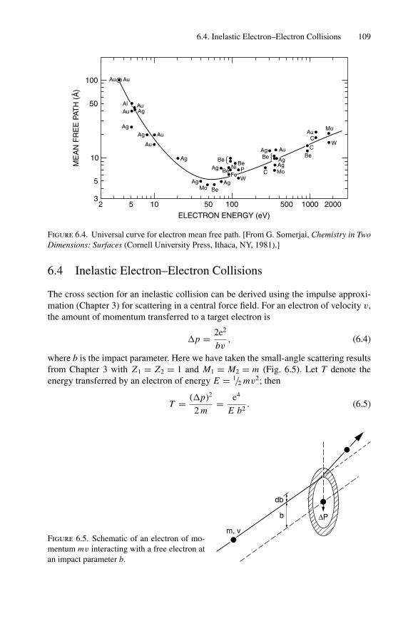
6.4. Inelastic Electron–Electron Collisions 109
2 5 10 50 100 500 1000 2000
ELECTRON ENERGY (eV)
3
5
10
50
100M
EA
N F
RE
E P
ATH
(Å
)Au Au
AuAu
Au
Au
Ag
AgAg
Ag
Ag
Ag
Ag
Ag
AgAg
Au
Au
Al
Mo Be
BeBe
BeW
W
PFeNi
Be Be
Mo
Mo
C
C
C
Figure 6.4. Universal curve for electron mean free path. [From G. Somerjai, Chemistry in TwoDimensions: Surfaces (Cornell University Press, Ithaca, NY, 1981).]
6.4 Inelastic Electron–Electron Collisions
The cross section for an inelastic collision can be derived using the impulse approxi-mation (Chapter 3) for scattering in a central force field. For an electron of velocity v,the amount of momentum transferred to a target electron is
p = 2e2
bv, (6.4)
where b is the impact parameter. Here we have taken the small-angle scattering resultsfrom Chapter 3 with Z1 = Z2 = 1 and M1 = M2 = m (Fig. 6.5). Let T denote theenergy transferred by an electron of energy E = 1/2 mv2; then
T = (p)2
2 m= e4
E b2. (6.5)
∆P
m, v
db
b
Figure 6.5. Schematic of an electron of mo-mentum mv interacting with a free electron atan impact parameter b.
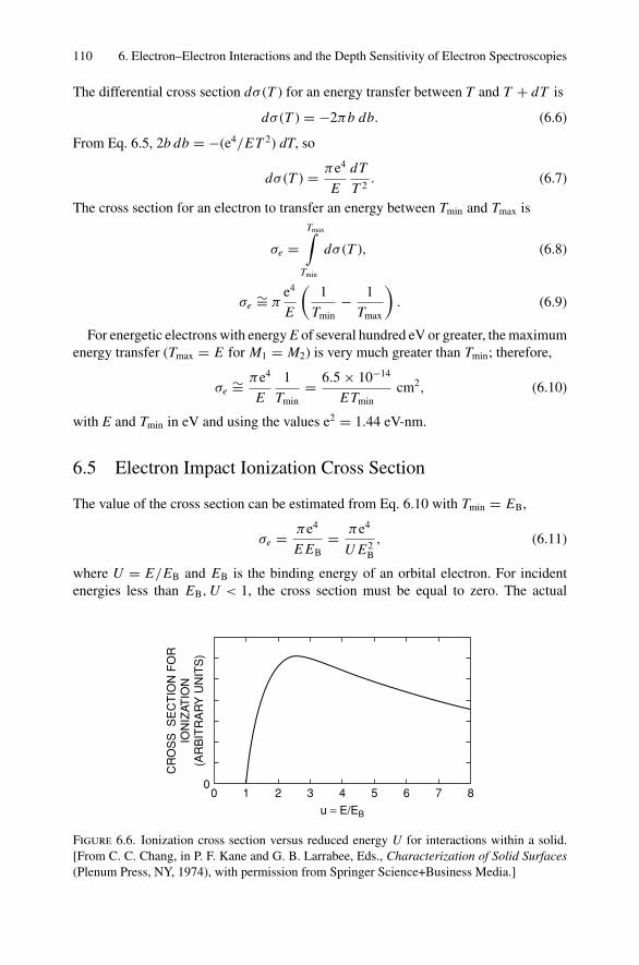
110 6. Electron–Electron Interactions and the Depth Sensitivity of Electron Spectroscopies
The differential cross section dσ (T ) for an energy transfer between T and T + dT is
dσ (T ) = −2πb db. (6.6)
From Eq. 6.5, 2b db = −(e4/ET 2) dT, so
dσ (T ) = πe4
E
dT
T 2. (6.7)
The cross section for an electron to transfer an energy between Tmin and Tmax is
σe =Tmax∫
Tmin
dσ (T ), (6.8)
σe∼= π
e4
E
(1
Tmin− 1
Tmax
). (6.9)
For energetic electrons with energy E of several hundred eV or greater, the maximumenergy transfer (Tmax = E for M1 = M2) is very much greater than Tmin; therefore,
σe∼= πe4
E
1
Tmin= 6.5 × 10⁻¹⁴
ETmincm2, (6.10)
with E and Tmin in eV and using the values e2 = 1.44 eV-nm.
6.5 Electron Impact Ionization Cross Section
The value of the cross section can be estimated from Eq. 6.10 with Tmin = EB,
σe = πe4
E EB= πe4
U E2B
, (6.11)
where U = E/EB and EB is the binding energy of an orbital electron. For incidentenergies less than EB, U < 1, the cross section must be equal to zero. The actual
00
1 2 3 4 5 6 7 8
u = E/EB
CR
OS
S S
EC
TIO
N F
OR
ION
IZAT
ION
(AR
BIT
RA
RY
UN
ITS
)
Figure 6.6. Ionization cross section versus reduced energy U for interactions within a solid.[From C. C. Chang, in P. F. Kane and G. B. Larrabee, Eds., Characterization of Solid Surfaces(Plenum Press, NY, 1974), with permission from Springer Science+Business Media.]
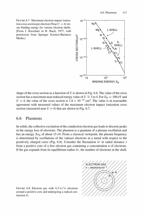
6.6. Plasmons 111
10 10210−20
10−19
10−18
10−17
103
BINDING ENERGY, EB
CR
OS
S S
EC
TIO
N/c
m2
L-SHELL
L-SHELL
K-SHELL
Na
Mg
AlSi
SiP
S
S
Cl
Ti O
N
Ar
C
Figure 6.7. Maximum electron impact ioniza-tion cross section per electron (Near U = 4) ver-sus binding energy for various electron shells.[From J. Kirschner in H. Ibach, 1977, withpermission from Springer Science+BusinessMedia.]
shape of the cross section as a function of U is shown in Fig. 6.6. The value of the crosssection has a maximum near reduced energy value of U ∼= 3 to 4. For EB = 100 eV andU = 4, the value of the cross section is 1.6 × 10⁻¹⁸ cm2. The value is in reasonableagreement with measured values of the maximum electron impact ionization crosssection (measured near U = 4) that are shown in Fig. 6.7.
6.6 Plasmons
In solids, the collective excitation of the conduction electron gas leads to discrete peaksin the energy loss of electrons. The plasmon is a quantum of a plasma oscillation andhas an energy hωp of about 15 eV. From a classical viewpoint, the plasma frequencyis determined by oscillations of the valence electrons in a metal with respect to thepositively charged cores (Fig. 6.8). Consider the fluctuation δr in radial distance rfrom a positive core of a free electron gas containing a concentration n of electrons.If the gas expands from its equilibrium radius δr , the number of electrons in the shell,
+
δr
ELECTRON GASn = electrons/cm−3
Figure 6.8. Electron gas with 4/3 πr 3n electronsaround a positive core and undergoing a radical con-traction δr .
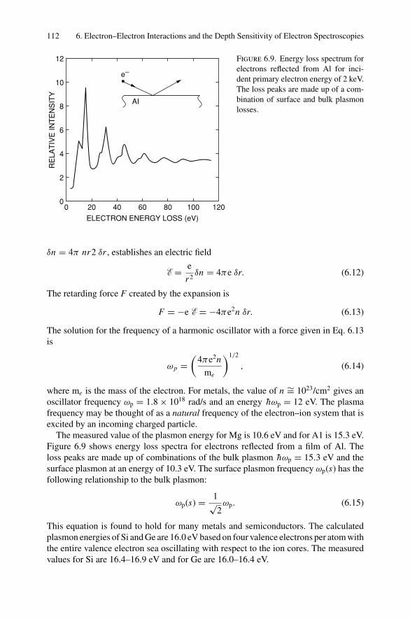
112 6. Electron–Electron Interactions and the Depth Sensitivity of Electron Spectroscopies
00
20 40 60 80 100 120
ELECTRON ENERGY LOSS (eV)
2
4
6
8
10
12R
ELA
TIV
E IN
TE
NS
ITY
e−
AI
Figure 6.9. Energy loss spectrum forelectrons reflected from Al for inci-dent primary electron energy of 2 keV.The loss peaks are made up of a com-bination of surface and bulk plasmonlosses.
δn = 4π nr2 δr , establishes an electric field
E = e
r2δn = 4πe δr. (6.12)
The retarding force F created by the expansion is
F = −e E = −4πe2n δr. (6.13)
The solution for the frequency of a harmonic oscillator with a force given in Eq. 6.13is
ωp =(
4πe2n
me
)1/2
, (6.14)
where me is the mass of the electron. For metals, the value of n ∼= 1023/cm2 gives anoscillator frequency ωp = 1.8 × 10¹⁸ rad/s and an energy hωp = 12 eV. The plasmafrequency may be thought of as a natural frequency of the electron–ion system that isexcited by an incoming charged particle.
The measured value of the plasmon energy for Mg is 10.6 eV and for A1 is 15.3 eV.Figure 6.9 shows energy loss spectra for electrons reflected from a film of Al. Theloss peaks are made up of combinations of the bulk plasmon hωp = 15.3 eV and thesurface plasmon at an energy of 10.3 eV. The surface plasmon frequency ωp(s) has thefollowing relationship to the bulk plasmon:
ωp(s) = 1√2ωp. (6.15)
This equation is found to hold for many metals and semiconductors. The calculatedplasmon energies of Si and Ge are 16.0 eV based on four valence electrons per atom withthe entire valence electron sea oscillating with respect to the ion cores. The measuredvalues for Si are 16.4–16.9 eV and for Ge are 16.0–16.4 eV.
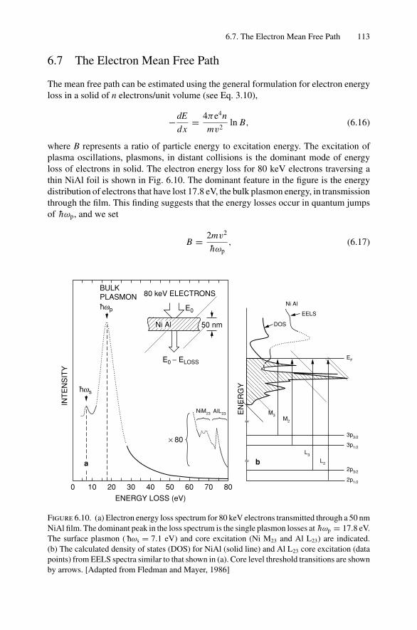
6.7. The Electron Mean Free Path 113
6.7 The Electron Mean Free Path
The mean free path can be estimated using the general formulation for electron energyloss in a solid of n electrons/unit volume (see Eq. 3.10),
−dE
dx= 4πe4n
mv2ln B, (6.16)
where B represents a ratio of particle energy to excitation energy. The excitation ofplasma oscillations, plasmons, in distant collisions is the dominant mode of energyloss of electrons in solid. The electron energy loss for 80 keV electrons traversing athin NiAl foil is shown in Fig. 6.10. The dominant feature in the figure is the energydistribution of electrons that have lost 17.8 eV, the bulk plasmon energy, in transmissionthrough the film. This finding suggests that the energy losses occur in quantum jumpsof hωp, and we set
B = 2mv2
hωp, (6.17)
0 10 20 30 40 50 60 70 80
ENERGY LOSS (eV)
INT
EN
SIT
Y
Ni Al
E0
E0 − ELOSS
50 nm
80 keV ELECTRONSBULKPLASMON
× 80
NiM23 AIL23
a b
≈
≈
EN
ER
GY
M3
3p3/2
3p1/2
2p3/2
2p1/2
M2
EF
L3
L2
DOS
EELS
Ni Alhwp
hws
Figure 6.10. (a) Electron energy loss spectrum for 80 keV electrons transmitted through a 50 nmNiAl film. The dominant peak in the loss spectrum is the single plasmon losses at hωp = 17.8 eV.The surface plasmon ( hωs = 7.1 eV) and core excitation (Ni M23 and Al L23) are indicated.(b) The calculated density of states (DOS) for NiAl (solid line) and Al L23 core excitation (datapoints) from EELS spectra similar to that shown in (a). Core level threshold transitions are shownby arrows. [Adapted from Fledman and Mayer, 1986]
114 6. Electron–Electron Interactions and the Depth Sensitivity of Electron Spectroscopies
and from ωp = (4πe2n/m)1/2 (Eq. 6.14), write the energy loss in terms of ωp:
−d E
dx= ω2
Pe2
v2ln
2mv2
hωp, (6.18)
A similar formulation is presented by Ibach (1977). If we treat the plasmon as the majorsource of energy loss in determining the mean free path λ for electrons, we can writeλ as
1
λ=(
−dE
dx
)1
hωp. (6.19)
This gives
1
λ= −ωpe2
hv2ln
2mv2
hωp. (6.20)
For example, we calculate the value of λ to be 0.92 nm for 350 eV electrons in Al( hωp = 15 eV, v2 = 2E/m = 1.23 × 1018 cm2/s2, and h = 6.6 × 10⁻¹⁶ eV-s). Thisvalue is in reasonable agreement with the data presented in Fig. 6.4.
6.8 Influence of Thin Film Morphology onElectron Attenuation
One of the many prominent uses of electron spectroscopies is in the characteriza-tion of different modes of film growth. Questions about the growth mode are particu-larly important in the creation of uniform layered films in which one desires extremeuniformity in composition for films thinner than 10 nm. Common types of growthinclude the following:
1. Layer-by-layer, in which the deposited film completes one monolayer of coverage,then the second, etc. This mode is commonly referred to as Frank–van der Merwegrowth.
2. Layer plus islanding, in which the first layer completely covers the surface of thesubstrate and subsequent layers form islands of deposited material. This mode isreferred to as Stranski–Krastanov growth.
3. Complete islanding, in which the material immediately forms islands on the surface.This mode is commonly referred to as Volmer–Weber growth.
4. Statistical deposition, in which the growth corresponds to the random occupancy ofsurface sites according to Poisson statistics.
6.8.1 Layer-by-Layer Growth
In the following discussions, we continually make use of the exponential probabilityof inelastic scattering for a characteristic electron emerging from a solid. As a firstexample, consider the attenuation of electrons from a substrate as a result of an overlayerthat deposits in a layer-by-layer mode. Although the derivation here is for attenuation
6.8. Influence of Thin Film Morphology onElectron Attenuation 115
of substrate electrons, very similar considerations can be used to derive formulae forthe increase of the electron yield from the overlayer.
A typical experiment involves a measurement of the intensity Is of a characteristicAuger electron from the substrate as a function of overlayer thickness t. (Naturally, theoverlayer is a different material.) The mean free path of the substrate Auger electron inthe material of the overlayer is λ. Then, for coverages up to one monolayer, the Augerintensity can be written as
IS/IS0 = (1 − x) + xe−l/λ, 0 ≤ x ≤ 1, (6.21)
where x is the fraction of the surface covered by the overlayer, IS0 is the intensity fromthe clean surface, and I is the thickness of a monolayer. In this regime of up to onemonolayer, the dependence of the intensity on coverage is linear in x. Hence, a similarformula can be written for the region from 1 to 2 monolayers as
IS/IS0 = (1 − x)e−l/λ + xe−2l/λ, 0 ≤ x ≤ 1, (6.22)
where x is now the fraction of the surface covered with two layers and (1 − x) is thefraction covered with one layer. Again, in the region of coverage of one to two layers,the attenuation is linear in x.
In general, a similar formula can be written for the transition from the n to the (n + 1)layer as
IS/IS0 = (1 − x)e−nl/λ + xe−(n+1)l/λ, 0 ≤ x ≤ 1, n = 0, 1 . . . , (6.23)
where (1 − x) is the fraction of the surface covered with n layers and x is the fractioncovered with (n + 1) layers. The characteristic shape of this curve is a series of straightlines (on a linear plot) with breaks at coverages corresponding to an integral numberof monolayers. The envelope of points corresponding to integral coverages describesan exponential decay of the form e−nt/λ (Fig. 6.11).
6.8.2 Single Layer plus Islanding
A second type of growth mode corresponds to the deposition of a single uniform layerthat is then followed by islanding. From the discussion in the previous section, we canwrite the attenuation of up to one monolayer of coverage as
IS/IS0 = (1 − x) + xe−l/λ, 0 ≤ x ≤ 1, (6.24)
where x represents the fraction of the covered surface. In the second stage of growth,the deposited material forms islands of unspecified dimensions, and we cannot writea simple analytical formula, as the actual attenuation will depend on the fraction ofcovered surface. As an example, however, we take as a very simple case that the islandscover 50% of the surface. Then, for the second monolayer’s worth of material, thecoverage formula can be written as
IS/IS0 = (1 − x)e−l/λ + xe−3l/λ, 0 ≤ x ≤ 0.5, (6.25)
where x is the fraction of the surface covered with two-monolayer-high islands. Asimilar formula can be written for any coverage regime, but there will always be a term
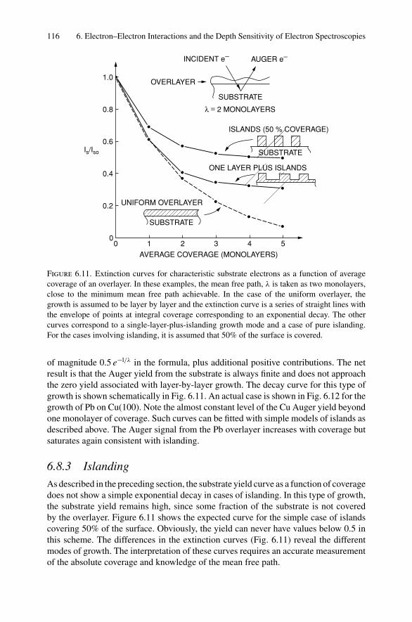
116 6. Electron–Electron Interactions and the Depth Sensitivity of Electron Spectroscopies
00
1 2 3 4 5
0.2
0.4
0.6
0.8
1.0
AVERAGE COVERAGE (MONOLAYERS)
Is/Iso
SUBSTRATE
SUBSTRATE
SUBSTRATE
UNIFORM OVERLAYER
ONE LAYER PLUS ISLANDS
ISLANDS (50 % COVERAGE)
OVERLAYER
λ = 2 MONOLAYERS
INCIDENT e− AUGER e−
Figure 6.11. Extinction curves for characteristic substrate electrons as a function of averagecoverage of an overlayer. In these examples, the mean free path, λ is taken as two monolayers,close to the minimum mean free path achievable. In the case of the uniform overlayer, thegrowth is assumed to be layer by layer and the extinction curve is a series of straight lines withthe envelope of points at integral coverage corresponding to an exponential decay. The othercurves correspond to a single-layer-plus-islanding growth mode and a case of pure islanding.For the cases involving islanding, it is assumed that 50% of the surface is covered.
of magnitude 0.5 e−l/λ in the formula, plus additional positive contributions. The netresult is that the Auger yield from the substrate is always finite and does not approachthe zero yield associated with layer-by-layer growth. The decay curve for this type ofgrowth is shown schematically in Fig. 6.11. An actual case is shown in Fig. 6.12 for thegrowth of Pb on Cu(100). Note the almost constant level of the Cu Auger yield beyondone monolayer of coverage. Such curves can be fitted with simple models of islands asdescribed above. The Auger signal from the Pb overlayer increases with coverage butsaturates again consistent with islanding.
6.8.3 Islanding
As described in the preceding section, the substrate yield curve as a function of coveragedoes not show a simple exponential decay in cases of islanding. In this type of growth,the substrate yield remains high, since some fraction of the substrate is not coveredby the overlayer. Figure 6.11 shows the expected curve for the simple case of islandscovering 50% of the surface. Obviously, the yield can never have values below 0.5 inthis scheme. The differences in the extinction curves (Fig. 6.11) reveal the differentmodes of growth. The interpretation of these curves requires an accurate measurementof the absolute coverage and knowledge of the mean free path.
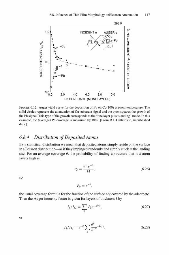
6.8. Influence of Thin Film Morphology onElectron Attenuation 117
0.00.0
0.5
1.0
2.0 4.0 6.0 8.0 10.0
Pb COVERAGE (MONOLAYERS)
293 K
Pb
Pb
PbCu
CuCu
INCIDENT e− AUGER e−
AU
GE
R IN
TE
NS
ITY
I cu/I
° cu
AU
GE
R IN
TE
NS
ITY
I Pb
(AR
BIT
RA
RY
UN
IT)
Figure 6.12. Auger yield curve for the deposition of Pb on Cu(100) at room temperature. Thesolid circles represent the attenuation of Cu substrate signal and the open squares the growth ofthe Pb signal. This type of the growth corresponds to the “one layer plus islanding” mode. In thisexample, the (average) Pb coverage is measured by RBS. [From R.J. Culbertson, unpublisheddata.]
6.8.4 Distribution of Deposited Atoms
By a statistical distribution we mean that deposited atoms simply reside on the surfacein a Poisson distribution—as if they impinged randomly and simply stuck at the landingsite. For an average coverage θ , the probability of finding a structure that is k atomlayers high is
Pk = θ k e−θ
k!, (6.26)
so
P0 = e−θ ,
the usual coverage formula for the fraction of the surface not covered by the adsorbate.Then the Auger intensity factor is given for layers of thickness I by
IS/IS0 =∑
k
Pke−kl/λ, (6.27)
or
IS/IS0 = e−θ∑
k
θ k
k!e−kl/λ. (6.28)
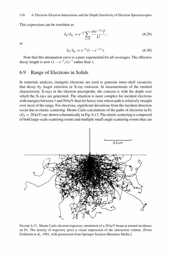
118 6. Electron–Electron Interactions and the Depth Sensitivity of Electron Spectroscopies
This expression can be rewritten as
IS/IS0 = e−θ∑k=0
(θe−l/λ)k
k!, (6.29)
or
IS/IS0 = e−θ (1 − e−l/λ). (6.30)
Note that this attenuation curve is a pure exponential for all coverages. The effectivedecay length is now (1 − e−l/λ)−1 rather than λ.
6.9 Range of Electrons in Solids
In materials analysis, energetic electrons are used to generate inner-shell vacanciesthat decay by Auger emission or X-ray emission. In measurements of the emittedcharacteristic X-rays in the electron microprobe, the concern is with the depth overwhich the X-rays are generated. The situation is more complex for incident electronswith energies between 1 and 50 keV than for heavy ions whose path is relatively straightover most of the range. For electrons, significant deviations from the incident directionoccur due to elastic scattering. Monte Carlo calculations of the paths of electrons in Fe(E0 = 20 keV) are shown schematically in Fig. 6.13. The elastic scattering is composedof both large-scale scattering events and multiple small-angle scattering events that can
0.5 µm
Figure 6.13. Monte Carlo electron trajectory simulation of a 20 keV beam at normal incidenceon Fe. The density of trajectory gives a visual impression of the interaction volume. [FromGoldstein et al., 1981, with permission from Springer Science+Business Media.]
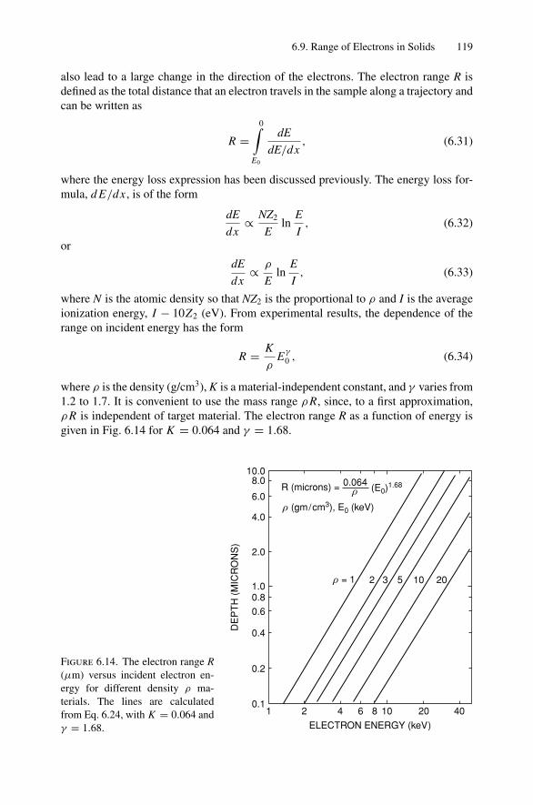
6.9. Range of Electrons in Solids 119
also lead to a large change in the direction of the electrons. The electron range R isdefined as the total distance that an electron travels in the sample along a trajectory andcan be written as
R =0∫
E0
dE
dE/dx, (6.31)
where the energy loss expression has been discussed previously. The energy loss for-mula, d E/dx , is of the form
dE
dx∝ NZ2
Eln
E
I, (6.32)
or
dE
dx∝ ρ
Eln
E
I, (6.33)
where N is the atomic density so that NZ2 is the proportional to ρ and I is the averageionization energy, I − 10Z2 (eV). From experimental results, the dependence of therange on incident energy has the form
R = K
ρEγ
0 , (6.34)
where ρ is the density (g/cm3), K is a material-independent constant, and γ varies from1.2 to 1.7. It is convenient to use the mass range ρR, since, to a first approximation,ρR is independent of target material. The electron range R as a function of energy isgiven in Fig. 6.14 for K = 0.064 and γ = 1.68.
10.08.0
6.0ρ (gm/cm3), E0 (keV)
4.0
2.0
1.00.8
0.6
0.4
0.2
0.11 2 4 6 8 10
DE
PT
H (
MIC
RO
NS
)
ELECTRON ENERGY (keV)
20 40
R (microns) = (E0)1.680.064ρ
ρ = 1 2 3 5 10 20
Figure 6.14. The electron range R(µm) versus incident electron en-ergy for different density ρ ma-terials. The lines are calculatedfrom Eq. 6.24, with K = 0.064 andγ = 1.68.
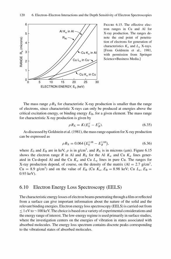
120 6. Electron–Electron Interactions and the Depth Sensitivity of Electron Spectroscopies
6
5
4
3
2
1
00 5 10 15
AI Ka in AI
Cu Ka in AI
Cu Ka in Cu
Cu La in Cu
RAI
ELECTRON ENERGY, E0 (keV)
RA
NG
E R
X (
mic
rons
)
20 25 30
Figure 6.15. The effective elec-tron ranges in Cu and Al forX-ray production. The ranges de-note the end point of penetra-tion of electrons for generation ofcharacteristics Kα and Lα X-rays.[From Goldstein et al., 1981,with permission from SpringerScience+Business Media.]
The mass range ρRX for characteristic X-ray production is smaller than the rangeof electrons, since characteristic X-rays can only be produced at energies above thecritical excitation energy, or binding energy EB, for a given element. The mass rangefor characteristic X-ray production is given by
ρRX = K (Eγ
0 − Eγ
B). (6.35)
As discussed by Goldstein et al. (1981), the mass range equation for X-ray productioncan be expressed as
ρRX = 0.064(E1.68
0 − E1.68B
), (6.36)
where E0 and EB are in keV, ρ is in g/cm3, and RX is in microns (µm). Figure 6.15shows the electron range R in Al and RX for the Al Kα and Cu Kα lines gener-ated in Cu-doped Al and the Cu Kα and Cu Lα lines in pure Cu. The ranges forX-ray production depend, of course, on the density of the matrix (Al = 2.7 g/cm3,Cu = 8.9 g/cm3) and on the value of EB (Cu Kα, EB = 8.98 keV; Cu Lα, EB =0.93 keV).
6.10 Electron Energy Loss Spectroscopy (EELS)
The characteristic energy losses of electron beams penetrating through a film or reflectedfrom a surface can give important information about the nature of the solid and therelevant binding energies. Electron energy loss spectroscopy (EELS) is carried out from≤ 1 eV to ∼100 keV. The choice is based on a variety of experimental considerations andthe energy range of interest. The low-energy regime is used primarily in surface studies,where the investigation centers on the energies of vibration in states associated withabsorbed molecules. The energy loss spectrum contains discrete peaks correspondingto the vibrational states of absorbed molecules.
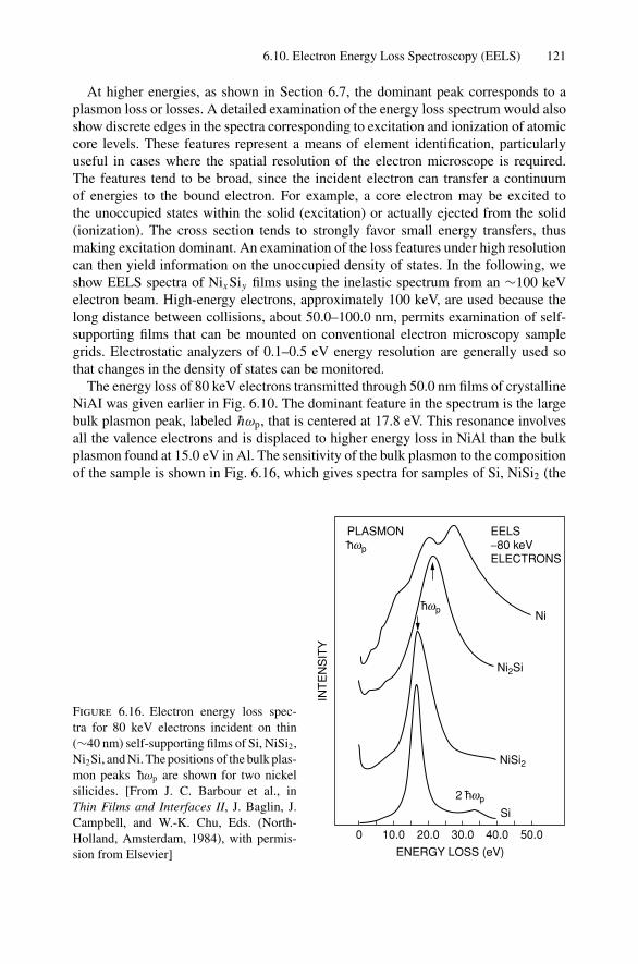
6.10. Electron Energy Loss Spectroscopy (EELS) 121
At higher energies, as shown in Section 6.7, the dominant peak corresponds to aplasmon loss or losses. A detailed examination of the energy loss spectrum would alsoshow discrete edges in the spectra corresponding to excitation and ionization of atomiccore levels. These features represent a means of element identification, particularlyuseful in cases where the spatial resolution of the electron microscope is required.The features tend to be broad, since the incident electron can transfer a continuumof energies to the bound electron. For example, a core electron may be excited tothe unoccupied states within the solid (excitation) or actually ejected from the solid(ionization). The cross section tends to strongly favor small energy transfers, thusmaking excitation dominant. An examination of the loss features under high resolutioncan then yield information on the unoccupied density of states. In the following, weshow EELS spectra of Nix Siy films using the inelastic spectrum from an ∼100 keVelectron beam. High-energy electrons, approximately 100 keV, are used because thelong distance between collisions, about 50.0–100.0 nm, permits examination of self-supporting films that can be mounted on conventional electron microscopy samplegrids. Electrostatic analyzers of 0.1–0.5 eV energy resolution are generally used sothat changes in the density of states can be monitored.
The energy loss of 80 keV electrons transmitted through 50.0 nm films of crystallineNiAI was given earlier in Fig. 6.10. The dominant feature in the spectrum is the largebulk plasmon peak, labeled hωp, that is centered at 17.8 eV. This resonance involvesall the valence electrons and is displaced to higher energy loss in NiAl than the bulkplasmon found at 15.0 eV in Al. The sensitivity of the bulk plasmon to the compositionof the sample is shown in Fig. 6.16, which gives spectra for samples of Si, NiSi2 (the
PLASMONhwp
hwp
2 hwp
Si
ENERGY LOSS (eV)
INT
EN
SIT
Y
0 10.0 20.0 30.0 40.0 50.0
Ni
NiSi2
Ni2Si
EELS−80 keVELECTRONS
Figure 6.16. Electron energy loss spec-tra for 80 keV electrons incident on thin(∼40 nm) self-supporting films of Si, NiSi2,Ni2Si, and Ni. The positions of the bulk plas-mon peaks hωp are shown for two nickelsilicides. [From J. C. Barbour et al., inThin Films and Interfaces II, J. Baglin, J.Campbell, and W.-K. Chu, Eds. (North-Holland, Amsterdam, 1984), with permis-sion from Elsevier]
122 6. Electron–Electron Interactions and the Depth Sensitivity of Electron Spectroscopies
most Si-rich nickel silicide), Ni2Si, and Ni. The bulk plasmon peaks become broaderand are centered at increasingly higher energies with increasing Ni concentration.Silicon, NiSi2, and Ni2Si have bulk plasmon energies, hωp, of 16.7, 17.2, and 21.8 eV,respectively. The spectra in Fig. 6.16 were scaled such that the plasmon peak heights areequivalent, even though the absolute intensity of the Si plasmon peak is much greaterthan the corresponding peaks in the Ni spectrum.
The bulk plasmon may also be used to estimate the relative amount of plural scat-tering. Scattering of the incident electron beam by two sequential bulk plasmon eventsproduces a peak in the loss function at twice the bulk plasmon energy, as can be seenin the peak in the Si spectrum at 33.4 eV in Fig. 6.16. From the figure we can see thatthe ratio of the double to single plasmon intensity is quite small, which indicates thatthe sample thickness is less than the mean free path for excitation of bulk plasmons.
In the EELS spectrum of NiAI (Fig. 6.10), weak but sharp peaks appear at highenergy loss values of ∼70 eV. These correspond to excitation of individual deeplybound core electrons to the unfilled conduction band states. The Al L23 transition ofabout 75 eV in the spectrum of Figure 6.10 corresponds to excitations of the Al 2p coreelectrons to unfilled states above the Fermi level. In this figure, the measured Al L23
data points are aligned with calculated values (solid line) of the density of states (DOS).The experimental points mirror the DOS shape, indicating that EELS measurementscan be used to determine the density of states above the conduction band.
The energy loss spectra for nickel silicides also display features due to core ex-citations. Figure 6.17a is an electron energy loss spectrum of a 40 nm thick NiSi2self-supporting film taken over the energy region from 0 to 138 eV. The largest peakis the bulk plasmon ( hωp), with the Ni M23 and Si L23 core excitation peaks at higherenergies, magnified by 100 and 350 times, respectively. No multiple scattering eventsare discernible in the EELS spectrum (no higher-order plasmon loss peaks are present),indicating that the background on the low energy loss side of the Ni before the Ni Medge is primarily due to the tail of the plasmon peak. The heights of the steps at the NiM and Si L edges can be used to determine the composition.
At energies below the bulk plasmon peak (energy loss values 0–15 eV in Fig. 6.17a),there are peaks in the spectrum that correspond to interband transitions. The interbandtransitions involve a convolution of the valence and conduction band densities of statesand hence are more difficult to interpret than core level spectra, where the initial statesare sharp.
The differences in the spectrum step heights at the Ni and Si edges for different Nito Si concentration ratios can be seen in Fig. 6.17b, which gives spectra taken fromsamples of Ni2Si and NiSi2. The yield YA for detection of an incident electron that losesenergy E A when passing through a material of thickness t containing a concentrationNA of atoms is given by
YA = Q NA t σA η , (6.37)
where Q is the integrated incident electron current density, NAt is the number of A atomscontributing to the inelastic scattering events, σA is the cross section for excitationof an electron in a given core energy level of atom A, η is a collection efficiency,and is the detector collection angle. Equation 6.37 assumes the collected electronsexperience only single inelastic scattering events. Provided that the collection efficiency
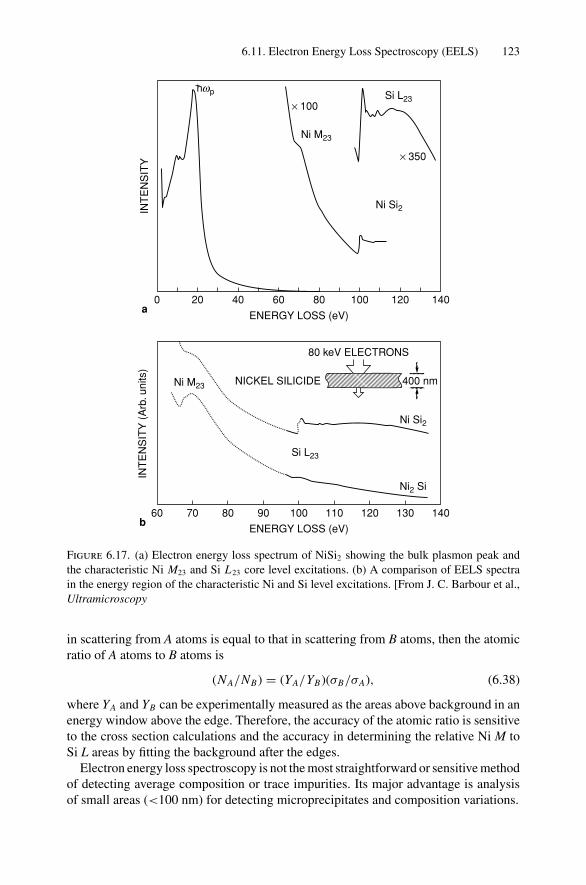
6.11. Electron Energy Loss Spectroscopy (EELS) 123
INT
EN
SIT
Y
× 100
× 350
Ni M23
Ni M23
Ni Si2
Ni Si2
Si L23
Si L23
NICKEL SILICIDE
80 keV ELECTRONS
Ni2 Si
0
60 70 80 90 100 110 120 130 140
14012010080604020
ENERGY LOSS (eV)
ENERGY LOSS (eV)
INT
EN
SIT
Y (
Arb
. uni
ts)
hwp
400 nm
b
a
Figure 6.17. (a) Electron energy loss spectrum of NiSi2 showing the bulk plasmon peak andthe characteristic Ni M23 and Si L23 core level excitations. (b) A comparison of EELS spectrain the energy region of the characteristic Ni and Si level excitations. [From J. C. Barbour et al.,Ultramicroscopy 14, 79 (1984).]
in scattering from A atoms is equal to that in scattering from B atoms, then the atomicratio of A atoms to B atoms is
(NA/NB) = (YA/YB)(σB/σA), (6.38)
where YA and YB can be experimentally measured as the areas above background in anenergy window above the edge. Therefore, the accuracy of the atomic ratio is sensitiveto the cross section calculations and the accuracy in determining the relative Ni M toSi L areas by fitting the background after the edges.
Electron energy loss spectroscopy is not the most straightforward or sensitive methodof detecting average composition or trace impurities. Its major advantage is analysisof small areas (<100 nm) for detecting microprecipitates and composition variations.
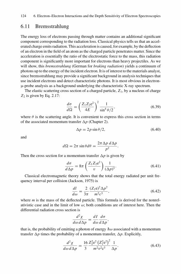
124 6. Electron–Electron Interactions and the Depth Sensitivity of Electron Spectroscopies
6.11 Bremsstrahlung
The energy loss of electrons passing through matter contains an additional significantcomponent corresponding to the radiation loss. Classical physics tells us that an accel-erated charge emits radiation. This acceleration is caused, for example, by the deflectionof an electron in the field of an atom as the charged particle penetrates matter. Since theacceleration is essentially the ratio of the electrostatic force to the mass, this radiationcomponent is significantly more important for electrons than heavy projectiles. As wewill show, this bremsstrahlung (German for braking radiation) yields a continuum ofphotons up to the energy of the incident electron. It is of interest to the materials analyst,since bremsstrahlung may provide a significant background in analysis techniques thatuse incident electrons and detect characteristic photons. It is most obvious in electron-µ-probe analysis as a background underlying the characteristic X-ray spectrum.
The elastic scattering cross section of a charged particle, Z1, by a nucleus of chargeZ2 is given by Eq. 2.17:
dσ
d=(
Z1 Z2e2
4E
)21
sin4 θ/2, (6.39)
where θ is the scattering angle. It is convenient to express this cross section in termsof the associated momentum transfer p (Chapter 2).
p = 2p sin θ/2, (6.40)
and
d = 2π sin θdθ = 2πp dp
p2.
Then the cross section for a momentum transfer p is given by
dσ
dp= 8π
(Z1 Z2e2
v
)1
(p)3. (6.41)
Classical electromagnetic theory shows that the total energy radiated per unit fre-quency interval per collision (Jackson, 1975) is
dl
dω= 2
3π
(Z1e)2p2
m2c3, (6.42)
where m is the mass of the deflected particle. This formula is derived for the nonrel-ativistic case and in the limit of low ω; both conditions are of interest here. Then thedifferential radiation cross section is
d2χ
dω dp= d I
dω
dσ
dp,
that is, the probability of emitting a photon of energy hω associated with a momentumtransfer p times the probability of a momentum transfer, p. Explicitly,
d2χ
dω dp= 16
3
Z22e2(Z2
1e2)2
m2v2c3
1
p. (6.43)
6.11. Bremsstrahlung 125
We integrate over all possible energy transfers pmin to pmax to find the frequencyspectrum,
dχ
dω= 16
3
Z22e2(Z2
1e2)2
m2v2c3ln
pmax
pmin.
To determine the ratio, pmax/pmin, we consider in detail the kinematics of theprocess. Energy conservation and momentum conservation can be written as
E = E ′ + hω,
and
(p)2 = (p − p′ − k)2 = (p − p′)2, (6.44)
where E, p and E ′, p′ refer to the energy and momentum of the particle before andafter the collision, and hk is the momentum of the emitted bremsstrahlung photon.Here we have neglected the momentum associated with the photon. Then
pmax
pmin= p + p′
p − p′ =(√
E − √E − hω
)2
hω,
so
dχ
dω= 16
3
Z22e2(Z2
1e2)2
m2v2c3ln
(2 − hω/E + 2
√1 − hω/E
hω/E
). (6.45)
This function falls off as ( hω/E) for small hω/E and flattens out with a sharp cut-offat E = hω (Fig. 6.18). This form of the bremsstrahlung spectrum was first derived byBethe and Heftier in 1934.
The radiation cross section, dχ/dω, is proportional to Z 22 Z4
1/m2, showing that theemission is most important for light particles (electrons) in materials of high atomicnumber. The total energy lost by radiation for a particle traversing a material of N nucleiper unit volume is
dErad
dx= N
ωmax∫0
dχ (ω)
dωdω.
Letting x = hω/E and noting that(1 + √
1 − x√x
)2
=(
2 − x + 2√
1 − x
x
),
we have
d Erad
dx= 16
3
N Z22e2(Z2
1e2)2
c3 h
1∫0
ln
(1 + √
1 − x√x
)dx . (6.46)
The dimensionless integral has the value of unity. The radiative loss is essentiallyenergy independent. The ratio of radiative loss (for electrons) to nonradiative loss,
126 6. Electron–Electron Interactions and the Depth Sensitivity of Electron Spectroscopies
0 0.2 0.4 0.6 0.8 1.0
Bethe-Heitler
/hwE
dχ N
R
dw
Figure 6.18. Radiation cross section (energy × area / unit frequency) for nonrelativisticCoulomb collisions as a function hωp/E (Eq. 6.45).
d Erad/d Enr, is approximately given by
dErad
dEnr
∼= 4
3π
Z2
137
(v
c
)2, (6.47)
and is small for v < c. For electron probe analysis, we are concerned that thebremsstrahlung photon may obscure the characteristic energy of interest. As shownby Evans, the ratio of the ionization cross section to the radiative cross section isroughly Z2(v/c)2/137, or −0.01 for Z2/137 = 4 and 100 keV electrons. This is whatsets the limit for detecting approximately 1% of an impurity in a solid matrix.
Problems
6.1. Draw the curve of Auger yield versus overlayer thickness for the signal from theoverlayer atoms in the case of(a) uniform growth in a layer-by-layer fashion and(b) island growth with 50% coverage.Assume that the mean free path λ is equivalent to two monolayers.
Problems 127
6.2. Typically, electron impact ionization cross sections have a maximum at E/EB = 3.Calculate the value of E at σmax for the K shell and L shell of Si for incidentelectrons. As discussed in the text, ionization cross sections depend primarily onthe velocity of the incident charged particles; calculate the energies of incidentprotons where the protons have the same velocities as those of the electrons in theexamples for the ionization of K- and L-shell electrons.
6.3. You deposit an Al film on a copper substrate, and use 3 keV electrons to ex-cite Cu Lα X-rays for the determination of Cu penetration into Al. What thick-ness of the deposited Al film is required so that the electrons do not excite CuLα X-rays in the Cu substrate? Use values of K = 0.064 and γ = 1.68, andEq. 6.34.
6.4. You are carrying out a transmission electron energy loss experiment with100 keV electrons incident on an Al film where the bulk plasmon energy is 15.3 eV.Estimate the value of λ for 100 keV electrons. Compare the values of the rangeof 100 keV electrons using Eq. 6.34 with that of Eq. 6.31 where you assume thatdE/dx is a constant evaluated at 50 keV.
6.5. The Si LVV Auger electron is emitted with 92 eV. Assuming that the only mech-anism for energy loss is ionization of Si atoms (Appendix 4), calculate the meanfree path for these electrons(a) with the relations given in Section 6.7 and(b) with λ = 1/Nσ , where σ is the cross section given in Eq. 6.11.
6.6. In a vacuum system, the flux of gas atoms impinging on a surface is Nv/4, whereN is the density of atoms per cm3 and v is the thermal velocity of the gas atoms.Assuming every gas atom sticks, calculate the value of N such that an absorbedlayer of oxygen atoms is thinner than two monolayers after one hour. Express N intorr, noting that one atmosphere (760 torr) is approximately 2 × 10¹⁹ atoms/cm3.It is these basic requirements that determine the need for good vacuum in thin filmanalysis.
6.7. Consider a semiconductor structure consisting of 2.5 nm of Si, one monolayerof Ge, 2.5 nm of Si, and one monolayer of Ge on a thick Si substrate. Imaginean Auger/sputter profiling analysis of this structure in which one detects the GeMVV Auger line (λ = 1.0 nm in Si). Assume that the sputtering process removesone monolayer of material at a time with no interface broadening or other mixingeffects. Write an equation for the yield of Ge as a function of material removed,and plot the Ge profile expected in this kind of analysis. (Ignore the effect of thesingle monolayers of Ge in the extinction path.)
References
1. C. R. Brundle and A. D. Baker, Eds., Electron Spectroscopy: Theory, Techniques and Ap-plications (Academic Press, New York, 1981).
2. M. Cardona and L. Ley, Eds., Photoemission in Solids, I, II, Topics in Applied Physics, Vols.26 and 27 (Springer-Verlag, New York, 1978 and 1979).
3. T. A. Carlson, Photoelectron and Auger Spectroscopy (Plenum Press, New York, 1975).4. W. Czanderna, Ed., Methods of Surface Analysis (Elsevier Science Publishing Co., New
York, 1975).

128 6. Electron–Electron Interactions and the Depth Sensitivity of Electron Spectroscopies
5. G. Ertl and J. Kuppers, Low Energy Electrons and Surface Chemistry (Verlag Chemie Inter-national, Weinheim, 1974).
6. R. D. Evans, The Atomic Nucleus (McGraw-Hill, New York, 1955).7. J. I. Goldstein, D. E. Newbury, P. Echlin, D. C. Joy, C. Fiori, and E. Lifshin, Scanning
Electron Microscopy and X-ray Microanalysis (Plenum Press, New York, 1981).8. H. Ibach, Ed., Electron Spectroscopy for Surface Analysis, Topics in Current Physics, Vol.
4 (Springer-Verlag, New York, 1977).9. J. D. Jackson, Classical Electrodynamics, 2nd ed. (John Wiley and Sons, New York, 1975).
10. L. C. Fledman and J. W. Mayer, Fundamentals of Surface and Thin Film Analysis (PrenticeHall, New Jersey, 1986).
7X-ray Diffraction
7.1 Introduction
Crystalline structures are deduced by the diffraction of known radiation incident fromsolid materials. The three-dimensional regularity of unit cells in crystalline materialsresults in coherent scattering of the radiation. The directions of the scattered beamsare a function of the wavelength of the radiation and the specific interatomic spacing(dhkl) of the plane from which the radiation scatters. The intensity of the scatteredbeam depends on the position of each atom in the unit and on the orientation of thecrystal relative to the direction of the incident X-ray beam. Those beams that scatter ina constructive manner result in allowed reflections, i.e., the intensity is a nonzero value.Those beams that scatter in a destructive manner result in unallowed reflections, i.e.,the intensity has a minimal value. Each of the constructively scattered beams dependsdirectly on the wavelength of the incident radiation. Having said this, we must addressthe issue: Why is the wavelength important? One of the requirements for diffractionis that the wavelength of the incident radiation λ must be smaller than the distancebetween scattering sites. Typically, in crystalline solids, we desire to measure atomicspacing on the order of the lattice constants, e.g., 0.2–0.4 nm. Hence, we must useradiation with wavelengths less than 0.2 nm. This range of wavelength includes thoseof X-rays and high-energy electrons. Another criteria is that the scattering occurs ina coherent manner, i.e., the energy of the incident radiation equals the energy of thescattered radiation.
W.L. Bragg derived a simplistic description of coherent scattering from an array ofperiodic scattering sites, such as atoms in a crystalline solid. The scalar descriptionof diffraction considers the case of monochromatic radiation impinging onto sheets ofatoms spaced at dhkl within the crystal. The wavelength λ of the radiation is smallerthan the interatomic spacing dhkl of the specific (hkl) plane. Based on this description ofdiffraction, we can conduct experiments to determine the distance between reflectingplanes, crystallographic structure, coefficient of thermal expansion, texture, stress, andcomposition of thin films.
X-rays typically used in diffraction analysis penetrate to a depth of 1–2 µm, depend-ing on the atomic number and destiny of the sample (see Section 8.8). This limits toapproximately one micron the depth at which useful information can be derived.
130 7. X-ray Diffraction
7.2 Bragg’s Law in Real Space
We now know that when a solid is irradiated under specific conditions, unique reflectionsare allowed. However, the question posed is:
In a straightforward manner, can we predict the angle of specific reflections?
Historical records show evidence of Laue’s diffraction experiments prior to the pub-lication of W.L. Bragg’s explanation of diffraction of radiation by crystalline solids.However, it was the inquisitive attempts by W.L. Bragg to resolve an intellectual debatebetween his father, W.H. Bragg, and Laue that resulted in the formulation of the famousBragg’s Law.
Laue argued that only optical rules determine the occurrences of diffraction (i.e.,wave interactions only). Radiation acts as waves, and scattering depends on the opticallaws of scattering (e.g., Law of Reflectivity) and of constructive interference (i.e., wavesin phase add constructively and waves out of phase add destructively). These publishedrules even gained the name the Laue Equations. (We will review these equations whenwe develop Bragg’s Law vectorally in Section 8.4). Laue’s description of diffractionin three-dimensional space required solving three equations with twelve unknowns.Even then, the derivation is arduous. W.H. Bragg’s rebuttal stated that any symmetricalelements present in the diffraction pattern reduces the number of unknowns and thatonly particle–particle interactions induce diffraction. Kinetic theory required that theparticles scatter from atoms coherently, i.e., the incident particle does not lose anyenergy during the scattering event. Even the earliest Laue experiment supported thisaccount. W.L. Bragg utilized all the above precepts to derive a simplistic descriptionof coherent scattering. The actual development first appeared in vector form. However,the most recognized form appears in scalar form and is represented in Fig. 7.1.
The scalar description of diffraction considers the case of monochromatic radiationimpinging on two sheets of atoms in the crystal, spaced at a distance of dhkl betweenthe reflecting planes. Invoking the Law of Reflectivity (or Reflections), θin = θout, gives
180 = ψ + 90 + α
= (90 − θ) + 90 + α
θ = α.
Constructive inference occurs if and only if the wave scattered by the atoms results in atotal path difference (2P) for the reflected waves that is equal to integer (n) multiplesof λ:
nλ = 2P = 2dhkl sin θ. (7.1)
Hence, the scalar form of Bragg’s Law, nλ = 2dhkl sin θ , defines the condition fordiffraction.
7.2.1 X-ray Powder Analysis
The simplest of all modern X-ray analyses is powder analysis using an X-ray diffrac-tometer. The technique can be used to characterize powders as well as polycrystallinematerials. The material of interest is ground to produce a fine, randomly orientated
7.2. Bragg’s Law in Real Space 131
∆P∆P
dhkl
α
ψ
θin θout
Figure 7.1. Development of Bragg’s Law.
powder, with each particle in the powder consisting of small single crystals or an ag-gregate of crystals 10 µm or less. The powder is placed into a recess of a plastic sampleholder and leveled flat in the sample holder with a straight edge.
The key components of a modern diffractometer include a monochromatic radiationsource, sample stage (goniometer), radiation detection system, enclosure, and safetyfeatures. One of the most common configurations is the θ–θ upright. This type ofdiffractometer has a movable detector and X-ray source, rotating about the circumfer-ence of a circle centered on the surface of a flat powder specimen. Figure 7.2 showsthe beam path schematically. The intensity of a diffracted beam is measured directlyby an electronic solid-state detection system. The scattered X-rays dissipate energyby generating electron–hole pairs in the detector. The electronic system converts thecollected charge into voltage pulses. The electronics counts the number of pulses per
sample
source detector
side view
2
Figure 7.2. Schematic of a θ–θ upright showshow the source and detector each move at a con-stant rate of θ/s relative to the sample. Hence,the source and detector move at constant rate of2θ/s relative to one another. This tool is idealfor loose powders and large samples.
132 7. X-ray Diffraction
Table 7.1. Normalized h2 + k2 + l2 values for the BCC and FCC structures.
BCC FCC
(hkl) h2 + k2 + l2 nomalized (hkl) h2 + k2 + l2 nomalized
(0 1 1) 2 1.00 (1 1 1) 3 1.00(2 0 0) 4 2.00 (2 0 0) 4 1.33(1 1 2) 6 3.00 (2 2 0) 8 2.67(0 2 2) 8 4.00 (3 1 1) 11 3.67(0 1 3) 10 5.00 (2 2 2) 12 4.00(2 2 2) 12 6.00 (4 0 0) 16 5.33(1 2 3) 14 7.00 (3 3 1) 19 6.33(4 0 0) 16 8.00 (4 2 0) 20 6.67
unit of time, and this number is directly proportional to the intensity of the X-ray beamentering the detector.
7.2.2 Data Analysis
Software for peak location and intensity determination allows for significant time sav-ings during the identification of an unknown specimen. Even with this luxury, experi-enced operators still examine each peak of every spectrum, inspecting peak positionsand shapes, the presence or absence of peaks, and relative background levels. The useof software packages without understanding the algorithms that are employed can leadto serious misinterpretation. Hence, we will index a diffraction pattern from first prin-ciples and will start with the simplest case: the analysis of FCC and BCC structures.
Indexing a diffraction pattern (also called a diffractogram or spectrum) involvesdetermining the lattice constant and structure and labeling each peak with its appropriatehkl designation. Starting with Bragg’s Law, we rewrite dhkl in terms of the latticeparameter ao and then rearrange the equation and square both sides:
nλ = 2dhkl1 sin θ = 2ao1√
h2 + k2 + l2sin θ,√
h21 + k2
1 + l21 = 2
ao1
nλsin θ = κ sin θ, (7.2)
h21 + k2
1 + l21 = κ2 sin2 θ.
The next step is to normalize all the equations relative to the equation for the firstreflection:
(h2i + k2
i + l2i )i
(h21 + k2
1 + l21)1
= κ2 sin2 θ
κ2 sin2 θ= sin2 θ
sin2 θ. (7.3)
In a later section, the structure factor calculations give the relationship for allowedreflections for the cases of FCC and BCC structures:
FCC — h, k, l unmixed (all odd or all even numbers)
BCC — h + k + l equals an even number
Table 7.1 lists the normalized values for both BCC and FCC structures based on Eq. 7.3.
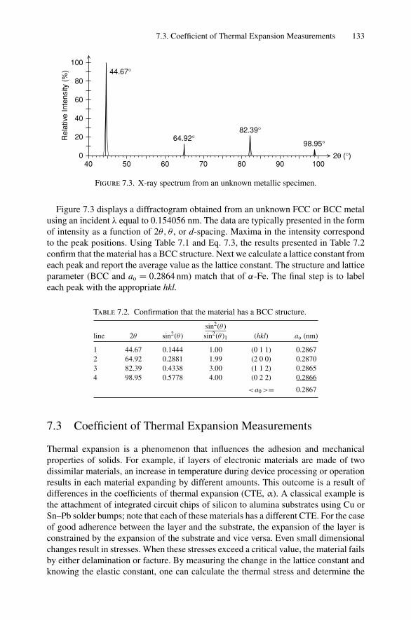
7.3. Coefficient of Thermal Expansion Measurements 133
100
80
60
40
40 50 60 70 80 90 100
20
0
Rel
ativ
e In
tens
ity (
%) 44.67°
64.92°82.39°
98.95°
2θ (°)
Figure 7.3. X-ray spectrum from an unknown metallic specimen.
Figure 7.3 displays a diffractogram obtained from an unknown FCC or BCC metalusing an incident λ equal to 0.154056 nm. The data are typically presented in the formof intensity as a function of 2θ, θ , or d-spacing. Maxima in the intensity correspondto the peak positions. Using Table 7.1 and Eq. 7.3, the results presented in Table 7.2confirm that the material has a BCC structure. Next we calculate a lattice constant fromeach peak and report the average value as the lattice constant. The structure and latticeparameter (BCC and ao = 0.2864 nm) match that of α-Fe. The final step is to labeleach peak with the appropriate hkl.
Table 7.2. Confirmation that the material has a BCC structure.
sin2(θ )line 2θ sin2(θ ) sin2(θ )1 (hkl) ao (nm)
1 44.67 0.1444 1.00 (0 1 1) 0.28672 64.92 0.2881 1.99 (2 0 0) 0.28703 82.39 0.4338 3.00 (1 1 2) 0.28654 98.95 0.5778 4.00 (0 2 2) 0.2866
<a0 >= 0.2867
7.3 Coefficient of Thermal Expansion Measurements
Thermal expansion is a phenomenon that influences the adhesion and mechanicalproperties of solids. For example, if layers of electronic materials are made of twodissimilar materials, an increase in temperature during device processing or operationresults in each material expanding by different amounts. This outcome is a result ofdifferences in the coefficients of thermal expansion (CTE, α). A classical example isthe attachment of integrated circuit chips of silicon to alumina substrates using Cu orSn–Pb solder bumps; note that each of these materials has a different CTE. For the caseof good adherence between the layer and the substrate, the expansion of the layer isconstrained by the expansion of the substrate and vice versa. Even small dimensionalchanges result in stresses. When these stresses exceed a critical value, the material failsby either delamination or facture. By measuring the change in the lattice constant andknowing the elastic constant, one can calculate the thermal stress and determine the
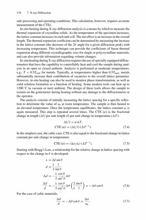
134 7. X-ray Diffraction
safe processing and operating conditions. This calculation, however, requires accuratemeasurement of the CTEs.
In-situ heating during X-ray diffraction analysis is a means by which to measure thethermal expansion of crystalline solids. As the temperature of the specimen increases,the lattice constant increases in each unit cell. The net effect is an increase in the overalllength. The thermal expansion coefficient can be determined by measuring the increasein the lattice constant (the decrease of the 2θ angle for a given diffraction peak) withincreasing temperature. This technique can provide the coefficients of linear thermalexpansion along different crystallographic axes for single or polycrystalline materials,and can also provide information regarding volume changes.
In-situ heating during X-ray diffraction requires the use of specially equipped diffrac-tometers that have the capability to controllably heat and cool the sample during anal-ysis in an open or closed ambient. Analysis is performed at moderate temperatures,e.g., T < 0.5Tmelt for metals. Typically, at temperatures higher than 0.5Tmelt, metalssubstantially increase their contribution of vacancies to the overall lattice parameter.However, in-situ heating can also be used to monitor phase transformation, as well assolid solution formation as a function of heating. Some modern tools can heat up to1200 C in vacuum or inert ambient. The design of these tools allows the sample toremain on the goniometer during heating without any damage to the diffractometer orthe operator.
The analysis consists of initially measuring the lattice spacing for a specific reflec-tion to determine the value of a0 at room temperature. The sample is then heated toan elevated temperature. Once the temperature equilibrates, the lattice constant ai isagain measured. This step is repeated several times. The CTE (α) is the fractionalchange in length (l) per unit length (l) per unit change in temperature (T ):
l/ l = αT,
CTE (α) = (l/ l) (T −1). (7.4)
In the simplest case, the cubic case, CTE is also equal to the fractional change in latticeconstant per unit change in temperature:
CTE (α) = (a/ai) (T −1). (7.5)
Starting with Bragg’s Law, a relationship for the relative change in lattice spacing withrespect to the change in θ is developed:
λ = 2d sin θ
d = λ
2
1
sin θ
d = −λ
2
cos θ
sin2 θθ
d
d= −λ
2
cos θ
sin2 θθ
(2
λ
sin θ
1
)= −θ cot θ. (7.6)
For the case of cubic materials,
d
d= −θ cot θ = a
a0. (7.7)
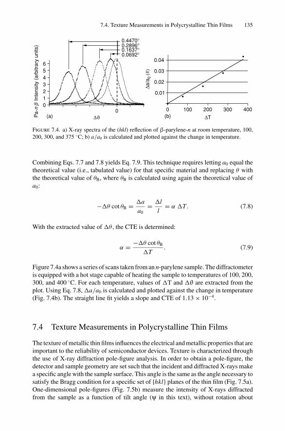
7.4. Texture Measurements in Polycrystalline Thin Films 135
6543210
0∆
0.4470°0.2896°0.1637°0.0692°
0 100 200 300 400
0.04
0.03
0.02
0.01
∆T
∆a/a
0 (#
)
Pa-
nb
Inte
nsity
(ar
bitr
ary
units
)
(a) (b)
Figure 7.4. a) X-ray spectra of the (hkl) reflection of β-parylene-n at room temperature, 100,200, 300, and 375 C; b) a/a0 is calculated and plotted against the change in temperature.
Combining Eqs. 7.7 and 7.8 yields Eq. 7.9. This technique requires letting a0 equal thetheoretical value (i.e., tabulated value) for that specific material and replacing θ withthe theoretical value of θB, where θB is calculated using again the theoretical value ofa0:
−θ cot θB = a
a0= l
l= α T . (7.8)
With the extracted value of θ , the CTE is determined:
α = −θ cot θB
T. (7.9)
Figure 7.4a shows a series of scans taken from an n-parylene sample. The diffractometeris equipped with a hot stage capable of heating the sample to temperatures of 100, 200,300, and 400 C. For each temperature, values of T and θ are extracted from theplot. Using Eq. 7.8, a/a0 is calculated and plotted against the change in temperature(Fig. 7.4b). The straight line fit yields a slope and CTE of 1.13 × 10⁻⁴.
7.4 Texture Measurements in Polycrystalline Thin Films
The texture of metallic thin films influences the electrical and metallic properties that areimportant to the reliability of semiconductor devices. Texture is characterized throughthe use of X-ray diffraction pole-figure analysis. In order to obtain a pole-figure, thedetector and sample geometry are set such that the incident and diffracted X-rays makea specific angle with the sample surface. This angle is the same as the angle necessary tosatisfy the Bragg condition for a specific set of hkl planes of the thin film (Fig. 7.5a).One-dimensional pole-figures (Fig. 7.5b) measure the intensity of X-rays diffractedfrom the sample as a function of tilt angle (ψ in this text), without rotation about

136 7. X-ray Diffraction
φ(0--360°)X-ray outX-ray in
φ
ψ
θ θ
(a) (b)
ψ (0--90°)
Figure 7.5. Schematic drawing (a) showing the geometry of pole-figure measurements with anX-ray diffractometer, and (b) a diagram showing the corresponding stereographic projection.
an axis perpendicular to the sample surface. The results of one-dimensional pole-figure measurements are shown in the form of intensity versus tilt-angle (ψ) plots(Fig. 7.6). The 200 texture of Ag films on amorphous SiO2 is determined for samplesannealed at different temperatures. The Ag films display preferred 111 orientation
806040200
104
103
102
101
<111>
<111>
<100>
600 °C
400 °Cas-dep
Tilt Angle, ψ (degree)
111
In
tens
ity (
c/s)
Figure 7.6. 111 pole-figures obtained from Ag thin films on SiO2 substrates, as-deposited(solid line) and annealed at 400 C (dashed line) and 600 C (dotted line) for 1 hour in vacuum.

7.5. Strain Measurements in Epitaxial Layers 137
(texture) when annealed at different temperatures, respectively. At ψ (tilt angle) = 0,the 111 intensity is the highest, indicating that the Ag films are highly textured, with<111> directions of grains in the films being normal to the surface of the substrate.Theoretically, given a <111> texture orientation at ψ = 0, another 111-type set ofplanes can be expected to be present at ψ = 70.5 in cubic crystal systems. Consistentwith this expectation, high 111 intensities are detected at ψ = 70.5. Note that thetexturing increases with increased annealing.
A two-dimensional pole-figure is obtained by first setting the tilt angle, and thenmeasuring intensity as a function of sample rotation (φ) about an axis perpendicular tothe surface of the sample (see Fig. 7.5a,b). The sample is rotated from 0 to 360(φ).After completing an azimuthal rotation, the sample is tilted (ψ) by a single tilt-anglestep (typically 1). Azimuthal rotation of the sample is repeated, while the intensityof the diffracted beam is recorded. This process is repeated for the entire range ofdesired rotation and tilt angles. Three-dimensional contour plots are then generated toshow texture. The two-dimensional pole-figure measurements and three-dimensionalcontour maps are obtained from a 150 nm layer of Ag on SiO2 substrates, annealedin vacuum. Two-dimensional 200 pole-figures are plotted in Fig. 7.7a,b, and thecorresponding contour maps are displayed in Fig. 7.7c,d. Silver exhibits fiber-texturefor both as-deposited and annealed samples. In addition, the fiber-textured grains (111and 200) are distributed randomly about the normal to the substrate, i.e., the filmpossesses mosaic structure. This is indicated by the contour line-shapes being circularat each tilt-angle position. Due to the mosaic structure of the Ag, the 111 intensityat ψ = 70.5 is lower than the 111 intensity at ψ = 0. Upon annealing, the 200intensity is reduced and the 111 increases with temperature.
7.5 Strain Measurements in Epitaxial Layers
The strain in an epitaxial layer is determined by comparing the perpendicular and paral-lel lattice spacings (a) of the film to that of the underlying substrate asub and determiningwhether they are larger or smaller and by how much. The film is pseudomorphic whenlattice planes of the epilayer align with the lattice planes of the substrate. The resultingstrain values are expressed as [a/a]⊥ and [a/a]‖, and are based on the differencein the perpendicular and parallel lattice constants, respectively. Since these differencesare measured relative to the substrate, the substrate lattice spacing must be known.From these parameters, a strain value is calculated by determining the difference in thelattice spacing of the film from its bulk relaxed state.
The application of X-ray diffraction in thin film samples is illustrated by diffractionmeasurement of epitaxial layers of SiGeC layers on silicon. Initially, an asymmetricalscan is taken about a plane (hkl) not parallel to the surface plane, where that planemakes an angle ψ relative to the surface (see Fig. 7.8). Since, in this case, θin + ψand θout − ψ are not identical, the asymmetrical scan provides information about bothperpendicular spacing (a⊥) and parallel spacing (a‖). For analysis of Si-based structures,both (2 2 4) and (2 2 4) reflections are typically used (Fig. 7.9). In one case, the spectrumis a glancing incidence (2 2 4) reflection and the other is a (2 2 4) glancing exitingreflection. Note the presence of a peak from the Si substrate and from the SiGeC film in
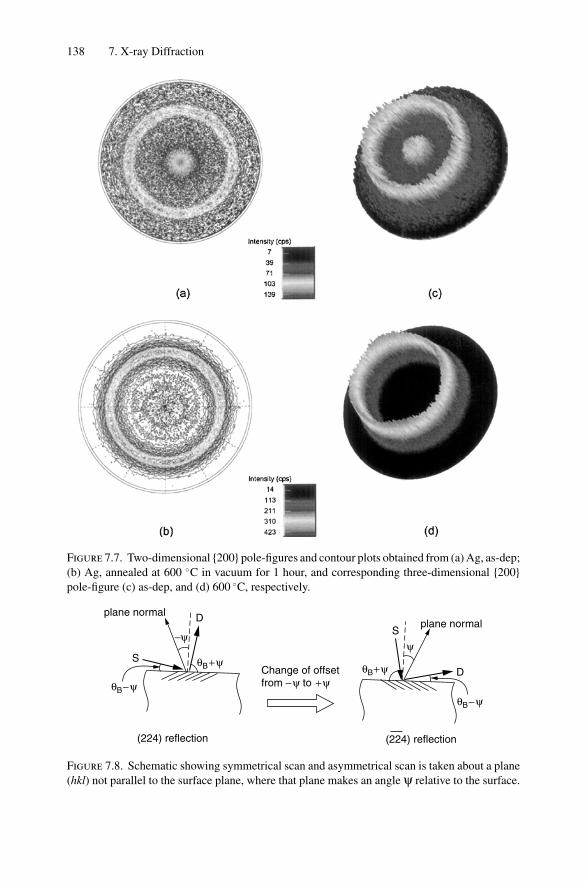
138 7. X-ray Diffraction
Figure 7.7. Two-dimensional 200 pole-figures and contour plots obtained from (a) Ag, as-dep;(b) Ag, annealed at 600 C in vacuum for 1 hour, and corresponding three-dimensional 200pole-figure (c) as-dep, and (d) 600 C, respectively.
plane normalplane normalD
S
S
DθB+ψ θB+ψ
θB−ψθB−ψ
−ψψ
Change of offsetfrom −ψ to +ψ
(224) reflection (224) reflection
Figure 7.8. Schematic showing symmetrical scan and asymmetrical scan is taken about a plane(hkl) not parallel to the surface plane, where that plane makes an angle ψ relative to the surface.
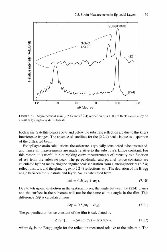
7.5. Strain Measurements in Epitaxial Layers 139
−1.2 −0.9 −0.6 −0.3 0.0 0.3
SiGeCLAYER
SUBSTRATE
(224)
(224)
∆θ (degree)
Rel
ativ
e in
tens
ity (
Arb
.Uni
t)
Figure 7.9. Asymmetrical scan (2 2 4) and (2 2 4) reflection of a 180 nm thick Ge–Si alloy ona Si(0 0 1) single-crystal substrate.
both scans. Satellite peaks above and below the substrate reflection are due to thicknessinterference fringes. The absence of satellites for the (2 2 4) peaks is due to dispersionof the diffracted beam.
For epilayer strain calculations, the substrate is typically considered to be unstrained,and hence all measurements are made relative to the substrate’s lattice constant. Forthis reason, it is useful to plot rocking curve measurements of intensity as a functionof θ from the substrate peak. The perpendicular and parallel lattice constants arecalculated by first measuring the angular peak separation from glancing incident (2 2 4)reflections, ω1, and the glancing exit (2 2 4) reflections, ω2. The deviation of the Braggangle between the substrate and layer, θ , is calculated from
θ = 0.5(ω1 + ω2). (7.10)
Due to tetragonal distortion in the epitaxial layer, the angle between the 224 planesand the surface in the substrate will not be the same as this angle in the film. Thisdifference ψ is calculated from
ψ = 0.5(ω1 − ω2). (7.11)
The perpendicular lattice constant of the film is calculated by
[a/a]⊥ = −θ cot(θB) + ψ tan(ψ), (7.12)
where θB is the Bragg angle for the reflection measured relative to the substrate. The
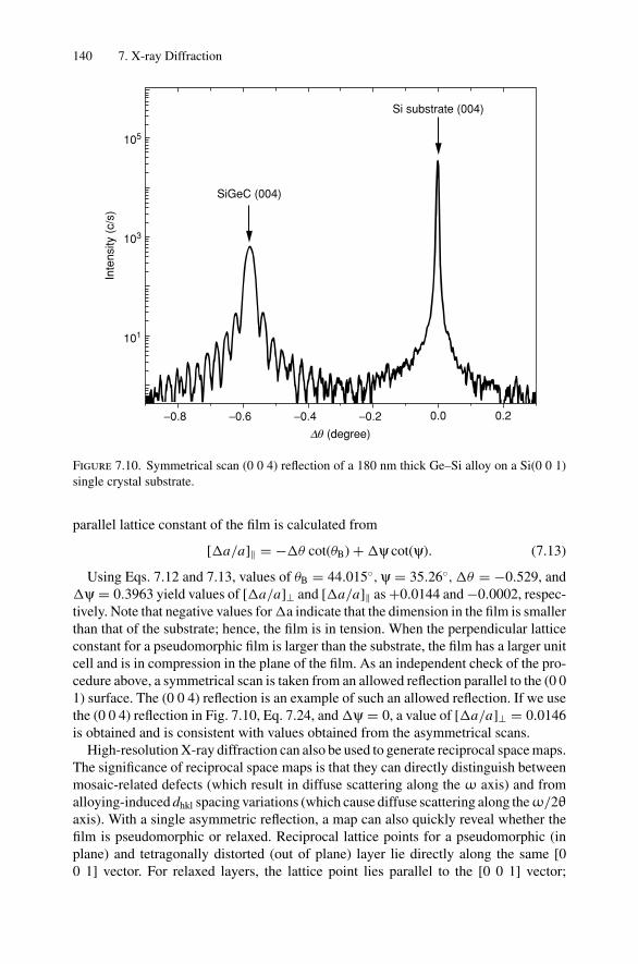
140 7. X-ray Diffraction
−0.8 −0.6 −0.4 −0.2 0.0
105
103
101
Dθ (degree)
Si substrate (004)
SiGeC (004)
Inte
nsity
(c/
s)
0.2
Figure 7.10. Symmetrical scan (0 0 4) reflection of a 180 nm thick Ge–Si alloy on a Si(0 0 1)single crystal substrate.
parallel lattice constant of the film is calculated from
[a/a]‖ = −θ cot(θB) + ψ cot(ψ). (7.13)
Using Eqs. 7.12 and 7.13, values of θB = 44.015, ψ = 35.26, θ = −0.529, andψ = 0.3963 yield values of [a/a]⊥ and [a/a]‖ as +0.0144 and −0.0002, respec-tively. Note that negative values for a indicate that the dimension in the film is smallerthan that of the substrate; hence, the film is in tension. When the perpendicular latticeconstant for a pseudomorphic film is larger than the substrate, the film has a larger unitcell and is in compression in the plane of the film. As an independent check of the pro-cedure above, a symmetrical scan is taken from an allowed reflection parallel to the (0 01) surface. The (0 0 4) reflection is an example of such an allowed reflection. If we usethe (0 0 4) reflection in Fig. 7.10, Eq. 7.24, and ψ = 0, a value of [a/a]⊥ = 0.0146is obtained and is consistent with values obtained from the asymmetrical scans.
High-resolution X-ray diffraction can also be used to generate reciprocal space maps.The significance of reciprocal space maps is that they can directly distinguish betweenmosaic-related defects (which result in diffuse scattering along the ω axis) and fromalloying-induced dhkl spacing variations (which cause diffuse scattering along the ω/2θ
axis). With a single asymmetric reflection, a map can also quickly reveal whether thefilm is pseudomorphic or relaxed. Reciprocal lattice points for a pseudomorphic (inplane) and tetragonally distorted (out of plane) layer lie directly along the same [00 1] vector. For relaxed layers, the lattice point lies parallel to the [0 0 1] vector;
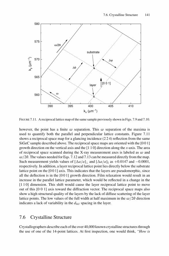
7.6. Crystalline Structure 141
580
575
570
565
560
390 395 400 405 410
substrate
layer
∆ψ
∆θ
ω
ω/2θ
kx (µm−1)
k y (
µm−1
)
[0 0 1]
Figure 7.11. A reciprocal lattice map of the same sample previously shown in Figs. 7.9 and 7.10.
however, the point has a finite ω separation. This ω separation of the maxima isused to quantify both the parallel and perpendicular lattice constants. Figure 7.11shows a reciprocal space map for a glancing incidence (2 2 4) reflection from the sameSiGeC sample described above. The reciprocal space maps are oriented with the [0 0 1]growth direction on the vertical axis and the [1 1 0] direction along the x-axis. The areaof reciprocal space scanned during the X-ray measurement axes is labeled as ω andω/2θ. The values needed for Eqs. 7.12 and 7.13 can be measured directly from the map.Such measurement yields values of [a/a]⊥ and [a/a]‖ as +0.0147 and −0.0001,respectively. In addition, a layer reciprocal lattice point lies directly below the substratelattice point on the [0 0 1] axis. This indicates that the layers are pseudomorphic, sinceall the deflection is in the [0 0 1] growth direction. Film relaxation would result in anincrease in the parallel lattice parameter, which would be reflected in a change in the[1 1 0] dimension. This shift would cause the layer reciprocal lattice point to moveout of this [0 0 1] axis toward the diffraction vector. The reciprocal space maps alsoshow a high structural quality of the layers by the lack of diffuse scattering of the layerlattice points. The low values of the full width at half maximum in the ω/2θ directionindicates a lack of variability in the dhkl spacing in the layer.
7.6 Crystalline Structure
Crystallographers describe each of the over 40,000 known crystalline structures throughthe use of one of the 14-point lattices. At first inspection, one would think, “How is
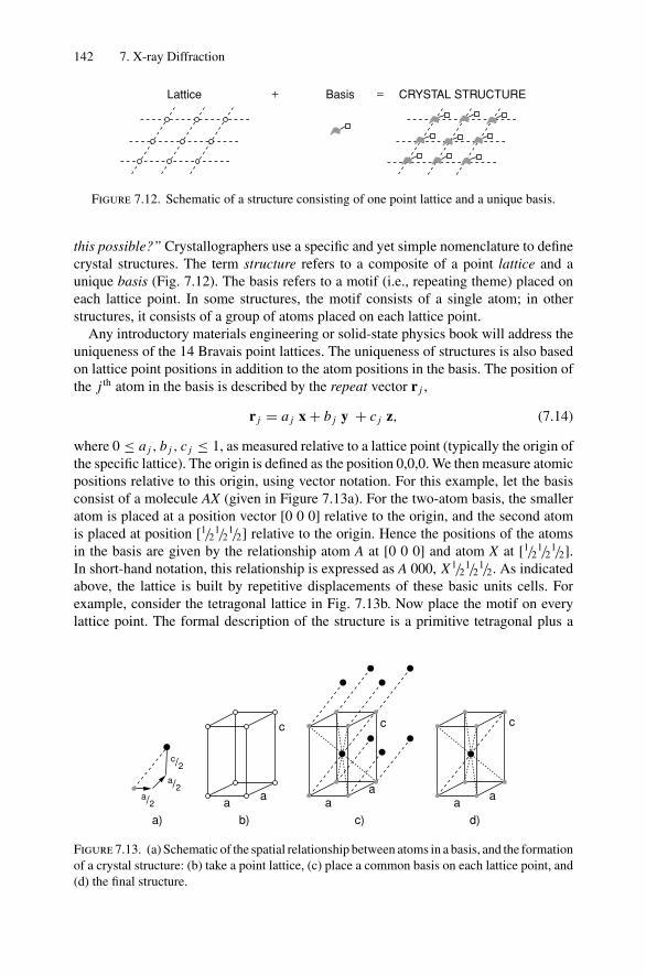
142 7. X-ray Diffraction
Lattice + Basis = CRYSTAL STRUCTURE
Figure 7.12. Schematic of a structure consisting of one point lattice and a unique basis.
this possible?” Crystallographers use a specific and yet simple nomenclature to definecrystal structures. The term structure refers to a composite of a point lattice and aunique basis (Fig. 7.12). The basis refers to a motif (i.e., repeating theme) placed oneach lattice point. In some structures, the motif consists of a single atom; in otherstructures, it consists of a group of atoms placed on each lattice point.
Any introductory materials engineering or solid-state physics book will address theuniqueness of the 14 Bravais point lattices. The uniqueness of structures is also basedon lattice point positions in addition to the atom positions in the basis. The position ofthe j th atom in the basis is described by the repeat vector r j ,
r j = a j x + b j y + c j z, (7.14)
where 0 ≤ a j , b j , c j ≤ 1, as measured relative to a lattice point (typically the origin ofthe specific lattice). The origin is defined as the position 0,0,0. We then measure atomicpositions relative to this origin, using vector notation. For this example, let the basisconsist of a molecule AX (given in Figure 7.13a). For the two-atom basis, the smalleratom is placed at a position vector [0 0 0] relative to the origin, and the second atomis placed at position [1/2
1/21/2] relative to the origin. Hence the positions of the atoms
in the basis are given by the relationship atom A at [0 0 0] and atom X at [1/21/2
1/2].In short-hand notation, this relationship is expressed as A 000, X1/2
1/21/2. As indicated
above, the lattice is built by repetitive displacements of these basic units cells. Forexample, consider the tetragonal lattice in Fig. 7.13b. Now place the motif on everylattice point. The formal description of the structure is a primitive tetragonal plus a
a) b) c) d)
aa
c
aa
c
aa
c
c/2a/2
a/2
Figure 7.13. (a) Schematic of the spatial relationship between atoms in a basis, and the formationof a crystal structure: (b) take a point lattice, (c) place a common basis on each lattice point, and(d) the final structure.
7.7. Allowed Reflections and Relative Intensities 143
two-atom basis 000, 1/21/2
1/2. Later we will use the formal notation to determine theallowed reflections during diffraction analysis. Note that Fig. 7.13c and Fig. 7.13dmaintain the same symmetry and hence they each describe the same structure.
Let us now examine the crystal structures of some widely used materials. The metalFe has a BCC structure that consists of a BCC lattice and a one-atom basis of Fe oneach lattice site. We describe its structure as BCC lattice + Fe 000. The atomic ar-rangement of the diamond structure consists of two interpenetrating FCC sublatticesdisplaced from each other by a
√3/4. Both sublattices are occupied by identical atoms.
Silicon, diamond, and germanium crystallize in this structure: FCC lattice + Si 000,1/4
1/41/4. The zinc-blend structure also consists of two interpenetrating FCC sublattices
displaced from each other by√
3 a/4, where a is the lattice parameter. In this case,one of the sublattices is occupied by one type of atom and the other sublattice is oc-cupied by another type of atom. GaAs, InP, and GaP crystallize in this structure: FCClattice + Ga 000, As 1/4
1/41/4. In the NaCl structure, Na and Cl ions reside on their
respective FCC sublattices. Furthermore, the nearest neighbors of Na+ ions are Cl−
ions. This structure occurs to avoid the electrostatic repulsion between the positively ornegatively charged ions. Based on the symmetry of the basis, the NaCl structure is de-scribed as FCC lattice + Na+ 000, Cl− 1/2
1/21/2 or FCC lattice + Cl− 000, Na+ 1/2
1/21/2.
In the CsCl structure, Cs and Cl ions reside on their respective simple cubic sublat-tice, and the structure is SC lattice + Cs+ 000, Cl− 1/2
1/21/2 or SC lattice +Cl− 000,
Cs+ 1/21/2
1/2.
7.7 Allowed Reflections and Relative Intensities
In X-ray diffraction, we view the incident and emergent radiation both as discreteparticles with a specific energy and as electromagnetic radiation with λ on the orderof 0.1 nm. Engineers and scientists use diffraction analyses to quantitatively determinecrystal structure, lattice parameter, orientation, defects, and mechanical properties.The analysis involves interrogating the sample with X-rays or electrons and interpretingthe resulting diffraction pattern. The pattern consists of a series of intensity peaks thatarise from coherent scattering from specific planes. Each peak corresponds to a specifichkl reflection and conveys information about crystal structure and symmetry. Note thatplanes are (hkl) and reflections are hkl. This leads us to the following question:
Can we predict the allowed reflections and their relative intensities?
Structure Factor Calculations (SFC) determine the resultant scattering power of thewhole crystal structure. Given the fact that the whole structure consists of a large num-ber of unit cells (all of which scatter in phase under Bragg diffraction conditions), theresultant scattering power need only be calculated for the contents of one unit cell.Structure factor calculations start by initially determining the relative scattering inten-sity of the atom relative to the scattering by a single electron. Secondly, we predict therelative scattering intensity of the unit cell relative to the scattering by a single electron.Those reflections that result in nonzero intensities are allowed. Those reflections thatresult in a zero intensity are not allowed.
144 7. X-ray Diffraction
13
sin θ/λ
fθ
Figure 7.14. Atomic scattering factor fϑ for Be as a function of sin θ /λ.
7.7.1 Scattering by the Atom—Atomic Scattering Factor
The efficiency of the atom in scattering waves is quantified relative to the scattering bya single electron. The atomic scattering factor fϑ is the amplitude of the wave scatteredby the atom relative to the amplitude of a wave scattered by an isolated electron.
fϑ = amplitude scattered by the atom/amplitude scattered by a single electron
= An/Ae (7.15)
The fθ depends on both scattering angle θ and λ of the incident radiation. Figure 7.14displays a schematic diagram showing the variation of the atomic scattering factor fθwith sin θ /λ for Be. Note that these two species have an identical number of electrons.At a zero scattering angle, the scattered waves are in phase and the scattered amplitudeis the sum from all the electrons, i.e., fθ equals Z (atomic number) in the atom or ion.As λ increases, the intensity decreases because the efficiency for scattering throughlarge angles is lower. From Appendix 5, the values can be determined for atoms andions. For example, the fθ value can be determined for the case when Mo Kα (λ ofMo Kα is 0.07107 nm) is incident on a Be atom at an angle of 16.52. First calculatethe value of sin θ /λ = sin(16.52)/0.07107 nm = 4.0 nm−1. The value of fθ can be obtainedfrom Appendix 5, and is found to be equal to 1.6. In a similar manner, Mo Kα incidenton N3+ at the same angle results in a fθ value of 2.0. Upon inspection, it becomesevident that atoms with greater numbers of electrons scatter radiation more effectively.
7.7.2 Scattering by Unit Cell and Structure Factor Calculations
A monochromatic beam incident upon a regularly spaced three-dimensional array ofatoms can result in an interference pattern. In this particular case, the path differencebetween scattered beams results in a phase difference. A phase difference of zero resultsin constructive inference. A phase difference of 180 results in destructive inference.The superimposition of all the scattered waves from the single unit cell produces theresultant intensity from the whole crystal. This resultant wave and the phase differenceare a function of the number of electrons and the positions of each of the atoms in the unitcell. The structure factor Fhkl therefore corresponds to the summation of amplitude Aof scattering of all the electrons of one unit cell relative to the amplitude of scattering
7.7. Allowed Reflections and Relative Intensities 145
θ θ θ
θ θ θ θ
θ
dhkl
Figure 7.15. Schematic of coherent scattering from a lattice with a basis of one atom.
from an isolated electron:
Fhkl = An/Ae
= amplitude of all atoms of the unit cell/amplitude of a single electron.
Structure factor calculations establish the allowed hkl reflections. In addition, SFCalso conveys the amplitude and the phase for each reflection. The intensity of thereflection is influenced by the direction and wavelength of the incident radiation andby the structure of the crystalline solid. Note that the presence of the reflection is notdependent on the method used to obtain the reflection or the type of radiation used.
Starting with the simplest case of a primitive unit cell with a single atom basis at eachlattice point, Fig. 7.15 displays a schematic of the incident and scattered waves for acrystalline lattice. For a specific set of (hkl) planes, each atom has an atomic scatteringfactor f0 at the correct Bragg angle. For all the atoms residing on the successive planes,the path difference is zero for the case of constructive interference. Hence, the totalscattered amplitude relative to a single electron is the sum of the contribution from allatoms [(1 atoms/8 corners)∗8 corners = 1 atom] in the unit cell, Fhkl , and this equals f0.
Next we consider the case for a two-atom basis (Fig. 7.16). Consider an atom placedat the origin with atomic scattering factor f0 and another atom placed at a positiondefined by r1, the position vector, and with atomic scattering factor f1. As previouslystated, r1 is expressed in terms of fractional coordinates [uvw] along the axes x, y, andz, respectively. The incident wave and scattered waves can be described by the vectorss0 and s, respectively. For a wave front scattering from points A and D, constructiveinterference will occur if the path difference PD = AB − CD is equal to an integral
θ
dhkl
θ θ
D
Cs
s0
B
r1
θ θr1
θ θr1
A
Figure 7.16. Schematic of coherent scattering from a lattice with a basis of two atoms.
146 7. X-ray Diffraction
multiple of λ:
P D = AB − C D
= r1 · s0 − r1 · s (7.16)
= r1 · (s0 − s) .
At this point, we need to solve Bragg’s Law vectorally in reciprocal space. We shall dothis later in Section 8.4. For the time being, we will accept that
PD = r1 · (s0 − s) = λ(hu1 + kv1 + lw1), (7.17)
where h, k, and l are Miller indices of the reflecting planes. Eq. 7.17 expresses thescattered wave’s path difference from different atoms in the unit cell (and from thebasis) conveniently as an angular phase difference (φ). This value is measured relativeto an atom at the origin of the unit cell (i.e., generally the origin of the basis as well).The resultant is calculated by the superimposition of waves, one from each atom inthe unit cell (and from the basis). The amplitude of each wave depends on the numberof electrons in the atom (atomic scattering factor, fθi, and scattering angle θ) and thephase, which depends on the position of the atom in the unit cell (and from the basis):
φn = (2π/λ) · PD
= (2π/λ) · λ(hun + kvn + lwn)
= 2π (hun + kvn + lwn). (7.18)
Equation 7.18 gives the phase difference for any unit cell of any shape. In general,to add combinations of the atoms, we need only to use a vector-phase relationship inwhich the vectors are proportional to the atom’s atomic scattering.
7.7.3 Allowed Reflections
Now we only need to sum the scattering of all the atoms in the unit cell to determinethe relative intensity of allowed reflections. This sum is called the structure factor Fhkl
for the crystal structure. For a primitive cell, the scattering from the whole unit cell(given by the structure factor Fhkl) is the same as the scattering from one single atom(given by the atomic scattering factor fθ ). The scattered amplitude (A) from each atomin the unit cell can be described as
A = fθ exp [iφ], (7.19)
where fθ is the scattering factor for a single atom and φ is the phase of the wave withrespect to the wave scattered from the origin of the unit cell. If diffraction occurs fromthe (hkl) plane, then the phases are such that scattering from the atom n at cell positionuvw can be given by
An = fn exp [iφn] = fn exp [2π i(hun + kvn + lwn)]. (7.20)
The scattering from each atom and its corresponding phase difference are summed overthe entire unit cell:
Fhkl = 1/AeAn = fn exp [2π i(hun + kvn + lwn)]. (7.21)
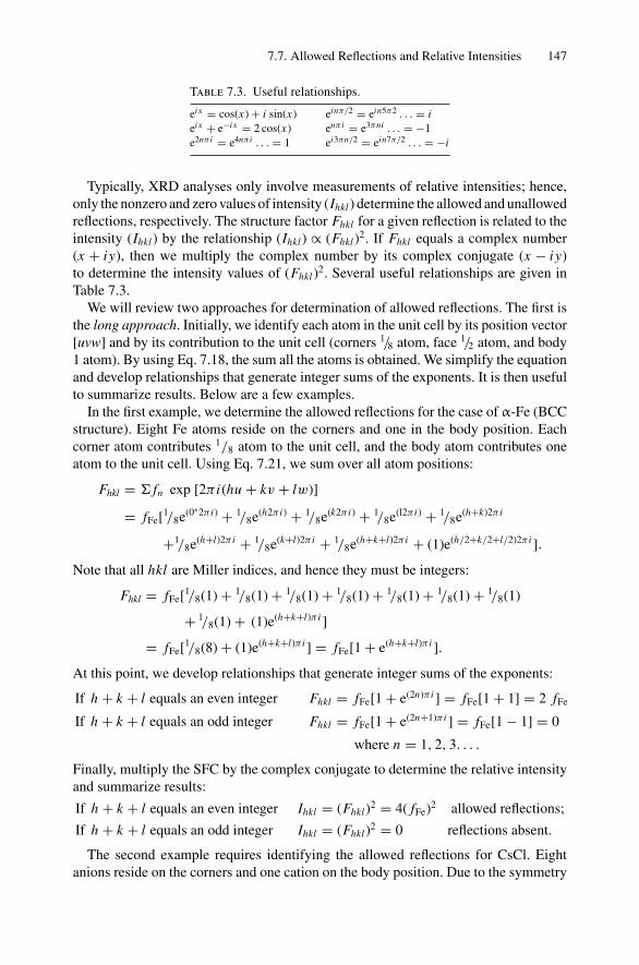
7.7. Allowed Reflections and Relative Intensities 147
Table 7.3. Useful relationships.
ei x = cos(x) + i sin(x) einπ/2 = ein5π2 . . . = iei x + e−i x = 2 cos(x) enπ i = e3πni . . . = −1e2nπ i = e4nπ i . . . = 1 ei3πn/2 = ein7π/2 . . . = −i
Typically, XRD analyses only involve measurements of relative intensities; hence,only the nonzero and zero values of intensity (Ihkl) determine the allowed and unallowedreflections, respectively. The structure factor Fhkl for a given reflection is related to theintensity (Ihkl ) by the relationship (Ihkl) ∝ (Fhkl)2. If Fhkl equals a complex number(x + iy), then we multiply the complex number by its complex conjugate (x − iy)to determine the intensity values of (Fhkl)2. Several useful relationships are given inTable 7.3.
We will review two approaches for determination of allowed reflections. The first isthe long approach. Initially, we identify each atom in the unit cell by its position vector[uvw] and by its contribution to the unit cell (corners 1/8 atom, face 1/2 atom, and body1 atom). By using Eq. 7.18, the sum all the atoms is obtained. We simplify the equationand develop relationships that generate integer sums of the exponents. It is then usefulto summarize results. Below are a few examples.
In the first example, we determine the allowed reflections for the case of α-Fe (BCCstructure). Eight Fe atoms reside on the corners and one in the body position. Eachcorner atom contributes 1/8 atom to the unit cell, and the body atom contributes oneatom to the unit cell. Using Eq. 7.21, we sum over all atom positions:
Fhkl = fn exp [2π i(hu + kv + lw)]
= fFe[1/8e(0∗2π i) + 1/8e(h2π i) + 1/8e(k2π i) + 1/8e(l2π i) + 1/8e(h+k)2π i
+1/8e(h+l)2π i + 1/8e(k+l)2π i + 1/8e(h+k+l)2π i + (1)e(h/2+k/2+l/2)2π i ].
Note that all hkl are Miller indices, and hence they must be integers:
Fhkl = fFe[1/8(1) + 1/8(1) + 1/8(1) + 1/8(1) + 1/8(1) + 1/8(1) + 1/8(1)
+ 1/8(1) + (1)e(h+k+l)π i ]
= fFe[1/8(8) + (1)e(h+k+l)π i ] = fFe[1 + e(h+k+l)π i ].
At this point, we develop relationships that generate integer sums of the exponents:
If h + k + l equals an even integer Fhkl = fFe[1 + e(2n)π i ] = fFe[1 + 1] = 2 fFe
If h + k + l equals an odd integer Fhkl = fFe[1 + e(2n+1)π i ] = fFe[1 − 1] = 0
where n = 1, 2, 3. . . .
Finally, multiply the SFC by the complex conjugate to determine the relative intensityand summarize results:
If h + k + l equals an even integer Ihkl = (Fhkl)2 = 4( fFe)2 allowed reflections;
If h + k + l equals an odd integer Ihkl = (Fhkl)2 = 0 reflections absent.
The second example requires identifying the allowed reflections for CsCl. Eightanions reside on the corners and one cation on the body position. Due to the symmetry
148 7. X-ray Diffraction
of the structure, it can also be stated that eight cations reside on the corners and oneanion on the body position. Again, each corner atom contributes 1/8 atom to the unitcell, and the body atom contributes one atom to the unit cell. For this example, we willassume Cs+ on the corners and Cl− in the body. Using Eq. 7.18, we sum over all atompositions:
Fhkl = fn exp [2π i(hu + kv + lw)]
= fCs[1/8e(0∗2π i) + 1/8e(h2π i) + 1/8e(k2π i) + 1/8e(l2π i) + 1/8e(h+k)2π i
+1/8e(h+l)2π i + 1/8e(k+l)2π i + 1/8e(h+k+l)2π i ] + fCl e(h/2+k/2+l/2)2π i .
Note that all hkl are Miller indices, and hence they must be integers:
= [ fCs1/8(8) + fCle
(h+k+l)π i ] = fCs + fCle(h+k+l)π i ].
In this case, we multiply the SFC by the complex conjugate and summarize the intensityresults:
If h + k + l equals an even integer,
Ihkl = (Fhkl)2 = ( fCs)
2 + 2( fCl)2 + 2( fCs)( fCl) allowed reflection;
If h + k + l equals an odd integer,
Ihkl = (Fhkl)2 = ( fCs)
2 + 2( fCl)2 − 2( fCs)( fCl) allowed reflection.
The structure of any crystalline solid is best described by its lattice and basis(Section 7.4). In a similar manner, the structure factor is also best described by therelationship between the structure factor of the lattice and the structure factor of thebasis:
Fhkl = FhklLattice · Fhkl
Basis = fn exp[2π i(hun + kvn + lwn)]. (7.22)
The relationship above, considered a short approach, often reduces the algebra bya considerable amount. Using this advancement, one initially identifies the structure(lattice and basis). This requires distinguishing each atom in the basis by its positionvector [uvw]. Each atom of the basis contributes one atomic scattering factor. Set up therelationship for the lattice times the basis equation, and solve for the allowed reflectionsfor the lattice first. The allowed reflections will contribute the number of lattice pointsper unit cell. Use any known relationships for allowed and absent reflections for thatlattice. Simplify the equation and develop relationships that generate integer sums ofthe exponents. Finally, summarize results.
If we repeat the previous example for CsCl, the structure is defined as a simple cubiclattice plus a basis of Cs 000 and Cl 1/2
1/21/2. Given the structure’s symmetry, a basis of
Cl 000 and Cs 1/21/2
1/2 can also be used. A convenient relationship is that all reflectionsare allowed for any simple lattice (regardless of the crystal system). Using Eq. 7.12,we multiply the lattice times the basis and sum over all atom positions:
Fhkl = FhklLattice · Fhkl
Basis = fn exp[2π i(hun + kvn + lwn)]
=All h,k,l allowed[1] · [ fCs e(0∗2π i) + fCle
(h/2+k/2+l/2)2π i].
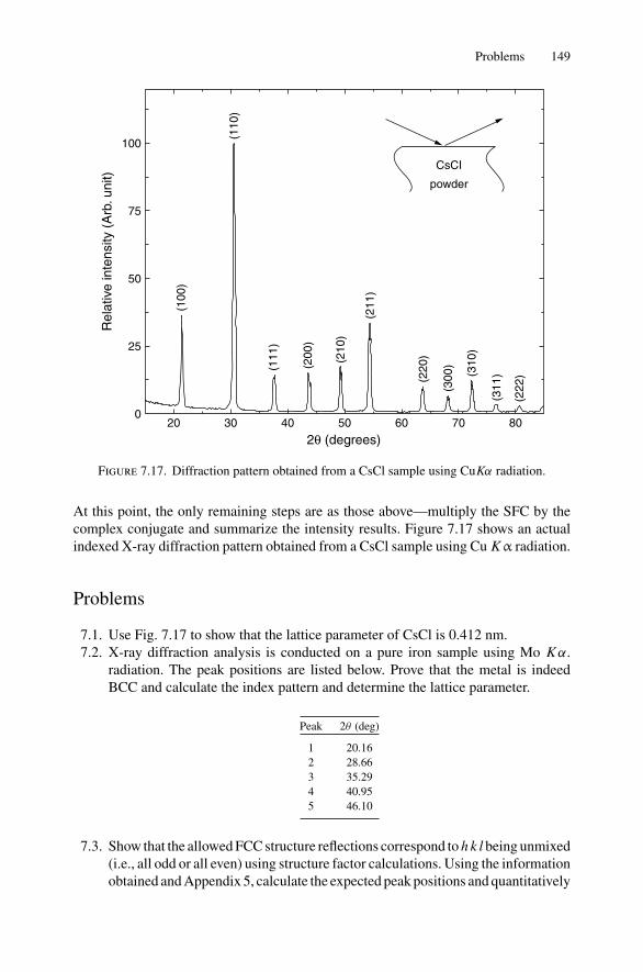
Problems 149
200
25
50
75
100
30
(100
)
(110
)
(111
)
(200
)
(210
)
(211
)
(220
)
(300
)
(310
)
(311
)
(222
)
40 50 60
CsCI
powder
70 80
2θ (degrees)
Rel
ativ
e in
tens
ity (
Arb
. uni
t)
Figure 7.17. Diffraction pattern obtained from a CsCl sample using CuKα radiation.
At this point, the only remaining steps are as those above—multiply the SFC by thecomplex conjugate and summarize the intensity results. Figure 7.17 shows an actualindexed X-ray diffraction pattern obtained from a CsCl sample using Cu Kα radiation.
Problems
7.1. Use Fig. 7.17 to show that the lattice parameter of CsCl is 0.412 nm.7.2. X-ray diffraction analysis is conducted on a pure iron sample using Mo Kα.
radiation. The peak positions are listed below. Prove that the metal is indeedBCC and calculate the index pattern and determine the lattice parameter.
Peak 2θ (deg)
1 20.162 28.663 35.294 40.955 46.10
7.3. Show that the allowed FCC structure reflections correspond to h k l being unmixed(i.e., all odd or all even) using structure factor calculations. Using the informationobtained and Appendix 5, calculate the expected peak positions and quantitatively
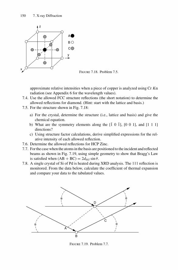
150 7. X-ray Diffraction
z
A
B
C
y
xFigure 7.18. Problem 7.5.
approximate relative intensities when a piece of copper is analyzed using Cr Kα
radiation (see Appendix 6 for the wavelength values).7.4. Use the allowed FCC structure reflections (the short notation) to determine the
allowed reflections for diamond. (Hint: start with the lattice and basis.)7.5. For the structure shown in Fig. 7.18:
a) For the crystal, determine the structure (i.e., lattice and basis) and give thechemical equation.
b) What are the symmetry elements along the [1 0 1], [0 0 1], and [1 1 1]directions?
c) Using structure factor calculations, derive simplified expressions for the rel-ative intensity of each allowed reflection.
7.6. Determine the allowed reflections for HCP Zinc.7.7. For the case when the atoms in the basis are positioned to the incident and reflected
beams as shown in Fig. 7.19, using simple geometry to show that Bragg’s Lawis satisfied when (AB + BC) = 2dhkl sin θ .
7.8. A single crystal of Si of Pd is heated during XRD analysis. The 111 reflection ismonitored. From the data below, calculate the coefficient of thermal expansionand compare your data to the tabulated values.
D
C
B
A
θ
θ
θ
θ
Figure 7.19. Problem 7.7.
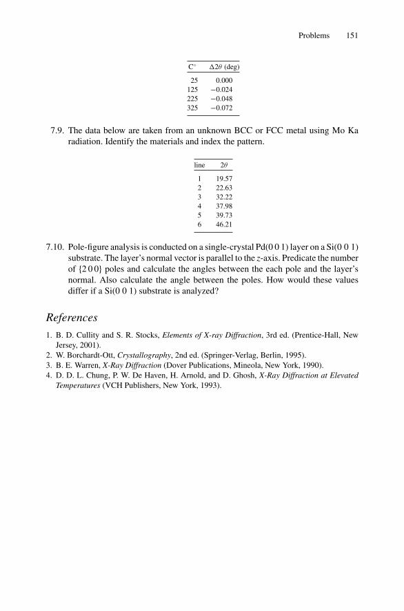
Problems 151
C 2θ (deg)
25 0.000125 −0.024225 −0.048325 −0.072
7.9. The data below are taken from an unknown BCC or FCC metal using Mo Karadiation. Identify the materials and index the pattern.
line 2θ
1 19.572 22.633 32.224 37.985 39.736 46.21
7.10. Pole-figure analysis is conducted on a single-crystal Pd(0 0 1) layer on a Si(0 0 1)substrate. The layer’s normal vector is parallel to the z-axis. Predicate the numberof 2 0 0 poles and calculate the angles between the each pole and the layer’snormal. Also calculate the angle between the poles. How would these valuesdiffer if a Si(0 0 1) substrate is analyzed?
References
1. B. D. Cullity and S. R. Stocks, Elements of X-ray Diffraction, 3rd ed. (Prentice-Hall, NewJersey, 2001).
2. W. Borchardt-Ott, Crystallography, 2nd ed. (Springer-Verlag, Berlin, 1995).3. B. E. Warren, X-Ray Diffraction (Dover Publications, Mineola, New York, 1990).4. D. D. L. Chung, P. W. De Haven, H. Arnold, and D. Ghosh, X-Ray Diffraction at Elevated
Temperatures (VCH Publishers, New York, 1993).
8Electron Diffraction
8.1 Introduction
In this chapter, we consider thin film analysis using high-energy electron diffractionwith an electron microscope. The most common form of the technique is known astransmission electron microscopy (TEM). As discussed in Chapter 7, diffraction revealsdetailed information about the crystalline nature of a thin film. Electron microscopyhas the critical advantage of providing a nanometer-scale electron beam spot as theradiation source. Thus crystallinity can be examined nanometer by nanometer in orderto address questions such as crystal uniformity and to identify individual large de-fects and a variety of other structures. A simple example illustrates the importance ofthis parameter. Most metal films, when deposited, form as polycrystalline structurescomposed of nanoscale crystallites. Clearly, it is of interest to directly characterizethis structure, to examine the crystallinity of individual crystallites, and to understandtheir connectivity. Such issues are addressed by transmission electron microscopyand the accompanying electron diffraction. This chapter presents the fundamentalaspects of electron diffraction and its implementation in the transmission electronmicroscope.
In the case of crystalline solids, we typically desire to measure atomic spacings onthe order of the lattice constants, e.g., 0.2–0.4 nm. Hence, we must use radiation withwavelengths less than 0.2 nm. This range of wavelengths corresponds to high-energyelectrons. Here we recall from earlier sections that photons are massless particles.The photon’s wavelength and energy are given by the relationship λ (µm) = 1.24 (eV-µm)/E (eV). Electrons are not massless particles; hence, the equation above does notyield the correct wavelength for high-energy electrons traveling at relativistic speeds.For such cases, the de Broglie (particle–wave) relation mv = h/λ and the kinetic energyof the electrons, 1/2 mv2 = eV, are used to correct the inverse relationship betweenapplied voltage and wavelength:
λ(nm) =[
0.139 volts-nm2
V (volts)
]1/2
, (8.1)
where V is the applied voltage in volts and wavelength is in units of nm. Using
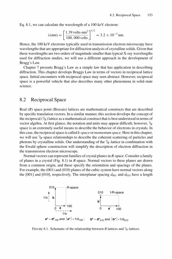
8.2. Reciprocal Space 153
Eq. 8.1, we can calculate the wavelength of a 100 keV electron:
λ(nm) =[
1.39 volts-nm2
100, 000 volts
]1/2
= 3.2 × 10⁻³ nm.
Hence, the 100 keV electrons typically used in transmission electron microscopy havewavelengths that are appropriate for diffraction analysis of crystalline solids. Given thatthese wavelengths are two orders of magnitude smaller than typical X-ray wavelengthsused for diffraction studies, we will use a different approach in the development ofBragg’s Law.
Chapter 7 presents Bragg’s Law as a simple law that has application in describingdiffraction. This chapter develops Braggs Law in terms of vectors in reciprocal latticespace. Initial encounters with reciprocal space may seen abstract. However, reciprocalspace is a powerful vehicle that also describes many other phenomena in solid-statescience.
8.2 Reciprocal Space
Real (R) space point (Bravais) lattices are mathematical constructs that are describedby specific translation vectors. In a similar manner, this section develops the concept ofthe reciprocal (1/R) lattice as a mathematical construct that is best understood in terms ofvector algebra. At first glance, the notation and units may appear difficult; however, 1/Rspace is an extremely useful means to describe the behavior of electrons in crystals. Inthis case, the reciprocal space is called k-space or momentum space. Here in this chapter,we will use 1/R-space relationships to describe the coherent scattering of particles andphotons by crystalline solids. Our understanding of the 1/R-lattice in combination withthe Ewald sphere construction will simplify the description of electron diffraction inthe transmission electron microscope.
Normal vectors can represent families of crystal planes in R-space. Consider a familyof planes in a crystal (Fig. 8.1) in R-space. Normal vectors to these planes are drawnfrom a common origin, and these specify the orientation and spacings of the planes.For example, the (001) and (010) planes of the cubic system have normal vectors alongthe [001] and [010], respectively. The interplanar spacing d001 and d010 have a length
010
1001000 0
010
1/b
1/a
b
a
b*
R-space
a*
a* = d*100 and a*=1/d100 ; b* = d*010 and b*=1/d010.
1/R-space
Figure 8.1. Schematic of the relationship between R-lattices and 1/R-lattices.
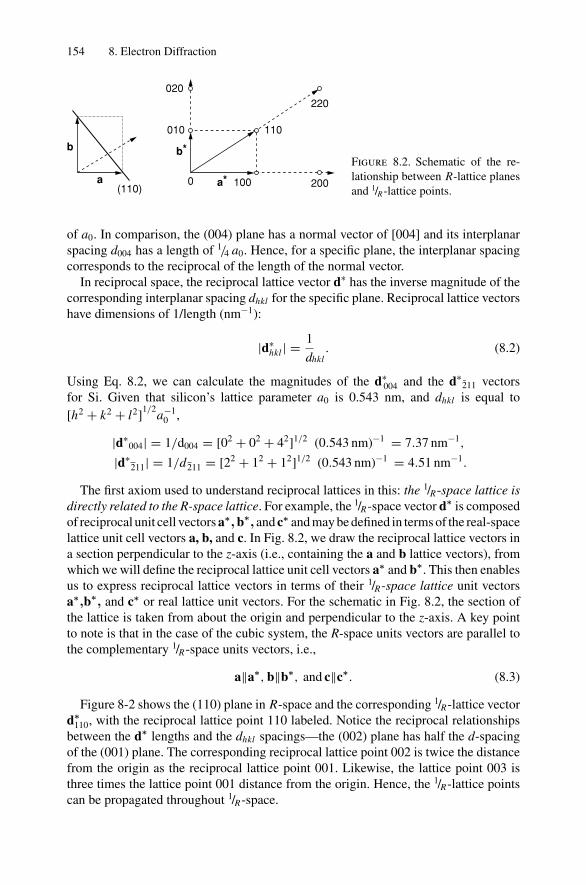
154 8. Electron Diffraction
b*
a*a
b
020
010
100
110
200
220
0(110)
Figure 8.2. Schematic of the re-lationship between R-lattice planesand 1/R-lattice points.
of a0. In comparison, the (004) plane has a normal vector of [004] and its interplanarspacing d004 has a length of 1/4 a0. Hence, for a specific plane, the interplanar spacingcorresponds to the reciprocal of the length of the normal vector.
In reciprocal space, the reciprocal lattice vector d∗ has the inverse magnitude of thecorresponding interplanar spacing dhkl for the specific plane. Reciprocal lattice vectorshave dimensions of 1/length (nm−1):
|d∗hkl | = 1
dhkl. (8.2)
Using Eq. 8.2, we can calculate the magnitudes of the d∗004 and the d∗
211 vectorsfor Si. Given that silicon’s lattice parameter a0 is 0.543 nm, and dhkl is equal to[h2 + k2 + l2]
1/2a−1
0 ,
|d∗004| = 1/d004 = [02 + 02 + 42]1/2 (0.543 nm)−1 = 7.37 nm−1,
|d∗211| = 1/d211 = [22 + 12 + 12]1/2 (0.543 nm)−1 = 4.51 nm−1.
The first axiom used to understand reciprocal lattices in this: the 1/R-space lattice isdirectly related to the R-space lattice. For example, the 1/R-space vector d∗ is composedof reciprocal unit cell vectors a∗,b∗, and c∗ and may be defined in terms of the real-spacelattice unit cell vectors a, b, and c. In Fig. 8.2, we draw the reciprocal lattice vectors ina section perpendicular to the z-axis (i.e., containing the a and b lattice vectors), fromwhich we will define the reciprocal lattice unit cell vectors a∗ and b∗. This then enablesus to express reciprocal lattice vectors in terms of their 1/R-space lattice unit vectorsa∗,b∗, and c∗ or real lattice unit vectors. For the schematic in Fig. 8.2, the section ofthe lattice is taken from about the origin and perpendicular to the z-axis. A key pointto note is that in the case of the cubic system, the R-space units vectors are parallel tothe complementary 1/R-space units vectors, i.e.,
a‖a∗, b‖b∗, and c‖c∗. (8.3)
Figure 8-2 shows the (110) plane in R-space and the corresponding 1/R-lattice vectord∗
110, with the reciprocal lattice point 110 labeled. Notice the reciprocal relationshipsbetween the d∗ lengths and the dhkl spacings—the (002) plane has half the d-spacingof the (001) plane. The corresponding reciprocal lattice point 002 is twice the distancefrom the origin as the reciprocal lattice point 001. Likewise, the lattice point 003 isthree times the lattice point 001 distance from the origin. Hence, the 1/R-lattice pointscan be propagated throughout 1/R-space.

8.2. Reciprocal Space 155
The reciprocal lattice vectors can now be expressed in terms of their components ofthe reciprocal unit cell vectors a∗, b∗, and c∗:
d∗hkl = ha∗ + kb∗ + lc∗. (8.4)
Note that the Miller indices hkl are the scalar components of a reciprocal lattice vector.Hence, a vector d∗
hkl drawn from the origin of the 1/R-lattice to any point with coor-dinates hkl is perpendicular to the R-space plane (hkl); the normal vector nhkl‖d∗
hkl .In the cubic system, any vector in 1/R-space that is drawn from the origin to the pointhkl is also perpendicular to the (hkl) plane in the real crystal. Each point in 1/R-spacerepresents a given set of parallel planes in R-space.
8.2.1 The Addition Rule
Just like vectors in R-space, 1/R-space vectors add in a tail-to-head manner to generatethe resultant vector. The addition rule simply states that the resultant vector is the sumof the indices of the two reciprocal lattice vectors:
d∗h1k1l1
+ d∗h2k2l2
= d∗h1+h2 k1+k2 l1+l2
. (8.5)
Using Eq. 8.5, we can develop several relationships for the reciprocal lattice vectord∗
hkl = [220]:
d∗220 = d∗
110 + d∗110 = 2d∗
110
= d∗200 + d∗
020 = 2d∗100 + 2d∗
010 = 2(d∗100 + d∗
010)
= d∗110 + d∗
010 + d∗100
= d∗330 − d∗
010 − d∗100.
For the case of orthogonal axes (in orthorhombic, tetragonal, and cubic systems), asimple expression is obtained for d∗
hkl · d∗hkl :
d∗hkl · d∗
hkl = (ha∗ + kb∗ + lc∗) · (ha∗ + kb∗ + lc∗)
= ha∗ · ha∗ + kb∗ · kb∗ + lc∗ · lc∗. (8.6)
For crystals where a∗ · b∗ = 0 and a∗ · a∗ = 1, etc.,
d∗hkl · d∗
hkl = h2
a2+ k2
b2+ l2
c2
= 1
d2hkl
. (8.7)
The angle γ between plane normal vectors from (h1k1l1) and (h2k2l2) planes or theangle γ between two vectors a and b is given by
cos γ = a · b
|a||b| . (8.9a)
156 8. Electron Diffraction
In a similar manner, the angle γ between two 1/R-space points h1k1l1 and h2k2l2 is givenby
cos γ = d∗h1k1l1
· d∗h2k2l2∣∣d∗
h1k1l1
∣∣∣∣d∗h2k2l2
∣∣ . (8.9b)
The volume (V) of the unit cell is given by a · (b × c). The cross product (b × c) yieldsa vector parallel to a∗ and with a magnitude equal to the area of the face of the unit celldefined by b and c; then
a∗ = b × ca · (b × c)
, b∗ = c × aV
, c∗ = a × bV
, (8.10)
In a similar manner, real space can be defined in terms of the reciprocal space unitvectors:
a = V · (b∗ × a∗), b = V · (c∗ × a∗), c = V · (a∗ × b∗). (8.11)
8.2.2 Proof of the Zone Law
The intersection of planes (h1k1l1) and (h2k2l2) is a vector. Figure 8.3 depicts the zoneaxis (ZA) as the common intersection of several planes. For example, consider the caseof planes A(h1k1l1) and B(h2k2l2) in the cubic system, having normal vectors [h1k1l1]and [h2k2l2], respectively. The vector ZA is defined by the relationship
ZA = nA × nB = [h1k1l1] × [h2k2l2] (8.12)
Given that the zone axis is [u v w], then for any plane (hkl) that belongs to that ZA (orzone), the following relationship is satisfied:
hu + kv + lw = 0 (8.13)
In order to belong to a zone, the normal of the plane must be perpendicular to the zoneaxis; hence, the Zone Law is given as
(u a + v b + w c) · nhkl = 0 (8.14)
For example, the zone axis for the (011) and (101) planes is calculated by taking thecross product [h1k1l1] × [h2k2l2] = (+1)a − (−1)b + (−1)c = [1 1 1]. To verify thatthe calculated ZA is indeed correct, one uses the zone law (ZA · nhkl = 0) for validation.Here, [0 1 1] · [1 1 1] = 0 and [1 0 1] · [1 1 1] = 0. Hence, the calculated ZA iscorrect.
To address the zone law in 1/R space, we consider the condition for a 1/R-lattice pointwith coordinates hkl with position vector d∗
hkl passing through the origin. For a ZA,
B AZA Figure 8.3. Schematic showing two intersecting
planes and the corresponding zone axis (ZA).
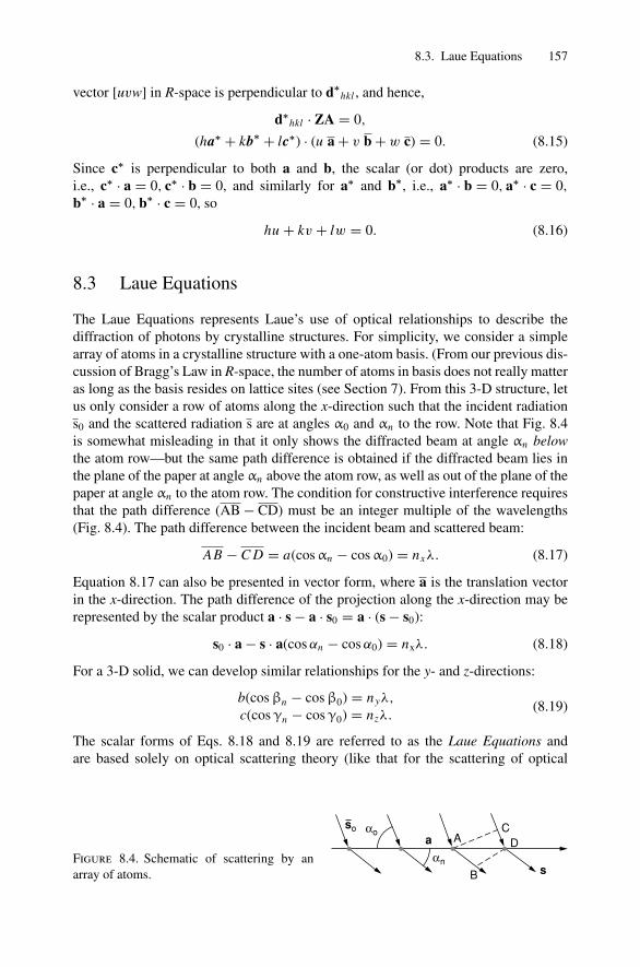
8.3. Laue Equations 157
vector [uvw] in R-space is perpendicular to d∗hkl , and hence,
d∗hkl · ZA = 0,
(ha∗ + kb∗ + lc∗) · (u a + v b + w c) = 0. (8.15)
Since c∗ is perpendicular to both a and b, the scalar (or dot) products are zero,i.e., c∗ · a = 0, c∗ · b = 0, and similarly for a∗ and b∗, i.e., a∗ · b = 0, a∗ · c = 0,
b∗ · a = 0, b∗ · c = 0, so
hu + kv + lw = 0. (8.16)
8.3 Laue Equations
The Laue Equations represents Laue’s use of optical relationships to describe thediffraction of photons by crystalline structures. For simplicity, we consider a simplearray of atoms in a crystalline structure with a one-atom basis. (From our previous dis-cussion of Bragg’s Law in R-space, the number of atoms in basis does not really matteras long as the basis resides on lattice sites (see Section 7). From this 3-D structure, letus only consider a row of atoms along the x-direction such that the incident radiations0 and the scattered radiation s are at angles α0 and αn to the row. Note that Fig. 8.4is somewhat misleading in that it only shows the diffracted beam at angle αn belowthe atom row—but the same path difference is obtained if the diffracted beam lies inthe plane of the paper at angle αn above the atom row, as well as out of the plane of thepaper at angle αn to the atom row. The condition for constructive interference requiresthat the path difference (AB − CD) must be an integer multiple of the wavelengths(Fig. 8.4). The path difference between the incident beam and scattered beam:
AB − C D = a(cos αn − cos α0) = nxλ. (8.17)
Equation 8.17 can also be presented in vector form, where a is the translation vectorin the x-direction. The path difference of the projection along the x-direction may berepresented by the scalar product a · s − a · s0 = a · (s − s0):
s0 · a − s · a(cos αn − cos α0) = nxλ. (8.18)
For a 3-D solid, we can develop similar relationships for the y- and z-directions:
b(cos βn − cos β0) = nyλ,
c(cos γn − cos γ0) = nzλ.(8.19)
The scalar forms of Eqs. 8.18 and 8.19 are referred to as the Laue Equations andare based solely on optical scattering theory (like that for the scattering of optical
B
DAC
s
soa
αn
αo
Figure 8.4. Schematic of scattering by anarray of atoms.
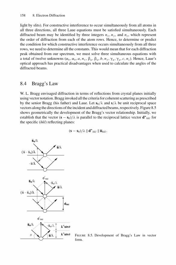
158 8. Electron Diffraction
light by slits). For constructive interference to occur simultaneously from all atoms inall three directions, all three Laue equations must be satisfied simultaneously. Eachdiffracted beam may be identified by three integers nx , ny , and nz , which representthe order of diffraction from each of the atom rows. Hence, to determine or predictthe condition for which constructive interference occurs simultaneously from all threerows, we need to determine all the constants. This would mean that for each diffractionpeak obtained from our spectrum, we must solve three simultaneous equations witha total of twelve unknowns (αn, αo, a, nx , βn, βo, b, ny, γn, γo, c, nz). Hence, Laue’soptical approach has practical disadvantages when used to calculate the angles of thediffracted beams.
8.4 Bragg’s Law
W. L. Bragg envisaged diffraction in terms of reflections from crystal planes initiallyusing vector notation. Bragg invoked all the criteria for coherent scattering as prescribedby the senior Bragg (his father) and Laue. Let s0/λ and s/λ be unit reciprocal spacevectors along the directions of the incident and diffracted beams, respectively. Figure 8.5shows geometrically the development of the Bragg’s vector relationship. Initially, weestablish that the vector (s − s0)/λ is parallel to the reciprocal lattice vector d∗
hkl forthe specific (hkl) reflecting planes:
(s − s0)/λ ‖ d∗hkl ‖ nhkl .
⎯s/λλλλ
(⎯s -
-
⎯so)/λλλλ
⎯so/λ
⎯s/λ
dhkl
d*hkl
(⎯s -⎯so)/λλλλ
⎯so/λ
⎯s/λ-⎯so/λ
q
⎯so/λ
⎯s/λ
d*hkl
-⎯so/λ λλλλ-1sinq
λλλλ-1sinq Figure 8.5. Development of Bragg’s Law in vectorform.
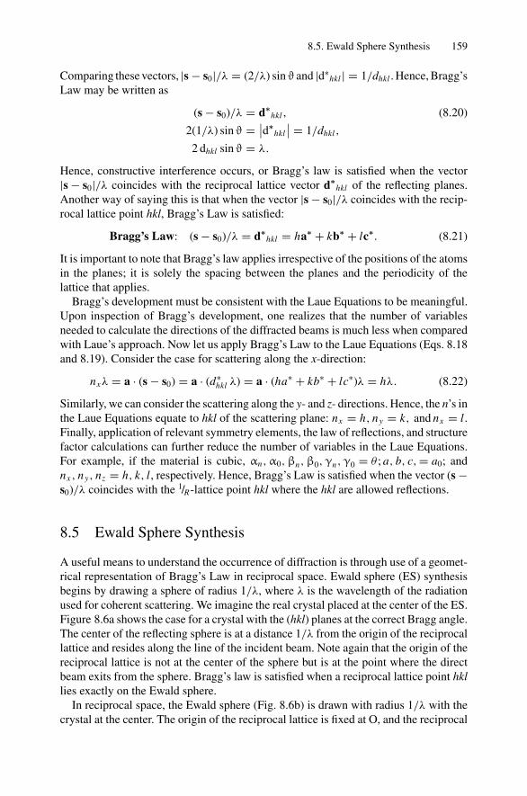
8.5. Ewald Sphere Synthesis 159
Comparing these vectors, |s − s0|/λ = (2/λ) sin ϑ and |d∗hkl | = 1/dhkl . Hence, Bragg’s
Law may be written as
(s − s0)/λ = d∗hkl , (8.20)
2(1/λ) sin ϑ = ∣∣d∗hkl
∣∣ = 1/dhkl ,
2 dhkl sin ϑ = λ.
Hence, constructive interference occurs, or Bragg’s law is satisfied when the vector|s − s0|/λ coincides with the reciprocal lattice vector d∗
hkl of the reflecting planes.Another way of saying this is that when the vector |s − s0|/λ coincides with the recip-rocal lattice point hkl, Bragg’s Law is satisfied:
Bragg’s Law: (s − s0)/λ = d∗hkl = ha∗ + kb∗ + lc∗. (8.21)
It is important to note that Bragg’s law applies irrespective of the positions of the atomsin the planes; it is solely the spacing between the planes and the periodicity of thelattice that applies.
Bragg’s development must be consistent with the Laue Equations to be meaningful.Upon inspection of Bragg’s development, one realizes that the number of variablesneeded to calculate the directions of the diffracted beams is much less when comparedwith Laue’s approach. Now let us apply Bragg’s Law to the Laue Equations (Eqs. 8.18and 8.19). Consider the case for scattering along the x-direction:
nxλ = a · (s − s0) = a · (d∗hkl λ) = a · (ha∗ + kb∗ + lc∗)λ = hλ. (8.22)
Similarly, we can consider the scattering along the y- and z- directions. Hence, the n’s inthe Laue Equations equate to hkl of the scattering plane: nx = h, ny = k, and nx = l.Finally, application of relevant symmetry elements, the law of reflections, and structurefactor calculations can further reduce the number of variables in the Laue Equations.For example, if the material is cubic, αn, α0, βn, β0, γn, γ0 = θ ; a, b, c, = a0; andnx , ny, nz = h, k, l, respectively. Hence, Bragg’s Law is satisfied when the vector (s −s0)/λ coincides with the 1/R-lattice point hkl where the hkl are allowed reflections.
8.5 Ewald Sphere Synthesis
A useful means to understand the occurrence of diffraction is through use of a geomet-rical representation of Bragg’s Law in reciprocal space. Ewald sphere (ES) synthesisbegins by drawing a sphere of radius 1/λ, where λ is the wavelength of the radiationused for coherent scattering. We imagine the real crystal placed at the center of the ES.Figure 8.6a shows the case for a crystal with the (hkl) planes at the correct Bragg angle.The center of the reflecting sphere is at a distance 1/λ from the origin of the reciprocallattice and resides along the line of the incident beam. Note again that the origin of thereciprocal lattice is not at the center of the sphere but is at the point where the directbeam exits from the sphere. Bragg’s law is satisfied when a reciprocal lattice point hkllies exactly on the Ewald sphere.
In reciprocal space, the Ewald sphere (Fig. 8.6b) is drawn with radius 1/λ with thecrystal at the center. The origin of the reciprocal lattice is fixed at O, and the reciprocal
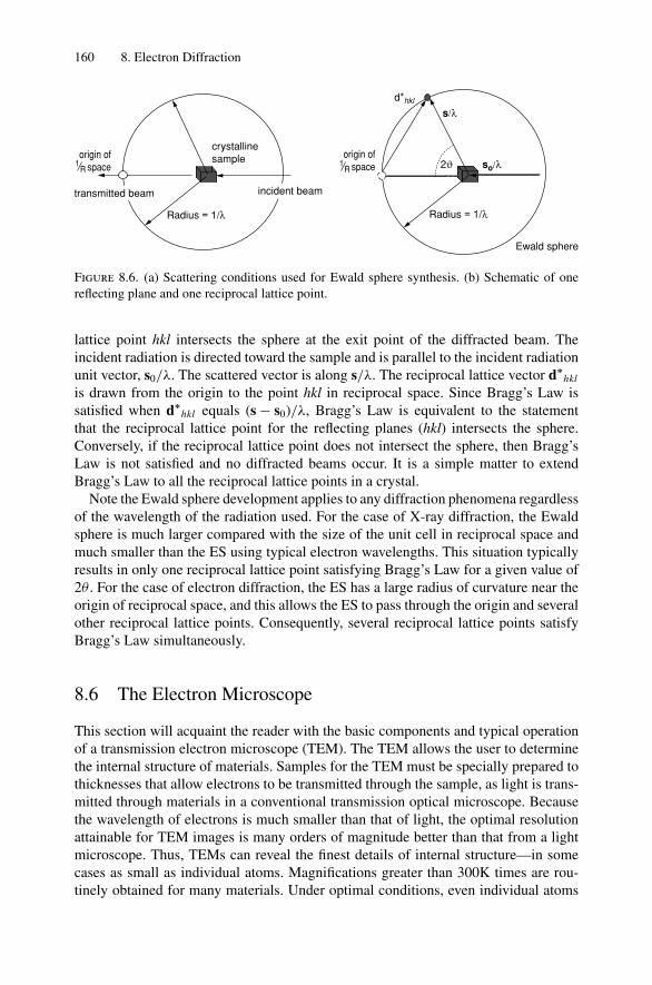
160 8. Electron Diffraction
crystalline sample
Radius = 1/λ Radius = 1/λ
Ewald sphere
2ϑ so/λ
s/λd*hkl
origin of spaceR
1origin of
space
transmitted beam incident beam
R1
Figure 8.6. (a) Scattering conditions used for Ewald sphere synthesis. (b) Schematic of onereflecting plane and one reciprocal lattice point.
lattice point hkl intersects the sphere at the exit point of the diffracted beam. Theincident radiation is directed toward the sample and is parallel to the incident radiationunit vector, s0/λ. The scattered vector is along s/λ. The reciprocal lattice vector d∗
hkl
is drawn from the origin to the point hkl in reciprocal space. Since Bragg’s Law issatisfied when d∗
hkl equals (s − s0)/λ, Bragg’s Law is equivalent to the statementthat the reciprocal lattice point for the reflecting planes (hkl) intersects the sphere.Conversely, if the reciprocal lattice point does not intersect the sphere, then Bragg’sLaw is not satisfied and no diffracted beams occur. It is a simple matter to extendBragg’s Law to all the reciprocal lattice points in a crystal.
Note the Ewald sphere development applies to any diffraction phenomena regardlessof the wavelength of the radiation used. For the case of X-ray diffraction, the Ewaldsphere is much larger compared with the size of the unit cell in reciprocal space andmuch smaller than the ES using typical electron wavelengths. This situation typicallyresults in only one reciprocal lattice point satisfying Bragg’s Law for a given value of2θ . For the case of electron diffraction, the ES has a large radius of curvature near theorigin of reciprocal space, and this allows the ES to pass through the origin and severalother reciprocal lattice points. Consequently, several reciprocal lattice points satisfyBragg’s Law simultaneously.
8.6 The Electron Microscope
This section will acquaint the reader with the basic components and typical operationof a transmission electron microscope (TEM). The TEM allows the user to determinethe internal structure of materials. Samples for the TEM must be specially prepared tothicknesses that allow electrons to be transmitted through the sample, as light is trans-mitted through materials in a conventional transmission optical microscope. Becausethe wavelength of electrons is much smaller than that of light, the optimal resolutionattainable for TEM images is many orders of magnitude better than that from a lightmicroscope. Thus, TEMs can reveal the finest details of internal structure—in somecases as small as individual atoms. Magnifications greater than 300K times are rou-tinely obtained for many materials. Under optimal conditions, even individual atoms
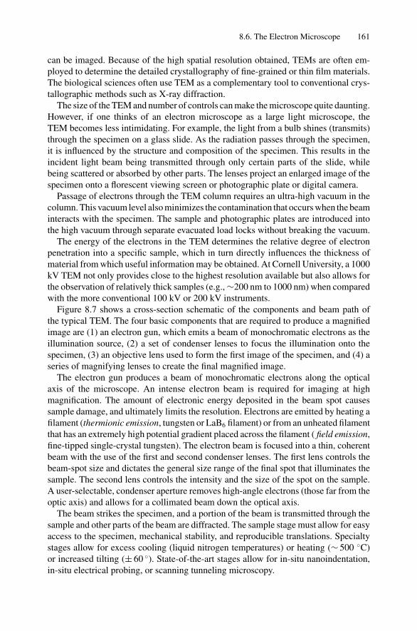
8.6. The Electron Microscope 161
can be imaged. Because of the high spatial resolution obtained, TEMs are often em-ployed to determine the detailed crystallography of fine-grained or thin film materials.The biological sciences often use TEM as a complementary tool to conventional crys-tallographic methods such as X-ray diffraction.
The size of the TEM and number of controls can make the microscope quite daunting.However, if one thinks of an electron microscope as a large light microscope, theTEM becomes less intimidating. For example, the light from a bulb shines (transmits)through the specimen on a glass slide. As the radiation passes through the specimen,it is influenced by the structure and composition of the specimen. This results in theincident light beam being transmitted through only certain parts of the slide, whilebeing scattered or absorbed by other parts. The lenses project an enlarged image of thespecimen onto a florescent viewing screen or photographic plate or digital camera.
Passage of electrons through the TEM column requires an ultra-high vacuum in thecolumn. This vacuum level also minimizes the contamination that occurs when the beaminteracts with the specimen. The sample and photographic plates are introduced intothe high vacuum through separate evacuated load locks without breaking the vacuum.
The energy of the electrons in the TEM determines the relative degree of electronpenetration into a specific sample, which in turn directly influences the thickness ofmaterial from which useful information may be obtained. At Cornell University, a 1000kV TEM not only provides close to the highest resolution available but also allows forthe observation of relatively thick samples (e.g., ∼200 nm to 1000 nm) when comparedwith the more conventional 100 kV or 200 kV instruments.
Figure 8.7 shows a cross-section schematic of the components and beam path ofthe typical TEM. The four basic components that are required to produce a magnifiedimage are (1) an electron gun, which emits a beam of monochromatic electrons as theillumination source, (2) a set of condenser lenses to focus the illumination onto thespecimen, (3) an objective lens used to form the first image of the specimen, and (4) aseries of magnifying lenses to create the final magnified image.
The electron gun produces a beam of monochromatic electrons along the opticalaxis of the microscope. An intense electron beam is required for imaging at highmagnification. The amount of electronic energy deposited in the beam spot causessample damage, and ultimately limits the resolution. Electrons are emitted by heating afilament (thermionic emission, tungsten or LaB6 filament) or from an unheated filamentthat has an extremely high potential gradient placed across the filament ( field emission,fine-tipped single-crystal tungsten). The electron beam is focused into a thin, coherentbeam with the use of the first and second condenser lenses. The first lens controls thebeam-spot size and dictates the general size range of the final spot that illuminates thesample. The second lens controls the intensity and the size of the spot on the sample.A user-selectable, condenser aperture removes high-angle electrons (those far from theoptic axis) and allows for a collimated beam down the optical axis.
The beam strikes the specimen, and a portion of the beam is transmitted through thesample and other parts of the beam are diffracted. The sample stage must allow for easyaccess to the specimen, mechanical stability, and reproducible translations. Specialtystages allow for excess cooling (liquid nitrogen temperatures) or heating (∼ 500 C)or increased tilting (± 60 ). State-of-the-art stages allow for in-situ nanoindentation,in-situ electrical probing, or scanning tunneling microscopy.
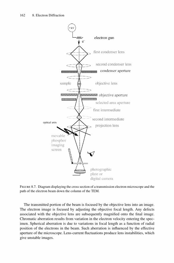
162 8. Electron Diffraction
Figure 8.7. Diagram displaying the cross section of a transmission electron microscope and thepath of the electron beam down the column of the TEM.
The transmitted portion of the beam is focused by the objective lens into an image.The electron image is focused by adjusting the objective focal length. Any defectsassociated with the objective lens are subsequently magnified onto the final image.Chromatic aberration results from variation in the electron velocity entering the spec-imen. Spherical aberration is due to variations in focal length as a function of radialposition of the electrons in the beam. Such aberration is influenced by the effectiveaperture of the microscope. Lens-current fluctuations produce lens instabilities, whichgive unstable images.
8.6. The Electron Microscope 163
The objective aperture and selected area diffraction aperture can both restrict thebeam. The objective aperture enhances image contrast by blocking out high-anglediffracted electrons. Use of a selected-area aperture enables the user to image the elec-tron diffraction pattern from a specific portion of the TEM sample. Accurate alignmentof the various apertures is important for good imaging. The image is passed down thecolumn through the intermediate and projector lenses. There the image of the sample ismagnified onto the viewing screen or onto the recording media. Upon selection of theappropriate control, the projector system magnifies the image of the electron diffractionpattern from the rear focal plane of the objective lens. It is the projection lens settingthat defines the camera length.
The electrons that form the image strike a fluorescent screen (typically coated with afine-grain ZnS). When the electrons strike the screen, fluorescence occurs and results inthe formation of a visible image, allowing the user to see the image. The darker areas ofthe image represent those areas of the sample where fewer electrons were transmitted(they are thicker or denser). The lighter areas of the image represent those areas ofthe sample where more electrons were transmitted (they are thinner or less dense).Note that X-rays are also generated when the electrons strike the viewing screen. Theleaded viewing glass absorbs the X-rays. A photographic plate or digital camera residesbeneath the moveable viewing screen.
A potential operational hazard can occur when the electron beam strikes the aperturesor part of the column and produces X-rays. Hence, the column is shielded to protect theoperator. On the other hand, the column must be shielded from external stray radiation,vibrations, and magnetic fields, if one desires a stable image.
8.6.1 Imaging Modes
In the bright field (BF) mode of the TEM, an aperture is placed in the back focal plane ofthe objective lens, allowing only the transmitted or direct beam to pass (see Fig. 8.8a).The diffracted beams are blocked. In this case, diffraction contrast contributes to imageformation. Crystalline regions that are oriented so as to strongly diffract intensityaway from the transmitted beam will appear dark. In addition, Z-contrast occurs whenregions with heavy atoms scatter more of the incident beam and appear darker. Usefulinformation is obtainable from BF images. However, interpretation of contrast shouldbe done with care, since the phenomena mentioned above occur simultaneously.
In dark field (DF) images, a selected diffracted beam is allowed to pass through theobjective aperture (see Fig. 8.8b). This is accomplished by electromagnetic lenses thateffectively tilt the incident beam from the optical axis by an amount 2θhkl such thatthe hkl diffracted beam exits the sample parallel to the TEM optical axis. The apertureblocks the direct beam. In contrast to the direct beam, the diffracted beam has interactedstrongly with the specimen, and very useful information is often present in DF images,e.g., about planar defects, stacking faults, or particles. Figure 8.9 shows a bright fieldimage and the corresponding dark field image for a TiAl(N,O) layer on an oxidizedsilicon substrate. In many analyses, correlation between DF and BF images providesuseful information about structure and morphology, including layer thickness, grainsize, grain orientation, and defect orientations. In general, one or both of these imagingmodes are used in conjunction with electron diffraction analysis.
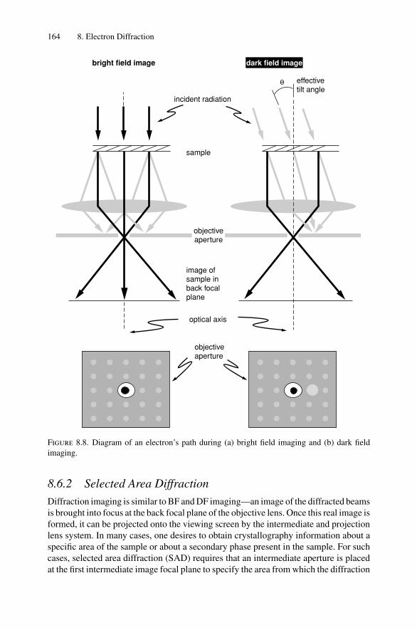
164 8. Electron Diffraction
sample
incident radiation
bright field image
objectiveaperture
image ofsample inback focal plane
optical axis
objectiveaperture
effective tilt angle
θ
dark field image
Figure 8.8. Diagram of an electron’s path during (a) bright field imaging and (b) dark fieldimaging.
8.6.2 Selected Area Diffraction
Diffraction imaging is similar to BF and DF imaging—an image of the diffracted beamsis brought into focus at the back focal plane of the objective lens. Once this real image isformed, it can be projected onto the viewing screen by the intermediate and projectionlens system. In many cases, one desires to obtain crystallography information about aspecific area of the sample or about a secondary phase present in the sample. For suchcases, selected area diffraction (SAD) requires that an intermediate aperture is placedat the first intermediate image focal plane to specify the area from which the diffraction
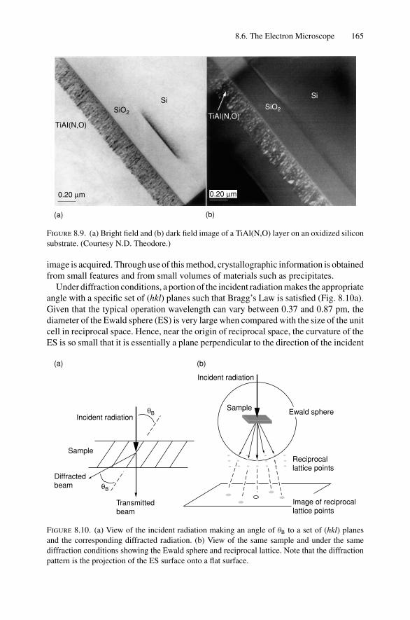
8.6. The Electron Microscope 165
TiAI(N,O)
Si
SiO2
TiAI(N,O)
SiSiO2
0.20 µm0.20 µm
(a) (b)
Figure 8.9. (a) Bright field and (b) dark field image of a TiAl(N,O) layer on an oxidized siliconsubstrate. (Courtesy N.D. Theodore.)
image is acquired. Through use of this method, crystallographic information is obtainedfrom small features and from small volumes of materials such as precipitates.
Under diffraction conditions, a portion of the incident radiation makes the appropriateangle with a specific set of (hkl) planes such that Bragg’s Law is satisfied (Fig. 8.10a).Given that the typical operation wavelength can vary between 0.37 and 0.87 pm, thediameter of the Ewald sphere (ES) is very large when compared with the size of the unitcell in reciprocal space. Hence, near the origin of reciprocal space, the curvature of theES is so small that it is essentially a plane perpendicular to the direction of the incident
Incident radiation
Sample
Sample
Diffractedbeam θB
θB
Transmittedbeam
Reciprocallattice points
Ewald sphere
Incident radiation
Image of reciprocal lattice points
(a) (b)
Figure 8.10. (a) View of the incident radiation making an angle of θB to a set of (hkl) planesand the corresponding diffracted radiation. (b) View of the same sample and under the samediffraction conditions showing the Ewald sphere and reciprocal lattice. Note that the diffractionpattern is the projection of the ES surface onto a flat surface.
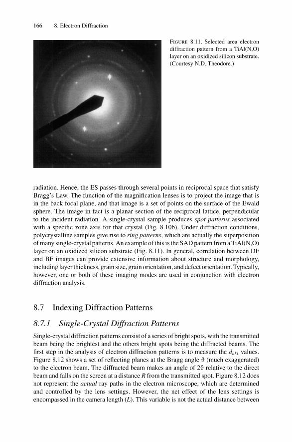
166 8. Electron Diffraction
Figure 8.11. Selected area electrondiffraction pattern from a TiAl(N,O)layer on an oxidized silicon substrate.(Courtesy N.D. Theodore.)
radiation. Hence, the ES passes through several points in reciprocal space that satisfyBragg’s Law. The function of the magnification lenses is to project the image that isin the back focal plane, and that image is a set of points on the surface of the Ewaldsphere. The image in fact is a planar section of the reciprocal lattice, perpendicularto the incident radiation. A single-crystal sample produces spot patterns associatedwith a specific zone axis for that crystal (Fig. 8.10b). Under diffraction conditions,polycrystalline samples give rise to ring patterns, which are actually the superpositionof many single-crystal patterns. An example of this is the SAD pattern from a TiAl(N,O)layer on an oxidized silicon substrate (Fig. 8.11). In general, correlation between DFand BF images can provide extensive information about structure and morphology,including layer thickness, grain size, grain orientation, and defect orientation. Typically,however, one or both of these imaging modes are used in conjunction with electrondiffraction analysis.
8.7 Indexing Diffraction Patterns
8.7.1 Single-Crystal Diffraction Patterns
Single-crystal diffraction patterns consist of a series of bright spots, with the transmittedbeam being the brightest and the others bright spots being the diffracted beams. Thefirst step in the analysis of electron diffraction patterns is to measure the dhkl values.Figure 8.12 shows a set of reflecting planes at the Bragg angle ϑ (much exaggerated)to the electron beam. The diffracted beam makes an angle of 2ϑ relative to the directbeam and falls on the screen at a distance R from the transmitted spot. Figure 8.12 doesnot represent the actual ray paths in the electron microscope, which are determinedand controlled by the lens settings. However, the net effect of the lens settings isencompassed in the camera length (L). This variable is not the actual distance between
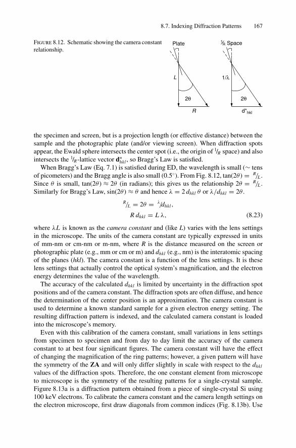
8.7. Indexing Diffraction Patterns 167
R
L
Plate
2θ 2θ
Space
d*hkl
1/λ
R1Figure 8.12. Schematic showing the camera constant
relationship.
the specimen and screen, but is a projection length (or effective distance) between thesample and the photographic plate (and/or viewing screen). When diffraction spotsappear, the Ewald sphere intersects the center spot (i.e., the origin of 1/R space) and alsointersects the 1/R-lattice vector d∗
hkl , so Bragg’s Law is satisfied.When Bragg’s Law (Eq. 7.1) is satisfied during ED, the wavelength is small (∼ tens
of picometers) and the Bragg angle is also small (0.5). From Fig. 8.12, tan(2θ ) = R/L .Since θ is small, tan(2θ ) ≈ 2θ (in radians); this gives us the relationship 2θ = R/L .Similarly for Bragg’s Law, sin(2θ ) ≈ θ and hence λ = 2 dhkl θ or λ/dhkl = 2θ .
R/L = 2θ = λ/dhkl ,
R dhkl = L λ, (8.23)
where λL is known as the camera constant and (like L) varies with the lens settingsin the microscope. The units of the camera constant are typically expressed in unitsof mm-nm or cm-nm or m-nm, where R is the distance measured on the screen orphotographic plate (e.g., mm or cm or m) and dhkl (e.g., nm) is the interatomic spacingof the planes (hkl). The camera constant is a function of the lens settings. It is theselens settings that actually control the optical system’s magnification, and the electronenergy determines the value of the wavelength.
The accuracy of the calculated dhkl is limited by uncertainty in the diffraction spotpositions and of the camera constant. The diffraction spots are often diffuse, and hencethe determination of the center position is an approximation. The camera constant isused to determine a known standard sample for a given electron energy setting. Theresulting diffraction pattern is indexed, and the calculated camera constant is loadedinto the microscope’s memory.
Even with this calibration of the camera constant, small variations in lens settingsfrom specimen to specimen and from day to day limit the accuracy of the cameraconstant to at best four significant figures. The camera constant will have the effectof changing the magnification of the ring patterns; however, a given pattern will havethe symmetry of the ZA and will only differ slightly in scale with respect to the dhkl
values of the diffraction spots. Therefore, the one constant element from microscopeto microscope is the symmetry of the resulting patterns for a single-crystal sample.Figure 8.13a is a diffraction pattern obtained from a piece of single-crystal Si using100 keV electrons. To calibrate the camera constant and the camera length settings onthe electron microscope, first draw diagonals from common indices (Fig. 8.13b). Use
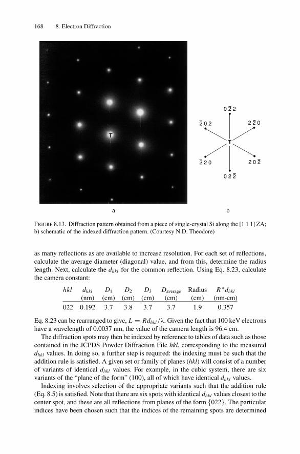
168 8. Electron Diffraction
T
0 2 2
2 2 0
2 0 2
0 2 2
2 2 0
2 0 2
ba
Figure 8.13. Diffraction pattern obtained from a piece of single-crystal Si along the [1 1 1] ZA;b) schematic of the indexed diffraction pattern. (Courtesy N.D. Theodore)
as many reflections as are available to increase resolution. For each set of reflections,calculate the average diameter (diagonal) value, and from this, determine the radiuslength. Next, calculate the dhkl for the common reflection. Using Eq. 8.23, calculatethe camera constant:
hkl dhkl D1 D2 D3 Daverage Radius R ∗dhkl
(nm) (cm) (cm) (cm) (cm) (cm) (nm-cm)
022 0.192 3.7 3.8 3.7 3.7 1.9 0.357
Eq. 8.23 can be rearranged to give, L = Rdhkl/λ. Given the fact that 100 keV electronshave a wavelength of 0.0037 nm, the value of the camera length is 96.4 cm.
The diffraction spots may then be indexed by reference to tables of data such as thosecontained in the JCPDS Powder Diffraction File hkl, corresponding to the measureddhkl values. In doing so, a further step is required: the indexing must be such that theaddition rule is satisfied. A given set or family of planes (hkl) will consist of a numberof variants of identical dhkl values. For example, in the cubic system, there are sixvariants of the “plane of the form” (100), all of which have identical dhkl values.
Indexing involves selection of the appropriate variants such that the addition rule(Eq. 8.5) is satisfied. Note that there are six spots with identical dhkl values closest to thecenter spot, and these are all reflections from planes of the form 022. The particularindices have been chosen such that the indices of the remaining spots are determined
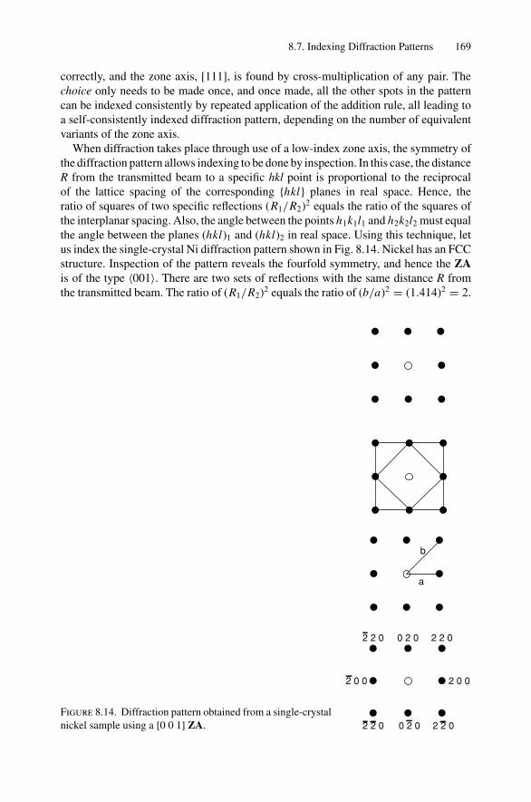
8.7. Indexing Diffraction Patterns 169
correctly, and the zone axis, [111], is found by cross-multiplication of any pair. Thechoice only needs to be made once, and once made, all the other spots in the patterncan be indexed consistently by repeated application of the addition rule, all leading toa self-consistently indexed diffraction pattern, depending on the number of equivalentvariants of the zone axis.
When diffraction takes place through use of a low-index zone axis, the symmetry ofthe diffraction pattern allows indexing to be done by inspection. In this case, the distanceR from the transmitted beam to a specific hkl point is proportional to the reciprocalof the lattice spacing of the corresponding hkl planes in real space. Hence, theratio of squares of two specific reflections (R1/R2)2 equals the ratio of the squares ofthe interplanar spacing. Also, the angle between the points h1k1l1 and h2k2l2 must equalthe angle between the planes (hkl)1 and (hkl)2 in real space. Using this technique, letus index the single-crystal Ni diffraction pattern shown in Fig. 8.14. Nickel has an FCCstructure. Inspection of the pattern reveals the fourfold symmetry, and hence the ZAis of the type 〈001〉. There are two sets of reflections with the same distance R fromthe transmitted beam. The ratio of (R1/R2)2 equals the ratio of (b/a)2 = (1.414)2 = 2.
a
b
2 2 0
2 0 0 2 0 0
2 2 00 2 02 2 0
0 2 0 2 2 0Figure 8.14. Diffraction pattern obtained from a single-crystalnickel sample using a [0 0 1] ZA.
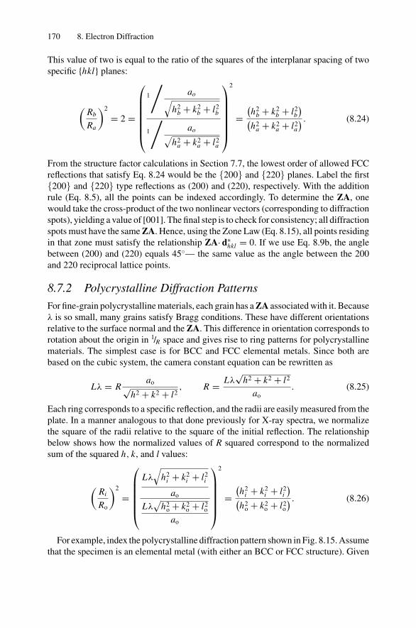
170 8. Electron Diffraction
This value of two is equal to the ratio of the squares of the interplanar spacing of twospecific hkl planes:
(Rb
Ra
)2
= 2 =
⎛⎜⎜⎜⎜⎜⎜⎝
1
/ao√
h2b + k2
b + l2b
1
/ao√
h2a + k2
a + l2a
⎞⎟⎟⎟⎟⎟⎟⎠
2
=(h2
b + k2b + l2
b
)(h2
a + k2a + l2
a
) . (8.24)
From the structure factor calculations in Section 7.7, the lowest order of allowed FCCreflections that satisfy Eq. 8.24 would be the 200 and 220 planes. Label the first200 and 220 type reflections as (200) and (220), respectively. With the additionrule (Eq. 8.5), all the points can be indexed accordingly. To determine the ZA, onewould take the cross-product of the two nonlinear vectors (corresponding to diffractionspots), yielding a value of [001]. The final step is to check for consistency; all diffractionspots must have the same ZA. Hence, using the Zone Law (Eq. 8.15), all points residingin that zone must satisfy the relationship ZA· d∗
hkl = 0. If we use Eq. 8.9b, the anglebetween (200) and (220) equals 45— the same value as the angle between the 200and 220 reciprocal lattice points.
8.7.2 Polycrystalline Diffraction Patterns
For fine-grain polycrystalline materials, each grain has a ZA associated with it. Becauseλ is so small, many grains satisfy Bragg conditions. These have different orientationsrelative to the surface normal and the ZA. This difference in orientation corresponds torotation about the origin in 1/R space and gives rise to ring patterns for polycrystallinematerials. The simplest case is for BCC and FCC elemental metals. Since both arebased on the cubic system, the camera constant equation can be rewritten as
Lλ = Rao√
h2 + k2 + l2, R = Lλ
√h2 + k2 + l2
ao. (8.25)
Each ring corresponds to a specific reflection, and the radii are easily measured from theplate. In a manner analogous to that done previously for X-ray spectra, we normalizethe square of the radii relative to the square of the initial reflection. The relationshipbelow shows how the normalized values of R squared correspond to the normalizedsum of the squared h, k, and l values:
(Ri
Ro
)2
=
⎛⎜⎜⎜⎜⎜⎝
Lλ
√h2
i + k2i + l2
i
ao
Lλ√
h2o + k2
o + l2o
ao
⎞⎟⎟⎟⎟⎟⎠
2
=(h2
i + k2i + l2
i
)(h2
o + k2o + l2
o
) . (8.26)
For example, index the polycrystalline diffraction pattern shown in Fig. 8.15. Assumethat the specimen is an elemental metal (with either an BCC or FCC structure). Given
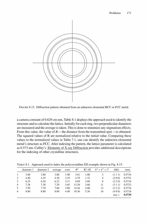
Problems 171
Figure 8.15. Diffraction pattern obtained from an unknown elemental BCC or FCC metal.
a camera constant of 0.629 cm-nm, Table 8.1 displays the approach used to identify thestructure and to calculate the lattice. Initially for each ring, two perpendicular diametersare measured and the average is taken. This is done to minimize any stigmatism effects.From this value, the value of R— the distance from the transmitted spot —is obtained.The squared values of R are normalized relative to the initial value. Comparing thesevalues to the normalized values in Table 7.1, one can identify the unknown elementalmetal’s structure as FCC. After indexing the pattern, the lattice parameter is calculatedas 0.573 nm. Cullity’s Elements of X-ray Diffraction provides additional descriptionsfor the indexing of other crystalline structures.
Table 8.1. Approach used to index the polycrystalline ED example shown in Fig. 8.15.
diameter 1 diameter 2 average (cm) R2 R2i /R2
o h2 + k2 + l2 (hkl) (nm)
1 3.80 3.80 3.80 1.90 3.61 1.00 3 (1 1 1) 0.57342 4.40 4.35 4.38 2.19 4.79 1.33 4 (2 0 0) 0.57513 6.25 6.20 6.23 3.11 9.69 2.68 8 (2 2 0) 0.57164 7.28 7.30 7.29 3.65 13.29 3.68 11 (3 1 1) 0.57235 7.50 7.70 7.60 3.80 14.44 4.00 12 (2 2 2) 0.57346 8.80 8.80 8.80 4.40 19.36 5.36 16 (4 0 0) 0.5718
avg = 0.5729
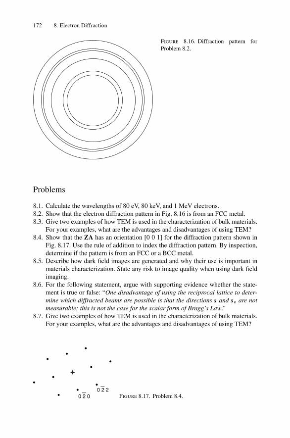
172 8. Electron Diffraction
Figure 8.16. Diffraction pattern forProblem 8.2.
Problems
8.1. Calculate the wavelengths of 80 eV, 80 keV, and 1 MeV electrons.8.2. Show that the electron diffraction pattern in Fig. 8.16 is from an FCC metal.8.3. Give two examples of how TEM is used in the characterization of bulk materials.
For your examples, what are the advantages and disadvantages of using TEM?8.4. Show that the ZA has an orientation [0 0 1] for the diffraction pattern shown in
Fig. 8.17. Use the rule of addition to index the diffraction pattern. By inspection,determine if the pattern is from an FCC or a BCC metal.
8.5. Describe how dark field images are generated and why their use is important inmaterials characterization. State any risk to image quality when using dark fieldimaging.
8.6. For the following statement, argue with supporting evidence whether the state-ment is true or false: “One disadvantage of using the reciprocal lattice to deter-mine which diffracted beams are possible is that the directions s and so are notmeasurable; this is not the case for the scalar form of Bragg’s Law.”
8.7. Give two examples of how TEM is used in the characterization of bulk materials.For your examples, what are the advantages and disadvantages of using TEM?
_0 2 0
_0 2 2
Figure 8.17. Problem 8.4.

Problems 173
8.8. Calculate the camera length for the diffraction pattern shown in Fig. 8.13. Note100 keV electrons are used to obtain the pattern.
8.9. Calculate the camera constant for the diffraction pattern shown in Fig. 8.14.
References
1. E. M. Slayter and H. S. Slayter, Light and Electron Microscopy (Cambridge University Press,New York, 1992 and 1994).
2. G. Thomas and M. J. Goringe, Transmission Electron Microscopy of Materials (John Wileyand Sons, New York, 1979).
3. M. H. Loretto, Electron Beam Analysis of Materials (University Press, Cambridge, 1984).4. T. Hahn, Ed., International Tables For Crystallography, 5th ed. (Kluwer Academic Publishers,
Boston, 2002).5. C. Hammond, The Basics of Crystallography and Diffraction (Oxford University Press, 2001).
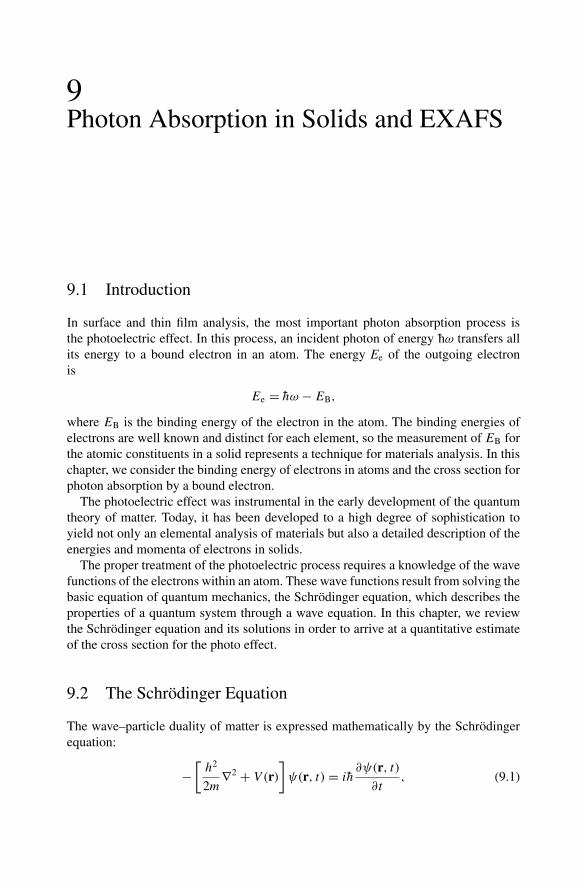
9Photon Absorption in Solids and EXAFS
9.1 Introduction
In surface and thin film analysis, the most important photon absorption process isthe photoelectric effect. In this process, an incident photon of energy hω transfers allits energy to a bound electron in an atom. The energy Ee of the outgoing electronis
Ee = hω − EB,
where EB is the binding energy of the electron in the atom. The binding energies ofelectrons are well known and distinct for each element, so the measurement of EB forthe atomic constituents in a solid represents a technique for materials analysis. In thischapter, we consider the binding energy of electrons in atoms and the cross section forphoton absorption by a bound electron.
The photoelectric effect was instrumental in the early development of the quantumtheory of matter. Today, it has been developed to a high degree of sophistication toyield not only an elemental analysis of materials but also a detailed description of theenergies and momenta of electrons in solids.
The proper treatment of the photoelectric process requires a knowledge of the wavefunctions of the electrons within an atom. These wave functions result from solving thebasic equation of quantum mechanics, the Schrodinger equation, which describes theproperties of a quantum system through a wave equation. In this chapter, we reviewthe Schrodinger equation and its solutions in order to arrive at a quantitative estimateof the cross section for the photo effect.
9.2 The Schrodinger Equation
The wave–particle duality of matter is expressed mathematically by the Schrodingerequation:
−[
h2
2m∇2 + V (r)
]ψ(r, t) = ih
∂ψ(r, t)
∂t, (9.1)
9.2. The Schrodinger Equation 175
where ψ(r, t) is the wave function that describes the motion of the particle underthe influence of the potential V (r). As in classical mechanics, a physics problem issolved when, under the influence of a given potential, the coordinates of the parti-cle are expressed as a function of time. In quantum mechanics, a problem is solvedwhen ψ is known as a function of r and t. There are very few interesting physicalproblems that can be solved exactly. Almost all processes that are necessary for materi-als analysis are approximate solutions to the Schrodinger equation using perturbationtheory.
In Cartesian coordinates, the Schrodinger equation is written explicitly as
− h2
2m
(∂2
∂x2+ ∂2
∂y2+ ∂2
∂z2
)ψ + V (x, y, z)ψ = ih
∂ψ
∂t, (9.2)
where ψ may be a function of x, y, z, and t.For many examples it is sufficient to consider the one-dimensional Schrodinger
equation
− h2
2m
∂2ψ(x, t)
∂x2+ V (x)ψ(x, t) = ih
∂ψ(x, t)
∂t. (9.3)
The solution ψ(x, t) can be written as the product of two functions:
ψ(x, t) = u(x)T (t). (9.4)
This can be substituted into Eq. 9.3 to yield
1
u
(− h2
2m
∂2u
∂x2+ V (x)u
)= ih
T
dT
dt. (9.5)
Using the mathematical device of separation of variables, we note that the left-handside depends only on x and the right-hand side only on t; therefore, both sides areproportional to a separation constant E. Then
T (t) = Ce−i Et/h, (9.6)
where C is an arbitrary constant and the equation for u(x) is[− h2
2m
∂2
∂x2+ V (x)
]u(x) = Eu(x) . (9.7)
The total solution is then
ψ(x, t) = Au(x)e−i Et/h, (9.8)
where A is a normalization constant. Eq. 9.7 is known as the time-independentSchrodinger equation; the separation is valid provided that the potential V is not afunction of time.
The philosophy underlying the Schrodinger equation is discussed in other books.Note, however, that −(h2/2m) · (∂2/∂x2) is associated with the kinetic energy, V withthe potential energy, and Eq. 9.7 is often written in shorthand as
Hψ = Eψ, (9.9)
176 9. Photon Absorption in Solids and EXAFS
where H (= kinetic energy + potential energy) is associated with the classicalHamiltonian. The meaning of ψ(r, t) is given through |ψ(r, t)|2, the probability offinding the particle at position r at time t. Eq. 9.7 is an example of an eigenvalue equa-tion, where u is said to be the eigenfunctions of the operator H = −(h2/2m) · ∇2 + ∇and E is the eigenvalue. E is the energy of the system. The solution of Eq. (9.7) formany real potentials involves only discrete values of E, thus verifying the quantizationassumptions in the Bohr theory given in Chapter 1.
In central force problems, the potential V (x, y, z) = V (r ), and we convert theSchrodinger equation to spherical coordinates (r, θ, φ):
− h2
2m
1
r2
∂
∂r
(r2 ∂u
∂r
)− h2
2mr2
[1
sin θ
∂
∂θ
(sin θ
∂u
∂θ
)+ 1
sin2 θ
∂2u
∂φ2
]+ V u = Eu.
(9.10)Separation of variables is again possible,
u(r, θ, φ) = R(r ) f (θ)g(φ), (9.11)
and the radial part becomes
− h2
2m
1
r2
d
dr
(r2 dR
dr
)+[
l(l + 1)h2
2mr2+ V (r )
]R = E R, (9.12)
where l is the orbital quantum number.
9.3 Wave Functions
There are two kinds of wave functions that we will need in order to illustrate the mainpoints of this chapter: (1) a free particle wave function (V = 0) and (2) hydrogenicwave functions (V = Z1 Z2e2/r ).
9.3.1 Plane Waves (V = 0)
Analysis techniques require an incident beam and outgoing radiation. The incidentparticle of energy E directed along the x-direction, say, is not under the influence of apotential. Then the solution to the appropriate Schrodinger equation,
− h2
2m
d2u
dx2= Eu,
is
u(x) = Aeikx , (9.13)
where
h2k2
2m= E . (9.14)
This describes a particle moving in the positive x-direction with momentum |p| = hk.The total wave function ψ(x, t) is given by
ψ(x, t) = Aei(kx−ωt), (9.15)
9.4. Wave Functions 177
where E = hω. In both Eqs. (9.13) and (9.15), A is an arbitrary constant to be determinedby the beam parameters.
9.3.2 Hydrogenic Wave Function [V(r) = Z e2/r]The solution to the Schrodinger equation in radial coordinates may be written as
u(r, θ, φ) = R(r )Y (θ, φ), (9.16)
where Y (θ, φ) is known as a spherical harmonic. The solution to the angular partof the differential equation results in quantum numbers, i.e., Y (θ, φ) is not always asolution; it only satisfies physical conditions for certain integer values of the parameters1 and m.
To see how this arises, consider the φ dependence of the Schrodinger equation:
d2g
dφ2= −m2g(φ), (9.17)
where m is a constant that arises in the separation of variables. Then
g(φ) = Aeimφ, (9.18)
but φ is the azimuthal angle, and the function must have the same value at φ = 0 orφ = 2π . This is true if
m = 0 or an integer. (9.19)
The separation of the three variables leads to three quantum numbers n, l, and m, andthe solutions to the hydrogen atom problem are
unlm(r, θ, φ) = Rnl(r ) flm(θ)eimφ. (9.20)
Rnl and flm, are functions that can be written explicitly for a particular value of n, l,and m. The first few wave functions are
u100 =[
1
πa3
]1/2
e−ρ,
u200 = 1
8
[2
πa3
]1/2
(2 − ρ)e−ρ/2, (9.21)
where ρ = Zr/a0 and a = a0/Z . Table 9.1 lists the lowest-energy wave functions forthe hydrogen atom, and Fig. 9.1 gives the radial distribution function in terms of r2 R2
n .This quantity gives the probability density of finding a particle within a shell of radius r.Figure 9.1 also shows the energy levels for the hydrogen atom; the same values arefound in the Bohr treatment.
The above wave functions are properly normalized, i.e., the probability of finding aparticle somewhere in space is unity. That is,∫
u∗u dr = 1, (9.22)
where u∗ is the complex conjugate of u.
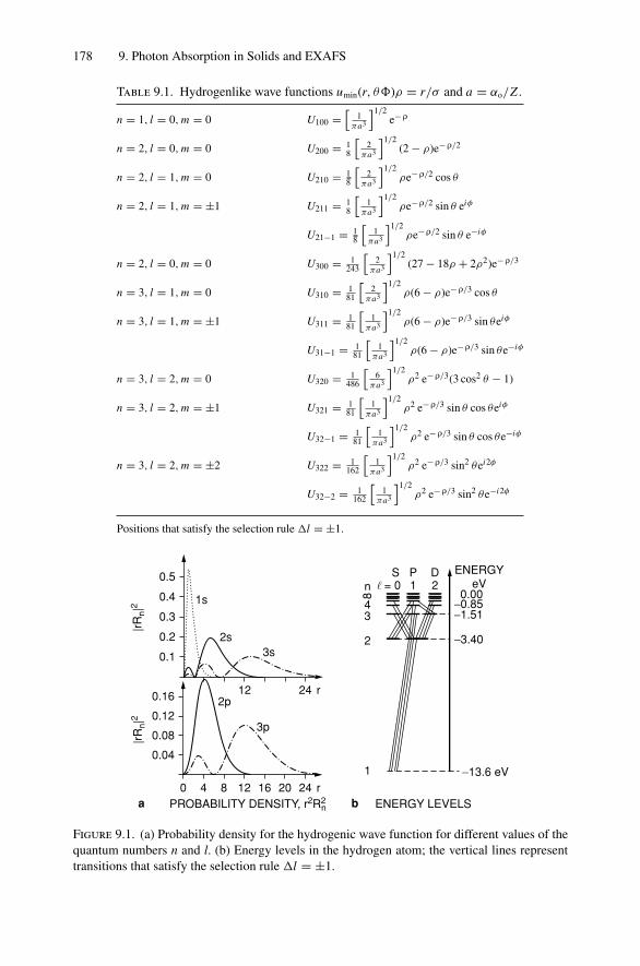
178 9. Photon Absorption in Solids and EXAFS
Table 9.1. Hydrogenlike wave functions umin(r, θ)ρ = r/σ and a = αo/Z .
n = 1, l = 0, m = 0 U100 =[
1πa3
]1/2e−ρ
n = 2, l = 0, m = 0 U200 = 18
[2
πa3
]1/2(2 − ρ)e−ρ/2
n = 2, l = 1, m = 0 U210 = 18
[2
πa3
]1/2ρe−ρ/2 cos θ
n = 2, l = 1, m = ±1 U211 = 18
[1
πa3
]1/2ρe−ρ/2 sin θ eiφ
U21−1 = 18
[1
πa3
]1/2ρe−ρ/2 sin θ e−iφ
n = 2, l = 0, m = 0 U300 = 1243
[2
πa3
]1/2(27 − 18ρ + 2ρ2)e−ρ/3
n = 3, l = 1, m = 0 U310 = 181
[2
πa3
]1/2ρ(6 − ρ)e−ρ/3 cos θ
n = 3, l = 1, m = ±1 U311 = 181
[1
πa3
]1/2ρ(6 − ρ)e−ρ/3 sin θeiφ
U31−1 = 181
[1
πa3
]1/2ρ(6 − ρ)e−ρ/3 sin θe−iφ
n = 3, l = 2, m = 0 U320 = 1486
[6
πa3
]1/2ρ2 e−ρ/3(3 cos2 θ − 1)
n = 3, l = 2, m = ±1 U321 = 181
[1
πa3
]1/2ρ2 e−ρ/3 sin θ cos θeiφ
U32−1 = 181
[1
πa3
]1/2ρ2 e−ρ/3 sin θ cos θe−iφ
n = 3, l = 2, m = ±2 U322 = 1162
[1
πa3
]1/2ρ2 e−ρ/3 sin2 θei2φ
U32−2 = 1162
[1
πa3
]1/2ρ2 e−ρ/3 sin2 θe−i2φ
Positions that satisfy the selection rule l = ±1.
0.1
0.04
0.12
0.16
0.08
0.2
0.3
0.4
0.5
12 24 r
12 16 2420 r
|rR
n|2
|rR
n|2
1s
2s3s
3p
2p
0 4 8PROBABILITY DENSITY, r2R2
n ENERGY LEVELSba
−13.6 eV1
2
21
34
n
8
S P D ENERGYeV = 0
0.00−0.85−1.51
−3.40
Figure 9.1. (a) Probability density for the hydrogenic wave function for different values of thequantum numbers n and l. (b) Energy levels in the hydrogen atom; the vertical lines representtransitions that satisfy the selection rule l = ±1.
9.4. Quantum Numbers, Electron Configuration, and Notation 179
9.4 Quantum Numbers, Electron Configuration, and Notation
Quantum mechanics requires the assignment of four quantum numbers to specify thestate of the electron in an atom:
Principal quantum number n = 1, 2, · · ·Orbital quantum number l = 0, 1, 2, . . . n − 1Magnetic quantum number m = 0, ±1, ±2, . . . , ±1Spin quantum number ms = + 1/2, − 1/2
The internal angular momentum of the electron, the spin, leads to the fourth quan-tum number, ms, which has values ±1/2. The existence of spin is responsible for thefine structure seen in high-resolution measurements of spectral lines. From the Pauliexclusion principle, only one electron can have a given set of quantum numbers; thatis, no two electrons in an atom can have the same set of values of the quantum numbersn, l, m, and ms. Another set of quantum numbers can be assigned when the intersectionbetween the orbital and spin is taken into account (i.e., the spin–orbit interaction).
An electron has both orbital angular momentum (the quantum number l) and spinangular momentum s. The resultant spin plus orbital angular momentum, j = l + s,has the value
A j =√
j( j + 1)h with j = |(1 ± 1/2)|,
and the projection of the component around the polar axis has a quantized value of
(A j )z = m jh,
where m j takes on integrally spaced values of j, j − 1, . . . , − j . Thus for j =3/2, m j = 3/2, 1/2, −1/2, −3/2. In spectroscopic notation, the total angular momen-tum quantum number of an atomic state is written as a subscript, so a state with principalquantum number 2, l = 1, and j = 1/2 is denoted as 2p1/2.
When spin–orbit splitting is considered, an appropriate set of quantum numbers isas follows:
Principal quantum number n = 1, 2, · · ·Orbital quantum number l = 0, 1, 2, . . . , n − 1Angular momentum quantum number j = |1 ± 1/2|Z-component of j quantum number m j = j, j − 1, . . . , − j
Here the quantum numbers j and m j are always half-integral.The periodic table can be built by assigning electrons to quantum states character-
ized by the four quantum numbers n, l, m, and ms with no two electrons in any oneatom having the same four quantum numbers. The Z electrons in the atom occupy thelowest energy states, with the energy primarily determined by the principal quantumnumber n and to a lesser degree by the orbital quantum number l with no apprecia-ble difference due to different values of the spin substates ms (spin–orbit splittingignored). The filling of electron levels within an atom is often designated in terms ofthe principal quantum numbers, n, and the historical notation for angular momentum,
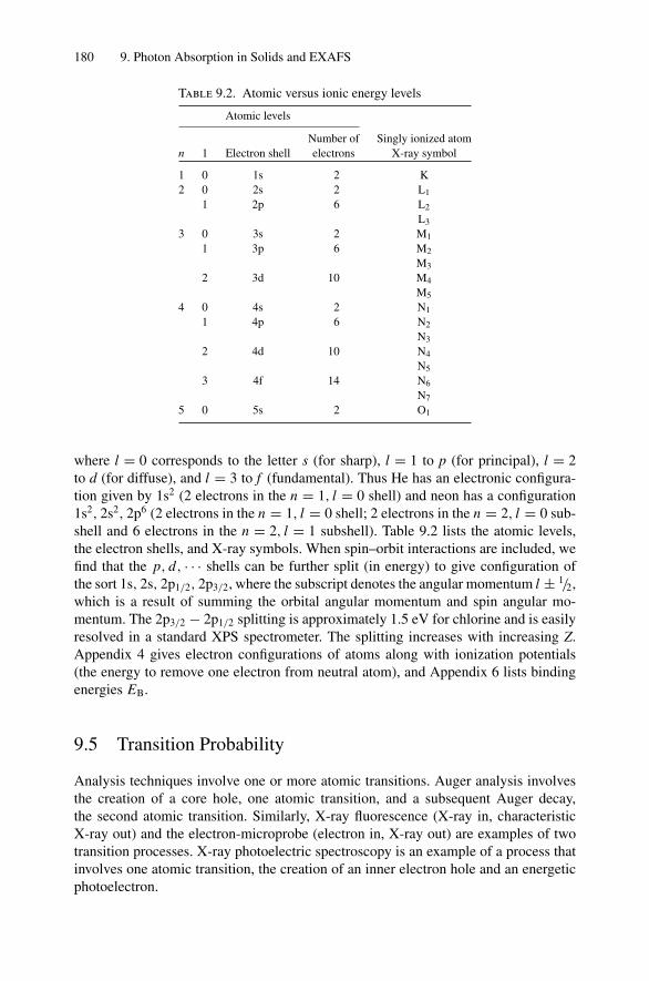
180 9. Photon Absorption in Solids and EXAFS
Table 9.2. Atomic versus ionic energy levels
Atomic levels
Number of Singly ionized atomn 1 Electron shell electrons X-ray symbol
1 0 1s 2 K2 0 2s 2 L1
1 2p 6 L2
L3
3 0 3s 2 M1
1 3p 6 M2
M3
2 3d 10 M4
M5
4 0 4s 2 N1
1 4p 6 N2
N3
2 4d 10 N4
N5
3 4f 14 N6
N7
5 0 5s 2 O1
where l = 0 corresponds to the letter s (for sharp), l = 1 to p (for principal), l = 2to d (for diffuse), and l = 3 to f (fundamental). Thus He has an electronic configura-tion given by 1s2 (2 electrons in the n = 1, l = 0 shell) and neon has a configuration1s2, 2s2, 2p6 (2 electrons in the n = 1, l = 0 shell; 2 electrons in the n = 2, l = 0 sub-shell and 6 electrons in the n = 2, l = 1 subshell). Table 9.2 lists the atomic levels,the electron shells, and X-ray symbols. When spin–orbit interactions are included, wefind that the p, d, · · · shells can be further split (in energy) to give configuration ofthe sort 1s, 2s, 2p1/2, 2p3/2, where the subscript denotes the angular momentum l ± 1/2,which is a result of summing the orbital angular momentum and spin angular mo-mentum. The 2p3/2 − 2p1/2 splitting is approximately 1.5 eV for chlorine and is easilyresolved in a standard XPS spectrometer. The splitting increases with increasing Z.Appendix 4 gives electron configurations of atoms along with ionization potentials(the energy to remove one electron from neutral atom), and Appendix 6 lists bindingenergies EB.
9.5 Transition Probability
Analysis techniques involve one or more atomic transitions. Auger analysis involvesthe creation of a core hole, one atomic transition, and a subsequent Auger decay,the second atomic transition. Similarly, X-ray fluorescence (X-ray in, characteristicX-ray out) and the electron-microprobe (electron in, X-ray out) are examples of twotransition processes. X-ray photoelectric spectroscopy is an example of a process thatinvolves one atomic transition, the creation of an inner electron hole and an energeticphotoelectron.
9.6. Photoelectric Effect—Square-Well Approximation 181
The most useful formula to calculate the probability of a transition comes fromtime-dependent perturbation theory. In first-order perturbation theory, the Hamiltonianacting on the system is written as
H = H0 + H ′. (9.23)
H0 is a Hamiltonian for which the Schrodinger equation can be solved, and H ′ containsan additional potential, i.e., an applied electric field.
There is a set of eigenfunctions that are the solutions to H0 such that H0un = Enun .As discussed in Section 9.10, the transition probability per unit time for a transition tothe state k from the initial state m is given by
W = 2π
hρ(E)|〈ψk |H ′|ψm〉|2. (9.24)
In this equation, ρ(E) is the density of final states per unit energy,
〈ψk |H ′|ψm〉 =∫
ψ∗k H ′ψdτ = ∣∣H ′
km
∣∣, (9.25)
where ψ∗ is the complex conjugate of ψ, dτ is a three-dimensional volume element(i.e., r2dr sin θ dθ dφ), and the wave function ψm is
ψm = ei tωm um . (9.26)
Eq. 9.24 is famous in quantum mechanics and is known as Fermi’s Golden Rule. Itsgreat advantage is that one need not know the wave functions for the true potential,H0 + H ′; rather, only the solutions to H0 are required. Note that W has dimensions of(time)−1:
W = 1
energy · time· 1
energy· (energy)2 = 1
time.
The derivation of Eq. 9.24 is given in Section 9.10.
9.6 Photoelectric Effect—Square-Well Approximation
The goal in this chapter is to make a quantitative calculation of the cross section for thephotoeffect: i.e., an electron with binding energy EB is irradiated with light of energyhω and is ejected with energy hω − EB. In this section, we calculate the relativelysimple problem of the transition probability and then the cross section for an electronbound in a one-dimensional square well. In the next section, we consider the morerealistic case of the photoeffect in a hydrogenic atom.
A flux of incident photons is represented by an electromagnetic field, and the per-turbation is
H ′(x, t) = H ′(x)eiωt = eExe−iωt , (9.27)
where the electric field E that acts on the particle is uniform in space (wavelengthgreater than atomic dimensions) but harmonic in time. This perturbation represents thepotential energy of the electron in the field of a photon of frequency ω.
182 9. Photon Absorption in Solids and EXAFS
The transition rate between the initial and final state is given in Eq. 9.24 as
W = 2π
hρ(E)
∣∣H ′f1
∣∣2,where the initial state is the wave function ψi of a particle bound in the well and thefinal state is an outgoing one-dimensional plane wave, e−ikx .
To calculate the density of final statesρ(E), we consider the system to have dimensionof length L and require periodic boundary conditions so that ψ(x0) = ψ(x0 + L). Thenormalized states are
ψE = 1√L
eikx , (9.28)
where kL = (2m E)1/2 L/h = 2π N (i.e., periodic boundary conditions).The density of states is the number of states with energy between E and E + E .
Then
ρ(E)E = N = L
2πk,
ρ(E) = L
2π· k
E. (9.29)
For a free particle, E = h2k2/2m and E = (h2k/m) · k, so
ρ(E) = L
2πh
(2m
E
)1/2
, (9.30)
where we have included a factor of 2 for positive and negative values of N. The matrixelement in the transition probability is
H ′f1
=∫
1√L
eikx eExψi (x) dx, (9.31)
where hk is the momentum of the final state.In order to calculate the matrix element for a specific example, we consider the
electron to be weakly bound in a narrow potential well. For the one-dimensional well,the wave function u0 outside the well must satisfy
−h2
2m
d2u0
dx2= −EBu0,
which leads to exponentially decaying solutions of the form
u0 = Ce±ki x ,
where ki is the momentum associated with the bound state, ki = (2mEB)1/2/h andC = √
ki . For ease of calculation, we extrapolate the exterior wave function to theorigin, as indicated in Fig. 9.2. Now, the normalized initial wave function ψi is
ψi (x) ∼=[√
ki
]e−ki |x |. (9.32)
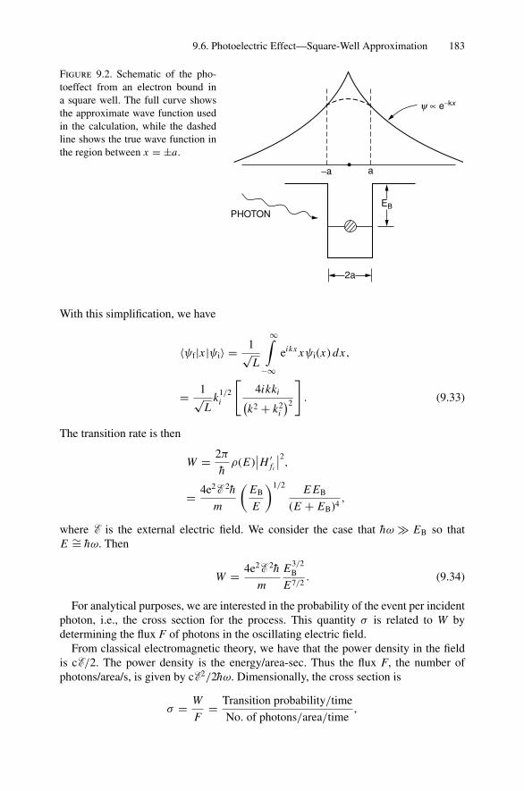
9.6. Photoelectric Effect—Square-Well Approximation 183
PHOTON
2a
EB
y ∝ e−kx
−a a
Figure 9.2. Schematic of the pho-toeffect from an electron bound ina square well. The full curve showsthe approximate wave function usedin the calculation, while the dashedline shows the true wave function inthe region between x = ±a.
With this simplification, we have
〈ψf|x |ψi〉 = 1√L
∞∫−∞
eikx xψi(x) dx,
= 1√L
k1/2i
[4ikki(
k2 + k2i
)2]
. (9.33)
The transition rate is then
W = 2π
hρ(E)
∣∣H ′fi
∣∣2,= 4e2E 2h
m
(EB
E
)1/2 E EB
(E + EB)4,
where E is the external electric field. We consider the case that hω EB so thatE ∼= hω. Then
W = 4e2E 2h
m
E3/2B
E7/2. (9.34)
For analytical purposes, we are interested in the probability of the event per incidentphoton, i.e., the cross section for the process. This quantity σ is related to W bydetermining the flux F of photons in the oscillating electric field.
From classical electromagnetic theory, we have that the power density in the fieldis cE/2. The power density is the energy/area-sec. Thus the flux F, the number ofphotons/area/s, is given by cE2/2hω. Dimensionally, the cross section is
σ = W
F= Transition probability/time
No. of photons/area/time,
184 9. Photon Absorption in Solids and EXAFS
or
σ = 8e2h
mc
E3/2B
E5/2. (9.35)
The cross section decreases with increasing photon energy (E = hω) as E5/2.
9.7 Photoelectric Transition Probability for a Hydrogenic Atom
In this section, we describe a calculation of the cross section for the photoelectriceffect using hydrogenic wave functions in three-dimensional space. The formula forthe transition probability is given by Eq. 9.24. The relevant wave functions for theinitial and final state are given by
ψi = 1√πa3
e−ρ
and
ψf = 1√V
eik·r, (9.36)
where the initial state, ψi, describes a ground state hydrogenic wave function in anatom of atomic number Z and the final state is the usual outgoing plane wave of finalenergy Ef = h2k2/2m normalized to a volume V. The binding energy of the electron,EB, is expressed as Z2e2/2a0 (see Eq. 1.17), and in this calculation we assume theenergy of the incoming photon, hω EB. Here, the three-dimensional density ofstates, ρ(E) = (V/2π2)(2m/h2)3/2 E1/2, is used.
The transition probability can be calculated explicitly if the perturbation potentialused is
H ′ = −eExeiωt .
In that case, the final result for the photoeffect cross section σph yields
σph = 288π
3
e2h
mc
E5/2B
E7/2,
a result similar to the square-well one-dimensional calculation carried out explicitly inthe previous section.
Using a more sophisticated description of the perturbation potential, but preciselythe same wave functions and assumption of hω EB, Schiff (1968) shows that
σph = 128π
3
e2h
mc
E5/2B
E7/2. (9.37)
The value of e2h/mc = 5.56 × 10⁻⁴ eV-nm2, so for convenience we write
σph = 7.52 × 10⁻² nm2
hω×(
EB
hω
)5/2
, (9.37′)
by setting the incoming photon energy hω in eV equal to the energy E of the outgoingelectron, since EB hω (i.e., E = hω − EB
∼= hω).
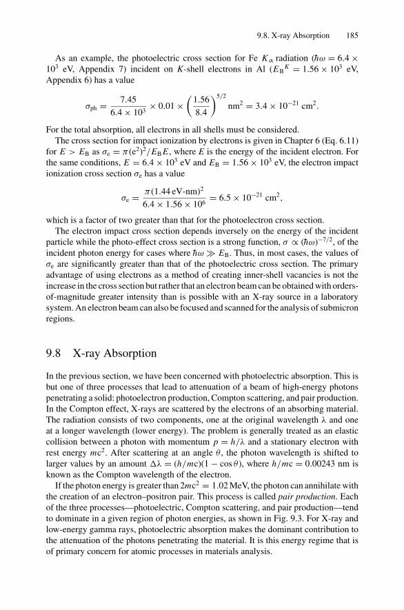
9.8. X-ray Absorption 185
As an example, the photoelectric cross section for Fe Kα radiation (hω = 6.4 ×10³ eV, Appendix 7) incident on K-shell electrons in Al (EB
K = 1.56 × 10³ eV,Appendix 6) has a value
σph = 7.45
6.4 × 103× 0.01 ×
(1.56
8.4
)5/2
nm2 = 3.4 × 10⁻²¹ cm2.
For the total absorption, all electrons in all shells must be considered.The cross section for impact ionization by electrons is given in Chapter 6 (Eq. 6.11)
for E > EB as σe = π (e2)2/EB E , where E is the energy of the incident electron. Forthe same conditions, E = 6.4 × 10³ eV and EB = 1.56 × 10³ eV, the electron impactionization cross section σe has a value
σe = π (1.44 eV-nm)2
6.4 × 1.56 × 106= 6.5 × 10⁻²¹ cm2,
which is a factor of two greater than that for the photoelectron cross section.The electron impact cross section depends inversely on the energy of the incident
particle while the photo-effect cross section is a strong function, σ ∝ (hω)−7/2, of theincident photon energy for cases where hω EB. Thus, in most cases, the values ofσe are significantly greater than that of the photoelectric cross section. The primaryadvantage of using electrons as a method of creating inner-shell vacancies is not theincrease in the cross section but rather that an electron beam can be obtained with orders-of-magnitude greater intensity than is possible with an X-ray source in a laboratorysystem. An electron beam can also be focused and scanned for the analysis of submicronregions.
9.8 X-ray Absorption
In the previous section, we have been concerned with photoelectric absorption. This isbut one of three processes that lead to attenuation of a beam of high-energy photonspenetrating a solid: photoelectron production, Compton scattering, and pair production.In the Compton effect, X-rays are scattered by the electrons of an absorbing material.The radiation consists of two components, one at the original wavelength λ and oneat a longer wavelength (lower energy). The problem is generally treated as an elasticcollision between a photon with momentum p = h/λ and a stationary electron withrest energy mc2. After scattering at an angle θ , the photon wavelength is shifted tolarger values by an amount λ = (h/mc)(1 − cos θ ), where h/mc = 0.00243 nm isknown as the Compton wavelength of the electron.
If the photon energy is greater than 2mc2 = 1.02 MeV, the photon can annihilate withthe creation of an electron–positron pair. This process is called pair production. Eachof the three processes—photoelectric, Compton scattering, and pair production—tendto dominate in a given region of photon energies, as shown in Fig. 9.3. For X-ray andlow-energy gamma rays, photoelectric absorption makes the dominant contribution tothe attenuation of the photons penetrating the material. It is this energy regime that isof primary concern for atomic processes in materials analysis.
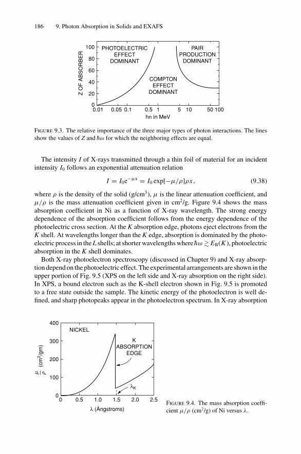
186 9. Photon Absorption in Solids and EXAFS
PHOTOELECTRIC EFFECT
DOMINANT
PAIR PRODUCTION
DOMINANT
COMPTON EFFECT
DOMINANT
hn in MeV
Z O
F A
BS
OR
BE
R
0.01 0.05 0.1 0.5 1 5 10 50 1000
20
40
60
80
100
Figure 9.3. The relative importance of the three major types of photon interactions. The linesshow the values of Z and hω for which the neighboring effects are equal.
The intensity I of X-rays transmitted through a thin foil of material for an incidentintensity I0 follows an exponential attenuation relation
I = I0e−µx = I0 exp[−µ/ρ]ρx, (9.38)
where ρ is the density of the solid (g/cm3), µ is the linear attenuation coefficient, andµ/ρ is the mass attenuation coefficient given in cm2/g. Figure 9.4 shows the massabsorption coefficient in Ni as a function of X-ray wavelength. The strong energydependence of the absorption coefficient follows from the energy dependence of thephotoelectric cross section. At the K absorption edge, photons eject electrons from theK shell. At wavelengths longer than the K edge, absorption is dominated by the photo-electric process in the L shells; at shorter wavelengths where hω EB(K ), photoelectricabsorption in the K shell dominates.
Both X-ray photoelectron spectroscopy (discussed in Chapter 9) and X-ray absorp-tion depend on the photoelectric effect. The experimental arrangements are shown in theupper portion of Fig. 9.5 (XPS on the left side and X-ray absorption on the right side).In XPS, a bound electron such as the K-shell electron shown in Fig. 9.5 is promotedto a free state outside the sample. The kinetic energy of the photoelectron is well de-fined, and sharp photopeaks appear in the photoelectron spectrum. In X-ray absorption
NICKEL
KABSORPTION
EDGE
(cm
2 /gm
)m r
0 0.5 1.0 1.5 2.0 2.50
100
200
300
400
λK
λ (Ångstroms)Figure 9.4. The mass absorption coeffi-cient µ/ρ (cm2/g) of Ni versus λ.
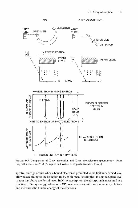
9.8. X-ray Absorption 187
ATT
EN
UAT
ION
OF
X
-RAY
BE
AM
X-RAY ABSORPTION SPECTRUM
PHOTO ELECTRON SPECTRUM
(XPS)CONDBANDN
UM
BE
R O
F
PH
OTO
ELE
CT
RO
NS
K-SHELL
FERMI LEVELFERMILEVEL
SPECIMEN
DETECTOR
X-RAY ABSORPTION
DETECTOR
XPS
X-RAY TUBE
X-RAY TUBE SPECIMEN
FREE ELECTRON
K METAL
LLL
LLL
KINETIC ENERGY OF PHOTO ELECTRONS
Figure 9.5. Comparison of X-ray absorption and X-ray photoelectron spectroscopy. [FromSiegbathn et al., in ESCA (Almguist and Wiksells, Uppsala, Sweden, 1967).]
spectra, an edge occurs when a bound electron is promoted to the first unoccupied levelallowed according to the selection rules. With metallic samples, this unoccupied levelis at or just above the Fermi level. In X-ray absorption, the absorption is measured as afunction of X-ray energy, whereas in XPS one irradiates with constant-energy photonsand measures the kinetic energy of the electrons.
188 9. Photon Absorption in Solids and EXAFS
The mass absorption coefficient µ/ρ for electrons in a given shell or subshell canbe calculated from the photoelectric cross section σ:
µ
ρ= σ (cm2/electrons) × N (atoms/cm3)2 · ns(electrons/shell)
ρ(g/cm3), (9.39)
where ρ is the density, N the atomic concentration, and ns the number of electrons in ashell. For example, for Mo Kα radiation (λ = 0.0711 nm and hω = 17.44 keV) incidenton Ni, which has a K-shell binding energy of 8.33 keV, the value of the photoelectriccross section per K electron is
σph = 7.45 × 10⁻¹⁶ cm2
17.44 × 10³
(8.33
17.44
)5/2
= 6.7 × 10⁻²¹ cm2.
The atomic density of Ni is 9.14 × 10²² atom/cm3 and the density is 8.91 g/cm3. Themass absorption coefficient µ/ρ for K-shell absorption (ns = 2 for the K-shell) is
µ
ρ= 6.7 × 10−21 × 9.14 × 1022 · 2
8.91= 138 cm2/g.
In this calculation, the contribution of the L-shell electrons was neglected. For photonenergies greater than the K-shell binding energy, the photoelectric cross section for theL-shell is at least an order of magnitude smaller than that of the K shell; of course, thisis the major factor in the sharp increasing absorption when one crosses the K absorptionedge. In the present case of MoKα radiation on Ni, if we assume an average bindingenergy of 0.9 keV for the L1, L2, and L3 shells, the photoelectric cross section perelectron is a factor of 3.8 × 10⁻³ smaller than that of the K-shell electrons due to the(EB/hω)5/2 term.
The calculated value, 138 cm2/g, is greater than the measured value of 47.24 (Ap-pendix 7). The major difficulty in the mass absorption calculation above was that theenergy E of Mo Kα radiation is only twice that of the K-shell binding energy EB,and the derivation of Eq. 9.37 was based on hω EB. For Cu Kα radiation withE = 8.04 keV, the photon energy is about 10 times that of the L-shell binding energy,and the calculated photoelectric cross section (σ = 3.1 × 10⁻²¹ cm2) for the L shellgives a value of µ/ρ = 32 cm2/g, a value close to the tabulated value of 48.8 cm 2/g.
Measured values of the mass absorption coefficient for different radiation are tabu-lated in Appendix 8 and displayed in Fig. 9.6a for Z = 2 − 40. For a given element,the absorption coefficient can vary over two orders of magnitude depending on thewavelength of the incident radiation. The strong photon energy dependence (hω−7/2)of the absorption coefficient is illustrated in Fig. 9.6b.
The tenfold change in the absorption coefficient on either side of the K edge, as shownin Fig. 9.4, represents a major change in transmitted intensity for thin foils becauseof the exponential nature of the transmission factor I/I0. If the transmission factor ofa particular sheet is 0.1 for a wavelength just longer than λK , then for a wavelengthjust shorter, the transmission is reduced by a factor of about exp(−10). This effecthas been used to design filters for X-ray diffraction experiments that require nearlymonochromatic radiation. As shown in Fig. 9.7a, the characteristic radiation from theK shell contains a strong Kα line and a weaker Kβ line (the Kβ/Kα emission ratio isdiscussed in Section 11.10). The Kβ line intensity relative to that of the Kα line canbe decreased by passing the beam through a filter made of material whose absorption
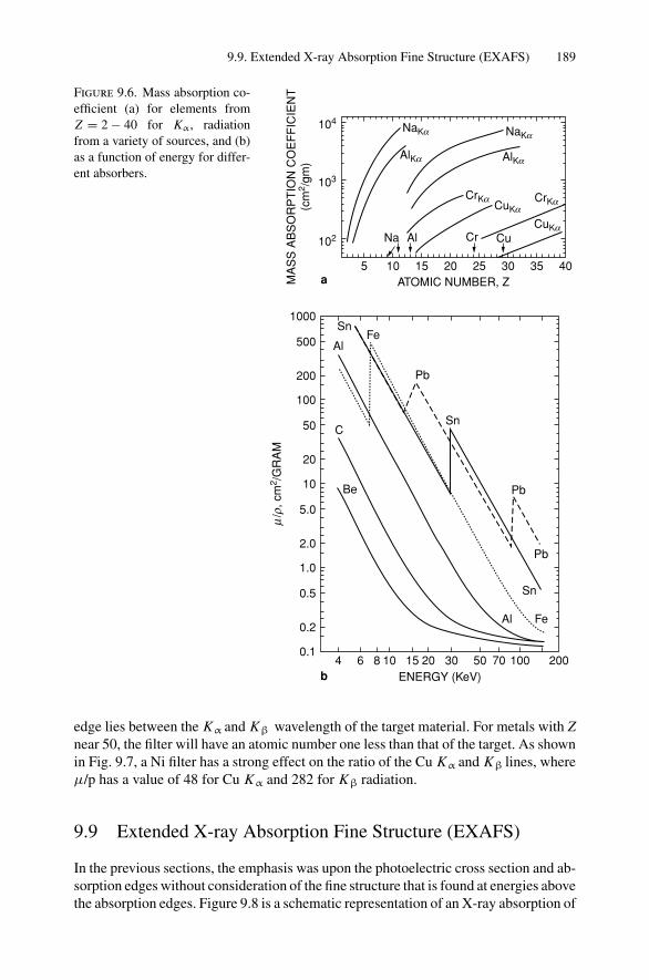
9.9. Extended X-ray Absorption Fine Structure (EXAFS) 189
4 6 8 10 15 20 30 50 70 100 2000.1
0.2
0.5
1.0
2.0
5.0
10
20
50
1000
500
200
100
ENERGY (KeV)
m/r,
cm
2 /G
RA
M
Pb
Pb
Pb
Sn
Sn
Sn
Fe
Fe
Be
Al
Al
C
b
ATOMIC NUMBER, ZMA
SS
AB
SO
RP
TIO
N C
OE
FF
ICIE
NT
(c
m2 /
gm)
104
103
102
5 10 15 20 25 30 35 40
NaKa
Na
NaKa
AlKa
Al
AlKa
CrKa
Cr
CrKaCuKaCuKa
Cu
a
Figure 9.6. Mass absorption co-efficient (a) for elements fromZ = 2 − 40 for Kα, radiationfrom a variety of sources, and (b)as a function of energy for differ-ent absorbers.
edge lies between the Kα and Kβ wavelength of the target material. For metals with Znear 50, the filter will have an atomic number one less than that of the target. As shownin Fig. 9.7, a Ni filter has a strong effect on the ratio of the Cu Kα and Kβ lines, whereµ/p has a value of 48 for Cu Kα and 282 for Kβ radiation.
9.9 Extended X-ray Absorption Fine Structure (EXAFS)
In the previous sections, the emphasis was upon the photoelectric cross section and ab-sorption edges without consideration of the fine structure that is found at energies abovethe absorption edges. Figure 9.8 is a schematic representation of an X-ray absorption of
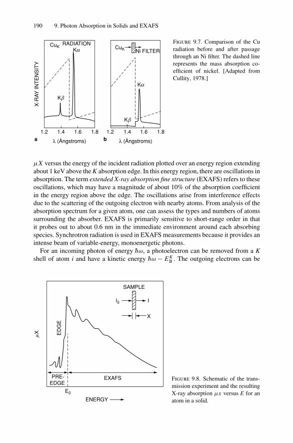
190 9. Photon Absorption in Solids and EXAFS
X-R
AY IN
TE
NS
ITY
1.2 1.4 1.6 1.8 1.2 1.4 1.6 1.8a b
CuK CuKRADIATION
Ka Ni FILTER
Kβ
Kβ
Ka
λ (Ångstroms) λ (Ångstroms)
Figure 9.7. Comparison of the Curadiation before and after passagethrough an Ni filter. The dashed linerepresents the mass absorption co-efficient of nickel. [Adapted fromCullity, 1978.]
µX versus the energy of the incident radiation plotted over an energy region extendingabout 1 keV above the K absorption edge. In this energy region, there are oscillations inabsorption. The term extended X-ray absorption fine structure (EXAFS) refers to theseoscillations, which may have a magnitude of about 10% of the absorption coefficientin the energy region above the edge. The oscillations arise from interference effectsdue to the scattering of the outgoing electron with nearby atoms. From analysis of theabsorption spectrum for a given atom, one can assess the types and numbers of atomssurrounding the absorber. EXAFS is primarily sensitive to short-range order in thatit probes out to about 0.6 nm in the immediate environment around each absorbingspecies. Synchrotron radiation is used in EXAFS measurements because it provides anintense beam of variable-energy, monoenergetic photons.
For an incoming photon of energy hω, a photoelectron can be removed from a Kshell of atom i and have a kinetic energy hω − E K
B . The outgoing electrons can be
EXAFS
ED
GE
PRE- EDGE
II0
E0
SAMPLE
µX
ENERGY
X
Figure 9.8. Schematic of the trans-mission experiment and the resultingX-ray absorption µx versus E for anatom in a solid.
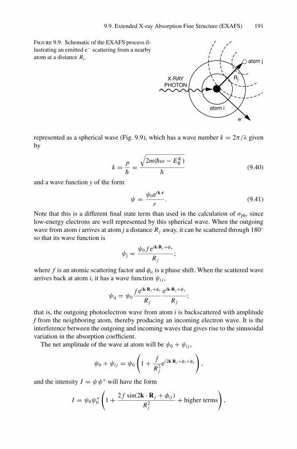
9.9. Extended X-ray Absorption Fine Structure (EXAFS) 191
atom i
atom j
RjX-RAY PHOTON
e−
Figure 9.9. Schematic of the EXAFS process il-lustrating an emitted e− scattering from a nearbyatom at a distance Rj.
represented as a spherical wave (Fig. 9.9), which has a wave number k = 2π/λ givenby
k = p
h=√
2m(hω − E KB )
h(9.40)
and a wave function y of the form
ψ = ψ0eik·r
r. (9.41)
Note that this is a different final state term than used in the calculation of σph, sincelow-energy electrons are well represented by this spherical wave. When the outgoingwave from atom i arrives at atom j a distance R j away, it can be scattered through 180
so that its wave function is
ψj = ψ0 f eik·R j +φa
R j;
where f is an atomic scattering factor and φa is a phase shift. When the scattered wavearrives back at atom i, it has a wave function ψi j ,
ψij = ψ0f eik·R j +φs
R j
eik·R j +φ j
R j;
that is, the outgoing photoelectron wave from atom i is backscattered with amplitudef from the neighboring atom, thereby producing an incoming electron wave. It is theinterference between the outgoing and incoming waves that gives rise to the sinusoidalvariation in the absorption coefficient.
The net amplitude of the wave at atom will be ψ0 + ψi j ,
ψ0 + ψi j = ψ0
(1 + f
R2j
ei2k·R j +φi +φa
),
and the intensity I = ψψ∗ will have the form
I = ψ0ψ∗0
(1 + 2 f sin(2k · R j + φi j )
R2j
+ higher terms
),
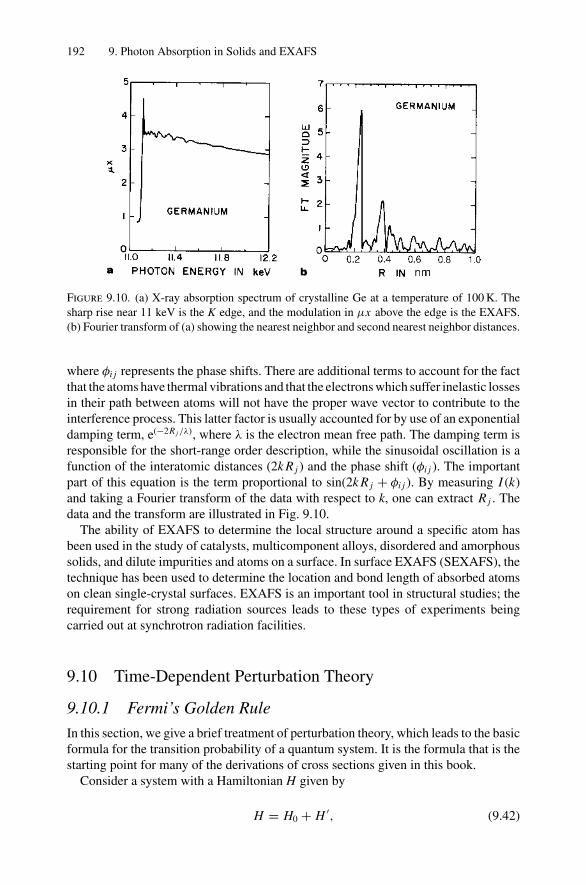
192 9. Photon Absorption in Solids and EXAFS
Figure 9.10. (a) X-ray absorption spectrum of crystalline Ge at a temperature of 100 K. Thesharp rise near 11 keV is the K edge, and the modulation in µx above the edge is the EXAFS.(b) Fourier transform of (a) showing the nearest neighbor and second nearest neighbor distances.
where φi j represents the phase shifts. There are additional terms to account for the factthat the atoms have thermal vibrations and that the electrons which suffer inelastic lossesin their path between atoms will not have the proper wave vector to contribute to theinterference process. This latter factor is usually accounted for by use of an exponentialdamping term, e(−2R j /λ), where λ is the electron mean free path. The damping term isresponsible for the short-range order description, while the sinusoidal oscillation is afunction of the interatomic distances (2k R j ) and the phase shift (φi j ). The importantpart of this equation is the term proportional to sin(2k R j + φi j ). By measuring I (k)and taking a Fourier transform of the data with respect to k, one can extract R j . Thedata and the transform are illustrated in Fig. 9.10.
The ability of EXAFS to determine the local structure around a specific atom hasbeen used in the study of catalysts, multicomponent alloys, disordered and amorphoussolids, and dilute impurities and atoms on a surface. In surface EXAFS (SEXAFS), thetechnique has been used to determine the location and bond length of absorbed atomson clean single-crystal surfaces. EXAFS is an important tool in structural studies; therequirement for strong radiation sources leads to these types of experiments beingcarried out at synchrotron radiation facilities.
9.10 Time-Dependent Perturbation Theory
9.10.1 Fermi’s Golden Rule
In this section, we give a brief treatment of perturbation theory, which leads to the basicformula for the transition probability of a quantum system. It is the formula that is thestarting point for many of the derivations of cross sections given in this book.
Consider a system with a Hamiltonian H given by
H = H0 + H ′, (9.42)
9.10. Time-Dependent Perturbation Theory 193
where H0 is a time-independent operator with an eigenvalue ψ0. H0 could be, forexample, the Hamiltonian that describes a hydrogenic atom, while H ′ may be a time-dependent perturbation, i.e., an oscillating electric field. The wave function ψ0 satisfiesthe Schrodinger equation such that
ih∂ψ0
∂t= H0ψ0. (9.43)
Since H0 is time independent, we can write
ψ0 = u(x, y, z)e−i E0t/h (9.44)
or
ψ0 =∑
n
a0nu0
ne−iE0n t/h, (9.45)
where
H0u0n = E0
nu0n, (9.46)
with the u0n being an orthonormal set of eigenvectors and the constants a0
n independentof time.
For the perturbed Hamiltonian, we write
Hψ = ih∂ψ
∂t= (H0 + H ′)ψ (9.47)
and
ψ =∑
n
an(t)u0ne−E0
n t/h, (9.48)
where the coefficients an are now a function of time.Substituting of (9.48) into (9.47), multiplying by the complex conjugate u0∗
n , andusing the orthonormality relation yields
das
dt= as = − i
h
∑n
an(t)Hsn′ei(E0
s −E0n )t/h, (9.49)
where
H ′sn =
∫u0∗
s H ′u0ndτ,
the integral being over all space. We approximate the solution by noting that if theperturbation is small, the time variation of an(t) is slow; then an(t) ∼= an(0) and
as(t) − as(0) = − i
h
∑n
an(0)
t∫0
H ′sn(t)eiωsn t dt , (9.50)
where hωsn = E0s − E0
n .A special case is if the system is in state n at t = 0; then an(0) = 1 and all other a’s
are zero. For the case s = n, Eq. 9.50 then gives
as(t) = i
h
t∫0
H ′sn(t)eiωsn t dt, (9.51)
194 9. Photon Absorption in Solids and EXAFS
The perturbation H ′(t) can induce transitions from the state n to any state s, and theprobability of finding the system in the state s at time t is |as(t)|2.
If H ′ is independent of time, then
as = −H ′sn
(eiωsn t − 1)
hωsn, (9.52)
and
|as(t)|2 = 4H ′2
sn sin2(ωsnt/2)
h2ω2sn
, (9.53)
and is valid if |as(t)| < 1.In many applications, the result of a perturbation is a particle in the continuum, i.e.,
a free particle. Then an explicit final state is not appropriate, but the density of finalstates is relevant. We call ρ(E) the density of final states (number of energy levels/perunit energy interval) and assume that H ′
sn is the same for all final states.The transition probability P(t) is then given by
P(t) =∑
s
|as(t)|2 = 4|H ′sn|2∑
S
sin2(ωsnt/2)
h2ω2sn
. (9.54)
For a continuum, we transform the sum to an integral and note that the number of statesin energy interval dEs is ρ(Es)dEs ; then
P(t) = 4∣∣H ′
sn
∣∣2 ∞∫−∞
ρ(Es)sin2(ωsnt/2)
h2ω2sn
dhωsn. (9.55)
The major contribution of the integral comes from ωsn = 0 (it is a bit like a deltafunction), and noting that
∫sin2 αx/x2 dx = πα, we have
P(t) = 4∣∣H ′
sn
∣∣2ρ(En)π t
2h, (9.56)
so the rate of the transition, W, is given by
W = 2π
hρ(En)
∣∣H ′sn
∣∣2. (9.57)
This is a famous and important formula denoted as the Golden Rule of Fermi.
9.10.2 Transition Probability in an Oscillating Electric Field
Another important application of perturbation theory is when the perturbing field hasa time dependence of the form eiωt . Consider for example an oscillating electric fielddirected along the x-axis such that
E = E cos ωt = E0
2(eiωt + e−iωt ) (9.58)
and
H ′(t) = e
2E0x(eiωt + e−iωt ). (9.59)
9.10. Time-Dependent Perturbation Theory 195
Inserting H ′(t) into (9.51) gives
as(t) = i
he
E0xsn
2
t∫0
(ei(ωsn+ω)t + e−i(ωsn−ω)t ) dt. (9.60)
If ωsn = ω, the integral averages to zero. If ωsn∼= ω, we have
|as(t)|2 = e2E20
h2 |xsn|2 sin2 [(t/2)(ω − ωsn)]
(ω − ωsn)2, (9.61)
where |xsn| = ∫ u∗s xun dτ . We recognize that E 2
0/2 is the energy density in the field,which can be represented by ρ(ω) to obtain a transition probability:
Tns = |as(t)|2 = 2e2|xsn|2∞∫
0
sin2[(t/2)(ω − ωsn)]
h2(ω − ωsn)ρ(ω) dω. (9.62)
Assume that the distribution ρ(ω) varies much more slowly than the sharply peakedfunction by which it is multiplied. Then ρ(ω) is nearly constant over the small rangeof values of ω for which the integrand is nonzero, so we can replace ρ(ω) by its valueat ω = ωsn , and remove it from the integral, with no loss of accuracy. With the furthersubstitution z = 1/2(ω − ωsn)t ′, the expression becomes
|asn(t ′)|2 = e2ρ(ωsn)|xsn|2t ′
h2
∞∫−∞
sin2 z
z2dz,
or, since
∞∫−∞
sin2 z
z2dz = π,
the transition probability is
Tsn = |asn(t ′)|2 = πe2ρ(ωsn)|xsn|2t ′
h2 , (9.63)
where xsn = ∫ u∗s xun dτ . Eq. 9.63 holds for radiation that is polarized along the x-axis.
In the general case, when radiation is incident upon the atom from all directions andwith random polarization, Tsn must include equal contributions from xsn, ysn , and zsn ,so
Tsn = πe2ρ(ωsn)t ′
3h2
∣∣⟨ψs |r|ψn⟩∣∣2, (9.64)
where the factor of 3 has been introduced into the denominator because each polariza-tion direction is assumed to contribute one-third of the intensity and |xn|2 + |ysn|2 +|zsn|2 = |〈ψs |r|ψn〉|2 = |rsn|2 · 〈ψs |r|ψn〉 is known as the dipole matrix element andEq. 9.64 is the dipole approximation to the transition probability.
196 9. Photon Absorption in Solids and EXAFS
9.10.3 Spontaneous Transitions
Spontaneous transitions are those that occur in the absence of an external field. Anexample is the transition from an excited state to a ground state. To calculate suchphenomena, we rely on a treatment developed in 1917 by Einstein, which enables oneto calculate the rate of spontaneous transitions from knowledge of the rate of inducedtransitions calculated in Section 9.10.2.
Consider a collection of atoms in thermal equilibrium; each atom must be emittingand absorbing radiation at the same rate. Let Pns be the probability that a given atomwill go from the nth state to the sth state in a short time dt. This probability, Pns ,must be proportional to the probability Pn that the atom is in the nth state to beginwith, multiplied by the transition probability to go from state n to state s, Tns (given byEq. 9.64):
Pns = Tns Pn.
In view of Eq. 9.64, we may write this expression as
Pns = Ans ρ(ωns)Pn dt, (9.65)
where ρ(ωns) is defined as before, dt takes the place of t ′ as the time interval, and Ans
is equal to all the other factors in Eq. 9.64.The probability of a downward transition from state s to state n may be written as
Psn = Asnρ(ωsn)Ps dt,
but because of the symmetry of the equations leading to Eq. 9.64, we know that Asn =Ans and ωsn = ωns , so
Psn = Asnρ(ωns)Ps dt. (9.66)
Notice that Pns does not equal Psn , because Pn > Ps ; the nth state, being lower inenergy, is more heavily populated, according to the Boltzmann factor.
The system is in equilibrium, so the total number of transitions from n to s must equalthe total number of transitions from s to n. Since the induced transition probabilitiesare unequal (Pns = Psn), there must be additional transitions from state s to state n thatare spontaneous. The spontaneous transition probability by definition does not dependon the energy density of the externally applied field; this probability may be writtenBsn Ps dt , where Bsn is the spontaneous transition probability. The coefficients A andB are referred to as the Einstein coefficients.
The total transition probability from s to n is therefore equal to Psn + Bsn Ps dt , andthis total should equal the transition probability Pns . Thus, from Eqs. 9.65 and 9.66,we have
ρ(ωns)Pn Ans = ρ(ωns)Pn Ans + Ps Bsn
or
Bsn = ρ(ωns)Ans
[Pn
Ps− 1
].
Problems 197
But the population of a state of energy E is proportional to the Boltzmann factor e−E/kT ,so the ratio Pn/Ps may be written
Pn
Ps= e(Es−En )/kT
= ehωm/kT .
Thus
Bsn = ρ(ωns)Ans(ehωm/kT − 1
). (9.67)
The factor ρ(ωns) in Eq. 9.67 is misleading because Bsn by definition does not dependon the energy density of the radiation field. We can eliminate this factor by using anexpression for the energy density inside the cavity. Planck’s law for thermal radiationgives
ρ(ω) = hω3
π2 c2(ehωm/kT − 1
) . (9.68)
Substitution of this expression into Eq. 9.67 yields an expression for Bsn involving onlyAns and known constants:
Bsn = hω3ns
π2 c3Ans . (9.69)
The transition rate for a spontaneous transition from a filled to an empty state is
W = 4
3
e2
h
[ωns
c
]3 ∣∣〈ψs |r|ψn〉∣∣2, (9.70)
where e2 = 1.44 eV-nm. This can be expressed as
W = 0.38 × 10¹⁴(hω)3 · ∣∣〈ψs |r|ψn〉∣∣2,
where hω is in units of keV and the matrix element has dimensions of (0.01 nm)2. Atypical value of W is 1015/s for elements in the middle of the periodic table.
In summary,
W = 2π
h|H ′
sn|2ρ(En); static perturbation [Eqs. 9.24 and 9.57]
W = πe2ρ(ωsn)
3h2 |rsn|2; time dependent, H ′ = E0 cos ωt [Eq. 9.64]
W = 4
3
e2
h
[ωsn
c
]3|rsn|2; spontaneous transitions [Eq. 9.70]
Problems
9.1. For Cu Ka radiation (E = 8.04 keV) incident on Al:(a) Calculate the photoelectric cross section σph for the K shell of Al and compare
its value with the electron impact ionization cross section σe for 8.04 keVelectrons.

198 9. Photon Absorption in Solids and EXAFS
(b) Calculate the mass absorption coefficient for Al based on only K-shell absorp-tion and compare with the values tabulated in Appendix 8. The Al L shellshave 8 electrons compared to 2 in the Al K shell.
(c) Estimate the contribution of L-shell electrons to the mass absorption coefficientfor 8.04 keV electrons.
9.2. Consider 5.41 keV radiation [photon (Cr Kα) and electron] incident on Si. Com-pare the values in microns of the linear absorption coefficient, the electron range,and the electron mean free path.
9.3. You use an Ni filter to attenuate the Cu Kβ radiation from a Cu X-ray source. Ifthe Ni filter thickness is sufficient to a attenuate the KB radiation by a factor of1000, how much will the Kα radiation be attenuated. How thick is the Ni filter?Estimate to zero order how much the Cu Lα radiation is attenuated.
9.4. Be is used as a “window” material that allows X-rays to enter the X-ray detectorwith minimum attenuation. The absorption of X-rays from elements with Z < 10is one of the limitations of microprobe analysis. Estimate the absorption of carbonKα X-rays by a 7-µm thick Be window.
9.5. Consider a photon of energy hω inducing a photoeffect process with an electronof binding energy EB bound in an atom of mass Mn . Assume that the electronis emitted in the forward direction, i.e., along the same direction as the incidentphoton. In the approximation that hω EB, show that the energy of the recoilingatom, E, is given by
Er = (hω)2
2Mnc2+ me
Mnhω = hω
Mnc2
√2Mec2hω
where me is the electron mass. Evaluate this expression for hω = 1 keV, 100 keV,and Mn = 28 (Silicon) and compare the result to 14 eV, the binding energy of Si inthe Si lattice. Such considerations are important in determining the destructivenessof a given analysis technique.
9.6. Using conservation of momentum and energy, show that the photoeffect cannotoccur with a free electron. Consider the nonrelativistic case, hω < mec2. Thephotoeffect occurs with photon irradiation of solids, since all electrons in solidsare bound to some degree.
References
1. E. E. Anderson, Modern Physics and Quantum Mechanics (W. B. Saunders, Philadelphia,1971).
2. B. D. Cullity, Elements of X-ray Diffraction, 2nd ed. (Addison-Wesley, Reading, MA, 1978).3. P. A. Lee, P. H. Citrin, P. Eisenberger, and P. M. Kincaid, “Extended X-ray Absorption Fine
Structure,” Rev. Mod. Phys. 53, 769 (1981).4. R. Saxon, Elementary Quantum Electrodynamics (Holden-Day, San Francisco, 1968).5. L. I. Schiff, Quantum Mechanics, 3rd ed. (McGraw-Hill Book Co., New York, 1968).6. R. L. Sproull and W. A. Phillips, Modern Physics, 3rd ed. (John Wiley and Sons, New York,
1980).7. P. A. Tipler, Modern Physics (Worth Publishers, New York, 1978).
10X-ray Photoelectron Spectroscopy
10.1 Introduction
In this chapter, electronic structure is the dominant theme. Photons with energies of upto 10 keV interact with the atomic electrons primarily via the photon absorption process(Chapter 9). The photoelectric process is a direct signature of the photon interactionwith the atom and is the basis of one of the major analytical tools—photoelectronspectroscopy. This is referred to as UPS when ultraviolet light is incident on the sampleand XPS when X-rays are used. Another acronym is ESCA (for Electron Spectroscopyfor Chemical Analysis); in this case, the main concern is the chemical bonding.
The energy spectrum of electromagnetic radiation along with the common nomen-clature is shown in Fig. 10.1. In material analysis, the photon energy range of interestcorresponds to the ultraviolet (UV) and X-ray region. In practice, it extends from 10 eV,close to the binding energy (13.6 eV) of the electron in the hydrogen atom, to energies ofaround 0.1 MeV. At these energies, photons can penetrate within the solid and interactwith the inner-shell electrons. Lower-energy photons are used to establish the visiblespectra associated with the outermost, less tightly bound electrons. These outermostelectrons are involved in chemical bonding and are not associated with specific atomsand hence are not useful for elemental identification. Photon-induced spectroscopieshave undergone a major advance due to the advent of electron synchrotrons, whichproduce an intense source of monochromatic photons over a broad range of energiesfor materials science. Most laboratory instruments produce X-rays in the 1–10 keVregion, which is the main region discussed in this chapter.
10.2 Experimental Considerations
The basic processes of interest in photoelectron spectroscopy are the absorption ofa quantum of energy hω and the ejection of an electron, the photoelectron, whosekinetic energy, referenced to an appropriate zero of energy, is related to the bindingenergy of an electron in the target atom. In this process, an incident photon transfersits entire energy to the bound electron, and element identification is provided by themeasurement of the energy of the electrons that escape from the sample without energyloss. As indicated in Fig. 10.2, photoelectron spectroscopy requires both a source of
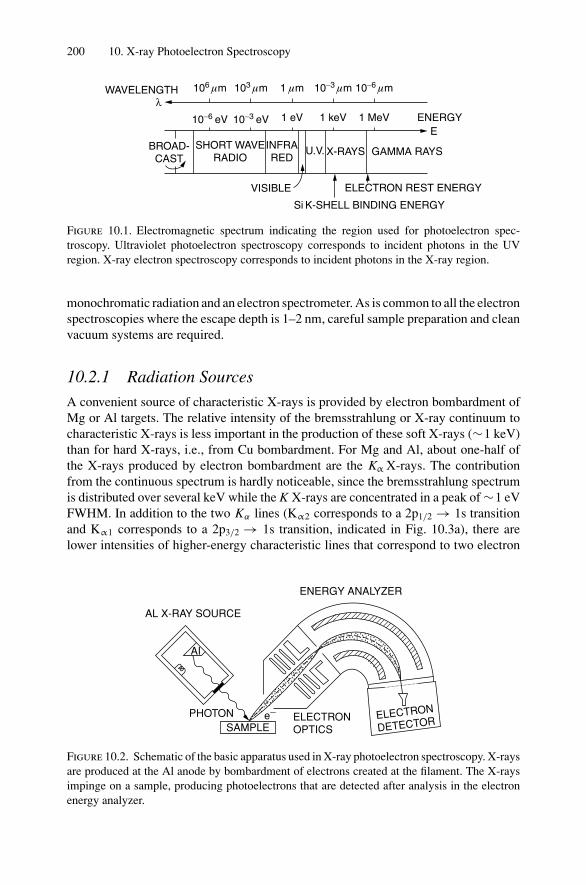
200 10. X-ray Photoelectron Spectroscopy
WAVELENGTHλ
106 µm 103 µm 10−3 µm
10−6 eV 10−3 eV
10−6 µm1 µm
1 eV 1 keV 1 MeV ENERGYE
GAMMA RAYSX-RAYSU.V.INFRARED
SHORT WAVERADIO
BROAD-CAST
VISIBLE
Si K-SHELL BINDING ENERGY
ELECTRON REST ENERGY
Figure 10.1. Electromagnetic spectrum indicating the region used for photoelectron spec-troscopy. Ultraviolet photoelectron spectroscopy corresponds to incident photons in the UVregion. X-ray electron spectroscopy corresponds to incident photons in the X-ray region.
monochromatic radiation and an electron spectrometer. As is common to all the electronspectroscopies where the escape depth is 1–2 nm, careful sample preparation and cleanvacuum systems are required.
10.2.1 Radiation Sources
A convenient source of characteristic X-rays is provided by electron bombardment ofMg or Al targets. The relative intensity of the bremsstrahlung or X-ray continuum tocharacteristic X-rays is less important in the production of these soft X-rays (∼1 keV)than for hard X-rays, i.e., from Cu bombardment. For Mg and Al, about one-half ofthe X-rays produced by electron bombardment are the Kα X-rays. The contributionfrom the continuous spectrum is hardly noticeable, since the bremsstrahlung spectrumis distributed over several keV while the K X-rays are concentrated in a peak of ∼1 eVFWHM. In addition to the two Kα lines (Kα2 corresponds to a 2p1/2 → 1s transitionand Kα1 corresponds to a 2p3/2 → 1s transition, indicated in Fig. 10.3a), there arelower intensities of higher-energy characteristic lines that correspond to two electron
AL X-RAY SOURCE
ENERGY ANALYZER
AI
PHOTONSAMPLE
e− ELECTRONOPTICS
ELECTRON
DETECTOR
Figure 10.2. Schematic of the basic apparatus used in X-ray photoelectron spectroscopy. X-raysare produced at the Al anode by bombardment of electrons created at the filament. The X-raysimpinge on a sample, producing photoelectrons that are detected after analysis in the electronenergy analyzer.
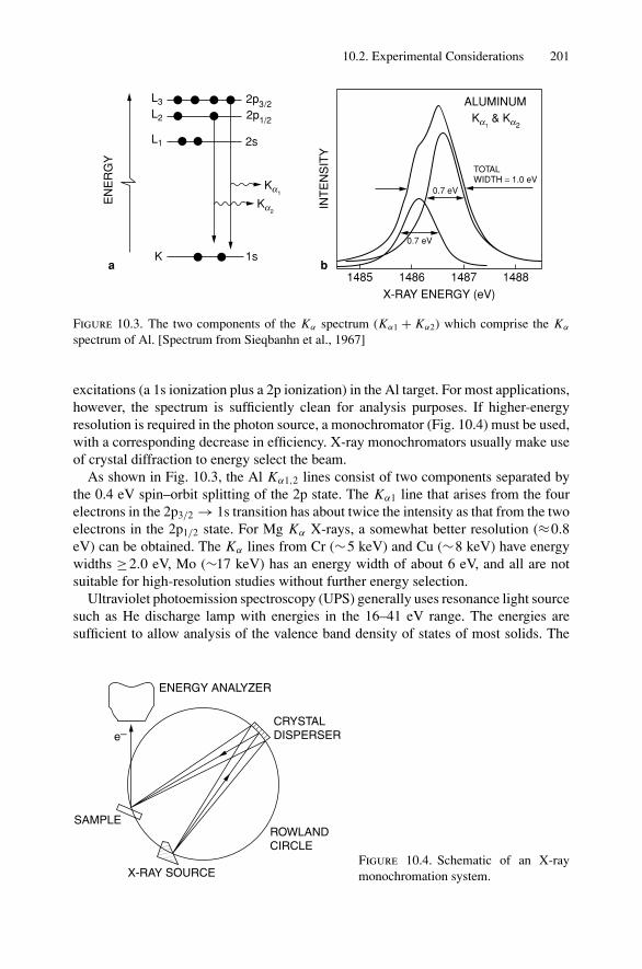
10.2. Experimental Considerations 201
a b1485 1486 1487 1488
X-RAY ENERGY (eV)
0.7 eV
0.7 eV
TOTALWIDTH = 1.0 eV
ALUMINUMKa1
& Ka2
INT
EN
SIT
Y
EN
ER
GY
L3
L2
L1
2p3/22p1/2
2s
Ka1
Ka2
K 1s
Figure 10.3. The two components of the Kα spectrum (Kα1 + Kα2) which comprise the Kα
spectrum of Al. [Spectrum from Sieqbanhn et al., 1967]
excitations (a 1s ionization plus a 2p ionization) in the Al target. For most applications,however, the spectrum is sufficiently clean for analysis purposes. If higher-energyresolution is required in the photon source, a monochromator (Fig. 10.4) must be used,with a corresponding decrease in efficiency. X-ray monochromators usually make useof crystal diffraction to energy select the beam.
As shown in Fig. 10.3, the Al Kα1,2 lines consist of two components separated bythe 0.4 eV spin–orbit splitting of the 2p state. The Kα1 line that arises from the fourelectrons in the 2p3/2 → 1s transition has about twice the intensity as that from the twoelectrons in the 2p1/2 state. For Mg Kα X-rays, a somewhat better resolution (≈0.8eV) can be obtained. The Kα lines from Cr (∼5 keV) and Cu (∼8 keV) have energywidths ≥2.0 eV, Mo (∼17 keV) has an energy width of about 6 eV, and all are notsuitable for high-resolution studies without further energy selection.
Ultraviolet photoemission spectroscopy (UPS) generally uses resonance light sourcesuch as He discharge lamp with energies in the 16–41 eV range. The energies aresufficient to allow analysis of the valence band density of states of most solids. The
X-RAY SOURCE
SAMPLEROWLANDCIRCLE
CRYSTALDISPERSER
ENERGY ANALYZER
e−
Figure 10.4. Schematic of an X-raymonochromation system.
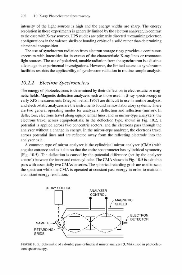
202 10. X-ray Photoelectron Spectroscopy
intensity of the light sources is high and the energy widths are sharp. The energyresolution in these experiments is generally limited by the electron analyzer, in contrastto the case with X-ray sources. UPS studies are primarily directed at examining electronconfigurations in the valence shells or bonding orbits of a solid rather than determiningelemental composition.
The use of synchrotron radiation from electron storage rings provides a continuousspectrum with intensities far in excess of the characteristic X-ray lines or resonancelight sources. The use of polarized, tunable radiation from the synchrotron is a distinctadvantage in experimental investigations. However, the limited access to synchrotronfacilities restricts the applicability of synchrotron radiation in routine sample analysis.
10.2.2 Electron Spectrometers
The energy of photoelectrons is determined by their deflection in electrostatic or mag-netic fields. Magnetic deflection analyzers such as those used in β-ray spectroscopy orearly XPS measurements (Siegbahn et al.,1967) are difficult to use in routine analysis,and electrostatic analyzers are the instruments found in most laboratory systems. Thereare two general operating modes for analyzers: deflection and reflection (mirror). Indeflectors, electrons travel along equipotential lines, and in mirror-type analyzers, theelectrons travel across equipotentials. In the deflection type, shown in Fig. 10.2, apotential is applied across two concentric sectors, and the electrons pass through theanalyzer without a change in energy. In the mirror-type analyzer, the electrons travelacross potential lines and are reflected away from the reflecting electrode into theanalyzer exit.
A common type of mirror analyzer is the cylindrical mirror analyzer (CMA) withangular entrance and exit slits so that the entire spectrometer has cylindrical symmetry(Fig. 10.5). The deflection is caused by the potential difference (set by the analyzercontrol) between the inner and outer cylinder. The CMA shown in Fig. 10.5 is a doublepass with essentially two CMAs in series. The spherical retarding grids are used to scanthe spectrum while the CMA is operated at constant pass energy in order to maintaina constant energy resolution.
X-RAY SOURCEANALYZERCONTROL
MAGNETICSHIELD
ELECTRONDETECTOR
SAMPLE
RETARDINGGRIDS
Figure 10.5. Schematic of a double pass cylindrical mirror analyzer (CMA) used in photoelec-tron spectroscopy.
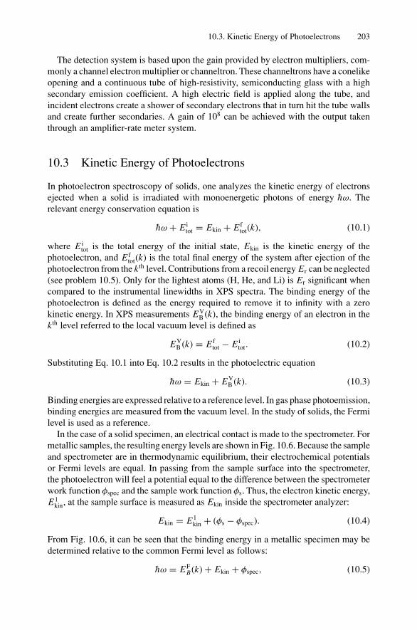
10.3. Kinetic Energy of Photoelectrons 203
The detection system is based upon the gain provided by electron multipliers, com-monly a channel electron multiplier or channeltron. These channeltrons have a conelikeopening and a continuous tube of high-resistivity, semiconducting glass with a highsecondary emission coefficient. A high electric field is applied along the tube, andincident electrons create a shower of secondary electrons that in turn hit the tube wallsand create further secondaries. A gain of 108 can be achieved with the output takenthrough an amplifier-rate meter system.
10.3 Kinetic Energy of Photoelectrons
In photoelectron spectroscopy of solids, one analyzes the kinetic energy of electronsejected when a solid is irradiated with monoenergetic photons of energy hω. Therelevant energy conservation equation is
hω + E itot = Ekin + E f
tot(k), (10.1)
where E itot is the total energy of the initial state, Ekin is the kinetic energy of the
photoelectron, and E ftot(k) is the total final energy of the system after ejection of the
photoelectron from the k th level. Contributions from a recoil energy Er can be neglected(see problem 10.5). Only for the lightest atoms (H, He, and Li) is Er significant whencompared to the instrumental linewidths in XPS spectra. The binding energy of thephotoelectron is defined as the energy required to remove it to infinity with a zerokinetic energy. In XPS measurements EV
B (k), the binding energy of an electron in thek th level referred to the local vacuum level is defined as
EVB (k) = E f
tot − E itot. (10.2)
Substituting Eq. 10.1 into Eq. 10.2 results in the photoelectric equation
hω = Ekin + EVB (k). (10.3)
Binding energies are expressed relative to a reference level. In gas phase photoemission,binding energies are measured from the vacuum level. In the study of solids, the Fermilevel is used as a reference.
In the case of a solid specimen, an electrical contact is made to the spectrometer. Formetallic samples, the resulting energy levels are shown in Fig. 10.6. Because the sampleand spectrometer are in thermodynamic equilibrium, their electrochemical potentialsor Fermi levels are equal. In passing from the sample surface into the spectrometer,the photoelectron will feel a potential equal to the difference between the spectrometerwork function φspec and the sample work function φs. Thus, the electron kinetic energy,E1
kin, at the sample surface is measured as Ekin inside the spectrometer analyzer:
Ekin = E1kin + (φs − φspec). (10.4)
From Fig. 10.6, it can be seen that the binding energy in a metallic specimen may bedetermined relative to the common Fermi level as follows:
hω = EFB(k) + Ekin + φspec, (10.5)
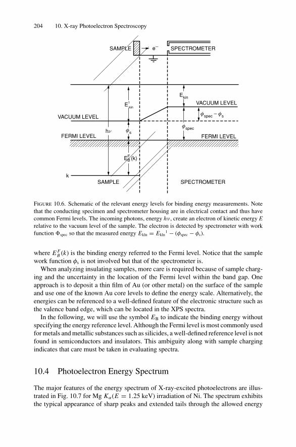
204 10. X-ray Photoelectron Spectroscopy
SAMPLE SPECTROMETERk
E (k)FB
FERMI LEVEL
VACUUM LEVEL
hν φs
E1 kin
Ekin
e−SAMPLE SPECTROMETER
φspec − φs
VACUUM LEVEL
FERMI LEVEL
φspec
Figure 10.6. Schematic of the relevant energy levels for binding energy measurements. Notethat the conducting specimen and spectrometer housing are in electrical contact and thus havecommon Fermi levels. The incoming photons, energy hν, create an electron of kinetic energy Erelative to the vacuum level of the sample. The electron is detected by spectrometer with workfunction spec so that the measured energy Ekln = Ekln
1 − (φspec − φs).
where E FB (k) is the binding energy referred to the Fermi level. Notice that the sample
work function φs is not involved but that of the spectrometer is.When analyzing insulating samples, more care is required because of sample charg-
ing and the uncertainty in the location of the Fermi level within the band gap. Oneapproach is to deposit a thin film of Au (or other metal) on the surface of the sampleand use one of the known Au core levels to define the energy scale. Alternatively, theenergies can be referenced to a well-defined feature of the electronic structure such asthe valence band edge, which can be located in the XPS spectra.
In the following, we will use the symbol EB to indicate the binding energy withoutspecifying the energy reference level. Although the Fermi level is most commonly usedfor metals and metallic substances such as silicides, a well-defined reference level is notfound in semiconductors and insulators. This ambiguity along with sample chargingindicates that care must be taken in evaluating spectra.
10.4 Photoelectron Energy Spectrum
The major features of the energy spectrum of X-ray-excited photoelectrons are illus-trated in Fig. 10.7 for Mg Kα(E = 1.25 keV) irradiation of Ni. The spectrum exhibitsthe typical appearance of sharp peaks and extended tails through the allowed energy
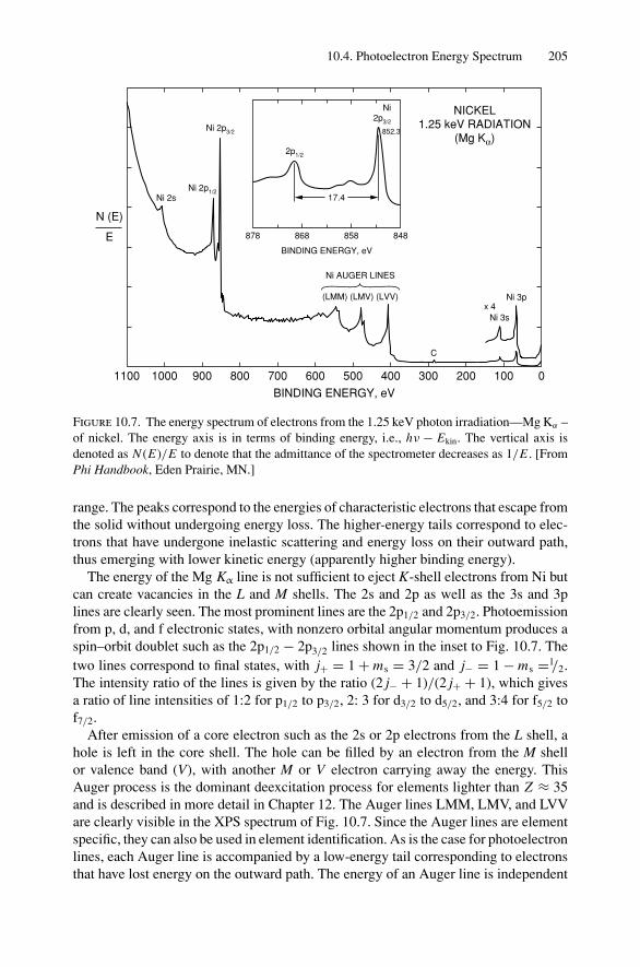
10.4. Photoelectron Energy Spectrum 205
N (E)
E
1100 1000 900 800 700 600 500 400 300 200 100 0
BINDING ENERGY, eV
NICKEL1.25 keV RADIATION
(Mg Kα)
(LMM) (LMV) (LVV)
Ni AUGER LINES
BINDING ENERGY, eV
878 868 858 848
17.4
2p1/2
Ni2p3/2
852.3Ni 2p3/2
Ni 2p1/2Ni 2s
C
Ni 3s
Ni 3px 4
Figure 10.7. The energy spectrum of electrons from the 1.25 keV photon irradiation—Mg Kα –of nickel. The energy axis is in terms of binding energy, i.e., hν − Ekin. The vertical axis isdenoted as N (E)/E to denote that the admittance of the spectrometer decreases as 1/E . [FromPhi Handbook, Eden Prairie, MN.]
range. The peaks correspond to the energies of characteristic electrons that escape fromthe solid without undergoing energy loss. The higher-energy tails correspond to elec-trons that have undergone inelastic scattering and energy loss on their outward path,thus emerging with lower kinetic energy (apparently higher binding energy).
The energy of the Mg Kα line is not sufficient to eject K-shell electrons from Ni butcan create vacancies in the L and M shells. The 2s and 2p as well as the 3s and 3plines are clearly seen. The most prominent lines are the 2p1/2 and 2p3/2. Photoemissionfrom p, d, and f electronic states, with nonzero orbital angular momentum produces aspin–orbit doublet such as the 2p1/2 − 2p3/2 lines shown in the inset to Fig. 10.7. Thetwo lines correspond to final states, with j+ = 1 + ms = 3/2 and j− = 1 − ms =1/2.The intensity ratio of the lines is given by the ratio (2 j− + 1)/(2 j+ + 1), which givesa ratio of line intensities of 1:2 for p1/2 to p3/2, 2: 3 for d3/2 to d5/2, and 3:4 for f5/2 tof7/2.
After emission of a core electron such as the 2s or 2p electrons from the L shell, ahole is left in the core shell. The hole can be filled by an electron from the M shellor valence band (V), with another M or V electron carrying away the energy. ThisAuger process is the dominant deexcitation process for elements lighter than Z ≈ 35and is described in more detail in Chapter 12. The Auger lines LMM, LMV, and LVVare clearly visible in the XPS spectrum of Fig. 10.7. Since the Auger lines are elementspecific, they can also be used in element identification. As is the case for photoelectronlines, each Auger line is accompanied by a low-energy tail corresponding to electronsthat have lost energy on the outward path. The energy of an Auger line is independent
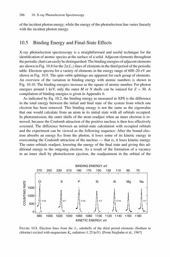
206 10. X-ray Photoelectron Spectroscopy
of the incident photon energy, while the energy of the photoelectron line varies linearlywith the incident photon energy.
10.5 Binding Energy and Final-State Effects
X-ray photoelectron spectroscopy is a straightforward and useful technique for theidentification of atomic species at the surface of a solid. Adjacent elements throughoutthe periodic chart can easily be distinguished. The binding energies of adjacent elementsare shown in Fig. 10.8 for the 2s(L1) lines of elements in the third period of the periodictable. Electron spectra for a variety of elements in the energy range of 600–20 eV areshown in Fig. 10.9. The spin–orbit splittings are apparent for each group of elements.An overview of the variation in binding energy with atomic numbers is shown inFig. 10.10. The binding energies increase as the square of atomic number. For photonenergies around 1 keV, only the outer M or N shells can be ionized for Z > 30. Acompilation of binding energies is given in Appendix 6.
As indicated by Eq. 10.2, the binding energy as measured in XPS is the differencein the total energy between the initial and final state of the system from which oneelectron has been removed. This binding energy is not the same as the eigenvaluethat one would calculate from an atom in its initial state with all orbitals occupied.In photoemission, the outer shells of the atom readjust when an inner electron is re-moved, because the Coulomb attraction of the positive nucleus is then less effectivelyscreened. The difference between an initial-state calculation with occupied orbitalsand the experiment can be viewed as the following sequence: After the bound elec-tron absorbs an energy hω from the photon, it loses some of its kinetic energy inovercoming the Coulomb attraction of the nucleus — that is, it loses kinetic energy.The outer orbitals readjust, lowering the energy of the final state and giving this ad-ditional energy to the outgoing electron. As a result of the formation of a vacancyin an inner shell by photoelectron ejection, the readjustment in the orbital of the
980 1000 1020 1040 1060 1080 1100 1120 1140 1160 1180
KINETIC ENERGY, eV
500
0
1000
1500
CO
UN
TIN
G R
ATE
270 250 230 210 190 170 150 130 110 90 70
BINDING ENERGY, eV
Cl S P Si Al Mg Na
×10 ×7 ×12 ×7 ×14 ×7
Figure 10.8. Electron lines from the L1 subshells of the third period elements (Sodium tochlorine) excited with magnesium Kα radiation (1.25 keV). [From Siegbahn et al., 1967]
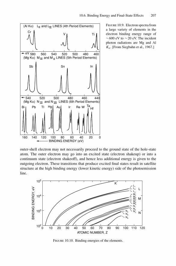
10.6. Binding Energy and Final-State Effects 207
eV 580
540 520 500 480 460 440
560 540 520 500 480 460(Mg Kα)
(Al Kα)
(Mg Kα)
M IV and M v LINES (5th Period Elements)
N VI and N VII LINES (6th Period Elements)
160 140 120 100 80 60 40 20 0BINDING ENERGY (eV)
LII and LIII LINES (4th Period Elements)
CrV Ti
Sb Sn In
Bi Pb TI Hg Au Ir Re W TaHf
Figure 10.9. Electron spectra froma large variety of elements in theelectron binding energy range of∼600 eV to ∼20 eV. The incidentphoton radiations are Mg and AlKα . [From Siegbahn et al., 1967.]
outer-shell electron may not necessarily proceed to the ground state of the hole-stateatom. The outer electron may go into an excited state (electron shakeup) or into acontinuum state (electron shakeoff), and hence less additional energy is given to theoutgoing electron. These transitions that produce excited final states result in satellitestructure at the high binding energy (lower kinetic energy) side of the photoemissionline.
0 10 20 30 40 50 60 70 80 90 100 110 120ATOMIC NUMBER, Z
102
103
104
105
BIN
DIN
G E
NE
RG
Y, e
V
K
L
M
N
L1L2L3M1M2M3M4M5N1N2N3
N4N5
N6
Figure 10.10. Binding energies of the elements.
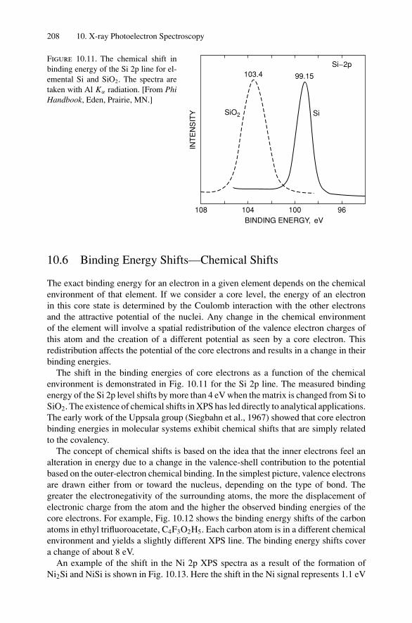
208 10. X-ray Photoelectron Spectroscopy
BINDING ENERGY, eV108 104 100 96
INT
EN
SIT
Y
103.4 99.15
Si−2p
SiSiO2
Figure 10.11. The chemical shift inbinding energy of the Si 2p line for el-emental Si and SiO2. The spectra aretaken with Al Kα radiation. [From PhiHandbook, Eden, Prairie, MN.]
10.6 Binding Energy Shifts—Chemical Shifts
The exact binding energy for an electron in a given element depends on the chemicalenvironment of that element. If we consider a core level, the energy of an electronin this core state is determined by the Coulomb interaction with the other electronsand the attractive potential of the nuclei. Any change in the chemical environmentof the element will involve a spatial redistribution of the valence electron charges ofthis atom and the creation of a different potential as seen by a core electron. Thisredistribution affects the potential of the core electrons and results in a change in theirbinding energies.
The shift in the binding energies of core electrons as a function of the chemicalenvironment is demonstrated in Fig. 10.11 for the Si 2p line. The measured bindingenergy of the Si 2p level shifts by more than 4 eV when the matrix is changed from Si toSiO2. The existence of chemical shifts in XPS has led directly to analytical applications.The early work of the Uppsala group (Siegbahn et al., 1967) showed that core electronbinding energies in molecular systems exhibit chemical shifts that are simply relatedto the covalency.
The concept of chemical shifts is based on the idea that the inner electrons feel analteration in energy due to a change in the valence-shell contribution to the potentialbased on the outer-electron chemical binding. In the simplest picture, valence electronsare drawn either from or toward the nucleus, depending on the type of bond. Thegreater the electronegativity of the surrounding atoms, the more the displacement ofelectronic charge from the atom and the higher the observed binding energies of thecore electrons. For example, Fig. 10.12 shows the binding energy shifts of the carbonatoms in ethyl trifluoroacetate, C4F3O2H5. Each carbon atom is in a different chemicalenvironment and yields a slightly different XPS line. The binding energy shifts covera change of about 8 eV.
An example of the shift in the Ni 2p XPS spectra as a result of the formation ofNi2Si and NiSi is shown in Fig. 10.13. Here the shift in the Ni signal represents 1.1 eV
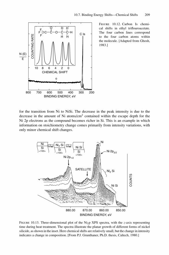
10.7. Binding Energy Shifts—Chemical Shifts 209
CHEMICAL SHIFT
CO
UN
TIN
G R
ATE
BINDING ENERGY, eV
10 8 6 4 2 0
N (E)
E
800 700 600 500 400 300 200
F
FF C C C C
H HH
HHO
O
o
C Is
Figure 10.12. Carbon Is chemi-cal shifts in ethyl triflouroacetate.The four carbon lines correspondto the four carbon atoms withinthe molecule. [Adapted from Ghosh,1983.]
for the transition from Ni to NiSi. The decrease in the peak intensity is due to thedecrease in the amount of Ni atoms/cm2 contained within the escape depth for theNi 2p electrons as the compound becomes richer in Si. This is an example in whichinformation on stoichiometry change comes primarily from intensity variations, withonly minor chemical shift changes.
CO
UN
TS
850.00860.00870.00880.00
BINDING ENERGY, eV
Ni Si
Ni SiNi2 Si
Nl2 Si
Ni 2p3/2
Ni 2p1/2
NiNiSi
SiSi
SATELLITE
275°C 275°C
<100><100>
<100>
Figure 10.13. Three-dimensional plot of the Ni2p XPS spectra, with the z-axis representingtime during heat treatment. The spectra illustrate the planar growth of different forms of nickelsilicide, as shown in the inset. Here chemical shifts are relatively small, but the change in intensityindicates a change in composition. [From P.J. Grunthaner, Ph.D. thesis, Caltech, 1980.]
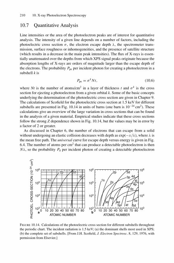
210 10. X-ray Photoelectron Spectroscopy
10.7 Quantitative Analysis
Line intensities or the area of the photoelectron peaks are of interest for quantitativeanalysis. The intensity of a given line depends on a number of factors, including thephotoelectric cross section σ , the electron escape depth λ, the spectrometer trans-mission, surface roughness or inhomogeneities, and the presence of satellite structure(which results in a decrease in the main peak intensities). The flux of X-rays is essen-tially unattenuated over the depths from which XPS signal peaks originate because theabsorption lengths of X-rays are orders of magnitude larger than the escape depth ofthe electrons. The probability Ppe per incident photon for creating a photoelectron in asubshell k is
Ppe = σ k N t, (10.6)
where Nt is the number of atoms/cm2 in a layer of thickness t and σ k is the crosssection for ejecting a photoelectron from a given orbital k. Some of the basic conceptsunderlying the determination of the photoelectric cross section are given in Chapter 9.The calculations of Scofield for the photoelectric cross section at 1.5 keV for differentsubshells are presented in Fig. 10.14 in units of barns (one barn is 10−24 cm2). Thesecalculations give an overview of the large variation in cross sections that can be foundin the analysis of a given material. Empirical studies indicate that these cross sectionsfollow the strong Z dependence shown in Fig. 10.14, but the values may be in error bya factor of 2 or greater.
As discussed in Chapter 6, the number of electrons that can escape from a solidwithout undergoing an elastic collision decreases with depth as exp(−x/λ), where λ isthe mean free path. The universal curve for escape depth versus energy is given in Fig.6.4. The number of atoms per cm2 that can produce a detectable photoelectron is thenNλ, so the probability Pd per incident photon of creating a detectable photoelectron
ATOMIC NUMBER0 10 20 30 40 50 60 70 80
PH
OTO
EL.
CR
OS
S-S
EC
TIO
N (
10−2
4 cm
2 )
105
104
103
106
1s4f
aATOMIC NUMBER
0 10 20 30 40 50 60 70 80
105
104
103
106
105
104
103
106
1s
2p
3p
4p
4p2s
5s
3s4s
3d
3d 4d5d
4d4f
4f
b
2p 3d
5p
Figure 10.14. Calculations of the photoelectric cross section for different subshells throughoutthe periodic chart. The incident radiation is 1.5 keV; (a) the dominant shells most used in XPS;(b) the complete set of subshells. [From J.H. Scofield, J. Electron Spectrosc. 8, 129, 1976, withpermission from Elsevier.]
Problems 211
from a subshell k is given by
Pd = σ k Nλ. (10.7)
Not all the photoelectrons from a given subshell contribute to the photopeak, whichcorresponds to the ground-state configuration for a single vacancy in an inner shell. Theinfluence of excited states (electron shakeup and shakeoff) is to decrease the intensityof the photopeak. The efficiency y in the production of a photopeak signal can vary overvalues of 0.7–0.8 for free atoms and, more importantly, can have a strong dependenceon the chemical environment.
Finally, the instrumental efficiency T is a function for the kinetic energy E of theelectron and usually varies as E−1. For example, Fig. 10.7 presents the energy spec-trum N (E) of the photoelectrons as N (E)/E to compensate for the transmission effi-ciency.
In chemical analysis, one is generally interested in the relative concentrations, nA/nB,of elements A and B in a sample, so that only the ratio of the areas of lines (the intensityratio IA/IB) is required. The composition ratio is then
nA
nB= IA
IB
σBλB yBTB
σAλA yATA. (10.8)
If the photopeaks have about the same energy so that λA∼= λB and TA
∼= TB and the pho-topeak efficiencies are about equal, then the composition ratio can be approximated by
nA
nB= IA
IB
σB
σA. (10.9)
This approach assumes that the sample is flat and homogeneous, that the photoelectronsare emitted isotropically, and that the sample surface is clean, without a layer of surfacecontamination.
The sensitivity to the detection of trace elements depends upon the cross sectionof the element and the background of the signals from the other elements. Underfavorable conditions, elemental analysis in bulk samples can reach sensitivities of1 part in 1000. XPS measurements are extremely sensitive to the presence of surfacelayers. One often can detect as little as 0.01 monolayers of an element. The main useof XPS in materials analysis is determination of the chemical binding of atoms in thesurface region of a solid.
Problems
10.1. (a) Compare the tabulated values of the binding energy, EB (Appendix 6), forthe 1s and 2s levels with the prediction of the Bohr theory (Eq. 1.15) foratoms with Z = 10, 20, 30, and 40. Does the Bohr theory serve as a usefulapproximation (to within 10%) of the binding energies?
(b) Using the Pauli exclusion principle and quantum numbers with spin–orbitsplitting, sketch an energy-level diagram for copper based on Bohr values ofthe binding energy. Indicate the number of electrons in each level and verifythat the ratio of electrons in the d levels, d3/2 to d5/2, is 2/3.
212 10. X-ray Photoelectron Spectroscopy
10.2. For Al Kα X-rays incident on the compound NiSi, calculate the ratio of yieldsusing Eq. 10.8, assuming that the ratios of photopeak and instrument efficienciesare equal. Use Fig. 10.14 and 6.4 to estimate the cross sections and escape depths:
(a) Ni 2s to Ni 2p;(b) Ni 2s to Ni 3s;(c) Ni 2p to Si 2p.
10.3. Consider incident radiation on Al at the same energy: 5.41 keV electrons and CrKα X-rays.
(a) Calculate the cross section for creating Al K-shell vacancies for electrons(Eq. 6.11) and photons (Eq. 10.37).
(b) Calculate the electron range (Eq. 6.25) and linear absorption coefficient(Eq. 10.35). Compare the calculated value of the mass absorption coefficientwith the value listed in Appendix 8.
(c) What is the energy of the K-shell photoelectrons? Calculate the value of theescape depth λ (Eq. 6.20) and compare it with the value estimated from Fig.6.4.
10.4. For Al Kα radiation incident on Cu, calculate the ratio of 2s to 3s photoelectronyields based only on cross sections (Fig. 10.15) and escape depths.
10.5. Estimate the binding energy shift between the Li (Z = 3) atom and LiF in thefollowing way (the Li atom has an electron configuration of 1s22s1):
(a) Calculate the probability of finding the 2s electron within the 1s orbit; i.e.,calculate
q =r=a0/Z∫r=0
ψ22sr
2 dr sin θdθdφ,
where ψ2s is a hydrogenic wave function (Chapter 9) and a0/Z is the Bohrradius of the 1s shell. (Note that 0 < q < 1).
(b) Estimate the binding energy of the 1s shell in the atom using the Bohr modelwith ZLi
eff = Z − q .(c) In LiF, the outer electron is essentially on the F atom. Assume there is no
contribution to the 1s screening from the 2s electron in LiF and estimate thebinding energy shift using the Bohr model.
References
Atomic Physics and Quantum Mechanics
1. E. E. Anderson, Modern Physics and Quantum Mechanics (W. B. Saunders, Philadelphia,1971).
2. J. D. McGervey, Introduction to Modern Physics (Academic Press, New York, 1971).3. F. K. Richtmyer, E. H. Kennard, and J. N. Cooper, Introduction to Modern Physics, 6th ed.
(McGraw-Hill Book Co., New York, 1969).4. L. I. Schiff, Quantum Mechanics, 3rd ed. (McGraw-Hill Book Co., New York, 1968).

References 213
5. R. L. Sproull and W. A. Phillips, Modern Physics, 3rd ed. (John Wiley and Sons, New York,1980).
6. P. A. Tipler, Modern Physics (Worth Publishers, New York, 1978).7. R. T. Weidner and R. L. Sells, Elementary Modern Physics, 3rd ed. (Allyn and Bacon, Boston,
MA, 1980).
X-Ray Photoelectron Spectroscopy
1. D. Briggs, Ed., Handbook of X-ray and Ultraviolet Photoelectron Spectroscopy (Heydon andSon, London, 1977, 1978).
2. D. Briggs and M. P. Seah, Practical Surface Analysis by Auger and X-ray PhotoelectronSpectroscopy (John Wiley and Sons, New York, 1983).
3. M. Cardona and L. Ley, Eds., Photoemission in Solids I and II, Topics in Applied Physics,Vols. 26 and 27 (Springer-Verlag, New York, 1978 and 1979).
4. T. A. Carlson, Photoelectron and Auger Spectroscopy (Plenum Press, New York, 1975).5. G. Ertl and J. Kuppers, Low Energy Electrons and Surface Chemistry (Verlag Chemie Inter-
national, Weinheim, 1974).6. P. K. Ghosh, Introduction to Photoelectron Spectroscopy (Wiley-Interscience Publishers, New
York, 1983).7. H. Ibach, Ed., Electron Spectroscopy for Surface Analysis, Topics in Current Physics, Vol. 4
(Springer-Verlag, New York, 1977).8. K. D. Sevier, Low Energy Electron Spectrometry (Wiley-Interscience Publishers, New York,
1972).9. K. Siegbahn, C. N. Nordling, A. Fahlman, R. Nordberg, K. Hamrin, J. Hedman, G. Johansson,
T. Bergmark, S. E. Karlsson, I. Lindgren, and B. Lindberg, ESCA, Atomic, Molecular, andSolid State Structure Studied by Means of Electron Spectroscopy (Almqvist and Wiksells,Uppsala, Sweden, 1967).
11Radiative Transitions and the ElectronMicroprobe
11.1 Introduction
In previous chapters, we have calculated the cross section for creating an inner-shell va-cancy by irradiation with X-rays (photoelectric cross section, Chapter 9) and energeticelectrons (impact ionization cross section, Chapter 6). After a vacancy is created, anelectron can make a transition from an outer shell to fill the vacancy with the emissionof a photon. This process is referred to as the spontaneous emission of radiation. In thischapter, we consider the energies of X-ray transitions and calculate radiative transitionrates. We will use the formula for the radiative transition rate from an initial state i toa final state f (derived in Chapter 9):
W = 4
3
(hωf1 )3
(hc)3
(e2)
h|〈ψ f |r|ψi〉|2 , (11.1)
where hωf1 = E iB − E f
B is the energy of the emitted radiation, where EB is the bindingenergy of the initial or final state. The transition rate increases strongly with pho-ton energy or, for a given transition, increases rapidly with Z. Evaluation of the ma-trix elements indicates that W = 0 for some of the transitions, and hence selectionrules for allowed transitions can be derived. These considerations are used in the de-scription of the electron microprobe, where bombardment of a solid by a beam ofelectrons leads to the emission of X-rays with energies characteristic of the atomicspecies. The relative advantages of proton-induced X-ray excitation will be discussed inSection 11.9.
Consider an excited atom with a hole in the K or L shell. A straightforward meansof deexcitation is the transition of an electron from an occupied state in a shell to theempty state (hole) with the emission of X-rays as shown by the L3 to K transition(Kα1 X-ray) in Fig. 11.1.
X-ray emission is mainly due to dipole radiation, and electron transition selectionrules are obeyed (l = ±1 , j = 0, ±1 ); the energy is given by the difference inbinding energies,
hω(Kα) = EKB − EL3
B = hν . (11.2)
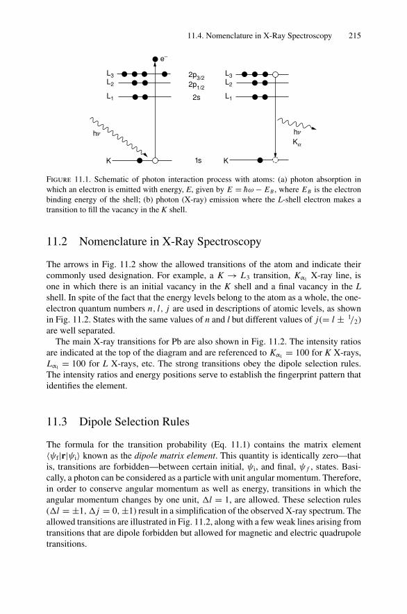
11.4. Nomenclature in X-Ray Spectroscopy 215
2p3/22p1/2
2s
L3L2
L1
L3L2
L1
KK
Ka
hνhν
1s
e–
Figure 11.1. Schematic of photon interaction process with atoms: (a) photon absorption inwhich an electron is emitted with energy, E, given by E = hω − EB , where EB is the electronbinding energy of the shell; (b) photon (X-ray) emission where the L-shell electron makes atransition to fill the vacancy in the K shell.
11.2 Nomenclature in X-Ray Spectroscopy
The arrows in Fig. 11.2 show the allowed transitions of the atom and indicate theircommonly used designation. For example, a K → L3 transition, Kα1 X-ray line, isone in which there is an initial vacancy in the K shell and a final vacancy in the Lshell. In spite of the fact that the energy levels belong to the atom as a whole, the one-electron quantum numbers n, l, j are used in descriptions of atomic levels, as shownin Fig. 11.2. States with the same values of n and l but different values of j(= l ± 1/2)are well separated.
The main X-ray transitions for Pb are also shown in Fig. 11.2. The intensity ratiosare indicated at the top of the diagram and are referenced to Kα1 = 100 for K X-rays,Lα1 = 100 for L X-rays, etc. The strong transitions obey the dipole selection rules.The intensity ratios and energy positions serve to establish the fingerprint pattern thatidentifies the element.
11.3 Dipole Selection Rules
The formula for the transition probability (Eq. 11.1) contains the matrix element〈ψf|r|ψi〉 known as the dipole matrix element. This quantity is identically zero—thatis, transitions are forbidden—between certain initial, ψi, and final, ψ f , states. Basi-cally, a photon can be considered as a particle with unit angular momentum. Therefore,in order to conserve angular momentum as well as energy, transitions in which theangular momentum changes by one unit, l = 1, are allowed. These selection rules(l = ±1, j = 0, ±1) result in a simplification of the observed X-ray spectrum. Theallowed transitions are illustrated in Fig. 11.2, along with a few weak lines arising fromtransitions that are dipole forbidden but allowed for magnetic and electric quadrupoletransitions.
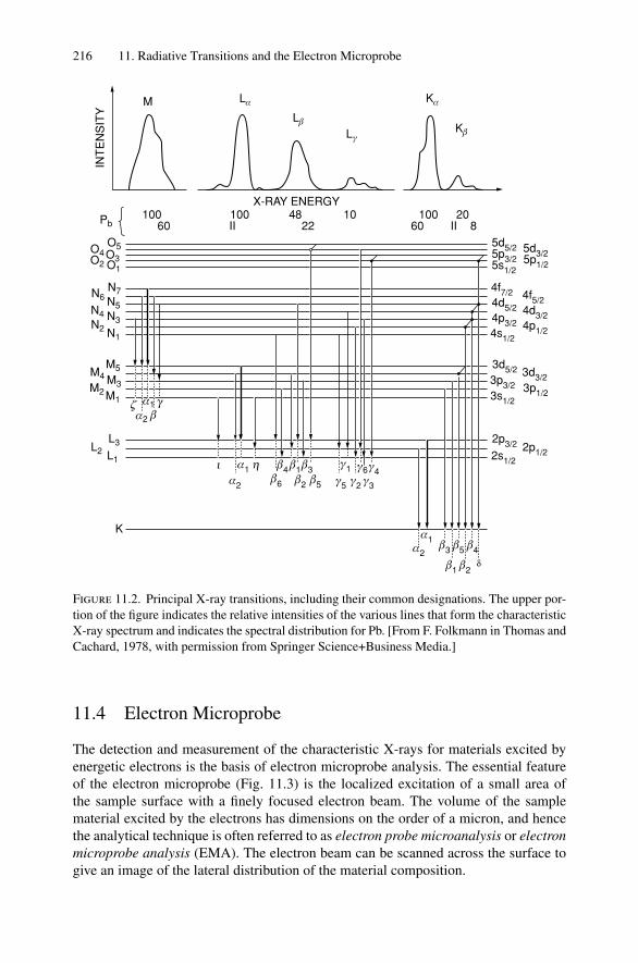
216 11. Radiative Transitions and the Electron Microprobe
M
100 100 48 10 100 2086022II II60
O5
Pb
O4O2 O1
N7N6 N5N4 N3N2 N1
M5M4 M3M2 M1
L1
K
α1
α1α2
α2
α1
α2
L2L3
O3
X-RAY ENERGY
Lα
Lβ
Lγ
Kα
Kβ
INT
EN
SIT
Y
γz
i h
δ
β3
β6 β2 β5
β3β1β4
β
β5 β4
β2β1
γ3
γ4γ6γ1
γ2γ5
2s1/2
2p3/2 2p1/2
3s1/23p1/2
3p3/23d3/2
3d5/2
4s1/2
5s1/2
4p1/2
5p1/25p3/2
5d5/2 5d3/2
4p3/2
4d5/2 4d3/2
4f5/24f7/2
Figure 11.2. Principal X-ray transitions, including their common designations. The upper por-tion of the figure indicates the relative intensities of the various lines that form the characteristicX-ray spectrum and indicates the spectral distribution for Pb. [From F. Folkmann in Thomas andCachard, 1978, with permission from Springer Science+Business Media.]
11.4 Electron Microprobe
The detection and measurement of the characteristic X-rays for materials excited byenergetic electrons is the basis of electron microprobe analysis. The essential featureof the electron microprobe (Fig. 11.3) is the localized excitation of a small area ofthe sample surface with a finely focused electron beam. The volume of the samplematerial excited by the electrons has dimensions on the order of a micron, and hencethe analytical technique is often referred to as electron probe microanalysis or electronmicroprobe analysis (EMA). The electron beam can be scanned across the surface togive an image of the lateral distribution of the material composition.
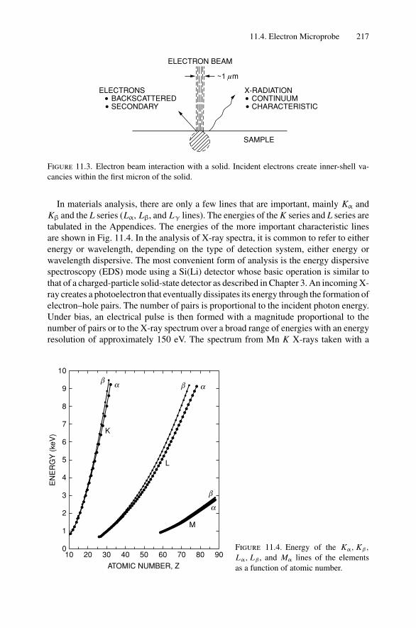
11.4. Electron Microprobe 217
SAMPLE
ELECTRONSBACKSCATTEREDSECONDARY
X-RADIATIONCONTINUUMCHARACTERISTIC
~1 µm
ELECTRON BEAM
Figure 11.3. Electron beam interaction with a solid. Incident electrons create inner-shell va-cancies within the first micron of the solid.
In materials analysis, there are only a few lines that are important, mainly Kα andKβ and the L series (Lα, Lβ, and Lγ lines). The energies of the K series and L series aretabulated in the Appendices. The energies of the more important characteristic linesare shown in Fig. 11.4. In the analysis of X-ray spectra, it is common to refer to eitherenergy or wavelength, depending on the type of detection system, either energy orwavelength dispersive. The most convenient form of analysis is the energy dispersivespectroscopy (EDS) mode using a Si(Li) detector whose basic operation is similar tothat of a charged-particle solid-state detector as described in Chapter 3. An incoming X-ray creates a photoelectron that eventually dissipates its energy through the formation ofelectron–hole pairs. The number of pairs is proportional to the incident photon energy.Under bias, an electrical pulse is then formed with a magnitude proportional to thenumber of pairs or to the X-ray spectrum over a broad range of energies with an energyresolution of approximately 150 eV. The spectrum from Mn K X-rays taken with a
10
8
9
7
6
5
4
3
2
1
010 20 30 40 50 60 70 80 90
ATOMIC NUMBER, Z
EN
ER
GY
(ke
V)
aβaβ
aβ
M
L
K
Figure 11.4. Energy of the Kα, Kβ,
Lα, Lβ , and Mα lines of the elementsas a function of atomic number.
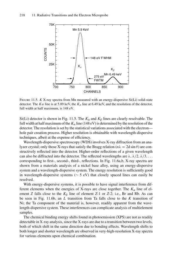
218 11. Radiative Transitions and the Electron Microprobe
75K
50K
25K
0700 750 800 850 900
Mn 5.9 KeV
148 eV F WHM
Kβ
Mn 6.49 keV275 eVFWTM
Kα
CHANNELS
CO
UN
TS
Figure 11.5. K X-ray spectra from Mn measured with an energy-dispersive Si(Li) solid-statedetector. The Kα line is at 5.89 keV, the Kβ line at 6.49 keV, and the resolution of the detector,full width at half maximum, is 148 eV.
Si(Li) detector is shown in Fig. 11.5. The Kα and Kβ lines are clearly resolvable. Thefull width at half maximum of the Kα line (148 eV) is determined by the resolution of thedetector. The resolution is set by the statistical variations associated with the electron—hole pair creation process. Higher resolution is obtainable with wavelength-dispersivetechniques, albeit at the expense of efficiency.
Wavelength-dispersive spectroscopy (WDS) involves X-ray diffraction from an ana-lyzer crystal; only those X-rays that satisfy the Bragg relation (nλ = 2d sin θ ) are con-structively reflected into the detector. Higher-order reflections of a given wavelengthcan also be diffracted into the detector. The reflected wavelengths are λ, λ/2, λ/3, . . .
corresponding to first-, second-, third-, reflections. In Fig. 11.6a,b, X-ray spectra areshown from a materials analysis of a nickel base alloy, using an energy-dispersivesystem and a wavelength-dispersive system. The energy resolution is sufficiently goodin wavelength-dispersive systems (∼ 5 eV) that closely spaced lines can easily beresolved.
With energy-dispersive systems, it is possible to have signal interference from dif-ferent elements when the energies of X-rays are close together. The Kα line of el-ement Z falls close to the Kβ line of element Z-1 or Z-2; i.e., Br and Rb. As canbe seen in Fig. 11.6b, an L transition from Ta falls close to the K transition ofNi; the Ta component of the material is, however, readily apparent from the wave-length-dispersive system. These interferences can complicate analysis of multielementsamples.
The chemical binding energy shifts found in photoemission (XPS) are not as readilydetectable in X-ray analysis, since the X-rays are due to a transition between two levels,both of which shift in the same direction due to bonding effects. Wavelength shifts toboth longer and shorter wavelength are observed in very-high-resolution X-ray spectrafor various elements upon chemical combination.
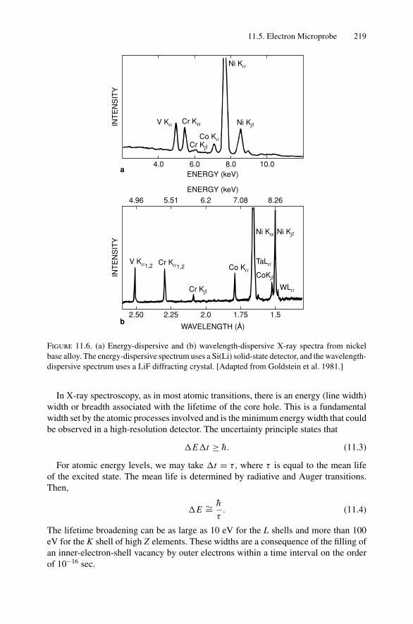
11.5. Electron Microprobe 219
4.0 6.0 8.0 10.0
INT
EN
SIT
Y
ENERGY (keV)
ENERGY (keV)
INT
EN
SIT
Y
4.96 5.51 6.2 7.08 8.26
2.50 2.25 1.752.0 1.5
WAVELENGTH (Å)
V Kα1,2 Cr Kα1,2 Co Kα
Co Kα
TaLα
Ni Ka Ni Kβ
Ni KβV Kα Cr Ka
Cr Kβ
WLα Cr Kβ
CoKβ
Ni Kα
a
b
Figure 11.6. (a) Energy-dispersive and (b) wavelength-dispersive X-ray spectra from nickelbase alloy. The energy-dispersive spectrum uses a Si(Li) solid-state detector, and the wavelength-dispersive spectrum uses a LiF diffracting crystal. [Adapted from Goldstein et al. 1981.]
In X-ray spectroscopy, as in most atomic transitions, there is an energy (line width)width or breadth associated with the lifetime of the core hole. This is a fundamentalwidth set by the atomic processes involved and is the minimum energy width that couldbe observed in a high-resolution detector. The uncertainty principle states that
Et ≥ h. (11.3)
For atomic energy levels, we may take t = τ , where τ is equal to the mean lifeof the excited state. The mean life is determined by radiative and Auger transitions.Then,
E ∼= h
τ. (11.4)
The lifetime broadening can be as large as 10 eV for the L shells and more than 100eV for the K shell of high Z elements. These widths are a consequence of the filling ofan inner-electron-shell vacancy by outer electrons within a time interval on the orderof 10−16 sec.
220 11. Radiative Transitions and the Electron Microprobe
11.5 Transition Rate for Spontaneous Emission
The rate for a spontaneous transition from an electron in an initial state i to a final statef is
W = 4
3
e2
h
(ωf1
c
)3 |〈ψf|r|ψi〉|2 , (11.5)
where e2 = 1.44 eV-nm, c is the speed of light, hωf1 is the energy of the emitted photon,and ψi and ψf are the wave functions of the initial and final states, respectively. Thisrate can be expressed as
W = 0.38 × 10¹⁸(hω)3 |〈ψf|r|ψi〉|2 ,
in units of inverse seconds, where hω is in units of keV and the matrix element(|〈ψf|r|ψi〉|2) has dimensions of (0.01 nm)2. A typical value of W is 1015/s for K-shell transitions of elements in the middle of the periodic table. This formula is derivedby considering the absorption transition probability in an electromagnetic field and theEinstein coefficients that describe the balance between photon absorption and inducedand spontaneous transitions (Section 9.10).
11.6 Transition Rate for Kα Emission in Ni
We illustrate the use of Eq. 11.5 by explicitly calculating the transition rate for aparticular case. Our starting point is the transition rate formula
W = 4
3
ω3e2
hc3
∣∣∣∣⟨ψf|r|ψi
⟩∣∣∣∣2
.
As a first estimate, we note that 〈ψf|r|ψi〉 ∼ a0/Z . The wave functions ψf(r) andψi(r) have a finite intensity only for values of |r| a0/Z , where a0 is the Bohr radius,a0 = 0.053 nm. Then
W = 4
3
ω3e2
hc3
a20
Z2. (11.6)
The energy of the transition, hω, for 2p → 1s transitions in hydrogenic atoms is 10.2 Z2
(eV) [i.e., hω = 13.6(1 − 1/n2)Z2, where n = 2]. Therefore, the transition probabilityis proportional to Z4:
W ∝ Z4. (11.7)
This dependence will hold in more sophisticated treatments as well. We can give asimple order-of-magnitude estimate of W. The units of W are often given in terms ofeV/ h. Thus we rewrite Eq. 11.6 as
W = 4
3
1
h(hω)3
(e2
hc
)3 (a0
e2
)2 1
Z2, (11.8)
11.7. Transition Rate for Kα Emission in Ni 221
(note that e2/hc = 1/137 and e2/a0 = 27.2 eV). Consider the Kα transition in Ni(Z = 28, hω = 7.5 × 10³ eV). Then
W = 0.38 eV/h.
Actually, the six 2p electrons in Ni can contribute to the process so that
W = 2.3 eV/h.
The accepted result is W = 0.551 eV/h. A factor of 4 is close for a crude estimate.In units of time and using the accepted value, W = 8.3 × 10¹⁴s−1, or
1
W= 1.2 × 10⁻¹⁵s.
A detailed evaluation of the transition probability is given in Section 11.9.The energy width of an atomic state is related to the mean life τ of the state through
the Heisenberg uncertainty principle:
τ = h. (11.9)
In the previous section, we estimated the radiative contribution to the width or, moreprecisely, the decay probability (per unit time) for a 2p to 1s transition, i.e.,
Wrad = rad/h. (11.10)
The width of the state is made up of all the processes that contribute to its finite lifetime:
= rad + nonrad, (11.11)
where rad represents all the radiative processes that contribute to the lifetime (i.e.,X-ray emission) and nonrad contributes to all nonradiative contributions (i.e., Augeremission). The probability of a radiative decay is rad/(rad + nonrad) and is knownas the fluorescence yield ωX (see Section 11.3). For a state consisting of a K vacancywith atomic Z > 40, radiative processes dominate: nonrad << rad. In a hydrogenicapproximation,
= 4
3(hω)3
(e2
hc
)3 (a0
e2
)2 0.74
Z2(6), (11.12)
where the extra factor of 6 allows for six 2p electrons. In the spirit of the hydrogenlikemodel, we note that the energy of the 2p–1s transition is given by
hω = 13.6(1 − 1
4)Z2, (11.13)
so
= 3.3 × 10⁻⁸ Z4(eV). (11.14)
This calculated result is only a factor of ∼2 greater than the fit to experimentshown in Fig. 11.7. Note that the Z 4 dependence is close to that observed experi-mentally.
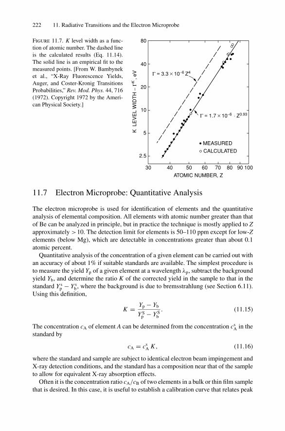
222 11. Radiative Transitions and the Electron Microprobe
80
40
20
10
30 40 50 60 70 80 90 100
5
2.5
ATOMIC NUMBER, Z
MEASURED
CALCULATED
Γ = 3.3 × 10⁻⁶ Z4
K L
EV
EL
WID
TH
−ΓK
, eV
Γ = 1.7 × 10⁻⁶ ⋅ Z3.93
Figure 11.7. K level width as a func-tion of atomic number. The dashed lineis the calculated results (Eq. 11.14).The solid line is an empirical fit to themeasured points. [From W. Bambyneket al., “X-Ray Fluorescence Yields,Auger, and Coster-Kronig TransitionsProbabilities,” Rev. Mod. Phys. 44, 716(1972). Copyright 1972 by the Ameri-can Physical Society.]
11.7 Electron Microprobe: Quantitative Analysis
The electron microprobe is used for identification of elements and the quantitativeanalysis of elemental composition. All elements with atomic number greater than thatof Be can be analyzed in principle, but in practice the technique is mostly applied to Zapproximately >10. The detection limit for elements is 50–110 ppm except for low-Zelements (below Mg), which are detectable in concentrations greater than about 0.1atomic percent.
Quantitative analysis of the concentration of a given element can be carried out withan accuracy of about 1% if suitable standards are available. The simplest procedure isto measure the yield Yp of a given element at a wavelength λp, subtract the backgroundyield Yb, and determine the ratio K of the corrected yield in the sample to that in thestandard Y s
p − Y sb , where the background is due to bremsstrahlung (see Section 6.11).
Using this definition,
K = Yp − Yb
Y Sp − Y S
b
. (11.15)
The concentration cA of element A can be determined from the concentration csA in the
standard by
cA = csA K , (11.16)
where the standard and sample are subject to identical electron beam impingement andX-ray detection conditions, and the standard has a composition near that of the sampleto allow for equivalent X-ray absorption effects.
Often it is the concentration ratio cA/cB of two elements in a bulk or thin film samplethat is desired. In this case, it is useful to establish a calibration curve that relates peak
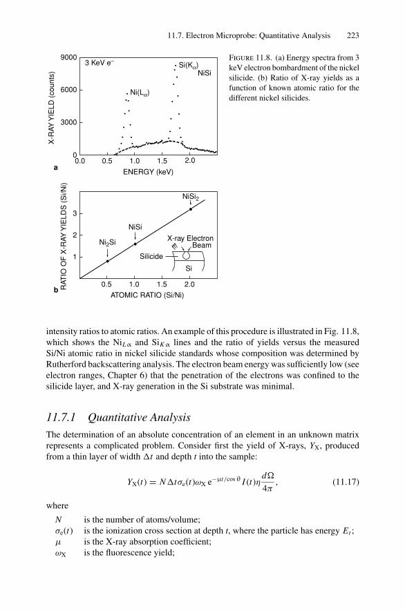
11.7. Electron Microprobe: Quantitative Analysis 223
9000
6000
3000
0
3 KeV e–
0.0 0.5 1.0 1.5 2.0
Ni(La)
Si(Ka)NiSi
ENERGY (keV)
X-R
AY Y
IELD
(co
unts
)
3
2
1
0.5 1.0 1.5 2.0
ATOMIC RATIO (Si/Ni)
Ni2Si
NiSi
NiSi2
Si
Silicide
X-ray ElectronBeam
RAT
IO O
F X
-RAY
YIE
LDS
(S
i/Ni)
a
b
Figure 11.8. (a) Energy spectra from 3keV electron bombardment of the nickelsilicide. (b) Ratio of X-ray yields as afunction of known atomic ratio for thedifferent nickel silicides.
intensity ratios to atomic ratios. An example of this procedure is illustrated in Fig. 11.8,which shows the NiLα and SiKα lines and the ratio of yields versus the measuredSi/Ni atomic ratio in nickel silicide standards whose composition was determined byRutherford backscattering analysis. The electron beam energy was sufficiently low (seeelectron ranges, Chapter 6) that the penetration of the electrons was confined to thesilicide layer, and X-ray generation in the Si substrate was minimal.
11.7.1 Quantitative Analysis
The determination of an absolute concentration of an element in an unknown matrixrepresents a complicated problem. Consider first the yield of X-rays, YX, producedfrom a thin layer of width t and depth t into the sample:
YX(t) = Ntσe(t)ωX e−µt/cos θ I (t)ηd
4π, (11.17)
where
N is the number of atoms/volume;σe(t) is the ionization cross section at depth t, where the particle has energy Et ;µ is the X-ray absorption coefficient;ωX is the fluorescence yield;
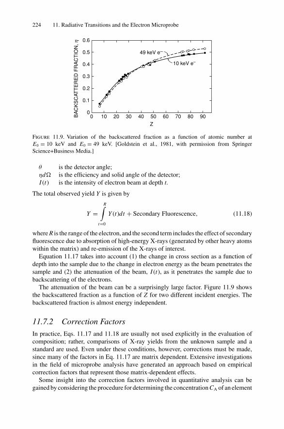
224 11. Radiative Transitions and the Electron Microprobe
0.6
0.5
0.4
0.3
0.2
0.1
00 10 20 30 40 50 60 70 80 90
Z
10 keV e–
49 keV e−
BA
CK
SC
ATT
ER
ED
FR
AC
TIO
N, h
Figure 11.9. Variation of the backscattered fraction as a function of atomic number atE0 = 10 keV and E0 = 49 keV. [Goldstein et al., 1981, with permission from SpringerScience+Business Media.]
θ is the detector angle;ηd is the efficiency and solid angle of the detector;I (t) is the intensity of electron beam at depth t.
The total observed yield Y is given by
Y =R∫
t=0
Y (t)dt + Secondary Fluorescence, (11.18)
where R is the range of the electron, and the second term includes the effect of secondaryfluorescence due to absorption of high-energy X-rays (generated by other heavy atomswithin the matrix) and re-emission of the X-rays of interest.
Equation 11.17 takes into account (1) the change in cross section as a function ofdepth into the sample due to the change in electron energy as the beam penetrates thesample and (2) the attenuation of the beam, I (t), as it penetrates the sample due tobackscattering of the electrons.
The attenuation of the beam can be a surprisingly large factor. Figure 11.9 showsthe backscattered fraction as a function of Z for two different incident energies. Thebackscattered fraction is almost energy independent.
11.7.2 Correction Factors
In practice, Eqs. 11.17 and 11.18 are usually not used explicitly in the evaluation ofcomposition; rather, comparisons of X-ray yields from the unknown sample and astandard are used. Even under these conditions, however, corrections must be made,since many of the factors in Eq. 11.17 are matrix dependent. Extensive investigationsin the field of microprobe analysis have generated an approach based on empiricalcorrection factors that represent those matrix-dependent effects.
Some insight into the correction factors involved in quantitative analysis can begained by considering the procedure for determining the concentration CA of an element

11.7. Electron Microprobe: Quantitative Analysis 225
A in an alloy from the ratio K of X-ray intensities from the sample and from a standardcomposed of element A. An expression of the form
CA = KZAF (11.19)
is used (Birks, 1979; Goldstein et al., 1981), where Z is the atomic number correctionfactor, A is the absorption correction factor, and F is the fluorescence correction factor.These corrections relate to the three major effects that arise from the differing character-istics of the sample and the standard with respect to electron and X-ray interactions. Theatomic number correction Z allows for the fact that the generation of primary X-rays inthe samples does not increase linearly with concentration. The proportion of incidentelectrons that are backscattered and the volume of the sample in which X-rays are gen-erated depend on sample composition. The absorption correction A is required becausethe absorption coefficients — i.e., the attenuation of the emerging X-radiation — will bedifferent in the sample and the standard. The fluorescent correction F accounts for thegeneration of secondary X-rays from element A due to fluorescent excitation by X-raysemitted by another element (Fig. 11.10). The effect is strongest when the exciting lineshave an energy slightly greater than the binding energy associated with the line that isbeing measured, i.e., near the maximum of the absorption cross section. For example,in a sample containing Fe and Ni, the Ni K X-rays could excite Fe K X-rays, and in aCu–Au sample, the Au L lines can excite Cu Kα. The correction for fluorescence bycharacteristic lines depends on the atomic fluorescence yield ωX and the fraction of theexciting element in the sample. For X-ray lines with energies below 3 keV, the values
ELECTRONS
ZONE OF FLUORESCENTEXCITATION OF λA BY λB
ZONE OF PRIMARYEXCITATION OF λA
ELECTRON-PROBE MICROANALYSIS
λA λA
X-RAYS TOSPECTROMETER
λB
Figure 11.10. Schematic illustration of the generation of secondary radiation as a result offluorescence excitation by primary radiation.
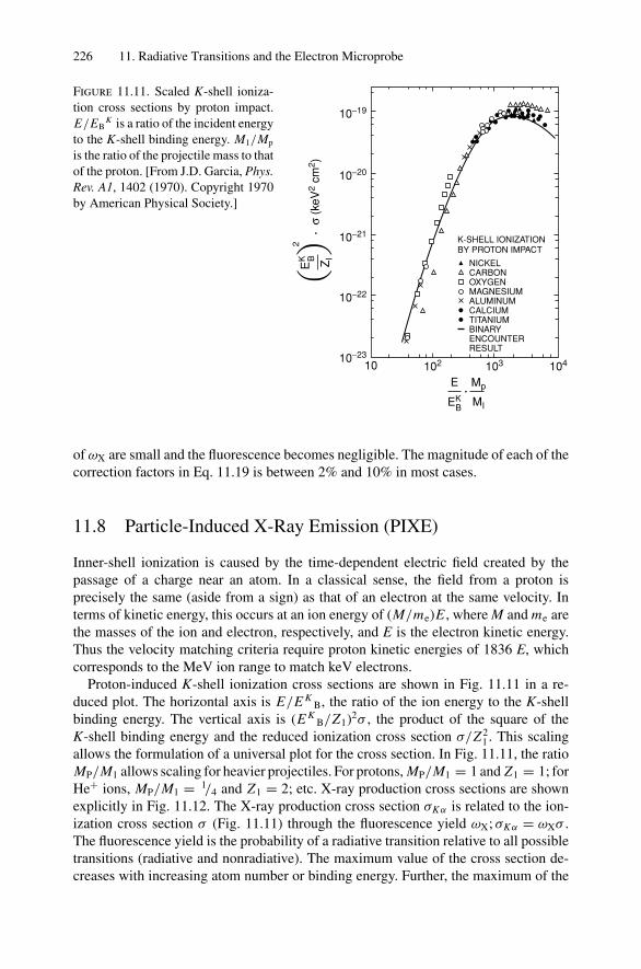
226 11. Radiative Transitions and the Electron Microprobe
K-SHELL IONIZATIONBY PROTON IMPACT
NICKELCARBONOXYGENMAGNESIUMALUMINUMCALCIUMTITANIUMBINARYENCOUNTERRESULT
10 10210−23
10−22
10−21
10−20
10−19
103 104
σ (k
eV2
cm2 )
ZI
EK B
2
Mp
MI
E
EKB
Figure 11.11. Scaled K-shell ioniza-tion cross sections by proton impact.E/EB
K is a ratio of the incident energyto the K-shell binding energy. M1/Mp
is the ratio of the projectile mass to thatof the proton. [From J.D. Garcia, Phys.Rev. A1, 1402 (1970). Copyright 1970by American Physical Society.]
of ωX are small and the fluorescence becomes negligible. The magnitude of each of thecorrection factors in Eq. 11.19 is between 2% and 10% in most cases.
11.8 Particle-Induced X-Ray Emission (PIXE)
Inner-shell ionization is caused by the time-dependent electric field created by thepassage of a charge near an atom. In a classical sense, the field from a proton isprecisely the same (aside from a sign) as that of an electron at the same velocity. Interms of kinetic energy, this occurs at an ion energy of (M/me)E , where M and me arethe masses of the ion and electron, respectively, and E is the electron kinetic energy.Thus the velocity matching criteria require proton kinetic energies of 1836 E, whichcorresponds to the MeV ion range to match keV electrons.
Proton-induced K-shell ionization cross sections are shown in Fig. 11.11 in a re-duced plot. The horizontal axis is E/E K
B, the ratio of the ion energy to the K-shellbinding energy. The vertical axis is (E K
B/Z1)2σ , the product of the square of theK-shell binding energy and the reduced ionization cross section σ/Z2
1. This scalingallows the formulation of a universal plot for the cross section. In Fig. 11.11, the ratioMP/M1 allows scaling for heavier projectiles. For protons, MP/M1 = 1 and Z1 = 1; forHe+ ions, MP/M1 = 1/4 and Z1 = 2; etc. X-ray production cross sections are shownexplicitly in Fig. 11.12. The X-ray production cross section σKα is related to the ion-ization cross section σ (Fig. 11.11) through the fluorescence yield ωX; σKα = ωXσ .The fluorescence yield is the probability of a radiative transition relative to all possibletransitions (radiative and nonradiative). The maximum value of the cross section de-creases with increasing atom number or binding energy. Further, the maximum of the
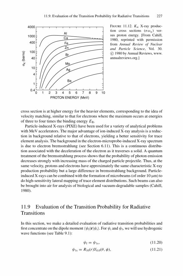
11.9. Evaluation of the Transition Probability for Radiative Transitions 227
AICa
FeZn
Br
Mo
Ag
Ba
0
4000
1000
400
100
40
10
4
1
0.41 2 3 4 5
PROTON ENERGY (MeV)
σ K (
barn
s)
6 7 8 9 10
Figure 11.12. Kα X-ray produc-tion cross sections (σωχ) ver-sus proton energy. [From Cahill,1980, reprinted with permissionfrom Annual Review of Nuclearand Particle Science, Vol. 30.c© 1980 by Annual Reviews, www.
annualreviews.org.]
cross section is at higher energy for the heavier elements, corresponding to the idea ofvelocity matching, similar to that for electrons where the maximum occurs at energiesof three to four times the binding energy EB.
Particle-induced X-rays (PIXE) have been used for a variety of analytical problemswith MeV accelerators. The major advantage of ion-induced X-ray analysis is a reduc-tion in background relative to that of electrons, yielding a better sensitivity for traceelement analysis. The background in the electron-microprobe-induced X-ray spectrumis due to electron bremsstrahlung (see Section 6.11). This is a continuous distribu-tion associated with the deceleration of the electron as it traverses a solid. A quantumtreatment of the bremsstrahlung process shows that the probability of photon emissiondecreases strongly with increasing mass of the charged particle projectile. Thus, at thesame velocity, protons and electrons have approximately the same characteristic X-rayproduction probability but a large difference in bremsstrahlung background. Particle-induced X-rays can be combined with the formation of microbeams (of order 10 µm) todo high-sensitivity lateral mapping of trace element distributions. Such beams can alsobe brought into air for analysis of biological and vacuum-degradable samples (Cahill,1980).
11.9 Evaluation of the Transition Probability for RadiativeTransitions
In this section, we make a detailed evaluation of radiative transition probabilities andfirst concentrate on the dipole moment 〈ψf|r|ψi〉. For ψi and ψf, we will use hydrogenicwave functions (see Table 9.1):
ψf = ψ1s, (11.20)
ψ1s = R10(r )Y0,0(θ, φ), (11.21)
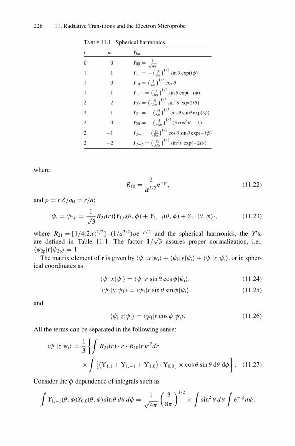
228 11. Radiative Transitions and the Electron Microprobe
Table 11.1. Spherical harmonics.
l m Ylm
0 0 Y00 = 1√4π
1 1 Y11 = − ( 38π
)1/2sin θ exp(iφ)
1 0 Y10 = ( 34π
)1/2cos θ
1 −1 Y1−1 = ( 38π
)1/2sin θ exp(−iφ)
2 2 Y22 = ( 1532π
)1/2sin2 θ exp(2iθ )
2 1 Y21 = − ( 158π
)1/2cos θ sin θ exp(iφ)
2 0 Y20 = − ( 516π
)1/2(3 cos2 θ − 1)
2 −1 Y2−1 = ( 158π
)1/2cos θ sin θ exp(−iφ)
2 −2 Y2−2 = ( 1532π
)1/2sin2 θ exp(−2iθ )
where
R10 = 2
a3/2e−ρ, (11.22)
and ρ = r Z/a0 = r/a;
ψi = ψ2p = 1√3
R21(r )Y1,0(θ, φ) + Y1,−1(θ, φ) + Y1,1(θ, φ), (11.23)
where R21 = [1/4(2π )1/2] · (1/a3/2)ρe−ρ/2 and the spherical harmonics, the Y’s,are defined in Table 11-1. The factor 1/
√3 assures proper normalization, i.e.,
〈ψ2p|r|ψ2p〉 = 1.The matrix element of r is given by 〈ψf|x |ψi〉 + 〈ψf|y|ψi〉 + 〈ψf|z|ψi〉, or in spher-
ical coordinates as
〈ψf|x |ψi〉 = 〈ψf|r sin θ cos φ|ψi〉, (11.24)
〈ψf|y|ψ1〉 = 〈ψf|r sin θ sin φ|ψi〉, (11.25)
and
〈ψf|z|ψi〉 = 〈ψf|r cos φ|ψi〉. (11.26)
All the terms can be separated in the following sense:
〈ψf|z|ψi〉 = 1
3
∫R21(r ) · r · R10(r )r2dr
×∫ [(
Y1,1 + Y1,−1 + Y1,0) · Y0,0
]× cos θ sin θ dθ dφ
. (11.27)
Consider the φ dependence of integrals such as∫Y1,−1(θ, φ)Y0,0(θ, φ) sin θ dθ dφ = 1√
4π
(3
8π
)1/2
×∫
sin2 θ dθ
∫e−iφdφ,
11.9. Evaluation of the Transition Probability for Radiative Transitions 229
where Y1,−1 = (3/8π )1/2 sin θe−iφ . In general, any integral of the form∫Yl,m(θ, φ)Yl ′,m ′(θ, φ) sin θ dθ dφ
will result in a factor of the form2π∫
0
e−i(m−m ′)φdφ.
This second integral is identically zero unless m = m ′, thus yielding a selection rule.That is, the matrix element and hence the transition probability is identically zero unlessm = m ′. For the z component, the selection rule reduces to mf = m i. For the x and ycomponents, the integral is of the form∫
sin φ e−i(m−m ′)φdφ
or ∫cos φ e−i(m−m ′)φdφ,
which yield a selection rule m ′ = m ± 1 or mf = mi ± 1. These dipole selection rulesgovern the observed spectra.
The z-matrix element for 2p to 1s hydrogenic wave functions reduces to
1
3〈ψ100|r cos θ |ψ210〉 = 0.248a. (11.28)
In a similar manner, one can show that
〈ψ1s|x |ψ2p〉 = 〈R10|r |R21〉δl ′,l±1δm ′,m±1, (11.29)
where
δl ′,1±1 = 1 if l ′ = l ± 1
= 0 otherwise. (11.30)
Then 〈ψ1s|x |ψ2p〉 reduces to
= 2
3√
24
1
a3
∫e−3r/2a r
ar3 dr, (11.31)
or
〈|x |〉 =(
81
54
)1/2
· 〈|z|〉, (11.32)
and
〈|y|〉 =(
81
54
)1/2
· 〈|z|〉.
Finally
〈|x |〉 + 〈|y|〉 + 〈|z|〉 = 〈|r|〉, (11.33)
230 11. Radiative Transitions and the Electron Microprobe
and
〈|r|〉 = 0.248a[1 + 2
(8154
)1/2],
〈|r|〉2 = 0.74a2, (11.34)
for 2p → 1s. Using Eq. (11.5), we find a value for the transition probability for Ni of
W = 1.2 eV/h,
a factor of 2 greater than the accepted value of 0.55 eV/h.
11.10 Calculation of the Kβ/Kα Ratio
As a further example of the use of the transition probability formula, we calculatethe Kβ/Kα ratio for hydrogenic atoms. We use the following form for the radiativetransition rate W:
W = 4ω3e2
3hc3|〈ψf|r|ψi〉|2 .
The ratio R is
R = WKβ
WKα
= ω3β |〈ψ100|r|ψ31〉|2
ω3α |〈ψ100|r|ψ21〉|2
, (11.35)
where
ψ3,1 = 1√3
(ψ310 + ψ311 + ψ31−1)
and
ψ2,1 = 1√3
(ψ210 + ψ211 + ψ21−1).
These equations represent wave functions that are properly normalized and reflect thestatistical weights of the degenerate sublevels, i.e.,
〈ψ3,1|ψ3,1〉 = 1/3(1 + 1 + 1) = 1.
We have also used the l = ±1 selection rule by considering p → s transitions only.Consider the z component, z = r cos θ :
〈ψ100|r cos θ |ψ3,1〉 = 1
3〈ψ100|r cos θ |ψ310〉
+ 〈ψ100|r cos θ |ψ311〉+ 〈ψ100|r cos θ |ψ31−1〉, (11.36)
which reduces to ∼0.1a.For the n = 2 → 1 transition: 〈ψ100|r cos θ |ψ2,1〉 reduces to 1/3〈ψ100|r cos θ |ψ210〉,
which is the matrix element in the Kα transition (=0.25a) (Eq. 11.28) given in the
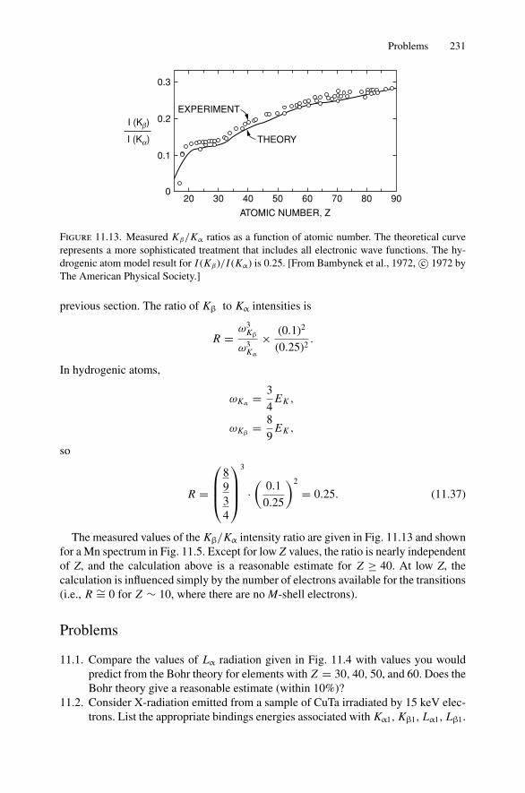
Problems 231
I (Kβ)
I (Ka)
0.3
0.2
0.1
020 30 40 50 60
ATOMIC NUMBER, Z
THEORY
EXPERIMENT
70 80 90
Figure 11.13. Measured Kβ/Kα ratios as a function of atomic number. The theoretical curverepresents a more sophisticated treatment that includes all electronic wave functions. The hy-drogenic atom model result for I (Kβ )/I (Kα) is 0.25. [From Bambynek et al., 1972, c© 1972 byThe American Physical Society.]
previous section. The ratio of Kβ to Kα intensities is
R =ω3
Kβ
ω3Kα
× (0.1)2
(0.25)2.
In hydrogenic atoms,
ωKα= 3
4EK ,
ωKβ= 8
9EK ,
so
R =
⎛⎜⎜⎝
8934
⎞⎟⎟⎠
3
·(
0.1
0.25
)2
= 0.25. (11.37)
The measured values of the Kβ/Kα intensity ratio are given in Fig. 11.13 and shownfor a Mn spectrum in Fig. 11.5. Except for low Z values, the ratio is nearly independentof Z, and the calculation above is a reasonable estimate for Z ≥ 40. At low Z, thecalculation is influenced simply by the number of electrons available for the transitions(i.e., R ∼= 0 for Z ∼ 10, where there are no M-shell electrons).
Problems
11.1. Compare the values of Lα radiation given in Fig. 11.4 with values you wouldpredict from the Bohr theory for elements with Z = 30, 40, 50, and 60. Does theBohr theory give a reasonable estimate (within 10%)?
11.2. Consider X-radiation emitted from a sample of CuTa irradiated by 15 keV elec-trons. List the appropriate bindings energies associated with Kα1, Kβ1, Lα1, Lβ1.
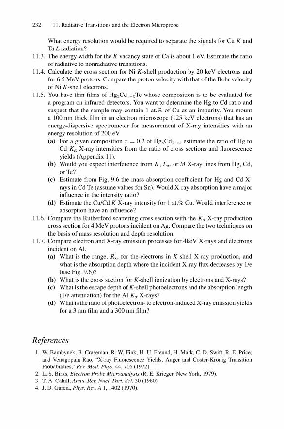
232 11. Radiative Transitions and the Electron Microprobe
What energy resolution would be required to separate the signals for Cu K andTa L radiation?
11.3. The energy width for the K vacancy state of Ca is about 1 eV. Estimate the ratioof radiative to nonradiative transitions.
11.4. Calculate the cross section for Ni K-shell production by 20 keV electrons andfor 6.5 MeV protons. Compare the proton velocity with that of the Bohr velocityof Ni K-shell electrons.
11.5. You have thin films of HgxCd1−xTe whose composition is to be evaluated fora program on infrared detectors. You want to determine the Hg to Cd ratio andsuspect that the sample may contain 1 at.% of Cu as an impurity. You mounta 100 nm thick film in an electron microscope (125 keV electrons) that has anenergy-dispersive spectrometer for measurement of X-ray intensities with anenergy resolution of 200 eV.(a) For a given composition x = 0.2 of HgxCd1−x, estimate the ratio of Hg to
Cd Kα X-ray intensities from the ratio of cross sections and fluorescenceyields (Appendix 11).
(b) Would you expect interference from K , Lα, or M X-ray lines from Hg, Cd,or Te?
(c) Estimate from Fig. 9.6 the mass absorption coefficient for Hg and Cd X-rays in Cd Te (assume values for Sn). Would X-ray absorption have a majorinfluence in the intensity ratio?
(d) Estimate the Cu/Cd K X-ray intensity for 1 at.% Cu. Would interference orabsorption have an influence?
11.6. Compare the Rutherford scattering cross section with the Kα X-ray productioncross section for 4 MeV protons incident on Ag. Compare the two techniques onthe basis of mass resolution and depth resolution.
11.7. Compare electron and X-ray emission processes for 4keV X-rays and electronsincident on Al.(a) What is the range, Rx, for the electrons in K-shell X-ray production, and
what is the absorption depth where the incident X-ray flux decreases by 1/e(use Fig. 9.6)?
(b) What is the cross section for K-shell ionization by electrons and X-rays?(c) What is the escape depth of K-shell photoelectrons and the absorption length
(1/e attenuation) for the Al Kα X-rays?(d) What is the ratio of photoelectron- to electron-induced X-ray emission yields
for a 3 nm film and a 300 nm film?
References
1. W. Bambynek, B. Craseman, R. W. Fink, H.-U. Freund, H. Mark, C. D. Swift, R. E. Price,and Venugopala Rao, “X-ray Fluorescence Yields, Auger and Coster-Kronig TransitionProbabilities,” Rev. Mod. Phys. 44, 716 (1972).
2. L. S. Birks, Electron Probe Microanalysis (R. E. Krieger, New York, 1979).3. T. A. Cahill, Annu. Rev. Nucl. Part. Sci. 30 (1980).4. J. D. Garcia, Phys. Rev. A 1, 1402 (1970).

References 233
5. J. I. Goldstein, D. E. Newbury, P. Echlin, D. C. Joy, C. Fiori, and E. Lifshin, ScanningElectron Microscopy and X-ray Microanalysis (Plenum Press, New York, 1981).
6. S. A. E. Johansson and T. B. Johansson, Nucl. Instrum. Meth. 137, 473 (1976).7. J. W. Mayer and E. Rimini, Eds., Ion Beam Handbook for Material Analysis (Academic
Press, New York, 1977).8. J. McGervey, Introduction to Modern Physics (Academic Press, New York, 1971).9. F. H. Read, Electromagnetic Radiation (John Wiley and Sons, New York, 1980).
10. P. K. Richtmyer, E. H. Kennard, and J. N. Cooper, Introduction to Modern Physics (McGraw-Hill Book Co., New York, 1969).
11. L. Schiff, Quantum Mechanics (McGraw-Hill Book Co., New York., 1968).12. J. P. Thomas and A. Cachard, Eds., Material Characterization Using Ion Beams (Plenum
Press, New York, 1978).13. D. B. Williams, Practical Analytical Electron Microscopy in Materials Science (Verlag
Chemie International, Weinheim, 1984).14. J. C. Willmott, Atomic Physics (John Wiley and Sons, New York, 1975).15. R. Woldseth, X-ray Energy Spectrometry (Kevex Corp., 1973).
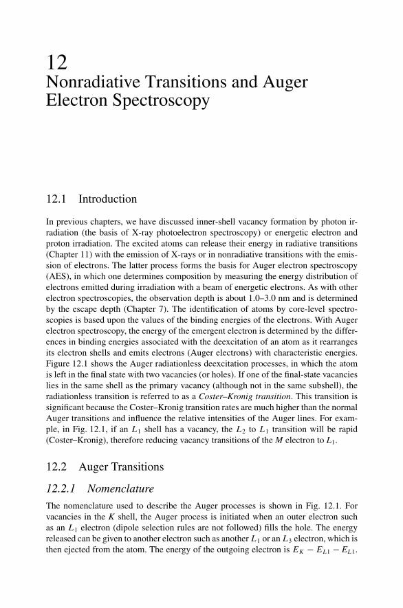
12Nonradiative Transitions and AugerElectron Spectroscopy
12.1 Introduction
In previous chapters, we have discussed inner-shell vacancy formation by photon ir-radiation (the basis of X-ray photoelectron spectroscopy) or energetic electron andproton irradiation. The excited atoms can release their energy in radiative transitions(Chapter 11) with the emission of X-rays or in nonradiative transitions with the emis-sion of electrons. The latter process forms the basis for Auger electron spectroscopy(AES), in which one determines composition by measuring the energy distribution ofelectrons emitted during irradiation with a beam of energetic electrons. As with otherelectron spectroscopies, the observation depth is about 1.0–3.0 nm and is determinedby the escape depth (Chapter 7). The identification of atoms by core-level spectro-scopies is based upon the values of the binding energies of the electrons. With Augerelectron spectroscopy, the energy of the emergent electron is determined by the differ-ences in binding energies associated with the deexcitation of an atom as it rearrangesits electron shells and emits electrons (Auger electrons) with characteristic energies.Figure 12.1 shows the Auger radiationless deexcitation processes, in which the atomis left in the final state with two vacancies (or holes). If one of the final-state vacancieslies in the same shell as the primary vacancy (although not in the same subshell), theradiationless transition is referred to as a Coster–Kronig transition. This transition issignificant because the Coster–Kronig transition rates are much higher than the normalAuger transitions and influence the relative intensities of the Auger lines. For exam-ple, in Fig. 12.1, if an L1 shell has a vacancy, the L2 to L1 transition will be rapid(Coster–Kronig), therefore reducing vacancy transitions of the M electron to L1.
12.2 Auger Transitions
12.2.1 Nomenclature
The nomenclature used to describe the Auger processes is shown in Fig. 12.1. Forvacancies in the K shell, the Auger process is initiated when an outer electron suchas an L1 electron (dipole selection rules are not followed) fills the hole. The energyreleased can be given to another electron such as another L1 or an L3 electron, which isthen ejected from the atom. The energy of the outgoing electron is EK − EL1 − EL1.
12.2. Auger Transitions 235
e− e− e−
M
M1
L3L2
L1
K
3s
2s
1s
2p3/22p1/2
AUGER(K L1 L1)K-SHELL
INITIALVACANCY
AUGER(L1M1 M1)L1-SUBSHELL
COSTER-KRONIG(L1L2M1)
Figure 12.1. Schematic diagram of various two-electron deexcitation processes. The KL, L,Auger transition corresponds to an initial K hole that is filled with an L1 electron, while simul-taneously the other L1 electron is ejected to the vacuum. The LM1M1 Auger transition is thecorresponding process with an initial 2s vacancy. The Coster–Kronig L1L2M1 transition containsan initial L1 hole that is filled with an L2 electron accompanied by ejection of an M1 electron.
The process described is called a KLL Auger transition in general terms and morespecifically denoted as KL1L1 or KL1L3. If there are vacancies in the L shell, one canhave Auger processes in which an electron from the M shell (M1 electron) fills theL hole and another M-shell electron (for example, an M1 electron) is ejected — anL1M1M1 Auger transition. Since electron–electron interactions are strongest betweenelectrons whose orbitals are closest together, the strongest Auger transitions are of thetype KLL or LMM. For Coster–Kronig transitions, the vacancy is filled by electronsthat come from the same shell, i.e., LLM. Auger transitions involving the outermostorbitals, the valence band, have an energy width of about twice that of the valenceband. In Fig. 12.2, the Si KL1L2,3 and L2,3V1V2 (or LVV) Auger transitions are indicatedwith V1 and V2 located at positions of maxima in the density of states in the valenceband.
A complete nomenclature describing Auger transitions indicates the shells involvedand the final state of the atom. The final state is usually described using the spectroscopicnotation describing the orbitals. For example, a K L1L1 transition would leave the2s shell empty (two vacancies) and the 2p shell with six electrons; the transition isKL1L1 (2s02p6). A KL2L3 would leave the vacancies in the 2p shell and would beindicated as KL2L3 (2s22p4). Even in the relatively simple KLL transition, there is alarge variety of final states that can have slightly different energies and hence willcorrespond to slightly different Auger lines. In the following, we discuss these states indetail.
236 12. Nonradiative Transitions and Auger Electron Spectroscopy
AUGERELECTRON (KLL)
AUGERELECTRON (LVV)
VACUUM VACUUM
O O
~13 ~13
99 99
149 149
1839 1839a
K K
L1 L1
L2,3 L2,3
EC ECEF EF
b
DENSITYOF STATES
VALENCEBAND
VALENCEBAND
Figure 12.2. Schematic of the (a) KL1 and (b) LVV Auger deexcitation processes in Si. Bindingenergies are indicated on the left. The energy of Auger electron in the K L1 L23 process isapproximately 1591 eV, and the L23V V Auger electron has an energy of approximately 90 eV.
12.2.1.1 K L1L1
In the usual X-ray notation, this transition corresponds to an initial state of a single1s hole and a final state of two 2s holes. We can consider electron holes as elec-trons to find the possible final configurations of the final states. The n = 2 shell isnow considered as 2s02p6 (where the filled shell is 2s22p6) and has states given bythe possible allowed quantum numbers consistent with the Pauli exclusion principle:ms = ±1, ML = 0, Ms = 0, where ML and Ms are the total orbital and spin angularmomenta, respectively. The notation 1S indicates a state of total orbital momentum zero(S). This transition is properly written KL1L1(1S), although the final state (1S) is theonly one allowed, and therefore, in this case, the notation is slightly redundant.
12.2.1.2 K L1L2 or K L1L3
In this case, the final-state electron configuration is written 2s12p5. The possible quan-tum states are 1 P and 3 P , where P denotes the total orbital angular momentum. Thiscorresponds to two states coupling to a total angular momentum L = 1, i.e., a P statewith the electron spins aligned 3 P and antialigned 1 P .
12.2.1.3 K L2L2, K L2 L3, and K L3L3 Transitions
Here the final states can couple to total angular momenta states of D(L = 2), P(L = 1),and S(L = 0), with different possible spin alignments to yield states 1D, 3 P , and 1S.
Thus, in KLL-type transitions, there is a total of six final states possible:
K L1L1—2s02p6(1S),
K L1L2,3—2s12p5(1P,3 P),
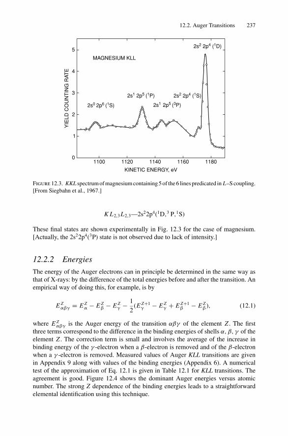
12.2. Auger Transitions 237
MAGNESIUM KLL
KINETIC ENERGY, eV
YIE
LD C
OU
NT
ING
RAT
E
5
4
3
2
1
01100 1120 1140 1160 1180
2s2 2p4 (1D)
2s2 2p4 (1S)
2s1 2p5 (3P)
2s1 2p5 (1P)
2s0 2p6 (1S)
Figure 12.3. KKL spectrum of magnesium containing 5 of the 6 lines predicated in L–S coupling.[From Siegbahn et al., 1967.]
K L2,3L2,3—2s22p4(1D,3 P,1S)
These final states are shown experimentally in Fig. 12.3 for the case of magnesium.[Actually, the 2s22p4(3P) state is not observed due to lack of intensity.]
12.2.2 Energies
The energy of the Auger electrons can in principle be determined in the same way asthat of X-rays: by the difference of the total energies before and after the transition. Anempirical way of doing this, for example, is by
E Zαβγ = E Z
α − E Zβ − E Z
γ − 1
2(E Z+1
γ − E Zγ + E Z+1
β − E Zβ), (12.1)
where E Zαβγ is the Auger energy of the transition αβγ of the element Z . The first
three terms correspond to the difference in the binding energies of shells α, β, γ of theelement Z . The correction term is small and involves the average of the increase inbinding energy of the γ -electron when a β-electron is removed and of the β-electronwhen a γ -electron is removed. Measured values of Auger KLL transitions are givenin Appendix 9 along with values of the binding energies (Appendix 6). A numericaltest of the approximation of Eq. 12.1 is given in Table 12.1 for KLL transitions. Theagreement is good. Figure 12.4 shows the dominant Auger energies versus atomicnumber. The strong Z dependence of the binding energies leads to a straightforwardelemental identification using this technique.
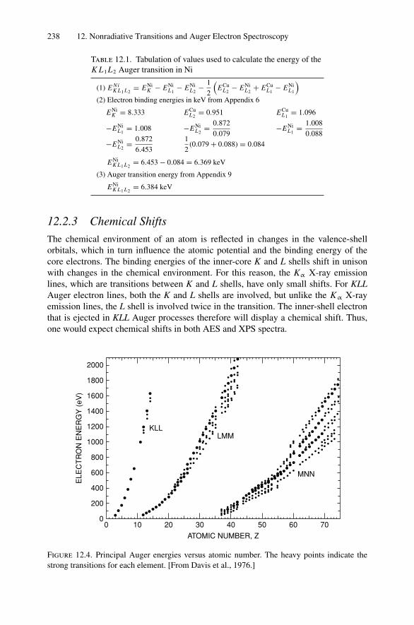
238 12. Nonradiative Transitions and Auger Electron Spectroscopy
Table 12.1. Tabulation of values used to calculate the energy of theK L1 L2 Auger transition in Ni
(1) E NiK L1 L2
= ENiK − ENi
L1− ENi
L2− 1
2
(ECu
L2− ENi
L2+ ECu
L1− ENi
L1
)(2) Electron binding energies in keV from Appendix 6
ENiK = 8.333 ECu
L2= 0.951 ECu
L1= 1.096
−ENiL1
= 1.008 −ENiL2
= 0.872
0.079−ENi
L1= 1.008
0.088
−ENiL2
= 0.872
6.453
1
2(0.079 + 0.088) = 0.084
ENiK L1 L2
= 6.453 − 0.084 = 6.369 keV
(3) Auger transition energy from Appendix 9
ENiK L1 L2
= 6.384 keV
12.2.3 Chemical Shifts
The chemical environment of an atom is reflected in changes in the valence-shellorbitals, which in turn influence the atomic potential and the binding energy of thecore electrons. The binding energies of the inner-core K and L shells shift in unisonwith changes in the chemical environment. For this reason, the Kα X-ray emissionlines, which are transitions between K and L shells, have only small shifts. For KLLAuger electron lines, both the K and L shells are involved, but unlike the Kα X-rayemission lines, the L shell is involved twice in the transition. The inner-shell electronthat is ejected in KLL Auger processes therefore will display a chemical shift. Thus,one would expect chemical shifts in both AES and XPS spectra.
2000
1800
1600
1400
1200
1000
800
600
400
200
00 10 20 30 40 50 60 70
ATOMIC NUMBER, Z
ELE
CT
RO
N E
NE
RG
Y (
eV)
KLLLMM
MNN
Figure 12.4. Principal Auger energies versus atomic number. The heavy points indicate thestrong transitions for each element. [From Davis et al., 1976.]
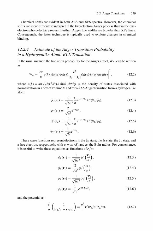
12.2. Auger Transitions 239
Chemical shifts are evident in both AES and XPS spectra. However, the chemicalshifts are more difficult to interpret in the two-electron Auger process than in the one-electron photoelectric process. Further, Auger line widths are broader than XPS lines.Consequently, the latter technique is typically used to explore changes in chemicalbinding.
12.2.4 Estimate of the Auger Transition Probabilityin a Hydrogenlike Atom: KLL Transition
In the usual manner, the transition probability for the Auger effect, WA, can be writtenas
WA = 2π
hρ(k)
∣∣∣∣φf(r1)ψf(r2)e2
|r1 − r2|φi(r1)ψi(r2) dr1dr2
∣∣∣∣2
, (12.2)
where ρ(k) = m(V/8π3 h2) k sin θ dθdφ is the density of states associated withnormalization in a box of volume V and for a KLL Auger transition from a hydrogenlikeatom:
φi (r1) = 1√6a3
r1
ae−r1/2aY m
1 (θ1, φ1), (12.3)
φf (r1) = 2√a3
e−r1/a, (12.4)
ψi(r2) = 1√6a3
r2
ae−r2/2aY m
1 (θ2, φ2), (12.5)
ψf (r2) = 1√V
eik.r2 . (12.6)
These wave functions represent electrons in the 2p state, the 1s state, the 2p state, anda free electron, respectively, with a = a0/Z , and a0 the Bohr radius. For convenience,it is useful to write these equations as functions of r/a:
φi (r1) = 1√6a3
φi′(r1
a
), (12.3′)
φf (r1) = 2√a3
φf′(r1
a
), (12.4′)
ψi (r2) = 1√6a3
ψ1′(r2
a
), (12.5′)
ψf (r2) = 1√V
eiak·r2/a, (12.6′)
and the potential as
e2
a
(1
|r1/a − r2/a|)
= e2
aV ′(r1/a, r2/a). (12.7)
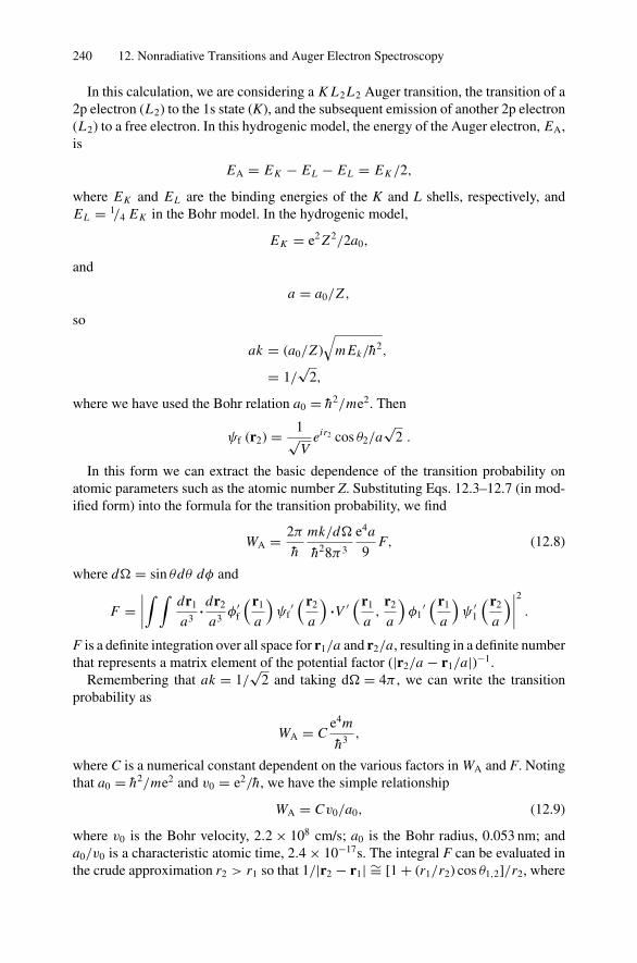
240 12. Nonradiative Transitions and Auger Electron Spectroscopy
In this calculation, we are considering a K L2 L2 Auger transition, the transition of a2p electron (L2) to the 1s state (K), and the subsequent emission of another 2p electron(L2) to a free electron. In this hydrogenic model, the energy of the Auger electron, EA,is
EA = EK − EL − EL = EK /2,
where EK and EL are the binding energies of the K and L shells, respectively, andEL = 1/4 EK in the Bohr model. In the hydrogenic model,
EK = e2 Z2/2a0,
and
a = a0/Z ,
so
ak = (a0/Z )√
m Ek/h2,
= 1/√
2,
where we have used the Bohr relation a0 = h2/me2. Then
ψf (r2) = 1√V
eir2 cos θ2/a√
2 .
In this form we can extract the basic dependence of the transition probability onatomic parameters such as the atomic number Z. Substituting Eqs. 12.3–12.7 (in mod-ified form) into the formula for the transition probability, we find
WA = 2π
h
mk/d
h28π3
e4a
9F, (12.8)
where d = sin θdθ dφ and
F =∣∣∣∣∫ ∫
dr1
a3·dr2
a3φ′
f
(r1
a
)ψf
′(r2
a
)·V ′(r1
a,
r2
a
)φ1
′(r1
a
)ψ ′
1
(r2
a
)∣∣∣∣2
.
F is a definite integration over all space for r1/a and r2/a, resulting in a definite numberthat represents a matrix element of the potential factor (|r2/a − r1/a|)−1.
Remembering that ak = 1/√
2 and taking d = 4π , we can write the transitionprobability as
WA = Ce4m
h3 ,
where C is a numerical constant dependent on the various factors in WA and F. Notingthat a0 = h2/me2 and v0 = e2/h, we have the simple relationship
WA = Cv0/a0, (12.9)
where v0 is the Bohr velocity, 2.2 × 108 cm/s; a0 is the Bohr radius, 0.053 nm; anda0/v0 is a characteristic atomic time, 2.4 × 10⁻¹⁷s. The integral F can be evaluated inthe crude approximation r2 > r1 so that 1/|r2 − r1| ∼= [1 + (r1/r2) cos θ1,2]/r2, where
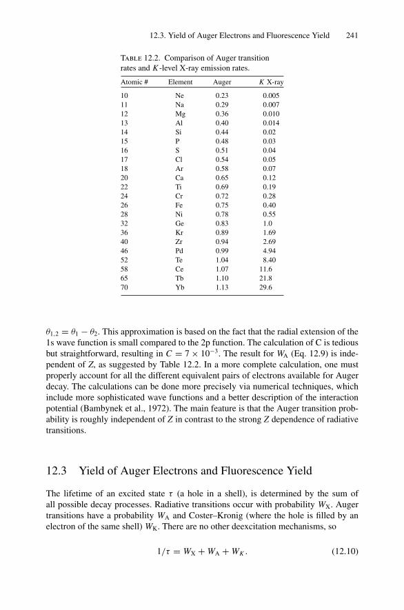
12.3. Yield of Auger Electrons and Fluorescence Yield 241
Table 12.2. Comparison of Auger transitionrates and K -level X-ray emission rates.
Atomic # Element Auger K X-ray
10 Ne 0.23 0.00511 Na 0.29 0.00712 Mg 0.36 0.01013 Al 0.40 0.01414 Si 0.44 0.0215 P 0.48 0.0316 S 0.51 0.0417 Cl 0.54 0.0518 Ar 0.58 0.0720 Ca 0.65 0.1222 Ti 0.69 0.1924 Cr 0.72 0.2826 Fe 0.75 0.4028 Ni 0.78 0.5532 Ge 0.83 1.036 Kr 0.89 1.6940 Zr 0.94 2.6946 Pd 0.99 4.9452 Te 1.04 8.4058 Ce 1.07 11.665 Tb 1.10 21.870 Yb 1.13 29.6
θ1,2 = θ1 − θ2. This approximation is based on the fact that the radial extension of the1s wave function is small compared to the 2p function. The calculation of C is tediousbut straightforward, resulting in C = 7 × 10⁻³. The result for WA (Eq. 12.9) is inde-pendent of Z, as suggested by Table 12.2. In a more complete calculation, one mustproperly account for all the different equivalent pairs of electrons available for Augerdecay. The calculations can be done more precisely via numerical techniques, whichinclude more sophisticated wave functions and a better description of the interactionpotential (Bambynek et al., 1972). The main feature is that the Auger transition prob-ability is roughly independent of Z in contrast to the strong Z dependence of radiativetransitions.
12.3 Yield of Auger Electrons and Fluorescence Yield
The lifetime of an excited state τ (a hole in a shell), is determined by the sum ofall possible decay processes. Radiative transitions occur with probability WX. Augertransitions have a probability WA and Coster–Kronig (where the hole is filled by anelectron of the same shell) WK. There are no other deexcitation mechanisms, so
1/τ = WX + WA + WK . (12.10)
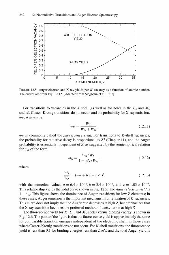
242 12. Nonradiative Transitions and Auger Electron Spectroscopy
353025201510500
1.0
0.9
0.8
0.7
0.6
0.5
0.4
0.3
0.2
0.1
AUGER ELECTRONYIELD
X-RAY YIELD
YIE
LD P
ER
K-E
LEC
TR
ON
VA
CA
NC
Y
ATOMIC NUMBER, Z
Figure 12.5. Auger electron and X-ray yields per K vacancy as a function of atomic number.The curves are from Equ 12.12. [Adapted from Siegbahn et al. 1967]
For transitions to vacancies in the K shell (as well as for holes in the L3 and M5
shells), Coster–Kronig transitions do not occur, and the probability for X-ray emission,ωX, is given by
ωX = WX
WA + WX, (12.11)
ωX is commonly called the fluorescence yield. For transitions to K-shell vacancies,the probability for radiative decay is proportional to Z4 (Chapter 11), and the Augerprobability is essentially independent of Z, as suggested by the semiempirical relationfor ωX of the form
ωX = WX/WA
1 + WX/WA, (12.12)
where
WX
WA= (−a + bZ − cZ3)4, (12.13)
with the numerical values a = 6.4 × 10⁻², b = 3.4 × 10⁻², and c = 1.03 × 10⁻⁶.This relationship yields the solid curve shown in Fig. 12.5. The Auger electron yield is1 − ωx. This figure shows the dominance of Auger transitions for low Z elements; inthese cases, Auger emission is the important mechanism for relaxation of K vacancies.This curve does not imply that the Auger rate decreases at high Z, but emphasizes thatthe X-ray transition becomes the preferred method of deexcitation at high Z.
The fluorescence yield for K , L3, and M5 shells versus binding energy is shown inFig. 12.6. The point of the figure is that the fluorescence yield is approximately the samefor comparable transition energies independent of the electronic shell, in those caseswhere Coster–Kronig transitions do not occur. For K-shell transitions, the fluorescenceyield is less than 0.1 for binding energies less than 2 keV, and the total Auger yield is
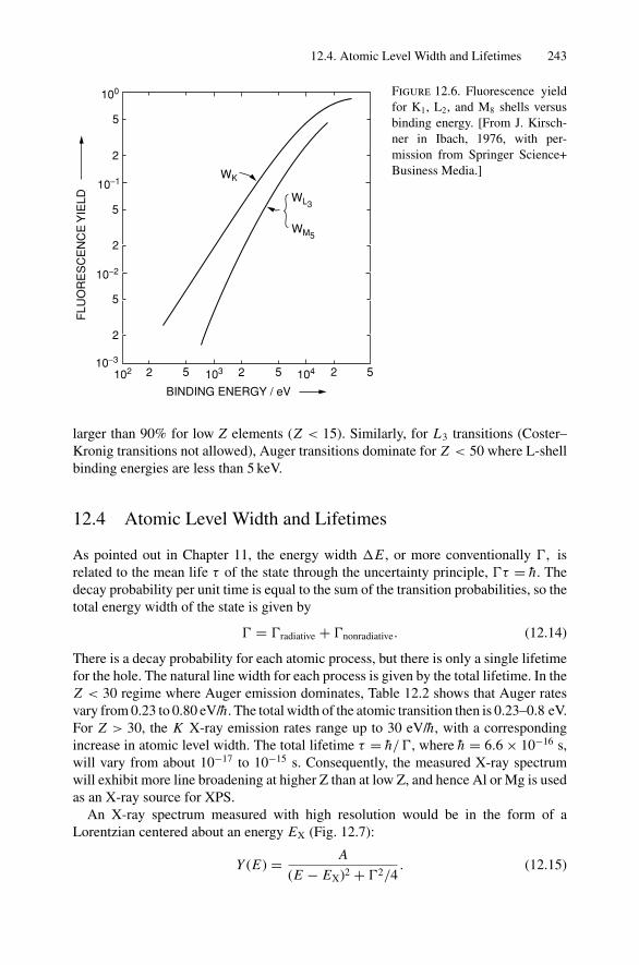
12.4. Atomic Level Width and Lifetimes 243
100
5
2
10−1
5
2
10−2
5
2
10−3
102 103 1042 5 2 5 2 5
WL3
WM5
WK
FLU
OR
ES
CE
NC
E Y
IELD
BINDING ENERGY / eV
Figure 12.6. Fluorescence yieldfor K1, L2, and M8 shells versusbinding energy. [From J. Kirsch-ner in Ibach, 1976, with per-mission from Springer Science+Business Media.]
larger than 90% for low Z elements (Z < 15). Similarly, for L3 transitions (Coster–Kronig transitions not allowed), Auger transitions dominate for Z < 50 where L-shellbinding energies are less than 5 keV.
12.4 Atomic Level Width and Lifetimes
As pointed out in Chapter 11, the energy width E , or more conventionally , isrelated to the mean life τ of the state through the uncertainty principle, τ = h. Thedecay probability per unit time is equal to the sum of the transition probabilities, so thetotal energy width of the state is given by
= radiative + nonradiative. (12.14)
There is a decay probability for each atomic process, but there is only a single lifetimefor the hole. The natural line width for each process is given by the total lifetime. In theZ < 30 regime where Auger emission dominates, Table 12.2 shows that Auger ratesvary from 0.23 to 0.80 eV/h. The total width of the atomic transition then is 0.23–0.8 eV.For Z > 30, the K X-ray emission rates range up to 30 eV/h, with a correspondingincrease in atomic level width. The total lifetime τ = h/, where h = 6.6 × 10⁻¹⁶ s,will vary from about 10−17 to 10−15 s. Consequently, the measured X-ray spectrumwill exhibit more line broadening at higher Z than at low Z, and hence Al or Mg is usedas an X-ray source for XPS.
An X-ray spectrum measured with high resolution would be in the form of aLorentzian centered about an energy EX (Fig. 12.7):
Y (E) = A
(E − EX)2 + 2/4. (12.15)
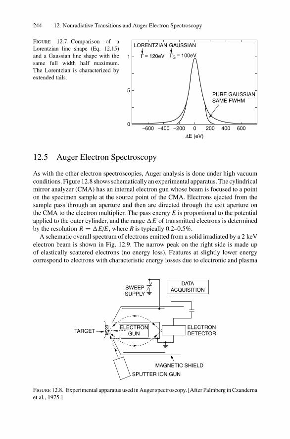
244 12. Nonradiative Transitions and Auger Electron Spectroscopy
1
5
0−600 −400 −200 0 200 400 600
LORENTZIAN GAUSSIAN
Γ = 120eV ΓG = 100eV
PURE GAUSSIANSAME FWHM
∆E (eV)
Figure 12.7. Comparison of aLorentzian line shape (Eq. 12.15)and a Gaussian line shape with thesame full width half maximum.The Lorentzian is characterized byextended tails.
12.5 Auger Electron Spectroscopy
As with the other electron spectroscopies, Auger analysis is done under high vacuumconditions. Figure 12.8 shows schematically an experimental apparatus. The cylindricalmirror analyzer (CMA) has an internal electron gun whose beam is focused to a pointon the specimen sample at the source point of the CMA. Electrons ejected from thesample pass through an aperture and then are directed through the exit aperture onthe CMA to the electron multiplier. The pass energy E is proportional to the potentialapplied to the outer cylinder, and the range E of transmitted electrons is determinedby the resolution R = E/E , where R is typically 0.2–0.5%.
A schematic overall spectrum of electrons emitted from a solid irradiated by a 2 keVelectron beam is shown in Fig. 12.9. The narrow peak on the right side is made upof elastically scattered electrons (no energy loss). Features at slightly lower energycorrespond to electrons with characteristic energy losses due to electronic and plasma
SPUTTER ION GUN
MAGNETIC SHIELD
ELECTRONDETECTOR
ELECTRONGUN
DATAACQUISITIONSWEEP
SUPPLY
TARGET
Figure 12.8. Experimental apparatus used in Auger spectroscopy. [After Palmberg in Czandernaet al., 1975.]

12.5. Auger Electron Spectroscopy 245
ENERGY, eV
INT
EN
SIT
Y (
AR
BIT
RA
RY
UN
ITS
)400
50 E0 − 50 E0
E0 = 2000 eV
0
500
dN (
E)
dE
Figure 12.9. Spectrum of 2 keV electrons scattered from a solid. The inset shows the regimefor Auger spectroscopy. The energy scale is nonlinear. [From Ibach, 1977, with permission fromSpringer Science+Business Media.]
excitations. Auger electron transitions generally appear as small features superimposedon the large background of secondary electrons. The usual practice is to use derivativetechniques and generate a dN(E)/dE function (inset to Fig. 12.9). Differential analysisof a hypothetical spectrum is shown in Fig. 12.10. The contribution from the slowlyvarying background is minimized by the derivative technique. The total backscatteredbackground current with energy greater than 50 eV is typically 30% of the primarybeam current. The noise level due to this current and the ratio of the analyzer E toAuger line width generally establishes the signal-to-noise ratio and hence the detection
GAUSSIAN
E
N(E)
E0
A
Em
A'
Em'
dN (E)
dE
EA
Figure 12.10. A hypothetical spec-trum N (E) containing a continuousbackground AE−m , a Gaussian peak,and a low-energy step of form A′ E−m .The lower spectrum is the derivativespectrum. Note that the energy EA
of the most negative excursion of thederivative corresponds to the steepestslope of N (E).
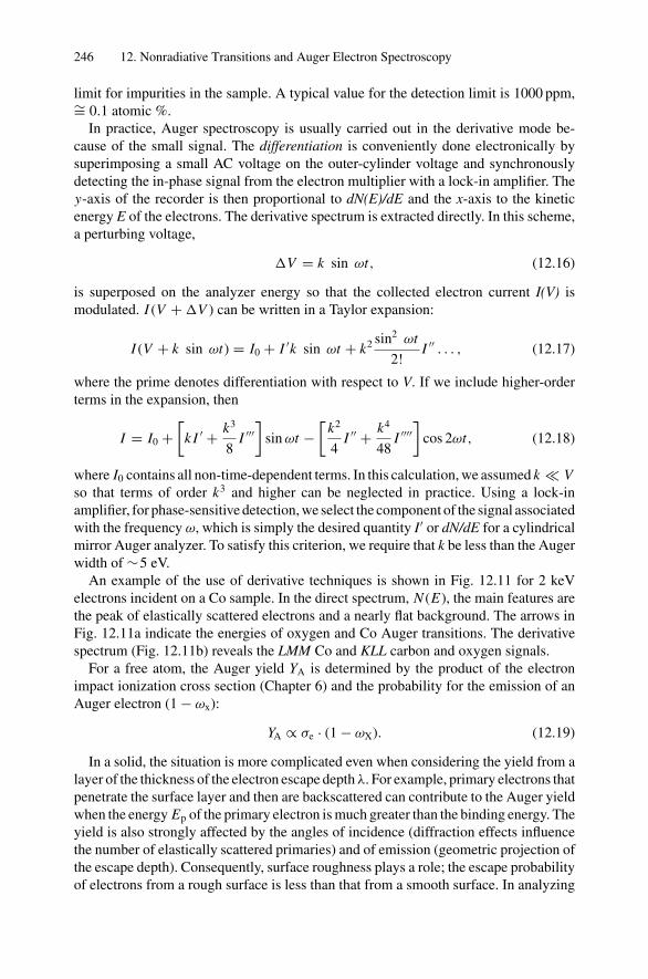
246 12. Nonradiative Transitions and Auger Electron Spectroscopy
limit for impurities in the sample. A typical value for the detection limit is 1000 ppm,∼= 0.1 atomic %.
In practice, Auger spectroscopy is usually carried out in the derivative mode be-cause of the small signal. The differentiation is conveniently done electronically bysuperimposing a small AC voltage on the outer-cylinder voltage and synchronouslydetecting the in-phase signal from the electron multiplier with a lock-in amplifier. They-axis of the recorder is then proportional to dN(E)/dE and the x-axis to the kineticenergy E of the electrons. The derivative spectrum is extracted directly. In this scheme,a perturbing voltage,
V = k sin ωt, (12.16)
is superposed on the analyzer energy so that the collected electron current I(V) ismodulated. I (V + V ) can be written in a Taylor expansion:
I (V + k sin ωt) = I0 + I ′k sin ωt + k2 sin2 ωt
2!I ′′ . . . , (12.17)
where the prime denotes differentiation with respect to V. If we include higher-orderterms in the expansion, then
I = I0 +[
k I ′ + k3
8I ′′′]
sin ωt −[
k2
4I ′′ + k4
48I ′′′′]
cos 2ωt, (12.18)
where I0 contains all non-time-dependent terms. In this calculation, we assumed k Vso that terms of order k3 and higher can be neglected in practice. Using a lock-inamplifier, for phase-sensitive detection, we select the component of the signal associatedwith the frequency ω, which is simply the desired quantity I′ or dN/dE for a cylindricalmirror Auger analyzer. To satisfy this criterion, we require that k be less than the Augerwidth of ∼5 eV.
An example of the use of derivative techniques is shown in Fig. 12.11 for 2 keVelectrons incident on a Co sample. In the direct spectrum, N (E), the main features arethe peak of elastically scattered electrons and a nearly flat background. The arrows inFig. 12.11a indicate the energies of oxygen and Co Auger transitions. The derivativespectrum (Fig. 12.11b) reveals the LMM Co and KLL carbon and oxygen signals.
For a free atom, the Auger yield YA is determined by the product of the electronimpact ionization cross section (Chapter 6) and the probability for the emission of anAuger electron (1 − ωx):
YA ∝ σe · (1 − ωX). (12.19)
In a solid, the situation is more complicated even when considering the yield from alayer of the thickness of the electron escape depth λ. For example, primary electrons thatpenetrate the surface layer and then are backscattered can contribute to the Auger yieldwhen the energy Ep of the primary electron is much greater than the binding energy. Theyield is also strongly affected by the angles of incidence (diffraction effects influencethe number of elastically scattered primaries) and of emission (geometric projection ofthe escape depth). Consequently, surface roughness plays a role; the escape probabilityof electrons from a rough surface is less than that from a smooth surface. In analyzing
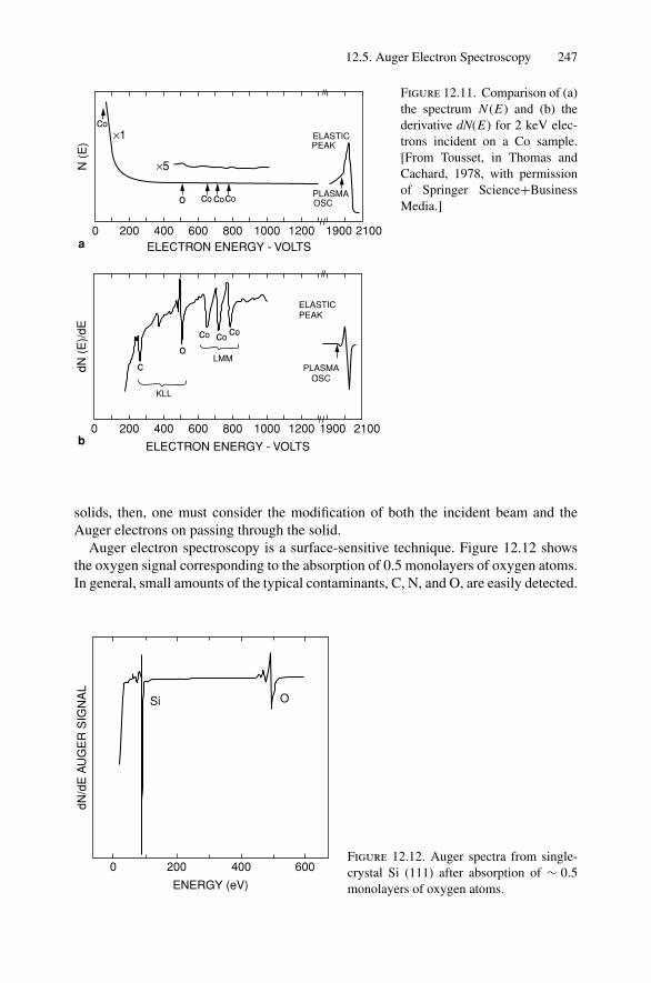
12.5. Auger Electron Spectroscopy 247
×1
×5
co
co
o coco
0a
b
N (
E)
ELECTRON ENERGY - VOLTS
ELECTRON ENERGY - VOLTS
200 400 600 800 1000 1200 1900 2100
0 200 400 600 800 1000 1200 1900 2100
ELASTICPEAK
PLASMAOSC
dN (
E)/
dE
KLL
co
co co
LMMPLASMA
OSC
ELASTICPEAK
co
Figure 12.11. Comparison of (a)the spectrum N (E) and (b) thederivative dN(E) for 2 keV elec-trons incident on a Co sample.[From Tousset, in Thomas andCachard, 1978, with permissionof Springer Science+BusinessMedia.]
solids, then, one must consider the modification of both the incident beam and theAuger electrons on passing through the solid.
Auger electron spectroscopy is a surface-sensitive technique. Figure 12.12 showsthe oxygen signal corresponding to the absorption of 0.5 monolayers of oxygen atoms.In general, small amounts of the typical contaminants, C, N, and O, are easily detected.
0 200 400
OSi
600
ENERGY (eV)
dN/d
E A
UG
ER
SIG
NA
L
Figure 12.12. Auger spectra from single-crystal Si (111) after absorption of ∼ 0.5monolayers of oxygen atoms.
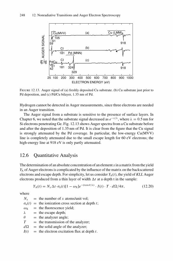
248 12. Nonradiative Transitions and Auger Electron Spectroscopy
Pd (MNN)
Cu(MVV)
105
59
181
1816142 324
329
25 100 200 300 400 500ELECTRON ENERGY (eV)
600 700 800 900 1000
CI
(a)
(b)
(c)
918
918
CI
Cu (LMM)
dN dE⎯, A
UG
ER
SIG
NA
L
PdCu
61
Figure 12.13. Auger signal of (a) freshly deposited Cu substrate. (b) Cu substrate just prior toPd deposition, and (c) Pd/Cu bilayer, 1.35 nm of Pd.
Hydrogen cannot be detected in Auger measurements, since three electrons are neededin an Auger transition.
The Auger signal from a substrate is sensitive to the presence of surface layers. InChapter 6, we noted that the substrate signal decreased as e−x/λ, where λ = 0.5 nm forSi electrons penetrating Ge. Fig. 12.13 shows Auger spectra from a Cu substrate beforeand after the deposition of 1.35 nm of Pd. It is clear from the figure that the Cu signalis strongly attenuated by the Pd coverage. In particular, the low-energy Cu(MVV)line is completely attenuated due to the small escape length for 60 eV electrons; thehigh-energy line at 918 eV is only partly attenuated.
12.6 Quantitative Analysis
The determination of an absolute concentration of an element x in a matrix from the yieldYA of Auger electrons is complicated by the influence of the matrix on the backscatteredelectrons and escape depth. For simplicity, let us consider YA(t), the yield of KLL Augerelectrons produced from a thin layer of width t at a depth t in the sample:
YA(t) = Nxt ·σe(t)[1 − ωX]e−(tcos θ/λ) · I (t) · T · d/4π, (12.20)
whereNx = the number of x atoms/unit vol;σe(t) = the ionization cross section at depth t ;ωX = the fluorescence yield;λ = the escape depth;θ = the analyzer angle;T = the transmission of the analyzer;d = the solid angle of the analyzer;I(t) = the electron excitation flux at depth t .
12.7. Auger Depth Profiles 249
It is convenient to separate the excitation flux density into two components,
I (t) = Ip + IB(t) = Ip(t)[1 + RB(t)],
where Ip is the flux of primary electrons at depth t, IB is the flux due to backscatteredprimary electrons, and RB is the backscattering factor (Section 10.7).
When external standards are used with a known concentration N SX of element x in
the standard, the concentration N TX in the test sample can be found from the ratio of
Auger yields:
N SX
N TX
= Y SX
Y TX
(λT
λS
)[1 + RT
B
1 + RSB
].
In this approach, the ionization cross section and the fluorescence yield are not requiredbecause the Auger yields from the same atom are measured. In addition, if the compo-sition of the standard is close to that of the test sample, the element composition canbe determined directly from the ratio of Auger yields if the measurements are madeunder identical experimental conditions. When the composition of the standard differssubstantially from that of the test specimen, the influence of the matrix on electronbackscattering and escape depth must also be considered.
Elemental sensitivities are acquired using pure element standards and are applied tounknown determinations in multielemental matrices. One must correct for the highlymatrix-dependent parameters, which include the inelastic mean free path λ.
Even with corrections for escape depth and backscattering, the measured surfacecomposition may not be related to the bulk composition of the sample because of the ionbombardment used in sputtering for sample cleaning and depth profiling (see Chapter 4).
12.7 Auger Depth Profiles
A major use of Auger electron spectroscopy is determining the composition as afunction of depth in thin films and layered structures. The conventional apparatusis illustrated in Fig. 12.8, which consists of an electron gun and CMA assembly aswell as a sputter ion gun. The Auger signal is generated in the near surface regionof the sample (∼3.0 nm), and ion sputtering provides the layer sectioning techniquerequired for depth analysis. In routine laboratory use, the depth profiles are shown asAuger signal height versus sputter time. Further calibrations are required to convertsputter time to depth and signal height to atomic concentration. The combination ofRutherford backscattering spectrometry (RBS) and Auger electron spectroscopy (AES)is quite useful in such depth profile analyses because RBS gives quantitative informa-tion on depths and heavy mass constituents without the complications introduced bythe intermixing due to sputtering. As discussed in Chapter 4, ion sputtering causes achange in the composition of the surface layers due to surface segregation and pref-erential sputtering. As compared to RBS, Auger depth profiling provides better depthresolution and is sensitive to both heavy and light elements.
In Fig. 12.14, we illustrate the data obtained from RBS and AES measurements on asample prepared by depositing 100 nm of Ni on 〈100〉 InP (Fig. 12.14a) and annealing
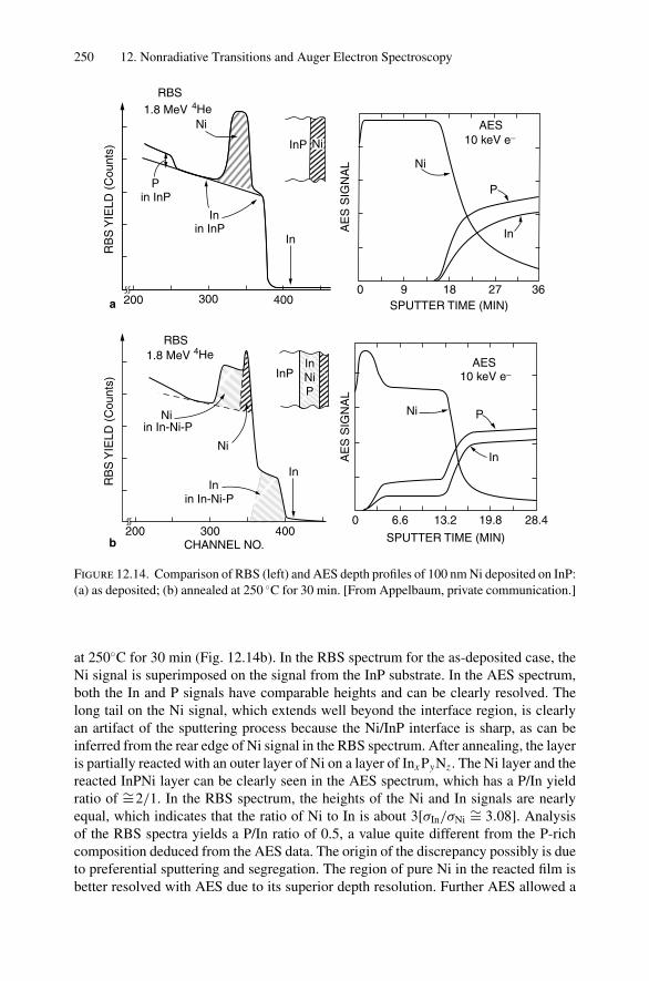
250 12. Nonradiative Transitions and Auger Electron Spectroscopy
Ni
RBS1.8 MeV 4He
Pin InP
in InPIn
In
200a
RB
S Y
IELD
(C
ount
s)
300 400
Ni
Ni
RBS1.8 MeV 4He
in In-Ni-P
In
200b
RB
S Y
IELD
(C
ount
s)
300 400
AE
S S
IGN
AL
AE
S S
IGN
AL
SPUTTER TIME (MIN)
SPUTTER TIME (MIN)
0
Ni
AES
AES
10 keV e−
10 keV e−
In
P
6.6 13.2 19.8 28.4
Ni
P
In
36271890
InP Ni
CHANNEL NO.
Inin In-Ni-P
InPInNiP
Figure 12.14. Comparison of RBS (left) and AES depth profiles of 100 nm Ni deposited on InP:(a) as deposited; (b) annealed at 250 C for 30 min. [From Appelbaum, private communication.]
at 250C for 30 min (Fig. 12.14b). In the RBS spectrum for the as-deposited case, theNi signal is superimposed on the signal from the InP substrate. In the AES spectrum,both the In and P signals have comparable heights and can be clearly resolved. Thelong tail on the Ni signal, which extends well beyond the interface region, is clearlyan artifact of the sputtering process because the Ni/InP interface is sharp, as can beinferred from the rear edge of Ni signal in the RBS spectrum. After annealing, the layeris partially reacted with an outer layer of Ni on a layer of Inx PyNz . The Ni layer and thereacted InPNi layer can be clearly seen in the AES spectrum, which has a P/In yieldratio of ∼=2/1. In the RBS spectrum, the heights of the Ni and In signals are nearlyequal, which indicates that the ratio of Ni to In is about 3[σIn/σNi
∼= 3.08]. Analysisof the RBS spectra yields a P/In ratio of 0.5, a value quite different from the P-richcomposition deduced from the AES data. The origin of the discrepancy possibly is dueto preferential sputtering and segregation. The region of pure Ni in the reacted film isbetter resolved with AES due to its superior depth resolution. Further AES allowed a
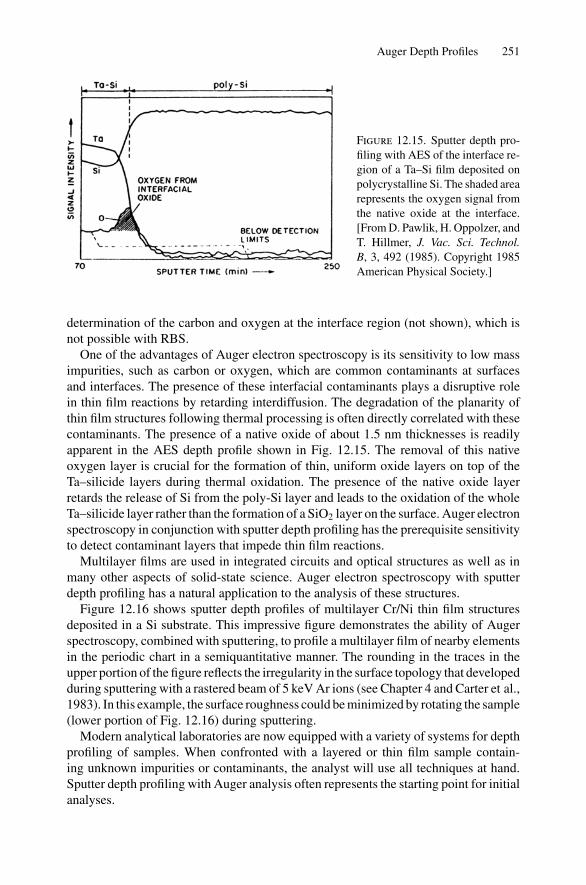
Auger Depth Profiles 251
Figure 12.15. Sputter depth pro-filing with AES of the interface re-gion of a Ta–Si film deposited onpolycrystalline Si. The shaded arearepresents the oxygen signal fromthe native oxide at the interface.[From D. Pawlik, H. Oppolzer, andT. Hillmer, J. Vac. Sci. Technol.B, 3, 492 (1985). Copyright 1985American Physical Society.]
determination of the carbon and oxygen at the interface region (not shown), which isnot possible with RBS.
One of the advantages of Auger electron spectroscopy is its sensitivity to low massimpurities, such as carbon or oxygen, which are common contaminants at surfacesand interfaces. The presence of these interfacial contaminants plays a disruptive rolein thin film reactions by retarding interdiffusion. The degradation of the planarity ofthin film structures following thermal processing is often directly correlated with thesecontaminants. The presence of a native oxide of about 1.5 nm thicknesses is readilyapparent in the AES depth profile shown in Fig. 12.15. The removal of this nativeoxygen layer is crucial for the formation of thin, uniform oxide layers on top of theTa–silicide layers during thermal oxidation. The presence of the native oxide layerretards the release of Si from the poly-Si layer and leads to the oxidation of the wholeTa–silicide layer rather than the formation of a SiO2 layer on the surface. Auger electronspectroscopy in conjunction with sputter depth profiling has the prerequisite sensitivityto detect contaminant layers that impede thin film reactions.
Multilayer films are used in integrated circuits and optical structures as well as inmany other aspects of solid-state science. Auger electron spectroscopy with sputterdepth profiling has a natural application to the analysis of these structures.
Figure 12.16 shows sputter depth profiles of multilayer Cr/Ni thin film structuresdeposited in a Si substrate. This impressive figure demonstrates the ability of Augerspectroscopy, combined with sputtering, to profile a multilayer film of nearby elementsin the periodic chart in a semiquantitative manner. The rounding in the traces in theupper portion of the figure reflects the irregularity in the surface topology that developedduring sputtering with a rastered beam of 5 keV Ar ions (see Chapter 4 and Carter et al.,1983). In this example, the surface roughness could be minimized by rotating the sample(lower portion of Fig. 12.16) during sputtering.
Modern analytical laboratories are now equipped with a variety of systems for depthprofiling of samples. When confronted with a layered or thin film sample contain-ing unknown impurities or contaminants, the analyst will use all techniques at hand.Sputter depth profiling with Auger analysis often represents the starting point for initialanalyses.
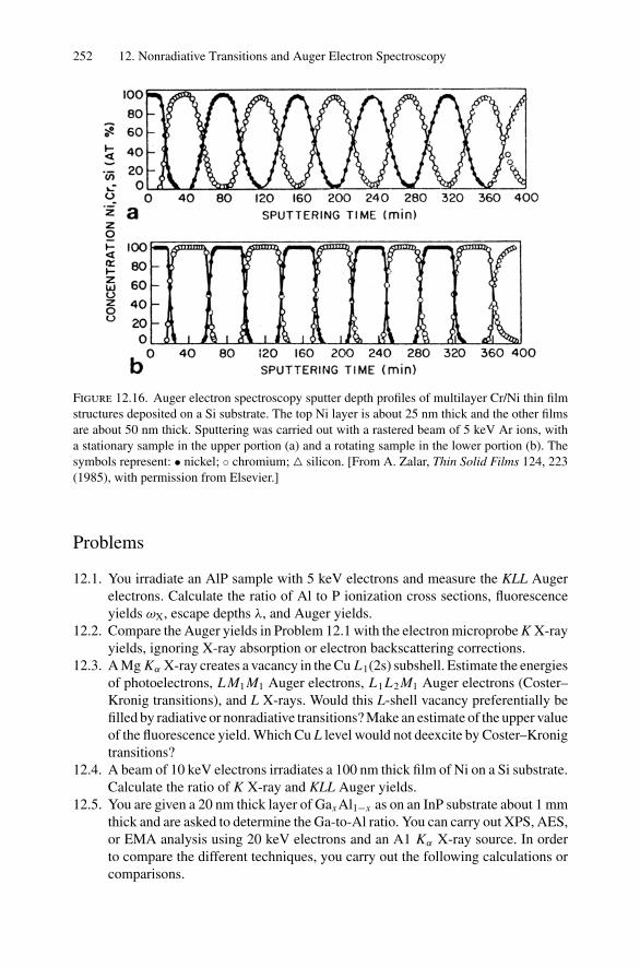
252 12. Nonradiative Transitions and Auger Electron Spectroscopy
Figure 12.16. Auger electron spectroscopy sputter depth profiles of multilayer Cr/Ni thin filmstructures deposited on a Si substrate. The top Ni layer is about 25 nm thick and the other filmsare about 50 nm thick. Sputtering was carried out with a rastered beam of 5 keV Ar ions, witha stationary sample in the upper portion (a) and a rotating sample in the lower portion (b). Thesymbols represent: • nickel; chromium; silicon. [From A. Zalar, Thin Solid Films 124, 223(1985), with permission from Elsevier.]
Problems
12.1. You irradiate an AlP sample with 5 keV electrons and measure the KLL Augerelectrons. Calculate the ratio of Al to P ionization cross sections, fluorescenceyields ωX, escape depths λ, and Auger yields.
12.2. Compare the Auger yields in Problem 12.1 with the electron microprobe K X-rayyields, ignoring X-ray absorption or electron backscattering corrections.
12.3. A Mg Kα X-ray creates a vacancy in the Cu L1(2s) subshell. Estimate the energiesof photoelectrons, L M1 M1 Auger electrons, L1 L2 M1 Auger electrons (Coster–Kronig transitions), and L X-rays. Would this L-shell vacancy preferentially befilled by radiative or nonradiative transitions? Make an estimate of the upper valueof the fluorescence yield. Which Cu L level would not deexcite by Coster–Kronigtransitions?
12.4. A beam of 10 keV electrons irradiates a 100 nm thick film of Ni on a Si substrate.Calculate the ratio of K X-ray and KLL Auger yields.
12.5. You are given a 20 nm thick layer of Gax Al1−x as on an InP substrate about 1 mmthick and are asked to determine the Ga-to-Al ratio. You can carry out XPS, AES,or EMA analysis using 20 keV electrons and an A1 Kα X-ray source. In orderto compare the different techniques, you carry out the following calculations orcomparisons.
Problems 253
(a) What is the cross section ratio σGa/σAl for the K-shell electron impact ion-ization and L-shell photoeffect?
(b) What is the fluorescence yield ratio ωX(Ga)/ωX(Al) for the K-shell hole?(c) You measure the intensity of the Kα X-ray emission from Ga and Al with a
detector system with 200 eV resolution. Would you expect interference fromK, Lα , or M X-rays from As atoms or from the InP substrate? Would youexpect electron backscattering from the InP substrate to influence the totalor the ratio of X-ray yields from Ga and Al?
(d) In XPS measurements (neglecting work functions), what are the Ga and Alphotoelectron energies and associated escape depths (λ)? What is the inten-sity ratio, assuming the same detector efficiency for both electron energies?
(e) In measurements of K L1L1 Ga and Al Auger electrons, what are the energiesand associated escape depths? What is the ratio of Ga to Al transition rates?
(f) Compare the three techniques in terms of analysis depth, corrections orinterferences, and yield ratios for values of x near 0.9.
12.6. Compare transitions for K -shell holes in Z = 20 and Z = 36 elements.
(a) What are the WX/WA ratios [Eq. 12.13]? Compare these values with thecurve in Fig. 12.5.
(b) What are the atomic level widths and lifetimes? Compare the lifetime valuesfor the two elements with the time for an electron to make a circular orbit inthe Bohr model of the atom.
12.7. In an XPS analysis system with an Al Kα X-ray source, Auger electrons as wellas photoelectrons are detected (see, for example, Fig. 10.7). For a vanadiumtarget, what would be the energies and escape depths of the 2s photoelectronsand L1MM Auger electrons? In comparison with 1.5 keV electrons, what is theratio of electron to photon cross sections, σe/σph, to form a 2s hole? The L shellfluorescence yield is small (Appendix 11 or Fig. 12.6), so estimate the ratio ofphotoelectron to Auger electrons, assuming Coster–Kronig transitions can beneglected. Is this a good assumption?
References
1. W. Bambynek et al., “X-ray Fluorescence Yields, Auger and Coster–Kronig Transitions,”Rev. Mod. Phys. 44, 716 (1972).
2. T. A. Carlson, Photoelectron and Auger Spectroscopy (Plenum Press, New York, 1975).3. G. Carter, B. Navinsek, and J. L. Whitton, “Heavy Ion Surface Topography Develop-
ment,” in Sputtering by Particle Bombardment II, R. Behrisch, Ed. (Springer-Verlag, Berlin,1983).
4. C. C. Chang, “Analytical Auger Electron Spectroscopy,” in Characterization of Solid Sur-faces, P. F. Kane and G. R. Larrabee, Eds. (Plenum Press, New York, 1974), Chap. 20.
5. A. W. Czanderna, Ed., Methods of Surface Analysis (Elsevier, Amsterdam, 1975).6. L. E. Davis, N. C. MacDonald, P. W. Palmberg, G. E. Riach, and R. E. Weber, Handbook
of Auger Electron Spectroscopy (Physical Electronics Industries, Inc., Eden Prairie, MN,1976).
254 12. Nonradiative Transitions and Auger Electron Spectroscopy
7. G. Ertl and J. Kuppers, Low Energy Electrons and Surface Chemistry (Verlag Chemie Inter-national, Weinheim, 1974).
8. G. Herzberg, Atomic Spectra and Atomic Structure (Dover, New York, 1944).9. H. Ibach, Ed., Electron Spectroscopy for Surface Analysis, Topics in Current Physics, Vol. 4
(Springer-Verlag, New York, 1977).10. A. Joshi, L. E. Davis, and P. W. Palmberg, “Auger Electron Spectroscopy” in Methods of
Surface Analysis, A. W. Czanderna, Ed. (Elsevier Science Publishing Co., New York, 1975),Chap. 5.
11. G. E. McGuire, Auger Electron Spectroscopy Reference Manual (Plenum Press, New York,1979).
12. K. D. Sevier, Low Energy Electron Spectroscopy (Wiley-Interscience, New York, 1972).13. K. Siegbahn, C. N. Nordling, A. Fahlman, R. Nordberg, K. Hamrin, J. Hedman, G. Johansson,
T. Bergmark, S. E. Karlsson, I. Lindgren, and B. Lindberg, ESCA, Atomic, Molecular andSolid State Structure Studied by Means of Electron Spectroscopy (Almqvist and Wiksells,Uppsala, Sweden, 1967).
14. J. P. Thomas and A. Cachard, Eds., Material Characterization Using Ion Beams (PlenumPress, New York, 1978).
13Nuclear Techniques: Activation Analysisand Prompt Radiation Analysis
13.1 Introduction
Analytical methods based on electronic interactions have long been used in the materialsanalysis laboratory, but determinations based on nuclear spectroscopy are much morerecent. If radioactivity is produced by the irradiation and detected afterward, the methodis called activation analysis; if radiations emitted instantaneously are detected, it istermed prompt radiation analysis. These two categories will be used for labeling majorsections of the discussion that follows. For example, when a material containing carbonis irradiated with a beam of deuterons, one of the nuclear reactions with the carbon,12C, in the sample is the transformation to radioactive nitrogen, 13N, by the promptemission of a neutron, n. The carbon content of the sample can be determined eitherby measurement of the radiation emitted from the radioactive product nuclide, 13N; byactivation analysis; or by measuring the yield of neutrons, prompt radiation analysis.Radioactive nuclides that are used in analysis decay with half-lives ranging betweenmilliseconds and thousands of years (the half-life of 13N is 9.96 min); whereas, theprompt radiation from a nuclear reaction is emitted within times less than 10−12 secafter the nuclear reaction is initiated.
Several different kinds of nuclear interactions can be used for analysis:
1. A charged particle can elastically scatter from the charged target nucleus as inRutherford scattering (Chapter 2) or nuclear elastic scattering.
2. Particles can excite the nucleus to a higher energy state (analogous to promoting anelectron to a higher energy state in atomic spectroscopy); the nucleus can then bedeexcited by γ-ray emission.
3. A different nucleus may be formed as a result of the nuclear reaction.
In most nuclear reactions, we have two particles or nuclei interacting to form twodifferent nuclei. Thus,
a + b → c + dReactants Products
.
Any reaction must meet the requirement that the sum of the atomic numbers and mass
256 13. Nuclear Techniques: Activation Analysis and Prompt Radiation Analysis
numbers of reactants and products must balance. In other words
Za + Zb = Zc + Zd
Aa + Ab = Ac + Ad.
Mass, however, is changed.Although there is no theoretical limitation on what the nuclides a, b, c, and d can
be, as a practical matter each side of the equation usually includes a very light nuclide.These are frequently termed particles. If we designate the particle (keep in mind thatthe distinction between particle and nucleus is a bit ambiguous) by the lower case, wecan write a nuclear reaction,
a + X → b + Y.
In a common shorthand notation, one would write
X(a,b)Y.
A nucleus with four neutrons and three protons is designated73X,
where the subscript is Z, the number of protons, and the superscript is the total nucleons,which we term the mass number, A. More generally, therefore, a nucleus is designated
AZ X.
A nuclear reaction of interest in determining boron depth profiles is10n + 10
5 B → 42He+ + 7
3Li
In shorthand,10B(n, α)7Li
The reactant and product light particles are placed in parentheses and separated by acomma.
As in any specialized field, a certain nomenclature has developed based on conve-nience and tradition. The terms most frequently used are given below.
Nucleon Either a proton or a neutron.Nuclide A specific nuclear species with a given proton number Z and
neutron number N.Isotopes Nuclides of same Z and different N.Isobars Nuclides of same mass number A, where A = Z + N .Isotones Nuclides with same N but different Z .Isomer Nuclide in an excited state with a measurable half-life.Proton 1
1HDeuteron (d) 2
1H, one proton and one neutron.Tritron (t) 3
1H, one proton and two neutrons.Alpha (α) 4
2He, two protons and two neutrons.
Let us consider the irradiation of nuclei in a flux of protons, specifically protonirradiation of 12C (Fig. 13.1). Some of the incident protons can be scattered due to long-range Coulomb interaction with the nuclei, known as elastic scattering (as described in
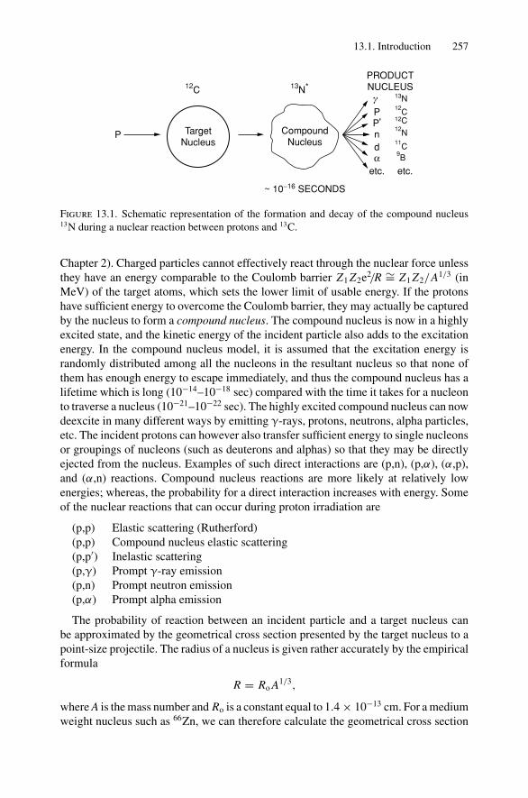
13.1. Introduction 257
TargetNucleus
PRODUCTNUCLEUS
CompoundNucleus
P
12C
12C12C
11C9B
13N*γ
~ 10−16 SECONDS
etc. etc.
13N
12N
PP'ndα
Figure 13.1. Schematic representation of the formation and decay of the compound nucleus13N during a nuclear reaction between protons and 13C.
Chapter 2). Charged particles cannot effectively react through the nuclear force unlessthey have an energy comparable to the Coulomb barrier Z1 Z2e2/R ∼= Z1 Z2/A1/3 (inMeV) of the target atoms, which sets the lower limit of usable energy. If the protonshave sufficient energy to overcome the Coulomb barrier, they may actually be capturedby the nucleus to form a compound nucleus. The compound nucleus is now in a highlyexcited state, and the kinetic energy of the incident particle also adds to the excitationenergy. In the compound nucleus model, it is assumed that the excitation energy israndomly distributed among all the nucleons in the resultant nucleus so that none ofthem has enough energy to escape immediately, and thus the compound nucleus has alifetime which is long (10−14–10−18 sec) compared with the time it takes for a nucleonto traverse a nucleus (10−21–10−22 sec). The highly excited compound nucleus can nowdeexcite in many different ways by emitting γ-rays, protons, neutrons, alpha particles,etc. The incident protons can however also transfer sufficient energy to single nucleonsor groupings of nucleons (such as deuterons and alphas) so that they may be directlyejected from the nucleus. Examples of such direct interactions are (p,n), (p,α), (α,p),and (α,n) reactions. Compound nucleus reactions are more likely at relatively lowenergies; whereas, the probability for a direct interaction increases with energy. Someof the nuclear reactions that can occur during proton irradiation are
(p,p) Elastic scattering (Rutherford)(p,p) Compound nucleus elastic scattering(p,p′) Inelastic scattering(p,γ) Prompt γ-ray emission(p,n) Prompt neutron emission(p,α) Prompt alpha emission
The probability of reaction between an incident particle and a target nucleus canbe approximated by the geometrical cross section presented by the target nucleus to apoint-size projectile. The radius of a nucleus is given rather accurately by the empiricalformula
R = Ro A1/3,
where A is the mass number and Ro is a constant equal to 1.4 × 10⁻¹³ cm. For a mediumweight nucleus such as 66Zn, we can therefore calculate the geometrical cross section
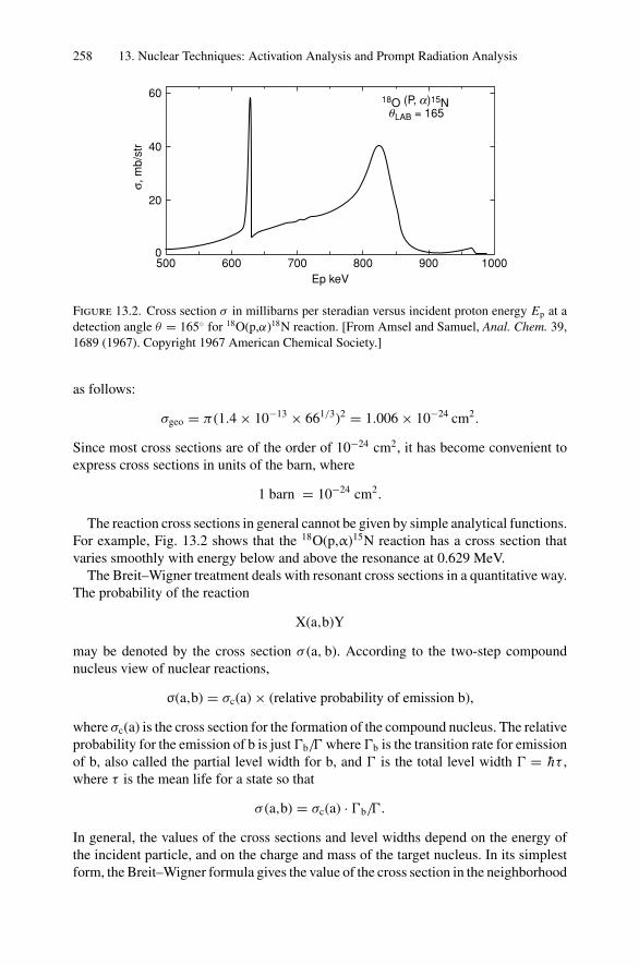
258 13. Nuclear Techniques: Activation Analysis and Prompt Radiation Analysis
500 600 700 800 900 1000
60
40
20
0
σ, m
b/st
r
18O (P, a)15NθLAB = 165
Ep keV
Figure 13.2. Cross section σ in millibarns per steradian versus incident proton energy Ep at adetection angle θ = 165 for 18O(p,α)18N reaction. [From Amsel and Samuel, Anal. Chem. 39,1689 (1967). Copyright 1967 American Chemical Society.]
as follows:
σgeo = π (1.4 × 10−13 × 661/3)2 = 1.006 × 10⁻²⁴ cm2.
Since most cross sections are of the order of 10−24 cm2, it has become convenient toexpress cross sections in units of the barn, where
1 barn = 10−24 cm2.
The reaction cross sections in general cannot be given by simple analytical functions.For example, Fig. 13.2 shows that the 18O(p,α)15N reaction has a cross section thatvaries smoothly with energy below and above the resonance at 0.629 MeV.
The Breit–Wigner treatment deals with resonant cross sections in a quantitative way.The probability of the reaction
X(a,b)Y
may be denoted by the cross section σ (a, b). According to the two-step compoundnucleus view of nuclear reactions,
σ(a,b) = σc(a) × (relative probability of emission b),
where σc(a) is the cross section for the formation of the compound nucleus. The relativeprobability for the emission of b is just b/ where b is the transition rate for emissionof b, also called the partial level width for b, and is the total level width = hτ ,where τ is the mean life for a state so that
σ (a,b) = σc(a) · b/.
In general, the values of the cross sections and level widths depend on the energy ofthe incident particle, and on the charge and mass of the target nucleus. In its simplestform, the Breit–Wigner formula gives the value of the cross section in the neighborhood
13.2. Q Values and Kinetic Energies 259
of a single resonance level in the compound nucleus, formed by an incident particlewith zero angular momentum. Under these conditions, the formula is
σ (a,b) = λ2
4π
ab
(E − E0)2 + (/2)2, (13.1)
where λ is the de Broglie wavelength of the incident particle (λ = h/mv), Eo the energyat the peak of the resonance, E the energy of the incident particle, and a the partiallevel width for the emission of a in the inverse reaction. It is clear from this equationthat the cross section will be at a maximum for E = Eo.
13.2 Q Values and Kinetic Energies
Nuclear reactions obey the following conservation laws:
1. Conservation of nucleons (A)2. Conservation of charge (Z)3. Conservation of mass-energy (E)4. Conservation of momentum (p)
If the exact rest masses of the reactants and of the products of a nuclear reaction aretotaled, there is likely to be a difference between the two because mass and energy maybe exchanged according to the equation
E = mc2,
where E is the energy, m is the mass, and c is the speed of light with 1 mass unit equalto 931.4 MeV.
The mass difference will correspond to either an emission or an absorption of energy.Thus a complete nuclear reaction should be written in the form
X + a → Y + b ± Q,
where Q is the energy balance, usually given in MeV. If energy is released by thereaction, the Q value will be positive. If the Q value is negative, energy must besupplied, and there will be a definite threshold below which these endoergic reactionswill not occur.
Once a nuclear reaction has occurred, the radiations emitted are characteristic ofthe excited nuclei, in much the same way that optical radiation is characteristic of anexcited emitting atom. It is the existence of a unique set of well-defined energy levels inthe atom or the nucleus that permits the use of the emitted radiation as an identificationof the source.
Symbolically, a nuclear reaction may be written
M1 + M2 → M3 + M4 + Q,
where M1 is the incident nucleus, M2 is the target, M3 is the emitted radiation, whichmay be either a nuclear particle or a gamma ray, M4 is the residual nucleus, and Q isthe energy released (absorbed) in the reaction. Q is simply the difference between the
260 13. Nuclear Techniques: Activation Analysis and Prompt Radiation Analysis
total energy, at rest, of the interacting system before the reaction takes place and afterthe reaction has occurred. If the M’s are taken to be masses,
Q = (M1 + M2)c2 − (M3 + M4)c2. (13.2)
Let us consider the reaction
3517Cl + 1
0n → 3215P + 4
2He+ + Q,
which can be written in an abbreviated form as
35Cl(n, α)32P.
The reaction is balanced with respect to nucleons and charge in that the reactantsand products have the same total number of nucleons (36) and protons (17). Thereaction energy Q is equivalent to the difference in mass between the reactants and theproducts:
M = M(35Cl) + M(n) − M(32P) − M(4He+)
= 34.96885 + 1.00867 − 31.97391 − 4.00260
= +0.00101 amu,
Q = 0.00101 × 931.4 = +0.94 MeV.
Similarly, the Q value can be calculated for the following reaction:
14N(p, n)14O, Q = −5.931 MeV.
Q values can thus be positive or negative. Positive Q values denote exoergic nuclearreactions. Negative Q values denote endoergic nuclear reactions.
If the residual nucleus M4 is left in an excited energy state, the Q for the reaction willbe reduced, relative to the value that would be obtained if the residual nucleus wereleft in its ground state. The reduction is just the amount of the excitation energy. Fora well-defined beam energy, the energy spectrum of M3 will be characteristic of theQ values possible in the reaction or, equivalently, to the excited states of the residualnucleus. Even if the emitted particles M3 are not observed, the prompt gamma raysemitted in the decay of the excited M4 nucleus will be characteristic of that nucleus.
In the case of activation analysis, the identifying characteristics for the radioactiveM4 nucleus can be the half-life for decay, the types of radiation emitted, and thecharacteristic gamma rays emitted from the daughter nuclei of M4.
For the prompt radiation analysis (PRA) case, if M3 is a gamma ray, the nuclearreaction is called a direct capture reaction. The case M1 = M3 and Q = 0 is just theelastic scattering reaction. When M1 = M3 but Q = 0, the reaction is called inelas-tic scattering, and, finally, when M1 = M3, it is commonly termed a rearrangementcollision.
In contrast to the case of atoms, nuclear characteristics usually differ markedly be-tween two isotopes of the same chemical element. The emitted radiations or reactionproducts are specific not only to the chemical element but also to a particular iso-tope of that element. It is this property that provides the basis for the many important
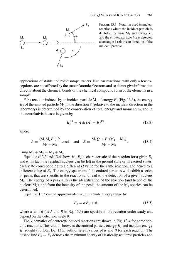
13.2. Q Values and Kinetic Energies 261
M1
E1
E4
M2
M4
M3
E3
θ
φ
Figure 13.3. Notation used in nuclearreactions where the incident particle isdentoted by mass M1 and energy E1
and the emitted particle M3 is detectedat an angle θ relative to direction of theincident particle.
applications of stable and radioisotope tracers. Nuclear reactions, with only a few ex-ceptions, are not affected by the state of atomic electrons and so do not give informationdirectly about the chemical bonds or the chemical compound form of the elements in asample.
For a reaction induced by an incident particle M1 of energy E1 (Fig. 13.3), the energyE3 of the emitted particle M3 in the direction θ (relative to the incident direction in thelaboratory) is determined by the conservation of total energy and momentum, and inthe nonrelativistic case is given by
E1/23 = A ± (A2 + B)1/2, (13.3)
where
A = (M1M2 E1)1/2
M3 + M4cos θ and B = M4 Q + E1(M4 − M1)
M3 + M4, (13.4)
using M1 + M2 = M3 + M4.Equations 13.3 and 13.4 show that E3 is characteristic of the reaction for a given E1
and θ . In fact, the residual nucleus can be left in the ground state or in excited states,each state corresponding to a different Q value for the same reaction, and hence to adifferent value of E3. The energy spectrum of the emitted particles will exhibit a seriesof peaks that are specific to the reaction and lead to the detection of a given nucleusM2. The energy of a peak allows the identification of the reaction (and hence of thenucleus M2), and from the intensity of the peak, the amount of the M2 species can bedetermined.
Equation 13.3 can be approximated within a wide energy range by
E3 = αE1 + β, (13.5)
where α and β (as A and B in Eq. 13.3) are specific to the reaction under study anddepend on the detection angle θ .
The kinematics of deuteron-induced reactions are shown in Fig. 13.4 for some spe-cific reactions. The relation between the emitted particle energy E3 and incident energyE1 roughly follows Eq. 13.5, with different values of α and β for each reaction. Thedashed line E3 = E1 denotes the maximum energy of elastically scattered particles and
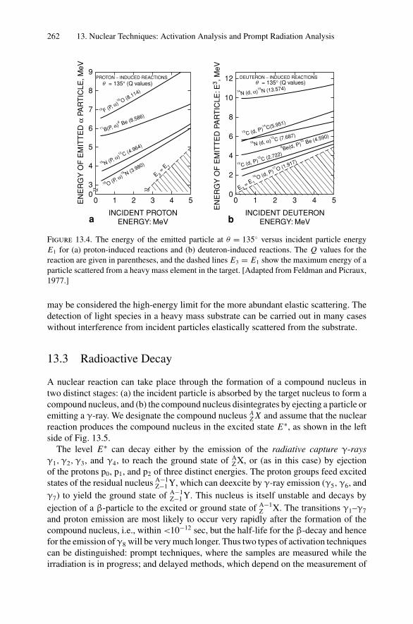
262 13. Nuclear Techniques: Activation Analysis and Prompt Radiation Analysis
00 1 2 3
3
4
4
5 00
2
4
6
8
10
12
1 2 3 4 5
5
6
7
8
9E
NE
RG
Y O
F E
MIT
TE
D α
PA
RT
ICLE
, MeV
EN
ER
GY
OF
EM
ITT
ED
PA
RT
ICLE
: E3 ,
MeV
INCIDENT PROTONENERGY: MeV
INCIDENT DEUTERONENERGY: MeV
E 3 = E 1
E 3 = E 118 O (P, α)
15 N (3.980)
16 O (d, P)17 O (1.917)15 N (P, α)
12 C (4.964)
14N (d, α)15N (13.574)
12 C (d, P)13 C (2.722)
13 C (d, P)14 C(5.951)
15 N (d, α)13 C (7.687)
11 B(P, α)8 Be (8.586)
9 Be(d, P)10 Be (4.590)
19 F (P, α)16 O (8.114)
θ = 135° (Q values) θ = 135° (Q values)PROTON − INDUCED REACTIONS DEUTERON − INDUCED REACTIONS
a b
Figure 13.4. The energy of the emitted particle at θ = 135 versus incident particle energyE1 for (a) proton-induced reactions and (b) deuteron-induced reactions. The Q values for thereaction are given in parentheses, and the dashed lines E3 = E1 show the maximum energy of aparticle scattered from a heavy mass element in the target. [Adapted from Feldman and Picraux,1977.]
may be considered the high-energy limit for the more abundant elastic scattering. Thedetection of light species in a heavy mass substrate can be carried out in many caseswithout interference from incident particles elastically scattered from the substrate.
13.3 Radioactive Decay
A nuclear reaction can take place through the formation of a compound nucleus intwo distinct stages: (a) the incident particle is absorbed by the target nucleus to form acompound nucleus, and (b) the compound nucleus disintegrates by ejecting a particle oremitting a γ-ray. We designate the compound nucleus A
Z X and assume that the nuclearreaction produces the compound nucleus in the excited state E∗, as shown in the leftside of Fig. 13.5.
The level E∗ can decay either by the emission of the radiative capture γ-raysγ1, γ2, γ3, and γ4, to reach the ground state of A
Z X, or (as in this case) by ejectionof the protons p0, p1, and p2 of three distinct energies. The proton groups feed excitedstates of the residual nucleus A−1
Z−1 Y, which can deexcite by γ-ray emission (γ5, γ6, andγ7) to yield the ground state of A−1
Z−1 Y. This nucleus is itself unstable and decays byejection of a β-particle to the excited or ground state of A−1
Z X. The transitions γ1–γ7
and proton emission are most likely to occur very rapidly after the formation of thecompound nucleus, i.e., within <10−12 sec, but the half-life for the β-decay and hencefor the emission of γ8 will be very much longer. Thus two types of activation techniquescan be distinguished: prompt techniques, where the samples are measured while theirradiation is in progress; and delayed methods, which depend on the measurement of
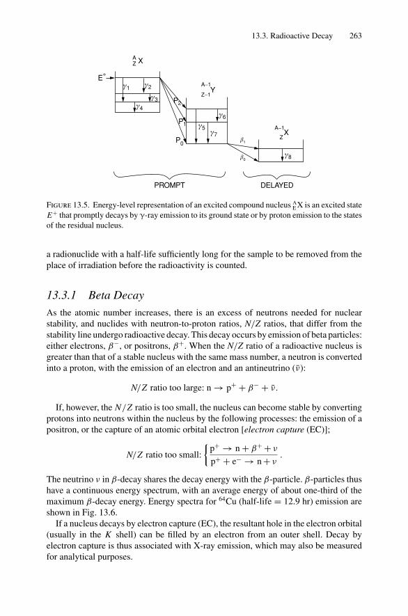
13.3. Radioactive Decay 263
E∗
AZ X
A−1
Z−1Y
A−1
ZX
γ8
γ7
γ4
γ3
γ2γ1
γ5
γ6
β1
β0
P0
P1
P2
PROMPT DELAYED
Figure 13.5. Energy-level representation of an excited compound nucleus AE X is an excited state
E+ that promptly decays by γ-ray emission to its ground state or by proton emission to the statesof the residual nucleus.
a radionuclide with a half-life sufficiently long for the sample to be removed from theplace of irradiation before the radioactivity is counted.
13.3.1 Beta Decay
As the atomic number increases, there is an excess of neutrons needed for nuclearstability, and nuclides with neutron-to-proton ratios, N/Z ratios, that differ from thestability line undergo radioactive decay. This decay occurs by emission of beta particles:either electrons, β−, or positrons, β+. When the N/Z ratio of a radioactive nucleus isgreater than that of a stable nucleus with the same mass number, a neutron is convertedinto a proton, with the emission of an electron and an antineutrino (ν):
N/Z ratio too large: n → p+ + β− + ν.
If, however, the N/Z ratio is too small, the nucleus can become stable by convertingprotons into neutrons within the nucleus by the following processes: the emission of apositron, or the capture of an atomic orbital electron [electron capture (EC)];
N/Z ratio too small:
p+ → n + β+ + ν
p+ + e− → n + ν.
The neutrino ν in β-decay shares the decay energy with the β-particle. β-particles thushave a continuous energy spectrum, with an average energy of about one-third of themaximum β-decay energy. Energy spectra for 64Cu (half-life = 12.9 hr) emission areshown in Fig. 13.6.
If a nucleus decays by electron capture (EC), the resultant hole in the electron orbital(usually in the K shell) can be filled by an electron from an outer shell. Decay byelectron capture is thus associated with X-ray emission, which may also be measuredfor analytical purposes.
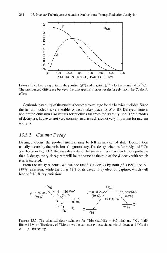
264 13. Nuclear Techniques: Activation Analysis and Prompt Radiation Analysis
100 200 300 400 500 600 7000KINETIC ENERGY OF β PARTICLES, keV
β P
AR
TIC
LES
PE
R U
NIT
EN
ER
GY
β+
β−64Cu
Figure 13.6. Energy spectra of the positive (β+) and negative (β−) electrons emitted by 64Cu.The pronounced difference between the two spectral shapes results largely from the Coulombeffect.
Coulomb instability of the nucleus becomes very large for the heavier nuclides. Sincethe helium nucleus is very stable, α-decay takes place for Z > 83. Delayed neutronand proton emission also occurs for nuclides far from the stability line. These modesof decay are, however, not very common and as such are not very important for nuclearanalysis.
13.3.2 Gamma Decay
During β-decay, the product nucleus may be left in an excited state. Deexcitationusually occurs by the emission of a gamma ray. The decay schemes for 27Mg and 64Cuare shown in Fig. 13.7. Because deexcitation by γ-ray emission is much more probablethan β-decay, the γ-decay rate will be the same as the rate of the β-decay with whichit is associated.
From the decay scheme, we can see that 64Cu decays by both β+ (19%) and β−
(39%) emission, while the other 42% of its decay is by electron capture, which willlead to 64Ni X-ray emission.
64 Zn
64Cu
64Ni
EC(~42 %)
β−, 0.57 MeV(39 %)
β−, 1.78 MeV(70 %)
β−, 1.59 MeV(30 %)
β+, 0.66 MeV(19 %);
O
OO
27Mg
27Al
1.0150.834
γ γ
Figure 13.7. The principal decay schemes for 27Mg (half-life = 9.5 min) and 64Cu (half-life = 12.9 hr). The decay of 27Mg shows the gamma rays associated with β-decay and 64Cu theβ+ − β− branching.
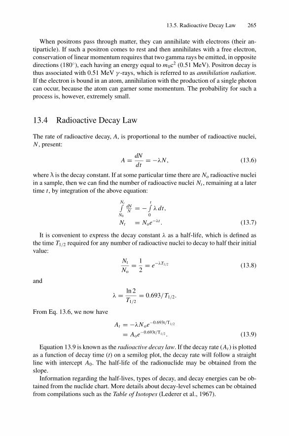
13.5. Radioactive Decay Law 265
When positrons pass through matter, they can annihilate with electrons (their an-tiparticle). If such a positron comes to rest and then annihilates with a free electron,conservation of linear momentum requires that two gamma rays be emitted, in oppositedirections (180), each having an energy equal to m0c2 (0.51 MeV). Positron decay isthus associated with 0.51 MeV γ -rays, which is referred to as annihilation radiation.If the electron is bound in an atom, annihilation with the production of a single photoncan occur, because the atom can garner some momentum. The probability for such aprocess is, however, extremely small.
13.4 Radioactive Decay Law
The rate of radioactive decay, A, is proportional to the number of radioactive nuclei,N , present:
A = dN
dt= −λN , (13.6)
where λ is the decay constant. If at some particular time there are No radioactive nucleiin a sample, then we can find the number of radioactive nuclei Nt , remaining at a latertime t , by integration of the above equation:
Nt∫N0
dNN = −
t∫0
λ dt,
Nt = Noe−λt . (13.7)
It is convenient to express the decay constant λ as a half-life, which is defined asthe time T1/2 required for any number of radioactive nuclei to decay to half their initialvalue:
Nt
No= 1
2= e−λT1/2 (13.8)
and
λ = ln 2
T1/2= 0.693/T1/2.
From Eq. 13.6, we now have
At = −λN oe−0.693t/T1/2
= Aoe−0.693t/T1/2 . (13.9)
Equation 13.9 is known as the radioactive decay law. If the decay rate (At ) is plottedas a function of decay time (t) on a semilog plot, the decay rate will follow a straightline with intercept A0. The half-life of the radionuclide may be obtained from theslope.
Information regarding the half-lives, types of decay, and decay energies can be ob-tained from the nuclide chart. More details about decay-level schemes can be obtainedfrom compilations such as the Table of Isotopes (Lederer et al., 1967).
266 13. Nuclear Techniques: Activation Analysis and Prompt Radiation Analysis
13.5 Radionuclide Production
In activation analysis, we are interested in the amount of radioactivity formed as afunction of irradiation time. Let us consider the nuclear reaction
X(a,b)Y,
with Y the radioactive product nucleus, which we determine as a measure of X in thesample. The rate at which nuclide Y is formed may be expressed as(
dNY
dt
)growth
= NXσφ,
where NX is the number of target nuclides and NY the number of product nuclidesformed, σ the reaction cross section (cm2), and φ the flux of incident particles (particlescm−2- sec−1). If the product nucleus is stable, the total number of nuclides Y formedduring an irradiation time of t seconds is
NY = NXσφt. (13.10)
If Y is radioactive, however, and decays with a decay constant λY, we have(dNY
dt
)decay
= −NYλY.
The total rate for forming the radioactive product nuclide Y is then given by
dNY
dt= NXσφ − NYλY. (13.11)
If the target number NX is a constant, as it usually is, one obtains by integration
NY = NXσφ
λY(1 − e−λYt ).
The activity At (in disintegrations per second) of the radioactive nuclide Y at time t isgiven by At = NY/λY so that
At = NXσφ(1 − e−λYt ). (13.12)
For t → ∞, the term in brackets (growth factor) equals unity and A∞ = NXσφ. Theactivity A∞ is referred to as the saturation Asat, and Eq. 13.12 may be written as
At = Asat(1 − e−λt ) (13.13)
The saturation factor At/Asat is plotted in Fig. 13.8 as a function of irradiation time texpressed in number of half-lives, where λ = 0.693/T1/2.
13.6 Activation Analysis
Activation analysis is a highly sensitive, nondestructive (if chemical separations arenot used) technique for qualitative and quantitative determination of trace amounts ofelements in a sample. It has been particularly useful for the simultaneous determinationof many elements in complex samples because it provides a simple alternative to muchmore difficult, tedious, and destructive analytical techniques.
13.7. Prompt Radiation Analysis 267
0 1 2 3 4 5 6IRRADIATION TIME, t / T1/2
0.0
0.2
0.4
0.6
0.8
1.0S
ATU
RAT
ION
FA
CTO
R, A
t / A
sat
Figure 13.8. Growth of radioactive nu-clide activity Ai/Asat as a function of irra-diation time t/T1/2. After an irradiationtime of four half-lives, about 94% of sat-uration activity Asat has formed.
In activation analysis, the element to be determined is uniquely identified by thehalf-life and energy of the radiation emitted by its radioactive product nuclide. Foroptimum analytical sensitivity, it is desirable to form the maximum amount of activityin the sample from the elements to be determined and to measure such activities withmaximum efficiency in the presence of other interfering activities. Fortunately, theirradiation and measurement parameters can be changed over wide ranges in order toselect the optimum conditions for analysis.
Figure 13.8 shows that 50% of the maximum activity is obtained after an irradiationtime equal to one half-life and more than 90% after four half-lives. Irradiations longerthan a few half-lives will thus only increase the amount of unwanted background activityfrom other longer-lived activities also found in the sample.
The measurement of activities with short half-lives should be carried out as soonas possible after the irradiation. For longer-lived activities, better sensitivity is usuallyobtained if measurement takes place after time is allowed for the shorter-lived activitiesin the sample to decay. Figure 13.9 shows the decay curve for two activities. It is clearthat the best time to measure the 24-hour activity would be after allowing 20 hoursof decay time. The different components contributing to a decay curve are usuallydetermined by decay curve stripping using a graphic approach or a computer.
Activation analysis is primarily a technique used for detection of impurities in bulkmaterials. The activation processes, involving neutrons, are deeply penetrating andthus sample many atoms throughout the material. The detection limits for thermalneutron activation analysis are generally in the range of 10−8–10−10 grams. In terms ofmonolayers, 5 × 10⁻⁸ g of Ni would correspond to one monolayer on a 1 cm2 sample.There is no intrinsic depth sensitivity in neutron activation analysis, so depth profilesmust be generated by the use of sample thinning techniques such as sputtering orchemical etching.
13.7 Prompt Radiation Analysis
In prompt radiation analysis, the presence of an element in a sample is detectedthrough the nuclear radiations emitted instantaneously from nuclear reactions produced
268 13. Nuclear Techniques: Activation Analysis and Prompt Radiation Analysis
0 10 20 30 40 50 60 70TIME (HOURS)
10
100
1000
RA
DIO
AC
TIV
ITY
t1/2 = 4 hr.
t1/2 = 24 hr.
Total
Figure 13.9. Decay diagram of a mix-ture of two independently decaying nu-clides with half-lives of 4 and 24 hrs.
in the target by the irradiating beam. Detection limits can be quite good, but typi-cally not as good as those that can be achieved under ideal conditions with activationanalysis.
One of the important advantages of prompt analysis and the backscattering tech-niques discussed in Chapter 3 is that they can be used to measure the depth distributionof elements in the surface or near-surface regions of the sample. The dependence of thecharacteristics of the emitted radiations on depth is due to the energy loss suffered bythe incident ions as they penetrate into the sample and also to the energy losses sufferedby charged particles emitted from the reaction as they emerge from within the sample.
Since nuclear-reaction analysis can provide essentially background-free detection oflight elements (Z ≤ 15), depth distributions of trace amounts within the near-surfaceregion can be measured. The primary emphasis in our discussion of prompt radiationanalysis is the determination of concentration depth profiles of trace element impurities.In the use of prompt analysis for depth profiles, two different methods are applied,namely, the energy-analysis method and the resonance method. The former is usedwhen the nuclear-reaction cross section is a smoothly varying function of energy.The latter method is used when a sharp peak (resonance) (see Fig. 13.2) in the crosssection as a function of energy is present, and the depth profile is derived from ameasurement of the nuclear-reaction yield as a function of the energy of the analyzingbeam.
13.7.1 Energy-Analysis Method
13.7.1.1 Thermal Neutron-Induced Reactions
Elemental depth distributions of certain trace elements can be determined by a thermalneutron beam to produce reactions with certain elements that yield monoenergetic
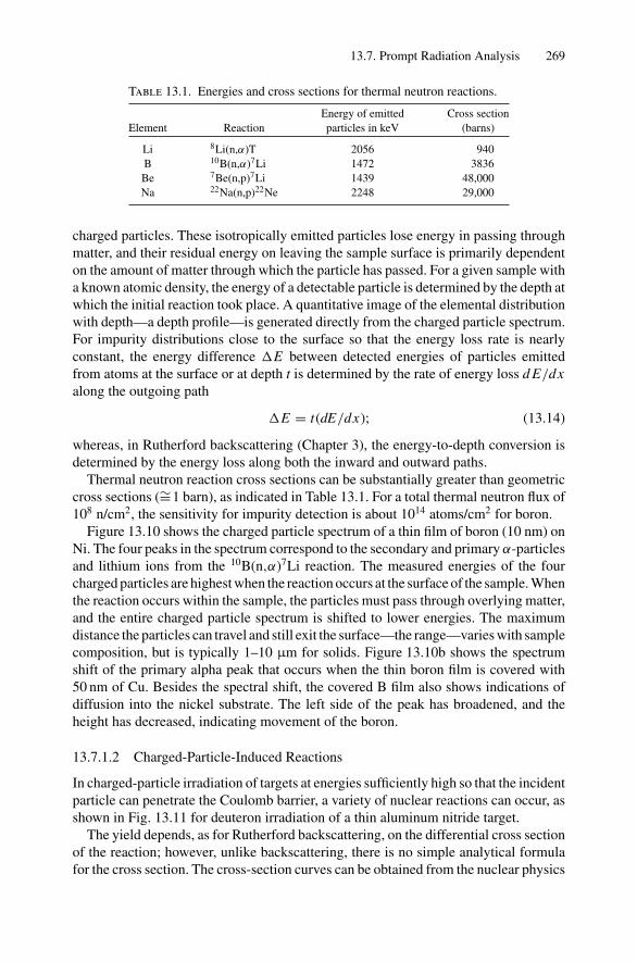
13.7. Prompt Radiation Analysis 269
Table 13.1. Energies and cross sections for thermal neutron reactions.
Energy of emitted Cross sectionElement Reaction particles in keV (barns)
Li 8Li(n,α)T 2056 940B 10B(n,α)7Li 1472 3836Be 7Be(n,p)7Li 1439 48,000Na 22Na(n,p)22Ne 2248 29,000
charged particles. These isotropically emitted particles lose energy in passing throughmatter, and their residual energy on leaving the sample surface is primarily dependenton the amount of matter through which the particle has passed. For a given sample witha known atomic density, the energy of a detectable particle is determined by the depth atwhich the initial reaction took place. A quantitative image of the elemental distributionwith depth—a depth profile—is generated directly from the charged particle spectrum.For impurity distributions close to the surface so that the energy loss rate is nearlyconstant, the energy difference E between detected energies of particles emittedfrom atoms at the surface or at depth t is determined by the rate of energy loss d E/dxalong the outgoing path
E = t(dE/dx); (13.14)
whereas, in Rutherford backscattering (Chapter 3), the energy-to-depth conversion isdetermined by the energy loss along both the inward and outward paths.
Thermal neutron reaction cross sections can be substantially greater than geometriccross sections (∼=1 barn), as indicated in Table 13.1. For a total thermal neutron flux of108 n/cm2, the sensitivity for impurity detection is about 1014 atoms/cm2 for boron.
Figure 13.10 shows the charged particle spectrum of a thin film of boron (10 nm) onNi. The four peaks in the spectrum correspond to the secondary and primary α-particlesand lithium ions from the 10B(n,α)7Li reaction. The measured energies of the fourcharged particles are highest when the reaction occurs at the surface of the sample. Whenthe reaction occurs within the sample, the particles must pass through overlying matter,and the entire charged particle spectrum is shifted to lower energies. The maximumdistance the particles can travel and still exit the surface—the range—varies with samplecomposition, but is typically 1–10 µm for solids. Figure 13.10b shows the spectrumshift of the primary alpha peak that occurs when the thin boron film is covered with50 nm of Cu. Besides the spectral shift, the covered B film also shows indications ofdiffusion into the nickel substrate. The left side of the peak has broadened, and theheight has decreased, indicating movement of the boron.
13.7.1.2 Charged-Particle-Induced Reactions
In charged-particle irradiation of targets at energies sufficiently high so that the incidentparticle can penetrate the Coulomb barrier, a variety of nuclear reactions can occur, asshown in Fig. 13.11 for deuteron irradiation of a thin aluminum nitride target.
The yield depends, as for Rutherford backscattering, on the differential cross sectionof the reaction; however, unlike backscattering, there is no simple analytical formulafor the cross section. The cross-section curves can be obtained from the nuclear physics
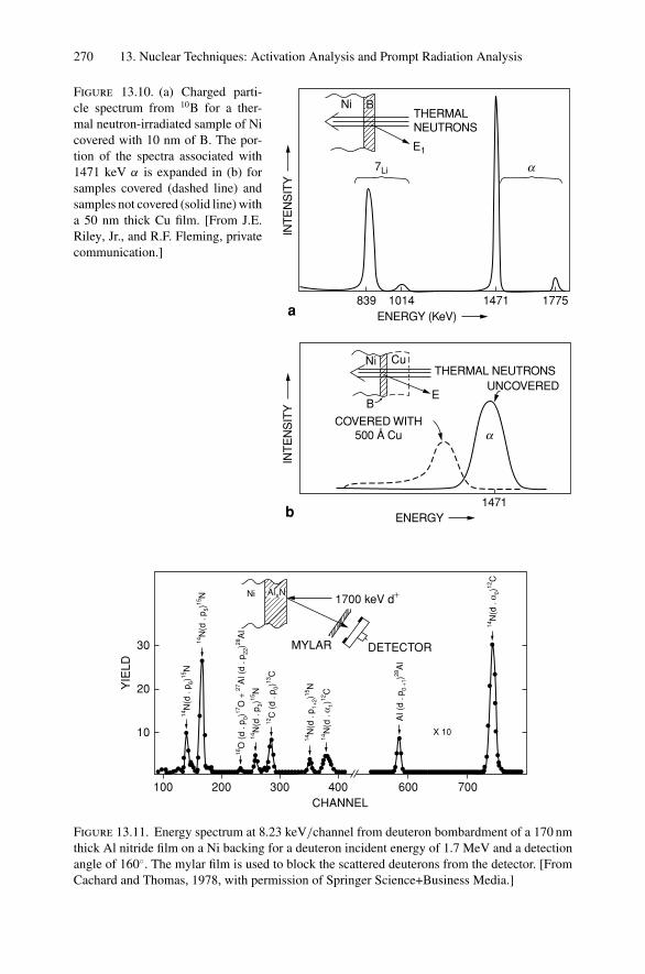
270 13. Nuclear Techniques: Activation Analysis and Prompt Radiation Analysis
ENERGY
COVERED WITH500 Å Cu
THERMAL NEUTRONS
THERMALNEUTRONS
1471
a
b
ENERGY (KeV)
INT
EN
SIT
YIN
TE
NS
ITY
a
a
Ni
Ni
Cu
BE
UNCOVERED
1471 17751014839
7Li
E1
BFigure 13.10. (a) Charged parti-cle spectrum from 10B for a ther-mal neutron-irradiated sample of Nicovered with 10 nm of B. The por-tion of the spectra associated with1471 keV α is expanded in (b) forsamples covered (dashed line) andsamples not covered (solid line) witha 50 nm thick Cu film. [From J.E.Riley, Jr., and R.F. Fleming, privatecommunication.]
10
20
30
YIE
LD
100 200 300 400 600 700CHANNEL
AlXNNi 1700 keV d+
DETECTORMYLAR
14N
(d .
p 6)15
N14
N(d
. p 5)
15N
14N
(d .
p 1+2)
15N
14N
(d .
α 0)12
C
14N
(d .
α 1)12
C
14N
(d .
p 3)15
N
16O
(d
. p0)
17O
+ 27
Al (
d . p
22)28
AI
12C
(d
. p0)
13C
AI (
d . p
0+1
)28A
l
X 10
Figure 13.11. Energy spectrum at 8.23 keV/channel from deuteron bombardment of a 170 nmthick Al nitride film on a Ni backing for a deuteron incident energy of 1.7 MeV and a detectionangle of 160. The mylar film is used to block the scattered deuterons from the detector. [FromCachard and Thomas, 1978, with permission of Springer Science+Business Media.]
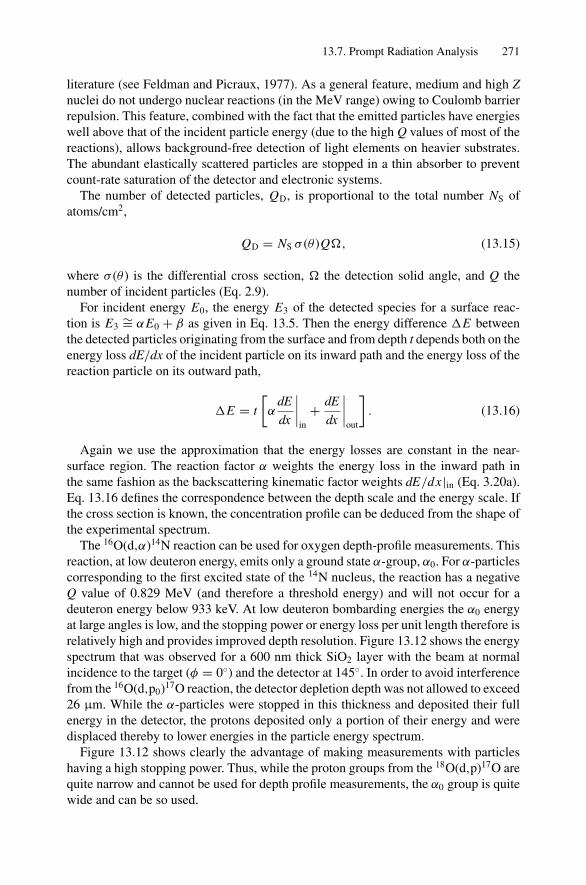
13.7. Prompt Radiation Analysis 271
literature (see Feldman and Picraux, 1977). As a general feature, medium and high Znuclei do not undergo nuclear reactions (in the MeV range) owing to Coulomb barrierrepulsion. This feature, combined with the fact that the emitted particles have energieswell above that of the incident particle energy (due to the high Q values of most of thereactions), allows background-free detection of light elements on heavier substrates.The abundant elastically scattered particles are stopped in a thin absorber to preventcount-rate saturation of the detector and electronic systems.
The number of detected particles, QD, is proportional to the total number NS ofatoms/cm2,
QD = NS σ (θ )Q, (13.15)
where σ (θ ) is the differential cross section, the detection solid angle, and Q thenumber of incident particles (Eq. 2.9).
For incident energy E0, the energy E3 of the detected species for a surface reac-tion is E3
∼= αE0 + β as given in Eq. 13.5. Then the energy difference E betweenthe detected particles originating from the surface and from depth t depends both on theenergy loss dE/dx of the incident particle on its inward path and the energy loss of thereaction particle on its outward path,
E = t
[α
dE
dx
∣∣∣∣in
+ dE
dx
∣∣∣∣out
]. (13.16)
Again we use the approximation that the energy losses are constant in the near-surface region. The reaction factor α weights the energy loss in the inward path inthe same fashion as the backscattering kinematic factor weights dE/dx |in (Eq. 3.20a).Eq. 13.16 defines the correspondence between the depth scale and the energy scale. Ifthe cross section is known, the concentration profile can be deduced from the shape ofthe experimental spectrum.
The 16O(d,α)14N reaction can be used for oxygen depth-profile measurements. Thisreaction, at low deuteron energy, emits only a ground state α-group, α0. For α-particlescorresponding to the first excited state of the 14N nucleus, the reaction has a negativeQ value of 0.829 MeV (and therefore a threshold energy) and will not occur for adeuteron energy below 933 keV. At low deuteron bombarding energies the α0 energyat large angles is low, and the stopping power or energy loss per unit length therefore isrelatively high and provides improved depth resolution. Figure 13.12 shows the energyspectrum that was observed for a 600 nm thick SiO2 layer with the beam at normalincidence to the target (φ = 0) and the detector at 145. In order to avoid interferencefrom the 16O(d,p0)17O reaction, the detector depletion depth was not allowed to exceed26 µm. While the α-particles were stopped in this thickness and deposited their fullenergy in the detector, the protons deposited only a portion of their energy and weredisplaced thereby to lower energies in the particle energy spectrum.
Figure 13.12 shows clearly the advantage of making measurements with particleshaving a high stopping power. Thus, while the proton groups from the 18O(d,p)17O arequite narrow and cannot be used for depth profile measurements, the α0 group is quitewide and can be so used.
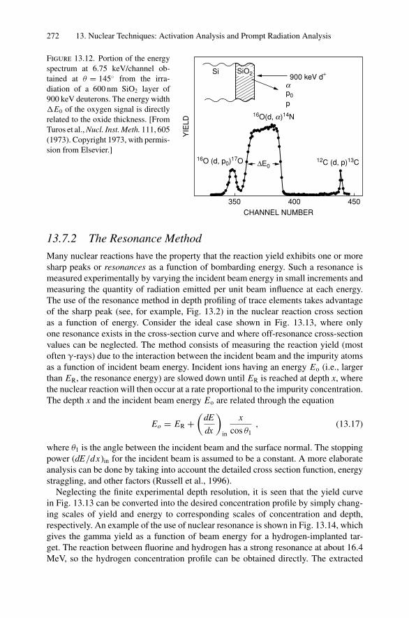
272 13. Nuclear Techniques: Activation Analysis and Prompt Radiation Analysis
900 keV d+
a
pp0
Si
16O(d, a)14N
350 400 450
CHANNEL NUMBER
YIE
LD
16O (d, p0)17O ∆E012C (d, p)13C
SiO2
Figure 13.12. Portion of the energyspectrum at 6.75 keV/channel ob-tained at θ = 145 from the irra-diation of a 600 nm SiO2 layer of900 keV deuterons. The energy widthE0 of the oxygen signal is directlyrelated to the oxide thickness. [FromTuros et al., Nucl. Inst. Meth. 111, 605(1973). Copyright 1973, with permis-sion from Elsevier.]
13.7.2 The Resonance Method
Many nuclear reactions have the property that the reaction yield exhibits one or moresharp peaks or resonances as a function of bombarding energy. Such a resonance ismeasured experimentally by varying the incident beam energy in small increments andmeasuring the quantity of radiation emitted per unit beam influence at each energy.The use of the resonance method in depth profiling of trace elements takes advantageof the sharp peak (see, for example, Fig. 13.2) in the nuclear reaction cross sectionas a function of energy. Consider the ideal case shown in Fig. 13.13, where onlyone resonance exists in the cross-section curve and where off-resonance cross-sectionvalues can be neglected. The method consists of measuring the reaction yield (mostoften γ-rays) due to the interaction between the incident beam and the impurity atomsas a function of incident beam energy. Incident ions having an energy Eo (i.e., largerthan ER, the resonance energy) are slowed down until ER is reached at depth x, wherethe nuclear reaction will then occur at a rate proportional to the impurity concentration.The depth x and the incident beam energy Eo are related through the equation
Eo = ER +(
dE
dx
)in
x
cos θ1, (13.17)
where θ1 is the angle between the incident beam and the surface normal. The stoppingpower (dE/dx)in for the incident beam is assumed to be a constant. A more elaborateanalysis can be done by taking into account the detailed cross section function, energystraggling, and other factors (Russell et al., 1996).
Neglecting the finite experimental depth resolution, it is seen that the yield curvein Fig. 13.13 can be converted into the desired concentration profile by simply chang-ing scales of yield and energy to corresponding scales of concentration and depth,respectively. An example of the use of nuclear resonance is shown in Fig. 13.14, whichgives the gamma yield as a function of beam energy for a hydrogen-implanted tar-get. The reaction between fluorine and hydrogen has a strong resonance at about 16.4MeV, so the hydrogen concentration profile can be obtained directly. The extracted
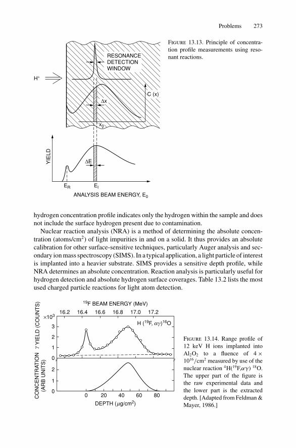
Problems 273
∆x
∆E
C (x)
ER El
x0
H+
ANALYSIS BEAM ENERGY, E0
YIE
LDRESONANCEDETECTIONWINDOW
Figure 13.13. Principle of concentra-tion profile measurements using reso-nant reactions.
hydrogen concentration profile indicates only the hydrogen within the sample and doesnot include the surface hydrogen present due to contamination.
Nuclear reaction analysis (NRA) is a method of determining the absolute concen-tration (atoms/cm2) of light impurities in and on a solid. It thus provides an absolutecalibration for other surface-sensitive techniques, particularly Auger analysis and sec-ondary ion mass spectroscopy (SIMS). In a typical application, a light particle of interestis implanted into a heavier substrate. SIMS provides a sensitive depth profile, whileNRA determines an absolute concentration. Reaction analysis is particularly useful forhydrogen detection and absolute hydrogen surface coverages. Table 13.2 lists the mostused charged particle reactions for light atom detection.
3
2
2
1
1
0
00 20 40 60 80
DEPTH (mg/cm2)
16.2 16.4 16.6 16.8 17.0 17.2
19F BEAM ENERGY (MeV)
CO
NC
EN
TR
ATIO
N(A
RB
UN
ITS
)γ
YIE
LD (
CO
UN
TS
)
×103
H (19F, aγ)16O
Figure 13.14. Range profile of12 keV H ions implanted intoAl2O2 to a fluence of 4 ×10¹⁶/cm2 measured by use of thenuclear reaction 4H(19F,αγ) 18O.The upper part of the figure isthe raw experimental data andthe lower part is the extracteddepth. [Adapted from Feldman &Mayer, 1986.]
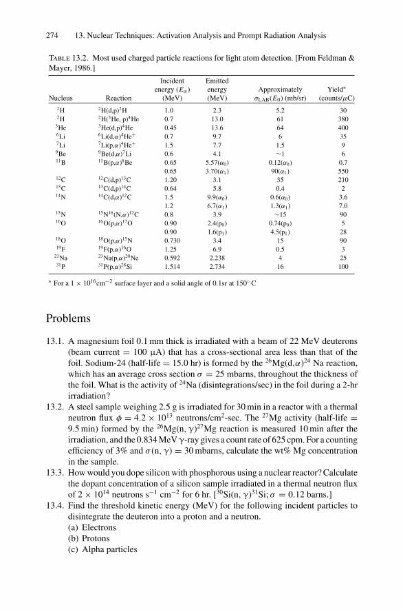
274 13. Nuclear Techniques: Activation Analysis and Prompt Radiation Analysis
Table 13.2. Most used charged particle reactions for light atom detection. [From Feldman &Mayer, 1986.]
Incident Emittedenergy (Eα) energy Approximately Yield∗
Nucleus Reaction (MeV) (MeV) σLAB(E0) (mb/sr) (counts/µC)2H 2H(d,p)2H 1.0 2.3 5.2 302H 2H(3He, p)4He 0.7 13.0 61 380
3He 3He(d,p)4He 0.45 13.6 64 4006Li 6Li(d,α)4He+ 0.7 9.7 6 357Li 7Li(p,α)4He+ 1.5 7.7 1.5 99Be 9Be(d,α)7Li 0.6 4.1 ∼1 611B 11B(p,α)8Be 0.65 5.57(α0) 0.12(α0) 0.7
0.65 3.70(α1) 90(α1) 55012C 12C(d,p)13C 1.20 3.1 35 21013C 13C(d,p)14C 0.64 5.8 0.4 214N 14C(d,α)12C 1.5 9.9(α0) 0.6(α0) 3.6
1.2 6.7(α1) 1.3(α1) 7.015N 15N16(N,α)12C 0.8 3.9 ∼15 9016O 16O(p,α)17O 0.90 2.4(p0) 0.74(p0) 5
0.90 1.6(p1) 4.5(p1) 2818O 18O(p,α)15N 0.730 3.4 15 9019F 19F(p,α)16O 1.25 6.9 0.5 3
23Na 23Na(p,α)20Ne 0.592 2.238 4 2531P 31P(p,α)28Si 1.514 2.734 16 100
∗ For a 1 × 1016cm−2 surface layer and a solid angle of 0.1sr at 150 C
Problems
13.1. A magnesium foil 0.1 mm thick is irradiated with a beam of 22 MeV deuterons(beam current = 100 µA) that has a cross-sectional area less than that of thefoil. Sodium-24 (half-life = 15.0 hr) is formed by the 26Mg(d,α)24 Na reaction,which has an average cross section σ = 25 mbarns, throughout the thickness ofthe foil. What is the activity of 24Na (disintegrations/sec) in the foil during a 2-hrirradiation?
13.2. A steel sample weighing 2.5 g is irradiated for 30 min in a reactor with a thermalneutron flux φ = 4.2 × 10¹³ neutrons/cm2-sec. The 27Mg activity (half-life =9.5 min) formed by the 26Mg(n, γ)27Mg reaction is measured 10 min after theirradiation, and the 0.834 MeV γ-ray gives a count rate of 625 cpm. For a countingefficiency of 3% and σ (n, γ) = 30 mbarns, calculate the wt% Mg concentrationin the sample.
13.3. How would you dope silicon with phosphorous using a nuclear reactor? Calculatethe dopant concentration of a silicon sample irradiated in a thermal neutron fluxof 2 × 10¹⁴ neutrons s−1 cm−2 for 6 hr. [30Si(n, γ)31Si; σ = 0.12 barns.]
13.4. Find the threshold kinetic energy (MeV) for the following incident particles todisintegrate the deuteron into a proton and a neutron.(a) Electrons(b) Protons(c) Alpha particles
Problems 275
13.5. A thin 8.0 mg foil of 113Cd is exposed to a flux of thermal neutrons. How many114Cd nuclei are formed? φn = 1.6 × 10¹³ n/cm2-s, the irradiation time is 2 hr,and σ (n, γ) = 2 × 10⁴ barns.
13.6. Compare proton backscattering and 15N(p,α)12C reactions from one monolayerof nitrogen atoms (1015 N/cm2) on a carbon substrate.(a) For backscattering with 0.8 MeV protons through 180 with a detector solid
angle of 0.01 str, calculate the yield (assuming pure Rutherford scattering,Eq. 2.17).
(b) Compare the RBS yield with the nuclear reaction yield (Table 13.2) for thesame detector.
(c) What are the relative advantages of the two techniques?13.7. The geometrical cross section for a reaction is given by σgeom = π R2, where R is
the nuclear radius and the distance of closest approach d equals Z1 Z2e2/E .(a) Calculate these values for 1 MeV p,d and α-particles incident on 14N.(b) Compare the values of the geometrical cross section with the Rutherford scat-
tering cross sections for 1 MeV particles (θ = 180) and with the 15N(p, α)and 14N(d, α) cross sections deduced from Table 13.2.
(c) Do these values give support to the rule of thumb that the onset of nuclearreactions occurs when the particles penetrate the Coulomb barrier?
13.8. Compare the depth scales in eV/nm for detection of F in an Al thin film withRBS for 3 MeV 4He ions incident (θ = 180) and for the 19F(p,α) reaction with1.25 MeV protons.
13.9. For X(a,b)Y resonant nuclear reactions, there is an inverse reaction a(X,Y)b. Ifthe energy of the resonance at Ea is known, what is EX in terms of Ea and themasses of the reactants? Evaluate your answer using energy values for 19F(p,α)in Table 13.2 compared with those for 1H(F,α) in Fig. 13.14.
References
1. A. Cachard and J. P. Thomas, “Microanalysis by Direct Observation of Nuclear Reactions,”in Material Characterization Using Ion Beams, J. P. Thomas and A. Cachard, Eds. (PlenumPress, New York, 1978).
2. G. R. Choppin and J. Ryaberg, Nuclear Chemistry (Pergamon Press, Oxford, 1980).3. R. D. Evans, The Atomic Nucleus (McGraw-Hill Book Co., New York, 1955).4. F. Everling, L. A. Koenig, J. H. E. Mattauch, and A. H. Wapstra, “Consistent Set of Ener-
gies Liberated in Nuclear Reaction,” 1960 Nuclear Data Tables (U.S. Government PrintingOffice, Washington, DC, 1961).
5. L. C. Feldman and J. W. Mayer, Fundamentals of Surface and Thin Film Analysis (Prentice-Hall, New Jersey, 1986)
6. L. C. Feldman and S. T. Picraux, “Selected Low Energy Nuclear Reaction Data,” in IonBeam Handbook for Material Analysis, J. W. Mayer and E. Rimini, Eds. (Academic Press,New York, 1977).
7. G. Friedlander, J. W. Kennedy, and J. M. Miller, Nuclear and Radiochemistry (John Wileyand Sons, New York, 1964).
8. G. B. Harvey, Nuclear Chemistry (Prentice-Hall, Englewood Cliffs, NJ, 1965).9. I. Kaplan, Nuclear Physics (Addison-Wesley, Reading, MA, 1964).

276 13. Nuclear Techniques: Activation Analysis and Prompt Radiation Analysis
10. M. Lederer, J. M. Hollander, and I. Perlman, Table of Isotopes, 6th ed. (John Wiley andSons, New York, 1967).
11. W. E. Meyerhof, Elements of Nuclear Physics (McGraw-Hill Book Co., New York, 1967).12. P. A. Tipler, Modern Physics (Worth Publishers, New York, 1978).13. E. A. Wolicki, “References to Activation and Prompt Radiation Analysis: Material Analysis
by Means of Nuclear Reactions,” in New Uses of Ion Accelerators, J. F. Ziegler, Ed. (PlenumPress, New York, 1975), Chap. 3.
14. S. W. Russell, T. E. Levine, A. E. Bair, and T. L. Alford, “Guidelines to the Applica-tion of Nuclear Resonance to Quantitative Thin Film Analysis,” Nuclear Instruments andMethods B, vol 118, 201–205 (1996).
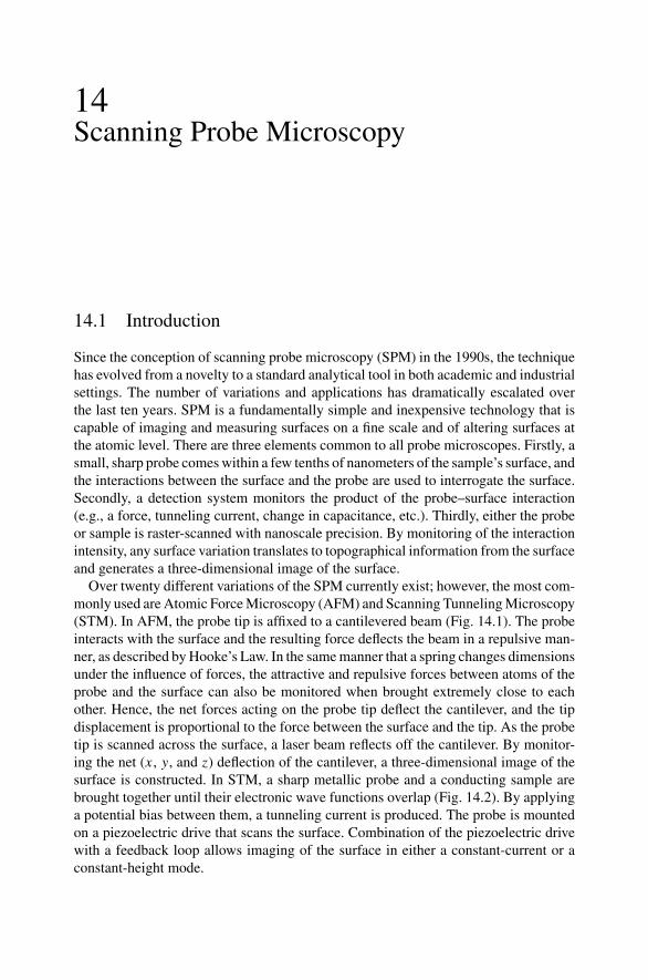
14Scanning Probe Microscopy
14.1 Introduction
Since the conception of scanning probe microscopy (SPM) in the 1990s, the techniquehas evolved from a novelty to a standard analytical tool in both academic and industrialsettings. The number of variations and applications has dramatically escalated overthe last ten years. SPM is a fundamentally simple and inexpensive technology that iscapable of imaging and measuring surfaces on a fine scale and of altering surfaces atthe atomic level. There are three elements common to all probe microscopes. Firstly, asmall, sharp probe comes within a few tenths of nanometers of the sample’s surface, andthe interactions between the surface and the probe are used to interrogate the surface.Secondly, a detection system monitors the product of the probe–surface interaction(e.g., a force, tunneling current, change in capacitance, etc.). Thirdly, either the probeor sample is raster-scanned with nanoscale precision. By monitoring of the interactionintensity, any surface variation translates to topographical information from the surfaceand generates a three-dimensional image of the surface.
Over twenty different variations of the SPM currently exist; however, the most com-monly used are Atomic Force Microscopy (AFM) and Scanning Tunneling Microscopy(STM). In AFM, the probe tip is affixed to a cantilevered beam (Fig. 14.1). The probeinteracts with the surface and the resulting force deflects the beam in a repulsive man-ner, as described by Hooke’s Law. In the same manner that a spring changes dimensionsunder the influence of forces, the attractive and repulsive forces between atoms of theprobe and the surface can also be monitored when brought extremely close to eachother. Hence, the net forces acting on the probe tip deflect the cantilever, and the tipdisplacement is proportional to the force between the surface and the tip. As the probetip is scanned across the surface, a laser beam reflects off the cantilever. By monitor-ing the net (x , y, and z) deflection of the cantilever, a three-dimensional image of thesurface is constructed. In STM, a sharp metallic probe and a conducting sample arebrought together until their electronic wave functions overlap (Fig. 14.2). By applyinga potential bias between them, a tunneling current is produced. The probe is mountedon a piezoelectric drive that scans the surface. Combination of the piezoelectric drivewith a feedback loop allows imaging of the surface in either a constant-current or aconstant-height mode.
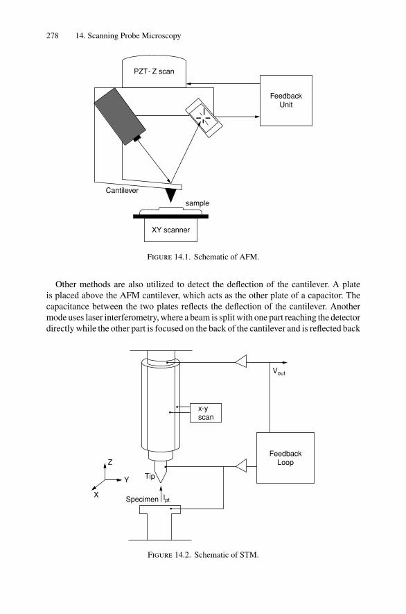
278 14. Scanning Probe Microscopy
FeedbackUnit
sample
XY scanner
Cantilever
PZT- Z scan
Figure 14.1. Schematic of AFM.
Other methods are also utilized to detect the deflection of the cantilever. A plateis placed above the AFM cantilever, which acts as the other plate of a capacitor. Thecapacitance between the two plates reflects the deflection of the cantilever. Anothermode uses laser interferometry, where a beam is split with one part reaching the detectordirectly while the other part is focused on the back of the cantilever and is reflected back
FeedbackLoop
x-yscan
Z
Y
X
Tip
Vout
Specimen lpt
Figure 14.2. Schematic of STM.
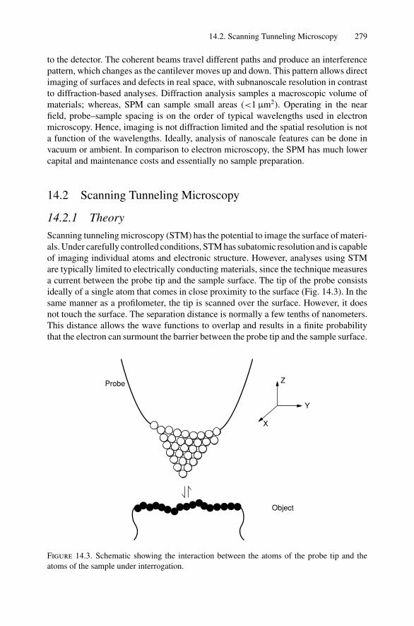
14.2. Scanning Tunneling Microscopy 279
to the detector. The coherent beams travel different paths and produce an interferencepattern, which changes as the cantilever moves up and down. This pattern allows directimaging of surfaces and defects in real space, with subnanoscale resolution in contrastto diffraction-based analyses. Diffraction analysis samples a macroscopic volume ofmaterials; whereas, SPM can sample small areas (<1 µm2). Operating in the nearfield, probe–sample spacing is on the order of typical wavelengths used in electronmicroscopy. Hence, imaging is not diffraction limited and the spatial resolution is nota function of the wavelengths. Ideally, analysis of nanoscale features can be done invacuum or ambient. In comparison to electron microscopy, the SPM has much lowercapital and maintenance costs and essentially no sample preparation.
14.2 Scanning Tunneling Microscopy
14.2.1 Theory
Scanning tunneling microscopy (STM) has the potential to image the surface of materi-als. Under carefully controlled conditions, STM has subatomic resolution and is capableof imaging individual atoms and electronic structure. However, analyses using STMare typically limited to electrically conducting materials, since the technique measuresa current between the probe tip and the sample surface. The tip of the probe consistsideally of a single atom that comes in close proximity to the surface (Fig. 14.3). In thesame manner as a profilometer, the tip is scanned over the surface. However, it doesnot touch the surface. The separation distance is normally a few tenths of nanometers.This distance allows the wave functions to overlap and results in a finite probabilitythat the electron can surmount the barrier between the probe tip and the sample surface.
Z
Y
X
Probe
Object
Figure 14.3. Schematic showing the interaction between the atoms of the probe tip and theatoms of the sample under interrogation.
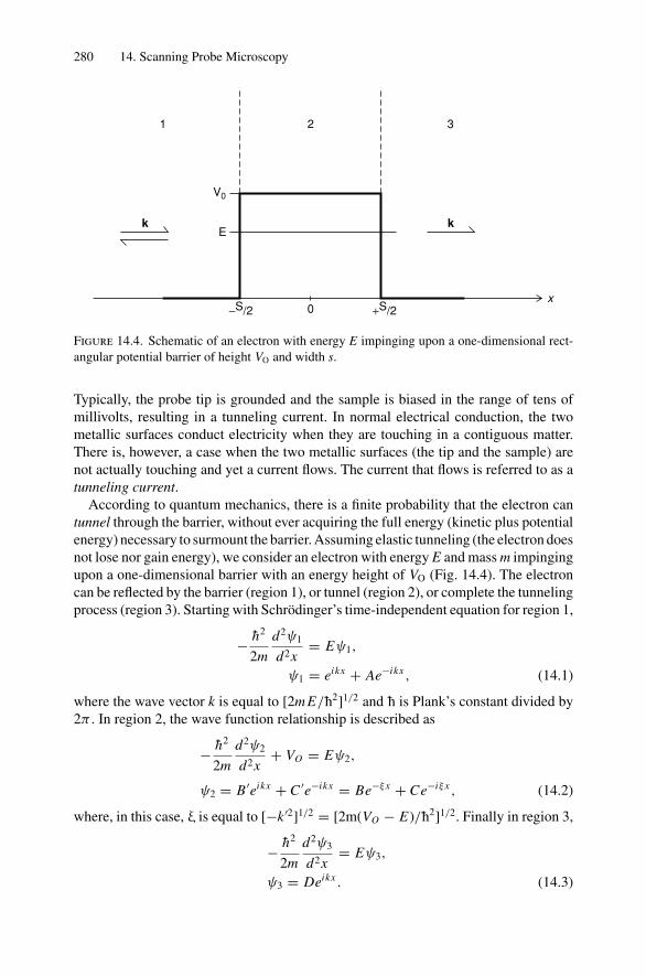
280 14. Scanning Probe Microscopy
0
2 31
E
V0
x
kk
−S/2 +S/2
Figure 14.4. Schematic of an electron with energy E impinging upon a one-dimensional rect-angular potential barrier of height VO and width s.
Typically, the probe tip is grounded and the sample is biased in the range of tens ofmillivolts, resulting in a tunneling current. In normal electrical conduction, the twometallic surfaces conduct electricity when they are touching in a contiguous matter.There is, however, a case when the two metallic surfaces (the tip and the sample) arenot actually touching and yet a current flows. The current that flows is referred to as atunneling current.
According to quantum mechanics, there is a finite probability that the electron cantunnel through the barrier, without ever acquiring the full energy (kinetic plus potentialenergy) necessary to surmount the barrier. Assuming elastic tunneling (the electron doesnot lose nor gain energy), we consider an electron with energy E and mass m impingingupon a one-dimensional barrier with an energy height of VO (Fig. 14.4). The electroncan be reflected by the barrier (region 1), or tunnel (region 2), or complete the tunnelingprocess (region 3). Starting with Schrodinger’s time-independent equation for region 1,
− h2
2m
d2ψ1
d2x= Eψ1,
ψ1 = eikx + Ae−ikx , (14.1)
where the wave vector k is equal to [2m E/h2]1/2 and h is Plank’s constant divided by2π . In region 2, the wave function relationship is described as
− h2
2m
d2ψ2
d2x+ VO = Eψ2,
ψ2 = B ′eikx + C ′e−ikx = Be−ξ x + Ce−iξ x , (14.2)
where, in this case, ξ is equal to [−k ′2]1/2 = [2m(VO − E)/h2]1/2. Finally in region 3,
− h2
2m
d2ψ3
d2x= Eψ3,
ψ3 = Deikx . (14.3)
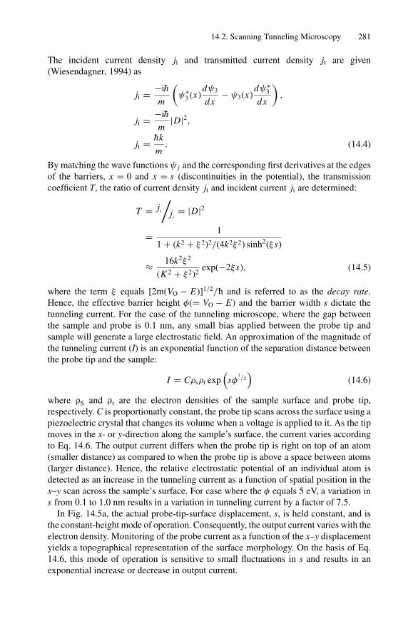
14.2. Scanning Tunneling Microscopy 281
The incident current density ji and transmitted current density jt are given(Wiesendagner, 1994) as
ji = −ih
m
(ψ∗
3 (x)dψ3
dx− ψ3(x)
dψ∗3
dx
),
ji = −ih
m|D|2,
jt = hk
m. (14.4)
By matching the wave functions ψ j and the corresponding first derivatives at the edgesof the barriers, x = 0 and x = s (discontinuities in the potential), the transmissioncoefficient T, the ratio of current density jt and incident current ji are determined:
T = jt
/ji
= |D|2
= 1
1 + (k2 + ξ 2)2/(4k2ξ 2) sinh2(ξs)
≈ 16k2ξ 2
(K 2 + ξ 2)2exp(−2ξs), (14.5)
where the term ξ equals [2m(VO − E)]1/2/h and is referred to as the decay rate.Hence, the effective barrier height φ(= VO − E) and the barrier width s dictate thetunneling current. For the case of the tunneling microscope, where the gap betweenthe sample and probe is 0.1 nm, any small bias applied between the probe tip andsample will generate a large electrostatic field. An approximation of the magnitude ofthe tunneling current (I) is an exponential function of the separation distance betweenthe probe tip and the sample:
I = Cρsρt exp(
sφ1/2
)(14.6)
where ρS and ρt are the electron densities of the sample surface and probe tip,respectively. C is proportionatly constant, the probe tip scans across the surface using apiezoelectric crystal that changes its volume when a voltage is applied to it. As the tipmoves in the x- or y-direction along the sample’s surface, the current varies accordingto Eq. 14.6. The output current differs when the probe tip is right on top of an atom(smaller distance) as compared to when the probe tip is above a space between atoms(larger distance). Hence, the relative electrostatic potential of an individual atom isdetected as an increase in the tunneling current as a function of spatial position in thex–y scan across the sample’s surface. For case where the φ equals 5 eV, a variation ins from 0.1 to 1.0 nm results in a variation in tunneling current by a factor of 7.5.
In Fig. 14.5a, the actual probe-tip-surface displacement, s, is held constant, and isthe constant-height mode of operation. Consequently, the output current varies with theelectron density. Monitoring of the probe current as a function of the x–y displacementyields a topographical representation of the surface morphology. On the basis of Eq.14.6, this mode of operation is sensitive to small fluctuations in s and results in anexponential increase or decrease in output current.
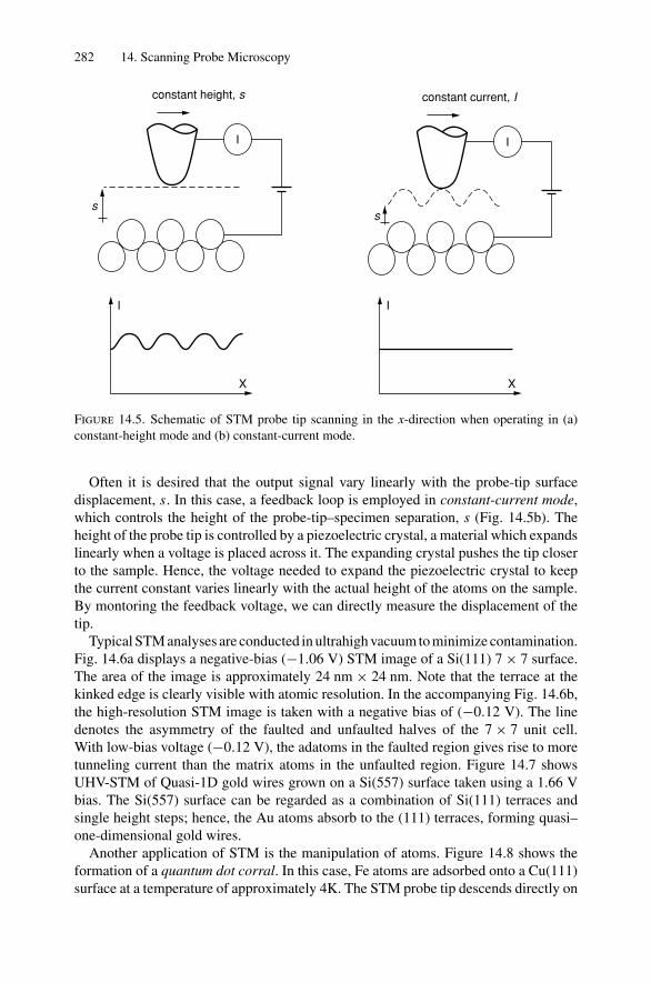
282 14. Scanning Probe Microscopy
I
constant height, s
s
I
constant current, I
s
I
X
I
X
Figure 14.5. Schematic of STM probe tip scanning in the x-direction when operating in (a)constant-height mode and (b) constant-current mode.
Often it is desired that the output signal vary linearly with the probe-tip surfacedisplacement, s. In this case, a feedback loop is employed in constant-current mode,which controls the height of the probe-tip–specimen separation, s (Fig. 14.5b). Theheight of the probe tip is controlled by a piezoelectric crystal, a material which expandslinearly when a voltage is placed across it. The expanding crystal pushes the tip closerto the sample. Hence, the voltage needed to expand the piezoelectric crystal to keepthe current constant varies linearly with the actual height of the atoms on the sample.By montoring the feedback voltage, we can directly measure the displacement of thetip.
Typical STM analyses are conducted in ultrahigh vacuum to minimize contamination.Fig. 14.6a displays a negative-bias (−1.06 V) STM image of a Si(111) 7 × 7 surface.The area of the image is approximately 24 nm × 24 nm. Note that the terrace at thekinked edge is clearly visible with atomic resolution. In the accompanying Fig. 14.6b,the high-resolution STM image is taken with a negative bias of (−0.12 V). The linedenotes the asymmetry of the faulted and unfaulted halves of the 7 × 7 unit cell.With low-bias voltage (−0.12 V), the adatoms in the faulted region gives rise to moretunneling current than the matrix atoms in the unfaulted region. Figure 14.7 showsUHV-STM of Quasi-1D gold wires grown on a Si(557) surface taken using a 1.66 Vbias. The Si(557) surface can be regarded as a combination of Si(111) terraces andsingle height steps; hence, the Au atoms absorb to the (111) terraces, forming quasi–one-dimensional gold wires.
Another application of STM is the manipulation of atoms. Figure 14.8 shows theformation of a quantum dot corral. In this case, Fe atoms are adsorbed onto a Cu(111)surface at a temperature of approximately 4K. The STM probe tip descends directly on
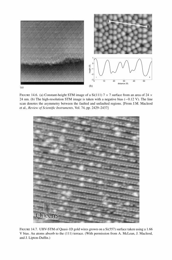
(a)
0
heig
ht (
Å)
1
0
−1
−2
−3i ii
10 20 30 40 50distance (Å)
(b)
Figure 14.6. (a) Constant-height STM image of a Si(111) 7 × 7 surface from an area of 24 ×24 nm. (b) The high-resolution STM image is taken with a negative bias (−0.12 V). The linescan denotes the asymmetry between the faulted and unfaulted regions. [From J.M. Macleodet al., Review of Scientific Instruments, Vol. 74, pp. 2429–2437]
Figure 14.7. UHV-STM of Quasi-1D gold wires grown on a Si(557) surface taken using a 1.66V bias. Au atoms absorb to the (111) terrace. (With permission from A. McLean, J. Macleod,and J. Lipton-Duffin.)
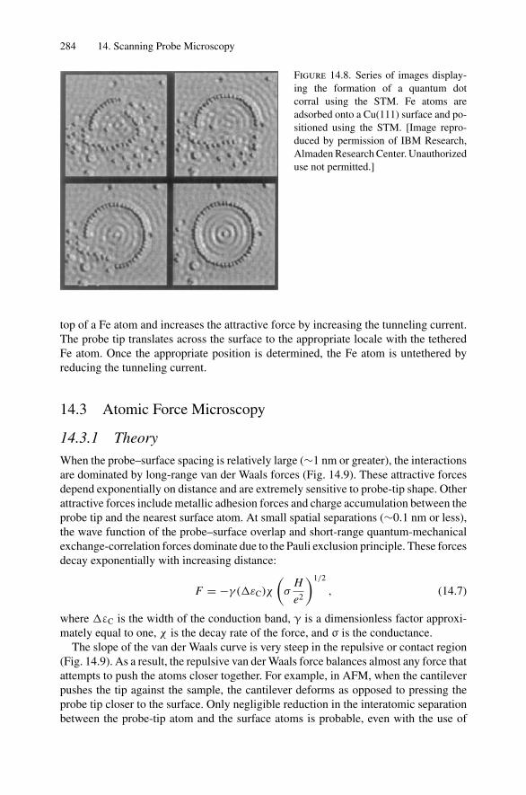
284 14. Scanning Probe Microscopy
Figure 14.8. Series of images display-ing the formation of a quantum dotcorral using the STM. Fe atoms areadsorbed onto a Cu(111) surface and po-sitioned using the STM. [Image repro-duced by permission of IBM Research,Almaden Research Center. Unauthorizeduse not permitted.]
top of a Fe atom and increases the attractive force by increasing the tunneling current.The probe tip translates across the surface to the appropriate locale with the tetheredFe atom. Once the appropriate position is determined, the Fe atom is untethered byreducing the tunneling current.
14.3 Atomic Force Microscopy
14.3.1 Theory
When the probe–surface spacing is relatively large (∼1 nm or greater), the interactionsare dominated by long-range van der Waals forces (Fig. 14.9). These attractive forcesdepend exponentially on distance and are extremely sensitive to probe-tip shape. Otherattractive forces include metallic adhesion forces and charge accumulation between theprobe tip and the nearest surface atom. At small spatial separations (∼0.1 nm or less),the wave function of the probe–surface overlap and short-range quantum-mechanicalexchange-correlation forces dominate due to the Pauli exclusion principle. These forcesdecay exponentially with increasing distance:
F = −γ (εC)χ
(σ
H
e2
)1/2
, (14.7)
where εC is the width of the conduction band, γ is a dimensionless factor approxi-mately equal to one, χ is the decay rate of the force, and σ is the conductance.
The slope of the van der Waals curve is very steep in the repulsive or contact region(Fig. 14.9). As a result, the repulsive van der Waals force balances almost any force thatattempts to push the atoms closer together. For example, in AFM, when the cantileverpushes the tip against the sample, the cantilever deforms as opposed to pressing theprobe tip closer to the surface. Only negligible reduction in the interatomic separationbetween the probe-tip atom and the surface atoms is probable, even with the use of
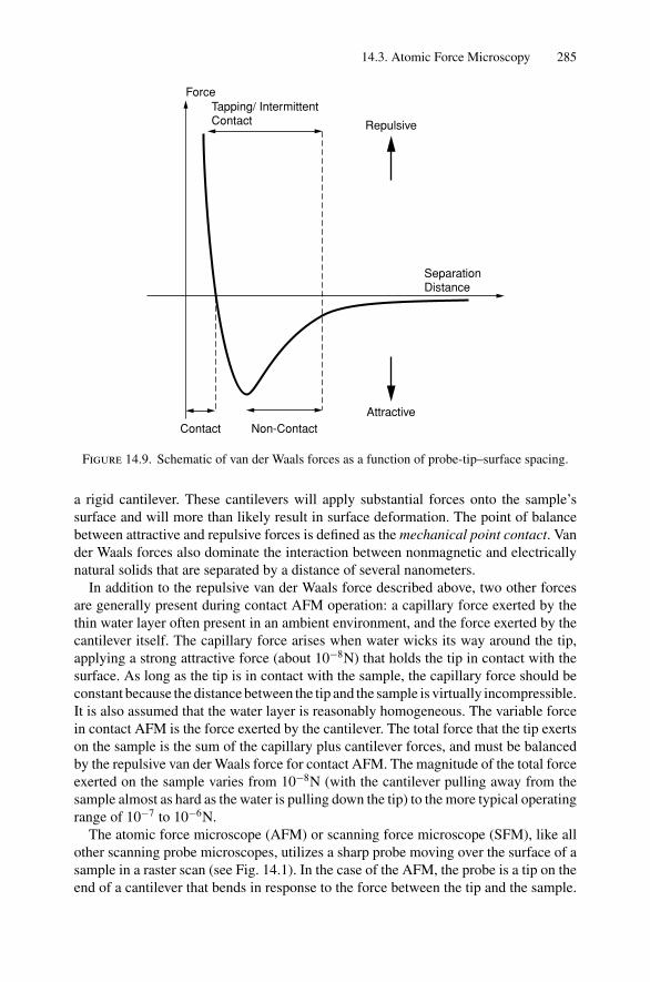
14.3. Atomic Force Microscopy 285
ForceTapping/ IntermittentContact Repulsive
SeparationDistance
AttractiveNon-ContactContact
Figure 14.9. Schematic of van der Waals forces as a function of probe-tip–surface spacing.
a rigid cantilever. These cantilevers will apply substantial forces onto the sample’ssurface and will more than likely result in surface deformation. The point of balancebetween attractive and repulsive forces is defined as the mechanical point contact. Vander Waals forces also dominate the interaction between nonmagnetic and electricallynatural solids that are separated by a distance of several nanometers.
In addition to the repulsive van der Waals force described above, two other forcesare generally present during contact AFM operation: a capillary force exerted by thethin water layer often present in an ambient environment, and the force exerted by thecantilever itself. The capillary force arises when water wicks its way around the tip,applying a strong attractive force (about 10−8N) that holds the tip in contact with thesurface. As long as the tip is in contact with the sample, the capillary force should beconstant because the distance between the tip and the sample is virtually incompressible.It is also assumed that the water layer is reasonably homogeneous. The variable forcein contact AFM is the force exerted by the cantilever. The total force that the tip exertson the sample is the sum of the capillary plus cantilever forces, and must be balancedby the repulsive van der Waals force for contact AFM. The magnitude of the total forceexerted on the sample varies from 10−8N (with the cantilever pulling away from thesample almost as hard as the water is pulling down the tip) to the more typical operatingrange of 10−7 to 10−6N.
The atomic force microscope (AFM) or scanning force microscope (SFM), like allother scanning probe microscopes, utilizes a sharp probe moving over the surface of asample in a raster scan (see Fig. 14.1). In the case of the AFM, the probe is a tip on theend of a cantilever that bends in response to the force between the tip and the sample.
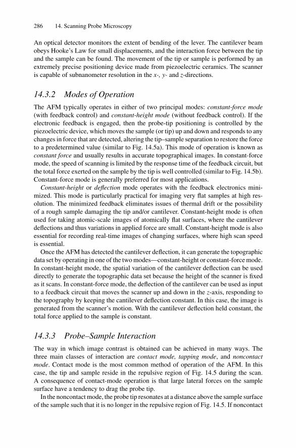
286 14. Scanning Probe Microscopy
An optical detector monitors the extent of bending of the lever. The cantilever beamobeys Hooke’s Law for small displacements, and the interaction force between the tipand the sample can be found. The movement of the tip or sample is performed by anextremely precise positioning device made from piezoelectric ceramics. The scanneris capable of subnanometer resolution in the x-, y- and z-directions.
14.3.2 Modes of Operation
The AFM typically operates in either of two principal modes: constant-force mode(with feedback control) and constant-height mode (without feedback control). If theelectronic feedback is engaged, then the probe-tip positioning is controlled by thepiezoelectric device, which moves the sample (or tip) up and down and responds to anychanges in force that are detected, altering the tip–sample separation to restore the forceto a predetermined value (similar to Fig. 14.5a). This mode of operation is known asconstant force and usually results in accurate topographical images. In constant-forcemode, the speed of scanning is limited by the response time of the feedback circuit, butthe total force exerted on the sample by the tip is well controlled (similar to Fig. 14.5b).Constant-force mode is generally preferred for most applications.
Constant-height or deflection mode operates with the feedback electronics mini-mized. This mode is particularly practical for imaging very flat samples at high res-olution. The minimized feedback eliminates issues of thermal drift or the possibilityof a rough sample damaging the tip and/or cantilever. Constant-height mode is oftenused for taking atomic-scale images of atomically flat surfaces, where the cantileverdeflections and thus variations in applied force are small. Constant-height mode is alsoessential for recording real-time images of changing surfaces, where high scan speedis essential.
Once the AFM has detected the cantilever deflection, it can generate the topographicdata set by operating in one of the two modes—constant-height or constant-force mode.In constant-height mode, the spatial variation of the cantilever deflection can be useddirectly to generate the topographic data set because the height of the scanner is fixedas it scans. In constant-force mode, the deflection of the cantilever can be used as inputto a feedback circuit that moves the scanner up and down in the z-axis, responding tothe topography by keeping the cantilever deflection constant. In this case, the image isgenerated from the scanner’s motion. With the cantilever deflection held constant, thetotal force applied to the sample is constant.
14.3.3 Probe–Sample Interaction
The way in which image contrast is obtained can be achieved in many ways. Thethree main classes of interaction are contact mode, tapping mode, and noncontactmode. Contact mode is the most common method of operation of the AFM. In thiscase, the tip and sample reside in the repulsive region of Fig. 14.5 during the scan.A consequence of contact-mode operation is that large lateral forces on the samplesurface have a tendency to drag the probe tip.
In the noncontact mode, the probe tip resonates at a distance above the sample surfaceof the sample such that it is no longer in the repulsive region of Fig. 14.5. If noncontact
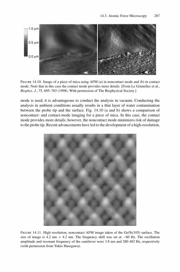
14.3. Atomic Force Microscopy 287
1.0 µm
0.5 µm
0.0 µm
Figure 14.10. Image of a piece of mica using AFM (a) in noncontact mode and (b) in contactmode. Note that in this case the contact mode provides more details. [From Le Grimellec et al.,Biophys. J., 75, 695–703 (1998). With permission of The Biophysical Society.]
mode is used, it is advantageous to conduct the analysis in vacuum. Conducting theanalysis in ambient conditions usually results in a thin layer of water contaminationbetween the probe tip and the surface. Fig. 14.10 (a and b) shows a comparison ofnoncontact- and contact-mode imaging for a piece of mica. In this case, the contactmode provides more details; however, the noncontact mode minimizes risk of damageto the probe tip. Recent advancements have led to the development of a high-resolution,
Figure 14.11. High resolution, noncontact AFM image taken of the Ge/Si(105) surface. Thesize of image is 4.2 nm × 4.2 nm. The frequency shift was set at −60 Hz. The oscillationamplitude and resonant frequency of the cantilever were 3.8 nm and 280 482 Hz, respectively(with permission from Yukio Hasegawa).
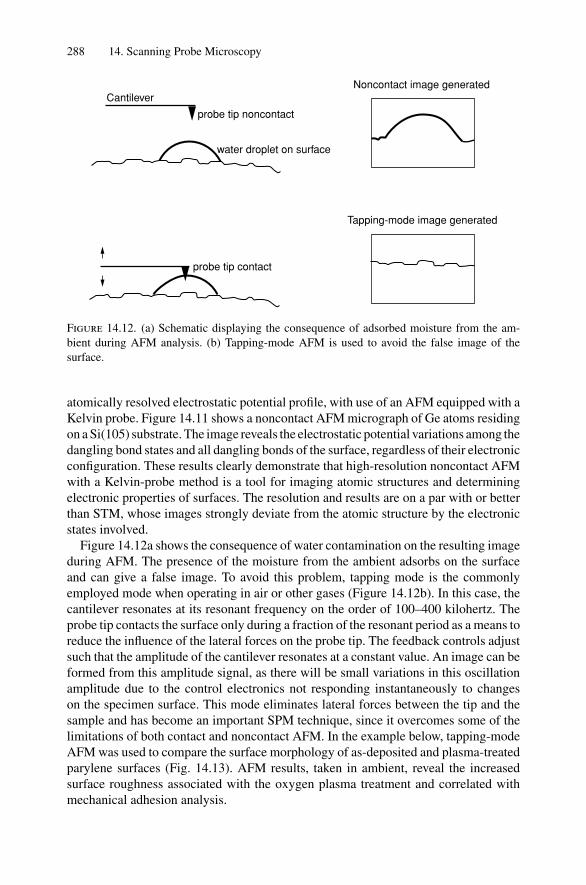
288 14. Scanning Probe Microscopy
probe tip noncontact
water droplet on surface
probe tip contact
Cantilever
Tapping-mode image generated
Noncontact image generated
Figure 14.12. (a) Schematic displaying the consequence of adsorbed moisture from the am-bient during AFM analysis. (b) Tapping-mode AFM is used to avoid the false image of thesurface.
atomically resolved electrostatic potential profile, with use of an AFM equipped with aKelvin probe. Figure 14.11 shows a noncontact AFM micrograph of Ge atoms residingon a Si(105) substrate. The image reveals the electrostatic potential variations among thedangling bond states and all dangling bonds of the surface, regardless of their electronicconfiguration. These results clearly demonstrate that high-resolution noncontact AFMwith a Kelvin-probe method is a tool for imaging atomic structures and determiningelectronic properties of surfaces. The resolution and results are on a par with or betterthan STM, whose images strongly deviate from the atomic structure by the electronicstates involved.
Figure 14.12a shows the consequence of water contamination on the resulting imageduring AFM. The presence of the moisture from the ambient adsorbs on the surfaceand can give a false image. To avoid this problem, tapping mode is the commonlyemployed mode when operating in air or other gases (Figure 14.12b). In this case, thecantilever resonates at its resonant frequency on the order of 100–400 kilohertz. Theprobe tip contacts the surface only during a fraction of the resonant period as a means toreduce the influence of the lateral forces on the probe tip. The feedback controls adjustsuch that the amplitude of the cantilever resonates at a constant value. An image can beformed from this amplitude signal, as there will be small variations in this oscillationamplitude due to the control electronics not responding instantaneously to changeson the specimen surface. This mode eliminates lateral forces between the tip and thesample and has become an important SPM technique, since it overcomes some of thelimitations of both contact and noncontact AFM. In the example below, tapping-modeAFM was used to compare the surface morphology of as-deposited and plasma-treatedparylene surfaces (Fig. 14.13). AFM results, taken in ambient, reveal the increasedsurface roughness associated with the oxygen plasma treatment and correlated withmechanical adhesion analysis.
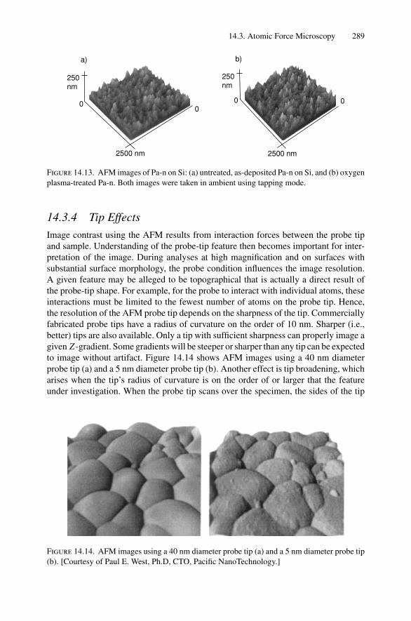
14.3. Atomic Force Microscopy 289
250nm
a)
0
2500 nm
0
250nm
b)
0
2500 nm
0
Figure 14.13. AFM images of Pa-n on Si: (a) untreated, as-deposited Pa-n on Si, and (b) oxygenplasma-treated Pa-n. Both images were taken in ambient using tapping mode.
14.3.4 Tip Effects
Image contrast using the AFM results from interaction forces between the probe tipand sample. Understanding of the probe-tip feature then becomes important for inter-pretation of the image. During analyses at high magnification and on surfaces withsubstantial surface morphology, the probe condition influences the image resolution.A given feature may be alleged to be topographical that is actually a direct result ofthe probe-tip shape. For example, for the probe to interact with individual atoms, theseinteractions must be limited to the fewest number of atoms on the probe tip. Hence,the resolution of the AFM probe tip depends on the sharpness of the tip. Commerciallyfabricated probe tips have a radius of curvature on the order of 10 nm. Sharper (i.e.,better) tips are also available. Only a tip with sufficient sharpness can properly image agiven Z -gradient. Some gradients will be steeper or sharper than any tip can be expectedto image without artifact. Figure 14.14 shows AFM images using a 40 nm diameterprobe tip (a) and a 5 nm diameter probe tip (b). Another effect is tip broadening, whicharises when the tip’s radius of curvature is on the order of or larger that the featureunder investigation. When the probe tip scans over the specimen, the sides of the tip
Figure 14.14. AFM images using a 40 nm diameter probe tip (a) and a 5 nm diameter probe tip(b). [Courtesy of Paul E. West, Ph.D, CTO, Pacific NanoTechnology.]
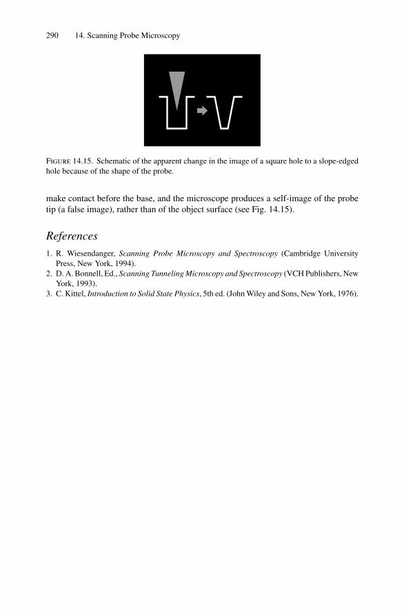
290 14. Scanning Probe Microscopy
Figure 14.15. Schematic of the apparent change in the image of a square hole to a slope-edgedhole because of the shape of the probe.
make contact before the base, and the microscope produces a self-image of the probetip (a false image), rather than of the object surface (see Fig. 14.15).
References
1. R. Wiesendanger, Scanning Probe Microscopy and Spectroscopy (Cambridge UniversityPress, New York, 1994).
2. D. A. Bonnell, Ed., Scanning Tunneling Microscopy and Spectroscopy (VCH Publishers, NewYork, 1993).
3. C. Kittel, Introduction to Solid State Physics, 5th ed. (John Wiley and Sons, New York, 1976).
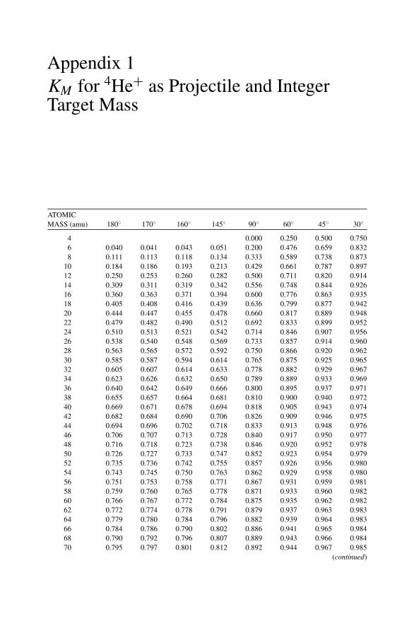
Appendix 1KM for 4He+ as Projectile and IntegerTarget Mass
ATOMICMASS (amu) 180 170 160 145 90 60 45 30
4 0.000 0.250 0.500 0.7506 0.040 0.041 0.043 0.051 0.200 0.476 0.659 0.8328 0.111 0.113 0.118 0.134 0.333 0.589 0.738 0.873
10 0.184 0.186 0.193 0.213 0.429 0.661 0.787 0.89712 0.250 0.253 0.260 0.282 0.500 0.711 0.820 0.91414 0.309 0.311 0.319 0.342 0.556 0.748 0.844 0.92616 0.360 0.363 0.371 0.394 0.600 0.776 0.863 0.93518 0.405 0.408 0.416 0.439 0.636 0.799 0.877 0.94220 0.444 0.447 0.455 0.478 0.660 0.817 0.889 0.94822 0.479 0.482 0.490 0.512 0.692 0.833 0.899 0.95224 0.510 0.513 0.521 0.542 0.714 0.846 0.907 0.95626 0.538 0.540 0.548 0.569 0.733 0.857 0.914 0.96028 0.563 0.565 0.572 0.592 0.750 0.866 0.920 0.96230 0.585 0.587 0.594 0.614 0.765 0.875 0.925 0.96532 0.605 0.607 0.614 0.633 0.778 0.882 0.929 0.96734 0.623 0.626 0.632 0.650 0.789 0.889 0.933 0.96936 0.640 0.642 0.649 0.666 0.800 0.895 0.937 0.97138 0.655 0.657 0.664 0.681 0.810 0.900 0.940 0.97240 0.669 0.671 0.678 0.694 0.818 0.905 0.943 0.97442 0.682 0.684 0.690 0.706 0.826 0.909 0.946 0.97544 0.694 0.696 0.702 0.718 0.833 0.913 0.948 0.97646 0.706 0.707 0.713 0.728 0.840 0.917 0.950 0.97748 0.716 0.718 0.723 0.738 0.846 0.920 0.952 0.97850 0.726 0.727 0.733 0.747 0.852 0.923 0.954 0.97952 0.735 0.736 0.742 0.755 0.857 0.926 0.956 0.98054 0.743 0.745 0.750 0.763 0.862 0.929 0.958 0.98056 0.751 0.753 0.758 0.771 0.867 0.931 0.959 0.98158 0.759 0.760 0.765 0.778 0.871 0.933 0.960 0.98260 0.766 0.767 0.772 0.784 0.875 0.935 0.962 0.98262 0.772 0.774 0.778 0.791 0.879 0.937 0.963 0.98364 0.779 0.780 0.784 0.796 0.882 0.939 0.964 0.98366 0.784 0.786 0.790 0.802 0.886 0.941 0.965 0.98468 0.790 0.792 0.796 0.807 0.889 0.943 0.966 0.98470 0.795 0.797 0.801 0.812 0.892 0.944 0.967 0.985
(continued)
292 Appendix 1
ATOMICMASS (amu) 180 170 160 145 90 60 45 30
72 0.801 0.802 0.806 0.817 0.895 0.946 0.968 0.98574 0.805 0.807 0.811 0.821 0.897 0.947 0.969 0.98676 0.810 0.811 0.815 0.826 0.900 0.949 0.970 0.98678 0.814 0.816 0.819 0.830 0.902 0.950 0.970 0.98680 0.819 0.820 0.824 0.834 0.905 0.951 0.971 0.98782 0.823 0.824 0.827 0.837 0.907 0.952 0.972 0.98784 0.826 0.828 0.831 0.841 0.909 0.953 0.972 0.98786 0.830 0.831 0.835 0.844 0.911 0.955 0.973 0.98888 0.834 0.835 0.838 0.847 0.913 0.956 0.974 0.98890 0.837 0.838 0.842 0.851 0.915 0.957 0.974 0.98892 0.840 0.841 0.845 0.854 0.917 0.957 0.975 0.98894 0.843 0.844 0.848 0.856 0.918 0.958 0.975 0.98996 0.846 0.847 0.851 0.859 0.920 0.959 0.976 0.98998 0.849 0.850 0.853 0.862 0.922 0.960 0.976 0.989
100 0.852 0.853 0.856 0.864 0.923 0.961 0.977 0.989102 0.855 0.856 0.859 0.867 0.925 0.962 0.977 0.990104 0.857 0.858 0.861 0.869 0.926 0.962 0.978 0.990106 0.860 0.861 0.864 0.872 0.927 0.963 0.978 0.990108 0.862 0.863 0.866 0.874 0.929 0.964 0.979 0.990110 0.865 0.866 0.868 0.876 0.930 0.964 0.979 0.990112 0.867 0.868 0.871 0.878 0.931 0.965 0.979 0.990114 0.869 0.870 0.873 0.880 0.932 0.966 0.980 0.991116 0.871 0.872 0.875 0.882 0.933 0.966 0.980 0.991118 0.873 0.874 0.877 0.884 0.934 0.967 0.980 0.991120 0.875 0.876 0.879 0.886 0.935 0.967 0.981 0.991122 0.877 0.878 0.881 0.888 0.937 0.968 0.981 0.991124 0.879 0.880 0.882 0.889 0.938 0.968 0.981 0.991126 0.881 0.882 0.884 0.891 0.938 0.969 0.982 0.992128 0.882 0.883 0.886 0.892 0.939 0.969 0.982 0.992130 0.884 0.885 0.887 0.894 0.940 0.970 0.982 0.992132 0.886 0.887 0.889 0.896 0.941 0.970 0.982 0.992134 0.887 0.888 0.891 0.897 0.942 0.971 0.983 0.992136 0.889 0.890 0.892 0.898 0.943 0.971 0.983 0.992138 0.890 0.891 0.894 0.900 0.944 0.971 0.983 0.992140 0.892 0.893 0.895 0.901 0.944 0.972 0.983 0.992142 0.893 0.894 0.896 0.903 0.945 0.972 0.984 0.992144 0.895 0.896 0.898 0.904 0.946 0.973 0.984 0.993146 0.896 0.897 0.899 0.905 0.947 0.973 0.984 0.993148 0.898 0.898 0.900 0.906 0.947 0.973 0.984 0.993150 0.899 0.900 0.902 0.908 0.948 0.974 0.984 0.993152 0.900 0.901 0.903 0.909 0.949 0.974 0.985 0.993154 0.901 0.902 0.904 0.910 0.949 0.974 0.985 0.993156 0.902 0.903 0.905 0.911 0.950 0.975 0.985 0.993158 0.904 0.904 0.906 0.912 0.951 0.975 0.985 0.993160 0.905 0.906 0.908 0.913 0.951 0.975 0.985 0.993162 0.906 0.907 0.909 0.914 0.952 0.976 0.986 0.993164 0.907 0.908 0.910 0.915 0.952 0.976 0.986 0.993166 0.908 0.909 0.911 0.916 0.953 0.976 0.986 0.994168 0.909 0.910 0.912 0.917 0.953 0.976 0.986 0.994170 0.910 0.911 0.913 0.918 0.954 0.977 0.986 0.994172 0.911 0.912 0.914 0.919 0.955 0.977 0.986 0.994
(continued)

KM for 4He+ as Projectile and Integer Target Mass 293
ATOMICMASS (amu) 180 170 160 145 90 60 45 30
174 0.912 0.913 0.915 0.920 0.955 0.977 0.987 0.994176 0.913 0.914 0.916 0.921 0.956 0.978 0.987 0.994178 0.914 0.915 0.917 0.921 0.956 0.978 0.987 0.994180 0.915 0.916 0.917 0.922 0.957 0.978 0.987 0.994182 0.916 0.916 0.918 0.923 0.957 0.978 0.987 0.994184 0.917 0.917 0.919 0.924 0.957 0.978 0.987 0.994186 0.918 0.918 0.920 0.925 0.958 0.979 0.987 0.994188 0.918 0.919 0.921 0.925 0.958 0.979 0.988 0.994190 0.919 0.920 0.922 0.926 0.959 0.979 0.988 0.994192 0.920 0.921 0.922 0.927 0.959 0.979 0.988 0.994194 0.921 0.921 0.923 0.928 0.960 0.980 0.988 0.994196 0.922 0.922 0.924 0.928 0.960 0.980 0.988 0.995198 0.922 0.923 0.925 0.929 0.960 0.980 0.988 0.995200 0.923 0.924 0.925 0.930 0.961 0.980 0.988 0.995
The Kinematic Factor, KM2 , defined by Eq. 2.5 for a 4He+ atom as projectile and integral atomic masses forthe target atom M2. The angle indicates the scattering angle as measured in the laboratory frame of reference.
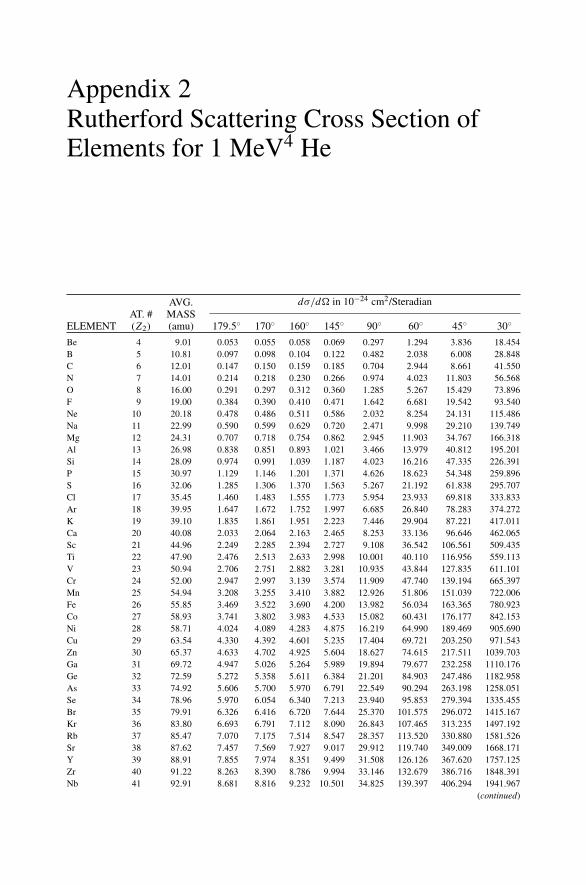
Appendix 2Rutherford Scattering Cross Section ofElements for 1 MeV4 He
dσ/d in 10−24 cm2/SteradianAVG.AT. # MASS
ELEMENT (Z2) (amu) 179.5 170 160 145 90 60 45 30
Be 4 9.01 0.053 0.055 0.058 0.069 0.297 1.294 3.836 18.454B 5 10.81 0.097 0.098 0.104 0.122 0.482 2.038 6.008 28.848C 6 12.01 0.147 0.150 0.159 0.185 0.704 2.944 8.661 41.550N 7 14.01 0.214 0.218 0.230 0.266 0.974 4.023 11.803 56.568O 8 16.00 0.291 0.297 0.312 0.360 1.285 5.267 15.429 73.896F 9 19.00 0.384 0.390 0.410 0.471 1.642 6.681 19.542 93.540Ne 10 20.18 0.478 0.486 0.511 0.586 2.032 8.254 24.131 115.486Na 11 22.99 0.590 0.599 0.629 0.720 2.471 9.998 29.210 139.749Mg 12 24.31 0.707 0.718 0.754 0.862 2.945 11.903 34.767 166.318Al 13 26.98 0.838 0.851 0.893 1.021 3.466 13.979 40.812 195.201Si 14 28.09 0.974 0.991 1.039 1.187 4.023 16.216 47.335 226.391P 15 30.97 1.129 1.146 1.201 1.371 4.626 18.623 54.348 259.896S 16 32.06 1.285 1.306 1.370 1.563 5.267 21.192 61.838 295.707Cl 17 35.45 1.460 1.483 1.555 1.773 5.954 23.933 69.818 333.833Ar 18 39.95 1.647 1.672 1.752 1.997 6.685 26.840 78.283 374.272K 19 39.10 1.835 1.861 1.951 2.223 7.446 29.904 87.221 417.011Ca 20 40.08 2.033 2.064 2.163 2.465 8.253 33.136 96.646 462.065Sc 21 44.96 2.249 2.285 2.394 2.727 9.108 36.542 106.561 509.435Ti 22 47.90 2.476 2.513 2.633 2.998 10.001 40.110 116.956 559.113V 23 50.94 2.706 2.751 2.882 3.281 10.935 43.844 127.835 611.101Cr 24 52.00 2.947 2.997 3.139 3.574 11.909 47.740 139.194 665.397Mn 25 54.94 3.208 3.255 3.410 3.882 12.926 51.806 151.039 722.006Fe 26 55.85 3.469 3.522 3.690 4.200 13.982 56.034 163.365 780.923Co 27 58.93 3.741 3.802 3.983 4.533 15.082 60.431 176.177 842.153Ni 28 58.71 4.024 4.089 4.283 4.875 16.219 64.990 189.469 905.690Cu 29 63.54 4.330 4.392 4.601 5.235 17.404 69.721 203.250 971.543Zn 30 65.37 4.633 4.702 4.925 5.604 18.627 74.615 217.511 1039.703Ga 31 69.72 4.947 5.026 5.264 5.989 19.894 79.677 232.258 1110.176Ge 32 72.59 5.272 5.358 5.611 6.384 21.201 84.903 247.486 1182.958As 33 74.92 5.606 5.700 5.970 6.791 22.549 90.294 263.198 1258.051Se 34 78.96 5.970 6.054 6.340 7.213 23.940 95.853 279.394 1335.455Br 35 79.91 6.326 6.416 6.720 7.644 25.370 101.575 296.072 1415.167Kr 36 83.80 6.693 6.791 7.112 8.090 26.843 107.465 313.235 1497.192Rb 37 85.47 7.070 7.175 7.514 8.547 28.357 113.520 330.880 1581.526Sr 38 87.62 7.457 7.569 7.927 9.017 29.912 119.740 349.009 1668.171Y 39 88.91 7.855 7.974 8.351 9.499 31.508 126.126 367.620 1757.125Zr 40 91.22 8.263 8.390 8.786 9.994 33.146 132.679 386.716 1848.391Nb 41 92.91 8.681 8.816 9.232 10.501 34.825 139.397 406.294 1941.967
(continued)
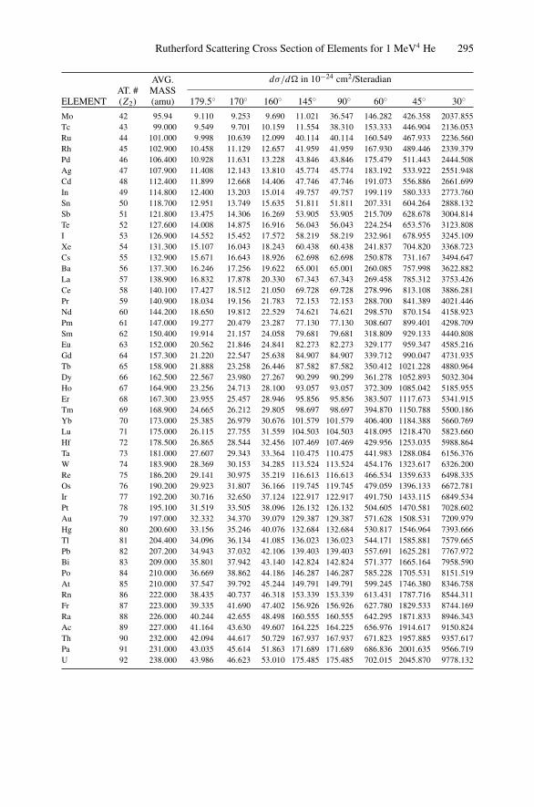
Rutherford Scattering Cross Section of Elements for 1 MeV4 He 295
dσ/d in 10−24 cm2/SteradianAVG.AT. # MASS
ELEMENT (Z2) (amu) 179.5 170 160 145 90 60 45 30
Mo 42 95.94 9.110 9.253 9.690 11.021 36.547 146.282 426.358 2037.855Tc 43 99.000 9.549 9.701 10.159 11.554 38.310 153.333 446.904 2136.053Ru 44 101.000 9.998 10.639 12.099 40.114 40.114 160.549 467.933 2236.560Rh 45 102.900 10.458 11.129 12.657 41.959 41.959 167.930 489.446 2339.379Pd 46 106.400 10.928 11.631 13.228 43.846 43.846 175.479 511.443 2444.508Ag 47 107.900 11.408 12.143 13.810 45.774 45.774 183.192 533.922 2551.948Cd 48 112.400 11.899 12.668 14.406 47.746 47.746 191.073 556.886 2661.699In 49 114.800 12.400 13.203 15.014 49.757 49.757 199.119 580.333 2773.760Sn 50 118.700 12.951 13.749 15.635 51.811 51.811 207.331 604.264 2888.132Sb 51 121.800 13.475 14.306 16.269 53.905 53.905 215.709 628.678 3004.814Te 52 127.600 14.008 14.875 16.916 56.043 56.043 224.254 653.576 3123.808I 53 126.900 14.552 15.452 17.572 58.219 58.219 232.961 678.955 3245.109Xe 54 131.300 15.107 16.043 18.243 60.438 60.438 241.837 704.820 3368.723Cs 55 132.900 15.671 16.643 18.926 62.698 62.698 250.878 731.167 3494.647Ba 56 137.300 16.246 17.256 19.622 65.001 65.001 260.085 757.998 3622.882La 57 138.900 16.832 17.878 20.330 67.343 67.343 269.458 785.312 3753.426Ce 58 140.100 17.427 18.512 21.050 69.728 69.728 278.996 813.108 3886.281Pr 59 140.900 18.034 19.156 21.783 72.153 72.153 288.700 841.389 4021.446Nd 60 144.200 18.650 19.812 22.529 74.621 74.621 298.570 870.154 4158.923Pm 61 147.000 19.277 20.479 23.287 77.130 77.130 308.607 899.401 4298.709Sm 62 150.400 19.914 21.157 24.058 79.681 79.681 318.809 929.133 4440.808Eu 63 152.000 20.562 21.846 24.841 82.273 82.273 329.177 959.347 4585.216Gd 64 157.300 21.220 22.547 25.638 84.907 84.907 339.712 990.047 4731.935Tb 65 158.900 21.888 23.258 26.446 87.582 87.582 350.412 1021.228 4880.964Dy 66 162.500 22.567 23.980 27.267 90.299 90.299 361.278 1052.893 5032.304Ho 67 164.900 23.256 24.713 28.100 93.057 93.057 372.309 1085.042 5185.955Er 68 167.300 23.955 25.457 28.946 95.856 95.856 383.507 1117.673 5341.915Tm 69 168.900 24.665 26.212 29.805 98.697 98.697 394.870 1150.788 5500.186Yb 70 173.000 25.385 26.979 30.676 101.579 101.579 406.400 1184.388 5660.769Lu 71 175.000 26.115 27.755 31.559 104.503 104.503 418.095 1218.470 5823.660Hf 72 178.500 26.865 28.544 32.456 107.469 107.469 429.956 1253.035 5988.864Ta 73 181.000 27.607 29.343 33.364 110.475 110.475 441.983 1288.084 6156.376W 74 183.900 28.369 30.153 34.285 113.524 113.524 454.176 1323.617 6326.200Re 75 186.200 29.141 30.975 35.219 116.613 116.613 466.534 1359.633 6498.335Os 76 190.200 29.923 31.807 36.166 119.745 119.745 479.059 1396.133 6672.781Ir 77 192.200 30.716 32.650 37.124 122.917 122.917 491.750 1433.115 6849.534Pt 78 195.100 31.519 33.505 38.096 126.132 126.132 504.605 1470.581 7028.602Au 79 197.000 32.332 34.370 39.079 129.387 129.387 571.628 1508.531 7209.979Hg 80 200.600 33.156 35.246 40.076 132.684 132.684 530.817 1546.964 7393.666Tl 81 204.400 34.096 36.134 41.085 136.023 136.023 544.171 1585.881 7579.665Pb 82 207.200 34.943 37.032 42.106 139.403 139.403 557.691 1625.281 7767.972Bi 83 209.000 35.801 37.942 43.140 142.824 142.824 571.377 1665.164 7958.590Po 84 210.000 36.669 38.862 44.186 146.287 146.287 585.228 1705.531 8151.519At 85 210.000 37.547 39.792 45.244 149.791 149.791 599.245 1746.380 8346.758Rn 86 222.000 38.435 40.737 46.318 153.339 153.339 613.431 1787.716 8544.311Fr 87 223.000 39.335 41.690 47.402 156.926 156.926 627.780 1829.533 8744.169Ra 88 226.000 40.244 42.655 48.498 160.555 160.555 642.295 1871.833 8946.343Ac 89 227.000 41.164 43.630 49.607 164.225 164.225 656.976 1914.617 9150.824Th 90 232.000 42.094 44.617 50.729 167.937 167.937 671.823 1957.885 9357.617Pa 91 231.000 43.035 45.614 51.863 171.689 171.689 686.836 2001.635 9566.719U 92 238.000 43.986 46.623 53.010 175.485 175.485 702.015 2045.870 9778.132
App
endi
x3
4 He+
Stop
ping
Cro
ssSe
ctio
ns
Ato
mN
o.40
060
080
010
0012
0014
0016
0018
0020
0024
0028
0032
0036
0040
00
H1
14.0
214
.11
13.5
12.4
911
.34
10.1
99.
154
8.28
97.
606
6.75
6.08
15.
534
5.10
84.
683
He
216
.72
17.8
818
.03
17.5
216
.63
15.5
614
.46
13.4
412
.52
11.1
210
.02
9.11
78.
416
7.71
4L
i3
22.2
821
.99
21.4
620
.64
19.6
18.4
217
.28
16.2
415
.35
13.6
312
.311
.22
10.3
39.
587
Be
427
.09
26.7
625
.89
24.7
123
.422
.06
20. 8
19.6
518
.64
16.5
514
.93
13.6
112
.61
11.6
8B
532
.633
.49
32.6
731
.27
29.4
827
.59
25.7
424
.122
.720
.09
18.0
916
.51
15.2
214
.14
C6
33.3
236
.58
37.2
136
.19
34.2
731
.99
29.7
227
.68
25.9
723
.120
.818
.99
17.5
916
.36
N7
46.2
348
.45
48.1
246
.24
43.5
440
.58
37.7
135
.15
32.9
829
.39
26.6
824
.45
22.6
21.0
5O
844
.34
47.7
248
.39
47.3
445
.29
42.8
140
.27
37.9
135
.84
32.3
929
.54
27.2
125
.18
23.5
5F
940
.07
43.9
945
.66
45.7
344
.76
43.1
541
.24
39.2
437
.31
34.4
431
.79
29.4
627
.45
25.7
5N
e10
39.3
243
.59
45.5
445
.86
45.1
43.6
841
.92
40.0
638
.24
35.7
933
.56
31.5
529
.66
27.9
9N
a11
42.0
244
.08
44.9
544
.88
44.2
443
.14
41.9
640
.73
39.5
636
.57
34.0
431
.86
29.9
528
.24
Mg
1256
.04
57.2
656
.78
55.2
653
.21
50.9
948
.82
46.8
545
.11
41.5
738
.67
36.2
34.1
632
.33
Al
1355
.39
54.8
653
.81
52.4
350
.85
49.1
847
.545
.85
44.2
540
.38
37.3
834
.96
32.9
231
.08
Si14
70.1
571
.09
69.4
466
.362
.558
.62
55.0
251
.88
49.2
644
.71
41.2
738
.44
36.1
134
.09
P15
64.6
668
.45
67.5
765
.13
62.0
658
.88
55.8
753
.08
50.6
745
.88
42.1
739
.14
36.6
634
.55
S16
62.1
268
.61
69.7
267
.75
64.7
261
.48
58.3
755
.41
52.8
947
.81
43.8
840
.68
38.0
635
.83
Cl
1783
.26
86.5
84.9
680
.68
75.1
869
.52
64.3
660
.04
56.6
551
.15
46.9
843
.53
40.6
838
.34
Ar
1883
.61
88.7
87.8
283
.47
77.5
271
.27
65.5
660
.81
57.1
351
.75
47.5
644
.07
41.1
838
.79
K19
83.1
689
.08
90.6
188
.88
85.5
680
.68
75.6
170
.84
66.6
460
.13
54.9
750
.847
.36
44.4
5C
a20
93.7
897
.397
.14
94.4
790
.585
.61
80.5
875
.64
71.1
964
.19
58.6
354
.150
.37
47.2
1Sc
2192
.58
96.2
796
.393
.86
90.4
285
.73
81.1
276
.65
72.5
365
.71
60.1
755
.651
. 848
.58
Ti
2291
.07
95.4
195
.76
93.5
489
.87
85.5
581
.14
77.0
73.3
167
.61
62.5
658
.04
54.1
750
.84
V23
86.1
990
.13
90.5
588
.785
.58
81.8
978
.13
74.6
71.4
566
.28
61.7
557
.64
53.9
550
.79
Cr
2479
.42
84.8
186
.62
85.9
783
.76
80.6
877
.24
73.7
870
.51
66.1
662
.13
58.5
455
.17
52.1
2M
n25
77.0
882
.69
84.4
83.6
81.3
578
.41
75.3
72.3
669
.72
65.2
961
.39
58.0
154
.85
52
4He+ Stopping Cross Sections 297A
tom
No.
400
600
800
1000
1200
1400
1600
1800
2000
2400
2800
3200
3600
4000
Fe26
80.1
586
.989
.26
88.6
486
.13
82.5
978
.65
74.7
171
.05
66.5
762
.86
59.5
956
.64
54.0
2C
o27
72.1
179
.07
82.0
482
.29
80.8
278
.38
75.5
72.5
569
.75
65.5
62.0
158
.96
56.2
353
.73
Ni
2868
.29
74.6
77.7
478
.66
78.0
776
.56
74.5
472
.370
.04
66.0
61.0
56.5
552
.64
49.9
4C
u29
62.4
168
.271
.77
73.5
874
.05
73.5
72.2
470
.51
68.4
864
.962
.059
.34
56.9
154
.72
Zn
3065
.53
70.4
772
.85
73.4
772
.98
71.7
169
.97
68.1
266
.04
62.2
559
.06
56.3
553
.91
51.7
7G
a31
74.2
378
.12
79.4
179
.12
77.7
975
.86
73.6
71.2
568
.82
64.4
660
.89
57.9
155
.29
53G
e32
77.7
681
.982
.76
82.1
80.2
677
.76
75.1
872
.46
69.8
65.0
861
.25
58.1
55.3
853
.02
As
3381
.41
87.0
387
.98
87.0
284
.84
82.0
179
.14
75.9
773
.05
67.8
563
.66
60.2
457
.32
54.8
Se34
83.2
89.4
89.8
87.8
84.9
81.6
78.4
75.3
72.4
67.0
662
.88
59.4
356
.553
.99
Br
3595
.55
101.
110
1.1
97.9
193
.04
87.7
82.6
578
.29
74.7
569
.06
64.6
450
.96
57.9
55.1
7K
r36
102.
210
8.2
108
104.
298
.67
92.7
487
.26
82.6
679
.04
63.0
468
.14
64.2
160
.94
58R
b37
98.1
810
8.3
110.
110
7.4
102.
697
.34
92.4
87.6
783
.47
76.5
171
.01
66.5
962
.85
59.7
Sr38
109
117
117.
411
4.2
109
103.
197
.75
92.5
687
.93
80.3
74.2
69.5
165
.46
62.0
4Y
3911
012
0.4
121.
111
7.3
111.
610
5.5
99.6
93.9
88.8
84.3
577
.65
72.1
167
.92
64.3
7Z
r40
115.
412
612
6.8
123.
211
7.9
112
106.
210
0.7
97.5
87.6
481
.02
75.7
271
.267
.44
Nb
4111
8.1
128.
212
8.7
125.
111
9.8
114
108.
410
398
.190
.26
83.6
678
.21
73.6
669
.88
Mo
4210
9.8
120.
512
2.2
119.
611
5.1
110
104.
899
.88
95.2
188
.09
81.8
676
.49
72.0
168
.18
Tc
4311
612
6.8
128.
912
6.3
121.
211
5.4
109.
210
3.3
97.8
590
.14
83.5
878
.09
73.4
369
.48
Ru
4410
4.1
116.
812
0.5
119.
511
611
1.3
105.
810
0.7
95.8
689
.05
82.9
577
.71
73.2
169
.35
Rh
4510
0.9
113.
611
7.7
117.
211
3.9
109.
510
4.6
99.8
595
.42
89.2
183
.44
78.3
373
.87
70.0
3Pd
4689
.09
104.
911
1.9
112.
911
0.3
105.
810
0.5
95.3
290
.65
86.2
681
.88
77.7
263
.77
70.0
4A
g47
88.6
310
1.9
108.
411
0.2
108.
810
5.4
100.
996
.02
91.2
286
.66
82.5
478
.53
73.9
868
.91
Cd
4896
.33
107
112
113
111.
410
8.1
103.
899
.24
94.7
189
.47
84.8
180
.43
76.3
172
.53
In49
104.
311
0.1
113.
711
5.2
114.
811
2.7
109.
310
510
0.0
94.4
689
.985
.69
81.8
178
.17
Sn50
108.
211
5.8
118.
611
8.3
115.
811
2.1
107.
910
3.6
99.4
993
.82
89.0
484
.81
81.1
477
.7Sb
5111
6.2
122.
212
2.2
119.
911
6.8
113.
311
010
6.8
103.
797
.58
92.4
588
.01
84.2
680
.61
Te52
121.
312
7.2
126.
512
3.4
119.
411
5.3
111.
210
7.4
103.
997
.592
.23
87.7
483
.82
80.3
4I
5313
514
1.7
141
135.
812
8.5
120.
611
3.2
106.
710
1.5
95.0
289
.84
85.3
181
.53
78.0
7X
e54
144.
714
9.7
148.
214
313
612
8.7
122
116.
211
1.5
104.
198
.28
93.2
689
.05
85.3
1C
s55
129.
714
1.5
143.
113
9.7
134.
412
8.7
123.
211
7.9
113.
110
598
.36
92.9
188
.36
84.2
9B
a56
141.
215
0.7
151.
414
7.4
141.
313
4.9
128.
712
2.9
117.
610
8.7
101.
695
.71
90.8
686
.53
La
5714
4.7
156.
515
6.9
152.
314
5.7
138.
613
1.7
125.
111
9.0
109.
910
2.6
96.7
191
.72
87.5
Ce
5813
6.4
146.
114
7.7
144.
513
9.1
133.
212
7.4
121.
811
6.7
108
101
95.2
290
.56
86.2
7(c
onti
nued
)
298 Appendix 3A
tom
No.
400
600
800
1000
1200
1400
1600
1800
2000
2400
2800
3200
3600
4000
Pr59
134.
114
3.8
145.
714
2.9
137.
813
2.2
126.
512
1.0
116.
010
7.5
100.
594
.84
90.2
786
.02
Nd
6013
1.9
141.
614
3.5
141
136.
513
112
5.5
120.
211
5.3
106.
999
.99
94.4
89.8
85.7
1Pm
6112
9.7
139.
414
1.4
139.
213
5.1
129.
812
4.4
119.
211
4.5
106.
299
.41
93.9
189
.35
85.3
5Sm
6212
7.7
137.
713
9.4
137.
413
3.2
128.
412
3.3
118.
311
3.6
105.
589
.893
.37
88.8
684
.96
Eu
6312
5.8
135.
613
7.4
135.
613
1.7
127.
112
2.1
117.
311
2.7
104.
798
.15
92.8
188
.34
84.5
3G
d64
130.
113
9.9
141.
713
9.9
135.
813
1.1
125.
812
0.8
116.
010
7.7
100.
895
.23
90.5
786
.59
Tb
6512
2.2
131.
713
3.6
132.
212
8.7
124.
511
9.7
115.
211
0.8
103.
196
.891
.62
87.2
483
.63
Dy
6611
1.5
123.
912
8.1
127.
912
5.4
121.
811
7.7
113.
510
9.5
102.
396
.491
.36
87.1
183
.41
Ho
6710
7.5
118.
412
2.4
122.
312
0.1
117
113.
210
9.5
105.
798
.56
92.7
187
.83
83.6
680
.21
Er
6810
6.1
116.
812
0.8
120.
711
8.6
115.
711
210
8.4
104.
897
.791
.98
87.1
783
.07
79.6
5T
m69
104.
711
5.2
119.
211
9.2
117.
211
4.1
110.
810
7.2
103.
796
.82
81.2
286
.46
82.4
379
.06
Yb
7010
3.5
113.
811
7.7
117.
811
5.9
113
109.
710
6.2
102.
996
.06
90.5
785
.87
81.8
978
.54
Lu
7110
6.3
116.
912
0.4
120.
211
8.1
115
111.
610
8.0
104.
597
.42
91.7
586
.89
82.7
979
.34
Hf
7210
9.7
120.
812
4.5
124.
312
2.2
118.
911
5.4
111.
610
8.0
100.
694
.789
.62
85.3
281
.72
Ta73
105.
811
7.5
121.
712
1.8
119.
811
6.7
113.
110
9.4
105.
698
.96
93.1
488
.484
.19
80.5
3W
7410
3.4
114.
211
811
8.2
116.
511
3.9
110.
910
7.6
104.
497
.87
92.1
787
.42
83.2
79.6
1R
e75
114.
412
5.8
129.
812
9.8
127.
312
4.1
120.
411
6.5
112.
710
5.2
98.9
793
.58
88.9
885
.12
Os
7611
2.5
124.
512
912
9.5
127.
312
4.3
120.
711
7.0
113.
310
699
.75
94.3
289
.69
85.7
9Ir
7711
0.7
123.
212
8.2
129.
312
7.3
124.
512
1.1
117.
711
4.0
106.
810
0.7
95.2
990
.62
86.6
7Pt
7810
3.1
117.
612
4.2
126.
212
5.6
123.
712
1.2
118.
211
5.0
108.
410
2.5
97.2
192
.688
.64
Au
7910
9.9
122.
712
812
9.1
127.
912
5.3
122.
311
8.9
115.
511
010
4.9
99.9
295
.42
91.3
9H
g80
103.
511
6.9
122.
712
4.2
123.
512
1.6
119.
211
6.3
113.
310
7 .1
101.
596
.45
91.9
87.9
5T
181
113.
412
512
9.5
130
128.
412
5.8
122.
911
9.6
116.
410
9.8
104.
098
.82
94.1
189
.99
Pb82
126.
413
8.1
141.
914
1.6
139.
113
5.9
132.
412
8.7
125.
011
7.7
111.
510
6.0
100.
996
.47
Bi
8312
4.6
136
139.
213
8.3
135.
413
1.9
128.
312
4.5
120.
811
3.6
107.
610
2.2
97.4
93.0
7Po
8412
7.3
140
143
141.
813
8.4
134.
613
0.6
126.
512
2.6
115.
210
9.0
103.
698
.76
94.3
8A
t85
128.
214
2.7
146.
114
5.1
141.
113
713
2.7
128.
512
4.4
116.
711
0.4
104.
910
0.0
95.6
Rn
8612
7.7
144.
414
8.7
147.
714
3.5
139.
213
4.7
130.
312
6.0
118.
111
1.7
106.
010
1.2
96.7
2Fr
8714
3.7
158.
216
0.9
158.
515
314
7.6
142.
213
7.0
132.
112
3.2
116.
010
9.9
104.
799
.92
Ra
8815
5.2
167.
816
9.8
166.
116
0.1
154
147.
914
2.1
136.
812
7.1
119.
411
2.9
107.
410
2.5
Ac
8915
8.1
171.
317
3.8
170
164.
115
7.6
151
144.
913
9.4
129.
212
1.3
114.
510
8.9
103.
9T
h90
159.
417
3.4
176.
617
3.2
167.
216
0.5
153.
714
7.4
141.
713
1.2
123.
011
6.0
110.
210
5.2
Pa91
153.
116
6.8
170.
416
816
2.8
156.
815
0.8
145.
013
9.5
129.
612
1.8
115.
110
9 .5
104.
7U
9215
0.7
164.
416
8.4
166.
616
1.9
156.
115
0.3
144.
613
9.3
129.
512
1.7
115.
210
9.7
105.
0
Appendix 4Electron Configurations and IonizationPotentials of Atoms
IonizationZ Element 1s 2s 2p 3s 3p 3d 4s 4p 4d 4f 5s 5p 5d 6s 6p 6d 7s potential (eV)
1 H 1 13.5952 He 2 24.5803 Li 2 1 5.3904 Be 2 2 9.3205 B 2 2 1 8.2966 C 2 2 2 11.2607 N 2 2 3 14.5328 O 2 2 4 13.6149 F 2 2 5 17.422
10 Ne 2 2 6 21.56411 Na 2 2 6 1 5.13812 Mg 2 2 6 2 7.64413 Al 2 2 6 2 1 5.98414 Si 2 2 6 2 2 8.14915 P 2 2 6 2 3 10.48616 S 2 2 6 2 4 10.35717 Cl 2 2 6 2 5 12.96718 Ar 2 2 6 2 6 15.75919 K 2 2 6 2 6 1 4.33920 Ca 2 2 6 2 6 2 6.11121 Sc 2 2 6 2 6 1 2 6.54022 Ti 2 2 6 2 6 2 2 6.28023 V 2 2 6 2 6 3 2 6.74024 Cr 2 2 6 2 6 5 1 6.76425 Mn 2 2 6 2 6 5 2 7.43226 Fe 2 2 6 2 6 6 2 7.87027 Co 2 2 6 2 6 7 2 7.86428 Ni 2 2 6 2 6 8 2 7.63329 Cu 2 2 6 2 6 10 1 7.72430 Zn 2 2 6 2 6 10 2 9.39131 Ga 2 2 6 2 6 10 2 1 6.0032 Ge 2 2 6 2 6 10 2 2 7.8833 As 2 2 6 2 6 10 2 3 9.8134 Se 2 2 6 2 6 10 2 4 9.7535 Br 2 2 6 2 6 10 2 5 11.84
(continued)
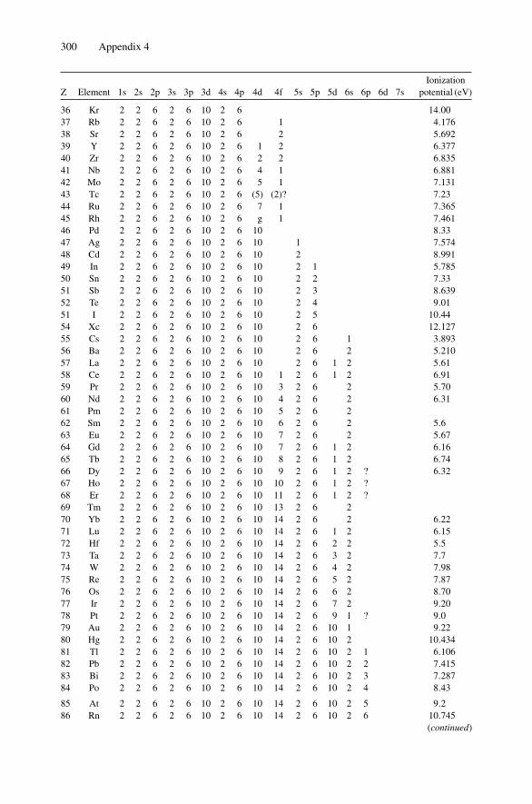
300 Appendix 4
IonizationZ Element 1s 2s 2p 3s 3p 3d 4s 4p 4d 4f 5s 5p 5d 6s 6p 6d 7s potential (eV)
36 Kr 2 2 6 2 6 10 2 6 14.0037 Rb 2 2 6 2 6 10 2 6 1 4.17638 Sr 2 2 6 2 6 10 2 6 2 5.69239 Y 2 2 6 2 6 10 2 6 1 2 6.37740 Zr 2 2 6 2 6 10 2 6 2 2 6.83541 Nb 2 2 6 2 6 10 2 6 4 1 6.88142 Mo 2 2 6 2 6 10 2 6 5 1 7.13143 Tc 2 2 6 2 6 10 2 6 (5) (2)? 7.2344 Ru 2 2 6 2 6 10 2 6 7 1 7.36545 Rh 2 2 6 2 6 10 2 6 g 1 7.46146 Pd 2 2 6 2 6 10 2 6 10 8.3347 Ag 2 2 6 2 6 10 2 6 10 1 7.57448 Cd 2 2 6 2 6 10 2 6 10 2 8.99149 In 2 2 6 2 6 10 2 6 10 2 1 5.78550 Sn 2 2 6 2 6 10 2 6 10 2 2 7.3351 Sb 2 2 6 2 6 10 2 6 10 2 3 8.63952 Te 2 2 6 2 6 10 2 6 10 2 4 9.0151 I 2 2 6 2 6 10 2 6 10 2 5 10.4454 Xc 2 2 6 2 6 10 2 6 10 2 6 12.12755 Cs 2 2 6 2 6 10 2 6 10 2 6 1 3.89356 Ba 2 2 6 2 6 10 2 6 10 2 6 2 5.21057 La 2 2 6 2 6 10 2 6 10 2 6 1 2 5.6158 Ce 2 2 6 2 6 10 2 6 10 1 2 6 1 2 6.9159 Pr 2 2 6 2 6 10 2 6 10 3 2 6 2 5.7060 Nd 2 2 6 2 6 10 2 6 10 4 2 6 2 6.3161 Pm 2 2 6 2 6 10 2 6 10 5 2 6 262 Sm 2 2 6 2 6 10 2 6 10 6 2 6 2 5.663 Eu 2 2 6 2 6 10 2 6 10 7 2 6 2 5.6764 Gd 2 2 6 2 6 10 2 6 10 7 2 6 1 2 6.1665 Tb 2 2 6 2 6 10 2 6 10 8 2 6 1 2 6.7466 Dy 2 2 6 2 6 10 2 6 10 9 2 6 1 2 ? 6.3267 Ho 2 2 6 2 6 10 2 6 10 10 2 6 1 2 ?68 Er 2 2 6 2 6 10 2 6 10 11 2 6 1 2 ?69 Tm 2 2 6 2 6 10 2 6 10 13 2 6 270 Yb 2 2 6 2 6 10 2 6 10 14 2 6 2 6.2271 Lu 2 2 6 2 6 10 2 6 10 14 2 6 1 2 6.1572 Hf 2 2 6 2 6 10 2 6 10 14 2 6 2 2 5.573 Ta 2 2 6 2 6 10 2 6 10 14 2 6 3 2 7.774 W 2 2 6 2 6 10 2 6 10 14 2 6 4 2 7.9875 Re 2 2 6 2 6 10 2 6 10 14 2 6 5 2 7.8776 Os 2 2 6 2 6 10 2 6 10 14 2 6 6 2 8.7077 Ir 2 2 6 2 6 10 2 6 10 14 2 6 7 2 9.2078 Pt 2 2 6 2 6 10 2 6 10 14 2 6 9 1 ? 9.079 Au 2 2 6 2 6 10 2 6 10 14 2 6 10 1 9.2280 Hg 2 2 6 2 6 10 2 6 10 14 2 6 10 2 10.43481 Tl 2 2 6 2 6 10 2 6 10 14 2 6 10 2 1 6.10682 Pb 2 2 6 2 6 10 2 6 10 14 2 6 10 2 2 7.41583 Bi 2 2 6 2 6 10 2 6 10 14 2 6 10 2 3 7.28784 Po 2 2 6 2 6 10 2 6 10 14 2 6 10 2 4 8.43
85 At 2 2 6 2 6 10 2 6 10 14 2 6 10 2 5 9.286 Rn 2 2 6 2 6 10 2 6 10 14 2 6 10 2 6 10.745
(continued)
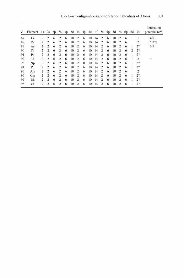
Electron Configurations and Ionization Potentials of Atoms 301
IonizationZ Element 1s 2s 2p 3s 3p 3d 4s 4p 4d 4f 5s 5p 5d 6s 6p 6d 7s potential (eV)
87 Fr 2 2 6 2 6 10 2 6 10 14 2 6 10 2 6 1 4.088 Ra 2 2 6 2 6 10 2 6 10 14 2 6 10 2 6 2 5.27789 Ac 2 2 6 2 6 10 2 6 10 14 2 6 10 2 6 1 2? 6.990 Th 2 2 6 2 6 10 2 6 10 14 2 6 10 2 6 2 2?91 Pa 2 2 6 2 6 10 2 6 10 14 2 6 10 2 6 1 2?92 U 2 2 6 2 6 10 2 6 10 14 2 6 10 2 6 1 2 493 Np 2 2 6 2 6 10 2 0 10 14 2 6 10 2 6 1 2?94 Pu 2 2 6 2 6 10 2 6 10 14 2 6 10 2 6 1 2?95 Am 2 2 6 2 6 10 2 6 10 14 2 6 10 2 6 296 Cm 2 2 6 2 6 10 2 6 10 14 2 6 10 2 6 1 2?97 Bk 2 2 6 2 6 10 2 6 10 14 2 6 10 2 6 1 2?98 Cf 2 2 6 2 6 10 2 6 10 14 2 6 10 2 6 1 2?
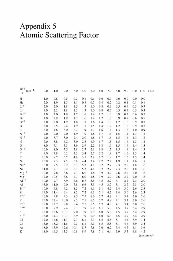
Appendix 5Atomic Scattering Factor
sin θ
λ(nm−1) 0.0 1.0 2.0 3.0 4.0 5.0 6.0 7.0 8.0 9.0 10.0 11.0 12.0
H 1.0 0.8 0.5 0.3 0.1 0.1 0.0 0.0 0.0 0.0 0.0 0.0He 2.0 1.9 1.5 1.1 0.8 0.5 0.4 0.2 0.2 0.1 0.1 0.1Li+ 2.0 2.0 1.8 1.5 1.3 1.0 0.8 0.6 0.5 0.4 0.3 0.3Li 3.0 2.2 1.8 1.5 1.3 1.0 0.8 0.6 0.5 0.4 0.3 0.3Be+2 2.0 2.0 1.9 1.7 1.6 1.4 1.2 1.0 0.9 0.7 0.6 0.5Be 4.0 2.9 1.9 1.7 1.6 1.4 1.2 1.0 0.9 0.7 0.6 0.5B+3 2.0 2.0 1.9 1.8 1.7 1.6 1.4 1.3 1.2 1.0 0.9 0.7B 5.0 3.5 2.4 1.9 1.7 1.5 1.4 1.2 1.2 1.0 0.9 0.7C 6.0 4.6 3.0 2.2 1.9 1.7 1.6 1.4 1.3 1.2 1.0 0.9N+5 2.0 2.0 2.0 1.9 1.9 1.8 1.7 1.6 1.5 1.4 1.3 1.2N+3 4.0 3.7 3.0 2.4 2.0 1.8 1.7 1.6 1.5 1.4 1.3 1.2N 7.0 5.8 4.2 3.0 2.3 1.9 1.7 1.5 1.5 1.4 1.3 1.2O 8.0 7.1 5.3 3.9 2.9 2.2 1.8 1.6 1.5 1.4 1.4 1.3O−2 10.0 8.0 5.5 3.8 2.7 2.1 1.8 1.5 1.5 1.4 1.4 1.3F 9.0 7.8 6.2 4.5 3.4 2.7 2.2 1.9 1.7 1.6 1.5 1.4F 10.0 8.7 6.7 4.8 3.5 2.8 2.2 1.9 1.7 1.6 1.5 1.4Ne 10.0 9.3 7.5 5.8 4.4 3.4 2.7 2.2 1.9 1.7 1.6 1.5Na+ 10.0 9.5 8.2 6.7 5.3 4.1 3.2 2.7 2.3 2.0 1.8 1.6Na 11.0 9.7 8.2 6.7 5.3 4.1 3.2 2.7 2.3 2.0 1.8 1.6Mg+2 10.0 9.8 8.6 7.3 6.0 4.8 3.9 3.2 2.6 2.2 2.0 1.8Mg 12.0 10.5 8.6 7.3 6.0 4.8 3.9 3.2 2.6 2.2 2.0 1.8AI+3 10.0 9.7 8.9 7.8 6.7 5.5 4.5 3.7 3.1 2.7 2.3 2.0Al 13.0 11.0 9.0 7.8 6.6 5.5 4.5 3.7 3.1 2.7 2.3 2.0Si+4 10.0 9.8 9.2 8.3 7.2 6.1 5.1 4.2 3.4 3.0 2.6 2.3Si 14.0 11.4 9.4 8.2 7.2 6.1 5.1 4.2 3.4 3.0 2.6 2.3P+5 10.0 9.8 9.3 8.5 7.5 6.6 5.7 4.8 4.1 3.4 3.0 2.6P 15.0 12.4 10.0 8.5 7.5 6.5 5.7 4.8 4.1 3.4 3.0 2.6P−3 18.0 12.7 9.8 8.4 7.5 6.5 5.7 4.9 4.1 3.4 3.0 2.6S+6 10.0 9.9 9.4 8.7 7.9 6.9 6.1 5.3 4.5 3.9 3.4 2.9S 16.0 13.6 10.7 9.0 7.9 6.9 6.0 5.3 4.5 3.9 3.4 2.9S−2 18.0 14.3 10.7 8.9 7.9 6.9 6.0 5.3 4.5 3.9 3.4 2.9CI 17.0 14.6 11.3 9.3 8.1 7.3 6.5 5.8 5.1 4.4 3.9 3.4Cl− 18.0 15.2 11.5 9.3 8.1 7.3 6.5 5.8 5.1 4.4 3.9 3.4Ar 18.0 15.9 12.6 10.4 8.7 7.8 7.0 6.2 5.4 4.7 4.1 3.6K+ 18.0 16.5 13.3 10.8 8.9 7.8 7.1 6.4 5.9 5.3 4.8 4.2
(continued)
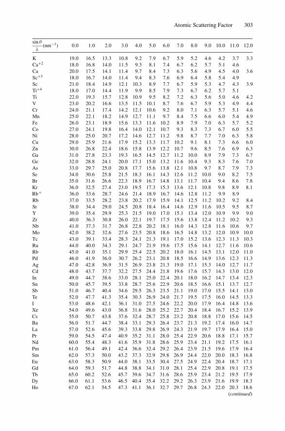
Atomic Scattering Factor 303
sin θ
λ(nm−1) 0.0 1.0 2.0 3.0 4.0 5.0 6.0 7.0 8.0 9.0 10.0 11.0 12.0
K 19.0 16.5 13.3 10.8 9.2 7.9 6.7 5.9 5.2 4.6 4.2 3.7 3.3Ca+2 18.0 16.8 14.0 11.5 9.3 8.1 7.4 6.7 6.2 5.7 5.1 4.6Ca 20.0 17.5 14.1 11.4 9.7 8.4 7.3 6.3 5.6 4.9 4.5 4.0 3.6Sc+3 18.0 16.7 14.0 11.4 9.4 8.3 7.6 6.9 6.4 5.8 5.4 4.9Sc 21.0 18.4 14.9 12.1 10.3 8.9 7.7 6.7 5.9 5.3 4.7 4.3 3.9Ti+4 18.0 17.0 14.4 11.9 9.9 8.5 7.9 7.3 6.7 6.2 5.7 5.1Ti 22.0 19.3 15.7 12.8 10.9 9.5 8.2 7.2 6.3 5.6 5.0 4.6 4.2V 23.0 20.2 16.6 13.5 11.5 10.1 8.7 7.6 6.7 5.9 5.3 4.9 4.4Cr 24.0 21.1 17.4 14.2 12.1 10.6 9.2 8.0 7.1 6.3 5.7 5.1 4.6Mn 25.0 22.1 18.2 14.9 12.7 11.1 9.7 8.4 7.5 6.6 6.0 5.4 4.9Fe 26.0 23.1 18.9 15.6 13.3 11.6 10.2 8.9 7.9 7.0 6.3 5.7 5.2Co 27.0 24.1 19.8 16.4 14.0 12.1 10.7 9.3 8.3 7.3 6.7 6.0 5.5Ni 28.0 25.0 20.7 17.2 14.6 12.7 11.2 9.8 8.7 7.7 7.0 6.3 5.8Cu 29.0 25.9 21.6 17.9 15.2 13.3 11.7 10.2 9.1 8.1 7.3 6.6 6.0Zn 30.0 26.8 22.4 18.6 15.8 13.9 12.2 10.7 9.6 8.5 7.6 6.9 6.3Ga 31.0 27.8 23.3 19.3 16.5 14.5 12.7 11.2 10.0 8.9 7.9 7.3 6.7Ge 32.0 28.8 24.1 20.0 17.1 15.0 13.2 11.6 10.4 9.3 8.3 7.6 7.0As 33.0 29.7 25.0 20.8 17.7 15.6 13.8 12.1 10.8 9.7 8.7 7.9 7.3Se 34.0 30.6 25.8 21.5 18.3 16.1 14.3 12.6 11.2 10.0 9.0 8.2 7.5Br 35.0 31.6 26.6 22.3 18.9 16.7 14.8 13.1 11.7 10.4 9.4 8.6 7.8Kr 36.0 32.5 27.4 23.0 19.5 17.3 15.3 13.6 12.1 10.8 9.8 8.9 8.1Rb+ 36.0 33.6 28.7 24.6 21.4 18.9 16.7 14.6 12.8 11.2 9.9 8.9Rb 37.0 33.5 28.2 23.8 20.2 17.9 15.9 14.1 12.5 11.2 10.2 9.2 8.4Sr 38.0 34.4 29.0 24.5 20.8 18.4 16.4 14.6 12.9 11.6 10.5 9.5 8.7Y 39.0 35.4 29.9 25.3 21.5 19.0 17.0 15.1 13.4 12.0 10.9 9.9 9.0Zr 40.0 36.3 30.8 26.0 22.1 19.7 17.5 15.6 13.8 12.4 11.2 10.2 9.3Nb 41.0 37.3 31.7 26.8 22.8 20.2 18.1 16.0 14.3 12.8 11.6 10.6 9.7Mo 42.0 38.2 32.6 27.6 23.5 20.8 18.6 16.5 14.8 13.2 12.0 10.9 10.0Tc 43.0 39.1 33.4 28.3 24.1 21.3 19.1 17.0 15.2 13.6 12.3 11.3 10.3Ru 44.0 40.0 34.3 29.1 24.7 21.9 19.6 17.5 15.6 14.1 12.7 11.6 10.6Rb 45.0 41.0 35.1 29.9 25.4 22.5 20.2 18.0 16.1 14.5 13.1 12.0 11.0Pd 46.0 41.9 36.0 30.7 26.2 23.1 20.8 18.5 16.6 14.9 13.6 12.3 11.3Ag 47.0 42.8 36.9 31.5 26.9 23.8 21.3 19.0 17.1 15.3 14.0 12.7 11.7Cd 48.0 43.7 37.7 32.2 27.5 24.4 21.8 19.6 17.6 15.7 14.3 13.0 12.0In 49.0 44.7 38.6 33.0 28.1 25.0 22.4 20.1 18.0 16.2 14.7 13.4 12.3Sn 50.0 45.7 39.5 33.8 28.7 25.6 22.9 20.6 18.5 16.6 15.1 13.7 12.7Sb 51.0 46.7 40.4 34.6 29.5 26.3 23.5 21.1 19.0 17.0 15.5 14.1 13.0Te 52.0 47.7 41.3 35.4 30.3 26.9 24.0 21.7 19.5 17.5 16.0 14.5 13.3I 53.0 48.6 42.1 36.1 31.0 27.5 24.6 22.2 20.0 17.9 16.4 14.8 13.6Xe 54.0 49.6 43.0 36.8 31.6 28.0 25.2 22.7 20.4 18.4 16.7 15.2 13.9Cs 55.0 50.7 43.8 37.6 32.4 28.7 25.8 23.2 20.8 18.8 17.0 15.6 14.5Ba 56.0 51.7 44.7 38.4 33.1 29.3 26.4 23.7 21.3 19.2 17.4 16.0 14.7La 57.0 52.6 45.6 39.3 33.8 29.8 26.9 24.3 21.9 19.7 17.9 16.4 15.0Pr 59.0 54.5 47.4 40.9 35.2 31.1 28.0 25.4 22.9 20.6 18.8 17.1 15.7Nd 60.0 55.4 48.3 41.6 35.9 31.8 28.6 25.9 23.4 21.1 19.2 17.5 16.1Pm 61.0 56.4 49.1 42.4 36.6 32.4 29.2 26.4 23.9 21.5 19.6 17.9 16.4Sm 62.0 57.3 50.0 43.2 37.3 32.9 29.8 26.9 24.4 22.0 20.0 18.3 16.8Eu 63.0 58.3 50.9 44.0 38.1 33.5 30.4 27.5 24.9 22.4 20.4 18.7 17.1Gd 64.0 59.3 51.7 44.8 38.8 34.1 31.0 28.1 25.4 22.9 20.8 19.1 17.5Tb 65.0 60.2 52.6 45.7 39.6 34.7 31.6 28.6 25.9 23.4 21.2 19.5 17.9Dy 66.0 61.1 53.6 46.5 40.4 35.4 32.2 29.2 26.3 23.9 21.6 19.9 18.3Ho 67.0 62.1 54.5 47.3 41.1 36.1 32.7 29.7 26.8 24.3 22.0 20.3 18.6
(continued)
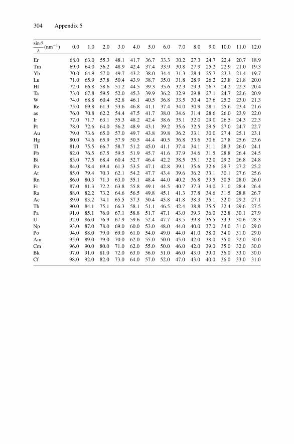
304 Appendix 5
sin θ
λ(nm−1) 0.0 1.0 2.0 3.0 4.0 5.0 6.0 7.0 8.0 9.0 10.0 11.0 12.0
Er 68.0 63.0 55.3 48.1 41.7 36.7 33.3 30.2 27.3 24.7 22.4 20.7 18.9Tm 69.0 64.0 56.2 48.9 42.4 37.4 33.9 30.8 27.9 25.2 22.9 21.0 19.3Yb 70.0 64.9 57.0 49.7 43.2 38.0 34.4 31.3 28.4 25.7 23.3 21.4 19.7Lu 71.0 65.9 57.8 50.4 43.9 38.7 35.0 31.8 28.9 26.2 23.8 21.8 20.0Hf 72.0 66.8 58.6 51.2 44.5 39.3 35.6 32.3 29.3 26.7 24.2 22.3 20.4Ta 73.0 67.8 59.5 52.0 45.3 39.9 36.2 32.9 29.8 27.1 24.7 22.6 20.9W 74.0 68.8 60.4 52.8 46.1 40.5 36.8 33.5 30.4 27.6 25.2 23.0 21.3Re 75.0 69.8 61.3 53.6 46.8 41.1 37.4 34.0 30.9 28.1 25.6 23.4 21.6as 76.0 70.8 62.2 54.4 47.5 41.7 38.0 34.6 31.4 28.6 26.0 23.9 22.0Ir 77.0 71.7 63.1 55.3 48.2 42.4 38.6 35.1 32.0 29.0 26.5 24.3 22.3Pt 78.0 72.6 64.0 56.2 48.9 43.1 39.2 35.6 32.5 29.5 27.0 24.7 22.7Au 79.0 73.6 65.0 57.0 49.7 43.8 39.8 36.2 33.1 30.0 27.4 25.1 23.1Hg 80.0 74.6 65.9 57.9 50.5 44.4 40.5 36.8 33.6 30.6 27.8 25.6 23.6Tl 81.0 75.5 66.7 58.7 51.2 45.0 41.1 37.4 34.1 31.1 28.3 26.0 24.1Pb 82.0 76.5 67.5 59.5 51.9 45.7 41.6 37.9 34.6 31.5 28.8 26.4 24.5Bi 83.0 77.5 68.4 60.4 52.7 46.4 42.2 38.5 35.1 32.0 29.2 26.8 24.8Po 84.0 78.4 69.4 61.3 53.5 47.1 42.8 39.1 35.6 32.6 29.7 27.2 25.2At 85.0 79.4 70.3 62.1 54.2 47.7 43.4 39.6 36.2 33.1 30.1 27.6 25.6Rn 86.0 80.3 71.3 63.0 55.1 48.4 44.0 40.2 36.8 33.5 30.5 28.0 26.0Fr 87.0 81.3 72.2 63.8 55.8 49.1 44.5 40.7 37.3 34.0 31.0 28.4 26.4Ra 88.0 82.2 73.2 64.6 56.5 49.8 45.1 41.3 37.8 34.6 31.5 28.8 26.7Ac 89.0 83.2 74.1 65.5 57.3 50.4 45.8 41.8 38.3 35.1 32.0 29.2 27.1Th 90.0 84.1 75.1 66.3 58.1 51.1 46.5 42.4 38.8 35.5 32.4 29.6 27.5Pa 91.0 85.1 76.0 67.1 58.8 51.7 47.1 43.0 39.3 36.0 32.8 30.1 27.9U 92.0 86.0 76.9 67.9 59.6 52.4 47.7 43.5 39.8 36.5 33.3 30.6 28.3Np 93.0 87.0 78.0 69.0 60.0 53.0 48.0 44.0 40.0 37.0 34.0 31.0 29.0Po 94.0 88.0 79.0 69.0 61.0 54.0 49.0 44.0 41.0 38.0 34.0 31.0 29.0Am 95.0 89.0 79.0 70.0 62.0 55.0 50.0 45.0 42.0 38.0 35.0 32.0 30.0Cm 96.0 90.0 80.0 71.0 62.0 55.0 50.0 46.0 42.0 39.0 35.0 32.0 30.0Bk 97.0 91.0 81.0 72.0 63.0 56.0 51.0 46.0 43.0 39.0 36.0 33.0 30.0Cf 98.0 92.0 82.0 73.0 64.0 57.0 52.0 47.0 43.0 40.0 36.0 33.0 31.0
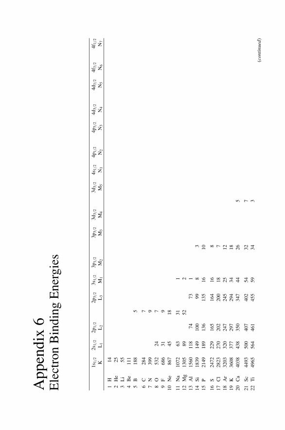
App
endi
x6
Ele
ctro
nB
indi
ngE
nerg
ies
1s1/
22s
1/2
2p1/
22p
3/2
3s1/
23p
1/2
3p3/
23d
3/2
3d3/
24s
1/2
4p1/
24p
3/2
4d3/
24d
3/2
4f3/
24f
1/2
KL
1L
2L
3M
1M
2M
3M
4M
5N
1N
2N
3N
4N
5N
6N
7
1H
142
He
253
Li
554
Be
111
5B
188
5
6C
284
77
N39
99
8O
532
247
9F
686
319
10N
e86
745
18
11N
a10
7263
311
12M
g13
0589
522
13A
l15
6011
874
731
14Si
1839
149
100
998
315
P21
4918
913
613
516
10
16S
2472
229
165
164
168
17C
l28
2327
020
220
018
718
Ar
3203
320
247
245
2512
19K
3608
377
297
294
3418
20C
a40
3843
835
034
744
265
21Sc
4493
500
407
402
5432
722
Ti
4965
564
461
455
5934
3(c
onti
nued
)
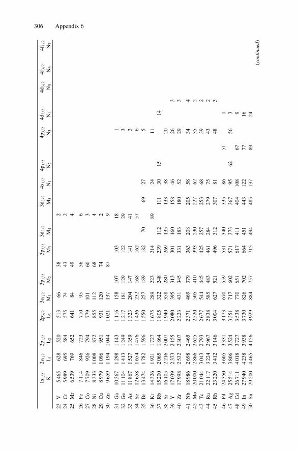
306 Appendix 6
1s1/
22s
1/2
2p1/
22p
3/2
3s1/
23p
1/2
3p3/
23d
3/2
3d3/
24s
1/2
4p1/
24p
3/2
4d3/
24d
3/2
4f3/
24f
1/2
KL
1L
2L
3M
1M
2M
3M
4M
5N
1N
2N
3N
4N
5N
6N
7
23V
546
562
852
051
366
382
24C
r5
989
695
584
575
7443
225
Mr
653
976
965
264
184
494
26Fe
711
484
672
371
095
566
27C
o7
709
926
794
779
101
603
28N
i8
333
100
887
285
511
268
429
Cu
897
91
096
951
931
120
742
30Z
n9
659
119
41
044
102
113
787
9
31G
a10
367
129
81
143
111
615
810
710
318
132
Ge
1110
41
413
124
91
217
181
129
122
293
33A
s11
867
152
71
359
132
320
414
714
141
334
Se12
658
165
41
476
143
623
216
816
257
635
Br
1347
41
782
159
61
550
257
189
182
7069
275
36K
r14
326
192
11
727
167
528
922
321
489
2411
37R
b15
200
206
51
864
180
532
224
823
911
211
130
1514
38Sr
1610
52
216
200
71
940
358
280
269
135
133
3820
39Y
1703
92
373
215
52
080
395
313
301
160
158
4626
340
Zr
1799
82
532
230
72
223
431
345
331
183
180
5229
3
41N
b18
986
269
82
465
237
146
937
936
320
820
558
344
42M
o20
000
286
62
625
252
050
541
039
323
022
762
352
43T
c21
044
304
32
793
267
754
444
542
525
725
368
392
44R
u22
117
322
42
967
283
858
548
346
128
427
975
432
45R
h23
220
341
23
146
300
462
752
149
631
230
781
483
46Pd
2435
03
605
333
13
173
670
559
531
340
335
8651
147
Ag
2551
43
806
352
43
351
717
602
571
373
367
9562
563
48C
d26
711
401
83
727
353
877
065
161
741
140
410
867
949
In27
940
423
83
938
373
082
670
266
445
144
312
277
1650
Sn29
200
446
54
156
392
988
475
771
549
448
513
789
24(c
onti
nued
)
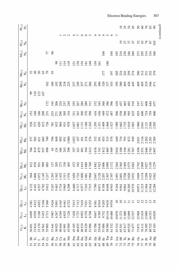
Electron Binding Energies 3071s
1/2
2s1/
22p
1/2
2p3/
23s
1/2
3p1/
23p
3/2
3d3/
23d
3/2
4s1/
24p
1/2
4p3/
24d
3/2
4d3/
24f
3/2
4f1/
2
KL
1L
2L
3M
1M
2M
3M
4M
5N
1N
2N
3N
4N
5N
6N
7
51Sb
3049
14
699
438
14
132
944
812
766
537
528
152
9932
52T
c31
814
493
94
612
434
11
006
870
819
582
572
168
110
4053
I33
170
518
84
852
455
71
072
931
875
631
620
186
123
5054
Xc
3456
15
453
510
44
782
114
599
993
768
567
220
814
763
55C
s35
985
571
35
360
501
21
217
065
998
740
726
231
172
162
7977
56B
a37
441
598
75
624
524
71
293
137
6379
678
125
319
218
093
9057
La
3892
56
267
589
15
483
136
220
512
484
983
227
120
619
299
58C
e40
444
654
96
165
572
41
435
273
186
902
884
290
224
208
111
159
Pr41
991
683
56
441
596
51
511
338
243
951
931
305
237
218
114
260
Nd
4356
97
126
672
26
208
157
640
329
81
000
978
316
244
225
118
2
61Pm
4518
57
428
701
36
460
165
047
235
71
052
102
733
125
523
712
14
62Sm
4683
57
737
731
26
717
172
454
242
110
71
081
347
267
249
130
763
Eu
4851
98
052
761
86
977
180
01
614
481
161
113
136
028
425
713
40
64G
d50
239
837
67
931
724
31
881
168
954
421
81
186
376
289
271
141
065
Tb
5199
68
708
825
27
515
196
81
768
161
227
61
242
398
311
286
148
3
66D
y53
788
904
78
581
779
02
047
184
21
676
332
129
541
633
229
315
44
67H
o55
618
939
58
919
807
12
128
192
31
741
391
135
143
634
330
616
14
68E
r57
486
975
29
265
835
82
207
200
61
812
453
140
944
936
632
017
716
84
69T
m59
390
1011
69
618
864
82
307
209
01
885
515
146
847
238
633
718
05
70Y
b61
332
1048
89
978
894
32
397
217
21
949
576
152
748
739
634
319
718
46
71L
u63
314
1087
010
924
42
491
226
42
024
640
158
950
641
035
920
519
57
72H
f65
351
1127
210
956
12
601
236
52
108
716
166
253
843
738
022
421
419
1873
Ta67
417
1168
011
988
12
708
246
92
194
793
173
556
646
540
524
223
027
2574
W69
525
1209
911
1020
52
820
257
52
281
872
181
059
549
242
625
924
637
3475
Re
7167
712
527
1110
535
293
22
682
236
794
91
883
625
518
445
274
260
4745
76O
s73
871
1296
812
1087
13
049
279
22
458
203
11
960
655
547
469
290
273
5250
77Ir
7611
113
419
1211
215
317
42
909
255
12
116
204
169
057
749
531
229
563
6078
Pt78
395
1388
013
1156
43
298
302
72
646
220
22
121
724
608
519
331
314
7470
79A
u80
725
1435
313
1191
83
425
315
02
743
229
12
206
759
644
546
352
334
8783
80H
g83
103
1483
914
1228
43
562
327
92
847
238
52
295
800
677
571
379
360
103
99
(con
tinu
ed)
308 Appendix 6
1s1/
22s
1/2
2p1/
22p
3/2
3s1/
23p
1/2
3p3/
23d
3/2
3d3/
24s
1/2
4p1/
24p
3/2
4d3/
24d
3/2
4f3/
24f
1/2
KL
1L
2L
3M
1M
2M
3M
4M
5N
1N
2N
3N
4N
5N
6N
7
81T
l85
531
1534
714
1265
73
704
341
62
957
248
52
390
846
722
609
407
386
122
118
82Pb
8800
515
861
1513
035
385
13
554
306
72
586
248
489
476
464
543
541
314
313
883
Bi
9052
616
388
1513
418
399
93
697
317
72
688
258
093
980
667
946
444
016
315
884
Po93
105
1693
916
1381
44
149
385
43
302
279
82
683
995
851
705
500
473
184
85A
t95
730
1749
316
1421
44
317
400
83
426
290
92
787
104
288
674
053
350
721
0
86R
n98
404
1804
917
1461
94
482
415
93
538
302
22
892
109
792
976
856
754
123
887
Fr10
1137
1863
917
1503
14
652
432
73
663
313
63
000
115
398
081
060
357
726
888
Ra
1039
2219
237
1815
444
482
24
490
379
23
248
310
51
208
105
887
963
660
329
989
Ac
1067
5519
840
1915
871
500
24
656
390
93
370
321
91
269
108
089
067
563
931
990
Th
1096
5120
472
1916
300
518
24
831
404
63
491
333
21
330
116
896
871
467
734
433
5
Appendix 7X-Ray Wavelengths (nm)
E(Kα) Kα1 Kα2 Kβ K Lα1 L III
Element (keV) Edge Edge
1 H2 He3 Li 0.05 22.8000 22.65004 Be 0.11 11.4000 11.10005 B 0.18 6.7600 6.5957
6 C 0.28 4.4700 4.36807 N 0.39 3.1600 3.09908 O 0.52 2.3620 2.33209 F 0.68 1.8320 1.807610 Ne 0.85 1.4610 1.4452 1.4302
11 Na 1.04 1.1910 1.1575 1.1569 40.500012 Mg 1.25 9.8900 0.9521 0.9512 25.070013 Al 1.49 0.8339 0.8342 0.7960 0.7948 17.040014 Si 1.74 0.7125 0.7128 0.6753 0.6738 12.300015 P 2.01 0.6157 0.6160 0.5796 0.5784 9.4000
16 Si 2.31 0.5372 0.5375 0.5032 0.5019 7.561017 Cl 2.62 0.4728 0.4731 0.4403 0.4397 6.200018 Ar 2.96 0.4192 0.4195 0.3886 0.3871 5.061219 K 3.31 0.3741 0.3745 0.3454 0.3437 4.210020 Ca 3.69 0.3358 0.3362 0.3090 0.3070 3.6330 3.5490
21 Sc 4.09 0.3031 0.3034 0.2780 0.2762 3.1350 3.084622 Ti 4.51 0.2749 0.2752 0.2514 0.2497 2.7420 2.729023 V 4.95 0.2504 0.2507 0.2284 0.2269 2.4250 2.417224 Cr 5.41 0.2290 0.2294 0.2085 0.2070 2.1640 2.070025 Mn 5.90 0.2102 0.2106 0.1910 0.1896 1.9450 1.9345
26 Fe 6.40 0.1936 0.1940 0.1757 0.1743 1.7590 1.752527 Co 6.93 0.1790 0.1793 0.1621 0.1608 1.5972 1.591528 Ni 7.47 0.1658 0.1662 0.1500 0.1488 1.4561 1.452529 Cu 8.04 0.1541 0.1544 0.1392 0.1381 1.3336 1.328830 Zn 8.63 0.1435 0.1439 0.1295 0.1283 1.2254 1.2131
(continued)

310 Appendix 7
E(Kα) Kα1 Kα2 Kβ K Lα1 L III
Element (keV) Edge Edge
31 Ga 9.24 0.1340 0.1344 0.1208 0.1196 1.1292 1.110032 Ge 9.88 0.1254 0.1258 0.1129 0.1117 1.0436 1.018733 As 10.53 0.1176 0.1180 0.1057 0.1045 0.9671 0.936734 Se 11.21 0.1105 0.1109 0.0992 0.0980 0.8990 0.864635 Br 11.91 0.1040 0.1044 0.0933 0.0920 0.8375 0.7984
36 Kr 12.63 0.0980 0.0984 0.0879 0.0866 0.7817 0.739237 Rb 13.38 0.0926 0.0930 0.0829 0.0816 0.7318 0.686238 Sr 14.14 0.0875 0.0879 0.0783 0.0770 0.6863 0.638739 Y 14.93 0.0829 0.0833 0.0741 0.0728 0.6449 0.596240 Zr 15.75 0.0786 0.0790 0.0702 0.0689 0.6071 0.5579
41 Mb 16.58 0.0746 0.0750 0.0666 0.0653 0.5724 0.523042 Mo 17.44 0.0709 0.0714 0.0632 0.0620 0.5407 0.491343 Tc 18.33 0.0675 0.0679 0.0601 0.0589 0.5115 0.463044 Ru 19.24 0.0643 0.0647 0.0572 0.0561 0.4846 0.436945 Rh 20.17 0.0613 0.0618 0.0546 0.0534 0.4597 0.4130
46 Pd 21.12 0.0585 0.0590 0.0521 0.0509 0.4368 0.390747 Ag 22.11 0.0559 0.0564 0.0497 0.0486 0.4154 0.370048 Cd 23.11 0.0535 0.0539 0.0475 0.0464 0.3956 0.350549 In 24.14 0.0512 0.0517 0.0455 0.0444 0.3772 0.332450 Sn 25.20 0.0491 0.0495 0.0435 0.0425 0.3600 0.3156
51 Sb 26.28 0.0470 0.0475 0.0417 0.0407 0.3439 0.300052 Te 27.38 0.0451 0.0456 0.0400 0.0390 0.3289 0.285653 I 28.51 0.0433 0.0438 0.0384 0.0374 0.3149 0.272054 Xe 29.67 0.0416 0.0421 0.0369 0.0358 0.3017 0.259355 Cs 30.86 0.0400 0.0405 0.0354 0.0345 0.2892 0.2474
56 Ba 32.07 0.0385 0.0390 0.0341 0.0331 0.2776 0.236357 La 33.31 0.0371 0.0375 0.0328 0.0318 0.2666 0.226158 Ce 34.57 0.0357 0.0362 0.0316 0.0306 0.2562 0.216659 Pr 35.87 0.0344 0.0349 0.0304 0.0295 0.2463 0.207960 Nd 37.19 0.0332 0.0336 0.0293 0.0285 0.2370 0.1997
61 Pm 38.54 0.0320 0.0325 0.0283 0.0274 0.2282 0.191962 Sm 39.92 0.0309 0.0314 0.0273 0.0265 0.2200 0.184663 Eu 41.33 0.0298 0.0303 0.0264 0.0256 0.2121 0.177664 Gd 42.77 0.0288 0.0293 0.0255 0.0247 0.2047 0.171265 Tb 44.24 0.0279 0.0283 0.0246 0.0238 0.1977 0.1650
66 Dy 45.73 0.0270 0.0274 0.0238 0.0230 0.1909 0.159267 Ho 47.26 0.0261 0.0265 0.0230 0.0223 0.1845 0.153768 Er 48.83 0.0252 0.0257 0.0223 0.0216 0.1784 0.148469 Tm 50.42 0.0244 0.0249 0.0216 0.0209 0.1727 0.143370 Yb 52.04 0.0237 0.0241 0.0209 0.0202 0.1672 0.1386
71 Lu 53.70 0.0229 0.0234 0.0202 0.0196 0.1620 0.134172 Hf 55.40 0.0222 0.0227 0.0196 0.0190 0.1570 0.129773 Ta 57.11 0.0215 0.0220 0.0190 0.0184 0.1522 0.125574 W 58.87 0.0209 0.0214 0.0184 0.0178 0.1476 0.121675 Re 60.67 0.0203 0.0208 0.0179 0.0173 0.1432 0.1177
(continued)

X-Ray Wavelengths (nm) 311
E(Kα) Kα1 Kα2 Kβ K Lα1 L III
Element (keV) Edge Edge
76 Os 62.50 0.0197 0.0202 0.0174 0.0168 0.1391 0.114177 Ir 64.36 0.0191 0.0196 0.0169 0.0163 0.1351 0.110678 Pt 66.26 0.0186 0.0190 0.0164 0.0158 0.1313 0.107279 Au 68.20 0.0180 0.0185 0.0159 0.0154 0.1276 0.104080 Hg 70.18 0.0175 0.0180 0.0154 0.0149 0.1241 0.1009
81 Tl 72.19 0.0170 0.0175 0.0150 0.0145 0.1207 0.097982 Pb 74.25 0.0165 0.0170 0.0146 0.0141 0.1175 0.095183 Bi 76.34 0.0161 0.0166 0.0142 0.0137 0.1144 0.092384 Po 78.48 0.0156 0.0161 0.0138 0.0133 0.1114 0.089885 At 80.66 0.0152 0.0157 0.0134 0.0130 0.1085 0.0872
86 Rn 82.88 0.0148 0.0153 0.0131 0.0126 0.1057 0.084887 Fr 85.14 0.0144 0.0149 0.0127 0.0123 0.1030 0.082588 Ra 87.46 0.0140 0.0145 0.0124 0.0119 0.1005 0.080389 Ac 89.81 0.0136 0.0141 0.0121 0.1160 0.0980 0.078190 Th 92.22 0.0133 0.0138 0.0117 0.0113 0.0956 0.0761
App
endi
x8
Mas
sA
bsor
ptio
nC
oeffi
cien
ts(µ
/ρ
)
Mo
Cu
Co
Cr
k αk β
k αk β
k αk β
k αk β
Abs
orbe
rD
ensi
ty(g
m/c
m3)
0.07
11nm
0.06
32nm
0.15
42nm
0.13
92nm
0.17
90nm
0.11
62nm
0.22
91nm
0.20
895
nm
1H
0.08
×10
−30.
3727
0.36
990.
3912
0.38
820.
3966
0.39
280.
4116
0.40
462
He
0.17
×10
−30.
2019
0.19
720.
2835
0.26
230.
3288
0.29
660.
4648
0.40
013
Li
0.53
0.19
680.
1866
0.47
700.
3939
0.65
900.
5283
1.24
30.
9639
4B
e1.
850.
2451
0.22
161.
007
0.77
421.
522
1.15
23.
183
2.38
85
Be
2.47
0.34
510.
2928
2.14
21.
590
3.35
72.
485
7.23
25.
385
6C
2.27
(gra
phite
)0.
5348
0.42
854.
219
3.09
36.
683
4.91
614
.46
10.7
67
N1.
17×
10−3
0.78
980.
6054
7.14
25.
215
11.3
38.
3324
.42
18.2
38
O1.
3×
10−3
1.14
70.
8545
11.0
38.
0617
.44
12.8
537
.19
27.8
89
F1.
70×
10−3
1.58
41.
154
15.9
511
.66
25.1
218
.57
53.1
439
.99
10N
e0.
84×
10−3
2.20
91.
597
22.1
316
.24
34.6
925
.72
72.7
154
.91
11N
a0.
972.
939
2.09
830
.30
22.2
347
.34
35.1
898
.48
74.6
612
Mg
1.74
3.97
92.
825
40.8
830
.08
63.5
447
.38
130.
899
.62
13A
l2.
705.
043
3.58
550
.23
37.1
477
.54
58.0
815
8.0
120.
714
Si2.
336.
533
4.62
465
.32
48.3
710
0.4
75.4
420
2.7
155.
615
P1.
82(y
ello
w)
7.87
05.
569
77.2
857
.44
118.
089
.05
235.
518
1.6
16S
2.09
9.62
56.
835
92.5
368
.90
141.
210
6.6
281.
921
7.2
17C
l3.
2×
10−3
11.6
48.
261
109.
281
.79
164.
712
5.3
321.
525
0.2
18A
r1.
67×
10−3
12.6
28.
949
119.
589
.34
180.
913
7.3
355.
527
5.8
19K
0.86
16.2
011
.51
148.
411
1.7
222.
016
9.9
426.
833
4.2
20C
a1.
5319
.00
13.5
617
1.4
129.
025
7.4
196.
449
9.6
389.
3(c
onti
nued
)
Mass Absorption Coefficients (µ/ρ) 313
Mo
Cu
Co
Cr
k αk β
k αk β
k αk β
k αk β
Abs
orbe
rD
ensi
ty(g
m/c
m3)
0.07
11nm
0.06
32nm
0.15
42nm
0.13
92nm
0.17
90nm
0.11
62nm
0.22
91nm
0.20
895
nm
21Sc
2.99
21.0
415
.00
186.
014
0.8
275.
521
2.2
520.
941
0.7
22T
i4.
5123
.25
16.6
520
2.4
153.
230
0.5
231.
057
1.4
449.
023
V6.
0925
.24
18.0
722
2.6
168.
033
2.7
254.
775
.150
1.0
24C
r7.
1929
.25
20.9
925
2.3
191.
137
5.0
288.
185
.765
.825
Mn
7.47
31.8
622
.89
272.
520
6.7
405.
131
1.2
96.1
73.8
26Fe
7.87
37.7
427
.21
304.
423
3.6
56.2
534
5.5
113.
186
.827
Co
8.80
41.0
229
.51
338.
625
8.7
62.8
647
.71
124.
696
.128
Ni
8.91
47.2
434
.18
48.8
328
2.8
73.7
556
.05
145.
711
2.5
29C
u8.
9349
.34
35.7
751
.54
38.7
478
.11
59.2
215
5.2
119.
530
Zn
7.13
55.4
640
.26
59.5
145
.30
88.7
168
.00
171.
713
3.5
31G
a5.
9156
.90
41.6
962
.13
46.6
594
.15
71.3
918
6.9
144.
032
Ge
5.32
60.4
744
.26
67.9
251
.44
102.
077
.79
199.
915
4.5
33A
s5.
7865
.97
48.5
775
.65
57.0
111
4.0
86.7
622
4.0
173.
334
Se4.
8168
.82
51.2
082
.89
62.3
212
5.1
95.1
124
6.1
190.
435
Br
3.12
(liq
uid)
74.6
855
.56
90.2
968
.07
135.
810
3.5
266.
220
6.2
36K
r3.
488
×10
−379
.10
5864
97.0
273
.22
145.
711
1.2
284.
622
0.7
37R
b1.
5383
.00
62.0
710
6.3
80.1
615
9.6
121.
831
1.7
241.
838
Sr2.
5888
.04
65.5
911
5.3
8677
173.
513
2.2
339.
326
3.4
39Y
4.48
97.5
672
.57
127.
196
.19
190.
214
5.4
368.
928
6.9
40Z
r6.
5116
.10
75.2
136.
810
3320
4.9
156.
639
8.6
309.
7
41N
b8.
5816
.96
81.2
214
8.8
112.
322
2.9
170.
443
1.9
336.
442
Mo
10.2
218
.44
13.2
915
8 .3
119.
723
6.6
181.
045
7.4
356.
543
To11
.50
19.7
814
.30
167.
712
6.9
250.
819
1.9
485.
537
8.0
44R
u12
.36
21.3
315
.40
180.
813
7.0
269.
420
6.6
517.
940
4.4
45R
h12
.42
23.0
516
.65
194.
114
7.1
289.
022
1.8
555.
243
3.7
46Pd
12.0
024
.42
17.6
320
5.0
155.
630
4.3
234.
058
0.9
455.
147
Ag
10.5
026
.38
19.1
021
8.1
165.
832
3.5
248.
961
7.4
483.
5(c
onti
nued
)
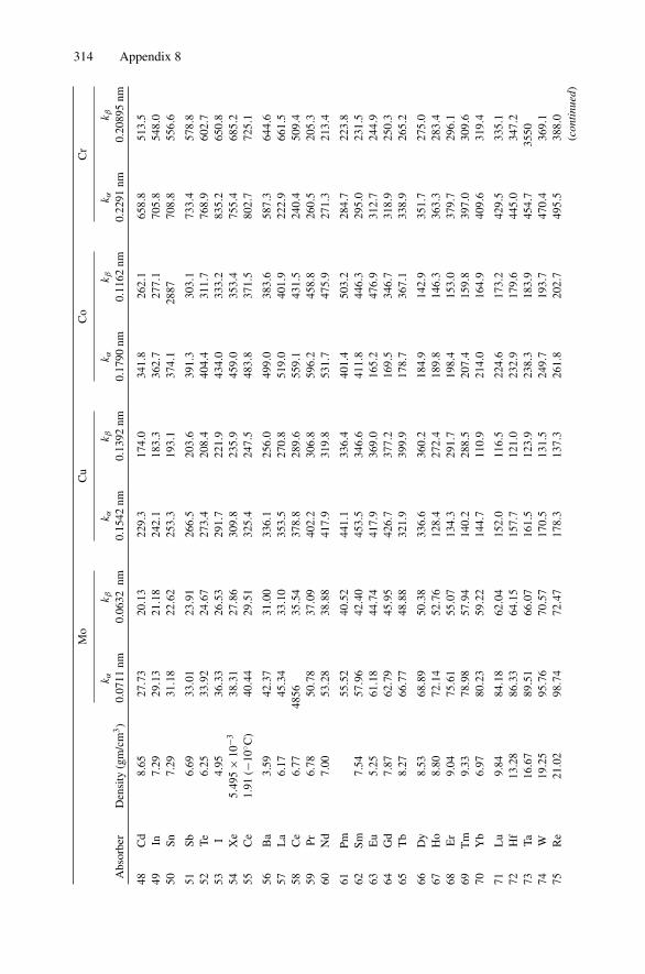
314 Appendix 8
Mo
Cu
Co
Cr
k αk β
k αk β
k αk β
k αk β
Abs
orbe
rD
ensi
ty(g
m/c
m3)
0.07
11nm
0.06
32nm
0.15
42nm
0.13
92nm
0.17
90nm
0.11
62nm
0.22
91nm
0.20
895
nm
48C
d8.
6527
.73
20.1
322
9.3
174.
034
1.8
262.
165
8.8
513.
549
In7.
2929
.13
21.1
824
2.1
183.
336
2.7
277.
170
5.8
548.
050
Sn7.
2931
.18
22.6
225
3.3
193.
137
4.1
2887
708.
855
6.6
51Sb
6.69
33.0
123
.91
266.
520
3.6
391.
330
3.1
733.
457
8.8
52Te
6.25
33.9
224
.67
273.
420
8.4
404.
431
1.7
768.
960
2.7
53I
4.95
36.3
326
.53
291.
722
1.9
434.
033
3.2
835.
265
0.8
54X
e5 .
495
×10
−338
.31
27.8
630
9.8
235.
945
9.0
353.
475
5.4
685.
255
Ce
1.91
(−10
C)
40.4
429
.51
325.
424
7.5
483.
837
1.5
802.
772
5.1
56B
a3.
5942
.37
31.0
033
6.1
256.
049
9.0
383.
658
7.3
644.
657
La
6.17
45.3
433
.10
353.
527
0.8
519.
040
1.9
222.
966
1.5
58C
e6.
7748
5635
.54
378.
828
9.6
559.
143
1.5
240.
450
9.4
59Pr
6.78
50.7
837
.09
402.
230
6.8
596.
245
8.8
260.
520
5.3
60N
d7.
0053
.28
38.8
841
7.9
319.
853
1.7
475.
927
1.3
213.
4
61Pm
55.5
240
.52
441.
133
6.4
401.
450
3.2
284.
722
3.8
62Sm
7.54
57.9
642
.40
453.
534
6.6
411.
844
6.3
295.
023
1.5
63E
u5.
2561
.18
44.7
441
7.9
369.
016
5.2
476.
931
2.7
244.
964
Gd
7.87
62.7
945
.95
426.
737
7.2
169.
534
6.7
318.
925
0.3
65T
b8.
2766
.77
48.8
832
1.9
399.
917
8.7
367.
133
8.9
265.
2
66D
y8.
5368
.89
50.3
833
6.6
360.
218
4.9
142.
935
1.7
275.
067
Ho
8.80
72.1
452
.76
128.
427
2.4
189.
814
6.3
363.
328
3.4
68E
r9.
0475
.61
55.0
713
4.3
291.
719
8.4
153.
037
9.7
296.
169
Tm
9.33
78.9
857
.94
140.
228
8.5
207.
415
9.8
397.
030
9.6
70Y
b6.
9780
.23
59.2
214
4.7
110.
921
4.0
164.
940
9.6
319.
4
71L
u9.
8484
.18
62.0
415
2.0
116.
522
4.6
173.
242
9.5
335.
172
Hf
13.2
886
.33
64.1
515
7.7
121.
023
2.9
179.
644
5.0
347.
273
Ta16
.67
89.5
166
.07
161.
512
3.9
238.
318
3.9
454.
735
5074
W19
.25
95.7
670
.57
170.
513
1.5
249.
719
3.7
470.
436
9.1
75R
e21
.02
98.7
472
.47
178.
313
7.3
261.
820
2.7
495.
538
8.0
(con
tinu
ed)
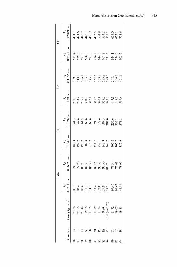
Mass Absorption Coefficients (µ/ρ) 315
Mo
Cu
Co
Cr
k αk β
k αk β
k αk β
k αk β
Abs
orbe
rD
ensi
ty(g
m/c
m3)
0.07
11nm
0.06
32nm
0.15
42nm
0.13
92nm
0.17
90nm
0.11
62nm
0.22
91nm
0.20
895
nm
76O
s22
.58
100.
274
.13
183.
814
1.3
270.
320
9.0
512.
440
1.1
77Ir
22.5
510
3.4
77.2
019
2.2
147.
628
3.4
218.
853
9.6
421.
678
Pt21
.44
108.
680
.23
198.
216
1.2
295.
222
6.4
571.
644
3.9
79A
u19
.28
111.
382
.33
207.
816
0.6
303.
323
5.7
568.
044
6.7
80H
g13
.55
114.
785
.30
216.
216
6.6
317.
024
5.7
597.
946
8.9
81T
l11
.87
119.
488
.25
222.
217
1.1
326.
325
2.7
616.
948
3.3
82Pb
11.3
412
2.8
90.5
523
2.1
178.
634
0.8
263.
864
4.5
504.
983
Bi
9.80
125.
993
.50
242.
918
7.5
355.
327
5.8
667.
252
4.2
86R
n4.
4(−
62 C
)11
7.2
100.
726
3.7
203.
038
7.1
299.
773
1.4
573.
2
90T
h11
.72
99.4
673
.34
306.
823
6.6
449.
034
8.4
844.
166
3.0
92U
19.0
596
.67
72.6
330
5.7
236.
244
6.3
346.
977
4.0
657.
194
Pu19
.81
48.8
478
.99
352.
927
1.2
519.
640
1.6
803.
277
1.6
Appendix 9KLL Auger Energies (eV)
2s12p5 2s22p4
2s02p6
1S01P1
3P03P2
1S01D2
3P03P0
3P2
KL1 L1 KL1 L2 KL1 L2 KL1 L2 KL1 L3 KL2 L2 KL2 L3 KL3 L3 KL3 L3
C 6 0.243 0.252 0.258 0.258 0.258 0.265 0.266 0.267 0.267N 7 0.356 0.362 0.369 0.369 0.369 0.373 0.375 0.377 0.377O 8 0.474 0.486 0.495 0.495 0.495 0.504 0.507 0.509 0.509F 9 0.610 0.627 0.638 0.638 0.638 0.650 0.654 0.657 0.657Ne 10 0.761 0.781 0.794 0.794 0.794 0.808 0.813 0.816 0.816Na 11 0.928 0.952 0.967 0.967 0.967 0.984 0.989 0.993 0.993Mg 12 0.105 1.135 1.151 1.151 1.151 1.172 1.179 1.183 1.183Al 13 0.301 1.336 1.354 1.354 1.354 1.379 1.387 1.392 1.392Si 14 0.516 1.554 1.574 1.574 1.575 1.602 1.611 1.616 1.617P 15 0.742 1.784 1.805 1.806 1.806 1.835 1.845 1.851 1.852S 16 0.982 2.034 2.057 2.058 2.059 2.096 2.107 2.114 2.115Cl 17 2.249 2.305 2.329 2.330 2.331 2.370 2.382 2.389 2.391Ar 18 2.527 2.586 2.612 2.613 2.614 2.656 2.669 2.677 2.679K 19 2.815 2.881 2.909 2.910 2.912 2.959 2.973 2.981 2.984Ca 20 3.122 3.195 3.224 3.225 3.227 3.279 3.294 3.303 3.306Sc 21 3.456 3.533 3.563 3.564 3.567 3.622 3.638 3.647 3.651Ti 22 3.799 3.886 3.916 3.919 3.922 3.985 4.002 4.011 4.016V 23 4.168 4.259 4.290 4.293 4.298 4.362 4.381 4.391 4.397Cr 24 4.557 4.651 4.683 4.687 4.692 4.757 4.778 4.788 4.795Mn 25 4.956 5.056 5.089 5.094 5.100 5.169 5.191 5.202 5.211Fe 26 5.374 5.480 5.514 5.519 5.527 5.598 5.622 5.634 5.644Co 27 5.808 5.923 5.957 5.964 5.972 6.049 6.075 6.088 6.099Ni 28 6.264 6.384 6.419 6.426 6.436 6.514 6.542 6.556 6.568Cu 29 6.732 6.861 6.896 6.905 6.916 7.000 7.030 7.045 7.059Zn 30 7.214 7.348 7.384 7.394 7.407 7.493 7.526 7.543 7.558Ga 31 7.712 7.852 7.888 7.900 7.915 8.000 8.037 8.057 8.073Ge 32 8.216 8.365 8.401 8.416 8.433 8.523 8.563 8.586 8.603As 33 8.749 8.903 8.939 8.957 8.975 9.063 9.107 9.133 9.152Se 34 9.283 9.447 9.483 9.504 9.524 9.616 9.665 9.695 9.715Br 35 9.840 10.014 10.049 10.074 10.096 10.189 10.244 10.279 10.300kr 36 10.412 10.594 10.630 10.658 10.682 10.777 10.837 10.877 10.899Rb 37 10.995 11.186 11.221 11.255 11.280 11.376 11.442 11.487 11.511
(continued)
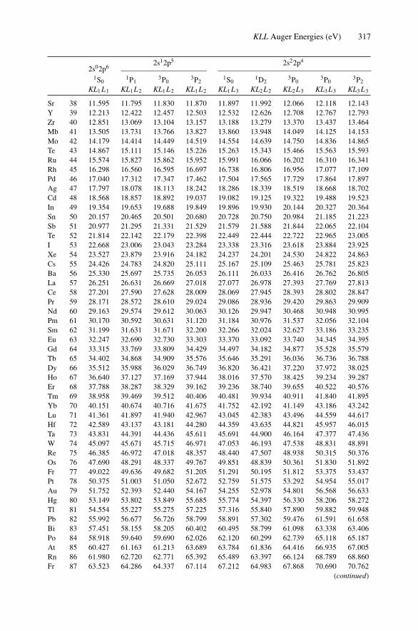
KLL Auger Energies (eV) 317
2s12p5 2s22p4
2s02p6
1S01P1
3P03P2
1S01D2
3P03P0
3P2
KL1 L1 KL1 L2 KL1 L2 KL1 L2 KL1 L3 KL2 L2 KL2 L3 KL3 L3 KL3 L3
Sr 38 11.595 11.795 11.830 11.870 11.897 11.992 12.066 12.118 12.143Y 39 12.213 12.422 12.457 12.503 12.532 12.626 12.708 12.767 12.793Zr 40 12.851 13.069 13.104 13.157 13.188 13.279 13.370 13.437 13.464Mb 41 13.505 13.731 13.766 13.827 13.860 13.948 14.049 14.125 14.153Mo 42 14.179 14.414 14.449 14.519 14.554 14.639 14.750 14.836 14.865Te 43 14.867 15.111 15.146 15.226 15.263 15.343 15.466 15.563 15.593Ru 44 15.574 15.827 15.862 15.952 15.991 16.066 16.202 16.310 16.341Rh 45 16.298 16.560 16.595 16.697 16.738 16.806 16.956 17.077 17.109Pd 46 17.040 17.312 17.347 17.462 17.504 17.565 17.729 17.864 17.897Ag 47 17.797 18.078 18.113 18.242 18.286 18.339 18.519 18.668 18.702Cd 48 18.568 18.857 18.892 19.037 19.082 19.125 19.322 19.488 19.523In 49 19.354 19.653 19.688 19.849 19.896 19.930 20.144 20.327 20.364Sn 50 20.157 20.465 20.501 20.680 20.728 20.750 20.984 21.185 21.223Sb 51 20.977 21.295 21.331 21.529 21.579 21.588 21.844 22.065 22.104Te 52 21.814 22.142 22.179 22.398 22.449 22.444 22.722 22.965 23.005I 53 22.668 23.006 23.043 23.284 23.338 23.316 23.618 23.884 23.925Xe 54 23.527 23.879 23.916 24.182 24.237 24.201 24.530 24.822 24.863Cs 55 24.426 24.783 24.820 25.111 25.167 25.109 25.463 25.781 25.823Ba 56 25.330 25.697 25.735 26.053 26.111 26.033 26.416 26.762 26.805La 57 26.251 26.631 26.669 27.018 27.077 26.978 27.393 27.769 27.813Ce 58 27.201 27.590 27.628 28.009 28.069 27.945 28.393 28.802 28.847Pr 59 28.171 28.572 28.610 29.024 29.086 28.936 29.420 29.863 29.909Nd 60 29.163 29.574 29.612 30.063 30.126 29.947 30.468 30.948 30.995Pm 61 30.170 30.592 30.631 31.120 31.184 30.976 31.537 32.056 32.104Sm 62 31.199 31.631 31.671 32.200 32.266 32.024 32.627 33.186 33.235Eu 63 32.247 32.690 32.730 33.303 33.370 33.092 33.740 34.345 34.395Gd 64 33.315 33.769 33.809 34.429 34.497 34.182 34.877 35.528 35.579Tb 65 34.402 34.868 34.909 35.576 35.646 35.291 36.036 36.736 36.788Dy 66 35.512 35.988 36.029 36.749 36.820 36.421 37.220 37.972 38.025Ho 67 36.640 37.127 37.169 37.944 38.016 37.570 38.425 39.234 39.287Er 68 37.788 38.287 38.329 39.162 39.236 38.740 39.655 40.522 40.576Tm 69 38.958 39.469 39.512 40.406 40.481 39.934 40.911 41.840 41.895Yb 70 40.151 40.674 40.716 41.675 41.752 42.192 41.149 43.186 43.242Lu 71 41.361 41.897 41.940 42.967 43.045 42.383 43.496 44.559 44.617Hf 72 42.589 43.137 43.181 44.280 44.359 43.635 44.821 45.957 46.015Ta 73 43.831 44.391 44.436 45.611 45.691 44.900 46.164 47.377 47.436W 74 45.097 45.671 45.715 46.971 47.053 46.193 47.538 48.831 48.891Re 75 46.385 46.972 47.018 48.357 48.440 47.507 48.938 50.315 50.376Os 76 47.690 48.291 48.337 49.767 49.851 48.839 50.361 51.830 51.892Fr 77 49.022 49.636 49.682 51.205 51.291 50.195 51.812 53.375 53.437Pt 78 50.375 51.003 51.050 52.672 52.759 51.575 53.292 54.954 55.017Au 79 51.752 52.393 52.440 54.167 54.255 52.978 54.801 56.568 56.633Hg 80 53.149 53.802 53.849 55.685 55.774 54.397 56.330 58.206 58.272Tl 81 54.554 55.227 55.275 57.225 57.316 55.840 57.890 59.882 59.948Pb 82 55.992 56.677 56.726 58.799 58.891 57.302 59.476 61.591 61.658Bi 83 57.451 58.155 58.205 60.402 60.495 58.799 61.098 63.338 63.406Po 84 58.918 59.640 59.690 62.026 62.120 60.299 62.739 65.118 65.187At 85 60.427 61.163 61.213 63.689 63.784 61.836 64.416 66.935 67.005Rn 86 61.980 62.720 62.771 65.392 65.489 63.397 66.124 68.789 68.860Fr 87 63.523 64.286 64.337 67.114 67.212 64.983 67.868 70.690 70.762
(continued)
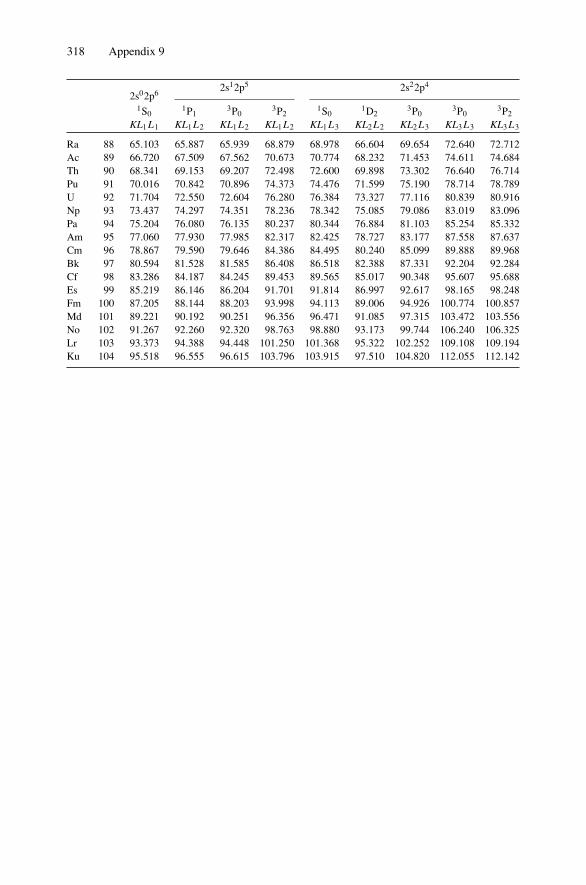
318 Appendix 9
2s12p5 2s22p4
2s02p6
1S01P1
3P03P2
1S01D2
3P03P0
3P2
KL1 L1 KL1 L2 KL1 L2 KL1 L2 KL1 L3 KL2 L2 KL2 L3 KL3 L3 KL3 L3
Ra 88 65.103 65.887 65.939 68.879 68.978 66.604 69.654 72.640 72.712Ac 89 66.720 67.509 67.562 70.673 70.774 68.232 71.453 74.611 74.684Th 90 68.341 69.153 69.207 72.498 72.600 69.898 73.302 76.640 76.714Pu 91 70.016 70.842 70.896 74.373 74.476 71.599 75.190 78.714 78.789U 92 71.704 72.550 72.604 76.280 76.384 73.327 77.116 80.839 80.916Np 93 73.437 74.297 74.351 78.236 78.342 75.085 79.086 83.019 83.096Pa 94 75.204 76.080 76.135 80.237 80.344 76.884 81.103 85.254 85.332Am 95 77.060 77.930 77.985 82.317 82.425 78.727 83.177 87.558 87.637Cm 96 78.867 79.590 79.646 84.386 84.495 80.240 85.099 89.888 89.968Bk 97 80.594 81.528 81.585 86.408 86.518 82.388 87.331 92.204 92.284Cf 98 83.286 84.187 84.245 89.453 89.565 85.017 90.348 95.607 95.688Es 99 85.219 86.146 86.204 91.701 91.814 86.997 92.617 98.165 98.248Fm 100 87.205 88.144 88.203 93.998 94.113 89.006 94.926 100.774 100.857Md 101 89.221 90.192 90.251 96.356 96.471 91.085 97.315 103.472 103.556No 102 91.267 92.260 92.320 98.763 98.880 93.173 99.744 106.240 106.325Lr 103 93.373 94.388 94.448 101.250 101.368 95.322 102.252 109.108 109.194Ku 104 95.518 96.555 96.615 103.796 103.915 97.510 104.820 112.055 112.142
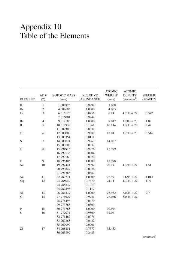
Appendix 10Table of the Elements
ATOMIC ATOMICAT. # ISOTOPIC MASS RELATIVE WEIGHT DENSITY SPECIFIC
ELEMENT (Z) (amu) ABUNDANCE (amu) (atom/cm3) GRAVITY
H 1 1.007825 0.9999 1.008He 2 4.002603 1.0000 4.003Li 3 6.015125 0.0756 6.94 4.70E + 22 0.542
7.016004 0.9244Be 4 9.012186 1.0000 9.012 1.21E + 23 1.82B 5 10.012939 0.1961 10.814 1.30E + 23 2.47
11.009305 0.8039C 6 12.000000 0.9889 12.011 1.76E + 23 3.516
13.003354 0.0111N 7 14.003074 0.9963 14.007
15.000108 0.0037C 8 15.994915 0.9976 15.999
16.999133 0.000417.999160 0.0020
F 9 18.998405 1.0000 18.998Ne 10 19.992441 0.9092 20.171 4.36E + 22 1.51
20.993849 0.002621.991385 0.0882
Na 11 22.989771 1.0000 22.99 2.65E + 22 1.013Mg 12 23.985042 0.7870 24.31 4.30E + 22 1.74
24.985839 0.101325.982593 0.1117
Al 13 26.981539 1.0000 26.982 6.02E + 22 2.7Si 14 27.976929 0.9221 28.086 5.00E + 22
28.976496 0.047029.973763 0.0309
P 15 30.973765 1.0000 30.974S 16 31.972074 0.9500 32.061
32.971462 0.007633.967865 0.042235.967090 0.0001
Cl 17 34.968851 0.7577 35.45336.965899 0.2423
(continued)
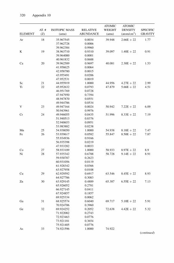
320 Appendix 10
ATOMIC ATOMICAT. # ISOTOPIC MASS RELATIVE WEIGHT DENSITY SPECIFIC
ELEMENT (Z) (amu) ABUNDANCE (amu) (atom/cm3) GRAVITY
Ar 18 35.967545 0.0034 39.948 2.66E + 22 1.7737.962728 0.000639.962384 0.9960
K 19 38.963710 0.9310 39.097 1.40E + 22 0.9139.964000 0.000140.961832 0.0688
Ca 20 39.962589 0.9697 40.081 2.30E + 22 1.5341.958625 0.006442.958780 0.001543.955491 0.020647.952531 0.0019
Sc 21 44.955919 1.0000 44.956 4.27E + 22 2.99Ti 22 45.952632 0.0793 47.879 5.66E + 22 4.51
46.951769 0.072847.947950 0.739448.947870 0.055149.944786 0.0534
V 23 49.947164 0.0024 50.942 7.22E + 22 6.0950.943961 0.9976
Cr 24 49.946055 0.0435 51.996 8.33E + 22 7.1951.940513 0.837652.940653 0.095153.983882 0.0238
Mn 25 54.938050 1.0000 54.938 8.18E + 22 7.47Fe 26 53.939617 0.0582 55.847 8.50E + 22 7.87
55.934936 0.916656.935398 0.021947.933282 0.0033
Co 27 58.933189 1.0000 58.933 8.97E + 22 8.9Ni 28 57.935342 0.6788 58.728 9.14E + 22 8.91
59.930787 0.262360.931056 0.011961.928342 0.036663.927958 0.0108
Cu 29 62.929592 0.6917 63.546 8.45E + 22 8.9364.927786 0.3083
Zn 30 63.929145 0.4889 65.387 6.55E + 22 7.1365.926052 0.278166.927145 0.041167.924857 0.185769.925334 0.0062
Ga 31 68.925574 0.6040 69.717 5.10E + 22 5.9170.924706 0.3960
Ge 32 69.924252 0.2052 72.638 4.42E + 22 5.3271.922082 0.274372.923463 0.077673.921181 0.365475.921405 0.0776
As 33 74.921596 1.0000 74.922(continued)
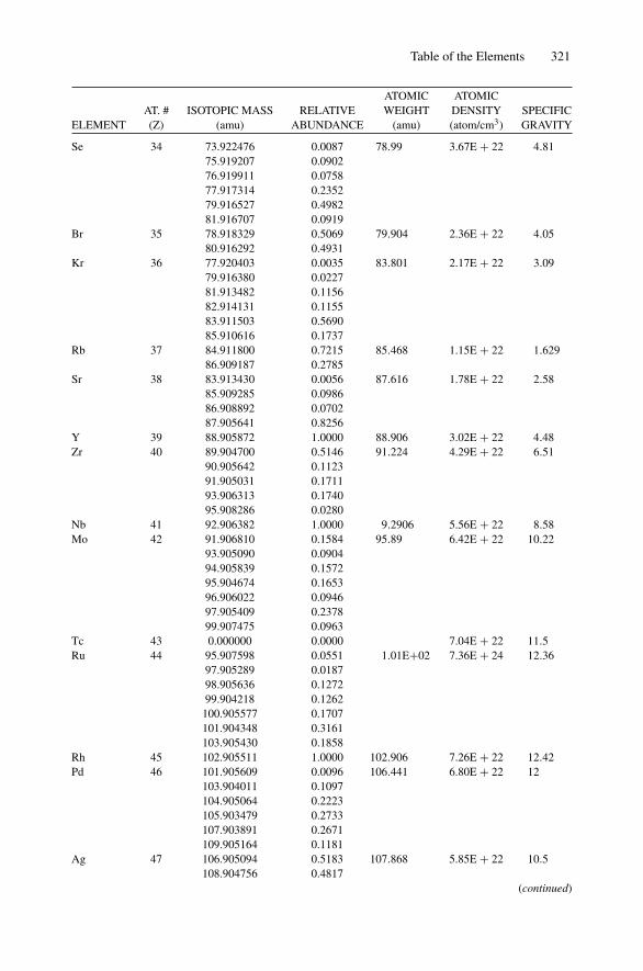
Table of the Elements 321
ATOMIC ATOMICAT. # ISOTOPIC MASS RELATIVE WEIGHT DENSITY SPECIFIC
ELEMENT (Z) (amu) ABUNDANCE (amu) (atom/cm3) GRAVITY
Se 34 73.922476 0.0087 78.99 3.67E + 22 4.8175.919207 0.090276.919911 0.075877.917314 0.235279.916527 0.498281.916707 0.0919
Br 35 78.918329 0.5069 79.904 2.36E + 22 4.0580.916292 0.4931
Kr 36 77.920403 0.0035 83.801 2.17E + 22 3.0979.916380 0.022781.913482 0.115682.914131 0.115583.911503 0.569085.910616 0.1737
Rb 37 84.911800 0.7215 85.468 1.15E + 22 1.62986.909187 0.2785
Sr 38 83.913430 0.0056 87.616 1.78E + 22 2.5885.909285 0.098686.908892 0.070287.905641 0.8256
Y 39 88.905872 1.0000 88.906 3.02E + 22 4.48Zr 40 89.904700 0.5146 91.224 4.29E + 22 6.51
90.905642 0.112391.905031 0.171193.906313 0.174095.908286 0.0280
Nb 41 92.906382 1.0000 9.2906 5.56E + 22 8.58Mo 42 91.906810 0.1584 95.89 6.42E + 22 10.22
93.905090 0.090494.905839 0.157295.904674 0.165396.906022 0.094697.905409 0.237899.907475 0.0963
Tc 43 0.000000 0.0000 7.04E + 22 11.5Ru 44 95.907598 0.0551 1.01E+02 7.36E + 24 12.36
97.905289 0.018798.905636 0.127299.904218 0.1262
100.905577 0.1707101.904348 0.3161103.905430 0.1858
Rh 45 102.905511 1.0000 102.906 7.26E + 22 12.42Pd 46 101.905609 0.0096 106.441 6.80E + 22 12
103.904011 0.1097104.905064 0.2223105.903479 0.2733107.903891 0.2671109.905164 0.1181
Ag 47 106.905094 0.5183 107.868 5.85E + 22 10.5108.904756 0.4817
(continued)
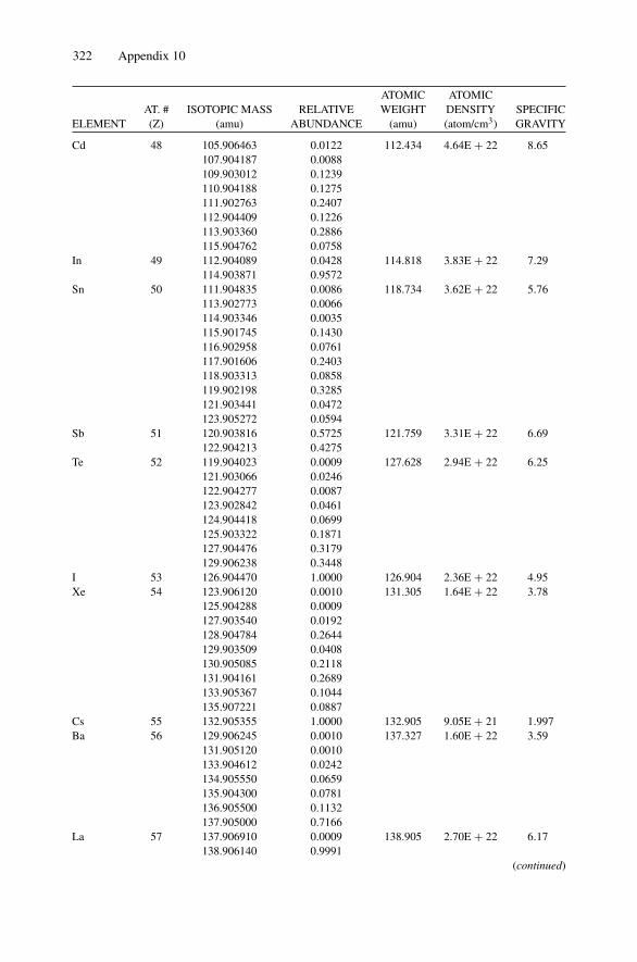
322 Appendix 10
ATOMIC ATOMICAT. # ISOTOPIC MASS RELATIVE WEIGHT DENSITY SPECIFIC
ELEMENT (Z) (amu) ABUNDANCE (amu) (atom/cm3) GRAVITY
Cd 48 105.906463 0.0122 112.434 4.64E + 22 8.65107.904187 0.0088109.903012 0.1239110.904188 0.1275111.902763 0.2407112.904409 0.1226113.903360 0.2886115.904762 0.0758
In 49 112.904089 0.0428 114.818 3.83E + 22 7.29114.903871 0.9572
Sn 50 111.904835 0.0086 118.734 3.62E + 22 5.76113.902773 0.0066114.903346 0.0035115.901745 0.1430116.902958 0.0761117.901606 0.2403118.903313 0.0858119.902198 0.3285121.903441 0.0472123.905272 0.0594
Sb 51 120.903816 0.5725 121.759 3.31E + 22 6.69122.904213 0.4275
Te 52 119.904023 0.0009 127.628 2.94E + 22 6.25121.903066 0.0246122.904277 0.0087123.902842 0.0461124.904418 0.0699125.903322 0.1871127.904476 0.3179129.906238 0.3448
I 53 126.904470 1.0000 126.904 2.36E + 22 4.95Xe 54 123.906120 0.0010 131.305 1.64E + 22 3.78
125.904288 0.0009127.903540 0.0192128.904784 0.2644129.903509 0.0408130.905085 0.2118131.904161 0.2689133.905367 0.1044135.907221 0.0887
Cs 55 132.905355 1.0000 132.905 9.05E + 21 1.997Ba 56 129.906245 0.0010 137.327 1.60E + 22 3.59
131.905120 0.0010133.904612 0.0242134.905550 0.0659135.904300 0.0781136.905500 0.1132137.905000 0.7166
La 57 137.906910 0.0009 138.905 2.70E + 22 6.17138.906140 0.9991
(continued)

Table of the Elements 323
ATOMIC ATOMICAT. # ISOTOPIC MASS RELATIVE WEIGHT DENSITY SPECIFIC
ELEMENT (Z) (amu) ABUNDANCE (amu) (atom/cm3) GRAVITY
Ce 58 135.907100 0.0019 140.101 2.91E + 22 6.77137.905830 0.0025139.905392 0.8848141.909140 0.1107
Pr 59 140.907596 1.0000 140.908 2.92E + 22 6.78Nd 60 141.907663 0.2711 144.241 2.93E + 22 7
142.909779 0.1217143.910039 0.2385144.912538 0.0830145.913086 0.1722147.916869 0.0573149.920915 0.0562
Pm 61 0.000000 0.0000Sm 62 143.911989 0.0309 150.363 3.03E + 22 7.54
146.914867 0.1497147.914791 0.1124148.917180 0.1383149.917276 0.0744151.919756 0.2672153.922282 0.2271
Eu 63 150.919838 0.4782 151.964 2.04E + 22 5.25152.921242 0.5218
Gd 64 151.919794 0.0020 157.256 3.02E + 22 7.89153.920929 0.0215154.922664 0.1473155.922175 0.2047156.924025 0.1568157.924178 0.2487159.927115 0.2190
Tb 65 158.925351 1.0000 158.925 3.22E + 22 8.27Dy 66 155.923930 0.0005 162.484 3.17E + 22 8.53
157.924449 0.0009159.925202 0.0229160.926945 0.1888161.926803 0.2553162.928755 0.2497163.929200 0.2818
Ho 67 164.930421 1.0000 164.93 3.22E + 22 8.8Er 68 161.928740 0.0014 167.261 3.26E + 22 9.04
163.929287 0.0156165.930307 0.3341166.932060 0.2294167.932383 0.2707169.935560 0.1488
Tm 69 168.934245 1.0000 168.934 3.32E + 22 9.32Yb 70 167.934160 0.0014 173.036 3.02E + 22 6.97
169.935020 0.0303170.936430 0.1431171.936360 0.2182172.938060 0.1613173.938740 0.3184175.942680 0.1273
(continued)
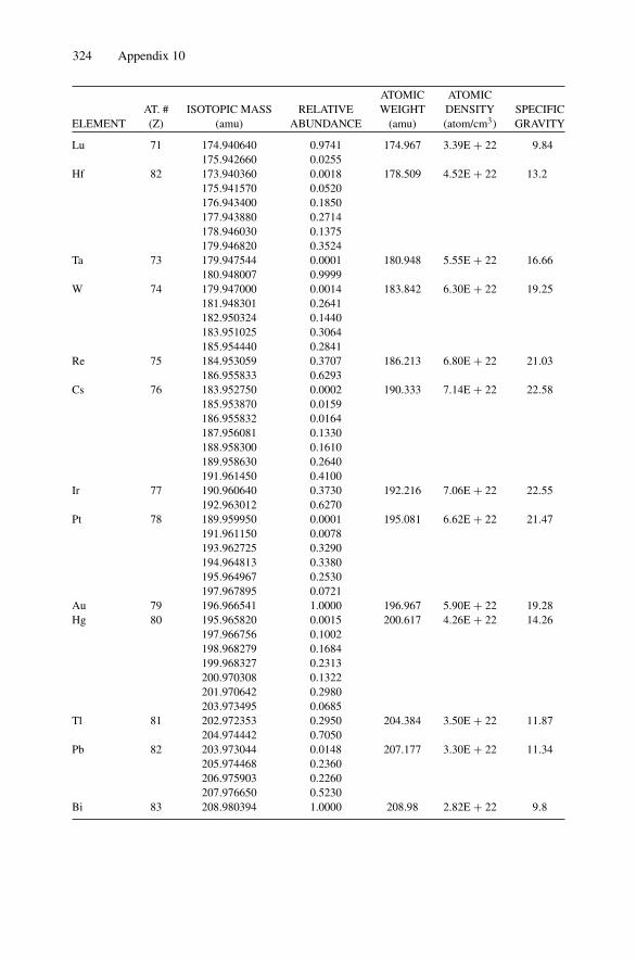
324 Appendix 10
ATOMIC ATOMICAT. # ISOTOPIC MASS RELATIVE WEIGHT DENSITY SPECIFIC
ELEMENT (Z) (amu) ABUNDANCE (amu) (atom/cm3) GRAVITY
Lu 71 174.940640 0.9741 174.967 3.39E + 22 9.84175.942660 0.0255
Hf 82 173.940360 0.0018 178.509 4.52E + 22 13.2175.941570 0.0520176.943400 0.1850177.943880 0.2714178.946030 0.1375179.946820 0.3524
Ta 73 179.947544 0.0001 180.948 5.55E + 22 16.66180.948007 0.9999
W 74 179.947000 0.0014 183.842 6.30E + 22 19.25181.948301 0.2641182.950324 0.1440183.951025 0.3064185.954440 0.2841
Re 75 184.953059 0.3707 186.213 6.80E + 22 21.03186.955833 0.6293
Cs 76 183.952750 0.0002 190.333 7.14E + 22 22.58185.953870 0.0159186.955832 0.0164187.956081 0.1330188.958300 0.1610189.958630 0.2640191.961450 0.4100
Ir 77 190.960640 0.3730 192.216 7.06E + 22 22.55192.963012 0.6270
Pt 78 189.959950 0.0001 195.081 6.62E + 22 21.47191.961150 0.0078193.962725 0.3290194.964813 0.3380195.964967 0.2530197.967895 0.0721
Au 79 196.966541 1.0000 196.967 5.90E + 22 19.28Hg 80 195.965820 0.0015 200.617 4.26E + 22 14.26
197.966756 0.1002198.968279 0.1684199.968327 0.2313200.970308 0.1322201.970642 0.2980203.973495 0.0685
Tl 81 202.972353 0.2950 204.384 3.50E + 22 11.87204.974442 0.7050
Pb 82 203.973044 0.0148 207.177 3.30E + 22 11.34205.974468 0.2360206.975903 0.2260207.976650 0.5230
Bi 83 208.980394 1.0000 208.98 2.82E + 22 9.8
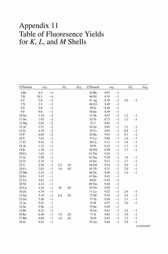
Appendix 11Table of Fluoresence Yieldsfor K, L, and M Shells
Z Element ωK ωL ωM Z Element ωK ωL ωM
4 Be 4.5 −4 45 Rh 8.07 −15 B 10.1 −4 46 Pd 8.19 −16 C 2.0 −3 47 Ag 8.30 −1 5.6 −27 N 3.5 −3 48 Cd 8.40 −18 0 5.8 −3 49 In 8.50 −19 F 9.0 −3 50 Sn 8.59 −1
10 Ne 1.34 −2 51 Sb 8.67 −1 1.2 −111 Na 1.92 −2 52 Te 8.75 −1 1.2 −112 Mg 2.65 −2 53 1 8.82 −113 Al 3.57 −2 54 Xe 8.89 −1 1.1 −114 Si 4.70 −2 55 Cs 8.95 −1 8.9 −215 P 6.04 −2 56 Ba 9.01 −1 9.3 −216 S 7.61 −2 57 La 9.06 −1 1.0 −117 Cl 9.42 −2 58 Ce 9.11 −1 1.6 −118 Ar 1.15 −1 59 Pr 9.15 −1 1.7 −119 K 1.38 −1 60 Nd 9.20 −1 1.7 −120 Ca 1.63 −1 61 Pm 9.24 −121 Sc 1.90 −1 62 Sm 9.28 −1 1.9 −122 Ti 2.19 −1 63 Eu 9.31 −1 1.7 −123 V 2.50 −1 2.4 .03 64 Gd 9.34 −1 2.0 −124 Cr 2.82 −1 3.0 .03 65 Tb 9.37 −1 2.0 −125 Mn 3.14 −1 66 Dy 9.40 −1 1.4 −126 Fe 3.47 −1 67 Ho 9.43 −127 Co 3.81 −1 68 Er 9.45 −128 Ni 4.14 −1 69 Tm 9.48 −129 Cu 4.45 −1 56 .03 70 Yb 9.50 −130 Zn 4.79 −1 71 Lu 9.52 −1 2.9 −131 Ga 5.10 −1 6.4 .03 72 Hf 9.54 −1 2.6 −132 Ge 5.40 −1 73 Ta 9.56 −1 2.3 −133 As 5.67 −1 74 W 9.57 −1 3.0 −134 Se 5.96 −1 75 Re 9.59 −135 Br 6.22 −1 76 Os 9.61 −1 3.5 −136 Kr 6.46 −1 1.0 .02 77 Ir 9.62 −1 3.0 −137 Rb 6.69 −1 1.0 .02 78 Pt 9.63 −1 3.3 −138 Sr 6.91 −1 79 Au 9.64 −1 3.9 −1
(continued)
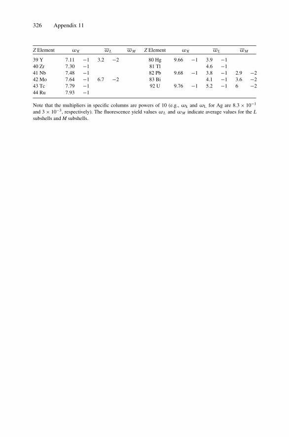
326 Appendix 11
Z Element ωK ωL ωM Z Element ωK ωL ωM
39 Y 7.11 −1 3.2 −2 80 Hg 9.66 −1 3.9 −140 Zr 7.30 −1 81 Tl 4.6 −141 Nb 7.48 −1 82 Pb 9.68 −1 3.8 −1 2.9 −242 Mo 7.64 −1 6.7 −2 83 Bi 4.1 −1 3.6 −243 Tc 7.79 −1 92 U 9.76 −1 5.2 −1 6 −244 Ru 7.93 −1
Note that the multipliers in specific columns are powers of 10 (e.g., ωk and ωL for Ag are 8.3 × 10⁻¹
and 3 × 10⁻³, respectively). The fluorescence yield values ωL and ωM indicate average values for the Lsubshells and M subshells.
Appendix 12Physical Constants, Conversions,and Useful Combinations
Physical constantsAvogadro constant NA = 6.022 × 10²³ particles/moleBoltzmann constant kB = 8.617 × 10⁻⁵ eV/KElementary charge e = 1.602 × 10⁻¹⁹ CoulombsPlanck constant h = 4.136 × 10⁻¹⁵ eV − s = 6.626 × 10⁻³⁴ J-s
h = h/2π = 6.582 × 10⁻¹⁶ eV-sSpeed of light c = 2.998 × 108 cm/s
Useful CombinationsElectron rest mass mc2 = 0.511 MeVBohr radius αo = h2/me2 = 0.0529 nmBohr velocity vo = e2/h = 2.188 × 108 cm/sFine structure constant α = e2/hc = 7.297 × 10⁻³ ≈ 1/137Hydrogen binding energy e2/2αo = 13.606 eVClassical electron radius re = e2/mc2 = 2.818 × 10⁻¹³ cmElectron charge e2 = 1.4395 eV-nmElectron Compton wavelength λ = h/mc = 3.861 × 10⁻¹¹ cmPhoton energy-wavelength hc = 1239.85 eV-nm
Conversions1 A= 10−8 cm = 10−1 nm1 eV = 1.602 × 10⁻¹⁹ J1 eV/particle = 23.06 kcal/molmp (proton mass) = 1.6726 × 10⁻²⁷ kg m(electron mass) = 9.1095 × 10⁻³¹ kg mp/m
mp/m = 1836.1
Appendix 13Acronyms
AEM Analytical Electron MicroscopyAES Auger Electron SpectroscopyAFM Atomic Force MicroscopyED Electron DiffractionEDS Energy-Dispersive SpectroscopyEELS Electron Energy-loss SpectroscopyEMA Electron Microprobe AnalysisESCA Electron Spectroscopy for Chemical AnalysisEXAFS Extended X-ray Absorption Fine StructureFRS Forward Recoil SpectroscopyGAXRD Glancing Angle X-Ray DiffractionHEED High-Energy Electron DiffractionHEIS High-Energy Ion ScatteringIIXS Ion-Induced X-ray SpectroscopyIMMA Ion Microprobe Mass AnalysisLEED Low-Energy Electron DiffractionLEIS Low-Energy Ion Scattering Neutron Activation AnalysisNRA Nuclear Reaction AnalysisPES Photoelectron SpectroscopyPIXE Particle-Induced X-ray EmissionPRA Prompt Reaction AnalysisRBS Rutherford Backscattering SpectrometryRHEED Reflection High EnergySEM Scanning Electron MicroscopySEXAF Surface Extended X-ray Absorption Fine StructureSIMS Secondary Ion Mass SpectroscopySNMS Secondary Neutral Mass SpectroscopySNOM Scanning Near-Field Optical MicroscopySPM Scanning Probe MicroscopySTM Scanning Tunneling MicroscopyTEM Transmission Electron MicroscopyTRXRF Total Reflection X-Ray Fluorescence

Acronyms 329
UPS Ultraviolet Photoelectron SpectroscopyWDS Wavelength Dispersive SpectroscopyXPS X-ray Photoelectron SpectroscopyXRD X-Ray DiffractionXRF X-Ray Fluorescence
Index
AAbsorption, X-ray, 185–189, 223Addition Rule, 155Activation analysis, 256, 261, 267
sensitivity, 268AES. See Auger electron spectroscopyAllowed reflections, 143, 146Alpha particle, 1–2, 7, 12, 15, 52, 258
range-energy, 53Aluminum
electron mean free path in, 114electron ranges in, 120energy loss in, 36, 39ion yield, 70Kα emission, 202plasmon, 112structure, 9
Aluminum nitride, analysis of, 271Arsenic implanted in Si, 72Atomic level width, 244Atomic force microscopy, 248Atomic number, App., 294, 299Atomic scattering factor, 144Auger electron spectroscopy, 245–249
chemical shifts, 239depth profiles, 250–252detection limit, 246–247KLL energies, App., 316–318escape depth, 201film growth, influence of, 115nomenclature, 235–237quantitative analysis, 249–250transition probability, 240–242transition rates, 242yield, 242–244
Auger electronsKLL energies, App., 316–318
escape depth, 201influence of film morphology on, 114–118rates, 243–244transitions, 235–238in XPS spectra, 239yield, 242–244See also Auger electron spectroscopy
Avogadro’s number, 6–7Axial channeling, 84, 87–88, 90
BBackscattering
electron, 250See also Rutherford backscattering spectrometry
Barn, 21, 211, 259Beta decay, 264–265Beta particles, 264Bethe, energy loss, 39Binding energy
in Auger electron spectroscopy, 238chemical shifts, 209–210of elements, 120hydrogen atom, 200in photoelectron spectroscopy, 207–208shifts, 209–210tables of, App., 305in X-ray emission, 215
Bohrenergy loss, 49–50model, 9–10radius, 10straggling, 49–50velocity, 10
Borondepth profile, 257(n, α) reaction, 257(p, α) reaction, 258
330

Index 331
Braggin diffraction, 158–159in energy loss, 40
Breit–Wigner cross section, 259Bremsstrahlung, 124–126
CCamera constant in TEM, 167–168, 170Carbon
photoelectric spectrum, 209proton irradiation, 257
Center of masslaboratory transformation, 28–31
Center of mass transformation, 28–31Central force scattering, 18–21Channeling, 84
critical angle, 86flux distribution, 88lattice location, 89minimum yield, 87potential, 85surface peak, 95–97thin film analysis, 152, 174
Charged particle reactions, 275Chemical shifts, 209–210Chlorine
(n, α) reaction, 261Cobalt
Auger transitions, 247–248Coefficient of thermal expansion, 133Compound nucleus, 258–259, 263Compounds, energy loss in, 40Compton scattering, 185Copper
Auger yield, 116decay scheme, 265energy loss in, 67sputtering of, 68
Correction factor, Rutherford scattering, 23Coster–Kronig transitions, 223, 236Coulomb barrier, 258, 270, 272Coulomb constant, 6Coulomb force, 19Coulomb shadow cone, 93Critical angle in channeling, 86Cross section
central force scattering, 18–21electron impact ionization, 110–111geometrical, 258inelastic electron, 109–111nuclear stopping, 63photoelectric effect, 181–184proton-induced ionization, 110–111radiation, 125resonant, 23, 25, 259
Rutherford, 23–24screened, 23square-well, 184stopping, 35–36thermal neutron, 269–270transformation, 28–29two-body scattering, 21–22scattering, 17–18
Cross-sectional TEM, 161Crystals
channeling in, 84–88lattice parameters, 88–89thermal vibrations, 87
Cylindrical mirror analyzer, 105, 203, 245
Dde Broglie relation, 8Density of states, 80, 182Deposited energy, surface, 63, 68Depth profiles
Auger, 250–252backscattering, 43–45prompt radiation analysis, 269SIMS, 73, 79sputtering, 59
Depth resolutionin backscattering, 47in sputtering, 79
Detection limitactivation analysis, 268Auger electron spectroscopy, 246–247electron microprobe, 223Rutherford backscattering, 54X-ray photoelectron spectroscopy, 221
Detector, nuclear particleacceptance angle, 48Si(Li), 218solid angle, 17
Deuteriumdetection, 50–52
Deuteron-induced reactions, 262
Diffractionelectron, 152X-ray, 129selected area, 164single crystalline patterns, 166polycrystalline pattern, 167
Dipole selection rules, 216Distance of closest approach, 18, 23–24, 66
in channeling, 87
EEinstein coefficients, 196, 221Elastic recoil. See Forward recoil spectrometry
332 Index
Elastic scattering. See Rutherford scatteringElectron
backscattered fraction, 225collisions, 109–110diffraction, 152energy loss spectroscopy, 120–124escape depth, 106–109impact ionization, 110inelastic collisions, 109–110mass, 8mean free path, 113microprobe, 223ranges, 118–120spectroscopies, 105–106
Electron capture, 264–265Electron configurations, App., 299Electron energy loss spectroscopy
of NiAl, 122of Ni silicide, 121–122yield, 122
Electron microprobebremsstrahlung, 223chemical binding shifts, 209correction factors, 225–227detection limit, 224–225energies, 218energy dispersive spectroscopy, 218quantitative analysis, 223transition rates, 221wavelength dispersive spectroscopy, 219
Electron microscopy, 160Electron shakeup, 208, 212Electron spectrometer, 203–204Electron spectroscopy for chemical analysis. See
X-ray photoelectron spectroscopyElectronic energy loss. See Energy lossElectrostatic analyzer, 24–26, 121, 203Endoergic nuclear reaction, 261Energy dispersive spectroscopy, 218Energy loss
in compounds, 40electron–electron, 120–124electron–plasmon, 111electronic, 40to electrons, 39–40factor, 42in mylar, 51nuclear, 63–66in silicon, 40–41stopping cross section, 35–36straggling, 47–50
Energy resolutionbackscattering, 16–17, 25cylindrical mirror analyzer, 105–106X-ray spectra, 219–220
Energy transfer, recoil, 13Energy width in backscattering, 40–43Energy width of atomic states, 220Epitaxy
Au on Ag, 97–99Au on Pd, 100–101in channeling, 102–103pseudomorphic growth, 99strain measurement, 137
ESCA. See X-ray photoelectron spectroscopyEscape depth
Auger electrons, 201photoelectrons, 211universal curve, 107–109
Ewald sphere, 159Excitation energy, 38–39, 113, 120Exoergic nuclear reaction, 261Extended X-ray absorption fine structure,
189–192
FFermi
golden rule, 181, 192–194level, 122, 187
Film growthepitaxial, 99influence on Auger electrons, 114–118islands, 116layer-by-layer, 114statistical distribution, 114types of, 114
Final state effects, 207–209Fine structure constant, 10Fluorescence yield, App., 325Flux distribution in channeling, 89–92Forward recoil spectrometry, 28
depth profiles, 50Frank–van der Merwe film growth, 114
GGallium arsenide, ion yield, 71Gamma decay, 265–266Gaussian, 49Germanium
Auger transitions, 242plasmon, 112
Goldepitaxy on Ag, 101
Grazing angle techniques, 48in channeling, 102in Rutherford backscattering, 48
HHamiltonian, 176, 181, 192–193Heisenberg uncertainty principle, 222
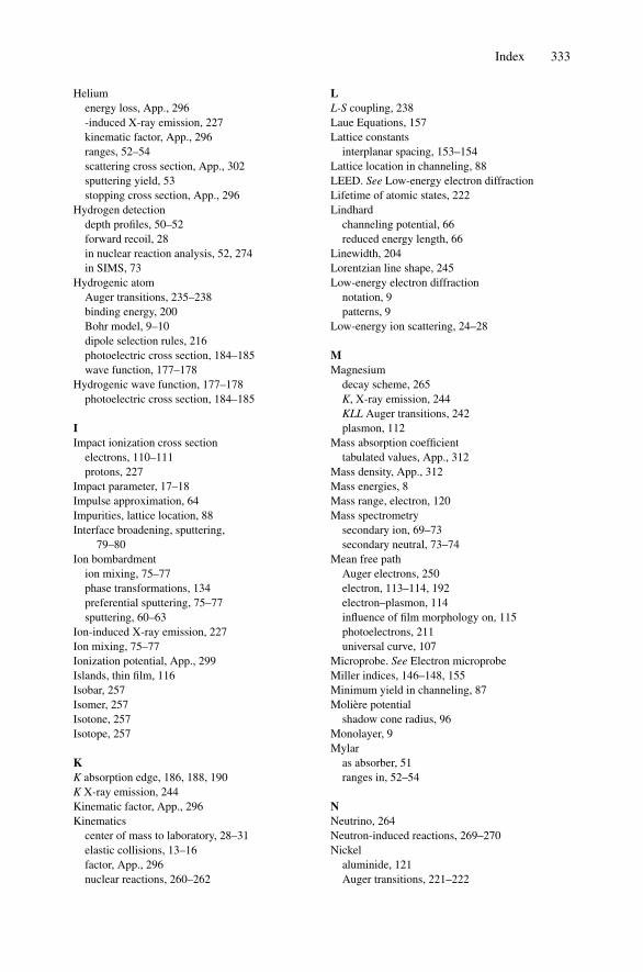
Index 333
Heliumenergy loss, App., 296-induced X-ray emission, 227kinematic factor, App., 296ranges, 52–54scattering cross section, App., 302sputtering yield, 53stopping cross section, App., 296
Hydrogen detectiondepth profiles, 50–52forward recoil, 28in nuclear reaction analysis, 52, 274in SIMS, 73
Hydrogenic atomAuger transitions, 235–238binding energy, 200Bohr model, 9–10dipole selection rules, 216photoelectric cross section, 184–185wave function, 177–178
Hydrogenic wave function, 177–178photoelectric cross section, 184–185
IImpact ionization cross section
electrons, 110–111protons, 227
Impact parameter, 17–18Impulse approximation, 64Impurities, lattice location, 88Interface broadening, sputtering,
79–80Ion bombardment
ion mixing, 75–77phase transformations, 134preferential sputtering, 75–77sputtering, 60–63
Ion-induced X-ray emission, 227Ion mixing, 75–77Ionization potential, App., 299Islands, thin film, 116Isobar, 257Isomer, 257Isotone, 257Isotope, 257
KK absorption edge, 186, 188, 190K X-ray emission, 244Kinematic factor, App., 296Kinematics
center of mass to laboratory, 28–31elastic collisions, 13–16factor, App., 296nuclear reactions, 260–262
LL-S coupling, 238Laue Equations, 157Lattice constants
interplanar spacing, 153–154Lattice location in channeling, 88LEED. See Low-energy electron diffractionLifetime of atomic states, 222Lindhard
channeling potential, 66reduced energy length, 66
Linewidth, 204Lorentzian line shape, 245Low-energy electron diffraction
notation, 9patterns, 9
Low-energy ion scattering, 24–28
MMagnesium
decay scheme, 265K, X-ray emission, 244KLL Auger transitions, 242plasmon, 112
Mass absorption coefficienttabulated values, App., 312
Mass density, App., 312Mass energies, 8Mass range, electron, 120Mass spectrometry
secondary ion, 69–73secondary neutral, 73–74
Mean free pathAuger electrons, 250electron, 113–114, 192electron–plasmon, 114influence of film morphology on, 115photoelectrons, 211universal curve, 107
Microprobe. See Electron microprobeMiller indices, 146–148, 155Minimum yield in channeling, 87Moliere potential
shadow cone radius, 96Monolayer, 9Mylar
as absorber, 51ranges in, 52–54
NNeutrino, 264Neutron-induced reactions, 269–270Nickel
aluminide, 121Auger transitions, 221–222
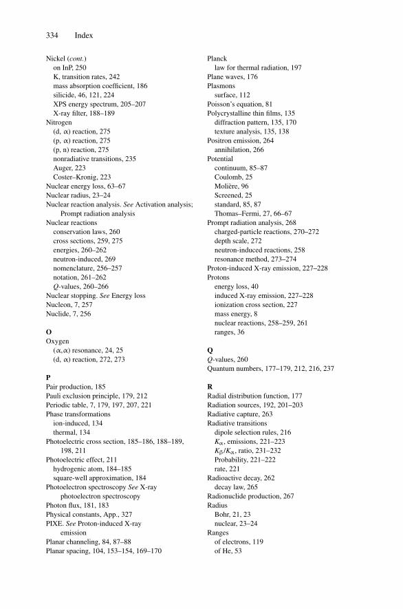
334 Index
Nickel (cont.)on InP, 250K, transition rates, 242mass absorption coefficient, 186silicide, 46, 121, 224XPS energy spectrum, 205–207X-ray filter, 188–189
Nitrogen(d, α) reaction, 275(p, α) reaction, 275(p, n) reaction, 275nonradiative transitions, 235Auger, 223Coster–Kronig, 223
Nuclear energy loss, 63–67Nuclear radius, 23–24Nuclear reaction analysis. See Activation analysis;
Prompt radiation analysisNuclear reactions
conservation laws, 260cross sections, 259, 275energies, 260–262neutron-induced, 269nomenclature, 256–257notation, 261–262Q-values, 260–266
Nuclear stopping. See Energy lossNucleon, 7, 257Nuclide, 7, 256
OOxygen
(α,α) resonance, 24, 25(d, α) reaction, 272, 273
PPair production, 185Pauli exclusion principle, 179, 212Periodic table, 7, 179, 197, 207, 221Phase transformations
ion-induced, 134thermal, 134
Photoelectric cross section, 185–186, 188–189,198, 211
Photoelectric effect, 211hydrogenic atom, 184–185square-well approximation, 184
Photoelectron spectroscopy See X-rayphotoelectron spectroscopy
Photon flux, 181, 183Physical constants, App., 327PIXE. See Proton-induced X-ray
emissionPlanar channeling, 84, 87–88Planar spacing, 104, 153–154, 169–170
Plancklaw for thermal radiation, 197
Plane waves, 176Plasmons
surface, 112Poisson’s equation, 81Polycrystalline thin films, 135
diffraction pattern, 135, 170texture analysis, 135, 138
Positron emission, 264annihilation, 266
Potentialcontinuum, 85–87Coulomb, 25Moliere, 96Screened, 25standard, 85, 87Thomas–Fermi, 27, 66–67
Prompt radiation analysis, 268charged-particle reactions, 270–272depth scale, 272neutron-induced reactions, 258resonance method, 273–274
Proton-induced X-ray emission, 227–228Protons
energy loss, 40induced X-ray emission, 227–228ionization cross section, 227mass energy, 8nuclear reactions, 258–259, 261ranges, 36
QQ-values, 260Quantum numbers, 177–179, 212, 216, 237
RRadial distribution function, 177Radiation sources, 192, 201–203Radiative capture, 263Radiative transitions
dipole selection rules, 216Kα, emissions, 221–223Kβ/Kα, ratio, 231–232Probability, 221–222rate, 221
Radioactive decay, 262decay law, 265
Radionuclide production, 267Radius
Bohr, 21, 23nuclear, 23–24
Rangesof electrons, 119of He, 53
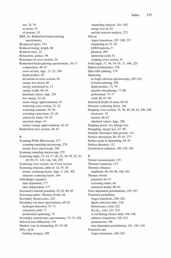
Index 335
ion, 78–79in mylar, 53of protons, 53
RBS. See Rutherford backscatteringspectrometry
Reciprocal space, 153Reduced energy, length, 66Reduced mass, 22Relaxation, surface, 98Resonance in cross section, 24Rutherford backscattering spectrometry, 16–17
composition, 46–47cross section, App., 21–22, 294depth profiles, 45deviations in cross section, 45energy loss factor, 40energy transferred in, 13energy width, 40–43kinematic factor, App., 291low energy, 24–26mean energy approximation, 43scattering cross section, 21–22scattering relations, 55, 56screening corrections, 23–24sensitivity limits, 54–55spectrum shape, 43surface energy approximation, 42–43
Rutherford cross section, 28, 43
SScanning Probe Microscopy, 277
scanning tunneling microscopy, 279atomic force microscopy, 284
Scanning tunneling microscopy, 279Scattering angle, 13–14, 17–20, 22, 29–30, 32, 41,
48, 50, 57, 124, 144, 146, 293Scattering cross section. See Cross sectionScattering relations, table of, 14, 55, 56
atomic scattering factor, App., 5, 144, 302structure scattering factor, 144
Schrodinger equationtime dependent, 177time independent, 177
Screened Coulomb potential, 25, 63, 80, 85Screening radius, Thomas–Fermi, 64Secondary fluorescence, 225Secondary ion mass spectrometry, 69–83
hydrogen detection, 72–73ionization yield, 73preferential sputtering, 75
Secondary neutral mass spectrometry, 73–75, 328Selected area diffraction, 154Shadow cone in channeling, 85, 93–98SiO2, on Si
binding energies, 209
channeling analysis, 101–102energy loss in, 42nuclear reaction analysis, 273
SiliconAuger transitions, 107–108, 237channeling in, 91–92LEED patterns, 9plasmon, 209sputtering yield, 61stopping cross section, 41
Solid angle, 17, 44, 54–55, 71, 106, 225Spherical harmonics, 229Spin orbit splitting, 179Sputtering
in Auger electron spectroscopy, 245–252in backscattering, 250depth profiles, 73, 79interface broadening, 77–80preferential, 75–77yield, 60, 67–69
Statistical model of atom, 80–81Structure scattering factor, 144Stopping cross section, 35, 36, 40, 46, 63, 296–298
electronic, 35nuclear, 66–67tabulated values, App., 296
Stopping power. See Energy lossStraggling, energy loss, 47–50Stranski–Krastanov film growth, 114Surface interaction, 84, 92–93, 277Surface peak in channeling, 95–97Surface plasmon, 112Synchrotron radiation, 190–192, 203
TTexture measurement, 135Thermal expansion, 133Thermal vibration
amplitude, 86, 94–96, 100, 103Thomas–Fermi
potential, 66–67screening radius, 64statistical model, 80–81
Time-dependent perturbations, 192–197Transition probability
Auger transitions, 240–242dipole selection rules, 216fluorescence yield, 222Kβ/Kα, ratio, 231–232in oscillating electric field, 194–196radiative transitions, 228–232spontaneous, 196time-dependent perturbation, 181, 192–194
Transition rateAuger transitions, 240–242
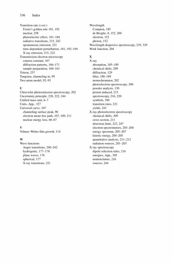
336 Index
Transition rate (cont.)Fermi’s golden rule 181, 192nuclear, 258photoelectric effect, 181–184radiative transitions, 215, 242spontaneous emission, 221time-dependent perturbation, 181, 192–194X-ray emission, 215, 222
Transmission electron microscopycamera constant, 167diffraction patterns, 166–171sample preparation, 160–163
Tritron, 257Tungsten, channeling in, 99Two-atom model, 92–93
UUltraviolet photoemission spectroscopy, 202Uncertainty principle, 220, 222, 244Unified mass unit, 6–7Units, App., 327Universal curve, 107
channeling surface peak, 96electron mean free path, 107, 109, 211nuclear energy loss, 66–67
VVolmer–Weber film growth, 114
WWave functions
Auger transitions, 240–242hydrogenic, 177–178plane waves, 176spherical, 177X-ray transitions, 221
WavelengthCompton, 185de Broglie, 8, 152, 260electron, 152photon, 152
Wavelength dispersive spectroscopy, 219, 329Work function, 204
XX-ray
absorption, 185–189chemical shifts, 209diffraction, 129filter, 188–189monochromator, 202photoelectron spectroscopy, 200powder analysis, 130proton-induced, 215spectroscopy, 216, 220symbols, 180transition rates, 221yields, 243
X-ray photoelectron spectroscopychemical shifts, 209cross section, 211detection limit, 223, 247electron spectrometers, 203–204energy spectrum, 205–207kinetic energy, 204–205quantitative analysis, 211–212radiation sources, 201–203
X-ray spectroscopydipole selection rules, 216energies, App., 305nomenclature, 216sources, 244

Printed in the United States