2 FPGA Fundamentals
34
FPGA FUNDAMENTALS Stanley L. Aquino, ECE
-
Upload
independent -
Category
Documents
-
view
2 -
download
0
Transcript of 2 FPGA Fundamentals

FPGAFUNDAMENTALS
Stanley L. Aquino,
ECE

FPGA DEFINITIONS
Field programmable gate arrays (FPGAs)are digital integrated circuits (ICs) that contain configurable (programmable) blocks of logic along with configurable interconnects between these blocks. Design engineers can configure, or program, such devices to perform a tremendous variety of tasks.
2

PLD
Programmable Logic Devices (PLDs) are devices whose internal architecture is predetermined by the manufacturer, but are created in such a way that they can be configured by engineers in the field to perform a variety of different functions.
3

ASIC & ASSP
Application-Specific Integrated Circuits (ASICs) and Application-Specific Standard Product (ASSPs) can contain hundreds of millions of logic gates and can be used to create incredibly large and complex functions. ASIC is designed and built to order for use by a specific company, while an ASSP is marketed to multiple customers.
4
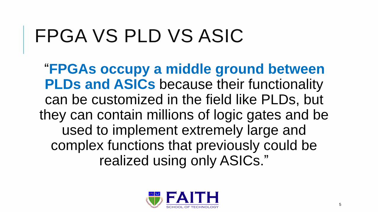
FPGA VS PLD VS ASIC
“FPGAs occupy a middle ground between PLDs and ASICs because their functionality can be customized in the field like PLDs, but
they can contain millions of logic gates and be used to implement extremely large and
complex functions that previously could be realized using only ASICs.”
5

TECHNOLOGY TRADE-OFFS (FPGA)
● The cost of an FPGA design is much lower than that of an ASIC (although the ensuing ASIC components are much cheaper in large production runs).
● Implementing design changes is much easier in FPGAs.
● Time to market for FPGAs is much faster.
6

FPGA APPLICATIONS
FPGAs are often used to prototype ASIC designs or to provide a hardware platform on which to verify the physical implementation of
new algorithms.
However, their low development cost and short time-to-market mean that they are increasingly finding their way into final products.
7

WHAT ARE THE MAJOR MARKET SEGMENTS FOR FPGAS?
ASIC and custom silicon
Digital signal processing
Embedded microcontrollers
Physical layer communications
Reconfigurable computing (RC)
8

SOME TECHNOLOGY BACKGROUND
The first FPGA devices contained only a fewthousand simple logic gates and the flows usedto design these components, predominantlybased on the use of schematic capture.
By comparison, today’s FPGAs are incrediblycomplex, and there are more design tools,flows, and techniques than you can swing astick at.
9

What distinguishes an FPGA from an ASIC is embodied in the name:
Field Programmable Gate Array
10

FUSIBLE-LINK TECHNOLOGY
11
A Simple Programmable Function
FUSIBLE-LINK TECHNOLOGY
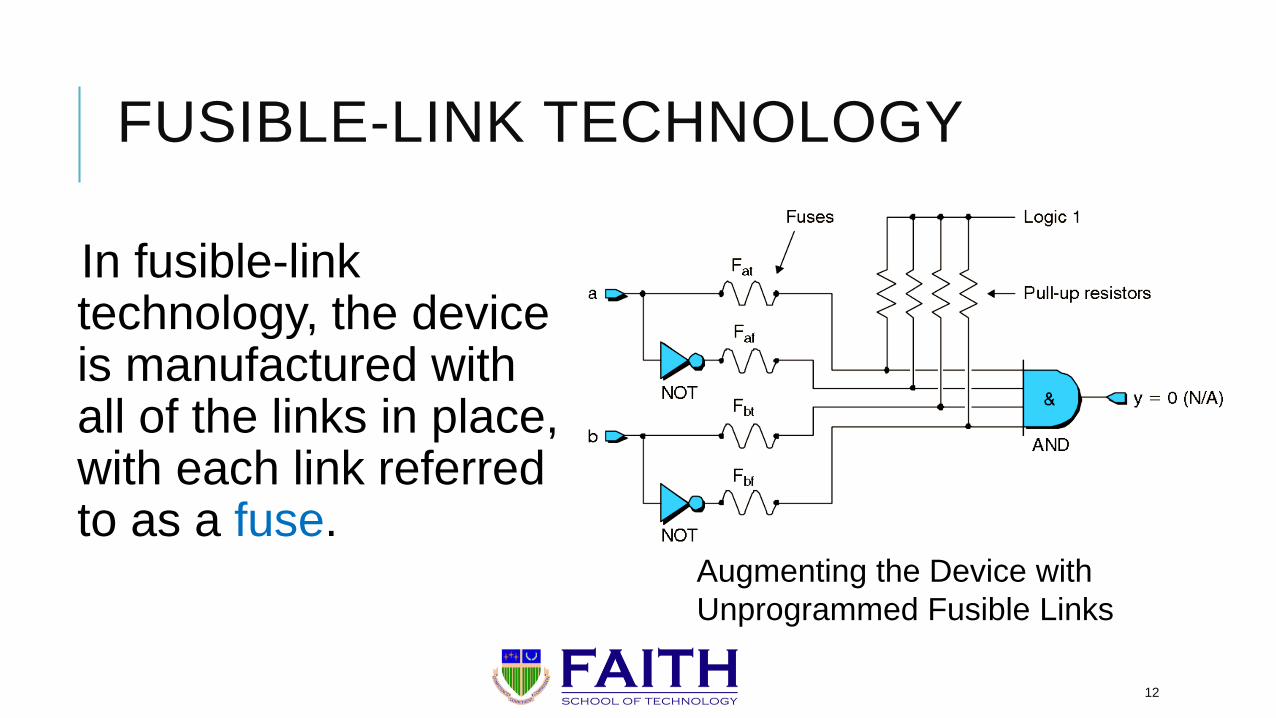
In fusible-link technology, the device is manufactured with all of the links in place, with each link referred to as a fuse.
12
Augmenting the Device with
Unprogrammed Fusible Links

FUSIBLE-LINK TECHNOLOGY
13
Programmed Fusible Links
Fusible-link technology is not used in today’s FPGAs but it sets the stage for understanding technologies.
The process of removing fuses is typically called programmingthe device, but it may also be called blowing the fuses or burning the device.

FUSIBLE-LINK TECHNOLOGY
14
Devices based on fusible-link technologies are one-time programmable (OTP) because once a fuse has been blown, it can’t be replaced and there’s no going back.

FPGA PROGRAMMING TECHNOLOGIES
Three different major technologies are in use today for programming FPGAs:
1. Antifuse
2. SRAM
3. Flash EPROM
15

ANTIFUSE TECHNOLOGY
Antifuse is a diametric alternative to fusible-link technologies, in which each configurable path has an associated link called an antifuse. In its unprogrammed state, an antifuse has such a high resistance that it may be considered an open circuit (a break in the wire).
16

ANTIFUSE TECHNOLOGY
17
Unprogrammed Antifuse Links Programmed Antifuse Links
ANTIFUSE TECHNOLOGY
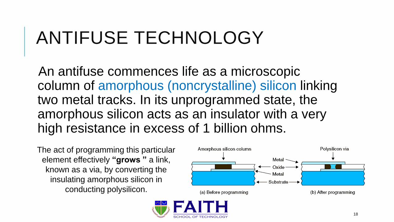
An antifuse commences life as a microscopic column of amorphous (noncrystalline) silicon linking two metal tracks. In its unprogrammed state, the amorphous silicon acts as an insulator with a very high resistance in excess of 1 billion ohms.
18
The act of programming this particular
element effectively “grows ” a link,
known as a via, by converting the
insulating amorphous silicon in
conducting polysilicon.

TECHNOLOGY TRADE-OFFS (ANTIFUSE)
Not surprisingly, devices based on antifusetechnologies are OTP, because once an antifuse has been grown, it cannot be removed, and there’s no changing your mind.
Antifuse devices tend to be faster and require lower power.
19

SRAM-BASED TECHNOLOGY
The “static” qualifier associated with SRAM means that—once a value has been loaded into an SRAM cell – it will remain unchanged unless it is specifically altered or until power is removed from the system.
20
An SRAM-based Programmable Cell

SRAM-BASED TECHNOLOGY
The entire cell comprises a multi-transistor SRAM storage element whose output drives an additional control transistor. Depending on the contents of the storage element (logic 0 or logic 1), the control transistor will be either OFF (disabled) or ON (enabled).
21
SRAM is currently the dominant FPGA technology

TECHNOLOGY TRADE-OFFS (SRAM)
A disadvantage of SRAM-based programmable devices is that each cell consumes a significant amount of silicon real estate because the cells are formed from four or six transistors configured as a latch.
22

SRAM-BASED TECHNOLOGY
Another disadvantage is that the device’s configuration data (programmed state) will be lost when power is removed from the system, so these devices always have to be reprogrammed when the system is powered on.
Advantages are that such devices can be reprogrammed quickly and easily, and SRAM uses a standard fabrication technology that is always being improved upon.
23

EPROM
This technology grew out of an earlier technology known as erasable programmable read-only memory (EPROM) that allows devices to be programmed, erased, and reprogrammed with new data.
24
Standard MOS versus EPROM Transistors

HOW EPROM WORKS
In its unprogrammed state, the floating gate is uncharged and doesn’t affect the normal operation of the control gate. In order to program the transistor, a relatively high voltage (on the order of 12V) is applied between the control gate and drain terminals.
25

HOW EPROM WORKS
This causes the transistor to be turned hard on, and energetic electrons force their way through the oxide into the floating gate in a process known as hot (high energy) electron injection.
When the programming signal is removed, a negative charge remains on the floating gate. This charge is very stable and will not dissipate for more than a decade under normal operating conditions.
26

EPROM MEMORY CELL
27
An EPROM Transistor-based Memory Cell

EPROM
The main problems with EPROMs are their expensive packages (with quartz windows through which ultraviolet (UV) radiation is used to erase the device) and the time it takes to erase them, on the order of 20 minutes.
28

EEPROM
Erasable programmable read-only memories (EEPROMs or E2PROMs) cell is approximately 2.5 times larger than an equivalent EPROM cell because it comprises two transistors and the space between them.
29
EEPROM
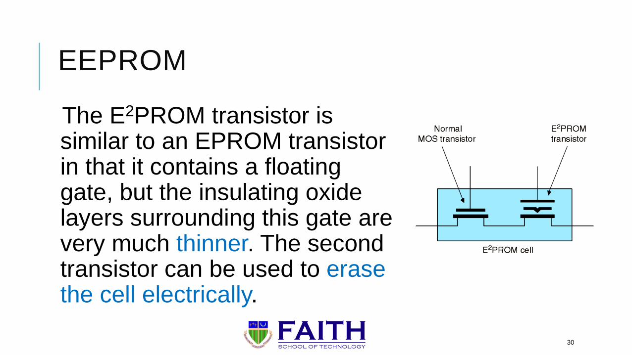
The E2PROM transistor is similar to an EPROM transistor in that it contains a floating gate, but the insulating oxide layers surrounding this gate are very much thinner. The second transistor can be used to erase the cell electrically.
30

FLASH-BASED TECHNOLOGIES
FLASH can trace its ancestry to both EPROM and EEPROM technologies. The name “FLASH” was originally coined to reflect this technology’s rapid erasure times compared to EPROM. Some have a single floating gate transistor cell, but with the thinner oxide layers characteristic of an E2PROM component.
Other architectures feature a two-transistor cell similar to that of an E2PROM cell, thereby allowing them to be erased and reprogrammed on a word-by-word basis.
31

TECHNOLOGY TRADE-OFFS (FLASH)
FLASH FPGAs are nonvolatile like antifuseFPGAs, but they are also reprogrammable like SRAM FPGAs.
FLASH FPGAs use a standard fabrication process like SRAM FPGAs and use lowerpower like antifuse FPGAs.
FLASH FPGAs are relatively fast.
32

SUMMARY OF PROGRAMMING TECHNOLOGIES
33
Technology Symbol Predominantly associated with
...
Fusible-link SPLDs
Antifuse FPGAs
EPROM SPLDs and CPLDs
E2PROM/FLASH SPLDs and CPLDs (some FPGAs)
SRAM FPGAs (some CPLDs)

THANK YOU!