
System Design using FPGA
16
System Design using FPGA G. Krishna Kumar Asst. Professor, Department of Electronics and Communication Engineering, CJITS Abstract— This paper provides the importance of System Design using FPGA for Engineering Education to utilize it as a commercial device to deliver a product, proposed by comparing with various technologies and tools with concern to Area, Speed and Power consumption of commercially available high-capacity FPGAs. According to the requirement of field applications the FPGAs are suitable to reach the Time to Market (TTM) of a product by avoiding the role of process industries up to some extent. The recent developing trends in VLSI Technology are Full custom design,ASICs,FPGAs,CPLDs, Masking and Non Masking of PLDs, Top to DN, DN to Top approaches of the semicustomdesigns like ASICs,FPGAs Field-Programmable Gate Arrays (FPGAs). The Architecture and implementation methods would be discussed here in detaill Keywords—Fullcustoms,FPGAs,Latches,Power,Area,Speed, K-Maps,CPLDs I. Introduction Types of IC Technologies and Implementation methods are mainly derived into the following methods shown in Figure- Figure-1 Types of IC-Technologies Full Custom Design: The Full custom design flow of the VLSI Technology is more concerned with micro based technology which consists of Sub-micron level A. Behavioral Level /Architectural level exploration and simulation by using HDL Languages like VHDL/ Verilog/ Verilog-a/ABEL for Conceive Design Implementation and Operation CDIO mechanisms B. Transistors schematic design to implement the Boolean function ‘F’ consists of A, B, C… by using the formula F-UP/PMOS, F-DN/NMOS network can be obtained from the formula given below for PMOS, NMOS respectively F-UP/PMOS = F (A’, B’, C’,………) - - - - - -- -Equation-1 F-DN/NMOS = (Boolean function F)’- - - - - - - - - Equation-2 In this formula Demorgan’s principles enormously used to get schematic design and simulations (by adjusting the transistor sizing between PMOS/Power-UP network or NMOS/Power-DN network, Proceedings of The Intl. Conf. on Information, Engineering, Management and Security 2014 [ICIEMS 2014] 361 ICIEMS 2014 ISBN : 978-81-925233-3-0 www.edlib.asdf.res.in / www.iciems.in Downloaded from www.edlib.asdf.res.in
Transcript of System Design using FPGA

System Design using FPGA
G. Krishna Kumar
Asst. Professor, Department of Electronics and Communication Engineering, CJITS
Abstract— This paper provides the importance of System Design using FPGA for Engineering Education to utilize it as a commercial device to deliver a product, proposed by comparing with various technologies and tools with concern to Area, Speed and Power consumption of commercially available high-capacity FPGAs. According to the requirement of field applications the FPGAs are suitable to reach the Time to Market (TTM) of a product by avoiding the role of process industries up to some extent.
The recent developing trends in VLSI Technology are Full custom design,ASICs,FPGAs,CPLDs, Masking and Non Masking of PLDs, Top to DN, DN to Top approaches of the semicustomdesigns like ASICs,FPGAs Field-Programmable Gate Arrays (FPGAs). The Architecture and implementation methods would be discussed here in detaill
Keywords—Fullcustoms,FPGAs,Latches,Power,Area,Speed, K-Maps,CPLDs
I. Introduction
Types of IC Technologies and Implementation methods are mainly derived into the following methods shown in Figure-
Figure-1 Types of IC-Technologies
Full Custom Design: The Full custom design flow of the VLSI Technology is more concerned with micro based technology which consists of Sub-micron level
A. Behavioral Level /Architectural level exploration and simulation by using HDL Languages like VHDL/ Verilog/ Verilog-a/ABEL for Conceive Design Implementation and Operation CDIO mechanisms
B. Transistors schematic design to implement the Boolean function ‘F’ consists of A, B, C… by using the formula F-UP/PMOS, F-DN/NMOS network can be obtained from the formula given below for PMOS, NMOS respectively
F-UP/PMOS = F (A’, B’, C’,………) - - - - - -- -Equation-1 F-DN/NMOS = (Boolean function F)’- - - - - - - - - Equation-2
In this formula Demorgan’s principles enormously used to get schematic design and simulations (by adjusting the transistor sizing between PMOS/Power-UP network or NMOS/Power-DN network,
Proceedings of The Intl. Conf. on Information, Engineering, Management and Security 2014 [ICIEMS 2014] 361
ICIEMS 2014 ISBN : 978-81-925233-3-0 www.edlib.asdf.res.in / www.iciems.in
Dow
nloa
ded
from
www.e
dlib.a
sdf.r
es.in

calculating the Id values and all) has to meet the Behavioral level’s simulations by doing the iterations and then continued for the layout design described in the part ‘C’
C. In the Layout design we need to follow the Lambda based or Submicron rules (Micro based design) to implement the Layout designs by using the standard layers (here four layer technology of AMS-Austrian Micro Systems based process rules are using) by special Manhattan’s principle, Euler-Path techniques were used to develop the layout to get the Optimistic values of getting Chip Area, Power, High speed, low cost for bulk production is here Layout (vs) Schematic are compared if they are equal(number of devices, number of interconnects ) then proceeds for the insertion of this layout into the PAD frame(Chip Assembly) for Electro Static Discharge ESD protection, I/O buffers for i/p,o/p connections, Analog protected input output frames (APRIOP) for the circuit protection and then converted to the GDS-II file format(Tape Out) for Fabrication industry by inserting the CAP NET on the total layout design in the pad frame.
Fiure-2 Flow of Full Custom Design
This process method would give more efficient results because it’s a pure handcrafting techniques are used(Intel 4004 Microprocessor is the worlds Single ChipMicroProcessor was developed by fullcustom designs in 1971 and now also implementing for super computers or Hyper Supercomputers only especially for Timing Modules like PLL,DLL,A/D,D/A converter at which the clock recovery mechanisms are more important) concern to Area, Low Power, High Speed but the more skilled designer is needed, Time to reach the market would be very much slow may be (months to year ) though it is suitable for bulk/mass production with low cost, and also It is too tough for developing countries which doesn’t have the process industries, to get the fabricated chip would consume more time which may not reach the market to launch the developed product, If any error comes while designing the product/ at the time of processing may leads to the loss by time, cost, scope of rectification to the design and fault finding in each level of design stage leads to more time.
Cadence ICFB tools (consists of Verilog-a,Virtuoso Schematic Composer for transistors level schematic capture, Analog environment with Spectre simulators, Virtuoso Layout for layout by using LSW window, Diva for DRC (design rule checking)
DRC:- Check the layout for design (sub-micron)rule violations Extract:- Create a extracted view of the layout. This view is used for simulations.Markers:- Explain: click on the marker to find out the design rule violated. Remove all the markers after a DRC run,
Proceedings of The Intl. Conf. on Information, Engineering, Management and Security 2014 [ICIEMS 2014] 362
ICIEMS 2014 ISBN : 978-81-925233-3-0 www.edlib.asdf.res.in / www.iciems.in
Dow
nloa
ded
from
www.e
dlib.a
sdf.r
es.in

Semicustom Designs: Application Specific Integrated Circuits Design flow (ASIC) In this design process some latest techniques can also be incorporated for Layout designs by using Physically Knowledgeable Synthesis (PKS) for layouts, NC-Launch and Soc-Encounter too.
Common Design flow for Semicustom Designs of ASIC and FPGA are in continuation with the following figure
Figure 3: Common Flow for ASICs and FPGAs
II. The Requirements and Necessities Lead the Technology towards Poor Men’s ASICs
Programmable Logic Designs: Programmable Logic Designs (PLDs) which are mostly in three important construction models
• Simple Programmable Logic Devices(SPLD's) PROM, PLAs, PALs shown in Figures • Complex Programmable Logic Devices(CPLD's) Figure • Field Programmable Gate Arrays (FPGA's) in figure Figure
SPLDs
An ad hoc approch to laying out a logic regular strctured design was adopted called as gate array structure.Predictablity over the logic is possible then improve area, performance by reducing two level layout i.e The Logic Shifts the Layout into SOP/POS Fashion of Prediffused/Mask Programmable Arrays, Bacthes of wafers containing arrays of primitive cells (or) Transistors are manufacture by the vendors & stored, with all fabrication steps are standadised & executed without regraded to the Final Application
Proceedings of The Intl. Conf. on Information, Engineering, Management and Security 2014 [ICIEMS 2014] 363
ICIEMS 2014 ISBN : 978-81-925233-3-0 www.edlib.asdf.res.in / www.iciems.in
Dow
nloa
ded
from
www.e
dlib.a
sdf.r
es.in
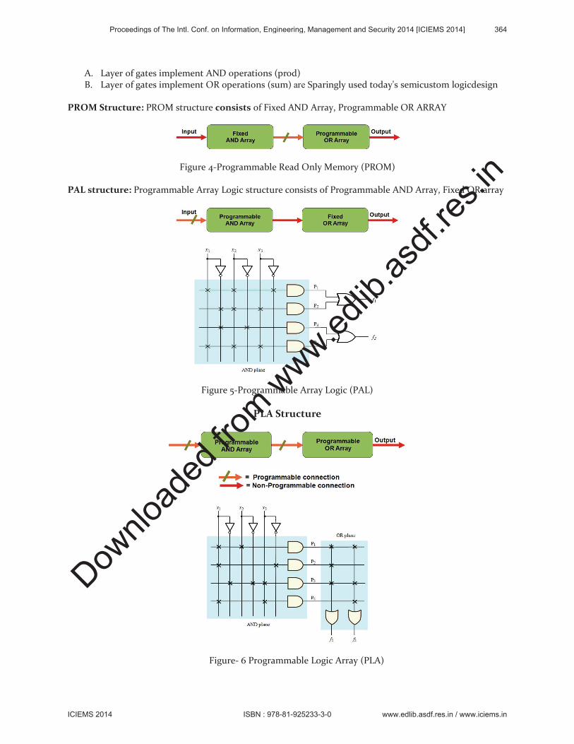
A. Layer of gates implement AND operations (prod) B. Layer of gates implement OR operations (sum) are Sparingly used today's semicustom logicdesign
PROM Structure: PROM structure consists of Fixed AND Array, Programmable OR ARRAY
Figure 4-Programmable Read Only Memory (PROM)
PAL structure: Programmable Array Logic structure consists of Programmable AND Array, Fixed OR array
Figure 5-Programmable Array Logic (PAL)
PLA Structure
Figure- 6 Programmable Logic Array (PLA)
Proceedings of The Intl. Conf. on Information, Engineering, Management and Security 2014 [ICIEMS 2014] 364
ICIEMS 2014 ISBN : 978-81-925233-3-0 www.edlib.asdf.res.in / www.iciems.in
Dow
nloa
ded
from
www.e
dlib.a
sdf.r
es.in

Demerits with SPLDs– Pre routed Channels are power hungry If Prediffused cell for 4-I/P then using it for 2-I/P wastes I/Ps, The multiple alternative cells creates geometry / Oxide isolation The "dogbone” terminations on the layout increases the Gate to poly(high resistance) In theses models which ever is more programmable nature will always tries to give the optimum logic and gives the good performence along with lowest Don't care states For Example PROM will have more number of Don't Care States than the PLA due to the (AND&OR) Arrays both are programmable.
The "dogbone” terminations,Longer fingure sizes on the layout increases the Gate/polyresistance (No option for free hand craft techniques for folding fingure of gate wire length)
Figure- 7 Dogbone structure
Here Masking(Non-Programmable Array) and Non-masking (Programmable Array)concepts needs to be under stand in an efficient manner to utilize these skills in System Designs at field levelimplementation, Pre Masked part gives optimistic results(Power,Area,Speed) point of view that’s why they never allowed to change /programm those modules/arrays.
CPLD's: CPLDs consists of like SPLD blocks connected with Programmable interconnectmatrix with Input/Output pins on S/CPLD
This PLDs structures and principles lead the concepts to preprocessed die that can be programmed at the field levels which acts as a poorrmen’s ASICs i.e.FPGA (without the help of Fab centre)
Figure: 8 A generic structure of CPLDs
Proceedings of The Intl. Conf. on Information, Engineering, Management and Security 2014 [ICIEMS 2014] 365
ICIEMS 2014 ISBN : 978-81-925233-3-0 www.edlib.asdf.res.in / www.iciems.in
Dow
nloa
ded
from
www.e
dlib.a
sdf.r
es.in

III. FPGA's
Field programmable gate arrays design flow consists of the folowing steps which reduces the design cost by low cost software,not much complex and low cost for the designers, fast TTM, executed at field level.
Figure- 9 FPGAs Design & Implementation Flow
Here I would like to express some internal contents and steps to execute the design steps for FPGAs implementations by writing the Verilog-code and get the simulations and must be synthesizable style of the design module. With the help of technology mapping and place and route the Configurable Logic Blocks (CLBs) into optimistic manner to get the low power, area by avoiding the longest interconnects.
Figure: 10 Classification of FPGAs based on memories
Proceedings of The Intl. Conf. on Information, Engineering, Management and Security 2014 [ICIEMS 2014] 366
ICIEMS 2014 ISBN : 978-81-925233-3-0 www.edlib.asdf.res.in / www.iciems.in
Dow
nloa
ded
from
www.e
dlib.a
sdf.r
es.in

Figure: 11Reliability of the FPGAs
Figure: 12 Vendors for FPGAs
FPGA Structures
Finegrained Architectures
Xilinx High reconfigurable nature, gives less performence Area, Delay time,Power Ex-Look Up Tables LUT's in Xilinxhe has become the major vendor in the market
Figure: 13 Market Survey for FPGAs
Coarsegrained Architectures
Dynamic Precision Scaling(DPS) blocks in Altrea Example DPS in ALTREA, Less reconfigurable nature due to it's Fixed position(masked) gives high performence Area,Delay time,Power Because the path which is allocated is fixed and can't reconfigured in any case[4] Nothing but Masking and kept the rights into vendor's usage at the time of layout designs/Asic is called as masking
Proceedings of The Intl. Conf. on Information, Engineering, Management and Security 2014 [ICIEMS 2014] 367
ICIEMS 2014 ISBN : 978-81-925233-3-0 www.edlib.asdf.res.in / www.iciems.in
Dow
nloa
ded
from
www.e
dlib.a
sdf.r
es.in

The FPGA Architecture is shown in figure below consists of CLBs,I/OBlocks,BlockRAMS
Figure: 14 FPGAs Structure and Architecture
Think about the Logic Modules which can be incorporate one near by the other rather than the random placing over all the FPGA area. Here no physical layout designs to manipulate for best design.
The design continued with the following steps; simulation, synthesis, optimistic design by logic (HDL code), place and route; user constraint file consists of the details about logical ports of the design module, physical ports of the FPGA board are used to communicate between system and FPGA board and to load the designed module in the form of bit-stream could be reconfigured by the designer at the field level by themselves
Manufacturing cycle for ASIC is very costly, lengthy and engages lots of manpower, Mistakes not detected at design time have large impact on development time and cost
Figure:15 Past and Present trends in VLSI
FPGAs are perfect for rapid prototyping of digital circuits Easy upgrades like in case of software, unique applications, and reconfigurable computing comparisons with ASIC and FPGA incorporated below
Figure: 16 Power comparisons for Xilinx Spartan 3 to 6 FPGAs
Proceedings of The Intl. Conf. on Information, Engineering, Management and Security 2014 [ICIEMS 2014] 368
ICIEMS 2014 ISBN : 978-81-925233-3-0 www.edlib.asdf.res.in / www.iciems.in
Dow
nloa
ded
from
www.e
dlib.a
sdf.r
es.in

Majority of FPGA vendors in the market for SRAM-based FPGAs: Xilinx, Inc., Altera[5] Corp., Atmel, Lattice Semiconductor refer the figure for market shares
EfficiencyPerformance
Delay Time, Low Power & AreaNRE-Cost Unit-Cost TTM & Rapid Prototyping
ASICASIC FPGA FPGA
FPGAFPGA ASIC ASIC
Figure: 17 comparisons between ASICs and FPGAs
Flash & antifuse FPGAs: Actel, Quick Logic CorpPrimary products: FPGAs and the associated CAD Software are listed below because the highest market share occupied by the vendor Xilinx.Inc. Main headquarters in San Jose, CA Fables* Semiconductor Company with earliest of CPLD, ISE Alliance and Foundation Series Design Software have been used
Figure: 18 Technology Performences
Figure: 19 The new Road Map for IGLOO-Nano FPGAs
Figure: 20 Spartan3A with Nomenclature
XC3S1500 - 4FG320
Spartan 3
Family
1500K=1.5 M
Equivalent Logic Gates
Speed
grade -4 Package
Type
320
Pins
Proceedings of The Intl. Conf. on Information, Engineering, Management and Security 2014 [ICIEMS 2014] 369
ICIEMS 2014 ISBN : 978-81-925233-3-0 www.edlib.asdf.res.in / www.iciems.in
Dow
nloa
ded
from
www.e
dlib.a
sdf.r
es.in

Xilinx consists of Vertex family boards for High performance; Spartan family is a Low Cost Family that we have used Spartan3A/3E, Spartan 6/7 too. Architectural details were described below for Spartan3A with Nomenclature
Figure: 21 Internal Structure of the Spartan3A
Figure: 22 Structure of each Configurable L-Block
Each slice contains two sets of the Following
Four-input LUT, Any 4-input logic function or 16-bit x 1 sync RAM (SLICEM only) or 16-bit shift registers (SLICEM only) Carry & Control, Fast arithmetic logic, Multiplier logic, Multiplexer logic, Storage element, Latch or flip-flop, Set and reset, True or inverted inputs, Sync. or async. Control after the design synthesis Map report with the FPGA hardware, software details and design date , number of errors, warnings, logic utilization like number of sliced flip-flops, number of 4-Input LUTs, number of used LUTs and number LUTs used for route through, Post layout, Timing, P&R report, resource utilization with design statistics
Figure: 23 Internal Structure of Configurable L-Block
Proceedings of The Intl. Conf. on Information, Engineering, Management and Security 2014 [ICIEMS 2014] 370
ICIEMS 2014 ISBN : 978-81-925233-3-0 www.edlib.asdf.res.in / www.iciems.in
Dow
nloa
ded
from
www.e
dlib.a
sdf.r
es.in

LUT’s: Look Up Tables are primary elements for Logic implementations, Each LUT can implement any function of 4 Inputs Example shown below
Figure: 24 Internal Structure of Configurable L-Block
LUT'S follow the Rent's rule pertains to the organization of computing logic, specifically the relationship between the number of external signal connections to a logic block (i.e., the number of "pins") with the number of logic gates in the logic block, and has been applied to circuits ranging from small digital circuits to mainframe computers. 5-Input Functions implemented using two LUTs One CLB Slice can implement any function of 5 inputs
• Logic function is partitioned between two LUTs • F5 multiplexer selects LUT
Figure: 25 Internal Structure of each Configurable L-Block
Figure: 26 Internal Structure of I/O –Block of Spartan 3
Proceedings of The Intl. Conf. on Information, Engineering, Management and Security 2014 [ICIEMS 2014] 371
ICIEMS 2014 ISBN : 978-81-925233-3-0 www.edlib.asdf.res.in / www.iciems.in
Dow
nloa
ded
from
www.e
dlib.a
sdf.r
es.in

Here need to take care while writing the HDL’s for any design While writing the HDL code
1) The case statement should be end with the default value of case otherwise it will generate and uses one extra Latch which consumes more power for Example 2 i/p binary count/ selects
Case 00, Case01, Case10, Case11,
Again we need to mention the case00; in last stage otherwise it definitely generate the Latch we can observe in the synthesis.
Observe the following code
Model of a Flip Flop with asynchronous reset always @(posedge clock) q <= d; always @(reset) if (reset) assign q = 1’b0; else deassign q; /*here if the deassign q is not mentioned the Latch would be generated along with the Flip Flop in the synthesis.
2)For the 2variable K-Map, approach i.e 00,01,11,10 Gray code counting method, like wise in Mux based select/ counter mechanisms also use the same method, if we use the binary count 00,01,10,11 which consumes 6 switching states where as in gray method it takes only 4 switching states which would directly impact on the Dynamic power consumption the Dynamic power = ½ CV2 f0-->1 binary counter getting 2 times more switching power than the gray code mechanism here power consumption effects are due to the f0-->1 depends on clock frequency is also applicable for CMOS switching activities too for primitive gates.
3) For mission critical application try to be stick on to the coding method as if, else, if, else method rather than looking for case/wait statements, and also for the FSMs use the MOORE model is better than the usage of MELAY Machine if reliability/ mission critical application to avoid the catastrophe though it’s speeder than the MOORE but power consumption is major constraint use the MELAY machine for field level implementations.
4) Implementation of the design View the placed and routed design in FPGA Editor Set up multiple place and route runs on your design
Figure: 27 Download onto FPGA
Proceedings of The Intl. Conf. on Information, Engineering, Management and Security 2014 [ICIEMS 2014] 372
ICIEMS 2014 ISBN : 978-81-925233-3-0 www.edlib.asdf.res.in / www.iciems.in
Dow
nloa
ded
from
www.e
dlib.a
sdf.r
es.in
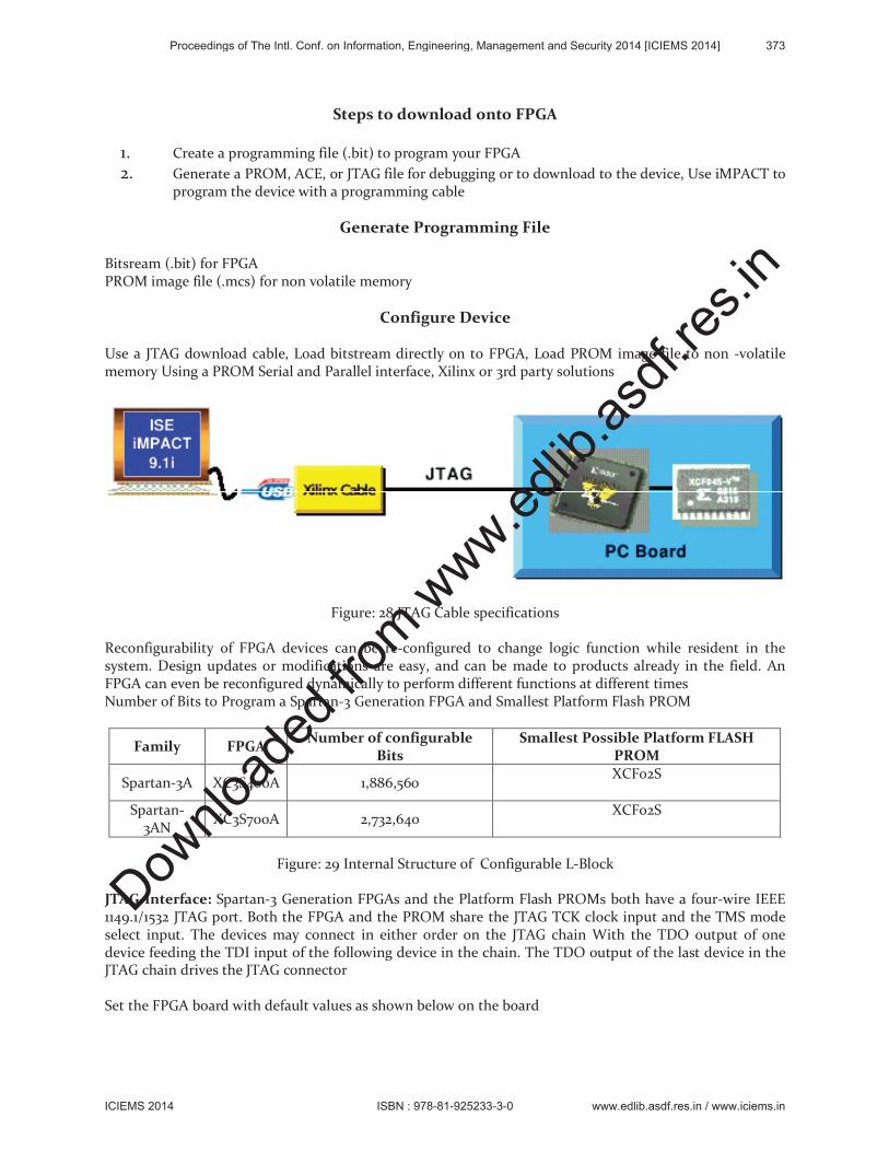
Steps to download onto FPGA
1. Create a programming file (.bit) to program your FPGA
2. Generate a PROM, ACE, or JTAG file for debugging or to download to the device, Use iMPACT to program the device with a programming cable
Generate Programming File
Bitsream (.bit) for FPGA PROM image file (.mcs) for non volatile memory
Configure Device
Use a JTAG download cable, Load bitstream directly on to FPGA, Load PROM image file to non -volatile memory Using a PROM Serial and Parallel interface, Xilinx or 3rd party solutions
Figure: 28 JTAG Cable specifications
Reconfigurability of FPGA devices can be re-configured to change logic function while resident in the system. Design updates or modifications are easy, and can be made to products already in the field. An FPGA can even be reconfigured dynamically to perform different functions at different times Number of Bits to Program a Spartan-3 Generation FPGA and Smallest Platform Flash PROM
Family FPGA Number of configurable
Bits Smallest Possible Platform FLASH
PROM
Spartan-3A XC3S400A 1,886,560 XCF02S
Spartan-3AN
XC3S700A 2,732,640 XCF02S
Figure: 29 Internal Structure of Configurable L-Block
JTAG Interface: Spartan-3 Generation FPGAs and the Platform Flash PROMs both have a four-wire IEEE 1149.1/1532 JTAG port. Both the FPGA and the PROM share the JTAG TCK clock input and the TMS mode select input. The devices may connect in either order on the JTAG chain With the TDO output of one device feeding the TDI input of the following device in the chain. The TDO output of the last device in the JTAG chain drives the JTAG connector
Set the FPGA board with default values as shown below on the board
Proceedings of The Intl. Conf. on Information, Engineering, Management and Security 2014 [ICIEMS 2014] 373
ICIEMS 2014 ISBN : 978-81-925233-3-0 www.edlib.asdf.res.in / www.iciems.in
Dow
nloa
ded
from
www.e
dlib.a
sdf.r
es.in

Figure: 30 Physical View of the Xilinx FPGAs
Conclusions
1. Here the Xilinx FPGAs more suitable to implement at the fields for engineering applications because it’s flexibility and Market share.
2. Keeping some notes about the FPGA Design can also be say top-down & down-top approach by taking the design module writing HDL, Simulate by giving test vectors and checking the simulation results according to specifications can be called as top- to –down approach here the design implemented by Logics, K-Maps, Truth tables etc.
3. Synthesis for the above same design using UCF, P and R and generating the .bit file and loading on to the FPGA to get it implement on the board called as down to top approach. Iterative methods can be done for better results (Area,Speed,Power) by verifying the Logics, K-Maps, Truth tables can be obtained in this synthesis delivered by the tool would be same as designed in step-2 (top-down), but the Logic implementation would be changed and optimized by using the Shannon’s principle , to implement all logics in Mux based implementations by implementing the
4) Shannon’s principle
Boolean function f(w1,w2,…wn) can be written in the format f(w1,w2,…wn) = w1’.f (0,w2,…wn) + w1.f(1,w2,……wn)
1) Example:Three-input XOR implemented with 2-to-1 Mux
Figure: 34 Three-input XOR
2)Optimized circuit for Three-input XOR gate implemented with a 4-to-1Mux
Proceedings of The Intl. Conf. on Information, Engineering, Management and Security 2014 [ICIEMS 2014] 374
ICIEMS 2014 ISBN : 978-81-925233-3-0 www.edlib.asdf.res.in / www.iciems.in
Dow
nloa
ded
from
www.e
dlib.a
sdf.r
es.in

Figure: 32 Internal Structure of Configurable L-Block
using the FPGAs in good manner to get synthesized and occupied very less to concern of the layout design and maps to the RTL, Technology file can be checked after the synthesis.
5) For easy understanding purpose took the NAND Gate as an example
DL for Nand Gate module NANDgate(A, B,F); input [0:0] A; input [0:0] B; output [0:0] F; reg F; //The Process Starts always@(A or B)begin F<= ~(A & B); end endmodule
Figure: 33 Simulation results for NAND gate
the result should be like this but never comes as usual changes to the eqivalent circuit
Figure: 34 NAND GATE
After synthesis we got the Values for truth table and Karnaugh -Map
Proceedings of The Intl. Conf. on Information, Engineering, Management and Security 2014 [ICIEMS 2014] 375
ICIEMS 2014 ISBN : 978-81-925233-3-0 www.edlib.asdf.res.in / www.iciems.in
Dow
nloa
ded
from
www.e
dlib.a
sdf.r
es.in

Figure : 35 Synthesis details to get the K-Map,T-Table
Figure : 36 Synthesis details to get the K-Map,T-Table
Equivalent circuits generated by synthesis for the above design. And get the results for RTL-Schematic, Technology schematic; K-Map for all parameters becomes correct.
6).After seeing all Macro level functions of the FPGAs are suitable for field level implementations at all levels without the fab-centre, Design can be configured n-number of times, FPGAs has become the Poor Man’s ASICs
Proceedings of The Intl. Conf. on Information, Engineering, Management and Security 2014 [ICIEMS 2014] 376
ICIEMS 2014 ISBN : 978-81-925233-3-0 www.edlib.asdf.res.in / www.iciems.in
Dow
nloa
ded
from
www.e
dlib.a
sdf.r
es.in