A New Single-Phase PLL Structure Based on Second Order Generalized Integrator
Upload
khangminh22Category
view
0download
0
DESIGN AND FPGA IMPLEMENTATION OF DIGITAL PLL AND
ITS APPLICATION IN FM
By
Vijaya Kumari-R790211058
Yashik Gulati-R790211061
Under the Guidance of
Dr. Adesh Kumar
College of Engineering
University of Petroleum & Energy Studies
Dehradun
May, 2015

DESIGN AND FPGA IMPLEMENTATION OF DIGITAL PLL AND ITS APPLICATION IN
FM
A project report submitted in partial fulfillment of the requirements for the Degree of
Bachelor of Technology
(Electronics Engineering)
By
Vijaya Kumari-R790211058
Yashik Gulati-R790211061
Under the guidance of
Dr. Adesh Kumar
Assistant Professor (Senior Scale)
Department of Electronics and Instrumentation
Approved
………………………………..
Dean
College of Engineering
University of Petroleum & Energy Studies
Dehradun
May, 2015

1
CERTIFICATE
This is to certify that the work contained in this report titled “DESIGN AND FPGA
IMPLEMENTATION OF DIGITAL PLL AND ITS APPLICATION IN FM” has been carried
out by YASHIK GULATI and VIJAYA KUMARI under my supervision and has not
been submitted elsewhere for a degree.
……………………
Mentor:-
Dr. Adesh Kumar
Assistant Professor (Senior Grade)
Deptt. Of Electronics, Instrumentation & Control Engineering
UPES, Dehradun

2
ACKNOWLEDGEMENT
We express our deepest thanks to Dr Adesh Kumar, our mentor for taking Part in
useful decisions and giving necessary advices and guidance. We choose this
moment to acknowledge his contribution gratefully.
It is our radiant sentiment to place on record deepest sense of gratitude to Dr.
Kamal Bansal (Dean, College of Engineering Studies) and Prof Sushabhan
Choudhary (HOD, Deptt of EIC) for careful and precious guidance which were
extremely valuable for the project.
We have taken efforts in this project, however it would not have been possible
without the kind support of many individuals. We would like to extend our sincere
thanks to them.

3
ABSTRACT
Recent advancement in the chip technology is integrating several sequential elements in System
on Chip (SoC). But most of the circuits are using traditional clock distribution networks and
facing the problem of skew and jitter problems. The clock signal generated by the oscillators and
the flip-flops and registers are not receiving the clock pulse at the accurate time. The problem can
be solved using Network of Phase-Locked Loop (PLL) oscillators coupled in phase. A phase
locked loop ensures that the clock frequencies seen at the clock inputs of various registers and flip-
flops match the frequency generated by the oscillator. The popular technique to demodulate FM
signal is Phase Locked Loop (PLL). The design approach is based on digital components rather
than analog components such as phase detector, loop filter and Voltage Controlled Oscillator
(VCO). The signal is presented using digital words instead of analog voltages. In digital FM
receiver, PLL is the main part to capture and lock the signals at different frequency and phase. The
main purpose of PLL is to maintain the coherence between the modulated signal frequency (fi) and
the respective frequency (fo), with the concept of phase comparison. PLL permits to track the
frequency changes of applied input signals, as it is locked once. The paper focuses on the design,
FPGA implementation of FM receiver integrated with digital PLL. There is a use of 8 bit analog to
digital conversion (ADC) circuit, which is accepting frequency modulated signal as a series of
digital numerical values. The same signals are demodulated by the receiver on every clock cycle.
The paper proposed the design and FPGA implementation of digital PLL and programmable all
FM receiver. The design is developed in Xilinx 14.2 ISE software and simulated in Modelsim
10.1b software with the help of VHDL programming language and the targeted onVirtex-5 FPGA.
4
TABLE OF CONTENTS
CONTENTS
LIST OF TABLES vi
LIST OF FIGURES vii
NOMENCLATURE ix
1 INTRODUCTION 1
1.1 Phase locked loop …………………………………………………………… 1
1.2 Design Development ………………………………………………………... 3
1.3 Problem Statement ……………………………………………………….….. 4
1.4 Objectives ……………………………………………………………….…... 4
1.5 Need of Research ……………………………………………………………. 4
1.6 Scope ………………………………………………………………………... 5
1.7 Thesis Outline …………………………………………………………….…. 5
2 LITERATURE REVIEW 7
3 THEORETICAL DEVELOPMENT 12
3.1 Architectural Description …………………………………………………… 12
3.2 Terms Related to PLL ………………………………………………………. 13
3.3 System Design ……………………………………………………………... 14
3.3.1 Phase Detector ……………………………………………………. 14
3.3.2 Loop Filter ……………………………………………………….... 15
3.3.3 Numerical Control Oscillator ……………………………………... 16
3.3.4 FIR Filter ……………………………………………………….….. 18
3.4 Functional Description of System …………………………………………… 19
4 MEATHODOLOGY AND IMPLEMENTATIONS 21
4.1 FPGA and Project Design Flow ……………………………………………… 22
4.2 FPGA Logic Implementation ………………………………………………… 24
4.3 Interconnects ……………………………………………………………..…. 26

5
4.4 Softwares Used ……………………………………………………………....…. 28
4.4.1 Xilinx ISE Project Navigator 14.1 ……………………………....…… 28
4.4.2 Modelsim 10.1 Student’s Edition …………………………………..…. 28
4.5 Simulation and Design Steps ……………………………………………….……. 29
4.6 Design Verification ……………………………………………………………… 29
4.6.1 Behavioral Simulation (RTL Simulation)……………………………..... 29
4.6.2 Functional simulation (Post Translate Simulation) …………………..... 30
4.6.3 Static Timing Analysis ……………………………………………….... 30
4.7 Contribution of Hardware Simulation and Synthesis in Networks…………….… 30
5 RESULTS AND DISCUSSIONS 32
5.1 Test Case 1 ………………………………………………………………………. 35
5.2 Test Case 2 ………………………………………………………………………. 35
5.3 Test Case 3 ………………………………………………………………………. 35
5.4 Test Case 4 ………………………………………………………………………. 35
5.5 Test Case 5 ………………………………………………………………………. 35
5.6 FPGA Results ……………………………………………………………………. 35
6 CONCLUSIONS AND RECOMMENDATIONS 41
REFRENCES 46
ANNEXURES 48

6
LIST OF TABLES
1. Table 4.1: Truth table for logic design......................................................... 26
2. Table 5.1: Pin Details of the FM Receiver................................................... 33
3. Table 5.2: Device utilization in DPLL based FM receiver.......................... 34
4. Table 5.3: Timing parameters for FM Receiver.......................................... 34

7
LIST OF FIGURES
1. Figure 1.1: Block Diagram of PLL……………………………………….. 2
2. Figure 1.2: Levels of abstraction: Behavioral, Structural and Physical….. 3
3. Figure 1.3: Structural representation of a “buzzer” circuit………………. 4
4. Figure 3.1: Block diagram of PLL……………………………………….. 12
5. Figure 3.2: Block diagram of FM receiver………………………………. 13
6. Figure 3.3: Phase Detector………………………………………………... 14
7. Figure 3.4: Loop Filter………………………………………….…………. 15
8. Figure 3.5: Block diagram of NCO……………………………………….. 16
9. Figure 3.6: Cosine ROM addressing…………………………….………… 17
10. Figure 3.7: Quarter wise values of one cycle of cosine ROM……………. 18
11. Figure 3.8: FIR filter structure……………………………………………. 19
12. Figure 3.9: Overall system block diagram……………………………….. 20
13. Figure 3.10.1: Z domain block diagram.................................................... 21
14. Figure 3.10.2: S domain block diagram..................................................... 21
15. Figure 4.1: FPGA Design project flow....................................................... 21
16. Figure 4.2: A VHDL entity consisting of an interface (entity declaration)
and a body (architectural description)....................................................... 22
17. Figure 4.3: FPGA View.............................................................................. 23
18. Figure 4.4: FPGA Architecture.................................................................. 24
19. Figure 4.5 Xilinx LUT................................................................................ 25
20. Figure 4.6 Logic Block Pin Locations......................................................... 26
21. Figure 4.7 Switch box topology................................................................... 27
22. Figure 5.1: Output of Phase Detector …………………………………… 32
23. Figure 5.2: Internal Diagram of Phase Detector ………………………… 32
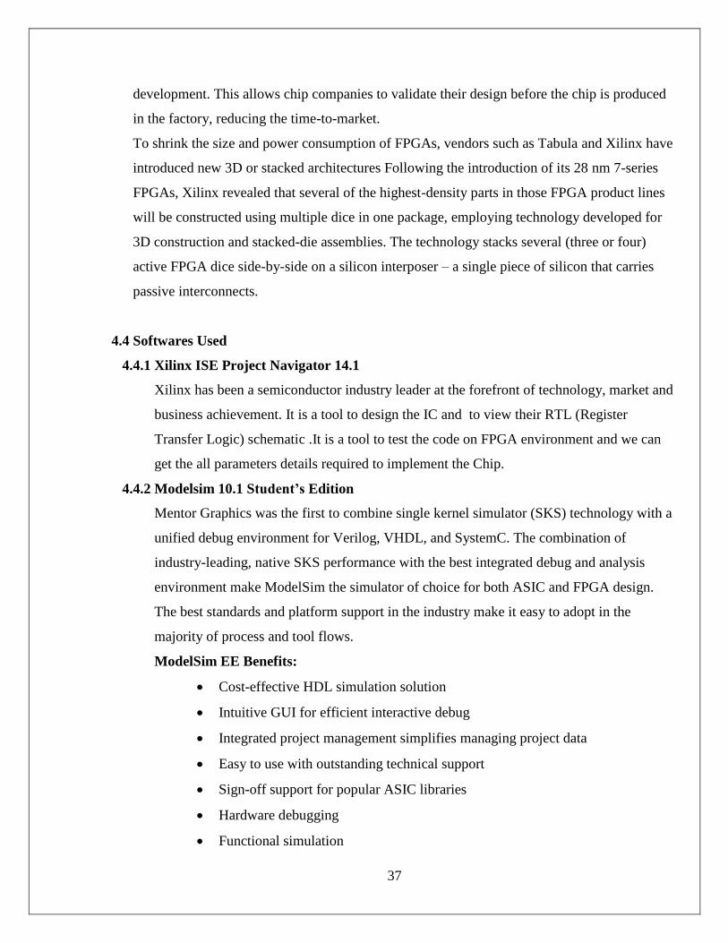
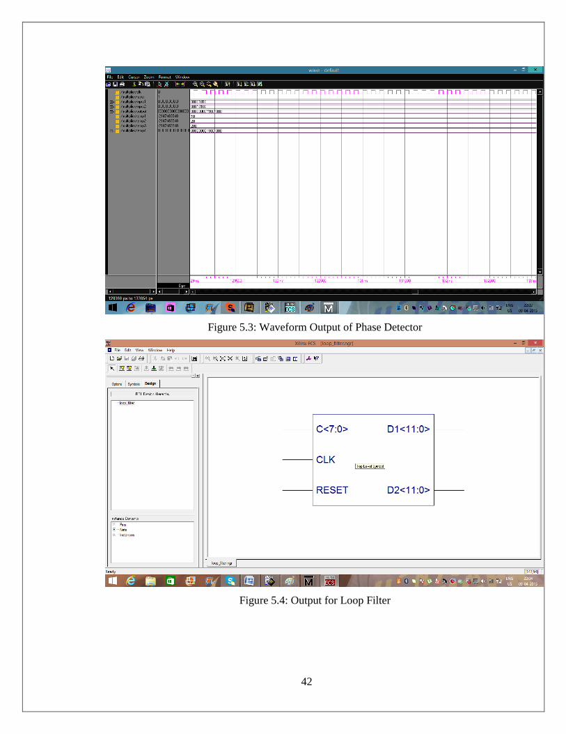
24. Figure 5.3: Waveform of Phase Detector……………………………….. 33
25. Figure 5.4: Output of Loop Filter ………………………………………... 33
26. Figure 5.5: Internal Diagram of Loop Filter ………………………….…. 34
27. Figure 5.6: Waveform Output of Loop Filter …………………………… 34

8
28. Figure 5.7: Output of ADC……………………………………………… 35
29. Figure 5.8: Output of DAC……………………………………………… 35
30. Figure 5.9: Internal Diagram of DAC …………………………………... 36
31. Figure 5.10 Output of FIR Filter ………………………………………... 36
32. Figure 5.11: Internal Diagram of FIR Filter ……………………………. 37
33. Figure 5.12 Waveform of FIR Filter ……………………………………. 37
34. Figure 5.13 Chip Design Process Flow..................................................... 38
35. Figure 5.14: RTL View of PLL................................................................. 38
36. Figure 5.15: Modelsim Simulation of FM Receiver................................... 38
37. Figure 5.16: FPGA synthesis process......................................................... 39
9
NOMENCLATURE
3D Three Dimensional
ABEL Advance Equation Boolean Language
AC Alternating Current
ADC Analog to Digital Converter
AES Advanced Encryption System
AM Analog Modulation
CAD Computer Aided Design
CDR Call Data Research
DC Direct Current
DDS Direct Digital Synthesis
DSO Digital Storage Oscillator
DSP Digital Signal Processor
FM Frequency Modulation
FPGA Field Programmable Gate Array
GPS Global Positioning System
HDL Hardware description language
LCD Liquid Crystal Display
LUT Look Up Table
MT Mobile Terminal
NCO Numeric Control Oscillator
OTP One Time Programmable
PLD Programmable Logic Design
PLL Phase Locked Loop
PM Phase Modulation
ROM Random Access memory
RTL Register Transfer Logic
SDR Software Defined ratio
SIM Subscriber Identity Module
SMSC Short Message Service Centre
SoC System on Chip
SP Service Provider
SROM Static Random Access Memory
VCO Voltage Control Oscillator
VHDL Very High Integrated Circuit Hardware Description Language
VHSIC Very High Speed Integrated Circuit
WLAN Wireless Local Ares Network

10
Chapter 1 Introduction
1.1 Phase locked loop (PLL)
Phase Locked Loops (PLL) is a closed loop system that locks two signals in such a way that
exist with same frequency and constant phase (zero) difference between them. The system
compares the frequencies of an input waveform to that of the output of PLL and then adjusts
the frequency of output such that they are totally synchronized with each other. PLL consist of
three parts: a phase detector, loop filter and a voltage controlled oscillator (VCO). The VCO
helps in changing the output frequency and provides frequency equal to the frequency of
incoming signal. PLL locks two signals in such a way that they are synchronized with each
other. The incoming signal in the reference or input signal is the frequency that is to be
adjusted so that it can match the reference signal and feed to VCO. PLL is used in clock
generation in system on chip (processors).PLLs can accurately generate a desired frequency. In
a communication system there are three modulation techniques, Amplitude Modulation (AM),
Frequency Modulation (FM) and Phase Modulation (PM). In the old system all transmissions
were analog so the traditional PLL are based on analog block. Analog PLL have noise and
gives varied output. Digital PLL are based on digital clock signal and lock the signal with
faster lock time such as in high speed microprocessor. This is the need of rapid change of the
technology existing for our handset and base station used in 3G mobile system. The existing
technologies are based on software defined radio (SDR) and the demand needs programmable
SDR instead of analog SDR. In SDR, Programmable digital devices are used and they transmit
and receive the baseband signal at radio frequency. The recent cellular devices follow the
communication protocol and provide connectivity to end user anywhere in the particular
region. The technologies which are using software and can process the data in real time use
base on field programmable gate array (FPGA) or digital signal processors (DSP). Frequency
modulation/demodulation is widely used schemes applied on mobile and fm devices. Audio
and voice signal clarity is the main issue in mobiles. In a FM modulated/demodulated signal it
is very difficult to achieve the good quality voice and clarity because VCO circuits are lagging
to provide desired frequency that is why there is a use of programmable chip implementation
of FM modulation system. The cellular industries always need such scalable hardware chip
which can support wireless local area network (WLAN) technologies, Bluetooth, global

11
positioning system (GPS) receiver, camera, MPEG videos etc. these applications need high
level of memory integration with transmitter-receiver integration.
PLL is a technique used to design a FM demodulator. In the PLL operation can be understood
with the help of the diagram as shown in Figure 1.1. The use of phase generator is to produce
an error signal with the help of the input signal and the reference signal. The phase comparator
is a multiplier of two signal inputs FM modulated signal and reference signal. Therefore
additional signal is generated so there is a need of digital filter. The reference signal is
generated using a numerically controlled oscillator (NCO) where oscillator is noticed by that
of error signal. Recent advancement in the chip technology is integrating several sequential
elements in System on Chip (SoC). But most of the circuits are using traditional clock
distribution networks and facing the problem of skew and jitter problems. The clock signal
generated by the oscillators and the flip-flops and registers are not receiving the clock pulse at
the accurate time. The problem can be solved using Network of Phase-Locked Loop (PLL)
oscillators coupled in phase. A phase locked loop ensures that the clock frequencies seen at the
clock inputs of various registers and flip-flops match the frequency generated by the oscillator.
The popular technique to demodulate FM signal is Phase Locked Loop (PLL). The design
approach is based on digital components rather than analog components such as phase
detector, loop filter and Voltage Controlled Oscillator (VCO). The signal is presented using
digital words instead of analog voltages. In digital FM receiver, PLL is the main part to
capture and lock the signals at different frequency and phase. The main purpose of PLL is to
maintain the coherence between the modulated signal frequency (fi) and the respective
frequency (fo), with the concept of phase comparison. PLL permits to track the frequency
changes of applied input signals, as it is locked once.
Phase Detector
Low Pass Filter
Amplifier
Voltage Control
Oscillator
FM Input
Output
Figure 1.1: Block Diagram of PLL
12
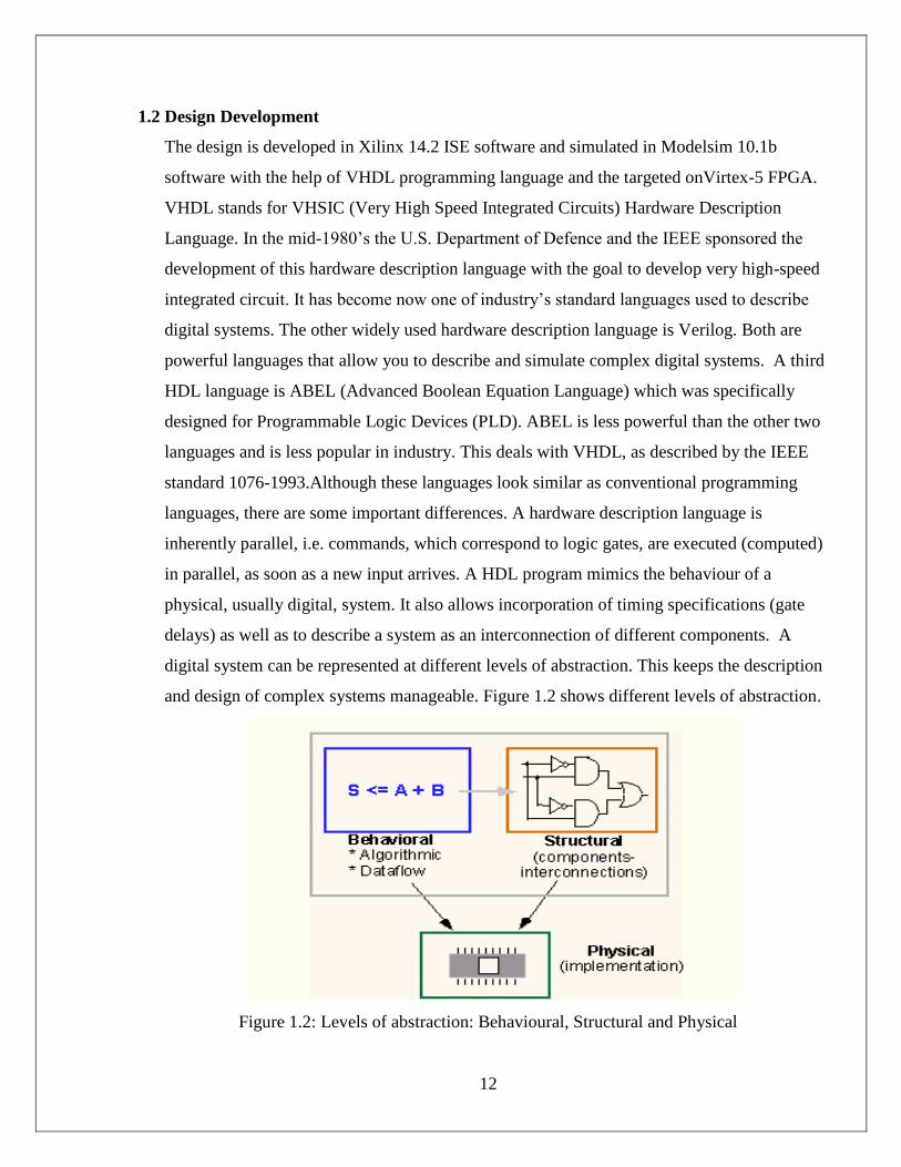
1.2 Design Development
The design is developed in Xilinx 14.2 ISE software and simulated in Modelsim 10.1b
software with the help of VHDL programming language and the targeted onVirtex-5 FPGA.
VHDL stands for VHSIC (Very High Speed Integrated Circuits) Hardware Description
Language. In the mid-1980’s the U.S. Department of Defence and the IEEE sponsored the
development of this hardware description language with the goal to develop very high-speed
integrated circuit. It has become now one of industry’s standard languages used to describe
digital systems. The other widely used hardware description language is Verilog. Both are
powerful languages that allow you to describe and simulate complex digital systems. A third
HDL language is ABEL (Advanced Boolean Equation Language) which was specifically
designed for Programmable Logic Devices (PLD). ABEL is less powerful than the other two
languages and is less popular in industry. This deals with VHDL, as described by the IEEE
standard 1076-1993.Although these languages look similar as conventional programming
languages, there are some important differences. A hardware description language is
inherently parallel, i.e. commands, which correspond to logic gates, are executed (computed)
in parallel, as soon as a new input arrives. A HDL program mimics the behaviour of a
physical, usually digital, system. It also allows incorporation of timing specifications (gate
delays) as well as to describe a system as an interconnection of different components. A
digital system can be represented at different levels of abstraction. This keeps the description
and design of complex systems manageable. Figure 1.2 shows different levels of abstraction.
Figure 1.2: Levels of abstraction: Behavioural, Structural and Physical

13
The highest level of abstraction is the behavioural level that describes a system in terms of
what it does (or how it behaves) rather than in terms of its components and interconnection
between them. A behavioural description specifies the relationship between the input and
output signals. This could be a Boolean expression or a more abstract description such as the
Register Transfer or Algorithmic level. As an example, let us consider a simple circuit that
warns car passengers when the door is open or the seatbelt is not used whenever the car key is
inserted in the ignition lock At the behavioural level this could be expressed as,
Warning = Ignition_on AND (Door_open OR Seatbelt_off)
The structural level, on the other hand, describes a system as a collection of gates and
components that are interconnected to perform a desired function. A structural description
could be compared to a schematic of interconnected logic gates. It is a representation that is
usually closer to the physical realization of a system. For the example above, the structural
representation is shown in Figure 1.3 below.
Figure 1.3: Structural representation of a “buzzer” circuit
VHDL allows one to describe a digital system at the structural or the behavioural level. The
behavioural level can be further divided into two kinds of styles: Data flow and Algorithmic.
The dataflow representation describes how data moves through the system. This is typically
done in terms of data flow between registers (Register Transfer level). The data flow model
makes use of concurrent statements that are executed in parallel as soon as data arrives at the
input. On the other hand, sequential statements are executed in the sequence that they are
specified. VHDL allows both concurrent and sequential signal assignments that will determine
the manner in which they are executed.

14
1.3 Problem Statement
The problem statement of the thesis is design and FPGA implementation of digital PLL and its
application in fm.
1.4 Objectives
The main objectives of the Project is to design a PLL system and show its applications in a FM
receiver
To design PLL system with the help of two main softwares which are Xilinx ISE
Project Navigator 14.1 and Modelsim 10.1 Student’s Edition.
The design has been implemented on FPGA board to show the proper working of the
DPLL
To show the application of PLL in FM receiver.
To understand the functionality of PLL components which are Phase Detector, Loop
Filter, Low Pass Filter and NCO.
To synthesise and simulate the DPLL by using VHDL language.
1.5 Need of Research
PLL system is been in the field of communication from a very long time, but as we know 21st
century is a digitalized century so there is a need to make a Digital PLL system. Earlier there
were analog PLL systems which had a lot of errors in their output which could lead to many
problems whereas a DPLL system has a Numeric Controlled Oscillator (NCO) instead of a
Voltage Controlled Oscillator (VCO) which is fully digitalized and has a very less amount of
error which results in better efficiency. There are many technologies which use PLL but this
thesis focuses on using a DPLL and showing its application in FM receiver and implementing
it on FPGA board using Xilinx ISE Project Navigator 14.1 and Modelsim 10.1 Student’s
Edition.
15
1.6 Scope of the Project
The phase locked loops (PLL) has many applications as FM receiver like as communication
and control system application. The balance mixtures can be used to reduce noise .we can also
use Improve the phase lock loop to handle larger signals. The loop used in our project
synchronizes only digital type signals.
1.7 Thesis Outline
The thesis consists of many chapters which are listed below
Chapter 1
This chapter includes basic principle and components of PLL and explains the basic
working of the system. This chapter also focuses on the design development of the
project. Two softwares are and their functions and uses are explained
Chapter 2
This chapter includes the Literature Review and the related work of the authors which
were studied in order to do the research work
Chapter 3
This chapter includes the theoretical development related to the project such as
architectural diagrams, terms related to PLL, system designs and the functional
description of the system.
Chapter 4
This chapter describes about the methods used to implement the project and explains
the working of the FPGA board and the functions of the softwares which are used to
implement the design
Chapter 5
This Chapter discusses about the results which were obtained after the project was
implemented.
Chapter 6
This chapter includes the conclusions which were drawn from the project and
recommends about the further research and possibilities.
16
Chapter 2 Literature Review
[1]. A. V. Rylyakov, et at have proposed a LC-DCO based PLL which is designed to work at
25GHz which has an output power spectrum of 36.064GHz and works over a temperature
range of 25⁰C to 85⁰C. An all static CMOS ADPLL fabricated in 65 nm digital CMOS SOI
technology has a fully programmable proportional-integral-differential (PID) loop filter and
features a third order delta sigma modulator. The DCO is a three stage, static inverter based
ring oscillator programmable in 768 frequency steps. The ADPLL lock range is 500 MHz to 8
GHz at 1.3 V and 25 C, and 90 MHz to 1.2 GHz at 0.5 V and 100 C. The IC dissipates 8
mW/GHz at 1.2 V and 1.6 mW/GHz at 0.5 V. The synthesized 4 GHz clock has a period jitter
of 0.7 ps rms, and long term jitter of 6 ps rms. The phase noise under nominal operating
conditions is 112 dBc/Hz measured at a10 MHz offset from a4 GHz centre frequency. The
total circuit area is 200 m 150 m. Digital phase-lock loop (DPLL) design approaches offer
multiple advantages, including compactness, broad programmability and testability, noise
immunity, direct migration between technology nodes, and enhanced robustness to process
variation [1-4]. In addition, DPLLs can be made modular, enabling the sharing of building
blocks between design points targeting different performance goals or feature sets. We report
two DPLLs fabricated in a standard 65nm bulk CMOS process.
[2]. Amr M. Fahim, et at has presented a book on research papers describing frequency
synthesizers from a front-end wireless transceiver perspective. The emphasis has historically
been on evaluating the frequency synthesizer's performance in the frequency domain, i.e. in
terms of phase noise and spurious signals. Examines the issue of design of fully integrated
frequency synthesizers suitable for system-on-a-chip (SOC) processors. This book takes a
more global design perspective in jointly examining the design space at the circuit level as
well as at the architectural level. The coverage of the book is comprehensive and includes
summary chapters on circuit theory as well as feedback control theory relevant to the operation
of phase locked loops (PLLs). On the circuit level, the discussion includes low-voltage analog
design in deep submicron digital CMOS processes, effects of supply noise, substrate noise, as
well device noise. On the architectural level, the discussion includes PLL analysis using
continuous-time as well as discrete time models, linear and nonlinear effects of PLL
performance, and detailed analysis of locking behaviour.
17
[3] Chia-Hung Huang, et at have design platform to develop and achieve the co-channel
separation and demodulation chip design for the additive white Gaussian noise (AWGN)
interference. In the thesis, he used an FPGA of Compact-RIO system are integrated and
applied to attain the function of communication characteristic chip. The modulated carrier is
often interfered by any type of noises. The co-channel separation system is a demodulation
function with dominant and subdominant signals using the receiver of modulation process
system by operating at the same as the carrier modulation system. In this thesis, we adopted
the field-programmable gate array (FPGA) design platform to develop and achieve the co-
channel separation and demodulation chip design for the additive white Gaussian noise
(AWGN) interference. In this thesis, the FPGA of Compact-RIO system are integrated and
applied to attain the function of communication characteristic chip and hardware design by
programming the graphical language.
[4] Chua-Chin Wang, et at have presented a 72.7 ps p2p jitter 80MHz PLL design using
components such as differential VCO, offset charge pump and regulator. A step down voltage
regulator is used to suppress the coupled supply noise. A zero offset charge pump is employed
is used to eliminate the static phase offset caused by the charge offset when the pll is in lock.
[5] Donald R. Stephens, at has proposed PLLs for Wireless Communications Digital, Analog
and Optical Implementations in MATLAB and communication media.
[6] Indranil Hatai, et at have proposed a high-performance digital FM modulator and a
Digital phase-locked loop-based FM demodulator and by individually optimizing the
components the performance has been improved. In this paper an FPGA implementation of a
high performance programmable digital FM modem has been done for targeting towards the
Software Defined Radio (SDR) application. The proposed design consists of the
reprogrammable, area optimized and low-power features. The modulator and demodulator
contain a compressed direct digital synthesizer (DDS) for generating the carrier frequency with
spurious free dynamic range of more than 70 dB. The demodulator has been implemented
based on the digital phase locked loop (DPLL) technique. The same DDS has been used for
demodulating the modulated signal. The proposed FM modem has been implemented and
tested using Virtex2Pro University board as a target device. Implementation of the FM modem
can run maximum 103 MHz, by taking less than 8k gate equivalent in the XC2VP-30 FPGA
device
18
[7] Indranil Hatai, et at have proposed VLSI implementation of high performance digital
phase locked loop based FM receiver which requires only 7.8K gates and can operate at
maximum frequency of 105MHz. This paper deals with an FPGA implementation of a high
performance FM modulator and demodulator for software defined radio (SDR) system. The
individual component of proposed FM modulator and demodulator has been optimized in such
a way that the overall design consists of a high-speed, area optimized and low-power features.
The modulator and demodulator contain an optimized direct digital frequency synthesizer
(DDFS) based on quarter-wave symmetry technique for generating the carrier frequency with
spurious free dynamic range (SFDR)of more than 64dB.The FM modulator uses pipeline
diversion of the DDFS to support the up conversion in the digital domain. The proposed FM
modulator and demodulator has been implemented and tested using XC2VP30-7ff896 FPGA
as a target device and can operate at a maximum frequency of 334.5MHz and 131MHz
involving around 1.93K and 6.4K equivalent gates for FM modulator and FM demodulator
respectively. After applying a 10 KHz triangular wave input and by setting the system clock
frequency to 100MHz using Xpower the power has been calculated. The FM modulator
consumes 107.67mW power while FM demodulator consumes 108.67mW power for the same
input running at same data rate.
[8] Indranil Hatai, et at have proposed a FM modem using FPGA implementation and is
integrated in a SDR-based next generation wireless communication transceiver circuit. In the
prevalent audio broadcasting applications like private mobile radio (PMR) and digital audio
broadcasting terrestrial (DAB-T) standards, excellent clarity along with the source stability is
required for the voice transmission. Frequency modulation (FM) scheme is used in most of
these standards. Traditionally, FM signal generation was performed using some analog
components to support the audio broadcasting standards. But difficulties arose in analog FM
modulation scheme due to the use of the voltage controlled oscillator (VCO)
[9] Jokin Segundo, et at have presented a PLL-based tuneable clock synthesizer in a 0:35mm
CMOS technology by using two continuous-time SD ADCs.
[10] Jose A. Tierno, et at have described a ADPLL built with static CMOS gates which has
features such as self-timed, bang bang phase and frequency control.
[11] Juan Pablo, et at have proposed a digital FM demodulator which is based on 2nd order
PLL and has 15K gates in it and operates at 150 MHz frequency.

19
[12] Jin Li, et at have proposed a software based radio FM stereo demodulation using general
quadrature demodulation technique.
[13] Martin John Burbidge, et at have suggested a idea of making a spectral purity CP-PLL
without using any traditional methods. This was achieved by mapping the output spectrum
degradation in terms of offset jitter to block level parameter values. Due to desirable
operational and implementation characteristics charge pump phase locked loops (CP-PLL)
systems are the architecture of choice for a variety of embedded frequency synthesis
applications.
[14] Nicholas Burnett et at has developed the digital FM demodulator and hardware testing is
done. The RF signal is given to the FM with the help of ADC and DAC demodulated signal is
tested.
[15] Nursani Rahmatullah, at has designed All Digital FM Receiver circuit is designed using
VHDL, then simulated and synthesized using ModelSim SE 6 simulator and Xilinx ISE 6.3i,
respectively. FPGA implementation also provided, here we use Virtex2 device.
[16] Praveen Kumar, et at has proposed a DPLL and an ADPLL and described about their
design and working parameters.
[17] Paolo Zikari, et at have proposed a highly versatile programmable Symbol Timing
Recovery circuit for BPSK, QPSK and OQPSK modulations with the help of VHDL and they
have implemented it on a Xilinx Virtex-4 XC4VLX60 device.
[18] Roberto Nonis, et at have proposed the architecture of DPLL which is based on bang
bang phase detector principle and it occupies 0.25mm2 and consumes 7.4 mW working on
25MHz. This paper introduces a novel architecture of digital PLL. The goal of this architecture
is to reach low jitter, fractional operation, and FSK modulation capability with low
architecture complexity for small area, low power, and minimal design effort. The architecture
is based on the bang-bang phase detector, so that usage of time-to-digital-converter circuits is
avoided, with no need for any background calibration. The key enabling blocks are a phase
interpolator-based exact fractional frequency divider, and a multi-output bang-bang phase
detector. The prototype implementedin130nmreaches1- absolute jitter while operating
inintegermodeand1.9 absolute jitter while operating in full fractional mode,with an output
frequency of 1GHz and reference frequency of 25 MHz, consuming 7.4 mW from a supply of

20
1.3 V. FSK modulation of the 1 GHz carrier up to 300 kbps with a frequency deviation of
150kHz is also implemented and measured
[19] Robert Bogdan Staszewski, et at have presented the first all-digital PLL and polar
transmitter for mobile phones which are a part of 90 nm digital CMOS process.
[20] S. Moorthi, et at have proposed a low jitter PLL used as a clock generator for analog to
digital converters having locking range from 95MHz-145MHz and centre frequency of
100MHz. This paper presents the circuit level implementation and analysis of the Phase
Locked Loop (PLL) architecture for clock generation in Analog to Digital Converters (ADCs).
The PLLs are required to generate low-noise or low-jitter clock signals and at the same time
need to achieve fast locking. The Analog to Digital Converters require a clock generator
whose clock output should have jitter less than 1 ps to have higher Effective Number Of Bits
(ENOB). Catering the needs of the ADC, low-jitter PLL architecture is proposed which consist
of pre-charged phase-frequency detector, charge pump, second order loop filter and a current-
starved inverter based Voltage Controlled Oscillator (VCO) circuit. The integrated PLL
architecture is implemented and simulated using CADENCE Analog Design Environment. It
is synthesized using TSMC 0.18µm, six-metal technology. The lock range (operating
frequency range) of the PLL is 95MHz to 145 MHz with a centre frequency of 100 MHz and a
jitter of around 700 fs are obtained as a result of its verification at all process corners.
21
Chapter 3 Theoretical Development
3.1 Architectural Description
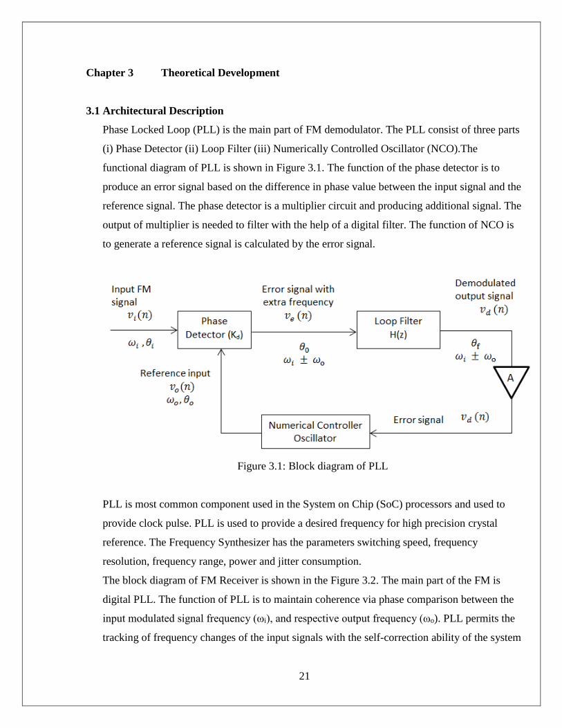
Phase Locked Loop (PLL) is the main part of FM demodulator. The PLL consist of three parts
(i) Phase Detector (ii) Loop Filter (iii) Numerically Controlled Oscillator (NCO).The
functional diagram of PLL is shown in Figure 3.1. The function of the phase detector is to
produce an error signal based on the difference in phase value between the input signal and the
reference signal. The phase detector is a multiplier circuit and producing additional signal. The
output of multiplier is needed to filter with the help of a digital filter. The function of NCO is
to generate a reference signal is calculated by the error signal.
Figure 3.1: Block diagram of PLL
PLL is most common component used in the System on Chip (SoC) processors and used to
provide clock pulse. PLL is used to provide a desired frequency for high precision crystal
reference. The Frequency Synthesizer has the parameters switching speed, frequency
resolution, frequency range, power and jitter consumption.
The block diagram of FM Receiver is shown in the Figure 3.2. The main part of the FM is
digital PLL. The function of PLL is to maintain coherence via phase comparison between the
input modulated signal frequency (ωi), and respective output frequency (ωo). PLL permits the
tracking of frequency changes of the input signals with the self-correction ability of the system

22
and lock the signal at particular frequency. The Frequency Modulated (FM) signal is
considered as a series of numerical values or digital data .This is done with the help of 8-bit
Analog to Digital converter (ADC) circuit. FIR filter will give the digital output and it can be
converted into FM. FM is a type of angle modulation scheme in which the instantaneous
frequency of the carrier signal varies linearly with the message signal m(t) as follows
𝑆𝐹𝑀(𝑡) = 𝐴𝑐 cos [2𝜋𝑓𝑐𝑡 + 2𝜋𝑘𝑓 ∫ 𝑚(𝑛)𝑑𝑛𝑡
0
] 𝐸𝑞𝑢𝑎𝑡𝑖𝑜𝑛 (1)
Where Ac = Amplitude of carrier, fc = Frequency of carrier signal, and Kf is frequency
deviation constant. The FM receiver gets the 8-bit modulated signal on every clock cycle and
provides the demodulated signal output.
Figure 3.2: Block diagram of FM receiver
3.2 Terms Related to PLL
1 Lock range: The frequency range the PLL is able to stay locked. Mainly defined by the VCO
range.
2 Capture range: The frequency range the PLL is able to lock-in, starting from unlocked
condition. This range is usually smaller than the lock range and will depend e.g. on phase
detector.
3 Loop bandwidth: Defining the speed of the control loop.
4 Transient response: Like overshoot and settling time to certain accuracy (like 50ppm).
5 Steady-state errors: Like remaining phase or timing error

23
6 Output spectrum purity: Like sidebands generated from a certain VCO tuning voltage
ripple.
7 Phase-noise: Defined by noise energy in a certain frequency band (like 10 kHz offset from
carrier). Highly dependent on VCO phase-noise, PLL bandwidth, etc.
General parameters: Such as power consumption, supply voltage range, output amplitude,
etc.
3.3 System Design
The description of the system with various comments of FM is discussed sequentially and
design aspects are also discussed.
3.3.1 Phase Detector
The function of the phase detector is to detect the phase error between the input signal and
the output signal coming from NCO. It is a multiplier circuit as shown in Figure3.3.
Figure 3.3: Phase Detector
The signal given to the phase detector is frequency modulated signal. Let the input signal
given to multiplier is vi(n) and expressed by equation 2.
𝑣𝑖(𝑛) = sin(𝜔𝑖𝑛 + 𝜃𝑖) 𝐸𝑞𝑢𝑎𝑡𝑖𝑜𝑛 (2)
Where 𝜔𝑖input is signal radian frequency and 𝜃𝑖 is phase angle. The output of NCO is
𝑣𝑜(𝑛) which is also sinusoidal and generated by NCO with feedback mechanism
𝑣𝑜(𝑛) = cos(𝜔𝑖𝑛 + 𝜃𝑜) 𝐸𝑞𝑢𝑎𝑡𝑖𝑜𝑛 (3)
24
The output of Phase detector to given by the multiplication of the two signals
𝑣𝑑 (𝑛) = 𝑘𝑑 sin(ω𝑖n + 𝜃𝑖) cos(ω𝑖n + 𝜃𝑜 )
𝑣𝑑 (𝑛) =𝑘𝑑
2[sin(2𝜔𝑖𝑛 + 𝜃𝑖 + 𝜃𝑜) + sin(𝜃𝑖 − 𝜃𝑜)] 𝐸𝑞𝑢𝑎𝑡𝑖𝑜𝑛 (4)
Where Ḳd = gain of the phase detector. Equation (4) is a combination of two terms. The
term 𝑠𝑖𝑛(2𝜔in + 𝜃𝑖+𝜃𝑜) presents the high frequency components and another term
sin(𝜃𝑖 − 𝜃𝑜) presents the phase difference between 𝑣𝑖(𝑛) and𝑣𝑜(𝑛). The size of both inputs
of the multiplier is 8-bit after multiplication the output is 16-bit. Input1 is minimum
frequency input fmin and input2 is NCO output. After multiplication sealing is done to crop
the most significant bits and the input of 8-bit is given to the loop filter. There are many
algorithms used for multiplication such as array multiplier, Booth’s multiplication. Booth
multiplier provides optimised results in comparison to Array multiplier, so it is used in the
design.
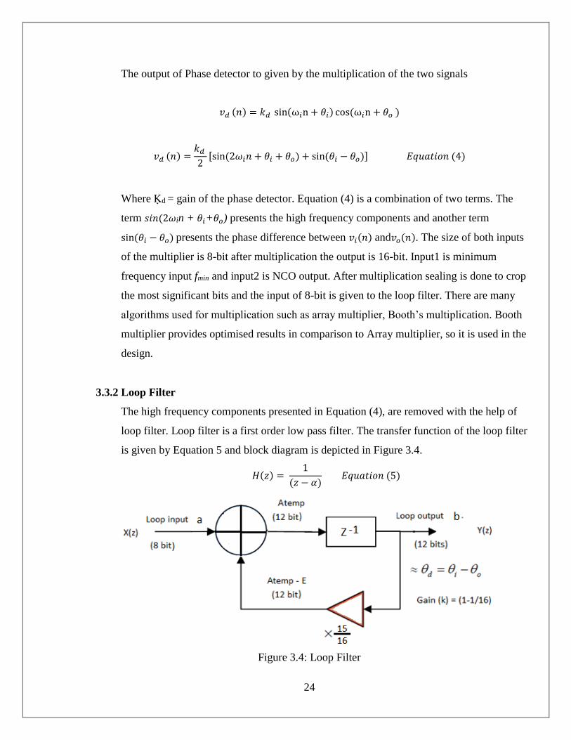
3.3.2 Loop Filter
The high frequency components presented in Equation (4), are removed with the help of
loop filter. Loop filter is a first order low pass filter. The transfer function of the loop filter
is given by Equation 5 and block diagram is depicted in Figure 3.4.
𝐻(𝑧) = 1
(𝑧 − 𝛼) 𝐸𝑞𝑢𝑎𝑡𝑖𝑜𝑛 (5)
Figure 3.4: Loop Filter

25
With the hardware implementation point of view the above equation uses addition of the
output signal from the phase detector and register output multiplied with a coefficient 𝛼 =
1 −1
16 =
15
16= 0.09375. The value of coefficient 𝛼 = 0.09375 lies within unit circle and
ensures the stability of the system. The complex multiplication operation is carried out in
such a way that extra multipliers are not needed and multiplication is implemented by just
4-bit right shift instead of a multiplier. The Equation (6) is written as
𝐻(𝑧) =𝑌(𝑧)
𝑋(𝑧)=
1
(𝑧 − 𝛼)=
1
(𝑧 − 0.09375) 𝐸𝑞𝑢𝑎𝑡𝑖𝑜𝑛 (6)
The input to the loop filter is ‘a’ of 8-bit and out is b which is multiplied by 15/16 and then
multiplication is given back to ’a’. The sum of a and b is carried by dtemp(12-bits), an
intermediate signal. dtemp is assigned, then
𝑑𝑡𝑒𝑚𝑝 ∗15
16=𝑑𝑡𝑒𝑚𝑝 ∗ (1 −
1
16) = 𝑑𝑡𝑒𝑚𝑝 − (𝑑𝑡𝑒𝑚𝑝 ∗
1
16)=𝑑𝑡𝑒𝑚𝑝 − 𝐸
The operation 𝐸 = 𝑑𝑡𝑒𝑚𝑝 ∗1
16is possible directly by shifting 4-bit right shift operation and
no extra multipliers are required.
3.3.3 Numerical Control Oscillator
NCO is also called Direct Digital Synthesizer (DDS). The function of DDS is to accept
Corrective Error Voltage 𝑣d(n) and then shifting its output frequency from its free running
value to the incoming input signal frequency ωi and thus keep the digital PLL in locking
condition. The block diagram of NCO is shown in Figure 3.5 and Figure 3.6.
Figure 3.5: Block diagram of NCO

26
Figure 3.6: Cosine ROM addressing
In the design, let us assume that the free running frequency of NCO is 1 MHz and system
clock frequency is 16 MHz so, there are 16 sampling points in the complete cycle of free
running frequency. In case of zero input, NCO generates an output equal to free running
frequency. In hardware chip point of view, Look up Table (LUT) technique is used to
sample real values of sinusoidal input of 1 MHz A digital integrator circuit is used to
accumulate input values and stored in predefined locations of Cosine Rom. A Cosine
signal is distributed in 4 quadrants as shown in figure and 1 MHz frequency of DDS is
defined using 1024 values of cosine signal. Based on 4 quarters distribution, first quarter is
having only 256 sample values. Therefore, the ROM size of (256 x 8) bit is chosen instead
of (1024 x 8) bit to store the 1024 values of Cosine Rom. Other quarters in the Cosine
ROM are duplicated of first quarter with an opposite sin of conversion to second and third.
The depth of LUT and width is decided in such a way that it can sustain the minimum
requirement for free dynamic range (SFDR) of 70dB. Accumulator is used to accumulate
the input phase and multiplexer to select the quadrant to assign the value is Cosine Rom
based on LUT. The Rom address is of 10-bits. Input D2 and offset value are added and
based on address mapping data values are stored in ROM locations.

27
Figure 3.7: Quarter wise values of one cycle of cosine ROM
The range of cosine ROM is accumulated data based on ROM address is given as
For first quadrant, 0 ≤ i ≤ 255 - cosrom (i)
For second quadrant, 256 ≤ i ≤512 - cosrom (512-i)
For third quadrant, 512≤ i ≤767 - cosrom (i-512)
For fourth quadrant, 768≤ i ≤1023 - cosrom (1024-i)
3.3.4 FIR Filter
In the last stage of FM demodulator FIR filter is used. The function of FIR filter is to
provide the wave from skipping. The FIR filter has ‘n’ number of taps and behaves as an
average filter because its output is equal to the average value of its input over the last ‘n’
samples. In the design, 16 tap FIR filter is used to perform digital low pass filtering and 16
configuration are needed to support the same configuration. If it is considered that all the
coefficients are same with value1
16. To perform multiplication by
1
16 will be equal to just
right shifting the value by 4 positions without extra multiplication. For hardware chip point
of view, the direct structure of FIR filter realization is not used. The block diagram of FIR
Filter is shown in Figure 3.8.

28
Figure 3.8: FIR filter structure
3.4 Functional Description of system
PLL is the main part of the receiver, having these major modules phase detector (multiplier),
loop filter and numerical control oscillator (NCO). The diagram for the complete system is
shown in the Figure 3.9. Initially, when no input signal is given to the system, NCO voltage
Vd(n) is zero. The operating frequency of NCO is f0 (radian frequency is 𝜔0) or the free
running frequency. The phase detector compares the phase and frequency of the input signals
with the frequency of NCO, if any input is applied to the system. NCO generates an error
signal voltage Ve(n) with the respect to the phase and frequency difference between these two
signals. The error voltage is filtered using loop filter and amplified with a factor of
amplification A=1
1024 and given directly to the control input of VCO. The NCO frequency is
forced by control voltage Vd(n) that can eliminate the frequency difference between W0 and
input signal. As the frequency𝜔𝑖close to𝜔𝑜, PLL cause the NCO to lock or synchronize the
incoming signal because of feedback existence in PLL. After the signal locking, NCO
frequency is identical to the input signal. The actual phase difference is θe = θi - θ0, essential to
produce the corrective error voltage Vd(n) and locking the PLL after shifting the NCO
frequency from its free running value or the input from the signal (𝜔𝑖).

29
Figure 3.9: Overall system block diagram
PLL tracks the frequency changes of the incoming signal. Locking and self-correction ability
of the system supports the functionality of the FM demodulator. The output of the phase
detector is mixed output of the frequency (𝜔𝑖± 𝜔𝑜). It can be observed from the Equation (4).
In the locking condition, input frequency is duplicated by NCO and (𝜔𝑖-𝜔𝑜) is zero. Therefore,
the output of the phase detector has only DC components and is passed to the amplifier and the
feedback to the NCO. Mathematically it is also possible to realize the transfer function of
NCO based on feedback control system concept. The system block diagram of digital PLL for
‘z’ domain and ‘s’ domain is shown in Figure 3.10.1 and Figure 3.10.2 respectively. It is very
much helpful in the transient state analysis and steady state analysis. Moreover in PLL
feedback system output is not followed immediately to input due to physical control system,
nature and energy conservation. The transfer function of the system is given as
𝑌(𝑠)
𝑋(𝑠)=
−𝑠2 + 𝑠
1.3375𝑠2 + 0.06161𝑠 + 0.00089 𝐸𝑞𝑢𝑎𝑡𝑖𝑜𝑛 (6)

30
Figure 3.10.1: Z domain block diagram Figure 3.10.2: S domain block diagram
Chapter 4 Methodology and Implementation
Figure 4.1 shows a flow chart over the design process when a design is implemented into an
FPGA. This flow was followed with all designs in this project and so became an important
structure in the project plan. For those that is not familiar with these concepts a short
description will follow. For more case specific see all the steps listed below at front end
design.
Figure 4.1: FPGA Design project flow
31
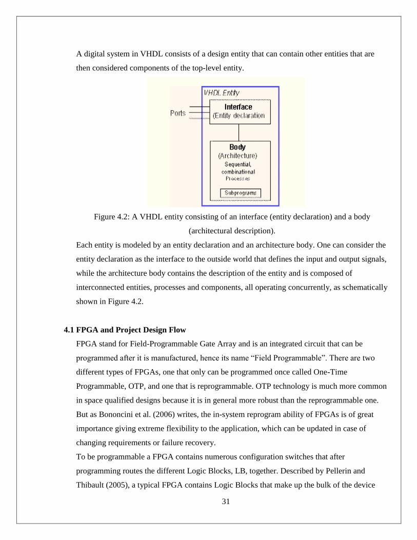
A digital system in VHDL consists of a design entity that can contain other entities that are
then considered components of the top-level entity.
Figure 4.2: A VHDL entity consisting of an interface (entity declaration) and a body
(architectural description).
Each entity is modeled by an entity declaration and an architecture body. One can consider the
entity declaration as the interface to the outside world that defines the input and output signals,
while the architecture body contains the description of the entity and is composed of
interconnected entities, processes and components, all operating concurrently, as schematically
shown in Figure 4.2.
4.1 FPGA and Project Design Flow
FPGA stand for Field-Programmable Gate Array and is an integrated circuit that can be
programmed after it is manufactured, hence its name “Field Programmable”. There are two
different types of FPGAs, one that only can be programmed once called One-Time
Programmable, OTP, and one that is reprogrammable. OTP technology is much more common
in space qualified designs because it is in general more robust than the reprogrammable one.
But as Bononcini et al. (2006) writes, the in-system reprogram ability of FPGAs is of great
importance giving extreme flexibility to the application, which can be updated in case of
changing requirements or failure recovery.
To be programmable a FPGA contains numerous configuration switches that after
programming routes the different Logic Blocks, LB, together. Described by Pellerin and
Thibault (2005), a typical FPGA contains Logic Blocks that make up the bulk of the device

32
and they are based on Lookup Tables, LUT, (of perhaps four or five binary inputs) combined
with one or two single-bit registers and additional logic elements such as clock enables and
multiplexers. These Logic Blocks and LUTs look differently depending on the technology
used, different companies use different technologies, but it usually also differ between product
series within a company. These Logic Blocks are then connected through a grid surrounding
them, which also connect with the I/O pins at the edges of the chip.
Figure 4.3: FPGA View
Many FPGAs provide internal SRAMs located between the Logic Blocks to greatly improve
functionality. This feature opens up to new possibilities although it also brings about another
trait that is usually sensitive to radiation. But despite that the use of SRAM-based FPGA is
growing in space based applications because of low application development cost, short time
to market, and the reprogramming flexibility that they offer, the need is recognized and today
there are FPGAs with radiation tolerant SRAM designs. Other FPGAs also include additional
internal blocks to increase the performance in different applications: like internal DLLs/PLLs;
multipliers or even more advanced DSP block (DSP Slices,); hard-macro processors (Power
PCs,); high speed serial links; etc. But these bring about even more radiation issues to
overcome.

33
4.2 FPGA Logic implementation
FPGA contains a two dimensional arrays of logic blocks and interconnections between logic
blocks. Both the logic blocks and interconnects are programmable. Logic blocks are
programmed to implement a desired function and the interconnects are programmed using the
switch boxes to connect the logic blocks. To be more clear, if we want to implement a
complex design (CPU for instance), then the design is divided into small sub functions and
each sub function is implemented using one logic block. Now, to get our desired design
(CPU), all the sub functions implemented in logic blocks must be connected and this is done
by programming the interconnects. Internal structure of an FPGA is depicted in the following
Figure 4.4
Figure 4.4: FPGA Architecture
FPGAs, alternative to the custom ICs, can be used to implement an entire System On one Chip
(SOC). The main advantage of FPGA is ability to reprogram. User can reprogram an FPGA to
implement a design and this is done after the FPGA is manufactured. This brings the name
“Field Programmable.”Custom ICs are expensive and takes long time to design so they are

34
useful when produced in bulk amounts. But FPGAs are easy to implement within a short time
with the help of Computer Aided Designing (CAD) tools (because there is no physical layout
process, no mask making, and no IC manufacturing).
Some disadvantages of FPGAs are, they are slow compared to custom ICs as they can’t handle
vary complex designs and also they draw more power.
Xilinx logic block consists of one Look up Table (LUT) and one Flip Flop. An LUT is used to
implement number of different functionality. The input lines to the logic block go into the
LUT and enable it. The output of the LUT gives the result of the logic function that it
implements and the output of logic block is registered or unregistered output from the LUT.
SRAM is used to implement a LUT.A k-input logic function is implemented using 2^k * 1 size
SRAM. Number of different possible functions for k input LUT is 2^2^k. Advantage of such
an architecture is that it supports implementation of so many logic functions, however the
disadvantage is unusually large number of memory cells required to implement such a logic
block in case number of inputs is large. Figure 4.5 below shows a 4-input LUT based
implementation of logic block. LUT based design provides for better logic block utilization. A
k-input LUT based logic block can be implemented in number of different ways with trade off
between performance and logic density.
Figure 4.5 Xilinx LUT
An n-LUT can be shown as a direct implementation of a function truth-table. Each of the
latches holds the value of the function corresponding to one input combination. For Example:
2-LUT can be used to implement 16 types of functions like AND, OR, A + not B.... etc.
35
Table 4.1: Truth table for logic design
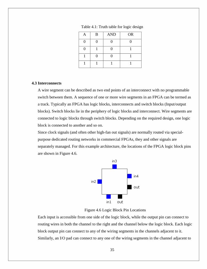
4.3 Interconnects
A wire segment can be described as two end points of an interconnect with no programmable
switch between them. A sequence of one or more wire segments in an FPGA can be termed as
a track. Typically an FPGA has logic blocks, interconnects and switch blocks (Input/output
blocks). Switch blocks lie in the periphery of logic blocks and interconnect. Wire segments are
connected to logic blocks through switch blocks. Depending on the required design, one logic
block is connected to another and so on.
Since clock signals (and often other high-fan out signals) are normally routed via special-
purpose dedicated routing networks in commercial FPGAs, they and other signals are
separately managed. For this example architecture, the locations of the FPGA logic block pins
are shown in Figure 4.6.
Figure 4.6 Logic Block Pin Locations
Each input is accessible from one side of the logic block, while the output pin can connect to
routing wires in both the channel to the right and the channel below the logic block. Each logic
block output pin can connect to any of the wiring segments in the channels adjacent to it.
Similarly, an I/O pad can connect to any one of the wiring segments in the channel adjacent to
A B AND OR
0 0 0 0
0 1 0 1
1 0 0 1
1 1 1 1

36
it. For example, an I/O pad at the top of the chip can connect to any of the W wires (where W
is the channel width) in the horizontal channel immediately below it.
Generally, the FPGA routing is unsegmented. That is, each wiring segment spans only one
logic block before it terminates in a switch box. By turning on some of the programmable
switches within a switch box, longer paths can be constructed. For higher speed interconnect,
some FPGA architectures use longer routing lines that span multiple logic blocks. Whenever a
vertical and a horizontal channel intersect, there is a switch box. In this architecture, when a
wire enters a switch box, there are three programmable switches that allow it to connect to
three other wires in adjacent channel segments. The pattern, or topology, of switches used in
this architecture is the planar or domain-based switch box topology. In this switch box
topology, a wire in track number one connects only to wires in track number one in adjacent
channel segments, wires in track number 2 connect only to other wires in track number 2 and
so on. The figure below illustrates the connections in a switch box.
Figure 4.7 Switch box topology
Modern FPGA families expand upon the above capabilities to include higher level
functionality fixed into the silicon. Having these common functions embedded into the silicon
reduces the area required and gives those functions increased speed compared to building them
from primitives. Examples of these include multipliers, generic DSP blocks, embedded
processors, high speed IO logic and embedded memories. FPGAs are also widely used for
systems validation including pre-silicon validation, post-silicon validation, and firmware
37
development. This allows chip companies to validate their design before the chip is produced
in the factory, reducing the time-to-market.
To shrink the size and power consumption of FPGAs, vendors such as Tabula and Xilinx have
introduced new 3D or stacked architectures Following the introduction of its 28 nm 7-series
FPGAs, Xilinx revealed that several of the highest-density parts in those FPGA product lines
will be constructed using multiple dice in one package, employing technology developed for
3D construction and stacked-die assemblies. The technology stacks several (three or four)
active FPGA dice side-by-side on a silicon interposer – a single piece of silicon that carries
passive interconnects.
4.4 Softwares Used
4.4.1 Xilinx ISE Project Navigator 14.1
Xilinx has been a semiconductor industry leader at the forefront of technology, market and
business achievement. It is a tool to design the IC and to view their RTL (Register
Transfer Logic) schematic .It is a tool to test the code on FPGA environment and we can
get the all parameters details required to implement the Chip.
4.4.2 Modelsim 10.1 Student’s Edition
Mentor Graphics was the first to combine single kernel simulator (SKS) technology with a
unified debug environment for Verilog, VHDL, and SystemC. The combination of
industry-leading, native SKS performance with the best integrated debug and analysis
environment make ModelSim the simulator of choice for both ASIC and FPGA design.
The best standards and platform support in the industry make it easy to adopt in the
majority of process and tool flows.
ModelSim EE Benefits:
Cost-effective HDL simulation solution
Intuitive GUI for efficient interactive debug
Integrated project management simplifies managing project data
Easy to use with outstanding technical support
Sign-off support for popular ASIC libraries
Hardware debugging
Functional simulation

38
4.5 Simulation and Design Steps
The following diagram shows the basic steps for simulating a design in ModelSim.
Figure 5.10 Chip Design Process Flow
Creating the Working Library: In ModelSim, all designs are compiled into a library.
Typically start a new simulation in ModelSim by creating a working library called "work,"
which is the default library name used by the compiler as the default destination for compiled
design units.
Compiling Design: After creating the working library, design is being compiled into it. The
ModelSim library format is compatible across all supported platforms.
Loading and Running the Simulator with the Design: With the design compiled, we load
the simulator with design by invoking the simulator on a top-level module (Verilog) or a
configuration or entity/architecture pair (VHDL). Assuming the design loads successfully, the
simulation time is set to zero, and you enter a run command to begin simulation.
Debugging: ModelSim’s robust debugging environment is used to track down the cause of the
problem.
4.6 Design Verification
Verification can be done at different stages of the process steps.
4.6.1 Behavioural Simulation (RTL Simulation)
This is first of all simulation steps; those are encountered throughout the hierarchy of the
design flow. This simulation is performed before synthesis process to verify RTL

39
(behavioural) code and to confirm that the design is functioning as intended. Behavioural
simulation can be performed on either VHDL or Verilog designs. In this process, signals
and variables are observed, procedures and functions are traced and breakpoints are set.
This is a very fast simulation and so allows the designer to change the HDL code if the
required functionality is not met with in a short time period. Since the design is not yet
synthesized to gate level, timing and resource usage properties are still unknown.
4.6.2 Functional simulation (Post Translate Simulation)
Functional simulation gives information about the logic operation of the circuit. Designer
can verify the functionality of the design using this process after the Translate process. If
the functionality is not as expected, then the designer has to made changes in the code and
again follow the design flow steps.
4.6.3 Static Timing Analysis
This can be done after MAP or PAR processes Post MAP timing report lists signal path
delays of the design derived from the design logic. Post Place and Route timing report
incorporates timing delay information to provide a comprehensive timing summary of the
design.
4.7 Contribution of Hardware Simulation and Synthesis in Networks
Mobile telecommunication handsets and networks are developing rapidly in recent years.
While GSM as a representative of 2nd generation (2G) systems has proven successful, 3rd
generation (3G) systems are burgeoning. Booming market of mobile telecommunication brings
both opportunity and competition in this area. A typical messaging service involves a Service
Provider (SP), a mobile network operator and mobile users. A mobile user needs to subscribe
to the service first, and can then receive messages or interact with the SP. Messaging users can
also communicate with each other. All messages are processed and sent by the Short Message
Service Centre (SMSC) of the mobile network. Current messaging systems provide only point-
to-point authentication and confidentiality mechanism from SP to SMSC and SMSC to mobile
terminals (MT). There is no end-to-end security from SP to mobile users and from MT to MT.
The messages are written into Call Detail Record (CDR) files. These messages are not
encrypted, and can be easy target for criminals. People working in the service operator or a
hacker who gets into the operator network can read the message contents. This is a security

40
weakness for messaging service in mobile networks, and may lead to failure of provisioning
services that need high level end-to-end security. For example, a bank may hope to set up
online banking service whereby its customers may pay their bills and check balance of their
accounts via SMS. There are practical messaging services already in use that have taken some
measures for security. Most of these messaging services rely on mobile network access
security and Internet security technologies. The GSM authentication centre (AUC) is used to
authenticate each Subscriber Interface Module (SIM) card that attempts to connect to the GSM
network. The authentication of the SIM depends on a shared secret key between SIM card and
the AUC. This secret key is embedded into the SIM card during manufacture, and it is securely
replicated into the AUC. The problem with GSM MAP is that it is an unencrypted protocol
allowing employees within the mobile operator’s network to eavesdrop or modify SMS
messages.
The only encryption involved during transmission is the encryption between the base
transceiver station and the mobile terminal. Technologies used in mobile networks and Internet
do not cover each other. Thus, there is no end-to-end security. There are various encryption
algorithms for cryptography. An encryption algorithm is the method of transforming a
message to add some cryptographic protection. Most encryption algorithms involve one or
more keys, often unique to one user, that control the algorithm and provide security against
attackers.
Advanced Encryption Standard (AES), a Federal Information Processing Standard (FIPS), is
an approved cryptographic algorithm that can be used to protect electronic data. The AES can
be programmed in software or built with pure hardware. However Field Programmable Gate
Arrays (FPGAs) offer a quicker and more customizable solution. This paper presents the AES
algorithm with regard to FPGA and the Very High Speed Integrated Circuit Hardware
Description language (VHDL). ModelSim is used for simulation and optimization of the
synthesizable VHDL code. Synthesizing and implementation (i.e. Translate, Map and Place
and Route) of the code can be carried out on Xilinx - Project Navigator suite. Most designed
modules can be used for both AES encryption and decryption. Besides, the architecture can
still deliver a high data rate in both encryption/decryption operations. The proposed
architecture is suited for hardware-critical applications, such as smart card, PDA, and mobile
phone, etc.

41
Chapter 5 Results and Discussions
Figure 5.1: Output for Phase Detector
Figure 5.2: Internal Diagram of Phase Detector
42
Figure 5.3: Waveform Output of Phase Detector
Figure 5.4: Output for Loop Filter

43
Figure 5.5: Internal Diagram of Loop Filter
Figure5.6 Waveform Output of Loop Filter

44
.
Figure 5.7: Output of ADC
Figure 5.8: Output of DAC

45
Figure 5.9: Internal D0iagram of DAC
Figure 5.10: Output of FIR Filter

46
Figure 5.11: Internal Diagram of FIR Filter
Figure 5.12: Waveform of FIR Filter

47
The Register Transfer Level (RTL) view of the developed chip of FM demolator is shown in
Figure 5.1 and function simulation in Modelsim foftware is shown in Figure 5.2. Table 5.1
describes the pins utilized in the development of chip. The simulations is carried for the data
by the chip. The simulation is carried at a frequency 98.00 MHz and received at the ending
side or by the receiver.
Figure 5.13: RTL View of PLL

48
Figure 5.14: Modelsim Simulation of FM Receiver
Table 5.1: Pin Details of the FM Receiver
Pins Description
Clock Clock is a default input used in sequential circuit design and provides the
synchronization between transmitter and receiver circuit of std_logic (1 bit)
Fmin[7:0] Input as minimum frequency to the analog to digital convertor(ADC) of 8 bits
of std_logic_vector (8 bits)
Reset Reset is also synchronized with clock and treated as default input for
synchronous and synchronous operation of the developed design of std_logic (1
bit)
Address[9:0] Address generator for the modulator Accumulator of std_logic_vector (10 bits)
FM_Signal FM Input signal of array type of std_logic_vector (8 bits)
FM_out Demodulated FM output signal of std_logic_vector (8 bits)
Dmout(11:0) Modulated out of FM signal in digital form and given to Digital to Analog
Convertor (DAC)

49
Device utilization report gives the percentage utilization of device hardware for the chip
development of the chip. Device utilization report provides the information of no. of slices,
no. of flip flops, no. of input LUTs, no. of bounded IOBs, and no of gated clocks (GCLKs)
used in the implementation of design. Timing details are helpful in analyzing the timing
performance based on the information of delay, timing parameters such as minimum period,
maximum frequency, minimum input arrival time before clock and maximum output required
time after clock. Table 5.2 and Table 5.3 show the synthesis results as device utilization and
timing parameters for digital FM Receiver. Total memory utilization required to complete the
design is also listed for individual stage. The target device is: xc5vlx20t-2-ff323 synthesized
with Virtex-5 FPGA. The diagram of FPGA synthesis is shown in Figure 5.3.
Figure 5.15: FPGA synthesis process
Table 5.2: Device utilization in DPLL based FM receiver
Device Utilization
Number of Slices 250 out of 12480, 2%
Number of Slice Flip
Flops
498 out of 12480, 4%
Number of 4 input LUTs 56 out of 493, 11%
Number of bonded IOBs 70 out of 172, 41%
Number of GCLKs 1 out of 32, 3%
Table 5.3: Timing parameters for FM Receiver
Timing parameter Utilization
Minimum period 1.151ns
Maximum frequency 400.00MHz
Minimum input arrival time before
clock
3.90 ns
Maximum time after the arrival of
clock
2.830ns
Total memory usage 124560 kB

50
The value of fmin can vary from 0 - 255 MHz In the synthesis, we have given the frequency
input to ADC that converts frequency input signal to digital. Virtex-5 FPGA has inbuilt ADC.
The reason of using ADC is that FPGA works on digital input only. With the help of input
switches other inputs are locked in the FPAG such as reset clock, and data is locked to LCD
pins. The bit file synthesized code is given to FPGA and FPGA process the output. The FPGA
data is in digital form again it is given tom inbuilt DAC. The FM demodulated signal is shown
on Digital Storage Oscilloscope (DSO), attached to FPGA and corresponding data LCD.
The following test cases are tested on FPGA.
5.2 Test Case 1: Frequency input = 98.00 MHz and data (64 bits)
“010101110110010101101100011001101101111011011010110010101000000” =
1’h57656C636F6D6540 (hex data) or welcome@ (ASCII value) is displayed on LCD, and
corresponding frequency demodulated output on DSO.
5.2 Test Case 2: Frequency input = 108.00 MHz and data (64 bits)
“0100100101101110011001000110100101100001001100010011001000110011” = 1’h
496E646961313233 (hex data) or India123 (ASCII data) is displayed on LCD, and
corresponding frequency demodulated output on DSO.
5.3 Test Case 3: Frequency input = 156.00 MHz and data (64 bits)
“0101010101010000010001010101001110000000001100010011001000110011” = 1’h
5550455340313233 UPES@123 (ASCII Data) is displayed on LCD, and corresponding
frequency demodulated output on DSO.
5.4 Test Case 4: Frequency input = 89.8 MHz and data (64 bits)
“0011000100110010001100110100100101101110011001000110100101100001” = 1’h
313233496E646961 (hex data) or 123 India (ASCII data) is displayed on LCD, and
corresponding frequency demodulated output on DSO.
5.5 Test Case 5: Frequency input = 80.00 MHz and (64 bits)
“0011000100110010001100110101010101010000010001010101001110000000” = 1’h
3132335550455340 or UPES@123 (ASCII Data) is displayed on LCD, and corresponding
frequency demodulated output on DSO.

51
5.6 FPGA Results

52
53
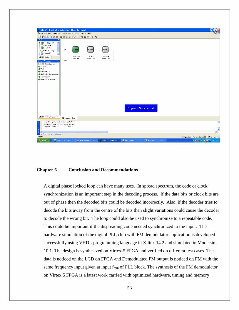
Chapter 6 Conclusion and Recommendations
A digital phase locked loop can have many uses. In spread spectrum, the code or clock
synchronization is an important step in the decoding process. If the data bits or clock bits are
out of phase then the decoded bits could be decoded incorrectly. Also, if the decoder tries to
decode the bits away from the centre of the bits then slight variations could cause the decoder
to decode the wrong bit. The loop could also be used to synchronize to a repeatable code.
This could be important if the dispreading code needed synchronized to the input. The
hardware simulation of the digital PLL chip with FM demodulator application is developed
successfully using VHDL programming language in Xilinx 14.2 and simulated in Modelsim
10.1. The design is synthesized on Virtex-5 FPGA and verified on different test cases. The
data is noticed on the LCD on FPGA and Demodulated FM output is noticed on FM with the
same frequency input given at input fmin of PLL block. The synthesis of the FM demodulator
on Virtex 5 FPGA is a latest work carried with optimized hardware, timing and memory

54
optimization results. The work is overcoming the problems of existing analog PLL having
problems electrical noise, temperature variations and components aging etc. The design is
programmable FM demodulator appropriately suiting software defined radio. The design
supports 13GBytes/sec of sustained memory bandwidth to the FPGA, 498 flip flops and low
power consumption of 120mW. The developed design is an optimal solution for SDR-based
next generation wireless communication transceiver circuit. The implementation of Digital
PLL on FPGA and FM demodulator is a boon to programmable industries for which the
crucial objectives are low-power consumption coupled with limited area at a high data rate.

55
REFRENCES
[1]. A. V. Rylyakov, J. A. Tierno, D. Z. Turker, J.-O. Plouchart, H. A. Ainspan, D. Friedman, “A
Modular All-Digital PLL Architecture Enabling Both 1-to-2GHz Operation in 65nm CMOS”
IEEE International Solid-State Circuits Conference, Vol. 28, IEEE Xplorer 2008, pp (516-632).
[2]. Amr M. Fahim, “Clock generators for SOC Processors” Kluwer Academic Publisher, 2005,
pp (1-159).
[3]. Chia-Hung Huang, Yin-Chih Chen, Gwo-Jia Jong, “The FPGA Implementation of Amplitude-
Locked Loop System for Co-channel Communication Chip Design” CSEE, Springer- Verlag
Berlin Heidelberg 2011, pp (458–461).
[4]Chua-Chin Wang, Gang- Neng Sung, Jian-Ming Huang, Li-Pin Lin “An 80 MHz PLL with
72.7 ps peak-to-peak jitter” Microelectronics Journal, Vol.38, Elsevier 2007, pp (716-721).
[5]. Donald R. Stephens, “Phase-Locked Loops for wireless Communication” Kluwer Academic
Publisher, 2002, pp (1-402).
[6] Indranil Hatai, Indrajit Chakrabarti, “A New High-Performance Digital FM Modulator and
Demodulator for Software-Defined Radio and its FPGA Implementation” International Journal of
Reconfigurable Computing, Vol. 2011, Hindawi Publishing Corporation 2011, pp (1-10).
[7]. Indranil Hatai, Indrajit Chakrabarti, “FPGA Implementation of a Digital FM Model”,
International Conference on Information and Multimedia Technology, IEEE Xplorer 2009, pp
(475-479).
[8]. Indranil Hatai, Indrajit Chakrabarti, “FPGA Implementation of a Digital FM Modem for SDR
Architecture” International Conference on Computers and Devices for Communication, 2009, pp
(1-4).
[9] Jokin Segundo, Luis Quintanilla, Jesus Arias, Lourdes Enriques, Jesus M. Hernandez, Jose
Vicente, “A PLL-based synthesizer for tuneable digital clock generation in a continuous-time ∑∆
A/D converter” INTEGERATION the VLSI journal, Vol. 42, Elsevier 2009, pp (24-33).
[10]. Jose A. Tierno, Alexander V. Rylyakov, Daniel J. Friedman, “A Wide Power Supply Range,
Wide Tuning Range, All Static CMOS All Digital PLL in 65 nm SOI” IEEE Journal of Solid State
Circuits, Vol. 43, IEEE Xplorer 2008, pp (42-51).
[11]. Juan Pablo, Martinez Brito, Sergio Bampi, “Design of a digital FM demodulator based on a
2nd-order all-digital phase-locked loop” Analog Integer Circ Sig Process, Springer 2008, pp (97-
105).
[12] Jin Li, Yijun Luo, Mao Tian, “FM Stereo Receiver Based on Software-Defined Radio”
International Journal of Digital Content Technology and its Applications, Vol. 6, pp (75-81).
[13] Martin John Burbidge, J. Tijou, “Towards generic charge-pump phase-locked loop, jitter
estimation techniques using indirect on chip methods” INTEGERATION the VLSI journal, Vol.
40, Elsevier 2007, pp (133-148).
[14]. Nicholas Burnett, thesis “FM Radio Receiver with Digital Demodulator” California
Polytechnic State University, San Luis Obispo, 2005, pp (1-50).
[15]. Nursani Rahmatullah, a research article on “Design of All Digital FM Receiver Circuit”
Institut Teknologi Bandung, pp (1-26).
[16]. Praveen Kumar, “Digital Phase Locked Loops” IETE Journal of Education, Vol. 52, Taylor
& Francis 2011, pp (5-10).
[17] Paolo Zikari, Emanuele Sciagura, Stephania Perri, Pasquale Corsonello, “A programmable
carrier phase independent symbol timing recovery circuit for QPSK/OQPSK signals”
Microprocessor and Microsystems, Vol.32, Elsevier 2008, pp (437-446).

56
[18]. Roberto Nonis, Werner Grollitsch, Thomas Santa, Dmytro Cherniak, Nicola DaDalt ,
“digPLL-Lite: A Low-Complexity, Low-Jitter Fractional-N Digital PLL Architecture” IEEE
Journal of Solid State Circuits, Vol. 48, IEEE Xplorer 2013, pp (3134-3145).
[19] Robert Bogdan Staszewski, John L. Wallberg, Sameh Rezeq, Chih-Ming Hung, Oren E.
Eliezer, Sudheer K. Vemulapalli, Chan Fernando, Ken Maggio, Roman Staszewski, Nathen
Barton, Meng-Chang Lee, Patric Cruise, Mitch Entezari, Khurram Muhammad, Dirk Leipold,
“All-Diggital PLL and transmitter for Mobile Phones” IEEE Journal of Solid State Circuits, Vol
40, IEEE Xplorer 2005, pp (2469-2482).
[20]. S. Moorthi, D. Meganathan, M. Shankar, R. Sridhar, J. Raja Paul Perinbam, “A Low- Jitter
Phase-Locked Loop Architecture for Clock Generation in Analog to Digital Converters” IEEE
Xplorer 2011, pp (81-84).

57
ANNEXURE 1
VHDL CODE for PHASE DETECTOR LIBRARY ieee; USE ieee.std_logic_1164.all; useieee.std_logic_arith.all; useieee.std_logic_unsigned.all; USE IEEE.numeric_std.ALL; ENTITY multiplier IS port (CLK : in std_logic; RESET : in std_logic; input1 : in std_logic_vector(7 downto 0); input2 : in std_logic_vector(7 downto 0); output : out std_logic_vector(7 downto 0)); END multiplier ; Architecture Mul_archof multiplier is Signal temp1 : integer; Signal temp2 : integer; Signal temp3 : integer; Signal temp4 : std_logic_vector(15 downto 0); begin process(clk, reset, input1, input2) begin if(reset = '1') then output<= "00000000"; elsif(clk = '1' and clk'event) then temp1 <= conv_integer(input1); temp2 <= conv_integer(input2); temp3 <= temp1 * temp2; temp4 <= conv_std_logic_vector(temp3,16); output<= temp4(7 downto 0); else null; end if; end process; END Mul_arch; VHDL CODE for LOOP FILTER LIBRARY ieee; USE ieee.std_logic_1164.all; useieee.std_logic_arith.all; useieee.std_logic_unsigned.all; USE IEEE.numeric_std.ALL; ENTITY loop_filter IS port ( CLK : in std_logic; RESET : in std_logic; C : in std_logic_vector(7 downto 0);

58
D1 : out std_logic_vector(11 downto 0); D2 : out std_logic_vector(11 downto 0)); END loop_filter ; ARCHITECTURE behavior OF loop_filter IS signal dtemp1 : std_logic_vector(11 downto 0); signal dtemp2 : std_logic_vector(11 downto 0); signal dtemp3 : std_logic_vector(11 downto 0); signal dtemp4 : std_logic_vector(11 downto 0); begin process(CLK, RESET) begin if (RESET='1') then D1 <= "000000000000"; D2 <= "000000000000"; dtemp1 <= "000000000000"; dtemp2 <= "000000000000"; dtemp3 <= "000000000000"; dtemp4 <= "000000000000"; elsif (clk ='1' and clk'event) then dtemp1 <= (C(7)&C(7)&C(7)&C&'0'); dtemp2 <= (C(7)&C(7)&C& "00"); dtemp3 <= (C(7)&C& "000"); dtemp4 <= (C& "0000"); D1 <= dtemp4; D2 <= dtemp1 ; end if; end process; END behavior; VHDL CODE for NCO LIBRARY ieee; USE ieee.std_logic_1164.all; use IEEE.STD_LOGIC_ARITH.ALL; use IEEE.STD_LOGIC_UNSIGNED.ALL; USE IEEE.numeric_std.ALL; ENTITY NCO IS port(clk : in std_logic; reset : in std_logic; din : in std_logic_vector(11 downto 0); address : in integer; dout : out std_logic_vector(7 downto 0)); END NCO ; ARCHITECTURE behavior OF NCO IS typevectype is array (0 to 255) of std_logic_vector(7 downto 0);

59
constantcosrom : vectype := ( 0 => "00000000", 1 => "00000001", 2 => "00000010", 3 => "00000011", 4 => "00000100", 5 => "00000101", 6 => "00000110", 7 => "00000111", 8 => "00001000", 9 => "00001001", 10 => "00001010", 11 => "00001011", 12 => "00001100", 13 => "00001101", 14 => "00001110", 15 => "00001111", 16 => "00010000", 17 => "00010001", 18 => "00010010", 19 => "00010011", 20 => "00010100", 21 => "00010101", 22 => "00010110", 23 => "00010111", 24 => "00011000", 25 => "00011001", 26 => "00011010", 27 => "00011011", 28 => "00011100", 29 => "00011101", 30 => "00011110", 31 => "00011111", 32 => "00100000", 33 => "00100001", 34 => "00100010", 35 => "00100011", 36 => "00100100", 37 => "00100101", 38 => "00100110", 39 => "00100111", 40 => "00101000", 41 => "00101001", 42 => "00101010", 43 => "00101011", 44 => "00101100", 45 => "00101101", 46 => "00101110",

60
47 => "00101111", 48 => "00110000", 49 => "00110001", 50 => "00110010", 51 => "00110011", 52 => "00110100", 53 => "00110101", 54 => "00110110", 55 => "00110111", 56 => "00111000", 57 => "00111001", 58 => "00111010", 59 => "00111011", 60 => "00111100", 61 => "00111101", 62 => "00111110", 63 => "00111111", 64 => "01000000", 65 => "01000001", 66 => "01000010", 67 => "01000011", 68 => "01000100", 69 => "01000101", 70 => "01000110", 71 => "01000111", 72 => "01001000", 73 => "01001001", 74 => "01001010", 75 => "01001011", 76 => "01001100", 77 => "01001101", 78 => "01001110", 79 => "01001111", 80 => "01010000", 81 => "01010001", 82 => "01010010", 83 => "01010011", 84 => "01010100", 85 => "01010101", 86 => "01010110", 87 => "01010111", 88 => "01011000", 89 => "01011001", 90 => "01011010", 91 => "01011011", 92 => "01011100", 93 => "01011101", 94 => "01011110",

61
95 => "01011111", 96 => "01100000", 97 => "01100001", 98 => "01100010", 99 => "01100011", 100 => "01100100", 101 => "01100101", 102 => "01100110", 103 => "01100111", 104 => "01101000", 105 => "01101001", 106 => "01101010", 107 => "01101011", 108 => "01100100", 109 => "01101101", 110 => "01101110", 111 => "01101111", 112 => "01110000", 113 => "01110001", 114 => "01110010", 115 => "01110011", 116 => "01110100", 117 => "01110101", 118 => "01110110", 119 => "01110111", 120 => "01111000", 121 => "01111001", 122 => "01111010", 123 => "01111011", 124 => "01111100", 125 => "01111101", 126 => "01111110", 127 => "01111111", 128 => "10000000", 129 => "10000001", 130 => "10000010", 131 => "10000011", 132 => "10000100", 133 => "10000101", 134 => "10000111", 135 => "10000111", 136 => "10001000", 137 => "10001001", 138 => "10001010", 139 => "10001011", 140 => "10001100", 141 => "10001101", 142 => "10001110",

62
143 => "10001111", 144 => "10010000", 145 => "10010001", 146 => "10010010", 147 => "10010011", 148 => "10010100", 149 => "10010101", 150 => "10010110", 151 => "10010111", 152 => "10011000", 153 => "10011001", 154 => "10011010", 155 => "10011011", 156 => "10011100", 157 => "10011101", 158 => "10011110", 159 => "10011111", 160 => "10100000", 161 => "10100001", 162 => "10100010", 163 => "10100011", 164 => "10100100", 165 => "10100101", 166 => "10100110", 167 => "10100111", 168 => "10101000", 169 => "10101001", 170 => "10101010", 171 => "10101011", 172 => "10101100", 173 => "10101101", 174 => "10101110", 175 => "10101111", 176 => "10110000", 177 => "10110001", 178 => "10110010", 179 => "10110011", 180 => "10110100", 181 => "10110101", 182 => "10110110", 183 => "10110111", 184 => "10111000", 185 => "10111001", 186 => "10111010", 187 => "10111011", 188 => "10111100", 189 => "10111101", 190 => "10111110",

63
191 => "10111111", 192 => "11000000", 193 => "11000001", 194 => "11000010", 195 => "11000011", 196 => "11000100", 197 => "11000101", 198 => "11000110", 199 => "11000111", 200 => "11001000", 201 => "11001001", 202 => "11001010", 203 => "11001011", 204 => "11001100", 205 => "11001101", 206 => "11001110", 207 => "11001111", 208 => "11010000", 209 => "11010001", 210 => "11010010", 211 => "11010011", 212 => "11010100", 213 => "11010101", 214 => "11010110", 215 => "11010111", 216 => "11011000", 217 => "11011001", 218 => "11011010", 219 => "11011011", 220 => "11011100", 221 => "11011101", 222 => "11011110", 223 => "11011111", 224 => "11100000", 225 => "11100001", 226 => "11100010", 227 => "11100011", 228 => "11100100", 229 => "11100101", 230 => "11100110", 231 => "11100111", 232 => "11101000", 233 => "11101001", 234 => "11101010", 235 => "11101011", 236 => "11101100", 237 => "11101101", 238 => "11101110",

64
239 => "11101111", 240 => "11110000", 241 => "11110001", 242 => "11110010", 243 => "11110011", 244 => "11110100", 245 => "11110101", 246 => "11110110", 247 => "11110111", 248 => "11111000", 249 => "11111001", 250 => "11111010", 251 => "11111011", 252 => "11111100", 253 => "11111101", 254 => "11111110", 255 => "11111111"); --signal address : integer; begin process(CLK, RESET) begin if (RESET='1') then dout<= "00000000"; elsifrising_edge(CLK) then if (address >= 0) and (address < 256) then dout<= cosrom(address); end if; else null; end if; end process; END behavior; VHDL CODE for ADC library IEEE; use IEEE.STD_LOGIC_1164.ALL; use IEEE.STD_LOGIC_ARITH.ALL; use IEEE.STD_LOGIC_UNSIGNED.ALL; entity ADC is Port ( data_in : in integer; data_out : out STD_LOGIC_VECTOR (15 downto 0)); end ADC; architecture Behavioral of ADC is begin data_out<= conv_std_logic_vector(data_in,16); end Behavioral;

65
VHDL CODE for DAC library IEEE; use IEEE.STD_LOGIC_1164.ALL; use IEEE.STD_LOGIC_ARITH.ALL; use IEEE.STD_LOGIC_UNSIGNED.ALL; entity DAC is Port ( in1 : in STD_LOGIC_vector(15 downto 0); out1 : out integer); end DAC; architecture Behavioral of DAC is begin out1 <= conv_integer(in1); end Behavioral; VHDL CODE for FIR FILTER
LIBRARY ieee;
USE IEEE.std_logic_1164.all;
USE IEEE.numeric_std.ALL;
entity FIR is
port(clock : in std_logic;
reset : in std_logic;
data_in : in signed(11 downto 0);
data_out : out std_logic_vector(11 downto 0)
);
end FIR;
architecture behavior of FIR is
signal d0,d1,d2,d3,d4,d5,d6,d7,d8,d9,d10,
d11,d12,d13,d14,d15 : signed(15 downto 0);
signal sum : signed(15 downto 0);
begin
process(clock,reset)
begin
if (reset = '1') then
d0 <= (others => '0');
d1 <= (others => '0');
d2 <= (others => '0');
d3 <= (others => '0');
d4 <= (others => '0');
d5 <= (others => '0');
d6 <= (others => '0');
d7 <= (others => '0');
d8 <= (others => '0');
d9 <= (others => '0');
d10 <= (others => '0');

66
d11 <= (others => '0');
d12 <= (others => '0');
d13 <= (others => '0');
d14 <= (others => '0');
d15 <= (others => '0');
sum<= (others => '0');
data_out<= (others => '0');
ELSIF rising_edge(clock) THEN
d0 <= data_in(11)&data_in(11)&
data_in(11)&data_in(11)&data_in;
d1 <= d0;
d2 <= d1;
d3 <= d2;
d4 <= d3;
d5 <= d4;
d6 <= d5;
d7 <= d6;
d8 <= d7;
d9 <= d8;
d10 <= d9;
d11 <= d10;
d12 <= d11;
d13 <= d12;
d14 <= d13;
d15 <= d14;
sum<= (d0+d1+d2+d3+d4+d5+d6+d7+d8+d9+
d10+d11+d12+d13+d14+d15) srl 4; -- 1/16 multiply is 4
bit right shift operation
data_out<= std_logic_vector(sum(11 downto 0));
end if;
end process;
end behavior;
VHDL CODE for PLL FM LIBRARY ieee; USE ieee.std_logic_1164.all; useieee.std_logic_arith.all; useieee.std_logic_unsigned.all; USE IEEE.numeric_std.ALL; package PLL is typet_data is array(0 to 7) of std_logic_vector(7 downto 0); end package PLL; LIBRARY ieee; USE ieee.std_logic_1164.all; useieee.std_logic_arith.all; useieee.std_logic_unsigned.all; use work. PLL.all; ENTITY PLL_FM IS

67
PORT(clk : IN std_logic; reset : IN std_logic; address : in integer; fmin : IN std_logic_vector(7 downto 0); FM_signal : in t_data; FM_output : out t_data; dmout : OUT std_logic_vector (11 DOWNTO 0) ); END PLL_FM ; ARCHITECTURE behavior OF PLL_FM IS SIGNAL d1 : std_logic_vector(11 DOWNTO 0); SIGNAL d2 : std_logic_vector(11 DOWNTO 0); SIGNAL dout : std_logic_vector(7 DOWNTO 0); SIGNAL output : std_logic_vector(7 DOWNTO 0); signalDACin: std_logic_vector(15 DOWNTO 0); signalDACout: integer; signalADCin : integer; signalADCout :std_logic_vector(15 DOWNTO 0); signal LPF : t_data; COMPONENT multiplier PORT ( clk : IN std_logic ; reset : IN std_logic ; input1 : IN std_logic_vector (7 DOWNTO 0); input2 : IN std_logic_vector (7 DOWNTO 0); output : OUT std_logic_vector (7 DOWNTO 0) ); END COMPONENT; COMPONENT FIR_filter PORT ( clk : IN std_logic ; reset : IN std_logic ; data_in : IN std_logic_vector (11 DOWNTO 0); data_out : OUT std_logic_vector (11 DOWNTO 0) ); END COMPONENT; COMPONENT loop_filter PORT (clk : IN std_logic ; reset : IN std_logic ; c : IN std_logic_vector (7 DOWNTO 0); d1 : OUT std_logic_vector (11 DOWNTO 0); d2 : OUT std_logic_vector (11 DOWNTO 0) ); END COMPONENT; COMPONENT nco PORT (clk : IN std_logic ; reset : IN std_logic ; address : in integer; din : IN std_logic_vector (11 DOWNTO 0); dout : OUT std_logic_vector (7 DOWNTO 0)

68
); END COMPONENT; component DAC is Port ( in1 : in STD_LOGIC_vector(15 downto 0); out1 : out integer); end component; component ADC is Port ( data_in : in integer; data_out : out STD_LOGIC_VECTOR (15 downto 0)); end component; BEGIN U1 : multiplier PORT MAP ( clk =>clk, reset => reset, input1 =>fmin, input2 =>dout, output => output ); U2 :loop_filter PORT MAP ( clk =>clk, reset => reset, c => output, d1 => d1, d2 => d2 ); U3 :nco PORT MAP ( clk =>clk, reset => reset, din => d2, address => address, dout =>dout ); U4 :FIR_filter PORT MAP ( clk =>clk, reset => reset, data_in => d1, data_out =>dmout ); U5: ADC port map (data_in =>ADCin, data_out =>ADCout);
69
U6: DAC port map (in1 =>DACin, out1 =>DACout); LPF <= FM_signal; FM_output<= LPF; END behavior;

70
ANNEXURE 2
Adesh Kumar, Vijaya Kumari, Yashik Gulati “ Design and FPGA implementation of Digital
FM Receiver using PLL” In conference proceedings for International Conference of
Telecommunication, Technology and Management- 2015 at IIT Delhi India and published by
Emerald Publications as special issue (Scopus Indexed): March, 2015.

71
Copyright © 2022 FDOKUMEN