GOSSIPO-4: an array of high resolution TDCs with a PLL control
10
This content has been downloaded from IOPscience. Please scroll down to see the full text. Download details: IP Address: 80.241.216.195 This content was downloaded on 15/10/2013 at 23:27 Please note that terms and conditions apply. GOSSIPO-4: an array of high resolution TDCs with a PLL control View the table of contents for this issue, or go to the journal homepage for more 2012 JINST 7 C01081 (http://iopscience.iop.org/1748-0221/7/01/C01081) Home Search Collections Journals About Contact us My IOPscience
Transcript of GOSSIPO-4: an array of high resolution TDCs with a PLL control
This content has been downloaded from IOPscience. Please scroll down to see the full text.
Download details:
IP Address: 80.241.216.195
This content was downloaded on 15/10/2013 at 23:27
Please note that terms and conditions apply.
GOSSIPO-4: an array of high resolution TDCs with a PLL control
View the table of contents for this issue, or go to the journal homepage for more
2012 JINST 7 C01081
(http://iopscience.iop.org/1748-0221/7/01/C01081)
Home Search Collections Journals About Contact us My IOPscience

2012 JINST 7 C01081
PUBLISHED BY IOP PUBLISHING FOR SISSA
RECEIVED: October 31, 2011ACCEPTED: December 29, 2011
PUBLISHED: January 24, 2012
TOPICAL WORKSHOP ON ELECTRONICS FOR PARTICLE PHYSICS 2011,26–30 SEPTEMBER 2011,VIENNA, AUSTRIA
GOSSIPO-4: an array of high resolution TDCs with aPLL control
F. Zappon,a,1 M. van Beuzekom,a V. Gromov,a R. Kluit,a X. Fangb and A. Kruthb
aNikhef,Science Park 105, Amsterdam, The Netherlands
bBonn University,Sigmund-Freud-Str. 25, Bonn, Germany
E-mail: [email protected]
ABSTRACT: GOSSIPO-4 is a prototype chip featuring an array of high resolution Time to DigitalConverters with a PLL control that has been taped out the 9th of August 2011. This prototype is thesuccessor of GOSSIPO-3 test chip and the precursor of the 65k pixel chip TimePix3. The prototypeis being developed to test a set of new features that will be used in TimePix3, including a 8 pixelstructure sharing one fast oscillator with a new topology, a PLL to provide the control voltage tothe oscillators, a custom fast counter and a new small-area cell library.
KEYWORDS: Front-end electronics for detector readout; CMOS readout of gaseous detectors;Particle tracking detectors (Gaseous detectors); Micropattern gaseous detectors (MSGC, GEM,THGEM, RETHGEM, MHSP, MICROPIC, MICROMEGAS, InGrid, etc)
1Corresponding author.
c© 2012 IOP Publishing Ltd and SISSA doi:10.1088/1748-0221/7/01/C01081

2012 JINST 7 C01081
Contents
1 Introduction 1
2 Time measurements 3
3 GOSSIPO-3: test results 3
4 GOSSIPO-4: design 44.1 Oscillator 54.2 Super Pixel 64.3 Pixel 64.4 PLL and buffer 7
5 Conclusion 8
1 Introduction
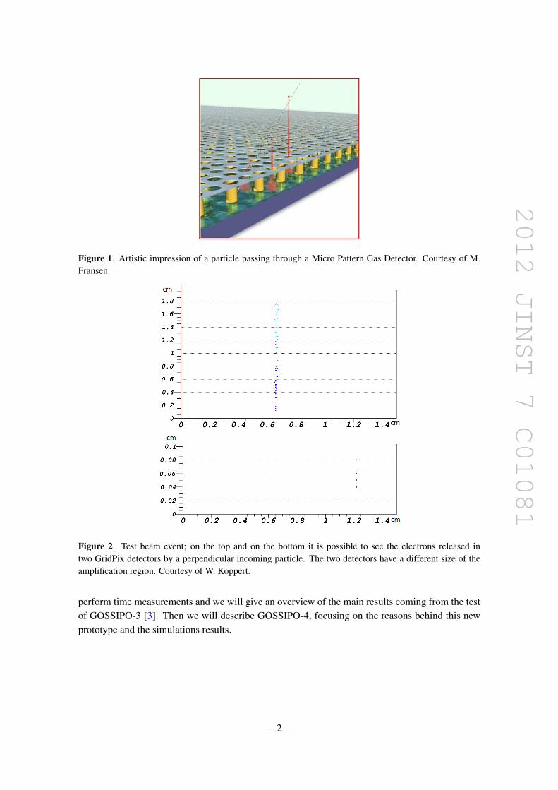
Micro Pattern Gas Detectors (MPGD, see figure 1) consist of a gas volume, that acts as detectormedium, and a readout pixel chip. A particle passing through the detector ionizes the gas alongits track: the generated electrons drift toward the anode by means of an electric field; close tothe readout pad a structure, called InGrid, is biased at high voltage and provides the requiredamplification so that the charge produced by the ionizing particle can be detected.
The main advantages of this kind of detector are that there is no leakage current due to thesensor and that the input capacitance is very low (less than 10 fF) which result in a very low noiseinput stage. The grid on top of the chip provides a high gas amplification factor which allows ahigh single electron efficiency for this type of detector. The use of MPGDs gives the possibility toperform a 3D reconstruction of a particle’s track; to do this one needs information about the threecoordinates: while the X-Y information is provided by the pixel structure of the readout chip, torecover the Z coordinates measurement of the drift time is necessary. Currently, TimePix chip isused [1]. However, this chip has some limitations: in particular it doesn’t allow to record the Timeof Arrival (ToA) and the Time over Threshold (ToT) at the same time and, in addition, the availabletime resolution is not enough for InGrid applications. As an example, consider figure 2 where itis possible to see the ionization track left behind by a particle passing through a GridPix detectorwith a drift region of 1.8 cm in perpendicular direction. On the bottom plot, we put the track leftwhen the drift region is reduced to 0.1 cm. It is clear that it is not possible to perform a good trackfit in this latter case case, having only a few measurements in the data.
Hence, this leads to the necessity to have a time resolution that is on the order of a nanosecond.A series of GOSSIP (Gas On Slimmed Silicon Pixel) chips has been produced to characterize themain components needed to achieve such performance [2]. In this article we will explain how we
– 1 –
2012 JINST 7 C01081
Figure 1. Artistic impression of a particle passing through a Micro Pattern Gas Detector. Courtesy of M.Fransen.
Figure 2. Test beam event; on the top and on the bottom it is possible to see the electrons released intwo GridPix detectors by a perpendicular incoming particle. The two detectors have a different size of theamplification region. Courtesy of W. Koppert.
perform time measurements and we will give an overview of the main results coming from the testof GOSSIPO-3 [3]. Then we will describe GOSSIPO-4, focusing on the reasons behind this newprototype and the simulations results.
– 2 –

2012 JINST 7 C01081
Figure 3. Timing diagram used in GOSSIPO-3 and GOSSIPO-4.
2 Time measurements
The main scheme used to perform time measurements is visible in figure 3.When the signal goes above threshold a fast oscillator (640 MHz) is started and it is stopped
by the first rising edge of the system clock (40 MHz): the number of oscillations is recorded in theFast Counter and provides the required resolution. After this, the number of system clock cyclesis recorded in the Slow Counter until a Trigger signal arrives (common stop) synchronous withthe system clock; the combination of the Fast Counter and the Slow Counter gives the ToA of theparticle. It is then straightforward to add to this structure another counter to record the ToT: thiscounter starts counting system clock cycles at the same moment as the Slow Counter and it stopswhen the signal goes below threshold.
3 GOSSIPO-3: test results
GOSSIPO-3 is a prototype chip developed in collaboration between Nikhef and Bonn University.It contains two pixels, one equipped with a full analog frontend while the other has only the digitalcomponents (state machine and counters, see figure 4). Tests of the chip proved the functionalityof the analog fronted, the foreseen characteristics of the Low Drop Out regulators and, in general,the reproducibility of the characteristics across different chips.
To characterize the Time to Digital Converter (TDC) we injected a pulse at the input of thepixel and delayed it with respect to the Trigger: an example of the outcome of such test is presentedin figure 5. In this figure it is possible to notice the difference in size between bin 1 and bin 2. Asa side note, notice that bin 0 is not taken into account in the analysis: this bin is intentionallysmaller than the others. The choice comes from the fact that the counters are Linear FeedbackShift Registers. This means that with the 4 bits available for the Fast Counter we can obtain only15 different counting values. Given that the system clock frequency has been chosen to be 40MHz (period of 25 ns) and the oscillator runs with a period of 1.65 ns we are left with fractionsof nanosecond.
– 3 –

2012 JINST 7 C01081
Figure 4. Block diagram of the analog pixel of GOSSIPO-3. Notice that the oscillator is present ineach pixel.
Figure 5. An example of the test results performed in GOSSIPO-3: notice the large difference in bin size,in particular bin 1 with respect to the other bins.
Table 1. Analysis results of Chip 1 for the full pixel (analog) and the only digital. Notice the big DNL. Thevalue in brackets refers to the DNL calculated not taking into account bin 1.
Chip Bin size (ns) Error Jitter (ns) Error DNL1 Digital 1.7525 0.3217 0.052 0.052 19.90%1 Analog 1.7701 0.2163 0.09 0.01 31.83% (19.90%)
The important aspect to notice is highlighted in table 1: a big Differential Non Linearity in theTDC characteristic is present, most likely caused by a crosstalk from the system clock. The effect,though, is not fully reproducible in simulations.
4 GOSSIPO-4: design
Given the results shown in section 3 a new design has been planned in the framework of theTimePix3 chip. To overcome the above mentioned problems, GOSSIPO-4 uses a 8 pixel struc-
– 4 –

2012 JINST 7 C01081
Figure 6. Schematic of the oscillator used in GOSSIPO-4.
Figure 7. Variation of the oscillation period for different values of VDD and Vcntr. Notice the plateau,indicating stable operations, for VDD > 1.2 V.
ture that shares a voltage controlled oscillator in contrast with GOSSIPO-3 where each pixel hashis own oscillator. In addition, the topology of the oscillator has been changed to be less sensitiveto any effect on the supply voltage, which is most likely the main source of the effects we see inGOSSIPO-3. A Phase Locked Loop (PLL), which contains a replica of the oscillator, is placed inthe periphery of the chip and provides the required control voltage to keep the oscillation frequencylocked to 640 MHz. Additionally, four rail-to-rail buffers have been placed to be tested. The chipis 1x2 mm and it contains 30 Super-Pixel for a total of 240 pixels.
4.1 Oscillator
In GOSSIPO-4 the four-stage ring oscillator has been redesigned to be less sensitive to variation ofthe supply voltage as this seems to be the main cause of the non-linear effects we see in GOSSIPO-3. In figure 6 you can see the schematic: notice that the power supply and the control voltage(Vcntr) are separated.
This latter voltage is provided by a PLL that has in it a replica of the oscillator and it is usedto mitigate effects due to process and temperature variations. The channel-to-channel mismatchis foreseen to be of the order of 0.4% in the TT corner. In figure 7 is shown the variation of theoscillation period as function of VDD for various values of the control voltage. It is important tonotice that for VDD > 1.2 V the frequency is independent of the Supply voltage over a wide rangeof control voltages.
– 5 –

2012 JINST 7 C01081
Figure 8. Block diagram of the super pixel structure adopted in GOSSIPO-4. The oscillator is shared among8 pixels to save area and to reduce the power consumption.
4.2 Super Pixel
To save area and to reduce the power consumption it has been decided to adopt a new structurecalled Super Pixel (see figure 8). The concept is based on sharing one oscillator among 8 pixels,distributing the fast clock to all of them. If a pixel is hit the oscillator is started and the numberof oscillations is recorded in its Fast Counter; then, if a second pixel in the group is hit, the FastCounter of this second pixel simply records the number of oscillations from that moment to the firstrising edge of the system clock when the oscillator is stopped. This operation of synchronizing theasynchronous signal, as the one coming from the detector, to the already running clock is performedinside the pixels by a special block called Synchronization Logic (see section 4.3).
4.3 Pixel
In figure 9 you can see the block diagram of the GOSSIPO-4 pixel. The two most importantstructures are the custom designed Fast Counter and Synchronization Logic. These two blockshave been custom designed because we need to be sure that they meet specifications and workproperly, since they are the key components in achieving the high precision time measurements.In fact, early stage simulations have shown metastability problems occurring when using standardcells: in particular, the simultaneous switching of the fast clock and the system clock could leadto an unpredictable state in the counter; moreover the blocks are running at the limit speed forthe technology The two blocks together occupy roughly the 12% of the pixel area (Counter andSynchronization Logic take respectively 179.52 µm2 and 187.11 µm2).
In the pixel are present several structures that have been placed only for test purposes. At theinput there is a multiplexer to be able to select among four different time indipendent test signals:this gives us the possibility to completely characterize the super pixel and its behavior in responseto different stimuli. At the output we decided to adopt a simple solution using a serial readout.
– 6 –

2012 JINST 7 C01081
Figure 9. Block diagram of the single pixel of GOSSIPO-4. Highlighetd in blue the test structures.
Figure 10. Schematic of the synchronization logic. Each pixel contains this block, that provides a Gate tostart the oscillator and the synchronized fast clock to the Fast Counter.
Figure 11. Corner simulations for the control voltage Vcntr provided by the PLL.
4.4 PLL and buffer
In addition to the above mentioned structures, we put in the chip two additional components thatneed to be tested. The first is a PLL: this PLL is based on the one used in FE-I4, but has beenmodified to use a different cell type. For the PLL the dynamic power consumption is expected tobe 7mW. In figure 11 the simulated Vcntr values for the slow, typical and fast corner.
Additionally, we put four equal copies of the rail-to-rail buffers that will be used in TIMEPIX-3 to supply in each double-column the Vcntr provided by the PLL. The buffer dynamic range isVDD-100 mV and VSS+100 mV and it has to guarante stable operations for loads up to 10 pF.The simulated power consumption is 16 µW: it is dominated by the bias current in the output stagewhich is needed to operate at the mentioned load.
– 7 –

2012 JINST 7 C01081
5 Conclusion
In the framework of TIMEPIX-3 chip a new prototype chip called G4 has been designed andsubmitted to test the reliability of a new structure to perform high precision time measurements. Inparticular, we hope to eliminate the effects we see in GOSSIPO-3: we have changed the topology ofthe Oscillator to be less sensitive to effects that might be caused by variations in the supply voltage.Moreover, by means of a custom designed Synchronization Logic and Fast Counter, we shouldguarantee a metastability free structure, an issue that is present in synchronization circuits andthat has been hilighted by early-stage simulations. The chip has been submitted at the beginningof August 2011 and will be tested to prove the solidity of the proposed solution in view of anintegration in TIMEPIX-3.
Acknowledgments
We want to thank the designers at Cern that helped us during the design phase of GOSSIPO-4 andin particular Xavi Llopart who has designed the small area, standard cell library that we extensivelyhave used in this project. Moreover, we want to thank Nikhef’s designer Vladimir Zivkovic for theconstant support throughout all the design phases: without his precious advice this work would nothave been possible.
References
[1] X. Llopart et al., Timepix, a 65k programmable pixel readout chip for arrival time, energy and/orphoton counting measurements, Nucl. Instrum. Meth. A 581 (2007) 485.
[2] R. Kluit, V. Gromov and H. van der Graaf, Development of a small-scale prototype of the GOSSIPO-2chip in 0.13 um CMOS technology, in the proceedings of the Topical Workshop on Electronics forParticle Physics, September 3–7, Prague, Czech Republic (2007).
[3] A. Kruth et al., GOSSIPO-3: measurements on the prototype of a read-out pixel chip for Micro-PatternGaseous Detectors, 2010 JINST 5 C12005.
– 8 –