
MC145181 Dual 550/60 MHz PLL Frequency Synthesizer with ...
71
Device Main/Secondary Loop Maximum Frequency Package SEMICONDUCTOR TECHNICAL DATA BiCMOS COMPONENT FOR 2 OR 3 VOLT SYSTEMS ORDERING INFORMATION MC145181FTAR2 550/60 MHz LQFP–32 PLASTIC PACKAGE CASE 873C (LQFP–32, Tape & Reel Only) VERY–SMALL 5 x 5 mm BODY 32 1 Order this document by MC145181/D DEVELOPMENT SYSTEM The MC145230EVK, which contains hardware and software, is strongly recommended for system development. (The user must provide the VCOs for evaluating the MC145181.) The software supports all features and modes of operation of the device. Up to four boards or devices can be controlled and the user is alerted to error conditions. The control program may be used with any board based on the MC145181, MC145225, or MC145230. (Scale 2:1) 1 MOTOROLA RF/IF DEVICE DATA 19 The MC145181 is a dual frequency synthesizer containing very–low supply voltage circuitry. The device supports two independent loops with a single input reference and operates down to 1.8 V. Phase noise reduction circuitry is incorporated into the device. The MC145181 operates up to 550 MHz on the main loop and up to 60 MHz on the secondary loop. The device has a 32/33 prescaler for the main loop. Lock detection circuitry for both loops is multiplexed to a single output. Two 8–bit DACs are powered through a dedicated pin. The DAC supply range is 1.8 to 3.6 V; this voltage may differ from the main supply. An on–chip voltage multiplier supplies power to the phase/frequency detectors. Thus, in a 2 V application, the detectors are supplied with 4 V power. In 2.6 to 3.6 V applications, the multiplied voltage is regulated at approximately 5 V. The current source/sink phase/frequency detector for the main loop is designed to achieve faster lock times than a conventional detector. Both high and low current outputs are available along with a timer, double buffers, and a MOSFET switch to adjust the external low–pass filter response. There are several levels of standby which are controllable with a 1–byte transfer through the serial port. Either of the PLLs and/or the reference oscillator may be independently placed in the low–power standby state. In addition, any of the phase/frequency detector outputs may be placed in the floating state to facilitate modulation of the external VCOs. Either DAC may be placed in standby via a 4–byte transfer. The MC145181 facilitates designing the receiver’s first and second local oscillators for ReFLEX two–way paging applications. Also, the device accommodates generation of the transmit carrier. • Operating Frequency Main Loop: 100 to 550 MHz Secondary Loop: 10 to 60 MHz • Operating Supply Voltage: 1.8 to 3.6 V • Nominal Supply Current, Both Loops Active: 3 mA • Maximum Standby Current, All Systems Shut Down: 10 μA • Phase Detector Output Current: 1.8 V Supply — PD out –Hi: 2.8 mA, PD out –Lo: 0.7 mA 2.5 V Supply — PD out –Hi: 4.4 mA, PD out –Lo: 1.1 mA • Two Independent 8–Bit DACs with Separate Supply Pin (Up to 3.6 V) • Lock Detect Output with Adjustable Lock Indication Window • Independent R Counters Allow Independent Step Sizes for Each Loop • Main Loop Divider Range: 992 to 262,143 • Secondary Loop Divider Range: 7 to 8,191 • Fractional Reference Counters Divider Range: 20 to 32,767.5 • Auxiliary Reference Divider with Small–Signal Differential Output — Ratios: 8, 10, 12.5 • Three General–Purpose Outputs • Direct Interface to Motorola SPI Data Port Up to 10 Mbps ReFLEX and BitGrabber are trademarks of Motorola, Inc. Motorola, Inc. 1999 Rev 1 This document contains information on a new product. Specifications and information herein are subject to change without notice. Freescale Semiconductor, I Freescale Semiconductor, Inc. For More Information On This Product, Go to: www.freescale.com nc...
-
Upload
khangminh22 -
Category
Documents
-
view
1 -
download
0
Transcript of MC145181 Dual 550/60 MHz PLL Frequency Synthesizer with ...

Device
Main/SecondaryLoop
MaximumFrequency Package
SEMICONDUCTORTECHNICAL DATA
BiCMOS COMPONENTFOR 2 OR 3 VOLT
SYSTEMS
ORDERING INFORMATION
MC145181FTAR2 550/60 MHz LQFP–32
PLASTIC PACKAGECASE 873C
(LQFP–32, Tape & Reel Only)VERY–SMALL 5 x 5 mm BODY
32 1
Order this document by MC145181/D
DEVELOPMENT SYSTEM
The MC145230EVK, which contains hardware andsoftware, is strongly recommended for systemdevelopment. (The user must provide the VCOs forevaluating the MC145181.) The software supportsall features and modes of operation of the device. Upto four boards or devices can be controlled and theuser is alerted to error conditions. The controlprogram may be used with any board based on theMC145181, MC145225, or MC145230.
(Scale 2:1)
1MOTOROLA RF/IF DEVICE DATA
19
" % "$ $! % #! ! "!
The MC145181 is a dual frequency synthesizer containing very–lowsupply voltage circuitry. The device supports two independent loops with asingle input reference and operates down to 1.8 V. Phase noise reductioncircuitry is incorporated into the device.
The MC145181 operates up to 550 MHz on the main loop and up to60 MHz on the secondary loop. The device has a 32/33 prescaler for themain loop. Lock detection circuitry for both loops is multiplexed to a singleoutput.
Two 8–bit DACs are powered through a dedicated pin. The DAC supplyrange is 1.8 to 3.6 V; this voltage may differ from the main supply.
An on–chip voltage multiplier supplies power to the phase/frequencydetectors. Thus, in a 2 V application, the detectors are supplied with 4 Vpower. In 2.6 to 3.6 V applications, the multiplied voltage is regulated atapproximately 5 V. The current source/sink phase/frequency detector for themain loop is designed to achieve faster lock times than a conventionaldetector. Both high and low current outputs are available along with a timer,double buffers, and a MOSFET switch to adjust the external low–pass filterresponse.
There are several levels of standby which are controllable with a 1–bytetransfer through the serial port. Either of the PLLs and/or the referenceoscillator may be independently placed in the low–power standby state. Inaddition, any of the phase/frequency detector outputs may be placed in thefloating state to facilitate modulation of the external VCOs. Either DAC maybe placed in standby via a 4–byte transfer.
The MC145181 facilitates designing the receiver’s first and second localoscillators for ReFLEX two–way paging applications. Also, the deviceaccommodates generation of the transmit carrier.
• Operating FrequencyMain Loop: 100 to 550 MHzSecondary Loop: 10 to 60 MHz
• Operating Supply Voltage: 1.8 to 3.6 V
• Nominal Supply Current, Both Loops Active: 3 mA
• Maximum Standby Current, All Systems Shut Down: 10 µA
• Phase Detector Output Current:1.8 V Supply — PDout–Hi: 2.8 mA, PDout–Lo: 0.7 mA2.5 V Supply — PDout–Hi: 4.4 mA, PDout–Lo: 1.1 mA
• Two Independent 8–Bit DACs with Separate Supply Pin (Up to 3.6 V)
• Lock Detect Output with Adjustable Lock Indication Window
• Independent R Counters Allow Independent Step Sizes for Each Loop
• Main Loop Divider Range: 992 to 262,143
• Secondary Loop Divider Range: 7 to 8,191
• Fractional Reference Counters Divider Range: 20 to 32,767.5
• Auxiliary Reference Divider with Small–Signal DifferentialOutput — Ratios: 8, 10, 12.5
• Three General–Purpose Outputs
• Direct Interface to Motorola SPI Data Port Up to 10 Mbps
ReFLEX and BitGrabber are trademarks of Motorola, Inc.
Motorola, Inc. 1999 Rev 1This document contains information on a new product. Specifications and information hereinare subject to change without notice.
Fre
esc
ale
Se
mic
on
du
cto
r, I
Freescale Semiconductor, Inc.
For More Information On This Product, Go to: www.freescale.com
nc
...

MC145181
2 MOTOROLA RF/IF DEVICE DATA
CONTENTS
1. BLOCK DIAGRAM 3. . . . . . . . . . . . . . . . . . . . . . . . . . . . . . . . . . . . . . . . . . . . . . . . . . . . .
2. PIN CONNECTIONS 4. . . . . . . . . . . . . . . . . . . . . . . . . . . . . . . . . . . . . . . . . . . . . . . . . . . .
3. PARAMETER TABLES 4. . . . . . . . . . . . . . . . . . . . . . . . . . . . . . . . . . . . . . . . . . . . . . . . . .
3A. Maximum Ratings 4. . . . . . . . . . . . . . . . . . . . . . . . . . . . . . . . . . . . . . . . . . . . . . . . . 3B. DC Electrical Characteristics 5. . . . . . . . . . . . . . . . . . . . . . . . . . . . . . . . . . . . . . . . 3C. PDout–Hi and PDout–Lo Phase/Frequency Detector Characteristics 5. . . . . . 3D. PDout Phase/Frequency Detector Characteristics 5. . . . . . . . . . . . . . . . . . . . . 3E. DAC Characteristics 6. . . . . . . . . . . . . . . . . . . . . . . . . . . . . . . . . . . . . . . . . . . . . . . 3F. Voltage Multiplier and Keep–alive Oscillator Characteristics 6. . . . . . . . . . . . . 3G. Dynamic Characteristics of Digital Pins 6. . . . . . . . . . . . . . . . . . . . . . . . . . . . . . . 3H. Dynamic Characteristics of Loop and fout Pins 8. . . . . . . . . . . . . . . . . . . . . . . . .
4. DEVICE OVERVIEW 9. . . . . . . . . . . . . . . . . . . . . . . . . . . . . . . . . . . . . . . . . . . . . . . . . . . .
4A. Serial Interface and Registers 9. . . . . . . . . . . . . . . . . . . . . . . . . . . . . . . . . . . . . . . 4B. Reference Input and Counters Circuits 9. . . . . . . . . . . . . . . . . . . . . . . . . . . . . . . . 4C. Loop Divider Inputs and Counter Circuits 9. . . . . . . . . . . . . . . . . . . . . . . . . . . . . . 4D. Voltage Multiplier and Keep–alive Circuits 9. . . . . . . . . . . . . . . . . . . . . . . . . . . . . 4E. Phase/Frequency Detectors 10. . . . . . . . . . . . . . . . . . . . . . . . . . . . . . . . . . . . . . . . . 4F. Lock Detectors 10. . . . . . . . . . . . . . . . . . . . . . . . . . . . . . . . . . . . . . . . . . . . . . . . . . . . 4G. DACs 10. . . . . . . . . . . . . . . . . . . . . . . . . . . . . . . . . . . . . . . . . . . . . . . . . . . . . . . . . . . . 4H. General–purpose Outputs 10. . . . . . . . . . . . . . . . . . . . . . . . . . . . . . . . . . . . . . . . . .
5. PIN DESCRIPTIONS 11. . . . . . . . . . . . . . . . . . . . . . . . . . . . . . . . . . . . . . . . . . . . . . . . . . . .
5A. Digital Pins 11. . . . . . . . . . . . . . . . . . . . . . . . . . . . . . . . . . . . . . . . . . . . . . . . . . . . . . . 5B. Reference Pins 13. . . . . . . . . . . . . . . . . . . . . . . . . . . . . . . . . . . . . . . . . . . . . . . . . . . . 5C. Loop Pins 13. . . . . . . . . . . . . . . . . . . . . . . . . . . . . . . . . . . . . . . . . . . . . . . . . . . . . . . . 5D. Analog Outputs 14. . . . . . . . . . . . . . . . . . . . . . . . . . . . . . . . . . . . . . . . . . . . . . . . . . . . 5E. External Components 15. . . . . . . . . . . . . . . . . . . . . . . . . . . . . . . . . . . . . . . . . . . . . . 5F. Supply Pins 15. . . . . . . . . . . . . . . . . . . . . . . . . . . . . . . . . . . . . . . . . . . . . . . . . . . . . . .
6. DETAILED REGISTER DESCRIPTIONS 16. . . . . . . . . . . . . . . . . . . . . . . . . . . . . . . . . . .
6A. C Register 16. . . . . . . . . . . . . . . . . . . . . . . . . . . . . . . . . . . . . . . . . . . . . . . . . . . . . . . . 6B. Hr Register 19. . . . . . . . . . . . . . . . . . . . . . . . . . . . . . . . . . . . . . . . . . . . . . . . . . . . . . . 6C. N Register 20. . . . . . . . . . . . . . . . . . . . . . . . . . . . . . . . . . . . . . . . . . . . . . . . . . . . . . . . 6D. R Register 22. . . . . . . . . . . . . . . . . . . . . . . . . . . . . . . . . . . . . . . . . . . . . . . . . . . . . . . 6E. Hn Register 25. . . . . . . . . . . . . . . . . . . . . . . . . . . . . . . . . . . . . . . . . . . . . . . . . . . . . . 6F. D Register 26. . . . . . . . . . . . . . . . . . . . . . . . . . . . . . . . . . . . . . . . . . . . . . . . . . . . . . . .
7. APPLICATIONS INFORMATION 29. . . . . . . . . . . . . . . . . . . . . . . . . . . . . . . . . . . . . . . . .
7A. Crystal Oscillator Considerations 29. . . . . . . . . . . . . . . . . . . . . . . . . . . . . . . . . . . . 7B. Main Loop Filter Design — Conventional 34. . . . . . . . . . . . . . . . . . . . . . . . . . . . . . 7C. Main Loop Filter Design — Adapt 41. . . . . . . . . . . . . . . . . . . . . . . . . . . . . . . . . . . . 7D. Secondary Loop Filter Design 50. . . . . . . . . . . . . . . . . . . . . . . . . . . . . . . . . . . . . . . 7E. Voltage Multiplier Stall Avoidance 57. . . . . . . . . . . . . . . . . . . . . . . . . . . . . . . . . . . .
8. PROGRAMMER’S GUIDE 58. . . . . . . . . . . . . . . . . . . . . . . . . . . . . . . . . . . . . . . . . . . . . . .
8A. Quick Reference 58. . . . . . . . . . . . . . . . . . . . . . . . . . . . . . . . . . . . . . . . . . . . . . . . . . 8B. Initializing the Device 65. . . . . . . . . . . . . . . . . . . . . . . . . . . . . . . . . . . . . . . . . . . . . . . 8C. Programming Without Adapt 66. . . . . . . . . . . . . . . . . . . . . . . . . . . . . . . . . . . . . . . . 8D. Programming Utilizing Horseshoe With Adapt 66. . . . . . . . . . . . . . . . . . . . . . . . . . 8E. Controlling the DACs 67. . . . . . . . . . . . . . . . . . . . . . . . . . . . . . . . . . . . . . . . . . . . . . .
9. APPLICATION CIRCUIT 69. . . . . . . . . . . . . . . . . . . . . . . . . . . . . . . . . . . . . . . . . . . . . . . . .
10. OUTLINE DIMENSIONS 70. . . . . . . . . . . . . . . . . . . . . . . . . . . . . . . . . . . . . . . . . . . . . . . . .
Fre
esc
ale
Se
mic
on
du
cto
r, I
Freescale Semiconductor, Inc.
For More Information On This Product, Go to: www.freescale.com
nc
...

MC145181
3MOTOROLA RF/IF DEVICE DATA
Clk
fin
Enb
C Register8 Bits Output A
Mux
Output C
Output A
PDout–Hi
16
9
19
Power Connections:Pin 2 = DAC VposPins 11, 24, 26, and 29 = VposPins 14, 15, 18, and 31 = Gnd
Output B25
Din
Phase /FrequencyDetector,
Timer,and Control
fin
Out C
Out B/Ref
Out A
Function
High–currentChargePump
Timer
Ph Det PulsefR
fRPLL Stby
PLL StbyPD FloatPD FloatOsc Stby
Low–currentChargePump
N Register24 Bits
N Counter18 Stages
3
fV
R Counter16 Stages
fR
16
R Register16 Bits
16
Hr Register16 Bits
3
R Register24 Bits
16
R Counter16 Stages
N Counter13 Stages
13
N Register13 Bits
13 MSBs
Hn Register16 Bits
D Register16 Bits
Shift Register andAddress Generator
5
6
7
18
–+
1213
Amp
Lo–I Gain
Polarity
PLL Stby
OscillatorOsceOscb
1
32
Rx17
PDout–Lo20
LockDetector
VoltageMultiplier
and Regulator
Cmult21
Creg22
LD8
LockDetector
Window V–MultControl
Phase /FrequencyDetectorfV
fR
PDout23
Supply CurrentMinimization
Circuit2
2
Test
Polarity
Ratio
10Mode
fin 30
Amp
8
8
AuxiliaryDivider
3 Stages
fout/Pol28
fout/Pol27
DAC8 Bits DAC1
3
DAC8 Bits DAC24
DAC Vpos2
1. BLOCK DIAGRAM
Osc
Fre
esc
ale
Se
mic
on
du
cto
r, I
Freescale Semiconductor, Inc.
For More Information On This Product, Go to: www.freescale.com
nc
...

MC145181
4 MOTOROLA RF/IF DEVICE DATA
2. PIN CONNECTIONS
OutputA
This device contains 15,260 active transistors.
Vpos
2532 31 30 29 28 27 26
24
23
22
21
20
19
18
17
OutputBVpos
fout/Pol
fout/Pol′Vposfin′GndOscb
PDout′
Creg
Cmult
PDout–Lo
PDout–Hi
Gnd
Rx
16
OutputC
15
Gnd
14
Gnd
13
fin
12
fin
11
Vpos
10
Mode
9
1
2
3
4
5
6
7
8
Osce
DAC Vpos
DAC1
DAC2
Enb
Din
Clk
LD
3. PARAMETER TABLES
3A. MAXIMUM RATINGS (Voltages Referenced to Gnd, unless otherwise stated)
Parameter Symbol Value Unit
DC Supply Voltages Vpos,DAC Vpos
–0.5 to 3.6 V
DC Input Voltage — Osce, fin, fin, Mode, Din, Clk, Enb, fout/Pol , fout/Pol
Vin –0.5 to Vpos + 0.5 V
DC Output Voltage Vout –0.5 to Vpos + 0.5 V
DC Input Current, per Pin Iin ±10 mA
DC Output Current, per Pin Iout ±20 mA
DC Supply Current, Vpos and Gnd Pins I 25 mA
Power Dissipation, per Package PD 100 mW
Storage Temperature Tstg –65 to 150 °C
Lead Temperature, 1 mm from Case for10 Seconds
TL 260 °C
NOTES: 1. Maximum Ratings are those values beyond which damage to the device may occur.Functional operation should be restricted to the limits in the Electrical Characteristics tablesor Pin Descriptions section.
2. ESD (electrostatic discharge) immunity meets Human Body Model (HBM) up to 2000 V.Additional ESD data available upon request.
This device contains protection circuitry toguard against damage due to high static volt-ages or electric fields. However, precautionsmust be taken to avoid applications of anyvoltage higher than maximum rated voltagesto this high–impedance circuit.
Fre
esc
ale
Se
mic
on
du
cto
r, I
Freescale Semiconductor, Inc.
For More Information On This Product, Go to: www.freescale.com
nc
...

MC145181
5MOTOROLA RF/IF DEVICE DATA
3B. DC ELECTRICAL CHARACTERISTICSVpos = 1.8 to 3.6 V, Voltages Referenced to Gnd, TA = –40 to 85°C, unless otherwise statedtt
Parameter Condition SymbolGuaranteed
Limit Unit
Maximum Low–Level Input Voltage(Din, Clk, Enb, Mode, fout/Pol , fout/Pol)
fout/Pol and fout/Pol Configured as Inputs VIL 0.3 x Vpos V
Minimum High–Level Input Voltage(Din, Clk, Enb, Mode, fout/Pol , fout/Pol)
fout/Pol and fout/Pol Configured as Inputs VIH 0.7 x Vpos V
Minimum Hysteresis Voltage (Clk) VHys 100 mV
Maximum Low–Level Output Voltage(LD, Output A, Output B)
Iout = 20 µA VOL 0.1 V
Minimum High–Level Output Voltage(LD, Output A, Output B)
Iout = –20 µA VOH Vpos – 0.1 V
Minimum Low–Level Output Current(LD, Output A, Output B)
Vout = 0.3 V IOL 0.7 mA
Minimum High–Level Output Current(LD, Output A, Output B)
Vout = Vpos – 0.3 V IOH –0.7 mA
Minimum Low–Level Output Current (Output C) Vout = 0.2 V IOL 2.8 mA
Maximum Input Leakage Current(Din, Clk, Enb, Mode, fout/Pol , fout/Pol)
Vin = Vpos or Gnd; fout/Pol and fout/PolConfigured as Inputs
Iin ±1.0 µA
Maximum Output Leakage Current(Output B, Output C)
Vout = Vpos or Gnd; Output in High–ImpedanceState
IOZ ±1 µA
Maximum ON Resistance (Output C) 1.8 V ≤ Vpos < 2.5 V Supply2.5 V ≤ Vpos ≤ 3.6 V Supply (Note 1)
Ron 7550
Ω
Maximum Standby Supply Current(Vpos and DAC Vpos Tied Together)
Vin = Vpos or Gnd; Outputs Open; Both PLLs inStandby Mode; Oscillator in Standby Mode;DAC1 and DAC2 Output = Zero; Keep–aliveOscillator Off (Notes 2, 3, and 4)
ISTBY 10 µA
NOTES: 1. For supply voltages restricted to 2.5 to 2.9 V and an ambient temperature range of –10 to 60°C, Output C has a guaranteed ON resistance range of 23to 44 Ω .
2. The total supply current drain for the keep–alive oscillator, voltage multiplier, and regulator is approximately 250 µA.3. When the Mode pin is tied high, bit C6 must be programmed to a 0 for minimum supply current drain. Otherwise, if C6 = 1, the current drain is approximately
8 µA for a 1.8 V supply and approximately 40 µA for a 3.6 V supply. This restriction on bit C6 does not apply when the Mode pin is tied low.4. To ensure minimum standby supply current drain, the voltage potential at the Cmult pin must not be allowed to fall below the potential at the Vpos pins.
See discussion in Section 5E under Cmult .
3C. PDout –Hi AND PDout –Lo PHASE/FREQUENCY DETECTOR CHARACTERISTICSNominal Output Current, Vpos = 1.8 V: PDout–Hi = 2.8 mA, PDout–Lo = 0.7 or 0.35 mANominal Output Current, Vpos ≥ 2.5 V: PDout–Hi = 4.4 mA, PDout–Lo = 1.1 or 0.55 mARx = 2.0 kΩ, Voltages Referenced to Gnd, Voltage Multiplier ON, TA = –40 to 85°C
Parameter ConditionGuaranteed
Limit Unit
Maximum Source Current Variation Part–to–Part (See Note) Vout = 0.5 x VCmult ±14 %
Maximum Sink–versus–Source Mismatch (See Note) Vout = 0.5 x VCmult 20 %
Output Voltage Range (See Note) Iout Variation ≤ 27% 0.6 to VCmult – 0.6 V V
Maximum Three–State Leakage Current Vout = 0 or VCmult ±50 nA
NOTE: Percentages calculated using the following formula: (Maximum Value – Minimum Value) / Maximum Value.
3D. PDout PHASE/FREQUENCY DETECTOR CHARACTERISTICSVpos = 1.8 to 3.6 V, Voltages Referenced to Gnd, Voltage Multiplier ON, TA = –40 to 85°C
Parameter ConditionGuaranteed
Limit Unit
Minimum Low–Level Output Current Vout = 0.3 V 0.3 mA
Minimum High–Level Output Current Vout = VCmult – 0.3 V –0.3 mA
Maximum Three–State Leakage Current Vout = 0 or VCmult ±50 nA
Fre
esc
ale
Se
mic
on
du
cto
r, I
Freescale Semiconductor, Inc.
For More Information On This Product, Go to: www.freescale.com
nc
...

MC145181
6 MOTOROLA RF/IF DEVICE DATA
3E. DAC CHARACTERISTICSVpos = 1.8 to 3.6 V, DAC Vpos = 1.8 to 3.6 V; TA = –40 to 85°C
ÁÁÁÁÁÁÁÁÁÁÁÁÁÁÁÁÁÁÁÁÁÁÁÁÁÁÁÁParameter
ÁÁÁÁÁÁÁÁÁÁÁÁÁÁÁÁÁÁÁÁÁÁÁÁÁÁCondition
ÁÁÁÁÁÁÁÁÁÁÁÁÁÁ
GuaranteedLimit
ÁÁÁÁÁÁUnitÁÁÁÁÁÁÁÁÁÁÁÁÁÁ
ÁÁÁÁÁÁÁÁÁÁÁÁÁÁResolutionÁÁÁÁÁÁÁÁÁÁÁÁÁÁÁÁÁÁÁÁÁÁÁÁÁÁ
ÁÁÁÁÁÁÁÁÁÁÁÁÁÁ8
ÁÁÁÁÁÁBitsÁÁÁÁÁÁÁÁÁÁÁÁÁÁ
ÁÁÁÁÁÁÁÁÁÁÁÁÁÁMaximum Integral NonlinearityÁÁÁÁÁÁÁÁÁÁÁÁÁÁÁÁÁÁÁÁÁÁÁÁÁÁ
ÁÁÁÁÁÁÁÁÁÁÁÁÁÁ±1
ÁÁÁÁÁÁLSBÁÁÁÁÁÁÁÁÁÁÁÁÁÁ
ÁÁÁÁÁÁÁÁÁÁÁÁÁÁMaximum Offset Voltage from GndÁÁÁÁÁÁÁÁÁÁÁÁÁÁÁÁÁÁÁÁÁÁÁÁÁÁNo External Load
ÁÁÁÁÁÁÁÁÁÁÁÁÁÁ1
ÁÁÁÁÁÁLSBÁÁÁÁÁÁÁÁÁÁÁÁÁÁ
ÁÁÁÁÁÁÁÁÁÁÁÁÁÁMaximum Offset Voltage from DAC VposÁÁÁÁÁÁÁÁÁÁÁÁÁÁÁÁÁÁÁÁÁÁÁÁÁÁNo External Load
ÁÁÁÁÁÁÁÁÁÁÁÁÁÁ2
ÁÁÁÁÁÁLSBÁÁÁÁÁÁÁÁÁÁÁÁÁÁ
ÁÁÁÁÁÁÁÁÁÁÁÁÁÁÁÁÁÁÁÁÁÁÁÁÁÁÁÁ
Maximum Output ImpedanceÁÁÁÁÁÁÁÁÁÁÁÁÁÁÁÁÁÁÁÁÁÁÁÁÁÁÁÁÁÁÁÁÁÁÁÁÁÁÁ
Over Entire Output Range, Including ZeroOutput (which is Low–power Standby)
ÁÁÁÁÁÁÁÁÁÁÁÁÁÁÁÁÁÁÁÁÁ
130ÁÁÁÁÁÁÁÁÁ
kΩ
ÁÁÁÁÁÁÁÁÁÁÁÁÁÁÁÁÁÁÁÁÁÁÁÁÁÁÁÁ
Maximum Standby Current ÁÁÁÁÁÁÁÁÁÁÁÁÁÁÁÁÁÁÁÁÁÁÁÁÁÁ
Zero Output, No External Load ÁÁÁÁÁÁÁÁÁÁÁÁÁÁ(See ISTBY in Section 3B)ÁÁÁ
ÁÁÁÁÁÁÁÁÁÁÁÁÁÁÁÁÁÁÁÁÁÁÁÁÁÁÁÁÁÁÁ
Maximum Supply Current per DAC @ DAC Vpos pinÁÁÁÁÁÁÁÁÁÁÁÁÁÁÁÁÁÁÁÁÁÁÁÁÁÁ
Except with Zero Output, No External Load ÁÁÁÁÁÁÁÁÁÁÁÁÁÁ
(DAC Vpos) / 36 ÁÁÁÁÁÁ
mA
3F. VOLTAGE MULTIPLIER AND KEEP–ALIVE OSCILLATOR CHARACTERISTICSVoltages Referenced to Gnd, TA = –40 to 85°C
Parameter ConditionGuaranteed
Limit Unit
ÁÁÁÁÁÁÁÁÁÁÁÁÁÁÁÁÁÁÁÁÁÁÁÁÁÁÁÁÁÁÁÁÁÁÁÁÁÁÁÁÁÁÁÁÁÁÁÁÁÁÁÁÁÁÁÁ
Voltage Multiplier Output Voltage ÁÁÁÁÁÁÁÁÁÁÁÁÁÁÁÁÁÁÁÁÁÁÁÁÁÁÁÁÁÁÁÁÁÁÁÁÁÁÁÁÁÁÁÁÁÁÁÁÁÁÁÁ
5 MHz Refresh Rate, 100 µA ContinuousSourcing, Measured at Cmult pinVpos = 1.8 VVpos = 3.6 V
ÁÁÁÁÁÁÁÁÁÁÁÁÁÁÁÁÁÁÁÁÁÁÁÁÁÁÁÁ
3.32 to 3.784.75 to 5.35
ÁÁÁÁÁÁÁÁÁÁÁÁ
V
ÁÁÁÁÁÁÁÁÁÁÁÁÁÁÁÁÁÁÁÁÁÁÁÁÁÁÁÁ
Keep–alive Refresh Frequency ÁÁÁÁÁÁÁÁÁÁÁÁÁÁÁÁÁÁÁÁÁÁÁÁÁÁ
Vpos = 1.8 to 3.6 V ÁÁÁÁÁÁÁÁÁÁÁÁÁÁ
300 to 700 ÁÁÁÁÁÁ
kHz
3G. DYNAMIC CHARACTERISTICS OF DIGITAL PINSVpos = 1.8 to 3.6 V, TA = –40 to 85°C, Input tr = tf = 10 ns, CL = 25 pF
ParameterFigure
No. SymbolGuaranteed
Limit Unit
Serial Data Clk FrequencyNOTE: Refer to Clk tw Below
1 fclk dc to 10 MHz
Maximum Propagation Delay, Enb to Output A (Selected as General–Purpose Output) 2, 7 tPLH, tPHL 200 ns
Maximum Propagation Delay, Enb to Output B 2, 3, 7, 8 tPLH, tPHL,tPZL, tPLZ,tPZH, tPHZ
200 ns
Maximum Propagation Delay, Enb to Output C 4, 8 tPZL, tPLZ 200 ns
Maximum Output Transition Time, Output A; Output B with Active Pullup and Pulldown 2, 7 tTLH, tTHL 75 ns
Minimum Setup and Hold Times, Din versus Clk 5 tsu, th 30 ns
Minimum Setup, Hold, and Recovery Times, Enb versus Clk 6 tsu, th, trec 100 ns
Minimum Pulse Width, Inactive (High) Time, Enb 6 tw * cycles
Minimum Pulse Width, Clk 1 tw 50 ns
Maximum Input Capacitance — Din, CLK, Enb Cin 10 pF
*For Hr register access, the minimum limit is 20 Osce cycles.For Hn register access, the minimum limit is 27 fin cycles.For N register access, the minimum limit is 20 Osce cycles + 99 fin cycles.When the timer is used for adapt, the minimum limit after the second N register access and before the next register access is the time–out interval + 99 fin cycles.
Fre
esc
ale
Se
mic
on
du
cto
r, I
Freescale Semiconductor, Inc.
For More Information On This Product, Go to: www.freescale.com
nc
...

MC145181
7MOTOROLA RF/IF DEVICE DATA
Figure 1. Figure 2.
10%
Vpos
Gnd
1/fclk
Clk
90%
90%50%10%
tPLH tPHL
tTLH tTHL
twtw
tf trEnb
Output AOutput B
Vpos
Gnd50%
Din
Clk
50%
Valid
50%
tsu thVpos
Gnd
Vpos
Gnd
Figure 3.
Clk
Enb
50%
tsu th
FirstClock
LastClock
trec
50%
Vpos
Gnd
Vpos
Gnd
tw
Figure 4.
Test Point
DeviceUnderTest
CL*
* Includes all probe and fixture capacitance.
Test Point
DeviceUnderTest
CL*
* Includes all probe and fixture capacitance.
250 µA
Figure 5. Figure 6.
Figure 7. Figure 8.
Enb
tPZL
tPLZ
tPHZ
10%
90%
HighImpedance
Enb
Output C
Output C
Vpos
GndtPZL
50%
tPLZ
10%
90%
HighImpedance
Source current andlimit voltage to Vposfor tPLZ and tPZL.Sink current and limit voltage to Gndfor tPHZ and tPZH.
Vpos
Gnd50%
Output B
Output B
Output B
Output B
90%
10%
tPZH
Fre
esc
ale
Se
mic
on
du
cto
r, I
Freescale Semiconductor, Inc.
For More Information On This Product, Go to: www.freescale.com
nc
...

MC145181
8 MOTOROLA RF/IF DEVICE DATA
3H. DYNAMIC CHARACTERISTICS OF LOOP AND f out PINSVpos = 1.8 to 3.6 V, TA = –40 to 85°C
Symbol Parameter ConditionFigure
No. Min Max Unit
vin Input Voltage Range, fin 100 MHz ≤ fin < 550 MHz 9 100 300 mVpp
vin Input Voltage Range, fin 10 MHz ≤ fin < 60 MHz 10 100 400 mVpp
fOsce Input Frequency Range, Osce vin = 350 to 600 mVpp,Device in External Reference Mode
11 9 80 MHz
fXtal Crystal Frequency, Oscb and Osce Device in Crystal Mode * 9 80 MHz
Cin Input Capacitance of Pins Oscb andOsce
— — pF
fout Output Frequency Range, fout and fout Output Signal Swing > 300 mVpp perpin (600 mVpp differential)
12 1 6.2 MHz
fφ Operating Frequency Range of thePhase/Frequency Detectors, PDout–Hi,PDout–Lo, PDout
dc 600 kHz
*Refer to the Crystal Oscillator Considerations section.
Figure 9. Figure 10.
RFMeter
RL = 50 Ω
100 pF
DeviceUnderTest
VposVpos
fin
Gndfin
100 pF
100 pF
DeviceUnderTest
VposVpos
fin
Vin
Gnd
VinRF
MeterRL = 50 Ω
Sine WaveGenerator
Zout = 50 Ω
Sine WaveGenerator
Zout = 50 Ω
Sine WaveGenerator
DeviceUnderTest
VposVpos
Osce
Vin
50 Ω
Figure 11.
GndOscb
DeviceUnderTest
fout
Figure 12.
NoConnection
0.1 µF
fout
20 pF
20 pF
V
V
Peak–to–peakVoltageMeasurement
Fre
esc
ale
Se
mic
on
du
cto
r, I
Freescale Semiconductor, Inc.
For More Information On This Product, Go to: www.freescale.com
nc
...

MC145181
9MOTOROLA RF/IF DEVICE DATA
4. DEVICE OVERVIEW
Refer to the Block Diagram in Section 1.
4A. SERIAL INTERFACE AND REGISTERS
The serial interface is comprised of a Clock pin (Clk), aData In pin (Din), and an Enable pin (Enb). Information on thedata input pin is shifted into a shift register on the low–to–hightransition of the serial clock. The data format is mostsignificant bit (MSB) first. Both Clk and Enb areSchmitt–triggered inputs.
The R and N registers contain counter divide ratios for themain loop, PLL. The R and N registers contain counterdivide ratios for the secondary loop, PLL. Additional contolbits are located in the R, N, and C registers. The D registercontrols the digital–to–analog converters (DACs). Randomaccess is allowed to the N, R, Hr, Hn, D, and C registers.
Two 16–bit holding registers, Hr and Hn, feed registers Rand N, respectively. [The three least significant bits (LSBs)of the Hn register are not used.] The R and N registersdetermine the divide ratios of the R and N counters,respectively. Thus, the information presented to the R and N
counters is double–buffered. Using the proper programmingsequence, new divide ratios may be presented to the N, R,and N counters; simultaneously.
Enb is used to activate the data port and allow transfer ofdata. To ensure that data is accepted by the device, the Enbsignal line must initially be a high voltage (not asserted), thenmake a transition to a low voltage (asserted) prior to theoccurrence of a serial clock, and must remain asserted untilafter the last serial clock of the burst. Serial data may betransferred in an SPI format (while Enb remains asserted).Data is transferred to the appropriate register on the risingedge of Enb (see Table 1). “Short shifting”, depicted asBitGrabber in the table, allows access to certain registerswithout requiring address bits. When Enb is inactive (high),Clk is inhibited from shifting the shift register.
The serial input pins may NOT be driven above the supplyvoltage applied to the Vpos pins.
4B. REFERENCE INPUT AND COUNTERS CIRCUITS
Reference (Oscillator) Circuit
For the Colpitts reference oscillator, one pin ties to thebase (Oscb, pin 32) and the other ties to the emitter (Osce,pin 1), of an on–chip NPN transistor. In addition, thereference circuit may be operated in the external reference(XRef) mode as selectable via bit C6 when the Mode pin ishigh.
The Oscb and Osce pins support an external fundamentalor overtone crystal. The output of the oscillator is routed toboth the reference counter for the main loop (R counter) andthe reference counter for the secondary loop (R counter).
In a second mode, determined by bit C6 being 1 and theMode pin being high, Osce is an input which accepts anac–coupled signal from a TCXO or other source. Oscb mustbe floated. If the Mode pin is low, this “XRef mode” is notallowed.
Reference Counter for Main Loop
Main reference counter R divides down the frequency atOsce and feeds the phase/frequency detector for the mainloop. The detector feeds the two charge pumps with outputsPDout–Hi and PDout–Lo. The division ratio of the R counter isdetermined by bits in the R register.
Reference Counter for Secondary Loop
Secondary reference counter R divides down thefrequency at Osce and feeds the phase/frequency detectorfor the secondary loop. The detector output is PDout. Thedivision ratio of the R counter is determined by the 16 LSBsof the R register.
The R counter has a special mode to provide a frequencyoutput at pins fout and fout (differential outputs). These arelow–jitter ECL–type outputs. With the Mode pin low, softwarecontrol allows the Osce frequency to be divided–by–8, –10,or –12.5 and routed to the fout pins. This output is derived bytapping off of a front–end stage of the R counter and feedingthe auxiliary counter which provides the divided–downfrequency. The chip must have the Mode pin low, whichactivates the fout pins. The actual R divide ratio must bedivisible by 2 or 2.5 when the fout pins are activated. There isno such restriction when the Mode pin is high. SeeSection 6D, R Register.
4C. LOOP DIVIDER INPUTS AND COUNTER CIRCUITS
fin Inputs and Counter Circuit
fin and fin are high–frequency inputs to the amplifier whichfeeds the N counter. A small signal can feed these inputseither differentially or single–ended.
The N counter divides down the external VCO frequencyfor the main loop. (The divide ratio of the N counter is alsoknown as the loop multiplying factor.) The divide ratio of thiscounter is determined by the 18 LSBs of the N register. Theoutput of the N counter feeds the phase/frequency detectorfor the main loop.
fin Input and Counter Circuit
fin is the high–frequency input to the amplifier which feedsthe N counter. A small signal can feed this inputsingle–ended.
The N counter divides down the external VCO frequencyfor the secondary loop. (The divide ratio of the N counter isalso known as the loop multiplying factor.) The divide ratio ofthis counter is determined by bits in the N register. Theoutput of the N counter feeds the phase/frequency detectorfor the secondary loop.
4D. VOLTAGE MULTIPLIER AND KEEP–ALIVECIRCUITS
The voltage multiplier produces approximately two timesthe voltage present at the Vpos pins over a supply range of1.8 V to about 2.5 V. With a supply range of approximately2.5 V to 3.6 V, the elevated voltage is regulated/limited toapproximately 5 V. The elevated voltage, present at the Cmult
Fre
esc
ale
Se
mic
on
du
cto
r, I
Freescale Semiconductor, Inc.
For More Information On This Product, Go to: www.freescale.com
nc
...

MC145181
10 MOTOROLA RF/IF DEVICE DATA
pin, is applied to both phase detectors. An external capacitorto Gnd is required on the Cmult pin. The other capacitorsrequired for the multiplier are on–chip.
A capacitor to Gnd is also required on the Creg pin. Thevoltage on this pin is equal to the voltage on the Vpos pinsover a supply range of 1.8 V to about 2.5 V. The voltage onCreg is limited to approximately 2.5 V maximum when theVpos pins exceed 2.5 V.
The refresh rate determines the repetition rate that thecapacitors for the voltage multiplier are charged. Refresh isnormally derived off of the signal present at the Osce pin,through a divider which is part of the voltage multiplier andregulator circuitry. The refresh rate is controlled via bits in theR register.
When the reference oscillator circuit is placed in standby,an on–chip keep–alive oscillator assists in maintaining theelevated voltage on the phase detectors. The keep–aliverefresh rate is per the spec table in Section 3F.
If desired, the keep–alive oscillator can be inhibited fromturning on, by placing the multiplier in the inactive state via R
register bits. This causes the phase/frequency detectorvoltage to bleed off while in standby, but has the advantage ofachieving the lowest supply current if all other sections of thechip are shut down.
4E. PHASE/FREQUENCY DETECTORS
Detector for Main Loop
The detector for the main loop senses the phase andfrequency difference between the outputs of the R and Ncounters. The detector feeds both a high–current chargepump with output PDout–Hi and a low–current charge pumpwith output PDout–Lo.
The charge pumps can be operated in three conventionalmanners as controlled by bits in the N register. PDout–Lo canbe enabled with PDout–Hi inhibited. Conversely, PDout–Hican be enabled with PDout–Lo inhibited. Both outputs can beenabled and tied together externally for maximum chargepump current. Finally, both outputs can be inhibited. In thislast case, they float. The outputs can also be forced to thefloating state by a bit in the C register. This facilitatesintroduction of modulation into the VCO input.
The charge pumps can be operated in an adapt mode ascontrolled by bits in the N register. The bits essentiallyprogram a timer which determines how long PDout–Hi isactive. After the time–out, PDout–Hi floats and PDout–Lobecomes active. In addition, a second set of R and N countervalues can be engaged after the time–out. For moreinformation, see Table 16 and Section 8, Programmer’sGuide .
Detector for Secondary Loop
The detector for the secondary loop senses the phase andfrequency difference between the outputs of the R and N
counters. Detector output PDout is a voltage–type outputwith a three–state push–pull driver.
The output can be forced to the floating state by a bit in theC register. This facilitates introduction of modulation into theVCO input.
4F. LOCK DETECTORS
Window counters in each of the lock detector circuitsdetermine the lock detector phase threshold for PLL andPLL. The window counter divide ratio for the main loop’s lockdetector is controlled via a bit in the N register. The windowcounter divide ratio for the secondary loop is not controllableby the user.
The lock detector window determines a minimum phasedifference which must occur before the Lock Detect pin goeshigh. Note that the lock detect signals for each loop drive anAND gate, which then feeds the LD pin. The LD pin indicatesthe condition of both loops, or the one active loop if the otheris in standby. If both loops are in standby, LD is low indicatingunlocked.
4G. DACs
The two independent 8–bit DACs facilitate crystaloscillator trimming and PA output power control. They arealso suitable for any general–purpose use.
Each DAC utilizes an R–2R ladder architecture. Theoutput pins, DAC1 and DAC2, are directly connected to theladder; that is, there is no on–chip buffer.
The DAC outputs are determined by the contents of the Dregister. When a DAC output is zero scale, it is also in alow–power mode. The power–on reset (POR) circuitinitializes the DACs in the low–power mode upon power up.
4H. GENERAL–PURPOSE OUTPUTS
There are three outputs which may be used as portexpanders for a microcontroller unit (MCU).
Output A is actually a multi–purpose output with apush–pull output driver. See Table 2 for details.
Output B is a three–state output. The state of Output Bdepends on two bits; one of these bits also controls whetherthe main PLL is in standby or not. See Table 5 for details.
Output C is an open–drain output. The state of this outputis controlled by one bit per Table 4. Output C is specified witha guaranteed ON resistance, and thus, may be used in ananalog fashion.
Fre
esc
ale
Se
mic
on
du
cto
r, I
Freescale Semiconductor, Inc.
For More Information On This Product, Go to: www.freescale.com
nc
...

MC145181
11MOTOROLA RF/IF DEVICE DATA
5. PIN DESCRIPTIONS
5A. DIGITAL PINS
Enb, Din, and ClkPins 5, 6, and 7 — Serial Data Port Inputs
The Enb input is used to activate the serial interface toallow the transfer of data to the device. To transfer data to thedevice, the Enb pin must be low during the interval that thedata is being clocked in. When Enb is taken back high(inactive), data is transferred to the appropriate registerdepending either on the data stream length or address bits.The C, Hr, and N registers can be accessed using either aunique data stream length (BitGrabber) or by using addressbits (Conventional). The D, Hn, and R registers can only beaccessed using address bits. See Table 1.
The bit stream begins with the MSB and is shifted in on thelow–to–high transition of Clk. The bit pattern is 1 byte (8 bits)long to access the C register, 2 bytes (16 bits) to access theHr register, or 3 bytes (24 bits) to access the N register. A bitpattern of 4 bytes (32 bits) is used to access the registerswhen using address bits. The device has double buffers forstorage of the N and R counter divide ratios. One doublebuffer is composed of the Hr register which feeds the Rregister. An Hr to R register transfer occurs whenever the Nregister is written. The other double buffer is the Hn registerwhich feeds the N register. An Hn to N register transferoccurs whenever the N register is written. Thus, new divideratios may be presented to the R, N, and N counterssimultaneously.
Transitions on Enb must not be attempted while Clk ishigh. This puts the device out of synchronization with themicrocontroller. Resynchronization occurs whenever Enb ishigh (inactive) and Clk is low.
Data is retained in the registers over a supply range of 1.8to 3.6 V. The bit–stream formats are shown in Figures 13through 18.
LDPin 8 — Lock Detectors Output
This signal is the logical AND of the lock detect signalsfrom both PLL and PLL. For the main PLL, the phasewindow that defines “lock” is programmable via bit N22. Thephase window for the secondary PLL is not programmable.
If either PLL or PLL is in standby, LD indicates the lockcondition of the active loop only. If both loops are in standby,the LD output is a static low level.
Each PLL’s lock detector is in the high state when therespective loop is locked (the inputs to the phase detectorbeing the same phase and frequency). The lock detect signalis in the low state when a loop is out of lock. See Figure 19.
Upon power up, the LD pin indicates a not lockedcondition. The LD pin is a push–pull CMOS output. If unused,LD should be left open.
Output APin 9 — Multiple–Purpose Digital Output
Depending on control bits R21 and R20, Output A isselectable by the user as a general–purpose output (eitherhigh or low level), fR (output of main reference counter), fR
(output of secondary reference counter), or a phase detectorpulse indicator for both loops. When selected asgeneral–purpose output, bit C7 determines whether theoutput is a high or low level per Table 2. When configured asfR, fR, or phase detector pulse, Output A appears as anormally low signal and pulses high.
Output A is a slew–rate limited CMOS totem–pole output.If unused, Output A should be left open.
Table 1. Register Access(LSBs are C0, R0, N0, D0, R0, and N0)ÁÁÁÁÁ
ÁÁÁÁÁÁÁÁÁÁÁÁÁÁÁ
AccessType
ÁÁÁÁÁÁÁÁÁÁÁÁÁÁÁÁ
AccessedRegister
ÁÁÁÁÁÁÁÁÁÁÁÁÁÁÁÁ
AddressNibble
ÁÁÁÁÁÁÁÁÁÁÁÁÁÁÁÁ
Numberof
Clocks
ÁÁÁÁÁÁÁÁÁÁÁÁÁÁÁÁÁÁÁÁÁÁÁÁÁÁÁÁÁÁÁÁ
Register BitNomenclature
ÁÁÁÁÁÁÁÁÁÁÁÁÁÁÁÁ
FigureNo.
ÁÁÁÁÁÁÁÁÁÁ
BitGrabber ÁÁÁÁÁÁÁÁ
C ÁÁÁÁÁÁÁÁ
— ÁÁÁÁÁÁÁÁ
8 ÁÁÁÁÁÁÁÁÁÁÁÁÁÁÁÁ
C7, C6, C5, ..., C0 ÁÁÁÁÁÁÁÁ
13
ÁÁÁÁÁÁÁÁÁÁ
BitGrabber ÁÁÁÁÁÁÁÁ
Hr ÁÁÁÁÁÁÁÁ
— ÁÁÁÁÁÁÁÁ
16 ÁÁÁÁÁÁÁÁÁÁÁÁÁÁÁÁ
R15, R14, R13, ..., R0 ÁÁÁÁÁÁÁÁ
14
ÁÁÁÁÁÁÁÁÁÁ
BitGrabber ÁÁÁÁÁÁÁÁ
N ÁÁÁÁÁÁÁÁ
— ÁÁÁÁÁÁÁÁ
24 ÁÁÁÁÁÁÁÁÁÁÁÁÁÁÁÁ
N23, N22, N21, ..., N0 ÁÁÁÁÁÁÁÁ
15
ÁÁÁÁÁÁÁÁÁÁ
ConventionalÁÁÁÁÁÁÁÁ
C ÁÁÁÁÁÁÁÁ
$0 ÁÁÁÁÁÁÁÁ
32 ÁÁÁÁÁÁÁÁÁÁÁÁÁÁÁÁ
C7, C6, C5, ..., C0 ÁÁÁÁÁÁÁÁ
13
ÁÁÁÁÁÁÁÁÁÁ
ConventionalÁÁÁÁÁÁÁÁ
Hr ÁÁÁÁÁÁÁÁ
$1 ÁÁÁÁÁÁÁÁ
32 ÁÁÁÁÁÁÁÁÁÁÁÁÁÁÁÁ
R15, R14, R13, ..., R0 ÁÁÁÁÁÁÁÁ
14
ÁÁÁÁÁÁÁÁÁÁ
ConventionalÁÁÁÁÁÁÁÁ
N ÁÁÁÁÁÁÁÁ
$2 ÁÁÁÁÁÁÁÁ
32 ÁÁÁÁÁÁÁÁÁÁÁÁÁÁÁÁ
N23, N22, N21, ..., N0 ÁÁÁÁÁÁÁÁ
15
ÁÁÁÁÁÁÁÁÁÁ
ConventionalÁÁÁÁÁÁÁÁ
D ÁÁÁÁÁÁÁÁ
$3 ÁÁÁÁÁÁÁÁ
32 ÁÁÁÁÁÁÁÁÁÁÁÁÁÁÁÁ
D15, D14, D13, ..., D0 ÁÁÁÁÁÁÁÁ
18
ÁÁÁÁÁÁÁÁÁÁ
ConventionalÁÁÁÁÁÁÁÁ
R ÁÁÁÁÁÁÁÁ
$5 ÁÁÁÁÁÁÁÁ
32 ÁÁÁÁÁÁÁÁÁÁÁÁÁÁÁÁ
R23, R22, R21, ..., R0ÁÁÁÁÁÁÁÁ
16
ÁÁÁÁÁÁÁÁÁÁ
ConventionalÁÁÁÁÁÁÁÁ
Hn ÁÁÁÁÁÁÁÁ
$4 ÁÁÁÁÁÁÁÁ
32 ÁÁÁÁÁÁÁÁÁÁÁÁÁÁÁÁ
N15, N14, N13, ..., N0ÁÁÁÁÁÁÁÁ
17
NOTE: $0 denotes hexadecimal zero, $1 denotes hexadecimal one, etc.
Fre
esc
ale
Se
mic
on
du
cto
r, I
Freescale Semiconductor, Inc.
For More Information On This Product, Go to: www.freescale.com
nc
...

MC145181
12 MOTOROLA RF/IF DEVICE DATA
Table 2. Output A ConfigurationÁÁÁÁÁÁÁÁÁÁÁÁ
BitR21ÁÁÁÁÁÁÁÁÁ
BitR20ÁÁÁÁÁÁÁÁÁ
BitC7ÁÁÁÁÁÁÁÁÁÁÁÁÁÁÁÁÁÁÁÁÁÁÁÁ
Function of Output AÁÁÁÁÁÁÁÁÁÁÁÁ
0ÁÁÁÁÁÁÁÁÁ
0ÁÁÁÁÁÁÁÁÁ
0ÁÁÁÁÁÁÁÁÁÁÁÁÁÁÁÁÁÁÁÁÁÁÁÁ
General–Purpose Output,Low Level
ÁÁÁÁÁÁÁÁÁÁÁÁ
0ÁÁÁÁÁÁÁÁÁ
0ÁÁÁÁÁÁÁÁÁ
1ÁÁÁÁÁÁÁÁÁÁÁÁÁÁÁÁÁÁÁÁÁÁÁÁ
General–Purpose Output,High Level
ÁÁÁÁÁÁÁÁ
0 ÁÁÁÁÁÁ
1 ÁÁÁÁÁÁ
x ÁÁÁÁÁÁÁÁÁÁÁÁÁÁÁÁ
fR
ÁÁÁÁÁÁÁÁ
1 ÁÁÁÁÁÁ
0 ÁÁÁÁÁÁ
x ÁÁÁÁÁÁÁÁÁÁÁÁÁÁÁÁ
fR
ÁÁÁÁÁÁÁÁÁÁÁÁ
1 ÁÁÁÁÁÁÁÁÁ
1 ÁÁÁÁÁÁÁÁÁ
x ÁÁÁÁÁÁÁÁÁÁÁÁÁÁÁÁÁÁÁÁÁÁÁÁ
Phase Detector PulseIndicator
ModePin 10 — Mode Input
When the Mode pin is tied low (approximately Gnd), thepair of pins named fout/Pol and fout/Pol become outputs foutand fout. As such, these pins are the divided down referencefrequency. The division ratio is controlled by bits per Table 6.In addition, when Mode is low, the R counter is preceded bya fixed–divide prescaler. Also, only a crystal may be used atpins Oscb and Osce; an external reference, such as a TCXO,should not be used to drive either pin. The default on thephase detector polarity is positive. See the summary inTable 3.
When the Mode pin is tied high (approximately Vpos), thepair of pins named fout/Pol and fout/Pol become inputs Poland Pol. As such, these pins control the polarity of thephase/frequency detectors for PLL and PLL, respectively. Inaddition, when Mode is high, the R counter is preceded by adual–modulus prescaler. Therefore, the R counter iscompletely programmable per Figure 16. Also, either acrystal or TCXO may be used with the device. See thesummary in Table 3.
Table 3. Mode Pin SummaryÁÁÁÁÁÁÁÁÁÁ
Attribute ÁÁÁÁÁÁÁÁÁÁÁÁÁÁ
Mode Pin = Low Level ÁÁÁÁÁÁÁÁÁÁÁÁÁÁ
Mode Pin = High Level
ÁÁÁÁÁÁÁÁÁÁÁÁÁÁÁ
fout/Pol pinÁÁÁÁÁÁÁÁÁÁÁÁÁÁÁÁÁÁÁÁÁ
Pin is fout output;polarity of phasedetector is positive
ÁÁÁÁÁÁÁÁÁÁÁÁÁÁÁÁÁÁÁÁÁ
Pin is Pol input andcontrols polarity ofphase detector
ÁÁÁÁÁÁÁÁÁÁÁÁÁÁÁÁÁÁÁÁ
fout/Pol pinÁÁÁÁÁÁÁÁÁÁÁÁÁÁÁÁÁÁÁÁÁÁÁÁÁÁÁÁ
Pin is fout output;polarity of phasedetector is positive
ÁÁÁÁÁÁÁÁÁÁÁÁÁÁÁÁÁÁÁÁÁÁÁÁÁÁÁÁ
Pin is Pol input andcontrols polarity ofphase detector
ÁÁÁÁÁÁÁÁÁÁ
Oscillatorcircuit
ÁÁÁÁÁÁÁÁÁÁÁÁÁÁ
Supports a crystal onlyÁÁÁÁÁÁÁÁÁÁÁÁÁÁ
Supports crystal oraccommodates TCXO
ÁÁÁÁÁÁÁÁÁÁÁÁÁÁÁ
R counterÁÁÁÁÁÁÁÁÁÁÁÁÁÁÁÁÁÁÁÁÁ
Programmable inincrements of 2 or 2.5
ÁÁÁÁÁÁÁÁÁÁÁÁÁÁÁÁÁÁÁÁÁ
Programmable inincrements of 0.5
ÁÁÁÁÁÁÁÁÁÁÁÁÁÁÁÁÁÁÁÁ
Output Bpin
ÁÁÁÁÁÁÁÁÁÁÁÁÁÁÁÁÁÁÁÁÁÁÁÁÁÁÁÁ
State of pin controlledby Bit C6
ÁÁÁÁÁÁÁÁÁÁÁÁÁÁÁÁÁÁÁÁÁÁÁÁÁÁÁÁ
Pin not used, Bit C6controls whethercrystal or TCXO isaccommodated
Output CPin 16 — General–Purpose Digital Output
This pin is controllable by bit C5 as either low level or highimpedance per Table 4.
The output driver is an open–drain N–channel MOSFETconnected to Gnd. The ESD (electrostatic discharge)protection circuit for this pin is tied to Gnd and Vpos. Thus,
voltages above Vpos are clipped at approximately 0.7 Vabove Vpos. If unused, Output C should be left open.
Table 4. Output C ProgrammingÁÁÁÁÁÁÁÁ
Bit C5 ÁÁÁÁÁÁÁÁÁÁÁÁÁÁÁÁÁÁ
State of Output C Pin
ÁÁÁÁÁÁÁÁÁÁÁÁ
0 ÁÁÁÁÁÁÁÁÁÁÁÁÁÁÁÁÁÁÁÁÁÁÁÁÁÁÁ
Low level(ON resistance per Electrical Table)ÁÁÁÁ
ÁÁÁÁÁÁÁÁ
1ÁÁÁÁÁÁÁÁÁÁÁÁÁÁÁÁÁÁÁÁÁÁÁÁÁÁÁ
High impedance(leakage per Electrical Table)
Output BPin 25 — General–Purpose Digital Output
This pin is controllable by bits C6 and C1 as either lowlevel, high level, or high impedance per Table 5. Note thatwhenever the main PLL is placed in standby by bit C1, OutputB is forced to high impedance. The three–state MOSFEToutput is slew–rate limited. If unused, Output B should be leftopen.
Table 5. Output B Programming
ÁÁÁÁÁÁÁÁBit C6
ÁÁÁÁÁÁBit C1ÁÁÁÁÁÁÁÁÁÁÁÁ
State ofOutput B Pin
ÁÁÁÁÁÁÁÁÁÁ
Condition ofMain PLLÁÁÁÁ
ÁÁÁÁ0ÁÁÁÁÁÁ0ÁÁÁÁÁÁÁÁÁÁÁÁLow level
ÁÁÁÁÁÁÁÁÁÁActiveÁÁÁÁ
ÁÁÁÁ0ÁÁÁÁÁÁ1ÁÁÁÁÁÁÁÁÁÁÁÁHigh impedance*
ÁÁÁÁÁÁÁÁÁÁStandby*ÁÁÁÁ
ÁÁÁÁ1ÁÁÁÁÁÁ0ÁÁÁÁÁÁÁÁÁÁÁÁHigh level
ÁÁÁÁÁÁÁÁÁÁActiveÁÁÁÁ
ÁÁÁÁ1ÁÁÁÁÁÁ1ÁÁÁÁÁÁÁÁÁÁÁÁHigh impedance
ÁÁÁÁÁÁÁÁÁÁStandby
*Power–up default.
fout /Pol and f out /PolPins 28 and 27 — Dual–purpose Outputs/Inputs
These pins are outputs when the Mode pin is low andinputs when the Mode pin is high.
When the Mode pin is low, these pins are small–signaldifferential outputs fout and fout with a frequency derived fromthe signal present at the Osce pin. The frequency of theoutput signal is per Table 6. If this function is not needed, theMode pin should be tied high, which minimizes supplycurrent. In this case, these inputs must be tied high or low perTables 7 and 8.
Table 6. f out and f out Frequency(Mode Pin = Low)
ÁÁÁÁÁÁÁÁ
Bit N23ÁÁÁÁÁÁÁÁ
Bit R 1 ÁÁÁÁÁÁ
Bit R 0ÁÁÁÁÁÁÁÁÁÁÁÁÁÁ
Output Frequency
ÁÁÁÁÁÁÁÁ
0 ÁÁÁÁÁÁÁÁ
0 ÁÁÁÁÁÁ
0ÁÁÁÁÁÁÁÁÁÁÁÁÁÁ
Osce divided by 10
ÁÁÁÁÁÁÁÁ
0 ÁÁÁÁÁÁÁÁ
0 ÁÁÁÁÁÁ
1ÁÁÁÁÁÁÁÁÁÁÁÁÁÁ
Osce divided by 12.5
ÁÁÁÁÁÁÁÁ
0 ÁÁÁÁÁÁÁÁ
1 ÁÁÁÁÁÁ
0ÁÁÁÁÁÁÁÁÁÁÁÁÁÁ
Osce divided by 12.5
ÁÁÁÁÁÁÁÁ
0 ÁÁÁÁÁÁÁÁ
1 ÁÁÁÁÁÁ
1ÁÁÁÁÁÁÁÁÁÁÁÁÁÁ
Osce divided by 12.5
ÁÁÁÁÁÁÁÁ
1 ÁÁÁÁÁÁÁÁ
0 ÁÁÁÁÁÁ
0ÁÁÁÁÁÁÁÁÁÁÁÁÁÁ
Osce divided by 8
ÁÁÁÁÁÁÁÁ
1 ÁÁÁÁÁÁÁÁ
0 ÁÁÁÁÁÁ
1ÁÁÁÁÁÁÁÁÁÁÁÁÁÁ
Osce divided by 10
ÁÁÁÁÁÁÁÁ
1 ÁÁÁÁÁÁÁÁ
1 ÁÁÁÁÁÁ
0ÁÁÁÁÁÁÁÁÁÁÁÁÁÁ
Osce divided by 10
ÁÁÁÁÁÁÁÁ
1 ÁÁÁÁÁÁÁÁ
1 ÁÁÁÁÁÁ
1ÁÁÁÁÁÁÁÁÁÁÁÁÁÁ
Osce divided by 10
Fre
esc
ale
Se
mic
on
du
cto
r, I
Freescale Semiconductor, Inc.
For More Information On This Product, Go to: www.freescale.com
nc
...

MC145181
13MOTOROLA RF/IF DEVICE DATA
When the Mode pin is high, these pins are digital inputsPol and Pol which control the polarity of the phase/frequencydetectors. See Tables 7 and 8. Positive polarity is used whenan increase in an external VCO control voltage input causesan increase in VCO output frequency. Negative polarity isused when a decrease in an external VCO control voltageinput causes an increase in VCO output frequency.
Table 7. Main Phase/Frequency Detector Polarity(Mode Pin = High)ÁÁÁÁ
ÁÁÁÁÁÁÁÁ
Mode Pin
ÁÁÁÁÁÁÁÁÁÁÁÁ
Pol Pin
ÁÁÁÁÁÁÁÁÁÁÁÁÁÁÁÁÁÁÁÁÁÁÁÁÁÁÁ
Main Detector Polarity(PDout –Lo and PD out –Hi)
ÁÁÁÁÁÁÁÁ
HighÁÁÁÁÁÁÁÁ
LowÁÁÁÁÁÁÁÁÁÁÁÁÁÁÁÁÁÁ
Positive
ÁÁÁÁÁÁÁÁ
HighÁÁÁÁÁÁÁÁ
HighÁÁÁÁÁÁÁÁÁÁÁÁÁÁÁÁÁÁ
Negative
ÁÁÁÁÁÁÁÁ
Low ÁÁÁÁÁÁÁÁ
* ÁÁÁÁÁÁÁÁÁÁÁÁÁÁÁÁÁÁ
Positive
*Pin configured as an output; should not be driven.
Table 8. Secondary Phase/FrequencyDetector Polarity(Mode Pin = High)ÁÁÁÁ
ÁÁÁÁÁÁÁÁÁÁÁÁ
Mode Pin
ÁÁÁÁÁÁÁÁÁÁÁÁÁÁÁÁ
Pol Pin
ÁÁÁÁÁÁÁÁÁÁÁÁÁÁÁÁÁÁÁÁÁÁÁÁÁÁÁÁ
Secondary DetectorPolarity(PDout )
ÁÁÁÁÁÁÁÁ
High ÁÁÁÁÁÁÁÁ
Low ÁÁÁÁÁÁÁÁÁÁÁÁÁÁ
Positive
ÁÁÁÁÁÁÁÁ
High ÁÁÁÁÁÁÁÁ
High ÁÁÁÁÁÁÁÁÁÁÁÁÁÁ
Negative
ÁÁÁÁÁÁÁÁ
Low ÁÁÁÁÁÁÁÁ
* ÁÁÁÁÁÁÁÁÁÁÁÁÁÁ
Positive
*Pin configured as an output; should not be driven.
5B. REFERENCE PINS
Osce and Osc bPins 1 and 32 — Reference Oscillator Transistor Emitterand Base
These pins can be configured to support an externalcrystal in a Colpitts oscillator configuration. The requiredconnections for the crystal circuit are shown in the CrystalOscillator Considerations section.
Additionally, the pins can be configured to accept anexternal reference frequency source, such as a TCXO. In thiscase, the reference signal is ac coupled into Osce and theOscb pin is left floating. See Figure 11.
Bit C6 and the Mode input pin control the configuration ofthese pins per Table 9.
Table 9. Reference ConfigurationÁÁÁÁÁÁÁÁÁÁÁÁÁÁÁÁ
ModeInputPin
ÁÁÁÁÁÁÁÁÁÁÁÁ
Bit C6
ÁÁÁÁÁÁÁÁÁÁÁÁÁÁÁÁÁÁÁÁÁÁÁÁ
ReferenceConfiguration
ÁÁÁÁÁÁÁÁÁÁÁÁÁÁÁÁÁÁÁÁÁÁÁÁÁÁÁÁ
Comment
ÁÁÁÁÁÁÁÁ
Low ÁÁÁÁÁÁ
XÁÁÁÁÁÁÁÁÁÁÁÁ
Supports Crystal(default)
ÁÁÁÁÁÁÁÁÁÁÁÁÁÁ
C6 used to controlOutput B*
ÁÁÁÁÁÁÁÁ
HighÁÁÁÁÁÁ
0ÁÁÁÁÁÁÁÁÁÁÁÁ
Supports CrystalÁÁÁÁÁÁÁÁÁÁÁÁÁÁ
Output B not usefulÁÁÁÁÁÁÁÁÁÁÁÁ
HighÁÁÁÁÁÁÁÁÁ
1ÁÁÁÁÁÁÁÁÁÁÁÁÁÁÁÁÁÁ
Requires ExternalReference
ÁÁÁÁÁÁÁÁÁÁÁÁÁÁÁÁÁÁÁÁÁ
Output B not useful
*See Table 5.
5C. LOOP PINS
fin and f inPins 12 and 13 — Frequency Input for Main Loop (PLL)
These pins feed the on–chip RF amplifier which drives thehigh–speed N counter. This input may be fed differentially.However, it is usually used in a single–ended configurationwith fin driven while fin is tied to a good RF ground (via acapacitor). The signal source driving this input must be accoupled and originates from an external VCO.
The sensitivity of the RF amplifier is dependent onfrequency as shown in the Loop Specifications table.Sensitivity of the fin input is specified as a level across a 50 Ωload driven by a 50 Ω source. A VCO that can drive a loadwithin the data sheet limits can also drive fin. Usually, to avoidload pull and resultant frequency modulation of the VCO, fin islightly coupled by a small value capacitor and/or a resistor.See the applications circuit of Figure 65.
fin
Pin 30 — Frequency Input for Secondary Loop (PLL )
This pin feeds the on–chip RF amplifier which drives thehigh–speed N counter. This input is used in a single–endedconfiguration. The signal source driving this input must be accoupled and originates from an external VCO.
The sensitivity of the RF amplifier is dependent onfrequency as shown in the Loop Specifications table.Sensitivity of the fin input is specified as a level across a50 Ω load driven by a 50 Ω source. A VCO that can drive aload within the data sheet limits can also drive fin. Usually, toavoid load pull and resultant frequency modulation of theVCO, fin is lightly coupled by a small value capacitor and/ora resistor. See the applications circuit of Figure 65.
If the secondary loop is not used, PLL should be placed instandby and fin should be left open.
PDout –Hi and PD out –LoPins 19 and 20 — Phase/Frequency Detector Outputsfor Main Loop (PLL)
Each pin is a three–state current source/sink/float outputfor use as a loop error signal when combined with an externallow–pass loop filter. Under bit control, PDout–Lo has eitherone–quarter or one–eighth the output current of PDout–Hi perTable 10. The detector is characterized by a linear transferfunction (no dead zone). The polarity of the detector iscontrollable. The operation of the detector is described belowand shown in Figure 20.
Table 10. Current Ratio of PD out –Hiand PDout –Lo
ÁÁÁÁÁÁÁÁÁ
BitN18
ÁÁÁÁÁÁÁÁÁÁÁÁÁÁÁÁÁÁÁÁÁÁÁÁ
Output Current RatioPDout –Hi:PDout –Lo
(Gain Ratio)ÁÁÁÁÁÁ
0ÁÁÁÁÁÁÁÁÁÁÁÁÁÁÁÁ
4 : 1ÁÁÁÁÁÁ
1ÁÁÁÁÁÁÁÁÁÁÁÁÁÁÁÁ
8 : 1
When the Mode pin is high, positive polarity occurs whenthe Pol pin is low. Also, when the Mode pin is low, polarity
Fre
esc
ale
Se
mic
on
du
cto
r, I
Freescale Semiconductor, Inc.
For More Information On This Product, Go to: www.freescale.com
nc
...
MC145181
14 MOTOROLA RF/IF DEVICE DATA
defaults to positive. Positive polarity is described below. fV isthe output of the main loop’s VCO divider (N counter). fR isthe output of the main loop’s reference divider (R counter).
(a) Frequency of fV > fR or phase of fV leading fR:current–sinking pulses from a floating state.
(b) Frequency of fV < fR or phase of fV lagging fR:current–sourcing pulses from a floating state.
(c) Frequency and phase of fV = fR: essentially a floatingstate, voltage at pin determined by loop filter.
When the Mode pin is high, negative polarity occurs whenthe Pol pin is high. Negative polarity is described below. fV isthe output of the main loop’s VCO divider (N counter). fR isthe output of the main loop’s reference divider (R counter).
(a) Frequency of fV > fR or phase of fV leading fR:current–sourcing pulses from a floating state.
(b) Frequency of fV < fR or phase of fV lagging fR:current–sinking pulses from a floating state.
(c) Frequency and phase of fV = fR: essentially a floatingstate, voltage at pin determined by loop filter.
These outputs can be enabled and disabled by bits in theC and N registers. Placing the main PLL in standby (bit C1= 1) forces the detector outputs to a floating state. In addition,setting the PD Float bit (bit C4 = 1) forces the detectoroutputs to a floating state while allowing the counters to runfor the main PLL. For selection of the outputs, see Table 11.
The phase detector gain (in amps per radian) = PDoutcurrent (in amps) divided by 2π.
If a detector output is not used, that pin should be leftopen.
Table 11. Selection of Main Detector OutputsÁÁÁÁÁÁÁÁÁÁÁÁ
BitN21
ÁÁÁÁÁÁÁÁÁ
BitN20
ÁÁÁÁÁÁÁÁÁ
BitN19
ÁÁÁÁÁÁÁÁÁÁÁÁÁÁÁÁÁÁÁÁÁÁÁÁÁÁÁÁÁÁ
Result
ÁÁÁÁÁÁÁÁ
0 ÁÁÁÁÁÁ
0 ÁÁÁÁÁÁ
0ÁÁÁÁÁÁÁÁÁÁÁÁÁÁÁÁÁÁÁÁ
Both outputs not enabled
ÁÁÁÁÁÁÁÁ
0 ÁÁÁÁÁÁ
0 ÁÁÁÁÁÁ
1ÁÁÁÁÁÁÁÁÁÁÁÁÁÁÁÁÁÁÁÁ
PDout–Lo enabled
ÁÁÁÁÁÁÁÁ
0 ÁÁÁÁÁÁ
1 ÁÁÁÁÁÁ
0ÁÁÁÁÁÁÁÁÁÁÁÁÁÁÁÁÁÁÁÁ
PDout–Hi enabled
ÁÁÁÁÁÁÁÁ
0 ÁÁÁÁÁÁ
1 ÁÁÁÁÁÁ
1ÁÁÁÁÁÁÁÁÁÁÁÁÁÁÁÁÁÁÁÁ
Both PDout–Lo and PDout–HienabledÁÁÁÁ
ÁÁÁÁÁÁÁÁ
1ÁÁÁÁÁÁÁÁÁ
0ÁÁÁÁÁÁÁÁÁ
0ÁÁÁÁÁÁÁÁÁÁÁÁÁÁÁÁÁÁÁÁÁÁÁÁÁÁÁÁÁÁ
PDout–Hi enabled for 16 fR cyclesonly, then PDout–Lo enabled
ÁÁÁÁÁÁÁÁÁÁÁÁ
1 ÁÁÁÁÁÁÁÁÁ
0 ÁÁÁÁÁÁÁÁÁ
1ÁÁÁÁÁÁÁÁÁÁÁÁÁÁÁÁÁÁÁÁÁÁÁÁÁÁÁÁÁÁ
PDout–Hi enabled for 32 fR cyclesonly, then PDout–Lo enabled
ÁÁÁÁÁÁÁÁ
1 ÁÁÁÁÁÁ
1 ÁÁÁÁÁÁ
0ÁÁÁÁÁÁÁÁÁÁÁÁÁÁÁÁÁÁÁÁ
PDout–Hi enabled for 64 fR cyclesonly, then PDout–Lo enabledÁÁÁÁ
ÁÁÁÁÁÁÁÁÁÁÁÁ
1ÁÁÁÁÁÁÁÁÁÁÁÁ
1ÁÁÁÁÁÁÁÁÁÁÁÁ
1ÁÁÁÁÁÁÁÁÁÁÁÁÁÁÁÁÁÁÁÁÁÁÁÁÁÁÁÁÁÁÁÁÁÁÁÁÁÁÁÁ
PDout–Hi enabled for 128 fRcycles only, then PDout–Loenabled
ÁÁÁÁÁÁÁÁÁÁÁÁÁÁÁÁÁÁÁÁÁÁÁÁÁÁÁÁÁÁÁÁÁÁÁÁÁÁÁÁÁÁÁÁÁÁÁÁÁÁÁ
NOTES: 1. When a detector output is not enabled, it is floating.2. Setting bit N21 = 1 places the IC in an adapt mode and engages a
timer.
PDout Pin 23 — Phase/Frequency Detector Output forSecondary Loop (PLL )
This pin is a three–state voltage output for use as a looperror signal when combined with an external low–pass loopfilter. The detector is characterized by a linear transferfunction (no dead zone). The polarity of the detector iscontrollable. The operation of the detector is described belowand shown in Figure 21.
When the Mode pin is high, positive polarity occurs whenthe Pol pin is low. Also, when the Mode pin is low, polaritydefaults to positive. Positive polarity is described below. fV isthe output of the secondary loop’s VCO divider (N counter).fR is the output of the secondary loop’s reference divider (R
counter.)
(a) Frequency of fV > fR or phase of fV leading fR:negative pulses from high impedance.
(b) Frequency of fV < fR or phase of fV lagging fR:positive pulses from high impedance.
(c) Frequency and phase of fV = fR : essentially ahigh–impedance state, voltage at pin determined byloop filter.
When the Mode pin is high, negative polarity occurs whenthe Pol pin is high. Negative polarity is described below. fV
is the output of the secondary loop’s VCO divider (N
counter). fR is the output of the secondary loop’s referencecounter (R counter.)
(a) Frequency of fV > fR or phase of fV leading fR:positive pulses from high impedance.
(b) Frequency of fV < fR or phase of fV lagging fR:negative pulses from high impedance.
(c) Frequency and phase of fV = fR : essentially ahigh–impedance state, voltage at pin determined byloop filter.
This output can be enabled and disabled by bits in the Cregister. Placing the secondary PLL in standby (bit C0 = 1)forces the detector output to a high–impedance state. Inaddition, setting the PD Float bit (bit C3 = 1) forces thedetector output to a high–impedance state while allowing thecounters to run for PLL.
The phase detector gain (in volts per radian) = Cmultvoltage (in volts) divided by 4π.
If the secondary loop is not used, PLL should be placed instandby and PDout should be left open.
5D. ANALOG OUTPUTS
DAC1 and DAC2Pins 3 and 4 — Digital–to–Analog Converter Outputs
These are independent outputs of the two 8–bit D/Aconverters. The output voltage is determined by bits in the Dregister. Each output is a static level with an outputimpedance of approximately 100 kΩ .
The DACs may be used for crystal oscillator trimming, PA(power ampli f ier) output power control , or othergeneral–purpose use.
If a DAC output is not used, the pin should be left open.
Fre
esc
ale
Se
mic
on
du
cto
r, I
Freescale Semiconductor, Inc.
For More Information On This Product, Go to: www.freescale.com
nc
...

MC145181
15MOTOROLA RF/IF DEVICE DATA
5E. EXTERNAL COMPONENTS
RxPin 17 — Current–Setting Resistor
An external resistor to Gnd at this pin sets a referencecurrent that is used to determine the current at thephase/frequency detector outputs PDout–Hi and PDout–Lo.A value of 2 kΩ is required.
CmultPin 21 — Voltage–Multiplier Capacitor
An external capacitor to Gnd at this pin is used for theon–chip voltage multiplier circuit. The value of this capacitormust be greater than 20 times the value of the largest loopfilter capacitor. For example, if the largest loop filter capacitoron either the main loop or the secondary loop is 0.01 µF, thena 0.22 µF capacitor could be used on the Cmult pin.
To ensure minimum standby supply current drain, thevoltage potential at the Cmult pin must not be allowed to fallbelow the potential at the Vpos pins. Therefore, if thekeep–alive oscillator is shut off, the user should tie a largevalue resistor (> 10 MΩ) between the Cmult pin and Vpos. Thisresistor should be sized to overcome leakage from Cmult toGnd due to the printed circuit board and the externalcapacitor. The consequence of not using the resistor ishigher supply current drain in standby. If standby is not used,the resistor is not necessary. Also, if the keep–alive oscillatoris used, the resistor can be omitted.
CregPin 22 — Regulator Capacitor
An external capacitor to Gnd at this pin is required for theon–chip voltage regulator. A value of 1 µF is recommended.
5F. SUPPLY PINS
DAC VposPin 2 — Positive Supply Potential for DACs
This pin supplies power to both DACs and determines thefull–scale output of the DACs. The full–scale output isapproximately equal to the voltage at DAC Vpos. The voltageapplied to this pin may be more, less, or equal to the potentialapplied to the Vpos pins. The voltage range for DAC Vpos is1.8 to 3.6 V with respect to the Gnd pins.
If both DACs are not used, DAC Vpos should be tied to thesame potential as Vpos.
VposPins 11, 24, 26, and 29 — Principal Positive SupplyPotential
These pins supply power to the main portion of the chip.All Vpos pins must be at the same voltage potential. Thevoltage range for Vpos is 1.8 to 3.6 V with respect to the Gndpins.
For optimum performance, all Vpos pins should be tiedtogether and bypassed to a ground plane using alow–inductance capacitor mounted very close to the device.Lead lengths and printed circuit board traces between thecapacitor and the IC package should be minimized. (Thevery–fast switching speed of the device can cause excessivecurrent spikes on the power leads if they are improperlybypassed.)
GndPins 14, 15, 18, and 31 — Ground
Common ground for the device. All Gnd pins must be atthe same potential and should be tied to a ground plane.
Fre
esc
ale
Se
mic
on
du
cto
r, I
Freescale Semiconductor, Inc.
For More Information On This Product, Go to: www.freescale.com
nc
...

MC145181
16 MOTOROLA RF/IF DEVICE DATA
Figure 13.
Enb
Clk
Din
A3A2
A1A0
C7
C6
C5
C4
C3
C2
C1
C0
12
34
56
78
910
1112
1314
1516
1718
1920
2122
2324
2526
2728
2930
3132
XX
XX
XX
XX
XX
XX
XX
XX
XX
XX
0
Enb
Clk
Din
12
34
56
78
C7
C6
C5
C4
C3
C2
C1
C0
NO
TE
S:
1.To
acc
ess
the
C r
egis
ter,
eith
er 8
or
32 c
lock
cyc
les
can
be u
sed.
2.F
or th
e 8–
bit s
trea
m, n
o ad
dres
s bi
ts a
re n
eede
d.3.
For
the
32–b
it st
ream
, add
ress
bits
A3
thro
ugh
A0
are
requ
ired.
4.A
t thi
s po
int,
the
new
byt
e is
tran
sfer
red
to th
e C
reg
iste
r. N
o ot
her
regi
ster
is a
ffect
ed.
5.X
sig
nifie
s a
don’
t car
e bi
t.
Not
e 4
Not
e 4
6. DETAILED REGISTER DESCRIPTIONS
6A. C REGISTER
00
0
Fig
ure
13. C
Reg
iste
r Acc
ess
and
For
mat
s
Fre
esc
ale
Se
mic
on
du
cto
r, I
Freescale Semiconductor, Inc.
For More Information On This Product, Go to: www.freescale.com
nc
...

MC145181
17MOTOROLA RF/IF DEVICE DATA
C REGISTER BITS
See Figure 13 for C register access and serial dataformats.
Out A (C7)
When the Output A pin is selected as a General–PurposeOutput (via bits R21 = R20 = 0), bit C7 determines the stateof the pin. When C7 is 1, Output A is forced to a high level.When C0 is 0 Output A is forced low.
When Output A is not selected as a General–PurposeOutput, bit C7 has no function; i.e., C7 is a “don’t care” bit.
Out B/XRef (C6)
Bit C6 is a dual–purpose bit.When the Mode pin is tied low, C6 and C1 (PLL Stby), can
be used to control Output B. See Table 12. (The referencecircuit defaults to crystal configuration.)
When the Mode pin is tied high, additional control of thereference circuit is allowed. See Table 13.
Table 12. Out B/XRef Bit with Mode Pin = LowÁÁÁÁÁÁÁÁÁÁÁÁ
Bit C6
ÁÁÁÁÁÁÁÁÁ
Bit C1
ÁÁÁÁÁÁÁÁÁÁÁÁÁÁÁÁÁÁ
State ofOutput B Pin
ÁÁÁÁÁÁÁÁÁÁÁÁÁÁÁ
Condition ofMain PLL
ÁÁÁÁÁÁÁÁ
0ÁÁÁÁÁÁ
0ÁÁÁÁÁÁÁÁÁÁÁÁ
Low levelÁÁÁÁÁÁÁÁÁÁ
ActiveÁÁÁÁÁÁÁÁ
0*ÁÁÁÁÁÁ
1*ÁÁÁÁÁÁÁÁÁÁÁÁ
High impedance*ÁÁÁÁÁÁÁÁÁÁ
Standby*ÁÁÁÁÁÁÁÁ
1ÁÁÁÁÁÁ
0ÁÁÁÁÁÁÁÁÁÁÁÁ
High levelÁÁÁÁÁÁÁÁÁÁ
ActiveÁÁÁÁÁÁÁÁ
1ÁÁÁÁÁÁ
1ÁÁÁÁÁÁÁÁÁÁÁÁ
High impedanceÁÁÁÁÁÁÁÁÁÁ
Standby
*Power up default.
Table 13. Out B/XRef Bit with Mode Pin = HighÁÁÁÁÁÁÁÁ
Bit C6ÁÁÁÁÁÁÁÁÁÁÁÁÁÁÁÁÁÁÁÁ
Reference ConfigurationÁÁÁÁÁÁÁÁ
0*ÁÁÁÁÁÁÁÁÁÁÁÁÁÁÁÁÁÁÁÁ
Supports Crystal*ÁÁÁÁÁÁÁÁ
1ÁÁÁÁÁÁÁÁÁÁÁÁÁÁÁÁÁÁÁÁ
Accommodates External Reference
*Power up default.
Out C (C5)
This bit determines the state of the Output C pin. When C5is 1, Output C is forced to a high–impedance state. When C5is 0, Output C is forced low.
PD Float (C4)
This bit controls the phase detector for the main loop,outputs PDout–Hi and PDout–Lo. When this bit is 0, the mainphase detector operates normally. When the bit is 1, theoutputs are forced to the floating state which opens the loopand allows modulation to be introduced into the external VCOinput. During this time, the counters are still active. This bit isinhibited from affecting the phase detector during a PDout–Hior PDout–Lo pulse.
If the loop is locked prior to C4 being set to 1, the lockdetect signal from the main loop continues to indicate “lock”immediately after PD Float is set to 1. If the phase of the loopdrifts outside the lock detect window, then the lock detectsignal indicates “not locked”. If the loop is not locked, and PDFloat is set to 1, then the lock detect signal from the main loopcontinues to indicate “not locked”.
PD Float (C3)
This bit controls the phase/frequency detector for thesecondary loop, output PDout. When this bit is 0, thesecondary phase detector operates normally. When the bit is1, the output is forced to the floating state which opens theloop and allows modulation to be introduced into the externalVCO input. During this time, the counters are still active. Thisbit is inhibited from affecting the phase detector during aPDout pulse.
If the loop is locked prior to C3 being set to 1, the lockdetect signal from the secondary loop continues to indicate“lock” immediately after PD Float is set to 1. If the phase ofthe loop drifts outside the lock detect window, then the lockdetect signal indicates “not locked”. If the loop is not locked,and PD Float is set to 1, then the lock detect signal from thesecondary loop continues to indicate “not locked”.
Osc Stby (C2)
This bit controls the crystal oscillator and externalreference input circuit. When this bit is 0, the circuit is active.When the bit is 1, the circuit is shut down and is in thelow–power standby mode. When this circuit is shut down, akeep–alive oscillator for the voltage doubler is activated,unless the doubler is shut off via bits in the R register. In thecrystal oscillator mode, when C2 transitions from a 1 to a 0state, a kick–start circuit is engaged for a few milliseconds.The kick–start circuit ensures self–starting for aproperly–designed crystal oscillator
NOTEWhenever C2 is 1, both bits C1 and C0 must be1, also.
To minimize standby supply current, the voltage multipliermay be shut down (by bits R19, R18, and R17 being allzeroes). If this is the case and the voltage multiplier feature isbeing used, the user must allow sufficient time for thephase/frequency detector supply voltage to pump up whenthe multiplier is brought out of standby. This “pump up” time isdependent on the Cmult capacitor size. Pump current isapproximately 100 µA. During the pump up time, either thePLL standby bits C1 and C2 must be 1 or the phase/frequency detector float bits C3 and C4 must be 1.
PLL Stby (C1)
When set to 1, this bit places the main PLL in the standbymode for reduced power consumption. PDout–Hi andPDout–Lo are forced to the floating state, the N and Rcounters are inhibited from counting, the main loop’s inputamp is shut off, the Rx current is inhibited, and the mainphase/frequency detector is shut off. The reference oscillatorcircuit is still active and independently controlled by bit C2.
When this bit is programmed to 0, the main PLL is takenout of standby in two steps. First, the input amplifier isactivated, all counters are enabled, and the Rx current is nolonger inhibited. Any fR and fV signals are inhibited fromtoggling the phase/frequency detectors and lock detector atthis time. Second, when the fR pulse occurs, the N counter isloaded, and the phase/frequency and lock detectors areinitialized via both flip–flops being reset. Immediately afterthe load, the N and R counters begin counting down together.At this point, the fR and fV pulses are enabled to the phase
Fre
esc
ale
Se
mic
on
du
cto
r, I
Freescale Semiconductor, Inc.
For More Information On This Product, Go to: www.freescale.com
nc
...

MC145181
18 MOTOROLA RF/IF DEVICE DATA
and lock detectors, and the phase/frequency detector outputis enabled to issue an error correction pulse on the next fRand fV pulses. (Patent issued on this method.)
During standby, data is retained in all registers and anyregister may be accessed. When setting or clearing the PLLStby bit, other bits in the C register may be changedsimultaneously.
PLL Stby (C0)
When set to 1, this bit places the PLL section of the chip,which includes the on–chip fin input amp, in the standbymode for reduced power consumption. PDout is forced to thefloating state. The R and N counters are inhibited fromcounting and placed in the low–current mode. The exceptionis the R counter’s prescaler when the Mode pin is low. TheR counter’s prescaler remains active along with the fout andfout pins when PLL is placed in standby (Mode pin = low).When the Mode pin is low, the fout pin, fout pin, and R
counter’s prescaler are shut down only when Osc Stby bit C2is set to 1.
When C0 is reset to 0, PLL is taken out of standby in twosteps. All PLL counters and the input amp are enabled. AnyfR and fV signals are inhibited from toggling the associatedphase/frequency detector at this time. Second, when the fR
pulse occurs, the N counter is loaded and the phase/frequency detector is initialized via both flip–flops beingreset. Immediately after the load, the N and R countersbegin counting down together. At this point, the fR and fV
pulses are enabled to the phase and lock detectors, and thephase/frequency detector output is enabled to issue an errorcorrection pulse on the next fR and fV pulses. (Patent issuedon this method.)
During standby, data is retained in all registers, and anyregister may be accessed. When setting or clearing the PLL
Stby bit, other bits in the C register may be changedsimultaneously.
Fre
esc
ale
Se
mic
on
du
cto
r, I
Freescale Semiconductor, Inc.
For More Information On This Product, Go to: www.freescale.com
nc
...

MC145181
19MOTOROLA RF/IF DEVICE DATA
Figure 14.
6B. Hr REGISTER
Enb
Clk
Din
A3A2
A1A0
R7
R6
R5
R4
R3
R2
R1
R0
12
34
56
78
910
1112
1314
1516
1718
1920
2122
2324
2526
2728
2930
3132
XX
XX
XX
XX
XX
XX
R15
R14
R13
R12
R11
R10
R9
R8
0
Enb
Clk
Din
12
34
56
78
R15
R14
R13
R12
R11
R10
R9
R8
1.To
acc
ess
the
Hr
regi
ster
(th
e ho
ldin
g re
gist
er o
r fir
st b
uffe
r of
the
doub
le–b
uffe
red
Hr
and
2.F
or th
e 16
–bit
stre
am, n
o ad
dres
s bi
ts a
re n
eede
d.3.
For
the
32–b
it st
ream
, add
ress
bits
A3
thro
ugh
A0
are
requ
ired.
4.A
t thi
s po
int,
the
two
new
byt
es a
re tr
ansf
erre
d to
the
Hr
regi
ster
. The
refo
re, t
he R
cou
nter
5.A
tran
sfer
from
Hr
(hol
ding
) re
gist
er to
the
R r
egis
ter
occu
rs w
ith e
ach
N r
egis
ter
acce
ss.
Not
e 4
Not
e 4
6.X
sig
nifie
s a
don’
t car
e bi
t.
910
1112
1314
1516
R7
R6
R5
R4
R3
R2
R1
R0
See
Belo
wSe
e Be
low
See
Belo
wSe
e Be
low
0 0 0 0 0 0 0 0
0 0 2 2 2 2 2 2
0 1 6 7 8 9 A B
Not
Allo
wed
Not
Allo
wed
Not
Allo
wed
R C
ount
er R
atio
= 2
0.5
R C
ount
er R
atio
= 2
1R
Cou
nter
Rat
io =
21.
5
. . . F F
. . . F F
. . . E FR
Cou
nter
Rat
io =
32,
767
R C
ount
er R
atio
= 3
2,76
7.5
Hex
adec
imal
0 0 0 0 0 0 0 0 . . . F F
Dec
imal
(Not
e 7)
Not
Allo
wed
. . .
. . .
. . .
. . .
R C
ount
er R
atio
= 2
0
02
CR
Cou
nter
Rat
io =
22
0
00
1
R c
ombi
natio
n), e
ither
16
or 3
2 cl
ock
cycl
es c
an b
e us
ed.
divi
de r
atio
is n
ot a
ltere
d ye
t and
ret
ains
the
prev
ious
rat
io lo
aded
. No
othe
r re
gist
er is
affe
cted
.
7.T
he d
ecim
al v
alue
mul
tiplie
d by
2 =
the
hexa
deci
mal
val
ue.
NO
TE
S:
Fig
ure
14. H
r R
egis
ter A
cces
s an
d F
orm
ats
Fre
esc
ale
Se
mic
on
du
cto
r, I
Freescale Semiconductor, Inc.
For More Information On This Product, Go to: www.freescale.com
nc
...

MC145181
20 MOTOROLA RF/IF DEVICE DATA
Figure 15.
6C. N REGISTER
Enb
Clk
Din
A3A2
A1A0
N7
N6
N5
N4
N3
N2
N1
N0
12
34
56
78
910
1112
1314
1516
1718
1920
2122
2324
2526
2728
2930
3132
XX
XX
N23
N22
N21
N20
N19
N18
N17
N16
N15
N14
N13
N12
N11
N10
N9
N8
0
Enb
Clk
Din
12
34
56
78
1.To
acc
ess
the
N r
egis
ter,
eith
er 2
4 or
32
cloc
k cy
cles
can
be
used
.2.
For
the
24–b
it st
ream
, no
addr
ess
bits
are
nee
ded.
3.F
or th
e 32
–bit
stre
am, a
ddre
ss b
its A
3 th
roug
h A
0 ar
e re
quire
d.
Not
e 4
Not
e 4
910
1112
1314
1516
See
Belo
wSe
e Be
low
See
Belo
wSe
e Be
low
0 0 0 0 0 0 0 0
0 0 3 3 3 3 3 3
0 1 E F 0 1 2 3
Not
Allo
wed
Not
Allo
wed
Not
Allo
wed
. . .
F F
. . .
F F
. . . E F
Hex
adec
imal
0 0 0 0 0 0 0 0
. . .
1 1
Dec
imal
Not
Allo
wed
. . .
. . .
. . .
. . . 03
40
01
0
4.A
t thi
s po
int,
the
thre
e ne
w b
ytes
are
tran
sfer
red
to th
e N
reg
iste
r. In
add
ition
, an
Hr
toR
and
Hn’
to N
’ tra
nsfe
r oc
curs
.5.
X s
igni
fies
a do
n’t c
are
bit.
0 0 D D E E E E F FE. . .. . .
0 0 0 0 0 0 0 0 1 10 . . .. . . Bina
ry
Cur
rent
Rat
ioLD
Win
dow
Con
trol
Phas
eD
etec
tor
Prog
ram
1718
1920
2122
2324
N7
N6
N5
N4
N3
N2
N1
N0
N23
N22
N21
N20
N19
N18
N17
N16
N15
N14
N13
N12
N11
N10
N9
N8
See
Belo
wSe
e Be
low
N C
ount
er R
atio
= 9
92N
Cou
nter
Rat
io =
993
N C
ount
er R
atio
= 9
94N
Cou
nter
Rat
io =
995
N C
ount
er R
atio
= 9
96
N C
ount
er R
atio
= 2
62,1
42N
Cou
nter
Rat
io =
262
,143
NO
TE
S:
Fig
ure
15. N
Reg
iste
r Acc
ess
and
For
mat
s
Fre
esc
ale
Se
mic
on
du
cto
r, I
Freescale Semiconductor, Inc.
For More Information On This Product, Go to: www.freescale.com
nc
...

MC145181
21MOTOROLA RF/IF DEVICE DATA
N REGISTER BITS
See Figure 15 for N register access and serial dataformats.
Control (N23)
When the Mode pin is low, Control bit N23 determines thedivide ratio of the auxiliary divider which feeds the buffers forthe fout and fout pins. See Table 14 for the overall ratiobetween Osce and fout/fout.
When the Mode pin is high, N23 must be programmedto 1.
Table 14. Osc e to f out Frequency Ratio,Mode = LowÁÁÁ
ÁÁÁÁÁÁ
N23
ÁÁÁÁÁÁÁÁÁÁÁÁ
R1
ÁÁÁÁÁÁÁÁÁ
R0
ÁÁÁÁÁÁÁÁÁÁÁÁÁÁÁÁÁÁ
Osce to f outFrequency Ratio
ÁÁÁÁÁÁ
0ÁÁÁÁÁÁÁÁ
0ÁÁÁÁÁÁ
0ÁÁÁÁÁÁÁÁÁÁÁÁ
10:1ÁÁÁÁÁÁ
0ÁÁÁÁÁÁÁÁ
0ÁÁÁÁÁÁ
1ÁÁÁÁÁÁÁÁÁÁÁÁ
12.5:1ÁÁÁÁÁÁ
0ÁÁÁÁÁÁÁÁ
1ÁÁÁÁÁÁ
0ÁÁÁÁÁÁÁÁÁÁÁÁ
12.5:1ÁÁÁÁÁÁ
0ÁÁÁÁÁÁÁÁ
1ÁÁÁÁÁÁ
1ÁÁÁÁÁÁÁÁÁÁÁÁ
12.5:1ÁÁÁÁÁÁ
1ÁÁÁÁÁÁÁÁ
0ÁÁÁÁÁÁ
0ÁÁÁÁÁÁÁÁÁÁÁÁ
8:1ÁÁÁÁÁÁ
1ÁÁÁÁÁÁÁÁ
0ÁÁÁÁÁÁ
1ÁÁÁÁÁÁÁÁÁÁÁÁ
10:1ÁÁÁÁÁÁ
1ÁÁÁÁÁÁÁÁ
1ÁÁÁÁÁÁ
0ÁÁÁÁÁÁÁÁÁÁÁÁ
10:1ÁÁÁÁÁÁ
1ÁÁÁÁÁÁÁÁ
1ÁÁÁÁÁÁ
1ÁÁÁÁÁÁÁÁÁÁÁÁ
10:1
LD Window (N22)
Bit N22 determines the lock detect window for the mainloop. Refer to Table 15 and Figure 19.
Table 15. Lock Detect Window
ÁÁÁÁÁÁN22ÁÁÁÁÁÁÁÁÁÁÁÁÁÁÁÁ
LD Window(Approximated)ÁÁÁ
ÁÁÁ0ÁÁÁÁÁÁÁÁÁÁÁÁÁÁÁÁ32 Osce periodsÁÁÁ
ÁÁÁ1ÁÁÁÁÁÁÁÁÁÁÁÁÁÁÁÁ128 Osce periods
Phase Detector Program (N21, N20, N19)
These bits control which phase detector outputs are activefor the main loop. These bits also control the timer intervalwhen adapt is utilized for the main loop. See Table 16.
Table 16. Main Phase Detector ControlÁÁÁÁ
N21ÁÁÁÁÁÁ
N20ÁÁÁÁÁÁ
N19ÁÁÁÁÁÁÁÁÁÁÁÁÁÁÁÁÁÁÁÁÁÁ
Result
ÁÁÁÁ
0ÁÁÁÁÁÁ
0ÁÁÁÁÁÁ
0ÁÁÁÁÁÁÁÁÁÁÁÁÁÁÁÁÁÁÁÁÁÁ
Both PDout–Hi and PDout–Lo floating
ÁÁÁÁ
0ÁÁÁÁÁÁ
0ÁÁÁÁÁÁ
1ÁÁÁÁÁÁÁÁÁÁÁÁÁÁÁÁÁÁÁÁÁÁ
PDout–Hi floating, PDout–Lo enabled
ÁÁÁÁ
0ÁÁÁÁÁÁ
1ÁÁÁÁÁÁ
0ÁÁÁÁÁÁÁÁÁÁÁÁÁÁÁÁÁÁÁÁÁÁ
PDout–Hi enabled, PDout–Lo floating
ÁÁÁÁ
0ÁÁÁÁÁÁ
1ÁÁÁÁÁÁ
1ÁÁÁÁÁÁÁÁÁÁÁÁÁÁÁÁÁÁÁÁÁÁ
Both PDout–Hi and PDout–Lo enabled
ÁÁÁÁÁÁ
1ÁÁÁÁÁÁÁÁÁ
0ÁÁÁÁÁÁÁÁÁ
0ÁÁÁÁÁÁÁÁÁÁÁÁÁÁÁÁÁÁÁÁÁÁÁÁÁÁÁÁÁÁÁÁÁ
PDout–Hi enabled and PDout–Lofloating for 16 fR cycles, then PDout–Hifloating and PDout–Lo enabled
ÁÁÁÁÁÁÁÁ
1ÁÁÁÁÁÁÁÁÁÁÁÁ
0ÁÁÁÁÁÁÁÁÁÁÁÁ
1ÁÁÁÁÁÁÁÁÁÁÁÁÁÁÁÁÁÁÁÁÁÁÁÁÁÁÁÁÁÁÁÁÁÁÁÁÁÁÁÁÁÁÁÁ
PDout–Hi enabled and PDout–Lofloating for 32 fR cycles, then PDout–Hifloating and PDout–Lo enabledÁÁ
ÁÁÁÁÁÁ
1ÁÁÁÁÁÁÁÁÁÁÁÁ
1ÁÁÁÁÁÁÁÁÁÁÁÁ
0ÁÁÁÁÁÁÁÁÁÁÁÁÁÁÁÁÁÁÁÁÁÁÁÁÁÁÁÁÁÁÁÁÁÁÁÁÁÁÁÁÁÁÁÁ
PDout–Hi enabled and PDout–Lofloating for 64 fR cycles, then PDout–Hifloating and PDout–Lo enabled
ÁÁÁÁÁÁÁÁ
1ÁÁÁÁÁÁÁÁÁÁÁÁ
1ÁÁÁÁÁÁÁÁÁÁÁÁ
1ÁÁÁÁÁÁÁÁÁÁÁÁÁÁÁÁÁÁÁÁÁÁÁÁÁÁÁÁÁÁÁÁÁÁÁÁÁÁÁÁÁÁÁÁ
PDout–Hi enabled and PDout–Lofloating for 128 fR cycles, thenPDout–Hi floating and PDout–Loenabled
Current Ratio (N18)
This bit allows for MCU control of the PDout–Hi toPDout–Lo current (or gain) ratio on the main loopphase/frequency detector outputs. See Table 17.
Table 17. PDout –Hi to PD out –Lo Current RatioÁÁÁÁÁÁÁÁÁÁÁÁÁÁÁÁÁÁÁÁ
N18
ÁÁÁÁÁÁÁÁÁÁÁÁÁÁÁÁÁÁÁÁÁÁÁÁÁ
PDout –Hi toPDout –Lo
Current Ratio
ÁÁÁÁÁÁÁÁÁÁÁÁÁÁÁÁÁÁÁÁ
PDout –HiCurrentCmult
Pin = 5 V(Nominal)
ÁÁÁÁÁÁÁÁÁÁÁÁÁÁÁÁÁÁÁÁÁÁÁÁÁ
PDout –LoCurrentCmult
Pin = 5 V(Nominal)
ÁÁÁÁÁÁÁÁ
0 ÁÁÁÁÁÁÁÁÁÁ
4:1 ÁÁÁÁÁÁÁÁ
4.4 mAÁÁÁÁÁÁÁÁÁÁ
1.1 mA
ÁÁÁÁÁÁÁÁ
1 ÁÁÁÁÁÁÁÁÁÁ
8:1 ÁÁÁÁÁÁÁÁ
4.4 mAÁÁÁÁÁÁÁÁÁÁ
0.55 mA
N Counter Divide Ratio (N17 to N0)
These bits control the N Counter divide ratio or loopmultiplying factor. The minimum allowed value is 992. Themaximum value is 262,143. For ease of programming, binaryrepresentation is used. For example, if a divide ratio of 1000is needed, the 1000 in decimal is converted to binary00 0000 0011 1110 1000 and is loaded into the device forN17 to N0. See Figure 15.
Fre
esc
ale
Se
mic
on
du
cto
r, I
Freescale Semiconductor, Inc.
For More Information On This Product, Go to: www.freescale.com
nc
...

MC145181
22 MOTOROLA RF/IF DEVICE DATA
Figure 16.
6D. R REGISTER
Enb
Clk
Din
A3A2
A1A0
R’7
R’6
R’5
R’4
R’3
R’2
R’1
R’0
12
34
56
78
910
1112
1314
1516
1718
1920
2122
2324
2526
2728
2930
3132
XX
XX
R’2
3R
’22
R’2
1R
’20
R’1
9R
’18
R’1
7R
’16
R’1
5R
’14
R’1
3R
’12
R’11
R’1
0R
’9R
’8
0
Not
e 3
0 0 0 0 0 0 0 0
0 0 0 0 0 0 0 0
0 1 6 7 8 9 A B
Not
Allo
wed
Not
Allo
wed
Not
Allo
wed
. . .
F F
. . .
F F
. . . E F
Hex
adec
imal
. . .
Dec
imal
(Not
e 4)
Not
Allo
wed
. . .
. . .
. . .
. . . 00
C
10
1
5.X
sig
nifie
s a
don’
t car
e bi
t.
0 0 2 2 2 2 2 2 F F2
Out
put A
Func
tion
YV–
Mul
tC
ontro
l
R’ C
ount
er R
atio
= 2
0R
’ Cou
nter
Rat
io =
20.
5R
’ Cou
nter
Rat
io =
21
R’ C
ount
er R
atio
= 2
1.5
R’ C
ount
er R
atio
= 2
2
R’ C
ount
er R
atio
= 3
2,76
7R
’ Cou
nter
Rat
io =
32,
767.
5
Coe
ffici
ent
Tst/R
st(U
ser m
ust
Prog
ram
to 0
)
1.To
acc
ess
the
R’ r
egis
ter,
32 c
lock
cyc
les
mus
t be
used
.2.
Add
ress
bits
A3
thro
ugh
A0
are
requ
ired.
3.A
t thi
s po
int,
the
thre
e ne
w b
ytes
are
tran
sfer
red
to th
e R
’ reg
iste
r. N
o ot
her
regi
ster
is a
ffect
ed.
4.T
he d
ecim
al v
alue
mul
tiplie
d by
2 =
the
hexa
deci
mal
val
ue. C
ount
er d
ivid
e ra
tios
show
n ap
ply
whe
nth
e M
ode
pin
is ti
ed h
igh.
For
rat
ios
whe
n th
e M
ode
pin
is ti
ed lo
w, s
ee T
able
21.
NO
TE
S:
Fig
ure
16. R
’ Reg
iste
r Acc
ess
and
For
mat
Fre
esc
ale
Se
mic
on
du
cto
r, I
Freescale Semiconductor, Inc.
For More Information On This Product, Go to: www.freescale.com
nc
...

MC145181
23MOTOROLA RF/IF DEVICE DATA
R REGISTER BITS
See Figure 16 for R register access and serial dataformat.
Y Coefficient (R 23 and R 22)
These bits are programmed per Table 18. Note that for theMC145181, the bits are always programmed as 00. Forcompatibility, the other combinations are reserved for usewith the MC145225 and MC145230.
Table 18. Y CoefficientÁÁÁÁÁÁÁÁÁ
R23
ÁÁÁÁÁÁÁÁÁÁÁÁ
R22
ÁÁÁÁÁÁÁÁÁÁÁÁÁÁÁÁÁÁÁÁÁÁÁÁ
Maximum AllowedFrequency at f in Pin
ÁÁÁÁÁÁ
0ÁÁÁÁÁÁÁÁ
0 ÁÁÁÁÁÁÁÁÁÁÁÁÁÁÁÁ
550 MHz
ÁÁÁÁÁÁ
0ÁÁÁÁÁÁÁÁ
1 ÁÁÁÁÁÁÁÁÁÁÁÁÁÁÁÁ
(not used)
ÁÁÁÁÁÁ
1ÁÁÁÁÁÁÁÁ
0 ÁÁÁÁÁÁÁÁÁÁÁÁÁÁÁÁ
(not used)
ÁÁÁÁÁÁ
1ÁÁÁÁÁÁÁÁ
1 ÁÁÁÁÁÁÁÁÁÁÁÁÁÁÁÁ
(not used)
Output A Function (R 21 and R 20)
These bits control the function of the Output A pin perTable 19. When selected as a general–purpose output, bit C7controls the state of the pin. The signals fR and fR are theoutputs of the R and R counters, respectively. The selectionas a detector pulse is a test feature.
Table 19. Output A Function Selection
ÁÁÁÁÁÁR21ÁÁÁÁÁÁÁÁR20
ÁÁÁÁÁÁÁÁÁÁÁÁÁÁÁÁ
Function Selectedfor Output AÁÁÁ
ÁÁÁ0ÁÁÁÁÁÁÁÁ0
ÁÁÁÁÁÁÁÁÁÁÁÁÁÁÁÁGeneral–Purpose OutputÁÁÁ
ÁÁÁ0ÁÁÁÁÁÁÁÁ1
ÁÁÁÁÁÁÁÁÁÁÁÁÁÁÁÁfRÁÁÁ
ÁÁÁ1ÁÁÁÁÁÁÁÁ0
ÁÁÁÁÁÁÁÁÁÁÁÁÁÁÁÁfRÁÁÁ
ÁÁÁÁÁÁ
1ÁÁÁÁÁÁÁÁÁÁÁÁ
1ÁÁÁÁÁÁÁÁÁÁÁÁÁÁÁÁÁÁÁÁÁÁÁÁ
Phase/Frequency DetectorPulse from either loop
V–Mult Control (R 19, R18, R17)
These bits control the voltage multiplier per Table 20.When the multiplier is in the active state, the bits determinethe voltage multiplier’s refresh rate of the capacitor tied to theCmult pin.
When active, the bits should be programmed for thelowest possible maximum frequency shown in the table. This
ensures that the voltage multiplier is operating at optimumefficiency. For example, for a system utilizing a 16.8 MHzreference, bits R19, R18, and R17 should be programmedas 001 if the user desires to use the voltage multiplier. If theuser does not want to use the multiplier, the bits should beprogrammed as 000. In the latter case, only a 0.1 µF bypasscapacitor is needed at the Cmult pin and an externalphase/frequency detector supply voltage of 3.6 to 5.25 Vmust be provided to the Cmult pin.
Table 20. Voltage Multiplier ControlÁÁÁÁÁÁÁÁÁR19
ÁÁÁÁÁÁÁÁÁR18
ÁÁÁÁÁÁÁÁÁR17
ÁÁÁÁÁÁÁÁÁÁÁÁ
Multiplier State
ÁÁÁÁÁÁÁÁÁÁÁÁÁÁÁÁÁÁÁÁÁ
Maximum AllowedFrequency at
Osce PinÁÁÁÁÁÁ0ÁÁÁÁÁÁ0ÁÁÁÁÁÁ0ÁÁÁÁÁÁÁÁInactive
ÁÁÁÁÁÁÁÁÁÁÁÁÁÁ80 MHzÁÁÁ
ÁÁÁ0ÁÁÁÁÁÁ0ÁÁÁÁÁÁ1ÁÁÁÁÁÁÁÁActive
ÁÁÁÁÁÁÁÁÁÁÁÁÁÁ20 MHzÁÁÁ
ÁÁÁ0ÁÁÁÁÁÁ1ÁÁÁÁÁÁ0ÁÁÁÁÁÁÁÁActive
ÁÁÁÁÁÁÁÁÁÁÁÁÁÁ40 MHzÁÁÁ
ÁÁÁ0ÁÁÁÁÁÁ1ÁÁÁÁÁÁ1ÁÁÁÁÁÁÁÁActive
ÁÁÁÁÁÁÁÁÁÁÁÁÁÁ80 MHzÁÁÁ
ÁÁÁ1ÁÁÁÁÁÁXÁÁÁÁÁÁXÁÁÁÁÁÁÁÁ—
ÁÁÁÁÁÁÁÁÁÁÁÁÁÁ(for factory evaluation)
Test/Rst (R 16)
This bit must be programmed to 0 by the user.
R Counter Divide Ratio (R 15 to R 0)
These bits control the R counter divide ratio. Thus, thesebits determine the secondary loop’s minimum step size. Thisstep size is the same as the phase/frequency detector’soperating frequency which must not exceed 600 kHz.
With the Mode pin tied high, the minimum allowed value is20. The maximum value is 32,767.5. For ease ofprogramming, binary representation is used. However, thebinary value must be multiplied by 2. For example, if a divideratio of 1000 is needed, the 1000 in decimal is converted tobinary 0000 0011 1110 1000. This value is multiplied by 2and becomes 0000 0111 1101 0000 and is loaded into thedevice for R15 to R0. See Figure 16.
With the Mode pin tied low, Table 21 shows the divideratios available. There are two formulas for the divide ratiowhen Mode is low.
If R1 R0 are 00: R Ratio = (Value of R15 to R2) x 2.If R1 R0 are 01, 10, 11: R Ratio = (Value of R15 to R2)
x 2.5.
Fre
esc
ale
Se
mic
on
du
cto
r, I
Freescale Semiconductor, Inc.
For More Information On This Product, Go to: www.freescale.com
nc
...
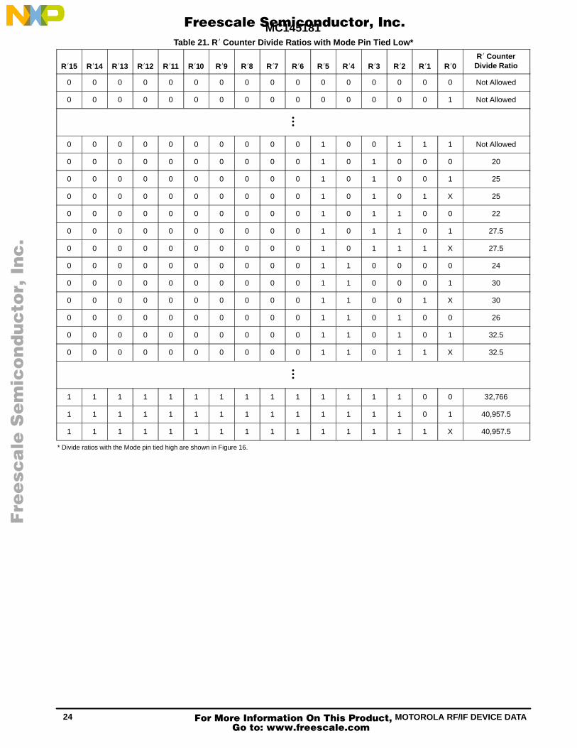
MC145181
24 MOTOROLA RF/IF DEVICE DATA
Table 21. R Counter Divide Ratios with Mode Pin Tied Low*ÁÁÁÁÁÁÁÁÁ
R15
ÁÁÁÁÁÁÁÁÁ
R14
ÁÁÁÁÁÁÁÁÁ
R13
ÁÁÁÁÁÁ
R12
ÁÁÁÁÁÁÁÁÁ
R11
ÁÁÁÁÁÁÁÁÁ
R10
ÁÁÁÁÁÁÁÁÁ
R9
ÁÁÁÁÁÁ
R8
ÁÁÁÁÁÁÁÁÁ
R7
ÁÁÁÁÁÁÁÁÁ
R6
ÁÁÁÁÁÁÁÁÁ
R5
ÁÁÁÁÁÁ
R4
ÁÁÁÁÁÁÁÁÁ
R3
ÁÁÁÁÁÁÁÁÁ
R2
ÁÁÁÁÁÁÁÁÁ
R1
ÁÁÁÁÁÁ
R0
ÁÁÁÁÁÁÁÁÁÁÁÁÁÁÁÁÁÁ
R CounterDivide Ratio
ÁÁÁÁÁÁ
0ÁÁÁÁÁÁ
0 ÁÁÁÁÁÁ
0 ÁÁÁÁ
0ÁÁÁÁÁÁ
0ÁÁÁÁÁÁ
0 ÁÁÁÁÁÁ
0 ÁÁÁÁ
0ÁÁÁÁÁÁ
0ÁÁÁÁÁÁ
0 ÁÁÁÁÁÁ
0 ÁÁÁÁ
0ÁÁÁÁÁÁ
0ÁÁÁÁÁÁ
0 ÁÁÁÁÁÁ
0 ÁÁÁÁ
0ÁÁÁÁÁÁÁÁÁÁÁÁ
Not Allowed
ÁÁÁÁÁÁ
0ÁÁÁÁÁÁ
0 ÁÁÁÁÁÁ
0 ÁÁÁÁ
0ÁÁÁÁÁÁ
0ÁÁÁÁÁÁ
0 ÁÁÁÁÁÁ
0 ÁÁÁÁ
0ÁÁÁÁÁÁ
0ÁÁÁÁÁÁ
0 ÁÁÁÁÁÁ
0 ÁÁÁÁ
0ÁÁÁÁÁÁ
0ÁÁÁÁÁÁ
0 ÁÁÁÁÁÁ
0 ÁÁÁÁ
1ÁÁÁÁÁÁÁÁÁÁÁÁ
Not Allowed
ÁÁÁÁÁÁÁÁÁÁÁÁÁÁÁÁÁÁÁÁÁÁÁÁÁÁÁÁÁÁÁÁÁÁÁÁÁÁÁÁÁÁÁÁÁÁÁÁÁÁÁÁÁÁÁÁÁÁÁÁÁÁÁÁÁÁÁÁÁÁÁÁÁÁÁÁÁÁÁÁÁÁÁÁÁÁÁÁÁÁÁÁÁÁÁÁÁÁÁÁÁÁ
ÁÁÁÁÁÁ
0ÁÁÁÁÁÁ
0 ÁÁÁÁÁÁ
0 ÁÁÁÁ
0ÁÁÁÁÁÁ
0ÁÁÁÁÁÁ
0 ÁÁÁÁÁÁ
0 ÁÁÁÁ
0ÁÁÁÁÁÁ
0ÁÁÁÁÁÁ
0 ÁÁÁÁÁÁ
1 ÁÁÁÁ
0ÁÁÁÁÁÁ
0ÁÁÁÁÁÁ
1 ÁÁÁÁÁÁ
1 ÁÁÁÁ
1ÁÁÁÁÁÁÁÁÁÁÁÁ
Not Allowed
ÁÁÁÁÁÁ
0ÁÁÁÁÁÁ
0ÁÁÁÁÁÁ
0ÁÁÁÁ
0ÁÁÁÁÁÁ
0ÁÁÁÁÁÁ
0ÁÁÁÁÁÁ
0ÁÁÁÁ
0ÁÁÁÁÁÁ
0ÁÁÁÁÁÁ
0ÁÁÁÁÁÁ
1ÁÁÁÁ
0ÁÁÁÁÁÁ
1ÁÁÁÁÁÁ
0ÁÁÁÁÁÁ
0ÁÁÁÁ
0ÁÁÁÁÁÁÁÁÁÁÁÁ
20ÁÁÁÁÁÁ0ÁÁÁÁÁÁ0ÁÁÁÁÁÁ0ÁÁÁÁ0ÁÁÁÁÁÁ0ÁÁÁÁÁÁ0ÁÁÁÁÁÁ0ÁÁÁÁ0ÁÁÁÁÁÁ0ÁÁÁÁÁÁ0ÁÁÁÁÁÁ1ÁÁÁÁ0ÁÁÁÁÁÁ1ÁÁÁÁÁÁ0ÁÁÁÁÁÁ0ÁÁÁÁ1ÁÁÁÁÁÁÁÁÁÁÁÁ25ÁÁÁ
ÁÁÁÁÁÁ
0ÁÁÁÁÁÁÁÁÁ
0ÁÁÁÁÁÁÁÁÁ
0ÁÁÁÁÁÁ
0ÁÁÁÁÁÁÁÁÁ
0ÁÁÁÁÁÁÁÁÁ
0ÁÁÁÁÁÁÁÁÁ
0ÁÁÁÁÁÁ
0ÁÁÁÁÁÁÁÁÁ
0ÁÁÁÁÁÁÁÁÁ
0ÁÁÁÁÁÁÁÁÁ
1ÁÁÁÁÁÁ
0ÁÁÁÁÁÁÁÁÁ
1ÁÁÁÁÁÁÁÁÁ
0ÁÁÁÁÁÁÁÁÁ
1ÁÁÁÁÁÁ
XÁÁÁÁÁÁÁÁÁÁÁÁÁÁÁÁÁÁ
25
ÁÁÁÁÁÁ
0ÁÁÁÁÁÁ
0 ÁÁÁÁÁÁ
0 ÁÁÁÁ
0ÁÁÁÁÁÁ
0ÁÁÁÁÁÁ
0 ÁÁÁÁÁÁ
0 ÁÁÁÁ
0ÁÁÁÁÁÁ
0ÁÁÁÁÁÁ
0 ÁÁÁÁÁÁ
1 ÁÁÁÁ
0ÁÁÁÁÁÁ
1ÁÁÁÁÁÁ
1 ÁÁÁÁÁÁ
0 ÁÁÁÁ
0ÁÁÁÁÁÁÁÁÁÁÁÁ
22
ÁÁÁÁÁÁ
0ÁÁÁÁÁÁ
0 ÁÁÁÁÁÁ
0 ÁÁÁÁ
0ÁÁÁÁÁÁ
0ÁÁÁÁÁÁ
0 ÁÁÁÁÁÁ
0 ÁÁÁÁ
0ÁÁÁÁÁÁ
0ÁÁÁÁÁÁ
0 ÁÁÁÁÁÁ
1 ÁÁÁÁ
0ÁÁÁÁÁÁ
1ÁÁÁÁÁÁ
1 ÁÁÁÁÁÁ
0 ÁÁÁÁ
1ÁÁÁÁÁÁÁÁÁÁÁÁ
27.5
ÁÁÁÁÁÁ
0ÁÁÁÁÁÁ
0ÁÁÁÁÁÁ
0ÁÁÁÁ
0ÁÁÁÁÁÁ
0ÁÁÁÁÁÁ
0ÁÁÁÁÁÁ
0ÁÁÁÁ
0ÁÁÁÁÁÁ
0ÁÁÁÁÁÁ
0ÁÁÁÁÁÁ
1ÁÁÁÁ
0ÁÁÁÁÁÁ
1ÁÁÁÁÁÁ
1ÁÁÁÁÁÁ
1ÁÁÁÁ
XÁÁÁÁÁÁÁÁÁÁÁÁ
27.5ÁÁÁÁÁÁ0ÁÁÁÁÁÁ0ÁÁÁÁÁÁ0ÁÁÁÁ0ÁÁÁÁÁÁ0ÁÁÁÁÁÁ0ÁÁÁÁÁÁ0ÁÁÁÁ0ÁÁÁÁÁÁ0ÁÁÁÁÁÁ0ÁÁÁÁÁÁ1ÁÁÁÁ1ÁÁÁÁÁÁ0ÁÁÁÁÁÁ0ÁÁÁÁÁÁ0ÁÁÁÁ0ÁÁÁÁÁÁÁÁÁÁÁÁ24ÁÁÁ
ÁÁÁÁÁÁ
0ÁÁÁÁÁÁÁÁÁ
0ÁÁÁÁÁÁÁÁÁ
0ÁÁÁÁÁÁ
0ÁÁÁÁÁÁÁÁÁ
0ÁÁÁÁÁÁÁÁÁ
0ÁÁÁÁÁÁÁÁÁ
0ÁÁÁÁÁÁ
0ÁÁÁÁÁÁÁÁÁ
0ÁÁÁÁÁÁÁÁÁ
0ÁÁÁÁÁÁÁÁÁ
1ÁÁÁÁÁÁ
1ÁÁÁÁÁÁÁÁÁ
0ÁÁÁÁÁÁÁÁÁ
0ÁÁÁÁÁÁÁÁÁ
0ÁÁÁÁÁÁ
1ÁÁÁÁÁÁÁÁÁÁÁÁÁÁÁÁÁÁ
30
ÁÁÁÁÁÁ
0ÁÁÁÁÁÁ
0 ÁÁÁÁÁÁ
0 ÁÁÁÁ
0ÁÁÁÁÁÁ
0ÁÁÁÁÁÁ
0 ÁÁÁÁÁÁ
0 ÁÁÁÁ
0ÁÁÁÁÁÁ
0ÁÁÁÁÁÁ
0 ÁÁÁÁÁÁ
1 ÁÁÁÁ
1ÁÁÁÁÁÁ
0ÁÁÁÁÁÁ
0 ÁÁÁÁÁÁ
1 ÁÁÁÁ
XÁÁÁÁÁÁÁÁÁÁÁÁ
30
ÁÁÁÁÁÁ
0ÁÁÁÁÁÁ
0 ÁÁÁÁÁÁ
0 ÁÁÁÁ
0ÁÁÁÁÁÁ
0ÁÁÁÁÁÁ
0 ÁÁÁÁÁÁ
0 ÁÁÁÁ
0ÁÁÁÁÁÁ
0ÁÁÁÁÁÁ
0 ÁÁÁÁÁÁ
1 ÁÁÁÁ
1ÁÁÁÁÁÁ
0ÁÁÁÁÁÁ
1 ÁÁÁÁÁÁ
0 ÁÁÁÁ
0ÁÁÁÁÁÁÁÁÁÁÁÁ
26
ÁÁÁÁÁÁ
0ÁÁÁÁÁÁ
0 ÁÁÁÁÁÁ
0 ÁÁÁÁ
0ÁÁÁÁÁÁ
0ÁÁÁÁÁÁ
0 ÁÁÁÁÁÁ
0 ÁÁÁÁ
0ÁÁÁÁÁÁ
0ÁÁÁÁÁÁ
0 ÁÁÁÁÁÁ
1 ÁÁÁÁ
1ÁÁÁÁÁÁ
0ÁÁÁÁÁÁ
1 ÁÁÁÁÁÁ
0 ÁÁÁÁ
1ÁÁÁÁÁÁÁÁÁÁÁÁ
32.5ÁÁÁÁÁÁ
0ÁÁÁÁÁÁ
0ÁÁÁÁÁÁ
0ÁÁÁÁ
0ÁÁÁÁÁÁ
0ÁÁÁÁÁÁ
0ÁÁÁÁÁÁ
0ÁÁÁÁ
0ÁÁÁÁÁÁ
0ÁÁÁÁÁÁ
0ÁÁÁÁÁÁ
1ÁÁÁÁ
1ÁÁÁÁÁÁ
0ÁÁÁÁÁÁ
1ÁÁÁÁÁÁ
1ÁÁÁÁ
XÁÁÁÁÁÁÁÁÁÁÁÁ
32.5ÁÁÁÁÁÁÁÁÁÁÁÁÁÁÁÁÁÁÁÁÁÁÁÁÁÁÁÁÁÁÁÁÁÁÁÁÁÁÁÁÁÁÁÁÁÁÁÁÁÁÁÁÁÁÁÁÁÁÁÁÁÁÁÁÁÁÁÁÁÁÁÁÁÁÁÁÁÁÁÁÁÁÁÁÁÁÁÁÁÁÁÁÁÁÁÁÁÁÁÁÁÁ
ÁÁÁÁÁÁ1ÁÁÁÁÁÁ1ÁÁÁÁÁÁ1ÁÁÁÁ1ÁÁÁÁÁÁ1ÁÁÁÁÁÁ1ÁÁÁÁÁÁ1ÁÁÁÁ1ÁÁÁÁÁÁ1ÁÁÁÁÁÁ1ÁÁÁÁÁÁ1ÁÁÁÁ1ÁÁÁÁÁÁ1ÁÁÁÁÁÁ1ÁÁÁÁÁÁ0ÁÁÁÁ0ÁÁÁÁÁÁÁÁÁÁÁÁ32,766ÁÁÁ
ÁÁÁÁÁÁ
1
ÁÁÁÁÁÁÁÁÁ
1
ÁÁÁÁÁÁÁÁÁ
1
ÁÁÁÁÁÁ
1
ÁÁÁÁÁÁÁÁÁ
1
ÁÁÁÁÁÁÁÁÁ
1
ÁÁÁÁÁÁÁÁÁ
1
ÁÁÁÁÁÁ
1
ÁÁÁÁÁÁÁÁÁ
1
ÁÁÁÁÁÁÁÁÁ
1
ÁÁÁÁÁÁÁÁÁ
1
ÁÁÁÁÁÁ
1
ÁÁÁÁÁÁÁÁÁ
1
ÁÁÁÁÁÁÁÁÁ
1
ÁÁÁÁÁÁÁÁÁ
0
ÁÁÁÁÁÁ
1
ÁÁÁÁÁÁÁÁÁÁÁÁÁÁÁÁÁÁ
40,957.5
ÁÁÁÁÁÁ
1ÁÁÁÁÁÁ
1 ÁÁÁÁÁÁ
1 ÁÁÁÁ
1ÁÁÁÁÁÁ
1ÁÁÁÁÁÁ
1 ÁÁÁÁÁÁ
1 ÁÁÁÁ
1ÁÁÁÁÁÁ
1ÁÁÁÁÁÁ
1 ÁÁÁÁÁÁ
1 ÁÁÁÁ
1ÁÁÁÁÁÁ
1ÁÁÁÁÁÁ
1 ÁÁÁÁÁÁ
1 ÁÁÁÁ
XÁÁÁÁÁÁÁÁÁÁÁÁ
40,957.5
ÁÁÁÁÁÁÁÁÁÁÁÁÁÁÁÁÁÁÁÁÁÁÁÁÁÁÁÁÁÁÁÁÁÁÁÁÁÁÁÁÁÁÁÁÁÁÁÁÁÁÁÁÁÁÁÁÁÁÁÁÁÁÁÁÁÁÁÁ
* Divide ratios with the Mode pin tied high are shown in Figure 16.
Fre
esc
ale
Se
mic
on
du
cto
r, I
Freescale Semiconductor, Inc.
For More Information On This Product, Go to: www.freescale.com
nc
...

MC145181
25MOTOROLA RF/IF DEVICE DATA
Figure 17.
6E. Hn REGISTER
Enb
Clk
Din
A3A2
A1A0
N’7
N’6
N’5
N’4
N’3
N’2
N’1
N’0
12
34
56
78
910
1112
1314
1516
1718
1920
2122
2324
2526
2728
2930
3132
XX
XX
XX
XX
XX
XX
N’1
5N
’14
N’1
3N
’12
N’11
N’1
0N
’9N
’8
0
Not
e 3
0 0 0 0 0 0 0 0
0 0 0 0 0 0 0 0
0 1 6 7 8 9 A B
Not
Allo
wed
Not
Allo
wed
Not
Allo
wed
. . .
F F
. . .
F F
. . . E F
Hex
adec
imal
. . .
Dec
imal
(Not
e 6)
Not
Allo
wed
. . .
. . .
. . .
. . . 00
C
10
0
5.X
sig
nifie
s a
don’
t car
e bi
t.
0 0 9 9 9 9 9 9 F F9
6.T
he d
ecim
al v
alue
mul
tiplie
d by
8 =
the
hexa
deci
mal
val
ue.
1.To
acc
ess
the
Hn’
reg
iste
r (t
he h
oldi
ng r
egis
ter
or fi
rst b
uffe
r of
the
doub
le–b
uffe
red
Hn’
and
N’ c
ombi
natio
n),
32 c
lock
cyc
les
mus
t be
used
.2.
Add
ress
bits
A3
thro
ugh
A0
are
requ
ired.
3.A
t thi
s po
int,
the
two
new
byt
es a
re tr
ansf
erre
d to
the
Hn’
reg
iste
r. T
here
fore
, the
N’ c
ount
er d
ivid
e ra
tio is
not
alte
red
yet a
nd r
etai
ns th
e pr
evio
us r
atio
load
ed. N
o ot
her
regi
ster
is a
ffect
ed.
4.A
tran
sfer
from
the
Hn’
(ho
ldin
g) r
egis
ter
to th
e N
’ reg
iste
r oc
curs
with
eac
h N
reg
iste
r ac
cess
.
N’ C
ount
er R
atio
= 1
9N
’ Cou
nter
Rat
io =
20
N’ C
ount
er R
atio
= 2
1N
’ Cou
nter
Rat
io =
22
N’ C
ount
er R
atio
= 2
3
N’ C
ount
er R
atio
= 8
,190
N’ C
ount
er R
atio
= 8
,191
Fig
ure
17. H
n’ R
egis
ter A
cces
s an
d F
orm
at
NO
TE
S:
Fre
esc
ale
Se
mic
on
du
cto
r, I
Freescale Semiconductor, Inc.
For More Information On This Product, Go to: www.freescale.com
nc
...

MC145181
26 MOTOROLA RF/IF DEVICE DATA
NO
TE
S:
Figure 18.
6F. D REGISTER
Enb
Clk
Din
A3A2
A1A0
D7
D6
D5
D4
D3
D2
D1
D0
12
34
56
78
910
1112
1314
1516
1718
1920
2122
2324
2526
2728
2930
3132
XX
XX
XX
XX
XX
XX
D15
D14
D13
D12
D11
D10
D9
D8
0
Not
e 3
0 1 2 3 D E
Hex
adec
imal
0 0 0 0 F F
Dec
imal
FF
01
1
. . .
. . .
DAC
1D
AC2
5.X
sig
nifie
s a
don’
t car
e bi
t.
1.To
acc
ess
the
D R
egis
ter,
32 c
lock
cyc
les
are
used
.2.
Add
ress
bits
A3
thro
ugh
A0
are
requ
ired.
3.A
t thi
s p
oint
, the
two
new
byt
es a
re tr
ansf
erre
d to
the
D r
egis
ter.
No
othe
r re
gist
er is
affe
cted
.4.
Low
–pow
er s
tand
by s
tate
.
Zero
+ 1
LSB
Out
put,
V=
(DAC
V) (
1/25
6)ou
tpo
s
Zero
+ 2
LSB
Out
put,
V=
(DAC
V) (
2/25
6)ou
tpo
s
Zero
Out
put,
V=
(DAC
V) (
0/25
6)(N
ote
4)
out
pos
Zero
+ 3
LSB
Out
put,
V=
(DAC
V) (
3/25
6)ou
tpo
s
Full
Scal
e O
utpu
t, V
= (D
AC V
) (25
5/25
6)ou
tpo
s
0 1 2 3 D E
Hex
adec
imal
0 0 0 0 F F
Dec
imal
FF
. . .
. . .
Zero
+ 1
LSB
Out
put,
V=
(DAC
V) (
1/25
6)ou
tpo
s
Zero
+ 2
LSB
Out
put,
V=
(DAC
V) (
2/25
6)ou
tpo
s
Zero
Out
put,
V=
(DAC
V) (
0/25
6)
(Not
e 4)
out
pos
Zero
+ 3
LSB
Out
put,
V=
(DAC
V) (
3/25
6)ou
tpo
s
Full
Scal
e O
utpu
t, V
= (D
AC V
) (25
5/25
6)ou
tpo
s
Fig
ure
18. D
Reg
iste
r Acc
ess
and
For
mat
Full
Scal
e –
2 LS
B O
utpu
t, V
= (D
AC V
) (25
3/25
6)ou
tpo
sFu
ll Sc
ale
– 1
LSB
Out
put,
V=
(DAC
V) (
254/
256)
out
pos
Full
Scal
e –
2 LS
B O
utpu
t, V
= (D
AC V
) (25
3/25
6)ou
tpo
sFu
ll Sc
ale
– 1
LSB
Out
put,
V=
(DAC
V) (
254/
256)
out
pos
Fre
esc
ale
Se
mic
on
du
cto
r, I
Freescale Semiconductor, Inc.
For More Information On This Product, Go to: www.freescale.com
nc
...

MC145181
27MOTOROLA RF/IF DEVICE DATA
Figure 19. Lock Detector Operation
fR vs fVPhase
Relationship
LDOutput
One fR Period
> LDWindow
< LDWindow
< LDWindow
< LDWindow
< LDWindow
< LDWindow
< LDWindow
> LDWindow
> LDWindow
Locked
Unlocked
NOTES:1. Illustration shown is for the main loop and applies when the secondary loop is either phase locked or in
standby. The actual detector outputs for each loop are ANDed together at the LD pin.2. The secondary loop is similar to the above illustration.3. The approximate lock detect window for the main loop is either 64 or 256 Osce cycles and is programmable
via bit N22. The approximate window for the secondary loop is 64 Osce cycles and is not programmable.4. The LD output is low whenever the phase difference is more than the lock detect window.5. The LD output is high whenever the phase difference is less than the lock detect window and continues to
be less than the window for 3 fR periods or more.
LOCK DETECTOR OUTPUT CONDITIONS
fR versus f V Relation Lock Detector Output Microcontroller Action
Frequency is the same with phase inside theLD window
Static high level output Senses high level and no edges, therefore loopis locked
Frequency is the same with phase outsidethe LD window
Static low level output Senses low level, therefore loop is unlocked
Frequency is slightly different, thus phase ischanging
Dynamic “chattering” output, output hastransitions
Senses edges, therefore loop is unlocked
Frequency is grossly different Static low level output Senses low level, therefore loop is unlocked
NOTE: For simplicity, this table applies to the main loop. The secondary loop is similar. The detector outputs feed an AND gate whose output is the LD pin.
Fre
esc
ale
Se
mic
on
du
cto
r, I
Freescale Semiconductor, Inc.
For More Information On This Product, Go to: www.freescale.com
nc
...

MC145181
28 MOTOROLA RF/IF DEVICE DATA
Figure 20. PD out –Hi and PD out –Lo Detector Output Characteristics
*At this point, when both fR and fV are in phase, the output source and sink circuits are turned on for a short interval.
NOTES:1. The detector generates error pulses during out–of–lock conditions. When locked in phase and frequency, the output is high impedance and
the voltage at that pin is determined by the low–pass filter capacitor.2. Waveform shown applies when the fout / Pol pin is low and the Mode pin is high.3. When the fout / Pol pin is high and Mode is high, the PDout–Hi and PDout–Lo waveform is inverted.4. The waveform shown is also the default when the Mode pin is low.
fRReferenceOsce ÷ R)
fVVCO Feedback
(fin ÷ N)
PDout–Hi,PDout–Lo
Source Current
Float
Sink Current
*
Figure 21. PD out Detector Output Characteristics
*At this point, when both fR and fV are in phase, the output source and sink circuits are turned on for a short interval.
NOTES:1. The detector generates error pulses during out–of–lock conditions. When locked in phase and frequency, the output is high impedance
and the voltage at that pin is determined by the low–pass filter capacitor.2. Waveform shown applies when the fout / Pol pin is low and the Mode pin is high.3. When the fout / Pol pin is high and Mode is high, the PDout waveform is inverted.4. The waveform shown is also the default when the Mode pin is low.
fR
ReferenceOsce ÷ R)
fV
VCO Feedback(fin ÷ N)
PDout
High Voltage
High Z
Low Voltage
*
Fre
esc
ale
Se
mic
on
du
cto
r, I
Freescale Semiconductor, Inc.
For More Information On This Product, Go to: www.freescale.com
nc
...

MC145181
29MOTOROLA RF/IF DEVICE DATA
7. APPLICATIONS INFORMATION
7A. CRYSTAL OSCILLATOR CONSIDERATIONS
The oscillator/reference circuit may be connected tooperate in either of two configurations. With the Mode pinplaced “high” and bi t C6 programmed to 1, theoscillator/reference circuit of the MC145181 will accept anexternal reference input. The external reference signalshould be capacitive, connected to Osce with Oscb leftfloating. Commercially available temperature compensatedcrystal oscillators (TCXOs) or crystal–controlled data clockoscillators provide a very stable reference frequency. Foradditional information about TCXOs and data clockoscillators, please consult the Electronic Engineers MasterCatalog, internet web page, or similar publication/service.
The on–chip Colpitts reference oscillator can be selectedby either tying the Mode pin low or by programming the C6 bitto zero when Mode is high. The oscillator may be operated ineither the fundamental mode, as show by Figure 22, or as anovertone oscillator. The “kick start” feature ensures reduced“stalling” of hard–starting crystals.
Crystal Resonators
The equivalent circuit of a crystal resonator mostcommonly used is shown in Figure 23. The crystal itself is aspecially cut (usually AT for overtone operation) block ofquartz. The dimensions, (shape, thickness, length, andwidth) determine the operating characteristics of the crystal.When deformed and allowed to return naturally to its restingshape, it is observed to oscillate. This oscillation has thetypical characteristics of a damped oscillation and anequivalent electrical signal can be found on the surface of thecrystal. In addition, if an equivalent electrical signal is appliedto the crystal, it will be observed to oscillate. The equivalentvalues for Rs, Ls, Cs, and Co can be used to predict theoperation of the crystal when used as an electronic oscillator.
Due to the series/parallel arrangement of the equivalentcomponents, the crystal exhibits two resonances. The first,sometimes just called resonance, is the series resonance ofthe Rs, Cs, Ls branch. The other, sometimes called theanti–resonance, is the parallel resonance including Co. Forthe series resonance the formula is
fs =2π Ls Cs
1.
For parallel resonance, the formula is
fp =
2π
1
Ls Cs CoCo + Cs
.
As can be seen from this equation, the anti–resonantfrequency is higher than the series resonant frequency. Theratio between the resonant and anti–resonant frequency canbe found using the formula
Cs =∆f
f 2 (Co + Cs)
where
∆f = fs – fp
and
.2
fs + fpf =
By exploiting this characteristic, the crystal oscillatorfrequency can be tuned slightly. If a capacitor is connected inseries with the crystal operating in the resonance mode, thefrequency will shift upward. If a capacitance is added inparallel with a crystal operating in an anti–resonant mode, thefrequency will be shifted down.
Figure 22. Fundamental Mode Oscillator Circuit
0
X1
0
0
C3
C2
C1
R1
R2
Q1
M1
+V
Oscb
Osce
Frequency Synthesizer
I1
200/800 µAM2
Fre
esc
ale
Se
mic
on
du
cto
r, I
Freescale Semiconductor, Inc.
For More Information On This Product, Go to: www.freescale.com
nc
...

MC145181
30 MOTOROLA RF/IF DEVICE DATA
21
2121
RsLs Cs
Re Xe
Co
X1
Figure 23. Crystal Resonator Equivalent Circuit
NOTE: Values are supplied by crystal manufacturer (parallelresonant crystal).
Figure 24. Overtone Crystal Equivalent Circuit
21
L1s C1sR1s
Co
L3s C3sR3s
L5s C5sR5s
Because of the acoustic properties of the crystalresonator, the crystal “tank” responds to energy not only at itsfundamental frequency, but also at specific multiples of thefundamental frequency. In the same manner that a shorted oropen transmission line responds to multiples of thefundamental frequency, the crystal “tank” responds similarly.A shorted half–wave transmission line (or closed acousticchamber) will not only resonate at its fundamental frequency,but also at odd multiples of the fundamental. These are calledthe overtones of the crystal and represent frequencies atwhich the crystal can be made to oscillate. The equivalentcircuit of an overtone crystal is shown is Figure 24.
The components for the appropriate overtone arerepresented by 1, 3, and 5. The fundamental components arerepresented by 1, and those of importance for the third andfifth overtones, by 3 and 5.
Fundamental Mode
The equivalent circuit for the Colpitts oscillator operating inthe fundamental mode is shown in Figure 25.
C3 is selected to provide a small reduction in the inductiveproperty of the crystal. In this manner, the frequency of theoscillator can be “pulled” slightly. The biasing combination of
M1R1 and M2R2 provide the ability to start operation with ahigher than normal operating current to stimulate crystalactivity. This “kick start” current is nominally four times thenormal current. An internal counter times the application ofthe “kick start” and returns the current to normal after the timeout period.
The mutual conductance (transconductance) of thetransistor Q1 is useful in determining the conditionsnecessary for oscillation. The nominal value for thetransconductance is found from the formula
Iegm =26
where Ie is the emitter current in mA.The operation of the oscillator can be described using the
concept of “negative resistance”. In a normal tuned circuit,any excitation tends to be dissipated by the resistance of thecircuit and oscillation dies out. The resistive part of the crystalalong with the resistance of the wiring and the internalresistance of C1, C2, and C3, make up this “damping”resistance. Some form of energy must be fed back into thecircuit to sustain oscillation. This is the purpose of theamplifier.
Figure 25. Fundamental Mode Colpitts Oscillator Equivalent Circuit
0
0
C3
C2
C1
R1
R2
Q1
M1
+V
Oscb
Osce
Frequency Synthesizer
I1
200/800 µA
0
R1s
Co
C1s
Rst
M2
L1s
Fre
esc
ale
Se
mic
on
du
cto
r, I
Freescale Semiconductor, Inc.
For More Information On This Product, Go to: www.freescale.com
nc
...

MC145181
31MOTOROLA RF/IF DEVICE DATA
If we define the damping as resistive, we can define theopposite or regenerative property as negative resistance.Figure 26 shows the basic circuit of the Colpitts oscillator. C3has been combined with the crystal elements for simplicity.For the circuit to oscillate, there must be at least as much“negative resistance” (regeneration) as there is resistance(damping). We can define this by deriving the inputimpedance for the amplifier.
Figure 26. Colpitts Oscillator Basic Circuit
Q1
C2
C1
Iin
Vin
If a driving signal is defined as Vin, the resultant currentthat flows can be identified as Iin. The relationship of Vin to Iinis
Vin = Iin (Zc1 + Zc2) – Ib (Zc2 – βZc1)and
0 = Iin (Zc2) + Ib (Zc2 + rb)
where Ib is the base current of transistor Q1. Solving the twoequations and assuming Zc2 << rb, the input impedance canbe expressed as
Zin
jω
1
C1 C2
C1 + C2
–gm
ω2 C1 C2+
where ω = 2πf. This is equivalent to the series combination ofa real part whose value is
REAL =–gm
ω2 C1 C2
and the imaginary part whose value is
IMAG =
jω
1
C1 C2
C1 + C2
To sustain oscillation, the amplifier must generate a“negative resistance” equal or greater than the REAL part ofthe above equation and opposite in polarity.
Rneg =–gm
ω2 C1 C2
As long as the relation
–Rneg = –SUM (Rs + Rst + Rc1 + Rc2 + Rc3) ,
the circuit will oscillate and the frequency of oscillation will bedefined as
fo =2π Ls (C1||C2||C3)
1
where C3 is the series frequency adjusting capacitor.
In determining values for C1, C2, and C3, two limits areconsidered. At one end is the relationship of C3 to C2 andC1. If C3 is made 0 or the reactance of C3 is small comparedto the reactance of C1 and C2, no adjustment of the crystalfrequency is possible. The other limit is the relationship
gm Zc1 Zc2 > Rsumwhere Rsum is the sum of resistances in the resonant loop.Since this equation must be true for the circuit to oscillate, itis obvious that as the values of C1 and C2 are increased, theseries resistances must be reduced and/or gm increased.Since gm is a function of device current and there is aphysical limit on how small Rsum can be made, at some pointoscillation can no longer be sustained.
Normally, it is desirable to choose the “negativeresistance” to be several times greater than the “damping”resistance to ensure stable operation. A factor of four or fiveis a good “rule of thumb” choice.
To determine crystal power, the equivalent circuit shown inFigure 27 can be used. In this case, we are addressing acondition where the transistor amplifier is operating at thelimit of class A; that is, the device is just at cutoff during thepeak negative excursions. At this point,
Re = gm Xc1 Xc2if the amplitude is constant and the oscillator is stable. Forthis to occur, the sum of all resistances in the resonant loopwill be equal to Re, where Re represents the effectiveresistance of I1. This can be written as
Rsum = Rs + Rst = Rewhere Rs is the crystal resistance and Rst is the additionaldistributed resistances within the resonant loop. At the pointwhere the transistor enters cutoff we have the equation
(Iin – Ib) Zc2+ (Iin + βib) Zc1 =v1 + v2
Xls + Re Xls + Re–Iin = .
β = current gain of the transistor. Rewriting:
Ib (Zc2 – βZc1)
Zc1 + Zc2 + Xls + ReIin = .
For oscillation to occur, we must have
Zc1 + Zc2 + Xls 0 .
If we assume βZc1 is normally much greater than Zc2 then
Iin –Ie Zc1
Re .
For the condition we have specified,
Ie(bias) + Ie(instantaneous ac) = 0
the transistor is just cutting off and the peak current, Iin isequal to the bias current. The peak input current isrepresented as
Iin(peak) =Ie|Zc1|
Re .
The power dissipation of the series resistances in theresonant loop can be written as
(Ie|Zc1|)2 =
Iin(peak)2 R
2 2 RsumP =
where Rsum = Re.The power dissipation for the crystal itself becomes
(Ie|Zc1|)2
2 RsPcrystal = .
Fre
esc
ale
Se
mic
on
du
cto
r, I
Freescale Semiconductor, Inc.
For More Information On This Product, Go to: www.freescale.com
nc
...

MC145181
32 MOTOROLA RF/IF DEVICE DATA
Figure 27. Equivalent Circuit for Crystal Power Estimation
C2
C1
Rs
Re200/800 µA
X1
I1
Blb
lb
LsVCC x R2 / (R1 + R2)
R1 || R2 Iin
VCC
Overtone Operation
For overtone operation, the circuit is modified by theaddition of an inductor, L1; and a series capacitor, C4. C4 isinserted as a dc blocking capacitor whose capacitance ischosen sufficiently large so that its reactance can be ignored.This circuit is shown in Figure 28.
For oscillation to occur at the overtone frequency, thecondition
gm Zc1 Zc2 > Rsmust exist.
Zc1 represents the impedance across C1 and can bedefined as
Zc1 = jXc1|| (Rl1 + jXl1)
where Rl1 is the dc resistance of the inductor L1.For overtone operation, this must occur at the desired
harmonic. For example, if the crystal is chosen to oscillate atthe third overtone, C1 and C2 must be chosen so that theabove condition exists for Zc1 and Zc2 at the third harmonic ofthe fundamental frequency for the crystal. In addition, caremust be taken that the “negative resistance” of the amplifier isnot sufficient at the fundamental frequency to induceoscillation at the fundamental frequency. It may be necessaryto add additional filtering to reduce the gain of the amplifier atthe fundamental frequency. The key to achieving stableovertone oscillator operation is ensuring the existence of theabove condition at the desired overtone while ensuring itsfailure at all other frequencies.
L1 and C1 are chosen so that
> Ff2π L1 C1
1
where Ff is the fundamental frequency of the crystalresonator. If L1 and C1 are chosen to be net capacitive at thedesired overtone frequency and if the condition
gm Zc1 Zc2 > Rs
is true only at the desired overtone frequency, the oscillatorwill oscillate at the frequency of the overtone. Normally, L1and C1 are not chosen to be resonant at the overtonefrequency but at a lower frequency to ensure that the parallel
combination of L1 and C1 is capacitive at the overtonefrequency and inductive at the fundamental frequency.
< Fo2π L1 C1
1Ff <
The net inductance of the rest of the resonant loop thenbalances this capacitance at the overtone frequency.
1
1
Xls – Xcs –
+ Xl2 + Xl(stray) – Xc31
Xc0
1
–
= 01
Xc1
1
Xl1
+
L2 and C3 are chosen to provide the desired adjustment tothe resonant overtone frequency. This is normally computedby calculating the expected ppm change at the resonantfrequency and using this to define the value of the reactancenecessary to produce this change.
X (of L2 and C3)
Z (crystal at resonance)∆Ff (ppm) =
∆Ff (ppm) = X(of L2 and C3)/Z(crystal at resonance)
The values needed for this calculation can be derived fromthe value of the fundamental frequency and Co. If Co isknown or can be measured, Cs is defined as
200
CoCs =
for an AT cut crystal.The fundamental frequency can be used to calculate the
value for Ls using either the series resonant or parallelresonant formulas given earlier. Since the Q of the crystal,
RXQ =
is usually sufficiently large at the resonant frequency so that
Rs << Z(crystal)
Fre
esc
ale
Se
mic
on
du
cto
r, I
Freescale Semiconductor, Inc.
For More Information On This Product, Go to: www.freescale.com
nc
...

MC145181
33MOTOROLA RF/IF DEVICE DATA
Rs can be ignored. The value for C3 and L2 are chosen sothat
Xc3 = Xl2when C3 is adjusted to approximately half its maximumcapacitance. At this setting, the combination produces a zerochange in the overtone frequency. If C3 is then chosen sothat Xc3 at minimum capacitance is
[Xc3(max)] – Xl2 >= ∆Ff (ppm) Z(crystal)
and L2 is approximately
Xc3(max)
2XI2 =
then
Xc3(max) >= 2[∆Ff (ppm)] Z(crystal)
and
Xc(max)
4Xc(min)=
This results in an adjustable change in the operatingfrequency of +[∆Ff (ppm)] and –[∆Ff (ppm)] /2. If ratios nearerto 1:1 are used for Xc3(max) and Xl2, the tuning range will beskewed with a wider –[∆Ff (ppm)] but at the expense of lessadjustability over the +[∆Ff (ppm)] range.
Figure 28. Colpitts Oscillator Configured for Overtone Operation
0
0
C3
C2
C1
R1
R2
Q1
M2
M1
+V
Oscb
Osce
Frequency Synthesizer
I1
200/800 µA
0
X1
0
C4
L1
L2
Fre
esc
ale
Se
mic
on
du
cto
r, I
Freescale Semiconductor, Inc.
For More Information On This Product, Go to: www.freescale.com
nc
...

MC145181
34 MOTOROLA RF/IF DEVICE DATA
7B. MAIN LOOP FILTER DESIGN — CONVENTIONAL
The current output of the charge pump allows the loopfilter to be realized without the need of any activecomponents. The preferred topology for the filter is illustratedin Figure 29.
The Ro/Co components realize the primary loop filter. Cais added to the loop filter to provide for reference sidebandsuppression. If additional suppression is needed, the Rx/Cxrealizes an additional filter. In most applications, this will notbe necessary. If all components are used, this results in afourth order PLL, which makes analysis difficult. To simplifythis, the loop design will be treated as a second order loop(Ro/Co), and additional guidelines are provided to minimizethe influence of the other components. If more rigorousanalysis is needed, mathematical/system simulation toolsshould be used.
Component Guideline
Ca <0.1 x Co
Rx >10 x Ro
Cx <0.1 x Co
The focus of the design effort is to determine what theloop’s natural frequency, ωo, should be. This is determined byRo, Co, Kp, Kv, and Nt. Because Kp, Kv, and Nt are given, it isonly necessary to calculate values for Ro and Co. There arethree considerations in selecting the loop bandwidth:
1. Maximum loop bandwidth for minimum tuning speed.
2. Optimum loop bandwidth for best phase noiseperformance.
3. Minimum loop bandwidth for greatest referencesideband suppression.
Usually a compromise is struck between these threecases, however, for a fixed frequency application, minimizingthe tuning speed is not a critical parameter.
To specify the loop bandwidth for optimal phase noiseperformance, an understanding of the sources of phasenoise in the system and the effect of the loop filter on them isrequired. There are three major sources of phase noise in thephase–locked loop — the crystal reference, the VCO, and
the loop contribution. The loop filter acts as a low–pass filterto the crystal reference and the loop contribution. The loopfilter acts as a high–pass filter to the VCO with an in–bandgain equal to unity. The loop contribution includes the PLL IC,as well as noise in the system; supply noise, switching noise,etc. For this example, a loop contribution of 15 dB has beenselected.
The crystal reference and the VCO are characterized ashigh–order 1/f noise sources. Graphical analysis is used todetermine the optimum loop bandwidth. It is necessary tohave noise plots from the manufacturers of both devices.This method provides a straightforward approximationsuitable for quickly estimating the optimal bandwidth. Theloop contribution is characterized as white–noise orlow–order 1/f noise, given in the form of a noise factor whichcombines all the noise effects into a single value. The phasenoise of the crystal reference is increased by the noise factorof the PLL IC and related circuitry. It is further increased bythe total divide–by–N ratio of the loop. This is illustrated inFigure 30. The point at which the VCO phase noise crossesthe amplified phase noise of the crystal reference is the pointof the optimum loop bandwidth. In the example of Figure 30,the optimum bandwidth is approximately 15 kHz.
To simplify analysis further, a damping factor of 1 will beselected. The normalized closed loop response is illustratedin Figure 31 where the loop bandwidth is 2.5 times the loopnatural frequency (the loop natural frequency is thefrequency at which the loop would oscillate if it wereunstable). Therefore, the optimum loop bandwidth is15 kHz/2.5 or 6.0 kHz (37.7 krads) with a dampingcoefficient, ζ 1. T(s) is the transfer function of the loopfilter.
whereNt = Total PLL Divide Ratio — 8 x N
where (N = 25 ... 40),Kv = VCO Gain – 2π Hz/V,Kp = Phase Detector/Charge Pump Gain – A
= ( |IOH | + |IOL | ) / 4π.
Technically, Kv and Kp should be expressed in radian units[Kv (rad/V), Kp (A/rad)]. Since the component designequation contains the Kv x Kp term, the 2π cancels and thevalue can be expressed as AHz/V (amp hertz per volt).
Figure 29. Loop Filter
ChargePump
Ph/FrqDet
N Counter
XtlOsc
PLL
VCO
Co
CaRo Cx
RxR Counter
0
0
0
Fre
esc
ale
Se
mic
on
du
cto
r, I
Freescale Semiconductor, Inc.
For More Information On This Product, Go to: www.freescale.com
nc
...

MC145181
35MOTOROLA RF/IF DEVICE DATA
Figure 30. Graphical Analysis ofOptimum Bandwidth
–60
–70
–80
–90
–100
–110
–120
–130
–140
–150
dB
10 100 1 k 10 k 100 k 1MHz
VCO
Optimum Bandwidth
Closed Loop Response
20 x log (Nt)
Crystal Reference
15 dB NF of the NoiseContribution from Loop
Natural Frequency
Figure 31. Closed Loop Frequency Responsefor ζ = 1
1.0 k
10
0
10
–20
–30
–40
–50
–600.1
Hz
1001.0
–10
dB
3 dB Bandwidth
In summary, follow the steps given below:
Step 1: Plot the phase noise of crystal reference and theVCO on the same graph.
Step 2: Increase the phase noise of the crystal reference bythe noise contribution of the loop.
Step 3: Convert the divide–by–N to dB (20log 8 x N) andincrease the phase noise of the crystal reference bythat amount.
Step 4: The point at which the VCO phase noise crosses theamplified phase noise of the crystal reference is thepoint of the optimum loop bandwidth. This isapproximately 15 kHz in Figure 30.
Step 5: Correlate this loop bandwidth to the loop naturalfrequency per Figure 31. In this case the 3.0 dBbandwidth for a damping coefficient of 1 is 2.5 timesthe loop’s natural frequency. The relationshipbetween the 3.0 dB loop bandwidth and the loop’s“natural” frequency will vary for different values of ζ.Making use of the equations defined in Figure 32, amath tool or spread sheet is useful to select thevalues for Ro and Co.
Appendix: Derivation of Loop Filter Transfer Function
The purpose of the loop filter is to convert the current fromthe phase detector to a tuning voltage for the VCO. The totaltransfer function is derived in two steps.
Step 1 is to find the voltage generated by the impedance ofthe loop filter.
Step 2 is to find the transfer function from the input of theloop filter to its output. The “voltage” times the “transferfunction” is the overall transfer function of the loop filter. Touse these equations in determining the overall transferfunction of a PLL, multiply the filter’s impedance by the gainconstant of the phase detector, then multiply that by thefilter’s transfer function. Figure 33 contains the transferfunction equations for the second, third, and fourth order PLLfilters.
PSpice Simulation
The use of PSpice or similar circuit simulation programscan significantly reduce laboratory time when refining a PLL
design. The following describes the use of behavioralmodeling to develop useful models for studying loop filterperformance. In many applications the levels of sidebandspurs can also be studied.
Behavioral modeling is chosen, as opposed to discretedevice modeling, to improve performance and reducesimulation time. PLL devices can contain several thousandindividual transistors. To simulate at this level can result ingeneration of an enormous amount of data when comparedto a simpler behavioral model. For example, a logic NANDgate can contain several transistors. Each of these requires adata set for each of the transistor terminals. If a half dozentransistors are used in the gate design, both current andvoltage measurements for each terminal of each device forevery node in the circuit is calculated. The gate can beexpressed as a behavioral model, which is treated andsimulated as a single device. Since PSpice sees this as asingle rather than multiple devices, the amount ofaccumulated data is much less, resulting in a fastersimulation.
For applications using integrated circuits such as PLLs, itis desirable to investigate the performance of the circuitryadded externally to the integrated circuit. By using behavioralmodeling rather than discrete device modeling to representthe integrated circuit, the engineer is able to study theperformance of the design without the overhead contributedby simulating the integrated circuit.
Phase Frequency Detector Model
The model for the phase frequency detector is derivedusing the waveforms shown in Figure 20. Two signals arepresent at the input of the phase frequency detector. Theseare the reference input and the feedback from the VCOand/or prescaler. The two signals are compared to determinethe lag/lead relationship between the two signals and pulsesgenerated to represent the leading edge of each signal. Apulse whose width equals the lead of one input signal overthe other is generated by an RS flip–flop (RSFF). One RSFFgenerates a pulse whose width equals the lead of thereference signal over the feedback signal, and a secondRSFF generates a signal whose width is the lead of thefeedback signal over the reference signal. The logical modelfor the phase frequency detector is shown in Figure 34.
Fre
esc
ale
Se
mic
on
du
cto
r, I
Freescale Semiconductor, Inc.
For More Information On This Product, Go to: www.freescale.com
nc
...

MC145181
36 MOTOROLA RF/IF DEVICE DATA
Figure 32. Design Equations for the Second Order System
RoCos + 1T(s) =
s2 + RoCos + 1NCoKpKv
=
s2 +1
ωo2 s + 1
2ζωo
s + 12ζωo
NCoKpKv
=1
ωo2 ωo =
NCo
KpKv
RoCo = 2ζωo ζ =
ωoRoCo2
Co =Nωo2KpKv
Ro =ωoCo
2ζ
Figure 33. Overall Transfer Function of the PLL
ZLF(s) =Cos
RoCos + 1Vt
Co
Vp
Ro
For the Second Order PLL:
For the Third Order PLL:
For the Fourth Order PLL:
Vt
Co
Vp
Ro Ca
Vt
Co
Vp
Ro Ca Cx
TLF(s) =Vp(s)
Vt(s)= 1 , Vp(s) = Kp(s)ZLF(s)
ZLF(s) =CoRoCas2 + (Co + Ca)s
RoCos + 1
TLF(s) =Vp(s)
Vt(s)= 1 , Vp(s) = Kp(s)ZLF(s)
ZLF(s) =CoRoCaRxCxs3 + [(Co + Ca)RxCx + CoRo (Cx + Ca)] s2 + (Co + Ca + Cx)s
(RoCos + 1) (RxCxs + 1)
TLF(s) =Vp(s)
Vt(s), Vp(s) = Kp(s)ZLF(s)=
(RxCxs + 1)
1
Fre
esc
ale
Se
mic
on
du
cto
r, I
Freescale Semiconductor, Inc.
For More Information On This Product, Go to: www.freescale.com
nc
...

MC145181
37MOTOROLA RF/IF DEVICE DATA
Figure 34. Phase Frequency Detector Logic Diagram
PG1
Pulse Generator
PG2
RSFF2
RSFF1
Ref
In
R
SP1
OutInRφ
Vφ
Pulse Generator
S
RP1
OutIn
The behavioral model of the phase frequency detectorshown in Figure 35 is derived using the phase frequencydetector logic diagram. Behavioral models for the pulsegenerator, AND gate (Figure 36), and RS flip–flops(Figure 37) are created using analog behavioral blocks. Thepulse generator is created using a delay block and a “gate”defined by the behavioral expression:
If [V(v1) ≥ 1 & V(v2) , 1, 5, 0]
v1 and v2 represent the two inputs to the block.This is the behavioral expression for an AND gate with one
input inverted. The addition of the delay element produces apulse whose width equals the delay element.
The pulses appearing at the output of HB1 and HB2(Figure 35) are used to set the flip–flops, RSFF1, andRSFF2. The leading pulse will set the appropriate flip–flopresulting in a high at the output of that flip–flop. The output ofthis flip–flop will remain high until the arrival of the second (orlagging) pulse sets the second RS flip–flop. The presence ofa high on both RS flip–flop outputs results in the generation ofthe reset pulse. The reset pulse is generated by the analogbehavioral block (configured as an AND gate) and the delayelement. The delay element is necessary to eliminate thezero delay paradox of input to output to input.
The output of the phase frequency detector is two pulsetrains appearing at Rφ and Vφ. When the PLL is locked, thepulses in both pulse trains will be of minimum width. Whenthe phase frequency detector is out of lock, one pulse trainwill consist of pulses of minimum width while the width of thepulses in the second train will be equal to the lead/lagrelationship of the input signals. If the Ref input leads ‘In’, thepulse train at Rφ will consist of pulses whose width equals thelead of Ref. If Ref lags ‘In’, the width of the pulses appearingat Vφ will equal this lag.
The terms lead and lag used in this explanation representan occurrence in time rather than a phase relationship. At anycondition other than locked, one input (either In or Ref), willbe of a higher frequency. This results in the arrival of thepulse at that input ahead of the pulse at the other input, orleading. The second then is lagging.
To simulate the operation of the phase frequency detectorin an actual circuit, a charge pump needs to be added. Thebehavioral model for this is shown in Figure 38. Twovoltage–to–current behavioral models are used to producethe charge pump output. Two voltage–controlled switcheswith additional behavioral models, monitor the voltage of theoutput of the charge pump and clamp to 0 or VCC to simulatea real circuit.
To ensure the model conforms to the PLL, the delay blocksin the phase frequency detector should be set to theexpected value as specified by the MC145181 data sheet. Inaddition, the charge pump sink and source current behavioralmodel should also be set to deliver the desired current andVCC specified to ensure correct clamping.
Modeling the VCO
The VCO (Figure 39) is also modeled using AnalogBehavioral Modeling (ABM). The model used in the followingexamples assumes a linear response; however, the controlvoltage equation can be modified as desired. The circuit ismodeled as a sine generator controlled by the controlvoltage. The sine generator can be modeled using theEVALUE function or the ABM function. In Figure 39, theEVALUE function is used to generate the divided output andthe ABM function is used for the undivided output. Either theGVALUE or the ABM/I function can be used for the controlvoltage.
Fre
esc
ale
Se
mic
on
du
cto
r, I
Freescale Semiconductor, Inc.
For More Information On This Product, Go to: www.freescale.com
nc
...

MC145181
38 MOTOROLA RF/IF DEVICE DATA
Figure 35. Behavioral Model of the Phase Frequency Detector
Ref
In
Rφ
Vφ
V1
V2
Out
HB2
If [V(Q1)>=1 & V(Q2)>=1, 5, 0]
RSFF1
R
S
P1
Delay
S
R
P1
RSFF2
Out In
Delay
In Out
Pulse Generator
V2
V1
Out
HB1
Delay
In Out
Pulse Generator
Figure 36. Behavioral Block Used for thePulse Generator
v1
v2v2
Out
If (V(v1) ≥ 1 | V(v2) < 1, 5, 0)v1
Figure 37. Behavioral Block Used as an RS Flip–flop
If [V(In1)>=1 & V(In2)<1 | V(In2)<1, 5]
Qout
S
R
In3
In2
In1
If [V(In2)>=1, 0]If [V(In3)>=1 & V(In2)<1, 5, 0]
If [V(Q)>=1, 5, 0]
Fre
esc
ale
Se
mic
on
du
cto
r, I
Freescale Semiconductor, Inc.
For More Information On This Product, Go to: www.freescale.com
nc
...

MC145181
39MOTOROLA RF/IF DEVICE DATA
Figure 38. Charge Pump Model
If [V(In1)>=1 V(In2)<1, 1 x 10⁻³, 0]
+
0
PDout
In1
In2 0
0If [V(In2)>=1 V(In1)<1, 1 x 10⁻³, 0]
S1
Sbreak
–+–
0
If [V(idrive) > 0, 0, 1]
If [V(idrive) < 5, 0, 1]S2
+
0
–
+–
0
+
–
Sbreak
5V1
idrive
Rφ
Vφ
Figure 39. VCO Behavioral Model
5 V
0 V
1 x 1099R1
sin tw [fc time + N v(int)]
1
1 x 10³
1 x 10⁻⁶
+
Parameters:
twfck1
6.283250 x 106525 x 106
Parameters:
NQc
50001 x 10–6
In+
In–
Out+
Out–
evalue
0
ctrlIn+
In–gvalue
G1
E1
C1
int
ctrl
Out
VCOout
IC = 0
N time + v(int)
fc
tw N v(ctrl) Qck1
sin tw
Fre
esc
ale
Se
mic
on
du
cto
r, I
Freescale Semiconductor, Inc.
For More Information On This Product, Go to: www.freescale.com
nc
...

MC145181
40 MOTOROLA RF/IF DEVICE DATA
The equation for the sine generator is:
N
fc time + v(int) .e = sin tw
fc is defined as the output frequency when the control voltageis 0. This is the expected VCO frequency before frequencydivision. For the purpose of simulation, the counter value, N,has been written into the equation to ensure the correlationbetween the modeled circuit and the mathematical loop filtercalculations. tw is 2π; additional decimal places can be addedas needed. v(int) is the control voltage effect and is defined inthese examples as:
twN
k1v(cntl) 1 x 10⁻⁶ .v(int) =
where k1 is the VCO gain in rad/V.The value C1 in the schematic of the VCO can be
arbitrarily changed; however, the value must match that ofQc. Qc determines the value of the current to be integrated bythe capacitor C1. R1 is arbitrarily set to 1 x 1099 and is not anactive part of the circuit; however, it must be included toprevent open pin errors from the PSpice software. TheGVALUE function is used to perform the generation of v(int).There is some interaction between the integrator, (GVALUEoutput and C1) and R1. V(int) is a continuous ramp that isloaded by the resistance of R1. Unless the GVALUE outputcurrent is sufficiently large for the value chosen for R1, theVCO control voltage required to maintain lock will increasethroughout the simulation producing nonlinear operation.Modifications to the circuit can be performed either bychanging the values in the parameter list or for majorchanges to the VCO characteristics, the equations for thesine generator, or control voltage can be altered.
The output of the sine generator is amplified by 1000 toproduce a sharp rise/fall time and the output limited to swingbetween the values of 0 V and 5 V to convert it to a digitaloutput. The resultant circuit/symbol accepts a voltage inputfrom the loop filter and produces a square wave output at the
desired frequency. This frequency should be chosen torepresent the frequency present at the output of the Ncounter of the PLL frequency synthesizer.
The second output represented by the ABM function is asine wave output of the frequency expected from the actualVCO. The primary purpose of this output is to allow fullfrequency simulation for spectrum analysis. By running atransient analysis of sufficient time, it is possible to determinespur content and level. If sufficient resolution is used in thesimulation, the PSpice probe FFT transform can be used toprovide the typical spectrum analyzer display.
Loop Filter Simulation
The circuit shown in Figure 40 is used to simulate theclosed loop operation for a single charge pump output.Component values for the loop filter should be computedusing information from the previous section. Initial conditionscan be set using the “IC1” symbol with starting valuesspecifying the initial condition.
By adjusting component values for the loop filter,performance of the closed loop operation can be monitored.The control voltage to the input of the VCO can be monitoredfor a variety of conditions including settling time, lock time,and ripple present at the VCO input. In addition, the output ofthe VCO can be monitored for spur sidebands caused byripple on the loop filter output; however, expected operationat high frequencies may be difficult due to the excessive datathat can be generated.
As the divider ratio, N, increases for a fixed stepfrequency, the number of data points required to obtainsufficient information to overcome aliasing problems maybecome excessively large. In addition, the number ofsamples required should be three or more per cycle. ForVCO frequencies in the range of 500 MHz, this means thestep ceiling needs to be in the range of 100 to 500 ps. If asimulation time of 1 ms is needed, the actual computer timecan be several hours with data accumulation in the 1– to2–Gbyte range.
Figure 40. PLL Closed Loop Model
U3
Ref
In
HB2
R3
75 k
0
0
C2C3
0 0
1 kR4
ctrl+–
+ +IC = 3.5
0.1 n
0
C1
V1Out
VCOout
7.5 k
IC = 3.5
PDout
Rφ
HB1
Vφ
Rφ
Vφ0.2 n2 n
R1
Fre
esc
ale
Se
mic
on
du
cto
r, I
Freescale Semiconductor, Inc.
For More Information On This Product, Go to: www.freescale.com
nc
...

MC145181
41MOTOROLA RF/IF DEVICE DATA
7C. MAIN LOOP FILTER DESIGN — ADAPT
Introduction
For PSpice simulation, the schematic model shown inFigure 41 was chosen. The classical PLL model employing aphase–frequency detector, a VCO, and an adaptive loop filteris used to simplify visualization of circuit operation. Theparameter tables allow for modification of circuit performanceby providing an easy method for altering critical valueswithout necessitating changes to sub–level schematics. Thedefinition for the terms are:
tw = 2π,
fr = reference frequency,
td = time delay; allows delay of the start of the highcurrent mode (used to perform reference spurmeasurements),
CPL = charge pump low current,
CPH = charge pump high current,
N = N counter value,
Sz = amount the N counter is being increased (ordecreased) by,
St = number of fr cycles that CPH is active; this valueis either 16, 32, 64, or 128,
VCPHH = charge pump voltage – high,
VCPHL = charge pump voltage – low,
K1 = VCO gain (Hz/volt),
fc = VCO frequency at 0 V control voltage,
H = reference spur scaling factor.
Modeling the Phase–frequency Detector
Figure 42 is a schematic of the phase–frequency detector.It includes the reference oscillator model, phase–frequencydetector model, and charge pump models. V1 is the controlelement used to generate the step time for switching betweenCPL and CPH. The signal source VPULSE, is used tosimulate the timer that controls when CPL and CPH areturned on. PW calculates the pulse width that simulates thecounter from the values for St and fr that are entered in theparameter tables on the top level schematic.
Figure 41. Top Level PLL Model
50 p
PDout–LoIn
HB2
C2
20 k
0
0
C5
C6
0
0
1 kR10ctrl
330 p
C4
Out
VCO
HB1
33 pR3
Parameters:
twfrH
6.28318530825 k1
Parameters:
CPLCPHK1
1 x 10–34 x 10–34 x 106
Parameters:
NSzSt
2932040032
PDout–Hi
+ +
60.4 k R1C1
40.2 k
+
+
3300 p10%
330 p C3
330 p
R2
Parameters:
VCPHHVCPHLfc
50727.6 x 106
Parameters:
td 0
K1IC =
fr N – fcK1
IC =fr N – fc
K1IC =
fr N – fc
K1IC =
fr N – fc
Figure 42. Phase–frequency Detector with Dual Charge Pumps
HB1
Shift
+–
HB3 HB2
PDout–Lo
PDout–HiPDout–Hi
PDout–LoRφ
Vφ
Rφ
Vφ
fin
RefRefShift
V1
0
In
Shift
PW =4 fr
St
td =fr
4 td
Fre
esc
ale
Se
mic
on
du
cto
r, I
Freescale Semiconductor, Inc.
For More Information On This Product, Go to: www.freescale.com
nc
...

MC145181
42 MOTOROLA RF/IF DEVICE DATA
Reference Oscillator
The reference oscillator is shown in Figure 43. Theoscillator is modeled using an analog behavioral block. Thefunction for the block is written as an “If” condition. If thesignal shift is low, the reference frequency fr will be generatedif shift is high, a signal of four times fr will be generated. Thelimiter/gain block converts the low level sine wave output ofthe analog behavioral block into a square wave. The valuesof 0 for the low value and 5 for the high value are usedthroughout. These values are chosen out of habit and are notcritical in an analog behavioral environment, providing theconformity is universal throughout the design.
Figure 43. Reference Oscillator
If [V(shift) < 1, sin (tw fr time), sin (tw fr time) 4]
Shift
5 V
0 V
1 k Ref
Shift
Phase–frequency Detector
The actual phase–frequency detector model minusreference oscillator and charge pumps is shown in Figure 44.The detector is composed of three delay modules: abehavioral AND gate, and two RS flip–flops. The STPfunction resets the phase/frequency detector logic oninitiation of the simulator. The circuit for the behavioral RSflip–flop is shown in Figure 45.
The RS flip–flop equation illustrates the benefit of usingthe behavioral block instead of using a primitive logicelement. A delay block and the behavioral gate equationgenerate a pulse whose width is equal to the value of thedelay block. To generate the output using a primitive logicelement such as a NAND gate, an inverter would benecessary to invert one of the NAND inputs. This approachrequires three elements to be used instead of the two of thebehavioral approach just for the pulse generator. In thebehavioral approach, the equation for the behavioral ANDgate is folded into the RS flip–flop, eliminating a separategate altogether. Constructing the model with classic logicelements would require two NOR gates for the flip–flop, adelay element, an inverter, and an AND gate; five elementsas compared with three for the behavioral approach. Sincethe RS flip–flop is used in two places in the model, four lesscomponents are needed for simulation. Since the speed ofthe simulation is directly impacted by the number ofcomponents being simulated, any reduction in the totalnumber of components is a savings in simulation time andcomputer memory.
The RS flip–flops generate the lead or lag outputs that areused to “steer” the VCO. The pulse generator equationproduces narrow pulses coincident with the leading edge ofeach of the input signals. These pulses set the appropriateRS flip–flop. Once set, the leading flip–flop must wait until thelagging flip–flop is also set. The behavioral AND gateprovides the necessary output pulse to reset the flip–flops.The delay element placed at the output of the behavioralAND gate prevents an undefined state for the detector. Thevalue 5 ns is chosen to correspond with the data sheet. Thelogic functions as a three state phase/frequency detector withan operating range of ±2π. Rφ and Vφ deliver positive pulses,whose width represents the amount of the lead of each inputover the other input.
Figure 44. Phase–frequency Detector Logic
Q1
HB1
Ref
In
In2
In1
Qout Rφ
Vφ
Delay5 ns
Q2
In2
In1
Qout
HB2
If [V(Q1)>=1 & V(Q2)>=1 | V(delay)>=1, 5, 0]
5 STP (5 ns – Time)
Delay
Fre
esc
ale
Se
mic
on
du
cto
r, I
Freescale Semiconductor, Inc.
For More Information On This Product, Go to: www.freescale.com
nc
...

MC145181
43MOTOROLA RF/IF DEVICE DATA
Figure 45. Behavioral RS Flip–flop
If [V(v1)>=1 & V(v2)<1 & V(In2)<1, 5]
QoutQ
In1
In2
Delay1 ns
In3
U1
In2
V1 V2If [V(In2)>=1, 0]
If [V(In3)>=1 & V(In2)<1, 5, 0]
If [V(Q)>=1, 5, 0]
Charge Pump Model
The schematic used for the charge pump in thephase–frequency detector model is shown in Figure 46. Eachcharge pump is made from two analog behavioral blocks.The blocks chosen are three input behavioral blocks withcurrent outputs. The two blocks are connected in push–pullto generate the appropriate source and sink output. Theoutput of each block is defined using an “If” statement tomonitor the input signals and generate the correct output atthe appropriate time.
One note about this type of design. SPICE does not limitthe output voltage swing necessary to generate theprogrammed current. It is possible to implement values forthe loop filter, which will cause the charge pump to exceedthe rail voltage. To limit the output voltage to preventexceeding the value of the rails, the two behavioral blocks,voltage–controlled switches S1 and S2, and constantsVCPHH and VCPHL are added. S1 and S2 on/off resistanceis set to 1 Ω and 1 x 10¹² Ω , and the off/on voltage is set to0 V and 1 V to correspond to the behavioral blocks. Thevalues defined by the constants are accessible from theparameter tables on the top level schematic.
VCO Model
The model used for simulating the VCO is shown inFigure 47. The VCO is composed of a sine wave generatorand a control element. An analog behavioral block is used asa sine wave generator and a GVALUE element is used as acontrol element. The GVALUE is operated as an integrator.The output of the integrator is defined as
v(int) = k1 v(ctrl) Qc .
The block designated to provide the feedback to thephase–frequency detector uses a single input analogbehavioral block. The signal shift generated by V1 in thephase–frequency detector block is used to define the outputfrequency of the behavioral block. In this manner, theswitching of the N and R values for the programmablecounters can be simulated. In the implementation shown, thetwo frequencies will be either 25 kHz or 100 kHz when lockedto the reference oscillator.
The other behavioral block is used to generate a VCOoutput dependent on the loop, but not contributing to theoperation of the loop. This is used to emulate the actual VCOoutput with one modification. “H” has been added to theequation generating the sine wave. If H is defined as 1, thesine wave generated will be the same as the expected VCOoutput. If H is chosen as some value greater than 1, thefrequency of the output will be reduced accordingly. This isuseful when running simulations designed to show referencespur levels.
In cases where it is desirable to view reference spur levels,simulation can become difficult or impossible. For example,consider the circuit that is being discussed. This circuitrepresents the evaluation kit (MC145230EVK) using a VCOtunable between 733 MHz to 742 MHz, with a step frequencyof 25 kHz.
NOTEThis example is for reference only. The
maximum operating frequency of the MC145181is 550 MHz. Operat ion of the VCO atfrequencies greater than 550 MHz requires theinclusion of additional external division such as aprescaler.
To obtain useful information from the simulation, asampling rate greater than the Nyquist limit must be used(three to five samples per cycle). This dictates a step sizeless than 1/2 nanosecond. Additionally, the referencefrequency is only 25 kHz. To accurately represent theconditions for spur generation, the simulation time must belong enough to include a sufficient number of fr periods.Otherwise, no spurs are generated. In addition, the data filesystem is limited to 2 Gbyte, either in the NT 4.0 operatingsystem or in PSpice itself. If the file exceeds 2 Gbyte, thedata is discarded. To simulate reference spur generation at730 MHz, a 1 ms simulation time was chosen. The simulationran for several hours and generated a data file just under2 Gbyte. The result is shown in Figure 48. The plot obtainedfrom the EVK is shown in Figure 49 for comparison.
Fre
esc
ale
Se
mic
on
du
cto
r, I
Freescale Semiconductor, Inc.
For More Information On This Product, Go to: www.freescale.com
nc
...

MC145181
44 MOTOROLA RF/IF DEVICE DATA
Figure 46. CPL and CPH Charge Pumps
If [V(In1)>=1 & V(In2) <1 & V(shift) <1, CPL, 0]In1
In2 0
0If [V(In2)>=1 & V(In1) <1 & V(shift) <1, CPL, 0]
Shift
If [V(In1)>=1 & V(In2) <1 & V(shift) >= 1, CPH, 0]
If (V(In2)>=1 & V(In1)<1 & V(shift) >= 1, CPH, 0)
PDout–Lo
PDout–Hi
Rφ
Vφ
Shift
0
0
+
0
S4
–
+
–
If [V(idrv) > VCPHH, 1, 0]
If [V(drv) < VCJPHL, 1, 0]S5+
0
–
+
–
Sbreak
drv
VCPHH
VCPHL
Fre
esc
ale
Se
mic
on
du
cto
r, I
Freescale Semiconductor, Inc.
For More Information On This Product, Go to: www.freescale.com
nc
...
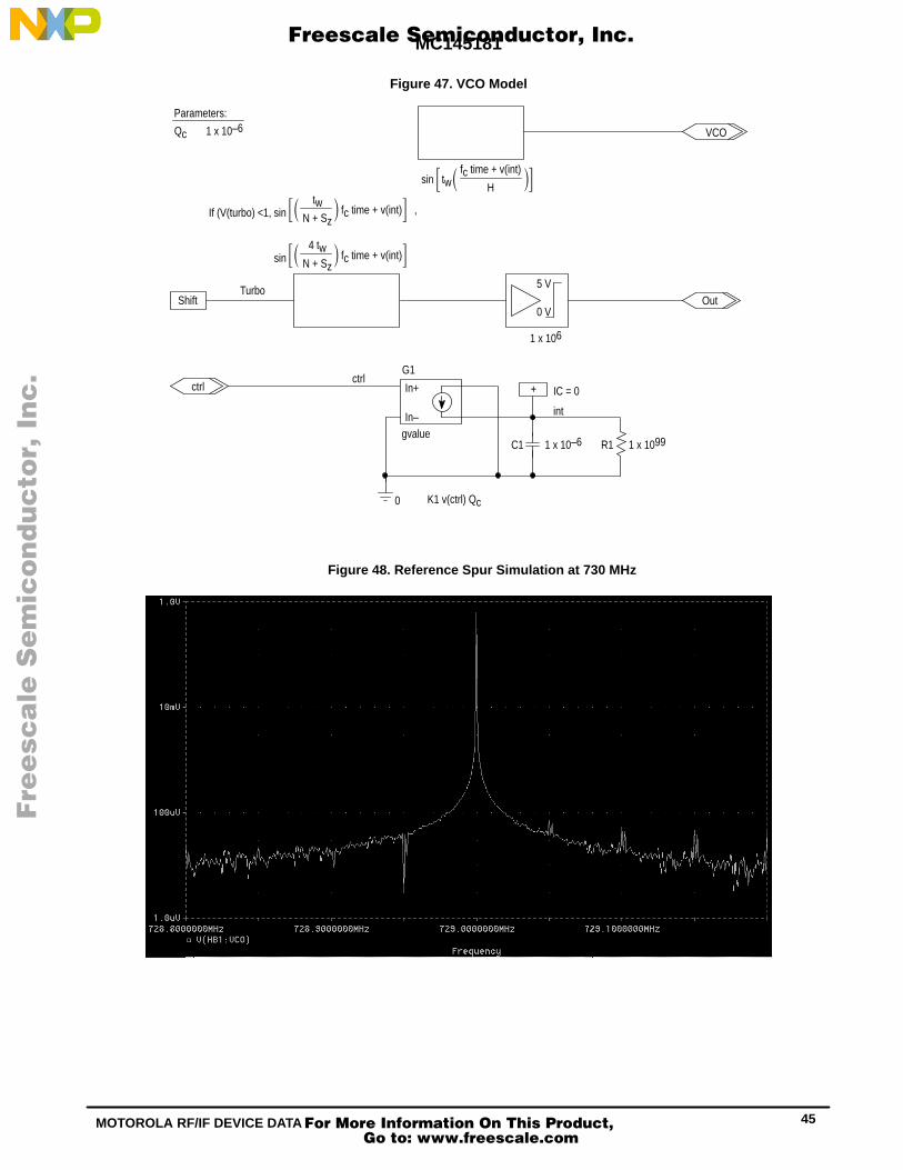
MC145181
45MOTOROLA RF/IF DEVICE DATA
Figure 47. VCO Model
Parameters:
Qc 1 x 10⁻⁶
5 V
0 VOut
VCO
1 x 10⁶
TurboShift
1 x 1099R11 x 10–6
+
0
ctrlIn+
In–gvalue
G1
C1
int
ctrl IC = 0
K1 v(ctrl) Qc
fc time + v(int)
Hsin tw
If (V(turbo) <1, sin fc time + v(int)N + Sz
tw ,
sin fc time + v(int)N + Sz
4 tw
Figure 48. Reference Spur Simulation at 730 MHz
Fre
esc
ale
Se
mic
on
du
cto
r, I
Freescale Semiconductor, Inc.
For More Information On This Product, Go to: www.freescale.com
nc
...

MC145181
46 MOTOROLA RF/IF DEVICE DATA
Figure 49. Sybil EVK Reference Spur Measurements
–10
–20
–30
–40
–110
–50
–60
–70
–80
–90
–100
Center 737.5000009 MHz Span 64 kHz
1AVG 1SA
10
–0
6.4 kHz
25.00000000 MHz10 dBmRef Lvl – 73.32 dB
SWT 130 ms Unit dBm
1
1
It should be noted that the reference spur values obtainedfrom the simulation are lower than the values obtained fromthe actual EVK. This is because the simulation model is an“ideal” modeling of the PLL. To obtain results closer to theactual implementation, the models should be “massaged” tobe more representative of the actual circuit. For example,spur levels more consistent with actual circuitry can beobtained by adding a resistance to ground at the input of theVCO to represent leakage. The value chosen should beconsistent with VCO and circuit component performance.
To reduce simulation time, the H value may be used. Byreducing the frequency of the VCO output, the number ofsamples required for simulation can also be reduced. Theoutput shown in Figure 50 shows the result of dividing theVCO output of 730 MHz by 7.3 to produce a 100 MHz output.The reference spurs are better represented since adequatesimulation time is possible.
To generate these outputs, the parameter values usedwere those shown on the top level schematic. The simulatorwas set to run a transient sweep, with td set for a delay thatwould prevent the 4X frequency from being started. The initialconditions were set to 1 V and the simulation run for 1 ms.VCO was monitored and the probe display button FFT wasinitiated. The X and Y axis were adjusted to those shown.
Note: These simulations are presented as the result of“ideal” models and may not accurately display real hardware.It would be best to load the VCO input with additional leakagedevices such as a large resistance, to accurately display real
conditions. These models are starting points for moreaccurate implementations.
Loop filter analysis is more accurate, since thepredominate factors are in the loop filter itself. To simulate theperformance of the loop filter, td is set for 0, N is set to thedesired divider value, and Sz is set to the desired step. Forthis example, 733 MHz was chosen.
NOTEThese values are for reference only. The
maximum operating frequency of the MC145181is 550 MHz. For VCO frequencies greater than550 MHz, an added external divider such as aprescaler is necessary.
With the VCO model shown, V(ctrl) = 0 produces an outputof 727.6 MHz and at V(ctrl) = 1.35 V, the VCO frequencywould be 733 MHz; the minimum MC145230EVK defaultoperating frequency. To show the response of the loop filter toa 10 MHz step at this operating frequency, Sz = 10 MHz/25 kHz = 400. The simulation is run for 1 ms with a stepceiling of 100 ns. The result is shown in Figure 51.
If the simulation is examined over a longer period of time,the long term settling can be compared to the performance ofthe actual circuitry. The plot shown in Figure 52 shows theVCO control voltage with the display resolution set to 1 mV.This compares to the plot of frequency variationmeasurements made on the actual EVK. This plot is shown inFigure 53.
Fre
esc
ale
Se
mic
on
du
cto
r, I
Freescale Semiconductor, Inc.
For More Information On This Product, Go to: www.freescale.com
nc
...

MC145181
47MOTOROLA RF/IF DEVICE DATA
Figure 50. H Set to Generate a 100 MHz Output
Figure 51. 10 MHz Step for an Operating Frequency of 729 MHz
Fre
esc
ale
Se
mic
on
du
cto
r, I
Freescale Semiconductor, Inc.
For More Information On This Product, Go to: www.freescale.com
nc
...
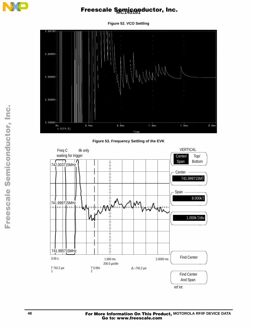
MC145181
48 MOTOROLA RF/IF DEVICE DATA
Figure 52. VCO Settling
Figure 53. Frequency Settling of the EVK
Freq C tlk onlywaiting for trigger
VERTICAL
Top/Bottom
ref int
200.0 µs/divT 0.00s
0.00 s
2
Center/Span
741.999715MZH
Center
Span
Find Center
Find Center
8.000k ZH
ZH1.000k /div
2.0000 ms
And Span
1.000 ms
T 742.2 µs1
∆ –742.2 µs
742.003715MHz
741.999715MHz
741.995715MHz
Fre
esc
ale
Se
mic
on
du
cto
r, I
Freescale Semiconductor, Inc.
For More Information On This Product, Go to: www.freescale.com
nc
...

MC145181
49MOTOROLA RF/IF DEVICE DATA
It is noted that the results obtained from the simulationcompare favorably to those obtained from the measurementsof the EVK. The simulation display resolution is adjusted torepresent the same ±4 kHz deviation as shown in Figure 53.Since variation in VCO control voltage is equal to the VCOfrequency divided by the VCO gain, this axis may beredefined to show change in frequency rather than change incontrol voltage.
The models shown represent a “skeleton” that may beused to develop extensive and reliable simulations that cangreatly reduce actual breadboarding and testing. In additionto the basic simulations shown, PSpice provides a method bywhich worst case and Monte Carlo evaluation can be
performed on all, or selected components. By limiting thecircuit to minimum necessary components, simulation can beperformed using only the PSpice evaluation copy. In addition,the optional PSpice program Optimizer should allow refiningthe loop filter more easily.
While PSpice is a powerful tool, it is not without limits.Since it was designed to run on large mainframe computers,the PC is just now becoming powerful enough to make use ofthe capability of the simulator. A fast Pentium class processorwith a large RAM and a hard drive of the Gbyte size is anecessity. Even with the most judicious planning, somesimulations will “bump” the limits of the system.
Fre
esc
ale
Se
mic
on
du
cto
r, I
Freescale Semiconductor, Inc.
For More Information On This Product, Go to: www.freescale.com
nc
...

MC145181
50 MOTOROLA RF/IF DEVICE DATA
7D. SECONDARY LOOP FILTER DESIGN
Low Pass Filter Design for PD out
The design of low pass filtering for PDout for the devicecan be accomplished using the following design information.In addition to the example included here, MotorolaApplication Note AN1207, also includes examples of activefiltering which may be used to supplement this information.
F(s) =
ωn =
(R1 + R2)sC + 1
R2sC + 1
C
VCO
R2
PDoutR1
NC(R1 + R2)
R2C + NKφKVCO
ζ = 0.5 ωn
KφKVCO
Definitions:N = Total Division Ratio in Feedback LoopKφ (Phase Detector Gain) = VDD/ 4π V/radian for PDoutKφ (Phase Detector Gain) = VDD/2π V/radian for φV
and φR
KVCO (VCO Gain) =2π∆fVCO∆VVCO
For a nominal design starting point, the user might consider adamping factor ζ ≈ 0.7 and a natural loop frequency ωn ≈(2πfR/50), where fR is the frequency at the phase detectorinput. Larger ωn values result in faster loop lock times and, forsimilar sideband filtering, higher fR–related VCO sidebands.
Recommended Reading:
Gardner, Floyd M., Phaselock Techniques (secondedition). New York, Wiley–Interscience, 1979.
Manassewitsch, Vadim, Frequency Synthesizers: Theoryand Design (second edition). New York, Wiley–Interscience,1980.
Blanchard, Alain, Phase–Locked Loops: Application toCoherent Receiver Design. New York, Wiley–Interscience,1976.
Egan, William F., Frequency Synthesis by Phase Lock.New York, Wiley–Interscience, 1981.
Rohde, Ulrich L., Digital PLL Frequency SynthesizersTheory and Design. Englewood Cliffs, NJ, Prentice–Hall,1983.
Berlin, Howard M., Design of Phase–Locked LoopCircuits, with Experiments. Indianapolis, Howard W. Samsand Co., 1978.
Kinley, Harold, The PLL Synthesizer Cookbook. BlueRidge Summit, PA, Tab Books, 1980.
Seidman, Arthur H., Integrated Circuits ApplicationsHandbook, Chapter 17, pp. 538–586. New York, John Wiley& Sons.
Fadrhons, Jan, “Design and Analyze PLLs on aProgrammable Calculator,” EDN. March 5, 1980.
AN535, Phase–Locked Loop Design Fundamentals,Motorola Semiconductor Products, Inc., 1970.
AR254, Phase–Locked Loop Design Articles, MotorolaSemiconductor Products, Inc., Reprinted with permissionfrom Electronic Design, 1987.
AN1207, The MC145170 in Basic HF and VHF Oscillators,Motorola Semiconductor Products, Inc., 1992.
AN1671, MC145170 PSpice Modeling Kit, MotorolaSemiconductor Products, Inc., 1998.
Example:
Given the following information:
VCO frequency = 45.555 MHz,
Frequency step size = 5 kHz,
VCO gain = 3.4 MHz/V.
Design a loop filter with a damping factor of 0.707.
The VCO is assumed to have a linear responsethroughout the range used in this example. The gain for theVCO has been given as 3.4 MHz/V and is multiplied by2π rad/s/Hz for calculating loop filter values.
KVCO = 2π rad/s/Hz x 3.4 MHz/V = 2.136 x 10⁷ rad/s/V .
The gain for the phase detector is defined as
4πVDDKφ = V/rad for PDout .
Using a value for VDD (phase detector supply voltage) of3.6 V with the output voltage multiplier turned off, the value is
4π3.6Kφ = = 0.2865 V/rad .
Let
50
2π frωn = = 628.3 rad/s
and
45.555 MHz =
FVCOFstep size 5 kHz
N = = 9111 .
Choosing C = 0.05 µF and calculating R1 + R2,
N C ωn2
Kφ KVCOR1 + R2 = = 34 kΩ .
With a damping factor of 0.707,
C
–
= 15 kΩ ,
N
Kφ KVCO
0.707
0.5 ωnR2 =
R1 = (R2 + R1) – R2 = 34 k – 15 k = 19 kΩ 20 kΩ .The choice for C is somewhat arbitrary, however, its value
does impact the performance of the loop filter. If possible, arange of choices for C should be used to calculate potentialloop filters and the resultant filters simulated, as will beshown below, to determine the best balance.
Fre
esc
ale
Se
mic
on
du
cto
r, I
Freescale Semiconductor, Inc.
For More Information On This Product, Go to: www.freescale.com
nc
...

MC145181
51MOTOROLA RF/IF DEVICE DATA
If additional filtering is desired, R1 may be split into twoequal resistors and a capacitor to ground inserted. Since theclosest resistance to one–half of 9 k is 4.7 kΩ , this value ischosen for R1a and R1b. The maximum value for the addedcapacitance is based on the bandwidth of the original loopfilter.
The general form for the transfer function for the passivefilter shown in Figure 54, can be shown to have the form:
s + ω2
(s + ω1) (s + ω3)F(s) = Kh
where
(R1a + R1b + R2) C
1ω1 = ,
R2C
1ω2 = ,
(R1 + R2)
1
R1a R1b + R1a R2ω3 = ,
Cc
where
R1 = R1a + R1band
ω3 > ω2 .
Since splitting R1 into two equal values, R1a and R1b, andinserting the capacitance between the junction of R1a andR1b does not change the position of the pole located at ω1,the value of ω1 remains
(R1a + R1b + R2) C
1ω1 = . =(R1 + R2) C
1
The 0 identified at ω2 = 1/R2 C is also unaffected by theaddition of Cc if ω3 > ω2.
Since
2
R1R1a = R1b = .
the value of Cc can be determined by specifying the value forω3 and using the values already determined for R1 and R2.The rule of thumb is to choose ω3 to be 10 x ωB so as not toimpact the original filter. ωB can be found as
(2 + 4ζ2 + 4ζ4)]ωB = ωn [1 + 2ζ2 +
ωB = 628.3 rad/s
(2+ 4 (0.707)2 + 4 (0.707)4)]
[1 + 2 (0.707)2
+
= 1.293 x 10³ rad/s .
10 ωB = 12.93 x 10³ rad/s .
The circuit for the passive loop filter is shown in Figure 54.R1 is split into two equal values and Cc inserted at the
junction of R1a and R1b. Using the values defined above, Ccis determined to be
(R1 + R2) ω3
1
R1a R1b + R1a R2Cc =
(R1 + R2) 10
1
R1a R1b + R1a R2= = 10.83 nfd 10 nfd
. ωB
ω3
Figure 54. Passive Loop Filter for PD out
R1a
10 k
0
0
C
15 k
10 k
R1b+
10 n
0
CcV1
IC = 0
50 n
R2
V
Open Loop AC Analysis of the Loop Filter
AC analysis is chosen for the mode of simulation forPSpice and VSIN is chosen for V1 and is set to produce a 1 Vpeak output signal. The simulation is then run and the resultshown in Figure 55.
A Bode plot of the loop filter is obtained which describesthe open loop characteristics of the loop filter. The cornerfrequencies of the filter can be modified and the simulationrerun until the desired wave shape is obtained. Since ACanalysis runs much faster than transient analysis, the ACopen loop analysis of the loop filter is much quicker andrequires less resources than the closed loop transientanalysis.
Closed Loop Filter Simulations Using PSpice
The top level schematic for simulating a simple loop filterfor PDout operating closed loop, is shown in Figure 56. Thisfilter uses the values calculated above.
The schematic represents the PLL function using theinternal phase detector, PDout, the loop filter calculatedabove, and a VCO. The parameter table allows altering thedivider value of N, the maximum current obtained fromPDout, and PDout charge pump voltage from the top levelschematic.
The schematic for the VCO is shown in Figure 57. Analogbehavioral modeling is used rather than discrete transistormodeling to reduce component count and improve simulationefficiency.
The behavioral VCO is composed of an integrator thattransforms the input ctrl into the voltage control V(int) and asine wave generator function whose frequency is controlledby V(int). EVALUE and GVALUE functions are used toperform the transforms. The analog behavioral models, ABMand ABMI, can also be used.
Fre
esc
ale
Se
mic
on
du
cto
r, I
Freescale Semiconductor, Inc.
For More Information On This Product, Go to: www.freescale.com
nc
...

MC145181
52 MOTOROLA RF/IF DEVICE DATA
Figure 55. Bode Plot of the Passive Loop Filter
Figure 56. Passive Loop Filter
HB1
Ref
In
HB2R1
10 k
0
0
C2
15 k
10 k
R6Ctrl
+–
+
+
IC = 0
10 nf
0
C4V2
Out
IC = 0
PDout
50 nf
R2
Parameters:
CPN
0.3 mA9111
Parameters:
VCPHVCPL
3.60
V
Fre
esc
ale
Se
mic
on
du
cto
r, I
Freescale Semiconductor, Inc.
For More Information On This Product, Go to: www.freescale.com
nc
...

MC145181
53MOTOROLA RF/IF DEVICE DATA
Figure 57. VCO Behavioral Model
1 x 1099R1
1 x 10⁶
1 x 10⁻⁶
+
Parameters:
twfcK1
6.28338.756 x 10621.36283005 x 106
Parameters:
Qc 1 x 10⁻⁶
In+
In–
Out+
Out–
evalue
0
ctrlIn+
In–
gvalue
G1
E1
C1
int
ctrl
Out
IC = 0
time + v(int)N
fcsin tw
v(ctrl) Qctw Nk1
5 V
0 V
G1 performs the operation [k1/(tw N)] v(ctrl) Qc. Thisintegrates the input ctrl to produce a voltage ramp used by E1to produce the desired output. This input is integrated by C1whose value should equal Qc for most applications. R1 isrequired by SPICE to prevent a floating node error.
E1 performs the calculations necessary to generate a sinewave of the desired frequency based on the values listed inthe parameter tables and the value of ctrl. The output of E1 ismultiplied by 1 x 10⁶ and limited to 0 and 5 to obtain a squarewave with a fast rise/fall time. Since I/O_STM is a standardmodel whose values are 0 and 5, these are used here and inthe phase detector rather than modifying the componentlibraries.
The parameter tables provide a convenient method forsetting VCO parameters. tw is 2π, fc is the zero controlvoltage VCO frequency, and K1 is the VCO gain in rad/s/V.
The sub–schematic for the phase/frequency detectorsection of the drawing is shown in Figure 58. This iscomposed of two blocks, HB3 and HB4. HB3 performs thePDout function with HB4 performing the actual phasedetector operation.
The circuit for the phase/frequency detector is shown inFigure 59. The model is made up of two pulse generators,two RS flip–flops, and appropriate behavioral gates.
HB1 and HB2 are RS flip–flops. These are constructedfrom behavioral blocks as shown in Figure 60. A behavioralAND gate with a 5 ns delay completes the three state (±2π)phase/frequency detector. The STP function ensures the RSflip–flops are reset at initiation.
To perform the phase detector function, the Ref and fininputs of the behavioral RS flip–flops are configured tosimulate edge triggered operation. This is achieved byplacing a 1 ns delay in the Ref and fin signal paths. The inputand output of the delay are compared by the input behavioralblock and interpreted as a 1 ns pulse. These pulses are usedto set HB1 and HB2. If fin leads Ref, the In flip–flop, HB2, willbe set first. When Ref leads fin, the Ref flip–flop, HB1, will beset first. The lagging edge drives the second flip–flop outputhigh and the behavioral AND gate then resets both flip–flops.The delay line at the output of the behavioral AND gateprevents PSpice from being confused and also completesthe simulation of the phase detector. The outputs of the twoRS flip=flops are labeled Rφ and Vφ. The time between the
leading and lagging edges is reflected in the pulse width ofthe leading edge flip–flop. The lagging edge flip–flop willdisplay a narrow pulse equal in width to the value chosen forthe delay at the output of the behavioral AND gate. Thisshould be programmed to the minimum value as specified bythe data sheet and is usually 5 ns or less.
Since the outputs Rφ and Vφ are pure logic signals,additional circuitry is necessary to produce the output PDout.This output should be high impedance when not driving, andpull either high or low depending on which function (Rφ or Vφ)is active. The circuitry shown in Figure 61 performs thisfunction.
To eliminate the need for discrete modeling of PDout,analog behavioral modeling is used. Analog behavioralblocks ABMI/2, generate a current source/sink outputwhenever the appropriate input is high.
A second set of behavioral blocks monitor the outputidrive, and switch on the appropriate voltage controlledswitch whenever the output rises to the value of VDD (phasedetector supply voltage) or drops to 0.
To model PDout, either a model of the transistors used forPDout must be used or this behavioral arrangement can beused. Since the output is specified by a specific output leveland current capability, this arrangement suffices. The outputswing becomes VCPH in the schematic and the currentcapability is CP. If a non–zero value is desired for Vlo, thevalue VCPL is adjusted from the parameter table on the toplevel schematic.
This arrangement allows setting the output voltage swingof PDout by specifying VCPH, the current drive of PDout byspecifying the desired value for CP, and leakage values canbe simulated by setting the appropriate attributes for S1 andS4 or by adding additional resistance.
Simulation
Figures 62 and 63 are the simulation results of running atransient analysis on the example shown above. The time tolock from power on is simulated by setting the initial condition(IC1) to 0 and running the simulation. Figure 62 is the timeversus value of the VCO control voltage. Figure 63 shows theoutput at the input of the loop filter and can be used todetermine lock time.
Fre
esc
ale
Se
mic
on
du
cto
r, I
Freescale Semiconductor, Inc.
For More Information On This Product, Go to: www.freescale.com
nc
...

MC145181
54 MOTOROLA RF/IF DEVICE DATA
Figure 58. Phase/Frequency Detector
HB4
fin
Ref
Rφ
Vφ
Rφ
Vφ
PDout′
HB3
Ref
In PDout
Figure 59. Phase Detector Logic
Q1
HB1
Ref
In
In2
In1
Qout
Rφ
Vφ
Delay5 ns
Q2
U10
In2
In1
Qout
HB2
If [V(Q1)>=1 & V(Q2)>=1 | V(delay)>=1, 5, 0]
5 STP (5 ns – Time)
Figure 60. Behavioral RS Flip–flop
If [V(v1)>=1 & V(v2)<1 & V(In2)<1, 5]
QoutQ
In1
In2
Delay1 ns
In3
U5
In2
V1 V2If [V(In2)>=1, 0]
If [V(In3)>=1 & V(In2)<1, 5, 0]
If [V(Q)>=1, 5, 0]
Fre
esc
ale
Se
mic
on
du
cto
r, I
Freescale Semiconductor, Inc.
For More Information On This Product, Go to: www.freescale.com
nc
...

MC145181
55MOTOROLA RF/IF DEVICE DATA
Figure 61. R φ /Vφ to PDout Conversion
If (V(In1)>=1 & V(In2)<1, CP, 0)
+
0
PDout
In1
In2 0
0If (V(In2)>=1 & V(In1)<1, CP, 0)
S1
Sbreak
–+–
If (V(idrive)> 0, 0, 1)
If (V(idrive)< 5, 0, 1)S4
+
0
–
+–
Sbreak
Rφ
Vφidrive
VCPL
VCPH
Figure 62. VCO Control Voltage versus Time
Fre
esc
ale
Se
mic
on
du
cto
r, I
Freescale Semiconductor, Inc.
For More Information On This Product, Go to: www.freescale.com
nc
...

MC145181
56 MOTOROLA RF/IF DEVICE DATA
Figure 63. PD out at Input to Loop Filter
Summary
PSpice provides a method by which the performance ofPLL circuitry can be simulated prior to, or in addition to,laboratory testing. The use of behavioral modeling allows thecreation of simulation circuits that can provide valuableinformation for loop filter design and adjustment. By judicious
attention to VCO modeling, expected output characteristicscan be verified prior to laboratory testing. While simulationdoes not replace laboratory testing, it can be used to findsolutions to “what if” questions without the need for extensiveempirical data gathering.
Fre
esc
ale
Se
mic
on
du
cto
r, I
Freescale Semiconductor, Inc.
For More Information On This Product, Go to: www.freescale.com
nc
...

MC145181
57MOTOROLA RF/IF DEVICE DATA
7E. VOLTAGE MULTIPLIER STALL AVOIDANCE
There are three important criteria to note, highlighted inthe following sections: Allowing for Voltage Build,Ensuring Valid Counter Programming, and Allowing forOvershoot. Violation of any of these may cause the voltagemultiplier to collapse. Once the voltage collapses, the loopgoes out of lock and can not recover until the voltage isallowed to build up again. For an active loop, the voltagemultiplier is designed to maintain the multiplied voltage on thephase/frequency detector supply pin (Cmult). If the main loopis active, the multiplier cannot build the voltage.
Allowing for Voltage Build
After power up, a sufficient time interval must be providedfor the on–chip voltage multiplier to build up the voltage onthe Cmult pin. During this interval, the phase/frequencydetector outputs for the main loop (PDout–Hi and PDout–Lo)must be inactive (floating outputs). The POR (power–onreset) circuit forces this “float” condition, thus allowing thevoltage to build on the Cmult pin.
The duration of the interval to build the voltage isdetermined by the external capacitor size tied to the Cmult pinand the charging current which is 100 µA minimum. Thefollowing formula may be used:
T = CV/ I
whereT is the interval in seconds,C is the Cmult capacitor size in farads,V is the desired voltage on Cmult in volts, andI is the charging current, 1 x 10⁻⁴ amps.
The desired voltage on Cmult is 4 V for a nominal 2 Vsupply and 5 V for any supply above 2.6 V.
After this interval, the chip can maintain the voltage on theCmult pin and the phase detectors may be safely placed in theactive state.
The interval above also applies when the voltage multiplieris turned off (with power applied) via bits R19 R18 R17being 000. After the multiplier is turned back on, sufficienttime must be allowed for the voltage to build on Cmult. In thiscase, typically an external resistor does not allow the Cmultvoltage to discharge below approximately Vpos (see Section5E, under Cmult ). Note that if the voltage multiplier is NOTturned off (that is, the above bits are unequal to 000), thekeep–alive circuit maintains the multiplied voltage on Cmult.
Ensuring Valid Counter Programming
Before the PLLs and/or phase detectors are taken out ofstandby, legitimate divide ratios (pertinent to the application)must be loaded in the registers. For example, proper divideratios must be loaded for the R, N, R, and N counters. Also,proper values for all other bits must be loaded. For example:selection of crystal or external reference mode must be madeprior to activation of the loops.
After the IC is initialized with the proper bits loaded, themain loop may then be safely activated via the phasedetector float bit and/or the PLL standby bit beingprogrammed to 0.
Allowing for Overshoot
The VCO control voltage overshoot for the main loop mustnot be allowed to exceed the capability of the phase/frequency detectors’ maximum output voltage. The
detectors’ maximum output voltage is determined by theminimum voltage at Cmult and the headroom required for thecurrent source. See the following figure.
Steady–state Control Voltage
VCO
Con
trol V
olta
ge
Voltage at Cmult Pin
Headroom for Current Source
Overshoot
Time
For example, if the main supply voltage (Vpos) is 3 V andthe voltage multiplier is utilized, the minimum voltage at Cmultis 4.75 V. Then, to allow for current source headroom, themaximum output voltage from the parameter table in Section3C is approximately Cmult – 0.6 V or 4.2 V approximately.Thus, the maximum output overshoot voltage at thephase/frequency detector outputs should be no more than4.2 V.
Continuing the above example, if the loop is designed with20% overshoot in the VCO control voltage, then theovershoot must be subtracted off of the 4.2 V shown above.Therefore, the upper end of the control voltage to the VCOmust be no more than approximately 3.64 V.
The equations below can be used to determineconstraints:
Vφ – 1.2
2α + 1∆V ≤
SSVmax = Vφ – α (∆V) – 0.6
where∆V is the VCO control voltage range, the maximum minus
the minimum voltage,Vφ is the minimum phase detector supply voltage (at the
Cmult pin) per the following table,α is the control voltage overshoot in decimal; for example,
20% overshoot is 0.2, andSSVmax is the maximum allowed steady–state VCO
control voltage.
MINIMUM PHASE DETECTOR VOLTAGEFROM VOLTAGE MULTIPLIER
Supply Voltage,Vpos
Minimum Phase DetectorVoltage, V φ
1.8 V 3.32 V
2.0 V 3.72 V
2.5 V 4.75 V
3.6 V 4.75 V
Fre
esc
ale
Se
mic
on
du
cto
r, I
Freescale Semiconductor, Inc.
For More Information On This Product, Go to: www.freescale.com
nc
...

MC145181
58 MOTOROLA RF/IF DEVICE DATA
Enb
Din
Clk
BitGrabber ACCESS OF THE REGISTERS
$0 Accesses C Register$1 Accesses Hr Register$2 Accesses N Register$3 Accesses D Register$4 Accesses Hn′ Register$5 Accesses R′ Register
MSB LSB
1 2 3 4
8 Clocks to Access the C Register16 Clocks to Access the Hr Register24 Clocks to Access the N Register
Enb
Din
Clk
x LSB
1 2 3 4
32 Clocks Always Used
CONVENTIONAL ACCESS OF THE REGISTERS
A0A1A2A3xxx
5 6 7 8 9 10 11 12 32
Address
= when the PLL device loads the data bit.
8. PROGRAMMER’S GUIDE
8A. QUICK REFERENCE
Fre
esc
ale
Se
mic
on
du
cto
r, I
Freescale Semiconductor, Inc.
For More Information On This Product, Go to: www.freescale.com
nc
...

MC145181
59MOTOROLA RF/IF DEVICE DATA
Don’t CareNibble
(Shifted in First)
LeastSignificant Nibble(Shifted in Last)
0
C REGISTER
Conventional Access
0 0 0
Most SignificantNibble
(Shifted in First)
Out A
Out B/Xref
Out C
BitGrabber Access
PDFloat
PD
FloatPLLStby
PLLStby
OscStby
LeastSignificant Nibble(Shifted in Last)
Address Nibble
See Below See Below
8A. QUICK REFERENCE (continued)
A3 A2 A1 A0x x x x x x x x x x x x x x x x x x x x C7 C6 C5 C4 C3 C2 C1 C0
C7 C6 C5 C4 C3 C2 C1 C0
NOTES: 1. For the Out A bit to control the Output A pin as a port expander, bits R′21 R′20 must be 00, which selects Output A as ageneral–purpose output. If R′21 R′20 are not equal to 00, then the Out A bit is a don’t care.
2. Whenever Osc Stby = 1, both PLL Stby and PLL′ Stby must be 1, also.
Out A = Output A Pin Logic State0 = Pin is forced to 0 (power up default)1 = Pin is forced to 1See Note 1
Out B/XRef = Output B Pin Logic State/External Reference SelectionSee table below
Out C = Output C Pin Logic State0 = Pin is forced to 0 (power up default)1 = Pin is forced to high impedance
PD Float = Phase Detector Float0 = Active, normal operation (power up default)1 = PDout–Hi/PDout–Lo are forced to high impedance
PD′ Float = Phase Detector′ Float0 = Active, normal operation (power up default)1 = PDout′ is forced to high impedance
Osc Stby = Oscillator Standby0 = Active, normal operation (power up default)1 = Oscillator/reference circuit in standbySee Note 2
PLL Stby = PLL Standby0 = Active, normal operation1 = Main PLL in standby (power up default)See table below
PLL′ Stby = PLL′ Standby0 = Active, normal operation1 = Secondary PLL in standby (power up default)
Mode Pin and Bit Summary
ÁÁÁÁMode PinÁÁÁÁÁÁOut B/XRef Bit ÁÁÁÁÁPLL Stby Bit ÁÁÁÁÁÁÁÁReference Circuit ÁÁÁÁOutput B PinÁÁÁÁÁMain PLLÁÁÁÁÁÁÁÁ0
ÁÁÁÁÁÁÁÁÁÁÁÁ0
ÁÁÁÁÁÁÁÁÁÁ0
ÁÁÁÁÁÁÁÁÁÁÁÁÁÁÁÁXtal Osc mode
ÁÁÁÁÁÁÁÁ0
ÁÁÁÁÁÁÁÁÁÁActiveÁÁÁÁ
ÁÁÁÁ0ÁÁÁÁÁÁÁÁÁÁÁÁ
0ÁÁÁÁÁÁÁÁÁÁ
1ÁÁÁÁÁÁÁÁÁÁÁÁÁÁÁÁ
Xtal Osc modeÁÁÁÁÁÁÁÁ
ZÁÁÁÁÁÁÁÁÁÁ
StandbyÁÁÁÁÁÁÁÁ
0ÁÁÁÁÁÁÁÁÁÁÁÁ
1ÁÁÁÁÁÁÁÁÁÁ
0ÁÁÁÁÁÁÁÁÁÁÁÁÁÁÁÁ
Xtal Osc modeÁÁÁÁÁÁÁÁ
1ÁÁÁÁÁÁÁÁÁÁ
ActiveÁÁÁÁÁÁÁÁ
0 ÁÁÁÁÁÁÁÁÁÁÁÁ
1 ÁÁÁÁÁÁÁÁÁÁ
1 ÁÁÁÁÁÁÁÁÁÁÁÁÁÁÁÁ
Xtal Osc mode ÁÁÁÁÁÁÁÁ
Z ÁÁÁÁÁÁÁÁÁÁ
StandbyÁÁÁÁÁÁÁÁ
1 ÁÁÁÁÁÁÁÁÁÁÁÁ
0 ÁÁÁÁÁÁÁÁÁÁ
0 ÁÁÁÁÁÁÁÁÁÁÁÁÁÁÁÁ
Xtal Osc mode ÁÁÁÁÁÁÁÁ
0 ÁÁÁÁÁÁÁÁÁÁ
Active
ÁÁÁÁÁÁÁÁ
1 ÁÁÁÁÁÁÁÁÁÁÁÁ
0 ÁÁÁÁÁÁÁÁÁÁ
1 ÁÁÁÁÁÁÁÁÁÁÁÁÁÁÁÁ
Xtal Osc mode ÁÁÁÁÁÁÁÁ
Z ÁÁÁÁÁÁÁÁÁÁ
Standby
ÁÁÁÁÁÁÁÁ
1 ÁÁÁÁÁÁÁÁÁÁÁÁ
1 ÁÁÁÁÁÁÁÁÁÁ
0 ÁÁÁÁÁÁÁÁÁÁÁÁÁÁÁÁ
External Reference mode ÁÁÁÁÁÁÁÁ
1 ÁÁÁÁÁÁÁÁÁÁ
Active
ÁÁÁÁÁÁÁÁ
1 ÁÁÁÁÁÁÁÁÁÁÁÁ
1 ÁÁÁÁÁÁÁÁÁÁ
1 ÁÁÁÁÁÁÁÁÁÁÁÁÁÁÁÁ
External Reference mode ÁÁÁÁÁÁÁÁ
Z ÁÁÁÁÁÁÁÁÁÁ
Standby
NOTES: Xtal osc = crystal oscillator. Z = high impedance.
Fre
esc
ale
Se
mic
on
du
cto
r, I
Freescale Semiconductor, Inc.
For More Information On This Product, Go to: www.freescale.com
nc
...

MC145181
60 MOTOROLA RF/IF DEVICE DATA
Hr REGISTER
8A. QUICK REFERENCE (continued)
Most SignificantNibble
(Shifted in First)
MSB of R CounterDivide Value
Least SignificantNibble
(Shifted in Last)
LSB of R CounterDivide Value
EXAMPLE: To program the R counter to divide by 1000 in decimal, first multiply 1000 by 2 which is 2000. Convert 2000 tohexadecimal: $7D0. Then, add leading 0s to form 2 bytes (4 nibbles): $07D0. Finally, load the Hr register bits R15to R0 with $07D0. When the N register is subsequently loaded, data passes from the first Hr register (buffer) to thesecond R register (buffer). (Data is still retained in the Hr register.)With BitGrabber, no address bits are needed. With a conventional load, address bits A3 to A0 must be included.
NOTE: Hexadecimal numbers are preceded with a dollar sign. For example: hexadecimal 1234 is shown as $1234.
LSB of R CounterDivide Value
Don’t CareNibble
(Shifted in First)
LeastSignificant Nibble(Shifted in Last)
0
Conventional Access
0 0 1
Address Nibble
MSB of R CounterDivide Value
BitGrabber Access
R7 . . . R4 R3 . . . R0R11 . . . R8R15 . . . R12
R7 . . . R4 R3 . . . R0R15 . . . R12 R11 . . . R8A3 A2 A1 A0x x x x x x x x x x x x
Fre
esc
ale
Se
mic
on
du
cto
r, I
Freescale Semiconductor, Inc.
For More Information On This Product, Go to: www.freescale.com
nc
...

MC145181
61MOTOROLA RF/IF DEVICE DATA
Don’t CareNibble
(Shifted in First)
LeastSignificant Nibble(Shifted in Last)
0
N REGISTERConventional Access
0 1 0
Most SignificantNibble
(Shifted in First)
Control
LDWindow
Phase DetectorProgram
MSB of N CounterDivide Value
CurrentRatio
LeastSignificant Nibble(Shifted in Last)
8A. QUICK REFERENCE (continued)
Address Nibble
Control = Control for Auxiliary DividerSee Table A
LD Window = Lock Detector Window for Main Loop0 = 32 Osce periods1 = 128 Osce periods
Phase Detector Program = Detector Program for Main LoopSee Table B
Current Ratio = PDout–Hi to PDout–Lo Current Ratio0 = 4:11 = 8:1
LSB of N CounterDivide Value
EXAMPLE: To program the N counter to divide by 1000 in decimal, first convert to hexadecimal: $3E8. Then, add leading 0s to form2 leading bits plus 2 bytes (2 bits plus 4 nibbles); this is N17 to N0. Bits N23 to N18 should be appropriate to control theabove functions. Finally, load the N register. Loading the N register also causes data to pass from the Hr register to theR register and data from the Hn′ register to pass to the N′ register. With BitGrabber, no address bits are needed. With a conventional load, address bits A3 to A0 must be included.
A3 A2 A1 A0x x x x N23 . . . N20 N19 . . . N16 N15 . . . N12 N11 . . . N8 N7 . . . N4 N3 . . . N0
N3 . . . N0N7 . . . N4N11 . . . N8N15 . . . N12N19 N18 N17 N16N23 N22 N21 N20
BitGrabber Access
See Below
ÁÁÁÁÁÁÁÁÁÁÁÁÁÁÁÁÁÁÁÁÁÁÁÁÁÁÁÁÁÁÁÁÁÁÁÁÁÁÁ
Table A. Osc e to f out Frequency Ratio,Mode = Low
ÁÁÁÁÁÁ
N23ÁÁÁÁÁÁÁÁ
R1ÁÁÁÁÁÁ
R0ÁÁÁÁÁÁÁÁÁÁÁÁ
Osce to f outFrequency Ratio
ÁÁÁÁÁÁ
0ÁÁÁÁÁÁÁÁ
0ÁÁÁÁÁÁ
0ÁÁÁÁÁÁÁÁÁÁÁÁ
10:1ÁÁÁÁÁÁ
0ÁÁÁÁÁÁÁÁ
0 ÁÁÁÁÁÁ
1 ÁÁÁÁÁÁÁÁÁÁÁÁ
12.5:1ÁÁÁÁÁÁ
0ÁÁÁÁÁÁÁÁ
1 ÁÁÁÁÁÁ
0 ÁÁÁÁÁÁÁÁÁÁÁÁ
12.5:1
ÁÁÁÁÁÁ
0ÁÁÁÁÁÁÁÁ
1 ÁÁÁÁÁÁ
1 ÁÁÁÁÁÁÁÁÁÁÁÁ
12.5:1
ÁÁÁÁÁÁ
1ÁÁÁÁÁÁÁÁ
0 ÁÁÁÁÁÁ
0 ÁÁÁÁÁÁÁÁÁÁÁÁ
8:1
ÁÁÁÁÁÁ
1ÁÁÁÁÁÁÁÁ
0 ÁÁÁÁÁÁ
1 ÁÁÁÁÁÁÁÁÁÁÁÁ
10:1
ÁÁÁÁÁÁ
1ÁÁÁÁÁÁÁÁ
1 ÁÁÁÁÁÁ
0 ÁÁÁÁÁÁÁÁÁÁÁÁ
10:1
ÁÁÁÁÁÁ
1ÁÁÁÁÁÁÁÁ
1 ÁÁÁÁÁÁ
1 ÁÁÁÁÁÁÁÁÁÁÁÁ
10:1
ÁÁÁÁÁÁÁÁÁÁÁÁÁÁÁÁÁÁÁÁÁÁÁÁÁÁ
NOTE: When the Mode pin is high, the fout pins are configuredas polarity inputs and N23 must be programmed to 1.
ÁÁÁÁÁÁÁÁÁÁÁÁÁÁÁÁÁÁÁÁÁÁÁÁÁÁÁÁÁÁÁÁ
Table B. Main Phase Detector Control
ÁÁÁÁ
N21ÁÁÁÁÁÁ
N20ÁÁÁÁÁÁ
N19ÁÁÁÁÁÁÁÁÁÁÁÁÁÁÁÁÁÁÁÁÁÁ
Result
ÁÁÁÁ
0ÁÁÁÁÁÁ
0ÁÁÁÁÁÁ
0 ÁÁÁÁÁÁÁÁÁÁÁÁÁÁÁÁÁÁÁÁÁÁ
Both PDout–Hi and PDout–Lo floating
ÁÁÁÁ
0ÁÁÁÁÁÁ
0ÁÁÁÁÁÁ
1 ÁÁÁÁÁÁÁÁÁÁÁÁÁÁÁÁÁÁÁÁÁÁ
PDout–Hi floating, PDout–Lo enabled
ÁÁÁÁ
0ÁÁÁÁÁÁ
1ÁÁÁÁÁÁ
0 ÁÁÁÁÁÁÁÁÁÁÁÁÁÁÁÁÁÁÁÁÁÁ
PDout–Hi enabled, PDout–Lo floating
ÁÁÁÁ
0ÁÁÁÁÁÁ
1ÁÁÁÁÁÁ
1 ÁÁÁÁÁÁÁÁÁÁÁÁÁÁÁÁÁÁÁÁÁÁ
Both PDout–Hi and PDout–Lo enabledÁÁÁÁÁÁÁÁ
1ÁÁÁÁÁÁÁÁÁÁÁÁ
0ÁÁÁÁÁÁÁÁÁÁÁÁ
0ÁÁÁÁÁÁÁÁÁÁÁÁÁÁÁÁÁÁÁÁÁÁÁÁÁÁÁÁÁÁÁÁÁÁÁÁÁÁÁÁÁÁÁÁ
PDout–Hi enabled and PDout–Lo floatingfor 16 fR cycles, then PDout–Hi floatingand PDout–Lo enabled
ÁÁÁÁÁÁ
1ÁÁÁÁÁÁÁÁÁ
0ÁÁÁÁÁÁÁÁÁ
1 ÁÁÁÁÁÁÁÁÁÁÁÁÁÁÁÁÁÁÁÁÁÁÁÁÁÁÁÁÁÁÁÁÁ
PDout–Hi enabled and PDout–Lo floatingfor 32 fR cycles, then PDout–Hi floatingand PDout–Lo enabled
ÁÁÁÁÁÁ
1ÁÁÁÁÁÁÁÁÁ
1ÁÁÁÁÁÁÁÁÁ
0 ÁÁÁÁÁÁÁÁÁÁÁÁÁÁÁÁÁÁÁÁÁÁÁÁÁÁÁÁÁÁÁÁÁ
PDout–Hi enabled and PDout–Lo floatingfor 64 fR cycles, then PDout–Hi floatingand PDout–Lo enabled
ÁÁÁÁÁÁ
1ÁÁÁÁÁÁÁÁÁ
1ÁÁÁÁÁÁÁÁÁ
1ÁÁÁÁÁÁÁÁÁÁÁÁÁÁÁÁÁÁÁÁÁÁÁÁÁÁÁÁÁÁÁÁÁ
PDout–Hi enabled and PDout–Lo floatingfor 128 fR cycles, then PDout–Hi floatingand PDout–Lo enabled
Fre
esc
ale
Se
mic
on
du
cto
r, I
Freescale Semiconductor, Inc.
For More Information On This Product, Go to: www.freescale.com
nc
...

MC145181
62 MOTOROLA RF/IF DEVICE DATA
Don’t CareNibble
(Shifted in First)
0
R′ REGISTER
1 0 1 YCoefficient
Output AFunction
Test/Rst MSB of R′Counter Divide
Value
V–MultControl
LeastSignificant Nibble(Shifted in Last)
8A. QUICK REFERENCE (continued)
Address Nibble
Y Coefficient0 0 = only programming values allowed
Output A Function = Controls Output A Mux0 0 = General–Purpose Output0 1 = fR1 0 = fR′1 1 = Phase Detector pulse
V–Mult Control = Voltage Multiplier Control0 0 0 = Multiplier OFF, 9 MHz ≤ Osce ≤ 80 MHz0 0 1 = Multiplier ON, 9 MHz ≤ Osce ≤ 20 MHz0 1 0 = Multiplier ON, 20 MHz < Osce ≤ 40 MHz0 1 1 = Multiplier ON, 40 MHz < Osce ≤ 80 MHz
Test/Rst = Test/Reset0 = only programming value allowed
LSB of R′ CounterDivide Value
EXAMPLE: When the Mode pin is tied low, see Table 21 for R′ counter programming. When the Mode pin is tied high, to program theR′ counter to divide by 1000 in decimal, first multiply 1000 by 2, which is 2000. Convert 2000 to hexadecimal: $7D0. Then,add leading 0s to form 2 bytes (4 nibbles); this becomes bits R′15 to R′0. Bits R′23 to R′16 should be appropriate to controlthe above functions. Finally, load the R′ register. With a conventional load, address bits A3 to A0 must be included.
NOTE: Hexadecimal numbers are preceded with a dollar sign. For example: hexadecimal 1234 is shown as $1234.
R′23 R′22 R′21 R′20 R′19 R′18 R′17 R′16 R′15 . . . R′12 R′11 . . . R′8 R′7 . . . R′4 R′3 . . . R′0A3 A2 A1 A0x x x x
Conventional Access only
Fre
esc
ale
Se
mic
on
du
cto
r, I
Freescale Semiconductor, Inc.
For More Information On This Product, Go to: www.freescale.com
nc
...

MC145181
63MOTOROLA RF/IF DEVICE DATA
A3 A2 A1 A0
Don’t CareNibble
(Shifted in First)
LeastSignificant Nibble(Shifted in Last)
0
Hn ′ REGISTER
1 0 0
x x x x
MSB of N′ CounterDivide Value
8A. QUICK REFERENCE (continued)
N′15 . . . N′12 N′11 . . . N′8 N′7 . . . N′4 N′3 . . . N′0
Address Nibble
EXAMPLE: To program the N′ counter to divide by 1000 in decimal, first multiply 1000 by 8, which is 8000. Convert 8000 tohexadecimal: $1F40. Then, add leading 0s (if necessary) to form 2 bytes (4 nibbles). Finally, configure address bits A3to A0 and load the Hn′ register. When the N register is subsequently loaded, data passes from the first Hn′ register (buffer)to the second N′ register (buffer). (Data is still retained in the Hn′ register.)
x x x x x x x x
LSB of N′ CounterDivide Value
Conventional Access only
Fre
esc
ale
Se
mic
on
du
cto
r, I
Freescale Semiconductor, Inc.
For More Information On This Product, Go to: www.freescale.com
nc
...

MC145181
64 MOTOROLA RF/IF DEVICE DATA
A3 A2 A1 A0
Don’t CareNibble
(Shifted in First)
LeastSignificant Nibble(Shifted in Last)
0
Conventional Access only
0 1 1
x x x x
MSB ofDAC2
8A. QUICK REFERENCE (continued)
D15 . . . D12 D11 . . . D8 D7 . . . D4 D3 . . . D0
Address Nibble
x x x x x x x x
D REGISTER
LSB ofDAC2
MSB ofDAC1
LSB ofDAC1
DAC2 Value DAC1 Value
DAC2 Value = Analog Output Level of DAC2$00 = zero output$01 = zero + 1 LSB output$02 = zero + 2 LSBs output$03 = zero + 3 LSBs output•••$FD = full scale – 2 LSBs output$FE = full scale – 1 LSB output$FF = full scale output
DAC1 Value = Analog Output Level of DAC1$00 = zero output$01 = zero + 1 LSB output$02 = zero + 2 LSBs output$03 = zero + 3 LSBs output•••$FD = full scale – 2 LSBs output$FE = full scale – 1 LSB output$FF = full scale output
Fre
esc
ale
Se
mic
on
du
cto
r, I
Freescale Semiconductor, Inc.
For More Information On This Product, Go to: www.freescale.com
nc
...

MC145181
65MOTOROLA RF/IF DEVICE DATA
8B. INITIALIZING THE DEVICE
Introduction
The registers retain data as long as power is applied to thedevice. The R and N registers contain counter divide ratiosfor the main loop, PLL. The R and N registers containcounter divide ratios for the secondary loop, PLL. Additionalcontrol bits are located in the R, N, and C registers. The Dregister controls the DACs. Section 8A is a handy referencefor register access and bit definitions.
The C, D, R, and N registers can be directly written, andhave an immediate impact on chip operation. The Hr and Hn
registers can be directly written, but have no immediateimpact on chip operation. This is because the Hr and Hn
registers are the front–ends of double buffers. The Hr registerfeeds the R register. The Hn register feeds the N register.Changing data in the R and/or N registers is done with awrite to the Hr and/or Hn register, respectively, followed by awrite to the N register. The transfer of data from the Hr to Rand Hn to N registers is triggered with a write to the Nregister.
Typically, the Hr and Hn registers are written once, duringinitialization after power up. The Hr and Hn registers onlyneed to be accessed if their data is changing.
An Example
Following is an initialization example for a system with amain loop that covers 450 to 500 MHz in 5 kHz steps. Anexternal reference of 19.44 MHz is utilized. The secondaryloop is selected to run at 50 MHz. Both VCOs are positivepolarity meaning that when the input control voltageincreases, the output frequency increases. A divided–downreference is not needed (fout and fout). Therefore, the Modepin is tied to Vpos and the Pol and Pol pins are tied to ground.
The following initialization gives serial data examples forBitGrabber access of the C, Hr, and N registers.
Initialization
Below is the six–step initialization sequence used afterpower up for the example given above.
Programming the C register first is recommended if thevoltage multiplier is utilized. There are three important criteriato note. Violation of any criterion may cause the voltagemultiplier to collapse. The first criterion is that after power up,a sufficient time interval must be provided (after the C and R
registers are initialized) for the on–chip voltage multiplier tobuild up the voltage on the Cmult pin. This interval isdetermined by the external capacitor size tied to the Cmult pinand the charging current which is about 100 µA. After thisinterval, the chip can maintain the voltage on the Cmult pinand the phase/frequency detectors for the main loop may besafely activated. The second criterion is that before thephase/frequency detectors are activated, legitimate divideratios (pertinent to the application) must be loaded in theregisters. The third criterion is a hardware issue. The threecriteria are discussed with more detail in Section 7E.
If the voltage multiplier is not used, Step 1 is eliminatedand the initialization sequence starts with Step 2.
Step 1: Load the C Register
The C register is programmed such that the main loop’sphase/frequency detector outputs are floating (PD Float bitC4 = 1), the reference circuit is active (Osc Stby bit C2 = 0),
and an external reference is accommodated (Out B/Xref bitC6 = 1, with the Mode pin high). When the voltage multiplieris enabled by programming the R register, the voltage isallowed to build on the Cmult pin such that a voltage higherthan the main supply voltage is providing power to thephase/frequency detectors. Both loops are active (PLL Stbybits C1 = C0 = 0). Also, for this example, Output A and OutputC are programmed low (Out bits C7 = C5 = 0).
In summary, hexadecimal 58 or $58 is serially transferred(BitGrabber access with no address bits).
Step 2: Load the R Register
For the secondary loop, the 19.44 MHz reference must bedivided down to 80 kHz by the R counter; the divide ratio is243. Per Section 8A, the value is doubled to 486. The 16LSBs of the R register determine the R counter divide ratio.Therefore, 486 is converted to $01E6 and becomes the 16LSBs (R15 to R0) in the R register. Test/Rst bit R16 mustbe a 0. Bits R19 to R17 determine the refresh rate of thevoltage multiplier. The frequency at Osce is <20 MHz.Therefore, per Section 8A, bits R19 to R17 must be 001. IfOutput A is needed as a MCU port expander, bits R21 =R20 = 0. Per Section 8A, Y Coefficient bits R23 = R22 = 0.
In summary, $050201E6 is serial ly transferred(conventional access with an address of 0101).
Step 3: Load the Hr Register
For the main loop, the 19.44 MHz reference must bedivided down to 5 kHz by the R counter; the divide ratio is3888. Per Section 8A, the ratio 3888 is doubled to 7776 andthen converted to $1E60. The Hr register value isprogrammed as $1E60. When the Hr register contents aretransferred to the R register, the R counter divide ratio isdetermined.
In summary, $1E60 is serially transferred (BitGrabberaccess). This value is transferred from the Hr to the Rregister when the N register is accessed in Step 5.
Step 4: Load the Hn Register
For the secondary loop, the phase detector is chosen torun at 80 kHz. Therefore, 80 kHz must be multiplied up to50 MHz which is a factor of 625. Per Section 8A, the factor isfirst multiplied by 8 which equals 5000 and then converted to$1388. The Hn register is programmed as $1388. When theHn register contents are transferred to the N register, the N
counter divide ratio is determined.In summary, $04001388 is serial ly transferred
(conventional access with an address of 0100). The value$1388 is transferred to the N register when the N register isaccessed in Step 5.
Step 5: Load the N Register
For this example, the IC is initialized to tune the lowest endof the main loop. The lowest end of the main loop’s frequencyrange is 450 MHz. Therefore, the 5 kHz must be multiplied upto 450 MHz which is a factor of 90,000 or $15F90 to beloaded into bits N17 to N0 of the N register. Bit N18 isprogrammed to 0 for a PDout–Hi to PDout–Lo current ratio of4:1. If PDout–Lo is used for the main loop, bits N21 to N19must be 001. (PDout–Lo must be used to initialize the devicewhen adapt is used, see Section 8D.) Bit N22 = 0 to select alock detect window of approximately 32 / Osce =32/19.44 MHz or 1.6 µs. Bit N23 must be programmed to 1
Fre
esc
ale
Se
mic
on
du
cto
r, I
Freescale Semiconductor, Inc.
For More Information On This Product, Go to: www.freescale.com
nc
...

MC145181
66 MOTOROLA RF/IF DEVICE DATA
by the user. (When the Mode pin is high, programming N23 toa 0 is for Motorola use only.)
In summary, $895F90 is serially transferred (BitGrabberaccess). The N register access also causes double–buffertransfers of Hr to R and Hn to N.
Step 6: Load the C Register
Now that legitimate divide ratios are programmed for thecounters, the main loop may be activated. Thus, the PD floatbit C4 is now programmed to 0. The standby bits areunchanged: C2 = C1 = C0 = 0. Bit C5 could be used to controlOutput C to either a low level or high impedance; for a lowlevel, C5 = 0. Whenever an external reference is utilized, bitC6 must be 1. Bit C7 may be used to control Output A to a lowor high level because it is selected as “port expander” by bitR21 and R20; for a low level, C7 = 0.
In summary, $40 is serially transferred (BitGrabberaccess). This causes the main loop to tune to 450 MHz, thesecondary loop to tune to 50 MHz, and both the Output A andOutput C pins to be forced low.
The device is now initialized.
8C. PROGRAMMING WITHOUT ADAPT
Tuning the Top of the Band
After initializing the device via steps 1 through 6 in Section8B, the only register that needs to be loaded to tune the mainloop is the N register.
For this example, tuning the upper end of the band(500 MHz) requires that the 5 kHz at the phase/frequencydetector be multiplied up to 500 MHz. This is a loopmultiplying factor of 100,000. This value is converted to$186A0 and is loaded for bits N17 to N0. Bits N23 to N18 arenot changed and are programmed as indicated in Section 8B,step 5.
In summary, $8986A0 is transferred to tune the main loop.No other registers are loaded.
Tuning Other Channels
Tuning other channels for the main loop, while keeping thesecondary loop at a constant frequency, only requiresprogramming the N register. See Table 22 for examplefrequencies.
Table 22. Main Loop Tuning ExamplesÁÁÁÁÁÁÁÁÁÁÁÁÁÁÁ
FrequencyDesired(MHz)
ÁÁÁÁÁÁÁÁÁÁÁÁ
MultiplyingFactor
(Decimal)
ÁÁÁÁÁÁÁÁÁÁÁÁÁÁÁÁÁÁ
MultiplyingFactor
(Hexadecimal)
ÁÁÁÁÁÁÁÁÁÁÁÁÁÁÁ
N RegisterData
(Hexadecimal)ÁÁÁÁÁÁÁÁÁÁ450.000
ÁÁÁÁÁÁÁÁ90,000
ÁÁÁÁÁÁÁÁÁÁÁÁ$15F90
ÁÁÁÁÁÁÁÁÁÁ$895F90ÁÁÁÁÁ
ÁÁÁÁÁ450.005ÁÁÁÁÁÁÁÁ90,001
ÁÁÁÁÁÁÁÁÁÁÁÁ$15F91
ÁÁÁÁÁÁÁÁÁÁ$895F91ÁÁÁÁÁ
ÁÁÁÁÁ450.010ÁÁÁÁÁÁÁÁ90,002
ÁÁÁÁÁÁÁÁÁÁÁÁ$15F92
ÁÁÁÁÁÁÁÁÁÁ$895F92ÁÁÁÁÁ
ÁÁÁÁÁ450.015ÁÁÁÁÁÁÁÁ90,003
ÁÁÁÁÁÁÁÁÁÁÁÁ$15F93
ÁÁÁÁÁÁÁÁÁÁ$895F93ÁÁÁÁÁ
ÁÁÁÁÁ455.000ÁÁÁÁÁÁÁÁ91,000
ÁÁÁÁÁÁÁÁÁÁÁÁ$16378
ÁÁÁÁÁÁÁÁÁÁ$896378ÁÁÁÁÁ
ÁÁÁÁÁ458.015ÁÁÁÁÁÁÁÁ91,603
ÁÁÁÁÁÁÁÁÁÁÁÁ$165D3
ÁÁÁÁÁÁÁÁÁÁ$8965D3ÁÁÁÁÁ
ÁÁÁÁÁ471.040ÁÁÁÁÁÁÁÁ94,208
ÁÁÁÁÁÁÁÁÁÁÁÁ$17000
ÁÁÁÁÁÁÁÁÁÁ$897000ÁÁÁÁÁ
ÁÁÁÁÁ500.000ÁÁÁÁÁÁÁÁ100,000
ÁÁÁÁÁÁÁÁÁÁÁÁ$186A0
ÁÁÁÁÁÁÁÁÁÁ$8986A0
8D. PROGRAMMING UTILIZING HORSESHOE WITHADAPT
Introduction
A unique adapt feature can be used with the MC145181when conventional tuning can not meet the lock–timerequirements of a system and the annoying spurs or noisecan not be tolerated from a fractional–N scheme. The adaptfeature is available on the main loop only.
For adapt, a timer is engaged which causes an internaldata update of the R and N registers to be delayed. The ICsupports the Horseshoe scheme for adapt by allowing afairly–close quickly–tuned approximate frequency to betuned, followed by the tuning of the exact frequency. Two setsof R and N data are sent to the device. The first set R1, N1is for tuning the approximate frequency. The second set R2,N2 is for tuning the exact frequency. Use of the timer delaysthe transfer of R2, N2 until a programmed interval haselapsed. In addition, after the interval has elapsed, the mainloop control switches from PDout–Hi to PDout–Lo.
Tuning Near the Top of the Band
Continuing the example, after initializing the device viasteps 1 through 6 in Section 8B, Horseshoe with adapt canbe used to tune the main loop to obtain fast frequency jumps.Use of the BitGrabber access is recommended to minimizethe number of serial data clocks required for sending the four“words”.
In this example, the first phase of adapt utilizesapproximate tuning with the phase/frequency detectorrunning at 4x the step size. Therefore, the approximatetuning runs the detector at about 20 kHz. The second phase,with exact tuning, runs the detector at 5 kHz. Horseshoe withadapt requires that two data sets be serially sent to thedevice for every frequency tuned. The first set is forapproximate tuning R1, N1; the second set is for exacttuning R2, N2.
Approximate tuning with Horseshoe is unique. Thismethod involves two key elements: (1) increasing the phasedetector frequency and (2) varying both the R and N dividevalues such that the approximate frequency is within acertain predetermined range. The Horseshoe algorithmcontained in the development system software also allowsplacing a constraint on the loop–gain variation that the usercan tolerate.
For example, to tune 459.97 MHz, the first R1, N1 dataset could contain divide ratios for the R and N counters of973.5 and 23,034, respectively. With this data set, the phasedetector is running at about 19.97 kHz and the approximatefrequency is about 170 Hz from the exact frequency. Thesecond data set contains R and N divide values of 3,888 and91,994, respectively. This achieves the exact (target)frequency of 459.97 MHz.
The timer must be programmed to determine the intervalthat the device is in the approximate–tune mode. For thisexample, assume this is 32 fR cycles; thus, bits N21 N20N19 = 1 0 1 in the first data set. Note that this time interval is32 cycles of fR, with the phase detector running at about20 kHz (approximate tune) or about 1.6 ms plus the MCUshift time shown in Figure 64. Included in the first data set areN23 = 1 which is required when the Mode pin is high, N22 = 0
Fre
esc
ale
Se
mic
on
du
cto
r, I
Freescale Semiconductor, Inc.
For More Information On This Product, Go to: www.freescale.com
nc
...

MC145181
67MOTOROLA RF/IF DEVICE DATA
for the lock detect window of 1.6 µs, and N18 = 0 for a currentratio of 4:1 (because the phase detector is running atapproximately 4x the step size). Note that bits N23, N22, andN18 are unchanged from the initialization values.
For the second data set, bits N23, N22, and N18 areunchanged. Bits N21, N20, and N19 must be programmed as001. This enables PDout–Lo for the exact tune after time out.
In summary, two data sets need to be sent to the device:R1, N1 and R2, N2. They are sent in succession as R1,N1, R2, N2; where R1 is the R register value for the first dataset, N1 is the N register value for the first set, etc. For theexample, these values are R1, N1 = $079B, $A859FA andR2, N2 = $1E60, $89675A. See Figure 64.
Tuning Other Channels
Tuning other channels for the main loop, while keeping thesecondary loop at a constant frequency, requires sendingtwo data sets to the part R1, N1 and R2, N2. See Table 23.
8E. CONTROLLING THE DACs
Introduction
The two 8–bit DACs are independent circuit blocks on thechip. They have no interaction with other circuits on the chip.A single 16–bit register, called the D register, holds the binaryvalue which controls both DACs.
Programming the DACs
A DAC programmed for 0 scale is in the low–power mode.The 0 scale is programmed as $00 for each 8–bit DAC.
As an example, consider a system that uses just one of theDACs (DAC 1). The other DAC output is unused and isprogrammed for 0 output. If a condition for a system requiresthat the DAC have a half–scale output, then DAC 1 isprogrammed as $80.
In summary, $03000080 is serial ly transferred(conventional access with an address of 0011).
Table 23. Main Loop Tuning Using Horseshoe With AdaptÁÁÁÁÁÁÁÁDesired
ÁÁÁÁÁÁÁÁÁÁÁÁÁÁÁÁÁÁÁÁÁÁ
Approximate TuningÁÁÁÁÁÁÁÁÁÁÁÁÁÁ
Exact TuningÁÁÁÁÁÁÁÁÁÁÁÁÁÁÁÁ
DesiredTarget
Frequency(MHz)
ÁÁÁÁÁÁÁÁÁÁÁÁÁÁÁÁ
R1
ÁÁÁÁÁÁÁÁÁÁÁÁÁÁÁÁ
N1
ÁÁÁÁÁÁÁÁÁÁÁÁÁÁÁÁÁÁÁÁ
FrequencyError(Hz)
ÁÁÁÁÁÁÁÁÁÁÁÁÁÁÁÁ
R2
ÁÁÁÁÁÁÁÁÁÁÁÁÁÁÁÁ
N2
ÁÁÁÁÁÁÁÁ
450.000ÁÁÁÁÁÁÁÁ
$0798ÁÁÁÁÁÁÁÁ
$A857E4ÁÁÁÁÁÁÁÁÁÁ
0 ÁÁÁÁÁÁÁÁ
$1E60 ÁÁÁÁÁÁÁÁ
$895F90
ÁÁÁÁÁÁÁÁ
450.005ÁÁÁÁÁÁÁÁ
$079BÁÁÁÁÁÁÁÁ
$A85807ÁÁÁÁÁÁÁÁÁÁ
548 ÁÁÁÁÁÁÁÁ
$1E60 ÁÁÁÁÁÁÁÁ
$895F91
ÁÁÁÁÁÁÁÁ
450.020ÁÁÁÁÁÁÁÁ
$0798ÁÁÁÁÁÁÁÁ
$A857E5ÁÁÁÁÁÁÁÁÁÁ
0 ÁÁÁÁÁÁÁÁ
$1E60 ÁÁÁÁÁÁÁÁ
$895F94
ÁÁÁÁÁÁÁÁ
450.255ÁÁÁÁÁÁÁÁ
$0795ÁÁÁÁÁÁÁÁ
$A857CEÁÁÁÁÁÁÁÁÁÁ
162 ÁÁÁÁÁÁÁÁ
$1E60 ÁÁÁÁÁÁÁÁ
$895FC3
ÁÁÁÁÁÁÁÁ
459.970ÁÁÁÁÁÁÁÁ
$079BÁÁÁÁÁÁÁÁ
$A859FAÁÁÁÁÁÁÁÁÁÁ
170 ÁÁÁÁÁÁÁÁ
$1E60 ÁÁÁÁÁÁÁÁ
$89675A
ÁÁÁÁÁÁÁÁ
500.000ÁÁÁÁÁÁÁÁ
$0798ÁÁÁÁÁÁÁÁ
$A861A8ÁÁÁÁÁÁÁÁÁÁ
0 ÁÁÁÁÁÁÁÁ
$1E60 ÁÁÁÁÁÁÁÁ
$8986A0
Fre
esc
ale
Se
mic
on
du
cto
r, I
Freescale Semiconductor, Inc.
For More Information On This Product, Go to: www.freescale.com
nc
...
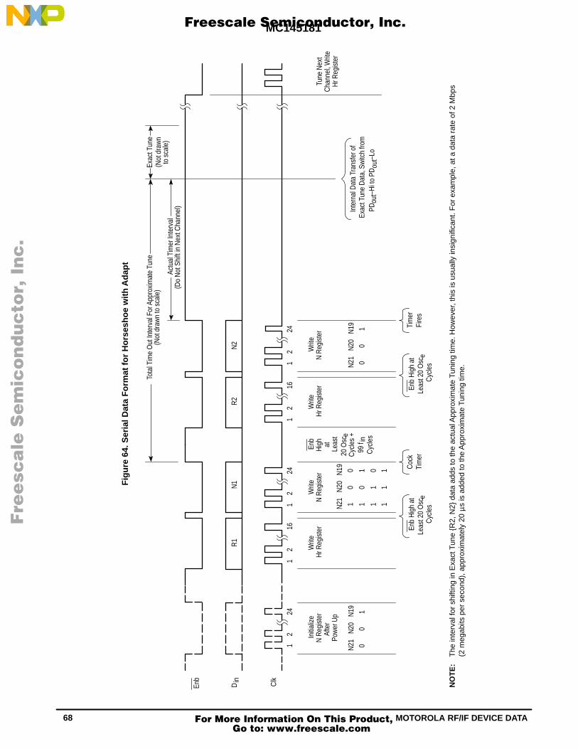
MC145181
68 MOTOROLA RF/IF DEVICE DATA
Figure 64.
Fig
ure
64. S
eria
l Dat
a F
orm
at fo
r H
orse
shoe
with
Ada
pt
NO
TE
:
224
12
241
224
12
161
216
1
Exac
t Tun
eTo
tal T
ime
Out
Inte
rval
For
App
roxi
mat
e Tu
ne
Actu
al T
imer
Inte
rval
(Do
Not
Shi
ft in
Nex
t Cha
nnel
)
N2
R2
N1
R1
Initi
aliz
eN
Reg
iste
rAf
ter
Pow
er U
p
N21
N20
N19
00
11
01
N21
N20
N19
10
0
11
01
11
Writ
eH
r Reg
iste
rW
rite
N R
egis
ter
Enb
Hig
hat
Leas
t20
Osc
C
ycle
s +
99 f
Cyc
lesin
Writ
eH
r Reg
iste
rW
rite
N R
egis
ter
N21
N20
N19
00
1In
tern
al D
ata
Tran
sfer
of
Exac
t Tun
e D
ata,
Sw
itch
from
PD
–H
i to
PD
–Lo
out
out
Tune
Nex
tC
hann
el, W
rite
Hr R
egis
ter
Enb
Hig
h at
Leas
t 20
Osc
C
ycle
s
Enb
Hig
h at
Leas
t 20
Osc
C
ycle
s
Coc
kTi
mer
Tim
erFi
res
ee
e
Enb
Clk
Din
(Not
dra
wn
to s
cale
)(N
ot d
raw
nto
sca
le)
The
inte
rval
for
shift
ing
in E
xact
Tun
e R
2, N
2 d
ata
adds
to th
e ac
tual
App
roxi
mat
e Tu
ning
tim
e. H
owev
er, t
his
is u
sual
ly in
sign
ifica
nt. F
or e
xam
ple,
at a
dat
a ra
te o
f 2 M
bps
(2 m
egab
its p
er s
econ
d), a
ppro
xim
atel
y 20
s
is a
dded
to th
e A
ppro
xim
ate
Tuni
ng ti
me.
µ
Fre
esc
ale
Se
mic
on
du
cto
r, I
Freescale Semiconductor, Inc.
For More Information On This Product, Go to: www.freescale.com
nc
...
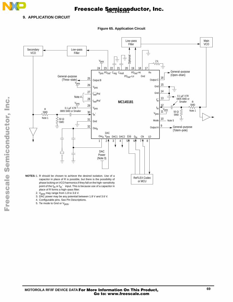
MC145181
69MOTOROLA RF/IF DEVICE DATA
9. APPLICATION CIRCUIT
Figure 65. Application Circuit
Low–passFilter
SecondaryVCO
Low–passFilter
Opt
iona
l
25
26
27
28
29
30
31
32
16
15
14
13
12
11
10
9
General–purpose(Open–drain)
MainVCO
General–purpose(Totem–pole)
General–purpose(Three–state)
Note 4
DACPower
(Note 3)
ReFLEX Codecor MCU
Osce
DACVpos DAC1 DAC2 Enb Din Clk LD
Output B
Vpos
fout/Pol
fout/Pol
Vpos
fin
Gnd
Oscb
Vpos PDout′ Creg CmultPDout–Lo
PDout–HiGnd
Rx
Output A
Output C
Gnd
Gnd
fin
fin
Vpos
Mode
1 2 3 4 5 6 7 8
24 23 22 21 20 19 18 17
Vpos
Note 5
Vpos
2 k
Vpos
Vpos MC145181
NOTES: 1. R should be chosen to achieve the desired isolation. Use of acapacitor in place of R is possible, but there is the possibility ofphase locking on VCO harmonics if they fall on the high–sensitivitypoint of the fin or fin input. This is because use of a capacitor inplace of R forms a high–pass filter.
2. Vpos may range from 1.8 to 3.6 V.3. DAC power may be any potential between 1.8 V and 3.6 V.4. Configurable pins. See Pin Descriptions.5. Tie mode to Gnd or Vpos.
RSMD
Note 150 ΩSMD
0.1 µF X7R0805 SMD or
Smaller
RSMD
50 ΩSMD
0.1 µF X7R0805 SMD or Smaller
Note 1
Fre
esc
ale
Se
mic
on
du
cto
r, I
Freescale Semiconductor, Inc.
For More Information On This Product, Go to: www.freescale.com
nc
...

MC145181
70 MOTOROLA RF/IF DEVICE DATA
10. OUTLINE DIMENSIONS
PLASTIC PACKAGECASE 873C–01
(LQFP–32)ISSUE A
6
H
NOTES:1. DIMENSIONS ARE IN MILLIMETERS. AND
TOLERANCING PER ASME Y14.5M, 1994.2. INTERPRET DIMENSIONS AND TOLERANCES
PER ASME Y14.5M, 1994.3. DATUMS A, B, AND D TO BE DETERMINED
WHERE THE LEADS EXIT THE PLASTIC BODY ATDATUM PLANE H.
4. DIMENSIONS D1 AND E1 DO NOT INCLUDE MOLDPROTRUSION. ALLOWABLE PROTRUSION IS 0.25mm PER SIDE. D1 AND E1 ARE MAXIMUMPLASTIC BODY SIZE DIMENSIONS INCLUDINGMOLD MISMATCH.
5. DIMENSION b DOES NOT INCLUDE DAMBARPROTRUSION. ALLOWABLE DAMBARPROTRUSION SHALL NOT CAUSE THE LEADWIDTH TO EXCEED THE MAXIMUM b DIMENSIONBY MORE THAN 0.08 mm. DAMBAR CAN NOT BELOCATED ON THE LOWER RADIUS OR THEFOOT. MINIMUM SPACE BETWEEN APROTRUSION AND AN ADJACENT LEAD IS 0.07mm.
6. EXACT SHAPE OF CORNERS MAY VARY.
DIM MIN MAXMILLIMETERS
A ––– 1.60A1 0.05 0.15A2 1.35 1.45b 0.18 0.27b1 0.17 0.23c 0.10 0.20c1 0.09 0.16D 7.00 BSCD1 5.00 BSCE 7.00 BSCE1 5.00 BSCe 0.50 BSCL 0.45 0.75L1 1.00 REFR1 0.08 –––R2 0.08 0.20S 0.20 ––– 0 7 0 ––– 11 13 11 13
123
E 2
D1 2
E
24 17
25
32
1 8
16
9
K
SEATING
D 2
E1 2
D
A B
C
D
D1
PLANE
ALL 4 SIDES
A–B0.10 DH
E1
ALL 4 SIDES
A–B0.20 DC
J
J
28x e
4x e/2
0.080 C
A A2
A1
L1
L
S
2
1
3
0.25
R2
R1
DETAIL K
ÇÇÇÇÇÇÇÇÇÇÇÇÇÇÇ
ÉÉÉÉÉÉÉÉÉÉÉÉ
b1
b
c1c
BASE METAL
PLATING
A–BM0.08 DC
SECTION J–J
Fre
esc
ale
Se
mic
on
du
cto
r, I
Freescale Semiconductor, Inc.
For More Information On This Product, Go to: www.freescale.com
nc
...

MC145181
71MOTOROLA RF/IF DEVICE DATA
Motorola reserves the right to make changes without further notice to any products herein. Motorola makes no warranty, representation or guarantee regardingthe suitability of its products for any particular purpose, nor does Motorola assume any liability arising out of the application or use of any product or circuit, andspecifically disclaims any and all liability, including without limitation consequential or incidental damages. “Typical” parameters which may be provided in Motoroladata sheets and/or specifications can and do vary in different applications and actual performance may vary over time. All operating parameters, including “Typicals”must be validated for each customer application by customer’s technical experts. Motorola does not convey any license under its patent rights nor the rights ofothers. Motorola products are not designed, intended, or authorized for use as components in systems intended for surgical implant into the body, or otherapplications intended to support or sustain life, or for any other application in which the failure of the Motorola product could create a situation where personal injuryor death may occur. Should Buyer purchase or use Motorola products for any such unintended or unauthorized application, Buyer shall indemnify and hold Motorolaand its officers, employees, subsidiaries, affiliates, and distributors harmless against all claims, costs, damages, and expenses, and reasonable attorney feesarising out of, directly or indirectly, any claim of personal injury or death associated with such unintended or unauthorized use, even if such claim alleges thatMotorola was negligent regarding the design or manufacture of the part. Motorola and are registered trademarks of Motorola, Inc. Motorola, Inc. is an EqualOpportunity/Affirmative Action Employer.
Mfax is a trademark of Motorola, Inc.How to reach us:USA/EUROPE/Locations Not Listed : Motorola Literature Distribution; JAPAN : Motorola Japan Ltd.; SPD, Strategic Planning Office, 141,P.O. Box 5405, Denver, Colorado 80217. 1–303–675–2140 or 1–800–441–2447 4–32–1 Nishi–Gotanda, Shinagawa–ku, Tokyo, Japan. 81–3–5487–8488
Customer Focus Center: 1–800–521–6274
Mfax : [email protected] – TOUCHTONE 1–602–244–6609 ASIA /PACIFIC : Motorola Semiconductors H.K. Ltd.; Silicon Harbour Centre,Motorola Fax Back System – US & Canada ONLY 1–800–774–1848 2, Dai King Street, Tai Po Industrial Estate, Tai Po, N.T., Hong Kong.
– http://sps.motorola.com/mfax/ 852–26668334HOME PAGE: http://motorola.com/sps/
MC145181/D◊
Fre
esc
ale
Se
mic
on
du
cto
r, I
Freescale Semiconductor, Inc.
For More Information On This Product, Go to: www.freescale.com
nc
...