FPGA-based Implementation of Signal Processing Systems
388
-
Upload
khangminh22 -
Category
Documents
-
view
2 -
download
0
Transcript of FPGA-based Implementation of Signal Processing Systems


FPGA-basedImplementation ofSignal ProcessingSystems
Roger Woods
Queen’s University, Belfast, UK
John McAllisterQueen’s University, Belfast, UK
Gaye Lightbody
University of Ulster, UK
Ying YiUniversity of Edinburgh, UK
A John Wiley and Sons, Ltd., Publication

FPGA-basedImplementation ofSignal ProcessingSystems


FPGA-basedImplementation ofSignal ProcessingSystems
Roger Woods
Queen’s University, Belfast, UK
John McAllisterQueen’s University, Belfast, UK
Gaye Lightbody
University of Ulster, UK
Ying YiUniversity of Edinburgh, UK
A John Wiley and Sons, Ltd., Publication

This edition first published 2008 2008 John Wiley & Sons, Ltd
Registered officeJohn Wiley & Sons Ltd, The Atrium, Southern Gate, Chichester, West Sussex, PO19 8SQ, United Kingdom
For details of our global editorial offices, for customer services and for information about how to apply forpermission to reuse the copyright material in this book please see our website at www.wiley.com.
The right of the author to be identified as the author of this work has been asserted in accordance with theCopyright, Designs and Patents Act 1988.
All rights reserved. No part of this publication may be reproduced, stored in a retrieval system, or transmitted, inany form or by any means, electronic, mechanical, photocopying, recording or otherwise, except as permitted bythe UK Copyright, Designs and Patents Act 1988, without the prior permission of the publisher.
Wiley also publishes its books in a variety of electronic formats. Some content that appears in print may not beavailable in electronic books.
Designations used by companies to distinguish their products are often claimed as trademarks. All brand namesand product names used in this book are trade names, service marks, trademarks or registered trademarks of theirrespective owners. The publisher is not associated with any product or vendor mentioned in this book. Thispublication is designed to provide accurate and authoritative information in regard to the subject matter covered.It is sold on the understanding that the publisher is not engaged in rendering professional services. If professionaladvice or other expert assistance is required, the services of a competent professional should be sought.
Library of Congress Cataloging-in-Publication Data
Wood, Roger.FPGA-based implementation of complex signal processing systems / Roger Wood ... [et al.].
p. cm.Includes bibliographical references and index.ISBN 978-0-470-03009-7 (cloth)1. Signal processing–Digital techniques. I. Title.TK5102.5.W68 2008621.382′2–dc22
2008035242
British Library Cataloguing in Publication Data
A catalogue record for this book is available from the British Library.
ISBN: 978-0-470-03009-7
Typeset by Laserwords Private Limited, Chennai, IndiaPrinted and bound in Great Britain by Antony Rowe Ltd, Chippenham, Wiltshire

To Rose and Paddy


Contents
About the Authors xv
Preface xvii
1 Introduction to Field-programmable Gate Arrays 1
1.1 Introduction 11.1.1 Field-programmable Gate Arrays 11.1.2 Programmability and DSP 3
1.2 A Short History of the Microchip 41.2.1 Technology Offerings 6
1.3 Influence of Programmability 71.4 Challenges of FPGAs 9References 10
2 DSP Fundamentals 11
2.1 Introduction 112.2 DSP System Basics 122.3 DSP System Definitions 12
2.3.1 Sampling Rate 142.3.2 Latency and Pipelining 15
2.4 DSP Transforms 162.4.1 Fast Fourier Transform 162.4.2 Discrete Cosine Transform (DCT) 182.4.3 Wavelet Transform 192.4.4 Discrete Wavelet Transform 19
2.5 Filter Structures 202.5.1 Finite Impulse Response Filter 202.5.2 Correlation 232.5.3 Infinite Impulse Response Filter 232.5.4 Wave Digital Filters 24
2.6 Adaptive Filtering 272.7 Basics of Adaptive Filtering 27
2.7.1 Applications of Adaptive Filters 282.7.2 Adaptive Algorithms 30

viii Contents
2.7.3 LMS Algorithm 312.7.4 RLS Algorithm 32
2.8 Conclusions 35References 35
3 Arithmetic Basics 37
3.1 Introduction 373.2 Number Systems 38
3.2.1 Number Representations 383.3 Fixed-point and Floating-point 41
3.3.1 Floating-point Representations 413.4 Arithmetic Operations 43
3.4.1 Adders and Subtracters 433.4.2 Multipliers 453.4.3 Division 473.4.4 Square Root 48
3.5 Fixed-point versus Floating-point 523.6 Conclusions 55References 55
4 Technology Review 57
4.1 Introduction 574.2 Architecture and Programmability 584.3 DSP Functionality Characteristics 594.4 Processor Classification 614.5 Microprocessors 62
4.5.1 The ARM Microprocessor Architecture Family 634.6 DSP Microprocessors (DSPµs) 64
4.6.1 DSP Micro-operation 664.7 Parallel Machines 67
4.7.1 Systolic Arrays 674.7.2 SIMD Architectures 694.7.3 MIMD Architectures 73
4.8 Dedicated ASIC and FPGA Solutions 744.9 Conclusions 75References 76
5 Current FPGA Technologies 77
5.1 Introduction 775.2 Toward FPGAs 78
5.2.1 Early FPGA Architectures 805.3 Altera FPGA Technologies 81
5.3.1 MAX r©7000 FPGA Technology 835.3.2 Stratix r© III FPGA Family 855.3.3 Hardcopy r© Structured ASIC Family 92
5.4 Xilinx FPGA Technologies 935.4.1 Xilinx Virtex
TM-5 FPGA Technologies 94

Contents ix
5.5 Lattice FPGA Families 1035.5.1 Lattice r© ispXPLD 5000MX Family 103
5.6 Actel FPGA Technologies 1055.6.1 Actel r© ProASICPLUS FPGA Technology 1055.6.2 Actel r© Antifuse SX FPGA Technology 106
5.7 Atmel FPGA Technologies 1085.7.1 Atmel r© AT40K FPGA Technologies 1085.7.2 Reconfiguration of the Atmel r© AT40K FPGA Technologies 109
5.8 General Thoughts on FPGA Technologies 110References 110
6 Detailed FPGA Implementation Issues 111
6.1 Introduction 1116.2 Various Forms of the LUT 1126.3 Memory Availability 1156.4 Fixed Coefficient Design Techniques 1166.5 Distributed Arithmetic 1176.6 Reduced Coefficient Multiplier 120
6.6.1 RCM Design Procedure 1226.6.2 FPGA Multiplier Summary 125
6.7 Final Statements 125References 125
7 Rapid DSP System Design Tools and Processes for FPGA 127
7.1 Introduction 1277.2 The Evolution of FPGA System Design 128
7.2.1 Age 1: Custom Glue Logic 1287.2.2 Age 2: Mid-density Logic 1287.2.3 Age 3: Heterogeneous System-on-chip 129
7.3 Design Methodology Requirements for FPGA DSP 1297.4 System Specification 129
7.4.1 Petri Nets 1297.4.2 Process Networks (PN) and Dataflow 1317.4.3 Embedded Multiprocessor Software Synthesis 1327.4.4 GEDAE 132
7.5 IP Core Generation Tools for FPGA 1337.5.1 Graphical IP Core Development Approaches 1337.5.2 Synplify DSP 1347.5.3 C-based Rapid IP Core Design 1347.5.4 MATLAB r©-based Rapid IP Core Design 1367.5.5 Other Rapid IP Core Design 136
7.6 System-level Design Tools for FPGA 1377.6.1 Compaan 1377.6.2 ESPAM 1377.6.3 Daedalus 1387.6.4 Koski 140
7.7 Conclusion 140References 141

x Contents
8 Architecture Derivation for FPGA-based DSP Systems 143
8.1 Introduction 1438.2 DSP Algorithm Characteristics 144
8.2.1 Further Characterization 1458.3 DSP Algorithm Representations 148
8.3.1 SFG Descriptions 1488.3.2 DFG Descriptions 149
8.4 Basics of Mapping DSP Systems onto FPGAs 1498.4.1 Retiming 1508.4.2 Cut-set Theorem 1548.4.3 Application of Delay Scaling 1558.4.4 Calculation of Pipelining Period 158
8.5 Parallel Operation 1618.6 Hardware Sharing 163
8.6.1 Unfolding 1638.6.2 Folding 165
8.7 Application to FPGA 1698.8 Conclusions 169References 169
9 The IRIS Behavioural Synthesis Tool 171
9.1 Introduction of Behavioural Synthesis Tools 1729.2 IRIS Behavioural Synthesis Tool 173
9.2.1 Modular Design Procedure 1749.3 IRIS Retiming 176
9.3.1 Realization of Retiming Routine in IRIS 1779.4 Hierarchical Design Methodology 179
9.4.1 White Box Hierarchical Design Methodology 1809.4.2 Automatic Implementation of Extracting Processor Models from Previously Syn-
thesized Architecture 1819.4.3 Hierarchical Circuit Implementation in IRIS 1849.4.4 Calculation of Pipelining Period in Hierarchical Circuits 1859.4.5 Retiming Technique in Hierarchical Circuits 188
9.5 Hardware Sharing Implementation (Scheduling Algorithm) for IRIS 1909.6 Case Study: Adaptive Delayed Least-mean-squares Realization 199
9.6.1 High-speed Implementation 2009.6.2 Hardware-shared Designs for Specific Performance 205
9.7 Conclusions 207References 207
10 Complex DSP Core Design for FPGA 211
10.1 Motivation for Design for Reuse 21210.2 Intellectual Property (IP) Cores 21310.3 Evolution of IP Cores 215
10.3.1 Arithmetic Libraries 21610.3.2 Fundamental DSP Functions 21810.3.3 Complex DSP Functions 21910.3.4 Future of IP Cores 219

Contents xi
10.4 Parameterizable (Soft) IP Cores 22010.4.1 Identifying Design Components Suitable for Development as IP 22210.4.2 Identifying Parameters for IP Cores 22310.4.3 Development of Parameterizable Features Targeted to FPGA Technology 22610.4.4 Application to a Simple FIR Filter 228
10.5 IP Core Integration 23110.5.1 Design Issues 23110.5.2 Interface Standardization and Quality Control Metrics 232
10.6 ADPCM IP Core Example 23410.7 Current FPGA-based IP Cores 23810.8 Summary 240References 241
11 Model-based Design for Heterogeneous FPGA 243
11.1 Introduction 24311.2 Dataflow Modelling and Rapid Implementation for FPGA DSP Systems 244
11.2.1 Synchronous Dataflow 24511.2.2 Cyclo-static Dataflow 24611.2.3 Multidimensional Synchronous Dataflow 24611.2.4 Dataflow Heterogeneous System Prototyping 24711.2.5 Partitioned Algorithm Implementation 247
11.3 Rapid Synthesis and Optimization of Embedded Software from DFGs 24911.3.1 Graph-level Optimization 25011.3.2 Graph Balancing Operation and Optimization 25011.3.3 Clustering Operation and Optimization 25111.3.4 Scheduling Operation and Optimization 25311.3.5 Code Generation Operation and Optimization 25311.3.6 DFG Actor Configurability for System-level Design Space Exploration 25411.3.7 Rapid Synthesis and Optimization of Dedicated Hardware from DFGs 25411.3.8 Restricted Behavioural Synthesis of Pipelined Dedicated Hardware Architectures 255
11.4 System-level Modelling for Heterogeneous Embedded DSP Systems 25711.4.1 Interleaved and Block Actor Processing in MADF 258
11.5 Pipelined Core Design of MADF Algorithms 26011.5.1 Architectural Synthesis of MADF Configurable Pipelined Dedicated Hardware 26111.5.2 WBC Configuration 262
11.6 System-level Design and Exploration of Dedicated Hardware Networks 26311.6.1 Design Example: Normalized Lattice Filter 26411.6.2 Design Example: Fixed Beamformer System 266
11.7 Summary 269References 269
12 Adaptive Beamformer Example 271
12.1 Introduction to Adaptive Beamforming 27112.2 Generic Design Process 27212.3 Adaptive Beamforming Specification 27412.4 Algorithm Development 276
12.4.1 Adaptive Algorithm 27712.4.2 RLS Implementation 278

xii Contents
12.4.3 RLS Solved by QR Decomposition 27812.4.4 Givens Rotations Used for QR Factorization 280
12.5 Algorithm to Architecture 28212.5.1 Dependence Graph 28312.5.2 Signal Flow Graph 28312.5.3 Systolic Implementation of Givens Rotations 28512.5.4 Squared Givens Rotations 287
12.6 Efficient Architecture Design 28712.6.1 Scheduling the QR Operations 290
12.7 Generic QR Architecture 29212.7.1 Processor Array 293
12.8 Retiming the Generic Architecture 30112.8.1 Retiming QR Architectures 305
12.9 Parameterizable QR Architecture 30712.9.1 Choice of Architecture 30712.9.2 Parameterizable Control 30912.9.3 Linear Architecture 31012.9.4 Sparse Linear Architecture 31012.9.5 Rectangular Architecture 31612.9.6 Sparse Rectangular Architecture 31612.9.7 Generic QR Cells 319
12.10 Generic Control 31912.10.1 Generic Input Control for Linear and Sparse Linear Arrays 32012.10.2 Generic Input Control for Rectangular and Sparse Rectangular
Arrays 32112.10.3 Effect of Latency on the Control Seeds 321
12.11 Beamformer Design Example 32312.12 Summary 325References 325
13 Low Power FPGA Implementation 329
13.1 Introduction 32913.2 Sources of Power Consumption 330
13.2.1 Dynamic Power Consumption 33113.2.2 Static Power Consumption 332
13.3 Power Consumption Reduction Techniques 33513.4 Voltage Scaling in FPGAs 33513.5 Reduction in Switched Capacitance 33713.6 Data Reordering 33713.7 Fixed Coefficient Operation 33813.8 Pipelining 33913.9 Locality 34313.10 Application to an FFT Implementation 34413.11 Conclusions 348References 348

Contents xiii
14 Final Statements 351
14.1 Introduction 35114.2 Reconfigurable Systems 351
14.2.1 Relevance of FPGA Programmability 35214.2.2 Existing Reconfigurable Computing 35314.2.3 Realization of Reconfiguration 35414.2.4 Reconfiguration Models 355
14.3 Memory Architectures 35714.4 Support for Floating-point Arithmetic 35814.5 Future Challenges for FPGAs 359References 359
Index 361


About the Authors
Roger Woods
Roger Woods has over 17 years experience in implementing complex DSP systems, both in ASICand FPGA. He leads the Programmable Systems Laboratory at Queen’s University (PSL@Q) whichcomprises 15 researchers and which is applying programmable hardware to DSP and telecommuni-catins applications. The research specifically involves: developing design flows for heterogeneousplatforms involving both multiprocessors and FPGAs; programmable solutions for programmablenetworks; design tools for FPGA IP cores; and low-power programmable DSP solutions. Rogerhas been responsible for developing a number of novel advanced chip demonstrators and FPGAsolutions for image processing and digital filtering.
John McAllister
John McAllister is currently a Lecturer in the Programmable Systems Laboratory and System-on-Chip (SoC) Research Cluster at Queen’s University Belfast investigating novel system, processorand IP core architectures, design methodologies and tools for programmable embedded DSPsystems, with a particular focus on FPGA-centric processing architectures. He has numerous peer-reviewed publications in these areas.
Gaye Lightbody
Dr Gaye Lightbody received her MEng in Electrical and Electronic Engineering in 1995 and PhDin High-performance VLSI Architectures for Recursive Least-squares Adaptive Filtering in 2000,from the Queen’s Univeristy of Belfast. During this time she worked as a research assistant beforejoining Amphion Semiconductor Limited (now Conexant Systems, Inc.) in January 2000 as a seniordesign engineer, developing ASIC and FPGA IP cores for the audio and video electronics industry.She returned to academia after five years in industry, taking up a position in the University ofUlster. Since then she has maintained an interest in VLSI design while broadening her activitiesinto the area of Electrencephalography (EEG) evoked potential analysis and classification.
Ying Yi
Dr Ying Yi received the BSc degree in Computer and Application from Harbin Engineering Uni-versity, Harbin, China, and the PhD degree from the Queen’s University, Belfast, UK, in 1996 and2003, respectively. She worked at the Wuhan Institute of Mathematical Engineering, China, as a

xvi About the Authors
Software Engineer and then in research and development at the China Ship Research and Develop-ment Academy, Beijing, China. Currently, she is a Research Fellow at the University of Edinburgh,Edinburgh, UK. Her research interests include low-power reconfigurable SoC systems, compileroptimization techniques for reconfigurable architecture, architectural level synthesis optimization,and multiprocessor SoC.

Preface
DSP and FPGAsDigital signal processing (DSP) is used in a very wide range of applications from high-definitionTV, mobile telephony, digital audio, multimedia, digital cameras, radar, sonar detectors, biomedicalimaging, global positioning, digital radio, speech recognition, to name but a few! The topic hasbeen driven by the application requirements which have only been possible to realize because ofdevelopment in silicon chip technology. Developing both programmable DSP chips and dedicatedsystem-on-chip (SoC) solutions for these applications, has been an active area of research anddevelopment over the past three decades. Indeed, a class of dedicated microprocessors have evolvedparticularly targeted at DSP, namely DSP microprocessors or DSPµs.
The increasing costs of silicon technology have put considerable pressure on developing ded-icated SoC solutions and means that the technology will be used increasingly for high-volumeor specialist markets. An alternative is to use microprocessor style solutions such as microcon-trollers, microprocessors and DSP micros, but in some cases, these offerings do not match well tothe speed, area and power consumption requirements of many DSP applications. More recently,the field-programmable gate array (FPGA) has been proposed as a hardware technology for DSPsystems as they offer the capability to develop the most suitable circuit architecture for the com-putational, memory and power requirements of the application in a similar way to SoC systems.This has removed the preconception that FPGAs are only used as ‘glue logic’ platform and morerealistically shows that FPGAs are a collection of system components with which the user cancreate a DSP system. Whilst the prefabricated aspect of FPGAs avoids many of the deep submi-cron problems met when developing system-on-chip (SoC) implementations, the ability to createan efficient implementation from a DSP system description, remains a highly convoluted problem.
The book looks to address the implementation of DSP systems using FPGA technology byaiming the discussion at numerous levels in the FPGA implementation flow. First, the book coverscircuit level, optimization techniques that allow the underlying FPGA fabric of localized memoryin the form of lookup tables (LUTs) and flip-flops along with the logic LUT resource, to be usedmore intelligently. By considering the specific DSP algorithm operation in detail, it is shown thatit is possible to map the system requirements to the underlying hardware, resulting in a more area-efficient, faster implementation. It is shown how the particular nature of some DSP systems suchas DSP transforms (fast Fourier transform (FFT) and discrete cosine transform (DCT)) and fixedcoefficient filtering, can be exploited to allow efficient LUT-based FPGA implementations.
Secondly, the issue of creating efficient circuit architecture from SFG representations is consid-ered. It is clear that the development of a circuit architecture which efficiently uses the underlyingresource to match the throughput requirements, will result in the most cost-effective solution. Thisrequires the user to exploit the highly regular, highly computative, data-independent nature ofDSP systems to produce highly parallel, pipelined circuit architectures for FPGA implementation.The availability of multiple, distributed logic resources and dedicated registers, make this type of

xviii Preface
approach, highly attractive. Techniques are presented to allow the circuit architecture to be createdwith the necessary levels of parallelism and pipelining, resulting in the creation of highly efficientcircuit architectures for the system under consideration.
Finally, as technology has evolved, FPGAs have now become a heterogeneous platform involvingmultiple hardware and software components and interconnection fabrics. It is clear that there is astrong desire for a true system-level design flow, requiring a much higher level system modellinglanguage, in this case, dataflow. It is shown how the details of the language and approach mustfacilitate the kind of optimizations carried out to create the hardware functionality as outlined inthe previous paragraph, but also to address system-level considerations such as interconnection andmemory. This is a highly active area of research at present.
The book covers these three areas of FPGA implementation with a greater concentration onthe latter two areas, namely that of the creation of the circuit architectures and the system levelmodelling, as these represent a more recent challenge; moreover, the circuit level optimizationtechniques have been covered in greater detail in many other places. It is felt that this represents amajor differentiating factor between this book and other many other texts with a focus on FPGAimplementation of DSP systems.
In all cases, the text looks to back up the description with the authors’ experiences in imple-menting real DSP systems. A number of examples are covered in detail, including the developmentof an adaptive beamformer which gives a detailed description of the creation of an QR-based RLSfilter. The design of an adaptive differential pulse-coded modulation (ADPCM) speech compres-sion system is described. Throughout the text, finite impulse response (FIR) and infinite impulseresponse (IIR) filters are used to demonstrate the mapping and introduce retiming. The low-poweroptimizations are demonstrated using a FFT-based application and the development of hierarchicalretiming, demonstrated using a wave digital filter (WDF).
In addition to the modelling and design aspect, the book also looks at the development ofintellectual property (IP) cores as this has become a critical aspect in the creation of DSP systems.With the absence of relevant, high-level design tools, designers have resorted to creating reusablecomponent blocks as a way of reducing the design productivity gap; this is the gap that has appearedbetween the technology and the designers’ ability to use it efficiently. A chapter is given over todescribing the creation of such IP cores and another chapter dedicated to the creation of a core foran important form of adaptive filtering, namely, recursive least-squares (RLS) filtering.
AudienceThe book will be aimed at working engineers who are interested in using FPGA technology to itsbest in signal processing applications. The earlier chapters would be of interest to graduates andstudents completing their studies, taking the readers through a number of simple examples thatshow the various trade-offs when mapping DSP systems into FPGA hardware. The middle part ofthe book contains a number of illustrative, complex DSP systems that have been implemented usingFPGAs and whose performance clearly illustrates the benefit of it use. These examples include:matrix multiplication, adaptive filtering systems for electronic support measures, wave digital filters,and adaptive beamformer systems based on RLS filtering. This will provide a range of readers withthe expertise of implementing such solutions in FPGA hardware with a clear treatise of the mappingof algorithmic complexity into FPGA hardware which the authors believe is missing from currentliterature. The book summarizes over 30 years of learned experience.
A key focus of the book has been to look at the FPGA as a heterogeneous platform whichcan be used to construct complex DSP systems. In particular, we take a system-level approach,addressing issues such as system-level optimization, implementation and integration of IP cores,system communications frameworks and implementation for low power, to mention but a few. The

Preface xix
intention is that the designer will be able to apply some of the techniques developed in the bookand use the examples along with existing C-based or HDL-based tools to develop solutions fortheir own specific application.
OrganizationThe purpose of the book is to give insights with examples of the challenges of implementing digitalsignal processing systems using FPGA technology; it does this by concentrating on the high-levelmapping of DSP algorithms into suitable circuit architectures and not so much on the detailedFPGA specific optimizations as this. This topic is addressed more effectively in other texts and alsoincreasingly, by HDL-based design tools. The focus of this text is to treat the FPGA as a hardwareresource that can be used to create complex DSP systems. Thus the FPGA can be viewed as aheterogeneous platform comprising complex resources such as hard and soft processors, dedicatedDSP blocks and processing elements connected by programmable and fast dedicated interconnect.The book is organized into four main sections.
The first section, effectively Chapters 2–5 covers the basics of both DSP systems and implemen-tation technologies and thus provides an introduction to both of these areas. Chapter 2 starts with abrief treatise on DSP, covering both digital filtering and transforms. As well as covering basic filterstructures, the text gives details on adaptive filtering algorithms. With regard to transforms, thechapter briefly covers the FFT, DCT and the discrete wavelet transform (DWT). Some applicationsin electrocardiogram (EEG) are given to illustrate some key points. This is not a detailed DSPtext on the subject, but has been included to provide some background to the examples that aredescribed later in the book.
Chapter 3 is dedicated to the computer arithmetic as it is an important topic for DSP systemimplementation. This starts with consideration of number systems and basic arithmetic functions,leading to adders and multipliers. These represent core blocks in FPGAs, but consideration isthen given to circuits for performing square root and division as these are required in some DSPapplications. A brief introduction is made to other number representations, namely signed digitnumber representations (SDNRs), logarithmic number systems (LNS), residue number systems(RNS) and coordinate rotation digital computer (CORDIC). However, this is not detailed as noneof the examples use these number systems.
Chapter 4 covers the various technologies available to implement DSP algorithms. It is importantto understand the other technology offerings so that the user can opt to choose the most suitabletechnology. Where possible, FPGA technology is compared with these other approaches with thedifferences clearly highlighted. Technologies covered include microprocessors with a focus on theARM processor and DSPµs with detailed description given on the TMS320C64 series familyfrom Texas Instruments. Parallel machines are then introduced, including systolic arrays, singleinstruction multiple data (SIMD) and multiple instruction multiple data (MIMD). Two examples ofSIMD machines are then given, namely the Imagine processor and the Clearspeed processor.
In the final part of this first section, namely Chapter 5, a detailed description of commercialFPGAs is given, concentrating on the two main vendors, namely Xilinx and Altera, specificallytheir Virtex
TMand Stratix r© FPGA families, but also covering technology offerings from Lattice r©,
Atmel r©, and Actel r©. The chapter gives details of the architecture, DSP specific processing capa-bility, memory organization, clock networks, interconnection frameworks and I/Os and externalmemory interfaces.
The second section of the book covers the system-level implementation in three main stagesnamely: efficient implementation from circuit architecture onto specific FPGA families; creation ofcircuit architecture from signal flow graph (SFG) representation and; system-level specification andimplementation methodologies from a high-level model of computation representations. The first

xx Preface
chapter in this part, Chapter 6 covers the efficient implementation of FPGA designs from circuitarchitecture descriptions. As this has been published extensively, the chapter only gives a review ofthese existing techniques for efficient DSP implementation specifically distributed arithmetic (DA),but also the reduced coefficient multiplier (RCM) which has not been described in detail elsewhere.These latter techniques are particularly attractive for fixed coefficient functions such as fixed filtersand transforms such as the DCT. The chapter also briefly discusses detailed design issues such asmemory realization and implementation of delays.
Chapter 7 then gives an overview of the tools for performing rapid design and covers systemspecification in the form of Petri nets and other MoCs for high level embedded systems. Toolscovered include Gedae, Compaan, ESPAM, Daedalus and Koski. The chapter also looks at IP coregeneration tools for FPGAs, including Labview FPGA and Synplify DSP as well as C-based rapidIP core design tools including MATLAB r©.
The next stage of how DSP algorithms in the form of SFGs or dataflow graphs (DFGs) aremapped into circuit architectures which was the starting point for the technique described inChapter 6, is then described in Chapter 8. This work is based on the excellent text by K. K.Parhi VLSI Digital Signal Processing Systems : Design and Implementation, Wiley, 1999, whichdescribes how many of the techniques can be applied to VLSI-based signal processing systems.The chapter describes how DFG descriptions can be transformed for varying levels of parallelismand pipelining to create circuit architectures which best match the application requirements. Thetechniques are demonstrated using simple FIR and IIR filters.
Chapter 9 then presents the IRIS tool which has been developed to specifically capture theprocesses of creating circuit architecture from, in this case, SFG descriptions of DSP systems andalgorithms involving many of the features described in Chapter 8. It demonstrates this for WDFsand specifically shows how hierarchy can be a major issue in system-level design, proposing thewhite box methodology as a possible approach. These chapters set the scene for the system-levelissues described in the rest of the book.
The final stage of the book, namely Chapters 10 and 12 represents the third aspect of this designchallenge, highlighting on high-level design. Chapters 8 and 9 have shown how to capture somelevel of DSP functionality to produce FPGA implementations. In many cases, these will representpart of the systems and could be seen as an efficient means of producing DSP IP cores. Chapter10 gives some detailed consideration to the concept of creating silicon IP cores, highlighting thedifferent flavours, namely hard, soft and firm, and illustrating the major focus for design for reusewhich is seen as a key means of reducing the design productivity gap. Generation of IP coreshas been a growth industry that has had a long association with FPGAs; indeed, attaining highlyefficient FPGA solutions in a short design time has been vital in the use of FPGAs for DSP. Detailsof core generation based on real company experience is described in Chapter 10, along with a briefhistory of IP core evolution. The whole process of how parameterizable IP cores are created is thenreviewed, along with a brief description of current FPGA IP core offerings from Xilinx and Altera.
Moving along with high-level design focus, Chapter 11 considers model-based design for het-erogeneous FPGA. In particular, it focuses on dataflow modelling as a suitable platform for DSPsystems and introduces the various flavours, including, synchronous dataflow, cyclo-static dataflow,multidimensional synchronous dataflow. Rapid synthesis and optimization techniques for creatingefficient embedded software solutions from DFGs are then covered with topics such as graph bal-ancing, clustering, code generation and DFG actor configurability. The chapter then outlines howit is possible to include pipelined IP cores via the white box concept using two examples, namelya normalized lattice filter (NLF) and a fixed beamformer example.
Chapter 12 then looks in detail at the creation of a soft, highly parameterizable core for RLSfiltering. It starts with an introduction to adaptive beamforming and the identification of a QR-basedalgorithm as an efficient means to perform the beamforming. The text then clearly demonstrateshow a series of architectures, leading to a single generic architecture, are then developed from the

Preface xxi
algorithmic description. Issues such as a choice of fixed- and floating-point arithmetic and controloverhead are also considered.
Chapter 13 then addresses a vital area for FPGA implementation and indeed, other forms ofhardware, namely that of low power design. Whilst FPGAs are purported as a low power solution,this is only the case when compared with microprocessors, and there is quite a gap when FPGAimplementations are compared with their ASIC counterparts. The chapter starts with a discussionon the various sources of power consumption, principally static and dynamic, and then presents anumber of techniques to first reduce static power consumption which is limited due to the fixednature of FPGA architecture and then dynamic power consumption which largely involves reducingthe switched capacitance of the specific FPGA implementation. An FFT-based implementation isused to demonstrate some of the gains that can be achieved in reducing the consumed power.
Finally, Chapter 14 summarizes the main approaches covered in the text and considers somefuture evolutions in FPGA architectures that may be introduced. In addition, it briefly covers sometopics not covered in the book, specifically reconfigurable systems. It is assumed that one of theadvantages of FPGAs is that they can be programmed at start-up, allowing changes to be made tothe design between operation cycles. However, considerable thought has been given to dynamicallyreconfiguring FPGAs, allowing them to be changed during operation, i.e. dynamically (where theprevious mode can be thought of as static reconfiguration). This is interesting as it allows the FPGAto be viewed as virtual hardware, allowing the available hardware to implement functionality wellbeyond the capacity available on the current FPGA device. This has been a highly attractiveproposition, but the practical realities somewhat limit its feasibility.
Acknowledgements
The authors have been fortunate to receive valuable help, support and suggestions from numerouscolleagues, students and friends. The authors would like to thank Richard Walke and John Gray formotivating a lot of the work at Queen’s University Belfast on FPGA. A number of other peoplehave also acted to contribute in many other ways to either provide technical input or support. Theseinclude: Steve Trimberger, Ivo Bolsens, Satnam Singh, Steve Guccione, Bill Carter, Nabeel Shirazi,Wayne Luk, Peter Cheung, Paul McCambridge, Gordon Brebner and Alan Marshall.
The authors’ research described in this book has been funded from a number of sources, includingthe Engineering and Physical Sciences Research Council, Ministry of Defence, Defence TechnologyCentre, Qinetiq, BAE Systems, Selex and Department of Education and Learning for NorthernIreland.
Several chapters are based on joint work that was carried out with the following colleaguesand students, Richard Walke, Tim Harriss, Jasmine Lam, Bob Madahar, David Trainor, Jean-PaulHeron, Lok Kee Ting, Richard Turner, Tim Courtney, Stephen McKeown, Scott Fischaber, EoinMalins, Jonathan Francey, Darren Reilly and Kevin Colgan.
The authors thank Simone Taylor and Nicky Skinner of John Wiley & Sons for their personalinterest and help and motivation in preparing and assisting in the production of this work.
Finally the authors would like to acknowledge the support from friends and family including,Pauline, Rachel, Andrew, Beth, Anna, Lixin Ren, David, Gerry and the Outlaws, Colm and David.


1Introduction toField-programmable Gate Arrays
1.1 IntroductionElectronics revolutionized the 20th century and continues to make an impact in the 21st century.The birth and subsequent growth of the computer industry, the creation of mobile telephony andthe general digitization of television and radio services has largely been responsible for the recentgrowth. In the 1970s and 1980s, electronic systems were created by aggregating standard com-ponents such as microprocessors and memory chips with digital logic components, e.g. dedicatedintegrated circuits (ICs) along with dedicated input/output (I/O) components on printed circuitboards (PCBs). As levels of integration grew, manufacturing working PCBs became more com-plex, largely due to increased component complexity in terms of the increase in the number oftransistors and I/O pins but also the development of multi-layer boards with up to as many as 20separate layers. Thus, the probability of incorrectly connecting components also grew, particularlyas the possibility of successfully designing and testing a working system before production wascoming under increasingly limited time pressure.
The problem was becoming more intense due to the difficulty that system descriptions wereevolving as boards were being developed. Pressure to develop systems to meet evolving standards,or that could change after the board construction due to system alterations or changes in the designspecification, meant that the concept of having a ‘fully specified’ design in terms of physical systemconstruction and development on processor software code, was becoming increasingly unlikely.Whilst the use of programmable processors such as microcontrollers and microprocessors gavesome freedom to the designer to make alterations in order to correct or modify the system afterproduction, this was limited as changes to the interconnections of the components on the PCB,was only limited to I/O connectivity of the processors themselves. Thus the attraction of usingprogrammability interconnection or ‘glue logic’ offered considerable potential and so the conceptof field-programmable logic (FPL) specifically field-programmable gate array (FPGA) technology,was borne.
1.1.1 Field-programmable Gate Arrays
FPGAs emerged as simple ‘glue logic’ technology, providing programmable connectivity betweenmajor components where the programmability was based on either antifuse, EPROM or SRAM
FPGA-based Implementation of Signal Processing Systems R. Woods, J. McAllister, G. Lightbody and Y. Yi 2008 John Wiley & Sons, Ltd

2 FPGA-based Implementation of Signal Processing Systems
2,800,000 T/mm2
1,000,000,000
Trans./Chip 100,000 T/mm2
Chip = 200mm2
Chip = 700mm2*
100,000,000
10,000,000
1,000,000
100,000
500 T/mm2
Chip = 4mm2
10,000
1,000
* based on 65nm 2B transistorQuad-Core Itanium processor see ISSC2008
100
10
1
1950 1960 1970 1980 1990 2000 2010
Figure 1.1 Moore’s law (Moore 1965)
technologies (Maxfield 2004). This approach allows design errors which had only been recognizedat this late stage of development to be corrected, possibly by simply reprogramming the FPGAthereby allowing the interconnectivity of the components to be changed as required. Whilst thisapproach introduced additional delays due to the programmable interconnect, it avoids a costly andtime-consuming board redesign and considerably reduced the design risks.
Like many other electronics industries, the creation and growth in the market has been drivenby Moore’s law (Moore 1965), represented pictorially in Figure 1.1. Moore’s law shows that thenumber of transistors has been doubling every 18 months. The incredible growth has led to thecreation of a number of markets and is the driving force between the markets of many electronicsproducts such as mobile telephony, digital musical products, digital TV to name but a few. Thisis because not only have the number of transistors doubled at this rate, but the costs have notincreased, thereby reducing the cost per transistor at every technology advance. This has meantthat the FPGA market has grown from nothing in just over 20 years to being a key player in theIC industry with a market judged to be of the order of US$ 4.0 billion.
On many occasions, the growth indicated by Moore’s law has led people to argue that transistorsare essentially free and therefore can be exploited as in the case of programmable hardware, toprovide additional flexibility. This could be backed up by the observation that the cost of a transistorhas dropped from one-tenth of a cent in the 1980s to one-thousandth of a cent in the 2000s. Thisobservation could be argued to have been validated by the introduction of hardware programmabilityinto electronics in the form of FPGAs. In order to make a single transistor programmable in anSRAM technology, the programmability is controlled by storing a ‘1’ or a ‘0’ on the gate ofthe transistor, thereby making it conduct or not. This value is then stored in an SRAM cell whichtypically requires six transistors, involving a 600% increase for the introduction of programmability.The reality is that in an overall FPGA implementation, the penalty is nowhere as harsh as this, butit has to be taken into consideration in terms of ultimate system cost.
It is the ability to program the FPGA hardware after fabrication that is the main appeal of thetechnology as it provides a new level of reassurance in an increasingly competitive market where‘right first time’ system construction is becoming more difficult to achieve. It would appear thatassessment was vindicated as in the late 1990s and early 2000s, when there was a major marketdownturn, the FPGA market remained fairly constant when other microelectronic technologies

Introduction to Field-programmable Gate Arrays 3
were suffering. Of course, the importance of programmability has already been demonstrated bythe microprocessor, but this represented a new change in how programmability was performed.
1.1.2 Programmability and DSP
The argument developed in the previous section presents a clear advantage of FPGA technologyin terms of the use of its programmability to reduce the risk of incorrectly creating PCBs orevolving the manufactured product to later changes in standards. Whilst this might have beentrue in the early days of FPGA technology, evolution in silicon technology has moved the FPGAfrom being a programmable interconnection technology to making it into a system component.If the microprocessor or microcontroller was viewed as programmable system component, thecurrent FPGA devices must also be viewed in this vein, giving us a different perspective on systemprogrammability.
In electronic system design, the main attraction of microprocessors/microcontrollers is that itconsiderably lessens the risk of system development by reducing design complexity. As the hard-ware is fixed, all of the design effort can be concentrated on developing the code which will makethe hardware work to the required system specification. This situation has been complemented bythe development of efficient software compilers which have largely removed the need for designerto create assembly language; to some extent, this can absolve the designer from having a detailedknowledge of the microprocessor architecture (although many practitioners would argue that thisis essential to produce good code). This concept has grown in popularity and embedded micropro-cessor courses are now essential parts of any electrical/electronic or computer engineering degreecourse.
A lot of this process has been down to the software developer’s ability to exploit an underlyingprocessor architecture, the Von Neumann architecture. However, this advantage has also been thelimiting factor in its application to the topic of this text, namely digital signal processing (DSP).In the Von Neumann architecture, operations are processed sequentially, which allows relativestraightforward interpretation of the hardware for programming purposes; however, this severelylimits the performance in DSP applications which exhibit typically, high levels of parallelism andin which, the operations are highly data independent – allowing for optimisations to be applied.This cries out for parallel realization and whilst DSP microprocessors (here called DSPµs) go someway to addressing this situation by providing concurrency in the form of parallel hardware andsoftware ‘pipelining’, there is still the concept of one architecture suiting all sizes of the DSPproblem.
This limitation is overcome in FPGAs as they allow what can be considered to be a second levelof programmability, namely programming of the underlying processor architecture. By creatingan architecture that best meets the algorithmic requirements, high levels of performance in termsof area, speed and power can be achieved. This concept is not new as the idea of deriving asystem architecture to suit algorithmic requirements has been the cornerstone of application-specificintegrated circuit or ASIC implementations. In high volumes, ASIC implementations have resultedin the most cost effective, fastest and lowest energy solutions. However, increasing mask costsand impact of ‘right first time’ system realization have made the FPGA, a much more attractivealternative. In this sense, FPGAs capture the performance aspects offered by ASIC implementation,but with the advantage of programmability usually associated with programmable processors. Thus,FPGA solutions have emerged which currently offer several hundreds of gigaoperations per second(GOPS) on a single FPGA for some DSP applications which is at least an order of magnitude betterperformance than microprocessors.
Section 1.2 puts this evolution in perspective with the emergence of silicon technology byconsidering the history of the microchip. It highlights the key aspect of programmability which is

4 FPGA-based Implementation of Signal Processing Systems
discussed in more detail in Section 1.3 and leads into the challenges of exploiting the advantagesoffered by FPGA technology in Section 1.4.
1.2 A Short History of the MicrochipMany would argue that the industrial revolution in the late 1700s and early 1800s had a major socialimpact on how we lived and travelled. There is a strong argument to suggest that the emergenceof the semiconductor market has had a similar if not more far-reaching impact on our lives.Semiconductor technology has impacted how we interact with the world and each other throughtechnologies such as mobile telephony, e-mail, videoconferencing, are entertained via TV, radio,digital video, are educated through the existence of computer-based learning, electronic books;and also how we work with remote working now possible through wireless communications andcomputer technology.
This all started with the first transistor that was discovered by John Bardeen and Walter Brattainwhilst working for William Shockley in Bell Laboratories. They were working with the semicon-ductor material silicon, to investigate its properties, when they observed that controlling the voltageon the ‘base’ connector, would control the flow of electrons between the emitter and collector.This had a considerable impact for electronics, allowing the more reliable transistor to replace thevacuum tube and leading to a number of ‘transistorized’ products.
Another major evolution occurred in the development of the first silicon chip, invented indepen-dently by Jack Kilby and Robert Noyce, which showed it was possible to integrate components ona single block of semiconductor material hence the name integrated circuit. In addition, Noyce’ssolution resolved some practical issues, allowing the IC to be more easily mass produced. Therewere many advantages to incorporating transistor and other components onto a single chip from amanufacturing and design point-of-view. For example, there was no more need for separate com-ponents with manually assembled wires to connect them. The circuits could be made smaller andthe manufacturing process could be automated. The evolution of the chip led to the developmentof the standard TTL 7400 series components pioneered by Texas Instruments and the buildingcomponents of many basic electronics kits. It was not known at the time, but these chips wouldbecome a standard in themselves.
Another key innovation was the development of the first microprocessor, the Intel 4004 by BobNoyce and Gordon Moore in 1968. It had just over 2300 transistors in an area of only 12 mm2
which can be compared with today’s 64-bit microprocessors which have 5.5 million transistorsperforming hundreds of millions of calculations each second. The key aspect was that by changingthe programming code within the memory of the microprocessor, the function could be alteredwithout the need to create a new hardware platform. This was fundamental to freeing engineersfrom the concept of building design by components which could not be easily changed to havinga programmable platform where the functionality could be changed by altering the program code.It was later in 1965 in (Moore 1965) that Gordon Moore made the famous observation that hasbeen coined as Moore’s law. The original statement indicated that the complexity for minimumcomponent costs has increased at a rate of roughly a factor of two per year, although this waslater revised to every 18 months. This is representative of the evolution of silicon technology thatallows us to use transistors, not only to provide functionality in processing data, but simply tocreate the overhead to allow us to provide programmability. Whilst this would suggest we coulduse transistors freely and that the microprocessor will dominate, the bottom line is that we are notusing these transistors efficiently. There is an overall price to be paid for this in terms of the powerconsumed, thus affecting the overall performance of the system. In microprocessor systems, onlya very small proportion of the transistors are performing useful work towards the computation.

Introduction to Field-programmable Gate Arrays 5
2.0
1.5
1.0
0.5
250
Technology generation (nm)
MaskCosts
($M)
6590130180
Figure 1.2 Mask cost versus technology generation (Zuchowski et al. 2002)
At this stage, a major shift in the design phase opened up the IC design process to a wide rangeof people, including university students (such as the main author at that time!). Mead and Conway(1979) produced a classic text which considerably simplified the IC design rules, allowing smallchips to be implemented even without the need for design rule checking. By making some worstcase assumptions, they were able to create a much smaller design rule set which could, given thesize of the chips at that time, be performed manually. This lead to the ‘demystifying’ of the chipdesign process and with the development of software tools, companies were able to create ASICsfor their own products. This along with the MOSIS program in the US (Pina 2001), provided amechanism for IC design to be taught and experienced at undergraduate and postgraduate levelin US universities. Later, the Eurochip program now known as Europractice (Europractice 2006)provided the same facility allowing a considerable number of chips to be fabricated and designthroughout European universities. However, the ASIC concept was being strangled by increasingnonrecurrent engineering (NRE) costs which meant that there was an increased emphasis on ‘rightfirst time’ design. These NRE costs were largely governed by the cost of generating masks forthe fabrication process; these were increasing as it was becoming more expensive (and difficult)to generate the masks for finer geometries needed by shrinking silicon technology dimensions.This issue has become more pronounced as illustrated in the graph of Figure 1.2, first listed inZuchowski et al. (2002) which gives the increasing cost (part of the NRE costs) needed to generatethe masks for an ASIC.
The FPGA concept emerged in 1985 with the XC2064TM FPGA family from Xilinx. At the sametime, a company called Altera were also developing a programmable device, later to become EP1200device which was the first high-density programmable logic device (PLD). Altera’s technology wasmanufactured using 3-µm CMOS erasable programmable read-only-memory (EPROM) technologyand required ultraviolet light to erase the programming whereas Xilinx’s technology was basedon conventional static RAM technology and required an EPROM to store the programming. Theco-founder of Xilinx, Ross Freeman argued that with continuously improving silicon technology,transistors were going to increasingly get cheaper and could be used to offer programmability.This was the start of an FPGA market which was then populated by quite a number of vendors,including Xilinx, Altera, Actel, Lattice, Crosspoint, Algotronix, Prizm, Plessey, Toshiba, Motorola,and IBM. The market has now grown considerably and Gartner Dataquest indicated a market sizegrowth to 4.5 billion in 2006, 5.2 billion in 2007 and 6.3 billion in 2008. There have been manychanges in the market. This included a severe rationalization of technologies with many vendorssuch as Crosspoint, Algotronix, Prizm, Plessey, Toshiba, Motorola, and IBM disappearing fromthe market and a reduction in the number of FPGA families as well as the emergence of SRAMtechnology as the dominant technology largely due to cost. The market is now dominated by Xilinx

6 FPGA-based Implementation of Signal Processing Systems
Table 1.1 Three ages of FPGAs
Period Age Comments
1984–1991 Invention Technology is limited, FPGAs are much smaller than theapplication problem size
Design automation is secondaryArchitecture efficiency is key
1992–1999 Expansion FPGA size approaches the problem sizeEase-of-design becomes critical
2000–2007 Accumulation FPGAs are larger than the typical problem sizeLogic capacity limited by I/O bandwidth
and Altera and more importantly, the FPGA has grown from being a simple glue logic componentto representing a complete System on Programmable Chip (SoPC) comprising on-board physicalprocessors, soft processors, dedicated DSP hardware, memory and high-speed I/O.
In the 1990s, energy considerations became a key focus and whilst by this time, FPGAs hadheralded the end of the gate array market, ASIC was still seen for the key mass market areas wherereally high performance and/or energy considerations were seen as key drivers such as mobilecommunications. Thus graphs comparing performance metrics for FPGA, ASIC and processor weregenerated and used by each vendor to indicate design choices. However, this is simplistic and anumber of other technologies have emerged over the past decade and are described in Section 1.2.1.
The FPGA evolution was neatly described by Steve Trimberger given in his plenary talk (Trim-berger 2007) and summarized in Table 1.1. It indicates three different eras of evolution of theFPGA. The age of invention where FPGAs started to emerge and were being used as system com-ponents typically to provide programmable interconnect giving protection to design evolutions andvariations as highlighted in Section 1.1. At this stage, design tools were primitive, but designerswere quite happy to extract the best performance by dealing with LUTs or single transistors. In theearly 1990s, there was a rationalization of the technologies described in the earlier paragraphs andreferred to by Trimberger as the great architectural shakedown where the technology was rational-ized. The age of expansion is where the FPGA started to approach the problem size and thus designcomplexity was key. This meant that it was no longer sufficient for FPGA vendors to just produceplace and route tools and so it was critical that HDL-based flows were created. The final evolutionperiod is described as the period of accumulation where FPGA started to incorporate processorsand high-speed interconnection. This is described in detail in Chapter 5 where the recent FPGAofferings are reviewed.
1.2.1 Technology Offerings
In addition to FPGAs, ASICs and microprocessors, a number of other technologies emerged overthe past decade which are worth consideration. These include:
Reconfigurable DSP processors. These types of processors allow some form of customization whilstproviding a underlying fixed type of architecture that provides some level of functionality for theapplication required. Examples include the Xtensa processor family from Tensilica (Tensilica Inc.2005) and D-Fabrix from Elixent (now Panasonic) which is a reconfigurable semiconductorintellectual property (IP) (Elixent 2005)
Structure ASIC implementation It could be argued that the concept of ‘gate array’ technology hasrisen again in the form of structured ASIC which is a predefined silicon framework where the

Introduction to Field-programmable Gate Arrays 7
user provides the interconnectivity in the form of reduced silicon fabrication. This option isalso offered by Altera through their Hardcopy technology (Altera Corp. 2005), allowing users tomigrate their FPGA design direct to ASIC.
The current situation is that quite a number of these technologies that now co-exist are targetedat different markets. This section has highlighted how improvements in silicon technologies haveseen the development of new technologies which now form the electronic hardware for developingsystems, in our case, DSP systems.
A more interesting viewpoint is to consider the availability of programmability in these technolo-gies. The mask cost issue highlighted in Figure 1.2, along with the increasing cost of fabricationfacilities, paints a depressing picture for developing application-specific solutions. This would tendto suggest that dedicated silicon solutions will be limited to mass market products and will onlybe able to exploited by big companies who can take the risk. Nanotechnology is purported to be asolution, but this will not be viable within the next decade in the authors’ opinion. Structured ASICcould be viewed as a re-emergence of the gate array technology (at least in terms of the concept ofconstructing the technology) and will provide an interesting solution for low-power applications.However, the authors would argue that the availability of programmability will be central to nextgeneration systems where time-to-market, production costs and pressures of right-first-time hard-ware are becoming so great that the concept of being able to program hardware will be vital. Thenext section attempts to compare technologies with respect to programmability.
1.3 Influence of ProgrammabilityIn many texts, Moore’s law is used to highlight the evolution of silicon technology. Another inter-esting viewpoint particularly relevant for FPGA technology, is Makimoto’s wave which was firstpublished in the January 1991 edition of Electronics Weekly. It is based on an observation by Tsu-gio Makimoto who noted that technology has shifted between standardization and customization(see Figure 1.3). In the early 1960s, a number of standard components were developed, namelythe Texas Instruments 7400 TTL series logic chips and used to create applications. In the early1970s, the custom LSI era was developed where chips were created (or customized) for specificapplications such as the calculator. The chips were now increasing in their levels of integration
StandardDiscretes
Custom LSIsfor TVs,
Calculators
MemoriesMicro-
processors
ASICs
FieldProgram-mability
Standardization
Customization
'67 '77 '87 '97
'57
'07
Standardized in Manufacturing
butCustomized in
Application
Figure 1.3 Makimoto’s wave. Reproduced by permission of Reed Business Information

8 FPGA-based Implementation of Signal Processing Systems
and so the term medium-scale integration (MSI) was born. The evolution of the microprocessorin the 1970s saw the swing back towards standardization where one ‘standard’ chip was usedfor a wide range of applications. The 1980s then saw the birth of ASICs where designers couldovercome the limitations of the sequential microprocessor which posed severe limitations in DSPapplications where higher levels of computations were needed. The DSP processor also emerged,such as the TMS32010, which differed from conventional processors as they were based on theHarvard architecture which had separate program and data memories and separate buses. Evenwith DSP processors, ASICs offered considerable potential in terms of processing power and moreimportantly, power consumption. The emergence of the FPGA from a ‘glue component’ that allowsother components to be connected together to form a system to becoming a system component oreven a system itself, led to increased popularity. The concept of coupling microprocessors withFPGAs in heterogeneous platforms was considerably attractive as this represented a completelyprogrammable platform with microprocessors to implement the control-dominated aspects of DSPsystems and FPGAs to implement the data-dominated aspects. This concept formed the basis ofFPGA-based custom computing machines (FCCMs) which has led to the development of severalconferences in the area and formed the basis for ‘configurable’ or reconfigurable computing (Vil-lasenor and Mangione-Smith 1997). In these systems, users could not only implement computationalcomplex algorithms in hardware, but use the programmability aspect of the hardware to change thesystem functionality allowing the concept of ‘virtual hardware’ where hardware could ‘virtually’implement systems, an order of magnitude larger (Brebner 1997). The concept of reconfigurablesystems is reviewed in Chapter 14.
We would argue that there have been two programmability eras with the first era occurringwith the emergence of the microprocessor in the 1970s, where engineers could now develop pro-grammable solutions based on this fixed hardware. The major challenge at this time was the softwareenvironments; developers worked with assembly language and even when compilers and assem-blers emerged for C, best performance was achieved by hand coding. Libraries started to appearwhich provided basic common I/O functions, thereby allowing designers to concentrate on theapplication. These functions are now readily available as core components in commercial compilerand assemblers. Increasing the need for high-level languages grew and now most programming iscarried out in high-level programming languages such as C and Java with an increased use of evenhigher level environments such as UML.
The second era of programmability is offered by FPGAs. In the diagram, Makimoto indicatesthat the field programmability is standardized in manufacture and customized in application. Thiscan be considered to have offered hardware programmability if you think in terms of the firstwave as the programmability in the software domain where the hardware remains fixed. This isa key challenge as most of computer programming tools work on the principle of fixed hardwareplatform, allowing optimizations to be created as there is a clear direction on how to improveperformance from an algorithmic representation. With FPGAs, the user is given full freedom todefine the architecture which best suits the application. However, this presents a problem in thateach solution must be handcrafted and every hardware designer knows the issues in designing andverifying hardware designs!
Some of the trends in the two eras have similarities. In the earlier days, schematic capture wasused to design early circuits which was synonymous with assembly level programming. Hardwaredescription languages such as VHDL and Verilog then started to emerge that could used to producea higher level of abstraction with the current aim to have C-based tools such as SystemC andCatapultC from Mentor Graphics as a single software based programming environment. Initiallyas with software programming languages, there was a mistrust in the quality of the resultingcode produced by these approaches. However with the establishment of improved cost-effective,synthesis tools which was equivalent to evolution of efficient software compilers for high-levelprogramming languages, and also the evolution of library functions, a high degree of confidence

Introduction to Field-programmable Gate Arrays 9
was subsequently established and use of HDLs is now commonplace for FPGA implementation.Indeed, the emergence of IP cores mirrored the evolution of libraries such as I/O programmingfunctions for software flows where common functions were reused as developers trusted the qualityof the resulting implementation produced by such libraries, particularly as pressures to producemore code within the same time-span grew with evolving technology. The early IP cores emergedfrom basic function libraries into complex signal processing and communications functions such asthose available from the FPGA vendors and various IP web-based repositories.
1.4 Challenges of FPGAsIn the early days, FPGAs were seen as glue logic chips used to plug components together to formcomplex systems. FPGAs then increasingly came to be seen as complete systems in themselves,as illustrated in Table 1.1. In addition to technology evolution, a number of other considerationsaccelerated this. For example, the emergence of the FPGA as a DSP platform was accelerated bythe application of distributed arithmetic (DA) techniques (Goslin 1995, Meyer-Baese 2001). DAallowed efficient FPGA implementations to be realized using the LUT-based/adder constructs ofFPGA blocks and allowed considerable performance gains to be gleaned for some DSP transformssuch as fixed coefficient filtering and transform functions such as fast Fourier transform (FFT).Whilst these techniques demonstrated that FPGAs could produce highly effective solutions for DSPapplications, the concept of squeezing the last aspect of performance out of the FPGA hardwareand more importantly, spending several person months to create such innovative designs, was nowbecoming unacceptable. The increase in complexity due to technology evolution, meant that therewas a growing gap in the scope offered by current FPGA technology and the designer’s abilityto develop solutions efficiently using currently available tools. This was similar to the ‘designproductivity gap’ (IRTS 1999) identified in the ASIC industry where it was viewed that ASICdesign capability was only growing at 25% whereas Moore’s law growth was 60%. The problem isnot as severe in FPGA implementation as the designer does not have to deal with sub-micrometredesign issues. However, a number of key issues exist and include:
Understanding how to map DSP functionality into FPGA. Some of the aspects are relatively basic inthis arena, such as multiplications, additions and delays being mapped onto on-board multipliers,adder and registers and RAM components respectively. However, the understanding of floating-point versus fixed-point, word length optimization, algorithmic transformation cost functions forFPGA and impact of routing delay are issues that must be considered at a system level and canbe much harder to deal with at this level.
Design languages. Currently hardware description languages such as VHDL and Verilog and theirrespective synthesis flows are well established. However, users are now looking at FPGAs withthe recent increase in complexity resulting in the integration of both fixed and programmablemicroprocessors cores as a complete system, and looking for design representations that moreclearly represent system description. Hence there is an increased EDA focus on using C as adesign language, but other representations also exist such as those methods based on models ofcomputations (MoCs) such as synchronous dataflow.
Development and use of IP cores. With the absence of quick and reliable solutions to the designlanguage and synthesis issues, the IP market in SoC implementation has emerged to fill thegap and allow rapid prototyping of hardware. Soft cores are particularly attractive as designfunctionality can be captured using HDLs and efficiently translated into the FPGA technologyof choice in a highly efficient manner by conventional synthesis tools. In addition, processorcores have been developed which allow dedicated functionality to be added. The attraction of

10 FPGA-based Implementation of Signal Processing Systems
these approaches are that they allow application specific functionality to be quickly created asthe platform is largely fixed.
Design flow. Most of the design flow capability is based around developing FPGA functionalityfrom some form of higher-level description, mostly for complex functions. The reality now isthat FPGA technology is evolving at such a rate that systems comprising FPGAs and processorsare starting to emerge as a SoC platform or indeed, FPGAs as a single SoC platform as theyhave on-board hard and soft processors, high-speed communications and programmable resource,and this can be viewed as a complete system. Conventionally, software flows have been moreadvanced for processors and even multiple processors as the architecture is fixed. Whilst toolshave developed for hardware platforms such as FPGAs, there is a definite need for software forflows for heterogeneous platforms, i.e. those that involve both processors and FPGAs.
These represent the challenges that this book aims to address and provide the main focus for thework that is presented.
ReferencesAltera Corp. (2005) Hardcopy structured asics: Asic gain without the paint. Web publication downloadable from
http://www.altera.com.
Brebner G (1997) The swappable logic unit. Proc. IEEE Symp. on FPGA-based Custom Computing Machines,Napa, USA, pp. 77–86.
Elixent (2005) Reconfigurable algorithm processing (rap) technology. Web publication downloadable fromhttp://www.elixent.com/.
Europractice (2006) Europractice activity report. Web publication downloadable from http://europractice-ic.com/documents annual reports.php.
Goslin G (1995) Using xilinx FPGAs to design custom digital signal processing devices. Proc. DSPX, pp. 565–604.
IRTS (1999) International Technology Roadmap for Semiconductors, 1999 edn. Semiconductor Industry Associa-tion. http://public.itrs.net
Maxfield C (2004) The Design Warrior’s Guide to FPGAs. Newnes, Burlington.
Mead C and Conway L (1979) Introduction to VLSI Systems. Addison-Wesley Longman, Boston.
Meyer-Baese U (2001) Digital Signal Processing with Field Programmable Gate Arrays. Springer, Germany.
Moore GE (1965) Cramming more components onto integrated circuits. Electronics. Web publication downloadablefrom ftp://download.intel.com/research/silicon/moorespaper.pdf.
Pina CA (2001) Mosis: IC prototyping and low volume production service Proc. Int. Conf. on MicroelectronicSystems Education, pp. 4–5.
Tensilica Inc. (2005) The Xtensa 6 processor for soc design. Web publication downloadable fromhttp://www.tensilica.com/.
Trimberger S (2007) FPGA futures: Trends, challenges and roadmap IEEE Int. Conf. on Field Programmable Logic.
Villasenor J and Mangione-Smith WH (1997) Configurable computing. Scientific American, pp. 54–59.
Zuchowski P, Reynolds C, Grupp R, Davis S, Cremen B and Troxel B (2002) A hybrid ASIC and FPGA archi-tecture. IEEE/ACM Int. Conf. on Computer Aided Design, pp. 187–194.

2DSP Fundamentals
2.1 IntroductionIn the early days of electronics, signals were processed and transmitted in their natural form, typi-cally an analogue signal created from a source signal such as speech, then converted to electricalsignals before being transmitted across a suitable transmission media such as a broadband connec-tion. The appeal of processing signals digitally was recognized quite some time ago for a numberof reasons. Digital hardware is generally superior and more reliable than its analogue counterpartwhich can be prone to ageing and can give uncertain performance in production. DSP on the otherhand gives a guaranteed accuracy and essentially perfect reproducibility (Rabiner and Gold 1975).In addition, there is considerable interest in merging the multiple networks that transmit these sig-nals, such as the telephone transmission networks, terrestrial TV networks and computer networks,into a single or multiple digital transmission media. This provides a strong motivation to convert awide range of information formats into their digital formats.
Microprocessors, DSP micros and FPGAs perform a suitable platform for processing such digitalsignals, but it is vital to understand a number of basic issues with implementing DSP algorithms on,in this case, FPGA platforms. These issues range from understanding both the sampling rates andcomputational rates of different applications with the aim of understanding how these requirementsaffect the final FPGA implementation, right through to the number representation chosen for thespecific FPGA platform and how these decisions impact the performance of the DSP systems. Thechoice of algorithm and arithmetic requirements can have severe implications on the quality of thefinal implementation.
The purpose of this chapter is to provide background and some explanation for many of theseissues. It starts with a introduction to basic DSP concepts that affect hardware implementation, suchas sampling rate, computational rate and latency. A brief description of common DSP algorithms isthen given, starting with a review of transforms, including the fast Fourier transform (FFT), discretecosine transform (DCT) and the discrete wavelet transform (DWT). The chapter then moves ontoto review filtering and gives a brief description of finite impulse response (FIR), filters and infiniteimpulse response (IIR) filters and wave digital filters (WDFs). The final section on DSP systemsis dedicated to adaptive filters and covers both the least-mean-squares (LMS) and recursive least-squares (RLS) algorithms. The final chapter of the book discusses the arithmetic implications ofimplementing DSP algorithms as the digitization of signals implies that the representation andprocessing of the signals are vital to the fidelity of the final system.
As the main aim of the book is in the implementation of such systems in FPGA hardware, thechapter aims to give the reader an introduction to DSP algorithms to such a level as to provide
FPGA-based Implementation of Signal Processing Systems R. Woods, J. McAllister, G. Lightbody and Y. Yi 2008 John Wiley & Sons, Ltd

12 FPGA-based Implementation of Signal Processing Systems
grounding to many of the examples that are described later. A number of good introductory textsthat explain the background of DSP systems can be found in the literature, ranging from thebasic principles (Lynn and Fuerst 1994, Williams 1986) to more comprehensive texts (Rabiner andGold 1975). Omondi’s book on computer arithmetic is also recommended for an excellent text oncomputer arithmetic for beginners (Omondi 1994).
The chapter is organized as follows. Section 2.2 gives details on how signals are digitized andSection 2.3 describes the basic DSP concepts, specifically sampling rate, latency and pipelining thatare relevant issues in FPGA implementation. Section 2.4 introduces DSP transforms and covers thefast Fourier transform (FFT), discrete cosine transform (DCT) and the discrete wavelet transform(DWT). Basic filtering operations are covered in Section 2.5 and extended to adaptive filtering insection 2.6.
2.2 DSP System BasicsThere is an increasing need to process, interpret and comprehend information, including numerousindustrial, military, and consumer applications. Many of these involve speech, music, images orvideo, or may support communication systems through error detection and correction, and cryptog-raphy algorithms. This involves real-time processing of a considerable amount of different typesof content at a series of sampling rates ranging from single Hz as in biomedical applications, rightup to tens of MHz as in image processing applications. In a lot of cases, the aim is to processthe data to enhance part of the signal, such as edge detection in image processing or eliminatinginterference such as jamming signals in radar applications, or removing erroneous input, as in thecase of echo or noise cancellation in telephony. Other DSP algorithms are essential in capturing,storing and transmitting data, audio, images and video; compression techniques have been usedsuccessfully in digital broadcasting and telecommunications.
Over the years, a lot of the need for such processing has been standardized, as illustrated byFigure 2.1 which gives an illustration of the algorithms required in a range of applications. Incommunications, the need to provide efficient transmission using orthogonal frequency divisionmultiplexing (OFDM) has emphasized the need for circuits for performing the FFT. In imagecompression, the evolution initially of the joint photographic experts group (JPEG) and then themotion picture experts group (MPEG), led to the development of the JPEG and MPEG standardsrespectively; these standards involve a number of core DSP algorithms, specifically DCT and motionestimation and compensation.
The appeal of processing signals digitally was recognized quite some time ago as digital hardwareis generally superior and more reliable than its analogue counterpart; analogue hardware can beprone to ageing and can give uncertain performance in production. DSP on the other hand, givesa guaranteed accuracy and essentially perfect reproducibility (Rabiner and Gold 1975). The mainproliferation of DSP has been driven by the availability of increasingly cheap hardware, allowing thetechnology to be easily interfaced to computer technology, and in many cases, to be implementedon the same computers. The need for many of the applications mentioned in Figure 2.1 has driventhe need for increasingly complex DSP systems which in turn has seen the growth of the researcharea involved in developing efficient implementation of some DSP algorithms. This has also driventhe need for DSP micros covered in Chapter 3.
2.3 DSP System DefinitionsThe basic realisation of DSP systems given in Figure 2.2, shows how a signal is digitized using ananalogue-to-digital (A/D) converter, processed in a DSP system before being converted back to ananalogue signal. The digitised signal is obtained as shown in Figure 2.3 where an analogue signal

DSP Fundamentals 13
is converted into a pulse of signals and then quantized to a series of numbers. The input streamof numbers in digital format to the DSP system is typically labelled x(n) and the output is givenas y(n). The original analogue signal can be derived from a range of source such as voice, music,medical or radio signal, a radar pulse or an image. Obviously, the representation of the data is a keyaspect and this is considered in the next chapter. A wide range of signal processing can be carriedout, as illustrated in Figure 2.1, as digitizing the signal opens up a wide domain of possibilities asto how the data can be manipulated, stored or transmitted.
A number of different DSP functions can be carried out either in the time domain, such asfiltering, or operations in the frequency domain by performing an FFT (Rabiner and Gold 1975).The DCT forms the central mechanism for JPEG image compression which is also the foundationfor the MPEG standards. This algorithm enables the components within the image that are invisibleto the naked eye to be identified by converting the spatial image into the frequency domain. Theycan then be removed using quantization in the MPEG standard without a discernible degradation in
Figure 2.1 Example applications for DSP

14 FPGA-based Implementation of Signal Processing Systems
A/D converter DSP System D/A converter
Figure 2.2 Basic DSP system
54 125 127 54 −41 −87
QuantiseDigitization
Figure 2.3 Digitization of analogue signals
the overall image quality. By increasing the amount of data removed, greater reduction in file sizeis achievable at a cost in image quality. Wavelet transforms offer both time domain and frequencydomain information and have roles, not only in applications for image compression, but also forextraction of key information from signals and for noise cancellation. One such example is inextracting key features from medical signals such as the EEG.
2.3.1 Sampling Rate
An introduction to DSP systems would be incomplete without a brief reminder of theNyquist–Shannon sampling theorem which states that the exact reconstruction of a continuous-time baseband signal from its samples is possible if the signal is band limited and the samplingfrequency is greater than twice the signal bandwidth. For a more detailed explanation refer to thepapers by Shannon and Nyquist (Nyquist 2002, Shannon 1949) and also some of the texts listedearlier in this chapter (Lynn and Fuerst 1994, Rabiner and Gold 1975, Williams 1986). In simpleterms when digitizing an analogue signal the rate of sampling must be at least twice the maximumfrequency fm (within the signal being digitized) so as to maintain the information and preventaliasing (Shannon 1949). In other words, the signal needs to be band limited, meaning that thereis no spectral energy above a certain maximum frequency fm. The Nyquist sampling rate fs isthen determined as 2fm.
A simple example is the sampling of the speech which is standardized at 8 kHz. This samplingrate is sufficient to provide an accurate representation of the spectral components of the speechsignal as the spectral energy above 4 kHz and probably 3 kHz, does not contribute greatly to signalquality. In contrast, digitizing of music typically requires a sample rate for example of 44.2 kHzto cover the spectral range of 22.1 kHz as it is acknowledged that this is more than sufficient tocope with the hearing range of the human ear which typically cannot detect signals above 18 kHz.Moreover, this increase is natural due to the more complex spectral composition of music whencompared with speech.
In other applications, the determination of the sampling rate does not just come down to humanperception, but involves other aspects. Take, for example, the digitizing of medical signals suchas the electroencephalogram (EEG) which are the result of electrical activity within the brainpicked up from electrodes in contact with the surface of the skin. Through the means of capturingthe information, the underlying waveforms can be heavily contaminated by noise. One particularapplication is a hearing test whereby a stimulus is applied to the subject’s ear and the resultingEEG signal is observed at a certain location on the scalp. This test is referred to as the auditory

DSP Fundamentals 15
brainstem response (ABR) as it looks for an evoked response from the EEG in the brainstem regionof the brain, within 10 ms from the stimulus onset. The ABR waveform of interest has a frequencyrange of 100–3000 Hz, therefore bandpass filtering of the EEG signal to this region is performedduring the recording process prior to digitization. However, there is a slow response roll-off atthe boundaries and unwanted frequencies may still be present. Once digitized the EEG signal maybe filtered again, possibly using wavelet denoising to remove the upper and lower contaminatingfrequencies. The duration of the ABR waveform of interest is 20 ms, 10 ms prior to stimulus and10 ms afterwards. The EEG is sampled at 20 kHz, therefore with a Nyquist frequency of 10 kHz,which exceeds twice the highest frequency component (3 kHz) present in the signal. This equatesto 200 samples, before and after the stimulus.
Sampling rate is directly related to DSP computation rates and therefore, performance require-ments in terms of the throughput rates required. Typical values are given in Figure 2.4, althoughsampling rate alone should not be used as the guide for technology choice. For example, take a 128tap FIR filter for an audio application, the sampling rate may be 44.2 kHz, but the throughput raterequired will be 11.2 Msample/s as during each sample as 128 multiplications and 127 additions(255 operations) need to be performed, at the sampling rate! If sampling rate is used as a mislead-ing comparison, then the clock rate of the processor can also be viewed as a misleading metric.Clock rate is usually quoted by technology providers as a measure of possible performance, asthroughput rate can then be computed by dividing the clock rate by the number of cycles needed tobe performed per sample. Most noticeably, personal computers (PCs) quote clock rates as a metricof performance but as Chapter 3 demonstrates, it is the throughput rate that is more important.
2.3.2 Latency and Pipelining
Latency is the time required to produce a result after the input is fed into the system. In a syn-chronous system, this can be defined as the number of clock cycles which must evolve before theoutput is produced. For a simple system with inputs a0 and xn which produces an output yn, thelatency is as indicated in Figure 2.5 given as TLatency, with the throughput rate given as 1/TD,where TD is the time between successive outputs, and therefore inputs.
In synchronous systems, throughput is related to clock rate. Given that TD is the critical pathbetween registers within a digital circuit, this will determine the maximum achievable clock rateand will be directly related to the amount of logic and the physical distance between two reg-isters. By adding additional pipelining stages the critical path within the circuit can be reduced,however, this is at a cost of increased latency and resulting area and power. Figure 2.6 illustratesa simple example of pipelining. Here, a computational block has six distinct stages. The diagramshows how by placing pipeline stages at certain locations within the circuit, the physical distancebetween registers can be reduced and hence the clock rate can be increased. The first examplein Figure 2.6(a) has a latency of just one clock cycle, but can only be clocked at maximum of36.4 MHz. Figure 2.6(b) shows pipelining cuts after each major logic block, resulting in a max-imum clock rate of 100 MHz and a latency of six clock cycles. By moving one of the pipelinecuts to within one of the larger computational blocks (block C) while removing a pipeline cut afterblock D as shown in Figure 2.6(c), the critical path can be reduced to 5 ns, resulting in a clock
Audio
Hz kHz MHz
Speech
Radar
Image Processing
Medical
Measurement
Control
Log scale
Figure 2.4 Sampling rates for many DSP systems

16 FPGA-based Implementation of Signal Processing Systems
t
Input a0
Input x(n)
Output y(n)
TLatencyTD
Figure 2.5 Illustration of latency for a simple DSP system
(a) Clock Rate =36.4 MHz
(b) Clock Rate =100 MHz
(c) Clock Rate =200 MHz
Figure 2.6 Simple pipelining example
rate of 200 MHz while maintaining a latency of 6 cycles. These figures demonstrate some basictheory behind circuit retiming, as important feature in efficient design practices and tools and willbe covered in more detail in chapters 8 and 9.
2.4 DSP TransformsThis section will give a brief overview of some of the key DSP transforms mentioned in Section 2.2,including a brief description of applications.
2.4.1 Fast Fourier Transform
The Fourier transform is the transform of a signal from the time domain representation to thefrequency domain representation. In basic terms it breaks a signal up into its constituent frequencycomponents, representing a signal as a sum of a series of sines and cosines. The Fourier series

DSP Fundamentals 17
expansion of a periodic function, f (t), is given in Equation (2.1) below
f (t) = 1
2a0 +
∞∑n=1
[ancos(ωnt) + bnsin(ωnt)] (2.1)
where, for any non-negative integer n, ωn is the nth harmonic in radians of f (t) and is givenbelow:
ωn = n2π
T(2.2)
and an are the even Fourier coefficients of f (t), given as
an = 2
T
∫ t2
t1
cos(ωnt)dt (2.3)
and bn are the odd Fourier coefficients, given as
bn = 2
T
∫ t2
t1
sin(ωnt)dt (2.4)
The Discrete Fourier transform (DFT), as the name suggests, is the discrete version of thecontinuous Fourier transform. applied to sampled signals. The input sequence is finite in durationand hence the DFT only evaluates the frequency components present in this portion of the signal.The inverse DFT will therefore only reconstruct using these frequencies and may not provide acomplete reconstruction of the original signal (unless this signal is periodic). Equation (2.5) givesa definition for the DFT where the input sampled signal is represented by a sequence of complexnumbers, x(0), x(1), . . . , x(N − 1), and the transformed output is given by the sequence of complexnumbers, X(0),X(1), . . . , X(N − 1).
X(k) =N−1∑n=0
x(n)e− 2πiN kn (2.5)
where k = 0, 1, . . . , N − 1.The fast Fourier transform (FFT) is a computationally efficient method for calculating the DFT.
It has immense impact in a range of applications. One particular use is in the central computa-tion within OFDM. This spread spectrum digital modulation scheme is used in communication,particularly within wireless technology, and has resulted in vastly improved data rates within the802.11 standards, to name just one example. Here, the algorithm relies on the orthogonal natureof the frequency components extracted through the FFT, allowing each of these components to actas a subcarrier. Note that the receiver uses the inverse FFT (IFFT) to detect the subcarriers andreconstruct the transmission. The individual subcarriers are modulated using a typical low symbolrate modulation scheme such as phase-shift or quadrature amplitude modulation (QAM), dependingon the application. For IEEE 802.11a, the data rate ranges up to 54 MBps depending on the envi-ronmental conditions and noise, i.e. phase shift modulation is used for the lower data rates whengreater noise is present, QAM is used in less noisy environments reaching up to 54 MBps. Figure2.7 gives an example of the main components within a typical communications chain.
The IEEE 802.11a wireless LAN standard using OFDM in the 5 GHz region of the US ISMband over a channel bandwidth of 125 MHz. From this bandwidth 52 frequencies are used, 48 fordata and 4 for synchronization. The latter point is very important, as the basis on which OFDMworks, i.e. orthogonality, relies on the receiver and transmitter being perfectly synchronized.

18 FPGA-based Implementation of Signal Processing Systems
Channelcoding
Mapper ModulationFrame
AssemblyDAC RF
ForwardErrorCorrection
OFDMFFT
QAMQSPK
Transmission
Figure 2.7 Wireless communications transmitter
2.4.2 Discrete Cosine Transform (DCT)
The DCT is based on the DFT, but uses only real numbers, i.e. the cosine part of the transform,as defined in Equation (2.6).
X(k) =N−1∑n=0
cos
[π
N
(n + 1
2
)k
](2.6)
where k = 0, 1, . . . , N − 1.Its two-dimensional (2D) form given in Equation (2.7), is a vital computational component in
the JPEG image compression and also features in MPEG standards.
Fu,v = α(u)α(v)
7∑x=0
7∑y=0
fx,ycos
[π
8
(x + 1
2
)u
]cos
[π
8
(y + 1
2
)v
](2.7)
where u is the horizontal spatial frequency for 0 ≤ u < 8, v is the vertical spatial frequency for0 ≤ v < 8, α(u) and α(v) are constants, fx,y is the value of the (x, y) pixel and Fu,v is the valueof the (u, v) DCT coefficient. Figure 2.8 gives an illustration of the DCT applied to JPEG imagecompression. The DCT is performed on the rows and the columns of the image block of 8 × 8 pixels.The resulting frequency decomposition places the more important lower-frequency components atthe top left-hand corner of the matrix, and the frequency of the components increase when movingtowards the bottom right-hand part of the matrix. Once the image has been transformed intonumerical values representing the frequency components, the higher-frequency components may beremoved through the process of quantization as they will have less importance in image quality.Naturally, the greater the amount to be removed the higher the compression ratio; at a certain pointthe image quality will begin to deteriorate. This is referred to as lossy compression. The numericalvalues for the image are read in a zigzag fashion, as depicted in Figure 2.8.
Each macro-block consistsof blocks of 8 x 8 pixels
Transform carried out oneach block of 8 x 8 pixels
DCcomponent
Numerical representation of the pixelstaken in a zigzag fashion
Increase infrequency
DCT
Visiblecomponents
Componentsnot visible
Figure 2.8 DCT applied to image compression

DSP Fundamentals 19
2.4.3 Wavelet Transform
A wavelet is a fast decaying waveform containing oscillations. Wavelet decomposition forms a pow-erful tool for multi-resolution filtering and analysis and is performed by correlating scaled versionsof this original wavelet function (i.e. mother wavelet) against the input signal. This decomposesthe signal into frequency bands that maintain a level of temporal information (Mallat 1989). Thisis particularly useful for frequency analysis of waveforms that are pseudo-stationary where thetime-invariant FFT may not provide the complete information.
There are many families of wavelet equations such as the Daubechies, Coiflet and Symmlet(Daubechies 1992). Wavelet decomposition may be performed in a number of ways, namely thecontinuous wavelet transform (CWT) or the discrete wavelet transform (DWT) which is describedin the next section.
2.4.4 Discrete Wavelet Transform
The DWT is performed using a series of filters, as illustrated in Figure 2.9 which shows a six-levelwavelet decomposition. At each stage of the DWT, the input signal is passed though a high-passand a low-pass filter, resulting in the detail and approximation coefficients such as those illustrated.
Equation (2.8) gives the equation for the low-pass filter. By removing half the frequencies ateach stage, the signal information can be represented using half the number of coefficients, hencethe equations for the low and high filters become Equations (2.9) and (2.10) respectively, where n
has now become 2n, representing the down-sampling process.
y(n) = (xg)(n) =−∞∑∞
x(k)g(n − k) (2.8)
ylow(n) =−∞∑∞
x(k)g(2n − k) (2.9)
yhigh(n) =−∞∑∞
x(k)h(2n − k) (2.10)
Figure 2.9 Discrete wavelet decomposition to six levels

20 FPGA-based Implementation of Signal Processing Systems
4
3
2
Vol
tage
(µV
)
1
0
Time (ms)
Wave I – acoustic (VIIIth) nerve
Wave II – cochlear nucleus (pons)
Wave III – superior olivary nucleus
Wave IV – lateral lemniscus
Wave V – inferior colliculus (midbrain)
0 ms 12 ms
I II
III
IV
V
−1
−2
4
3
2
1
0
−1
−2
Figure 2.10 EEG signal showing an ABR Jewett waveform
Wavelet decomposition is a form of subband filtering and has many uses in DSP. By breakingthe signal down into the frequency bands such as those illustrated in Figure 2.9, denoising canbe performed by eliminating the coefficients representing the highest frequency components (e.g.,levels D1 to D3) and then reconstructing the signal using the remaining coefficients. Naturally, thiscould also be used for data compression in a similar method to the DCT and has been applied toimage compression.
Wavelet decomposition is also a powerful transform to use in analysis of medical signals. Oneexample is the determination of hearing acuity using ABR signals from the EEG recordings asintroduced in Section 2.3.1. The ABR response itself is a deterministic signal giving the same,time-locked response at the same stimulus for the same subject, and is often referred to as theJewett waveform (Jewett 1970) given in Figure 2.10. The amplitude of the ABR is typically lessthan 1 µV and is hidden behind the background brain activity which may be as much as 100 µV. Toextract the ABR, averaging of several thousand responses is often performed. As the backgroundnoise is white Gaussian in nature, averaging over a substantial number acts to drive the noise to zero.Meanwhile, the deterministic ABR maintains its presence, though some alteration to the morphologycan be expected. Even with this noise reduction, it can be difficult to ascertain if the subject hasheard or not, particularly in threshold cases. The response is time locked within 10 ms post-stimulus.Furthermore, it has key peaks in certain frequency bands, namely, 200, 500 and 900 Hz. Waveletdecomposition enables these key frequency bands to be extracted whilst maintaining the temporalinformation useful in isolating the regions where the key peaks of the response are expected. Figure2.11 illustrates the wavelet coefficients from the D4 band (see Figure 2.9) for the section of thewaveform before the stimulus and compare it to the post-stimulus section. This figure highlightshow wavelet decomposition can be used to focus in on both the frequency and temporal regions ofinterest in a signal.
2.5 Filter Structures2.5.1 Finite Impulse Response Filter
A simple finite impulse response (FIR) filter is given in Equation (2.11) where ai are the coefficientsneeded to generate the necessary filtering response such as low-pass or high-pass and N is the

DSP Fundamentals 21
2
−6
−4
−2
0
Am
plitu
de
0
4
6
4 6 8
Coefficient
10
Post-stimulus
Pre-stimulus
12 14 16
Figure 2.11 Wavelet coefficients for the D4 level
number of filter taps contained in the function. Typically, ai and the input x(n), will have finitelength N , i.e. they will be non-zero for samples, x(n), n = 0, 1, . . . , N − 1.
The function given in Equation (2.12) can be represented using the classical signal flow graph(SFG) representation of Figure 2.12 for N = 3. In the classic form, the delay boxes of z−1 indicatea digital delay, the branches send the data to several output paths, labelled branches represent amultiplication by the variable shown and the black dots indicate summation functions. The blockdiagram form given in Figure 2.13 is also used where multiplication and additions is expressed bythe function blocks shown.
y(n) =N−1∑i=0
aix(n − i) (2.11)
y(n) = a0x(n) + a1x(n − 1) + a2x(n − 2) (2.12)
A FIR filter exhibits some important properties including the following:
Superposition. Superposition holds if a filter produces an output y(n) + v(n) from an input x(n) +u(n) where y(n) is the output produced from input x(n) and v(n) is the output produced frominput u(n).
x (n)z−1
y(n)a1a0 a2
z−1
Figure 2.12 Original FIR filter SFG

22 FPGA-based Implementation of Signal Processing Systems
x(n)
a0
z−1
y(n)
a1 a2
z−1
Figure 2.13 FIR filter SFG
Homogeneity. If a filter produces an output ay(n) from input ax(n), then the filter is said to behomogeneous.
Shift invariance. A filter is shift invariant, if and only if, the input of x(n + k) generates an outputy(n + k) where y(n) is the output produced by x(n).
If a filter exhibits all these properties then it is said to be a linear, time-invariant (LTI) filter.This property allows these filters to be cascaded, as shown in Figure 2.14(a) or connected in aparallel configuration as shown in Figure 2.14(b).
One basic way of developing a digital filter is to start with the desired frequency response,inverse filter it to get the impulse response, truncate the impulse response and then window thefunction to remove artifacts (Bourke 1999, Williams 1986). If we start with a typical low-passfunction, as indicated in Figure 2.15, then translating this back to the time domain gives a typicalsinc function with a starting point at zero. Realistically, we have to approximate this infinitely longfilter with a finite number of coefficients, and given that it needs data from the future, time shift itso that it does not have negative values. If we can then successfully design the filter and transform
x(n) x(1n) Filter#1
y (1n) x(2n) Filter#2
y(2n) y (n)
x(1n) Filter#1
y(1n)
x(n)
Filter#2
y(2n)
+y(n)
x(2n)
(b) Parallel FIR filter(a) Cascade FIR filter
Figure 2.14 FIR filter configurations
1.0
0.5
−200 −100 0 100 200
Frequency(Hz)
Figure 2.15 Low-pass filter response

DSP Fundamentals 23
it back to the frequency domain we get a ringing or rippling effect in the cut-off and passbandfrequency known as rippling and only a very gradual transition between passband and stopbandregions, termed the transition region. The ripple is often called Gibbs phenomenum after WillardGibbs who identified this effect in 1899.
We can reduce these effects by increasing the number of coefficients or taps to the filter, therebyallowing a better approximation of the filter, but at increased computation cost and also by usingwindowing. Indeed, it could be viewed that we were windowing the original frequency plot witha rectangular window, but there are other types most notably von Hann, Hamming and Kaiserwindows (Lynn and Fuerst 1994, Williams 1986); these can be used to minimize rippling and tran-sition in different ways and to different levels. The result of the design process is the determinationof the filter length and coefficient values which best meet the requirements of the filter response.FIR filter implementations are relatively simple to understand as there is a straightforward rela-tionship between the time and frequency domain. They have a number of additional advantages,including:
• linear phase, meaning that they delay the input signal, but do not distort its phase• inherent stability• can be implemented using finite arithmetic• low sensitivity to quantization errors
2.5.2 Correlation
A related function employed in digital communications is called correlation and is given by thefollowing computation:
y(n) =∞∑
i=−∞aix(n + i) (2.13)
Given that the correlation is performed on a finite sequence, xn, n = 0, 1, . . . , N − 1, this expressionis given by
y(n) =N−1∑i=0
aix(n + i) (2.14)
which is similar to the FIR filter expression of Equation (2.11) except that the order of the xn datastream is reversed. The structures created for correlation are similar to those for FIR filters.
2.5.3 Infinite Impulse Response Filter
The main disadvantage of FIR filters is the high number of taps needed to realize some aspectsof the frequency response, namely sharp cut-off, resulting in a high computational cost to achievethis performance. This can be overcome by using infinite impulse response (IIR) filters which useprevious values of the output as indicated in Equation (2.15). This is best expressed in the transferfunction expression given in Equation (2.16) and is shown in Figure 2.16.
y(n) =N−1∑i=0
aix(n − i) +M−1∑j=1
bjy(n − j) (2.15)
The design process is different from FIR filters and is usually achieved by exploiting the hugebody of analogue filter designs; by transforming the s-plane representation of the analogue filterinto the z -domain (Grant et al. 1989), a realistic digital filter implementation is achieved. A number

24 FPGA-based Implementation of Signal Processing Systems
aM−2
z−1
bN−1 bN−2
a0a1
b1
y(n)
x(n)
aM−1
z−1
Figure 2.16 Direct form IIR filter
of design techniques such as the Impulse Invariant method (Williams 1986), the match z -transformand the Bilinear transform (Grant et al. 1989, Williams 1986). The resulting design gives a transferfunction expression comprised of poles and zeroes as outlined by Equation (2.17). The main concernis to maintain stability which is achieved by ensuring that the poles are located within the unitcircle. The location of these zeroes and poles have a direct relationship on the filter properties. Forexample, a pole on the unit circle with no zero to annihilate it will produce an infinite gain at acertain frequency (Meyer-Baese 2001).
H(z) =
N−1∑i=0
aixn−i
1 −M−1∑j=1
bj yn−j
(2.16)
H(z) = G(z − ξ1)(z − ξ2) . . . (z − ξM)
(z − ρ1)(z − ρ2) . . . (z − ρN)(2.17)
Due to the feedback loops as shown in Figure 2.16, the structures are very sensitive to quanti-zation errors, a feature which increases as the filter order grows. For this reason, filters are builtfrom a concatenation of second-order IIR filters defined by Equation (2.18) leading to the structureof Figure 2.17 where each of block Hz(j), j = 1, 2, . . . , N/2 is a second-order IIR filter.
y(n) = a0x(n) + a1x(n − 1) + a2x(n − 2) + b1y(n − 1) + b2y(n − 2) (2.18)
2.5.4 Wave Digital Filters
In addition to nonrecursive (FIR) and recursive (IIR) filters, a class of filter structures calledwave digital filters (WDFs) are also of considerable interest as they possess a low sensitivity tocoefficient variations. This is important as in IIR filter, this determines the level of accuracy to
x(n)H1(z) H2(z) HN/2(z)
y(n)
Figure 2.17 Cascade of second-order IIR filter blocks

DSP Fundamentals 25
which the filter coefficients have to be realized and has a direct correspondence to the dynamicrange needed in the filter structure; adjusting internal wordlength sizes and filter performance isimportant from a hardware perspective as this will invariably affect throughput rate. This is largelybecause WDFs possess a low sensitivity to attenuation due to their inherent structure, therebyreducing the loss response due to changes in coefficient representation. This is important for manyDSP applications for a number of reasons: it allows short coefficient representations to be usedwhich meet the filter specification and which involve only a small hardware cost and; structureswith low coefficient sensitivities also generate small round-off errors, i.e. errors that result as aneffect of limited arithmetic precision within the structure (the issue of truncation and wordlengtherrors are discussed later). As with IIR filters, the starting principle is to generate low-sensitivitydigital filters by capturing the low-sensitivity properties of the analogue filter structures.
WDFs represent a class of filters that are modelled on classical analogue filter networks(Fettweis and Nossek 1982, Fettweis et al. 1986, Wanhammar 1999) which are typically networksconfigured in the lattice or ladder structure. For circuits that operate on low frequencies where thecircuit dimensions are small relative to the wavelength, the designer can treat the circuit as aninterconnection of lumped passive or active components with unique voltages and currents definedat any point in the circuit, on the basis that the phase change between aspects of the circuit willbe negligible. This allows a number of the circuit level design optimization techniques, such asKirchoff’s law, to be applied. However, at higher-frequency circuits, these assumptions no longerapply and the user is faced with solving Maxwell’s equations. To avoid this, the designers canexploit the fact that the designer is solving the problems only at restricted places, such as thevoltage and current levels at the terminals (Pozar 2005). By exploiting specific types of circuitssuch as transmission lines which have common electrical propagation times, circuits can then betreated as transmission line components treated as a distributed component characterized by itslength, propagation constant and characteristic impedance.
The process of producing a WDF has been comprehensively covered by Fettweis et al. (1986). Themain design technique is to generate filters using transmission line filters and relate these to classicalfilter structures with lumped circuit elements, thereby exploiting the well-known properties of thesestructures thereby termed a reference filter. The correspondence between the WDF and its referencefilter is achieved by mapping the reference structure using a complex frequency variable, ψ termed theRichards variable, allowing the reference structure to be mapped effectively into the ψ domain. Theuse of reference structures allows all the inherent passivity and lossless features to be transferred intothe digital domain, thereby achieving good filter performance and reducing the coefficient sensitivity toallow use of lower wordlengths. Work in Fettweis et al. (1986) give the simplest and most appropriatechoice of ψ as the bilinear transform of the z-variable, given in Equation (2.19),
ψ = z − 1
z + 1= tanh(ρT /2) (2.19)
where ρ is the actual complex frequency. This variable has the property that the real frequenciesω correspond to real frequencies φ, accordingly to Equation (2.20):
φ = tan(ωT /2), ρ = jα,ψ = jφ (2.20)
This implies that the real frequencies in the reference domain correspond to real frequenciesin the digital domain. Other properties (Fettweis et al. 1986) ensure that the filter is causal. Thebasic principle used for WDF filter design is illustrated in Figure 2.18, taken from (Wanhammar1999). The lumped element filter is shown in Figure 2.18(a) where the various passive componentsL2s, 1/C3s and L4s, map to R2ψ , R3/ψ and R4ψ , respectively in the analogous filter given inFigure 2.18(b). Equation (2.19) is then used to map the equivalent transmission line circuit to givethe ψ domain filter in Figure 2.18(c).

26 FPGA-based Implementation of Signal Processing Systems
WDF Building Blocks
As indicated in Figure 2.18(c), the basic WDF configuration is based upon the various one-, two-and multi-port elements. Figure 2.19 gives the basic description of the two-port element. Thenetwork can be described by incident A1, and reflected B2 waves which are related to the portcurrents, I1 and I2, port voltages, V1 and V2 and port resistances, R1 and R2 as given below(Fettweis et al. 1986):
A1 ∼= V1 + R1I1 (2.21)
B2 ∼= V2 + R2I2 (2.22)
(a) Reference lumped element filter
(b) y domain filter structure
(c) Resulting two port filter
Figure 2.18 Wave digital filter configuration (Wanhammar, 1999)

DSP Fundamentals 27
NA1
B1
V1E+ A2
B2
V2
I1 I2R1
R2
Figure 2.19 Basic description of a two-port adaptor
and the transfer function, S21 is given by Equation (2.23),
S21 = KB2/A1 (2.23)
where K is given as:
K =√
R1/R2 (2.24)
In their seminal paper, Fettweis et al. (1986) show that the loss α can be related to the circuitparameters, namely the inductances or capacitances, and frequency ω such that the loss is ω = ω0,indicating that for a well-designed filter, the sensitivity of the attenuation is small through itspassband, thus giving the earlier stated advantages of lower coefficient wordlengths.
The basic building blocks for the reference filters are a number of these common two-port andthree-port elements or adaptors, as can be seen from the simple structure in Figure 2.18(c). A morefuller definition of these blocks is given in (Fettweis et al. 1986, Wanhammar 1999), but mostlythey comprise multipliers and adders.
2.6 Adaptive FilteringThe material in Sections 2.2–2.5 has described both transforms and filtering algorithms that areused in a wide range of applications. Typically, these will be applied to provide transformationseither to or from the frequency domain using the FFT or DCT, or to identify some features of asignal as in the EEG filtering example using filtering algorithms. However, there are a number ofapplications where the area of interest will not be known and a different class of filtering algorithmsare required. These are known as adaptive algorithms; they are intriguing as they provide challengesfrom a high-speed implementation point-of-view. Indeed, a chapter is dedicated later in the bookto the hardware implementation of an adaptive filter.
2.7 Basics of Adaptive FilteringThe basic function of a filter is to remove unwanted signals from those of interest. Obtaining thebest design usually requires a priori knowledge of certain statistical parameters (such as the meanand correlation functions) within the useful signal. With this information, an optimal filter can bedesigned which minimizes the unwanted signals according to some statistical criterion. One popularmeasure involves the minimization of the mean square of the error signal, where the error is thedifference between the desired response and the actual response of the filter. This minimizationleads to a cost function with a uniquely defined optimum design for stationary inputs, knownas a Wiener filter (Widrow and Hoff 1960). However, it is only optimum when the statisticalcharacteristics of the input data match the a priori information from which the filter is designed,and is therefore inadequate when the statistics of the incoming signals are unknown or changing, i.e.

28 FPGA-based Implementation of Signal Processing Systems
in a nonstationary environment. For this situation, a time-varying filter is needed to allow for thesechanges. An appropriate solution is an adaptive filter, which is inherently self-designing throughthe use of a recursive algorithm to calculate updates for the filter parameters. These updates areused to compute the taps of the new filter, the output of which is used with new input data to formthe updates for the next set of parameters. When the input signals are stationary (Haykin 2001),the algorithm will converge to the optimum solution after a number of iterations, according to theset criterion. If the signals are non-stationary then the algorithm will attempt to track the statisticalchanges in the input signals, the success of which depends on its inherent convergence rate versusthe speed at which statistics of the input signals are changing. Figure 2.20 gives the generalizedstructure of an adaptive filter. Here we see an input signal x(n) fed into both the FIR filter andalso the adaptive algorithm. The output from the adaptive FIR filter is yest(n), an estimation ofthe desired signal, y(n). The difference between y(n) and yest(n) gives an error signal e(n). Theadaptive algorithm uses this signal and the input signal x(n) to calculate updates for the filterweights w(n). This generalized adaptive filter structure can be applied to a range of applications,some of which will be discussed in the next section.
2.7.1 Applications of Adaptive Filters
Adaptive filters, because of their ability to operate satisfactorily in non-stationary environments,have become an important part of DSP applications where the statistics of the incoming signals areunknown or changing. Some examples are in channel equalization, echo cancellation or adaptivebeamforming. The basic function comes down to the adaptive filter performing a range of differenttasks, namely, system identification, inverse system identification, noise cancellation and prediction.For each of these applications, different formats are used of the general filter structure shown inFigure 2.20. This section will give detail of each of these adaptive filtering set-ups with exampleapplications.
Adaptive filtering applied to system identification is illustrated in Figure 2.21. Here, the adaptivefilter aims to model the unknown system H , where H has an impulse response given by h(n),for n = 0, 1, 2, 3, . . . , ∞, and zero for n < 0. The x(n) input to H is also fed into the adaptivefilter. As before, an error signal e(n) is calculated and this signal is used to calculate an updatefor the filter weights, w(n), thus calculating a closer estimation to the unknown system, h(n). Intelecommunications, an echo can be present on the line due to a impedance mismatch in hybridcomponents on the public switched telephone networks. In this case, the adaptive system is trainedto model the unknown echo path so that in operation, the filter can negate effects of this path, bysynthesizing the resounding signal and then subtracting it from the original received signal.
Figure 2.20 General adaptive filter system

DSP Fundamentals 29
Figure 2.21 System indentification
Figure 2.22 shows the inverse system identification. Similarly to the example in Figure 2.21, theadaptive filter is trying to define a model, however, in this case it is trying to model the inverse ofan unknown system H , thereby negating the effects of this unknown system. One such applicationis channel equalization (Drewes et al. 1998) where the inter-symbol interference and noise withina transmission channel are removed by modelling the inverse characteristics of the contaminationwithin the channel.
Figure 2.23 shows the adaptive filter used for prediction. A perfect example of this applicationis in audio compression for speech for telephony. The adaptive differential pulse code modulation(ADPCM) algorithm tries to predict the next audio sample. Then only the difference betweenthe prediction and actual value is coded and transmitted. By doing this, the data rate for speechcan be halved to 32 kbps while maintaining ‘toll quality’. The international standard (InternationalTelecommunications Union) for ADPCM defines the structure as an IIR two-pole, six-zero adaptivepredictor (ITU-T 1990).
The structure of adaptive noise cancellation is given in Figure 2.24. Here the structure is slightlydifferent. The reference signal in this case is the data s(n) corrupted with a noise signal ν(n). Theinput to the adaptive filter is a noise signal ν′(n) that is strongly correlated with the noise ν(n), butuncorrelated with the desired signal s(n). There are many applications in which this may be used.It can be applied to echo cancellation for both echoes caused by hybrids in the telephone networks,
Figure 2.22 Inverse system indentification
Figure 2.23 Prediction

30 FPGA-based Implementation of Signal Processing Systems
Figure 2.24 Noise cancellation
but also for acoustic echo cancellation in hands-free telephony. Within medical applications, noisecancellation can be used to remove contaminating signals from electrocardiograms (ECG). A par-ticular example is the removal of the mother’s heartbeat from the ECG trace of an unborn child(Baxter et al. 2006).
Adaptive beamforming is another key application and can be used for noise cancellation (Litvaand Lo 1996, Moonen and Proudler 1998, Ward et al. 1986). The function of a typical adaptivebeamformer is to suppress signals from every direction other than the desired ‘look direction’ byintroducing deep nulls in the beam pattern in the direction of the interference. The beamformeroutput is a weighted combination of signals received by a set of spatially separated antennae, oneprimary antenna and a number of auxiliary antennae. The primary signal constitutes the input fromthe main antennae, which has high directivity. The auxiliary signals contain samples of interferencethreatening to swamp the desired signal. The filter eliminates this interference by removing anysignals in common with the primary input signal, i.e. those that correlate strongly with the referencenoise. The input data from the auxiliary and primary antennae is fed into the adaptive filter, fromwhich the weights are calculated. These weights are then applied on the delayed input data toproduce the output beam. This is considered in detail in Chapter 12.
2.7.2 Adaptive Algorithms
The computational ingenuity within adaptive filtering are the algorithms used to calculate theupdated filter weights. Two conflicting algorithms dominate the area, the recursive least-squares(RLS) algorithm and the least-mean-squares (LMS) algorithm. The RLS algorithm is a powerfultechnique derived from the method of least-squares. It offers greater convergence rates than itsrival LMS algorithm, but this gain is at a cost of increased computational complexity, a factorthat has hindered its use in real-time applications. The LMS algorithm offers a very simplistic yetpowerful approach, giving good performance under the right conditions (Haykin 2001). However,its limitations lie with its sensitivity to the condition number of the input data matrix as well asslow convergence rates.
Filter coefficients may be in the form of tap weights, reflection coefficients or rotation parametersdepending on the filter structure, i.e. transversal, lattice or systolic array respectively, (Haykin 1986).However, the LMS and RLS algorithms can be applied to the basic structure of a transversal filtergiven in Figure 2.13, consisting of a linear combiner which forms a weighted sum of the systeminputs, x(n), and then subtracts them from the desired signal, y(n), to produce an error signal, e(n),as given in Equation (2.25). In Figure 2.20, w(n) are the adaptive weight vectors.
e(n) = y(n) −N−1∑i=0
Wixn−i (2.25)

DSP Fundamentals 31
w1
w2
Costfunction,V(w(n))
Unique minimum
Figure 2.25 Error surface of a two-tap transversal filter (Haykin 2001)
There is no distinct technique to determine the optimum adaptive algorithm for a specific appli-cation. The choice comes down to a balance in the range of characteristics defining the algorithms,such as:
• rate of convergence, i.e. the rate at which the adaptive algorithm reaches within a tolerance ofan optimum solution
• steady-state error, i.e. the proximity to an optimum solution• ability to track statistical variations in the input data• computational complexity• ability to operate with ill-conditioned input data• sensitivity to variations in the wordlengths used in the implementation
2.7.3 LMS Algorithm
The LMS algorithm is a stochastic gradient algorithm, which uses a fixed step-size parameter tocontrol the updates to the tap weights of a transversal filter, (Widrow and Hoff 1960) as shown inFigure 2.20. The algorithm aims to minimize the mean-square error, the error being the differencein y(n) and yest(n). The dependence of the mean-square error on the unknown tap weights maybe viewed as a multidimensional paraboloid referred to as the error surface (depicted in Figure2.25 for a two-tap example) (Haykin 2001). The surface has a uniquely defined minimum pointdefining the tap weights for the optimum Wiener solution, (defined by the Wiener–Hopf equationsdetailed in the next subsection). However, in the non-stationary environment this error surface iscontinuously changing, thus the LMS algorithm needs to be able to track the bottom of the surface.The LMS algorithm aims to minimize a cost function, V (w(n)), at each time step n, by a suitablechoice of the weight vector w(n). The strategy is to update the parameter estimate proportional tothe instantaneous gradient value, dV (w(n))/dw(n), so that:
w(n + 1) = w(n) − µdV (w(n))
dw(n)(2.26)
where µ is a small positive step size and the minus sign ensures that the parameter estimatesdescend the error surface.

32 FPGA-based Implementation of Signal Processing Systems
The cost function, V (w(n)), which minimizes the mean-square error, results in the followingrecursive parameter update equation:
w(n + 1) = w(n) − µx(n)(y(n) − yest(n)) (2.27)
The recursive relation for updating the tap weight vector Equation (2.26) may be rewritten as:
w(n + 1) = w(n) − µx(n)(y(n) − xT(n)w(n)) (2.28)
which can be represented as filter output (Equation 2.29), estimation error (Equation 2.30) and tapweight adaptation (Equation 2.31).
yest(n) = wT(n)x(n) (2.29)
e(n) = y(n) − yest(n) (2.30)
w(n + 1) = w(n) + µx(n)e(n) (2.31)
The LMS algorithm requires only 2N + 1 multiplications and 2N additions per iteration for anN tap weight vector. Therefore it has a relatively simple structure and the hardware is directlyproportional to the number of weights.
2.7.4 RLS Algorithm
In contrast RLS is a computationally complex algorithm derived from the method of least-squares(LS) in which the cost function, J (n), aims to minimize the sum of squared errors, as given inEquation (2.32):
J (n) =N−1∑i=0
|e(n − i)|2 (2.32)
Substituting (Equation 2.25) into (Equation 2.32) gives:
J (n) =N−1∑i=0
∣∣∣∣∣y(n) −N−1∑i=0
wkx(n − i)
∣∣∣∣∣2
(2.33)
Converting from the discrete time domain to a matrix–vector form simplifies the representationof the equations. This is achieved by considering the data values from N samples, so that Equation(2.25) becomes:
e(n) =
e1
e2...
eN
=
y1
y2...
yN
−
xT1
xT2...
xTN
W1
W2...
WN
(2.34)
which may be expressed as:
e(n) = y(n) − X(n)w(n) (2.35)

DSP Fundamentals 33
The cost function J (n) may then be represented in matrix form as:
J (n) = e(n)Te(n) = (y(n) − X(n)w(n))T(y(n) − X(n)w(n)) (2.36)
This is then multiplied out and simplified to give:
J (n) = yT(n) − 2yT(n)X(n)w(n) + wT(n)XT(n)X(n)w(n) (2.37)
where XT(n) is the transpose of X(n) and yT(n) is the transpose of y(n). To find the optimalweight vector, this expression is differentiated with respect to w(n) and solved to find the weightvector that will drive the derivative to zero. This results in a least-squares weight vector estimation,wLS(n), which is derived from the above expression and can be expressed in matrix format as:
wLS(n) = (XT(n)X(n))−1XTy(n) (2.38)
These are referred to as the Wiener–Hopf normal equations (Equations 2.39–2.41)
wLS(n) = φ(n)−1θ(n) (2.39)
φ(n) = XT(n)X(n) (2.40)
θ(n) = XT(n)y(n) (2.41)
where φ(n) is the correlation matrix of the input data X(n) and θ(n) is the cross-correlationvector of the input data X(n) with the desired signal vector y(n). By assuming that the numberof observations is larger than the number of weights, a solution can be found since there are moreequations than unknowns.
The LS solution given so far is performed on blocks of sampled data inputs. This solution canbe implemented recursively, using the RLS algorithm, where the LS weights are updated with eachnew set of sample inputs. Continuing this adaptation through time would effectively perform theLS algorithm on an infinitely large window of data and would therefore only be suitable for astationary system. A weighting factor may be included within the LS solution for application innonstationary environments. This factor assigns greater importance to the more recent input data,effectively creating a moving window of data on which the LS solution is calculated. The forgettingfactor β is included in the LS cost function (from Equation 2.36) as:
J (n) =N−1∑i=0
β(n − i)e2(i) (2.42)
where β(n − i) is defined as 0 < β(n − i) ≤ 1, i = 1, 2 . . . , N . One form of the forgetting factoris the exponential forgetting factor:
β(n − i) = λn−i (2.43)
where i = 1, 2, . . . , N , and λ is a positive constant with a value close to, but less than 1. Its valueis of particular importance as it determines the length of data window that is used and will effectthe performance of the adaptive filter. The inverse of (1 − λ) gives a measure of the memory of thealgorithm. The general rule is that the longer the memory of the system, the faster the convergenceand the smaller the steady-state error. However, the window length is limited by the rate of change

34 FPGA-based Implementation of Signal Processing Systems
in the statistics of the system. Applying the forgetting factor to the Wiener–Hopf normal equations(Equations 2.39–2.41), the correlation matrix and the cross-correlation matrix become:
φ(n) =n∑
i=0
λn−1x(i)xT(i) (2.44)
θ(n) =n∑
i=0
λn−1x(i)y(i) (2.45)
The recursive representations are then expressed as:
φ(n) =[
n−1∑i=1
λn−i−1x(i)xT (i)
]+ x(n)xT(n) (2.46)
or more concisely as:
φ(n) = λφ(n − 1) + x(n)xT(n) (2.47)
Likewise, θ(n) can be expressed as:
θ(n) = λθ(n − 1) + x(n)y(n) (2.48)
Solving the Wiener–Hopf normal equations to find the LS weight vector requires the evaluationof the inverse of the correlation matrix, as highlighted by the example matrix vector expressionbelow (Equation 2.49):
w1
w2
w3
=
X11X12X13
X21X22X23
X31X32X33
T X11X12X13
X21X22X23
X31X32X33
−1
︸ ︷︷ ︸correlation matrix
•
X11X12X13
X21X22X23
X31X32X33
T y11
y12
y13
︸ ︷︷ ︸cross-correlation matrix
(2.49)
The presence of this matrix inversion creates an implementation hindrance in terms of bothnumerical stability and computational complexity. For instance the algorithm would be subject tonumerical problems if the correlation matrix became singular. Also, calculating the inverse foreach iteration requires an order of complexity N3, compared with a complexity of order N forthe LMS algorithm. There are two particular methods to solve the LS solution recursively withoutthe direct matrix inversion which reduce this complexity to order N2. The first technique, referredto as the standard RLS algorithm, recursively updates the weights using the matrix inversionlemma. The alternative and very popular solution performs a set of orthogonal rotations, e.g.Givens rotations (Givens 1958), on the incoming data, transforming the square data matrix into anequivalent upper triangular matrix (Gentleman and Kung 1981). The weights can then be calculatedby back-substitution. This method, known as QR decomposition (performed using one of a rangeof orthogonal rotation methods such as Householder transformations or Givens rotations), has beenthe basis for a family of numerically stable and robust RLS algorithms (Cioffi 1990, Cioffi andKailath 1984, Dohler 1991, Hsieh et al. 1993, Liu et al. 1990, 1992, McWhirter 1983, McWhirteret al. 1995, Rader and Steinhardt 1986, Walke 1997). There are versions of the RLS algorithmknown as Fast RLS algorithms. These manipulate the redundancy within the system to reduce thecomplexity to the order of N .

DSP Fundamentals 35
2.8 ConclusionsThe chapter has given a brief grounding in DSP terminology and covered some of the commonDSP algorithms, ranging from transforms such as the DCT, FFT and DWT through to basic filterstructures such as FIR and IIR filters right through to adaptive filters such as LMS and RLS filters.There are of course, a much wider range of algorithms, but the purpose of the chapter was to coverthe salient points of these algorithms as many are used in practical design examples later in thebook. A more detailed treatment has been given to the RLS filter structure as a chapter is dedicatedto the creation of a complex core later in the book (Chapter 12).
ReferencesBaxter P, Spence G and McWhirter J (2006) Blind signal separation on real data: tracking and implementing Proc.
ICA-2006, pp. 327–334, Charleston, USA.
Bourke P (1999) Fourier method of designing digital filters. Web publication downloadable fromhttp://local.wasp.uwa.edu.au/ pbourke/other/filter/.
Cioffi J (1990) The fast householder filters rls adaptive algorithm RLS adaptive filter. IEEE Proc. Int. Conf. onAcoustics, Speech and Signal Processing, pp. 1619–1621.
Cioffi JM and Kailath T (1984) Fast recursive-least-square, transversal filters for adaptive filtering. IEEE Trans.Acoustics, Speech, Signal Processing ASSP-32(2), 998–1005.
Daubechies I (1992) Ten lectures on wavelets. CBMS-NSF Regional Conference Series in Applied Mathematics.
Dohler R (1991) Squared Givens’ rotations. IMA J. of Numerical Analysis II, 1–5.
Drewes C, Hasholzner R and Hammerschmidt JS (1998) On implementation of adaptive equalizers for wirelessatm with an extended QR-decomposition-based RLS-algorithm. Proc. Int. Conf. on Acoustics, Speech and SignalProcessing, pp. 3445–3448.
Fettweis A and Nossek J (1982) On adaptors for wave digital filter. IEEE Trans. Circuits and Systems CAS-29(12),797–806.
Fettweis A, Gazsi L and Meerkotter K (1986) Wave digital filter: Theory and practice. Proc. the IEEE 74(2),270–329.
Gentleman WM and Kung HT (1981) Matrix triangularisation by systolic array. Proc. SPIE (Real-Time SignalProcessing IV) 298, 298–303.
Givens W (1958) Computation of plane unitary rotations transforming a general matrix to triangular form. J. Soc.Ind. Appl. Math 6, 26–50.
Grant P, Cowan C, Mulgrew B and Dripps JH (1989) Analogue and Digital Signal Processing and Coding.Chartwell-Bratt Inc., Sweden.
Haykin S (2001) Adaptive Filter Theory. Prentice Hall, Englewood Cliffs, NJ.
Hsieh SF, Liu KJR and Yao K (1993) A unified approach for QRD-based recursive least-squares estimation withoutsquare roots. IEEE Trans. Signal Processing 41(3), 1405–1409.
ITU-T (1990) Recommendation g.726,40, 32, 24, 16 kbit/s adaptive differential pulse code modulation (ADPCM).
Jewett D (1970) Volume conducted potentials in response to auditory stimuli as detected by averaging in the cat.Electroencephalography and Clinical Neurophysiology (Suppl.) 28, 609–618.
Litva J and Lo TKY (1996) Digital Beamforming in Wireless Communications. Artec House, Norwood, MA.
Liu KJR, Hsieh S and Yao K (1990) Recursive LS filtering using block householder transformations. Proc. Int.Conf. on Acoustics, Speech and Signal Processing, pp. 1631–1634.
Liu KJR, Hsieh S and Yao K (1992) Systolic block householder transformations for rls algorithm with two-levelpipelined implementation. IEEE Trans. On Signal Processing 40(4), 946–958.
Lynn P and Fuerst W (1994) Introductory Digital Signal Processing with Computer Applications. John Wiley &Sons, Chicester.
Mallat SG (1989) A theory for multiresolution signal decomposition: the wavelet representation. IEEE Trans.Pattern Anal. Machine Intelligence 11(7), 674–693.

36 FPGA-based Implementation of Signal Processing Systems
McWhirter JG (1983) Recursive least squares minimisation using systolic array. Proc. SPIE (Real-Time SignalProcessing IV) 431, 105–112.
McWhirter JG, Walke RL and Kadlec J (1995) Normalised givens rotations for recursive least squares processing.Proc. VLSI Signal Processing, VIII, pp. 323–332.
Meyer-Baese U (2001) Digital Signal Processing with Field Programmable Gate Arrays. Springer, Germany.
Moonen M and Proudler IK (1998) MDVR beamforming with inverse updating. Proc. EUSIPCO, pp. 193–196.
Nyquist H (2002) Certain topics in telegraph transmission theory. American Telephone and Telegraph Co. NewYork, NY 90(2), 280–305.
Omondi AR (1994) Computer Arithmetic Systems. Prentice Hall, New York.
Pozar DM (2005) Microwave Engineering. John Wiley & Sons, Inc., USA.
Rabiner L and Gold B (1975) Theory and Application of Digital Signal Processing. Prentice Hall, New York.
Rader CM and Steinhardt AO (1986) Hyperbolic householder transformations, definition and applications. Proc.Int. Conf. on Acoustics, Speech and Signal Processing, 11, 2511–2514.
Shannon CE (1949) Communications in the presence of noise. Proc. IRE, 37, 10–21.
Walke RL (1997) High Sample Rate Givens Rotations for Recursive Least Squares. PhD Thesis, University ofWarwick.
Wanhammar1999 L (1999) DSP Integrated Circuits. Academic Press, San Diego.
Ward CR, Hargrave PJ and McWhirter JG (1986) A novel algorithm and architecture for adaptive digital beam-forming. IEEE Trans. On Antennas and Propagation AP-34(3), 338–346.
Widrow B and Hoff CSJ (1960) Adaptive switching circuits. IRE WESCON Conv. Rec., pp. 96–104.
Williams C (1986) Designing digital filters. Prentice Hall, New York.

3Arithmetic Basics
3.1 IntroductionThe choice of arithmetic has always been a key aspect for DSP implementation as it not only affectsalgorithmic performance, but also can impact system performance criteria, specifically area, speedand power consumption. For a DSP implementation on processor platforms, the choice of arithmeticbecomes one of selecting the suitable platform, typically either a floating-point implementationor a fixed-point realization, with a subsequent choice of suitable wordlength for the fixed-pointwordlength. However, with FPGA platforms, the choice of arithmetic can have a much widerimpact on the performance cost right through the design process; though to be fair, architecturaldecisions made by FPGA vendors which can be seen in Chapter 5, tend to dominate arithmeticchoice. Nonetheless, it is therefore worth considering and understanding arithmetic representations,in a little more detail.
A key requirement of DSP implementations is the availability of suitable processing elements,specifically adders and multipliers; however, some DSP algorithms, particularly adaptive filters,also require dedicated hardware for performing division and square root. The realization of thesefunctions and indeed the choice of number systems, can have a major impact on hardware imple-mentation quality. For example, it is well known that different DSP application domains, i.e. imageprocessing, radar and speech, can have different levels of bit toggling not only in terms of the num-ber of transitions, but also in the toggling of specific bits (Chandrakasan and Brodersen 1996). Morespecifically, the signed bit in speech input, can toggle quite often, as data oscillates around zerowhereas in image processing, the input typically is all positive. In addition, different applicationscan have different toggling activity in their lower significant bits (Chandrakasan and Brodersen1996). For this reason, it is important that some basics of computer arithmetic are covered, specif-ically number representation as well as the implementation choices for some common arithmeticfunctions, namely adders and multipliers. However, these are not covered in great detail as thereality is that in the case of addition and multiplication, dedicated hardware is becoming avail-able on FPGA and thus for many applications, the lowest area, fastest speed and lowest powerimplementations will be based on these hardware elements.
Whilst adders and multipliers are vital for DSP systems, it is important to concentrate on divisionand square root operations as these are required in many, more complex DSP functions. These arecovered in some detail here, and a brief comparison of the various methods used to implementthe operations, included. Dynamic range is a key issue in DSP, therefore the data representations,namely fixed- and floating-point, are important. A basic description along with a review of thenotation is included.
FPGA-based Implementation of Signal Processing Systems R. Woods, J. McAllister, G. Lightbody and Y. Yi 2008 John Wiley & Sons, Ltd

38 FPGA-based Implementation of Signal Processing Systems
The chapter is organized as follows. In Section 3.2, some basics of computer arithmetic arecovered, including the various forms of number representations with mention of more advancedrepresentations such as signed digit number representations (SDNRs), logarithmic number systems(LNS), residue number systems (RNS) and the coordinate rotation digital computer (CORDIC).Fixed- and floating-point representations are covered in Section 3.3. Section 3.4 gives a brief intro-duction to the implementation of adders and multipliers with some discussion on the implementationof more complex arithmetic operations that are useful in DSP systems, namely division and squareroot. The chapter finishes with a discussion of some key issues including details of fixed- andfloating-point implementations and a highlight on some of the other issues in terms of arithmeticand its representation.
3.2 Number SystemsFrom our early years, we have been taught to deal with decimal representations in terms of cal-culating values, but the evolution of transistor technology inferred the adoption of binary numbersystems as a more natural representation for DSP systems. Initially, the section starts with a basictreatment of conventional number systems, explaining signed magnitude and one’s complement,but concentrating on two’s complement as it is the most popular representation currently employed.Alternative number systems are briefly reviewed as indicated in the introduction, as they have beenapplied in some FPGA-based DSP systems.
3.2.1 Number Representations
If N is an (n + 1)-bit unsigned number, then the unsigned representation of Equation (3.1) applies:
N =n∑
i=0
xi2i (3.1)
where xi is the i th binary bit of N and x0 and xn are least significant bit (lsb) and most significantbit (msb) respectively.
Signed Magnitude
In signed magnitude systems, the n − 1 lower significant bits represent the magnitude, and themsb, xn bit, represents the sign. This is best represented pictorially in Figure 3.1(a), which givesthe number wheel representation for a 4-bit word. In the signed magnitude notation, the magnitudeof the word is decided by the three lower significant bits, and the sign determined by the signbit, i.e. msb. However, this representation presents a number of problems. First, there are tworepresentations of 0 which must be resolved by any hardware system, particularly if 0 is used totrigger any event, e.g. checking equality of numbers. As equality is normally achieved by checkingbit-by-bit, this complicates the hardware. Lastly, operations such as subtraction are more complex,as there is no way to check the sign of the resulting value, without checking the size of the numbersand organizing accordingly.
One’s Complement
In one’s complement systems, the inverse of the number is obtained by inverting, i.e. one’s com-plementing the bits of the original word. The conversion is given in Equation (3.2) for an n-bitword, and the pictorial representation for a 4-bit binary word given in Figure 3.1(b). The problem

Arithmetic Basics 39
0
1
2
3
4
5
6
7
−7
−6
−5
−4
−3
−2
−1
−0
1111 00001110 0001
1101 0010
1100 0011
1011 0100
1010 01011001 0110
1000 0111
(a) Sign and Magnitude (b) One’s Complement (c) Two's Complement
11111110 0001
1101 0010
1100 0011
1011 0100
1010 01011001
1000
−0 0
−1 1
−2
−3
−4 4
−5 5
−6 6
−7 7
3
2
0000
01100111
1111 00001110 0001
1101 0010
1100 0011
1011 0100
1010 01011001 0110
1000 0111
−1
−2
−3
−4 3
−5
−6
−7 6
5
−8 7
4
2
1
0
Figure 3.1 Number wheel representation of 4-bit number
still exists of two representations of 0 and a correction needs to be carried out when performingone’s complement subtraction (Omondi 1994).
N = (2n − 1) − N (3.2)
Two’s Complement
In two’s complement systems, the inverse of the number is obtained by inverting the bits of theoriginal word and adding 1. The conversion is given in Equation (3.3) and the pictorial represen-tation for a 4-bit binary word given in Figure 3.1(c). Whilst this may seem less intuitively obviousthan the previous two approaches, it has a number of advantages: there is a single representationfor 0, addition and more importantly subtraction, can be performed readily in hardware and, if thenumber stays within the range, overflow can be ignored in the computation. For these reasons,two’s complement has become the dominant number system representation.
N = 2n − N (3.3)
Signed Digit Number Representations
SDNRs were originally developed by Avizienis (1961), as a means to break carry propagation chainsin arithmetic operations. A signed binary number representation (SBNR) was successfully appliedby a number of authors (Andrews 1986, Knowles et al. 1989) in the high-speed design of circuitsfor arithmetic processing, digital filtering and Viterbi decoding functionality. By allowing a negativeas well as a positive digit, means that a value can have a number of redundant representations. Byexploiting this, Avizienis (Avizienis 1961) was able to demonstrate a system for performing paralleladdition without the need for carry propagation. Of course, the redundant representation had to beconverted back to binary, but several techniques were developed to achieve this (Sklansky 1960).
SBNR representation necessitated the development of a binary set for the SDNR digit, x wherex ∈ (−1,0,1) or strictly speaking (1,0,1) where 1 represents −1. This is typically encoded by twobits, namely a sign bit, xs and a magnitude bit, xm bit as shown in Table 3.1. A more interestingassignment is the (+, −) scheme where a SBNR digit is encoded as (x+, x−) where x = x+ +(x− − 1). Alternatively this can be thought of as x− = 0 implying −1 and x− = 1 implying 0and x+ = 0 and x+ = 1 implying 0 and 1, respectively. The key advantage of this approach isthat it provides the ability to construct generalized SBNR adders from conventional adder blocks,

40 FPGA-based Implementation of Signal Processing Systems
Table 3.1 SDNR encoding
SDNR digit SDNR representations
Sig-and-mag +/− coding
x xs xm x+ x−0 0 0 0 11 0 1 1 01 0 1 0 10 or X 1 0 1 0
and it is the key to the creation of high-speed multipliers. Whilst SDNR representations offerperformance advantages from a speed perspective, conversion to and from, binary becomes anissue and dedicated circuitry is needed (Sklansky 1960); in addition, performing simple operationssuch as comparison becomes an issue due to the redundant representation of the internal data.
Other Representations
There are a number of other number representations, including logarithmic number representations(LNS) (Muller 2005), residue number representations (RNS) (Soderstrand et al. 1986) and thecoordinate rotation digital computer (CORDIC) (Volder 1959, Walther 1971).
In LNS, a number x is represented as a fixed-point value i as given by Equation (3.4).
i = log2 |x| (3.4)
where extra bits are used to represent the sign of x and the special case of x = 0. A major advantageof the LNS is that multiplication and division in the linear domain is simply replaced by additionor subtraction in the log domain. However, the operations of addition and subtraction are morecomplex. In (Collange et al. 2006), the development of a LNS floating-point library is describedand it is shown how it can be applied to some arithmetic functions and graphics applications.
RNS representations are useful in processing large integer values and therefore have applicationin computer arithmetic systems, and also in some DSP applications (see later), where there is aneed to perform large integer computations. In RNS, an integer is converted into a number whichis a N -tuple of smaller integers called moduli, given as (mN , mN−1,. . ., m1). An integer X isrepresented in RNS by an N -tuple (xN , xN−1, . . ., x1) with xi is a non-negative integer, satisfyingthe following
X = mi · qi + xi (3.5)
where qi is the largest integer such that 0 ≤ xi ≤ (mi − 1) and the value xi is known as the residueof the X modulo mi . The main advantage of RNS is that additions, subtractions and multiplicationsare inherently carry-free due to the translation into the format. Unfortunately, other arithmeticoperations such as division, comparison and sign detection are very slow and this has hindered thebroader application of RNS. For this reason, the work has largely been applied to DSP operationsthat involve a lot of multiplications and additions such as FIR filtering and transforms such as theFFT and DCT (Soderstrand et al. 1986).
The CORDIC algorithm was originally proposed by Volder (1959). The algorithm makes it possi-ble to perform rotations using only shift and add operations. This makes it attractive for computingtrigonometric operation such as sine and cosine and also for multiplying or dividing numbers,

Arithmetic Basics 41
although Walther (1971) made it applicable to hyperbolic functions, logarithms, exponentials andsquare roots and for the first time, presented a unified algorithm for the three coordinate systems,namely linear, circular and hyperbolic. In CORDIC implementation, the reduced computationalload in performing rotations (Takagi et al. 1991) means that it has been used for some DSP appli-cations, particularly those implementing matrix triangularization (Ercegovac and Lang 1990) andRLS adaptive filtering (Ma et al. 1997) as this latter application requires rotation operations.
These represent dedicated implementations and the restricted application domain of theapproaches where a considerable performance gain can be achieved, has tended to have limitedtheir use. More importantly, to the authors’ knowledge, the necessary performance gain overexisting approaches has not been demonstrated substantially enough to merit wider adoption.Given that most FPGA architectures have dedicated hardware based on conventional arithmetic,this somewhat skews the focus towards conventional two’s complement-based processing. Forthis reason, much of the description and the examples in this text, have been restricted to two’scomplement.
3.3 Fixed-point and Floating-point
A widely used format for representing and storing numerical data in the binary numbersystem, is the fixed-point format. In fixed-point arithmetic, an integer value x represented by theseries of bits xm+n−1, xm+n−2, . . ., x0 is mapped in such a way that xm+n−1, xm+n−2, . . ., xn
represents the integer part of the number and xn−1, xn−2, . . ., x0 represents the fractional part ofthe number. This is the interpretation placed on the number system by the user and generally inDSP systems users represent input data, say x (n), and output data, y(n), as integer values andcoefficient word values as fractional so as to maintain the best dynamic range in the internalcalculations.
The key issue when choosing a fixed-point representation is to best use the dynamic range inthe computation. Scaling can be applied to cover the worst-case scenario, but this will usuallyresult in poor dynamic range. Adjusting to get the best usage of the dynamic range usually meansthat overflow will occur in some cases and additional circuitry has to be implemented to copewith this condition; this is particualrly problematic in two’s complement as overflow results inan ‘overflowed’ value of completely different sign to the previous value. This can be avoided byintroducing saturation circuitry to preserve the worst-case negative or positive overflow, but thishas a non-linear impact on performance and needs further investigation.
This issue is usually catered for in the high-level modeling stage using tools such as those fromMatlab r© or Labview. These tools allow the high-level models to be developed in a floating-pointrepresentation and then be translated into a fixed-point realization. At this point, any overflowproblems can be investigated. A solution may have implications for the FPGA implementationaspects as the timing problems may now exist as a result of the additional circuitry. This mayseem to be more trouble than it is worth, but fixed-point implementations are particularly attractivefor FPGA implementations (and for some DSP microprocessor implementations), as word sizetranslates directly to silicon area. Moreover, a number of optimizations are available that makefixed-point extremely attractive; these are explored in later chapters.
3.3.1 Floating-point Representations
Floating-point representations provide a much more extensive means for providing real numberrepresentations and tend to be used extensively in scientific computation applications, but also

42 FPGA-based Implementation of Signal Processing Systems
1 10001001 10000111010101010000000
S Exp Fraction
31 30 (8-bits) 22 (23-bits) 0 bit indexbias = +127
(a) Single precision
1 10000001001 10000111010101010000000000000000000000000000000000000
S Exp Fraction
63 62 (11-bits) 52 51 (52-bits) 0 bit indexbias = +1023
(b) Double precision
Figure 3.2 Floating-point representations
increasingly, in DSP applications. In floating-point, the aim is to represent the real number usinga sign (S), exponent (Exp) and mantissa (or fraction) as shown in Figure 3.2. The most widelyused form of floating-point is IEEE Standard for Binary Floating-Point Arithmetic (IEEE 754). Itspecifies four formats:
• single-precision (32-bit)• double-precision (64-bit)• single-extended precision• double-extended precision
The single-precision is a 32-bit representation where one bit is used for the sign (S ), 8 bits forthe exponent (Exp) and 23 bits for the mantissa (M ). This is illustrated in Figure 3.2(a). This allowsrepresentation of the number N where N is created by 2Exp−127 × M as the exponent is representedas unsigned, giving a single-extended number of approximately ± 1038.53. The double precision isa simple extension of the concept to 64 bits, allowing a range of ± 10308.25.
The simple example below shows how a real number, −1082.5674 is converted into IEEE 754floating-point representation.
It can be determined that S = 1 as the number is negative.The number (1082) is converted to binary by successive division (Omondi 1994), giving
10000111010.The fractional part (0.65625) is computed in the same way as above, giving 10101.The parts are combined to give the value 10000111010.10101.The radix point is moved left, to leave a single 1 on the left, giving 1.000011101010101 × 210.Filling with 0s to get the 23-bit mantissa gives the value 10000111010101010000000.The exponent is 10 and with the 32-bit IEEE 754 format bias of 127, giving 137 which is given
as 10001001 in binary.
Putting all this together gives the binary pattern of Figure 3.2(a) for single precision. The sameprocess is applied to double precision given in Figure 3.2(b), with the main difference being theoffset added to the exponent, and the addition zero padding for the mantissa.

Arithmetic Basics 43
3.4 Arithmetic OperationsThis section looks at the implementation of various arithmetic functions, including addition andmultiplication and also division and square root. As the emphasis is on FPGA implementation whichcomprises on-board adders and multipliers, the book concentrates on using these constructions,particularly fixed-point realizations. A brief description of a floating-point adder is given in thefollowing section.
3.4.1 Adders and Subtracters
Addition is a key operation in itself, but also forms the basic unit of multiplication which is,in effect, a series of shifted additions. The basic addition function is given in Table 3.2 and theresulting implementation in Figure 3.3(a). This form comes directly from solving the 1-bit addertruth table leading to Equations (3.6) and (3.7) and the logic gate implementation of Figure 3.3(a).
Si = Ai ⊕ Bi ⊕ Ci−1 (3.6)
Ci = Ai · Bi + Ai · Ci−1 + Bi · Ci−1 (3.7)
The truth table can also be interpreted as follows: when Ai = Bi , then Ci = Bi and Si = Ci−1;when Ai = Bi , then Ci = Ci−1 and Si = Ci−1. This implies a multiplexer for the generation of thecarry and, by cleverly using Ai ⊕ Bi (already generated in order to develop the sum value, Si ), verylittle additional cost is required. This is the preferred construction for FPGA vendors as indicatedby the partition of the adder cell in Figure 3.3(b). By providing a dedicated EXOR and MUX logic,the adder cell can then be built by using the LUT to generate the additional EXOR function.
There has been a considerable detailed investigation of adder structures in the computer arithmeticfield as the saving of a few hundred picoseconds has considerable performance impact. A wide rangeof adder structures have been developed including carry-ripple or ripple-carry, carry lookahead,carry-save, carry skip, conditional sum, to name but a few (Omondi 1994). The ripple-carry orcarry-ripple adder is highlighted in Figure 3.4 which gives a 4-bit adder implementation whereeach of the cells are defined logic represented by Equations (3.6) and (3.7).
Table 3.2 Truth table for a 1-bit adder
Inputs Outputs
A B Ci So Co
Co = A or B 0 0 0 0 00 0 1 1 00 1 0 1 0
Co = Ci 0 1 1 0 11 0 0 1 01 0 1 0 1
Co = A or B 1 1 0 0 11 1 1 1 1

44 FPGA-based Implementation of Signal Processing Systems
Ci-1
Ai Si
Bi
Ci
(a) Conventional
(b) Mux-based
4 I/p LUTCi−1
AiBi
Si
Fast carry logic
CY Xor
CY
Ci
Figure 3.3 1-bit adder structures
AN−1 BN−1CN−1
CN−1 SN−1
A2 B2
C3 S2
A0 B0 C0A1 B1
C1 S0C2 S1
Figure 3.4 N-bit adder structure
To a large extent, the variety of different adder structures trade off gate complexity with systemregularity, as many of the techniques end up with structures that are much less regular. The aimof much of the research which took place in the 1970s and 1980s, was to develop higher-speedstructures where transistor switching speed was the dominant feature. However, the analysis inthe introduction to the book, indicates the key importance of interconnect, and somewhat reducesthe impact of using specialist adder structures. Another critical consideration for FPGAs is theimportance of being able to scale adder word sizes with application need, and in doing so, offer alinear scale in terms of performance reduction.
For this reason, the ripple-carry adder has great appeal in FPGAs and is offered in many of theFPGA structures as a dedicated resource (see Chapter 5).

Arithmetic Basics 45
3.4.2 Multipliers
Multiplication can be simply performed through a series of additions. Consider the example below,which illustrates how the the simple multiplication of 5 by 11 is carried out in binary.
5 = 00101 multiplicand11 = 01011 multiplier
0010100101
0000000101
00000
55 = 000110111
The usual terminology in computer arithmetic is to align the data in a vertical line and shift rightrather than shift left, as shown below. However, rather than perform one single addition at the endto add up all the multiples, each multiple is added to an ongoing product called a partial product.This means that every step in the computation equates to the generation of the multiples using anand function or gate and the use of an adder to compute the partial product.
5 = 00101 multiplicand11 = 01011 multiplier
00000 initial partial product00101 add 1st multiple
00101000101 shift right
00101 add 2nd multiple
0011110001111 shift right00000 add 3rd multiple
000111100001111 shift right00101 add 4th multiple
0011011100001111 shift right00000 add 5th multiple
55 = 000110111

46 FPGA-based Implementation of Signal Processing Systems
The repetitive nature of the computation implies a serial processor unit for each stage, comprisingan array of and gates to create the product terms and an adder to perform the stage-wise addition.With improvements in silicon technology though, parallel multipliers have now become the norm,which means that multiple adder circuits can be used. However, if the adder structures of Figure 3.4were used, this would result in a very slow multiplier circuit. Use of fast adders would improve thespeed, but would result in increased hardware cost. For this reason, the carry-save adder structureof Figure 3.5 is used to generate these additions as indicated in the carry-save array multiplier(Figure 3.6). The carry-save adder is as fast as the individual cell namely 3 gate delays, as givenin Figure 3.3. This arrangement allows a final sum and carry to be quickly generated; a fast addergiven as CPA, is then used to produce the final sum.
Even though each addition stage is reduced to two or three gate delays, the speed of the multiplieris then determined by the number of stages. As the word size m grows, the number of stages isthen given as m − 2. This limitation is overcome in a class of multipliers known as Wallace treemultipliers, which allows the addition steps to be perform in parallel. An example is shown inFigure 3.7. As the function of the carry-save adder is to compress three words to two words, thismeans that if n is the input wordlength, then after each stage, the n words are represented as 3k+l
An−1Bn−1Cn−1
C’n−1 Sn−1
A1 B1 C1
C’1 S1
A0 B0 C0
C’0 S0
Figure 3.5 Carry-save adder
CSA1
1st multiple
3rd multiple2nd multiple
CSA2
4th multiple
CSA3
5th multiple
CPA
Figure 3.6 Carry-save array multiplier

Arithmetic Basics 47
CSA1
1st multiple
3rd multiple2nd multiple
CSA2
CSA3
CPA
CSA1
4th multiple
6th multiple5th multiple
Figure 3.7 Wallace tree multiplier
where 0 ≤ l ≤ 2. This means that the final sum and carry values are produced after log1.5 n ratherthan n-1 stages as with the carry-save array multiplier.
3.4.3 Division
Division may be thought of as the inverse process of multiplication, but it differs in several aspectsthat make it a much more complicated function. There are a number of ways of performing division,including recurrence division and division by functional iteration. Algorithms for division andsquare root have been a major research area in the field of computer arithmetic since the 1950s.The methods can be divided into two main classes, namely digit-by-digit methods and convergencemethods. The digit-by-digit methods, also known as direct methods, are somewhat analogous tothe pen and paper method of computing quotients and square roots. The results are computed ona digit-by-digit basis, most significant digit (msd) first. The convergence methods, which includethe Newton–Raphson algorithm and the Taylor series expansion, require the repeated updating ofan approximation to the correct result.
Recurrence Division
Digit recurrence algorithms are well-accepted subtractive methods which calculate quotients onedigit per iteration. They are analogous to the pencil and paper method in that they start withthe msbs and work toward the lsbs. The partial remainder is initialized to the dividend, then oneach iteration, a digit of the quotient is selected according to the partial remainder. The quotientdigit is multiplied by the divisor and then subtracted from the partial remainder. If negative, therestoring version of the recurrence divider restores the partial remainder to the previous value, i.e.the results of one subtraction (comparison) determine the next division iteration of the algorithm,which requires the selection of quotient bits from a digit set. Therefore, a choice of quotient bitsneeds to be made at each iteration by trial and error. This is not the case with multiplication, asthe partial products may be generated in parallel, and then summed at the end. These factors makedivision a more complicated algorithm to implement than multiplication and addition.

48 FPGA-based Implementation of Signal Processing Systems
When dividing two n-bit numbers this method may require up to 2n + 1 additions. This canbe reduced by employing the non-restoring recurrence algorithm in which the digits of the partialremainder are allowed to take negative and positive values; this reduces the number of additionsto n. The most popular recurrence division method is an algorithm known as the SRT divisionalgorithm which was named after the initials of the three researchers who independently developedit, Sweeney, Robertson and Tocher (Robertson 1958, Tocher 1958).
The recurrence methods offer simple iterations and smaller designs, however, they also sufferfrom high latencies and converge linearly to the quotient. The number of bits retired at eachiteration depends on the radix of the arithmetic being used. Larger radices may reduce the number ofiterations required, but will increase the time for each iteration. This is because the complexity of theselection of quotient bits grows exponentially as the radix increases, to the point that lookup tables(LUTs) are often required. Therefore, a trade-off is needed between the radix and the complexity;as a result the radix is usually limited to 2 or 4.
Division by Functional Iteration
The digit recurrence algorithms mentioned in the previous section, retire a fixed number of bitsat each iteration, using only shift and add operations. Functional iterative algorithms on the otherhand employ multiplication as the fundamental operation and produce at least double the number ofcorrect bits with each iteration (Flynn 1970, Ito et al. 1995, Obermann and Flynn 1997, Oklobdzijaand Ercegovac 1982). This is an important factor as there may be as many as three multiplicationsin each iteration. However, with the advantage of at least quadratic convergence, a 53-bit quotientcan be achieved in 6 iterations, as shown in Figure 3.8.
3.4.4 Square Root
Methods for performing the square root operation are similiar to those for performing division. Theyfall broadly into the two categogies, digit recurrence methods and methods based on convergencetechniques. The following sections give a brief overview of each.
1 bit
4
2 bits4 bits
8 bits
32 bits
Number ofcorrect bits:
Iteration:
16 bits
6
64 bits
1 2 3 5
Figure 3.8 Quadratic convergence

Arithmetic Basics 49
Digit Recurrence Square Root
Digit recurrence methods can either be restoring or non-restoring techniques, both of which operatemsd first. The algorithm is subtractive and after each iteration, the resulting bit is set to 0 if anegative value is found, and then the original remainder is ‘restored’ as the new remainder. If digitis positive, a 1 is set and the new remainder is used. The ‘non-restoring’ algorithm allows thenegative value to persist and then performs a compensative addition operation in the next iteration.The overall process between the square root and division algorithms is very similar and, as such,there have been a number of implementations of systolic arrays designed to perform both arithmeticfunctions (Ercegovac and Lang 1991, Heron and Woods 1999).
The algorithms mentioned have limited performance due to the dependence of the iterationsand the propagated carries along each row. The full values need to be calculated at each stage toenable a correct comparison and decision to be made. The SRT algorithm is a class of non-restoringdigit-by-digit algorithms in which the digit can assume both positive and negative nonzero values.It requires the use of a redundant number schemes (Avizienis 1961), thereby allowing digits totake the values of 0, −1 or 1. The most important feature of the SRT method is that the algorithmallows each iteration to be performed without full precision comparisons at each iteration, thusgiving higher performance.
Consider a value R for which the algorithm is trying to find the square root, and Si is the partialsquare root obtained after i iterations. The scaled remainder at the ith step is:
Zi = 2i (R − S2i ) (3.8)
where 1/4 ≥ R > 1 and hence 1/2 ≥ S < 1. From this, a recurrence relation based on previousremainder calculations can be derived as (McQuillan et al. 1993):
Zi = 2Zi−1 − si(2Si−1 + si2−i ) i = 2, 3, 4 . . . (3.9)
where, si is the root digit for iteration i − 1.Typically, the initial value for Z0 will be set to R, while the initial estimate of the square root,
S1 is set to 0.5, (due to the initial boundaries placed on R).Higher-radix square root algorithms exist (Ciminiera and Montuschi 1990, Cortadella and Lang
1994, Lang and Montuschi 1992). However, for most algorithms with a radix greater than 2, thereis a need to provide an initial estimate to the square root from a LUT. This relates to the followingsection.
Square Root by Functional Iteration
As with the convergence division in Section 3.4.3, square root calculation can be performed usingfunctional iteration. They can be additive or multiplicative. If additive, then each iteration is basedon addition and will retire the same number of bits with each iteration. In other words, they convergelinearly to the solution. An example of such an algorithm is CORDIC, one use of which has beenin performing Givens rotations for matrix triangularization (Hamill et al. 2000). Mulitplicativealgorithms offer an interesting alternative as they double the precision of the result with eachiteration, that is, they converge quadratically to the result. However, they have the disdvantage ofthe increased computational complexity due to the multiplications within each iterative step.
Similarly to the division methods, the square root can be estimated using Newton–Raphson orseries convergence algorithms. For the Newtown–Raphson method an iterative algoritm can befound by using:
xi+1 = Xi − f (xi)
f ′(xi)(3.10)

50 FPGA-based Implementation of Signal Processing Systems
and choosing f (x) that has a root at the solution. One possible choice is f (x) = x2 − b whichleads to the following iterative algorithm:
xi+1 = 1/2
(Xi − b
xi
)(3.11)
This had the disadvantage of requiring division. An alternative method would be to aim todrive the algorithm towards calculating the reciprocal of the square root, that is 1/x2. For this,f (x) = 1/x2 − b is used which leads to the following iterative algorithm:
xi+1 = xi
2
(3 − bx2
i
)(3.12)
Once solved, the square root can then be found by multiplying the result by the original valueX, that is, 1/
√X × X = √
X.Another method for implementing the square root function is to use series convergence
(Soderquist and Leeser 1995), Goldschmidt’s algorithm) which produces equations similar to thoseequations for division (Even et al. 2003).
The aim of this algorithm is to compute successive iterations to drive one value to 1 whiledriving the other value to the desired result. To calculate the square root of a value a, for eachiteration:
xi+1 = xi × r2i (3.13)
yi+1 = yi × ri (3.14)
where we let, x0 = y0 = a. Then by letting:
ri = 3 − yi
2(3.15)
xi → 1 and consequently yi → √a. In other words, with each iteration x is driven closer to 1
while, y is driven closer to√
a.As with the other convergence examples, the algorithm benefits from using an initial estimate
of 1/√
a to prescale the initial values of x0 and y0.In all of the examples given for both the division and square root convergence algorithms, vast
improvements in performance can be obtained by using a LUT to provide an initial estimate to thedesired solution. This is covered in the following section.
Initial Approximation Techniques
The number of iterations for convergence algorithms can be vastly reduced by providing an ini-tial approximation to the result read from a LUT. For example, the simplest way of formingthe approximation R0 to the reciprocal of the divisor D, is to read an approximation to 1/D
directly out of a LUT. The first m bits of the n-bit input value D are used to address thetable entry of p bits holding an approximation to the reciprocal. The value held by the tableis determined by considering the maximum and minimum errors caused by truncating D from n tom bits.
The access time to a LUT is relatively small so it provides a quick evaluation of the first numberof bits to a solution. However, as the size of the input value addressing the LUT increases, the size

Arithmetic Basics 51
Table 3.3 Precision of approximations for examplevalues of g and m
Address bits Guard bits g Out bits Precision at least
m 0 m m + 0.415bitsm 1 m + 1 m + 0.678bitsm 2 m + 2 m + 0.830bitsm 3 m + 3 m + 0.912bits
of the table grows exponentially. For a table addressed by m bits and outputting p bits the tablesize will have 2m entries of width p bits. Therefore, the size of the LUT soon becomes very largeand will have slower access times.
A combination of p and m can be chosen to achieve the required accuracy for the approximation,with the smallest possible table. By denoting the number of bits that p is larger than m as the numberof guard bits g, the total error Etotal may be expressed as (Sarma and Matula 1993):
Etotal = 2m+1(
1
2g+1
)(3.16)
Table 3.3 shows the precision of approximations for example values of g and m. These resultsare useful in determining whether adding a few guard bits might provide sufficient additionalaccuracy in place of the more costly step in increasing m to m + 1 which more than doubles thetable size.
Another simple approximation technique is known as ROM interpolation. Rather than just trun-cating the value held in memory after the mth bit, the first unseen bit (m + 1) is set to 1, and allbits less significant than it, are set to 0 (Fowler and Smith 1989). This has the effect of averagingthe error. The resulting approximate is then rounded back to the lsb of the table entry by addinga 1 to the bit location just past the output width of the table. The advantage with this techniqueis its simplicity. However, it would not be practical for large initial approximations as there is noattempt to reduce the table size.
There are techniques for table compression, such as bipartite tables, which use two or moreLUTs and then add the output values to determine the approximation. To approximate a reciprocalfunction using bipartite tables the input operand is divided into three parts as shown in Figure 3.9.
The (n0 + n1) bits provide the address for the first LUT, giving the coefficient a0 of length p0
bits. The sections d0 and d2, equating to (n0 + n2) bits provide addresses for the second LUT,giving the second coefficient a1 of length p1 bits. The outputs from the tables are added togetherto approximate the reciprocal, R0, using a two-term Taylor series expansion. The objective is touse the first (n0 + n1) msbs to provide the lookup for the first table which holds coefficients basedon the values given added with the mid-value of the range of values for d2. The calculation of thesecond coefficient is based on the value from sections d0 and d2 summed with the mid-value ofthe range of values for d1. This technique forms a method of averaging so that the errors causedby truncation are reduced. The coefficients for the reciprocal approximation take the form:
a0(d0, d1) = f (d0 + d1 + δ2) = 1
d0 + d1 + δ2(3.17)
a0(d0, d1) = f ′(d0 + d1 + δ2)(d2 = δ2) = δ2 − d2
(d0 + δ1 + δ2)2(3.18)

52 FPGA-based Implementation of Signal Processing Systems
d0 d1 d2
Table 1a0(d0, d1)
Table 2a1(d0, d2)
Adder
P0 bits
n0 bits n1 bits n2 bits
P1 bits
n bits
P bits
R0
msb
Figure 3.9 Block diagram for the bipartite approximation method (Schulte et al. 1997)
where, δ1 and δ2 are constants exactly halfway between the minimum and maximum values for d1
and d2 respectively.The benefit is that the two small LUTs will have less area than the one large LUT for the same
accuracy, even when the size of the addition is considered. Techniques to simplify the bipartiteapproximation method also exist. One method, (Sarma and Matula 1995), eliminates the additionby using each of the two LUTs to store the positive and negative portions of a redundant binaryreciprocal value. These are ‘fused’ with slight recoding to round off a couple of low-order bits toobtain the required precision of the least significant bit. With little extra logic this recoding canconvert the redundant binary values into Booth encoded operands suitable for input into a Boothencoded multiplier.
3.5 Fixed-point versus Floating-pointIf the natural assumption is that ‘more accurate is always best’, then there appears no choice indetermining the number representation as floating-point will be chosen. However, the area costof floating-point, particularly for FPGA implementations, is prohibitive, with area costs for someDSP applications being quoted as much as 10 times larger than fixed-point (Lightbody et al. 2007).Take, for example, the floating-point adder given in Figure 3.10 which is derived from Pillai et al.(2001) and is typical of adder implementations. A first examination shows that there is a number ofadders/subtracters, as well as barrel shifters and other control logic. This additional logic is neededto perform the various normalization steps for the adder implementation. This is highlighted inTable 3.4 which shows the various functionality required, namely circuit A, circuit B and circuitC, i.e. bypass (illustrated in dashed lines in Figure 3.10). The table gives a simplified interpretation

Arithmetic Basics 53
Table 3.4 Simplified version of exponent criteriafor floating-point adder operation (Pillai et al. 2001)
Exponent criteria Circuitry activated
|e1 − e2| > p C|e1 − e2| ≤ p and subtraction B|e1 − e2| ≤ p and addition A
for what circuitry is needed for the various conditions of the exponent values of the two numbersnamely e1 and e2 and the significance width, p. Please note this does not consider special casessuch as 0 ± operand or ∞ ± operand as the idea of the example has just been to give some ideaof complexity and to indicate why the cost of floating-point hardware is much larger than that offixed-point.
The area comparison for floating-point is additionally complicated as the relationship betweenmultiplier and adder area is now changed. In fixed-point, multipliers are generally viewed to be Ntimes bigger than adders where N is the wordlength. However, in floating-point, the area of floating-point adders is comparable to that of floating-point multipliers which corrupts the assumption at thealgorithmic stages to reduce number of multiplications in favour of additions. Table 3.5 gives somefigures taken from Lightbody et al. (2007) which gives area and speed figures for floating-pointaddition and multiplication implemented in a Xilinx Virtex 4 FPGA technology. Figures are also
Exponent logic
Data selector
Barrel shifter/Complementer
2’s complement adder + rounding
Result selectorExponentIncr/Decr
Result Integration/Flags
ExponentSubtracter
Control logic
Data selector/pre-align0/1 bit right shifter
Adder/rounding logic
1-bit right/left shifter
Resultsselector
Leading zerocounting Logic
NormalizationLeft Barrel Shifter
Bypass
Exponents Significand
A CB
Figure 3.10 Triple data path floating-point adder block diagram

54 FPGA-based Implementation of Signal Processing Systems
Table 3.5 Area and speed figures for variousfloating-point operators implemented using Xilinx Virtex4 FPGA technology
Function DSP48 LUT Flip-flops Speed (MHz)
Multiplier 4 799 347 141.4Adder × 620 343 208.2Reciprocal 4 745 266 116.5
Table 3.6 Typical wordlengths
Application Word sizes (bits)
Control systems 4–10Speech 8–13Audio 16–24Video 8–10
included for a special case of floating-point division, namely a reciprocal function. The values arebased on the variable precision floating-point modules available from North Eastern University.
The decision though, is more complex than just a simple area and speed comparison, and shouldbe judged on the actual application requirements. For example, many applications vary in terms ofthe data word sizes and the resulting accuracy. Applications can require different input wordlengths,as illustrated in Table (3.6) and can vary in terms of their sensitivity to errors created as result oflimited, internal wordlength. Obviously, smaller input wordlengths will have smaller internal accu-racy requirements, but the perception of the application will also play a major part in determiningthe internal wordlength requirements. The eye is tolerant of wordlength limitations in images, par-ticularly if they appear as distortion at high frequencies, whereas the ear is particularly intolerant todistortion and noise at any frequency, but specifically high frequency. Therefore cruder truncationmay be possible with some image processing applications, but less so in audio applications.
Table (3.7) gives some estimation of the dynamic range capabilities of some fixed-point repre-sentations. It is clear that, depending on the internal computations being performed, many DSPapplications can give acceptable signal-to-noise ratios (SNRs) with limited wordlengths, say,12–16 bits. Given the performance gain of fixed-point over floating point in FPGAs, this hasmeant that fixed-point realizations have dominated, but the choice will also depend on applicationinput and output wordlengths, required SNR, internal computational complexity and the nature
Table 3.7 Fixed wordlength dynamic range
Wordlength (bits) Wordlength range Dynamic range dB
8 −127 to +127 20 log 28 � 4816 −32768 to +32767 20 log 216 � 9624 −8388608 to +8388607 20 log 224 � 154

Arithmetic Basics 55
of computation being performed, i.e. whether specialist operations such as matrix inversions oriterative computations, are required.
A considerable body of work has been dedicated to reduce the number precision to best matchthe performance requirements. In Constantinides et al. (2004), the author looks to derive accu-rate bit approximations for internal wordlengths by considering the impact on design quality. Afloating-point design flow is presented in (Fang et al. 2002) which takes an algorithmic input, andgenerates floating-point hardware by performing bit width optimization, with a cost function relatedto hardware, but also to power consumption. This activity is usually performed manually by thedesigner, using suitable fixed-point libraries in tools such as Matlab r© or Labview, as suggestedearlier.
3.6 ConclusionsThe chapter has given a brief grounding in computer arithmetic basics and given some idea ofthe hardware needed to implement basic computer arithmetic functions and some more complexfunctions such as division and square root. In addition, the chapter has highted some criticalaspects of arithmetic representations and the implications that choice of either fixed- or floating-point arithmetic can have in terms of hardware implementation, particularly given the currentFPGA support for floating-point. It clearly demonstrates that FPGA technology is currently veryappropriate for fixed-point implementation, but much less so for floating-point arithmetic.
ReferencesAndrews M (1986) A systolic sbnr adaptive signal processor. IEEE Trans. on Circuits and Systems 33(2), 230–238.
Avizienis A (1961) Signed-digit number representations for fast parallel arithmetic. IRE Transactions on ElectronicComputers EC-10, 389–400.
Chandrakasan A and Brodersen R (1996) Low Power Digital Design. Kluwer, Dordrecht.
Ciminiera L and Montuschi P (1990) Higher radix square rooting. IEEE Trans. Comput. 39(10), 1220–1231.
Collange S, Detrey J and de Dinechin F (2006) Floating point or lns: choosing the right arithmetic on an aapplicationbasis. Proc. 9th EUROMICRO Conf. on Digital System Design, pp. 197–203.
Constantinides G, Cheung PYK and Luk W (2004) Synthesis and Optimization of DSP Algorithms. Kluwer,Dordrecht.
Cortadella J and Lang T (1994) High-radix division and square-root with speculation. IEEE Trans. Comput. 43(8),919–931.
Ercegovac MD and Lang T (1990) Redundant and on-line cordic: Application to matrix triangularization. 39(6),725–740.
Ercegovac MD and Lang T (1991) Module to perform multiplication, division, and square root in systolic arraysfor matrix computations. J. Parallel Distrib. Comput. 11(3), 212–221.
Even G, Seidel PM and Ferguson W (2003) A parametric error analysis of Goldschmidt’s division algorithm,pp. 165–171.
Fang F, Chen T and Rutebnbar RA (2002) Floating-point bit-width optimisation for low-power signal processingapplications Proc. Int. Conf. on Acoustics, Speech and Signal Proc., vol. 3, pp. 3208–3211.
Flynn M (1970) On division by functional iteration. IEEE Trans. on Computing C-19(8), 702–706.
Fowler D L and Smith JE (1989) High speed implementation of division by reciprocal approximation IEEE Symp.on Computer Arithmetic, pp. 60–67.
Hamill R, McCanny J and Walke R (2000) Online CORDIC algorithm and vlsi architecture for implementingqr-array processors. IEEE Trans. on Signal Processing 48(2), 592–598.
Heron JP and Woods RF (1999) Accelerating run-time reconfiguration on FCCMS. Proc. IEEE Symp. on Field-Programmable Custom Computing Machines, pp. 260–261.

56 FPGA-based Implementation of Signal Processing Systems
Ito M, Takagi N and Yajima S (1995) Efficient initial approximation and fast converging methods for division andsquare root. Proc. 12th IEEE Symp. on Comp. Arith., pp. 2–9.
Knowles S, Woods R, McWhirter J and McCanny J (1989) Bit-level systolic architectures for high performanceIIR filtering. Journal of VLSI Signal Processing 1(1), 9–24.
Lang T and Montuschi P (1992) Higher radix square root with prescaling. IEEE Trans. Comput. 41(8), 996–1009.
Lightbody G, Woods R and Francey J (2007) Soft IP core implementation of recursive least squares filter usingonly multiplicative and additive operators Proc. Int. Conf. on Field Programmable Logic, pp. 597–600.
Ma J, Deprettere EF and Parhi K (1997) Pipelined cordic based QRD-RLS adaptive filtering using matrix lookaheadProc. IEEE Intl. Workshop-SiPS, pp. 131–140.
McQuillan SE, McCanny J and Hamill R (1993) New algorithms and VLSI architectures for SRT division andsquare root. Proc. IEEE Symp. Computer Arithmetic, pp. 80–86.
Muller JM (2005) Elementary Functions, Algorithms and Implementation. Birkhauser, Boston.
Obermann SF and Flynn MJ (1997) Division algorithms and implementations. IEEE Trans. Comput. C-46(8),833–854.
Oklobdzija V and Ercegovac M (1982) On division by functional iteration. IEEE Trans. Comput. C-31(1), 70–75.
Omondi AR 1994 Computer Arithmetic Systems. Prentice Hall, New York.
Pillai RVK, Al-Khalili D, Al-Khalili AJ and Shah SYA (2001) A low power approach to floating point adderdesign for DSP applications. Journal of VLSI Signal Proc. 27, 195–213.
Robertson J (1958) A new class of division methods. IRE Trans. on Electronic Computing EC-7, 218–222.
Sarma DD and Matula DW (1993) Measuring the accuracy of ROM reciprocal tables Proc. IEEE Symp. onComputer Arithmetic, pp. 95–102.
Sarma DD and Matula DW (1995) Faithful bipartite rom reciprocal tables. Proc. IEEE 12th Symposium on ComputerArithmetic, pp. 17–28.
Schulte MJ, Stine JE and Wires KE (1997) High-speed reciprocal approximations. Proc. 31st Asilomar Conferenceon Signals, Systems and Computers, pp. 1183–1187.
Sklansky J (1960) Conditional sum addition logic. IRE Trans. Elect. Comp. EC-9(6), 226–231.
Soderquist P and Leeser M (1995) An area/performance comparison of subtractive and multiplicative divide/squareroot implementations Proc. IEEE Symp. on Computer Arithmetic.
Soderstrand MA, Jenkins WK, Jullien GA and Taylor FA (1986) Residue Number Systems Arithmetic: ModernApplications in Digital Signal Processing. IEEE Press.
Takagi N, Asada T and Yajima S (1991) Redundant CORDIC methods with a constant scale factor for sine andcosine computation. 40, 989–995.
Tocher K (1958) Techniques of multiplication and division for automatic binary computers. Quart. J. Mech. Appl.Math. XI(3), 364–384.
Volder JE (1959) The CORDIC trigonometric computing technique. EC-8, 330–334.
Walther JS (1971) A unified algorithm for elementary functions. Spring Joint Comput. Conf., pp. 379–385.

4Technology Review
4.1 IntroductionThe technology used for DSP implementation is very strongly linked with the astonishing develop-ments in silicon technology. As was highlighted in the introduction to this book, the availability of atransistor which has continually decreased in cost, has been the major driving force in creating newmarkets and has overseen the development of a number of DSP technologies. Silicon technologyhas not only offered an increasingly cheaper platform, but has also offered this at higher speedsand at a lower power cost. This has inspired a number of DSP-based markets, specifically mobiletelephony and digital video products.
As Chapter 2 clearly indicated, there are numerous advantages of systems in the digital domain,specifically guaranteed accuracy, essentially perfect reproducibility and better ageing; these devel-opments are seen as key to the continued realization of future systems. The earliest DSP filtercircuits were pioneered by Leland B. Jackson and colleagues at Bell laboratories (Jackson 1970) inthe late 1960s and early 1970s. At that time, the main aim was to create silicon chips for performingbasic filtering functions such as FIR and IIR filtering. A key aspect was the observation that thebinary operation of the transistor, could be well matched, to creating the necessary digital operationrequired in DSP systems.
From these early days, a number of technologies have emerged; these range from simplemicrocontrollers where the performance requirement, typically sampling rate, are in the moderatekHz range, right through to dedicated DSP SoCs that give performance nearing the TeraOPSrange. This processor style architecture has been exploited in various forms ranging from single tomulti-core processor implementations, dedicated DSP microprocessors where hardware has beenincluded to allow specific DSP functionality to be realized efficiently, and also reconfigurable DSPprocessor architectures. Another concept is the development of application specific instructionprocessors (ASIPs) that have been developed for specific application domains. The authors wouldargue that the main criteria in DSP system implementation is in terms of the circuit architectureemployed. Generally speaking, the hardware resources and how they are interconnected have amajor part to play in the performance of the resulting DSP system. FPGAs allow this architectureto be created to best match the algorithmic requirements, but this comes at increased design cost.It is interesting to compare the various approaches, and thus the chapter aims to give an overviewof the various technologies, available for implementing DSP systems, using relevant exampleswhere applicable. In addition, the technologies are also compared and contrasted. As Chapter 5 isdedicated to the variety of FPGA architectures, the FPGA material is only covered briefly here. Themajor themes considered in the description include the level of programmability, the programming
FPGA-based Implementation of Signal Processing Systems R. Woods, J. McAllister, G. Lightbody and Y. Yi 2008 John Wiley & Sons, Ltd

58 FPGA-based Implementation of Signal Processing Systems
environment (including tools, compilers and frameworks), the scope for optimization ofspecifically DSP functionality on the required platform, and quality of the resulting designs interms of area, speed, throughput, power and even robustness. The chapter is broken down as follows.Section 4.2 outlines some further thoughts on circuit architecture, giving some insight towardthe performance limitations of the technologies and also, comments on the importance ofprogrammability. In Section 4.3, the functional requirements of DSP systems are examined,highlighting issues such as computational complexity, parallelism, data independence andarithmetic advantages. Section 4.4 outlines the processor classification and is followed by a briefdescription of microprocessors in Section 4.5, and DSP processors in Section 4.6. A number ofparallel machines are then described in Section 4.7 which include systolic array architectures,single instruction multiple data (SIMD) and multiple instruction multiple data (MIMD) along withsome examples. For completeness, the ASIC and FPGA route is briefly reviewed in Section 4.8,but only briefly as this forms the major focus of the rest of the book. The final section givessome thoughts of how the various technologies compare and sets the scene for FPGAs in the nextchapter.
4.2 Architecture and ProgrammabilityIn many processor-based systems, design simply represents the creation of the necessary high-level code with some thought given to the underlying technology architecture, in order to optimizecode quality and thus improve performance. Crudely speaking though, performance is sacrificedto provide this level of programmability. Take, for example, the microprocessor architecture basedon the Von Neumann sequential model. The underlying architecture is fixed and the maximum,achievable performance will be determined by efficiently scheduling the algorithmic requirementsonto the inherently sequential, processing architecture. If the computation under consideration ishighly parallel in nature (as is usually the case in DSP), then the resulting performance could bepoor. If we were to take the other extreme and develop an SoC-based architecture to best matchthe computational complexity of the algorithm by developing the right level of parallelism needed(if such a concept exists), then the best performance should be achieved in terms of area, speed andpower consumption. This requires the use of a number of design activities to ensure that hardwareimplementation metrics best match the performance criteria of the algorithm, strictly applicationand indeed, that the resulting design operates correctly.
To more fully understand this concept of generating a circuit architecture, consider ‘state-of-the-art’ in 1969. Hardware capability in terms of numbers of transistors was limited and thus highlyvaluable, so the processing in the filters described in (Jackson 1970), had to be done in a ratherserial fashion. With current FPGAs, the technology provides hundreds of bit parallel multipliers,so therefore the arithmetic style and resulting performance is therefore quite different, implyinga very different sort of architecture. The aim is thus to make best use of the available hardwareagainst the performance criteria of the application. Whilst this latter approach of developing thehardware to match the performance needs is highly attractive, the architecture development presentsa number of problems related to the very process of producing this architecture, namely designtime, verification and test of the architecture in all its various modes, and all the issues associatedwith producing a right first time design. Whilst the performance of implementing these algorithmson a specific hardware platform can be compared in terms of metrics such as throughput rate,latency, circuit area, energy, power consumption, etc. one major theme that can also be used todifferentiate these technologies is programmability, or strictly speaking, ease of programmability.As will become clear in the descriptive material in this section, DSP hardware architectures canrange in their level of programmability. A simplest platform with a fixed hardware architecture can

Technology Review 59
then be easily programmed using a high-level software language as, given the fixed nature of theplatform, efficient software compilers can be and indeed have been, developed to create the mostefficient realizations. However, as the platform becomes more complex and flexible, the complexityand efficiency of these tools is compromised, as now special instructions have to be introduced tomeet this functionality. The main aim of the compiler is to take source code that may not have beenwritten for the specific hardware architecture, and identify how these special functions might beapplied to improve performance. In a crude sense, we suggest that making the circuit architectureprogrammable achieves the best efficiency in terms of performance, but presents other issues withregard to evolution of the architecture either to meet small changes in applications requirements orrelevance to similar applications. This highlights the importance of tools and design environments,which is described in Chapter 11.
ASIC is at the other end of the spectrum from a programmability point-of-view; here, theplatform will have been largely developed to meet the needs of the system under considerationor some domain-specific, standardized application. For example, WCDMA-based mobile phonesrequire specific standardized DSP functionality which can be met by developing a SoC platformcomprising processors and dedicated hardware IP blocks. This is essential to meet the energyrequirements for most mobile phone implementations. However, the silicon fabrication costs havenow pushed ASIC implementation into a specialized domain and typically solutions in this domain,are either for high volume, or have specific domain requirements, e.g. ultra-low power as in low-power sensors.
The concept of developing the architecture with some level of hardware programmability andalso software programmability, is met with the FPGA architecture. The FPGA architecture largelycomprises logic elements, LUTs, memory, routing, configurable I/O and some dedicated hardware,and provides the ideal framework for achieving a high level of performance.
4.3 DSP Functionality CharacteristicsTypically, DSP operations are characterized as being: computationally intensive; highly suited toimplementation with parallel processors, exhibiting a high degree of parallelism, data independentand in some cases, having lower arithmetic requirements than other high-performance applications,e.g. scientific computing. It is important to understand these issues more fully in order to judgetheir impact for mapping DSP algorithms onto hardware platforms such as FPGAs.
Computational Complexity
DSP algorithms can be highly complex. For example, consider the N -tap FIR filter expressiongiven in the previous chapter as Equation (2.11) and repeated here (Equation 4.1) for convenience.
yn =N−1∑i=0
aixn−i (4.1)
In effect, this computation indicates that a0 must be multiplied by xn, followed by the multipli-cation of a1 by xn−1 to which it must be added, and so on. Given that the tap size is N, this meansthat the computation requires N multiplications followed by N − 1 additions in order to computeyn as shown below
yn = a0xn + a1xn−1 + a2xn−2 + . . . + aN−1xn−N+1 (4.2)

60 FPGA-based Implementation of Signal Processing Systems
Given that another computation will start on the arrival of next sample, namely xn+1, this definesthe computations required per cycle, namely 2N operations per sample or two operations per tap.If a processor implementation is targeted, then this requires, say, a loading of the data every cyclewhich would need two or three cycles (to load data and coefficients) and to store the accumulatingsum. This could mean an additional three operations per cycle, resulting in six operations per tap, oroverall, 6N operations per sample. For an audio application with a sampling rate of 44.2 kHz, a 128-tap filter will require 33.9 megasamples/s (MSPS) which may seem realistic for some technologies,but when you consider image processing rates of 13.5 MHz, these computational rates quicklyexplode, resulting a computation rate of 10 gigasamples/s (GSPS). In addition, this may only beone function within the system and thus represent only a small proportion of the total processingrequired.
For a processor implementation, the designer will determine if the hardware can meet thethroughput requirements by dividing the clock speed of the processor by the number of oper-ations that need to be performed each cycle, as outlined above. This can give a poor returnin performance, as if N is large, there will be a large disparity between clock and throughputrates. The clock rate may be fast enough to provide the necessary sampling rate, but it willpresent problems in system design, both in delivering a very fast clock rate and controlling thepower consumption, particularly dynamic power consumption, as this is directly dependent on theclock rate.
Parallelism
The nature of DSP algorithms are such that high level of parallelism are available. For example, theexpression in Equation (4.1) can be implemented in a single processor, or a parallel implementation,as shown in Figure 4.1, where each element in the figure becomes a hardware element thereforeimplying 127 registers for the delay elements, 127 multipliers for computing the products aixn−i
where i = 0, 1, 2, . . . , N − 1 and an 128-input addition which will typically be implemented as anadder tree. In this way, we have the hardware complexity to compute an iteration of the algorithmin one sampling period. Obviously, a system with high levels of parallelism and the needed memorystorage capability will accommodate this computation in the time necessary. There are other waysto derive the required levels of parallelism to achieve the performance which is the focus of laterchapters.
a1
z−1
z−1
aN−1
+
Xxn
yn
X
X
z−1
a0
Figure 4.1 Simple parallel implementation of a FIR filter

Technology Review 61
Data Independency
The data independent property is important as it provides a means for ordering the computation.This can be highly important in reducing the memory and data storage requirements. For example,consider N iterations of the FIR filter computation of Equation (4.1), below:
yn = a0xn + a1xn−1 + +a2xn−2 + . . . + +aN−1xn−N+1
yn+1 = a0xn+1 + a1xn + +a2xn−1 + . . . + +aN−1xn−N+2
yn+2 = a0xn+2 + a1xn+1 + +a2xn + . . . + +aN−1xn−N+3
... = ...
yn+N−1 = a0xn+N−1 + a1xn+N + +a2xn+N+1 + . . . + +aN−1xn.
It is clear that the xn data is required for all N calculations and there is nothing to stop usperforming the calculation in such a way that N computations are performed at the same time foryn, yn+1, . . ., yn+N−1, using the xn data and thus removing any requirement to store it. Obviouslythe requirement is now to store the intermediate accumulator terms. This obviously presents thedesigner with a number of different ways of performing system optimization and in this case,gives in a variation of schedule in the resulting design. This is just one implication of the dataindependence.
Arithmetic Requirements
In many DSP technologies, the wordlength requirements of the input data are such that the useof internal precision can be considerably reduced. For example, consider the varying wordlengthsfor the different applications as illustrated in Table 3.6. Typically, the input wordlength will bedetermined by the precision of the A/D device creating the source material, or the amount ofnoise in the original source which can have an impact on the total noise in the system. Dependingof the amount and type of computation required, e.g. multiplicative or additive, the internal wordgrowth can be limited, which may mean that a suitable fixed-point realization is sufficient.
The low arithmetic requirement is vital, particularly for FPGA implementations where as ofyet, no dedicated floating point flexibility is available. This limited wordlength means small mem-ory requirements, faster implementations as adder and multiplier speeds are governed by inputwordlengths, and smaller area. For this reason, there has been a lot of work involved in determin-ing maximum wordlengths as discussed in the previous chapter. One of the interesting aspects isthat for many processor implementations, both external and internal wordlengths will have beenpredetermined when developing the architecture, but in FPGAs, it may be required to carry outdetailed analysis to determine the wordlength at different parts of the DSP system (Constantinideset al. 2004).
All of these characteristics of DSP computation are vital in determining an efficient implementa-tion, and have in some cases, driven technology evolution. For example, one the main differencesbetween the early DSP processors and microprocessor, was the availability of a dedicated multi-plier core. This was viable for DSP processors as they were targeted at DSP applications wheremultiplication is a core operation but this is not the case for general processing applications, andso multipliers were not added to microprocessors at that time.
4.4 Processor ClassificationThe technology for implementing DSP ranges from microcontrollers, right though to single chipDSP multiprocessors which range from conventional processor architectures with a very long

62 FPGA-based Implementation of Signal Processing Systems
Table 4.1 Flynn’s taxonomy of processors
Class Description Examples
Single instruction singledata (SISD)
Single instruction stream operating onsingle data stream
Von Neumann processor
Single instructionmultiple data (SIMD)
Several processing elements , operating inlockstep on individual data streams
VLIW processors
Multiple instructionsingle data (MISD)
Few practical examples
Multiple instructionmultiple data (MIMD)
Several processing elements operatingindependently on their own data streams Multiprocessor
instruction word (VLIW) extension to allow instruction level parallelism, through to dedicatedarchitecture defined for specific application domains. Although, there have been other more compre-hensive classifications after it, Flynn’s classification is the most widely known and used, identifyingthe instruction and the data as two orthogonal streams in a computer. The taxonomy is summarizedin Table 4.1.
4.5 MicroprocessorsThe classical Von Neumann (vN) microprocessor architecture is shown in Figure 4.2. These typesof architecture are classical SISD type architectures, sequentially evaluating a list of instructionsto apply a variety of instructions to specified data in turn. The architecture consists of five typesof unit: a memory containing data and instructions, an instruction fetch and decode (IFD) unit, thearithmetic logic unit (ALU), and the memory access (MA) unit. These units correspond to the fourdifferent stages of processing, which repeat for every instruction executed on the machine.
1. Instruction fetch2. Instruction decode3. Execute4. Memory access
During the instruction fetch (IF) stage, the IFD unit loads the instruction at the address in theprogram counter (PC) into the instruction register (IR). In the second, instruction decode (ID) stage,this instruction is decoded to produce an opcode for the ALU and the addresses of the two dataoperands, which are loaded into the input registers of the ALU. During the execute stage (E), theALU performs the operation specified by the opcode on the input operands to produce the result,which is written back into memory in the memory access (MA) stage. In general, these typesof SISD machine can be subdivided into two categories, depending on their instruction set style.Complex instruction set computer (CISC) machines have complex instruction formats which canbecome highly specific for specific operations. This leads to compact code size, but can complicatepipelined execution of these instructions. Reduced instruction set computer (RISC) machines, on theother hand, have regular, simple instruction formats which may be processed in a regular manner,promoting high throughput via pipelining, but will have increased code size. The vN processorarchitecture is designed for general purpose computing, and is limited for embedded applications,due to its highly sequential nature. This makes this kind of processor architecture suitable, forgeneral-purpose environments. However, whilst embedded processors must be flexible, they are

Technology Review 63
Program Counter
Instruction Register
Instruction DecodeInst
ruct
ion
Fetc
han
d D
ecod
e U
nit
Memory
InstructionMemory
Data Memory
ALUReg
Reg Reg
Figure 4.2 Von Neumann processor architecture
often tuned to a particular application and require advanced performance requirements, such as lowpower consumption or high throughput.
4.5.1 The ARM Microprocessor Architecture Family
The ARM family of embedded microprocessors are a good example of RISC processor architectures,exhibiting one of the key trademarks of RISC processor architectures, namely that of instructionexecution path pipelining. Table 4.2 outlines the main characteristics of three members of the ARMprocessor family.
The increasingly low pipelines in these processor architectures (as identified for the ARM proces-sors in Table 4.2 and Figure 4.3) are capable of enabling increased throughput of the unit, but onlyup to a point. With increased pipeline depth comes increased control complexity, a limiting factorand one which places a limit on the depth of pipeline which can produce justifiable performanceimprovements. After this point, processor architectures must exploit other kinds of parallelism,for increased real-time performance. Different techniques and exemplar processor architectures toachieve this are outlined in Section 4.6.
Table 4.2 ARM Microprocessor family overview
Member Pipeline depth Description
ARM7 3 Fetch, Decode, Execute
ARM9 5 Fetch, Decode, ALU, Memory Access, Write Back
ARM11 8 See Figure 4.3

64 FPGA-based Implementation of Signal Processing Systems
PipelineStage
ALUPipe
MACPipe
LoadStorePipe
Instruction FetchInstruction
DecodeReg. readand issue
Shifter
MAC1
AddressGenerate
ALU
MAC2
DataCache 1
Saturation
MAC3
DataCache 2
WritebackMul/ALU
Writeback
1 2 3 4 5 6 7 8
Figure 4.3 ARM11 pipeline architecture
4.6 DSP Microprocessors (DSPµs)As was demonstrated in the previous section, the sequential nature of the microprocessor architecturemakes it unsuitable for the efficient implementation of computationally complex DSP systems, eitherin that it cannot achieve the required sampling rate, or it meets the requirement, but consumes a lot ofpower. For microprocessor implementations, the serial architecture is such that for data processingapplications, a lot of the transistors will not be performing any useful part in the computation beingperformed. Thus, the sacrifice of the fixed nature of a general processor means there are a lot oftransistors that are consuming power, but which are not contributing to the performance.
This spurred the motivation to look at other types of processor architectures for performingDSP. In the 1980s, DSPµs such as the TMS32010 from Texas Instruments Inc. emerged, whichhad similar functionality to microprocessors, but differed in that they were based on the Harvardarchitecture, with separate program and data memories and separate buses. Crudely speaking, theywere microprocessor architectures which had been optimized for DSP that perform multiply andaccumulation operations, consuming less power. Figure 4.4 shows the difference between the VonNeumann and Harvard architecture. In the Von Neumann machine, one memory is used for bothcode and data, effectively providing a memory bottleneck. In the Harvard architecture, data memory
Storedprogramand data
Programcontrol
Input/Output
ArithmeticLogic Unit
(a) Von Neumann architecture
(b) Harvard architecture
Storedprogram
Programcontrol
ArithmeticLogic Unit
Input/Output
Storeddata
Figure 4.4 Von Neumann and Harvard architectures

Technology Review 65
and program memory are separate, allowing the program to be loaded into the processor indepen-dently from the data. The Harvard architecture has also some dedicated hardware for performingspecific operations on the data. Initially, this was a dedicated multiplier, but with increasing levelof integration, more complex functions have been added.
Separate data and program memories and dedicated DSP hardware have become the cornerstoneof earlier DSP processors. The Texas Instrument’s TMS32010 DSP (Figure 4.5) which is recognizedas the first DSP architecture, was an early example of the Harvard architecture and highlights thesefeatures. It comprises program and data buses which can be clearly seen and even with this earlydevice, a dedicated multiply–accumulate functions was included in addition to the normal arithmeticlogic unit (ALU). The earlier TMS32010 16-bit processor had a 200 ns instruction cycle (5 MIPS)and could perform a multiply–accumulate (MAC) operation in 400 ns.
Since this early devices, a number of modifications have occurred to this original architecture(Berkeley Design Technology 2000) which are listed below; the TI TMS320C64xx series device isdescribed on the next section (Dahnoun 2000, Texas Instruments Inc. 1998).
VLIW. Modern processor architectures have witnessed an increase the internal bus wordlengths. Thisallows a number of operations performed by each instruction in parallel, using multiple processingfunction units. If successful, the processor will be able to use this feature to exploit these multiple
CLKOUT
WEDENMENBIO
MC/MPINTRS
X1X2/CLKIN
16
16
16
16
16 1616
16 16 16
16
12 12
12 LSB
1212
12
3
3
7
8 8
8
Program Bus
Program Bus
Data Bus
Data Bus
Instruction
ProgramROM/EPROM(1.5K Words)
MUX
MU
X
MU
X
Con
trol
ler
PC (12)
AR0 (16)AR1 (16)
ALU (32)
ACC (32)
Stack4 x 12
A11-A0/PA2-PA0
Add
ress
Address
Data RAM(144 Words)
Data
T (16)
Multipiler
P (32)
Shifter(0-16)
DP
D15-D0
ARP
3232
32 32
32
3232
Shifter (0,1,4)
Legend:ACC = AccumulatorALU = Arithmetic Logic UnitARP = Auxiliary Register PointerAR0 = Auxiliary Register 0AR1 = Auxiliary Register 1DP = Data Page PointerP = Program CounterT = T Register
MUX
MUX
Figure 4.5 Texas Instruments TMS32010 DSP processor. Reproduced by permission of TexasInstruments

66 FPGA-based Implementation of Signal Processing Systems
hardware units; this depends on the computation to be performed and the efficiency of thecompiler in utilizing the underlying architecture. This is complicated by the move toward higher-level programming languages which requires good optimizing compilers that can efficientlytranslate the high-level code and eliminate any redundancies introduced by the programmer.
Increased number of data buses. In devices such the Analog Devices super harvard architec-ture (SHARC) ADSP-2106x (Analog Devices Inc. 2000), the number of data buses have beenincreased. The argument is that many DSP operations involve two operands, thus requiring threepieces of information (including the instruction) to be fed from memory. By increasing the num-ber of buses, a speed-up is achieved, but this also increases the number of pins on the device.However, the SHARC architecture gets around this by using a program cache, thereby allowingthe instruction bus to double as a data bus, when the program is being executed out of theprogram cache.
Pipelining. Whilst the introduction of VLIW has allowed parallelism, another way to exploit con-currency is to introduce pipelining, both within the processing units in the DSP architecture,and in the execution of the program. The impact of pipelining is to break the processing intosmaller time units, thereby allowing several overlapping computations to take place at once, inthe same hardware. However, this comes at the expense of increased latency. Pipelining canalso be employed within the processor control unit (Figure 4.6) which controls the programfetch, instruction dispatch and instruction decode operation and is described in detail, in the nextsection.
Fixed point operations. Many practical DSP systems only require fixed-point arithmetic and do notrequire the full precision arithmetic offered by some DSP processing units. For this reason, fixed-and floating-point DSP micros have evolved to match application environments. However, evenin fixed-point applications, some operations do not require the full fixed-point range of someprocessor, e.g. 32 bits in the TMS320C64xx series processor and therefore inefficiency exists.For example, for a filter application in image processing applications, the input wordlength mayvary between 8 and 10 bits, and coefficients could take the range 12–16. Thus, the multiplicationstage will not require anything larger than a 16 × 16 multiplier. This is exploited by the DSPprocessors by organizing the processing unit such as in the TMS320C64xx, by allowing two16 × 16 bit multiplications to be take place at the one time, thereby improving throughput. Thus,the processors are not compromised in terms of the internal wordlength used.
These optimizations have evolved over a number of years, and have led to improved performance.However, it is important to consider the operation, in order to understand how the architectureperforms in some applications.
4.6.1 DSP Micro-operation
In this section, the TMS320C64xx series architecture (Dahnoun 2000, Texas Instruments Inc. 1998)has been chosen as it is indicative of typical DSP processors. The simplified model of the CPU ofthe processor is given in Figure 4.6. It comprises the program control unit (PCU) which fetchesthe instructions, dispatches them to the required processor and then performs the decode for theinstruction. In the TMS320C64xx series device, there are two datapath units. In the case of the TIdevice, the function units are grouped into two sets of four (L, M, S and D) where the L unit canbe used for 32/40-bit arithmetic and compare operations, 32-bit logical operations, normalizationand bit count operations and saturated arithmetic for 32/40-bit operations, the M unit can performvarious types of multiply operation, e.g. quad 8 × 8, dual 16 × 16 and single 16 × 32 operations,the S unit can perform various arithmetic, shift, branch and compare operations and the D unit,various load and store operations. The reader should note that this is not an exact definition ofthe processing units (Texas Instruments Inc. 1998), but gives some idea of the functionality. The

Technology Review 67
Test, Emulation, Control and Interrupt Logic
.L1 .S1 .M1 .D1
Register file
Data Path 1
Program Control Unit
.L1 .S1 .M1 .D1
Register file
Data Path 1
Control Registers
Figure 4.6 Texas Instruments TMS320C62 and TMS320C67 block diagram(Dahnoun 2000)
processor also contains a register file and multiple paths for communication between each block.In the case of the TI processor, there are cross-paths to allow linking of one side of the CPU tothe other (Dahnoun 2000, Texas Instruments Inc. 1998).
The key objective is to be able to exploit the processing capability offered by this multiplehardware which depends both on the computation to be performed and the use of optimizingcompilers that perform a number of simplifications to improve efficiency. These simplificationsinclude routines to remove all functions that are never called, to simplify functions that returnvalues that are never used, to reorder function declarations and propagate arguments into functionbodies (Dahnoun 2000). The compiler also performs a number of optimizations to take advantageof the underlying architecture including software pipelining, loop optimizations, loop unrolling andother routines to remove global assignments and expressions (Dahnoun 2000).
4.7 Parallel MachinesWhilst the sequential model has served well in the sense that it can implement a wide range ofalgorithms, the real gain from DSP implementation comes from parallelism of the hardware. For thisreason there has been a considerable interest in developing hardware involving parallel hardwareevolving from the early days of the transputer (Inmos 1989). However, it is capturing this level ofparallelism that is the key issue. A key architecture which was developed to capture parallelism isthe systolic array (Kung and Leiserson 1979, Kung 1988) which forms the starting point for thissection.
4.7.1 Systolic Arrays
Systolic array architectures were introduced into VLSI design by Kung and Leiserson in 1978(Kung and Leiserson 1979). In summary, they have the following general features (Kung 1988):
• an array of processors with extensive concurrency• small number of processor types• control is simple• interconnections are local
Their processing power comes from the concurrent use of many simple cells, rather than thesequential use of a few very powerful cells. They are particularly suitable for parallel algorithmswith simple and regular dataflows, such as matrix-based operations. By employing pipelining, the

68 FPGA-based Implementation of Signal Processing Systems
schedulevector s
(a) (b)
schedulevector s
Figure 4.7 Linear systolic array architectures: (a) column; (b) row
operations in the systolic array can be continually filtered through the array, enabling full efficiencyof the processing cells.
The examples in Figure 4.7 show a simple case of a systolic array with a linear structure. Here,the black circles represent pipeline stages after each processing element (PE). The lines drawnthrough these pipeline stages are the scheduling lines depicting which PEs are operating on thesame iteration at the same time; in other words, these calculations are being performed at the sameclock cycle.
Figure 4.8 shows two more examples. Figure 4.8(a) is a rectangular array of cells, each withlocal interconnects. This type of array is highly suitable to matrix operations. Figure 4.8(b) givesan example systolic array with a hexagonal structure. In all cases illustrated, each PE receives dataonly from its nearest neighbour and each processor contains a small element of local memory onwhich intermediate values are stored. The control of the data through the array is by a synchronousclock, effectively pumping the data through the array hence giving them the name of ‘systolic’arrays due to the analogy of a heart pumping blood around the body. Figure 4.9 depicts the systolic
schedulevector s
(a)
schedulevector s
(b)
Figure 4.8 Systolic array architectures: (a) rectangular (b) hexagonal

Technology Review 69
schedulevector s
Figure 4.9 Triangular QR systolic array
array applied for QR decomposition. The array is built from two types of cells, boundary andinternal, all locally interconnected.
The concept of systolic arrays was employed in many ways. McCanny and McWhirter (1987)applied it at the bit level whereas the original proposer of the technique, developed the concept intothe iWarp which was an attempt in 1988 by Intel and Carnegie Mellon University to build an entirelyparallel computing node in a single microprocessor, complete with memory and communicationslinks. The main issue with this type of development was that it was very application specific,coping with a range of computational complex algorithms; instead, the systolic array design conceptwas applied more successfully to develop a wide range of signal processing chips (Woods andMasud 1998, Woods et al. 2008) and indeed, Chapter 12 demonstrates how the concept has beensuccessfully applied to the development of an IP core.
4.7.2 SIMD Architectures
The first kinds of parallel computers based on the SIMD architectures included the Illiac IV (Barneset al. 1968) and the connection machine-2 or CM-2 (Hillis 1985). The Illiac IV stood for the Illinoisintegrator and automatic computer and was a highly parallel machine with 64 processing engines(PEs), all controlled by one Control Unit (CU). The PEs implemented the same operation simul-taneous, and each PE had its localized memory. The original CM-2 concept came from MIT, andinvolved a hypercube of simple processing engines comprised of simple CPUs with their own mem-ory. The CM-2 had quite of number of simple PEs (typically 64 000) which processed one bit at atime, but was later extended to floating point. These early architectures fell into the category of thegeneral SIMD-type architectures, in that they consisted of one CU, fetching and issuing instructionsto a number of processing elements (PEs) which performed the same operations simultaneously(Sima et al. 1997). The major properties that differentiate many architectures classified as SIMDtypes are PE complexity, degree of PE autonomy, PE connection types and number and connec-tion topology of the PEs (Sima et al. 1997). Essentially, the SIMD model applies very well toregular structure of computations which are encountered in a range of signal and image processingapplications. However, the development of traditionally massively parallel SIMD type machinesrequired custom implementation which were specialized for certain algorithms or applications.This was expensive and compared poorly against the development of the complex microprocessorwhich was now being driven by evolving silicon technology. For this reason, traditional SIMD type

70 FPGA-based Implementation of Signal Processing Systems
architectures lost ground to the MIMD-type architectures which could be built from cheap, off-the-shelf microprocessors.
More recently, SIMD type architectures have become relevant again, although in a much smallerscale as instruction set extensions to handle multimedia workloads in modern microprocessors.Examples of such instruction set extensions include Streaming SIMD Extensions (SSE2) providedby Intel initially for their Pentium 3 microprocessor families (Intel Corp. 2001) and Apple, IBM, andMotorola’s combined offering for Altivec (Intel Corp. 2001), allowing 128 bits to be processed at atime translating to 16 (8-bit) or 8 (16-bit) integer operations at a time, or 4 floating operations. Thesenew instruction sets imply architectural changes to be made to the underlying processor in termsof processing and register file organization, and also increases in the instruction sets. Additionally,new single-chip dedicated SIMD architectures have appeared such as Imagine processor (Khailanyet al. 2001) and Clearspeed’s CSX600 (Clearspeed Tech. plc 2006). The efficient and high-levelprogramming of these platforms is still a hot research issue, but the two processors are describedin a little more detail.
Imagine Processor
The Imagine chip is a parallel architecture which comprises 48 floating-point ALUs and a specialmemory hierarchy, optimized for stream-based programs (Kapasi et al. 2002). The Imagine projecteffort comprises, not only the architecture development, but a programming environment based ona ‘streaming programming’ model. The key in developing both the programming environment andthe platform is vital in achieving an efficient implementation platform. The streaming programmingmodel is ideal for image processing applications which exhibit high levels of data streaming, dueto the need to pass around image data which is typically large. This model allows the software toexploit the locality and parallelism inherent in many image processing applications, allowing highperformance to be gained from the underlying architecture. An expected processing performance of18.3 GOPS is quoted for MPEG-2 encoding applications, corresponding to 105 frames per secondon a 720 × 480 pixel, 24-bit colour image whilst dissipating 2.2 W (Khailany et al. 2001).
A block diagram of the Imagine Stream Processor architecture is shown in Figure 4.10. It com-prises a 128-kbyte stream register file known as a SRF, 48 floating-point arithmetic units organizedinto 8 arithmetic clusters which are controlled by a microcontroller, a network interface, a streamingmemory system with 4 SDRAM channels, and a stream controller. A series of stream instructionshave been created: load and store which load (and store) data from (and to) the off-chip SDRAM to(and from) the SRF, allowing access to external data; send and receive instructions which send andreceive streams of data from the SRF to other Imagine processors or processing elements connectedvia the external network; a Cluster op instruction which loads the streams to the processing unitsand then stores the streams back to the SRFs and Load microcode instruction which loads streamsconsisting of kernel microcode, 576-bit VLIW instructions from the SRF into the microcontrollerinstruction store (a total of 2,048 instructions, (Khailany et al. 2001). Imagine supports streams of32 k words long. The processor is set up by the host processor which sends stream instructions tothe stream controller, which are then decoded and commands then issued to other on-chip modules.
One of the key attractions of Imagine is that the processing kernels can perform compoundoperations; these read an element from the input stream in the SRF and then perform multiplearithmetic operations before appending the results to output streams and transferring them back tothe SRF. This avoids the various series of fetch and execute instructions of sequential processorand considerably reduces the data transfers as the data can be used multiple times in one process-ing stage. This aspect was similar to the concepts of systolic arrays (Kung 1988) which reducebandwidth communications by reusing the data when available in the processor.
A number of examples have been presented which demonstrate the capability of the processor.In the case of 7 × 7 convolution, Khailany et al. (2001) show how Imagine can load data from

Technology Review 71
ALU Cluster 6
ALU Cluster 5
ALU Cluster 4
ALU Cluster 3
ALU Cluster 2
ALU Cluster 1
ALU Cluster 0
ALU Cluster 7
StreamRegister File
(SRF)
StreamingMemorySystem
Imagine Stream Processor
SDRAM
HostProcessor
HostInterface
StreamController
Network Interface
Microcontroller
Other ImagineNodes, I/O
Figure 4.10 Imagine stream processor architecture (Khailany et al. 2001)
the external RAM as a row of pixels and then distribute these pixels individually to the each ofthe eight processors, along with the previously stored data, namely an accumulating partial productwhich is loaded from the SRFs. Each of these operations is then computed until the full operation iscomplete. This demonstrates a number of highly important features of Imagine which is central toachieving a high performance, namely loading of data efficiently, reuse of data within the processingengine and efficient exploitation of parallelism within the processing engine.
The choice of 8 processors is related to the fact that the core image block size of many applica-tions is a 8 × 8 image block and provides an efficient match between the processing requirementsand the computation needs. Thus for smaller image processing operations such as the 3 × 3 blockused in various image processing operations such as Sobel and Laplace filters, there will be anunder-utilization of the performance.
A hierarchical approach to bandwidth optimization has been used with the highest bandwidthcapability reserved for the processing engine, namely 544 Gbytes/s which is then reduced to32 Gbytes/s (SRF bandwidth) and even further to 2.67 Gbytes/s for the off-chip bandwidth to theSDRAM. Many of the optimizations employed to achieve performance gain in FPGA implementa-tions, which are developing by creating the detailed circuit architecture, have been employed in theImagine processor, but admittedly for a limited range of application. This highlights the on-goingtrend, as will be seen in the latest family of FPGA devices, to develop devices that are specific toa range of applications and ties in with the discussion in the first chapter.
Storm Stream Processor
The concept of the Stream processor has been captured in the Storm Processor by Stream ProcessorsInc., (SPI), which is a fabless semiconductor company that has spun off from the Stanford research.The Storm-1 processor family is argued to deliver considerable improvement over other DSPtechnologies as demonstrated by Table 4.3.

72 FPGA-based Implementation of Signal Processing Systems
Table 4.3 Storm comparison with other processors(Stream Processors Inc. 2007)
Supplier SPI Xilinx Altera TIdevice Storm-1 Virtex
TM-5 Stratix III TMS320
SP16HP 5VSX35T EP3SL70 C6454
Architecture DSP FPGA FPGA DSP
Clock Frequency 700 MHz 550 MHz 300 MHz 1 GHz
GMACS/chip 112 106 86 8
Design Software Reconfigurable Reconfigurable Softwaremethodology programmable hardware hardware programmable
The Storm-1 processor comprises a host CPU (System MIPS) for system-level tasks and a DSPCo-processor Subsystem with a DSP MIPS which runs the main threads that make kernel functioncalls to the data parallel unit (DPU). The DPU comprises a data parallel unit with 16 or 8 data-parallel execution lanes (depending on the device chosen) compared with 8 in the Imagine processor.There are 5 ALUs in each lane or cluster and an instruction fetch unit and VLIW sequencer whichwould seem to capture aspects of the Stream register file. The DPU Dispatcher receives kernelfunction calls to manage runtime kernel and stream loads. As in the Imagine processor, one kernelat a time is executed across the lanes, operating on local stream data stored in the lane registerfiles. Each lane has a set of VLIW ALUs and distributed operand register files (ORF) allow fora large working data set and high local bandwidth. The interlane switch is a full crossbar forhigh-speed access between lanes which is scheduled at compile time and would seem to representan enhancement on the basic bus interconnection from the SRF in the Imagine processor. At thetime or writing, the device is priced at US$149 for a volume of 10 000 units.
As can be seen from the performance figures, the Storm-1 processor considerably outperformsthe TI processor, given that it has been developed with clear exploitation of parallelism in mindfrom the start and the notion of a simple programming models to harness this power. However,the FPGAs have not performed that badly, given the lower processing speed. The table overallreiterates the importance of being able to harness the circuit architecture development in a way tocapture the performance.
Clearspeed CSX600 Processor
The CSX600 (Clearspeed Tech. plc 2006) is an embedded, low-power, data-parallel co-processorfrom Clearspeed. The technology is targeted at fine-grained operations such as matrix and vectoroperations, unrolled independent loops and multiple simultaneous data channels; these are opera-tions where parallel processing will achieve gains and which represent classical SIMD computations.It would appear that the architecture is now targeted at high-performance computing applications,providing an acceleration for BLAS (basic linear algebra subprograms) libraries, standardized appli-cation programming interfaces for subroutines to perform linear algebra operations, e.g. vector andmatrix multiplication, and the Linear Algebra PACKage (LAPACK) which is a software libraryfor numerical computing. Several examples are quoted for accelerating Matlab simulations andforce field in molecular dynamics (Amber 9 Sander Implicit methods). It is programmed in C, but

Technology Review 73
ALU
Reg. file
Memory
I/O
ALU
Reg. file
Memory
I/O
Reg. file
Memory
I/O
ALU
Figure 4.11 Clearspeed CSX ‘poly’ execution unit
various libraries are provided to allow it to allow C++ and Fortran applications, to interact withthe processor.
The CSX600 provides 25 GFLOPS of sustained single or double precision floating-point per-formance, while dissipating an average of 10 W. The architecture uses 64-bit addressing, thussupporting access to multi-gigabyte DDR2 SDRAMs via a local ECC protected memory interface,to provide the necessary memory bandwidth. Central to the CSX600 architecture is a process-ing engine called a multi-threaded array processor (MTAP), which allows parallel computation totake place on a core DSP function, and the ClearConnectTM Network on Chip (NoC) technologyaddressing the needs of a processing engine, in getting data to and from, the processing engine viathe high bandwidth.
The architecture comprises an MTAP processor core comprising 96 high-performance ‘poly’PE cores, each with 6 kbytes of dedicated memory, allowing local memory for each of the PEs;128 kbytes on-chip scratch pad memory; an external 64-bit DDR2 DRAM interface; 64-bit virtual,48-bit physical addressing and various instruction and data caches all of which are interconnectedvia the ClearConnect on-chip network. The poly PE structure is given in Figure 4.11. One part of thePE performs one-off operations and handles program control such as branch and thread switchingwhereas the computational aspects that handle the highly parallel computation, are carried out inthe rest of the core.
4.7.3 MIMD Architectures
MIMD type architectures consist of a collection of processors that are interconnected by variousnetwork topologies, each having its own control units that issue instructions. The major catego-rization among different MIMD architectures is based on memory organization. A shared memorymodel is one in which a number of processors equally share a memory space and communicate byreading and writing locations in the shared memory. The memory would then have to be equallyaccessible by all processors. A distributed memory model is one, in which processors have theirown local memories and message-passing is used for the communication among the processors(Sima et al. 1997). This avoids any memory contention as each distributed processor will havemain access to the memory, and they are more scalable, as memory access bandwidth is limited bythe interconnection network in shared-memory architectures. Because of the scalability restrictions,shared memory MIMD architectures have fewer processors than those of the distributed memoryMIMD architectures which can scale up to massively parallel machines.
Computer clusters, where a farm of computers (PCs, workstations or symmetric multiprocessors(SMPs)) are connected to each other over networks implemented with high-speed interconnect

74 FPGA-based Implementation of Signal Processing Systems
SERDESand otherhighspeed I/O
DDR2 controller
Tile Tile Tile Tile Tile Tile Tile Tile
Tile Tile Tile Tile Tile Tile Tile Tile
Tile Tile Tile Tile Tile Tile Tile Tile
Tile Tile Tile Tile Tile Tile Tile Tile
DDR2 controller
DDR2 controller DDR2 controller
Tile Tile Tile Tile Tile Tile Tile Tile
Tile Tile Tile Tile Tile Tile Tile Tile
Tile Tile Tile Tile Tile Tile Tile Tile
Tile Tile Tile Tile Tile Tile Tile Tile
Figure 4.12 Tilera TILE architecture (Tilera Corp. 2007)
technologies such as Myrinet (Boden et al. 1995) are considered as distributed memory MIMDarchitectures. These architectures provide a lower-cost solution compared with the massively parallelcomputers, albeit with a much slower interconnect.
TILE64TM
Multi-core System
A recent example of a multi-core processor is the TILE64TM
which comprises 64 identical processorcores called tiles, interconnected using a propriety on-chip network topology called Mesh
TM. The
TILE64TM
architecture is shown in Figure 4.12. Each tile is a complete full-featured processor whichincludes integrated level 1 (L1) and level 2 (L2) cache, and a nonblocking switch that connectsthe tile into the mesh. The localization of the memory, means that each tile can run its own OSseparately, or multiple tiles taken together, can run a multi-processing operating system like SMPLinux (Tilera Corp. 2007).
4.8 Dedicated ASIC and FPGA SolutionsUp to now, the DSP technology offerings have been in the form of some type of pre-definedarchitectural offering. The major attraction of dedicated ASIC offerings (which largely apply toFPGA realizations) is that the architecture can be developed to specifically match the algorithmicrequirements, allowing the level of parallelism to be created to ultimately match the performancerequirements. Take for example, the 128-tap FIR filter example quoted earlier. With FPGA andASIC implementations, it is possible to dedicate a multiplier and adder to each multiplication and

Technology Review 75
addition respectively, thereby creating a fully parallel implementation. Moreover, this can then bepipelined in order to speed up the computation and indeed, duplicated N times to give a N -foldspeed improvement. The concept of how the designer can create the hardware necessary to givethe required performance is covered in detail in Chapter 8.
When considering the programmability argument, these types of ASIC solutions will not havebeen developed to include additional hardware to provide programmability as performance (speed,area and power) has probably been the dominant aspect, to justify using the technology in the firstplace. Moreover, additional levels of programmability cause an increase in test and verificationtimes. Non-recurrent engineering (NRE) costs are such that the cost to produce a number of pro-totypes is now typically in excess of 1B$. Thus the argument for using dedicated ASIC hardwarehas therefore got to be compelling.
However, by their very nature, FPGA solutions avoid these high NRE costs by giving the usera part that can be programmed. Whilst the area, speed and particularly power performance is notas compelling, the notion that the part can be programmed or configured, avoids the NRE costproblems, but also considerably the design risk as the part can be reconfigured if mistakes havebeen made in the design process.
Crudely speaking, FPGAs can be viewed as comprising:
• programmable logic units that can be programmed to realize different digital functions• programmable interconnect to allow different blocks to be connected together• programmable I/O pins.
This presents a huge level of programmability allowing functions that are implemented on theFPGA to be changed, or existing functions on the FPGA to be interconnected in a different wayor indeed, circuits on different FPGAs to be interconnected in different ways. In the earlier days,the ability to change the interconnection was the main attraction, but as FPGAs have grown incomplexity, this has been supplemented by changing actual functionality. Given that the aim isto create highly efficient designs, the main aim is to utilize the huge processing resource in themost efficient manner, allowing the solution to outperform other technology offerings. Like ASIC,this requires the design of a suitable circuit architecture to best utilize this underlying hardware.Historically, this has been viewed as a hardware design process which compared with software, islong and involved. However, the performance advantages that some of the examples given laterin the book will demonstrate are quite large and need to be taken into consideration, which is themain focus of this book.
4.9 ConclusionsThe chapter has highlighted the variety of different technologies used for implementing DSP com-plex systems. These compare in terms of speed and power consumption and, of course area, althoughthis is a little difficult to ascertain for processor implementations. The chapter has taken a specificslant on programmability with regard to these technologies and in particular, has highlighted howthe underlying chip architecture can limit the performance. Indeed, the fact that it is possible todevelop application-specific circuit architectures for ASIC and FPGA technologies is the key fea-ture in achieving the high performance levels. It could be argued that the fact that FPGAs allowcircuit architectures and are programmable are the dual factors that makes them so attractive forsome system implementation problems.
Whilst the flavour of the chapter has been to present different technologies and in somecases, compare and contrast them, the reality is that modern DSP systems are now collections

76 FPGA-based Implementation of Signal Processing Systems
of these different platforms. Many companies are now offering complex DSP boards comprisingmicroprocessors, DSPµs and FPGAs, and companies such as IBM are offering embedded FPGAdevices. Given the suitability of different platforms to different computational requirements,this comes as no surprise. Current DSPµs and, as the next chapter will demonstrate, recentFPGA offerings, can be viewed as heterogeneous platforms comprising multiple hardwarecomponents.
ReferencesAnalog Devices Inc. (2000) Adsp-2106x sharcfi dsp microcomputer family: Adsp-21060/adsp-21060l. Web publi-
cation downloadable from http://www.analog.com/.
Barnes GH, Brown RM, Kato M, Kuck DJ, Slotnick DL and Stokes RA (1968) The ILLIAC IV computer. IEEETrans. Computers C-17, 746–757.
Berkeley Design Technology (2000) Choosing a DSP processor. Web publication downloadable from http://www.bdti.com.
Boden NJ, Cohen D, Felderman RE, Kulawik A, Seitz C, Seizovic J and Su WK (1995) Myrinet: A gigabit-per-second local area network. IEEE Micro pp. 29–36.
Clearspeed Tech. plc (2006) Csx600 datasheet. Web publication downloadable from http://www.clearspeed.com.
Constantinides G, Cheung PYK and Luk W 2004 Synthesis and Optimization of DSP Algorithms. Kluwer, Dor-drecht.
Dahnoun N (2000) Digital Signal Processing implementation using the TMS320C6000T M DSP Platform. PearsonEducation, New York.
Hennessey J and Patterson D (1996) Computer Architecture: a quantitative approach. Morgan Kaufmann, NewYork.
Hillis W (1985) The Connection Machine. MIT Press, Cambridge, MA, USA.
Inmos (1989) The Transputer Databook (2nd edn). INMOS Limited. INMOS document number: 72 TRN 203 01.
Intel Corp. (2001) Ia32 intel architecture software developers manual volume 1: Basic architecture.
Jackson LB (1970) Roundoff noise analysis for fixed-point digital filters realized in cascade or parallel form. IEEETrans. Audio Electroacoustics AU-18, 107–122.
Kapasi U, Dally W, Rixner S, J.D. O and Khailany B (2002) Virtex5.pdf Proc. 2002 IEEE Int. Conf. on ComputerDesign: VLSI in Computers and Processors, pp. 282–288.
Khailany B, Dally WJ, Kapasi UJ, Mattson P, Namkoong J, Owens JD, Chang A and Rixner S (2001) Imagine:Media processing with streams. IEEE Micro 21, 35–46.
Kung HT and Leiserson CE (1979) Systolic arrays (for VLSI) Sparse Matrix proc. 1978, pp. 256–282.
Kung SY (1988) VLSI Array Processors. Prentice Hall, Englewood Cliffs, NJ.
McCanny JV and McWhirter JG (1987) Some systolic array developments in the UK. IEEE Computer Specialissue on Systolic Arrays, pp. 51–63.
Sima D, Fountain T and Kacsuk P (1997) Advanced Computer Architectures:A Design Space Approach. Addison-Wesley, Harlow, UK.
Stream Processors Inc. (2007) Stream processing: Enabling a new class of easy to use, high-performance DSPs.Web publication downloadable from http://www.streamprocessors.com.
Texas Instruments Inc. (1998) Tms320 DSP development support reference guide. Web publication downloadablefrom http://www.ti.com/.
Tilera Corp. (2007) Tile64 product brief. Web publication downloadable from www.tilera.com.
Woods R and Masud S (1998) Chip design for high performance DSP. IEE Elect. and Comms. Jour. 10, 191–200.
Woods RF, McCanny JV and McWhirter JG (2008) From bit level systolic arrays to HDTV processor chips.Journal of VLSI Signal Proc. Special issue on 20 years of ASAP. DOJ 10.1007/S11265-007-0132-z. ISSN 0922-5773.

5Current FPGA Technologies
5.1 IntroductionBy describing the details of the various technologies in the previous chapter, it becomes clear thatthe choice of the specific technology, and the resulting design approach implied by the technology,indicates the level of performance that will be able to be achieved for the specific DSP systemunder consideration. For example, the use of simple DSP microcontrollers implies a DSP systemwith relatively low performance requirements, and indicates that the user needs to produce C orC++ code as a source for its implementation. However, it is possible that the user can employMatlab r© or Labview as not only the initial design environment to scope the requirements such aswordlength or number representation for the system, but also to use the design approach and itsavailable software routines, to produce the actual DSP source code for the microcontroller. Whilstit could be argued that the quality of the code produced by such approaches can be inefficient, it isquite possible that it is sufficient to meet the performance requirements of the applications, whilststill using a practical, i.e. low-cost, microcontroller, thus, meeting cost requirements as well, byreducing design time.
This design approach can be applied for the full range of ‘processor’ style platforms, but it maybe required that dedicated handcrafted C code is produced, to achieve the necessary performance.This is probably particularly relevant in applications where performance requirements are tight (andcannot be met by the computational complexity of the platform), or the specific structure possessesdedicated functionality not well supported within the high-level tool environment; this is typicallythe case for the newer reconfigurable or dedicated processors, such as the Storm Stream Processor.In these cases, it is clear that the platform has been chosen as it offers some superior performancein terms of an area–speed–power metric; the attraction of the platforms could be in the form ofspecific features such as multiple MAC units of some commercial DSP platforms or, the dedicatedprocessing functionality of the specialized DSP platform such as the data parallel unit of the StormStream Processor. In these cases, the user is having to compromise the ease of design, in order toavail of the specific architectural feature offered by the technology.
This notion is taken to extreme in the SoC concept where the user is now faced with creating thecircuit architecture to best match the performance requirements of the specific system. The user cannow create the system requirements to ultimately match the DSP systems requirements. However,this ideal notion is tampered with the practical limitations of being able to create this ultimatearchitecture, and hence, design approaches which either involve a specific, existing architecturalstyle, or which utilize a range of existing building blocks, tend to dominate. This suggests an SoC
FPGA-based Implementation of Signal Processing Systems R. Woods, J. McAllister, G. Lightbody and Y. Yi 2008 John Wiley & Sons, Ltd

78 FPGA-based Implementation of Signal Processing Systems
implementation style, where a limited range of functionality will be employed to create systemswithin a reasonable time.
As Section 4.8 indicated, this is effectively what an FPGA platform offers; FPGAs have emergedfrom being a ‘glue logic’ platform, to become a collection of system components with which theuser can create a DSP system. The purpose of this chapter is to give a reasonably detailed descriptionof the current FPGA technologies, with a focus on how they can be used in creating DSP systems.The complete detail is given in the various data sheets available from the variety of companies whosell the technology, such as Xilinx, Altera, Atmel, Lattice and Atmel; however the chapter actsto stress the important features and highlights aspects that are important for DSP implementation.Whilst quite a number of different technologies are available from each company, the focus hasbeen to concentrate of the latest commercial offering such as the Stratix r©III family from Altera andthe Virtex
TM-5 FPGA family from Xilinx. In addition, technology that is particularly different from
other offerings is also described, such as the ProASICPLUS FPGA technology from Actel whichis based on flash technology and the ispXPLD
TM5000MX family from Lattice which extends the
CPLD concept (as compared to the LUT-based approach).The chapter starts with a brief historical perspective of FPGAs in Section 5.2, describing how they
have emerged from being a fine-grained technology to a technology with complex system blocks.Section 5.3 describes the Altera FPGA family, concentrating specifically on their Stratix r© III FPGAfamily, as it represents the most powerful FPGA family that the company offers. The MAX r©7000FPGA technology is also briefly described as it represents the evolution of the PLD concept whichwas architecture on which Altera based their initial programmable hardware offerings. Section 5.4then goes on to describe the FPGA technology offerings from Xilinx, specifically the Virtex
TM
FPGA family. Once again, we concentrate on the most recent FPGA version of this technology,namely the Virtex
TM-5 FPGA family. With both Altera and Xilinx, we have tried to concentrate on
the aspects of the hardware that are very relevant to DSP systems, but also have made an attemptto highlight other aspects such as high speed I/O, clocking strategy and memory organization, asthese are also very important in determining overall system performance.
There are a number of other technologies offered by Actel, Atmel and Lattice that offer specificfeatures and are very relevant in certain markets. For example, Lattice offer the ispXPLD
TM5000MX
family which offers a combination of E2PROM nonvolatile cells to store the device configurationand SRAM technology to provide the logic implementation; these are described in Section 5.5.Actel r© offer a number of FPGA technologies based on flash and antifuse technologies. Initially,Actel were known for, and still offer, an antifuse technology, namely the Antifuse SX FPGAtechnology which is described in Section 5.6.1. In Section 5.6.2, the ProASICPLUS flash, FPGAtechnology is described. This approach allows the device to store its program and remove the needfor a programming device as in SRAM-based technology. The company’s most recent offering, theFusion
TMtechnology which represents the first mixed signal FPGA, is also covered. Finally, the
Atmel r© AT40K FPGA technology is described in Section 5.7, as though a little older, it offers apartially reconfigurable solution. In Section 5.8, some conclusions are given.
5.2 Toward FPGAsIn the 1970s, logic systems were created by building PCB boards comprising of TTL logic chips.However, one the limitations was that as the functions got larger, the size of the logic increased,but more importantly, the number of logic levels increased, thereby compromising the speed of thedesign. Typically, designers used logic minimization techniques such as those based on Karnaughmaps or Quine–McCluskey minimization, to create a sum of products expression which could becreated by generating the product terms using AND gates and summing them using an OR gate.

Current FPGA Technologies 79
The concept of creating a structure to achieve implementation of this functionality, was capturedin the programmable array logic (PAL) device, introduced by Monolithic Memories in 1978. ThePAL comprised a programmable AND matrix connected to a fixed OR matrix which allowed sumof products structures to be implemented directly from the minimized expression. The concept ofan AND and OR matrix became the key feature of a class of devices known as the programmablelogic devices family; a brief classification is given in Table 5.1. As illustrated in Figure 5.1, a readonly memory (ROM) possesses the same structure, only with a fixed AND plane (effectively adecode) and a programmable OR plane. In one sense, the structure can be viewed as providing thecapability of storing four (in general 2n) of two- (or m-) bit words, as shown in Figure 5.2. Thedecoder, which is only required to reduce the number of pins coming into the memory, is usedto decode the address input pins and a storage area or memory array is used to store the data.As the decoder generates the various address lines using AND gates and the outputs are summedusing OR gates, this provides the AND–OR configuration needed for Boolean implementation. Ingeneral, a 2n by 1-bit ROM could implement any n-input Boolean function; a 4-input ROM or LUTthus became the core component of the very first FPGA, namely the Xilinx XC2000 FPGA. The4-input LUT was small enough to achieve efficient utilization of the chip area, but large enoughto implement a reasonable range of functions. If a greater number of inputs was required, thiscould be achieved by cascading or parallelizing the LUT inputs. This would result in a slowerimplementation, but it would provide a better utilization than with larger LUTs.
Table 5.1 PLD types
AND matrix OR matrix
ROM Fixed ProgPLA Prog ProgPAL Prog Fixed
f1 f2
A1 A0
AND Plane
ORPlane m0
m1
m2
m3
Figure 5.1 ROM detailed structure

80 FPGA-based Implementation of Signal Processing Systems
Decoder
A0
A1
An–1
Memory Array2n words x m bits
m Output Lines
Figure 5.2 ROM block diagram
The PLD structure had a number of advantages. It clearly matched the process of how the sumof products sum was created by the logic minimization techniques. The function could then befitted into one PLD device, or if enough product terms were not available, could be fed back intoa second PLD stage. Another major advantage was that the circuit delay is deterministic eithercomprising one level of logic level or two, etc. However, the real advantage came in the formof the programmability which reduced the risk in hardware PCB development, allowing possibleerrors to be fixed by adjusting the logic implementation of the PLD. However, as integration levelsgrew, the concept of using the PLD as a building block became an attractive FPGA proposition asillustrated by the early Altera offerings and indeed, by their current MAX 7000 device family. Asmentioned earlier, Xilinx opted for the ROM or look up table (LUT) approach.
5.2.1 Early FPGA Architectures
The early FPGA offerings comprised a Manhattan style architecture where each individual cellcomprised simple logic structures and cells were linked by programmable connections. Thus theFPGA could be viewed as comprising the following:
• programmable logic units that can be programmed to realize different digital functions• programmable interconnect to allow different blocks to be connected together• programmable I/O pins.
This was ideal for situations where FPGAs were viewed a glue logic as programmability was thenthe key to providing redundancy and protection against PCB board manufacture errors, and FPGAcomponents could be used to provide programmable system interconnectivity; this might evenprovide a mechanism to correct faults caused by incorrect system design. However, technologyevolution outlined by Moore’s law, now provided scalability for the FPGA vendor. During the1980s, this was exploited by FPGA vendors in scaling their technology in terms of number ofprogramming blocks, numbers of levels of interconnectivity and number of I/Os. However, it wasrecognized that this approach had limited scope, as scaling meant that interconnect was becoming amajor issue and technology evolution now raised the interesting possibility that dedicated hardwarecells could be included, such as dedicated multipliers and more recently, processors. In addition,the system interconnectivity issue would also be alleviated by including dedicated interconnectivityin the form of SERDES and Rapid I/O.
Technology evolution has had a number of implications for FPGA technology:
Technology debate The considerable debate of which technology was effectively determined byMoore’s law. In the early days, three different technologies emerged, namely conventional

Current FPGA Technologies 81
SRAM, antifuse and EPROM or E2PROM technologies. In the latter two cases, both technologiesrequired special steps, either to create the antifuse links or to create the special transistors toprovide the EPROM or E2PROM transistor. Technological advances favoured SRAM technol-ogy as it only required standard technology; this became particularly important for Altera andXilinx, as the fabrication of FPGAs was being outsourced and meant that no specialist tech-nology interaction with the fabrication companies was needed. Indeed, it is worth noticing thatsilicon manufacturers now see FPGA technologies as the most advanced technology to test theirfabrication facilities.
Programmable resource functionality A number of different offerings again exist in terms of thebasic logic block building resource used to construct systems. Companies such as Algotronix,Crosspoint and Plessey had offered FPGAs which were fine-grained with simple logic gatesor multiplexers, being offered as the logic resources. With interconnect playing an increasingrole in determining system performance, these devices were doomed, as described in Chapter 1.There also existed a number of options in the coarser-grained technologies, namely the PLD-type structure or the LUT. The PLD structure was related to logic implementation whereas theLUT was much more flexible and it was a concept understood by computer programmers andengineers. Examining the current FPGA offerings, it is clear to see that the LUT-based structurenow dominates with the only recent evolution an increase in the size of the LUT from 4-inputto 5/6-input in the Xilinx Virtex
TM-5 technology and to 6-input in the Altera Stratix r©III family.
Change of FPGA market With the FPGAs growing in complexity, it now meant that the FPGA hadgone from being primarily a glue logic component, to being a major component in a complexsystem with DSP being the target area of this book. However, it should still be observed that theFPGA is an important part of the telecommunications industry. This means that FPGA vendorshave to compare their technology offerings in terms of new competitors, primarily DSP processordevelopers such as TI, Analog Devices and multi-core developers. Some of these technologieswere presented in the previous chapter.
Tool flow Initially, FPGAs were not that complex, so up until the mid 1990s, it was usual thatthe designer would perform manual placement of designs. The first major tool development wasautomatic place and route tools which still plays a major role in the vendors’ tool flow. However,increasingly there is a well-recognized need for system-level design tools, to address latest designchallenges. For this reason, FPGA vendors have been increasingly involved in developing system-level design tools such as the DSP and SOPC builder from Altera, and System Generator forDSP and AccelDSP
TMfrom Xilinx in addition to system-level offerings from tools vendors. This
is an increasing problematic issue as tools tend to lag well behind technology developments andis a major area of focus in this book.
It has now got to the stage that FPGAs represent system platforms. This is recognized by bothmajor vendors who now describe their technology in these terms; in Xilinx’s case, they describetheir Virtex
TMas a platform FPGA and with Altera, they describe their Stratix III as a high end being
able to design entire systems-on-a-chip. Thus we have moved from the era of programmable cellsconnected by programmable interconnect as highlighted at the start if this section, to devices thatare complex, programmable SoCs which comprise a number of key components, namely dedicatedDSP processor blocks, soft and hard processor engines.
5.3 Altera FPGA TechnologiesAltera is one of the two main FPGA companies and evolved their initial architectures, basedon the PLD structure, described in the previous section. Its current FPGA portfolio is organizedinto several different technologies, as outlined in Table 5.2. Altera FPL families are organized

82 FPGA-based Implementation of Signal Processing Systems
Table 5.2 Altera’s FPGA family range
Type Family Brief description
CPLDs MAX r©II Technology with numerous interconnectedPLD-based blocks. Family includes MAX r©II,MAX r©3000A and MAX r©7000
FPGAs Cyclone Cost-optimized, memory-rich FPGA familyFPGAs Stratix r© High-performance, low-power FPGAsFPGAs Stratix r© GX FPGA with high-speed serial transceivers with a
scalable, high-performance logic arrayStructured HardCopy r© Low-cost, high-performance structured ASICASIC with pin-outs, densities, and architecture that
complement Stratix II devices
4-inputLUT Carry
logic
Figure 5.3 Block diagram of Altera LE cell
into: configurable programmable logic devices (CPLDs) comprising the MAX r© and MAX r©IIseries families; low-cost FPGA families such as the Cyclone and Cyclone II families; high-densityFPGA families such as the Stratix r©, Stratix r©II, Stratix r©III and Stratix r©GX families and; structuredASIC solutions HardCopy r© and HardCopy r©II families. The section will concentrate mostly on theStratix r©III family, as we are targeting DSP and particularly, high-performance DSP applications;however the MAX7000 series FPGA is also briefly reviewed as it is an obvious extension of thePLD concept.
The core block in the Altera FPGAs has been the logic element (LE) which is given in Figure 5.3.This is very similar to the Xilinx’s logic cell (LE) in their XC4000 and early Virtex
TMFPGA
families, although Xilinx have migrated recently to a 6-input LUT. The cell was built from theconcept of meeting the criteria for implementing a purely combinational logic function (LUTtable only), delay or shift function (flip-flop only) or sequential logic circuit (combinational logicfeeding into flip-flops). Thus all configurations are provided along with various multiplexing andinterconnection. The notion of choosing a 4-input LUT (rather than larger or smaller LUT) probablydates back to the work by Rose et al. (1990) which showed that this size of LUT produced the bestarea efficiency for a number of different examples. Combinational logic implementations can thenbe constructed using series of these 4-input LUTs by using the programmable interconnect to linkthese 4-input LUTs together to build larger LUTs. The cell also provides a fast carry logic circuitfor accelerating the implementation of adders using the approach, illustrated in Figure 3.3(b).

Current FPGA Technologies 83
5.3.1 MAX r©7000 FPGA Technology
The basic PLD structure is given in Figure 5.4 where each of the PLD blocks are of the form givenin detail in Figure 5.5. The framework provides a mechanism for connecting PLD blocks togethervia the programmable interconnect, in the same way that several PLD chips would have beenconnected to provide blocks of complex logic using commercial PLDs, with the added advantagethat the PLD-based FPGA interconnect is programmable, the importance of which has already beenhighlighted on a number of occasions.
The MAX r© and MAX r©II series families from Altera (Altera Corp. 2000) are extensions of thebasic concept of PLD technology. The MAX 7000 architecture is given in Figure 5.6 and consistsof logic array blocks (LABs) which comprise 16-macrocell arrays, a programmable interconnectarray (PIA) to allow connection of the blocks to each other and connection of various control inputssuch as clock, reset etc., and I/O control blocks to allow internal interfacing to both the LABs andPIA. Four dedicated inputs allow high-speed, global control signals such as clock, reset and enable,to be fed into each macrocell and I/O pin. Each LAB is fed by 36 general logic signals from the
PLDBlock
PLDBlock
I/O I/O
PLDBlock
PLDBlock
I/O I/O
Interconnection Matrix
Figure 5.4 Generalized PLD-based FPGA architecture
A B C
Flip-flop
SelectEnable
D Q
Clock
AND plane
MUX
f1
Figure 5.5 PLD building block

84 FPGA-based Implementation of Signal Processing Systems
INPUT/GCLK1
INPUT/OE2/QCLK2
INPUT/OE1
INPUT/GCLRn
6 to 16 I/O Pins
6 to 16 I/O Pins
6 to 16 I/O Pins
6 to 16 I/O Pins
6 to 16
6 to 16 6 to 16
6 to 16
6 to 16
6 to 16
6 to 16
6 to 16 6 to 16
6 to 16
6 to 16
6 Output Enables 6 Output Enables
6 to 16
I/OControlBlock
I/OControlBlock
I/OControlBlock
I/OControlBlock
6 6
6 6
LAB A
LAB C
LAB B
LAB D
Macrocells1 to 16
Macrocells33 to 48
Macrocells17 to 32
Macrocells49 to 64
16 16
36 36
16 16
36 36
PIA
Figure 5.6 Altera MAX 7000E and MAX 7000S device block diagram. Reproduced by permissionof Altera Corp.
PIA, global controls for use with the register part of the functionality and also direct connection toI/O pins to the registers in order to minimize delays for off-chip and on-chip communication.
The key computational part is the MAX 7000 macrocell given in Figure 5.7, which can beconfigured for either sequential or combinatorial logic operation. It consists of a logic array, aproduct-term select matrix and a programmable register. The logic array allows five product termsto be summed and product-term select matrix allows this to be used as the main (primary) outputof the cell per macrocell, thereby providing a combinational output, or as part of a larger logicfunction, i.e. a secondary input to the register, allowing sequential logic circuits to be implemented.The flip-flop can be used as a delay, or part of a larger sequential circuit, and can be controlled in anumber of ways in terms of reset or clock, using the various select functions. The cell also containsshareable expanders which allow inverted product terms to be fed back into the logic array, andparallel expanders to allow creation of larger fan-in logic functions by allowing inputs from othermacrocells.
Logic is routed between LABs via the programmable interconnect array (PIA), which is aprogrammable path and allows any signal to connect to any destination on the device. The route iscreated by programming an E2PROM cell which controls one input of a 2-input AND gate therebydisabling or enabling the connection. One of the key advantages of the PLD is preserved in thePLD-based FPGA, namely the routing delays are fixed unlike other FPGA architectures describedlater, which are cumulative, variable, and path-dependent and can cause problems when achievingtiming closure (timing closure is the process when all of the individual delays in the design have

Current FPGA Technologies 85
Logic Array
36 Signalsfrom PIA
16 ExpanderProduct Terms
Shared LogicExpanders
Parallel LogicExpanders(from othermacrocells)
Product-TermSelectMatrix
GlobalClear
GlobalClocks
Clock/EnableSelect
ClearSelect
VCC
to PIA
to I/OControlBlock
RegisterBypass
fromI/O pin
Fast InputSelect
ProgrammableRegister
2
PRN
CLRN
D/T
ENA
Q
Figure 5.7 LAB block diagram. Reproduced by permission of Altera Corp.
to meet the various timing constraints namely, critical path and edge to edge timing delays). Thusthis makes the timing performance easier to predict. From a DSP perspective, these devices havelimited usage as the main combinational blocks are for conventional logic implementations.
5.3.2 Stratix r© III FPGA Family
A number of variations exist for the Stratix r© III FPGA family. The Stratix III E family wouldseem to be targeted toward DSP applications given the memory and multiplier rich for data-centricapplications. The Stratix III E family offers a number of features useful for DSP applications,including: 48 000–338 000 equivalent LEs, up to 20 Mbits of memory and a number of high-speedDSP blocks that provide dedicated implementation of multipliers, multiply accumulate blocks andFIR filter functionality. In addition, the devices also provide adjustable voltage levels, a number ofPLLs and various clocks. The floorplan of the Altera Stratix EP3SE50 is given in Figure 5.8.
Adaptive Logic Modules
In the Stratix III, the LE concept has been extended, leading to what Altera term an adaptivelogic module or ALM, as shown in Figure 5.9. The ALM is based on 8-input LUT which can befractured, allowing the original LE configuration of Figure 5.3; however, it also allows a numberof other combinations, including not surprisingly, 7-input and 6-input LUTs, but also combinationsof 5-input and 3-input, and even 5-input and 5-input, 4-input and 5-input, and 6-input and 6-inputLUTs (as long as the total number of individual inputs does not exceed 8!). In addition, thereare two dedicated adders and two registers. The 2:1 register-to-LUT ratio in ALMs ensures thatthe FPGA is not register-limited. The two adders can perform a 2-bit addition or a single ternaryaddition. The core concept of a LUT–multiplexer–register combination still remains, but just witha bigger LUT.

86 FPGA-based Implementation of Signal Processing Systems
M9Kblocks
DSPblocks
M144Kblocks
DLL PLL
I/Obanks
Figure 5.8 Altera Stratix EP3SE50 floorplan
Combin-ational
logicblock Adder
Adder
Figure 5.9 Altera ALM block diagram
Memory Organization
The Altera Stratix FPGA has a hierarchy of memory called TriMatrix memory, ranging from smaller,distributed memory blocks right through to larger memory blocks which provide a memory capacityof 17 Mbits, performing at rates of over 600 MHz. The types of memory are listed in Table 5.3.Three types are included and listed below:
MLAB blocks or memory LABs which are created from the ALMs and is a new derivative of theLAB. MLAB is a superset of the LAB and can give 640 bits of simple dual-port SRAM. As eachALM can be configured as either a 64 × 1 or 32 × 2 block, the MLAB can be configured as a64 × 10-bit or 32 × 20-bit simple dual-port SRAM block. MLAB and LAB blocks co-exist aspairs, allowing 50% of the LABs to be traded for MLABs. The MLABs would tend to be usedas localized memory in DSP applications to store temporary and local data, thus giving highperformance as a lot of the memory can be accessed in parallel.

Current FPGA Technologies 87
Table 5.3 Stratix memory types and usage
Memory type Bits/block No. of blocks Suggested usage
MLAB 640 6750 Shift registers, small FIFO buffers, filterFIFO buffers, filter delay lines
M9K 9,216 1144 General-purpose applications, packetheaders, cell buffers
M144K 147,456 48 Processor code storage, packet or videoframe buffers
M9K blocks which are 9 kB block RAM allow storing of fairly large data. These are located asshown in Figure 5.8.
M144K blocks are larger, 144 kB of RAM, and from a DSP perspective for example, could be usedin image processing applications to store images.
Each embedded memory block can be independently configured to be a single- or dual-port RAM,ROM, or shift register
DSP Processing Blocks
A key component of the Altera Stratix III FPGA, is the DSP function block; the largest Stratixdevice supports up to 112 such blocks, operating up to 550 MHz, thereby allowing huge performancecapability for many DSP applications. The detailed block diagram for a half-DSP block is shownin Figure 5.10. The input wordlength to the input register block is 144 bits which is split into 8 of18-bit words for the multiplier inputs shown as dataa and datab respectively; the output is 72 bits.The data is registered into and out of the DSP block, thereby avoiding any timing problems inmeeting critical path delays, when the DSP block forms part of a larger system. In addition to theseregister inputs, the DSP blocks supports optional pipelining for higher speed, as indicated by thepipeline register bank in the figure. As will be seen in later chapters, the delays introduced by thepipeline stages, have to be taken into account in the development of the circuit architecture for theDSP function under consideration.
The first stage of the block comprises two dual multiplication/accumulation blocks which hasbeen clearly developed to support specific DSP functions, namely: a 2-tap FIR filter configurationfor each block, with the second stage adder/accumulator after the optional pipeline being used tosum the two 2-tap filters to give a four tap filter within the block; a part of a FFT bufferfly stageand; complex operations such as a complex multiplication, where the input stage ideally implementsthe complex multiplication of a + jb by c + jd given as (ac − bd) + j (ad + bc). The multipliersare 18-bit but can also function as two 9-bit multipliers. From the Altera literature (Altera Corp.2007), it is also indicated that 9-bit, 12-bit, 18-bit and 36-bit word lengths are supported as wellas signed and unsigned.
This multiply accumulate stage is then followed by an optional pipeline register bank and then thesecond stage adder/accumulator. Once again, the adder is configured to give maximum advantageto implement fast DSP systems, by providing a loop back from the output register bank allowingrecurrence functions, commonly found in common in IIR filter implementations, to be computed.In addition, the DSP block provides the mechanism via the chainout adder, to add in the outputfrom the DSP block above; this is possible as the DSP blocks are connected in columns as shownin Figure 5.8. This means it is now possible to implement a 4-tap filter by connecting two DSPblocks together in this way, and even much larger filters, with accordingly more DSP blocks.

88 FPGA-based Implementation of Signal Processing Systems
datab_1[ ]
dataa_2[ ]
datab_2[ ]
dataa_3[ ]
datab_3[ ]
dataa_0[ ]
loopback
chainin[ ]
clock[3..0]ena[3..0]alcr[3..0]
zero_loopbackaccum_aload
zero_chainoutchainout_round
chainout_saturate
signbsigna
output_roundoutput_saturate overflow
chainout_sat_overflowrotate
shift_rightscanina[ ]
datab_0[ ]dataa_1[ ]
Inpu
t Reg
iste
r B
ank
Pipe
line
Reg
iste
r B
ankFi
rst S
tage
Add
er
Firs
t Rou
nd/S
atur
ate
Seco
nd S
tage
Add
er/A
ccum
ulat
or
Seco
nd A
dder
Reg
iste
r B
ank
Cha
inou
t Add
er
Seco
nd R
ound
/Sat
urat
e
Out
put R
egis
ter
Ban
k
Shif
t/Rot
ate
MU
X
Firs
t Sta
ge A
dder
Half-DSP Block
result[ ]
Figure 5.10 Altera Stratix DSP block diagram (Altera Corp. 2007). Reproduced by permissionof Altera Corp.
Rounding and saturation blocks are included after the second stage adder/accumulator andchainout adder blocks. The word growth is predictable in the first stage, but given that the outputcan be continually fed back via the loop back, it is essential to employ rounding and/or saturationto avoid overflow; likewise for the chainout adder when very larger filters are being created. Thereasons for this have been highlighted in Chapter 4.
In summary, the DSP block can perform five basic DSP operations, as illustrated in Table 5.4which is a summary of the information presented in the data sheet. This gives more detail onthe arithmetic (signed/unsigned) and whether rounding can be applied. Two rounding modes aresupported in namely round-to-nearest-integer which is normal rounding in DSP systems and round-to-nearest-even mode which as the name suggest rounds to nearest even number. Two saturationmodes are supported, namely asymmetric and symmetric saturation. In 2’s complement format,the maximum negative number that can be represented is −2n−1, i.e. −128 for 8-bit, while themaximum positive number is 2n−1 − 1, i.e. 127 for 8-bit. This is the range to which any numberwill be saturated in the asymmetric case, where the range is −2n + 1 i.e. −127 to 2n−1 − 1, i.e.127 in the symmetrical case. There are 16 different cases for rounding and saturation in the 44-bitrepresentation, thereby allowing a trade-off between accuracy and dynamic range, depending onthe application.

Current FPGA Technologies 89
Table 5.4 DSP block operation modes(Altera Corp. 2007)
Mode Multiplier No. of perwidth (bits) mults block
Independent multiplier 9 1 812 1 618 1 436 1 2
Double 1 2Two-multiplier adder 18 2 4Four-multiplier adder 18 4 2Multiply–accumulate 18 4 2
Shift 36 1 2
Stratix Clock Networks and PLLs
Whilst it is important to understand the DSP blocks in detail for the FPGA technology underconsideration, it is also important to have some appreciation of the clocking strategies and it can becritical in obtaining the required performance. The Stratix III devices have a number of dedicatedglobal clock networks (GCLKs), regional clock networks (RCLKs), and periphery clock networks(PCLKs). These are organized into a hierarchical clock structure that provides up to 220 uniqueclock domains (16 GCLK + 88 RCLK + 116 PCLK). As the clock network can consume aconsiderable amount of power, the Quartus r© II software compiler, automatically turns off clocknetworks not used in the design. The Stratix has up to 12 PLLs per device and up to 10 outputsper PLL, each of which can be programmed independently, allowing the creation of a customizableclock frequency, with no fixed relation to any other input or output clock.
In all, 16 GCLKs are provided which seem to be organized in an H clock tree network suchas that shown in Figure 5.11. This provides an equal delay to each clock signal thereby balancingthe skew. The GCLKs signals can drive functional blocks such as ALMs, DSP blocks, TriMatrixmemory blocks and PLLs. Stratix III device I/O elements (IOEs) and internal logic can also driveGCLKs, to create internally generated global clocks and other high fan-out control signals such asglobals resets or clock enables. The RCLK networks only pertain to the quadrant they drive into,and once again, can be used for globals resets or clock enables. Periphery clock (PCLK) networksare a collection of individual clock networks driven from the periphery of the Stratix III device.
Alternatively, the PLL can be used to synchronize the phase and frequency of an internal orexternal clock, fco to an input reference clock, fci. The basic diagram for a PLL of the type usedin the Altera Stratix, is given in Figure 5.12. The voltage-controlled oscillator (VCO) generates aperiodic output signal. If we assume that the oscillator starts at nearly the same frequency as thereference signal, then if the VCO falls behind that of the reference clock fci, this will be detectedby a phase detector block called a phase-frequency detector (PFD). It will do this by generatingan up (U ) or down (D) signal that effectively determines whether the VCO needs to operate at ahigher or lower frequency. These signals will then cause a circuit called a charge pump to changethe control voltage, so that the VCO either speeds up or slows down. The low-pass filter sometimescalled a loop filter, smooths out the abrupt control inputs from the charge pump, thereby preventingvoltage overshoot and converts these U and D signals to a voltage that is used to bias the VCOvia the bias generator, and thus determine how fast the VCO operates. A divider counter (÷N) inthe feedback loop increases the VCO frequency, given as fco above the input reference frequency,meaning that the feedback clock to the PFD from the VCO is N times that of the input reference

90 FPGA-based Implementation of Signal Processing Systems
Clock
Figure 5.11 H tree buffer for clock
Phasefrequencydetector
Chargepump
Low-passfilter
Biasgenerator
VoltageControlledoscillator
Outputconverter
fco
fci
VCO
U
D
÷N
Figure 5.12 Phase lock loop
clock fci. Thus, the feedback clock applied to one input of the PFD is locked to the clock, fci thatis applied to the other input of the PFD.
In the Altera Stratix FPGA, the VCO output from left/right PLLs in the FPGA die, feeds 7 post-scale counters, whilst the corresponding VCO output from top/bottom PLLs can feed 10 post-scalecounters. These counters then allow the generation of a number of harmonically related frequenciesto be produced by the PLL.

Current FPGA Technologies 91
Table 5.5 Typical memory interface speeds for Altera Stratix (Altera Corp. 2007)
Memory interface standard I/O standard Max. clock rate
−4 speed grade −2 speed grade
DDR SDRAM SSTL-2 333 400DDR2 SDRAM SSTL-1.8 267 400DDR3 SDRAM SSTL-1.5 200 200RLDRAM II 1.8V HSTL 250 350QDRII SRAM 1.8V HSTL 250 350QDRII+ SRAM 1.5V HSTL 250 400
I/O and External Memory Interfaces
The Stratix III FPGA produces a number of standard interfaces to each of the low-voltage CMOSand TTL standard programmable input and output pins. These pins are contained within a complexI/O element (IOE), located in I/O blocks around the Stratix device periphery; this contains bidi-rectional I/O buffers and I/O registers, allowing the pin to be configured for complete embeddedbidirectional single or double data rate (DDR) transfer where both the rising and falling edges ofthe clock are used to accelerate data transfer. As indicated on Figure 5.8, there are up to four IOEsper row I/O block and four IOEs per column I/O block; the row IOEs drive the row, column, ordirect link interconnects and the column IOEs, drive the column interconnects. A number of stan-dard features are supported, including programmable input and output delay, slew rate, bus-holdand pull-up resistors, open-drain output as well as a number of on-chip series termination modes.This I/O configuration allows a 132 full duplex 1.25 Gbps true low-voltage differential signaling(LVDS) channels (132 Tx + 132 Rx) to be supported on the row I/O banks.
The I/O structure also provides support for high-performance external memory standards; DDRmemory standards are supported such as DDR3, DDR2 and DDR SDRAM, QDRII+ and QDRIISRAM and RLDRAM II at frequencies of up to 400 MHz. A sample of some of the data rates fordifferent speed grade technologies is listed in Table 5.5
Gigabit Transceivers
The Stratix r© III device family offers a series of high-speed Gigagbit transceiver blocks, whichallow data to be transferred at high speed, between different system devices in the DSP system,i.e. from chip to chip. The transceiver uses one pair of differential signals, i.e. a pair of signalswhich always carry opposite logical values, to transmit data and another set, to receive the data;hence the transmit and receive properties lead to the name transceiver. These transceivers operateat very high data rates, in the case of the Stratix r© III device family at up to 1.25 Gbps and supporta number of communication protocols such as Utopia and Rapid I/O
TM. These are explained below.
Conventional systems can be constructed by connecting systems devices using a hierarchy ofbuses; devices are thus placed at the appropriate level in the hierarchy, according to the performancelevel they require, i.e. low-performance devices placed at lower-performance buses, etc. A numberof specific techniques have been introduced to achieve the performance requirements of individualconnections, such as increasing bus frequency or width, splitting the transactions and allowingout-of-order completion. This required the development of individual system interfaces and com-plicated the design process. Over the past several years, with the development of the concept of theshared multi-drop bus that allows the full range of low/high bandwidth, high-speed communicationshas grown in interest. The Rapid I/O
TMstandard facilitates the operation of such a platform and

92 FPGA-based Implementation of Signal Processing Systems
effectively sits on top of the high speed gigagbit transceiver just described. In operation, a mas-ter or initiator processor generates a request transaction, which is transmitted to a target over thehigh-speed communications framework. The target then generates a response transaction back to theinitiator to complete the operation. The Rapid I/O
TMtransactions are encapsulated in packets, which
include all of the necessary bit fields to ensure reliable delivery to the targeted end point. RapidI/O
TMprovides the same programming models, addressing mechanisms and transactions for both
serial and parallel implementations, including basic memory mapped I/O transactions, port-basedmessage passing and globally shared distributed memory with hardware-based coherency (Bouvier2007). It can also manage any resulting errors that occur as each packet includes an end-to-endcyclic redundancy check (CRC). The adoption of Utopia and Rapid I/O
TMthus reduces the design
complexity by providing a standard interface for communications.
Device Security
Security is a major concern in FPGA technology as most of the major FPGA devices are based onSRAM technology; like standard memory, the contents can be easily read. Typically the designerwill create a design using the commercial vendors’ proprietary software, resulting in a configurationdata file which programs the SRAM-based device. An EPROM can then be used to store the FPGAprogramming information, or more commonly it can be stored in system memory of an availablemicroprocessor and loaded at power-up. Thus, the configuration information data can be captured,either from the EPROM or the FPGA SRAM configuration data locations in the FPGA which is aproblem as it represents the designer’s intellectual property.
A feature has thus been included in the Stratix III devices that allows the FPGA configurationbitstream to be encrypted using the industry standard, AES algorithm. The AES algorithm workson the principle of a security key stored in the Stratix III device, which is used to encrypt theconfiguration file. The design security feature is available when configuring Stratix III devices, usingthe fast, passive, parallel (FPP) configuration mode with an external host such as a microprocessor,or when using fast active serial or passive serial configuration schemes (Altera Corp. 2007). Thedesign security feature is also available in remote update with fast active serial configuration mode.
5.3.3 Hardcopy r© Structured ASIC Family
These devices are structured ASICs with pin-outs, densities, and architecture that complementStratix r© II devices. The main focus of the HardCopy r© device is to strip the reprogrammable FPGAlogic, routing, memory, and FPGA configuration-related logic and replace SRAM configurationresources by direct metal connections. Thus, it is envisaged that the designer would prototypethe design using the Stratix r© II FPGA family and then implement the volume product usingHardCopy r©.
The memory, clock networks and PLLs are identical in both devices as these are standardcomponents, but the Stratix r© II adaptive logic modules (ALMs) and dedicated DSP blocks arereplaced by combinations of logic blocks, known as HCells. The Quartus II software used toimplement the design, then uses the library of pre-characterized HCell macros to replace StratixII ALM and DSP configurations before the design is transferred to the FPGA. This is achievedby having eight HCell macros which implement the eight supported modes of operation for theStratix II DSP block for various forms of 9, 18 and 36-bit multiplication, multiply–accumulate andcomplex multiplication and addition.
The HardCopy r© II memory blocks can also implement various types of memory, with or withoutparity, including true dual-port, simple dual-port, and single-port RAM, ROM, and FIFO buffers.

Current FPGA Technologies 93
HardCopy II devices support the same memory functions and features as Stratix II FPGAs, specif-ically the 4 k M4K RAM blocks and the 512-bit M-RAM blocks.
Of course, one the attractions of the structured ASICs compared with conventional SRAM-basedFPGA implementations, is that they do not need to be programmed as the programmability has beeneffectively removed. Thus, some features need to be turned off such as the design security featureneeded to encrypt the data stream and the configuration status pins. The HardCopy II structuredASIC follows the same principle of ASIC power-up except that is has an instant on time delayof 50 ms. During this time, all registers are reset; having resettable flip-flops is highly attractivefeature as, for cost reasons, not all registers will be made to be resettable in ASIC implementations.
5.4 Xilinx FPGA TechnologiesThe first FPGA was the Xilinx XC2000 family developed in 1982. The basic concept was to haveprogrammable cells, connected to programmable fabric which in turn were fed by programmable I/Oas illustrated by Figure 5.13. This differentiated Xilinx FPGAs from the early Altera devices whichwere PLD-based; thus the Altera FPGAs did not possess the same high levels of programmableinterconnect. The architecture comprised cells called logic cells or LCs which had functionality verysimilar to the Altera LE given earlier in Figure 5.3. The interconnect was programmable and wasbased on the 6-transistor SRAM cell given in Figure 5.14. By locating the cell at interconnections, itcould then provide flexible routing by allowing horizontal-to-horizontal, vertical-to-vertical, vertical-to-horizontal and horizontal-to-vertical routing, to be achieved. The I/O cell had a number ofconfigurations that allowed pins to be configured as input, output and bidirectional, with a numberof interface modes.
ProgrammableI/O
ProgrammableInterconnect
Programmablelogic units
Figure 5.13 Early Xilinx FPGA architecture
Figure 5.14 Xilinx FPGA SRAM interconnect

94 FPGA-based Implementation of Signal Processing Systems
4 I/p LUT
CY XOR
CY MUX
BA
Co
Ci
So
Spare
Spare
Figure 5.15 Adder implementation on Xilinx VirtexTM
FPGA slice
At this stage, FPGAs were viewed as glue logic devices with Moore’s law providing a continualexpansion in terms of logic density and speed. The device architecture continued largely unchangedfrom the XC2000 right up to the XC4000; for example, the same LUT table size was used. Themain evolution was the inclusion of the fast adder where manufacturers observed that, by includingan additional multiplexer in the LE cell, a fast adder implementation could be achieved by mappingsome of the logic into the fast carry adder logic, and some into the LUT. The principle is illustratedfor the Virtex
TMFPGA device in Figure 5.15. At this stage, the device was still being considered
as glue logic for larger systems, but the addition of the fast adder logic started to open up thepossibility of implementing a limited range of DSP systems, particularly those where multiplicativeproperties were required, but which did not require the full range of multiplicands. This formedthe basis for a lot of early FPGA-based DSP implementation techniques which are described inChapter 6.
At that time, a lot of FPGA products manufacturers faded away and there began a period definedas accumulation (see Table 1.1) where FPGAs started to accumulate more complex components,starting with on-board dedicated multipliers, which appeared in the first Xilinx Virtex
TMFPGA
family (Figure 5.16), Power-PC blocks and gigabit transceivers with the Xilinx VirtexTM
-II pro andEthernet MAC with the Virtex
TM-4. As with the Altera technology, it can be seen from Figure 5.16,
that the Xilinx FPGA was now becoming increasingly like a SoC with the main aim of the pro-grammability to allow the connection together of complex processing blocks with the LCs used toimplement basic logic functionality. The fabric now comprised the standard series of LCs, allowingfunctions to be connected as before, but now complex processing blocks such as 18-bit multipliersand PowerPC processors (Figure 5.17), were becoming commonplace. The concept of platformFPGA was now being used to describe recent FPGA devices to reflect this trend. The full currentFPGA family available from Xilinx is given in Table 5.6.
5.4.1 Xilinx VirtexTM
-5 FPGA Technologies
The text concentrates on the latest VirtexTM
FPGA, namely the VirtexTM
-5 family on the basis thatit represents a more evolved member of the FPGA family. Description of the CPLD family is notincluded on the basis that details are included on the Xilinx web pages. The Virtex
TM-5 comes in a
variety of flavours, namely the LX which has been optimized for high-performance logic, the LXTwhich has been optimized for high-performance logic with low-power serial connectivity, and the

Current FPGA Technologies 95
Digital Clock Manager
Multipliers and BlockSelectRAM
Configurable Logic
CLB CLB
CLB
CLB
Rocket IOMulti Gbps Transceiver
PowerPC ProcessorBlock
Select IO Ultra
Figure 5.16 VirtexTM
-II Pro FPGA architecture overview
Table 5.6 Xilinx’s FPGA family range
Type Family Brief description
CPLDs XC9500XL Older CPLD technologyCPLDs CoolRunner High-performance, low-power CPLDFPGAs Virtex
TM/ E / EM Main Xilinx high-performance FPGA
technology.FPGAs Spartan Low-cost, high-volume FPGA
SXT which has been optimized for DSP and memory-intensive applications with low-power serialconnectivity. The Xilinx Virtex
TM-5 family has a two speed-grade performance gain and is able to
be clocked at 550 MHz. It has a number of on-board IP blocks and a number of DSP48E sliceswhich give a maximum of 352 GMACS performance. It also provides up to 600 pins, giving an I/Oof 1.25 Gbps LVDS and, if required, RocketIO GTP transceivers which deliver between 100 Mbpsand 3.2 Gbps of serial connectivity. It also includes hardened PCI Express endpoint blocks andTri-mode Ethernet MACs.
VirtexTM
-5 Configurable Logic Block
The logic implementation in the Xilinx device is contained within configurable logic blocks orCLBs. Each CLB is connected to a switch matrix for access to the general routing matrix asshown in Figure 5.18 and contains a pair of slices which are organized into columns, each with anindependent carry chain. For each CLB, slices in the bottom of the CLB are labelled as SLICE(0),

96 FPGA-based Implementation of Signal Processing Systems
PPC 405Core
OC
MC
ontr
olle
r
OC
MC
ontr
olle
r
Control
BRAM BRAM
BRAMBRAM
FP
GA
CL
B A
rray
Figure 5.17 PowerPC processor block architecture
Figure 5.18 Arrangement of slices within the CLB
and slices in the top of the CLB, are labelled as SLICE(1) and so on. Every slice contains fourlogic-function generators (or LUTs), four storage elements, wide-function multiplexers, and carrylogic and so can be considered to contain four of the logic cell logic as given in Figure 5.19. Inaddition to this, some slices, called SLICEM, support two additional functions: storing data usingdistributed RAM and shifting data with 32-bit registers.

Current FPGA Technologies 97
6-inputLUT Carry
logic
Figure 5.19 Logic cell functionality within a slice
The basic logic cell configuration is similar to the Altera LE given of Figure 5.3. It com-prises a logic resource in this case, a 6-input LUT connected to a single flip-flop, via a numberof multiplexers, together with a circuit for performing fast addition. As with the Altera LE ele-ment, the basic logic cell has been designed to cope with the implementation of combinationaland sequential logic implementations, along with some simple DSP circuits that use an adder.The basic combination of LUT plus register has stayed with the Xilinx architecture, and hasnow been extended from a 4-input LUT in the Xilinx XC4000 series and Virtex
TM-5 series
FPGA family to a 6-input LUT; this is a reflection of improving technology as governed byMoore’s law. It is now argued in Xilinx Inc. (2007a) that a 6-input rather than a 4-input LUTwhich went all the way back to the study by Rose et al. (1990), now provides a better returnon silicon area utilization for the critical path needed within the design. The combination ofLUTs, flip-flops (FFs), and special functions such as carry chains and dedicated multiplexers,together with the ways by which these elements are connected, has been termed ExpressFabrictechnology.
The CLB can implement the following: a pure logic function by using the 6-input LUT logicand using the multiplexers to bypass the register; a single register using the multiplexers to feeddata directly into and out of the register; and sequential logic circuits using the LUTs feeding intothe registers. Scope is also provided to create larger combinational and sequential circuits, usingthe multiplexers to create large LUTs and registers. One special feature of the 6-input LUT is thatit has two outputs. This allow the LUT to implement two arbitrarily defined, five-input Booleanfunctions, as long as these two functions share common inputs (see Figure 5.20). This is an attemptto provide better utilization of the LUT resource when the number of inputs is smaller than six. Thisconcept also allows the logic cell to implement a full adder, as shown in Figure 5.15 whilst at thesame time, using the additional inputs and outputs to realize a 4-input LUT for some other function.This provides better utilization of the hardware in many DSP applications, where otherwise LUTswould be wasted to just provide a single gate implementation for a adder.
As with the Altera technology, the register resource is also very flexible, allowing a wide rangeof storage possibilities ranging from edge-triggered D-type flip-flops to level-sensitive latches, allwith a variety of synchronous and asynchronous inputs for clocks, clock enables, set/reset. The Dinput can be driven directly from a number of sources, including the LUT output, other D-typeflip-flops and external inputs.
One of the advantages of the larger LUT in the Xilinx VirtexTM
-5 device is that it provideslarger distributed RAM blocks and SRL chains. A sample of the various distributed memoryconfigurations is given in Table 5.7 which gives the number of LUTs needed to create the variousmemory configurations listed. The distributed RAM modules have synchronous write resources, andcan be made to have a synchronous read by using the flip-flop of the same slice. By decreasing theclock-to-out delay, this will improve the critical path, but adds an additional clock cycle latency.
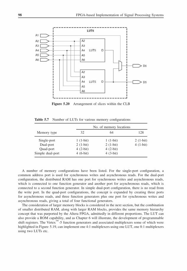
98 FPGA-based Implementation of Signal Processing Systems
Figure 5.20 Arrangement of slices within the CLB
Table 5.7 Number of LUTs for various memory configurations
No. of memory locations
Memory type 32 64 128
Single-port 1 (1-bit) 1 (1-bit) 2 (1-bit)Dual-port 2 (1-bit) 2 (1-bit) 4 (1-bit)Quad-port 4 (2-bit) 4 (2-bit)
Simple dual-port 4 (6-bit) 4 (3-bit)
A number of memory configurations have been listed. For the single-port configuration, acommon address port is used for synchronous writes and asynchronous reads. For the dual-portconfiguration, the distributed RAM has one port for synchronous writes and asynchronous reads,which is connected to one function generator and another port for asynchronous reads, which isconnected to a second function generator. In simple dual-port configuration, there is no read fromthe write port. In the quad-port configurations, the concept is expanded by creating three portsfor asynchronous reads, and three function generators plus one port for synchronous writes andasynchronous reads, giving a total of four functional generators.
The consideration of larger memory blocks is considered in the next section, but the combinationof smaller distributed RAM, along with larger RAM blocks, provides the same memory hierarchyconcept that was purported by the Altera FPGA, admittedly in different proportions. The LUT canalso provide a ROM capability, and as Chapter 6 will illustrate, the development of programmableshift registers. The Virtex
TM-5 function generators and associated multiplexers some of which were
highlighted in Figure 5.19, can implement one 4:1 multiplexers using one LUT, one 8:1 multiplexersusing two LUTs etc.

Current FPGA Technologies 99
Table 5.8 VirtexTM
-5 memory types and usage
Memory type Bits/block No. of blocks Suggested usage
Distributed 1024 14720 Shift registers, small FIFO buffers,RAM/slice filter FIFO buffers, filter delay lines
36 kbit 18000 488 Multi-rate FIFOBlock RAM
Memory Organization
In addition to distributed RAM, the VirtexTM
-5 device has a large number of 36kB block RAMs,each of which contain two independently controlled, 18 kB RAMs. The total memory configurationis given in Table 5.8. The 18 kB RAMs have been implemented in such a way, that the blockscan be configured to act as one 36 kB block RAM without the use of programmable interconnect.Block RAMs are placed in columns and can be cascaded to create deeper and wider RAM blocks.Each 18 kB block RAM, dual-port memory consists of an 18 kB storage area and two completelyindependent access ports along with other circuitry to allow the full expected RAM functionalityto be achieved (See Figure 5.21). The full definition in terms of access pins is given below, andrepresents a standard RAM configuration.
A clock for each 18 kB block RAM which can be configured to have rising or falling edge. Allinput and output ports are referenced to the clock.
An enable signal to control the read, write, and set/reset functionality of the port with an inactiveenable pin, implying that the memory keeps the previous state.
An additional enable signal called the byte-wide write enable signal which controls the writing andreading of the RAM in conjunction with the enable signal
The register enable pin which controls the optional output register.The set/reset pin which forces the data output latches to contain a set value.The address bus which selects the memory cells for read or write; its data bit width is decided by
the size of RAM function chosen.
In latch mode, the read address is registered on the read port, and the stored data is loaded intothe output latches after the RAM access time. When using the output register, the read operationwill take one extra latency cycle. The write operation is also a single clock-edge operation withthe write address being registered on the write port, and the data input is stored in memory. Theadditional circuitry highlighted in Figure 5.21, shows how inverted clock can be supported alongwith a registered output. The contents of the RAM can be initialized using the INIT parameter andcan be indicated from the HDL source code.
The RAM provides a number of options for RAM configuration, some of which are listed inTable 5.9; the table shows how bit data width is traded off for memory depth, i.e. number ofmemory locations.
Dedicated logic has also been included in the block RAM enables, to allow the creation ofsynchronous or asynchronous FIFOs; these are important in some high-level design approaches,as will be seen later. This dedicated logic avoids use of the slower programmable CLB logic androuting resource, and generates the necessary hardware for the pointer write and read generation

100 FPGA-based Implementation of Signal Processing Systems
Figure 5.21 Block RAM logic diagram(Xilinx Inc. 2007b). Reproduced by permission of XilinxInc.
Table 5.9 Memory sizes for Xilinx VirtexTM
-5 blockRAM
Data width Memory depth
1 (cascade) 32768 (65 536)2 163844 81929 409618 204836 102472 512
along with the setting of the various flags associated with FIFOs. A number of FIFO sizes can beinferred, including 8KX4, 4KX4, 4KX9, 2KX9, 2KX18, 1KX18, 1KX36, 512X36 and 512X72.
VirtexTM
-5 DSP Processing Resource
In addition to the scalable adders in the CLBs, the VirtexTM
-5 also provides a dedicated DSPprocessing block called DSP48E. The Virtex
TM-5 can have up to 640 DSP48E slices which are
located at various positions in the FPGA, and supports many independent functions includingmultiply, MAC, multiply add, three-input add, barrel shifting, wide-bus multiplexing, magnitudecomparator, bit-wise logic functions, pattern detect, and wide counter. The architecture also allowsthe multiple DSP48E slices to be connected together to form a wider range of DSP functions, suchas DSP filters, correlators and frequency domain functions.
A simplified version of the DSP48E processing block is given in Figure 5.22. The basic archi-tecture of the DSP48E block is a multiply–accumulate core, which is a very useful engine formany DSP computations. However, in addition to the basic MAC function, the DSP48E block alsoallows a number of other modes of operation, as summarized below:
• 25-bit x 18-bit multiplication which can be pipelined• 96-bit accumulation or addition or subtracters (across two DSP48E slices)

Current FPGA Technologies 101
Figure 5.22 DSP processing blocks called DSP48E(Xilinx Inc. 2007c). Reproduced by permissionof Xilinx Inc.
• triple and limited quad addition/subtraction• dedicated bitwise logic operations• arithmetic support for overflow/underflow
Each DSP48E slice has a 25-bit X18-bit multiplier which is fed from two multiplexers; themultiplexers accept a 30-bit A input and a 18-bit B input either from the switching matrix or fromthe DSP48E directly below. These can be stored in registers (not shown in Figure 5.22) before beingfed to the multiplier. Just before multiplication, the A signal is split and only 25 bits of the signalare fed to the multiplier. A fast multiplier technique is employed which produces an equivalent43-bit two’s complement result in the form of two partial products, which are then sign-extendedto 48 bits in the X multiplexer and Y multiplexer respectively before being fed into three inputadder/subtracter for final summation.
As illustrated in Chapter 4, many fast multipliers work on the concept of using fast carry-saveadders to eventually produce a final sum and carry signals, and then using a fast carry ripple toperform the final addition. This final addition is costly, either in terms of speed or if a speed-uptechnique is employed, then area. By postponing the addition to the ALU stage, a two-stage additioncan then be avoided for multiply–accumulation, by performing a three-stage addition to computethe final multiplication output and an addition for the accumulation input in one stage. Once again,for flexibility, the adder/subtracter unit has been extended to function as a arithmetic logic unit(ALU), thereby providing more functionality at little hardware overhead. As the final stage of theconventional multiplication is being performed in the second-stage adder, a three-input addition isrequired with the third input used to complete the MAC operation if required.
The multiplexers allow a number of additional levels of flexibility to be added. For example, theP input can be used to feed in an input either from another DSP48E block from below using thePCIN in the Z multiplexer or looped back from the current DSP48E block say, for example,if a recursion is being performed using the P input to the Z multiplexer. The multiplier canbe bypassed if not required, by using the A:B input which is a concatenation of the two inputsignals A and B, 25-bit and 18-bit words respectively; this gives a 43-bit word size which isthe same as the multiplier output. Provision to initialize the inputs to the ALU to all 0s or all 1s,

102 FPGA-based Implementation of Signal Processing Systems
is also provided. To increase the flexibility of the unit, the adder can also be split into severalsmaller adders, allowing two 24-bit additions or four 12-bit additions to be performed. This isknown as the SIMD mode, as a single operation namely addition, is performed on multiple data,thus giving the SIMD operation. The DSP48E slice also provides a right-wire-shift by 17, allowingthe partial product from one DSP48E slice to be shifted to the right and added to the next partialproduct, computed in an adjacent DSP48E slice. This functionality is useful, when the dedicatedmultipliers are used as building blocks, in constructing larger multipliers.
The diagram in Figure 5.22 is only basic, and does not indicate that other signals are alsoprovided, in addition to the multiply or multiply–accumulate output, P. These include:
The cascadable A data port called ACOUT, which allows the A internal value to be fed directlyto the output. Given that the A signal has been internally delayed, this would provide the delaychain for DSP functions e.g. a FIR filter.
Cascadable carryout (CARRYCASCOUT ) and sign (MULTSIGNOUT ) signals which are internalsignals used to indicate the carryout and sign, when supporting 96-bit addition/subtraction acrosstwo DSP48E slices.
Up to four carry out signals (CARRYOUT ) to support the SIMD mode of addition where up to fourseparate adders will need to generate carry out signals.
A pattern detector provides support for a number of numerical convergent rounding, over-flow/underflow, block floating-point, and support for accumulator terminal count (counter autoreset) with pattern detector outputs (PATTERNDETECT and PATTERNBDETECT ), to indicateif a pattern has been met and separate signals for overflow (OVERFLOW ) and underflow(UNDERFLOW ).
From a functional perspective, the synthesis tools will largely hide the detail of how the designfunctionality is mapped to the FPGA hardware, but it is important to understand that the level offunctionality that is available as it determines the design approach the user will adopt. A numberof detailed examples are listed in the relevant user guide (Xilinx Inc. 2007c), indicating howperformance can be achieved.
Clock Networks and PLLs
The Xilinx VirtexTM
-5 FPGA family can provide a clock frequency of 550 MHz. The clock domainsin the Virtex
TM-5 FPGA are organized into six clock management tiles or CMTs, each of which
contain two digital clock managers (DCMs) and one PLL. In total, the FPGA has eighteen totalclock generators.
A key feature of the Xilinx VirtexTM
-5 FPGA is the DCM, which provides a wide range ofpowerful clock management features including a delay-locked loop (DLL); this acts to align theincoming clock to the produced clock as described earlier. It also allows a range of clock frequenciesto be produced, including a doubled frequency a range of fractional clock frequencies specifically1.5, 2, 2.5, 3, 3.5, 4, 4.5, 5, 5.5, 6, 6.5, 7, 7.5, 8, 9, 10, 11, 12, 13, 14, 15, or 16 of the inputclock. Coarse (90◦, 180◦ and 270◦) fine-grained phase shifting and various types of fine-grained orfractional phase-shifting are supported.
The PLL’s main purpose is to act as a frequency synthesizer and to remove jitter from eitherexternal or internal clocks, in conjunction with the DCMs. With regard to clock generation, the sixPLL output counters are multiplexed into a single clock signal for use as a reference clock to theDCMs. Two output clocks from the PLL can drive the DCMs; for example, one could drive thefirst DCM while the other could drive the second DCM. Flexibility is provided to allow the outputof each DCM output to be multiplexed into a single clock signal, for use as a reference clock to the

Current FPGA Technologies 103
PLL, but one DCM can be used as the reference clock to the PLL at any given time (Xilinx Inc.2007c).
I/O and External Memory Interfaces
As with the Altera FPGA device, the VirtexTM
-5 FPGA supports a number of different I/O standardinterfaces termed SelectIO
TMdrivers and receivers, allowing control of the output strength and
slew rate and on-chip termination. As with the Altera FPGA, the I/Os are organized into a bankcomprising 40 IOBs which covers a physical area that is 20 CLBs high, and is controlled by asingle clock. The Virtex
TM-5 FPGA also includes digitally controlled impedance (DCI) technology,
allowing the output impedance or input termination to be adjusted, and therefore, accurately matchthe characteristic impedance of the transmission line. The need to effectively terminate PCB tracesignals, is becoming an increasing important issue in high-speed circuit implementation, and thisapproach purports to avoid the need to add termination resistors on the board. A number of standardsare supported, including low-voltage transistor–transistor logic (LVTTL), low-voltage complemen-tary metal oxide semiconductor (LVCMOS), peripheral component interface (PCI) including PCIX,PCI33, PCI66, and low-voltage differential signalling (LVDS), to name but a few.
Input serial-to-parallel converters (ISERDES) and output parallel-to-serial converters(OSERDES) are also supported. These allow very fast external I/O data rates such as SDR andDDR, to be fed into the internal FPGA logic which may be running an order of magnitude slower.This is essentially a serial-to-parallel converter with some additional hardware modules that allowreordering of the sequence of the parallel data stream going into the FPGA fabric, and circuitry tohandle the strobe-to-FPGA clock domain crossover.
5.5 Lattice FPGA Families
Lattice r© offer a number of FPGA architectures, including the ispXPLDTM
5000MX family whichextends the CPLD concept, the LatticeSC/M family which is a more of a standard FPGA withadditional high-speed communications, memory and dedicated ASIC block implementation, andthe Lattice ECP2/M family which is a low cost FPGA with a number of the features outlined inthe LatticeSC/M family.
5.5.1 Lattice r© ispXPLD 5000MX Family
The ispXPLDTM
5000MX family offers a combination of E2PROM nonvolatile cells which stores thedevice configuration, and SRAM technology to provide the logic implementation, giving a solutionthat provides logic availability at boot-up. It also includes flexible memory capability, supportingsingle- or dual-port SRAM, FIFO, and ternary content addressable memory (CAM) operation alongwith dedicated arithmetic functionality. However, the technology benefits from the main attractionof using the CPLD architecture to provide predictable deterministic timing. The architecture ofispXPLD 5000MX device (Figure 5.23), consists of units called multi-function blocks (MFBs)interconnected with a global routing pool which are connected via multi sharing arrays (MSAs)to the input and output pins. The MFB consists of a multi-function array and associated routing,which can cope with up to 68 inputs from the GRP and the four global clock and reset signals andproduce outputs to the macrocells or elsewhere. The device allows cascading of adjacent MFBs tosupport wider operation. Each MFB can be configured in a number of modes, including logic andmemory configurations e.g., single- and dual-port RAM, FIFO Mode and CAM.
This description concentrates on the LatticeSC/M FPGA (Lattice Semi. Inc. 2007), as it repre-sents the high-performance FPGA family, with many of the features which appear on the lower cost

104 FPGA-based Implementation of Signal Processing Systems
I/O
OutputSharingArray
MFB
MFBGlobalrouting
poolPLL
MFB
MFB
ISP port
PLL
MFB
MFB
MFB
MFB
Figure 5.23 Lattice ispXPLD 5000MX family
Lattice ECP2/M families. The architecture of LatticeSC/M device is given in Figure 5.24. It com-prises the standard programmable I/O block which is connected to rows of logic blocks organizedas programmable functional units or PFUs. These PFUs comprise slices, each of which comprisetwo 4-input LUTs and two registers, along with carry propagate and carry generate signals whichallow the creation of fast adder structures. As with other FPGA offerings, this functionality canbe used to create combinational and sequential logic with the capability to scale LUT table sizesand register dimensions as required. As in the ispXPLD
TM5000MX family, the PFUs can also be
configured to act as memory types. The largest device offers 115 k of LUTs.In addition to the programmable logic, the device also incorporates up to 7.8 Mb of embedded
block RAM, to match the 2 Mb of distributed RAM contained within the PFUs. These sysMEMEBRs as they are called, can be configured as RAM, ROM or FIFO, allowing a high level ofprogrammability. In addition to the standard programmable I/O pins, high performance I/O isincluded in the form of dedicated SERDES and PCS hardware which provides 2Gbps I/O capability.This matches the concept of gathering large dedicated IP functionality on IP cores.
A feature that is different from offerings from Altera and Xilinx, is the structured ASIC capabilityas highlighted in Figure 5.25. This masked array for cost optimization or MACO block is a seaof 50 000 ASIC gates which has been created using a 90 nm CMOS process technology andoptimized for speed, power dissipation, and area (Lattice Semi. Inc. 2006). The MACO blockinterfaces directly to the I/O and also to the FPGA fabric, thereby allowing dedicated fast low-powerimplementation for specialized hardware. In addition to the gates, each MACO block contains three64 × 40 asynchronous dual-port RAMs in addition to the RAM of the FPGA; the dual-port RAMsare co-located to the MACO block and can be accessed through the dedicated MACO interfaceblock or MIB. By being located between the I/O pins and the on-board block RAM makes this idealfor implementing a number of fast, lower-power blocks such as dedicated or specialized memoryinterfaces.

Current FPGA Technologies 105
PFU
SERDES block
BlockRAM
StructuredASIC
DLLs &PPLs
I/O
Figure 5.24 LatticeSC/M Family
5.6 Actel FPGA TechnologiesActel r© offers a number of FPGA technologies, based on flash and antifuse technologies. Theyhave also recently launched a Fusion
TMtechnology which represents the first mixed signal FPGA
(Actel Corp. 2007a). It comprises A/D converters, embedded flash memory and as well as moreconventional digital FPGA hardware in the form of D-type flip-flops and RAM. The flash technologyis nonvolatile, meaning that the FPGA stores its design and is live at power-up, without the needto be programmed from a ROM or co-processor. The largest device has 1.5 M system gates with270 kbits of dual-port SRAM, up to 8 Mbits of flash memory, 1 kbit of user flash ROM, and up to278 user I/Os.
5.6.1 Actel r© ProASICPLUS FPGA Technology
The ProASICPLUS FPGA technology is based on flash technology. It is similar to E2PROM tech-nology in that it stores its charge and therefore allows the device to store its program. The FPGAtechnology is organized with an architecture comparable to gate arrays, as illustrated in Figure 5.25,and comprises a sea of tiles where each tile can be configured as a three-input logic function, ora D-type flip-flop. As the diagram shows, the architecture comprises a grid of tiles with a numberof embedded two-port SRAM blocks, top and bottom which allow synchronous and asynchronousoperation. The tiles consist of a number of multiplexers and logic gates, sufficient to allow thecreation of a flip-flop with the necessary globally connected reset and clock signalling. The tilesconnect to both the local and the longer line routing.
The tiles are connected by a hierarchy of routing that has four levels which are organized interms of length; it would appear to have a similar organisation to the older Xilinx XC62000 FPGAtechnology which was a similarly fine-grained architecture. The next level of lines run one, two or

106 FPGA-based Implementation of Signal Processing Systems
RAM Block
RAM Block
256x9 Two-Port SRAMor FIFO Block
256x9 Two Port SRAMor FIFO Block
I/Os
Logic Tile
Figure 5.25 Actel r© ProASICPLUS FPGA (Actel Corp. 2007b). Reproduced by permission ofActel Corp.
four tiles. Both of these are accessible at the tile output. The next level of interconnect are long-lineresources which span the length of the chip. The final level is global signals, which by definitionhave to be low-delay, as they will be used for global signals such as clock, reset and enable signalswhich would be used globally and would degrade the performance of the chip.
The device also incorporates two clock conditioning blocks which, like other FPGA devices,comprise PLLs and delay circuits for synchronizing the external clock as well as multiplier/dividerscircuits along with necessary circuitry to connect to the global routing network. The device comeswith four clock networks or global trees, specifically designed for distributing a low-latency, low-skew clock signal.
A key aspect of the implementation process with such a fine-grained technology, is the goodplacement of the design units into the hardware, as the limited routing organization can hamperdesign quality and utilization of the underlying hardware blocks. For this reason, the softwareallows the use of constraints to control the placement of the design. The concept of generating acircuit architecture to best match the FPGA resource requirements, is definitely needed, not only toachieve the necessary performance, but also to alleviate the software effort in achieving an efficientimplementation. As with other FPGAs, a range of I/O blocks is available and boundary scan in theform of JTAG is provided for system text at the board level.
5.6.2 Actel r© Antifuse SX FPGA Technology
In addition to flash memory devices, Actel also provide an antifuse technology which is once-onlyprogrammable. An antifuse is a two-terminal device with an unprogrammed state presenting avery high resistance between its terminals. Typically as shown in Figure 5.26, two conductors areseparated by mostly insulator, but at certain points by amorphous or ‘programmable’ silicon. Whena high voltage is applied across its terminals, the antifuse will ‘blow’ and create a low-resistancelink (as opposed to an open circuit as in a fuse).
In the case of the Actel antifuse link shown in Figure 5.27, the connection is made up froma combination of amorphous silicon and dielectric material and has an ‘on’ state resistance of

Current FPGA Technologies 107
INSULATOR INSULATOR
CONDUCTOR
CONDUCTOR
ANTIFUSE
Figure 5.26 Basic antifuse link
Routing Tracks
Metal 3
Metal 2
Metal 1
Tungsten PlugContact
Silicon Substrate
Amorphous Silicon/Dielectric Antifuse
Tungsten Plug ViaTungsten Plug Via
Figure 5.27 Actel r© ProASICPLUS FPGA(Actel Corp. 2007c). Reproduced by permission ofActel Corp.
25 with a capacitance of 1.0 fF (Actel Corp. 2007c). The use of three-layer metal as shown inFigure 5.27 and the use of metal-to-metal antifuse results in better performance and smaller area.The metal-to-metal antifuse lowers the programmed resistances, thereby providing better speed,and the multiple metal layers now allows the placement of the antifuses above the logic, therebyavoiding routing channels. This provides better density of logic and lead to smaller devices withbetter, performance.
The architecture comprises a sea of modules which like the ProASICPLUS FPGA technology,is fine-grained with two types of cells, namely a C-cell which is effectively a combinational cellcomprising a series of multiplexers and logic gates, and an R-cell which is a register cell whichcomprises a D-type flip-flop with various multiplexing hardware, to allow various connections to theinput, and to allow various clock signals to be used to clock the cell. Because of the programmabilityto configure the cell, the fabric is comprised of a variety of the different cell types, meaning thatpre-defined mappings of the cells must be created, called clusters. The two types of superclusters

108 FPGA-based Implementation of Signal Processing Systems
C R C C R C
(a) Type 1 supercluster (b) Type 2 supercluster
C R R C R C
Figure 5.28 Cluster organization
are illustrated in Figure 5.28; the one supercluster comprises two C, R and C clusters and the othersupercluster comprises a C, R and R cluster followed by a C, R and C cluster.
In this structure, a number of different level of routing is given. The first type of routingcomprises the DirectConnect which is a horizontal routing resource that connects from C-cell to itsneighbouring R-cell in a cluster, and the FastConnect routing which provides vertical routing. Twoglobally orientated routing resources are also provided, known as segment routing and high-driverouting, which as the names suggest are for smaller routes, i.e. segments and more global routes.As with the ProASICPLUS FPGA technology, consideration has to be given to the careful placementof the cells in order to achieve efficient implementation, otherwise the disadvantage of the delaysof programmable routes will have to be suffered.
Clock rates of 300 MHz are quoted in (Actel Corp. 2007c). In addition, it is also argued thatsecurity is a key feature of the technology, as it proves difficult to reverse engineer the devicebecause it is hard to distinguish between the programmed and unprogrammed antifuses, and thereis no configuration bitstream to intercept.
5.7 Atmel FPGA TechnologiesAtmel offer a range of FPGA technologies, ranging from the AT40K and AT40KAL series co-processor FPGAs range which offer the concept of what is termed FreeRAM
TMwhich can be used
without infringing the available logic resource. Their FPGA technology can be used as an embeddedcore in the form of FPSLIC
TMFPGA family, which provides from 5 k up to 50 k gates, up to 36 k of
SRAM and a 25 MHz AVR MCU. The AT6000 series FPGAs are marketed as reconfigurable DSPco-processors, as they offer register counts of 1024 to 6400 registers, making them ideal for use ascomputing DSP functions that have been off-loaded into hardware. One of the key features of theAT6000, AT40K and AT40KAL FPGA families is that they offer reconfigurability, allowing partof the FPGA to be reprogrammed without loss of register data, whilst the remainder of the FPGAcontinues to operate without disruption. For this reason, the AT40K FPGA family are consideredin a little more detail.
5.7.1 Atmel r© AT40K FPGA Technologies
The AT40KAL is a SRAM-based FPGAs with distributed dual-port/single-port SRAM and eightglobal clocks with only one global reset. The family ranges in size from 5000 to 50 000 usable gates.The AT40KAL is a fine-grained FPGA architecture comprising simple cells organized into 4 × 4grids, each of which are surrounded by repeater cells, as shown in Figure 5.29 (Atmel Corp. 2006).The repeaters regenerate the signals and allow connection of any bus to any other bus, on the sameplane. Each repeater has connections to two adjacent local-bus segments, which provide localizedconnections in the four cells shown, and two express-bus segments for longer line connection whichspans eight cells.
The core cell is very fine-grained, comprising two 3-input LUTs (8 × 1 ROM) which can beconfigured as a 4-input LUT, a D flip-flop, a 2-to-1 multiplexer and an AND gate for implementing

Current FPGA Technologies 109
RAM
RH RH
RAM RV RV RV RV RAM
RV RV RV RV RAM
Tile Tile Tile Tile
Tile Tile Tile Tile
Tile Tile Tile Tile
Tile Tile Tile Tile
RH Tile
RH Tile
RH Tile
Figure 5.29 Atmel AT50K FPGA 4 × 4 cell
multiplier arrays. As with the other FPGA technologies, the combination of LUT and D-typeflip-flops allow a wide range of combinational and sequential logic to be implemented. There is aDSP mode, but it is basic, compared with other technologies, as it only allows the generation ofan array multiplier using the cells, resulting in a relatively poor DSP performance compared withother FPGA technologies.
At the intersection of each repeater row and column, there is a 32 × 4 RAM block accessibleby adjacent buses, which can be individually addressed through the provision of a series of local,and express horizontal and vertical buses. Reading and writing of the dual-port FreeRAM areindependent of each other, and reading is completely asynchronous.
An interesting aspect of the Atmel r© AT40K FPGA technology is the fact that it can be partiallyreconfigured, i.e. programmed, allowing the function of the design or part of the design to bechanged whilst it is operating. This is worth examining in a little more detail.
5.7.2 Reconfiguration of the Atmel r© AT40K FPGA Technologies
The AT40K FPGA technology has four basic configuration modes of operation (Atmel Corp. 2006).First, there is power-on reset when the device is first powered up which involves a complete resetof all of the internal configuration SRAM. Second, the same reset sequence can be invoked by themanual reset, via the reset pin. The third configuration mode is configuration download, where theFPGA’s configuration SRAM is programmed using serial, or parallel data via its input pins. Thefourth mode is when no configuration is active. The AT40K FPGA allows complete reconfigurabilitydown to the byte level.
The CacheLogic r© architecture lets users reconfigure part of the FPGA, while the rest of theFPGA continues to operate unaffected; this done using a windowing mechanism. This allows theuser to load the SRAM memory map in smaller segments, allowing overwriting of portions of theconfiguration SRAM that is not being used, with new design information. In synchronous RAMmode, the device receives a 32- or 40-bit-wide bitstream composed of a 24-bit address and either an8-bit-wide or 16-bit-wide dataword. Address, data and write enable are applied simultaneously at therising edge of CCLK. In this mode, designed to interface to a generic IO port of a microprocessor,the FPGA configuration SRAM is seen as a simple memory-mapped address space. The user has fullread and write access to the entire FPGA configuration SRAM. The overhead normally associatedwith bitstreams is eliminated, resulting in faster reconfiguration.

110 FPGA-based Implementation of Signal Processing Systems
5.8 General Thoughts on FPGA TechnologiesThe chapter has covered a number of FPGA technologies from a variety of companies, but high-lighting the two major vendors, namely Xilinx and Altera. The major drive in FPGA technology, hasbeen a move from an FPGA being a fine-grained device where simple logic was implemented usingLUTs and programmable interconnect, to one where it is a collection of heterogeneous complexunits such as dedicated DSP blocks, high-speed communications blocks, soft and hard processorand of course, the previously mentioned LUTs.
This has had a number of implication for the design process. With earlier FPGAs, the targethas been to develop an efficient implementation where utilization of FPGA hardware had beenthe main focus. This involved using, initially, schematic design capture packages and then morerecently HDL-based tools, to achieve an efficient design implementation. Given that the focus wasto achieve high utilization, considerable effort was expended to utilize the underlying LUTs. Thus,a number of circuit-level design techniques were developed to best use LUTs, and flip-flops for thatmatter, to achieve the implementation. These techniques are covered in more detail in Chapter 6 asit is important to understand the principles, even though a lot of this activity is carried in synthesistools. For this reason, the design techniques are only briefly covered.
As complexity has grown with more recent FPGAs, the major challenge has been to create acircuit architectures at one level (see Chapter 8) and then system-level architectures at another levelwhich is a major focus in Chapters 7, 9 and 11. There has been a major focus on generating circuitarchitectures that contain all of the FPGA specific details from a SFG representation of the DSPalgorithm. Since the major performance gains of FPGAs in the area of DSP implementation, thisinvolves exploiting concurrency in terms of parallelism and pipelining. The processes for achievingthis are described in detail in Chapter 8; the higher-level tools flows are then described in the laterchapters.
ReferencesActel Corp. (2007a) Fusion family of mixed-signal flash FPGAs with optional soft arm support. Web publication
downloadable from www.actel.com.
Actel Corp. (2007b) Proasicplus flash family FPGAs. Web publication downloadable from www.actel.com.
Actel Corp. (2007c) Sx family FPGAs. Web publication downloadable from www.actel.com.
Altera Corp. (2000) Max ii device family data sheet. Web publication downloadable from http://www.altera.com.
Altera Corp. (2007) Stratix iii device handbook. Web publication downloadable from http://www.altera.com.
Atmel Corp. (2006) 5k–50k gates coprocessor FPGA with freeram. Web publication downloadable fromhttp://www.atmel.com.
Bouvier D (2007) Rapidio: the interconnect architecture for high performance embedded systems. Web publicationdownloadable from http://www.techonline.com/.
Lattice Semi. Inc. (2006) Delivering FPGA-based pre-engineered IP using structured ASIC technology. Web pub-lication downloadable from www.latticesemi.com.
Lattice Semi. Inc. (2007) Latticesc/m family data sheet. Web publication downloadable from www.latticesemi.com.
Rose J, Francis RJ, Lewis D and Chow P (1990) Architecture of field programmable gate arrays: the effect oflogic block functionality on area efficiency. IEEE Journal of Solid State Circuits 25(5), 1217–1225.
Xilinx Inc. (2007a) Achieving higher system performance with the virtex-5 family of FPGAs. Web publicationdownloadable from www.xilinx.com/bvdocs/whitepapers/wp245.pdf.
Xilinx Inc. (2007b) Virtex-5 user guide. Web publication downloadable from www.xilinx.com.
Xilinx Inc. (2007c) Xilinx ug193 virtex-5 xtremedsp design considerations: User guide. Web publication down-loadable from www.xilinx.com/bvdocs/userguides/ug193.pdf.

6Detailed FPGA ImplementationIssues
6.1 IntroductionThe previous chapters have set the scene in terms of background to DSP and computer arithmetic,and then in the last two chapters, the various implementation technologies have been highlighted;Chapter 4 has highlighted the wider range of technologies and Chapter 5 has described, in alittle more detail, the various FPGA offerings. The remaining chapters now describe the issuesfor implementing complex DSP systems onto heterogeneous platforms, or even a single FPGAdevice. This encompasses considerations such as selection of the suitable model for DSP systemimplementation, partitioning of DSP complexity into hardware and software, mapping of DSPfunctions efficiently onto FPGA hardware, development of a suitable memory architecture, andachievement of design targets in terms of throughput, area and energy. However, it is imperativethat the reader understands the detailed FPGA implementation of DSP functionality in order thatthis process is inferred correctly at both the system partitioning and circuit architecture developmentstages.
At the system partitioning level, for example, it may become clear that the current system underconsideration will consume more than the dedicated multiplicative resources available. The designeris then faced with a number of options, either to restrict the design space so that the design mappingensures that only the dedicated multiplier resources are used, or alternatively, to map the design tothe existing FPGA resources, in order to create the additional multipliers using LUTs and dedicatedadders. Moreover, it may be that the additional multiplicative operations are fixed in nature, whichmeans that constant coefficient multipliers could be used which need considerably less LUTs.
From a circuit architecture perspective, the key objective is to achieve faster implementation,where area against speed is a key trade-off. It is essential to be aware of the optimizations availablein producing the required design as this could determine the trade-off between implementing thedesign in FPGA hardware or in software, which may be a critical decision for the system. It is clearfrom published work that the decision is not obvious unless a lot of detailed work is undertakento investigate the FPGA implementation; however, this is clearly not practical at system level asthe design detail is severely limited. Indeed, it was the efficient mapping in the earlier LUT-baseddevices such as the Xilinx XC4000 that first led to the concept of achieving performance gainsover existing DSP processor devices (Goslin 1995); this was demonstrated for some DSP functionssuch as FIR filters. With modern day synthesis tools, a lot of these optimizations are containedwithin the synthesis tools, but it is important that the underlying principles are understood.
FPGA-based Implementation of Signal Processing Systems R. Woods, J. McAllister, G. Lightbody and Y. Yi 2008 John Wiley & Sons, Ltd

112 FPGA-based Implementation of Signal Processing Systems
Finally, the utilization of the design may be an issue: indeed it could be argued that, for a cost-effective design, it should always be so, otherwise the designer is selecting a larger FPGA devicethan needed, thereby increasing cost! In this case, optimization to achieve the last few nanosecondsof timing from the design may be the critical aspect. Of course, a lot of these optimizations arenow increasingly buried within synthesis tools.
A trivial example is the design of a walking one circuit. In a typical design environment, onewould be tempted to describe this design as a finite state machine (FSM) where each state willhave one bit high. The synthesis tool will treat this as FSM machine with one hot encoding, but itis clear that the design can be achieved by writing the code for a register chain where one of theflip-flops is set logic ‘1’ using preset, with others being reset. This comes from the understandingthat the FPGA flip-flop has a set–preset facility. The synthesis tool might be able to come withan efficient design, but it is clear that any doubt that the synthesis tool would give this efficientsolution can be removed by coding critical parts of the circuit in this direct way. Of course, thiscould be viewed as working against the design principle of writing the code to be as portable aspossible. Therefore, the focus of this chapter is to introduce and cover in reasonable detail someof these technology-specific design optimizations and show how the functionality is mapped intoFPGA fabric. In particular, the chapter will look at the implementation of memory in FPGAs as thistends to be a key issue in many applications. In addition, the use of advanced design techniques forDSP functions such as distributed arithmetic (DA) and reconfigurable mux technique for buildingcoefficient specific DSP functions, are also covered.
6.2 Various Forms of the LUTThe reason why most FPGA vendors choose the LUT as the logic fundamental building block, isthat an n-input LUT can implement any n-input logic function. As shown in Figure 6.1, the useof LUTs as compared with logic gates, places different constraints on the design. For example,the diagram shows how the function can be mapped into logic gates, where number of gates isthe design constraint. This is irrelevant from a LUT implementation perspective however, as theunderlying criteria in determining the number of LUTs is directly related to number of inputs and,in some cases, the number of outputs in the design rather than the logic complexity. For the earlyXilinx devices, a 4-input LUT with the capability to extend this efficiently to a 5-input LUT was
A
B
C
D
f
f
AB
CD
Figure 6.1 Mapping logic functions into LUTs

Detailed FPGA Implementation Issues 113
LUTGD
SE
RS
C
D Q
Q
SE
RS
C
…SRL16RAM16
…
LUTG
…SRL16RAM16
Figure 6.2 Additional usage of CLB LUT resources
the core unit, but recently, this has been extended to a 6-input LUT in the latest Xilinx VirtexTM
-5FPGA technologies, and to an 8-input LUT in the latest Altera Stratix r© III FPGA devices.
This represents however, only one of the reasons for using a n-input LUT as the main logicbuilding block of FPGAs. Figure 6.2 illustrates the resources of the CLB for the family of XilinxFPGA devices; this comprises two LUTs, shown on the left, two flip-flops, shown on the rightand the fast carry adder chain, shown in the middle. The figure highlights how the LUT resourceshown on the left-hand side, can be used as a LUT, but also as a shift register for performing aprogrammable shift and as a RAM storage cell.
The basic principle of how the LUT can be used as a shift register is covered in detail in theXilinx application note (Xilinx Inc. 2005). First, the LUT can be thought of as 16:1 multiplexer asshown in Figure 6.3 where the address input (here a 4-bit input as the note is dealing with a XilinxSpartan device) is used to address the specific input stored in the RAM. In this case, the contentsof the multiplexer would have been treated as being fixed. In the case of the SRL16, the Xilinxname for the 16-bit shift register, the fixed LUT values are configured instead as an addressableshift register, as shown in Figure 6.3(b).
The shift register inputs are the same as those for the synchronous RAM configuration of theLUT given in (Xilinx Inc. 2005) namely, a data input, clock and clock enable. The LUT usesa special output called Q15 in the Xilinx library primitive device which is in effect the outputprovided from the last flip-flop.
The design works as follows. By setting up an address, say 0111, the value of that memorylocation is read out as an output and at the same time, a new value is read in which is deemed tobe the new input, DIN in Figure 6.3(b). If the next address is 0000 and the address value is incre-mentally increased, it will take 8 clock cycles until the next time that 0111 address correspondingto an shift delay of 8. In this way, the address size can mimic the shift register delay size. So ratherthan shift all the data as would happen in a shift register, the data is stored statically in a RAMand the changing address line mimics the shift register effect by reading the relevant data out atthe correct time.
Details of the logic cell SRL structure are given in Figure 6.4 which refers to the Xilinx SpartanFPGA family with a 4-input LUT. The cell has an associated flip-flop and a multiplexer whichmake up the full cell. The flip-flop provides a write function synchronized with the clock, and theadditional multiplexer allows a direct DI input, or if a large shift register is being implemented,

114 FPGA-based Implementation of Signal Processing Systems
1
0000A[3:0]
A[3:0]
DINCLK
0001 0010 0011 0100 0101 0110 0111 1000
D
D
Q15 orMC15
(a) 16:1 Multiplexer
(b) Shift register
1001 1010 1011 1100 1101 1110 1111
0000 0001 0010 0011 0100 0101 0110 0111 1000 1001 1010 1011 1100 1101 1110 1111
0 1 1 1 0 0 0 1 1 1 0 1 0 0 1
Figure 6.3 Configurations for Xilinx CLB LUT (Xilinx Inc. 2005). Reproduced by permission ofXilinx Inc.
SHIFTIN SRLC16
SHIFT-REG
WS
WSG
WECK
DI
D
D
(optional)
SHIFTOUTor YB
Output
RegisteredOutput
Q
4
MC15A[3:0] A[3:0]
DI (BY)
CE (SR)CLK
Figure 6.4 Detail SRL logic structure(Xilinx Inc. 2005). Reproduced by permission of Xilinx Inc.
an SHIFTIN input from the cell above. The address lines can be changed dynamically, but in asynchronous design implementation it would be envisaged that they would be synchronized to theclock.
This has huge implications for the implementation of DSP systems. As will be demonstratedin Chapter 8, the homogeneous nature of DSP operations is such that hardware sharing can beemployed to reduce circuit area. In effect, this results in a scaling of the delays in the originalcircuit; if this transformation results in a huge memory increase, then the overall emphasis to

Detailed FPGA Implementation Issues 115
reduce complexity has been negated. Being able to use the LUTs as shift registers in addition to theexisting flip-flops can result in a very efficient implementation. Thus, a key design criteria at thesystem level, is to balance the flip-flop and LUT resource in order to achieve the best utilizationof the CLB usage. This can be seen in a number of designs later in the book.
6.3 Memory AvailabilityFPGAs offer a wide range of different types of memory, ranging from block RAM, through tohighly distributed RAM in the form of the multiple LUTs available, right down to the storage ofdata in the flip-flops that are widely available in the FPGA fabric. As was demonstrated in theprevious section, a trade-off can be performed between the LUT and flip-flop storage capability,but this will be for small distributed memories. There may be cases where there is a need to storea lot of input data, such as an image of block of data in image processing applications, or largesets of coefficient data, as in some DSP applications, particularly when multiplexing of operationshas been employed. In these cases, the requirement is probably for large RAM blocks.
As illustrated in Table 6.1, FPGA families are now adopting quite large on-board RAMs. Thetable gives details of the DSP-flavoured FPGA devices, from both Altera and Xilinx. Consideringboth vendors’ high-end families, the Xilinx Virtex
TM-5 and the Altera Stratix r© FPGA technologies,
it can be determined that block RAMs have grown from being a small proportion of the FPGAcircuit area, to representing 1/15 or 1/10 of the circuit area. Typically these ratios tend to be lower forthe logic-flavoured FPGA families. In addition to small distributed RAMs, the FPGA families alsopossess larger block RAM which have the advantage that they are dual-port, providing flexibilityfor some DSP applications. The Virtex-5 block RAM stores up to 36K bits of data and can beconfigured as either two independent 18 kb RAMs, or a 36 kb RAM. Each 36 kb block RAM can beconfigured as a 64 k × 1 (when cascaded with an adjacent 36 kb block RAM), 32 k × 1, 16 k × 2,8 k × 4, 4 k × 9, 2 k × 18, or 1 k × 36 memory. Each 18 kb block RAM can be configured as a16 k × 1, 8 k × 2, 4 k × 4, 2 k × 9, or 1 k × 18 memory.
This section has highlighted the range of memory capability in the two most common FPGAfamilies. This provides a clear mechanism to develop a memory hierarchy to suit a wide range ofDSP applications. In image processing applications, various sizes of memory are needed at differentparts of the system. Take for example, the fast motion estimation circuit shown in Figure 6.5 where
Table 6.1 FPGA RAM size comparison for Xilinx Virtex 4 and 5 and Spartan FPGAs andAltera Stratix and Cyclone FPGAs
Family Model Block Distributed Mults I/O BRAMRAM (kb) RAM (kb) /LUT
Virtex XC5VSX35T 3024 520 192 360 5.8XC5VSX95T 8784 1520 640 640 5.8XC4VSX25 2304 160 128 320 14.4XC4VSX55 5760 384 320 640 15.0
Spartan XC3S100E 72 15 4 108 4.8XC3S1600E 648 231 36 376 2.8
Stratix EP3SE50 5328 594 384 480 9.0EP3SE260 14688 3180 768 960 4.6
Cyclone EP2C5 117 72 13 158 1.6EP2C70 1125 1069 150 622 1.1

116 FPGA-based Implementation of Signal Processing Systems
LocalStoragefor SW
data
LocalStoragefor CB
data
Data Flow
control
PE
SystemStorage
405 MB
Low bandwidthconnection
PE
PE
Local Highbandwidthconnection
Com
biningResult
3kB
0.5kB
12GB/s48MB/s12MB/s
Figure 6.5 Dataflow for motion estimation IP core
the aim is to perform the highly complex motion estimation (ME) function on dedicated hardware.The figure shows the memory hierarchy and data bandwidth considerations for implementing sucha system. In order to perform the ME functions, it is necessary to download the current block (CB)data and area where the matching is to be performed, namely the search window (SW), into localmemory. Given that the SW is typically 24 × 24 pixels, the CB sizes are 8 × 8 pixels and a pixelis 8-bits, this corresponds to 3 k and 0.5 k memory files which would typically be stored in theembedded RAM blocks. This is because the embedded RAM is an efficient mechanism for storingsuch data and the bandwidth rates are not high.
In an FPGA implementation, it might then be necessary to implement a number of hardwareblocks or IP cores to perform the ME operation, so this might require a number of computations tobe performed in parallel. This requires smaller memory usage which could correspond to smallerdistributed RAM or if needed, LUT-based memory and flip-flops. However, the issue is not justthe data storage, but the data rates involved which can be high as illustrated in the figure. Smallerdistributed RAM, LUT-based memory and flip-flops provide much high data rates as they eachpossess their own interfaces. Whilst this date rate may be comparable to the larger RAMs, the factthat each memory write or read can be done in parallel, results in a very high, data rate. Thus it isclear, that even in one specific application, there are clear requirements for different memory sizesand date rates; thus the availability of different memory types and sizes, such as those available inFPGAs, is vital.
6.4 Fixed Coefficient Design TechniquesUsually, a fully programmable multiplier capability is needed which is why FPGA vendors havenow included quite of number of these on FPGAs. In some DSP applications however, there issometimes the need to perform a multiplication of one word by a single coefficient value suchas in a fixed filtering operation, or DSP transforms such as the DCT or FFT. In a processorimplementation, this has little impact, but in dedicated hardware there is the chance to alter thehardware complexity needed to perform the task, thus dedicated coefficient multiplication or fixedcoefficient multiplication (KCM) has the considerable potential to reduce the circuitry overhead. Anumber of mechanisms have been used to derive KCMs. These include: DA (Goslin and Newgard1994), string encoding and common sub-expression elimination (Cocke 1970, Feher 1993).

Detailed FPGA Implementation Issues 117
This concept translated particularly well to earlier FPGA devices where only LUTs and dedicatedfast adders were available for building multipliers; thus an area gain was achieved in implementinga range of these fixed coefficient functions (Goslin and Newgard 1994, Peled and Liu 1974).A number of techniques have evolved to these fixed coefficient multiplications and whilst a lotof FPGA architectures have dedicated multiplicative hardware on-board in the form of dedicatedmultipliers or DSP blocks, it is still worth briefly reviewing the approaches available. The sectionconsiders the use of DA which is used for single fixed coefficient multiplication (Peled and Liu1974) and also the reduced coefficient multiplier (RCM) approach which can multiply a range ofcoefficient values (Turner and Woods 2004).
6.5 Distributed ArithmeticDistributed arithmetic (DA) is an efficient technique for performing multiply-and-add in which themultiplication is re-organized such that multiplication and addition is performed on data and singlebits of the coefficients, at the same time. The principle of the technique is based on the assumptionthat we will store the computed values rather than carry out the computation (as FPGAs have areadily supply of LUTs).
Assume that we are computing the sum of products computation in Equation (6.1) where thevalues xj represent a data stream and the values a0, a1, . . . aN−1 represent a series of coefficientvalues. Rather than compute the partial products using AND gates, we can use LUTs to generatethese and then use fast adders to compute the final multiplication. An example of a 8-bit LUT-basedmultiplier is given in Figure 6.6; it can seen that this multiplier would require a 4 kbits of LUTmemory resource which would be considerable.
y =N−1∑i=0
aixi (6.1)
The memory requirement is vastly reduced (to 512 bits for the 8-bit example) when the coef-ficients are fixed which now makes this an attractive possibility for an FPGA architecture. Theobvious implementation is to use a LUT-based multiplier circuit such as that in Figure 6.6 to per-form the multiplication a0x0. However, a more efficient structure results by employing DA (which
64k X 16-bit LUT
16-bit adder
16
x8–15 a8–15
64k X 16-bit LUT
x0–7 a8–15
64k X 16-bit LUT
x8–15 a0–7
64k X 16-bit LUT
x0–7 a0–7
168
1624
24-bit adder
24
16-bit adder
168
16
16
8
y8-31 y0-7
8
Figure 6.6 LUT-based 8-bit multiplier (Omondi 1994)

118 FPGA-based Implementation of Signal Processing Systems
is described in detail in (Peled and Liu 1974, Meyer-Baese 2001, White 1989). The followinganalysis follows closely the approach described in White (1989). Again in the following analysis,remember that the coefficient values a0, a1, . . . aN−1 represent a series of fixed coefficient values.
Assume the input stream xn is represented by as a two’s complement signed number whichwould be given as:
xn = −x0n +
M−1∑j=1
xjn2j (6.2)
where xjn2j denotes the j th bit of xn which is the nth sample of the stream of data x and x0
n denotesthe sign bit and so is indicated as negative in the equation. The data wordlength is thus M bits.The computation of y can then be rewritten as:
y =N−1∑i=0
ai
−x0
n +M−1∑j=1
xj
i .2j )
(6.3)
Multiplying out the brackets, we get:
y =N−1∑i=0
ai(−x0n) +
N−1∑i=0
ai
M−1∑j=1
xj
i 2j (6.4)
The fully expanded version of this is given below:
y = a0(−x00 ) + a0(x
10 21 + x2
0 22 + . . . + xM−10 2M−1)
+a1(−x01 ) + a1(x
11 21 + x2
1 22 + . . . + xM−11 2M−1)
...
+aN−1(−x0N−1) + aN−1(x
1N−121 + x2
N−122 + . . . + xM−1N−1 2M−1).
Reordering, we get:
y =N−1∑i=0
ai(−x0i ) +
M−1∑j=1
[N−1∑i=0
ai(xj
i )
]2j (6.5)
and once again, the expanded version gives a clearer idea of how the computation has been reor-ganized as shown below:
y = 20(a0(−x00 ) + a1(−x0
1 ) + . . . + a1(−x0N−1)
+2−1(a0x10 + a1x
11 + . . . + aN−1x
0N−1)
...
+2−M+1(a0xM−10 + a1x
M−11 + . . . + aN−1x
M−1N−1 )

Detailed FPGA Implementation Issues 119
Given that the coefficients are now fixed values, the term∑N−1
i=0 ai(xin) in Equation (6.5) has
only 2K possible values and the term∑N−1
i=0 ai(−x0n) has only 2K possible values. Thus the imple-
mentation can be stored in a LUT of size 2 × 2K bits which for the earlier 8-bit example wouldrepresent 512 bits of storage.
Consider an implementation where N = 4 in order to see how it fits into the FPGA LUT-basedarchitecture. This gives the expanded expressions for each of the terms in Equation (6.6) as follows:
N−1∑i=0
ai(xj
i ) = a0(x00 ) + a1(x
01 ) + a2(x
02 ) + a3(x
03 ) (6.6)
This then shows that if we use the x inputs as the addresses to the LUT, then the stored values arethose shown in Table 6.2. By rearranging Equation (6.7) to achieve the representation in Equation(6.8), we see that the contents of the LUT for this calculation are simply the inverse of those storedin Table 6.2 and can be performed by performing a subtraction rather than addition for the two’scomplement bit. The computation can either be performed using parallel hardware or sequentially,by rotating the computation around an adder, as shown in Figure 6.7 where the final stage ofcomputation is a subtraction rather than addition. It is clear to see that this computation can beperformed using the basic CLB structure of the Xilinx FPGA family and the LE from Altera wherethe 4-bit LUT is used to store the DA data; the fast adder is used to perform the addition andthe data is stored using the flip-flop. In effect, a CLB can perform one ‘bit’ of the computationmeaning that now 8 LUTs are only needed to perform the computation admittedly at a slower ratethan a parallel structure, due to the sequential nature of the computation.
Table 6.2 LUT contents for DA computation
Address LUT contents
x03 x0
2 x01 x0
0
0 0 0 0 00 0 0 1 a0
0 0 1 0 a1
0 0 1 1 a1 + a0
0 1 0 0 a2
0 1 0 1 a2 + a0
0 1 1 0 a2 + a1
0 1 1 1 a2 + a1 + a0
1 0 0 0 a3
1 0 0 1 a3 + a0
1 0 1 0 a3 + a1
1 0 1 1 a3 + a1 + a0
1 1 0 0 a3 + a2
1 1 0 1 a3 + a2 + a0
1 1 1 0 a3 + a2 + a1
1 1 1 1 a3 + a2 + a1 + a0

120 FPGA-based Implementation of Signal Processing Systems
÷2
x0x1x2x3
16wordROM
+/−
y
Z−1+
Figure 6.7 DA-based multiplier block diagram
N−1∑i=0
ai(x0i ) = a0(x
00 ) + a1(x
01 ) + a2(x
02 ) + a3(x
03 ) (6.7)
N−1∑i=0
ai(−x0i ) = x0
0 (−a0) + x01 (−a1) + x0
2 (−a2) + x03 (−a3) (6.8)
It is clear to see the considerable advantages that this technique offers for a range of DSPfunctions where one part of the computation is fixed. This includes some fixed FIR and IIR filters,a range of fixed transforms, namely the DCT and FFT and other selected computations. Thetechnique has been covered in detail elsewhere (Peled and Liu 1974, Meyer-Baese 2001, White1989) and a wide range of applications notes are available from each FPGA vendor on the topic.
6.6 Reduced Coefficient MultiplierThe DA approach has enjoyed considerable success and has really been the focal point of usingthe earlier FPGA technologies in DSP computations. However, the main limitation of the tech-niques is that the coefficients must be fixed in order to achieve the area reduction gain. If someapplications require full coefficient range then a full programmable multiplier must be used, whichin earlier devices was costly as it had to be built of existing LUT and adder resources, but inmore recent FPGA families has been provided in the form of dedicated DSP hardware in theXilinx Virtex
TM-5 and the Altera Stratix r© families. However, in some applications such as the
DCT and FFT, there is the need for limited range of multipliers. This is illustrated for the DCTcomputation.
The DCT is an important transformation, widely employed in image compression techniques.The two-dimensional (2D) DCT works by transforming an N × N block of pixels to a coefficientset which relates to the spatial frequency content that is present in the block. It is expressed asfollows:
y(k, l) = α(k)α(l)
N−1∑n=0
N−1∑m=0
x(n,m)c(n, k)c(m, k) (6.9)
where c(n, k) = cos(2n + 1)πk/2N and c(m, k) = cos(2m + 1)πk/2N and indices k and l rangefrom 0 to N − 1 inclusive. The values α(k) and α(l) are scaling variables. Typically, the sepa-rable property of the function is exploited, to allow it to be decomposed into two successive 1Dtransforms; this is achieved using techniques such as row–column decomposition which requiresa matrix transposition function between the two 1D transforms.

Detailed FPGA Implementation Issues 121
The equation for an N-point 1D transform, which relates an input data sequencex(i), i = 0>N − 1, to the transformed values Y (k), k = 0>N − 1, is given in Equations (6.10)and (6.11).
Y (0) = α(0)
N−1∑n=0
x(i) (6.10)
Y (k) = α(k)
N−1∑n=0
x(i)cos
[kα(2i + 1)
2N
]∀k = 1, . . . , N − 1 (6.11)
where α(0) = 1/√
N , otherwise α(k) = 2/√
N . Expanding out the equation into a matrix form, weget the following matrix vector computation.
Y0
Y1
Y2
Y3
Y4
Y5
Y6
Y7
=
C4 C4 C4 C4 C4 C4 C4 C4
C1 C3 C5 C7 −C7 −C5 −C3 −C1
C2 C6 −C6 −C2 −C2 −C6 C6 C2
C3 −C7 −C1 −C5 C5 C1 C7 −C3
C4 −C4 −C4 C4 C4 −C4 −C4 C4
C5 −C1 C7 C3 −C3 −C7 C1 −C5
C6 −C2 C2 −C6 −C6 C2 −C2 C6
C7 −C3 C3 −C1 C1 −C1 C5 −C7
X0
X1
X2
X3
X4
X5
X6
X7
(6.12)
In its current form the matrix vector computation would require 64 multiplications and 63 additionsto compute the Y vector. However, a lot of research work has been undertaken to reduce the com-plexity of the DCT by precomputing the input data in order to reduce the number of multiplications.One such approach proposed by Chen et al. (1977) leads to the realization of the form given inEquation (6.13). These types of optimizations are possible and a range of such transformations existfor the DCT for both the 1D version (Hou 1987, Lee 1984, M.T. Sun et al. 1989) and the direct2D implementation (Duhamel et al. 1990, Feig and Winograd 1992, Haque 1985, Vetterli 1985).
Y0
Y2
Y4
Y6
Y1
Y3
Y5
Y7
=
C4 C4 C4 C4 0 0 0 0C2 C6 −C6 −C2 0 0 0 0C4 −C4 −C4 C4 0 0 0 0C6 −C2 C2 −C6 0 0 0 0
0 0 0 0 C1 C3 C5 C7
0 0 0 0 C3 −C7 −C1 −C5
0 0 0 0 C5 −C1 C7 C3
0 0 0 0 C7 −C5 C3 −C1
X0 + X7
X1 + X6
X2 + X5
X3 + X4
X0 − X7
X1 − X6
X2 − X5
X3 − X4
(6.13)
Equation (6.13) can either be implemented with a circuit where a fully programmable multiplierand adder combination could be used to implement either a row or a column, or possibly thewhole circuit. However, this is unfortunate as the multiplier is only using 4 separate values at themultiplicand, as illustrated by the block diagram in Figure 6.8. This shows that ideally we need amultiplier which can cope with 3 separate values. Alternatively, a DA approach could be used whereeither 32 separate DA multipliers could be used to implement the matrix computation. Alternatively,8 DA multipliers could be used, thereby achieving a reduction in hardware, but the dataflow would

122 FPGA-based Implementation of Signal Processing Systems
Multiplier
a0 a1 a2 a3
MUX
Input (X ) Output (Y )
Coefficient (Q)
Coefficientselection
Figure 6.8 Reduced complexity multiplier
be complex in order to load the correct data at the correct time. It would be much more attractiveto have a multiplier of the complexity of the DA multiplier which would multiply a limited rangeof multiplicands, thereby trading hardware complexity off with computational requirements whichis exactly what is achieved in the RCM multipliers developed by Turner and Woods (2004).
6.6.1 RCM Design Procedure
The previous section on DA highlighted how the functionality could be mapped into a LUT-basedFPGA technology. In effect, if you view the multiplier as a structure that generates the productterms and then uses an adder tree to sum the terms to produce a final output, then the impact ofhaving fixed coefficients and organizing the computation as proposed in DA allows one to mapa large level of functionality of the product term generator and adder tree within the LUTs. Inessence, this is where the main area gain is achieved.
The concept is illustrated in Figure 6.9, although it is a little bit of illusion, as the actual AND andadder operations are not actually generated in hardware, but will have been precomputed. However,this gives us an insight in how we can map additional functionality onto LUT-based FPGAs whichis the core part of the approach.
+
÷2
+
+
+
1
aNx0
N
1
bx1
N
1
cx2
N
1
dx3 LUT
y
Z−1
Figure 6.9 DA-based multiplier block diagram

Detailed FPGA Implementation Issues 123
In the DA implementation, the focus was to map as much as possible of the adder tree into theLUT. If we consider mapping a fixed coefficient multiplication into the same CLB capacity, thenthe main requirement is to map the EXOR function for the fast carry logic into the LUT as shownin Figure 6.10. This will not be as efficient as the DA implementation, but now the spare inputs canbe used to implement additional functionality, as shown by the various structures of Figure 6.11.This is the starting point for us to create the structures for realizing a plethora of circuits.
Figure 6.11(a) implements the functionality of A + B or A + C, Figure 6.11(b) implements thefunctionality of A − B or A − C, and Figure 6.11(c) implements the functionality of A + B orA − C. This leads to the concept of the generalized structure of Figure 6.12 and Turner (2002)gives a detailed treatment of how to generate these structures automatically, based on an input ofdesired coefficient values. However, here we use an illustrative approach to show the functionalityof the DCT example is mapped using his technique, but it should be noted that this is not thetechnique used in Turner (2002).
Co
MUXCY
B
Ci
So
Spare
Spare
A
4 I/p LUT
Figure 6.10 Mapping multiplier functionality into Virtex 4 CLB
CB
S
+A
So
CB
S
ASo So
−−
CB
S
A+/−
+/−
(a) 1st cell (b) 2nd cell (c) 3rd cell
Figure 6.11 Possible implementations using the multiplexer-based design technique
M I/p LUT
f
Dedicatedresource
N DataLines
M-N Selectlines
M inputs
Arithmeticor
Delay
Figure 6.12 Generalized view of technique where a set of N input functions are mapped to anM input LUT and the spare line M − N inputs are used for function selection

124 FPGA-based Implementation of Signal Processing Systems
+X×22
X×20
15/45
+
×21
×20
×23
×9 (10012)or ×3 (112)
Y
X×45 (1011012)or X×15 = (11112)
× 5 (1012)
Figure 6.13 Multiplication by either 45 or 15
Some simple examples are used to demonstrate how the cells given in Figure 6.11, can beconnected together to build multipliers. The circuit in Figure 6.13 multiplies, an input by twocoefficients namely, 45 and 15. The notation x × 2n represents a left-shifting by n. The circuit isconstructed from two 2n ± 1 cascaded multipliers taking advantage of 45 × x and 15 × x havingthe common factor of 5 × x. The first cell performs 5 × x and then the second cell performs afurther multiplication of 9 or 3, by adding either a shifted version by 2(21) or by 8(23), dependingon the multiplexer control signal setting (labelled 15/45). The shifting operation does not requireany hardware as it can be implemented as routing in the FPGA.
Figure 6.14 gives a circuit for multiplying by 45 or the prime number, 23. Here a common factorcannot be used, so a different factorization of 45 is applied, and a subtracter is used to generatemultiplication by 15, i.e. (16 − 1), needing only one operation as opposed to three. The second cellis set up to add a multiple of the output from the first cell, or a shifted version of the input X. Theresulting multipliers implement the two required coefficients in the same area as a KCM for eithercoefficient, without the need for reconfiguration. Furthermore, the examples give some indicationthat there are a number of different ways of mapping the desired set of coefficients and arrangingthe cells in order to obtain an efficient multiplier structure.
In Turner and Woods (2004), the authors have derived a methodology for achieving the bestsolution, for the particular FPGA structure under consideration. The first step involves identifyingthe full range of cells of the type shown in Figure 6.11. Those shown only represent a small samplefor the Xilinx Virtex
TM-II range. The full range of cells depends on the number of LUT inputs
and the dedicated hardware resource. The next stage is then to encode the coefficients to allow themost efficient structure to be identified which was shown to be signed digit (SD) encoding. Thecoefficients are thus encoded and resulting shifted signed digits (SSDs) then grouped to developthe tree structure for the final RCM circuit. Prototype C++ software was developed to automatethis process.
−X×24
X×20
X×23
23/45
−
+
×20
×21
×15 (11112)
X×45 (1011012)or X×23 (101112)
Y+
Figure 6.14 Multiplication by either 45 or 23

Detailed FPGA Implementation Issues 125
6.6.2 FPGA Multiplier Summary
The DA technique has been shown to work well in applications where the coefficients have fixedfunctionality. As can be seen from Chapter 2, this is not just limited to fixed coefficient operationssuch as fixed coefficient FIR and IIR filtering, but also could have application in fixed transformssuch as the FFT and DCT. However, the latter RCM design technique provides a better solution asthe main requirement is to develop multipliers that multiply a limited range of coefficients, not justa single value. The RCM technique has been demonstrated for DCT and a polyphase filter with acomparable quality in terms of performance to implementation based on DA techniques for otherfixed DSP functions (Turner and Woods 2004, Turner et al. 2002).
It must be stated that changes in FPGA architectures, primarily the development of DSP48s in theXilinx Virtex
TM-5 FPGA technologies, and the DSP function blocks in the latest Altera Stratix r© III
FPGA devices, have reduced the requirement to build fixed coefficient or even limited coefficientrange structures as the provision of dedicated multiplier-based hardware blocks results in muchsuperior performance. However, there may still be instances where FPGA resource is limited andthese techniques, particularly if they are used along with pipelining, can result in implementationsof the same speed performance of these dedicated blocks. Thus, it is useful to know that thesetechniques exist if required.
6.7 Final StatementsThe chapter has aimed to cover some techniques that are specifically looking at mapping DSPsystems onto specific FPGA platforms. Many will argue that in these days of improving technologyand the resulting design productivity gap (IRTS 1999) we should move away from this aspect ofthe design approach altogether. Whilst the sentiment is well intentioned, there are many occasionswhere the detailed implementation has been important in realizing practical circuit implementations.
In image processing implementations as the design example in Figure 6.5 indicated, the derivationof a suitable hardware architecture is predicated on the understanding of what the underlyingresources are, both in terms of speed and size. Thus a clear understanding of the practical FPGAlimitations is important in developing a suitable architecture. Some of the other fixed coefficienttechniques may be useful in applications where hardware is limited and users may wish to tradeoff between the DSP resource for other parts of the application. Whilst it has not been specificallycovered in the chapter, a key aspect of efficient FPGA implementation is the development of efficientdesign styles. A good treatment of this was given by Michael Keating and Pierre Bricaud in theirReuse Methodology Manual for System-On-A-Chip Designs (Keating and Bricaud 1998). The mainscope of this text was to highlight a number of good design styles that should be incorporated inthe creation of efficient HDL code for implementation on SoC platforms. In addition to indicationsfor good HDL coding, the text also offered some key advice on mixing clock edges, developingapproaches for reset and enabling circuitry and clock gating. These are essential, but it was feltthat the scope this book was to concentrate on the generation of the circuit architecture from a highlevel.
ReferencesChen WA, Harrison C and Fralick SC (1977) A fast computational algorithm for the discrete cosine transform.
IEEE Trans on Comms. COM-25(9), 1004–1011.
Cocke J (1970) Global common subexpression elimination. Proc. Symp. on Compiler Construction, pp. 850–856.

126 FPGA-based Implementation of Signal Processing Systems
Duhamel P, Guillemot C and Carlach J (1990) A DCT chip based on a new structured and computationally efficientDCT algorithm. Proc. IEEE Int. Symp. on Circuits and Systems, pp. 77–80.
Feher B (1993) Efficient synthesis of distributed vector multipliers. Euromicro Symp. on Microprocessing andMicroprogramming, pp. 345–350.
Feig E and Winograd S (1992) Fast algorithms for the discrete cosine transform. IEEE Trans. on Signal Processing40(9), 2174–2193.
Goslin G (1995) Using xilinx FPGAs to design custom digital signal processing devices. Proc. DSPX, pp. 565–604.
Goslin G and Newgard B (1994) 16-tap, 8-bit FIR filter applications guide. Web publication downloadable fromwww.xiLinx.com.
Haque MA (1985) A two-dimensional fast cosine transform. IEEE Trans. on Acoustics, Speech, and Signal Pro-cessing 33(6), 1532–1539.
Hou HS (1987) A fast recursive algorithm for computing the discrete cosine transform. IEEE Trans. Acoustics,Speech, and Signal Processing 35(10), 1455–1461.
IRTS (1999) International Technology Roadmap for Semiconductors, 1999 edn. Semiconductor Industry Associa-tion. http://public.itrs.net
Keating M and Bricaud P (1998) Reuse Methodology Manual for System-On-A-Chip Designs. Kluwers, Norwell,MA, USA.
Lee BG (1984) A new algorithm to compute the discrete cosine transform. IEEE Trans. on Acoustics, Speech andSignal Processing 32, 1243–1245.
Meyer-Baese U (2001) Digital Signal Processing with Field Programmable Gate Arrays. Springer, Germany.
Sun MT, Chen TC and Gottlieb AM (1989) VLSI implementation of a 16x16 discrete cosine transform. IEEETransaction on Circuits and Systems 36, 610–617.
Omondi AR (1994) Computer Arithmetic Systems. Prentice Hall, New York.
Peled A and Liu B (1974) A new hardware realisation of digital filters. IEEE Trans. on Acoustics, Speech andSignal Processing, pp. 456–462.
Turner RH (2002) Functionally diverse programmable logic implementations of digital processing algorithms. PhDdissertation, Queen’s University Belfast.
Turner RH and Woods R (2004) Highly efficient, limited range multipliers for LUT-based FPGA architectures.IEEE Trans. on VLSI Systems 12, 1113–1118.
Turner RH, Woods R and Courtney T (2002) Multiplier-less realization of a poly-phase filter using LUT-basedFPGAs Proc. Int. Conf. on Field Programmable Logic and Application, pp. 192–201.
Vetterli M (1985) Fast 2-d discrete cosine transform. Proc. IEEE Int. Conf. on Acoustics, Speech and SignalProcessing, pp. 1538–1541.
White SA (1989) Applications of distributed arithmetic to digital siganl processing. IEEE ASSP Magazine,pp. 4–19.
Xilinx Inc. (2005) Using look-up tables as shift registers (srl-16) in spartan-3 generation FPGAs. Web publicationdownloadable from http://www.xilinx.com.

7Rapid DSP System Design Toolsand Processes for FPGA
7.1 IntroductionThe evolution of computing architectures, spurred by the relentless growth in silicon integrationtechnology, has seen the development of a number of new DSP implementation technologies. Theseplatforms include single chip multiprocessor or heterogeneous system-on-chip solutions and indeed,FPGA. As highlighted as early as Chapter 1, the evolution in the computing architectures for thistechnology has for a number of years, outpaced the designers’ ability to implement DSP systemsusing them. This observation has been popularly termed, the design productivity gap (IRTS 1999),and its main causes are a major limiting factor in the industry drive towards realising SoC designflows. It is forcing the electronic design automation (EDA) industry, to significantly reconsiderthe concepts of system design (Keutzer et al. 2000, Lee et al. 2003, Rowson and Sangiovanni-Vincentelli 1997).
Modern DSP implementation platforms are composed of a mixture of heterogeneous processingarchitectures, including microcontroller unit (MCU) Von Neumann-like processing architectures,increased computationally capable processors such as VLIW DSP microprocessors, or dedicatedhardware for efficient task implementation. The evolution of the modern FPGA means that it is also apotential candidate as an implementation platform, either as a standalone SoPC, or as a complementto existing software-based platforms. FPGA-based embedded platforms propose entirely new andmore complex implementation issues to the designer, due to the lack of a defined processingarchitecture.
This wide range of target processing architectures and corresponding implementation techniquesmakes DSP system implementation, at the current levels of design abstraction, an arduous task.Consequently, the use of coherent rapid implementation frameworks which translate a behaviouralsystem description directly to an embedded manifestation, is critical. This chapter outlines currentapproaches to this problem.
Generally, the concept of model-based design of embedded systems is rapidly growing in pop-ularity. This concept, a generalization of numerous specific design methodology types and tools,encourages the use of semantically well-defined modelling languages for expression of algorithmbehaviour. The semantics of each of these types of models are then exploited to provide rapidimplementation capabilities. As such, there are two crucial aspects to any design approach: theparticular model of computation (MoC) employed for algorithm specification, and the methodology
FPGA-based Implementation of Signal Processing Systems R. Woods, J. McAllister, G. Lightbody and Y. Yi 2008 John Wiley & Sons, Ltd

128 FPGA-based Implementation of Signal Processing Systems
used for refinement of these models leading to an implementation. This chapter outlines majordevelopments in these fields in particular.
Following from this, FPGA-specific system synthesis problems are numerous. Three concernsare most prominent for the programmable logic community at present: synthesis of dedicatedhardware intellectual property (IP) cores and core networks; software synthesis for multiprocessorarchitectures, and finally large-scale system level design for deriving and automatically realizing agiven application on a heterogeneous FPGA architecture. These three aspects are addressed in turn,with a number of typical design tools in each field supplied.
The chapter is organized as follows. The reasons for the need for and prevalence of certaindesign approaches and tools are highly linked with the evolution of FPGA devices, and this moti-vation is outlined in Section 7.2. The underpinning design methodologies and modelling languageswhich enable toolsets such as those outlined above are outlined in Section 7.3. Section 7.4.3describes how such modelling and rapid implementation techniques are exploited for single andmulti-processor software synthesis; tools and techniques for IP core and core network synthesis areoutlined in Section 7.5. Section 7.6 focuses on tools for automatically generating heterogeneousFPGA architectures and mapping algorithm specifications onto these architectures.
7.2 The Evolution of FPGA System DesignThe unconventional evolutionary path charted by FPGA since the emergence of the first deviceshas strongly influenced the design methodology and tool requirements of modern devices. Threedistinct ‘ages of FPGA’ can be identified, each of which has its own distinct device design andprogramming methods.
7.2.1 Age 1: Custom Glue Logic
When FPGAs first emerged, the relative dearth (by today’s standards) of logic resource on asingle device means that little substantial functionality could be realized on a single chip, but theirprogrammable nature meant FPGA made ideal host devices for customizable glue logic for multi-chip ASIC processing platforms. The low levels of complexity meant that single chip architecturescould be realized with sufficiently high productivity using gate-level schematic-based capture ofchip architectures and functionality. As such, gate-level schematic-based design prevailed duringthis period.
7.2.2 Age 2: Mid-density Logic
With the introduction of new generations of FPGA devices, such as the Xilinx XC4000 and Virtexdevices and Altera Stratix devices, the levels of logic density realisable continued to increase withMoore’s Law. This, coupled with the potentially exceptionally high levels of parallelism meantthat gradually FPGA moved from being simple glue logic enabling devices to hosts for complexDSP components such as filters and transforms. This evolution gave rise to an industry for thedevelopment of high-performance DSP IP cores. This trend continued with the introduction ofhigh-performance small components such as multipliers, adders and memories on Virtex
TMand
VirtexTM
-2 series FPGAs from Xilinx and Cyclone devices from Altera. The increased designcomplexity for these devices means that the emergence of register transfer level (RTL) designtools such as Xilinx ISE and languages such as VHDL, complemented the emergence of RTL-levelsynthesis tools to translate EDIFs to FPGA programming files.
This phase resulted in a legacy of large numbers of IP cores and the associated need for designtools for core network construction have continued to play an important part in current FPGAdesign methodologies and tools. These are considered in Section 7.5.

Rapid DSP System Design Tools and Processes for FPGA 129
7.2.3 Age 3: Heterogeneous System-on-chip
The emergence of VirtexTM
-2 Pro and Stratix FPGA devices meant that the traditional FPGA pro-grammable logic was complemented by embedded microprocessors such as PowerPC in Virtex
TM-2
Pro, and high-speed dedicated serial communications transceivers such as Xilinx RocketI/O. Sincethen until the present, FPGA have been single chip heterogeneous processing solutions, with theperformance capability and flexibility which meant they could be placed at the heart of DSP systems,rather than as add-on accelerators.
This substantial jump in device performance requires similarly substantial advances in FPGAdesign tool capabilities. The capability of these devices were now directly in league with SoC ASICsolutions, and whilst the performance of these devices was similar, it meant the FPGA design com-munity had to adopt new technology in terms of multiprocessor software design, core networkconstruction, heterogeneous system integration and high-speed off-chip and on-chip communica-tions network design. Unfortunately, this technology was not readily forthcoming.
Whilst the move from between ages 1 and 2 of FPGA evolution was readily assisted by theindustry-wide move from gate-level to RTL-level design abstraction, a similar standardization effortfor the move from ages 2 to 3 has not been readily forthcoming. In the context of FPGA, suchtechnology should address the issues of IP core synthesis and core network construction, multipro-cessor system design, and system integration and optimization. Unfortunately, the initial design toolofferings, such as Xilinx Embedded Development Kit (EDK) and Altera SoPC Builder offered onlyprimitive initial capabilities in this area. The remainder of this chapter outlines current state-of-the-art tools and practices in each of these areas, starting from the global system design methodologyperspective (Section 7.3), and incorporating multiprocessor software synthesis (Section 7.4.3), IPcore and core network synthesis (Section 7.5) and heterogeneous multiprocessor architecture designand synthesis is covered in Section 7.6.
7.3 Design Methodology Requirements for FPGA DSPSystem design approaches have fallen largely into three main categories, namely: hardware–software codesign (HSC), function–architecture codesign (FAC - Fig.7.1(b) and platform-baseddesign (PBD), Figure 7.1(a), (Keutzer et al. 2000).
The PBD ethos follows the classic Y-chart approach to system design, where one of a domain ofalgorithms is mapped to a relatively fixed structure platform (although it may be tailored in a numberof specific ways). The platform is considered a ‘flexible’ integrated circuit where customization fora particular application is achieved by ‘programming’ one or more of the components of the chip.
7.4 System SpecificationIt should be noted from Section 7.1, that a key common aspect in all system design processes(in particular PBD and FAC), is the use of a model of the application in a well-defined model ofcomputation (MoC) type language. In the description of design processes and tools which follow,it is apparent that these all follow this philosophy.
7.4.1 Petri Nets
A Petri net (Murata 1989) is a weighted, directed bipartite graph, consisting of places and transitions(Figure 7.2). Places (P1 –P4 in Fig.7.2) contain tokens, with tokens moving from place to place viatransitions. A transition (T1 and T2 in Figure 7.2) is enabled if each of its input places have aspecified minimum number of tokens, at which point the specified numbers of tokens are removedfrom the input places, and a specified number inserted into the output places. The state of a Petrinet is defined by a configuration of tokens in places, with the firing or transition rule of the net,determining the next state from the current state.

130 FPGA-based Implementation of Signal Processing Systems
(a) PBD Y-Chart
Platform Architecture
Platform Instance Applications
Simulation
PerformanceNumbers
Device PlatformInstance
Mapping/Compling
(b) FAC
Simulation andVerification
ArchitectureSelection
Architecture G
eneration
Architecture M
apping
System Architecture
Estimation
Software Model Scheduled Model Hardware Model
SoftwareGeneration
IPC Generation
Simulation
Implementation
HardwareSynthesis
Scheduling
Simulation andVerification
Mapping
System Specification
Figure 7.1 PBD and FAC design processes

Rapid DSP System Design Tools and Processes for FPGA 131
P1
T1 T2
P2
P3
P4
Figure 7.2 Petri net
7.4.2 Process Networks (PN) and Dataflow
The roots of the most popular current dataflow languages lie in the Kahn process network (KPN)model (Kahn 1974). The KPN model describes a set of parallel processes, or ‘computing stations’,communicating via unidirectional first-in first-out (FIFO) queues. A computing station consumesdata tokens coming along its input lines, using localized memory, producing output on one or allof its output lines. In DSP systems, the tokens are usually digitized input data values. Continuousinput to the system generates streams of input data, prompting the computing stations to producestreams of data on the system outputs. The general structure of a KPN is shown in Figure 7.3. Thesemantics of repetitive application of specific computing functions to every input sample in KPNmakes this modelling approach a good match with the behaviour of DSP systems.
In the dataflow process network (DPN) model (Lee and Parks 1995), the KPN model is augmentedwith semantics for the computing station (known here as an actor) behaviour. A sequence of actorfirings is defined to be a particular type of Kahn process called a dataflow process, where each firingmaps input tokens to output tokens, and a succession maps input streams to output streams. A set offiring rules determine for each actor, how and when it fires. Specifically, actor firing consumes inputtokens and produces output tokens. A set of sequential firing rules exist for each actor, and define theinput data conditions under which the actor may fire. Given the solid computational foundation ofDPN, which describes how actors fire and communicate deterministically, numerous application-specific refinements on this general theme have been proposed. Three specific variants are ofparticular importance in this section, synchronous dataflow (SDF), cyclo-static dataflow (CSDF)
Input DataStream
FIFO Queue
Actor/ComputingStation
Output DataStream
InputPort
OutputPort
Figure 7.3 Simple KPN structure

132 FPGA-based Implementation of Signal Processing Systems
and multidimensional synchronous dataflow (MSDF), variants whose capabilities are exploited inlater chapters of this book.
As outlined previously, numerous different MoC languages are popularly exploited in mod-ern system level design tools for embedded systems in general and FPGA in particular. Indeed,standardization efforts such as the unified modelling language or UML, (Marsh 2003) attempt tostandardize the interaction of these models. UML has various domains of system description, eachof which exposes different system characteristics and which are suitable for describing a differenttype of system. Whilst the implementations may be less efficient than hand-coded realizations inmany specific systems cases, the rapid implementation still may produce adequately efficient resultsacross a range of systems, saving on design time. A number of such approaches exploiting thesetechniques for software synthesis for single and multi-processor architectures are outlined next.
7.4.3 Embedded Multiprocessor Software Synthesis
A number of tools associated with UML, such as Real Time Studio from Artisan (Arti-san Software Tools Ltd 2004) and Rhapsody from I-Logix can produce embedded code from suchmodels. Other approaches use domain-specific graphical system descriptions. The MATLAB r©Real Time Workshop (RTW) offers code generation capabilities for a number of target typesdirectly from Simulink r© graphical system descriptions. Given the availability of hardwaresynthesis flows from Simulink r© for FPGA technology (Hwang et al. 2001), this places theMATLAB r© toolsuite in a very promising position for heterogeneous system design, although anintegrated heterogeneous environment does not yet exist.
Alternative approaches, such as the Rhapsody and Statemate tools from I-Logix (Gery et al. 2001,Hoffmann 2000) and Ptolemy Classic (Madahar et al. 2003), offer code generation capabilitiesfrom various domain-specific high-level system descriptions. Whilst each of these approaches offerspecific rapid implementation capabilities, none is a complete system level heterogeneous FPGAdesign solution. A number of tools offer a different type of approach, where applications aredescribed in a MoC (to provide a platform-independent description of the DSP algorithm), beforeinterfacing to an API to enable rapid porting of autocoded implementations of the algorithm to thetarget platform. Typical of such an approach is GEDAE.
7.4.4 GEDAE
GEDAE is a graphical dataflow algorithm specification and embedded rapid multiprocessor imple-mentation environment. The structure of the GEDAE development environment is shown in Figure7.4(a). Every processor in the system is characterised by a board support package (BSP), which isthe platform API. The flow graph editor connects a set of primitives (the basic leaf functions ofthe application) in a DFG format, and schedules them. The primitives are described as structuredC functions with some imposed semantics to express the dataflow nature of the actors.
For high-level system optimization, a number of graph transformations can be applied, as will bedescribed in Chapter 11. The DFG is partitioned across the processors in the platform, and a numberof primitives inserted on-the-fly, such as inter-processor communication (send/recv) primitives, copyboxes for data movement within a schedule and sync primitives for synchronization of primitiveswith data streams. The resulting structure is then scheduled to generate the program to be executedon the target processor. For high-level system optimization, a number of graph transformations canbe applied. The DFG is partitioned across the processors in the platform, and a number of inter-processor communication (send /recv ) primitives are inserted on-the-fly. The resulting structure isthen scheduled to generate the program to be executed on the target processor.
The result of the scheduler is a launch package consisting of executables for all of the micro-processors in the implementation platform and the schedule information for each processor. The

Rapid DSP System Design Tools and Processes for FPGA 133
(a) GEDAE Development Environment
Workstation Program
Command Program
Comm. Program API
Primitives
Host BSP RISC/DSP BSP
Runtime Kernel
Command Handler
RISC/DSP Program
Primitives
Runtime Kernel
Scheduler
Flow GraphEditor
LaunchPackage
ApplicationSpecification Matlab
Simulink/RTW
ED
E I
nfra
stru
ctur
eE
SP_f
ram
ewor
k
Dom
ain
Lib
rary
:E
SP_l
ibra
ry
AlgorithmPrototyping
Functional Design
Architectural Design
Implementation
LibrariesStandards
Ptolemy GEDAE
Handel-C
Target Porting Kit
VSIP MPI-RT
Range of target H/W
(b) ESPADON Environment
Figure 7.4 GEDAE in the ESPADON system-level design environment
schedules can utilize a set of optimized vector library functions, for improved function performanceon embedded processors. The distributed application schedules for each processor are executed bythe data driven runtime kernel. The command program on the host transfers data with the dis-tributed application and has access to all elements of the distributed application for alteration andeven dynamic reconfiguration. Part of the GEDAE BSP permits embedded inter-processor commu-nication without the command program. When the application is deployed, the command program isremoved, and the host system reads the launch package, initializes the various platform processors,and the application then runs distributed across the processors.
This currently plays a major part in current rapid prototyping approaches for military applications.Figure 7.4(b) shows the place of GEDAE in the ESPADON design flow, the result of a majorEuropean collaboration primarily involving BAE Systems and Thales.
7.5 IP Core Generation Tools for FPGA7.5.1 Graphical IP Core Development Approaches
Block-based tools generate VHDL or Verilog HDL code from the block diagram to support hardwaredesign. The code can then be fed to a hardware synthesis tool, to implement the DSP design in anFPGA or ASIC. The block-based approach still requires that the designer be intimately involvedwith the timing and control aspects of cores, in addition to being able to execute the back-endprocessor of the FPGA design flow. Furthermore, the only blocks available to the designer are thestandard IP core library. The system designer must still be intimate with the underlying hardwarein order to effectively implement the DSP algorithm into the hardware.
Most of these tools represent signal-processing algorithms on the popular Simulink r© andMATLAB r© platforms and enable FPGA implementation from these high-level descriptions, bygenerating VHDL or Verilog HDL code. Libraries of Simulink r© blocks are provided to representcommon signal processing functions. After users employ these special blocks to develop theiralgorithms, the FPGA tools can convert the design into an FPGA implementation. These toolsinclude Xilinx’s System Generator and Altera’s DSP Builder.

134 FPGA-based Implementation of Signal Processing Systems
System Generator (Xilinx Inc. 2000) uses the popular MATLAB r©Simulink r© tool from Math-Works Inc., and the cores developed by Xilinx Inc. to give a powerful high-level modelling envi-ronment which can be used for DSP system design. The algorithm is described using Simulink r©,implemented initially using double precision arithmetic, then trimmed down to fixed point, andtranslated into hardware implementation. System Generator consists of a Simulink r© library calledthe Xilinx Blockset, and software to translate a Simulink r© model into a hardware realization of themodel. In addition, System Generator automatically produces command files for FPGA synthesis,HDL simulation, and implementation tools, thereby allowing the user to work entirely in a graph-ical environment. The Xilinx Blockset can be freely combined with other Simulink r© blocks, butonly the Xilinx blocks and subsystems are converted into hardware. System Generator does this bymapping the Xilinx Blockset subsystems into IP library modules, and converting the Simulink r©hierarchy into a hierarchical VHDL netlist.
Whilst this allows fast algorithmic level description, implementation issues such as core datapathlatencies, levels of pipelining and numerical truncation, which can have a major impact on theresulting system performance, are not considered. Currently, it is left to the user to incorporatethe impact of these issues when using the cores, and modify the model accordingly, which is notinconsiderable. Furthermore, the standard library of Xilinx IP Cores are the only blocks availableto the designer. Other ‘black-box’ cores can be developed by a logic designer using standard HDLtechniques, but these cannot currently be modelled in the same environment. When combined withthe Xilinx System Generator
TMfor DSP tool, the new AccelDSP Synthesis 8.1 tool provides DSP
algorithm and system designers who use MATLAB r© and Simulink r© design tools with the a capabledesign flow for high-performance DSP systems.
7.5.2 Synplify DSP
Synplify r© DSP is an IP core architectural synthesis tool which generates RTL-level core architec-tures from combinations of low-level IP cores connected via the MATLAB Simulink r© algorithmsimulation environment. The designer develops their algorithm model in Simulink r© and graduallyrefines it to a dedicated hardware FPGA architecture via a number of steps, as outlined in Figure7.5. As this shows, the starting point is the ideal algorithm model, incorporating any manner ofnumber representation system (such as float, double, etc.). This is then refined to a fixed-pointequivalent in the Synplify DSP design environment. Each actor on the Simulink r© graph is thenmapped to an actor in a Simulink r© blockset supplied with the tool, representing the behaviour ofthe core which represents that actor.
To account for discrepancies between the ideal algorithm behaviour and the physical behaviourof the equivalent core, a number of automated optimizations of the architecture are possible duringthe DSP Synthesis phase in Figure 7.5, including pipelining, retiming and automated vectorizationof the architecture. The resulting finalized architecture is then converted to an RTL equivalent forimplementation on the device via traditional RTL-level synthesis.
Further features, including fine-tuned design of state machine behaviour and architectures viasynthesis from specification in a subset of MATLAB M-code, allow fine-grained optimization ofthe architecture and behaviour.
7.5.3 C-based Rapid IP Core Design
The C language is also commonly used to describe DSP algorithms because of the large amountof proven open source code that exists, particularly in standards-based applications. In addition,

Rapid DSP System Design Tools and Processes for FPGA 135
MinimallyParameterized
Simulink Model
RTL Optimizedfor Target
Architecture
DSP Synthesis
FPGA Synthesis
FPGA
Figure 7.5 Synplify r© DSP core synthesis
designing in C enables significant productivity gains when compared with a traditional Verilog orVHDL RTL design methodology due to the higher level of abstraction provided by C. MentorGraphics Catapult C and Celoxica’s Handel-C are two of the leading tools that enable designers totarget FPGA product using C. C-based design tools for FPGAs have had their limitations in fullyexploiting the FPGA architecture. FPGA constructs such as lookup tables, shift-register logic, andpipelining all need to be understood for implementing high-performance designs.
SPARK is a high-level synthesis framework for applying parallel compiler tranformations (Guptaet al. 2003). The effect of SPARK is that high-quality synthesis results are generated for designswith complex control flow. It takes an unrestricted input behavioural description in ANSI-C, parsesit to give a hierarchical intermediate representation, and produces synthesizable RTL-level VHDL.During scheduling, a series of transformations are used including a data dependency extractionpass, parallelizing code motion techniques, basic operation of loop (or software) pipelining, andsome supporting compiler passes (Gupta et al. 2003). After scheduling, the SPARK system thenperforms resource allocation, control synthesis and optimization to generate a FSM controller.
Handel-C is a high level programming language for implementing algorithms in hardware(FPGAs or ASICs), and the accompanying design tools allow architectural design space explo-ration, and hardware/software co-design (Oxford Hardware Compilation Group 1997), (Page 1996),(Celoxica Ltd 2002). It extends a small subset of C, removing processor-oriented features such as

136 FPGA-based Implementation of Signal Processing Systems
pointers and floating-point arithmetic. It has been extended with a few constructs for configuring thehardware device and to support generation of efficient hardware. These hardware design extensionsinclude flexible data widths, parallelism and communications between parallel elements.
Handel-C can be used to describe complex algorithms using all common expressions, and thentranslate them into hardware at the netlist level with a few hardware-optimizing features. Unfor-tunately, Handel-C allows only the design of digital, synchronous circuits and highly specializedhardware features are not provided. The low-level problems described earlier are hidden com-pletely, because its focus is on fast prototyping and optimization at the algorithmic level, instead ofinvestigation of all potentially possible design features. The compiler carries out all the gate-leveldecisions and optimization so that the programmer can focus on the design task.
7.5.4 MATLAB r©-based Rapid IP Core Design
Although C/C++ has been the popular choice as a language for synthesis, users may chooseMATLAB r© in some approaches because of the following factors (Haldar 2001). First, MATLAB r©provides a higher level of abstraction and less development time than C. Secondly, MATLAB r©has a well-defined signal/image processing function blockset with a rich set of library functionsrelated to matrix manipulation. In MATLAB r©, the optimizations are easier and the compiler is lesserror-prone because of the absence of pointers and other complex data structures. Finally, extractingparallelism from MATLAB r© is easier than C because automatic extraction of parallelism from Cloops suffers from complex data dependency analysis, whereas DSP algorithms in MATLAB r© areexpressed as matrix operations which are very amenable to parallelization.
AccelFPGA (AccelFPGA 2002) provides a missing link between the DSP algorithm crea-tion and FPGA hardware design. It produces optimized and synthesized RTL models fromMATLAB r© and Simulink r© in terms of the target FPGA’s internal execution resources, routingarchitecture and physical design. This designer productivity tool is based on MATCH (MATLAB r©compiler for heterogeneous computing systems, (Haldar 2001)). It helps the designer to developefficient code for configurable computing systems (Banerjee et al. 1999). In the MATCH project(Haldar 2001), a comparison in performance between compiler-generated hardware and manuallydesigned hardware, indicates that the manually designed hardware was highly optimized forperformance. Therefore, as AccelFPGA attempts to raise the abstraction level for design entry,higher levels of abstraction do not address the underlying complexities required for efficientimplementations and so there is a trade-off between design time and quality.
7.5.5 Other Rapid IP Core Design
Synopsys Behavioral CompilerTM
(Synopsys Inc. 2000) is a behavioural synthesis tool, which allowsdesigners to evaluate alternative architectures, quickly generate an optimal gate-level implementa-tion, and create designs that consist of a datapath, memory I/O and a control FSM. The features ofBehavioral Compiler include chaining, multicycle operation, pipelined operations, loop pipelining,behavioural retiming and so on. Chaining schedules multiple intra-iteration-dependent operationsinto a single cycle, where the sum delay of the individual operators is less than the given clockperiod. Multicycle operations take more than a single cycle to complete, and are automaticallyscheduled over the required number of cycles. Behavioral Compiler can create multiple architec-tures from a single specification, and trade-off throughput and latency using high-level constraintsbecause of these features.
MMAlpha, which is written in C and Mathematica, is a programming environment for manip-ulating and transforming the ALPHA program language (Derrien and Risset 2000). It provides a

Rapid DSP System Design Tools and Processes for FPGA 137
path from high-level functional specification of an algorithm, to a synthesizable VHDL program.MMAlpha targets both ASICs and FPGAs, and is a functional data parallel language that allowsexpression of both recurrence equations and the hardware architecture of systolic arrays (Dupont deDinechin et al. 1999). Advanced manipulation of ALPHA programs consists of pipelining, changesof basis, normalization and scheduling. Pipelining is a transformation widely used in systolic syn-thesis. It can be implemented by changing the basis in ALPHA. ALPHA also provides syntax forretiming synchronous architectures. In order to produce a hardware implementation for an ALPHAspecification, ALPHARD, a subset of ALPHA, is used. ALPHARD enables a structural definitionof a regular architecture such as systolic arrays to be given, and generates VHDL code at RTLlevel. However, only 1D and not 2D systolic arrays represented by ALPHARD programs can betranslated to VHDL code.
JHDL (Bellows and Hutchings 1998) is a set of FPGA CAD tools based on Java HDL, originallyfor reconfigurable systems, developed at Brigham Young University. The main objective of JHDLis to develop a tool for describing circuits that can be dynamically changed over time. It allowsthe user to develop high-performance reconfigurable computing applications. JHDL is based onJava and is a structural design environment that results in smaller and faster circuits, comparedwith those developed using conventional behavioural synthesis tools. It supports some level ofdevice independence, and uses TechMapper to target particular FPGA platforms. JHDL assumesa globally synchronous design, and does not support multi-clock synchronous and asynchronousloops. In addition, JHDL does not support behavioural synthesis. Compared with Handel-C, it is alower level and provides much more control over the actual implementation in hardware, but is amuch more difficult design environment.
7.6 System-level Design Tools for FPGA7.6.1 Compaan
This research effort, is composed of three main tools, Compaan, LAURA and ESPAM. Com-paan/LAURA (Stefanov et al. 2004) is a system-level design and optimization approach followingthe design ethics of PBD. Compaan is an automated toolset for generation of stream-based function(SBF) models (a variant of Process Networks with nodes of the structure shown in Figure 7.6(b)(Kienhuis and Deprettere 2001)) of DSP applications from nested loop representations written inconventional sequential languages such as MATLAB r© or C++, as shown in Figure 7.6(a). The SBFalgorithm representation can then be implemented as dedicated hardware networks on FPGA via animplementation paradigm, which produces wrappers for pre-design intellectual property cores, asdescribed in Harriss et al. (2002). In recent years, this effort has expanded to produce the LAURAtool for implementation optimisation, and the ESPAM tool for code generation for multiproces-sors communicating via a crossbar switch component. System optimization is performed largelyby exploiting sequential code parallelization techniques such as loop unrolling or loop skewing, asoutlined in Stefanov et al. (2002).
7.6.2 ESPAM
The ESPAM system synthesis tool (Nikolov et al. 2006) extends the design process proposed byCompaan to target heterogeneous multiprocessor platforms. Again, the design process starts with asequential application specified in MATLAB r© or C++ or an equivalent programing language, whichis automatically converted to a parallel KPN specification by the KPNgen tool (Verdoolaege et al.2007), which has added capabilities to process so-called weakly dynamic program types and estimate

138 FPGA-based Implementation of Signal Processing Systems
(a) Compare SBF Derivation (b) SBF Node Structure
InputBuffer 1
OutputBuffer
Controller
f0
f1
fn−1
InputBuffer 2
State SBFObject
Matlab NLP
MatParser
DGParser
Reduced PolyhedralDependence Graph
PANDA
SBF ObjectsSBF Network
Single Assignment Code
Figure 7.6 Compaan SBF network derivation
KPN FIFO buffer sizes. The resulting KPN is then mapped to a multiprocessor system-on-chip(MPSoC) platform specification. Source for each processor in the platform is generated, along witha crossbar, bus-based or point-to-point inter-processor communication architecture (Nikolov et al.2006). System optimization is achieved via the application of various optimising transformations inthe process of translating the input sequential specification to a KPN. An overview of the ESPAMdesign approach is given in Figure 7.7.
7.6.3 Daedalus
The Daedalus MPSoC design approach combines the synthesis capabilities of ESPAM with thesystem-level simulation capabilities of the Sesame system-level simulation and exploration envi-ronment, that has been developed at the University of Amsterdam (Pimentel et al. 2006, Thompsonet al. 2007). Essentially, this combination augments the parallel algorithm derivation and rapidsynthesis capabilities of ESPAM, with the capability to automatically explore the multiprocessornetwork topology and algorithm to architecture mapping design spaces. This allows automatic gen-eration of the platform and mapping specifications to the ESPAM synthesis tool, where previouslythese inputs were manually generated. The overall Daedalus system design framework is shown inFigure 7.8. In Thompson et al. (2007), the developers have demonstrated the capabilities of thistool, to automatically explore the real-time performance design space for an MPEG application,by varying the number of PowerPC and Microblaze processor components in an MPSoC network,hosted on a Xilinx Virtex 2 Pro 2 FPGA.

Rapid DSP System Design Tools and Processes for FPGA 139
PlatformSpecification
IP CoreLibrary
MappingSpecification
IP CoreDescription
Netlist
Commercial Synthesizer/Compiler
ESPAM
Program Codefor Processors
PlatformTopology
Description
AuxiliaryInformation
ApplicationSpecification
Figure 7.7 ESPAM MPSoC design process
High LevelModels
System Level Architecture Exploration(Sesame)
System Level Synthesis (ESPAM)
RTL Synthesis(Commercial Tools – Xilinx Platform Studio ...)
Parallelisation(KPNGen)
Application(C/C++)
Kahn ProcessNetwork (XML)
Mapping Spec.(XML)
Platform Spec.(XML)
PlatformNetlist
DeviceNetlist
IP Cores(VHDL)
ProcessorC/C++
AuxiliaryFiles
IP Library
RTL Models
Figure 7.8 Daedalus MPSoC design process

140 FPGA-based Implementation of Signal Processing Systems
Application Implementationand Verification
ApplicationSpecification
DesignConstraints
ArchitectureSpecification
ApplicationModel
MappingModel
ArchitectureModel
Static ArchitectureExploration
Dyanmic ArchitectureExploration
Physical Implementation
UML Parsers UML ProfilerUML back-
annotate
Specification andRequirements
UMLDesign
UMLInterface
ArchitectureExploration Flow
Automatic CodeGeneration
Functional Simulation
Figure 7.9 Koski MPSoC design environment
7.6.4 Koski
The Koski multiprocessor SoC (MP-SoC) design environment is a unified UML-based infras-tructure for design space exploration and automatic synthesis, programming and prototyping ofMPSoCs, primarily aimed at wireless sensor network applications (Kangas et al. 2006). The Koskienvironment structure is outlined in Figure 7.9.
Koski has a component-based design ethos, with the final architecture composed of numerousembedded processors and IP cores interface to a HIBI bus network (Salminen et al. 2006). As thisshows, the inputs to Koski are manual specifications of application behaviour, the architecture anddesign constraints. Algorithm specification in Koski is via the KPN modelling language discussedin Section 7.4.2. From these, models of both the algorithm and architecture, as well as the mappingof KPN actors to the platform are derived. As Figure 7.9 shows, the architecture explorationconsists of two phases: a static and a dynamic phase. The static phase determines the allocationof multiprocessor resources (in a variety of possible architectures from single to multiprocessor)and the mapping of the application onto the platform, and scheduling of the implementation.In the dynamic phase, finer-grained exploration is enabled, via time-accurate modelling of theimplementation. Koski then supplies the software and RTL synthesis technology to enable the finalimplementation to be prototyped on an FPGA prototyping platform.
7.7 ConclusionThis chapter has outlined cutting-edge technology in the fields of application modelling, designmethodology, IP core and core network synthesis, multiprocessor software synthesis and system-level design tools for heterogeneous FPGA systems. It has been shown that the rapid implemen-tation capabilities of all these approaches stem from the exploitation of well-defined semantics inapplication-defining MoCs to produce embedded hardware and software implementations.
Rapid DSP System Design Tools and Processes for FPGA 141
When considering rapid implementation tools in varying domains, it is notable that they havethis single global similarity in common. Chapter 8 examines techniques for exploiting signal flowmodelling for automatic, component-based synthesis of highly pipelined IP cores. It is revelatory tocompare and contrast the treatment of the inherent dataflow modelling semantics, in this case withtheir treatment in multiprocessor software synthesis tools, such as GEDAE. Chapter 11 outlineshow, although these two approaches have identical starting points, they are quite disparate andnoncomplementary approaches. Furthermore, this chapter outlines techniques to exploit the commonstarting point for joint synthesis of systems which are more efficient than those which could beachieved using these current, disparate techniques.
ReferencesAccelFPGA (2002) AccelFPGA: High-level synthesis for DSP design. Web publication downloadable from
http://www.accelchip.com/.
Artisan Software Tools Ltd. (2004) Artisan real-time studio. Datasheet, available from http://www.artisansw.com/pdflibrary/Rts S.O datasheet.pdf.
Banerjee P, Shenoy N, Choudhary A, Hauck S, Bachmann C, Chang M, Haldar M, Joisha P, Jones A, Kanhare A,Nayak A, Periyacheri S and Walkden M (1999) Match: A MATLAB compiler for configurable computing system.Technical report, Center of Parallel and Distributed Computing, Northwestern University. CPDC-TR-9908-013.
Bellows P and Hutchings B (1998) JHDL – an HDL for reconfigurable systems. IEEE Symposium on FPGA’s forCustom Computing Machines, pp. 175–184, Napa, USA.
Celoxica Ltd. (2002) Handle-C for hardware design. White Paper downloadable from http://www.celoxica.com.
Derrien S and Risset T (2000) Interfacing compiled FPGA programs: the MMAlpha approach. Journal of Paralleand Distributed Processing Techniques and Applications.
Dupont de Dinechin F, Quinton P, Rajopadhye S and Risset T (1999) First steps in ALPHA. Publication Interne1244, Irisa.
Gery E, Harel D and Palachi E (2001) Rhapsody: A complete life-cycle model-based development system. Proc.3rd lat. conf. on Integrated Formal Methods, Springer, pp. 1–10.
Gupta S, Dutt N, Gupta R and Nicolau A (2003) Spark: A high-level synthesis framework for applying parallelizingcompiler transformations Int. Conf. on VLSI Design, New Delhi, pp. 461–466.
Haldar M (2001) Optimised Hardware Synthesis for FPGAs PhD Dissertation, Northwestern University.
Harriss T, Walke R, Kienhuis B and Deprettere EF (2002) Compilation from MATLAB to process networks realisedin FPGA. Design Automation for Embedded Systems 7(4), 385–403.
Hoffmann HP (2000) From concept to code: the automotive approach to using statemate magnum and rhapsodymicroC. White Paper available from http://whitepaper.silicon.com.
Hwang J, Milne B, Shirazi N and Stroomer JD (2001) System Level Tools for DSP in FPGAs. Proc. 11th Int.Conf. on Field Programmable Logic and Applications, pp. 534–5438.
IRTS (1999) International Technology Roadmap for Semiconductors, 1999 end. Semiconductor Industry Associa-tion. http://public.itrs.net
Kahn G (1974) The Semantics of a Simple Language for Parallel Programming Proc. IFIP Congress, pp. 471–475.
Kangas T, Kukkala P, Orsila H, E. S, Hannikainen B, Hamalainen T, Riihmaki J and Kuusilinna K (2006) Uml-based multiprocessor soc design framework. ACM Transactions on Embedded Computing Systems (TECS) 5,281–320.
Keutzer K, Malik S, Richard Newton S, Rabaey JM and Sangiovanni-Vincentelli A (2000) System level design:Orthogonolization of concerns and platform-based design. IEEE Trans. CAD 19, 1523–1543.
Kienhuis B and Deprettere EF (2001) Modelling stream-based applications using the sbf model of computationProc. IEEE Workshop on Signal Processing Systems (SIPS), pp. 291–300.
Lee EA and Parks TM (1995) Dataflow Process Networks. Proc. IEEE 85(3), 773–799.

142 FPGA-based Implementation of Signal Processing Systems
Lee EA, Neuendorffer S and Wirthlin WJ (2003) Actor-oriented design of embedded hardware and softwaresystems. Journal of Circuits, Systems and Computers 12, 231–260.
Madahar BK, Alston ID, Aulagnier D, Schurer H and Saget B (2003) How rapid is rapid prototyping? Analysisof ESPADON programme results. EURASIP Journal on Applied Signal Processing 2003(1), 580–593.
Marsh P (2003) Models of control. IEE Elect. Syst. and Software 1(6), 16–19.
Murata T (1989) Petri nets: properties, analysis and applications. Proc. IEEE 77(4), 541–580.
Nikolov H, Stefanov S and Deprettere E (2006) Multi-processor system design with ESPAM. Proc. 4th Int. Conf.on Hardware/Software Codesign and System Synthesis, pp. 211–216.
Oxford Hardware Compilation Group (1997) The Handel language. Technical report, Oxford University.
Page I (1996) Constructing hardware-software systems from a single description. Journal of VLSI Signal Processing12(1), 87–107.
Pimentel A, Erbas C and Polstra S (2006) A systematic approach to exploring embedded system architectures atmultiple abstraction levels. IEEE Transaction on Computers 55(2), 1–14.
Rowson JA and Sangiovanni-Vincentelli A (1997) Interface-based design Proc. 34th Design Automation Confer-ence, pp. 178–183.
Salminen E, Kangas T, Hamalainen T, Riihimaki J, Lahtinen V and Kuusilinna K (2006) Hibi communicationnetwork for system-on-chip. Proc. IEEE 43(2-3), 185–205.
Stefanov T, Kienhuis B and Deprettere E (2002) Algorithmic transformation techniques for efficient explorationof alternative application instances Proc. 10th Int. Symp. on Hardware/Software Codesign, pp. 7–12.
Stefanov T, Zissulescu C, Turjan A, Kienhuis B and Deprettere E (2004) System design using Kahn processnetworks: The Compaan/LAURA approach Proc. Design Automation and Test in Europe (DATE) Conference,p. 10340.
Synopsys Inc. (2000) Behavioural compilerTM quick reference. Web publication downloadable fromhttp://www.synopsys.com/.
Thompson M, Stefanov T, Nikolov H, Pimentel A, Erbas C, Polstra E and Deprettere E (2007) A framework forrapid system-level exploration, synthesis and programming of multimedia MPSoCs Proc. ACM/IEEE/IFIP Int.Conference on Hardware-Software Codesign and System Synthesis, pp. 9–14.
Verdoolaege S, Nikolov H and Stefanov T (2007) Pn:a tool for improved derivation of process networks. EurasipJournal on Embedded Systems. 1.
Xilinx Inc. (2000) Xilinx system generator v2.1 for simulink reference guide. Web publication downloadable fromhttp://www.xilinx.com.

8Architecture Derivation forFPGA-based DSP Systems
8.1 IntroductionThe technology review, Chapters 4 and 5, clearly demonstrated the need to develop a circuitarchitecture when implementing DSP algorithms on silicon hardware, whether the platform isASIC or FPGA technology. The circuit architecture allows the performance needs of the applicationto be captured effectively. As was highlighted earlier, it is possible to implement high levels ofparallelism available in the FIR filter expression (Equation 2.11 in Chapter 2), in order to achieve aperformance increase, or to pipeline the SFG or dataflow graph (DFG) heavily. The first realizationassumes that the hardware resource is available in terms of silicon area and the second approachassumes that the increased latency in terms of clock cycles, incurred as a result of the pipelining(admittedly at a smaller clock period), can be tolerated. It is clear that optimizations made at thehardware level can have direct cost implications for the resulting design. Both of these aspects canbe captured in the circuit architecture.
As described in Chapter 5, this trade-off is much easier to explore in ‘fixed architectural’ plat-forms such as microprocessors, DSP processors or even reconfigurable processors, as sufficientlyappropriate tools can, or have been developed to map the algorithmic requirements efficiently ontothe available hardware. As already discussed, the main attraction of using FPGAs is that the highlevel of available hardware, can be developed to meet the specific needs of the algorithm. However,this negates the use of efficient compiler tools as in effect, the architectural ‘goalposts’ have movedas the architecture is created on demand! This fact was highlighted in Chapter 8 which coveredsome of the high-level tools that are being developed either commercially, or in universities andresearch labs. Thus, it is typical that a range of architecture solutions are explored with cost factorsthat are computed at a high level of abstraction.
In this chapter, we will explore the direct mapping of simple DSP systems or more precisely,DSP components such as FIR or IIR filters, adaptive filters, etc. as these will now form the part ofmore complex systems such as beamformers, echo cancellers, etc. The key focus is to investigatehow changes applied to SFG representations can impact the FPGA realizations of such functions,allowing the reader to quickly work in the SFG domain, rather than at the circuit architecturedomain. This trend becomes increasingly prevalent through the book, as we attempt to move to ahigher level representation. The later chapters demonstrate how higher levels of abstraction can beemployed to allow additional performance improvements by considering system level implications.
FPGA-based Implementation of Signal Processing Systems R. Woods, J. McAllister, G. Lightbody and Y. Yi 2008 John Wiley & Sons, Ltd

144 FPGA-based Implementation of Signal Processing Systems
Section 8.2, looks at the DSP characteristics and gives some indication of how these map to FPGAimplementation. We then attempt to describe how SFG changes are manifested in FPGA technologyconcentrating specifically on the Xilinx Virtex FPGA family. Given that a key aspect of FPGAarchitecture is the distributed memory, efficient pipelining is highlighted as a key optimization. Thisis explored in detail and formal methods to achieve the required levels of pipelining are presented.This section relies heavily on an excellent text by Keshab K. Parhi (Parhi 1999) which covers theimplementation of complex DSP systems in VLSI hardware. The chapter then goes onto to covera number of circuit level optimisations available to achieve the necessary speed but at a lower(or higher) area cost. This involves transforming the original SFG to achieve the necessary speedtarget; this could involve duplicating the hardware in order to improve the number of computations,a process called unfolding, or by sharing the available hardware if the speed available is too great.This is known as folding. Throughout the chapter, the techniques are applied to simple examplesusually FIR and IIR filters.
8.2 DSP Algorithm CharacteristicsBy their very nature, DSP algorithms tend to be used in applications where there is a demand toprocess lots of information. As highlighted in Chapter 2, the sampling rates can range from kHzas in speech environments, right through to MHz, in the case of image processing applications.It is vital to clearly define a number of parameters with regard to system implementation of DSPsystems:
• sampling rate can be defined as the rate at which we need to process the DSP signal samples forthe system or algorithm under consideration. For example, in a speech application, the maximumbandwidth of speech is typically judged to be 4 kHz, resulting in a sampling rate of 8 kHz.
• throughput rate defines the rate at which data samples are processed. In some cases, the aimof DSP system implementation is to match the throughput and sampling rates, but in the lowersampling rates systems (speech and audio), this would result in under-utilization of the processinghardware. For example speech sampling rates are 8 kHz, but the speeds of many DSP processorsare of the order of hundreds of MHz. In these cases, there is usually a need to perform a highnumber of computations per second which means that the throughput rate can be several oforders of magnitude higher say p, than the sampling rate. In cases where the throughput is highand the computational needs are moderate, then the possibility exists to reuse the hardware, sayp times.
• clock rate defines the operating speed of the system implementation and is a figure that has beenhistorically quoted by PC vendors to give some notion of performance. We argue it can be falsein some applications as memory size, organization and usage can be more critical in determiningperformance. In DSP systems, a simple perusal of DSP and FPGA data sheets indicates that theclock rates of the latest Xilinx Virtex 5 FPGA family is 550 MHz whereas the TI’s C64xx DSPfamily can run up to 1 GHz. At first thought, it would appear that the DSP processor is fasterthan the FPGA, but it is the amount of computation that can be performed in a single cycle thatit is important. This is a major factor in determining the throughput rate which is a much moreaccurate estimate of performance, but is of course, application dependent.
Thus, it is clear that we need to design systems ultimately for throughput and therefore samplingrate, as a first measure of performance. This relies heavily on how efficiently we can develop thecircuit architecture. As Chapters 4 and 5 clearly indicated, this comes from harnessing effectivelythe underlying hardware resources to meet the performance requirements. For ASIC applications,this is a fairly open hardware platform, but for FPGAs this is restricted in terms of processing

Architecture Derivation for FPGA-based DSP Systems 145
elements, e.g. dedicated DSP blocks, scalable adder structures, LUT resources, memory resource(distributed RAM, LUT RAM, registers) and interconnection, e.g. high-speed Rocket I/O, variousforms of programmable interconnect etc. The aim is to match these resources to the computationalneeds which we will do here based initially on performance and then trading off area, if throughputis exceeded.
This does present major challenges. In DSP processors, the fixed nature of the architecture issuch that efficient DSP compilers have evolved to allow high-level descriptions, for example Clanguage descriptions, to be compiled, assembled and implemented onto the processors. Thus theaim of the DSP compiler is to investigate if the processing clock speed will allow one iterationof the algorithm to be computed at the required sampling rate. It does this by examining the fixedresources of the processor and scheduling the computation in such a way to achieve the requiredsampling rate. In effect, this involves reusing the available hardware, but we intend not to thinkabout the process in these terms. From FPGA implementation, an immediate design considerationis to consider how many times can we reuse the hardware and does this allow us to achieve thesampling rate? This change of emphasis is creating the hardware resource to match the performancerequirements is a key focus of the chapter.
8.2.1 Further Characterization
Some basic definitions of sampling, throughput and clock rates have now been explored for DSPsystems. However, as we start to explore different techniques to change and improve circuitarchitectural descriptions, it is important to explore other timing aspects. For example, employ-ing concurrency, in the form of parallelism and pipelining, can have additional impact on theperformance and timing of the resulting FPGA implementations.
Latency is the time required to produce the output, y(n) for the corresponding x(n) input. At firstglance, this would appear to equate to the throughput rate, but as the computation of y(n) = a x(n)
shown in Figure 8.1 clearly demonstrates, this is not the case, particularly if pipelining is applied.In Figure 8.1, the circuit could have three pipeline stages and thus will produce a first output afterthree clock cycles, hence known as the latency ; thereafterwards, it will produce an output onceevery cycle which is the throughput rate. Consider the simple recursion y(n) = a y(n − 1) shownin Figure 8.2. The present output y(n) is dependent on the previous output y(n − 1), and thus the
Figure 8.1 Latency and throughput rate relationship for system y(n) = ax(n)

146 FPGA-based Implementation of Signal Processing Systems
Input a
Output y
TLatency
1Throughput
Figure 8.2 Latency and throughput rate relationship for system y(n) = a, y(n − 1)
latency determines the throughput rate. This means that if it takes three clock cycles to producethe first output, then we have to wait three clock cycles for the circuit to produce each outputand for that matter, enter every input. Thus it is clear that any technique such as pipelining thatalters both the throughput and the latency, must be considered carefully, when deriving the circuitarchitectures for different algorithms.
There are a number of optimizations that can be carried out in FPGA implementation to performthe required computation, as listed below. Whilst it could be argued that parallelism is naturallyavailable in the algorithmic description and not an optimization, the main definitions here focusaround exploitation within FPGA realization; a serial processor implementation does not necessarilyexploit this level of parallelism.
Parallelism can either naturally exist in the algorithm description or can be introduced by organizingthe computation to allow a parallel implementation. In Figure 8.3, we can realize processes P1,P2 and P3 as three separate processors, PE1, PE2 and PE3 in all three cases. In Figure 8.3(a),the processes are driven from a single source, in Figure 8.3(b), they are from separate sourcesand in Figure 8.3(c), the processes are organized sequentially. In the latter case, the processingis inefficient as only one processor will be used at any one time, but it is shown here forcompleteness.
P1
P2
P3
P1
P2
P3
P1 P2 P3
(a) Single source (b) Multiple sources
(c) Sequential algorithm
Figure 8.3 Algorithms realizations using three processors PE1, PE2 and PE3

Architecture Derivation for FPGA-based DSP Systems 147
PE1
PE2
PE3
P1 P2 P3
x(n−2) y(n−2)
P1 P2 P3
x(n−1) y(n−1)
P1 P2 P3
x(n) y(n)
(a) Demonstration of interleaving
(b) Interleaving realization
PE2
PE1
x(n) y(n)
PE2
TR/3
TR TR
Figure 8.4 Interleaving example
Interleaving can be employed to speed up computation, by sharing a number of processors tocompute iterations of the algorithm in parallel, as illustrated in Figure 8.4 for the sequentialalgorithm of Figure 8.3(c). In this case, the three processes P1, P2 and P3 perform three iterationsof the algorithm in parallel and each row of the outlined computation is mapped to an individualprocessor, PE1, PE2 and PE3.
Pipelining is effectively another form of concurrency where processes are carried out on separatepieces of data, but at the same time, as illustrated in Figure 8.5. In this case, the three processesP1, P2 and P3 are performed at the same time, but on different iterations of the algorithm. Thusthe throughput is now given as tPE1 or tPE2 or tPE3 rather than tPE1 + tPE2 + tPE3 as forFigure 8.3(c). However, the application of pipelining is limited for some recursive functions suchas the computation y(n) = ay(n − 1) given in Figure 8.6. As demonstrated in Figure 8.6(a), theoriginal processor realization would have resulted in an implementation with a clock rate fc andthroughput rate f . Application of four levels of pipelining, as illustrated in Figure 8.6(b), resultsin an implementation that can be clocked four times faster, but since the next iteration dependson the present output, then it will have to wait four clock cycles. This gives a throughput rateof once every four cycles, indicating a nil gain in performance. Indeed, the flip-flop setup andhold times now form a much larger fraction of the critical path, and thus the performance wouldactually have been degraded in real terms.
It is clear then, whilst these optimizations exist, it is not a straightforward application of onetechnique. For example, it may be possible to employ parallel processing in the final FPGA

148 FPGA-based Implementation of Signal Processing Systems
P1 P2 P3 pPE0
Figure 8.5 Example of pipelining
a y
z−1
a y
(a) Original recursive computation (clock rate, f and throughput rate, f )
(b) Pipelined version (clock rate, 4f and throughput rate, f )
Figure 8.6 Pipelining of recursive computations y(n) = ay(n − 1)
realization and then employ pipelining within each of the processors. In Figure 8.6(b), pipelin-ing did not give a speed increase, but now four iterations of the algorithm can be interleaved,thereby achieving a fourfold improvement. It is clear that there are a number of choices availableto the designer to achieve the required throughput requirements with minimal area requirementssuch as sequential versus parallel, trade-off between parallelism/pipelining and efficient use of hard-ware sharing. The focus of this chapter is to demonstrate how the designer can start to explorethese trade-offs in an algorithmic representation, by starting with a SFG or DFG description andthen carrying out manipulations with the aim of achieving improved performance.
8.3 DSP Algorithm RepresentationsThere are a number of ways of representing DSP algorithms ranging from mathematical descriptions,to block diagrams, right through to HDL descriptions of implementations. In this chapter, weconcentrate on a SFG and DFG representation as we use this as a starting point for exploring someof the optimizations briefly outlined above. For this reason, it is important to provide more detailon SFG and DFG representations.
8.3.1 SFG Descriptions
The classical description of a DSP system is typically achieved using a signal flow graph (SFG).The SFG representation is a collection of nodes and directed edges, where a directed edge (j, k )denotes a linear transform from the signal at node j to the signal at node k. Edges are usuallyrestricted to multiplier, adder or delay elements. The classical SFG of the expression y(n) =

Architecture Derivation for FPGA-based DSP Systems 149
x(n)
a0 z−1
y(n)
+ X
ynxn a
D
A B
(1)(1)
D
(a) SFG (b) Block diagram (c) DFG
Figure 8.7 Various representations of simple DSP recursion y(n) = ay(n − 1) + x(n)
ay(n − 1) + x(n) is given in Figure 8.7(a) whereas the block diagram is given in Figure 8.7(b).The DFG representation is shown in Figure 8.7(c) and it shown here, as it is a more usefulrepresentation for applying much of the retiming optimizations applied later in the chapter.
8.3.2 DFG Descriptions
In DFGs, nodes represent computations or functions and directed edges represent data paths withnon-negative numbers associated with them. Dataflow captures the data-driven property of DSPalgorithms where node can fire (perform its computation) when all the input data is available. Thiscreates precedence constraints (Parhi 1999). There is an intra-iteration constraint if an edge has nodelay, in other words the ordering of firing is dictated by DFG arrow direction. The inter-iterationconstraint applies if the edge has one or more delays and will be translated to a digital delay orregister when implemented.
A more practical implementation can be considered for a 3-tap FIR filter configuration. TheSFG representation is given in Figure 8.8. One of the transformations that can be applied to SFGrepresentation is that of transposition. This is carried out by reversing the directions in all edges,exchanging input and output nodes whilst keeping edge gains or edge delays unchanged as shownin Figure 8.8(b). The reorganized version is shown in Figure 8.8(c). The main difference is that thedataflow of the x(n) input has been reversed without causing any functional change to the resultingSFG. It will be seen later how the SFG of Figure 8.8(c) is a more appropriate structure to whichto apply pipelining.
The data flow representation of the SFG of Figure 8.8(b) is shown in Figure 8.9. In Figure 8.9,the multipliers labelled as a0, a1 and a2 represent pipelined multipliers with two levels of pipelinestages. The adders labelled as A0 and A1 represented pipelined adders with a pipeline stage of 1.The D labels represent single registers with size equal to the wordlength (not indicated on theDFG representation). In this way, the dataflow description gives a good indication of the hardwarerealization; it is clear that it is largely an issue of developing the appropriate DFG representation forthe performance requirements needed. In the case of pipelined architecture, this is largely a case ofapplying suitable retiming methodologies to develop the correct level of pipelining, to achieve theperformance required. The next section is totally dedicated to retiming because as will be shownthere, recursive structures, i.e. those involving feedback loops, can present particular problems.
8.4 Basics of Mapping DSP Systems onto FPGAsOne of the main goals in attaining an FPGA realization is to determine the levels of pipeliningneeded. The timing of the data through the 3-tap FIR filter of Figure 8.8(a) for the nodes labelled

150 FPGA-based Implementation of Signal Processing Systems
x(n) z−1z−1
a0 a1 a2
y(n)(1) (2) (3)
z−1z−1
a0 a1 a2
y(n)
x(n)
z−1z−1
a0a1a2
x(n)
y(n)
(a) SFG representation of 3-tap FIR filter
(b) Transposed SFG representation
(c) Re-organized transposed SFG representation
Figure 8.8 SFG representation of 3-tap FIR filter
a0 a1 a2
A0 A1
xn D D
(2) (2) (2)
(1) (1)yn
Figure 8.9 Simple DFG
(1), (2) and (3), is given in Table 8.1. We can add a delay to each multiplier output as shown inFigure 8.8(a), giving the change in data scheduling, as shown in Table 8.2. Note that the latencyhas now increased, as the result is not available for one cycle. However, adding another delay ontothe outputs of the adders causes failure, as indicated by Table 8.3. This is because the process bywhich we are adding these delays has to be carried out in a systematic fashion by the applicationof a technique known as retiming. Obviously, retiming was applied correctly in the first instanceas it did not change the circuit functionality but incorrectly in the second case. Retiming can beapplied via the cut theorem as described in (Kung 1988).
8.4.1 Retiming
Retiming (Leiserson and Saxe 1983) is a transformation technique used to move delays in a circuitwithout affecting the input/output characteristics. Retiming has been applied in synchronous designsfor clock period reduction (Leiserson and Saxe 1983), power consumption reduction (Monteiro et al.

Architecture Derivation for FPGA-based DSP Systems 151
Table 8.1 FIR filter timing
Clock Input Node 1 Node 2 Node 3 Output
0 x(0) a0x(0) a0x(0) a0x(0) y(0)
1 x(1) a0x(1) a0x(1) + a1x(0) a0x(1) + a1x(0) y(1)
2 x(2) a0x(2) a0x(2) + a1x(1) a0x(2) + a1x(1) + a2x(0) y(2)
3 x(3) a0x(3) a0x(3) + a1x(2) a0x(3) + a1x(2) + a2x(1) y(3)
4 x(4) a0x(4) a0x(4) + a1x(3) a0x(4) + a1x(3) + a2x(2) y(4)
Table 8.2 Revised FIR filter timing
Clock Input Node 1 Node 2 Node 3 Output
0 x(0) a0x(0)
1 x(1) a0x(1) a0x(0) a0x(0) y(0)
2 x(2) a0x(2) a0x(1) + a1x(0) a0x(1) + a1x(0) y(1)
3 x(3) a0x(3) a0x(2) + a1x(1) a0x(2) + a1x(1) + a2x(0) y(2)
4 x(4) a0x(4) a0x(3) + a1x(2) a0x(3) + a1x(2) + a2x(1) y(3)
Table 8.3 Faulty application of retiming
Clock Input Node 1 Node 2 Node 3 Output
0 x(0) a0x(0)
1 x(1) a0x(1) a1x(0)
2 x(2) a0x(2) a0x(1) + a1x(0) a2x(0) y(0)
3 x(3) a0x(3) a0x(2) + a1x(1) a0x(1) + a1x(0) + a2x(0)
4 x(4) a0x(4) a0x(3) + a1x(2) a0x(2) + a1x(1) + a2x(1)
1993), and logical synthesis. The basic process of retiming is given in Figure 8.10 as taken from(Parhi 1999). For a circuit with two edges U and V and ω delays between them, as shown inFigure 8.10(a), a retimed circuit can be derived with ω′ delays as shown in Figure 8.10(b), bycomputing the ω′ value as given in equation (8.1) where r(U) and r(V ) are the retimed values fornodes U and V , respectively.
ωr(e) = ω(e) + r(U) − r(V ) (8.1)
Retiming has a number of properties which are summarized (Parhi 1999):
1. Weight of any retimed path is given by Equation (8.1).2. Retiming does not change the number of delays in a cycle.

152 FPGA-based Implementation of Signal Processing Systems
U V
r(U) r(V)
'U V
(a) SFG representation of 3-tap FIR filter (b) Transposed SFG representation
ωω
Figure 8.10 SFG representation of 3-tap FIR filter (Parhi 1999)
3. Retiming does not alter the iteration bound (see later) in a DFG as the number of delays in acycle does not change.
4. Adding the constant value j to the retiming value of each node does not alter the number ofdelays in the edges of the retimed graph.
Figure 8.11 gives a number of examples of how retiming can be applied to the FIR filterDFG of Figure 8.11(a). For simplicity, we have replaced the labels of a0, a1, a2, A0 and A1
of Figure 8.9 by 2, 3, 4, 5 and 6 respectively. We have also shown separate connections betweenthe x(n) data source and nodes 2, 3 and 4; the reasons for this will be shown shortly. By applyingequation (8.1) to each of the edges, we get the following relationships for each edge:
ωr(1 → 2) = ω(1 → 2) + r(2) − r(1)
ωr(1 → 3) = ω(1 → 3) + r(3) − r(1)
ωr(1 → 4) = ω(1 → 4) + r(4) − r(1)
ωr(2 → 5) = ω(2 → 5) + r(5) − r(2)
ωr(3 → 5) = ω(3 → 5) + r(5) − r(3)
ωr(4 → 6) = ω(4 → 6) + r(6) − r(4)
ωr(5 → 6) = ω(5 → 6) + r(6) − r(5)
(8.2)
Using a retiming vector r(1) = −2, r(2) = −2, r(3) = −2, r(4) = −2, r(5) = 0, r(6) = 0 inEquation (8.2), we get the following values:
ωr(1 → 2) = 0 + (−2) − (−2) = 0
ωr(1 → 3) = 1 + (−2) − (−2) = 1
ωr(1 → 4) = 2 + (−2) − (−2) = 2
ωr(2 → 5) = 0 + (0) − (−2) = 2
ωr(3 → 5) = 0 + (0) − (−2) = 2
ωr(4 → 6) = 0 + (0) − (−2) = 2
ωr(5 → 6) = 0 + (0) − (0) = 0

Architecture Derivation for FPGA-based DSP Systems 153
1
3
2DD
2
5
4
6
1
3
2DD
2
5
4
6
2D 2D2D
1
3
3D
D
2
5
4
6
DD
D
D
(a) DFG of original 3-tap FIR filter
(b) FIR filter DFG retimed with r(1) = −2, r(2) = −2, r(3) = −2r(4) = −2, r(5) = 0, r(6) = 0
(c) FIR filter DFG retimed with r(1) = −2, r(2) = −2, r(3) = −2r(4) = −1, r(5) = −1, r(6) = 0
Figure 8.11 Retimed FIR filter
This gives the revised diagram shown in Figure 8.11(b) which gives a circuit where each mul-tiplier has two pipeline delays at the output edge. A retiming vector could have been appliedwhich provides one delay at the multiplier output, but the reason for this retiming will be seenlater. Application of an alternative retiming vector namely, r(1) = −2, r(2) = −2, r(3) = −2,
r(4) = −1, r(5) = −1, r(6) = 0 gives the circuit of Figure 8.11(c) which gives a fully pipelinedimplementation. It can be seen from this figure that the application of pipelining to the adder stage

154 FPGA-based Implementation of Signal Processing Systems
required an additional delay D, to be applied to the connection between 1 and 4. It is clear fromthese two examples that a number of retiming operations can be applied to the FIR filter. A retimingsolution is feasible if ωr ≥ 0, holds for all edges.
ωr(1 → 2) = 0 + (−2) − (−2) = 0
ωr(1 → 3) = 1 + (−2) − (−2) = 1
ωr(1 → 4) = 2 + (−1) − (−2) = 3
ωr(2 → 5) = 0 + (−1) − (−2) = 1
ωr(3 → 5) = 0 + (−1) − (−2) = 1
ωr(4 → 6) = 0 + (0) − (−1) = 1
ωr(5 → 6) = 0 + (0) − (−1) = 1
It is clear from the two examples outlined that retiming can be used to introduce inter-iterationconstraints (Parhi 1999) to the DFG which is manifested as a pipeline delay in the final FPGAimplementation. However, the major issue would appear to be the determination of the retimingvector which must be such that it moves the delays to the edges needed in the DFG whilst at thesame time, preserving the viable solution, i.e. ωr ≥ 0 holds for all edges. One way of determiningthe retiming vector, is to apply a graphical methodology to the DFG which symbolizes applyingretiming. This is known as the cut-set or cut theorem and was presented by Kung (1988).
8.4.2 Cut-set Theorem
A cut-set in an SFG (or DFG) is a minimal set of edges, which partitions the SFG into two parts.The procedure is based upon two simple rules.
Rule 1: Delay scaling. All delays D presented on the edges of an original SFG may be scaled, i.e.,D′ −→ αD, by a single positive integer α, which is also known as the pipelining period ofthe SFG. Correspondingly, the input and output rates also have to be scaled by a factor ofα (with respect to the new time unit D′). Time scaling does not alter the overall timingof the SFG.
Rule 2: Delay transfer. (Leiserson and Saxe 1983) Given any cut-set of the SFG, which partitionsthe graph into two components, we can group the edges of the cut-set into inbound andoutbound, as shown in Figure 8.12, depending upon the direction assigned to the edges. Thedelay transfer rule states that a number of delay registers, say k, may be transferred fromoutbound to inbound edges, or vice versa, without affecting the global system timing.
Let’s consider the application of Rule 2 to the FIR filter DFG of Figure 8.11(a). The first cutis applied in Figure 8.13(a) where the DFG graph is cut into two distinct regions or sub-graphs,sub-graph # 1 comprising nodes 1, 2, 3 and 4, and sub-graph # 2 comprising 5 and 6. Since alledges between the regions are outbound from sub-graph # 1 to sub-graph # 2, a delay can be addedto each. This gives Figure 8.11(b). The second cut splits the DFG into sub-graph # 3, comprisingnodes 1, 2, 3 and 5 and sub-graph # 4 comprising nodes 4 and 6. The addition of a single delayto this edge lead to the final pipelined design, as shown in Figure 8.11(c).
These rules provide a method of systematically adding, removing and distributing delays in a SFGand therefore adding, removing and distributing registers throughout a circuit, without changingthe function. The cut-set retiming procedure is then employed, to cause sufficient delays to appear

Architecture Derivation for FPGA-based DSP Systems 155
Processor1
Processor2
Outbound Edge
Outbound Edge
Inbound Edge
Cut
Figure 8.12 Cut-set theorem application
1
3
2DD
2
5
4
6
Sub-graph# 1
Sub-graph
# 2
1
3
D
2
5
4
DD D
2D
Sub-graph# 3
Sub-graph# 4
6
(a) 1st cut-set (b) 2nd cut-set
Figure 8.13 Cut-set timing applied to FIR filter
on the appropriate SFG edges, so that a number of delays can be removed from the graph edgesand incorporated into the processing blocks, in order to model pipelining within the processors; ifthe delays are left on the edges, then this represents pipelining between the processors.
Of course, the selection of the original algorithmic representation can have a big impact onthe resulting performance. Take, for example, the alternative version of the SFG shown initiallyin Figure 8.8(c), and represented as a DFG in Figure 8.14(a); applying an initial cut-set allowspipelining of the multipliers as before, but now applying the cut-set between nodes 3 and 5, andnodes 4 and 6, allows the delay to be transferred resulting in a circuit architecture with a lowernumber of delay elements as shown in Figure 8.14(c).
8.4.3 Application of Delay Scaling
In order to investigate the delay scaling aspect, let’s consider a recursive structure such as the secondorder IIR filter section given in Equation (8.3). The block diagram and the corresponding DFG isgiven in Figures 8.15(a) and 8.15(b) respectively. The target is to apply pipelining at the processorlevel, thereby requiring a delay D on each edge. The problem is that there is not sufficient delays inthe 2 → 3 → 2 loop, to apply retiming. For example, if the cut shown on the figure was applied, thiswould end up moving the delay on edge 3 → 2 to edge 2 → 3. The issue is resolved by applyingtime scaling, by working out the worse case pipelining period, as defined by Equations (8.4)and (8.5).
y(n) = a0x(n) + a1x(n − 1) + a2x(n − 2) + b1y(n − 1) + b2y(n − 2) (8.3)
αc = Bc
Dc(8.4)
α = max {allαc} (8.5)

156 FPGA-based Implementation of Signal Processing Systems
2
1
3
2D D
5
4
6
Sub-graph# 4
D D D
Sub-graph # 3
1
3
D
D
2
5
4
6
D D D
1
3
2D D
2
5
4
6
Sub-graph
# 2
(a) 1st cut-set (b) DFG
(c) DFG
Figure 8.14 Cut-set timing applied to FIR filter
b2
yn
b1
un
z−1z−1
3
2D
D4
21
(a) Block diagram (b) DFG
Figure 8.15 2nd-order IIR filter
In Equation (8.4), the value Bc refers to the delays required for processor pipelining and the valueDc refers to the delays available in the original DFG. The optimal pipelining period is computedusing Equation (8.5) and is then used as the scaling factor. There are two loops as shown, givinga worst-case loop bound of 2. The loops are given in terms of unit time (u.t.) steps.
1 → 2 → 4 → 1 (3 u.t.)
2 → 3 → 2 (2 u.t.)
Loop bound � 1 (3/2 = 1.5 u.t.)
Loop bound � 2 (2/1 = 2 u.t.)

Architecture Derivation for FPGA-based DSP Systems 157
3
4D
2D4
21
3
3D
D
DD
4
21
3
2D
D
D
4
21
DD
3
D
(1) (1)
(1) (1)
4
21
(a) Scaled IIR recursion (b) Recursion with 2nd cut applied
(c) Delays moved to processors (d) Final pipelined IIR recursion
Figure 8.16 Pipelining of a 2nd-order IIR filter
Table 8.4 Faulty application of retiming
Area Throughput
Circuit DSP48 Flip-flopsClock Data rate(MHz) (MHz)
Figure 8.15(b) 2 20 176 176Figure 8.16(d) 2 82 377 188
The process of applying the scaling and retiming is given in Figure 8.16. Applying scaling of 2gives the retimed DFG of Figure 8.16(a). Applying the cut shown in the figure gives the modifiedDFG of Figure 8.16(b) which then has another cut applied, giving the DFG of Figure 8.16(c).Mapping of the delays into the processor and adding the numbers to show the pipelining levelgives the final pipelined IIR recursion (Figure 8.16(d)).
The final implementation has been synthesized using the Xilinx Virtex 5 FPGA and the synthesisresults can be viewed for the circuits of Figure 8.15(b) and Figure 8.16(d) in Table 8.4.

158 FPGA-based Implementation of Signal Processing Systems
(1)
1
3
(1) (1) (1)
2 4D D Dd1 d2 d3
Figure 8.17 Simple DFG example (Parhi 1999)
8.4.4 Calculation of Pipelining Period
The previous sections have outlined a process for first determining the pipelining period then allow-ing scaling of this pipelining period to allow pipelining at the processor level which is the finestlevel of pipelining possible within FPGA technology (Although, as will be seen in Chapter 14,adding higher levels of pipelining can be beneficial for low-power FPGA implementations). How-ever, the computation of the pipelining period was only carried out on a simple example of anIIR filter 2nd-order section and therefore much more efficient means of computing the pipeliningperiod are needed. A number of different techniques have been presented in (Parhi 1999). The oneconsidered here is known as the longest path matrix algorithm (Parhi 1999) and is best illustratedwith an example.
Longest Path Matrix Algorithm
A series of matrices is constructed and the iteration bound is found by examining the diagonalelements. If d is the number of delays in DFG, then create L(m) matrices where m = 1, 2, >, d
such that element l11,j is the longest path from delay element di which passes through exactlym − 1 delays (not including di and dj ); if no path exists, then l11,j is −1. The longest path can becomputed using Bellman–Ford or Floyd–Warshall algorithm (Parhi 1999).
Example 1. Consider the example given in Figure 8.17. Since the aim is to produce a pipelinedversion of the circuit, we have started with pipelined version indicated by the (1) expression includedin each processor. This can be varied by changing the expression to (0) if the necessary pipeliningis not required, or to a higher value, e.g. (2) or (3), if additional pipelined delays are needed in therouting to aid placement and routing or for low-power implementation.
The first stage is to compute the L(m) matrices, beginning with the L(m) matrix. This is computedby generating each term, namely l1
1,j , which is given as the path from delay di through to dj . Forexample, d1 to d1 passes through either 1 (d1 → d2 → 2 → 3 → 1 → d1) or 2 delays (d1 → d2 →2 → d4 → 1 → d1), therefore (1, 1) = −1. For l1
3,1, the path d3 to d1 passes goes through nodes(4) and (1), giving a delay of 2; therefore, l1
3,1 = 2. For l12,1, the path d2 to d1 passes goes through
nodes (2), (3) and (1), therefore l12,1 = 3. This gives the matrix as shown below:
−1 0 −1
7 −1 33 −1 −1

Architecture Derivation for FPGA-based DSP Systems 159
The higher-order matrices do not need to derived from the DFG. They can be recursivelycomputed as:
lm+1i,j =
maxkεK (−1, l1
i,j + lmk,j )
where K is the set of integers k in the interval [1, d ] such that, neither l1i,k = −1 nor lmi,k = −1
holds. Thus for l21,1, we can consider K = 1, 2, 3 but 1,3 include −1, so only K = 2 is valid. Thus
l21,1 =
maxkε3 (−1, 0 + 7)
The whole L(2) is generated is this way as shown below.
−1 0 −17 −1 33 −1 −1
L(1)
−1 0 −17 −1 33 −1 −1
⇒
L(1)
7 −1 36 7 −1
−1 3 −1
L(2)
While L(2) was computed using only L(1), the matrix L(3), is computed using both L(1) and L(2)
as shown below, with the computation for each element given as
l3i,j =
maxkεK (−1, l1
i,j + l2k,j )
as before. This gives the computation of L(3) below:
−1 0 −17 −1 33 −1 −1
L(1)
7 −1 36 7 −1
−1 3 −1
⇒
L(2)
6 7 −114 6 1010 −1 6
L(3)
Once the matrix L(m) is created, the iteration bound can be determined using Equation (8.6)as shown below. In this case, m = 3 as there are three delays, therefore L(3) represents the finaliteration.
T∞ =max
i,mε1, 2, . . . , D
{lml,l
m
}(8.6)
For this example, this gives the following:
T∞ ={
7
2,
7
2,
6
3,
6
3,
6
3
}= 4

160 FPGA-based Implementation of Signal Processing Systems
+
X
XD
(1)
(1)
(1)
+
(1)+
X
XD
(1)
(1)
In
Out
M1
M2
M3
M4
A1
A2
A3
A4
D2 D1
(1)
+
(1)
+
X
X5D
+
+
X
X5D
In
Out3D
#3
#2#4
2D
#1
4D
3D
+
+
X
X4D
(1)
(1)
(1)
+
(1)+
X
X3D
(1)
(1)
In
Out
M1
M2
M3
M4
A1
A2
A3
A43D
(1)
+
(1)
(a) DFG
(b) DFG with cuts indicated
(c) Retimed DFG
Figure 8.18 Lattice filter (Parhi 1999)
Example 2. Consider the lattice filter DFG structure given in Figure 8.18(a). Once again, apipelined version has been chosen by selecting a single delay (1) for each processor.
The four possible matrix values are determined as follows:
D1 → M3 → A3 → D1D1 → A4 → D2 and D1 → M4 → A3 → M3 → A4 → D2D2 → M2 → A1 → A3 → D1D2 → M2 → A1 → A3 → M2 → A4 → D2
thereby giving: (2 43 5
)

Architecture Derivation for FPGA-based DSP Systems 161
The higher-order matrix L2 is then calculated as shown below:
(2 43 5
)
L(1)
(2 43 5
)⇒
L(1)
(7 98 10
)
L(2)
This gives the iteration bound as follows:
T∞ =max
i, mε1, 2
{lmi,i
m
}(8.7)
which resolves to:
T∞ ={
2
1,
5
1,
7
2,
10
2
}= 5
Applying this scaling factor to the lattice filter DFG structure of Figure 8.18(b) gives the finalstructure of Figure 8.18(c), which has pipelined processors as indicated by the (1) expression addedto each processor. This final circuit was created by applying delays across the various cuts andapplying retiming at the processor level to transfer delays from input to output.
8.5 Parallel OperationThe previous section has highlighted methods to allow levels of pipelining to be applied to anexisting DFG representation, mostly based on applying processor-level pipelining as this representsthe greatest level applicable in FPGA realizations. This works on the principle that increased speedis required, as demonstrated by the results in Table 8.4, and more clearly speed improvements withFIR filter implementations. Another way to improve performance is to parallelize up the hardware(Figure 8.19). This is done by converting the SISO system such as that in Figure 8.19(a) into aMIMO system such as that illustrated in Figure 8.19(b).
This is considered for the simple FIR filter given earlier. Consider the 4-tap delay line filtergiven next
y(n) = a0x(n) + a1x(n − 1) + a2x(n − 2) + a3x(n − 3) (8.8)
xn ynSISO
xk
MIMOxk+1
yk
yk+1
(a) SISO (b) MIMO
Figure 8.19 Manipulation of parallelism

162 FPGA-based Implementation of Signal Processing Systems
a3
yk
a2a0 a1
a3a2a0 a1
xk xk−1 xk−2 xk−3
xk+1
yk+1
xk xk−1 xk−2
a3a2a0 a1
a3a2a0 a1
xk xk−2
xk+1 xk−1
yk
yk+1
Not needed but shown for completeness
(a) Two iterations (b) Combined operation
Figure 8.20 Block FIR filter
Assuming blocks of two samples per clock cycle, we get the following iterations performed onone cycle.
y(k) = a0x(k) + a1x(k − 1) + a2x(k − 2) + a3x(k − 3)
y(k + 1) = a0x(k + 1) + a1x(k) + a2x(k − 1) + a3x(k − 2)
In the expressions above, two inputs x(k) and x(k + 1) are processed and corresponding outputsy(k) and y(k + 1) produced at the same rate. The data is effectively being processed in blocks andso the process is known as block processing, where k is given as the block size. Block diagrams forthe two cycles are given in Figure 8.20(a). Note that in these structures any delay is interpreted asbeing k delays as the data is fed at twice the clock rate. As the same data is required at differentparts of the filter at the same time, this can be exploited to reduce some of the delay elements,resulting in the circuit of Figure 8.20(b).
The FIR filter has a critical path of TM + (N − 1)TA where N is the number of filter taps whichdetermines the clock cycle. In the revised implementation however, two samples are being producedper cycle, thus throughput rate is 2/(TM + (N − 1)TA). In this way, block size can be varied asrequired, but this results in increased hardware cost.
Parhi (Parhi 1999) introduced a technique where the computation could be reduced by reorderingthe computation as below.
y(k) = a0x(k) + a2x(k − 2) + z−1(a1x(k + 1) + a3x(k − 1))
By creating two tap filters, given as y(1k) = a0x(k) + a2x(k − 2) and y(2k) = a1x(k + 1) +a3x(k − 1), we re-cast the expressions for y(k) as below:
y(k) = y(1k) + z−1(y(2(k + 1)))
The expression for y(k + 1) is rewritten as below:
y(k + 1) = (a0 + a1)(x(k + 1) + x(k)) + (a2 + a3)(x(k − 1) + x(k − 2))
−a0x(k) − a1x(k + 1) − a2x(k − 2) − a3x(k − 1)

Architecture Derivation for FPGA-based DSP Systems 163
yk
xk+1+xk
xk−2xk
a0 a1
xk xk−2
a0+a1a2+a3−
−
−yk+1
a0 a2
Figure 8.21 Reduced block-based FIR filter
This results in a single 2-tap filter given below, comprising a structure with coefficients (a0 +a1) and (a2 + a3), thereby reducing the complexity of the original 4-tap filter. It does involvethe subtraction of two terms, namely y(k) and y(2k + 1), but these were created earlier for thecomputation of y(k). The impact is to reduce the overall multiplications by 2 at the expense ofone addition/subtraction. This is probably not as important for an FPGA implementation wheremultiplication cost is comparable to addition for typical wordlengths. More importantly though,the top and bottom filters are reduced in length by 2 (N /2) taps and an extra 2- (N /2)-tap filter iscreated to realize the first line in each expression. In general terms, filters have been halved, thus thecritical path is given as TM + (N/2)TA + 3TA with three adders, one to compute x(k) + x(k + 1),one to subtract y(1k) and one to subtract y(2(k + 1)).
y(k + 1) = (a0 + a1)(x(k + 1) + x(k)) + (a2 + a3)(x(k − 1) + x(k − 2))
− y(1k) − y(2(k + 1))
8.6 Hardware Sharing8.6.1 Unfolding
The previous section indicated how we could perform parallel computations in block. Strictlyspeaking this is known as unfolding. Unfolding is a transformation technique that can be applied

164 FPGA-based Implementation of Signal Processing Systems
xn
yn
XD+
a
BDA
A0 B0
A1D B1
A2 B2
(a) SFG and DFG (b) Unfolded operation
Figure 8.22 Unfolded first-order recursion
to a DSP program to create a new program that performs more than one iteration of the originalprogram. It is typically described using an unfolding factor typically J which describes the numberof iterations by which it is unfolded. For example, consider unfolding the first-order IIR filtersection, y(n) = x(n) + by(n − 1) by three, giving the expressions below:
y(k) = x(k) + by(k − 1)
y(k + 1) = x(k + 1) + by(k)
y(k + 2) = x(k + 2) + by(k + 1)
The SFG and DFG representation is given in Figure 8.22(a) where the adder is replaced byprocessor A and the multiplier by B. The unfolded version given in Figure 8.22(b) where A0, A1
and A2 represent the hardware for computing the three additions and B0, B1 and B2 represent thehardware for computing the three multiplications. With unlooped expressions, each delay is nowequivalent to three clock cycles. For example, the previous value needed at processor B0 is y(n − 1)
which is generated by the delaying the output of A2, namely y(n + 2), by an effective delay of 3.When compared with the original SFG, the delays would appear to have been redistributed betweenthe various arcs for A0 –B0, A1 –B1 and A2 –B2.
An algorithm for automatically performing unfolding was given in Parhi (Parhi 1999) andrepeated here. It is based on the fact that the kth iteration of the node U(i) in the J -unfoldedDFG executes the J (k + i)th iteration of the node U in the original DFG.
Unfolding algorithm:
1. For each node U in the original DFG, draw the J nodes U(0), U(1), . . . , U(J − 1).2. For each edge U → V with w delays in the original DFG, draw the J edges U(i) → V (i + w)/J
with (i + w%J ) delays for i = 0, 1, . . . , J − 1 where % is the remainder.
Consider the FIR filter DFG, a DFG representation of the FIR filter block diagram ofFigure 8.23(a). Computations of the new edges in the transformed graphs, along with thecomputation of the various delays, is given below for each edge. This gives the unfolded DFG ofFigure 8.23(b) which equates to the folded circuit given in Figure 8.23(a).
X0 → A(0 + 0)%2 = A(0), Delay=�0/2� = 0X1 → A(1 + 0)%2 = A(1), Delay=�1/2� = 0X0 → B(0 + 1)%2 = B(1), Delay=�1/2� = 0X1 → B(1 + 1)%2 = B(2), Delay=�2/2� = 1X0 → C(0 + 2)%2 = C(0), Delay=�2/2� = 1

Architecture Derivation for FPGA-based DSP Systems 165
X1 → C(1 + 2)%2 = C(1), Delay=�3/2� = 1X0 → D(0 + 3)%2 = D(1), Delay=�3/2� = 1X1 → D(1 + 3)%2 = D(0), Delay=�4/2� = 2
8.6.2 Folding
The previous section outlined a technique for a parallel implementation of the FIR filter structure.However in some cases, the desire is to perform hardware sharing or folding to reduce the amountof hardware by a factor, say k, and thus also reduce the sampling rate. Consider the FIR filter blockdiagram of Figure 8.24(a). By collapsing the filter structure onto itself four times i.e. folding byfour, the circuit of Figure 8.24(b) is derived. In the revised circuit, the hardware requirements have
X
B
2DD
A
E
C
F
3D
D
G
X0
B0
DD
A0
E0
C0
F0
2D
D0
G0
B1
D
A1
E1
C1
F1
D
D1
G1
X1
(a) SFG and DFG
(b) Unfolded operation
Figure 8.23 Unfolded FIR filter-block

166 FPGA-based Implementation of Signal Processing Systems
a3
yk
a2
xk
0
a0 a1
a0
a3
a2
a1
yk
xk
0
(a) Original block diagram (b) Folded circuit (sampling rate = 1/4)
Figure 8.24 Folded FIR filter section
Table 8.5 Scheduling for Figure 8.24(b)
Cycle Adder Adder Adder Systemclock input input output Output
0 a3 0 a3x(0) (y(3)′′′)1 a2 0 a2x(0) (y(2)′′)2 a1 0 a1x(0) (y(1)′)3 a0 0 a0x(0) y(0)
4 a3 0 a3x(1) (y(4)′′′)5 a2 a2x(1) a2x(1) + a3x(0) (y(3)′′)6 a1 a1x(1) a1x(1) + a2x(0) (y(2)′)7 a0 a0x(1) a1x(1) + a2x(0) y(1)
8 a3 0 a3x(2) (y(5)′′′)9 a2 a2x(1) + a3x(0) a2x(1) + a2x(1) + a3x(0) (y(4)′′)
been reduced by four with the operation scheduled onto the single hardware units, as illustrated inTable 8.5.
The timing of the data in terms of the cycle number number is given by 0, 1, 2 and 3, respectively,which repeats every four cycles (strictly, this should by k, k + 1, k + 2 and k + 3). It is clear fromthe table that a result is only generated once every four cycles, in this case on the 4th, 8th cycle,etc. The partial results are shown in brackets as they are not generated as an output. The expressiony(3)′′′ signifies the generation of the first part of y(3), y(3)′′, second part of y(3) etc.
This folding equation (Parhi 1999) is given in Equation (8.9), where all inputs of a simplexcomponent arrive at the same time and the pipelining levels from each input to an output are thesame.
DF (U e−→V ) = Nw(e) − Pu + v − u (8.9)

Architecture Derivation for FPGA-based DSP Systems 167
U V w(e)D Nl+v+Av
DF(U→V) PuDHu Hv::
(a) An edge U→V with w(e) delays (b) Corresponding folded datapath
Figure 8.25 Folding transformation
where w(e) is the number of delays in the edge U e−→V , N is the pipelining period, Pu is thepipelining stages of the Hu output pin and u and v are folding orders of the nodes U and V thatsatisfy 0 ≤ u, v ≤ N − 1. Consider the edge e connecting the nodes U and V with w(e) delaysshown in Figure 8.25(a), where the nodes U and V may be hierarchical blocks. Let the executions ofthe l th iteration of the nodes U and V be scheduled at time units NL + u and NL + v respectively,where u and v are folding orders of the nodes U and V that satisfy 0 ≤ u, v ≤ N−1. The foldingorder of a node is the time partition to which the node is scheduled to execute in hardware (Parhi1999). Hu and Hv are the functional units that execute the nodes U and V respectively. N isthe folding factor and is defined as the number of operations folded onto a single functional unit.Consider the l th iteration of the node U. If the Hu output pin is pipelined by Pu stages, then theresult of the node U is available at the time unit Nl + u + Pu, and is used by the (l + w(e))thiteration of the node V. If the minimum value of the data time format of Hu input pin is Av , thisinput pin of the node V is executed at N(l + w(e)) + v + Av . Therefore, the result must be storedfor D
′F (U e−→V ) = [N(l + w(e)) + v + Av] − [Nl + Pu + Av + u] time units. The path from Hu
to Hv needs D′F (U e−→V ) delays, and data on this path are inputs Hv at Nl + v + Av , as illustrated
in Figure 8.25(b). Therefore, the folding equation for hierarchical complexity component is givenin Equation (8.10).
DF (U e−→V ) = Nw(e) − Pu + Av + v − u (8.10)
This expression can be systematically applied to the block diagram of Figure 8.24(a) to derivethe circuit of Figure 8.24(b). For ease of demonstration, the DFG of Figure 8.26(a) is used. In thefigure, an additional adder, H has been added for simplicity of folding. In Figure 8.26(a), we haveused a number of brackets to indicate the desired ordering of the processing elements. Thus, thegoal indicated is that we want to use one adder to implement the computations a3x(n), a2x(n),a1x(n) and a0x(n) in the order listed. Thus, these timings indicate the schedule order values uand v. The following computations are created as below, giving the delays and timings required asshown in Figure 8.26(a).
DF(A→H) = 4(0) − 0 + 1 − 1 = 0DF(B→E) = 4(0) − 0 + 2 − 2 = 0DF(C→F) = 4(0) − 0 + 3 − 3 = 0DF(D→G) = 4(0) − 0 + 4 − 4 = 0DF(H→E) = 4(1) − 0 + 2 − 1 = 5DF(E→F) = 4(1) − 0 + 3 − 2 = 5DF(F→G) = 4(1) − 0 + 4 − 3 = 5
Figure 8.27(a) shows how a reverse in the timing ordering leads to a slightly different foldedcircuit (Figure 8.27(b)) where the delays on the feedback loop have been changed and the timingson the multiplexers have also been altered accordingly. This example demonstrates the impact ofchanging the time ordering on the computation. The various timing calculations are shown below.The example below works on a set of order operations given as (1), (3), (2) and (4), respectively,

168 FPGA-based Implementation of Signal Processing Systems
A
X
B
DDE
C
F
D
HD
(1) (2) (3) (4)
(1) (2) (3) (4)
G
(3) a0
(0) a3
(1) a2
(2) a1
yk
xk
0(3)
(0,1,2)
(0)
(1,2,3)
(b) Folded circuit (sampling rate = 1/4)(a) Original block diagram
Figure 8.26 Folding process
(b) Circuit with changed scheduling(a) Revised block diagram
A
X
B
DDE
C
F
D
HD
(1) (3) (2) (4)
(1) (3) (2) (4)
G
(3) a0
(0) a3
(1) a2(2) a1
xk
yk0(3)
(0,1)
(2)
(0)
(2,3) (1)
Figure 8.27 Alternative folding
and requires two different connections between adder output and adder input with different delaysnamely 3 and 6.
DF(A→H) = 4(0) − 0 + 1 − 1 = 0DF(B→E) = 4(0) − 0 + 3 − 3 = 0DF(C→F) = 4(0) − 0 + 2 − 2 = 0DF(D→G) = 4(0) − 0 + 4 − 4 = 0

Architecture Derivation for FPGA-based DSP Systems 169
DF(H→E) = 4(1) − 0 + 3 − 1 = 6DF(E→F) = 4(1) − 0 + 2 − 3 = 3DF(F→G) = 4(1) − 0 + 4 − 2 = 6
The application of the technique becomes more complex in recursive computations, as demon-strated using the second-order IIR filter example given in (Parhi 1999). In this example, the authordemonstrates how the natural redundancy involved when a recursive computation is pipelined, canbe exploited to allow hardware sharing to improve efficiency.
8.7 Application to FPGAThe chapter has briefly covered some techniques for mapping algorithmic descriptions in the formof DFGs, into circuit architectures. The initial material demonstrates how we could apply delayscaling to first introduce enough delays into the DFGs in order to allow retiming to be applied. Thistranslates to FPGA implementations where the number of registers can be varied as required. AsChapter 5 had illustrated, use of pipelining is a powerful technique for producing high-performanceFPGA implementations.
In the design examples presented, a pipelining of 1 was chosen as this represents the finest levelof pipelining possible in FPGAs. This is done by ensuring inter-iteration constraints on the edgeswhich can then be mapped into the nodes to represent pipelining. The delays remaining on theedges then represent the registers needed to ensure correct retiming of the DFG.
The chapter also reviews how to incorporate parallelism into the DFG representation which againis a realistic optimization to apply to FPGAs given the hardware resources available. In reality, amixture of parallelism and pipelining is usually employed in order to allow the best implementationin terms of area and power that meets the throughput requirement.
8.8 ConclusionsThe chapter has highlighted a number of techniques that allow the user to map an algorithmic DFGrepresentation into a circuit architecture that is suitable for FPGA implementation. The techniqueconcentrates on introducing registers into DFG representations and also transforming the DFG rep-resentation into a parallel implementation. These techniques are particularly suitable in generatingIP core functionality for specific DSP functionality. As Chapter 11 illustrates, these techniques arenow becoming mature, and the focus is moving to creating efficient system implementations fromhigh-level descriptions where the node functionality may have been already captured in the formof IP cores. Thus, the rest of the book concentrates on this higher-level problem.
ReferencesLeiserson CE and Saxe JB (1983) Optimizing synchronous circuitry by retiming Proc. Third Caltech Conference
on VLSI, pp. 87–116.
Kung SY (1988) VLSI Array Processors. Prentice Hall, Englewood Cliffs, NJ.
Monteiro J, Devadas S and Ghosh A (1993) Retiming sequential circuits for low power. Proc. IEEE Int. Conf. onComputer Aided Design, pp. 398–402.
Parhi KK (1999) VLSI digital signal processing systems : design and implementation. John Wiley and Sons, Inc.,New York.


9The IRIS Behavioural SynthesisTool
The descriptions in Chapter 7 have highlighted the range of tools and methodologies availablefor implementing FPGA-based DSP systems. In particular, the chapter highlighted the tools forsynthesizing dedicated IP cores; however, the discussion in Chapter 8 highlighted some of theissues in creating the circuit architectures that are the basis of these IP cores. The exploration ofthe algorithmic concurrency in the form of levels of parallelism and pipelining in the algorithmrepresentation typically a DFG, is instrumental in generating an efficient FPGA implementation. Anumber of simple examples were covered to illustrate the basic techniques, but the reality is thatthese techniques are difficult to explore on even reasonably complex algorithms. For this reason,there is a strong interest in developing synthesis tools to automate many of these techniques.
Behavioural synthesis tools accept a behavioural description of the functionality required of thehardware, then select suitable hardware building block components from libraries supplied by thetool vendor or the user, generate the interconnections needed among components, assign operationsand data used in the behavioural description to the selected computational and storage components,determine the order in which operations execute on computational and storage components, and thengenerate a specification for a controller to implement this sequencing of operations. The resultingdesign can then be targeted to FPGA implementation using logic synthesis tools. To be effective,behavioural synthesis tools must accept user-specified constraints and/or optimization goals for thesynthesized architecture. These typically include cost, clock cycle time, throughput, and latency.Such tools should also provide intuitive presentations of the results of the synthesis process thatallow the user to quickly understand the synthesized architecture and the results of assignmentand scheduling. The chapter describes the IRIS synthesis tool that has been developed at Queen’sUniversity, which captures many of these aspects and in effect, implement the techniques exploredin Chapter 8. The tool represents one example of a number of behavioural synthesis, but givesdetails on implementing FPGA-based DSP systems from SFG descriptions. The chapter presentsan expanded version of the paper by Yi and Woods (2006).
The chapter is organized as follows. Section 9.1 gives a brief introduction to behavioural synthesistools with the aim of highlighting some of the processes described in the chapter. The IRIS synthesistool is described in Section 9.2 which is based on the modular design procedure, described in Section9.2.1. A key aspect of the synthesis flow is retiming and is described in Section 9.3. The examplesin Chapter 8 were simple DFG descriptions, but the description in Section 9.4 shows the challengesin creating hierarchical implementations of SFG functionality. Section 9.5 then goes on to describehow hardware sharing can be implemented in hierarchically described functions.
FPGA-based Implementation of Signal Processing Systems R. Woods, J. McAllister, G. Lightbody and Y. Yi 2008 John Wiley & Sons, Ltd

172 FPGA-based Implementation of Signal Processing Systems
9.1 Introduction of Behavioural Synthesis ToolsSome vendors provide CAD tools for digital system synthesis, typically using some form of synthe-sis, starting from the RTL level. A number of mature lower-level design tools for FPGA-based DSPdesign exist, such as Synplify (Synplify 2003) and Design Manager (Xilinx Inc. 2001). However,there is a clear need for higher-level synthesis tools to efficiently implement system and architec-tural level synthesis. At behavioural or algorithm level, the specification is given as an algorithmwhere basic structural elements are controllers and netlist. Architectural level synthesis (Vanhoofet al. 1993) generates a structural system description of the RTL level, starting from a behavioural(algorithmic) specification.
The following metrics are used to define a good synthesis system (Roy 1993).
Capability to synthesize complex designs: a synthesis system should be able to handle examples ofreasonable size and complexity.
Shorter design cycles: a good synthesis system reduces the product life cycle and lowers chip costsignificantly.
Extensive design space exploration: it is essential that a synthesis system explores a vast designspace in an effort to produce optimal or near optimal designs.
Realistic constraints-driven synthesis: it should be able to work with realistic instead of abstractconstraints.
However, some of the above metrics are conflicting and in a single processor implementation,an improvement in one metric tends to result in slippage in another. For example, extensive designspace exploration will usually slow down the design process that can mean an increase in the designcycle. The various tasks associated with architectural level synthesis include scheduling of operatorsto control steps (scheduling), allocation of operators to operations in the description (allocation),assignment of operators to operations (binding) and allocation and assignment of memory modulesto variables (allocation and binding).
Scheduling, resource allocation and binding are tasks involved in finding a satisfactory solutionwithin the design space. Scheduling is an important sub-task in the synthesis process. Schedulingaffects several aspects of the synthesized design, including the total number of functional units used,the total time of computation, the storage and interconnect requirements. The main focus here isto minimize the number of function units and therefore circuit area. Scheduling algorithms canbe broadly classified as time-constrained or resource-constrained. In time-constrained scheduling,the number of function units are minimized for a fixed number of control steps. In resource-constrained scheduling, the number of control steps is minimized for a given design cost, i.e. thenumber of functional and storage units. Previous synthesis approaches include as soon as possible(ASAP) or as late as possible (ALAP) scheduling, which are the simplest ways to find a solution to ascheduling problem with precedence constraints (Dewilde et al. 1985). ASAP and ALAP schedulinghave the disadvantage that nowhere does the algorithm refer to the resource usage. Therefore,no attempt is made to minimize the cost function and take into account resource constraints.List scheduling methods (Davidson et al. 1981) are targeted to resource-constrained problems byidentifying the available time instants in increasing order and scheduling as many operations ata certain instant before moving to the next. The integer linear programming (ILP) method (Leeet al. 1989) tries to find an optimal schedule using a branch-and-bound search algorithm, which isrelatively straightforward to automate. Most of these algorithms are based on a simplex method. Thecomplexity of the ILP formulation increases rapidly with the number of control steps. In practice,the ILP approach is applicable only to very small-scale problems.
Force directed scheduling FDS (Paulin and Knight 1989) acts to minimize area hardware subjectto a given time constraint by balancing the concurrency of operations, values to be stored, and data

The IRIS Behavioural Synthesis Tool 173
transfers. The iterative refinement (IR) scheduling method (Park and Kyung 1991) is a heuristicscheduling algorithm that has the feature of escaping from a local minimum. Each edge describes aprecedence constraint between two nodes, which is an intra-iteration precedence constraint if theedge has zero delays or an inter-iteration precedence constraint if the edge has one or more delays(Parhi 1999). Together, the intra- and inter-iteration precedence constraints specify the order inwhich the nodes in the signal flow graph (SFG) can be executed. If recursive nodes in noncriticalrecursive loops have loop flexibility (as will be illustrated later), then the nodes of that loop canbe shifted to another time partition without violating intra- and inter-iteration precedence con-straints. Exploration of the inter-precedence constraints generates better schedules and minimizesthe number of allocated processors by using loop flexibility. All these algorithms described aboveare only concerned with the intra-iteration precedence constraints. Minnesota architecture synthesis(MARS, Wang and Parhi 1994) exploits both inter- and intra-iteration precedence constraints.
9.2 IRIS Behavioural Synthesis ToolIn the brief survey of design tools for mapping DSP systems to FPGAs in Chapter 7, it wasshown that some of these efforts have focused on the design of FPGA-based architectural synthesistools. However, there still are some limitations for each tool and there are clearly a number ofimportant issues that are not adequately addressed by current systems. One example is that thecomputational delay generated by pipelining effects on system behaviour and system architecture.Although Handel-C, AccelChip (AccelFPGA 2002), JHDL (Bellows and Hutchings 1998) andMMAlpha (Derrien and Risset 2000) can pipeline the circuit using syntax, and System Generator(Xilinx Inc. 2000) can change the latencies of Xilinx processor blocks to pipeline the circuit,the resulting timing problems are left to the designer to solve. There is less work in the areaof automatically implementing the circuit-level issues, such as data time format, pipelining leveland numerical truncations, at the high level. In addition, many of the tools impose architecturalconstraints on the designer, limiting free exploration of a wide range of architectural alternatives.Specifically, the designer may want to exploit solutions with hardware sharing, but the circuitsand corresponding control circuitry cannot be automatically generated by current tools. Finally, thetools have not allowed the architecture of the algorithmic design function to be determined in termsof specific technology features, and actually low-level design techniques such as pipelining.
This work described in this chapter, acts to solve the implementation-level issues during archi-tectural synthesis for FPGA-based DSP design. The work is based on the existing architecturaltools, IRIS (Trainor et al. 1997), which was developed at Queen’s University Belfast and originallytargeted at VLSI. The corresponding synthesis methodology in the IRIS architectural synthesis toolsis reviewed in following sections.
It is important to have synthesis tools which perform optimizations at each level of the designflow. In the mid 1990s, it was argued that a design tool was required that allowed users to quicklydevelop VLSI circuit architectures from SFG representations using user-generated processing units.For this reason, the IRIS architectural synthesis tool was developed (Trainor et al. 1997); it providedan effective path to lower-level silicon design tools. Unlike other approaches, the emphasis in IRISwas to allow architectural exploration of algorithms by using user-generated processing units inorder to generate optimal architectures based on those units. This was based on the premise of usingin-house-developed processor cores provided by large companies and so this allowed developmentof solutions based on their own processing cores. The main advantage of IRIS was that it offered thedesigner full freedom to investigate a wide range of architectures using user-preferred blocks. Thishas gathered increasing importance as the silicon IP cores have been developed thereby increasingthe need for these user-preferred blocks. The tool was also coupled to conventional VHDL synthesis

174 FPGA-based Implementation of Signal Processing Systems
tools, and has been used to produce practical and realistic designs as it fully considered the effects ofchip-level engineering issues. Some design issues such as the organization of the data entering andleaving the various processors, number systems employed, levels of pipelining and the handling ofnumerical truncation can change the characteristics of the complete system, particularly timing andlatency (McGovern 1993), and thereby alter system function. A synthesis methodology, termed themodular design procedure (MDP, Trainor 1995) was proposed to provide a bridge between high-level algorithms to architecture mapping techniques and lower-level design tools. This became thecore component of IRIS.
9.2.1 Modular Design Procedure
The MDP provides a way of incorporating all necessary implementation-level criteria into thearchitectural derivation process. Two processor performance issues were considered: space–timedata format and parameterization of processor latencies (Trainor 1995).
Space–Time Data Format at the Processor Inputs and Outputs
The data format, or ‘time shape’, of data entering or leaving a processor may be defined as theposition in the time of the bits, or digits, of the data value relative to each other (McGovern 1993).Figure 9.1 shows some examples of typical data time format.
The common procedure of pipelining processing elements at a fine-grained level, i.e. withinthe processor module, leads to non-parallel output format, so a tool’s ability to cope with thesenonstandard formats was essential. This is probably not as relevant with modern FPGA structureswhere most adders and multipliers consume inputs and produce outputs in bit-parallel form, asindicated by Figure 9.1(a). The detailed structure of the particular processor, and particularly theplacement of internal pipelining registers, determines the data time shape at each processor inputand output. It is also necessary to maintain information on the processor time shapes to determine
LSB
LSBMSB
MSBDataword N + 1Dataword N
(a) m-bit parallel:(0,0, . . . ,0)
(c) m-bit parallel, msb first:(0,1, . . . ,M − 2,M − 1)
(d) m-bit skewed, parallel skewed:(0,1, . . . ,K,K, . . . ,K + 1,K + 2, . . .)
(b) m-bit parallel, lsb first:(M − 1,M − 2, . . . ,1,0)
LSB
LSB
MSB
MSB
Dataword N + 1Dataword N
LSB
LSB
MSB
MSBDataword N + 1
Dataword N
LSB
LSB
MSB
MSBDataword N + 1
Dataword N
Figure 9.1 Typical data time formats

The IRIS Behavioural Synthesis Tool 175
what extra circuitry, if any, needs to be placed between connected processors to convert betweenthe formats of the data at the output of the first processor, and the format expected at the input ofthe second.
Parameterization of Processor Latencies
The latency in each datapath of processor must be incorporated into the processor model usedduring synthesis. The main reason is that the number of clock cycles required for a particularprocessor to produce its results has profound effects on the timing of data throughout the entirearchitecture. In order to illustrate the operation of the MDP, the example of the design of a simpleWallace tree multiplier architecture processor is considered and shown in Figure 9.2.
A Wallace tree multiplier given earlier in Figure 3.7 comprises CSAs connected to a fast adder.The obvious approach of pipelining is shown in Figure 9.2(b). In order to use the Wallace treemultiplier in conjunction with the MDP, the appropriate processor performance values, namelydata time shapes and parameterized datapath latencies, must be determined and incorporated withinmodels of the particular processor. An MDP example of partial product summation with Wallacetrees, for 9-bit operands, is shown in Figure 9.2(c). The box represents the tree of CSA processors.The parameterized expressions within boxes along a particular datapath refer to the latency of that
PP9
SvCv
lsb9-bits
PP8
lsb9-bits
PP1
lsb9-bits
lsb18-bits lsb18-bits
5D
(a)
(c)
x x x x x x x x x Multiplicand
Multiplierx x x x x x x x xx
x x x x x x x x x PP1 x x x x x x x x x PP2
x x x x x x x x x PP3 x x x x x x x x x PP4
x x x x x x x x x PP5 x x x x x x x x x PP6
x x x x x x x x x PP7 x x x x x x x x x PP8
x x x x x x x x x PP9 x x x x x x x x x x x x x x x x x x Products
+
(b)
Partial products
CSA
CSACSA
CSA CSA CSA
CSA
Fast Adder
PP9 PP1…
Carry vector (CV) Sum vector (SV)
Pipeliningregister
Carry save adder
1199 119 11
1491112
1512
18 18
Figure 9.2 Wallace tree multiplier architecture compared with the MDP processor model

176 FPGA-based Implementation of Signal Processing Systems
datapath, whilst the data time shape is shown graphically at the input and output of the model.The time shape is deduced by considering the timing of each bit of data as it passes through themultiplier. Notice that the construction of a processor model has abstracted away the detail, leavingonly the latency and data time shape information. In addition to the word-length parameters andinternal pipelining stages, some of the latency values in the processor model are also dependenton an additive truncation term t to reflect the fact that the latency through that datapath canbe increased if numerical truncation is applied. The latency of the datapath is redefined as thetime difference between when the first bit of the input enters the array and when the first usablebit emerges from the output. As was highlighted in Chapter 3, modeling of truncation in DSPapplications is important, although it may seem odd to model truncation within the processor inthis way, but this allows the impact of system level truncation decisions to be taken into accountin the synthesis of systems as truncation can sometimes increase output latency. For example, ifthe output time shape is a skewed format and numerical truncation is needed, a certain numberof the least significant bits are discarded and extra clock cycles may be needed to be taken intoaccount before the first usable bit emerges. These extra cycles are reflected in the truncation termwithin the latency expression. The value of the term depends on the output data time shape andon which output bit the truncation is applied. The key feature of IRIS is the creation of the circuitarchitecture from the SFG representation which requires the use of a retiming process which isdescribed next.
9.3 IRIS RetimingThe starting point for IRIS, is a SFG representation of the algorithm to be synthesized where eachprocessing node in the SFG is then assigned a model of a fine-grained pipelined processor. With theprocessor MDP models now defined, these models can be embedded into the SFG representation.The architecture now requires to be rescheduled, i.e. retimed because of the changes in processorlatencies. This retiming process is based on the retiming routine outlined via the cut-set theorem(Kung 1988, Leiserson and Saxe 1983) described earlier in Section 8.4.2; as with the cut-theorem,retiming routine in IRIS includes two steps, namely delay scaling and delay transfer. Delay scalingis used in a recursive architecture, i.e. one with feedback loops, in order to introduce sufficientdelays around the feedback loop such that delay transfer can be carried out successfully. After thedelay transfer routine, sufficient delays will have been created to appear on the appropriate SFGedges so that a number can be removed from the graph edges and incorporated into the processingblocks, in order to model the datapath latencies. This is referred to as embedding the processormodels into the SFG (Trainor et al. 1997). The pure delays refer to any excess delays left on thegraph edges, and are required for correct timing. This is the fundamental to the correct design ofcircuit architectures in IRIS.
When using the cut-set retiming procedure for a nonrecursive structures such as FIR filters,delay transfer is repeatedly applied to add or remove delays until sufficient delays appear withinthe architecture to allow processor embedding to take place. Recursive architectures, such as IIRfilters, which exhibit feedback loops, cause additional problems. If delay transfer is applied tosuch loops, it cannot change the number of delays in the loops because delays that are removedfrom connections travelling in one direction must be transferred to the connections travelling inthe opposite direction. Therefore, the delay transfer procedure is insufficient to carry out retimingsuccessfully. The time scaling procedure can be applied by scaling up all the delay values by a factorα, called the pipelining period, and then redistributing this increased number of registers aroundthe feedback loop, using the delay transfer procedure, in order to facilitate processor embedding.It is important to realize that applying time scaling to recursive architectures reduces the efficiencyof such circuits by a factor of α, which may be defined as the ratio of sampling rate and clock rate.

The IRIS Behavioural Synthesis Tool 177
Clearly, the problem is the determination of the optimal value of α for recursive structures.A value that is too small will lead to an incorrectly timed circuit, whilst too large a value willproduce extra unnecessary registers in the architecture. This problem is solved by exploiting analysiscarried out in Kung (1988) which was highlighted in Section 8.4.3 which identified the worst-casepipelining period (see Equations (8.3) and (8.4)).
9.3.1 Realization of Retiming Routine in IRIS
In order to carry out the retiming routines in IRIS, the SFG schematic is modelled as a doublyweighted graph (Christofides 1975), where the various external connectors and arithmetic processorsrepresent the graph nodes and connections between these nodes represent the graph edges. For eachedge, two weights can be defined, namely SFGW and PW. SFGW, previously called SFGWeight inearlier papers (Yi et al. 2005), refers to the number of delay elements on a particular edge, and PW(previously, ProcWeight) refers to the number of delay elements required on that edge for processorembedding to occur. The maximum allowable sampling period is α as defined in Equation (9.1).
In order to automate the procedure, IRIS employs the Floyd–Warshall algorithm (Parhi 1999)from graph theory, which determines the fastest loop in doubly weighted graphs. The algorithmsolves the problem of finding a loop φ that satisfies Equation (9.2), where e is an edge in theweighted graph. Due to the fact that the algorithm has been cast as a minimization problem, thecorrect value of α is the reciprocal of the minimal value of Z(φ) (Trainor et al. 1997).
α = max
∑e∈φ
P rocWeight (e)∑e∈φ
SFGWeight (e)
(9.1)
Z(�) =
∑e∈φ
SFGWeight (e)∑e∈φ
P rocWeight (e)
(9.2)
When the pipelining period has been determined, all delay elements within the SFG are scaledup by this value, which is equivalent to adjusting the rate of the entire structure to its slowest loop.
After delay scaling, the retiming procedure needs to be applied, in order to compensate for thedifferent performance characteristics between the generic SFG processors and the practical models.The retiming routine, which has been solved as a linear programming problem in IRIS, minimizesthe total number of delays used. A retiming r of a SFG G gives the nodes an integer value.The value r(v) is the number of delays drawn from each of the incoming edges of node v andpushed to each of outgoing edges. The value r(v) is positive if delays move from input to output,otherwise negative. Equation (9.3) represents the objective function for the linear programmingproblem, where β(e) denotes the edge width, the symbol e(v −→?) and e(? −→ v) represent edgesbeginning and ending at node v respectively. The formulation of the linear constraints involvesconstructing expressions of the form of Equation (9.4), in which the edge e leaves node u andenters node v. The retiming functions within IRIS utilize the revised simplex technique (Gnizio1985), which is widely used in automated linear programming solvers.
min∑v∈V
r(v)
∑
e(v−→?)
β(e) −∑
e(?−→v)
β(e)
(9.3)
r(u) − r(v) ≥ ProcWeight(e) − SFGWeight(e) (9.4)

178 FPGA-based Implementation of Signal Processing Systems
x(n)
0
D
a0 a1 a2 b2 b1
D
D D
y(n)MAC1 MAC2 MAC3 MAC4 MAC5
(1)(2)
Pi
D
D
Qi
Po
Si So
MAC
0
2
[0] Pi
[0] Qi
[+1] Si So [+2]
Po [0]
Truncationcircuit
8
8
8
8
8
8
16
(a) IIR filter implementtation using zero latency MACs
(b) Pipelined MAC processor and MDP model
Figure 9.3 Second-order IIR filter
In order to illustrate the process of retiming procedure in IRIS, the second-order IIR filter, givenearlier as Equation (8.3), is used. The example was implemented in Section 8.4.3, but is given hereagain in order to illustrate how IRIS operates. A SFG is represented in Figure 9.3(a), where theMAC processor is assumed to have zero latency.
High-speed applications usually require pipelined designs, so all of the nodes of the circuit are tobe implemented using pipelined MAC processors where adders and multipliers have one pipelinestage. Notice that in Figure 9.3(b), the ‘width’ for each connection in the structure equals thewordlength of the data travelling along that connection. Parameter values for the nodes shown inFigure 9.3(b) need to be supplied to calculate specific latency values and data time shapes for thefilter design.
In this example, the MAC processor architecture and the corresponding MDP models are shownin Figure 9.3(b). The latency value of an output equals the maximum delays of all datapaths fromall inputs to this output. For example, there are three datapaths from each input to output So inthe pipelined MAC processor. The latency of output So is 2, which is equal to the delays frominputs Pi, Qi to output So. The paths that have the maximum latency are used to define the inputdata time format at clock cycle 0. As all bits of the inputs or outputs in this model enter or leavethe processor at the same time, the data time format is [0, 0, 0 · · · 0] labeled [0]. All of the otherinputs and outputs data time formats will be referenced with respect to these paths. For example,the latency of the signal So equals 2 and is the maximum value of all output latencies. As thesignal Pi and Qi data time formats are equal to [0, 0, 0, 0, 0, 0, 0, 0] shown in Figure 9.3(b) and thelatency from Si to So is 1, the signal Si should enter the processor one clock after the signal Pi andQi, so the data time format is [1, 1, 1, 1, 1, 1, 1, 1], labeled [+1], in the processor MDP model. Allinputs and outputs data time formats and datapath latencies are given in Figure 9.3(b). The SFGof Figure 9.3(a) exhibits two loops, highlighted in Figure 9.3(a). Using the MDP model shown in

The IRIS Behavioural Synthesis Tool 179
x(n)
0
a0 a1 a2 b2 b1
D
D
y(n)
DD DD D
DD DD D
D 2D 3D 4D
3D3D
Figure 9.4 The second-order IIR filter implementation using pipelined MACs
Figure 9.3(b), evaluating Equation (9.1) gives the result that is displayed in Equation (9.5).
α1 =
∑e∈φ
PW(e)∑e∈φ
SFGW(e)
= 2
1= 2{loop1}
α2 =
∑e∈φ
PW(e)∑e∈φ
SFGW(e)
= 2 + 2
1 + 1= 2{loop2}
α = max (α1, α2) = 2 (9.5)
Notice that the loop bound of loop 2 should equal to (1 + 1 + 1)/(1 + 1) = 1.5 which is differentfrom α2. The reason is that the data time format at the inputs may be at a different time, whichis not considered in the delay scaling and delay transfer retiming procedure in IRIS. Given theconnection between output So(MAC4) and input Si(MAC5) in loop 2, the data time format of Si
is [+1], which means the input data enters MAC5 one clock cycle later than the other inputs (Pi
and Qi). When the two delays are moved into the processor MAC5 to incorporate the pipelinedprocessor, an additional delay should be added in the edge of input Si(MAC5). This additionaldelay can be used to model the output latencies of MAC4 caused by pipelining. Pipelining periodof the second-order IIR filter is 2 cycles, and hence all delay elements in the filter SFG must bescaled by a factor of 2 before retiming takes place. After delay scaling and retiming, the revisedSFG is given in Figure 9.4.
The figures shows the time at which the inputs need to enter the design by indication of thenumber of delays on the inputs. In reality, these delays would not need to be implemented in thecircuit, but would represent the control needed for correct operation.
9.4 Hierarchical Design MethodologyThe description in the previous section has indicated how the retiming techniques outlined inChapter 8 have been automated within IRIS. The output of the tool flow is then an optimizedcircuit architecture which could be coded up in VHDL and implemented using FPGA place and routedesign tools. The examples described represent DSP functionality where the design is implementedas a flat SFG representation. Increasingly, DSP hardware design flows need to cope with hierarchy

180 FPGA-based Implementation of Signal Processing Systems
involving complex components Typically, designs are constructed in a hierarchical fashion wheresub-components are created and then used to build larger systems. This brings specific problemswhen applying retiming in the way proposed, as these sub-components cannot be treated simply asblack box components as they comprise internal timing.
This section describes how hierarchy is incorporated within the design flow, and introducesthe concept of white box hierarchical management which allows some changes to the internalarchitecture of the previously created cores. The challenges are illustrated using a wave digitalelliptic (WDE) filter example (Lawson and Mirzai 1990) which could not be synthesized using theoriginal IRIS tools; thus, it represents a good example to illustrate the timing issues for hierarchicalcircuits using the original IRIS tools. The white box methodology is then proposed and applied tosynthesize hierarchical structures. A revision to MDP is also proposed to deal with the hierarchicalautomatic synthesis issues.
9.4.1 White Box Hierarchical Design Methodology
During the synthesis process, one must decide whether to keep the hierarchy of the design or flattenit (Xilinx Inc. 1999). Flattening of the design may produce a smaller or faster design from a logicperspective, but it creates other complications in the design flow. First of all, blindly flatteningthe entire design may produce a single block of logic, large enough to overwhelm the capacityof the synthesis tool, resulting in unmanageable run times, or a suboptimal netlist. In addition, itmay result in a highly disorganized netlist since the regularity of the various subsystems has notbeen maintained. As higher density FPGAs are introduced, the advantages of hierarchical designsconsiderably outweigh any disadvantages.
The disadvantage of a hierarchical approach compared with a flattened method is that designmapping may give a solution that is not as optimal across hierarchical boundaries. Whilst this cancause inefficient device utilization and decreased design performance, the hierarchical approachallows efficient design partitioning, a mix of options for individual block and incremental designchanges, more efficient management of the design flow, and reduces design and debugging timeby exploiting reuse. To benefit from a hierarchical approach, effective strategies are required topartition the design, optimize the hierarchy, and fine-tune the hierarchical synthesis process.
The hierarchical design flow is synonymous with the concept of IP core reuse (Keating andBricaud 1998), where designs can be pre-generated for a range of system parameters so that theycan be widely applied (McCanny et al. 1997). This is explored in more detail in Chapters 10 and12. Thus, the use of IP cores is forcing a hierarchical approach.
Two different hierarchical synthesis methodologies have been defined by Bringmann and Rosen-stiel (1997), and are based on:
• black-box reuse, where previously synthesized systems as components with no access to internalstructure;
• white-box reuse, where previously synthesized systems as components with the possibility ofchanging internal architecture for pipelining or retiming reasons.
Both these approaches are commensurate with the IP core design approach, where the systemdesigner may have limited knowledge and control over the complex components. It is then possibleto develop models giving datapath latency and input timing, and perform synthesis in a hierarchicalmanner which is synonymous with the approach proposed in IRIS. As will be demonstrated usingthe WDE filter example (Parhi 1999), this is counterproductive and can lead to very inefficientsolutions.
White box hierarchical management is used in Synplify Pro synthesis tools. During the syn-thesis process, the tools dissolve as much of the design’s hierarchy as possible to allow efficient

The IRIS Behavioural Synthesis Tool 181
optimization of logic across hierarchical boundaries while maintaining fast run times (Drost 1999).Synplify Pro then rebuilds the hierarchy as closely as possible to the original, with the exceptionof any changes caused by optimizations that straddles the hierarchical boundaries. This gives afinal netlist that will have the same hierarchy as the original source code, ensuring that hierarchicalregister names remain consistent, and that major blocks of logic remain grouped together. Thismethod of handling hierarchical boundaries, combined with the architecture-specific mapping, cre-ates an efficient and effective optimization engine. However, designers need to manually considerthe circuit level issues in terms of the selection of components in Synplify Pro (such as the latencyof selected component). Manual solutions of circuit-level issues reduce design space exploration atthe algorithm level, and increase time-to-market.
This section presents a design methodology based on white box reuse, which allows changes to bemade to the internal delays without affecting the overall architecture. Along with the developmentof a hierarchical approach, the automatic synthesis methods for circuit level issues need to be addedto hierarchical design. In the following section, MDP model extraction from previously synthesizedsubsystems in hierarchical circuits will be introduced.
9.4.2 Automatic Implementation of Extracting Processor Models from Previously SynthesizedArchitecture
The hierarchical timing issues will be demonstrated using a simple fifth-order WDE filter circuitshown Figure 9.5(a) which has been taken from Parhi (1999). As briefly described in Chapter 2,WDF filters have excellent stability properties (even under nonlinear operating conditions resultingfrom overflow and roundoff effects), low-coefficient wordlength requirements, inherently gooddynamic range, etc. (Gazsi 1985). They are particularly attractive due to their low sensitivity tocoefficient quantization (Lawson and Mirzai 1990). The fifth-order WDE filter is constructed frommodule A, B, C and D subsystems which are given in Figure 9.5(b–e), and are composed ofmultiplication and addition operations.
A number of steps are proposed to cope with this design in a hierarchical fashion. First, theprocessor models of the basic arithmetic operations are formulated. To achieve a high-performanceFPGA implementation, each multiplier and adder is assumed to have a pipeline register on theiroutputs although various levels of pipelining can be modelled in IRIS. This is commensuratewith FPGA implementations where pipelining at the component level represents the finest level ofpipelining possible. Next, the basic arithmetic processors are used to synthesize the SFGs for themodule subsystems. Then the synthesized module architectures are used to derive equivalent IRISprocessors. Finally, the processor models for the module A, B, C and D subsystems are employedto synthesize the SFG for the fifth-order WDE filter.
The major difficulty is that some modules, namely A and D, may include registers that canimpact the process of determining the pipelining period. For example, the delay in the moduleD subsystem results in the wrong pipelining period in the top-level circuit. Second, techniqueswhereby the original IRIS can automatically extract processor models from previously synthesizedarchitectures have not yet been implemented and so a new technique is needed. Finally, thereare some instances where the hierarchical circuit cannot be synthesized, even if the pipeliningperiod can be calculated correctly because retiming using the linear programming used by IRIS(Trainor 1995, Trainor et al. 1997) will have no solution. The alternative is to flatten the hierarchicalSFG level until the circuit can be synthesized. These approaches will be discussed in detail. It isimportant to note that these timing problems are applicable to a wider range of tools than IRISwhen investigating hierarchical designs.
In the hierarchical SFG, the pipelining period for each processor will have been determined inadvance for the MDP model. Thus, the calculation of the pipelining period α (Parhi 1999) of thehierarchical SFG becomes a complex task in IRIS. To calculate the whole circuit pipelining period,

182 FPGA-based Implementation of Signal Processing Systems
In2
Out2
In1
Out1
Out3 D
In1
Out1
In2
In3
Out2
Out3
In1
Out1
In2 In3
Out2 Out3
In Out
D
In
Out
Module A(0)
ModuleE
ModuleC
Module B(B1)
Module B(B0)
Module A(1)
DD DD
Loop 1
(2)
Loop 3Loop 2
(b) Module A
(d) Module C (e) Module C
(c) Module B
(a) Complete SFG
Figure 9.5 SFG of fifth-order WDE filter (pipelining of TA and TM is 0). Reproduced fromHierarchical Synthesis of Complex DSP Functions Using IRIS by Y. Yi & R. Woods, IEEE Transon Computer Aided Design, Vol. 25, No. 5, 2006 IEEE
it is necessary to assume that the pipelining period equals 1 and then allow IRIS to change it tothe maximum pipelining period of all modules. When the IRIS synthesis and retiming routines areapplied to the module level subsystems, which are modules A–D shown in Figure 9.5(b–e), amaximum pipelining period of seven clock cycles is calculated, which is the pipelining period ofmodule D(αD = 7) shown below. Thus, the whole circuit pipelining period changes to 7.
Module A: loop bound αA = 3Module B: no loopModule C: no loopModule D: loop bound αD = 7
IRIS ensures that when the subsystem architecture is converted to a processor model, there areas few delays as possible contained within the subsystem model. As these delays cannot take part

The IRIS Behavioural Synthesis Tool 183
4
In
Module A
Out
8-bits lsb 8-bits lsbIn Out
2D
2D
4D
D
D
D
D
(a) Synthesized architecture (b) MDP model
Figure 9.6 Module A subsystem (TM = 1 and TA = 1). Reproduced from Hierarchical Synthesisof Complex DSP Functions Using IRIS by Y. Yi & R. Woods, IEEE Trans on Computer AidedDesign, Vol. 25, No. 5, 2006 IEEE
in the retiming process initiated during the synthesis of the complete fifth-order WDE filter, thisprovides a better solution. Thus, any retiming latches that are necessary to change the input/outputdata flow in module A, will appear between the various processor instances. This allows IRIS tobe more successful in minimizing the total number of retiming latches employed both within andbetween, the various subsystems in the fifth-order WDE filter.
The synthesized architecture for the module A subsystem is given in Figure 9.6(a). The retimingvalues of inputs and outputs can be obtained using a revised simplex linear programming (Vajda1981). The retiming value of an input refers to the number of delays that move from outside toinside the subsystem and vice versa for the output. For example, the retiming value of input In is4, which means that four delays are moved into subsystem. The retiming value of output Out iszero, which means that no delays are moved out from the subsystem.
In order to generate the MDP model for the retimed module A architecture shown inFigure 9.6(a), first consider the original SFG algorithm representation of module A subsystemshown in Figure 9.5(b), where the latency of multiplier and adder is 0. The input arrives andoutput leaves the subsystem at the same time, therefore the data time formats of the input andoutput are 0 and latency of output is also 0. After changing the latency of multiplier and adder toone, the IRIS retiming subroutine is used to deal with the timing problem caused by the latencyof the multiplier and adder. The retiming value of the input In refers to the required numberof delays when the latency of a processor changes, and is added to the input. The data timeformat of the output Out will be changed to 4 because the output Out appears after four clockcycles. The synthesized architecture is generated after moving four delays into module A andperforming retiming. The implemented MDP representation of the module A subsystem is shownin Figure 9.6(b).
The module A subsystem with one input and one output, is a simple subsystem, and so themodule B subsystem will be used to demonstrate the extraction method for multiple inputs andoutputs. The module B subsystem has no loops with a pipelining period of 7 that would equalthe system pipelining period. In the original module B, all the inputs/outputs appeared at the sametime and their data time formats and output latencies were zero. After retiming, the various inputsand outputs of the module B subsystem may emerge during different clock cycles, as shown inFigure 9.7(a) where retiming values of inputs, e.g. In1 and outputs are shown in brackets, e.g. (+5).
IRIS selects the maximum retiming value of all inputs in subsystem as β, and adds [+β] delaysto all inputs. The data time format of all outputs will be changed to β because β delays are insertedin the inputs. After IRIS retiming, the number of delays in the input edge will reduce the retimingvalue of that input, and the number of delays that equal the retiming value will be added to that

184 FPGA-based Implementation of Signal Processing Systems
In1(+5)
Out1(0)
In2(+5)
In3(+4)
Out2(+4 )
Out3(+1)3D
3D5
Module B
Out1 [+5]
1
4
Out2 [+1]
Out3 [+4]
[0]
[0]
[+1]
(a) Synthesized architecture (c) MDP model
OriginalModule B
MDP
OriginalModule B
MDP
[0]
[0]
[0]
[0]
[0]
[0]
[0]
[+5]
[0]
[+5]
[0]
[+5]
5D
5D
5D
PipelinedModule B
MDP
[0]
[+5]
[0]
[+5]
[0]
[+5]
D
4D[+1]
[+4]D
[+1]
(b) The MDP model derived process
In1
In2
In3
Figure 9.7 The module B subsystem (TM = 1 and TA = 1). Reproduced from Hierarchical Syn-thesis of Complex DSP Functions Using IRIS by Y. Yi & R. Woods, IEEE Trans on ComputerAided Design, Vol. 25, No. 5, 2006 IEEE
output. For module B, the β value is 5, and these delays are added to all inputs. After retiming, thenumber of delays at the input In3 edge is changed to 1 and equals the β value minus the retimingvalue of input In3. The number of delay at output Out2 edge is the retiming value of Out2 and isequal to 4. The whole procedure is illustrated in Figure 9.7(b). The latency of an output is definedas the time difference, in terms of clock cycles, between the input of the first bit of an operand andthe emergence of the first bit of the corresponding output. For example, the output Out1 is relatedto all inputs, the first input comes at clock cycle 0; the emergence time of the output is 5, thereforethe latency of output Out1 is 5. The resulting MDP model that will be used in next-level synthesisis shown in Figure 9.7(c).
9.4.3 Hierarchical Circuit Implementation in IRIS
Once processor models of the type described in the previous section have been obtained for allthe different processing subsystems, the appropriate models are then embedded into the processingnodes of the higher level SFG. As previously stated, a rescheduling or retiming of the architecture isnow required in the higher-level circuit because of the change in the lower-level processor latenciesdue to pipelined processor used.
Retiming of the hierarchical architecture is then carried out in two stages: delay scaling andprocessor embedding (Kung 1988). However, the previously used, double-weighted graph repre-sentation is not sufficient to solve the timing problem in hierarchical circuits because the inputscan emerge at different times. For example, the latency of output Out3 in the module B subsystemis 5, therefore five delays are needed in the output Out3 edge for embedding in the processor. Theadditional one delay will be added in the input In3 edge after processor embedding. The originalIRIS tool cannot represent the additional one delay in the weighted graph, and cannot thereforesolve the problem efficiently. To address this, the treble-weighted graph is introduced where vari-ous external connectors, arithmetic processors and wire joints that permit branching of signal paths

The IRIS Behavioural Synthesis Tool 185
represent the graph nodes, and the connections between these nodes represent graph edges. Foreach edge, three weights can be defined, as shown below. Whilst SFGW and PW were defined forthe original IRIS, PWI (or strictly ProcWeightIn) is new and is added to solve the problem outlinedabove, with PW changed to PWO, i.e. ProcWeightOut.
SFGW – number of delays on a particular edgePWO – number of delays required for processor embedding to occurPWI – number of delays added to the edge for processor embedding
The PWO value of edges is related to the output of the starting processor and is the latency ofthe output that is the smallest value of data time format representation of that output pin (this is tocater for cases not discussed here, where data is bit skewed and not bit parallel). The PWI valueof edges is associated with the input signal of the end processor, and equals the smallest value ofdata time format representation of that input pin. The PWO and PWI values of edges are relatedwith connectors and wire joints and equal 0. The pipelining period α is changed to Equation (9.6)for the hierarchical circuit and the objective function and constraints for the linear programmingproblem is shown in Equation (9.7). The new PWI parameter is added to correct Equation (9.1)and Equation (9.4) because of hierarchical synthesis.
α = max
⌈∑e∈φ PWO(e) −∑
e∈φ PWI(e)∑e∈φ SFGW(e)
⌉(9.6)
min∑v∈V
r(v)
∑
e(v−→?)
β(e) −∑
e(?−→v)
β(e)
r(u) − r(v) ≥ PWO(e) − SFGW(e) − PWI(e) (9.7)
As the algorithm delays of the subsystems in low-level schematics can determine the pipeliningperiod of the higher-level circuit, the calculation of the pipelining period, (α) of the hierarchicalSFG, using Equation (9.6), becomes a complex task in IRIS. After the generation of the MDPmodels of subsystems, IRIS will calculate the whole fifth-order WDE filter pipelining period asoutlined in the following subsections.
9.4.4 Calculation of Pipelining Period in Hierarchical Circuits
In the example of a fifth-order WDE filter, modules A and D include registers that may affectthe pipelining period determined by the IRIS retiming subroutine. From the previous section, thepipelining period of the module level subsystems is 7, which is greater than the initial value 1.Therefore, the whole system pipelining period changes to 7. The synthesized MDP models formodule A and B subsystems have been shown in Figures 9.6(b) and 9.7(c). The same automaticprocessor model extraction is applied to the modules C and D, and the synthesized circuits andgraphical representations are shown in Figures 9.8 and 9.9.
Once all of the processor models have been obtained, the appropriate models are then embeddedinto the processing nodes of the higher-level SFG. As previously stated, a retiming of the architectureis now required in the higher-level circuit because of the changes in the lower-level processorlatencies.
Due to the fact that the delays in the subsystem of the original SFG cannot be used as SFGWin Equation (9.6) in the higher-level hierarchical synthesis, the pipelining period of hierarchicalarchitectures using Equation (9.6) will produce the wrong result in many cases. For example, the

186 FPGA-based Implementation of Signal Processing Systems
6
In2
Module C
Out1[+6]
4
5
In1
In3
Out2[+4]
Out3[+5]
[0]
[0]
[+1]
In1
Out1
In2 In3
Out2 Out3
3D 2D
2D D
(a) Synthesized architecture (b) MDP model
Figure 9.8 Module C subsystem (TM = 1 and TA = 1)
5
Module D
Out1[+5]
6
1
In1
In2
Out2[+6]
Out3[+1]
[0]
[+1]
In2
Out2
In1
Out1
Out3 3D 4D
3D 2D
(a) Synthesized architecture (b) MDP model
Figure 9.9 Module D subsystem (TM = 1 and TA = 1)
fifth-order WDE filter (Figure 9.5(a)) exhibits two recursive loops highlighted below. Using thePWO, PWI and SFGW values, evaluating Equation (9.6) gives the results below.
Loop1: B(0) −→ B(1) −→ C −→ B(1) −→ B(0) −→ D
α1 =∑e∈φ
P rocWeightOut(e)−∑e∈φ
P rocWeightIn(e)∑e∈φ
SFGWeight (e)
= 1+1+4+4+5−0−0−1−1−01 = 13
Loop2: Module B(0) −→ Module B(1) −→ Module C −→ Module D −→ Module C −→Module B(1) −→ Module B(0)−→ D
α2 =∑e∈φ
P rocWeightOut(e)−∑e∈φ
P rocWeightIn(e)∑e∈φ
SFGWeight (e)
= 1+1+5+1+4+4+5−0−0−1−1−1−1−01 = 17
The critical loop is loop 2 whose pipelining period is 17, but the loop 2 datapath includesone algorithm delay in module D subsystem and its pipelining period should have been 12, i.e.�23/(1 + 1)�. In addition, the pipelining period is equal to infinity when Equation (9.6) is used tocalculate loop 3 shown in Figure 9.5(a). This is because the output Out2 of module B subsystemis only related to the inputs In1 and In2. The connections between module B(0) and module B(1)cannot form a loop. In order to solve these two problems, some other parameter needs to be addedto the output in addition to data time format and latency.

The IRIS Behavioural Synthesis Tool 187
Table 9.1 Relationship inputs vectors of module A–D
Output Module A Module B Module C Module D
Out 1 [In 1] [In 1, In 2, In 3] [In 1, In 2, In 3] [In 1, In 2]Out 2 [In 1, In 2] [In 1, In 2, In 3] [In 1, In 2]Out 3 [In 1, In 2, In 3] [In 1, In 2, In 3] [In 1, In 2]
The relationship inputs vector of an output is introduced and describes inputs that have a datapathlink to that output. For example, the relationship inputs vector of the output Out2 in module B is[In1, In2 ] and means it is dependent on In1 and In2. The relationship inputs vectors of ModuleA–D were shown in Table 9.1. If there is a datapath from input u to output v in a subsystem, theinformation (latency, function delay), called datapath delay pair, will be calculated. The functiondelay does not increase the latency, but generates the correct function and can be used as SFGW. Thelatency refers to the pipelining delay and is used as PWO. If there are multiple datapaths betweenu and v, the values of function delay are different, and IRIS needs to keep all the information pairsto calculate the pipelining period. If the function delay in the datapath delay pair is the same, thebiggest latency value will be selected to calculate the pipelining period. The datapath delay pair isnot needed if the subsystems do not include the function delay as the MDP model treble weights canbe used to calculate the pipelining period. If the subsystems include the function delay, the MDPmodel and datapath delay pair will be used together to calculate the pipelining period. The MDPmodel determines the PWI and the datapath delay pair determines the PWO and SFGW values.The datapath delay pairs of module A and D, which include the function delay, have been shownin Table 9.2. The MDP model now includes four parameters that are data time format, datapathlatency, relationship inputs vector and datapath delay pair.
By applying this method, the pipelining period of the higher-level circuit can be calculated. IRISexamines the SFG for loops and determines whether delay scaling is necessary. There are 25 loopsin the top-level fifth-order WDE filter. The calculation of critical loops is shown below, and thepipelining period of the circuit is 13.
Loop1: Module B(0) −→ Module B(1) −→ Module C −→ Module B(1) −→ Module B(0)−→ D
α1 =∑e∈φ
PWO(e)−∑e∈φ
PWI(e)∑e∈φ
SFGW(e)
= 1+1+4+4+5−0−0−1−1−01 = 13
Table 9.2 Datapath delay pair of modules A and D
Module A Module D
In 1 In 1 In 2
Out 1 (4,0) (5,1) (5,0) (12,1) (4,0) (11,1)Out 2 (6,0) (13,1) (5,0) (12,1)Out 3 (1,0) (8,1) (7,1)

188 FPGA-based Implementation of Signal Processing Systems
Loop2: Module B(1) −→ Module C −→ Module B(1) −→ Module A −→ D
α2 =∑e∈φ
PWO(e)−∑e∈φ
PWI(e)∑e∈φ
SFGW(e)
= 1+4+5+4−0−1−0−01 = 13
9.4.5 Retiming Technique in Hierarchical Circuits
After delay scaling, the linear programming routine is employed to carry out processor embedding.In some situations, the hierarchical circuit cannot be synthesized, even when the pipelining periodcan be calculated correctly because the linear programming has no solution. The retiming routineof IRIS will carry out synthesis from the top level and generate the circuit. Otherwise, it will flattenthe conflicting subsystem and synthesize the circuit again. If there is no result for circuit synthesisexists in this level, the IRIS tool will continue iteratively to flatten the conflicting subsystem andretime until the circuit can be synthesized. Currently, the IRIS tools cannot do this automatically.
The linear programming can have no solution because some constraints are in conflict. Forexample, the constraint of edge from output Out2 of module B(0) to input In2 of module B(1) isr(B0) − r(B1) ≥ 1, using Equation (9.7), and the constraint of edge from output Out3 of moduleB (1) to input In3 of module B(0) is r(B1) − r(B0) ≥ 3. These two constraints are in conflict, sothe linear program will have no solution. In this case, the IRIS retiming routine flattens modulesB(0), B(1), C and D, performs retiming, and translates the flattened circuit back to the hierarchicalcircuit. The treble-weighted graph for the partly flattened SFG of the fifth-order WDE filter is givenin Figure 9.10, where the inputs and outputs of the flattened subsystems are used as graph nodeswith zero values for PWO and PWI. After retiming, the synthesized architecture for the fifth-orderWDE filter is as shown in Figure 9.11. It can be translated back to a hierarchical representation.For example, the module B(0) subsystem is flattened in the retiming procedure and the inputs andoutputs of the module B(0) are marked and related with the corresponding nodes of the treble-weighed graph in order to be translated back to the module B(0) subsystem after retiming. In orderto test methodology correctness, the completely flattened circuit of the fifth-order WDE filter isbuilt up and synthesized using the IRIS tools. The retimed SFG is the same as in Figure 9.11.
D
Module A0
Module B0 Module C
D
Module B1
Module A1
D
D D
1 2 3 4
7 98
12
5 6
13 141110
17 18 19
22 2423
27
20 21
28 292625
3216
33 34 35
39
36
40 42 43
46 47
37 38
4544 48 49
50
51
52 53 54
58 59 60
68
55 57
65
56
696766
71
74
73
15 30
41
3172
Module D
61 62 63 64
70
Figure 9.10 Treble-weighted graph for partly flattened SFG of the fifth-order WDE filter

The IRIS Behavioural Synthesis Tool 189
Out
Module A0
10D
Module B0
In
Module C Module D
3D
Module B1
Module A1
10D
11D 7D
D
2D
2D
2D
2D
8D 4D 3D 2D
2D
D
7D
3D 6D 7D
3D 2D3D 3D
Figure 9.11 Retimed SFG of the fifth-order WDE filter pipelining level of TA = 1 and TM = 1
During synthesis, IRIS produces the structural VHDL description of the fifth-order WDE filtercircuit. Each processor type (multiplier and adder) and delay blocks are defined and their inter-connection specified. Separate blocks of code for the modules (A0, A1, B0, B1, C and D) andthe filter architecture are generated. This permits the complete hierarchical VHDL description tobe loaded into Synplify Pro for logic synthesis, and hence physical implementation via the XilinxDesign Manager.
Out
Module A0
14D
Module B0
In
Module CModule D
7D
Module B1
Module A1
14D
11D 7D
5D
2D
2D
2D
2D
8D 4D 3D 2D
2D
D
11D
3D 6D 7D
3D 2D3D 3D
4D
4D
Figure 9.12 Retimed SFG of the fifth-order WDE filter using original IRIS tools (TA = 1 andTM = 1)

190 FPGA-based Implementation of Signal Processing Systems
Table 9.3 Comparison of the characteristics
Architecture Critical pathHardware elements
Adder Multiplier Delay
WDEF 3TM + 11TA 26 8 7PWDEF TM 26 8 104OPWDEF TM 26 8 132
Table 9.4 Virtex-II post-layout results for sampling rate
Circuit name Clock (MHz)Critical paths (ns)
Logic Route Total
WDEF 25.6 24.2 14.9 39.0PWDEF 173.0 3.8 1.9 5.8
Table 9.5 Virtex-II implementation (post-layout) results for area
Circuit name Clock (MHz)Area
LUTs MULT SRL16 FFs Slice
WDEF 25.6 286 8 56 161PWDEF 173.0 430 8 144 464 448
A comparison of the fifth-order WDE filter implementations in terms of critical paths and hard-ware overhead is given in Table 9.3. WDEF is the original filter shown in Figure 9.5 and PWDEFis the optimized design shown in Figure 9.11. The circuit shown in Figure 9.12 is the originalpipelined WDE filter (OPWDEF) generated by the original IRIS tools. The PWDEF and OPWDEFcircuits have a 93% critical path reduction over the WDEF circuit. PWDEF gives a 27% reductionin delays compared with OPWDEF. Tables 9.4 and 9.5 give details on 8-bit input/output coefficientspost-layout information for WDEF and PWDEF system using a Virtex-II XC2V80fg144-5 chip.The implementation results obtained by the design flow show that the system performance can reachup to 173 MHz for the PWDEF circuit. The retimed designs have smaller routing interconnectiondelays than their non-pipelined counterpart because of the pipelining registers.
9.5 Hardware Sharing Implementation (Scheduling Algorithm)for IRIS
Section 9.4 presented the main functions of the new IRIS tool, which allow the designer to quicklyand automatically synthesize a circuit architecture from a hierarchical algorithmic SFG representa-tion, and evaluate the effects of the latency and data time format on the architectural synthesis. Inregard to architectural exploration, the designer may want to investigate solutions with hardwaresharing. This will require complex control, therefore a means of scheduling and generating controlfor the circuit is essential. This section describes the scheduling algorithm and controller adoptedin the IRIS tools, namely the extended Minnesota architecture synthesis (EMARS) scheduling

The IRIS Behavioural Synthesis Tool 191
algorithm for hierarchical scheduling (Yi et al. 2002). This is an extension to the MARS schedul-ing algorithm presented by (Wang and Parhi 1994) which exploits both inter- and intra-iterationprecedence constraints. This section concentrates on adopting the EMARS scheduling algorithm forIRIS in order to realize scheduling and hardware sharing architectural transformations. A revisedfolding transformation technique provides a systematic technique for designing control circuits forhardware where several algorithm operations are time-multiplexed onto a single functional unit.
The main changes to the MARS algorithm are that the calculation of loop bound is changed toapply the complex component and hierarchical circuit. The corresponding changes are needed forinitial scheduling, resolving conflict, scheduling and resource allocation. The folding transformation(Parhi 1999) provides a systematic technique for designing control circuits for hardware whereseveral algorithm operations are time-multiplexed onto a single functional unit. The derivation ofthe folding equation is based on this technique. In the hierarchical architecture, the folding equationis changed to suit the hierarchical architecture. The main steps of EMARS algorithm are describedas follows.
Step 1: Scheduling and Resource Allocation Algorithm for Recursive Nodes
The objective of high level architectural synthesis is to translate an algorithmic description to anefficient architectural design while using realistic technological constraints. The resultant architec-ture must maintain the original functionality while meeting speed and area requirements. As waspreviously demonstrated, the recursive sections of the system determine the maximum samplingrate. The scheduling for recursive nodes is considered first.
Step 1.1: Loop Search and Iteration Bound
When a loop is located, the original MARS calculates the loop bound as follows:
TLBj= TLj
DLj
(9.8)
where TLj= the loop computation time of loop j and DLj
= the number of loop delays withinloop j. The iteration bound can be calculated from the loop bound values by locating the maximumloop bound. As the original MARS only considers the simple components with all inputs arrivingand outputs leaving at the same time, the computation equation of the complex and hierarchicalarchitecture block is considered here. In EMARS, the loop bound and the computation time ofcritical path are calculated as follows:
TLBj=
∑e∈j
PWO(e) − ∑e∈j
PWI(e)∑e∈j
SFGW(e)(9.9)
TCrit =∑e∈p
PWO(e) −∑e∈p
PWI(e) (9.10)
where the meanings of PWO(e), PWI(e) and SFGW(e) are same as those given for Equation (9.6).The values j and p refer to loop j and datapath p respectively.
The second-order IIR filter is used to illustrate the limitations of the original MARS schedulingalgorithm and to indicate that the new Equations (9.9), (9.10) are correct for the second-order IIRfilter.

192 FPGA-based Implementation of Signal Processing Systems
(a)
(b)
Pi
D
D
qi
Po
Si So
MAC
0
2
Po[0]
qi[0]
Pi[0]
Si[+1][+2]So
(c)
MAC1
MAC2
MAC3
MAC5 PGH = 0
PGH = 1
PGH = 3
PGH = 4
PGH = 2
MAC4
x(n)
0
D
a0 a1 a2 b2 b1
D
D D
y(n)MAC1 MAC2 MAC3 MAC4 MAC5
D2
D3 D4
D1
Figure 9.13 (a) SFG of the second order IIR filter using MACs; (b) pipelined MAC architecture;(c) dependence graph and PGH value for nodes. Reproduced from Hierarchical Synthesis of Com-plex DSP Functions Using IRIS by Y. Yi & R. Woods, IEEE Trans on Computer Aided Design,Vol. 25, No. 5, 2006 IEEE
Consider the second-order IIR filter benchmark as shown in Figure 9.13(a), which consists offive MACs. It is assumed that each multiplier and adder has a computation time of 1 unit, which iscommensurate with FPGA implementation. The MDP model of MAC is shown in Figure 9.13(b)and the dependence graph and PGH values for the nodes of the filter are shown in Figure 9.13(c).This filter contains a recursive section which has two recursive nodes (MAC4 and MAC5), and anon-recursive section which has three non-recursive nodes (MAC1, MAC2 and MAC3). There are2 loops in this filter:
Loop1: MAC5(Pi)−→MAC5(So)−→ D4
Loop bound = 2−01 = 2
Loop2: MAC4(Pi)−→MAC4(So)−→ MAC5(Si)−→MAC5(So)−→ D4−→ D3
Loop bound = 2−1+2−01+1 = 3
2
Critical path:MAC1(So)−→MAC2(So)−→MAC3(So)−→Mac4(So)−→MAC5(So)Tcrit = 2 − 1 + 2 − 1 + 2 − 1 + 2 − 1 + 2 = 6
Therefore the total number of loops required to schedule the recursive nodes is 2: Loop1and Loop2. In the filter, the iteration bound is 2 units and the computation time of the critical pathis 6 units.
Step 1.2: Initial Schedule
The iteration bound (or pipelining period) has been calculated in step 1.1. The iteration time partitionis defined to be the time step at which a task is executed modulo of the iteration bound (Wang andParhi 1994). For example, the iteration bound of the second-order IIR filter is 2, therefore there aretwo iteration time partitions (0,1). If a task is scheduled at time step 5, then the task is assigned to

The IRIS Behavioural Synthesis Tool 193
time partition 1 which is 5 modulo 2. The processor lower bound is given in MARS as follows:
(Lower bound)u =⌈
Nu × Tu
Pu × T
⌉(9.11)
where Nu = number of U -type operations, Tu = computation time of a U -type operation, Pu =pipelining level of a U -type processor and T = iteration period.
Compared with the single operation in the MARS scheduling algorithm, the different outputs inthe hierarchical architecture in IRIS may have different computation times and pipelining levels.In EMARS, Tu refers to the longest computation time of all outputs of a U -type operation and Pu
is the highest pipelining level of a U -type operation. The Tu and Pu of the MAC are related tooutput So. The lower bound of the MAC in the second-order IIR filter is given in Equation (9.12),which means 3 MAC processors are required.
(Lower bound)MAC =⌈
5 × 2
2 × 2
⌉= 3 (9.12)
At this point, the schedule matrices are created with one matrix for each operation type. Thematrices represent each recursive node scheduled in one iteration time partition, where rows rep-resent iteration time partitions and columns represent loops and loop sections. Each loop or loopsection is assigned to a set of columns in such a way that the first set of columns correspondsto the most critical loop and the last set to the least critical loop. The most critical loop is firstlyscheduled, starting from time 0 and maintaining the intra-iteration precedence constraints.
In IRIS, the intra-dependence constraint used to generate scheduling matrices is different fromthe simple operation because all inputs of the revised MDP model in IRIS come into the processor atdifferent times. In the EMARS algorithm, the starting scheduling time of the node refers to the timeof an input pin with data time format [0]. For example, the scheduling time of the MAC processorshown in Figure 9.13(b) is determined by the input pins Pi and Qi. If there is an intra-dependenceconstraint from processor A to B, the scheduling time of the processor B can be calculated usingthe following equation:
TB = TA + LA − DB (9.13)
where TA = the scheduling time of processor A, TB = the scheduling time of processor B, LA =the latency of the output pin of processor A and DB = the minimum value of data time format ofthe input pin of processor B.
For the second-order IIR filter example, Loop1, the critical loop, is scheduled first and the nodeMAC5 is scheduled at time 0. Because there is an intra-dependence constraint between MAC4 andMAC5 in Loop2 and the starting time partition of MAC5 is 0, the scheduling time of node MAC4is calculated as −1 using Equation (9.13). MAC4 is a wrapped node (Wang and Parhi 1994), i.e. anode which has been scheduled at time steps which are either negative (i.e. t < 0) or greater thanor equal to T (i.e. t ≥ T . Non-wrapped nodes are those which are scheduled at time steps equalto the time partitions (i.e. 0 ≤ t ≤ T − 1). Wrapped nodes are identified in the schedule with asuperscript of +l or −1. The schedule matrix and initial schedule are shown in Tables 9.6 and 9.7,where L1 and L2 refer to the loops, and M1, M2 and M3 are the physical MAC processors.
The loop flexibility available for each member of set L defines the number of iterations thatnodes of a loop may be shifted before violating the inter-iteration precedence constraint. MARScalculates the loop flexibility F for each loop of L by the following equation, where T is iteration

194 FPGA-based Implementation of Signal Processing Systems
Table 9.6 Schedule matrixfor 2nd-order IIR filter
Time L1 L2
0 MAC51 MAC4+1
Table 9.7 Initial schedule for2nd-order IIR filter
Time M1 M2 M3
0 MAC51 MAC4+1
period, DL is number of loop delays and TL is loop computation time.
F = T × DL − TL (9.14)
For EMARS, TL = ∑e∈L PWO(e) −∑
e∈L PWI (e) and DL = ∑e∈L SFGW(e).
The flexibility of Loop1 and Loop2 can be determined as F1 = 2 × 1 − 2 = 0 and F2 = 2 ×2 − (2 + 2 − 1 − 0) = 1.
Step 1.3: Resolve Confict
The EMARS algorithm adopts the same principle as the MARS scheduling for resolving conflict(Wang and Parhi 1994). In the second-order IIR filter example, a valid conflict-free scheduling forrecursive nodes is the same as the initial schedule shown in Table 9.7.
Step 2: Scheduling and Resource Allocation for Non-recursive Nodes
In this subsection, the main EMARS steps for scheduling and resource allocation of the non-recursive nodes are described.
Step 2.1: Calculate Minimum Number of Processors
The exact number of additional processors, (P rocessor)u, can be calculated in MARS using theequation below.
(Processor)u =⌈
(Nu − T Su) × Tu
Pu × T
⌉(9.15)
where Nu is the number of type U operations within the non-recursive section, T Su is the numberof available time partitions in the U -type processors, Tu is the computation time of a U -typeoperation, Pu is the pipelining level of a U -type processor and T is the iteration period.

The IRIS Behavioural Synthesis Tool 195
In EMARS, once again, Tu refers to the longest computation time of all outputs of a U -typeoperation and the Pu is the highest pipelining level of a U -type operation. For the second-orderIIR filter, the exact number of additional MAC processors is given as:
(Processor)MAC =⌈
(3 − 4) × 2
2 × 2
⌉= 0 (9.16)
There are four time partitions available for the MAC processor, and three time partitions neededfor non-recursive MAC nodes. MARS determined that this filter will not require any new processors,therefore the number of MAC processors required will be three which is given in Equation (9.12).
Step 2.2: Locate Feed-forward Paths
The second-order IIR filter in Figure 9.13 only contains one feed-forward path shown in Figure 9.14,which ends on a recursive node. The recursive node MAC4 does not include in this feed-forwardpath.
Step 2.3: Create an Initial Schedule
Continuing with the second-order IIR filter shown in Figure 9.13, the initial scheduling from feed-forward paths is shown in Table 9.8, where M1–M3 refer to the three MAC processors. Note thatfrom the schedule matrix, there exists no conflict and it is also the final conflict-free schedule forthe non-recursive nodes.
Step 3: Control Circuit Implementation Using Revised Folding Technique
After a final schedule and the number of processors are given, IRIS can construct the datapaths thatconnect the processors, and generate the control circuitry using a revised folding transformation
MAC1
MAC2
MAC3
MAC4
MAC5 PGH = 0
PGH = 1
PGH = 3
PGH = 4
Non-RecursiveNodes
PGH = 2
RecursiveNodes
D
D
Figure 9.14 Schedule for a second order IIR filter

196 FPGA-based Implementation of Signal Processing Systems
Table 9.8 Final conflict-free schedule for2nd-order IIR filter
TimeMAC processors
M1 M2 M3
0 MAC5 MAC3+1 MAC1+2
1 MAC4+1 MAC2+1
technique. The derivation of the revised folding equation, which forms the basis for the IRIScontroller, is introduced in this subsection.
While the folding transformation reduces the number of functional units in the architecture, itmay also lead to an architecture that uses a large number of registers. Some techniques can be usedto minimize the number of registers (Parhi 1994), but they increase the routing circuit complexity.In this subsection, the hardware-sharing circuits are targeted to Xilinx FPGAs. As FPGAs are a‘register rich’ architecture and the interconnect delay of the routed circuit can often be up to as muchas 60% of the total critical path in an FPGA, there is a deliberate intention not to reduce registersas these can be used by retiming routine to improve throughout. These issues are highlighted innext section in the implementation of the delayed LMS filters (Yi and Woods 2006, Yi et al. 2005).
Step 3.1: Revised Folding Transformation
As illustrated in Section 8.6.2, a folding set is an ordered set of operations executed by the samefunctional unit (Parhi 1999). Each folding set contains N entries, some of which may be nulloperations. The operation in the j th position within the folding set (where j goes from 0 toN − 1) is executed by the functional unit during the time partition j. The use of systematic foldingtechniques is demonstrated using the second-order IIR filter example. This filter is folded withfolding factor N = 2, using folding sets that can be written as S1 = MAC5, MAC4, S2 = MAC3,MAC2 and S3 = MAC1, -. The folding sets S1, S2 and S3 contain only MAC operations, andthe nodes in same folding set are executed by the same MAC hardware. The folding factor N = 2means that the iteration period of the folding hardware is 2.
If a folded system can be realized, D′F(U e−→V ) ≥ 0 must hold for all of the edges in the SFG.
Once valid folding sets have been assigned, retiming can be used to either satisfy this property ordetermine that the folding sets are not feasible. A set of constraints for each edge of the SFG isfound using Equation (9.17) and the technique for solving systems of inequalities can be used todetermine if a solution exists and to find a solution, if one indeed exists. The inequalities constraintsis given below:
r(U) − rV ≤ �D′F(U e−→V )
N� (9.17)
where �x� is the largest integer less than or equal to x.In the following, the method by which these techniques can be used to design folded architectures
and generate the folded second-order IIR filter is described. The basic procedure is as follows:
• perform retiming for folding• write the folding equations• perform register allocation• draw the folded architecture

The IRIS Behavioural Synthesis Tool 197
Table 9.9 Folding equations and retiming for folding constraints
Edge Folding equation Retiming for folding constraint
1 −→ 2(P ) D′F(U e−→V ) = 2(1) − 0 + 0 + 1 − 0 = 3 r(1) − r(2) ≤ 1
1 −→ 2(S) D′F(U e−→V ) = 2(0) − 2 + 1 + 1 − 0 = 0 r(1) − r(2) ≤ 0
2 −→ 3(P ) D′F(U e−→V ) = 2(1) − 0 + 0 + 0 − 1 = 1 r(2) − r(3) ≤ 0
2 −→ 3(S) D′F(U e−→V ) = 2(0) − 2 + 1 + 0 − 1 = −2 r(2) − r(3) ≤ −1
3 −→ 4(S) D′F(U e−→V ) = 2(0) − 2 + 1 + 1 − 0 = 0 r(3) − r(4) ≤ 0
4 −→ 5(S) D′F(U e−→V ) = 2(0) − 2 + 1 + 0 − 1 = −2 r(4) − r(5) ≤ −1
5 −→ 5(S) D′F(U e−→V ) = 2(1) − 2 + 0 + 0 − 0 = 0 r(5) − r(5) ≤ 0
5 −→ 4(P ) D′F(U e−→V ) = 2(2) − 2 + 0 + 1 − 0 = 3 r(5) − r(4) ≤ 1
The folding equation (see Equation 8.10) and the retiming for folding constraints (seeEquation 9.17) for the SFG in Figure 9.13(a) are given in the Table 9.9. According to thetechnique for solving systems of inequalities, the first step is to draw a constraint graph. Given aset of M inequalities in N variables where each inequality has the form ri − rj ≤ k for integervalue of k, the constraint graph can be drawn using the following procedure (Parhi 1999):
• draw the node i for each of the N variables ri;• for each inequalities ri − rj ≤ k, draw the edge j −→ i from the node j to the node i with
length k;• draw the node N + 1, for each node i, i = 1, 2, . . . , N , draw the edge N + 1 −→ i from the
N + 1 to the node i with length 0.
One of the shortest path algorithms (Parhi 1999) can be used to determine if a solution existsand to find a solution. The system of inequalities has a solution if and only if the constraint graphcontains no negative cycles. If a solution exists, one solution is where ri is the minimum-lengthpath from the node N + 1 to the node i. The constraint graph for the inequalities in the right columnof Table 9.9 is shown in Figure 9.15. The set of constraints has a solution because no negativecycles exist. One solution is r(1) = −2, r(2) = −2, r(3) = −1, r(4) = −1, r(5) = 0.
The retimed SFG is shown in Figure 9.16. The folding equation for the retimed SFG is given inTable 9.10, and the folded SFG is shown in Figure 9.17.
The revised folding transformations have been described in this section for mapping DSP algo-rithms to time-multiplexed architectures. The new folding equations suit both hierarchical andflattened circuits. For flattened circuits, Av will equal 0, and the folding equation will be theoriginal one.
3 4 5
6
1 2−10
−1
0
00 0 0 0
1
0
Figure 9.15 Constraints graph for the second-order IIR filter

198 FPGA-based Implementation of Signal Processing Systems
x(n)
0
2D
a0 a1 a2 b2 b1
D
D
y(n)MAC1 MAC2 MAC3 MAC4 MAC5
D
D D 2D
D
Figure 9.16 Retimed second-order IIR filter. Reproduced from Hierarchical Synthesis of ComplexDSP Functions Using IRIS by Y. Yi & R. Woods, IEEE Trans on Computer Aided Design, Vol.25, No. 5, 2006 IEEE
Table 9.10 Folding equations for the retimed SFG inFigure 9.16
Edge Folding equation
1 −→ 2(P ) D′F(U e−→V ) = 2(1) − 0 + 0 + 1 − 0 = 3
1 −→ 2(S) D′F(U e−→V ) = 2(0) − 2 + 1 + 1 − 0 = 0
2 −→ 3(P ) D′F(U e−→V ) = 2(2) − 0 + 0 + 0 − 1 = 3
2 −→ 3(S) D′F(U e−→V ) = 2(1) − 2 + 1 + 0 − 1 = 0
3 −→ 4(S) D′F(U e−→V ) = 2(0) − 2 + 1 + 1 − 0 = 0
4 −→ 5(S) D′F(U e−→V ) = 2(1) − 2 + 1 + 0 − 1 = 0
5 −→ 5(S) D′F(U e−→V ) = 2(1) − 2 + 0 + 0 − 0 = 0
5 −→ 4(P ) D′F(U e−→V ) = 2(1) − 2 + 0 + 1 − 0 = 1
a0 −→ 1(Q) D′F(U e−→V ) = 2(0) − 0 + 0 + 0 − 0 = 0
a1 −→ 2(Q) D′F(U e−→V ) = 2(0) − 0 + 0 + 1 − 0 = 1
a2 −→ 3(Q) D′F(U e−→V ) = 2(1) − 0 + 0 + 0 − 0 = 2
b2 −→ 4(Q) D′F(U e−→V ) = 2(1) − 0 + 0 + 1 − 0 = 3
b1 −→ 5(Q) D′F(U e−→V ) = 2(2) − 0 + 0 + 0 − 0 = 4
‘0’
b2b1
0
4D 3D
a0
0 1
x(n) 0
1
0
1
3D
0
1
0
1
0
1
D D D
D D D0
1
0
1
3D
0
1y(n)
D
M3M2 M1
0
a1a2
D2D
11
Figure 9.17 Folded second-order IIR filter. Reproduced from Hierarchical Synthesis of Com-plex DSP Functions Using IRIS by Y. Yi & R. Woods, IEEE Trans on Computer Aided Design,Vol. 25, No. 5, 2006 IEEE

The IRIS Behavioural Synthesis Tool 199
9.6 Case Study: Adaptive Delayed Least-mean-squares RealizationAdaptive filters have uses in a number of applications that require differing filter characteristicsin response to variable signal conditions, such as noise cancellation, linear prediction, adaptivesignal enhancement, and adaptive control. The LMS algorithm is the most widely used adaptivefiltering algorithm in practice (Farhang-Boroujeny 1998). The wide spectrum of applications of theLMS algorithm can be attributed to its simplicity and robustness to signal statistic. The TF-DLMSalgorithm is described by the following equations:
Filter output:
yn =N−1∑i=0
wn−i,ixn−i = wn,0xn + wn−1,1xn−1 + · · · + wn−(N−1),N−1xn−(N−1) (9.18)
Error:
e(n − m) = d(n − m) − y(n − m) (9.19)
Delayed coefficient update:
wn,i = wn−1,i + 2µen−mxn−m−i (9.20)
An 8-tap TF-DLMS architecture is given in Figure 9.18. Using the DLMS algorithm, registerscan be inserted into the error feedback path before the adaptation loop. The main challenge nowis to use these delays as a means of pipelining the LMS filter. This process first involves thedetermination of the number of delays needed to achieve a fully pipelined version of the circuit.This is important as a value that is too small will lead to a low-speed circuit, whilst too large a valuewill produce a slower convergence rate and poor tracking capacity. IRIS determines the unknownamount of delays (e.g. mD) in terms of circuit performance (speed and area) requirements. Oncethis has been determined, a fully pipelined implementation is developed.
x(n)
y(n)
e(n-mD)−+
PM7 PM1PM2PM3PM4PM5PM6 PM0
µ
D
µ
D
µ
D
µ
D
µ
D
µ
D
µ
D
2D
µ
D
0
D
2D2D2D2D2D2D
D D D D D D
mD
mD
d(n)
D D D D D D D
mD
CoefficientUpdate Path
(CUP)
Filter Feed-forward Path
(FFP)
Error FeedbackPath (EFP)
Figure 9.18 An 8-tap TF-DLMS algorithm architecture

200 FPGA-based Implementation of Signal Processing Systems
x(n)
y(n)
−+
0
mD
mD
D D D D D D
µ
D
µ
D
2D
D
µ
D
µ
D
µ
D
µ
D
µ
D
µ
D
D
D
2D 2D
D
2D
D
2D
D
2D
DD
2D
MAC1 MAC2 MAC3 MAC4 MAC5 MAC6 MAC7 MAC8
MACµ1 MACµ2 MACµ3 MACµ4 MACµ5 MACµ6 MACµ7 MACµ8
Tap1 Tap2 Tap3 Tap4 Tap5 Tap6 Tap7 Tap8
mD
d(n)
A1
Figure 9.19 The 8-tap TF-DLMS filter with m delays in EFP datapath. Reproduced from Hier-archical Synthesis of Complex DSP Functions Using IRIS by Y. Yi & R. Woods, IEEE Trans onComputer Aided Design, Vol. 25, No. 5, 2006 IEEE
9.6.1 High-speed Implementation
The TF-LMS adaptive filter (Jones 1992) has similar convergence behaviour as the DLMS filter.An 8-tap predictor system with mD delays is given in Figure 9.18. The number of delays has beendefined as mD as this value will be determined by the number of pipeline stages (mD) which hasnot yet been determined. This emphasizes how choices at the circuit architectural level impacts thedesign of the algorithm.
The hierarchical SFG of the 8-tap TF-DLMS with m delays in the EFP datapath is given inFigure 9.19. It shows that the DLMS filter is constructed from an adder and eight instances oftap cell. Within these tap cells, one MAC and several MACµ (a MAC with a scaling circuit µ)operations are carried out to implement the multiplier and accumulate function.
The arithmetic representation of a circuit is a three-level hierarchical circuit. The types of pro-cessor chosen for this design example include pipelined dedicated multiplier and adder processors.The DLMS filter was implemented using fixed-point arithmetic and all fixed-point implementationissues were considered (Ting et al. 2000). This analysis includes: a detailed study of wordlengthgrowth in order to achieve the best wordlength in terms of the adaptive filtering performance andcost of realization, application of truncation/rounding circuitry, use of saturation, and exploitationof bit-shift for simple multiplication (Ting et al. 2000).
If the given specification demands a high-speed circuit which we assume here as an FPGAimplementation is being targeted, the multipliers and adders will be pipelined. In this design, themultiplier operation in the MAC and MACµ subsystems is based on a dedicated 8-bit signedmultiplier, which is pipelined by one stage. The circuit for the adder processor is based on anaddition of two 8-bit and 16-bit words in the MAC and MACµ subsystem respectively, and canbe implemented using a fast carry chain adder pipelined by one stage. The scaling circuit isimplemented using a 5-bit arithmetic shift right operation. The step size used in the RDLMSdesign is 2−5 (0.03125) which is the nearest power-of-2 number to the optimal step size obtainedusing MatlabTM simulation.
Changing the latency of the multiplier and adder to one delay gives the circuit architecture inFigure 9.20. After the IRIS SignalCompiler reads the model file of the 8-tap TF-DLMS adaptivefilter, graphical representations of the basic parameterized processor models (multiplier and adder),displaying the information contained within the IRIS processor library, are generated. They arealso shown in Figure 9.20. All input and output data time formats and the output latency of basic

The IRIS Behavioural Synthesis Tool 201
lsb lsb
1
lsb
D
Ai Bi
Po
lsb
1
lsb
lsb
D
Pi Qi
So
(a) Multiplier (b) Adder
Figure 9.20 Multiplier and adder models. Reproduced from Hierarchical Synthesis of ComplexDSP Functions Using IRIS by Y. Yi & R. Woods, IEEE Trans on Computer Aided Design,Vol. 25, No. 5, 2006 IEEE
Table 9.11 Data time format and latency of multiplier (S=A*B)
Port nameData time format
LatencyType Value
A Parallel [0,0,0,0,0,0,0,0] 0B Parallel [0,0,0,0,0,0,0,0] 0S Parallel [1,1,1,1,1,1,1,1,1,1,1,1,1,1,1,1] 1
Table 9.12 Data time format and latency of adder (S=A+B)
Port nameData Time Format
LatencyType Value
A Parallel[0,0,0,0,0,0,0,0](8-bit)
0[0,0,0,0,0,0,0,0,0,0,0,0,0,0,0,0] (16-bit)
B Parallel[0,0,0,0,0,0,0,0](8-bit)
0[0,0,0,0,0,0,0,0,0,0,0,0,0,0,0,0] (16-bit)
S Parallel[1,1,1,1,1,1,1,1](8-bit)
1[1,1,1,1,1,1,1,1,1,1,1,1,1,1,1,1] (16-bit)
Xilinx processor blocks used in this design are given in Tables 9.11 and 9.12. Parameter values forthe nodes shown in Figure 9.21 need to be supplied to calculate specific latency values and datatime shapes for the filter design. In this example, the automatic synthesis process for hierarchicaldesign is implemented using the IRIS tools described in Section 9.4.
Since there is no feedback loop in the subsystems of MAC and MACµ, the pipelining period is1. IRIS automatically synthesizes the MAC and MACµ subsystems using the retiming techniquedescribed in Section 9.4, and the truncation question is also considered using this method. Theoriginal circuit, synthesized circuit and the MDP models for the MAC and MACµ subsystems areshown in Figure 9.21(a) and (b), respectively. All inputs and outputs data time formats and outputlatency are given in Tables 9.13 and 9.14. The relationship inputs vectors are shown in Table 9.15.
The generated MDP models of subsystems MAC and MACµ are used in the higher-level sub-system synthesis. The higher-level subsystem is a TAP subsystem and its pipelining period is 1.

202 FPGA-based Implementation of Signal Processing Systems
lsb
lsb
lsb
[0]
lsb
lsb
lsb
2
1
0
0
Si
Pi
Qi
So
Qo
Poµ
D
Qi
SoSi
Pi
Qo
Po
µ [+2]
[0]
[0]
[+1]
[0]
Qi
SoSi
Pi
D
D
Po
Qi
SoSi
Pi Po
lsb
lsb
lsb2ls
1
0lsb
[+2]
[0][0]
[0]
[+1]
ei
yi
xiMAC
MACµ
D
yo
xo
xi1eo
xo1
lsb
lsb
xi[+1]
[+2]
[0]
[0]
3ls
b
3
2
0
lsb
lsb
lsb
lsb
lsb
0
1
0
xo1
eo
yi
xo
ei
yo
xi1
[+1]
[+3]
[0]
[0]
D
D
µ
D
D
ei
yi
xi
yo
xo
xi1
eo
xo1
D
(a) Creation of MDP model for MAC subsystem
(b) Creation of MDP model for MACm subsystem
(c) Creation of MDP model for TAP subsystem
Figure 9.21 Subsystem models in TF-DLMS filter. Reproduced from Hierarchical Synthesis ofComplex DSP Functions Using IRIS by Y. Yi & R. Woods, IEEE Trans on Computer Aided Design,Vol. 25, No. 5, 2006 IEEE
Table 9.13 The data time format and latency of the MACSubsystem
Port nameData time format
LatencyType Value
Pi Parallel [0,0,0,0,0,0,0,0]Qi Parallel [0,0,0,0,0,0,0,0]Si Parallel [1,1,1,1,1,1,1,1]Po Parallel [0,0,0,0,0,0,0,0] 0So Parallel [2,2,2,2,2,2,2,2] 2
The original circuit, synthesized circuit and the MDP model of the TAP subsystem are shown inFigure 9.21(c). All inputs and outputs data time formats and the output latency of TAP are given inTable 9.16. The relationship inputs vectors of subsystem TAP have been shown in Table 9.15. Thedatapath delay pairs of TAP subsystem, which include the function delay, are shown in Table 9.17.
The top-level 8-tap TF-DLMS circuit is synthesized using the MDP models of the TAP subsys-tem and adder processor. The number of pipeline cuts in the error feedback (mD) of TF-DLMS

The IRIS Behavioural Synthesis Tool 203
Table 9.14 The data time format and latency of MACµ Subsystem
Port nameData time format
LatencyType Value
Pi Parallel [0,0,0,0,0,0,0,0]Qi Parallel [0,0,0,0,0,0,0,0]Si Parallel [1,1,1,1,1,1,1,1,1,1,1,1,1,1,1,1]Po Parallel [0,0,0,0,0,0,0,0] 0Qo Parallel [0,0,0,0,0,0,0,0] 0So Parallel [2,2,2,2,2,2,2,2,2,2,2,2,2,2,2,2] 2
Table 9.15 Relationship inputs vectors of MAC, MAC and TAP
Module output MAC MACµ Module output TAP
Po [Pi] [Pi] x0 [xi]Qo [Qi ] x0l [xil]So [Pi, Qi, Si] [Pi,Qi, Si ] e0 [ei ]
y0 [xi, xil , ei , yi]
Table 9.16 The data time format and latency of TAP
Port nameData time format
LatencyType Value
xi Parallel [1,1,1,1,1,1,1,1]xil Parallel [0,0,0,0,0,0,0,0]ei Parallel [0,0,0,0,0,0,0,0]yi Parallel [2,2,2,2,2,2,2,2]xo Parallel [1,1,1,1,1,1,1,1] 1xol Parallel [0,0,0,0,0,0,0,0] 0eo Parallel [0,0,0,0,0,0,0,0] 0yo Parallel [3,3,3,3,3,3,3,3] 3
Table 9.17 Datapath delay pair of TAPsubsystem
TAPxi xil ei yi
xo (0,0)xol (0,0)eo (0,0)yo (2,0) (4,1) (4,1) (1,0)

204 FPGA-based Implementation of Signal Processing Systems
x(n)
Tap1 Tap2 Tap3 Tap42D
D
2D
D
2D
D
‘0’ Tap5 Tap6 Tap7 Tap82D
D
2D
D
2D
D
2D
D
Dy(n-2)
2DD
D
Figure 9.22 The synthesized TF-RDLMS filter. Reproduced from Hierarchical Synthesis of Com-plex DSP Functions Using IRIS by Y. Yi & R. Woods, IEEE Trans on Computer Aided Design,Vol. 25, No. 5, 2006 IEEE
circuit needs to be determined. Eight loops are identified in the top-level 8-tap TF-DLMS archi-tecture as shown below. The corresponding pipelining period is calculated using Equation (9.16).Pipelining periods of 1–8 are determined and made equal to 1 cycle in order to generate a high-speed architecture. The optimal values for these loops are given as: m8 = −3D,m7 = −2D,m6 =−1D,m5 = 0D,m4 = 1D, m3 = 2D,m2 = 3D,m1 = 4D. From this equation, it can be seen thatthe optimal value of the number of delays m for the complete architecture is determined by theslowest cycle and equals 4D. The synthesized circuit for the 8-tap predictor filter using IRIS isshown in Figure 9.22, where the synthesized tap architecture in shown in Figure 9.21(c).
Loop 1: TAP8(yo) −→ mD −→ A1 −→ TAP8(ei)
α1 = ⌈ 4+1−0−0m+1
⌉ = 1 �⇒ m1 = 4D
Loop 2: TAP7(yo) −→ TAP8(yo) −→ mD −→ A1 −→ TAP8(eo) −→ TAP7(ei)
α2 = ⌈ 4+4+1+0−2−0−0−01+1+m+2
⌉ = 1 �⇒ m2 = 3D
Loop 3: TAP6(yo) −→ TAP7(yo) −→ TAP8(yo) −→ mD −→ A1 −→ TAP8(eo)
−→ T AP 7(eo) −→ T AP 6(ei)
α3 = ⌈ 4+4+4+1+0+0−2−2−0−0−0−01+1+1+m+4
⌉ = 1 �⇒ m3 = 2D
...
Loop 8: TAP1(yo) −→ TAP2(yo) −→ TAP3(yo) −→ TAP4(yo) −→ TAP5(yo)
−→ TAP6(yo) −→ TAP7(yo) −→ TAP8(yo) −→ mD −→ A1 −→ TAP8(eo) −→TAP7(eo) −→ TAP6(eo) −→ TAP5(eo) −→ TAP4(eo) −→ TAP3(eo) −→TAP2(eo) −→ TAP1(ei)
α8 = ⌈ 4×8+1+0×7−2×7−0−0×61×8+m+14
⌉ = 1 �⇒ m8 = −3D
m = max(allmc) = 4D
The TF-RDLMS N-tap filter has been constructed using the TAP processor module structureshown in Figure 9.23. In this TAP structure, the filter weights are updated locally, therefore theorder can be increased by adding more TAP elements, if needed. The filter also has the advantagethat increasing the filter order does not increase the critical path. The latency of the error signale(n), which is used to update the filter coefficient and affects filter performance, is increased by 4delays rather than by 3N delays as in the TF-FPDLMS structure (Ting et al. 2000) which providesa performance advantage.

The IRIS Behavioural Synthesis Tool 205
(b) N-order TF-RDLMS filter
(a) TAP module
0
x(n-2)
y(n-2)
x(n)
D
D
2D
Tap NTap N-1Tap 3Tap 2Tap1
x(n) x(n)
x(n−3−2i)x(n−2i−5)
−e(n−3−i)me(n−4−i)
y+1(n−1) yi(n−2)
2D
D D
D
D
µ
D
Figure 9.23 Transposed fine-grain retiming DLMS filter
9.6.2 Hardware-shared Designs for Specific Performance
Due to the advance of the Xilinx FPGA Virtex-II technology, the speed of the dedicated adder andmultiplier has up to 180 MSPS performance. In many applications, sampling rates can exceed expec-tations, so hardware sharing may be desirable. To achieve this, the EMARS scheduling algorithmand revised folding technique is used. Here, the hardware sharing circuit for an 8-tap TF-DLMSfilter is generated using the IRIS scheduling functions. The ratio between the clock rate and thesampling rate can be regarded as a hardware sharing factor (HSF):
HSF = clock rate
sampling rate
which is also equal to the pipelining period. Assuming that the circuit sampling rate is 80 MHz,the hardware sharing factor is then 2, which is �180/80� = 2.
As the subsystems of MAC and MAC do not include the feedback loop and delays, the synthe-sized circuit and MDP model with pipelining period of 2 will be the same as the circuit with thepipelining period of 1 shown in Figure 9.21(a) and (b). The synthesized circuit of the TAP subsys-tem, and the corresponding IRIS MDP Model with pipelining period of 2 are shown in Figure 9.24.All inputs and outputs data time formats and the TAP output latency with pipelining period of 2 aregiven in Table 9.18. The relationship input vectors of the TAP subsystem are the same as for theTF-DLMS filter shown in Table 9.15. The datapath delay pairs of the TAP subsystem with sharingcircuit is shown in Table 9.19.
The top-level 8-tap TF-DLMS circuit is synthesized using this TAP subsystem MDP model andadder processors. The number of pipeline-cuts in the error feedback (mD) needs to be decided.The same method is used to decide the optimal m values for the TF-DLMS circuit in Figure 9.19.In this case, the optimal value of m is 2 because the pipelining period is 2. The final conflict-freescheduling matrix for the TF-DLMS is shown in Table 9.20. Note that iteration period is equal

206 FPGA-based Implementation of Signal Processing Systems
to the pipelining period in this matrix. However, a new processor was allocated because of thetight precedence constraints. The final hardware operators counted for this example equal the exactnumber of four TAP operators (T1–T4) and one addition operator (A1).
lsb
lsb
xi[0]
[+1]
[0]
[0]
2
lsb
2
2
0
lsb
lsb
lsb
lsb
lsb
0
1
0
xo1
eo
yt
xo
ei
yo
xi1
[0]
[+2]
[0]
[0]
D
D
µ
D
D
ei
yi
xi
yo
xo
xi2
eo
xo2
D
Figure 9.24 The synthesized tap subsystem and MDP models (α = 2)
Table 9.18 The data time format and latency ofTAP
Port nameData time format
LatencyType Value
xi Parallel [0,0,0,0,0,0,0,0]xil Parallel [0,0,0,0,0,0,0,0]ei Parallel [0,0,0,0,0,0,0,0]yi Parallel [1,1,1,1,1,1,1,1]xo Parallel [0,0,0,0,0,0,0,0] 0xol Parallel [0,0,0,0,0,0,0,0] 0eo Parallel [0,0,0,0,0,0,0,0] 0yo Parallel [2,2,2,2,2,2,2,2] 2
Table 9.19 Datapath delay pairof TAP subsystem
TAPxi xil ei yi
xo (0,0)xol (0,0)eo (0,0)yo (2,0) (4,2) (4,12) (1,0)
Table 9.20 The scheduling matrix of ahardware-sharing TF-DLMS filter
Time stepTAP Adder
T1 T2 T3 T4 A1
0 Tap1 Tap2 Tap3 Tap4 Adder1 Tap5 Tap6 Tap7 Tap8

The IRIS Behavioural Synthesis Tool 207
x(n)
y(n)
−+
A1
D
D3D
T1 T2 T3 T4D
4D
2D
D
4D
2D
D
4D
2D
4D
‘0’
2D
D
d(n)4D
D
10
1
010
10
10
10
Figure 9.25 The final hardware architecture of the TF-DLMS filter of Figure 9.5 as generated byIRIS with pipelining period of 2
The hardware sharing circuit for the TF-DLMS circuit with pipelining period of 2, using theIRIS scheduling function is shown in Figure 9.25.
9.7 ConclusionsThe material presented here describes work undertaken in creating a SFG-based synthesis tool,IRIS which has been used to automate many of the techniques presented in Chapter 8. In addition,the material has shown how the hierarchical nature of design creation, places considerable designconstraints on the techniques presented there and additional criteria need to be taken into consid-eration to create the hardware cores. In the chapter, two examples, namely the second-order IIRfilter and the fifth-order WDE filter have been used to demonstrate the challenges. This providesa clear insight into the challenges that will be met when creating FPGA functionality. Chapter 12now gives details on the additional aspects required to capture this functionality in the form of auseful IP core.
ReferencesAccelFPGA (2002) Accelfpga: High-level synthesis for dsp design. Web publication downloadable from
http://www.accelchip.com/.
Bellows P and Hutchings B (1998) Jhdl – an hdl for reconfigurable systems. IEEE Symposium on FPGA’s forCustom Computing Machines, pp. 175–184, Napa, USA.
Bringmann O and Rosenstiel W (1997) Resource sharing in hierarchical synthesis. Int. Conf. on Computer AidedDesign, pp. 318–325.
C. E. Leiserson FMR and Saxe JB (1983) Optimizing synchronous circuitry by retiming. Proc. 3rd Caltech Con-ference on VLSI, pp. 87–116.
Christofides N (1975) Graph Theory – An Algorithmic Approach, Academic Press, London.
Davidson S, Landskov D, Shriver B and Mallett PW (1981) Some experiments in local microcode compaction forhorizontal machines. IEEE Trans. Computers, pp. 460–477.
Derrien S and Risset T (2000) Interfacing compiled fpga programs: the mmalpha approach. Journal of Paralleland Distributed Processing Techniques and Applications.
Dewilde P, Deprettere E and Nouta R (1985) Parallel and Pipelined VLSI Implementation of Signal ProcessingAlgorithms, Prentice Hall, pp. 258–264.
Drost A 1999 Hierarchy management in synplify. Web publication downloadable from http://www.xilinx.com/.

208 FPGA-based Implementation of Signal Processing Systems
Farhang-Boroujeny B (1998) Adaptive Filters Theory and Applications. John Wiley & Sons Inc.
Gazsi L (1985) Explicit formulas for lattice wave digital filters. IEEE Trans. Circuits and Systems CAS-32, 68–88.
Gnizio JP (1985) Introduction to Linear Goal Programming. Sage Publications, Beverly Hills.
Jones DL (1992) Learning characteristics of transpose-form lms adaptive filters. IEEE Trans. Circuits and Systems-II: Analog and Digital Signal Proc. 39, 745–749.
Keating M and Bricaud P (1998) Reuse Methodology Manual for System-On-A-Chip Designs. Kluwer AcademicPublishers, Norwell, MA, USA.
Kung SY (1988) VLSI Array Processors. Prentice Hall, Englewood Cliffs, NJ.
Lawson S and Mirzai A (1990) Wave Digital Filters. Ellis Horwood, New York.
Lee J, Hsu Y and Lin Y (1989) A new integer linear programming formulation for the scheduling problem indata-path synthesis Proc. Int. Conf. on Computer Aided Design, pp. 20–23.
McCanny JV, Ridge D, Hu Y and Hunter J (1997) Hierarchical vhdl libraries for dsp asic design Proc Int. Conf.on Acoustics, Speech and Signal Processing, Munich, pp. 675–678.
McGovern B (1993) The Systematic Design of VLSI Signal Processing Architectures. PhD dissertation School ofElectrical and Electronic Engineering, Queen’s University of Belfast.
Parhi KK (1994) Calculation of minimum number of registers in arbitrary life time chart. IEEE Trans. Circuitsand Systems-II 41(6), 434–436.
Parhi KK (1999) VLSI digital signal processing systems : design and implementation. John Wiley & Sons, Inc.,New York.
Park IC and Kyung CM (1991) Fast and near optimal scheduling in automatic data path synthesis Proc. 28th DAC,pp. 680–685.
Paulin PG and Knight JP (1989) Force directed scheduling for the behavioural synthesis of asic’s. IEEE Trans.Computer Aided Design 8, 661–679.
Roy J (1993) Parallel Algorithms For High-Level Synthesis. PhD dissertation the University of Cincinnati.
Synplify (2003) Synplify pro: the industry #1 fpga synthesis solution. Web publication downloadable fromhttp://www.synplicity.com/.
Ting L, Woods R, Cowan C, Cork P and Sprigings C (2000) High-performance fine-grained pipelined lms algorithmin virtex fpga Advanced Signal Processing Algorithms, Architectures, and Implementations X: SPIE San Diego,pp. 288–299.
Trainor DW (1995) An Architectural Synthesis Tool for VLSI Signal Processing Chips. PhD dissertation School ofElectrical and Electronic Engineering, Queen’s University of Belfast.
Trainor DW, Woods RF and McCanny JV (1997) Architectural synthesis of digital signal processing algorithmsusing iris. Journal of VLSI Signal Processing 16(1), 41–56.
Vajda S (1981) Linear Programming: Algorithms and Applications. Chapman and Hall, London.
Vanhoof J, Rompaey KV, Bolsens I, Goossens G and De Man H (1993) High-Level Synthesis for Real-Time DigitalSignal Processing. Kluwer Academic Publishers, Dordrecht/Boston/London.
Wang CY and Parhi KK (1994) The MARS High-Level DSP Synthesis System. VLSI Design Methodologies forDigital Signal Processing Architectures, Kluwer.
Xilinx Inc. (1999) Using xilinx and synplify for incremental designing (ceo). Web publication downloadable fromhttp://www.xilinx.com/xapp/xapp164.pdf. Xilinx Application Notes.
Xilinx Inc. (2000) Xilinx system generator v2.1 for simulink reference guide. Web publication downloadable fromhttp://www.xilinx.com.
Xilinx Inc. (2001) Xilinx software manual: Design manage / flow engineer guide. Web publication downloadablefrom http://toolbox.xilinx.com/docsan.

The IRIS Behavioural Synthesis Tool 209
Yi Y and Woods R (2006) Hierarchical synthesis of complex dsp functions using iris. IEEE Trans. Computer AidedDesign, 25(5), 806–820.
Yi Y, Woods R, Ting L and Cowan C (2002) Implementing high-speed delayed-lms filter using the virtex-ii fpgProc. IEE Non-Linear and Non-Gaussian Signal Processing - N2SP Workshop, Peebles, London.
Yi Y, Woods R, Ting L and Cowan C 2005 High speed fpga-based implementations of delayed-lms filters. J. VLSISignal Processing 39(1-2), 113–131.


10Complex DSP Core Designfor FPGA
Silicon technology is now at the stage where it is feasible to incorporate many millions of gates ona single square centimetre of silicon (Rowen 2002) with predictions of chip designs reaching over 2billion transistors/cm2 by 2015 (Soderquist and Leeser 2004). This now permits extremely complexfunctions, which would previously be implemented as a collection of individual chips, to be builtas a complete system-on-a-chip (SoC). The ability to encompass all parts of an application on thesame piece of silicon presents advantages of lower power, greater reliability and reduced cost ofmanufacture. Consequently, increased pressure has been put on designers to meet ever-tighteningtime-to-market deadlines, now measured in months rather than years. The whole emphasis withinthe consumer market is to have high numbers of sales of cheaper products with a slimmer life spanand in a much shorter time-to-market. Particularly with the onset of new standards such as H.264and MPEG4 which are driving the growth of high-definition TV and mobile video.
This increasing chip density has enabled an expansion of FPGA capabilities with devices suchas Xilinx’s Virtex V and Altera’s Stratix III offering full SoC functionality. With their vast expanseof usable gates comes the problem of developing increased complex systems to be implementedon these devices. Just as with ASIC development, as the complexity of the designs rises, thedifference in the growth rate of the feasible number of gates per chip and the number of gates perchip actually being manufactured, widens. As was indicated in Chapter 1, this is commonly referredto as the design productivity gap (IRTS 1999) and highlights a divergence that will not be closedby incremental improvements in design productivity. Instead a complete shift in the methodologyof designing and implementing multi-million gate chips is needed that will allow designers toconcentrate on higher levels of abstraction within the designs.
As the silicon density grows, design complexity increases at a far greater rate since they arenow composed of more facets of the full system design and may combine components from arange of technological disciplines. Working more at the system level, designers are now becomingmore heavily involved with integrating the key components without the freedom to delve deepinto the design functionality. Existing design and verification methodologies have not progressedat the same pace, consequently adding to the widening gap between design productivity and siliconfabrication capacity.
Test and verification has become a major aspect of electronic design under much concern atpresent. Verification of such complex systems has now become the bottleneck in system-level
FPGA-based Implementation of Signal Processing Systems R. Woods, J. McAllister, G. Lightbody and Y. Yi 2008 John Wiley & Sons, Ltd

212 FPGA-based Implementation of Signal Processing Systems
design as the difficulties scale exponentially with chip complexity. Design teams may often spendas much as 90% of their development effort on block or system level verification (Rowen 2002).There are many strategies being investigated to develop systems to accelerate chip testing andverification, particularly to address the increased difficulty in testing design components integratedfrom a third party. So much more is at stake, both with time and monetary concerns. The industryconsensus on the subject is well encapsulated by Rowen (2002):
“Analysts widely view earlier and faster hardware and software validation as a critical risk-reducer for new product development projects”.
This chapter will cover the evolution of reusable design processes, with a focus on FPGA-basedIP core generation. Issues such as the development of reusable IP cores through to integration issuesare discussed. The chapter starts in Section 10.1 by outlining the motivation for design for reuse andgiving some targets for reuse. Section 10.2 outlines the development of IP cores and Section 10.3highlights how they have grown from simple arithmetic libraries to complex system components.This is followed by a description of how parameterizable IP cores are created in Section 10.4 withthe FIR filter used to demonstrate some of the key stages. The integration process is covered inSection 10.5 and followed by a description of a case study, namely the ADPCM IP core inSection 10.6. Finally, a brief description is given of the third party FPGA IP vendors in Section10.7 followed by some conclusions in Section 10.8.
10.1 Motivation for Design for ReuseThere is a great need to develop design and verification methodologies that will accelerate thecurrent design process so that the design productivity gap can be narrowed. As the number ofavailable transistors doubles with every technology cycle then the target should be to increasedesign productivity at this same rate. To enable such an achievement, a greater effort is neededto research the mechanics of the design, test, and verification processes, an area that to date hasso often been neglected. Design for reuse is heralded to be one of the key drivers in enhancingproductivity, particularly aiding system-level design.
In addition to exponentially increased transistor counts, the systems themselves have becomeincreasingly complex, due to the combination of complete systems on a single device with com-ponent heterogeneity bringing with it, a host of issues regarding chip design, and in particular testand verification. Involving full system design means that developers need to know how to combineall the different components building up to a full system-level design. The sheer complexity of thisdevelopment process impacts the design productivity and creates ever-demanding time-to-marketdeadlines. Obtaining a balance of design issues such as performance, power management and manu-facturability, with time-to-market and productivity is a multidimensional problem that is increasingin difficulty with each technological advancement.
Enhancement in design productivity can be achieved by employing design for reuse strategiesthroughout the entire span of the project development from initial design through to functional testand final verification. By increasing the level of abstraction, the design team can focus on pullingtogether the key components of the system-level design, using a hierarchical design approach. Thissame approach needs to be employed through all the modelling, simulation, test and verification ofcomponent and higher-level blocks. For verification there needs to be a formal strategy with codereuse and functional test coverage (Huang et al. 2001, Moretti 2001, Varma and Bhatia 1998).
To increase the overall productivity and keep pace with each technology generation, the amountof reuse within a system design must increase at the same rate, and the level of abstraction mustrise. Productivity gains by employing reuse strategies for high-level functional blocks are estimated

Complex DSP Core Design for FPGA 213
to be in excess of 200% (Semiconductor Industry Association 2005). These reusable componentsneed to be pre-verified with their own independent test harness that can be incorporated into thehigher-level test environment. This can be achieved by incorporating IP cores from legacy designsor third party vendors. The need for such cores has driven the growth in IP core market, with evergreater percentages of chip components coming from IP cores.
Within the International Technology Roadmap for Semiconductors 2005 report (Semiconduc-tor Industry Association 2005) the percentage of logic from reused blocks is currently at 36%(2008) and this figure is expected to steadily increase to 48% by 2015, and continue increasing ina similar manner beyond this time frame. The ITRS has published an update to the 2005 roadmapgiving market-driven drivers (Association SI 2006). Table 10.1 gives a summary of some of thedata referring to the need for reuse.
Another important area for improving design productivity is by forming the same design forreuse principles with embedded software, resulting in libraries of functions that can be integratedinto the system-level design.
10.2 Intellectual Property (IP) CoresOne of the most favourable solutions for enhancing productivity is the strategy of using pre-designed functional blocks known as silicon intellectual property (IP) cores, often referred to asvirtual circuits (VCs). The terminology of IP cores applies to a range of implementations, fromdedicated circuit layout designs through to efficient code targeted to programmable DSP or RISCprocessors, or core descriptions captured in a hardware description language (HDL). Within therealms of ASIC and FPGA implementations, IP cores are often partitioned into three categories:
• hard IP• firm IP• soft IP
Hard IP refers to designs represented as mask layouts, whereas firm IP refers to synthesized netlistsfor a particular technology. Soft IP refers to the HDL version of the core that will have scalabilityand parameterization built in. For the latter, the term that has evolved is parameterizable IP.They can be designed so that they may be synthesized in hardware for a range of specificationsand processes. For digital signal processing (DSP) applications parameters such as filter tap size,transform point size, or wordlength (Erdogan et al. 2003, Guo et al. 2004, Hunter 1999, McCannyet al. 1996), may be made to be a programmable feature. Parameters controlling these features wouldbe fed into the code during the synthesis, resulting in the desired hardware for the application. Thereare advantages and disadvantages with each type of IP core, as illustrated in Figure 10.1.
Table 10.1 SOC design productivity trends (normalized to 2005)
2005 ’08 ’10 ’12 ’14 ’16 ’18 ’20
Design needed to be reused (%) 30 42 50 58 66 74 82 90Trend: SOC total logic size 1.0 2.2 3.4 5.5 8.5 13.8 20.6 34.2Required productivity for new designs 1.0 2.0 3.0 4.6 6.7 10.2 14.3 22.1Required productivity for reused
designs2.0 4.0 6.0 9.2 13.5 20.4 28.6 44.2

214 FPGA-based Implementation of Signal Processing Systems
Soft IP cores Hard IP cores
Scalability
Flexibility
Portability
Predictability
Protection
Performance
Firm IP cores
Design confidence
Design flexibility
Figure 10.1 Benefits of IP types
These types of parameterizable soft IP cores allow the most flexibility and will provide the bestlevels of reuse, but there is a major cost in terms of test and verification as they will need to be testedin every mode. Moreover, there is an presumption that the cores will work best across differentFPGA technologies or that the performance will scale linearly as the parameters are changed withinthe current FPGA technology. These issues thus act to reduce design confidence. These problemsdo not arise with hard IP cores such as the PowerPC in the Xilinx FPGAs, where the dedicatedfunctionality is predictable. However, the major limitation here is that this platform is not suitablefor DSP applications, as the concurrency offered by the FPGA was the main reason for opting forthe FPGA platform in the first place. Thus, the flexibility is extremely limited by the underlyingdedicated hardware platform.
Although fixed in their design, some flexibility can still be included from the onset in firm andhard IP devices. In these cases, the IP parameters that define the core are termed static IP (Junchaoet al. 2001), whereby registers internal to the final design can be set to allow a multiplexing ofinternal circuits so to reconfigure the functionality of the design. Reconfiguration has been a subjectof great interest with FPGAs, particularly with their increasing capabilities, (Alaraje and DeGroat2005, Sekanina 2003). In contrast, the IP parameters within soft IP cores are termed dynamic IPparameters. They are often local or global parameters such as data widths, memory sizes and timingdelays. Control circuitry may also be parameterized, allowing scalability of the design. Parametersmay also be set to allow the same primary code to be optimized for varying target technologiesfrom ASIC libraries to different FPGA implementations.
Many companies offer IP products based around DSP solutions, that is, where the IP codeis embedded onto DSP processors. This offers full flexibility, but with the obvious reduction inperformance in terms of area, power and speed. Texas Instruments (TI) and ARM are two examplesof extremely successful companies supplying both the chip sets and the supporting libraries ofembedded components. In a similar manner, a wealth of companies delivering firm and soft IPcores has been established. This has been of particularly true for the advent of FPGA companiesthat not only sell the chips on which to implement the user’s designs, but can also provide manyof the fundamental building blocks needed to create these designs. The availability of such variedlibraries of functions and the blank canvas of the FPGA brings great power to even the smallestdesign team. They no longer have to rely on internal experts in certain areas, allowing them toconcentrate on the overall design, with the confidence that the cores provided by the FPGA vendorshave been tested through use by previous companies.

Complex DSP Core Design for FPGA 215
A list of some current IP vendors (Davis 2006) follows:
4i2i Communications Ltd: IP Cores in Verilog and VHDL for FPGAs and ASICs. Specializing invideo coding and DSP technology (http://www.4i2i.com/)
Conexant, Amphion IP Cores: IP Cores in Verilog and VHDL for FPGAs and ASICs. The companyspecializes in video, imaging, security, speech and audio, broadband wireless and DSP technology(http://www.conexant.com/products).
Axeon Ltd: Vindax IP Cores – Synthesizable and scalable microprocessor architecture, optimizedto support machine learning, (http://www.axeon.com)
ARC: configurable cores: CPUs/DSP (http://www.arc.com/)Digital Core Design: VHDL and Verilog cores for microcontrollers, bus interfaces and arithmetic
co-processors (http://www.dcd.com.pl/)
This gives some idea of the diversity of IP products, and the increasing scale of the components.The large cores tend to come in areas where dedicated standards have indicated a desired orrestricted performance, such as in the case of video coding (JPEG, MPEG) and bus and memoryinterfaces.
Within hard IP cores, components can be further defined (Chiang et al. 2001), although thedefinitions could be applied across all variations of IP cores, with the pre-silicon stage relatingmore to the soft IP core and the production stage relating to a pre-implemented fixed design hardIP core:
Pre-silicon: given a one-star rating if design verified through simulationFoundry verified: given a three-star rating if verified on a particular processProduction: given a five-star rating if the core is production proven
When developing IP, vendors often offer low-cost deals to attract system designers to use theirnew product and prove its success. Once silicon is proven, the product offers a market edge tocompetitive products.
10.3 Evolution of IP CoresAs technology has advanced, the complexity of the granularity of the core building blockshas increased, raising the level of design abstraction. This has led to a design evolutionresulting in a hierarchy of fundamental building blocks. This section gives a summary of thisevolution.
Within the realms of ASICs, families of libraries evolved, bringing a high level of granularityto synthesis. At the lowest level, the libraries defined gated functions and registers. With increasedgranularity, qualified functional blocks were available within the libraries for functions such asUARTs, Ethernet, USBs controllers, etc. Meanwhile within the DSP domain, processors companiessuch as Texas Instruments Inc. (TI) were successfully producing software solutions for implemen-tation on their own devices. It was with the development of families of arithmetic functions thatthe role of IP cores in design for reuse for ASIC and FPGA designs, came into play. It was anatural progression from the basic building blocks that supported ASIC synthesis. The wealth ofdedicated research into complex and efficient ways for performing some of the most fundamen-tal arithmetic operations lent itself to the design of highly sophisticated IP cores operating withappealing performance criteria.

216 FPGA-based Implementation of Signal Processing Systems
Figure 10.2 gives an illustration of this evolution of IP cores and how they have increased incomplexity with lower-level blocks forming key components for the higher levels of abstraction.The arithmetic components block shows a number of key mathematical operations, such as addition,multiplication and division, solved and implemented using a number of techniques such as carry-look-ahead and high radix forms of arithmetic. Many of the techniques to achieve this level offunctionality were covered in Chapter 3.
With greater chip complexity on the horizon, the arithmetic components became building blocksfor the next level of complexity hierarchy, such as filter banks which consist of a large array ofMAC blocks. This led to the development of fundamental DSP functions such as FFTs and DCTs.These examples are matrix-based operations, consisting of a large number of repetitive calculationsthat are performed poorly in software. They may be built up from a number of key building blocksbased on multiply and accumulate operations. The structured nature of the algorithms lends itselfto scalability, allowing just a small number of parameters to control the resulting architecture forthe design. Such examples of parameters could be the choice of wordlength and truncation. Otherexamples would be based on the dimensions of the matrix operations, relating, for example, to thenumber of taps on a filter. This allows the work devoted to a single application to be expanded tomeet the needs of a range of applications.
Other more complicated foundation blocks were developed from the basic arithmetic functions.More complicated filter-based examples followed such as adaptive filters implemented by the LMSalgorithm or the more complex QR based RLS algorithm. The latter is given as an example inChapter 12. Highly mathematical operations lend themselves well to IP core design. Other examples,such as forward error correction chains and encryption, whereby there is a highly convolutedmanipulation of values, have also been immensely successful.
IP cores have now matured to the level of being able to perform full functions that might havepreviously been implemented on a number of independent logic blocks or devices. Again, thisraises the level of complexity within the base logic blocks. An example of this is the DCT. Thedevelopment of a high-performance IP block for the DCT has been an area of keen interest (Hunter1999). A complex component in itself, it is a fundamental part of the JPEG and MPEG imagecompression algorithms which are themselves commercial IP products.
Each of the levels of design abstraction is covered in more detail over the following sections.
10.3.1 Arithmetic Libraries
The examples in Figure 10.2 list a number of basic mathematical operations namely addition,multiplication, division and square root. The efficient hardware implementation of even the mostbasic of these, that is addition, has driven an area of research, breaking down the operationsto their lowest bit level abstraction and cleverly manipulating these operations to enhance theoverall performance in terms of area, clock speed, and output latency (Ercegovac and Lang 1987,Hwang 1979, Koren 1993, Schwarz and Flynn 1993, Srinivas and Parhi 1992, Takagi et al. 1985).The following sections give some detail regarding the choice of arithmetic components and howparameters could be included within the code.
Fixed-point and Floating-point Arithmetic
The arithmetic operations maybe performed using fixed-point or floating-point arithmetic. As dis-cussed in Chapter 3, with fixed-point arithmetic the bit width is divided into a fixed-width magnitudecomponent and a fixed-width fractional component. Due to the fixed bit widths, overflow andunderflow detection are vital to ensuring that the resulting values are accurate. With floating-pointarithmetic, the numbers are represented as shown earlier in Figure 3.2 and provide a much betterdynamic range.

Complex DSP Core Design for FPGA 217
Adaptive filters
Video compression
DCTWavelets
RLSLMS
JPEG
H.263
Audio compression
CELPAAC
MP3
ADPCM
Channelequalization
Echocancellation
Adaptivebeamforming
MPEG 4
FIR Filterbanks
FFT
IIRFilterbanks
Increasinglevels of
complexity
Pixelgeneration
Motioncompensation
Bit streampackers
MPEG 2
Arithmetic Components
CarrySaveadder
Highradix
adders
Carry look-aheadadder
Carry look-multipliers
SRTdivision
Boothencoded
multipliers
Highradix
division
High radixmultipliers
Figure 10.2 Evolution of IP cores
Although the number representation within the data width differs for fixed- and floating-pointdesign, there is overlap on how the main functionality of the operation is performed, as illustratedfor multiplication in Figure 10.3, and there has been research into automating the conversion fromfixed- to floating-point, (Shi and Brodersen 2003).
As was discussed in Chapter 3, floating-point and fixed-point arithmetic have their advantagesand disadvantages. A QR filter implementation on FPGA using floating-point arithmetic is givenin Lightbody et al. (2007). Earlier studies (Walke 1997) of the QR filter implementation showedfloating-point arithmetic to be a more efficient and higher-performing solution for particular appli-cation (adaptive beamforming for radar) when compared with fixed-point arithmetic. However, thisinvestigation concentrated on ASIC implementations. With the FPGA implementation the issueof fixed- versus floating-point arithmetic was clouded and no longer clear-cut, and seems heavilydependent on the capabilities of the prospective FPGA device. Indeed, with the absence of dedi-cated floating-point hardware in FPGA, the performance is poor and work by Craven and Athanas(2007) suggests that the performance can be even poorer than a processor implementation.
Addition, Multiplication, Division and Square Root
There has been an extensive body of work devoted to high-performance implementations ofarithmetic components, (Ercegovac and Lang 1987, Hwang 1979, Koren 1993, Schwarz andFlynn 1993, Srinivas and Parhi 1992, Takagi et al. 1985) some of which has been highlighted inChapter 3. For addition and subtraction and also now for multiplication, the evolution ofdedicated fixed-point additive and multiplicative hardware has negated the need for any detailed

218 FPGA-based Implementation of Signal Processing Systems
Operation Mantissaoperation
Exponentoperation
Fixed-point Floating-point
…
…
…
…
…………………………
Similar operation
Figure 10.3 Fixed- and floating-point operations
implementation discussion and, to a great extent, dedicated cores are irrelevant, except of course,in floating-point. Floating-point arithmetic cores have been developed for both ASIC and FPGAby Amphion semiconductors (now Conexant) and also by Northeastern university (University N2007). As Chapter 3 highlighted, there are a number of ways of performing division, includingrecurrence methods and division by functional iteration. These techniques lead to an architecturaldescription with defined multiplicative and additive stages which can be scaled to meet thewordlength requirements. The key trade-off is the use of the LUT to create the initial estimatewhich acts to speed up the process, but which makes the core less scalable.
As the level of abstraction within VLSI design has been raised beyond the bit level arithmeticcomputations described above, tools such as Synplicity enable key arithmetic components of fixed-point multiplication and addition to be inferred using simple arithmetic operands. Within FPGAs,the devices have high-performance fixed-point multiplication operations already implemented onthe device.
10.3.2 Fundamental DSP Functions
This section gives some examples of the more intricate cores that can be based from lower-levelarithmetic modules. See Chapter 2 for more detail of the following algorithms.
FFT: the FFT is a powerful and efficient matrix based operation. It is widely used and can beutilised in applications such as orthogonal frequency division multiplexing, a powerful modula-tion/demodulation scheme for communications applications such as wireless (IEEE802.11a/g) orbroadcasting (DVB-T/H)
DCT: this is another matrix-based operation that is of great importance for many image processingapplications.
LMS and RLS filter: adaptive filtering algorithms are used in many applications such as mobiletelephony and radar.
Wavelets: wavelet decomposition has a range of signal processing applications, including imagecompression.

Complex DSP Core Design for FPGA 219
Filter banks: filter bank architectures can be highly regular, consisting of a systolic array of repet-itive cells, e.g. MAC operations. Within such a regular structure there is an obvious ability tocreate scalable code to allow a range of filter taps to be supported. The complexity increasesdrastically if the level of hardware needs to be kept to a minimum, with hardware reuse focusedon a core number of operations on which to schedule the full functionality of the algorithm.
In each case, the aim is to derive the circuit architecture in such a way so as to preserve regularityand programmability as this will allow the core to be parameterized and produce reasonably con-sistent performance results across the range of parameters. Take for example the FFT; it is possibleto decompose the FFT in such a way that large FFTs can be created from smaller block sizes. Thisis a clear means of allowing the block size to be parameterized, even though it may not be themost area- and speed-efficient solution; however, it will give good performance across the blocksize parameters. The availability of a scalable adder also means that performance is predictablefor different wordlengths, although this becomes an issue for the multiplier function as these havelimited wordlength in Xilinx Virtex (18-bit) and Altera Stratix (36-bit) FPGA families. Once thesewordlengths are exceeded, the multipliers have to be constricted from several blocks.
10.3.3 Complex DSP Functions
The DSP functions summarized above form main algorithmic functions within a range of applica-tions and would need to be scalable across key parameters. However, there are some applicationswhere the performance is reasonably well defined within the standards such as JPEG and MPEG.As already discussed, the DCT forms a key function within JPEG compression. This is illustratedin Figure 10.4. A key balance is to create the more complex DCT functionality directly in hard-ware and dedicate the rest of the functionality into software. It might then be possible to reuse thehardware block to create bigger block sizes, if needed. MPEG4 video encoding involves additionalmotion estimation and compensation blocks which represent some 90% of the processing time.Thus, there is interest in developing parameterizable cores for motion estimation.
10.3.4 Future of IP Cores
As the level of abstraction within the core building blocks of designs increases, the role of thedesigner is moving more toward that of a system integrator, particularly with development usingcurrent FPGA devices enabling full system functionality on a single device. For the growth in IPcore use to continue, other aspects within the design flow will need to be addressed. The followingis quoted from Gajski et al. (2000):
“IP tool developers provide IP providers and system integrators with design methodologies andtools to support IP development and system integration”.
The following section details the process from design concept to scalable (soft IP) solution.
8 × 8 Pixelblock
DCT Quantizer Huffmanencoding
Compressedimage
Source encoder Entropy encoder
Figure 10.4 JPEG image compression

220 FPGA-based Implementation of Signal Processing Systems
10.4 Parameterizable (Soft) IP CoresThis section will cover the development of parameterizable IP cores for DSP functions. The startingpoint for the hardware design of a mathematical component may be from the SFG representationof the algorithm. Here, a graphical depiction of the algorithm shows the components requiredwithin the design and their interdependence. The representation could be at different levels, fromthe bit-level arithmetic operations through to the cell-level functions. The SFG gives informationregarding the flow of data through these components and provides a very powerful representationof the design from which the hardware architecture can be developed.
An example SFG is given in Figure 10.5 which depicts two variations of how to perform complexmultiplication. This simple example shows how, by reordering the arithmetic operations, changescan be made to enhance the area or critical path of the resulting hardware architecture. This solutionfor the complex multiplication of two numbers (a + jb) and (c + jd) is:
(a + jb)(c + jd) = [a(c − d) + d(a − b)] + j [b(c + d) + d(a − b)]
Figure 10.6 shows the conventional design flow for a DSP-based circuit design, starting fromthe SFG representation of the algorithm. Typically, this cycle would be re-iterated, either becauseof design changes or lack of desired performance. Many of the steps were covered in the pre-vious chapters. The process starts with a definition of the algorithm in terms of the SFG orDFG description. A detailed analysis is then carried out as highlighted in Chapter 2, to deter-mine key aspects such as internal wordlengths, truncation issues, throughput rate requirements.These then form the bounds for the creation of the circuit architecture which was covered in detailin Chapter 8. When complete, the circuit architecture is coded up as a HDL-based description andconventional synthesis tools used to create the final design. If a certain aspect of the specificationwere to be changed, such as wordlength, then the traditional full design flow would need to berepeated.
The development of the IP core where the HDL is parameterized allows this flow to be dra-matically altered, as shown in Figure 10.7. The design needs to encompass the initial studies inthe effects of wordlength and arithmetic on SNR, area and timing performance. Effort would be
jdc
ac−bd j(ad+bc)
1 add and 1 multiplyin both paths
a jb
(a) 4 multiplications/2 additions (b) 3 multiplications/5 additions
jdc
ac−bd j(ad+bc)
a jb
2 adds and 1 multiplyin both paths
Figure 10.5 Complex multiplication SFG

Complex DSP Core Design for FPGA 221
Algorithmic studySoftware simulations todetermine wordlength
requirements
Architectureretiming andoptimization
Architecture synthesisProcessor latency,
truncation, wordlengths andinternal word growth
Realisablecircuit
architecture
Synthesis intoEDIF netlists
Floorplan place and route
Circuitlayout
Simulations of HDLmodel to confirm
accuracy of design
SignalFlow
Graph
HDLsynthesizable
code
Reiterate to achieveefficient area/time
Figure 10.6 VLSI circuit design flow
needed to ensure that operation scheduling would still be accurate if additional pipeline stages wereto be included, the aim being that the parameterization of the core would lead seamlessly to alibrary of accurate implementations targeted to a range of specifications, without the need to alterthe internal workings of the code. The system should effectively allow a number of parametersto be fed into the top level of the code. These would then be passed down through the differentlevels of abstraction of the code to the lowest levels. Obviously, considerable effort is needed at thearchitecture level to develop this parameterizable circuit architecture. This initial expense in termsof time and effort undoubtedly hinders the expanded use of design for reuse principles. However,with this initial outlay, great savings in company resources of time and money may be obtained.The choice of which design components on which to base further designs and develop them as

222 FPGA-based Implementation of Signal Processing Systems
Synthesis intoEDIF netlists
Floorplan place and route
Circuitlayout
Simulations of HDLmodel to confirm
accuracy of design
Parameterizablecircuit
architecture
Software simulations todetermine wordlength
requirements
Choice ofparameters
E.g. wordlength, pipelining,number of inputs
IP core
Figure 10.7 Rapid design flow
IP, is vital for this success. The initial expenditure must in the long run result in a saving ofresources.
Future design engineers need to be taught how to encompass a full design for reuse method-ology from the project outset to its close. The design process needs to consider issues such aswordlength effects, hardware mapping, latency and other timing issues before the HDL modelof the circuit can be generated. The aspects that need to be considered create a whole newdimension to the design process, and designers need to keep in mind reusability of whateverthey produce whether for development or test purposes. If a design is developed in a parame-terized fashion then initial analysis stages can be eliminated from the design flow, as illustratedin Figure 10.7, allowing additional circuits to be developed and floorplanned in extremely shorttime scales, typically in days as opposed to months. This activity represents a clear market forIP core developers (Howes 1998) as it can considerably accelerate the design flow for their cus-tomers. However, it requires a different design approach on behalf of the IP core companies todevelop designs that are parameterizable and which will deliver a quality solution across a range ofapplications.
10.4.1 Identifying Design Components Suitable for Development as IP
Within a company structure, it is vital that the roadmap is considered within the development of IPlibraries, as there is a greater initial overhead when introducing design for reuse concepts. Greatersuccess can be obtained by taking an objective look into possible future applications, so that apipeline of developments can evolve from the initial groundwork, thereby justifying incorporationof design for reuse from the outset. It is often possible to develop a family of products from the

Complex DSP Core Design for FPGA 223
same seed design, by including parameterization in terms of wordlength and level of pipelining,and by allowing scalability of memory resources and inputs.
Larger designs may need to be broken down into manageable sections that will form the reusablecomponents. This is particularly true for large designs such as MPEG video compression, wherebya range of different applications would require slightly different implementations and capabilities.By picking out the key components that remain unchanged throughout the different MPEG profilesand using these as the key hardware accelerators for all of the designs, vast improvements in time-to-market can be met. Furthermore, existing blocks from previous implementations also have theadvantage of having been tested in full, especially if they have gone to fabrication or deploymenton FPGA. Reusing such blocks adds confidence to the overall design. Existing IP may also formthe key building blocks for higher-level IP design, creating a hierarchical design.
Figure 10.8 illustrates some of these key points. A depiction is given of repetitive blocks beingused in multiple designs. Similarly, the figure shows larger designs built up from a hierarchy oflower-level blocks. The company roadmap is illustrated, highlighting the importance of carefulchoice of which components to assign the extra design effort. Scalability is another key consider-ation. Can the design be expanded and scaled to meet the demands of a variation of applications?An example of this is in speech compression whereby a codec may need to work on a range ofchannel numbers depending on the overall application, for example, a simple DECT phone or fora telecommunications network.
10.4.2 Identifying Parameters for IP Cores
Identifying the key parameters when developing an IP core requires a detailed understanding ofthe range of implementations in which the core may be used. The aim is not to just create asmuch flexibility into the design as possible, but to identify the benefits that this additional effortwill bring in the long run. Over-parameterization of a design not only affects the developmenttime, but also affects the verification and testing to ensure that all permutations of the core havebeen considered. In other words, consider the impact on the design time and design performanceof adding an additional variable and weigh this against how the added flexibility will broaden thescope of the IP core!
Company roadmap
Repetitive block
Scalability
Library of IP
Hierarchical design
Figure 10.8 Components suitable for IP

224 FPGA-based Implementation of Signal Processing Systems
……
Scalability
Wordlength
…
A
B
C
D
Modules/architecture
A
B
C
D
Pipelining
Core
FPGA
ASIC
Targeting different processes
Truncation Rounding
Arithmetic:RadixTwo’s complementBooth encodingCarry-save etc.
Figure 10.9 IP parameters
There follows a list of example parameters, some of which are illustrated in Figure 10.9:
• modules/architecture• wordlength• memory• pipelining• control circuitry• test environment
An obvious parameter is wordlength. Choice of wordlength comes down to a trade-off betweenSNR and performance criteria such as area and critical path. Figure 10.10 gives an illustrationof such an analysis, plotting the SNR against a range of wordlengths. From this simple exampleit can be seen that increasing the wordlength further will not significantly improve the overallperformance. For some components such as addition, an increase of one bit will linearly scale thearea of the resulting implementation. However, for components such as multiplication and division,increasing the wordlength will have an exponential effect on the area. For this reason, wordlengthanalysis is critical as well as truncation or rounding analysis.
Enabling full scalability of the hardware is another example. The diagram shows a single blockthat is repeated as the needs of the application scale. An example of this could be for an N-tapfilter. As N increases the hardware should be able to increase the logic blocks accordingly to meetthe application requirements.

Complex DSP Core Design for FPGA 225
Signal tonoise ratio
(SNR)
Wordlength
Negligible improvementin SNR
Figure 10.10 Wordlength analysis
Memory may also need to be scalable to account for the different wordlengths, but also forvariations in the number of inputs or stored values. More importantly, how the memory architectureis created is also very important. This was highlighted in Chapter 5 where Tables 5.3 and 5.8 givethe list of memory available in Altera Stratix and Xilinx Virtex FPGA families respectively. It isclear that embedded RAM gives area efficient, coarse memory blocks, but embedded LUTs allowfaster operation due to the highly parallel nature of their operation and the fact that they canbe co-located to the hardware. This would need to be taken into consideration when the core isdeveloped.
Different applications could be implemented using a combination of sub-blocks. This is rep-resented in the Figure 10.9 with the module blocks labelled A, B, C and D, depicting a simplearchitecture. As with area, additional bits within the wordlength will have a knock-on effect onthe critical path, possibly resulting in the need to introduce further pipeline stages throughout thedesign, as illustrated, using the same simple architecture of sub-blocks, A, B, C and D. Enablingthe level of pipelining to be varied is an important parameterizable feature that can widen theapplication opportunities.
Allowing flexibility in the data rate and associated clock rate performance for an application willalso require the ability to vary the level of pipelining within the design to meet the critical pathrequirements. As already mentioned, this may tie in with changes in the wordlength and often avariation in the number of pipeline stages will be part of the reusable arithmetic cores. Obviouslyan increase or decrease in the number of pipeline cuts in one module will have a knock-on effecton the scheduling and timing for the associated modules and the higher level of hierarchy. Forthis reason, control over the pipeline cuts within the lower-level components of a design must beaccessible from the higher level of the module design, so that lower-level code will not need to beedited manually.
There may also be a need to develop scalable control circuitry that will allow for the changesin parameters, such as additional pipelining delays or any increase in the number of inputs orwordlength, that may have an effect on the scheduling and timing of the module. One importantexample is how to develop parameterizable control to handle the scheduling of multiple operationsonto a single instantiation of hardware.
Obtaining a fully parameterizable design is a convoluted issue that needs to be planned; theoverall goal is that the code can be resynthesized for a new architecture in extremely short timescales

226 FPGA-based Implementation of Signal Processing Systems
while still meeting the desired performance criteria. This a key factor for the success of an IP core.It is crucial that the resulting core has performance figures in terms of area, power and speed,comparable to a handcrafted design. As usual, the process comes down to a balance between timeand money resources and the performance criteria of the core.
An alternative method for developing parameterizable cores can be to create a softwarecode to automate the scripting of the HDL version of the module. This is particularly usefulwith Verilog as it does not possess the same flexibility in producing scalable designs asVHDL.
Consideration must be made to the level of parameterization within a design. From the outsetit would seem reasonable to include as much flexibility within a design as possible. Surely doingthis would widen the market potential for the IP core. Gajski et al. (2000), highlight the issue ofover-parameterization. The more variables that are placed within a core the harder it is to verifythe full functionality of each permutation of the design. There is also the aspect that a designthat has been made overly generic may not command the performance requirements for a specificapplication. Gajski stated that, as the number of parameters increases, there is a decrease in thequality and characterization of the design, that is, how well the design meets the needs of the user.There are also the added complications with verification and testing. These points are highlightedin Figure 10.11. It is essential to consider such issues when choosing parameters, so as to find abalance between design flexibility and design reliability.
10.4.3 Development of Parameterizable Features Targeted to FPGA Technology
Many of the IP designs targeted for ASIC implementation can be expanded for FPGA implemen-tations and vice versa. Each technology has its own characteristics, but by accounting for thesedifferences, it becomes viable to create the code in such as way that cores can be retargeted atthe top level to the FPGA or ASIC family of choice. This is of particular importance as FPGAsare rapidly progressing, thus legacy code needs to accommodate additions for future devices andpackages. This was illustrated in the example in Figure 10.9 where it is shown how one seed designcan be used as a base from which to generate technology-specific designs targeted to ASIC andFPGA.
Allowing the same code to be altered between the two technologies has the obvious advantage ofcode reuse, broadening the market for the product by not limiting the target technology. However,it also allows for a verification framework, whereby cores are prototyped on FPGA; the samecode is then retargeted to ASIC. There is obviously no guarantee that the code conversion fromFPGA to ASIC implementations will not in itself incur errors. However, the ability to verify thecode on a real-time FPGA platform brings great confidence to the design process and enables eventhe functional design to be enhanced to better meet the needs of the specification. Typically the
Number ofparameters
QualityEase of verification
and testingCharacterizability
Balanceof needs
Gen
eral
ity
Rel
iabi
lity
Figure 10.11 Effect of generalization on design reliability (Gajski et al. 2000)

Complex DSP Core Design for FPGA 227
following issues need to be considered when switching between the two main streams of targetimplementation:
FPGA embedded arithmeticASIC custom designed arithmetic coresTechnology specific memoryPipelining may need to be adjusted to meet the desired performance on the chosen technology.Area and resources. The chosen FPGA will have limited resources compared with ASIC. The
designer may wish to keep within a particular grade and size of FPGA device for cost reasons.This may impact the maximum achievable clock rate while limiting the amount of possiblepipelining.
IP components for FPGA implementation offer a great acceleration of the development full sys-tems on a single device. Furthermore, vendors such as Xilinx and Altera have collaborated withexternal design houses to develop a wide library of functions targeted to their devices, available todownload from their home websites, specifically the Xilinx Alliance program and Altera’s Mega-functions Partners program. The accessibility of such material enhances the user’s capabilities whenusing their FPGA devices and expands the market sector. It is a symbiotic relationship, allowingthe IP core vendors, the FPGA companies, and design houses to flourish.
Memory Block Instantiation
One example of the variations between FPGA devices are the memory blocks. Each family has itsown architecture for these blocks. In Verilog for FPGA implementation, one of two solutions can beused. Instantiations of block RAMs for the target device can be scripted with DEFINEs at the toplevel of the code pointing to the memory of choice. Alternatively, the code can be written in sucha way as to ‘infer’ the application of a memory, which will be picked up during synthesis by themodern tools and they will instantiate the memories accordingly. However, slight improvementsmay be still be obtained if the memory instantiations are handcrafted, but this results in morecomplex code.
Arithmetic Block Instantiation
Different target FPGAs may have variants of arithmetic operations available for the user. Theimplementation of these embedded blocks could be inferred within the code. However, some cus-tomization may be required to build up arithmetic operations on wider bit widths. Another examplecould be the implementation of floating-point arithmetic blocks using these embedded FPGA mod-ules as the core computation blocks. If the code is to be employed over a range of FPGA families,and even between FPGA and ASIC, then there needs to be a facility to define the operator choiceat the top level. Within Verilog, this would be done through the use of DEFINEs held in a top-levelfile, allowing the user to tailor the design to their current requirements, providing them with threechoices:
1. Infer arithmetic operation: A + B, etc.2. Instantiate built-in operators available on FPGA device3. Instantiate custom crafted arithmetic operators
The later may be the better choice for multiplication of larger numbers or floating-point arith-metic. Or it may also be important to use custom arithmetic functions if extra pipelining stages

228 FPGA-based Implementation of Signal Processing Systems
are required within the operators to meet critical path demands. This is design dependent and mayrequire analysis.
Parameterized Design and Test Environment
All associated testing code accompanying the IP core should be designed with scalability in mind.Bit-accurate software models used for functional verification should have the capability to vary bitwidths to match the IP core. For cycle-accurate testing, timing must also be considered. Test benchesand test data derivation are also required to be parameterizable, allowing for a fully automationgeneration of an IP core and its associated test hardness. The use of software such as C to generatethe test harness and test data files may be advantageous in the development of the IP core, and isillustrated in Figure 10.12.
10.4.4 Application to a Simple FIR Filter
This section gives an example of parametric design applied to a simple FIR filter given originallyin Figure 2.13. The key parameters for the design will be highlighted and suggestions as to howthey can be incorporated into the code will be made. A more complete FIR design example is givenin Chapter 8.
Floating point C-model
Functional operation
Key parameters:number of inputs, filter dimensions,
performance criteria such as pipelining,memory dimensions, wordlengths
Fixed pointcycle accurate C-model
Test cycle accurateC-model against thefunctional C-model
Develop HDL
Test HDLagainst the
bit accurate C-model
GenerateHDL test bench
and test data
HDL with test benchand test data
Figure 10.12 Test design flow

Complex DSP Core Design for FPGA 229
×
Σ Σ Σ
...× × ×
a0 a1 a2
x(n)
y(n)Arithmetic
level ofhierarchy
Level3
Repetitive module levelof hierarchy
Level2
...
...
...
...
........................................
Lowest level ofhierarchy
Level4
Top level ofhierarchy
Level1
aN−1
Z−1 Z−1 Z−1x(n−1) x(n−2) x(n−N+1)
Figure 10.13 FIR example
In this example the FIR filter has four levels of hierarchy, as depicted in Figure 10.13, withthe individual arithmetic units being the lowest level of hierarchy and the full FIR filter being thehighest level of hierarchy:
Level 1: This is the top level of the filter structure within input x(n) and output y(n).Level 2: The top level of the FIR filter can be composed of a single multiplier for a0x(n) followed
by a number of delay–MAC modules (shown in the shaded boxes in Figure 10.13).Level 3: This is the arithmetic operation level, consisting of the multiply, add and delay
modules.Level 4: The arithmetic modules can be broken down to another lower level of hierarchy, performing
the bit-level operations which will usually not be relevant for FPGAs unless the designer isbuilding multipliers from adders and LUTs.
Another dimension of the design may be the folding of the FIR operations onto a reducedarchitecture, that is, the hardware modules are reused for different operations within the filter, asdepicted in Figure 10.14. In this example, all the MAC operations are performed on one set ofmultiplier and adder modules. Multiplexers are used to control the flow of data from the output ofthe MAC operations and back into the arithmetic blocks. The scheduling of operations onto a singleunit provides technical challenges that are beyond the scope of this chapter, but were covered indetail in Chapters 8 and 9.
The choice of level of hardware reduction will depend on the performance requirements for theapplication. Taking this same example, we can provide figures to give a performance comparison

230 FPGA-based Implementation of Signal Processing Systems
×
Σ
aN−1 ... a3, a2, a1
Z−1
Z-1
x(n)
y(n)
Figure 10.14 FIR example with hardware reduction
between a version without hardware reduction with our example of just a single MAC unit.Figure 10.15 depicts a 6-tap FIR example, specified by the equation:
y(n) = a0x(n) + a1x(n − 1) + a2x(n − 2) + a3x(n − 3) + a4x(n − 4) + a5x(n − 5)
For the purposes of this example, the latencies for the multiplication and addition moduleswithin the MAC units are 2 and 1 clock cycles respectively. These latencies are due to pipelinecuts placed within the modules and achievable with FPGA implementations. The pipeline cutswithin the arithmetic modules are represented by the diagonal lines in Figure 10.15. Additional
a0 a1 a2 a5
Z−1 Z−1x(n)
y(n−7)
x(n−1) x(n−3) x(n−9)Z−1
a3
Z−1 x(n−5)
a4
Z−1 x(n−7)
Algorithmic delay:1 clock cycle
Pipeline cut:1 clock cycle
Adder latency:1 clock cycle
Multiplier latency:2 clock cycles
3 4 5 6 7
Clock cycle
The latency for the output is 7 clock cyclesA new input x(n) can be input every clock cycle
2
Σ Σ Σ Σ Σ
Figure 10.15 Six-tap FIR example with timing

Complex DSP Core Design for FPGA 231
pipeline cuts are labelled and are used to retime the circuit and schedule the operations correctlydue to the latency within the arithmetic modules.
Numbers within the figure represent the clock cycle at which the operation has been performed.For example, after two clock cycles, due to the latency of the multiplier, a0x(n) has been calculated.After three clock cycles, due to the algorithmic delay plus the multiplier latency, a1x(n − 1) hasbeen calculated. These values need to be summed. However, to match the scheduling of the resultsfor a0x(n) and a1x(n − 1), a0x(n) needs to be delayed further by one clock cycle. This was coveredin detail in Chapter 8. The overall latency for resulting output, y(n) is seven clock cycles. In otherwords, the result for y(n) is ready for output seven clock cycles after x(n) is input into the filter,with a new result available with each subsequent clock cycle. Once again, the FIR operations canbe mapped down onto one MAC unit with a few multiplexers. This means that all the operationsneed to scheduled appropriately so that they are performed at the correct time with the correctinputs. The latency of the arithmetic units is the same. This was covered by section 8.6.2. Asalways, choosing an appropriate architecture comes down to a balance of performance needs, and,area and timing criteria.
10.5 IP Core IntegrationOne of the key challenges of successful design reuse is with the integration of the IP cores withina user’s system design. This can often be the stumbling block within a development. Investigationshave been performed to highlight these issues, (Chiang et al. 2001, Gajski et al. 2000, Moretti 2001)while others have set out guidelines to try to standardize this process (Birnbaum 2001, Birnbaumand Sachs 1999, Coussy et al. 2002, 2006, 2007).
In order to achieve successful integration of an IP core into a current design project certaindesign strategies must be employed to make the process as smooth as possible. Section 10.5.1highlights some of the pitfalls that might be met, and provides some guidance when dealing withIP cores sourced externally from the design team, whether internal or external to the company.
One of the considerations that may need to be addressed is whether to source IP componentsfrom external sources, or from within a company or organization, but from different departments.Successful intra-company use of IP requires adequate libraries and code management structures.Incorporating IP components from other design teams, whether they are inter- or intra-company,can often be the main barrier slowing down the employment of design for reuse strategies insystem-level design. This is largely due to the requirement to fully validate the core across therange of functionality.
10.5.1 Design Issues
Greater success can be obtained by taking an objective look into possible future applications sothat a pipeline of developments can evolve from the initial groundwork. If design for reuse isincorporated from the initial outset then there can be incredible benefits in the development of alibrary of functions from the initial design. To summarize:
• Need to determine the parts of the design that will be useful in future developments.• What are the possible future applications?• Study the road map for future products.• Is there a possibility of developing a family of products from the same seed design?• How can a larger design be partitioned into manageable reusable sections?• Find existing level of granularity, i.e. is there any previous IP available that could provide a
starting level for development?

232 FPGA-based Implementation of Signal Processing Systems
Outsourcing IP
One of the limiting factors of using outsourced IP is the lack of confidence in that IP. The IP canbe thought of as having different grades, with a one-star relating to a core verified by simulation, athree-star would relate to a core that has been verified through simulation on the technology, thatis, a gate level simulation. Finally, a five-star IP core provides the most confidence as it has beenverified through implementation (Chiang et al. 2001).
FPGA vendors have collaborated with the IP design houses to provide a library of functions forimplementation on their devices, and this brings a level of confidence to the user. The aspect ofcore reliability is not as crucial for FPGA as it is for ASIC, but it is still important. Time wastedon integration issues of the IP into the user’s product may be critical to the success of the project.
Certain questions could be answered to help determine the reliability of an IP vendor:
• Has the core been used in previous implementations for other users?• Do the company supply user guide and data book documentation?• Does the core come supplied with its own testbench and sufficient and suitable test data?• Will the company supply support with the integration, and will this incur an added cost?
In-house IP
For a small company within the same location, it would be a much easier task to share and distributeinternal IP. However, this task becomes logistically difficult with larger companies spanning anumber of locations, some of which may be in different time zones as well as the physical distance.Furthermore, there is always competition of staff time resources. Project leaders may not be happywith their team spending time supporting the integration of their legacy code into another group’sdevelopment. This time resource needs to be recognized at a company level and measures put inplace to support such collaboration.
It would be appropriate for the company to introduce a structure for IP core design, and giveguidelines on the top-level design format. Stipulating a standard format for the IP cores could beworthwhile and can create greater ease of integration. Forming a central repository for the coresonce they have been verified to an acceptable level would be a necessity to enable the company’sfull access to the IP. Most companies already employ some method of code management to protecttheir products.
10.5.2 Interface Standardization and Quality Control Metrics
A major limiting factor in the use of IP has been due to integration problems. Another issue is thelack of confidence that a developer might have in third party IP. This section gives a brief summaryof some of the standards
Virtual Socket Interface Alliance
The Virtual Socket Interface Alliance (VSIA) is a standards organization that was established in1996 to support the standardization and adoption of IP core development and design for reusepractices in the electronics industry. It was an alliance that was representative of a cross-section ofthe SoC industry. After 11 years, this organization has recently ceased operation within the SoCindustry. During this time in operation, VSIA established more than 20 standards, specificationsand technical documents distributed to members at a small fee, or no fee at all. They have passedon their standards and work to be handled and progressed by other organizations who develop IPand electronics standards. One such example is the IEEE.

Complex DSP Core Design for FPGA 233
One of their particular successes has been the VSIA Quality IP (QIP) metric (VSIA 2007). Thisfree document covers the major design considerations met when deciding to integrate third partyIP. It provides a metric for vendor qualification as well as metrics for the comparison of soft, hardand verification IP. It is well established and has been widely employed by developers over severalyears since publication.
In addition to supporting documentation the QIP is implemented by an Excel spreadsheet inwhich the user has to insert certain information and parameters about the product and vendorsthat they are considering to use. The spreadsheet consists of a number of individual sheets, onefor vendor assessment, and several for soft IP integration, IP development among others. The listbelow gives some of the questions asked about the vendor:
Processes:Is the development process for IP defined and documented?Does a process for measuring customer satisfaction exist and is this process used consistently?
Verification:Is the requirements change process for IP defined, documented and followed consistently?Does a detailed and coordinated test plan exist and can this document be made available to the
user?Has the IP been used in a real production environment?
Revision control:Are the revision control scheme and related guidelines fully documented?Are end-of-life notices for IP given well in advance (at least 6 months)?
Distribution:Does the user get notified automatically if supporting deliverables of the IP change, or if new
features or revisions of the IP become available?Consistency:
Are the IP and associated deliverables provided in a standardized consistent manner?Support:
Is a problem-reporting infrastructure and corresponding processes in use?Can IP be evaluated before purchase?
Documentation:Does the documentation cover all aspects necessary to successfully integrate the IP into a system?
Vendor confidence:Has the company been in existence for over 5 years?Are there more than 50 employees?Can customer references be made available?
This is just a subset of the detail asked within the QIP spreadsheet. The sheet for the metric forSoft IP integration asks questions such as:
• Has the IP be integrated by a team other than the developers?• Is there training?• Has it been in FPGA or IC production?• Is there adequate documentation?
Interface information; instantiation guidance; area and power estimates on the relevant technol-ogy; verification methods; deliverable list.
• Integration:Build environment: are scripts supplied? Scan insertion scripts? Portability with other design
tools?

234 FPGA-based Implementation of Signal Processing Systems
This list is far from complete. The QIP asks questions in great detail.The Soft IP development sheet is a useful guide to those planning to develop an IP core. It can
act as a checklist for providing quality code and represents much of what has been discussed inthis chapter. These are some of the most relevant comments:
• Are all delay values passed as parameters rather than being hard coded?• Are values such as bit widths, register addresses, etc. represented by parameters?• Is there consistency with signal naming standards?• Verilog: are the ‘define’ references kept to one file?• VHDL: are the deferred constants obtaining their values from one package?• Does functional coverage receive 98% for all synthesizable statements?• Are the regression tests scripted with log files?
The QIP documentation is a very useful tool and as a result has been widely used. It is constantlygoing through revisions and the VSIA has now passed it on to the IEEE where it will be developedfurther.
VSIA also had an IP protection working group and had been currently involved in developingencryption standards for IP cores in addition to their existing soft and hard tagging standards.Commercial entities ChipEstimate (www.chipestimate.com) and Design and Reuse (www.design-reuse.com), benefited from the use of VSIA’s IP transport specifications.
10.6 ADPCM IP Core ExampleAdaptive differential pulse code modulation (ADPCM) is one of a number of speech compressionalgorithms defined by the International Telecommunication Union (ITU). It is a popular choicefor speech compression for a number of applications, from digital cordless phones to telephonenetworks. It provides the compression of a 64 kbit/s pulse code modulation (PCM) audio channelto a 40, 32, 24 or 16 kbit/s ADPCM audio channel and vice versa. The standard operating rate of32 kbit/s offers high-quality compressed speech with no noticeable loss in fidelity in comparisonwith PCM. Table 10.2 gives a summary of the key ITU standards for PCM and ADPCM.
Due to the variability in the range of applications within which ADPCM could be used, devel-oping a design to match the diverse needs is a challenge. Figure 10.16 gives the basic structure forAPDCM compression from a PCM input. The crux of APDCM compression is adaptive predictionof the current sample using the previous speech samples. Once calculated the predicted sampleis subtracted from the actual current sample. Only this error signal is quantized and encoded fortransmission. Then on the decoding side, that is, the receiver, the reverse process is performed toregenerate the actual speech sample.
This technique relies on the fact that speech offers some level of pseudo stationarity. That is,over a short period of time, about 20 ms, the statistics of the signal remain largely unchanged.This allows for the adaptive prediction used in ADPCM. For the other variants of the ADPCMITU (G.726) standard there are different quantizer tables to perform the encoding to 40, 32, 24 or16 kbit/s, and similarly, with the decoding. Or alternatively, a single quantization table can be usedfor all four compression rates (ITU G.727), but with the quantization tables for the 16, 24, and32 kbit/s data rates being subsets of the table for the 40 kbit/s data rate. However, this optimizationis at a cost of a slight degradation to the signal-to-quantization-noise ratio.
As it can be seen in the figures for encoding (Figure 10.16) and decoding (Figure 10.17), thereare certain components that are consistent in both and could be used to perform both tasks, therefore

Complex DSP Core Design for FPGA 235
Table 10.2 Summary of key ITU standards for PCM and ADPCM
Compression standard Rates (kbit/s) Features
PCM (G.711) 64 Conversion from 14-bit or 13-bit uniform PCM to8-bit logarithmic PCM using either A or µencoding laws. With 8-bits being used torepresent each sample the data rate for speechis reduced from 96 kbit/s to 64 kbit/s whensampled at 8 kHz
ADPCM (G.726) 40, 32, 24, 16 This standard is based on the G.723 and G.721standards It has the added flexibility of allowingthe difference signal to be coded using only2 bits, thus resulting in a data rate of 16 kbit/s(16 kbit/s overload channels carrying voice inDCME)
ADPCM (G.727) 40, 32, 24, 16 The standard provides conversion of a 64 kbit/sPCM channel to and from variable rateembedded ADPCM channels, at rates of 40, 32,24 and 16 kbit/s. The standard has beendeveloped to allow the difference signal to berepresented by a set of core bits andenhancement bits. The core bits are theessential part for transmission. In the presenceof congestion the enhancement bits may bedropped from the transmission so that theessential core bits are not lost
Adaptivequantizer
s(n)
−
sest(n)
+
+
32 kbit/s ADPCMoutputΣ
Σ
e(n)
Pole-zeroadaptive predictor
Convert touniformPCM
64 kbit/sPCM input
Inverseadaptivequantizer
Differencesignal
Signalestimate
Inputsignal
Quantizeddifference signal
Reconstructedsignal
B(z)
A(z)+
+
+
Σ
Figure 10.16 Basic structure for ADPCM coding

236 FPGA-based Implementation of Signal Processing Systems
+
+
64 kbit/sPCM
outputΣ
Adaptivepredictor
Convert toPCM
Inverseadaptivequantizer
Signalestimate
Quantizeddifference
signalReconstructed
signal32 kbit/sADPCMinput
Synchronouscoding
adjustment
Figure 10.17 Basic structure for ADPCM decoding
giving the opportunity to develop a single device with dual functionality. Alternatively, separatemodules could be developed for the encoding and decoding functions. Scalability can be achievedby scaling the memory and addressing logic, or by implementing multiple instantiations of theencoder or decoder blocks if needed.
A summary of the implementation considerations for an IP core for ADPCM is given below:
Range of Applications to be Supported
Applications range from simple DECT phones to high-end telecommunications systems such asOC-192 supporting over 1000 voice channels. Scalability would need to be incorporated to allowuse of the core computation blocks for multiples of channels (Figure 10.18). Likewise, multipleinstantiations of the core computational block may be needed to meet aggressive channel demands.Note that speech has set requirements on data rate and the sampling rate that can be delivered.Adding additional channels requires that the key hardware can manage the computation meetingreal-time voice requirements.
Variations of ADPCM Standard
There are a number of variants of the ADPCM and PCM standards, some of which are listed inTable 10.2, and illustrated in Figure 10.19. It is wise to support an extensive variation of thesestandards, as this will increase the widespread suitability. For example, PCM has two variants,referred to as A-law and µ-law. The A-law variant is the standard within Europe whereas theµ-law is the standard in the US.
Supporting a Range of FPGA Devices and/or ASIC Technologies
By including additional code and parameters, the same core design can be retargeted to a differenttechnology which can enable a design to be prototyped on FPGA before targeting to ASIC. Itwould also allow for low-yield implementations that would not warrant the ASIC design overhead.

Complex DSP Core Design for FPGA 237
Likewise, there is a great benefit in the ability to quickly redevelop the core for emerging ASICfoundries.
Ability to Support a Range of Performance Criteria
Variation in voice compression applications creates a wide span of desired features. For someapplications, for example, mobile communications, power consideration and chip area could be thedriving criteria for the device. For others, a high-data-rate system could be the primary objective.
Scalable Architecture
To create the flexibility needed to support such a wide range of design criteria, a scalable architectureneeds to be developed that can increase the level of physical hardware to match the needs of thespecification. Some key points driving the scalable architecture are:
• desired data rate• area constraints• clock rate constraints• power constraints
Figure 10.18 illustrates possible architectures for scalable design.
Clock Rate Performance
The required clock rate for the system is dependent on the architecture design and the targettechnology. Specifying the system requirements enables the designer to make a choice regardingthe target technology and facilitates a compromise with other performance criteria such as powerand area.
Level of Pipelining
The desired clock rate may rely on pipelining within the design to reduce the critical path. Thechoice of pipelining within the submodules of the design will have a great influence over perfor-mance. For example, consider a module that performs both the encoding and decoding function,in other words, it can perform the full duplex operation. Speech is sampled at 8 kHz. For a multi-channel implementation all the computation for the encoding and decoding of all the channelsneeds to be carried out before the next sample, that is, within 1/8000 s (0.000125 s). For anexample module with a maximum clock rate of 300 MHz there will be 37 500 clock cycles in a0.000125 s time frame. If in this example we consider that a duplex operation takes 20 clock cyclesthen the number of possible channels that can be supported is then (300000000 ÷ 8000) ÷ 20 =1875 duplex channels. That is 1875 encode and 1875 decode channels.
If, for example, the module was more heavily pipelined so to reach a clock rate of 500 Hz andthis increased the number of cycles per a duplex operation to 25, the number of duplex channelssupported can be estimated as (500000000 ÷ 8000) ÷ 25 = 2500.
Figures 10.18 and 10.19 illustrate the range of applications that a parameterized ADPCM IP corewould need to support.

238 FPGA-based Implementation of Signal Processing Systems
Decodercore
Encodercore
......
......
NADPCMchannels
MPCM
channels
NPCM
channels
MADPCMchannels
NPCM
channels
MADPCMchannels
NPCM
channels
MADPCMchannels
NADPCMchannels
MPCM
channels
NADPCMchannels
MPCM
channels
Channel memory
Channel memory
Codeccore
Channel memory
Function control
Singlecodec corewith dual
functionality
Decoder core
......
......
......
......
Channel memory
Decoder core
Decoder core
Encoder core
Encoder core
Encoder core
Channel memory
Separatecores for
encode anddecode
Multipleinstantiations
to supporthigh channel
numbers
Simplex operation
Duplex operation
Figure 10.18 Multichannel ADPCM
10.7 Current FPGA-based IP CoresFPGA companies identified earlier on the importance of IP cores to assist in developing solutionsusing their technology. For this reason, they began to develop their in-house IP libraries, but quicklyidentified that there were advantages to be had in developing relationships with third party vendors,

Complex DSP Core Design for FPGA 239
ADPCM standard
Data rates supported: 40, 32, 24 and 16 kbit/s
G.726
40 kbit/s
24 kbit/s
16 kbit/s
G.72740 kbit/s32 kbit/s
24 kbit/s16 kbit/s
Single quantization tableIndividual quantization tables
PCM standardG.711
A-law13 bit A-law linear data → 8 bit PCM
µ-law14 bit µ-law linear data → 8 bit PCM
ADPCM extensionG.726a, G.727a
The encoder input,or decoder output, may be:
A-law 13 bit logarithmic PCMµ-law 13 bit logarithmic PCM
A-law 14 bit uniform PCMµ-law 14 bit uniform PCM
Figure 10.19 Variations of PCM and ADPCM
as both parties could benefit from the relationship, one because they would receive income for theircores and the other because the availability of the IP was making the solution easier for the customer.Both the main vendors have active IP programs, Xilinx in the form of the Alliance program andAltera in the form of the Megafunctions Partners Program; Actel have a CompanionCore AllianceProgram and Lattice have the ispLeverCORE
TMConnection. In all cases, companies must meet a
number of criteria to become members of the respective IP programs.Table 10.3 gives the full range of third party IP available in the areas of processors, interfaces,
DSP and communications. As can be seen from the table, soft cores are available for at least oneform of a microprocessor or microcontroller. The interfaces give a wide range of most commoninterface technologies which is vitally important, given the use of FPGAs in telecommunicationsapplications. The DSP list comprises most of the functions listed in this book, along with complexsystems such as JPEG and MPEG.
Of course, as was highlighted in this chapter, there can be changes from technology offeringto technology offering and there is some work in migrating the cores to the latest technology.Moreover, some of the IP cores may no longer be actively supported by the component. Take forexample, Amphion, who have been bought out by Conexant; the encryption and encryption coresare no longer their core business, but will be still be offered.

240 FPGA-based Implementation of Signal Processing Systems
Table 10.3 Complete third party IP available from Altera
Technical area IP available
ProcessorsNIOSII, ARM Cortex, 2901 processor, C68000 microprocessor, CZ80CPU,
R8051 microcontroller, DF6811 CPU microcontroller
InterfacesDDR/DDR2 RAM, 32/64-bit PCI, PCI express, Rapid I/O, DMA, CAN,
UART, I2C, Gigabit Ehternet, 10/100/1000 Ethernet, ATA-4/5, AMBA,USB
DSP
FIR filter, FFT, Reed Solomon Decoder/encoder, Viterbi decoder, AES andDES encryption/decryption, SHA, Turbo encoder, motion JPEG, ADPCM,H264, JPEG, DCT/IDCT, DWT, PPL, digital modulators receivers, CCIRencoder/decoder
CommunicationsCRC compiler, POS-phy, UTOPIA, SONeT/SDH, Ethernet layer 2, Gigabit
ethernet MUX, ATM format/deformat, AA5, HDLC, SPI-4
Table 10.4 Third party IP available for Xilinx Virtex FPGAs
Area Function Provider
Encryption/decryption SHA, MD5 Hashing, AESAES Enc./Dec., TDES,RSA
Helion Tech. Limited Hidea Sol. Co.,Ltd, CAST, Inc.
Video H.264/AVC decoder, deblockH.264/AVC deblock JPEGencoder
Nero AG, Global Dig. Tech. ElecardDev. CJSC CAST Inc., Barco-Silex
Audio processor Sample rate conversion 32-bitAPS3 processor
Coreworks CAST, Inc.
Computer
SDRAM controller Flash, SDmemory controllersDDR controller Serial ATA8-bit high speed controllers
Array Electronics Eureka TechnologyHCL Tech. Ltd., CAST Inc. ASICSWorld Ser. Ltd CAST Inc.
Telecommunications
SONET/SDH framer, digitalwrapper EtherCAT slavecontroller ADPCMEthernet MAC, MAC,HiGig Interlakeninterconnect
Xelic, Inc. Beckhoff Auto. GmbHPinpoint Sol. Inc. MorethanIPGmbH Sarance
Data compression LZRW3 Helion Tech. Ltd
10.8 SummaryThis chapter has provided an overview of some of the key challenges in IP design with a focuson FPGAs. The motivation behind using IP cores and design for reuse practices is covered, withdiscussion of the ever-widening design productivity gap. This point is highlighted in the ITRS

Complex DSP Core Design for FPGA 241
2005 report (Semiconductor Industry Association 2005) where it states that ‘to avoid exponentiallyincreasing design cost, overall productivity of designed functions on chip must scale at > 2× pertechnology generation’. To do this, design reuse is a necessity which is in effect, what IP corescapture. For this reason, we have seen a remarkable growth in the IP industry.
To some extent, many of the techniques described in Chapter 8 become the cornerstone for thedevelopment of such techniques. The major goal is to develop methodologies and flows which derivecircuit architectures in such a way that aspects such as regularity and scaling are naturally capturedwhen translating the algorithmic description into hardware. However, this is not straightforwardand for this reason, Chapter 12 has been dedicated to the development of a silicon IP core for RLSfiltering.
As the IP core problem has evolved from the creation of simple arithmetic cores, to the creationof system components such as FFT, DCT and DWT cores, right up to the development of completesystems such as JPEG and MPEG encoders, so therefore has the design problem. The methodsin Chapter 8 are successful in creating efficient architectures for complex components such asFIR filters, DCT cores and the like, but as the work in Chapter 9 quickly demonstrated, this wasinsufficient for system descriptions. Therefore the design problem has changed and we need todevelop higher-level techniques as the problem grows. However, any future design flow must alsoattempt to incorporate the IP cores as this considerable body of design work cannot be ignored.Thus, the next chapter acts to address this issue.
ReferencesAlaraje N and DeGroat J (2005) Evolution of re-configurable architectures to SoFPGA. 48th Midwest Symp. on
Circuits and Systems pp. 818–821.
Association SI (2005) International technology roadmap for semiconductors: Design. Web publication downloadablefrom http://www.itrs.net/Links/2005ITRS/Design2005.pdf.
Association SI (2006) International technology roadmap for semiconductors: Design and systems drivers. Webpublication downloadable from http://www.itrs.net/Links.
Birnbaum M (2001) VSIA Quality Metrics for IP and SoC. Int. Symp. on Quality Electronic Design, pp. 279–283.
Birnbaum M and Sachs H (1999) How VSIA answers the SOC dilemma. Computer 32(6), 42–50.
Chiang S and C. T (2001) Foundries and the dawn of an open IP era. IEEE Computer 34(4), 43–46.
Coussy P, Baganne A and Martin E (2002) A design methodology for IP integration. Proc. Int. Symp. on Circuitsand Systems, pp. 127–130.
Coussy P, Casseau E, Bomel P, Baganne A and Martin E (2006) A formal method for hardware IP design andintegration under I/O and timing constraints. ACM Transactions on Embedded Comp. Syst. 5(1), 29–53.
Coussy P, Casseau E, Bomel P, Baganne A and Martin E (2007) Constrained algorithmic IP design for system-on-chip. Journal of Integr. VLSI 40(2), 94–105.
Craven S and Athanas P (2007) Examining the viability of FPGA supercomputing. EURASIP Journal on EmbeddedSystems 1, 13–13.
Davis L (2006) Hardware Components, Semiconductor–Digital–Programmable Logic IP Cores. Web publicationdownloadable from http://www.interfacebus.com/IP Core Vendors.html.
Ercegovac MD and Lang T (1987) On-the-fly conversion of redundant into conventional representations. IEEETrans. Comput. 36(7), 895–897.
Erdogan A, Hasan M and Arslan T (2003) Algorithmic low power FIR cores. IEE Proc. Circuits, Devices andSystems 150(3), 155–160.
Gajski D, Wu AH, Chaiyakul V, Mori S, Nukiyama T and Bricaud P (2000) Essential issues for IP reuse. Proc.ASP Design Automation Conf., pp. 37–42.
Guo JJ, Ju R-C and Chen J-W (2004) An efficient 2-D DCT/IDCT core design using cyclic convolution andadder-based realization. IEEE Trans. Circuits and Systems for Video Tech. 14(4), 416–428.

242 FPGA-based Implementation of Signal Processing Systems
Howes J (1998) IP New Year. New Electronics 31(1), 41–42.
Huang Y, Cheng W, Tsai C, Mukherjee N, Samman O, Zaidan Y and Reddy S (2001) Resource allocation and testscheduling for concurrent test of core-based SOC design. Proc. IEEE Asian Test Symposium (ATS), pp. 265–270.
Hunter J (1999) Rapid Design of DCT cores. PhD Dissertation, School of Electrical and Electronic Engineering,Queen’s University of Belfast.
Hwang K (1979) Computer Arithmetic: Principles, Architecture and Design. John Wiley & Sons, Inc., New York,NY, USA.
IRTS (1999) International Technology Roadmap for Semiconductors, 1999 edn. Semiconductor Industry Associa-tion. Web publication downloadable from http://public.itrs.net
Junchao Z, Weiliang C and Shaojun W (2001) Parameterized IP core design. Proc. 4th Int. Conf. on ASIC,pp. 744–747.
Koren I (1993) Computer arithmetic algorithms. Prentice-Hall, Upper Saddle River, NJ, USA.
Lightbody G, Woods R and Francey J (2007) Soft IP core implementation of recursive least squares filter usingonly multiplicative and additive operators Proc. Int. Conf. on Field Programmable Logic, pp. 597–600.
McCanny J, Hu Y, Ding T, Trainor D and Ridge D (1996) Rapid design of DSP ASIC cores using hierarchicalVHDL libraries. 30th Asilomar Conf. on Signals, Systems and Computers, pp. 1344–1348.
Moretti G (2001) Your core, my design, our problem, EDN, 10 November 2001, pp. 57–64.
Rowen C (2002) Reducing SoC simulation and development time. Computer 35(12), 29–34.
Schwarz EM and Flynn MJ (1993) Parallel high-radix nonrestoring division. IEEE Trans. Comput. 42(10),1234–1246.
Sekanina L (2003) Towards evolvable IP cores for FPGAs. Proc. NASA/DoD Conf. on Evolvable Hardware,pp. 145–154.
Shi C and Brodersen R (2003) An automated floating-point to fixed-point conversion methodology. IEEE Int. Conf.on Acoustics, Speech, and Signal Proc. 2(2), 529–32.
Soderquist P and Leeser M (2004) Technology Roadmap for Semiconductors. IEEE Computer 37(1), 47–56.
Srinivas H and Parhi K (1992) A fast VLSI adder architecture. IEEE Journal of Solid-State Circuits 27(5), 761–767.
Takagi N, Yasuura H and Yajima S (1985) High-speed VLSI multiplication algorithm with a redundant binaryaddition tree. IEEE Trans. Comput. 34(9), 789–796.
University N (2007) Variable precision floating point modules. Web publication downloadable fromhttp://www.ece.neu.edu/groups/rpl/projects/floatingpoint/index.html.
Varma P and Bhatia S (1998) A structured test re-use methodology for core-based system chips. Proc. IEEE Int.Conf. on Test., pp. 294–302.
VSIA 2007 Vsia quality IP metric. Web publication downloadable from http://www.vsia.org/documents/.
Walke R (1997) High sample rate givens rotations for recursive least squares. PhD Thesis, University of Warwick.

11Model-based Designfor Heterogeneous FPGA
11.1 IntroductionThe material to this point has clearly indicated the requirement for a shift toward higher-levelrepresentations of FPGA-based DSP systems and the need for carrying out optimizations at thishigher level. The material in Chapter 6 covered lower-level design techniques which were aimed atproducing efficient FPGA implementations of circuit architectures. These design techniques coverednot only the choice of how to map memory requirements into LUT and embedded RAM resourcesand the implications that this has on performance, but also the use of distributed arithmetic andreconfigurable multiplexers to reduce hardware costs. However, the evolution of FPGA technologiestoward coarser-grained heterogeneous platforms, i.e. those comprising processors and complex DSPblocks involving dedicated multipliers and MAC units, has negated the impact of many of theselatter techniques.
The material in Chapter 8 and the subsequent tool development work in Chapter 9, showed howit is possible to explore levels of parallelism and pipelining at SFG and DFG descriptions of DSPsystem, rather than at the lower-level HDL-based circuit architecture. It was shown how levelsof parallelism and pipelining could be adjusted to best match the performance requirement of theapplication under consideration against the processing and memory resources of the FPGA technol-ogy available. This assumes that the SFG representation effectively represents the computationalneeds of a DSP system, but this is not the case. Take for example, a system implementation whichrequires a number of FIR filters in different places in the system; the SFG limitations requiresthat each filter requires separate hardware unless hardware sharing has been explicitly created inthe SFG representation. It should not be an issue of how the system is described, but a systemoptimization that the user could investigate.
Thus, it is clear that a higher-level representation is required than SFG that allows the userto investigate the impact of system-level partitioning and system-level optimizations such as thehardware-sharing just proposed, to be explored. Such approaches form part of a larger trend towardmodel of computation (MoC)-based design. MoCs are used to express characteristics of systemssuch as timeliness, i.e. how the system deals with the concept of time, concurrency, liveness,heterogeneity, interfacing and reactivity (Lee and Sangiovanni-Vincentelli 1998). They attemptto define how a system works and how it interacts with the real, analogue world. A plethoraof models has been suggested for rigorous modelling of different types of embedded systems.
FPGA-based Implementation of Signal Processing Systems R. Woods, J. McAllister, G. Lightbody and Y. Yi 2008 John Wiley & Sons, Ltd

244 FPGA-based Implementation of Signal Processing Systems
Determining the appropriate MoC for modelling of certain types of system should be based onthe specific characteristics of that system. For instance, a general characterization of DSP systemscould describe systems of repetitive intensive computation on streams of input data. As such, DSPsystem developers frequently come to the same conclusion on this choice and use the dataflowMoC (Najjar et al. 1999). The most widely used dataflow domains, and the manner in which theyenable system-level design and optimization of embedded DSP systems, are outlined in this section.
The chapter gives a detailed analysis of how dataflow MoC can be used to create FPGA-basedDSP systems and illustrated this with some innovative work in creating the features of such a systemand demonstrating it using suitable examples. Section 11.2 which gives an overview of dataflowmodelling and highlights some of the different flavours; in particular, it covers the challengesof rapidly implementing FPGA-based DSP systems. Section 11.3 describes how changes in DFGdescriptions can have a major impact in embedded system implementation. In Section 11.4, thereader is given a detailed treatment of the synthesis of system descriptions using pipelined cores,without the need for the redesign of these cores. The design of the necessary control and wrappersfor these cores is then outlined in Section 11.5. Two examples, namely a normalized lattice filter anda fixed beamformer, are then used to demonstrate the approach in Section 11.6. Finally, concludingremarks are made in Section 11.7.
11.2 Dataflow Modelling and Rapid Implementation for FPGA DSPSystems
The roots of the most popular current dataflow languages lie in the Kahn process network (KPN)model (Kahn 1974). The KPN model describes a set of parallel processes (or ‘computing stations’)communicating via unidirectional first-in first-out (FIFO) queues. A computing station consumesdata tokens coming along its input lines, using localized memory, producing output on one or allof its output lines. In DSP systems, the tokens are usually digitized input data values. Continuousinput to the system generates streams of input data, prompting the computing stations to producestreams of data on the system outputs. The general structure of a KPN is shown in Figure 11.1.The semantics of repetitive application of specific computing functions to every input sample inKPN makes this modelling approach a good match with the behaviour of DSP systems.
In the dataflow process network (DPN) model (Lee and Parks 1995), the KPN model is augmentedwith semantics for computing station (known here as actor) behaviour. A sequence of actor firingsis defined to be a particular type of Kahn process called a dataflow process, where each firingmaps input tokens to output tokens, and a succession map input streams to output streams. A setof firing rules determine, for each actor, how and when it fires. Specifically, actor firing consumes
Actor/ComputingStation
Input DataStream
Output DataStream
FIFO Queue InputPort
OutputPort
Figure 11.1 Simple KPN Structure

Model-based Design for Heterogeneous FPGA 245
input tokens and produces output tokens. A set of sequential firing rules exist for each actor, anddefine the input data conditions under which the actor may fire. Given the solid computationalfoundation of DPN, which describes how actors fire and communicate deterministically, numerousapplication-specific refinements on this general theme have been proposed. Three specific variantsare of particular importance in this section, synchronous dataflow (SDF), cyclo-static dataflow(CSDF) and multidimensional synchronous dataflow (MSDF). The semantics of these three areoutlined now.
11.2.1 Synchronous Dataflow
Lee defines a synchronous dataflow (SDF) system (Lee and Messerschmitt 1987b) to be one where‘we can specify a priori the number of input samples consumed on each input and the number ofoutput samples produced on each output each time the block is invoked’. This is not the definitionof synchronicity supplied for general MoC definition in (Lee and Sangiovanni-Vincentelli 1998);nevertheless, this knowledge allows derivation of a static system schedule (i.e. one that is generatedat compile time), which is important because it means that multiprocessor schedules with low run-time overhead can be created. This was a significant advance in the dataflow MoC, and pioneereda large body of research into dataflow system modelling and implementation techniques. However,this advantage is gained at the expense of expressive power since SDF forbids data-dependentdataflow behaviour.
Each port j on an actor i in an SDF graph has an associated firing threshold tfij which specifiesthe number of tokens consumed/produced (depending on the direction of the port) at that port ina firing of the actor. This value is quoted adjacent to the port, as illustrated in Figure 11.2. Whenall port thresholds in an SDF are unity, the graph is known as homogeneous, or a single-rate DFG(SRDFG). Otherwise, the DFG is known as a multi-rate dataflow graph (MRDFG).
If, for actor j connected to arc i, xij (n) is the number of tokens produced and yi
j (n) is the numberconsumed at the nth invocation of the actor, an SDF graph can characterized by a topology matrix� (Equation 11.1).
�ij =
xij (n) if task j produces on arc i
−yij (n) if task j consumes from arc i
0 otherwise
(11.1)
A key element of proving the consistency of a DFG is the satisfaction of a set of balanceequations (Lee 1991). Actor A fires proportionally q(A) times in an iteration of the schedule andproduces tA tokens per firing, and actor B fires proportionally q(B) times and consumes tB tokensper firing. If A is connected to B, in an iteration of the schedule all FIFO queues return to theirinitial state (Lee and Messerschmitt 1987a), then Equation (11.2) will hold. Collecting such anequation for each arc in the graph, a system of balance equations is constructed, which is writtencompactly as Equation (11.3). In Equation (11.3), the repetitions vector q describes the number of
A11
1
2
B3 1
C
1
i2
i1
A2
Figure 11.2 Simple SDF graph

246 FPGA-based Implementation of Signal Processing Systems
firings of each actor in an iteration of the execution schedule of the graph, where entry qi is thenumber of firings of actor i in the schedule.
q(A)tA = q(B)tB (11.2)
�q = 0 (11.3)
11.2.2 Cyclo-static Dataflow
The cyclo-static dataflow (CSDF) model (Bilsen et al. 1996) notes the limitation of the MRDFGthat only invariant actor behaviour from firing to firing can be supported. It expands the SDFmodel to allow a cyclically changing actor behaviour, whilst still maintaining the static schedula-bility capabilities. The firing activity of each actor is generalized where every actor vj now has asequence of j firings γ = [fj (1), fj (2), . . . , fj (Pj )] each of which has different firing rules, withγi occurring on the i (mod j )th firing of the actor, creating the scenario where the sequence of firingsis repeatedly cycled through in turn. The scalar production and consumption values of actor ports inthe SDF graphs are replaced with vectors of length P , where Pi defines the number of tokens con-sumed/produced at that port on the ith firing of the actor. If, for actor j connected to arc i, Xi
j (n) isthe total number of tokens produced and Y i
j (n) the total number consumed during the first n invoca-tions of the actor, a CSDF topology matrix � is defined as in Equation (11.4). Figure 11.3 shows anexample CSDF graph with the threshold vector enclosed in rectangular braces adjacent to the port.
�ij =
Xij (Pj ) if task j produces on arc i
−Y ij (Pj ) if task j consumes from arc i
0 otherwise
(11.4)
11.2.3 Multidimensional Synchronous Dataflow
The atomic token principle of SDF mean multidimensional systems (i.e. those featuring compu-tations on multidimensional tokens such as vectors or matrices) must be collapsed onto graphsusing unidimensional streams, a restriction which can hide data-level parallelism in the algorithm.To overcome this limitation, the SDF model was generalized to multidimensional synchronousdataflow (MSDF). Initial work (Lee 1993a,b) evolved the SDF domain to sampling on rectangularlattice shaped problems, but later (Murthy and Lee 2002) extended the technique to arbitrarilyshaped lattices. Token production and consumption are now specified as M -tuples, and the numberof balance equations per arc increased from 1 to M. An example MSDF graph and its associatedbalance equations are given in Figure 11.4 (Lee 1993a) where the M dimensions of the tokensproduced and consumed, are given in circular braces adjacent to the port. This domain provides an
A
C
B
[1,1,1]
[1,1]
[3]
[1]
[1][1,0,0]
Figure 11.3 Simple CSDF graph

Model-based Design for Heterogeneous FPGA 247
(a) MSDF Graph (b) Balance Equations
(od1,od2)
(id1,id2)a b
ra,1od1 = rb,1id1
ra,2od2 = rb,2id2
Figure 11.4 MSDF graph and association balance equations
elegant solution to multidimensional scheduling problems in SDF graphs, and exposes additionalintra-token parallelism for higher-order dimension tokens (Lee 1993a).
11.2.4 Dataflow Heterogeneous System Prototyping
Typically, heterogeneous system design for system-on-chip (SOC) and FPGA requires an incremen-tal refinement from a high-level system model to implementation (Keutzer et al. 2000). This requiresresolution of issues such as communication refinement (Rowson and Sangiovanni-Vincentelli 1997)and dedicated hardware synthesis, amongst a plethora of others. Alternatively by closely matchingthe behavioural semantics of the implementation to the semantics of the high-level specification,a direct translation from the functional to the implementation domains can be enabled. This is arapid system integration technique. A general overview of such a desired methodology is outlinedin Figure 11.5, and this shows the three key requirements for such an approach:
1. A suitable modelling domain for the specification2. A rapid integration approach3. Capability for analysis and high-level optimization of the implementation
The high-level algorithm model should ideally employ infinitely precise mathematics, but thearchitecture of modern workstation technology where this modeling is performed in practice meansthat integer and single- or double-precision floating-point mathematics are used in modelling appli-cations such as MATLAB, which is usually sufficient for most applications. After ideal algorithmverification the numerical modelling is then adapted to incorporate reduced precision numericalmodelling (fixed/floating-point) and wordlength minimization with a view to identifying candidatefunctions for implementation as dedicated hardware components. The importance of this type ofoperation is acknowledged by the incorporation of reduced precision mathematical modelling insystem design languages such as SystemC (Grotker et al. 2002), and tools such as MATLAB.
The system functionality is then mapped to one of the physical processors on the embeddedplatform. This partitioning is usually based on physically constraining implementation factors suchas throughput requirements, available dedicated hardware resources, communications bandwidth orpower consumption (Gajski et al. 1994, Kalavade and Lee 1997). After partitioning, the implemen-tation begins.
11.2.5 Partitioned Algorithm Implementation
Implementation requires rapid translation of the partitioned algorithm to networks of interactinghardware and software portions. The general structure of this integration approach is shown inFigure 11.6. The partitioned algorithm specifies pools of functionality to be implemented on one ormore microprocessors, pools to be implemented on one or more FPGAs, and inter-processor com-munication points. This describes the entire embedded system at a functional level. This description

248 FPGA-based Implementation of Signal Processing Systems
Fine-tune algorithmIdeal
AlgorithmTarget Specific Specification Domain
Arithmetic Typeand Sizing
Bit True Simulation
Iterate Wordlengths ofSpecific Operators
Partitioning
Partitioned Algorithm
ImplementationDomain Low-Level Optimization
AnalysisImplemen-
tation
RISC DSP
Heterogeneous Platform
FPGA
Modify Algorithm forImproved Numerical
Performance
AlgorithmTransformation for
ImplementationOptimization
FunctionalTesting
FunctionalSpecification
AlgorithmTransformation
Figure 11.5 DSP system design methodology
then requires translation to a physical manifestation. Actors are collected into pools, before resolu-tion of three major issues:
1. Software synthesis for each of the embedded microprocessors2. Hardware synthesis for each FPGA3. Inter-processor communication fabric insertion
For design time minimization, the designer can make use of the extensive and growing librariesof precomposed functionality for efficient implementation of specific actors in both hardware andsoftware. In particular for FPGA designers, there now exist extensive libraries of intellectual prop-erty (IP) components (cores), parameterized in terms of features such as word size to encouragereuse in multiple system instances. This methodology emphasizes core-based design due to thepotential for reduced design time offered by use of these components, since implementation effortreduces to core integration.
There are however, a number of issues with such an approach. Integrating multiple differentcores from multiple different sources into a single FPGA core network means that interfacingissues may occur. Despite efforts by standards bodies such as the Virtual Socket Interface Allianceor VSIA (VSIA 2007), no standard interface protocol for cores has been widely adopted, meaningthat the designer must impose one for a particular application. Additionally, in the MoC-baseddesign approaches used in this methodology, there may be behavioural flexibility demands made ofthe core, not addressed by the core synthesis procedure. These are considered in more detail later

Model-based Design for Heterogeneous FPGA 249
Domain Specific PartitionedAlgorithm
send/recvinsertion
SoftwareSynthesis
HardwareSynthesis
integration
SoftwareCompilation
CommunicationsConfiguration
System Configuration
Implementation
Hardware architecturalSynthesis
Figure 11.6 DSP system rapid implementation
in this chapter. In the remainder of this section the processes of inter-processor communicationrefinement and software synthesis are described.
11.3 Rapid Synthesis and Optimization of Embedded Softwarefrom DFGs
A DFG G = V , E, describes a set of vertices (actors) V interconnected by a set of edges E.Recalling that the edges are conceptually FIFO token queues, where the tokens can be any arbitrarynumerical storage unit, then in translation from algorithm to a software routine executing on anembedded microprocessor there are four main stages, as outlined in Figure 11.7. Consider the foursteps in the context of the example DFG in Figure 11.8.
a dDFG
Description GraphBalancing Clustering Scheduling
Buffer memoryrequirements Embedded Code
CodeGeneration
b
c
Figure 11.7 Rapid software synthesis from DFGs

250 FPGA-based Implementation of Signal Processing Systems
A B C
2(3,1)
1(3,1)
1(3,1)
2(3,1)
Figure 11.8 Example DFG
11.3.1 Graph-level Optimization
The first level of optimization occurs by applying algorithmic engineering techniques to the DFGfor implementation optimization. This is particularly applicable to system modelling using MSDFsemantics (Murthy and Lee 2002). Consider the simple equivalent DFGs in Figure 11.9. Assumingtoken atomicity, then the maximum possible partitioning of the DFG of Figure 11.9(a) is to asingle processor, with all the communication channels implementing vector transfers. This hidessome of the data parallelism inherent in the vector multiplication algorithm. For an n-element vector,processing the vector multiplication may require n cycles, a critical drawback for high-throughputimplementation. Alternatively, the token may be specified as a scalar as in Figure 11.9(b), allowingan n-fold increase in multiprocessor partitioning and corresponding throughput. This manipulationalso alters the required memory resource for each processor, since each now requires buffering forscalar tokens rather than n-element vectors. The drawbacks include increased scheduling complexitywhen the intra-token parallelism is exploited. This optimization may be particularly applicable toFPGA hardware component network synthesis, since the structure of the computational resourceon FPGA is under control of the designer. Hence, this may offer a very promising architecturalexploration approach for DFG actor networks mapped to FPGA.
Notice that at this level, to enable the kinds of optimizing transformation described here, thegraph must be flexible, primarily in terms of the tokens it processes: i.e. the token dimensions xi
processed at port i.
11.3.2 Graph Balancing Operation and Optimization
In the domain of dataflow-based rapid embedded system design, undoubtedly the two most signif-icant advances were the establishment of the SDF domain, and associated potential for minimal
A1 B1 C1
C2
C3
B2
B3
A2
A3
2(1,1)
1(1,1)2(1,1)
2(1,1)
1(1,1)
1(1,1)
1(1,1)
2(1,1)1(1,1)
1(1,1)
2(1,1)
2(1,1)
A B C(3,1)
(3,1) (3,1)
(3,1)2 2
1 1
(a) 3 Element Vector Token DFG
(b) Scalar Token DFG
Figure 11.9 Scalar/vector DFG comparison

Model-based Design for Heterogeneous FPGA 251
run-time overhead embedded execution, and the introduction of formal analysis methods for con-sistency of DFGs in terms of ensuring memory-bounded and deadlock-free execution (Lee 1991).All the other, more expressive dataflow domains in this section stem from generalization of theseideas, and in particular Equations (11.2) and (11.3). For instance, CSDF merely generalizes thescalar q and r in Equation (11.2) to two-dimensional objects, and exploits the space afforded bythe extra dimension to affect variable actor firing activity, exploiting previously hidden parallelismand enabling more effective use of memory resources, without violating the consistency conditionsin Equations (11.2) and (11.3) (Parks et al. 1995).
During the first stage, of translation from the application DFG to an embedded implementation,graph balancing is performed, i.e. the consistency conditions in Equations (11.2) and (11.3) (Parkset al. 1995) are satisfied. For the example SDF graph of Figure 11.8, with actor and arc numberingas in Figure 11.10, � and q are given in Equations (11.5) and (11.6), respectively.
� =[
2 −1 00 2 −1
](11.5)
qT = [1 2 4
](11.6)
At the balancing level of abstraction, the main optimization opportunities arise as a result ofimplementing block processing (Lee and Messerschmitt 1987a). Essentially, this involves applica-tion of an integer scaling factor to q to scale the number of firings of each actor by an integernumber. Once this is applied, lower-level transformations can be applied to increase implementationefficiency and performance, as outlined in Section 11.3.4.
11.3.3 Clustering Operation and Optimization
Numerous valid schedules exist for the example DFG of Figure 11.8, two valid examples being S1 =ABCCBCC and S2 = ABBCCCC. Note that these two schedules have different ordered groupingsof the various actor firings. Within a given balanced manifestation of a dataflow algorithm, qi
defines the number of firings of actor i in an iteration of the schedule. At the clustering stage, theset of firings of each actor is subdivided into groups of one or more consecutive firings, knownas executions. The number of firings per execution of actor i is known as its granularity anddefines the number of tokens which must be available at the input to each port of the actor prior toexecution. For the example schedules S1 and S2, the dependence graphs, outlining the firings andexecutions of each actor are given in Figure 11.11.
2(3,1)
2(3,1)
1(3,1)
1(3,1)
1
1
2
2
3
BA C
Figure 11.10 Numbered example DFG
Firing Execution
A B C C B C C A B B C C C C
(a) S1 Dependence Graph (b) S2 Dependence Graph
Figure 11.11 Schedules firing/execution organization

252 FPGA-based Implementation of Signal Processing Systems
Reinterpreting Equation (11.2) in terms of execution thresholds and invocations allows the defi-nition of a balanced system as Equation (11.9), where �e is given as in equation (11.7) and qe, theexecution repetition vector, is derived by solving Equation (11.8) for each DFG arc. Note particu-larly the inclusion of a scaling factor kj associated with each actor j . This is used for optimizationof the clustering stage later in this section.
�ij =
kj × xij (n) if task j produces on arc i
−kj × yij (n) if task j consumes from arc i
0 otherwise
(11.7)
qe(j) = q(j)/kj (11.8)
�eqe = 0 (11.9)
Provided that Equation (11.9) is satisfied, the schedule is sample rate consistent, one of the twokey features of a valid schedule (Lee 1991, see Section 11.3.4 for more details). Hence controllingthe clustering stage via manipulation of �e and qe provides two degrees of freedom for implemen-tation optimization. This manipulation is affected by manipulating the k factor associated with eachactor during the clustering stage. Consider how this may enable implementation optimization in thecontext of the example DFG of Figure 11.8. The values of �e and qe given the actor/arc labellingin Figure 11.10 are given in Table 11.1.
The high-g transformation is used to maximize individual actor execution thresholds by increas-ing the values of kj in Equations (11.8) and (11.7). This reduces the number of executions of eachactor, and is used to cluster the actors in a manner which may reduce run-time overheads in theimplementation. These overheads may arise from a variety of sources, such as IPC (where timepenalties can be incurred for setting up/shutting down a communication link with a remote proces-sor) or dynamic scheduling. Consider the first schedule, A(2B(2C)), in Figure 11.11(a), where theactor C is an IPC actor, sending data to a remote processor. In this scenario, the overhead associ-ated with setting up and shutting down the transfer is invoked at the invocation and conclusion ofthe actor execution, respectively. To maximize the efficiency of the communication (i.e. amount ofdata transferred per overhead penalty invoked), the number of firings of C per execution (i.e. thegranularity of C ) should be maximized by increasing the value of kc. This is affected by settingkc = 4 during the clustering step, such that a single execution of C occurs, with all the firingsoccurring during this execution. This may result in a schedule such as ABBCCCC.
Consider, on the other hand, the two schedules from Figure 11.15 in terms of data memoryrequirements for execution initiation. In Figure 11.11(a), the high granularity of C means that adata buffer must be maintained to store all four of the tokens to be input to C before the first firingstarts. In cases like this, to reduce the amount of buffer memory required for execution, high-qtransformation may be used. In the case of Figure 11.15, this involves minimizing kc and kb to,
Table 11.1 Example Schedules �e and qe
Schedule � qeT
ABCCBCC
[2 −1 00 2 −2
] [1 2 2
]ABBCCCC
[2 −2 00 4 −4
] [1 1 1
]

Model-based Design for Heterogeneous FPGA 253
for instance, kc = 2 and kb = 1, respectively. This reduces the number of firings in an execution,reducing the number of tokens which must be stored before execution of b and c can begin.
11.3.4 Scheduling Operation and Optimization
The final step before generating the source code for the embedded implementation of the DFG isscheduling of the executions. During this step the various executions of each actor are sequencedfor sequential execution. As outlined in (Lee 1991), two key steps must be satisfied before it can beensured that a periodic admissible schedule is achievable for the embedded schedule implementationof the DFG. The first step, verification of graph sample rate consistency is ensured during graphbalancing, as outlined Section 11.3.2. The second step is to ensure that the phenomenon of deadlockis avoided.
A significant body of research effort has been invested in studying various scheduling techniquesfor optimization of the embedded implementation in terms of varying aspects, such as data/codememory (Bhattacharyya et al. 1999), IPC or inter-processor synchronization overhead (Sriram andBhattacharyya 2000). For instance, the high-q transformation techniques outlined in Section 11.3.3are somewhat redundant without the ability to perform an interleaved scheduling optimization onthe system. In the high-q schedule of Figure 11.11(a), fragmenting the executions of B and C hasno effect on the data memory requirements unless the scheduling step can recognize the potential tointerleave the executions of B and C such that the data buffer used to store the tokens for inputto C can be reused for each execution, thus halving the input data buffer memory requirementsfor C. Without this interleaving, high-q optimization has no effect on data buffer requirements ofembedded software.
11.3.5 Code Generation Operation and Optimization
Given q for the example DFG in Figure 11.8, some valid schedules for this graph include: S1 =A(2B(2C)); S2 = ABCBCCC; S3 = A(2B)(4C) and S4 = A(2BC)(2C). The terms in parenthesesin S1, S3 and S4 indicate looped invocations of these schedules. Hence S1 has one firing of A,followed by two repetitions of BCC. Likewise S3 implements ABBCCCC, and S4 implementsABCBCCC. The code generator inserts code portions representing the functionality of an actor ateach schedule actor instance. For example, in S2 the code generator must instantiate seven codesegments, one for each actor instance in the schedule. However, in S1, S3 and S4 the terms inparentheses are replaced by single instantiations in code loops, reducing the number of scheduleactor instances. The code segment in Figure 11.12 is typical of that which may be generated fromS4. The different scheduling methods generate schedules requiring differing code memory space.Likewise, the buffer memories for each schedule also vary. Table 11.2 summarizes the code andbuffer memory requirements for each schedule. It is clear that how the system is scheduled has asignificant impact on the physical embedded manifestation.
code block for Afor (i=0;i<2;i++){
code block for Bcode block for C
code block for C
}
}
for(i=0;i<2;i++){
Figure 11.12 Looped schedule source generated from schedule S4

254 FPGA-based Implementation of Signal Processing Systems
Table 11.2 Scheduling variants memory requirements
Schedule Code memory size (blocks) Buffer memory size (tokens)
A(2B(2C)) 3 4ABCBCCC 7 5A(2B)(4C) 3 6A(2BC)(2C) 4 5
11.3.6 DFG Actor Configurability for System-level Design Space Exploration
Post integration, the real-time and physical constraints of the specification, such as throughput,processing resource, memory usage or some other constraining factors, must be met. Should theseconstraints be met, the implementation process is then complete. Otherwise, a method to transformthe implementation must be applied. These transformations can be applied at low abstraction levels,where the high design detail means that applying numerous different transformations can be difficultand time consuming, somewhat negating the fast design time capabilities of a rapid implementationmethodology. An alternative approach is to apply high-level transformations to the algorithm toinfluence the embedded implementation. This is a coarse-grained exploration, but is significantlyfaster and less detailed than low-level transformation, and may be complemented by lower-leveltransformations to allow the necessary fine-grained control of the implementation. This fast designspace exploration is a major benefit of current MoC-based rapid implementation approaches.
This section has shown how flexibility of dataflow actors in certain respects enables generationof different multiprocessor schedules, to influence the embedded implementation. This allows thedesigner to manipulate the DFG context in which an actor operates to allow system-level explorationof the embedded implementation at the graph, balancing and clustering levels. A summary of thevarious types of flexibility required for optimization at the various abstraction levels is given inTable 11.3.
The graph-level transformations outlined in Section 11.3.1 depend on the ability to trade offthe number of actors with the token dimensions of the incoming and outgoing arcs, as definedby the symbols A and X respectively in Table 11.3. At the balancing stage, the number of firingsof each actor in the schedule can be manipulated by implementing block processing, i.e. scalingthe q vector in Equation (11.3) by a constant scaling factor J . Finally, at the clustering stage theactor execution scaling factor is introduced to enable high-g /high-q transformation, as outlined inSection 11.3.3.
11.3.7 Rapid Synthesis and Optimization of Dedicated Hardware from DFGs
Chapters 6 and 8 have described how the register-rich programmable logic present on an FPGAmakes them ideal for hosting high-throughput, pipelined circuit architectures for DSP functions.Furthermore, the substantial body of research into automated design techniques for translating signal
Table 11.3 DFG actor configuration for embedded optimization
Abstraction level Manipulation aspect Description
A Number of actorsAlgorithm X Connecting arcs token dimensions
S Number of arcsBalancing J Blocking factorClustering k Actor execution scaling factor

Model-based Design for Heterogeneous FPGA 255
RTL PipelinedCircuit ArchitectureMRDFG → SFG
Conversion
MRDFG
SFGGraph Transformations:
RetimingFolding/Unfolding
Synthesis
Implementation
Figure 11.13 MRDFG pipelined core synthesis process
flow graphs (SFGs – a type of SRDFG) to pipelined hardware architectures (Parhi 1999), meansthat these design approaches can achieve high real-time performance and fit into a dataflow-centricsystem level design approach. These types of approach are in line with the requirements for arapid core generation technique for this rapid implementation methodology. A typical architecturalsynthesis technique for translating MRDFG specifications to pipelined circuit implementations, isoutlined in Figure 11.13.
The most important factor of note in this process is the first, i.e. conversion of the MRDFGdescription of the algorithm to a single rate SFG description. This conversion is required becausethe behavioural semantics of the multi-rate model are significantly more expressive than the singlerate (Lee and Messerschmitt 1987b) and these semantics must be refined to enable the lower-leveldesign processes for pipelined hardware (Parhi 1999). Specifically, there are a number of restrictionsassociated with SFG modeling of the system:
1. The port thresholds of all ports in the DFG are fixed at unity2. The each actor fires only once in an iteration of the schedule3. Port tokens are atomic
The restricted behavioural semantics of SFG as compared with MRDFG result in the morecomplicated semantics of the MRDFG model, and corresponding manipulations of these aspects,manifest as structural changes in the SFG graph. Architectural synthesis itself consists of three mainSFG structural transformations to produce a suitable pipelined component implementation (Parhi1999). Retiming processes were described earlier in Chapter 8 as well as folding and unfolding,used to optimize the circuit architecture for area or throughput constraints.
Technology for SFG architectural synthesis now includes techniques for hierarchical synthesis,advanced scheduling algorithms and incorporation of predefined cores for the lowest level (knownhere as primitive level) components (Yi and Woods 2006). However, the main bulk of recent workin this area has been performed in the translation from SFG to pipelined hardware architecture,largely considering the transformation from MRDFG to SFG to be a necessary precursor step.Given that the entire architectural synthesis process in Figure 11.13 is based on the SFG domain,the resulting pipelined core architecture is specific for that SFG structure, and hence by logicalextension the MRDFG behavioural configuration from which the SFG was created. The restrictionsimposed by this scenario are outlined in Section 11.3.8.
11.3.8 Restricted Behavioural Synthesis of Pipelined Dedicated Hardware Architectures
The problem with applying SFG synthesis approaches to actors is that alteration of any of theconfiguration factors in Table 11.3 does not affect the structure of the MRDFG, but conceals the

256 FPGA-based Implementation of Signal Processing Systems
A B C(2,1) (m,n) (m,n) (2,1)
Figure 11.14 Example architectural synthesis MRDFG
changes in the behavioural semantics of the language. However, in conversion from MRDFG toSFG, these changes are then manifest as structural changes in the SFG, since the behaviouralsemantics are fixed here. Since the pipelined core is the result of applying architectural synthesistechniques to the SFG, this means that exploring the system design space using MRDFG actorconfiguration alterations requires re-synthesis of the resulting pipelined core for every exploredpoint in the design space mapped out by the factors in Table 11.3. To illustrate the issues thatarise from this restriction, consider Figure 11.14, which represents the MRDFG for a hypotheticalarchitectural synthesis process.
Here, actor A produces tokens with dimensions (2, 1) onto the arc. These tokens are consumedby B, which is to be implemented as a pipelined hardware component. B consumes and producestokens with dimensions (m, n), with the values of m and n under the control of the designerfor algorithm level optimization as described in Section 11.3.1. The multidimensional semantics ofMSDF enables token dimension exploration via manipulation of the language semantics, as outlinedin Section 11.2.3. When converted to SFG however, this type of graph-level exploration of intra-token parallelism is forbidden, and manifests as structural changes in the DFG. To demonstratethis, the SFG for different values of (m, n) for B in Figure 11.14 are shown in Figure 11.15. It isassumed that the token dimensions transferred at an SFG actor port is (1, 1) with a value of G of1, to ensure that SFG structural changes are as a result of token dimension alteration only.
In the three different configurations, altering the DFG token dimensions has altered the numberof input ports on B since each SFG actor must transfer (m, n) of dimension (1, 1) in one firing.Furthermore, it is clear that varying the token dimensions has had the effect of altering qi , thenumber of firings of actor i in an iteration of the graph schedule, resulting in variable numbersof actor instances since, in an SFG, q(i) is always 1. Hence, applying the types of graph-leveltransformation outlined in Section 11.3.1 without having to re-synthesize the pipelined hardwarefor every point in the exploration space, actors must be flexible in terms of their number of portsand the number of firing instances. This observation is reinforced by analysis of the variationof SFG structure with block processing exploration at the graph balancing stage as outlined inSection 11.3.2. Figure 11.16 shows the SFG resulting from the MRDFG of Figure 11.14, for j = 1
C1,1
C1,2
C1,3
B2,1
B1,1
A1,1
A1,2
A1,3
A1,1 B1,1 C1,1B1,1
B1,1
C1,1A1,1
(b) (m,n) = (1,3 )
(a) (m,n) = (1,1 )
(c) (m,n) = (2,1)
Figure 11.15 SFG structure variation with graph-level manipulation

Model-based Design for Heterogeneous FPGA 257
C1,1
C1,2
C1,3
B2,1
B1,1
A1,1
A1,2
A1,3
C1,1
C1,2
C1,3
B2,1
B1,1
A1,1
A1,2
A1,3
C1,4
C1,5
C1,6
B2,2
B1,2
A1,4
A1,5
A1,6
(a) J = 1 (b) J = 2
Figure 11.16 SFG structure variation with block processing factor
and J = 2 and constant token dimensions. As this illustrates, applying block processing effectivelyreplicates the SFG.
This section has shown that, due to the discrepancies between the MRDFG and the SFGbehavioural semantics, SFG cannot be used for multiple MRDFG actor configurations. It logicallyfollows that any pipelined core generated from an SFG via architectural synthesis cannot be usedfor different MRDFG actor configuration realizations, i.e. is not reusable in multiple MRDFG sys-tems; every configuration change of an MRDFG actor in high-level embedded system explorationrequires redesign and re-synthesis of a new pipelined core.
This is not just a drawback of SFG architectural synthesis techniques, but has ramifications forall pipelined cores when these are to be included in embedded systems, generated from MRDFGs.Hence, the dual requirements of rapid pipelined hardware component synthesis and core-basedreuse of the generated components are not concurrently possible for MRDFG frameworks, giventhe current technology; when designing algorithms at the MRDFG level, the designer has onlyinferred, rather than exerted direct control on, the structure of the dedicated hardware architecture.The next section outlines a pipelined hardware core synthesis approach which overcomes thesedifficulties to enable generation of pipelined dedicated hardware flexible enough to implementmultiple configurations of MRDFG actor without redesign, enabling true system-level explorationof heterogeneous FPGA DSP systems.
11.4 System-level Modelling for Heterogeneous Embedded DSPSystems
The key issue with lack of explicit designer control on the structure of the implementation is thelack of structural flexibility in the MRDFG itself. A single actor in standard dataflow languages suchas SDF or MSDF can represent any number of tasks in the implementation, rather than employinga close relationship between the number of DFG actors and number of cores in the solution.To overcome this structural inflexibility, the multidimensional arrayed dataflow (MADF) domainmay be used (McAllister et al. 2006). To demonstrate the semantics of the domain, consider a matrixmultiplication problem – multiplication of m1 by m2 (dimensions (m, n) and (n, p) respectively).The MSDF graph of this problem is given in Figure 11.17(a).
By interpreting m2 as a series of parallel column vectors, each of which is a column of m2,the vectors can be grouped into matrices of any size, allowing concurrent multiplication of m1
by an array of y matrices m20 ,m21 , . . . , m2y−1 where m2iis composed of the p column vectors
i × p/y, . . . , ((i + 1) × p/y) − 1 of m2. The subdivision of m2 into parallel sub-matrices for p = 4is given in Figure 11.17(b). Note the regular relationship between the number of multipliers and

258 FPGA-based Implementation of Signal Processing Systems
(a) MSDF Matrix Multiplier
(b) Parallel Matrix Multiplication
m_src1
m_src2
o
o i
o
a
b
(m,n)
(m,p)
(m,p)
(n,p)
m_mult m_snk
m1 m2_0 m2_1 m2_2 m2_3
m3_0 m3_1 m3_2 m3_3
m2
Figure 11.17 Matrix multiplication MSDF and parallelism exploration
the size of sub-matrix consumed by each. This kind of relationship could be exploited to regularlychange the structure of the DFG, trading off the number of actors and the token dimensionsprocessed at the ports of each, enabling trade-off of the number of actors and the token dimensionsprocessed by each (i.e. the same kind of transformation as enabled in MSDF) whilst still controllingthe algorithm ‘structure’. Given an appropriate synthesis methodology, this could be extended toinfluence the number of FPGA cores and token dimensions processed by each, and used to traderesource usage with throughput by instantiation of variable numbers of cores.
The MADF modelling domain is designed to enable this kind of graph-level control of theunderlying processing structure. In MADF, the notions of DFG actors and edges are extendedto arrays. An MASDF graph G = Va, Ea describes arrays of actors connected by arrays of arcs.An MADF graph for matrix multiplication is shown in Figure 11.18. Actor arrays are black, asopposed to single actors (or actor arrays of size 1) which are white. Arc arrays are solid, as opposedto single arcs (or arc arrays of size 1) which are dashed. The size of an actor array is quoted inangle brackets above the actor array.
In such a graph, the system designer controls parameters such as y in Figure 11.18. This is usedto define the size of the m mult, m src1, m src2 and snk actor arrays, as well as the dimensionsof the tokens consumed/produced at the ports o on m src2, and b and o on m mult. If the array ofm mult actors is translated to a family of cores configurable in terms of port token dimension, thisallows simple graph-level control of the number of cores and token dimensions for each. However,as outlined in Section 11.3.8, cores produced via single rate dataflow synthesis have fixed porttoken dimensions. The technique for overcoming this restriction, is outlined next.
11.4.1 Interleaved and Block Actor Processing in MADF
Consider the case of the array of sub-matrices of m2 input to m mult in the matrix multiplicationexample of Figure 11.18. How may a single core be made flexible enough to implement any sizeof input matrix on this input, given that the pipelined core produced from an SFG description hasfixed token dimensions?
m_src1
m_src2
(m,n)
(m,p/y)
(m,p/y)
(m,n) <y><y>
<y>
o
o ci
o(n,p/y)
(n,p/y)
m_multa
b
Figure 11.18 Matrix multiplication MADF

Model-based Design for Heterogeneous FPGA 259
Actual Token<0>Xb
<1>Xb
Xb = (3,2) Xb = (3,1)
<0>Xb<1>Xb
<2>Xb<3>Xb
Figure 11.19 Sub-matrix decomposition for fixed token size processing
As outlined in Section 11.4, each of the y sub-matrices can be interpreted as a series of p columnvectors, with the ith sub-matrix composed of the column vectors i × p/y, . . . , ((i + 1) × p/y) − 1of m2. As for the example of Section 11.4, where y = 4, the ith sub-matrix can be interpreted intwo ways, as illustrated in Figure 11.19.
As this shows, the matrix token can be interpreted as an array of base tokens. If the actorto process the sub-matrix can only process the base tokens, then the entire sub-matrix may beprocessed using multiple iterations to process the independent base tokens. To enable this, MADFallows variable-sized arrays of actor ports, with each consuming tokens of fixed dimensions (thebase token). To enable the multiple iterations of the actor to process the multiple base tokens inthe actual token, MADF actors may be cyclic (Section 11.2.2), with individual firings consumingone or more base tokens through each port in the array in turn. Figure 11.20 illustrates the full,fixed token processing version of the MADF matrix multiplication problem. Note the presence ofport arrays (black) with fixed token dimensions.
Having opened up the intra-token exploration space by separating the actual token processedacross multiple streams transporting base tokens, further implementation exploration may beenabled. In the case where the port array is used to process a single token, interleaved processingof each port in the array can be implemented, i.e. a single base token is consumed through eachport in turn to form the full token. In this case, the threshold of each port array element is 1.However, having opened up the token processing into a multi-stream processing problem, blockprocessing is enabled, by allowing thresholds greater than 1 at each element of the port arrayelement. At a port array, the ith element has a production/consumption vector of length psize
(the size of the port array) with all entries zero except the ith. These vectors exhibit a diagonalrelationship, i.e. for the port array a, all entries in the consumption vector of a0 are zero exceptelement 0, all entries in the consumption vector for a1 are zero except the element 1, and so forth.A generalized version of this pattern, for a port array with n elements with thresholds z is denotedby < n > [z], as illustrated in Figure 11.21 for m mult when y = 3. The value of z, the thresholdon each child port indicates whether interleaved or block processing is used (z = 1 for interleaved,z > 1 for block processing).
Given this level of flexibility in the MADF structure, it is clear that given the appropriatededicated hardware synthesis methodology, the designer can control the number of hardware com-ponents and the characteristics of each from the graph level. The most pressing concern when
m_src1
m_src2
o
o
ao
b
(3,3)
<y>
<y><y>
<n>(3,1)
<n>(3,1)
<n>(3,1)
<n>(3,1)
(3,3)
m_mult m_snki
Figure 11.20 Full MADF matrix multiplication

260 FPGA-based Implementation of Signal Processing Systems
m_src1
m_mult m_snk
m_src2
oz(3,3)
<y>
<y><y>z(3,3)
<n>z(3,1)
<n>z(3,1)
<n>z(3,1)
<n>z(3,1)
ao i
o
b
Figure 11.21 Block processing matrix multiplication
generating the embedded implementation of an MADF is the manner in which the architecturalsynthesis methodology can bridge the gap between the fixed semantics of the pipelined core(i.e. fixed token dimensions, threshold and number of processed streams). As outlined in thissection, these restrictions are in direct contrast to the flexible nature of the MADF actors that thehardware components are to implement. An appropriate architectural synthesis methodology mustbe able to exploit pipelined IP cores of fixed semantics to the implementation of a MADF actor witha configuration Cb, as given in Equation (11.10), where X, T and S represent variable expressionsof the token dimensions, thresholds and number of streams processed at each port respectively.Section 11.5 outlines how this is achieved.
Cb = {Tb Xb Sb} (11.10)
11.5 Pipelined Core Design of MADF AlgorithmsAn array of MADF actors translates to an array of virtual processors (VPs) on implementation, asoutlined in Figure 11.22. There are two main implementation tasks to be resolved: generation ofthe VP nodes and the interconnecting FIFO network. A VP is composed of three parts:
1. Control and communications wrapper (CCW)2. Functional engine (FE)3. Parameter bank (PB)
The CCW implements the cyclic schedule to switch the streams of data across which the VP(which represents an MADF actor) may be shared, into and out of the FE. The read unit here alsoimplements the necessary edge FIFO buffering for the MADF network. The FE implements the
Controller
FE
Control Wrapper
Wri
te M
ux
Rea
d M
ux
ParameterBank Virtual
Processor
ParamData
ParamAddr
Inpu
t Dat
aSt
ream
s
Out
put D
ata
Stre
ams
Figure 11.22 Virtual processor architecture

Model-based Design for Heterogeneous FPGA 261
functionality of the node and is the core portion of the unit. It can take any architecture, but here itis a high-throughput pipelined core. The PB provides local data storage for run-time constants forthe core, e.g. FIR filter tap weights. All portions of the VP are automatically generated; however,the pipelined FE core part is flexible for reuse across multiple applications and MADF actorconfigurations, and as such may only require creation and reuse in a core-based design strategy.Efficient generation of FIFO buffers and controllers for automatic generation of dedicated dataflowhardware is a well-researched area (e.g. Dalcolmo et al. 1998, Harriss et al. 2002, Jung and Ha2004, Williamson and Lee 1996). Specifically, the remainder of this chapter is concerned withdesign of reusable FE cores.
In the case where the FE part of a VP is a pipelined core, it is designed as a white box component(WBC) as described in Chapter 9 (Yi and Woods 2006); the structure and behaviour of which aredescribed here using an example two-stage finite impulse response (FIR) filter WBC, as illustratedin Figure 11.23. The WBC is composed of a computational portion and a state space and is createdas described earlier in Chapter 9, but the key aspect to designing reusable, configurable cores liesin the proper design of the circuitry for the state space portion. The SFG architectural synthesisprocess generates a base data state space for a MADF actor, operating on base tokens. This thenundergoes a series of augmentations to give the WBC a flexible internal structure which may beregularly changed without redesign to achieve regular changes in MADF actor configuration.
11.5.1 Architectural Synthesis of MADF Configurable Pipelined Dedicated Hardware
The pipelined WBC architecture resulting from SFG architectural synthesis is merely a retimedversion of the original SFG algorithm, the computational resource of which must effectively be timemultiplexed between each of the n elements of the input stream array, with the entire computationresource of the SFG dedicated to a single stream for a single cycle in the case of interleavedprocessing, and for multiple cycles in the case of block processing.
To enable interleaved processing, the first stage in the WBC state space augmentation process islateral delay scaling. To enable interleaved sharing, the the SFG structure is k -slowed (Parhi 1999),where the delay length on every edge resulting from SFG architectural synthesis is scaled bya factor k, where in the case of interleaved processing of n input streams, k = n. This type ofmanipulation is known as lateral delay scaling.
In the case where block processing is required, base tokens are consumed/produced from asingle port array element for a sustained number of cycles. Accordingly, the VP state space shouldhave enough state capacity for all S streams, activating the state space associated with a single
WBC State
D D D3D 3Ddout
din
‘0’
WBC Compute WB
C
Figure 11.23 Two-stage FIR WBC

262 FPGA-based Implementation of Signal Processing Systems
stream in turn, processing for an arbitrary number of tokens, before loading the state space forthe next stream. This kind of load–compute–store behaviour is most suited to implementationas a distributed memory component, with the active memory locations determined by controllerschedule. This is known here as vertical delay scaling, where each SFG delay is scaled into anS -element DisRAM.
Given the two general themes of lateral and vertical delay scalability, an architecturalsynthesis process for reusable WBC cores to allow actor and pipelined core configuration interms of the factors in Equation (11.10), a four-stage architectural synthesis procedure has beendeveloped.
1. Perform MASDF Actor SFG Architectural Synthesis. For a chosen MADF actor, C is fixed anddefined as the base configuration Cb. This is converted to a SFG for architectural synthesis. TheMADF actor Cb is the minimum possible set of configuration values for which the resultingpipelined architecture, the base processor Pb may be used, but, by regular alteration of theparameterized structure, the processor can implement integer supersets of the configuration. Thelower the configuration values in the base, the greater the range of higher-order configurationsthat the component can implement. To more efficiently implement higher-order configurations,Cb can be raised to a higher value. For a two-stage FIR Cb = {1 1 1}, the WBC of the Pb isshown in Figure 11.23.
2. Lateral Delay Scalability for Interleaved Processing. To implement k -slowing for variable inter-leaved operation, the length of all delays must be scaled by a constant factor Q. All thelowest level components (adder/multipliers) are built from pre-designed cores which have fixedpipelined depths (in the case of Figure 11.23 these are all one) which cannot be altered bythe designer. To enable the scaling of these delays, these are augmented with delays on theiroutputs to complete the scaling of the single pipeline stages to that of length Q. The resultingFIR circuit architecture for the pipelined FIR of Figure 11.23 is shown in Figure 11.24(a).The notation (Q)D refers to an array of delays with dimensions (1,Q). Note that all delaylengths are now a factor of Q, the lateral scaling factor, and the presence of the added delaychains on the outputs of the lowest level components. This type of manipulation is ideallysuited to FPGA where long delays are efficiently implemented as shift registers (Xilinx Inc.2005).
3. Vertical Delay Scalability for Block Processing. For block processing, the circuit delays arescaled by a vertical scaling factor P to allow combined interleaved/block processing. Thisresults in arrays of delays with dimensions (P, Q). When this is applied to the circuit ofFigure 11.24(a), the FIR circuit architecture shown in Figure 11.24(b) is created. Note thepresence of the vertical scaling factor on all delay arrays. This kind of miniature embeddedRAM-based behaviour is ideally suited to FPGA implementation, since these can implementsmall distributed RAMs (DisRAM) in programmable logic. These DisRAMs have the sametiming profile as a simple delay (Xilinx Inc. 2005), and as such do not upset edge weights inthe circuit architecture.
4. Retime Structure to Minimize Lateral Delay Scalability. When Pb is configured toimplement a much higher order MADF actor configuration than Cb, very large delaylengths can result. To minimize these, retiming is applied to the augmented processorarchitecture.
11.5.2 WBC Configuration
After creation of the configurable based WBC architecture Pb, it must be configured for use withspecific MADF actor configuration. To configure Pb (Cb = {Tb Xb Sb}) with pipeline period αc

Model-based Design for Heterogeneous FPGA 263
stream address(from controller)
din
m1
0
0
a1 d1
d2
m1 douta1
(P,1
)D
(P,1
)D
(P,1
)D
(P,3Q)D
(P,2Q)D
(P,1
)D
(P,Q
-1)D
(P,Q
-1)D
(P,Q
-1)D
(P,Q
-1)D
tap1
(Q-1
)D
(Q-1
)D
(Q-1
)D
(Q-1
)D
3QD
2QD
din
a1
d1
d2
m1 a1
DD
tap0
tap0
D D
tap0
dout
(a) Laterally Scaled 2-staged FIR WBC
(b) Vertically Scaled 2-staged FIR WBC
Figure 11.24 Scaled variants of two-stage FIR WBC
(Parhi 1999) to implement a higher-order MADF actor P, where X is an n-dimensional token ofsize x(i) in the ith dimension, the following procedure is used.
1. Determine lateral scaling factor Q by Equation (11.11)
Q =⌈
1
αc
n−1∏i=0
xi
xbi
⌉(11.11)
2. Scale all edge delay lengths by a factor Q. Scale primitive output delays to length (Q − 1) × L
where L is the number of pipeline stages in the primitive.3. Scale all delays vertically by a vertical scaling factor P as given by Equation (11.12)
P = S
Sb(11.12)
11.6 System-level Design and Exploration of Dedicated HardwareNetworks
This section outlines two examples, namely a normalized lattice filter (NLF) and a fixed beamformer,in order to demonstrate many of the features outlined in the previous sections.

264 FPGA-based Implementation of Signal Processing Systems
<8/y>z<8/y>z <y> <8>
1(1,1)
(1,1)(1,1)
(1,1)
iio o sink1
nlfsrc
<8>
Figure 11.25 Eight-stage NLF MADF graph
11.6.1 Design Example: Normalized Lattice Filter
To demonstrate the effectiveness of this architectural synthesis and exploration approach, it isapplied to an eight-stage NLF design problem given in (Parhi 1999). The MADF graph is shownin Figure 11.25, with the NLF actor, the only part implemented in dedicated hardware as part ofthis design example.
As Figure 11.25 shows, the src and sink arrays generate an array of eight scalar tokens which areprocessed by the NLF array. The designer controls the size of the NLF actor array by manipulatingthe variable y on the graph canvas. This, in turn, determines n, the size of the port array ofeach element of the NLF actor array. To test the efficiency of this MADF synthesis and explorationapproach, the SFG architectural synthesis capability for Pb is limited to only retiming (i.e. advancedarchitectural explorations such as folding/unfolding are not performed), placing the emphasis forimplementation optimization entirely on the MADF design and exploration capabilities. The Pb
operates on scalar tokens with Cb = {1b 1b 1} to maximize SFO flexibility by maximizing thenumber of achievable configurations. The target device is the smallest possible member of theVirtex-II ProTM family which can support the implementation. This enables two target devicespecific design rules for efficient synthesis:
1. if (P, Q) = (1, 1)Dtype = FDE
2. if P > 1, Dtype = DisRAM (RAM16x1s), otherwise Dtype = SRL16 + FDE.
The SFG of an 8 stage NLF with Cb = {1b 1b 1} is shown in Figure 11.26(a), with the SFG ofthe NLF stage shown in Figure 11.27(a). If the lowest-level components (adders and multipliers)from which the structure is to be constructed are implemented using single-stage pipelined black boxcomponents (a common occurrence in modern FPGA), then a particular feature of the NLF structureis the presence of 36 recursive loops in the structure, with the critical loop (Parhi 1999) occurringwhen two pipelined stages are connected. For single-stage pipelined adders and multipliers, thishas a pipeline period, (α), of 4 clock cycles. Hence by Equation (11.11), Q = xi
4×xb.
The base processor Pb is created via hierarchical SFG architectural synthesis (Yi and Woods2006), and produces the pipelined architecture of Figure 11.26(b), with the architecture of eachstage as shown in Figure 11.27(b). After lateral and vertical delay scaling and retiming, the NLFand stage WBC architectures are as shown in Figure 11.26(c) and Figure 11.27(c) respectively.
Synthesis of the given architecture for three different values of y has been performed. 81BS-NLF,
24BS-NLF and 1
8BS-NLF are the structures generated when y is 8, 2 and 1 respectively and eachVP performs interleaved sharing over the impinging data streams, whilst results for a single VPprocessing a 68 element vector (68
1 BS-NLF ), are also quoted to illustrate the flexibility of the WBCarchitectures. A block processing illustration of 16 streams of four-element vector tokens (1
4BS-NLF 16) is also quoted in Table 11.4. These results illustrate the effectiveness of this approach forcore generation and high-level architecture exploration. Transforming the MASDF specification bytrading off number of actors in the family, token size per actor, and number of functions in theMASDF actor cyclic schedule, has enabled an effective optimization approach without redesign.

Model-based Design for Heterogeneous FPGA 265
outin
stage0 stage6 stage7
DDD
y1
y3
x2
x1
y2x3
y1
y3
x2
x1
y2x3
y1
y3
x2
x1
y2x3
outin
stage0 stage6 stage7
D
D
D
DDy1
y3
x2
x1
y2
x3
y1
y3
x2
x1
y2
x3
y1
y3
x2
x1
y2
x3
outin
stage0 stage6 stage7
y1
y3
x2
x1
y2
x3
y1
y3
x2
x1
y2
x3
y1
y3
x2
x1
y2
x3
(P,Q)D (P,Q)D
(P,Q)D
(P,Q)D
(P,1)D(P,Q−1)D
(a) 8-staged NLF SFG
(b) Pipelined NLF Architecture
(c) NLF WBC
Figure 11.26 NLF SFG, pipelined architecture and WBC
y3
y1
x2
DD
D
D D
D DD
x1
y2
x3
Critical Loop:Two Multipliers (2 * 1 clock cycle) +
Two adders (2* 1 clock cycle)=4 clock cycles
y1
x2
x1
x2
y2y2
y3
y1
x3
x1
x3y3
D
(a) NLF Stage SFG (b) Pipelined NLF Stage
(P,Q
−1)D(P,1
)D
(P,1
)D(P
,1)D
(P,1
)D
(P,1
)D
(P,1
)D
(P,1
)D
(P,1)D
(P,Q
−1)D
(P,2
*(Q
−1))
D
y1
x2
y3
x1
y2
x3
(P,(
2*Q
−1))
D
(c) NLF Stage WBC
Figure 11.27 NLF stage SFG, pipelined architecture and WBC

266 FPGA-based Implementation of Signal Processing Systems
Table 11.4 NLF post Place and route synthesis results on Virtex-II Pro FPGA
Configuration Slices Logic Throughputmult18LUTs SRL DisRAM FDE (Msamples/s)
81BS-NLF 2784 1472 4840 312 397.4
24BS-NLF 670 368 1210 78 377.9
18BS-NLF 442 186 207 801 39 208.6
681 BS-NLF 442 186 207 801 39 208.6
14BS-NLF 16 508 188 7 576 105 39 135.8
The initial implementation (y = 8, 81BS-NLF ) created an eight-element VP array. Given the large
number of multipliers (mult18) required for implementation, the smallest device on which thisarchitecture can be implemented is an XCV2VP70. However, given the pipeline period inefficiencyin the the original WBC architecture, reducing y to 2 produces two four-element vector processors(24BS-NLF ) with almost identical throughput, enables a significant reduction in required hardware
resource with little effect on throughput. This amounts to a throughput increase by a factor 3.9 foreach VP with no extra hardware required in the WBC. The large reduction in required number ofembedded multipliers also allows implementation on a much smaller XC2VP20 device. Decreasingy still further to 1, produces a single eight-element vector processor (1
8BS-NLF ). Whilst throughputhas decreased, a significant hardware saving has been made. The NLF array can now be implementedon a smaller XC2VP7 device.
This example shows that the MADF synthesis approach can achieve impressive implementationresults via simple system-level design space exploration. Using a single pipelined core, this approachhas enabled highly efficient architectures (3.9 times more efficient than one-to-one mappings) to beeasily generated, in a much simpler and more coherent manner than in SFG architectural synthesis.Furthermore, by manipulating a single DFG-level parameter, this design example can automaticallygenerate implementations with wildly varying implementation requirements, offering an order ofmagnitude reduction in device complexity. This illustrates the power of this approach as a system-level, core-based design flow with highly efficient implementation results and rapid design spaceexploration capabilities.
11.6.2 Design Example: Fixed Beamformer System
Beamforming provides an effective and versatile method of spatial filtering for radar, sonar, biomed-ical and communications applications (Haykin 1986). A beamformer is typically used with an arrayof sensors which are positioned at different locations so that they are able to ‘listen’ for a receivedsignal by taking spatial samples of the received propagating wave fields. The structure of a fixedbeamformer (FBF) is shown in Figure 11.28.
The FBF samples complex data impinging on N sensors and performs independent FIR filteringand scaling on the output of each of the N samples by individual elements of a constant weightingvector to steer the beamformer response spatially toward a particular target. The scaled values areall then summed. For a target, the average power at the output of the beamformer is maximizedwhen the beamformer is steered toward the target. The structure of the FBF system is highly regular,and can be exploited by the MADF modelling domain to provide wide-ranging and effective designspace exploration. The MADF graph of the FBF algorithm is shown in Figure 11.29.

Model-based Design for Heterogeneous FPGA 267
SensorArray
Chan 0
Chan 1
Chan N−1
DRx
DRx
DRx
Decimate Interpolate
Adaptive WeightGeneration
Engine
+ Out
Figure 11.28 Fixed beamformer overview
in<n>
<n> <n>
i o o oi iDRx multK1 1
1<n>1sum
1out
Figure 11.29 Fixed beamformer MADF graph
The MADF graph consists of an array of N inputs, one for each sensor in the array. This istightly correlated with the number of members in the DRx and multK actor families, as well asthe size of the port family i on the sum actor (again a port family is denoted in black). Hence, byaltering the value of N, parameterized control of the algorithm structure is harnessed for a variablenumber of sensors. By coupling the implementation structure tightly to the algorithm structure, thisgives close control of the number of DRx and multK cores in the implementation.
For the purposes of this design example, N = 128 and the design process targets a Xilinx VirtexII Pro 100 FPGA. The core library consists only of complex multiplication, addition and sum cores,and hence the entire system is to be composed from these. The lengths of the DRx filters is takenas 32 taps. Given that this structure then requires 16896 multipliers, and it is desirable to utilize theprovided 18 bit multipliers on the target device (of which only 444 are available), this presents ahighly resource-constrained design problem. The approach here offers two ways to help counteractthis problem: architectural manipulation when the functionality has been implemented already, andprocessing of multiple streams of data in each VP.
To enable the exploration of the number of channels processed by each core in the implementa-tion, each actor must be able to process multiple channels in the MADF algorithm. This is enabledusing the MADF structure of Figure 11.30. Here, a second parameter, M has been introduced todenote the number of actors used to process the N channels of data. Note that the ports on the DRxand multK actors are now both families of size M to denote the sharing of the actor amongst N /Mdata streams processed in a cyclic fashion (McAllister et al. 2006). On synthesis, a wide range ofsynthesis options are available for the FBF dedicated hardware system on a chosen device, withan accompanying wide range of real-time performance capabilities and resource requirements, andthese are summarized in Table 11.5. The breakdown of the proportion of the programmable logic(LUT/FDE) by VP function (WBC, PB or CCW) is given in Table 11.6
An initial implementation consisting of a single core can process a 128-element vector(i.e. interleave shared across the 128 input streams); increasing the value of M by 2 and 4 canproduce increases in throughput by factors of 2.2 and 4.3, respectively; it should be noted

268 FPGA-based Implementation of Signal Processing Systems
<128>
<128/m>in i DRx o oi
<m><128/m>
<128/m>
<m>
multK<128>
<128/m>i sum o out
Figure 11.30 Fixed beamformer MADF graph
Table 11.5 FBF post-place and route synthesis results on Virtex II Pro FPGA
M(i) Logic mult18 mux ThroughputLUT/SRL/DisRAM/FDE (%) F5/F6/F7/F8(%) (MSamples/s)
1(i)3493/16128/8448/5790 99 528/256/128/64
1.45(8)/(37)/(19)/(6) (22) (1)/(1)/(1)/(1)
2(i)4813/16128/8448/10844 198 512/256/128/64
3.18(11)/(37)/(19)/(11) (45) (1)/(1)/(1)/(1)
4(i)8544/16128/8448/21576 396 528/256/128/64
6.19(19)/(37)/(19)/(22) (89) (1)/(1)/(1)/(1)
1(b)3490/0/24576/5278 99 528/256/128/64
1.45(8)/(0)/(56)/(5) (22) (1)/(1)/(1)/(1)
2(b)4812/0/24576/8892 198 528/256/128/64
3.51(11)/(0)/(56)/(9) (45) (1)/(1)/(1)/(1)
4(b)8554/0/24576/17672 396 528/256/128/64
1.45(19)/(0)/(56)/(18) (89) (1)/(1)/(1)/(1)
Table 11.6 FBF implementation resource breakdown
M(i)LUT FDE
%WBC %CCW %PB %WBC %CCW %PB
1(i) 3.7 31.3 6.5 1.3 0 98.72(i) 3.6 28.7 69.5 0.9 0 99.14(i) 3.2 25.5 71.3 0.3 0 99.71(b) 3.7 31.3 6.5 1.3 0 98.72(b) 3.6 28.7 69.5 1.0 0 99.04(b) 3.2 25.5 71.3 0.3 99.7
that the architectures used for core sharing amongst multiple streams exhibit minimal resourcedifferences. This is a direct result of the abstraction of the core architectures for target portability.Whilst the overheads in terms of LUTs (which may be configured as 16 bit shift registers(SRLs) or DisRAMS for the WBC wrapping in the VP is expensive (up to 35% overhead) themajor part of this is required entirely for storage of on-chip filter tap and multiplier weightsin the SFO parameter banks. This storage penalty is unavoidable without exploiting on-chipembedded BlockRAMs. In addition, the overhead levels decrease with increasing values of Msince the number of tap weights remains constant independent of M. The CCW incurs little LUToverhead, instead exploiting the embedded muxF5, muxF6, muxF7 and muxF8 multiplexers of theFPGA (Xilinx Inc. 2005) to implement the switching. These are not used at all anywhere else in

Model-based Design for Heterogeneous FPGA 269
the design and hence are plentiful. Finally, it should be noted that all the cores in the system are100% utilized, depending on input data.
11.7 SummaryThis chapter has described techniques to enable system-level design and optimization of dedicatedhardware networks in FPGA. It is important to note that in industrial system design flows, dedicatedhardware generally forms a small part of a final embedded DSP system, and as such its design,integration and reuse should lend itself well to industrial heterogeneous system design flows.
Popularly, rapid DSP system implementation approaches are based on dataflow-centricapproaches. Whilst rapid implementation of pipelined DSP cores is in itself a dataflow designflow, the final product of the process is rigid and inflexible for integration, reuse and manipulation,along with software parts of the system. For such approaches to become popularly accepted, thissituation must be rectified.
A number of techniques have been outlined to bridge the gap between what system designersrequire and what dedicated hardware permits. By accepting that flexibility is imperative in theresulting dedicated hardware, this section has shown that dedicated hardware creation, manipulationand reuse can be effectively merged into a heterogeneous system design flow.
The use of MADF as a modelling approach for DSP systems helps encapsulate the requiredaspects of system flexibility for DSP systems, in particular the ability to exploit data-level par-allelism, and control how this influences the implementation. This has been shown to be aneffective approach; for a NLF filter design example, impressive gains in the productivity of thedesign approach were achieved. This included an almost four-fold increase in the efficiency ofthe implementation via simple transformations at the DFG level, negating the need for complexSFG architectural manipulations. Otherwise, this approach has proven effective at rapid designspace exploration, producing NLF implementations of varying throughput and drastically differentphysical resource requirements (an order of magnitude variation in device complexity) simply bymanipulating a single parameter at the graph level. Furthermore, in a FBF design example, theeffectiveness of this approach has been demonstrated by enabling rapid design space exploration,producing a variety of implementations for a specific device via manipulation of a single DFGparameter.
ReferencesBhattacharyya S, Murthy P and Lee E (1999) Synthesis of embedded software from synchronous dataflow speci-
fications. Journal of VLSI Signal Processing 21(2), 151–166.
Bilsen G, Engels M, Lauwereins R and Peperstraete J (1996) Cyclo-static dataflow. IEEE. Trans Signal Processing44(2), 397–408.
Dalcolmo J, Lauwereins R and Ade M (1998) Code generation of data dominated DSP applications for FPGAtargets Proc. 9th International Workshop on Rapid System Prototyping, pp. 162–167.
Gajski D, Vahid F, Narayan S and Gong J (1994) Specification and Design of Embedded Systems. Prentice Hall.
Grotker T, Liao S, Swan S and Martin G (2002) System Design with System C. Kluwer.
Harriss T, Walke R, Kienhuis B and Deprettere EF (2002) Compilation from matlab to process networks realisedin fpga. Design Automation for Embedded Systems 7(4), 385–403.
Haykin S (1986) Adaptive Filter Theory. Prentice Hall, Englewood Cliffs, NJ.
Jung H and Ha S (2004) Hardware synthesis from coarse-grained dataflow specification for fast HW/SW cosynthesisProc. International Conference on Hardware/Software Codesign and System Synthesis, pp. 242–29.
Kahn G (1974) The Semantics of a Simple Language for Parallel Programming Proc. IFIP Congress, pp. 471–475.

270 FPGA-based Implementation of Signal Processing Systems
Kalavade A and Lee E (1997) The extended partitioning problem: hardware/software mapping, scheduling andimplementation-bin selection. Design Automation for Embedded Systems 2(2), 125–163.
Keutzer K, Malik S, Richard Newton S, Rabaey JM and Sangiovanni-Vincentelli A (2000) System level design:orthogonolization of concerns and platform-based design. IEEE Trans. CAD 19, 1523–1543.
Lee E (1991) Consistency in dataflow graphs. IEEE Trans. Parallel and Distributed Systems 2(2), 2233–2235.
Lee E and Messerschmitt D (1987a) Static scheduling of synchronous data flow programs for digital signalprocessing. IEEE Trans. Computers C-36(1), 24–35.
Lee E and Messerschmitt D (1987b) Synchronous data flow. Proc. IEEE 75(9), 1235–1245.
Lee E and Sangiovanni-Vincentelli A (1998) A framework for comparing models of computation. IEEE. Trans.CAD 17(12), 1217–1229.
Lee EA (1993a) Multidimensional streams rooted in dataflow. IFIP Transactions; Vol. A-23: Proceedings of theIFIP WG10.3. Working Conference on Architectures and Compilation Techniques for Fine and Medium GrainParallelism, pp. 295–306.
Lee EA (1993b) Representing and exploiting data parallelism using multidimensional dataflow diagrams Proc.1993 IEEE International Conference on Acoustics, Speech and Signal Processing (ICASSP-93), pp. 27–30.
Lee EA and Parks TM (1995) Dataflow process networks. Proc. IEEE 85(3), 773–799.
McAllister J, Woods R, Walke R and Reilly D (2006) Multidimensional DSP core synthesis For FPGA. Journalof VLSI Signal Processing 43(2/3), 207–221.
Murthy PK and Lee EA (2002) Multidimensional synchronous dataflow. IEEE Trans. Signal Processing 50(8),20647–20799.
Najjar WA, Lee EA and Gao GR (1999) Advances in the dataflow computational model. Parallel Computing 25(4),1907–1929.
Parhi KK (1999) VLSI digital signal processing systems : design and implementation. John Wiley and Sons, Inc.,New York.
Parks T, Pino J and Lee E (1995) A comparison of syncronous and cyclo-Static dataflow. Conference Record ofthe 29th Asilomar Conference on Signals, Systems and Computers, pp. 204–210.
Rowson JA and Sangiovanni-Vincentelli A (1997) Interface-based design Proc. 34th Design Automation Confer-ence, pp. 178–183.
Sriram S and Bhattacharyya S (2000) Embedded Multiprocessors: Scheduling and Synchronization. Marcel Dekker.
VSIA (2007) Vsia quality ip metric. Web publication downloadable from http://www.vsia.org/documents/.
Williamson M and Lee E (1996) Synthesis of parallel hardware implementations from synchronous dataflow graphspecifications Proc. 30th Asilomar Conference on Systems, Signals and Computers, pp. 1340–1343.
Xilinx Inc. (2005) Virtex-ii pro and virtex-ii pro x platform fpgas: Complete data sheet. Web publication down-loadable from http://www.xilinx.com.
Yi Y and Woods R (2006) Hierarchical synthesis of complex dsp functions using iris. IEE Trans. Computer AidedDesign 25(5), 806–820.

12Adaptive Beamformer Example
Chapter 8 covered techniques to create efficient circuit architectures for SFG-based DSP systems.In this description, it was clear that many of the implementations could be created in a genericfashion with levels of pipelining used as a control parameter. Chapter 10 indicated that developmentof this generic architecture could be used across a wide range of applications if the parameterizablefeatures could be used to drive efficient implementations across this range of parameters. This canonly be achieved by identifying the key parameters of the DSP core functionality and then cleverlyderiving a scalable architecture that will allow these parameters to be altered, whilst still producinglinearly scaled performance. This requires a combination of high-level design optimizations anduse of the techniques highlighted in Chapter 8.
This chapter is dedicated to the development of a QR-based IP core for adaptive beamforming.This example covers a number of stages, from the development of the mathematical algorithmthrough to the design of a scalable architecture. Focus is given to the techniques used to take theoriginal architecture, then map and fold it down onto an efficient and scalable implementation,meeting the needs of the system requirements. Issues such as parameterizable timing and controlmanagement are also covered and how this relates to the earlier techniques.
The chapter is organized as follows. Section 12.1 gives an introduction to adaptive beamformingand the generic design process is covered in Section 12.2. The adaptive beamforming application isoutlined in Section 12.3 and the development of the QR-based algorithm covered in Section 12.4.Algorithm to architecture procedures are covered in Section 12.5 and then applied to produce theefficient architecture design given in Section 12.6. A series of different architectures are developed.These are then used to develop the generic architecture which is given in Section 12.7. The detailsof how the architecture is retimed to cope with processors with detailed timing considerations aregiven in Section 12.8, leading to the parameterized QR architecture, highlighted in Section 12.9. InSection 12.10, the issues of generic control for this architecture is covered. Finally, a beamformerapplication is described in Section 12.11 and followed by conclusions.
12.1 Introduction to Adaptive BeamformingAdaptive beamforming is a form of filtering whereby input signals are received from a number ofspatially separated antennae, referred to as an antennae array. Typically its function is to suppresssignals from every direction other than the desired ‘look direction’ by introducing deep nulls inthe beam pattern in the direction of the interference. The beamformer output is a weighted linearcombination of input signals from the antennae array, represented by complex numbers, therefore
FPGA-based Implementation of Signal Processing Systems R. Woods, J. McAllister, G. Lightbody and Y. Yi 2008 John Wiley & Sons, Ltd

272 FPGA-based Implementation of Signal Processing Systems
X(n) y(n)
Adaptive filter
e(n)
Auxiliaryantennae
Primaryantenna
Output
Beam pattern
Desired signal
Jammer
Jammer
Adaptive
weight
calculation
Delay
Beamforming
Output
w(n)
Complex inputs fromantenna array:
N–
ante
nnae
Receiver
ADC
ADC
ADC
Receiver
Receiver
Figure 12.1 Diagram of an adaptive beamformer for interference cancelling. Reproduced fromLightbody et al., 2003 IEEE
allowing an optimization both in amplitude and phase due to the spatial element of the incomingdata.
Figure 12.1 illustrates an example with one primary antenna and a number of auxiliary antennae.The primary signal constitutes the input from the main antennae, which has high directivity. Theauxiliary signals contain samples of interference, threatening to swamp the desired signal. The filtereliminates this interference by removing any signals in common with the primary input signal.The input data from the auxiliary and primary antennae is fed into the adaptive filter, shown inFigure 12.1, from which the weights are calculated. These weights are then applied on the delayedinput data to produce the output beam, as depicted in Figure 12.1. It is the choice and developmentof an algorithm for adaptively calculating the weights that is the focus of this chapter.
There are a range of applications for adaptive beamforming from military radar applications tocommunications and medical applications, (Athanasiadis et al. 2005, Baxter and McWhirter 2003,Choi and Shim 2000, de Lathauwer et al. 2000, Hudson 1981, Shan and Kailath 1985, Wiltgen2007). Due to the possible applications for such a core, this chapter will investigate the developmentof an IP core to perform the key computation found in a number of such adaptive beamformingapplications.
12.2 Generic Design ProcessIn the development of a new hardware core, a series of design stages may be followed. Figure 12.2gives a summary of a typical design process applied in the development of a single-use implemen-tation. It also gives the additional considerations required in generic IP core design, as highlightedin Chapter 10. A number of key issues are addressed.
The process begins with a detailed specification of the problem and the purpose of the design. Atthis point, consideration may be given toward employing design for reuse strategies to develop ageneric end product. Considerations include the initial extra cost in terms of money and time inthe development of a generic core, so it is essential that this cost will be more than recouped if

Adaptive Beamformer Example 273
Analysisfrom specification
FunctionalC-model
Bit accurate
Specification
Analysis of algorithms
Choice of algorithm
Choice of implementationof algorithm
Floating point
Fixed point
Wordlength and SNR analysis
Data rate andperformance analysis
Desired clock rate
Pipeline cuts
Circuit retiming
Architecturedesign
Circuit control
C models Test benches
Choice of sub-modules,arithmetic units, memory
blocks etc
Implementation
Target technology
Reuse potentialAdded value for future designsConsideration of overall cost of
generic design
Suitable components forIP design
Consistent components over arange of applications
Decision forDesign For Reuse
Identifying componentsfor IP design
IP parametersAlgorithmic factors,
e.g. number of inputs, SNRFinite precision: Wordlengths,
truncation, rounding
Level of pipelining:Timing and control
Choice of sub-modules,e.g. arithmetic units or memory blocks
specific to target technology
Identifying IPparameters
Generic test andsynthesisplatform
Parameterized architecture Design scaled using input parameters
Generic mapping of algorithmdown to efficient architecture with
high processor usageGeneric scheduling of operations onto
architectureGeneric control design
Scalablearchitecture
Single implementationdesign process
Additional considerations for ageneric design process
Figure 12.2 Generic design process. Reproduced from Lightbody et al., 2003 IEEE
the IP core is used in future designs. Is the development applicable over a range of applicationsor is it a one-off requirement?
Analysis is then required to determine the most suitable algorithm. The choice of this algorithmis key as successful hardware implementation requires a detailed understanding of how themathematical functionality is implemented. This has impact on the overall performance of acircuit, in terms of area, critical path, and power dissipation.
Identification of the core functionality as there may only be a number of key components that aresuitable to be implemented as IP cores. These are functions that will transfer from applicationto application, so it is imperative to determine expected variations in specification for futureapplications. Are all these variables definable with parameters within the generic design, orwould other techniques be required to create the flexibility of the design?
Wordlength analysis to determine fixed-/floating-point arithmetic and consideration of rounding andtruncation within the design.

274 FPGA-based Implementation of Signal Processing Systems
Details of architecture design which will determine possible clock rates and area requirements.This will depend on the target technology or specific FPGA device, influence the choice of sub-modules involving analysis of levels of parallelism and pipelining. It is an interlinked loop, asdepicted in Figure 12.2, with each factor influencing a number of others. All these factors havean influence over the final architecture design and it is a multidimensional optimization with noone parameter operating in isolation.
Determination of parameters for the generated architectures. Within a generic design, differentallowable ranges may be set on the parameters defining the generated architectures. For example,different wordlength parameters will have a knock-on effect on the level of pipelining requiredto meet certain performance criteria.
Generic design choices could be included for a range of target implementations, e.g. parameters toswitch between ASIC and FPGA specific code. Even within a certain implementation platform,there should be parameters in place to support a range of target technologies or devices, so tomake the most of their capabilities and the availability of on-board processors or arithmetic units.
Refinement of architecture solution to meet the performance criteria, but at a reduced area cost. Thisincludes application of the folding techniques outlined in Chapter 8, but the key mechanics of asuccessful generic design also require the development of scalable control circuitry and scalablescheduling of operations. Generating an architecture to meet the performance criteria of a largerdesign is one thing, but developing the generic scheduling and control of such a design is of adifferent level in complexity.
Software modelling of the algorithm is essential in the design development, initially for verifica-tion and to analyse the finite precision effects. Such a model then forms the basis for furtherdevelopment and implementation of the hardware architecture involving creation of test data forvalidation of the HDL code and synthesized netlist. For the generic IP core the software mod-elling forms an important part of the reuse design process as analysis is still required from theoutset to determine the desired criteria for the implementation such as SNR and data wordlengthsfor the new applications.
12.3 Adaptive Beamforming SpecificationThe specification for this design is to have a generic core that can be redeveloped quickly for futureadaptive beamforming applications. The process of designing such a generic architecture adds tothe development time, and the future potential should be considered up front before deciding toapply a design for reuse methodology. However, gains can be made if such a generic core hasreuse potential, providing for powerful and useful design libraries.
Adaptive beamforming is a general algorithm applicable in a range of applications, from medicalseparation of signals to military radar applications. The key factor for development of a genericdesign is to determine the key component within a range of adaptive beamforming applications thatwould be consistent to some degree and could therefore be suitable to develop as an IP core. Towiden the potential of the core, it will need to be able to support a varied range of specificationsdealing with issues such as the following.
Number of Inputs
The beamformer design will need to support a varied number of auxiliary and primary inputs, asdepicted in Figure 12.3. The weights are calculated for a block of the input data coming from N
antennae (generally, only a proportion of this input data is needed, but there should be at least2N data samples used from each block). These weights are then applied to the same input data togenerate the beamformer output for that block. For the final design, a more efficient post-processoris developed to extract the weights such as that described in Shepherd and McWhirter (1993).

Adaptive Beamformer Example 275
Weight calculation
1Beamforming
Beam zBeam 1
wz
w1
Complex inputs from antenna array:N
- ant
enna
e
Receiver
ADC
ADC
ADC
Receiver
Receiver
Delay
weights
WeightcalculationConstraints
Stage 1 Stage 3Stage 2
1
Adaptivealgorithm
z z
ADCReceiver
ADCReceiver
A auxiliaryinputs
P primaryinputs
N inputs
Figure 12.3 Multiple beam adaptive beamformer system. Reproduced from Lightbody et al., 2003 IEEE
Supporting a Range of FPGA Devices and/or ASIC Technologies
By including some additional code and parameters, the same core design can be re-targeted to adifferent technology. Doing this could enable a design to be prototyped on FPGA before targetingto ASIC. It would also allow for low-yield implementations that would not warrant the ASIC designoverhead. Likewise, there is a great benefit in the ability to quickly redevelop the core for emergingASIC foundries.
Ability to Support a Range of Performance Criteria
The variation in adaptive beamformer applications creates a wide span of desired features. For someapplications, for example, mobile communications, power consideration and chip area could be thedriving criteria for the device. For others, a high data rate system could be the primary objective.
Scalable Architecture
To create the flexibility needed to support such a wide range of design criteria, a scalable architectureneeds to be developed that can increase the level of physical hardware to match the needs of thespecification. Some key points driving the scalable architecture are
• desired data rate• area constraints• clock rate constraints• power constraints
Clock Rate Performance
The required clock rate for the system is dependent on the architecture design and the targettechnology. Specifying the system requirements enables the designer to make a choice regarding

276 FPGA-based Implementation of Signal Processing Systems
the target technology and facilitates compromise with other performance criteria such as power andarea.
Wordlength
Different applications will require different wordlengths, therefore a range of wordlengths shouldbe supported.
Level of Pipelining
The desired clock rate may rely on pipelining within the design to reduce the critical path. Giv-ing a choice of pipelining within the submodules of the design will have a great influence overperformance.
These values will form the basis from which to develop the adaptive beamformer solution fromthe generic architecture. The surrounding software models and testbenches should include the samelevel of scalability so to complete the parameterization process.
The remainder of this chapter will describe the design stages in the development of a genericadaptive beamformer core suitable for parameterization and fast prototyping. A summary is pre-sented, showing the transition from problem to mathematical algorithm. From this a suitable solutionis determined and an architecture is derived. A focus is given for the later as a design for reusemethodology is followed with the aim of developing a generic core, forming a key component ofthe full adaptive beamforming application.
12.4 Algorithm DevelopmentThe aim of an adaptive filter is to continually optimize itself according to the environment in whichit is operating. A number of mathematically and highly complex algorithms exist to calculatethe filter weights according to an optimization criterion. Typically, the target is to minimize anerror function, which is the difference between a desired performance and the actual performance.Figure 12.4 highlights this process.
Adaptivealgorithm
FIRtransversal
filter
w(n)
yest(n)
e(n)
x(n)
y(n)
− +
X(n)
x(n) system input data
y(n) desired system response
yest(n) estimation of desired response
y(n)−yest(n) = e(n) estimation error
w(n) adaptive weight vector
w(n+1) updated adaptive weight vectorΣ
Figure 12.4 Adaptive filter system

Adaptive Beamformer Example 277
A great volume of research has been carried out into different methods for calculating the filterweights. Adaptive Filter Theory by Haykin (2002) gives a well-rounded introduction to adaptivefiltering. The possible algorithms range in complexity and capability, requiring detailed analysisto determine a suitable algorithm. However there is no distinct technique in finding the optimumadaptive algorithm for a specific application. The choice comes down to a balance of the range ofcharacteristics defining the algorithms, such as:
1. Rate of convergence, i.e. the rate at which the adaptive algorithm comes within a tolerance ofan optimum solution
2. Steady-state error, i.e. the proximity to an optimum solution3. Ability to track statistical variations in the input data4. Computational complexity5. Ability to operate with ill-conditioned input data6. Sensitivity to variations in the wordlengths used in the implementation
Two methods for deriving recursive algorithms for adaptive filters use Wiener filter theory andthe method of least-squares (LS), resulting in the LMS and RLS algorithms respectively which havebeen covered in Chapter 2. The key issue concerning the choice of these algorithms is complexityversus performance.
12.4.1 Adaptive Algorithm
It is widely accepted that RLS solutions offer superior convergence rates to the LMS solutions understationary environments. A RLS solution would therefore be expected to react faster under non-stationary conditions; however, this is not a straightforward comparison (Eleftheriou and Falconer1986, Eweda 1998, Eweda and Macchi 1987, Haykin 2002, Kalouptsidis and Theodoridis 1993).General observations made from these references include:
In general, the RLS algorithm is preferable over the LMS algorithm when tracking performanceand speed of convergence is critical, especially in situations where there is a high-to-mediumSNR (Kalouptsidis and Theodoridis 1993).
The convergence rate of the LMS algorithm is governed by the choice of step size µ, whereincreasing µ accelerates the convergence. However, this does not compensate fully for the slowerrate as the algorithm loses the benefits of noise smoothing at the steady state when µ is large.There are normalized versions that allow for a greater step size at the start, which is thenreduced as the algorithm approaches its steady state (Bitmead and Anderson 1980, Kalouptsidisand Theodoridis 1993, Morgan and Kratzer 1996).
The convergence rate of the RLS algorithm is independent of the spread of eigenvalues within theinput correlation matrix. This is not the case for the LMS algorithm, as when the eigenvaluespread of the correlation matrix is great then the convergence is rather slow, (Eweda and Macchi1987), i.e. the eigenvalues effectively form a convergence time constant and determine the valueof the correction size µ, which ensures stability (Eleftheriou and Falconer 1986).
The memory of the adaptive algorithm governs the rate of convergence. The RLS algorithm incor-porates a forgetting factor λ, which assigns greater importance to more recent data. It takes avalue between 0 and 1 and acts to determine a window of data on which the LS solution iscarried out. With larger values of λ, the window length will be longer and will possess a longermemory. Bringing λ further away from 1 shortens the memory and enables the algorithm totrack the statistical changes within the data. However, λ also governs the rate of convergenceand the steady-state error. In a stationary environment the best steady-state performance results

278 FPGA-based Implementation of Signal Processing Systems
from slow adaptation where λ is close to 1. Conversely, smaller values of λ result in faster con-vergence but greater steady state error. This is similar to the memory-convergence relationshipexisting within the LMS algorithm, which is determined by the step size µ.
The optimum choice comes down to a fine balance of convergence rate, steady-state error,tracking ability, numerical stability, and computational complexity. The main hindrance of the RLSalgorithm has been its computational complexity; however with technological growth the use ofRLS in real-time applications is becoming feasible. The RLS solution was chosen over the LMSsolution for the example presented here due to its superior convergence rates and reduced sensitivityto ill-conditioned data.
12.4.2 RLS Implementation
As outlined in Section 2.7.4, the standard RLS algorithm requires the explicit computation ofthe correlation matrix, φ(n) = XT(n)X(n). This is an intensive computation that has the effect ofsquaring the condition number of the problem, causing a negative effect on the required wordlengthfor stability in finite wordlength systems. The weights can be found in a more stable manner,avoiding both the computation of the correlation matrix and its inverse by using QR decomposition,a form of orthogonal triangularization with good numerical properties.
The choice of implementation uses QR decomposition (QR-RLS) as the central algorithm foradaptively calculating the filter weights, (Gentleman and Kung 1981, McWhirter 1983).
12.4.3 RLS Solved by QR Decomposition
The P × N dimensioned data matrix, X(n), is decomposed into an N × N dimensioned uppertriangular matrix, R(n), through the application of a unitary matrix, Q(n), such that:
Q(n)X(n) =[
R(n)
O
](12.1)
where O is a zero matrix resulting if N < P . Since Q(n) is a unitary matrix, then:
φ(n) = XT(n)X(n) = XT(n)QT(n)Q(n)X(n) = RT(n)R(n) (12.2)
The triangular matrix, R(n), is the Cholesky (square root) factor of the data correlation matrixφ(n). Since Q(n) is unitary then the original system equation may be expressed as:
‖J (n)‖ = ‖Q(n)e(n)‖ =
∥∥∥∥∥∥∥QT (n)X(n)︸ ︷︷ ︸
R(n)
WLS(n) + QT (n)y(n)︸ ︷︷ ︸u(n)
∥∥∥∥∥∥∥ (12.3)
It follows that the least-squares weight vector wLS(n), must satisfy the equation:
R(n)wLS(n) + u(n) = 0 (12.4)
Since R(n) is an upper triangular matrix the weights can be solved using back-substitution. QRdecomposition is an extension of this QR factorization, which enables the matrix to be triangularizedagain when new data enter the data matrix, without having to compute the triangularization from the

Adaptive Beamformer Example 279
original square matrix format. In other words, it updates the old triangular matrix when new dataare entered. The data matrix X(n) and the measurement vector y(n) at time n can be representedin a recursive manner by the previous resulting matrix and vector and the new data, such that:
X(n) =[
λ(n)X(n − 1)
xT (n)
](12.5)
and
y(n) =[
λ(n)y(n − 1)
y(n)
](12.6)
where xT(n) and y(n) form the appended row at time n. A square root form of the algorithm isachieved as follows:
QT
[λ0.5R(n − 1)
xT (n)
]WLS(n) = QT(n)
[λ0.5u(n − 1)
y(n)
]+ QT(n)e(n) (12.7)
where β = λ0.5. This then gives:
QT
[β(n)R(n − 1) β(n)u(n − 1)
xT (n) y(n)
]=[
R(n) u(n)
O α(n)
](12.8)
This is computed to give: [R(n)
O
]WLS(n) =
[u(n)
α(n)
](12.9)
α(n) is related to the a posteriori least-squares residual, e(n), at time n such that:
e(n) = α(n)γ (n) (12.10)
where γ (n) is the product of cosines generated in the course of eliminating xT(n).The high-level dependence graph realization of the QR solution for RLS is shown in Figure 12.5.
a(n)
b(n) R(n)xT(n) y(n)
R(n−1)
u(n−1)
u(n)
g (n)(Where e(n) = g (n) a(n))
Figure 12.5 High-level dependence graph for the QR-RLS solution

280 FPGA-based Implementation of Signal Processing Systems
12.4.4 Givens Rotations Used for QR Factorization
A family of numerically stable and robust RLS algorithms has evolved from a range of QR decom-position methods such as Givens rotations (Gentleman and Kung 1981, Givens 1958, McWhirter1983), CORDIC (Hamill 1995), and Householder transformations (Cioffi 1990, Liu et al. 1990,1992, Rader and Steinhardt 1986). Givens rotations are orthogonal plane rotations, used to elimi-nate elements within a matrix. By applying a series of successive Givens rotations, a matrix canbe triangularized by eliminating the elements beneath the diagonal. This operation is known as QRfactorization whereby a matrix X(n) is decomposed into an upper triangular matrix R(n) and anorthogonal matrix Q(n), such that:
X(n) = Q(n)R(n) (12.11)
The X(n) matrix is pre-multiplied by rotation matrices one element at a time. The rotationparameters are calculated so that the sub-diagonal elements of the first column are zeroed. Then thenext column’s sub-diagonal elements are zeroed and so forth, until an equivalent upper triangularmatrix is formed.
Givens performs this operation through a sequence of rotations, which are best described by atrivial example using a 2 × 3 matrix, as shown below:[
a11 a12 a13
a11 a12 a13
](12.12)
This matrix is transformed into a pseudo-triangular matrix by eliminating the element, a21. Thisis achieved by multiplying the matrix through by the rotation matrix:[
cos α sin α
−sin α cos α
]
Thus: [a11 a12 a13
a11 a12 a13
] [cos α sin α
−sin α cos α
]=
[a11cos α + a21sin α a12cos α + a22sin α a13cos α + a23sin α
−a11sin α + a21cos α −a12sin α + a22cos α − a13sin α + a23cos α
]
To eliminate a21 we need to solve for [−a11sin α + a21cos α] = 0
Therefore, from trigonometry:
sin α = a21/
√a2
11 + a221
cos α = a11/
√a2
11 + a221

Adaptive Beamformer Example 281
BoundaryCell
R12new
x23newx22new
R13newR11new
R12R11
x23x22x21
R13
InternalCell
InternalCell
c, sc, s Representsthe cellmemory
x23
R13
x22
R12
x21
R11
x23new
R13new
x22new
R12newR11new
Figure 12.6 Givens rotations
Applying the rotation to eliminate a21 results in the pseudo-triangular matrix:[a11 new a12 new a13 new
a12 new a13 new
](12.13)
This function lends itself for implementation on a triangular systolic array, as shown inFigure 12.6, consisting of two types of cell, referred to as a boundary cell (BC) and an internal cell(IC). The elements on which the rotations are performed are x and R, where x is the input valueinto the cell and R is the value that is held in the memory of that cell. The rotation parameters, cosα, and sin α are calculated in the BC (denoted by a circle) so that the input x value to that cell iseliminated, and the R value within that cell is updated according to that rotation and stored for thenext iteration. The rotation parameters are then passed along the entire row unchanged through theICs (denoted by a square) continuing the rotation. The dependence graph in Figure 12.6 representsthe elimination of x21, relating to the sub-diagonal element, a21 in the first column shown in theprevious example. In effect, the R and x values are considered as a polar coordinate, (R, x).
Eliminating the x input to the BC is achieved by rotating R through an angle α, such that:
Rnew = Rcos α + xsin α = R2 + x2
√R2 + x2
=√
R2 + x2
where
c = cos α = R
Rnew
ands = sin α = x
Rnew
The same rotation within the BC is carried on throughout the ICs:
Rnew = cR + sx
xnew = cx − sR

282 FPGA-based Implementation of Signal Processing Systems
RR R
x3(n+2)x3(n+1)x3(n)
x2(n+2)x2(n+1)x2(n)
x1(n+2)x1(n+1)x1(n)
R′R′
c, s
R′
RR′
RR′
RR′
R12 R13
R23
R11
R22
R33R = from last iteration
R′ = new R
Where:c and s are the rotationparamters
Figure 12.7 QR factorization applied to a 3×3 matrix
By concatenating successive Givens rotations QR factorization can be implemented for an n × n
matrix. The diagram Figure 12.7, shows an example of a 3×3 matrix. It has been pipelined allowingthe R values to be fed back into the cells for the next iteration.
The following section gives a more detailed look at the process of developing a hardwarearchitecture from a mathematical algorithm for the RLS algorithm solved by QR decompositionusing Givens rotations.
12.5 Algorithm to ArchitectureIn the previous section, details have been given on the analysis of adaptive algorithms and inparticular RLS solved by QR decomposition using Givens rotations. A key aspect in achieving ahigh-performance circuit implementation is to ensure an efficient mapping of the algorithm ontosilicon hardware. This may involve developing a hardware architecture in which independent oper-ations are performed in parallel so as to increase the throughput rate. In addition, pipelining may beemployed within the processor blocks to achieve faster throughput rates. One architecture that usesboth parallelism and pipelining is a systolic array. Its processing power comes from the concurrentuse of many simple cells rather than the sequential use of a few very powerful cells. The result is aregular array of identical processors with only local interconnections. As technology advances, gatedelay is no longer the dominating factor controlling the performance of circuits. Instead, intercon-nection lengths have the most influence over the critical paths and power consumption of a circuit,hence the importance of keeping connections local.
Figure 12.8 illustrates the process from algorithm to architecture with the starting point withinthe diagram being the RLS algorithm solved by QR decomposition. The next stage of the diagramdepicts the RLS algorithm solved through QR decomposition using a sequential algorithm. That is,for each iteration of the algorithm, a new set of values are input to the equations thus continuouslyprogressing toward a solution. The QR operation can be depicted as a triangular array of operations.The data matrix is input at the top of the triangle and with each row another term is eliminatedso to eventually result in an upper triangular matrix. The dependence graph (DG) in Figure 12.8depicts this triangularization process. The cascaded triangular arrays within the diagram representthe iterations through time, i.e. each one represents a new iteration. The arrows between the cascadedarrays highlight the dependency through time.
From the DG, a suitable SFG can be derived and from this representation, an architecture canbe developed. The following sections give a brief overview of each of these stages as depicted inFigure 12.8.

Adaptive Beamformer Example 283
Recursive Least Squaressolved by QRdecomposition
wLS = [XTX ]−1Xy
wLS = R−1u
Sequential algorithm
Givens Rotations:
=a(n)
b(n)u(n − 1)b(n)R(n − 1)
u(n)R(n)
y(n)xT(n)QT(n)
Stage 1:Dependence Graph
design
Stage 2:Signal FlowGraph design
Stage 3:VLSI array design
Systolic arrayarchitecture
Time
O
Figure 12.8 From algorithm to architecture
12.5.1 Dependence Graph
The dependences between data can be identified in a DG, allowing the maximum level of con-currency to be identified by breaking the algorithm into nodes and arrows. The nodes outline thecomputations and the direction of the arrows shows the dependence of the operations. This isshown for the QR algorithm by the three-dimensional DG in Figure 12.9. The diagram shows threesuccessive QR iterations, with ‘dependence arcs’ connecting the dependent operations. Some of thevariable labels have been omitted for clarity.
The new data are represented by xT(n). The term n represents the iteration of the algorithm. Insummary, the QR array performs the rotation of the input xT(n) vector with R values held withinthe memory of the QR cells so that each input x value into the BCs, are rotated to zero. The samerotation is continued along the line of ICs via the horizontal arrows between QR cells. From thisDG, it is possible to derive a number of SFG representations. The most obvious projection whichis used here, is to project the DG along the time (i.e. R) arrows.
12.5.2 Signal Flow Graph
The transition from the DG to SFG is clearly depicted in Figure 12.10. To derive the SFG from theDG, the nodes of the DG are assigned to processors, then their operations are scheduled on theseprocessors. One common technique for processor assignment is linear projection of all identicalnodes along one straight line onto a single processor. This is represented mathematically by the

284 FPGA-based Implementation of Signal Processing Systems
xT(n)
time
R13(n+2)
R23(n+2)
R33(n+2)
node
R33(n−1)
R11(n+2)
x1(n) x2(n) x3(n)
x1(n+1) x2(n+1) x3(n+1)
x1(n+2) x2(n+2) x3(n+2)
R12(n+2)
R22(n+2)
arrow
R11(n−1) R12(n−1)
R22(n−1) R23(n−1)
R13(n−1)
R
QR iteration:
n
n+1
n+2
Figure 12.9 Dependence graph for QR decomposition
projection vector d (Figure 12.10). Linear scheduling is then used to determine the order in whichthe operations are performed on the processors. The schedule lines in Figure 12.10 indicate theoperations that are performed in parallel at each cycle. Mathematically they are represented by aschedule vector s normal to the schedule lines, which points in the direction of dependence of theoperations, i.e. it shows the order in which each line of operations is performed.
There are two basic rules that govern the projection and scheduling, and ensure that sequenceof operations is retained. Given a DG and a projection vector d , the schedule is permissible if andonly if:
• all the dependence arcs flow in the same direction across the schedule lines;• the schedule lines are not parallel with the projection vector d .
In the QR example (Figure 12.10), each triangular array of cells within the DG represents one QRupdate. When cascaded, the DG represents a sequence of QR updates. By projecting along the timeaxis, all the QR updates may be assigned onto a triangular SFG, as depicted in the Figure 12.10(b).

Adaptive Beamformer Example 285
(b) Signal Flow Graph(a) Dependence Graph
Schedule lines
Algorithmic delayshowing that R(n) isstored for use for theiteration at time (n+1)
sNormalschedulevector
X2(n+2)X1(n+2) X2(n+1)
X3(n+2)X3(n+1)X3(n)
X1(n+1) X2(n) •X1(n) • •
R11(n) R12(n) R13(n)
R23(n)R22(n)
R33(n)
Feedback path
dProjectiondirection
Projectionalong thetime axis
X1(n) X2(n) X3(n)X1(n+1) X2(n+1) X3(n+1)
X1(n+2) X2(n+2) X3(n+2)
Figure 12.10 From dependence graph to signal flow graph
In the DG, the R values are passed through time from one QR update to another, representedby the cascaded triangular arrays. This transition is more concisely represented by the loops inFigure 12.10(b), that feed the R values back into the cells via an algorithmic delay needed to holdthe values for use in the next QR update. This is referred to as a recursive loop.
The simplicity of the SFG is that it assumes that all operations performed within the nodes takeone cycle, as with the algorithmic delays, represented by small black nodes. These algorithmicdelays partition the iterations of the algorithm and are a necessary part of the algorithm. The resultof the SFG is a more concise representation of the algorithm than the DG.
The remainder of the chapter gives a detailed account of the processes involved in derivingan efficient architecture and hence hardware implementation of the SFG representation of thealgorithm. In particular, emphasis is on creating an intuitive design that will be parameterizable,therefore enabling a fast development for future implementations.
12.5.3 Systolic Implementation of Givens Rotations
The resulting systolic array for the conventional Givens RLS algorithm is shown in Figure 12.11.Note that the original version, proposed by Gentleman and Kung (1981), shown in Figure 12.7,did not include the product of cosines formed down the diagonal line of BCs, and is representedby the arrows connecting the BCs down the diagonal. This modification was made by McWhirter(1983) and is of significant importance as it allows the QR array to perform both the functions forcalculating the weights and also enables it to operate as the filter itself, that is, the error residual(a posteriori error) may be found without the need for weight vector extraction. This offers anattractive solution in applications such as adaptive beamforming, where the output of interest isthe error residual. The definitions for the BC and ICs are depicted in Figures 12.12 and 12.13respectively.

286 FPGA-based Implementation of Signal Processing Systems
e4,4
u34R33
u24R23R22
u14R13R12R11
g0(n)
gin(n)
x3(n)x2(n)x1(n) y(n)
e(n)
xin
xout
xBC
c, s
c and s are rotation parameters
g (n) isthe product of cosines generated in thecourse of eliminating xT(n)
a(n)
c, s c, s
u14(n−1)u24(n−1) = u(n−1)u34(n−1)
gout(n)
Where:
x1(n) x2(n) x3(n) = xT(n)
R11(n−1) R12(n−1) R13(n−1)R22(n−1) R23(n−1) = R(n−1)
R33(n−1)
Figure 12.11 Systolic QR array for the RLS algorithm
Xi,j(n)
ci(n)si(n)
gi−1(n)
Ri,j(n)
gi(n) gi(n) = ci (n)gi−1(n)
si(n) =
ci(n) = b.
Ri,i(n) = { 21x2i,i(n)}b2Ri,i
2(n−1) +
Ri,i(n−1)
Ri,i(n)
xi,i(n)
Ri,i (n)
Figure 12.12 BC for QR-RLS algorithm
The data vector xT(n) is input from the top of the array and is progressively eliminated, byrotating it within each row of the stored triangular matrix R(n − 1) in turn. The rotation parametersc and s are calculated within a BC such that they eliminate the input, xi,i (n). These parametersare then passed unchanged along the row of ICs, continuing the rotation. The output values of theICs, xi+1,j (n) become the input values for the next row. Meanwhile, new inputs are fed into thetop of the array, and so the process repeats. In the process, the R(n) and u(n) values are updatedto account for the rotation and then stored within the array to be used on the next cycle.
For the RLS algorithm, the implementation of the forget factor λ, and the product of cosines γ ,need to be included within the equations. Therefore the operations of the BC and ICs have beenmodified accordingly. A notation has been assigned to the variables within the array. Each R andu term has a subscript, denoted by (i, j), which represents the location of the elements within theR matrix and u vector. A similar notation is assigned to the X input and output variables. The celldescriptions for the updated BC and ICs are shown in Figures 12.12 and 12.13 respectively. Thesubscripts are coordinates relating to the position of the cell within the QR array.

Adaptive Beamformer Example 287
ci(n)si(n)
Xi,j(n)
Ri,j(n)ci(n)si(n)
Xi+1, j(n)
xi+1, j(n) = ci(n)xi,j(n) − si(n)b.Ri,j(n−1)
Ri, j(n) = ci(n)b.Ri,j(n−1) + si(n)xi,j(n)
Figure 12.13 IC for QR-RLS algorithm
12.5.4 Squared Givens Rotations
There are division and square root operations within the BC cell computation for the standardGivens rotations (Figure 12.12). There has an extensive body of research into deriving Givensrotation QR algorithms which avoid these complex operations, while reducing the overall number ofcomputations (Cioffi and Kailath 1984, Dohler 1991, Hsieh et al. 1993, Walke 1997). One possibleQR algorithm is the squared Givens rotation (SGR (Dohler 1991)). Here the Givens algorithm hasbeen manipulated to remove the need for the square root operation within the BC and half thenumber of multipliers in the ICs. Studies by Walke (1997) showed that this algorithm providedexcellent performance within adaptive beamforming at reasonable wordlengths (even with mantissawordlengths as short as 12 bits with an increase of 4 bits within the recursive loops). This algorithmproves to be a suitable choice for the adaptive beamforming design. Figure 12.14 depicts the SFGfor the SGR algorithm, and includes the BC and IC descriptions.
This algorithm still requires the dynamic range of floating-point arithmetic, but offers reducedsize over fixed-point algorithms, due to the reduced wordlength and operations requirement. It hasthe added advantage of allowing the use of a multiply–accumulate operation to update R. Thesimplicity of the recursive loop is a key advantage as the number of clock cycles within this loopwill govern the maximum throughput for a particular clock frequency. For example, if a QR arrayhad 10 clock cycles within the recursive loop then there would need to be 10 clock cycles betweensuccessive QR iterations, to enable the value R(n) to be calculated in time for use in iterationn + 1.
At little cost in hardware, the wordlength of the accumulator can be increased to improve theaccuracy to which R is accumulated, while allowing the overall wordlength to be reduced. Thishas been referred to as the enhanced SGR algorithm, (E-SGR) (Walke 1997).
However, even with the level of computation reduction achievable by the SGR algorithm, thecomplexity of the QR cells is still large. In addition the number of processors within the QR arrayincreases quadratically with the number of inputs, such that for an N-input system, (N2 + N)/2QR processors are required; furthermore, implementing a processor for each cell could offer datarates far greater than those required by most applications. The following section details the processof deriving an efficient architecture with generic properties for implementing the SGR QR-RLSalgorithm.
12.6 Efficient Architecture DesignWith the complexity of the SGR QR-RLS algorithm coupled by the number of processors increasingquadratically with the number of inputs, it is vital to generate efficient QR array architectures tailoredto the applications that meet desired performance with the lowest area cost. Consider an example

288 FPGA-based Implementation of Signal Processing Systems
1 y(n)x6(n)x5(n)x4(n)x3(n)x2(n)x1(n)
e(n)
a(n)
R1,2 U1,7R1,6R1,5R1,4R1,3
R2,3 U2,7R2,6R2,5R2,4
R3,4 U3,7R3,6R3,5
R4,5 U4,7R4,6
R5,6 U5,7
U6,7
D2,2
D3,3
D4,4
D5,5
D6,6
D1,1
xOUT(n)
a, ba, b
xIC(n)
Internal Cell
Ri,j
xBC(n)
dout(n)
din(n)
Boundary Cell
Di,j a, b
Primaryinputs
Auxiliaryinputs
(Note: in the SGR algorithm D = R2)
Output Cell
Figure 12.14 Squared Givens rotations QR-RLS algorithm
application consisting of 40 inputs, but only requiring a throughput of 1 MSPS. Implementingthe full QR array, using a clock rate of 200 MHz and a recursive loop delay of 4 clock cycles(a value which is used throughout the duration of this chapter). This means that the new inputscould be fed into the QR array every 4 clock cycles, therefore providing throughput capability of200 MHz/4 = 50 MSPS. Quite clearly, this performance is not required and the design could benefitfrom a reduction in hardware.
This is achievable by mapping the triangular functionality down onto a smaller array of proces-sors. The triangular shape of the QR array, in addition to the position of the BC operations alongthe diagonal, complicates the process of deriving an efficient architecture. Figure 12.15 shows anexample of a simple mapping of the QR cells onto a linear architecture by a projection from leftto right onto N processors. There are two issues with such a mapping. First, both BC and ICoperations are mapped onto the same processor; from Figure 12.14 it can be seen that there aredistinct differences between these operations. Second, the processors of the mapped architecture are

Adaptive Beamformer Example 289
N inputs N processors
Schedule lines
Usage:
100%
83.3%
66.7%
50.0%
33.3%
16.7%Schedulevector, S
Projection
Figure 12.15 Simple linear array mapping
(b)
y
x
(a)
B
(c) (d)
N/2 processors
projection
N inputs
A
Figure 12.16 Radar mapping (Rader 1992, 1996)
not used efficiently, with only the first being exploited to its full capacity. This efficiency reducesdown the column of processors, leading to an overall efficiency in the region of 60%–certainly notan optimum use of resources.
Rader (1992, 1996) produced an efficient architecture by manipulation of the triangular shapebefore assigning the operations to the processors, as depicted in Figure 12.16. Part B of the QRarray is mirrored in the x-axis and then folded back onto the rest of the array. This results in arectangular array of cells which can then be mapped down onto a linear architecture consisting ofN/2 processors. However, the processors still need to perform both QR operations. One option isthe use of the CORDIC algorithm (Hamill 1995) which has strong archiecture similarities betweenBC and IC, another could be to design a generic QR cell (Lightbody et al. 2007) based on corearithmetic blocks on which to build up cell functionality. Other mappings for the QR array alsoexist, one solution (Tamer and Ozkurt 2007) used a tile structure on which to map the QR cells,leading to processors performing only the IC operation and also ones performing both functions.
Another mapping (Walke 1997), manages to maintain an efficient architecture while keeping theBC and IC operations to distinct processors. This is achieved by cleverly manipulating the triangularshape of the array so as to align all the BC operations onto one column of a rectangular array ofprocessors, while all the IC operations are mapped to the other columns. It does this by foldingand rotating parts of the QR array, as depicted in Figure 12.17 for an example 7-input triangulararray. The resulting mapping assigns the triangular array of 2m2 + 3m + 1 cells (i.e. N = 2m + 1

290 FPGA-based Implementation of Signal Processing Systems
inputs) onto a linear architecture, with local interconnections, comprising of 1 BC processor and m
IC processors, all used with 100% efficiency. The method is described in greater detail elsewhere(Lightbody 1999, Lightbody et al. 2003, Walke 1997).
For clarity, each QR operation is assigned a co-ordinate originating from the R (or U ) termcalculated by that operation, i.e. the operation R1,2 is denoted by the coordinate, 1, 2, and U1,7 isdenoted by 1, 7. To simplify the explanation, the multiplier at the bottom of the array is treated asa BC, denoted by 7, 7.
The initial aim of this mapping is to manoeuvre the cells so that they form a locally interconnectedregular rectangular array. This can then be partitioned evenly into sections, each to be assigned to anindividual processor. This should be done in such a way to achieve 100% cell usage and a nearestneighbour connected array. Obtaining the rectangular array is achieved through the following fourstages. The initial triangular array is divided into two smaller triangles A and B. A cut is thenmade after the (m + 1)th BC at right angles to the diagonal line of BCs (Figure 12.17a). TriangleA forms the bottom part of a rectangular array, with m + 1 columns and m + 1 rows.
Triangle B now needs to be manipulated so that it can form the top part of the rectangular array.This is done in two stages. By mirroring triangle B first in the x-axis, the BCs are aligned in sucha way that they are parallel to the BCs in the triangle A, forming a parallelogram, as shown inFigure 12.17(b). The mirrored triangle B is then moved up along the y-axis and left along thex-axis to a position above A, forming the rectangular array (Figure 12.17(c)). As depicted, the BCoperations are aligned down two columns and so the rectangular array is still not in a suitableformat for assigning operations onto a linear architecture.
The next stage aims to fold the large rectangular array in half so that the two columns ofBC operations are aligned along one column. This fold interleaves the cells so that a compactrectangular processor array (Figure 12.17(d)) is produced. From this rectangular processor array, areduced architecture can be produced by projection down the diagonal onto a linear array, with allthe BC operations assigned to one BC process and all the IC operations assigned to a row of m ICprocessors (Figure 12.17e). The resulting linear architecture is shown in more detail in Figure 12.18.
There are lines drawn through each row of processors within the rectangular array of operationsin Figure 12.17(e) (labelled 1–7). These represent the operations that need to be performed on eachcycle of the resulting linear array architecture. This is what is termed as the schedule of operationsand is more compactly denoted by s , the schedule vector, an arrow that is perpendicular to theschedule lines. At this stage of the analysis, it is assumed that each cell processor takes one clockcycle. There are registers present on the all the processor cell outputs of the resulting linear arrayto maintain this schedule. Multiplexers are placed on the inputs of the QR cells to control the datainputs, whether from the system inputs or from the adjacent cells. The bottom multiplexers governthe different directions of data flow that occur between rows of the original array.
The original QR array cells store the R values from one iteration to the next. This same storageneeds to be performed for the reduced architecture, therefore requiring a number of R values tobe stored within the recursive loops of the cells for multiple clock cycles. One solution is to holdthe values locally within the recursive datapaths of the QR cells, rather than external memory, i.e.the values are pipelined locally to delay them until they are needed. Some of the required delayswithin the recusive loop are met by the latency of existing operations within the loop and theremainder are achieved by inserting additional registers. External memory could be suitable undersome specifications.
12.6.1 Scheduling the QR Operations
The derivation of the architecture is only a part of the necessary development. A more complextask can be the determination of a valid schedule that ensures that the data required by each set ofoperations is available at the time of execution, while maintaining efficiency. This implies that the

Adaptive Beamformer Example 291
7,7
4,4
6,6
3,3
2,2
1,1
5,5
(e) Projection of cells on to a linear array oflocally connected processors
A
B
BA
Interleavecells
BA
Movecells
(a) Triangular array (d) Locally connected array(c) Rectangular array(b) Modified array
B
A
Boundarycells
1
Cyclenumber
2,3
5,7
1,4
5,6
1,3
4,7
1,2
4,6
3,7
4,5
2,7
3,6
1,7
3,5
2,6
3,4
1,6
2,5
6,7
2,4
1,5
Cell processesprojected onto
linear array
1
2
1
4
3
5
7
6
Figure 12.17 Interleaved processor array. Reproduced from Design of a Parameterizable SiliconIntellectual Property Core for QR-Based RLS Filtering, by G. Lightbody & R. Woods, IEEE Transon VLSI Systems, Vol. 11, No. 4, 2003 IEEE
data must flow across the schedule lines in the direction of the schedule vector. The rectangularprocessor array in Figure 12.17(e) contains all the operations required by the QR algorithm, showingthe sequence that they are to be implemented on the linear architecture. Therefore, this diagramcan be used to show the schedule of the operations to be performed on the linear architecture. Ananalysis of the scheduling and timing issues can now be refined. Looking at the first schedule line, itcan be seen that operations from two different QR updates have been interleaved. The shaded cells

292 FPGA-based Implementation of Signal Processing Systems
IC2BC1
δ′
δ
d′
dx
Output
y(n)
δ1(n) =1 x2(n)x1(n)
IC3
x6(n)x3(n)
r
r′
r
r′
IC4
x5(n)x4(n)
r
r′
MUX MUX MUX
MUX
MUX
MUX
MUX
MUX
MUX
MUX
Figure 12.18 Linear architecture for a 7-input QR array. Reproduced from Design of a Param-eterizable Silicon Intellectual Property Core for QR-Based RLS Filtering, by G. Lightbody &R. Woods, IEEE Trans on VLSI Systems, Vol. 11, No. 4, 2003 IEEE
represent the current QR update at time n and the unshaded cells represent the previous unfinishedupdate at time n − 1. Effectively the QR updates have been interleaved. This is shown in moreclarity in Figure 12.19. The first QR operation begins at cycle =1 then after 2m + 1 cycles of thelinear architecture, the next QR operation begins. Likewise, after a further 2m + 1 cycles the thirdQR operation is started. In total, it takes 4m + 1 cycles of the linear architecture to complete onespecific QR update.
The QR cells need to be able to take the x inputs from external system inputs, i.e. from thesnapshots of data forming the input x(n) matrix and y(n) vector, as depicted in Figure 12.19.The external inputs are fed into the linear architecture every 2m + 1 clock cycles. They willalso take inputs, which are internal to the linear array. The mapping process has enabled theseinterconnections to be kept local which is a major benefit.
If each QR cell takes a single clock cycle to produce an output then there will be no violationof the schedule shown in Figure 12.17. However, additional timing issues must be taken intoaccount as processing units in each QR cell have detailed timing requirements. The retiming of theoperations is discussed in more detail later in Section 12.8.
Note that the processor array highlighted in Figure 12.19 is equivalent to the processor arraygiven in Figure 12.17(e). This processor array is the key starting point from which to develop ageneric QR architecture.
12.7 Generic QR ArchitectureThe technique presented so far has been applied to a QR array with only one primary input, thatis, one y input. To develop a generic QR architecture the number if primary inputs would need tobe variable. This would result in a QR array consisting of a triangular part and a rectangular part(Figure 12.20), the sizes of which are determined by the number of auxiliary and primary inputs,respectively. Typically, the number of inputs to the triangular part is at least a factor greater thanthe number of inputs to the rectangular part, with example numbers for the radar application being40 inputs for the triangular part and in the region of only 2 for the rectangular part.

Adaptive Beamformer Example 293
Update n
Update n+2
Update n+1
Processorarray
Time
QR updates
Interleaving thesuccessive QRupdates
11
12
13
10
9
8
1
6
5
3
4
1
2
2,63,51,7
3,62,74,5
3,74,6
4,75,6
5,7
6,7
2,51,63,4
1,2
1,3
1,42,3
1,52,4
3,62,74,5
3,74,6
6,75,6
5,7
6,7
1,2
1,3
1,42,3
1,52,4
5,5
6,6
7,7
1,1
2,2
3,3
2,51,63,4
7 4,4
5,5
6,6
7,7
1,1
2,2
3,3x6(1)
y(1)
x5(1)
x4(1)
x3(1)
x2(1)
x1(1)Cycle:
Processorarray
Figure 12.19 Interleaving successive QR operations. Reproduced from Design of a Parameteriz-able Silicon Intellectual Property Core for QR-Based RLS Filtering, by G. Lightbody & R. Woods,IEEE Trans on VLSI Systems, Vol. 11, No. 4, 2003 IEEE
This section extends the mapping technique already presented to implement architectures for thegeneric QR array consisting of both the triangular and rectangular parts. Different levels of hardwaremapping are applied, providing a range of suitable architectures based on the original linear array.The number of IC processors may be reduced further, or multiple linear arrays may be combined,depending on the performance requirements for the application. Note that the connections havebeen removed from Figure 12.20 and in following diagrams, in order to reduce the complexity ofthe diagram and aid clarity.
12.7.1 Processor Array
In the previous section, the triangular structure of the QR array was manipulated into a rectangularprocessor array of locally interconnected processors, as shown in Figure 12.17(d). From this startingpoint the operations can be mapped onto a reduced architecture. A simplified method for creatingthe processor array is demonstrated in the following example.

294 FPGA-based Implementation of Signal Processing Systems
1,31,2 1,51,4 1,71,6
2,3 2,52,4 2,72,6
3,53,4 3,73,6
4,64,5 4,7
5,75,6
5,7
2,10
1,101,91,8
2,9
3,10
2,8
3,93,8
4,8 4,104,9
5,95,8 5,10
6,8 6,106,9
7,97,8 7,10
1,1
2,2
3,3
4,4
5,5
6,6
7,7
2m+1 auxiliary inputs p primary inputs
fold
2m+1
12
3
4
56
7
8
9
1011
12
13 14 15 16
Schedulelines
Figure 12.20 Generic QR array with (2m + 1) auxiliary inputs and p primary inputs. Reproducedfrom Design of a Parameterizable Silicon Intellectual Property Core for QR-Based RLS Filtering,by G. Lightbody & R. Woods, IEEE Trans on VLSI Systems, Vol. 11, No. 4, 2003 IEEE
The processor array is obtained through two steps. First, a fold is made by folding over thecorner of the array after the mth cell from the right-hand side, as depicted in Figure 12.20. Thecells to be folded from the corner of the array are then interleaved between the rows of unfoldedcells, as shown in Figure 12.21. For the next stage, successive QR updates need to be considered.The gaps within the structure in Figure 12.21 are removed by interleaving this QR update with theprevious iteration and the next iteration. This is effectively the same process as the derivation forthe linear array, as shown in Figure 12.19 for the original triangular array without the rectangularpart.
The choice of position of the fold and the size of the triangular part of the array are important. Byplacing the fold after the mth cell from the right-hand side, a regular rectangular array of operationscan be produced. This can be shown in greater detail, for the generic QR array of Figure 12.22.Just as with the triangular array, the same process applied to the triangular and rectangular partleads to a section which repeats over time and contains each of all the required QR operations.This section is referred to as the processor array. It is more clearly depicted in Figure 12.23, whichshows just the repetitive section from Figure 12.22.
In the example given in Figure 12.23 the processor array contains QR operations built up fromthree successive QR updates, represented by the differently shaded cells. The interconnections havebeen maintained within this figure, highlighting the local interconnectivity of cells. The size of theprocessor array is determined by the original size of the triangular QR array, that is, the number ofauxiliary and primary inputs; (2m + 1) and p respectively. The resulting processor array has thedimensions (2m + 1) rows by (m + p + 1) columns, the product of which gives the total number ofcells in the original array. From this processor array, a range of architectures with a variable levelof hardware reduction can be obtained by dividing the array into partitions and then assigning eachof the partitions to an individual processor. There are several possible variants of QR architecture,as listed next:

Adaptive Beamformer Example 295
2,101,10
1,9
1,8
2,9
3,10
2,8
3,93,8
4,8 4,104,9
5,95,8 5,10
6,8 6,106,9
7,8 7,107,9
1,31,2 1,51,4 1,71,6
2,3 2,52,4 2,72,6
3,53,4 3,73,6
4,64,5 4,7
5,75,6
5,7
1,1
2,2
3,3
4,4
5,5
6,6
7,7
12
3
4
56
7
8
9
11
12
13 14 15 16
Schedulelines
Figure 12.21 Generic QR array: Folded corner of the mth cell from the right-hand side. Repro-duced from Design of a Parameterizable Silicon Intellectual Property Core for QR-Based RLSFiltering, by G. Lightbody & R. Woods, IEEE Trans on VLSI Systems, Vol. 11, No. 4, 2003IEEE
4,64,5 4,84,7 4,104,9
5,75,6 5,95,8 5,10
6,86,7 6,106,9
7,97,8 7,10 2,101,10
1,9
1,8
2,9
3,10
1,31,2 1,51,4 1,71,6
2,3 2,52,4 2,72,6 2,8
3,53,4 3,73,6 3,93,8
4,64,5 4,84,7 4,104,9
5,75,6 5,95,8 5,10
6,86,7 6,106,9
7,97,8 7,10
Processorarray
Update n
Operation :
Time
Update n+1
1,31,2 1,51,4 1,71,6
2,3 2,52,4 2,72,6
3,53,4 3,73,6
4,64,5 4,7
Update n+2
1,1
2,2
3,3
4,4
5,5
6,6
7,7
1,1
2,2
3,3
4,4
4,4
5,5
6,6
7,7
Figure 12.22 Repetitive section. Reproduced from Design of a Parameterizable Silicon Intellec-tual Property Core for QR-Based RLS Filtering, by G. Lightbody & R. Woods, IEEE Trans onVLSI Systems, Vol. 11, No. 4, 2003 IEEE

296 FPGA-based Implementation of Signal Processing Systems
2,10
1,10
1,9
1,8
2,9
3,10
2,7
2,83,7
3,6
3,9
3,8
4,6
4,5
4,8
4,7
4,10
4,9
5,7
5,6
5,9
5,8
5,10
6,8
6,7
6,97,8
1,3
1,2
1,5
1,4
1,7
1,6
2,3
2,5
2,4
2,63,5
3,4
6,107,9
7,105,5
6,6
7,7
1,1
2,2
3,3
4,4
2m+1 rows
m+p+1 columns
QR update:
n
n+1
n+2
Figure 12.23 Processor array. Reproduced from Design of a Parameterizable Silicon IntellectualProperty Core for QR-Based RLS Filtering, by G. Lightbody & R. Woods, IEEE Trans on VLSISystems, Vol. 11, No. 4, 2003 IEEE
Linear architecture: the rectangular array is projected down onto a linear architecture with oneBC and (m + p) ICs.
Rectangular architecture: the rectangular array is projected down onto a number of linear rowsof cells. The architecture will have r rows, (where 1 < r = 2m + 1), and each row will haveone BC and (m + p) ICs.
Sparse linear architecture: the rectangular array is projected down onto a linear architecture withone BC and less than (m + p) ICs.
Sparse rectangular architecture: the rectangular array is projected down onto a number of linearrows of cells. The architecture will have r rows, (where 1 < r = 2m + 1), and each row willhave one BC and less than (m + p) ICs.
The above extract is taken from Lightbody et al., 2003 IEEEUsing the same QR processor array example from Figure 12.23, examples of each type of reduced
architecture are given in the following sections.
Linear Array
The linear array is derived by assigning each column of operations of the processor array ontoan individual processor, resulting in a linear architecture of m + p + 1 processors, as shown inFigure 12.24. In total it takes 16 (i.e. 4m + p + 1) cycles of the linear array to complete each QR

Adaptive Beamformer Example 297
2,10
1,10
1,9
1,8
2,9
3,10
2,7
2,83,7
3,6
3,9
3,8
4,6
4,5
4,8
4,7
4,10
4,9
5,7
5,6
5,9
5,8
5,10
6,8
6,7
6,97,8
1,3
1,2
1,5
1,4
1,7
1,6
2,3
2,5
2,4
2,63,5
3,4
6,107,9
7,105,5
6,6
7,7
1,1
2,2
3,3
4,4
Project downonto m + p + 1
cells
m + p + 1 cells
IC5IC3IC1 IC6IC4IC2BC
1
2
3
4
5
6
7
Schedulelines
S
Figure 12.24 Linear array. Reproduced from Design of a Parameterizable Silicon IntellectualProperty Core for QR-Based RLS Filtering, by G. Lightbody & R. Woods, IEEE Trans on VLSISystems, Vol. 11, No. 4, 2003 IEEE
operation. In addition there are 7 (i.e. 2m + 1) cycles between the start of successive QR updates.This value is labelled as TQR. Note that so far, the latency of the QR cells is considered to beone clock cycle, i.e. on each clock cycle, one row of QR operations are performed on the lineararchitecture. Likewise, it is also assumed that the recursive loops only have a one cycle delay. Thelater sections will examine the effect of multi-cycle latency, which occurs when cell processingelements with detailed timings are used in the development of the generic QR architecture.
Sparse Linear Array
A further level of hardware reduction is given in Figure 12.25, resulting in a sparse linear array.Here the number of IC processors has been halved. When multiple columns (i.e. NIC columns)of IC operations are assigned to each processor then the number of iterations of the architectureis increased by this factor. Hence, for the sparse linear array, TQR is expressed as the product of2m + 1 (used in the linear array) and NIC. The schedule for the sparse linear array example isillustrated in Figure 12.26.

298 FPGA-based Implementation of Signal Processing Systems
2,10
1,10
1,9
1,8
2,9
3,10
2,7
2,83,7
3,6
3,9
3,8
4,6
4,5
4,8
4,7
4,10
4,9
5,7
5,6
5,9
5,8
5,10
6,8
6,7
6,97,8
1,3
1,2
1,5
1,4
1,7
1,6
2,3
2,5
2,4
2,63,5
3,4
6,107,9
7,105,5
6,6
7,7
1,1
2,2
3,3
4,4
Project downonto 4
processors
4 processors
1
23
45
67
89
1011
1213
1415 16 17 18 19
IC3IC1 IC2BC
Schedulelines
S
Figure 12.25 Sparse linear array. Reproduced from Design of a Parameterizable Silicon Intel-lectual Property Core for QR-Based RLS Filtering, by G. Lightbody & R. Woods, IEEE Trans onVLSI Systems, Vol. 11, No. 4, 2003 IEEE
Rectangular Array
The processor array can be partitioned by row rather than by column so that a number of rows ofQR operations are assigned to a linear array of processors. Figure 12.27 shows the processor arraymapped down on an array architecture. As the processor array consisted of 7 rows, 4 are assignedto one row and 3 are assigned to the other. To balance the number of rows for each linear array, adummy row of operations is needed and is represented by the cells marked by the letter D.
On each clock cycle the rectangular array processor executes two rows of the original processorarray. Each QR iteration takes 18 cycles to be completed which is 2 more clock cycles than forthe linear array due to the dummy row of operations. However, the QR updates are started morefrequently. In this case TQR is 4, compared with the linear array which took 7 cycles. For the arrayarchitecture, TQR is determined by
TQR = (2m + 1) + ND
Nrows

Adaptive Beamformer Example 299
1,3
1,2
1,4
2,3
2,5
2,4
3,5
3,4
1,5
2,6
1,6
1
2
3
4
5
6
7
8
9
10
11
12
13
14
15
16
17
7,9
7,10
6,10
6,9
5,9 3,10
5,10
4,10
1,1
2,2
3,3
4,4
5,5
4,5
5,5
6,6
7,7
3,6
4,6
4,5
4,7
5,7
5,6
5,8
6,8
6,7
6,9
7,8
1,10
3,7
4,8
5,9
2,10
1,9
1,8
2,9
3,10
2,7
2,8
3,9
3,8
4,10
4,9
3,5
1,6
2,6
1,7
7,9
1,1
18
19
20
21
22
23
24
25
26
27
28
29
30
31
32
33
34
7,10
6,10
5,10
1,1
2,2
1,2
6,6
7,7
3,6
4,6
4,7
5,7
5,6
5,8
6,8
6,7
6,9
7,8
1,10
3,7
4,8
5,9
2,10
1,9
1,8
2,9
3,10
2,7
2,8
3,9
3,8
4,10
4,9
5,10
1,7
7,9
6,10
1,3
1,2
1,4
2,3
2,5
2,4
3,5
3,4
1,5
2,6
1,7
1,64,5
4,6
3,6
2,75,6 7,10
2,2
3,3
4,4
5,5
Schedulelines
Key: QR updateshown in full
Xparameter
Rotationparameters
Boundarycell output
Figure 12.26 One QR update scheduled on the sparse linear array
where, Nrows is the number of lines of processors in the rectangular architecture, and, ND isthe number of rows of dummy operations needed to balance the schedule. The resulting valuerelates to the number of cycles of the architecture required to perform all the operations withinthe processor array.

300 FPGA-based Implementation of Signal Processing Systems
IC25IC23IC21 IC26IC24IC22BC2
IC15IC13IC11 IC16IC14IC12BC1
Project downonto 2 rows of
processors
Columns = m+p+1 processors
Not all feedbackconnections shown
2,10
1,10
1,9
1,8
2,9
3,10
2,7
2,83,7
3,6
3,9
3,8
4,6
4,5
4,8
4,7
4,10
4,9
5,7
5,6
5,9
5,8
5,10
6,8
6,7
6,97,8
1,3
1,2
1,5
1,4
1,7
1,6
2,3
2,5
2,4
2,63,5
3,4
6,107,9
7,105,5
6,6
7,7
1,1
2,2
3,3
4,4
DDD DDDD
Row 1
Row 2
1
2
3
4
1
2
3
4
Nrows = numberof rows oflinear arrays
S
Figure 12.27 Rectangular array
Sparse Rectangular Array
The sparse rectangular array assigns the operations to multiple rows of sparse linear arrays. Anumber of rows of the processor array are assigned to each linear array. The columns are alsopartitioned so that multiple columns of operations are assigned to each IC processor, as shown inFigure 12.28.
The QR update takes 34 cycles for completion and each update starts every 7 cycles, i.e. TQR = 7.Including the term NIC the equation for TQR becomes:
TQR = ((2m + 1) + ND)NIC
Nrows
For example, TQR = ((2 × 3 + 1 + 0) × 2)/2 = 7 cycles.
The discussion to date has concentrated on mapping QR arrays that have an odd number ofauxiliary inputs. The technique can be applied to an array with an even number with a slightreduction in overall efficiency.

Adaptive Beamformer Example 301
Project down onto 2rows of 4 processors
2,10
1,10
1,9
1,8
2,9
2,7
2,83,7
3,6
3,9
3,8
4,6
4,5
4,8
4,7
4,9
5,7
5,6
5,8
6,8
6,7
7,8
1,3
1,2
1,5
1,42,3
2,5
2,4
3,4
6,107,9
7,105,5
6,6
7,7
1,1
2,2
3,3
4,4
2IC1 2IC32C22BC
1IC1 1IC31IC21BC
4 processors
Not allfeedback
connectionsare shown
Row 1
Row 2
1
2
3
4
5
6
7
1
2
3
4
5
6
7
3,10
4,105,9
5,106,9 1,7
1,6
2,63,5
s
Operationsfor row 1
Operationsfor row 2
cycle
Schedulelines
Schedulevector
Figure 12.28 Sparse rectangular array
12.8 Retiming the Generic ArchitectureThe QR architectures discussed so far, have assumed that the QR cells have a latency of oneclock cycle. The mapping of the architectures is based on this factor; hence there will be noconflicts of the data inputs. However, the inclusion of actual timing details within the QR cells willaffect this guarantee of a valid data schedule. The arithmetic intellectual property (IP) processors(McCanny et al. 1997, University N 2007), used to implement the key arithmetic functions suchas multiplication, addition and division, involve timing details which will impact the overall circuittiming. This was discussed in detail in Chapter 8. The overall effect of retiming is to incur variablelatencies in the output datapaths of the QR cells. The effect of real timing as a result of using realhardware within the QR cells is discussed in this section. The choice for the QR array was to usefloating-point arithmetic to support the dynamic range of the variables within the algorithm. Thefloating-point library used supported variable wordlengths and levels of pipelining, as depicted inFigure 12.29.

302 FPGA-based Implementation of Signal Processing Systems
Floatingpointblock
Add
Addition:S = A + B
Adder/sub.:S = A + B
when Sub = 0else S = A − B
Shift-subtractor:
D = A −Shift (A,N ).
Multiplier:P = X × Y
Divdier:Q = N/D
Rounder
SubAdd ShftSub Mult Div Round
Function
SymbolA
B
S
A A
BSub
S D
X N Fin
FoutQ
Y D R
P
Latency 0 − 3 0 − 3 0 − 1 0 − 2 0 − Mbits+1 0 − 1
PA PA PS PM PD PRLabel forLatency
Figure 12.29 Arithmetic modules. Reproduced from Design of a Parameterizable Silicon Intel-lectual Property Core for QR-Based RLS Filtering, by G. Lightbody & R. Woods, IEEE Trans onVLSI Systems, Vol. 11, No. 4, 2003 IEEE
1d
R
R
G
δout
δin
dnew
dold
b
Recursive
Recursiveloop
a
xin
R
xout
b
a
xin
b
a
(b) Internal Cell(a) Boundary Cell
rnew
rold
Z-1
Key:
Special multiplyfunction
c(a−jb)
c(a2+b2)a+jb
Rounder
Shift multiplyComplex
Real
ExtendedprecisionAlgorithmic
delay
G
Realoperation
Real /complexoperation
Complexoperation
dindoutdnew
dold
dnew = b2dold + din xin
dold
xinb =
a = δinxin∗
b2=
xout = xin − brold
rnew = b2rold + axin
Complex conjugate
1/dold
Z−1
Z−1
R
Z−1
loop
Figure 12.30 Cell SFGs for the complex arithmetic SGR QR algorithm. Reproduced from Designof a Parameterizable Silicon Intellectual Property Core for QR-Based RLS Filtering, by G. Light-body & R. Woods, IEEE Trans on VLSI Systems, Vol. 11, No. 4, 2003 IEEE

Adaptive Beamformer Example 303
Function Complex/RealMultiplication:
ComplexAddition:
ComplexMultiplication:
SpecialFunction
Symbol
Realcomponents
Total latency PM PA PA + PM PA + PM
G
a + jb
ca + jcb
a + jb
(a + c) + j(b + d) (ac − bd) + j(ad + bc) c(a2 + b2)
c(a2 + b2)
c(a − jb)
a + jbc
cc
c
a a
a
jb jb
jba jb
jd
jdca jcb
caa+c j(b + d)
ac − bd j(ad + bc)
cb
c + jd
a + jb
c + jd
PM PM
PM PMPM PM
PM PMPA
PA PA PA
PA
Figure 12.31 Arithmetic modules. Reproduced from Design of a Parameterizable Silicon Intel-lectual Property Core for QR-Based RLS Filtering, by G. Lightbody & R. Woods, IEEE Trans onVLSI Systems, Vol. 11, No. 4, 2003 IEEE
In adaptive beamforming, as with many signal-processing applications, complex arithmetic rep-resentations are needed as incoming signals contain a magnitude and a phase component. Thisis implemented using one signal for the real part and another for the imaginary part, and givesthe BC and IC operations shown in the SFGs depicted in Figure 12.30. The floating-point com-plex multiplication is built up from four real multiplications and two real additions: that is,(a + jb)(c + jd) = (ac − bd) + j (ad + bc). An optimization is available to implement the com-plex multiplication using three multiplications and five additions/subtractions. However, given thatan addition is of a similar area to multiplication within floating-point arithmetic due to the costlyexponent calculation, this is not beneficial. For this reason, the four-multiplication version is used.The detail of the complex arithmetic operations is given in Figure 12.31.
The SFGs for the BC and ICs are given in Figures 12.32 and 12.33, respectively. These diagramsshow the interconnections of the arithmetic modules within the cell architectures. Most functionsare self-explanatory except for the shift-subtracter. For small values of x, the operation
√1 − x
can be approximated by 1 − x2 which may be implemented by a series of shifts denoted by,D = A − Shift(A, N). This operation is used to implement the forgetting factor, β within thefeedback paths of the QR cells. This value β is close to one, therefore x is set to (1 − β) for thefunction application.
There are a number of feedback loops within the QR cells, as shown in Figures 12.32 and 12.33.These store the R values from one RLS iteration to the next. These loops will be a fundamentallimit to achieving a throughput rate that is close to the clock rate and, more importantly, could leadto considerable inefficiency in the circuit utilization. In other words, even when using a full QRarray, the delay in calculating the new R values will limit the throughput rate.

304 FPGA-based Implementation of Signal Processing Systems
TQR
1d
R
R
G
δout
Latency of δout = 2LIC
δin
dnew
dold
b(LB)
Recursive loop
a(LA)
xBC
1/dold
b2dold
a
latency of a, LA,increased to LIC
δout (Lδ)
b
latency of b, LB,increased to LIC
PB7
PB6
PB4
PB1
PB3PB2a
PB2b
PB5a
PB5b
PB8
Parameterizabledelay blocks
Key:
Real data pathComplex data path
Figure 12.32 Generically retimed BC. Reproduced from Design of a Parameterizable SiliconIntellectual Property Core for QR-Based RLS Filtering, by G. Lightbody & R. Woods, IEEE Transon VLSI Systems, Vol. 11, No. 4, 2003 IEEE
Figures 12.32 and 12.33 show the QR cell descriptions with generic delays placed within thedatapaths. These are there to allow for the re-synchronization of operations due to the variablelatencies within the arithmetic operators, i.e. to ensure correct timing. The generic expressions forthe programmable delays are listed in Tables 12.1 and 12.2 for the BC and IC, respectively.
Second, to maintain a regular data schedule, the latencies of the QR cells are adjusted so thatthe x values and rotation parameters are output from the QR cells at the same time. The latency ofthe IC in producing these outputs can be expressed generically using a term LIC. The latencies of theBC in producing the rotation parameters a and b are also set to LIC to keep outputs synchronized.However, the latency of the BC in producing the δout is set to double this value, i.e. 2LIC, as thisrelates back to the original scheduling of the full QR array, which showed that no two successiveBC operations are performed on successive cycles. By keeping the structure of the data schedule,the retiming process comes down to a simple relationship, as illustrated in Table 12.3.

Adaptive Beamformer Example 305
xout, latency of xout = LIC
blatency of bset to LIC
alatency of aset to LIC
Recursive loop
R
xIC
b
a
rnew
rold
TQR
xout (Lx)
PI1b
PI5
PI3
PI6PI2
PI1a
PI4 Parameterizabledelay blocks
All data pathscomplex
Figure 12.33 Generically retimed IC. Reproduced from Design of a Parameterizable Silicon Intel-lectual Property Core for QR-Based RLS Filtering, by G. Lightbody & R. Woods, IEEE Trans onVLSI Systems, Vol. 11, No. 4, 2003 IEEE
Table 12.1 BC generic timing. Reproduced from Design of aParameterizable Silicon Intellectual Property Core for QR-BasedRLS Filtering, by G. Lightbody & R. Woods, IEEE Trans onVLSI Systems, Vol. 11, No. 4, 2003 IEEE
BC Delay value
BRL 2PA + 2PM + PR + PS − TQR
PB1 PM
PB2 TQR − PA − PB
PB2a If BRL < 0, then −BRL, otherwise, 0PB2b If BRL < 0, then PB2 − PB2a, otherwise PB2PB3 If BRL > 0, then BRL, otherwise, 0PB4 2PA + PM + PR + PD − PB3PB5 2PA + 2PM + PR + PD − TQR
PB5a If PB5 < 0, then PB5, otherwise, 0PB5b If PB5 > 0, then PB5, otherwise, 0PB6 LIC − Lδ
PB7 LIC − La
PB8 LIC − Lb
12.8.1 Retiming QR Architectures
This next section continues to discuss the retiming issues and how to include them in a genericarchitecture.

306 FPGA-based Implementation of Signal Processing Systems
Table 12.2 IC generic timing. Reproduced from Design of a ParameterizableSilicon Intellectual Property Core for QR-Based RLS Filtering, by G. Lightbody & R.Woods, IEEE Trans on VLSI Systems, Vol. 11, No. 4, 2003 IEEE
IC Delay value
IRL 2PA + PM + PR − TQR
PI 1 TQR − PA − PS
PI 1a If IRL < 0, −IRL, otherwise, 0PI 1b If IRL < 0, PI1 − PI1a, otherwise, PI1PI 2 If IRL > 0, IRL, otherwise, PI1PI 3 PI2 + PA + PM
PI 4 LIC − Lx
PI 5 LIC
PI 6 LIC − PI2
Table 12.3 Generic expressions for the latencies of the BC and IC.Reproduced from Design of a Parameterizable Silicon Intellectual PropertyCore for QR-Based RLS Filtering, by G. Lightbody & R. Woods, IEEE Transon VLSI Systems, Vol. 11, No. 4, 2003 IEEE
Latency Value
La PM
Lb PM + PB5Lδ PB3 + PB4 + 2PM
Lx P I3 + PA
Retiming of the Linear Array Architecture
The latency has the effect of stretching out the schedule of operations for each QR update. Thismeans that iteration n = 2 begins 2m + 1 clock cycles after the start of iteration n = 1. However,the introduction of processor latency stretches out the scheduling diagram such that the n = 2iteration begins after (2m + 1)LIC clock cycles. This is obviously not an optimum use of the lineararchitecture as it would only be used every LICth clock cycle.
A factor, denoted as TQR, was introduced in the last section as the number of cycles between thestart of successive QR updates, as determined by the level of hardware reduction. It can be shownthat a valid schedule which results in a 100% utilization can be achieved by setting the latency LIC
to a value that is relatively prime to TQR. That is, if the two values do not share a common factorother than 1 then their lowest common multiple will be their product. Otherwise there will be datacollisions at the products of LIC and TQR with their common multiplies.
If : TQR = mod c and LIC = mod c
Then : TQR = d × c and LIC = e × c
Giving : c = TQR
d= LIC
e
Where c is a common multiple of TQR and LIC and a positive integer other than 1, and, d and e
are factors of TQR and LIC, respectively. Hence, there would be a collision at, TQR × e = LIC × d .

Adaptive Beamformer Example 307
This means that the products of both TQR × e and LIC × d must be less than TQR × LIC. Therefore,there is a collision of data. Conversely, to obtain a collision-free set of values c is set to 1.
The time instance TQR × LIC does not represent a data collision as the value of TQR is equal to2m + 1, and the QR operation that was on line to collide with a new QR operation will have justbeen completed. The other important factor in choosing an optimum value of TQR and LIC is toensure that the processors are 100% efficient.
The simple relationship between TQR and LIC is a key factor in achieving a high utilizationfor each of the types of structure. More importantly, the relationship gives a concise mathematicalexpression that is needed in the automatic generation of a generic QR architecture, complete withscheduling and retiming issues solved.
Figure 12.34 shows an example schedule for the 7-input linear array shown in Figure 12.17where LIC is 3 and TQR is 7. The shaded cells represent the QR operations from different updatesthat are interleaved with each other and fill the gaps left by the highlighted QR update. The scheduleis assured to be filled by the completion of the first QR update; hence, this is dependent on thelatency LIC.
12.9 Parameterizable QR ArchitectureThe main areas of parameterization include the wordlength, latency of arithmetic functions, and thevalue of TQR. Different specifications may require different finite precision therefore the wordlengthis an important parameter. The QR cells have been built up using a hierarchical library of arithmeticfunctions, which are parameterized in terms of wordlength, with an option to include pipelining toincrease the operation speed as required. These parameters are passed down through the hierarchyof the HDL description of the QR cells to these arithmetic functions. Another consideration is thevalue of TQR, which determines the length of the memory needed within the recursive loops of theQR cells which hold the R and u values from one QR update to the next. Both TQR and the levelof pipelining within the arithmetic functions are incorporated in generic timing expressions of theSGR QR cells.
12.9.1 Choice of Architecture
Table 12.4 demonstrates the process for designing a QR architecture when given a specific samplerate (100 MHz) and QR array size. The examples below are for a large QR array with 45 auxiliaryinputs and 12 primary inputs, i.e. m = 22 and p = 12. The resulting processor array is 2m + 1 = 45rows by m + p + 1 = 35 columns. For a given sample throughput rate and clock rate we candetermine the value for TQR, as depicted in Table 12.4. Note that the resulting value for TQR, andLIC must be relatively prime, but for these examples we can leave this relationship at present.
The general description for TQR, as shown above, can be rearranged to give the followingrelationship:
NIC
Nrows= TQR
2m + 1
This result is rounded down to the nearest integer. There are 3 possibilities:
IfTQR
2m + 1> 1then a sparse linear array is needed
IfTQR
2m + 1= 1then a linear array is needed
IfTQR
2m + 1< 1then a rectangular array is needed

308 FPGA-based Implementation of Signal Processing Systems
5,5
2,63,51,7
3,62,74,5
3,74,6
4,75,6
5,7
6,7
2,51,63,4
1,2
1,3
1,42,3
1,52,4
1,1
2,2
3,3
4,4
6,6
7,7
5,5
2,63,51,7
3,62,74,5
3,74,6
4,75,6
5,7
2,51,63,4
1,2
1,3
1,42,3
1,52,4
1,1
2,2
3,3
4,4
6,6
5,5
2,63,51,7
3,62,74,5
3,74,6
2,51,63,4
1,2
1,3
1,42,3
1,52,4
1,1
2,2
3,3
4,4
5,5
2,51,63,4
1,2
1,3
1,42,3
1,52,4
1,1
2,2
3,3
1,2
1,3
1,42,3
1,1
2,2
1,2
1,1
1
2
3
4
5
6
7
8
9
10
11
12
13
14
15
16
17
18
19
20
21
22
23
24
25
26
27
28
29
30
31
32
33
34
35
36
37
38
39
Figure 12.34 Schedule for a linear array with an IC latency of 3. Reproduced from Linear QRArchitecture for a Single Chip Adaptive Beamformer, by G. Lightbody, R. Woods, R. Walke &J. McCanny, Journal of VLSI Signal Processing Systems 24, 67–81 2000, Kluwer AcademicPublishers, Springer

Adaptive Beamformer Example 309
Table 12.4 Example QR architectures
ArchitectureNo. of processors
TQRData rate
BC IC Total (MSPS)
Full QR array (processor foreach QR cell)
45 1530 1575 4 25
Rectangular 1 (12 lineararrays, one for 4 rows)
12 408 420 4 25
Rectangular 2 (3 lineararrays, one for 15 rows)
3 102 105 15 6.67
Sparse rectangular (2columns of ICs to eachprocessor of 3 lineararrays)
3 51 54 30 3.33
Linear (1 BC,26 ICs) 1 34 35 45 2.22
Sparse linear 2 columns ofICs to each IC processoron a linear array
1 17 18 90 1.11
The above equation is reproduced from Design of a Parameterizable Silicon Intellectual PropertyCore for QR-Based RLS Filtering, by G. Lightbody & R. Woods, IEEE Trans on VLSI Systems,Vol. 11, No. 4, 2003 IEEE.
Depending on the dimensions of the resulting architecture, the designer may decide toopt for a sparse rectangular architecture. Note that the maximum throughput rate that thefull triangular array can meet for a 100 MHz clock is limited to the 25 MSPS due to the4 cycle latency within the QR cell recursive path (i.e. 100 MHz ÷ 4 = 25 MSPS). Thefirst rectangular array solution is meeting the same throughput performance as the full QRarray while using only 408 ICs and 12 BCs instead of the full array which requires 1530 ICsand 45 BCs.
12.9.2 Parameterizable Control
A key aspect of the design of the various architectures is the determination of the control data neededto drive the multiplexers in these structures. Due to the various mappings that have been applied,it is more relevant of think of the IC operation as having four different modes of operation, input,mirrored input, unmirrored cell and mirrored cell (Figure 12.35, Walke 1997), where x representsthe x-input data and θ represents the rotation parameters. The mirrored ICs are the result of thefold used to derive the rectangular processor array from the QR array, and simply reflect a differentdata flow. The cell orientation is governed by the multiplexers and control, and is therefore an issueconcerning control signal generation.
The four modes of operation can be controlled using two control signals, C, which determineswhether the x input is from the array (I) or from external data (E), and F, which distinguishesbetween a folded (M) and an unfolded operation (U). The latter determines the source direction of

310 FPGA-based Implementation of Signal Processing Systems
2,10
1,10
1,9
1,8
2,9
3,10
5,7
5,6
5,9
5,8
5,10
6,8
6,7
6,97,8
2,3
2,5
2,4
2,63,5
3,4
6,101
2
3
4
5
6
7
1,3
1,2
1,5
1,4
1,7
1,6
2,7
2,83,7
3,6
3,9
3,8
4,6
4,8
4,7
4,10
4,9
7,9
7,10
4,5
2,9θ
x′
x
θ′
Mirrored cellC = I, F = MMode MC
1,3
θ
x′
x
θ′Mirrored input cell
C = E, F = MMode MIC
1,9
θ
x′
x
θ′Input cell
C = E, F = UMode IC
4,5
xδ
θ′x′Unmirrored cell
C = I, F = UMode UC
5,5
6,6
7,7
1,1
2,2
3,3
4,4
Figure 12.35 Types of cells in processor array. Reproduced from Design of a ParameterizableSilicon Intellectual Property Core for QR-Based RLS Filtering, by G. Lightbody & R. Woods, IEEETrans on VLSI Systems, Vol. 11, No. 4, 2003 IEEE
the inputs. The outputs are then from the opposite side of the cell. A mechanism for determiningthe control of each architecture is given in the next few sections.
12.9.3 Linear Architecture
The control signals for the linear architecture were derived directly from its data schedule. Themodes of operation of the cells were determined for each cycle of the schedule, as shown in Table12.5. Figure 12.36 shows the QR cells with the surrounding control and multiplexers needed toaccept and process the correct data. The control signals for a full QR operation for this exampleare given in Table 12.6.
The control and timing of the architectures for the other variants is more complex, but can bederived from the original control for the linear array. Consideration needs to be given to the effectthat latency has on the control sequences. In the sparse variants, extra delays need to be placedwithin the cells to organize the schedule, and in the rectangular variants, the cells need to be ableto take x and θ inputs from the cells above and below, as well as from adjacent cells. Each ofthese variants shall be looked at in turn.
12.9.4 Sparse Linear Architecture
Figure 12.37(a) shows two columns of operations being assigned onto each IC. From the partialschedule shown in Figure 12.37(b) it can be seen that the transition of a value from left to rightwithin the array requires a number of delays. The transfer of θ1 from the BC(1,1), to the adjacentIC(1,2) takes three cycles. However, the transfer of X12 from the IC to the BC only takes onecycle.

Adaptive Beamformer Example 311
Table 12.5 Modes of operation of the QR cells for the linear array
Cycle BC1 IC2 IC3 IC4 IC5 IC6 IC7
1 IC UC UC UC UC UC MIC2 UC IC UC UC UC MIC UM3 UC UC IC UC MIC UC MIC4 UC UC UC IC UM MIC UM5 UC UC UC UC IC UM MIC6 UC UC UC UC UM IC UM7 UC UC UC UC UM UM IC
E I
XL
XL
BC
E I
c
(a) Boundary cell
E I
Xout
UM
XR
F
I C
C
(b) Internal cell
F
UM
XExt XExtdExt
θ
θL
θout
θR
Figure 12.36 QR cells for the linear architecture. Reproduced from Design of a ParameterizableSilicon Intellectual Property Core for QR-Based RLS Filtering, by G. Lightbody & R. Woods, IEEETrans on VLSI Systems, Vol. 11, No. 4, 2003 IEEE
The example in Figure 12.38 shows the partitioning of three columns of ICs. Scheduling themonto a single processor requires their sequential order to be maintained. The IC operations havebeen numbered, 1, 2 and 3, for the first row, and 1′, 2′ and 3′ for the second row. The outputsgenerated from operation 2 are required for operation 1′ and 3′. Because, all the operations arebeing performed on the same processor, then delays are needed to hold these values until they arerequired by operations 1′ and 3′. Operation 3 is performed before operation 1′, and operations 3, 1′,and 2′ are performed before operation 3′, which relates to two and four cycle delays respectively.

312 FPGA-based Implementation of Signal Processing Systems
Table 12.6 Linear array control for the external/internal x inputs and formirrored / not mirrored cells
Cycle C1 C2 C3 C4 C5 C6 C7 F1 F2 F3 F4 F5 F6
1 E I I I I I E U U U U U M2 I E I I I E I U U U U M U3 I I E I E I I U U U M U M4 I I I E I I I U U U U M U5 I I I I E I I U U U U U M6 I I I I I E I U U U U U U7 I I I I I I E U U U U U U8 E I I I I I E U U U U U M9 I E I I I E I U U U U M U
10 I I E I E I I U U U M U M11 I I I E I I I U U U U M U12 I I I I E I I U U U U U M13 I I I I I E I U U U U U U
This has been generically defined according to the number of columns of operations within theprocessor array assigned to each IC, NIC, as shown in Figure 12.39.
In general terms, the two output values x and θ are transferred from operation (c + 1) to c and(c + 2) to match Figure 12.39. The value that is fed to a specific operation depends on whether thecells perform the folded or unfolded modes of operation as summarized in Table 12.6. If the data istransferred between the same type of cell (i.e. U → U , or M → M) then the delay will be eitherNIC − 1 or NIC + 1, according to Table 12.7. However, if the data transfer is between differenttypes of cell (i.e. U → M , or M → U , as in the case of the end processor), then the number ofdelays will be NIC. This is summarized in Table 12.7.
Table 12.7 Required delays for sparse linear array
Transfer of databetween cells:U not mirrored;M mirrored
Direction in terms ofQR operation
Direction ofdata flowshown inprocessorarray
Delays needed Label
U → U (i, j) → (i, j + 1), θ → NIC + 1 D1(i, j) → (i + 1, j), x ← NIC − 1 D2
M → M (i, j) → (i + 1, j), θ ← NIC − 1 D2(i, j) → (i, j + 1), x → NIC + 1 D1
U → M(end cell) (i, j) → (i, j + 1), θ ↓ NIC D3
M → U (end cell) (i, j) → (i + 1, j), x ↓ NIC D3

Adaptive Beamformer Example 313
i,ji, j unmirrored mirrored
(b) Schedule
(a) processor array
2,10
1,10
1,9
1,8
2,9
3,10
2,7
2,83,7
3,6
3,9
3,8
4,6
4,5
4,8
4,7
4,10
4,9
5,7
5,6
5,9
5,8
5,10
6,8
6,7
6,97,8
1,3
1,2
1,5
1,4
1,7
1,6
2,3
2,5
2,4
2,63,5
3,4
6,107,9
7,105,5
6,6
7,7
1,1
2,2
3,3
4,4
123456789
1011121314
15 16 17 18 19
Schedulelines
θ1,1
3 cyclesX1,2
1cycle
End cell
18
19
20
21
22
23
24
25
26
27
28
29
30
31
32
33
34
5,10
1,1
2,2
1,2
6,6
7,7
4,6
5,7
5,6
6,8
6,7
7,8
2,10
1,9
1,8
2,9
3,10
2,7
2,8
3,9
3,8
4,10
4,9
5,10
1,7
7,9
1,3
1,2
2,3
2,4
3,5
3,4
1,7
1,64,5
4,6
2,75,6
7,10
6,10
3,6
4,7
5,8
6,9
1,10
3,7
4,8
5,9
6,10
1,4
2,5
1,5
2,6
3,6
7,10
2,2
3,3
4,4
5,5
2delays
x
θ
unused
Figure 12.37 Sparse linear array schedule
Schedule:
21 3 2′1′ 3′
t+1 t+2 t+3 t+4 t+5 t+6
NIC = 3
42
Cycle:
Example: NIC = 3
2′
21
0′ 1′
0
3′
3
0″ 2″1″ 3″
Schedulelines
Projection on to 1internal cellIC
Figure 12.38 Example partitioning of three columns onto one processor

314 FPGA-based Implementation of Signal Processing Systems
The number of cycles between operation (c+1) and:
c′ are: (t+c+NIC)-(t+c+1) = NIC -1
(c+1)′ are: (t+c+NIC+1)-(t+c+1) = NIC
(c+2)′ are: (t+c+NIC+2)-(t+c+1) = NIC+1
…
…
0
0′
……
Schedulelines
NIC
Projection onto 1internal cell
c+1c c+21 NIC
c+1′c′ c+2′1′ NIC
IC
Schedule:
t+c t+c+1 t+c+2 t+NIC
NIC
Cycle:
t+1 …
c+1c c+21 NIC… c+1′c′ c+2′1′ NIC′…
t+1+NIC t+c+NIC t+c+1+NIC t+c+2+NIC t+2NIC…
NIC+1
NIC-1
…
…
…
…
…
…
Figure 12.39 Generic partitioning of NIC columns onto one processor
These delays are then used within the sparse linear architecture to keep the desired schedule,shown in Figure 12.40. The three levels of delays are denoted by the square blocks labelled D1, D2and D3. These delays can be redistributed to form a more efficient QR cell architecture, as shownin Figure 12.41. The extra L and R control signals indicate the direction source of the inputs, withE and I control values determining whether the inputs come from an adjacent cell or from thesame cell. EC refers to the end IC that differs slightly in that there are two modes of operationwhen the cell needs to accept inputs from its output. The control sequences for this example aregiven in Table 12.8.
From Table 12.8, it can be seen that EC is the same as R and is the inverse of L. In addition,the states alternate between E and I with every cycle, therefore, one control sequence could beused to determine the control of the internal inputs. This control value has been labeled D. Thecontrol signals are categorized as external input control, Ci , fold control Fi , array control Li andinternal input control Di The subscripts are coordinates representing the cells to which the controlsignals are being fed.
One of the key issues with the sparse linear array is the effect of the latencies in the QR cellson the schedule (which previously assumed a one cycle delay). With the linear architecture, theschedule was scaled by the latency. However, with the sparse linear array there was a concern thatthe delays NIC − 1, NIC, and NIC + 1, would also need to be scaled in order to keep the structureof the original schedule, which would cause inefficiency.
In the example given in Figure 12.42, the latency of the IC is 3, so this gives the minimum valuefor NIC as 4. NIC + 1 is therefore 5 and NIC − 1 is 3 clock cycles. The shaded cells in Figure 12.42show one complete QR update with interconnection included. The rest of the QR operations areshown, but with limited detail to aid clarity. Since it is most probable that the latency of the IC willexceed the number of columns assigned to each processor, then it figures that the delays within

Adaptive Beamformer Example 315
1 Xext
C
C
D3D2D1D1 D3D2D1D1
F
ECL ECL
δ xδ′θ′
BC
E I E I
UM
Xext Xext
C
D2D2D1D1
F
D2D2D1D1
RL RL
θ x
θ′x′IC
θ x
θ′x′IC
E I
UM MU
I EE I I EE I E I
MU
I EI E E I
E I
θOUT
θL θR XL XR θL θR XL XR
Where, D1 = NIC +1
D2 = NIC −1
D3 = NIC End internal cellMiddle internal cell
Boundary cell
Figure 12.40 Sparse linear array cells
Xext
C
122 122
F
ECL ECL
IC
E I
UM
Xext
C
22
F
22
RL RL
IC
E I
UM MU
I EE I I EE I I EE I I EE I
MU
1 Xext
C
BC
E I E I
Boundary cell
NIC-1 NIC-1
δ xδ′θ′
θ x
θ′x′
θ xθ′x′
θOUT
θL θR XL XR
End internal cell
θL θR XL XR
Middle internal cell
NIC-1 NIC-1
Figure 12.41 Redistributed delays for sparse linear array cells

316 FPGA-based Implementation of Signal Processing Systems
Table 12.8 Control sequence for sparse linear array.
External input control Fold control Internal input
Cycle External inputcontrol
C1 C2 C3 C4 F2 F3 F4 L R EC
1 X1(1) E I I I U U M E I E2 X8(0) I I I E U U U I E I3 I I I I U U U E I E4 X2(1) I E I I U U U I E I5 X7(0) I I I E U U U E I E6 I I I I U U U I E I7 X3(1)X8(0) I E I E U U M E I E8 X9(0) I I I E U U M I E I9 X10(0) I I E I U M U E I E
10 X4(1) I I E I U U U I E I11 I I I I U U M E I E12 I I I I U U M I E I13 X5(1) I I E I U U U E I E14 I I I I U U U I E I
the linear sparse array will depend on LIC, i.e. the (NIC − 1) delay will not be needed and theschedule realignment will be performed by the single and double cycle delays shown by numberedboxes in Figure 12.41. The highlighted cells represent a full QR update while the other numberedcells represent interleaved QR operations. The faded gray BCs with no numbers represent unusedpositions within the schedule.
12.9.5 Rectangular Architecture
The rectangular architecture consists of multiple linear array architectures that are concatenated.Therefore, the QR cells need to be configured so that they can accept inputs from the above lineararray. In addition, the top linear array needs to be able to accept values from the bottom lineararray. The QR cells are depicted in Figure 12.43. The control signals, E and I , decide on whetherthe X inputs are external (i.e. system inputs) or internal. The control value T refers to inputs fromthe above array and A refers to inputs from adjacent cells. When used as subscripts, TR and TLrefer to values coming from the left and right cells of the array above; AR and AL refer to thevalues coming from the right and left adjacent cells within the same linear array.
12.9.6 Sparse Rectangular Architecture
The QR cells for the sparse rectangular array need to be able to feed inputs back to themselvesin addition to the variations already discussed with the linear and rectangular architectures. Theextra control circuitry is included in the QR diagrams shown in Figure 12.44. The control andthe delays required by the sparse arrays to realign the schedule are brought together into LMRmultiplexer cells (Figure 12.45) that include delays needed to take account of the retiming analysisdemonstrated in this section.
It was discussed in connection with the sparse linear array how certain transfer in data valuesrequired the insertion of specific delays to align the schedule. This also applies to the rectangulararray and the same rules can be used.

Adaptive Beamformer Example 317
31
32
33
34
35
36
37
38
39
40
0
1
2
3
4
5
6
7
8
9
10
11
12
13
14
15
16
17
18
19
20
21
22
23
24
25
26
27
28
29
30
41
42
43
44
45
46
47
48
49
50
51
52
53
54
55
56
57
58
59
60
61
62
63
5,7
4,5
7,9
6,7
2,4
4,6
3,4
6,8
5,6
7,8
3,5
2,9
5,10
1,7
2,10
3,9
2,7
1,8
4,9
3,10
1,9
2,8
1,6
4,10
3,8
2,6
1,4
4,8
3,6
6,10
5,8
1,5
7,10
3,7
2,5
5,9
4,7
1,10
6,9
3,3
5,5
7,7
4,4
6,6
5,7
4,5
7,9
6,7
4,6
1,2
2,9
5,10
1,7
2,10
3,9
2,7
1,8
4,9
3,10
1,9
2,8
1,1
5,5
7,7
2,2
6,6
1,1
3,3
7,7
2,2
4,4
1,1
3,3
5,5
2,2
4,4
6,6
1,1
3,3
5,5
7,7
2,6
4,8
3,6
6,10
5,8
7,10
3,7
5,9
4,7
1,10
6,9
1,4
4,8
6,10
5,8
1,5
7,10
2,5
5,9
6,9
2,6
1,4
3,6
6,10
1,5
7,10
3,7
2,5
4,7
1,10
2,6
1,4
4,8
3,6
5,8
1,5
4,10
3,8
2,9
5,10
2,10
3,9
4,9
3,10
1,6
4,10
5,10
1,7
2,7
1,8
1,9
2,8
1,6
3,8
2,9
1,7
2,10
3,9
2,7
1,8
4,9
6,8
5,6
7,8
1,3
2,3
5,7
4,5
7,9
2,4
4,6
3,4
5,6
3,5
1,2
1,3
2,3
7,9
6,7
2,4
3,4
6,8
7,8
3,5
1,2
1,3
2,3
5,7
4,5
6,7
2,4
4,6
3,4
1,2
1,1
2,2
3,3
4,4
5,5
6,6
7,7
2,7
1,2
1,3
1,4
1,5
1,6
1,7
1,9
2,3
2,4
3,4
3,5
4,5
4,6
5,6
5,7
6,7
6,8
2,5
2,6
3,6
3,7
3,8
4,7
2,9
1,10
2,10
4,10
5,10
6,10
7,10
7,8
7,9
4,8
5,8
5,9
6,9
1,8
4,9
3,10
2,8
3,9
Figure 12.42 Effect of latency on schedule for the sparse linear array (LIC = 3)

318 FPGA-based Implementation of Signal Processing Systems
Xout θoutθout
M UE I
TA T
A
XExt
XAL
XTL
U MTAθAL
θTL
XAR
XTR
θTR
θARTA
IC
E I
TA
TA
XExt
dAL
δTL
XAR
XTR
BC
E I
dExt
Boundary cell Internal cell
D
D
F
C
D
D
C
Figure 12.43 QR cells for the rectangular array
L M RE I
TA T
A
XAL
XTL
TA
TA
L M RTAθAL
θTL
XAR
DF
TA
IC
DF
L
L
C
L
E I
TA
TA XAL
XTL
BC
E IL
L
C
Boundary cell
Internal cell
XTR
θAR
θTR
XExt
Xout θout
θout
XExt XTop θTop
dTL
δAL
dExt
Figure 12.44 QR cells for the sparse rectangular array. Reproduced from Design of a Param-eterizable Silicon Intellectual Property Core for QR-Based RLS Filtering, by G. Lightbody &R. Woods, IEEE Trans on VLSI Systems, Vol. 11, No. 4, 2003 IEEE

Adaptive Beamformer Example 319
U M
L M RFD
12 2
L M R
E I
E I I E
M U F
LC
D
LC = 1 on the lastright-most column
12 2
L M R
E I
I EE I
U M F
LC
D
L M RFD
Figure 12.45 LMR control circuitry for sparse arrays. Reproduced from Design of a Parameteri-zable Silicon Intellectual Property Core for QR-Based RLS Filtering, by G. Lightbody & R. Woods,IEEE Trans on VLSI Systems, Vol. 11, No. 4, 2003 IEEE
The starting point for determining the schedule for the sparse rectangular array is the schedulefor the sparse linear array. From this, the rows of operations are divided into sections, each to beperformed on a specific sparse linear array. The control, therefore, is derived from the control forthe sparse linear version.The next section deals with parametric ways of generating the control forthe various QR architectures. In addition to the control shown so far, the next section analyses howlatency may be accounted for within the control generation.
12.9.7 Generic QR Cells
The sparse rectangular array QR cells shown in Figure 12.44 can be used for all the QR architecturevariants, by altering the control signals and timing parameters. However, in the sparse variants thereare added delays embedded within the LMR control cells. These can be removed for the full linearand rectangular array versions, by allowing them to be programmable so that they may be set tozero for the non-sparse versions. The key to the flexibility in the parameterizable QR core designis the generic generation of control signals. This is discussed in the following section.
12.10 Generic ControlThe previous section detailed the various architectures derived from the QR array. Some detail wasgiven of the control signals needed to operate the circuits. This section looks at generic techniquesof generating the control signals that may be applied to all the QR architecture variants. It issuggested that a software interface is used to calculate each control sequence as a bit-vector seed(of length TQR) that may be fed through a linear feedback register which will allow this value tobe cyclically output bit by bit to the QR cells. The first stage in developing the control for a sparseQR array architecture is to look at the generic processor array which gives the control needed forthe linear array. This can be used as a base from which to determine the control by folding and

320 FPGA-based Implementation of Signal Processing Systems
Cycle
1 X1(1), X1(1)
X2(1)
X3(1),
X4(1)
X5(1)
234567
891011121314
Input Lineary arrayC1
EE
EE
E
IIIIII
I
I
IIII
II
II
II
I II
I
II
I
I
II
III
IIIIII
I I
IIIIII I I I I
I I II III
I
II
I III
IIIII
I
I
II II I I
II
EE
EE
EE
EE
EII
II I I
III
I III
II
II
II I
I I
IIIIIII
I IIIII
II
II
IIIIIII
E
E
E
EE
E
E
E
E
E
E
E
E
E
E
E
C2 C3 C4 C5 C6 C7 C1 C2 C3 C4Input Sparse linear array
X8(0)X2(1), X9(0) X6(0)
X7(0)
X9(0)X10(0)
X8(0)
X3(1),X4(1),X5(1),X6(1),X7(1),
X8(1),
X10(0)
X1(2)X9(1), X2(2)X10(1),X3(2)X4(2)X5(2)X6(2)X7(2)
Figure 12.46 Control for the external inputs for the linear QR arrays. Reproduced from Design ofa Parameterizable Silicon Intellectual Property Core for QR-Based RLS Filtering, by G. Lightbody& R. Woods, IEEE Trans on VLSI Systems, Vol. 11, No. 4, 2003 IEEE
manipulating the control signals sequence into the required sequence for the sparse linear arrays.The control for the rectangular versions may be generated quite simply from the control for thelinear architectures.
12.10.1 Generic Input Control for Linear and Sparse Linear Arrays
The input of external X values follows the original folding of the QR triangular array with a newexternal X-input fed into a cell of the linear array on each cycle. It starts from the left-most cell,reaching the right-most cell and then folding back until all the 2m + p + 1 inputs are fed into thearray for that specific QR update. This is highlighted for one set of QR inputs in Figure 12.46. Thenext set of inputs follow the same pattern, but start after TQR cycles. This results in a repetitivesegment of control that repeats every TQR cycles, (which is 7 for the linear array example and 14for the sparse linear array example). From this, it can be possible to automatically generate thecontrol vectors, containing TQR bits, which represent the repeating sections for each of the controlsignals, C1–C7. Determining the start of a set of QR inputs in relation to the previous set can beachieved using the dimensions of the original array, and the resulting processor array from whichthe reduced QR architectures are derived. This relationship is depicted by Figure 12.47. The heavylines indicate the series of inputs for one QR update, and relate to the highlighted control for theexternal inputs for the linear array example in Figure 12.46.
Software code can be written to generate the control signals for the external inputs for the linearand sparse linear array. The inputs are broken down into two series (Figure 12.47), one dealingwith the inputs going from left to right, and the other dealing with the inputs from right to left (thechange in direction being caused by the fold). The code generates the position of the control signalswithin the control vector for each input into each processor. If the vector number is larger thanthe vector then the vector size is subtracted from this value, leaving the modulus as the position.However, after initializing the operation of the QR array it is necessary to delay this control signalby an appropriate value.

Adaptive Beamformer Example 321
m + p + 1
p − m
m2m + 12m + 1
2m + 1
If p is more than m:
2m + 1 2m + 1m + p + 1 m + p + 1
m
If p is less than m:
m
If p = m:
series one
series two
Figure 12.47 Control for the external inputs for the linear QR arrays. Reproduced from Design ofa Parameterizable Silicon Intellectual Property Core for QR-Based RLS Filtering, by G. Lightbody& R. Woods, IEEE Trans on VLSI Systems, Vol. 11, No. 4, 2003 IEEE
12.10.2 Generic Input Control for Rectangular and Sparse Rectangular Arrays
The control from the rectangular versions is relatively easy and comes directly from the controlvectors for the linear array, given in Figure 12.46, by dividing the signals vectors into parts relatingto the partitions within the processor array. For example, if the control seed vectors for the lineararray are 8 bits wide and the rectangular array for the same system consists of two rows, then eachcontrol vector seeds would be divided into two 4 bit wide vectors. One for the first rectangulararray and the other for the second. The control seed for the sparse rectangular array is derived inthe same manner, but from the control of the sparse linear array with the same value of NIC. Thesame code may be edited to include the dummy operations that may be required for the sparseversions. Figure 12.48(a) shows an example sparse linear array mapping with m = 4, p = 3, andNIC = 2. The control (Figure 12.48b) can be divided into two sections for implementing a sparserectangular array consisting of two rows of the sparse linear array.
12.10.3 Effect of Latency on the Control Seeds
The next stage is to determine the effect that latency has on the control vectors. Previously delayvalues, D1, D2 and D3, as discussed for the sparse linear array, were necessary to accountfor multiple columns (NIC) of operations applied to each IC, where, for a system with a sin-gle cycle latency, D1 = (NIC − 1), D2 = NIC , and D3 = (NIC + 1). However, in the real systemthe processors have multiple latency. It is assumed that the latency of the IC (LIC) will be greaterthan these delays the latencies are increased such that the appropriate delays become D1 = LIC,D2 = LIC + 1, and D3 = LIC + 2. For the linear array the values D1, D2 and D3 are all set toLIC; then the code may be used to generate the control vectors. The only difference is when theposition of the control value exceeds the width of the vector. With the single latency versions thiswas accounted for by subtracting the value TQR from the value, (where the width of the vector seedis TQR).

322 FPGA-based Implementation of Signal Processing Systems
(b) External input control(a) Sparse array example
Controlfor Row 2
5,6 9,11 4,7 8,12 3,8
5,7 9,12 4,8
5,8
1,10
1,11
1,12
2,9
3,9
4,9
5,9
6,9
7,9
8,9
9,9
6,6
8,8
7,7
7,8
6,8
6,7
9,10
2,10
3,10
4,11
3,11
4,12
5,12
5,11
5,10 3,12
2,12
2,11
4,10
6,10
6,11
6,12
7,12
7,11
7,10
1,2
1,3
1,4
1,5
1,6
1,7
1,8
1,9
2,3
3,4
2,4
2,5
3,5
4,5 3,6
3,74,6
2,6
2,7
2,8
8,10
8,11
D
D
D
D
D
D
D
D
D
1,1
2,2
3,3
4,4
5,5
123456789
101112131415161718
Cycle:
Controlfor Row 1
cycle Input BC IC2 IC3 IC4 IC51
1 E E IIIII
I I II I I
II
II II II I
I II II II II I II II I I I
I II II II II I
I II I
I III
I II I
2 I3 I4 I
IE E
5 I6 X9(0) E7 I E I E I8 X11(0) I E I9 X12(0) E10 X4(1) E11 I12 I
I13 X5(1) E14 I15 I16 X6(1) I E I17 I18 I
X3(1), X10(0)
X2(1), X8(0)
X1(1), X7(o)
Figure 12.48 Partitioning of control seed. Reproduced from Design of a Parameterizable SiliconIntellectual Property Core for QR-Based RLS Filtering, by G. Lightbody & R. Woods, IEEE Transon VLSI Systems, Vol. 11, No. 4, 2003 IEEE
Cycle Input c1 c2 c3 c4 c5 c6 c7 c8 c9 1 X1(1) X8(0) E I I I I I I E I2 X2(1) X9(0) I E I I I I I I E3 X3(1) X10(0) I I E I I I I I E4 X4(1) X11(0) I I I E I I I E I5 X5(1) X12(0) I I I I E I E I I 6 X6(1) I I I I I E I I I 7 X7(1) I I I I I I E I I
Figure 12.49 Control when latency = 1. Reproduced from Design of a Parameterizable SiliconIntellectual Property Core for QR-Based RLS Filtering, by G. Lightbody & R. Woods, IEEE Transon VLSI Systems, Vol. 11, No. 4, 2003 IEEE
Finding the section that repeats is complicated as the delays lengthen the control sequence.However, a repetitive control sequence of length TQR can still be found. When latency is includedwithin the calculations, it is not sufficient to reduce the value to within the bounds of the vectorwidth. Alternatively, the position of the control value within the vector is found by taking themodulus of TQR. An analysis of the effect of latency on the control vectors is shown through anexample linear array where m = 3, p = 5 and TQR = 2m + 1 = 7. Figure 12.49 shows the controlvectors for the system with single cycle latency. Figure 12.50, shows the effect of the control timingfor the set of inputs for one QR update when a latency of 3 is considered. Using these controlvalue positions gives the control vectors shown in Figure 12.51.
One point to highlight is the fact that there may be several cycles of the control vector beforethe required input is present. For example, the vector in the above example for C4 is [I I E I II I ], however, the first required input is at time=10, not 3. Therefore it is necessary to delay thestart of this control signal by 7 cycles. The technique relies on the use of initialization control

Adaptive Beamformer Example 323
Input Latency = 1 Latency = 3
Time Position in vector Time Position in vector X1 1 1 1 1 X2 2 2 4 4 X3 3 3 7 7 X4 4 4 10 10mod7 = 3X5 5 5 13 13mod7 = 6X6 6 6 16 16mod7 = 2X7 7 7 19 19mod7 = 5X8 8 8mod7 = 1 22 22mod7 = 1X9 9 9mod7 = 2 25 25mod7 = 4X10 10 10mod7 = 3 28 28mod7 = 0, set to 7X11 11 11mod7 = 4 31 31mod7 = 3X12 12 12mod7 = 5 34 34mod7 = 6
Figure 12.50 Determining the position in control vector. Reproduced from Design of a Param-eterizable Silicon Intellectual Property Core for QR-Based RLS Filtering, by G. Lightbody &R. Woods, IEEE Trans on VLSI Systems, Vol. 11, No. 4, 2003 IEEE
cycle Inpu t c1 c2 c3 c4 c5 c6 c7 c8 c91 X8(1) E I I I I I I E I2 X6(2) I I I I I E I I I 3 X11(0) X4(3) I I I E I I I E I4 X9(1) I E I I I I I I E5 X7(2) I I I I I I E I I 6 X12(0) X5(3) I I I I E I E I I 7 X10(1) I I E I I I I I E
X1(4)
X2(4)
X3(4),
Figure 12.51 Effect of latency on control seeds. Reproduced from Design of a ParameterizableSilicon Intellectual Property Core for QR-Based RLS Filtering, by G. Lightbody & R. Woods, IEEETrans on VLSI Systems, Vol. 11, No. 4, 2003 IEEE
signals to start the cycling of the more complicated control vectors for the processors. This wouldbe provided by the overall system level control for the full application. The method discussed offersa parametric way of dealing with control signal generation and allows the majority of the controlto be localized. These same principles applied to the control signals for the timing of the externalinputs may be extended for the rest of the control signals, i.e. the fold, internal input, and rowcontrol.
12.11 Beamformer Design ExampleFor a typical beamforming application in radar, the values of m would be in range of 20 to over100. The number of primary inputs p would typically range from 1 to 5 for the same application.An example specification is given in Figure 12.52. One approach is to use the QR array. Assumingthe fastest possible clock rate, fCLK, then the fundamental loop will dictate the performance forexample, resulting in a design with 25% utilisation for a TQR of four clock cycles. Thus the majorchallenge is now to select the best architecture which will closest match the throughput rate withthe best use of hardware. For the example here, a desired input sample rate of 15 MSPS with amaximum possible clock rate of 100 MHz is assumed.

324 FPGA-based Implementation of Signal Processing Systems
2m+1=45 p=4
2m+1=45 2m+1=45
1 boundary cell, m+p=26 internal cells,
Triangular QR arrayProcessor array
Figure 12.52 Example QR architecture derivation, m = 22, p = 4. Reproduced from Design of aParameterizable Silicon Intellectual Property Core for QR-Based RLS Filtering, by G. Lightbody& R. Woods, IEEE Trans on VLSI Systems, Vol. 11, No. 4, 2003 IEEE
The value for TQR can be calculated using the desired sample rate SQR and the maximum clockrate fCLK:
TQR = fCLK
SQR= 100 × 106
15 × 106= 6.67
This value is the maximum number of cycles allowed between the start of successive QR updates,therefore, it needs to be rounded down to the nearest integer. The ratio of Nrows/NIC can be obtainedby substituting for the known parameters into the relationship below:
Nrows
NIC= 2m + 1
TQR= 45
6= 7.5
where 1 ≤ Nrows ≤ 2m + 1 (i.e. 45) and 1 ≤ NIC ≤ m + p (i.e. 26). Using these guidelines anefficient architecture can be derived by setting NIC = 2, and hence, Nrows = 15. The operations aredistributed over 15 sparse linear architectures, each with 1 BC and 13 ICs, as shown in Figure 12.53.
Also note that the critical path within the circuit must be considered to ensure that the core canbe clocked fast enough to support the desired QR operation. Here, additional pipeline stages maybe added to reduce the critical path and therefore improve the clock rate. However, this has the
Performs 3rows of the
processor array
1
2
3
4
13
14
15
13 internal cellsrows
Figure 12.53 Example architecture. Reproduced from Design of a Parameterizable Silicon Intel-lectual Property Core for QR-Based RLS Filtering, by G. Lightbody & R. Woods, IEEE Trans onVLSI Systems, Vol. 11, No. 4, 2003 IEEE

Adaptive Beamformer Example 325
effect of increasing the latencies and these must then be included in the architecture analysis. Eachrow of processors is responsible for three rows of operations within the processor array, therefore,TQR = 6, resulting in an input sample rate of 16.67 MSPS, which exceeds the required performance.The details of some example architectures for the same QR array are given in Table 12.4.
The value for TQR for the full QR array implementation is determined by the latency in therecursive loop of the QR cells (consisting of a floating-point addition and a shift-subtract function).For the example shown, the QR array needs to wait four clock cycles for the calculation of thevalue in the recursive loop, which therefore determines the sample rate of the system. This exampleemphasizes the poor return of performance of the full QR implementation at such a high cost ofhardware. As shown in Table 12.4 the same performance may be achieved by using a rectangulararray of a reduced number of processors resulting in a saving in hardware resources at no cost.
12.12 SummaryThe goal of this chapter was to document each of the stages of the development for an IP core foradaptive beamforming. The main aspects covered were the design choices made with regard to:
• decision to use design for reuse strategies to develop an IP core• determination of the algorithm• determination of a suitable component to design as an IP core• specifying the generic parameters• algorithm to architecture development• scalable architectures• scalable scheduling of operations and control
Each stage listed above was detailed for the adaptive beamforming example. Background infor-mation was supplied regarding the RLS choice of algorithm decided upon for the adaptive weightcalculations. The key issue with the algorithm used is its computational complexity. Techniques andbackground research were summarized, showing the derivation of the simplified QR-RLS algorithmsuitable for implementation on a triangular systolic array. Even with such reduction in the complex-ity, there may still be a need to map the full QR-array down onto a reduced architecture set. Thisformed a key component of the chapter giving a step-by-step overview of how such a process canbe achieved while maintaining a generic design. Focus was given to architecture scalability and theeffects of this on operation scheduling. Further detail was given to the effects of processor latencyand retiming on the overall scheduling problem, showing how such factors could be accounted forupfront. Finally, examples were given on how control circuitry could be developed so to scale withthe architecture, while maintaining performance criteria. It is envisaged that the principles coveredby this chapter should be expandable to other IP core developments.
ReferencesAthanasiadis T, Lin K and Hussain Z (2005) Space-time OFDM with adaptive beamforming for wireless multimedia
applications. ICITA 2005, 3rd Int. Conf. Information Technology and Applications, pp. 381–386.
Baxter P and McWhirter J (2003) Blind signal separation of convolutive mixtures. Conference Record of the 37thAsilomar Conference on Signals, Systems and Computers, pp. 124–128.
Bitmead R and Anderson B (1980) Performance of adaptive estimation algorithms in dependent random environ-ments. IEEE Transactions on Automatic Control, 25(4), 788–794.
Choi S and Shim D (2000) A novel adaptive beamforming algorithm for a smart antenna systemin a CDMA mobilecommunication environment. IEEE Transactions on Vehicular Technology, 49(5), 1793–1806.

326 FPGA-based Implementation of Signal Processing Systems
Cioffi J (1990) The fast Householder filters-RLS adaptive filter. ICASSP-90. International Conference on Acoustics,Speech, and Signal Processing, pp. 1619–1622.
Cioffi J and Kailath T (1984) Fast, recursive-least-squares transversal filters for adaptive filtering. Acoustics, Speech,and Signal Processing see also IEEE Transactions on Signal Processing 32(2), 304–337.
de Lathauwer L, de Moor B and Vandewalle J (2000) Fetal electrocardiogram extraction by blind source subspace-separation. IEEE Transactions on Biomedical Engineering 47(5), 567–572.
Dohler R (1991) Squared Givens rotation. IMA Journal of Numerical Analysis 11(1), 1.
Eleftheriou E and Falconer D (1986) Tracking properties and steady-state performance of RLS adaptive filteralgorithms. Acoustics, Speech, and Signal Processing ; see also IEEE Transactions on Signal Processing 34(5),1097–1110.
Eweda E (1998) Maximum and minimum tracking performances of adaptive filtering algorithms over target weightcross correlations. Circuits and Systems II: Analog and Digital Signal Processing, see also IEEE Transactionson Circuits and Systems 45(1), 123–132.
Eweda E and Macchi O (1987) Convergence of the RLS and LMS adaptive filters. IEEE Transactions on Circuitsand Systems, 34(7), 799–803.
Gentleman W and Kung H (1981) Matrix triangularization by systolic arrays. Proc. SPIE 298, 19–26.
Givens W (1958) Computation of plane unitary rotations transforming a general matrix to triangular form. Journalof the Society for Industrial and Applied Mathematics 6(1), 26–50.
Hamill R (1995) VLSI algorithms and architectures for DSP arithmetic computations, PhD Thesis, Queen’s Uni-versity Belfast.
Haykin S (2002) Adaptive Filter Theory. Beijing: Publishing House of Electronics Industry, pp. 320–331.
Hsieh S, Liu K and Yao K (1993) A unified approach for QRD-Based recursive least-squares estimation withoutsquare roots. IEEE Transaction on Signal Processing 41(3), 1405–1409.
Hudson J (1981) Adaptive Array Principles. Institution of Engineering and Technology.
Kalouptsidis N and Theodoridis S (1993) Adaptive System Identification and Signal Processing algorithms. Prentice-Hall, Upper Saddle River, NJ, USA.
Lightbody G (1999) High performance VLSI architectures for recursive least squares adaptive filtering, PhD ThesisQueen’s University Belfast.
Lightbody G, Woods R and Francey J (2007) Soft IP core implementation of recursive least squares filter usingonly multiplicative and additive operators Proc. Int. Conf. on Field Programmable Logic, pp. 597–600.
Lightbody G, Woods R and Walke R (2003) Design of a parameterizable silicon intellectual property core forQR-based RLS filtering. IEEE Transactions on Very Large Scale Integration (VLSI) Systems, 11(4), 659–678.
Liu K, Hsieh S and Yao K (1990) Recursive LS filtering using block Householder transformations. Proc. Int.Acoustics, Speech, Signal Processing Conf., pp. 1631–1634.
Liu K, Hsieh S and Yao K (1992) Systolic block Householder transformation for RLS algorithm with two-levelpipelined implementation. IEEE Transactions on Signal Processing 40(4), 946–958.
McCanny J, Ridge D, Hu Y and Hunter J (1997) Hierarchical VHDL Libraries for DSP ASIC Design. Proc. IEEEInt. Conf. on Acoustics, Speech, and Signal Proc., p. 675.
McWhirter J (1983) Recursive least-squares minimization using a systolic array. Proc. SPIE 431, 105–109.
Morgan D and Kratzer S (1996) On a class of computationally efficient, rapidly converging, generalized NLMSalgorithms. Signal Processing Letters, IEEE 3(8), 245–247.
Rader C (1992) MUSE-a systolic array for adaptive nulling with 64 degrees of freedom, using Givens transforma-tions and wafer scale integration. Proc. Int. Conf. on Application Specific Array Processors, pp. 277–291.
Rader C (1996) VLSI systolic arrays for adaptive nulling. Signal Processing Magazine, IEEE 13(4), 29–49.
Rader C and Steinhardt A (1986) Hyperbolic householder transformations. IEEE Transactions on Signal Processing34(6), 1589–1602.

Adaptive Beamformer Example 327
Shan T and Kailath T (1985) Adaptive beamforming for coherent signals and interference. IEEE Transactions onSignal Processing 33(3), 527–536.
Shepherd T and McWhirter J (1993) Systolic adaptive beamforming. Array Signal Processing pp. 153–243.
Tamer O and Ozkurt A (2007) Folded systolic array based MVDR beamformer. ISSPA 2007, International Sym-posium on Signal Processing and its Applications, Sharjah United Arab Emirates.
University N (2007) Variable precision floating point modules. Web publication downloadable fromhttp://www.ece.neu.edu/groups/rpl/projects/floatingpoint/index.html.
Walke R (1997) High sample rate givens rotations for recursive least squares, PhD Thesis, University of Warwick.
Wiltgen T (2007) Adaptive Beamforming using ICA for Target Identification in Noisy Environments. MSc Thesis,Virginia Polytechnic Institute and State University.


13Low Power FPGA Implementation
13.1 IntroductionAs has been indicated in the introduction to this book, a lot has been made about improving tech-nology and how this has offered increased numbers of transistors, along with improving the speedof the individual transistors. This has been central to the growth of FPGA technology and largelyresponsible for the change in constitution of FPGA technology during the emergence of platformSoC devices. This technological evolution has been largely responsible for driving the success ofFPGA technology as the programmability aspect allows the user to develop circuit architectureswith a high levels of parallelism and pipelining that are ideally suited to DSP applications. Thisdegree of control allows the user to produce high performance without the need to resort to highclock rates as in processor implementations.
One issue that deserves special attention is power consumption. Power consumption scales downwith technology evolution, which would suggest that it should be less of an issue. The problem,though, is that the number of transistors that can be associated with a single implementation has alsoincreased, thereby increasing the power consumed by a single chip. However, this represents onlyone aspect of the problem. The major issue is that the nature of how power is consumed in siliconchips is changing as technology evolves, and this has severe implications for FPGAs. One trend isthat the leakage power which was treated as negligible many years ago and virtually ignored, is nowbecoming dominant; this is a problem for all microelectronics devices. However, the power neededto charge and discharge the interconnect in chips as compared with that required by the transistors,which had been an increasingly important problem over the past decade, is particularly relevant toFPGA implementation due to the programmable interconnection provided. This is known as dynamicpower consumption and worsens as technology evolves. It will therefore mean that interconnect willplay a much more dominant part in FPGA implementations when compared with equivalent designsin ASIC technology. Of course, the programmable nature of FPGA means that we can act to reducethis power consumption, which is not the case for processors where the underlying architecturedeveloped for ease of programmability is particularly unsuited for low power implementations.
There are a number of important reasons therefore, for reducing power consumption. Increasedpower consumption leads to an increase in device temperature which if uncontrolled can havesevere implications for device reliability. Lower power consumption has the impact of reducingheat dissipation leading to lower costs for thermal management, both in terms of packaging costs todispense the heat from the chip die thereby avoiding the ghastly aluminium towers seen on manymicroprocessor chips, and also reducing the cost or even reducing the need for fan-based coolingsystems usually needed to ensure better airflow for lower temperatures of the complete board. Work
FPGA-based Implementation of Signal Processing Systems R. Woods, J. McAllister, G. Lightbody and Y. Yi 2008 John Wiley & Sons, Ltd

330 FPGA-based Implementation of Signal Processing Systems
(Xilinx Inc. 2007) indicates that ‘a decrease of 10◦C in device operating temperature can translateto a 2× increase in component life’. A lower-power FFGA implementation has immediate benefitsto the design of the power supply of the complete system, which could result in fewer and cheapercomponents. For example, the implementation cost for a high-performance power system has beenestimated as being between US$0.50 and US$1.00 per watt (Xilinx Inc. 2007). Thus, reducing thepower consumption of the FPGA implementation has clear cost and reliability impact.
With battery technology not really offering any major innovations to increase energy withoutincreasing system cost or weight, portability is now relying heavily on reducing device powerconsumption. As new services are introduced in mobile hardware, this translates to an increasingsystem performance budget, which must be achieved within the existing, or more realistically, areduced power budget. To reduce risk, this would imply using programmable hardware solutionswhich immediately implies high power consumption.
The purpose of the chapter is to give an overview of the sources of power consumption and thedesign techniques that can be used to reduce it. It starts off in Section 13.2 by looking at the varioussources of power and describes how they will be vary in the future by referring to the InternationalTechnology Roadmap for Semiconductors (IRTS 2003). Section 13.3 briefly reviews the possibleapproaches to reduce power consumption. Voltage reduction is introduced in Section 13.4, as atechnique to reduce static power consumption. However, given the limited scope to reduce powerthrough voltage scaling in FPGA due to the fact that the voltage has been carefully chosen for safeoperation of the device, a number of techniques for reducing dynamic power consumption are thenoutlined in Section 13.5. These include use of pipelining, imposition of locality, data reorderingand fixed coefficient exploitation. In Section 13.10, some of these techniques are then applied tothe design of an FFT and real power results, presented.
13.2 Sources of Power ConsumptionPower consumption in a CMOS technology can be defined in two parts, namely static powerconsumption which as the name suggests is the power consumed when the circuit is in staticmode, switched on, but necessarily processing data, and dynamic power consumption which iswhen the chip is processing. The static power consumption is important for battery life in standbymode as it represents the power consumed when the device is powered up and dynamic poweris important for battery life when operating as it represents the power consumed when processingdata. The static power consumption comprises a number of components, as shown in Figure 13.1.
Gate
Source Drain
Subthresholdleakage Reverse biased
Junction BTBTReverse biasedJunction BTBT
Gate leakage
Bulk
Figure 13.1 Sources of leakage components in MOS transistor

Low Power FPGA Implementation 331
IP
IN
ISCIN OUT
VDD
CL
VSS VSS
Figure 13.2 Simple CMOS inverter
The gate leakage is current that flows from gate to substrate, source-to-drain leakage (known asthe subthreshold current) is the current that flows in the channel from the drain to source, eventhough the device is deemed to be off (i.e. the gate-to-source voltage VGS is less than the thresholdvoltage of the transistor VT) and reverse-biased BTBT currents which are the currents that flowthrough the source–substrate and drain–substrate junctions of the transistors when the source anddrain are at higher potential than the substrate.
13.2.1 Dynamic Power Consumption
For dynamic power consumption, the leakage through a simple inverter, given in Figure 13.2, isconsidered. Assume that a pulse of data is fed into the transistor charging up and charging downthe device. Power is consumed when the gates drive their output to a new value and is dependenton the resistance values of the p and n transistors in the CMOS inverter.
Thus, the current through the capacitor and the voltage across it are given as (Wolf 2004):
iC(t) = VDD − VSS
Rpe(−t/RpCL) (13.1)
where the voltage is given by:
vC(t) = VDD − VSS[1 − e(−t/RpCL)
]. (13.2)
giving the energy required to charge the capacitor as:
EC =∫
iCL(t)VCL(t))dt, (13.3)
=[CL(VDD − VSS)
2(
e−t/RpCL − 1
2e−2t/RpCL
)]∞
0, (13.4)
= 1
2CL(VDD − VSS)
2 (13.5)

332 FPGA-based Implementation of Signal Processing Systems
Table 13.1 Typical switching activity levels (Chandrakasan andBrodersen 1996)
Signal Activity (α)
Clock 0.5Random data signal 0.5Simple logic circuits driven by random data 0.4–0.5Finite state machines 0.08–0.18Video signals 0.1(MSB)–0.5(LSB)Conclusion 0.05–0.5
As the same charge will then be dissipated through the n-type transistor when the capacitanceis discharging, therefore, in a cycle of operation of the transistor, the total energy consumptionof the capacitance will 1
2CL(VDD − VSS)2. When this is factored in with the normal operation ofthe design, which can be assumed to synchronous operating at a clock frequency of f, then thiswill define the total power consumed, namely 1
2CL(VDD − VSS)2f . However, this assumes that
every transistor is charging and discharging at the rate of the clock frequency which will neverhappen. Therefore, a figure to indicate what proportion of transistors are changing, namely α, isintroduced. For different circuits, the value of α will vary, as shown in Table 13.1 (Chandrakasanand Brodersen 1996).
This gives the expression for the dynamic power consumption of a circuit, Pdyn as shown inEquation (13.6):
Pdyn = 1
2CL(VDD − VSS)
2f α (13.6)
which, when VSS is assumed to be 0, reduces to the better-known expression of Equation (13.7):
Pdyn = 1
2CLV 2
DDf α (13.7)
In addition, short-circuit current can be classified as dynamic power consumption. Short-circuitcurrents occur when the rise/fall time at the input of a gate is larger than the output rise/fall time,causing imbalance and meaning that the supply voltage VDD is short-circuited for a very short spaceof time. This will particularly happen when the transistor is driving a heavy capacitative load whichit could be argued, can be avoided in good design. To some extent therefore, short-circuit powerconsumption is manageable.
13.2.2 Static Power Consumption
The scaling of technology has provided the impetus for many product evolutions as it gives ascaling of the transistor dimensions, as illustrated in Figure 13.3. Simply speaking, scaling by kmeans that the new dimensions shown in Figure 13.3(b) are given by L′ = 1/k(L), W ′ = 1/k(W)
and tox = 1/k(tox). It is clear that this will translates to an k2 increase in the number of transistorsand also an increase in transistor speed; an expected decrease in transistor power as currents willalso be reduced.
The expected decrease in power consumption, however, does not transpire. In order to avoidexcessively high electric fields in the scaled structure, it is necessary to scale the supply voltage

Low Power FPGA Implementation 333
W
L tox
Channel
Source Drain
(a) Original technology (b) Multiple sources
W’
L’ t'ox
Channel
Source Drain
Figure 13.3 Impact of transistor scaling
VDD. This in turn requires a scaling in the threshold voltage Vth, otherwise the transistors willnot turn off properly. The reduction in threshold voltage results in an increase in subthresholdcurrent. In order to cope with the short channel effects which have come about as a result ofscaling the transistor dimensions, it is typical to scale the oxide thickness which results in hightunnelling through the gate insulator of the transistor, leading to the gate leakage. This gate leakageis therefore inversely proportional to the gate oxide which will continue to decrease for improvingtechnologies, therefore exacerbating the problem.
Scaled devices also require high substrate doping densities to be used near the source–substrateand drain–substrate junctions in order to reduce the depletion region. However, under high reversedbias, this results in significantly large BTBT currents through these junctions (Roy et al. 2003).The result is that scaling results in a dramatic increase in each of these components of leak-age and, with increasing junction temperatures, the impact is worsened as the leakage impact isincreased (Xilinx Inc. 2007).
The main issue with increasing number of transistors is that their contribution to static powerconsumption is also growing. This is illustrated from the graph in Figure 13.4, taken from Interna-tional Technology Roadmap for Semiconductors (IRTS 2003), (Kim et al. 2003) which shows thata cross-over point is emerging for 90 nm and smaller technology nodes where static power willbegin to eclipse dynamic power for many applications.
This graph has a major impact for many technologies as it now means that, unlike powerconsumption in the previous decade where the power consumption issue largely impacted thedynamic operation of the device, allowing designers to reduce its impact, the power consumptionwill not be predicated on the normal standby mode of operation for the device. This will have impactfor system design for fixed, but particularly for wireless applications. A number of approaches arebeing adopted to address this.
Xilinx has attempted to address the impact of high static power in the Virtex-4 and followingdevices by employing a triple-oxide in their 90 nm FPGA (Xilinx Inc. 2007). Triple-oxide is usedto represent the three levels of oxide thickness used in FPGAs. A thin-oxide is used for the small,fast, transistors in the FPGA core, a thick-oxide is used for the higher-voltage, swing transistorsfor the I/O which do not have to be fast, and a third-level oxide called a middle-thickness oxide isused for the configuration memory cells and interconnect pass transistors. These transistors operateat a higher threshold voltage than the thin-oxide transistors, but as they are only used to store theconfiguration for logic and data passing, there is no strict requirement for speed. This represents asensible trade-off in reducing power consumption and is not really applicable to technologies otherthan FPGAs such as microprocessors and DSP processors, unless they have transistors for storingconfiguration data.

334 FPGA-based Implementation of Signal Processing Systems
500100
Nor
mal
ized
Pow
er
1
0.01
0.0001
0.0000001
1990 1995
Static Power(Leakage)
Dynamic Power
2000 2005 2010 2015 2020
350 250 180 130
Process Nodes (nm)
90 65 45 22
Figure 13.4 Impact of static versus dynamic power consumption with technology evolution (Kimet al. 2003). Reproduced from IEEE
Altera employ a similar strategy using two types of transistors, namely a transistor with low-voltage threshold and small minimal channel length for high-speed operation in the DSP blocksand logic elements, and a low power transistor with a higher threshold voltage and larger channellength to implement the less demanding areas of the chip in terms of performance such as theconfiguration RAM and memory blocks.
Whilst addressing static power consumption is therefore vital in developing a low power FPGAsolution, it is somewhat determined by the underlying application of many of the transistors usedin FPGA architectures; some of these used for storage and control, and are therefore not under thedirect influence of the designer. In addition, the device will have already been optimized for lowpower performance as outlined above. There are however, some techniques that can act to reducethe power consumption from a static power consumption perspective.
Clock Tree Isolation
One of the main contributors to static power consumption is the clock signal through its distributionnetwork, namely a clock tree and the circuits connected to it which it will act to toggle on a regularbasis, particularly if the design is synchronous. As the description in Chapter 5 indicated, mostFPGAs have a number of clock signals with PPLs and individual dedicated clock tree networkswhich can be turned off and on as required. This is done by using clock multiplexing to turn offparts of the FPGA.
In the Virtex-4 FPGA, this is achieved using a clock gating block which provides an efficientmeans of turning off a global clock net. This has much more impact than simply disabling flip-flopsas it allows the large toggling net to be turned off, thereby avoiding the dynamic power dissipationdue to the intense toggling. Moreover, it should be noted that unlike Equation (13.7), these netsare being clocked at the clock frequency and hence, will produce a much higher power reduction.

Low Power FPGA Implementation 335
13.3 Power Consumption Reduction TechniquesBy examining the expression of Equation (13.7), it is clear that there are number of factors thatcan be varied for dynamic power consumption. The power supply voltage VDD will obviously havebeen predetermined by the FPGA vendor (and optimized to provide low power operation) and anyscope to reduce this voltage will be made available to the user via the design software. This onlyleaves adjustment of the other parameters, namely the toggling rate which will be determined by theclock frequency f, the switching activity α, and the load capacitance CL. However, any techniquethat acts to adjust the clock frequency f and/or switching activity α should be developed on theunderstanding that the overall clock rate for the system will have generally been determined bythe application, and that the switching activity will be governed again by the application domain,meaning that levels shown in Table 13.1 should be given consideration.
Generally speaking, power reduction techniques either act to minimize the switched capacitanceCf or employ techniques which reduce the supply voltage by increasing the system’s throughputbeyond that necessary, either through the use of parallel hardware, thereby increasing area andtherefore capacitance, or increasing the speed (Chandrakasan and Brodersen 1996). The voltageis then reduced, slowing up performance until the required throughput rate is met, but at a lowerpower consumption budget. This latter approach acts to give a squared reduction in power, at theexpense of a linear increase in area, i.e. CL and/or frequency f . This is a little more difficult inFPGAs, but work by (Chow et al. 2005) suggests appropriate techniques and will be described inSection 13.4.
There is also some scope to reduce the capacitance and the switching activity, but rather thanconsider this separately, it is useful to think about reducing the switched capacitance of a circuit,i.e. the sum of all of toggling activity of each node multiplied by the capacitance of that node.This is an important measure of power consumption as opposed to just circuit capacitance alone,as a circuit can either have a ‘large’capacitative net with a ‘low’ switching activity which willnot contribute greatly to power consumption, or a number of ‘low’ capacitance nets with a ‘lot’ofswitching activity which can contribute to power consumption. The same argument applies toswitching activity levels; some nets can have high switching activity, but a low capacitance and soon. A large proportion of the techniques fall into this domain, so detailed consideration is given inSection 13.5.
13.4 Voltage Scaling in FPGAsAs the name indicates, voltage scaling involves reducing the supply voltage of the circuit in sucha way that the circuit can still operate correctly. Typically, the designer will have exploited anyvoltage capacity by applying design techniques to slow down the circuit operation, presumablyby achieving an area reduction or some other gain. Reductions in the voltage may cause a circuitfailure as the critical path timing may or may not, be met. This is because scaling the voltagecauses affects the circuit delay, td, as determined by the expression below (Bowman et al. 1999):
td = kVDD
(VDD − Vt)2(13.8)
where k and α are constants with 1 < α < 2. As VDD is scaled, the circuit delay td increases.The impact of voltage scaling can be addressed in two ways, adding circuitry to detect exactly
when this happens with a specific FPGA implementation and detecting the correct voltage thresholdto achieve lower-power operation (Chow et al. 2005), or applying design techniques to speed upthe circuit operation.

336 FPGA-based Implementation of Signal Processing Systems
Operation Operation Operation
(a) Original implementation (b) Parallel implementation
Figure 13.5 Use of parallelism (and voltage scaling) to lower power consumption
One such approach is to speed up the computation, as shown in Figure 13.5. If we presume theoperation shown in Figure 13.5(a) matches the speed requirements at the operating voltage, then ifparallelism can either be added to the circuit implementation or possibly exploited if it naturallyexists (as is the case in many DSP systems), then the circuit shown in Figure 13.5(b) can result.This resulting circuit now operates much faster than the original circuit, so it is possible to applyvoltage scaling; this will result in a power reduction due to the V 2
DD voltage scaling as well asthe scaling in the frequency. Of course, the circuit in Figure 13.5(b) will have a larger area and,therefore, capacitance and switching activity, but the squared reduction and frequency reductionwill more than outweigh this gain.
It is also important to consider the possible means by which voltage scaling can be applied toFPGAs. This should only applied to the FPGA core as the device will be used in a wide rangeof applications; this is possible as there are many VDD pins supplied to the core and I/O ring.It is important that the I/O pins operates to the specifications to which they have been designed,particularly as some static power consumption techniques will have already been applied to someFPGA devices such as the Xilinx Virtex-4 and -5 families and Altera’s Stratix II and III FPGAfamilies. Reducing the voltage has the impact of increasing the circuit delay, but given that onlyparts of the circuit need to operate at the slowest circuit delay, there is scope for reducing thevoltage for a large portion of the circuit without impacting performance. Of course, the design hasto be reliable across a range of devices and there can be a variation in delay times as well asoperating temperature.
The work in Chow et al. (2005) follows the first principle of assuming the original circuit,altering the internal voltage supply and then checking for any possible errors (although it can ofcourse be used for the second approach shown in Figure 13.5). They argue that on the basis thatthe designer can observe any two types of design errors as a result of the voltage scaling in normaloperation, then it is just a case of trying to work out two other types of error: I/O errors whichhave resulted as the lower-voltage core circuit has to interface to the I/O which is operating atthe original voltage; and delay errors which occur as a result of the critical path now possibly notmeeting the timing requirement. In the case of I/O errors, the danger is that a high output signalfrom the core will be too small for the threshold voltage of the I/O buffer to correctly detect it, asa high value; this means it will incorrectly interpret it as a low value.
Chow et al. (2005) use a logic delay measurement circuit (LDMC) (Gonzalez et al. 1997) whichis used in addition to the designer’s FPGA circuit and which consists of a delay line or inverter chain,a chain of flip-flops, and a leading zero detector implemented using normal FPGA logic resources.The circuit effectively generates a warning signal by propagating a wave front through the inverterchain using the clock signal, and then measuring how many of the flip-flops will have correctly

Low Power FPGA Implementation 337
clocked the data using the same clock signal. Thus, the number of inputs that have switched willdepend on the delay of the inverters which in turn will depend on temperature and supply voltage;the circuit’s propagation delay can then be computed using this leading-zero detector. In this way,the LDMC measures how many delay stages that the falling edge propagates in half of a clockperiod. The circuit is investigated for a number of circuits and the authors show power reductionsin the range of 4–54%, although they would typically expect to achieve 20–30% which is stillimpressive. The main limitation of this approach is that the design would have to be investigatedfor each FPGA operating in its specific environment as circuit performance will vary from FPGAto FPGA. Given the relationship between power consumption, delay and temperature, it cannot beassumed that the performance will be the same from device to device. This is avoided in normalFPGA operation by specifying for worst-case operation. However, they are a number of other lowpower design techniques that do not require alteration of FPGA parameters that the designer maywant to investigate before adopting such an approach.
13.5 Reduction in Switched CapacitanceThe previous techniques require that the voltage is scaled (typically only the internal voltage),but does not deal with the results in the application of this scaling. However, as was suggestedin Section 13.3, another technique to reduce power consumption involves reducing the switchedcapacitance of the circuit. As demonstrated in Equation (13.7), this produces a squared (f × CL
product) reduction in dynamic power consumption. The resulting FPGA layout can have a majorinfluence on the switched capacitance as the layout determines first, the capacitance of the routedinterconnect and therefore to some extent, the switching activity due to the different delays invarious routes (although overall switching will be governed by input data and circuit functionality).However, the FPGA layout can be heavily influenced by the architectural style developed to createthe design, meaning that, as will be seen in this section and in the FFT example (Section 13.10),architectural decisions can have a major impact on power consumption.
A number of techniques are considered which are well understood in the literature. These tech-niques are not covered in detail and represent only a number of possible optimizations possible.
13.6 Data ReorderingIn DSP processor implementations described in Chapter 4, the architecture is typically composedof data and program memory connected to the processor via data busses. In these architecturestherefore, the capacitance of the buses will be fixed, but in some cases it may be possible to reorderthe data computation in order to minimize the Hamming difference and thereby achieve a reductionin the switching activity on the large capacitative buses. Consider a simple 4-tap filter with 4-bitcoefficients listed below:
a0 1011 a0 10113 1
a1 0110 a2 10014 3
a2 1001 a3 01003 1
a3 0100 a1 01104 3
a0 1011 a0 10118 transitions 3 transitions

338 FPGA-based Implementation of Signal Processing Systems
X
+
Data fromneighbouringMAC cell
R0 R1 RN−1
yn
High capacitance buses
Datamemory
Coefficientmemory
Figure 13.6 Generic MAC time domain filter implementation (Erdogan and Arslan 2002)
It can be seen that if the coefficients are loaded in the normal numerical order, namelya0, a1, a2, a3 and back to a0, then this will require 14 transitions. This will involve chargingand discharging of the line capacitance of the interconnect to load these coefficients into theprocessing engine. Depending on the architectural decisions made, this interconnection lengthcould be considerable. For example, a DSPµ-style implementation was chosen where data isloaded from coefficient memory across a lengthy bus, so this would translate to quite a largecontribution to switched capacitance. By changing the order of loading, the number of transitionscan be reduced to 8 as shown. The main issue is then to resolve the out-of-order operation of thecoefficient. Whilst this may be an issue in some circuit architecture implementations where theselection of the coefficients is done using fixed multiplexers which cannot be changed and whichwill never be the case for DSP processor implementations. This works well in applications wherethe coefficients are predetermined and will not change. If this was the case, it would be possible todevelop the circuit architecture using many of the techniques outlined in Chapter 8, to produce anarchitecture where this was exploited. For example, hardware sharing could be controlled basedon the switching activity of the coefficients.
In (Erdogan and Arslan 2002), the authors show how this can be applied to the design ofFIR filters to achieve a reported 62% reduction in power consumption. The architecture shownin Figure 13.6 has been reproduced from their paper and represents a MAC structure comprisinga multiplier and adder which are fed by program and coefficient data from the memory. Thestructure presented can be made to be cascadable by feeding the output of the previous section intothe current block. This structure clearly supports out-of-order operation to be performed, resultingin a reduction of the switching data from the coefficient memory via the large coefficient data bus.By exploiting the direct form FIR filter implementation rather than the transposed form, this alsoreduces the switching on the data bus as one data word is loaded and then reused.
13.7 Fixed Coefficient OperationThe DA and RCM techniques presented in Chapter 6 represent an optimization that can be appliedin addition to the reordering technique. These techniques were originally presented as they allowedboth a reduction in area and in some cases, an increase in speed. However, the underlying concept

Low Power FPGA Implementation 339
for both approaches is that they reduce the amount of hardware required to perform the computationof a full multiplication, and therefore by implication, reduce the amount of interconnection neededto construct the multipliers and therefore the switched capacitance accordingly. In the case ofthe RCM, only part of the multiplier structure is implemented to perform the computation, soscope exists to create additional multiplexing features which could be used to turn off parts of themultipliers, although this had not been investigated in detail.
13.8 PipeliningAn effective method to reduce power consumption is by using pipelining coupled with power-aware component placement. Pipelining, as illustrated in Figure 13.7, breaks the processing of theoriginal circuit of Figure 13.7(a) into short stages, as illustrated in Figure 13.7(b), thereby providinga speed-up, but with increasing the latency in terms of the number of clock cycles, not necessarilythe actual time (as the clock period has been shortened). The increase in processing speed can beused in a similar way to the use of parallelism in Figure 13.5, to allow the voltage to be reduced,thereby achieving a power reduction (Chandrakasan and Brodersen 1996). Indeed as seen in earlierchapters, both techniques can be applied to provide considerable speed improvement.
In addition to providing the speed-up, pipelining provides a highly useful mechanism to reducepower consumption (Raghunathan 1999, Keane et al. 1999), particularly in FPGA (Wilton et al.2004). In FPGA designs, the aim of the place and route tools is to achieve the best placementin order to achieve the required speed (and more recently, power-efficient realization). Pipeliningprovides more rigorous structure to the design, allowing faster placement and also reduces thenumber of longer nets that result in the design. Moreover, the pipelined circuit suffers fewer glitchesthan an unpipelined version, since it typically has fewer logic levels between registers. Thus, thereis a reduction in the overall and average netlengths and a decrease in the switching activity, asa highly pipelined circuit suffers fewer glitches than an unpipelined circuit, since it typically hasfewer logic levels between registers, which results in less dynamic power being consumed.
Operation
f
f
Operation/N
f
Operation
f
Operation/N
f
f
(a) Original implementation (b) Pipelined implementation
Figure 13.7 Application of pipelining

340 FPGA-based Implementation of Signal Processing Systems
CLB
CLB
Figure 13.8 Typical FPGA interconnection route
a3
yk
a2
Cut2
xk xk−1 xk−2 xk−3
a0 a1
Cut1
Figure 13.9 Pipelined FIR filter implementation for low power
This technique is particularly effective in FPGA technology because the increasing flexibilitycomes at a power budget cost due to the long routing tracks and programmable switches. Thesefeatures afford the programmability, but are laden with parasitic capacitance (Chen et al. 1997),as illustrated by Figure 13.8 which shows a model of a typical FPGA route. Another benefit ofimplementing pipelining in a FPGA is that it may be using an under-utilized resource, namely theflip-flop at the output of the logic cell, thereby only providing a small area increase (Wilton et al.2004). Whilst it could be argued that the flip-flop would not have been used in the unpipelinedversion and is therefore not contributing to power, it should be noted that it will still probably havea clock supplied to it which will act to dominate the power consumption.
Consider the application of pipelining to a FIR filter given in Figure 13.9. The filter is a simpledelay line filter structure as described in earlier chapters. Two levels of pipelining will be investi-gated, namely a layer of pipelining after the multipliers, as shown by Cut2 and given as PL1 inTable 13.2, and another pipeline cut in the adder (and delay) chain, Cut1 in addition to the firstlevel of pipelining, given as PL2 in Table 13.2, i.e. PL2 encompasses Cut1 and Cut2.
A number of filter realizations were investigated namely a 4, 8, 16, and 32 tap FIR filter imple-mented on a Virtex-II XC-2V3000bf 957-6 FPGA (McKeown et al. 2006). The filter is initializedby loading coefficients using an address bus, data bus and enable signal so that this was consistentfor all implementations. No truncation was employed and the output word length is 24 and 27 bitsfor the 4-tap and 32-tap filters respectively. Expansion is handled by including a word growthvariable which is defined for each filter size to prevent truncation. The unpipelined version (PL0) isused to benchmark the power consumption before reduction techniques are applied. Functionalityremains the same in all versions, except for the latency imposed by pipelining stages. A speechdata file is used to simulate the designs, filter clock speed is 20 MHz and simulation time is 200 µs.
The FIR filters were coded in VHDL with generic parameters used for coefficient and input dataword sizes. Three filters (band-pass, low-pass and high-pass) were created in Matlab r© for 4, 8, 16and 32 tap filters and filter coefficients extracted and used as input. ModelSim
TMand Synplicity r©

Low Power FPGA Implementation 341
Synplify Pro r© were used for simulation and synthesis respectively. Xilinx ISETM
Project Navigator(version 6.2) was used to translate, map, place and route the designs and sub-programs of the ISE
TM
design suite were used to compile component libraries, manually place and route and generate postplace and route VHDL files for XPower. Xpower was then used to generate simulation results forTable 13.2. The flow is given in Figure 13.10. The results shows power reductions of 63–59% for
Table 13.2 Internal signal/logic power consumption of various FIR filters(McKeown et al. 2006)
Filter tap size
Technique 4 8 16 32
PL0 8.4 89.7 272.0 964.2PL1 3.1 (−63%) 29.1 (−68%) 89.7 (−67%) 391.7 (−59.3%)PL2 1.5 (−82%) 6.7 (−93%) 8.1 (−97%) 16.4 (−98%)
ModelSimTM ISETM Project Navigator
Design Entry
VHDL
NGDBuild
NGD
MAP Map ReportFloorplanner
ConstraintsEditor
UCF
EDIF & NCF
DesignSynthesis
Synplify Pro®
TestbenchFuntional
Simulation
SIMPRIMLibrary
LibraryCompiler
VCD
TimingSimulation
Netlist
NetGen
NGA FPGA Editor NCD & PCF
PAR
NCD
XPower XML Settings
Timing Report
Timing Analysis
Power Report
PAR Report
NGDAnno
Figure 13.10 Detailed design flow for Xpower estimation

342 FPGA-based Implementation of Signal Processing Systems
0
10000
20000
30000
40000
50000
60000
70000
80000
0 2 4 6 8 10 12 14 16 18
Capacitance (pF)
Sign
al T
oggl
e A
ctiv
ity (
Mhz
)
PL2
PL1
PL0
Figure 13.11 Tap signal capacitance and toggle activity
single stage pipelined versions and 82–98% for the two stage pipelined versions, depending onfilter size.
It is clear from the table that the pipelining becomes more effective as filter size and thusdesign area and interconnection lengths increase; this gives greater opportunity for power-awareplacement. Net lengths are shortened by placing interconnected components closely together. Thisreduces power consumption in two ways, first by decreasing the net capacitances and second byreducing unequal propagation delays. Partitioning the design into pipelined stages further reducespower consumption by diminishing the ripple effect of propagation delays. This can be seen inFigure 13.11 which shows post place and route capacitances rounded to the nearest integer, plottedagainst the summation of the toggling activity on nets with equivalent capacitances. These valuesare plotted for PL0, PL1 and PL2 versions and show that, not only is toggle activity reduced on highcapacity nets, but overall there are fewer toggles in the design when power reduction techniquesare implemented.
The results presented in Wilton et al. (2004) are more thorough as they are based on data froma real board set-up and are equally impressive. They have presented results for a 64-bit unsignedinteger array multiplier, a triple-DES encryption circuit, an 8-tap floating point FIR filter and aCordic circuit to compute sine and cosine of an angle. A summary of the power results just for theFIR filter and the CORDIC circuit are given in the Table 13.3. They were taken from the circuitsimplemented on an Altera Nios Development Kit (Stratix Professional Edition) which contains a0.13 µm CMOS Stratix EP1S40F780C5 device; this was used to produce the original FPGA powerresults and the estimated power was taken from Quartus simulator and power estimator.
The results show the impact of applying of different levels of pipelining. They quote savings over-all of 40–82% and indicate that, when quisicient power is factored out from the results, the savingson the dynamic logic block energy can be as high as 98%. They indicate that lower-level physical

Low Power FPGA Implementation 343
Table 13.3 Pipelining results for 0.13 µm FPGA
Benchmark circuit Pipeline stages Estimated power Original FPGA power
8-tap floating point FIR filter2 4420 78664 2468 5580
Max. 776 3834
Cordic circuit to computesine and cosine of angle
4 971 51398 611 4437
16 565 4716Max. 567 4140
design optimizations presented in the work of (Lamoureux and Wilton 2003) can only achieveenergy savings of up 23%, highlighting the importance of applying system-level optimizations, andhighlighting the impact of pipelining generally.
13.9 LocalityAs discussed in Chapter 4, systolic arrays (Kung and Leiserson 1979, Kung 1982) were initiallyintroduced as a solution to solve the design problems inherent at the time, namely design complex-ity and the increasing problem of long interconnect in VLSI designs (Mead and Conway 1979).Systolic array architectures have many attractive features, including data and processor regularity,as well as locality in terms of processor interconnection. The early structures were developed forregular computations such as matrix–matrix multiplication and LU decomposition which involveda combination of parallel and pipelined processing. Systolic array architectures take advantage ofthe highly regular nature of DSP computations and offered huge performance potential.
The key attraction of systolic array architectures is that they provide an architectural frameworkto ensure regularity in the development of FPGA circuit architectures. As was demonstrated inthe pipelining example in the previous section, an architectural optimization can bring benefitsin terms of reduced power consumption. The work of Keane et al. (1999), showed clearly howcreating architectures, in this case bit-level architectures for multipliers, could provide reducedpower consumption. The comparison was based on ASIC, but the key message from the paperwas the importance of preserving locality. Figure 13.12 shows the switching activity for differentnetlengths for a carry-save multiplier (Figure 3.6) and a Wallace tree multiplier (Figure 3.7).
The first graph Figure 13.12(a) shows how the switching is limited to a few netlist length sizeswhen regularity is preserved in the layout process. The second graph Figure 13.12(b) shows theimpact when the same design is flattened during synthesis for the same structure. The final graphFigure 13.12(c) gives the distribution for the Wallace tree. It should be noted that higher activityoccurs on the larger nets. Both designs have similar transistor counts and toggling activity forthe simulation undertaken, and clearly indicate that this effect is responsible for the 40% increasein power in the Wallace tree implementation. The problem worsens as wordlength grows. Theapplication of locality to FPGA implementations is demonstrated next in the application of theapproach to an FFT implementation.

344 FPGA-based Implementation of Signal Processing Systems
0
100000
200000
300000
400000
500000
600000
0 500 1000 1500 2000 2500 3000
Netlength (l)
Num
ber
of T
oggl
es
0
5000
10000
15000
20000
25000
30000
35000
40000
0 500 1000 1500 2000 2500 3000
Num
ber
of T
oggl
es
Netlength (l)
0
5000
10000
15000
20000
25000
30000
35000
40000
0 500 1000 1500 2000 2500 3000
Num
ber
of T
oggl
es
Netlength (l)
(a) Carry-save with regularity preserved
(b) Carry-save multiplier based on flattened netlist
(c) Wallace tree multiplier based on flattened netlist
Figure 13.12 Switched capacitance activity for different multiplier structures
13.10 Application to an FFT ImplementationMany of these concepts can be applied to a real DSP example, in this case an FFT design imple-mentation which can be implemented in many ways. There are a number of texts that look at FPGAimplementation Meyer-Baese (2001). Consider the discrete Fourier transform (DFT) of N complex

Low Power FPGA Implementation 345
x[0]
x[1]
x[2]
x[3]
X[0]
X[1]
X[2]
X[3]
0NW
qNW
2qNW
3qNW
x[0]x[1]x[2]x[3]x[4]x[5]x[6]x[7]x[8]x[9]x[10]x[11]x[12]x[13]x[14]x[15]
X[0]X[4]X[8]X[12]X[1]X[5]X[9]X[13]X[2]X[6]X[10]X[14]X[3]X[7]X[11]X[15]
(a) Radix-4 butterfly unit (b) 16-point radix-4 FFT
Figure 13.13 FFT structure
data points, x(n)is defined by:
Xk =N−1∑n=0
x(n)WnkN k = 0, 1, . . . , N − 1 (13.9)
where WN is the twiddle factor WN = e−j (2π/N). The FFT can be derived from this, as presentedin Bi and Jones (1989) which involves rewriting the DFT expression. By far the most common andwidely used of these is the Cooley–Tukey algorithm (Cooley and Tukey 1965) which reduces thealgorithmic complexity from O(N2) to O(N log N) through use of an index mapping scheme usingthe symmetry and periodicity in the transform coefficients. The radix-4 implementation recursivelydecomposes the algorithm until only 4-point DFTs are required. The results are then combined tocompute the N -point transform. The FFT is computed using the butterfly unit (Figure 13.13(a))and the perfect shuffle network (Figure 13.13(b)). The globally recursive nature of the algorithmmanifests itself as global interconnect, requiring irregular routing where data is routinely passed tononadjacent processing elements (PEs, Stone 1989). The radix-4 algorithmic expression is expressedas:
Xk =N/4−1∑n=0
x(n)WnkN + W
Nk/4N
N/4−1∑n=0
x(n + N/4)WnkN
+WNk/2N
N/4−1∑n=0
x(n + N/2)WnkN + W
3Nk/4N
N/4−1∑n=0
x(n + 3N/4)WnkN (13.10)
Typically, larger point FFTs are created from small FFT blocks, but the inherent irregularitycan impact speed performance and contribute to consumed power. An alternative decompositionof the computation is possible which involves identifying repetitive patterns in the structure of the

346 FPGA-based Implementation of Signal Processing Systems
16-point DFT matrix shown in Equation (13.11).
X0X1X2X3X4X5X6X7X8X9X10X11X12X13X14X15
=
1 1 1 1 1 1 1 1 1 1 1 1 1 1 1 1
1 W W2 W3 −j W5 W6 W7 −1 −W −W2 −W3 j −W5 −W6 −W7
1 W2 −j W6 −1 −W2 j −W6 1 W2 −j W6 −1 −W2 j −W6
1 W3 W6 −W j −W7 W2 W5 −1 −W3 −W6 W −j W7 −W2 −W5
1 −j −1 j 1 −j −1 J 1 −j −1 j 1 −j −1 j
1 W5 −W2 −W7 −j −W −W6 W3 −1 −W5 W2 W7 j W W6 −W3
1 W6 j W2 −1 −W6 −j −W2 1 W6 j W2 −1 −W6 −j −W2
1 W7 −W6 W5 j W3 −W2 W −1 −W7 W6 −W5 −j −W3 W2 −W
1 −1 1 −1 1 −1 1 −1 1 −1 1 −1 1 −1 1 −1
1 −W W2 −W3 −j −W5 W6 −W7 −1 W −W2 W3 j W5 −W6 W7
1 −W2 −j −W6 −1 W2 j W6 1 −W2 −j −W6 −1 W2 j W6
1 −W3 W6 W j W7 W2 −W5 −1 W3 −W6 −W −j −W7 −W2 W5
1 j −1 −j 1 j −1 −j 1 j −1 −j 1 j −1 −j
1 −W5 −W2 W7 −j W −W6 −W3 −1 W5 W2 −W7 j −W W6 W3
1 −W6 j −W2 −1 W6 −j W2 1 −W6 j −W2 −1 W6 −j W2
1 −W7 −W6 −W5 j −W3 −W2 −W −1 W7 W6 W5 −j W3 W2 W
x1x2x3x4x5x6x7x8x9x10x11x12x13x14x15
(13.11)
Figure 13.14 shows how the roots to the left and right of the imaginary (Im) axis and the rootsabove and below the real (Re) axis are mirrored. The angle q of roots 1, −j, −1 and j followas 2π/(N/4). Factoring out −j,−1 and j from the roots in the third, second and first quadrants,respectively, means that the remaining factors of these roots lie solely in the fourth 1 quadrant. Ifthe roots are then grouped with a periodicity of θ = 2π/(N/4), an extremely efficient factorizationof the transform matrix is obtained.
After mapping the indices and rearranging the input/output sequences of the DFT matrix inEquation (13.11), it can be partitioned into N /4 blocks of columns, allowing extraction of a com-mon factor for each row, resulting in each column block being identically factorized. The transformmatrix can then be partitioned row-wise into four separate (N /4) by (N /4) matrices. Further factor-ization along each column is then carried out resulting in the transform matrix in Equation (13.12).This implementation retains the same computational efficiencies as the Cooley–Tukey algorithm,but with increased data locality, as shown in Figure 13.15.
X(k0, 0)
X(k0, 1)
X(k0, 2)
X(k0, 3)
=
1 1 1 11 −j −1 j
1 −1 1 −11 j −1 −j
ak1(0)
Wk1ak1(1)
W 2k1ak1(2)
W 3k1ak1(3)
(13.12)
The architecture was originally developed as part of a major chip design project carried out inthe 1990s, involving Queen’s University Belfast, Snell and Wilcox and the BBC with the aim of
Im
ReθWN/2 = −1
WN/4 = −J
WN/4 = −J
W0 = 1
Figure 13.14 Factorization of the roots by −1, j and −j

Low Power FPGA Implementation 347
1 1 1
−j
−j
−1 j
j−1 1 −1
−1
InputFormatter
16-pointcommutator
1 1 1
−1
−1−1 1
−1
X X X ROM
64-pointcommutator
X X X ROM
OutputFormatter
j
−j
−j
−j
−j
j
j
j
1 1 1
−1
−1 1
−1
−1
Figure 13.15 64-point FFT architecture
developing a 64-point FFT processor for use in digital TV applications (Hui et al. 1996). The focusof the work was to investigate if this regularity would transfer to a FPGA implementation, so a64-point FFT (QFFT 64) architecture was coded in VHDL and compared with AFFT 64, a 64-pointsoft IP FFT core from Amphion (now Conexant) and XFFT 64, a 64-point FFT core generated fromXilinx’s Coregen IP library. The latter two designs were designed to be highly parameterized andcould operate in various modes, but both would appear to be based on a similar architecture to thatpresented in Figure 13.13(a). Table 13.4 has been developed from results taken from the Virtex-2Pro
platform developed specifically to allow power comsumption measurements using a test harnessand real power measurements. As the cores operated at different speeds, a number of different coreswere used for each configuration namely 1 × QFFT 64, 4 × XFFT 64 and 4 × AFFT 64 cores at800 MSPS and 3 × QFFT 64, 12 × XFFT 64 and 12 × AFFT 64 cores at 2.4 GSPS.
Figure 13.16 shows the toggling activity for the various netlengths given. As with the multiplierexample shown in Figure 13.12, the regularity of the architecture has resulted in much smallernetlength, as indicated by the capacitances on the x -axis. In addition, there is dramatically reducedtoggling on these nets. This represents the main saving in power consumption for the core.
In addition to the regular structure, the designs have all been pipelined, which has acted toreduce the netlengths in all of the designs. To further minimize interconnect, coefficients werepre-computed and stored in distributed RAM local to the PE. The input, output and commutator
Table 13.4 Power consumption and resource usage for 800 MSPS
Power Resources
Data set 1 Data set 2 Slices LUTs Mult18 × 18
QFFT64 1029 945 1950 2966 18XFFT64 1616 (36%) 1496 (37%) 4991 (61%) 6571 (55%) 24 2(5%)AFFT64 4044 (75%) 3288 (71%) 9697 (80%) 15871 (81%) 0QFFT64 1029 945 1950 2966 18XFFT64 1616 (36%) 1496 (37%) 4991 (61%) 6571 (55%) 24 2(5%)

348 FPGA-based Implementation of Signal Processing Systems
1
10
100
1000
10000
0 6 12 18 24 30 36 42 49 58 66 72 90 210
Capacitances (pF)
Num
ber
of in
stan
ces
QFFT64
XFFT64
AFFT64
Figure 13.16 Signal capacitance for QFFT 64-point, XFFT 64-point and AFFT 64-point at 800MSPS throughput
components consist of a series of delays and commutation multiplexers. Delay lines are implementedas shift register LUTs (SRLs) which allow variable delay length with no interconnect penalty.
13.11 ConclusionsThe chapter has given a description of the sources of power consumption in FPGAs, covering bothstatic and dynamic power consumption. Whilst some techniques were presented for static powerreduction, the majority of the techniques focused on dynamic power reduction as this representedthe main techniques available to the designer, due to the prefabricated nature of the FPGA. Anumber of techniques including data reordering, fixed coefficient functionality, use of pipeliningand imposition of regularity were highlighted. These were then applied to the design of a 64-pointFFT processor.
There are a number of other technqiues that merit considerations such as the development ofmemory architectures. One of the main advantages of FPGAs is the availability of localized memory.Typically this is not exploited as it is difficult to operate with multiple memory resources. However,developing high-level design methodologies to allow the creation of local memory in the resultingarchitecture is highly attractive as it represents a much more powerful, locality optimization thanthe one presented here. In addition, this can be driven from the dataflow level as shown in Fischaberet al. (2007). It is the authors’ opinion that this will increasingly become an area of research overthe next decade.
ReferencesRaghunathan A, Dey S and Jha NK (1999) Register transfer level power optimization with emphasis on glitch
analysis and reduction. IEEE Trans. CAD 18(8), 114–131.

Low Power FPGA Implementation 349
Bi G and Jones EV (1989) A pipelined fft processor for word-sequential data. IEEE Transactions on Acoustic,Speech, and Signal Processing 37(12), 1982–1985.
Bowman K, Austin L, Eble J, Tang X and Meindl J (1999) A physical alpha-power-law mosfet model IEEEJournal of Solid-State Circuits, 32, pp. 1410–1414.
Chandrakasan A and Brodersen R (1996) Low Power Digital Design. Kluwer.
Chen CS, Hwang TT and Liu C (1997) Low power fpga design – a re-engineering approach Proc. 34th DesignAutomation Conference, pp. 656–661.
Chow CT, Tsui LSM, Leong PHW, Luk W and Wilton S (2005) Dynamic voltage scaling for commercial fpgasInt. Conf. on Field Programmable Technology, pp. 215–222.
Cooley J and Tukey J (1965) An algorithm for the machine calculation of complex Fourier series. Mathematics ofComputation 19, 297–301.
Erdogan A and Arslan T (2002) Implementation of fir filtering structures on single multiplier dsps. IEEE Trans.Circuits and Systems II 49(3), 223–229.
Fischaber S, Woods R and McAllister J (2007) Soc memory hierarchy derivation from dataflow graphs IEEEWorkshop on Signal Processing Systems, pp. 469–474.
Gonzalez R, Gordon B and Horowitz M (1997) Supply and threshold scaling for low power cmos. IEEE Journalof Solid-State Circuits, 32(8), 1210–1216.
Hui C, Ding TJ, Woods RF and McCanny JV (1996) A 64 point Fourier transform chip for video motion com-pensation using phase correlation. IEEE Journal of Solid State Electronics 31(11), 1751–1761.
IRTS (2003) International Technology Roadmap for Semiconductors, 2003 edn. Semiconductor Industry Associa-tion.
Keane G, Spanier JR and Woods R (1999) Low-power design of signal processing systems using characterizationof silicon ip cores. 33rd Asilomar Conference on Signals, Systems and Computers, pp. 767–771.
Kim N, Austin T, Baauw D, Mudge T, Flautner K, Hu J, Irwin M, Kandemir M and Narayanan V (2003) Leakagecurrent: Moore’s law meets static power. IEEE Computer 36(12), 68–75.
Kung HT (1982) Why systolic architectures?. IEEE Computer 15(1), 37–46.
Kung HT and Leiserson CE (1979) Systolic arrays (for vlsi). Sparse Matrix Proc. 1978, pp. 256–282.
Lamoureux J and Wilton S (2003) On the interaction between power-aware fpga cad algorithms Proc. Int. Conf.on Computer-aided Design, pp. 701–708.
McKeown S, Fischaber S, Woods R, McAllister J and Malins E (2006) Low power optimisation of dsp core net-works on fpga for high end signal processing systems Proc. Int. Conf. on Military and Aerospace ProgrammableLogic Devices.
Mead C and Conway L 1979 Introduction to VLSI Systems. Addison-Wesley Longman, Boston.
Meyer-Baese U (2001) Digital Signal Processing with Field Programmable Gate Arrays. Springer, Germany.
Roy K, Mukhopadhyay S and Meimand H (2003) Leakage current mechanisms and leakage reduction technqiuesin deep-submicron cmos circuits. Proc. IEEE 91(2), 305–327.
Stone HS (1989) Parallel processing with the perfect shuffle. IEEE Trans. on Circuits and Systems 36, 610–617.
Wilton SJE, Luk W and Ang SS (2004) The impact of pipelining on energy per operation in field-programmablegate arrays Proc. Int. Conf. on Field Programmable Logic and Application, pp. 719–728.
Wolf W (2004) FPGA-Based System Design. Prentice-Hall, New Jersey.
Xilinx Inc. (2007) White paper: Virtex-5 fpgas ‘power consumption in 65 nm fpgas’. Web publication downloadablefrom www.xilinx.com.


14Final Statements
14.1 IntroductionThe book has outlined many of the techniques needed to create FPGA solutions for DSP systems.Some of these have been encapsulated within the design tools and then applied to a number ofdesign examples. In addition to achieving efficient FPGA implementations in terms of area, speedand throughput rates, the book has also covered the key area of low-power implementations, brieflycovering a number of techniques to reduce the dynamic power consumption. The key of theseapproaches was to derive an efficient circuit architecture which successfully utilized the underlyingresources of the FPGA to best match the computational and communication requirements of theapplications. Typically, this involved using high levels of parallelism and pipelining.
If FPGA-based DSP system implementation is to be successfully automated, this requires incor-poration of the tools described in Chapter 9, either within commerical HDL-based or C-baseddesign tools (as is beginning to happen with the Synplify DSP tools), or within higher-level designenvironments such as those outlined in Chapter 11. If this is to be successful, then any high-levelapproach should allow designers to create efficient FPGA implementations from high-level descrip-tions, and/or to incorporate existing IP cores, as this may represent considerable years of designtime, within the high-level design flow.
The purpose of this chapter is to give some attention to issues which have either had to be ignoredor that have not been described in detail. In Section 14.2, reconfigurable FPGA systems fall into thislatter category, as the underlying programmable nature of FPGAs provides an interesting platformto allow the realization of such systems. Two topics which need additional comment and whichare mentioned in the text in Sections 14.2 and 14.3, are implementation of dedicated floating-pointhardware on FPGA and the creation of memory architectures, respectively. In Section 14.4, thechapter also attempts to address future trends and outline future challenge for FPGA developers.
14.2 Reconfigurable SystemsConventionally, the realm of programmability has been the domain of the microprocessor whichexecutes a sequence of instructions describing the required behaviour of the system; system func-tionality is then changed by changing the instructions. This has the advantage that it does notrequire any modification of the circuitry, but is limited in that it cannot deliver the same processingperformance and power consumption that comes with a custom hardware solution. The problem isthat quite a considerable portion of the circuitry that goes into a modern microprocessor is used
FPGA-based Implementation of Signal Processing Systems R. Woods, J. McAllister, G. Lightbody and Y. Yi 2008 John Wiley & Sons, Ltd

352 FPGA-based Implementation of Signal Processing Systems
for storage and control. This overhead is needed to allow the computational tasks to heavily reusethe small, active portion of the microprocessor, namely the function units (FUs).
Conceptually, the FUs are all that are needed to evaluate the operations describing the system.However, in practice, a processor needs to move data between the FUs as well as between thememory and FUs. This is complicated by the practical limitation of how much fast multi-portmemory can be placed near the FUs. To address this problem, the memory in a processor isorganized into layers of hierarchy. The fastest, most costly memory (the register file) forms thetop layer of the memory hierarchy and is placed at the heart of the system to store for values overmultiple cycles. With each step down the hierarchy, the memory increases in capacity, but at thecost of slower access speeds. The movement and management of moving data between the layersis another essential task required of the processor.
The result of developing this programmable architecture is that a lot of transistors are notperforming any useful computation at one time. In an environment where silicon area is increasinglybecoming a premium commodity, there is a strong need to reduce the pressure on large memoryblocks as this will lead to bottlenecks. With regard to system memory, there is an effect knownas memory wall, as proposed by Flynn et al. (1989) which indicates that the ratio of the memoryaccess time to the processor cycle time will increase as the technology improves.
This would tend to indicate that a major change is needed in terms of how architectural solu-tions are derived. To some extent this was seen in the 1980s where damning forecasts on theimpact of interconnect delay implied a shift to new architectures, such as those based on systolicarrays architectures (Kung and Leiserson 1979, Kung 1988); one major development was the ill-fated iWarp multiprocessing supercomputer developed jointly by Intel and H T Kung’s group atCarnegie Mellon University. The aim was to build an entire parallel-computing node in a singlemicroprocessor with the classical organization of systolic arrays, namely with localized memoryand nearest-neighbour communications links. Whilst this concept worked well for highly compu-tational operations, such as matrix–matrix and matrix–vector-based computations, it worked lesswell for less regularly organized computations.
Reconfigurable computing however, does not suffer from this limitation as the main attractionis to change the hardware based on the computational needs. It is targeted at complex systemswith the aim to organize functionality in such a way that the computationally complex aspects aredecomposed into the field-programmable hardware; reconfigurable computing allows the accelera-tion seen in the earlier sections of this book to be achieved with the more control-orientated aspectsbeing mapped to a more suitable platform, namely a processor. This infers the use of programmableprocessors connected to single or arrays of FPGAs.
14.2.1 Relevance of FPGA Programmability
In the early days of FPGAs, a number of different programming technologies emerged specificallyE2PROM technology, antifuse technology and of course, SRAM technology. SRAM programmingtechnology brought about an interesting mode of operation, namely that the functionality could bechanged as part of the normal mode of operation or in other words, reconfigured. This could eitherbe done statically between downtimes in normal modes of operation or dynamically, i.e. as partof the normal mode of operation. Basically, the FPGA comprise a huge amount of programmablelogic, registers, memory blocks and dedicated processing blocks which can be configured to workin different ways to realize a variety of functions. The FPGA can be considered to be like a smartmemory device where the ‘state’ of the structure is downloaded from a processor to the FPGAdevice. This configuration of the FPGA is then used to perform an operation on the incoming data.By rewriting different data to the FPGA device, the function performed on the data is changed. So,rather than writing and reading data to a memory device, we are storing data to the FPGA devicewhich changes the function of the data fed into, and accepted back from, the FPGA device.

Final Statements 353
This is designated as comprising two distinct strata by (Maxfield 2004), namely the logic stra-tum which performs the operation as outlined above and stores the necessary information for thedata in the available memories and the SRAM configuration stratum which contains the necessaryprogramming information. Thus, interacting with the logic stratum is a normal mode of operationwhereas programming the SRAM configuration stratum defines the mode of configuration. To usethis as a programming mode is highly attractive, meaning it is possible to program the hardwareto best meet the computational requirements under consideration, ideally on demand, as and whenrequired.
This concept remains a key attraction as it meant that the available hardware resource couldbe configured to most efficiently implement the functionality required, but this presents a numberof challenges. These include the impact of the time to reconfigure the hardware in environmentssuch as DSP, where data is continually being fed and thus must be stored. In addition, there is theimpact in processing time, as indicated by the graph in Figure 14.1 taken from Heron et al. (2001)which shows that the reconfiguration time TR can have an impact on the performance capability,even though the performance rate of the FPGA is superior. Thus there is a break-even time, TB
after which it becomes advantageous to perform reconfiguration. The underlying reliability of asystem is not in question as the state of the device is constantly being changed; the question mustbe asked if the hardware has configured properly.
14.2.2 Existing Reconfigurable Computing
There has been a lot of work on reconfigurable computing platforms, with a good reviews available(Bondalapati and Prasanna 2002, Compton and Hauck 2002, Todman et al. 2005). The classificationof reconfigurable systems was highlighted initially in (Compton and Hauck 2002) and revised inTodman et al. (2005). A simplified version of the diagram shown in Todman et al. (2005) is givenin Figure 14.2. The figure shows how reconfigurable units, typically in the form of FPGAs, can beadded to conventional CPUs to provide the CPU/FPGA configuration.
In the first class shown in Figure 14.2(a), the reconfigurable unit is seen as an external pro-cessing unit. A number of example boards exist for this type of configuration from both mainFPGA vendors, and also companies such as Celoxica. The second and third classes use a recon-figurable unit as a dedicated co-processor unit, either connected solely to the bus or to both theCPU and the bus. Research examples include RAPid (Ebeling et al. 1996) and Piperench (Lauferet al. 1999). The fourth class incorporates the reconfigurable unit or fabric within the CPU. Thiswould either be in the form of a fabric to change the interconnectivity of the individual processor
Time (ms)
ComputationalPerformance(2D 8 × 8 DCT/s)
µPFPGA
TB
TR 5.74.2
1696
Figure 14.1 Impact of reconfiguration time for an 8 × 8 2D DCT implementation

354 FPGA-based Implementation of Signal Processing Systems
CPUC
ache
I/O
inte
rfac
e
ReconfigurableProcessing
Unit
(a) External stand-alone processing unit
(c) Co-processor (b) Configurable functional unit
CPU
Cac
he
I/O
inte
rfac
e
RPU
CPU
Cac
he
I/O
inte
rfac
e
ReconfigurableProcessing
Unit
(b) Attached processing unit
CPU
Cac
he
I/O
inte
rfac
e
ReconfigurableProcessing
Unit
Figure 14.2 Classes of reconfigurable systems
or could involve the reconfiguration of a subunit to change its functionality or individual intercon-nectivity, or both. An example is the reconfigurable algorithm processing (RAP) technology fromElixent (2005).
This comparison now is a little dated as the evolution in FPGA technology, as described inChapter 5, indicates. FPGAs are now available with both software and hard microprocessorsincluded on the FPGA substrate. This means that the concept of using FPGAs as a hardwareaccelerator can still exist, as demonstrated in some commercial and high-performance computingsolutions, but now the concept of incorporating the core within the FPGA fabric exists. However,many of the issues addressed by the models still apply as many of the approaches consideredthe implications in terms of performance with regard to the ratio of communications/computinghardware, both in terms of speed and cost.
14.2.3 Realization of Reconfiguration
There are a number of ways that this reprogrammability can be realized where each approach hassubtle, but important differences. The first lies in how the reprogrammability is used in the design toallow a degree of flexibility to be incorporated into the circuit. A large circuit will quickly becomevery large if many partially redundant components are incorporated at any particular instant oftime. MacBeth and Lysaght (2001) highlight the unnecessary overhead of having a reprogrammablecore in a reprogrammable device and propose categorizing these circuits as programmable multi-function cores (PMCs). This can also help FPGA realization close the performance gap with ASICs;in ASICs, circuits have to be developed in such a way that they provide versatility, allowing allpossible situations to be covered in the one implementation, thereby trading area and speed forflexibility. As the FPGA fabric has to support reconfiguration by its very nature, these resourcescould be used to change the circuit (its state) so that the best circuit implementation can operate atany given time. The more tailored the circuit becomes, the more likely it will have to be modified tomaintain the advantage, but there is a great benefit in terms of both circuit area and data throughput.

Final Statements 355
Using the fabric of the FPGA as part of the process of changing the circuit’s state, can deliver anarea decrease of 21% and a speed increase of 14% (MacBeth and Lysaght 2001).
Run-Time Reconfiguration
FPGAs have a limited capacity to perform logic operations, but reconfiguration can be used to getaround this. By time-sharing the FPGAs logic, the FPGA can implement circuit operations thatare beyond the area capability of the hardware (Lysaght and Stockwood 1996). This has led to theconcept of virtual hardware (Brebner 1999) where the physical resource does not limit the amountof circuitry that can be accommodated on a single device.
Run-time Reconfiguration (RTR) can be used to simplify the design of the hardware (Brebner1999, MacBeth and Lysaght 2001, Walke et al. 2000). When a circuit design is constrained bybeing used across multiple tasks or by being reduced in size through data folding, it will causecomplex timing issues and may require hardware sharing. Within the FPGA, a circuit can time-share portions of the hardware. This can be used to simplify the circuit designs. For example, ina hypothetical system proposed by (Walke et al. 2000), three finite impulse response (FIR) poly-phase filters are required with different tap lengths; each filter was designed to time-share a limitednumber of multipliers, but not all at the same time; reconfiguring the circuitry with the choiceof FIR filter to be used, removes the time and control complexity required to combine the threefilters together. So when the hardware is required to cover a number of possibilities, for reasonsof limited hardware resource or multiple standards, a system can reconfigure to select the partsof the circuit that are required. This has distinct advantages as it obviates the need to developthe complex control circuitry needed to switch the various circuit modes, such as that required inASIC design.
14.2.4 Reconfiguration Models
A number of models have emerged for reconfiguration.
Single Context
The traditional model of the commercially available FPGA is the single context, which only allowsthe circuitry to be changed by loading a completely new configuration. This type of model is notbest suited for RTR because of the associated time to make changes in the firmware. The speed atwhich the data can be written is limited by the bandwidth of the configuration data transfer fromits source to the FPGA. This can be determined by the width (pins) and speed of the interface onthe device and in the way it is interfaced to the system. While reconfiguration data is being writtenonto the device, the current circuitry cannot be used. Other features have been proposed and addedto overcome this bandwidth limitation.
Partially Reconfigurable
Examples of commercial partially reconfigurable FPGAs include the Stratix r©III family from Alteraand the Virtex
TM-5 FPGA family from Xilinx. These devices have much more scope for RTR than
single context FPGA as sections can be changed independently. As the reconfiguration sections aremade smaller, the cost incurred in making changes to the circuitry reduces, thus allowing frequentchanges without significant overheads. A feature that is often available with this type of device isreconfiguration with continued operation. While parts of the FPGA are reconfigured, other partscan still be functional, masking the time needed for reconfiguration.

356 FPGA-based Implementation of Signal Processing Systems
Multi-Context
There have been a number of studies into multi-context designs (DeHon 1996, Scalera and Vazquez1998, Trimberger et al. 1997), but so far this has not resulted in a commercially available product.These devices tackle the problem of transferring the reconfiguration data by storing more than oneplane of reconfiguration data on-chip. The process of reconfiguration is achieved by selecting oneof the planes to drive the configuration of the logic. The switch between contexts can be achievedin only a few clock cycles. The multiple contexts allow background loading of the configurationdata, as the configuration data can be loaded into a context that is not active.
A possible problem with such a device lies in the number of contexts required in a typical systemimplementation, this may be greater than the available hardware and the sharing of data betweencontexts. The SCORE (Section 2.6.2) architecture shares some similarities with the multipliercontexts FPGA, but allows the amount of resources used for the contexts to be altered.
Pipeline Reconfiguration
The pipeline reconfiguration model views the reconfiguration of the device as pipelined blocks andcan be seen as a modification of partially reconfigurable FPGAs (Luk et al. 1997). It is viewedas pipeline datapaths, each stage of which is reconfigured as a whole. This permits the overlap-ping of the reconfiguration and execution. The required reconfiguration is broken into stages ofreconfiguration where each stage is loaded in sequence. After each stage has been programmed,it immediately begins to operate, thereby the configuration of a stage is exactly one step aheadof the dataflow. Once the device has run out of space, it starts to swap out stages that have beenresident longest on the FPGA, replacing them in the next stage. This allows applications to exceedthe physical resources of the device and still run with a reduced throughput. Piperench (Lauferet al. 1999) is an example of this type of model. In this case, the author points out the advantage offorward compatibility, as further devices can retain the same stages and just increase the numbersof stages.
Configuration Caching
Figure 14.3 shows an abstracted model of the FPGA, where there is a FPGA array and a reconfig-uration data storage device. As it is not possible to supply the bandwidths required, the movementof configuration data can result in a long halt in the circuit processing. In this case, pre-fetchingand caching can be used (Hauck et al. 1999), as shown in Figure 14.3, to reduce the ‘burstiness’ of
Outgoing data
CacheMemory
Reconfigurationdata transfer Incoming data
Memory
Narrow channel with lowthroughput
Width channel with highthroughput
HW
Processingarray
Figure 14.3 Pre-fetching and caching used to get around the bandwidth limitation of reconfigu-ration data transfer

Final Statements 357
the data movement. Caching data close to the FPGA’s array, such as on-chip, makes it possible touse a high-bandwidth channel with the cache being fed via a narrow channel. However, a problemwith pre-fetching occurs with conditional branching when incorrect data is fetched (Hauck et al.1999).
Configuration Compression
Configuration compression reduces the amount of data to be moved and therefore cuts the recon-figuration time by using data compression. Figure 14.4 shows an abstract view of this model.As with the pre-fetching, the link from the decompression hardware to the FPGA array is muchlarger than the link to the reconfiguration data store. The concept was initially developed for theXilinx XC6200 FPGA technology which has a wildcarding feature that allows address and datavalues to be written simultaneously to multiple locations. This device had been developed specif-ically to support dynamic reconfiguration and it recognized that it is necessary to change partsof the device at the same time, hence the wildcarding features. Hauck et al. (1999) showed thatit is possible to compress the data streams in a way that allows the wildcarding hardware of theXC6200 to decompress the reconfiguration data stream. Hauck et al. (1999) and Li and Hauck(2001) went on to consider other compression methods with low overheads that can be used withother FPGAs.
14.3 Memory ArchitecturesThe support for parallel and pipelining operation was highlighted as the major attraction of FPGAswhen considered for implementing DSP systems. However, one factor that has received someattention throughout is the availabilitiy of a wide range of different sizes of parallel memory,whether this was in the form of distributed RAM blocks, simple LUTs or a single flip-flop. As washighlighted by Flynn et al. (1989), the memory wall gives a depressing future for fixed computerarchitectures as the ratio of the memory access time to the processor cycle time increases. Whilstsome approaches act to address this via technology, FPGAs get around this problem by naturallydeveloping a highly parallel solution through the use of a distributed memory architecture. Thiscan happen through deliberate derivation of a distributed memory architecture or as a result of aalgorithmic optimization, as for example in the application of pipelining which is in effect results
Outgoing data
DecompressionHW
Reconfiguration datatransfer Incoming data
Memory
CompressReconfiguration
data
Narrow channel with lowthroughput
Width channel with highthroughput
HW
Processingarray
Figure 14.4 Compression used to get around the bandwidth limitation of reconfiguration datatransfer

358 FPGA-based Implementation of Signal Processing Systems
in the creation of distributed memory. This approach is particularly suited for DSP due to data-independent operation and resgular high computation rates, thereby allowing parallel architectureswith little control complexity.
This would then suggest that FPGAs provide a useful platform for developing new types ofcomputer architectures which are memory-orientated, rather than computation-orientated. The texthas clearly shown how different circuit architectures were developed for different DSP algorithms.The architectrual derivations were usually driven by creating the necessary computation resourcesto meet the detailed specifications of the system. There is a strong case for suggesting more detailedresearch into the development of memory-orientated architectures where some basic principles aredeveloped for creating the memory requirements of some DSP algorithms. This was seen to someextent in the Imagine processor (Kapasi et al. 2002) where the memory was developed for theclass of algroithms needed, and in trivial FPGA examples in Chapters 6, 8 and 9, where differentmemory, i.e. LUTs in the forms of SRLs, was selected in preference to flip-flops to provide moreefficient implementation delay chains, either because of lack of flip-flop resource or more relevantselection of resource. However, this has tended to be a good design decision rather than a consciousneed to develop memory-orientated architectures. Work by Fischaber et al. (2007) has suggestedhow design of memory can be directed from the dataflow level.
14.4 Support for Floating-point ArithmeticA conscious decision to first introduce scalable adder structures in early FPGAs and then dedicatedmultiplicative complexity in latter versions, such as the such as the Stratix r©III family from Alteraand the Virtex
TM-5 FPGA family from Xilinx, has really influenced the use of FPGAs for DSP
systems. Along with the availability of distributed memory, this has driven an additional interestin using FPGAs for supercomputing due to the extremely high computation rates required. Anumber of hardware platforms are now available from a wide range of vendors including solutionsfrom Cray, SGI and Nallatech, and would appear to offer high performance for supercomputing.However, work by Craven and Athanas (2007) would suggest that the performance achievable,even when using many of the techniques highlighted in this book, is limited and that use of FPGAin supercomputing applications, will have limited application.
A key reason for this is the lack of suitable floating-point support in FPGA, even though thework in Craven and Athanas (2007) avoided the use of floating-point arithmetic and used fixed-pointhardware. The figures outlined in Chapter 3 and repeated here in Table 14.1, highlight the problemsof using floating-point arithmetic in FPGAs. A fixed-point implementation would only need oneDSP48 if the wordlength was less than 18 bits, and would not require a lot of the flip-flops outlinedin the table. This extra hardware is required to implement the hardware necessary to perform thedata selection, rounding and normalization, illustrated earlier in Figure 3.10. If FPGAs are to be
Table 14.1 Area and speed figures for variousfloating-point operators implemented using XilinxVirtex-4 FPGA technology
Function DSP48 LUT Flip-flops Speed (MHz)
Multiplier 4 799 347 141.4Adder 620 343 208.2Reciprocal 4 745 266 116.5

Final Statements 359
Table 14.2 Impact of technology scaling on interconnect delay (Davis et al. 2001)
Intrinsic delay of 1mm interconnect (ps)Technology MOSFET switching delay (ps) Minimum scaled Reverse scaled
1.0 µm(Al, SiO2) 20 5 50.1 µm(Al, SiO2) 5 30 535 nm(Cu, low k) 2.5 250 5
used extensively in supercomputing, support for these functions will need to be included in futureversions of FPGAs as well as much better high-level programming support for pipelining.
14.5 Future Challenges for FPGAsThe offerings in the most recent commercial FPGAs are highly impressive. The recent devicesrepresent highly complex platforms which push the silicon technology and now apparently areused, in preference to memory, as complex devices to test future silicon technologies. However,there are number of challenges that will particularly affect FPGAs.
Technology scaling offers a number of advantages, but it accentuates one particular relationshipwhich is problematic for FPGAs and that is the ratio of interconnect to transistor delay. Someexamples of this are shown in Table 14.2 which is taken from (Davis et al. 2001) and showsthe ratio of interconnect to transistor delay for various technologies. In this table, minimum scalingrepresent what will actually happen to the delay if no measures are taken into consideration whereasreverse scaling refers to the impact of fattening the wires, thereby reversing the scaling process.Reverse scaling will be deliberately employed to counteract the increased resistance impact of theinterconnect, as indicated in (Table 14.2). Whilst this addresses the timing problems, it causes adramatic decrease in wiring densities, thereby reducing levels of integration and making largerbus-driven structures inefficient from an area perspective. Given the high dependence of FPGAson programmable routing, either approach has implications; one, minimum scaling, will act to slowthe system considerably whereas the other, reverse scaling, will have a major area impact. It seemslikely that the impact of this effect will be to increase the use of larger heterogeneous blocks onFPGAs.
Progressive scaling has driven the semiconductor industry, allowing vendors to deliver faster,cheaper circuits with ever-increasing functionality. A more serious issue than increasing impactdue to interconnect delay, is the impact of process variation. With technology at 40 nm and theshift towards sub-10 nm by 2018 (Semiconductor Industry Association 2005), variability in devicecharacteristics now represents a major challenge in delivering next-generation SoC systems, includ-ing FPGAs. With other problems it has been possible to adopt the worst case and then use otherapproaches to overcome the limitations, but with process variation, questions arise about the reasonsfor investing in next-generation scaling.
ReferencesBondalapati K and Prasanna V (2002) Reconfigurable computing systems. Proc. IEEE 90(7), 1201–1217.
Brebner G (1999) Tooling up for reconfigurable system design Proc. IEE Coll. on Reconfigurable Systems, pp.2/1–2/4.
Compton K and Hauck S (2002) Reconfigurable computing: a survey of systems and software. ACM ComputingSurveys 34(2), 171–210.

360 FPGA-based Implementation of Signal Processing Systems
Craven S and Athanas P (2007) Examining the viability of fpga supercomputing. EURASIP Journal on EmbeddedSystems 1, 13–13.
Davis J, Venkatesan R, Kaloyeros A, Beylansky M, Souri S, Banerjee K, Saraswat K, Rahman A, Reif R andMeindl J (2001) Interconnect limits on gigascale integration (gsi) in the 21st century. Proc. IEEE 89, 305–324.
DeHon A (1996) Dynamically programmable gate arrays: A step toward increased computational density Proc.4th Canadian Workshop on Field-Programmable Devices, pp. 47–54.
Ebeling C, Cronquist DC and Franklin P (1996) Rapid: Reconfigurable pipeline datapath Proc. 6th Int. Workshopon Field-Programmable Logic and Compilers, pp. 126–135.
Elixent (2005) Reconfigurable algorithm processing (rap) technology. Web publication downloadable fromhttp://www.elixent.com/.
Fischaber S, Woods R and McAllister J (2007) Soc memory hierarchy derivation from dataflow graphs IEEEWorkshop on Signal Processing Systems, pp. 469–474.
Flynn MJ, Hung P and Rudd K (1989) Deep-submicron microprocessor design issues. IEEE Micro 19, 11–22.
Hauck S, Li Z and Schwabe EJ (1999) Configuration compression for the xilinx xc6200 fpga. IEEE Trans.Computer-Aided Design of Integrated Circuits and Systems 18(8), 1107–1113.
Heron J, Woods R, Sezer S and Turner RH (2001) Development of a run-time reconfiguration system withlow reconfiguration overhead. Journal of VLSI Signal Processing, Special issue on Re-configurable Computing28(1/2), 97–113.
Kapasi U, Dally W, Rixner S, J.D. O and Khailany B (2002) Virtex5.pdf Proc. 2002 IEEE Int. Conf. on ComputerDesign: VLSI in Computers and Processors, pp. 282–288.
Kung HT and Leiserson CE (1979) Systolic arrays (for vlsi) Sparse Matrix Proc. 1978, pp. 256–282.
Kung SY (1988) VLSI Array Processors. Prentice Hall, Englewood Cliffs, NJ.
Laufer R, Taylor R and Schmit H (1999) PCI-Piperench and the SWORDAPI – a system for stream-based recon-figurable computing. Proc. IEEE Symp. on Field-programmable Custom Computing Machines, Napa, USA, pp.200–208.
Li Z and Hauck S (2001) Configuration compression for virtex fpgas Proc. IEEE Conf. on FPGA-based CustomComputing Machines, pp. 147–159.Luk W, Shirazi N, Guo SR and Cheung PYK (1997) Pipeline morphing and virtual pipelines. 7th Int. Workshopon Field-programmable Logic and Applications, pp. 111–120.
Lysaght P and Stockwood J (1996) A simulation tool for dynamically reconfigurable field programmable gatearrays. IEEE Trans. on VLSI Systems 42(2), 381–390.
MacBeth J and Lysaght P (2001) Dynamically reconfigurable cores Proc. IEEE Conf. on FPGA-based CustomComputing Machines, pp. 462–472.
Maxfield C (2004) The Design Warrior’s Guide to FPGAs. Newnes, Burlington.
Scalera SM and Vazquez JR (1998) The design and implementation of a context switching fpga Proc. IEEE Conf.on FPGA-based Custom Computing Machines, pp. 78–85.
Semiconductor Industry Association (2005) International technology roadmap for semiconductors: Design. Webpublication downloadable from http://www.itrs.net/Links/2005ITRS/Design2005.pdf.
Todman T, Constantinides G, Wilton S, Cheung P, Luk W and Mencer O (2005) Reconfigurable computing:architectures and design methods. 152(2), 193–205.
Trimberger S, Carberry D, A. J and Wong J (1997) A time-multiplexed fpga Proc. IEEE Conf. on FPGA-basedCustom Computing Machines, pp. 22–28.
Walke R, Dudley J and Sadler D (2000) An fpga based digital radar receiver for soft radar Proc. 34th AsilomarConf. on Signals, Systems, and Computers, pp. 73–78.

Index
2nd order IIR filter, 178, 195
Actel r© Antifuse SX FPGA, 106Actel r© FPGA, 105adaptive algorithms, 277adaptive beamformer, 271adaptive beamforming, 271adaptive delayed LMS filter, 199adaptive filtering, 27, 277adaptive filters, 28adders, 43adaptive differential pulse code modulation
(ADPCM), 29as late as possible (ALAP), 172allocation, 172adaptive logic module (ALM), 85Altera FPGAs, 82Amphion FFT core, 347architecture, 58architecture design, 287architecture development, 282arithmetic libraries, 301arithmetic requirements, 61advanced RISC machine (ARM)
microprocessor, 63as soon as possible (ASAP), 172application specific integrated circuit
(ASIC), 74Atmel r© AT40K FPGA, 108, 109Atmel r© FPGAs, 108
balance equations, 246beamformer, 266, 271beamformer design, 323behavioural synthesis, 171
FPGA-based Implementation of Signal Processing Systems R. Woods, J. McAllister, G. Lightbody and Y. Yi 2008 John Wiley & Sons, Ltd
bilinear transform, 24binding, 172boundary cell, 303
carry-save adder, 46carry-save multiplier, 46cell latency, 306cell timing, 305, 306circuit architecture, 58complex instruction set computer (CISC), 62configurable logic block (CLB), 95, 96Clearspeed CSX600 processor, 72clock networks, 89, 102clock rate, 144clock tree, 334clustering, 251Connection Machine 2 (CM-2), 69code generation, 253complex multiplication, 303computational complexity, 59control of QR architecture, 314control wrapper, 260COordinate Rotation Digital Computer
(CORDIC), 38, 342correlation, 23critical loop, 186cyclo-static dataflow (CSDF), 246cut-set theorem, 154cyclo-static dataflow, 246
data independency, 61data re-ordering, 337datapath delay pair, 187delay scaling, 154, 155delay transfer, 154

362 Index
dependence graph, 283design reuse, 125, 180DFG actor, 254dataflow graph (DFG), 149discrete cosine transform (DCT), 18, 123discrete Fourier transform (DFT), 17discrete wavelet transform, 19distributed arithmetic (DA), 117, 340distributed RAMs, 115division by functional iteration, 47dataflow process network (DPN), 245digital signal processing (DSP) function
blocks, 87DSP processing blocks, 87DSP system mapping, 149DSP48E, 100dynamic power consumption, 331
Electroencephalography (EEG), 14extended MARS (EMARS) algorithm, 193energy, 331exponent, 42external memory interfaces, 91, 103
fast Fourier Transform (FFT), 16, 347finite impulse response (FIR) filter, 20, 151,
344fixed beamformer, 266fixed coefficient, 116, 338fixed-point arithmetic, 41Flynn’s taxonomy, 62folding, 165, 195force directed scheduling, 173field programmable gate array (FPGA), 1FPGA challenges, 9FPGA definition, 80FPGA evolution, 6FPGA I/O, 103FPGA memory organisation, 99functional engine, 260Fusion
TM, 105
generic architecture, 292, 301generic control, 319generic QR cells, 319Gibbs phenomenum, 23Gigabit transceivers, 91Givens rotations, 280, 285graph balancing, 250graph level optimizations, 250
Hardcopy r© Structured ASIC, 92hardware sharing, 163, 190Harvard architecture, 64heterogeneous system prototyping, 247hierarchical retiming, 188hierarchy, 179homogeneity, 22
ILLIAC IV, 69Imagine processor, 70impulse invariant method, 24infinite impulse Response (IIR) filter, 23, 157integrated circuit (IC), 4interleaving, 147, 258internal cell, 303intellectual property (IP) cores, 213IP core design process, 272iteration bound, 191, 193iterative refinement scheduling, 173
Jewett waveform, 20
latency, 15, 146lateral delay scaling, 262lattice filter, 160Lattice r© ispXPLD 5000MX FPGA, 103least mean squares (LMS), 30least significant bit (Isb), 38linear architecture, 310linear array, 296, 306linear phase, 23linear programming, 188linear time invariant (LT1), 22LMS algorithm, 31LMS filter, 199LMS versus RLS, 278locality, 343logarithmic number systems (LNS), 38logic delay measurement circuit (LMDC), 337longest path matrix algorithm, 158loop search, 191
Makimoto’s wave, 8mantissa, 42Minnesota architecture synthesis (MARS)
algorithm, 191match z -transform, 24matrix multiplication, 257MAX r© FPGA technology, 83

Index 363
MAX r©II FPGA technology, 83microchip, 4microcontrollers, 57microprocessors, 62modular design procedure, 174Moore’s Law, 2most significant bit (msb), 38motion estimation, 116multi-rate DFGs (MRDFG), 255multidimensional array DF (MADF), 259, 263multidimensional SDF, 246multiply-accumulate, 178multiple-input multiple-data (MIMD), 75
noise cancellation, 30non-recurrent engineering (NRE) costs, 5non-restoring recurrence algorithm, 48normalized lattice filter, 264Noyce, 4
one’s complement, 38orthogonal frequency division multiplexing
(OFDM), 17overflow, 41
parallel FIR filter, 161parallelism, 60, 146parameterizable QR architecture, 307phase lock loop (PLLs), 91, 104pipeline cores, 254pipelining, 3, 15, 66, 147, 276, 339pipelining period, 158, 176, 182, 185, 193power reduction, 335ProASICPLUS , 105processor classification, 61processor latency, 175programmability, 3, 8, 58programmable array logic, 81programmable logic device (PLD), 81programmable shift register, 114
QR architecture, 307QR decomposition, 278QR factorization, 280
read only memory (ROM), 81rectangular architecture, 316rectangular array, 298recurrence division, 47
recursive least squares (RLS), 30Reduced coefficient multiplier, 120reduced instruction set computer (RISC), 65redundant representation, 39relationship inputs vector, 187repetitions vector, 246residue number systems (RNS), 38retiming, 150, 176, 185, 301, 306RLS algorithm, 32RLS filtering, 278
sampling rate, 14, 144saturation, 41scalable, 275scaling, 41scheduling, 252, 290scheduling algorithms, 172second order IIR filter, 193security, 92shift invariance, 22shift register, 113sign, 42signal flow graph (SFG), 150, 283signal to noise ratios, 55signed digit number representations, 38, 39signed magnitude, 38single-input multiple-data (SIMD), 69sources of power consumption, 330space-time data format, 174sparse linear architecture, 310sparse linear array, 297sparse rectangular architecture, 316sparse rectangular array, 300square root, 48squared Givens rotation, 287static power consumption, 330, 332Storm processor, 71Stratix, 342Stratix r© III FPGA, 85sub matrix decomposition, 259super Harvard architecture (SHARC), 68superposition, 21switched capacitance, 337synchronous dataflow (SDF), 245systolic arrays, 67, 285
throughput rate, 144TILE64 processor, 74TMS32010, 65TMS320C64xx, 67

364 Index
treble weighted graph, 188triangular array, 293triple data encryption standard (DES),
342two’s complement, 39
unfolding, 163
vertical delay scaling, 262very long instruction set (VLIW), 68Virtex
TMFPGA, 95
VirtexTM
-5 FPGA, 97, 100virtual processor, 260voltage scaling, 335von Neumann, 62, 64
walking one, 112Wallace tree multiplier, 47, 176wave digital filter, 183, 188wavelet transform, 19white box, 180, 260Wiener filter, 28windowing, 23wordlength, 276
XC2064, 5Xilinx FFT core, 347Xilinx FPGA technology, 93Xilinx Virtex
TM-5, 94
Xilinx XC2000, 79Xpower, 340