Efficient Design and Implementation on FPGA of a MicroBlaze Peripheral for Processing Direct...
7
Efficient Design and Implementation on FPGA of a MicroBlaze Peripheral for Processing Direct Electrical Networks Measurements J. Viejo, M.J. Bellido, A. Millan, E. Ostua, J. Juan, P. Ruiz-de-Clavijo and D. Guerrero Departamento de Tecnología Electrónica - Universidad de Sevilla Av. Reina Mercedes, s/n (E. T. S. Ingeniería Informática) - 41012 Sevilla {julian, bellido, amillan, ostua, jjchico, paulino, guerre}@dte.us.es Tel.: +34 954556160 - Fax: +34 954552764 http://www.dte.us.es/gtm/ Abstract This contribution successfully accomplished the design and implementation of an advanced DSP circuit for direct measurements of electrical network parameters (RMS and real and reactive power) with application to network monitoring and quality assurance. The device is implemented on a mid-range Xilinx Spartan-3 family FPGA and includes an OPB interface so that it can be integrated as a standard peripheral of a microprocessor system like the MicroBlaze. Special attention has been paid to resources optimization and accuracy with simulated error below 1%. 1. Introduction The technological development has given rise to such a significant increase of the integration density that it is causing more and more parts of a complete system to be included inside the main core, constituted by a single chip. This chip has been traditionally referred to as Integrated Circuit, but new terms like Integrated System or System on Chip (SoC) have become popular because they better express the fact that the chip can contain not only a part of the system but the whole system itself. Most of the times, a SoC structure includes a microprocessor as a central core in charge of the control of the system, and a set of general purpose and/or custom peripherals that carry out different operations: co-processing, display control, communication, etc. SoC clearly fulfils the demand for more compact, function- rich and portable appliances that has become so popular, like multimedia-enabled cellular phones, tiny multimedia players, pocket computers, etc. In fact, SoC design is currently the most relevant methodology for the design of a wide range of embedded systems. SoC designs are commonly built out of already available parts in the form of IP-cores: microprocessors, memory blocks, Ethernet controllers, standard input- output devices, etc; so that SoC designers typically do a work of integrations of already available parts and design of specific functions and glue logic. This scheme improves re-usability and reduce the time to market and total costs. The advance in technology has also made possible to produce better programmable circuits (FPGAs) with increased performance and higher integration densities. FPGAs offer the highest flexibility and cost effectiveness because hardware implementation can be done several times on the same chip at no additional cost and because mass productions of FPGA chips has lead to very competitive prices. Today, full systems may be implemented in mid-range FPGAs from several vendors [1, 2] that can allocate 1,5×10 6 equivalent gates working at 100MHz or more (Spartan-3 XC3S1500 FPGA [3]). FPGA vendors also provide high level development tools where the designer typically works by assembling high level configurable building blocks from a library and designing custom parts through a Hardware Description Language (Verilog, VHDL, etc.) [4, 5]. This makes FPGAs an ideal platform to implement SoC where flexibility, re-usability, development cost and time to market is improved by an order of magnitude when compared to the traditional ASIC design path. This methodology, widely known as System on a Programmable Chip (SoPC) is rapidly gaining acceptance as technology produces more powerful FPGA chips widening the range of possible applications. With this in mind, FPGA vendors offer some chips that integrate processor cores and memory in the FPGA, focusing at processor-driven applications, thus leaving plenty resources for custom modules or soft IP cores. On the side of the tools, development platforms usually provide and integrates both hardware and software design and test for the convenience of the system designer. This work is part of the OpenRTU project (see section 7) which main objective is the implementation of flexible embedded system to be used as a technology core for Remote Terminal Units (RTU) with application in industrial control systems. Most of these units are 1-4244-0777-X/06/$20.00 ©2006 IEEE
Transcript of Efficient Design and Implementation on FPGA of a MicroBlaze Peripheral for Processing Direct...
Efficient Design and Implementation on FPGA of a MicroBlaze Peripheral for Processing Direct Electrical Networks Measurements
J. Viejo, M.J. Bellido, A. Millan, E. Ostua, J. Juan, P. Ruiz-de-Clavijo and D. Guerrero Departamento de Tecnología Electrónica - Universidad de Sevilla
Av. Reina Mercedes, s/n (E. T. S. Ingeniería Informática) - 41012 Sevilla {julian, bellido, amillan, ostua, jjchico, paulino, guerre}@dte.us.es
Tel.: +34 954556160 - Fax: +34 954552764 http://www.dte.us.es/gtm/
Abstract
This contribution successfully accomplished the design and implementation of an advanced DSP circuit for direct measurements of electrical network parameters (RMS and real and reactive power) with application to network monitoring and quality assurance.
The device is implemented on a mid-range Xilinx Spartan-3 family FPGA and includes an OPB interface so that it can be integrated as a standard peripheral of a microprocessor system like the MicroBlaze. Special attention has been paid to resources optimization and accuracy with simulated error below 1%.
1. Introduction
The technological development has given rise to such a significant increase of the integration density that it is causing more and more parts of a complete system to be included inside the main core, constituted by a single chip. This chip has been traditionally referred to as Integrated Circuit, but new terms like Integrated System or System on Chip (SoC) have become popular because they better express the fact that the chip can contain not only a part of the system but the whole system itself.
Most of the times, a SoC structure includes a microprocessor as a central core in charge of the control of the system, and a set of general purpose and/or custom peripherals that carry out different operations: co-processing, display control, communication, etc. SoC clearly fulfils the demand for more compact, function-rich and portable appliances that has become so popular, like multimedia-enabled cellular phones, tiny multimedia players, pocket computers, etc. In fact, SoC design is currently the most relevant methodology for the design of a wide range of embedded systems.
SoC designs are commonly built out of already available parts in the form of IP-cores: microprocessors, memory blocks, Ethernet controllers, standard input-
output devices, etc; so that SoC designers typically do a work of integrations of already available parts and design of specific functions and glue logic. This scheme improves re-usability and reduce the time to market and total costs.
The advance in technology has also made possible to produce better programmable circuits (FPGAs) with increased performance and higher integration densities. FPGAs offer the highest flexibility and cost effectiveness because hardware implementation can be done several times on the same chip at no additional cost and because mass productions of FPGA chips has lead to very competitive prices. Today, full systems may be implemented in mid-range FPGAs from several vendors [1, 2] that can allocate 1,5×10⁶ equivalent gates working at 100MHz or more (Spartan-3 XC3S1500 FPGA [3]). FPGA vendors also provide high level development tools where the designer typically works by assembling high level configurable building blocks from a library and designing custom parts through a Hardware Description Language (Verilog, VHDL, etc.) [4, 5].
This makes FPGAs an ideal platform to implement SoC where flexibility, re-usability, development cost and time to market is improved by an order of magnitude when compared to the traditional ASIC design path. This methodology, widely known as System on a Programmable Chip (SoPC) is rapidly gaining acceptance as technology produces more powerful FPGA chips widening the range of possible applications. With this in mind, FPGA vendors offer some chips that integrate processor cores and memory in the FPGA, focusing at processor-driven applications, thus leaving plenty resources for custom modules or soft IP cores. On the side of the tools, development platforms usually provide and integrates both hardware and software design and test for the convenience of the system designer.
This work is part of the OpenRTU project (see section 7) which main objective is the implementation of flexible embedded system to be used as a technology core for Remote Terminal Units (RTU) with application in industrial control systems. Most of these units are
1-4244-0777-X/06/$20.00 ©2006 IEEE
customized for a particular application despite they may share most of the functionality, so the ability to re-use the building blocks from a previous implementation and the possibility of timely and predictable production of variants at a low cost is mandatory. For these reason the implementation of the system as a SoPC seems the most appropriate solution. The system is based on a microprocessor and a set of optional devices connected to the internal bus that provide various processing and communication capabilities: LAN, wireless, signal processing, etc. But the most important technology challenge of the project is to include in the same device a Digital Signal Processor (DSP) for direct measurement and real-time processing of electrical network parameters. In this paper, the design and implementation details of this DSP are presented. The overall objective is to provide a much improved alternative to the current solution in which a RTU consists of a set of general purpose DSPs mounted on a board, which implement the required functionality. The board is then connected to a computer running a controlling software. The new system will drastically improve the solution in all the senses: physical allocation, power consumption, performance, robustness and cost, since most of the hardware is now included in a single FPGA chip.
The designed DSP is able to process electrical network parameters in real time, which involves complex operations like filtering, multiplications and square root calculations. As a result, it provides a continuous flow of high level calibrated and filtered data like instant current and voltage, active and reactive power, etc. that can then be used in a variety of applications like quality assurance or network monitoring. Moreover, the DSP is implemented as a standard peripheral connected to the standard OPB bus and is included in a peripheral library, so that its use in other designs is straightforward.
In order to optimize the implementation of such a device in hardware, two different design methodologies have been explored: direct VHDL coding and use of system level tools provided by the programmable device foundry, it is System Generator for DSP [6] from Xilinx, since Xilinx Spartan-3 FPGAs were selected to implement the hardware platform. The use of system-level tools resulted in a much more productive, resource-efficient and produced better performance do to the variety of fully parametrizable building blocks available in the library and the fact that these blocks are highly optimized for the target programmable chip. Then, it is this methodology that is described in this work.
The rest of the paper is organized as follows: in the next section, the system tools used to develop the DSP device will be described. In section 3, DSP specifications will be presented. In the fourth section, the most important details of the design are discussed. The fifth section is dedicated to presenting the main results both
from simulation and implementation. Finally, some conclusions will be derived.
2. Design and implementation methodology
As it has been mentioned previously, it was decided to address the design of the system using the new tools developed by Xilinx to facilitate the design and implementation of DSPs on its FPGAs: System Generator for DSP [6] and EDK [7].
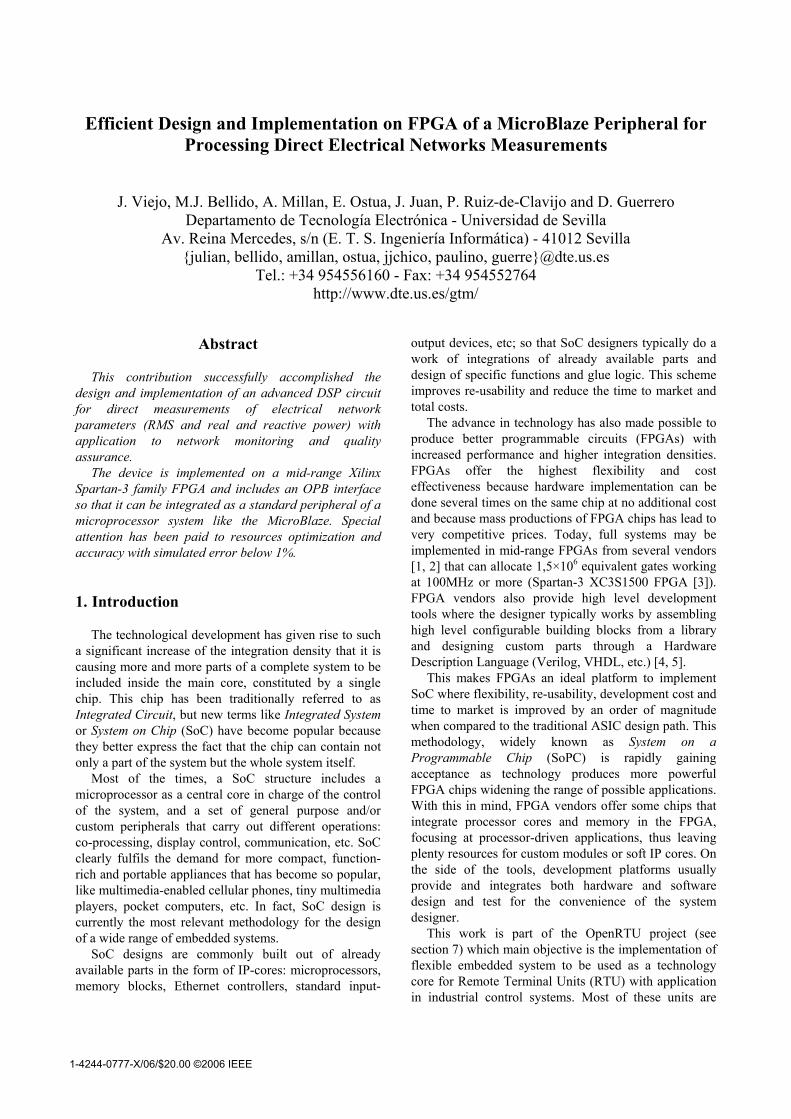
System Generator for DSP is a software platform, integrated within MATLAB and Simulink [8] tools from The MathWorks, that allows for the design of DSP systems using The Xilinx BlockSet [9, 10]. System Generator also handles the automatic generation of peripherals for MicroBlaze [11], synthesizable on Xilinx FPGAs. The typical methodology for digital system design has been followed, based on a control unit implemented in VHDL code and a data path built out of System Generator´s building blocks. The different tools used in the methodology followed for the design of the DSP peripheral are shown in Fig. 1. Most of the system simulation is carried out using Simulink; however, Mentor Graphics tool ModelSim [12] has been used to simulate VHDL code (HDL Co-simulation). Synthesis and implementation of the system on FPGA have been done using the Xilinx Platform Studio for embedded systems (XPS) integrated within the Embedded Development Kit (EDK).
Fig. 1: Environment and tools used.
3. System specifications
With regard to the specifications, the designed DSP peripheral carries out digital processing tasks on eight analog inputs (AI) which are acquired through an external Analog Front-End (AFE). These signals come from a system of three-phase measurement transformers (voltages and/or currents in power lines: R, S, T phases and neuter).
The eight analog inputs are subjected to a series of configurable treatments. Different sampling frequencies, gain control or offset elimination can be configured. Different sampling rates are determined by two setup bits: TADC and C50/60, so that it is possible to sample at 64 or 128 samples by cycle of the electrical signal; this is equivalent to sampling frequencies of 3200 Hz (64 s/c) or 6400 Hz (128 s/c) for 50 Hz input signals and of 3840 Hz (64 s/c) or 7680 Hz (128 s/c) for 60 Hz input signals.
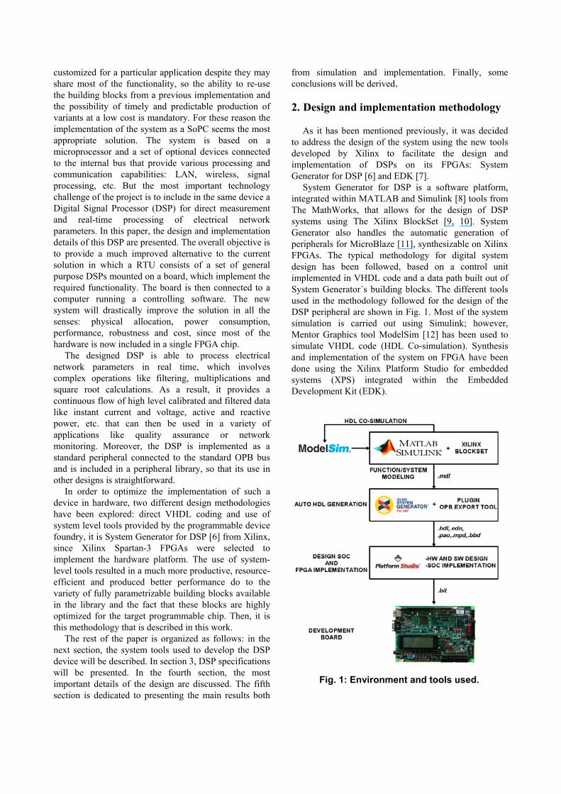
A diagram of the modules that form the DSP peripheral is shown in Fig. 2. We can clearly distinguish three parts: AFE Interface, OPB Interface and Direct Measurements Processing. Next, we will briefly explain the functionality of each one of these subsystems.
The AFE Interface module carries out the two following functions: A/D Conversion Control that is in charge of controlling the sampling frequency of the external ADC converters and capturing the digitized analog inputs, coming from these converters; and Gain Control applies to each analog input.
The OPB Interface module establishes the connection of the peripheral with the On-chip Peripheral Bus (OPB), allowing the communication and the interchange of information between MicroBlaze and the designed DSP. MicroBlaze and the AI peripheral exchange information in two ways: sending of configuration parameters from MicroBlaze to the peripheral (write operation of the setup registers) and relay of calculated data from the peripheral to MicroBlaze (read operation of the calculated parameters). Configuration parameters that this peripheral handles refer to control registers and calibration factors.
Fig. 2: DSP peripheral designed.
The Direct Measurements Processing module is in charge of processing the signals acquired by the A/D conversion module. The group of subsystems that form this module are: FIR filter, offset control, instantaneous values, average and calibration.
The FIR filter module filters the eight analog inputs. Specifically, the implemented filter is a linear low-pass FIR filter that eliminates high-frequency components.
The offset control function calculates the DC component of each filtered signal using the following equation:
( ) ( )∑−
=
−=1
000
1 N
nii nnx
NnDC (1)
where DCi(n0) is the offset value calculated in the instant for the input signal i, N is the number of samples by cycle and xi is the filtered input signal i.
These calculated data will be used in the instantaneous values subsystem. The instantaneous values subsystem calculates root mean square values (RMS) and real and reactive power associated to each analog input. RMS values are calculated as follows:
( )( )
( )02
1
00
2
0 nDCN
nnxnX i
N
ni
RMSi −
−
=∑−
= (2)
where XiRMS(n0) is the RMS value of the input signal i
in the instant n0. Real (Pi,j(n0)) and reactive (Qi,j(n0)) power are given
by:
( ) ( ) ( )nnxnnxN
nP j
N
niji −×−= ∑
−
=0
1
000,
1 (3)
( ) ( )∑−
=
−−×−=
1
0 mod000, 4
31 N
n Njiji nNnxnnx
NnQ (4)
where i,j indexes are selected so that xi and xj correspond to voltage and current signals of the same phase, respectively.
Finally, AC power can be obtained by subtracting the DC component:
( ) ( ) ( ) ( )000,0, nDCnDCnPnP jijiacji ×−= (5)
( ) ( ) ( ) ( )000,0, nDCnDCnQnQ jijiac
ji ×−= (6)Parameters calculated by the two previous subsystems
are average values, the average period being one cycle of the electrical signal. For the estimation of reactive power the approximation that the input signal is sinusoidal and stationary has been used, so that the derivative of the current signal is the same signal shifted 3N/4 samples.
The purpose of the average modules is to calculate the average of instantaneous values over a number of signal cycles determined by the NCP configuration parameter.
Finally, the average instantaneous parameters must be calibrated. The calibration subsystem does two
operations: the first one is the correction of distortions of the board and the second one is the correction of external distortions. Calibration parameters are available through configuration registers. Calibrated average values are made available to the MicroBlaze processor through the OPB interface as depicted in Fig. 2.
4. System design and implementation
In this section, the most important aspects of design and implementation are commented.
The AFE Interface subsystem has been designed according to the datasheets of the external systems we have to interface to, AD7656 converter [13] and AD5233 digital potentiometer [14], by using a VHDL behavioral description. The OPB Interface has been modeled using the Xilinx BlockSet, just as it is described in [11].
To design the Direct Measurements Processing subsystem, we have modeled a data path using System Generator blocks, together with a VHDL control unit that is in charge of controlling the processing of the eight analog inputs.
In the design of this DSP peripheral, a great effort has been made to optimize both FPGA resources and operation frequency.
In order to optimize resources, it has been taken advantage of the fact that operation frequency is much higher than AI sampling frequency (75-100MHz versus 3200-7680Hz). This feature allows us to have a lot of clock cycles at our disposal between two consecutive captures.
Fig. 3: Processing algorithm.
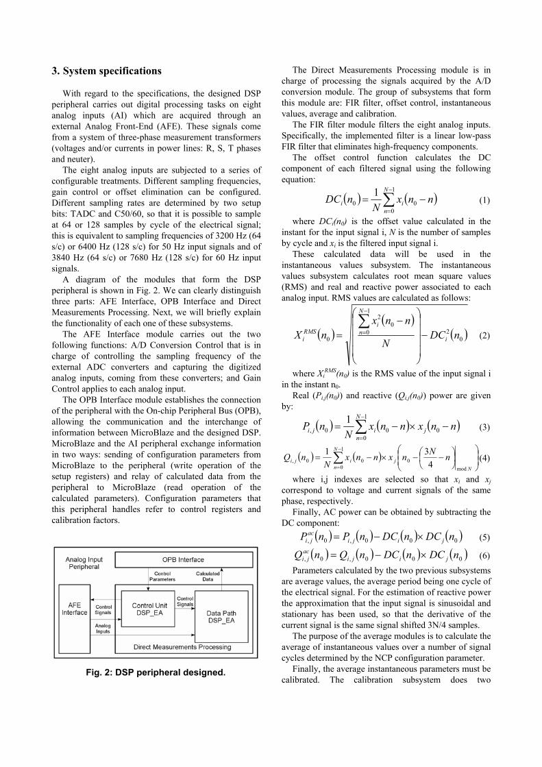
Thus, the suggested approach consists on designing a data path that uses the same processing elements for every input (multipliers, adders, etc.) in series. The control unit is in charge of arbitrating the processing, establishing the input that is processed in each moment. A general algorithm of the functionality that implements the control unit is shown in Fig. 3.
In this behavioral description, two counters have been declared: samples and average_cycles which will count the number of processed samples and average cycles, respectively, and two registers: limit_samples and limit_average_cycles. The first one will be initiated to 64 or 128 samples according to the TADC bit, and the second to 2NCP. Moreover, a set of accumulators have been defined: ACDC, ACRMS, ACP and ACQ. These accumulators will store the average values of the functions: offset control (7), RMS value (8), real power (9) and reactive power (10).
( ) ( )∑−
=
−=1
000
N
niDC nnxnAC (7)
( ) ( )∑−
=
−=1
00
20
N
niRMS nnxnAC (8)
( ) ( ) ( )nnxnnxnAC j
N
niP −×−=∑
−
=0
1
000 (9)
( ) ( )∑−
=
−−×−=
1
0 mod000 4
3N
n NjiQ nNnxnnxnAC (10)
In the following lines, the most outstanding implementation details will be commented.
First, FIR filter design and coefficient calculation have been carried out using FDATool, a MATLAB package [10]. FDATool features an advanced interface that allows the design to define filter type, filter order, pass and stop frequencies, passband ripple, stopband attenuation, etc. The System Generator FIR block has been used for the filter implementation, providing a great variety of implementation options: filter coefficients (those generated by FDATool), number of bits per coefficient (16 bits), entry number of channels (eight channels), processing type (serial input) and latency (10 cycles).
In order to implement offset control, RMS, real and reactive power subsystems, a data path where all inputs share the same resources has been modeled. Thus, multiplexing logic has been added to select the input channel that will be processed.
System Generator´s CORDIC SQRT block has been used to implement square root operation. This block has been modified so that negative inputs produce zero as result, which is part of the system specifications.
System Generator facilitates DSP design and verification [10], reducing the design time and simplifying the exploration of the design space. Therefore, the challenge is to improve hardware area and
ACDC=0, ACRMS=0, ACP=0, ACQ=0. for each sampling period do capture_and_filter_analog_inputs(); process_analog_inputs(); update_accumulators(ACDC, ACRMS, ACP, ACQ); if(samples=limit_samples-1) then --One electrical signal cycle has been processed calculate_instantaneous_values(); average_instantaneous_values(); if(average_cycles=limit_average_cycles-1) then --2NCP cycles have been processed
calibrate_instantaneous_values(); average_cycles=0; else average_cycles=average_cycles+1; end if;
samples=0; else samples=samples+1; end if;
end for each;
speed while producing acceptable results. To do this, as well as optimizing the hardware architecture to suit the ideal algorithm [15], a number of options are available: using on-chip resources (embedded multipliers, BRAMs, etc.) and configuring System Generator blocks [9, 10]: arithmetic type, precision, latency, overflow, quantization, etc. By using these options the system functional behavior is not affected only the precision and overall performance.
Taking account of these two last alternatives, two versions of the peripheral have been developed: 1.0 and 1.2. In the first version, all intermediate operations are carried out using 32 bits fixed-point arithmetic. In version 1.2, the design has been modeled using 16 bits fixed-point arithmetic. Besides, operations which produce 32 bits results are rounded to 16 bits.
System Generator´s blocks may also be configured for frequency optimization, by adding pipeline stages and latency in the different data path components: multipliers, adders, etc. However, these modifications affect the system behavior, making it necessary to modify the control unit so that it behaves properly.
Once system requirements are fulfilled and checked by simulation at the block level, the two versions of the DSP peripheral are generated and imported into an EDK project for later integration with the MicroBlaze processor provided by Xilinx. OPB_Export_Tool [11] carries out these tasks.
5. Results
In this section, simulation and hardware implementation results are described in some detail.
5.1. Simulation results To check that the design fulfills the specifications
Simulink and ModelSim tools have been used together (HDL Co-simulation) for system simulation. This kind of simulation is mandatory in order to take account of blocks that are only available as black boxes.
A wide range of system configurations have been simulated: different sampling rates, NCP, amplitudes, offset, etc., getting a correct operation in all the cases.
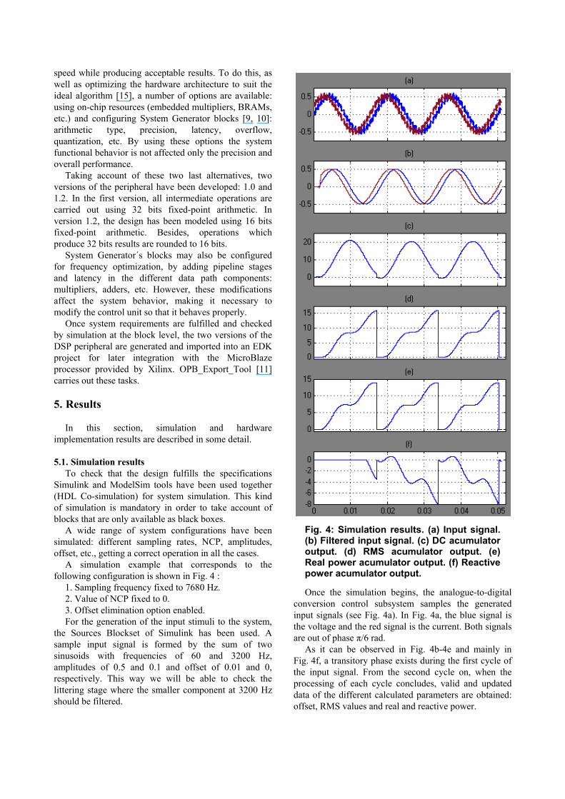
A simulation example that corresponds to the following configuration is shown in Fig. 4 :
1. Sampling frequency fixed to 7680 Hz. 2. Value of NCP fixed to 0. 3. Offset elimination option enabled. For the generation of the input stimuli to the system,
the Sources Blockset of Simulink has been used. A sample input signal is formed by the sum of two sinusoids with frequencies of 60 and 3200 Hz, amplitudes of 0.5 and 0.1 and offset of 0.01 and 0, respectively. This way we will be able to check the littering stage where the smaller component at 3200 Hz should be filtered.
Fig. 4: Simulation results. (a) Input signal. (b) Filtered input signal. (c) DC acumulator output. (d) RMS acumulator output. (e) Real power acumulator output. (f) Reactive power acumulator output.
Once the simulation begins, the analogue-to-digital conversion control subsystem samples the generated input signals (see Fig. 4a). In Fig. 4a, the blue signal is the voltage and the red signal is the current. Both signals are out of phase π/6 rad.
As it can be observed in Fig. 4b-4e and mainly in Fig. 4f, a transitory phase exists during the first cycle of the input signal. From the second cycle on, when the processing of each cycle concludes, valid and updated data of the different calculated parameters are obtained: offset, RMS values and real and reactive power.
DSP (v.1.0)
DSP (v.1.2)
Theoretical value
RMS value 0.3571 0.3571 0.35355
Real power 0.1084 0.1084 0.10825
Reactive power -0.0626 -0.0626 -0.0625
Table 1: Simulation results.
For the offset and RMS values calculation the filtered signal is used (Fig. 4b). The signals in Fig. 4c-4f show the outputs of the accumulators ACDC, ACRMS, ACP and ACQ, respectively, which store inter-cycle transitory values of the parameters being processed. When a cycle of the input signal is completed, the accumulated values in that instant are used to calculate the offset, the RMS value and real and reactive power corresponding to that cycle, according to equations (1) to (6).
In Table 1 the obtained simulation results are shown for each implemented peripheral, as well as the theoretical values calculated for those functions. Comparing the results obtained by the peripherals we realize that they are identical. Accuracy of both DSP implementations for RMS values calculated are typically under 1% of the exact theoretical value whereas accuracy for real and reactive power are under 1‰.
5.2. Hardware implementation results In order to compare the implementations of the two
versions of the peripheral, they have been synthesized separately using XPS from Xilinx [7]. Some figures of merit will be analyzed in this section: used hardware resources and maximum frequency of operation.
Both designs have been implemented on a Spartan-3 XC3S1500 FPGA. These devices have all the features required for efficiently implementing DSP functions: Embedded 18x18 Multipliers, Distributed RAM, Shift Register Logic, etc [15]. In short, these features allow for the implementation of high-performance DSP functions in a small fraction of the total device. XC3S1500 device features about 1,5×10⁶ equivalent gates, 32 multipliers and 32 BRAM and is in the moderate to low capacity range of the Spartan-3 family.
The hardware implementation results show that the version 1.0 of the peripheral occupies 5181 slices (38% of a XC3S1500 FPGA) and 6 embedded multipliers whereas the version 1.2 only uses 4232 slices (31%) and half of the embedded multipliers, leaving plenty of available resources for implementing the MicroBlaze processor and additional circuitry (see Table 2).
Finally, we observe that frequency optimization have provided a maximum frequency of 110.461MHz which easily meet the initial 75-100 MHz requirements.
6. Conclusions
An advanced DSP for direct electrical measurements has been successfully designed and implemented on a Xilinx Spartan-3 FPGA. The DSP takes the form of a standard OPB peripheral so that it can be managed by a system processor implemented in the same FPGA like the MicroBlaze provided by Xilinx. The device is able to monitor eight analog input signals and calculate offset, root mean square and real and reactive powers from the inputs in every signal cycle, thus providing the basic data to determine the quality of the electrical network.
Different design alternatives have been tried out in order to optimize available resources and meet frequency requirements. As a result, the implemented device easily exceeds the required operation frequency and accuracy while only consuming 30% of the available resources of a XC3S1500 Xilinx FPGA chip.
We can also conclude that state-of-the-art FPGAs are ready to be used for advanced DSP design, taking advantage of a variety of tools and integrated design environments that automate the most tedious design tasks, allowing the designer to focus on architecture and specifications and facilitating the exploration of the design space in search of an optimal solution.
7. Acknowledgment
This work has been partially supported by the PROFIT-MITC OPENRTU FIT-330101-2004-5 and MYCT MEC META TEC 2004-00840/MIC projects of the Spanish Government and the CICE OFU TIC 1023 project of the Andalusian Government.
References
[1] “Altera Website.” http://www.altera.com/. [2] “Xilinx Website.” http://www.xilinx.com/. [3] “Spartan-3 FPGA Family: Complete Data Sheet.”
http://www.xilinx.com/bvdocs/publications/ds099.pdf. [4] W. F. Lee, Verilog Coding for Logic Synthesis, John
Wiley & Sons Inc., ISBN 0-471-42976-7, 2003. [5] B. Cohen, VHDL Coding Styles and Methodologies, 2nd
Edition, Kluber Academic Publishers, ISBN 0-7923-8474-1, 1999.
[6] Xilinx Inc., Xilinx System Generator for DSP v8.1 User’s Guide, April 25, 2006.
DSP (v.1.0) DSP (v.1.2) Slices 5181 (38%) 4232 (31%) MULT18X18s 6 (18%) 3 (9%)
RAMB16s 5 (15%) 5 (15%)
Max. Freq. 110.461 MHz
Table 2: Hardware implementation results.
http://www.xilinx.com/support/sw_manuals/sysgen_ug.pdf
[7] Xilinx Inc., Platform Studio User Guide, Embedded Development Kit EDK 7.1i, February 15, 2005. http://www.xilinx.com/ise/embedded/edk7_1docs/ps_ug.pdf.
[8] “Simulink® - Simulation and Model-Based Design.” http://www.mathworks.com/products/simulink/.
[9] Robert D. Turney, Chris Dick, David B. Parlour, and James Hwang, “Modeling and Implementation of DSP FPGA Solutions”, International Conference on Signal Processing Applications and Technology, ICSPAT'99, Orlando, November 1-4, 1999. http://www.xilinx.com/products/logicore/dsp/matlab_final.pdf
[10] J. Hwang, B. Milne, N. Shirazi, J. Stroomer, “System Level Tools for DSP in FPGAs”, Field-Programmable Logic and Applications - 11th International Conference, FPL 2001, Belfast, Northern Ireland, UK, August 27-29, 2001.
http://www.xilinx.com/products/logicore/dsp/sysgen_fpl2001.pdf
[11] J. Ballagh, J. Hwang, P. James-Roxby, E. Keller, S. Seng and B. Taylor, “Building OPB Slave Peripherals using System Generator for DSP”, Xilinx Inc., 2004. http://www.xilinx.com/bvdocs/appnotes/xapp264.zip.
[12] “The Mentor Graphics Website.” http://www.model.com/.
[13] Analog Devices Inc., “250 kSPS, 6-Channel, Simultaneous Sampling, Bipolar 12/14/16-Bit ADC”, 2005. http://www.analog.com/UploadedFiles/Data_Sheets/88119461AD7656_7_8_prl.pdf.
[14] Analog Devices Inc., “Nonvolatile Memory, Quad 64-Position Digital Potentiometer”, 2005. http://www.analog.com/UploadedFiles/Data_Sheets/112773373AD5233_a.pdf.
[15] S. Zack and S. Dhanani, “DSP Co-Processing in FPGAs: Embedding High-Performance, Low-Cost DSP Functions”, Xilinx Inc., March 18, 2004. http://www.xilinx.com/bvdocs/whitepapers/wp212.pdf