
Advanced FPGA Design
355
-
Upload
khangminh22 -
Category
Documents
-
view
3 -
download
0
Transcript of Advanced FPGA Design


Advanced FPGADesignArchitecture, Implementation,and Optimization
Steve KiltsSpectrum Design Solutions
Minneapolis, Minnesota


Advanced FPGA
Design


Advanced FPGADesignArchitecture, Implementation,and Optimization
Steve KiltsSpectrum Design Solutions
Minneapolis, Minnesota

Copyright # 2007 by John Wiley & Sons, Inc. All rights reserved.
Published by John Wiley & Sons, Inc., Hoboken, New Jersey.
Published simultaneously in Canada.
No part of this publication may be reproduced, stored in a retrieval system, or transmitted in any
form or by any means, electronic, mechanical, photocopying, recording, scanning, or otherwise,
except as permitted under Section 107 or 108 of the 1976 United States Copyright Act, without
either the prior written permission of the Publisher, or authorization through payment of the
appropriate per-copy fee to the Copyright Clearance Center, Inc., 222 Rosewood Drive, Danvers,
MA 01923, 978-750-8400, fax 978-646-8600, or on the web at www.copyright.com.
Requests to the Publisher for permission should be addressed to the Permissions Department,
John Wiley & Sons, Inc., 111 River Street, Hoboken, NJ 07030, (201) 748-6011,
fax (201) 748-6008.
Limit of Liability/Disclaimer of Warranty: While the publisher and author have used their best
efforts in preparing this book, they make no representations or warranties with respect to
the accuracy or completeness of the contents of this book and specifically disclaim any implied
warranties of merchantability or fitness for a particular purpose. No warranty may be created
or extended by sales representatives or written sales materials. The advice and strategies contained
herein may not be suitable for your situation. You should consult with a professional where
appropriate. Neither the publisher nor author shall be liable for any loss of profit or any
other commercial damages, including but not limited to special, incidental, consequential,
or other damages.
For general information on our other products and services please contact our Customer Care
Department within the U.S. at 877-762-2974, outside the U.S. at 317-572-3993 or
fax 317-572-4002.
Wiley also publishes its books in a variety of electronic formats. Some content that appears in print,
however, may not be available in electronic format.
Library of Congress Cataloging-in-Publication Data
Kilts, Steve, 1978-
Advanced FPGA design: Architecture, Implementation, and Optimization/by Steve Kilts.
p. cm.
Includes index.
ISBN 978-0-470-05437-6 (cloth)
1. Field programmable gate arrays- -Design and construction.
I. Title.
TK7895.G36K55 2007
621.3905- -dc22
2006033573
Printed in the United States of America
10 9 8 7 6 5 4 3 2 1

To my wife, Teri, who felt that the
subject matter was rather dry

Flowchart of Contents

Contents
Preface xiii
Acknowledgments xv
1. Architecting Speed 1
1.1 High Throughput 2
1.2 Low Latency 4
1.3 Timing 6
1.3.1 Add Register Layers 6
1.3.2 Parallel Structures 8
1.3.3 Flatten Logic Structures 10
1.3.4 Register Balancing 12
1.3.5 Reorder Paths 14
1.4 Summary of Key Points 16
2. Architecting Area 17
2.1 Rolling Up the Pipeline 18
2.2 Control-Based Logic Reuse 20
2.3 Resource Sharing 23
2.4 Impact of Reset on Area 25
2.4.1 Resources Without Reset 25
2.4.2 Resources Without Set 26
2.4.3 Resources Without Asynchronous Reset 27
2.4.4 Resetting RAM 29
2.4.5 Utilizing Set/Reset Flip-Flop Pins 31
2.5 Summary of Key Points 34
3. Architecting Power 37
3.1 Clock Control 38
3.1.1 Clock Skew 39
3.1.2 Managing Skew 40
vii

3.2 Input Control 42
3.3 Reducing the Voltage Supply 44
3.4 Dual-Edge Triggered Flip-Flops 44
3.5 Modifying Terminations 45
3.6 Summary of Key Points 46
4. Example Design: The Advanced Encryption Standard 47
4.1 AES Architectures 47
4.1.1 One Stage for Sub-bytes 51
4.1.2 Zero Stages for Shift Rows 51
4.1.3 Two Pipeline Stages for Mix-Column 52
4.1.4 One Stage for Add Round Key 52
4.1.5 Compact Architecture 53
4.1.6 Partially Pipelined Architecture 57
4.1.7 Fully Pipelined Architecture 60
4.2 Performance Versus Area 66
4.3 Other Optimizations 67
5. High-Level Design 69
5.1 Abstract Design Techniques 69
5.2 Graphical State Machines 70
5.3 DSP Design 75
5.4 Software/Hardware Codesign 80
5.5 Summary of Key Points 81
6. Clock Domains 83
6.1 Crossing Clock Domains 84
6.1.1 Metastability 86
6.1.2 Solution 1: Phase Control 88
6.1.3 Solution 2: Double Flopping 89
6.1.4 Solution 3: FIFO Structure 92
6.1.5 Partitioning Synchronizer Blocks 97
6.2 Gated Clocks in ASIC Prototypes 97
6.2.1 Clocks Module 98
6.2.2 Gating Removal 99
6.3 Summary of Key Points 100
7. Example Design: I2S Versus SPDIF 101
7.1 I2S 101
7.1.1 Protocol 102
7.1.2 Hardware Architecture 102
viii Contents

7.1.3 Analysis 105
7.2 SPDIF 107
7.2.1 Protocol 107
7.2.2 Hardware Architecture 108
7.2.3 Analysis 114
8. Implementing Math Functions 117
8.1 Hardware Division 117
8.1.1 Multiply and Shift 118
8.1.2 Iterative Division 119
8.1.3 The Goldschmidt Method 120
8.2 Taylor and Maclaurin Series Expansion 122
8.3 The CORDIC Algorithm 124
8.4 Summary of Key Points 126
9. Example Design: Floating-Point Unit 127
9.1 Floating-Point Formats 127
9.2 Pipelined Architecture 128
9.2.1 Verilog Implementation 131
9.2.2 Resources and Performance 137
10. Reset Circuits 139
10.1 Asynchronous Versus Synchronous 140
10.1.1 Problems with Fully Asynchronous Resets 140
10.1.2 Fully Synchronized Resets 142
10.1.3 Asynchronous Assertion, Synchronous Deassertion 144
10.2 Mixing Reset Types 145
10.2.1 Nonresetable Flip-Flops 145
10.2.2 Internally Generated Resets 146
10.3 Multiple Clock Domains 148
10.4 Summary of Key Points 149
11. Advanced Simulation 151
11.1 Testbench Architecture 152
11.1.1 Testbench Components 152
11.1.2 Testbench Flow 153
11.1.2.1 Main Thread 153
11.1.2.2 Clocks and Resets 154
11.1.2.3 Test Cases 155
Contents ix

11.2 System Stimulus 157
11.2.1 MATLAB 157
11.2.2 Bus-Functional Models 158
11.3 Code Coverage 159
11.4 Gate-Level Simulations 159
11.5 Toggle Coverage 162
11.6 Run-Time Traps 165
11.6.1 Timescale 165
11.6.2 Glitch Rejection 165
11.6.3 Combinatorial Delay Modeling 166
11.7 Summary of Key Points 169
12. Coding for Synthesis 171
12.1 Decision Trees 172
12.1.1 Priority Versus Parallel 172
12.1.2 Full Conditions 176
12.1.3 Multiple Control Branches 179
12.2 Traps 180
12.2.1 Blocking Versus Nonblocking 180
12.2.2 For-Loops 183
12.2.3 Combinatorial Loops 185
12.2.4 Inferred Latches 187
12.3 Design Organization 188
12.3.1 Partitioning 188
12.3.1.1 Data Path Versus Control 188
12.3.1.2 Clock and Reset Structures 189
12.3.1.3 Multiple Instantiations 190
12.3.2 Parameterization 191
12.3.2.1 Definitions 191
12.3.2.2 Parameters 192
12.3.2.3 Parameters in Verilog-2001 194
12.4 Summary of Key Points 195
13. Example Design: The Secure Hash Algorithm 197
13.1 SHA-1 Architecture 197
13.2 Implementation Results 204
14. Synthesis Optimization 205
14.1 Speed Versus Area 206
14.2 Resource Sharing 208
x Contents

14.3 Pipelining, Retiming, and Register Balancing 211
14.3.1 The Effect of Reset on Register Balancing 213
14.3.2 Resynchronization Registers 215
14.4 FSM Compilation 216
14.4.1 Removal of Unreachable States 219
14.5 Black Boxes 220
14.6 Physical Synthesis 223
14.6.1 Forward Annotation Versus Back-Annotation 224
14.6.2 Graph-Based Physical Synthesis 225
14.7 Summary of Key Points 226
15. Floorplanning 229
15.1 Design Partitioning 229
15.2 Critical-Path Floorplanning 232
15.3 Floorplanning Dangers 233
15.4 Optimal Floorplanning 234
15.4.1 Data Path 234
15.4.2 High Fan-Out 234
15.4.3 Device Structure 235
15.4.4 Reusability 238
15.5 Reducing Power Dissipation 238
15.6 Summary of Key Points 240
16. Place and Route Optimization 241
16.1 Optimal Constraints 241
16.2 Relationship between Placementand Routing 244
16.3 Logic Replication 246
16.4 Optimization across Hierarchy 247
16.5 I/O Registers 248
16.6 Pack Factor 250
16.7 Mapping Logic into RAM 251
16.8 Register Ordering 251
16.9 Placement Seed 252
16.10 Guided Place and Route 254
16.11 Summary of Key Points 254
17. Example Design: Microprocessor 257
17.1 SRC Architecture 257
17.2 Synthesis Optimizations 259
17.2.1 Speed Versus Area 260
Contents xi

17.2.2 Pipelining 261
17.2.3 Physical Synthesis 262
17.3 Floorplan Optimizations 262
17.3.1 Partitioned Floorplan 263
17.3.2 Critical-Path Floorplan: Abstraction 1 264
17.3.3 Critical-Path Floorplan: Abstraction 2 265
18. Static Timing Analysis 269
18.1 Standard Analysis 269
18.2 Latches 273
18.3 Asynchronous Circuits 276
18.3.1 Combinatorial Feedback 277
18.4 Summary of Key Points 278
19. PCB Issues 279
19.1 Power Supply 279
19.1.1 Supply Requirements 279
19.1.2 Regulation 283
19.2 Decoupling Capacitors 283
19.2.1 Concept 283
19.2.2 Calculating Values 285
19.2.3 Capacitor Placement 286
19.3 Summary of Key Points 288
Appendix A 289
Appendix B 303
Bibliography 319
Index 321
xii Contents

Preface
In the design-consulting business, I have been exposed to countless FPGA(Field Programmable Gate Array) designs, methodologies, and design tech-niques. Whether my client is on the Fortune 100 list or is just a start-upcompany, they will inevitably do some things right and many things wrong.After having been exposed to a wide variety of designs in a wide range ofindustries, I began developing my own arsenal of techniques and heuristicsfrom the combined knowledge of these experiences. When mentoring newFPGA design engineers, I draw my suggestions and recommendations fromthis experience. Up until now, many of these recommendations have refer-enced specific white papers and application notes (appnotes) that discussspecific practical aspects of FPGA design. The purpose of this book is to con-dense years of experience spread across numerous companies and teams ofengineers, as well as much of the wisdom gathered from technology-specificwhite papers and appnotes, into a single book that can be used to refine adesigner’s knowledge and aid in becoming an advanced FPGA designer.
There are a number of books on FPGA design, but few of these truly address
advanced real-world topics in detail. This book attempts to cut out the fat of
unnecessary theory, speculation on future technologies, and the details of outdated
technologies. It is written in a terse, concise format that addresses the various
topics without wasting the reader’s time. Many sections in this book assume that
certain fundamentals are understood, and for the sake of brevity, background
information and/or theoretical frameworks are not always covered in detail.
Instead, this book covers in-depth topics that have been encountered in real-world
designs. In some ways, this book replaces a limited amount of industry experience
and access to an experienced mentor and will hopefully prevent the reader from
learning a few things the hard way. It is the advanced, practical approach that
makes this book unique.
One thing to note about this book is that it will not flow from cover to cover
like a novel. For a set of advanced topics that are not intrinsically tied to one
another, this type of flow is impossible without blatantly filling it with fluff.
Instead, to organize this book, I have ordered the chapters in such a way that they
follow a typical design flow. The first chapters discuss architecture, then simu-
lation, then synthesis, then floorplanning, and so on. This is illustrated in the
Flowchart of Contents provided at the beginning of the book. To provide
xiii

accessibility for future reference, the chapters are listed side-by-side with the
relevant block in the flow diagram.
The remaining chapters in this book are heavy with examples. For brevity, I
have selected Verilog as the default HDL (Hardware Description Language).
Xilinx as the default FPGA vendor, and Synplicity as the default synthesis and
floorplanning tool. Most of the topics covered in this book can easily be mapped
to VHDL, Altera, Mentor Graphics, and so forth, but to include all of these
for completeness would only serve to cloud the important points. Even if the
reader of this book uses these other technologies, this book will still deliver its
value. If you have any feedback, good or bad, feel free to email me at
STEVE KILTS
Minneapolis, Minnesota
March 2007
xiv Preface

Acknowledgments
During the course of my career, I have had the privilege to work with many
excellent digital design engineers. My exposure to these talented engineers began
at Medtronic and continued over the years through my work as a consultant for
companies such as Honeywell, Guidant, Teradyne, Telex, Unisys, AMD, ADC,
and a number of smaller/start-up companies involved with a wide variety of
FPGA applications. I also owe much of my knowledge to the appnotes and white
papers published by the major FPGA vendors. These resources contain invaluable
real-world heuristics that are not included in a standard engineering curriculum.
Specific to this book, I owe a great deal to Xilinx and Synplicity, both of
which provided the FPGA design tools used throughout the book, as well as a
number of key reviewers. Reviewers of note also include Peter Calabrese of
Synplicity, Cliff Cummins of Sunburst Design, Pete Danile of Synplicity, Anders
Enggaard of Axcon, Mike Fette of Spectrum Design Solutions, Philip Freidin of
Fliptronics, Paul Fuchs of NuHorizons, Don Hodapp of Xilinx, Ashok Kulkarni of
Synplicity, Rod Landers of Spectrum Design Solutions, Ryan Link of Logic,
Dave Matthews of Verein, Lance Roman of Roman-Jones, B. Joshua Rosen of
Polybus, Gary Stevens of iSine, Jim Torgerson, and Larry Weegman of Xilinx.
S.K.
xv


Chapter 1
Architecting Speed
Sophisticated tool optimizations are often not good enough to meet most design
constraints if an arbitrary coding style is used. This chapter discusses the first of
three primary physical characteristics of a digital design: speed. This chapter also
discusses methods for architectural optimization in an FPGA.
There are three primary definitions of speed depending on the context of the
problem: throughput, latency, and timing. In the context of processing data in an
FPGA, throughput refers to the amount of data that is processed per clock cycle.
A common metric for throughput is bits per second. Latency refers to the time
between data input and processed data output. The typical metric for latency will
be time or clock cycles. Timing refers to the logic delays between sequential
elements. When we say a design does not “meet timing,” we mean that the delay
of the critical path, that is, the largest delay between flip-flops (composed of
combinatorial delay, clk-to-out delay, routing delay, setup timing, clock skew,
and so on) is greater than the target clock period. The standard metrics for timing
are clock period and frequency.
During the course of this chapter, we will discuss the following topics in detail:
. High-throughput architectures for maximizing the number of bits per
second that can be processed by the design.
. Low-latency architectures for minimizing the delay from the input of a
module to the output.
. Timing optimizations to reduce the combinatorial delay of the critical path.
Adding register layers to divide combinatorial logic structures.
Parallel structures for separating sequentially executed operations into
parallel operations.
Flattening logic structures specific to priority encoded signals.
Register balancing to redistribute combinatorial logic around pipelined
registers.
Reordering paths to divert operations in a critical path to a noncritical path.
1
Advanced FPGA Design. By Steve KiltsCopyright # 2007 John Wiley & Sons, Inc.

1.1 HIGH THROUGHPUT
A high-throughput design is one that is concerned with the steady-state data rate
but less concerned about the time any specific piece of data requires to propagate
through the design (latency). The idea with a high-throughput design is the same
idea Ford came up with to manufacture automobiles in great quantities: an assem-
bly line. In the world of digital design where data is processed, we refer to this
under a more abstract term: pipeline.
A pipelined design conceptually works very similar to an assembly line in
that the raw material or data input enters the front end, is passed through various
stages of manipulation and processing, and then exits as a finished product or data
output. The beauty of a pipelined design is that new data can begin processing
before the prior data has finished, much like cars are processed on an assembly
line. Pipelines are used in nearly all very-high-performance devices, and the
variety of specific architectures is unlimited. Examples include CPU instruction
sets, network protocol stacks, encryption engines, and so on.
From an algorithmic perspective, an important concept in a pipelined design
is that of “unrolling the loop.” As an example, consider the following piece of
code that would most likely be used in a software implementation for finding the
third power of X. Note that the term “software” here refers to code that is targeted
at a set of procedural instructions that will be executed on a microprocessor.
XPower = 1;for (i=0;i < 3; i++)
XPower = X * XPower;
Note that the above code is an iterative algorithm. The same variables and
addresses are accessed until the computation is complete. There is no use for par-
allelism because a microprocessor only executes one instruction at a time (for the
purpose of argument, just consider a single core processor). A similar implemen-
tation can be created in hardware. Consider the following Verilog implementation
of the same algorithm (output scaling not considered):
module power3(output [7:0] XPower,output finished,input [7:0] X,input clk, start); // the duration of start is a
single clockreg [7:0] ncount;reg [7:0] XPower;
assign finished = (ncount == 0);
always@(posedge clk)if(start) begin
XPower <= X;ncount <= 2;
end
2 Chapter 1 Architecting Speed

else if(!finished) beginncount <= ncount - 1;XPower <= XPower * X;
endendmodule
In the above example, the same register and computational resources are reused
until the computation is finished as shown in Figure 1.1.
With this type of iterative implementation, no new computations can begin
until the previous computation has completed. This iterative scheme is very
similar to a software implementation. Also note that certain handshaking signals
are required to indicate the beginning and completion of a computation. An
external module must also use the handshaking to pass new data to the module
and receive a completed calculation. The performance of this implementation is
Throughput ¼ 8/3, or 2.7 bits/clock
Latency ¼ 3 clocks
Timing ¼ One multiplier delay in the critical path
Contrast this with a pipelined version of the same algorithm:
module power3(output reg [7:0] XPower,input clk,input [7:0] X);reg [7:0] XPower1, XPower2;reg [7:0] X1, X2;always @(posedge clk) begin
// Pipeline stage 1X1 <= X;XPower1 <= X;
// Pipeline stage 2X2 <= X1;XPower2 <= XPower1 * X1;
// Pipeline stage 3XPower <= XPower2 * X2;
endendmodule
Figure 1.1 Iterative implementation.
1.1 High Throughput 3
MC
文本方块
实际上流水线设计是牺牲资源换取通量(throughout)的方法,即在同一个时钟周期中尽可能多地对数据进行计算,以使得单位时间内可以得到更多的结果。

In the above implementation, the value of X is passed to both pipeline stages
where independent resources compute the corresponding multiply operation. Note
that while X is being used to calculate the final power of 3 in the second pipeline
stage, the next value of X can be sent to the first pipeline stage as shown in
Figure 1.2.
Both the final calculation of X3 (XPower3 resources) and the first calculation
of the next value of X (XPower2 resources) occur simultaneously. The perform-
ance of this design is
Throughput ¼ 8/1, or 8 bits/clock
Latency ¼ 3 clocks
Timing ¼ One multiplier delay in the critical path
The throughput performance increased by a factor of 3 over the iterative
implementation. In general, if an algorithm requiring n iterative loops is
“unrolled,” the pipelined implementation will exhibit a throughput performance
increase of a factor of n. There was no penalty in terms of latency as the pipelined
implementation still required 3 clocks to propagate the final computation. Like-
wise, there was no timing penalty as the critical path still contained only one
multiplier.
Unrolling an iterative loop increases throughput.
The penalty to pay for unrolling loops such as this is an increase in area. The
iterative implementation required a single register and multiplier (along with some
control logic not shown in the diagram), whereas the pipelined implementation
required a separate register for both X and XPower and a separate multiplier for
every pipeline stage. Optimizations for area are discussed in the Chapter 2.
The penalty for unrolling an iterative loop is a proportional increase in area.
1.2 LOW LATENCY
A low-latency design is one that passes the data from the input to the output as
quickly as possible by minimizing the intermediate processing delays. Oftentimes,
a low-latency design will require parallelisms, removal of pipelining, and logical
short cuts that may reduce the throughput or the max clock speed in a design.
Figure 1.2 Pipelined implementation.
4 Chapter 1 Architecting Speed
MC
高亮
MC
高亮
MC
文本方块
低时滞设计要求在一定的数据操作过程中尽量少的时钟周期,则与流水线将操作拆分到不同时钟周期中完成以达到同时处理多个数据的想法有冲突。
MC
高亮
MC
文本方块
由于要减少时滞(latency),则势必要在同一个时钟周期之间(寄存器之间)安排更多的逻辑电路,这样增加了时延,则降低了时钟的频率。

Referring back to our power-of-3 example, there is no obvious latency optim-
ization to be made to the iterative implementation as each successive multiply
operation must be registered for the next operation. The pipelined implemen-
tation, however, has a clear path to reducing latency. Note that at each pipeline
stage, the product of each multiply must wait until the next clock edge before it is
propagated to the next stage. By removing the pipeline registers, we can minimize
the input to output timing:
module power3(output [7:0] XPower,input [7:0] X);reg [7:0] XPower1, XPower2;reg [7:0] X1, X2;
assign XPower = XPower2 * X2;
always @* beginX1 = X;XPower1 = X;
end
always @* beginX2 = X1;XPower2 = XPower1*X1;
endendmodule
In the above example, the registers were stripped out of the pipeline. Each stage
is a combinatorial expression of the previous as shown in Figure 1.3.
The performance of this design is
Throughput ¼ 8 bits/clock (assuming one new input per clock)
Latency ¼ Between one and two multiplier delays, 0 clocks
Timing ¼ Two multiplier delays in the critical path
By removing the pipeline registers, we have reduced the latency of this design
below a single clock cycle.
Latency can be reduced by removing pipeline registers.
The penalty is clearly in the timing. Previous implementations could theoreti-
cally run the system clock period close to the delay of a single multiplier, but in the
Figure 1.3 Low-latency implementation.
1.2 Low Latency 5
MC
文本方块
这里assign后面的‘=’号左边不能是reg类型的变量;所以以下的XPower1、XPower2写法不一样。另外,作为always块里面的组合逻辑写法,用阻塞赋值语句而不用非阻塞赋值语句。

low-latency implementation, the clock period must be at least two multiplier delays
(depending on the implementation) plus any external logic in the critical path.
The penalty for removing pipeline registers is an increase in combinatorial delay
between registers.
1.3 TIMING
Timing refers to the clock speed of a design. The maximum delay between any
two sequential elements in a design will determine the max clock speed. The idea
of clock speed exists on a lower level of abstraction than the speed/area trade-offsdiscussed elsewhere in this chapter as clock speed in general is not directly
related to these topologies, although trade-offs within these architectures will cer-
tainly have an impact on timing. For example, one cannot know whether a pipe-
lined topology will run faster than an iterative without knowing the details of the
implementation. The maximum speed, or maximum frequency, can be defined
according to the straightforward and well-known maximum-frequency equation
(ignoring clock-to-clock jitter):
Equation 1.1 Maximum Frequency
Fmax ¼1
Tclk�q þ Tlog ic þ Trouting þ Tsetup � Tskew
(1:1)
where Fmax is maximum allowable frequency for clock; Tclk-q is time from clock
arrival until data arrives at Q; Tlogic is propagation delay through logic between
flip-flops; Trouting is routing delay between flip-flops; Tsetup is minimum time data
must arrive at D before the next rising edge of clock (setup time); and Tskew is
propagation delay of clock between the launch flip-flop and the capture flip-flop.
The next sections describes various methods and trade-offs required to
improve timing performance.
1.3.1 Add Register Layers
The first strategy for architectural timing improvements is to add intermediate
layers of registers to the critical path. This technique should be used in highly
pipelined designs where an additional clock cycle latency does not violate the
design specifications, and the overall functionality will not be affected by the
further addition of registers.
For instance, assume the architecture for the following FIR (Finite Impulse
Response) implementation does not meet timing:
module fir(output [7:0] Y,input [7:0] A, B, C, X,input clk,
6 Chapter 1 Architecting Speed
MC
高亮
MC
高亮

input validsample);reg [7:0] X1, X2, Y;
always @(posedge clk)if(validsample) begin
X1 <= X;X2 <= X1;Y <= A* X+B* X1+C* X2;
endendmodule
Architecturally, all multiply/add operations occur in one clock cycle as
shown in Figure 1.4.
In other words, the critical path of one multiplier and one adder is greater
than the minimum clock period requirement. Assuming the latency requirement is
not fixed at 1 clock, we can further pipeline this design by adding extra registers
intermediate to the multipliers. The first layer is easy: just add a pipeline layer
between the multipliers and the adder:
module fir(output [7:0] Y,input [7:0] A, B, C, X,input clk,input validsample);reg [7:0] X1, X2, Y;reg [7:0] prod1, prod2, prod3;
always @ (posedge clk) beginif(validsample) begin
X1 <= X;X2 <= X1;prod1 <= A * X;prod2 <= B * X1;prod3 <= C * X2;
end
Y <= prod1 + prod2 + prod3;end
endmodule
Figure 1.4 MAC with long path.
1.3 Timing 7

In the above example, the adder was separated from the multipliers with a pipe-
line stage as shown in Figure 1.5.
Multipliers are good candidates for pipelining because the calculations can
easily be broken up into stages. Additional pipelining is possible by breaking the
multipliers and adders up into stages that can be individually registered.
Adding register layers improves timing by dividing the critical path into two paths
of smaller delay.
Various implementations of these functions are covered in other chapters, but
once the architecture has been broken up into stages, additional pipelining is as
straightforward as the above example.
1.3.2 Parallel Structures
The second strategy for architectural timing improvements is to reorganize the
critical path such that logic structures are implemented in parallel. This technique
should be used whenever a function that currently evaluates through a serial
string of logic can be broken up and evaluated in parallel. For instance, assume
that the standard pipelined power-of-3 design discussed in previous sections does
not meet timing. To create parallel structures, we can break the multipliers into
independent operations and then recombine them. For instance, an 8-bit binary
multiplier can be represented by nibbles A and B:
X ¼ {A, B};
where A is the most significant nibble and B is the least significant:Because the multiplicand is equal to the multiplier in our power-of-3
example, the multiply operation can be reorganized as follows:
X � X ¼ {A, B} � {A, B} ¼ {(A � A), (2 � A � B), (B � B)};
This reduces our problem to a series of 4-bit multiplications and then recombining
the products. This can be implemented with the following module:
module power3(output [7:0] XPower,
Figure 1.5 Pipeline registers added.
8 Chapter 1 Architecting Speed
MC
高亮

input [7:0] X,input clk);reg [7:0] XPower1;// partial product registersreg [3:0] XPower2_ppAA, XPower2_ppAB, XPower2_ppBB;reg [3:0] XPower3_ppAA, XPower3_ppAB, XPower3_ppBB;reg [7:0] X1, X2;wire [7:0] XPower2;
// nibbles for partial products (A is MS nibble, B is LSnibble)
wire [3:0] XPower1_A = XPower1[7:4];wire [3:0] XPower1_B = XPower1[3:0];wire [3:0] X1_A = X1[7:4];wire [3:0] X1_B = X1[3:0];wire [3:0] XPower2_A = XPower2[7:4];wire [3:0] XPower2_B = XPower2[3:0];wire [3:0] X2_A = X2[7:4];wire [3:0] X2_B = X2[3:0];
// assemble partial productsassign XPower2 = (XPower2_ppAA << 8)+
(2*XPower2_ppAB << 4)+XPower2_ppBB;
assign XPower = (XPower3_ppAA << 8)+(2*XPower3_ppAB << 4)+XPower3_ppBB;
always @(posedge clk) begin
// Pipeline stage 1X1 <= X;XPower1 <= X;
// Pipeline stage 2X2 <= X1;// create partial productsXPower2_ppAA <= XPower1_A * X1_A;XPower2_ppAB <= XPower1_A * X1_B;XPower2_ppBB <= XPower1_B * X1_B;
// Pipeline stage 3// create partial productsXPower3_ppAA <= XPower2_A * X2_A;XPower3_ppAB <= XPower2_A * X2_B;XPower3_ppBB <= XPower2_B * X2_B;
endendmodule
This design does not take into consideration any overflow issues, but it serves to
illustrate the point. The multiplier was broken down into smaller functions that
could be operated on independently as shown in Figure 1.6.
1.3 Timing 9

By breaking the multiply operation down into smaller operations that can
execute in parallel, the maximum delay is reduced to the longest delay through
any of the substructures.
Separating a logic function into a number of smaller functions that can be
evaluated in parallel reduces the path delay to the longest of the substuctures.
1.3.3 Flatten Logic Structures
The third strategy for architectural timing improvements is to flatten logic structures.
This is closely related to the idea of parallel structures defined in the previous section
but applies specifically to logic that is chained due to priority encoding. Typically,
synthesis and layout tools are smart enough to duplicate logic to reduce fanout, but
they are not smart enough to break up logic structures that are coded in a serial
fashion, nor do they have enough information relating to the priority requirements of
the design. For instance, consider the following control signals coming from an
address decode that are used to write four registers:
module regwrite(output reg [3:0] rout,input clk, in,input [3:0] ctrl);
always @(posedge clk)if(ctrl[0]) rout[0] <= in;else if(ctrl[1]) rout[1] <= in;else if(ctrl[2]) rout[2] <= in;else if(ctrl[3]) rout[3] <= in;
endmodule
In the above example, each of the control signals are coded with a priority rela-
tive to the other control signals. This type of priority encoding is implemented as
shown in Figure 1.7.
Figure 1.6 Multiplier with separated stages.
10 Chapter 1 Architecting Speed
MC
文本方块
展平逻辑,意思是去掉信号的优先级
MC
高亮
MC
高亮
MC
文本方块
优先级编码(priority encoding) ,指的是控制信号中有优先级区分的编码方式,一般以if-else if形式出现。这种 优先级编码会加大时延。

If the control lines are strobes from an address decoder in another module,
then each strobe is mutually exclusive to the others as they all represent a unique
address. However, here we have coded this as if it were a priority decision. Due
to the nature of the control signals, the above code will operate exactly as if it
were coded in a parallel fashion, but it is unlikely the synthesis tool will be smart
enough to recognize that, particularly if the address decode takes place behind
another layer of registers.
To remove the priority and thereby flatten the logic, we can code this module
as shown below:
module regwrite(output reg [3:0] rout,input clk, in,input [3:0] ctrl);
always @(posedge clk) beginif(ctrl[0]) rout[0] <= in;if(ctrl[1]) rout[1] <= in;if(ctrl[2]) rout[2] <= in;if(ctrl[3]) rout[3] <= in;
endendmodule
As can be seen in the gate-level implementation, no priority logic is used as
shown in Figure 1.8. Each of the control signals acts independently and controls
its corresponding rout bits independently.
By removing priority encodings where they are not needed, the logic structure is
flattened and the path delay is reduced.
Figure 1.7 Priority encoding.
1.3 Timing 11

1.3.4 Register Balancing
The fourth strategy is called register balancing. Conceptually, the idea is to redis-
tribute logic evenly between registers to minimize the worst-case delay between
any two registers. This technique should be used whenever logic is highly imbal-
anced between the critical path and an adjacent path. Because the clock speed is
limited by only the worst-case path, it may only take one small change to success-
fully rebalance the critical logic.
Many synthesis tools also have an optimization called register balancing. This
feature will essentially recognize specific structures and reposition registers around
logic in a predetermined fashion. This can be useful for common structures such
as large multipliers but is limited and will not change your logic nor recognize
custom functionality. Depending on the technology, it may require more expensive
synthesis tools to implement. Thus, it is very important to understand this concept
and have the ability to redistribute logic in custom logic structures.
Figure 1.8 No priority encoding.
12 Chapter 1 Architecting Speed
MC
高亮

Note the following code for an adder that adds three 8-bit inputs:
module adder(output reg [7:0] Sum,input [7:0] A, B, C,input clk);reg [7:0] rA, rB, rC;
always @(posedge clk) beginrA <= A;rB <= B;rC <= C;Sum <= rA + rB + rC;
endendmodule
The first register stage consists of rA, rB, and rC, and the second stage consists of
Sum. The logic between stages 1 and 2 is the adder for all inputs, whereas
the logic between the input and the first register stage contains no logic (assume
the outputs feeding this module are registered) as shown in Figure 1.9.
If the critical path is defined through the adder, some of the logic in the criti-
cal path can be moved back a stage, thereby balancing the logic load between the
two register stages. Consider the following modification where one of the add
operations is moved back a stage:
module adder(output reg [7:0] Sum,input [7:0] A, B, C,input clk);reg [7:0] rABSum, rC;
Figure 1.9 Registered adder.
1.3 Timing 13

always @(posedge clk) beginrABSum <= A + B;rC <= C;Sum <= rABSum + rC;
endendmodule
We have now moved one of the add operations back one stage between the input
and the first register stage. This balances the logic between the pipeline stages
and reduces the critical path as shown in Figure 1.10.
Register balancing improves timing by moving combinatorial logic from the
critical path to an adjacent path.
1.3.5 Reorder Paths
The fifth strategy is to reorder the paths in the data flow to minimize the critical
path. This technique should be used whenever multiple paths combine with the
critical path, and the combined path can be reordered such that the critical path
can be moved closer to the destination register. With this strategy, we will only
be concerned with the logic paths between any given set of registers. Consider the
following module:
module randomlogic(output reg [7:0] Out,input [7:0] A, B, C,input clk,input Cond1, Cond2);
always @(posedge clk)if(Cond1)Out <= A;
else if(Cond2 && (C < 8))Out <= B;
elseOut <= C;
endmodule
Figure 1.10 Registers balanced.
14 Chapter 1 Architecting Speed
MC
高亮

In this case, let us assume the critical path is between C and Out and consists of a
comparator in series with two gates before reaching the decision mux. This is
shown in Figure 1.11. Assuming the conditions are not mutually exclusive, we
can modify the code to reorder the long delay of the comparitor:
module randomlogic(output reg [7:0] Out,input [7:0] A, B, C,input clk,input Cond1, Cond2);wire CondB = (Cond2 & !Cond1);
always @(posedge clk)if(CondB && (C < 8))
Out <= B;else if(Cond1)
Out <= A;else
Out <= C;
endmodule
By reorganizing the code, we have moved one of the gates out of the critical path
in series with the comparator as shown in Figure 1.12. Thus, by paying careful
Figure 1.11 Long critical path.
Figure 1.12 Logic reordered to reduce critical path.
1.3 Timing 15

attention to exactly how a particular function is coded, we can have a direct
impact on timing performance.
Timing can be improved by reordering paths that are combined with the critical
path in such a way that some of the critical path logic is placed closer to the des-
tination register.
1.4 SUMMARY OF KEY POINTS
. A high-throughput architecture is one that maximizes the number of bits
per second that can be processed by a design.
. Unrolling an iterative loop increases throughput.
. The penalty for unrolling an iterative loop is a proportional increase in
area.
. A low-latency architecture is one that minimizes the delay from the input
of a module to the output.
. Latency can be reduced by removing pipeline registers.
. The penalty for removing pipeline registers is an increase in combinatorial
delay between registers.
. Timing refers to the clock speed of a design. A design meets timing when
the maximum delay between any two sequential elements is smaller than
the minimum clock period.
. Adding register layers improves timing by dividing the critical path into
two paths of smaller delay.
. Separating a logic function into a number of smaller functions that can be
evaluated in parallel reduces the path delay to the longest of the
substructures.
. By removing priority encodings where they are not needed, the logic struc-
ture is flattened, and the path delay is reduced.
. Register balancing improves timing by moving combinatorial logic from
the critical path to an adjacent path.
. Timing can be improved by reordering paths that are combined with the
critical path in such a way that some of the critical path logic is placed
closer to the destination register.
16 Chapter 1 Architecting Speed

Chapter 2
Architecting Area
This chapter discusses the second of three primary physical characteristics of
a digital design: area. Here we also discuss methods for architectural area
optimization in an FPGA.
We will discuss area reduction based on choosing the correct topology.
Topology refers to the higher-level organization of the design and is not device
specific. Circuit-level reduction as performed by the synthesis and layout tools
refers to the minimization of the number of gates in a subset of the design and
may be device specific.
A topology that targets area is one that reuses the logic resources to the
greatest extent possible, often at the expense of throughput (speed). Very often
this requires a recursive data flow, where the output of one stage is fed back to
the input for similar processing. This can be a simple loop that flows naturally
with the algorithm or it may be that the logic reuse is complex and requires
special controls. This section describes both techniques and describes the necess-
ary consequences in terms of performance penalties.
During the course of this chapter, we will discuss the following topics in
detail:
. Rolling up the pipeline to reuse logic resources in different stages of a
computation.
. Controls to manage the reuse of logic when a natural flow does not exist.
. Sharing logic resources between different functional operations.
. The impact of reset on area optimization.Impact of FPGA resources that lack reset capability.
Impact of FPGA resources that lack set capability.
Impact of FPGA resources that lack asynchronous reset capability.
Impact of RAM reset.
Optimization using set/reset pins for logic implementation.
17
Advanced FPGA Design. By Steve KiltsCopyright # 2007 John Wiley & Sons, Inc.

2.1 ROLLING UP THE PIPELINE
The method of “rolling up the pipeline” is the opposite operation to that described
in the previous chapter to improve throughput by “unrolling the loop” to achieve
maximum performance. When we unrolled the loop to create a pipeline, we also
increased the area by requiring more resources to hold intermediate values and
replicating computational structures that needed to run in parallel. Conversely,
when we want to minimize the area of a design, we must perform these operations
in reverse; that is, roll up the pipeline so that logic resources can be reused.
Thus, this method should be used when optimizing highly pipelined designs with
duplicate logic in the pipeline stages.
Rolling up the pipeline can optimize the area of pipelined designs with duplicated
logic in the pipeline stages.
Consider the example of a fixed-point fractional multiplier. In this example,
A is represented in normal integer format with the fixed point just to the right
of the LSB, whereas the input B has a fixed point just to the left of the MSB.
In other words, B scales A from 0 to 1.
module mult8(output [7:0] product,input [7:0] A,input [7:0] B,input clk);reg [15:0] prod16;
assign product = prod16[15:8];
always @(posedge clk)prod16 <= A * B;
endmodule
With this implementation, a new product is generated on every clock. There isn’t an
obvious pipeline in this design as far as distinct sets of registers, but note that the mul-
tiplier itself is a fairly long chain of logic that is easily pipelined by adding intermedi-
ate register layers. It is this multiplier that we wish to “roll up.” We will roll this up
by performing the multiply with a series of shift and add operations as follows:
module mult8(output done,output reg [7:0] product,input [7:0] A,input [7:0] B,input clk,input start);reg [4:0] multcounter; // counter for number of
shift/adds
18 Chapter 2 Architecting Area

reg [7:0] shiftB; // shift register for Breg [7:0] shiftA; // shift register for A
wire adden; // enable addition
assign adden = shiftB[7] & !done;assign done = multcounter[3];
always @(posedge clk) begin// increment multiply counter for shift/add opsif(start) multcounter <= 0;else if(!done) multcounter <= multcounter + 1;
// shift register for Bif(start) shiftB <= B;else shiftB[7:0] <= {shiftB[6:0], 1’b0};
// shift register for Aif(start) shiftA <= A;else shiftA[7:0] <= {shiftA[7], shiftA[7:1]};
// calculate multiplicationif(start) product <= 0;else if(adden) product <= product + shiftA;
endendmodule
The multiplier is thus architected with an accumulator that adds a shifted
version of A depending on the bits of B as shown in Figure 2.1. Thus, we comple-
tely eliminate the logic tree necessary to generate a multiply within a single clock
and replace it with a few shift registers and an adder. This is a very compact form
of a multiplier but will now require 8 clocks to complete a multiplication. Also
note that no special controls were necessary to sequence through this multiply
operation. We simply relied on a counter to tell us when to stop the shift and add
operations. The next section describes situations where this control is not so
trivial.
Figure 2.1 Shift/add multiplier.
2.1 Rolling Up the Pipeline 19

2.2 CONTROL-BASED LOGIC REUSE
Sharing logic resources oftentimes requires special control circuitry to determine
which elements are input to the particular structure. In the previous section, we
described a multiplier that simply shifted the bits of each register, where each reg-
ister was always dedicated to a particular input of the running adder. This had a
natural data flow that lent itself well to logic reuse. In other applications, there
are often more complex variations to the input of a resource, and certain controls
may be necessary to reuse the logic.
Controls can be used to direct the reuse of logic when the shared logic is larger
than the control logic.
To determine this variation, a state machine may be required as an additional
input to the logic.
Consider the following example of a low-pass FIR filter represented by the
equation:
Y ¼ coeffA �X½0� þ coeffB �X½1� þ coeffC �X½2�
module lowpassfir(output reg [7:0] filtout,output reg done,input clk,input [7:0] datain, // X[0]input datavalid, // X[0] is validinput [7:0] coeffA, coeffB; coeffC); // coeffs for
low passfilter
// define input/output samplesreg [7:0] X0, X1, X2;reg multdonedelay;reg multstart; // signal to multiplier to
begin computationreg [7:0] multdat;reg [7:0] multcoeff; // the registers that are
multiplied togetherreg [2:0] state; // holds state for sequencing
through multsreg [7:0] accum; // accumulates multiplier productsreg clearaccum; // sets accum to zeroreg [7:0] accumsum;wire multdone; // multiplier has completedwire [7:0] multout; // multiplier product
// shift-add multiplier for sample-coeff multsmult8 � 8 mult8 � 8(.clk(clk), .dat1(multdat),
.dat2(multcoeff), .start(multstart),
.done(multdone), .multout(multout));
20 Chapter 2 Architecting Area
always @(posedge clk) beginmultdonedelay <= multdone;
// accumulates sample-coeff productsaccumsum <= accum + multout[7:0];
// clearing and loading accumulatorif(clearaccum) accum <= 0;else if(multdonedelay) accum <= accumsum;
// do not process state machine if multiply is not donecase(state)
0: begin// idle stateif(datavalid) begin// if a new sample has arrived// shift samplesX0 <= datain;X1 <= X0;X2 <= X1;multdat <= datain; // load multmultcoeff <= coeffA;multstart <= 1;clearaccum <= 1; // clear accumstate <= 1;
endelse beginmultstart <= 0;clearaccum <= 0;done <= 0;
endend1: beginif(multdonedelay) begin// A*X[0] is done, load B*X[1]multdat <= X1;multcoeff <= coeffB;multstart <= 1;state <= 2;
endelse beginmultstart <= 0;clearaccum <= 0;done <= 0;
endend2: beginif(multdonedelay) begin// B*X[1] is done, load C*X[2]multdat <= X2;
2.2 Control-Based Logic Reuse 21

multcoeff <= coeffC;multstart <= 1;state <= 3;
endelse beginmultstart <= 0;clearaccum <= 0;done <= 0;
endend3: beginif(multdonedelay) begin// C*X[2] is done, load outputfiltout <= accumsum;done <= 1;state <= 0;
endelse beginmultstart <= 0;clearaccum <= 0;done <= 0;
endenddefaultstate <= 0;
endcaseend
endmodule
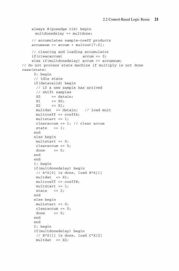
In this implementation, only a single multiplier and accumulator are used as can
be seen in Figure 2.2. Additionally, a state machine is used to load coefficients
and registered samples into the multiplier. The state machine operates on every
combination of coefficients and samples: coeffA*X[0], coeffB*X[1],and coeffC*X[2].
The reason this implementation required a state machine is because there was
no natural flow to the recursive data as there was with the shift and add multiplier
Figure 2.2 FIR with one MAC.
22 Chapter 2 Architecting Area
example. In this case, we had arbitrary registers that represented the inputs
required to create a set of products. The most efficient way to sequence through
the set of multiplier inputs was with a state machine.
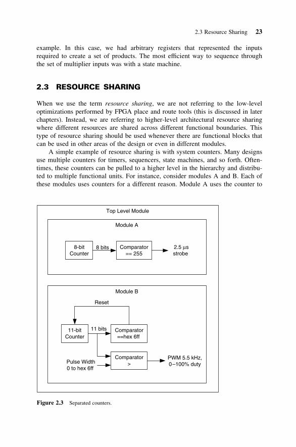
2.3 RESOURCE SHARING
When we use the term resource sharing, we are not referring to the low-level
optimizations performed by FPGA place and route tools (this is discussed in later
chapters). Instead, we are referring to higher-level architectural resource sharing
where different resources are shared across different functional boundaries. This
type of resource sharing should be used whenever there are functional blocks that
can be used in other areas of the design or even in different modules.
A simple example of resource sharing is with system counters. Many designs
use multiple counters for timers, sequencers, state machines, and so forth. Often-
times, these counters can be pulled to a higher level in the hierarchy and distribu-
ted to multiple functional units. For instance, consider modules A and B. Each of
these modules uses counters for a different reason. Module A uses the counter to
Figure 2.3 Separated counters.
2.3 Resource Sharing 23

flag an operation every 256 clocks (at 100 MHz, this would correspond with a
trigger every 2.56 ms). Module B uses a counter to generate a PWM (Pulse Width
Modulated) pulse of varying duty cycle with a fixed frequency of 5.5 kHz (with a
100-MHz system clock, this would correspond with a period of hex 700 clocks).
Each module in Figure 2.3 performs a completely independent operation. The
counters in each module also have completely different characteristics. In module
A, the counter is 8 bits, free running, and rolls over automatically. In module B,
the counter is 11 bits and resets at a predefined value (1666). Nonetheless, these
counters can easily be merged into a global timer and used independently by
modules A and B as shown in Figure 2.4.
Here we were able to create a global 11-bit counter that satisfied the require-
ment of both module A and module B.
For compact designs where area is the primary requirement, search for resources
that have similar counterparts in other modules that can be brought to a global
point in the hierarchy and shared between multiple functional areas.
Figure 2.4 Shared counter.
24 Chapter 2 Architecting Area

2.4 IMPACT OF RESET ON AREA
A common misconception is that the reset structures are always implemented in a
purely global sense and have little effect on design size. The fact is that there are a
number of considerations to take into account relative to area when designing a reset
structure and a corresponding number of penalties to pay for a suboptimal design.
The first effect on area has to do with the insistence on defining a global
set/reset condition for every flip-flop. Although this may seem like good design
practice, it can often lead to a larger and slower design. The reason for this is
because certain functions can be optimized according to the fine-grain architecture
of the FPGA, but bringing a reset into every synchronous element can cause the
synthesis and mapping tools to push the logic into a coarser implementation.
An improper reset strategy can create an unnecessarily large design and inhibit
certain area optimizations.
The next sections describe a number of different scenarios where the reset
can play a significant role in the speed/area characteristics and how to optimize
accordingly.
2.4.1 Resources Without Reset
This section describes the impact that a global reset will have on FPGA resources that
do not have reset available. Consider the following example of a simple shift register:
IMPLEMENTATION 1 : Synchronous Reset
always @(posedge iClk)if(!iReset) sr <= 0;else sr <= {sr[14:0], iDat};
IMPLEMENTATION 2 : No Reset
always @(posedge iClk)sr <= {sr[14:0], iDat};
The differences between the above two implementations may seem trivial. In one
case, the flip-flops have resets defined to be logic-0, whereas in the other
implementation, the flip-flops do not have a defined reset state. The key here is
that if we wish to take advantage of built-in shift-register resources available in
the FPGA, we will need to code it such that there is a direct mapping. If we were
targeting a Xilinx device, the synthesis tool would recognize that the shift-register
SRL16 could be used to implement the shift register as shown in Figure 2.5.
Note that no resets are defined for the SRL16 device. If resets are defined in
our design, then the SRL16 unit could not be used as there are no reset control
2.4 Impact of Reset on Area 25

signals to the resource. The shift register would be implemented as discrete flip-
flops as shown in Figure 2.6. The difference is drastic as summarized in
Table 2.1.
An optimized FPGA resource will not be used if an incompatible reset is
assigned to it. The function will be implemented with generic elements and will
occupy more area.
By removing the reset signals, we were able to reduce 9 slices and 16 slice
flip-flops to a single slice and single slice flip-flop. This corresponds with an opti-
mally compact and high-speed shift-register implementation.
2.4.2 Resources Without Set
Similar to the problem raised in the previous section, some internal resources lack
any type of set capability. An example is that of an 8�8 multiplier:
module mult8(output reg [15:0] oDat,input iReset, iClk,input [7:0] iDat1, iDat2,);
Figure 2.5 Shift register implemented with SRL16 element.
Figure 2.6 Shift register implemented with flip-flops.
Table 2.1 Resource Utilization for Shift Register
Implementations
Implementation Slices slice Flip-flops
Resets defined 9 16
No resets defined 1 1
26 Chapter 2 Architecting Area

always @(posedge iClk)if(!iReset) oDat <= 16’hffff;else oDat <= iDat1 * iDat2;
endmodule
Again, the only variation to the above code will be the reset condition. Unlike the
shift-register example, the multiplier resources in most FPGAs have built-in reset
resources. They do not, however, typically have set resources. If the set function-
ality as described above (16’hffff instead of simply 0) is required, the circuit illus-
trated in Figure 2.7 will be implemented.
Here an additional gate for each output is required to set the output when the
reset is active. The reset on the multiplier, in this case, will go unused. The
resource usage between the set and reset implementations is shown in Table 2.2.
By changing the multiplier set to a reset operation, we are able to reduce 9
slices and 16 slice flip-flops to a single slice and single slice flip-flop. This corre-
sponds with an optimally compact and high-speed multiplier implementation.
2.4.3 Resources Without Asynchronous Reset
Many new high-performance FPGAs provide built-in multifunction modules that
have general applicability to a wide range of applications. Typically, these
resources have some sort of reset functionality but are constrained relative to the
type of reset topology. Here we will look at Xilinx-specific multiply–accumulate
modules for DSP (Digital Signal Processing) applications. The internal structure
of a built-in DSP is typically not flexible to varying reset strategies.
DSPs and other multifunction resources are typically not flexible to varying reset
strategies.
Figure 2.7 Set implemented with external logic.
Table 2.2 Resource Utilization for Set and Reset
Implementations
Implementation Slices slice Flip-flops LUTs Mult16
Reset 9 16 1 1
Set 1 1 1 1
2.4 Impact of Reset on Area 27

Consider the following code for a multiply and accumulate operation:
module dspckt(output reg [15:0] oDat,input iReset, iClk,input [7:0] iDat1, iDat2);reg [15:0] multfactor;
always @(posedge iClk or negedge iReset)if(!iReset) beginmultfactor <= 0;oDat <= 0;
endelse beginmultfactor <= (iDat1 * iDat2);oDat <= multfactor + oDat;
end
endmodule
The above code defines a multiply–accumulate function with asynchronous
resets. The DSP structures inside a Xilinx Virtex-4 device, for example, have
only synchronous reset capabilities as shown in Figure 2.8.
The reset signal here is fed directly into the reset pin of the MAC core. To
implement an asynchronous reset as shown in the above code example, on the
other hand, the synthesis tool must create additional logic outside of the DSP core.
Figure 2.8 Xilinx DSP block with synchronous reset.
28 Chapter 2 Architecting Area

Comparing this to a similar structure using synchronous resets, we are able to
obtain the results shown in Table 2.3.
When the synchronous reset was used, the synthesis tool was able to use the
DSP core available in the FPGA device. By using a different reset than what was
available on this device, however, a significant amount of logic was created
around it to implement the asynchronous reset.
2.4.4 Resetting RAM
There are reset resources in many built-in RAM (Random Access Memory)
resources for FPGAs, but similar to the DSP resource described in the previous
sections, often only synchronous resets are available. Attempting to implement an
asynchronous reset on a RAM module can be catastrophic to area optimization
because there are not smaller elements that can be optimally used to construct a
RAM (like a multiplier and an adder can be stitched together to form a MAC
module) other than smaller RAM resources, nor can the synthesis tool easily add
a few gates to the output to emulate this functionality.
Resetting RAM is usually poor design practice, particularly if the reset is
asynchronous.
Consider the following code:
module resetckt(output reg [15:0] oDat,input iReset, iClk, iWrEn,input [7:0] iAddr, oAddr,input [15:0] iDat);reg [15:0] memdat [0:255];
always @(posedge iClk or negedge iReset)if(!iReset)oDat <= 0;
else beginif(iWrEn)
memdat[iAddr] <= iDat;
oDat <= memdat[oAddr];end
endmodule
Table 2.3 Resource Utilization for Synchronous and
Asynchronous Resets
Architecture Slices Flip-flops LUTs DSPs
Async Reset 17 32 16 1
Sync Reset 0 0 0 1
2.4 Impact of Reset on Area 29

Again, the only variation we will consider in the above code is the type of reset:
synchronous versus asynchronous. In Xilinx Virtex-4 devices, for example,
BRAM (Block RAM) elements have synchronous resets only. Therefore, with a
synchronous reset, the synthesis tool will be able to implement this code with a
single BRAM element as shown in Figure 2.9.
However, if we attempt to implement the same RAM with an asynchronous
reset as shown in the code example above, the synthesis tool will be forced to
create a RAM module with smaller distributed RAM blocks, additional decode
logic to create the appropriate-size RAM, and additional logic to implement the
asynchronous reset as partially shown in Figure 2.10. The final implementation
differences are staggering as shown in Table 2.4.
Improperly resetting a RAM can have a catastrophic impact on the area.
Figure 2.9 Xilinx BRAM with synchronous reset.
Figure 2.10 Xilinx BRAM with asynchronous reset logic.
Table 2.4 Resource Utilization for BRAM with Synchronous and
Asynchronous Resets
Implementation Slices slice Flip-flops 4 Input LUTs BRAMs
Asynchronous reset 3415 4112 2388 0
Synchronous reset 0 0 0 1
30 Chapter 2 Architecting Area

2.4.5 Utilizing Set/Reset Flip-Flop Pins
Most FPGA vendors have a variety of flip-flop elements available in any given device,
and given a particular logic function, the synthesis tool can often use the set and reset
pins to implement aspects of the logic and reduce the burden on the look-up tables.
For instance, consider Figure 2.11. In this case, the synthesis tool may choose to
implement the logic using the set pin on a flip-flop as shown in Figure 2.12. This
eliminates gates and increases the speed of the data path. Likewise, consider a logic
function of the form illustrated in Figure 2.13. The AND gate can be eliminated by
running the input signal to the reset pin of the flip-flop as shown in Figure 2.14.
The primary reason synthesis tools are prevented from performing this class
of optimizations is related to the reset strategy. Any constraints on the reset will
not only use available set/reset pins but will also limit the number of library
elements to choose from.
Using set and reset can prevent certain combinatorial logic optimizations.
For instance, consider the following implementation in a Xilinx Spartan-3
device:
module setreset(output reg oDat,input iReset, iClk,input iDat1, iDat2);
always @(posedge iClk or negedge iReset)if(!iReset)oDat <= 0;
elseoDat <= iDat1 | iDat2;
endmodule
Figure 2.11 Simple synchronous logic with OR gate.
Figure 2.12 OR gate implemented with set pin.
2.4 Impact of Reset on Area 31

In the code example above, an external reset signal is used to reset the state of
the flip-flop. This is represented in Figure 2.15.
As can be seen in Figure 2.15, a resetable flip-flop was used for the asynchro-
nous reset capability, and the logic function (OR gate) was implemented in dis-
crete logic. As an alternative, if we remove the reset but implement the same
logic function, our design will be optimized as shown in Figure 2.16.
In this implementation, the synthesis tool was able to use the FDS element
(flip-flop with a synchronous set and reset) and use the set pin for the OR oper-
ation. Thus, by allowing the synthesis tool to choose a flip-flop with a synchro-
nous set, we are able to implement this function with zero logic elements.
Figure 2.14 AND gate implemented with CLR pin.
Figure 2.13 Simple synchronous logic with AND gate.
Figure 2.15 Simple asynchronous reset.
32 Chapter 2 Architecting Area

We can take this one step further by using both synchronous set and reset
signals. If we have a logic equation to evaluate in the form of
oDat ,¼ !iDat3 & (iDat1 j iDat2)
we can code this in such a way that both the synchronous set and reset resources
are used:
module setreset (output reg oDat,input iClk,input iDat1, iDat2, iDat3);
always @(posedge iClk)if(iDat3)oDat <= 0;else if(iDat1)oDat <= 1;
elseoDat <= iDat2;
endmodule
Here, the iDat3 input takes priority similar to the reset pin on the associated
flip-flops. Thus, this logic function can be implemented as shown in
Figure 2.17.
In this circuit, we have three logical operations (invert, AND, and OR) all
implemented with a single flip-flop and zero LUTs. Because these optimizations
Figure 2.16 Optimization without reset.
2.4 Impact of Reset on Area 33

are not always known at the time the design is architected, avoid using set or
reset whenever possible when area is the key consideration.
Avoid using set or reset whenever possible when area is the key consideration.
2.5 SUMMARY OF KEY POINTS
. Rolling up the pipeline can optimize the area of pipelined designs with
duplicated logic in the pipeline stages.
. Controls can be used to direct the reuse of logic when the shared logic is
larger than the control logic.
. For compact designs where area is the primary requirement, search for
resources that have similar counterparts in other modules that can be
brought to a global point in the hierarchy and shared between multiple
functional areas.
. An improper reset strategy can create an unnecessarily large design and
inhibit certain area optimizations.
. An optimized FPGA resource will not be used if an incompatible reset is
assigned to it. The function will be implemented with generic elements and
will occupy more area.
Figure 2.17 Optimization using both set and reset pins.
34 Chapter 2 Architecting Area

. DSPs and other multifunction resources are typically not flexible to varying
reset strategies.
. Improperly resetting a RAM can have a catastrophic impact on the area.
. Using set and reset can prevent certain combinatorial logic optimizations.
. Avoid using set or reset whenever possible when area is the key
consideration.
2.5 Summary of Key Points 35


Chapter 3
Architecting Power
This chapter discusses the third of three primary physical characteristics of a
digital design: power. Here we also discuss methods for architectural power
optimization in an FPGA.
Relative to ASICs (application specific integrated circuits) with comparable func-
tionality, FPGAs are power-hungry beasts and are typically not well suited for
ultralow-power design techniques. A number of FPGA vendors do offer low-
power CPLDs (complex programmable logic devices), but these are very limited
in size and capability and thus will not always fit an application that requires any
respectable amount of computing power. This section will discuss techniques to
maximize the power efficiency of both low-power CPLDs as well as general
FPGA design.
In CMOS technology, dynamic power consumption is related to charging and
discharging parasitic capacitances on gates and metal traces. The general equation
for current dissipation in a capacitor is
I ¼ V �C � f
where I is total current, V is voltage, C is capacitance, and f is frequency.
Thus, to reduce the current drawn, we must reduce one of the three key par-
ameters. In FPGA design, the voltage is usually fixed. This leaves the parameters
C and f to manipulate the current. The capacitance C is directly related to the
number of gates that are toggling at any given time and the lengths of the routes
connecting the gates. The frequency f is directly related to the clock frequency.
All of the power-reduction techniques ultimately aim at reducing one of these two
components.
During the course of this chapter, we will discuss the following topics:
. The impact of clock control on dynamic power consumption
. Problems with clock gating
Managing clock skew on gated clocks
. Input control for power minimization
37
Advanced FPGA Design. By Steve KiltsCopyright # 2007 John Wiley & Sons, Inc.

. Impact of the core voltage supply
. Guidelines for dual-edge triggered flip-flops
. Reducing static power dissipation in terminations
Reducing dynamic power dissipation by minimizing the route lengths of high
toggle rate nets requires a background discussion of placement and routing, and is
therefore discussed in Chapter 15 Floorplanning.
3.1 CLOCK CONTROL
The most effective and widely used technique for lowering the dynamic power
dissipation in synchronous digital circuits is to dynamically disable the clock in
specific regions that do not need to be active at particular stages in the data flow.
Since most of the dynamic power consumption in an FPGA is directly related to
the toggling of the system clock, temporarily stopping the clock in inactive
regions of the design is the most straightforward method of minimizing this type
of power consumption. The recommended way to accomplish this is to use either
the clock enable pin on the flip-flop or to use a global clock mux (in Xilinx
devices this is the BUFGMUX element). If these clock control elements are not
available in a particular technology, designers will sometimes resort to direct
gating of the system clock. Note that this is not recommended for FPGA
designs, and this section describes the issues involved with direct gating of the
system clock.
Clock control resources such as the clock enable flip-flop input or a global clock
mux should be used in place of direct clock gating.
Note that this section assumes the reader is already familiar with general
FPGA clocking guidelines. In general, FPGAs are synchronous devices, and a
number of difficulties arise when multiple domains are introduced through gating
or asynchronous interfaces. For a more in-depth discussion regarding clock
domains, see Chapter 6.
Figure 3.1 illustrates the poor design practice of simple clock gating. With this
clock topology, all flip-flops and corresponding combinatorial logic is active
(toggling) whenever the Main Clock is active. The logic within the dotted box,
however, is only active when Clock Enable ¼ 1. Here, we refer to the Clock
Enable signal as the gating or enable signal. By gating portions of circuitry as
shown above, the designer is attempting to reduce the dynamic power dissipation
proportional to the amount of logic (capacitance C) and the average toggle
frequency of the corresponding gates (frequency f ).
Clock gating is a direct means for reducing dynamic power dissipation but
creates difficulties in implementation and timing analysis.
Before we proceed to the implementation details, it is important to note how
important careful clock planning is in FPGA design. The system clock is central
38 Chapter 3 Architecting Power

to all synchronous digital circuits. EDA (electronic design automation) tools are
driven by the system clock to optimize and validate synthesis, layout, static
timing analysis, and so forth. Thus, the system clock or clocks are sacred and
must be characterized up front to drive the implementation process. Clocks are
even more sacred in FPGAs than they are in ASICs, and thus there is less flexi-
bility relative to creative clock structures.
When a clock is gated even in the most trivial sense, the new net that drives
the clock pins is considered a new clock domain. This new clock net will require
a low-skew path to all flip-flops in its domain, similar to the system clock from
which it was derived. For the ASIC designer, these low-skew lines can be built in
the custom clock tree, but for the FPGA designer this presents a problem due to
the limited number and fixed layout of the low-skew lines.
A gated clock introduces a new clock domain and will create difficulties for the
FPGA designer.
The following sections address the issues introduced by gated clocks.
3.1.1 Clock Skew
Before directly addressing the issues related to gated clocks, we must first briefly
review the topic of clock skew. The concept of clock skew is a very important
one in sequential logic design.
In Figure 3.2, the propagation delay of the clock signal between the first flip-
flop and the second flip-flop is assumed to be zero. If there is positive delay
through the cloud of combinatorial logic, then timing compliance will be deter-
mined by the clock period relative to the combinatorial delayþ logic routing
Figure 3.1 Simple clock gating: poor design practice.
3.1 Clock Control 39

delayþ flip-flop setup time. A signal can only propagate between a single set of
flip-flops for every clock edge. The situation between the second and third flip-
flop stages, however, is different. Because of the delay on the clock line between
the second and third flip-flops, the active clock edge will not occur simultaneously
at both elements. Instead, the active clock edge on the third flip-flop will be
delayed by an amount dC.
If the delay through the logic (defined as dL) is less than the delay on the
clock line (dC), then a situation may occur where a signal that is propagated
through the second flip-flop will arrive at the third stage before the active edge of
the clock. When the active edge of the clock arrives, the same signal could be
propagated through stage 3. Thus, a signal could propagate through both stage 2
and stage 3 on the same clock edge! This scenario will cause a catastrophic
failure of the circuit, and thus clock skew must be taken into account when per-
forming timing analysis. It is also important to note that clock skew is indepen-
dent of clock speed. The “fly-through” issue described above will occur exactly
the same way regardless of the clock frequency.
Mishandling clock skew can cause catastrophic failures in the FPGA.
3.1.2 Managing Skew
Low-skew resources provided on FPGAs ensure that the clock signal will be
matched on all clock inputs as tightly as possible (within picoseconds). Take, for
instance, the scenario where a gate is introduced to the clock network as shown in
Figure 3.3.
The clock line must be removed from the low-skew global resource and
routed to the gating logic, in this case an AND gate. The fundamental problem of
adding skew to the clock line is now the same as it was in the problem described
previously. It is conceivable that the delay through the gate (dG) plus the routing
delays will be greater than the delay through the logic (dL). To handle this poten-
tial problem, the implementation and analysis tools must be given a set of con-
straints such that any timing problems associated with skew through the gating
item are eliminated and then analyzed properly in post-implementation analysis.
Figure 3.2 Clock skew.
40 Chapter 3 Architecting Power

As an example, consider the following module that uses clock gating:
// Poor design practicemodule clockgating(
output dataout,input clk, datain,input clockgate1);reg ff0, ff1, ff2;wire clk1;
// clocks are disabled when gate is lowassign clk1 = clk & clockgate1;assign dataout = ff2;
always @(posedge clk)ff0 <= datain;
always @(posedge clk)ff1 <= ff0;
always @(posedge clk1)ff2 <= ff1;
endmodule
In the above example, there is no logic between the flip-flops on the data path,
but there is logic in the clock path as shown in Figure 3.4.
Figure 3.4 Clock skew as the dominant delay.
Figure 3.3 Clock skew introduced with clock gating: Poor design practice.
3.1 Clock Control 41

Different tools handle this situation differently. Some tools such as Synplify
will remove the clock gating by default to create a purely synchronous design.
Other tools ignore skew problems if the clocks remain unconstrained but will add
artificial delays once the clocks have been constrained properly.
Unlike ASIC designs, hold violations in FPGA designs are rare due to the
built-in delays of the logic blocks and routing resources. One thing that can cause a
hold delay, however, is excessive delay on the clock line as shown above. Due to the
fact that the data propagates in less than 1 ns and the clock in almost 2 ns, the data
will arrive almost 1 ns before the clock and lead to a serious timing violation.
Depending on the synthesis tool, this can sometimes be fixed by adding a clock con-
straint. A subsequent analysis may or may not show (depending on the technology)
that artificial routing delay was added to the data path to eliminate the hold violation.
Clock gating can cause hold violations that may or may not be corrected by the
implementation tools.
It is again worth reiterating that most vendors have advanced clock buffer tech-
nology that provide enable capability to certain branches of the clock tree. This
type of control is always recommended above clock gating with logic elements.
3.2 INPUT CONTROL
An often overlooked power-reduction technique is that of input slew rates. CMOS
input buffers can create excessive current draw under conditions where both the
high-side and low-side transistors are conducting at the same time. To conceptual-
ize this, consider a basic first-order model of a CMOS transistor that describes Idsin terms of Vds as illustrated in Figure 3.5, where the regions are defined by:
Cutoff: Vgs , Vth
Linear (resistive): 0 , Vds , Vgs – Vth
Saturation: 0 , Vgs – Vth , Vds
where Vgs is the gate-to-source voltage, Vth is the device threshold voltage, and
Vds is the drain-to-source voltage.
An ideal switching scheme would be one where the input to a gate switched
from cutoff to the linear region instantaneously, and the complementary logic
switched the opposite direction at the same instant. If one of the two complements
is always in cutoff, there is no current flowing through both sides of the logic gate
at the same time (and thus providing a resistive path between power and ground).
For an inverter, this would mean that the NMOS (N-channel MOSFET) device
would transition from 0 to VDD (positive power rail) taking the NMOS from
cutoff to the linear region instantly, and the PMOS (P-channel MOSFET) would
transition from the linear region to cutoff at the same instant. In the opposite tran-
sition when Vgs transitions from VDD to 0, the NMOS would move from the
linear region to cutoff instantly, and the PMOS would move from the cutoff
region to the linear region at the same instant.
42 Chapter 3 Architecting Power

In a real system, however, we must take into consideration the transition
times and the behavior of the transistors during those transitions. For instance,
consider a CMOS inverter that has an input of 0 V and an output of VDD. As
the input transitions from 0 to VDD (a 0 to 1 transition), the NMOS transistor
leaves the cutoff region as soon as the input passes the threshold Vth and enters
into the saturation region. The PMOS device is still in the linear region during
the early part of this transition, and so current begins to flow between VDD
and ground. As the input rises, the output falls. When the drain of the NMOS
falls below a threshold of the gate voltage, the NMOS transitions into the linear
region, and the PMOS transitions to saturation and then to cutoff. To minimize
the power dissipation, it is desirable to minimize the time in the saturation region;
that is, minimize the time during which the gate inputs are transitioning.
To minimize the power dissipation of input devices, minimize the rise and fall
times of the signals that drive the input.
Another important conclusion can be drawn from the above equations. If the
driving signal is not within a threshold voltage of 0 or Vdd in steady state (i.e.,
when the gate is not switching), the transistor previously in cutoff will enter into
the saturation region and begin to dissipate a small amount of current. This can
be a problem in systems where smaller signal swings are used to drive inputs that
are powered by a higher voltage.
In harmony with the principle described above, a floating input may be an
even worse problem than an underdriven input. A floating input is by definition
an underdriven input, but because it is floating there is no way to know how
underdriven it is. It may be that the input has settled at a metastable point where
both transistors are in the saturation region. This would have disastrous impli-
cations relative to power dissipation. Worse yet, this would not be a repeatable
problem. Because most FPGA devices have resistive terminations available for
unused inputs, it is good design practice to define a logic state for these and avoid
the unpredictable effects of floating inputs.
Always terminate unused input buffers. Never let an FPGA input buffer float.
Figure 3.5 Simple I/V curve for a CMOS transistor.
3.2 Input Control 43

3.3 REDUCING THE VOLTAGE SUPPLY
Although reducing the supply voltage is usually not a desirable option, it is worth
mentioning due to the dramatic effect it can have on power consumption. Power
dissipation in a simple resistor will drop off with the square of the voltage. Thus,
significant power savings can be achieved by lowering the power supply voltage
of the FPGA near the minimum required voltage. It is important to note, however,
that lowering the voltage will also decrease the performance of the system. If this
method is used, ensure that the timing analysis takes into consideration the lowest
possible voltage on the supply rail for worst-case maximum timing.
Dynamic power dissipation drops off with the square of the core voltage, but
reducing voltage will have a negative impact on performance.
Because the core voltage on an FPGA will be rated from 5% to 10% of
the specified value, great care must be given to this from a system perspective.
Typically, power issues can be addressed with other techniques while keeping the
core voltage well within the specified range.
3.4 DUAL-EDGE TRIGGERED FLIP-FLOPS
Due to the fact that power dissipation is proportional to the frequency that a
signal toggles, it is desirable to maximize the amount of functionality for each
toggle of a high fan-out net. Most likely, the highest fan-out net is the system
clock, and thus any techniques to reduce the frequency of this clock would have a
dramatic impact on dynamic power consumption. Dual-edge triggered flip-flops
provide a mechanism to propagate data on both edges of the clock instead
of just one. This allows the designer to run a clock at half the frequency that
would otherwise be required to achieve a certain level of functionality and
performance.
Coding a dual-edge triggered flip-flop is very straightforward. The following
example illustrates this with a simple shift register. Note that the input signal is
captured on the rising edge of the clock and is then passed to dual-edge flip-flops.
module dualedge(output reg dataout,input clk, datain);reg ff0, ff1;
always @(posedge clk)ff0 <= datain;
always @(posedge clk or negedge clk) beginff1 <= ff0;dataout <= ff1;end
endmodule
44 Chapter 3 Architecting Power

Note that if dual-edge flip-flops are not available, redundant flip-flops and
gating will be added to emulate the appropriate functionality. This could comple-
tely defeat the purpose of using the dual-edge strategy and should be analyzed
appropriately after implementation. A good synthesis tool will at least flag a
warning if no dual-edge devices are available.
Dual-edge triggered flip-flops should only be used if they are provided as primi-
tive elements.
The Xilinx Coolrunner-II family includes a feature named CoolClock, which
divides the incoming clock by 2 and then switches the flip-flops to dual-edge
devices as described above. From an external perspective, the device behaves the
same as a single-edge triggered system but with half of the dynamic power dissi-
pation on the global clock lines.
3.5 MODIFYING TERMINATIONS
Resistive loads connected to output pins are common in systems with bus
signals, open-drain outputs, or transmission lines requiring termination. In all of
these cases, one of the CMOS transistors on the output driver of the FPGA
will need to source or sink current through one of these resistive loads. For
outputs requiring pull-up resistors, calculate the minimum acceptable rise-time
to size the resistor as large as possible. If there are high side drivers as well as
low side drivers, ensure there is never a condition where bus contention occurs
as this will draw excessive currents even if for only a few nanoseconds at
a time. For transmission lines with shunt termination at the load, a series termin-
ation may be used as an alternate depending on the requirements of the system.
As can be seen in Figure 3.6, there is not steady-state current dissipation with a
series termination.
There is no steady-state current dissipation with a series termination.
The disadvantages are
. An initial reflection from the load to the terminating resistor
. A small amount of attenuation through the series resistor during a transition
Figure 3.6 Termination types.
3.5 Modifying Terminations 45

If these performance characteristics are acceptable for a given system, the
series termination approach will eliminate static power dissipation through the
termination resistor.
3.6 SUMMARY OF KEY POINTS
. Clock control resources such as the clock enable flip-flop input or a global
clock mux should be used in place direct clock gating when they are
available.
. Clock gating is a direct means for reducing dynamic power dissipation but
creates difficulties in implementation and timing analysis.
. Mishandling clock skew can cause catastrophic failures in the FPGA.
. Clock gating can cause hold violations that may or may not be corrected by
the implementation tools.
. To minimize the power dissipation of input devices, minimize the rise and
fall times of the signals that drive the input.
. Always terminate unused input buffers. Never let an FPGA input buffer float.
. Dynamic power dissipation drops off with the square of the core voltage,
but reducing voltage will have a negative impact on performance.
. Dual-edge triggered flip-flops should only be used if they are provided as
primitive elements.
. There is no steady-state current dissipation with a series termination.
46 Chapter 3 Architecting Power

Chapter 4
Example Design: The
Advanced Encryption
Standard
The Advanced Encryption Standard (AES; also referred to by its original name,
Rijndael) specifies the latest standard in encryption for the protection of electronic
information. The standard has been approved by the U.S. National Institute of
Standards and Technology (NIST), which has made the specification publicly
available in a Federal Information Processing Standards Publication (FIPS PUB
197). The motivation behind the new standard was the weakness of the existing
Data Encryption Standard (DES). In addition to providing more security, AES is
designed to lend itself to an easy implementation in hardware. In this context,
easier means less prone to design error (more reliable) and faster (simple combi-
natorial logic).
The objective of this chapter is to describe a number of AES architectures and to
analyze the various trade-offs relative to performance versus area.
4.1 AES ARCHITECTURES
AES is a symmetric, secret-key cipher that maps a 128-bit block of plaintext data
to a 128-bit block of ciphertext. The length of the key is variable between 128,
192, and 256 bits and will determine level of security (longer key ¼ larger key
space ¼ more security). The transformations in the AES algorithm consist of four
components organized as distinct modules: Sub Bytes (bit mapping), shift rows
(swapping), mult-column [transformation over GF(28)], and Add Round Key
[addition of round key with bitwise operations in the field GF(2)]. These trans-
formations make up a “round,” and the number of rounds is determined by the
key size (128 bits, 10 rounds; 192 bits, 12 rounds; 256 bits, 14 rounds). Note that
47
Advanced FPGA Design. By Steve KiltsCopyright # 2007 John Wiley & Sons, Inc.

the round key for each round is unique. These round keys are derived from the
original key through the key expansion. The key expansion is one of the architec-
tural focal points of this chapter and will be discussed in more detail. For a more
detailed explanation of the complete AES cipher, see the Federal Information Pro-
cessing Standard 197 (FIPS 197), as provided by NIST.
The key expansion, which runs parallel to the data path, takes the cipher key
and creates a unique key for each transformation round. Let a word ¼ 32 bits and
Nk ¼ Keysize/Wordsize (¼128, 192, or 256/32). The first Nk words of the
expanded key are filled with the cipher key. Every subsequent 32-bit word in
the expanded key is the XOR (Exclusive-OR) of the previous 32-bit word and the
32-bit-word Nk words previous to the current word. For words that occur on a
multiple of Nk, the current word undergoes a transformation prior to the XOR
operation, followed by an XOR with a round constant. The transformation con-
sists of a cyclic permutation, followed by an 8-byte mapping for all four bytes in
the 32-bit word. The round constant is defined by FIPS 197 as the values given
by [x(i21), f00g, f00g, f00g], with x(i21) being powers of x, where x is denoted as
f02g in the field GF(28).
A single key expansion operation is autonomous relative to the high-level
architecture and is shown in the following implementation.
module KeyExp1Enc(// updated values to be passed to next iterationoutput [3:0] oKeyIter, oKeyIterModNk,
oKeyIterDivNk,output [32*‘Nk-1:0] oNkKeys,input iClk, iReset,// represents total # of iterations and value mod Nkinput [3:0] iKeyIter, iKeyIterModNk,
iKeyIterDivNk,// The last Nk keys generated in key expansioninput [32*‘Nk-1:0] iNkKeys);// updated values to be passed to next iterationreg [3:0] oKeyIter, oKeyIterModNk,
oKeyIterDivNk;reg [32*‘Nk-1:0] OldKeys;reg [31:0] InterKey; // intermediate key valuewire [32*‘Nk-1:0] oNkKeys;wire [31:0] PrevKey, RotWord, SubWord,
NewKeyWord;wire [31:0] KeyWordNk;wire [31:0] Rcon;
assign PrevKey = iNkKeys[31:0]; // last word in keyarray
assign KeyWordNk = OldKeys[32*‘Nk-1:32*‘Nk-32];
// 1 byte cyclic permutationassign RotWord = {PrevKey[23:0], PrevKey[31:24]};
48 Chapter 4 Example Design: The Advanced Encryption Standard

// new key calculated in this roundassign NewKeyWord = KeyWordNk ^ InterKey;
// calculate new key setassign oNkKeys = {OldKeys[32*‘Nk-33:0], NewKeyWord};
// calculate Rcon over GF(2^8)assign Rcon = iKeyIterDivNk == 8’h1 ? 32’h01000000:
iKeyIterDivNk == 8’h2 ? 32’h02000000:iKeyIterDivNk == 8’h3 ? 32’h04000000:iKeyIterDivNk == 8’h4 ? 32’h08000000:iKeyIterDivNk == 8’h5 ? 32’h10000000:iKeyIterDivNk == 8’h6 ? 32’h20000000:iKeyIterDivNk == 8’h7 ? 32’h40000000:iKeyIterDivNk == 8’h8 ? 32’h80000000:iKeyIterDivNk == 8’h9 ? 32’h1b000000:32’h36000000;
SboxEnc SboxEnc0(.iPreMap(RotWord[31:24]),.oPostMap(SubWord[31:24]));SboxEnc SboxEnc1(.iPreMap(RotWord[23:16]),.oPostMap(SubWord[23:16]));SboxEnc SboxEnc2(.iPreMap(RotWord[15:8]),.oPostMap(SubWord[15:8]));SboxEnc SboxEnc3(.iPreMap(RotWord[7:0]),.oPostMap(SubWord[7:0]));
‘ifdef Nk8
wire [31:0] SubWordNk8;
// Substitution only when Nk = 8SboxEnc SboxEncNk8_0(.iPreMap(PrevKey[31:24]),.oPostMap(SubWordNk8[31:24]));SboxEnc SboxEncNk8_1(.iPreMap(PrevKey[23:16]),.oPostMap(SubWordNk8[23:16]));SboxEnc SboxEncNk8_2(.iPreMap(PrevKey[15:8]),.oPostMap(SubWordNk8[15:8]));SboxEnc SboxEncNk8_3(.iPreMap(PrevKey[7:0]),.oPostMap(SubWordNk8[7:0]));
‘endif
always @(posedge iClk)if(!iReset) begin
oKeyIter <= 0;oKeyIterModNk <= 0;InterKey <= 0;oKeyIterDivNk <= 0;OldKeys <= 0;
endelse begin
4.1 AES Architectures 49

oKeyIter <= iKeyIter + 1;OldKeys <= iNkKeys;
// update "Key iteration mod Nk" for next iterationif(iKeyIterModNk + 1 == ‘Nk) begin
oKeyIterModNk <= 0;oKeyIterDivNk <= iKeyIterDivNk+1;
endelse begin
oKeyIterModNk <= iKeyIterModNk + 1;oKeyIterDivNk <= iKeyIterDivNk;
end
if(iKeyIterModNk == 0)InterKey <= SubWord ^ Rcon;
‘ifdef Nk8// an option only for Nk = 8else if(iKeyIterModNk == 4)
InterKey <= SubWordNk8;‘endifelse
InterKey <= PrevKey;end
endmodule
Likewise, the autonomous operation for the data path is the combination of
all functions required for a round encryption as shown in the following
implementation.
module RoundEnc(output [32*‘Nb-1:0] oBlockOut,output oValid,input iClk, iReset,input [32*‘Nb-1:0] iBlockIn, iRoundKey,input iReady,input [3:0] iRound);wire [32*‘Nb-1:0] wSubOut, wShiftOut, wMixOut;wire wValidSub, wValidShift,
wValidMix;
SubBytesEnc sub( .iClk(iClk), .iReset(iReset),.iBlockIn(iBlockIn),.oBlockOut(wSubOut),.iReady(iReady),.oValid(wValidSub));
ShiftRowsEnc shift( .iBlockIn(wSubOut), .oBlockOut(wShiftOut),
.iReady(wValidSub), .oValid(wValidShift));
MixColumnsEnc mixcolumn( .iClk(iClk), .iReset(iReset),.iBlockIn(wShiftOut),
50 Chapter 4 Example Design: The Advanced Encryption Standard

.oBlockOut(wMixOut),.iReady(wValidShift),
.oValid(wValidMix),.iRound(iRound));
AddRoundKeyEnc addroundkey(.iClk(iClk), .iReset(iReset),.iBlockIn(wMixOut),.iRoundKey(iRoundKey),.oBlockOut(oBlockOut),.iReady(wValidMix),
.oValid(oValid));endmodule
The implementation of the Round subblocks is straightforward. For reasons
described later, assume that each Round has a latency of 4 clocks. It would be
reasonable (based on logic balancing) to distribute the pipeline stages as follows.
4.1.1 One Stage for Sub-bytes
Sub-bytes is implemented as a look-up table due to the iterative nature of the
algorithms implemented by it as well as the relatively small map space. Thus, an
8-bit to 8-bit mapping would be efficiently implemented as a synchronous
8 � 256 (28) ROM with a single pipeline stage. This is shown in Figure 4.1.
4.1.2 Zero Stages for Shift Rows
This stage simply mixes the rows in the data block, so no logic is used here.
Thus, another pipeline stage at this point would create an imbalance of logic
Figure 4.1 An 8-bit mapping in the sub-bytes module.
4.1 AES Architectures 51

around the pipeline stages and thus decrease maximum frequency and total
throughput. The shifted rows are illustrated in Figure 4.2.
4.1.3 Two Pipeline Stages for Mix-Column
This stage has the most logic out of all four Round stages and is thus the best place to
add the additional pipeline stage. The mix-column hierarchy is shown in Figure 4.3.
As can be seen from Figure 4.3, Mix-Column uses a module called Map-
Column as a building block. This can be seen in Figure 4.4.
As can be seen from Figure 4.4, Map-Column uses a block called Poly-Mult
X2 (polynomial �2 multiplier) as a building block. This is shown in Figure 4.5.
4.1.4 One Stage for Add Round Key
This stage simply XORs the round key from the key expansion pipeline with the
data block. This is shown in Figure 4.6.
Figure 4.2 Shift-row implementation.
Figure 4.3 The mix-column hierarchy.
52 Chapter 4 Example Design: The Advanced Encryption Standard

4.1.5 Compact Architecture
The first implementation under consideration is a compact implementation
designed to iteratively reuse logic resources. Initially, the incoming data and key
are added together in the Initial Round module, and the result is registered before
entering the encryption loop. The data is then applied to the Sub Bytes, Shift
Rows, Mult-Column, and Add Round Key in the specified order. At the end of
each round, the new data is registered. These operations are repeated according to
the number of rounds. A block diagram of the iterative architecture is shown in
Figure 4.7.
The top-level implementation is shown in the following code.
module AES_Enc_core(output [32*‘Nb-1:0] oCiphertext, // output cipthertextoutput oValid, // data at output is validoutput oKeysValid,
Figure 4.4 The Map-column hierarchy.
Figure 4.5 Polynomial multiplication x2.
Figure 4.6 The add-round-key block.
4.1 AES Architectures 53

input iClk, iReset,input [32*‘Nb-1:0] iPlaintext, // input data to be
encryptedinput [32*‘Nk-1:0] iKey, // input cipther keyinput iReady, // valid data to encryptinput iNewKey); // signals new key isinput
// registered inputswire [32*‘Nk-1:0] wKeyReg;wire wNewKeyReg, wReadyReg;wire [127:0] wPlaintextReg, wBlockOutInit;wire [127:0] wRoundKeyInit, wRoundKey;
// register inputsInputRegsEnc InputRegs( .iClk(iClk), .iReset(iReset),
.iKey(iKey),.iNewKey(iNewKey), .iPlaintext
(iPlaintext),.oKeysValid(oKeysValid),
.iReady(iReady),.oKey(wKeyReg), .oPlaintext(wPlaintextReg),
.oReady(wReadyReg));
// initial addition of round keyAddRoundKeyEnc InitialKey( .iClk(iClk), .iReset(iReset),
.iBlockIn(wPlaintextReg),
.iRoundKey(wRoundKeyInit),
.oBlockOut(wBlockOutInit),
.iReady(wReadyReg),
.oValid(wValidInit));
// Number of rounds is a function of key size (10, 12, or14)
// Key expansion block
Figure 4.7 A compact implementation.
54 Chapter 4 Example Design: The Advanced Encryption Standard

KeyExpansionEnc KeyExpansion( .iClk(iClk), .iReset(iReset),
.iNkKeys(wKeyReg),.iReady(wReadyReg),
.oRoundKey(wRoundKey));
RoundsIterEnc RoundsIter( .iClk(iClk), .iReset(iReset),.iBlockIn(wBlockOutInit),.oBlockOut(oCiphertext),.iReady(wValidInit),
.oValid(oValid),.iRoundKey(wRoundKey));
‘ifdef Nk4assign wRoundKeyInit = wKeyReg[128-1:0];‘endif
‘ifdef Nk6assign wRoundKeyInit = wKeyReg[192-1:192-128];‘endif
‘ifdef Nk8assign wRoundKeyInit = wKeyReg[256-1:256-128];‘endif
endmodule
In the above code, the modules KeyExpansionEnc and RoundsIterEnc perform
the iterative operations required of the compact architecture. The KeyExpansio-
nEnc handles the iterations for the key expansion, and RoundsIterEnc handles the
data path. A unique round key is passed from the key expansion module to
RoundsIterEnc for every iteration of the round. The following code loops the key
information through the same expansion module to reuse the logic for every
round:
module KeyExpansionEnc(output [128-1:0] oRoundKey,input iClk, iReset,// The last Nk keys generated in initial key expansioninput [32*‘Nk-1:0] iNkKeys,input iReady); // signals a
new key is inputwire [3:0] KeyIterIn, KeyIterOut;wire [3:0] KeyIterDivNkIn, KeyIterDivNkOut;wire [3:0] KeyIterModNkIn, KeyIterModNkOut;wire [32*‘Nk-1:0] NkKeysOut, NkKeysIn;wire wReady;
assign wReady = iReady;assign KeyIterIn = wReady ? ‘Nk : KeyIterOut;assign oRoundKey = NkKeysOut[32*‘Nk-1:32*‘Nk-128];
4.1 AES Architectures 55

assign KeyIterModNkIn = wReady ? 4’h0 : KeyIterModNkOut;
assign KeyIterDivNkIn = wReady ? 4’h1 : KeyIterDivNkOut;
assign NkKeysIn = wReady ? iNkKeys : NkKeysOut;
KeyExp1Enc KeyExp1(.iClk(iClk), .iReset(iReset),.iKeyIter(KeyIterIn),
.iKeyIterModNk(KeyIterModNkIn),
.iNkKeys(NkKeysIn), .iKeyIterDivNk(KeyIterDivNkIn),
.oKeyIter(KeyIterOut),
.oKeyIterModNk(KeyIterModNkOut),
.oNkKeys(NkKeysOut),
.oKeyIterDivNk(KeyIterDivNkOut));endmodule
In the above module, the output of the single key expansion module
KeyExp1Enc is routed back to the input for further expansion on subsequent
rounds as shown in Figure 4.8.
Thus, the logic in the KeyExp1Enc is reused for every round.
Figure 4.8 Iterative key expansion.
56 Chapter 4 Example Design: The Advanced Encryption Standard

4.1.6 Partially Pipelined Architecture
The second implementation under consideration is a partially pipelined architec-
ture. An AES round is completed in 11 to 14 clock cycles depending on the
key size.
As can be seen from Figure 4.9, multiple instantiations of the data path core
can be used to create a pipelined design, where the key expansion is performed in
a static fashion. This implementation is shown in the following code for Nk ¼ 4.
module AES_core(output [32*‘Nb-1:0] oCiphertext, // output cipthertextoutput oValid, // data at output is valid// signals that new key has been completely processedoutput oKeysValid,input iClk, iReset,input [32*‘Nb-1:0] iPlaintext, // input data to
be encryptedinput [32*‘Nk-1:0] iKey, // input cipther keyinput iReady, // valid data to encryptinput iNewKey); // signals new key
is inputwire [32*‘Nb-1:0] wRoundKey1, wRoundKey2,
wRoundKey3, wRoundKey4,wRoundKey5, wRoundKey6,
wRoundKey7, wRoundKey8,wRoundKey9, wRoundKeyFinal,
wRoundKeyInit;wire [32*‘Nb-1:0] wBlockOut1, wBlockOut2,
wBlockOut3, wBlockOut4,wBlockOut5, wBlockOut6,
Figure 4.9 A partially pipelined implementation.
4.1 AES Architectures 57

wBlockOut7, wBlockOut8,wBlockOut9, wBlockOutInit;
wire [32*‘Nk-1:0] wNkKeysInit;wire [3:0] wKeyIterInit;wire [3:0] wKeyIterModNkInit;wire [3:0] wKeyIterDivNkInit;wire wValid1, wValid2, wValid3,
wValid4,wValid5, wValid6, wValid7,
wValid8,wValid9, wValidFinal,
wValidInit;wire wNewKeyInit;wire [128*(‘Nr+1)-1:0] wKeys; // complete set
of round keys
// registered inputswire [32*‘Nk-1:0] wKeyReg;wire wNewKeyReg, wReadyReg;wire [127:0] wPlaintextReg;
// register inputsInputRegs InputRegs( .iClk(iClk), .iReset(iReset),
.iKey(iKey),.iNewKey(iNewKey),.iPlaintext(iPlaintext),.iReady(iReady), .oKey(wKeyReg),.oNewKey(wNewKeyReg),.oPlaintext(wPlaintextReg),.oReady(wReadyReg));
// initial key expansionKeyExpInit KeyExpInit( .iClk(iClk), .iReset(iReset),
.iNkKeys(wKeyReg), .iNewKey(wNewKeyReg),
.oKeyIter(wKeyIterInit),
.oNewKey(wNewKeyInit),
.oKeyIterModNk(wKeyIterModNkInit),
.oNkKeys(wNkKeysInit),
.oKeyIterDivNk(wKeyIterDivNkInit));
// initial addition of round keyAddRoundKey InitialKey( .iClk(iClk), .iReset(iReset),
.iBlockIn(wPlaintextReg),
.iRoundKey(wRoundKeyInit),
.oBlockOut(wBlockOutInit),.iReady(wReadyReg),.oValid(wValidInit));
58 Chapter 4 Example Design: The Advanced Encryption Standard

// Number of rounds is a function of key size (10, 12, or14)
// Key expansion blockKeyExpansion KeyExpansion( .iClk(iClk),
.iReset(iReset),.iKeyIter(wKeyIterInit),.iKeyIterModNk(wKeyIterMod
NkInit),.iNkKeys(wNkKeysInit),.iKeyIterDivNk(wKeyIterDiv
NkInit),.iNewKey(wNewKeyInit),.oKeys(wKeys), .oKeysValid
(oKeysValid));
// round transformation blocksRound R1( .iClk(iClk), .iReset
(iReset),.iBlockIn(wBlockOutInit),.iRoundKey(wRoundKey1),.oBlockOut(wBlockOut1),.iReady(wValidInit),.oValid(wValid1));
Round R9( .iClk(iClk), .iReset(iReset),
.iBlockIn(wBlockOut8),
.iRoundKey(wRoundKey9),
.oBlockOut(wBlockOut9),
.iReady(wValid8),.oValid(wValid9));
// 10 rounds total// Initial key additionassign wRoundKeyFinal = wKeys[128*(‘Nr-7)-1:
128*(‘Nr-8)];
// round key assignmentsassign wRoundKey9 = wKeys[128*(‘Nr-6)-1: 128*(‘Nr-7)];assign wRoundKey8 = wKeys[128*(‘Nr-5)-1: 128*(‘Nr-6)];assign wRoundKey7 = wKeys[128*(‘Nr-4)-1: 128*(‘Nr-5)];assign wRoundKey6 = wKeys[128*(‘Nr-3)-1: 128*(‘Nr-4)];assign wRoundKey5 = wKeys[128*(‘Nr-2)-1: 128*(‘Nr-3)];assign wRoundKey4 = wKeys[128*(‘Nr-1)-1: 128*(‘Nr-2)];assign wRoundKey3 = wKeys[128*‘Nr-1: 128*(‘Nr-1)];assign wRoundKey2 = wKeys[128*(‘Nr+1)-1: 128*‘Nr];
assign wRoundKey1 = wNkKeysInit[128-1:0];assign wRoundKeyInit = iKey[128-1:0];
4.1 AES Architectures 59

FinalRound FinalRound( .iClk(iClk), .iReset(iReset),.iBlockIn(wBlockOut9),.iRoundKey(wRoundKeyFinal),.oBlockOut(oCiphertext),.iReady(wValid9), .oValid
(oValid));endmodule
Although pipelined designs such as the one above can potentially encrypt
data at fast data rates, a problem arises in these architectures if one were to intro-
duce new keys at a rate faster than the encryption speed. The surrounding system
would have to be smart enough to wait for the pipe to empty before introducing
the new data block along with the new key.
This information has to be fed back to the outside system that is providing
the information and the corresponding keys so that they can be buffered and held
appropriately. In the worst case where a new key is required for every block of
data, the pipelined architecture would have a throughput equivalent to that of the
iterative architecture and would be a massive waste of space (not to mention the
disappointment of not achieving the advertised throughput). The next section pre-
sents an architecture that eliminates this problem.
4.1.7 Fully Pipelined Architecture
The term fully pipelined refers to an architecture for the key expansion that runs
in parallel to the round transformation pipeline, where corresponding stages in the
pipeline provide each other with the exact information at just the right time. In
other words, the round key for any particular stage and any particular data block
is valid for only one clock cycle and is used by the corresponding round at that
time. This occurs in parallel for every pipeline stage. Thus, a unique key may be
used for potentially every block of data, with no penalization in terms of latency
or wait states. The maximum throughput of the round transformation pipeline is
always achieved independent of the topology of the key set. A block diagram for
the fully pipelined implementation is shown in Figure 4.10.
This means that a single iteration through the Key Expansion function (four
32-bit word expansion of the key) would happen fully synchronous with the
round previous to the round that the key being generated would be used. Also, the
latency for the Key Expansion block would have to maintain a clock latency
equal to that of the Round block, typically equal to 1–4 clocks.
For the round key at any arbitrary key expansion block to arrive at its corre-
sponding Round block appropriately, and on potentially every clock pulse, the
timing must be very precise. Specifically, each key expansion block must generate
a round key in exactly the same number of clock cycles that the Round block can
generate its corresponding data. Also, the latency must be such that each key is
valid when presented to the add-round-key sub-block. To handle these require-
ments, each key expansion block is divided into four incremental expansion
60 Chapter 4 Example Design: The Advanced Encryption Standard

blocks. Each incremental expansion block generates a single word (128/4 ¼ 32
bits) for the key as described in the NIST specification. Each of these blocks is
given a pipeline stage. This is shown in Figure 4.11.
As mentioned above, each Key-Exp1 block generates a single word (32 bits)
of the expanded key. The stages to add pipelining is shown in Figure 4.12.
As can be seen in Figure 4.12, the S-box can be implemented as a synchronous
8 � 256 ROM, and to preserve latency timing accuracy, a pipeline stage must also
be added to the R-CON calculation as described in the NIST specification.
Also, to ensure that the latency timing between the key pipeline and the data
propagation pipeline is accurate, the keys must be generated one clock cycle earlier
than the round data is completed. This is because the round key is necessary for the
add-round-key block that clocks the XOR operation into its final register. In other
words, clock 4 of the key expansion block must be synchronous with clock 3 of the
corresponding Round block. This is handled by the initial key addition at the begin-
ning of the key expansion process. This is shown in Figure 4.13.
The key data beyond the first 128 bits begins to expand on the first clock
cycle, while the data pipeline begins on the second clock (a one-clock latency
Figure 4.10 Fully pipelined key expansion.
Figure 4.11 Propagation through 32-bit key expansion stages.
4.1 AES Architectures 61

from the initial add-round-key operation). The top-level implementation is shown
in the code below for Nk ¼ 4.
module AES_core(output [32*‘Nb-1:0] oCiphertext, // output cipthertextoutput oValid, // data at output is validinput iClk, iReset,input [32*‘Nb-1:0] iPlaintext, // input data to be
encryptedinput [32*‘Nk-1:0] iKey, // input cipther keyinput iReady); // valid data to encrypt
Figure 4.12 Single word expansion inside Key-Exp1.
Figure 4.13 Skewing of the key pipeline.
62 Chapter 4 Example Design: The Advanced Encryption Standard

wire [32*‘Nb-1:0] wRoundKey1, wRoundKey2, wRoundKey3,wRoundKey4,
wRoundKey5, wRoundKey6, wRoundKey7,wRoundKey8,
wRoundKey9, wRoundKeyFinal,wRoundKeyInit;
wire [32*‘Nb-1:0] wBlockOut1, wBlockOut2, wBlockOut3,wBlockOut4,
wBlockOut5, wBlockOut6, wBlockOut7,wBlockOut8,
wBlockOut9, wBlockOutInit;
wire [32*‘Nk-1:0] wNkKeys1, wNkKeys2, wNkKeys3,wNkKeys4,
wNkKeys5, wNkKeys6, wNkKeys7,wNkKeys8,
wNkKeys9, wNkKeysFinal,wNkKeysInit;
wire [3:0] wKeyIter1, wKeyIter2, wKeyIter3,wKeyIter4,
wKeyIter5, wKeyIter6, wKeyIter7,wKeyIter8,
wKeyIter9, wKeyIterFinal,wKeyIterInit;
wire [3:0] wKeyIterModNk1, wKeyIterModNk2,wKeyIterModNk3,
wKeyIterModNk4, wKeyIterModNk5,wKeyIterModNk6,
wKeyIterModNk7, wKeyIterModNk8,wKeyIterModNk9,
wKeyIterModNkFinal,wKeyIterModNkInit;
wire [3:0] wKeyIterDivNk1, wKeyIterDivNk2,wKeyIterDivNk3,
wKeyIterDivNk4, wKeyIterDivNk5,wKeyIterDivNk6,
wKeyIterDivNk7, wKeyIterDivNk8,wKeyIterDivNk9,
wKeyIterDivNkFinal,wKeyIterDivNkInit;
wire wValid1, wValid2, wValid3, wValid4,wValid5, wValid6, wValid7, wValid8,wValid9, wValidFinal, wValidInit;
// registered inputswire [32*‘Nk-1:0] wKeyReg;wire wReadyReg;wire [127:0] wPlaintextReg;
4.1 AES Architectures 63

// Initial key additionassign wRoundKeyInit = wKeyReg[32*‘Nk-1:32*‘Nk-128];
// round key assignmentsassign wRoundKey1 = wNkKeysInit[32*‘Nb-1:0];assign wRoundKey2 = wNkKeys1[32*‘Nb-1:0];assign wRoundKey3 = wNkKeys2[32*‘Nb-1:0];assign wRoundKey4 = wNkKeys3[32*‘Nb-1:0];assign wRoundKey5 = wNkKeys4[32*‘Nb-1:0];assign wRoundKey6 = wNkKeys5[32*‘Nb-1:0];assign wRoundKey7 = wNkKeys6[32*‘Nb-1:0];assign wRoundKey8 = wNkKeys7[32*‘Nb-1:0];assign wRoundKey9 = wNkKeys8[32*‘Nb-1:0];
// register inputsInputRegs InputRegs( .iClk(iClk), .iReset(iReset),
.iKey(iKey),.iPlaintext(iPlaintext),.iReady(iReady), .oKey(wKeyReg),.oPlaintext(wPlaintextReg),.oReady(wReadyReg));
// initial key expansionKeyExpInit KeyExpInit( .iClk(iClk), .iReset(iReset),
.iNkKeys(wKeyReg),
.oKeyIter(wKeyIterInit),
.oKeyIterModNk(wKeyIterModNkInit),
.oNkKeys(wNkKeysInit),
.oKeyIterDivNk(wKeyIterDivNkInit));
// initial addition of round keyAddRoundKey InitialKey( .iClk(iClk), .iReset(iReset),
.iBlockIn(wPlaintextReg),
.iRoundKey(wRoundKeyInit),
.oBlockOut(wBlockOutInit),
.iReady(wReadyReg),.oValid(wValidInit));
// Number of rounds is a function of key size (10, 12, or14)
// Key expansion blocksKeyExpBlock KeyExpBlock1( .iClk(iClk), .iReset(iReset),
.iKeyIter(wKeyIterInit),
.iKeyIterModNk(wKeyIterModNkInit),
.iNkKeys(wNkKeysInit),
.iKeyIterDivNk(wKeyIterDivNkInit),
.oKeyIter(wKeyIter1),
64 Chapter 4 Example Design: The Advanced Encryption Standard

.oKeyIterModNk(wKeyIterModNk1),
.oNkKeys(wNkKeys1),
.oKeyIterDivNk(wKeyIterDivNk1));
KeyExpBlock KeyExpBlock8( .iClk(iClk), .iReset(iReset),.iKeyIter(wKeyIter7),.iKeyIterModNk(wKeyIter
ModNk7),.iNkKeys(wNkKeys7),.iKeyIterDivNk(wKeyIter
DivNk7),.oKeyIter(wKeyIter8),.oKeyIterModNk(wKeyIter
ModNk8),.oNkKeys(wNkKeys8),.oKeyIterDivNk(wKeyIter
DivNk8));
// round transformation blocks
Round R1( .iClk(iClk), .iReset(iReset),.iBlockIn(wBlockOutInit),.iRoundKey(wRoundKey1),.oBlockOut(wBlockOut1),.iReady(wValidInit),
.oValid(wValid1));...
Round R9( .iClk(iClk), .iReset(iReset),.iBlockIn(wBlockOut8),.iRoundKey(wRoundKey9),.oBlockOut(wBlockOut9),.iReady(wValid8),.oValid(wValid9));
// 10 rounds total
assign wRoundKeyFinal = wNkKeys9[32*‘Nb-1:0];
KeyExpBlock KeyExpBlock9( .iClk(iClk), .iReset(iReset),.iKeyIter(wKeyIter8),.iKeyIterModNk
(wKeyIterModNk8),.iNkKeys(wNkKeys8),.iKeyIterDivNk
(wKeyIterDivNk8),.oKeyIter(wKeyIter9),.oKeyIterModNk
(wKeyIterModNk9),.oNkKeys(wNkKeys9),
4.1 AES Architectures 65

.oKeyIterDivNk(wKeyIterDivNk9));
FinalRound FinalRound( .iClk(iClk), .iReset(iReset),.iBlockIn(wBlockOut9),.iRoundKey(wRoundKeyFinal),.oBlockOut(oCiphertext),.iReady(wValid9), .oValid
(oValid));endmodule
4.2 PERFORMANCE VERSUS AREA
In this section, we discuss speed/area trade-offs for pipelined versus compact
architectures and provide actual measurements from typical target technologies.
All three architectures were designed with the same hardware description
language (Verilog), and all used the same coding conventions.
The first target technology was a Xilinx Virtex II FPGA. The statistics are
shown in Table 4.1.
For comparison against the FPGA implementation, the design was also tar-
geted to an 0.35 mm ASIC process as shown in Table 4.2.
The performance metrics shown in the tables are defined as follows:
1. LUTs: This represents the logic utilization that the AES core consumes
inside the FPGA.
Table 4.1 Speed/Area Statistics Targeting a Xilinx Virtex II
Architecture
Area
(Xilinx LUTs)
Best Possible
Throughput (MBPS)
Worst-Case
Throughput
Iterative 886 340 340
Partially Pipelined 4432 15,400 314
Fully Pipelined 5894 15,400 15,400
Worst-case throughput assumes that a new key is introduced for every data block.
Table 4.2 Speed/Area Statistics for an 0.35-mm AMI ASIC
Architecture
Area
(ASIC Gates)
Best Possible
Throughput (MBPS)
Worst-Case
Throughput
Iterative 3321 788 788
Partially Pipelined 15,191 40,064 817
Fully Pipelined 25,758 40,064 40,064
Worst-case throughput assumes that a new key is introduced for every data block.
66 Chapter 4 Example Design: The Advanced Encryption Standard

2. ASIC gates: This is the number of logic gates that is consumed by the
AES core in an ASIC.
3. Best possible throughput: This is the maximum number of data bits that
can be processed per second in the best-case scenario. “Best case” refers
to the situation where there is the least amount of penalty delay due to
expanding new keys.
4. Worst-case throughput: “Worst case” here refers to the situation where
there is the greatest amount of penalty delay due to expanding new keys.
This situation arises when every data block has a unique key.
As can be seen from the data in Tables 4.1 and 4.2, the fully pipelined archi-
tecture is two orders of magnitude faster (in terms of throughput) under the worst-
case scenario of a new key introduced for every data block. Note that the
pipelined architecture is “penalized” for frequent key changes if it cannot fill the
pipeline until previous encryptions are complete. This is what accounts for
the drastic drop from best-case to worst-case throughput in the standard pipelined
architecture.
4.3 OTHER OPTIMIZATIONS
As can be seen from the comparisons section, one of the primary issues with a
fully pipelined design is area utilization. Also an issue with this pipelined archi-
tecture is the number of block RAMs needed to hold the S-box transformation
look-up table. Many modern implementations use the block RAM LUT approach
as it is easy to implement and can generate the necessary transformation in a
single clock cycle. An arbitrary mapping over GF(28) will require one 8 � 256
RAM module. A single mapping would not cause an issue, but considering that
approximately 320 look-ups need to be performed on every clock, this presents a
major issue for FPGA implementations because this memory requirement pushes
the limits of even the larger modern FPGAs.
Another solution would be to implement the multiplicative inverse using the
Extended Euclidean Algorithm as outlined in various technical references.
However, the algorithm to compute the inverse of an arbitrary polynomial in
GF(2m) has complexity of O(m) and requires 2 m calculations. These steps cannot
be placed in parallel for efficient hardware because each calculation depends on the
previous. This type of iterative algorithm may be acceptable for software
implementations, but the latency in a hardware implementation (2 � m �
Rounds ¼ 160 to 224 clocks) may be unacceptable for applications frequently
encrypting small amounts of data.
A third approach to implementing the S-box in hardware was proposed by
Vincent Rijmen (one of the inventors of Rijndael). The idea is to represent every
element of GF(256) as a polynomial of the first degree with coefficients from
GF(16). Denoting the irreducible polynomial as x2þAxþ B, the multiplicative
4.3 Other Optimizations 67

inverse for an arbitrary polynomial bx þ c is given by:
(bxþ c)�1 ¼ b(b2Bþ bcAþ c2)�1xþ (cþ bA)(b2Bþ bcAþ c2)�1
The problem of calculating the inverse in GF(256) is now translated to calcu-
lating the inverse in GF(16) and performing some arithmetic operations in
GF(16). The inverse in GF(16) can be stored in a much smaller table relative to
the mapping in GF(256) and will correspond with an even more compact S-box
implementation.
68 Chapter 4 Example Design: The Advanced Encryption Standard

Chapter 5
High-Level Design
Due to the increasing complexity of FPGA designs as well as the increasing
sophistication and capability of the corresponding design tools, there will always
be an increasing in demand for the ability to model a design with higher levels
of abstraction. The move from schematic-based design to HDL (Hardware
Description Language) design was revolutionary. It allowed a designer to describe
modules in a behavioral fashion that was theoretically technology independent.
There are many aspects of digital design with HDL that have become monotonous
and time consuming and where higher levels of abstraction are obvious fits and
have natural paths of progression. Other technologies that have been introduced
over the past decade have had a difficult time migrating to mainstream because
(and this point can be argued) the fit has been less obvious. This chapter discusses
a number of high-level design techniques that have been found to provide utility
to FPGA design engineers.
During the course of this chapter, we will discuss the following topics in
detail:
. Abstract state-machine design using graphical tools
. DSP design using MATLAB and Synplify DSP
. Software/hardware codesign
5.1 ABSTRACT DESIGN TECHNIQUES
In the 17th century, the mathematician Leibniz postulated that a mathematical
theory must be simpler than the system it describes, otherwise it has no use as a
theory. This is a very profound statement and one that has a direct corollary to
modern engineering. If a new form of abstract design is not simpler to compre-
hend or easier to design with than a previous form, then it is of little or no use to
us in the real world. Some high-level design techniques that have been developed
69
Advanced FPGA Design. By Steve KiltsCopyright # 2007 John Wiley & Sons, Inc.

over the past 10–15 years certainly fall under the category of “lateral abstrac-
tion,” or new design techniques that are no more abstract than existing technol-
ogies. These technologies are slow to catch on; that is, if there is any benefit at
all. This chapter discusses techniques that do provide the true benefits of abstrac-
tion and that can increase the effectiveness of a designer.
5.2 GRAPHICAL STATE MACHINES
One obvious fit for high-level design techniques is that of state-machine creation.
Remembering back to our first course in logic design, we learned to design state
machines by first drawing a state-transition diagram and then translating this to
HDL (or gates as the course may be) manually. The state-diagram representation
is a natural abstraction that fits well with our existing design process.
One feature of describing state machines in HDL is the vast number of valid
state-machine encodings that are available to the designer. There are state-
machine encodings that are optimal for compact designs and those that are well
suited for high-speed designs. Many of the variations have to do with designer
preference, but this also introduces the possibility of human error, not to mention
software translation error when recognizing a state-machine description. Often-
times a designer does not have the knowledge whether one state-machine encod-
ing will be optimal for his or her implementation until after synthesis has been
performed. Modifying the state-machine encoding is time consuming and is gen-
erally not related to the functionality of the state machine. It is true that most syn-
thesis tools will recognize a state machine and recode it based on the physical
design constraints, but a higher-level description that gives the synthesis tool the
most flexibility regarding the implementation details is, in general, an optimal
approach.
Take for example the following state machine that loads a multiplier and
accumulator for a low-pass DSP function:
module shelflow(output reg multstart,output reg [23:0] multdat,output reg [23:0] multcoeff,output reg clearaccum,output reg [23:0] U0,input CLK, RESET,input [23:0] iData, // X[0]input iWriteStrobe, // X[0] is validinput [23:0] iALow, iCLow, // coeffs for low pass filterinput multdone,input [23:0] accum);
// define input/output samplesreg [23:0] X0, X1, U1;
70 Chapter 5 High-Level Design

// the registers that are multiplied together in mult24reg [2:0] state; // holds state for sequencing
through mults
parameter State0 = 0,State1 = 1,State2 = 2,State3 = 3;
always @(posedge CLK)if(!RESET) begin
X0 <= 0;X1 <= 0;U0 <= 0;U1 <= 0;multstart <= 0;multdat <= 0;multcoeff <= 0;state <= State0;clearaccum <= 0;
endelse begin// do not process state machine if multiply is not donecase(state)
State0: begin// idle stateif(iWriteStrobe) begin
// if a new sample has arrived// shift samplesX0 <= iData;X1 <= X0;U1 <= U0;multdat <= iData; // load multmultcoeff <= iALow;multstart <= 1;clearaccum <= 1; // clear accumstate <= State1;
endelse begin
multstart <= 0;clearaccum <= 0;
endendState1: begin
// A*X[0] is done, load A*X[1]if(multdone) begin
multdat <= X1;multcoeff <= iALow;
5.2 Graphical State Machines 71

multstart <= 1;state <= State2;
endelse begin
multstart <= 0;clearaccum <= 0;
endendState2: begin
// A*X[1] is done, load C*U[1]if(multdone) begin
multdat <= U1;multcoeff <= iCLow;multstart <= 1;state <= State3;
endelse begin
multstart <= 0;clearaccum <= 0;
endendState3: begin
// C*U[1] is done, load G*accum// [RL-1] U0 <= accumsum;if(multdone) begin
U0 <= accum;state <= State0;
endelse begin
multstart <= 0;clearaccum <= 0;
endenddefault
state <= State0;endcase
end
endmodule
The above module sequences through the operations for executing multiply
and accumulate operations. For the purposes of this example, the multiplier and
accumulator are located outside of this module. Let us take a look at the effect of
describing this state machine in a more abstract format.
There are a number of tools that can be used for graphical state-machine
entry. To begin with, let us use the free Xilinx state-machine editor called State-
CAD. The graphical state machine is represented in Figure 5.1.
72 Chapter 5 High-Level Design

Clearly, the above representation is much easier to read than the Verilog
representation because it represents the state machine as we would visualize it.
Graphical state machines are much easier to read and allow for automatic speed/area optimizations.
Despite the clarity of the graphical representation, however, the RTL that is
generated is hardly more readable than a netlist. For brevity, we show only a few
snippets (exported in the older Verilog-1995 format).
State Decoding:
if ( ~iWriteStrobe & STATE0 | multdone & STATE3 | RESET )next_STATE0=1;else next_STATE0=0;
if ( ~RESET & iWriteStrobe & STATE0 | ~RESET & ~multdone& STATE1)
next_STATE1=1;else next_STATE1=0;
if ( ~RESET & multdone & STATE1 | ~RESET & ~multdone & STATE2 )next_STATE2=1;else next_STATE2=0;
Figure 5.1 Graphical state machine design.
5.2 Graphical State Machines 73

if ( ~RESET & multdone & STATE2 | ~RESET & ~multdone & STATE3 )next_STATE3=1;else next_STATE3=0;
Output Decoding for one of the inputs to the multiplier:
multcoeff=({24{STATE0}}&({24{~RESET}}&({24{~RESET}}&{24{iWRITESTROBE}})&({iALow23, iALow22, iALow21, iALow20,iALow19, iALow18, iALow17, iALow16, iALow15, iALow14,iALow13, iALow12, iALow11, iALow10, iALow9, iALow8,iALow7, iALow6, iALow5, iALow4, iALow3, iALow2, iALow1,iALow0}))|({24{STATE0}}&{24{~RESET}}&{24{~iWriteStrobe}})&(’h0))|({24{STATE1}}&{24{~RESET}}&{24{~multdone}})&(‘h0))|({24{STATE1}}&({24{~RESET}}&{24{multdone}})&({iALow23, iALow22, iALow21, iALow20,iALow19, iALow18, iALow17, iALow16, iALow15, iALow14,iALow13, iALow12, iALow11, iALow10, iALow9, iALow8,iALow7, iALow6, iALow5, iALow4, iALow3, iALow2, iALow1,iALow0}))|({24{STATE2}}&{24{~RESET}}{24{~multdone}})&({iCLow23, iCLow22, iCLow21, iCLow20, iCLow19, iCLow18,iCLow17, iCLow16, iCLow15, iCLow14, iCLow13, iCLow12,iCLow11, iCLow10, iCLow9, iCLow8, iCLow7, iCLow6, iCLow5,iCLow4, iCLow3, iCLow2, iCLow1, iCLow0}))|({24{STATE2}}&{24{~RESET}}&{24{~multdone}})&(’h0))|({24{STATE3}}&{24{~RESET}}&{24{~multdone}})&(’h0))|({24{STATE3}}&{24{~RESET}}&{24{~multdone}})&(’h0))|(({24{RESET}})&(’h0));
When implemented, the two state machines show comparable results in terms
of area utilization and performance. The state machine implemented in StateCad,
however, can be optimized further for either performance or area based on the
implementation options.
The downside to the StateCad implementation is that the autogenerated RTL
is almost as unreadable as a netlist. Even if this is optimized, is it acceptable to
have such unreadable code? The answer in most cases is, yes. When we made the
transition from schematic design to RTL, we had to let go of the low-level rep-
resentation and put more trust in our tools. This allowed us to design more
complex circuits quicker, design at a more abstract level, produce source code
that was portable between technologies, and so on. It is true that we analyze por-
tions of the gate-level design to ensure proper logic implementation, but as tools
become more and more refined and as we RTL designers become more experi-
enced, this is required less frequently. Regardless, as a whole we can never
expect to look at a synthesized netlist or sea of gates and derive any high-level
meaning about a design. We must refer to the level of abstraction that the
designer created directly to understand the design. In a similar fashion, when
designing at levels of abstraction above RTL, we will not always have readable
74 Chapter 5 High-Level Design

RTL to reference. Instead, we will always have to rely on the following regardless
of where abstract design takes us in the future:
1. We can analyze and understand the top level of abstraction. This is the
level that the designer originally described the design.
2. We have tools to verify that lower levels of abstraction are implemented
as we intended.
Of key importance is the readability of the top level of abstraction where the
design takes place. Of less importance is the readability of the autogenerated
RTL.
There are still FPGA designers out there that design with schematics and
have not been able to make the move to RTL-based design. It is easy to become
comfortable with a methodology and feel that it is unnecessary to learn the latest
design methods. This is a dangerous attitude, as it will cause a designer to lose
effectiveness as an engineer or even become obsolete.
5.3 DSP DESIGN
DSP design is another great fit for abstract design techniques because design of a
DSP with any reasonable complexity already takes place at a higher level of
abstraction. DSP design is very mathematical by nature, and thus design tools
such as MATLAB are commonly used for the development and analysis of these
algorithms. Tools like MATLAB make it very easy to construct DSPs out of pre-
existing building blocks and provide sophisticated tools to analyze frequency
response, phase response, distortion characteristics, and many of the other metrics
associated with digital filters.
Traditionally, the DSP algorithms are designed and analyzed with these high-
level mathematical tools, and once the design is verified, the designer must
convert these algorithms to synthesizable constructs manually for the FPGA
target. The bridge that is being gapped by abstract FPGA design techniques is to
take these preexisting highlevel descriptions and convert them directly to FPGA
implementations. This is truly an abstract approach that simplifies the design
process and allows the designer to focus on the top level of abstraction.
One tool that does a particularly good job of this is Synplify DSP from Syn-
plicity. The Synplify DSP tool runs as an application within MATLAB, allowing
a close coupling between MATLAB constructs and modeling capabilities with
Synplicity’s DSP to RTL synthesis. The system represented in Figure 5.2 is a
Simulink model of a basic FIR filter.
The “Port In” and “Port Out” blocks indicate the I/O of the FPGA, and the
FIR block is the DSP function to be synthesized to the FPGA. The Sinewave and
Scope blocks are used only for MATLAB/Simulink simulation. Finally, the FDA
Tool block is used to parameterize the FIR filter as shown in Figure 5.3.
5.3 DSP Design 75

In Figure 5.3, a low-pass FIR filter is parameterized with a pass frequency of
0.1 (normalized to the sampling frequency). Any one of the filter characteristics can
be modified with the corresponding response shown in the adjacent window. Once
the parameters are set, a MATLAB/Simulink simulation can be run to verify the
filter. Finally, Synplify DSP will generate the following Verilog code for the filter
(exported with mixed Verilog-1995 and Verilog-2001 formats):
// AUTO-GENERATED CODE FROM SYNPLIFY DSPmodule FIR( clk, gReset, gEnable, rst, en, inp, outp);parameter inpBitWidth = 16;parameter inpFrac = 8;parameter coefBitWidth = 10;parameter coefFrac = 8;parameter dpBitWidth = 17;parameter dpFrac = 8;parameter outBitWidth = 17;parameter tapLen = 46;parameter extraLatency = 0;input clk;input gReset;input gEnable;input rst;input en;
Figure 5.2 Simulink model of an FIR filter.
76 Chapter 5 High-Level Design

input [inpBitWidth-1:0] inp;output [outBitWidth-1:0] outp;
wire signed [coefBitWidth-1:0] CoefArr [0:tapLen + 0 - 1];generatebegin: CoefArrGen
assign CoefArr[0] = 10’b0000000000;...assign CoefArr[45] = 10’b0000000000;
endendgeneratewire signed [inpBitWidth-1:0] multInp;wire signed [coefBitWidth + inpBitWidth-1:0] multOuts
[0:tapLen-1];wire signed [coefBitWidth + inpBitWidth-1:0] multBufs1
[0:tapLen-1];wire signed [coefBitWidth + inpBitWidth-1:0] multBufs1pre
[0:tapLen-1];wire rstBuf;wire enBuf;reg signed [dpBitWidth-1:0] mem [0:tapLen-2];
Figure 5.3 FIR parameterization.
5.3 DSP Design 77

assign multInp = inp;generategenvar i1;for(i1=0; i1<=tapLen-1; i1=i1+1)begin: multOuts_gen
assign multOuts[i1] = multBufs1[i1];end
endgenerateassign rstBuf = rst;assign enBuf = en;assign outp = multOuts[0] + mem[0];generategenvar i2;for(i2=0; i2<=tapLen-1; i2=i2+1) begin: floop
assign multBufs1pre[i2] = multInp * CoefArr[i2];assign multBufs1[i2] = multBufs1pre[i2] >>>
(coefFrac+inpFrac-dpFrac);end
endgenerate
generateinteger i3;begin: inner_floop
always @(posedge clk) beginif( (rstBuf==1) || (gReset==1) ) begin
for(i3 = 0; i3 <= tapLen-2; i3=i3+1) beginmem[i3] <= 0;
endend // reset
else if( (enBuf==1) && (gEnable==1) ) beginfor(i3 = 0; i3 <= tapLen-3; i3=i3+1) begin
mem[i3] <= mem[i3+1] + multOuts[i3+1];end
mem[tapLen-2] <= multOuts[tapLen-1];end // enable
end // alwaysend // inner_floop
endgenerateendmodule
Figure 5.4 Auto-Generated Pipelined FIR.
78 Chapter 5 High-Level Design

The code generated above assumes a pipelined architecture where a new sample
can be applied on every clock edge. The pipelined architecture is shown in
Figure 5.4.
As can be seen in Figure 5.4, the input sample is multiplied by the coeffi-
cients and added to the appropriate stage in the pipeline. The above topology is
consistent for all taps of the FIR. The final implementation results are listed in
Table 5.1.
Thus, with a 16-bit data path, the FIR is capable of handling data at a rate of
2.24 Gbps (2.24 � 109 bits/second). The primary drawback to the above architec-
ture is that the amount of space required in an FPGA implementation is relatively
large. In many DSP applications, there are a certain number of clocks per sample
(i.e., the system clock frequency is greater than the sampling frequency), which
means that a more compact architecture may be used to reuse the same DSP hard-
ware for the required MAC operations. With an abstract design tool such as
Synplify DSP, this architectural modification can be made as an implementation
option during MATLAB to RTL synthesis. For example, Synplify DSP provides
an option for “folding,” which essentially folds up the pipeline to reuse hardware
resources. The amount of folding is dependent on the number of clocks available
per sample period. In general, the worst-case ratio between the slowest clock
period and the fastest sample rate will provide a guide to the maximum amount
of folding possible. For example, if we take the above FIR implementation and
define 200 clocks per sample period, there is enough time to calculate 45 taps
with a single set of MAC hardware. This is shown in Figure 5.5.
In the architecture of Figure 5.5, all filtered samples for a 45th order filter are
queued in the output shift register. When a new sample arrives, the ROM begins
sequencing to multiply the input sample by every coefficient. The shift register
holding all filtered samples begins shifting and adding the input sample multiplied
by the appropriate coefficient. At the end of the sequence, all output samples have
been shifted to the appropriate location with the addition of the scaled version of
Table 5.1 Implementation Results for Pipelined FIR
Register 806
LUT 828
Speed 140 MHz
Figure 5.5 FIR logic folded for area efficiency.
5.3 DSP Design 79

the input sample. This is a folded version of the pipelined architecture and is
much more compact as shown in the resource report listed in Table 5.2.
The total area has been reduced dramatically with the compact architecture,
with a trade-off in the reduction of maximum throughput that has now been
reduced to one sample every 45 clocks, or 42 Mbps (42 � 106 bits/second).
Some abstract design tools such as Synplify DSP allow for automatic architec-
tural trade-offs such as pipelined versus folded implementations.
5.4 SOFTWARE/HARDWARE CODESIGN
Looking back at our definition of higher (and better) levels of abstraction,
C-based FPGA design is one that has traditionally sat very close to the border. In
the 1990s, a number of companies aggressively pursued C-level synthesis as a
replacement for HDL design. Some companies were advertising that their tool
could convert ANSI-compliant C code to synthesizable HDL. The problem with
this claim is that C code (and software design for microprocessors in general) is a
sequential, instruction-based language. One instruction is executed after another
in a sequence. To convert this to synthesizable HDL, this sequence of commands
had to be converted to a state-machine format, and for any design of any reason-
able size, this produced code that was unusable.
To remedy this problem, these companies developed various flavors of cycle-
based C syntax that would convert easily to HDL. The fundamental problem with
this approach was that a new HDL language had been invented that was no more
easy to use than the standard languages for HDL. Additionally, they required an
extra synthesis step (sometimes automated, sometimes not) that could have been
easily bypassed in the first place. The argument in favor of the cycle-based C
language was that it could be compiled and run against other C models, but for
the majority of HDL designers, this was unnecessary for most of their appli-
cations. Although there are applications where this is a fit, C-based design still
has not caught on in the mainstream FPGA world because the EDA companies
have not convinced the design community that there is a benefit or simplification
of the design process with C-level design.
One of the primary benefits of C-level design today is the ability to simulate
hardware and software in the same environment. Despite this, it is still important
to understand where to divide the line between software and hardware implemen-
tation. A few of the issues to consider are listed here.
Complexity: There are certain algorithms that simply lend themselves well to
a software implementation over hardware. Sophisticated algorithms that require
recursion or a number of iterations that is not well defined prior to executing the
Table 5.2 Implementation Results for Folded FIR
Registers 938
LUT 249
Speed 120 MHz
80 Chapter 5 High-Level Design

code will usually be better suited for software. An example may include a succes-
sive approximation algorithm where certain error functions are monitored to
determine an acceptable stopping point (discussed in Chapter 8). Another
example would be floating-point operations. A simple floating-point calculation
can easily be performed in hardware if the boundary conditions are understood up
front, but to be truly IEEE compliant, a floating-point coprocessor is much more
efficient than a dedicated hardware implementation.
Speed: Any operations that need to run extremely fast are usually targeted
toward the hardware implementation. There will always be a certain amount of
overhead when running an algorithm in software and associated delays due to
other unrelated events. Hardware designs, on the other hand, can be highly opti-
mized for high-throughput or low-latency timing requirements (see Chapter 1).
Repetition: A task that is repeated continuously, even if it is not complex,
could have the effect of slowing down the normal operation of the microproces-
sor. Thus, a microprocessor can often benefit from off-loading very repetitive
tasks to dedicated hardware. Examples may include a function that scans for
events or any type of continuously modulated output.
Real-Time Precision: A microprocessor executes instructions in a specific
order, and any tasks will have to wait to be serviced. The amount of wait time
depends on the priority of the triggering event, but often too many high-priority
events begin to step on each other and the microprocessor cannot service these
events fast enough. Additionally, if a function must be timing accurate down to a
single clock cycle, only a hardware implementation will be able to guarantee this
level of precision.
Operating System or User Interface: If any type of operating system is
required, then a microprocessor (most likely 32 bits) will be required to support
it. Also, if even a simple user interface is required over a common bus format, it
is often easier to use an embedded 8-bit microprocessor with a predefined periph-
eral rather than design something from scratch (this includes bit-banging around
the peripheral itself).
Many of these decisions cannot be made by a machine and depend on the
judgment of the designer. Understanding the criteria for partitioning a design
between hardware and software will be a requirement of system engineers into
the foreseeable future.
5.5 SUMMARY OF KEY POINTS
. Graphical state machines are much easier to read and allow for automatic
speed/area optimizations.
. Of key importance is the readability of the top level of abstraction where
the design takes place. Of less importance is the readability of the autogen-
erated RTL.
. Some abstract design tools such as Synplify DSP allow for automatic archi-
tectural trade-offs such as pipelined versus folded implementations.
5.5 Summary of Key Points 81


Chapter 6
Clock Domains
Interestingly, a number of traditional textbooks on the topic of digital design,
particularly when referring to FPGAs, take a hard-line stance on using only one
clock domain for an entire design. In other words, only a single net may drive the
clock inputs of all flip-flops in a design. Although this would greatly simplify
timing analysis and eliminate many of the problems associated with multiple
clock domains, the use of only one clock is often not possible due to various
system constraints outside the domain of the FPGA. Oftentimes, FPGAs are used
to pass data between two systems with predefined clock frequencies, receive and
transmit data over multiple I/O interfaces, process asynchronous signals, and to
prototype low-power ASICs with gated clocks. The attempt of this chapter is to
provide practical guidance relative to the problems and solutions associated with
multiple clock domains and asynchronous signals in FPGA designs.
A clock domain, as it is referred to here and in following chapters, is a section of
logic where all synchronous elements (flip-flops, synchronous RAM blocks,
pipelined multipliers, etc) are clocked by the same net. If all flip-flops are clocked
by a global net, say the main clock input to the FPGA, then there is one clock
domain. If there are two clock inputs to the design, say one for “interface 1” and
one for “interface 2” as shown in Figure 6.1, then there are two clock domains.
Gated clocks, derived clocks, and event-driven flip-flops all fall into the category
of clock domains. Figure 6.2 illustrates the creation of a new clock domain through
a simple gated clock. Note that this type of clock control is not recommended
for FPGA designs (one would typically use a clock-enable input on the second bank
of flip-flops), but it serves to illustrate the concept.
During the course of this chapter, we will discuss the following topics in detail:
. Passing signals between two different clock domains.
Cause of metastability and the effect it can have on design reliability
Avoiding metastability through phase control
Double flopping to pass individual signals between clock domains
83
Advanced FPGA Design. By Steve KiltsCopyright # 2007 John Wiley & Sons, Inc.

FIFOs for passing multibit words between clock domains
Partitioning synchronizer blocks to improve design organization
. Handling gated clocks in ASIC prototypes.
Establishing a single clocks module
Automatic gating removal
6.1 CROSSING CLOCK DOMAINS
The first problem that needs to be addressed when dealing with multiple clock
domains is the issue of passing signals between the domains. There are a number
of reasons clock domain crossing can be a major problem:
1. The failures are not always repeatable. If you have two clock domains that
are asynchronous, then failures are often related to the relative timing
Figure 6.2 Clock domain creation via gated clock.
Figure 6.1 Dual clock domains.
84 Chapter 6 Clock Domains

between the clock edges. The clock often comes from an external source
not in any way related to the actual functionality of your device.
2. Problems will vary from technology to technology. Often one will find
that higher speed technologies with smaller setup and hold constraints will
have statistically fewer problems than slower technologies (although due
to other effects this is not always the case). Also, factors such as the
implementation of the synchronous device, such as the manner in which
the output is buffered, will also have a significant impact on the prob-
ability of a failure.
3. EDA tools typically do not detect and flag these problems. Static timing
analysis tools analyze timing based on individual clock zones and will only
perform interclock analysis if they are specified to do so in a specific manner.
4. In general, cross-clock domain failures are difficult to detect and debug if
they are not understood. It is very important that all interclock interfaces
are well defined and handled before any implementation takes place.
Let us first discuss what can go wrong when passing signals between clock
domains. Consider the situation in Figure 6.3 where a signal is passed between
two clock domains.
As shown in Figure 6.4, the slow clock domain has exactly twice the period
of the fast clock domain. The time from the rising edge of the slow clock to the
rising edge of the fast clock is always constant and equal to dC. Due to the
matched phases of these clocks, dC will always remain constant (assuming no
frequency drift) and in this case is always greater than the logic delay plus the
setup time of the flip-flop clocked by “fast clock.”
When these clocks started up, they had a phase relationship that avoided any
setup or hold timing violations. As long as neither clock drifts, no timing viola-
tions will occur, and the device will work as expected. Now consider the scenario
where the same clocks power up with the phase relationship as shown in
Figure 6.5.
In this scenario, the clock edges line up to create a timing violation. This
scenario can occur between any two clock domains of any relative frequencies.
However, if the frequencies are not well matched, the violations will not occur in
such a regular pattern.
Figure 6.3 Simple propagation between clock domains.
6.1 Crossing Clock Domains 85

Clock synchronization issues are generally not repeatable and will affect the
reliability of the FPGA design.
Solutions to these problems are discussed later in this chapter, but first we
need to discuss what really happens when setup and hold violations occur. This
topic is covered in the next section.
6.1.1 Metastability
A timing violation occurs when the data input to a flip-flop transitions within a
window around the active clock edge as defined by the setup and hold times. This
timing violation exists because if the setup and hold times are violated, a node
within the flip-flop (an internal node or one that is exposed to the outside world)
can become suspended at a voltage that is not valid for either a logic-0 or logic-1.
In other words, if the data is captured within the window described above, the tran-
sistors in the flip-flop cannot be reliably set to a voltage representing logic-0 or
logic-1. Rather than saturating at a high or low voltage, the transistors may dwell at
an intermediate voltage before settling on a valid level (which may or may not be
the correct level). This is called metastability and is illustrated in Figure 6.6.
Figure 6.4 Timing between clock domains.
Figure 6.5 Phase relationship creates timing violation.
86 Chapter 6 Clock Domains

As can be seen in the waveforms, a transition within the boundaries of
the setup and hold conditions means that the output could rise to a voltage level
that is not valid for either logic value. If a flip-flop contains an output buffer,
the metastability may manifest itself as a spurious transition at the output as the
internal signal settles. The amount of time the output can stay metastable is prob-
abilistic, and it is possible for the output to remain metastable for the entire clock
period. Thus, if this metastable value is fed into combinatorial logic, incorrect
operations may occur depending on the thresholds of the logic gates. From a
timing closure standpoint, the delay through the logic from one flip-flop to
another is assumed to be less than the minimum clock period, but with a meta-
stable signal the duration of metastability will consume available path delay.
Clearly, a metastable signal can cause catastrophic functional failures in a design
and will be very inconsistent depending on the relationship of the clock edges.
Metastability can cause catastrophic failures in the FPGA.
One important thing to note about the FPGA design flow is that simulating
the effects of metastability can be very difficult. Digital-only simulators will not
check for setup and hold violations, and then propagate a logic-X (unknown) if
the violation occurs. In an RTL simulation, no setup and hold violations occur,
and thus no signal will ever go metastable. Even with gate-level simulations, that
check for setup and hold violations, it may be a difficult matter to simulate a con-
dition where two asynchronous signals line up to cause a synchronization failure.
This is especially difficult when the design or verification engineer is not looking
for the problem in the first place. Thus, it is extremely important to understand
how to design for reliability and avoid the need to uncover synchronization issues
in simulation. There are a number of solutions to this problem, and these are
discussed in the remainder of this chapter.
Figure 6.6 Metastability caused by timing violation.
6.1 Crossing Clock Domains 87

6.1.2 Solution 1: Phase Control
Consider two clock domains of different periods and with an arbitrary phase
relationship. If at least one of the clocks is controllable inside the FPGA via an
internal PLL (Phase locked loop) or DLL (Delay locked loop) and one of the
clocks has a period that is a multiple of the other within the resolution of the PLL
or DLL, then phase matching can be used to eliminate timing violations as shown
below.
Consider the example where a signal is passed from a slow clock domain to a
domain with half the period. Without any guarantee of the phase relationship
between the clocks, timing violations may occur as described above. However, by
using a DLL to derive the faster clock from the first, phase matching can be
achieved.
In Figure 6.7, the DLL adjusts the phase of the faster (capture) clock domain
to match that of the slower (transmitting) clock domain. The total amount of time
available for data to pass between the two domains dC is always at its maximum
possible value. In this case, as long as the propagation delay between the flip-flop
from the slow register to the flip-flop of the fast register is less than the period of
the fast clock, no setup violations will occur. If the skew cannot be tightly
matched in a way to ensure hold time compliance, the fast could also be config-
ured to capture the signal on the falling edge assuming there is enough slack to
maintain setup time compliance.
Figure 6.7 DLL for phase matching.
88 Chapter 6 Clock Domains

The phase-control technique can be used when the period of one clock is a mul-
tiple of the other and when one of the clocks can be controlled by an internal
PLL or DLL.
In many cases, the designer does not have the luxury of controlling the phase
relationships between clock domains. In particular, this occurs when specific
timing requirements are imposed on the FPGA from outside the chip or if the
periods of the two clock domains have no relationship to each other. For instance,
if the FPGA is providing an interface between two systems that have very tight
timing requirements imposed on the input and output delays of the chip, adjusting
the phase of either clock may not be possible. Cases such as these arise very fre-
quently, and new methods must be derived for dealing with them. The most
common techniques are discussed in the following sections.
6.1.3 Solution 2: Double Flopping
Double flopping is a technique that can be used when passing single-bit signals
between two asynchronous clock domains. As discussed in previous sections, a
setup or hold violation may cause a node within a flip-flop to become metastable,
and there will be an undefined amount of dwell time before the signal settles at a
valid level. This dwell time adds to the clock-to-out time (and subsequently to the
propagation delay of the path) and may cause a timing violation on the next
stage. This is particularly dangerous if the signal feeds into a control branch or a
decision tree. Unfortunately, there is no good way of predicting how long the
metastability will last, nor is there a good way of back-annotating this information
into the timing analysis and optimization tools. Assuming the two clock domains
are completely asynchronous (phase control is not possible), a very simple way to
minimize the probability of metastability is to use double-flopping. Note that
other texts may refer to these as synchronization bits, dual rank flip-flops, or dual
rank synchronizers.
In the configuration shown in Figure 6.8, the first flop in the synchronizer
circuit (with the input labeled Din) may experience metastability but will have a
chance to settle before it is relatched by the second stage and before it is seen by
other logic structures. This is illustrated in Figure 6.9.
Figure 6.8 Double flopping.
6.1 Crossing Clock Domains 89

Here, Dsync is the first flip-flop, and Dout is the output of the second flip-
flop. Dout essentially protects any other circuitry from seeing the metastable
signal and passes it on once the synchronized signal has had a chance to settle.
By adding no logic between the two flip-flops, we maximize the amount of time
provided to the signal to settle.
Double flopping can be used to resynchronize single-bit signals between two
asynchronous clock domains.
In theory, an output could remain metastable indefinitely, but in reality it will
settle due to higher order effects of a real system. As an illustration, think of a
ball parked perfectly at the top of a hill. A small nudge in either direction will
send the ball down one side or the other. Likewise with a metastable logic gate,
the random fluctuations in heat, radiation, and so forth, will push the metastable
output to one state or another.
When sampling an asynchronous signal using the double-flopping technique,
it is not possible to fully predict whether the desired transition will occur on the
clock you expected or the following clock. This is usually not helpful when the
bits are part of a bus containing data (some of the bits may transition a clock later
than its companions) or when the arrival of the data is critical down to the pre-
cision of a single clock. It is useful, however, when used for control signals that
can withstand a variance of +1 clock or more.
For instance, an external event that toggles a bit to trigger an action inside
the FPGA may happen slowly and can handle a delayed reaction time of micro-
seconds or even milliseconds. In this case, a few additional nanoseconds will not
affect the behavior. If the bit driven by the external event feeds into the control
structure of a state machine, the desired transition may be delayed by one clock
cycle using double flopping. However if double flopping is not used, different por-
tions of the decision logic may interpret the metastable state differently and acti-
vate multiple branches in the state machine simultaneously!
Figure 6.9 Double-flop resynchronization.
90 Chapter 6 Clock Domains

In addition to digital-only systems, a common scenario is that of a mixed-
signal system that generates asynchronous feedback signals to the FPGA. This is
illustrated in Figure 6.10.
The Verilog code to implement double flopping on an asynchronous signal is
trivial:
module analog_interface(...output reg fbr2,input feedback);reg fbr1;
always @(posedge clk) beginfbr1 <= feedback;fbr2 <= fbr1; //; double flop
end...
The signal feedback may cause timing violations, and fbr1 may be metastable
for an undetermined time after the clock edge. Therefore, fbr2 is the only
usable signal for other logic.
When using the double-flopping method, it is important to specify timing
constraints such that the signal path between the first and second clock domain
is ignored during timing analysis. Because the double-flop structure resynchro-
nizes the signal, there is no valid synchronous path between the two domains.
In addition, the timing between the flip-flops should be minimized to reduce
the probability that the metastable state is propagated through the second
flip-flop.
Figure 6.10 Resynchronization of analog feedback.
6.1 Crossing Clock Domains 91

Timing analysis should ignore the first resynchronization flip-flop and ensure that
the timing between the synchronization flip-flops themselves is minimized.
6.1.4 Solution 3: FIFO Structure
A more sophisticated way of passing data between clock domains is through the
use of a first-in, first-out (FIFO) structure. FIFOs can be used when passing multi-
bit signals between asynchronous clock domains. Very common applications for
FIFOs include passing data between standardized bus interfaces and reading/writing burstable memory. For example, Figure 6.11 illustrates the interface
between burstable memory and a PCI bus.
Figure 6.11 FIFO in a PCI Application.
92 Chapter 6 Clock Domains

FIFOs can be used when passing multibit signals between asynchronous clock
domains.
FIFOs are very useful data structures for a variety of applications, but in the
context of this discussion we will be concerned with its ability to handle bursts of
data that need to be passed between clock domains.
The simplest analogy for a FIFO is a line at the supermarket. Customers
arrive at the checkout at more or less random times and at a particular average
frequency. Sometimes there will be little traffic, and at other times there will
be bursts of customers. The cashiers at the checkout cannot immediately service
every customer as they arrive, and thus a line forms. In an abstract sense, a line
of data is called a queue. Subsequently, the cashiers proceed to service the
customers at a more or less constant frequency regardless of the length of the
line. If the average rate of customers exceeds the rate at which they can be
serviced, the structure will be unsustainable. At that point, either another mechan-
ism must be put in place to service the customers at a faster rate or the rate of
new customers must decrease.
The same principles hold for many types of data transfers. Data may arrive
on one clock domain at essentially random time intervals, some of which may
contain large bursts of traffic. The receiving device, in this case sitting on a differ-
ent clock domain, can only process the data at a particular rate. The queue that is
formed takes place inside a device called a FIFO as shown in Figure 6.12.
With an asynchronous FIFO, data can arrive at arbitrary time intervals on the
transmission side, and the receiving side pulls data out of the queue as it has the
bandwidth to process it. Due to the finite size of any queue implemented with a
FIFO, certain controls need to be in place to prevent an overflow. Two options
are available for this scenario:
. Prior knowledge of the transmission rate (burstable or nonburstable), the
minimum receiving rate, and the corresponding maximum queue size.
. Handshaking controls.
Note that it is not necessary for the clock domain of the transmission device
to run at a faster frequency than the clock domain of the receiving device for an
overflow to occur. A slower clock domain may require fewer clock cycles to pass
Figure 6.12 Asynchronous FIFO.
6.1 Crossing Clock Domains 93

data to the FIFO than the number of clock cycles for the receiving side to process
the data. Thus, if handshaking controls are not in place, it is critically important
to understand the worst-case scenario as described above.
Note that if the transmitting side passes data to the FIFO at a rate faster than
the receiving side can handle it for an arbitrary amount of time, the system
simply will become unsustainable as the queue increases indefinitely. Because no
memory device can store an unlimited amount of data, this issue would need to
be addressed at the system architecture level. In general, the transmissions will
arrive in bursts separated by periods of little or no activity. The maximum FIFO
size would then need to be equal to or greater than (depending on the properties
of the receiver) the size of the burst.
In many cases, neither the size of the bursts nor the distribution of the arriv-
ing data can be well defined. In this case, handshaking controls are necessary to
control the data flow into the FIFO. This is often implemented with flags as
shown in Figure 6.13. These include a full flag to inform the transmitting side
that there is no more room in the FIFO and an empty flag to inform the receiving
side that there is no more data to fetch. A state machine may be needed to
manage the handshaking controls as illustrated in Figure 6.13.
FIFOs in FPGAs are typically implemented with a wrapper around a dual-
port RAM. The seemingly trivial flags such as full and empty are in reality the
difficult features to implement. The reason is because the flags for the input con-
trols are often generated by the output stage, and similarly the flags for the output
controls are often generated by the input stage. For instance, the logic that drives
the input data must know whether or not the FIFO is full. This can only be deter-
mined by the amount of data that has been read by the output stage. Likewise, the
logic that reads the data at the output stage must know if there is any new data
available (whether the FIFO is empty). This can only be determined based on the
write pointer from the input stage.
The purpose of the FIFO in this context is to handle the data transfer between
asynchronous clock domains, but in the implementation of the FIFO itself we run
into the same problems with respect to the handshaking flags. To pass the necess-
ary signals from one domain to the other, we must revert to a technique such as
double flopping as discussed in the previous section. Consider the diagram of a
simplified asynchronous FIFO as shown in Figure 6.14.
In Figure 6.14, both the write address and read address must be resynchro-
nized when passed to the other domain for empty and full generation. The problem
that arises is that during the resynchronization of a multibit address, some of the
bits may lag others by a clock cycle, depending on the individual propagation
times of the individual traces. In other words, due to the asynchronous nature of
the two clock domains, some bits may be captured on one edge of the capture
clock, and the others may be captured on the next depending on whether the data
arrives at the first flip-flop with sufficient time prior to the clock edge. This could
be disastrous if some of the bits of a binary address change and others do not, as
the receiving logic will see a completely invalid address not equal to either the
previous or current address.
94 Chapter 6 Clock Domains

Figure 6.13 FIFO handshaking.
6.1 Crossing Clock Domains 95

This problem is solved by converting the binary address to gray code. A gray
code is a special counter where adjacent addresses differ by only one bit. If every
change to the address toggles only one bit, this eliminates the problem discussed
above. If the one bit that changes is not captured by the next clock edge, the old
address will remain as the synchronized value. Thus, any possibility for an incor-
rect address (something other than the old address and the current address) is
eliminated.
Gray codes can be used to pass multibit counter data between asynchronous
clock domains and are often used inside FIFOs.
An additional point is that just because the addresses that are passed through
the asynchronous boundaries may arrive one clock cycle late does not necessarily
mean that empty or full flags will be asserted incorrectly causing an overflow con-
dition. The worst-case scenario is that the address is delayed. If this occurs when
transferring the address to the read domain, the read logic will simply not realize
that data has been written and will assume an empty condition when there is none.
This will have a small impact on the overall throughput but will not cause an
underflow (read when empty) condition. Similarly with the data that is passed into
the write domain, if the read address is delayed, the write logic will assume that
there is no space to write even though the space exists. This will also have a small
impact on overall throughput but will not cause an overflow (write when full).
FIFOs are common enough that most FPGA vendors provide tools that auto-
matically generate soft cores based on specifications from the user. These custom
FIFOs can then be manually instantiated in the design similar to other blocks of
IP (Intellectual Property). Thus, it is very likely these issues will not have to be
Figure 6.14 Simplified asynchronous FIFO.
96 Chapter 6 Clock Domains

addressed by the designer for a specific FIFO implementation in an FPGA.
Similar issues, however, arise very frequently when passing data between
domains, and a good understanding of these design practices are important for the
advanced FPGA designer.
6.1.5 Partitioning Synchronizer Blocks
As a matter of good design practice, the top-level design should be partitioned
such that the synchronizer blocks are contained in individual modules outside of
any functional blocks. This will help to achieve the ideal clock domain scenario
(one clock for the entire design) on a block by block basis. This is illustrated in
Figure 6.15.
This is good partitioning for a number of reasons. First, the timing analysis
on each functional block becomes trivial because it is fully synchronous. Second,
the timing exceptions are easily definable when they apply to the entire sync
block. Third, the synchronizers along with the corresponding timing exceptions
are brought out to the top level lowering the probability that one will be over-
looked due to human error.
Synchronization registers should be partitioned as independent blocks outside of
the functional modules.
There are a number of good design practices similar to this that apply when
designing ASICs to be targeted at an FPGA prototype. This is discussed in the
next section.
6.2 GATED CLOCKS IN ASIC PROTOTYPES
ASIC designs often have very tight requirements for power dissipation, and
because of the flexibility in the design of an ASIC clock tree, it is very common
for gated clocks to be scattered throughout the chip to disable any activity when
it is not required. Although the FPGA prototype for this ASIC will be able to
Figure 6.15 Partitioned synchronizer blocks.
6.2 Gated Clocks in ASIC Prototypes 97

emulate the logical functionality, it will not have the same physical characteristics
such as power dissipation. Thus, it is not necessarily a requirement that the FPGA
emulate all low-power optimizations of the ASIC. In fact, due to the coarse
nature of an FPGA’s clock resources, it is not always possible (or desirable) to
emulate this functionality. This section discusses methods to handle these situ-
ations and discusses techniques that can be applied to the ASIC design to make
the FPGA prototyping much easier. For a more in-depth discussion regarding the
use of gated clocks for power optimizations, see Chapter 3.
6.2.1 Clocks Module
If a number of clocks are to be gated in an ASIC, it is recommended that all of
these gating operations are consolidated into a single module dedicated to clock
generation. This is illustrated in Figure 6.16.
Keep all gated clocks inside a dedicated clocks module and separate from the
functional modules.
By keeping all the clock gating inside a single module, it makes the con-
straints easier to deal with as well as any modifications that must be made on the
FPGA prototype. For instance, if the designer chooses to add a compile time
macro to remove all gating elements for the FPGA, this can be easily organized
within a single module. This is described in the following section.
Figure 6.16 Consolidated clocks module.
98 Chapter 6 Clock Domains

6.2.2 Gating Removal
There are a number of slick ways to remove the clock gating for an FPGA proto-
type. The following example shows the most obvious, but cumbersome, method.
This code removes all gating functions for the FPGA prototype.
‘define FPGA// ‘define ASIC
module clocks_block(...)
‘ifdef ASICassign clock_domain_1 = system_clock_1 & clock_enable_1;‘elseassign clock_domain_1 = system_clock_1;‘endif
If the above format were used for the clocks module, only the define macro
would need to be changed for the FPGA prototype. The downside is that a modifi-
cation is required whenever targeting the FPGA prototype versus the ASIC. Many
designers feel uncomfortable with this because they are not emulating the same
RTL. A superior method would be to use an automatic gating removal tool to
eliminate the probability of human error. Many modern synthesis tools will do
this now with the proper constraints. For example, Synplify has an option called
“fix gated clocks” which automatically moves the gating operation off of the
clock line and into the data path. Consider the following example.
module clockstest(output reg oDat,input iClk, iEnable,input iDat);
wire gated_clock = iClk & iEnable;
always @(posedge gated_clock)oDat <= iDat;
endmodule
In the above example, the system clock is gated with an enable signal to generate
a gated clock. This gated clock is used to drive the flip-flop oDat, which registers
the input iDat. Without fixing the clock gating, the synthesis tool will implement
this directly.
In the implementation shown in Figure 6.17, the gating operation is placed on
the clock line. Two clock domains now exist, must be constrained independently,
and must be located on independent clocking resources. By enabling the clock
gating removal, however, this gate is easily moved to the data path as shown in
Figure 6.18.
6.2 Gated Clocks in ASIC Prototypes 99

Most modern devices now provide a clock enable input which will eliminate
the need for this type of solution. If a particular technology does not provide a
flip-flop clock enable, however, this technique will add delay to the data path.
6.3 SUMMARY OF KEY POINTS
. Clock synchronization issues are generally not repeatable and will affect
the reliability of the FPGA design.
. Metastability can cause catastrophic failures in the FPGA.
. The phase control technique can be used whenever the period of one clock
is a multiple of the other and when one of the clocks can be controlled by
an internal PLL or DLL.
. Double flopping can be used to resynchronize single-bit signals between
two asynchronous clock domains.
. Timing analysis should ignore the first resynchronization flip-flop and
ensure that the timing between the synchronization flip-flops themselves is
minimized.
. FIFOs can be used when passing multibit signals between asynchronous
clock domains.
. Gray codes can be used to pass multibit counter data between asynchronous
clock domains and are often used inside FIFOs.
. Synchronization registers should be partitioned as independent blocks
outside of the functional modules.
. If at all possible, avoid clock gating. If gating is necessary, keep all gated
clocks inside a dedicated clocks module and separate from the functional
modules.
Figure 6.17 Direct clock gating.
Figure 6.18 Clock-gating removal.
100 Chapter 6 Clock Domains

Chapter 7
Example Design: I2S Versus
SPDIF
The SPDIF (Sony/Philips Digital Interface Format) and I2S (Inter-IC Sound)
standards have been developed and used by many consumer electronics
manufacturers to provide a means for transmitting digital audio information
between ICs and to eliminate the need to transmit analog signals between devices.
By keeping the signal digital until the conversion to analog can be localized, it
will be less susceptible to noise and signal degradation.
The objective of this chapter is to describe architectures for both I2S and SPDIF
receivers and to analyze the method for recovery of the asynchronous signals and
resynchronization of the audio data.
7.1 I2S
The I2S format is designed to transmit audio data up to sampling rates of
192 kHz in a source-synchronous fashion. By “source-synchronous” we are refer-
ring to the scenario where a clock is transmitted along with the data. With a
source-synchronous signal, it is not necessary to share a system clock between the
transmitting and receiving device. The sample size of the data can be 16 bits to
24 bits and is normalized to full-scale amplitude regardless of sample size. Unlike
the SPDIF format, words of different lengths cannot be interchanged without
defining the new size in the receiver.
The main design issue related to I2S is passing the samples between the
source clock domain to the local clock domain. Because the signal is transmitted
along with the source clock, the data can be easily reconstructed using the source
clock and subsequently resynchronized.
101
Advanced FPGA Design. By Steve KiltsCopyright # 2007 John Wiley & Sons, Inc.

7.1.1 Protocol
I2S has a very simple three-wire synchronous protocol. The three signals are
defined as follows:
. LRCK (left/right channel select): When LRCK is low, the data belongs to
the left channel, and when LRCK is high, the data belongs to the right
channel.
. BCK (bit clock): This is the source-synchronous clock.
. DATA (serial audio data): This provides raw sample bits from the audio
codes. The bits are synchronous with BCK.
The timing is illustrated with the waveforms shown in Figure 7.1.
As can be seen from these waveforms, LRCK defines the channel
(low ¼ left, high ¼ right), and BCK clocks in the logic value on the DATA line.
All transitions of the LRCK and DATA take place on the falling edge of the
clock, which allows for a small amount of skew in either direction without
violating setup and hold times. The length from the MSB to the LSB is defined
by the word size, which is predefined in some manner depending on the
application. Note that many I2S receivers have multiple modes outside of the
“true” I2S format that are also considered a part of the protocol. These other
formats include right and left justification mode, but here we will only consider
the I2S format described above. Additionally, we will fix the data word size to
16 bits.
7.1.2 Hardware Architecture
The hardware architecture for an I2S module is very simple as shown in
Figure 7.2.
On every rising edge of BCK, the logic value on DATA is clocked into the
shift register. When a transition on LRCK is detected, the data word in the shift
register is loaded into an output register determined by the polarity of LRCK. The
entire I2S circuit uses BCK as the system clock to create a fully synchronous
receiver. The data, once latched in the output register, must be passed to the local
Figure 7.1 I2S timing.
102 Chapter 7 Example Design: I2S Versus SPDIF

system clock domain. Thus, the domain transition occurs at the very end of the
I2S data recovery. The implementation is shown below.
module I2S(output reg oStrobeL, oStrobeR,output reg [23:0] oDataL, oDataR,input iBCK, // bit clockinput iSysClk, // local system clockinput iDataIn,input iLRCK);reg DataCapture;reg rdatain;// registers to capture input data on rising and falling// edges of clockreg [23:0] Capture;// strobes for valid datareg StrobeL, StrobeR;reg [2:0] StrobeDelayL, StrobeDelayR;reg [23:0] DataL, DataR;reg LRCKPrev;reg [4:0] bitcounter;reg triggerleft, triggerright;
wire LRCKRise, LRCKFall;wire [23:0] DataMux;
// detect edges of LRCKassign LRCKRise = iLRCK & !LRCKPrev;assign LRCKFall = !iLRCK & LRCKPrev;
// assuming 16 bit dataassign DataMux = {Capture[15:0], 8’b0};
always @(posedge iBCK) beginDataCapture <= (bitcounter != 0);triggerleft <= LRCKRise;triggerright <= LRCKFall;rdatain <= iDataIn;// for detecting edges of LRCKLRCKPrev <= iLRCK;
Figure 7.2 I2S architecture.
7.1 I2S 103

// capture data on rising edge, MSB firstif(DataCapture)
Capture[23:0] <= {Capture[22:0], rdatain};
// counter for left justified formatsif(LRCKRise || LRCKFall)
bitcounter <= 16;else if(bitcounter != 0)
bitcounter <= bitcounter - 1;
// Load data into register for resynchronizationif(triggerleft) begin
DataL[23:0] <= DataMux;StrobeL <= 1;
endelse if(triggerright) begin
DataR[23:0] <= DataMux;StrobeR <= 1;
endelse begin
StrobeL <= 0;StrobeR <= 0;
endend
// resynchronize to new clock domainalways @(posedge iSysClk) begin
// delay strobes relative to dataStrobeDelayL <= {StrobeDelayL[1:0], StrobeL};StrobeDelayR <= {StrobeDelayR[1:0], StrobeR};
// upon the rising edge of the delayed strobe// the data has settledif(StrobeDelayL[1] & !StrobeDelayL[2]) begin
oDataL <= DataL; // load outputoStrobeL <= 1; // single cycle strobe in
new domainendelse
oStrobeL <= 0;
if(StrobeDelayR[1] & !StrobeDelayR[2]) beginoDataR <= DataR; // load outputoStrobeR <= 1; // single cycle strobe in new
domainendelse
oStrobeR <= 0;end
endmodule
104 Chapter 7 Example Design: I2S Versus SPDIF

The first step in the above implementation is to detect a transition on LRCK so
we can clear the bit counter. This is implemented in a synchronous fashion as
shown in Figure 7.3.
Next, we need to begin capturing bits into our shift register as shown in Figure 7.4.
Finally, we use the LRCK trigger to load the shift register into the output
register and resynchronize the data with the local clock domain.
7.1.3 Analysis
When capturing and resynchronizing data from a source-synchronous data stream,
there are a number of options available to the designer. The three options
available with the I2S implementation are
1. Using a delayed validity bit to resynchronize the outputs
2. Double flopping the input stream
3. FIFO outputs
In the above implementation, we chose to use a delayed validity bit. Note
that there are a number of design considerations when choosing a method for a
particular implementation. The first consideration is speed. The advantage of the
Figure 7.4 Bit capture.
Figure 7.3 LRCK detection.
7.1 I2S 105

above implementation is that it runs at the audio bit clock speed, which in the
worst case (192 kHz) is about 12 MHz. If we were running this module at the
system clock speed, we may have to meet timing at perhaps hundreds of
megahertz. Clearly, timing compliance will be much easier at the slower clock
speed, which will allow the designer flexibility to implement low-area design
techniques and allow the synthesis tool to target a compact implementation. The
disadvantage is the increased complexity of the clock distribution and timing
analysis. The implementation results are shown for each topology at the end of
this section.
The scenario where a FIFO would be required at the outputs would arise
when the receiving system (located behind the I2S interface) cannot handle peri-
odic bursts of data. If the hardware were a pure pipeline or was at least dedicated
to the processing of the incoming audio data, this would not be a problem.
However, if the device that is capturing the data accesses the module through a
shared bus, the data cannot simply present itself as soon as it is available. In this
case, a FIFO provides a clean transition to the new domain as long as the average
data rate on the bus end is greater than the audio data rate as shown in Figure 7.5.
The implementation of Figure 7.5 will require dual-port RAM resources as
well as some control logic to implement the FIFOs. The final implementation
results for all topologies are shown in Table 7.1.
Clearly, there is a significant amount of overhead associated with the FIFO
implementation and it would not be a desirable solution unless required by the
system.
Figure 7.5 FIFO synchronization.
Table 7.1 Implementation Results for I2S Synchronization
Double-flop outputs Double-flop inputs FIFO outputs
Frequency 197 MHz 220 MHz 164 MHz
Flip-flops 62 72 130
LUTs 15 35 62
Clock buffers 2 1 2
Block RAMs 0 0 2
106 Chapter 7 Example Design: I2S Versus SPDIF

7.2 SPDIF
The SPDIF format is designed to transmit audio data up to sampling rates of
192 kHz (until recently, the maximum sampling frequency has been locked at
96 kHz, so many devices will not upsample beyond this prior to transmission).
The sample size of the data can be 16 bits to 24 bits and is normalized to full-
scale amplitude regardless of sample size. In other words, additional bits are
automatically detected as additional bits of precision and not an increase in
absolute amplitude. From an implementation perspective, a 16-bit word can be
viewed as a 24-bit word with 8 bits of zeros appended to the least significant bits
of precision. Thus, capturing the data word is the same regardless of word size
(contrast this with I2S, which must have word size and format defined prior to
capture).
The main design issue related to SPDIF is its asynchronous nature. Because
the signal is transmitted via only one wire, there is no way to directly synchronize
to the transmitting device and ultimately the audio signal. All of the information
necessary to recover the clock is encoded into the serial stream and must be
reconstructed before audio information can be extracted.
7.2.1 Protocol
Each sample of audio data is packetized into a 32-bit frame that includes
additional information such as parity, validity, and user-definable bits (the user
bits and even the validity bits are often ignored in many general-purpose devices).
For stereo applications, two frames must be transmitted for each sample period.
Thus, the bit rate must be 32*2*Fs (2.8224 MHz for 44.1 kHz, 6.144 MHz for
96 kHz, etc). The 32-bit packet format is defined in Table 7.2.
In the implementation described in this chapter, we will only decode the
audio data and preamble.
To enable the SPDIF receiver to identify distinct bits as well as to resynchro-
nize the packets, a special one-wire encoding is used called Biphase Mark Code
(BMC). With this form of encoding, the data signal transitions on every bit
regardless of whether it is encoded as a 1 or a 0. The difference between these
Table 7.2 SPDIF Frame Definition
Bits Field
31 Parity (not including the preamble)
30 Channel status information
29 Subcode data
28 Validity (0 ¼ valid)
27 : 4 Audio sample (MSB at bit 27)
3 : 0 Preamble
7.2 SPDIF 107

bits is that the SPDIF signal will transition once per bit for a logic-0 and twice
per bit for a logic-1. An example encoding is shown in Figure 7.6.
The first two waveforms shown in Figure 7.6 are the clock and data seen
by the transmitter. In a synchronous transmission medium such as I2S, this
clock as well as the synchronized data are passed to the receiver making the
data recovery trivial. When only one wire is available, the data is encoded in
BMC format as shown in the third waveform. As can be seen from this wave-
form, the clock is encoded into the data stream with the requirement of at least
one transition for every bit. Note that the clock that sources the SPDIF stream
must be twice the frequency of the audio clock to provide two transitions for
every logic-1.
Due to the fact that the encoding of a data bit must transition once per bit,
SPDIF provides a means to synchronize each frame by violating this condition
once per frame. This is performed in the preamble as shown in Table 7.3.
As can be seen from these bit sequences, each preamble violates the tran-
sition rule by allowing a sequence of three consecutive clock periods of the same
level. Detecting these preambles allows the receiver to synchronize the audio data
to the appropriate channel. For a hardware implementation, a clock with a suffi-
cient frequency must be used to be able to not only distinguish the difference
between a logic-0 and a logic-1 (a 2� difference in pulse widths) but also a
difference between a logic-0 and a preamble (a 1.5� difference in pulse widths).
7.2.2 Hardware Architecture
The basic architecture for the SPDIF receiver is shown in Figure 7.7.
Figure 7.6 Example BMC encoding.
Table 7.3 SPDIF preambles
Preamble
SPDIF signal if
last level ¼ 0
SPDIF signal if
last level ¼ 1
Left channel at the start of a data block 11101000 00010111
Left channel not at the start of a data block 11100010 00011101
Right channel 11100100 00011011
108 Chapter 7 Example Design: I2S Versus SPDIF

The pulse width detection logic contains a free-running counter that resets
whenever the input from the BMC code toggles. In addition to the counter reset,
the current width is decoded against the running minimum pulse width. If the
current width is greater than 2.5� the minimum pulse width, the pulse is decoded
as a BMC violation and part of the preamble. If the width is greater than 1.5�
the min pulse width, the pulse is decoded as a logic-0. If the width is less than
the running minimum pulse width, it overrides the minimum pulse width, and the
audio data is assumed to be invalid due to the absence of a lock. Otherwise, the
pulse is decoded as half of a logic-1.
If a logic-1 or logic-0 is detected, this bit is shifted into a 24-bit shift register
in preparation for synchronization with the preamble. When a preamble is
detected, the previous frame has completed and can now be decoded based on the
mapping of the various fields. The implementation is shown in the following code.
module spdif(output reg oDatavalidL, oDatavalidR,output reg [23:0] oDataL, oDataR,input iClk, // main system clock used to
sample spdif datainput iSPDIFin);reg [2:0] inputsr; // input shift registerreg datatoggle; // register pulses high
when data toggles// counts the width between data transitionsreg [9:0] pulsewidthcnt;// register to hold width between transitionsreg [9:0] pulsewidth;reg [9:0] onebitwidth; // 1-bit width reference// signals that pulsewidth has just become validreg pulsewidthvalid;reg bitonedet; // detect logic-1 capturereg newbitreg; // new data registeredreg [27:0] framecapture; // captured framereg preambledetect;reg preamblesyncen;reg channelsel; // select channel based
on preamble
Figure 7.7 SPDIF architecture.
7.2 SPDIF 109

reg [5:0] bitnum;reg [10:0] onebitwidth1p5;
reg onebitload; // load 1-bit referencewidth
reg onebitupdown; // 1: reference widthshould increment
// width used for comparison against referencereg [9:0] pulsewidthcomp;reg onebitgood; // reference is equal to
input widthreg preamblesync; // flags preamble in
spdif streamreg shiftnewdat; // ok to capture// load data into output bufferreg outputload, outputloadprev;reg pulsewidthsmall, pulsewidthlarge;reg [11:0] onebitwidth2p5;wire trigviolation;wire newbit; // raw data decoded from stream
// flag a violation in BMC codeassign trigviolation = {1’b0, pulsewidth[9:0], 1’b0} >
onebitwidth2p5;
// if width is small, data is 1. Otherwise data is 0assign newbit = ({pulsewidth[9:0],1’b0} <
onebitwidth1p5[10:0]);
always @(posedge iClk) begininputsr <= {inputsr[1:0], iSPDIFin};
// shift data in// trigger on change in data
datatoggle <= inputsr[2] ^ inputsr[1];
// counter for pulse widthif(datatoggle) begin
// counter resets when input togglespulsewidth[9:0] <= pulsewidthcnt[9:0];pulsewidthcnt <= 2;
endelse
pulsewidthcnt <= pulsewidthcnt + 2;
// width register will be valid 1 clock after the datatoggles
pulsewidthvalid <= datatoggle;
// onebitload checks to see if input period is out ofbounds
// current width is 1/2 1-bit widthpulsewidthsmall <= ({1’b0, onebitwidth[9:1]} >
pulsewidth[9:0]);
110 Chapter 7 Example Design: I2S Versus SPDIF

// current width is 4x 1-bit widthpulsewidthlarge <= ({2’b0, pulsewidth[9:2]} >
onebitwidth);// load new reference if out of boundsonebitload <= pulsewidthlarge || pulse
widthsmall;
// register width comparison valueif(!newbit)
pulsewidthcomp <= {1’b0, pulsewidth[9:1]};else
pulsewidthcomp <= pulsewidth[9:0];
// checks to see if reference is equal to input widthonebitgood <= (pulsewidthcomp == onebit
width);// increment reference if input width is greater than
referenceonebitupdown <= (pulsewidthcomp > onebitwidth);
// keep track of 1-bit width// load reference if input width is out of boundsif(onebitload)
onebitwidth <= pulsewidth[9:0];else if(!onebitgood && pulsewidthvalid) begin
// adjust referenceif(onebitupdown)
onebitwidth <= onebitwidth+1;else
onebitwidth <= onebitwidth-1;end
// set onebitwidth*1.5 and onebitwidth*2.5onebitwidth1p5 <= ({onebitwidth[9:0], 1’b0} +{1’b0, onebitwidth[9:0]});
onebitwidth2p5 <= ({onebitwidth[9:0], 2’b0} +{2’b0, onebitwidth[9:0]});
// preamblesync is valid only when last frame hascompleted
preamblesyncen <= (bitnum == 0) && datatoggle;// trigger on preamble in spdif header if input width
> 2.5*referencepreamblesync <= preamblesyncen && trigviolation;
// capture preambleif(preamblesync)
preambledetect <= 1;else if(preambledetect && pulsewidthvalid)
preambledetect <= 0;
// set channelif(preambledetect && pulsewidthvalid)
7.2 SPDIF 111

channelsel <= !trigviolation;else if(trigviolation && pulsewidthvalid)
channelsel <= 0;
newbitreg <= newbit;// only trigger on a bit-1 capture every other transitionif(!newbitreg)
bitonedet <= 0;else if(newbit && datatoggle)
bitonedet <= !bitonedet;
// set flag to capture data when bit-0 or bit-1 is validshiftnewdat <= pulsewidthvalid && (!newbit ||
bitonedet);
// shift register for capture dataif(shiftnewdat)
framecapture[27:0] <= {newbit, framecapture[27:1]};
// increment bit counter when new bit is valid// reset bit counter when previous frame has finishedif(outputload)
bitnum <= 0;else if(preamblesync)
bitnum <= 1;else if(shiftnewdat && (bitnum != 0))
bitnum <= bitnum + 1;
// data for current frame is readyoutputload <= (bitnum == 31);outputloadprev <= outputload;
// load captured data into output registerif(outputload & !outputloadprev) begin
if(channelsel) beginoDataR <= framecapture[23:0];oDatavalidR <= 1;
endelse begin
oDataL <= framecapture[23:0];oDatavalidL <= 1;
endendelse begin
oDatavalidR <= 0;oDatavalidL <= 0;
endend
endmodule
The first step in the above architecture is to resynchronize the incoming data stream
to the local system clock. A double-flop technique is used as described in previous
chapters for passing a single bit across domains. This is shown in Figure 7.8.
112 Chapter 7 Example Design: I2S Versus SPDIF

Note that the bits that are used for edge detection are bits 2 and 1. Bits 0 and
1 in the shift register are used for clock synchronization only, and bit 2 is used
for the detection of a transition. The synchronized toggle flag in datatoggle is
used to reset the counter for the pulse width as shown in Figure 7.9. Notice how
the synthesis tool was able to utilize the reset and clock enable pins of the flip-
flop elements and eliminate any muxing. This was described in Chapter 2.
The next step is to determine if the pulse width is out of acceptable bounds
and whether we need to reset the running value for a 1-bit width. The logic
shown in Figure 7.10 performs the boundary condition checks and sets a bit to
reload the reference width.
Figure 7.9 SPDIF pulse width counter.
Figure 7.8 Resynchronizing the SPDIF input.
Figure 7.10 Pulse width reference.
7.2 SPDIF 113

The next block of logic is to detect a preamble. Figure 7.11 shows the scaling
of the reference width by 2.5 and performing of the frame synchronization.
Note in the implementation of Figure 7.11 that the factor of 2.5 was opti-
mally implemented by a simple shift and add of the original signal. Similarly, we
need to determine if the pulse width is indicating a bit-0 or a bit-1 (assuming the
pulse width is not indicating a preamble).
In the circuit shown in Figure 7.12, the data that is shifted into the frame-
capture shift register is dependent on the width of the current pulse. In other
words, if the current pulse width is less than 1.5� the pulse width of the value of
a single bit width, the data shifted in is a logic-1. Otherwise, the data is a logic-0.
Finally, a transition on the output load is detected (dependent on the bit
counter), the channel is selected, and the frame data is loaded into the appropriate
output register as shown in Figure 7.13.
7.2.3 Analysis
When resynchronizing a signal with an encoding such as BMC, there is no choice
but to sample this signal at the front end and map it into the local clock domain.
No processing can take place until this initial resynchronization occurs. Addition-
ally, the system clock that is used to sample the SPDIF stream must be suffi-
ciently faster than the minimum pulse width of the SPDIF stream itself to provide
Figure 7.11 Preamble detection.
Figure 7.12 Bit detection.
114 Chapter 7 Example Design: I2S Versus SPDIF

enough resolution when detecting thresholds in the pulse width. Specifically,
under all relative phases of the sampling clock to the SPDIF stream, we require
the following:
. The pulse width of a logic-0 is between 1.5� and 3� of the minimum
pulse width (logic-1).
. The pulse width of a preamble violation is between 2.5� and 4� of the
minimum pulse width.
. There are at least two clock periods of margin in the thresholds to account
for jitter of either the input stream or the system clock.
Figure 7.14 illustrates the various sampling rates.
As can be seen from this diagram, the criteria for reliable signal recovery is
when we have a sampling rate of at least 8� the maximum clock frequency (full
Figure 7.13 SPDIF output Synchronization
Figure 7.14 SPDIF sampling rates.
Table 7.4 Implementation Results in a Xilinx Spartan-3
XC3S50
Frequency 130 MHz
FFs 161
LUTs 153
7.2 SPDIF 115

period for a logic-1). For a 192-kHz sampling rate, this corresponds with a worst-
case timing of: 192 kHz-64*8 ¼ 98.304 MHz. If we target this at a Xilinx
Spartan-3 device with a 10 ns period (allowing for about 100 ps of jitter), we
obtain the results shown in Table 7.4.
Although we can easily achieve the desired frequency, the logic required to
implement the signal recovery is large relative to a source-synchronous system
such as I2S.
116 Chapter 7 Example Design: I2S Versus SPDIF

Chapter 8
Implementing Math Functions
This chapter covers a variety of problems encountered when an FPGA designer
attempts to implement a complex math function in an FPGA. Interestingly, most
real-world math problems can be solved by combinations of shift and add oper-
ations. This chapter describes a few of these methods as they relate to division
and trigonometric operations and then also explains how to expand this to a
broader class of functions. In many cases, there are a number of alternative
solutions that require optimizations for a given application.
During the course of this chapter, we will discuss the following topics:
. Methods for performing efficient division for both fixed and floating point
operations.
Basic multiply and shift algorithm for fixed divisors
Iterative division for fixed point operations
The Goldschmidt method for high-throughput, pipelined division operations
. Successive approximation using Taylor and Maclaurin series.
. CORDIC algorithm for trigonometric functions.
8.1 HARDWARE DIVISION
Division operations have always caused headaches for digital logic designers.
Unlike addition, subtraction, or multiplication, there is no simple logic operation
that will generate a quotient. Among other subtle difficulties, division differs from
the other arithmetic operations in that fixed-point operations do not produce a
finite and predictable fixed-point result. There are, however, a number of ways to
deal with this issue. The simplicity of the solution will be entirely application
dependent, but for the sake of discussion we will begin with the simple solutions
requiring specific constraints and then move on to general solutions.
117
Advanced FPGA Design. By Steve KiltsCopyright # 2007 John Wiley & Sons, Inc.

8.1.1 Multiply and Shift
The multiply and shift method is the simplest solution to the division problem
and is essentially equivalent to multiplying by the inverse of the divisor.
This solution leverages the basic property of binary numbers that a shift to
the least-significant position (a right shift in most HDL representations) will result
in a divide-by-two. If an 8-bit register has a fixed point at bit 4 and contains the
integer value of 3, the register will have the representation shown in Figure 8.1.
With the fixed-point representation defined earlier, the number represented in
Figure 8.1 is equivalent to: 21þ 20 ¼ 3. If we divide by 2, we can perform a right
shift by 1 as shown in Figure 8.2.
The register of Figure 8.2 now holds the value 20þ 221 ¼ 1.5. A simple mul-
tiply and shift technique assumes the divisor is fixed to some constant and defines
the divide operation as a multiply followed by a divide by some power of 2. For
instance, a divide by 7 could be approximated by a multiplication by 73 followed
by a divide by 512 (implemented with a 9-bit right shift). The result is a divide
by 7.013 . . . . Greater precision can be achieved by increasing the power of 2 and
increasing the multiplication factor appropriately.
As mentioned previously, this is essentially equivalent to inverting the divisor
and multiplying. Specifically, the divisor is inverted and converted to a unique
fixed-point number (fixed point at the ninth bit in the above example) and then con-
verted back to the original fixed-point format. This technique works well for high-
speed divisions by constant factors or for applications where only a few bits of
precision are required (many bits of precision require large multiply operations).
The multiply and shift method is an easy way to perform division but can only be
used when the divisor is represented in a specific form.
It should be noted that to represent the fractional number properly, some
other device such as an external microprocessor will need to provide an initial
Figure 8.1 Fixed-point representation of 3.
Figure 8.2 Fixed-point representation of 1.5.
118 Chapter 8 Implementing Math Functions

inversion. If an external device is defining the divisor, this method can work well.
If the divisor is determined by some other logic and the design does not have the
luxury of this representation, then other methods will be required as described in
the following sections.
8.1.2 Iterative Division
The division algorithm discussed in this section is an example of an algorithm
that falls into a class of digit recurrence methods. Iterative methods typically refer
to successive approximation methods (discussed in the next section), but for con-
sistency with other chapters, we will refer to this as an iterative method as it maps
to similar iterative methods used for compact implementations of other functions.
Iterative division works much like long division with decimal numbers did in
elementary school. One of the advantages in using binary numbers, however,
comes from the fact that certain optimizations can be made in the division
process. Take the following long division example with the binary representations
of 2 divided by 3 as shown in Figure 8.3.
The divider for a fixed-point number can be architected as shown in
Figure 8.4 with a comparator and a subtraction unit. With this architecture, the
dividend is “normalized” to a fixed-point value that is necessarily smaller than
twice the divisor. By doing this, every subsequent shift operation will produce a
new partial quotient that must be less than twice the divisor. This means that the
divisor will “go into” the partial quotient 1 or 0 times. If the divisor is less than
or equal to the partial dividend for the current iteration, a logic-1 is shifted into
the quotient register, otherwise, a logic-0 is shifted in and the partial dividend is
shifted left by 1. After the necessary number of iterations to achieve the desired
precision, the output is postnormalized to shift the data to the proper fixed-point
location (undo the prenormalization).
Figure 8.3 Long division in binary.
Figure 8.4 Simple-fixed point division architecture.
8.1 Hardware Division 119

Because of the frequency with which this arises, advanced synthesis tools
such as Synplify Pro will automatically implement this type of structure for fixed-
point operations. If an integer is declared, Synplify Pro will use a 32-bit word and
automatically optimize unused bits.
This compact architecture is useful for fixed-point divisions that can afford the
relatively large latency of an iterative division process.
If more space can be afforded and faster divide operations are required
between arbitrary numbers, more sophisticated techniques are required as
described in the following section.
8.1.3 The Goldschmidt Method
The Goldschmidt method can be used when high-speed division operations need
to be pipelined to maximize throughput. This method falls into a class of successive
approximation algorithms (sometimes called iterative, but not to be confused with
the implementation from the previous section) that approach the true quotient
with each recursion of the algorithm. The nice feature about algorithms such as
Goldschmidt is that they can be pipelined in an efficient manner. In other words, the
hardware can be constructed such that one division operation can be completed on
each edge of the clock and can be implemented with less area than would be required
for a brute-force unrolling of the iterative method discussed in the previous section.
The Goldschmidt method provides a way to pipeline the division process in a
manner that is much more efficient than unrolling the loop of the iterative
method.
The idea behind the Goldschmidt algorithm is to calculate Q ¼ N/D by
approximating the value 1/D for multiplication with N, and then approach the
true quotient through successive approximations. This is useful for large numbers
such as those represented by the IEEE 754 floating-point standard, which has
64-bit operators. Clearly, a look-up table of the order 250 bits (potential size of a
floating-point mantissa) is infeasible, but drastically reduced look-up tables of the
order 210 (a typical value for a Goldschmidt implementation) can be practical.
There are a number of papers that provide a fine theoretical foundation for
the Goldschmidt algorithm. Of particular interest to the design engineer is the
number of iterations required to produce an error within acceptable bounds. The
steps to approximate Q ¼ N/D using the Goldschmidt algorithm are as follows:
1. Move the fixed point for N and D to locations such that N � 1 and D , 2.
In the context of floating-point operations, this is referred to as normaliz-
ing the numerator and denominator.
2. Start with an initial approximation to 1/D by use of a look-up table and
call it L1. Eight to 16 bits of precision is often enough depending on the
application.
3. Calculate the first approximation to q1 ¼ L1N and the error term e1 ¼ L1D
(which will approach 1 as the iterations approach infinity).
120 Chapter 8 Implementing Math Functions

4. Iteration begins by assigning L2 ¼ 2e1 (two’s complement).
5. e2 ¼ e1L2 and q2 ¼ q1L2.
6. L3 ¼ 2e2 similar to step 4 and continue with successive iterations.
After each iteration of this algorithm, ei approaches 1 (the denominator D multi-
plied by 1/D), and qi approaches the true quotient Q. To calculate the bounded
error value based on the number of iterations and number of bits in your system,
refer to one of the many papers that discusses this algorithm from a more rigorous
sense. In practice, 4–5 iterations often provides sufficient accuracy for 64-bit
floating-point (53-bit fixed-point) calculations.
The following example illustrates the use of the Goldschmidt algorithm.
module div53(output [105:0] o, // quotientinput clk,input [52:0] a, b); // dividend and divisorreg [261:0] mq5;reg [65:0] k2;reg [130:0] k3;reg [130:0] k4;reg [130:0] k5;reg [52:0] areg, breg;reg [65:0] r1, q1;reg [130:0] r2, q2;reg [130:0] r3, q3;reg [130:0] q4;wire [13:0] LutOut;wire [13:0] k1;wire [66:0] mr1, mq1;wire [131:0] mr2, mq2;wire [261:0] mr3, mq3;wire [261:0] mr4, mq4;
gslut gslut(.addr(b[51:39]),.clk(clk),.dout(LutOut));
assign k1 = LutOut;
assign o = mq5[261-1:261-1-105];
assign mr1 = breg * k1;assign mq1 = areg * k1;
assign mr2 = r1 * k2;assign mq2 = q1 * k2;
assign mr3 = k3 * r2;assign mq3 = k3 * q2;
assign mr4 = k4 * r3;assign mq4 = k4 * q3;
8.1 Hardware Division 121

always @(posedge clk) beginareg <= a;breg <= b;
r1 <= mr1[65:0];k2 <= ~mr1[65:0] + 1;q1 <= mq1[65:0];
r2 <= mr2[130:0];k3 <= ~mr2[130:0] + 1;q2 <= mq2[130:0];
r3 <= mr3[260:130];k4 <= ~mr3[260:130] + 1;q3 <= mq3[260:130];
k5 <= ~mr4[260:130] + 1;q4 <= mq4[260:130];
mq5 <= k5 * q4;end
endmodule
In the above example, a 53-bit division is performed (as may be required by the
IEEE 754 standard for 64-bit floating-point numbers) using a fully pipelined archi-
tecture. The inputs are assumed to be normalized (and thus instantiated somewhere
in the hierarchy), and no overflow checks are performed. It is noted that this is
fully expanded for maximum speed (one operation per clock) but will also be rela-
tively large when synthesized. Possible area optimizations include the use of a
single multiplier using a state machine to iterate through the product coefficients
and/or the use of a compact multiplier that uses repetitive shift-add operations.
8.2 TAYLOR AND MACLAURIN SERIESEXPANSION
Taylor and Maclaurin series expansions can be used to break down operations
such as exponentials, trigonometric functions, and logarithms into simple multiply
and add operations that are better suited for hardware. The general form of the
Taylor expansion is shown in Equation (8.1),
T(x) ¼X1
0
f(n)(a)(x� a)n
n!(8:1)
where f(n) is the n-th derivative of f. Commonly in practice, a ¼ 0, and the above
expansion simplifies to the Maclaurin series as shown in Equation (8.2):
M(x) ¼X1
0
f(n)(0)(x)n
n!(8:2)
122 Chapter 8 Implementing Math Functions

Methods for creating the expansion functions are covered in many other
texts, and in practice the most common functions are already well defined. Some
useful expansions are listed in Figure 8.5.
Figure 8.6 illustrates the sine wave approximation as the order of the series
expansion is increased. Clearly, the accuracy as well as the desired range will
determine the order of the approximation.
From the expansions of Figure 8.5, the usefulness of Taylor and Maclaurin
series expansions should be readily evident. All denominators are fixed numbers
Figure 8.5 Useful expansions.
Figure 8.6 Sine wave approximations.
8.2 Taylor and Maclaurin Series Expansion 123

that can be inverted ahead of time and applied as a fixed-point multiplication as
described in previous sections.
Taylor and Maclaurin series expansions can be used to break down complex
functions into multiply and add operations that are easily implemented in
hardware.
The primary drawbacks to a series expansion algorithm are both the number
of multiplies required and the time required to properly iterate. These two are
often related as a very compact architecture would require shift-and-add multi-
pliers that set the algorithm into potentially hundreds of clock cycles. The next
section describes an algorithm that uses binary approximation via vector rotation
that can dramatically increase the speed of the approximation.
8.3 THE CORDIC ALGORITHM
The CORDIC (coordinate rotation digital computer) method is a successive
approximation algorithm that is useful for calculating the trigonometric functions
sine and cosine very efficiently. CORDIC uses a sequence of vector rotations to
calculate trigonometric functions with successive approximation. To conceptual-
ize, consider the following graph-based technique for calculating sine and cosine:
1. Draw a vector on the x–y plane with a magnitude of 1 and a phase of 0
as shown in Figure 8.7.
2. Begin rotating the vector counterclockwise until the desired angle is
reached. Maintain a magnitude of 1 as shown in Figure 8.8.
3. Note the (x, y) coordinates at the desired angle. The sine is simply the y
value, and the cosine is the x value (the hypotenuse is 1, so sin ¼ y/1 and
cos ¼ x/1). This is illustrated in Figure 8.9.
In a hardware implementation, the vector rotation is performed by making
adjustments in increments of 90 degrees divided by successively larger powers of
2 (successively smaller angle increments) and updating the x–y coordinates for
each jump. The decision to add or subtract the current incremental value depends
on where the algorithm is relative to the target angle. Thus, we successively
Figure 8.7 CORDIC initialization.
124 Chapter 8 Implementing Math Functions

approach the desired angle in progressively smaller increments. The iterative
equations are defined as follows:
xiþ1 ¼ Ki½Xi � yidi2�i�
yiþ1 ¼ Ki½yi þ xidi2�i�
Ki ¼ (1þ 2�2i)�1=2
Note that Ki is a fixed value determined by the iteration stage and approaches
0.60725. . . as i approaches infinity. The decision term di is 1 if the target angle is
greater than the cumulative angle (increase the angle by increasing y and decreas-
ing x). Similarly, di is 21 if the target angle is less than the cumulative angle
(decrease the angle by decreasing y and increasing x). In a practical application,
the designer would calculate Ki ahead of time based on the number of iterations
and apply this at the end of the calculation as a constant factor. For a theoretical
proof of these equations, the reader may refer to one of the many papers pub-
lished on the topic of CORDIC theory.
For most implementations, the recursion operates on add/subtract and com-
parison operations, all of which can easily be performed in a single clock cycle.
Thus, the algorithm will run much faster or for a given speed can be implemented
with fewer gates than required by a Taylor approximation. The only multiply
operations are those that occur once at the very end of the calculation and are
constant factor multiplications that can be further optimized.
Figure 8.8 CORDIC rotation.
Figure 8.9 Final CORDIC angle with sine and cosine.
8.3 The CORDIC Algorithm 125

The CORDIC algorithm should be preferred over a Taylor expansion for the cal-
culation of sine and cosine operations.
8.4 SUMMARY OF KEY POINTS
. The multiply and shift method is an easy way to perform division but can
only be used when the divisor is represented in a specific form.
. This compact architecture is useful for fixed-point divisions that can afford
the relatively large latency of an iterative division process.
. The Goldschmidt method provides a way to pipeline the division process in
a manner that is much more efficient than unrolling the loop of the iterative
method.
. Taylor and Maclaurin series expansions can be used to break down
complex functions into multiply and add operations that are easily
implemented in hardware.
. The CORDIC algorithm should be preferred over a Taylor expansion for
the calculation of sine and cosine operations.
126 Chapter 8 Implementing Math Functions

Chapter 9
Example Design:
Floating-Point Unit
Most of the implementations in the previous chapter described manipulations of
fixed-point numbers. If calculations are taking place over a very wide range of
numbers, however, a floating-point representation may be required. The floating-
point unit (FPU) described in this section is a hardware model for the IEEE
754-1985 floating-point standard. The objective of this chapter is to describe a
pipelined architecture for implementing add and subtract operations and to
analyze the implementation.
9.1 FLOATING-POINT FORMATS
According to the IEEE standard, a floating-point number contains a sign bit, an
exponent, and a mantissa. For the 32-bit standard, the format is illustrated in
Figure 9.1.
When not considering the boundary conditions or the maximization of the
full numerical range of a given floating-point representation, floating-point add
and subtract operations are very simple to implement via manipulation of the
mantissa and exponents. However, for compliance with the IEEE standard, the
aforementioned considerations must be taken into account. In particular, a region
called the “subnormal region” is a provision in the standard to provide additional
precision for numbers near the low end of the numerical representation. The
normal and subnormal regions are defined in Table 9.1.
Note that there are a number of other of conditions including infinity, NaN
(not-a-number), and so forth. We will not discuss these additional formats in this
chapter.
127
Advanced FPGA Design. By Steve KiltsCopyright # 2007 John Wiley & Sons, Inc.

9.2 PIPELINED ARCHITECTURE
The FPU is implemented with a fully pipelined architecture. This architecture
maximizes performance for high-speed applications, allowing the user to apply
new inputs on every clock edge. Figure 9.2 illustrates the various functional
blocks and the flow of the pipeline.
The first step is to detect whether we are operating in the subnormal region
(with exponent ¼ 0). The circuit shown in Figure 9.3 appends a logic-1 to the
MSB of the mantissa if we are in the normal region and a logic-0 if we are in the
subnormal region.
Next, the smaller of the two numbers must be normalized such that the expo-
nents of the mantissas are equal.
In Figure 9.4, the mantissa of the smaller number is shifted by the difference
between the two exponents. The addition/subtraction operation can now operate
on the two mantissas. If the sign of the two floating-point numbers are the same,
the mantissas can add, but otherwise they will subtract. The logic is shown in
Figure 9.5.
Finally, the resulting mantissa must be shifted into the proper floating-point
format (1.xxx for normal representation, 0.xxx for subnormal). The mantissa is
postnormalized, and the resulting shift is subtracted from the exponent. This is
shown in Figure 9.6.
Table 9.1 Normal and Subnormal Regions
Region Condition Representation
Normal 0 , exponent , 255 (21)s � 2e2127� 1.m
Subnormal exponent ¼ 0 (21)s � 22126� 0.m
Figure 9.1 32-bit floating point representation.
Figure 9.2 Fully pipelined FPU.
128 Chapter 9 Example Design: Floating-Point Unit

All overflow and special condition operations are performed with compara-
tors and multiplexers as shown in the final Verilog implementation but are not
shown in these logic diagrams. Finally, because the design is pipelined, a new
floating-point operation may take place on every clock edge. The following list
describes the steps necessary to perform a floating-point addition:
1. Present the operands OpA and OpB to the input. They will be clocked in
on the next rising edge of Clk.
2. Present the control signals AddSub and Rmode (rounding mode) to the
input synchronous to OpA and OpB. These four inputs define an operation
that will begin on the next rising edge of Clk.
3. When the Add-Sub operation has completed, the operation output
becomes valid synchronous with all of the condition flags.
Figure 9.4 Mantissa normalization.
Figure 9.3 Subnormal detection.
Figure 9.5 Sign detection.
9.2 Pipelined Architecture 129

Figure
9.6
Post-norm
alization.
130

9.2.1 Verilog Implementation
// Floating point addition according to the IEEE 754 standard.//
‘define ROUNDEVEN 2’b00‘define ROUNDZERO 2’b01‘define ROUNDUP 2’b10‘define ROUNDDOWN 2’b11
// other‘define INF 31’b1111111100000000000000000000000‘define INDVAL 31’b1111111110000000000000000000000‘define LARGESTVAL 31’b1111111011111111111111111111111
module FPAdd(output [31:0] oFPSum, // floating
point sumoutput oIneAdd, // inexact
additionoutput oOverflowAdd, // overflow
from additioninput iClk,input [31:0] iFP1, iFP2, // floating
point inputsinput [1:0] iRMode, // rounding
mode// "Not a number" was inputinput iSNaNS5);
wire [47:0] Man2Shifted; // shiftedmantissa
wire [48:0] ManS2Norm, ManS2SubnormalNorm; // normalizedmantissa
// amount shifted during normalizationwire [7:0] NormShiftedS2;// number of times to shift mantissa if result is sub-normalwire [7:0] ShiftSubNormalS2;// Value to be subtracted for rounding adjustmentwire RoundAdjS2;// amount to shift second mantissawire [7:0] ShiftVal;// input mantissas in stage 0wire [23:0] Man1, Man2;wire IneAddS0;wire [22:0] ManS4p1;// adjusted exponent in stage 3wire [7:0] ExpOutS4;wire coS4;
9.2 Pipelined Architecture 131

// staged sign bitsreg Sign1S2, Sign2S2, SignS3, SignS4, SignS5;// normalized mantissareg [48:0] ManS3Norm, ManS3SubnormalNorm, ManSubNormAdjS3;// staged exponent bitsreg [7:0] ExpS2, ExpS3, ExpS4;// staged mantissa valuesreg [48:0] ManS2, ManS3, ManS4, ManS5;// staged inexact flagsreg IneAddS1, IneAddS2, IneAddS3, IneAddS4, IneAddS5;// staged rounding mode valuesreg [1:0] RModeS0, RModeS1, RModeS2, RModeS3, RModeS4,RModeS5;
// flags if operation was subtractreg SubS2, SubS3, SubS4;// flags if mantissa is zeroreg ManZeroS3;// input signreg s1, s2;// input exponentreg [7:0] e1, e2;// input mantissareg [22:0] f1, f2;// flags a round-down adjustmentreg ExpAdjS4;reg ManZeroS2;reg [7:0] NormShiftedS3;// shifted mantissareg [47:0] Man2ShiftedS1;reg [23:0] Man1S1;// adjusted floating point inputs: swap so first is largerreg [31:0] FP1Adj, FP2Adj;// mantissa stage 3, and man stage 3 plus 1reg [22:0] ManS5Out, ManS5p1;// carry out from plus 1 operationreg coS5;// adjusted exponent in stage 3reg [7:0] ExpOutS5;// flags a swap of input operatorsreg SwapS0;reg [7:0] ShiftValSwapS0, ShiftValNoSwapS0;reg RoundAdjS3;
assign Man1 = (FP1Adj[30:23] == 0) ? {1’b0,FP1Adj[22:0]} :// if e1=0, then it is subnormal{1’b1, FP1Adj[22:0]};
132 Chapter 9 Example Design: Floating-Point Unit

assign Man2 = (FP2Adj[30:23] == 0) ? {1’b0,FP2Adj[22:0]} :{1’b1, FP2Adj[22:0]};
// shift less 1 if the smaller value is subnormal andlarger is not
assign ShiftVal = SwapS0 ? ShiftValSwapS0 :ShiftValNoSwapS0;
// stage 3 mantissa plus 1assign {coS4, ManS4p1} = ManS4[47:25] + 1;
assign ExpOutS4 = ExpS4 - ExpAdjS4;
// adjust for rounding mode// - if rounding away from infinity, then we end up at
largest valueassign oFPSum = ((ExpOutS5 == 8’hff) & !iSNaNS5 &
(RModeS5 == ‘ROUNDEVEN )) ?{SignS5, ‘INF } :((ExpOutS5 == 8’hff) & !iSNaNS5 &(RModeS5 == ‘ROUNDZERO )) ?{SignS5, ‘LARGESTVAL } :((ExpOutS5 == 8’hff) & !iSNaNS5 &(RModeS5 == ‘ROUNDUP ) & !SignS5) ?{1’b0,‘INF } :((ExpOutS5 == 8’hff) & !iSNaNS5 &(RModeS5 == ‘ROUNDUP ) & SignS5) ?{1’b1, ‘LARGESTVAL } :((ExpOutS5 == 8’hff) & !iSNaNS5 &(RModeS5 == ‘ROUNDDOWN ) & !SignS5) ?{1’b0, ‘LARGESTVAL } :((ExpOutS5 == 8’hff) & !iSNaNS5 &(RModeS5 == ‘ROUNDDOWN ) & SignS5) ?{1’b1,‘INF } :((ExpOutS5 == 8’hff) && iSNaNS5) ?{SignS5, ExpOutS5, 1’b1,ManS5Out[21:0]} :{SignS5, ExpOutS5 + (coS5 &(ManS5Out == ManS5p1)), ManS5Out};// adjust exponent if there is a
carry over
// overflow if we reached our maximum valueassign oOverflowAdd = ((oFPSum[30:0] == ‘LARGESTVAL) &
({ExpOutS5, ManS5Out} !=‘LARGESTVAL) );
// inexact also if there is overflow or if there aretruncated bits
assign oIneAdd = IneAddS5 | oOverflowAdd |(|ManS5[24:0]);
9.2 Pipelined Architecture 133

// number of times to shift mantissa if result is subnormalassign ShiftSubNormalS2 = ExpS2 + (ExpS2 == 0); // shift at
leastonce
// Rounding conditions to subtract 1 from resultassign RoundAdjS2 = ((RModeS2 == ‘ROUNDZERO ) &
IneAddS2 & SubS2 & ManZeroS2) |((RModeS2 == ‘ROUNDDOWN ) &IneAddS2 &!Sign1S2 & SubS2 & ManZeroS2) |((RModeS2 == ‘ROUNDUP ) &IneAddS2 & Sign1S2 & SubS2 &ManZeroS2);
// pre-normalize second operator so that decimals arealigned
PreNormAdd PreNormAdd (.iPreShift(Man2),.iShiftVal(ShiftVal),.oPostShift(Man2Shifted),.oIneAdd(IneAddS0));
// normalize result by shifting mantissa and adjusting// exponent by NormShiftedPostNormAdd PostNormAdd (.iMantissa(ManS2),
.oMantissaNorm(ManS2Norm),
.oNormShifted(NormShiftedS2));
// normalization if result is sub normalNormSubNormalAdd NSNA (.iPreShift(ManS2),
.oPostShift(ManS2SubnormalNorm),
.iShiftVal(ShiftSubNormalS2));
always @(posedge iClk) begin// Stage 0// First FP must be bigger than the second// if not, then swap the twoif(iFP1[30:0] > iFP2[30:0]) begin
FP1Adj <= iFP1;FP2Adj <= iFP2;SwapS0 <= 0;
endelse begin
FP1Adj <= iFP2;FP2Adj <= iFP1;SwapS0 <= 1;
endShiftValNoSwapS0 <= iFP1[30:23]-iFP2[30:23] -
((iFP2[30:23] == 0) &(iFP1[30:23] != 0));
134 Chapter 9 Example Design: Floating-Point Unit

ShiftValSwapS0 <= iFP2[30:23]-iFP1[30:23] -((iFP1[30:23] == 0) &(iFP2[30:23] != 0));
RModeS0 <= iRMode;
// Stage 1{s1, e1, f1} <= FP1Adj; // pick out fields from
raw FP values{s2, e2, f2} <= FP2Adj;RModeS1 <= RModeS0;IneAddS1 <= IneAddS0;Man2ShiftedS1 <= Man2Shifted;Man1S1 <= Man1;
// Stage 2Sign1S2 <= s1;Sign2S2 <= s2;ExpS2 <= e1;RModeS2 <= RModeS1;IneAddS2 <= IneAddS1;ManZeroS2 <= (Man2ShiftedS1 == 0); // flags
additionto zero
// add or sub mantissa valuesif(s1 == s2) begin // add mans if signs equal
ManS2 <= {Man1S1, 24’b0} + Man2ShiftedS1;SubS2 <= 0;
endelse begin // subtract mans if signs opposite
ManS2 <= {Man1S1, 24’b0} - Man2ShiftedS1;SubS2 <= 1;
end
// Stage 3SignS3 <= Sign1S2;ExpS3 <= ExpS2;IneAddS3 <= IneAddS2;RModeS3 <= RModeS2;ManZeroS3 <= ManZeroS2;SubS3 <= SubS2;ManS3 <= ManS2;ManS3Norm <= ManS2Norm;ManS3SubnormalNorm <= ManS2SubnormalNorm;NormShiftedS3 <= NormShiftedS2;ManSubNormAdjS3 <= ManS2SubnormalNorm - RoundAdjS2;RoundAdjS3 <= RoundAdjS2;
// Stage 4RModeS4 <= RModeS3;
9.2 Pipelined Architecture 135

// zeroth bit shifted out of mantissa - if 1 then inexactIneAddS4 <= IneAddS3;SubS4 <= SubS3;
if(ManS3 == 0) begin// sign depends on rounding modeSignS4 <= ((RModeS3 == ‘ROUNDDOWN) &
(SubS3 | SignS3)) |((RModeS3 == ‘ROUNDEVEN) &(!SubS3 & SignS3)) |((RModeS3 == ‘ROUNDZERO) &(!SubS3 & SignS3)) |((RModeS3 == ‘ROUNDUP) &(!SubS3 & SignS3));
// if the total mantissa is zero, then result is zero// and therefore exponent is zero
ExpS4 <= 0;ExpAdjS4 <= 0;ManS4 <= ManS3Norm; // normalized result
endelse if((ExpS3 < NormShiftedS3) & (NormShiftedS3 != 1)) begin
// the result is a subnormal numberSignS4 <= SignS3;ExpS4 <= 0;ExpAdjS4 <= 0;ManS4 <= ManSubNormAdjS3; // adjust for
rounding modeendelse begin
// otherwise, the final exponent is reduced by thenumber of
// shifts to normalize the mantissaSignS4 <= SignS3;ExpS4 <= ExpS3 - NormShiftedS3 + 1 +
(ExpS3 == 0);ExpAdjS4 <= (RoundAdjS3 &
(ManS3Norm[47:24] == 0));ManS4 <= ManS3Norm - {24’b0, RoundAdjS3,
24’b0};end
// Stage 5SignS5 <= SignS4;RModeS5 <= RModeS4;ManS5p1 <= ManS4p1;IneAddS5 <= IneAddS4;ManS5 <= ManS4;coS5 <= coS4;
136 Chapter 9 Example Design: Floating-Point Unit

// adjust for rounding mode// - various conditions to round upManS5Out <= (RModeS4 == ‘ROUNDEVEN &((ManS4[24]&
|ManS4[23:0])|(ManS4[24] & ManS4[25]&((SubS4 & !IneAddS4)|!SubS4)))?ManS4p1:(RModeS4 == ‘ROUNDUP)&((|ManS4[24:0]&!SignS4)|(IneAddS4 & !SignS4 &!SubS4))?ManS4p1 : (RModeS4 == ‘ROUNDDOWN ) &((|ManS4[24:0] & SignS4) | (IneAddS4 &SignS4 & !SubS4)) ? ManS4p1 :ManS4[47:25];
ExpOutS5 <= ExpOutS4;endendmodule
9.2.2 Resources and Performance
This section reports the resource utilization of the Add-Sub module targeted at
various architectures as well as performance measurements. The pipelined archi-
tecture is designed for maximum throughput and therefore has many pipelining
registers and parallel logic. The implementation results are shown in Table 9.2.
The throughput at the maximum frequency is 3.52 Gbps. Note that we can
avoid register duplication by targeting a slower frequency. At the low end, we
can achieve a throughput of 2.08 Gbps.
Much of the area in a true IEEE floating-point calculation is related to the
subnormal region, overflow conditions, and the detection of various conditions of
the input/output including infinity, not-a-number, and so forth. If a given appli-
cation does not have the requirement to be IEEE compliant and the range can be
bounded within the normal region of the floating-point representation, the design
can be implemented with about half the resources shown in Table 9.2.
Table 9.2 Implementation in a Xilinx Spartan-3
Frequency 65 MHz 110 MHz
FFs 538 1087
LUTs 2370 2363
9.2 Pipelined Architecture 137


Chapter 10
Reset Circuits
Despite their critical importance, reset circuits are among the most often
ignored aspects of an FPGA design. A common misconception among FPGA
designers is that reset synchronization is only important in ASIC design and
that the global reset resources in the FPGA will handle any synchronization
issues. This is simply not true. Most FPGA vendors provide library elements with
both synchronous and asynchronous resets and can implement either topology.
Reset circuits in FPGAs are critically important because an improperly designed
reset can manifest itself as an unrepeatable logical error. As mentioned in
previous chapters, the worst kind of error is one that is not repeatable.
This chapter discusses the problems associated with improperly designed resets
and how to properly design a reset logic structure. To understand the impact reset
has on area, see Chapter 2.
During the course of this chapter, we will discuss the following topics:
. Discussion of asynchronous versus synchronous resets.
Problems with fully asynchronous resets
Advantages and disadvantages of fully synchronous resets
Advantages of asynchronous assertions, synchronous deassertion of reset
. Issues involved with mixing reset types.
Flip-flops that are not resettable
Dealing with internally generated resets
. Managing resets over multiple clock domains.
139
Advanced FPGA Design. By Steve KiltsCopyright # 2007 John Wiley & Sons, Inc.

10.1 ASYNCHRONOUS VERSUS SYNCHRONOUS
10.1.1 Problems with Fully Asynchronous Resets
A fully asynchronous reset is one that both asserts and deasserts a flip-flop asyn-
chronously. Here, asynchronous reset refers to the situation where the reset net is
tied to the asynchronous reset pin of the flip-flop. Additionally, the reset assertion
and deassertion is performed without any knowledge of the clock. An example
circuit is shown in Figure 10.1.
The code for the asynchronous reset of Figure 10.1 is trivial:
module resetff(output reg oData,input iClk, iRst,input iData);
always @(posedge iClk or negedge iRst)if(!iRst)
oData <= 0;else
oData <= iData;endmodule
The above coding for a flip-flop is very common but is very dangerous if the
module boundary represents the FPGA boundary. Reset controllers are typically
interested in the voltage level they are monitoring. During power-up, the reset
controller will assert reset until the voltage has reached a certain threshold. At
this threshold, the logic is assumed to have enough power to operate in a valid
Figure 10.1 Example asynchronous
reset source.
140 Chapter 10 Reset Circuits

manner, and so the reset is deasserted. Likewise during a power-down or a brown-
out condition, reset is asserted when the voltage rail drops below a corresponding
threshold. Again, this is done with no thought to the system clock of the device
that is being reset.
The biggest problem with the circuit described above is that it will work
most of the time. Periodically, however, the edge of the reset deassertion will be
located too close to the next clock edge and violate the reset recovery time. The
reset recovery time is a type of setup timing condition on a flip-flop that defines
the minimum amount of time between the deassertion of reset and the next rising
clock edge as shown in Figure 10.2.
As can be seen in the waveform of Figure 10.2, the reset recovery con-
dition is met when the reset is deasserted with an appropriate margin before
the rising edge of the clock. Figure 10.3 illustrates a violation of the reset
recovery time that causes metastability at the output and subsequent unpredict-
able behavior.
Reset recovery time violations occur at the deassertion of reset.
It is important to note that reset recovery time violations only occur on the
deassertion of reset and not the assertion. Therefore, fully asynchronous resets are
not recommended. The solutions provided later in this chapter regarding the reset
recovery compliance will be focused on the transition from a reset state to a func-
tional state.
Figure 10.2 Reset recovery time.
Figure 10.3 Reset recovery time violation.
10.1 Asynchronous Versus Synchronous 141

10.1.2 Fully Synchronized Resets
The most obvious solution to the problem introduced in the preceding section is
to fully synchronize the reset signal as you would any asynchronous signal. This
is illustrated in Figure 10.4.
The code to implement a fully synchronous reset is similar to the double-
flopping technique for asynchronous data signals.
module resetsync(output reg oRstSync,input iClk, iRst);reg R1;
always @(posedge iClk) beginR1 <= iRst;oRstSync <= R1;
endendmodule
The advantage to this type of topology is that the reset presented to all func-
tional flip-flops is fully synchronous to the clock and will always meet the reset
recovery time conditions assuming the proper buffering is provided for the high
fan-out of the synchronized reset signal. The interesting thing about this reset
topology is actually not the deassertion of reset for recovery time compliance as
discussed in the previous section but rather the assertion (or more specifically
the duration of reset). In the previous section, it was noted that the assertion of
reset is not of interest, but that is true only for asynchronous resets and not
necessarily with synchronous resets. Consider the scenario illustrated in
Figure 10.5.
Figure 10.4 Fully synchronized reset.
142 Chapter 10 Reset Circuits

Here, a single reset is synchronized to a fast clock domain and a relatively
slow clock domain. For purposes of illustration, this could also be a non-periodic-
enabled clock. What happens to the circuit’s ability to capture the reset under
conditions where the clock is not running? Consider the waveforms shown in
Figure 10.6.
In the scenario where the clock is running sufficiently slow (or when the
clock is gated off), the reset is not captured due to the absence of a rising clock
edge during the assertion of the reset signal. The result is that the flip-flops within
this domain are never reset.
Fully synchronous resets may fail to capture the reset signal itself (failure of
assertion) depending on the nature of the clock.
For this reason, fully synchronous resets are not recommended unless the
capture of the reset signal (reset assertion) can be guaranteed by design. Combin-
ing the last two reset types into a hybrid solution that asserts the reset asynchro-
nously and deasserts the reset synchronously would provide the most reliable
solution. This is discussed in the next section.
Figure 10.5 Fully synchronous reset with slow/gated clock.
Figure 10.6 Reset synchronization failure.
10.1 Asynchronous Versus Synchronous 143

10.1.3 Asynchronous Assertion, SynchronousDeassertion
A third approach that captures the best of both techniques is a method that asserts
all resets asynchronously but deasserts them synchronously.
In Figure 10.7, the registers in the reset circuit are asynchronously reset via
the external signal, and all functional registers are reset at the same time. This
occurs asynchronous with the clock, which does not need to be running at the
time of the reset. When the external reset deasserts, the clock local to that domain
must toggle twice before the functional registers are taken out of reset. Note that
the functional registers are taken out of reset only when the clock begins to
toggle and is done so synchronously.
A reset circuit that asserts asynchronously and deasserts synchronously generally
provides a more reliable reset than fully synchronous or fully asynchronous
resets.
The code for this synchronizer is shown below.
module resetsync(output reg oRstSync,input iClk, iRst);reg R1;
always @(posedge iClk or negedge iRst)if(!iRst) begin
R1 <= 0;oRstSync <= 0;
end
Figure 10.7 Asynchronous assertion, synchronous deassertion.
144 Chapter 10 Reset Circuits

else beginR1 <= 1;oRstSync <= R1;
endendmodule
The above reset implementation allows a group of flip-flops to be placed into
reset independent of a clock but taken out of reset in a manner synchronous with
the clock. As a matter of good design practice, the asynchronous assertion–
synchronous deassertion method is recommended for system resets.
10.2 MIXING RESET TYPES
10.2.1 Nonresetable Flip-Flops
As a matter of good design practice, flip-flops of different reset types should not be
combined into a single always block. The following code illustrates the scenario
where a nonresetable flip-flop is fed by a resetable flip-flop:
module resetckt (output reg oDat,input iReset, iClk,input iDat);reg datareg;
always @(posedge iClk)if(!iReset)
datareg <= 0;else begin
datareg <= iDat;oDat <= datareg;
endendmodule
The second flip-flop (oDat) will be synthesized with a flip-flop that has a load
or clock enable input driven by the reset of the first. This is illustrated in
Figure 10.8.
This requires larger sequential elements as well as extra routing resources. If
the two flip-flops are split according to the following code:
module resetckt(output reg oDat,input iReset, iClk);input iDat);reg datareg;
always @(posedge iClk)if(!iReset)
datareg <= 0;
10.2 Mixing Reset Types 145

elsedatareg <= iDat;
always @(posedge iClk)oDat <= datareg;
endmodule
the second flip-flop will have no unnecessary circuitry as represented in
Figure 10.9.
Different reset types should not be used in a single always block.
10.2.2 Internally Generated Resets
In some designs, there are conditions where an internal event will cause a reset
condition for a portion of the chip. There are two options in this case:
. Using asynchronous resets, design the logic that derives the reset to be free
of any static hazards.
. Use synchronous resets.
The main problem with a static hazard on an asynchronous reset is that due
to variances in propagation delays, a reset pulse could occur even though the
logic is switching from one inactive state to another. Assuming an active low
Figure 10.9 Optimal implementation with mixed reset types.
Figure 10.8 Implementation with mixed reset types.
146 Chapter 10 Reset Circuits

reset, a glitch on an inactive state would be defined as a static-1 hazard. As an
example, consider Figure 10.10.
With the circuit in Figure 10.10, a static-1 hazard can occur during the tran-
sition (a, b, c) = (1, 0, 1) 2. (0, 0,1) as shown in Figure 10.11.
As can be seen from the waveforms in Figure 10.11, a static-1 glitch can
occur on the reset line when one of the terms that sets the output inactive
(logic-1) becomes invalid before the next term sets the reset high. Remembering
back to logic design 101, this can be represented in a K-map format as shown in
Figure 10.12.
Each circled region in Figure 10.12 indicates a product term that sets the
reset inactive. The static-1 hazard occurs when the state of the inputs changes
from one adjacent product term to another. If the first product term becomes in-
active before the second is set, a glitch will occur. To fix this problem, a redun-
dant prime implicant is created to bridge the two product terms as shown in
Figure 10.13.
By adding the new product term as indicated by the redundant logic
mapping, we eliminate the possibility of a hazard that will cause a glitch while
the reset is in the inactive state.
In general, the technique for eliminating static-1 hazards will prevent a glitch
on an internally generated reset line. However, the use of a fully synchronous
Figure 10.10 Potential hazard on reset
pin.
Figure 10.11 Example wave-
form with reset hazard.
10.2 Mixing Reset Types 147

reset synchronizer is typically recommended in practice. This helps to maintain a
fully synchronous design and to eliminate the redundant logic necessary to main-
tain a glitch-free reset signal.
10.3 MULTIPLE CLOCK DOMAINS
We have already established that reset deassertion must always be synchronous
and that asynchronous reset signals must be resynchronized for deassertion. As an
Figure 10.13 Adding a prime implicant.
Figure 10.14 Reset synchronization with multiple clock domains.
Figure 10.12 Identifying the static-1 hazard.
148 Chapter 10 Reset Circuits

extension of this principle, it is important to synchronize resets independently for
each asynchronous clock domain.
As can be seen in Figure 10.14, a separate reset synchronization circuit is
used for each clock domain. This is necessary because of the fact that a synchro-
nous reset deassertion on one clock domain will not solve the clock recovery pro-
blems on an asynchronous clock domain. In other words, a synchronized reset
signal will still be asynchronous relative to the synchronized reset from an inde-
pendent clock domain.
A separate reset synchronizer must be used for each independent clock domain.
10.4 SUMMARY OF KEY POINTS
. Reset recovery time violations occur at the deassertion of reset.
. Fully synchronous resets may fail to capture the reset signal itself (failure
of assertion) depending on the nature of the clock.
. A reset circuit that asserts asynchronously and deasserts synchronously
generally provides a more reliable reset than fully synchronous or fully
asynchronous resets.
. Different reset types should not be used in a single always block.
. A separate reset synchronizer must be used for each independent clock
domain.
10.4 Summary of Key Points 149


Chapter 11
Advanced Simulation
Because of recent advancements in rapid implementation, FPGA programming,
and in-system debugging, many FPGA designers are spending less time creating
comprehensive simulation testbenches and relying more on hardware debug to
validate their designs. A trend with many modern FPGA designers is to only
write “quick-and-dirty” simulations for individual modules, ignore the top-level
sims, and anxiously jump directly to hardware. This is of course not the case in
regulated industries such as medical or aviation but is the case in many of the
thousands of new unregulated industries recently introduced to the power of
FPGAs. Although in-system debug methods have become very sophisticated and
design methods that focus on this type of debug and design validation have
matured, one rarely regrets creating a comprehensive, fully automated simulation
environment.
This chapter discusses many of the techniques involved in creating a useful
simulation environment for verifying FPGA designs and describes a number of
heuristics that have proved to work across numerous industries. During the course
of this chapter, we will discuss the following topics:
. Architecting a testbench.
Components of a testbench
Proper flow of a testbench including the main thread, clock generation,
and testcase inclusion
. Creating system stimulus using tools such as MATLAB.
. Bus-functional models for common interfaces.
. Gaining insight into overall coverage of stimulus.
. Running gate-level sims for verification, debug, and power estimation.
. Common testbench traps and proper methods for modeling devices.
151
Advanced FPGA Design. By Steve KiltsCopyright # 2007 John Wiley & Sons, Inc.

11.1 TESTBENCH ARCHITECTURE
The first step in creating a useful simulation environment is setting up and orga-
nizing the testbench properly. The testbench is the top-level module in the simu-
lation that is responsible for stitching all the models together. Often, the
testbench will provide portions of the stimulus depending on the size and com-
plexity of the design. A poorly designed testbench, typically one that was orig-
inally designed to be quick and dirty, can grow into a monstrous abomination of
scattered behavioral constructs and stimulus that no one can read or completely
understand.
11.1.1 Testbench Components
A top-level testbench can be modeled abstractly according to Figure 11.1.
The testbench is the top-level module in the simulation and stitches together
all subcomponents in the system model. The test procedure, which typically
resides within the testbench, manages the main thread of the simulation and the
flow of tests. This process defines which tests are run, which vectors are used,
and how the data is logged and reported.
The global stimulus represents the basic vectors that apply to the system as a
whole. These most often include the system clocks, resets, or any initial con-
ditions that set the system into an appropriate state for simulation.
The hardware models are called out in the testbench as well. These are the
devices-under-test in the simulation, and these are the modules that will ultimately
Figure 11.1 Testbench components.
152 Chapter 11 Advanced Simulation

be implemented in the FPGA. Often, there is only one hardware model in the test-
bench, that is, the top-level module in the FPGA.
Finally, the testbench calls out any number of simulation models. These
modules represent other components in the system that the FPGA will interact
with but will not be implemented in the FPGA. These could be models of
memories, microprocessors, analog components, or any other system components
that interact with the FPGA.
11.1.2 Testbench Flow
The flow of a simulation is typically quite a bit different from the hardware
description itself. At a very fundamental level, the hardware is described in a con-
current fashion, whereas simulations operate in a procedural fashion. In other
words, hardware is described based on logical operations triggered from synchro-
nous events. There are no valid descriptions for chronological execution in
synthesizable hardware and synthesis will simply ignore timing information
written into the code. This is the primary conceptual difference between software
and hardware design. Simulation code, similar to a software design, operates on
primarily a procedural basis. In other words, a simulation will apply stimulus a,
then b, then c in a particular order and with specific timing. Thus, simulation
much more closely represents software design than hardware design.
11.1.2.1 Main Thread
To model procedural behavior in the testbench, certain behavioral constructs are
used that would not be used for hardware design. In Verilog, the main simulation
thread is often modeled with an initial statement that contains a series of blocking
expressions. Consider the following code example.
initial beginerrors = 0; // reset error count
// reset inputs to chipchipin1 = 0;chipin2 = 16’ha5;
// reset simulation parametersresetsim();
// reset for chipreset_fpga();
//// Add testcases here//‘include "test1.v"‘include "test2.v"
11.1 Testbench Architecture 153

$display("\nSimulation completed with %d errors\n", errors);$stop;
end
There are a number of interesting observations that can be made from the above
code. First, all assignments are blocking in nature. This means that they will be
executed one at a time in a sequence, similar to execution in software. Second,
the main simulation thread only contains global initialization assignments,
whereas all specific functional tests are written into the individual testcases
“test1.v” and “test2.v.” Third, the main execution path is kept thin and modular-
ized. In other words, the main initial statement does not contain large amounts of
initialization data to maintain a readable format.
It is good design practice to partition the individual test cases from the main
thread.
Finally, the testbench is self-checking. It is assumed that each of the individ-
ual functional tests comprehensively checks the conditions within the hardware
models, reports any mismatches to the standard output or the log file, and incre-
ments the error count. When the simulation completes, a success or failure is indi-
cated by the final statement. This basic automation greatly reduces the amount of
time spent verifying vectors.
It is good design practice to create an automated, self-checking testbench. This
will save a significant amount of time down the road as the testbench grows.
There is a certain temptation to skip this automation step early on in the
development of the testbench. However, this typically creates major portability
issues downstream as new designers begin to analyze the system. If a new
designer is focusing on a particular module, it may be necessary to verify particu-
lar changes against the system to ensure that nothing else was broken by the modi-
fications. A fully automated testbench will greatly speed this process as it will
allow for the appropriate validation without complete understanding of the system.
11.1.2.2 Clocks and Resets
The testbench clocks and resets should be modeled at a global level. The main
initial statement should not define the starting or transition points for the clocks
and resets. Instead, an independent initial statement external to the main loop
generates the initial condition and the oscillation.
‘timescale 1ns/1ns
‘define PERIOD 5 // 100MHz clock
initial beginclk <= 0;forever #(‘PERIOD) clk = ~clk;
end
154 Chapter 11 Advanced Simulation

In the above code, the timescale is set to 1 ns meaning that any timing infor-
mation as defined by the “#” symbol will be of the order 1 ns. Also, by defining
the period as 5 ns, we are really defining the time between transitions on the
clock (there will be two transitions in a 10-ns period). In the above example, the
signal clk will be logic-0 at time ¼ 0, logic-1 at time ¼ 5 ns, logic-0 at
time ¼ 10 ns, and so on throughout the entire simulation.
The reset can be modeled in a similar fashion as shown below.
initial beginreset <= 0;@(posedge clk); //may need several cycles for reset@(negedge clk) reset = 1;
end
One interesting thing to note about these initial blocks is that we have mixed non-
blocking and blocking assignments, noted in later chapters to be a bad coding
style. Although it is certainly a poor coding style for synthesizable always blocks,
it is not necessarily so for initial blocks that are used for simulation only. In this
case, nonblocking assignments to the initial value of logic-0 are used. This ensures
that all always blocks in the design are evaluated prior to this assignment. In other
words, this ensures that any always blocks that might be triggered from the initial
assignment are properly evaluated. If asynchronous resets are used, then this
would apply to the initial reset assertion as well (assuming it is asserted at time 0).
Initialize testbench clocks and resets with nonblocking assignments and update
them with blocking assignments.
11.1.2.3 Test Cases
If at all possible, it is good design practice to make the test cases themselves as
modular as possible. By this we mean that any of the test-case calls can be
removed from the testbench, reordered, or new test cases inserted. This is import-
ant as it clearly defines a boundary for the conditions for a particular test making
the simulation more understandable. Also, during the debug phase it will be very
common to run only particular tests to attempt to reproduce a problem.
Create test cases such that they can stand alone inside the main thread.
If the entire test suite is extensive and time consuming, it will be desirable to
quickly remove all unnecessary tests that do not focus on the problem at hand.
This is where a modular design becomes extremely useful.
Consider the following code for the first test case defined in our testbench:
// test1.v// test scenario #1resetsim();reset_fpga();
11.1 Testbench Architecture 155

$display("Begin testing scenario 1... \n");...// compare output with expected value and report if mismatchverify_output(output_value, expected_value);
$display("\nCompleted testing scenario 1 with %d errors",errors);
There are a number of notable aspects to the example test case above. First, the
test case ensures modularity by resetting the simulation parameters as well as
resetting the FPGA. If every test case resets the simulation, modularity can be
ensured. In most cases, this will have a performance impact on the simulation
run-time, but as a matter of good design practice this is typically recommended.
Second, note that the reset is always deasserted on the falling edge of the clock.
Due to the fact that the free running clock may not be reset with the other simu-
lation parameters, it is important to have a consistent method of releasing the reset
to avoid any reset recovery times (although a good reset circuit will eliminate this
problem). Third, a common function called “verify_output()” is used throughout
all test cases as a means to compare simulated values with expected values. This
function is typically defined in the testbench itself but used in the particular test
cases. This checking function can be implemented as a task in Verilog:
task verify_output;input [23:0] simulated_value;input [23:0] expected_value;beginif (simulated_value[23:0] != expected_value[23:0])
beginerrors = errors + 1;$display("Simulated Value = %h, Expected Value = %h,errors = %d,at time = %d\n", simulated_value, expected_value,errors, $time);
endendtask
The task shown above simply compares the simulated value with the
expected value (both of which were passed in from the test case), and any mis-
matches are reported.
An additional note for creating test cases is to try and reference signals at
module boundaries. In other words, when comparing signals inside the FPGA
hierarchy to expected vectors, it is good design practice to reference signals that
are defined as inputs or outputs somewhere in the hierarchy. The reason for this is
that during the debug phase, a designer will often back-annotate a netlist into the
simulation environment to debug a specific problem or to simply run the entire
test suite against the final implementation (design that has been placed and
routed) depending on the verification standards at a particular organization. When
back-annotating a netlist with all low-level component and timing information, it
156 Chapter 11 Advanced Simulation

is fairly easy to maintain the hierarchy but quite difficult to preserve the structure
and naming conventions of all nets and registers. There is a particular conflict to
preserving names if certain optimizations such as resource sharing or register
balancing are performed by the synthesis tool.
Reference signals inside the design at the module boundaries whenever possible.
If the design is partitioned well and the hierarchy is preserved during
implementation, then a testbench that references only module boundaries will
have a much easier mapping to a back-annotated environment.
11.2 SYSTEM STIMULUS
Generating stimulus for a testbench can be one of the most tedious and time-
consuming tasks of the simulation development. At a very low level (typically at
the module level sim), it is easy to “bit-bang” the inputs with hard-coded values
that exercise the basic functionality of a design. For instance, in the case of an
FIR filter, it may be fairly straightforward to present a dozen or so inputs that test
the basic multiply and accumulate functionality at the boundary conditions.
However, at a system level, it is not so easy to generate stimulus and analyze the
results to measure characteristics of the filter such as frequency and phase
response. Also, when communicating with standardized interfaces such as PCI or
an SDRAM device, it is no easy task to generate a set of hard-coded vectors that
emulate the response of the device.
11.2.1 MATLAB
MATLAB is a high-level mathematical modeling and analysis tool that is extre-
mely useful when generating large sets of vectors that have some regular pattern
or mathematical description. For the case of the DSP filter described earlier, it
would be difficult to generate the appropriate superposition of signals to allow for
a proper filter simulation. With a tool like MATLAB, however, this is trivial.
clear;% generate 100Hz wave sampled at 40kHzsinewave = sin(10.*(1:4000).*2.*pi./4000); % 10 periodssinehalfamp = sinewave * hex2dec(’3fff’); % for normalizationfid = fopen(’100hz.vec’, ’w’); % file containing sim vectors% normalize for 2’s complementfor i=1:length(sinehalfamp)
if(sinehalfamp(i) < 0)sinehex(i) = floor(hex2dec(’ffff’) + sinehalfamp(i) + 1);
elsesinehex(i) = floor(sinehalfamp(i));
end
11.2 System Stimulus 157

fwrite(fid, dec2hex(sinehex(i), 4));fprintf(fid, ’\n’);
endfclose(fid);
The MATLAB script above generates 10 periods of a 100-Hz sine wave sampled at
40 kHz (each vector represents a sample). The data is normalized to a 16-bit 2’s comp-
lement hex format that can be read into a Verilog simulation with minimal effort.
MATLAB can be very useful when creating large or complex patterns for
simulation.
11.2.2 Bus-Functional Models
Very often, certain system-level components are important to simulate yet difficult
to model. An HDL netlist or Spice model will provide a high level of accuracy
and reliability, but it will suffer poor simulation performance. For off-the-shelf
components such as memories, microprocessors, or even standard bus interfaces
such as PCI, bus-functional models (BFMs) can provide a means to simulate
against the interface defined in the model without requiring a model for the entire
device. For instance, a bus-functional model for a PCI interface will provide all
of the timing information and functional checks to verify that the PCI protocol is
operating correctly. It will not, however, necessarily contain a model for a micro-
processor or other device behind the PCI bus.
BFMs have an obvious advantage in their simplicity. A designer can verify
against a set of timing or protocol requirements without simulating a low-level
model for an entire device. The disadvantage is, of course, that the model is only
as good as the engineer that writes it. It is typically recommended that a BFM is
used when it is provided by the vendor of the device. For instance, consider the
example where an FPGA interfaces the PCI bus with a burstable Flash device as
shown in Figure 11.2.
Figure 11.2 Testbench with bus functional models.
158 Chapter 11 Advanced Simulation

In this example, the synthesizable FPGA design sits between the BFMs for
the PCI bus interface and the burstable Flash. The BFMs are simply high-level
descriptions of the interfaces that will check the timing and protocol of the PCI
core and the state machine to control the Flash. Most PCI core vendors such as
Quicklogic will provide BFMs for the PCI bus, which allows the user to apply
read and write commands at the testbench level. Additionally, vendors that sell
large Flash devices with any complexity, such as Intel, will provide BFMs to
verify the handshaking, buffering, and so forth.
11.3 CODE COVERAGE
A very powerful simulation technique is that of code coverage. To put it simply,
code coverage is a feature of the simulation tool that provides statistical infor-
mation regarding the simulation including the structures and transitions that were
exercised and how often they were exercised. The most common pieces of data
include lines that were covered (covered vs. not covered) with an associated
“code coverage” number, state-machine coverage to verify all states and tran-
sitions, toggle coverage to estimate the amount of activity in different regions of
the design, and so on. Code coverage is often used in an ASIC design because of
the high importance verification plays in the process (every spin of the ASIC is
relatively expensive, and thus the ASIC must be exhaustively simulated prior to
tape-out).
Due to the strides forward in recent years relative to the sizes and densities
of high-end FPGAs, designs have become complex enough that code coverage is
playing a greater role in the verification of these as well. It is often not good
enough to run a quick-and-dirty simulation and then debug in hardware. The
designs are becoming too complex and the debug methods too time consuming.
Code coverage provides a slick means to quickly determine which portions of the
design have not been simulated. This can indicate weaknesses in the design and
help to identify new verification tasks.
Code coverage checks the extent to which the design has been simulated and
identifies any unsimulated structures.
11.4 GATE-LEVEL SIMULATIONS
The utility of gate-level simulations in the typical design flow has always been a
debate, particularly in recent years with the advancements of in-system debugging
tools such as Chipscope from Xilinx or Identify from Synplicity. Despite the speed
at which these tools provide visibility into a design real-time, they cannot provide
all the hooks necessary to observe every element and every net with characterized
accuracy. Additionally, gate level simulations are the only way to debug certain
types of unusual behavior, especially during conditions such as reset deassertion
that are not easily analyzed by static timing analysis or in-system debug tools.
11.4 Gate-Level Simulations 159

A well-designed testbench will typically allow for an easy migration to a
gate-level simulation. Figure 11.3 illustrates the various components in a gate-
level simulation.
Note that the simulation models, test procedures, global elements, external
vectors, and so on are essentially unchanged from the RTL simulation environ-
ment. The primary change is the removal of the synthesizable RTL files and the
addition of a netlist with supporting libraries and timing info.
The netlist is the gate-level representation of the design after implementation.
The netlist contains a list of primitive elements in the FPGA with relevant inter-
connect information. Relative to the logic and cycle-by-cycle functionality, it
should be identical to the RTL description. For instance, consider the following
Verilog module.
module andor (output oDat,input iDat1, iDat2, iDat3);wire ANDNET;
assign ANDNET = iDat1 & iDat2;assign oDat = ANDNET | iDat3;
endmodule
This code simply combines the three inputs into an AND-OR operation. Although
we think of this as a two-gate operation, the low-level FPGA structure allows us
to combine this entire operation into a single LUT. The physical implementation
into a Xilinx device is represented in the netlist as shown below.
Figure 11.3 Testbench with gate-level blocks.
160 Chapter 11 Advanced Simulation

X_LUT4 #(.INIT(16’hFCF0)) oDat1 (.ADR0(VCC),.ADR1(iDat2_IBUF_1),.ADR2(iDat3_IBUF_2),.ADR3(iDat1_IBUF_0),.O(oDat_OBUF_3)
);
As can be seen from the LUT instantiation above, all I/O are connected to a
single LUT that handles the two-logic-gate operation. Larger designs will have
many LUT instantiations with wire interconnects to represent the physical
implementation of the logic. Note that the LUT is configured (via the INIT state-
ment) such that the logical operation is identical to our RTL description.
The library files are low-level technology models provided by the FPGA
vendor that define the cells in the FPGA. In our Xilinx implementation above, the
library file would contain a definition of the X_LUT4 element. Note that we
cannot simulate this netlist until all cells are defined down to a level of abstraction
that only contains generic Verilog constructs. The library file for the Xilinx cell
shown above contains the following definition.
o_out = INIT[{a3, a2, a1, a0}];
Here, the signals a0–a3 are the inputs to the LUT, and INIT is a 16-element array
of bits defined by the defparam statement in the netlist. Because Xilinx is an
SRAM-based FPGA, all logic is packed into small LUTs implemented as
SRAMs. The above description of the LUT is consistent with what we understand
about how this works and is constructed with generic Verilog constructs that can
be interpreted by any simulator.
The final component to the back-annotated netlist is the timing information.
In the ASIC design world, a designer would be concerned about both hold and
setup violations in the fast and slow extremes, respectively. However, in the
FPGA world we are typically not concerned with hold delays due to the built-in
signal delays through the routing matrices and the low-skew clock lines. Thus, we
will only concern ourselves with the slow corner; that is, the extreme condition
where the voltage supply is at the minimum level and temperature is at the
maximum. The following entries in the SDF (Standard Delay Format) file illus-
trate this condition.
(VOLTAGE 1.14)(TEMPERATURE 85)(TIMESCALE 1 ps)
The above entries indicate that the timing defined in this SDF file are with the
assumption that we want to simulate at the minimum voltage allowable (1.14 V)
and the maximum temperature that this device is rated for (858C). Additionally,
11.4 Gate-Level Simulations 161

all timing information is defined in picoseconds. The timing info for the single
LUT is shown as follows.
(CELL (CELLTYPE "X_LUT4")(INSTANCE oDat1)
(DELAY(ABSOLUTE
(PORT ADR1 ( 499 ))(PORT ADR2 ( 291 ))(PORT ADR3 ( 358 ))(IOPATH ADR0 O ( 519 ))(IOPATH ADR1 O ( 519 ))(IOPATH ADR2 O ( 519 ))(IOPATH ADR3 O ( 519 ))
))
)
This SDF entry contains both interconnect and device delay. The SDF specifica-
tion allows interconnect delay to be abstracted as a port delay; that is, only occur-
ring at the input port of a device. The PORT entries of this LUT contain the
interconnect delay from the input buffers to the individual inputs of this LUT.
The IOPATH entries contain the timing through the LUT. Specifically, this is the
delay from an input to the output and is defined here to be 519 ps.
A simulation with all of these components will provide a very accurate
model of the inner workings of the FPGA as real vectors are used to stimulate the
design. Not only can this be useful when debugging the design, but it can also be
used to uncover other important pieces of information about the design as shown
in the following sections.
11.5 TOGGLE COVERAGE
Node coverage is not frequently applied to gate-level netlists for FPGA design
verification. Due to the ability of an FPGA to rapidly prototype the design and to
run vectors real-time in hardware, the development time for gate-level code cove-
rage is rarely justified. That said, code coverage can still be useful at the gate
level as it is at the RTL level. When running a gate-level simulation, the code
coverage analysis will provide a coverage number relative not to the logical
constructs but to the physical elements themselves.
One aspect of code coverage at the gate level that can often provide useful
information not available through a rapid prototype is that of toggle coverage.
Toggle coverage provides not only coverage statistics in the form of “covered”
and “not-covered” but also in the form of frequency-related information. In the
absence of a more sophisticated power analysis tool, designers can use toggle
coverage to produce an estimate of power dissipation based on the average
162 Chapter 11 Advanced Simulation

number of toggles per clock cycle, the system voltage, and the average gate
capacitance.
Pdynamic ¼ CV2dd f (11:1)
In the dynamic power-dissipation equation (11.1), statistical values for C
(capacitance) and Vdd (supply voltage) are provided by the silicon manufacturer,
and the frequency f is dependent on both the design and the stimulus. An accurate
value for f is difficult to find without specific statistical information from the
simulation environment.
To see how different stimulus will affect the dynamic power, the Xilinx
tools can generate a testbench shell for the design that can be used as a starting
point.
‘include "C:/Xilinx/verilog/src/glbl.v"‘timescale 1 ns/1 ps
// Xilinx generated testbench shellmodule testtb;reg iDat1;reg iDat2;reg iDat3;wire oDat;test UUT (
.iDat1 (iDat1),
.iDat2 (iDat2),
.iDat3 (iDat3),
.oDat (oDat));initial begin
$display(" T iiio");$display(" i DDDD");$display(" m aaaa");$display(" e tttt");$display(" 123 ");$monitor("%t",$realtime,,iDat1,iDat2,iDat3,oDat);
endinitial begin
#1000 $stop;// #1000 $finish;
endendmodule
The testbench shell above includes the library file for global elements, instantiates
the design under consideration (the instance of “test” is automatically assigned
the name “UUT”), and initializes a text-based log of the vector changes. We can
initialize the data and provide stimulus for periodic events.
11.5 Toggle Coverage 163

initial begin$dumpfile("test.vcd");$dumpvars(1, testtb.UUT);$dumpon;
#1000 $dumpoff;#10 $stop;end
initial beginiDat1 <= 0;forever #5 iDat1 = ~iDat1;
end
initial beginiDat2 <= 0;forever #10 iDat2 = ~iDat2;
end
initial beginiDat3 <= 0;forever #15 iDat3 = ~iDat3;
end
In the above simulation, all inputs are initialized to logic-0 and at 10-ns iDat3
transitions to a logic-1, which means the output will subsequently change to a
logic-1. The “dump” commands define how the simulation vectors will be
recorded in the VCD (vector change dump) file. This VCD file (test.vcd) contains
the stimulus in vector format and can be used to estimate toggle activity and
power estimation.
Gate-level simulations can be useful when estimating dynamic power dissipation.
Side Note: In the FPGA design world, more sophisticated power-estimation
tools are often bundled with the implementation tools. Xilinx provides a tool
called XPower, which provides power estimation for a given netlist and stimulus.
After reading in the above VCD file, XPower provides the following as a
dynamic power estimate.
Power summary: I(mA) P(mW)----------------------------------------------------------Total estimated power consumption: 36
———Vccint 1.20V: 6 7Vccaux 2.50V: 7 18Vcco25 2.50V: 5 12
The numbers provided by XPower will be similar to those generated by running
toggle coverage and plugging the average toggle rate into our equation for
dynamic power dissipation.
164 Chapter 11 Advanced Simulation

11.6 RUN-TIME TRAPS
11.6.1 Timescale
The timescale directive defines the units of the simulation timing as well as the
resolution of the simulation. Consider the following timescale directive:
‘timescale 1ns/100ps
This directive defines the absolute timing unit to be 1 ns, and the precision is
defined to be 100 ps. The following assignment will resolve as 1.1 ns:
assign #1.1 out = in;
If the units were set to 100 ps and the resolution set to 10 ps, the delay in the
above statement would resolve to 110 ps. One potential hazard in simulation is
not providing sufficient resolution to the simulator. If an RTL simulation is per-
formed with no back-annotated timing information and the system clock has a
period that is an integer multiple of the timescale, the precision will have essen-
tially no effect on the results. However, if fractional timing is defined (as it often
is with SDF timing information), the resolution must be set high enough to
resolve the number. If the resolution were set to 1 ns in the first example, the
1.1 ns delay would resolve to 1 ns and may cause simulation errors.
In addition to hazards due to resolutions that are too coarse, resolutions that
are too fine will directly impact the simulation time. If the resolution is chosen to
be, say, 1 ps when the finest timing precision is 100 ps, the simulation will run
much slower than necessary. Because simulation run-time is often long (particu-
larly with back-annotated netlists), this dramatic decrease in speed will directly
affect the designer’s productivity.
Timescale precision must be chosen to balance simulation accuracy against
run-time.
It is also important to note that although the timescale is clearly an important
directive for simulations, it is completely ignored by synthesis tools. Thus, it is
important that any absolute timing information only be used in the testbench and
simulation-only modules and should not define specific behavior of synthesizable
hardware.
11.6.2 Glitch Rejection
A common trap with gate-level simulations is the automatic glitch rejection built
into simulation algorithms. A device is defined as having transport delay if a
pulse of any width is propagated from the input to the output (Fig. 11.4).
A wire is a device that exhibits transport delay. There is no minimum pulse
width required to pass over a wire model. In contrast, a device is defined as
11.6 Run-Time Traps 165

having inertial delay if there is a minimum pulse width required to propagate
from a device input to the output.
A logic gate is a device that exhibits inertial delay. As can be seen from
Figure 11.5, if the pulse width of the input to the logic gate is smaller than the
inertial delay of the gate, the pulse (glitch) will be rejected at the output. This
illustrates the importance of obtaining correct simulation models and providing
accurate stimulus to the gate-level simulation. This is especially important if the
logic is driving an asynchronous circuit that does not have the glitch-filtering
benefit of an intermediate register.
Glitch rejection becomes an issue particularly when a designer needs to
model delay through logic elements. The next section discusses the topic of
proper delay modeling.
11.6.3 Combinatorial Delay Modeling
Delay modeling is a common problem for creating behavioral models of
nonsynthesizable elements and interfaces. Typically, delays should not be added
to synthesizable constructs to fix race conditions or to change the cycle-by-cycle
Figure 11.4 Transport delay.
Figure 11.5 Inertial delay.
166 Chapter 11 Advanced Simulation

behavior of the circuit. Delays are always ignored by synthesis tools, and this
type of modeling can easily create mismatches between simulation and synthesis.
That said, hard-coded delays can be useful for simulation-only models to approxi-
mate certain types of behavior.
Due to the nature of the Verilog language, combinatorial delays should never
be added to blocking assignments. Consider the following code for an 8-bit adder:
// INCORRECT DELAY MODELINGmodule delayadd(output reg [8:0] oDat,input [7:0] iDat1, iDat2);
always @*#5 oDat = iDat1 + iDat2;
endmodule
The danger here is that a very simple simulation will probably work. If both
inputs change at T0, the output will change at T0þ 5. However, with this type
of modeling scheme, the output will change 5 ns after the first trigger of the
always block since the last update to the output. In other words, if iDat1 and
iDat2 change at T0, iDat1 changes again at T0þ 2, and the output will update
at T0þ5 with the latest values of both iDat1 and iDat2. This is illustrated in
Figure 11.6.
This does not model combinatorial logic with 5 ns of prop delay and was not
likely the intended behavior. To model pure transport delays, a designer could use
nonblocking assignments as follows.
// POOR CODING STYLE// MODELS TRANSPORT DELAYmodule delayadd(
Figure 11.6 Result of
incorrect delay modeling.
11.6 Run-Time Traps 167

output reg [8:0] oDat,input [7:0] iDat1, iDat2);
// nonblocking assignment typically not used forcombinatorial logic
always @*oDat <= #5 iDat1 + iDat2;
endmodule
As can be seen in Figure 11.7, this accurately models the transport delay scenario
of the previous example.
When modeling transport delay behavior such as with behavioral or bus-
functional models, this method is sufficient. However, when modeling the behavior
Figure 11.7 Result with transport delays.
Figure 11.8 Result with inertial delays.
168 Chapter 11 Advanced Simulation

of true combinatorial logic, it is better to use a coding style that represents inertial
delay. This is accomplished with a continuous assignment as shown below.
module delayadd(output [8:0] oDat,input [7:0] iDat1, iDat2);assign #5 oDat = iDat1 + iDat2;
endmodule
This type of representation will behave as shown in Figure 11.8.
As can be seen from the waveform of Figure 11.8, the output rejects the 2-ns
pulse where iDat1 holds the value of 3. The output changes to the final value of 8
5-ns after both inputs have settled at 4. Thus, the continuous assignment models
inertial delay and should be used for modeling combinatorial logic. If the combi-
natorial logic is complex and requires an always block, the outputs should drive a
continuous assignment to model the delay.
Intertial delays due to combinatorial logic should be modeled with continuous
assignments.
11.7 SUMMARY OF KEY POINTS
. It is good design practice to partition the individual test cases from the
main thread.
. It is good design practice to create an automated, self-checking testbench.
This will save a significant amount of time down the road as the testbench
grows.
. Initialize testbench clocks and resets with nonblocking assignments and
update them with blocking assignments.
. Create test cases such that they can stand alone inside the main thread.
. Reference signals inside the design at the module boundaries whenever
possible.
. MATLAB can be very useful when creating large or complex patterns for
simulation.
. Code coverage checks the extent to which the design has been simulated
and identifies any unsimulated structures.
. Gate-level simulations can be useful when estimating dynamic power
dissipation.
. Timescale precision must be chosen to balance simulation accuracy against
run-time.
. Intertial delays due to combinatorial logic should be modeled with continu-
ous assignments.
11.7 Summary of Key Points 169


Chapter 12
Coding for Synthesis
At the level of abstraction where logic is coded in an HDL language, synthesis
optimizations can only take a designer so far when meeting design requirements.
At its very fundamental level, a synthesis tool will follow the coding structure
and map the logic according to the architecture laid out in the RTL. Only for very
regular structures such as FSMs, RAMs, and so forth can a synthesis tool extract
the functionality, identify alternative architectures, and implement accordingly.
Aside from optimization, a fundamental guiding principle when coding for syn-
thesis is to minimize, if not eliminate, all structures and directives that could
potentially create a mismatch between simulation and synthesis. A good coding
style typically ensures that the RTL simulation will behave the same as the syn-
thesized netlist. One class of deviations are the vendor-supplied directives that
can be added to the RTL code in the form of special comments (that are ignored
by the simulation tool) that will cause the synthesis tool to interpret a logic struc-
ture in a way that is not obvious from the RTL code itself.
During the course of this chapter, we will discuss the following topics:
. Creating efficient decision trees.
Trade-offs between priority and parallel structures
Dangers of the “parallel_case” and “full_case” directives
Dangers of multiple control branches
. Coding style traps.
Usage of blocking and nonblocking assignments
Proper and improper usage of for-loops
Inferrence of combinatorial loops and latches
. Design partitioning and organization.
Organizing data path and control structures
Modular design
. Parameterizing a design for reuse.
171
Advanced FPGA Design. By Steve KiltsCopyright # 2007 John Wiley & Sons, Inc.

12.1 DECISION TREES
In the context of FPGA design, we refer to a decision tree as the sequence of con-
ditions that are used to decide what action the logic will take. Usually, this breaks
down to if/else and case structures. Consider a very simple register write
example:
module regwrite(output reg rout,input clk,input [3:0] in,input [3:0] ctrl);
always @(posedge clk)if(ctrl[0]) rout <= in[0];else if(ctrl[1]) rout <= in[1];else if(ctrl[2]) rout <= in[2];else if(ctrl[3]) rout <= in[3];
endmodule
This type of if/else structure can be conceptualized according to the mux struc-
ture shown in Figure 12.1.
This type of decision structure could be implemented in a number of different
ways depending on speed/area trade-offs and required priority. This section
describes how various decision trees can be coded and constrained to target differ-
ent synthesized architectures.
12.1.1 Priority Versus Parallel
Inherent in the if/else structure is the concept of priority. Those conditions that
occur first in the if/else statement are given priority over others in the tree. A
higher priority with the structure above would correspond with the muxes near
the end of the chain and closer to the register.
Figure 12.1 Simple priority with seri-
alized mux structure.
172 Chapter 12 Coding for Synthesis

In Figure 12.2, if bit 0 of the control word is set, in[0] will be registered
regardless of the state of the other bits of the control word. If bit 0 of the control
word is not set, then the states of the other bits are used to determine the signal
that is passed to the register. In general, a bit will only be used to select the
output if all bits ahead of it (in this case the LSBs) are not set. This is true of the
priority mux implementation shown in Figure 12.3.
Regardless of the final implementation of the if/else structure, a higher pri-
ority is given to the conditional statements that occur previous to any given
condition.
If/else structures should be used when the decision tree has a priority encoding.
Case structures, on the other hand, are often (but not always) used in circum-
stances where all conditions are mutually exclusive. In other words, they can be
used to optimize the decision tree when only one condition can be true at any
given time. For instance, when making a decision based on the value of some
Figure 12.2 Priority placement.
Figure 12.3 Priority mux.
12.1 Decision Trees 173

other multibit net or register (say for an address decoder), only one condition can
be true at one time. This is true of the decode operation that is implemented
above with an if/else structure. To implement the exact same functionality in
Verilog, a case statement can be used:
case(1)ctrl[0]: rout <= in[0];ctrl[1]: rout <= in[1];ctrl[2]: rout <= in[2];ctrl[3]: rout <= in[3];
endcase
Due to the fact that the case statement is available as an alternative to the if/elsestructure, many novice designers assume that this will implement a priority-less
decision tree automatically. This happens to be true for the more rigorous
language VHDL but is not the case for Verilog as can be seen in the implemen-
tation of the case statement in Figure 12.4.
As can be seen in Figure 12.4, the default is such that the priorities are
encoded to set the appropriate enable pins on the mux. This leads many designers
into a trap. To remove the priority encoding, it is possible to use the synthesis
Figure 12.4 Priority-encoded logic.
174 Chapter 12 Coding for Synthesis

directive “parallel_case” to implement a truly parallel structure. The syntax
shown below will work with Synplicity and XST synthesis tools.
// DANGEROUS CASE STATEMENTcase(1) // synthesis parallel_case
This directive can typically be added to the synthesis constraints. If this directive
is used, it is certainly better to add it to the constraints so it is not “hidden” in the
code if the designer needs to port to a new tool. This directive informs the syn-
thesis tool that the cases are mutually exclusive and that it may forego any pri-
ority encoding as shown in Figure 12.5.
Here, all inputs are selected based on enable bits that are assumed to be
mutually exclusive. This implementation is faster and consumes less logic
resources.
Note that the parallel_case directive is a synthesis-only directive, and thus
mismatches between simulation and actual implementation can occur. Frequent
use of synthesis directives in general is bad design practice. It is better to code
the RTL such that both the synthesis and simulation tools recognize the parallel
architecture.
Use of the parallel_case directive is generally bad design practice.
Good coding practice dictates that priority encoders should be implemented
with if/else statements, and structures that are parallel by design should be coded
with case statements. There is typically no good reason to use the parallel_case
Figure 12.5 No priority encoding.
12.1 Decision Trees 175

directive. Some designers can successfully use these statements to optimize
one-hot decoders, but because of the risks involved it is better to never use these
statements at all. If the synthesis tool reports that the case structure is not parallel,
then the RTL must be changed to make it so. If it is truly a priority condition,
then an if/else should be used in its place.
12.1.2 Full Conditions
In the decision trees examined thus far, if none of the conditions of a case state-
ment were true, the synthesis tool has fed the output of the register back around
to the decision tree as a default condition (this behavior will of course depend on
the default implementation style of the synthesis tool, but for this section we will
assume it is true). Even with the “full_case” implementation, there is logic that
will disable the register if none of the selection bits are asserted. The assumption
is that if no conditions are met, the value does not change.
One option available to the designer is to add a default condition. This may
or may not be the current value, but it avoids the condition where the tool auto-
matically latches the current value assuming that the output is assigned a value
under each case condition. The register enable will be eliminated with this default
condition as shown in the following modification to the case statement.
// DANGEROUS CASE STATEMENTmodule regwrite(
output reg rout,input clk,input [3:0] in,input [3:0] ctrl);
always @(posedge clk)case(1) // synthesis parallel_case
ctrl[0]: rout <= in[0];ctrl[1]: rout <= in[1];ctrl[2]: rout <= in[2];ctrl[3]: rout <= in[3];default: rout <= 0;
endcaseendmodule
As can be seen in Figure 12.6, the default condition is now explicit and is
implemented as an alternative input to the mux. Although the flip-flop no longer
requires an enable, the total logic resources have not necessarily decreased. Also note
that if not every condition defines an output for the register (this often occurs when
multiple outputs are assigned within a single case statement), neither a default con-
dition nor any synthesis tag will prevent the creation of a latch. To ensure that a value
is always assigned to the register, an initial assignment can be used to assign a value
to the register prior to the case statement. This is shown in the following example.
176 Chapter 12 Coding for Synthesis

module regwrite(output reg rout,input clk,input [3:0] in,input [3:0] ctrl);
always @(posedge clk) beginrout <= 0;case(1)
ctrl[0]: rout <= in[0];ctrl[1]: rout <= in[1];ctrl[2]: rout <= in[2];ctrl[3]: rout <= in[3];
endcaseend
endmodule
This type of coding style eliminates the need for a default case and also ensures
that the register is assigned to the default value if no other assignment is defined.
A synthesis directive similar to the parallel_case statement is the full_case
directive. This directive informs the synthesis tool that all cases have been
covered and that an implied default condition is not required. In general, the
full_case directive is dangerous and can create a number of traps leading to incor-
rect or inefficient synthesis as well as mismatches with simulation.
Use of the full_case directive is generally bad design practice.
Full conditions can be designed with proper coding styles that completely
avoid this directive as shown in the following example.
Figure 12.6 Encoding for default condition.
12.1 Decision Trees 177

The full_case directive can be added in a similar way to the parallel_case
directive as shown in the following example.
// DANGEROUS CASE STATEMENTcase(1) // synthesis full_case
Figure 12.7 illustrates the implementation with this directive.
The full_case statement tells the synthesis tool that all possible conditions
have been covered by the case statement regardless of how the tool interprets the
conditions. This implies that a default condition such as holding its current value
is not necessary. As can be seen from the above implementation, all logic for
maintaining the current value has been removed. All cases are assumed to be
covered, and thus the only logic remaining is the mux itself.
The full_case directive, like the parallel_case directive, is synthesis-only
meaning that it will be ignored by simulation. This makes the full_case directive
dangerous in that mismatches between simulation and synthesis may occur.
Specifically, if an output value is not provided by each condition, the simulation
tool will latch the current value, whereas the synthesis tool will consider this a
“don’t care.”
Parallel_case and full_case can cause mismatches between simulation and
synthesis.
The recommended approach is to avoid this constraint and to guarantee full
coverage by design; that is, by using a default condition and setting default values
prior to the case statement as shown above. This will make the code more porta-
ble and reduce the possibility of undesirable mismatches.
One of the biggest dangers when setting FPGA synthesis options is the allow-
ance of a default setting whereby all case statements are automatically assumed to
be full_case, parallel_case, or both. It is quite frankly shocking that any vendors
actually provide this as an option. In practice, this option should never be used.
This type of option only creates hidden dangers in the form of improperly
Figure 12.7 No default condition.
178 Chapter 12 Coding for Synthesis

synthesized code that may not be discovered with basic in-system testing and cer-
tainly not in simulation.
12.1.3 Multiple Control Branches
One common mistake (in the form of a poor coding style) is to disconnect the
control branches for a single register. In the following example, oDat is assigned
to two different values in two unique decision trees.
// BAD CODING STYLEmodule separated(
output reg oDat,input iClk,input iDat1, iDat2, iCtrl1, iCtrl2);
always @(posedge iClk) beginif(iCtrl2) oDat <= iDat2;if(iCtrl1) oDat <= iDat1;
endendmodule
Because there is no way to tell if iCtrl1 and iCtrl2 are mutually exclusive, this
coding is ambiguous, and the synthesis tool must make certain assumptions for
the implementation. Specifically, there is no explicit way to handle the priority
when both conditions are true simultaneously. Thus, the synthesis tool must
assign a priority based on the sequence in which these conditions occur. In this
case, if the condition appears last, it will take priority over the first.
Based on Figure 12.8, iCtrl1 has priority over iCtrl2. If the order of these is
swapped, the priority will likewise be swapped. This is the opposite behavior of
an if/else structure that will give priority to the first condition.
It is good design practice to keep all register assignments inside one single
control structure.
Figure 12.8 Implementation with implicit priority.
12.1 Decision Trees 179

12.2 TRAPS
Because of the fact that behavioral HDL is very flexible in terms of its ability to
describe functionality relative to the constrictive nature of synthesizable RTL,
there will naturally be a number of traps that a designer can fall into when they
do not understand how various structures are interpreted by synthesis tools. This
section identifies a number of traps and discusses design methods to avoid them.
12.2.1 Blocking Versus Nonblocking
In the world of software design, functionality is created by defining operations
that are executed in a predefined sequence. In the world of HDL design, this type
of execution can be thought of as blocking. This means that future operations are
blocked (they are not executed) until after the current operation has completed.
All future operations are under the assumption that all previous operations have
completed and all variables in memory have been updated. A nonblocking oper-
ation executes independent of order. Updates are triggered off of specified events,
and all updates occur simultaneously when the trigger event occurs.
HDL languages such as Verilog and VHDL provide constructs for both
blocking and nonblocking assignments. Failure to understand where and how to
use these can lead not only to unexpected behavior but also to mismatches
between simulation and synthesis. For example, consider the following code.
module blockingnonblocking(output reg out,input clk,input in1, in2, in3);reg logicfun;
always @(posedge clk) beginlogicfun <= in1 & in2;out <= logicfun | in3;
endendmodule
The logic is implemented as a logic designer would expect as shown in
Figure 12.9.
Figure 12.9 Simple logic with nonblocking assignments.
180 Chapter 12 Coding for Synthesis

In the implementation shown in Figure 12.9, both the signals “logicfun” and
“out” are flip-flops, and any changes on “in1” or “in2” will take two clock cycles
to propagate to “out.” A move to blocking assignments appears to be only a
subtle change.
// BAD CODING STYLElogicfun = in1 & in2;out = logicfun | in3;
In the above modification, the nonblocking statements have been changed to
blocking. This means that out will not be updated until logicfun has been
updated, and both updates must occur on one event of the clock.
As can be seen from Figure 12.10, by changing the assignments to blocking,
we have effectively eliminated the register for logicfun and changed the timing
through the entire design. This is certainly not to say that the same functionality
cannot be accomplished with blocking assignments. Consider the following
modification.
// BAD CODING STYLEout = logicfun | in3;logicfun = in1 & in2;
In the above modification, we force the out register to be updated before logicfun,
which forces a 2-clock cycle delay for the inputs in1 and in2 to propagate to out.
This will give us the intended logic implementation, but with a less straightfor-
ward approach. In fact, for many logic structures with a significant amount of
complexity, this is not a clean or even a feasible approach. One temptation may
be to use independent always statements for each assignment.
// BAD CODING STYLEalways @(posedge clk)logicfun = in1 & in2;
always @(posedge clk)out = logicfun | in3;
Despite the fact that these assignments are split into seemingly parallel blocks,
they will not simulate as such. This type of coding style should be avoided.
Figure 12.10 Incorrect implementation with blocking assignments.
12.2 Traps 181

One case where blocking assignments often arise is with operations that
require a relatively large number of default conditions. In the following code
example that uses nonblocking assignments, the control signal ctrl defines which
input is assigned to the corresponding output. The remaining outputs are assigned
to zero.
// POOR CODING STYLEmodule blockingnonblocking(
output reg [3:0] out,input clk,input [3:0] ctrl, in);
always @(posedge clk)if(ctrl[0]) begin
out[0] <= in[0];out[3:1] <= 0;
endelse if(ctrl[1]) begin
out[1] <= in[1];out[3:2] <= 0;out[0] <= 0;
endelse if(ctrl[2]) begin
out[2] <= in[2];out[3] <= 0;out[1:0] <= 0;
endelse if(ctrl[3]) begin
out[3] <= in[3];out[2:0] <= 0;
endelse
out <= 0;endmodule
In each decision branch in the above implementation, all outputs that are not
assigned must be set to zero. Each branch contains a single output assignment to
an input and three zero assign statements. To simplify the code, blocking state-
ments are sometimes used with initial assignments as shown in the following
example.
// BAD CODING STYLEmodule blockingnonblocking(
output reg [3:0] out,input clk,input [3:0] ctrl, in);
always @(posedge clk) beginout = 0;
182 Chapter 12 Coding for Synthesis

if(ctrl[0]) out[0] = in[0];else if(ctrl[1]) out[1] = in[1];else if(ctrl[2]) out[2] = in[2];else if(ctrl[3]) out[3] = in[3];
endendmodule
Because the last assignment is the one that “sticks,” the above modification sets
an initial value for all output bits and then only changes one output as necessary.
Although this code will synthesize to the same logic structure as the more
complex nonblocking structure, race conditions may appear in simulation.
Although it is less intuitive, nonblocking assignments can be used to accomplish
the same thing with a similar coding style as shown below.
module blockingnonblocking(output reg [3:0] out,input clk,input [3:0] ctrl, in);
always @(posedge clk) beginout <= 0;if(ctrl[0]) out[0] <= in[0];else if(ctrl[1]) out[1] <= in[1];else if(ctrl[2]) out[2] <= in[2];else if(ctrl[3]) out[3] <= in[3];
endendmodule
This coding style is superior as the race conditions have been eliminated with the
nonblocking assignments. There are a number of widely accepted guidelines
regarding blocking and nonblocking assignments when coding for synthesis:
Use blocking assignments to model combinatorial logic.
Use nonblocking assignments to model sequential logic.
Never mix blocking and nonblocking assignments in one always block.
Violating these guidelines will likely lead to mismatches in simulation versus
synthesis, poor readability, decreased simulation performance, and hardware
errors that are difficult to debug.
12.2.2 For-Loops
C-like looping structures such as the for-loop can present a trap to a designer with
a background in software design. The reason for this is, unlike the C software
language, these loops cannot typically be used for algorithmic iterations in synthe-
sizable code. Instead, HDL designers will typically use these looping structures to
minimize typing a large array of similar assignments that operate on similar
12.2 Traps 183

elements. For instance, a software designer may use a for-loop to take X to the
power of N as shown in the following snippet.
PowerX = 1;for(i=0;i<N;i++) PowerX = PowerX * X;
This algorithmic loop uses iteration to perform a multiply operation N times.
Each time through the loop, the running variable is updated. This works well in
software because for every loop iteration, an internal register is updated with the
current value of PowerX.
Synthesizable HDL, in contrast, does not have any implied registering that
occurs during an iterative loop. Instead, all register operations are defined expli-
citly. If a designer attempted to create the above structure in a similar way with
synthesizable HDL, they might end up with something that looks like the follow-
ing code segment.
// BAD CODING STYLEmodule forloop(
output reg [7:0] PowerX,input [7:0] X, N);integer i;
always @* beginPowerX = 1;for(i=0;i<N;i=i+1)
PowerX = PowerX * X;end
endmodule
This will work in a behavioral simulation and, depending on the synthesis tool,
may be synthesizable to gates. XST will not synthesize this code without a fixed
value of N, whereas Synplify will synthesize this loop based on the worst-case
value of N. The end result if this is indeed synthesized will be a loop that is com-
pletely unrolled into a massive block of logic that runs extremely slow. A design
that manages the registers during each iteration of the loop may utilize control
signals as shown in the following example.
module forloop(output reg [7:0] PowerX,output reg Done,input Clk, Start,input [7:0] X, N);integer i;
always @(posedge Clk)if(Start) begin
PowerX <= 1;i <= 0;
184 Chapter 12 Coding for Synthesis

Done <= 0;endelse if(i < N) begin
PowerX <= PowerX * X;i <= i + 1;
endelse
Done <= 1;endmodule
In the above design, the power function will be an order of magnitude smaller and
will run an order of magnitude faster than the “software-like” implementation.
For-loops should not be used to implement software-like iterative algorithms.
In contrast with the previous example, understanding the proper use
of for-loops can help to create readable and efficient HDL code. As mentioned
earlier, for-loops are often used as a short form to reduce the length of repetitive
but parallel code segments. For instance, the following code generates an output
by taking every bit in X and applying the XOR operation with every even
bit of Y.
Out[0] <= Y[0] ^ X[0];Out[1] <= Y[2] ^ X[1];Out[2] <= Y[4] ^ X[2];...Out[31] <= Y[62] ^ X[31];
To write this out in long form would require 32 lines and a fair amount of typing.
To condense this, and to make it more readable, a for-loop can be used to
replicate the operation for each bit.
always @(posedge Clk)for(i=0;i<32;i=i+1) Out[i] = Y[i*2] ^ X[i];
As can be seen from the above example, there are no feedback mechanisms in the
loop. Rather, the for-loop is used to condense similar operations.
12.2.3 Combinatorial Loops
Combinatorial loops are logic structures that contain feedback without any inter-
mediate synchronous elements. As can be seen from Figure 12.11, a combinator-
ial loop occurs when the output of a cloud of combinatorial logic feeds back to
itself with no intermediate registers. This type of behavior is rarely desirable and
typically indicates an error in the design or implementation. In Chapter 18, we
will discuss how to handle the timing analysis of such a structure, but for this
12.2 Traps 185

discussion we will discuss traps that may create such a structure and how to avoid
them. Consider the following code segment.
// BAD CODING STYLEmodule combfeedback(
output out,input a);reg b;
// BAD CODING STYLE: this will feed b back to bassign out = b;
// BAD CODING STYLE: incomplete sensitivity listalways @(a)
b = out ^ a;endmodule
The above module represents a behavioral description that in simulation may
behave as follows: when the wire “a” changes, the output is assigned the result of
the current output XOR “a.” The output only changes when “a” changes and does
not exhibit any feedback or oscillatory behavior. In FPGA synthesis, however, an
always structure describes the behavior of either registered or combinatorial logic.
In this case, the synthesis tool will likely expand the sensitivity list (currently con-
taining only “a”) to include all inputs assuming the structure is combinatorial.
When this happens, the feedback loop is closed and will be implemented as an
XOR gate that feeds back on itself. This is represented in Figure 12.12.
This type of structure is very problematic as it will oscillate any time the
input “a” is a logic-1. The Verilog listed above describes a circuit with a very
poor coding style. The designer clearly did not have the hardware in mind and
Figure 12.11 Combinatorial versus sequential loops.
Figure 12.12 Accidental combinatorial
feedback.
186 Chapter 12 Coding for Synthesis

will see a drastic mismatch between simulation and synthesis. As a matter of
good coding practice, all combinatorial structures should be coded such that all
inputs to the expressions contained within the always block are listed in the sensi-
tivity list. If this had been done in the prior example, the problem would have
been detected prior to synthesis.
12.2.4 Inferred Latches
Special types of combinatorial feedback can actually infer sequential elements.
The following module models a latch in the typical manner.
// latch inferrencemodule latch (
input iClk, iDat,output reg oDat);
always @*if(iClk) oDat <= iDat;
endmodule
Whenever the control is asserted, the input is passed directly to the output. When the
control is deasserted, the latch is disabled. A very common coding mistake is to
create a combinatorial if/else tree and forget to define the output for every condition.
The implementation will contain a latch and will usually indicate a coding error.
Latches are typically not recommended for FPGA designs, but it is possible
to design and perform timing analysis with these devices (timing analysis with
latches is discussed in future chapters). Note that there are other ways of acciden-
tally inferring latches and are more than likely unintended. In the following
assignment, the default condition is the signal itself.
// BAD CODING STYLEassign O = C ? I: O;
Instead of inferring a mux with feedback to one of its inputs (which would not be
desirable anyway), some synthesis tools will infer a latch that enables passthrough
of the input whenever the control is asserted. The problem with this is that a
timing end point (the latch) is inserted into a path that was most likely not
designed to have an intermediate sequential element. This type of latch inference
typically indicates an error in the HDL description.
Functions
Latches are typically not recommended for FPGA designs and can very easily
become implemented improperly or not implemented at all. One example is
through the use of a function call. Consider, for example the typical instantiation
of a latch encapsulated into a function as shown in the following example.
12.2 Traps 187

// BAD CODING STYLEmodule latch (
input iClk, iDat,output reg oDat);
always @*oDat <= MyLatch(iDat, iClk);
function MyLatch;input D, G;
if(G) MyLatch = D;endfunction
endmodule
In this case, the conditional assignment of the input to the output is pushed into a
function. Despite the seemingly accurate representation of the latch, the function
will always evaluate to combinatorial logic and will pass the input straight
through to the output.
12.3 DESIGN ORGANIZATION
Anyone who has worked with a team of engineers to design a large FPGA under-
stands the importance of organizing a design into useful functional boundaries
and designing for reusability and expandability. The goal when organizing a
design at the top level is to create a design that is easier to manage on a
module-by-module basis, to create readable and reusable code, and to create a
basis that will allow the design to scale. This section discusses some of the issues
to consider when architecting a design that will affect the readability, reusability,
and synthesis efficiency.
12.3.1 Partitioning
Partitioning refers to the organization of the design in terms of modules, hierar-
chy, and other functional boundaries. The partitioning of a design should be con-
sidered up front, as major changes to the design organization will become more
difficult and expensive as the project progresses. Designers can easily wrap their
minds around one piece of functionality, and this will allow them to design, simu-
late, and debug their block in an efficient manner.
12.3.1.1 Data Path Versus Control
Many architectures can be partitioned into what is called data path and control
structures. The data path is typically the “pipe” that carries the data from the
input of the design to the output and performs the necessary operations on the
data. The control structure is usually one that does not carry or process the data
188 Chapter 12 Coding for Synthesis

through the design but rather configures the data path for various operations.
Figure 12.13 illustrates a logic partitioning between the data path and the control.
With the partitioning shown in Figure 12.13, it would be logical to place the
data path and control structures into different modules and to clearly define the
interface for the individual designers. This makes it easier not only for various
logic designers to divide up the design activities but also for the optimizations
that may be required downstream.
Data path and control blocks should be partitioned into different modules.
Because the data path is often the critical path of the design (the throughput
of the design will be related to the timing of the pipeline), it may be required that
a floorplan is designed for this path to achieve maximum performance. The
control logic, on the other hand, will often have slower timing requirements
placed on it because it is not a part of the primary data path.
For instance, it is very common to have a simple SPI (Serial Peripheral Inter-
face) or I2C (Inter-IC) type bus to set up control registers in the design. If the
pipeline is running at perhaps hundreds of megahertz, there will certainly be a
large discrepancy between the two timing requirements. Thus, if a floorplan is
required for the data path, the control logic can usually remain unconstrained
(spatially) and scattered around the pipeline wherever it fits and as decided by the
automatic place and route tool.
12.3.1.2 Clock and Reset Structures
Good design practice dictates that any given module should have only one type of
clock and one type of reset. If, as is the case in many designs, there are multiple
Figure 12.13 Partitioning between datapath and control.
12.3 Design Organization 189

clock domains and/or reset structures, it is important to partition the hierarchy so
that they are separated by different modules.
It is good design practice to use only one clock and only one type of reset in
each module.
Other chapters discuss the hazards involved with mixing clock and reset
types in procedural descriptions, but if any given module has only one clock and
reset, these problems are less likely to arise.
12.3.1.3 Multiple Instantiations
If there are cases where certain logic operations occur more than once in a par-
ticular module (or across multiple modules), a natural partition to the design
would be to group that block into a separate module and push it into the hierarchy
for multiple instantiations.
There are a number of advantages to the partitioning described in
Figure 12.14. First of all, it will be much easier to assign blocks of functionality
to designers independent of one another. One designer can focus on the top-level
design, organization, and simulation, while another designer can focus on the
functionality specific to the submodule. If the interfaces are clearly defined, this
type of group design can work very well. If, however, both designers are develop-
ing within the same module, greater confusion and difficulty can occur. Addition-
ally, the submodules can be reused in other areas of the design or perhaps in
different designs altogether. It is typically much easier to reinstantiate an existing
module rather than cut and paste out of larger modules and redesign the corre-
sponding interfaces.
One difficulty that may arise with such a strategy is the case where there are
slight variations on the individual modules such as data width, iteration count, and
so forth. These cases are addressed with a design method called parameterization,
whereby like-kind modules can share a common code-base that is parameterizable
on an instance-by-instance basis. The next section discusses this in more detail.
Figure 12.14 Modular design.
190 Chapter 12 Coding for Synthesis

12.3.2 Parameterization
In the context of FPGA design, a parameter is a property of a module that can
be changed either on a global sense or on an instance-by-instance basis while
maintaining the root functionality of the module. This section describes the
forms of parameterization and how they can be leveraged for efficient coding
for synthesis.
12.3.2.1 Definitions
Parameters and definitions are similar and in many cases can be used interchange-
ably. However, there are a number of circumstances where one is preferred over
another for efficient, readable, and modular design. Definitions are typically used
either to define global values that are constant across all modules or to provide
compiler time directives for inclusion and exclusion of portions of code. In
Verilog, definitions are utilized with the ‘define statement, and for compiler time
controls with subsequent ‘ifdef statements. Examples of global definitions may be
to define design-wide constants such as:
‘define CHIPID 8’hC9 // global chip ID‘define onems 90000 // approximately 1ms with an 11ns
clock‘define ulimit16 65535 // upper limit of an unsigned
16-bit word
The definitions listed above are examples of global “truisms” that will not change
from submodule to submodule. The other use for a global define is to specify
compile-time directives for code selection. One very common application is that
of ASIC prototyping in an FPGA. There will often be slight modifications to the
design (particularly at the I/O and global structures) that will be different
between the ASIC and FPGA. For example, consider the following lines in a
defines file:
‘define FPGA//‘define ASIC
In the top-level module, there may be entries such as:
‘ifdef ASICinput TESTMODE;output TESTOUT;‘endif
‘ifdef FPGAoutput DEBUGOUT;‘endif
12.3 Design Organization 191

In the above code example, test pins must be included for ASIC test insertion but
have no meaning in the FPGA implementation. Thus, a designer would only
include these placeholders in ASIC synthesis. Likewise, the designer may have
outputs that are used for debug in the FPGA prototype but will not be included in
the final ASIC implementation. Global definitions allow the designer to maintain
a single code base with the variations included in-line.
Ifdef directives should be used for global definitions.
To ensure that definitions are applied in a global sense and do not contradict
one another, it is recommended that a global definitions file be created that can be
included in all design modules. Thus, any global parameters that change can be
modified in one central location.
12.3.2.2 Parameters
Unlike global definitions, parameters are typically localized to specific modules
and can vary from instantiation to instantiation. A very common parameter is that
of size or bus width as shown in the following example of a register.
module paramreg #(parameter WIDTH = 8) (output reg [WIDTH-1:0] rout,input clk,input [WIDTH-1:0] rin,input rst);
always @(posedge clk)if(!rst) rout <= 0;else rout <= rin;
endmodule
The above code example illustrates a simple parameterized register with variable
width. Although the parameter defaults to 8 bits, every individual instantiation
can modify the width for that instantiation only. For instance, a module at a
higher level in the hierarchy could instantiate the following 2-bit register:
// CORRECT, BUT OUTDATED PARAMETER PASSINGparamreg #(2) r1(.clk(clk), .rin(rin), .rst(rst),.rout(rout));
Or the following 22-bit register:
// CORRECT, BUT OUTDATED PARAMETER PASSINGparamreg #(22) r2(.clk(clk), .rin(rin), .rst(rst),.rout(rout));
As can be seen from the above instantiations, the same code base for “paramreg”
was used to instantiate two registers with different properties. Also note that the
192 Chapter 12 Coding for Synthesis

base functionality of the module did not change between the instantiations (a reg-
ister) but only a specific property of that functionality (size).
Parameters should be used for local definitions that will change from module to
module.
Parameterized code such as this is useful when different modules of similar
functionality but slightly different characteristics are required. Without parameter-
ization, the designer would need to maintain a large code base for variations of
the same module where changes would be tedious and error-prone. The alterna-
tive would be to use the same module across instantiations for which the charac-
teristics are not optimal.
An alternative to the above parameter definition is the use of the “defparam”
command in Verilog. This allows the designer to specify any parameter in the
design hierarchy. The danger here is that because parameters are typically used at
specific module instances and are not seen outside of that particular instance (ana-
logous to local variables in software design), it is easy to confuse the synthesis
tool and create mismatches to simulation. A common scenario that illustrates poor
design practice is shown in Figure 12.15.
Figure 12.15 illustrates the practice of passing parameters through the hierar-
chy from top to bottom through instantiations but then redefining the top-level
parameter from a submodule in the hierarchy. This is poor design practice not
only from an organization and readability standpoint; there also exists the poten-
tial for a mismatch between simulation and synthesis. Although the simulation
tool may simulate properly and as the designer intended, synthesis tools often
evaluate parameters from the top down and construct the physical structure
accordingly. It is therefore recommended that if defparams are used, they should
always be included at the module instantiation corresponding with the parameter
it is defining.
A superior form of parameterization was introduced in Verilog-2001, and this
is discussed in the next section.
Figure 12.15 Abuse of defparam.
12.3 Design Organization 193

12.3.2.3 Parameters in Verilog-2001
An improved method of parameterization was introduced in Verilog-2001. In
older versions of Verilog, the passing of parameter values was either cryptic or
hard to read with positional parameter passing, and a number of dangers arose
with defparams as discussed in the previous section. Ideally, a designer would
pass a list of parameter values to a module in a similar way that signals
are passed between the I/O of a module. In Verilog-2001, the parameters can be
referenced by name outside of the module, eliminating the readability issues
as well as the dangers associated with defparam. For instance, the instantiation
of paramreg from the previous section would be modified to include the par-
ameter name.
paramreg #(.WIDTH(22)) r2(.clk(clk), .rin(rin), .rst(rst),.rout(rout));
This unlocks the position requirement, enhances the readability of the code, and
reduces the probability of human error. This type of named parameterization is
highly recommended.
Named parameter passing is superior to positional parameter passing or the def-
param statement.
The other major enhancement to parameterization in Verilog-2001 is the
“localparam.” The localparam is a Verilog parameter version of a local variable.
The localparam can be derived from an expression using other parameters and is
confined to the particular instantiation of the module in which it resides. For
instance, consider the following parameterized multiplier.
// MIXED HEADER STYLE FOR LOCALPARAMmodule multparam #(parameter WIDTH1 = 8, parameter WIDTH2 = 8)
(oDat, iDat1, iDat2);localparam WIDTHOUT = WIDTH1 + WIDTH2;output [WIDTHOUT-1:0] oDat;input [WIDTH1-1:0] iDat1;input [WIDTH2-1:0] iDat2;
assign oDat = iDat1 * iDat2;endmodule
In the above example, the only parameters that need to be defined externally are
the widths of the two inputs. Because the designer is always assuming that the
width of the output is the sum of the widths of the inputs, this parameter can be
derived off of the input parameters and not redundantly calculated externally.
This makes the job of the designer easier and eliminates the possibility that the
output size does not match the sum of the input sizes.
194 Chapter 12 Coding for Synthesis

Currently, localparam is not supported in the module header, and thus the
port list must be stated redundantly (Verilog-1995 style) if the localparam is used
in the I/O list. Regardless, localparam is recommended whenever it can be
derived off of other input parameters as it will further reduce the possibility of
human error.
12.4 SUMMARY OF KEY POINTS
. If/else structures should be used when the decision tree has a priority
encoding.
. Use of the parallel_case directive is generally bad design practice.
. Use of the full_case directive is generally bad design practice.
. Parallel_case and full_case can cause mismatches between simulation and
synthesis.
. It is good design practice to keep all register assignments inside one single
control structure.
. Use blocking assignments to model combinatorial logic.
. Use nonblocking assignments to model sequential logic.
. Never mix blocking and nonblocking assignments in one always block.
. For-loops should not be used to implement software-like iterative
algorithms.
. Data path and control blocks should be partitioned into different modules.
. It is good design practice to use only one clock and only one type of reset
in each module.
. Ifdef directives should be used for global definitions.
. Parameters should be used for local definitions that will change from
module to module.
. Named parameter passing is superior to positional parameter passing or the
defparam statement.
12.4 Summary of Key Points 195


Chapter 13
Example Design: The Secure
Hash Algorithm
The secure hash algorithm (SHA) defines a method for creating a condensed
representation of a message (the message digest) that is computationally infeasible
to create without the message itself. This property makes the SHA useful for
applications such as digital signatures to verify the authenticity of a message or
for more ancillary applications such as random number generation.
One of the advantages of the SHA algorithms defined by NIST is that they lend
themselves to an easy implementation in hardware. All of the operations are rela-
tively simple to code with logical operations that are efficiently implemented in
FPGAs. The objective of this chapter is to implement the SHA-1 standard in a
parameterized fashion and evaluate the effects of varying the parameters.
13.1 SHA-1 ARCHITECTURE
The various SHA standards are related to the hash size, which corresponds
directly with the level of security (particularly for applications such as digital sig-
natures). The SHA standard that is considered in this chapter is the most basic,
the SHA-1. The SHA-1 algorithm operates on 32-bit words, and each intermediate
calculation (hash) is computed from 512-bit blocks (16 words). The message
digest is 160 bits, which is the condensed representation of the original message.
For the purposes of this illustration, we will assume that the initial message
has been properly padded and parsed. The 160-bit hash is initialized with five
32-bit words defined by the SHA standard and are labeled H0(i), H1
(i), H2(i), H3
(i), and
H4(i) (with initialized values H(0)). The message schedule is represented as 80
words W0, W1, . . . , W79, the five working variables are represented by registers
A–E, and the one temporary word is represented as T. The basic architecture is
shown in Figure 13.1.
197
Advanced FPGA Design. By Steve KiltsCopyright # 2007 John Wiley & Sons, Inc.

Initially, the working variables are updated with the current hash values
H0(i)–H4
(i) where the initial hash values themselves are defined as constants in the
SHA specification. For a total of 80 loops, the message schedule must generate a
unique Wt, which is added to a function of the working variables over the finite
field mod 232. The constant generator is defined as shown in Table 13.1. The func-
tion ft of B, C, and D is defined in Table 13.2. After 80 updates of the working
variables, A–E are added to H0–H4, respectively, for the final hash value.
The implementation under consideration is a compact implementation
designed to iteratively reuse logic resources. Both the message schedule and the
working variable updates operate in an iterative manner as shown in the block
diagram. It is not until the hash is complete that a new hash can begin. Note that
because the previous hash must complete before the next can begin, there is very
little in the design that can be pipelined. The code is shown below.
‘define H0INIT 32’h67452301
‘define H1INIT 32’hefcdab89
‘define H2INIT 32’h98badcfe
Figure 13.1 Basic SHA-1 architecture.
Table 13.1 Constant Generator Definition
Kt Iteration t
5a827999 0 � t � 19
6ed9eba1 20 � t � 39
8f1bbcdc 40 � t � 59
ca62c1d6 60 � t � 79
Table 13.2 ft Definition
ft Iteration t
(B & C) ^ (�B & D) 0 � t � 19
B ^ C ^ D 20 � t � 39
(B & C) ^ (C & D)
^ (B & D)
40 � t � 59
B ^ C ^ D 60 � t � 79
198 Chapter 13 Example Design: The Secure Hash Algorithm

‘define H3INIT 32’h10325476
‘define H4INIT 32’hc3d2e1f0
‘define K0 32’h5a827999
‘define K1 32’h6ed9eba1
‘define K2 32’h8f1bbcdc
‘define K3 32’hca62c1d6
module sha1 #(parameter WORDNUM = 16, parameter WORDSIZE = 32,
parameter WSIZE = 480)(
output [159:0] oDat,
output reg oReady,
input [WORDSIZE-1:0] iDat,
input iClk,
input iInitial, iValid);
reg [6:0] loop;
reg [WORDSIZE-1:0] H0, H1, H2, H3, H4;
reg [WSIZE-1:0] W;
reg [WORDSIZE-1:0] Wt, Kt;
reg [WORDSIZE-1:0] A, B, C, D, E;
// Hash functions
wire [WORDSIZE-1:0] f1,f2,f3, WtRaw, WtROTL1;
wire [WORDSIZE-1:0] ft;
wire [WORDSIZE-1:0] T;
wire [WORDSIZE-1:0] ROTLB; // rotate B left
// define SHA-1 function based on loop iteration
assign f1 = (B & C) ^ (~B & D);
assign f2 = B ^ C ^ D;
assign f3 = (B & C) ^ (C & D) ^ (B & D);
assign ft = (loop < 21) ? f1:(loop < 41) ? f2:(loop < 61) ?
f3:f2;
// Raw Wt computation before ROTL1
assign WtRaw = {W[(WORDNUM-2)*WORDSIZE-1:(WORDNUM-3)*WORDSIZE]̂
W[(WORDNUM-7) * WORDSIZE-1:(WORDNUM-8) * WORDSIZE] ^
W[(WORDNUM-13)* WORDSIZE-1:(WORDNUM-14)* WORDSIZE] ^
W[(WORDNUM-15)* WORDSIZE-1:(WORDNUM-16)* WORDSIZE]};
// Wt ROTL by 1
assign WtROTL1 = {WtRaw[WORDSIZE-2:0],
WtRaw[WORDSIZE-1]};
assign T ={A[WORDSIZE-6:0],A[WORDSIZE-1:WORDSIZE-5]} +
ft + E + Kt + Wt;
assign ROTLB = {B[1:0],B[WORDSIZE-1:2]};
assign oDat = {H0, H1, H2, H3, H4};
// define Kt based on loop iteration
always @ (posedge iClk)
if (loop < 20) Kt <= ‘K0;
else if (loop < 40) Kt <= ‘K1;
else if (loop < 60) Kt <= ‘K2;
else Kt <= ‘K3;
13.1 SHA-1 Architecture 199

// message schedule
always @(posedge iClk) begin
// preparing message schedule
if(loop < WORDNUM) Wt <= iDat;
else Wt <= WtROTL1;
// shift iDat into MS position
if((loop < WORDNUM-1) & iValid)
W[WSIZE-1:0] <= {iDat, W[WSIZE-1:WORDSIZE]};
// shift Wt into MS position
else if(loop > WORDNUM-1)
W[WSIZE-1:0] <={Wt,W[(WORDNUM-1)* WORDSIZE-1:WORDSIZE]};
end
always @(posedge iClk)
if(loop == 0) begin
if(iValid) begin
// initialize working variables
if(!iInitial) begin
A <= ‘H0INIT;
B <= ‘H1INIT;
C <= ‘H2INIT;
D <= ‘H3INIT;
E <= ‘H4INIT;
H0 <= ‘H0INIT;
H1 <= ‘H1INIT;
H2 <= ‘H2INIT;
H3 <= ‘H3INIT;
H4 <= ‘H4INIT;
end
else begin
A <= H0;
B <= H1;
C <= H2;
D <= H3;
E <= H4;
end
oReady <= 0;
loop <= loop + 1;
end
else
oReady <= 1;
end
else if(loop == 80) begin
// compute intermediate hash
H0 <= T + H0;
H1 <= A + H1;
H2 <= ROTLB + H2;
H3 <= C + H3;
H4 <= D + H4;
oReady <= 1;
loop <= 0;
end
200 Chapter 13 Example Design: The Secure Hash Algorithm

else if(loop < 80) begin
E <= D;
D <= C;
C <= ROTLB;
B <= A;
A <= T;
loop <= loop + 1;
end
else
loop <= 0;
endmodule
Both the function ft(B,C,D) and Kt are implemented as muxes with the appropri-
ate outputs selected based on the current iteration. The function ft(B,C,D) selects
the appropriate transformation as shown in Figure 13.2.
Likewise, the constant generator simply selects predefined constants depend-
ing on the current iteration (Fig. 13.3).
Note that because only constants are selected, the synthesis tool was able to
optimize certain bits. For the finite field addition, simple adders are used as
shown in Figure 13.4.
Additions over mod 232 are trivial in hardware because the modulus is
handled automatically with a 32-bit register width containing the sum. Thus, the
math for this type of finite field is easier than standard arithmetic because no
overflow checks are necessary.
Figure 13.2 ft implementation.
13.1 SHA-1 Architecture 201

Figure 13.3 Constant generator implementation.
202 Chapter 13 Example Design: The Secure Hash Algorithm

Note from the example that both definitions and parameters were used. Nor-
mally, the definitions would be contained in a separate defines.v file, but for this
illustration they are included above the module. Note that the definitions contain
the global or system-wide constants. The SHA specification defines the initial
hash values and the constant table, both of which will never change. The par-
ameters are used for module-specific parameters. The SHA specification defines
the word size to be 32 bits and the block size to be 512 bits (16 words), but these
are listed as parameters to serve as an illustration. It is feasible that a bus is
driving data to the SHA core that is less than 32 bits, in which case parameters
such as these as well as a parameterizable interface would be required. Note how
all signal declarations and bit operations are based off of the basic parameters.
Figure 13.4 Finite field addition.
13.1 SHA-1 Architecture 203

Using this method, data paths of different widths can be created simply by chan-
ging the corresponding parameter, and the corresponding implementation results
are described next.
13.2 IMPLEMENTATION RESULTS
In this section, we discuss speed/area trade-offs of parameter variances based off
of a Xilinx Spartan-3 implementation. All variances were performed with the
same code base with only the parameter definitions as independent variables.
Table 13.3 shows the effects of varying both the width of the data path (WORD-
SIZE) and the number of input words (WORDNUM).
The implementation results in Table 13.3 illustrate the vast difference small
parameterizations can make. The first parameter, WORDNUM, made very little
difference as it simply adjusts the number of inputs that are initially muxed into
the message schedule. This should add very little overhead as it will only impact
a comparison and multiplex operation. The second parameter WORDSIZE, on the
other hand, directly impacts the data path of the entire design. In this case, dou-
bling the word size will effectively double the total number of resources required
to implement this design.
Table 13.3 Speed/Area Statistics Targeting a Xilinx Spartan-3
WORDNUM WORDSIZE
Max clock
frequency
(MHz)
Area
(Xilinx LUTs)
16 32 86 858
32 32 86 860
16 64 78 1728
204 Chapter 13 Example Design: The Secure Hash Algorithm

Chapter 14
Synthesis Optimization
Most implementation tools for FPGA synthesis provide the designer with
dozens of optimization options. The main problem most designers run into is that
it is not clear what these options do exactly and more importantly how these can
be used to actually optimize a design. Most designers never fully understand
these optimization options, and after spending hours, days, or weeks playing
around with the endless combinations, they find a formula that seems to give
them the best results. After having gone down this road, few designers ever
approach these optimizations beyond the formulas that have worked for them
in the past. Thus, most optimizations go unused due to a fundamental lack of
understanding and the difficulty in developing a full arsenal of heuristics.
This chapter describes the most important aspects of synthesis optimization at the
implementation level based on tried-and-true real-world experience and will
provide practical heuristics along the way that can be immediately leveraged by
the reader. During the course of this chapter, we will discuss the following topics
in detail:
. Trade-offs with speed versus area.
. Resource sharing for area optimization.
. Pipelining, retiming, and register balancing for performance optimization.
The effect of reset on register balancing
Handling resynchronization registers
. Optimizing FSMs.
. Handling black boxes.
. Physical synthesis for performance.
205
Advanced FPGA Design. By Steve KiltsCopyright # 2007 John Wiley & Sons, Inc.

14.1 SPEED VERSUS AREA
Most synthesis tools provide switches that allow the designer to target speed
versus area optimization. This seems like a no-brainer: If you want it to run
faster, choose speed. If you want it to be smaller, choose area. This switch is mis-
leading because it is a generalization of certain algorithms that can sometimes
produce the opposite result (i.e., the design becomes slower after telling it to go
faster). Before we understand why this happens, we must first understand what
speed and area optimizations actually do to our design.
At the synthesis level, speed and area optimizations determine the logic top-
ology that will be used to implement our RTL. At this level of abstraction, there
is little known about the physical nature of the FPGA. Specific to this discussion,
this would relate to the interconnect delay based on the place and route. Synthesis
tools use what are called wire load models, which are statistical estimates of inter-
connect delay based on various criteria of the design. In an ASIC, this is accessi-
ble to the designer, but with FPGA design this is hidden behind the scenes. This
is where the synthesis tool comes up with its estimates, which are often signifi-
cantly different from the end result. Due to this lack of knowledge from the back
end, synthesis tools will primarily execute gate-level optimizations. In high-end
FPGA design tools, there exists a flow called placement-based synthesis to help
close this loop, and this is discussed at the end of the chapter.
The synthesis-based gate-level optimizations will include things like state-
machine encoding, parallel versus staggered muxing, logic duplication, and so on.
As a general rule of thumb (although certainly not always true), faster circuits
require more parallelism, which equates with a larger circuit. Therein lies the
basic conceptual trade-off between speed and area: Faster circuits require more
parallelism and an increase in area. Because of the second-order effects from
FPGA layout, however, this does not always work out as expected.
It isn’t until place and route is completed before the tool really knows how
congested the device is or the difficulty in the place and route process. At this
point in the flow, a particular logic topology has already been committed to by
the synthesis tool. Thus, if an optimization effort was set to speed at the synthesis
level and the back-end tool finds that the device is overly congested, it must still
attempt to place and route all the extra logic. When the device is congested, the
tool will have no choice but to place the components wherever they will fit and
will therefore introduce long delays due to the suboptimal routes. Because of the
fact that designers will often use the smallest FPGA possible for economic
reasons, this situation occurs very frequently. This leads to the general heuristic:
As the resource utilization approaches 100%, a speed optimization at the
synthesis level may not always produce a faster design. In fact, an area
optimization can actually result in a faster design.
The plot in Figure 14.1 represents actual timing data from a RISC micropro-
cessor implemented in a Virtex-II FPGA relative to the timing constraint.
206 Chapter 14 Synthesis Optimization

To illustrate the effect, the critical path was constrained to a tight physical region
via placement constraints.
Based on Figure 14.1, the performance graph can be divided into four
regions:
. Underconstrained: This is the flat region near the bottom where the con-
straint was defined to be less than 95 MHz. In this region, a compact
implementation of the logic will run at approximately 95 MHz without any
significant timing optimizations.
. Optimization region: The linear region between 95 MHz and 135 MHz that
represents the range where increases in the timing constraints can be ful-
filled by corresponding optimizations in the logic implementation. In other
words, the timing constraints in this region can be met by synthesizing
higher speed (and correspondingly higher area) logic structures.
. Peak: The upper peak represents the maximum constraint that can be satis-
fied with improvements to the logic structure given the parallel architec-
tures for the specific design and the amount of space available in the
FPGA.
. Overconstrained: This is the flat region near the top where the constraint
exceeds the maximum achievable frequency.
This example helps to illustrate the problem associated with overconstraining
a design. If the target frequency is set too high (i.e., greater than 15–20% above
the final speed), the design can be implemented in a suboptimal manner that actu-
ally results in a lower maximum speed. During the initial implementation, the
synthesis tool will create logic structures based on the timing requirements.
If during the initial timing analysis phase it is determined that the design is too
Figure 14.1 Actual speed versus constrained speed.
14.1 Speed Versus Area 207

far from achieving timing, the tool may give up early. If, however, the constraints
are set to the correct target and not more than 20% above the final frequency
(assuming it does not make timing initially), the logic will be implemented with
minimal area to achieve the specified timing and will have more flexibility during
timing closure. It is also important to point out that due to second order effects of
the FPGA implementation, targeting a smaller design may or may not also
improve timing depending on the particular circumstances. This issue is discussed
in later sections.
14.2 RESOURCE SHARING
Architectural resource sharing was discussed in an earlier chapter, whereby por-
tions of the design that can be used for different blocks of functionality are reused
via steering logic. At a high level, this type of architecture can dramatically
reduce the overall area with a penalty that may include throughput if the oper-
ations are not mutually exclusive. Resource sharing on the synthesis optimization
level typically operates on groups of logic between register stages. These simpler
architectures can be boiled down to simple logical and often arithmetic
operations.
A synthesis engine that supports resource sharing will identify similar arith-
metic operations that are mutually exclusive and combine the operations via steer-
ing logic. For instance, consider the following example.
module addshare (output oDat,input iDat1, iDat2, iDat3,input iSel);
assign oDat = iSel ? iDat1 + iDat2: iDat1 + iDat3;endmodule
In the above example, the output oDat is assigned either the sum of the first two
inputs or the sum of the first and third input depending on a selection bit. A direct
implementation of this logic would be as shown in Figure 14.2.
In Figure 14.2, both sums are computed independently and selected based on
the input iSel. This is a direct mapping from the code but may not be the most
efficient method. An experienced designer will recognize that the input iDat1 is
used in both addition operations, and that a single adder could be used with the
inputs iDat2 and iDat3 muxed at the input as shown below.
This result can also be achieved by use of a synthesis-provided resource
sharing option. Resource sharing will identify the two add operations as two
mutually exclusive events. Either one adder will be updated or the other depend-
ing on the state of the selection bit (or other conditional operator). The synthesis
tool is then able to combine the adders and mux the input (Fig. 14.3).
208 Chapter 14 Synthesis Optimization

Although the maximum delay through the above implementation was not
affected by the resource-sharing optimization, there are cases where resource-
sharing will require additional muxing along an individual path. Consider the
following extension of the previous example.
module addshare (output oDat,input iDat1, iDat2, iDat3,input [1:0] iSel);
assign oDat = (iSel == 0) ? iDat1 + iDat2:(iSel == 1) ? iDat1 + iDat3:iDat2 + iDat3;
endmodule
A direct mapping will produce a structure as shown in Figure 14.4. This
implementation has been created with parallel structures for all adders and selec-
tion logic. The worst-case delay will be the path through an adder plus a mux.
With resource sharing enabled, the adder inputs are combined as shown in
Figure 14.5. In this implementation, all adders have been reduced to a single
adder with muxed inputs. Note now, however, that the critical path spans three
levels of logic. Whether or not this actually affects the timing of this path
depends not only on the specifics of the logic that is implemented but also on the
available resources in the FPGA.
Figure 14.2 Direct implementation of two adders.
Figure 14.3 Combined adder resource.
14.2 Resource Sharing 209

Figure 14.4 Direct mapping of three adders.
Figure 14.5 An extra logic level when adders are shared.
210 Chapter 14 Synthesis Optimization

An intelligent synthesis tool will typically utilize resource sharing if the path
is not critical; that is, if the operation is not in the worst-case flip-flop to flip-flop
timing path. If the synthesis tool has this capability, then this option will almost
always be useful. If not, then the designer must analyze the critical path to see if
this optimization is adding additional delay.
If resource sharing is activated, verify that it is not adding delay to the critical path.
14.3 PIPELINING, RETIMING, AND REGISTERBALANCING
In earlier chapters that discussed architecting for speed, pipelining was a method
that was used to increase the throughput and flip-flop to flip-flop timing by adding
register stages between groups of logic. A well-designed module can usually be
pipelined by adding additional register stages and only impact total latency with a
small penalty in area. The synthesis options for pipelining, retiming, and register
balancing operate on the same structures but do not add or remove the registers
themselves. Instead, these optimizations move flip-flops around logic to balance
the amount of delay between any two register stages and therefore minimize the
worst-case delay. Pipelining, retiming, and register balancing are very similar in
meaning and often only vary slightly from vendor to vendor. Conceptually, this is
illustrated in Figure 14.6.
Figure 14.6 Balancing combinatorial logic.
14.3 Pipelining, Retiming, and Register Balancing 211

Pipelining typically refers to the first widely adopted method of load balan-
cing whereby regular structures such as pipelined memories or multipliers could
be identified by the synthesis tool and rearchitected with redistributed logic. In
this case, pipelining requires that a regular pipeline exists and that it is easily
recognizable by the tool. For instance, the following code defines a parameteriz-
able pipelined multiplier:
module multpipe #(parameter width = 8, parameter depth = 3) (output [2*width-1: 0] oProd,input [width-1: 0] iIn1, iIn2,input iClk);reg [2*width-1: 0] ProdReg [depth-1: 0];integer i;
assign oProd = ProdReg [depth-1];
always @(posedge iClk) beginProdReg[0] <= iIn1 * iIn2;
for(i=1;i <depth;i=i+1)ProdReg[i] <= ProdReg [i-1];
endendmodule
In the above code, the two inputs are simply multiplied together, registered, and
succeeded with a number of register stages defined by the parameter depth. A
direct mapping without automatic pipelining will produce the implementation
shown in Figure 14.7.
In the example of Figure 14.7, only one register was pulled into the multiplier
to serve as an output register (indicated by the number 1 in the multiplier block).
The remainder of the pipeline registers are left at the output with an overall
imbalance of logic. By enabling the pipeline, we can push the output registers
into the multiplier as shown in Figure 14.8. The number “3” in the symbol indi-
cates that the register has a three-layer pipeline internally.
Retiming and register balancing typically refer to the more general case
where a flip-flop is moved around logic while maintaining the same logic function
to the outside world. This general case is illustrated in the following example.
module genpipe (output reg oProd,
Figure 14.7 Multiplier behind a pipeline.
212 Chapter 14 Synthesis Optimization

input [7:0] iIn1,input iReset,input iClk);reg [7:0] inreg1;
always @(posedge iClk)if(iReset) begin
inreg1 <= 0;oProd <= 0;
endelse begin
inreg1 <= iIn1;oProd <= (inreg1[0]|inreg1[1]) & (inreg1[2]|inreg1[3]) &
(inreg1[4]|inreg1[5]) & (inreg1[6]|inreg1[7]);end
endmodule
A synthesis run that is accurate register-for-register would produce the implemen-
tation shown in Figure 14.9.
Here, all logic is contained between two distinct register stages as represented
in the code. If register balancing is enabled, the overall timing can be improved
by moving registers into the critical path logic as shown in Figure 14.10.
As can be seen from the diagram of Figure 14.10, there is no penalty in
terms of latency or throughput when register balancing is used. The register utiliz-
ation may increase or decrease depending on the application, and run time will be
extended. Thus, if retiming is not a necessity for timing compliance, an intelligent
synthesis tool will not perform these operations on noncritical paths.
Register balancing should not be applied to noncritical paths.
14.3.1 The Effect of Reset on Register Balancing
As with many other optimizations, the reset can have a direct impact on the
ability of the synthesis tool to use register balancing. Specifically, if two flip-flops
Figure 14.8 Pipeline moved into multiplier.
14.3 Pipelining, Retiming, and Register Balancing 213

Figure 14.9 Imbalanced logic.
Figure 14.10 Balanced logic.
214 Chapter 14 Synthesis Optimization

are required to combine to balance the logic load, the two flip-flops must have the
same reset state. For instance, if one reset has a synchronous reset and another an
asynchronous reset (which would typically be poor design practice) or if one had
a set versus a reset, the two could not be combined, and register balancing would
have no effect. If this condition existed in the previous example, the final
implementation would be prevented as shown in Figure 14.11. In this implemen-
tation, the registers that drive the logic gates are initialized to an alternating
1-0-1-0 pattern. This prevents any register balancing or recombination due to
incompatible register types. A smart synthesis tool may analyze the path and
determine that inverting the reset type along with a corresponding inversion of
the flip-flop input and inversion of the flip-flop output (a workaround for the
offending flip-flop) will improve the overall timing. However, if the delay intro-
duced by this workaround eliminates the overall effectiveness of the register bal-
ancing, the synthesis tool will use a direct mapping and this technique will offer
no significant optimization.
Adjacent flip-flops with different reset types may prevent register balancing from
taking place.
14.3.2 Resynchronization Registers
One case where register balancing would be a problem is in the area of signal
resynchronization. In previous chapters, we discussed the double-flop method for
resynchronizing an asynchronous signal either from outside the FPGA or from
another clock domain as shown in Figure 14.12.
Figure 14.11 Mixed reset types preventing register balancing.
14.3 Pipelining, Retiming, and Register Balancing 215

If register balancing is enabled, the logic following the resynchronization reg-
isters could be pushed between these registers as shown in Figure 14.13.
Because it is desirable not to perform any logical operations on a potentially
metastable signal, as well as provide as much time as possible for the signal to
become stable, it is important that register balancing does not affect these special
circuits. If register balancing is enabled, these circuits must be analyzed to ensure
there will be no effect to the resynchronization. Most synthesis tools will have the
ability to constrain the design to prevent register balancing on individual
registers.
Constrain resynchronization registers such that they are not affected by register
balancing.
14.4 FSM COMPILATION
FSM compilation refers to the automatic identification of a finite state machine in
the RTL and recoding as needed for the speed/area constraints. This means that
as long as a standard state-machine architecture is used, the exact coding in the
RTL is unimportant. Due to the regular structure of a state machine coded with a
standard style, the synthesis tool can easily extract the state transitions and output
dependencies and transform the FSM into something that is more optimal for a
given design and set of constraints.
Figure 14.12 Resynchronization registers without balancing.
Figure 14.13 Balancing applied to resynchronization registers.
216 Chapter 14 Synthesis Optimization

Design state machines with standard coding styles so they can be identified and
reoptimized by the synthesis tool.
Binary and sequential encoding will depend on all flip-flops in the state rep-
resentation, and thus a state-decode will be necessary. FPGA technologies that are
logic rich or that have multiple input gates for the decode logic will optimally
implement these FSMs.
One-hot encoding is implemented such that one unique bit is set for each
state.With this encoding, there is no state decode and the FSMwill usually run faster.
The disadvantage is that one-hot encodings typically require many registers.
Gray codes are a common alternative to one-hot encoding in two primary
applications:
. Asynchronous outputs
. Low-power devices
If the output of the state machine, or any of the logic that the state machine oper-
ates on, is asynchronous, gray codes are typically preferred. This is due to the
fact that asynchronous circuits are not protected from race conditions and glitches.
Thus, the path differential between two bits in the state register can cause unex-
pected behavior and will be very dependent on layout and parasitics. Consider the
output encoding for a Moore machine as shown in Figure 14.14. In this case, state
transition events will occur where a single bit will be cleared and a single bit will
be set, thereby creating the potential for race conditions. The waveforms illustrat-
ing this condition are shown in Figure 14.15.
One solution to this problem is to use gray encoding. A gray code only
experiences a single bit change for any transition. The fact that gray codes can be
used to safely drive asynchronous outputs is apparent after analyzing the structure
of coding scheme. To construct a gray code, use the mirror-append sequence as
described below.
1. Begin with a “0” and a “1” listed vertically.
2. Mirror the code from the bottom digit.
3. Append “0” to the upper half of the code (the section that was copied in
the mirror operation).
4. Append “1” to the lower half of the code (the section that was created in
the mirror operation).
Figure 14.14 Example moore machine output.
14.4 FSM Compilation 217

This sequence is illustrated in Figure 14.16.
As can be seen in Figure 14.16, a gray code will only experience a single bit
toggle for every state transition and thus eliminates race conditions within the
asynchronous logic.
Use gray codes when driving asynchronous outputs.
Aside from conditions such as described above, one-hot encoding is typically
preferred for FPGA design. This is because FPGAs are register rich, there is no
decoding logic required, and because it is usually faster. For these reasons, most
state machines will be replaced with a one-hot structure, so for good design prac-
tice and to reduce overall run time it is advised to design all state machines with
one-hot encoding unless there is a compelling reason to do otherwise.
Figure 14.15 Potential hazard.
Figure 14.16 Creating gray codes.
218 Chapter 14 Synthesis Optimization

14.4.1 Removal of Unreachable States
Most state-machine compilers will remove unused states and may be intelligent
enough to detect and remove unreachable states. For most applications, this will
help to optimize both speed and reduce area. The main application that would
require the retention of unreachable states would be for high-reliability circuits
used in aviation, by the military, or in spacecraft. With ultrasmall geometries, par-
ticles of radiation from solar or nuclear events can cause flip-flops to spon-
taneously change states. If this happens in a circuit that is critical to human life, it
is important to ensure that any combination of register states has a quick recovery
path. If every possible state in a FSM is not accounted for, it is possible that such
events could put the circuit into a state from which it cannot recover. Thus, syn-
thesis tools often have a “safe mode” to cover all states even if they are unreach-
able through normal operation.
The following module contains a simple FSM that continuously sequences
through three states after reset. The output of the module is simply the state itself.
module safesm (output [1:0] oCtrl,input iClk, iReset);reg [1:0] state;
// used to alias state to oCtrlassign oCtrl = state;
parameter STATE0 = 0,STATE1 = 1,STATE2 = 2,STATE3 = 3;
always @(posedge iClk)if(!iReset) state <= STATE0;else
case(state)STATE0: state <= STATE1;STATE1: state <= STATE2;STATE2: state <= STATE0;
endcaseendmodule
The implementation is simply a shift register as shown in Figure 14.17. Note
that if bits 1 and 2 are errantly set simultaneously, this error will continue to recir-
culate and generate an incorrect output until the next reset. If safe mode is
enabled, however, this event will cause an immediate reset as shown in
Figure 14.18.
With the implementation of Figure 14.18, an incorrect state will be detected
by the additional logic and force the state registers to the reset value.
14.4 FSM Compilation 219

14.5 BLACK BOXES
Black boxes are placeholders in the synthesis flow for a netlist or layout opti-
mized block that will be included in the design later in the implementation flow.
The main problem with a black box is that it cannot be optimized by synthesis,
and the synthesis tool will have trouble optimizing around it. If the timing engine
in the synthesis tool does not know the nature of the interfaces or the timing in
and out of the black box, it must assume the worst-case condition and optimize
accordingly.
In general, it is not recommended to generate low-level optimized cores that
require black boxes in synthesis because this prevents the synthesis from optimiz-
ing the entire design. If this is not possible, it is important to include the timing
models provided by the core generation tool if optimization around the black box
is required.
If a black box is required, include the timing models for the I/O.
Consider the following example of a counter that is periodically pushed into
a FIFO.
module fifotop(output [15:0] oDat,output oEmpty,
Figure 14.17 Simple state machine implementation.
Figure 14.18 State machine implementation with safe mode.
220 Chapter 14 Synthesis Optimization

input iClk, iReset,input iRead,input iPushReq);reg [15:0] counter;wire wr_en, full;
assign wr_en = iPushReq & !full;
always @(posedge iClk)if(!iReset) counter <= 0;else counter <= counter + 1;
myfifo myfifo (.clk (iClk),.din (counter),.rd_en(iRead),.rst (iReset),.wr_en(wr_en),.dout (oDat),.empty(oEmpty),.full (full));
endmodule
In the above example, the 16-bit free running counter pushes its current value
into the FIFO whenever a push request is input (iPushReq) and only if the FIFO
is not full. Note that the FIFO myfifo is an instantiation of a core generated from
the Xilinx core generator tool. The black-box instantiation is defined with only
the I/O as placeholders as shown in the following module definition.
module myfifo(output [15: 0] dout,output empty,output full,input clk,
Figure 14.19 Critical path around black box.
14.5 Black Boxes 221

input [15: 0] din,input rd_en,input rst,input wr_en) /* synthesis syn_black_box */;
endmodule
The black-box synthesis directive shown in the above code tells the synthesis
tool not to optimize this module out of the design and to leave placeholders for
the netlist in the back-end tool. The drawbacks as stated earlier are the fact that
timing and area utilization are unknown. This prevents the synthesis tool from
making any optimizations on or around the interface of the black box. Addition-
ally, if the critical path intersects with the black box, the perceived worst-case
timing will be incorrect and will render max speed estimates entirely incorrect.
For instance, in the above design, the worst-case path is determined to lie
between one of the black-box outputs and one of the inputs.
Because no setup or hold timing is defined for the black box represented in
Figure 14.20, this is determined to be zero, and thus a max frequency of 248 MHz
is provided as an estimate. To see the inaccuracy of this, consider the modified
black-box instantiation that simply defines setup and hold times on the black box
relative to the system clock.
module myfifo(output [15: 0] dout,output empty,output full,input clk,input [15: 0] din,input rd_en,input rst,
Figure 14.20 Simplified routing matrix.
222 Chapter 14 Synthesis Optimization

input wr_en) /* synthesis syn_black_boxsyn_tsu1 = "din[15:0]->clk=4.0"syn_tsu2 = "rd_en->clk=3.0"syn_tsu3 = "wr_en->clk=3.0"syn_tco1 = "clk->dout=4.0"syn_tco2 = "clk->empty=3.0"syn_tco3 = "clk->full=3.0"*/;
endmodule
In this case, we define the setup and hold times for the control signals to be 3 ns and
the setup and hold times for the I/O data to be 4 ns. Using this new information, the
synthesis tool decides that the identical path is still critical, but the timing can now
be accurately estimated at 125 MHz, which is about half of the original estimate.
14.6 PHYSICAL SYNTHESIS
Physical synthesis has taken on a number of different forms from various
vendors, but ultimately it is the utilization of physical layout information to opti-
mize the synthesis process. In other words, by providing either preliminary phys-
ical estimates about placement or by performing actual physical layout, the
synthesis tool will have better loading models to work with and will be able to
optimize a design with information that is very close to the final implementation.
The physical synthesis tools that perform preliminary placement will forward
annotate the layout information to the back-end place and route tool.
In some ways, physical synthesis is simpler in the ASIC world than with
FPGAs. The reason is than because ASICs have flexible routing resources, the
delays can be statistically estimated based on the distance between the two end
points of the route. In an FPGA, the routing resources are fixed. There will be a
number of fast routing resources (usually long lines between major areas of the chip)
and a number of slower routing resources (switch matrices) to handle local routing
congestion. Figure 14.20 illustrates a simplified view of an abstract routing matrix.
As can be seen from Figure 14.20, there will be a hierarchy of routing
resources. The low-skew lines will have the ability to carry signals long distances
around the FPGA with little delay but are very limited in extent among all logic
elements. The local routing resources are used to make connections to local
resources but are very inefficient in their ability to carry signals for any distance
and will be very dependent on congestion in adjacent elements. Thus, the ability
to route between point A and point B will greatly depend on the availability of
routing resources near the logic elements and the utilization of these resources.
For the reasons discussed above, estimating routing delay can be very
complex for FPGA synthesis tools. This is a major problem with modern FPGAs
as routing delays become dominant in smaller geometries. Thus, an inaccurate
estimate of routing delays can prevent a synthesis tool from optimizing accord-
ingly. Physical synthesis provides a solution to this by generating placement
information during synthesis.
14.6 Physical Synthesis 223

14.6.1 Forward Annotation Versus Back-Annotation
Back-annotation is the traditional path to timing closure. The synthesis
implements logic based on statistical estimates of the final place and routing
timing information. The place and route tool then takes this netlist and creates a
physical layout of the logic structures. Timing analysis is then performed, and
any timing violations are fed back either to the placement tool (smaller violations
can typically be fixed with a better placement as discussed in later chapters) or to
the synthesis tool for major violations. In the latter case, the designer creates con-
straints either by hand to inform the synthesis tool that a particular path needs to
be tightened or in an automated manner with more sophisticated tools.
Although the methodology described above does typically bring the design to
timing closure, the primary drawback is the total design time and lack of auto-
mation to close the entire loop. The above methodology forces the designer to run
the tool many times and for each iteration to feed timing information back to syn-
thesis. Figure 14.21 illustrates the traditional timing closure flow, which includes
design constraints, synthesis, place and route, and static timing analysis. Note that
the timing information for the design is fed back to an earlier point in the flow for
optimization.
Figure 14.21 Back-annotating timing violations.
224 Chapter 14 Synthesis Optimization

Forward annotation, on the other hand, passes design-related information
forward as a set of constraints or physical parameters that indicates or defines the
assumptions that were made by synthesis. By using this information to drive the
back-end implementation, the estimates from synthesis will be more accurate, and
the need to re-run the flow will be minimized.
Physical synthesis provides tighter correlation between synthesis and layout.
In Figure 14.22, the timing failures may still need to feed back to the physical
synthesis tool. Even if timing failed due to poor routing, either the placement or
the fundamental logic structures will need to be reoptimized. The key here is that
because synthesis and placement are tightly coupled, the number of iterations
before achieving timing closure will be far fewer. The degree to which this
process can be automated is directly related to algorithms used in the physical
synthesis for placement estimates as discussed in the next section.
14.6.2 Graph-Based Physical Synthesis
One of the keys to high-performance physical synthesis is to create accurate esti-
mates of routing congestion and delay. Synplicity has developed a technology for
FPGA physical synthesis called graph-based physical synthesis. The idea is to
Figure 14.22 Forward-annotating placement data.
14.6 Physical Synthesis 225

abstract the routing resources and related timing information into a routing resource
graph. The physical placement is performed based not on a physical distance but on
weighted calculations from the graph. Figure 14.23 illustrates the difference
between minimum physical distance and weighted distance based on congestion.
The graph-based synthesis flow takes into account certain criteria that will
affect the final layout including routing resources between any two points as well
as existing utilization. This methodology creates a tighter correlation between
synthesis and layout but does not address high-level partitioning issues or critical
path constraints. This is discussed further in Chapter 15.
14.7 SUMMARY OF KEY POINTS
. As the resource utilization approaches 100%, a speed optimization at the
synthesis level may not always produce a faster design. In fact, an area
optimization can actually result in a faster design.
Figure 14.23 Graph based physical synthesis.
226 Chapter 14 Synthesis Optimization

. If resource sharing is activated, verify that it is not adding delay to the criti-
cal path.
. Register balancing should not be applied to noncritical paths.
. Adjacent flip-flops with different reset types may prevent register balancing
from taking place.
. Constrain resynchronization registers such that they are not affected by reg-
ister balancing.
. Design state machines with standard coding styles so they can be identified
and reoptimized by the synthesis tool.
. Use gray codes when driving asynchronous outputs.
. If a black box is required, include the timing models for the I/O.
. Physical synthesis provides tighter correlation between synthesis and
layout.
14.7 Summary of Key Points 227


Chapter 15
Floorplanning
As discussed in Chapter 14, there are only so many optimizations that can be
made in the synthesis tool, and only a small subset of those can be forward anno-
tated to the back-end place and route tool such as described in the physical syn-
thesis flow. All of those optimizations are performed at a low level of abstraction
and operate on individual logic structures. There are no methodologies discussed
thus far that address higher-level constraints that can be passed to the back-end
tools to optimize the speed and quality of the place and route algorithms. This
chapter describes one such high-level method called floorplanning.
During the course of this chapter, we will discuss the following topics:
. Partitioning a design with a floorplan.
. Performance improvements by constraining the critical path.
. Floorplanning dangers.
. Creating an optimal floorplan.
Floorplanning the data path
Constraining high fan-out logic
Shaping the floorplan around built-in FPGA devices
Reusability
. Floorplanning to reduce power dissipation.
15.1 DESIGN PARTITIONING
As device densities and corresponding design sizes have become very large
(millions of gates), newer methodologies have been developed to assist the place-
ment tools when laying out logic elements from a sea of gates. To address this
issue, floorplanning has become common in the area of design partitioning.
A typical design flow that utilizes floorplanning to partition a design is shown in
Figure 15.1 (with and without physical synthesis).
229
Advanced FPGA Design. By Steve KiltsCopyright # 2007 John Wiley & Sons, Inc.

In the two flow diagrams of Figure 15.1, the floorplanning stage must always
come before the placement operation. In the case of the physical synthesis flow,
the floorplan is created prior to synthesis. In either case, the floorplan is fixed and
used as a guide to partition the physical location of all logic elements.
A high-level floorplan such as one that is used to partition designs not only
captures all major blocks in the design but also abstracts those blocks such that
the individual logic structures need no specific reference. This allows large func-
tional blocks to be partitioned for very large designs that have precisely defined
timing at their interfaces. For instance, consider a design with three main func-
tional blocks called A, B, and C, respectively. The pipeline is defined as shown in
Figure 15.2.
In the design partition of Figure 15.2, there are three major functional blocks,
each of which is assigned to a separate designer. The blocks only interact at
specific interfaces that have been predefined by the system designer, who has also
defined the timing of these interfaces by means of a timing budget. Because the
interfaces have been clearly defined, and most likely all I/O of the functional
blocks will be registered, the critical path timing will lie within the blocks them-
selves. In other words, with a good design partition, the critical path will not
cross any major functional boundaries, and so timing compliance can be
Figure 15.1 Standard versus physical synthesis flow.
230 Chapter 15 Floorplanning
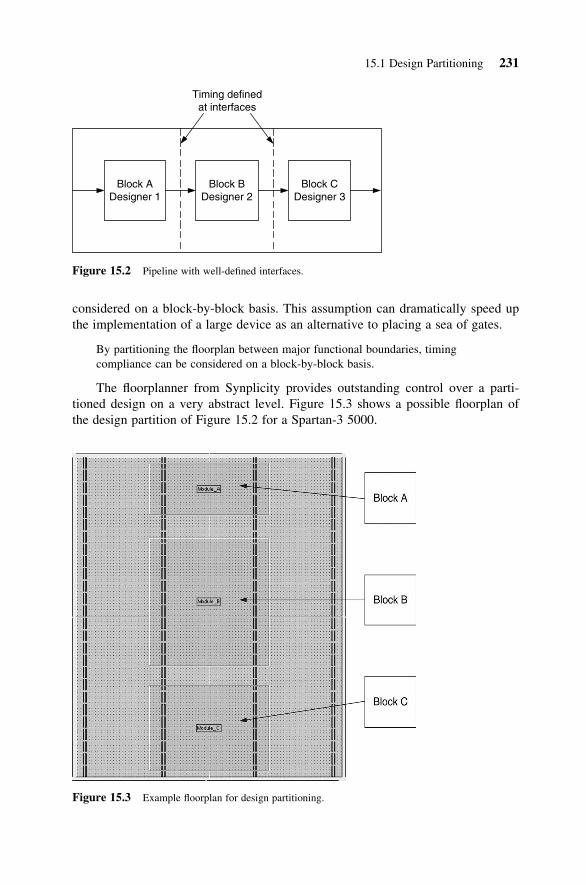
considered on a block-by-block basis. This assumption can dramatically speed up
the implementation of a large device as an alternative to placing a sea of gates.
By partitioning the floorplan between major functional boundaries, timing
compliance can be considered on a block-by-block basis.
The floorplanner from Synplicity provides outstanding control over a parti-
tioned design on a very abstract level. Figure 15.3 shows a possible floorplan of
the design partition of Figure 15.2 for a Spartan-3 5000.
Figure 15.2 Pipeline with well-defined interfaces.
Figure 15.3 Example floorplan for design partitioning.
15.1 Design Partitioning 231

The regions in this diagram define the physical area occupied by each block.
An FPGA device of this size would normally take many hours to successfully place
and route with a blanket sea of gates. With the above partitioning, however, this run
time will be dramatically reduced to three smaller (and more manageable) place
and route operations. Assuming all interfaces are registered at the boundary, the
relatively large gaps between the blocks will not cause timing problems. Besides
run time, another benefit to this type of partitioning is that major structural or layout
changes in one block need not affect the others. Thus, a methodology that employs
design partitioning works in close harmony with an incremental design flow.
15.2 CRITICAL-PATH FLOORPLANNING
Floorplanning is often used by designers who have very difficult timing con-
straints and need to tighten their critical paths as much as possible. The floorplan
in this case would be created after the final implementation results were generated
and the critical path was defined. This information would be back-annotated to
the floorplanner whereby the designer would manually define location constraints
for the critical logic elements. These physical constraints would then be forward
annotated into the place and route tool to complete an iterative cycle. Figure 15.4
illustrates the design flow when using a floorplan to constrain only critical paths.
Figure 15.4 Design flow with critical path floorplanning.
232 Chapter 15 Floorplanning

In this case, the floorplanning step is not a static and unchanged step in the
process as it is with a design partition but rather a key link in the iterative timing
closure loop.
When floorplanning the critical path, the floorplan is a key link in the iterative
timing closure loop.
Note that the floorplan is not modified until a critical path has been deter-
mined and will be modified during every iteration of the timing closure loop.
Figure 15.5 illustrates two possible critical-path-floorplan constraints.
In this example, there are no major functional partitions in the floorplan.
Instead, the floorplan consists of two small regions designed to tighten the timing
for two distinct critical paths in the design. These regions are created ad hoc
based on the timing info that is fed back to the floorplanner and will be updated
for every iteration of the timing closure loop.
15.3 FLOORPLANNING DANGERS
The danger in floorplanning is that if done incorrectly, it can dramatically
decrease the performance of the implementation. This is because of the fact that
good placement directly corresponds with a design that performs well, and bad
placement directly corresponds with a design that performs poorly. This may
seem like an obvious statement, but a corollary to this is that a bad floorplan will
lead to bad placement and will subsequently lead to poor performance. Thus, a
floorplan of any type will not have a nondecreasing impact on performance.
Rather, a bad floorplan will make things much worse.
A bad floorplan can dramatically reduce the performance of a design.
It is important to note that not all designs lend themselves to floorplanning.
Designs that are pipelined and have a very regular data flow, such as with a pipe-
lined microprocessor, clearly lend themselves to floorplanning. Devices that
implement primarily control or glue logic or that don’t have any definable major
Figure 15.5 Example critical-path-floorplan constraints.
15.3 Floorplanning Dangers 233

data path often do not lend themselves to a good floorplan that is intended to par-
tition the design. If the design is indeed simply a sea of gates, then it would be
optimal to allow the synthesis and place and route tools to treat it as such.
One general heuristic to determine if a design is a good candidate for critical-
path floorplanning is to analyze the routing versus logic delays. If the percentage
of a critical path that is consumed in routing delay is the vast majority of the total
path delay, then floorplanning may assist in bringing these structures closer
together and optimizing the overall routing resources and improving timing per-
formance. If, however, the routing delay does not take up the majority of the
critical-path delay and there is no clearly definable data path, then the design may
not be a good candidate for floorplanning.
Floorplanning is a good fit for highly pipelined designs or for layouts dominated
by routing delay.
For designs that may lend themselves to a good floorplan, there are a number
of considerations that must be taken into account to ensure that the performance
will actually be improved. This is discussed in the next section.
15.4 OPTIMAL FLOORPLANNING
The optimal floorplan will group logic structures that have direct interconnect in
close proximity to one another and will not artificially separate elements that may
lie in a critical path. The following sections describe methods to optimize the
floorplan.
15.4.1 Data Path
A design that is data path centric is often relatively easy to partition. For most
high-speed applications, the pipeline to be partitioned will usually apply to the
data path. Because the data path carries the processed information and is required
to do so at very high speeds (often running continuously), it is recommended to
floorplan this first as shown in Figure 15.6.
In this scenario, a floorplan is created to partition the data path only. This
includes the main pipeline stages and all associated logic. The control structures
and any glue logic that do not lie on the primary data path can be placed auto-
matically by the back-end tools.
The floorplan usually includes the data path but not the associated control or glue
logic.
15.4.2 High Fan-Out
High fan-out nets are often good candidates for floorplanning as they require a
large amount of routing resources in one specific region. This requirement often
234 Chapter 15 Floorplanning

leads to a high degree of congestion if the loads are not placed in a close proxi-
mity to the driver as shown in Figure 15.7.
If the loads are located a relatively long distance from the driver, the inter-
connect will occupy a large amount of routing resource at the output of the
driver. This will make other local routes more difficult and correspondingly
longer with larger delays. Figure 15.8 illustrates the benefit of constraining the
high fan-out region to a small area.
By confining the high fan-out region to a small and localized area, the effects
to other routes will be minimized. This will provide faster run times for the place
and route tool as well as a higher performance implementation due to the mini-
mization of routing delays.
15.4.3 Device Structure
The device structure is critical in the floorplan, as built-in structures cannot be
moved around with either the floorplan or the placement tools. These built-in
Figure 15.6 Data-path floorplanning.
15.4 Optimal Floorplanning 235

structures include memories, DSPs, hard PCI interfaces, hard microprocessors,
carry chains, and so forth. It is therefore important not only to floorplan the
design such that the blocks are placed optimally relative to one another but also
such that built-in structures can be utilized efficiently and that routes to the
custom logic are minimized.
A floorplan should take into consideration built-in resources such as memories,
carry chains, DSPs, and so forth.
In Figure 15.9, input and output logic resources are tied to the RAM inter-
face. For a sizable RAM block, it is usually more desirable to use the fixed RAM
Figure 15.7 Congestion near high fan-out regions.
Figure 15.8 Floorplanning high fan-out regions.
236 Chapter 15 Floorplanning

resources available in certain regions of the FPGA as opposed to an aggregation
of smaller RAM elements distributed throughout the FPGA. The constraint for a
floorplan on this path would then be dependent on the fixed location of the RAM
resource as shown in Figure 15.10.
Figure 15.9 Fixed FPGA resources.
Figure 15.10 Floorplanning around fixed FPGA resources.
15.4 Optimal Floorplanning 237

15.4.4 Reusability
A good floorplan will allow various modules and groups of modules to be reused
without a dramatic impact on the performance of those modules. In a sea of gates
design, it is common to find that changes to totally unrelated areas of the design
can cause timing problems in other aspects of the design. This is due to the pro-
gressive nature of an unconstrained place and route algorithm. The chaos effect
ensues when a small placement change on one side of the FPGA shifts logic
resources over, forcing other local logic structures out of the way, and so on until
the entire chip has been replaced with entirely new timing. For a constrained pla-
cement via a good floorplan, this is not an issue as the relative timing is fixed for
the critical-path modules, and any changes must operate around that floorplan.
In Figure 15.11, the critical logic is constrained inside the floorplan region
and will not be affected internally as placement changes around it.
15.5 REDUCING POWER DISSIPATION
Previous sections discussed floorplanning in the context of timing performance,
organization, and implementation run-time. There is an additional use for floor-
planning, and that is the reduction of the dynamic power dissipation. A route
from logic device A to device B is illustrated in Figure 15.12.
Because of the fact that the capacitance of the trace (Ctrace) is proportional to
the area of the trace, and assuming the width of the trace is fixed for an FPGA
routing resource, the capacitance will be proportional to the length of the trace. In
other words, the capacitance that the driver must charge and discharge will be
proportional to the distance between the driver and the receiver.
Figure 15.11 Shielding from layout changes.
238 Chapter 15 Floorplanning

In our original discussion on dynamic power dissipation, it was determined
that the power dissipated on high-activity lines was proportional to the capaci-
tance of the trace times the frequency. In this section, we will assume that the
functionality is locked down and the activity on the various traces cannot be
changed. Thus, to minimize the power dissipation, we must minimize the routing
lengths of high-activity lines.
For timing optimization, the place and route tool will place critical-path com-
ponents in close proximity to one another in an attempt to achieve timing compli-
ance. The critical path, however, does not indicate anything about high activity.
In fact, a critical path may have a very low toggle rate, whereas a component that
easily meets timing such as a free running counter may have a very high toggle
rate. Consider the scenario where the critical path has been constrained to a small
region.
In Figure 15.13, the critical path has been constrained, and the clock frequency
has been maximized. However, the timing-driven placement has not identified the
high-activity circuit as a timing problem and has scattered the components around
Figure 15.12 LC trace parasitics.
Figure 15.13 Floorplanning to minimizing high-activity nets.
15.5 Reducing Power Dissipation 239

the critical path as was convenient. The problem is that due to the long routes on
the high-activity lines, the total dynamic power dissipation will be relatively high.
To reduce this power consumption, another placement region can be added for the
high-activity circuit to ensure that the interconnect is minimized. If the high-
activity circuit is independent of the critical path, this can usually be done with
little impact to the timing performance.
A floorplan targeted at minimizing trace lengths of high-activity nets can reduce
dynamic power dissipation.
15.6 SUMMARY OF KEY POINTS
. By partitioning the floorplan between major functional boundaries, timing
compliance can be considered on a block-by-block basis.. When floorplanning the critical path, the floorplan is a key link in the itera-
tive timing closure loop.. A bad floorplan can dramatically reduce the performance of a design.. Floorplanning is a good fit for highly pipelined designs or for layouts domi-
nated by routing delay.. The floorplan usually includes the data path but not the associated control
or glue logic.. A floorplan should take into consideration built-in resources such as mem-
ories, carry chains, DSPs, and so forth.. A floorplan targeted at minimizing trace lengths of high-activity nets can
reduce dynamic power dissipation.
240 Chapter 15 Floorplanning

Chapter 16
Place and Route Optimization
Most implementation tools for FPGA layout (commonly referred to by the two
main stages of layout: place and route) provide the designer with dozens of
optimization options. The problem designers will run into with these options is
similar to the problem they will run into with synthesis optimization; that is, they
typically do not fully understand the implication of all of these options. Therefore,
certain optimizations are often used where they are not needed, and other optimi-
zations go unused where they could have a significant impact on performance.
Similar to Chapter 14, this chapter describes the most important aspects of place
and route optimization and provides practical heuristics that can be immediately
leveraged by the reader. During the course of this chapter, we will discuss the
following topics:
. Creating optimal constraints prior to place and route optimization.
. The relationship between placement and routing.
. Reducing route delays with logic replication.
. Optimization across hierarchy.
. Packing registers into I/O buffers.
. Utilizing the pack factor.
. When to pack logic into RAM.
. Ordering registers.
. Variances with placement seed.
. Greater consistency with guided place and route.
16.1 OPTIMAL CONSTRAINTS
Before launching into the actual place and route optimizations themselves, it is
important to emphasize the importance of defining a complete set of timing
241
Advanced FPGA Design. By Steve KiltsCopyright # 2007 John Wiley & Sons, Inc.

constraints. The reason this topic is listed first is to ensure that the optimizations
contained in this chapter are not addressed until sufficient time has been spent
creating accurate design constraints.
A complete set of constraints should be created before any optimization takes
place.
The constraints that must be included on every design include all clock defi-
nitions, I/O delays, pin placements, and any relaxed constraints including multi-
cycle and false paths. Although a particular path may not be a critical timing path,
often by relaxing specifications on unrelated paths, placement and routing
resources can be freed for more critical paths. For more information regarding
these constraints, see Chapter 18.
One class of constraints that is often not covered by typical timing analysis
for FPGAs (and is not included in Chapter 18) includes voltage and temperature
specifications. The voltage/temperature specifications are among the set of con-
straints that most often go overlooked by designers but in many cases provide the
easiest way to achieve significant timing improvements.
Most designers know that all FPGA devices (like most semiconductor devices)
specify a worst-case voltage and temperature under which the device will operate.
In the context of FPGA timing analysis, worst-case temperature would be the
highest temperature, and the worst-case voltage would be the lowest voltage,
because both of these constraints will increase the propagation delays (we typically
don’t worry about hold delays in FPGAs because of the minimum delays built into
the routing matrix). For example, the high end of the commercial temperature
range for Xilinx FPGAs is 858C, and the worst-case voltage rating is usually
between 5% and 10% of the recommended operating voltage. This would corre-
spond with approximately 1.14 V for a 1.2-V rail, 3.0 V for a 3.3-V rail, and so on.
These worst-case voltage and temperature conditions are used by default
when performing worst-case timing analysis. However, few systems will require
the FPGA to run at the extreme conditions of 858C (junction temperature of the
FPGA) and a 10% droop in the power rail. In fact, most systems will only experi-
ence conditions far less extreme than this.
If the system in which the FPGA operates is designed within certain temperature
and voltage conditions, then the FPGA timing analysis can and should be
performed under the same conditions.
When this is taken into consideration, many engineers find that they can
shave full nanoseconds off of their critical path (depending on the device technol-
ogy of course). If the timing violations are less than this incremental improve-
ment, engineers will find that they were struggling over timing violations that
didn’t really exist!
Consider the example of a 16-bit counter. Under default timing analysis con-
ditions, this counter will run at 276 MHz in a Virtex-II device. The menu in
242 Chapter 16 Place and Route Optimization

Figure 16.1 shows the default voltage and temperature settings that will be passed
to the Xilinx timing analysis tool.
In this case, the worst-case voltage setting is 95% of the specified supply
voltage. A 5% voltage variance may be reasonable for a switching supply, but if this
is running off of a linear supply that can supply more than enough current to the
core, this specification is overkill. Additionally, the junction temperature setting is at
858C. Most likely, the functional design will not generate such a temperature, and
thus this specification is again probably overkill. We can reduce these to more
reasonable parameters for our hypothetical “light-weight” system where the supply
only varies by 2% and the temperature never exceeds 458C (Fig. 16.2).
Figure 16.1 Default operating voltage and temperature settings.
Figure 16.2 Realistic operating voltage and temperature settings.
16.1 Optimal Constraints 243

The result is that the counter now runs at just under 290 MHz. This perform-
ance improvement did not require any actual changes to the FPGA but was
simply a matter of analyzing the design under the correct conditions.
Adjusting the voltage and temperature settings does not require any changes to
the FPGA implementation and can provide an easy means to incrementally
improve the worst-case performance.
The only drawback to this approach is that devices need to be fully character-
ized according to temperature and voltage before the vendor will allow access to
this option. Due to the ongoing battle between the FPGA vendors to produce the
fastest FPGAs before their competitors, they typically release devices before this
characterization has been completed. In fact, if you are using a brand-new tech-
nology, you can usually count on this option not being available. In the timing
analysis tools, this option will be inaccessible. This is one of the advantages of
using a device with a moderate amount of maturity.
16.2 RELATIONSHIP BETWEEN PLACEMENTAND ROUTING
Most modern FPGA place and route tools do a very good job of achieving timing
compliance with the automated algorithms, and because of this, manual placement
and/or routing is no longer commonplace. However, many FPGA design engin-
eers have been “spoiled” by automated implementation tools to the point where
the layout is not even considered outside of very-high-speed designs. This lack of
attention has created a lack of understanding and therefore a very inefficient use
of the various implementation options available for the layout. Most important of
all these options, whether the goal is area or speed, is the relationship of place-
ment and routing relative to processor effort.
Specifically, we are referring to the hooks provided to the FPGA design in
the back-end tools that allow the designer to adjust the processor effort and corre-
sponding algorithmic sophistication of the placement and routing. These options
are almost always presented and controlled independently, which is unfortunate
due to the strong relationship they possess.
In basic training, engineers are told that they can increase the effort of place-
ment and routing to achieve better results. We practice increasing the effort levels
in lab experiments and see the improvements. In practice, we see similar improve-
ments. So what’s the problem? The problem is that if you turn the router effort
level up beyond trivial effort before you have an optimal placement, you are
wasting time. Because of the fact that most projects have schedules with deadlines
and the fact that most FPGA designers go through many iterations before achiev-
ing timing closure, this is certainly something worth considering.
The fundamental concept to understand here is that routing is extremely
dependent on placement. For a design of any complexity, a good route can only
be achieved with a good placement. Most FPGA design engineers have not run
244 Chapter 16 Place and Route Optimization

enough experiments to realize this on their own, but placement is vastly more
important to performance than is routing. This is particularly true of FPGAs due
to the coarse nature of a routing matrix (in an ASIC, there is more flexibility to
be creative with the routing).
If you were to take a typical design and run hundreds of combinations of
placement and routing effort levels and then plot your data, you would likely see
something very similar to the graph shown in Figure 16.3.
As can be seen from the curves in Figure 16.3, placement has a dominant
(call it first-order effect) on the performance of the design, and routing has a
relatively minor effect.
Placement effort has a dominant effect on performance, whereas routing effort
has a relatively minor effect.
To determine the optimal placement and routing effort levels, a designer
should follow this procedure:
1. Set both placement and routing effort levels to minimum.
2. Run place and route to determine if the worst case timing is in fact due to
a sub-optimal layout and not due to excessive logic levels.
3. Increment placement effort until timing is met or max effort has been
reached.
4. If at max placement effort timing is not met, begin incrementally increas-
ing the routing effort.
5. If timing closure cannot be met, revisit the architecture of the design.
6. If a high routing effort is required to meet timing, it may be a good
idea to revisit the architecture of the design to optimize for timing (see
Chapter 1).
Figure 16.3 Performance versus placement and routing effort.
16.2 Relationship between Placement and Routing 245

16.3 LOGIC REPLICATION
Logic replication occurs early in the placement process for structures that fan out
to other logic elements that cannot (for any number of reasons) reside in the same
proximity. The problem this addresses is illustrated in Figure 16.4.
In this scenario, the output of D2 fans out to two structures that are relatively
distant from one another. Regardless of where the driver is placed, the resultant
route will be lengthy to one of the driven elements. To eliminate potentially long
routing delays, logic duplication will replicate the driver as shown in Figure 16.5.
Logic duplication should be used only on critical path nets with multiple loads
that cannot be physically localized.
The effect of this duplication is that an individual driver can be placed closer
to each load, thereby minimizing the route length and delay of the route. Clearly,
Figure 16.4 A fan-out that forces long routes.
Figure 16.5 Registers duplicated to balance route length.
246 Chapter 16 Place and Route Optimization

this optimization will reduce routing delays but will increase area. This optimiz-
ation may cause inferior results if the utilization of the device is already high. If
the placement tool is not intelligent enough to only perform this on critical-path
routes, this option may need to be disabled and duplication added to the RTL
with corresponding “don’t touch” attributes to ensure that the synthesis does not
optimize the duplicate structures.
16.4 OPTIMIZATION ACROSS HIERARCHY
Optimizing across hierarchical boundaries will allow any of the placement algor-
ithms to operate when the path extends across a module boundary as shown in
Figure 16.6.
Typically, if a particular optimization is desired, it will be beneficial to apply
it to intermodule interfaces as well as simply the paths within the modules them-
selves. Often, logic at the module boundaries does not fully occupy entire LUTs.
An example is shown in Figure 16.7.
In this above, a separate LUT is used to implement a NAND operation at
each module boundary. By enabling the optimization across boundaries, each of
these logical operations can be combined into a single LUT, thereby reducing the
area utilization of this operation by one half.
The primary case where this would not be desired is if gate-level simulations
need to be run on the postimplementation netlist. In this case, a hierarchy that is
intact will be very desirable.
Optimization across hierarchy is not desirable when gate-level simulations are
required.
If debug is required on the back-annotated netlist, a preserved hierarchy will
allow the designer not only to traverse the design but also to easily identify
signals at the boundaries of the modules that may be useful for debug.
Figure 16.6 Critical path that crosses hierarchy.
16.4 Optimization across Hierarchy 247

16.5 I/O REGISTERS
Many FPGAs have flip-flops built into the input and output buffers to optimize
the timing in and out of the chip. Along with these special I/O buffers will be an
optimization to enable or disable the packing of these registers into the I/O.Figure 16.8 illustrates the concept of packing registers into the I/O buffers.
There are a number of advantages to placing a register in the I/O:
. The delays at the I/O of the FPGA are minimized.
. More logic is available internally.
. Superior clock-to-out timing.
. Superior setup timing.
The disadvantage of this optimization is that a register that is placed in an
I/O buffer may not be optimally placed for the internal logic as shown in
Figure 16.9.
For high-speed designs that have tight timing requirements at both the I/Oand the internal logic, it may be advantageous to add another layer of pipeline
registers at the I/O if allowed by the design protocol as shown in Figure 16.10.
Figure 16.7 Example hierarchy optimization.
248 Chapter 16 Place and Route Optimization

Figure 16.8 Register packed into I/O buffer.
Figure 16.9 Imbalanced route delays with I/O packing.
16.5 I/O Registers 249

If there are a large number of I/O registers, the extra pipeline layer may add
significant overhead in terms of register utilization and potentially congestion.
An extra pipeline register may be required for high-speed designs when packing
registers into I/O.
Thus, if there are not tight I/O timing requirements and there are a relatively
large number of I/O registers, this optimization is not recommended.
16.6 PACK FACTOR
The pack factor is defined as a percentage and will artificially limit the usage of
logic resources in the FPGA. For instance, a pack factor of 100% tells the placement
tool that all logic elements are available for implementation, whereas a pack factor
of 50% will tell the tool that only half of the total logic resources are available.
The uses for this optimization are limited but can be leveraged by advanced
users. For instance, to keep a placeholder for future logic that is not included in the
current flow, the pack factor can be reduced according to the estimated size. The
ease of implementation will be similar to what the designer can expect when the
new core is integrated. Thus, resource utilization problems may be identified sooner.
Additionally, the pack factor can be used to determine the amount of head-
room in a design, or “true” utilization. If there are unused logic elements, the
place and route tool will be more liberal in the duplication of logic elements and
the manner in which these are spread out to optimize the layout. A logic element
is defined as utilized if any portion of it is used to implement logic and not
necessarily when it is fully utilized. Thus, the percentage utilization will usually
be higher than the true utilization.
Setting a pack factor can help to determine the true utilization.
In other words, an FPGA that reports 60% utilization may have much more
than 40% more logic resources available (ignoring the routability issues as utiliz-
ation approaches 100% of course). To estimate true utilization and headroom in
the design, the pack factor can be reduced until the design cannot be properly
routed.
Figure 16.10 Additional pipeline register with I/O packing.
250 Chapter 16 Place and Route Optimization

16.7 MAPPING LOGIC INTO RAM
The major players in the high-end FPGA world are SRAM based, which means
that logic functions are coded into LUTs. These LUTs are small SRAM cells dis-
tributed across the FPGA and available for general logic implementation. It
would seem that a natural extension of this would be to implement logic in the
larger dedicated RAM blocks (the ones actually used like RAM), particularly
when utilization is running low. Although this may make sense conceptually, the
problem associated with this is performance.
The small distributed RAM cells will have very small delays, and logic will
propagate through these LUTs very quickly and efficiently relative to other logic
elements. The larger RAM blocks, on the other hand, will have much larger
delays associated with them and will subsequently create a very slow implemen-
tation. In general, it is not wise to rely on logic that is packed into dedicated
RAM blocks. Only as a last resort in an extremely high density and slow design
would this be useful.
16.8 REGISTER ORDERING
Register ordering is a method used by the placement tool to group adjacent bits
of a multibit register into a single logic element. Most cell-based logic elements
have more than one flip-flop, and thus by placing adjacent bits together the timing
can be optimized as shown in Figure 16.11.
Figure 16.11 Sequential bits are ordered.
16.8 Register Ordering 251

The problem that arises with register ordering is that it may prevent a group
of registers that have added pipelining for route balancing to be grouped together.
This will prevent the additional registers from dividing the routing delay as orig-
inally intended. Consider the delay balancing register used above when packing
registers into I/O buffers.
As can be seen from Figure 16.12, the benefit of the pipelined register has
been eliminated due to the fact that it has been placed adjacent to its driver.
Register ordering should not be used when extra flip-flops have been added to
divide routing delay.
16.9 PLACEMENT SEED
Designers typically do not like the concept that there may be a certain degree of
randomness in their design flow or implementation tools. However, it is important
to note that a placement for a given design with a set of constraints is not entirely
deterministic. In other words, there is no single optimal placement for any given
design; at least, not one that can be easily determined by today’s technology prior
to the placement process itself. In fact, as shown in Figure 16.13 this is not an
obvious problem at all, even for an automated placer, to determine the optimal
starting point for the placement process.
Thus, the placement tool needs to be “seeded” similar to a process for
random number generation. The exact definition of a seed is a bit abstracted from
the standpoint of the designer, but for useful purposes, different seeds essentially
provide the placer with slightly different starting points by which the rest of the
placement process branches. This is illustrated in Figure 16.14.
Some vendors extend this beyond simply the initialization to other “random”
parameters of the placement process such as relative weighting of the various
constraints, desirable placement distances, and estimates for routing congestion.
Xilinx calls this the placement “cost table,” which affects the various placement
parameters, but abstracts this to an integer (1, 2, 3, etc.). Each integer corresponds
with a different set of initial conditions and placement parameters, but because of
the low level complexity, it is abstracted to a single number and the actual func-
tionality is hidden from the parameter table.
Figure 16.12 Performance reduction with register ordering.
252 Chapter 16 Place and Route Optimization

The benefit to adjusting the placement seed is that the user can “take another
shot” at meeting the timing constraints without actually changing anything in the
design. This can be automated with a process called multipass place and route.
When this option is selected, the place and route tool will run the implementation
multiple times and automatically vary the seed on every run. This will of course
require a large amount of time to produce effective results, so this is typically
used on overnight runs where the target design is not already meeting the timing
constraints in a repeatable manner.
It is important to note here that the place and route algorithms are actually
very good regardless of the seed, and any changes to the various parameters will
have a very small effect. The danger some newer designers run into is to spend
Figure 16.13 Initial placement.
Figure 16.14 Different placement starting conditions.
16.9 Placement Seed 253

large amounts of time focusing on this type of optimization to meet their timing
constraints instead of focusing on the true issues in their design. Adjustment of
the placer seed should only be used as a last resort when all architectural changes
have been exhausted, all constraints have been added, and the timing violations
are very small (hundreds of picoseconds or less).
Seed variances with multipass place and route should only be used as a last
resort.
This should also be used only when repeatability is not a critical issue. If
timing is so tight that tweaking the seed is required to meet timing, then any
other changes to the RTL or constraints will more than likely lead to new random
behavior in the design and require multiple runs of the placer with new variations
in the seed. Thus, with this type of methodology, the designer will not have
repeatability in the timing closure when small changes are made. This issue of
repeatability is discussed in the following section.
16.10 GUIDED PLACE AND ROUTE
A very common situation for a designer is to spend days or weeks tweaking a
design to meet timing, perhaps even using the automated seed variances as
described above, only to be faced with a small change that could ripple through
the existing placement and completely change the timing characteristics. At this
point, the designer may have to reoptimize the design and possibly find a new
seed that allows timing closure.
To avoid a situation where small changes initiate a domino effect on the
placement of logic elements and subsequent change in overall performance
characteristics (not to mention the run-time associated with reimplementing every-
thing for a small change), FPGA place and route tools often provide a guide
option that leverages the placement and routes from a prior implementation.
A placement guide will find all components that match the old implemen-
tation and lock the same elements to the same location. The advantage to this
strategy is that the run time is dramatically reduced and the timing characteristics
of the guided elements stay the same. Thus, a guide mode such as described
above can provide the designer with a means to make small changes with a corre-
sponding small change in the place and route process.
The place and route process following small changes should utilize a guide file to
maximize consistency and minimize run time.
16.11 SUMMARY OF KEY POINTS
. A complete set of constraints should be created before any optimization
takes place.
254 Chapter 16 Place and Route Optimization

. Adjusting the voltage and temperature settings does not require any
changes to the FPGA implementation and can provide an easy means to
incrementally improve the worst-case performance.
. Placement effort has a dominant effect on performance, whereas routing
effort has a relatively minor effect.
. Logic duplication should be used only on critical-path nets with multiple
loads that cannot be physically localized.
. Optimization across hierarchy is not desirable when gate-level simulations
are required.
. An extra pipeline register may be required for high-speed designs when
packing registers into I/O.
. Setting a pack factor can help to determine the true utilization.
. Register ordering should not be used when extra flip-flops have been added
to divide routing delay.
. Seed variances with multipass place and route should only be used as a last
resort.
. The place and route process following small changes should utilize a guide
file to maximize consistency and minimize run time.
16.11 Summary of Key Points 255


Chapter 17
Example Design:
Microprocessor
The simple RISC computer (SRC) implemented in this chapter is a widely used
microprocessor model for academic purposes (a detailed description of the SRC
architecture can be found in the book Computer Systems Design and Architecture
by Vincent Heuring and Harry Jordan). The SRC microprocessor has a fairly
generic architecture and is not complicated by many of the optimizations
required in a commercial processor. Thus, it lends itself well to a straightforward
pipelined implementation that helps to illustrate some of the various optimization
strategies.
The objective of this chapter is to describe an implementation for the SRC pro-
cessor and optimize the performance characteristics using various options
described in previous chapters.
17.1 SRC ARCHITECTURE
The SRC is a 32-bit machine with 32 general-purpose registers (5-bit register
addressing), 232 bytes of main memory (addressable from any of the 32-bit registers),
a single 32-bit program counter, and a 32-bit instruction register (Fig. 17.1).
The instruction classes are defined as follows:
. Load and store
. Branch
. Simple arithmetic: add, sub, invert
. Bitwise and shift
The pipelined implementation of the SRC processor partitions the main func-
tional operations into distinct stages. Each stage is separated by a layer of
257
Advanced FPGA Design. By Steve KiltsCopyright # 2007 John Wiley & Sons, Inc.

registers that limits the timing between the stages themselves. The pipeline is
shown in Figure 17.2.
With the topology shown in Figure 17.2, it is possible to theoretically
execute instructions such that one operation is completed every clock cycle. Note
that because of a number of conditions that will periodically stall the pipeline, the
number of clocks per instruction will be slightly larger than one, but for the pur-
poses of this example we will assume that the fully pipelined implementation pro-
vides us with one instruction per clock cycle.
The code for the top level of the pipeline is shown in Appendix B. For
brevity, the code for the submodules is not listed unless explicitly referred to for
the sake of the example. There are a few interesting things to note about this
implementation. First, it is assumed that the register file and system memory are
located outside of the FPGA. These could be implemented inside the FPGA if
block RAM resources are available, but if a large amount of system memory is
required, it may be more cost effective to use an external memory device.
Second, note that each stage is separated by a layer of registers that define the
pipeline. Any feedback signals as defined by the “Feedback” elements are also reg-
isters. Thus, any signal that passes to any stage is clearly defined as to the stage it
belongs to and keeps the timing organized as the design becomes more complex.
Third, notice the parameterization of the registers themselves. The first par-
ameter passed to the DRegister module is the width, which allows the register
module to be reused among all DRegister elements.
Figure 17.1 SRC registers and memory.
258 Chapter 17 Example Design: Microprocessor

Taking this pipelined design as a starting point, the following section
describes some of the key optimization options and how they can be used to
modify the performance of this design.
17.2 SYNTHESIS OPTIMIZATIONS
The SRC microprocessor was implemented in a Xilinx Virtex-2 part for this
example as this is a mature FPGA technology that has been well characterized. A
first-pass synthesis targeted at a XC2V250 with a 50-MHz clock gives us the per-
formance as shown in Table 17.1.
Figure 17.2 Main SRC pipeline.
17.2 Synthesis Optimizations 259

Note that due to the relatively slow timing constraint, the logic in the critical
path is implemented in a serialized compact fashion and contains 23 levels of
logic as shown in Figure 17.3.
17.2.1 Speed Versus Area
In the initial implementation, timing was easily met. This means that any paths
that were not determined to be critical (worst-case delay) would be implemented
with a compact architecture. This is not to say, however, that this is the
maximum achievable frequency. If we push the timing constraint to 100 MHz,
the synthesis tool will implement parallel architectures with a corresponding
increase in area.
As can be seen from Table 17.2, the synthesis tool was able to expand the
critical paths into higher speed implementations, thereby increasing the area 9%
and the speed by more than 50%. Note that the timing increase does not display a
1 : 1 mapping to the area increases. This is because of the fact that the timing is
only limited to the worst-case path. Therefore, the area increase is only an indi-
cator that represents the number of paths that have been expanded to achieve the
faster timing constraint. For example, the path that was previously the critical
path with 23 levels of logic was remapped to a parallel structure as shown in
Figure 17.4.
Assuming all reasonable architectural trade-offs have been made, there are
various synthesis options that can be used to improve performance as described in
the following sections.
Table 17.1 Initial Synthesis
Speed 63.6 MHz Slack ¼ 4.3 ns
LUTs 1386 45% utilization
Registers 353 11% utilization
Figure 17.3 Serialized logic in critical path.
Table 17.2 Increase in Target Frequency
Speed 97.6 MHz Slack ¼ 22.4 ns
LUTs 1538 50% utilization
Registers 358 11% utilization
260 Chapter 17 Example Design: Microprocessor

17.2.2 Pipelining
The new critical path now lies on the feedback path from IR2, through stage 2,
and ending at X3 as shown in Figure 17.5.
To increase the performance of the new critical path, pipelining can be
enabled to rebalance the logic around register layers. In this example, X3 is pushed
into stage 2 and rebalanced around the multiplexing logic. Due to the replication of
Figure 17.4 Parallel logic in the old critical path.
Figure 17.5 New critical path in stage 2.
17.2 Synthesis Optimizations 261

registers from the output of muxes to multiple inputs, the total register utilization
essentially doubled with an insignificant change to the overall logic utilization.
The end result is that by pushing registers across logic boundaries and adding
the necessary registers for all inputs, the critical path was reduced enough to meet
timing at 100 MHz. Note that once the timing constraint was met, the synthesis
tool stopped the pipelining operations to minimize overall register utilization.
This is illustrated by the fact that bumping up the timing requirement to 110 MHz
increases the additional register utilization as shown in Table 17.4.
17.2.3 Physical Synthesis
By engaging physical synthesis, we now begin to use physical placement infor-
mation to optimize the performance of the design. With this placement infor-
mation, we are able to target 120 MHz and easily close timing.
Note that the results in Table 17.5 are obtained by allowing the synthesis tool
to determine all placement information with no user intervention. However,
because this microprocessor design is highly pipelined, it is possible to guide the
placement via a floorplan to achieve even better timing. This is discussed in the
next section.
17.3 FLOORPLAN OPTIMIZATIONS
Because of the fact that the design is nicely partitioned into clearly defined pipe-
line stages, there is an opportunity to increase performance even further using
predefined floorplan topologies.
Table 17.3 Results with Pipelining
Speed 100.7 MHz Slack ¼ 0.1 ns
LUTs 1554 50% utilization
Registers 678 22% utilization
Table 17.4 Results with Extra Pipelining
Speed 111.2 MHz Slack ¼ 0.1 ns
LUTs 1683 54% utilization
Registers 756 24% utilization
Table 17.5 Results with Physical Synthesis using Synplify
Premiere
Speed 122 MHz Slack ¼ 0.2 ns
LUTs 1632 53% utilization
Registers 772 25% utilization
262 Chapter 17 Example Design: Microprocessor

17.3.1 Partitioned Floorplan
The first method that is used is that of a design partition. This is where the pipe-
line structure itself provides guidance as to the initial floorplan. In Figure 17.6,
stages 2–4 are shown in block diagram form with intermediate register layers.
It is sensible to begin floorplanning with a similar physical layout. In the initial
floorplan shown in Figure 17.7, the various pipeline stages are defined to be vertical
sections of area to allow for ease of carry chain structures inside the FPGA.
For this floorplan, it was noted that the majority of the long paths reside
between stages 1, 2, and 3. The three stages are given individual regions as
shown in the floorplan of Figure 17.7. The data path flows from left to right, and
a small amount of space is left between the stages for register placement. The
critical paths between these modules are incrementally optimized as shown in
Table 17.6. Note that the timing constraint has been increased to 125 MHz.
Our initial try did not produce results significantly better than the default phys-
ical synthesis approach. This is because of the large groups of constrained elements,
the high aspect ratio of the physical regions themselves, and the fact that little
importance was given to grouping only those paths that had tighter timing
Figure 17.6 Natural pipeline flow between stages 2 through 4.
17.3 Floorplan Optimizations 263

requirements. To continue optimizing the performance, we must focus on the critical
paths one at a time and physically group these together to minimize routing delays.
17.3.2 Critical-Path Floorplan: Abstraction 1
The iterative process begins by identifying the critical path and grouping these
components together in a specified region. In this example, the critical paths lie
between the registers surrounding stage 2. Figure 17.8 shows the worst-case path
through stage 2.
With the first iterative method, we can first try constraining stage 2 and then
adding in surrounding registers as required. The new floorplan is shown in Figure 17.9.
The advantage of the floorplan of Figure 17.9 is that it is more closely focused
on the problem area and provides an even aspect ratio for ease of routing. The
floorplan of Figure 17.9 represents stage 2 as well as the source register IR2 and
the destination registers X3 and Y3. The performance is shown in Table 17.7.
As can be seen from these results, focusing our floorplan will allow us to
achieve timing compliance at 125 MHz.
Table 17.6 Results with Initial Floorplan
Speed 123 MHz Slack ¼ 20.17 ns
LUTs 1840 59% utilization
Registers 492 16% utilization
Figure 17.7 Floorplan that reflects pipeline flow.
264 Chapter 17 Example Design: Microprocessor

17.3.3 Critical-Path Floorplan: Abstraction 2
The final approach used to optimize the floorplan is to focus solely on the logic
elements in the critical path itself. This has the advantage of constraining the difficult
paths very tightly with minimal constraints on paths not under consideration. This is
Figure 17.8 Worst case path through stage 2.
Figure 17.9 Floorplan with stage 2.
Table 17.7 Results with a Focused Floorplan
Speed 127.6 MHz Slack ¼ 0.16 ns
LUTs 1804 58% utilization
Registers 559 18% utilization
17.3 Floorplan Optimizations 265

performed by taking the critical path from the default run and only constraining
these components to a particular region to reduce all routing delays in the path.
In the default implementation, the critical path lies between stage 2 and the
feedback register IR2. The implementation report indicates that approximately
50% of the total critical-path delay is routing delay only, which indicates there is
room for improvement from critical-path floorplanning.
Table 17.8 Results with Critical-Path Floorplanning
Speed 135 MHz Slack ¼ 0.0 ns
LUTs 1912 62% utilization
Registers 686 22% utilization
Figure 17.10 Critical path floorplan.
Figure 17.11 Final critical path.
266 Chapter 17 Example Design: Microprocessor

The first two critical paths from our default run are from IR2 to Y3 and
another between IR2 and X3. The elements from just these paths can be con-
strained to a region smaller than that of the previous floorplan.
By constraining only the critical paths to a smaller region, we again improve
the performance. In Table 17.8, we are now targeting 135 MHz.
After these paths have been constrained to the region shown in Figure 17.10,
the critical path now moves to the path between Y3 and Z4 through stage 3 as
shown in Figure 17.11.
The routing delay has now dropped to 40% of the total delay (60% of the
path is logic delay), which means that although there may be additional perform-
ance increases with further floorplanning, there will certainly be a diminishing
rate of return relative to the effort involved.
17.3 Floorplan Optimizations 267


Chapter 18
Static Timing Analysis
The goal of this chapter is to describe general static timing analysis (STA) as
well as methods for performing static timing analysis on complex circuit
configurations not commonly discussed in the context of STA such as
asynchronous circuits, latches, and combinatorial feedback paths. Note that these
latter structures are typically not recommended for FPGA designers mainly
because of the difficulty in implementing them correctly. However, an advanced
designer can use these structures if necessary as long as the associated issues
(particularly the timing analysis) are understood.
During the course of this chapter, we will discuss the following topics:
. Summary of basic static timing analysis
. Understanding latches in STA
. Handling asynchronous circuits in STA with combinatorial logic or event-
driven clocks
This chapter assumes the reader is already familiar with general static timing
analysis but will provide a brief summary of the basic concepts.
18.1 STANDARD ANALYSIS
Static timing analysis, as it is referred to in this chapter, is the comprehensive
analysis of all timing paths in a design relative to a set of constraints so as to
determine whether a design is “timing compliant.” The basic paths encountered
by an FPGA designer will be input to flip-flop, flip-flop to flip-flop, and flip-flop
to output as illustrated in Figure 18.1.
These have associated input delay, output delay, setup, and hold timing
requirements. The setup timing analysis refers to the long-path analysis, and the
hold timing refers to the short-path analysis. The maximum frequency is set by
the longest path in the design, which is also referred to as the critical path. The
269
Advanced FPGA Design. By Steve KiltsCopyright # 2007 John Wiley & Sons, Inc.

path analysis takes into consideration more than just the logic delays as shown in
Figure 18.2.
The maximum path delay is a function of the clock-to-Q delay, the logic and
routing delays, the setup time, and the clock skew. The maximum frequency
(minimum period) will be determined by the sum of the data-path delays minus
the clock skew. In Chapter 1, we defined the maxium frequency in terms of all
the associated delays, and here we define the minimum period as the inverse of
this relationship as shown in Equation (18.1) (minimum clock period calculation):
(again ignoring clock jitter).
Equation 18.1 minimum clock period calculation.
Tmin ¼ Tclk-q þ Tlogic þ Trouting þ Tsetup � Tskew (18:1)
where Tmin is minimum allowable period for clock, Tclk-q is time from clock
arrival until data arrives at Q, Tlogic is propagation delay through logic between
flip-flops, Trouting is routing delay between flip-flops, Tsetup is minimum time data
must arrive at D before the next rising edge of clock (setup time), and Tskew is
propagation delay of clock between the launch flip-flop and the capture flip-flop.
If the required period is greater than the minimum period defined by Tmin,
then there will be positive slack as shown in Figure 18.3.
As can be seen from the waveforms of Figure 18.3, positive slack occurs
when the data arrive at the capture flip-flop before the capture clock less the setup
time. If the data arrive after the capture clock less the setup time, the path will
Figure 18.1 Typical synchronous timing paths.
Figure 18.2 Elements of timing analysis.
270 Chapter 18 Static Timing Analysis

have negative slack and will not meet timing. Setup analysis also applies to I/O.For an input, the launch clock-to-Q and external prop time are lumped into a
single external delay for the analysis. Similarly, the output setup analysis will
assume a single external prop time that includes the setup time and clock skew.
Because these external delays are unknown to the FPGA timing analysis tool,
they must be defined by the designer.
Hold violations occur when data arrives at a flip-flop too soon after the rising
edge of the clock and are relatively easy to fix by adding additional buffering.
Hold delay violations are rare in FPGA designs due to the built-in delay of the
routing matrix. If a hold violation occurs, it usually indicates a clock skew
problem.
In addition to defining accurate constraints for the system clocks, it is also
important to define any path constraints that can be relaxed. The two most
common constraints that fall into this category are multicycle and false paths. The
multicycle path is illustrated in Figure 18.4.
Figure 18.3 Positive slack.
Figure 18.4 Multicycle path.
18.1 Standard Analysis 271

The multicycle path allows constrained signals n-cycles to propagate between
timing end points. Note that even with a multicycle path, the setup and hold
requirements are still in effect. This is because regardless of which clock edge the
data arrives at, if it arrives too close to the clock edge, a metastable condition
could still occur. A multicycle path may be added as a constraint if the data does
not need to be used in the immediately following clock period. This could occur
when interfacing to devices that do not require the immediate arrival of the data.
This often occurs in DSP applications where there is a fixed sampling rate and an
available number of clocks per sample.
A false path is similar to the multicycle path in that it is not required to pro-
pagate signals within a single clock period. The difference is that a false path is
not logically possible as dictated by the design. In other words, even though the
timing analysis tool sees a physical path from one point to the other through a
series of logic gates, it is not logically possible for a signal to propagate between
those two points during normal operation. This is illustrated in Figure 18.5.
Because the path will never be traversed during normal operation of the design,
the static timing analysis tool ignores the path between these points and is not con-
sidered during timing optimization and critical-path analysis. The main difference
between a multicycle path with many available cycles (large n) versus a false path is
that the multicycle path will still be checked against setup and hold requirements and
will still be included in the timing analysis. It is possible for a multicycle path to still
fail timing, but a false path will never have any associated timing violations.
It is possible for a multicycle path to fail timing even with an arbitrarily high
cycle constraint, but it is not possible for false paths to fail timing.
Once these constraints are in place, the STA tool can run a comprehensive
analysis of every path in the design. There are a number of advantages of static
timing analysis over simulation-based dynamic timing analysis as discussed in
previous chapters:
. Dynamic timing analysis (simulations with timing information) will only
catch a few problems. The utility of dynamic analysis is only as good as
Figure 18.5 False path.
272 Chapter 18 Static Timing Analysis

the person that wrote the simulation. STA, on the other hand, will catch all
problems within the bounds of standard timing analysis. In other words, STA
performs an exhaustive analysis on the design. The only requirement for the
designer is to set up the necessary conditions and constraints.
. It is hard to model characteristics such as jitter, as this would create a very
complex testbench and push the run times to unreasonable levels.
. With STA, combinations of various conditions can be verified with a pro-
portional increase in run time. With dynamic timing analysis, combinations
of various conditions can push the run time out exponentially.
. STA does not require any simulation cycles, and there is no overhead due
to event schedulers.
. STA provides a larger scope of timing violations including positive and
negative setup/hold, min and max transition, clock skew, glitch detection,
and bus contention.
. STA tools have the ability to automatically detect and identify critical
paths, violations, and asynchronous clocks.
The difficulty with STA arises when structures that are not well suited for
STA are analyzed in this environment. Because of these constraints, dynamic
timing analysis is often used to analyze these structures. The following sections
discuss some of the more complex topologies in more detail and recommend
methods to analyze these structures. Note that many of these structures are
uncommon and are typically not recommended for FPGA designs. Listing these
structures is not an endorsement to use them, but if an FPGA designer has good
reason, then the suggestions can be used to analyze these successfully.
18.2 LATCHES
A latch can certainly be a useful device when creating very-high-speed chips such
as microprocessors or with other high-speed pipelines. Latches should only be
used by expert designers, and even then there must be a good justification to do
so. Most of the time, latches are implemented unintentionally by poor coding
styles and then show up in the STA reports to create confusion.
Latches are usually created unintentionally by poor coding styles.
One of the most common ways latches get implemented is with modules
such as the one shown below.
// CAUTION: LATCH INFERENCEmodule latch (output reg oDat,input iClk, iDat);
always @*if (iClk) oDat <= iDat;
endmodule
18.2 Latches 273

In the above assignment, when iClk goes low the current value of oDat is held
until the next assertion of iClk. Latches such as this are typically not desirable,
but in some cases they are. Consider the following module where the latch was
most likely induced unintentionally:
// POOR CODING STYLEmodule latchinduced(output reg oData,input iClk, iCtrl,input iData);reg rData;reg wData;
always @*if (iCtrl) wData <= rData;
always @(posedge iClk) beginrData <= iData;oData <= wData;
endendmodule
In the above code segment, a latch is induced between the two D flip-flops as
shown in Figure 18.6.
In this example, the data input and the data output are both registered with a
standard D-type rising edge flip-flop, whereas the data is latched between the flip-
flops. This circuit configuration is not one that is likely implemented intentionally,
but it helps to cleanly illustrate the points regarding STA. We call this latch
active-high because the data passes through when the control input is high,
whereas the output is held when the control to the latch is low. From a timing
analysis standpoint, we are not concerned with the condition where the control to
the latch is high because the data is simply flowing through. Likewise, we are not
concerned with the condition where the control is low because the output is
frozen. What we are concerned with, however, is the timing relative to the point at
which the data is actually latched; that is, during the transition from high to low.
When analyzing timing through a latch, the STA tool will be primarily concerned
with the edge of the control signal that switches the latch into a hold state.
Figure 18.6 Induced latch.
274 Chapter 18 Static Timing Analysis

In a sense, the control to the latch is treated like a clock in STA, and the
latch is treated like a falling-edge flip-flop. The waveforms shown in Figure 18.7
illustrate the conditions for timing compliance.
A common topology that utilizes latches is called two-phase latching. In this
technique, one stage in a pipeline is latched with one polarity of the clock, while
the stages on either side are latched with the opposite polarity as shown in
Figure 18.8.
Figure 18.7 Timing compliance with induced latch.
Figure 18.8 Dual-phase latching.
18.2 Latches 275

A dual-phase module could be designed as shown in the example below.
// CAUTION: LATCH INFERENCEmodule dualphase(
output oData,input iCtrl, iNCtrl,input iData);reg [3:0] wData;
assign oData = wData[3];
always @* beginif(iCtrl) wData[0] <= iData;if(iNCtrl) wData[1] <= wData[0];if(iCtrl) wData[2] <= wData[1];if(iNCtrl) wData[3] <= wData[2];
endendmodule
This would be implemented with a single clock signal and alternating latch
polarities (Fig. 18.9).
In heavily pipelined designs such as microprocessors, a two-phase latching
method can provide a smaller implementation (latches are smaller than flip-flops)
and a lower power implementation (both edges of the clock are used for proces-
sing data). Note that this does not necessarily extend to all designs. If a circuit
does not have a very well defined pipeline (and this is not always possible), then
two-phase latching will be very difficult if not impossible.
For heavily pipelined designs, a dual-phase latching topology can lead to a
smaller and faster implementation.
The STA report for such an implementation will define a single clock domain;
that is, the control signal to all of the latches. All of the paths will be reported
between a rising edge (active low latch) and a falling edge (active high latch).
18.3 ASYNCHRONOUS CIRCUITS
In the context of this discussion, asynchronous circuits will refer to the broad
class of circuits not within the domain of clocked element to clocked element
paths that lend themselves to straightforward analysis. We will define a few of the
most common configurations (although none are very common in general) and
Figure 18.9 Alternating polarities with dual-phase latching.
276 Chapter 18 Static Timing Analysis

describe methods for analyzing the corresponding timing paths. Note that these
are typically not recommended for FPGA designs, and so any designer that
utilizes these must have a very good justification for doing so.
18.3.1 Combinatorial Feedback
A combinatorial feedback loop is a path through logic that begins at a net or
wire, traverses combinatorial logic gates (AND, OR, MUX, etc.), and ends up at
the same net without passing through any synchronous elements. Typically, a
combinatorial feedback loop is a result of a design error and should be flagged as
a warning by the synthesis tool. These can also cause problems for simulators
(particularly if there are no combinatorial delays).
Combinatorial feedback typically indicates a coding error.
Depending on the specifics of the design, a combinatorial feedback loop will
either exhibit oscillatory behavior (such as a free-running oscillator built with an
inverter and a delay element) or contain properties of a memory element (basic
latches and flip-flops can be built with cross-coupled NAND gates). Although it is
possible to build a limited number of useful circuits with combinatorial feedback
there is typically not an easy way to perform timing analysis because the end
points are not sequential elements. Instead of measuring timing from one flip-flop
to another, a designer needs to artificially define timing end points in the
constraints. Take for example the free-running oscillator:
// BAD CODING STYLE.module freeosc(output oDat,input iOscEn, iOutEn);wire wdat;
assign wdat = iOscEn ? !wdat: 0;assign oDat = iOutEn ? wdat : 0;
endmodule
This is implemented with a combinatorial loop as shown in Figure 18.10. This
type of combinatorial feedback would certainly indicate a coding error, but it
serves to illustrate the point.
Figure 18.10 Accidental combinatorial feedback.
18.3 Asynchronous Circuits 277

This design will synthesize unless the tool is explicitly prevented from
synthesizing combinatorial loops. During analysis, the STA will only include
paths from the input to the output. In fact, the STA tool will probably not even
have the necessary data to measure the delay of the loop itself. To solve this
problem, it is necessary to add a timing end point to at least one of the nets. In
this case, we can add one to the net wdat (the net that is fed back). In a Xilinx
implementation, the UCF (user constraints file) constraint would be:
NET "wdat" TPSYNC = "looptime";TIMESPEC "ts_looptime" = FROM "looptime" TO "looptime"
1 ns;
In the above constraint, we place a timing end point on the net wdat as a part of
the timing group looptime. We then place a constraint on looptime so the STA
has something to measure against. The STA will now report about 850 ps as the
loop delay.
18.4 SUMMARY OF KEY POINTS
. It is possible for a multicycle path to fail timing even with an arbitrarily
high cycle constraint, but it is not possible for false paths to fail timing.
. Latches are usually created unintentionally by poor coding styles.
. When analyzing timing through a latch, the STA tool will be primarily con-
cerned with the edge of the control signal that switches the latch into a hold
state.
. For heavily pipelined designs, a dual-phase latching topology can lead to a
smaller and faster implementation.
. Combinatorial feedback typically indicates a coding error.
278 Chapter 18 Static Timing Analysis

Chapter 19
PCB Issues
The topic of PCB (Printed Circuit Board) design has been discussed in great
detail in hundreds of other engineering texts. Thus, rather than regurgitate the
same information that has been repeated dozens of times in these other books,
I will refer the reader to one of these for a general discussion. There are a
number of PCB design issues, however, that are specific (or exceptionally
important) in an FPGA-based system.
During the course of this chapter, we will discuss the following topics:
. Characteristics of a proper FPGA power supply.
. Calculating, choosing, and placing decoupling capacitors.
19.1 POWER SUPPLY
The topic of power supply may seem trivial, but for FPGA applications in particu-
lar it is not. Poor use of decoupling around the FPGA can dramatically reduce the
reliability of the FPGA, and worse yet, most problems will not be repeatable and
may not show up in a lab environment at all (particularly if the nature of the
failure is not understood). As mentioned in previous chapters, the worst kind of
failure is one that is not repeatable.
19.1.1 Supply Requirements
Modern FPGAs that are fabricated with extremely small geometries will often
have multiple supply voltages and complex power supply requirements. There
have been many appnotes and white papers on the topic of power supply design,
but as of yet there is no perfect power and decoupling solution for every FPGA
application. The problem is that FPGAs themselves are so widely configurable
relative to functionality, I/O, and system clock speeds that the corresponding
279
Advanced FPGA Design. By Steve KiltsCopyright # 2007 John Wiley & Sons, Inc.

power requirements can be just as variable. Small, low-speed devices that reside
in electrically shielded environments will not have a significant impact on the
power rail, and excessive decoupling will only add unnecessary cost. Applications
with high electrical noise or applications that produce excessive transients due to
high-speed signals, on the other hand, will have a dramatic impact on the power
supply, and a miscalculation of those effects can lead to a failure of the device.
The power supply requirements for FPGAs can be complex, but ignoring these
requirements may lead to failures in the field that are not repeatable in the lab.
Overall requirements for FPGA power will vary from device to device, but
out of these are a number of requirements that are worth noting in this discussion.
. Monotonicity
. Soft start
. Ramp control: min and max ramp times
. Peak-to-peak ripple
. Ripple rate of change
. Clean power for clock management
. Supply sequencing and tracking
Monotonicity is the requirement that during power-on, the rail is nondecreas-
ing. That is, the power supply must always have a positive slope (or zero slope)
and must never decrease (negative slope). For example, the time-domain power
curve shown in Figure 19.1 illustrates a violation to this rule. In contrast, the
curve in Figure 19.2 illustrates a monotonic power-on condition where the slope
is always positive (or, more precisely, nondecreasing).
Soft start is a requirement that defines the amount of in-rush current that can
be supplied to the FPGA during power-up. Most off-the-shelf power supply
devices do not have built-in soft-start capability, and so an external circuit is
often added to the PCB to satisfy this requirement.
Figure 19.1 Nonmonotonic power curve.
280 Chapter 19 PCB Issues

As can be seen from the circuit in Figure 19.3, if the power supply ramps up
too quickly, the polarity of the gate on the pass-transistor will adjust itself to
increase the output impedance of the power supply and reduce the rate of
increase. This is directly related to the maximum ramp-time requirement.
The minimum and maximum ramp time requirements define the rate at which
the power supply can increase during power-up. Ramping too quickly will cause
Figure 19.2 Monotonic power curve.
Figure 19.3 Typical soft-start circuit.
Figure 19.4 Min and max ramp times.
19.1 Power Supply 281

an in-rush condition as described above, and an unnecessarily slow ramp will
dwell at threshold voltages and may not reset properly. This is illustrated in
Figure 19.4.
For sensitive analog components such as clock-control circuitry, there is
sometimes a requirement on the rate of change on the power supply ripple itself
as illustrated in Figure 19.5. In other words, the power output must be clean of
any high-frequency components above a certain threshold.
The requirement to have a clean supply for sensitive analog circuitry will
typically require a linear supply on that particular rail to ensure that the majority
of the frequency components have been removed (within the bandwidth of the
linear supply itself ).
In general, it is good design practice to add supply sequencing and supply
tracking to a power supply design as shown in Figure 19.6. This comes from a
basic principle that I/Os should not be powered before the core that drives the
logic states. Most ICs including FPGAs will have circuitry built in to prevent any
catastrophic failures due to unknown logic values driven to the outputs, but these
problems have not always been successfully eliminated (despite what the data
sheets say), and as a matter of good design practice, the core voltage should be
powered before the I/O.
Figure 19.5 Ripple rate of change.
Figure 19.6 Supply sequencing.
282 Chapter 19 PCB Issues

19.1.2 Regulation
The first and most obvious component in the overall power supply is the voltage
regulator. A linear voltage regulator compensates for changes in the demand of
current as shown in Figure 19.7.
If the load fluctuates momentarily, the current through the transistor will
increase and drop the voltage at the output according to the series resistance of the
transistor. The op-amp in the feedback senses this drop and increases the gate
voltage, which has the effect of decreasing series resistance and increasing the output
voltage to compensate for the drop. Although this feedback loop works well for rela-
tively low- frequency signals in the low- to sub-megahertz range, the bandwidth of
this type of loop is not fast enough to compensate for very-high-frequency transients.
19.2 DECOUPLING CAPACITORS
Decoupling capacitors are used to deliver small amounts of transient energy as the
power rail fluctuates. Most PCB designers are trained to add capacitors to the
power supply and place those capacitors close to the power pins of the ICs under
consideration. The problem is that because this is not fully understood by many
designers (particularly FPGA designers), the decoupling strategy is not executed
properly, and capacitors are wasted without achieving any real benefit. For instance,
many engineers will simply add one capacitor type to the power supply, and dupli-
cate that for all power pins on the PCB. It is common to spread a number of 0.1-mF
capacitors around the PCB with a bulk cap at the output of the regulator. Other
PCB designers will use a variety of capacitor sizes, but not understanding why, they
will use them in a proportion that is not appropriate for optimal decoupling.
Xilinx has published a great application note regarding power distribution
system (PDS) design in XAPP623. It is recommended that the reader study this
appnote for an in-depth discussion of this topic. The purpose of the following sec-
tions is to describe these issues as they apply to the FPGA designer.
19.2.1 Concept
Taking a step back, it is important to first understand the nature of a real capaci-
tor. Every real-world capacitor will not only have capacitance as a dominant
Figure 19.7 Linear regulation.
19.2 Decoupling Capacitors 283

property but also inductance and resistance. A second-order model of a capacitor
will be an RLC (Resistor-Inductor-Capacitor) circuit as shown in Figure 19.8.
Conceptually, the dominant impedance will be controlled by the capacitor at
low frequencies and by the inductor at high frequencies. Due to this behavior, the
real capacitor will have a high impedance at both very low and very high frequen-
cies. There will also be a frequency at which the capacitive and inductive com-
ponents effectively cancel each other out, and this will be a point of minimum
impedance for the real capacitor modeled as a RLC circuit. This is shown in
Figure 19.9.
This point of minimum impedance is called the resonance frequency and will
define the band over which the decoupling cap will provide the most benefit for
filtering out disturbances in the supply. Thus, it makes sense that to achieve a
wide band of frequency attenuation, a relatively wide range of capacitors with
different resonance frequencies will need to be used together.
As can be seen from Figure 19.10, by using a range of capacitors, we can
achieve attenuation over a wide range of frequencies. Note, too, that to achieve
significant attenuation with smaller capacitors (higher frequencies), a greater
number of capacitors must be used. Because of the fact that a smaller capacitor
Figure 19.9 RLC resonance in a real capacitor.
Figure 19.8 RLC capacitor model.
284 Chapter 19 PCB Issues

will hold a smaller amount of charge, a smaller capacitor will not be able to
deliver as much energy to support the power rail as a larger capacitor.
A wide range of decoupling capacitors is required to attenuate a wide frequency
range.
Although parasitics vary from technology to technology, as a general heuris-
tic, a smaller package for an equivalent capacitance will tend to have smaller
inductance. Thus, it is typically desirable to choose the smallest package available
for a given capacitance to minimize the parasitic inductance and increase the
bandwidth of the capacitor.
19.2.2 Calculating Values
Conceptually understanding capacitor resonance is one thing, but calculating the
correct distribution of capacitors is another. Fortunately, there are a number of
tools available to help automate this process. For instance, Xilinx provides a
spreadsheet that allows a designer to plug in a range of capacitor values, and the
corresponding impedance plot is graphed. This allows the designer to modify the
capacitance values and visually adjust the attenuation plot for a specific set of cri-
teria. As a general rule of thumb, capacitors of the following orders of magnitude
should be used:
. 100–1000 mF
. 1–10 mF
. 0.1 mF
. 0.01 mF
. 0.001 mF
Additionally, for every reduction in the order of capacitance magnitude, the
number of capacitors in that range should approximately double. In other words,
Figure 19.10 Wideband attenuation with multiple capacitors.
19.2 Decoupling Capacitors 285

if two 0.1-mF caps are used, four 0.01-mF caps should be used to achieve the
same level of attenuation in the higher frequency band. The total number of caps,
however, will be determined by the overall power requirements and the noise
characteristics.
To make things even easier, Xilinx has added a feature to their XPower tool
that calculates the recommended decoupling capacitors based not only on the
static characteristics of the FPGA device but also on the dynamic power usage.
For an example design and vector set (not shown here), XPower calculates 7 mW
of dynamic power in the core and determines the following decoupling strategy.
Decoupling Network Summary: Cap Range (mF) #
––––––––––––––––––––––––––––––––––––––––––––––––––––––Capacitor Recommendations:Total for Vccint : 4
470.0 - 1000.0 : 10.0100 - 0.0470 : 10.0010 - 0.0047 : 2
---Total for Vccaux : 8
470.0 - 1000.0 : 10.0470 - 0.2200 : 10.0100 - 0.0470 : 20.0010 - 0.0047 : 4
---Total for Vcco25 : 8
470.0 - 1000.0 : 10.0470 - 0.2200 : 10.0100 - 0.0470 : 20.0010 - 0.0047 : 4
Minimally, a designer needs to put at least one capacitor near each power
pin. Maximally, if high-frequency capacitors cannot fit near the FPGA power
pins, their effectiveness is greatly reduced and may need to be removed. This is
discussed in the next section.
19.2.3 Capacitor Placement
Aside from the actual capacitance values, poor placement of the cap can add to the
parasitic inductance and diminish the utility of a decoupling cap as illustrated in
Figure 19.11. Specifically, long narrow traces will tend to have a significant induc-
tive component and will add to the effective inductance of the decoupling cap.
This increase in inductance will become a dominant feature in the RLC
circuit for high frequencies, and as a consequence of this, it is extremely
286 Chapter 19 PCB Issues

important that the high-frequency caps be placed very close to the power pin of
the FPGA.
Higher-frequency caps should be placed closer to the FPGA power pins.
Because there will never be enough space to place all caps next to the power
pin on a real PCB layout, the trade-off must be made such that the smaller caps
are placed closer than the larger caps. The bulk caps (100–1000 mF), at the other
extreme, can be placed virtually anywhere on the PCB as they only respond to
slower transients.
At times, there is a temptation to share traces or vias as shown in Figure 19.12.
The effect of this is to increase the inductance and eliminate the overall effective-
ness of the additional capacitors. It is recommended to assign a single via to each
capacitor pad and to connect the two through minimal trace lengths.
Minimize trace lengths to decoupling caps and assign a unique via to each
capacitor pad.
Figure 19.11 Decoupling capacitor placement.
Figure 19.12 Poor design practice: shared vias.
19.2 Decoupling Capacitors 287

If any additional parasitic inductance is added to the decoupling capacitor
through any of the methods discussed here, the range of attenuation will be dra-
matically affected. As can be seen in Figure 19.13, the additional inductance will
reduce the overall bandwidth of the capacitor and reduce the amount of attenu-
ation at the resonance frequency.
For a more comprehensive study of PCB design, refer to the book
High-Speed Digital Design by Howard Johnson and Martin Graham.
19.3 SUMMARY OF KEY POINTS
. The power supply requirements for FPGAs can be complex, but ignoring
these requirements may lead to failures in the field that are not repeatable
in the lab.
. A wide range of decoupling capacitors is required to attenuate a wide
frequency range.
. Higher-frequency caps should be placed closer to the FPGA power pins.
. Minimize trace lengths to decoupling caps and assign a unique via to each
capacitor pad.
Figure 19.13 Bandwidth reduction with extra inductance.
288 Chapter 19 PCB Issues

Appendix A
Pipeline Stages for AES
Encryption
The modules defined in this appendix belong to the AES core of Chapter 4.
// Provides necessary parameters to theAES implementation
// number of data words (always 32*4 = 128)‘define Nb 4
// 128 bit key mode‘define Nk4
// 192 bit key mode//‘define Nk6
// 256 bit key mode//‘define Nk8
‘ifdef Nk4‘define Nk 4‘define Nr 10
‘endif
‘ifdef Nk6‘define Nk 6‘define Nr 12
‘endif
‘ifdef Nk8‘define Nk 8‘define Nr 14
‘endif
// Performs the column mapping for MixColumnsmodule MapColumnEnc(
output reg [31:0] oColumnOut,input iClk, iReset,
289
Advanced FPGA Design. By Steve KiltsCopyright # 2007 John Wiley & Sons, Inc.

input [31:0] iColumnIn);// intermediate Poly mult resultswire [7:0] S0x2, S1x2, S2x2, S3x2;wire [7:0] S0x3, S1x3, S2x3, S3x3;// Mapped cells in columnwire [7:0] S0PostMap, S1PostMap,
S2PostMap, S3PostMap;
// Modules that will perform poly mults over GF(2^8)PolyMultx2Enc PolyMultS0x2(.iPolyIn(iColumnIn[31:24]),
.oPolyOut(S0x2));
PolyMultx2Enc PolyMultS1x2(.iPolyIn(iColumnIn[23:16]),.oPolyOut(S1x2));
PolyMultx2Enc PolyMultS2x2(.iPolyIn(iColumnIn[15:8]),.oPolyOut(S2x2));
PolyMultx2Enc PolyMultS3x2(.iPolyIn(iColumnIn[7:0]),.oPolyOut(S3x2));
PolyMultx3Enc PolyMultS0x3(.iPolyIn(iColumnIn[31:24]),.oPolyOut(S0x3));
PolyMultx3Enc PolyMultS1x3(.iPolyIn(iColumnIn[23:16]),.oPolyOut(S1x3));
PolyMultx3Enc PolyMultS2x3(.iPolyIn(iColumnIn[15:8]),.oPolyOut(S2x3));
PolyMultx3Enc PolyMultS3x3(.iPolyIn(iColumnIn[7:0]),.oPolyOut(S3x3));
// Sum terms over GF(2)assign S0PostMap = S0x2 ^ S1x3 ^ iColumnIn[15:8] ^
iColumnIn[7:0];assign S1PostMap = iColumnIn[31:24] ^ S1x2 ^ S2x3 ^
iColumnIn[7:0];assign S2PostMap = iColumnIn[31:24] ^
iColumnIn[23:16] ^ S2x2 ^ S3x3;assign S3PostMap = S0x3 ^ iColumnIn[23:16] ^
iColumnIn[15:8] ^ S3x2;
always @(posedge iClk or negedge iReset) beginif (!iReset)
oColumnOut <= 0;else // output is combination of post mapped cells
oColumnOut <= {S0PostMap, S1PostMap, S2PostMap,S3PostMap};
endendmodule
module MixColumnsEnc(output reg [32 * ‘Nb - 1:0] oBlockOut,
290 Appendix A

output reg oValid,input iClk, iReset,input [32 *‘Nb - 1:0] iBlockIn, // Data input to
be transformedinput iReady,input [3:0] iRound);reg [32 *‘Nb - 1:0] BlockInHold; // registered
outputwire [32 *‘Nb - 1:0] wPostMap;
MapColumnEnc MapColumnEnc0(.iClk(iClk),.iReset(iReset),.iColumnIn({iBlockIn[127:120],
iBlockIn[119:112],iBlockIn[111:104],iBlockIn[103:96]}),
.oColumnOut({wPostMap[127:120],
wPostMap[119:112],wPostMap[111:104],wPostMap[103:96]}));
MapColumnEnc MapColumnEnc1(.iClk(iClk), .iReset(iReset),.iColumnIn({iBlockIn[95:88],
iBlockIn[87:80],iBlockIn[79:72],iBlockIn[71:64]}),
.oColumnOut({wPostMap[95:88],wPostMap[87:80],wPostMap[79:72],wPostMap[71:64]}));
MapColumnEnc MapColumnEnc2(.iClk(iClk), .iReset(iReset),.iColumnIn({iBlockIn[63:56],
iBlockIn[55:48],iBlockIn[47:40],iBlockIn[39:32]}),
.oColumnOut({wPostMap[63:56],wPostMap[55:48],wPostMap[47:40],wPostMap[39:32]}));
MapColumnEnc MapColumnEnc3(.iClk(iClk), .iReset(iReset),.iColumnIn({iBlockIn[31:24],
iBlockIn[23:16],iBlockIn[15:8],iBlockIn[7:0]}),
.oColumnOut({wPostMap[31:24],wPostMap[23:16],wPostMap[15:8],wPostMap[7:0]}));
Appendix A 291

always @*if (iRound != ‘Nr )
oBlockOut = wPostMap;else
oBlockOut = BlockInHold;
always @(posedge iClk or negedge iReset)if (!iReset) begin
oValid = 0;BlockInHold = 0;
endelse begin
BlockInHold = iBlockIn;oValid = iReady;
endendmodule
// Multiplies input poly by {02} over GF(2^8) and reduces// mod m(x) = x^8 + x^4 + x^3 + x + 1module PolyMultx2Enc(
output [7:0] oPolyOut,input [7:0] iPolyIn);wire [8:0] PolyPreShift, PolyPostShift, PolyReduced;
assign PolyPreShift = {1’b0, iPolyIn};assign PolyPostShift = PolyPreShift << 1;assign PolyReduced = PolyPostShift[8] ?
(PolyPostShift ^ (9’b100011011)):PolyPostShift;
assign oPolyOut = PolyReduced[7:0];endmodule
// PolyMultx2Enc// Multiplies input poly by {03} over GF(2^8) and reduces// mod m(x) = x^8 + x^4 + x^3 + x + 1module PolyMultx3Enc(
output [7:0] oPolyOut,input [7:0] iPolyIn);wire [8:0] PolyPreShift, PolyPostShift, PolyReduced;
assign PolyPreShift = {1’b0, iPolyIn};assign PolyPostShift = (PolyPreShift << 1) ^ PolyPreShift;assign PolyReduced = PolyPostShift[8] ?
(PolyPostShift ^ (9’b100011011)):PolyPostShift;
assign oPolyOut = PolyReduced[7:0];endmodule
// PolyMultx3Encmodule ShiftRowsEnc(
292 Appendix A

output [32 *‘Nb - 1:0] oBlockOut,output oValid,input [32 *‘Nb - 1:0] iBlockIn, // Data input to be
transformedinput iReady);
assign oValid = iReady;assign oBlockOut[7:0] = iBlockIn[39:32];assign oBlockOut[15:8] = iBlockIn[79:72];assign oBlockOut[23:16] = iBlockIn[119:112];assign oBlockOut[31:24] = iBlockIn[31:24];assign oBlockOut[39:32] = iBlockIn[71:64];assign oBlockOut[47:40] = iBlockIn[111:104];assign oBlockOut[55:48] = iBlockIn[23:16];assign oBlockOut[63:56] = iBlockIn[63:56];assign oBlockOut[71:64] = iBlockIn[103:96];assign oBlockOut[79:72] = iBlockIn[15:8];assign oBlockOut[87:80] = iBlockIn[55:48];assign oBlockOut[95:88] = iBlockIn[95:88];assign oBlockOut[103:96] = iBlockIn[7:0];assign oBlockOut[111:104] = iBlockIn[47:40];assign oBlockOut[119:112] = iBlockIn[87:80];assign oBlockOut[127:120] = iBlockIn[127:120];
endmodule
// ShiftRowsEnc// This block performs the SboxEnc transformation
on the iBlockIn data// and places it on oBlockOutmodule SubBytesEnc(
output reg [32 *‘Nb - 1:0] oBlockOut,output reg oValid,input iClk, iReset, iReady,input [32 *‘Nb - 1:0] iBlockIn); // Data input
to be transformedwire [32 *‘Nb - 1:0] wPostMap;
SboxEnc SboxEnc1( .oPostMap(wPostMap[7:0]),.iPreMap(iBlockIn[7:0]));
SboxEnc SboxEnc2( .oPostMap(wPostMap[15:8]),.iPreMap(iBlockIn[15:8]));
SboxEnc SboxEnc3( .oPostMap(wPostMap[23:16]), .iPreMap(iBlockIn[23:16]));
SboxEnc SboxEnc4( .oPostMap(wPostMap[31:24]), .iPreMap(iBlockIn[31:24]));
SboxEnc SboxEnc5( .oPostMap(wPostMap[39:32]), .iPreMap(iBlockIn[39:32]));
SboxEnc SboxEnc6( .oPostMap(wPostMap[47:40]), .iPreMap(iBlockIn[47:40]));
SboxEnc SboxEnc7( .oPostMap(wPostMap[55:48]), .iPreMap(iBlockIn[55:48]));
Appendix A 293

SboxEnc SboxEnc8( .oPostMap(wPostMap[63:56]), .iPreMap(iBlockIn[63:56]));
SboxEnc SboxEnc9( .oPostMap(wPostMap[71:64]), .iPreMap(iBlockIn[71:64]));
SboxEnc SboxEnc10(.oPostMap(wPostMap[79:72]), .iPreMap(iBlockIn[79:72]));
SboxEnc SboxEnc11(.oPostMap(wPostMap[87:80]), .iPreMap(iBlockIn[87:80]));
SboxEnc SboxEnc12(.oPostMap(wPostMap[95:88]), .iPreMap(iBlockIn[95:88]));
SboxEnc SboxEnc13(.oPostMap(wPostMap[103:96]), .iPreMap(iBlockIn[103:96]));
SboxEnc SboxEnc14(.oPostMap(wPostMap[111:104]), .iPreMap(iBlockIn[111:104]));
SboxEnc SboxEnc15(.oPostMap(wPostMap[119:112]), .iPreMap(iBlockIn[119:112]));
SboxEnc SboxEnc16(.oPostMap(wPostMap[127:120]), .iPreMap(iBlockIn[127:120]));
always @(posedge iClk or negedge iReset)if (!iReset) begin
oBlockOut <= 0;oValid <= 0;
endelse beginoBlockOut <= wPostMap;oValid <= iReady;
endendmodule
// SubBytesEnc// This block performs the AddRoundKey transformation
on the iBlockIn data// and places it on oBlockOutmodule AddRoundKeyEnc(
output reg [32 *‘Nb - 1:0] oBlockOut,output reg oValid,input iClk, iReset, iReady,// Data input to be transformedinput [32 *‘Nb - 1:0] iBlockIn, iRoundKey);reg [32 *‘Nb - 1:0] BlockOutStaged;reg ValidStaged;
always @(posedge iClk or negedge iReset)if (!iReset) begin
oBlockOut <= 0;oValid <= 0;BlockOutStaged <= 0;ValidStaged <= 0;
end
294 Appendix A

else beginBlockOutStaged <= iBlockIn ^ iRoundKey;ValidStaged <= iReady;oBlockOut <= BlockOutStaged;oValid <= ValidStaged;
endendmodule
// Registers all inputsmodule InputRegsEnc(output reg [32 *‘Nk - 1:0] oKey,output reg oReady, oKeysValid,output reg [127:0] oPlaintext,input iClk, iReset,input [32 *‘Nk - 1:0] iKey,input iNewKey, iReady,input [127:0] iPlaintext);reg [32 *‘Nk - 1:0] KeyReg;reg NewKeyReg, ReadyStaged;reg [127:0] PlaintextStaged;
always @(posedge iClk or negedge iReset)if (!iReset) begin
oKey <= 0;oReady <= 0;oPlaintext <= 0;NewKeyReg <= 0;KeyReg <= 0;oKeysValid <= 0;ReadyStaged <= 0;PlaintextStaged <= 0;
endelse begin
NewKeyReg <= iNewKey;KeyReg <= iKey;
if (NewKeyReg) beginoKeysValid <= 1;oKey <= KeyReg;
endelseoKeysValid <= 0;
ReadyStaged <= iReady;PlaintextStaged <= iPlaintext;oReady <= ReadyStaged;oPlaintext <= PlaintextStaged;
endendmodule
Appendix A 295

// RoundsIterEnc.v// This module iterates the intermediate data through
the round blockmodule RoundsIterEnc(
output reg [32*‘Nb-1:0] oBlockOut,output reg oValid,input iClk, iReset,input [32*‘Nb-1:0] iBlockIn,input iReady,input [127:0] iRoundKey);reg [3:0] round;// keeps track of current roundreg ValidReg;reg [127:0] BlockOutReg;wire [127:0] wBlockIn, wBlockOut;wire wReady, wValid;
assign wBlockIn = iReady ? iBlockIn: wBlockOut;
// ready is asserted when we have a new input or when the// previous round has completed and we are not doneassign wReady = iReady || (wValid && (round !=
‘Nr));
RoundEnc Riter(.iClk(iClk), .iReset(iReset),.iBlockIn(wBlockIn), .iRoundKey(iRoundKey),.oBlockOut(wBlockOut), .iReady(wReady),.oValid(wValid), .iRound(round));
always @(posedge iClk or negedge iReset)if(!iReset) begin
round <= 0;oValid <= 0;oBlockOut <= 0;ValidReg <= 0;BlockOutReg <= 0;
endelse begin
oValid <= ValidReg;oBlockOut <= BlockOutReg;
if(iReady) beginround <= 1;ValidReg <= 0;
endelse if(wValid && (round != 0)) begin
// rounds continue and data has completed another roundif(round == ‘Nr) begin
// data has completed last roundround <= 0;
296 Appendix A

ValidReg <= 1;BlockOutReg <= wBlockOut;
endelse begin
// data will continue through roundsround <= round + 1;ValidReg <= 0;
endend
else ValidReg <= 0;end
endmodule
// SboxEnc.v// returns mapped value from LUTmodule SboxEnc(
output reg [7:0] oPostMap,input [7:0] iPreMap);
// Define the Sboxalways @*case(iPreMap[7:0])
8’h00: oPostMap = 8’h63;8’h01: oPostMap = 8’h7c;8’h02: oPostMap = 8’h77;8’h03: oPostMap = 8’h7b;8’h04: oPostMap = 8’hf2;8’h05: oPostMap = 8’h6b;8’h06: oPostMap = 8’h6f;8’h07: oPostMap = 8’hc5;8’h08: oPostMap = 8’h30;8’h09: oPostMap = 8’h01;8’h0a: oPostMap = 8’h67;8’h0b: oPostMap = 8’h2b;8’h0c: oPostMap = 8’hfe;8’h0d: oPostMap = 8’hd7;8’h0e: oPostMap = 8’hab;8’h0f: oPostMap = 8’h76;8’h10: oPostMap = 8’hca;8’h11: oPostMap = 8’h82;8’h12: oPostMap = 8’hc9;8’h13: oPostMap = 8’h7d;8’h14: oPostMap = 8’hfa;8’h15: oPostMap = 8’h59;8’h16: oPostMap = 8’h47;8’h17: oPostMap = 8’hf0;8’h18: oPostMap = 8’had;8’h19: oPostMap = 8’hd4;8’h1a: oPostMap = 8’ha2;
Appendix A 297

8’h1b: oPostMap = 8’haf;8’h1c: oPostMap = 8’h9c;8’h1d: oPostMap = 8’ha4;8’h1e: oPostMap = 8’h72;8’h1f: oPostMap = 8’hc0;8’h20: oPostMap = 8’hb7;8’h21: oPostMap = 8’hfd;8’h22: oPostMap = 8’h93;8’h23: oPostMap = 8’h26;8’h24: oPostMap = 8’h36;8’h25: oPostMap = 8’h3f;8’h26: oPostMap = 8’hf7;8’h27: oPostMap = 8’hcc;8’h28: oPostMap = 8’h34;8’h29: oPostMap = 8’ha5;8’h2a: oPostMap = 8’he5;8’h2b: oPostMap = 8’hf1;8’h2c: oPostMap = 8’h71;8’h2d: oPostMap = 8’hd8;8’h2e: oPostMap = 8’h31;8’h2f: oPostMap = 8’h15;8’h30: oPostMap = 8’h04;8’h31: oPostMap = 8’hc7;8’h32: oPostMap = 8’h23;8’h33: oPostMap = 8’hc3;8’h34: oPostMap = 8’h18;8’h35: oPostMap = 8’h96;8’h36: oPostMap = 8’h05;8’h37: oPostMap = 8’h9a;8’h38: oPostMap = 8’h07;8’h39: oPostMap = 8’h12;8’h3a: oPostMap = 8’h80;8’h3b: oPostMap = 8’he2;8’h3c: oPostMap = 8’heb;8’h3d: oPostMap = 8’h27;8’h3e: oPostMap = 8’hb2;8’h3f: oPostMap = 8’h75;8’h40: oPostMap = 8’h09;8’h41: oPostMap = 8’h83;8’h42: oPostMap = 8’h2c;8’h43: oPostMap = 8’h1a;8’h44: oPostMap = 8’h1b;8’h45: oPostMap = 8’h6e;8’h46: oPostMap = 8’h5a;8’h47: oPostMap = 8’ha0;8’h48: oPostMap = 8’h52;8’h49: oPostMap = 8’h3b;8’h4a: oPostMap = 8’hd6;8’h4b: oPostMap = 8’hb3;
298 Appendix A

8’h4c: oPostMap = 8’h29;8’h4d: oPostMap = 8’he3;8’h4e: oPostMap = 8’h2f;8’h4f: oPostMap = 8’h84;8’h50: oPostMap = 8’h53;8’h51: oPostMap = 8’hd1;8’h52: oPostMap = 8’h00;8’h53: oPostMap = 8’hed;8’h54: oPostMap = 8’h20;8’h55: oPostMap = 8’hfc;8’h56: oPostMap = 8’hb1;8’h57: oPostMap = 8’h5b;8’h58: oPostMap = 8’h6a;8’h59: oPostMap = 8’hcb;8’h5a: oPostMap = 8’hbe;8’h5b: oPostMap = 8’h39;8’h5c: oPostMap = 8’h4a;8’h5d: oPostMap = 8’h4c;8’h5e: oPostMap = 8’h58;8’h5f: oPostMap = 8’hcf;8’h60: oPostMap = 8’hd0;8’h61: oPostMap = 8’hef;8’h62: oPostMap = 8’haa;8’h63: oPostMap = 8’hfb;8’h64: oPostMap = 8’h43;8’h65: oPostMap = 8’h4d;8’h66: oPostMap = 8’h33;8’h67: oPostMap = 8’h85;8’h68: oPostMap = 8’h45;8’h69: oPostMap = 8’hf9;8’h6a: oPostMap = 8’h02;8’h6b: oPostMap = 8’h7f;8’h6c: oPostMap = 8’h50;8’h6d: oPostMap = 8’h3c;8’h6e: oPostMap = 8’h9f;8’h6f: oPostMap = 8’ha8;8’h70: oPostMap = 8’h51;8’h71: oPostMap = 8’ha3;8’h72: oPostMap = 8’h40;8’h73: oPostMap = 8’h8f;8’h74: oPostMap = 8’h92;8’h75: oPostMap = 8’h9d;8’h76: oPostMap = 8’h38;8’h77: oPostMap = 8’hf5;8’h78: oPostMap = 8’hbc;8’h79: oPostMap = 8’hb6;8’h7a: oPostMap = 8’hda;8’h7b: oPostMap = 8’h21;8’h7c: oPostMap = 8’h10;
Appendix A 299

8’h7d: oPostMap = 8’hff;8’h7e: oPostMap = 8’hf3;8’h7f: oPostMap = 8’hd2;8’h80: oPostMap = 8’hcd;8’h81: oPostMap = 8’h0c;8’h82: oPostMap = 8’h13;8’h83: oPostMap = 8’hec;8’h84: oPostMap = 8’h5f;8’h85: oPostMap = 8’h97;8’h86: oPostMap = 8’h44;8’h87: oPostMap = 8’h17;8’h88: oPostMap = 8’hc4;8’h89: oPostMap = 8’ha7;8’h8a: oPostMap = 8’h7e;8’h8b: oPostMap = 8’h3d;8’h8c: oPostMap = 8’h64;8’h8d: oPostMap = 8’h5d;8’h8e: oPostMap = 8’h19;8’h8f: oPostMap = 8’h73;8’h90: oPostMap = 8’h60;8’h91: oPostMap = 8’h81;8’h92: oPostMap = 8’h4f;8’h93: oPostMap = 8’hdc;8’h94: oPostMap = 8’h22;8’h95: oPostMap = 8’h2a;8’h96: oPostMap = 8’h90;8’h97: oPostMap = 8’h88;8’h98: oPostMap = 8’h46;8’h99: oPostMap = 8’hee;8’h9a: oPostMap = 8’hb8;8’h9b: oPostMap = 8’h14;8’h9c: oPostMap = 8’hde;8’h9d: oPostMap = 8’h5e;8’h9e: oPostMap = 8’h0b;8’h9f: oPostMap = 8’hdb;8’ha0: oPostMap = 8’he0;8’ha1: oPostMap = 8’h32;8’ha2: oPostMap = 8’h3a;8’ha3: oPostMap = 8’h0a;8’ha4: oPostMap = 8’h49;8’ha5: oPostMap = 8’h06;8’ha6: oPostMap = 8’h24;8’ha7: oPostMap = 8’h5c;8’ha8: oPostMap = 8’hc2;8’ha9: oPostMap = 8’hd3;8’haa: oPostMap = 8’hac;8’hab: oPostMap = 8’h62;8’hac: oPostMap = 8’h91;8’had: oPostMap = 8’h95;
300 Appendix A

8’hae: oPostMap = 8’he4;8’haf: oPostMap = 8’h79;8’hb0: oPostMap = 8’he7;8’hb1: oPostMap = 8’hc8;8’hb2: oPostMap = 8’h37;8’hb3: oPostMap = 8’h6d;8’hb4: oPostMap = 8’h8d;8’hb5: oPostMap = 8’hd5;8’hb6: oPostMap = 8’h4e;8’hb7: oPostMap = 8’ha9;8’hb8: oPostMap = 8’h6c;8’hb9: oPostMap = 8’h56;8’hba: oPostMap = 8’hf4;8’hbb: oPostMap = 8’hea;8’hbc: oPostMap = 8’h65;8’hbd: oPostMap = 8’h7a;8’hbe: oPostMap = 8’hae;8’hbf: oPostMap = 8’h08;8’hc0: oPostMap = 8’hba;8’hc1: oPostMap = 8’h78;8’hc2: oPostMap = 8’h25;8’hc3: oPostMap = 8’h2e;8’hc4: oPostMap = 8’h1c;8’hc5: oPostMap = 8’ha6;8’hc6: oPostMap = 8’hb4;8’hc7: oPostMap = 8’hc6;8’hc8: oPostMap = 8’he8;8’hc9: oPostMap = 8’hdd;8’hca: oPostMap = 8’h74;8’hcb: oPostMap = 8’h1f;8’hcc: oPostMap = 8’h4b;8’hcd: oPostMap = 8’hbd;8’hce: oPostMap = 8’h8b;8’hcf: oPostMap = 8’h8a;8’hd0: oPostMap = 8’h70;8’hd1: oPostMap = 8’h3e;8’hd2: oPostMap = 8’hb5;8’hd3: oPostMap = 8’h66;8’hd4: oPostMap = 8’h48;8’hd5: oPostMap = 8’h03;8’hd6: oPostMap = 8’hf6;8’hd7: oPostMap = 8’h0e;8’hd8: oPostMap = 8’h61;8’hd9: oPostMap = 8’h35;8’hda: oPostMap = 8’h57;8’hdb: oPostMap = 8’hb9;8’hdc: oPostMap = 8’h86;8’hdd: oPostMap = 8’hc1;8’hde: oPostMap = 8’h1d;
Appendix A 301

8’hdf: oPostMap = 8’h9e;8’he0: oPostMap = 8’he1;8’he1: oPostMap = 8’hf8;8’he2: oPostMap = 8’h98;8’he3: oPostMap = 8’h11;8’he4: oPostMap = 8’h69;8’he5: oPostMap = 8’hd9;8’he6: oPostMap = 8’h8e;8’he7: oPostMap = 8’h94;8’he8: oPostMap = 8’h9b;8’he9: oPostMap = 8’h1e;8’hea: oPostMap = 8’h87;8’heb: oPostMap = 8’he9;8’hec: oPostMap = 8’hce;8’hed: oPostMap = 8’h55;8’hee: oPostMap = 8’h28;8’hef: oPostMap = 8’hdf;8’hf0: oPostMap = 8’h8c;8’hf1: oPostMap = 8’ha1;8’hf2: oPostMap = 8’h89;8’hf3: oPostMap = 8’h0d;8’hf4: oPostMap = 8’hbf;8’hf5: oPostMap = 8’he6;8’hf6: oPostMap = 8’h42;8’hf7: oPostMap = 8’h68;8’hf8: oPostMap = 8’h41;8’hf9: oPostMap = 8’h99;8’hfa: oPostMap = 8’h2d;8’hfb: oPostMap = 8’h0f;8’hfc: oPostMap = 8’hb0;8’hfd: oPostMap = 8’h54;8’hfe: oPostMap = 8’hbb;8’hff: oPostMap = 8’h16;
endcaseendmodule
302 Appendix A

Appendix B
Top-Level Module for the
SRC Processor
The module defined in this appendix belongs to the SRC processor example of
Chapter 17.
module SrcProcessor(output hasExecutedStop,output [31:0] memory_Port1_DataIn,output [31:0] memory_Port1_AddressIn,output memory_Port1_WriteStrobe,output [31:0] memory_Port2_DataIn,output [31:0] memory_Port2_AddressIn,output memory_Port2_WriteStrobe,output [31:0] registerFile_Port1_DataIn,output [4:0] registerFile_Port1_AddressIn,output registerFile_Port1_WriteStrobe,output [31:0] registerFile_Port2_DataIn,output [4:0] registerFile_Port2_AddressIn,output registerFile_Port2_WriteStrobe,output [31:0] registerFile_Port3_DataIn,output [4:0] registerFile_Port3_AddressIn,output registerFile_Port3_WriteStrobe,output [31:0] registerFile_Port4_DataIn,output [4:0] registerFile_Port4_AddressIn,output registerFile_Port4_WriteStrobe,input clock,input srcProcessorReset,input canRun,input [31:0] memory_Port1_DataOut,input [31:0] memory_Port2_DataOut,input [31:0] registerFile_Port1_DataOut,input [31:0] registerFile_Port2_DataOut,input [31:0] registerFile_Port3_DataOut,input [31:0] registerFile_Port4_DataOut,
303
Advanced FPGA Design. By Steve KiltsCopyright # 2007 John Wiley & Sons, Inc.

input enableForwarding,input [31:0] cycleNumber);wire hasDecodedStop;wire hasExecutedStop;
// Stage1 declarationswire [31:0] intoStage1_PC;wire [31:0] intoStage1_IR;wire stage2IsStalled;wire intoStage1_CanRun;wire intoStage1_ShouldStop;wire fromStage2_BranchIsTaken;wire [31:0] fromStage1_PC;wire [31:0] fromStage1_IR;wire [31:0] fromStage1_NextPC;wire stage1IsStalled;
// Stage2 declarationswire [31:0] intoStage2_PC;wire [31:0] intoStage2_IR;wire [31:0] intoStage2_NextPC;wire [31:0] fromStage2_PC;wire [31:0] fromStage2_IR;wire [31:0] fromStage2_DecodedIR;wire [31:0] fromStage2_X;wire [31:0] fromStage2_Y;wire [31:0] fromStage2_MD;wire fromStage2_IsRegisterWrite;wire [4:0] fromStage2_Ra;wire [31:0] fromStage2_NextPC;wire fromStage2_IsStop;wire [4:0] ra;wire [31:0] contentsRaFromRegisterFile;wire [4:0] rb;wire [31:0] contentsRbFromRegisterFile;wire [4:0] rc;wire [31:0] contentsRcFromRegisterFile;wire isRegisterWriteInStage3;wire [4:0] raInStage3;wire [31:0] contentsRaFromStage3;wire contentsRaFromStage3Ready;wire isRegisterWriteInStage4;wire [4:0] raInStage4;wire [31:0] contentsRaFromStage4;wire contentsRaFromStage4Ready;wire isRegisterWriteInStage5;wire [4:0] raInStage5;wire [31:0] contentsRaFromStage5;wire contentsRaFromStage5Ready;wire enableForwarding;
304 Appendix B

// Stage3 declarationswire [31:0] intoStage3_PC;wire [31:0] intoStage3_IR;wire [31:0] intoStage3_DecodedIR;wire [31:0] intoStage3_X;wire [31:0] intoStage3_Y;wire [31:0] intoStage3_MD;wire intoStage3_IsRegisterWrite;wire [4:0] intoStage3_Ra;wire [31:0] fromStage3_PC;wire [31:0] fromStage3_IR;wire [31:0] fromStage3_DecodedIR;wire [31:0] fromStage3_Z;wire [31:0] fromStage3_MD;wire fromStage3_IsRegisterWrite;wire [4:0] fromStage3_Ra;
// Stage4 declarationswire [31:0] intoStage4_PC;wire [31:0] intoStage4_IR;wire [31:0] intoStage4_DecodedIR;wire [31:0] intoStage4_Z;wire [31:0] intoStage4_MD;wire intoStage4_IsRegisterWrite;wire [4:0] intoStage4_Ra;wire [31:0] fromStage4_PC;wire [31:0] fromStage4_IR;wire [31:0] fromStage4_DecodedIR;wire [31:0] fromStage4_Z;wire fromStage4_IsRegisterWrite;wire [4:0] fromStage4_Ra;wire [31:0] toDataMemory_Address;wire [31:0] toDataMemory_Data;wire toDataMemory_WriteStrobe;wire [31:0] fromDataMemory_Data;
// Stage5 declarationswire [31:0] intoStage5_PC;wire [31:0] intoStage5_IR;wire [31:0] intoStage5_DecodedIR;wire [31:0] intoStage5_Z;wire intoStage5_IsRegisterWrite;wire [4:0] intoStage5_Ra;wire fromStage5_IsStop;wire [4:0] toRegisterFile_Address;wire [31:0] toRegisterFile_Data;wire toRegisterFile_WriteStrobe;
// unused but included here for completenesswire [31:0] fromRegisterFile_Data;
Appendix B 305

// logic for interface to instruction and data memoryassign intoStage1_IR = memory_Port1_
DataOut;assign memory_Port1_DataIn = 32’b0;assign memory_Port1_AddressIn = intoStage1_PC;assign memory_Port1_WriteStrobe = 1’b0;
assign fromDataMemory_Data = memory_Port2_DataOut;
assign memory_Port2_DataIn = toDataMemory_Data;
assign memory_Port2_AddressIn = toDataMemory_Address;
assign memory_Port2_WriteStrobe = toDataMemory_WriteStrobe;
// logic for interface to register fileassign contentsRaFromRegisterFile = registerFile_
Port1_DataOut;assign registerFile_Port1_DataIn = 32’b0;assign registerFile_Port1_AddressIn = ra;assign registerFile_Port1_WriteStrobe = 1’b0;
assign contentsRbFromRegisterFile = registerFile_Port2_DataOut;
assign registerFile_Port2_DataIn = 32’b0;assign registerFile_Port2_AddressIn = rb;assign registerFile_Port2_WriteStrobe = 1’b0;
assign contentsRcFromRegisterFile = registerFile_Port3_DataOut;
assign registerFile_Port3_DataIn = 32’b0;assign registerFile_Port3_AddressIn = rc;assign registerFile_Port3_WriteStrobe = 1’b0;
assign fromRegisterFile_Data = registerFile_Port4_DataOut;
assign registerFile_Port4_DataIn = toRegisterFile_Data;
assign registerFile_Port4_AddressIn = toRegisterFile_Address;
assign registerFile_Port4_WriteStrobe = toRegisterFile_WriteStrobe;
//// Module: FeedbackDRegisterWith2Inputs//// Description:// Special register for PC
306 Appendix B

//// Inputs:// clk <-- clock// shouldHold <-- stage1IsStalled// d0 <-- fromStage1_NextPC// d1 <-- fromStage2_NextPC// select <-- fromStage2_BranchIsTaken// reset <-- srcProcessorReset// resetValue//// Outputs:// q --> intoStage1_PC//
FeedbackDRegisterWith2Inputs #(32, 5, 0, 0) PC( clock,stage1IsStalled,fromStage1_NextPC,fromStage2_NextPC,fromStage2_BranchIsTaken,intoStage1_PC,srcProcessorReset,32’b0);
or IntoStage1_ShouldStop ( intoStage1_ShouldStop,hasDecodedStop,fromStage2_IsStop);
assign intoStage1_CanRun = canRun;
//// Module: Stage1//// Description:// Instruction Fetch//// Inputs:// inputPC <-- intoStage1_PC// inputIR <-- intoStage1_IR// stage2IsStalled <-- stage2IsStalled// canRun <-- intoStage1_CanRun// shouldStop <-- intoStage1_ShouldStop// branchIsTakenInStage2 <-- fromStage2_BranchIsTaken//// Outputs:// outputPC --> fromStage1_PC// outputIR --> fromStage1_IR// outputNextPC --> fromStage1_NextPC
Appendix B 307

// stage1IsStalled --> stage1IsStalled//
Stage1 stage1 (intoStage1_PC,intoStage1_IR,stage2IsStalled,intoStage1_CanRun,intoStage1_ShouldStop,fromStage2_BranchIsTaken,fromStage1_PC,fromStage1_IR,fromStage1_NextPC,stage1IsStalled);
//// Module: FeedbackDRegisterWith1Input//// Description:// Registers for interface between stage 1 and stage 2//// Inputs:// clk <-- clock// shouldHold <-- stage2IsStalled// d// reset <-- srcProcessorReset// resetValue//// Outputs:// q//
FeedbackDRegisterWith1Input #(32, 5, 0, 0) IR2( clock,
stage2IsStalled,fromStage1_IR,intoStage2_IR,srcProcessorReset,32’hF0000000);
FeedbackDRegisterWith1Input #(32, 5, 0, 0) PC2( clock,
stage2IsStalled,fromStage1_PC,intoStage2_PC,srcProcessorReset,32’b0);
FeedbackDRegisterWith1Input #(32, 5, 0, 0) NextPC2( clock,
stage2IsStalled,fromStage1_NextPC,
308 Appendix B

intoStage2_NextPC,srcProcessorReset,32’b0);
//// Module: Stage2//// Description:// Instruction Decode and Operand Read//// Inputs from Stage1 to Stage2:// inputPC <-- intoStage2_PC// inputIR <-- intoStage2_IR// inputNextPC <-- intoStage2_NextPC//// Outputs from Stage2 to Stage3:// outputPC --> fromStage2_PC// outputIR --> fromStage2_IR// outputDecodedIR --> fromStage2_DecodedIR// outputX --> fromStage2_X// outputY --> fromStage2_Y// outputMD --> fromStage2_MD// outputIsRegisterWrite --> fromStage2_
IsRegisterWrite// outputRa --> fromStage2_Ra//// Outputs from Stage2 to Stage1 and PC register:// outputBranchIsTaken --> fromStage2_
BranchIsTaken// outputNextPC --> fromStage2_NextPC//// Output to indicate that Stage2 current sees stop
instruction:// outputIsStop --> fromStage2_IsStop//// Interface with Register File:// ra --> ra// contentsRaFromRegisterFile <-- contentsRaFrom
RegisterFile// rb --> rb// contentsRbFromRegisterFile <-- contentsRbFrom
RegisterFile// rc --> rc// contentsRcFromRegisterFile <-- contentsRcFrom
RegisterFile//// Interface with Stage3 for forwarding:// isRegisterWriteInStage3 <-- isRegisterWrite
InStage3
Appendix B 309

// raInStage3 <-- raInStage3// contentsRaFromStage3 <-- contentsRaFromStage3// contentsRaFromStage3Ready <-- contentsRaFromStage3
Ready//// Interface with Stage4 for forwarding:// isRegisterWriteInStage4 <-- isRegisterWrite
InStage4// raInStage4 <-- raInStage4// contentsRaFromStage4 <-- contentsRaFromStage4// contentsRaFromStage4Ready <-- contentsRaFromStage
4Ready//// Interface with Stage5 for forwarding:// isRegisterWriteInStage5 <-- isRegisterWrite
InStage5// raInStage5 <-- raInStage5// contentsRaFromStage5 <-- contentsRaFromStage5// contentsRaFromStage5Ready <-- contentsRaFromStage
5Ready//// Output to Stage1 to indicate stall condition:// stage2IsStalled --> stage2IsStalled//// Selectively enable forwarding for experimentation:// enableForwarding <-- enableForwarding//
Stage2 stage2 (intoStage2_PC,intoStage2_IR,intoStage2_NextPC,fromStage2_PC,fromStage2_IR,fromStage2_DecodedIR,fromStage2_X,fromStage2_Y,fromStage2_MD,fromStage2_IsRegisterWrite,fromStage2_Ra,fromStage2_BranchIsTaken,fromStage2_NextPC,fromStage2_IsStop,ra,contentsRaFromRegisterFile,rb,contentsRbFromRegisterFile,rc,contentsRcFromRegisterFile,isRegisterWriteInStage3,
310 Appendix B

raInStage3,contentsRaFromStage3,contentsRaFromStage3Ready,isRegisterWriteInStage4,raInStage4,contentsRaFromStage4,contentsRaFromStage4Ready,isRegisterWriteInStage5,raInStage5,contentsRaFromStage5,contentsRaFromStage5Ready,stage2IsStalled,enableForwarding);
//// Module: DRegister//// Description:// Registers for interface between stage 2 and stage 3//// Inputs:// clk <-- clock// d// reset <-- srcProcessorReset// resetValue//// Outputs:// q//
DRegister #(32, 5, 0, 0) PC3 ( clock,fromStage2_PC,intoStage3_PC,srcProcessorReset,32’b0);
DRegister #(32, 5, 0, 0) IR3 ( clock,fromStage2_IR,intoStage3_IR,srcProcessorReset,32’hF0000000);
DRegister #(32, 5, 0, 0) DecodedIR3( clock,
fromStage2_DecodedIR,intoStage3_DecodedIR,srcProcessorReset,32’h40000000);
DRegister #(32, 5, 0, 0) X3 ( clock,fromStage2_X,
Appendix B 311

intoStage3_X,srcProcessorReset,32’b0);
DRegister #(32, 5, 0, 0) Y3 ( clock,fromStage2_Y,intoStage3_Y,srcProcessorReset,32’b0);
DRegister #(32, 5, 0, 0) MD3 ( clock,fromStage2_MD,intoStage3_MD,srcProcessorReset,32’b0);
DRegister #(1, 5, 0, 0) IsRegisterWrite3( clock,
fromStage2_IsRegisterWrite,intoStage3_IsRegisterWrite,srcProcessorReset,1’b0);
DRegister #(5, 5, 0, 0) Ra3 ( clock,fromStage2_Ra,intoStage3_Ra,srcProcessorReset,5’b0);
//// Module: FeedbackDRegisterWith1Input//// Description:// Registers for interface between stage 1 and stage 2//// Inputs:// clk <-- clock// shouldHold <-- hasDecodedStop// d <-- fromStage2_IsStop// reset <-- srcProcessorReset// resetValue//// Outputs:// q --> hasDecodedStop//
FeedbackDRegisterWith1Input #(1, 5, 0, 0) HasDecodedStop( clock,
hasDecodedStop,fromStage2_IsStop,
312 Appendix B

hasDecodedStop,srcProcessorReset,1’b0);
//// Module: Stage3//// Description:// ALU operations//// Inputs from Stage2:// inputPC <-- intoStage3_PC// inputIR <-- intoStage3_IR// inputDecodedIR <-- intoStage3_DecodedIR// inputX <-- intoStage3_X// inputY <-- intoStage3_Y// inputMD <-- intoStage3_MD// inputIsRegisterWrite <-- intoStage3_IsRegister
Write// inputRa <-- intoStage3_Ra//// Outputs to Stage3:// outputPC --> fromStage3_PC// outputIR --> fromStage3_IR// outputDecodedIR --> fromStage3_DecodedIR// outputZ --> fromStage3_Z// outputMD --> fromStage3_MD// outputIsRegisterWrite --> fromStage3_IsRegister
Write// outputRa --> fromStage3_Ra//// Interface with Stage2 for forwarding:// isRegisterWrite --> isRegisterWriteInStage3// ra --> raInStage3// contentsRa --> contentsRaFromStage3// contentsRaReady --> contentsRaFromStage3Ready//
Stage3 stage3 (intoStage3_PC,intoStage3_IR,intoStage3_DecodedIR,intoStage3_X,intoStage3_Y,intoStage3_MD,intoStage3_IsRegisterWrite,intoStage3_Ra,fromStage3_PC,fromStage3_IR,fromStage3_DecodedIR,
Appendix B 313

fromStage3_Z,fromStage3_MD,fromStage3_IsRegisterWrite,fromStage3_Ra,isRegisterWriteInStage3,raInStage3,contentsRaFromStage3,contentsRaFromStage3Ready);
//// Module: DRegister//// Description:// Registers for interface between stage 3 and stage 4//// Inputs:// clk <-- clock// d// reset <-- srcProcessorReset// resetValue//// Outputs:// q//
DRegister #(32, 5, 0, 0) PC4 ( clock,fromStage3_PC,intoStage4_PC,srcProcessorReset,32’b0);
DRegister #(32, 5, 0, 0) IR4 ( clock,fromStage3_IR,intoStage4_IR,srcProcessorReset,32’hF0000000);
DRegister #(32, 5, 0, 0) DecodedIR4( clock,
fromStage3_DecodedIR,intoStage4_DecodedIR,srcProcessorReset,32’h40000000);
DRegister #(32, 5, 0, 0) Z4 ( clock,fromStage3_Z,intoStage4_Z,srcProcessorReset,32’b0);
314 Appendix B

DRegister #(32, 5, 0, 0) MD4 ( clock,fromStage3_MD,intoStage4_MD,srcProcessorReset,32’b0);
DRegister #(1, 5, 0, 0) IsRegisterWrite4( clock,
fromStage3_IsRegisterWrite,intoStage4_IsRegisterWrite,srcProcessorReset,1’b0);
DRegister #(5, 5, 0, 0) Ra4 ( clock,fromStage3_Ra,intoStage4_Ra,srcProcessorReset,5’b0);
//// Module: Stage4//// Description:// Memory Access//// Inputs from Stage3:// inputPC <-- intoStage4_PC// inputIR <-- intoStage4_IR// inputDecodedIR <-- intoStage4_DecodedIR// inputZ <-- intoStage4_Z// inputMD <-- intoStage4_MD// inputIsRegisterWrite <-- intoStage4_IsRegisterWrite// inputRa <-- intoStage4_Ra//// Clock phase for qualifying write strobe:// qualifierClock <-- clock//// Outputs to Stage5:// outputPC --> fromStage4_PC// outputIR --> fromStage4_IR// outputDecodedIR --> fromStage4_DecodedIR// outputZ --> fromStage4_Z// outputIsRegisterWrite --> fromStage4_
IsRegisterWrite// outputRa --> fromStage4_Ra//// Interface with Stage2 for forwarding:// isRegisterWrite --> isRegisterWriteInStage4
Appendix B 315

// ra --> raInStage4// contentsRa --> contentsRaFromStage4// contentsRaReady --> contentsRaFromStage4Ready//// Interface with data memory:// toDataMemory_Address --> toDataMemory_Address// toDataMemory_Data --> toDataMemory_Data// toDataMemory_WriteStrobe --> toDataMemory_Write
Strobe// fromDataMemory_Data <-- fromDataMemory_Data//
Stage4 stage4 (intoStage4_PC,intoStage4_IR,intoStage4_DecodedIR,intoStage4_Z,intoStage4_MD,intoStage4_IsRegisterWrite,intoStage4_Ra,clock,fromStage4_PC,fromStage4_IR,fromStage4_DecodedIR,fromStage4_Z,fromStage4_IsRegisterWrite,fromStage4_Ra,isRegisterWriteInStage4,raInStage4,contentsRaFromStage4,contentsRaFromStage4Ready,toDataMemory_Address,toDataMemory_Data,toDataMemory_WriteStrobe,fromDataMemory_Data);
//// Module: DRegister//// Description:// Registers for interface between stage 4 and stage 5//// Inputs:// clk <-- clock// d// reset <-- srcProcessorReset// resetValue//// Outputs:// q//
316 Appendix B

DRegister #(32, 5, 0, 0) IR5 ( clock,fromStage4_IR,intoStage5_IR,srcProcessorReset,32’hF0000000);
DRegister #(32, 5, 0, 0) PC5 ( clock,fromStage4_PC,intoStage5_PC,srcProcessorReset,32’b0);
DRegister #(32, 5, 0, 0) DecodedIR5( clock,
fromStage4_DecodedIR,intoStage5_DecodedIR,srcProcessorReset,32’h40000000);
DRegister #(32, 5, 0, 0) Z5 ( clock,fromStage4_Z,intoStage5_Z,srcProcessorReset,32’b0);
DRegister #(1, 5, 0, 0) IsRegisterWrite5( clock,
fromStage4_IsRegisterWrite,intoStage5_IsRegisterWrite,srcProcessorReset,1’b0);
DRegister #(5, 5, 0, 0) Ra5 ( clock,fromStage4_Ra,intoStage5_Ra,srcProcessorReset,5’b0);
//// Module: Stage5//// Description:// Register Write//// Inputs from Stage4:// inputPC <-- intoStage5_PC// inputIR <-- intoStage5_IR// inputDecodedIR <-- intoStage5_DecodedIR
Appendix B 317

// inputZ <-- intoStage5_Z// inputIsRegisterWrite <-- intoStage5_IsRegisterWrite// inputRa <-- intoStage5_Ra//// Clock phase for qualifying write strobe:// qualifierClock <-- clock//// Outputs from Stage5:// outputIsStop --> fromStage5_IsStop//// Interface with Stage2 for forwarding:// isRegisterWrite --> isRegisterWriteInStage5// ra --> raInStage5// contentsRa --> contentsRaFromStage5// contentsRaReady --> contentsRaFromStage5Ready//// Interface with data memory:// toRegisterFile_Address --> toRegisterFile_
Address// toRegisterFile_Data --> toRegisterFile_Data// toRegisterFile_WriteStrobe --> toRegisterFile_
WriteStrobe//
Stage5 stage5 ( intoStage5_PC,intoStage5_IR,intoStage5_DecodedIR,intoStage5_Z,intoStage5_IsRegisterWrite,intoStage5_Ra,clock,fromStage5_IsStop,isRegisterWriteInStage5,raInStage5,contentsRaFromStage5,contentsRaFromStage5Ready,toRegisterFile_Address,toRegisterFile_Data,toRegisterFile_WriteStrobe);
FeedbackDRegisterWith1Input #(1, 5, 0, 0) HasExecute Stop(clock,hasExecutedStop,fromStage5_IsStop,hasExecutedStop,srcProcessorReset,1’b0);
endmodule
318 Appendix B

Bibliography
MARK ALEXANDER. Power distribution
system (PDS) design: using bypass/decoupling capacitors. Xilinx XAPP623,
San Jose, CA 95124 February 2005.
PETER ALFKE AND CLIFFORD E. CUMMINGS.
Simulation and synthesis techniques for
asynchronous FIFO design with asynchro-
nous pointer comparisons. SNUG 2002
(Synopsys Users Group), San Jose, CA
April 2002.
KEN CHAPMAN. Get smart about reset
(think local, not global). Xilinx Tech-
XClusives, San Jose, CA 95124 October
2001.
KEN COFFMAN. Real World FPGA Design
with Verilog. Prentice Hall, Upper Saddle
River, NJ, 2000.
CLIFFORD E. CUMMINGS. Full case parallel
case, the evil twins of verilog synthesis.
SNUG 1999 (Synopsys Users Group)
Boston MA.
CLIFFORD E. CUMMINGS. Synthesis and
scripting techniques for designing multi-
asynchronous clock designs. SNUG 2001
San Jose, CA (Synopsys Users Group),
March 2001.
CLIFFORD E. CUMMINGS. New Verilog-
2001 techniques for creating parameter-
ized models (or down with `define and
death of a defparam!). HDLCON 2002,
San Jose, CA May 2002.
CLIFFORD E. CUMMINGS, STEVE GOLSON,
AND DON MILLS. Asynchronous &
synchronous reset design techniques —
part deux. SNUG 2003 (Synopsys Users
Group), Boston, MA September 2003.
WILLIAM J. DALLY AND JOHN W.
POULTON. Digital Systems Engineering.
Cambridge University Press, Cambridge,
UK, 1998.
VINCENT P. HEURING AND HARRY
F. JORDAN. Computer Systems Design
and Architecture. Addison Wesley
Longmann, Menlo Park, CA, 1997.
PHILIPPE GARRAULT AND BRIAN
PHILOFSKY. HDL coding practices to
accelerate design performance. Xilinx
White Paper WP231, San Jose, CA
95124 January 2006.
HOWARD W. JOHNSON AND MARTIN
GRAHAM. High-Speed Digital Design: A
Handbook of Black Magic. Prentice Hall,
Upper Saddle River, NJ, 1992.
The Institute of Electrical and Electronics
Engineers (IEEE). IEEE Standard for
Binary Floating-Point Arithmetic. IEEE
Standards Board, New York, NY March
1985.
National Institute of Standards and Tech-
nology (NIST). Advanced Encryption
Standard (AES). Federal Information
Processing Standards Publication 197,
Gaithersburg, MD 20899 November
2001.
National Institute of Standards and Tech-
nology (NIST). Secure Hash Standard
(SHA). Federal Information Processing
Standards Publication 180-2, Gaithersburg,
MD 20899 2001
SAMIR PALNITKAR. Verilog HDL, A Guide
to Digital Design and Synthesis. Prentice
Hall, Upper Saddle River, NJ, 1996.
319
Advanced FPGA Design. By Steve KiltsCopyright # 2007 John Wiley & Sons, Inc.

BOAZ PORAT. A Course in Digital Signal
Processing. John Wiley & Sons,
New York, 1997.
Synplicity Inc. Fast timing closure on
FPGA designs using graph-based phys-
ical synthesis. Synplicity White papers,
Sunnyvale, CA 94086 September 2005.
320 Bibliography

Index
Abstract design techniques
FPGA, 75
high-level design, 69
Adders critical paths, 13
Address decoder, 11, 174
Add-round-key block, 53
Advanced encryption standard (AES),
47–67
architectures, 47–64
compact architecture, 53–56
fully pipelined architecture, 60–64
one stage for add round key, 52
one stage for sub-bytes, 51
partially pipelined architecture,
57–59
two pipeline stages for mix-column, 52
zero stages for shift rows, 51
clock cycles, 57
performance versus area, 66
Advanced simulation, 151–169
code coverage, 159
gate-level simulations, 159–161
run-time traps, 165–166
combinatorial delay modeling,
166–168
glitch rejection, 165
timescale, 165
system stimulus, 157–158
bus-functional models, 158
MATLAB, 157
testbench architecture, 152–155
testbench components, 152
testbench flow, 153–155
toggle coverage, 162
AES. See Advanced encryption standard
(AES)
Algorithm division, 119
Alternating polarities
dual-phase latching, 276
Analog feedback
resynchronization, 91
Application specific integrated circuits
(ASIC)
versus FPGA, 99, 223
test insertion, 192
gated clocks, 98
Architecting area, 18–35
control-based logic reuse, 20–22
reset impact on area, 25–34
resetting RAM, 29–30
resources without asynchronous
reset, 27–28
resources without reset, 25
resources without set, 26
utilizing set/reset flip-flop pins, 31–34
resource sharing, 23–24
rolling up pipeline, 18–19
Architecting power, 37–46
clock control, 38–41
clock skew, 39–40
managing skew, 40–41
dual-edge triggered flip-flops, 44
input control, 42–43
terminations modification, 45
voltage supply reduction, 44
Architecting speed, 2–16
high throughput, 2–3
low latency, 4–5
timing, 6–14
add register layers, 6–7
flatten logic structures, 10–11
parallel structures, 8–9
321
Advanced FPGA Design. By Steve KiltsCopyright # 2007 John Wiley & Sons, Inc.

Architecting speed (Continued)
register balancing, 12–13
reorder paths, 14
Architectural resource sharing, 208
Architectural timing
strategies for improvement, 6, 8, 10, 12, 14
ASIC. See Application specific integrated
circuits (ASIC)
Asynchronous assertion
reset circuits, 144
synchronous deassertion, 144
Asynchronous circuits
STA, 269
static timing analysis, 276–277
Asynchronous clock domains
FIFO, 100
Asynchronous data signals, 142
Asynchronous feedback signals, 91
Asynchronous reset, 33, 140
external logic implementation, 29
external signal, 144
logic, Xilinx BRAM, 31
resource utilization, 29
for BRAM, 31
source example, 140
static hazard, 146
versus synchronous circuits, 140–144
Auto-generated pipelined FIR, 78
Back-annotation, 224
Back-annotations
versus forward annotation, 224
timing violations, 224
Balanced logic, 214
Balance route length
registers duplication, 246
Balancing combinatorial logic, 211
BCK. See Bit clock (BCK)
Behavioral tools
synthesis tools, 184
BFM. See Bus-functional model (BFM)
Binary division
long, 119
Binary encoding
FPGA technology, 217
Biphase Mark Code (BMC), 107
encoding example, 108
Bit capture, 105
Bit clock (BCK), 102
rising edge, 102
Bit detection, 114
32-bit floating point
representation, 128
32-bit key expansion stages
propagation through, 61
8-bit mapping
sub-bytes module, 51
Black box, 227
critical path, 221
synthesis directive, 222
synthesis flow, 220
synthesis optimization, 220–222
Blocking, 180
assignments, 155
incorrect implementation of, 181
mixing with nonblocking
assignments, 195
code example statements, 182
expressions, 153
versus nonblocking, 180–182
Block RAM (BRAM)
elements, 30
resource utilization, 31
BMC. See Biphase Mark Code (BMC)
BRAM. See Block RAM (BRAM)
Built-in delays
logic blocks, 42
Built-in shift register
advantages, 25
Burstable Flash
PCI bus interface, 159
Bus-functional model (BFM), 158, 168
advanced simulation
system stimulus, 158
PCI interface, 158
test bench, 158
Capacitor placement
PCB issues, 286
Capacitor resonance, 285
Capacitor values, 286
Cell-based logic elements, 251
Chipscope, 159
C-level synthesis, 80
Clock. See also Bit clock (BCK); Gated
clocks; Multiple clock domains
ASIC prototypes, 98
asynchronous domains, 100
audio bit speed, 106
clock skew, 41
322 Index

consolidated module, 98
control
architecting power, 38–41
resources, 46
CoolClock, 45
cross domain, 84–87
cycles, 57
derived, 83
distribution, 106
domains, 84–100, 98
clocks module, 98
creation, 84
crossing, 84–87
double flopping, 89–91
FIFO, 100
FIFO structure, 92–96
gated clocks in ASIC prototypes,
97–99
gating removal, 99
metastability, 86–87
partitioning synchronizer blocks, 97
phase control, 88
simple propagation, 85
timing between, 86
dual domains, 84
fast, 85
fast domain, 143
FPGA, 98, 99
gating, 46, 84
global buffer, 42
mixing, hazards, 190
module, 98
path logic, 41
placement, 42
propagation delay, 39–40
removal, 99, 100
resources, 98
signal, 39–40
single domain, 276
skew, 40
architecting power, 39–40
clock control, 39–40
dominant delay, 41
introduced with clock gating, 41
slow/gated, 143speed, 12
design, 6, 16
timing reference, 16
CMOS transistor, 37, 42, 45
simple I/V curve, 43
Coding styles
conventions, 66
coverage
advanced simulation, 159
ASIC design, 159
design state machines, 227
latches, 273, 278
types, 177
types of, 181–182
Combinatorial delay modeling
advanced simulation, 166–168
Combinatorial feedback, 278
asynchronous circuits, 277
static timing analysis, 277
types of, 187
Combinatorial logic, 169
internal delays, 169
Combinatorial loops
versus sequential loops, 186
synthesis coding traps, 185–186
synthesizing of, 278
Combined adder resource, 209
Compact architecture
AES architectures, 53–56
Compact implementation, 54
Consolidated clocks module, 98
Constrained speed
versus speed, 207
Control-based logic reuse
architecting area, 20–22
Control signals, 11
CoolClock, 45
Coordinate rotation digital computer
(CORDIC), 124
algorithms, 124–125
angle with cosine, 125
angle with sine, 125
initialization, 124
rotation, 125
theory, 125
CORDIC. See Coordinate rotation digital
computer (CORDIC)
Cosine
CORDIC angle, 125
Taylor expansion, 126
Cost table, 252
Critical path
adders, 13
black box, 221
floorplanning, 232, 266
Index 323

Critical path (Continued )
design flow, 232
example design microprocessor,
264–265
example of constraints, 233
optimizations, 264–265
reduction, 15
reorganizing codes, 15
SRC, 261
Cross clock domain
clock domains, 84–87
failures, 85
Cycle-based C syntax
HDL, 80
Cycle-by-cycle
FPGA, 160
Data encryption
pipeline design, 60
Data flow
FIFO, 94
Data path
floorplanning, 235
optimal, 234
Debug phase, 155
Decision trees
absence of priority encoding, 175
case statement examination, 176
FPGA design, 172
implementation with implicit priority, 179
in-system testing, 179
modular designs, 190
priority placement, 173
synthesis coding, 172–179
synthesis tools, 179
Decoupling capacitor, 283
parasitic inductance, 288
PCB issues, 283–286
placement, 287
poor design practice, 287
Default conditions
absence of, 178
encoding for, 177
Default operating voltage
temperature settings, 243
Defparam
abuse of, 193
Verilog, 193
Delay locked loop (DLL), 88–89
phase matching, 88
Delay modeling, 166
result of incorrect, 167
Derived clocks, 83
Design
clock speed, 6
coding styles, 227
floorplanning, 229–231, 232
flow with critical paths, 232
organization, 188–194
partitioning, 229–231
floorplanning example, 231
priority requirements, 10
state machines, 227
synthesis coding, 188–194
Destination register critical paths, 14
Device delay SDF entry, 162
Device structure floorplanning, 235
Digital design, HDL, 69
Digital filters, 75
Digital Signal Processing
(DSP), 27
algorithms, 75
applications, 272
design, high-level, 75–79
fixed sampling rate, 272
hardware, 79
multifunction resources, 35
synthesis core, 29
DLL. See Delay locked loop (DLL)
Double flopping
crossing clock domains, 89–91
resynchronization, 90
technique, 89, 90, 100, 142
DSP. See Digital Signal
Processing (DSP)
D-type rising edge
flip-flop, 274
Dual clock domains, 84
Dual-edge triggered flip-flops, 44
architecting power, 44
Dual-phase latching, 275
alternating polarities, 276
Dual rank synchronizers, 89
Dynamic power
consumption, 44
dissipation, 46, 164
equation, 163
estimation of, 169
reduction, 38
Dynamic timing analysis, 272
324 Index

EDA. See Electronic design automation
(EDA) tools
8-bit mapping
sub-bytes module, 51
Electronic design automation (EDA)
tools, 39
Event-driven flip-flops, 83
Example design, 101–116, 127–138,
197–204, 257–265
floating-point formats, 127
floating-point unit, 127–138
floorplan optimizations, 262–265
critical-path, 264–265
partitioned, 263
implementation results, 204
I2S, 101–106
analysis, 105
hardware architecture,
102–105
protocol, 102
microprocessor, 257–265
pipelined architecture, 128–137
resources and performance, 137
Verilog implementation,
131–136
secure hash algorithm, 197–204
SHA-1 architecture, 197–203
SPDIF, 107–116
analysis, 114
hardware architecture, 108–114
protocol, 107–108
SRC architecture, 257–258
synthesis optimizations, 259–262
physical synthesis, 262
pipelining, 261
speed versus area, 260
External logic
asynchronous reset implementation, 29
set implementations, 27
External signal
asynchronously reset, 144
False path STA, 272
Fan-out long routes, 246
Federal Information Processing Standard
(FIPS), 48
Federal Information Processing Standards
Publication (FIPS PUB), 47
Feedback elements, 258
Feedback mechanisms loops, 185
FIFO. See First-in, first-out structure (FIFO)
Finite impulse response (FIR), 6
area efficiency, 79
auto-generated pipelined, 78
filter, 20
Simulink model, 76
logic, 79
MAC, 22
parameterization, 77
FIPS. See Federal Information Processing
Standard (FIPS)
FIR. See Finite impulse response (FIR)
First-in, first-out structure (FIFO), 92
asynchronous clock domains, 100
crossing clock domains, 92–96
data flow, 94
FPGA, 94
vendors, 96
handshaking, 95
PCI application, 92
synchronization, 106
Fixed FPGA resources, 237
Fixed-point fractional multiplier, 18
Fixed-point multiplication, 124
Fixed-point representation, 118
Flatten logic structures
architecting speed, 10–11
Flip-flops, 83
implementation shift register, 26
setup time, 40
timing path, 211
Floating-point formats
example design floating-point unit, 127
Floating point unit (FPU), 127
IEEE standard, 127
pipe lined architecture, 128
Floorplanning, 229–240
candidates for, 234
critical-path, 232
dangers, 233
data path, 234
design flow with critical paths, 232
design partitioning, 229–231, 231
device structures, 235
example design microprocessor,
262–265
fixed FPGA resources, 237
focused, 265
Index 325

Floorplanning (Continued)
functional partitions, 233
glue logic, 240
high-activity nets, 239
high fan-out nets, 234
high fan-out regions, 236
initial results, 264
method, 229
optimal, 234–237
data path, 234
device structure, 235–237
high fan-out, 234
reusability, 238
optimizations, 262–265
paths of, 240
performance of design, 240
pipeline flow reflection, 264
reducing power dissipation, 238–239
shielding from layout changes,
238
timing constraints, 232
worst case path, 265
Focused floorplanning, 265
Folded FIR
implementation results, 80
For-loops
synthesis coding traps, 183–184
Forward annotation
versus back-annotations, 224
placement data, 225
FPGA
ASIC, 223
catastrophic failures, 87
clock resources, 98
complex math functions, 117
corresponding timing paths, 277
cycle-by-cycle, 160
design, 187
decision tree, 172
flow, 87
ignored aspects, 139
quick-and-dirty simulations, 151
RTL-based design, 75
timing analysis performance, 187
device voltage, 242
FIFO, 94
fixed resources, 237
hierarchy, 156
hold delay violations, 271
instance-by-instance basis, 191
layout implementation tools, 241
logic resources, 250
physical synthesis technology for, 225
placement route tools, 254
power pins, 288
power supply requirements, 279, 288
programming, 151
prototype
AISC test insertion, 192
versus ASIC, 99
clock gating, 99
prototype designing, 97
routing matrix, 245
SRAM, 251
synthesis
dangers of options, 178
optimization options, 205
structure description, 186
tools, 223
technology
binary encoding, 217
sequential encoding, 217
timing analysis, 241
vendor, 161
FIFO, 96
library elements, 139
FPU. See Floating point unit (FPU)
Free-running oscillator, 277
Frequency
maximum, 6
FSM, 171, 205
compilation, 219
synthesis optimization, 216–219
RTL, 216
Full case directive, 171
synthesis, 195
Fully asynchronous resets problems
asynchronous versus synchronous,
140–143
Fully pipelined
AES architectures, 60–65
architecture, 60
FPU, 128
key expansion, 61
Fully synchronized resets, 142
asynchronous versus synchronous
circuits, 142–143
slow/gated clock, 143
326 Index

Gated clocks, 46, 83, 84
ASIC prototypes, 97–99, 98
clock domains, 97–99
creation, 84
FPGA prototype, 99
placement, 42
global clock buffer, 42
removal, 99, 100
skew, 41
Gate-level blocks
test bench, 160
Gate-level simulations, 255
advanced simulation, 159–161
Gating removal, 99
Glitch rejection, 165, 166
Global clock buffer
gated clock placement, 42
Global initialization assignments, 154
Glue logic, 240
Goldschmidt algorithm, 120
Goldschmidt method, 120
math functions implementation
hardware division, 120–121
Graph-based physical synthesis
optimization, 225
Graphical state machines, 81
design, 73
high-level design, 70–74
Gray codes, 100
synthesis optimization, 218
Guided place and route
place and route optimization, 254
Hardware architecture
example design
I2S, 102–105
SPDIF, 108–114
high-level design, 80
Hardware Description Language
(HDL), 69
cycle-based C syntax, 80
designers
looping structures, 183
digital design, 69
iterative loops, 184
languages, 180
synthesis optimization, 171
representations, 118
synthesizable, 184
Hardware designs
repetition, 81
speed, 81
Hardware division
math functions implementation, 117–121
HDL. See Hardware Description
Language (HDL)
Hierarchical boundaries, 247
Hierarchy optimization, 248
High-activity nets, 239
High fan-out
floorplanning, 234, 236
nets, 234
optimal floorplanning, 234
regions, 236
High-level design, 69–81
abstract design techniques, 69
DSP design, 75–79
graphical state machines, 70–74
software/hardware codesign, 80High throughput, 1
architecting speed, 2–3
architecture, 16
Hold delay violations
FPGA, 271
I2S
architecture, 103
design issues, 101
example design I2S versus SPDIF,
101–106
format, 101
hardware architecture, 102
signals, 102
three-wire synchronous protocol, 102
timing, 102
IEEE standard, 88, 120, 122, 127, 131
floating-point calculation, 137
FPU, 127
Imbalanced logic, 214
Induced latch
STA, 274
timing compliance, 275
Inertial delays, 166
results with, 168
Inferred latches
synthesis coding traps, 187
Input control
architecting power, 42–43
Index 327

Input/output (I/O)buffer, register packs, 249
packing
additional pipeline register, 250
imbalanced route delays, 249
registers place and route optimization,
248–249
Interconnect delay
SDF entry, 162
Internal delays
combinatorial logic, 169
Internally generated resets
mixing reset types, 146–147
I/O. See Input/output (I/O)Iterative implementation, 3
computations, 3
Iterative key expansion, 56
Iterative loops
HDL, 184
penalty for unrolling, 16
Key-exp1
single word expansion, 62
KeyExpansionEnc, 55
Key Expansion function, 60
Latches
coding styles, 273, 278
static timing analysis, 273–275
Latency, 1
LC trace parasitics, 239
Left/right channel select (LRCK), 102–105detection, 105
Linear regulation, 283
Load balancing method, 212
Localparam, 194
human error, 195
Logic blocks
built-in delays, 42
Logic duplication, 255
Logic replication
place and route optimization, 246
Logic resources
FPGA, 250
sharing, 20
Logic structures
levels of, 229
non blocking structure, 183
Long critical path, 15
Long routes
fan-out, 246
Look-up table
subtypes, 51
Looping structures
HDL designers, 183
Loops. See also Delay locked loop (DLL);
Phase locked loop (PLL)
combinatorial
versus sequential loops, 186
synthesis coding traps, 185–186
synthesizing of, 278
feedback mechanisms, 185
for-loops
synthesis coding traps, 183–184
iterative
HDL, 184
penalty for unrolling, 16
sequential
combinatorial versus, 186
unrolling, 2, 4
Low latency
architecting speed, 4–5
implementation, 5
Low-pass DSP function, 70
Low-skew resources, 40
LRCK. See Left/right channel select(LRCK)
LUT, 27, 29, 31, 35, 66, 67, 79, 106, 247,
261, 264
hierarchy optimization, 248
instantiation, 161
SRAM implementation, 161
timing, 162
MAC, 29
FIR, 22
long path, 7
module, 30
operations, 79
Maclaurin series expansions, 122
Mantissa normalization, 129
Map-column hierarchy, 53
Mapping
logic into RAM, 251
sub-bytes module, 51
Math functions implementation,
117–126
hardware division, 117–121
328 Index

Goldschmidt method, 120–121
iterative division, 119
multiply and shift, 118
Taylor and Maclaurin series expansion,
122–123
CORDIC algorithms,
124–125
MATLAB, 75
advanced simulation, 157
system stimulus creation, 152
Metastability
crossing clock domains, 86–87
timing violation, 87
Mix-column
hierarchy, 52
two pipeline stages, 52
Mixed reset types
implementation, 146
optimal implementation, 146
Mixing clock
hazards involved with, 190
Mixing reset types, 145–146
Modular designs decision
trees, 190
Monotonic power curve, 281
Multiple capacitors wide
band attenuation, 285
Multiple clock domains, 84
reset circuits, 148
reset synchronization with, 148
Multipliers
addition, 19
architectural design, 19
implementations, 22
output decoding, 74
separated stages, 10
shifting, 19
Mux
alternative input, 176
priority, 173
implementation, 173
serialized structure, 172
National Institute of Standards and
Technology (NIST), 47
Natural pipeline
SRC, 263
N-channel MOSFET (NMOS), 43
NIST. See National Institute of Standards
and Technology (NIST)
NMOS. See N-channel
MOSFET (NMOS)
Nonblocking, 180
assignments, 155
code examples, 182
coding for synthesis, 183
race conditions of, 183
simple logic with, 180
versus blocking
synthesis coding traps, 180–182
Noncritical paths
register balancing, 213
Nonmonotonic power curve, 280
Nonresetable flip-flops
mixing reset types, 145
Normal regions, 128
Operating voltage
temperature settings, 243
Optimization across hierarchy
place and route optimization, 247
Optimization options
FPGA synthesis, 205
Optimization region, 207
Optimization without reset, 33
Output. See also Input/Outputdecoding multipliers, 74
logic resources, 236
pins, 45
RAM interfaces, 236
resistive loads, 45
Over constrained, 207
Overflow issues, 9
Pack factor, 250
Parallel case directive, 171, 175
full case directives, 178
synthesis, 195
Parallel logic
SRC, 261
Parallel structures
creation, 8
timing, 8–9
Parameterization
synthesis coding, 191–194
Paramreg, 192
Index 329

Partially pipelined architecture
AES architectures, 57–59
Partitioning, 188–189
between data path and control, 189
floorplan example design
microprocessor, 263
synchronizer blocks, 97, 97
synthesis coding, 188–190
PCB. See Printed circuit
board (PCB)
P-channel MOSFET (PMOS), 42–43
PCI
application
FIFO, 92
burstable Flash, 159
bus interface, 159
interface, 236
BFM, 158
standardized, 157
PDS. See Power distribution system (PDS)
Performance
pipelined architecture, 137
Performance reduction
register ordering, 252
Phase control
crossing clock domains, 88
techniques, 100
Phase locked loop (PLL), 88–89
Phase matching DLL, 88
Physical synthesis, 227
example design microprocessor, 262
flow versus standard, 230
FPGA technology, 225
graph based on, 226
optimization, 223–225, 262
tool, 223
Pipeline
architecture, 8, 66
example design floating-point unit,
128–137
FPU, 128
design data encryption, 60
example design microprocessor, 261
FIR implementation results, 79
implementation, 4
partially planned, 57
SRC processor, 257
moved into multiplier, 213
multiplier, 212
registers
addition, 8
latency, 16
latency of design, 5
removal, 5
rolling up, 35
SRC, 262
stages distribution, 51
synthesis optimization, 211–215, 261
well-defined interfaces, 231
Place and route optimization, 241–254
guided place and route, 254
I/O registers, 248–249
logic replication, 246
mapping logic into RAM, 251
optimal constraints, 241–243
optimization across hierarchy, 247
pack factor, 250
placement and routing relationship,
244–245
placement seed, 252–253
register ordering, 251
Placement-based synthesis, 206
Placement relationship
place and route optimization, 244–245
Placement seed
initial placement, 253
place and route optimization,
252–253
Placer seed
adjustment, 254
PLL. See Phase locked loop (PLL)
PMOS. See P-channel MOSFET
(PMOS)
Polynomial multiplication X2, 53
Port in. See also Input/output (I/O)blocks, 75
Port out. See also Input/output (I/O)blocks, 75
Positive power rail, 42, 280, 281, 282
Positive slack
STA, 271
Power distribution system (PDS), 283
Power-of-3 example, 5
Power supply
PCB designers, 283
PCB issues, 279–282
requirements
FPGA, 279, 288
330 Index

ramp time, 281
Preamble detection, 114
Prime implicant
addition of, 148
Printed circuit board (PCB),
279–288
decoupling capacitors, 283–286
calculating values, 285
capacitor placement, 286
design, 279, 283
power supply, 279–282
regulation, 283
supply requirements, 279–282
Priority encoding, 11
absence, 12
logic, 174
removal, 16
Priority-less decision tree, 174
Priority mux, 173
implementation, 173
Propagation delay
clock signal, 39–40
Pulse width reference, 113
RAM
cells, 251
interfaces output logic resources, 236
mapping logic, 251
resetting, 29–30, 30
synchronous blocks, 83
Ramp times, 281
requirements
power supply, 281
Reducing power dissipation
floorplanning, 238–239
Register adder, 13
Register balancing, 14, 157, 205,
212, 227
architecting speed, 12–13
improvements, 16
mixed reset types, 215
noncritical paths, 213
pipelining, retiming, and register
balancing, 213–214
signal resynchronization, 215
synthesis optimization, 211–215
timing, 12–13
Register duplication
balance route length, 246
Register layers
addition, 16
timing, 6–7
Register ordering
performance reduction, 252
place and route optimization, 251
Register packs
I/O buffer, 249
Register stage
add operations, 14
Reorder paths
timing, 14
Repetitive shift-add operations,
122
Resetable flip-flop code, 145
Reset circuits, 139–149
asynchronous versus synchronous,
140–144
fully asynchronous resets problems,
140–143
fully synchronized resets, 142–143
mixing reset types, 145–146
internally generated resets,
146–147
nonresetable flip-flops, 145
multiple clock domains, 148
Reset hazard
example wave form, 147
Reset impact on area
architecting area, 25–34
Reset implementations
resource utilization, 27
Reset pin
optimization, 34
potential hazard, 147
Reset RAM
architecting area, 29–30
Reset recovery
compliance, 141
time, 141
Reset structures, 25
Reset synchronization
failure, 143
multiple clock domains, 148
Reset types
hazards involved with, 190
Resistive loads
output pins, 45
Resistive termination, 45
Index 331

Resistor inductor capacitor (RLC), 286
model, 284
resonance, 284
Resources
pipelined architecture, 137
sharing, 23, 157
architecting area, 23–24
optimization, 209
synthesis optimization, 208–210
utilization
asynchronous resets, 29
for BRAM, 31
set implementations, 27
shift register implementations, 26
synchronous resets, 29, 31
without reset
asynchronous, 27–28
reset impact on area, 25
without set, 26
Resynchronization
analog feedback, 91
flip-flop, 100
registers
balancing applied to, 216
synthesis optimization, 215
without balancing, 216
timing analysis, 100
Retiming
balancing, 212
synthesis optimization, 211–215
Reusability
optimal floorplanning, 238
Ripple rate of change
voltage, 282
RLC. See Resistor inductor capacitor
(RLC)
Rolling up pipeline
architecting area, 18–19
method, 18
Round encryption, 50
Round key
one stage for add, 52
RoundsIterEnc, 55
Round sunblocks
implementation, 51
Round transformation blocks, 65
Route algorithms, 253
Route optimizations, 241–254
Route tools
FPGA placement, 254
Routine delay, 267
Routing effort
performance versus placement, 245
Routing matrix
FPGA, 245
simplification, 222
Routing relationship
place and route optimization, 244–245
RTL
based design
FPGA, 75
coding for synthesis, 171, 175
constrictive nature, 180
FSM, 216
gating removal, 99
levels of abstraction, 74
simulation, 87, 160
StateCad implementation, 74
synthesis, 79
synthesis level, 206
traps, 180
Run-time traps
advanced simulation, 165–166
Safe mode, 219
state machine implementation,
220
SDF. See Standard Delay Format
(SDF)
Secure hash algorithm (SHA), 197
algorithms, 197
constant generator implementation, 203
current values, 198
NIST definition, 197
Self-checking test bench, 169
Separated counters, 23
Sequential bits
ordering, 251
Sequential encoding
FPGA technology, 217
Sequential loops
versus combinatorial, 186
Serial audio data, 102
Serialized logic
SRC, 260
Serialized mux structure
simple priority, 172
Serial Peripheral Interface (SPI), 189
332 Index

Set implementations
external logic, 27
resource utilization, 27
Set pin
optimization, 34
SHA. See Secure hash algorithm
(SHA)
SHA-1 architecture
example design secure hash algorithm,
197–203
Shared counters, 24
Shared logic
controls of reuse, 35
Shift register
implementations, 219
flip-flop, 26
resource utilization, 26
SRL 16 element, 26
Shift rows
AES architectures, 51
implementation, 52
Shunt termination
transmission lines, 45
Signal feedback
timing violations, 91
Signal resynchronization
register balancing, 215
Sign detection, 129–130
Simple clock gating
poor design practice, 39
Simple-fixed point division architecture,
119
Simple I/V curve
CMOS transistor, 43
Simple RISC computer (SRC)
architecture, 257–258
critical paths, 261
increase in target frequency, 260
initial synthesis, 260
memory, 258
microprocessor, 257
natural pipeline, 263
parallel logic, 261
pipelining, 259
results with, 262
processor
implementation, 257
registers, 258
results with pipelining, 262
serialized logic, 260
Simple synchronous logic
OR gate, 31
Simplified asynchronous FIFO, 96
Simulation code, 153
Simulink model
FIR filter, 76
Sine
CORDIC angle, 125
Taylor expansion, 126
wave approximations, 123
Single clock domain
STA, 276
Single word expansion
Key-Exp1, 62
Skewing
clock control, 40–41
key pipeline, 62
managing, 40–41
Slow/gated clock
fully synchronous reset, 143
Soft start, 280
circuit, 281
Software, 2
high-level design, 80
implementation, 185
Sony/Philips Digital Interface Format
(SPDIF), 101, 107
architecture, 109
basic architecture, 108
frame definition, 108
input resynchronization, 113
versus I2S, 107–114
output synchronization, 115
preambles, 108
pulse width counter, 113
receiver, 107
sampling rates, 115
Source-synchronous, 101
data stream, 105
SPDIF. See Sony/Philips Digital InterfaceFormat (SPDIF)
Speed
characteristics, 25
versus constrained speed, 207
definition, 1
expense, 17
SPI. See Serial Peripheral Interface (SPI)
SRC. See Simple RISC computer (SRC)
Index 333

SRL 16 element
shift register, 26
STA. See Static timing analysis (STA)
Standard analysis
static timing analysis, 269–272
Standard Delay Format (SDF), 161
device delay, 162
interconnect delay, 162
Standard flow
versus physical synthesis flow, 230
Starting conditions
different placement, 253
State-CAD, 72
StateCad implementation
RTL, 74
State machine implementation, 220
safe mode, 220
State machines
implementation requirements, 22
State-transition diagrams, 70
Static hazard
asynchronous reset, 146
Static-1 hazard
identification of, 148
Static timing analysis (STA),
269–278
asynchronous circuits, 269,
276–277
combinatorial feedback, 277
comprehensive analysis, 272
false path, 272
induced latch, 274
latches, 273–275
multicycle path, 271
positive slack, 271
single clock domain, 276
standard analysis, 269–272
timing violations, 273
Steady-state current dissipation, 45
Sub-bytes
AES architectures, 51
8-bit mapping, 51
Subnormal detection, 129
Subnormal regions, 128
Supply sequencing, 282
Synchronous deassertion
asynchronous assertion, 144
method, 145
Synchronous digital circuits, 38
Synchronous elements, 83
Synchronous logic, 32
Synchronous reset
Xilinx BRAM, 30
Synchronous reset circuits
versus asynchronous, 140–144
Synchronous resets
resource utilization, 29, 31
Synchronous reset signals, 34
Synchronous set signals, 34
Synchronous timing paths, 270
Synplify
Identify, 160
Synplify DSP, 75, 76, 81
Synplify Premiere
results with physical synthesis, 262
Synplify Pro, 120
Synthesis coding, 171, 172–195
decision trees, 172–179
full conditions, 176–179
multiple control branches, 179
priority versus parallel, 172–176
design organization, 188–194
parameterization, 191–194
partitioning, 188–190
traps, 180–187
blocking versus nonblocking,
180–182
combinatorial loops, 185–186
for-loops, 183–184
inferred latches, 187
Synthesis core
DSP core, 29
Synthesis flow
black boxes, 220
Synthesis optimization, 206–226
black boxes, 220–222
FSM compilation, 216–219
unreachable states removal, 219
gray code creation, 218
HDL language, 171
physical synthesis, 223–225
forward annotation versus
back-annotations, 224
graph-based physical synthesis, 225
pipelining, retiming, and register
balancing, 211–215
reset effect on register balancing,
213–214
334 Index

resynchronization registers, 215
potential hazard, 218
resource sharing, 208–210
speed versus area, 206–207
Synthesis optimizations
example design microprocessor,
259–262
Synthesis-provided resource sharing
option, 208
Synthesis tags, 176
Synthesis tools
behavioral tools, 184
decision trees, 179
structure reports, 176
Synthesizable
HDL, 184
System stimulus
advanced simulation, 157–158
Taylor and Maclaurin series expansion
math functions implementation, 122–123
Taylor expansion, 122
calculation of cosine operations, 126
calculation of sine operations, 126
Temperature settings, 255
default operating voltage, 243
operating voltage, 243
Terminations modification
architecting power, 45
Testbench
architecture, 152–155
BFM, 158
calls, 153
components, 152
advanced simulation, 152
development of, 154
flow, 153–155
gate-level blocks, 160
organization, 152
shell, 163
32-bit floating point representation, 128
32-bit key expansion stages
propagation through, 61
Three-wire synchronous protocol
I2S, 102
Throughput (speed)
expense, 17
Time-domain power curve, 280
Timescale
directive, 165
run-time traps, 165
Timing, 1
analysis
complexity, 106
elements, 270
FPGA, 187, 241
resynchronization flip-flop, 100
architecting speed, 6–14
between clock domains, 86
clock speed design reference, 16
compliant, 269
induced latch, 275
constraints, 232
direct impact, 16
LUT, 162
measurement of, 277
paths
FPGA, 277
reordering, 16
violation
back-annotation, 224
metastability, 87
phase relationship, 86
signal feedback, 91
STA, 273
Toggle coverage
advanced simulation, 162
Transistors
intermediate voltage, 86
Transmission lines
shunt termination, 45
Transport delay, 165, 166, 167
behavior, 168
results, 168
Traps
synthesis coding, 180–187
True utilization, 250
Two-phase latching, 275
Ultra low-power design
techniques, 37
Under constrained, 207
Unreachable states removal
synthesis optimization, 219
Index 335

Unrolling loops, 2
penalty to pay, 4
User interfaces, 81
US National Institute of Standards and
Technology, 47
Utilizing set/reset flip-flop pins, 31–34
VDD (positive power rail), 42, 280,
281, 282
Vector change dump, 164
Verify output function, 156
Verilog, 66, 153, 156, 180
code, 76, 91
defparam, 193
implementation, 131–136
language, 167
representation, 73
Verilog-2001, 193, 194
VHDL, 180
language, 174
Virtex-II device, 242
Voltage
architecting power, 44
FPGA devices, 242
ripple rate of change, 282
settings, 255
supply reduction, 44
transistors, 86
Xilinx, 161, 252, 286
implementation, 278
state-machine editor, 72
Xilinx BRAM
asynchronous reset
logic, 31
synchronous reset, 30
Xilinx-cool runner-II dual-edge
flip-flops, 45
Xilinx DSP block
with synchronous reset, 28
Xilinx Spartan-3
area statistics, 204
implementation, 137
speed statistics, 204
XC3S50, 115
Xilinx Virtex
area statistics, 66
speed statistics, 66
Xilinx Virtex-2, 259
Xilinx Virtex-4 devices, 30
Xilinx Virtex II FPGA, 66
Xpower tool, 286
336 Index