New FPGA Design Tools and Architectures - UGent Biblio
267
-
Upload
khangminh22 -
Category
Documents
-
view
0 -
download
0
Transcript of New FPGA Design Tools and Architectures - UGent Biblio


Nieuwe FPGA-ontwerptools en -architecturen
New FPGA Design Tools and Architectures
Elias Vansteenkiste
Promotor: prof. dr. ir. D. StroobandtProefschrift ingediend tot het behalen van de graad vanDoctor in de ingenieurswetenschappen: elektrotechniek
Vakgroep Elektronica en InformatiesystemenVoorzitter: prof. dr. ir. R. Van de Walle
Faculteit Ingenieurswetenschappen en ArchitectuurAcademiejaar 2016 - 2017

ISBN 978-90-8578-960-4NUR 959Wettelijk depot: D/2016/10.500/92

Examination Commission
prof. dr. ir. Gert De CoomanDepartment of Electronics and Information Systems - ELISFaculty of Engineering and ArchitectureGhent University
prof. dr. ir. Joni Dambre, secretaryDepartment of Electronics and Information Systems - ELISFaculty of Engineering and ArchitectureGhent University
prof. dr. ir. Steve WiltonSoC Research GroupDepartment of Electrical and Computer EngineeringThe University of British Columbia
prof. dr. ir. Nele MentensDepartment of Electrical Engineering - ESATFaculty of Engineering TechnologyKU Leuven
prof. dr. ir. Pieter SimoensDepartment of Information Technology - INTECFaculty of Engineering and ArchitectureGhent University
prof. dr. ir. Guy TorfsDepartment of Information Technology - INTECFaculty of Engineering and ArchitectureGhent University
em. prof. dr. ir. Erik D’HollanderDepartment of Electronics and Information Systems - ELISFaculty of Engineering and ArchitectureGhent University
prof. dr. ir. Dirk Stroobandt, advisorDepartment of Electronics and Information Systems - ELISFaculty of Engineering and ArchitectureGhent University
i

ii

Dankwoord
Eerst en vooral wil ik Karel Bruneel bedanken voor het overdragen vanzijn enthousiasme waarmee hij over zijn - op het eerste gezicht - exo-tische technieken vertelde. Hij heeft me warm gemaakt voor een the-sis rond dynamische herconfiguratie van FPGAs en later ook voor eendoctoraat. Tijdens mijn doctoraat spendeerde hij soms meer tijd in mijnkantoor dan in het zijne. Karel Bruneel, samen met Tom en Brahim,leerden Karel Heyse en mij de kneepjes van het vak kennen. Ik appre-cieer ook de beschikbaarheid van Karel Heyse als collega-student. Hijwas altijd bereid om klankbord te spelen. Ik wil ook Dries bedankenvoor de goeie samenwerking en de steun op het einde van mijn doc-toraat. Hij was er al bij als masterstudent toen hij een project deed aanonze onderzoeksgroep, daarna als thesisstudent en nu ook als doctor-aatsstudent. Karel Heyse en Dries hebben ook geholpen bij het nalezenvan deze thesis. Graag wil ook de rest van het Hardware and Embed-ded System team bedanken voor de discussies en samenwerking. Ikapprecieer ook enorm de vrijheid die mijn promoter Dirk mij gegevenheeft tijdens mijn doctoraat. Ook ben ik erg dankbaar voor de tijden moeite die de leden van de examencomissie besteed hebben in hetnalezen van een eerdere versie van mijn boek. Het heeft de kwaliteitvan deze thesis verhoogd.
I am especially grateful towards professor Steve Wilton for making the tripfrom Vancouver to Ghent to be in my examination board.
De mensen uit het reslab wil ik ook bedanken, waaronder Aaron,Sander, Francis, Pieter, Tim, Jonas, Lio, Jeroen, Ira, Tom, ... Ik keekaltijd uit naar de avonden die we gevuld hebben met spelletjes, vanAge of Empires II tot Game of Thrones. Daarnaast waren er ook degeanimeerde discussies tijdens de lunch. Het begon altijd met de jachtop goed eten in centrum Gent, waar de nodige onderhandelingen opzijn plaats waren. In het bijzonder bedank ik Aaron. Hij is een goedevriend en was een compagnon de route sinds de beginjaren van onzestudies aan de Universiteit. We vertrokken samen op uitwisseling naarTaiwan, begonnen na onze studies een doctoraatsstudie en liepen bijnagelijktijdig een stage in Silicon Valley.
My gratitude also goes to Alireza Kaviani for the chance he gave me to do
iii

an internship at Xilinx’ CTO Lab in San Jose. I learned a lot about FPGAsduring my stay. I also want to thank my two other colleagues at Xilinx. HenriFraisse and Pongstorn Maidee accepted me in their team and helped me guidethrough Vivado’s source code, which is a complex maze.
Zo wil ik ook Karel Bruneel bedanken omdat hij mij onderdak heeftverschaft in San Francisco.
Voor de rest wil ik ook mijn trouwe vrienden bedanken, waaronderStijn, Elke, Benjamin, Sofie, Dries, ... De vrienden van de zwemcluben de waterpolo, Brecht, Jorley, Willem, Dirk, Jens, Fien, Tim zorgdenaltijd voor geanimeerde gesprekken na training.
Een speciaal plaatsje wil ik hier reserveren voor mijn vriendin Kaat.Zij is mijn nummer 1. Alhoewel ze de afgelopen maanden af en toeheeft moeten plaats maken voor mijn nummer 2, mijn macbook, hoopik dat ze me dat niet al te kwalijk zal nemen. Ze was altijd bereid inde bres te springen als ik een deadline had. Ik neem er ook graag deluidruchtige schoonzussen, Sara, Liesbet en Hanne bij en de rest van degezellige schoonfamilie.
Last but not least, dank aan mijn ouders voor alle kansen die ikgekregen heb, en hun onvoorwaardelijke steun. Ze staan samen metmijn zus en broer altijd voor mij klaar, hoe hectisch het soms ook is.
Elias VansteenkisteDecember 19, 2016
iv

Samenvatting
Field-Programmable Gate Arrays (FPGA’s) zijn programmeerbare, di-gitale chips die ingezet kunnen worden voor verschillende doelein-den. Ze worden gebruikt voor toepassingen waarbij hogere prestatiesvereist zijn dan de prestaties die door de goedkopere microprocessorsgeleverd kunnen worden. Typische vereisten zijn een hoge doorvoer,korte wachttijden en een laag stroomverbruik. Een voorbeeld van eentoepassing die vaak wordt uitgevoerd met een FPGA is het routerenen filteren van pakketjes in de internet-infrastructuur. In de internet-infrastructuur moeten de pakketjes verwerkt worden aan hoge door-voersnelheden en met een minimale vertraging. Om dit te kunnen rea-liseren bestaan FPGA’s uit een groot aantal blokken die georganiseerdzijn in een rooster. Sommige blokken zijn flexibel, anderen zijn gespe-cialiseerd in het uitvoeren van een specifieke functie. Al deze blokkenkunnen verbonden worden om een grotere functionaliteit uit te voeren.
De ontwerper beschrijft de versneller op een hoog niveau. EenFPGA-configuratie wordt dan gecompileerd door gespecialiseerdesoftware. Zodra de configuratie gecompileerd is, kan de ontwerpercontroleren of de configuratie aan de applicatie-eisen voldoet. Als deconfiguratie aan de vereisten voldoet, dan is het ontwerp klaar. In hetgeval dat de vereisten niet voldaan zijn, moet de ontwerper zijn be-schrijving veranderen zodat de eigenschappen van het ontwerp ver-beteren. Daarna moet de FPGA-configuratie andermaal gecompileerdworden en moet de ontwerper opnieuw controleren als aan de eisenvan de applicatie voldaan is. Dit langzame proces heet de FPGA-ontwerpcyclus en wordt typisch vele keren doorlopen. Een belang-rijk knelpunt in de ontwerpcyclus is de uitvoeringstijd van de FPGA-compilatie. FPGA-ontwerpen zijn steeds groter (of complexer) gewor-den volgens de wet van Moore. Grotere ontwerpen hebben meerdereuren nodig om gecompileerd te worden. Een belangrijk doel van hetwerk in dit proefschrift is het verkorten van de ontwerpcyclus doorde FPGA-compilatie te versnellen.
FPGA-compilatie is opgedeeld in verschillende deelproblemen:synthese, packing, plaatsing en routering. Elk deelprobleem wordt be-handeld door een ander ontwerptool. De ontwerpbeschrijving wordt
v

eerst gesynthetiseerd en afgebeeld op de primitieve blokken die be-schikbaar zijn op de FPGA. Het resultaat is een netwerk van primitieveblokken. Tijdens packing worden de primitieve blokken geclusterd,waardoor we een netwerk van complexe blokken verkrijgen. De com-plexe blokken in het netwerk worden toegewezen aan een fysieke loca-tie op de FPGA tijdens plaatsing terwijl de schakeling op de FPGA ge-optimaliseerd wordt voor de toepassingsvereisten. Na plaatsing wor-den de connecties tussen de blokken gerouteerd.
Plaatsing en routering zijn de meest tijdrovende stappen van deFPGA-compilatiecyclus. De uitvoeringstijd van de packing stap is min-der kritisch, maar het beınvloedt de uitvoeringstijd en de kwaliteit vande plaatsing en routering, daarom hebben we ons gefocust op het ver-snellen en verbeteren van de packing, plaatsing en routering. De tradi-tionele algoritmes ontwikkeld voor deze problemen zijn niet geschiktvoor processors met meerdere kernen, die in het afgelopen decenniumde norm geworden zijn in computersystemen. We introduceren nieuwepacking- en plaatsingtechnieken die ontwikkeld zijn voor het uitvoerenop processors met meerdere kernen.
De Packing stap is geıntroduceerd voor het compileren van ont-werpen die geımplementeerd moeten worden op moderne FPGAsmet een hierarchische architectuur. Er zijn twee populaire technie-ken voor packing: kiem-gebaseerd en partitionering-gebaseerd. Eenkiem-gebaseerd algoritme clustert het ontwerp in een keer en kan daar-door gemakkelijker verzeild geraken in een lokaal minimum. Hetis ook moeilijk om te implementeren zodat het gebruik kan makenvan meerdere processorkernen. Een kiem-gebaseerd algoritme is welgoed in het opleggen van architectuurbeperkingen. Partitionering-gebaseerde algoritmes produceren een hogere kwaliteit omdat ze denatuurlijke hierarchie van het ontwerp behouden. Het is ook gemakke-lijker een meerdradige implementatie te maken van een partitionering-gebaseerde algoritme. In tegenstelling tot de kiem-gebaseerde algo-ritmes is het echter wel moeilijk om de architectuurbeperkingen op teleggen. We combineerden deze twee benaderingen om het beste vanbeide werelden te krijgen.
Bij plaatsing van de blokken in het ontwerp wordt voor ieder blokeen fysieke bloklocatie op de FPGA toegewezen. Conventionele ana-lytische methodes plaatsen een ontwerp door het minimaliseren vaneen kostfunctie die een schatting van de post-routeringprestatie voor-stelt. Helaas is het niet mogelijk om alle architectuurbeperkingen dooreen analytisch oplosbare kostfunctie te beschrijven, daarom wordt hetprobleem opgelost in meerdere iteraties. In elke iteratie wordt een kost-functie aangepast aan het resultaat van de vorige iteraties en de archi-
vi

tectuurbeperkingen. Daarna wordt de functie opnieuw geminimali-seerd. De minimalisering omvat een tijdrovend proces: het oplossenvan een lineair systeem. Experimenten tonen aan dat het niet nodig isom een hoge nauwkeurigheid te hebben voor de tussentijdse resulta-ten. In onze nieuwe plaatsingstechniek volgen we de snelst afdalendegradient. Dit is sneller dan het oplossen van een lineair systeem. Hetmaakt het ook mogelijk om blokniveauparallellisme toe te passen.
In de routeringsstap vindt de router een pad voor elk net in hetontwerp. Een net bestaat uit meerdere verbindingen vanuit dezelfdesignaalbron, dit is typisch een uitgangspin van een blok. Paden voorverschillende netten kunnen geen draden delen of dit zou leiden tot eenkortsluiting. Conventionele routeringsalgoritmen lossen dit probleemop door een mechanisme toe te passen waarbij netten meermaals wor-den opgebroken en opnieuw gerouteerd, terwijl de kost van dradenverhoogd wordt als die door meerdere netten gebruikt worden. Hier-door lost de congestie geleidelijk op en krijgen we een routering zonderkortsluitingen. In onze aanpak herrouteren we connecties in plaats vannetten. Dit stelt ons in staat om enkel connecties die gecongesteerdedraden gebruiken opnieuw te routeren (in plaats van volledige netten)wat veel tijd bespaart, zeker voor de netten met veel connecties.
Tijdens het ontwikkelen van de nieuwe ontwerptools ontdekten weeen ander belangrijk probleem in de academische FPGA-gemeenschap.Onderzoek naar FPGA-ontwerptools of -architecturen wordt meestaluitgevoerd met behulp van een academisch raamwerk waarvan debroncode vrij te verkrijgen is, omdat academici geen toegang hebbentot de broncode van commerciele FPGA-ontwerptools en -ontwerpen.We hebben een populair academisch raamwerk met een commercieelraamwerk van een van de belangrijke FPGA-fabrikanten vergeleken.We hebben het verschil in resultaten gemeten en we vonden een grotekloof op het vlak van compilatietijd en kwaliteit van het eindresultaat.De snelheidsprestaties van de ontwerpen gecompileerd door het acade-misch raamwerk waren 2x slechter dan wanneer ze werden gecompi-leerd door het commercieel raamwerk. Een tweede doel van dit proef-schrift is het bewust maken van de kloof tussen commerciele en aca-demische resultaten en die kloof proberen te verkleinen.
Om de kloof te verkleinen introduceren we nieuwe technieken omde runtime en de kwaliteit van de FPGA-ontwerptools te verbeteren,in lijn met onze eerste doelstelling. Een groot deel van het verschil iste verklaren door de geavanceerdere commerciele FPGA-architectuur.Daarom onderzochten we nieuwe FPGA-architecturen met kleine lo-gische poorten in het interconnectienetwerk. We dimensioneerden detransistoren in deze architecturen en we hebben nieuwe ontwerptools
vii

ontwikkeld voor deze architecturen om de prestaties te evalueren.Een derde doelstelling is het verhogen van de efficientie van
FPGA-ontwerpen. De efficientie van FPGA-ontwerpen kan verhoogdworden door gebruik te maken van de runtime-herconfigureerbaarheidvan FPGA’s. Een FPGA-configuratie kan gespecialiseerd worden voorde eisen van de applicatie terwijl de applicatie op de FPGA uitgevoerdwordt. Gespecialiseerde configuraties zijn sneller en kleiner. We heb-ben bijgedragen aan een automatische toolflow die geparametriseerdeconfiguraties produceert. Tijdens de uitvoering worden deze gepara-metriseerde configuraties geevalueerd om gespecialiseerde configura-ties te verkrijgen zonder de tijdrovende compilatie van het ontwerpopnieuw uit te voeren. We hebben nieuwe plaatsings- en routerings-technieken ontworpen die de herconfigureerbaarheid van de intercon-nectieschakelaars in de FPGA uitbuiten.
In het kort: deze thesis draagt bij tot nieuwe ontwerptools, architecturen enhet verkleinen van de kloof tussen commerciele and academische ontwerptools.
viii

Summary
Field-Programmable Gate Arrays (FPGAs) are programmable, multi-purpose digital chips. They are used to accelerate applications in case ahigher performance is required than the performance delivered by thecheaper microprocessors. Typical requirements are high throughput,low latency and low power consumption. An example of an applica-tion that is often implemented with an FPGA is packet routing and fil-tering in the internet infrastructure where packets have to be processedat high throughputs and with a low latency. To realize this functional-ity, the FPGA consists of an array of blocks. Some blocks are flexible,others are specialized in executing a specific function. All these blockscan be connected which each other to form a more complex functional-ity.
The designer describes the accelerator in a high level descriptionlanguage and is compiled by specialized software to an FPGA con-figuration. Once compiled the designer checks if the application re-quirements are satisfied. If the requirements are met, the design is fin-ished. If the requirements are not satisfied, the designer has to changehis description and recompile the design to recheck the constraints.This slow process is called the FPGA design cycle. It is typically per-formed multiple times. An important bottleneck in the design cycle isthe FPGA compilation runtime. FPGA design sizes have grown follow-ing Moore’s law. Large designs take multiple hours to be compiled. Animportant goal of the work in this thesis is to shorten the design cycleby speeding up FPGA compilation.
FPGA compilation software is divided in several subproblems: syn-thesis, packing, placement and routing. Each subproblem is handledby a different design tool. The design description is first synthesizedand mapped to the primitive blocks available on the FPGA. The resultis a network of primitive blocks. During packing the primitive blocksare packed into more complex blocks. The complex blocks in the net-work are assigned to a physical location on the FPGA during placementwhile optimizing the circuit on the FPGA for the application require-ments. After placement the connections between the blocks are routedby setting switches in the interconnection network of the FPGA.
ix

Placement and routing are the most time consuming steps of theFPGA compilation flow. Packing requires less runtime but it influ-ences the runtime and quality of the placement and routing process.So to reduce the compilation runtime we focused on new techniques toimprove packing, placement and routing. The traditional algorithmsdesigned for these problems are not suited to exploit processors withmultiple cores, which have become a commodity in the last decade.We introduce new packing and placement techniques that have beendeveloped with a multi-core environment in mind.
Our new packing technique observes that modern FPGAs have ahierarchical structure to improve area (cost) and delay. On each hi-erarchical level there are a number of equivalent blocks which can beconnected by a routing network. This hierarchical structure is the mainreason why a packing phase has been introduced in the compilationflow. In our approach we want to better take the natural hierarchy ofthe design into account during packing. There are two common ap-proaches to the packing problem: seed-based packing and partitioning-based packing. Seed-based packing packs the design in a single pass.It is prone to local minima and difficult to adapt to be able to exploitmultiple processor cores, but it handles architectural constraints well.Partitioning-based packing produces better quality designs because itpreserves the natural hierarchy of the design. It is also easy to executein multiple threads. However it is difficult to handle architectural con-straints. We combined these two packing approaches to get the best ofboth worlds.
In placement the packed blocks in the design are assigned to a phys-ical block onto the FPGA. Conventional analytical placement placesa design by analytically solving the minimization of a cost function,which represents an estimate of the post-route performance. Unfortu-nately it is not possible to put all the architectural constraints in oneanalytically solvable cost function. So the problem is divided in multi-ple iterations. In each iteration the cost function is adapted to the resultof the previous iterations and is minimized again. The minimizationencompasses the runtime intensive solving of a linear system. Exper-iments show that it is not necessary to have the high accuracy of theintermediate solutions. In our approach we use a steepest gradient de-scent based optimization which is faster than solving a linear systemand still produces the same quality placements. It also allows to ex-ploit block level parallelism.
In the routing step the router finds a path for each net in the de-sign. A net consists of several connections coming from the same signalsource. Paths for different nets cannot share wires or this would lead
x

to a short circuit. Regions where paths want to share wires but can’tare called congested regions. Conventional routing algorithms solvethis problem by a negotiated congestion mechanism in which nets areripped up and rerouted multiple times while increasing the cost of con-gested wires. In this way the congestion is gradually solved. In ourapproach we rip up and reroute connections instead of nets. This al-lows us to only reroute the congested connections which saves a lot ofruntime, certainly for the nets with a lot of connections.
In the process of improving the design tools, we discovered an-other important problem in the academic FPGA community. Researchon FPGA design tools or architectures is typically performed with anopen source framework, because the commercial FPGA design toolsare proprietary and closed source. We compared the popular academicframework with the commercial framework of one of the importantFPGA vendors. We measured the gap and found it to be significant interms of compilation runtime and quality of the end result. The speed-performance of the designs compiled by the academic framework were2x slower than if they were compiled by the commercial framework.So another goal of this thesis is to raise awareness and reduce the gapbetween commercial and academic results.
To reduce the gap we introduced new techniques to improve theruntime and quality of the FPGA design tools, which aligns with ourfirst objective (to shorten the design cycle by speeding up FPGA com-pilation). A large part of the gap is also because of a more advancedcommercial FPGA architecture. We investigated new FPGA architec-tures that have small logic gates in the routing network. We sized thetransistors in these architectures, developed new compilation tools forthese architectures and evaluated their performance.
A third objective of this thesis was improving the efficiency ofFPGA designs. The efficiency of FPGA designs can be improved byexploiting the runtime reconfigurability of FPGAs. An FPGA config-uration can be specialized for the runtime needs of the applicationwhile the FPGA is executing. Specialized configurations are faster andsmaller. We contributed to an automatic flow that produces parameter-ized configurations. These parameterized configurations are evaluatedat runtime to get a specialized configuration without the runtime inten-sive recompilation of the design. We developed placement and routingtools that exploit the reconfigurability of the routing switches in theFPGA.
We conclude with emphasizing that this thesis contributes to newdesign tools, new architectures, and the reduction of the gap betweencommercial and academic tools.
xi


Contents
Examination Commission i
Dankwoord ii
Samenvatting (Dutch) v
Summary (English) ix
Contents xiii
List of Acronyms xix
1 Introduction 11.1 Introduction to FPGAs . . . . . . . . . . . . . . . . . . . . 11.2 Introduction to the Research . . . . . . . . . . . . . . . . . 7
1.2.1 The Slow FPGA Design Cycle . . . . . . . . . . . . 81.2.2 The Gap between Academic and Commercial Re-
sults . . . . . . . . . . . . . . . . . . . . . . . . . . 101.2.3 Improving the Efficiency of FPGAs . . . . . . . . . 10
1.3 Contributions . . . . . . . . . . . . . . . . . . . . . . . . . 111.4 Structure of the Thesis . . . . . . . . . . . . . . . . . . . . 141.5 Publications . . . . . . . . . . . . . . . . . . . . . . . . . . 14
2 Background 172.1 FPGA Architecture . . . . . . . . . . . . . . . . . . . . . . 17
2.1.1 Low Level Building Blocks . . . . . . . . . . . . . 172.1.2 Basic Logic Element (BLE) . . . . . . . . . . . . . . 232.1.3 Soft Blocks . . . . . . . . . . . . . . . . . . . . . . . 232.1.4 Hard Blocks . . . . . . . . . . . . . . . . . . . . . . 252.1.5 Input/Output Blocks . . . . . . . . . . . . . . . . . 262.1.6 High-level Overview . . . . . . . . . . . . . . . . . 262.1.7 Programmable Interconnection Network . . . . . 28
2.2 FPGA CAD Tool Flow . . . . . . . . . . . . . . . . . . . . 302.2.1 Optimization Goals . . . . . . . . . . . . . . . . . . 31
xiii

2.2.2 Overview of the Tools . . . . . . . . . . . . . . . . 322.2.3 Compilation Runtime . . . . . . . . . . . . . . . . 342.2.4 Related Work . . . . . . . . . . . . . . . . . . . . . 36
2.3 The History of the FPGA . . . . . . . . . . . . . . . . . . . 372.3.1 FPGA versus ASIC . . . . . . . . . . . . . . . . . . 372.3.2 Age of Invention (1984-1991) . . . . . . . . . . . . 382.3.3 Age of Expansion (1992-1999) . . . . . . . . . . . . 392.3.4 Age of Accumulation (2000-2007) . . . . . . . . . . 402.3.5 Current Age . . . . . . . . . . . . . . . . . . . . . . 412.3.6 Current State of FPGA Vendors . . . . . . . . . . . 42
3 The Divide between FPGA Academic and Commercial Results 433.1 Introduction . . . . . . . . . . . . . . . . . . . . . . . . . . 433.2 Background and Related Work . . . . . . . . . . . . . . . 443.3 Commercial and Academic Tool Comparison . . . . . . . 46
3.3.1 Evaluation frameworks . . . . . . . . . . . . . . . 463.3.2 Speed-performance . . . . . . . . . . . . . . . . . . 473.3.3 Area-efficiency . . . . . . . . . . . . . . . . . . . . 493.3.4 Runtime . . . . . . . . . . . . . . . . . . . . . . . . 503.3.5 Using VTR for a Commercial Target Device . . . . 523.3.6 The Reasons for the Divide . . . . . . . . . . . . . 53
3.4 Hybrid Commercial and Academic Evaluation Flow . . . 543.4.1 Benchmark Design Suites . . . . . . . . . . . . . . 57
3.5 Concluding Remarks . . . . . . . . . . . . . . . . . . . . . 60
4 Preserving Design Hierarchy to Improve Packing Performance 634.1 Introduction . . . . . . . . . . . . . . . . . . . . . . . . . . 634.2 Related Work . . . . . . . . . . . . . . . . . . . . . . . . . 654.3 Heterogeneous Circuit Partitioning . . . . . . . . . . . . . 67
4.3.1 Balanced Area Partitioning . . . . . . . . . . . . . 674.3.2 Pre-packing . . . . . . . . . . . . . . . . . . . . . . 684.3.3 Hard Block Balancing . . . . . . . . . . . . . . . . 69
4.4 Timing-driven Recursive Partitioning . . . . . . . . . . . 714.4.1 Introduction to Static Timing Analysis . . . . . . . 714.4.2 Timing Edges in Partitioning . . . . . . . . . . . . 72
4.5 PARTSA . . . . . . . . . . . . . . . . . . . . . . . . . . . . 734.5.1 Introduction to Simulated annealing . . . . . . . . 734.5.2 Cost Function . . . . . . . . . . . . . . . . . . . . . 754.5.3 Fast Partitioning . . . . . . . . . . . . . . . . . . . 764.5.4 Parallel Annealing . . . . . . . . . . . . . . . . . . 784.5.5 Problems with PARTSA . . . . . . . . . . . . . . . 80
4.6 MULTIPART . . . . . . . . . . . . . . . . . . . . . . . . . . 804.6.1 Optimal Number of Subcircuits . . . . . . . . . . . 81
xiv

4.6.2 Passing Timing Information via Constraint Files . 824.7 Experiments . . . . . . . . . . . . . . . . . . . . . . . . . . 83
4.7.1 Optimal Number of Threads . . . . . . . . . . . . 834.7.2 An Architecture with Complete Crossbars . . . . 844.7.3 An Architecture with Sparse Crossbars . . . . . . 864.7.4 A Commercial Architecture . . . . . . . . . . . . . 87
4.8 Conclusion and Future Work . . . . . . . . . . . . . . . . 88
5 Steepest Gradient Descent Based Placement 915.1 Introduction . . . . . . . . . . . . . . . . . . . . . . . . . . 915.2 FPGA Placement . . . . . . . . . . . . . . . . . . . . . . . 93
5.2.1 Wire-length Estimation . . . . . . . . . . . . . . . 955.2.2 Timing Cost . . . . . . . . . . . . . . . . . . . . . . 96
5.3 Simulated Annealing . . . . . . . . . . . . . . . . . . . . . 975.3.1 The Basic Algorithm . . . . . . . . . . . . . . . . . 985.3.2 Fast and Low Effort Simulated Annealing . . . . . 99
5.4 Analytical Placement . . . . . . . . . . . . . . . . . . . . . 1005.4.1 High level overview . . . . . . . . . . . . . . . . . 1015.4.2 Building the linear system . . . . . . . . . . . . . . 1025.4.3 Bound-to-bound Net Model . . . . . . . . . . . . . 1045.4.4 Runtime Breakdown . . . . . . . . . . . . . . . . . 1055.4.5 Timing-Driven Analytical Placement . . . . . . . . 106
5.5 Liquid . . . . . . . . . . . . . . . . . . . . . . . . . . . . . 1065.5.1 The Basic Algorithm . . . . . . . . . . . . . . . . . 1065.5.2 Modeling the Problem . . . . . . . . . . . . . . . . 1075.5.3 Momentum Update . . . . . . . . . . . . . . . . . 1115.5.4 Optimizations . . . . . . . . . . . . . . . . . . . . . 1135.5.5 Runtime Breakdown Comparison . . . . . . . . . 115
5.6 Legalization . . . . . . . . . . . . . . . . . . . . . . . . . . 1165.7 Experiments . . . . . . . . . . . . . . . . . . . . . . . . . . 117
5.7.1 Methodology . . . . . . . . . . . . . . . . . . . . . 1175.7.2 Runtime versus Quality . . . . . . . . . . . . . . . 1185.7.3 Runtime Speedup . . . . . . . . . . . . . . . . . . . 1205.7.4 The Best Achievable Quality . . . . . . . . . . . . 1225.7.5 Comparison with Simulated Annealing . . . . . . 1225.7.6 Post-route Quality . . . . . . . . . . . . . . . . . . 123
5.8 Future Work . . . . . . . . . . . . . . . . . . . . . . . . . . 1235.9 Conclusion . . . . . . . . . . . . . . . . . . . . . . . . . . . 124
6 A Connection-based Routing Mechanism 1256.1 Introduction . . . . . . . . . . . . . . . . . . . . . . . . . . 1256.2 The Routing Resource Graph . . . . . . . . . . . . . . . . 1276.3 The Routing Problem . . . . . . . . . . . . . . . . . . . . . 128
xv

6.3.1 PATHFINDER: A Negotiated Congestion Mecha-nism . . . . . . . . . . . . . . . . . . . . . . . . . . 129
6.4 CROUTE: The Connection Router . . . . . . . . . . . . . . 1326.4.1 Ripping up and Rerouting Connections . . . . . . 1326.4.2 The Change in Node Cost . . . . . . . . . . . . . . 133
6.5 Negotiated Sharing Mechanism . . . . . . . . . . . . . . . 1366.5.1 The Negotiated Sharing Mechanism Inherent to
CROUTE . . . . . . . . . . . . . . . . . . . . . . . . 1366.5.2 Trunk Bias . . . . . . . . . . . . . . . . . . . . . . . 137
6.6 Partial Rerouting Strategies . . . . . . . . . . . . . . . . . 1376.7 Experiments and Results . . . . . . . . . . . . . . . . . . . 138
6.7.1 Methodology . . . . . . . . . . . . . . . . . . . . . 1386.7.2 Results . . . . . . . . . . . . . . . . . . . . . . . . . 139
6.8 Conclusion and Future Work . . . . . . . . . . . . . . . . 141
7 Place and Route tools for the Dynamic Reconfiguration of theRouting Network 1437.1 Overview of Dynamic Partial Reconfiguration . . . . . . 143
7.1.1 Introduction to Dynamic Circuit Specialization . . 1447.1.2 Contributions . . . . . . . . . . . . . . . . . . . . . 145
7.2 Background . . . . . . . . . . . . . . . . . . . . . . . . . . 1457.2.1 Configuration Swapping . . . . . . . . . . . . . . . 1457.2.2 Dynamic Circuit Specialization . . . . . . . . . . . 1477.2.3 TLUT Tool Flow . . . . . . . . . . . . . . . . . . . . 149
7.3 The TCON tool flow . . . . . . . . . . . . . . . . . . . . . 1497.3.1 Synthesis . . . . . . . . . . . . . . . . . . . . . . . . 1507.3.2 Technology Mapping . . . . . . . . . . . . . . . . . 1507.3.3 TPACK and TPLACE . . . . . . . . . . . . . . . . . 1527.3.4 TROUTE . . . . . . . . . . . . . . . . . . . . . . . . 1537.3.5 Limitations . . . . . . . . . . . . . . . . . . . . . . 155
7.4 TPACK . . . . . . . . . . . . . . . . . . . . . . . . . . . . . 1557.5 TPLACE . . . . . . . . . . . . . . . . . . . . . . . . . . . . . 157
7.5.1 Wire Length Estimation for Nets in Static Circuits 1587.5.2 Wire Length Estimation for Tuneable Circuits . . 1597.5.3 Evaluation of the Wire Length Estimation . . . . . 163
7.6 TROUTE . . . . . . . . . . . . . . . . . . . . . . . . . . . . . 1647.6.1 The TCON Routing Problem . . . . . . . . . . . . 1657.6.2 Modifications to the Negotiated Congestion Loop 1657.6.3 Resource sharing extension . . . . . . . . . . . . . 166
7.7 Applications and Experiments . . . . . . . . . . . . . . . 1687.7.1 FPGA Architecture . . . . . . . . . . . . . . . . . . 1687.7.2 Methodology . . . . . . . . . . . . . . . . . . . . . 169
xvi

7.7.3 Virtual Coarse Grained Reconfigurable Arrays . . 1707.7.4 Clos Networks . . . . . . . . . . . . . . . . . . . . 1727.7.5 Runtime comparison . . . . . . . . . . . . . . . . . 1747.7.6 Specialization Overhead . . . . . . . . . . . . . . . 175
7.8 Conclusion . . . . . . . . . . . . . . . . . . . . . . . . . . . 176
8 Logic Gates in the Routing Nodes of the FPGA 1778.1 Overview . . . . . . . . . . . . . . . . . . . . . . . . . . . . 1778.2 FPGA Architecture . . . . . . . . . . . . . . . . . . . . . . 178
8.2.1 High-level Overview . . . . . . . . . . . . . . . . . 1788.2.2 Baseline Architecture . . . . . . . . . . . . . . . . . 1798.2.3 Routing Node . . . . . . . . . . . . . . . . . . . . . 181
8.3 Transistor-level Design . . . . . . . . . . . . . . . . . . . . 1828.3.1 Selecting the Type of Logic Gate . . . . . . . . . . 1838.3.2 The N:2 Multiplexer . . . . . . . . . . . . . . . . . 1848.3.3 Level Restoring Tactics . . . . . . . . . . . . . . . . 1878.3.4 Routing Nodes in Different Locations . . . . . . . 1898.3.5 Concluding Remarks on the Sizing Results . . . . 189
8.4 Conventional Technology Mapping . . . . . . . . . . . . . 1908.4.1 Optimisation Criteria . . . . . . . . . . . . . . . . . 1908.4.2 Definitions . . . . . . . . . . . . . . . . . . . . . . . 1928.4.3 Conventional Technology Mapping Algorithm . . 193
8.5 Mapping to LUTs and AND Gates . . . . . . . . . . . . . 1988.5.1 Cut Enumeration and Cut Ranking . . . . . . . . 1998.5.2 Cut Selection and Area Recovery . . . . . . . . . . 2018.5.3 Area and Depth . . . . . . . . . . . . . . . . . . . . 2028.5.4 AND Gate Chains . . . . . . . . . . . . . . . . . . 204
8.6 Packing . . . . . . . . . . . . . . . . . . . . . . . . . . . . . 2058.6.1 Modeling the Architecture . . . . . . . . . . . . . . 2058.6.2 Conventional Packing . . . . . . . . . . . . . . . . 2088.6.3 Resynthesis during Cluster Feasibility Check . . . 2098.6.4 Performance Improvement . . . . . . . . . . . . . 211
8.7 Post-route Performance . . . . . . . . . . . . . . . . . . . 2128.8 Concluding Remarks . . . . . . . . . . . . . . . . . . . . . 214
9 Conclusions and Future Work 2179.1 Conclusions . . . . . . . . . . . . . . . . . . . . . . . . . . 217
9.1.1 The Gap between the Academic and CommercialResults . . . . . . . . . . . . . . . . . . . . . . . . . 217
9.1.2 New FPGA Compilation Techniques . . . . . . . . 2189.1.3 Dynamic Reconfiguration of the Routing Network 2189.1.4 FPGA Architectures with Logic Gates in the
Routing Network . . . . . . . . . . . . . . . . . . . 219
xvii

9.2 Future Work . . . . . . . . . . . . . . . . . . . . . . . . . . 2199.2.1 Further Acceleration of the FPGA Compilation . . 2209.2.2 Generic Method to Investigate New FPGA Archi-
tectures . . . . . . . . . . . . . . . . . . . . . . . . . 221
Bibliography 223
xviii

List of Acronyms
ADC Analog-to-Digital Converter
AES Advanced Encryption Standard
AIG And-Inverter Graph
AP Analytical Placement
ARM Advanced RISC Machines
ASIC Application-Specific Integrated Circuit
ASIP Application-Specific Instruction-set Processor
BDD Binary Decision Diagram
BLE Basic Logic Element
BLIF Berkeley Logic Interchange Format
BRAM Block RAM
CAD Computer-Aided Design
CAM Content-addressable Memory
CGRA Coarse-Grained Reconfigurable Array
CLB Configurable Logic Block
CM Configuration Manager
CMOS Complementary Metal–Oxide–Semiconductor
CPD Critical Path Delay
CPU Central Processing Unit
CTO Chief Technology Officer
CV Computer Vision
CW Channel Width
xix

DAO Depth-optimal Area Optimization
DCS Dynamic Circuit Specialisation
DDR SDRAM Double data rate synchronous dynamic random-access memory
DPR Dynamic Partial Reconfiguration
DRAM Distributed RAM
DSP Digital Signal Processing
EDA Electronic Design Automation
FB Functional Block
FET Field-Effect Transistor
FF Flip-Flop
FIFO First In, First Out
FinFET Fin Field Effect Transistor
FIR filter Finite Impulse Response filter
FM Frequency Modulation
FPGA Field-Programmable Gate Array
GB GigaByte
GP General Purpose
GPGPU General-Purpose computing on Graphics Processing Units
GPU Graphics Processing Unit
HDL Hardware Description Language
HP High-Performance
HPC High-Performance Computing
HPWL Half-Perimeter Wire Length
HWICAP Hardware ICAP
HLS High-Level Synthesis
IBM International Business Machines Corporation
ICAP Internal Configuration Access Port
IO Input/Output
xx

IOB Input/Output Block
IP Intellectual Property
ISE Xilinx Integrated Synthesis Environment
JIT Just-In-Time
K-LUT K-input LUT
KU Kintex UltraScale
LAB Logic Array Block
LC Logic Cluster
LD Logic Depth
LI Local Interconnect
LIFO Last In, First Out
LVDS Low-Voltage Differential Signaling
LUT LookUp Table
MAC Multiply-Accumulate Unit
MB MegaByte
MM Multi-mode
MCW Minimum Channel Width
MOSFET Metal-Oxide-Semiconductor Field-Effect Transistor
MUX Multiplexer
NFA Non deterministic Finite Automaton
NIDS Network Intrusion Detection System
NMOS N-channel MOSFET
NRE cost Non-Recurring Engineering cost
OS Operating System
PAL Programmable Array Logic
PaR Place and Route
PCIe Peripheral Component Interconnect Express
PE Processing Element
xxi

PI Primary Input
PLL Phase Lock Loop
PMOS P-channel MOSFET
PO Primary Output
PPC Partial Parameterized Configuration
PR Partial Reconfiguration
RAM Random-Access Memory
ROM Read-Only Memory
RCP Representative Critical Path
RRG Routing Resource Graph
RTL Register-Transfer Level
RTR Run-Time Reconfiguration
RTL Register-Transfer Level
SA Simulated Annealing
SB Switch Block
SDC Synopsys Design Constraints format
SRAM Static Random Access Memory
SRL Shift Register LUT
STA Static Timing Analysis
TCAM Ternary Content-Addressable Memory
TCON Tuneable Connection
TH Treshold
TLUT Tuneable LUT
TPaR Tuneable Place and Route
TWL Total Wire Lenght
TRCE The Timing Reporter And Circuit Evaluator tool from Xilinx
VCGRA Virtual CGRA
VHDL Hardware Description Language
xxii

VPR Versatile Place and Route
VTB Verilog-To-Bitstream
VTR Verilog-To-Routing
WL Wire Length
WNS Worst Negative Slack
XDL Xilinx Design Language
xxiii


1Introduction
This thesis starts with an introduction to the FPGA by answering somefrequently asked questions. Next the fundamental problems related toFPGA compilation and architectures that are addressed in this thesisare described. This is followed by our contributions that help towardssolving the problems. In the last sections we describe the structure ofthis thesis and list the publications about the work in this dissertation.
1.1 Introduction to FPGAs
What is an FPGA? A Field Programmable Gate Array is a type ofprogrammable, multi-purpose digital chip. They are programmable inthe ’field’ after they are manufactured. An FPGA essentially consists ofa huge array of gates which can be programmed and reconfigured anytime, anywhere. However, “A huge array of gates” is an oversimplifieddescription of an FPGA. A modern FPGA consists of an array of pro-grammable blocks. Some of those blocks are very flexible. They containlook-up tables which can perform simple Boolean logic operations, reg-isters to temporarily store results and resources that connect the lookuptables and registers. Other blocks are specialized in a specific task suchas Digital Signal Processing (DSP) blocks, memory blocks, high speedcommunication resources, ... The blocks are embedded in an intercon-nection network, which can be programmed to connect the blocks to-gether to make a circuit of your choice.
1

Why would we use an FPGA? An FPGA is used to accelerate an ap-plication that requires intensive computations, high throughput, lowlatency calculations or has a stringent power budget. An FPGA is flexi-ble and is built to exploit the parallel nature of the problem. How muchparallelism is used to implement the application is completely up to thedesigner. The application design architect can tailor a custom processorto meet the individual needs of the application.
How does it work? How is an FPGA used? The typical work envi-ronment for an FPGA is depicted in Figure 1.1. The hardware/appli-cation designer writes his application accelerator or process kernel ina high level description language such as VHDL, Verilog, OpenCL, ...Subsequently the design description is compiled by specialized soft-ware to an FPGA configuration bitstream on the workstation of theapplication designer. The compilation software is typically divided indifferent steps which are being handled by different tools. The compi-lation tool flow is also called Computer Aided Design (CAD) or Elec-tronic Design Automation (EDA) tool flow. We use the former termin what follows. The software tools in the CAD tool flow are an im-portant subject in this thesis. The majority of the chapters describeimprovements and speed-up techniques made to the most time con-suming steps of the compilation tool flow. After the compilation, thedesign is then typically tested on a printed circuit board which con-tains the target FPGA. The FPGA configuration bitstream is sent to theprogram interface of the test board and the FPGA is programmed withthe configuration bitstream.
How does it compare to other popular digital chips? Other impor-tant popular digital chips are microprocessors, Graphical ProcessingUnits (GPUs) and Application-Specific Integrated Circuits (ASICs):
• Microprocessors perform tasks by splitting them up in small andsimple operations and perform these operations sequentially inone or more threads, depending on the number of cores in themicroprocessor. Each of these simple operations (instructions) isexecuted by specific hardware on the microprocessor chip.
• GPUs contain a large array of processors specialized for multi-ply and accumulate (MAC) operations and distributed memoryto support this. They are specially designed to support video pro-cessing and graphics rendering, but they are also used for otherapplications that need a lot of MACs, such as training convolu-
2

1101010101010101010101010000101010110010101000100010101010101010101010101010101000111
FPGA configuration bitstream
Design description
Printed Circuit Board (PCB) with FPGA chip
WorkstationPC
Compilation software
Figure 1.1: An overview of a work environment for an FPGA
3

Table 1.1: Comparison of typical microprocessor, FPGA, ASIC and GPUdesigns. Partly reproduced from [56].
Microprocessor FPGA ASIC GPU
Example ARM Cortex-A9 Virtex Ultrascale 440 Bitfury 16nm Nvidia Titan X
Flexibility during development Medium High Very high Low
Flexibility after development1 High High Low High
Parallelism Low High High Medium
Performance2 Low Medium High Medium
Power consumption High Medium Low High
Development cost Low Medium High Low
Production setup cost3 None None High None
Unit cost4 Medium High Low High
Time-to-market Low Medium High Medium1E.g. to fix bugs, add new functionality when already in production2For a sufficiently parallel application3Cost of producing the first chip4Cost of producing each chip after the first
tional networks, digital signal processing, ...
• ASICs are single purpose chips. They are manufactured to onlyperform one big function. Any digital circuit can be baked intothe silicon during production, but they cannot be reprogrammed.They are typically fast and low power, like FPGAs, but each chipcan only perform the one function that is baked into the siliconduring production and cannot be reprogrammed.
An overview and comparison of the properties of these chips withthe properties of the FPGA is summarized in Table 1.1
FPGAs are typically used when the application requirements arenot met by the cheaper microprocessors. They have a vastly wider po-tential to accelerate applications than the microprocessor and they excelin power consumption. Only ASICs can achieve higher speeds, lowerpower consumption and lower unit costs, because they are speciallymade for the application and don’t have the overhead sustained by theprogrammability of the FPGA. However, for low and medium volumesASICs are too expensive, because producing a custom silicon chip has alarge upfront cost due to the high cost of design and production setup(e.g. photomasks). FPGAs are mainly used for small to medium vol-ume products and ASICs for very high volume products. ASICs alsolack flexibility, once they are produced they can’t change their function-ality
During development an ASIC is specialized for the application.Each wire and transistor is placed specially for the application and it is
4

therefor the most flexible of accelerators. The FPGA is the second mostflexible during development. The application has to be implementedby connecting low level generic programmable blocks and specializedblocks on the FPGA. They can be interconnected in various patterns.Microprocesors are less flexible during development, because the ap-plication has to be executed by splitting the task up in simple opera-tions that are executed sequentially in one or a few threads. The de-velopment of the accelerator is restricted mostly when developing forGPUs. GPUs typically contain from several hundred up until severalthousand cores. However, each processing core is only capable of exe-cuting a small subset of basic operations, most notably the multiply andaccumulate operations. GPUs are very specialized accelerators, theyare focused on MAC-heavy applications that require a high through-put and low latency. In an ASIC and an FPGA the dataflow can bespecialized for the application, in a GPU you are restricted by differentaspects, such as the available memory caches and the 16/32/64 float-ing point operations. Additionally FPGAs serve a broader spectrum ofapplications than the GPU.
FPGAs, GPUs and microprocessors have a lower commercial riskand a faster time-to-market than ASICs [142]. Mistakes made duringdevelopment can easily be fixed after development by reprogrammingthe device. There is also the possibility to add new functionality in fu-ture upgrades. The reprogrammability extends the time a product staysrelevant, because features can be changed according to the changingdemand. For this reason, some products ship with an FPGA/GPU/mi-croprocessor that is over-dimensioned, to allow for future upgrades.For ASICs there is almost no flexibility after development. Develop-ment mistakes that make it into an ASIC require a very expensive sili-con respin or even a product recall. Microprocessor solutions have thelowest time-to-market, because of its ubiquity and the well developedcompilation and debug tools. Developing for FPGAs and GPUs is morecomplex, which results in a higher time-to-market The ASIC takes thecake for time-to-market with its complex and slow development pro-cess.
Microprocessors have only limited capabilities to exploit the paral-lellism of an application. They typically only have a 1 to 6 cores. GPUshave typically much more with up to 3840 cores for the recent NvidiaQuadro P6000 GPU. For FPGAs and ASICs, the number of processingunits is completely up to the designer. It can be adapted to the needs ofthe application.
For a same technology node an ASIC will have a higher perfor-mance compared to the FPGA in terms of area, speed and power con-
5

sumption, because the functionality is hard-wired and there is no pro-grammability overhead. However, many new ASIC designs do notuse the latest process technology, because they are way more expen-sive than older ones, whereas FPGA vendors do [1, 4]. Because of this,the speed, area and power gap is smaller between FPGAs compared toa functionally equivalent ASIC in an older process technology. For aMAC heavy application that requires high throughput, the GPU prob-ably will have the upper hand in comparison to the FPGA, but wherethe FPGA excels is the power performance. FPGAs even outperformthe GPU in terms of energy efficiency for the MAC intensive evalua-tion of convolutional networks [81]. The microprocessor typically hasthe lowest performance in terms of area, speed and power consump-tion.
An ASIC is has the highest development cost. A lot of man hoursand high license costs for the EDA tools. It also has a large productionsetup costs, which is the cost to produce the first chip. The FPGA doesnot have production setup costs and it has a lower development costthan an ASIC, but it has a higher development cost than developing anaccelerator for GPU or CPU, because of the license costs and the moretime consuming design cycle. A downside of both the FPGA and theGPU is the relatively high unit cost, which is typically higer than theomnipresent microprocessor. An ASIC has relatively the lowest unitcost.
Who uses FPGAs? What are the important applications of the FPGA?The most important applications implemented on the FPGA are packetrouting, switching and filtering in the internet infrastructure. Wiredand wireless communication has grown to over half of the FPGA busi-ness with important customers as Cisco, TE connectivity, Juniper net-works and many more. With such an important share of the revenue, ithas driven innovation in FPGAs to support this application domain.
Another important application domain is high performance com-puting, with important customers as IBM for example. Datacentersprefer FPGAs to perform some tasks over other processing units, be-cause of their superior performance per power unit and the flexibilityto reprogram the FPGA at any time. Microsoft is a pionier in this aspect.Other important application domains are video processing and sensorprocessing, for example low latency virtual reality rendering and seis-mic imaging software. FPGAs are also favoured in embedded systems,because of their low power signature.
FPGAs are also used by engineers in the design of ASICs. The ap-plication is first prototyped, debugged and tested with the help of an
6

FPGA. Radiation upsets are emulated with an FPGA. Test vectors arecalculated by injecting faults in the design. Possibly the first generationof a product is sold with an embedded FPGA. Once the major problemshave been ironed out, the hard-wired version of the design is producedand embedded in the second generation of products. An example is theLattice Semiconductor LFXP2-5E low-cost non-volatile FPGA that wasembedded in the motherboard of Apple’s 2011 Macbook pro to switchthe LVDS display signal between the two GPUs. In the 2012 versionsit was replaced by the Texas Instrument’s dedicated ASIC, HD3SS212.Another company using the same strategy is Nokia.
New application fields are being unlocked as we write. One ex-ample is accelerating inference by evaluating convolutional nets on theFPGA.
Who produces FPGAs? The main FPGA vendors are Xilinx and Al-tera, now part of Intel. They are both based in Silicon Valley. They de-sign and sell FPGAs, but they outsource the manufacturing to special-ized silicon foundries, such as Taiwan Semiconductor ManufacturingCompany, Limited (TSMC) or Intel. Other smaller FPGA companiesfocus on niche markets, such as Lattice with its low power and lowcost FPGAs and Microsemi with its non-volatile low power FPGAs.
How much does an FPGA cost? The cost of an FPGA is largely de-pendent on the size of the chip, i.e. how many programmable blocksand input/output interfaces are available on it. The price range of oneFPGA unit varies a lot between 1 EUR for low end, smaller and olderFPGAs to a few 10,000 EUR for the high end, large flagship devices ofthe newest technology node.
The second aspect of an implementation that affects its cost is theclock frequency. The clock frequency is the drum beat that defines therate at which computations are performed. It is determined by the elec-tric delay of the hardware and depends on the configuration of theFPGA. If a design does not meet minimal performance requirements,this can be solved by redesigning it using more resources (e.g. moreparallelism or pipelining) or choosing a more expensive FPGA withlower electric delay (higher speedgrade or newer technology node).
1.2 Introduction to the Research
There are a few fundamental problems and opportunities we try to ad-dress in this thesis. We will mainly discuss the problems in this section,
7

Design cycle
(Re-)designing accelerator
Compilation
Check constraints
Synthesis
Placement
Routing
28 %
31 %
41 %
Runtime breakdown Vivado - VTR benchmark designs
Chapter V
Chapter VI
Chapter IV
Figure 1.2: The FPGA design cycle and the runtime breakdown of theFPGA compilation.
the solutions we investigated are described in the next section.
1.2.1 The Slow FPGA Design Cycle
The design cycle for FPGA design is illustrated in Figure 1.2. The hard-ware engineer designs the accelerator by describing the different mod-ules of the accelerator. Once the design has been described, the designis compiled to an FPGA configuration. The compiler tries to meet thedesign constraints. However, it is possible that the design constraintsare too stringent for the given design description and FPGA architec-ture. So after the compilation is finished, the designer has to checkif the FPGA configuration meets all the application constraints. Typ-ical constraints are maintaining a certain throughput, an upper limitfor latency, lowest cost (area) and a small power budget. In case thecompiled design meets the constraints, the cycle is finished. In caseit doesn’t meet the constraints, the engineer has to change his designto obtain different characteristics after compilation. Depending on thegap between the obtained performance and the goal, there a numberof options: make fundamental changes to the algorithm, target a dif-ferent FPGA or make smaller changes, such as properly pipelining forexample. The design has to be recompiled and the constraints have tobe rechecked. This cycle typically has to be performed numerous times.We want to shorten the design cycle as much as possible, because a slowdesign cycle means high engineering costs and a slow time-to-market.
There are two important approaches for shortening the design cy-
8

cle. On the one hand we can try to increase the productivity of the engi-neer by increasing the ease of use. For example, an active research fieldwith this aim is the high-level synthesis efforts. They make it easier forthe designer to describe the application by using a high level language:C, SystemC or OpenCL. On the other hand the compilation runtimeshould be as short as possible. For large designs the compilation is thebottleneck of the design cycle. It can easily take a few hours to compilea design. For example the mes noc design from the Titan benchmarksuite with 549K blocks requires 4h to be compiled by the Altera’s Quar-tus compilation tool flow and 10h with an academic compilation toolflow for a single threaded execution. The size of commercial designseasily surpasses 500K blocks.
Reducing the compilation time also improves the ease of use, be-cause the engineer can use the compilation flow for trial and error ap-proaches as is common in the software programming domain. In thisthesis we focus on reducing the compilation time by improving thecompilation steps.
FPGA Configuration Compilation
Generating the optimal FPGA configuration is nearly impossible, be-cause the solution space is very large. To simplify the problem, thecompilation is split up in several steps. In the first step the design de-scription is synthesized and mapped to the available functional blocktypes on an FPGA, resulting in a network with functional block in-stances. We call this step synthesis. Next, each block in the networkis assigned to a physical block location on the FPGA, which is calledthe placement step. Finally, the connections between the blocks arerouted by deciding which switches need to be set in the interconnectionnetwork. Even the subproblems in each of the compilation steps arehard to solve. Generating the optimal solution for one step would takea very long time. This only worsens for larger designs, so the FPGAvendors and academic community try to find heuristics that generatea near optimal solution in a reasonable timeframe. Each compilationstep has its influence on the end result and influences the runtime of theother steps downstream. The bar chart in Figure 1.2 shows the runtimebreakdown for the different compilation steps. The current synthesis,placement and routing approaches account for an equal part of the to-tal compilation runtime. In this thesis we look at each of these steps ina dedicated chapter and propose new techniques to reduce the runtimeand improve the quality of the result.
9

1.2.2 The Gap between Academic and Commercial Results
It is hard to make conclusions about research work around new FPGAcompilation techniques or new FPGA architectures, because everyoneis working with a different framework. A framework includes the tar-get FPGA, the compilation tools and the benchmark designs. The FPGAvendors keep the details of their architecture secret. They specializetheir FPGA compilation tools to their architectures and the compilationtools are closed source. This makes it hard for academic researchersto benchmark their new approaches in a commercial framework. Thereare academic frameworks available but they lag behind the commercialframeworks in almost every aspect, which makes it hard to estimate thevalue of new techniques.
1.2.3 Improving the Efficiency of FPGAs
As Moore’s law is ending and technology process scaling is slowingdown [4, 119, 139], it is imperative to find new ways to improve theFPGAs performance. This includes investigating new architectures anddifferent techniques to use the FPGA more efficiently. The main objec-tive is to reduce the cost of FPGA design, while improving the perfor-mance.
Architecture
In the past years the continuous race towards the next smaller tech-nology node pushed FPGA architects towards designing architecturesthat are performing well when scaling down and are easy to adapt tothe new process technology node. Incremental changes to the archi-tecture and tools were preferred above drastic changes. One exampleis changing the ratio between specialized blocks and generic blocks inthe FPGA. Another example is changing the size of specialized memoryblocks.
As the advantage of newer process technology diminishes, newermore exotic architectures can become more interesting to further pushthe performance forward.
Partial Reconfiguration
New techniques are emerging that try to exploit the “hidden” featuresof the current FPGAs to improve the efficiency. One example is partialand runtime reconfiguration. The configuration memory of an FPGAhas to be loaded with a configuration bitstream at start-up before the
10

FPGA can start to execute. Modern FPGAs allow parts of the configu-ration memory to be rewritten at runtime, thus changing the functionof these resources. This can be done without affecting the operation ofother parts of the FPGA. Two types of reconfiguration can be distin-guished. They are illustrated in Figure 1.3.
Modular Reconfiguration is a technique in which a region of theFPGA is reserved to implement several predefined circuits, one at atime, and it is possible to switch between the predefined circuits onthe fly using partial reconfiguration (Figure 1.3a) [12, 141, 146]. With-out partial reconfiguration, all of the circuits would have to be imple-mented in separate regions of the FPGA, each using its own set of re-sources. This would result in a resource cost that is many times larger.This type of partial runtime reconfiguration is becoming popular in dat-acenters. It reduces the cost when larger FPGAs in the cloud can runtwo or more independent accelerators concurrently.
Micro Reconfiguration Partial reconfiguration can also be used to re-configure very small parts of the FPGA, such as a single logic or rout-ing resource (Figure 1.3b). This is called micro reconfiguration. Microreconfiguration is used to slightly tweak a circuit, for example the coef-ficients of a digital filter or ease the transition between different modes.
Problems The partial and runtime reconfiguration techniques havenot found their way in a lot of commercial applications because thetechniques perform badly in terms of ease of use. There is a lack of goodcompilation tools and the process currently requires a lot of manualwork. In this work we mainly focused on micro reconfiguration.
1.3 Contributions
In this dissertation we contributed towards solving the problems men-tioned in the previous section. These are our main contributions:
Quantifying the Gap between Academic and Commercial Results Itis difficult to assess how the new ideas on compilation tools and ar-chitectures presented in academic conferences and publications wouldperform in a commercial framework. Academic work is benchmarkedagainst the well known compilation tools, architectures and benchmarkdesigns in open source frameworks. There is a danger in only usingopen source frameworks to evaluate new tool and architectural ideas,
11

FPGA
Static part
Dynamic part
Configuration 0
Configuration 1
Configuration 2
Configuration 3
(a) Modular reconfiguration.
FPGA
Static part
Static template
Configuration 3
Configuration 2
Configuration 1
Configuration 0
(b) Micro reconfiguration
Figure 1.3: The two partial and runtime reconfiguration techniques
12

it creates an academic bias. We measured the gap between academicand commercial results and found it to be substantial. To reduce thegap we focused mainly on new FPGA compilation techniques and ar-chitectures. There are already other academic researcher working ontrying to reduce the gap between commercial and academic benchmarkdesigns [106].
New FPGA Compilation Techniques Many of the old compilationtechniques are designed for single core processors. It is hard to adaptthese old techniques in order to exploit the acceleration potential ofthe multiple cores in the modern workstations. We investigated themain runtime consuming parts of the old techniques and propose newcompilation techniques that can accelerate these parts by exploiting themulti-core processor environment. We propose new pack, placementand routing techniques that improve the runtime and quality. Theseefforts contribute to a shorter FPGA design cycle and a smaller di-vide between the academic and commercial results We also made ournew compilation tools available to the academic community in an opensource project [136]. In contrast to the other open source projects in theacademic community, which are mainly implemented in C [1, 88], thenew compilation tools are implemented in Java. Java is a platform in-dependent high level programming language. This makes it easier forother researchers to adapt the compilation tools to suit their researchobjective.
Developing New Compilation Techniques for Micro ReconfigurationTo exploit micro reconfiguration, we propose to dynamically specializethe accelerator for the needs of the application. To make it easier forthe designer we automatically produce a static template and parame-terized configurations for the micro parts in the configuration. This isonly possible because of the newly proposed dynamic circuit special-ization compilation flow. We contributed to this compilation flow withnew place and route techniques.
Investigating new FPGA Architectures To improve the efficiency ofFPGAs we investigated a range of new architectures. We focused onFPGA architectures with small logic gates introduced in their intercon-nection network. To test these architectures we developed new com-pilation techniques and sized the architecture with the help of an elec-tronic circuit simulator.
13

1.4 Structure of the Thesis
This thesis is organized as follows: in the background section (Chap-ter 2) we give an overview of the current state of the FPGA architec-ture and describe the different steps in the CAD tool flow that gener-ate FPGA configurations, synthesis, technology mapping and packing,placement and routing. A historic context of the FPGA is also describedin this chapter to put the work in this thesis in perspective. In Chap-ter 3 we investigate the performance gap between the results obtainedby academic and commercial research frameworks. A research frame-work includes the FPGA CAD tool flow, a target FPGA architectureand benchmark designs. A research framework allows researchers tomake conclusions about new techniques, algorithms or architectures.The gap indicates that research conclusions in the academic and com-mercial world can differ, which negatively impacts the whole FPGAecosystem.
In Chapters 4, 5 and 6 we give more detailed background on thepacking, placement and routing problem respectively and describe newalgorithms applied to these problems. A hierarchical multi-threadedpartitioning algorithm for packing is described in Chapter 4. A steepestgradient descent based algorithm for placement is explained in Chap-ter 5 and in Chapter 6 we introduce a connection-based routing al-gorithm with a more fine grained negotiated congestion mechanismwhich allows to save routing runtime.
In Chapter 7 we describe the placement and routing algorithms wedeveloped for compiling parameterized FPGA configurations for thedynamic reconfiguration of the FPGA’s routing network. We also inves-tigated a new FPGA architecture with logic gates in the routing nodesand in Chapter 8 we describe the sizing results, the technology map-ping and packing algorithms we developed to test the architecture.
1.5 Publications
Journal Papers
• Dries Vercruyce, Elias Vansteenkiste and Dirk Stroobandt. “Howpreserving Design Hierarchy during Multi-threaded packingcan improve Post Route Performance”. IEEE Transactions onComputer-Aided Design of Integrated Circuits and Systems, In review.
• Tom Davidson, Elias Vansteenkiste, Karel Heyse, Karel Bruneeland Dirk Stroobandt. “Identification of Dynamic Circuit Special-ization Opportunities in RTL Code”. ACM Transactions on Recon-
14

figurable Technology and Systems, Vol. 8, Issue 1, No. 4, 2015, 24pages
• D. Pnevmatikatos, K. Papadimitriou, T. Becker, P. Bohm, A.Brokalakis, Karel Bruneel, C. Ciobanu, Tom Davidson, G. Gay-dadjiev, Karel Heyse, W. Luk, X. Niu, I. Papaefstathiou, D. Pau,O. Pell, C. Pilato, M.D. Santambrogio, D. Sciuto, Dirk Stroobandt,T. Todman and Elias Vansteenkiste. “FASTER: Facilitating Anal-ysis and Synthesis Technologies for Effective Reconfiguration”.Microprocessors and Microsystems, Volume 39, Issues 4–5, June–July2015, Pages 321–338.
• Elias Vansteenkiste, Brahim Al Farisi, Karel Bruneel and DirkStroobandt. “TPaR : Place and Route Tools for the Dynamic Re-configuration of the FPGA’s Interconnect Network”. IEEE Trans-actions on Computer-Aided Design of Integrated Circuits and Systems,Vol. 33, Issue 3, 2014, Pages 370–383.
Conference Papers with International Peer Review
• Elias Vansteenkiste, Seppe Lenders and Dirk Stroobandt. “Liq-uid: Fast Placement Prototyping Through Steepest Gradient De-scent Movement”. In 26th International Conference on Field Pro-grammable Logic and Applications, Proceedings (FPL2016), 2016.Pages 49-52
• Dries Vercruyce, Elias Vansteenkiste and Dirk Stroobandt.“Runtime-Quality Tradeoff in Partitioning Based MultithreadedPacking”. In 26th International Conference on Field ProgrammableLogic and Applications, Proceedings (FPL2016), 2016. Pages 23-31
• Elias Vansteenkiste, Alireza Kaviani and Henri Fraisse. “Ana-lyzing the divide between FPGA academic and commercial re-sults”. In International Conference on Field-Programmable Technol-ogy, Proceedings (ICFPT2015). Pages 96-103 (nominated for BestPaper Award)
• Berg Severens, Elias Vansteenkiste and Dirk Stroobandt. “Esti-mating Circuit Delays in FPGAs after Technology Mapping”. In25th International Conference on Field Programmable Logic and Appli-cations, Proceedings (FPL2015), 2015, Pages 380 - 383
• Alexia Kourfali, Elias Vansteenkiste and Dirk Stroobandt. “Pa-rameterised FPGA Reconfigurations for Efficient Test Set Genera-
15

tion”. In International Conference on ReConFigurable Computing andFPGAs, Proceedings (ReConFig2014), 2014, 6 Pages
• Brahim Al Farisi, Elias Vansteenkiste, Karel Bruneel and DirkStroobandt. “A Novel Tool Flow for Increased Routing Ronfigu-ration Similarity in Multi-mode Circuits. In IEEE Computer Soci-ety Annual Symposium on Very-Large-Scale Integration, Proceedings(VLSI2013), 2013. Pages 96-101
• Elias Vansteenkiste, Karel Bruneel and Dirk Stroobandt. “AConnection-based Router for FPGAs”. In International Conferenceon Field-Programmable Technology, Proceedings (ICFPT2013), Pages326 - 329.
• Karel Heyse, Tom Davidson, Elias Vansteenkiste, Karel Bruneeland Dirk Stroobandt. “Efficient Implementation of Virtual CoarseGrained Reconfigurable Arrays on FPGAs”. In 23rd InternationalConference on Field Programmable Logic and Applications, Proceedings(FPL2013), 2013, 8 pages
• Karel Heyse, Tom Davidson, Elias Vansteenkiste, Karel Bruneeland Dirk Stroobandt. “Efficient Implementation of Virtual CoarseGrained Reconfigurable Arrays on FPGAs”. In 50th Design Au-tomation Conference (DAC2013), 2013, Pages 1-8
• Elias Vansteenkiste, Karel Bruneel and Dirk Stroobandt. “Max-imizing the Reuse of Routing Resources in a Reconfiguration-aware Connection Router”. In 22nd International Conference onField Programmable Logic and Applications, Proceedings (FPL2012),2012, Pages 322 - 329
• Elias Vansteenkiste, Karel Bruneel and Dirk Stroobandt. “A Con-nection Router for the Dynamic Reconfiguration of FPGAs”. InLecture Notes in Computer Science: 8th International Symposium onApplied Reconfigurable Computing (ARC2012), 2012, Pages 357 - 364
16

2Background
This chapter contains background information about FPGAs. The ar-chitecture of an FPGA and the CAD tools that are used to compile a de-sign to an FPGA configuration are described first. Subsequently the his-tory of the FPGA is described to put the work in this thesis in perspec-tive and explain the current state of the FPGA architecture and tools.The goal of this chapter is to provide a solid foundation for the follow-ing chapters.Throughout the background you will find references to allthe other chapters in this thesis.
2.1 FPGA Architecture
In this section, a basic overview of a typical FPGA architecture and thestate of commercial FPGA architectures is described. An FPGA consistsof a large number of functional blocks embedded in a programmableinterconnection network. The functional blocks can roughly be dividedinto a number of categories: Input/Output blocks, hard blocks and softblocks. We start with the low level building blocks of the FPGA andfollow a bottom-up approach to explain the architecture. The descrip-tion starts with the basic building blocks and ends with the high-leveloverview of the FPGA architecture.
2.1.1 Low Level Building Blocks
17

~set
In
Pass gate
Out
NMOS
InverterVDD
In Out In Out
set
CMOSTransmission gate
set
In Out
Symbol
Figure 2.1: The schematics for the pass gate and inverter. Both are basicbuilding blocks of an FPGA.
Pass Gates are basic switches, with three pins, the input, output andon/off pin. If it is turned on, it passes the logic level from the input pinto the output pin. If the switch is turned off, then the input and outputpin are disconnected by a high impedance. It is a basic element usedto build multiplexers and SRAM cells. Pass gates can be implementedusing an n-type MOSFET (NMOS) or p-type MOSFET (PMOS). NMOSpass gates are good at passing a logic low signal but they are bad atpassing a logic high. Similarly PMOS pass gates are good at passinga logic high but bad at passing a logic low. This causes problems forchained pass gates. The logic signal degrades at each stage and needsto be restored. Instead of restoring the signal, another common solutionis to combine the advantages of the NMOS and PMOS pass gate byconnecting them in parallel. This is called a transmission gate. Thedownside here is that two transistors are used to produce a tranmissiongate. Figure 2.1 shows the symbol used for a NMOS pass gate and theschematic for the transmission gate.
Inverters have only two pins. The inverter outputs the complementof the input signal. The schematic of an inverter is depicted in Fig-ure 2.1. The input signal drives the gates of an NMOS and a PMOS.The NMOS is switched to pass on the logic low level if the input signalis high and the PMOS passes the logic high level if the input signal islow. The inverter is the preferred circuit to strengthen signals becausethe NMOS and PMOS are switched in the way their advantages are ex-
18

VDD VDD
In~In
Set Set
Out~Out
Out
~Out
In
~In
Set
Symbol Simplified Schematic Full Transistor Schematic
Figure 2.2: Schematics for the SRAM cell.
ploited. The PMOS is good at passing a logic high and the NMOS isgood at passing a logic low. Inverters are used to strengthen a weak-ened signal and reduce the rise/fall times for signals that have to drivea large downstream capacitance. Typically two or more inverters arecascaded to form a chain buffer.
Static Random-Access Memory Cells (SRAM cells) are able to store asingle bit. Figure 2.2 shows schematics for an SRAM cell. They consistof two inverters connected in a ring. Feedback ensures that the valueis stored as long as VDD is high. Two pass gates are used to enforcethe input signal and its inverse to the nodes in-between the inverters.The drivers of the input signal have to be stronger than the invertersused in the cell. The nodes in-between the inverters are also used asthe output pins of the SRAM cell. SRAM cells are the basic elementof the configuration memory. The layout of the SRAM cell is highlyoptimized because FPGAs contain so many, e.g. Xilinx’ flagship FPGA,the Virtex UltraScale 440 contains close to one billion SRAM cells. In thefollowing sections is described how SRAM cells are used to configurethe interconnection network and the soft blocks.
Multiplexers (MUX) select one of their input pins depending on theselection signal and pass the logic value of the selected input pin tothe output pin. N:1 multiplexers have N input signals, one output sig-nal and at least dlog2Ne selection signals. Multiplexers are completelybuilt up by pass gates. In Figure 2.3 the typical symbol of a multiplexerand two common transistor-level implementations are shown. For the
19

In3 In4 In5
In6 In7 In8
In0 In1 In2
Sel0 Sel1 Sel2
Sel3
Sel4
Sel5
Symbol
Out
In
Sel
1 level implementationNMOS pass gates
Sel0
2 level implementationNMOS pass gates
Out
In0
Out
In1In2In3In4In5In6In7In8
Figure 2.3: Different transistor schematics for multiplexers.
sake of simplicity only NMOS pass gates are used in the schematics,because of the more compact symbol. For smaller multiplexers the 1-level implementation is the fastest implementation because the inputsignals only have to pass a single NMOS gate. For larger multiplexers,the capacity and the resistance of the summing node becomes too high,which makes the 1-level implementation slower. Another downsideof the 1-level implementation is that the number of selection signals isequal to the number of inputs, which will be an important disadvan-tage for routing multiplexers, because the selection signals in routingmultiplexers are provided by SRAM cells and consequently more sili-con area will be required. The 2-level implementation is a good trade-off. The signal has to pass two NMOS gates and encounters a largerpropagation delay, but the number of selection signals is now between2 · b√Nc and 2 · d
√Ne, which is much more scalable for larger multi-
plexers. Multiplexers are extensively used in the routing network andare an important part of the LookUp Table implementation.
LookUp Tables - LUTs implement arbitrary Boolean functions oftheir inputs using a truth table stored in configuration memory. Thetruth table contains the desired output value for each combination ofthe input values. In Figure 2.4 a schematic of a 4-input LUT is depicted.A LUT is typically built up by a 2:1 multiplexer tree and it acts as alarge 2k : 1 multiplexer with k the number of LUT inputs. The SRAMcells provide the multiplexer inputs and the LUT input pins providethe selection signals. Each selection signal is shared between all the 2:1
20

O0
SRAM cells
LUT input pins
0
0
0
0
0
0
0
0
0
0
0
0
0
0
1
0
I0 I1 I2 I3
LUT output pin
O1
Symbol
Full Transistor Schematic
LUT
Inputs Outputs
Figure 2.4: Schematic of a 4-input LUT. The basic building block is a 2:1multiplexer. The SRAM cells in this example are configured so that theLUT implements a 4-input AND gate.
21

Clk
Set Reset
VDD
Clk
Symbol Full Transistor Schematic
FFIn Out
In Clk Out
~Reset
Figure 2.5: Symbol and schematic for a positive edge triggered D-typeflip-flop.
MUXes of each stage. Normally the signal is buffered after passing 2or more pass gates, but the buffers are omitted for clarity. The optimalposition of the buffers and the number of buffer stages depend on theprocess technology anyway. The LUT input pins are logically equiv-alent, but there exist typically faster and slower pins. In our 4-LUTexample, the I0 pin is the slowest input pin and I3 pin is the fastest.
In the example in Fig. 2.4 two 3-inputs LUTs can be combined inone 4-input LUT if they share two input signals. LUT implementationsthat are capable of combining LUTs with shared inputs are called frac-turable LUTs. The main FPGA vendors introduced LUTs with moreinputs and more sharing options. Altera uses 8-input fracturable LUTssince the introduction of Stratix II family in 2004. The 8-input frac-turable LUTs can implement a selection of 7 input functions and two 6input LUTs with 4 shared signals. Xilinx moved from 4-input LUTs to6-input LUTs with the introduction of their Virtex 5 architecture in 2006.The sharing options are more limited since two 5-input LUTs have toshare all inputs to be implemented in the same LUT.
Flip-flops - FFs are memory elements that are designed to transfer thelogic value at the input pin to the output pin after one clock cycle. Theycan be used to implement sequential logic. In Figure 2.5 a positive edgetriggered D-type flip-flop is depicted. This is the most common type offlip-flop used in digital design. The flip-flops in commercial FPGA ar-chitectures are more versatile. The flip-flop takes the logic value at theinput pin on the positive edge of the clock signal and makes it available
22

at the output pin on the next rising edge of the clock. Flip-flops in com-mercial devices are more complex. They can be programmed to triggeron the negative edge by inverting the clock signal, but they can also beprogrammed to act as simple set-reset latches. Additionally setting andresetting can be done synchronously or asynchronously. We refer thereader to the manuals of the FPGA vendors for more details [147, 13].
2.1.2 Basic Logic Element (BLE)
A basic logic element contains typically one or two LUTs, one or twoFlip-Flops, adder or carry chain logic gates and multiplexers to connectthe blocks. The majority of the BLE inputs are connected directly tothe inputs of the LUT. There is also typically an input that bypasses theLUT and is directly fed to the FF input MUX. The output of the LUTis connected to the FF input MUX, in that way the output of the LUTcan be stored. The FF input MUX selects which signal is fed to the FF.The output of the FF and the LUT are outputs of the BLE. Figure 2.6shows schematics for the basic logic element architecture used by themain FPGA vendors.
2.1.3 Soft Blocks
A typical soft block is depicted in Figure 2.7. A soft block is very flexibleand is able to implement almost any function of its inputs. They typi-cally contain a number of BLEs and a number of MUXes. The MUXesare switched to form the local interconnect crossbar which can be con-figured to connect the soft block inputs and BLE outputs to the BLEinputs. There is a lot of symmetry in this architecture. The position ofBLEs and the LUT input pins can be swapped without changing thefunctionality of the soft block. This can be exploited to reduce the con-nectivity of the local interconnect crossbar, so typically the local inter-connect crossbar is not a fully connected one. At the moment of writ-ing FPGAs generally contain 10,000s-100,000s of soft blocks. Soft blocksare also called Configurable Logic Blocks (CLBs) in Xilinx’ architecturesand Logic Array Blocks (LABs) in Altera’s architectures. In this thesiswe mainly use the CLB abbreviation. Soft blocks commonly contain ex-tra resources to implement wide multiplexers and carry logic or adders.Another feature is that the SRAM cells in the LUTs of the soft block canbe configured to implement memories, such as synchronized RAM andshift registers.
23

(a) Schematic of the Adaptive Logic Module in Altera’s Stratix V architectures.
(b) Schematic of the basic logic element in Xilinx’ UltraScale architectures.
Figure 2.6: Schematic of the Basic Logic Elements in the FPGAs from themain FPGA vendors. Schematics are taken from the respective manu-als [13, 147].
24

…
BLE
……………… …
4
…
BLE
……………… …
4
…
BLE
……………… …
4
…
BLE
……………… …
4
…
BLE
……………… …
4
…
BLE
……………… …
4
…
BLE
……………… …
4
…
BLE
……………… …
432
Outputs
InputsBLE Feedbacksignals
32
Local Interconnect Crossbar
Figure 2.7: A simplified schematic of a soft block. Soft blocks are alsocalled Configurable Logic Blocks (CLBs) in Xilinx’ architectures andLogic Array Blocks (LABs) in Altera’s architectures.
2.1.4 Hard Blocks
Hard blocks are optimized for a specific function or task that is com-mon in FPGA designs. They are smaller, faster and consume less en-ergy compared to their implementation in soft blocks. We describe theimportant ones:
DSP Blocks contain one or more adders and multipliers to acceler-ate the common multiply-accumulate operations heavily used in digi-tal signal processing applications such as video and audio processing.The DSP blocks also contain registers for pipelining the input and out-put. DSP blocks are capable to combine different smaller width multi-plications/additions. Commonly they can also be used to implementbitwise logic functions, pattern detection, barrel shifters, wide coun-ters, wide XOR and wide-bus multiplexing. We refer the reader to themanuals and white papers of the FPGA vendors for more detailed in-formation about the architecture and features of the DSP blocks in com-mercial devices [9, 108, 148].
RAM Blocks are specialized large memories. They have one or moredata ports, address ports and clock inputs. RAM blocks support mem-ory with different aspect ratios, different data and address widths.They can be cascaded to form larger memories. Dual port RAM blockshave two independent data and address ports and two clock inputs.Both data ports access the same memory. RAM blocks are frequently
25

used to implement FIFO and LIFO buffers and have some extra hard-ware features to support these use cases. The size of RAM blocks variesamongst vendors and device families, Xilinx’ UltraScale architecturehas 36 Kb and 288 Kb blocks. Altera has 9 Kb blocks and 144 Kb blocksin their Stratix IV devices but only 20 Kb blocks in their Stratix V de-vices. We refer the reader to the manuals of the FPGA vendors for moredetailed information about the features of the RAM blocks in commer-cial devices [149, 13].
Other Blocks typically found in FPGA devices are clock managementresources and processor blocks. Clock management resources are an es-sential part of the FPGA. They generate the clock signal with a PLL, dis-tribute the clock signal to all registers and take care of the clock skew ef-fect. It additionally allows to use different clock domains. Some FPGAscontain hard microprocessor blocks. They are more powerful and effi-cient than soft-core microprocessors implemented on the fabric of theFPGA. PowerPC processors have been embedded in Xilinx’ Virtex fam-ilies since the introduction of the Virtex-II Pro family. The fully fledgedARM processors are embedded in Altera’s System-on-a-Chip (SoC) de-vices and Xilinx’ Zynq devices.
2.1.5 Input/Output Blocks
The Input/Output Blocks (IOBs) are connected to the external pins ofthe chip and thus allow communication with the outside world. It isdifficult to scale the I/O pads and pins down at the same rate as hasbeen done for transistors. This problem leads to the number of I/Opins being an important part that determines the area of the die andconsequently influences the price setting of FPGAs. The solutions forthis I/O bandwidth constriction is the introduction of higher speed I/Otransceivers with serializer/deserializer infrastructure. There are alsospecialized blocks to implement different IO protocols, such as PCIe,Ethernet, . . . Some FPGAs have embedded ADC’s to capture analog in-put signals.
2.1.6 High-level Overview
In the beginning FPGA devices only contained simple soft blocks andIOBs. FPGA architects designed one tile for the soft block and repli-cated the tile to make the masks for the whole die. The soft blocks inthese older devices are organized in a large array, hence the ”Array”in the acronym FPGA. Nowadays an FPGA is a heterogeneous device
26

Figure 2.8: A high level overview of the block organisation of Altera’sArria 10 architecture.
Table 2.1: Flagship devices of the latest device families for the mainFPGA vendors.
Property/Device GX 5500 GX 2800 XCVU13P ZU19FPGA vendor Altera Altera Xilinx XilinxDevice Family Stratix 10 Stratix 10 Virtex Zynq
UltraScale+ UltraScale+Technology Proc. 14nm 14nm 16nm 16nmIO Blocks GP/HiS 1,640/72 1,160/144 832/128 310/572Total Mem. Size* 166 Mb 244 Mb 503 Mb 80 MbSoft Blocks** 187K LABs 93K LABs 216K CLBs 65K CLBsDSP blocks** 3,960 11,520 12,288 1,968Embedded µ-proc. yes yes no yesGP = general purposeHiS = High Speed* Total memory size includes distributed memory and RAM blocks** DSP blocks and Soft blocks are different for each vendor and family. Here follow themain differences, keep in mind that there are other important differences. DSP blocks inAltera’s Stratix 10 devices contain 18x19 multipliers. DSP blocks in UltraScale devicescontain 18x27 multipliers. CLBs contain 8 6-LUTs and LABs contain 20 6-LUTs.
27

Figure 2.9: A 9:1 routing multiplexer consisting of 6 SRAM cells, a 2-level mux and a 2-level buffer.
and contains several types of blocks. Typically flagship FPGA devicescontain an embedded micro processor, several hundreds of IOBs, 100Kor more soft blocks, several thousand DSP blocks, several hundred Mbof memory spread out in RAM blocks and distributed memory. In Ta-ble 2.1 the properties are listed for the devices from the main FPGA ven-dors that we consider flagship devices. The blocks are still organized inarrays but some columns contain different types of blocks. Figure 2.8shows an overview of a fabric fragment of Altera’s Arria 10 device fam-ily, which clearly demonstrates the column based layout.
2.1.7 Programmable Interconnection Network
To execute a larger functionality the functional blocks in an FPGA haveto be able to connect. The inputs and outputs of the functional blockscan be connected to each other using the FPGA’s routing network.To provide interconnectivity the routing network is built up of a lotof routing multiplexers and wiring in-between the routing multiplex-ers. The wiring is partly realised in the metal layers that run on topof the functional block tiles. A typical routing multiplexer is shownin Figure 2.9. A routing multiplexer is a multiplexer with SRAM cellsconnected to the selection inputs. The selected signal is then typicallybuffered and distributed to other routing multiplexers and input pinsof the functional blocks. The routing multiplexers are the subject ofinvestigation in Chapter 8. We investigated the performance of the ar-chitecture if we insert a NAND gate in the buffer after the multiplexer.
28

Vertical routing channels
Connection Block Local interconnect crossbar
BLE
BLE
BLE
Switch Block
Soft Block
Horizontal routing channels
Figure 2.10: The routing network fragment of one tile.
At a higher level, the routing network is typically organized in con-nection blocks, switch blocks and routing channels, as depicted in Fig-ure 2.10. The wiring is bundled in vertical and horizontal routing chan-nels. The width of the routing channel indicates the number of wires inthe channel, which can easily surpass 200 in commercial devices. A ma-jority of the wires span multiple blocks. The length of wires typicallyvaries and spans between 1 and 24 functional block tiles. In commercialdevices the routing network also has diagonal wires. Switch blocks arelocated at the intersection of vertical and horizontal routing channelsand provide a limited crossbar functionality. Switch block routing mul-tiplexers are configured to select a signal from one of the wires in theother channels or from the outputs of the functional block. The selectedsignals are strengthened and driven onto the wires. Connection blockshook the functional block up to the routing network by routing multi-plexers that connect the wires inside the routing channels to the inputsof the functional block. A functional block tile typically contains a partof the routing network, such as its connection block, a switch block andwires going to other tiles. In that way the routing network can be builtup by stitching tiles together. The local interconnect crossbar of thesoft logic block is typically also considered to be routing infrastructure.The clock signal however is distrubuted to the flip-flops in the CLBsby a dedicated routing tree network. They are different from regular
29

HDL descriptionof the design
Synthesis
Gate-level netlist
TechnologyMapping
Elementary block netlist
Packing
Functional block netlist
Placement
netlist + placement
Routing
netlist +placement +
routing
Bitstream compiler
FPGA configuration
bitstream
Figure 2.11: Tool flow for FPGA configuration compilation.
routing resources because they are optimised for clock signals, e.g. tominimize clock skew.
The routing network constitutes a very significant part of the siliconarea of an FPGA. We sized a soft logic block tile of the basic architectureused in [30] and the switch block contributes 34% of the area, the con-nection block 20 % and the local interconnect crossbar 15%. Togetherthese account for 69% of the soft block tile area.
The collection of SRAM cells from the routing network and the func-tional blocks form the configuration memory. In our explanation weommitted the special infrastructure to read and write the configurationmemory. SRAM cells are volatile and, they have to be configured againevery time at boot-up.
2.2 FPGA CAD Tool Flow
The functionality of an FPGA is not fixed during the production processand can be changed by writing a different configuration to the config-uration memory. This flexibility leads to a substantial reduction of theeconomic risk of developing hardware accelerators. Unfortunately theflexibility of the FPGA comes at a price. Each time the application de-veloper wants to test his design, a new FPGA configuration has to becompiled. Finding the configuration bits that define the FPGA’s func-tionality is done in an automated way by the FPGA CAD tool flow. Thecompilation/translation of a high-level description of the application toan FPGA configuration is typically divided in several steps: synthesis,technology mapping, packing, placement and routing (Figure 2.11). Ashort description of each step is given in the following sections. In eachstep NP-hard problems have to be solved. The main FPGA device man-ufacturers and the academic community have developed heuristics toapproximate an optimal solution, unfortunately it remains a compu-tationally intensive process. The most time-consuming steps are theplacement and routing steps. Murray et al. report a placement runtimeof 7 hours for the one million block sized bitcoin miner design, which ispart of the Titan23 benchmark suite [106].
30

Table 2.2: Density and cost scaling of low cost Kintex UltraScale FPGAs.Prices in EUR were obtained from Octopart for one item of the cheapestedition of each FPGA (August 2016).
Device Price CLBs IOBs DSP Slices Total Mem.(Mb)KU025 850 1818 456 1152 17KU035 977 25391 760 1700 25KU040 1270 30300 760 1920 28KU060 2290 41460 912 2760 47KU085 3480 62190 996 4100 71KU095 4243 67200 1014 768 64KU0115 5175 82920 1216 5520 94
2.2.1 Optimization Goals
In each compilation step the tools can pursue different optimizationgoals. Depending on the constraints given by the designer the tools op-timize the FPGA configuration for the application. The most importantoptimization goals are listed here.
Power Consumption Low power applications such as wearable de-vices, space satellites, ... have stringent power consumption require-ments. The CAD tools can optimize the FPGA configuration for lowerpower consumption by reducing the switching activity in the designbased on typical design usage. Making frequently used connectionsshorter helps reducing the power consumption of the design. Reduc-ing the size of the device also helps because smaller FPGAs typicallyconsume less energy. Lowering the clock frequency or partially switchoff unused parts of the design can also help but that is considered to bethe area of the designer. The designer can adapt the design or constraintfile respectively if the applications allow it.
Speed High speed applications in the area of wired/wireless commu-nication, high performance computing and real time applications ben-efit from achieving high clock frequencies and high throughput. TheCAD tools optimize the FPGA configuration to be run at higher clockfrequencies. To increase the maximal clock frequency the CAD tools tryto shorten the critical path, which is the slowest combinational path inthe design from one sequential block to another. A sequential block isa Flip-flop or register in the DSP/RAM blocks.
31

Cost (Area) Cost is a factor that impacts every application imple-mented on FPGAs. A smaller FPGA is always cheaper, this appliesto each FPGA family. An FPGA family is a series of FPGA devices fromthe same company, made in the same technology node and typicallyoptimized for the purpose (High performance/Low Cost/Low powerconsumption). As a demonstration the prices for Xilinx’ Kintex Ultra-Scale devices are listed in Table 2.2. Depending on the application thecritical resource usage may be the soft, IO, RAM or DSP block usage.Tools are typically trying to reduce soft and hard block usage as muchas possible.
Since the routing infrastructure is a major part of the chip, minimiz-ing the routing resource usage of a design can greatly reduce the FPGAproduction cost. Efficient compilation tools can help to reduce the sili-con area and the number of metal layers needed to produce the FPGA.The routing resource usage metrics used by the tools are the total wire-length and routing channel width.
2.2.2 Overview of the Tools
In the following paragraphs we introduce each of the steps in a typicalFPGA tool flow.
Synthesis
In the synthesis step the design, described in an HDL (Hardware De-scription Language), is translated to a gate-level logic circuit (Fig-ure 2.12a), which means a Boolean network of simple logic gates (AND,NOT, flip-flop, . . . ) (Figure 2.12b). Some optimisation steps can be ap-plied to the resulting Boolean network to improve the quality of theresult of the next step, technology mapping. These steps try to reducethe number of simple logic gates in the Boolean network or reduce itslogic depth. Some specific structures such as multipliers or adders maydirectly be synthesised into predefined implementations obtained froma library using LUTs, carry chains, DSP blocks or RAM blocks.
Technology Mapping
During technology mapping, the Boolean network generated by thesynthesis step is mapped onto the resource primitives available in thetarget FPGA architecture. The basic primitives of most FPGAs are con-sidered to be the LUT and the FF. The LUT is limited by the numberof inputs it has. Other primitives, such as DSPs, are typically inferreddirectly from HDL and not mapped during technology mapping.
32

The result of this step is a netlist with elementary blocks (LUTs, FFs,DSPs, etc.) (Figure 2.12c). The technology mapper tries to minimizethe depth, i.e. the number of LUTs on the longest path from input tooutput, and area, i.e. the total number of LUTs, of the netlist.
Packing
During the packing step, LUT primitives, flip-flops, memory slices andDSP slices from the mapped netlist are clustered into functional blocks,taking the connectivity possibilities of the functional block and the de-sign constraints into account. The packing algorithms try to pack theprimitives with critical connections together in one block, because intrablock connections are typically faster. In order to minimize the rout-ing congestion, packing tools also try to pack closely connected prim-itives together. This minimizes the number of connections betweenfunctional blocks that have to be realised by the routing network. Ad-ditional constraints may have to be taken into account: e.g. on XilinxFPGAs only one set of clock, clock enable and reset signals is allowedper CLB. The result of the packing step is a netlist of functional blocks(Figure 2.12d). In Xilinx’ latest FPGA tool flow, Vivado, this step is be-ing merged with the placement step [145]. In Chapter 4 we proposea new multi-threaded packing algorithm in which the netlist of func-tional blocks is partitioned while trying to preserve the design hierar-chy.
Placement
During the placement step, functional block sites on the FPGA are as-signed to implement the instances of the functional block primitivesin the packed netlist (Figure 2.12e). Placement takes into account thetiming, wirelength and congestion of the design [145], e.g. by plac-ing strongly connected blocks or blocks with critical connections in-between closer together. The placement problem is a NP-completeproblem. Approximate solutions are found by placement heuristics.Simulated annealing is the conventional heuristic used to produceplacements. Simulated annealing for the larger designs can take sev-eral hours. In the last decade analytical placement techniques have be-come more popular to speed up the FPGA placement process. Analyt-ical placement techniques produce a placement in two steps, a globalplacement prototyping step and a refinement step. In Chapter 5 wepropose a new Steepest Gradient Descent based technique for globalplacement prototyping.
33

Routing
During the subsequent routing step, the routing resources are assignedto realise each net as described in the mapped circuit netlist withoutcausing short-circuits, see Figure 2.12f. The FPGA’s interconnectionnetwork not only requires the larger portion of the total silicon areain comparison to the logic available on the FPGA, it also contributesto the majority of the delay and power consumption. Therefore it isessential that routing algorithms assign the routing resources as effi-ciently as possible. Additionaly the routing solution of the design de-termines the maximum clock frequency of the circuit. Routing thereforehas to take into account the timing constraints and the contributions ofall nets to the critical path, but also the availability of the scarce routingresources. Unfortunately the routing problem is a NP-complete prob-lem and in most cases the most time-consuming physical design step.Routing for the larger designs can easily take multiple hours. For agiven architecture and design it is not always sure if a routing solu-tion can be found. If a routing solution is found, the routing infras-tructure settings are extracted and used to compile a FPGA configura-tion bitstream. The conventional methods to solve the routing problemare based on the PATHFINDER algorithm [100]. The PATHFINDER al-gorithm rips up and reroutes nets iteratively until no more congestionexists. The cost of overused routing resource is increased in each itera-tion. To reduce the routing runtime, only the congested nets are rippedup and rerouted. In Chapter 6 we propose a more refined version ofthe PATHFINDER algorithm, which is called the connection router. Theconnection router is able to reduce the runtime by partially reroutingnets. To achieve this, the main congestion loop of the connection routerrips up and reroutes only the congested and critical connections, whichallows the router to skip congestion free parts of large fanout nets andconsequently converges much faster to a solution.
2.2.3 Compilation Runtime
Since the introduction of high-level synthesis [2] and the emergenceof new markets [123], more and more engineers with a software back-ground attempt to accelerate applications with an FPGA. They areused to gcc-like compilation times and their design methodologies areadapted to these short compilation times. In order to fix bugs and mea-sure the performance of their design, the compilation is performed nu-merous times to evaluate if the design meets the constraints of the ap-plication. Hence, they cannot accept the long compilation times thatare common in FPGA design. This is an important reason for research
34

e n t i t y crossbar i sport (
s e l : in s t d l o g i c v e c t o r (1 downto0) ;
i : in s t d l o g i c v e c t o r (1 downto 0);
o : out s t d l o g i c v e c t o r (1 downto 0) ;) ;end crossbar ;
a r c h i t e c t u r e behavior of crossbar i sbegin
o ( 0 ) <= i ( t o i n t e g e r ( s e l ( 0 ) ) ) ;o ( 1 ) <= i ( t o i n t e g e r ( s e l ( 1 ) ) ) ;
end behavior ;
(a) HDL design.
A A AA
OO
i0sel0
o0
N
o1
sel1
N
i1
(b) After Synthesis.
o1
L1
L0 = sel0.i0 + sel0.i1L1 = sel1.i0 + sel1.i1
L0
i0sel0 sel1 i1
o0
(c) After Technology Mapping.
CLB1CLB0
i0sel0 sel1 i1
o0
IOB
o1
IOB
IOB IOB IOB IOB
(d) After Packing.
i0 o0
i1 o1
sel0
sel1IOB IOB IOB IOB
IOB
IOB
IOB CLB
IOB
IOB
IOB
IOB
IOB IOB IOB IOB
CLB
CLB
CLB
(e) After Placement.
i0
o0
i1 o1
sel0
sel1IOB IOB IOB IOB
IOB
IOB
IOB CLB
IOB
IOB
IOB
IOB
IOB IOB IOB IOB
IOB CLB
CLB CLB
(f) After Routing.
Figure 2.12: Intermediate results of the different steps of the FPGA toolflow.
35

into speeding up the CAD algorithms. The most problematic runtimeconsuming steps of the FPGA design compilation are placement androuting.
Additionally we still observe an increase in both the size of appli-cations and target devices following Moore’s law [117]. Moore’s lawstates that for integrated circuits the density of transistors at which thecost per transistor is the lowest increases at a rate of factor two per year.The increase in size for designs and target FPGAs makes it hard to keepthe CAD tools scalable in terms of runtime and memory requirements.To overcome this problem, device manufacturers and academics de-veloped multi-threaded versions of the previously serial implementedalgorithms [18, 51, 63, 85]. Although seemingly successful, the algo-rithms cope with problems such as serial equivalence, being determin-istic and the fact that algorithms are not designed to scale in terms ofnumber of threads.
In this thesis we describe novel concepts and improvements forpacking, placement and routing algorithms in Chapters 4, 5 and 6 thatimprove the compilation runtime - solution quality tradeoff.
2.2.4 Related Work
Open-source projects such as VTR [88] and RapidSmith [77] aim tobuild academic FPGA tool flows. VTR consists of the ODIN II synthe-sis tool, the ABC logic optimization and technology mapping frame-work and VPR the Versatile Place and Route framework. VPR was de-signed to investigate FPGA architectures and tools. VPR has shownsome flexibility to investigate architectures, but it serves less for pro-totyping CAD algorithms because it is implemented in C and is onlyrecently being ported to C++. C/C++ are low level languages, makingit easier to build faster tools, but it requires more work and time to pro-totype new CAD algorithms. The algorithmic improvements describedin Chapters 4, 5 and 6 to the packing, placement and routing steps areimplemented in an abstract and heavily object-oriented fashion in Java,making it easier to try out new algorithms. In the future we plan tocombine the tools and release them in one framework [136], making iteasier for academics to try out new CAD algorithms.
In Chapter 3 we describe a considerable gap between the qualityof results obtained by the VTR framework and the Xilinx’ framework,which influences research conclusions made in the academic commu-nity.
36

Figure 2.13: Initial chip design cost, by process node, worldwide [62]The design cost is the cost to design the chip in the specific technologyprocess node.
2.3 The History of the FPGA
In this section we give a historic context of the FPGA that allows toput the work in this thesis in a larger timescale perspective. We largelyfollow the three ages of FPGA as suggested by Steve Trimberger in [127,128]. Steve Trimberger is a research fellow at Xilinx and an importantvoice in the academic community on reconfigurable architectures.
2.3.1 FPGA versus ASIC
An application-specific integrated circuit (ASIC) is a chip customizedfor a particular application, rather than intended for a general-purposeuse. In the 1980s FPGAs performed poorly on all important aspects incomparison with ASICs, such as price per unit, low power, high capac-ity and high speed. Despite the poor performance they were still be-coming popular because of the high non-recurring engineering (NRE)cost involved with producing an ASIC. Producing an ASIC requires tonot only design the transistor level circuit, but also design the masksrequired to produce the silicon wafers. The NRE cost is a huge thresh-old for new companies that want to accelerate their application. TheFPGA vendors can amortize the NRE costs of the ASIC developmentover all their FPGA customers. Additionally FPGAs allow a faster time-to-market, because the FPGA customers save time by avoiding the lowlevel engineering work involved with producing an ASIC.
The bar chart in Figure 2.13 shows that the NRE cost for ASICs in-creased as the process technology scaled down, which pushed the costcrossover point favourably towards FPGAs. Today, ASIC customersuse an older process technology, which reduces the NRE cost but also
37

decreases the gap in performance and per unit cost gain. Addition-ally the FPGA vendors reduce the risk for developing a hardware ac-celerator by raising the abstraction level for designing hardware andeliminating low level design problems. Bugs could be corrected by re-configuring the FPGA in contrast to ASICs, for which new masks needto be produced, making it a costly and timing intensive design cycle.
2.3.2 Age of Invention (1984-1991)
In the age of invention of FPGAs cost containment was critical and themost important parameter determining the cost was silicon area. Ev-ery advantage in process technology and architecture was exploitedto reduce the area of the die. FPGAs are more scalable in size thanother programmable architectures such as Programmable Array Logic(PALs). A PAL is a programmable AND array which generate productterms and a fixed OR gate that combines the terms. The number of pro-grammable points of a PAL architecture grows with the square of thenumber of inputs which puts PALs at a big disadvantage.
Cost efficient programming technologies such as antifuse architec-tures were popular with the largest FPGA at the time being an antifusedevice, the Actel 1280. They only used one transistor, but could only beprogrammed once. SRAM cells based architectures were at a disadvan-tage, because SRAM cells require 6 transistors and are volatile. Xilinxused 4-input LUTs but FPGA architects looked at finer grained archi-tectures to increase the efficiency with smaller LUTs or NAND/XORgates.
As cost was really the number one issue and consequently siliconarea too, the interconnect wiring was designed as efficient as possiblewith only short wires. Early FPGAs were starved for interconnect andconsequently notoriously hard to route.
The Rise of FPGA design Tools
Automated design tools such as placement and routing were not yetconsidered essential in the age of invention, but each FPGA vendor hadhis own architecture, which prevented universal FPGA design tools.For customers it was hard to tell if a function would fit the FPGA. Theperformance of the design was hard to predict and dependent on theplacement of the logic and routing of the inter-block connections. Toaid the customer to get the most out of the FPGA, the FPGA vendorsstarted developing their own CAD tools. Here lays an important rea-son for the gap between commercial and academic research results de-scribed in Chapter 3.
38

2.3.3 Age of Expansion (1992-1999)
FPGA startup companies were fabless manufacturers, they designedand sold FPGAs but outsourced the fabrication of the FPGAs to spe-cialized manufacturers, the semiconductor foundries. As a result theycould not use the leading edge process technology, but in the 1990s theybecame the process leaders as foundries realized the value of using theFPGA as a process-driven application. Foundries were able to buildSRAM FPGAs as soon as they could yield transistors and wires in thenew technology. So FPGA companies caught up on the recent technol-ogy process and could ride the technology wave fuelled by Moore’slaw. Additionally the introduction of chemical-mechanical polishingallowed stacking more metal layers on the die, which made intercon-nect much cheaper. This had several effects. The area became less pre-cious. The device capacity of the FPGA increased exponentially andapplications became too large for manual design, so FPGA CAD toolsbecame the main way to program FPGAs. The FPGA vendors chooseautomation-friendly architectures with regular and plentiful intercon-nect resources to simplify algorithmic decision-making.
Cheaper wire also admitted longer wire segmentation, intercon-nect wires that spanned multiple logic blocks. Wires spanning manyblocks effectively make physically distant logic logically closer, whichimproved performance.
The survivors in the FPGA business were those that leveraged pro-cess technology advancement to enable automation. An important ex-ample is the emergence of LUT as logic cell of choice. A LUT imple-ments any function of its inputs which made technology mapping eas-ier and the LUT’s logic equivalent pins reduced the complexity of theplacement and routing problem.
The FPGA vendors were/are locked in a race to the next processtechnology node. Only architectures that were the easiest to adopt tothe next process technology survived. An example is the emergence ofSRAM as technology of choice. It contains more transistors than anti-fuse, flash, ... but it can be built with only transistors and wires. Theother technologies were only qualified months or years later, after thefirst introduction of the process technology node.
FPGA Capacity Bell Curve
The bell curve in Figure 2.14 shows the histogram of distribution ofsizes of ASIC applications. In the age of expansion FPGA capacity grewfollowing Moore’s law. The growth in FPGA capacity was faster thanthe FPGA application size, which allowed FPGA vendors to address
39

1992 1997 2004
SizeFPGAApplica4on
Thenumberofapplica4ons
Figure 2.14: The growth of the FPGA addressable market. Reproducedfrom [128]. The size of the bell curve changes over time, but the shapestays constant. The vertical lines indicate the year when the FPGA be-came large enough to cover the left part of the bell curve starting fromthe line.
customers with larger applications. A small increase in capacity ad-mitted a large number of new applications which further fuelled thegrowth of FPGA business. Until the end of the age of expansion theFPGA vendors successfully absorbed nearly the entire low-end of theASIC business.
2.3.4 Age of Accumulation (2000-2007)
In the 2000s FPGAs became larger than the typical problem size, whichput them over the top of the bell curve of the typical applications sizeand this leads to diminished returns for the number of new applicationsthat could be implemented by increasing the FPGA capacity. FPGAscould contain large designs which implemented complete subsystems.The cost and power became more important.
The winning application of the FPGA was found in the communi-cations industry, with customers as Cisco. The sales to the communi-cation industry amount to half of the total FPGA business. This largemarket segment drives FPGA vendors to customize their FPGAs forthe communication industry, which lead to the introduction of high-speed flexible IO and source-synchronous transceivers, thousands ofdedicated high performance multipliers, the ability to make wide datapaths and deep pipelines for switching large amounts of data with-
40

out sacrificing throughput. Soft logic IP was developed to save designeffort, most notably the communication standard protocols, bus proto-cols, microprocessors and other function generators.
The Dennard scaling states that power density stays constant astransistors get smaller. The Dennard scaling ended in the mid 2000’s.A new technology generation still gave improvements in capacity andcost. Power also improved but with a clear tradeoff against speed per-formance. To increase the performance the FPGA vendors relied moreon hardening commonly used functions.
The high capacity FPGAs were too expensive for the customer thatonly needed a low capacity low cost device. So new FPGA familieswere dedicated to this market segment, with low cost and low capacityFPGAs, such as the Xilinx’ Spartan and Altera’s Cyclone family.
2.3.5 Current Age
In the current age ASICs are only feasible for the very high volumeproducts, which are microprocessors, memories, cell phone processorsand FPGAs.
The slowing process technology improvements push the FPGA ar-chitects to investigate the viability of novel FPGA circuits and architec-ture, without degrading the ease of use. In Chapter 8 we investigate anew architecture for the routing switches.
FPGAs are becoming complete systems-on-a-chip, but suffer fromprogramming complexity. They require a large design effort to be usedeffectively. Designers looking for hardware acceleration are attractedto multicore systems, such as Graphics Processing Units and softwareprogrammable Application Specific Standard Products (ASSPs), thatprovide pre-engineered systems with software to simplify the mappingproblems onto them, e.g. Lasagne and TensorFlow simplify mappingneural network training procedures to GPUs [41, 72]. The designerssacrifice some of the flexibility, performance and power efficiency forease-of-use and fast prototyping.
Two important directions can help to ease the design effort. The firstone is the elevation of the abstraction level of programming hardware.New High-Level Synthesis (HLS) tools are released by the main FPGAvendors [10, 144]. Xilinx introduced a python library called PYNQ toprogram their SoC Zynq devices [92]. The second one is speeding upthe design cycle. Large designs can take up to hours to compile, whichmakes it hard for the designer to apply trial and error approaches formeeting the design constraints. In Chapters 4, 5 and 6 we present new
41

techniques to improve the runtime of the most time consuming compi-lation steps of the FPGA tool flow.
FPGAs still have an important edge over GPUs. They are muchmore flexible and they serve a broader range of applications. They excelin the speed performance versus power consumption metric, which is abig advantage in datacenter and wearable application domains. A con-volutional neural network showcase in a Microsoft research whitepa-per shows that an Nvidia Tesla K20 GPU consumes 235 W to evaluate aseven layer network on the Imagenet 1K dataset at 376 images per sec-ond. Using FPGAs the power consumption is reduced with an order ofmagnitude to 25 W at a slightly reduced throughput of 233 images persecond [109].
The inclusion of ADCs in the Xilinx’ Virtex 7 family and the newXilinx Ultrascale+ Zynq SoC devices with embedded GPUs suggeststhat the FPGA SoCs move from a pure hardware accelerator to a proto-typing platform.
2.3.6 Current State of FPGA Vendors
The current FPGA market can be considered dominated by a duopoly.Xilinx and Altera have product lines which are similar. They, respec-tively, hold 50% and 39% of the market share [105]. Intel bought Alterain 2015 for 16.7 billion USD. The press release states that the two mainreasons were datacenter integration and a better market position in re-spect with Xilinx because Intel has its own semiconductor device fab-rication division. The remaining market share is divided by Microsemiand Lattice. Both companies focus on low power and low cost. Mi-crosemi focuses on FPGAs with non-volatile configuration memory.
42

3The Divide between FPGA
Academic and Commercial Results
The pinnacle of success for academic work is achieved by having im-pact on commercial products. In order to have a successful transferbridge, academic evaluation flows need to provide representative re-sults of similar quality to commercial flows. A majority of publicationsin FPGA research use the same set of known academic CAD tools andbenchmarks to evaluate new architecture and tool ideas. However, itis not clear whether the claims in academic publications based on thesetools and benchmarks translate to real benefits in commercial products.
In this chapter we compare the latest Xilinx commercial tools andproducts with these well-known academic tools to identify the gap inthe major figures of merit.
3.1 Introduction
Commercial Field-Programmable Gate Arrays (FPGAs) have beenrapidly growing in both capacity and performance, opening the doorto a large number of applications. Advances in process technologyalong with FPGA CAD tools and architecture have enabled this growth.Further advances in both tools and architecture are required to sustainthis growth. Potentially, academic research efforts in these areas couldcontribute to this success by identifying promising tool or architectureideas. This is especially important as FPGAs serve a wider range of ap-
43

plications compared to ASIC or ASSP counterparts in semiconductorbusiness. FPGA architecture and tool ideas that are seeded from theFPGA academic community have decreased significantly over the lastdecade.
The few that are proposed do not offer significant benefits when in-corporated and evaluated in a commercial framework. If this trend con-tinues, the academic work in this area might become irrelevant. Thiswill adversely impact both FPGA industry and academic community,as the products can no longer leverage the broader academic ecosys-tem. We claim one of the main reasons of this trend to be the signif-icant performance gap between the academic and commercial frame-work. We try to examine this claim by comparing the most prevalentacademic architecture tools with Xilinx Vivado used for UltraScale de-vices [150, 89]. When academic tools lag behind the state of the art by alarge amount, it is easy to show improvement, but those improvementsdo not translate to any benefits for commercial tools and devices. Afteridentifying the gap, we investigate the historical reasons for how thedivide came to be, we try to provide guidance on how to reduce it andalso provide a few rules of thumb for assessing the merits of academicwork.
The work described in this chapter is largely done at the CTO Re-search lab of Xilinx during a six month internship. The research wasdone in close collaboration with Alireza Kaviani, principal engineer atXilinx and head of the next generation FPGA architectures group andHenri Fraisse, senior staff software engineer at Xilinx. The work waspresented at ICFPT2015 and is described in [134].
3.2 Background and Related Work
The most popular academic open source tools used for FPGAs are Ver-satile Place and Route (VPR) [89] and ABC logic optimization and tech-nology mapping [1]. There is also a front-end synthesis tool, calledODIN II [110], which takes a Verilog design and performs RTL elabora-tion. A recent academic framework, called Verilog-To-Routing (VTR),combines ODIN II, ABC and VPR to offer a complete unified flow forFPGA compilation [61]. We chose this well-known academic frame-work as our academic reference because it is the most flexible frame-work available. It gives researchers control over every part of theframework from architecture to tools and benchmark designs. Thefront-end synthesis step produces a Berkeley Logic Interchange Format(BLIF) file, which is read by ABC to perform logic optimizations andtechnology mapping to LUTs. VPR then packs the LUTs and FFs into
44

CLBs, places the CLBs and routes the whole design. There are threemain components in an evaluation framework: the target FPGA archi-tecture, the CAD tools and the benchmark designs.
There are two works that have also raised the issue of the gap be-tween commercial and academic results. The first one provides the abil-ity to compile designs for commercial devices using a VTR-to-Bitstream(VTB) flow presented in [61]. The VTB flow translates the mapped andplaced circuits to an XDL description, a format provided by Xilinx ISEtools. These XDL text descriptions are translated to binary files andsubsequently the design is routed with Xilinx ISE’s PAR. VTR supportsFPGA routing but is unable to model complex routing structures thatexist in Xilinx FPGAs. New advances in the VTB project [60] enablesrouting designs on Xilinx’ older architectures, such as the Virtex 6. Therouted designs are analysed by Xilinx ISE’s TRCE static timing anal-yser to get reliable timing information. Our analysis is different in sev-eral aspects: we use the most recent commercial and academic tools (incontrast with a decade old commercial tools) and show that the divideis actually much wider now. The focus of VTB is to realize a designon a commercial device and they achieved that goal. However, XDLand the relevant flow are no longer supported by Xilinx and the pro-posed flow will unfortunately not work with the latest products, suchas UltraScale. A second work [106] focuses on addressing the mismatchin benchmark designs by providing larger designs for the open sourcecommunity. They contributed 23 large benchmark designs and 20 mid-size designs. They identify the critical path delay gap as 50%, but theyuse a commercial tool for synthesis providing a hybrid evaluation flowand this gap is only measured on the benchmarks that did not fail.Their hybrid flow was only able to place and route 13 of the 23 largedesigns. They are also comparing to older 40nm products from Altera.This framework can easily be used to test advancements in place androute tools. In contrast to previous work, we focus on a new compari-son to identify the gap for the most recent products and tools and showthat it is much wider than stated in the literature. If the quality of aca-demic tools is inadequate such that the required figures of merit arenot met, there is little value in implementing those designs on commer-cial products using the VTB flow. We also address the area-efficiencyand runtime scaling gaps. We then take a deeper dive in one of theacademic tools, ABC logic optimization, to show that it is possible toachieve quality results on par with commercial tools with some effort.
45

Framework 1
Commercial Arch. UltraScale xcku035
Commercial Flow Vivado
Academic VTR benchmark suite
Framework 2
Academic Arch. k6_frac_2ripple_N8_22nm
Academic Flow VTR
Academic VTR benchmark suite
Framework 3
Commercial Arch. Virtex 7 330t
Commercial Flow Vivado
Academic VTR benchmark suite
Framework 4
Academic Flow VTR
Academic VTR benchmark suite
Commercial Arch. Virtex 7 330t
Figure 3.1: The four frameworks used to compare commercial and aca-demic flows
3.3 Commercial and Academic Tool Comparison
In order to make a fair comparison, we should use the same bench-mark designs and the same target architecture. Unfortunately, VTR isnot designed to compile for commercial architectures. First, we com-pare Vivado and VTR for the architectures available for the latest com-parable process technology nodes, Framework 1 vs Framework 2 inFigure 3.1. Later, we will use the VTB flow to target a commercial archi-tecture and assess if the gap diminishes, Framework 3 vs Framework 4in Figure 3.1.
3.3.1 Evaluation frameworks
We selected the smallest 20nm Ultrascale Kintex device (xcku035) withthe largest package (ffva1156) and the fastest speed grade to match thatof academic architectures. Together with the Vivado 2014.3 tool flow,we call this the commercial implementation. The academic target de-vice is the most advanced architecture closest to 20nm available in VTR.We choose k6 frac 2ripple N8 22nm, because it performed best in termsof speed-performance of all the architectures available in VTR. We willcall this architecture VTR-22nm from here on. The original architec-ture was sized for a 22nm high performance process and we needed toresize the transistor-level circuit for this architecture so that both com-
46

mercial and academic devices are optimized for the same nominal op-erating voltage (0.95V). We used an automatic transistor sizing tool [30]and 22nm predictive technology models optimized for high perfor-mance [155]. It is worth noting that the process technology for xcku035is a low power process technology, and hence our speed-performanceresults for the academic flow will be somewhat optimistic. The VTR-22nm architecture contains carry chains, fracturable 36x36 multiplierblocks, and fracturable 32Kb memory blocks. Each CLB contains 8fracturable LUTs similar to that of the xcku035, but contains only oneflip-flop per LUT and no distributed memory capabilities. The routingarchitecture was kept simple with only length-four wires. We refer tothe VTR-22nm architecture together with VTR tool flow revision 4591as the academic implementation and use it as a reference in this sec-tion. As benchmark suite we used the 19 designs available in the VTRframework. The results for the most important figures of merit (area,maximum clock frequency) are listed in Table 3.1 and will be discussedin the following subsections.
3.3.2 Speed-performance
Vivado is designed to compile a design for a set of known constraintsand not to find the highest possible operating frequency for a given de-sign. To find the maximum clock frequency we started with constrain-ing the designs with a clock period that could be easily met. Subse-quently the data path delay of the most critical path in the clock domainwas used as a new constraint for the clock period. We repeated this pro-cess until Vivado just failed the constraint with a violation of less than1ns. Another approach could be to constrain the design with an un-realistic clock period like in VTR, for example 1ns, but Vivado wouldrecognize that it could never meet the constraint and it would exit early.Therefore the latter approach is not an option for the commercial flow.As noted in Table 3.1, the maximum clock frequency for all benchmarkdesigns is higher for the commercial implementations compared to theacademic implementations. The geomean of the maximum clock fre-quencies of the commercial implementations is 2.24 times higher thanthat of the academic implementations. We believe this 2.24X dividein quality of results is an important result. It indicates why many aca-demic FPGA architecture and tool improvements cannot translate to re-alistic benefits for FPGA industry. This wide gap includes architectureand tool differences, but excludes differences caused by benchmark de-signs and process technology. Referring to previous work [60], we mayalso estimate that 50% of this divide is due to synthesis and the rest is
47

Table3.1:O
verviewofthe
post-routingresults
forthe
VTR
benchmarks
Academ
ic(V
TR
-k6frac
2rippleN
822nm
)C
omm
ercial(Vivado
–U
ltraScale)A
reaFm
axR
untime
Area
Fmax
Runtim
eB
enchmarks
CLB
Mult
Mem
Norm
*(M
hz)(m
in)C
LBD
SPBR
AM
Norm
*rel
(Mhz)
rel(m
in)rel
bgm4259
110
442452
10.42150
220
22600,51
1833,52
6.30.61
blobm
erge717
00
71796
4.71437
00
11991,67
3643.79
2.80.60
boundtop280
01
300146
4.5813
01
8362,79
3672,52
2.80.63
diffeq133
50
10864
4.378
90
1231,14
1352,11
1.60.36
diffeq221
50
9681
4.334
90
790,82
1491,84
1.50.35
LU8PEEng
26458
453665
168.5
253416
233143
0,8624
1,515.2
0.61LU
32PEEng8794
32168
1263416
25.18867
64136
123150,97
231,46
9.20.37
LU64PEEng
1702864
34024788
1659.4
15574128
18820538
0,8326
1,6318.5
0.31m
cml
813727
15911722
2732.1
6988104
15411050
0,9455
2,0113.2
0.41m
kDelayW
∼755
043
1615117
5.2140
027
7610,47
6455,51
1.90.37
mkSM
Ada∼
2100
5310
1584.6
1930
3262
0,85491
3,112.3
0.50or1200
3081
2363
1024.7
3654
1408
1,12176
1,731.9
0.40raygentop
2667
1391
1484.6
3909
0,5446,5
1,14469
3,181.9
0.41sha
2440
0244
1794.6
2120
0212
0,87299
1,682.2
0.47stereovision0
11950
01195
2454.9
10130
01013
0,85635
2,592.6
0.52stereovision1
191646
02606
1495.6
25110
02511
0,96337
2,274.1
0.73stereovision2
3290201
06305
1007.9
2213270
03563
0,57136
1,364.6
0.58stereovision3
220
022
2704.4
300
030
1,36474
1,761.3
0.29G
eomean
0.952.24
0.46G
eo.Std.Dev.
1.521.45
1.30Total
199.883.9
*N
ormalized
Area:the
totalareaexpressed
interm
sofC
LBtiles,itincludes
theD
SP/Multand
Mem
/BRA
Musage,see
equation(1)and
(2)
48

from the place and route portion of the flow and the architecture differ-ence. We will discuss this further in the following sections.
3.3.3 Area-efficiency
Comparing the area-efficiency between commercial and academic im-plementations is more difficult because of the different hard blocksin the target architectures. The VTR-22nm architecture contains frac-turable 36x36 multiplier blocks and fracturable 32 Kb memory blocks.The Ultrascale fabric has versatile DSP48E2 blocks that can implement27x18 multiplications, 48-bit addition/subtraction, XOR, and some ad-ditional functionality. It also contains fracturable 36Kb block RAMs.Comparing the multiplier logic consumption for the academic andcommercial implementations, we find the commercial DSP usage to beabout twice the amount of academic multiplier block usage. This corre-sponds with the size of the respective multipliers. The only exceptionis stereovision1. The default behaviour of Vivado is to implement the di-visions in stereovision1 without DSP blocks in contrast with VTR. Thisleads, however, to an increased LUT count for Vivado, but a faster cir-cuit. Vivado chooses the most delay-optimal implementation if thereare enough resources available. Academic implementations typicallyuse more memory blocks than the commercial ones. The Ultrascale fab-ric has slightly larger memory blocks, but that is not the main reason.The VTR benchmark designs contain a lot of shallow memories andVivado implements these shallow memories with distributed memory.To overcome the issue of comparing resource usage for different typesof hard blocks, we define a normalized area measure. The measure isexpressed in terms of CLB tiles and encompasses the CLB count and allhard block occurrences:
Areanorm,academic = nCLB + kmult · nmult + kmem · nmem (3.1)
Areanorm,commercial = nCLB + kDSP · nDSP + kBRAM · nBRAM (3.2)
For the academic area constants kmult and kmem, we use the mini-mum transistor width count as reported in the architecture descriptionfor each type of hard block. We compare it to the area used for oneCLB tile in the newly sized academic architecture [88]. Taking the in-terconnect area into consideration, we set the constants to kmult = 15and kmem = 20. For the commercial area constants kDSP and kBRAM asimilar approach to the academic calculations is used, but we scale theblock areas based on multiplier bits and memory bits. Each DSP pairand memory block pair has a height of 5 CLBs, as seen in Figure 3.2
49

DSP48E2
DSP48E2
BRAM CLB
CLB
CLB
CLB
CLB
CLB
CLB
CLB
CLB
CLB
RAMB18
RAMB18
Figure 3.2: RAMB and DSP height vs CLB height, image taken fromVivado Design Editor
0
0.5
1
1.5
2
2.5
3
3.5
4
Academic Commercial 1 thread
Commercial 8 threads
Runtime in hours Synthesis
Place
Route
69%
27% 41%
31% 28%
39%
36%
Figure 3.3: Total Runtime for compiling the VTR benchmark designsfor a single run
from Vivado design editor. This results in the following area constants,kDSP = 5 and kBRAM = 23. The hard block occurrences and nor-malized area is reported for each design in Table 3.1. The commercialimplementations use on average 96% of the normalized area used byacademic implementations. This gap is significant, but not a showstop-per in contrast with the other figures of merit we investigated.
3.3.4 Runtime
The benchmark designs were compiled on a workstation with a 3.4GHz quad-core Intel Core i7-3770 processor and 32 GB memory. In Ta-ble 3.1, the runtime for each benchmark design is reported for the com-mercial and academic flow. VTR can only operate in a single-threaded
50

y = 0.0159x1.015 R² = 0.97798
y = 0.112x0.7742 R² = 0.94315
200
400
800
1600
3200
10000 40000 160000
Runtime (s)
Area (LUTs)
Academic
Commercial
Power (Academic)
Power (Commercial)
Figure 3.4: Runtime scalability of the Academica and Commercial CADtools with respect to the size of the design
mode, so to be fair we compare it to Vivado restricted to only run asingle thread. Even in single-threaded mode Vivado is on average 2.2Xfaster than VTR. This runtime gap is consistent with a geometric stan-dard deviation of 1.3. All benchmark designs compile faster when us-ing Vivado with runtimes ranging from 73% to 35% of the runtime ofVTR. Figure 3.3 shows the total runtime to compile all VTR benchmarkdesigns for both the commercial and academic flow and a breakdownfor each major step in the compilation. As a reference we also includeda run in which we let Vivado run unrestricted. On our test machine thismode used 8-threads, which decreased the total runtime from 1.45h to1.1h. This is not a huge decrease mainly because we only deal withsmaller benchmarks for which the runtime is so small that Vivado can-not fully take advantage of multithreading. Overall we see the samepicture for the total runtime as for the separate benchmark designs.The total runtime for Vivado is a little under one hour and half and alittle over three hours for VTR. So Vivado compiles the benchmarks inless than half the time VTR does. In Vivado the runtime is more equallydivided between the three major steps, synthesis, placement, and rout-ing than in VTR. In VTR, synthesis takes only 4% of the total runtime.The placer in VTR is responsible for biggest chunk of runtime (69%)followed by the routing step (27%).
We also considered the runtime scalability with respect to the sizeof the benchmark designs. We choose the LUT count as area figure andwe only selected the designs with more than 20K LUTs to minimize theimpact of the nonrecurring runtime cost. The runtime for smaller de-
51

signs is often dominated by fixed portions, such as reading or writingthe files. The fixed portions don’t have a significant impact on scala-bility. The data points for each flow are plotted in Figure 3.4 and fittedusing a power regression model. The runtime scaling gap widens pro-portional to the equation 0.14 · x0.24, where x represents the number ofLUTs, so for each 60K LUT increase the runtime gap doubles. We pre-dict that the runtime gap will increase in the same fashion beyond the160K mark. This makes the compile time of academic flows imprac-tical for today’s FPGA application sizes, because they easily surpassthe 160K LUT mark. The small number of designs shown in Figure 3.4might not be sufficient for calculating a statistically valid scaling factor.However, the trend of growing runtime gap, which is the main mes-sage of this section, will hold as we add larger and more designs to thegraph. Out of this comparison, placement is clearly a main cause of thegap in runtime scalability. At its core, the VTR placer still uses simu-lated annealing which is more runtime intensive and does not scale aswell as the analytical placement techniques used in the Vivado placer.The academic framework could benefit greatly from an open-source an-alytical placer. We built an open source analytical placement tool anddesigned a new fast placement prototyping algorithm. They are de-scribed in Chapter 5. The academic framework also spends little timeon synthesis in comparison with the commercial framework. Hung hasinvestigated and reported his findings in [60]. His results indicated thata large part of the quality gap is caused because by the academic syn-thesis tools.
3.3.5 Using VTR for a Commercial Target Device
VTR is not designed to map to commercial devices but we made an at-tempt to use the VTB flow introduced in the previous work. In [61],the authors present a VTR-to-Bitstream (VTB) flow that enables usersto map to Virtex 6 devices. Vivado does not support the older Virtex6 devices. We extended VTB to target the Virtex 7 vx330t device withthe help of the authors of [61]. We compared the frameworks 3 and4 as shown in Figure 3.1. VTB and Vivado target the same commer-cial device. We choose to target the fastest speed grade and the largestfootprint. This resulted in Vivado implementations that consume 25%less area and are able to operate at 2.1X higher operating frequencieson average than VTB implementations. This is more or less in linewith the gap reported for the commercial versus academic comparison.The only major difference was that the VTB was remarkably slowerthan Vivado by a factor of 5.5X. There is only a very slight reduction
52

Synthesis
RTL Elaboration
Technology Independent Optimization
Technology Mapping
Combinational Gate-level circuit
ABC
LUT-mapped circuit
Script Balancing Restructuring Resynthesizing
Integration
Figure 3.5: Hybrid flow for logic optimization
in speed-performance gap if we compare Vivado versus VTB targetinga commercial device (2.1X) and the commercial versus fully academiccomparison (2X). We attribute this reduction in the gap to a better archi-tecture, but conclusions are difficult here because VTB is not designedto fully exploit this commercial architecture, so the actual architecturegap could be much wider. Our initial intention for using VTB was toidentify which part of the gap can be attributed to the architecture andwhich part to the tools. We believe the large quality gap in the toolsmay be misleading and hence we defer making solid conclusions onthe architecture gap to future work.
3.3.6 The Reasons for the Divide
In Chapter 2 we described the three ages of the FPGA. During the firstage, the age of invention, architecture efficiency was the highest good.There was no uniformity in FPGA architectures. This forced the FPGAvendors to own their own tools, because research into new architec-tural ideas is faster if you have in-house tools. The advantage wasthat it prevented the commoditization of FPGAs. A big disadvantageof the closed source tools is that the academic researchers could notbuild on the advances made in the industry. Additionally commercialdesigns are proprietary and difficult to access for common academicresearchers, which makes it hard for academics to benchmark new in-novative architecture and tool ideas. This leads to a one way street inwhich the industry cherry picks the advances in academic research, butacademics have to start from scratch every time again. This is the his-torical reason for the growing divide between the academic and com-mercial results. Nowadays the closed source nature of commercial toolsis further promoted by the protection of vendor’s IP design cores. IP
53

design cores are common basic building blocks for a design which en-ables hardware designers to faster prototype their design.
3.4 Hybrid Commercial and Academic EvaluationFlow
We described the gap between academic and commercial tools forFPGA design implementation in Section 3.3. However, the main advan-tage of open-source academic tools is that they are easier to change andaugment toward a research goal. The tools are often data-driven andskip unnecessary detail, helping the researcher conclude faster. Thequestion we are trying to answer in this section is how to combine thecredibility of commercial tools with the flexibility of academic tools toreach pragmatic architectural or tool conclusions. In contrast to the pre-vious section, we use commercial tools as our baseline for assessing anew tool flow. We created a hybrid evaluation flow using Vivado andABC [1], which is a well-known academic tool for logic optimizationand technology mapping. The advantages of such a hybrid flow aretwo-fold: 1) we can accurately quantify the quality of logic optimiza-tion; 2) we can quickly evaluate architecture ideas or opportunities incommercial tool optimization. Even if such evaluation flow helps usdetect failures for certain ideas, it will prevent researchers from invest-ing unnecessary additional time. Figure 3.5 summarizes the hybridflow that we created. The key to creating such a flow is identifyingthe best interception points to exit and re-enter the commercial Vivadoflow. The Vivado synthesis tool processes the design in three steps:elaboration, architecture-independent optimizations, and technologymapping. During RTL elaboration, common data path operations suchas additions and storage elements such as memory blocks are identifiedand inferred. Architecture-independent optimizations include constantpropagation, operation sharing, strength reduction; expression opti-mization, finite state machine encoding/minimization, generic restruc-turing and don’t-care optimizations. During technology mapping theoptimized design is mapped onto target architecture structures, suchas DSP blocks, adders with dedicated carry-chains, BRAMs, LUTs andFFs. In the new hybrid flow, the combinational portion of the logicgate network is cut out and written to a BLIF file. ABC reads in theBLIF file and performs logic optimizations and mapping as stated inthe script given by the user. The script may contain commands to re-structure and balance the logic network and to perform different map-ping algorithms. After ABC optimizations, the circuit mapped to LUTs
54

0.8$
0.85$
0.9$
0.95$
1$
1.05$
1.1$
1.15$
1.2$
1.25$
1$ 11$ 21$ 31$ 41$ 51$ 61$ 71$ 81$
Fmax
rat
io
Designs
Figure 3.6: Maximum clock frequency ratio for the hybrid flow versusthe Vivado baseline
is stitched back into the design in Vivado. This new flow replaces thecommercial technology mapping and optimization with that of the aca-demic flow. Initially, this new hybrid flow with ABC performed worsethan the baseline Vivado flow in all figures of merits: performance, areaand runtime. However, the differences were all within 2% except forruntime. This indicates that the significant performance gap we notedearlier is not due to the logic optimization and technology mappingportion of the flow. After a number of iterations and modifications toboth ABC and the script, we managed to show some improvementscompared to baseline Vivado. According to our results 2.5% increasein maximum clock frequency along with 1.8% decrease in area wasachieved on average for more than 80 commercial benchmark designs,as summarized in Table 3.2. These modest average improvements com-pared to Vivado were achieved at the expense of additional runtime inABC.
Figure 3.6 depicts the maximum clock frequency ratio for each de-sign in the commercial suite, providing a more detailed view. Fmaximproved for roughly 70% of the designs and up to 20% in the bestcases. The main reason for improving the quality was less emphasis onearly depth reduction. Initial scripts aggressively reduced the depth ofthe deepest paths in the designs, which led to worse post routing re-sults. This is expected because at the time of technology mapping thereis too much uncertainty to predict the real critical path after routing.The critical path could be dominated by routing and aggressive depthreduction will adversely affect the final results. The ABC script thatproduced the best results is available in [129]. It contains multiple LUTmapping iterations interleaved with sum-of-product balancing.
55

Table 3.2: Summary for the hybrid flow vs vivado results. The percent-ages indicate relative improvement for the geomean of the ratios.
Early depth Fmax Area (CLBs)Whole suite -16 % +2.5 % -1.8 %High depth -24 % + 5 % -3 %Low Depth -13.5 % +0.4 % -1 %Arithmetic -7 % +1.1 % -1 %
The hybrid flow helped us find the right balance between the areaand depth reduction by focusing on average depth reduction and ob-serving post-routing results from the commercial tool. It is worthwhileto note that even the initial results from the hybrid flow (before our op-timizations) were within a few percentages of the baseline Vivado flow.This indicates that the synthesis gap observed in previous work is notdue to logic optimization portion of the academic flows. We can maketwo high level observations using our hybrid flow. First, the fact thatwe could reach the quality of commercial tools and even improve theresults for some designs shows the potential for academic tools if usedin a correct framework. The second high level conclusion from thisexercise was that depth reduction does not translate to post routing im-provement directly. A good rule of thumb to estimate post-routing ben-efits of the academic work that claim improvements by reporting depthreduction is to divide the gain by an order of magnitude. We furtherinvestigated this by focusing on depth-oriented designs and confirmedthat ABC indeed improves the results by 5% on average on these de-signs. This is a significant improvement even for commercial productsand we will elaborate on this classification more in the next section. Wealso used this evaluation flow to dismiss some of the published archi-tecture ideas and tool optimizations quickly without additional expen-sive investments in changing the commercial flow. For example, pre-vious work has suggested using cascaded LUTs [115, 101] as potentialFPGA architecture improvements, because they improved area and thedepth of the circuit. Since these ideas are often implemented in ABCframework we used our hybrid flow to evaluate some of them. Wefound that conclusions that are mainly based on early depth reductionwill not hold after routing the designs. Another example is the and-inverter cones [111]. In this case the authors further investigated theirclaims in a second publication [154] and came to the conclusion that theobserved benefits after technology mapping did not translate to post-routing improvements. We experienced it ourselves in the work doneon logic in routing nodes explained in Chapter 8.
56

3.4.1 Benchmark Design Suites
An important aspect of any evaluation framework is the benchmark de-signs. In this section we focus on highlighting the differences betweenacademic and commercial benchmark suites.
Academic benchmark designs Unfortunately it is hard to separatebenchmark designs from the framework they were written for, so we in-spect the benchmark designs with their framework in mind. Typicallyused in academia are the well-known evaluation frameworks such asthe VPR framework [89], the VTR framework [88] and the recent Titanframework [106]. The Versatile Place and Route (VPR) framework con-sists of 20 large benchmark designs synthesized by the MicroelectronicsCentre of North Carolina (MCNC). VPR is used as place and route tooland a homogeneous LUT-only architecture at 48nm technology nodeas a target architecture. The MCNC benchmarks are still quite popu-lar [5, 40, 50, 116] and the VPR framework is still maintained as partof the VTR framework. The Verilog-To-Routing framework (VTR) [88]includes several benchmark designs described in Verilog. There is arange of architectures that can be targeted in VTR and researchers canadd or tweak their own architecture. We used the most advanced ar-chitecture available, called k6 frac 2ripple N8 22nm. Researchers work-ing on applications or tools will probably not change the default archi-tectures provided in the VTR framework. The Titan framework [106]consists of 23 large benchmarks and 20 mid-sized benchmarks. Theyare synthesized with Quartus II and VPR is used for backend of theflow to map to an architecture closely matching the Altera Stratix-IVarchitecture [38]. They used identical hard blocks, but the routing ar-chitecture was only modelled approximately. Unfortunately VPR doesnot succeed at routing 13 of the 23 large designs because of memoryrequirements or routing congestion as also reported by Murray et al. in[106].
Comparing with commercial benchmark designs We profiled morethan 80 industry benchmark designs in order to understand the differ-ences with academic designs. The commercial benchmark designs werepart of the Xilinx Quality of Results benchmark design suite. They areproprietary designs from Xilinx’ most important customers. The aca-demic designs are much smaller compared to the industry benchmarkdesigns we used, which typically have more than 100k LUTs. The othernoticeable difference is that the majority of VTR benchmark designsare I/O-bound. They also have fewer memory and DSP components
57

0"
20"
40"
60"
80"
100"
Port
ion
of b
ench
mar
k de
sign
s (%
)
LUT_HD LUD_LD Arithmetic
Benchmark suite MCNC20 VTR Titan Xilinx QoR
CAD tool flow VPR VTR QuartusII & VPR Vivado
Target Architecture Homogeneous 48nm VTR-22nm Stratix IV* Ultrascale
*hybrid architecture
Figure 3.7: Benchmark Suite Profiles. For each framework, the bench-mark designs are classified in three categories depending on the pathsand the type of instances in the critical zone of the circuit, LUT dom-inant and High Depth (LUT HD), LUT dominant and Low Depth(LUT LD) and Arithmetic dominant.
compared to industrial designs. All these differences may contribute tomisleading academic conclusions in the academic frameworks. Someof these differences such as size of the benchmark designs are alreadyhighlighted in previous work [106].
In this work, we highlight and analyse another subtle, yet impor-tant difference that may skew the academic conclusions. Figure 3.7 de-picts how the depth profile differs for various academic and industrialdesigns compiled within their respective framework. For each frame-work, the benchmark designs are classified in three categories depend-ing on the paths and the type of instances in the critical zone of therouted circuit. For the commercial framework, each benchmark cate-gory contains around the same number of designs. For the VTR and Ti-tan benchmark designs, the category of designs with a LUT dominantand shallow critical zone is under-represented. Lastly, the MCNC20benchmark suite contains only LUT dominant designs with deep criti-cal zones. It is clear from this comparison that the academic benchmarksuites contain relatively much more designs with a high depth criticalzone than the industrial benchmark suite.
We have a certain bias because we only looked at important bench-mark designs Xilinx obtained from his customers. Analyzing bench-
58

mark designs from other important FPGA vendors such as Altera isdifficult without working at the company. However, Xilinx is the mar-ket leader and accounts for more than the half of the total FPGA busi-ness, so we think our results can be generalized.
A large number of academic publications, especially those that useABC, make conclusions based on depth improvement after technologymapping. Therefore, it is important to understand how depth reduc-tion correlates to the end performance improvement after routing. Inthe next subsection we dig deeper into this depth profiling to under-stand the trends.
Depth Classification of the Benchmark Designs: Discussion andTrends Our depth classification is based on the profile of the criticalzone in the commercial benchmark designs. We define the critical zoneas all the paths in the design with 5% worst negative slack. The slackindicates whether timing is met along a timing path. A positive slackindicates that the signal can get from the startpoint to the endpoint ofthe timing path fast enough for the circuit to operate correctly. A nega-tive slack means that the signal is unable to traverse the combinationalpath fast enough to ensure correct circuit operation. The worst negativeslack is the most negative slacks of the design.
Taking into account the type of instances in the critical zone, weobserve that for 68% of the designs the critical zone is dominated byLUT instances. The most occurring instance type is CARRY blocksfor 20% of the designs. The DSP blocks dominate the critical zonefor the 12% remaining designs. The average logic depth of the DSPdominated designs is typically lower than the carry dominated designs.We group both CARRY and DSP dominated designs in the same class,the arithmetic designs, because they show similar behaviour regardingour analysis. The remaining designs with a critical zone dominatedby LUTs are further divided into 2 groups. We take into account theaverage depth of the paths in the critical zone for the LUT dominantcircuits. 29% of the designs have an average logic depth smaller thanor equal to 2. This class contains heavily pipelined designs with criticalzone dominated by routing and net delays. We also refer to this groupof applications as low depth. The other group contains benchmark de-signs with an average logic depth higher than 2. We now revisit theresults of our hybrid flow explained in Section 3.4 in the context of thislogic depth classification. The results are summarized in Table 3.2. Thehybrid flow augmented with ABC has an average 5% higher maximumclock frequency and uses on average 3% less CLBs for the high depth,LUT-dominant designs. LUT-dominant, low depth designs show no
59

significant improvement in performance, but they show a 1% area re-duction. For the arithmetic dominant circuits the new flow producessolutions with 1.1% higher clock frequency and 1% lower CLB usage.Our results show that ABC advantages for performance are mostly ap-plicable to a third of the designs which have critical paths with a lotof logic levels. This is in line with the academic literature where mostof ABC work is focused on depth reductions. However, the FPGA ap-plication trends are in the direction of highly pipelined designs withlower depth. Therefore, these advantages will be less pronounced inthe future. The representativeness of academic benchmark suites couldbe improved by adding low-depth designs. Another important obser-vation is that depth reduction no longer translates to significant post-routing delay improvement in commercial frameworks.
3.5 Concluding Remarks
We examined the divide between the quality of the FPGA config-urations produced by the commercial and academic frameworks toshow that it has grown beyond acceptance. For example, the speed-performance quality gap is more than 2.2X. This makes it hard to as-sess the merits of academic results, because it is much easier to improvesomething that is so far from optimal. On the other hand, we showedthat it is still possible to use academic tools in a credible frameworkthat is a hybrid with an academic logic optimization and technologymapping tool and the rest of the commercial Xilinx framework. Ourresults showed that close to 5% improvement is possible on average fordesigns with high depth paths in the critical zone. This work also high-lighted a trend in industrial applications towards low depth, highlypipelined designs. Designs with shallow LUT dominated critical zonesare under-represented in the academic frameworks. This further em-phasizes the need for updating benchmark designs and suggests thatacademic tools need to focus on other optimizations such as retiminginstead of early depth reduction. Academic contributions in the area ofFPGA architecture and tools are still possible, but only if the wide di-vide highlighted in this work is addressed or academic work is done inthe context of intercepting a commercial framework at the right accesspoints in the flow. Such effort requires joint cooperation and involve-ment of academic and commercial interested parties. Commercial par-ties are often questioning the return of investment on such efforts dueto the significant gap. On the other hand, some academics dismiss theimportance of the quality gap as the responsibility of the industry. Thisis leading to a tentative stale-mate and the solution requires contribu-
60

tion from both parties. Industry needs to provide easier interfaces atappropriate interception points for their tools. Academics need to buildhybrid flows that use commercial frameworks with the exception of theportion under investigation. In Chapters 4, 5 and 6 we use the hybridTitan framework to evaluate our new tool improvements. Other aca-demic FPGA work in the areas of applications or where commercialtools are evolving such as high-level synthesis is still relevant if qual-ity of results is properly maintained. This may also imply combiningthem correctly with the relevant commercial framework and collabo-ration between industry and academic ecosystems. We also encourageacademic researchers to use commercial tool flows and architectures asa baseline when possible. The evaluation framework we used is avail-able online on GitHub [129]. It includes the VTR benchmarks partlyrewritten to enable compilation with Vivado and a collection of scriptsto derive the statistics used in this chapter. The gap found in this chap-ter has grown steadily since the invention of the FPGAs and we triedto reduce the gap by improving the tools in Chapters 4, 5 and 6. Sincewe are aware of the gap, we try to evaluate our innovative tool ideaswith hybrid flows as much as possible, see Chapters 4, 5 and 6. Thisis however not always possible as is the case for the architectural re-search in Chapter 8 and the research in the dynamic reconfigurationof routing network in Chapter 7. The architectural research requireschanges in technology mapping, packing and the architecture. Archi-tectures are difficult to change in commercial frameworks. First andforemost because academic researchers don’t have access to the sourcecode of the commercial frameworks. However, even for the researchersat FPGA vendors, it is a time consuming job to test out new architec-tural ideas, because the commercial frameworks are highly optimizedfor a few families of architectures with the same fabric. The dynamicreconfiguration of the routing network requires changes in the bench-mark design, all the steps of the compilation tool flow at the same timeand access to lower level details of the architecture. For these two chap-ters we use academic frameworks to evaluate our results.
61


4Preserving Design Hierarchy toImprove Packing Performance
In this chapter we introduce a new superior packing algorithm, whichcombines the two most popular approaches in conventional packing.In the introduction we explain why the packing step is introduced inthe compilation flow and which metrics a packing algorithm shouldoptimize. The introduction ends with a summary of the most importantresults.
4.1 Introduction
The early FPGA architectures have a flat architecture where the func-tional blocks contain only one programmable lookup table and a flip-flop. The functional blocks in modern architectures have a hierarchicalstructure to improve area and delay [96]. On each hierarchical levela number of equivalent blocks are available which are connected by alocal interconnection network. The routing pathways on the lowest hi-erarchical level are short and hence very fast while the top level connec-tions in the interconnection network are slower. Due to this hierarchicalstructure a packing step is introduced in the FPGA CAD tool flow. Dur-ing packing, all low level primitives in the circuit are packed into thehigh level functional block types available in the FPGA architecture.These clusters are then placed and routed on the highest hierarchicallevel.
63

Several optimization criteria are used during packing such as totalwirelength, area, critical path delay and power consumption. They areevaluated after the design is routed. Total wirelength (TWL) is a goodmeasure for the number of routing resources required and it is alsoclosely related to power consumption. The total wirelength is reducedwhen less connections are required between the clusters. The area isdetermined mainly by the number of high level clusters in the pack-ing solution. However, if a design is too tightly packed it can lead torouting problems. Congestion prone designs require extra wire tracksin the routing channels, that leads to more area and metal layers orit forces the FPGA designer to move towards a larger more expensivechip. Minimizing the critical path delay is obtained by using the fastconnections on the low hierarchical levels for the critical connectionsin the design. Because these fast connections are short, they also havea lower capacitance and therefore they should be favoured for connec-tions with a high switching activity if reducing power consumption isan objective.
Packing can greatly influence the end result. We introduced twopartitioning based packers that improved the quality of the routed de-sign by preserving the design hierarchy. The best performing packingapproach, called MULTIPART, reduces the total wirelength with 28%and the critical path delay with 8% on average compared with the con-ventional seed-based packing approach in VPR for the Titan23 bench-mark suite, which targets Altera’s Stratix IV FPGA. This is an importantresult, because it closes a major part of the gap between commercial andacademic results in terms of total wirelength. Murray et al. reported atotal wirelength gap of 2.19x. The improvements in MULTIPART reducethis gap to 1.58x. An additional advantage of partitioning based pack-ers is the opportunity to implement a multi-threaded version of the al-gorithm. Our multi-threaded implementation has an average runtimespeedup factor of 3.6 on a CPU with four cores compared with the con-ventional approach in VPR.
The results are reported in a conference publication [138]. The workin this chapter is done in collaboration with Dries Vercruyce. At themoment of writing, he is a Phd. student in our research group, theHardware and Embedded Systems group. We start this chapter withdescribing related work and defining the fundamental problems in thecurrent packing approaches.
64

4.2 Related Work
Existing packing approaches can be divided into three main classes,seed based, depth-optimal, and partitioning based packers. Seed basedpackers are fast, because they pack the circuit in a single pass. They pro-duce tight packings but they are unable to escape from local minima.They lack a global overview, because they use a bottom up approach.
For each new functional block a seed block is selected with a certainoptimization criterium in mind. An affinity metric between the seedblock and its surrounding blocks is calculated. The block that scoresthe highest on this affinity metric is packed into the cluster. This is re-peated until the cluster is full. Several cost functions for the affinitymetric are proposed to improve the quality for a specific optimizationcriterium. A well-known seed based packer is T-VPack [98] and thenewer version AAPack [90] which is used in the VTR tool flow [87].This packer is used as a baseline in our experiments. The main ob-jective of this packer is minimizing the critical path delay. A routabil-ity driven affinity metric is proposed in iRAC [120] and T-RPack [19].Un/DoPack [126] and T-NDPack [84] try to increase routability withdepopulation based clustering methods. Depopulation resolves con-gestion problems in the routing network by preventing that functionalblocks are filled to their full capacity, thereby increasing total area be-cause the functional logic is spread across the FPGA. P-T-VPack [75]and W-P-T-VPack [44] incorporate switching activities of the nets in theaffinity metric to reduce power consumption at the cost of an increasein channel width and critical path delay. W-MO-Pack [114] and YAMO-Pack [74] are multi-objective packers that incorporate several criteria inthe affinity metric to obtain good quality for all optimization criteria.
Due to synchronization problems, it is difficult to apply multi-threading to the seed based packing approaches. Each thread wouldhave its own seed and picking blocks from the neighbourhood of thatseed could conflict with the neighbourhood of the seed from otherthreads that run concurrently. To our knowledge, no multi-threadedseed based packer is proposed yet.
Depth-optimal methods such as TLC [37], RCP [39], and MLC [125]try to duplicate netlist primitives on the critical path to optimize thedepth of all clusters. Although these methods reduce the critical pathdelay, they lead to an increase in total area because logic duplication ishard to control.
Chen et al. [28] proposed a very fast clustering method to packthe Titan benchmarks in limited time. It uses structure-aware packingand datapath extraction to handle different structures of heterogeneous
65

components and reduce the critical path delay respectively. AlthoughChen et al.’s packing approach obtains good results for runtime and to-tal wirelength, this method leads to a large increase in the number ofrequired functional blocks.
In partitioning based packers, the clusters are determined by per-forming a hierarchical partitioning of the circuit. Hierarchical partition-ing is a top-down approach. First the circuit is bi-partitioned, the par-titioning algorithm minimizes the number of connections cut by split-ting the circuit in two. The two parts of the circuit are then further bi-partitioned independently. The resulting parts are again bi-partionedand this repeats itself recursively until the parts contain less primitivesthan a predefined limit.
Fully partitioning based packers are proposed in Marrakchi etal. [99], PPack [47], and PPack2 [48]. These partitioning based methodsobtain good quality results for the total wirelength but still have somefundamental problems that we solved in our packing approaches. Thefirst fundamental problem is due to the difficulty to impose constraintsduring partitioning. It is not possible to control the number of pins oneach partitioned subcircuit, while functional blocks have a fixed num-ber of input pins. Partitioning tends to minimize this number, but thereis no guarantee that every subcircuit will have less than the allowablenumber of pins. Furthermore, it is hard to control the number of blocksin each subcircuit. It is likely that there are too many or too few blocksin a subcircuit compared to the number of available positions in a func-tional block. Due to these problems a constraints enforcing post pro-cessing step is required which results into a loss of quality because thenatural hierarchy of the circuit is disturbed. In Marrakchi et al. blocksare swapped between the clusters until all constraints are met. In PPackand PPack2 an architecture without an input bandwidth constraint isused, which is far removed from commercial FPGA devices. But evenwith this unrealistic architecture, it is required to swap blocks betweenthe clusters to limit the number of blocks in each subcircuit. Next tothe difficulty to impose constraints during partitioning, large packingruntimes are expected because many subcircuits have to be partitioned.Each time a subcircuit on a certain hierarchy level is cut in half, it leadsto two new subcircuits on the next hierarchical level. In total, the num-ber of required cuts to fully partition a circuit, is approximately equal tothe number of blocks in that circuit. In PPack2, a runtime overhead of10x is reported for the MCNC-20 benchmark circuits when compared toVPR4.3. Luckily partitioning based packing offers an opportunity formultithreaded parallelism. Once a subcircuit is split in half, then thetwo new independent subcircuits on the next hierarchical level can be
66

partitioned concurrently, by spawning a seperate thread for each sub-circuit.
HDPack [26] solves some of the problems while preserving thereduction in total wirelength. HDPack uses a seed based clusteringmethod but incorporates physical information from a global placementin the affinity metric. This global placement is obtained by partitioningthe circuit to a certain hierarchical level. All blocks in the subcircuitson this level have a physical location on the architecture assigned. Thephysical information leads to a reduction of 20% in total wirelength anda reduction of 6% in critical path delay when compared to T-VPack forthe MCNC-20 benchmark designs. However, these reductions come atthe cost of additional runtime to partition the circuit.
4.3 Heterogeneous Circuit Partitioning
Digital designs are build-up hierarchically to cope with the increasingvastness and complexity of applications. The application is dividedinto several subproblems, which are in turn divided into smaller sub-problems. Typically the interconnection complexity of these subprob-lems is high while there are only a small number of connections be-tween them. This hierarchical structure of applications is exploited inour packing tool to improve the properties of the routed design. Inthe partitioning phase, the circuit is split into a set of subcircuits. Adesign is recursively bi-partitioned while minimizing the number ofconnections to be cut. In this way an optimal Rent characteristic [76] isobtained and the natural hierarchy of the circuit is preserved [48]. Thismethod works as follows. First the circuit is split into two parts. Theamount of cut edges is minimized and the difference in size betweenthese parts is limited by an unbalance factor, U:
Sizes1Sizes2
< U (4.1)
This leads to two subcircuits on the first hierarchy level of the partitiontree. The two subscircuits are further bi-partitioned which results insubcircuits on the next hierarchy level. The number of hierarchy levelsa circuit has, is approximately equal to log2(N), with N the number ofblocks in the circuit. The hMetis tool [67] is used because it is fast andable to generate partitions with a high quality.
4.3.1 Balanced Area Partitioning
Rent’s rule states that the relation between the number of terminals, nt,(cut nets) and the number of internal blocks, nb, is a power law over
67

the hierarchical levels of a recursively partitioned circuit. The circuithas to be hierarchically partitioned while minimizing the number ofcut nets. Rent’s rule emerges because of the natural hierarchy present inthe circuit. The natural hierarchy is introduced by the human hardwaredesigners.
nt = t · (nb)rent exponent (4.2)
In the experiments section, we use heterogeneous architectures andbenchmark applications, so the architectures contain different blocktypes. Different block types have very different sizes in terms of area.RAM blocks are large in comparison to Flip-flops (FF). It is apparentthat for such large hard blocks the number of block terminals will bemuch larger than for a FF, which only has 1 input and 1 output. Weadvocate that these large blocks should be seen as blocks on a higherhierarchical level. Therefore we use the following extension of Rent’srule: instead of defining the size of a circuit as the number of internalblocks, we use the area of these circuits. The area of a FF and a LUTare based on COFFE simulations [30]. The area of the hard blocks inthe VTR architectures can be found in their description. In our exper-iments we also use a description of the Stratix IV [80] which is madepublicly available by Murray et al.[106]. The area of the hard blocks inthis architecture is estimated by comparing the area of the hard blocksin the VTR architecture description and the representative area factorsgiven in [135].
4.3.2 Pre-packing
In this step, all netlist primitives that should be packed together areclustered into a molecule. During partitioning a molecule is processedas a single block, with an area equal to the total area of all its atoms. Ex-amples of primitives that should be packed together are DSP primitivesand adder primitives that are part of a carry chain.
Carry and Share Chains
Many carry and share chains are part of a long combinational path inthe circuit, leading to a large path delay in the routed design. Thereforemodern architectures have short and fast dedicated connections built-in for these chains. Blocks that are separated during partitioning arelocated in different subcircuits and thus all connections between theseseparated blocks are routed with the slow interconnection network. Forthis reason connections between blocks that are part of a chain should
68

(a) Without hard block swap (b) With hard block swap
Figure 4.1: Hard block swap during circuit partitioning
not be cut during partitioning. To avoid that such connections are cut,we generate molecule blocks that contain all atom blocks in a chain.
DSP Primitives
Each DSP element in modern architectures consists of a one or moremultipliers connected to an accumulator. It is possible to pack thesemultiplier and accumulator blocks in different DSP hard blocks, butthis leads to an increase in total wirelength and path delay because thededicated connections in a DSP block are shorter and faster than theinterconnection network. To prevent that DSP primitives are scatteredand thus part of different subcircuits, we also cluster them into DSPmolecules.
4.3.3 Hard Block Balancing
The hard blocks are typically able to implement multiple netlist prim-itives. All memory slices that share the same address and control sig-nals can be packed together in the same memory block. Similarly a DSPblock is able to implement several DSP primitives. If a set of memoryslices that would be packed together into a single memory block arescattered over different subcircuits after partitioning, then each sub-circuit requires at least one memory block to implement these slicesbecause no hard blocks can be shared between the subcircuits. In theworst case, this leads to a resource requirement withM memory blocksif M memory slices are scattered over different subcircuits.
The problem is solved by adding a hard block swap during recur-sive bi-partitioning to balance the hard block primitives between both
69

partitions after each cut. In Figure 4.1 an example is shown for eightmemory slices that share the same address and control signals. Con-sider an architecture in which the memory hard blocks are able to im-plement three of these slices. The minimum number of required mem-ory blocks to implement these slices is equal to three. If there is no hardblock balancing during partitioning, five memory blocks are required.The first subcircuit requires two blocks, while the others require one.If hard block balancing is added, memory slices are swapped betweenboth partitions after partitioning if this reduces the total number of re-quired memory blocks. In this case, only three memory hard blocks arerequired to pack all memory slices.
The difference with the pre-packing step is that the netlist primi-tives in the pre-packing step are clustered to a molecule prior to parti-tioning. We do this because there is little or no choice for the blocks wepack together in the pre-packing step. These blocks have to be packedinto the same functional block. During partitioning, we add hard blockbalancing because there are many candidate primitives that fit into afew hard block instances. Choosing a hard block instance for each ofthese hard block primitives before partitioning could disturb the natu-ral hierarchy of the circuit because the decision can’t be based on thehierarchy that is only obtained after partitioning.
The hard block swapping algorithm is defined as follows. Beforepartitioning we group all hard block slices that can be implemented bythe same hard block type. Let’s assume that one of these groups con-sists of P hard block primitives and that each hard block of this typecan implement N slices. In total we thus require H = d PN e hard blocksof this type. When a circuit is partitioned in two parts C1 and C2, bothparts have PC1 and PC2 hard block slices, with PC1 + PC2 = P . Nowa total of H1 + H2 hard blocks are required, with H1 equal to dPC1
N eand H2 equal to dPC2
N e. If H1 + H2 is larger than the original num-ber of required hard blocks H then a hard block swap is added afterpartitioning to rebalance the hard block primitives in such a way thatH1 +H2 = H . In this swap blocks are moved from C1 to C2 or from C2
to C1. To determine the direction in which hard blocks are moved, wecalculate the number of movesM12 andM21 that are required to ensurethat H = H1 +H2 when blocks are moved in the C1→2 and C2→1 direc-tion respectively. The best direction is determined by the minimum ofM12 and M21. Once the direction is known, we move blocks betweenthe subcircuits until H = H1 + H2. Hereby the moved blocks are cho-sen in such a way that the total number of cut edges is minimized. Eachtime a block is moved, the minimum cut increase is chosen by compar-ing all possible moves.
70

Once the number of hard block primitives in the subcircuit issmaller than the number of available positions in a hard block, all theseprimitives will be packed into a single hard block. In this case, theprimitives are clustered to a molecule to prevent that they are furtherpartitioned.
4.4 Timing-driven Recursive Partitioning
4.4.1 Introduction to Static Timing Analysis
Before describing the timing-driven version of the hierarchical parti-tioning method, we describe how timing properties of a circuit are an-alyzed. The timing properties are typically analyzed statically withoutsimulating the full circuit. In synchronized systems, the clock signalconducts the synchronized elements such as flip-flops or latches, whichcopy their input to their output at the rising or falling edge of the clocksignal. Logic signals are supposed to move in lockstep, advancing onestage on each tick of the clock signal. During static timing analysis thetiming constraints are checked. A typical constraint is a lower limit forthe clock frequency. Only two kinds of timing violations are possible:
• Setup time violation: a signal arrives too late at the input pin of asequential element
• Hold time violation: an input signal of a sequential elementchanges too soon after the clock’s active transition.
To analyze when violations will occur, a timing graph is constructedin which each node is a pin of a primitive block and each edge a con-nection between these primitives. After technology mapping little isknown about the routing pathways of the connections so typically eachedge has the same delay. In the packing stage a different delay can beassigned to the edges because connections on a higher hierarchical levelwill be slower than low level connections. The further downstream inthe compilation flow, the more accurate the timing graph will become.
The arrival time of a signal is the time elapsed for a signal to ar-rive at a certain point, Tarr. The reference, or time 0.0, is often takenas the arrival time of the clock signal. Calculating the arrival time re-quires a forward topological traversal through the timing graph. Therequired time, Treq, is the latest time at which a signal can arrive at anode without timing violations. The timing constraints determine therequired times at the sequential inputs. A backward topological traver-sal is required to calculate the required time at each node. The slack isthe difference between the required time and the arrival time.
71

A positive slack at a node implies that the arrival time at that nodemay be increased without affecting the maximum delay in the circuit.Conversely, negative slack implies that a path is too slow, and the pathmust be sped up (or the reference signal delayed) if the timing con-straints have to be met. The worst negative slack (WNS) indicates thecritical path of the circuit. The timing violations will not improve unlessthis path is taken care of. To indicate how critical an edge is a criticalitymeasure is introduced:
Crit(edge) =Slack(edge)
WNS(4.3)
In case the only timing constraint is that the clock frequency should beas high as possible then the critical path is defined as the path with themaximum delay, Dmax.
4.4.2 Timing Edges in Partitioning
Edges on the critical or on a near critical path should not be cut on highhierarchical levels because this leads to longer and slower connectionsin the interconnection network. These edges should remain uncut aslong as possible. For this reason weighted timing edges are added tothe circuit graph before it is passed to the partitioning tool. These tim-ing edges avoid that the critical or a near critical path is cut when apartition is possible without cutting this path. The amount of timingedges added and the weight of these edges are important parametersto obtain good results for both the total wirelength and the critical pathdelay. Adding too many timing edges with too large weights results inpartitions that violate the natural hierarchy of the circuit and leads toan increase in total wirelength.
A timing analysis of the mapped circuit determines where the tim-ing edges should be added. We optimistically assume that the fastestpossible connection is used between two blocks. A timing edge isadded for each edge in the circuit that has a criticality larger than thethreshold value. However there are two types of designs: designs withonly a few long paths and circuits with a more gradual path delay dis-tribution.
For the circuits with only a few long paths the process is straight-forward. A treshold criticality is set to 0.65. All edges with a highercriticality are added, thereby assuring that they are not cut during par-titioning. However, many circuits have a more gradual path delay dis-tribution. Adding every critical connection would lead to too manytiming edges in the circuit. For these circuits we avoid adding too manyedges by considering only the 20% most critical edges.
72

We also add a weight to each timing edge, in order to differentiatebetween the critical and near critical edges. The larger the criticalityof an edge, the larger its corresponding weight will be. hMetis onlyallows integer values for the weights [68], so the criticality of the edgeis multiplied with a factor M and rounded to the nearest integer value.We found experimentally that 12 is an optimal value for M .
Timing Edge Weight Update
If a critical or near critical path is cut during recursive bi-partitioning,then this path should have special attention. Otherwise it could be cutseveral times and this would lead to multiple slow connections in theinterconnection network. To prevent this, all timing edges on a crit-ical or near critical path have a very large weight assigned once it iscut. This ensures that other uncut critical connections are cut first if apartition is not possible without cutting critical edges.
4.5 PARTSA
Our first packing algorithm we propose is PARTSA. It is a fully par-titioning based packer with a simulated annealing based refinementstep instead of the constraints enforcing post processing step that iscommon for the partitioning based packers we described in Section 4.2.In the first phase the circuit is completely partitioned to small sets ofblocks. In existing packing tools, partitioning ends when the size of allsets is smaller than the available number of positions in a functionalblock. In this approach, an additional constraints enforcing step is re-quired for two reasons. Firstly it is not possible to limit the number ofpins on each subcircuit. Secondly it is very difficult to obtain subcircuitsthat exactly fill all empty positions in a functional block.
To remedy this PARTSA uses the distance from the resulting parti-tion tree as a cost metric in a simulated annealing process. Two advan-tages are obtained with this method. Firstly it is possible to impose abandwidth constraint on each functional block by adding a penalty, rel-ative to the number of used input pins. Secondly the problem with toolarge or too small subcircuits is solved because the simulated annealingmethod fills all functional blocks until no more empty positions are left.
4.5.1 Introduction to Simulated annealing
Simulated annealing [70] is a heuristic to find the global minimum of acost function inspired by the physical annealing of metals. Physical an-
73

Figure 4.2: Partition tree and distance metric between two blocks
nealing of metals involves heating and controlled cooling of a materialto increase the size of its crystals and reduce their defects. To apply sim-ulated annealing, each state in the search space should have an easilycalculable cost.
Simulated annealing is an iterative algorithm in which a solutionis repeatedly randomly altered and evaluated. If a proposed alterationcauses the cost of the solution to drop, the newly altered solution is ac-cepted and used for further alterations in the next iterations. To avoidgetting stuck in local minima, sometimes an alteration causing a highercost is accepted as well. The probability of such a solution to get ac-cepted depends on how much worse the solution is and the value ofthe temperature (T ) at the current iteration. The alteration is acceptedwith a probability of e−
∆CT , where ∆C is the change in cost due to the
alteration. T , the temperature, controls the probability by which hill-climbing moves/swaps are accepted. Initially, T is very high so thatmost moves are accepted, which allows a thorough exploration of thesolution space. Gradually T is decreased so that the probability bywhich hill-climbing moves are accepted decreases and the placementconverges towards a close to optimal solution. The algorithm stopswhen the solution does not improve anymore.
Initialization During initialization the primitives are packed in highlevel functional blocks without optimization. The blocks are filled withthe sets from the hierarchical partitioning. All available positions in thehigh level functional blocks are filled, in that way we avoid the problemof having too large or too small subcircuits after partitioning.
74

Alterations An alteration is randomly constructed by choosing a ran-dom primitive and a random primitive block location in one of the highlevel functional blocks and different from the location of first randomlychosen primitive. If there is a primitive assigned to the chosen location,then the primitives are considered to be swapped. In the other casethe chosen primitive is considered to be moved to the vacant primitivelocation. Following an annealing schedule, alterations are performeduntil the total cost is minimized.
Annealing Schedule The ensemble of the following parameters iscalled the annealing schedule: the initial temperature, the rate at whichthe temperature is decreased, the number of moves that are attemptedat each temperature, the way in which potential moves are selected andthe exit criterion. A good annealing schedule is crucial for finding agood solution in a reasonable amount of time. We used the anneal-ing schedule proposed in [16]. The annealing schedule is formulatedin Equation (4.4) with an exponential cooling using a variable parame-ter γ. The goal of the variable parameter γ(β) is to make the algorithmspend more time in the stage where the algorithm makes the most im-provement, namely when the fraction of accepted alterations β is be-tween 15% and 96%.
Tnew = γ(β) · Told (4.4)
γ(β) =
0.5, if 96% < β
0.9, if 80% < β ≤ 96%
0.95, if 15% < β ≤ 80%
0.8, if β ≤ 15%
(4.5)
The initial temperature can be estimated by performing some ran-dom alterations and calculating the changes in the cost function. Thestandard deviation of the delta costs determines the initial tempera-ture. Both the quality and runtime are not very sensitive to the initialtemperature, because the annealing schedule adapts the temperatureexponentially, if the number of accepted alterations is too high.
A detailed description of the annealing schedule falls out of thescope of this thesis. We refer the reader to [16] for more details.
4.5.2 Cost Function
The cost function used in simulated annealing is based on the partitiontree distance. Additionally the annealer also imposes an input band-
75

width constraint to each functional block by assigning a cost, relativeto the number of input pins. In this way a post-processing constraintsenforcing step can be avoided.
The cost of each functional block (FB) is a weighted sum of twoelements, a distance cost and a pin cost:
CostFB = α · CostDistance + (1− α) · CostPin (4.6)
The distance cost is the sum of the distance between all pairs ofblocks in the considered functional block Equation (4.7). The distancebetween two blocks is defined as the distance of the path between theseblocks in the partition tree. In Figure 4.2, the path between block A andB is shown and has a distance equal to five. This way, blocks that arepartitioned on a low hierarchy level are preferably put into the samefunctional block.
CostDistance =∑
b1,b2∈FBdistancetree(b1, b2) (4.7)
If a functional block has more input pins, PFB , than the thresholdvalue, PTH , then a penalty cost is added (4.8). For a PTH value of 35 allfunctional blocks typically satisfy an input bandwidth constraint of 40.
CostPin =
{0 PFB ≤ PTH
(PFB − PTH)2 PFB > PTH(4.8)
We empirically devised the optimal weight α in Equation (4.6) to be0.16667.
4.5.3 Fast Partitioning
In PARTSA the circuit is completely partitioned because the informa-tion from the resulting partition tree is used in the simulated annealingstep. This results in large runtimes because many subcircuits have tobe cut in half. A large gain is obtained by using multithreading andavoiding partitioning on the lowest hierarchy levels.
In Figure 4.3 the cumulative partitioning runtime over all hierarchi-cal levels is shown for LU64PEEng. On the high hierarchical levels onlya few large subcircuits have to be partitioned. To speed up this process,multithreading is used. This is possible because once a circuit is cut inhalf, both subcircuits can be partitioned independently.
Firstly the circuit is split into two subcircuits. Then these are parti-tioned in parallel by using two threads. On the next hierarchical levelfour subcircuits are available which are partitioned in four threads. The
76

Figure 4.3: Cumulative partitioning runtime over all hierarchical levelsfor LU64PEEng
0
5
10
15
200 5 10 15
Hierarchicallevel
Par,,oningrun,me[s]
Figure 4.4: Partitioning runtime per level for a multi-threaded parti-tioning on a CPU with four cores. For the first four levels, the runtimedecreases because there are unused threads because of the low numberof subcircuits.
maximum number of threads is parameterized and is best adapted tothe number of cores on the used CPU.
A problem occurs on the lower hierarchical levels. On these levelsmany small subcircuits have to be partitioned which leads to a largeamount of overhead. For LU64PEEng more than 100000 subcircuits arepartitioned on the lowest two hierarchy levels. This takes around 40%of the total partitioning time as shown in Figure 4.3. Even if we applymulti-threading to the partitioning problem, the runtime increase re-mains because of the sheer amount of subcircuits that have to be parti-tioned, see Figure 4.4. The solution is to stop partitioning when the sizeof a subcircuit is smaller than a certain threshold value Nstop. In thiscase, a subcircuit of sizeN withN ≤ Nstop is not further cut with recur-sive bi-partitioning but instead it is immediately split into N subcircuitsthat contain only one block. This means that recursive bi-partitioningends when the size of a subcircuit is smaller than the threshold valueresulting in less distance information in the partition tree.
77

(a) Critical path delay (b) Total wirelength
Figure 4.5: Clustering quality in function of Nstop for bgm
Reducing the partitioning depth leads to a disturbance in the nat-ural hierarchy. There is no detailed distance information available be-yond the threshold hierarchy level, but it is still possible to obtain highquality clustering results with the simulated annealing method. In Fig-ure 4.5 the critical path delay and total wirelength for bgm are shownin function of Nstop. We observe that this method does not lead to alarge loss in quality when Nstop is small. The total wirelength starts toincrease rapidly when Nstop is larger than the number of available po-sitions in a functional block. In our experiments we use an Nstop = 4.This leads to a loss in quality of less than 1% while reducing the parti-tioning runtime with 40%.
4.5.4 Parallel Annealing
To speed up the process and quality of simulated annealing not allblocks are packed with one simulated annealing step. Instead annealroots are chosen for independent multithreaded annealing. These an-neal roots are subcircuits on a high hierarchical level in the partitiontree.
In Figure 4.6 a partition tree of a small circuit is shown. If the toycircuit is packed into functional blocks with two available positions,then this will result in a solution with four clusters as shown in the fig-ure. These blocks are the result of the annealing based packer becausein this case the total cost is minimized. If subcircuits S1 and S2 wouldhave been used as independent subcircuits for simulated annealing, thesame result would have been obtained because blocks from S1 and S2are not packed into the same functional block. Doing this would in-crease the total cost because the tree distance between blocks in S1 andS2 is large. More in general, if two subcircuits on a high hierarchicallevel in the partition tree are considered, then the blocks in these sub-
78

Figure 4.6: Anneal roots for fast independent multithreaded annealing
circuits will not be packed into the same functional block because thiswould increase the total cost. Therefore it is possible to pack the blocksfrom these subcircuits independently with the annealing based packer.
This method reduces the annealing runtime for two reasons. Firstlythe size of the annealing problem is largely reduced because less swapsare possible in the smaller search domain. Secondly multithreading canbe used because all subcircuits are annealed independently.
The drawback is that lower filling rates for the functional blocksare obtained because each anneal root possibly leads to unfilled posi-tions. If the number of available positions in the example of Figure 4.6would increase to three, then three clusters are required to pack theeight blocks from the circuit and one position remains unfilled. Forthe approach with anneal roots each subcircuit has four blocks and thisleads to functional block with unfilled positions for each anneal root.For each of these anneal roots two functional blocks are required. Thetwo functional blocks would provide six positions from which two areunused.
In Figure 4.7 the total anneal runtime and fill rate are shown in func-tion of the anneal root size. The anneal root size is the number of primi-tives that is annealed in one simulated annealing process. The root sizeshould be as small as possible to reduce the annealing runtime, but ifthe root size becomes too small than there is a penalty in terms of areaoverhead. For each simulated annealing root, there will be high levelfunctional blocks that are not completely filled, so the filling rate willbe smaller for smaller root sizes.
We use an anneal root size of 300, this leads to filling rates of 98%and up to 10x faster anneal runtimes when compared to the case whereno anneal roots are used.
79

(a) Total anneal runtime (b) Fill rate of the functional blocks
Figure 4.7: Total anneal runtime and fill rate of the functional blocks infunction of the anneal root size for LU32PEEng
4.5.5 Problems with PARTSA
A problem occurs when complex architectures with sparse crossbarsare used. Each time two blocks are swapped, a detailed routing wouldbe required to check if a legal solution is obtained because not all con-nections can be realized in the local interconnection network. This re-sults in large runtimes because the detailed routing check would haveto be executed in the kernel of the simulated annealing algorithm thatis swapping blocks. Many swaps have to be performed in a simulatedannealing algorithm to obtain a result with a low wiring cost and ittakes too much time to perform a detailed routing every time.
4.6 MULTIPART
To solve the problems with sparse crossbars, we propose to combinethe advantages of partitioning based and seed based packing in onealgorithm that we call MULTIPART. It consists of two main parts (Fig-ure 4.8): a partitioning step to partition the circuit hierarchically to a setof subcircuits and a seed based packing step that packs all these subcir-cuits concurrently. There are a number of advantages to this approach:
• The natural hierarchy of the circuit is retained in the partitioningstep, so a large reduction in total wirelength is achieved.
• No partitioning is required on the deep hierarchical levels, whichsaves runtime.
80

Figure 4.8: Overview of the MULTIPART algorithm. The tool consistsof two steps, a partitioning step to split the circuit into N independentsubcircuits and a seed based packing step to pack these independentsubcircuits concurrently.
• Heterogeneous designs can be packed on architectures withsparse crossbars, because detailed routing is taking care of by theseed-based packer backend.
The subcircuits that result from the partitioning step are packedwith a seed based packer. To obtain a maximum gain in total runtime,all these subcircuits are packed independently on a virtual target withits own resources. Afterwards all resulting functional blocks are com-bined into a single netlist and placed onto the target device.
The seed based packer introduces a large runtime overhead to ini-tialize all modes of the modern and complex architectures. To allow fastpacking on complex architectures, we automatically generate a designspecific architecture in which only the required modes are described.Otherwise all modes are initialized even if these modes are never usedby the design. This method effectively reduces the runtime overheadof the seed based packer.
4.6.1 Optimal Number of Subcircuits
To determine the optimal number of subcircuits for multithreaded seedbased packing, there are two conflicting motivations. Firstly the num-
81

ber of subcircuits should be minimized because partitioning results inan increase in runtime. There should also be enough subcircuits in or-der to fully exploit the available number of threads available on thetarget CPU. This way all threads are used to pack the subcircuits con-currently during the seed-based packing stage. Secondly packing a cir-cuit with a partitioning based packer leads to better results for the totalwirelength. The number of subcircuits should be maximized in orderto partition the circuit as much as possible, thereby reducing the totalwirelength.
A maximum cluster size (Nmax) is defined for all subcircuits. If thesize of a subcircuit is smaller than this value, then it is further clusteredwith the seed based packer. Because all circuits have a different size N ,choosing an Nmax value that gives good results for all circuits is diffi-cult. Therefore anNsub is introduced, which is the minimum number ofsubcircuits resulting from the hierarchical partitioning. By making useof this factor, Nmax is calculated as follows: Nmax = N/Nsub. We foundthat a Nsub of 30 leads to a good result for both small and large designs.
4.6.2 Passing Timing Information via Constraint Files
For some circuits it is impossible to avoid that critical edges are cut,as explained in Section 4.4.2. This problem is more pronounced forMULTIPART, because a cut critical path results in smaller paths in bothsubcircuits that are treated independently by the seed-based packingphase. In Figure 4.9 the critical path P2 is cut during partitioning, lead-ing to two subcircuits where the cut critical edge is replaced with aninput/output pin. If these subcircuits are further processed, the pathP2 will not be considered as critical by the seed-based packer becausenow it is shorter than in the original circuit. This will lead to an increasein critical path delay.
To solve this problem, additional timing information is passed on tothe seed-based packer for each subcircuit. We use the Synopsys DesignConstraints (SDC) format in our implementation [103]. In this format,it is possible to assign a delay to any input and output pin of the circuit.In MULTIPART these delays are added to all input/output pins that arethe result of cutting a critical edge. This way, the seed based packerknows the total delay of all critical paths in the circuit and is able tominimize the maximum delay.
82

Figure 4.9: Partitioning of a circuit with cut and uncut critical path
4.7 Experiments
Post-routing total wirelength and critical path delay are obtained byplacing and routing the packed circuits with VPR 7.07. For PARTSAan architecture with complete crossbars is used in a 40 nm tech-nology (k6 N10 40nm). The results of MULTIPART are also anal-ysed on this architecture to compare both packers. A second morerealistic architecture with sparse crossbars in a 22nm technology(k6 N10 gate boost 0.2V 22nm) is used to further analyse the MULTI-PART packer. Finally we also use a commercial architecture, Altera’sStratix IV to evaluate MUTLIPART for the heterogenous Titan bench-mark suite.
The performance of the routed designs produced by VPR can vary.To account for this variance all experiments are run eight times, eachtime with a different seed for placement. The results shown below areaveraged out over these eight experiments.
4.7.1 Optimal Number of Threads
First, we experimentally determine the optimal number of availablethreads for the multithreaded algorithms. In all our experiments aworkstation with an Intel(R) Core(TM) i7-4770 CPU @ 3.40GHz withfour cores is used. For the PARTSA packer, the partitioning runtime isshown in function of the number of threads in Figure 4.10(a). When thenumber of threads is increased from one till eight, then we maximally
83

(a) PartSA: partitioning basedpacking
(k6 N10 40nm)
(b) MultiPart: seed basedpacking
(k6 N10 gate boost 0.2V 22nm)
Figure 4.10: Runtime versus available threads for LU64PEEng
obtain a runtime speed up of 4x. This result is expected because thetarget CPU has four available cores. For the MULTIPART packer, seedbased packing runtime is shown in function of the number of threadsin Figure 4.10(b). Here the same result is obtained when ten threads areused. Again multithreading results in 4x faster runtimes. In case theabsolute values for the runtimes are compared between Figure 4.10(a)and Figure 4.10(b), then we should take into account that a different tar-get architecture is used. The k6 N10 gate boost 0.2V 22nm architecturehas depopulated local interconnect crossbars, which makes it harder topack, because each time a block is packed, the packer has to check if thelocal routing is feasible.
4.7.2 An Architecture with Complete Crossbars
In Figure 4.11 the reduction in total wirelength is shown for the 10largest VTR benchmark circuits when compared to AAPack. PARTSAleads to the largest reduction in total wirelength for all circuits with ageomean equal to 26%. For MULTIPART smaller gains are obtained, es-pecially for circuits where it is difficult to control the critical path delay.For these circuits, it is hard to find partitions without cutting a criti-cal path. Each time a critical path is cut, all weights on this path areincreased, leading to worse cuts on the next hierarchical level becauseother, less optimal, edges are cut. The geomean of the reduction for thispacker is equal to 12% (Table 4.3).
The large reduction in total wirelength has the benefit that the mini-mum required channel width to route all connections is smaller. There-fore it is possible to route these circuits on FPGAs with a smaller chan-nel width when these packers are used. This is important because less
84

Figure 4.11: Reduction in total wirelength for PARTSA and MULTIPART
when compared to AAPack with the k6 N10 40nm architecture
routing resources are required, and smaller and cheaper FPGAs can beused to implement the same design. Due to the computational com-plexity we omitted LU64PEEng. The gain in minimum channel widthof the remaining circuits is shown in Figure 4.12 and has a geomeanequal to 28% when PARTSA is used and equal to 15% for MultiPart.
Figure 4.12: Reduction in minimum channel width for PARTSA andMULTIPART when compared to AAPack with the k6 N10 40nm archi-tecture
The total runtime is shown relative to the area in Figure 4.13. Onaverage a gain of 1.8x is obtained for PARTSA while MULTIPART has again of 2.7x (Table 4.3). The results for the largest circuits are most im-portant because these require largest packing runtimes. With AAPack162 seconds are required to pack LU64PEEng. This is reduced to 69seconds for the PARTSA packer and to 40 seconds for the MULTIPART
packer, which is 4x faster than AAPack for a CPU with four cores.We notice that larger runtime gains are mainly obtained for the
larger circuits. In Table 4.1 the gain for PARTSA and MULTIPART isshown for the LU circuits. These are three scalable linear system solvers
85

Figure 4.13: Runtime of AAPack, PARTSA and MULTIPART with thek6 N10 40nm architecture
with a different size. The larger the size of the circuit, the larger the ob-tained gain in total runtime.
Table 4.1: Gain in total runtime for LU circuits
Name Area PARTSA MultiPartLU8PEEng 770K 1.7x 2.6x
LU32PEEng 2.7M 2x 3.3xLU64PEEng 5.3M 2.3x 4x
The ratio of the critical path delay is shown relative to AAPack inTable 4.2. For both packers, the geomean of the ratio is smaller than one,which means that they do not lead to an increase in critical path delay.Although for some circuits an increase is obtained, especially for thePARTSA packer. In PARTSA it is difficult to control the cut critical pathsthrough all hierarchical levels, especially when the circuit has manycritical edges. Therefore, MULTIPART leads to better results, here lesshierarchy levels are partitioned and the seed based packing phase alsouses information of the cut critical edges during seed based packing bymaking use of the SDC files.
4.7.3 An Architecture with Sparse Crossbars
MULTIPART is able to pack circuits on an architecture with sparse cross-bars (k6 N10 gate boost 0.2V 22nm). With this architecture, it is harderto pack all blocks because detailed routing fails many times. This leadsto longer packing runtimes and an increase in total wirelength becauseless connections are implemented inside the functional blocks. Whenresults from AAPack are compared on both architectures, an increase of38% in total wirelength is observed. With MULTIPART better clustering
86

Table 4.2: Ratio of the critical path delay relative to AAPack with thek6 N10 40nm architecture as a target device
Design name PARTSA MultiPartbgm 0.92 0.97
blob merge 1.07 1.00LU8PEEng 0.96 0.92
LU32PEEng 0.99 1.01LU64PEEng 0.99 1.01
mcml 1.11 1.01mkDelayWorker32B 1.07 1.02
stereovision0 1.04 1.02stereovision1 0.92 0.91stereovision2 0.82 0.88
geomean 0.985 0.974stdev 0.088 0.052
results are obtained, resulting in a smaller increase in total wirelength.A gain in total wirelength of 20% is achieved when compared to AA-Pack on this architecture. We thus observe that better results are ob-tained with MULTIPART if a more complex architecture is used. For thegain in critical path delay and the gain in total runtime similar resultsas with the other architecture are obtained. Runtime speed-ups up to4x are achieved for the largest circuits with a geomean of 2.9x and thegain in critical path is equal to 3.7% (Table 4.3).
Table 4.3: Summary of the properties for PARTSA and MULTIPART onthe three target architectures when compared with AAPack on a CPUcore with four cores
Total wirelength Critical path delay Runtime speedup
k6 N10 40nm - VTR benchmark
PARTSA -26% -1.5% 1.8xMULTIPART -12% -2.6% 2.7x
k6 N10 gate boost 0.2V 22nm - VTR benchmark
MULTIPART -20% -3.7% 2.9x
Stratix IV - Titan benchmark
MULTIPART -28% -8% 3.6x
4.7.4 A Commercial Architecture
MULTIPART is able to handle heterogeneity, so we tested it on a com-
87

Table 4.4: Post-route results for MULTIPART in comparison with AA-Pack, for the Titan benchmark designs and Stratix IV as a target device
Size Runtime TWL CPDDesign name x1000 Packing Placement Routingneuron 91 0.31 0.95 0.79 0.66 1.01sparcT1 core 91 0.34 0.96 0.31 0.72 0.98stereo vision 92 0.33 0.95 0.82 0.73 0.95cholesky mc 108 0.32 0.94 0.88 0.81 1.00des90 110 0.27 0.92 0.34 0.72 0.80segmentation 168 0.20 1.07 0.11 0.85 0.96bitonic mesh 192 0.26 0.86 0.05 0.66 0.81stap qrd 237 0.22 0.96 0.64 0.60 0.89cholesky bdti 256 0.29 0.91 0.88 0.74 0.93Geomean ratio 0.28 0.95 0.39 0.72 0.92Std. Dev. 0.05 0.06 0.34 0.08 0.08
TWL = Total WirelengthCPD = Critical Path Delay
mercial architecture, the Stratix IV, and used the larger designs in theTitan suite to benchmark the packer in comparison with AAPack. Theresults are listed in Table 4.4. The resulting gains are better for the largerdesigns with a 28% reduction in total wirelength and an 8% decrease incritical path delay while speeding packing with a factor of 3.6x.
An additional advantage of the better packing quality is the reduc-tion in routing runtime and this becomes apparent for the larger de-signs in the Titan suite. For the selection of benchmark designs in Ta-ble 4.4, the routing runtime is reduced with a factor of 2.56x, albeit notconsistent with a high standard deviation of 0.34.
4.8 Conclusion and Future Work
A partitioning based packing method leads to a better quality in termsof total wirelength but is slower when a single core approach is used.In contrast to seed based packing, partitioning a circuit offers the op-purtunity to multithread packing. Once a circuit is split into two parts,then both parts can be further processed concurrently by two separatethreads. Furthermore, a large reduction in minimum channel width isobtained, which reduces the required number of metal layers and gen-erally allows designers to move to a smaller and cheaper target FPGAif the routing congestion is a bottleneck.
Although obtaining good results, a fully partitioning basedmethodology is not suitable for architectures with sparse crossbars.This is solved by combining the advantages of partitioning based and
88

seed based packing. The end result is 3.6 x shorter packing runtimesand 2.56 shorter routing runtimes on average, while increasing thequality of the routed design with 8% shorter critical path delays and28% less wiring. The improved packing performance substantially re-duces the gap between the academic and commercial results from theprevious chapter.
In Future work we want to use the intermediate results producedby the partitioning based packing algorithms during placement. Thepartitioning based packers that we described in this chapter build apartitioning tree in the first phase of their algorithm. The partitioningtree can be used to guide the placement process by producing an initialplacement based on the partitioning tree for example.
89


5Steepest Gradient Descent Based
Placement
In this chapter, we introduce a new placement algorithm and compareit to conventional approaches. In the introduction we start with de-scribing why we should develop fast placement approaches and sub-sequently we give an overview of the conventional techniques. We dis-cuss the problems of conventional techniques and the oppurtunities weexploited in our new placement tool.
5.1 Introduction
Placing a design on an FPGA encompasses assigning each block in themapped input circuit onto a physical block on the FPGA while ensuringthat no two blocks occupy the same physical location. Placement is aruntime intensive task and easily takes one third of the total runtimeof the FPGA CAD tool flow, as shown in Figure 3.3 and described inChapters 1 and 3. Since the FPGA CAD runtime is a bottleneck in theFPGA design cycle, we want to reduce the placement runtime as muchas possible. Unfortunately the placement problem is NP hard.
Several heuristic approaches have been proposed to solve the place-ment problem. The oldest is the simulated annealing approach toFPGA placement. It produces results with a very high quality, but atthe cost of a high runtime. Circuit sizes have grown over the years, andplacing a large circuit with the VPR simulated annealing based placer
91

can now take up to multiple hours. A lot of research has gone intospeeding up simulated annealing. One approach is to parallelize thesimulated annealing algorithm. This approach has yielded speedups of2.2× on four cores with no quality loss [86] and 10× using GPGPU withsome quality losses [33]. The latter result however was achieved on anunrealistic homogeneous devices with smaller logic clusters. Highlyheterogeneous devices with larger clusters were introduced in the early2000’s.
Another class of placement algorithms that shows promising re-sults, is analytical placement. Analytical placers were first inventedin the 1980s in the field of ASIC design [71] and continue to be widelyused in that field. For FPGAs, Xilinx first started using analytical tech-niques in 2007 [54]. Academic research on analytical placers is still lag-ging behind proprietary tools in terms of QoR. Multiple analytical plac-ers have been proposed in academic literature that are competitive withthe VPR placer, most notably [53, 152, 83, 151]. None of these placershave publicly available source code and a lot of details are omitted inthe publications, which makes it hard to reproduce the results. The re-sults are also reported for unrealistic homogeneous FPGA architectureswith smaller logic clusters. We had to develop our own timing-drivenanalytical place, which is described in Section 5.4. Our implementationis largely based on the wirelength-driven placer HeAP [53], which is inturn based on an analytical placer for ASICs called SimPL [69].
In this chapter we describe a new way to calculate FPGA place-ments and compare it to analytical placement and simulated anneal-ing. Analytical placement places a design by minimizing a cost func-tion. Unfortunately it is not possible to put all the constraints in oneanalytical solvable cost function. So the problem is divided in multi-ple iterations. In each iteration the cost function is adapted to the re-sult of the previous iterations and minimized again. The minimizationencompasses deriving the cost function and finding the minimum bysolving a linear system. Experiments show that it is not necessary tohave the high accuracy of the analytical solution. In LIQUID we moveall the blocks in the placement in several small steps, instead of mini-mizing the cost function. The steps are taken in the direction that re-duces the cost function the most. This is called the steepest gradientdescent (SGD). After each step is taken the cost function is updated.This SGD optimization is much faster than solving a linear system.
Another big advantage of using SGD optimization is that there ismore freedom in choosing the cost functions. More complex cost func-tions are possible as long as they are derivable. SGD optimization ispopular in machine learning. It is successfully being used in training
92

deep convolutional networks [66], which are complex non-linear func-tions. In analytical placement the form of the cost function is restricted.Minimization of the cost function should lead to system of equationsthat are solvable in a reasonable time frame. This forces the cost func-tion to be a sum of squares. After derivation, a sum of squares can berepresented by a matrix, which can be inverted to find the minimum.
Calculating the SGD move vectors is computationally less intensivethan solving the linear system, which makes LIQUID much faster thanclassic analytical placement. Additionally the movement vectors canbe calculated independently, which makes it uniquely suitable for par-allelisation. The total workload is very fine grained and liquid, hencethe name of the algorithm. It can be divided in arbitrary partitions overmultiple CPU or GPU cores. We describe a single threaded implemen-tation as a proof-of-concept. Experimental results are already show-ing superior performance at lower runtime budgets. LIQUID performsbetter in the runtime-quality tradeoff at lower runtimes in comparisonwith simulated annealing and analytical placement.
The work in this chapter was done in collaboration with SeppeLenders. Seppe Lenders was a master thesis student in our researchgroup in 2015-2016. The work is reported in a conference publica-tion [49].
5.2 FPGA Placement
An FPGA placement algorithm takes two inputs: the mapped inputcircuit and a description of the target FPGA architecture. A placementalgorithm searches a legal placement for the functional blocks of theinput circuit so that circuit wiring and timing are optimised. In a le-gal placement every functional block is assigned to one of the physi-cal blocks that is capable of implementing the functional block and nophysical block can be assigned more than one functional block. Thistype of optimization problem is called an assignment problem.
The main optimisation goal used by placement tools is to minimizethe total wire length required to route the wires in the given place-ment. Placers that are only based on this goal are called wire-length-driven placers. More complex tools such as routability-driven [124] andtiming-driven placers [97] trade some of the wire-length for a more bal-anced wiring density across the FPGA or a higher maximum clock fre-quency of the circuit, respectively. The total wirelength leads to moreconvex optimization functions and is generally easier to optimize, ithas an impact on power consumption, routability and critical path de-lay. However optimizing for maximum clock frequency directly is nec-
93

(a) Initial Random Placement.Cost: 74.5526.
(b) Final Placement.Cost: 28.5384.
Figure 5.1: Visualization of the placement for the MCNC benchmarkcircuit e64.
essary to obtain reasonable timing characteristics. Our new placementtool, LIQUID can be run in two modi, wirelength-driven and timing-driven.
Finding a placement with a decent quality is important. Poor qual-ity placements generally cannot be routed or lead to low operation fre-quencies and high power consumption. In Figure 5.1 the initial ran-dom placement and an optimized placement are visualized for the e64benchmark design from the MCNC suite. We choose this small bench-mark design because it is still feasible to visualize its placement. Forthis design a random placement leads to a critical path delay of 73nsand a minimal channel width of 22 if we want to implement it on the4lut sanitized architecture. In case the placement is optimized with thesimulated annealing placement tool in VPR 4.30, the post-routing criti-cal path delay decreases to 40ns and the minimum channel width dropsto 9. This quality difference increases enormously for larger circuits andlarger target devices. So it is important to find a good placement to re-duce the wiring on an FPGA which will reduce the silicon area and thenumber of metal layers needed to fabricate an FPGA. For FPGA design-ers the wiring of the design can be a bottleneck that forces them to buya larger and therefor more expensive chip.
Additionally, the placement problem is computationally hard, sothere are no known algorithms that can find an optimal solution in areasonable time. Therefore, many heuristics have been developed forthe placement problem. Most of these algorithms belong to one of three
94

types of placers: partition-based placers [94], analytical placers [22](Section 5.4) and simulated annealing placers [16] (Section 5.3). Thetwo main commercial FPGA vendors use different techniques. Analyt-ical placement is the main technique used in Xilinx Vivado’s placementtool [85] and Altera’s Quartus placer is mainly based on simulated an-nealing [46]. In the past Xilinx also used simulated annealing in its nowdeprecated Integrated Synthesis Environment (ISE) Design Suite.
Figure 5.2: The bounding box (left) and a routing solution (right) fora net placement. The Half Perimeter Wire Length (HPWL) for this netplacement is 6.
5.2.1 Wire-length Estimation
The only way to exactly calculate the total wire-length of a given place-ment is to route the wires in a placement and sum the wire-length overall nets. Since routing is in itself a computationally hard problem, solv-ing it repeatedly in the inner loop of the placer and in this way exactlycalculating the total wire-length, leads to unacceptably long executiontimes for the placer. Therefore, the cost is not exactly calculated butestimated. A common way of estimating is calculating the sum of theestimated wire lengths of each net, where the Wire Length of a net isestimated as the Half-Perimeter of its bounding box (HPWL) weightedby a factor q(n) which depends on the number of terminals of the net(taken from [29], see Table 5.1). It is equal to 1 for nets with up to threeterminals because the HPWL is equal to the wirelength of the minimumSteiner tree routing solution for these nets. It slowly grows to 2.79 fornets with 50 terminals. An illustration of the bounding box is depicted
95

Table 5.1: The net weight factors to account for the number of net ter-minals while estimating post-routing wirelength.
n=#sinks q(n)1 ≤ n ≤ 3 1.000
4 1.08285 1.15366 1.22067 1.28238 1.33859 1.3991
10 1.449310 < n ≤ 15 (n− 10) · (1.6899− 1.4493)/5 + 1.4493
15 < n ≤ 20 (n− 15) · (1.8924− 1.6899)/5 + 1.6899
20 < n ≤ 25 (n− 20) · (2.0743− 1.8924)/5 + 1.8924
25 < n ≤ 30 (n− 25) · (2.2334− 2.0743)/5 + 2.0743
30 < n ≤ 35 (n− 30) · (2.3895− 2.2334)/5 + 2.2334
35 < n ≤ 40 (n− 35) · (2.5356− 2.3895)/5 + 2.3895
40 < n ≤ 45 (n− 40) · (2.6625− 2.5356)/5 + 2.5356
45 < n ≤ 50 (n− 45) · (2.7933− 2.6625)/5 + 2.6625
n > 50 (n− 50) · 0.02616 + 2.7933
in Figure 5.2. The cost of a placement is then calculated as follows:
Cwl =∑n∈nets
q(n) ·HPWL(n) (5.1)
As an example the wirelength estimation is applied to the simple exam-ple in Figure 5.2. With an HPWL = 6 and q(6) = 1.2206, we calculatethe estimated wirelength to be 7.3236 which is very close to the effectivetotal wirelength which is 7.
5.2.2 Timing Cost
All placement tools compared in this thesis keep track of the criticalpaths in a placement by building a timing graph. The timing graph is adirected acyclic graph. The vertices represent block pins such as CLB,LUT and FF pins, .... The edges represent timing arcs and each edge isassigned a delay depending on the physical delay and position of the
96

blocks on the device. The timing cost is calculated by multiplying thedelay of all the timing edges with their respective criticality:
Ctiming =∑
e∈edgesCrit(e) · Tdelay(e) (5.2)
To speed up the calculation of Tdelay a delay lookup table is built beforeplacement by routing connections with a different Manhattan distanceand saving the routing delay. The criticality of an edge is calculatedduring a timing graph update as follows:
Crit(e) =
(Slack(e)
WNS
)ε(5.3)
with WNS the worst negative slack in the timing graph and ε the crit-icality exponent. The slack is calculated during static timing analysis,as explained in section 4.4.1. The routing delay between blocks is op-timistically estimated as the shortest path between the physical blocklocations. Before placement all the possible shortest paths between theblocks are calculated and kept in a delay lookup table. During statictiming analysis the delay lookup table is then used to calculate theslacks.
The total placement cost is calculated as a weighted sum of Ctimingand Cwl with the timing tradeoff factor α;
Ctotal = α · Ctiming,total + (1− α) · Cwl,total (5.4)
C∆ = α ·Ctiming,∆Ctiming,total
+ (1− α) ·Cwl,∆Cwl,total
(5.5)
The timing and wirelength delta costs are normalized by the total tim-ing or total wirelength cost of the placement respectively.
5.3 Simulated Annealing
We start with explaining the simulated annealing heuristic approach.We already introduced simulated annealing in the previous chapter,but here we repeat the most important basics.
Simulated annealing is an older although still relevant approachthat is still used for FPGA placement by Altera. The algorithm hasbeen fine tuned over many years and is implemented in the VPR suite.We also implemented our own version and use it as baseline in ourcomparative analysis.
97

Listing 5.1: Pseudo code for a simulated annealing algorithm.1 function simulatedAnnealing():2 s = randomSolution()3 T = T0
4 R = R0
5 while not stopCondition:6 repeat n times:7 cprevious = cost(s)8 sproposed = randomAlteration(s,R)9 cproposed = cost(sproposed)
10 ∆c = cproposed − cprevious11 if ∆c < 0 or e−
∆cT > random([0, 1]):
12 s = sproposed13 T = nextTemperature(T )14 R = nextR(R)15 return s
5.3.1 The Basic Algorithm
The pseudo code of the algorithm is shown in Listing 5.1. The place-ment starts by randomly, but legally, placing the logic blocks in theinput circuit on physical blocks of the FPGA architecture. Simulatedannealing is an iterative algorithm in which a solution is repeatedlyrandomly altered and evaluated.
A random block in the input netlist and a random physical block lo-cation that is not the location of the random block are chosen. If there isa block assigned to the chosen physical block location, then the blocksare considered to be swapped. In the other case the chosen block isconsidered to be moved to the vacant physical block location. If themove/swap causes a decrease in placement cost, it is always accepted.To avoid getting stuck in local minima, sometimes a move/swap caus-ing a higher cost is accepted as well. The probability of such a solutionto get accepted depends on how much worse the solution is and thevalue of the temperature (T ) at the current iteration. The move/swapis accepted with a probability of e−
∆CT , where ∆C is the change in cost
due to the move. T , the temperature, controls the probability by whichhill-climbing moves/swaps are accepted. Initially, T is very high sothat most moves are accepted, which allows a thorough exploration ofthe solution space. Gradually T is decreased so that the probability bywhich hill-climbing moves are accepted decreases and the placementconverges towards a close to optimal solution. The algorithm stopswhen the solution does not improve anymore.
98

Annealing Schedule The ensemble of the following parameters iscalled the annealing schedule: the initial temperature, the rate at whichthe temperature is decreased, the number of moves that are attemptedat each temperature, the way in which potential moves are selected andthe exit criterion. A good annealing schedule is crucial for finding agood solution in a reasonable amount of time. We used an annealingschedule (Equation (5.6)) with exponential cooling using a variable pa-rameter γ. The goal of the variable parameter γ(β) is to make the al-gorithm spend more time in the stage where the algorithm makes themost improvement, namely when the fraction of accepted alterations βis between 15% and 96%.
Tnew = γ(β) · Told (5.6)
γ(β) =
0.5, if 96% < β
0.9, if 80% < β ≤ 96%
0.95, if 15% < β ≤ 80%
0.8, if β ≤ 15%
(5.7)
The same cooling schedule is used in VPR’s simulated annealingplacment tool. The schedule is described in more detail in [16]
During placement the algorithm has to be able to estimate the qual-ity of the placement at all times, therefore the optimization goals areestimated based only on the location of the functional blocks on thedevice.
Random Alterations The random alterations that are used are a swapof two blocks and a move of a block to a vacant site. Only alterationsare considered that move a block or swap blocks over a distance smallerthanR in the x or y direction. The variableR is used to keep the fractionof accepted solutions, β, close to βtarget = 44% in order to speed upconvergence. It is updated once per temperature iteration according tothe following equations.
R′new = (1− βtarget + β) ·Rold (5.8)Rnew = max(Rmin,min(R′new, Rmax)) (5.9)
5.3.2 Fast and Low Effort Simulated Annealing
In the comparison in section 5.7 a low effort fast simulated annealingplacement approach is used as a baseline. To achieve a low effort place-ment we tweaked the two following parameters of the temperatureschedule:
99

• The kernel of an SA based algorithm is finding a move and calcu-lating the cost difference. The kernel is performed Nmoves timesduring each temperature step.
Nmoves = b · (Nblocks)R (5.10)
In the experiments the effort level b is varied from 0.1 to 5.0. Thevalue of R is set to a more scalable 1.0 instead of 1.333 as sug-gested by Sidiropoulos et al. in [118].
• The starting temperature is typically determined by trying toswap a number of blocks and depending on the swap cost theinitial temperature is calculated as follows
Tinit = M · σ(∆Caccepted) (5.11)
with ∆Caccepted, an array with the cost differences of the acceptedswaps and M , the temperature multiplier. In VPR M = 20 as firstproposed in [59], which is typically too high. In our implementa-tion we set M = 1 without significant loss of quality of results.
5.4 Analytical Placement
Another common placement technique is analytical placement. Our an-alytical placement implementation is largely based on HeAP [53]. Un-fortunately there is no open source analytical placer available and sowe built an analytical placer from scratch and made it publicly avail-able [136]. The analytical placement implementation was also used asthe foundation for LIQUID. It also serves a baseline in our comparativeanalysis in section 5.7.
Build linear system
LegalizeSolve
Stop condition: solved placement cost close to legal
placement cost
Figure 5.3: Analytical Placement Cycle
100

Listing 5.2: Pseudo code for our analytical placement implementation.1 function analyticalPlacement():2 slegal = randomSolution()3 clegal = calculateCost(slegal)4 csol lin sys = 0.000001
5 while Clegal
Csolution> β:
6 sys = buildLinearSystem(slegal)7 slin sys = solve(sys)8 csol lin sys = calculateCost(slin sys)9 slegal = legalize(slin sys)
10 clegal = calculateCost(slegal)11 return slegal
5.4.1 High level overview
In Analytical Placement (AP) the placement problem is represented asa linear system. The linear system is built by taking the partial deriva-tives of the cost function with respect to the position of the movableblocks. The linear system is solved and results in the most optimal x-and y-locations for all movable blocks. However the solution containsrational numbers and on an FPGA only integer block coordinates coin-cide with legal placement positions. Furthermore, several blocks mightbe placed on the same location. Consequently the solution of the linearsolver cannot be used as a final result. The solution should first be le-galized. The legalization process will be discussed in section 5.6. Afterlegalization the placement quality is typically degraded. Kim et al. [69]proposed a cyclic solve - legalize approach to solve the problem of over-lapping blocks and degraded quality of the legalized solution. In Fig-ure 5.3 the cycle is visualized and the pseudocode of the cyclic approachis listed in Listing 5.2. The placer always keeps track of two solutions:a non-legal solution obtained by solving the linear system and a legalsolution obtained by legalizing the solution of the linear system. Thealgorithm performs multiple iterations. In each iteration one non-legalsolved and one legalized solution are obtained. The amount of over-lap between blocks is gradually reduced over consecutive iterations byadding so-called anchor connections to the system. These pseudo con-nections connect the moveable block to the last legalized position. Bygradually increasing the weights of the pseudo connections the place-ment is gradually spread and converges closer to the legal placement:
wρ(i) = ρ0 · ρi (5.12)
with ρ0 the initial anchor weight, ρ the anchor weight multiplierand i the iteration number. In [53] wρ is increased linearly, but we have
101

found that exponential increase produces comparable results in slightlyless iterations.
00
100
200
300
400
500
600
0 5 10 15 20
Placement Cost
(x1000)
Iteration
Solution linear system
Legalized Placement
Figure 5.4: The evolution of the placement cost of the bitcoin minerbenchmark design for the 20 first iterations of the analytical placementprocess (ρ = 1.2)
Over the course of several iterations better legalized solutions areproduced. The placement cost of the solved placement and the legal-ized solutions will gradually converge towards each other, as can beseen in Fig. 5.4. When the placement cost of the solved solution reachesa predefined fraction β of the legalized solution the algorithm stops.
Figure 5.5: A simple netlist
5.4.2 Building the linear system
Let us consider the simple netlist depicted in Figure 5.5. The two redcircles indicate fixed blocks, e.g. fixed IO block positions. We will onlyconsider the placement problem in the x-direction here, as the solutionin the y-direction is fairly easy to obtain: all blocks should be placedat the same y-location. The green rectangles indicate movable blocks,such as CLBs. The placement problem can now be formulated as find-
102

ing the most optimal locations of the movable blocks A and B such thatthe total necessary wire-length is minimized.
Let us first consider the sum of the squares of the wire-lengths inthe x-direction.
Cx = (xA − 1)2 + (xA − xB)2 + (xB − 3)2 (5.13)
In order to find the values of xA and xB that minimize Cx;
∂Cx∂xA
= (xA − 1) + (xA − xB) = 0 (5.14)
∂Cx∂xB
= −(xA − xB) + (xB − 3) = 0 (5.15)
It is clear that we end up with a linear system of equations. Thislinear system of equations can be represented by a matrix and a vector:
A · x = b with A =
[2 −1−1 2
],x =
[xAxB
],b =
[13
](5.16)
Note that when the problem in the y-direction would not have beentrivial it could be solved in exactly the same way as the problem inthe x-direction. The problems in the x- and y-direction are always com-pletely independent from each other and can thus be solved at the sametime.
Now we found the placement that minimizes the square wire-length, but the optimization goal is the wire-length. The square wire-length is used because it makes ∂Φx
∂x = 0 meaningful equations and itcan be represented by a symmetric and positive definite matrix whichcan be solved more efficiently with the conjugate gradient method thanregular linear systems. To target the wirelength instead of the squarewirelength constant weight factors are added for each term:
Cx = w1 · (xA − 1)2 + w2 · (xA − xB)2 + w3 · (xB − 3)2 (5.17)
More generally;
Cx =∑i,j
wi,j · (xi − xj)2 (5.18)
In timing-driven analytical placement for example these weight factorsare also used to incorporate timing information in the linear systemformulation.To trick the system in minimizing the wire-length instead of the squarewire-length the weight factors are chosen as follows:
103

w1 = 1
|x′A−1|
w2 = 1|x′A−x
′B |
w3 = 1|x′B−3|
(5.19)
More generally;
wi,j =1
|x′i − x′j |(5.20)
with x′A and x′B the position of the blocks in the current placement. Incase the current positions x′A = 0.5 and x′B = 1.0, then the minimizationof (5.17) results in x = [4
3 ,53 ] and contains rational numbers. So this
result should be legalized.
Figure 5.6: Bound-to-bound Net model
5.4.3 Bound-to-bound Net Model
In the toy example of Fig. 5.5 only nets with two terminals are con-sidered. In Fig. 5.6 a net with 5 terminals is depicted. To build a linearsystem the higher fanout nets are split up in 1-to-1 connections. It is im-portant that the number of connections is kept low and the added con-nections represent the effective cost as good as possible. The bound-to-bound net model first introduced in [122] represents the HPWL exactlywith 2 · (n− 2) + 1 connections per dimension.1 The weights of (5.19)are adapted to take into account the number of pins and the number oftimes the bound-to-bound model accounts for the HPWL:
wAB =1
n− 1· 1
|x′A − x′B|· q(n) (5.21)
1The number of connections is 2 · (n− 2) + 1 only in case each block inside thebounding box is a moveable block.
104

with n the number of terminals and a weighting factor q(n) taken from[25], see Table 5.1.
Figure 5.7: The runtime breakdown for analytical placement(ρ = 1.1, β = 0.8) in wire-length driven mode to reach a placement costof 221.6K for the bitcoin miner design.
5.4.4 Runtime Breakdown
The donut chart in Fig. 5.7 shows the runtime breakdown for the analyt-ical placement of the bitcoin miner design. The bitcoin miner design isthe largest Titan23 benchmark design that we were able to place on our32GB workstation. By far the largest runtime consumer is solving thelinear system with 68.5% followed by initializing the data with 16.4%and building the linear system with 9.5%. In the development of LIQ-UID we focused on reducing the runtime of solving the linear system,because it accounts for the majority of the total runtime.
Figure 5.8: The source-sink connections of a net that are added to thesystem if the connection’s criticality exceeds the criticality threshold.The source pin of the net is located in block B.
105

5.4.5 Timing-Driven Analytical Placement
In our timing-driven analytical placement we add a third type of con-nections to the linear system: source-sink connections. As explained in5.2.2 every connection corresponds with an edge in the timing graphand has a criticality (5.3). A connection from block i to block j is addedto the linear system with the weight
wi,j =
0, crit < θc
α · Critεc|x′i−x′j|, otherwise (5.22)
There are three parameters that determine the weight of the source-sink connections:
• The criticality threshold θc: Source-sink connections with a criti-cality lower than θc are not added to the linear system. Increasingθc speeds up calculations, but only to a certain extent. The run-time and quality penalty of adding too much connections is smallso the default value is set to 0.8.
• The timing trade-off factor α determines the importance of thesource-sink connections compared to the bound-to-bound con-nections. Setting the timing tradeoff high does not hurt the qual-ity of the placement in terms of wirelength much but improvesthe critical path delay so the default value is set to 30.
• The criticality exponent ε. A higher criticality exponent puts moreemphasis on minimizing the wirelength of the most critical con-nections, at the cost of an increased total wirelength. The defaultvalue is set to 1.
5.5 Liquid
5.5.1 The Basic Algorithm
LIQUID is based on the same cyclic approach used in AP. Each iterationconsists of an optimization phase and a legalization phase. The biggestdifference between LIQUID and AP is the linear solving step. AP buildsa linear system and calculates the exact solution to this system. LIQUID
approximates this solution in an iterative way. This iterative procedureresembles a classical gradient descent solving procedure. In every it-eration, all the blocks are moved over a small distance. The directions
106

and sizes of these steps are chosen so that the total cost function de-creases. The steps are calculated for each block individually: there isno global view of the optimization problem at hand.
5.5.2 Modeling the Problem
The problem is modeled in a slightly different way than is the case forAP. Every block is connected with extended springs to fixed locationsand other movable blocks. Every one of these springs exerts a pullingforce on the block. The magnitude Fs of this force increases with thewire length. Every iteration these forces are combined into a singleforce with a direction and a magnitude Fc. In that iteration the blockwill move in that direction over a distance Fc.
Figure 5.9: The Extremes Net Model.
The Extremes Net Model
The x and y problem are treated separately, as was the case for AP. Weonly describe the x problem; the y problem is completely analogous.The cost function for wirelength-driven placement is the sum of thehalf-perimeter wirelengths of all the nets in the circuit. Minimizing thecost function in the x-dimension is accomplished by minimizing thewidths of all nets simultaneously. The width of a net is determined byits leftmost and rightmost block: the extreme blocks on the edge of thebounding box. The positions of the internal blocks do not matter.
For every net in the circuit we only add one spring between thetwo extreme blocks. This is the ”extremes net model” as shown in Fig-ure 5.9. As a result of this single spring the two extreme blocks will bepulled towards each other without affecting the internal blocks. Theyare not important for the cost of the net in question, but they could be
107

Figure 5.10: Hooke’s law and the modified law that has a maximumforce.
relevant to other nets they are attached to and we want to give theseblocks all the freedom in this aspect.
At first sight this rudimentary net model doesn’t seem to work verywell: it does not keep all the blocks in the net together. If an inter-nal block of the net is also an extreme block in some other net, as isoften the case, it can be pulled away far from the other blocks of thenet. However every linear solving step consists of multiple iterations(up to fifty for high-quality solutions). Every iteration different blocksend up at extreme positions. Over the course of multiple iterations themovement is smoothed and the placement converges to a good solu-tion. Moreover we have found that this simple net model introducessome randomness to the blocks’s movements that helps to escape lo-cal optima. Experiments with the star and bound-to-bound net modelsyielded inferior results.
Spring Force
The magnitude of a spring’s pulling force Fs depends on the distancedb1,b2 between the two blocks. If the springs were to obey Hooke’s law,the force would be proportional to this distance:
Fs = k · db1,b2 (5.23)
where k is the spring stiffness. All springs have the same stiff-ness: this is a placer-wide parameter that influences the step size of theblocks. We have found that the solution quality increases if we limit themaximal force a spring can exert. Otherwise long distance connectionswould be represented by a very high force and they would overshadowthe smaller distance connections. We use the following formula:
108

Figure 5.11: A block on which five forces pull
Fs = k ·db1,b2 × dmax
db1,b2 + dmax/2(5.24)
where dmax is a placer-wide parameter. Using this formula an in-finitely long spring will only exert the force that a spring of length dmax
would exert according to Hooke’s law. Figure 5.10 plots Hooke’s lawand our modified law. dmax = 30 is the value that produces the bestresults.
Combining the forces
Only the nets attached to the block are under consideration. This isan important insight that allows us to consider each block separately.Additionally only the blocks on the edge of the bounding box have adirect impact on the HPWL cost.
As most blocks are part of a large number of nets, many are an ex-treme block in more than one net. This results in multiple forces pullingon a single block, e.g. as shown in Figure 5.11. The most straightfor-ward way to combine these forces is to simply sum them. In our smallexample this would result in a force that points to the right and hasa magnitude of 3. However moving the block in the direction of thisforce would not decrease the total cost function: this block is the right-most block in three nets, and it is the leftmost block in two other nets.Moving the block to the right over a distance ∆x increases the widthof three nets with ∆x each, and decreases the width of two other netswith ∆x each. The net cost function increase is equal to ∆x.
To overcome this problem LIQUID always moves blocks in the direc-tion with the maximum cardinality, the highest number of forces. Thisis the direction for which the total wirelength cost function reduces themost, so the steepest gradient. The step size, ∆x,step, is taken equal tothe average force magnitude in that direction. We do not sum the mag-nitudes of the forces because we want the step size to be independentof the number of nets a block is in. In the example of Figure 5.11 thiscalculation leads to a step of size 2 to the left.
109

Timing-Driven Springs
The timing-driven version of LIQUID adds a second type of springs:between the net source and net sinks (see Figure 5.8). The magni-tude of these forces is calculated in the same way as the wirelength-driven forces, i.e. according to Equation 5.24. To balance the impor-tance of wirelength objectives against timing objectives we introduce anew property for every force: the tradeoff weight.
Every spring in the system is given a weight wt. The weight ofwirelength-driven springs is fixed to 1. Only springs are added for con-nections with a criticality larger than θc. The weight of timing-drivensprings is closely related to the weight of timing-driven connections intiming-driven AP (see Equation 5.22):
wt =
{0, crit < θc
tradeoff × crit εc , otherwise(5.25)
The placer-wide parameters θc, tradeoff and εc are explained in Sec-tion 5.4.5.
To determine the direction that a block will move to LIQUID doesnot simply count the number of springs on each side anymore: it nowsums the tradeoff weights of the springs attached to the block. Theblock will move in the direction that has the highest sum. Once the di-rection is known, the tradeoff weights do not influence the magnitudeof the step: the step size still equals the average of the force magnitudes,as explained in Section 5.5.2
Including Legalized Positions
LIQUID follows the same cycle of linear solving and legalization as AP.In the first linear solving step LIQUID places all movable blocks veryclose to each other near the center of the FPGA, much in the same waythat AP does. In all subsequent linear solving steps LIQUID incorpo-rates the legal positions found in the most recent legalization step.
AP includes legal positions by means of pseudo-connections. Theseare forces that pull a movable block to it’s legal position. Theseforces are entirely equivalent to the other forces in the linear system.This approach does not work very well in LIQUID, because it is notpossible to gradually increase the importance of a connection as theplacer progresses. We tried to adopt the ”weight” concept introducedinSection 5.4.1 for pseudo-springs. In wirelength-driven mode it onlymakes sense to increase this weight in steps of 1, because of the steepestgradient descent procedure. However the number of springs attached
110

to an average block is relatively small, so the effect of increasing theweight by 1 is large. So we propose the following solution based onlinear interpolation.
Linear Interpolation We call xi the position of a block at the end ofiteration i, and xl the legal position for that block found in the last legalsolving step. If we ignore the legal position of a block, the block move-ment is only determined by the wirelength- and timing-driven springs.We calculate a good new position for the block as explained in the pre-vious paragraphs. We call this position xopt . We combine these twodifferent positions by interpolating linearly between them:
xi = (1− wρ)xopt + wρxl (5.26)
wρ is a placer-wide variable that indicates the importance of ablock’s legal position while solving linearly. It changes as the place-ment progresses. In the first linear solving step wρ is equal to 0: thelegal position is not taken into consideration. Every linear solving stepa fixed value wρ,step is added to wρ: the influence of the legal positionincreases. The placer stops when wρ reaches a predefined value wρ,stop,typically chosen below and close to 1.
We have now introduced two new parameters that can be changedto make a trade-off between the placer speed and quality of the finalplacement: wρ,step and wρ,stop. We want to highlight an important con-sequence of this method: the number of solving steps is determinedonly by the pre-defined parameters, and can be calculated prior to start-ing the placement. In AP algorithms execution is stopped when theplacement quality reaches some satisfactory level. For this the place-ment quality has to be recalculated every iteration. In LIQUID we neverneed to know the current placement quality, this means we can avoid alot of time-consuming calculations.
5.5.3 Momentum Update
We introduced an momentum update, because it smoothes out the jit-tery steepest gradient descent vectors. As an analogy we consider aparticle with speed v = 0 at some random location in a hilly landscape.Gravity is a conservative force so the particle has a potential energy,U = mgh and the force can be expressed as F = −∇U. In LIQUID wetry to simulate the particle rolling down to the bottom and apply it tothe linear system representing the FPGA placement problem. In severalsteps we update the speed and the location of all the blocks. The blocks
111

are given a certain mass. During simulation, the blocks built up mo-mentum and can escape local minima. The new location and speed ofthe block, xi and vi are updated following Nesterov’s momentum up-date. Nesterov’s Accelerated Gradient Descent is an optimal methodfor smooth convex optimization [107] and is widely used for trainingdeep convolutional networks [66]. The speed of each block at the be-ginning of the optimization phase is v0 = 0. The start location of theblocks, x0, is determined by the previous legalization procedure (or ran-dom in the first iteration). First the x-location is updated, x′, with themomentum the block still has from the previous speed vi−1:
x′ = xi−1 + µ · vi−1 (5.27)
Subsequently the velocity is integrated:
vi = µ · vi−1 − γ · ∇C(x′) (5.28)
with∇C(x′) the gradient of the cost function for position x′, calculatedas explained in Section 5.5.2, and µ the coefficient of friction. Frictiondampens the velocity and reduces the kinetic energy of the system, oth-erwise the block would never come at a stop. γ is the gradient sensitiv-ity rate and can be compared to the product of the mass of the particleand the gravitational constant. µ and γ are parameters of the algorithmthat mainly affect the quality of the placement. With the new speed thenew position is found by integrating:
xi = x′ + vi ·∆x,step (5.29)
29
momentum step
gradient step
actual step
Regular Momentum Update
momentum step
“Lookahead” gradient step
actual step
Nesterov’s Momentum Update
Xi-‐1 Xi-‐1
Xi Xi
X’
Figure 5.12: The Nesterov momentum update versus regular momen-tum update
The Nesterov’s momentum update converges slightly better thanthe regular momentum update and it is theoretically proven that it isan optimal first order method for convex optimizations [107]. The dif-ference between Nesterov’s momentum update and the regular mo-mentum update is clarified in Fig. 5.12. The main difference is that the
112

Listing 5.3: Pseudo code for the inner optimizaton function.1 function optimize(sys, ninner):2 for i in range(ninner):3 for block b in sys:4 b.x = b.x+ µ · b.v5 vforce = wρ · (b.ll − b.x) + (1− wρ) · ∇C(b.x)6 b.v = µ · b.v + γ · vforce7 return slegal
momentum update is performed first before calculating the steepestgradient descent vector.
Up until now we neglected the anchor positions in our description.In order to converge towards a good legalized placement, (5.28) is up-dated to include a weighted sum of the last legal position of the blockxl and∇C based on the anchor weight wρ as explained in Section 5.5.2;
vi = µ · vi−1 − γ · (wρ · (xl − x′) + (1− wρ) · ∇C(x′)) (5.30)
The new block positions and speeds can be calculated for each blockindividually based on the previous positions of other blocks. There isno global view of the optimization problem at hand. Once all the newpositions and speeds are calculated, the old positions and speeds arediscarded. Next, a new iteration is started in which new positions andspeeds are calculated. The momentum update is summarized in List-ing 5.3.
5.5.4 Optimizations
Effort Level
Every optimization phase consists of a number of steepest gradient de-scent block movement iterations. We call the number of iterations in asolving step the effort level. It is an important parameter to control theplacement quality: a higher effort level leads to a higher QoR.
LIQUID does not stop when the optimised placement cost reaches afraction of the legalized placement cost as is the case for our analyticalplacer. Instead we empirically devised a fixed schedule in which allparameters are inferred from the number of outer loop iterationsNouter,which can be used as a single effort level tuning parameter. An outerloop iteration contains an optimization phase and a legalizing phase.
We have found that as the algorithm progresses the number of inneriterations which perform momentum updates can be reduced without
113

compromising placement quality. The number of iterations in a solvingstep is interpolated linearly between efirst in the first solving step andelast in the last step. Normally one would choose these so that elast �efirst .
The first solving step must start from a random placement. We con-sidered it likely that the first solving step might require more iterationsto reach a good solution, so we tried to increase the number of itera-tions for just the first step. Experiments have shown that this did notimprove the runtime-quality trade-off. Linearly decreasing the weightsworked very well.
Let i be the outer loop counter then the anchor weights are calcu-lated as follows;
wρ(i) = i · wρ,targetNouter − 1
(5.31)
with wρ,target the final anchor weight with a default value of 0.85. Thenumber of inner loop iterations (number of momentum updates)Ninner
starts at Nouter and is linearly decreased to end at 1 in the final outeriteration.
0
50
100
150
200
250
300
350
400
450
0 5 10 15 20
Placement Cost
(x1000)
Iteration
Optimized Placement
Legalized placement
Figure 5.13: The evolution of the placement cost of the bitcoin minerbenchmark design when placing with LIQUID for the 20 first iterationsof a run with ρ = 1.2
In Figure 5.13, the evolution of the placement cost of the legalizedand optimized placement of the bitcoin miner design is shown for thefirst 20 iterations for Nouter = 37. The evolution of the optimized place-ment cost for LIQUID looks slightly different when comparing with an-alytical placement in Figure 5.4. The main cause for this difference isthe different way in which the anchor weights are updated. In our
114

analytical placement the weights are updated exponentially, see Equa-tion (5.12) and in LIQUID they are updated linearly, see Equation (5.31)
Recalculate Criticalities
The timing graph keeps the criticality for each connection. These crit-icalities depend on the positions of the blocks, and should be updatedas the placement algorithm progresses. Initially we recalculated thecriticalities prior to each optimization step, as shown in Figure 5.14a.This recalculation is very time consuming. We have found that theQoR doesn’t deteriorate when the criticalities are only recalculated af-ter some of the legal solving steps, for example 40% as shown in Fig-ure 5.14b. How often the criticalities are recalculated can be controlledusing a parameter we call Fc. For values lower than 0.4 the QoR usuallydecreases.
We expected that recalculations would be more important near thebeginning of the algorithm. As the algorithm progresses a single stepperturbs the placement less and less, so we assumed changes in thetiming graph would also reduce. This means recalculations would op-timally be distributed as in Figure 5.14c. Experiments have shown thatthis assumption is not true: the QoR for uniform recalculation distri-bution is comparable to non-uniform distributions. In further experi-ments we always used a uniform distribution.
5.5.5 Runtime Breakdown Comparison
The runtime breakdown of the analytical placer and LIQUID for thewirelength-driven mode are charted in Fig. 5.15 for placing the bit-coin miner benchmark design with a same placement quality with thetotal wirelength at 221.6K. Different qualities can be reached by chang-ing the effort level, which is the anchor multiplier for AP and Nouter,the number of outer iterations for LIQUID. A total wirelength of 221.6Kis chosen because beyond this point the analytical placer requires muchmore time to improve the quality of the design. According to the break-down we have succeeded in our intent to reduce the time to solve oroptimize the system which is indicated in green in the bar chart. Thegradient descent based approach in Liquid is with 0.1s much faster thansolving the linear system with 79.1s. This leads to an overall 3.9x run-time speedup.
115

0 5 10 15 20 25 30
solving step
(a) Fc = 1
0 5 10 15 20 25 30
solving step
(b) Fc = 0.4, Pc = 1
0 5 10 15 20 25 30
solving step
(c) Fc = 0.4, Pc = 2
Figure 5.14: Recalculating the criticalities every step as in (a) is not nec-essary. Fewer recalculations can be spread (b) uniformly or (c) with anemphasis on the first solving steps.
5.6 Legalization
We describe legalization in a seperate section because it is both used inLIQUID and our analytical placement implementation. The fundamen-tals of our legalizer are the same as those of the legalizer described inHeAP [53]. However the details provided in that publication are scarceand no source code is publicly available.
Our legalization method legalizes the blocks per type in three steps.In the first step each block is mapped to the closest legal position. Ifthere are no overlapping blocks than legalization is finished, but typi-cally there are blocks occupying the same legal position. These blocksare spreaded gradually in the next steps. In the second step the legal-izer builds a set of regions on the FPGA. The regions are rectangularand should not overlap. Every region should also contain enough po-sitions for the blocks it contains.
The legalizer starts at the center of the FPGA and then it spirals out-wards until al positions have been investigated. Positions containing≤ 1 blocks or positions that are already assigned to a region are ne-glected. Starting from an overused position a region is grown in searchfor more empty block positions. The region is expanded in one direc-tion at a time in a round robin fashion to keep the region rectangular
116

00
20
40
60
80
100
120
Analytical Placement Liquid
Run
time
(sec
s) Update circuit
Legalization
Calculate cost
Solve/optimize system
Build system
Initialize data
Figure 5.15: The runtime breakdown for analytical placement(ρ = 1.1, β = 0.8) and LIQUID (Nouter = 17), both in wire-length drivenmode to reach a placement cost of 220K for the bitcoin miner design.
and the initial block in the center of the region. The region is expandeduntil there are enough legal positions for the blocks it contains. In casea new expansion contains blocks they are absorbed in the same region.In case an expansion contains a block that is already assigned to a re-gion, the two regions are merged. In Fig. 5.16 is illustrated how a regionis grown on a small FPGA fragment.
Once we have a set of disjunct under-utilized regions, the blocksinside the regions are legalized separately. The blocks and the regionare bi-partitioned recursively and equally until each block in the regionhas its own position.
5.7 Experiments
The main purpose of the experiments is investigating the runtime-quality tradeoff for LIQUID and AP for large heterogeneous designs.To investigate the runtime-quality tradeoff the effort levels of the place-ments tools are swept.
5.7.1 Methodology
The Titan23 designs are used for benchmarking. The designs arepacked by VPR 7.07 with default settings. VPR failed packing theLU Networks benchmark. For gaussianblur and directrf our workstationran out of memory [106]. What remains are the 20 benchmark designslisted in Table 5.2. The target device for the Titan23 designs is Altera’sStratix-IV FPGA.
LIQUID and the conventional analytical placer are implemented inthe FPGA placement framework, which is available online [136]. The
117

1
0
1
0
0
1
0
1
1
0
0
2
3
2
1
0
1
0
0
0
1
0
0
1
0
1
0
1
0
0
1
0
1
1
0
0
2
3
2
1
0
1
0
0
0
1
0
0
1
0
1
0
1
0
0
1
0
1
1
0
0
2
3
2
1
0
1
0
0
0
1
0
0
1
0
1
0
1
0
0
1
0
1
1
0
0
2
3
2
1
0
1
0
0
0
1
0
0
1
0
1
0
1
0
0
1
0
1
1
0
0
2
3
2
1
0
1
0
0
0
1
0
0
1
0
1
0
1
0
0
1
0
1
1
0
0
2
3
2
1
0
1
0
0
0
1
0
0
1
0
Figure 5.16: Growing a region until it is not overutilized anymore. Thenumber in the rectangles denote the number of blocks assigned to thatposition
framework is written in Java and the experiments are performed withOpenJDK 64-Bit Server VM v24.95 on a workstation with an Intel [email protected] and with 32GB 1600Mhz DDR3 work memory run-ning Scientific Linux 6.5.
5.7.2 Runtime versus Quality
To make a fair comparison in the following sections we first give anoverview of the capabilities of both LIQUID and analytical placement.For both algorithms we looked at the parameter that influenced theruntime-quality tradeoff the most. For Liquid this is Nouter, the num-ber of outer iterations. Nouter is varied from 3 to 96. For analyticalplacement the most sensitive parameter is ρ, the anchor weight multi-plier. ρ is varied from 1.005 to 2.4. The placement results in terms of thecritical path delay are charted in Fig. 5.17 and in terms of wirelengthin Fig. 5.18 in respect to the runtime of the placement tool. All met-rics reported are the geometric mean of the values for the individualbenchmark designs. The results are post-placement estimates, becauserouting all the pareto points is computational too intensive. Using esti-mates also allows us to also use the largest Titan23 benchmark designs
118

24
24.5
25
25.5
26
26.5
27
27.5
28
28.5
29
0 10 20 30 40 50 60 70 80
Geomean Critical Path Delay(ns)
Geomean Runtime (s)
td_ap liquid
Figure 5.17: Pareto front for LIQUID and analytical placement: criticalpath delay versus runtime
which VPR is unable to route. In Section 5.7.6 the post route quality fora few important points is presented and the ratios of post route resultsare almost identical to the ratios of the placement estimates. So we ad-vocate that the placement estimates are very good and can be used tomake conclusions.
We can clearly observe that the placement results of LIQUID are su-perior to the placement results of analytical placement. All the datapoints on the Pareto front of Liquid have either a better runtime ora better critical path delay and wirelength cost with their respectivecounterparts on the Pareto front of the analytical placer. While develop-ing LIQUID we hypothesized that we can rely on the legalization phaseto disturb the solution enough to keep the placement from crystallisingand converging to a local minimum. It seems that this hypothesis iscorrect, because we are able to obtain better quality placement results.
Another observation is that the data points for analytical placementshow more variance. The behaviour of the analytical placement toolseems more erratic. The main cause is that the initial placement deter-mines the weights of (5.19) in the first iteration, which in turn influencesthe result of the linear system. The analytical placer is set on differentcourses depending the initial placement. For LIQUID we see a moresmooth progress, because simulating an accelerated gradient descentprocess gradually changes the placement’s structure, which leads to a
119

40000
42000
44000
46000
48000
50000
52000
0 10 20 30 40 50 60 70 80
Geomean Wirelength Cost
Geomean Runtime (s)
td_ap Liquid
Figure 5.18: Pareto front for LIQUID and analytical placement: wire-length versus runtime
more consistent placement improvement.
5.7.3 Runtime Speedup
To investigate the runtime speedup we measure how fast LIQUID iswhen trying to achieve the same quality as analytical placement. Thedatapoints chosen for the comparison are indicated by the orangestriped line in Fig. 5.17. We choose the datapoint (ρ = 1.11) in the kneeof the analytical placement’s curve, so AP can comfortably achieve thisquality without slowing down too much. We call this modus AP-Fast.To reach the same quality LIQUID needs 20 outer iterations, this settingis called Liquid-Fast. The results are reported per benchmark design inthe first two major columns of Table 5.2. The results in the first ma-jor column Liquid-Fast are reported in real numbers. The other data-points in Table 5.2 are reported relative to Liquid-Fast. Liquid-Fast andAP-Fast obtain on average the same quality, but LIQUID is able to pro-duce the results 1.93x faster. Additionally the total wire-length cost ofLIQUID’s placement is 7% lower. However, we should note that there isa lot of variability if we look across the different designs for all metrics.The speedup is clearly visible with almost all runtimes of AP-fast be-ing slower, but the wire-length and critical path delay results are moreerratic, which can be explained by the fact that we are investigating the
120

Tabl
e5.
2:R
unti
me
(RT
),w
ire-
leng
th(W
L)an
dcr
itic
alpa
thde
lay
(CPD
)for
anal
ytic
alpl
acem
ent(
AP)
and
Liqu
id.
The
resu
lts
are
repo
rted
rela
tive
toLi
quid
-Fas
t
Liqu
id-F
ast
AP
-Fas
tLi
quid
-HQ
AP
-HQ
SA-H
QSe
ttin
gNouter
=20
ρ=
1.1
1Nouter
=80
ρ=
1.0
18
R=
1.0,b
=6
Des
ign\
Met
ric
RT
[s]
WL[
K]
CPD
[ns]
RT
WL
CPD
RT
WL
CPD
RT
WL
CPD
RT
WL
CPD
bitc
oin
min
er57
.86
215.
9716
.90
1.29
1.12
1.03
4.30
0.95
0.95
3.59
1.13
1.01
49.3
21.
230.
65bi
toni
cm
esh
19.8
666
.79
17.1
01.
531.
081.
073.
691.
011.
053.
351.
111.
0636
.47
1.11
0.92
chol
esky
bdti
11.3
332
.93
11.4
61.
611.
320.
955.
260.
911.
032.
481.
330.
9958
.64
1.15
0.81
chol
esky
mc
4.97
12.3
59.
671.
441.
050.
944.
961.
020.
901.
771.
060.
9365
.66
1.05
0.87
dart
8.99
31.0
217
.88
2.84
1.09
1.14
5.56
0.98
0.94
6.26
1.07
1.11
49.2
21.
400.
88de
nois
e24
.59
55.9
114
72.3
18.
220.
770.
745.
660.
900.
8441
.49
0.78
0.75
62.5
70.
920.
77de
s90
7.59
29.4
115
.10
3.94
1.00
0.99
4.85
1.00
1.00
11.2
30.
981.
0250
.10
1.08
0.94
gsm
swit
ch17
.15
103.
3215
.52
2.95
1.12
1.15
5.17
0.95
0.93
4.97
1.08
1.12
65.5
41.
090.
84LU
230
34.1
528
1.23
39.9
31.
201.
270.
713.
790.
900.
696.
550.
800.
7049
.53
0.78
0.73
mes
noc
37.1
585
.92
20.5
31.
981.
110.
953.
880.
960.
931.
901.
140.
9640
.38
1.11
0.76
min
res
14.0
852
.57
10.5
61.
100.
910.
983.
790.
920.
994.
310.
850.
9334
.81
0.88
0.90
neur
on3.
0113
.12
11.0
90.
391.
241.
145.
400.
950.
970.
381.
241.
1449
.08
0.81
0.97
open
CV
15.9
647
.85
12.6
51.
571.
361.
173.
660.
930.
935.
941.
081.
1137
.41
1.14
0.99
segm
enta
tion
15.4
625
.96
1297
.12
5.94
0.82
0.85
4.84
1.01
0.87
31.5
90.
830.
8448
.27
0.93
0.83
SLA
Msp
heri
c9.
2124
.11
110.
286.
800.
830.
935.
020.
870.
8937
.74
0.83
0.93
53.4
40.
900.
89sp
arcT
1ch
ip2
42.0
412
3.76
31.5
11.
841.
191.
173.
490.
901.
022.
001.
251.
1843
.80
0.97
0.98
spar
cT1
core
3.56
12.4
310
.24
3.08
1.17
1.20
6.15
0.97
0.98
10.1
91.
121.
1860
.48
1.02
0.93
spar
cT2
core
17.4
950
.45
13.1
92.
931.
131.
123.
950.
961.
013.
761.
131.
1046
.55
0.93
0.90
stap
qrd
14.4
145
.84
11.8
21.
020.
830.
903.
560.
870.
924.
330.
820.
9158
.59
0.95
0.76
ster
eovi
sion
3.07
10.6
211
.90
0.38
1.31
1.05
5.66
0.87
0.97
0.38
1.31
1.05
46.6
60.
890.
94G
eom
ean
13.2
243
.48
26.0
41.
931.
071.
004.
560.
940.
944.
551.
030.
9949
.49
1.01
0.87
Std.
Dev
.2.
130.
180.
140.
850.
050.
0812
.38
0.18
0.13
9.30
0.15
0.09
HQ
stan
dsfo
rhi
ghqu
alit
y
121

low effort modus of both placers.
5.7.4 The Best Achievable Quality
To investigate the best achievable quality we gave both placement toolsmore time. We choose a geomean of 60s, because beyond this point thequality did not improve much for both placers. The datapoints underinvestigation are indicated by the green striped line in Fig. 5.17. ForAP this comes down to ρ = 1.018, we call this AP-HQ and for LIQUID
this equates to setting the number of outer iterations to 80. We call thismodus Liquid-HQ. The individual results of the benchmark designs arereported in the third and fourth major column of Table 5.2. All resultsare reported relative to Liquid-Fast. For AP-HQ we don’t observe muchquality improvement compared to AP-Fast, 1% improvement for thecritical path delay and 4% for the wirelength cost. For Liquid-HQ on theother hand a clear quality improvement compared to Liquid-Fast canbe observed with a 6% improvement for both the critical path delayand the wirelength cost and clearly a lower variance in the results forthe different benchmark designs. Overall this leads to a gap betweenAP-HQ and Liquid-HQ of 5% for the critical path delay and 9% for thewirelength cost.
5.7.5 Comparison with Simulated Annealing
In Table 5.2 we added the results for a high effort simulated annealingrun, SA-HQ, with the effort set to b = 6 (Equation 5.10). LIQUID in loweffort modus achieves the same quality in terms of wirelength as SA-HQ in only a fraction of the time, 49x faster. However the critical pathdelay of the result is 13% worse. If we take a look at the high qualitymodus of LIQUID which is 11x faster than SA-HQ, then the critical pathdelay gap reduces to 7% and the wirelength further improves with a7% decrease in comparison with SA-HQ. We can conclude that the cur-rent version of LIQUID optimizes for wirelength too aggressively andshould focus more on critical path delay. To achieve this new ways toincorporate timing information in LIQUID should be investigated, suchas non linear timing cost functions. We also have to point out that ouranalytical placement tool is also not able to reach the critical path de-lay results of SA-HQ. Improvements to our legalizer could help here toimprove the timing results for both LIQUID and AP.
122

Table 5.3: Post-route Quality Results. The geomean ratios for the totalwirelength and critical path delay are reported relative to the post-routeresults of Liquid - Fast (Nouter = 20)
Effort Total Wirelength Critical path delayAP - Fast ρ = 1.11 1.08 1.02Liquid - HQ Nouter = 80 0.92 0.91AP- HQ ρ = 1.018 1.05 1.00SA - HQ b = 6 1.03 0.87
5.7.6 Post-route Quality
In Table 5.3 the post-route results are listed for a subset of the bench-mark designs that were able to route in the reasonable timespan of 5hours. The designs are routed with the default settings of the router inVPR 7.07. The post-route geomean ratios are very similar to the post-placement quality ratios in Table 5.2. This indicates that the placementcost estimation is good and makes the conclusions based on placementquality valid. The wirelength decrease achieved by LIQUID is slightlymore pronounced with 8% compared with AP both in fast modus and13% both in high quality modus. For the critical path delay the gap be-tween LIQUID and AP increases. The post-route solutions placed withLiquid-HQ have a 9% better critical path delay than the solutions placedby AP- HQ. The critical path delay gap of LIQUID compared with SA-HQ reduces slightly to 10% with Liquid-fast and 4% with Liquid-HQ.
5.8 Future Work
There are several interesting future research paths around improvingLIQUID:
• Investigating the use of nonlinear functions for the timing cost.In analytical placement the system has to be solved, so you aretied to a linear cost function, but for a steepest gradient descentmethod there is much more freedom. The only condition for thefunction is that it is derivable.
• In our current implementation we gave each block the same massin our accelerated gradient descent simulation, but we could dif-fer the mass for each block type.
• LIQUID calculates the move vectors of the blocks only based onthe location of the attached blocks in the previous iteration. Itcould be improved by also taking into account the momentum ofthe attached blocks in the previous iteration.
123

• Our legalization method could be improved by adding the ad-vanced architecture aware techniques described in [27].
• All movement vectors in LIQUID can be calculated independently,which makes it uniquely suitable for parallelisation, so a straight-forward path is adapting LIQUID for GPU acceleration.
5.9 Conclusion
The main conclusion of this chapter is that it is not necessary to solvethe linear system built in conventional analytical placement techniques.It is sufficient to optimize the placement in between legalization phasesby following the steepest gradient descent with a momentum simula-tion. We implemented this method in our new placer called LIQUID
and achieved a speedup of 1.9 compared to our own conventional ana-lytical placement implementation for the same quality. Another impor-tant result is that given more time LIQUID is able to find higher qualityplacements in comparison to our analytical placement implementationwith a 9% decrease in critical path delay and 9% decrease in wire-lengthcost. We want to help the community by releasing our source code forboth LIQUID and our analytical placer on GitHub [136].
124

6A Connection-based Routing
Mechanism
In this chapter we introduce a new routing algorithm that is faster thanthe conventional routing strategies. In the introduction we discuss thesignificance of speeding up the routing process. We describe the con-ventional routing algorithm and how we developed a faster routingalgorithm.
6.1 Introduction
In most cases the most time consuming step of the FPGA design flowis the routing step. In Chapter 3 we reported the runtimes for compil-ing the VTR benchmark designs with Xilinx’ Vivado tool flow targetingan UltraScale device. Vivado spent 28% in synthesis and technologymapping, 31% in pack and placement and 41% in routing. Clearly thelargest runtime consumer is the routing process. However, the VTRbenchmark suite contains relatively small benchmarks. In case we con-sider larger benchmarks, the routing runtime grows more relative tothe other tool runtimes. In [106] Murray et al. report that VPR needson average 26 min to pack, 36 min to place and a massive 171 min toroute the Titan benchmark suite. The runtimes for the different tools inthe compilation flow are depicted in Figure 6.1. The routing runtime isclearly the most problematic and will only worsen if FPGA devices anddesigns further continue to increase in size. Therefore, one of the main
125

goals of the work in this chapter is to improve the runtime scalabilityof the state-of-the-art routing algorithms.
(a) Vivado targeting the VTRbenchmark suite
(b) VTR targeting the Titanbenchmark suite
Figure 6.1: The runtime breakdown of the compilation runtime. Therouting process is clearly the largest runtime consumer.
Traditionally PATHFINDER-based algorithms are used to route de-signs [100]. PATHFINDER routes a design in several iterations. In eachiteration all the nets in the circuit are ripped up and rerouted. Af-ter each iteration the cost of overused routing resources is increased.PATHFINDER stops if a legal routing solution is found. A Pathfinder-based router is implemented in VPR [89]. The runtime breakdown inFig. 6.2 of the VPR router shows that each routing iteration consumesabout the same amount of runtime. A straightforward speedup methodis to trade some quality for runtime by only ripping up and reroutingcongested nets [51]. This leads to a 1.9x speedup when routing the VTRbenchmark suite. A runtime inspection of the routing process with thespeedup method reveals a new clear culprit. Rerouting high fanoutnets takes up the majority of the runtime, see Figure 6.3. Large fanoutnets typically require a lot of routing resources and they span a largearea of the die and therefore they have more chance to be congested. Inpractice they almost always have to be rerouted. To further reduce theruntime, we propose a new routing mechanism in which only parts ofthe routing tree are rerouted. We implemented this mechanism in theConnection Router (CROUTE) . To achieve a speedup CROUTE reroutesa connection only if it’s congested or if it’s critical and the delay di-verges too much from the minimum delay.
We described the connection router mechanism first in [133] andin this chapter a timing-driven version is described and we focus onits ability to reduce the routing runtime. The connection router mecha-nism is orthogonal to a lot of related work on speeding up routing, suchas parallelisation. If we further analyse the runtime of the CROUTE, see
126

0
2
4
6
8
10
12
14
16
1 6 11 16
Run$
me (s)
Itera$on
Reroute only congested nets
Vanilla Pathfinder (VPR)
Figure 6.2: Runtime per iteration when routing stereovision1 for thePATHFINDER-based router in VPR and for an adapted version that onlyreroutes congested nets.
Fig. 6.3, the breakdown shows that a large amount of the runtime isspent in the first routing iteration. Each connection needs to be routedat least once. Typically in the first iteration the router tries to reduce thepath delay and is therefor congestion-oblivious. So nets can be routedindependent of each other. No synchronization is required during thefirst iteration, only at the end of the first iteration. To further reducethe runtime parallelization techniques can be used that are describedin related work [51, 52]. The negotiated congestion mechanism in itselfis harder to parallelize because the router tends to have convergenceproblems and solutions tend to suffer quality loss if the occupation ofthe routing resources is not synchronized in time.
6.2 The Routing Resource Graph
The FPGA’s routing infrastructure consists of a network of wires orga-nized in channels. At the intersections of the channels, multiplexersinterconnect the wires from different channels. Multiplexers also hookup the functional blocks to the routing network. They connect someof the wire tracks in the channel to the inputs and outputs of the func-tional block. The capacity of the routing infrastructure can be regulatedby the number of tracks per channel. The routing infrastructure can berepresented by a Routing Resource Graph (RRG), which is a directedgraph, C = (N,E), used as a model for the routing architecture of anFPGA. This graph can be constructed for any routing architecture. The
127

Figure 6.3: The average runtime breakdown for the VPR router andthe connection router with partial rerouting strategy for a subset of theTitan23 benchmark designs.
nodes N represent wires. A directed edge (t, h) represents the possibil-ity of routing a signal from wire t (the tail of the edge) to wire h (thehead of the edge), by setting a switch. For example, when a unidirec-tional switch is closed, the logic value of resource i is forced on resourceo, this is modeled as a directed edge (i, o) in the RRG.
6.3 The Routing Problem
After placement, each of the functional blocks in the input circuit isassigned to a physical block on the FPGA. The router has to determinewhich of the switches in the routing architecture need to be closed inorder to connect the physical blocks in accordance with the way theirassociated functional blocks are connected in the mapped circuit. Theinterconnections between functional blocks are conventionally definedas a list of nets. Each net is an interconnection between one source andone or more sinks. The netlist can also be easily defined as a list ofsource-sink connections.
When the routing architecture of the FPGA is represented as arouting-resource graph, the routing problem reduces to finding a sub-graph of the routing resource graph, called a routing tree, for each net inthe input circuit. The routing trees should be disjoint in order to avoidshort circuits. Each routing tree should contain at least the source nodeand sink nodes of its associated net and enough wire nodes so thatsource and sink nodes are connected.
This problem definition can also be expressed in terms of connec-tions, in which a connection is an ordered pair containing a source and
128

a sink. Each net can be seen as a set of connections and thus all in-terconnection between logic blocks can be defined as a set of connec-tions. The routing problem then reduces to finding a simple path inthe routing-resource graph for each connection in the circuit. Each pathstarts at the source node and ends at the sink node of its associatedconnection. These paths should only share nodes if the correspondingconnections have the same source. Allowing other connections to sharenodes would lead to short circuits.
Listing 6.1: Pseudo code for PATHFINDER
1 while (IllegalSharedResourcesExist()) :2 for each Net n do:3 ripUpRouting(n)4 route(n)5 n.resources() .updatePresentCongestionCost()6 allResources() .updateHistoryCost()7 updatePresentCongestionMultiplier()8 allResources() .updatePresentCongestionCost()
6.3.1 PATHFINDER: A Negotiated Congestion Mechanism
The main structure of PATHFINDER is the negotiated congestionloop [100]. The pseudo-code is shown in Listing 6.1. In every rout-ing iteration, the algorithm rips up and reroutes all the nets in thecircuit. These iterations are repeated until no resources are shared il-legally. This is achieved by gradually increasing the cost of illegallyshared resources. During the first iteration, nets can illegally share re-sources at little extra cost. In the subsequent iterations, the cost of arouting resource does not only depend on the current sharing cost butalso on the sharing history of the resource. Resources that were illegallyshared in past routing iterations become more expensive. In this waya congestion map is built, which enables the router to avoid routingthrough heavily congested areas, if possible.
Listing 6.2: Pseudo code of the maze router implemented in VPRrouters as a net router heuristic.1 function route(Net n):2 routingTree = {source}3 for each Sink s of n:4 path = dijkstra (routingTree, s)5 routingTree = routingTree∪path
129

B B
C C
A A
(a) A possible solution from Lee’smaze router (#wires=13)
B B
C C
A A
(b) One of the optimal Steiner treesolutions (#wires=10)
Figure 6.4: An example of the Lee’s maze router producing a subopti-mal solution for a net with three terminals
To route one net, the embedded net router tries to find a mini-mum cost routing tree in the RRG. This problem is called the minimumsteiner tree problem and is NP-complete [65]. To find a solution in areasonable time a heuristic is needed. In Listing 6.2 the pseudocode isshown for a variant of Lee’s maze router [78] as it is implemented inVPR. For each sink of the net, the heuristic extends the already foundrouting tree with the shortest path from the routing tree to the sink un-der consideration with Dijkstra’s shortest path algorithm [42]. This netrouter heuristic is fast but does not always come up with an optimal so-lution, certainly in case of nets with a high fanout. It forces the router toextend the routing tree alongside the paths that were previously addedto the routing tree. As an example we show a suboptimal solution pro-duced by the maze router alongside an optimal Steiner tree solution inFigure 6.4. If the connection A-B is routed first and Dijkstra finds thepath depicted in Figure 6.4 (a), then the resulting routing tree will nothave any shared wires and will be suboptimal. To overcome this prob-lem the Connection router has a negotiated sharing mechanism whichis explained in Section 6.5.
Once the nets are routed some of the wires are used by multiplenets. To solve this congestion, a negotiated congestion mechanism isused, which is the main contribution of [100]. To achieve a negotiatedcongestion mechanism the cost of the node is modulated with conges-tion penalties and timing factors. The following equation describeshow the cost of a node is calculated. In what follows the equation isbroken down and each factor and penalty explained.
c(n) = cprev + (1− fcrit) · b(n) · h(n) · p(n) + fcrit · Tdel + α · cexp, (6.1)
130

The cost of the node is a weighted sum of the congestion cost and thetiming cost. The weights are determined by the criticality factor. Thecriticality factor denotes how critical a connection is.
fcrit = min
(1− slack
Treq,max, fcrit,max
), (6.2)
The criticality factor is zero in the first routing iteration and is updatedafter each iteration following a timing analysis and according to Equa-tion (6.2). The criticality factor is capped at fcrit,max to prevent dead-lock in case a congested wire is occupied by several critical connections.Typically fcrit,max is around 0.99. Treq,max is the maximum of all re-quired times and it is used to normalize the slack. Together with theslack it is calculated during the traversals of the timing graph duringthe timing analysis. The slack is calculated from the net delay, the ar-rival time acquired during a forward traversal and the required timeacquired during a backward traversal.
slack = Treq − Tarr − Tdel (6.3)
The congestion cost in Equation (6.1) is the product of b(n), the basecost of the node, p(n), the present congestion penalty, and h(n), thehistorical congestion penalty. If a net is rerouted the present congestionpenalty is updated as follows,
p(n) =
1 if cap(n) > occ(n)1 + pf ·(occ(n)− cap(n) + 1) otherwise
, (6.4)
where cap(n) represents the capacity of the node and occ(n) is the occu-pancy of the node. The occupancy of a node is the number of nets thatare presently using the node. The factor pf is used to increase the illegalsharing cost as the algorithm progresses. After every routing iteration,i, the historical congestion penalty is updated as follows,
hi(n) =
1 if i = 1
h(i−1)(n) if cap(n) ≥ occ(n)
h(i−1)(n)+hf (occ(n)− cap(n)) otherwise
. (6.5)
Again, the factor hf is used to control the impact of the historical con-gestion penalty on the total resource cost. The way the congestion fac-tors pf and hf change as the algorithm progresses is called the routingschedule. In the connection router the same routing schedule is used asin the VPR router.
The location of the sink node, found in the placement of the circuit,is used to direct the search and thereby reducing the number of nodesvisited during the search. The nodes that lead to a least-cost path are
131

Listing 6.3: Pseudo code of the Connection Router1 while (IllegalSharedResourcesExist()) :2 for each Connection c do:3 ripUpRouting(c)4 route(c)5 c.resources() .updatePresentCongestionCost()6 allResources() .updateHistoryCost()7 updatePresentCongestionMultiplier()8 allResources() .updatePresentCongestionCost()
expanded first. Equation (6.1) is actually the path cost seen in the nodeunder consideration. This results in a narrow wavefront that expandsin the direction of the target pin to be connected. α is the directionfactor, which determines how aggressively the router explores towardsthe target sink, cprev the cost of the previous wire nodes on the pathfrom the source to this wire node and cexp the expected cost of the pathfrom this wire node to the sink node. The expected cost heuristic is cal-culated based on the Manhattan distance, ∆m, from current wire nodeto the sink node as follows,
cexp = fcrit ·(∆m · tlin + ∆2
m · tquad +Rup ·∆m · Cload)
+
(1− fcrit) · (∆m · b+ bipin + bsink)(6.6)
with tlin and tquad the linear respectively quadratic timing weights.Rup is the sum of all wire resistances of the wires upstream and Cload isthe capacity per wire segment. b is the base cost of a wire segment, bipinand bsink are the base cost of an input pin and a sink node respectively.
6.4 CROUTE: The Connection Router
In the connection router each connection in the circuit is ripped up andrerouted seperately. This seems straightforward to implement, but itrequires changes in the node cost and the main congestion loop.
6.4.1 Ripping up and Rerouting Connections
To partially break up and rebuild the routing tree of a net, CROUTE
rips up and reroutes connections in the main congestion loop insteadof nets. The pseudocode is listed in Listing 6.3. There is no netrouterheuristic necessary in CROUTE. The connection router breaks up a con-nection, recalculates the occupation of the nodes in the old routing path
132

and updates the present congestion penalty according to Equation (6.4)if the occupation of a node decreases. Next, Dijkstra’s algorithm is usedto find a path. The occupation of each node in the path is recalcu-lated. If the occupation of a node increases, then the present congestionpenalty of that node is updated according to Equation (6.4).
The advantage of routing on a connection based routing mechanismis that the negotiated congestion mechanism is effectively applied on afiner scale compared to net based routing. First the routing trees of thenets are only partially broken down and rebuilt to solve congestion.The nodes in the path of one connection will be reconsidered whenDijkstra’s algorithm is searching a path for another connection of thesame net. This differs with the mechanism applied by the maze netheuristic, see Listing 6.2. Once a node is added to a routing tree of anet, the maze net router is forced to make use of the node, if it is alongthe way to the sink of another connection of the same net. Second, thepresent congestion penalties are updated along with adding the nodesto the routing path of a connection. In PATHFINDER, the present con-gestion penalties are only updated after the whole routing tree is found.
To make ripping up and rerouting connections possible, the nodecost in Equation (6.1) has to be modified to take into account the nodesthat will be shared between connections driven by the same source.
6.4.2 The Change in Node Cost
The cost of a node for a connection should be cheaper in case it is al-ready being used by other connections of the same net, but it can’t bezero either, because that would force the router to explore these nodes.The node cost model should optimise the total wirelength of a circuit.To derive the node cost for a certain connection, let’s look at the defini-tion of the total wirelength: The total wirelength is the sum of the basecosts of the different nodes used in the routing solution. This total costcan be partitioned according to the nets in the circuit. The total wire-length is the sum of the cost of each net. In a legal routing solution, thenets are disjoint so no nodes can be shared between nets. So the cost ofa net can be calculated as the sum of the cost of each node used in thenet, see Equation (6.7).
133

Total Wirelength =∑
Node n ∈ routing solution
b(n)
=∑
Net k ∈ nets
(∑n ∈ k
b(n)
)
=∑
Con c ∈ cons
(∑n ∈ c
b(n)
share(n)
) (6.7)
In the same way, it is also possible to partition the cost according tothe source-sink connections in the circuit. However, in a legal solutionthe connections do not have to be disjoint. Connections can legallyshare routing nodes if they are driven by the same source. So if thetotal wirelength is partitioned by connections, the cost of a connectionis the sum of the base costs of the nodes that realise the connections, butif a node is shared between a number of connections, share(n), then thecost of a node has to be shared by all the connections using it.
In one iteration all the connections are ripped up and rerouted.Dijkstra’s algorithm searches the lowest cost path between the sink andthe source of the connection. The cost of a node is now calculated asfollows
c(n) = cprev + (1− fcrit) ·b(n) · h(n) · p(n)
1 + share(n)+ fcrit · Tdel + α · cexp, (6.8)
The most important difference with Equation (6.1) is that the costof the node is now divided by share(n), the number of connectionsthat legally share the node with the connection that Dijkstra’s algorithmis currently searching a path for. Note that the definition of share(n)slightly differs from the definition used in equation 6.7.
The congestion penalties are calculated in the same way as in Equa-tion (6.4) and (6.5), but the occupancy is now expressed in terms ofconnections, occ(n), is now the number of different sources that drivethe connections that use the node n.
To calculate share(n), the routing algorithm keeps a map for eachnet. The map contains the used nodes and for each node the numberof connections that use the node. In the rip up method, the values forshare(n) are loaded in into the node data structure and loaded out aftera path is found. This implementation limits the extra data that has to bekept per node in the routing resource graph, and is therefore scalablewith respect to the size of the FPGA.
cexp = fcrit ·(∆m · tlin + ∆2
m · tquad +Rup ·∆m · Cload)
+
(1− fcrit) ·(
∆m · b1 + share(n)
+ bipin + bsink
) (6.9)
134

Iteration i Iteration i+1 Ilegal routing tree
Iteration i+2 Iteration i+3
Congested node
Congested node
Congested node
A B C A B C
A B C A B C
source source
source source
Figure 6.5: Intermediary illegal routing tree
The expected cost heuristic in the connection router needs to changein order to keep it admissible, as shown in Equation (6.9). The base costof the segments has to be divided by the number of connections thatuse the node under consideration because it is possible that all the wiresegments up to the input pin of a connection are shared with otherconnections that have the same source.
After routing each connection, the timing graph and the delay ofeach connection in the net is updated. In case a node is congested, therouter will try to circumvent the congestion, but it is possible that therouting graph will be temporary illegal in-between iterations. An ex-ample is given in Figure 6.5. Connections with sink A, B, and C use acongested node in iteration i and the congestion mechanism is gradu-ally solving the connection. In iteration i+1 the routing graph is not atree. To take into account illegal routing graphs, the calculation of thenet delays is modified. It always assumes the worst case scenario. Inthe first iterations, this will happen occasionally, but in almost all casesthe number of occurrences drops to zero as the congestion dissolves. Aminimum delay tree is extracted from the illegal graph in the rare casethere are illegal routing graphs left after all the congestion is solved.
135
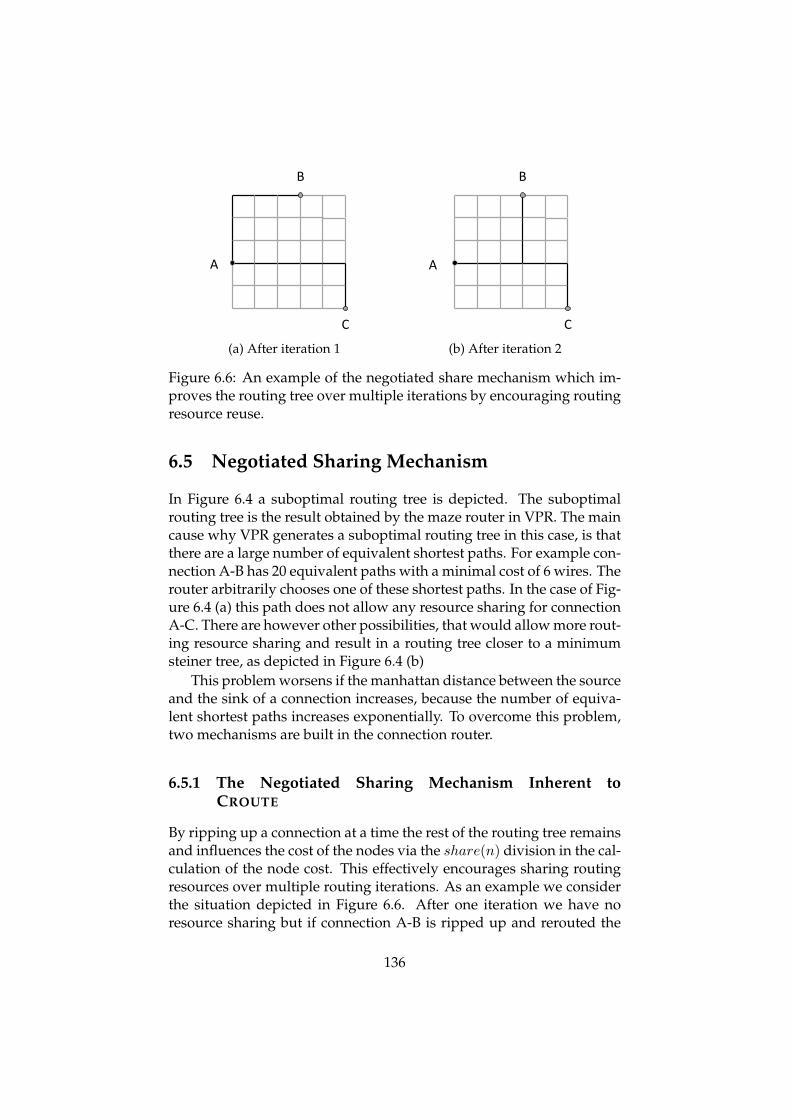
B B
C C
A A
(a) After iteration 1
B B
C C
A A
(b) After iteration 2
Figure 6.6: An example of the negotiated share mechanism which im-proves the routing tree over multiple iterations by encouraging routingresource reuse.
6.5 Negotiated Sharing Mechanism
In Figure 6.4 a suboptimal routing tree is depicted. The suboptimalrouting tree is the result obtained by the maze router in VPR. The maincause why VPR generates a suboptimal routing tree in this case, is thatthere are a large number of equivalent shortest paths. For example con-nection A-B has 20 equivalent paths with a minimal cost of 6 wires. Therouter arbitrarily chooses one of these shortest paths. In the case of Fig-ure 6.4 (a) this path does not allow any resource sharing for connectionA-C. There are however other possibilities, that would allow more rout-ing resource sharing and result in a routing tree closer to a minimumsteiner tree, as depicted in Figure 6.4 (b)
This problem worsens if the manhattan distance between the sourceand the sink of a connection increases, because the number of equiva-lent shortest paths increases exponentially. To overcome this problem,two mechanisms are built in the connection router.
6.5.1 The Negotiated Sharing Mechanism Inherent toCROUTE
By ripping up a connection at a time the rest of the routing tree remainsand influences the cost of the nodes via the share(n) division in the cal-culation of the node cost. This effectively encourages sharing routingresources over multiple routing iterations. As an example we considerthe situation depicted in Figure 6.6. After one iteration we have noresource sharing but if connection A-B is ripped up and rerouted the
136

shortest path will be alongside the routing path of connection A-C, be-cause the cost of these wires will only be half the base cost.
6.5.2 Trunk Bias
The negotiated sharing mechanism only works if one of the other con-nections is routed on a part of one of the shortest paths. When therouter is routing the first connection of a net with Dijkstra, it is cluelessabout the location of the rest of the net’s sinks. In order to help therouter with initially choosing a good path from the equivalent short-est paths we add a bias towards the geometric center of the net. Thebias must have a smaller influence than the wire cost, because it is onlymeant to be a tie breaker. We add the following term to the node cost:
cbias =b(n)·
2 · fanout· ∆m,c
HPWL(6.10)
The minimum wire cost is b(n)/fanout in case a wire is shared byall of the connections. The bias cost will be maximally half of the min-imum wire cost. The bias cost depends on the manhattan distance tothe geometric center which is normalized against the Half PerimeterWire Length (HWPL). As we close in on the geometric center the effectreduces.
During the negotiated congestion mechanism the cost of the nodescan only increase, so the effect of the bias cost becomes smaller towardsthe later iterations of the routing algorithm.
6.6 Partial Rerouting Strategies
To speed up the routing process the router could be programmed toonly focus on the congested nets. Right before ripping up the net, thenodes of the old routing tree are checked and if no nodes are congested,the net is skipped. This method has an average speedup of 1.9x for theVTR benchmark suite, but the quality of the result decreases with a 25%increase in critical path delay. The cause of the critical path detoriationis that the routing solution converges too quickly. The router focusestoo much on routability with not enough emphasis on optimizing crit-ical path delay. In the first iteration the router routes the connectionsin the circuit congestion-oblivious. Each connection is routed with aminimum delay. To put more stress on timing, the most critical netsare rerouted if the delay of one of its connections is higher than theminimum delay obtained in the first iteration independent of their con-gestion status. Only nets with one of their pin criticalities above a tim-
137

ing criticality threshold, fcrit,cutoff are rerouted. We experimented withdifferent values for the criticality threshold and for a value of 0.9 the re-sulting critical path delays are on average the same as the PATHFINDER
algorithm built in VPR.In order to further reduce the runtime, the runtime profiling re-
sults in Fig. 6.3 show that the majority of time is spent by reroutinghigh-fanout nets. High-fanout nets have more chance to be reroutedbecause they typically require a lot of routing resources, span a largerarea of the die and are more critical than their low-fanout counterparts.Partially rerouting the high-fanout nets would obviously reduce run-time and the connection-based routing mechanism allows us to onlyreroute the congested and the critical connections. Instead of rerout-ing an entire critical net, only the connections with a criticality above0.9 are rerouted. Since the connection delays are updated after rout-ing a connection, we can check if a critical connection is longer thanits minimum after routing. Unfortunately the congestion status of theconnection can be changed after routing the connection, so the routerrechecks the old routing trace for congested nodes before it decides ifthe connection will be rerouted.
6.7 Experiments and Results
6.7.1 Methodology
To measure the performance of the connection router with partialrerouting we compare it to the PATHFINDER router implemented inVPR [88]. CROUTE is implemented in the VTR framework, whichis mainly written in C. The Titan suite is used to benchmark therouters [106]. The target architecture is the Stratix-IV based architec-ture. The architecture has identical functional blocks as in the commer-cial Stratix-IV, but a simplified routing architecture with 87% wires thatspan four logic blocks and 13% wires that span 16 logic blocks. Thewires are fully populated, branching of in each connection block andswitch block they come across. The switch blocks have a Wilton topol-ogy. The Titan benchmark suite contains 23 small designs and 19 largerdesigns that are more challenging to place and route. To prevent over-fitting the smaller designs were used to fine-tune the routers and searchfor optimal parameter values, such as fcrit. The larger designs are usedfor the final evaluation. The placements were generated with the VPRtiming-driven placer with default settings. For each benchmark designthe following properties of the routing implementation were measured:
138

• The Runtime is the time the router needs to find a solution foran FPGA architecture with a given channel width. It does notinclude the time to parse the netlist and generate the routing re-source graph. The routing algorithms were executed on a work-station with an Intel quad-core [email protected] and with 32GB1600Mhz DDR3 memory.
• The Maximum Clock Frequency is determined by the slowestpath delay, also called the critical path delay. In case there aremore clock domains, the geomean of all maximum clock frequen-cies is used for comparison.
• The Total Wire-length is the number of wires needed to realisethe design.
Table 6.1: Runtime, total wire-length and critical path delay forCROUTE and the baseline which is the routing algorithm implementedin VPR slightly adapted to only reroute the congested and critical nets.
Runtime [s] Critical Path Delay [ns] Total Wirelength [x1000]Benchmark Design baseline Croute ratio baseline Croute ratio baseline Croute ratiocholesky mc 289 215 0.74 9.3 9.3 1.00 1443 1265 0.88stereo vision 130 115 0.88 9.3 10.0 0.93 998 982 0.98sparcT1 core 514 540 1.05 10.1 9.9 1.02 1674 1647 0.98neuron 179 148 0.83 10.0 9.7 1.03 1275 1252 0.98segmentation 4456 3475 0.78 894.2 897.3 1.00 3222 3152 0.98stap qrd 609 437 0.72 9.1 9.9 0.92 4112 3346 0.81SLAM spheric 3682 3539 0.96 84.8 84.8 1.00 3166 3159 1.00mes noc 4183 2273 0.54 16.8 16.6 1.01 10955 9678 0.88des90 894 664 0.74 14.6 13.7 1.07 3522 3333 0.95bitonic mesh 3464 2286 0.66 16.0 16.9 0.95 7641 7440 0.97cholesky bdti 502 371 0.74 10.5 11.4 0.92 3575 3161 0.88Geomean 0.77 0.99 0.92Std. Dev. 0.13 0.05 0.06
6.7.2 Results
We slightly adapted the router in VPR to reroute only congested andcritical nets, because then we can clearly show the advantage of con-nection based routing apart from the effect of partial rerouting. Partialrerouting strategies can be both applied to the net and connection basedrouter. The modified VPR router will be used as a baseline to compareto CROUTE and we will refer to this router as the baseline router. Therouters target the Stratix IV architecture with a fixed channel width of
139

300. In what follows the runtime to find a routing solution and qualityof the solutions are compared. The results are summarized in Table 6.1.We only listed the benchmark designs that we were able to route in thereasonable timespan of 5 hours.
0 20 40 60 80 100 120 140 160 180 200
1 6 11 16 21 26 31 36 41 46
Run$
me (s)
Itera$on
baseline
Croute
original VPR
Figure 6.7: Iteration runtime for the LU32PEEng benchmark design
The connection router is able to find routing solutions on aver-age 23% faster than the baseline router. Almost all the designs arerouted faster with CROUTE. The main cause for the drop in runtimeis the decrease in runtime for one routing iteration. The routing it-eration runtime dramatically drops in the first few iterations for bothrouters, because the easier to solve congestion is solved and thoseparts are not rerouted anymore. For CROUTE this effect is even moreprononounced. However, CROUTE typically needs slightly more itera-tions. The net effect is a reduction in runtime. To further elaborate thedecrease in routing iteration runtime, we investigate the routing iter-ation runtime for the benchmark design LU32PEEng implemented onthe k6 frac N10 mem32K 40nm architecture in Figure 6.7. The channelwidth is set to 168, which is the minimal channel width for the defaultrouter in VPR, so there is a fair amount of congestion the routers needto solve to find a solution. We clearly see the initial drop in runtimeboth for the baseline and CROUTE, but for CROUTE the drop is morepronounced. The runtime for one iteration for CROUTE typically stayslower than an iteration for the baseline router. To highlight the differ-ence between a router with and without a partial rerouting strategy,we also included the results for the original VPR router. The runtimeclearly is much higher without partial rerouting strategy and this ismore extreme compared to CROUTE, mainly because the speedup frompartial rerouting is larger when applied on connections, because it is a
140

finer scale.The quality of CROUTE solutions in terms of critical path delay is
similar as the baseline routing solutions with an average 1% reduc-tion in critical path delay, but with a standard deviation of 5%. Thetotal wire-length is consistently better. The total wire-length for eachbenchmark design is lower with an average decrease of 8%, albeit withsome variation with a standard deviation of 6%. This improvementis attributed to CROUTE’s negotiated sharing mechanism which is de-scribed in section 6.5. The mechanism improves the routing tree of anet over multiple iterations.
6.8 Conclusion and Future Work
In this chapter we proposed a new routing algorithm called the connec-tion router, CROUTE. It is a router which applies a more congestion ori-ented rerouting instead of simply rerouting the whole circuit. CROUTE
rips up and reroutes parts of the routing tree of a net, by ripping upand rerouting connections instead of nets in the main congestion loopCROUTE is more runtime efficient than the PATHFINDER-based routerimplemented in VPR. Given an FPGA with a certain channel width,CROUTE is able to find routing solutions 23% faster, the quality of therouting solutions is slightly better in terms of total wirelength with anaverage decrease of 6%. The solutions have a similar critical path delay.
The techniques applied in CROUTE are largely orthogonal to manyadvanced routing runtime reduction techniques described in the litera-ture. They can be applied in tandem with CROUTE, for example selec-tive routing resource graph expansion [104] and parallel routing [51].
Nevertheless routing remains an important bottleneck in the designcycle.
141


7Place and Route tools for the
Dynamic Reconfiguration of theRouting Network
In this chapter we describe the placement and routing tools that we de-veloped for the special FPGA technique that exploits the reconfigurabil-ity of the routing switches in the FPGA. The goal is to improve the cir-cuit properties by dynamically reconfiguring the routing switches. Wefirst start with giving an overview of dynamic partial reconfigurationand clarifying the contributions we made. Subsequently we describethe modifications made to the conventional placement and routing ap-proaches to enable the dynamic reconfiguration of the FPGA’s routingnetwork.
7.1 Overview of Dynamic Partial Reconfiguration
Traditionally, a configuration of a Field Programmable Gate Array(FPGA) is loaded at the end of the design phase, and it remains thesame throughout the runtime of the application. In order to changethe configuration, the computation is stopped, the new configurationis written to the configuration memory and then the computation canstart again. The high write speed of SRAM memory cells in SRAM-based FPGAs opened up the possibility to reconfigure the FPGA be-tween different stages of computation. In 1996 Xilinx released one of
143

the first dynamically and partially reconfigurable FPGAs, the XC6000[140]. Dynamic Partial Reconfiguration (DPR) is a technique that allowsreconfiguring only a portion of the FPGA at runtime, while the rest ofthe FPGA remains active. In order to change the functionality imple-mented by certain FPGA resources, the configuration memory bits thatcontrol those resources can be updated by sending a new partial con-figuration to the FPGA. In 2010 Altera, Xilinx’s main competitor, alsointroduced an FPGA that supported DPR, the Stratix V (28 nm) [11].
DPR can be used to build self-reconfiguring systems that write aconfiguration to the FPGA’s configuration memory, specialized for theapplication specifics at hand. Specialized configurations use fewerresources, because resources are reused, and therefore less FPGA re-sources are occupied. Thus, this technique allows larger circuits to beimplemented on smaller and cheaper FPGAs. Additional advantagesare that specialized configurations have a reduced logic depth and re-quire less power than their generic counterparts. However, the down-side is that the gain in efficiency can be diminished by the specializationoverhead, because when the problem at hand changes, a new special-ized configuration is needed. The specialization overhead is the extraFPGA resources and the extra time needed to obtain a configuration up-date and write the FPGA’s configuration memory using DPR. Further-more, the complexity of implementing a design using DPR and the lackof automatic tools hinder the widespread use of the DPR technique.
7.1.1 Introduction to Dynamic Circuit Specialization
In [21] these problems are addressed by using the Dynamic Circuit Spe-cialization (DCS) technique. The proposed two-stage tool flow for DCSstarts from an HDL (Hardware Description Languange) description inwhich the slowly varying signals, called parameters, are annotated.The parameters represent the application specifics at the current mo-ment. Infrequently varying input signals are good choices to consideras parameter candidates. We don’t want the system to calculate config-uration updates frequently.
A computational intensive offline stage calculates a parameterizedconfiguration. This is an FPGA configuration in which the bits areBoolean functions of the parameters. In the second, online, stage the pa-rameterized configuration can be quickly evaluated to a configurationupdate. The configuration update can be applied using DPR and af-ter the update the FPGA is running the new specialized configuration.This rapid evaluation leads to a low specialization overhead. Since thetechnique uses an annotated HDL file as input, it enables designers to
144

benefit from DPR without much extra design effort. The only require-ment to use this tool flow is an FPGA that is capable of dynamic partialreconfiguration.
The tool flow introduced in [21], is called the TLUT tool flow and isavailable online [55]. It was the first tool flow developed for DCS. Theoffline stage is quite similar to a conventional FPGA tool flow. Onlythe mapping stage differs greatly. However, the TLUT tool flow is lim-ited because it is only capable of dynamically specialising the values ofthe LookUp Tables (LUTs) present in FPGAs. The TCON tool flow, de-scribed in section 7.3, extends the TLUT tool flow with the possibility todynamically specialize the interconnection network of an FPGA. Thisspecialization has a lot of potential, because reusing routing resourcescould drastically reduce the area usage, delay and power consumption.For the test cases in this chapter, a Clos switch network and a VirtualCoarse Grain Array, the TCON tool flow generates implementationsthat need 50% up to 92% less LUTs and 36% up to 81% less wiringthan conventional implementations. The logic depth decreases with63% up to 80% in comparison with their corresponding conventionalimplementations.
7.1.2 Contributions
To implement the TCON tool flow, major changes were needed, notonly in the mapping, but also in the pack, place and route steps. In [57],Heyse and Bruneel proposed an altered technology mapping algo-rithm. We introduced a pack and placement algorithm, called TPACK
and TPLACE. TPACK and TPLACE are described in [130]. We also in-troduced the routing algorithms for the TCON tool flow. In [131],[132] and [130] routing algorithms, enhancements and extensions aredescribed, leading to a honed routing algorithm, called TROUTE.
This work was done in collaboration with Karel Bruneel and BrahimAl Farisi. At the time, Karel Bruneel was a post-doctoral researcher andBrahim Al Farisi was a Phd. student in our research group.
7.2 Background
7.2.1 Configuration Swapping
In conventional dynamic reconfiguration tool flows runtime reconfig-uration is used to have multiple processes timeshare a set of FPGAresources. The functionality of a part of an FPGA is swapped withanother pre-computed configuration that is loaded from a storage
145

FPGA Static part
Dynamic part
Configuration 0
Configuration 1
Configuration 2
Configuration 3
Figure 7.1: Conventional Dynamic Reconfiguration: Configurationswapping, different modules are loaded in
medium. This method is called configuration swapping or modularreconfiguration. The concept is illustrated in Figure 7.1. Tool supportfor configuration swapping can simply be realized by slightly adaptinga conventional tool flow. FPGA manufacturers have adapted their toolflows for this type of reconfiguration. Xilinx has adapted its modulardesign flow [143] and a similar tool flow is available for Altera [12]. Thecommercial configuration swapping tool flows are complex and requirea skilled designer. The designer has to prepare one or more parts of theFPGA for dynamic reconfiguration and he will need to describe all thefunctionalities that might be implemented using an HDL. Preparing adynamically reconfigurable area encompasses:
• selecting the FPGA resources that are part of that area;
• defining a fixed interface for this area.
In the commercial tool flows the resources are selected by defining arectangular area on the FPGA. The area must be large enough so thatthe worst case functionality in terms of resource usage fits into it. Thefixed interface is important because whichever functionality is loadedin the area, it needs to plug into the static part present on the FPGAin exactly the same way so that the FPGA’s configuration does not getcorrupted.
Next, the tool flow needs to generate the partial configurations foreach of the functionalities. All the functionalities that will be imple-mented by the same area need to have the same interface and this in-terface must be mapped on the interface of the associated area. The con-ventional tool flow is then run for each of the functionalities, with the
146

Figure 7.2: The two-staged tool flow
exception that the placement and routing tools which are constrainedto the defined area and that the signals of the functionality’s interfaceare forced to hook up to the area’s interface.
Configuration swapping is only applicable to applications that havedistinct subtasks that are not to be executed simultaneously. Themethod is also restricted in the number of different tasks that can betime multiplexed. Every task must be defined in a different HDL file,ran by the conventional tool flow and needs to be stored on a storagemedium.
7.2.2 Dynamic Circuit Specialization
As mentioned in the introduction the specialization overhead cannegate the benefits of a self-reconfiguring system. To keep the special-ization overhead low, new specialized configurations need to be up andrunning as quickly as possible, but this is not trivial. For example, theconventional tool flow can be used to create specialized configurationsat runtime. This would in many cases take minutes to hours, because itencompasses computationally hard problems, such as placement androuting. Another solution could be computing all specialized config-urations in advance and storing them in a database, but this solutionquickly becomes infeasible because of the immense number of possibleconfigurations. E.g. 232 or ca. 4 billion configurations are needed for a32-bit multiplier with an infrequently varying coefficient.
To solve this issue the authors in [21] introduced a two-stagedmethod, called Dynamic Circuit Specialization, to generate specializedconfigurations. A simple diagram can be seen in Figure 7.2. The first
147

Pack
Place
Route
Parameterized Configuration
(T)LUTs and Nets
(T)CLBs and Nets
Placed (T)CLBs and Nets
Placed (T)CLBs and Routed Nets
Parameterized HDL design
Synthesis
TLUTMap
Logic ports
Figure 7.3: Generic stage of the TLUT Tool flow
stage, called the generic stage, starts from a parameterized HDL design.This is a regular HDL design in which some of the input signals are an-notated as parameters. From this a parameterized configuration (PConf) isgenerated. A PConf is a multi-valued Boolean function that expresses aspecialized FPGA configuration bitstream as a function of the parame-ters. At runtime this Boolean function can be evaluated using a specificset of parameter values to obtain a regular FPGA configuration (duringthe specialization stage). So it is possible to derive specialized config-urations with different properties and/or functionality from a singlePConf during runtime.
The advantage of generating specialized configurations from aPConf, instead of directly running the conventional FPGA tool flow,is the much lower overhead per specialized configuration. Generat-ing a PConf costs about the same amount of time as generating a reg-ular configuration, but the evaluation of Boolean functions is severalorders of magnitude faster. An additional advantage is that only oneconfiguration needs to be stored while the different specialized config-urations can be generated in milliseconds [21]. For example, a PConffor an adaptive FIR filter, generated by the TLUT tool flow, describedin section 7.2.3 can be evaluated to a specialized FIR configuration (8-bit input, 8-bit coefficients and 32 taps) in only 1.3 ms on a PowerPC405 (PPC405) clocked at 300 MHz (available in the Xilinx Virtex-II proFPGAs), while the conventional method needs several minutes to pro-duce a specialized configuration on a standard desktop PC.
148

7.2.3 TLUT Tool Flow
The tool flow, that generates the PConf in the generic stage, consists ofadapted versions of the tools found in the conventional tool flow. Ittakes a parameterized HDL design as input and outputs a PConf. Afirst tool flow for DCS, called the TLUT tool flow, is described in [21].In figure 7.3 an overview of the different steps of this tool flow is given.In the first step of the tool flow, the parameterized HDL design is syn-thesized in a conventional way. Next, the design is mapped with amodified technology mapper, called TLUTMAP. A conventional map-per maps the design to a LUT circuit, while TLUTMAP maps the designto a Tunable LUT circuit. A Tunable LUT (TLUT) is a parameterizedabstraction of a LUT. The truth table bits are expressed as functions ofparameter inputs. Since parts of the design functionality depending onthe parameters are incorporated in the parameterized truth table bits ofthe TLUTs, the size of the TLUT circuit is much smaller than the regularLUT circuit for the same design [21]. The next step is to pack, place androute the TLUT circuit. These steps can be performed by the conven-tional pack, place and routing tools, because the packing, placementand routing is independent of the content of the LUTs.
A PConf, produced by the TLUT method, only expresses the truthtables of the LUTs as a function of the parameters. All the routing be-tween the LUTs is fixed. This leads to high quality specialized config-urations. However, it has been shown in [130] that also expressing therouting configuration as a function of the parameters (TCON tool flow)leads to specialized configurations with an even better quality. For ex-ample, a 256 × 256 Clos switch, implemented as described in section7.7, requires 1792 LUTs when the TLUT method is used, while only 768LUTs are needed when the TCON method is used.
7.3 The TCON tool flow
The TCON tool flow produces PConf’s following the same principleconcept as the TLUT tool flow. It also starts from an RT level HDLdescription and generates a PConf. However, to allow dynamic spe-cialization of the FPGA’s interconnection network, changes are alsorequired in the technology mapping, packing, placement and routingsteps of the tool flow. In Figure 7.4 an overview of the different stepsof the generic stage of the TCON tool flow are depicted. The changesneeded in each step are described in the following sections. A simple2× 2 crossbar is used as an example.
149

TPack
TPlace
TRoute
Parameterized Configura6on
(T)LUTs and (T)CONs
(T)CLBs and (T)CONs
Placed (T)CLBs and (T)CONs
Placed (T)CLBs and Routed (T)CONs
TPAR
Parameterized HDL design
Synthesis
TCONMap
Logic ports
Figure 7.4: Generic stage of the TCON Tool flow
7.3.1 Synthesis
The synthesis step converts a HDL description in which some inputsare annotated as parameters into a parameterized Boolean network. InListing 7.1 you can find the VHDL description of the 2 × 2 crossbarswitch example. No significant changes need to be made to this stepbecause parameters can be synthesized just like regular inputs. Exceptthat parameter inputs in the HDL description do have to be annotatedas parameter inputs in the resulting Boolean network as well. Design-ers only have to add a comment before and after the parameters in thedescription, as can be seen on line 3 and 5 of the VHDL code of thecrossbar switch in Listing 7.1.
7.3.2 Technology Mapping
During technology mapping, the parameterized Boolean network gen-erated by the synthesis step is not mapped onto the resource primitivesavailable in the target FPGA architecture, but on abstract primitivesthat represent parameterized versions of these resource primitives:
• a Tuneable LookUp Table (TLUT): a LookUp Table with the truthtable expressed in terms of parameters, τ(p) : Bk → B2n , with kthe number of parameters and n the number of inputs LUTs haveon the target FPGA. A TLUT will be implemented by a regularLUT and the dynamic reconfiguration of its truth table.
150

Listing 7.1: The VHDL code for the 2× 2 crossbar switch example.1 entity crossbar is2 port(3 −− param4 sel : in std logic vector (1 downto 0);5 −− param6 i : in std logic vector (1 downto 0);7 o : out std logic vector (1 downto 0);8 ) ;9 end crossbar;
1011 architecture behavior of crossbar is12 begin13 o(0) <= i(to integer ( sel (0) ) ) ;14 o(1) <= i(to integer ( sel (1) ) ) ;15 end behavior;
• a Tuneable Connection (TCON): a connection with a connectioncondition expressed in terms of parameters. A TCON will be im-plemented by a set of wires and switches, and the dynamic re-configuration of some of the switches in the set. A schematic of aTCON can be found in Figure 7.6.
Analogously to a regular connection, a TCON has a source and asink. Additionally, every TCON has a connection condition ζ(p) : Bk →B, with k the number of parameters. This is a Boolean function of theparameters that returns true when the design requires the connectionto be active. The connection conditions of the TCONs reflect the factthat not all connections are needed at the same time. They allow us todistinguish which connections are mutually exclusive in time. Theseconnections will be allowed to share FPGA routing resources. TCONsare abstract concepts generated in the technology mapping step. Theseare refined to concrete FPGA resources during packing, placement androuting. After placement the endpoints of the TCONs are fixed and therouter further refines the TCON by reserving the switches and wires torealize the connection.
The abstract concepts, TCON and TLUT, also cover static connec-tions and static LUTs. A static connection is a TCON with a connectioncondition equal to 1 and a static LUT is a TLUT with a truth table inde-pendent of the parameter inputs.
In [57] TCONMap is presented. It is a technology mapping algo-rithm, able to exploit both the reconfigurable properties of the LUTsand the interconnect network of the FPGA. For more details on theTCONMap algorithm, we refer to the Phd. thesis of Karel Heyse [56].
151

Listing 7.2: Netlist for the 2×2 crossbar mapped by a conventional tech-nology mapper1 . input i02 pinlist : n03 . input i14 pinlist : n15 . input sel06 pinlist : n27 . input sel18 pinlist : n39
10 .output o011 pinlist : n412 .output o113 pinlist : n51415 . clb clb a16 pinlist : n0 n1 n2 open n4 open17 subblock: n4 0 1 2 3 4 open18 . clb clb b19 pinlist : n0 n1 n3 open n5 open20 subblock: n5 0 1 2 3 4 open
TCONMap produces a tunable circuit. Tuneable circuits contain TLUTsand TCONs. A schematic of the 2 × 2 crossbar switch and the TCONnetlist, generated after TCONMap can be seen in Figure 7.7. TCON-Map succeeds at mapping the functionality of the 2×2 crossbar on fourTCONs and four Input/Output Blocks (IOBs). As a reference, conven-tional technology mapping needs six nets, two CLBs and six IOBs, seethe netlist generated by the conventional technology mapping in List-ing 7.2.
7.3.3 TPACK and TPLACE
In the packing step, LUTs and FFs are packed into CLBs. Subsequentlythe placer chooses a physical CLB on the FPGA for every CLB in-stance in the circuit. To optimise routability and interconnect delay,wirelength-driven placers use wire length estimates of the interconnec-tions between CLBs. Conventional placers have to take into accountthat a connection can share wires and switches starting at source end ofthe connection. However TROUTE is not only able to let TCONs shareresources at the source end, but also at the sink end, see Figure 7.8.To better estimate routing resource usage of a placement, new wirelenght estimation methods for TCONs are introduced for TPLACE, in
152

IOB IOB IOB IOB
IOB
IOB
IOB
IOB CLB CLB
IOB
IOB
IOB
IOB
CLB CLB
IOB IOB IOB IOB
i0 o0
i1 o1
sel0
sel1
IOB IOB IOB IOB
IOB
IOB
IOB
IOB CLB CLB
1 ¬sel1
¬sel1
sel0
sel0
sel1
sel1
¬sel0
¬sel0
1
1 1
1 1 IOB
IOB
IOB
IOB
CLB CLB
IOB IOB IOB IOB
i0 o0
i1 o1
Figure 7.5: The FPGA circuit for the 2×2 crossbar switch example, com-piled by the conventional tool flow. The target FPGA has 2×2 CLBs.The thick lines in the schematic represent the wires of the FPGA, thethin lines the edges. The wires and edges that are used, are accentu-ated in black. Output pins are open boxes and input pins are filledboxes.
section 7.5.
7.3.4 TROUTE
In the routing step routing resources are assigned to the TCONs. Im-portant changes have to be made to the conventional routing algo-rithms, because the routing problem changes significantly. In the con-ventional case the router needs to route a set of nets. Each net is aninterconnection between a source and one or more sinks. Nets may notshare resources, otherwise this would lead to shorts. In the TCON toolflow TROUTE has to route a set of TCONs. TCONs have more than oneresource sharing possibility. TCONs may share resources if they havethe same source (because they carry the same signal) or if they are notactive at the same time. Two TCONs, t1 and t2, with their connectionconditions ζ1 and ζ2 respectively, are not active at the same time, if ζ1
and ζ2 are not simultaneously true for every parameter value:
153

13#
ζ(p)
Source Pin Sink Pin
Figure 7.6: Schematic of a Tuneable Connection (TCON)
Listing 7.3: The TCON netlist for the 2×2 crossbar switch functionality1 .parameter sel02 .parameter sel134 . input i05 pinlist : i0p6 . input i17 pinlist : i1p8 . input o09 pinlist : o0p
1011 .output o112 pinlist : o1p1314 . tcon i0p o0p ¬sel015 . tcon i0p o1p ¬sel116 . tcon i1p o0p sel017 . tcon i1p o1p sel1
t1 en t2 not active simultaneously⇐⇒ ∀p ∈ P : ¬(ζ1(p) ∧ ζ2(p)) (7.1)
This is an important property that can be used to minimize rout-ing resource usage. In section 7.6 the connection router, first presentedin [132] and [131] is discussed, it is capable of routing TCONs whilestimulating both resource sharing possibilities.
In Figure 7.8, two possible implementations are given for the 2 × 2crossbar switch example on a FPGA with an array of 2 by 2 CLBs anda very basic routing architecture. The first routing solution exploitsthe first resource sharing possibility, TCONs driven by the same sourcemay share routing resources. The second routing solution exploits thesecond sharing possibility, TCONs not active at the same time mayshare resources. Both routing solutions contain 8 wires and 14 switchesand the same number of switches need to be reconfigured when thevalue of the control signals of the crossbar change. In this example
154

sel0 sel1 o0 o1
0 0 i0 i00 1 i0 i11 0 i1 i01 1 i1 i1
sel0! sel1! o0! o1!
0! 0! i0! i0!
0! 1! i0! i1!
1! 0! i1! i0!
1! 1! i1! i1!
!!!
!!
!!
!!
i0!
i1!
o0!
o1#
Figure 7.7: A schematic and truth table of a 2×2 crossbar switch func-tionality represented by 4 TCONs
there is no real advantage by choosing one of the two sharing mecha-nisms. However, practically, one sharing possibility may outperformthe other. Choosing the most economic solutions reduces the requiredwiring resources.
7.3.5 Limitations
In academic tool flows, such as VTR, multipliers, block RAMs and otherhard blocks are recognised at the synthesis level. These hard blocks cannot be parameterized, in contrast to LUTs. However, if two hard blocksof the same type are not used at the same time, the TCON tool flowcould be used to reuse one hard block and thereby reducing the areaused. At this stage, the TCON tool flow does not support heteroge-neous FPGAs. For applications that benefit from hard blocks, such asDSP applications, this could lead to considerable area gains.
In the following sections we describe in more detail the packing,placement and routing algorithms that have to be changed to enablecompiling to configurations with the parameterized routing bits.
7.4 TPACK
TPACK packs the LUTs and FFs of the circuit into Configurable LogicBlocks (CLBs) (also called Adaptive Logic Modules in Altera devices).TPACK is similar to conventional packing, more details on conventionalpacking can be found in [17]. Some alterations are made to be able todeal with tuneable circuits. In this section, a CLB architecture with atwo level hierarchy is assumed. The first level is a basic logic element(BLE), it contains a LUT and a FF. The second level consists of Config-urable Logic Blocks (CLBs) containing several BLEs and fast internalrouting resources to interconnect them.
155

IOB IOB IOB IOB
IOB
IOB
IOB
IOB CLB CLB
IOB
IOB
IOB
IOB
CLB CLB
IOB IOB IOB IOB
1
sel0
¬sel1
¬sel0
1
¬sel1
1
1
¬sel0 1
sel1 1
sel1
sel0
i0 o0
i1 o1
IOB IOB IOB IOB
IOB
IOB
IOB
IOB CLB CLB
1 ¬sel1
¬sel1
sel0
sel0
sel1
sel1
¬sel0
¬sel0
1
1 1
1 1 IOB
IOB
IOB
IOB
CLB CLB
IOB IOB IOB IOB
i0 o0
i1 o1
Figure 7.8: Two routing solutions for the 2×2 crossbar switch example,produced by the TCON tool flow. For every switch used in the cir-cuit, the connection condition is given. The connection condition is aboolean function of the parameters sel0 and sel1.
156

Accordingly conventional packing is composed of two stages. Inthe first stage the LUTs and FFs are packed into LUT-FF pairs via apattern matching algorithm. No alterations are needed in the first stageto pack TLUTs and FFs interconnected via TCONs.
In the second stage the LUT-FF pairs are packed in CLBs. The op-timization goals are two-fold. The first optimization goal is to fill eachCLB to its capacity. The second optimization goal is to minimize thenumber of occupied inputs to each CLB. This is done in order to reducethe number of connections to be routed between CLBs and thereby ex-ploiting the fast internal routing resources of the CLBs and enhance theoverall routability of the circuit.
In a similar manner as in the conventional packing algorithm,TPACK greedily packs the BLEs with highest attraction in CLBs sequen-tially. The attraction of a BLE and a cluster of BLEs is the number ofinputs and outputs they have in common. A hill-climbing phase isinvoked only if the greedy phase is unable to fill a CLB completely.However, the problem of packing BLEs connected via TCONs slightlydiffers from the problem of packing BLEs connected via nets. TCONscan share input pins of the CLBs, nets cannot. TCONs driven by thesame source or TCONs not active at the same time can share a CLB in-put pin. The only modification applied to the conventional packing, isthe way the number of occupied inputs of a CLB is calculated. Giventhe set of TCONs that connect the inputs of the BLEs to the routinginterconnect network, the number of occupied inputs is the maximumnumber of sources connected to the CLB at the same time.
7.5 TPLACE
This section describes modifications made to the different aspects ofa conventional FPGA placement algorithm to deal with tuneable cir-cuits. For an introduction on placement algorithms we refer the readerto Chapter 5. We use the wirelength-driven simulated annealing place-ment algorithm as a starting point to build TPLACE. TPLACE has twoinputs: a tuneable circuit and a description of the target FPGA archi-tecture. TPLACE searches a legal placement for the functional blocks ofthe input circuit so that the total wire length is minimized. In the futuremore complex optimisation goals, such as timing-driven [97] placers,can be implemented.
The placement problem is computationally hard, so there are noknown algorithms that can find an optimal solution in a reasonabletime. Therefore, many heuristics have been developed for the place-ment problem. In this chapter we used a simulated annealing algo-
157

rithm to place tuneable circuits, but the same principle can be applied tomore advanced placement techniques like an analytical placement tech-nique or a gradient descent based placement technique as described inChapter 5.
Wirelength-driven simulated annealing placers try to minimize thetotal wire length needed to route all wires in a placement. They use thetotal wire length as their cost function. The only way to exactly calcu-late the total wire length for a given placement is to route the connec-tions in the circuit and to count the used wires. Since routing is in itselfa computationally hard problem, solving it repeatedly for every movetried in the inner loop of the SA algorithm, leads to very long executiontimes. Therefore, the cost is not exactly calculated but estimated.
7.5.1 Wire Length Estimation for Nets in Static Circuits
In this section we partially repeat what we described in Section 5.2.1to clearly accentuate the difference with the wire length estimation intuneable circuits, which is explained in the next section.
In case of a conventional static circuit, a legal routing solution con-tains a disjoint set of routing resources for each net. A wirelength-driven placer estimates the total wire length as the sum of the estimatedwire lengths of each net. The wire length of a net is estimated as thehalf-perimeter of its bounding box weighted by a factor which dependson the number of terminals of the net.
Cwl =∑n∈nets
q(#terminals(n)) ·HPWL(n) (7.2)
The factor q(.) is taken from [29]. It is equal to 1 for nets with up tothree terminals and slowly grows to 2.79 for nets with 50 terminals.
To evaluate the estimation, the circuits in the Toronto 20 benchmarksuite [15], the 20 largest circuits of the MCNC benchmark suite, wereplaced with the wirelength-driven placer and routed with the breadth-first router in VPR 4.30 with default settings. The channel width had20% more tracks than the minimum channel width, to allow a relaxedrouting, as recommended in [17]. To evaluate the conventional estima-tion we calculate the correlation between the estimated and the actualrouting cost of the placed benchmark circuits. The resulting correlationcoefficient is 0.9705. Further on this correlation coefficient will be com-pared with the correlation coefficient of the newly proposed estimationmethod for tuneable circuits to evaluate the quality of the proposed es-timation.
158

7.5.2 Wire Length Estimation for Tuneable Circuits
This section describes how the routing resource usage of a tuneablecircuit can be estimated. It is important not to make the calculation ofthe estimation more complex than the estimation of the nets in staticcircuits, because the estimation is needed in the kernel of the simulatedannealing algorithm. Hence the time needed for the estimation shouldbe reduced to the very minimum.
(a) Sharing of routing resources be-tween connections with the samesource.
p
!p
(b) Sharing of routing resources be-tween connections (TCONs) withthe same sink.
Figure 7.9: Sharing of routing resources between connections with thesame source or sink. Shared resources are annotated with a dottedshape.
A new wirelength estimation method is necessary because in tune-able circuits, a routing solution does not contain a disjoint routing setfor each of the TCONs. There are two sharing mechanisms. In Fig-ure 7.9 the two sharing mechanisms are demonstrated on a small ex-ample routing solution. TCONs can legally share resources with otherTCONs if they carry the same signal or if they are not active at the sametime. The first resource sharing mechanism, TCONs carrying the samesignal, is easily distinguished, because the TCONs are driven by thesame source. The second resource sharing mechanism, TCONs that arenot active at the same time, is harder to recognise. The connection con-ditions of the TCONs have to be compared. After comparison, eachTCON t has an associated set of TCONs. Each of the TCONs in that setmay share resources with t, but some of the TCONs in the set can befar away from t and are not interesting to consider as sharing resourcewith. For example, two connections that are not active at the same time
159

with the terminals of the connections situated on the other side of theFPGA. These two connections will most likely not share resources, evenif it is allowed. The most interesting TCONs in the set are the TCONsthat have the same sink as t. They can be distinguished easily and theyare forced to overlap because they have to reach the same sink anyway.So to simplify the problem we consider only overlap between TCONswith the same source or TCONs with the same sink.
The estimation is not as straightforward as in case of static circuits.In case we use the same estimation method that is used for static cir-cuits, then the second sharing mechanism is neglected and the wire-lenght is systematically overestimated. Let’s consider the toy examplein Figure 7.10a. The conventional estimation method considers all con-nections starting from the source as a collection and tracks the bound-ing boxes of these collections during placement. The estimation forthe toy example is 10 wires, but the post-route solution contains only9 wires. The number of bounding boxes that are tracked during place-ment equals the number of sources in the circuit.
To achieve a better estimation, all connections starting from a sinkcould also be considered a collection. Each connection would then bepart of a source collection and a sink collection. The estimation methodwould than track the bounding boxes of the source and the sink col-lections. The total wirelength estimate in this case is the half of thesum of the bounding box estimates. As can be seen in Figure 7.10b,the estimated wirelength is 9.5, which is slightly better than the con-ventional estimation, but the number of bounding boxes that needs tobe tracked during placement is the number of sources and sinks in thecircuit, which is typically at least twice the amount of bounding boxes.The toy circuit has three sources and two sinks, so there are five bound-ing boxes which need to be tracked.
To reduce the number of bounding boxes that needs to be trackedand improve the accuracy even more, we propose to partition theTCONs in the tuneable circuit according to the dominant resource shar-ing mechanism. After the partitioning process, each TCON is only partof one collection and the number of collections is typically in the sameballpark as the conventional estimation and the accuracy is typicallybetter. The partition-based estimation correctly predicts the number ofwires for our toy example in Figure 7.10c while only needing 2 bound-ing boxes. This improvement is even more pronounced for tuneablecircuits with larger fanout source collections and/or larger fanin col-lections.
We define the dominant resource sharing mechanism to be the shar-ing mechanism that is used by the largest number of connections. Let’s
160

(a) ConventionalCwl,est = 10, #BB = 3
(b) Both sharing mechanismsCwl,est = 9.5, #BB = 5
A B
(c) Partitioning according to thedominant sharing mechanism
Cwl,est = 9, #BB = 2
A B
(d) Post-route solutionCwl = 9
Figure 7.10: The wirelength estimation methods for tuneable circuitsapplied to a simple toy circuit and the post-route solution
161

Listing 7.4: Pseudocode of the greedy multi-iteration algorithm used topartition the TCONs1 while (candidateParts.size > 0):2 int maxCardinality = 03 Set maxPart = 04 /* Find the set with the maximum number of TCONs */5 for each Set s in candidateParts do:6 if (s . size > maxCardinality || (s . size == maxCardinality && BB(s) > BB(
maxPart)))7 maxCardinality = s.size8 maxPart = s9 partitioning .add(maxPart)
10 /* Remove each TCON of maxPart from its other set */11 for each TCON t in maxPart do:12 Set source = candidateParts.getSourceSet(t)13 Set sink = candidateParts.getSinkSet(t)14 if (maxPart == source) sink.remove(t)15 else source.remove(t)
consider the TCON that connects block A and B in the toy circuit de-picted in Figure 7.10c. The TCON is driven by a source that has a fanoutof two (two connections in the circuit are driven by this source). On theother hand, the sink of the TCON is also used by two other connections.In this case the dominant resource sharing mechanism for this TCONis sharing between TCONs with the same sink.
To partition the TCONs, according to the dominant resource shar-ing mechanism, we propose a greedy multi-iteration algorithm. In List-ing 7.4 the pseudocode of the partitioning algorithm is given. Initially,the TCONs sharing the same sink are part of the same sink set andTCONs sharing the same source are part of the same source set. EachTCON is therefore initially part of 2 sets, a source set and a sink set.All the sets are added to a possibleParts collection. Each iteration of thepartitioning algorithm consists of two steps. It starts with greedily se-lecting the largest set in the possibleParts collection and in the secondstep each TCON in the selected set is removed from the other set ofwhich they are part of. The loop iterates until all the connections arecovered by the chosen sets. In the end every TCON belongs to only oneset.
The total wire length of the tuneable circuit is then estimated asshown in Equation (7.3). The estimate is the sum of the estimated wirelengths of each set in the partition, where the wire length of a set is es-timated as the half-perimeter of its bounding box weighted by a factorwhich depends on the number of terminals of the set.
162

TRoute
Parameterized Configura3on
…
Combine Modes
…
Synthesis
HDL design Mode 1
Pack & Place
Technology Mapping
Synthesis
HDL design Mode 2
Pack & Place
Technology Mapping
…
…
…
Placed Tuneable Circuits
Figure 7.11: A tool flow for the compilation of multi-mode circuits, thatincreases the routing similarity between modes. The tuneable circuitsand the corresponding placement produced by this tool flow can beused to evaluate routing cost estimations for tuneable circuits.
Cwl =∑
∀s ∈ partitionq(#terminals(s)) ·HPWL(s) (7.3)
The same weighting factors q(.) are used as in the conventional esti-mation of a net, see Equation (7.2). For source sets this is quite straight-forward, because they are the equivalent to nets in a static circuit, butthe estimation can be generalised for the sink sets. The factor q(.) is in-dependent of the fact if a set is a source or a sink set. This generalisationcan be justified because the bounding box estimation first proposed in[29] has as goal to estimate the cost of a minimum Steiner tree. Rout-ing sink or source sets is in fact the same problem, finding the shortestinterconnect for a given set of terminals, which is the minimum Steinertree problem.
7.5.3 Evaluation of the Wire Length Estimation
To evaluate the proposed partition-based estimation, tuneable circuitsgenerated by the multi-mode tool flow in Figure 7.11 are used as bench-marks. The tool flow in Figure 7.11 was first proposed in [8]. A multi-mode circuit implements the functionality of a limited number of cir-cuits, called mode circuits or modes. For example all the circuits imple-mented in the dynamic part of modular configuration, see Figure 7.1.At any given time only one mode circuit needs to be realised. Using
163

DPR all the modes of a multi-mode circuit can be time-multiplexedon the same FPGA area, requiring only an area that can contain thebiggest mode. This way significant area savings can be realized com-pared to a static implementation of the multi-mode circuit that usesspace-multiplexing to switch between modes. The tool flow aims at de-creasing the reconfiguration time when changing modes by increasingthe similarity of routing configurations of the different modes. Given anumber of placed mode circuits, a tuneable circuit is generated wherethe parameter indicates the mode. The tuneable circuit is then routedwith TROUTE, which stimulates sharing of routing resources betweenthe connections of different modes. This results in a factor of 1.5 upto 5 reduction in reconfiguration time (depending on the number ofnodes and the granularity of reconfiguration) in comparison with con-ventional methods. The downside is an increase of 10% up to 25% intotal wirelength (depending on the number of modes).
The multi-mode tool flow was used to combine the following cir-cuits from the MCNC benchmark suite, e64, rd73, s400, alu4, s1238,s1488 and s1494. The placed tuneable circuits with 2 up to 5 modes wererouted with TROUTE. The wire length usage was first estimated usingthe partition-based method and compared with the actual wire lengthafter routing. In this experiment it turned out that the proposed estima-tion and the actual routing cost for these multi-mode circuits correlatestrongly, with a correlation coefficient of 0.9904, which is stronger thanthe conventional estimation for the Toronto 20 benchmark suite, whichobtained a correlation coefficient of 0.9705, see section 7.5.1. This newlyproposed partition-based estimation is used to build TPLACE and en-able high quality placement for tuneable circuits.
7.6 TROUTE
After placement, there is a physical block on the FPGA assigned foreach of the functional blocks in the tuneable circuit. The router thenneeds to determine which of the switches in the routing architectureneed to be closed and which need to be opened in order to connect thephysical blocks in accordance to the way their associated logic blocksare connected in the tuneable circuit. In a tuneable circuit with TCONs,the interconnection pattern is dependent upon the value of the parame-ters. So TROUTE outputs a Boolean function of the parameters for eachswitch used in the FPGA’s interconnect network. This Boolean functionindicates the state the switch should be in, dependent on the value ofthe parameters. TROUTE is built based on the CROUTE algorithm de-scribed in Chapter 6. We also refer the reader to Chapter 6 for an intro-
164

Listing 7.5: Pseudo code of the TROUTE algorihm.1 while (IllegalSharedResourcesExist()) :2 for each TCON t do:3 t .ripUpRouting()4 t . Dijkstra( t .source,t .sink)5 t .resources() .updateSharingCost()6 allResources() .updateHistoryCost())
duction on the routing problem and algorithms. This section describesthe alterations made to CROUTE to enable routing tuneable circuits.
7.6.1 The TCON Routing Problem
When the routing architecture of the FPGA is represented as a routing-resource graph, the routing problem for tuneable circuits reduces tofinding a simple path in the routing-resource graph for each of theTCONs in the tuneable circuit. These paths should only share nodes ifthe corresponding TCONs may legally share resources, otherwise thiswould lead to short circuits. Each path starts at the source node andends at the sink node of its associated TCON and contains the wiresneeded to realise a connection between the sink and the source of theTCON. Figure 7.8 shows the legal solution of the 2 × 2 crossbar on arouting resource graph of a simple 2 × 2 island style FPGA with wiresspanning only 1 CLB and bidirectional switches. The wires are repre-sented by solid black lines, the input pins and output pins by smallsquares. The input pins are filled and the output pins are not. For thesake of clarity the individual edges are not drawn but the thin lineseach represent two edges, one for each direction.
7.6.2 Modifications to the Negotiated Congestion Loop
The main structure of the TROUTE algorithm is the negotiated con-gestion loop, similar to the CROUTE algorithm from Chapter 6. Thepseudo-code is shown in Listing 7.5. In every routing iteration, the al-gorithm rips up and reroutes all the TCONs in the tuneable circuit. Thenegotiated congestion mechanism determines the cost of the node bymodulating the cost of a node with congestion penalties:
c(n) = cprev + ·b(n) · h(n) · p(n)
1 + share(n)+ α · cexp, , (7.4)
where b(n) is the base cost, p(n) the present congestion penalty, andh(n) the historical congestion penalty. The cost of the node is divided
165

by share(n), the number of TCONs that legally share the node with theTCON that Dijkstra’s algorithm is currently searching a path for.
To explain the main difference with CROUTE, we repeat the equa-tions 6.4 and 6.5 for the update to the congestion multipliers fromChapter 6. The present congestion penalty, p(n), is updated whenevera TCON is rerouted. The update is done as follows
p(n) =
{1 if cap(n) > occ(n)1 + pf (occ(n)− cap(n) + 1) otherwise
, (7.5)
The historical congestion penalty is updated after every routing it-eration i, except for the first iteration. The update is done as follows
hi(n) =
1 if i = 1
h(i−1)(n) if cap(n) ≥ occ(n)
h(i−1)(n)+hf (occ(n)− cap(n)) otherwise
. (7.6)
cap(n) represents the capacity of the node and occ(n) is the occu-pancy of the node. The occupancy is a measure for the congestion ofa node. For CROUTE this is straightforward, the number of differentnets that use the node in question. For TROUTE the occupancy of awire node is calculated by taking the minimum of the number of dif-ferent sources and the number of different sinks of the TCONS usingthe node in question. In case of source nodes and output pin nodesthe occupancy is calculated as the number of different sources of theTCONs that are using the resource. In the same manner the occupancyof sink nodes and input pin nodes is the number of different sinks ofthe TCONs that are presently occupying the node. So herein lies thebiggest difference with CROUTE.
The factor pf is used to increase the illegal sharing cost as the algo-rithm progresses and the hf is used to control the impact of the histori-cal congestion penalty on the total resource cost. The way the factors pfand hf change as the algorithm progresses is called the routing sched-ule. Again the same routing schedule proposed for CROUTE is used.
7.6.3 Resource sharing extension
As explained in section 7.5.2, TPLACE and TROUTE only consider rout-ing resource sharing between TCONs with the same source or samesink. A TCON may share resources with another TCON with the samesink, because they are not active at the same time. However, there isa possibility that there are other TCONs not active at the same time,with another sink but with terminals in the vicinity of the terminals of
166
Sink pin A
Sink pin B
Source 2
Source 1
Source 3
m2
m1
m1
m2
m3
m3
with resource sharing extension
without resource sharing extension
Figure 7.12: Two neighboring sink sets of a multi-mode circuit that willbe merged in the resource sharing extension. The modes, in which eachTCON has to be active, are annotated.
the first TCON. These TCONs are interesting to share resources with,because this can further reduce the total wire length. In this section wedescribe an extension to our initial resource sharing mechanism. Theconsequences for the total wire length and minimum channel widthare described.
For each sink set, the neighboring sink sets are considered to shareresources. Neighboring sink sets are sink sets that contain at least oneTCON driven by the same source. In Figure 7.12 two sink sets of amulti-mode circuit are depicted. The set of sink pin A and the set of sinkpin B are neighboring sink sets, because both sink sets have a TCONfrom each of the sources emphasized in the figure.
If every TCON in the neighboring sink set may share resources withall the TCONs in the current sink set, the sink sets can be merged. Theset of sink pin A and the set of sink pin B can be merged, because theTCONs are driven by the same source or are active in a different mode.On the right side of figure the wires necessary to realise these sink setsare given. Without the resource extension 15 wires are needed and withit only 9 wires. We used a multi-mode circuit because it is intuitive andeasy, but this extension is also applicable to other kinds of tuneablecircuits.
167

Table 7.1: The resource sharing extension tested on the hybrid TCON-TLUT implementation of the Clos switch networks.
Size without with
16Min. Channel Width 8 6Total Wire Length (CWtest = 10) 514 415
64Min. Channel Width 18 16Total Wire Length (CWtest = 21) 3921 4055
265Min. Channel Width 30 28Total Wire Length (CWtest = 36) 30213 29572
This extension leads to an average decrease in the total wire lengthof 7.23% (standard deviation 3.39%) and a decrease in minimum chan-nel width of 6.41% (standard deviation 4.28%) for the multi-mode cir-cuits introduced in section 7.5.3. Another application that benefits fromthis extension is the TCON implementation of the Clos switch net-works, described in section 7.7.4, with a modest but significant decreaseof 2 tracks for the minimum channel width, the solutions need aboutthe same amount of wires, see Table 7.1. To measure the wire lengthan FPGA is used with a channel width (CWtest) with 20% more tracksthan the minimum channel width needed to implement the Clos switchwithout resource sharing extension.
7.7 Applications and Experiments
This section describes the experiments done with the TCON tool flow.We demonstrate the usefulness of this flow for two main applications:a Clos switch network and VCGRAs. This section is divided in 4 sub-sections. The first subsection describes the properties of the FPGA ar-chitecture that is used to implement the applications. In the secondsubsection an overview is given of the different properties of the im-plementations that were measured and the circumstances under whichthey were measured. The third and the fourth subsection each describethe Clos switch network and the VCGRAs respectively. The conven-tional implementation is compared with the TCON implementation.
7.7.1 FPGA Architecture
The FPGA architecture used in this chapter is based on the4LutSanitized1 architecture. It is a basic architecture, with only three
1A description of this architecture is provided with the VPR tool suite 4.30 in4lut sanitized.arch.
168

types of functional blocks (inputs, outputs and CLBs) and two typesof physical blocks (IOBs and CLBs). The inputs and the outputs canbe placed on the IOBs while the functional CLBs can be placed on thephysical CLBs. The CLBs contain only one 4-input LUT and one flip-flop. The logic blocks are connected to the routing network via fully-connected connection blocks. The wire segments in the interconnec-tion network only span one logic block. Two modifications were madeto the routing architecture to better resemble the commercial FPGAs.Wilton switch blocks are used instead of disjoint switch blocks andunidirectional wires are used instead of bidirectional wires [79]. Thearchitecture is specified by three parameters: the number of logic ele-ment columns (cols), rows (rows) and the number of wires in a routingchannel (W ).
7.7.2 Methodology
For each application three FPGA implementations were compared,Conv, TLUT and TCON. They were generated with the conventional,the TLUT and the TCON tool flow, respectively. The Conv and TLUTimplementations were placed with the wire length driven simulatedannealing placer and router in VPR 4.30 with default settings. For eachimplementation, the following properties of the implementation weremeasured;
• Area: The number of LUTs in the circuit (#LUTs). To place androute the implementation a square FPGA was used with 20%more LUTs than present in the circuit. The dimensions of theFPGA will be given in the ’Dim’ column.
• Logic Depth (LD): The maximum number of LUTs a signal needsto travel through to get from the input to the output.
• Minimum Channel Width (CWmin): the minimum number oftracks the router needs to find a routing solution. The routershave 30 routing iterations to find a solution.
• Total Wire Length (WL): The number of wires needed to realisethe design. To measure the wire length, the FPGA had a channelwidth with 20% more tracks than the minimum channel widthof the implementation with the highest minimum channel width.This guarantees a relaxed routing [17] for every implementationand a fair comparison.
• Runtime (RT): The place and route step were executed on a work-station with a 2.13GHz Intel Core 2 processor and 2GB memory.
169

VCGRA HDL design
Parameterised Configuration
Specialisation Stage
Parameterised Configuration
Application Design
VCGRA Tool Flow
VCGRA Settings
TCON Tool Flow VCGRA Tool Flow
Generic Stage
Figure 7.13: Implementing VCGRAs with the TCON Tool Flow
7.7.3 Virtual Coarse Grained Reconfigurable Arrays
FPGA tool flows need a lot of time to compile a design in a FPGA con-figuration. To avoid this problem, Virtual Coarse Grained Reconfig-urable Arrays (VCGRA), or CGRAs implemented on FPGAs, have beenproposed. Conventional implementations of VCGRAs use LookUp Ta-bles, to implement the virtual switch blocks, registers and other com-ponents that make the VCGRA configurable. In [58] this large over-head is avoided by mapping these components directly on TCONs andTLUTs. An HDL design of the VCGRA, with the settings of the VCGRAannotated as parameters, is compiled by the TCON tool flow to a pa-rameterised configuration. An overview of this method is given in Fig-ure 7.13.
As an example we will describe a VCGRA for regular expressionmatching, and show how it can be implemented with a significantlysmaller area. For a full comparison with existing approaches to regularexpression matching, we refer the reader to [58].
Regular expressions are a way of describing patterns of data. Theyare extensively used in network intrusion detection and prevention sys-tems to detect malicious network packets based on content signatures.These systems need to match network packets against many regularexpressions at extremely high bandwidths of up to several Gbps. Thiswarrants a hardware based regular expression matching accelerator.
The proposed architecture uses a Nondeterministic Finite Automa-ton (NFA) type implementation of regular expression matching. Thislends itself very well to parallelisation and implementation in hard-ware. An NFA-style regular expression matcher basically consists of aset of states and a set of transitions between them. The matcher pro-
170

cesses an input string at one byte per cycle. During each cycle, everytransition concurrently checks if its input state is active and its transi-tion condition is satisfied by the input character. If that is the case itwill activate its output state in the next cycle.
Each Processing Element (PE) of the proposed VCGRA contains theequivalent of one transition and one state in addition to some logic toallow for efficient implementation of constrained repetitions. The regu-lar expression matcher in this chapter has a global decoder. The globaldecoder is implemented by one or more memory blocks, depending onthe number of PEs in the design. For example, the 18-Kbit RAM Blocksin the Virtex-5 device family have a maximum read width of 36 bits. Soone 18-Kbit RAM block can drive 36 PEs. Each 8-bit character repre-sents an address in the memory (256 entries). Each entry contains a bitfor each PE. This bit is 1 if the bit has to be activated for that character.So one PE has the following functionality:
• A PE can match one input character against an arbitrary characterclass.
• A PE can implement repetition (‘?’, ‘∗’, ‘+’ and constrained repe-tition with an upper bound of at most 255) of a character class.
• A group of PEs can be configured to implement the union,Kleene-star (‘∗’), at-most-once repetition (‘?’) and at-least-oncerepetition (‘+’) of one or more subexpressions.
• A PE can also be configured as pass-through. The input signal isthen routed trough the PE without applying any operation to it.
Every PE has 22 setting bits to configure it. The design of this PE isbased on [43]. Since one PE only implements one state, many PEs haveto be combined to match a complex regular expression. A networkof connections between the PEs is provided for this purpose. The 22setting bits of each PE and the settings that determine whether or notto establish a connection between PEs, will be the parameters of thedesign.
Using the TCON tool flow to set up this VCGRA for a Regular Ex-presssion matcher, leads to an area reduction of 50% in comparisonwith the conventional tool flow. The properties of the implementationcan be seen in Table 7.2. The total wire length decreases with 31-35%in comparison with the conventional implementation and 12-16% incomparison with the TLUT implementations. The downside is the in-crease in minimum channel width with two tracks for the 8× 8 and forthe 14 × 14 grid, but the channel width increase is relatively low. The
171

Table 7.2: Properties of the Regular Expression Matcher for three differ-ent grid sizes
Size Impl #LUTs Dim CWmin WL RTplace RTroute
4× 4
Conv 1141 38 6 5989 3.1s 7.3sTLUT 653 28 6 4446 2.2s 5.0sTCON 577 27 6 4139 2.2s 4.6s
8× 8
Conv 4581 75 6 26428 1m36s 1m38sTLUT 2697 57 6 19230 45s 43sTCON 2305 53 8 16939 48s 56s
14× 14
Conv 14061 130 6 86328 3m11s 4m45TLUT 8403 101 6 61835 2m28s 2m37sTCON 7057 93 8 55049 2m19s 2m42s
number of routing resources reduces if we take into account that thedimensions of the FPGA. The dimensions of the FPGA for the TCONimplementation are further reduced in comparison with the TLUT andConv implementations. The logic depth of the expression matcher de-pends on the settings of the VCGRA and is not considered here, but thelogic depth of one PE decreases from 8 (Conv) to 3 (TCON). The run-time to route the grids decreases with about 50% in comparison withthe conventional implementation. The runtime to place the implemen-tations decreases also with about 50% for the 4 × 4 and 8 × 8 grid, butthe decrease drops to 22% for the 14× 14 grid.
7.7.4 Clos Networks
TCONMap maps some functionalities to a tuneable circuit with onlyTCONs and no TLUTs [57]. These functionalities are crossbars, multi-plexers or shifters with low speed/high latency control signals. If thecontrol signals are selected as parameters, these functionalities will becompletely implemented by the FPGA’s interconnect network. Appli-cations in which such functionalities are used, benefit from the TCONtool flow. However, in some cases, the application is built with onlycrossbars, shifters or multiplexers. This is not desirable, because thereare not enough routing resources available. This section describeshow it is possible to balance the functionality between TCONs andTLUTs. As example, a hybrid TCON-TLUT implementation for ClosNetworks [34] is proposed, similar to the implementations in [93, 153].Since our design is done at the abstract level of tunable circuits, whiletheirs is done at the architectural level, our method greatly reduces thedesign effort.
Clos networks are multi-stage interconnect networks built up by
172

Table 7.3: Properties of the multi-stage Clos switch network implemen-tations for three different sizes. The size indicates the number of input-s/outputs of the Clos switch.
Size Impl #LUTs Dim LD CWmin WL RTplace RTroute
16Conv 202 20 5 6 2340 1.6s 1.7sTLUT 48 10 3 6 492 0.5s 0.4sHybrid 16 8 1 6 453 0.8s 0.6s
64Conv 1016 47 9 8 11941 18s 1m43sTLUT 320 23 5 10 3034 2.4s 2.1sHybrid 128 18 2 16 4289 4.9s 8s
256Conv 6760 114 12 10 98471 9m37s 25m22sTLUT 1792 53 7 14 23612 52s 2m15sHybrid 768 39 3 28 30579 1m32s 4m18s
crossbar switches. In our implementation we use 4×4 crossbars asbuilding blocks, these can be efficiently implemented with 4 TLUTs or16 TCONs. The crossbar switches in the even stages are implementedusing TLUTs and the crossbar switches in the odd stages are imple-mented with TCONs. This results in a good balance between TLUTsand TCONs. Other balanced solutions can be easily found by simplychanging the choice of TLUTs or TCONs.
The hybrid TCON-TLUT implementation is compared with theConv and TLUT implementation for three sizes: 16×16 (3 stages),64×64 (5 stages) and 256×256 (7 stages). Figure 7.14 shows a schematicof the TLUT and the hybrid TCON-TLUT implementation of the 16×16Clos network.
The advantages of the hybrid TCON-TLUT implementation is theenormous reduction in area and logic depth. The hybrid TCON-TLUTimplementation needs a factor of 8 to 12 less area than the Conv imple-mentation and a factor of 2.3 to 3 less area than the TLUT implemen-tation. The logic depth decreases with a factor of 4 to 5 in comparisonwith the Conv implementation and a factor of 2.3 to 3 in comparisonwith the TLUT implementation.
The downside is the increase in channel width up to a factor of2.8 in comparison with Conv implementations and up to a factor of2 in comparison with TLUT implementations. It is possible to give upsome of the area gain to spread out the routing and achieve lower chan-nel widths, but to fully exploit a routability-driven version of TPLACE
needs to be developed.The total wire length decreases with a factor 2.8 to 5 in comparison
with Conv implementation but increases with a factor of 1.3 to 1.4 incomparison with the TLUT implementation for the 64×64 and the 256×
173

256 Clos networks.The runtime of placement decreases with a factor 2 to 9 in compari-
son with the Conv implementation but increases with a factor of 1.7 to2.0 in comparison with the TLUT implementation. So TPLACE needsmore time to place the smaller TCON-TLUT circuits than the VPR wirelength driven placer needs to place the larger TLUT circuit. This is be-cause the hybrid TCON-TLUT implementations have relatively moreinterconnections than the TLUT implementations, so during placementthere are more interconnections for which the placer needs to estimatethe routing resource usage. This is also the reason why the total wirelength increases for the hybrid implementation in comparison with theTLUT implementation. The same applies for TROUTE, but more ex-treme. The runtime of the routing step decreases with a factor 2.8 to12 in comparison with the Conv implementation but increases with afactor of 1.5 to 4 in comparison with the TLUT implementation. Themain reason is that the number of connections per CLB increases andmore congestion occurs at routing time. The increase in runtime rela-tive to the size of the circuit is acceptable, because the parameterizedconfiguration generated by TPAR can be used many times to generatea specialized configuration.
7.7.5 Runtime comparison
The runtime of the place and route tools can be compared on two dif-ferent levels. The first level is the runtime to place and route the samefunctionality but different implementations. The runtime for TPLACE
and TROUTE to place and route the TCON netlist of a TCON imple-mentation versus the runtime for VPR to place and route the netlist ofa TLUT implementation versus the runtime for VPR to place and routethe netlist of a conventional implementation. This comparison was de-scribed separately in the Clos Networks section and the section on theVCGRA for Regular Expression Matching. We can conclude that theruntime difference of TPLACE and TROUTE greatly depends on the typeof application, and on how dense the functional blocks in the circuitare interconnected with TCONs. The runtime of TPLACE and TROUTE
scale very well in comparison with the runtimes for the conventionaland TLUT implementation for the Regular Expression matcher, but notso good for the Clos switch networks. The TCON implementation ofthe 4 × 4 grid has 577 LUTs and 1830 connections. The TCON imple-mentation of the 64 × 64 Clos switch on the other hand has only 128LUTs, but 2304 connections. So clearly the routing problem for 64× 64Clos switch is harder than the 4 × 4 grid, which reflects in larger run-
174

times for the place and especially the route step.
TCONs
TCONs
TCONs
TCONs
TLUTs
TLUTs
TLUTs
TLUTs
TCONs
TCONs
TCONs
TCONs
TLUTs
TLUTs
TLUTs
TLUTs
TLUTs
TLUTs
TLUTs
TLUTs
TLUTs
TLUTs
TLUTs
TLUTs
(a)
TCONs
TCONs
TCONs
TCONs
TLUTs
TLUTs
TLUTs
TLUTs
TCONs
TCONs
TCONs
TCONs
(b)
Figure 7.14: The two implementations of the 16×16 Clos network, thatuse reconfiguration to control the crossbar switches
7.7.6 Specialization Overhead
The specialization overhead consists of an area overhead and a run-time overhead. The runtime overhead is defined by how many timesthe application needs to be reconfigured and by the reconfigurationoverhead, the time to evaluate the PConf and reconfigure the bits thatchanged. The Clos switch needs to be reconfigured when the settingsof the switch, which define what outputs are connected to which in-puts, change. The VCGRA needs to be reconfigured when the specificapplication implemented on it changes. The frequency of reconfigu-ration therefore greatly depends on the application in which the Closswitch or VCGRA is used. For example, the generic regular expressionmatcher can be used in a Network Intrusion Detection System (NIDS).It is used to rapidly implement the new regular expressions released inthe last update. Updates for NIDS are typically released with intervalsof a few days to a few hours. If the Clos switch is used in a telecomapplication, then the time a connection has to be active ranges betweena few seconds to a few hours. The reconfiguration overhead is typicallya few milliseconds. This is an acceptable overhead in the applicationsmentioned here as an example, but could be unacceptable for other ap-plications.
The online specialization stage of the TCON tool flow also requiresextra processing power to evaluate the Boolean functions in the pa-rameterized configuration produced by the offline generic stage of theTCON tool flow. An embedded processor can be used to evaluate theBoolean functions. The Xilinx’ Virtex family has embedded IBM Pow-erPC cores. Zynq, a recent Xilinx device family, has ARM multi-cores.If no processor is available, a softcore can be implemented, such as themicroblaze processor (∼1200 LUTs) or picoblaze (∼200 LUTs). If the
175

processor is only used to evaluate the parameterized configuration, afaster and smaller customized processor can be designed [6]. To alterthe configuration from within the FPGA fabric, an interface is required.In Xilinx devices this is called the Internal Configuration Access Port(ICAP). For example, the Virtex-6 devices offer two ICAPs in the centerof the device, one at the top and one at the bottom. The processor hasto be able to communicate with the ICAP, so a bus has to be provided.The overhead of this bus is small (∼150 LUTs).
7.8 Conclusion
In this chapter we introduced new placement and routing algorithms,TPLACE and TROUTE. They are part of the easy-to-use TCON tool flow,that enables designers to use dynamic partial reconfiguration to spe-cialize not only the lookup tables, but also the routing infrastructure ofthe FPGA for the runtime needs of their designs.
The TCON tool flow generates implementations that need 50% upto 92% less LUTs and 36% to 81% less wiring than conventional imple-mentations. The logic depth of the TCON implementations decreaseswith 63% up to 80% in comparison with their corresponding conven-tional implementations. The downside is that the FPGA needs a factor1.3 to 2.8 more tracks per channel to be able to implement the configu-rations generated by the TCON tool flow. This could be improved bygiving up some of the area gain to spread the routing.
In the future, we want to investigate the timing behaviour of thesolutions produced by TPLACE and TROUTE. Other optimisation goalscan be implemented, such as a timing-driven placement and routing.
176

8Logic Gates in the Routing Nodes of
the FPGA
In this chapter we investigate a new kind of FPGA architecture with arouting network that not only provides interconnections between thefunctional blocks but also performs some logic operation. More specif-ically we replaced the routing multiplexer in the conventional archi-tecture with an element that can be used as both a two input AND/ORgate and a multiplexer. The aim of this study is to determine if this kindof architecture is feasible. We developed a new technology mapping al-gorithm and sized the transistors in these new architectures to evaluatethe area, delay and power consumption. The mapping results indi-cated two promising two promising architectures. We implementedpacking algorithms for these architecture to be able to place and routebenchmark designs on these new architectures and to evaluate the netresults.
8.1 Overview
Traditionally, the part of the infrastructure of an FPGA that providesthe functionality is called logic blocks and the part that provides inter-connections between those blocks is called the routing network. Theseparts are considered and optimised separately. Past studies have fo-cused almost exclusively on the best architecture for the routing net-work or for the logic blocks [111, 32, 79, 7]. For example, in [79] the au-
177

Tile
Logic Cluster
Switch Block
CB
CB
Figure 8.1: The tiled fabric of an FPGA architecture
thors describe the advantage of using a routing architecture with uni-directional and single-driven wires. Another example is the researchfor the optimal size of the LUTs and the optimal number LUTs in alogic block [7]. These studies never deviate from the paradigm that theblocks provide functionality and the routing network provides inter-connection between those blocks.
In this chapter we loosen this assumption and take a look at the costand performance of inserting some logic functionality into the routingnetwork. The routing network is built up by programmable multiplex-ers (MUXes) and buffers. The buffers drive wires that route the outputsignal of the preceding MUX to other MUXes and input pins. Bufferstypically consist of two subsequent inverters. In the new FPGA archi-tecture the N:1 MUXes are replaced with N:2 MUXes and the first stageinverter is replaced by a NAND gate. This new routing node architec-ture can be used either as an AND gate or as a MUX.
The routing network is built up by a large number of routingMUXes, so in case something is added in each multiplexer the areaoverhead could increase enormously. To measure the area, delay andpower consumption overhead of the new routing node architecture,COFFE [30], an automated transistor-sizing tool, was adapted to be ableto size the new architecture and optimise it for area-delay-power prod-uct [137].
8.2 FPGA Architecture
8.2.1 High-level Overview
To design an FPGA, the FPGA is divided into tiles [82]. Each tile con-sists of a functional block and a small part of the routing network.Those tiles are replicated and stitched together to obtain a complete
178

LC
SBCB
FPGA Tile
Routing Channel
CB
Fig. 1: Tile-based FPGA.
the art topologies for the various subcircuits that make upthe FPGA (LUTs, MUXes, etc.) which we then optimize forminimal area-delay product using a custom transistor sizingtool that employs new, more accurate, area and wire loadmodeling. Our contributions include:
• A comparison between pass-transistor and transmissiongate FPGAs for various levels of gate boosting.
• A new methodology for FPGA circuit design includingmore accurate area and wire load models.
• Detailed circuit designs and VPR architecture files1 thatreflect the complexity of current commercial FPGAs; in-terestingly, these lead to tile area and critical path delaybreakdowns that differ from oft-quoted maxims.
The remainder of this paper is organized as follows. Sec-tion 2 describes the chosen FPGA architecture. Section 3gives details on our circuit designs. Our methodology ispresented in Section 4 and results are given in Section 5.Section 6 concludes the paper.
2. FPGA ARCHITECTURE
An FPGA consists of an array of tiles that can each im-plement a small amount of logic and routing. Horizontaland vertical routing channels run on top of the tiles and al-low them to be stitched together to perform larger functions.Figure 1 illustrates FPGA tile architecture at a high-level.A logic cluster (LC) supplies the tile’s logic functionality.Connection blocks (CBs) provide connectivity between LCinputs and routing channels. A switch block (SB) connectsLC outputs to routing channels and provides connectivitybetween wires within the routing channels. One replicatesthis basic tile to obtain a complete FPGA. Although Figure 1shows logic and switching functions as distinct sub-blocks,we assume an interleaved layout in our area, loading anddelay estimates.
Figure 2 shows our logic architecture. Each logic clus-ter contains N = 10 basic logic elements (BLEs) and eachBLE contains a 6-input LUT (K = 6) as these parametershave been shown to produce FPGAs with good area-delay
1Available for download at: http://www.eecg.utoronto.ca/˜vaughn/downloads/FPGA_architecture.html.
6-LUT FF
BLE with internal details shown
AB
C
D
E
Logic Cluster
BLE
BLE
10 BLEs total
Switch block MUX
Vertical routing channel
10 local feedback
wires
40 local wires
6 local routing MUXes
per BLE
Connection block MUX
Horizontal routing channel
Fig. 2: Logic cluster architecture.
product [8] and are close to the values used in current com-mercial FPGAs (Virtex 7: K=6, N=8 and Stratix V: K=6,N=10). The BLEs of modern commercial FPGAs [9, 10]contain many more features than the commonly used aca-demic BLE which consists of a K-input LUT and a FF witha very limited ability to use both LUT and FF together [1].To design a more realistic FPGA where the LUT and FF canbe used in concert in many more ways, we add additional 2-input MUXes to our design which can potentially improvedensity and speed. These MUXes are labeled A to E in Fig-ure 2 and are similar to those used in Stratix [11].
Local routing MUXes select the BLE inputs from thecluster’s local interconnect. These MUXes are sparsely pop-ulated (at 50%) as this was shown to be a good choice in[12]. The local interconnect consists of 10 local feedbackwires from the BLEs and 40 cluster input wires. The num-ber of cluster inputs is set to 40 based on the relationshipI = K(N +1)/2 given in [8] plus a few extra cluster inputsrequired by the sparsely populated local interconnect [12].
The wires in the routing channels are directional, single-driver wires which means they can only be driven from oneend [13]. All routing wires span 4 tiles (L = 4). To obtain apractical tile layout, the number of wires in a routing channelshould be a multiple of 2L [13]. The routing channel widthis set to W = 320 by adding 30% more routing tracks tothe minimum channel width required to route our biggestbenchmark circuit. As is common in FPGA research, eachincoming wire can connect to 3 routing multiplexer inputsin a switch block (Fs = 3).
Cluster input flexibility, Fcin, is set to 0.2W based onresults from [1, 12] for similar N and K. Since the archi-tecture described thus far is fairly different from prior workin terms of logic cluster outputs (e.g. two outputs per BLEand single-driver routing wires), Fcout is determined exper-imentally. In Section 5.1, we show that for this architecture,an Fcout = 0.025W produces an FPGA with the best area-delay product.
Figure 8.2: Logic cluster architecture and interconnectivity providedby the connection block and switch block multiplexers in the baselinearchitecture, figure reproduced from [30].
FPGA. Fig. 8.1 illustrates how the FPGA fabric is divided in tiles. Inthis work we focus on a tile that contains a soft block, also called logiccluster. Each tile is built up by a logic cluster (LC), a connection block(CB) and a switch block (SB). An LC provides a small amount of logicfunctionality and local routing. The connection blocks allow signals tobe routed from the wires within the routing channels to the logic clus-ter. The switch block allows the output signals of the logic cluster to beconnected with the wires in the routing channels and it also providesconnectivity between wires within the routing channels.
8.2.2 Baseline Architecture
The baseline FPGA architecture used in the experiments is the exam-ple architecture present in COFFE [30] and depicted in Fig. 8.1. Therouting channel width W is set to 320. COFFE currently only supportsdirectional, single-driver routing wires and they span 4 logic tiles. Inthe switch block, each incoming wire can be programmed to connect to3 different routing MUX inputs. A logic cluster contains 10 basic logicentities (BLEs). Each BLE has one 6-input LUT, a FF, several 2-inputMUXes to use the LUT and FF simultaneously and three outputs. Twooutputs are able to connect to 0.025W = 8 routing MUXes in the switch
179

N:1 MUX
2-stage buffer
N:2 MUX
2-input gate buffer
? ?
Figure 8.3: The conventional routing node consists of a N:1 MUX and abuffer. The new routing architecture has a N:2 MUX, 2-input gate anda buffer
Level 1 Level 2
2-level multiplexer 2-stage buffer
1st inverter with level restorer 2nd inverter
SRAM cells
Figure 8.4: Transistor-level design of a routing node. A 16:1 two-levelmultiplexer and a two-stage buffer.
block, thus output signals from the basic logic entity can be routed to8 wires in the adjacent channels. The other output drives a feedbackwire. Each logic cluster has 40 inputs and each input can be drivenby signals routed from 0.2W = 64 wires in the adjacent channel. Localrouting MUXes select the BLE inputs from the 40 input and 10 feedbackwires. These MUXes are sparsely populated (at 50%). More informa-tion on the motivation for the different architectural parameters in thebaseline architecture can be found in [30] and [31].
180

8.2.3 Routing Node
We define a routing node as a many-to-one MUX and a buffer thatdrives the subsequent wire. This is one of the basic building blocksused to build the connection block, switch block and the local intercon-nect in the logic cluster. In Figure 8.3 a schematic of the routing node isdepicted and in Figure 8.4 the corresponding transistor-level design isshown. Routing nodes are extensively used to implement FPGAs andare an interesting point to insert logic.
A MUX in the baseline architecture is built up by NMOS pass gates.If the gate of an NMOS transistor is driven high, the NMOS transistorwill conduct the signal. These pass gates can be connected in severaldifferent topologies to form a MUX, each of which possesses a differentarea-delay trade-off. The MUXes in the example architecture of COFFEare implemented as two-level MUXes because they have been shown togive the best area-delay product [24] and are used in commercial archi-tectures. An important parameter in the design of two-level MUXes isthe size of each level. If SL1 and SL2 are the sizes of the first and secondlevel respectively, any combination of SL1 and SL2 such that SL1.SL2 =MUX size is a possible MUX topology. Since SRAM cells occupy 35-40%of tile area [30], we choose a MUX topology that minimizes the numberof SRAM cells, this leads to SL1 ≈ SL2 as illustrated in the 16:1 MUXexample in Fig. 8.4. Let n be the size of the MUX. The number of SRAMcells in the MUX is
⌈√n⌉
+⌈n/⌈√
n⌉⌉
and the number of pass gates isn+
⌈√n⌉. The 16:1 MUX example has 8 SRAM cells and 20 pass gates.
The output of each MUX is driven by a two-stage buffer, built up bytwo inverters in series. The buffer enables faster charging of a possiblelarge downstream capacitance. We optimized the baseline architectureby investigating the optimal number of inverter stages in the buffersand the performance in terms of area-delay-power product improvedwith 36% in case we added two extra inverter stages in the local inter-connection routing nodes. See Table 8.1 for more detailed results. Ourmotivation to investigate buffer optimizations is that it will lead to amore fair comparison. Inserting logic gates in the routing nodes willgive more buffering capacity to the routing nodes and this may distortthe results if we do not optimize the buffering strength of the routingnodes in the baseline architecture.
NMOS pass gates are incapable of passing a full logic-high voltage.Their output voltage saturates at approximately Vg − Vth, where Vg isthe gate voltage and Vth is the threshold voltage of the transistor. Thisgate-source voltage drop causes a static power dissipation in down-stream inverters. This problem worsens as technology scales becauseVDD is lowered more rapidly than Vth to keep the power consump-
181

tion within the limits. To overcome this issue, there are two techniquesthat are commonly used, pass gate boosting and PMOS level restorers.Both have their disadvantage. When applying gate boosting, the out-put voltage of the SRAM cells that drive the gate of the NMOS passtransistor is chosen slightly higher than the general voltage source inthe circuit. In this way the voltage drop reduces, but it accelerates de-vice ageing. In the example architecture NMOS pass gate voltages areboosted 200mV above the nominal VDD of 0.8V. Another solution isillustrated in Fig. 8.4, a level-restoring PMOS transistor is connectedacross the first-stage inverter of the buffer. It creates a positive feed-back loop which pulls up the degraded voltage. The main issue withPMOS level-restorers is robustness. A Vth that is a larger fraction ofVDD means it takes longer for level-restorers to turn on (which increasesshort-circuit currents) or, in the extreme case, they might not turn on atall.
In the following sections we evaluate if it is advantageous to in-sert basic logic gates in between the MUX and the driver of the rout-ing nodes, so we are also confronted with the gate-source voltage dropproblem. We also have to note that commercial FPGA designs havelikely moved towards a transmission-gate based implementation forincreased reliability, especially at smaller process nodes operating withlower voltages as hinted in [112]. In the initial phase of this researchwe were biased by the results reported in [31]. Chiasson and Betz re-ported that transmission gate based FPGAs were 2% worse in terms ofarea-delay product for the 22nm process. The results were produced byusing the high performance technology process. However, most ven-dors use the low power technology process, because the static powerconsumption is the lion’s share of the total power consumption for anFPGA. This changes the results in favor of the transmission gate. Al-though we consider pass-transistor based FPGAs in this chapter, webelieve that this work can be easily adapted to consider transmission-gate based FPGAs. Additionally the recent FinFet process technologyadvances may allow FPGA vendors to shift back to pass gates [14].
8.3 Transistor-level Design
The schematic in Fig. 8.3 gives an overview of the general idea of thenew routing node architecture. The N:1 MUX in the conventional rout-ing node architecture is replaced by a N:2 MUX and a gate is introducedbetween the multiplexer and the buffer. This section focuses on themotivations for the different choices made when replacing the routingnode architecture and the effects on the area and delay of the sized tile.
182

Balanced tree structure
Unbalanced tree structure
Figure 8.5: Associativity and commutativity of the AND/OR gate cre-ates extra degrees of freedom for packing, placement and routing. Thelight grey boxes are the logic clusters that have an output that drivesan input of the AND network and the dark grey box is the logic clusterthat has an input pin connected to the output of the AND network.
To size the buffers and the gates in the new FPGA architecture we usedthe transistor sizing algorithm implemented in the COFFE tool [30].COFFE’s transistor sizing algorithm maintains circuit non-linearitiesby relying on HSPICE simulations to measure the delay. However,FPGAs are user programmable and hence they have application de-pendent critical paths which implies that at the time of designing anFPGA, there is no clear critical path to optimize. To deal with this is-sue, a representative critical path is optimised in COFFE. It containsone of each type of the FPGA’s subcircuits and the delay is taken as aweighted sum of the delay of each subcircuit. The weighting scheme ischosen based on the frequency with which each subcircuit was foundon the critical paths of placed and routed benchmark circuits [73]. Thedifferent weights used in COFFE are plotted in Fig. 8.8. The area is es-timated using the 22nm HP Predictive Technology device Models [3].
Table 8.1 contains the sizing results of all the variations on the newarchitecture considered in this work. These results will be used to mo-tivate different choices.
8.3.1 Selecting the Type of Logic Gate
The tile areas in Table 8.1 indicate that inserting logic gates in the rout-ing adds an area and in most cases also a delay overhead. In order tominimize the area and delay overhead only non-reconfigurable 2-inputgates are considered. To facilitate packing, placement and routing, thechoice of gates is further restricted to only associative and commutative
183

gates, because associativity and commutativity leave extra degrees offreedom for packing, placement and routing. For example in Fig. 8.5, afour-input AND gate has to be realised in the routing using the smaller2-input AND gates present in the routing nodes. There are two possi-bilities depicted in Fig. 8.5: a balanced and an unbalanced tree topol-ogy. Both are possible because the AND gate has the commutative andassociative property. There are four eligible 2-input gates with the as-sociative and commutative property, the AND, OR, XOR and XNORgate. There are three compelling reasons for not considering XOR andXNOR gates. The first and most important reason is that mapping theVTR [88] and the 20 largest MCNC benchmarks to LUTs and X(N)ORgates showed that there is little to no gain in both area and logic depthof the mapped circuits compared with LUT-only mapping. Secondly,the CMOS implementations of the X(N)OR gates are larger and slowerthan the AND and OR gates. Thirdly, the X(N)OR gates also have tosupport the MUX functionality present in the original routing node.This is not straightforward, because extra transistors have to be addedto be able to pass a signal. In contrast, passing a signal can be eas-ily achieved when using AND and OR gates by connecting the supplyvoltage or the ground respectively to the unused input.
So the only candidates left are the AND and OR gates. The typi-cal CMOS AND gate implementation is built up by a NAND gate witha subsequent inverter, similarly the typical CMOS implementation forthe OR gate is a NOR gate with a subsequent inverter. The NAND gatein CMOS is smaller and faster because the NOR gate has two PMOS inseries hence it has to be sized larger to have good rise and fall times.The NAND gate also has less leakage current than the NOR gate whileimplemented in CMOS. So in what follows the NAND gate and a sub-sequent inverter will be used as a basic building block.
8.3.2 The N:2 Multiplexer
In the new routing node all the incoming wires have to be multiplexedto two inputs of the NAND gate. Let N be the number of incomingwires of the routing node. In a first attempt we considered a new rout-ing node architecture with the ability to provide any combination oftwo of the incoming signals to the AND gate. We will call this archi-tecture the “maximum architecture”. To realise the maximum archi-tecture, all but two of the incoming wires have to be routed to twodifferent MUXes, as depicted in Fig. 8.6. Two wires are only routed toone of the MUXes, because it is not necessary to be able to program allthe possible combinations, due to the commutativity of the subsequent
184

Tabl
e8.
1:Ti
leA
rea,
Rep
rese
ntat
ive
Cri
tica
lPat
h(R
CP)
and
Pow
erC
onsu
mpt
ion
(PC
)an
dA
rea-
Del
ay-P
ower
prod
uct
(A*D
*P)f
orth
edi
ffer
entt
rans
isto
rle
veld
esig
nsof
the
tile
.
Des
ign
Tile
Are
aR
CP
PCA
*D*P
Gat
eSB
CB
LIC
onn
(µm
2)
(%)
(ps)
(%)
(µW
)(%
)(µm
2.ns.nW
)(%
)A
ND
xx
xm
ax15
5568
149
3026
335
60,9
193
AN
Dx
xm
ax11
6526
146
2726
234
44,6
114
AN
Dx
xm
ax13
2242
129
1225
732
43,8
111
AN
Dx
xx
min
1161
2512
610
235
2134
,465
AN
Dx
xm
in11
0419
125
923
822
32,8
58A
ND
xx
min
1092
1812
37
241
2432
,456
AN
Dx
min
1086
1712
15
237
2231
,150
AN
Dx
min
1069
1511
93
224
1528
,537
OR
xx
xm
ax15
6569
128
1125
330
50,7
144
OR
xx
max
1432
5412
59
260
3346
,512
4O
Rx
xm
ax12
9640
127
1025
631
42,1
102
OR
xx
xm
in12
0029
114
-122
817
31,2
50O
Rx
xm
in11
3422
112
-323
118
29,3
41O
Rx
xm
in10
2811
114
-118
9-3
22,1
6O
Rx
min
1048
1310
0-1
324
224
25,4
22O
Rx
min
1005
811
93
221
1326
,427
Base
line
CO
FFE
arch
.98
66
121
523
722
28,3
36Ba
selin
eop
t.bu
ffer
s92
811
519
520
,8
The
rela
tive
diff
eren
cew
ith
the
sizi
ngre
sult
sof
the
base
line
arch
itec
ture
wit
hop
tim
ized
buff
ers
isre
port
edfo
rea
chm
easu
re.
185

Figure 8.6: The maximum node architectures. These nodes are ableto select any possible combination of two incoming signals and per-form a basic logic operation or to let any incoming signal pass through.The left routing node contains an AND gate in which level restorer isswitched across the NAND gate and the right routing node contains anOR gate in which the signal is restored before entering the NAND gate.
AND gate. The new routing node also has to provide the ability to passany of the incoming signals. To achieve this both MUXes have one in-put connected to the voltage source. If the logic high input is selectedin the upper MUX, the subsequent AND gate will pass any signal fromthe lower MUX and vice versa. The two MUXes have a size ofN , so theresource usage is doubled compared with a singleN :1 MUX in the orig-inal node. For example the 16:2 MUX in Fig. 8.6 has 16 SRAM cells and40 pass gates, but the 16:1 MUX in Fig. 8.4 has only 8 SRAM cells and 20pass gates. The 16:2 MUX will also create an extra wiring load for thebuffers upstream that drive the incoming wires, compared with the 16:1MUX in the original node. Taking into account a completely sized tile,see Table 8.1, the maximum architectures have a large area overhead of23-65%, a delay overhead of 10-27% and a consistent 30-35% increasein power consumption compared with the original architecture. Thisresults in a 2-3x larger area-delay-power product. This overhead is toohigh to be compensated by the gain in area and logic depth achievedby mapping to the new architecture.
To lower the area overhead, the number of combination possibili-ties could be restricted by only connecting each incoming wire to onlyone MUX, as depicted in Fig. 8.7. We call this the “minimum architec-ture”, because the number of combinations is halved, but it still has theability to pass any of the incoming signals. The area overhead woulddecrease to 2
(⌈√N/2 + 1
⌉+⌈(N/2+1)/
⌈√N/2 + 1
⌉⌉)SRAM cells and
N + 2 + 2⌈√
N/2 + 1⌉
pass gates. For example, in the 16:2 example
186

Figure 8.7: The minimum node architectures. These nodes are able toperform a basic logic operation of two incoming signals with a minimaloverhead, while still able to multiplex any incoming signal. The leftrouting node contains an AND gate in which level restorer is switchedacross the NAND gate and the right routing node contains an OR gatein which the signal is restored before entering the NAND gate.
in Fig. 8.7 the area usage amounts to only 12 SRAM cells and 24 passgates in contrast to the maximal configuration with 16 SRAM cells and40 pass gates. This is also reflected in the sizing results. The tile areaoverhead of the sized minimum architectures reduces to 6-25%, as re-ported in Table 8.1. Another advantage is that the wiring load will notonly decrease compared with the maximal configuration, it will also besmaller compared with the original routing node. The upstream bufferswill only have to push the transition through MUXes half the size of theoriginal one. This is also reflected in the representative critical path de-lays of the sized minimum architectures. The delay ranges from a 10%increase to a 13% decrease, depending on the level restoring tactic andthe locations where the gates are inserted.
A downside of the minimum architectures is that they can only beprogrammed to provide about half of the number of possible combi-nations, from N2/2−N/2 combinations for the maximum architectureto N2/4 for the minimum architecture. This will have consequencesfor packing and post-routing performance, which is described in Sec-tion 8.6 and 8.7. In-between these extreme routing node architecturesit is possible to develop architectures in which some of the incomingwires are connected to both MUXes and some to only one.
8.3.3 Level Restoring Tactics
In the original routing node a level-restoring PMOS transistor is con-nected across the first-stage inverter of the buffer. This creates a posi-tive feedback loop which pulls up the degraded voltage. There are twooptions to achieve the same effect in the new routing node architecture.Add two level-restoring PMOS transistors connected across the NAND
187

0
0.05
0.1
0.15
0.2
0.25
0.3
0.35
0.4
0.45
0.5
0
20
40
60
80
100
120
140
160
180
200
SB mux CB mux local mux local BLE output
general BLE output
LUT
Weighing Scale
Delay (ps)
Subcircuit
Baseline AND OR Weights
Figure 8.8: The delays for the subcircuits of an FPGA with the mini-mum routing node architecture implemented in each routing node. Therelative importance of the different subcircuits is given by the weightsof each subcircuit in the representative critical path
gate, one for each input, as depicted in the left schematics of Fig. 8.6 andFig. 8.7. The second option is to restore the two input signals’ logic highlevel before they are fed to the NAND gate. To realise this two invert-ers with accompanying level restorers are added for each input of theNAND gate. The extra inverters at the inputs change the logic func-tionality to a NOR gate, and an extra inverter has to be added to keepthe logic functionality associative, as depicted in the right schematics ofFig. 8.6 and Fig. 8.7. The first option implements a logic AND2 gate andthe second option represents a logic OR2 gate. The level restoring tac-tic used in the OR2 gate needs three extra inverters in the routing nodecompared with the level restoring for the AND2 gate, so the OR2 gateimplementations are supposed to have more area overhead, but theyare more reliable which leads to a similar area overhead between OR2and AND2 gates. The sized tiles of the minimum OR2 gates architec-tures are typically faster than the AND2 gate architectures and in mostcases even faster than the baseline with a delay that ranges betweena 3% increase and a 13% decrease, despite adding extra logic into thenodes. To investigate this we plotted the delays for each subcircuit inFig. 8.8 for the minimum OR2 gate architecture alongside the minimumAND2 architecture and the baseline architecture. A first glance showsthat the different delays are very similar. The delays are slightly lowerfor the OR2 gate implementation and slightly higher for the AND2 gateimplementation for the two most important subcircuits, the SB MUX
188

subcircuit and the LUT subcircuit. These are also the circuits where thewire loads are most relevant.
8.3.4 Routing Nodes in Different Locations
The routing node architecture can be modified in different locations, theconnection block (CB), switch block (SB) and the intra-cluster crossbar(local interconnect, LI). An FPGA design was sized for any combinationof the locations and the sizing results are tabulated in Table 8.1. Addinglogic gates in every SB, CB and LI creates a large area overhead, 25-29-%for the minimum architectures, but it has a lot of flexibility to logicallycombine signals. For example, a frequently used subcircuit is one inwhich an output signal of a BLE in one cluster is routed to an input ofa BLE in another cluster. In this subcircuit the signal traverses at leastthree routing nodes. First the routing node in at least one SB, then theone in a CB and finally the one in the LI that drives the input of the BLE.So it is possible to have three subsequent gates in-between BLEs forconnections between clusters without having to detour. A three-leveltree of two-input gates allows up to eight different signals processed ifa balanced tree structure is used (see Fig. 8.5 for a balanced tree with2-input AND gates). Feedback connections inside the logic cluster canalso use the gate in the LI routing node, but this is limited to only onegate in-between LUTs. Only adding gates to the routing nodes in theCB and the LI or in the CB and the SB reduces the area overhead with 7-18% for the minimum architectures, but it will restrict the possibility ofadding gates in-between LUTs. In case gates are only added in the CBand LI routing nodes, the number of subsequent gates in between BLEsfor inter-cluster connections is restricted to two, so only four differentsignals can be processed. In case gates are added only in the CB and SBrouting nodes, feedback connections between BLEs in the same clustercan’t have a gate in between.
8.3.5 Concluding Remarks on the Sizing Results
The most promising architectures considering the sizing results are thearchitectures with the minimum OR routing nodes in the connectionblock and/or in the local interconnect multiplexers, because of theirlower area-delay-power product. Additionally conventional place androute algorithms can be used, because only the routing nodes insidethe CLB are changed. The results of these architectures are highlightedin green in Table 8.1. In what follows, we focus on these architectures.Mapping to an FPGA with LUTs and OR gates is in essence the sameproblem as mapping to an FPGA with LUTs and AND gates. The OR
189

network in between LUTs can easily be replaced by an AND network ifwe invert both the input and outputs of the network and vice versa. Ex-plaining the technology mapping algorithm for mapping to LUTs andAND gates is somewhat simpler, because an AIG is built up by ANDgates and inverting edges, so in Section 8.5 we present a novel technol-ogy mapping algorithm which targets an FPGA with LUTs and ANDgates, but we start with explaining the techniques behind conventionaltechnology mapping first.
In section 8.6 modifications to the packing algorithm are describedin order to exploit the commutativity and associativity of the gates.
8.4 Conventional Technology Mapping
During technology mapping, the Boolean network generated by thesynthesis step is mapped onto the resource primitives available in thetarget FPGA architecture, e.g. LUTs. The result of the technology map-ping step is a circuit of these primitives that is functionally equivalentto this Boolean network. We focus on the technology mapping to LUTprimitives, since the other primitives, such as DSPs, are typically di-rectly inferred from HDL. An example of a LUT circuit can be found inFigure 8.9.
In this section, we first explain the optimisation criteria of a technol-ogy mapping algorithm in more detail. Then, we introduce a numberof concepts used in technology mapping algorithms such as Booleannetworks and cuts. Finally, we describe the conventional technologymapping algorithm.
8.4.1 Optimisation Criteria
A technology mapping algorithm typically tries to find a LUT circuitwith minimal logic depth, i.e. the number of LUTs on the longest com-binational path from sequential primitive to another. Sequential prim-itives are flip-flops, Block RAM, in- and outputs (Figure 8.9). As a sec-ondary optimisation criterion, the area of the circuit, i.e. the total num-ber of LUTs, is minimized.
The number of LUTs on the longest combinational path is used as anapproximation of the path with the longest propagation delay, whichdetermines the maximum clock frequency of the implemented design.Each LUT on this path contributes to the delay of the path. The in-terconnection between LUTs also contributes significantly to the delay,but because little is known about it at this stage, the delay is assumed
190

i0 i1 i2 i3 i4
o0 o1
α β Ɣ δ
ζε
ϑ
Figure 8.9: A toy LUT circuit with the functions of the LUTs shown asGreek letters. The logic depth of this circuit is 3 LUTs and the area is 7LUTs.
191

to be constant per connection. In this way, the total delay of a com-binational path is approximated as being proportional to the numberof LUTs on the path, which is why the number of LUTs on the longestcombinational path is minimized.
However, not all combinational paths should be mapped with min-imal logic depth. Once the longest combinational path in a circuit isfound, all shorter paths can be relaxed and allowed to have an equallogic depth. This gives the technology mapper more freedom to try toreduce the area of the circuit by extracting more common LUTs and re-ducing duplication of logic. When the desired clock frequency can beachieved with a longer combinational path than the minimal, an evenless stringent logic depth constraint can be used to achieve a lower areacost.
The number of LUTs, in the context of technology mapping is usedas a measure for area. It correlates strongly with the number of CLBsused in the final design. Although the number of available LUTs on aspecific FPGA is fixed and the number of different FPGA sizes is lim-ited, the number of LUTs in a design is typically minimized as muchas possible. Besides maximising the amount of functionality that fitson the target FPGA, fewer LUTs typically result in fewer connectionsand less congestion. Less congestion typically leads to a lower routingruntime and a higher maximum operating frequency.
8.4.2 Definitions
Boolean network A Boolean network is a directed acyclic graph ofwhich the nodes represent logic gates and the directed edges thewires that connect them. For technology mapping, And-InverterGraphs (AIG) are used to represent the combinational circuits thatform the output of the synthesis step. AIGs are Boolean networkscontaining only 2-input AND gates and inverted or non invertededges. AIGs can represent any combinational circuit. Sequentialcircuits can also be handled by transforming them into combina-tional circuits by turning the registers into additional inputs andoutputs of the circuit.
Primary inputs and outputs Primary inputs (PI) and primary outputs(PO) are the inputs and outputs of the combinational circuit.
Cut A cut with a node n as its root is a set of nodes c = {n1, n2, . . . }called leaves, so that every path from the PIs to the node n passesthrough at least one of the leaves (Figure 8.10). The trivial cut isthe set {n} containing only the root itself.
192

n4 n5 n6
n2 n3
n1
�n,c(n4,n5,n6)=¬(n4�n5)�¬(¬n5�¬n6)
c={n4,n5,n6}
n=n1
out
Figure 8.10: A section of an AIG with a cut (dotted line) and corre-sponding cone (light grey shape) drawn for root n1. Large circles rep-resent AND nodes, small circles inverters.
The local function of a cut c = {n1, n2, . . . }with root n is the logicfunction that expresses the output of the root of the cut in functionof the leaves: ψn,c(n1, n2, . . . ).
The cone corresponding to a cut with root n is the set of all thenodes on the paths from the leaves to the root, including the rootand excluding the leaves.
8.4.3 Conventional Technology Mapping Algorithm
During technology mapping, the goal is to find a covering of the nodesof the AIG using cones, so that every cone can be implemented usingone of the FPGA’s combinatorial primitives. The inputs of every conehave to be available as the roots of other cones or inputs of the AIG. Theresult of the conventional technology mapping algorithm is a circuit ofLUTs that is functionally equivalent to the input AIG. The optimisationcriteria described above are used to choose one of the many possiblecoverings of the AIG.
The pseudocode of the conventional technology mapping algo-rithm [25, 35] is listed in Listing 8.1. It consists of 3 main steps: cutenumeration, cut ranking and node selection. It can be proven that af-ter these steps a depth-optimal mapping result is found. The proof isbased on mathematical induction and is almost identical to the proofgiven in [35]. Additional steps are performed afterwards to optimisethe area of the result without increasing the depth [25]. Many varia-
193

Listing 8.1: Overview of the conventional technology mapping algo-rithm.1 // Input: AIG graph2 // Output: LUT netlist3 function technologyMapping():4 foreach node in aigGraph.nodesInTopologicalOrder():5 node.enumerateAllCuts()6 foreach node in aigGraph.nodesInTopologicalOrder():7 node.selectBestCut()8 foreach node in aigGraph.nodesInReverseTopologicalOrder():9 node.determineIfSelected()
10 return aigGraph.netlistOfSelectedBestCuts()
tions of the algorithm exist but the main idea of the algorithm can bedescribed as follows:
Cut Enumeration A cut is called K-feasible if its local function canbe implemented using a K-input LUT, i.e. when the cut has at most Kleaves. In the first step, all K-feasible cuts Φ(n) of every node n in theAIG are computed using Equations 8.1, 8.2 and 8.3.
Φ(n) =
{{n}}, if n ∈ PI{{nin1}}, if n ∈ PO{{n}} ∪M(n), otherwise
(8.1)
M(n) = {c = c1 ∪ c2 | ci ∈ Φ(nini), θ(n, c)} (8.2)θ(n, c) = |c| ≤ K (8.3)
The function M(n) generates all possibly feasible cuts of n by combin-ing a feasible cut of each of its inputs nin1 and nin2 . The function θ(n, c)evaluates if a cut can be mapped to the K-LUT primitive. Cut enumera-tion is done for every node in topological order from the PIs to the POs,i.e. in such a way that the inputs of each node are processed before thenode itself.
In Table 8.2 you can find the results of this process applied to theAIG example in Figure 8.12.
In the cone enumeration process, redundant cuts are generated. Acut c of node n is redundant if some proper subset of c is also a cut of n(Equation 8.4, Figure 8.11). These cuts do not contribute to the qualityof the mapping and can therefore be removed.
c is redundant in Φ(n) ⇐⇒ ∃cs ∈ Φ(n) : cs ⊂ c ∧ cs 6= c (8.4)
194

n4 n5 n6
n2 n3
n1
out
redundant cut
Figure 8.11: Cut c1 = {n3, n4, n5, n6}with root n1 is redundant becauseof cut c2 = {n4, n5, n6} and can be removed.
Cut Ranking For each node in topological order, the cut with the low-est depth is selected as the best cut. This ensures an end result withminimal number of LUTs on the longest path from any output to anyinput. The depth of a mapped circuit is the maximum depth of all pri-mary outputs.
The delay of a non-trivial and non-PO cut is 1, the delay of a LUT.
depth(n, c) =
0, if n ∈ PImaxm∈c
depth(bestCut(m))
+delay(n, c), otherwise
(8.5)
areaF low(n, c) =
0, if n ∈ PI∑m∈c
areaflow(bestCut(m))numFanouts(m)
+area(n, c), otherwise
(8.6)
bestCut(n) =
{n}, if n ∈ PIargminc∈Φ(n)
(depth(n, c), area flow(n, c)) otherwise
(8.7)
With “argmina(f(a), g(a))” the operator that returns the argument awhich minimizes the function f . In case two or more arguments givethe same value for f , then the argument which minimizes the functiong is returned. In case the depth of two cuts is equal, the area flow [95] isused as a tie breaker. Area flow is a measure for the area of the mappedcircuit. Unfortunately at the moment of ranking the area of the map-ping solution is unknown. Area flow estimates the area of the subgraphbelow it and can be calculated simultaneously with the depth in thesame forward pass of the AIG, because it can be defined recursively.
195

Area flow of the PIs is set to 0. The area of the best cut of the incomingedges is summed and the area of the current node is added. The sum isevenly divided among the number of edges (numFanout) flowing outof the node. This promotes the reuse of signals and gives a measure forhow useful a signal is.
The results of this process for the example in Figure 8.12 can also befound in Table 8.2.
Node Selection This step starts by selecting the POs and recursivelyselecting all nodes in the best cuts of the previously selected nodes untilthe PIs are reached (Equation 8.8). The local function of the best cut ofeach selected node, except the POs, will be implemented using a LUT.After this step a depth-optimal mapping has been defined.
S = PO ∪⋃n∈S
bestCut(n) (8.8)
Applied to the example in Table 8.2 this givesS = {o0, o1, a11, a9, a8, a7, a2, a1, a0, i0, i1, i2, i3, i4}. The correspondingcones are also shown in Figure 8.12.
Additional Steps Additional, heuristic steps can reduce the areawithout increasing the depth of the mapped circuit [95], this is calledArea Recovery. Other heuristics try to minimize the number of connec-tions to improve routability [64].
Complexity
Technology mapping an AIG for minimal logic depth can be done inpolynomial time with reference to the size of the AIG [35]. The abovealgorithm guarantees that all feasible cuts will be enumerated and thatthose nodes will be selected that result in a covering of the AIG withminimal logic depth. Note, however, that this does not overall guar-antee a circuit with minimal logic depth because other, functionallyequivalent AIGs may exist that result in a better mapping. This iscalled structural bias [23]. Optimisation for area, on the other hand, isNP-hard and is therefore always performed using heuristics [45]. Cutenumeration also has a worst-case complexity that is exponential withreference to the number of inputs of the LUTs [36].
196

a0 a1 a2 a3 a4
a5 a6 a7 a8
a9 a10
i1 i2 i3 i4
o1
a11
o1
i0
Figure 8.12: AIG of a toy circuit with the resulting cones of conventionaltechnology mapping to 3-input LUTs. This mapping corresponds to theLUT circuit in Figure 8.9.
197

Table 8.2: Intermediate results of the conventional technology mappingof the AIG in Figure 8.12 to 3-input LUTs.
Node K-feasible cuts with best cut in bold Best cutn Φ(n) depth(n, bc) area flow(n, bc)
a0 {{a0},{i0i1}} 1 1a1 {{a1},{i0i2}} 1 1a2 {{a2},{i1i3}} 1 1a3 {{a3},{i1i3}} 1 1a4 {{a4},{i3i4}} 1 1a5 {{a5}, {a0a2}, {a0i1i3}, {a2i0i1},{i0i1i3}} 1 1a6 {{a6}, {a1a2}, {a1i1i3},{a2i0i2}} 2 4/3a7 {{a7}, {a1a3},{a1i1i3}, {a3i0i2}} 2 3/2a8 {{a8}, {a2a4},{i1i3i4}, {a2i3i4}, {a4i1i3}} 1 1a9 {{a9}, {a5a6},{a5a1a2}, {a6a0a2},{a0a1a2}} 2 17/6a10 {{a10}, {a7a8}, {a7a2a4},{a8a1a3}} 2 7/2a11 {{a11}, {a9a10},{a9a7a8}, {a5a6a10}} 3 59/12o0 {{a9}} 2o1 {{a11}} 3
8.5 Mapping to LUTs and AND Gates
In case of mapping to LUTs and AND gates, a node in the AIG can beimplemented by a LUT or an AND gate if and only if both input edgesof the node in the AIG are not inverted. In that case one extra cut isadded to the cut set of the node. This cut has a lower depth than acut which represents a LUT. This opportunity can be used to reducethe total depth. However this first approach is not depth-optimal. Toachieve depth-optimal mapping to LUTs and AND gates, an extra de-gree of freedom should be used: the costless inversion of inputs andoutputs of LUTs. An example AIG is depicted in Figure 8.13. If the im-plementation of node a2 outputs an inverted signal, then node a6 can beimplemented by an AND gate. However for the AND gate implemen-tation of node a8, the output of node a2 can’t be inverted. This exampleshows that by introducing the inversion of the inputs and outputs ofLUTs more degrees of freedom can be used to optimise the depth of thecircuit, but the mapping problem clearly becomes more complex. Wedesigned a depth-optimal algorithm with area recovery, which is de-scribed in the following sections.In a first attempt we assumed that the extra delay introduced by theAND gate is negligible compared to the delay of a LUT and the routingdelay of the connection between the output pin of that LUT and theinput pin of the subsequent block. However the modifications to themapping algorithm are generic and allow an arbitrary AND gate delay.
198

Listing 8.2: Pseudo code for the Technology Mapping algorithm forLUTs and AND gates1 // Input: AIG graph2 // Output: LUT netlist3 function technologyMapping():4 // Cut Enumeration5 foreach node in aigGraph.nodesInTopologicalOrder():6 node.enumerateAllCuts()7 node.addAndCut() // always one cut with two direct inputs8 // Cut Ranking9 foreach node in aigGraph.nodesInTopologicalOrder():
10 foreach cut in allLutCuts(node):11 cut.depth = maxDepthOfLeaves(minDepth(invDepth, nonInvDepth)) + 112 node.andCut.depth = maxDepthOfLeaves(appropriateInvOrNonInvDepth)13 node.bestCutInverted = bestCut(allLutCuts)14 node.bestCutNonInverted = bestCut(node.bestCutInverted, andCut)15 // CutSelection16 foreach node in aigGraph.nodesInReverseTopologicalOrder():17 if node.determineIfSelected():18 node.setAppropriateInversionVisible()19 return aigGraph.netlistOfSelectedBestCuts()
In Listing 8.2, the pseudocode of the mapping algorithm is listed andin Table 8.2 the intermediate mapping results for the example in Fig-ure 8.13. The new mapping algorithm keeps a depth for an ‘inverted’or ‘non inverted’ implementation of each node. By using mathemat-ical induction, we proved that this method provides a depth-optimalsolution for a given input network. To keep the depth minimal it issometimes necessary that nodes are implemented twice (‘inverted’ and‘non inverted’), because otherwise it would require an extra LUT toprovide the ‘inverted’ or ‘non inverted’ signal. On average only 1.2%of the nodes are duplicated for this sake.
8.5.1 Cut Enumeration and Cut Ranking
In cut enumeration all possible cuts are enumerated for each node. Thecut that contains the two direct inputs of the current node is copiedand marked as an AND gate. In the new mapping algorithm a dis-tinction is made whether the implementation of a node has to be in-verted or not. Therefore a ‘non inverted depth’ and an ‘inverted depth’is assigned to each node. An ‘inverted implementation’ is only LUT-feasible, whereas a ‘non inverted implementation’ is not only LUT-feasible, but also AND-feasible. The depth calculation of a cut is nowas follows: if the cut represents a LUT, the maximal depth of all input
199

a0 a1 a2 a3 a4
a5 a6 a7 a8
a9 a10
i0 i1 i2 i3 i4
o0 o1
a11
Figure 8.13: AIG of the toy circuit from Figure 8.9 with the resultingcones of technology mapping to AND gates and 3-input LUTs. Thecones drawn with a dashed line are supposed to be implemented byAND gates and cones drawn with a solid line are to be implementedby 3-LUTs.
nodes is selected. Here the lowest depth of the node (‘inverted’ or ‘noninverted’) can be chosen as the inputs of a LUT can be inverted. Thenthe maximal depth is incremented. If the cut represents an AND gate,take the appropriate depth of both inputs: if the input edge is inverted,the ‘inverted depth’ of the input node is taken. Otherwise, the ‘noninverted depth’ is considered. We proved that this algorithm yields adepth-optimal solution. An example of the cut ranking is given in Ta-ble 8.3. For each node the ‘inverted’ and the ‘non inverted depth’ islisted.
200

Table 8.3: Intermediate results of the mapping of the AIG to 2-inputAND gates and 3-input LUTs in Figure 8.13.
Node K-feasible cuts with best cut in bold Best cutn Fanout Φ(n) depth(n, bc) area flow(n, bc)
non-inv inv non-inv inva0 1 {{a0},{i0i1}} 1 1 1 1a1 2 {{a1},{i0i2}} 1 1 1 1a2 3 {{a2},{i1i3}} 1 1 1 1a3 1 {{a3},{i1i3}} 1 1 1 1a4 1 {{a4},{i3i4}} 0 1 0 1a5 1 {{a5}, {a0a2}, {a0i1i3}, {a2i0i1},{i0i1i3}} 1 1 1 1a6 1 {{a6}, {a1a2}, {a1i1i3},{a2i0i2}} 1 2 5/6 4/3a7 1 {{a7}, {a1a3},{a1i1i3}, {a3i0i2}} 1 2 3/2 3/2a8 1 {{a8}, {a2a4},{i1i3i4}, {a2i3i4}, {a4i1i3}} 1 1 1 1a9 2 {{a9},{a5a6},{a5a1a2}, {a6a0a2},{a0a1a2}} 2 2 17/6 17/6a10 1 {{a10},{a7a8}, {a7a2a4},{a8a1a3}} 2 2 7/2 7/2a11 1 {{a11},{a9a10}, {a9a7a8}, {a5a6a10}} 2 3 59/12 71/12o0 1 {{a9}} 2o1 1 {{a11}} 2
The best cut for the non inverted depth is emphasized with a bold font and the best cutfor the inverted depth is underlined.
8.5.2 Cut Selection and Area Recovery
The cut selection decides which nodes are implemented. If a node isimplemented, it is marked ‘visible’. In our case nodes have to be set ‘in-verted visible’, ‘non inverted visible’ or even both (in 1.2% of the caseson average). The new algorithm sets the output nodes ‘non invertedvisible’ and traverses the network starting from the outputs towardsthe inputs. If a node with an AND gate implementation is visible, theinputs of the AND gate are set ‘non inverted visible’ or ‘inverted visi-ble’, based on the inversion of the edges in the AIG. For a node with aLUT implementation the inputs of the cut are set ‘visible’ without fur-ther specification. Later on the inversion can be updated to a specificstate.
In conventional depth optimal mapping there is only one imple-mentation per node. In the case of mapping to LUTs and AND gates itis possible that a node is implemented twice. We directly adopted theimplementation of the area recovery of [102], neglecting this difference.Nevertheless the area recovery still has a high performance: the state-of-the-art area recovery yields a reduction of 17% in number of 6-LUTson average for the VTR benchmarks. Area recovery for mapping withAND gates yields an average reduction of 24% in number of 6-LUTs.
201

0
5
10
15
20
25
30
35
40
45
1 2 3 4 5 6 7 8 9
Rela%v
e occurences
Depth in terms of AND gates
(a) Unlimited levels
0
10
20
30
40
50
60
70
1 2 3
Rela%v
e occurences
Depth in terms of AND gates
(b) Max 3 levels
Figure 8.14: Histogram for the depth of the AND gate network of eachinput pin
8.5.3 Area and Depth
Extra low-delay logic is added to the solution space, consequently thenew circuit depth will always be equal or lower than the original cir-cuit depth. This can be observed in Table 8.4, the geometrical mean ofthe depth decreases with 21.3% for the VTR benchmarks [88] for map-ping to 6-LUTs and AND gates. For the MCNC20 benchmarks an aver-age depth reduction of 32% is reported. The depth-optimal algorithmfocuses on depth, therefore the area decreases only slightly with a de-crease in geometrical mean of 5.7% for the number of 6-input LUTs, butwith a standard deviation of 12.2%, there are some benchmark designswhich have an increase in number of LUTs. By implementing ANDcuts, the inputs of the gate must be implemented. It often occurs thatthis increases the number of LUTs locally. The area reduction and thelogical depth decrease amounts to an on average 26% decrease in area-delay product.
The number of AND gates in the mapped circuit is on average 22%compared with the number of 6-LUTs for the VTR benchmarks. Thislow number will result in a relatively low overhead for the FPGA ar-chitecture. If we consider an FPGA architecture in which all MUXesin the SB, CB and LI are replaced, then this architecture will have 42times more candidate routing nodes than LUTs, then only one gate outof 168 physical gates would be used. We expect that it is possible tolower the number of routing nodes with an AND gate compared in thearchitecture without losing too many degrees of freedom.
202

Table 8.4: The number of #6-luts, AND gates and the logic depth formapping the VTR benchmarks to LUTs and AND gates. The number ofAND gates is also reported relative to the number of LUTs in the newarchitecture. The area-delay product (A*D) is calculated as the productof the number of LUTs and the logic depth.
#LUTs #AND2 Logic Depth A*DCircuit orig. new (%) gates (%) orig. new (%) (%)bgm 30766 29521 -4 17097 58 34 23 -32,4 -35,1blob merge 6171 6196 0,4 1138 18 18 15 -16,7 -16,4boundtop 2911 2216 -23,9 1139 51 9 7 -22,2 -40,8ch intrinsics 392 286 -27 147 51 3 2 -33,3 -51,3diffeq1 474 489 3,2 95 19 15 13 -13,3 -10,5diffeq2 325 329 1,2 93 28 14 13 -7,1 -6LU8PEEng 22050 23058 4,6 6610 29 158 122 -22,8 -19,2LU32PEEng 73963 72281 -2,3 14085 19 158 122 -22,8 -24,6mcml 95886 110383 15,1 14586 13 116 99 -14,7 -1,8mkDelayWorker 5197 4481 -13,8 1122 25 8 5 -37,5 -46,1mkPktMerge 225 228 1,3 16 7 3 2 -33,3 -32,4mkSMAdapter 2066 1642 -20,5 594 36 7 5 -28,6 -43,2or1200 2916 2887 -1 550 19 27 23 -14,8 -15,7raygentop 2048 1550 -24,3 754 49 8 7 -12,5 -33,8sha 2197 2055 -6,5 456 22 21 18 -14,3 -19,9stereovision0 11212 11220 0,1 1203 11 6 4 -33,3 -33,2stereovision1 10172 10035 -1,3 794 8 7 7 0 -1,3stereovision2 28423 32700 15 3836 12 17 15 -11,8 1,4stereovision3 165 148 -10,3 34 23 4 3 -25 -32,7Geomean 3768 3552 -5,7 22 15 12 -21,3 -26Std. Dev 12,2 10,4 16,1
203

8.5.4 AND Gate Chains
Another important metric to consider is the number of subsequentAND gates between two blocks (LUTs, FFs, IOBs, ...). Fig. 8.14a con-tains a histogram for the depth of the AND network for each input pinthat is preceded by AND gates. With 41%, the majority of input pinsconnected to an AND network have a one level AND network, 35%have a two level AND network and 15% a three level AND network.This means the majority of the AND gate networks have a very lowdepth and thus chains of AND2 gates rarely occur. The longest chainof AND2 gates that can be found has 9 subsequent AND2 gates. Forthese few longer chains our assumption that AND gates have negli-gible delay does not hold, because these long chains put more strin-gent constraints on the pack, placement and routing process. So wemodified the technology mapping algorithm described in the previoussections to be able to limit the number of subsequent AND gates. Be-fore we start our explanation we refer the reader to Figure 8.2 from thebackground section. The figure has a schematic of the logic cluster tileand it allows the reader to follow the routing pathways for the con-nections. The number of subsequent AND gates was set to three, twoand one levels. Three levels because inter-CLB connections in the pro-posed architectures have to pass through at least three routing nodesand one level because intra-CLB connections have to pass through onerouting node. In the best case a connection between LUTs in the samelogic cluster will be implemented by the feedback path provided insidethe cluster, so in that case, the connection will be routed through oneLI MUX. A connection between LUTs in different logic clusters will berouted through at least 3 MUXes, one or more SB MUX, one CB MUXand one LI MUX. The new architectures have one AND2 gate per MUX,so AND gate networks with up to three levels could be implementedwithout making detours and putting too much constraints on the place-ment of the design. The results for limiting the number of subsequentAND2 gates are listed in Table 8.5 and they fit our expectations. Lim-iting the number of subsequent AND2 gates to 3 only leads to a 2.6%decrease in logic depth gain. Unfortunately we lose the area gain, wenow have an overhead of 2.5% in terms of number of LUT gates. Asexpected the logic depth gain gradually decreases to a 14% decreaseand the area overhead increases to a 3.9% increase if we further limitthe subsequent AND2 gates to 1.
204

Table 8.5: Technology mapping results for restricting the AND2 gatesin a chain.
Max # LD (%) LUTs (%) A*D (%) AND2s (%)∞ 11.8 -21.3 3552 -5.7 42e3 -25.8 784 22.13 12.2 -18.7 3863 +2.5 47e3 -16.6 813 21.02 12.3 -18.0 3921 +4.1 48e3 -14.7 667 16.01 12.9 -14.0 3916 +3.9 51e3 -10.6 390 10.00 15.0 3768 56e3
All results are reported relative to only mapping to LUTs, which is the last row in the table,except for the percentage AND2 gates in the rightmost column which is reported relative tothe number of LUTs in the circuit. (LD = Logic Depth, A*D = area-delay product)
Listing 8.3: Definition of the new local interconnect routing node in thearchitecture description for VPR1 <pb type name=”mxand” num pb=”6”>2 <input name=”in” num pins=”2”/>3 <output name=”out” num pins=”1”/>4 <mode name=”multiplexer”>5 <interconnect>6 <mux name=”mux2and” input=”mxand.in[0] mxand.in[1]” output=”mxand.out”/>7 </interconnect>8 </mode>9 <mode name=”and”>
10 <pb type name=”and” blif model=”.subckt and” num pb=”1”>11 <input name=”in” num pins=”2”/>12 <output name=”out” num pins=”1”/>13 <delay constant max=”50.0e−12” in port=”and.in” out port=”and.out”/>14 </pb type>15 <interconnect>16 <direct name=”inand” input=”liand.in” output=”and.in”/>17 <direct name=”outand” input=”and.out” output=”liand.out”/>18 </interconnect>19 </mode>20 </pb type>
8.6 Packing
8.6.1 Modeling the Architecture
We use VPR to model the new architecture. VPR is built to handlevery diverse architectures. An architecture is described hierarchically.Each element of the architecture can be described as a module via thepb type tag. A module typically contains one or more child modules.The interconnection between these child modules and the I/O of themodule is described between the interconnection tags. A module canhave different modes. For example a DSP block can have a multiplieronly mode and a multiplier and accumulate mode. Modes are also used
205

CLB
FFLUT
BLE
(a) Baseline
CLB
FFLUT
BLE
(b) New architecture with AND gates after the local interconnect and connec-tion block multiplexer
Figure 8.15: Schematic of the different blocks described in the architec-ture file.
to describe a multiplier block that can be fractured in several smallerwidth multipliers. Different aspect ratios for RAM modules are alsodescribed via different modes.
In the new architecture a new basic building block is introduced. InListing 8.3 the new basic building block is described with VPR’s archi-tecture description format. The mxand block has two inputs and oneoutput. The block has two modes. In the first mode the block actslike a 2:1 multiplexer and in the second mode the block implements an2-input AND gate. This basic building block is used to build the ar-chitecture. In Figure 8.15 a schematic is depicted for the baseline andthe new architecture. It shows how the architecture is built up frombasic building blocks. Each rectangle in the schematics correspond to amodule. In the new architecture the mxand block is introduced after theconnection block and local interconnect multiplexers.
Restrictions and Opportunities Since we limit ourselves to ANDgates in the local interconnect and connection block multiplexer
206

AB
CD
AC
BD
AD
BC
Connection Block
Multiplexer
Local Interconnect Multiplexer
AB
C
Connection Block
Multiplexer
Local Interconnect Multiplexer
A
BC
AC
B
3-input network4-input network
AB
Connection Block
Multiplexer
Local Interconnect Multiplexer
AB
2-input network
Figure 8.16: The different degrees of freedom for implementing ANDnetworks in the logic cluster .
AB
CD
Connection Block
Multiplexer
Local Interconnect Multiplexer
E
Figure 8.17: Two AND networks can share an intermediate signal,which leads to fewer pins being used to implement both networks.
207

mapped circuits, the architecture only has 2-level AND gates and LUTs.The first restriction is that the second level AND gates have to be im-plemented in the local interconnect routing nodes. These AND gatescan only have a fanout of one, because the output of the local inter-connect routing nodes is fed directly to the BLE input. Consequently,second level AND gates with a fanout higher than one in the input cir-cuit should be duplicated.
Another restriction is that the AND networks with a feedback inputsignals need to be implemented in the local interconnect multiplexer.In case one of the inputs of the AND network is produced by a blockthat is already packed in the cluster, then the feedback signal can onlybe combined in the local interconnect multiplexers. A 2-input ANDnetwork with one or two feedback input signals has to be implementedin the local interconnect multiplexer. A 3-input AND network can onlyhave one feedback input signal and a 4-input AND network shouldnot have a feedback input signal, because the local interconnect andconnection block routing nodes are necessary to implement the 4-inputAND gate.
Next to these restrictions, there are also a few opportunities to op-timize the input circuit. The associative and commutative property ofthe AND gate networks allows some flexibility on how to implementAND networks and decide which signals are combined in the first level.In Figure 8.16 the different ways to implement 4, 3 and 2-input ANDnetworks are depicted.
Another opportunity is intermediate signal sharing. In Figure 8.17a 4-input and a 3-input AND network are depicted. They share theintermediate signal after the AND gate that combines input C and D.In that way signal sharing can lead to tighter packing results.
To be able to handle these restrictions and opportunities, we slightlymodified the packing algorithm. The AND networks are resynthesizedduring the cluster feasibility check in order to produce tighter packingresults. We used a greedy algorithm to resynthesize the AND networks,because the cluster feasibility check is part of the inner loop of the pack-ing algorithm. In order to explain our modification we start with a briefdescription of the conventional packing algorithms.
8.6.2 Conventional Packing
Conventional packing algorithms can be divided into two main classes,seed based and partitioning based packers. The packer implemented inVPR is based on the seed based packer AAPack, which was described
208

first in [91]. We focus on AAPack, because we use VPR to model ournew architecture.
Seed-based Packing Seed based packing is a greedy algorithm. Itstarts with an unpacked elementary block called the seed. In AAPackthis seed is the unpacked block with the highest number of nets at-tached. Subsequently an affinity metric between the seed block and itssurrounding blocks is calculated. Several cost functions for the affinitymetric are proposed by various authors [88, 20, 121] and are designedto improve the quality for a specific optimisation criterium. The blockthat scores the highest on this affinity metric is considered as a candi-date to be packed into the cluster. Next the block is checked if it can belegally packed into the cluster. Once the cluster is full, the algorithm“closes” that cluster and opens up a new cluster to be filled by select-ing a new seed block. In AAPack, for example, the new seed is theunpacked block with the most nets attached. Packing finishes when allblocks in the netlist have been packed into clusters.
Cluster Feasibility Check All elementary blocks in the cluster areplaced and the intra cluster connections are routed in order to checkif an elementary block can be legally packed in a cluster. This part ofthe packing algorithm will be slightly modified to enable VPR to packcircuits with AND gates more efficiently.
Speculative Packing In the process of filling the cluster, the packerdoes not do a complete feasibility check, but only a fast check based onthe easy to calculate feasibility statistics, such as the number of clusterinputs/outputs and the number of blocks of each type. Once a clusteris completely filled the extensive feasibility check is performed. If itsucceeds, a lot of runtime is saved. In case the final feasibility checkfails, the cluster is repacked with the extensive cluster feasibility checkfor each addition.
8.6.3 Resynthesis during Cluster Feasibility Check
For the new architecture we extended the cluster feasibility check witha resynthesis step. Each time a block is considered as candidate to addto the cluster, the AND networks attached to the blocks inside the clus-ter are resynthesized in order to maximize signal sharing. In orderto decide which intermediate signals are chosen to be implemented,a greedy algorithm is used. We will first give a high level overviewof the algorithm and then apply it to an example. In the first step of
209

the resynthesis algorithm a histogram of all the possible intermediatesignals is built. For each input AND network several different interme-diate signals can be used to implement the network. The intermediatesignals for the example networks from Figure 8.16 are listed here:
• 4-input AND network with inputs A,B,C,D:AB, AC, AD, BC, BD, CD
• 3-input AND networks with inputs A, B, C:A, BC, B, AC, AB, C
• 2-input networks with inputs A, B:A, B, AB
The second step of the algorithm consists of a decision loop. In each it-eration all the possibilities for each AND input network are ranked andthe highest scoring option is chosen and implemented. Subsequentlythe histogram is adapted accordingly. All the possibilities for each ofthe example networks in Figure 8.16 are listed here:
• 4-input AND networks: AB-CD, AC-BD, AD-BC
• 3-input AND networks: A-BC, AB-C, AC-B
• 2-input networks: A-B, AB
The decision loop ends when for each network a possibility is chosenand no decisions need to be made anymore.
The resynthesis algorithm is applied to the example in Table 8.6.The example consists of a cluster with 3 LUTs. The AND networks foreach LUT input are listed in the first column of Table 8.6. Each net orsignal is represented by a single character. There are 9 different netsfrom a to i. In Table 8.7 the histogram with all the possible interme-diate signals and their ranking scores are listed. Before the iterationloop starts, there are a few preliminary decisions that have to be made.The preliminary decisions are shown in the second column of Table 8.6,marked with the decision loop number 0 as a header. There are twotypes of preliminary decisions. The first type is input networks thatonly have one signal, they are implemented as intermediary signals.These are regular inputs to the cluster and they have to be available tothe local interconnect multiplexers. Examples in Table 8.6 are net a andc as inputs to LUT 0 and net i to LUT 2. The second type of decisionsare forced by the fact that feedback paths are only connected to the lo-cal interconnect multiplexers. Examples in Table 8.6 are k-o for LUT 1and ij-k, k-ef, im-k for LUT 2, because signal k is an output of LUT 0 ando of LUT 2.
210

Table 8.6: Decision table for the resynthesis of a cluster with 3 LUTs.The input networks for each LUT are listed in the first column. Thistable corresponds with the histogram in Table 8.7.
Decision loop # 0 1 2 3 4 5 6 7Input NetwerkLUT0 - output net: ka a - - - - - - -c c - - - - - - -abcd 5|2|3 5|2|3 5|2|3 5|2|3 ab-cd - - -ad 7|2 6|2 5|2 4|2 4|1 4|1 a-d -LUT1 - output net: ncde 5|6|5 4|6|5 cd-e - - - - -cdf 5|7|5 cd-f - - - - - -aef 5|4|3 5|4|3 5|4|3 5|4|3 5|4|3 a-ef - -fgh 4|2|2 4|2|2 4|2|2 4|2|2 4|2|2 3|2|2 3|2|2 f-ghko k-o - - - - - -LUT2 - output net: oijk ij-k - - - - - - -kef k-ef - - - - - - -imk im-k - - - - - - -i i - - - - - - -cdi 5|6|5 4|6|4 3|6|3 cd-i - - - -
Next the decision loop is started. The highest ranking possibilitiesin iteration 1 are a-d and cd-f with a score of seven. cd-f is chosen be-cause it has the highest number of inputs. The histogram in Table 8.7is adapted by subtracting the counter for the intermediary signals thatare not implemented by taking this decision, which is c, d, cf and df inour case. In the second iteration we have three intermediary signalsand of these three signals cd-e and cd-i are ranked highest and have thesame number of inputs. In this case we just implement the first one.The subsequent decisions are made in a similar manner. The algorithmends after the implementation for each AND network in the cluster isdecided. The resulting cluster uses 6 regular inputs and 12 inputs torealize 6 AND gates in the connection block multiplexers
8.6.4 Performance Improvement
Without resynthesis during clustering, the post route performance isworse than the baseline for the architecture with AND2 gates in the lo-cal interconnect and connection block routing nodes. The critical pathdelay is similar with a 1% improvement, but there is a 25% area over-head in terms of CLBs on average. Resynthesizing AND networks dur-ing packing allows us to recover some of the area overhead, but a con-siderable area overhead remains. The area overhead reduces to 11%.The average critical path delay improves greatly to a 9% decrease. In
211

Table 8.7: The changes made to the histogram of intermediate signalsduring the decision loop of the resynthesis algorithm applied on theexample from Table 8.6
Decision loop # 0 1 2 3 4 5 6 7Intermediate signala 3 = = = = = = =c 4 3 2 1 = = = =ab 1 = = = = = = =ac 1 = = = 0 - - -ad 2 = = = 1 = 0 -bc 1 = = = 0 - - -bd 1 = = = 0 - - -cd 4 = = = = = = =d 4 3 2 1 = = = =e 2 = = = = 1 = =ce 1 = 0 - - - - -de 1 = 0 - - - - -f 3 = = = = 2 = =cf 1 0 - - - - - -df 1 0 - - - - - -ae 1 = = = = 0 - -af 1 = = = = 0 - -ef 2 = = = = = = =g 1 = = = = = = 0h 1 = = = = = = 0fg 1 = = = = = = 0fh 1 = = = = = = 0gh 1 = = = = = = =ij 1 = = = = = = =im 1 = = = = = = =i 2 = = = = = = =ci 1 = = 0 - - - -di 1 = = 0 - - - -Number of regular inputs: 6Number of AND2: 6
An equal sign indicates that the count for the specific intermediatesignal is not changed in this iteration.
the next section the results with the modified pack algorithm are dis-cussed in more detail.
8.7 Post-route Performance
The VTR benchmark designs are mapped while restricting the mappingalgorithm from Section 8.5 to only one or two AND2 gates. The result-ing netlists are packed by the modified packing algorithm describedin the previous section. Subsequently, the packed designs are placedand routed with the default settings in VPR. The architecture used inCOFFE [30] is used as a baseline. See Section 8.2.2 for a more detailed
212

Table 8.8: Post route performance of the new architectures
LI Muxes only LI and CB MuxesCircuit CPD Area (#CLBs) CPD Area (#CLBs)bgm 1,02 1,40 0,96 1,48blob merge 0,93 1,00 0,81 1,02boundtop 0,96 1,05 0,88 1,08ch intrinsics 1,12 0,91 1,06 0,96diffeq1 0,89 1,20 0,86 1,29diffeq2 1,03 1,36 0,99 1,41LU8PEEng 1,05 1,04 0,95 1,09LU32PEEng 1,03 1,08 1,02 1,16mcml 0,99 1,29 0,97 1,30mkDelayWorker32B 0,81 0,99 0,78 1,03mkPktMerge 0,83 0,99 0,81 1,01mkSMAdapter4B 0,74 1,06 0,63 1,13or1200 0,84 1,04 0,82 1,10raygentop 0,86 1,14 0,76 1,15sha 0,96 1,19 0,94 1,22stereovision0 0,87 1,02 0,79 0,98stereovision1 1,00 0,96 1,00 0,96stereovision2 0,96 1,05 0,87 1,07stereovision3 1,88 0,84 1,86 0,86Geomean 0,97 1,08 0,91 1,11Std. Dev. 0,06 0,02 0,06 0,03
CPD = Critical Path DelayAll results are reported relative to the baseline architecture without extra gatesin the routing nodes
213

description. The description is available in the VTR project [88] underthe name k6 N10 gate boost 0,2V 22nm. New descriptions were madefor the new architectures with new blocks, see Listing 8.3 and the delaysare taken from the sizing results, see Section 8.3. The final post-routingresults are reported relative to the baseline. The ratios are listed in Ta-ble 8.8.
The results show a clear trend. The new architecture performsslightly better in terms of speed-performance at the cost of a larger areaoverhead. For the architecture with the AND2 gates in LI routing nodesonly the critical path delay improves with 3% on average and the num-ber of CLBs increases with 8%. The same applies to the architecturewith AND2 gates in the LI and SB routing nodes, but more pronounced.The critical path delay improves with 9% at an area overhead cost of11%. For both architectures the standard deviation is similar. The crit-ical path delay improves for the majority of the benchmarks, but forsome designs the critical path delay worsens. This is reflected in thestandard deviation of 6% for the critical path delay. The area overheadis more consistent with a standard deviation of 2-3%
In section 8.3.2 we described that the maximum architectures arenot feasible, because of the large tile area overhead. The minimumarchitectures have less tile area overhead, but less flexibililty to com-bine signals. Using the minimum architectures instead of the max-imum architectures comes at a cost and that is clearly observable ifwe look at the post route area overhead. There is a higher area over-head in terms of number of CLBs than in terms of LUTs, see Table 8.5and 8.8. For restricting the AND2 gates in series to only one AND2 gatethe technology mapping algorithm achieved solutions with a 3.9% in-crease in LUTs on average, but the post routing area overhead in termsof CLBs increases to 7%. For restricting the AND2 gates in series totwo AND2 gates the technology mapping algorithm achieved solutionswith a 4.1% increase in LUTs on average, but the post routing area over-head in terms of CLBs increases to 11%.
8.8 Concluding Remarks
We investigated a new kind of FPGA architecture with routing nodesthat contain N:2 instead of N:1 multiplexers, and an AND or OR gate.The new routing nodes have two modi. They are able to pass throughsignals like a conventional routing node or apply an AND or OR op-eration on two signals. By sizing the tile of the new architectures anddeveloping a new technology mapping algorithm for the new architec-ture we are able to estimate the performance of the new architecture.
214

Adding gates to the routing nodes increased the area of the tile but thegates in the routing nodes are used to reduce the logic levels in thecircuits. The minimum architecture with OR gates in the local intercon-nect and/or connection block routing nodes leads to the most promis-ing result. To further investigate these architectures we used VPR tomodel these architectures and pack, place and route the benchmark de-signs. The post-route performance of the designs on the new architec-ture improves in term of critical path delay with a 3-9% decrease inpost-route critical path delay. Unfortunately the large depth reductionof 14-18% achieved during technology mapping doesn’t completelytranslate post-routing. Additionally the downside of these architec-tures is the large area overhead with a 7-11% increase in number ofCLBs and a 8-11% increase in tile area.
For the main FPGA manufacturers, the relatively small increasein maximum clock frequency probably will not justify the larger areaoverhead, but this technique may be applicable for niche products inwhich speed performance is the highest good. To decrease the areaoverhead of the logic gates, we would like to investigate depopulationin the future. The architecture does not need extra gates in every localinterconnect block and connection block multiplexer.
We think improvements are possible if we would implement a hier-archical packing algorithm for these architectures. Seed-based packinggreedily selects the most attracted neighbour as a candidate to includein the cluster, which leads to suboptimal solutions because the solu-tion is easily stuck in a local minimum. The new architecture suffersmore from seed based packing, because the clusters are more difficultto pack. In the future we want to apply hierarchical packing strate-gies discussed in Chapter 4 to improve performance. At the moment ofwriting we are still improving our hierarchical packing algorithms.
We are also interested in how the results would change if we con-sider Altera’s Stratix 10 fabric. Altera has inserted simple latches in therouting network of the Stratix 10 FPGAs
Lastly, we noticed that investigating new architectures requires alot of engineering work. The CAD tool flow has to be modified andoptimised for the new target architecture. The new architectures haveto be sized to extract wire delays and area usage. An additional hurdleis the computational intensity involved with sizing new architectures.This is a significant problem and in future work we want to investigatehow we can shorten this hardware design cycle.
215


9Conclusions and Future Work
We start with repeating the fundamental problems we described in theintroduction and the goals we proposed. The first problem is the slowFPGA design cycle. The bottleneck of the design cycle is FPGA compi-lation. To shorten the design cycle the goal is to introduce new compi-lation techniques to speed up FPGA compilation. The second problemis the gap between the academic and commercial results. The goal wasto investigate the gap and find out what we can do to reduce it as muchas possible. We also tried to improve the efficiency of FPGA devices byinvestigating new architectures and micro-reconfiguration.
9.1 Conclusions
In this section, I present the overall conclusions of this dissertation andsummarise how the goals of this dissertation were achieved. The con-clusions of each chapter separately can be found at the end of the re-spective chapters.
9.1.1 The Gap between the Academic and Commercial Re-sults
We measured the gap between academic and commercial results andfound it considerably large. Certainly for speed-performance and run-time there is more than a factor of 2x difference in results. We hope
217

by measuring and publishing about this divide that we increase theawareness amongst other academic researchers.
By introducing new compilation techniques we effectively reducedthe gap, but we did not close it and we predict that the gap will neverclose completely. Academics will always lag behind and there are clearcauses for this statement. FPGA vendors have capital for hiring moreresearch engineers to investigate new tool and architecture ideas. Theyalso have access to sensitive information that researchers don’t have.The designs of their customers and the parameters and characteris-tics of the latest process technologies are sensitive information FPGAvendors have at their disposal, but can’t share with the academic com-munity because they don’t own it. Nevertheless we have to strive tokeep the academic work relevant in this area. We suggest to try to usehybrid evaluation frameworks as much as possible. We used hybridframeworks in Chapter 4, Chapter 5 and Chapter 6.
9.1.2 New FPGA Compilation Techniques
We successfully shortened the design cycle by speeding up the compi-lation. We described new techniques for the packing, placement androuting steps of the compilation flow. The hierarchical multi-threadedpacking approach from Chapter 4 reached speedup factors of 3.6 on afour core CPU while reducing wiring and reducing routing runtime byhalf. We reduced the placement time by half with our steepest gradi-ent descent placement technique, LIQUID from Chapter 5. The rout-ing runtime is further reduced by 23% by the connection-based routingmechanism from Chapter 5.
9.1.3 Dynamic Reconfiguration of the Routing Network
We designed place and route techniques for the dynamic reconfigura-tion of the routing network. In this way we contributed to an easyto use compilation flow for micro-reconfiguration. The flow exploitsboth the reconfigurablility of the LUTs and the routing network in anautomatic fashion by compiling parameterized configurations. The de-signer only has to annotate which input signals in his design should beprocessed as parameters. By doing so, we hope to unlock the potentialof dynamically reconfiguring the routing network of the FPGA. Themain problems that remain are the limited commercial tool support.There is no public information about the low level configuration de-tails and timing characteristics of commercial devices, which preventsus to generate competitive solutions.
218

Compilation
Architecture definition
Change compilation tools
Sizingarchitecture
Characteristics
Results
Benchmark designs
Figure 9.1: The FPGA architecture design cycle.
9.1.4 FPGA Architectures with Logic Gates in the RoutingNetwork
Although mapping results seemed very promising at first glance, anarchitecture with logic gates in the routing network is not unilaterallybetter. It performs slightly better in speed-performance and power con-sumption at the cost of a substantial area increase. It is therefore not acost effective architecture. The most important takeaway from the ar-chitecture investigation was the observation that the investigation pro-cess is slow and tedious. We observed the FPGA architecture designcycle, which is illustrated in Figure 9.1 and not to be confused withthe FPGA design cycle. An architecture definition is where the cyclestarts. The architecture needs to be sized with the help of several elec-tronic circuit simulations. Several characteristics are extracted, such asdelay, area and power consumption of the basic blocks. The compila-tion tools need to be changed to be able to compile designs to the newarchitectures. Once these two steps are finished the architecture can betested by compiling benchmark designs. The results will indicate theperformance of the new architecture and suggest what to change in thearchitecture to improve performance. Almost all steps in this cycle aretime consuming and prohibit a wide exploration.
9.2 Future Work
I finish this chapter with a number of suggestions for the future of re-search on FPGA compilation techniques and architectures.
219

9.2.1 Further Acceleration of the FPGA Compilation
The new compilation techniques proposed in this thesis are in their in-fancy and are not completely fine-tuned in comparison with the con-ventional compilation techniques which have been refined for manyyears. There are also some opportunities in better integrating the com-pilation steps. One example is using the partitioning tree informa-tion from the hierarchical partitioning based packer from Chapter 4 toquickly build a placement prototype and use the placement algorithmfrom Chapter 5, LIQUID, to further optimize the placement prototype.Another example is soft packing. Soft packing is a technique in whichthe placer is allowed to move primitives from one packed cluster toanother if it improves the placement.
To achieve very short compilation runtimes researchers try to useGPU acceleration. LIQUID is an excellent candidate for GPU accelera-tion, but now that routing becomes the main bottleneck it is paramountthat we investigate how we can accelerate the routing process. Speed-ing up routing is not straightforward on a GPU because it is not de-signed to accelerate the pointer chasing operations that are common inrouting algorithms.
We also predict that FPGA compilation will be performed mainlyin the cloud in the near future. Setting up workstations for compila-tion is a hassle and a costly diversion for a lot of small companies, itis not their core business. A startup pioneer in this field is Plunify.The business model of this provider allows to design specific accelera-tors for the compilation techniques, because they have more interest inspeeding up the compilation. It is more closely related to their prod-uct. There have already been articles published about machine learn-ing techniques used to speed up the search for optimal compilationparameter values [113]. Now Plunify is a small player that still hasto gain trust before the incumbent FPGA design companies will comeon board. In case Xilinx or Intel Altera start with cloud services thiscould gain traction much faster, because the important customers al-ready trust Altera/Xilinx to let them use their design to benchmarktheir tool flow and architecture. At the last moment of writing, Xilinxtogether with Amazon Web Services introduced a cloud instance withUltraScale+ VU9P FPGAs, instant access to the Xilinx’ design tools anda web store to sell FPGA designs. This allows startups to avoid the highhardware setup cost and the high license costs for the design tools.
220

9.2.2 Generic Method to Investigate New FPGA Architectures
In the future we want to investigate how we can shorten the FPGA ar-chitecture design cycle, as schematized in Figure 9.1. This was the mainmotivation for developing the partitioning based packer. We wanted toinvestigate the natural hierarchy levels in the benchmark circuits andmap this natural hierarchy to our architecture automatically. In thisway we don’t follow the traditional cycle for the prototype of the archi-tecture. The partitioning based packer turned out to be a more qualita-tive packing tool and it could be easily adapted to exploit the multi-coreenvironment in commodity hardware. We plan to get back to our initialgoal.
221


Bibliography
[1] ABC: A System for Sequential Synthesis and Verification. [On-line] http://www.eecs.berkeley.edu/˜alanmi/abc.
[2] AutoESL Acquisition a Great Move for Xilinx. http://www.
eetimes.com/author.asp?section_id=36&doc_id=1284904,Jan. 2011. Accessed: 2016-01-10.
[3] Predictive Technology Model (PTM). http://ptm.asu.edu/,2014.
[4] Technology Quarterly: After Moore’s Law, March 2016. last ac-cessed on 2 November 2016.
[5] A. M. A. Petkovska, D. Novo and P. Ienne. Constrained inter-polation for guided logic synthesis. In IEEE/ACM InternationalConference on Computer-Aided Design, 2014.
[6] F. Abouelella, T. Davidson, W. Meeus, K. Bruneel, andD. Stroobandt. How to Efficiently Implement Dynamic CircuitSpecialization Systems. ACM Transactions on Design Automationof Electronic Systems (TODAES), 18(3):35:1–35:38, 2013.
[7] E. Ahmed and J. Rose. The effect of LUT and cluster size ondeep-submicron FPGA performance and density. IEEE TVLSI,12(3):288–298, March 2004.
[8] B. Al Farisi, E. Vansteenkiste, K. Bruneel, and D. Stroobandt. Anovel tool flow for increased routing configuration similarity inmulti-mode circuits. Proceedings of the 50th Annual Design Automa-tion Conference, page to appear, 2013.
[9] Altera. Enabling High-Performance DSP Applications withStratix V Variable-Precision DSP Blocks. White Paper, May 2011.
[10] Altera. White Paper: Implementing FPGA Design withthe OpenCL Standard. https://www.altera.com/en_US/pdfs/literature/wp/wp-01173-opencl.pdf, November 2013.
223

[11] Altera Corporation. Increasing Design Functionality with Partialand Dynamic Reconfiguration in 28-nm FPGAs, 2010.
[12] Altera Corporation. Design Planning for Partial Reconfiguration.2013.
[13] Altera Corporation. Stratix V Device Handbook Volume 1: DeviceInterfaces and Integration, January 2016.
[14] R. Arunya, S. Ranjith, P. Umarani, A. Ramya, and T. Ravi. EnergyEfficient Multiplexer and De-multiplexer Using FINFET Technol-ogy. Research Journal of Applied Sciences, Engineering and Technol-ogy, 10(8):923–931, 2015.
[15] V. Betz. The FPGA Place-and-Route Challenge, Aug. 2011.
[16] V. Betz and J. Rose. VPR: A New Packing, Placement and Rout-ing Tool for FPGA Research. In International Conference on Field-Programmable Logic and Applications (FPL), Proceedings of the, pages1–10, London, UK, 1997. Springer-Verlag.
[17] V. Betz, J. Rose, and A. Marquardt, editors. Architecture and CADfor Deep-Submicron FPGAs. Kluwer Academic Publishers, Nor-well, MA, USA, 1999.
[18] V. Betz, J. Swartz, and V. Gouterman. Method and apparatusfor performing parallel routing using a multi-threaded routingprocedure, Sept. 10 2013. US Patent 8,533,652.
[19] E. Bozorgzadeh, S. O. Memik, X. Yang, and M. Sarrafzadeh.Routability-driven packing: Metrics and algorithms for cluster-based FPGAs. Journal of Circuits, Systems, and Computers,13(01):77–100, 2004.
[20] E. Bozorgzadeh, S. Ogrenci-Memik, and M. Sarrafzadeh. RPack:routability-driven packing for cluster-based FPGAs. In Proceed-ings of the 2001 Asia and South Pacific Design Automation Conference,pages 629–634. ACM, 2001.
[21] K. Bruneel, W. Heirman, and D. Stroobandt. Dynamic Data Fold-ing with Parameterizable FPGA Configurations. ACM Trans-actions on Design Automation of Electronic Systems (TODAES),16(4):43:1–43:29, 2011.
[22] P. K. Chan and M. D. F. Schlag. Parallel Placement for FieldProgrammable Gate Arrays. In FPGA ’03: Proceedings of the
224

2003 ACM/SIGDA eleventh international symposium on Field pro-grammable gate arrays, pages 43–50, New York, NY, USA, 2003.ACM.
[23] S. Chatterjee, A. Mishchenko, R. Brayton, X. Wang, and T. Kam.Reducing Structural Bias in Technology Mapping. IEEE Transac-tions on Computer-Aided Design of Integrated Circuits and Systems(TCAD), 25(12):2894–2903, Dec. 2006.
[24] C. Chen, R. Parsa, N. Patil, S. Chong, K. Akarvardar, J. Provine,D. Lewis, J. Watt, R. T. Howe, H.-S. P. Wong, et al. Efficient FPGAsusing nanoelectromechanical relays. In FPGA, pages 273–282.ACM/SIGDA, 2010.
[25] D. Chen and J. Cong. DAOmap: A depth-optimal area optimiza-tion mapping algorithm for FPGA designs. In ICCAD, pages 752–759. IEEE, 2004.
[26] D. T. Chen, K. Vorwerk, and A. Kennings. Improving timing-driven FPGA packing with physical information. In 2007 Inter-national Conference on Field Programmable Logic and Applications,pages 117–123. IEEE, 2007.
[27] S.-Y. Chen and Y.-W. Chang. Routing-architecture-aware analyti-cal placement for heterogeneous fpgas. In Proceedings of the 52NdAnnual Design Automation Conference, DAC ’15, pages 27:1–27:6,New York, NY, USA, 2015. ACM.
[28] Y.-C. Chen, S.-Y. Chen, and Y.-W. Chang. Efficient and effectivepacking and analytical placement for large-scale heterogeneousFPGAs. In Proceedings of the 2014 IEEE/ACM International Confer-ence on Computer-Aided Design, pages 647–654. IEEE Press, 2014.
[29] C.-L. E. Cheng. RISA: Accurate And Efficient PlacementRoutability Modeling. In IEEE/ACM International Conference onComputer-Aided Design (ICCAD), Proceedings of the, pages 690–695,Los Alamitos, CA, USA, 1994.
[30] C. Chiasson and V. Betz. COFFE: Fully-automated transistor siz-ing for FPGAs. In ICFPT, pages 34–41. IEEE, Dec 2013.
[31] C. Chiasson and V. Betz. Should FPGAs abandon the pass-gate?In FPL, pages 1–8. IEEE, 2013.
[32] S. A. Chin and J. H. Anderson. A case for hardened multiplex-ers in fpgas. In Field-Programmable Technology (FPT), 2013 Interna-tional Conference on, pages 42–49. IEEE, 2013.
225

[33] A. Choong, R. Beidas, and J. Zhu. Parallelizing simulatedannealing-based placement using GPGPU. In Field ProgrammableLogic and Applications (FPL), 2010 International Conference on,pages 31–34. IEEE, 2010.
[34] C. Clos. A study of non-blocking switching networks. The BellSystem Technical Journal, XXXII:406–424, 1953.
[35] J. Cong and Y. Ding. FlowMap: An optimal technology mappingalgorithm for delay optimization in lookup-table based FPGA de-signs. IEEE Transactions on Computer-Aided Design of IntegratedCircuits and Systems (TCAD), 13(1):1–12, 1994.
[36] J. Cong and Y. Ding. On Area/Depth Trade-off in LUT-basedFPGA Technology Mapping. IEEE Transactions on Very Large ScaleIntegration (VLSI) Systems, 2(2):137–148, 1994.
[37] J. Cong and M. Romesis. Performance-driven multi-level cluster-ing with application to hierarchical FPGA mapping. In DesignAutomation Conference, 2001. Proceedings, pages 389–394. IEEE,2001.
[38] A. Corporation. Stratix IV Device Handbook. Altera Corporation,2008. Available online: https://www.altera.com/en_US/pdfs/literature/hb/stratix-iv/stratix4_handbook.pdf.
[39] M. E. Dehkordi and S. D. Brown. Performance-driven recursivemulti-level clustering. In Field-Programmable Technology (FPT),2003. Proceedings. 2003 IEEE International Conference on, pages262–269. IEEE, 2003.
[40] A. DeHon and N. Mehta. Exploiting partially defective luts: Whyyou don’t need perfect fabrication. In IEEE International Confer-ence on Field-Programmable Technology (FPT), pages 12–19, 2013.
[41] S. Dieleman, J. Schlueter, and D. Nouri. Lasagne: Lightweightlibrary to build and train neural networks in Theano. https://github.ugent.be/Lasagne, 2014-2016.
[42] E. W. Dijkstra. A note on two problems in connexion with graphs.Numerische Mathematik, 1:269–271, 1959. 10.1007/BF01386390.
[43] J. Divyasree, H. Rajashekar, and K. Varghese. Dynamically Re-configurable Regular Expression Matching Architecture. Interna-tional Conference on Application-Specific Systems, Architectures andProcessors, pages 120–125, July 2008.
226

[44] L. Easwaran and A. Akoglu. Net-length-based routability-drivenpower-aware clustering. ACM Transactions on Reconfigurable Tech-nology and Systems (TRETS), 4(4):38, 2011.
[45] A. Farrahi and M. Sarrafzadeh. Complexity of the Lookup-TableMinimization Problem for FPGA Technology Mapping. IEEETransactions on Computer-Aided Design of Integrated Circuits andSystems (TCAD), 13(11):1319–1332, Nov 1994.
[46] T. Feist. Vivado design suite. White Paper, 5, 2012.
[47] W. Feng. K-way partitioning based packing for FPGAlogic blocks without input bandwidth constraint. In Field-Programmable Technology (FPT), 2012 International Conference on,pages 8–15. IEEE, 2012.
[48] W. Feng, J. Greene, K. Vorwerk, V. Pevzner, and A. Kundu. Rent’srule based FPGA packing for routability optimization. In Pro-ceedings of the 2014 ACM/SIGDA international symposium on Field-programmable gate arrays, pages 31–34. ACM, 2014.
[49] C. Fobel, G. Grewal, and D. Stacey. A scalable, serially-equivalent, high-quality parallel placement methodology suit-able for modern multicore and gpu architectures. In Field Pro-grammable Logic and Applications (FPL), 2014 24th InternationalConference on, pages 1–8. IEEE, 2014.
[50] P.-E. Gaillardon, X. Tang, G. Kim, and G. De Micheli. A novelfpga architecture based on ultrafine grain reconfigurable logiccells. Very Large Scale Integration (VLSI) Systems, IEEE Transactionson, 23(10):2187–2197, 2015.
[51] M. Gort and J. Anderson. Accelerating FPGA Routing ThroughParallelization and Engineering Enhancements Special Sectionon PAR-CAD 2010. Computer-Aided Design of Integrated Circuitsand Systems, IEEE Transactions on, 31(1):61–74, Jan 2012.
[52] M. Gort and J. H. Anderson. Deterministic multi-core parallelrouting for FPGAs. In Field-Programmable Technology (FPT), 2010International Conference on, pages 78–86. IEEE, 2010.
[53] M. Gort and J. H. Anderson. Analytical placement for heteroge-neous fpgas. In D. Koch, S. Singh, and J. Torresen, editors, FPL,pages 143–150. IEEE, 2012.
227

[54] S. Gupta, J. H. Anderson, L. Farragher, and Q. Wang. CAD tech-niques for power optimization in Virtex-5 FPGAs. In CICC, pages85–88. Citeseer, 2007.
[55] Hardware and E. S. group Computer Systems Lab ELIS depart-ment Ghent University. The TLUT tool flow, Oct. 2012.
[56] K. Heyse. Improving the Gain and Reducing the Overhead of Dy-namic Circuit Specialisation and Micro-reconfiguration. PhD thesis,University of Ghent, Faculty of Engineering Science, 2015.
[57] K. Heyse, K. Bruneel, and D. Stroobandt. Mapping logic to recon-figurable FPGA routing. In Field Programmable Logic and Applica-tions (FPL), 2012 22nd International Conference on, pages 315 –321,aug. 2012.
[58] K. Heyse, T. Davidson, E. Vansteenkiste, K. Bruneel, andD. Stroobandt. Efficient implementation of virtual coarse grainedreconfigurable arrays on FPGAs. Proceedings of the 50th AnnualDesign Automation Conference, page to appear, 2013.
[59] M. Huang, F. Romeo, and A. Sangiovanni-Vincentelli. An effi-cient general cooling schedule for simulated annealing. In IC-CAD, pages 381–384, 1986.
[60] E. Hung. Mind The (Synthesis) Gap: Examining Where Aca-demic FPGA Tools Lag Behind Industry. In 25th International Con-ference on Field Programmable Logic and Applications (FPL), 2015.
[61] E. Hung, F. Eslami, and S. J. E. Wilton. Escaping the academicsandbox: Realizing VPR circuits on Xilinx devices. In Field-Programmable Custom Computing Machines (FCCM), 2013 IEEE21th Annual International Symposium on. IEEE, 2013.
[62] International Business Strategies, Inc. Rising design costs. XcellJournal, 88(3):10, 2014.
[63] J. Jain, V. Verma, T. Ahmed, S. Kalman, S. Kwatra, C. Kingsley,J. Anderson, and S. Das. Multi-threaded deterministic router,Mar. 11 2014. US Patent 8,671,379.
[64] S. Jang, B. Chan, K. Chung, and A. Mishchenko. WireMap: FPGATechnology Mapping for Improved Routability and EnhancedLUT Merging. ACM Transactions on Reconfigurable Technology andSystems (TRETS), 2(2):1–24, 2009.
228

[65] R. Karp. Reducibility among combinatorial problems. InR. Miller and J. Thatcher, editors, Complexity of Computer Com-putations, pages 85–103. Plenum Press, 1972.
[66] A. Karpathy and F.-F. Li. CS231n Convolutional Neu-ral Networks for Visual Recognition. cs231n.github.io/
neural-networks-3/#sgd, 2015.
[67] G. Karypis, R. Aggarwal, V. Kumar, and S. Shekhar. Multilevelhypergraph partitioning: applications in VLSI domain. IEEETransactions on Very Large Scale Integration (VLSI) Systems, 7(1):69–79, 1999.
[68] G. Karypis and V. Kumar. hMETIS 1.5: A hypergraph partition-ing package. Technical report, Technical report, Department ofComputer Science, University of Minnesota, 1998. Available onthe WWW at URL http://www. cs. umn. edu/metis, 1998.
[69] M.-C. Kim, D. Lee, and I. L. Markov. Simpl: An effective place-ment algorithm. IEEE Trans. on CAD of Integrated Circuits and Sys-tems, 31(1):50–60, 2012.
[70] S. Kirkpatrick, C. D. Gelatt, Jr., and M. P. Vecchi. Optimization bySimulated Annealing. Science, 220:671–680, 1983.
[71] J. M. Kleinhans, G. Sigl, F. M. Johannes, and K. J. Antreich. GOR-DIAN: VLSI placement by quadratic programming and slicingoptimization. Computer-Aided Design of Integrated Circuits and Sys-tems, IEEE Transactions on, 10(3):356–365, 1991.
[72] M. Kudlur, V. Vasudevan, and I. Polosukhin. TensorFlow: Com-putation using data flow graphs for scalable machine learn-ing. https://github.ugent.be/tensorFlow and https://www.tensorflow.org/, 2015-2016.
[73] I. Kuon and J. Rose. Exploring area and delay tradeoffs in fpgaswith architecture and automated transistor design. IEEE VLSI,19(1):71–84, 2011.
[74] M. Y. J. Lai and J. Tong. Yet another many-objective clustering(YAMO-Pack) for FPGA CAD. In 2013 23rd International Confer-ence on Field programmable Logic and Applications, pages 1–4. IEEE,2013.
[75] J. Lamoureux and S. J. Wilton. On the interaction betweenpower-aware FPGA CAD algorithms. In Proceedings of the 2003
229

IEEE/ACM international conference on Computer-aided design, page701. IEEE Computer Society, 2003.
[76] B. S. Landman and R. L. Russo. On a pin versus block relation-ship for partitions of logic graphs. IEEE Transactions on computers,100(12):1469–1479, 1971.
[77] C. Lavin, M. Padilla, J. Lamprecht, P. Lundrigan, B. Nelson, andB. Hutchings. RapidSmith: Do-It-Yourself CAD Tools for Xil-inx FPGAs. In 21st International Conference on Field-ProgrammableLogic and Applications (FPL), Proceedings of the, pages 349–355,sept. 2011.
[78] C. Y. Lee. An algorithm for path connections and its applications.Electronic Computers, IRE Transactions on, EC-10(3):346–365, Sept.1961.
[79] G. Lemieux, E. Lee, M. Tom, and A. Yu. Directional and Single-Driver Wires in FPGA Interconnect. In International Conference onField-Programmable Technology (FPT), Proceedings of the, pages 41 –48. IEEE, dec. 2004.
[80] D. Lewis, E. Ahmed, D. Cashman, T. Vanderhoek, C. Lane,A. Lee, and P. Pan. Architectural enhancements in Stratix-III™and Stratix-IV™. In Proceedings of the ACM/SIGDA internationalsymposium on Field programmable gate arrays, pages 33–42. ACM,2009.
[81] H. Li, X. Fan, L. Jiao, W. Cao, X. Zhou, and L. Wang. A highperformance fpga-based accelerator for large-scale convolutionalneural network. In 2016 International Conference on Field Pro-grammable Logic and Applications, pages 69–77. IEEE, 2016.
[82] J. Lien, S. Feng, E. Huang, C. Sun, T. Liu, and N. Liao. Tileablefield-programmable gate array architecture, Nov. 2002. US Patent6,476,636.
[83] T.-H. Lin, P. Banerjee, and Y.-W. Chang. An efficient and effec-tive analytical placer for FPGAs. In Proceedings of the 50th AnnualDesign Automation Conference, page 10. ACM, 2013.
[84] H. Liu and A. Akoglu. Timing-driven nonuniform depopulation-based clustering. International Journal of Reconfigurable Computing,2010:3, 2010.
230

[85] A. Ludwin and V. Betz. Efficient and Deterministic ParallelPlacement for FPGAs. ACM Trans. Des. Autom. Electron. Syst.,16(3):22:1–22:23, June 2011.
[86] A. Ludwin, V. Betz, and K. Padalia. High-quality, deterministicparallel placement for FPGAs on commodity hardware. In Pro-ceedings of the 16th international ACM/SIGDA symposium on Fieldprogrammable gate arrays, pages 14–23. ACM, 2008.
[87] J. Luu, J. Goeders, M. Wainberg, A. Somerville, T. Yu,K. Nasartschuk, M. Nasr, S. Wang, T. Liu, N. Ahmed, et al.VTR 7.0: Next generation architecture and CAD system forFPGAs. ACM Transactions on Reconfigurable Technology and Sys-tems (TRETS), 7(2):6, 2014.
[88] J. Luu, J. Goeders, M. Wainberg, A. Somerville, T. Yu,K. Nasartschuk, M. Nasr, S. Wang, T. Liu, N. Ahmed, K. B. Kent,J. Anderson, J. Rose, and V. Betz. VTR 7.0: Next Generation Ar-chitecture and CAD System for FPGAs. volume 7, pages 6:1–6:30,June 2014.
[89] J. Luu, I. Kuon, P. Jamieson, T. Campbell, A. Ye, W. M. Fang,K. Kent, and J. Rose. VPR 5.0: FPGA CAD and architecture explo-ration tools with single-driver routing, heterogeneity and processscaling. ACM Trans. Reconfigurable Technol. Syst., 4(4):32:1–32:23,Dec. 2011.
[90] J. Luu, J. Rose, and J. Anderson. Towards interconnect-adaptivepacking for FPGAs. In Proceedings of the 2014 ACM/SIGDA inter-national symposium on Field-programmable gate arrays, pages 21–30.ACM, 2014.
[91] J. Luu, J. Rose, and J. Anderson. Towards interconnect-adaptivepacking for fpgas. In Proceedings of the 2014 ACM/SIGDA inter-national symposium on Field-programmable gate arrays, pages 21–30.ACM, 2014.
[92] P. Lysaght. Python on Zynq (Pynq) Documentation. Xilinx, release1.0 edition, July 5, 2016.
[93] P. Lysaght and D. Levi. Of gates and wires. Parallel and DistributedProcessing Symposium, International, 4:132a, 2004.
[94] P. Maidee, C. Ababei, and K. Bazargan. Timing-drivenpartitioning-based placement for island style FPGAs. Computer-Aided Design of Integrated Circuits and Systems, IEEE Transactionson, 24(3):395 – 406, march 2005.
231

[95] V. Manohararajah, S. D. Brown, and Z. G. Vranesic. Heuristics forArea Minimization in LUT-Based FPGA Technology Mapping.IEEE Transactions on Computer-Aided Design of Integrated Circuitsand Systems (TCAD), 25(11):2331 –2340, Nov. 2006.
[96] A. Marquardt, V. Betz, and J. Rose. Speed and area tradeoffs incluster-based FPGA architectures. IEEE Transactions on Very LargeScale Integration (VLSI) Systems, 8(1):84–93, 2000.
[97] A. Marquardt, V. Betz, and J. Rose. Timing-Driven Placement forFPGAs. In ACM/SIGDA Eighth International Symposium on Field-Programmable Gate Arrays (FPGA), Proceedings of the, volume 313,pages 203–213, New York, NY, USA, 2000. ACM.
[98] A. S. Marquardt, V. Betz, and J. Rose. Using cluster-based logicblocks and timing-driven packing to improve FPGA speed anddensity. In Proceedings of the 1999 ACM/SIGDA seventh interna-tional symposium on Field programmable gate arrays, pages 37–46.ACM, 1999.
[99] Z. Marrakchi, H. Mrabet, and H. Mehrez. Hierarchical FPGAclustering based on a multilevel partitioning approach to im-prove routability and reduce power dissapation. In null, page 25.IEEE, 2005.
[100] L. McMurchie and C. Ebeling. Pathfinder: a negotiation-basedperformance-driven router for FPGAs. In Proceedings of the 1995ACM third international symposium on Field-programmable gate ar-rays, FPGA ’95, pages 111–117, New York, NY, USA, 1995. ACM.
[101] A. Mishchenko. Enumeration of irredundant circuit structures. InProceedings of International Workshop on Logic and Synthesis, 2014.
[102] A. Mishchenko, S. Chatterjee, and R. Brayton. Improvementsto technology mapping for LUT-based FPGAs. IEEE TCAD,26(2):240–253, Feb 2007.
[103] J. Mistry. VSLI Basic: SDC (Synopsys Design Con-straints). http://vlsibasic.blogspot.be/2014/10/
sdc-synopsys-design-constraints.html, 2014.
[104] Y. Moctar, G. Lemieux, and P. Brisk. Routing algorithms forFPGAs with sparse intra-cluster routing crossbars. In Field Pro-grammable Logic and Applications (FPL), 2012 22nd InternationalConference on, pages 91–98, 2012.
232

[105] Morningstar. Xilinx is a Key Player in the PLD Seg-ment of the Semiconductor Industry. [Online] http://analysisreport.morningstar.com/stock/research?t=
XLNX®ion=USA&culture=en-US&productcode=MLE, July 2014.Accessed: 08/05/2015.
[106] K. E. Murray, S. Whitty, S. Liu, J. Luu, and V. Betz. Timing-DrivenTitan: Enabling Large Benchmarks and Exploring the Gap be-tween Academic and Commercial CAD. ACM Transactions on Re-configurable Technology and Systems (TRETS), 8(2):10, 2015.
[107] Y. Nesterov. A method of solving a convex programming prob-lem with convergence rate o (1/k2). In Soviet Mathematics Dok-lady, volume 27, pages 372–376, 1983.
[108] B. New and S. Young. Method and apparatus for incorporating amultiplier into an FPGA, Mar. 26 2002. US Patent 6,362,650.
[109] K. Ovtcharov, O. Ruwase, J.-Y. Kim, J. Fowers, K. Strauss, andE. S. Chung. Accelerating deep convolutional neural networksusing specialized hardware. Microsoft Research Whitepaper, 2,2015.
[110] F. G. P. Jamieson, K. B. Kent and L. Shannon. ODIN II: An Open-source Verilog HDL Synthesis Tool for CAD Research. In Field-Programmable Custom Computing Machines (FCCM), pages 149–156, 2010.
[111] H. Parandeh-Afshar, H. Benbihi, D. Novo, and P. Ienne. Rethink-ing fpgas: elude the flexibility excess of luts with and-invertercones. In Proceedings of the ACM/SIGDA international symposiumon Field Programmable Gate Arrays, pages 119–128. ACM, 2012.
[112] T. Pi and P. Crotty. FPGA lookup table with transmission gatestructure for reliable low-voltage operation, Dec. 2003. US Patent6,667,635.
[113] H. N. Que Yanghua1, Nachiket Kapre. Boosting convergence oftiming closure using feature selection in a learning-driven ap-proach. In 2016 International Conference on Field ProgrammableLogic and Applications, pages 69–77. IEEE, 2016.
[114] S. T. Rajavel and A. Akoglu. MO-Pack: Many-objective cluster-ing for FPGA CAD. In Proceedings of the 48th Design AutomationConference, pages 818–823. ACM, 2011.
233
http://analysisreport.morningstar.com/stock/research?t=XLNX®ion=USA&culture=en-US&productcode=MLE

[115] S. Ray, A. Mishchenko, N. Een, R. Brayton, S. Jang, and C. Chen.Mapping into lut structures. In Proceedings of the Conference on De-sign, Automation and Test in Europe, pages 1579–1584. EDA Con-sortium, 2012.
[116] S. U. Rehman, A. Blanchardon, A. Ben Dhia, M. Benabdenbi,R. Chotin-Avot, L. Naviner, L. Anghel, H. Mehrez, E. Amouri,and Z. Marrakchi. Impact of cluster size on routability, testabil-ity and robustness of a cluster in a mesh fpga. In VLSI (ISVLSI),2014 IEEE Computer Society Annual Symposium on, pages 553–558.IEEE, 2014.
[117] L. Shannon, V. Cojocaru, C. N. Dao, and P. H. Leong. Technol-ogy Scaling in FPGAs: Trends in Applications and Architectures.In Field-Programmable Custom Computing Machines (FCCM), 2015IEEE 23rd Annual International Symposium on, pages 1–8. IEEE,2015.
[118] H. Sidiropoulos, K. Siozios, P. Figuli, D. Soudris, M. Hubner, andJ. Becker. Jitpr: A framework for supporting fast application’simplementation onto fpgas. ACM Transactions on ReconfigurableTechnology and Systems (TRETS), 6(2):7, 2013.
[119] T. Simonite. Intel Puts the Brakes on Moore’s Law, March 2016.last accessed on 2 November 2016.
[120] A. Singh, G. Parthasarathy, and M. Marek-Sadowska. Efficientcircuit clustering for area and power reduction in FPGAs. ACMTransactions on Design Automation of Electronic Systems (TODAES),7(4):643–663, 2002.
[121] A. Singh, G. Parthasarathy, and M. Marek-Sadowska. Efficientcircuit clustering for area and power reduction in FPGAs. ACMTransactions on Design Automation of Electronic Systems (TODAES),7(4):643–663, 2002.
[122] P. Spindler, U. Schlichtmann, and F. M. Johannes. Kraftwerk - afast force-directed quadratic placement approach using an accu-rate net model. Trans. Comp.-Aided Des. Integ. Cir. Sys., 27(8):1398–1411, Aug. 2008.
[123] N. Suda, V. Chandra, G. Dasika, A. Mohanty, Y. Ma, S. Vrud-hula, J.-s. Seo, and Y. Cao. Throughput-Optimized OpenCL-based FPGA Accelerator for Large-Scale Convolutional NeuralNetworks. In Proceedings of the 2016 ACM/SIGDA International
234

Symposium on Field-Programmable Gate Arrays, FPGA ’16, pages16–25, New York, NY, USA, 2016. ACM.
[124] J. S. Swartz, V. Betz, and J. Rose. A Fast Routability-Driven Routerfor FPGAs. In ACM/SIGDA Sixth International Symposium on Field-Programmable Gate Arrays (FPGA), Proceedings of the, pages 140–149, 1998.
[125] C. Sze, T.-C. Wang, and L.-C. Wang. Multilevel circuit cluster-ing for delay minimization. IEEE Transactions on Computer-AidedDesign of Integrated Circuits and Systems, 23(7):1073–1085, 2004.
[126] M. Tom, D. Leong, and G. Lemieux. Un/DoPack: re-clusteringof large system-on-chip designs with interconnect variation forlow-cost FPGAs. In Proceedings of the 2006 IEEE/ACM internationalconference on Computer-aided design, pages 680–687. ACM, 2006.
[127] S. Trimberger. Three Ages of FPGA. http://www.eecg.toronto.edu/˜jayar/FPGAseminar/2014-2/the-three-ages-of-fpga.
html.
[128] S. Trimberger. Three Ages of FPGA: A Retrospective on theFirst Thirty Years of FPGA Technology. Proceedings of the IEEE,103:318–331, 2015.
[129] E. Vansteenkiste. An evaluation frameworkfor an academic and commercial comparison.github.com/EliasVansteenkiste/EvaluationFramework, De-cember 2015.
[130] E. Vansteenkiste, B. Al Farisi, K. Bruneel, and D. Stroobandt.TPaR: Place and Route Tools for the Dynamic Reconfiguration ofthe FPGA’s Interconnect Network. IEEE Transactions on Computer-Aided Design of Integrated Circuits and Systems (TCAD), 33(3):370–383, Mar. 2014.
[131] E. Vansteenkiste, K. Bruneel, and D. Stroobandt. A ConnectionRouter for the Dynamic Reconfiguration of FPGAs. In LECTURENOTES IN COMPUTER SCIENCE, volume 7199, pages 357–365,Berlin, Germany, 2012. Springer Verlag Berlin.
[132] E. Vansteenkiste, K. Bruneel, and D. Stroobandt. Maximizing thereuse of routing resources in a reconfiguration-aware connectionrouter. In Field Programmable Logic and Applications (FPL), 201222nd International Conference on, pages 322–329, 2012.
235

[133] E. Vansteenkiste, K. Bruneel, and D. Stroobandt. A Connection-based Router for FPGAs. In Field-Programmable Technology (FPT),2013 International Conference on, pages 326–329. IEEE, 2013.
[134] E. Vansteenkiste, H. Fraisse, and A. Kaviani. Analyzing the Di-vide between FPGA Academic and Commercial Results. In Inter-national Conference on Field Programmable Technology (ICFPT), Pro-ceedings of the, 2015.
[135] E. Vansteenkiste, A. Kaviani, and H. Fraisse. Analyzing the di-vide between fpga academic and commercial results. In FieldProgrammable Technology (FPT), 2015 International Conference on,pages 96–103. IEEE, 2015.
[136] E. Vansteenkiste and S. Lenders. Liquid: Fast FPGA Place-ment Via Steepest Gradient Descent Movement. github.com/EliasVansteenkiste/The-Java-FPGA-Placement-Framework,2016.
[137] E. Vansteenkiste and J. Rommens. COFFE with cream: Extensionfor an automatic transistor sizing tool. https://github.ugent.be/UGent-HES/COFFE_WITH_CREAM, 2016.
[138] D. Vercruyce, E. Vansteenkiste, and D. Stroobandt. Runtime-Quality Tradeoff in Partitioning Based Multithreaded Packing. In26st International Conference on Field-Programmable Logic and Appli-cations (FPL), Proceedings of the, page 8, Lausanne, Swiss, 2016.
[139] M. M. Waldrop. The chips are down for Moore’s law, February2016. last accessed on 2 November 2016.
[140] K. Weiss, R. Kistner, A. Kunzmann, and W. Rosenstiel. Analy-sis of the XC6000 architecture for embedded system design. InFPGAs for Custom Computing Machines, 1998. Proceedings. IEEESymposium on, pages 245 –252, apr 1998.
[141] Xilinx. Two Flows for Partial Reconfiguration : Module Based or SmallBit Manipulations, 2002. UG290.
[142] Xilinx. Comparing and Contrasting FPGA and Microprocessor, 2004.WP213.
[143] Xilinx. Partial Reconfiguration User Guide, 2010. UG702.
[144] Xilinx. Backgrounder: The Xilinx SDAccel Development En-vironment. http://www.xilinx.com/support/documentation/backgrounders/sdaccel-backgrounder.pdf, 2014.
236

[145] Xilinx. Vivado Design Suite User Guide: Implementation, 2014.UG892.
[146] Xilinx. Vivado Design Suite User Guide: Partial Reconfiguration,2014. UG909.
[147] Xilinx. UltraScale Architecture Configurable Logic Block User GuideUG574, November 2015.
[148] Xilinx. UltraScale Architecture DSP Slice User Guide UG579,November 2015.
[149] Xilinx. UltraScale Architecture Memory Resources UG573, Novem-ber 2015.
[150] Xilinx. Vivado Design Suite User Guide 910. XilinxInc., Apr. 2015. Available online: http://www.xilinx.
com/support/documentation/sw_manuals/xilinx2015_1/
ug910-vivado-getting-started.pdf.
[151] M. Xu, G. Grewal, and S. Areibi. Starplace: A new analyticmethod for {FPGA} placement. Integration, the {VLSI} Journal,44(3):192 – 204, 2011.
[152] Y. Xu and M. A. S. Khalid. Qpf: Efficient quadratic placement forfpgas. In T. Rissa, S. J. E. Wilton, and P. H. W. Leong, editors, FPL,pages 555–558. IEEE, 2005.
[153] S. Young, P. Alfke, C. Fewer, S. McMillan, B. Blodget, and D. Levi.A high I/O reconfigurable crossbar switch. In FCCM ’03: Pro-ceedings of the 11th Annual IEEE Symposium on Field-ProgrammableCustom Computing Machines. IEEE Computer Society, 2003.
[154] G. Zgheib, L. Yang, Z. Huang, D. Novo, H. Parandeh-Afshar,H. Yang, and P. Ienne. Revisiting and-inverter cones. In Pro-ceedings of the 2014 ACM/SIGDA international symposium on Field-programmable gate arrays, pages 45–54. ACM, 2014.
[155] W. Zhao and Y. Cao. New generation of predictive technologymodel for sub-45nm early design exploration. IEEE Transactionson Electron Devices, 53(11):2816–2823, Nov. 2006.
237
http://www.xilinx.com/support/documentation/sw_manuals/xilinx2015_1/ug910-vivado-getting-started.pdf