UG0443 User Guide SmartFusion2 and IGLOO2 FPGA ...
159
UG0443 User Guide SmartFusion2 and IGLOO2 FPGA Security and Best Practices
-
Upload
khangminh22 -
Category
Documents
-
view
3 -
download
0
Transcript of UG0443 User Guide SmartFusion2 and IGLOO2 FPGA ...
UG0443User Guide
SmartFusion2 and IGLOO2 FPGA Security and BestPractices

50200443. 10.0 2/19
Microsemi HeadquartersOne Enterprise, Aliso Viejo,CA 92656 USAWithin the USA: +1 (800) 713-4113 Outside the USA: +1 (949) 380-6100Sales: +1 (949) 380-6136Fax: +1 (949) 215-4996Email: [email protected]
©2019 Microsemi, a wholly owned
subsidiary of Microchip Technology Inc. All
rights reserved. Microsemi and the
Microsemi logo are registered trademarks of
Microsemi Corporation. All other trademarks
and service marks are the property of their
respective owners.
Microsemi makes no warranty, representation, or guarantee regarding the information contained herein or the suitability of its products and services for any particular purpose, nor does Microsemi assume any liability whatsoever arising out of the application or use of any product or circuit. The products sold hereunder and any other products sold by Microsemi have been subject to limited testing and should not be used in conjunction with mission-critical equipment or applications. Any performance specifications are believed to be reliable but are not verified, and Buyer must conduct and complete all performance and other testing of the products, alone and together with, or installed in, any end-products. Buyer shall not rely on any data and performance specifications or parameters provided by Microsemi. It is the Buyer’s responsibility to independently determine suitability of any products and to test and verify the same. The information provided by Microsemi hereunder is provided “as is, where is” and with all faults, and the entire risk associated with such information is entirely with the Buyer. Microsemi does not grant, explicitly or implicitly, to any party any patent rights, licenses, or any other IP rights, whether with regard to such information itself or anything described by such information. Information provided in this document is proprietary to Microsemi, and Microsemi reserves the right to make any changes to the information in this document or to any products and services at any time without notice.
About Microsemi
Microsemi, a wholly owned subsidiary of Microchip Technology Inc. (Nasdaq: MCHP), offers a comprehensive portfolio of semiconductor and system solutions for aerospace & defense, communications, data center and industrial markets. Products include high-performance and radiation-hardened analog mixed-signal integrated circuits, FPGAs, SoCs and ASICs; power management products; timing and synchronization devices and precise time solutions, setting the world's standard for time; voice processing devices; RF solutions; discrete components; enterprise storage and communication solutions, security technologies and scalable anti-tamper products; Ethernet solutions; Power-over-Ethernet ICs and midspans; as well as custom design capabilities and services. Learn more at www.microsemi.com.
Contents
1 Revision History . . . . . . . . . . . . . . . . . . . . . . . . . . . . . . . . . . . . . . . . . . . . . . . . . . . . . 11.1 Revision 10.0 . . . . . . . . . . . . . . . . . . . . . . . . . . . . . . . . . . . . . . . . . . . . . . . . . . . . . . . . . . . . . . . . . . . . . . 1
1.2 Revision 9.0 . . . . . . . . . . . . . . . . . . . . . . . . . . . . . . . . . . . . . . . . . . . . . . . . . . . . . . . . . . . . . . . . . . . . . . . 1
1.3 Revision 8.0 . . . . . . . . . . . . . . . . . . . . . . . . . . . . . . . . . . . . . . . . . . . . . . . . . . . . . . . . . . . . . . . . . . . . . . . 1
1.4 Revision 7.0 . . . . . . . . . . . . . . . . . . . . . . . . . . . . . . . . . . . . . . . . . . . . . . . . . . . . . . . . . . . . . . . . . . . . . . . 1
1.5 Revision 6.0 . . . . . . . . . . . . . . . . . . . . . . . . . . . . . . . . . . . . . . . . . . . . . . . . . . . . . . . . . . . . . . . . . . . . . . . 1
1.6 IGLOO2 Document List of Changes (Outdated) . . . . . . . . . . . . . . . . . . . . . . . . . . . . . . . . . . . . . . . . . . . 2
1.7 SmartFusion2 Document List of Changes (Outdated) . . . . . . . . . . . . . . . . . . . . . . . . . . . . . . . . . . . . . . . 2
2 Security Concerns in FPGAs . . . . . . . . . . . . . . . . . . . . . . . . . . . . . . . . . . . . . . . . . . . 32.1 Design Security . . . . . . . . . . . . . . . . . . . . . . . . . . . . . . . . . . . . . . . . . . . . . . . . . . . . . . . . . . . . . . . . . . . . 3
2.2 Data Security . . . . . . . . . . . . . . . . . . . . . . . . . . . . . . . . . . . . . . . . . . . . . . . . . . . . . . . . . . . . . . . . . . . . . . 3
2.3 Design Security Concerns . . . . . . . . . . . . . . . . . . . . . . . . . . . . . . . . . . . . . . . . . . . . . . . . . . . . . . . . . . . . 42.3.1 Cloning . . . . . . . . . . . . . . . . . . . . . . . . . . . . . . . . . . . . . . . . . . . . . . . . . . . . . . . . . . . . . . . . . . . 42.3.2 Overbuilding . . . . . . . . . . . . . . . . . . . . . . . . . . . . . . . . . . . . . . . . . . . . . . . . . . . . . . . . . . . . . . . 42.3.3 Reverse Engineering . . . . . . . . . . . . . . . . . . . . . . . . . . . . . . . . . . . . . . . . . . . . . . . . . . . . . . . . . 42.3.4 Counterfeiting . . . . . . . . . . . . . . . . . . . . . . . . . . . . . . . . . . . . . . . . . . . . . . . . . . . . . . . . . . . . . . 5
2.4 Data Security Concerns . . . . . . . . . . . . . . . . . . . . . . . . . . . . . . . . . . . . . . . . . . . . . . . . . . . . . . . . . . . . . . 5
2.5 Design Security Impact on Data Security . . . . . . . . . . . . . . . . . . . . . . . . . . . . . . . . . . . . . . . . . . . . . . . . 6
3 Security Features Overview . . . . . . . . . . . . . . . . . . . . . . . . . . . . . . . . . . . . . . . . . . . 73.1 Security Architecture . . . . . . . . . . . . . . . . . . . . . . . . . . . . . . . . . . . . . . . . . . . . . . . . . . . . . . . . . . . . . . . . 7
3.2 SmartFusion2 Security Architecture . . . . . . . . . . . . . . . . . . . . . . . . . . . . . . . . . . . . . . . . . . . . . . . . . . . . 7
3.3 IGLOO2 Security Architecture . . . . . . . . . . . . . . . . . . . . . . . . . . . . . . . . . . . . . . . . . . . . . . . . . . . . . . . . . 8
3.4 System Controller for Programming and Various Services . . . . . . . . . . . . . . . . . . . . . . . . . . . . . . . . . . . 9
3.5 Hardware Cryptographic Accelerators . . . . . . . . . . . . . . . . . . . . . . . . . . . . . . . . . . . . . . . . . . . . . . . . . . 10
3.6 AES-128/256 Hardware Accelerator . . . . . . . . . . . . . . . . . . . . . . . . . . . . . . . . . . . . . . . . . . . . . . . . . . . 10
3.7 SHA-256 Hardware Accelerator . . . . . . . . . . . . . . . . . . . . . . . . . . . . . . . . . . . . . . . . . . . . . . . . . . . . . . . 11
3.8 Non-Deterministic Random Bit Generator (NRBG) . . . . . . . . . . . . . . . . . . . . . . . . . . . . . . . . . . . . . . . . 11
3.9 Elliptic Curve Cryptography Hardware Accelerator (P-384 Curve) . . . . . . . . . . . . . . . . . . . . . . . . . . . . 12
3.10 SRAM-PUF Secure Key Storage and Random Seed Generation Engine . . . . . . . . . . . . . . . . . . . . . . . 13
3.11 Design Security Features . . . . . . . . . . . . . . . . . . . . . . . . . . . . . . . . . . . . . . . . . . . . . . . . . . . . . . . . . . . . 14
3.12 Cryptographic Design Security . . . . . . . . . . . . . . . . . . . . . . . . . . . . . . . . . . . . . . . . . . . . . . . . . . . . . . . 143.12.1 Bitstream Protection and Key Management . . . . . . . . . . . . . . . . . . . . . . . . . . . . . . . . . . . . . . 143.12.2 FPGA Hardware Access Control . . . . . . . . . . . . . . . . . . . . . . . . . . . . . . . . . . . . . . . . . . . . . . . 143.12.3 Supply Chain Assurance . . . . . . . . . . . . . . . . . . . . . . . . . . . . . . . . . . . . . . . . . . . . . . . . . . . . . 15
3.13 Anti-Tamper Protection . . . . . . . . . . . . . . . . . . . . . . . . . . . . . . . . . . . . . . . . . . . . . . . . . . . . . . . . . . . . . 15
3.14 Data Security Features . . . . . . . . . . . . . . . . . . . . . . . . . . . . . . . . . . . . . . . . . . . . . . . . . . . . . . . . . . . . . 15
3.15 Cryptography Research Incorporated (CRI) DPA Patent Portfolio License . . . . . . . . . . . . . . . . . . . . . . 16
3.16 Summary of SmartFusion2 and IGLOO2 FPGA Security Features . . . . . . . . . . . . . . . . . . . . . . . . . . . . 16
4 Cryptographic Security Features . . . . . . . . . . . . . . . . . . . . . . . . . . . . . . . . . . . . . . . 194.1 SmartFusion2 and IGLOO2 FPGAs Programming Model . . . . . . . . . . . . . . . . . . . . . . . . . . . . . . . . . . . 19
4.1.1 Security Segment . . . . . . . . . . . . . . . . . . . . . . . . . . . . . . . . . . . . . . . . . . . . . . . . . . . . . . . . . . 204.1.2 User Security Segment . . . . . . . . . . . . . . . . . . . . . . . . . . . . . . . . . . . . . . . . . . . . . . . . . . . . . . 234.1.3 Fabric Configuration Segment . . . . . . . . . . . . . . . . . . . . . . . . . . . . . . . . . . . . . . . . . . . . . . . . . 244.1.4 FPGA Fabric . . . . . . . . . . . . . . . . . . . . . . . . . . . . . . . . . . . . . . . . . . . . . . . . . . . . . . . . . . . . . . 244.1.5 eNVM Array . . . . . . . . . . . . . . . . . . . . . . . . . . . . . . . . . . . . . . . . . . . . . . . . . . . . . . . . . . . . . . . 24
Microsemi Proprietary UG0443 User Guide Revision 10.0 iii
4.2 Bitstream Security . . . . . . . . . . . . . . . . . . . . . . . . . . . . . . . . . . . . . . . . . . . . . . . . . . . . . . . . . . . . . . . . . 244.2.1 Bitstream Encryption Overview . . . . . . . . . . . . . . . . . . . . . . . . . . . . . . . . . . . . . . . . . . . . . . . . 254.2.2 Bitstream Content . . . . . . . . . . . . . . . . . . . . . . . . . . . . . . . . . . . . . . . . . . . . . . . . . . . . . . . . . . 264.2.3 Programming Modes . . . . . . . . . . . . . . . . . . . . . . . . . . . . . . . . . . . . . . . . . . . . . . . . . . . . . . . . 26
4.3 Key Management . . . . . . . . . . . . . . . . . . . . . . . . . . . . . . . . . . . . . . . . . . . . . . . . . . . . . . . . . . . . . . . . . . 274.3.1 Key Modes (Encryption/Authentication Key Selection) . . . . . . . . . . . . . . . . . . . . . . . . . . . . . . 274.3.2 Default Key Mode . . . . . . . . . . . . . . . . . . . . . . . . . . . . . . . . . . . . . . . . . . . . . . . . . . . . . . . . . . 284.3.3 Factory Key Mode & Associated Symmetric Key Databases . . . . . . . . . . . . . . . . . . . . . . . . . 284.3.4 Factory ECC Public Key Modes . . . . . . . . . . . . . . . . . . . . . . . . . . . . . . . . . . . . . . . . . . . . . . . 284.3.5 User Symmetric Key Modes . . . . . . . . . . . . . . . . . . . . . . . . . . . . . . . . . . . . . . . . . . . . . . . . . . 294.3.6 User ECC Public Key Modes . . . . . . . . . . . . . . . . . . . . . . . . . . . . . . . . . . . . . . . . . . . . . . . . . . 29
4.4 Authorization Code Component and Key Mode . . . . . . . . . . . . . . . . . . . . . . . . . . . . . . . . . . . . . . . . . . . 294.4.1 Use of the Authorization Code to Prevent Overbuilding . . . . . . . . . . . . . . . . . . . . . . . . . . . . . 304.4.2 Authorization Code Key Mode . . . . . . . . . . . . . . . . . . . . . . . . . . . . . . . . . . . . . . . . . . . . . . . . . 304.4.3 Authorization Code with ECC Key Modes . . . . . . . . . . . . . . . . . . . . . . . . . . . . . . . . . . . . . . . . 31
4.5 Support for Configuration Variations . . . . . . . . . . . . . . . . . . . . . . . . . . . . . . . . . . . . . . . . . . . . . . . . . . . 31
4.6 Versioning (Bitstream Re-Play Protection) . . . . . . . . . . . . . . . . . . . . . . . . . . . . . . . . . . . . . . . . . . . . . . . 32
4.7 Key Confirmation/Verification Protocols . . . . . . . . . . . . . . . . . . . . . . . . . . . . . . . . . . . . . . . . . . . . . . . . . 32
4.8 Passcode Matching Protocols . . . . . . . . . . . . . . . . . . . . . . . . . . . . . . . . . . . . . . . . . . . . . . . . . . . . . . . . 324.8.1 Plaintext Passcode Matching Protocol . . . . . . . . . . . . . . . . . . . . . . . . . . . . . . . . . . . . . . . . . . 324.8.2 One-Time-Use Encrypted Passcode Matching Protocol . . . . . . . . . . . . . . . . . . . . . . . . . . . . . 33
4.9 FlashLock . . . . . . . . . . . . . . . . . . . . . . . . . . . . . . . . . . . . . . . . . . . . . . . . . . . . . . . . . . . . . . . . . . . . . . . . 33
4.10 Permanent FlashLock (OTP Mode) . . . . . . . . . . . . . . . . . . . . . . . . . . . . . . . . . . . . . . . . . . . . . . . . . . . . 33
5 FPGA Hardware Access Controls . . . . . . . . . . . . . . . . . . . . . . . . . . . . . . . . . . . . . . 345.1 FlashLock Passcode Security (256-bit) . . . . . . . . . . . . . . . . . . . . . . . . . . . . . . . . . . . . . . . . . . . . . . . . . 34
5.2 FPGA Lock-bits . . . . . . . . . . . . . . . . . . . . . . . . . . . . . . . . . . . . . . . . . . . . . . . . . . . . . . . . . . . . . . . . . . . 345.2.1 Security Segment Lock-bits (Erase/Write/Verify) . . . . . . . . . . . . . . . . . . . . . . . . . . . . . . . . . . . 355.2.2 Passcode Locks (Permanent Locks) . . . . . . . . . . . . . . . . . . . . . . . . . . . . . . . . . . . . . . . . . . . . 355.2.3 Fabric Programming Erase Verify Read Lock-bits . . . . . . . . . . . . . . . . . . . . . . . . . . . . . . . . . . 365.2.4 Key-Mode Lock-bits . . . . . . . . . . . . . . . . . . . . . . . . . . . . . . . . . . . . . . . . . . . . . . . . . . . . . . . . . 375.2.5 Lock-bit to Require One-Time-Use Encrypted Passcodes
(Prohibit Plaintext Passcode Matching) 385.2.6 Programming Port Lock-bits . . . . . . . . . . . . . . . . . . . . . . . . . . . . . . . . . . . . . . . . . . . . . . . . . . 385.2.7 Lock-bit to Deactivate Debugging Features . . . . . . . . . . . . . . . . . . . . . . . . . . . . . . . . . . . . . . 395.2.8 Cryptographic Services Lock-bits . . . . . . . . . . . . . . . . . . . . . . . . . . . . . . . . . . . . . . . . . . . . . . 405.2.9 Hardware Firewall Lock-bits . . . . . . . . . . . . . . . . . . . . . . . . . . . . . . . . . . . . . . . . . . . . . . . . . . 40
5.3 Memory Access Controls . . . . . . . . . . . . . . . . . . . . . . . . . . . . . . . . . . . . . . . . . . . . . . . . . . . . . . . . . . . . 40
5.4 Software MPU . . . . . . . . . . . . . . . . . . . . . . . . . . . . . . . . . . . . . . . . . . . . . . . . . . . . . . . . . . . . . . . . . . . . 405.4.1 Software eNVM User Page-Write Locks . . . . . . . . . . . . . . . . . . . . . . . . . . . . . . . . . . . . . . . . . 415.4.2 Hardware eNVM Factory Page-Write Locks . . . . . . . . . . . . . . . . . . . . . . . . . . . . . . . . . . . . . . 415.4.3 Hardware eNVM, eSRAM, and MDDR Data Security Access Controls . . . . . . . . . . . . . . . . . 41
5.5 Factory-reserved eNVM . . . . . . . . . . . . . . . . . . . . . . . . . . . . . . . . . . . . . . . . . . . . . . . . . . . . . . . . . . . . . 45
6 Supply Chain Assurance . . . . . . . . . . . . . . . . . . . . . . . . . . . . . . . . . . . . . . . . . . . . . 466.1 Certificate-of-Conformance (C-of-C) . . . . . . . . . . . . . . . . . . . . . . . . . . . . . . . . . . . . . . . . . . . . . . . . . . . 46
6.2 Back-Tracking Prevention (Versioning) . . . . . . . . . . . . . . . . . . . . . . . . . . . . . . . . . . . . . . . . . . . . . . . . . 46
6.3 Exporting Public Information or Configuration Data . . . . . . . . . . . . . . . . . . . . . . . . . . . . . . . . . . . . . . . . 476.3.1 Device Certificates (Anti-Counterfeiting) . . . . . . . . . . . . . . . . . . . . . . . . . . . . . . . . . . . . . . . . . 47
6.4 Information Services . . . . . . . . . . . . . . . . . . . . . . . . . . . . . . . . . . . . . . . . . . . . . . . . . . . . . . . . . . . . . . . 506.4.1 Device and Design Information System Service . . . . . . . . . . . . . . . . . . . . . . . . . . . . . . . . . . . 516.4.2 Serial Number Service . . . . . . . . . . . . . . . . . . . . . . . . . . . . . . . . . . . . . . . . . . . . . . . . . . . . . . . 526.4.3 USERCODE Service . . . . . . . . . . . . . . . . . . . . . . . . . . . . . . . . . . . . . . . . . . . . . . . . . . . . . . . . 536.4.4 User Design Version Service . . . . . . . . . . . . . . . . . . . . . . . . . . . . . . . . . . . . . . . . . . . . . . . . . . 536.4.5 Security Settings . . . . . . . . . . . . . . . . . . . . . . . . . . . . . . . . . . . . . . . . . . . . . . . . . . . . . . . . . . . 53
Microsemi Proprietary UG0443 User Guide Revision 10.0 iv
6.4.6 Exporting User SRAM-PUF Activation Codes . . . . . . . . . . . . . . . . . . . . . . . . . . . . . . . . . . . . . 536.4.7 Configuration Read Back in User Mode . . . . . . . . . . . . . . . . . . . . . . . . . . . . . . . . . . . . . . . . . 546.4.8 Configuration Read Back in Factory Test Mode . . . . . . . . . . . . . . . . . . . . . . . . . . . . . . . . . . . 54
7 Device Level Anti-Tamper Features . . . . . . . . . . . . . . . . . . . . . . . . . . . . . . . . . . . . 577.1 SmartFusion2 and IGLOO2 FPGA Tamper Detection and Tamper Response . . . . . . . . . . . . . . . . . . . 57
7.1.1 Tamper Detection Flags . . . . . . . . . . . . . . . . . . . . . . . . . . . . . . . . . . . . . . . . . . . . . . . . . . . . . 587.1.2 Tamper Response . . . . . . . . . . . . . . . . . . . . . . . . . . . . . . . . . . . . . . . . . . . . . . . . . . . . . . . . . . 607.1.3 LOCKDOWN_ALL_N . . . . . . . . . . . . . . . . . . . . . . . . . . . . . . . . . . . . . . . . . . . . . . . . . . . . . . . 607.1.4 DISABLEIO_ALL_IOS_N . . . . . . . . . . . . . . . . . . . . . . . . . . . . . . . . . . . . . . . . . . . . . . . . . . . . 617.1.5 RESET_N . . . . . . . . . . . . . . . . . . . . . . . . . . . . . . . . . . . . . . . . . . . . . . . . . . . . . . . . . . . . . . . . 617.1.6 ZEROIZE_N . . . . . . . . . . . . . . . . . . . . . . . . . . . . . . . . . . . . . . . . . . . . . . . . . . . . . . . . . . . . . . 61
7.2 Differential Power or Side-Channel Analysis Resistance . . . . . . . . . . . . . . . . . . . . . . . . . . . . . . . . . . . . 65
7.3 CRI Pass-Through DPA Patent License . . . . . . . . . . . . . . . . . . . . . . . . . . . . . . . . . . . . . . . . . . . . . . . . 66
7.4 Fabric Configuration and eNVM Integrity Tests . . . . . . . . . . . . . . . . . . . . . . . . . . . . . . . . . . . . . . . . . . . 667.4.1 Legacy Verification Method – Resubmitting Bitstream . . . . . . . . . . . . . . . . . . . . . . . . . . . . . . 667.4.2 Digest-Based Verification Method . . . . . . . . . . . . . . . . . . . . . . . . . . . . . . . . . . . . . . . . . . . . . . 677.4.3 Automatic Integrity Check (Power-up Digest Check) . . . . . . . . . . . . . . . . . . . . . . . . . . . . . . . . 687.4.4 Exporting Digests (Externally) . . . . . . . . . . . . . . . . . . . . . . . . . . . . . . . . . . . . . . . . . . . . . . . . . 697.4.5 On-Demand Integrity Check . . . . . . . . . . . . . . . . . . . . . . . . . . . . . . . . . . . . . . . . . . . . . . . . . . 69
8 Data Security Through System Services . . . . . . . . . . . . . . . . . . . . . . . . . . . . . . . . . 728.1 SmartFusion2 and IGLOO2 System Services . . . . . . . . . . . . . . . . . . . . . . . . . . . . . . . . . . . . . . . . . . . . 73
8.2 Non-Deterministic Random Bit Generator Service . . . . . . . . . . . . . . . . . . . . . . . . . . . . . . . . . . . . . . . . . 778.2.1 SmartFusion2 and IGLOO2 NRBG Implementation . . . . . . . . . . . . . . . . . . . . . . . . . . . . . . . . 788.2.2 Self Test Service . . . . . . . . . . . . . . . . . . . . . . . . . . . . . . . . . . . . . . . . . . . . . . . . . . . . . . . . . . . 808.2.3 Instantiate Service . . . . . . . . . . . . . . . . . . . . . . . . . . . . . . . . . . . . . . . . . . . . . . . . . . . . . . . . . . 818.2.4 Generate Service . . . . . . . . . . . . . . . . . . . . . . . . . . . . . . . . . . . . . . . . . . . . . . . . . . . . . . . . . . . 838.2.5 Reseed Service . . . . . . . . . . . . . . . . . . . . . . . . . . . . . . . . . . . . . . . . . . . . . . . . . . . . . . . . . . . . 858.2.6 Uninstantiate Service . . . . . . . . . . . . . . . . . . . . . . . . . . . . . . . . . . . . . . . . . . . . . . . . . . . . . . . . 878.2.7 DRBG Reset Service . . . . . . . . . . . . . . . . . . . . . . . . . . . . . . . . . . . . . . . . . . . . . . . . . . . . . . . . 88
8.3 AES-128/256 Service (ECB, OFB, CTR, CBC modes) . . . . . . . . . . . . . . . . . . . . . . . . . . . . . . . . . . . . . 89
8.4 SHA-256 Service . . . . . . . . . . . . . . . . . . . . . . . . . . . . . . . . . . . . . . . . . . . . . . . . . . . . . . . . . . . . . . . . . . 92
8.5 HMAC-SHA-256 Service . . . . . . . . . . . . . . . . . . . . . . . . . . . . . . . . . . . . . . . . . . . . . . . . . . . . . . . . . . . . 94
8.6 Key Tree System Service . . . . . . . . . . . . . . . . . . . . . . . . . . . . . . . . . . . . . . . . . . . . . . . . . . . . . . . . . . . 96
8.7 PUF Emulation (Pseudo-PUF) Service . . . . . . . . . . . . . . . . . . . . . . . . . . . . . . . . . . . . . . . . . . . . . . . . . 99
8.8 SRAM-PUF Services . . . . . . . . . . . . . . . . . . . . . . . . . . . . . . . . . . . . . . . . . . . . . . . . . . . . . . . . . . . . . . 1018.8.1 Create User AC or Delete User AC Service . . . . . . . . . . . . . . . . . . . . . . . . . . . . . . . . . . . . . 1028.8.2 Create Delete Export Import User Key Code . . . . . . . . . . . . . . . . . . . . . . . . . . . . . . . . . . . . 1048.8.3 Fetch a User PUF Key . . . . . . . . . . . . . . . . . . . . . . . . . . . . . . . . . . . . . . . . . . . . . . . . . . . . . . 1098.8.4 Fetch a PUF ECC Public Key . . . . . . . . . . . . . . . . . . . . . . . . . . . . . . . . . . . . . . . . . . . . . . . . 1118.8.5 Get a PUF Seed . . . . . . . . . . . . . . . . . . . . . . . . . . . . . . . . . . . . . . . . . . . . . . . . . . . . . . . . . . 113
8.9 Elliptic Curve Cryptography (ECC) Services . . . . . . . . . . . . . . . . . . . . . . . . . . . . . . . . . . . . . . . . . . . . 1158.9.1 ECC Point Multiplication Service . . . . . . . . . . . . . . . . . . . . . . . . . . . . . . . . . . . . . . . . . . . . . . 116
8.10 Elliptic Curve Cryptography (ECC) Point-Addition Service . . . . . . . . . . . . . . . . . . . . . . . . . . . . . . . . . 118
8.11 Summary of Expected DPA-Resistance of Cryptographic Services . . . . . . . . . . . . . . . . . . . . . . . . . . 120
9 Using System Services Driver . . . . . . . . . . . . . . . . . . . . . . . . . . . . . . . . . . . . . . . . 123
10 Reverse Engineering Protection . . . . . . . . . . . . . . . . . . . . . . . . . . . . . . . . . . . . . . 12410.1 Configuration Port Security . . . . . . . . . . . . . . . . . . . . . . . . . . . . . . . . . . . . . . . . . . . . . . . . . . . . . . . . . 125
10.2 User JTAG (UJTAG) Security Considerations . . . . . . . . . . . . . . . . . . . . . . . . . . . . . . . . . . . . . . . . . . . 125
10.3 Programming Port Monitor . . . . . . . . . . . . . . . . . . . . . . . . . . . . . . . . . . . . . . . . . . . . . . . . . . . . . . . . . . 126
10.4 Intrusion Detection and Protection . . . . . . . . . . . . . . . . . . . . . . . . . . . . . . . . . . . . . . . . . . . . . . . . . . . . 127
10.5 Side Channel Analysis (SCA), Passive & Active, Non- and Semi-Invasive . . . . . . . . . . . . . . . . . . . . . 127
Microsemi Proprietary UG0443 User Guide Revision 10.0 v
11 Internal Security Features . . . . . . . . . . . . . . . . . . . . . . . . . . . . . . . . . . . . . . . . . . . 12911.1 Single Event Upset Robustness . . . . . . . . . . . . . . . . . . . . . . . . . . . . . . . . . . . . . . . . . . . . . . . . . . . . . 129
11.1.1 FPGA Fabric Configuration Memory . . . . . . . . . . . . . . . . . . . . . . . . . . . . . . . . . . . . . . . . . . . 12911.1.2 Security Non-Volatile Memory (NVM) . . . . . . . . . . . . . . . . . . . . . . . . . . . . . . . . . . . . . . . . . . 13011.1.3 Embedded NVM Array . . . . . . . . . . . . . . . . . . . . . . . . . . . . . . . . . . . . . . . . . . . . . . . . . . . . . . 13011.1.4 MSS embedded SRAM (eSRAM) . . . . . . . . . . . . . . . . . . . . . . . . . . . . . . . . . . . . . . . . . . . . . 13011.1.5 Miscellaneous SRAM Blocks Throughout the MSS . . . . . . . . . . . . . . . . . . . . . . . . . . . . . . . . 13011.1.6 DDR Memory Controllers . . . . . . . . . . . . . . . . . . . . . . . . . . . . . . . . . . . . . . . . . . . . . . . . . . . 13011.1.7 FPGA Fabric SRAM Blocks . . . . . . . . . . . . . . . . . . . . . . . . . . . . . . . . . . . . . . . . . . . . . . . . . . 13111.1.8 System Controller SRAM Buffers . . . . . . . . . . . . . . . . . . . . . . . . . . . . . . . . . . . . . . . . . . . . . 13111.1.9 FPGA Fabric User Flip-Flops . . . . . . . . . . . . . . . . . . . . . . . . . . . . . . . . . . . . . . . . . . . . . . . . 132
11.2 Environmental Monitoring . . . . . . . . . . . . . . . . . . . . . . . . . . . . . . . . . . . . . . . . . . . . . . . . . . . . . . . . . . 132
11.3 Partial Reconfiguration Security . . . . . . . . . . . . . . . . . . . . . . . . . . . . . . . . . . . . . . . . . . . . . . . . . . . . . . 132
11.4 User Test and Debug Modes . . . . . . . . . . . . . . . . . . . . . . . . . . . . . . . . . . . . . . . . . . . . . . . . . . . . . . . . 13211.4.1 FPGA Fabric Real-Time Probes and Probe Read/Write Features . . . . . . . . . . . . . . . . . . . . 13311.4.2 System IP Interface (SII) Bus Test Modes . . . . . . . . . . . . . . . . . . . . . . . . . . . . . . . . . . . . . . 13311.4.3 Cortex - M3 Debugging Modes . . . . . . . . . . . . . . . . . . . . . . . . . . . . . . . . . . . . . . . . . . . . . . . 13311.4.4 MSS Debug Features . . . . . . . . . . . . . . . . . . . . . . . . . . . . . . . . . . . . . . . . . . . . . . . . . . . . . . 13411.4.5 Activating and Deactivating Debugging Features . . . . . . . . . . . . . . . . . . . . . . . . . . . . . . . . . 134
11.5 Flash*Freeze Service . . . . . . . . . . . . . . . . . . . . . . . . . . . . . . . . . . . . . . . . . . . . . . . . . . . . . . . . . . . . . . 135
11.6 System Controller Suspend Mode . . . . . . . . . . . . . . . . . . . . . . . . . . . . . . . . . . . . . . . . . . . . . . . . . . . . 135
12 Security Glossary . . . . . . . . . . . . . . . . . . . . . . . . . . . . . . . . . . . . . . . . . . . . . . . . . 13612.1 A . . . . . . . . . . . . . . . . . . . . . . . . . . . . . . . . . . . . . . . . . . . . . . . . . . . . . . . . . . . . . . . . . . . . . . . . . . . . . . 136
12.1.1 Advanced Encryption Standard (AES) . . . . . . . . . . . . . . . . . . . . . . . . . . . . . . . . . . . . . . . . . 13612.1.2 AES . . . . . . . . . . . . . . . . . . . . . . . . . . . . . . . . . . . . . . . . . . . . . . . . . . . . . . . . . . . . . . . . . . . . 13612.1.3 ANSI . . . . . . . . . . . . . . . . . . . . . . . . . . . . . . . . . . . . . . . . . . . . . . . . . . . . . . . . . . . . . . . . . . . 13612.1.4 Authentication . . . . . . . . . . . . . . . . . . . . . . . . . . . . . . . . . . . . . . . . . . . . . . . . . . . . . . . . . . . . 13612.1.5 Authorization . . . . . . . . . . . . . . . . . . . . . . . . . . . . . . . . . . . . . . . . . . . . . . . . . . . . . . . . . . . . . 136
12.2 B . . . . . . . . . . . . . . . . . . . . . . . . . . . . . . . . . . . . . . . . . . . . . . . . . . . . . . . . . . . . . . . . . . . . . . . . . . . . . . 13612.2.1 Block Cipher . . . . . . . . . . . . . . . . . . . . . . . . . . . . . . . . . . . . . . . . . . . . . . . . . . . . . . . . . . . . . 136
12.3 C . . . . . . . . . . . . . . . . . . . . . . . . . . . . . . . . . . . . . . . . . . . . . . . . . . . . . . . . . . . . . . . . . . . . . . . . . . . . . 13712.3.1 CERT . . . . . . . . . . . . . . . . . . . . . . . . . . . . . . . . . . . . . . . . . . . . . . . . . . . . . . . . . . . . . . . . . . . 13712.3.2 Checksum . . . . . . . . . . . . . . . . . . . . . . . . . . . . . . . . . . . . . . . . . . . . . . . . . . . . . . . . . . . . . . . 13712.3.3 Cipher . . . . . . . . . . . . . . . . . . . . . . . . . . . . . . . . . . . . . . . . . . . . . . . . . . . . . . . . . . . . . . . . . . 13712.3.4 Code . . . . . . . . . . . . . . . . . . . . . . . . . . . . . . . . . . . . . . . . . . . . . . . . . . . . . . . . . . . . . . . . . . . 13812.3.5 Cloning . . . . . . . . . . . . . . . . . . . . . . . . . . . . . . . . . . . . . . . . . . . . . . . . . . . . . . . . . . . . . . . . . 13812.3.6 Configuration . . . . . . . . . . . . . . . . . . . . . . . . . . . . . . . . . . . . . . . . . . . . . . . . . . . . . . . . . . . . . 13812.3.7 Corrupt Data . . . . . . . . . . . . . . . . . . . . . . . . . . . . . . . . . . . . . . . . . . . . . . . . . . . . . . . . . . . . . 13812.3.8 CPLD . . . . . . . . . . . . . . . . . . . . . . . . . . . . . . . . . . . . . . . . . . . . . . . . . . . . . . . . . . . . . . . . . . . 13812.3.9 CRC . . . . . . . . . . . . . . . . . . . . . . . . . . . . . . . . . . . . . . . . . . . . . . . . . . . . . . . . . . . . . . . . . . . . 13812.3.10 Cryptography . . . . . . . . . . . . . . . . . . . . . . . . . . . . . . . . . . . . . . . . . . . . . . . . . . . . . . . . . . . . . 13812.3.11 Cyclic Redundancy Check (CRC) . . . . . . . . . . . . . . . . . . . . . . . . . . . . . . . . . . . . . . . . . . . . . 139
12.4 D . . . . . . . . . . . . . . . . . . . . . . . . . . . . . . . . . . . . . . . . . . . . . . . . . . . . . . . . . . . . . . . . . . . . . . . . . . . . . 13912.4.1 Data Encryption . . . . . . . . . . . . . . . . . . . . . . . . . . . . . . . . . . . . . . . . . . . . . . . . . . . . . . . . . . . 13912.4.2 Data Encryption Standard (DES) . . . . . . . . . . . . . . . . . . . . . . . . . . . . . . . . . . . . . . . . . . . . . . 13912.4.3 Decryption . . . . . . . . . . . . . . . . . . . . . . . . . . . . . . . . . . . . . . . . . . . . . . . . . . . . . . . . . . . . . . . 14012.4.4 Denial of Service . . . . . . . . . . . . . . . . . . . . . . . . . . . . . . . . . . . . . . . . . . . . . . . . . . . . . . . . . . 14012.4.5 DES . . . . . . . . . . . . . . . . . . . . . . . . . . . . . . . . . . . . . . . . . . . . . . . . . . . . . . . . . . . . . . . . . . . . 14012.4.6 Differential Power Analysis (DPA) . . . . . . . . . . . . . . . . . . . . . . . . . . . . . . . . . . . . . . . . . . . . . 14012.4.7 Diffie-Hellman Key Exchange . . . . . . . . . . . . . . . . . . . . . . . . . . . . . . . . . . . . . . . . . . . . . . . . 14012.4.8 Digital Signatures . . . . . . . . . . . . . . . . . . . . . . . . . . . . . . . . . . . . . . . . . . . . . . . . . . . . . . . . . 14112.4.9 Disable . . . . . . . . . . . . . . . . . . . . . . . . . . . . . . . . . . . . . . . . . . . . . . . . . . . . . . . . . . . . . . . . . . 141
12.5 E . . . . . . . . . . . . . . . . . . . . . . . . . . . . . . . . . . . . . . . . . . . . . . . . . . . . . . . . . . . . . . . . . . . . . . . . . . . . . . 14212.5.1 Electromagnetic Analysis (EMA) . . . . . . . . . . . . . . . . . . . . . . . . . . . . . . . . . . . . . . . . . . . . . . 14212.5.2 Elliptic Curve Cryptography (ECC) . . . . . . . . . . . . . . . . . . . . . . . . . . . . . . . . . . . . . . . . . . . . 142
Microsemi Proprietary UG0443 User Guide Revision 10.0 vi
12.5.3 Encryption . . . . . . . . . . . . . . . . . . . . . . . . . . . . . . . . . . . . . . . . . . . . . . . . . . . . . . . . . . . . . . . 14212.5.4 Entropy . . . . . . . . . . . . . . . . . . . . . . . . . . . . . . . . . . . . . . . . . . . . . . . . . . . . . . . . . . . . . . . . . 142
12.6 H . . . . . . . . . . . . . . . . . . . . . . . . . . . . . . . . . . . . . . . . . . . . . . . . . . . . . . . . . . . . . . . . . . . . . . . . . . . . . 14212.6.1 Hacker . . . . . . . . . . . . . . . . . . . . . . . . . . . . . . . . . . . . . . . . . . . . . . . . . . . . . . . . . . . . . . . . . . 14212.6.2 Hash Function . . . . . . . . . . . . . . . . . . . . . . . . . . . . . . . . . . . . . . . . . . . . . . . . . . . . . . . . . . . . 14312.6.3 HEX / Hexadecimal . . . . . . . . . . . . . . . . . . . . . . . . . . . . . . . . . . . . . . . . . . . . . . . . . . . . . . . . 143
12.7 I . . . . . . . . . . . . . . . . . . . . . . . . . . . . . . . . . . . . . . . . . . . . . . . . . . . . . . . . . . . . . . . . . . . . . . . . . . . . . . 14312.7.1 IAP . . . . . . . . . . . . . . . . . . . . . . . . . . . . . . . . . . . . . . . . . . . . . . . . . . . . . . . . . . . . . . . . . . . . . 14312.7.2 In-Application Programming (IAP) . . . . . . . . . . . . . . . . . . . . . . . . . . . . . . . . . . . . . . . . . . . . . 14312.7.3 In-System Programming (ISP) . . . . . . . . . . . . . . . . . . . . . . . . . . . . . . . . . . . . . . . . . . . . . . . . 14312.7.4 Intellectual Property (IP) . . . . . . . . . . . . . . . . . . . . . . . . . . . . . . . . . . . . . . . . . . . . . . . . . . . . 14312.7.5 Invasive Attack . . . . . . . . . . . . . . . . . . . . . . . . . . . . . . . . . . . . . . . . . . . . . . . . . . . . . . . . . . . 14412.7.6 ISP . . . . . . . . . . . . . . . . . . . . . . . . . . . . . . . . . . . . . . . . . . . . . . . . . . . . . . . . . . . . . . . . . . . . . 144
12.8 M . . . . . . . . . . . . . . . . . . . . . . . . . . . . . . . . . . . . . . . . . . . . . . . . . . . . . . . . . . . . . . . . . . . . . . . . . . . . . 14412.8.1 Malicious Code . . . . . . . . . . . . . . . . . . . . . . . . . . . . . . . . . . . . . . . . . . . . . . . . . . . . . . . . . . . 14412.8.2 Message Authentication Code . . . . . . . . . . . . . . . . . . . . . . . . . . . . . . . . . . . . . . . . . . . . . . . . 14412.8.3 Message Digest . . . . . . . . . . . . . . . . . . . . . . . . . . . . . . . . . . . . . . . . . . . . . . . . . . . . . . . . . . . 14412.8.4 Modes of Operation . . . . . . . . . . . . . . . . . . . . . . . . . . . . . . . . . . . . . . . . . . . . . . . . . . . . . . . . 144
12.9 N . . . . . . . . . . . . . . . . . . . . . . . . . . . . . . . . . . . . . . . . . . . . . . . . . . . . . . . . . . . . . . . . . . . . . . . . . . . . . 14412.9.1 National Institute of Standards and Technology (NIST) . . . . . . . . . . . . . . . . . . . . . . . . . . . . 14412.9.2 Nonce . . . . . . . . . . . . . . . . . . . . . . . . . . . . . . . . . . . . . . . . . . . . . . . . . . . . . . . . . . . . . . . . . . 14412.9.3 Noninvasive Attack . . . . . . . . . . . . . . . . . . . . . . . . . . . . . . . . . . . . . . . . . . . . . . . . . . . . . . . . 14512.9.4 Nonvolatile . . . . . . . . . . . . . . . . . . . . . . . . . . . . . . . . . . . . . . . . . . . . . . . . . . . . . . . . . . . . . . . 145
12.10 O . . . . . . . . . . . . . . . . . . . . . . . . . . . . . . . . . . . . . . . . . . . . . . . . . . . . . . . . . . . . . . . . . . . . . . . . . . . . . 14512.10.1 Overbuilding . . . . . . . . . . . . . . . . . . . . . . . . . . . . . . . . . . . . . . . . . . . . . . . . . . . . . . . . . . . . . 145
12.11 P . . . . . . . . . . . . . . . . . . . . . . . . . . . . . . . . . . . . . . . . . . . . . . . . . . . . . . . . . . . . . . . . . . . . . . . . . . . . . . 14512.11.1 Power Analysis . . . . . . . . . . . . . . . . . . . . . . . . . . . . . . . . . . . . . . . . . . . . . . . . . . . . . . . . . . . 14512.11.2 Public Key Cryptography . . . . . . . . . . . . . . . . . . . . . . . . . . . . . . . . . . . . . . . . . . . . . . . . . . . . 145
12.12 R . . . . . . . . . . . . . . . . . . . . . . . . . . . . . . . . . . . . . . . . . . . . . . . . . . . . . . . . . . . . . . . . . . . . . . . . . . . . . 14612.12.1 Random Numbers . . . . . . . . . . . . . . . . . . . . . . . . . . . . . . . . . . . . . . . . . . . . . . . . . . . . . . . . . 14612.12.2 Reverse Engineering . . . . . . . . . . . . . . . . . . . . . . . . . . . . . . . . . . . . . . . . . . . . . . . . . . . . . . . 146
12.13 S . . . . . . . . . . . . . . . . . . . . . . . . . . . . . . . . . . . . . . . . . . . . . . . . . . . . . . . . . . . . . . . . . . . . . . . . . . . . . . 14612.13.1 Security Strength . . . . . . . . . . . . . . . . . . . . . . . . . . . . . . . . . . . . . . . . . . . . . . . . . . . . . . . . . . 14612.13.2 Semi-Invasive Attack . . . . . . . . . . . . . . . . . . . . . . . . . . . . . . . . . . . . . . . . . . . . . . . . . . . . . . . 14712.13.3 Side-Channel Analysis . . . . . . . . . . . . . . . . . . . . . . . . . . . . . . . . . . . . . . . . . . . . . . . . . . . . . 14712.13.4 Simple Power Analysis . . . . . . . . . . . . . . . . . . . . . . . . . . . . . . . . . . . . . . . . . . . . . . . . . . . . . 14712.13.5 SRAM FPGA . . . . . . . . . . . . . . . . . . . . . . . . . . . . . . . . . . . . . . . . . . . . . . . . . . . . . . . . . . . . . 147
12.14 T . . . . . . . . . . . . . . . . . . . . . . . . . . . . . . . . . . . . . . . . . . . . . . . . . . . . . . . . . . . . . . . . . . . . . . . . . . . . . . 14812.14.1 Tamper Detection . . . . . . . . . . . . . . . . . . . . . . . . . . . . . . . . . . . . . . . . . . . . . . . . . . . . . . . . . 14812.14.2 Tamper Resistant Packaging . . . . . . . . . . . . . . . . . . . . . . . . . . . . . . . . . . . . . . . . . . . . . . . . 148
12.15 V . . . . . . . . . . . . . . . . . . . . . . . . . . . . . . . . . . . . . . . . . . . . . . . . . . . . . . . . . . . . . . . . . . . . . . . . . . . . . . 14812.15.1 Volatile . . . . . . . . . . . . . . . . . . . . . . . . . . . . . . . . . . . . . . . . . . . . . . . . . . . . . . . . . . . . . . . . . . 148
12.16 Z . . . . . . . . . . . . . . . . . . . . . . . . . . . . . . . . . . . . . . . . . . . . . . . . . . . . . . . . . . . . . . . . . . . . . . . . . . . . . . 14812.16.1 Zeroization . . . . . . . . . . . . . . . . . . . . . . . . . . . . . . . . . . . . . . . . . . . . . . . . . . . . . . . . . . . . . . . 148
Microsemi Proprietary UG0443 User Guide Revision 10.0 vii
Figures
Figure 1 SmartFusion2 Device Security Architecture . . . . . . . . . . . . . . . . . . . . . . . . . . . . . . . . . . . . . . . . . . . 8Figure 2 IGLOO2 Device Security Architecture . . . . . . . . . . . . . . . . . . . . . . . . . . . . . . . . . . . . . . . . . . . . . . . 9Figure 3 Non-Deterministic Random Bit Generator (NRBG) Block Diagram . . . . . . . . . . . . . . . . . . . . . . . . 11Figure 4 Quiddikey SRAM-PUF in SmartFusion2 and IGLOO2 devices . . . . . . . . . . . . . . . . . . . . . . . . . . . 13Figure 5 Trademark Logo of Cryptography Research, Inc., used under license . . . . . . . . . . . . . . . . . . . . . . 15Figure 6 SmartFusion2 and IGLOO2 FPGA Programming Model . . . . . . . . . . . . . . . . . . . . . . . . . . . . . . . . 20Figure 7 Various Key Modes . . . . . . . . . . . . . . . . . . . . . . . . . . . . . . . . . . . . . . . . . . . . . . . . . . . . . . . . . . . . . 27Figure 8 Permanently Lock Settings via SPM in the Libero SoC . . . . . . . . . . . . . . . . . . . . . . . . . . . . . . . . . 35Figure 9 Permanently Protect Factory Test Mode Settings via SPM in the Libero SoC . . . . . . . . . . . . . . . . 36Figure 10 Fabric Update Protection via SPM in the Libero SoC . . . . . . . . . . . . . . . . . . . . . . . . . . . . . . . . . . . 37Figure 11 UEK1 and UEK2 Programming Key Mode Lock via SPM in the Libero SoC . . . . . . . . . . . . . . . . . 37Figure 12 Programming Interfaces Lock via SPM in the Libero SoC . . . . . . . . . . . . . . . . . . . . . . . . . . . . . . . 38Figure 13 Disabling JTAG Boundary Scan . . . . . . . . . . . . . . . . . . . . . . . . . . . . . . . . . . . . . . . . . . . . . . . . . . . 39Figure 14 Setting Debug Locks via SPM in the Libero SoC . . . . . . . . . . . . . . . . . . . . . . . . . . . . . . . . . . . . . . 39Figure 15 Cortex -M3 Configurator . . . . . . . . . . . . . . . . . . . . . . . . . . . . . . . . . . . . . . . . . . . . . . . . . . . . . . . . . 41Figure 16 MSS Security Policies Configurator-eSRAM0, eSRAM1, eNVM0, eNVM1 and DDR Bridge Lock 43Figure 17 M2S090TS/M2GL090TS MSS Security Configurator showing eNVM Special Sectors . . . . . . . . . 44Figure 18 MSS Security Policies Configurator - Fabric master to MSS . . . . . . . . . . . . . . . . . . . . . . . . . . . . . 44Figure 19 Back Level Protection Settings in the Security Policy Manager . . . . . . . . . . . . . . . . . . . . . . . . . . . 47Figure 20 Digital Signature Processes . . . . . . . . . . . . . . . . . . . . . . . . . . . . . . . . . . . . . . . . . . . . . . . . . . . . . . 48Figure 21 Device Certificate System Service Flow . . . . . . . . . . . . . . . . . . . . . . . . . . . . . . . . . . . . . . . . . . . . . 49Figure 22 Device and Design Information System Service Flow . . . . . . . . . . . . . . . . . . . . . . . . . . . . . . . . . . 52Figure 23 Layered Security Preventing Read-back of Design IP or User Data . . . . . . . . . . . . . . . . . . . . . . . 55Figure 24 Built-in Tamper Detection Flags and Tamper Response Inputs . . . . . . . . . . . . . . . . . . . . . . . . . . . 57Figure 25 Tamper Flags Waveform . . . . . . . . . . . . . . . . . . . . . . . . . . . . . . . . . . . . . . . . . . . . . . . . . . . . . . . . 58Figure 26 DETECT_CATEGORY Flags Waveform . . . . . . . . . . . . . . . . . . . . . . . . . . . . . . . . . . . . . . . . . . . . 60Figure 27 DETECT_FAIL Flags Waveform . . . . . . . . . . . . . . . . . . . . . . . . . . . . . . . . . . . . . . . . . . . . . . . . . . . 60Figure 28 DPA Logo . . . . . . . . . . . . . . . . . . . . . . . . . . . . . . . . . . . . . . . . . . . . . . . . . . . . . . . . . . . . . . . . . . . . 66Figure 29 Message Digests Used for Integrity Checking of NVM . . . . . . . . . . . . . . . . . . . . . . . . . . . . . . . . . . 68Figure 30 Power up Digest Check Selection in Tamper Macro . . . . . . . . . . . . . . . . . . . . . . . . . . . . . . . . . . . 69Figure 31 Integrity Check System Service Flow . . . . . . . . . . . . . . . . . . . . . . . . . . . . . . . . . . . . . . . . . . . . . . . 70Figure 32 Interfacing of COMM_BLK with System Controller . . . . . . . . . . . . . . . . . . . . . . . . . . . . . . . . . . . . . 74Figure 33 Generic System Service Flow Diagram Using the Cortex-M3 Processor . . . . . . . . . . . . . . . . . . . . 75Figure 34 Generic System Service Flow Diagram using an FPGA Fabric Master . . . . . . . . . . . . . . . . . . . . . 76Figure 35 Generic System Service Flow Diagram . . . . . . . . . . . . . . . . . . . . . . . . . . . . . . . . . . . . . . . . . . . . . 77Figure 36 NRBG Block in SmartFusion2 and IGLOO2 Devices . . . . . . . . . . . . . . . . . . . . . . . . . . . . . . . . . . . 78Figure 37 DRBG Self Test Check System Service Flow . . . . . . . . . . . . . . . . . . . . . . . . . . . . . . . . . . . . . . . . . 80Figure 38 DRBG Instantiate Check System Service Flow . . . . . . . . . . . . . . . . . . . . . . . . . . . . . . . . . . . . . . . 82Figure 39 DRBG Generate System Service Flow . . . . . . . . . . . . . . . . . . . . . . . . . . . . . . . . . . . . . . . . . . . . . . 84Figure 40 DRBG Reseed System Service Flow . . . . . . . . . . . . . . . . . . . . . . . . . . . . . . . . . . . . . . . . . . . . . . . 86Figure 41 DRBG Uninstantiate System Service Flow . . . . . . . . . . . . . . . . . . . . . . . . . . . . . . . . . . . . . . . . . . . 87Figure 42 DRBG Reset System Service Flow . . . . . . . . . . . . . . . . . . . . . . . . . . . . . . . . . . . . . . . . . . . . . . . . 88Figure 43 Cryptographic Services Block in SmartFusion2 . . . . . . . . . . . . . . . . . . . . . . . . . . . . . . . . . . . . . . . 89Figure 44 AES System Service Flow . . . . . . . . . . . . . . . . . . . . . . . . . . . . . . . . . . . . . . . . . . . . . . . . . . . . . . . 90Figure 45 SmartFusion2 and IGLOO2 SHA-256 Operation . . . . . . . . . . . . . . . . . . . . . . . . . . . . . . . . . . . . . . 92Figure 46 SHA-256 System Service Flow . . . . . . . . . . . . . . . . . . . . . . . . . . . . . . . . . . . . . . . . . . . . . . . . . . . . 93Figure 47 HMAC-256 System Service Flow . . . . . . . . . . . . . . . . . . . . . . . . . . . . . . . . . . . . . . . . . . . . . . . . . . 95Figure 48 Key Tree System Service Flow . . . . . . . . . . . . . . . . . . . . . . . . . . . . . . . . . . . . . . . . . . . . . . . . . . . . 97Figure 49 Pseudo-PUF System Service Flow . . . . . . . . . . . . . . . . . . . . . . . . . . . . . . . . . . . . . . . . . . . . . . . . 100Figure 50 SRAM-PUF Block in SmartFusion2 and IGLOO2 Devices . . . . . . . . . . . . . . . . . . . . . . . . . . . . . . 102Figure 51 SRAM-PUF User AC System Service Flow . . . . . . . . . . . . . . . . . . . . . . . . . . . . . . . . . . . . . . . . . 103Figure 52 SRAM-PUF Key Codes . . . . . . . . . . . . . . . . . . . . . . . . . . . . . . . . . . . . . . . . . . . . . . . . . . . . . . . . 105Figure 53 Create Delete Export Import User Key Code System Service Flow . . . . . . . . . . . . . . . . . . . . . . . 106Figure 54 Fetching a User PUF Key System Service Flow . . . . . . . . . . . . . . . . . . . . . . . . . . . . . . . . . . . . . . 110
Microsemi Proprietary UG0443 User Guide Revision 10.0 viii
Figure 55 Fetching a PUF ECC Public Key System Service Flow . . . . . . . . . . . . . . . . . . . . . . . . . . . . . . . . 112Figure 56 Get a PUF Seed System Service Flow . . . . . . . . . . . . . . . . . . . . . . . . . . . . . . . . . . . . . . . . . . . . . 114Figure 57 ECC Point Multiplication System Service Flow . . . . . . . . . . . . . . . . . . . . . . . . . . . . . . . . . . . . . . . 117Figure 58 ECC Point Addition System Service Flow . . . . . . . . . . . . . . . . . . . . . . . . . . . . . . . . . . . . . . . . . . 119Figure 59 System Service Firmware Driver Generation . . . . . . . . . . . . . . . . . . . . . . . . . . . . . . . . . . . . . . . . 123Figure 60 JTAG Controllers CBlock Diagram (Including UJTAG Data Registers) . . . . . . . . . . . . . . . . . . . . 126Figure 61 DPA Logo . . . . . . . . . . . . . . . . . . . . . . . . . . . . . . . . . . . . . . . . . . . . . . . . . . . . . . . . . . . . . . . . . . . 127
Microsemi Proprietary UG0443 User Guide Revision 10.0 ix
Tables
Table 1 SmartFusion2 and IGLOO2 Design Security Features through System Service . . . . . . . . . . . . . . 16Table 2 SmartFusion2 and IGLOO2 Data Security Features through System Service . . . . . . . . . . . . . . . . 17Table 3 eNVM Special Sector Address Ranges . . . . . . . . . . . . . . . . . . . . . . . . . . . . . . . . . . . . . . . . . . . . . 44Table 4 Device Certificate System Service Request . . . . . . . . . . . . . . . . . . . . . . . . . . . . . . . . . . . . . . . . . . 50Table 5 Device Certificate System Service Response . . . . . . . . . . . . . . . . . . . . . . . . . . . . . . . . . . . . . . . . . 50Table 6 Service Status . . . . . . . . . . . . . . . . . . . . . . . . . . . . . . . . . . . . . . . . . . . . . . . . . . . . . . . . . . . . . . . . . 50Table 7 Public Information Accessible . . . . . . . . . . . . . . . . . . . . . . . . . . . . . . . . . . . . . . . . . . . . . . . . . . . . . 50Table 8 Information System Services . . . . . . . . . . . . . . . . . . . . . . . . . . . . . . . . . . . . . . . . . . . . . . . . . . . . . 51Table 9 Serial Number Service Request . . . . . . . . . . . . . . . . . . . . . . . . . . . . . . . . . . . . . . . . . . . . . . . . . . . 52Table 10 Serial Number Service Response . . . . . . . . . . . . . . . . . . . . . . . . . . . . . . . . . . . . . . . . . . . . . . . . . . 52Table 11 Service Status . . . . . . . . . . . . . . . . . . . . . . . . . . . . . . . . . . . . . . . . . . . . . . . . . . . . . . . . . . . . . . . . . 52Table 12 USERCODE Service Request . . . . . . . . . . . . . . . . . . . . . . . . . . . . . . . . . . . . . . . . . . . . . . . . . . . . 53Table 13 USERCODE Service Response . . . . . . . . . . . . . . . . . . . . . . . . . . . . . . . . . . . . . . . . . . . . . . . . . . . 53Table 14 Design Version Service Request . . . . . . . . . . . . . . . . . . . . . . . . . . . . . . . . . . . . . . . . . . . . . . . . . . 53Table 15 Design Version Service Response . . . . . . . . . . . . . . . . . . . . . . . . . . . . . . . . . . . . . . . . . . . . . . . . . 53Table 16 Tamper Macro Port Description . . . . . . . . . . . . . . . . . . . . . . . . . . . . . . . . . . . . . . . . . . . . . . . . . . . 58Table 17 DETECT_CATEGORY Flag Description . . . . . . . . . . . . . . . . . . . . . . . . . . . . . . . . . . . . . . . . . . . . 58Table 18 Built-in Tamper Response Options . . . . . . . . . . . . . . . . . . . . . . . . . . . . . . . . . . . . . . . . . . . . . . . . . 60Table 19 Zeroization Options . . . . . . . . . . . . . . . . . . . . . . . . . . . . . . . . . . . . . . . . . . . . . . . . . . . . . . . . . . . . . 61Table 20 FPGA Components during the Zeroization . . . . . . . . . . . . . . . . . . . . . . . . . . . . . . . . . . . . . . . . . . . 63Table 21 Security Segments during the Zeroization . . . . . . . . . . . . . . . . . . . . . . . . . . . . . . . . . . . . . . . . . . . 64Table 22 Integrity Check Service Request . . . . . . . . . . . . . . . . . . . . . . . . . . . . . . . . . . . . . . . . . . . . . . . . . . 70Table 23 Integrity Check Service Response . . . . . . . . . . . . . . . . . . . . . . . . . . . . . . . . . . . . . . . . . . . . . . . . . 70Table 24 Integrity Check Function . . . . . . . . . . . . . . . . . . . . . . . . . . . . . . . . . . . . . . . . . . . . . . . . . . . . . . . . . 71Table 25 SmartFusion2 and IGLOO2 Data Security Features through System Service . . . . . . . . . . . . . . . . 72Table 26 DRBG Self Test Check System Service Request . . . . . . . . . . . . . . . . . . . . . . . . . . . . . . . . . . . . . . 81Table 27 DRBG Self Test Check System Service Response . . . . . . . . . . . . . . . . . . . . . . . . . . . . . . . . . . . . 81Table 28 DRBG Service Response Status Codes . . . . . . . . . . . . . . . . . . . . . . . . . . . . . . . . . . . . . . . . . . . . . 81Table 29 DRBG Instantiate Check System Service Request . . . . . . . . . . . . . . . . . . . . . . . . . . . . . . . . . . . . 82Table 30 DRBG Instantiate Check System Service Response . . . . . . . . . . . . . . . . . . . . . . . . . . . . . . . . . . . 83Table 31 DRBGINSTANTIATE Data Descriptor Structure . . . . . . . . . . . . . . . . . . . . . . . . . . . . . . . . . . . . . . . 83Table 32 DRBG Generate System Service Request . . . . . . . . . . . . . . . . . . . . . . . . . . . . . . . . . . . . . . . . . . . 84Table 33 DRBG Generate System Service Response . . . . . . . . . . . . . . . . . . . . . . . . . . . . . . . . . . . . . . . . . 85Table 34 DRBGGENERATE Data Descriptor Structure . . . . . . . . . . . . . . . . . . . . . . . . . . . . . . . . . . . . . . . . 85Table 35 DRBG Reseed System Service Request . . . . . . . . . . . . . . . . . . . . . . . . . . . . . . . . . . . . . . . . . . . . 86Table 36 DRBG Reseed System Service Response . . . . . . . . . . . . . . . . . . . . . . . . . . . . . . . . . . . . . . . . . . . 86Table 37 DRBGRESEED Data Descriptor Structure . . . . . . . . . . . . . . . . . . . . . . . . . . . . . . . . . . . . . . . . . . . 87Table 38 DRBG Uninstantiate System Service Request . . . . . . . . . . . . . . . . . . . . . . . . . . . . . . . . . . . . . . . . 87Table 39 DRBG Reset System Service Request . . . . . . . . . . . . . . . . . . . . . . . . . . . . . . . . . . . . . . . . . . . . . . 88Table 40 DRBG Reset System Service Response . . . . . . . . . . . . . . . . . . . . . . . . . . . . . . . . . . . . . . . . . . . . 88Table 41 DRBG Uninstantiate System Service Response . . . . . . . . . . . . . . . . . . . . . . . . . . . . . . . . . . . . . . 88Table 42 AES System Service Request . . . . . . . . . . . . . . . . . . . . . . . . . . . . . . . . . . . . . . . . . . . . . . . . . . . . 90Table 43 AES System Service Response . . . . . . . . . . . . . . . . . . . . . . . . . . . . . . . . . . . . . . . . . . . . . . . . . . . 91Table 44 AES128 Data Descriptor . . . . . . . . . . . . . . . . . . . . . . . . . . . . . . . . . . . . . . . . . . . . . . . . . . . . . . . . . 91Table 45 AES256 Data Descriptor . . . . . . . . . . . . . . . . . . . . . . . . . . . . . . . . . . . . . . . . . . . . . . . . . . . . . . . . . 91Table 46 SHA-256 System Service Request . . . . . . . . . . . . . . . . . . . . . . . . . . . . . . . . . . . . . . . . . . . . . . . . . 93Table 47 SHA-256 System Service Response . . . . . . . . . . . . . . . . . . . . . . . . . . . . . . . . . . . . . . . . . . . . . . . 94Table 48 SHA256DATA Structure . . . . . . . . . . . . . . . . . . . . . . . . . . . . . . . . . . . . . . . . . . . . . . . . . . . . . . . . . 94Table 49 HMAC System Service Request . . . . . . . . . . . . . . . . . . . . . . . . . . . . . . . . . . . . . . . . . . . . . . . . . . . 95Table 50 HMAC System Service Response . . . . . . . . . . . . . . . . . . . . . . . . . . . . . . . . . . . . . . . . . . . . . . . . . 96Table 51 HMACDATA Structure . . . . . . . . . . . . . . . . . . . . . . . . . . . . . . . . . . . . . . . . . . . . . . . . . . . . . . . . . . 96Table 52 KeyTree System Service Request . . . . . . . . . . . . . . . . . . . . . . . . . . . . . . . . . . . . . . . . . . . . . . . . . 98Table 53 KeyTree System Service Response . . . . . . . . . . . . . . . . . . . . . . . . . . . . . . . . . . . . . . . . . . . . . . . . 98Table 54 KEYTREEDATA Structure . . . . . . . . . . . . . . . . . . . . . . . . . . . . . . . . . . . . . . . . . . . . . . . . . . . . . . . 98
Microsemi Proprietary UG0443 User Guide Revision 10.0 x
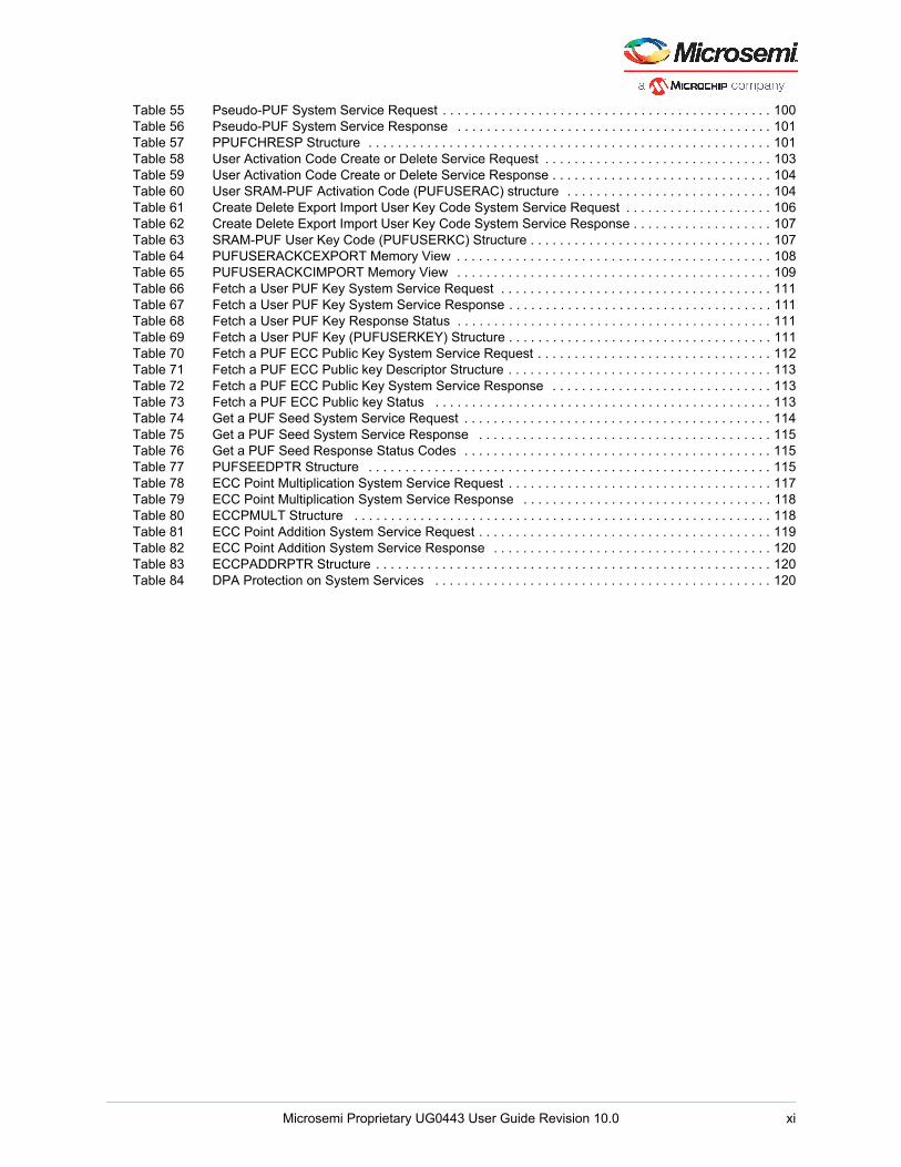
Table 55 Pseudo-PUF System Service Request . . . . . . . . . . . . . . . . . . . . . . . . . . . . . . . . . . . . . . . . . . . . . 100Table 56 Pseudo-PUF System Service Response . . . . . . . . . . . . . . . . . . . . . . . . . . . . . . . . . . . . . . . . . . . 101Table 57 PPUFCHRESP Structure . . . . . . . . . . . . . . . . . . . . . . . . . . . . . . . . . . . . . . . . . . . . . . . . . . . . . . . 101Table 58 User Activation Code Create or Delete Service Request . . . . . . . . . . . . . . . . . . . . . . . . . . . . . . . 103Table 59 User Activation Code Create or Delete Service Response . . . . . . . . . . . . . . . . . . . . . . . . . . . . . . 104Table 60 User SRAM-PUF Activation Code (PUFUSERAC) structure . . . . . . . . . . . . . . . . . . . . . . . . . . . . 104Table 61 Create Delete Export Import User Key Code System Service Request . . . . . . . . . . . . . . . . . . . . 106Table 62 Create Delete Export Import User Key Code System Service Response . . . . . . . . . . . . . . . . . . . 107Table 63 SRAM-PUF User Key Code (PUFUSERKC) Structure . . . . . . . . . . . . . . . . . . . . . . . . . . . . . . . . . 107Table 64 PUFUSERACKCEXPORT Memory View . . . . . . . . . . . . . . . . . . . . . . . . . . . . . . . . . . . . . . . . . . . 108Table 65 PUFUSERACKCIMPORT Memory View . . . . . . . . . . . . . . . . . . . . . . . . . . . . . . . . . . . . . . . . . . . 109Table 66 Fetch a User PUF Key System Service Request . . . . . . . . . . . . . . . . . . . . . . . . . . . . . . . . . . . . . 111Table 67 Fetch a User PUF Key System Service Response . . . . . . . . . . . . . . . . . . . . . . . . . . . . . . . . . . . . 111Table 68 Fetch a User PUF Key Response Status . . . . . . . . . . . . . . . . . . . . . . . . . . . . . . . . . . . . . . . . . . . 111Table 69 Fetch a User PUF Key (PUFUSERKEY) Structure . . . . . . . . . . . . . . . . . . . . . . . . . . . . . . . . . . . . 111Table 70 Fetch a PUF ECC Public Key System Service Request . . . . . . . . . . . . . . . . . . . . . . . . . . . . . . . . 112Table 71 Fetch a PUF ECC Public key Descriptor Structure . . . . . . . . . . . . . . . . . . . . . . . . . . . . . . . . . . . . 113Table 72 Fetch a PUF ECC Public Key System Service Response . . . . . . . . . . . . . . . . . . . . . . . . . . . . . . 113Table 73 Fetch a PUF ECC Public key Status . . . . . . . . . . . . . . . . . . . . . . . . . . . . . . . . . . . . . . . . . . . . . . 113Table 74 Get a PUF Seed System Service Request . . . . . . . . . . . . . . . . . . . . . . . . . . . . . . . . . . . . . . . . . . 114Table 75 Get a PUF Seed System Service Response . . . . . . . . . . . . . . . . . . . . . . . . . . . . . . . . . . . . . . . . 115Table 76 Get a PUF Seed Response Status Codes . . . . . . . . . . . . . . . . . . . . . . . . . . . . . . . . . . . . . . . . . . 115Table 77 PUFSEEDPTR Structure . . . . . . . . . . . . . . . . . . . . . . . . . . . . . . . . . . . . . . . . . . . . . . . . . . . . . . . 115Table 78 ECC Point Multiplication System Service Request . . . . . . . . . . . . . . . . . . . . . . . . . . . . . . . . . . . . 117Table 79 ECC Point Multiplication System Service Response . . . . . . . . . . . . . . . . . . . . . . . . . . . . . . . . . . 118Table 80 ECCPMULT Structure . . . . . . . . . . . . . . . . . . . . . . . . . . . . . . . . . . . . . . . . . . . . . . . . . . . . . . . . . 118Table 81 ECC Point Addition System Service Request . . . . . . . . . . . . . . . . . . . . . . . . . . . . . . . . . . . . . . . . 119Table 82 ECC Point Addition System Service Response . . . . . . . . . . . . . . . . . . . . . . . . . . . . . . . . . . . . . . 120Table 83 ECCPADDRPTR Structure . . . . . . . . . . . . . . . . . . . . . . . . . . . . . . . . . . . . . . . . . . . . . . . . . . . . . . 120Table 84 DPA Protection on System Services . . . . . . . . . . . . . . . . . . . . . . . . . . . . . . . . . . . . . . . . . . . . . . 120
Microsemi Proprietary UG0443 User Guide Revision 10.0 xi
Revision History
1 Revision History
The revision history describes the changes that were implemented in the document. The changes are listed by revision, starting with the most current publication.
1.1 Revision 10.0The following is a summary of changes made in this revision.
• Updated the document for Libero SoC v12.0.• Updated the sections Passcode Locks (Permanent Locks), page 35 and Fabric Programming Erase
Verify Read Lock-bits, page 36.• Added a note under Table 25, page 72 to include a programming workaround when cryptographic
system services are enabled in the design.• Updated the section Using Zeroization to Decommission Devices, page 64.• Added a footnote for Table 1, page 16.• Added descriptions for DETECT_CATEGORY flag, see Table 17, page 58.• Added information about how to disable JTAG boundary scan using Libero SoC, seeProgramming
Port Lock-bits, page 38.• Updated Table 19, page 61 to clearly specify which information segment is retained and which
segment is destroyed when the Recoverable option is selected.
1.2 Revision 9.0The following changes were made in this revision.
• Information about eNVM array was updated to include SRAM-PUF/ECC key storage information. For more information, see eNVM Array, page 24.
• Throughout the document, figures were updated to show Libero SoC v11.8.• Information about key mode lock bits was updated to include UEK3. For more information, see Key-
Mode Lock-bits, page 37.• Throughout the document, KUS was replaced by UEK3.
1.3 Revision 8.0The following changes were made in this revision.
• Security Concerns in FPGAs, page 3, Reverse Engineering Protection, page 124, and Internal Security Features, page 129 were added.
• “Error Detection and Correction Controllers” section was deleted.• Security Features Overview, page 7, Cryptographic Security Features, page 19, FPGA Hardware
Access Controls, page 34, Supply Chain Assurance, page 46, Data Security Through System Services, page 72, and Using System Services Driver, page 123 were updated.
• DISABLEIO_ALL_IOS_N, page 61 was updated (SAR 80923).
1.4 Revision 7.0In revision 7.0 of this document, a note was updated in Programming Port Lock-bits, page 38 (SAR 78163).
1.5 Revision 6.0The following changes were made in revision 6.0 of this document.
• IGLOO2 Security and Reliability User Guide and SmartFusion2 Security and Reliability User Guide were merged into this user guide.
• This revision number continues for further updates. Refer to SmartFusion2 and IGLOO2 list of changes tables provided below for earlier updates.
• Zeroization Procedure, page 61 was updated (SAR 56959).• Fabric Configuration and eNVM Integrity Tests, page 66 was updated (SAR 67636).
Microsemi Proprietary UG0443 User Guide Revision 10.0 1
Revision History
1.6 IGLOO2 Document List of Changes (Outdated)
1.7 SmartFusion2 Document List of Changes (Outdated)
Revision Changes
Revision 4(July 2015)
This user guide was restructured and rewritten (SAR 57510 and 68479).
Revision 3(January 2015)
Removed all instances of and references to M2S100 device from Table 1, Table 2, Table 4, Table 16 and Table 25 (SAR 62858).Replaced all instances of “S” version with “S” or “TS” version.
Revision 2(June 2014)
User guide was restructured and rewritten (SAR 57510).
Revision 1(September 2013)
Added “How to Use EDAC” section in Error Detection and Correction Controllers chapter (SAR 50571)
Revision 0(June 2013)
Initial release.
Revision Changes
Revision 5(January 2015)
Removed all instances of and references to M2S100 device from Table 1, Table 2, Table 4, Table 16 and Table 25 (SAR 62858).Replaced all instances of “S” version with “S” or “TS” version.
Revision 4(May 2014)
This user guide was restructured and rewritten (SAR 57510).
Revision 3(September 2013)
Updated the “SmartFusion2 Security Features Overview” chapter (SAR 42854).
Revision 2(April 2013)
Restructured the Error Detection and Correction Controllers chapter (SAR 46164).
Revision 1(November 2012)
Added the “SmartFusion2 Security Features Overview” Chapter.
Revision 0(October 2012)
Initial release.
Microsemi Proprietary UG0443 User Guide Revision 10.0 2
Security Concerns in FPGAs
2 Security Concerns in FPGAs
As FPGA sizes have grown to exceed the million-gate mark, they are used for more complex and valuable designs. These days FPGAs include millions of gates of logic, megabytes of memory, high-speed transceivers, analog interfaces, and robust processors. Hence, applications such as communications infrastructure, sensitive database access, critical industrial control, and high-performance signal processing that run in the FPGAs, have more value and handle more data. This brings a greater need to protect these applications and data. This chapter briefly describes the various common security concerns in FPGAs designs.
Throughout this document, the FPGA security functions are referenced as “design security” features and “data security” features. The following section describes the design security and data security features.
2.1 Design SecurityDesign security feature protects the design IP and other sensitive information such as cryptographic keys that are used in the FPGA initial configuration. Design IP includes designer’s logic design, firmware code, and security settings loaded in the design. Designer’s logic design is typically a register-transfer-level (RTL) source code in a design language such as Verilog or VHDL. This source code is compiled ultimately to a binary form that is used to configure the FPGA Fabric look-up tables (LUTs), routing switches and other programmable elements that give the FPGA Fabric and I/Os their desired functionality. Another aspect of design IP is firmware code (C language or assembly source code) that can be complied to binary code and is normally loaded and stored in eNVM within the device for execution by the Cortex-M3 -based microprocessor sub-system (MSS). Microsemi SoC FPGAs such as SmartFusion®2 also contain a hard ARM® Cortex™-M3 processor. The larger programs may require external non-volatile memory as well, to hold them, but the security of this code must be managed by the application that the user writes, not the built-in features of the device.
Static end-application data values, considered as part of the design IP, may also be stored in the on-chip eNVM.
A third broad category of IP includes all the cryptographic keys and security settings loaded into a device that configures the security properties, for example, whether upgrades are allowed, and what action to take if tampering is detected, etc. In SmartFusion2 most of the security keys and settings are stored in a specially designed flash-based security segment described later in the guide.
Common security goals of the design owner are to keep the design IP confidential, to control the number of devices (and systems containing such devices) that are produced, and to prevent tampering with the design either when initially programmed, or thereafter. If field updates are allowed, they should only originate with the design owner, and must be installed only with the exact configuration the owner intends. The systems configured should perform reliability as intended, without unwanted extra functionality. This implies that the design owner wants to use only trusted devices with the expected performance, environmental capabilities, and reliability characteristics.
2.2 Data SecurityData security feature protects the data that is processed by the end application. The asset being protected is the data generated/computed, stored, or communicated by the run-time application. This data is often dynamic and usually owned by the user. Very often, cryptographic techniques are used to protect these assets. Data security is closely related to the terms— information assurance (IA) and information security. For example, if the configured design is implementing the key management and encryption portion of a secure military radio, data security can entail encrypting and authenticating the radio traffic, and protect the associated application-level cryptographic keys.
All Smartfusion2 and IGLOO®2 devices incorporate enhanced design security which make them the most secure programmable logic devices. SmartFusion2 and IGLOO2 devices also include an advanced set of on-chip data security features that make designing secure information assurance applications easier and better than before. Several of the largest family members have additional design and data
Microsemi Proprietary UG0443 User Guide Revision 10.0 3

Security Concerns in FPGAs
security features not present in the smaller devices. The design and data security features are described later in the document.
2.3 Design Security ConcernsIn this section, few specific design security concerns are described:
2.3.1 CloningCloning (with respect to FPGAs) refers to producing additional devices that are programmed identical to legitimately produced ones. The concern arises as FPGAs are generally openly available on the market, and anyone with valid binary configuration data (often referred to as a “bitstream” file) can obtain devices and, without proper FPGA security, might be able to produce as many fully configured copies as they wish. An understanding of how the design works is not necessarily a requirement to produce clones; possessing the configuration data and blank devices may be all that is required.
2.3.2 OverbuildingOverbuilding is a special case of cloning of whole systems where the legitimate design owner hires a contract manufacturer (CM) to build a certain number of systems, but a dishonest CM (or perhaps his rogue employees) produce more systems than that were authorized so they can sell the overage themselves. Because of the CM's privileged and trusted insider position and possessing all the data required to produce legitimate systems including, for example, the FPGA configuration files and perhaps even the associated cryptographic keys, overbuilding by dishonest CMs or insiders is generally a bigger threat than cloning from other types of adversaries that don’t have access to all the same data.
SmartFusion2 and IGLOO2 contain security features, described later, that allow the design owner to control the number of FPGAs that are programmed with a given design, almost completely eliminating the risk of cloned FPGAs, and thus also preventing overbuilding of systems containing FPGAs.
2.3.3 Reverse EngineeringModern FPGAs can be configured with large and very complex functionality. Reverse engineering (RE) by observing only the FPGA inputs and outputs is quite difficult. This can be a significant hurdle to those attempting to steal the design IP. However, if an adversary can gain access to the binary FPGA Fabric or CPU firmware configuration data in plaintext form, reverse engineering of the system is much easier, since it becomes more of a “white-box” class of problem where some or all of the internal elements of the design are visible.
The detailed knowledge and understanding of how the FPGA logic or CPU firmware in a design works, can be very valuable IP, a high-value asset in its own right. For example, the IP could be an industrial or national security secret. The adversary may wish to understand how the design works to find security vulnerabilities that can be exploited in systems of the same or similar design. In some cases, just publishing full or partial design secrets can be a major concern.
The cost of reverse engineering can be lower than the cost of designing a competitive system from publicly available knowledge, giving the IP thief an unfair economic advantage versus the legitimate IP owner. Such IP, once revealed, may be cloned, ported to other implementations, or even sometimes enhanced. The useful lifetime of systems with known exploits may be reduced, which requires expensive development of replacement systems.
Furthermore, if the workings of a design are known, it may also be possible for an adversary to insert undesired functionality into it, such as a Trojan Horse that provides a back-door for extracting sensitive run-time data, and then re-introduce the modified design, undetected into the otherwise legitimate original system.
The main approach to prevent reverse engineering is to keep the design confidential. This confidentiality can be lost if the FPGA configuration data (e.g., for the FPGA fabric, or the firmware for the MCU) is captured in plaintext form or can be read-back from a device; or if an encrypted version of the configuration data is known and the encryption keys are stolen or extracted from a device. SmartFusion2 and IGLOO2 have strong countermeasures to maintain the confidentiality of the design configuration and associated secret keys. See Reverse Engineering Protection, page 124 to know more.
Microsemi Proprietary UG0443 User Guide Revision 10.0 4

Security Concerns in FPGAs
2.3.4 CounterfeitingCounterfeiting can refer to several types of fraud at either the component or system level. While there is a remote possibility of an FPGA being copied and produced by an unauthorized manufacturer, the more realistic threats are from devices originally produced by the FPGA’s original component manufacturer (OCM) that are somehow obtained by, and then misrepresented and sold by the counterfeiter.
These devices can be used devices that are removed from old systems, refurbished, and resold as new; or devices binned as lower-speed grade or requiring a more restricted operating temperature that are re-marked and misrepresented as faster or having guaranteed performance over a wider temperature range. Similarly, devices could be misrepresented as having been screened for higher reliability levels, which actually are not screened, or which have failed screening tests. In many of the above cases the devices may work at first, or in benign environments, but fail under conditions where the properly binned or screened devices would have worked correctly. As these are “real” devices that work correctly (at least initially) they can be very difficult to segregate from legitimate devices by performing an inspection or an electrical test. It is a challenge for the legitimate suppliers of ICs to provide better marking and inspection methods while the counterfeiters create higher fidelity fakes that are harder to detect.
Rogue insiders could possibly obtain devices that have failed some functional test, and fraudulently introduce them into the supply chain as fully functional devices. In some cases, the devices in question may be obtained by “buying low and selling high,” (after being re-marked with added features that aren’t actually present) or they may be stolen from fabrication, test or assembly facilities, delivery trucks, warehouses, or in stages further down the supply chain.
Microsemi has instituted a number of very strong measures during the manufacturing process and in the shipped devices which help in stopping counterfeiting and related fraud. These features, supported in the Libero® design automation tool suite, detect counterfeit devices before being shipped in end-user systems, no matter where they are introduced in the supply chain.
Counterfeiting at the system level usually means a clone, or a system that is designed to work similar to the real system, but produced by a counterfeiter who fraudulently misrepresents it as coming from the legitimate source. Counterfeit systems are often made using inferior components and processes in order to produce them at the lowest possible cost. Any brand damage due to bad design, shoddy construction, or poor reliability will unfortunately be directed to the legitimate brand owner while the counterfeiter can stay safe with the illegal profits earned. In extreme cases, the legitimate manufacturer may find counterfeit systems returned under warranty, or even worse, to the subject of liability or litigation.
Many of the other security concerns mentioned so far may also lead to counterfeiting at the system level. For example, a counterfeit system may include a Trojan Horse. It could be a standard-grade offering misrepresented as a premium grade, or modified to provide optional premium services with the premium price going to the counterfeiter rather than the legitimate producer.
If good FPGA security makes cloning and reverse engineering difficult, it can be a useful deterrent to several types of system-level fraud. Therefore, good FPGA security can be part of the solution to system-level counterfeiting.
2.4 Data Security ConcernsData security is potentially as broad a subject as there are possible end uses of an FPGA, since in the broadest sense an FPGA is always used to process data, a concise but all-encompassing definition is difficult. In order to concise the definition, the data considered is usually restricted to data that are sensitive.
Data security very often uses cryptographic techniques, implementing various security services. Often the services provided are amongst the five familiar information security services:
• Confidentiality – Keeping the data secret• Integrity – Insuring the data hasn’t been altered• Availability – Both available when needed, and denied to unauthorized uses (including unauthorized
privilege escalation)• Authenticity – Data is genuine and from the correct source• Non-repudiation – A completed transaction cannot be denied
Microsemi Proprietary UG0443 User Guide Revision 10.0 5
Security Concerns in FPGAs
Listed below are some of the attacks that may be used to break the security services.
• Monitoring or snooping on communication traffic or stored data in motion, or data at rest)• Tampering with or changing data (for example, a “replay attack”)• Impersonating one of the legitimate actors (for example, man-in-the-middle attack)• Exploiting weak protocols
• Freshness, oracle, type, binding, repudiation, or other flaws• Exploiting other design security weaknesses
• Weakness discovered with reverse engineering• Inserting a Trojan Horse into user’s system• Re-introducing a weakness user had fixed with an update
2.5 Design Security Impact on Data SecurityWithout design/device security, it is virtually impossible to provide good data security. Most design security threats, such as reverse engineering, insertion of a Trojan Horse, unauthorized field upgrades, etc. can lead to serious data security vulnerabilities. Data Security, including features provided by Microsemi intended for use in data security applications, are discussed later in the document.
Microsemi Proprietary UG0443 User Guide Revision 10.0 6
Security Features Overview
3 Security Features Overview
Microsemi’s SmartFusion2 and IGLOO2 devices have built-in features that provide enhanced security during all stages of the device life-cycle from user key injection and bitstream programming, to field updates, and finally to device decommissioning, when necessary. This chapter gives an overview of these security features.
3.1 Security ArchitectureThe following sections describe SmartFusion2 and IGLOO2 security model architecture
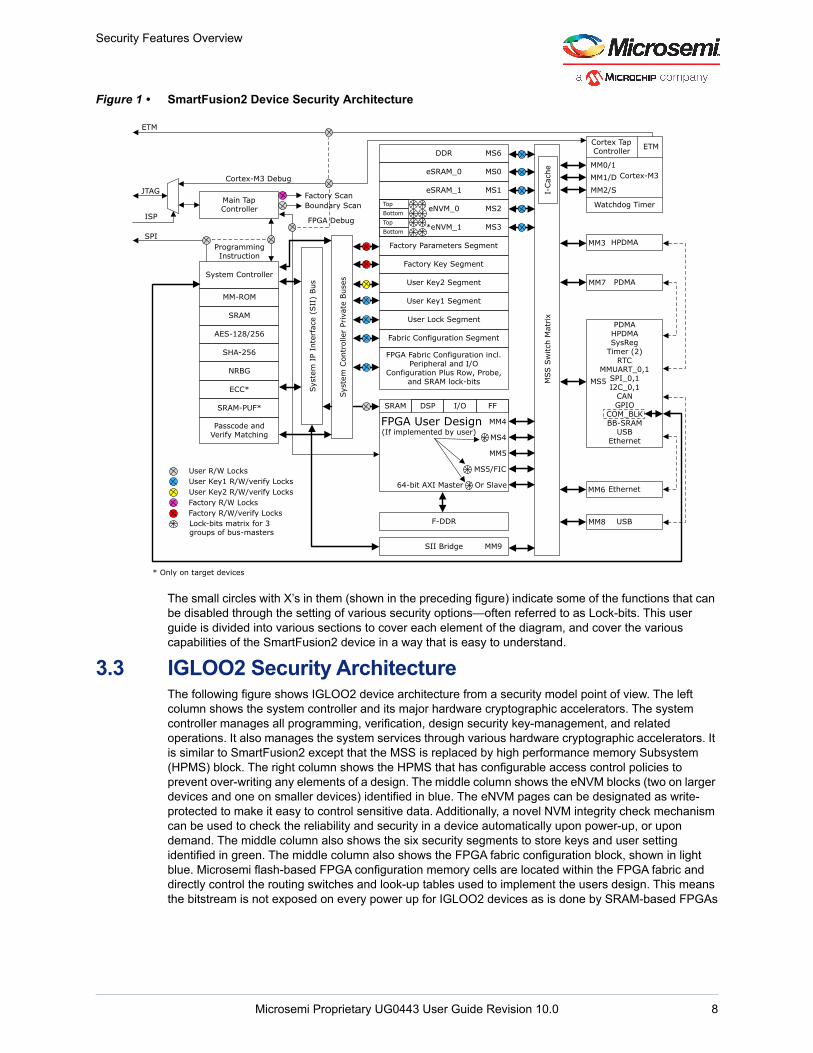
3.2 SmartFusion2 Security ArchitectureThe following figure shows SmartFusion2 device architecture from a security model point of view. The left column shows the system controller and its major hardware cryptographic accelerators. The system controller manages all programming, verification, design security key-management, and related operations. Also, it manages the system services through various hardware cryptographic accelerators. The right column shows the Microcontroller Subsystem (MSS) that has configurable access control policies to prevent over-writing any elements of a design. The middle column shows the eNVM blocks (two on -090 and -150 devices and one on other SmartFusion2 devices) identified in blue. The eNVM pages can be designated as write-protected to make it easy to control sensitive data. Additionally, a novel NVM integrity check mechanism can be used to check the reliability and security in a device automatically upon power-up, or upon demand. The middle column also shows the six security segments to store keys and user settings (identified in green) and shows the FPGA fabric configuration block (shown in light blue). Microsemi flash-based FPGA configuration memory cells are located within the FPGA fabric and directly control the routing switches and look-up tables that are used to implement the user's design. This means the bitstream is not exposed on every power up for SmartFusion2 devices as is done by SRAM-based FPGAs.
Microsemi Proprietary UG0443 User Guide Revision 10.0 7
Security Features Overview
Figure 1 • SmartFusion2 Device Security Architecture
The small circles with X’s in them (shown in the preceding figure) indicate some of the functions that can be disabled through the setting of various security options—often referred to as Lock-bits. This user guide is divided into various sections to cover each element of the diagram, and cover the various capabilities of the SmartFusion2 device in a way that is easy to understand.
3.3 IGLOO2 Security ArchitectureThe following figure shows IGLOO2 device architecture from a security model point of view. The left column shows the system controller and its major hardware cryptographic accelerators. The system controller manages all programming, verification, design security key-management, and related operations. It also manages the system services through various hardware cryptographic accelerators. It is similar to SmartFusion2 except that the MSS is replaced by high performance memory Subsystem (HPMS) block. The right column shows the HPMS that has configurable access control policies to prevent over-writing any elements of a design. The middle column shows the eNVM blocks (two on larger devices and one on smaller devices) identified in blue. The eNVM pages can be designated as write-protected to make it easy to control sensitive data. Additionally, a novel NVM integrity check mechanism can be used to check the reliability and security in a device automatically upon power-up, or upon demand. The middle column also shows the six security segments to store keys and user setting identified in green. The middle column also shows the FPGA fabric configuration block, shown in light blue. Microsemi flash-based FPGA configuration memory cells are located within the FPGA fabric and directly control the routing switches and look-up tables used to implement the users design. This means the bitstream is not exposed on every power up for IGLOO2 devices as is done by SRAM-based FPGAs
System Controller
MM-ROM
SRAM
AES-128/256
SHA-256
NRBG
Passcode and Verify Matching
Syst
em I
P In
terf
ace
(SII
) Bus
Syst
em C
ontr
olle
r Pr
ivat
e Bus
es
DDR
eSRAM_0
eSRAM_1
eNVM_0TopBottom
*eNVM_1TopBottom
MS6
MS0
MS1
MS2
MS3
Factory Parameters Segment
Factory Key Segment
User Key2 Segment
User Key1 Segment
User Lock Segment
Fabric Configuration Segment
FPGA Fabric Configuration incl. Peripheral and I/O
Configuration Plus Row, Probe, and SRAM lock-bits
SRAM DSP I/O FF
MM4
MS4
MM5
MS5/FIC
Or Slave64-bit AXI Master
FPGA User Design(If implemented by user)
F-DDR
SII Bridge MM9
Main Tap Controller
Factory ScanBoundary Scan
JTAG
SPI
User R/W LocksUser Key1 R/W/verify LocksUser Key2 R/W/verify LocksFactory R/W LocksFactory R/W/verify LocksLock-bits matrix for 3 groups of bus-masters
ECC*
SRAM-PUF*
MSS
Sw
itch
Mat
rix
I-Cac
he
Cortex Tap Controller ETM
Cortex-M3MM0/1MM1/D
MM2/S
Watchdog Timer
HPDMA
PDMA
MM3
MM7
PDMAHPDMASysReg
Timer (2)RTC
MMUART_0,1SPI_0,1I2C_0,1
CANGPIO
COM_BLKBB-SRAM
USBEthernet
MS5
Ethernet
USB
MM6
MM8
* Only on target devices
Programming Instruction
ETM
Cortex-M3 Debug
ISP FPGA Debug
Microsemi Proprietary UG0443 User Guide Revision 10.0 8
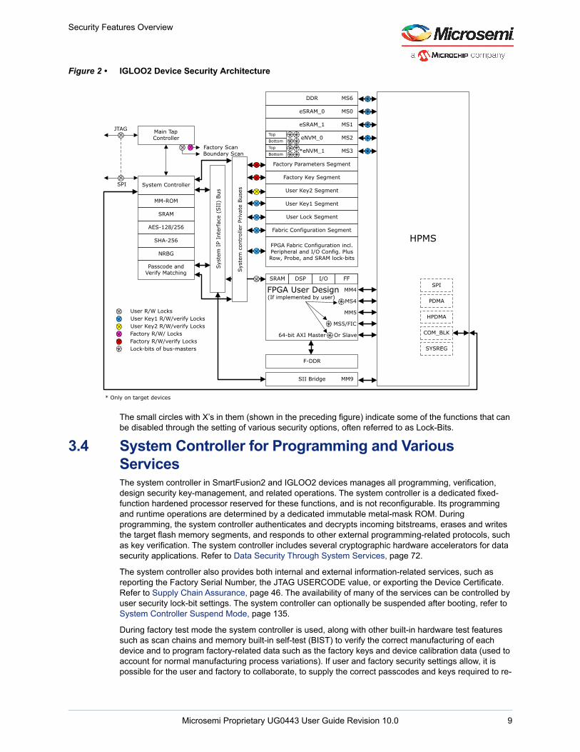
Security Features Overview
Figure 2 • IGLOO2 Device Security Architecture
The small circles with X’s in them (shown in the preceding figure) indicate some of the functions that can be disabled through the setting of various security options, often referred to as Lock-Bits.
3.4 System Controller for Programming and Various Services The system controller in SmartFusion2 and IGLOO2 devices manages all programming, verification, design security key-management, and related operations. The system controller is a dedicated fixed- function hardened processor reserved for these functions, and is not reconfigurable. Its programming and runtime operations are determined by a dedicated immutable metal-mask ROM. During programming, the system controller authenticates and decrypts incoming bitstreams, erases and writes the target flash memory segments, and responds to other external programming-related protocols, such as key verification. The system controller includes several cryptographic hardware accelerators for data security applications. Refer to Data Security Through System Services, page 72.
The system controller also provides both internal and external information-related services, such as reporting the Factory Serial Number, the JTAG USERCODE value, or exporting the Device Certificate. Refer to Supply Chain Assurance, page 46. The availability of many of the services can be controlled by user security lock-bit settings. The system controller can optionally be suspended after booting, refer to System Controller Suspend Mode, page 135.
During factory test mode the system controller is used, along with other built-in hardware test features such as scan chains and memory built-in self-test (BIST) to verify the correct manufacturing of each device and to program factory-related data such as the factory keys and device calibration data (used to account for normal manufacturing process variations). If user and factory security settings allow, it is possible for the user and factory to collaborate, to supply the correct passcodes and keys required to re-
System Controller
MM-ROM
SRAM
AES-128/256
SHA-256
NRBG
Passcode and Verify Matching
Syst
em I
P In
terf
ace
(SII
) Bus
Syst
em c
ontr
olle
r Pr
ivat
e Bus
es
DDR
eSRAM_0
eSRAM_1
eNVM_0TopBottom
*eNVM_1TopBottom
MS6
MS0
MS1
MS2
MS3
Factory Parameters Segment
Factory Key Segment
User Key2 Segment
User Key1 Segment
User Lock Segment
Fabric Configuration Segment
FPGA Fabric Configuration incl. Peripheral and I/O Config. Plus Row, Probe, and SRAM lock-bits
SRAM DSP I/O FF
MM4
MS4
MM5
MS5/FIC
Or Slave64-bit AXI Master
FPGA User Design(If implemented by user)
F-DDR
SII Bridge MM9
HPMS
SPI
PDMA
HPDMA
COM_BLK
SYSREG
Main Tap Controller
Factory ScanBoundary Scan
JTAG
SPI
User R/W LocksUser Key1 R/W/verify LocksUser Key2 R/W/verify LocksFactory R/W/ LocksFactory R/W/verify LocksLock-bits of bus-masters
* Only on target devices
Microsemi Proprietary UG0443 User Guide Revision 10.0 9

Security Features Overview
enter factory test mode in order to perform failure analysis of a failed device. There are strong, layered, protections in place to prevent an adversary (or just the user or factory) from being able to enter factory test mode. In user-configured devices there are default mechanisms that lock-out the factory, including several optional layered mechanisms whereby the user can permanently prevent the device from entering the factory test mode. Of course, if any of these permanent lock options are used, failure analysis becomes impossible. Depending on the exact mechanisms deployed, field updates or design verification may also be permanently blocked.
3.5 Hardware Cryptographic AcceleratorsThe system controller and associated security hardware includes hardware-based security countermeasures to protect it against a broad range of threats, and manages the hardware-based security countermeasures throughout the rest of the device. This section describes the hardware cryptographic accelerators. The cryptographic system services are only available in premium devices denoted with an “S” (or “TS”) suffix in the model number immediately following the device capacity code.
The hardware accelerator includes the following:
• Cryptographic Services block:• AES-128/256 Hardware Accelerator• SHA-256 Hardware Accelerator
• Non-Deterministic Random Bit Generator (NRBG)• Elliptic Curve Cryptography Hardware Accelerator (P-384 Curve)• SRAM-PUF Secure Key Storage and Random Seed Generation Engine
These hardware accelerators have been certified in NIST's cryptographic algorithm validation program (CAVP). Refer to the following sections for links to the appropriate certificates in the NIST algorithm validation lists on the NIST website.
The use of the hardware accelerators in the SmartFusion2 and IGLOO2 design security protocols have been assessed by an accredited independent third-party security laboratory for resistance to side channel analysis and have been certified as defined by the Rambus Cryptography Research Differential Power Analysis (DPA) Countermeasure Validation Program (CVP) scheme. The following design security protocols and services were assessed and certified:
• Bitstream Loading Protocol, BSP• Bitstream Authentication Service, BAS• Key Verification Protocol, KVP• Plaintext Passcode Matching & Privilege Escalation, PTP• One-Time Passcode, OTP• Device Certificate Service DCS• Pseudo-PUF Challenge/Response Service, PPS
The underlying cryptographic primitives (AES, ECC, SHA), used in the context of these protocols are included. These protocols and services are described later in this document.
3.6 AES-128/256 Hardware AcceleratorThe system controller has a hardware accelerator for encrypting or decrypting 128-bit blocks of data as defined by the Advanced Encryption Standard and Technology Federal Information Processing Standard Publication 197 (NIST FIPS PUB 197). The AES accelerator supports 128 and 256 bit key sizes. It is used for both design and data security. For example, it is used for bitstream decryption. While the AES accelerator does not have strong DPA countermeasures built-in, for design security applications it is only used in protocols that nevertheless effectively prevent successful DPA attacks. Primarily, this is done by strictly limiting the number of uses of any given key.
The AES hardware accelerator can also be used for data security applications as a system service (“S” and “TS” devices only), please refer to AES-128/256 Service (ECB, OFB, CTR, CBC modes), page 89.
The AES hardware accelerators used in SmartFusion2 and IGLOO2 FPGAs have been certified in NIST's cryptographic algorithm validation program (CAVP) for several common AES modes of operation and key sizes for encryption and decryption. Refer to the certificates on the NIST website: certificate 2908 (applicable to all -005, -010, -025 devices) and certificate 2935 (applicable to all -060, -090 and -150 devices).
Microsemi Proprietary UG0443 User Guide Revision 10.0 10
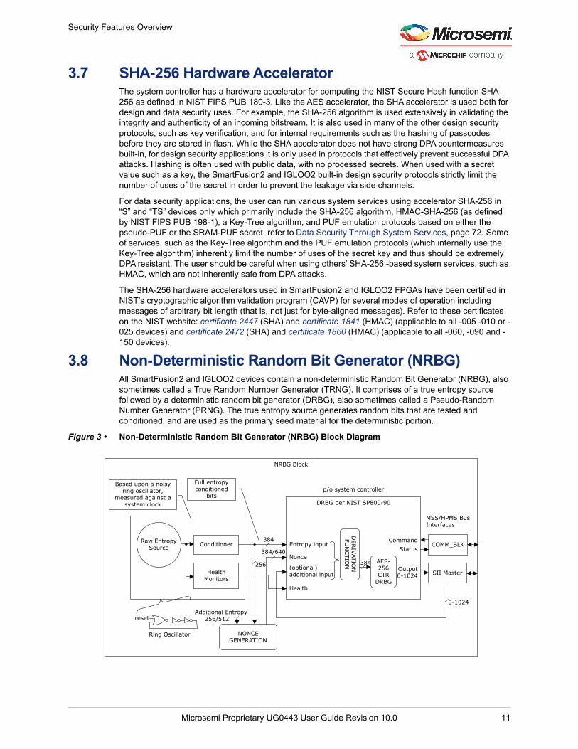
Security Features Overview
3.7 SHA-256 Hardware AcceleratorThe system controller has a hardware accelerator for computing the NIST Secure Hash function SHA-256 as defined in NIST FIPS PUB 180-3. Like the AES accelerator, the SHA accelerator is used both for design and data security uses. For example, the SHA-256 algorithm is used extensively in validating the integrity and authenticity of an incoming bitstream. It is also used in many of the other design security protocols, such as key verification, and for internal requirements such as the hashing of passcodes before they are stored in flash. While the SHA accelerator does not have strong DPA countermeasures built-in, for design security applications it is only used in protocols that effectively prevent successful DPA attacks. Hashing is often used with public data, with no processed secrets. When used with a secret value such as a key, the SmartFusion2 and IGLOO2 built-in design security protocols strictly limit the number of uses of the secret in order to prevent the leakage via side channels.
For data security applications, the user can run various system services using accelerator SHA-256 in “S” and “TS” devices only which primarily include the SHA-256 algorithm, HMAC-SHA-256 (as defined by NIST FIPS PUB 198-1), a Key-Tree algorithm, and PUF emulation protocols based on either the pseudo-PUF or the SRAM-PUF secret, refer to Data Security Through System Services, page 72. Some of services, such as the Key-Tree algorithm and the PUF emulation protocols (which internally use the Key-Tree algorithm) inherently limit the number of uses of the secret key and thus should be extremely DPA resistant. The user should be careful when using others’ SHA-256 -based system services, such as HMAC, which are not inherently safe from DPA attacks.
The SHA-256 hardware accelerators used in SmartFusion2 and IGLOO2 FPGAs have been certified in NIST’s cryptographic algorithm validation program (CAVP) for several modes of operation including messages of arbitrary bit length (that is, not just for byte-aligned messages). Refer to these certificates on the NIST website: certificate 2447 (SHA) and certificate 1841 (HMAC) (applicable to all -005 -010 or -025 devices) and certificate 2472 (SHA) and certificate 1860 (HMAC) (applicable to all -060, -090 and -150 devices).
3.8 Non-Deterministic Random Bit Generator (NRBG)All SmartFusion2 and IGLOO2 devices contain a non-deterministic Random Bit Generator (NRBG), also sometimes called a True Random Number Generator (TRNG). It comprises of a true entropy source followed by a deterministic random bit generator (DRBG), also sometimes called a Pseudo-Random Number Generator (PRNG). The true entropy source generates random bits that are tested and conditioned, and are used as the primary seed material for the deterministic portion.
Figure 3 • Non-Deterministic Random Bit Generator (NRBG) Block Diagram
NRBG Block
Based upon a noisy ring oscillator,
measured against a system clock
Raw Entropy Source Conditioner
Health Monitors
DRBG per NIST SP800-90
DER
IVATION
FU
NCTIO
N AES-256 CTR
DRBG
Entropy input
Nonce
(optional) additional input
Health
COMM_BLK
SII Master
p/o system controller
CommandStatus
Output0-1024
NONCE GENERATION
Additional Entropy 256/512
Ring Oscillator
reset
Full entropy conditioned
bits
MSS/HPMS Bus Interfaces
384
384
384/640
256
0-1024
Microsemi Proprietary UG0443 User Guide Revision 10.0 11

Security Features Overview
The NRBG is designed to meet U.S. NIST Special Publication SP800-90A (for which it is) and the German Bundesamt für Sicherheit in der Informationstechnik (BSI) random bit generator standard AIS-31. One of the primary selection criteria for the chosen NRBG is its certified heritage under both these standards in prior implementations. The random bits produced by the NRBG (ahead of the deterministic random bit generator, DRBG) are tested against the customary cryptographic statistical tests, for randomness, such as the NIST Statistical Test Suite STS-22, giving result to all passed tests.
The NRBG is used for design security protocols and related internal device functions. For example, it is used for generating certain random keys. It is also used extensively in on-line protocols to generate random nonces that is numbers used just once, often in order to prevent replay attacks against those protocols. Since each time the protocol is run, a fresh random number is used; the expected output results are different each time, even if the rest of the input parameters are the same as in an earlier execution. The random numbers are sufficiently long and the chance of generating the same number more than once is minimal.
The NRBG can also be used (only in “S” and “TS” devices) to generate random bit strings for the user’s data security applications. Refer to SmartFusion2 and IGLOO2 System Services, page 73 for detail.
The DRBG used in the SmartFusion2 and IGLOO2 FPGA’s NRBGs are certified in NIST’s cryptographic algorithm validation program (CAVP) for a security strength of 256 bits using AES CTR mode, including support for prediction resistance (Refer to U.S. NIST Special Publication SP800-90A). and certificates on the NIST website: certificate 535 (applicable to all -005, -010, -025 devices) and certificate 542 (applicable to all -060, -090 and -150 devices).
3.9 Elliptic Curve Cryptography Hardware Accelerator (P-384 Curve)In larger SmartFusion2 and IGLOO2 devices (-060, -090 and -150), the system controller also has an Elliptic Curve Cryptography (ECC) hardware accelerator. It can perform two mathematical functions, based on the NIST-defined P-384 curve and its associated domain parameters: scalar point multiplication, and point addition. The P-384 domain parameters are defined in NIST FIPS PUB 186-3 Appendix D.1.2.4. At present, this is the only elliptic curve approved for protecting classified information up to and including the top secret in the NIST Suite B list of approved algorithms.
The system controller can use the ECC accelerator to compute ECC public keys when the private key (as defined by NIST FIPS PUB 186-3 Appendix B.4) is provided, or to establish a shared secret with an external entity (the “x” -coordinate of the resulting point), using the Elliptic Curve Cryptography Co-factor Diffie-Hellman (ECC-CDH) protocol as specified in NIST SP800-56A. A shared 256-bit secret symmetric key is derived from the shared secret using a proprietary one-way DPA-resistant key derivation algorithm. The shared secret key can be used to authenticate the device by knowing the shared secret key (and thus by extension, the private key of the ECC key pair) using a challenge-response key verification protocol, or it can be used as an encryption key; to transport user key(s) into the device, for example.
Besides these design security uses, in “S” and “TS” devices, the user may access the point-multiplication and point addition capabilities of the ECC hardware accelerator as system services via the internal CommBlk bus interface. Refer to the SmartFusion2 and IGLOO2 System Services, page 73 for detail.
The scalar point multiplication service of the ECC hardware accelerators used in SmartFusion2 and IGLOO2 FPGAs are certified in NIST’s cryptographic algorithm validation program (CAVP) via the ECC co-factor Diffie-Hellman (CDH) primitive. Refer to the certificate on the NIST website: certificate 335 (applicable to all -060, -090 and -150 devices). Note that the other devices in the family do not support ECC.
Though the third-party DPA assessment technically only includes ECC scalar point multiplication in the context of the seven design security protocols certified the DPA countermeasures used in this implementation are equally effective in data security applications in preventing the (normally secret) scalar leakage via power or electro-magnetic side channels.
Microsemi Proprietary UG0443 User Guide Revision 10.0 12
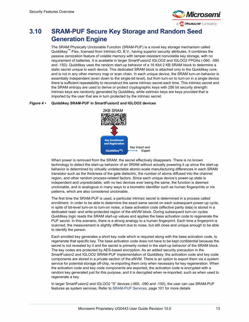
Security Features Overview
3.10 SRAM-PUF Secure Key Storage and Random Seed Generation EngineThe SRAM Physically Unclonable Function (SRAM-PUF) is a novel key storage mechanism called Quiddikey™-Flex, licensed from Intrinsic-ID, B.V., having superior security attributes. It combines the passive zeroization feature of volatile memory with tamper-resistant nonvolatile key storage, with no requirement of batteries. It is available in larger SmartFusion2 IGLOO2 and IGLOO2 FPGAs (-060, -090 and -150). Quiddikey uses the random start-up behavior of a 16 Kbit 2 KB SRAM block to determine a static secret unique to each device. This dedicated SRAM block is attached only to the Quiddikey core, and is not in any other memory map or scan chain. In each unique device, the SRAM turn-on behavior is essentially independent (even down to the single-bit level), but from turn-on to turn-on in a single device there is sufficient repeatability to reconstruct the same intrinsic secret each time. This intrinsic secret and the SRAM entropy are used to derive or protect cryptographic keys with 256 bit security strength: Intrinsic keys are randomly generated by Quiddikey, while extrinsic keys are keys provided that is imported by the user that are in turn protected by the intrinsic secret.
Figure 4 • Quiddikey SRAM-PUF in SmartFusion2 and IGLOO2 devices
When power is removed from the SRAM, the secret effectively disappears. There is no known technology to detect the start-up behavior of an SRAM without actually powering it up since the start-up behavior is determined by virtually undetectable atomic-scale manufacturing differences in each SRAM transistor such as the thickness of the gate dielectric, the number of atoms diffused into the channel region, and other random process-related factors. Since each unique device’s power-up state is independent and unpredictable, with no two devices ever being the same, the function is deemed unclonable, and is analogous in many ways to a biometric identifier such as human fingerprints or iris patterns, which are also considered unclonable.
The first time the SRAM-PUF is used, a particular intrinsic secret is determined in a process called enrollment. In order to be able to determine the exact same secret on each subsequent power-up cycle, in spite of bit-level turn-on to turn-on noise, a base activation code (effective parity data) is stored in a dedicated read- and write-protected region of the eNVM block. During subsequent turn-on cycles Quiddikey logic reads the SRAM start-up values and applies the base activation code to regenerate the PUF secret. In this scenario, there is a strong analogy to a human fingerprint. Each time a fingerprint is scanned, the measurement is slightly different due to noise, but still close and unique enough to be able to identify the person.
Each enrolled key generates a short key code which is required along with the base activation code, to regenerate that specific key. The base activation code does not have to be kept confidential because the secret is not revealed by it and the secret is primarily rooted in the start-up behavior of the SRAM block. The key codes are protected by AES-based encryption. As an added security precaution in the SmartFusion2 and IGLOO2 SRAM-PUF implementation of Quiddikey; the activation code and key code components are stored in a private section of the eNVM. There is an option to export them via a system service for potential storage off-chip, re-importing them only when necessary for key regeneration. When the activation code and key code components are exported, the activation code is encrypted with a random key generated just for this purpose, and it is decrypted when re-imported, such as when used to regenerate a key.
In larger SmartFusion2 and IGLOO2 “S” devices (-060, -090 and -150), the user can use SRAM-PUF features as system services, Refer to SRAM-PUF Services, page 101 for more details
Microsemi Proprietary UG0443 User Guide Revision 10.0 13
Security Features Overview
3.11 Design Security FeaturesDesign security is the assurance that the user design programmed into a device is secure and operates as intended for the life of the product. In the context of FPGAs this implies a secure FPGA fabric, a secure configuration bitstream (which can include eNVM content), secure update scheme for the configuration bitstream, and a secure key storage system. Cryptographic design security provides information security of the configuration data. Supply chain assurance provides protection against counterfeiting, and anti-tamper protection provides physical security of the underlying data. The various security mechanisms can be combined and layered to improve and build upon overall system level security. Below is a list of the design security features available in SmartFusion2 and IGLOO2 devices.
• Cryptographic Design Security• Bitstream protection and key management• FPGA hardware access control
• FlashLock® (passcode) security against unauthorized changes• FPGA lock-bits to enforce more granular protection• Software memory protection unit (MPU) to provide fine grain memory control (only available
in SmartFusion2 devices)• Memory hardware firewalls to protect the access to memories from the bus masters• Version control
• Supply Chain Assurance• Device certificates• Back-tracking prevention• Key confirmation verification protocols• Certificate-of-Conformance (C of C)
• Device Level Anti-Tamper Features• Resistance to differential/side-channel analysis• Tamper detection and response• Operational integrity verification
3.12 Cryptographic Design SecurityImportant attributes for a strong cryptographic FPGA design security solution are described in the following sub-sections
3.12.1 Bitstream Protection and Key ManagementAll SmartFusion2 and IGLOO2 configuration bitstreams are protected with AES-256 bit encryption, and authenticated with SHA-256. No options exist within the Libero SoC tool flow to generate plain text bitstreams. A default bitstream key is used if no user keys are specified.
Key management is often the critical link in a secure system. The FPGA and configuration bitstreams are protected by a cryptographic key. Key management includes secure generation, distribution, and storage of keys. All SmartFusion2 and IGLOO2 devices contain factory provisioned key material that can be used to authenticate a device and provide a starting point for enrolling private user keys. Secret device keys (both factory provided and user enrolled) are stored encrypted in all members of the device family. The larger SmartFusion2 and IGLOO2 devices (-060, -090 and -150 devices) contain an elliptic curve cryptography (ECC) engine to support asymmetric cryptographic techniques for key establishment. For key storage, these same devices contain the Quiddikey IP core, an SRAM Physically Unclonable Function (SRAM-PUF) licensed from Intrinsic-ID. In all SmartFusion2 and IGLOO2 FPGAs having the SRAM-PUF feature, Microsemi enrolls one 384-bit Factory Private ECC PUF key (SKFP) during device manufacturing. This is a completely random key unique per each device that is generated inside a FIPS140-2 level 3 hardware security module (HSM) during the key provisioning steps of the device manufacturing process, and is not recorded or re- constructible by Microsemi. The various key management features are described in Cryptographic Security Features, page 19.
3.12.2 FPGA Hardware Access ControlSmartFusion2 and IGLOO2 FPGAs incorporate a number of configurable access control policies to prevent over-writing any elements of a design. This includes the FlashLock passcode, FPGA lock-bits, and the software memory protection unit for the MSS to enforce more granular protection for both
Microsemi Proprietary UG0443 User Guide Revision 10.0 14
Security Features Overview
general purpose memory and security segments. Refer to FPGA Hardware Access Controls, page 34 for details.
3.12.3 Supply Chain AssuranceSupply chain assurance in the context of Microsemi FPGAs implies that the device purchased is a genuine Microsemi FPGA component. This ensures that devices have not been counterfeited or fraudulently marked with characteristics other than what the device contains (that is, speed grade, revision number). All SmartFusion2 and IGLOO2 devices include an X.509 certificate that is digitally signed with a Microsemi private key. The certificate is bound to the serial and model numbers of the device, grading info, and a unique per device secret factory key. The Device Certificates (Anti-Counterfeiting), page 47 provides more details on SmartFusion2 and IGLOO2 X.509 certificate and its uses. In addition, unique device keys enable exact controls over the customer manufacturing process to prevent over-building of customer systems at third-party manufacturing facilities. Refer to the Supply Chain Assurance, page 46 for details.
3.13 Anti-Tamper ProtectionSmartFusion2 and IGLOO2 FPGAs are the first devices in the industry, incorporating differential power analysis (DPA) countermeasures to protect the bitstream keys from discovery using side-channel analysis.
Figure 5 • Trademark Logo of Cryptography Research, Inc., used under license
In addition to the DPA countermeasures, SmartFusion2 and IGLOO2 FPGAs have additional anti-tamper countermeasures. As a tamper countermeasure, the device provides a zeroization function to clear and verify the configuration array (including key material contained on the device.) Refer to Device Level Anti-Tamper Features, page 57 chapter for detail.
3.14 Data Security FeaturesData security is protecting the information the FPGA is storing, processing, or communicating in its role in the end application. If, for example, the configured design implements the key management and encryption portion of a secure military radio, data security could entail encrypting and authenticating the radio traffic, and protecting the associated application-level cryptographic keys. SmartFusion2 and IGLOO2 devices allow the users to use the hardware accelerator blocks for designing secure information assurance applications. The hardware accelerator blocks are available to the user in the “S” or “TS” version of the devices.
The hardware accelerators can be accessed by system services through the communication block (COMM_BLK). In SmartFusion2 SOC FPGAs, system services are the system controller actions initiated by asynchronous events from the ARM Cortex-M3 processor or a fabric master through the COMM_BLK. In IGLOO2, the system services are system controller actions initiated by asynchronous events from a fabric master through the COMM_BLK. The Data Security Through System Services, page 72 describes each system service and explains how to access the hardware accelerator blocks. Refer to the “Communication Block” section in UG0331: SmartFusion2 Microcontroller Subsystem User Guide for architectural details of the COMM_BLK.
Microsemi Proprietary UG0443 User Guide Revision 10.0 15
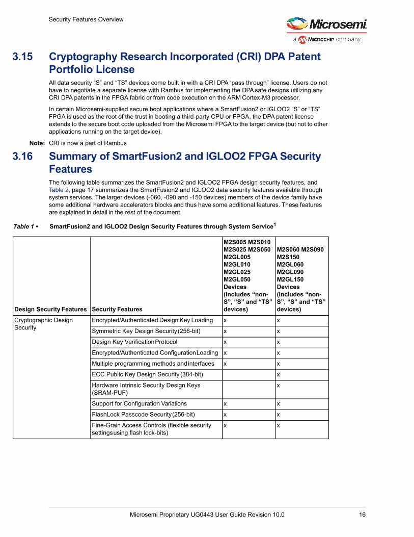
Security Features Overview
3.15 Cryptography Research Incorporated (CRI) DPA Patent Portfolio LicenseAll data security “S” and “TS” devices come built in with a CRI DPA “pass through” license. Users do not have to negotiate a separate license with Rambus for implementing the DPA safe designs utilizing any CRI DPA patents in the FPGA fabric or from code execution on the ARM Cortex-M3 processor.
In certain Microsemi-supplied secure boot applications where a SmartFusion2 or IGLOO2 “S” or “TS” FPGA is used as the root of the trust in booting a third-party CPU or FPGA, the DPA patent license extends to the secure boot code uploaded from the Microsemi FPGA to the target device (but not to other applications running on the target device).
Note: CRI is now a part of Rambus
3.16 Summary of SmartFusion2 and IGLOO2 FPGA Security FeaturesThe following table summarizes the SmartFusion2 and IGLOO2 FPGA design security features, and Table 2, page 17 summarizes the SmartFusion2 and IGLOO2 data security features available through system services. The larger devices (-060, -090 and -150 devices) members of the device family have some additional hardware accelerators blocks and thus have some additional features. These features are explained in detail in the rest of the document.
Table 1 • SmartFusion2 and IGLOO2 Design Security Features through System Service1
Design Security Features Security Features
M2S005 M2S010 M2S025 M2S050 M2GL005 M2GL010 M2GL025 M2GL050Devices (Includes “non-S”, “S” and “TS” devices)
M2S060 M2S090 M2S150 M2GL060 M2GL090 M2GL150Devices (Includes “non-S”, “S” and “TS” devices)
Cryptographic Design Security
Encrypted/Authenticated Design Key Loading x x
Symmetric Key Design Security (256-bit) x x
Design Key Verification Protocol x x
Encrypted/Authenticated Configuration Loading x x
Multiple programming methods and interfaces x x
ECC Public Key Design Security (384-bit) x
Hardware Intrinsic Security Design Keys (SRAM-PUF)
x
Support for Configuration Variations x x
FlashLock Passcode Security (256-bit) x x
Fine-Grain Access Controls (flexible security settings using flash lock-bits)
x x
Microsemi Proprietary UG0443 User Guide Revision 10.0 16
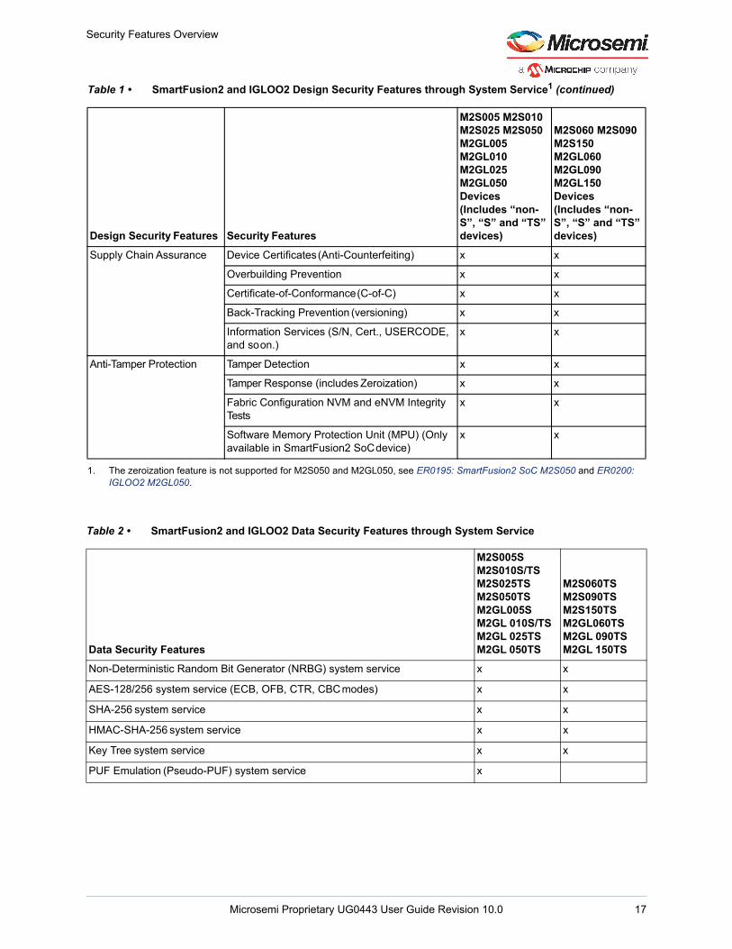
Security Features Overview
Supply Chain Assurance Device Certificates (Anti-Counterfeiting) x x
Overbuilding Prevention x x
Certificate-of-Conformance (C-of-C) x x
Back-Tracking Prevention (versioning) x x
Information Services (S/N, Cert., USERCODE, and so on.)
x x
Anti-Tamper Protection Tamper Detection x x
Tamper Response (includes Zeroization) x x
Fabric Configuration NVM and eNVM Integrity Tests
x x
Software Memory Protection Unit (MPU) (Only available in SmartFusion2 SoC device)
x x
1. The zeroization feature is not supported for M2S050 and M2GL050, see ER0195: SmartFusion2 SoC M2S050 and ER0200: IGLOO2 M2GL050.
Table 2 • SmartFusion2 and IGLOO2 Data Security Features through System Service
Data Security Features
M2S005S M2S010S/TS M2S025TS M2S050TSM2GL005S M2GL 010S/TS M2GL 025TS M2GL 050TS
M2S060TS M2S090TS M2S150TSM2GL060TS M2GL 090TS M2GL 150TS
Non-Deterministic Random Bit Generator (NRBG) system service x x
AES-128/256 system service (ECB, OFB, CTR, CBC modes) x x
SHA-256 system service x x
HMAC-SHA-256 system service x x
Key Tree system service x x
PUF Emulation (Pseudo-PUF) system service x
Table 1 • SmartFusion2 and IGLOO2 Design Security Features through System Service1 (continued)
Design Security Features Security Features
M2S005 M2S010 M2S025 M2S050 M2GL005 M2GL010 M2GL025 M2GL050Devices (Includes “non-S”, “S” and “TS” devices)
M2S060 M2S090 M2S150 M2GL060 M2GL090 M2GL150Devices (Includes “non-S”, “S” and “TS” devices)
Microsemi Proprietary UG0443 User Guide Revision 10.0 17
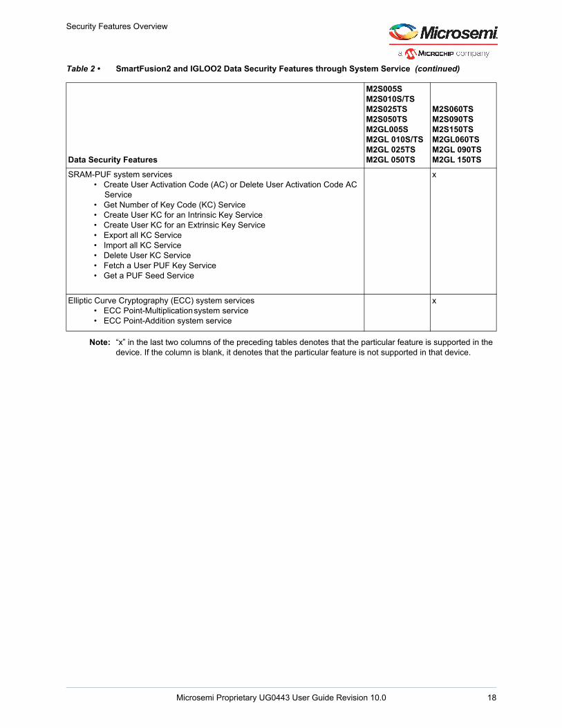
Security Features Overview
Note: “x” in the last two columns of the preceding tables denotes that the particular feature is supported in the device. If the column is blank, it denotes that the particular feature is not supported in that device.
SRAM-PUF system services• Create User Activation Code (AC) or Delete User Activation Code AC
Service• Get Number of Key Code (KC) Service• Create User KC for an Intrinsic Key Service• Create User KC for an Extrinsic Key Service• Export all KC Service• Import all KC Service• Delete User KC Service• Fetch a User PUF Key Service• Get a PUF Seed Service
x
Elliptic Curve Cryptography (ECC) system services• ECC Point-Multiplication system service• ECC Point-Addition system service
x
Table 2 • SmartFusion2 and IGLOO2 Data Security Features through System Service (continued)
Data Security Features
M2S005S M2S010S/TS M2S025TS M2S050TSM2GL005S M2GL 010S/TS M2GL 025TS M2GL 050TS
M2S060TS M2S090TS M2S150TSM2GL060TS M2GL 090TS M2GL 150TS
Microsemi Proprietary UG0443 User Guide Revision 10.0 18
Cryptographic Security Features
4 Cryptographic Security Features
Cryptographic design security provides information security of the configuration data. It is the assurance that the user design programmed into a device is secure and operates as intended for the life of the product. SmartFusion2 and IGLOO2 devices have built-in features that provide enhanced security during all stages of the device life cycle: from wafer probe and initial Microsemi provisioning of factory keys and certificates, to assurance that the supply chain has delivered genuine devices to the user, to user key injection and bitstream programming, to field updates, and finally to device decommissioning.
This chapter describes SmartFusion2 and IGLOO2 FPGA cryptographic design security including bitstream protection and key management. The FPGA programming model and various cryptographic design security features offered by SmartFusion2 and IGLOO2 FPGAs are described. While the description that follows is at a level of detail appropriate for a designer to implement the described security services, more specific details about the modes of operation and the underlying transactions are available upon request through a specific NDA.
4.1 SmartFusion2 and IGLOO2 FPGAs Programming ModelThe following figure depicts the simplified programming model used in SmartFusion2 and IGLOO2 FPGAs. The microcontroller sub-system in SmartFusion2 SoC FPGAs is not displayed in the simplified model. There are three main user programmable sub-blocks within the SmartFusion2 and IGLOO2 devices. The FPGA fabric contains configurable user logic and can be programmed independently of other blocks. The eNVM block is user non-volatile flash memory and can also be programmed independently. There are three separate groups of security segments that are tamper protected blocks used to safely store factory and user security keys as well as configurable security settings. Various representative keys and the device serial number (DSN) are depicted in the figure. All programming operations including program, verify, and security key management are managed by the system controller. During programming mode, the system controller authenticates and decrypts incoming bitstreams, erases and writes the target programmable sub-blocks, and responds to other external programming-related protocols such as key verification.
The system controller and associated security hardware includes hardware-based security countermeasures to protect the device against a broad range of threats, and manages the hardware-based security countermeasures throughout the rest of the device. The system controller subsystem includes various hardware cryptographic accelerators such as AES and SHA, and also includes a non-deterministic random bit generator (NRBG). The SRAM-PUF and the elliptic-curve cryptography accelerator are only available in the -060, -090 and -150 devices. The SPI interface can be used to attach an external SPI flash device that is used to hold the updated and “golden” configuration bitstreams.
Microsemi Proprietary UG0443 User Guide Revision 10.0 19
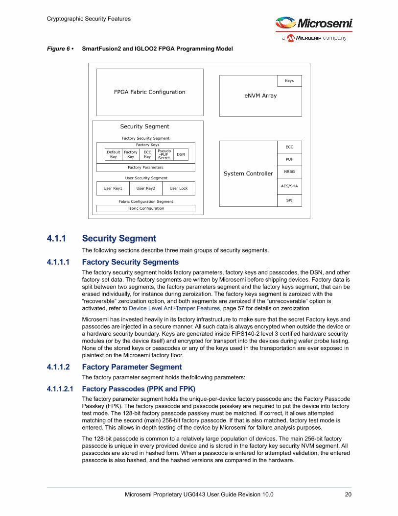
Cryptographic Security Features
Figure 6 • SmartFusion2 and IGLOO2 FPGA Programming Model
4.1.1 Security SegmentThe following sections describe three main groups of security segments.
4.1.1.1 Factory Security SegmentsThe factory security segment holds factory parameters, factory keys and passcodes, the DSN, and other factory-set data. The factory segments are written by Microsemi before shipping devices. Factory data is split between two segments, the factory parameters segment and the factory keys segment, that can be erased individually, for instance during zeroization. The factory keys segment is zeroized with the “recoverable” zeroization option, and both segments are zeroized if the “unrecoverable” option is activated, refer to Device Level Anti-Tamper Features, page 57 for details on zeroization
Microsemi has invested heavily in its factory infrastructure to make sure that the secret Factory keys and passcodes are injected in a secure manner. All such data is always encrypted when outside the device or a hardware security boundary. Keys are generated inside FIPS140-2 level 3 certified hardware security modules (or by the device itself) and encrypted for transport into the devices during wafer probe testing. None of the stored keys or passcodes or any of the keys used in the transportation are ever exposed in plaintext on the Microsemi factory floor.
4.1.1.2 Factory Parameter SegmentThe factory parameter segment holds the following parameters:
4.1.1.2.1 Factory Passcodes (PPK and FPK)The factory parameter segment holds the unique-per-device factory passcode and the Factory Passcode Passkey (FPK). The factory passcode and passcode passkey are required to put the device into factory test mode. The 128-bit factory passcode passkey must be matched. If correct, it allows attempted matching of the second (main) 256-bit factory passcode. If that is also matched, factory test mode is entered. This allows in-depth testing of the device by Microsemi for failure analysis purposes.
The 128-bit passcode is common to a relatively large population of devices. The main 256-bit factory passcode is unique in every provided device and is stored in the factory key security NVM segment. All passcodes are stored in hashed form. When a passcode is entered for attempted validation, the entered passcode is also hashed, and the hashed versions are compared in the hardware.
FPGA Fabric Configuration eNVM Array
Default Key
Factory Key
ECC Key
User Key1 User Key2 User Lock
Factory Security Segment
User Security Segment
Keys
Fabric Configuration
System Controller
ECC
PUF
SPI
NRBG
AES/SHA
Factory Parameters
DSN
Factory Keys
Fabric Configuration Segment
Security Segment
Pseudo-PUFSecret
Microsemi Proprietary UG0443 User Guide Revision 10.0 20

Cryptographic Security Features
The user can protect or permanently block the factory test mode. A lock-bit disables factory passcode matching. Once the user keys are programmed, the lock-bit is automatically set and the factory test mode can only be entered if explicitly allowed by the user. The bit can be rolled-back (that is, unlocked) by the user using the FlashLock passcode (UPK1). Another option is that the FlashLock passcode itself can be permanently disabled, which permanently disables the factory passcode matching by preventing such roll-back. If the FlashLock passcode is permanently disabled, all security settings are permanently frozen and the failure analysis of that device is not possible.
In addition, there is another user lock-bit option that permanently prohibits factory passcode matching (whether or not the FlashLock passcode is matched). In devices where this lock-bit is set; the device can never again enter factory test mode, and failure analysis is impossible. “Microsemi Factory Test Mode Access Level” setting in Security Policy manager (SPM) in the Libero SoC software is used for configuring these lock bits.
4.1.1.2.2 Device Serial Number Part1- Factory Serial Number (FSN)The device serial number (DSN) is a 128-bit unique device ID. It comprises of two parts: the factory serial number (FSN) and the serial number modifier (SNM). The first part, the 64-bit FSN uniquely identifies a device and is located in the factory parameter segment.
4.1.1.2.3 Factory ParametersFactory parameters contain calibration data used for programming and other device operations.
4.1.1.2.4 Factory Lock-BitsFactory lock-bits are used to control access to device features and are typically only used by Microsemi.
4.1.1.3 Factory Keys SegmentThe factory keys segment holds followings keys:
4.1.1.3.1 Device Serial Number Part2- Serial Number Modifier (SNM)The SNM is the second part of the DSN and is stored in the factory keys segment. The 64-bit SNM is zeroized during the “recoverable” or “unrecoverable” zeroization mode action (along with all the contents of the factory keys segment). The SNM is used after the “recoverable” zeroization mode to tell if a device has been “'zeroized”' and a new set of factory keys are installed. For more information about how to load new factory keys and a new SNM that is how to recover a device after zeroization, refer to the Technical Support website and by email.
4.1.1.3.2 Default Key-Loading Key (KLK)The default key-loading key (KLK) is used to load user keys and security settings in situations where high levels of security are not required. The default key is a pre-placed factory key used to encrypt any of the flash configuration segments. This is a key that is same for a large number of devices, and should only be used where high levels of security are not required. One such situation could be where programming is done in a completely trusted secure facility with cleared personnel and stringent data handling and protection processes in place. Another is where the design IP is not very valuable and security is not a primary concern of the user. In this case, KLK can be selected as the root key for encryption and authentication of the bitstream component used to load the user’s keys.
The 256 bit default Key-Loading Key is common to a relatively large population of devices of the same type and vintage, and is frequented within the programming tool software. This makes it the easiest key to use, but not as secure as the other options, having a “software” rather than a “hardware” level of protection.
KLK provides protection against capturing of user keys with the trivial approach of snooping on them when they are being transported into the device for programming. In the prior art PLDs, before SmartFusion2 and IGLOO2 FPGAs, all user keys were loaded in plaintext or using algorithms that were reversible with known plaintext data, making even this trivial attack fairly easy.
After the user’s security settings are loaded, the KLK is automatically disabled by a user lock-bit reserved for this purpose, without any action required by the user. After this point, any programming updates require use of the user keys. Typically the user security settings (user lock security segment) and the first
Microsemi Proprietary UG0443 User Guide Revision 10.0 21
Cryptographic Security Features
user key and the FlashLock passcode (in the user keys security segment) are loaded from the same bitstream file.
4.1.1.3.3 Factory Key (FK)The factory key is a 256-bit key that has a unique value in every device produced by Microsemi. In -005, -010, -025, -050 devices this key is the preferred key to use for loading the user’s keys when security is important. If used for loading the user’s keys, it is selected as the root key for encryption and authentication of the bitstream component used to load the user’s keys. More accurately, it is used as the encryption key for an authorization code bitstream component that permits loading of the remainder of the encrypted user bitstream (containing the user’s keys and security settings) into the device. After the user’s security settings are loaded, the factory key is automatically disabled for encryption purposes by a user lock-bit without any action required by the user. It may still be used for key verification, which is commonly done in conjunction with checking the validity of the device certificate, especially in the smaller devices that don’t offer a public key alternative.
Since the factory key is a symmetric key, the programmer must know a derived/related key (for every device) in order to prepare bitstreams that can be decrypted by the devices, or to verify that the device is familiar with the factory key. The process is performed by installing encrypted key databases – distributed by Microsemi – into the Microsemi-supplied Secure Production Programming Solution’s hardware security module (HSM) and its server. Each key database distributed by Microsemi is encrypted by a key unique to the targeted HSM, and the contents are also unique, which prevents anyone else with a key database and HSM from decrypting another user’s bitstream files. The security imperative is that no copies are made of a key database (and the associated database encryption key that unlocks it) which could find a way into an adversary’s hands.
Though this method is logistically more complex than using the default key (KLK), it is cryptographically sound, with all the keys used in this system, for example., the Factory Keys, the derived keys in the key databases, the database encryption keys and so on, never leaving the hardware security module (HSM) or the FPGA’s boundaries except in encrypted form. In the Microsemi Factory, the HSMs are FIPS140-2 level 3 certified, and the HSMs used by the user as part of the programming tool also have this certification level. This approach using factory key, provides a “hardware” level of design security.
4.1.1.3.4 Factory Pseudo-PUF Secret (FPP)The Pseudo-PUF Secret (FPP) is a unique 256-bit secret generated by the device’s own nondeterministic random bit generator (NRBG) during the manufacturing of the device at Microsemi, during zeroization recovery, and is stored permanently in the factory keys security segment. It is used in the PUF-emulation protocol in the devices that don’t have an SRAM-PUF, that is, -005, -010, -025, and -050 SmartFusion2 and IGLOO2 devices.
4.1.1.3.5 Factory ECC Public Key Pair (SKFE and PKFE)In the -060, -090 and -150 devices, those having the ECC hardware accelerator, a completely random unique-per-device 384-bit private ECC key (SKFE) is stored in the Factory Keys security NVM segment in encrypted form. From this private key, the associated 768-bit ECC public key (PKFE) is calculated, and this public key is certified in the secondary Device Certificate which is stored in the part of the eNVM array that is private to the system controller to prevent the certificate from being overwritten, as it is considered public data, and can be exported on demand. The Device Certificate is X.509 compliant, so it can be parsed using most third party tools. Some Microsemi proprietary X.509 extensions, though are legal may not be recognized by non-Microsemi parsers.
The ECC key pair can be used by the FPGA for establishing a shared symmetric key with the programmer tool and for using the Elliptic Curve Diffie-Hellman (ECDH) protocol followed by a key derivation function. The 256-bit derived key becomes the root key which can then be used either for encrypting/authenticating a bitstream (such as for injecting user keys and security settings in a new device), or for authenticating the device using the key confirmation challenge-response protocol.
4.1.1.3.6 Factory SRAM-PUF ECC Key Pair (SKFP, PKFP)In the larger devices (-060, -090 and -150 devices), that is, those having the Elliptic Curve Cryptography (ECC) hardware accelerator and the Quiddikey SRAM-PUF, a completely random unique-per-device 384-bit private ECC key (SKFP) is enrolled by the SRAM-PUF. From the private key, the associated ECC public key (PKFP) is calculated. This 768-bit public ECC key is certified in the primary Device Certificate.
Microsemi Proprietary UG0443 User Guide Revision 10.0 22
Cryptographic Security Features
This X.509 compliant public key certificate also contains standard and extension fields containing other important device data such as the serial number, model number and date code which can be used to help prevent counterfeit or fraudulently marked devices from being accepted into the supply chain. Since the security of the associated private key is rooted in the SRAM-PUF, which is analogous to a silicon biometric, the user can prove with a very high assurance level that the device certificate and the device itself go together. This process is implemented using the key confirmation protocol.
As with the ECC key stored in the security NVM (Refer to SKFE and PKFE, in the Factory ECC Public Key Pair (SKFE and PKFE), page 22), this key pair can be used in an ECDH protocol followed by a key derivation function to establish a 256-bit shared symmetric key which can then be used either as the root key for encrypting or decrypting and authenticating a bitstream, or for assuring the authenticity of the device by performing a key confirmation protocol. As with all the other Factory keys, this key is automatically disabled for bitstream-loading purposes by a user lock-bit at the same time the user security settings are loaded, without any action required by the user.
Using this key pair is the preferred method of injecting the encrypted user keys in new larger devices, particularly those that don’t have the “TS” class features activated. In “TS” class devices, there is an alternative user-enrolled PUF-protected key pair with similar advantages that can be used. Public key cryptography has the advantages of not requiring a key database –unlike the symmetric Factory Key, FK, which does – while still being completely cryptographically sound. It provides the highest level of protection of the associated private key (using the SRAM-PUF); with biometrically-strong unclonable binding to the device, providing the highest possible assurance that the device is a genuine Microsemi FPGA.
One minor disadvantage of this key mode is that a 384-bit ECC private key has security strength of approx. 192 bits, whereas the main alternative, the 256-bit Factory Key, which is used in conjunction with AES, has security strength of approx. 256 bits. But, since the P-384 ECC system has been approved for use in Suite B up to and including top secret, the slightly lower cryptographic security strength is probably not a very important factor in most cases, and is offset by the much greater convenience of public key methods over symmetric ones and other offsetting security advantages.
4.1.2 User Security SegmentThe user security segment group is comprised of three user security segments: “User Key1”, “User Key2”, and the “User Lock-Bit” segment. All three user security segments are zeroized in all zeroization modes.
4.1.2.1 User Key1 SegmentThe User Key1 segment holds the User Encryption Key1 (UEK1). It can be the root key for encrypting and decrypting bitstreams, and for authentication of bitstreams. This segment also holds the FlashLock passcode, also known as the User Passcode1 (UPK1), which is used to unlock access to the three user security segments, and unlocks many of the user lock-bits. Also in this segment is the Debug Passcode (DPK). It unlocks just certain lock-bits related to FPGA fabric and Cortex-M3 debugging features (if present), but does not unlock as many lock-bits as the FlashLock passcode does. It does not allow the user to overwrite keys, passcodes, or security settings. It, stays in effect only until the device is reset.
The passcodes are never used for encryption, but used only for escalating the privileges during the session when the passcode is matched successfully. This passcode is loaded along with the other user keys and passcodes using an encrypted bitstream and stored (after being hashed) in the user key security segment. When the FlashLock passcode is subsequently successfully matched using either the plaintext or one-time-use encrypted passcode protocols, it unlocks many of the user-set security lock-bits. This allows the contents of the three security segments to be erased and rewritten. Refer to FlashLock Passcode Security (256-bit), page 34 for more information.
4.1.2.2 User Key2 SegmentThe User Key2 segment stores a second bitstream User Encryption Key2 (UEK2). This can be used interchangeably with UEK1. This segment has its own passcode, User Passcode2 (UPK2), which allows overwriting of the UEK2 after the passcode is successfully matched (and before the device is reset).
This passcode does not unlock anything in the user key1 or user lock segments. Use of the UEK2 segment is strictly optional. Having a second user key can facilitate use models that would be difficult to
Microsemi Proprietary UG0443 User Guide Revision 10.0 23
Cryptographic Security Features
implement with just one user key. The secondary key can be used to program or update a subset or class of products in the field.
4.1.2.3 User Lock-BitsThis segment holds the majority of lock-bits for setting security options. Many of the lock-bits are overridden if the FlashLock passcode is matched. Refer to FPGA Lock-bits, page 34 for details.
Note: The lock-bit to permanently protect factory test mode access is located in the User Key2 Segment, page 23.
4.1.2.4 JTAG USERCODEThis section holds the 32-bit JTAG USERCODE instruction response. The JTAG USERCODE is a 32-bit value stored in the User Lock security NVM segment. It is read out of the device using the IEEE JTAG 1149.1 -defined optional instruction by the same name. The USERCODE value is public information, and can be used by the user for any purpose. It is often used to identify the function of one FPGA design as differentiated with other designs which may be loaded in the same or similar part number devices from Microsemi, in other words, the USERCODE is used to tell functionally different designs apart from each other. It is loaded using an encrypted/authenticated bitstream along with the user’s security settings. It can be changed if the FlashLock passcode is matched, and if other security settings allow it. It can also be read internally using a system service.
4.1.3 Fabric Configuration SegmentThe Fabric configuration segment is used as an extension of the FPGA fabric to store data used during normal operation of the device. It is also used as storage for programming session information. For example: it stores design version, version Back-Level, design ID, programming cycle count and so on. It is updated whenever the FPGA Fabric is updated.
4.1.4 FPGA FabricThe FPGA fabric contains configurable user logic and can be programmed independently. The FPGA fabric is a single atomic unit, and is always erased or written in its entirety. If for any reason the FPGA fabric is only partially programmed, the FPGA refuses to boot up when power is applied. The device may attempt to take corrective action, such as retrying, or loading a “golden” image from local memory, depending on user configuration settings.
4.1.5 eNVM ArrayThe eNVM block is user non-volatile flash memory and can also be programmed independently. The smallest unit of the eNVM memory that can be erased or written at one time is a one K-bit page. A few pages of the eNVM are reserved for factory use and for SRAM-PUF/ECC keys storage. One use of the factory reserved pages is to hold the device certificate, which is loaded by Microsemi before the devices are shipped. In the -005, -010, -025, -050 devices the top eight 1024-bit pages are used by the system controller. These pages are readable but not writable by the user. In the larger devices (-060, -090 and -150) the top 64 pages are reserved by the system controller. These 64 pages are private to the system controller; they are neither readable nor writable by the user. The reserve page also stores UEK3, which can be enrolled by running system service using SRAM-PUF. For more information, see SRAM-PUF Services, page 101.
4.2 Bitstream SecuritySmartFusion2 and IGLOO2 FPGAs have layered protections to ensure that the user’s intent is met. These protections include the use of encryption to protect the confidentiality of the design IP and prevent reverse engineering, and authentication to ensure that only legitimate bitstream files are loaded by devices. Versioning is used to ensure that previously valid bitstreams are not reloaded in a replay attack against fielded devices. Since every device is shipped from Microsemi is already securely provisioned with a number of secret keys and a public certificate (two in the -060, -090 and -150 devices), it is possible to be assured that the devices are genuine Microsemi devices of the correct type, and to strictly control the number of devices configured with a given bitstream, thus preventing overbuilding, with no requirement for expensive trusted facilities and cleared personnel, or the physical transfer of devices between such a trusted facility and a more normal less-trusted manufacturing facility.
Microsemi Proprietary UG0443 User Guide Revision 10.0 24
Cryptographic Security Features
Due to the cryptographic protocols Microsemi has implemented in these devices and associated software programming tools all the device programming, including initial user key injection, can be securely performed in an ordinary manufacturing environment without the fear of interference from rogue insiders.
The security mechanisms and the choices available to the user are described in the following sections. While the cryptography may at first seem complicated, remember that Microsemi has provided extensive automation via the Libero™ SoC FPGA design tool set and the optional Secure Production Programming Solution (SPPS) to make using the SmartFusion2 and IGLOO2 FPGA’s security features easy. In many cases the user can just accept default settings. Most of the explanation below is just for informational purposes, with enough background for expert users with special use model scenarios to be able to make informed decisions where alternatives are offered.
4.2.1 Bitstream Encryption OverviewSmartFusion2 and IGLOO2 FPGAs are flash-based devices configured using a Microsemi proprietary and confidential format bitstream file. All bitstreams are encrypted with the Advanced Encryption Standard (AES) block cipher using secret keys, and then an authentication tag is added using a type of symmetric message authentication code (MAC) based on the Secure Hash SHA-256.
4.2.1.1 Bitstreams EncryptedIt is Microsemi’s goal to maintain the confidentiality of the details of the SmartFusion2 and IGLOO2 bitstream formats that may assist an adversary in performing reverse engineering attacks on user designs. History has shown that plaintext bitstream file formats are often reverse engineered by the academic community; and the nation-state -level adversaries have either repeated or extended the academic results. Combined with key recovery attacks such as differential power analysis (DPA), the adversaries and bitstream reverse engineering can provide the main building blocks to reverse engineer confidential user FPGA design.
To maintain bitstream format confidentiality, one of the measures taken by Microsemi is that, unlike the bitstream files for most (if not all) other PLDs, there is no plaintext bitstream format option. Microsemi tools only generate encrypted bitstreams for these fourth generation devices, and the devices only accept properly encrypted and authenticated bitstream files. By eliminating the generation of plaintext bitstream files, reverse engineering of the contents of bitstreams – for example, the detailed format for the bits used in setting up look-up tables, configuring flip-flops, I/Os and SRAM blocks and DSP blocks, and programming the routing of signals – may become much more difficult.
SmartFusion2 and IGLOO2 FPGAs architecture and bitstream format is sufficiently different from previous generations, where plaintext bitstreams were offered as an option, and potential knowledge about past generation bitstream formats does not inform the analyst about the fourth generation details.
Preparing bitstreams with known simple designs is often the first step towards reverse engineering the bitstream format. The Microsemi bitstream encryption is done in a way that prevents an adversary, posing as a legitimate user, from decrypting the bitstreams they generate themselves, even if the value of the user encryption key is known.
4.2.1.2 Differential Power Analysis (DPA) Resistant AES ModeThe bitstream format for SmartFusion2 and IGLOO2 devices uses the Advanced Encryption Standard (AES), as defined by the NIST FIPS PUB 197, with 256-bit keys. AES encrypts 128-bit blocks of data at a time. In order to encrypt large amounts of data such as an FPGA bitstream, a “mode” such as Counter (CTR) Mode or Cipher Block Chaining (CBC) Mode is commonly used; that defines how multiple AES 128-bit block encryptions are used to encrypt the larger total amount of plaintext.
In order to prevent differential power analysis and the related side channel attacks from succeeding in extracting the bitstream key during bitstream decryption by a device, Microsemi has, with the advice of Rambus Cryptography Research, used a modified form of a common AES mode. The primary modification is to update the frequently used AES key using non-linear mixing, so any one key cannot leak enough information to allow its reconstruction. The rotation of AES keys, patented by Rambus Cryptography Research and licensed for use on FPGAs by Microsemi, provides one of the best DPA countermeasures available since it does not rely on many difficulties to prove assumptions like those required in signal-cancellation-by-matching countermeasures.
Microsemi Proprietary UG0443 User Guide Revision 10.0 25
Cryptographic Security Features
4.2.2 Bitstream ContentSmartFusion2 and IGLOO2 FPGAs are flash-based devices configured using a Microsemi proprietary and confidential format bitstream file. The SmartFusion2 and IGLOO2 devices are divided into three main bitstream components that can be targeted during the configuration process: FPGA fabric, eNVM Array, and security segments.
• FPGA Fabric: The FPGA fabric configuration holds the configuration bits that configure the routing switches and look-up tables of the logic elements that define the user’s design, as well as the I/O cells, embedded memories, and Math blocks.
• eNVM Array: The eNVM array is a general purpose flash memory, a portion of which is typically used as a boot up ROM for the MSS in SmartFusion2 SoC FPGAs. Certain non-secret information pertinent to device configuration, such as public keys and the device certificate, are also contained in write-protected pages within the eNVM. In addition, hardware level write protection can be applied to eNVM. Refer to the FPGA Hardware Access Controls, page 34 for details. In the larger devices, the PUF Activation Code and encrypted Key Codes are stored in two 4 K-byte eNVM sectors (64 pages) that are private (in other words, read and write protected) and accessible only to the system controller. A bitstream can contain any integer number of pages, from zero to the maximum of 4096 in the largest devices currently planned, or a little more than four million bits. Generally, all the pages are loaded in the same bitstream component section, but this does not necessarily have to be the case. For example, if one or a few pages contain variable data, these pages may be treated in a component section separate from the rest. There are many scenarios where the payload in a field update consists only of a portion of the eNVM. In the extreme case, a bitstream payload may consist of just a single page of eNVM, to load a key or to activate a feature of the device
• Security Segments: The security segments hold cryptographic keys and passcodes required for design security as well as device unique identifiers. All the keys are stored in encrypted form; all the passcodes are stored only after cryptographically hashing them. Each of the five security segments loaded using the KEYS component is an atomic unit. The two Factory segments are programmed by Microsemi before shipping the parts. The three user security segments are often programmed using one KEYS component, but this is not a requirement. The three user segments are relatively small, on the order of ten kilo-bits altogether. If one or more of the segments contain variable data (for example unique user codes or user keys or passcodes, the variable and fixed security segments may be placed in different bitstream components. Also, one of the reasons for segmenting the user security data is to allow different segments to be programmed at different times or by different actors, thus the security segments may end up not only in different component sections, but in completely different bitstreams.
Special mandatory header and footer components (BITS and EOB) which along with other components, program the FPGA Configuration security segment. A special component called an Authorization Code (AUTH) is used to transport an encrypted ephemeral key into the device for use in decrypting one or more of the later components. Refer to Authorization Code Component and Key Mode, page 29 for more details.
The various payload and Authorization Code components are optional, and supplied by the programming tools as needed to accomplish the user’s goals. However, whatever components the programming tool assembles on behalf of the user are bound together cryptographically and authenticated as a whole. Removal, insertion, re-arranging, or any other sort of tampering with any component sections is detected and the programming session fails. If an authentication failure is detected before any data is committed, the detected part remains as previously programmed. Devices that are only partially programmed for any reason, including due to a late authentication failure, that is, after NVM programming has begun, will not boot until successful reprogramming.
4.2.3 Programming ModesSmartFusion2 and IGLOO2 FPGAs support the following programming interfaces:
• JTAG port• System control SPI port (SC_SPI)• MSS/HPMS SPI_0 port.
These programming interfaces allow various programming modes, refer to the UG0451: SmartFusion2 and IGLOO2 Programming User Guide. The programming interfaces and programming modes provide
Microsemi Proprietary UG0443 User Guide Revision 10.0 26
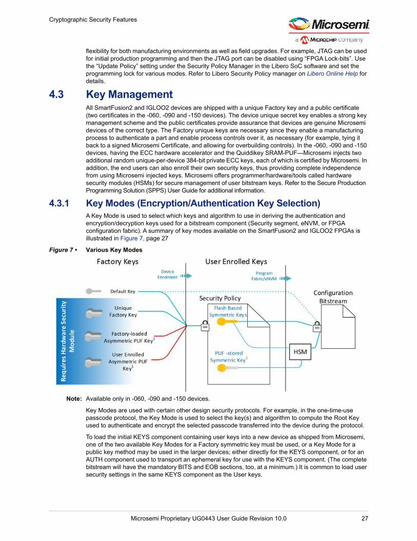
Cryptographic Security Features
flexibility for both manufacturing environments as well as field upgrades. For example, JTAG can be used for initial production programming and then the JTAG port can be disabled using “FPGA Lock-bits”. Use the “Update Policy” setting under the Security Policy Manager in the Libero SoC software and set the programming lock for various modes. Refer to Libero Security Policy manager on Libero Online Help for details.
4.3 Key ManagementAll SmartFusion2 and IGLOO2 devices are shipped with a unique Factory key and a public certificate (two certificates in the -060, -090 and -150 devices). The device unique secret key enables a strong key management scheme and the public certificates provide assurance that devices are genuine Microsemi devices of the correct type. The Factory unique keys are necessary since they enable a manufacturing process to authenticate a part and enable process controls over it, as necessary (for example, tying it back to a signed Microsemi Certificate, and allowing for overbuilding controls). In the -060, -090 and -150 devices, having the ECC hardware accelerator and the Quiddikey SRAM-PUF—Microsemi injects two additional random unique-per-device 384-bit private ECC keys, each of which is certified by Microsemi. In addition, the end users can also enroll their own security keys, thus providing complete independence from using Microsemi injected keys. Microsemi offers programmer/hardware/tools called hardware security modules (HSMs) for secure management of user bitstream keys. Refer to the Secure Production Programming Solution (SPPS) User Guide for additional information.
4.3.1 Key Modes (Encryption/Authentication Key Selection)A Key Mode is used to select which keys and algorithm to use in deriving the authentication and encryption/decryption keys used for a bitstream component (Security segment, eNVM, or FPGA configuration fabric). A summary of key modes available on the SmartFusion2 and IGLOO2 FPGAs is illustrated in Figure 7, page 27
Figure 7 • Various Key Modes
Note: Available only in -060, -090 and -150 devices.
Key Modes are used with certain other design security protocols. For example, in the one-time-use passcode protocol, the Key Mode is used to select the key(s) and algorithm to compute the Root Key used to authenticate and encrypt the selected passcode transferred into the device during the protocol.
To load the initial KEYS component containing user keys into a new device as shipped from Microsemi, one of the two available Key Modes for a Factory symmetric key must be used, or a Key Mode for a public key method may be used in the larger devices; either directly for the KEYS component, or for an AUTH component used to transport an ephemeral key for use with the KEYS component. (The complete bitstream will have the mandatory BITS and EOB sections, too, at a minimum.) It is common to load user security settings in the same KEYS component as the User keys.
Microsemi Proprietary UG0443 User Guide Revision 10.0 27
Cryptographic Security Features
Field updates are done using one of the user symmetric keys; again, either directly with the main bitstream components or in conjunction with an Authorization Code (AUTH) component. Device authentication can be done using most of the Key Modes, including the asymmetric ones in the larger devices that are equipped with the ECC engine.
Key Modes are selected by the user using the Programmer tool at the time he prepares his files for production. The most common use model scenarios are presented by the tool, and the user selects the one that best fits his situation. All of the key modes used to initially load user keys, except the default key mode using the default key-loading key (KLK), require use of the HSM-assisted Secure Production Programming Solution (SPPS). Once user keys are loaded, the key modes relying on them can be used for encrypting FPGA or eNVM updates. The same environment (with or without an HSM, respectively) that was used to load the user keys initially can be used to encrypt the update bitstream.
4.3.2 Default Key ModeIn this Key Mode, a Default Key-Loading Key (KLK) is used to load user security settings in situations where high levels of security are not required. In this case, KLK is used by default as the root key for encryption and authentication of the bitstream component used to load the user’s keys. At a minimum, it provides protection against capturing of user keys with the trivial approach of snooping on them when they are being transported into the device for programming. The Libero SoC uses this key as a default key even when no key mode is specified by the user.
Note: No HSM is required for this key mode. Default Key Mode can be performed by Libero with or without the aid of the optional Secure Production Programming Solution.
4.3.3 Factory Key Mode & Associated Symmetric Key DatabasesIn the Factory Key Mode, a Derived Factory Key (DFK) is used as the Root Key. The Derived Factory Key is a symmetric key computed in a DPA-resistant one-way algorithm from the Factory Key (FK) and the database’s Unique User ID (UUID). As part of this Key Mode, the UUID value is transported into the device. Since each device has a unique Factory Key, each device also computes the unique Derived Factory Key from its own Factory Key, given the UUID value. The HSM-assisted programmer gets the Diversified Factory Key already computed for each device, as identified by serial number, in a Factory Key Database distributed by Microsemi.
4.3.4 Factory ECC Public Key ModesIn the -060, -090 and -150 devices, there are two ECC key pairs: the Factory SRAM-PUF ECC key pair (SKFP, PKFP), and the Factory ECC key pair (SKFE, PKFE). The public halves of these keys are certified in X.509 -compliant public key certificates: called the Primary and Secondary Device Certificates, respectively. These key pairs are intended for design security purposes, such as establishing a Root Key that can be used for importing the user’s initial keys into a new device. As with the symmetric-key Key Modes, the Root Key that is ultimately derived is a 256-bit symmetric key.
This Root Key can also be used in a number of other design security protocols, perhaps most notably the key confirmation protocol, which proves the device “knows” the private key associated with the public key used in the protocol. Since bitstreams are fully authenticated by a key derived from the Root Key, they also effectively confirm that the device knows the private key; thus there is no need to perform the key verification protocol if the key is also going to be used immediately to load a bitstream, unless one needs to differentiate a failure caused by not having the correct key from a failure caused by other types of bitstream authentication errors such as a hash failing to match due to a message error.
For the asymmetric key methods there are two Key Mode algorithm options for use with each available public key, which all rely ultimately on the Elliptic Curve Cryptography Co-factor Diffie-Hellman (ECC-CDH) protocol as specified in NIST SP800-56A. Note that in the curve defined by the P-384 domain parameters there is only one “co-factor,” so ECC-CDH reduces down to simple ECC-DH (a.k.a. ECDH).
In the first option, the device uses the selected (certified) ECC key pair, and the programmer uses an ephemeral ECC key pair, generated just for this purpose using a fresh random number which is discarded immediately after usage. As per the ECDH protocol, the device and programmer exchange public keys and compute a shared secret; the device using its built-in ECC engine. The shared secret is used in a DPA-resistant key derivation algorithm to reduce the result to the 256-bit Root Key. During the
Microsemi Proprietary UG0443 User Guide Revision 10.0 28
Cryptographic Security Features
overall process the programmer also checks that the public key is certified and the signature on the public key certificate is valid.
In the second, preferred, option the device uses both the selected (certified) ECC key pair and a second fresh ephemeral key pair generated using its on-chip true random bit generator and the ECC engine. As with the first option, the programmer generates a fresh ephemeral key pair. In this option, the ECDH protocol is run twice: once with the device’s certified key pair and the programmer’s ephemeral key pair; and a second time using the device’s ephemeral key pair and the programmer’s ephemeral key pair (used again). This results in two shared secrets. These are used in a DPA-resistant key derivation algorithm to reduce the result down to a single 256-bit Root Key.
The advantage of the second option is the freshness the second (ephemeral) device key pair brings. Even if the private half of the certified long-term key pair is compromised, at some time in the future, the confidentiality of the data would still be protected against an adversary who had monitored and stored the external communications of the device during a programming session. This property is often referred to as “perfect forward secrecy.”
One of the disadvantages of the second option is that it is time consuming. The device has to perform two additional ECC point multiplication operations and the programmer one more. Another disadvantage is that the power has to remain applied to the device during the whole protocol as it does not save the ephemeral key pair in non-volatile memory. This is not normally an issue, except if the communication link to the programmer is very slow (like email). In this case, the first option lends itself better to batch operations.
4.3.5 User Symmetric Key ModesIn all devices the user has the option of configuring two User keys (UEK1 and UEK2). In larger “data security” -enabled devices -060, -090 and -150, the user can also enroll a symmetric design security key (KUS), also known as UEK3, with the SRAM-PUF. Each of these three keys has an associated Key Mode where the symmetric key is the primary key used to compute the 256-bit Root Key. User keys are loaded into new devices using one of the factory key modes using a key pre-placed by Microsemi, or using one of the user ECC public key modes.
4.3.6 User ECC Public Key ModesIn larger security-enabled devices (-060, -090 and -150 devices), the user can have the SRAM-PUF generate an intrinsic private ECC key (SKUP), and from it calculate the associated public key (PKUP), which is exported to the user along with an authentication tag. The public key is also stored in plaintext in the system controller’s private eNVM area. The private key is protected by the SRAM-PUF, and neither leaves the device nor is it ever exported to the user of the FPGA internally.
The main advantage of this key pair is that it is generated after the user receives and has control over the devices, typically just before the key is used. Though it is intended to be a persistent long-term key pair that could be used at any time for device authentication purposes, there is an option to permanently delete it via a system service. Like each of the factory ECC key pairs, there are two key modes based on the user ECC public key pair: one using the user ECC key pair and an ephemeral programmer ECC key pair, and one using the user ECC key pair plus an ephemeral device ECC key pair and an ephemeral programmer ECC key pair, the second mode providing perfect forward secrecy even if SKUP is compromised.
4.4 Authorization Code Component and Key ModeThe authorization code (AUTH) bitstream component is a short special bitstream component that is used only to transport another key into the device. In its usage with an authorization code, the Root Key is sometimes referred to as the wrapper key. The 256-bit payload key, that is, the key that is transported into the device, is a key referred to as the IP Key (KIP). After the device decrypts (that is unwraps) the authorization code it temporarily holds KIP in volatile memory for use as a possible Root Key in subsequent components. After it is used, KIP is permanently deleted from the device.
One authorization code component can be inserted in front of each other type of bitstream component, thus different IP Keys can be used on different components within the same overall bitstream. The authorization code component is cryptographically bound to the bitstream (or portion of a bitstream) that it proceeds. It will not work with any other bitstream than the one to which it is bound. The bitstream will
Microsemi Proprietary UG0443 User Guide Revision 10.0 29
Cryptographic Security Features
not authenticate or load into any device without the authorization code, since the code supplies an essential key.
4.4.1 Use of the Authorization Code to Prevent OverbuildingThe purpose of the authorization code is to translate from a key the device knows or can compute, that is that is the wrapper key, to a key the device doesn’t know (until then): the payload key, called the IP Key (KIP). This can be useful when a population of devices, all have a common key programmed in them, for example if the user makes the User Key (UEK1) the same in all the devices used in a project. This process is invaluable when the key known by the device is different in every device, like the Factory Key. In that case, the authorization code is unique for every device. The code can then transport the same IP Key (KIP) into all the devices in a project so a common bitstream file can be used for the bulky parts of the data, like the FPGA and eNVM components. Since (in this scenario) each authorization code only works with one specific device having a specific Factory Key, and the device can’t load the common bitstream without the authorization code, it in effect “authorizes” that one device to load the subsequent bit stream. The use of authorization codes to prevent overbuilding and provide a higher overall level of key management is enabled by the optional Secure Protection Programming Solution (SPPS) offered by Microsemi.
Some key modes where the root key is unique per device include the (Diversified) Factory Key mode, any ECC key mode (where every session is unique due to the fresh random keys), and the user key modes when the user chooses to load a unique key in every device (vs. one key for the design). In all these cases, the authorization code is used with the unique-per-device key as the root key to transport KIP into the device so that all the devices individually authorized can accept a common bitstream with KIP as the root encryption key, rather than requiring all the content of each bitstream to be encrypted uniquely for each device.
Authorization codes are generated by SPPS as directed by its FlashPro Express software client running on a production workstation. The actual cryptography is managed by an HSM server, and is computed inside the security boundary of the server’s attached hardware security module (HSM) in real time as the devices are programmed. The SPPS, via the manufacturing HSM, keeps track of the number of authorization codes generated, only creating as many as the legitimate user has authorized, thus preventing overbuilding. In most cases, the SPPS configures the devices it is presented with on a first-come basis. It reads the Device Certificates and Device Serial Numbers from the devices, and fetches the matching Diversified Factory Key (DFK) from the key database to use as the wrapper key (assuming the Factory Key Mode is being used).
To authorize specific serial numbers in advance, only authorization codes for those specific devices are generated by the programming solution. This can be done either by binding the serial number into the component, or by using a device-unique key such as the Factory Key (or both). A device won’t accept a bitstream component with a specified serial number if it doesn’t match its own, and it can’t load a component for which it has the wrong key. This serial number binding feature will be available in the future version of SPPS software.
Besides generating and counting authorization codes, the manufacturing HSM securely monitors and collects information on other aspects of the programming operation such as the Certificate-of-Conformance generated by each device, and any devices that are securely removed from service, which HSM returns to the user in the form of certified reports and log files.
4.4.2 Authorization Code Key ModeThere is a key mode where the IP Key, KIP, is the Root Key that can be used with any bitstream components following the authorization code (for example, BITS, KEYS, FPGA, eNVM, or EOB). This is often the preferred Key Mode for these components. It has the advantage that, at least on the device (that is, decryption) side, KIP is ephemeral, as are the authorization codes that transported it into each device. After a bitstream is loaded, the actual derived keys used to decrypt and authenticate the bitstream and the Root Key (KIP) used to generate the derived keys, and the authorization code used to transport KIP into the device, are all deleted. An adversary attempting to decrypt bitstream files encrypted with KIP will not be able to find KIP stored in any devices, or ever in plaintext outside the security boundary. KIP is usually only retained in an HSM located in the user’s trusted design environment long enough to complete all the production runs using the bitstream encrypted under it. After near-term production is complete, the KIP and the encrypted bitstream can be permanently deleted,
Microsemi Proprietary UG0443 User Guide Revision 10.0 30
Cryptographic Security Features
as the user has all the project source files and can always generate a new encrypted version of the bitstream with a fresh IP Key if production were to resume at some point in the future.
The security risks associated with the IP Key, which is not stored in the device, are thus lower than for keys that persist inside the FPGA such as the user keys. The IP Key can’t possibly be extracted from the device because it isn’t stored there. It is only used for one purpose, the encryption of one version of one bitstream. Unlike the other keys, the IP Key cannot be used to authenticate the device or any of the other security services the device provides.
4.4.3 Authorization Code with ECC Key ModesIn the larger devices, ECC Key Modes are supported. The ECC Key Modes use the ECDH protocol to establish a shared secret between the programmer and the device, from which a Root Key is derived. This Root Key is unique every time the ECDH protocol is run because the programmer, and preferably also the device, use fresh ECC key pairs each time.
The authorization code allows translation from the unique ephemeral ECC-derived Root Key (wrapper key) to the key which is used to encrypt the common (shared) bitstream, the IP Key (KIP). As described above, the programmer counts the number of authorization codes generated to prevent overbuilding. This feature will be available in the future versions of SPPS software.
4.5 Support for Configuration Variations“Variations” is a method where some parts of a bitstream can be different from device-to-device in a project, while most parts of the bitstream are the same, or common. This method allows the bulk of a bitstream (the common part) to be encrypted just once, as is customary for most projects considering the efficiency. Small parts such as a security segment or a few pages of the eNVM array can be unique for each part (or a group of parts smaller than the whole project).
In SmartFusion2 and IGLOO2, variations are cryptographically bound to the main bitstream. Variations, like the rest of the bitstream file, can be prepared well in advance of when they are used to configure devices. Variations, which are just another instance of a bitstream component, for example, a second eNVM component, can be produced so that the components are interchangeable with each other within a group of variable data encrypted at the same time as the rest of the bitstream, or alternatively they can be tied to specific serial number devices. In the former case, the programmer will assign one variation to each device on a first-come basis. Variations are serialized within the group, and can be cryptographically bound to individual devices by using a unique random key for encrypting each one.
Assignments of the serialized variations are securely logged by the programmer in certified files. As with any other bitstream component, a bitstream will not authenticate properly when loaded into a device if a variation component is left out. Likewise, the order of components, including the placement of the variation component in relation to the fixed components, cannot be changed without an authentication error.
The main uses anticipated for variations are:
• Load a different 32-bit JTAG USERCODE in every device, for use as a system-level serial number, for example. Thus the user lock security segment is unique in every device
• Load a unique user key, for example, UEK2, derived from a base key, in each device. Thus the User Key2 security segment is unique in every device
• Enroll a unique random user key, for example, UEK3, in each device’s SRAM-PUF. Thus, the portion of the KEYS component that does PUF enrollment would be unique in every device
• Load some unique data into a few pages of eNVM into every device. Thus, there is a small second eNVM bitstream component
• Other uses could include:• Storing unique data security keys in eNVM• Storing a unique public key certificate in eNVM• Activating features uniquely per device using eNVM• Storing a unique system-level serial number in eNVM
In future, Microsemi plans to support some of such most common operations with aids built into the programmer bitstream encryption tools:
Microsemi Proprietary UG0443 User Guide Revision 10.0 31

Cryptographic Security Features
• Generate random bit strings (for example, for keys) and insert them into a security segment key slot or into eNVM pages as Variations
• Generate sequential serial numbers and insert them into a security segment or eNVM as Variations• Convert a file formatted with images of eNVM pages into eNVM Variations• Convert a file formatted with multiple keys into security segment Variations
4.6 Versioning (Bitstream Re-Play Protection)In prior art FPGAs, an authenticated/encrypted bitstream remains valid as long as the device retains the associated key. In some FPGAs, it is impossible to load a new key. Even in previous generation flash FPGAs most users would not update the stored keys when they did field updates. The net result is that in most cases the bitstream keys stayed the same and thus every valid bitstream stayed valid (from the device point-of-view) more-or-less forever.
The problem arises when there are bitstream updates. The user generally wishes the devices to store (or, in the case of SRAM FPGAs, load) only the latest version of the design. This design may have been updated to remove various design bugs or known security vulnerabilities in earlier versions. However, if the adversary has a copy of an earlier valid bitstream, he may be able to get the device to load it, instead, thus reintroducing the bugs or security vulnerabilities that the updated version would have fixed.
SmartFusion2 and IGLOO2 FPGAs solve this problem with a very simple design versioning system. This optional feature (activated or disabled by a lock-bit) requires that all new bitstreams loaded have a new 16-bit version that is strictly larger than the 16-bit back-level stored in the Fabric Configuration segment. If the bitstream version is equal or less than the back-level, it is immediately rejected, before any on-chip NVM is updated. A new bitstream with a high-enough version will be programmed into the device, including the new version number and a new back-level value.
If the user wants to allow repetitive design versions to be accepted, the back-level for each design can be updated to be equal to the version number of that design. Refer to Back-Tracking Prevention (Versioning), page 46 for detail.
If a “golden” bitstream is used to recover from failed configuration operations, either its version has to be greater than the back-level recorded by the last loaded bitstream, or the versioning feature and the golden bitstream recovery feature should not be used at the same time. The back-level loaded as part of the golden bitstream could be set fairly low, to allow later versions to overwrite it. The use of the fall-back mechanism can be enabled or disabled by a user lock-bit. The version number is included in the public data that can be exported from the FPGA.
4.7 Key Confirmation/Verification ProtocolsSmartFusion2 and IGLOO2 FPGAs have a built-in on-line challenge-response -type key confirmation protocol. This can be used to have a device prove it “knows” a particular secret key, without exposing the value of the key in the external communications used in the protocol.
Key confirmation is required in order to positively bind the Device Certificate(s) to a particular device with a high assurance. It requires a device to prove; it knows a secret bound to the certificate, not just public data that could more easily be copied.
All devices support the symmetric key version of the key confirmation protocol. The larger devices having the ECC engine can also support the asymmetric version of the protocol. The key to be verified is selected using the Key Mode mechanism described in Key Modes (Encryption/Authentication Key Selection), page 27. The key verification can also be disabled with a lock-bit, refer to FPGA Lock-bits, page 34.
4.8 Passcode Matching Protocols
4.8.1 Plaintext Passcode Matching ProtocolIn this very traditional plaintext passcode matching protocol, the “prover” enters the passcode (in plaintext). The device hashes it using the SHA-256 hardware accelerator, and compares the result to the hashed value stored in NVM. Unless prohibited, this protocol can be used with any of the five passcodes: User Passcode (also known as FlashLock Passcode, UPK1), User 2 Passcode (UPK2), Debug
Microsemi Proprietary UG0443 User Guide Revision 10.0 32
Cryptographic Security Features
Passcode (DPK), Factory Passcode (FPK), and Factory Passcode Passkey (PPK). The passcodes are protected by being stored in hashed form on the device.
The plaintext protocol is deprecated in favor of the one-time-use encrypted passcode matching protocol explained in the following section. One security issue with the plaintext passcode matching protocol is that if it is monitored by an adversary (for example, a rogue insider), the plaintext passcode can be recorded and replayed later in order to escalate the privileges associated with that particular passcode.
4.8.2 One-Time-Use Encrypted Passcode Matching ProtocolThe one-time-use encrypted passcode matching protocol is a challenge-response type protocol in which the user (or factory) proves to the device that they know the selected passcode and key. The device generates a random nonce which is exported to the HSM-assisted Programmer tool (or Factory HSM). The programmer also generates a nonce, and with a key the user selects it. This message is sent to the device, which can authenticate it. If the authentication succeeds, the privileges associated with that passcode are escalated.
The protocol has been designed to be DPA resistant. Nonces are used to prevent replay attacks. Only the User Key (UEK1), User Key2 (UEK2), User symmetric PUF Key (UEK3) or the Diversified Factory Key Modes can be selected for calculating the encryption/authentication Root Key; and the Diversified Factory Key Mode is disabled automatically once the user keys are loaded.
4.9 FlashLock“FlashLock” refers to a specific passcode, also known as the User Passcode (UPK1) that protects the three security segments. It also refers to the locked state of the device, controlled by the FlashLock passcode and the user lock-bits. The FlashLock passcode is programmed as part of the initial user key injection procedure, and is stored in the user key security segment in hashed form. If it is re-entered and matched later, it will temporarily unlock the three user segments, allowing changes to the keys, passcodes, and security settings (that is, lock-bits) stored in the segments. Refer to FlashLock Passcode Security (256-bit), page 34 for detail.
4.10 Permanent FlashLock (OTP Mode)While the Microsemi Flash-based FPGAs’ ability to be reconfigured allows the FPGAs to be updated in the lab or in the field with encrypted/authenticated bitstreams, they also have the capability to be one-time-programmable as well to provide an even higher assurance that overloading the design by unauthorized entities is impossible. This is beneficial for designs where single function ASICs are traditionally used, but the design and development flow requires the ability to be reprogrammed through development. Refer to Passcode Locks (Permanent Locks), page 35 for details
Microsemi Proprietary UG0443 User Guide Revision 10.0 33

FPGA Hardware Access Controls
5 FPGA Hardware Access Controls
SmartFusion2 and IGLOO2 FPGAs implement following configurable access control policies to prevent overwriting any elements of a design.
• FlashLock passcode security protects against unauthorized changes to security policies.• FPGA lock-bits (configurable hardware flags) enforces more granular write-protections when
compared to FlashLock passcode security, for both general purpose memory and security segments.• Memory hardware firewalls protect the access to memories from the unauthorized bus masters • Software MPU(Memory Protection Unit) provides fine grain memory control, enabling applications to
utilize multiple privilege levels, separating and protecting code, data and stack on a task-by-task basis.
The following sections describe these features in detail.
5.1 FlashLock Passcode Security (256-bit)FlashLock refers to a specific passcode, also known as the User Passcode1(UPK1) that protects the user security segments of SmartFusion2 and IGLOO2 devices. Flashlock is a 256-bit passcode that SmartFusion2 and IGLOO2 devices use to allow security segments to be reprogrammed when the passcode is correctly entered. The FlashLock passcode is stored in the device in hashed format.When the passcode is re-entered and applied to the device, it is hashed and compared with the stored hashed passcode. If the hashed value of the passcode is matched it temporarily allows changes to the user keys, passcodes, and security settings including lock-bits.The device returns to normal locked state (as defined by the non-volatile lock-bit settings) on the next device or JTAG reset, or power cycle.
The FlashLock passcode is the basic level of security. The higher levels of security may be obtained by using the permanent lock feature of the devices or by setting additional individual lock-bits.
The user should be careful during the time a FlashLock passcode is matched and device is reset or power cycle. During this time not only a new authenticated bitstream is loaded, but also the device can be erased, and other lock-bits are temporarily unlocked. Usage of passcodes to unlock a device is not recommended in untrusted locations. In a use model, where field updates are required in untrusted locations, Microsemi recommends to use bitstream authentication features to prevent overwriting. In this scenario the lock-bit that prevents overwriting will not be used.
Use the Security Policy Manager in the Libero SoC software and apply the FlashLock passcode that can be loaded using a, STAPL file. Microsemi recommends allowing the Secure Production Programming Solution (SPPS) with an HSM, when available, to select the Flashlock passcode rather than importing it or generating it on a general-purpose workstation.
The HSM generates a high quality 256-bit true random bit string, and stores it securely in the hardware security boundary. The random bit string, if is exported for storage, injection into the device, or for unlocking the device, it is strongly encrypted.
During debugging, it is recommended to use the one-time-use encrypted passcode protocol only (versus the deprecated plain text passcode protocol). The HSM used in SPPS flow supports the one-time-use passcode generation.The one-time-use passcode protocol can be used to match the FlashLock passcode (without revealing its value outside the SPPS HSM), and as a result it allows bitstream updates again, even if overwriting was disabled in the security policy.
5.2 FPGA Lock-bitsThe SmartFusion2 and IGLOO2 devices security segment holds various lock-bits. The lock-bits act as access control (read or write) bits to the security segment they are applied to. The factory lock-bits are set and locked in the two factory security segments before shipping the parts. Some factory lock-bits prohibit the same function as a user lock-bit. In this case, if either one is set, the function is disabled.
Many lock-bits can temporarily be unlocked using the appropriate passcode(s) assigned to that bit; some bits can only be modified by erasing or overwriting the security segment to which they belong using an encrypted/authenticated bitstream. If lock-bits are unlocked using a passcode, it is just temporary, until
Microsemi Proprietary UG0443 User Guide Revision 10.0 34
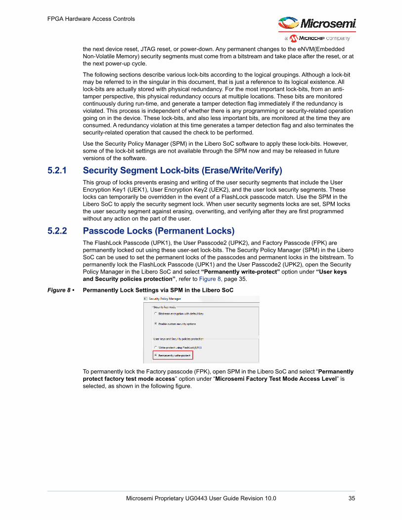
FPGA Hardware Access Controls
the next device reset, JTAG reset, or power-down. Any permanent changes to the eNVM(Embedded Non-Volatile Memory) security segments must come from a bitstream and take place after the reset, or at the next power-up cycle.
The following sections describe various lock-bits according to the logical groupings. Although a lock-bit may be referred to in the singular in this document, that is just a reference to its logical existence. All lock-bits are actually stored with physical redundancy. For the most important lock-bits, from an anti-tamper perspective, this physical redundancy occurs at multiple locations. These bits are monitored continuously during run-time, and generate a tamper detection flag immediately if the redundancy is violated. This process is independent of whether there is any programming or security-related operation going on in the device. These lock-bits, and also less important bits, are monitored at the time they are consumed. A redundancy violation at this time generates a tamper detection flag and also terminates the security-related operation that caused the check to be performed.
Use the Security Policy Manager (SPM) in the Libero SoC software to apply these lock-bits. However, some of the lock-bit settings are not available through the SPM now and may be released in future versions of the software.
5.2.1 Security Segment Lock-bits (Erase/Write/Verify)This group of locks prevents erasing and writing of the user security segments that include the User Encryption Key1 (UEK1), User Encryption Key2 (UEK2), and the user lock security segments. These locks can temporarily be overridden in the event of a FlashLock passcode match. Use the SPM in the Libero SoC to apply the security segment lock. When user security segments locks are set, SPM locks the user security segment against erasing, overwriting, and verifying after they are first programmed without any action on the part of the user.
5.2.2 Passcode Locks (Permanent Locks)The FlashLock Passcode (UPK1), the User Passcode2 (UPK2), and Factory Passcode (FPK) are permanently locked out using these user-set lock-bits. The Security Policy Manager (SPM) in the Libero SoC can be used to set the permanent locks of the passcodes and permanent locks in the bitstream. To permanently lock the FlashLock Passcode (UPK1) and the User Passcode2 (UPK2), open the Security Policy Manager in the Libero SoC and select “Permanently write-protect” option under “User keys and Security policies protection”, refer to Figure 8, page 35.
Figure 8 • Permanently Lock Settings via SPM in the Libero SoC
To permanently lock the Factory passcode (FPK), open SPM in the Libero SoC and select “Permanently protect factory test mode access” option under “Microsemi Factory Test Mode Access Level” is selected, as shown in the following figure.
Microsemi Proprietary UG0443 User Guide Revision 10.0 35
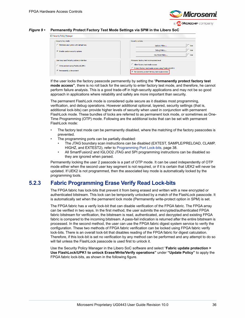
FPGA Hardware Access Controls
Figure 9 • Permanently Protect Factory Test Mode Settings via SPM in the Libero SoC
If the user locks the factory passcode permanently by setting the “Permanently protect factory test mode access”, there is no roll back for the security to enter factory test mode, and therefore, he cannot perform failure analysis. This is a good trade-off in high-security applications and may not be so good approach in applications where reliability and safety are more important than security.
The permanent FlashLock mode is considered quite secure as it disables most programming, verification, and debug operations. However additional optional, layered, security settings (that is, additional lock-bits) can provide higher levels of security when used in conjunction with permanent FlashLock mode. These bundles of locks are referred to as permanent lock mode, or sometimes as One-Time Programming (OTP) mode. Following are the additional locks that can be set with permanent FlashLock mode:
• The factory test mode can be permanently disabled, where the matching of the factory passcodes is prevented.
• The programming ports can be partially disabled:• The JTAG boundary scan instructions can be disabled (EXTEST, SAMPLE/PRELOAD, CLAMP,
HIGHZ, and EXTEST2), refer to Programming Port Lock-bits, page 38.• All SmartFusion2 and IGLOO2 JTAG and SPI programming instructions can be disabled so
they are ignored when parsed.
Permanently locking the user 2 passcode is a part of OTP mode. It can be used independently of OTP mode either when the second user key segment is not required, or if it is certain that UEK2 will never be updated. If UEK2 is not programmed, then the associated key mode is automatically locked by the programming tools.
5.2.3 Fabric Programming Erase Verify Read Lock-bitsThe FPGA fabric has lock-bits that prevent it from being erased and written with a new encrypted or authenticated bitstream. This lock can be temporarily unlocked by a match of the FlashLock passcode. It is automatically set when the permanent lock mode (Permanently write-protect option in SPM) is set.
The FPGA fabric has a verify lock-bit that can disable verification of the FPGA fabric. The FPGA array can be verified in two ways. In the first method, the user submits the encrypted/authenticated FPGA fabric bitstream for verification, the bitstream is read, authenticated, and decrypted and existing FPGA fabric is compared to the incoming bitstream. A pass-fail indication is returned after the entire bitstream is processed. In the second method, the user can use the FPGA fabric digest system service to verify the configuration. These two methods of FPGA fabric verification can be locked using FPGA fabric verify lock-bits. There is an overall lock-bit that disables reading of the FPGA fabric for digest calculation. Therefore, if this lock-bit is set no verification by any method can be performed and any attempt to do so will fail unless the FlashLock passcode is used first to unlock it.
Use the Security Policy Manager in the Libero SoC software and select “Fabric update protection > Use FlashLock/UPK1 to unlock Erase/Write/Verify operations” under “Update Policy” to apply the FPGA fabric lock-bits, as shown in the following figure.
Microsemi Proprietary UG0443 User Guide Revision 10.0 36

FPGA Hardware Access Controls
Figure 10 • Fabric Update Protection via SPM in the Libero SoC
Note: SmartFusion2 and Igloo2 eNVM’s bitstream programming and verification is protected by UEK1/UEK2 when the security policy is programmed. To prevent reading from eNVM, the user must select to protect SmartDebug with DPK in the Debug Policy of the SPM.
5.2.4 Key-Mode Lock-bitsEach key mode has a lock-bit, which disables it. Some of these are set automatically. In a new device, any one of the factory keys may be used to load the user keys in encrypted form. After the user keys are loaded, all the factory keys are automatically disabled, leaving only the user key modes in operation. Thus, any subsequent bitstream updates must be done using the user keys. Keys that are not loaded are also automatically disabled. The user may choose to disable any additional key modes. If all key modes are disabled, this is effectively another layer of security to prevent bitstream updates. The key mode lock-bits are not temporarily unlocked by the FlashLock passcode. It is required to match the FlashLock passcode to allow the key mode lock-bits to be erased, after which they can be reprogrammed by a new bitstream. Use the Security Policy Manager in the Libero SoC software and select “Programming Key Mode Policy>Disable Key Mode” option under “Key Mode Policy” to apply key mode lock for UEK1, UEK2, and for devices with data security enabled (-060, -090 and -150 devices), UEK3, as shown in the following figure.
Figure 11 • UEK1 and UEK2 Programming Key Mode Lock via SPM in the Libero SoC
The two user keys (UEK1 and UEK2) and the User PUF symmetric design security key (UEK3) in larger “TS” class devices have essentially identical capabilities. While individual key modes may be disabled with lock-bits, and certain programming functions, such as field updates of the eNVM or the FPGA fabric or both can be disabled, If a key is not disabled, it has access to all the same programming capabilities as any other enabled key has access to. Key-mode enabling is an all-or-nothing affair, independent to selection of which programming functions are enabled. So, if UEK1 can overwrite the eNVM with new programming data, UEK2 can also overwrite too provided if it is enabled. Conversely, if overwriting of the FPGA fabric is locked, it is locked for all possible keys.
Microsemi Proprietary UG0443 User Guide Revision 10.0 37
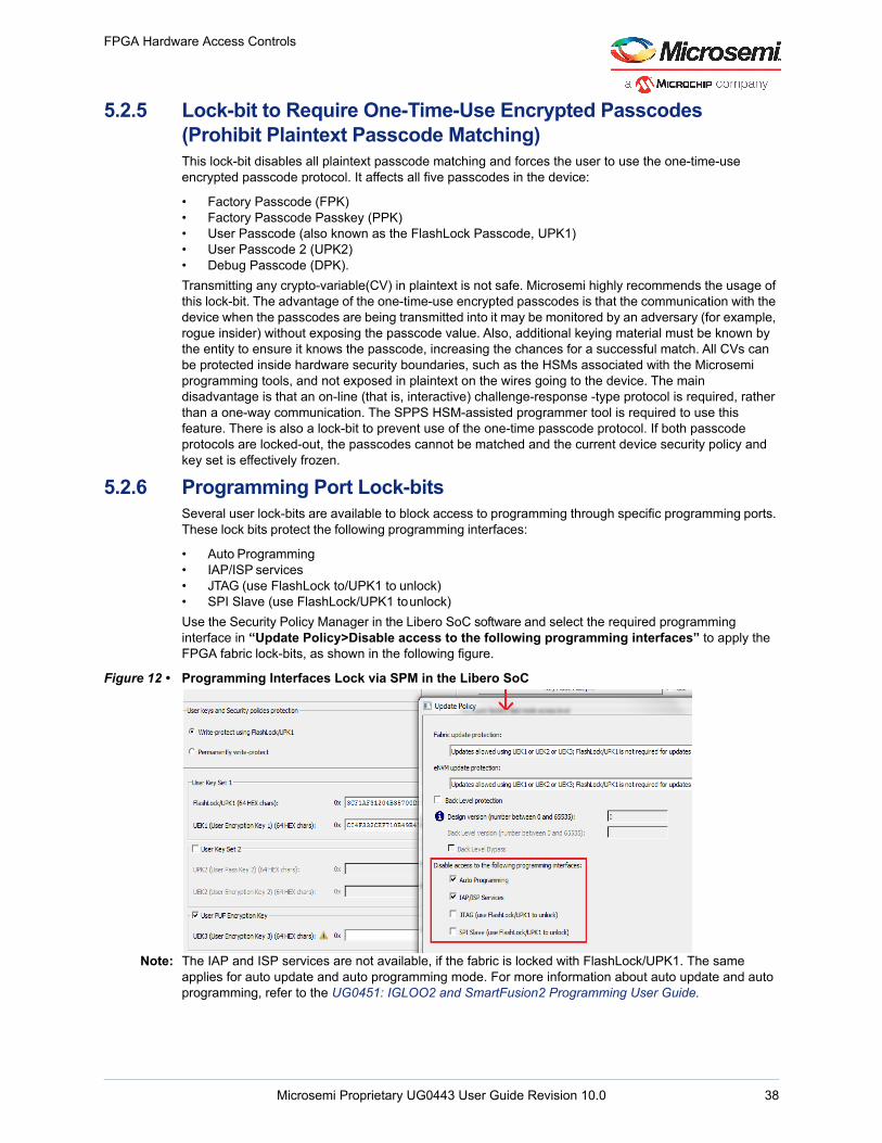
FPGA Hardware Access Controls
5.2.5 Lock-bit to Require One-Time-Use Encrypted Passcodes (Prohibit Plaintext Passcode Matching)This lock-bit disables all plaintext passcode matching and forces the user to use the one-time-use encrypted passcode protocol. It affects all five passcodes in the device:
• Factory Passcode (FPK) • Factory Passcode Passkey (PPK)• User Passcode (also known as the FlashLock Passcode, UPK1)• User Passcode 2 (UPK2)• Debug Passcode (DPK).
Transmitting any crypto-variable(CV) in plaintext is not safe. Microsemi highly recommends the usage of this lock-bit. The advantage of the one-time-use encrypted passcodes is that the communication with the device when the passcodes are being transmitted into it may be monitored by an adversary (for example, rogue insider) without exposing the passcode value. Also, additional keying material must be known by the entity to ensure it knows the passcode, increasing the chances for a successful match. All CVs can be protected inside hardware security boundaries, such as the HSMs associated with the Microsemi programming tools, and not exposed in plaintext on the wires going to the device. The main disadvantage is that an on-line (that is, interactive) challenge-response -type protocol is required, rather than a one-way communication. The SPPS HSM-assisted programmer tool is required to use this feature. There is also a lock-bit to prevent use of the one-time passcode protocol. If both passcode protocols are locked-out, the passcodes cannot be matched and the current device security policy and key set is effectively frozen.
5.2.6 Programming Port Lock-bitsSeveral user lock-bits are available to block access to programming through specific programming ports. These lock bits protect the following programming interfaces:
• Auto Programming• IAP/ISP services• JTAG (use FlashLock to/UPK1 to unlock)• SPI Slave (use FlashLock/UPK1 to unlock)
Use the Security Policy Manager in the Libero SoC software and select the required programming interface in “Update Policy>Disable access to the following programming interfaces” to apply the FPGA fabric lock-bits, as shown in the following figure.
Figure 12 • Programming Interfaces Lock via SPM in the Libero SoC
Note: The IAP and ISP services are not available, if the fabric is locked with FlashLock/UPK1. The same applies for auto update and auto programming mode. For more information about auto update and auto programming, refer to the UG0451: IGLOO2 and SmartFusion2 Programming User Guide.
Microsemi Proprietary UG0443 User Guide Revision 10.0 38
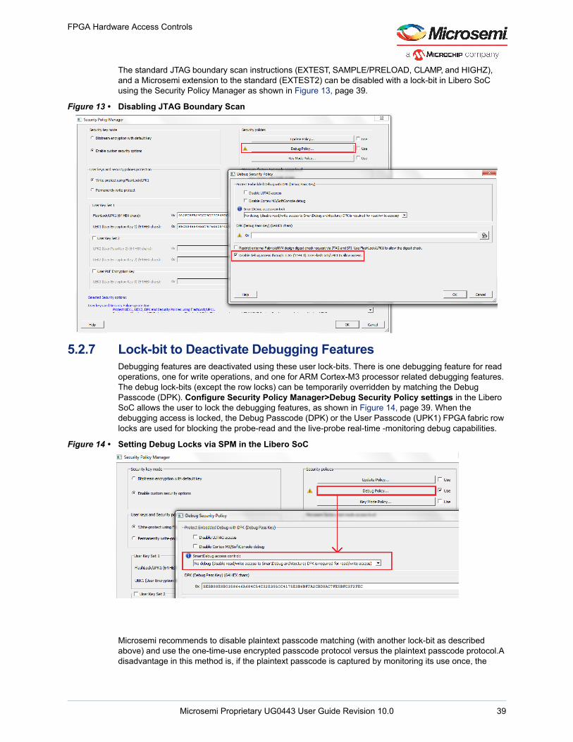
FPGA Hardware Access Controls
The standard JTAG boundary scan instructions (EXTEST, SAMPLE/PRELOAD, CLAMP, and HIGHZ), and a Microsemi extension to the standard (EXTEST2) can be disabled with a lock-bit in Libero SoC using the Security Policy Manager as shown in Figure 13, page 39.
Figure 13 • Disabling JTAG Boundary Scan
5.2.7 Lock-bit to Deactivate Debugging FeaturesDebugging features are deactivated using these user lock-bits. There is one debugging feature for read operations, one for write operations, and one for ARM Cortex-M3 processor related debugging features. The debug lock-bits (except the row locks) can be temporarily overridden by matching the Debug Passcode (DPK). Configure Security Policy Manager>Debug Security Policy settings in the Libero SoC allows the user to lock the debugging features, as shown in Figure 14, page 39. When the debugging access is locked, the Debug Passcode (DPK) or the User Passcode (UPK1) FPGA fabric row locks are used for blocking the probe-read and the live-probe real-time -monitoring debug capabilities.
Figure 14 • Setting Debug Locks via SPM in the Libero SoC
Microsemi recommends to disable plaintext passcode matching (with another lock-bit as described above) and use the one-time-use encrypted passcode protocol versus the plaintext passcode protocol.A disadvantage in this method is, if the plaintext passcode is captured by monitoring its use once, the
Microsemi Proprietary UG0443 User Guide Revision 10.0 39
FPGA Hardware Access Controls
plaintext passcode can be used thereafter to unlock the debugging features of the device (unless subsequently locked-out).
5.2.8 Cryptographic Services Lock-bitsEach group of cryptographic system services such as AES and all its modes (ECB, CBC, CTR, OFB), or SHA-256 (including HMAC-SHA-256), may be disabled by these user lock-bits. This may be done for services that are not required in a given application. These lock-bits may be used if in some countries with issues related to export of cryptographically enabled devices. This feature will be available in future versions of Microsemi programming software.
5.2.9 Hardware Firewall Lock-bitsHardware firewalls protection block read or write operations from three groupings of bus masters to memory. The hardware firewall lock-bits are the lock-bits that control access. Refer to Memory Access Controls, page 40 for details.
5.3 Memory Access ControlsAll SmartFusion2 and IGLOO2 devices contain some basic software and hardware memory access control mechanisms.:
• Hardware protection refers to quasi-static access control bits that can only be changed by reconfiguring the appropriate sections of the device with a new authenticated or encrypted bitstream.
• Software protection refers to access control bits that can be dynamically changed by a bus master attached to the AMBA®(Advanced Microcontroller Bus Architecture)system bus.
Consequently, the hardware access controls have a higher level of security than the software controls. For example, hardware controls are protected against change by malware that may infect the Cortex-M3 processor in SmartFusion2 devices. The risk of malware infection is higher if the Cortex-M3 processor is attached to a public network. If the access controls prohibit access by the Cortex-M3, then the affected memory regions are more efficiently protected from the risk of malware.
Many of these memory access control mechanisms are layered. The access restrictions are cumulative, that is, if read or write permissions are locked at any level, then that access is denied regardless of whether it is locked at another level or not.
5.4 Software MPUIn SmartFusion2 devices, the ARM Cortex-M3 processor contains an ARM MPU. The MPU provides more memory control, enables applications to utilize multiple privilege levels, separates and protects code, data and stack on a task-by-task basis. These requirements are critical in several embedded applications, like the automotive systems.
The Cortex-M3 processor in SmartFusion2 devices can be used to configure the access permissions for up to eight potentially overlapping regions of the memory and background under software control. The MPU divides the memory map into a number of regions, and defines the location, size, access permissions, and memory attributes of each region. It supports:
• Independent attribute settings for each region• Overlapping regions• Export of memory attributes to the system
The MPU can be enabled using System Builder -> Microcontroller in the Libero SoC, as shown in the following figure.
Microsemi Proprietary UG0443 User Guide Revision 10.0 40

FPGA Hardware Access Controls
Figure 15 • Cortex -M3 Configurator
For more information about how to use MPU, refer to UG0331: SmartFusion2 Microcontroller Subsystem User Guide.
5.4.1 Software eNVM User Page-Write LocksEach 1K-bit page of eNVM (with 1024 available user bits) contains some additional hidden data which is managed by the memory controller hardware and/or the system controller, including a user page-level write-protect bit. This bit can prevent accidental overwriting of marked eNVM pages since it executes an additional operation on the part of the bus master to unlock the page before it can be written. The user page-write lock bit can be set or cleared dynamically by any bus master that has access to the respective page of memory. This gives these locks a software level of protection. Refer to “Embedded NVM (eNVM) Controllers” chapter in UG0331: SmartFusion2 Microcontroller Subsystem User Guide for more details on setting these locks bits.
5.4.2 Hardware eNVM Factory Page-Write LocksEach 1K-bit page of eNVM also contains a quasi-static factory page-level write-protect bit. These bits prevent accidental or malicious overwriting of the marked pages. The system controller controls these bits, which are not accessible by any other bus masters. These locks have a “hardware” level of security, as defined earlier.
The system controller reserved pages in the eNVM are always write-protected using these factory page-write locks. The factory page-write protect bits in the remaining (that is, user) eNVM pages are set (or cleared) if and when the attached eNVM pages are programmed by an authenticated or encrypted user bitstream. The user sets those regions of memory to write-protect. In effect, the user declares these pages in the read-only memory (ROM) region, the Libero SoC “MSS Configuration - eNVM” tool allows the user to create these ROM regions.
5.4.3 Hardware eNVM, eSRAM, and MDDR Data Security Access ControlsThe microcontroller subsystem (MSS) in SmartFusion2 and high-performance memory sub-system (HPMS) in IGLOO2 SoC FPGAs has a multi-layer AMBA bus interconnection between the many bus masters and slaves in the subsystem. The multi-layer bus acts like a cross-point switch, allowing any bus master to communicate with any bus slave. For security reasons, such an open system is not desirable
Microsemi Proprietary UG0443 User Guide Revision 10.0 41
FPGA Hardware Access Controls
sometimes. Therefore, the premium “S” or “TS” version of SmartFusion2 SoC and IGLOO2 devices have the capability to block read or write operations from three groupings of the bus masters. The fourth bus master group contains the system controller which always has access to the multi-layer bus. These lock-bits control access to the eSRAM blocks, the eNVM block(s), and the MDDR memory controller slaves. The lock bits block read or write traffic from a specific group of bus masters to a specific memory slave (or portion thereof). In addition to the SmartFusion2 device, the user can control access to the MSS memory region from the fabric master and also can block changing MSS configuration registers settings using lock-bits.
The Libero SoC software allows setting up these lock-bits. For SmartFusion2 designs, the MSS Security Policies configurator has three sets of lock-bits to control the hardware-firewall:
• Cortex-M3, Fabric Interface Controller (FIC), and DMA(Dynamic Memory Access) bus masters access lock-bits
• Fabric master to MSS memory map access lock-bits • MSS configuration registers lock-bits
In IGLOO2 designs, it is the System Builder- Security Configurator that sets the control access from the various masters (FIC and DMA bus) in HPMS.
5.4.3.1 Cortex-M3, FIC and DMA Bus Masters Access Lock-BitsThe various bus master access lock-bits can be set in the Libero SoC. For SmartFusion2 designs, the MSS Security Policies Configurator’s Master/Slave configuration tab defines how masters and slaves communicate and whether it also has write access when a master has read access. User can define AMBA bus interconnect locks and eNVM special sectors locks.
5.4.3.1.1 AMBA Bus Interconnect Locks, shows the MSS Security Policies Configurator window in the Libero SoC that sets the control access from these internal bus lock-bits. The access for eSRAM, eNVM, and the DDR bridge from various masters (Cortex-M3, FIC, and DMA bus) in the MSS can be locked. The AHB bus matrix can be configured to restrict these accesses.
Microsemi Proprietary UG0443 User Guide Revision 10.0 42

FPGA Hardware Access Controls
Figure 16 • MSS Security Policies Configurator-eSRAM0, eSRAM1, eNVM0, eNVM1 and DDR Bridge Lock
The master/slave access is defined in the matrix as follows:
• –: No access is granted • R: Only read access is available • RW: Both read and write accesses are available.
To restrict a master or slave access, un-check the read or write field for a particular group of masters. Whenever you restrict a master/slave access by un-checking the Read or Write access for a particular group of masters(masters are organized in three groups with respect to access configuration), the actual access is displayed in the matrix. When a specific lock is selected, the corresponding lock-bit is set in the user security segment. These locks can be temporarily overridden in the event of a FlashLock passcode match.
5.4.3.1.2 eNVM Special Sectors LocksThe eNVM blocks have special sectors that can be write protected. The following figure shows the MSS Security Configurator window with eNVM Special Sectors lock option. The user can check the Use as ROM checkbox option to write protect these eNVM regions. The number of special sectors depends on the device selected. The size of each sector is 4 KB and the address range for each special sector is listed in Table 3, page 44.
Microsemi Proprietary UG0443 User Guide Revision 10.0 43
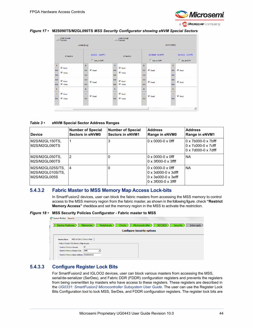
FPGA Hardware Access Controls
Figure 17 • M2S090TS/M2GL090TS MSS Security Configurator showing eNVM Special Sectors
5.4.3.2 Fabric Master to MSS Memory Map Access Lock-bitsIn SmartFusion2 devices, user can block the fabric masters from accessing the MSS memory to control access to the MSS memory region from the fabric master, as shown in the following figure. check “Restrict Memory Access” checkbox and set the memory region in the MSS to activate the restriction.
Figure 18 • MSS Security Policies Configurator - Fabric master to MSS
5.4.3.3 Configure Register Lock BitsFor SmartFusion2 and IGLOO2 devices, user can block various masters from accessing the MSS, serial/de-serializer (SerDes), and Fabric DDR (FDDR) configuration registers and prevents the registers from being overwritten by masters who have access to these registers. These registers are described in the UG0331: SmartFusion2 Microcontroller Subsystem User Guide. The user can use the Register Lock Bits Configuration tool to lock MSS, SerDes, and FDDR configuration registers. The register lock bits are
Table 3 • eNVM Special Sector Address Ranges
DeviceNumber of Special Sectors in eNVM0
Number of Special Sectors in eNVM1
AddressRange in eNVM0
AddressRange in eNVM1
M2S/M2GL150TS,M2S/M2GL090TS
1 3 0 x 0000-0 x 0fff 0 x 7b000-0 x 7bfff0 x 7c000-0 x 7cfff0 x 7d000-0 x 7dfff
M2S/M2GL050TS,M2S/M2GL060TS
2 0 0 x 0000-0 x 0fff0 x 3f000-0 x 3ffff
NA
M2S/M2GL025S/TS,M2S/M2GL010S/TS,M2S/M2GL005S
4 0 0 x 0000-0 x 0fff0 x 3d000-0 x 3dfff0 x 3e000-0 x 3efff0 x 3f000-0 x 3ffff
NA
Microsemi Proprietary UG0443 User Guide Revision 10.0 44
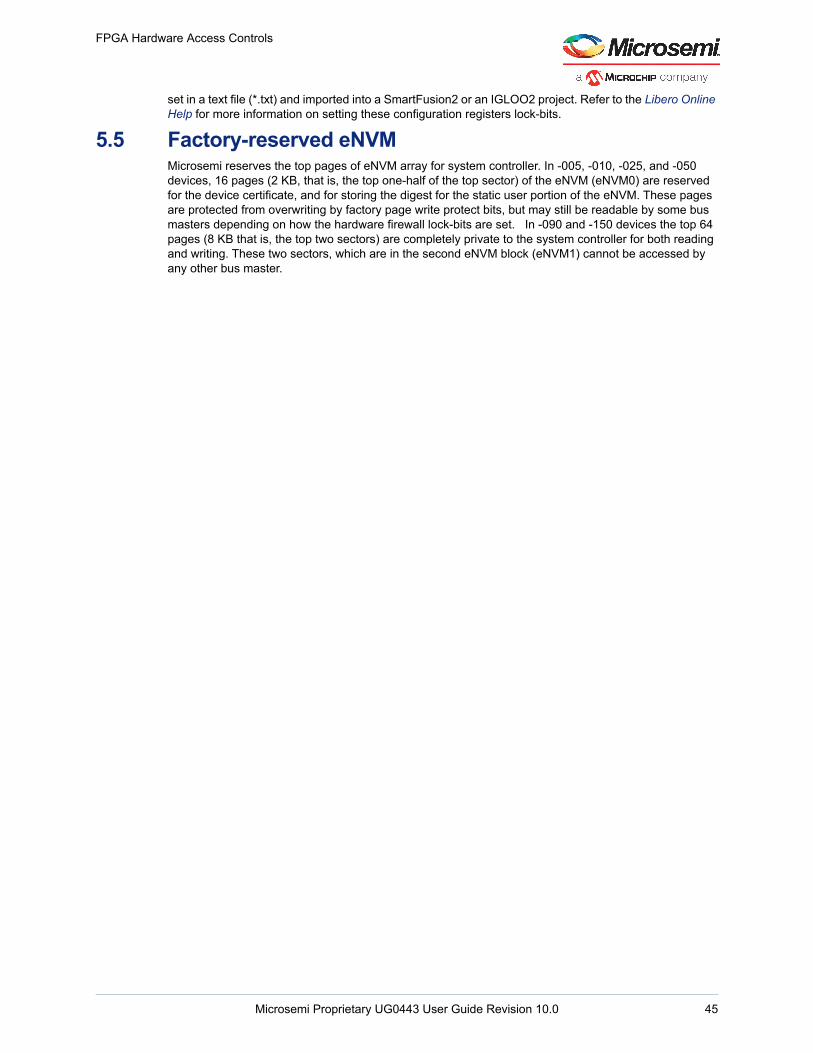
FPGA Hardware Access Controls
set in a text file (*.txt) and imported into a SmartFusion2 or an IGLOO2 project. Refer to the Libero Online Help for more information on setting these configuration registers lock-bits.
5.5 Factory-reserved eNVMMicrosemi reserves the top pages of eNVM array for system controller. In -005, -010, -025, and -050 devices, 16 pages (2 KB, that is, the top one-half of the top sector) of the eNVM (eNVM0) are reserved for the device certificate, and for storing the digest for the static user portion of the eNVM. These pages are protected from overwriting by factory page write protect bits, but may still be readable by some bus masters depending on how the hardware firewall lock-bits are set. In -090 and -150 devices the top 64 pages (8 KB that is, the top two sectors) are completely private to the system controller for both reading and writing. These two sectors, which are in the second eNVM block (eNVM1) cannot be accessed by any other bus master.
Microsemi Proprietary UG0443 User Guide Revision 10.0 45
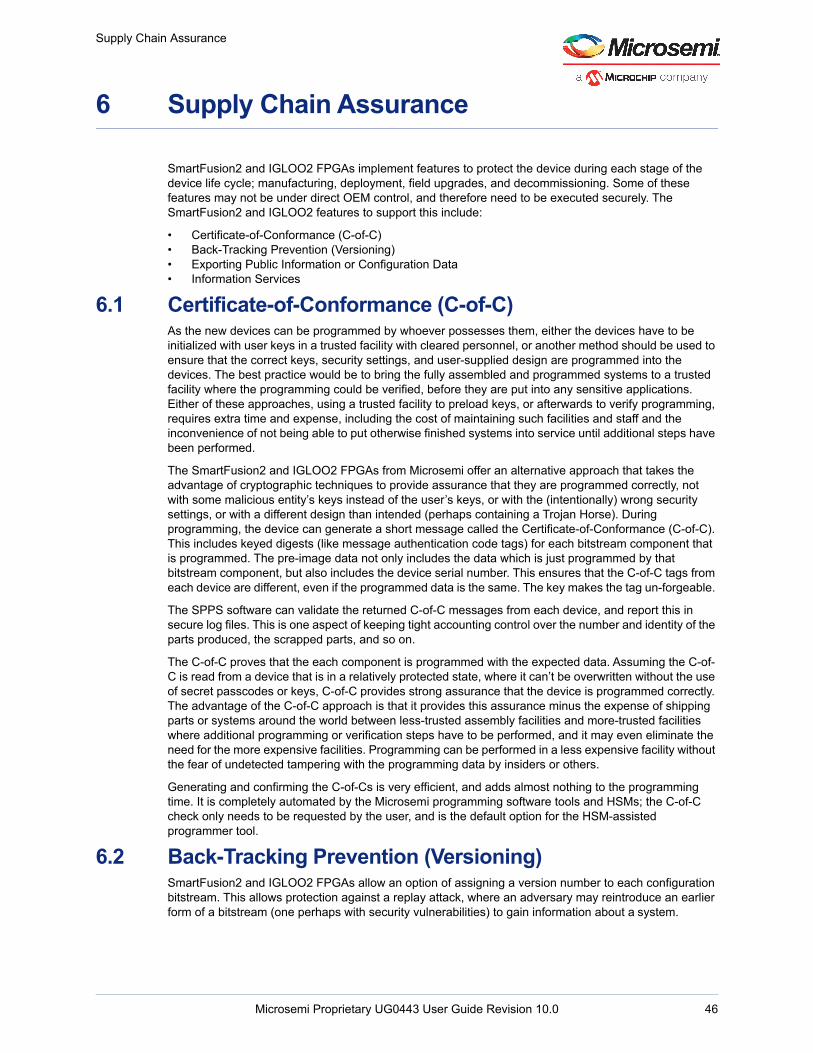
Supply Chain Assurance
6 Supply Chain Assurance
SmartFusion2 and IGLOO2 FPGAs implement features to protect the device during each stage of the device life cycle; manufacturing, deployment, field upgrades, and decommissioning. Some of these features may not be under direct OEM control, and therefore need to be executed securely. The SmartFusion2 and IGLOO2 features to support this include:
• Certificate-of-Conformance (C-of-C)• Back-Tracking Prevention (Versioning)• Exporting Public Information or Configuration Data• Information Services
6.1 Certificate-of-Conformance (C-of-C)As the new devices can be programmed by whoever possesses them, either the devices have to be initialized with user keys in a trusted facility with cleared personnel, or another method should be used to ensure that the correct keys, security settings, and user-supplied design are programmed into the devices. The best practice would be to bring the fully assembled and programmed systems to a trusted facility where the programming could be verified, before they are put into any sensitive applications. Either of these approaches, using a trusted facility to preload keys, or afterwards to verify programming, requires extra time and expense, including the cost of maintaining such facilities and staff and the inconvenience of not being able to put otherwise finished systems into service until additional steps have been performed.
The SmartFusion2 and IGLOO2 FPGAs from Microsemi offer an alternative approach that takes the advantage of cryptographic techniques to provide assurance that they are programmed correctly, not with some malicious entity’s keys instead of the user’s keys, or with the (intentionally) wrong security settings, or with a different design than intended (perhaps containing a Trojan Horse). During programming, the device can generate a short message called the Certificate-of-Conformance (C-of-C). This includes keyed digests (like message authentication code tags) for each bitstream component that is programmed. The pre-image data not only includes the data which is just programmed by that bitstream component, but also includes the device serial number. This ensures that the C-of-C tags from each device are different, even if the programmed data is the same. The key makes the tag un-forgeable.
The SPPS software can validate the returned C-of-C messages from each device, and report this in secure log files. This is one aspect of keeping tight accounting control over the number and identity of the parts produced, the scrapped parts, and so on.
The C-of-C proves that the each component is programmed with the expected data. Assuming the C-of-C is read from a device that is in a relatively protected state, where it can’t be overwritten without the use of secret passcodes or keys, C-of-C provides strong assurance that the device is programmed correctly. The advantage of the C-of-C approach is that it provides this assurance minus the expense of shipping parts or systems around the world between less-trusted assembly facilities and more-trusted facilities where additional programming or verification steps have to be performed, and it may even eliminate the need for the more expensive facilities. Programming can be performed in a less expensive facility without the fear of undetected tampering with the programming data by insiders or others.
Generating and confirming the C-of-Cs is very efficient, and adds almost nothing to the programming time. It is completely automated by the Microsemi programming software tools and HSMs; the C-of-C check only needs to be requested by the user, and is the default option for the HSM-assisted programmer tool.
6.2 Back-Tracking Prevention (Versioning)SmartFusion2 and IGLOO2 FPGAs allow an option of assigning a version number to each configuration bitstream. This allows protection against a replay attack, where an adversary may reintroduce an earlier form of a bitstream (one perhaps with security vulnerabilities) to gain information about a system.
Microsemi Proprietary UG0443 User Guide Revision 10.0 46

Supply Chain Assurance
The user may set the design version number and also a back-level version by using the Security Policy manager > Update Policy dialog box in the SoC tool, as shown in the following figure. The back- level version is set at or before where the device rejects the next incoming file. The back level version value limits the design versions, the device can update. So, only programming bitstreams with Design version > Back Level version are allowed for programming. The back-level protection is secured by FlashLock/UPK1. FlashLock/UPK1 can be used to bypass the back level protection.
Note: The entire bitstream configuration file, including the versioning and back level fields, is authenticated to detect tampering with the versioning mechanism.
Figure 19 • Back Level Protection Settings in the Security Policy Manager
6.3 Exporting Public Information or Configuration DataThe following paragraphs discuss the type of information which can be exported from SmartFusion2 and IGLOO2 devices using the built-in services. Also discussed are the protections applied to data that is not intended to be exported, such as the user’s design IP or any cryptographic variables.
6.3.1 Device Certificates (Anti-Counterfeiting)Counterfeiting in electronic parts can take various forms. Some examples are copying designs at the transistor level, black-topping, and remarking devices to misrepresent used devices as new, changing the date codes, improving the speed grade or the temperature grade, and increasing the alleged screening level.
To prevent counterfeiting and fraud, SmartFusion2 and IGLOO2 FPGAs incorporate anX.509 compliant digital certificate, stored in the device's eNVM. The digital certificate includes a digital signature, an electronic analog of a written signature. The digital signature can be used to provide assurance that the claimed signatory signed the information. In addition, a digital signature can be used to detect whether or not the information is modified after it is signed. Figure 20, page 48 shows the standard digital signature processes.
Microsemi Proprietary UG0443 User Guide Revision 10.0 47
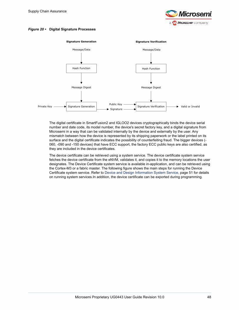
Supply Chain Assurance
Figure 20 • Digital Signature Processes
The digital certificate in SmartFusion2 and IGLOO2 devices cryptographically binds the device serial number and date code, its model number, the device's secret factory key, and a digital signature from Microsemi in a way that can be validated internally by the device and externally by the user. Any mismatch between how the device is represented by its shipping paperwork or the label printed on its surface and the digital certificate indicates the possibility of counterfeiting fraud. The bigger devices (-060, -090 and -150 devices) that have ECC support, the factory ECC public keys are also certified, as they are included in the device certificates.
The device certificate can be retrieved using a system service. The device certificate system service fetches the device certificate from the eNVM, validates it, and copies it to the memory locations the user designates. The Device Certificate system service is available in-application, and can be retrieved using the Cortex-M3 or a fabric master. The following figure shows the main steps for running the Device Certificate system service. Refer to Device and Design Information System Service, page 51 for details on running system services.In addition, the device certificate can be exported during programming.
Hash Function Hash Function
Signature Generation Signature Verification
Message Digest Message Digest
Signature Generation Signature Verification
Private KeyPublic Key
SignatureValid or Invalid
Message/Data Message/Data
Microsemi Proprietary UG0443 User Guide Revision 10.0 48
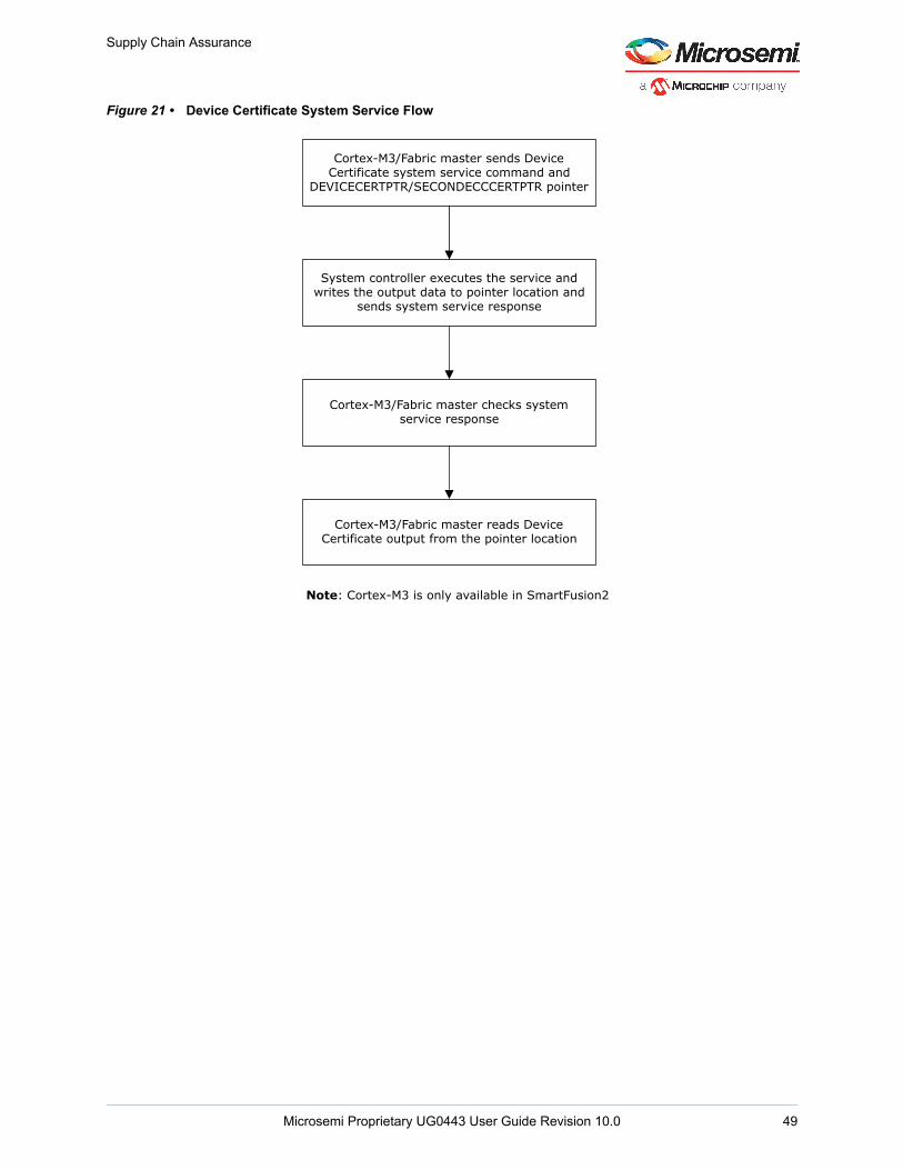
Supply Chain Assurance
Figure 21 • Device Certificate System Service Flow
Note: Cortex-M3 is only available in SmartFusion2
Cortex-M3/Fabric master sends Device Certificate system service command and
DEVICECERTPTR/SECONDECCCERTPTR pointer
System controller executes the service and writes the output data to pointer location and
sends system service response
Cortex-M3/Fabric master checks system service response
Cortex-M3/Fabric master reads Device Certificate output from the pointer location
Microsemi Proprietary UG0443 User Guide Revision 10.0 49

Supply Chain Assurance
The following tables show Device Certificate system service request, response, and status.
Table 4 • Device Certificate System Service Request
Table 5 • Device Certificate System Service Response
Table 6 • Service Status
The firmware catalog has the driver for exporting the device certificate so that the API can be used in their system. In addition, CoreSysServices IP can be used to run the Device Certificate system service using the RTL code. Refer to AC436: Using Device Certificate System Service in SmartFusion2 Application Note for details.
6.4 Information ServicesSome of the device data are considered public and may be exported internally using the system services accessible through the COMM_BLK. The Information services return information about the device and current user design. In addition, the device information can be exported from SmartFusion2 and IGLOO2 devices using an external interface, such as the JTAG or SPI-slave programming interfaces.The following table summarizes the public data that can be exported using the system service and external JTAG or SPI-slave programming interfaces.
Offset Length (bytes) Field Description
0 1 CMD = 0 or 30 Command0: Primary device certificate (all “S” or “TS” devices)30: Secondary device certificate (M2S060TS, M2S090TS, M2S150TS, M2GL060TS, M2GL090TS, and M2GL150TSdevices only)
1 4 DDEVICECERTPTR/ SECONDECCCERTPTR
DEVICECERTPTR: Pointer to 768-byte buffer to receive the primary device certificateSECONDECCCERTPTR: Pointer to 640-byte buffer to receive the secondary certificate
Offset Length (bytes) Field Description
0 1 CMD = 0or 30 Command
1 1 STATUS Service status (see the following table)
2 4 DEVICECERTPTR/ SECONDECCCERTPTR
Pointer to original buffer from request
Status Description
0 Success
127 MSS/HPMS memory access error (HRESP)
Table 7 • Public Information Accessible
Information
Internal (System Service)
External (JTAG/SPI) Comment
Serial Number x x Unique-per-device, 128 bits
IDCODE x Std. IEEE 1149.1 JTAG IDCODE value, 32 bits
USERCODE x x Std. IEEE 1149.1 JTAG USERCODE value, 32 bits
Microsemi Proprietary UG0443 User Guide Revision 10.0 50
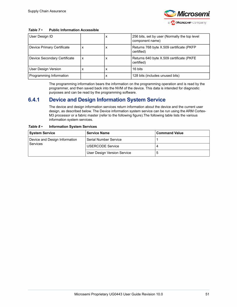
Supply Chain Assurance
The programming information bears the information on the programming operation and is read by the programmer, and then saved back into the NVM of the device. This data is intended for diagnostic purposes and can be read by the programming software.
6.4.1 Device and Design Information System ServiceThe device and design information services return information about the device and the current user design, as described below. The Device information system service can be run using the ARM Cortex-M3 processor or a fabric master (refer to the following figure).The following table lists the various information system services.
User Design ID x 256 bits, set by user (Normally the top level component name)
Device Primary Certificate x x Returns 768 byte X.509 certificate (PKFP certified)
Device Secondary Certificate x x Returns 640 byte X.509 certificate (PKFE certified)
User Design Version x x 16 bits
Programming Information x 128 bits (includes unused bits)
Table 8 • Information System Services
System Service Service Name Command Value
Device and Design Information Services
Serial Number Service 1
USERCODE Service 4
User Design Version Service 5
Table 7 • Public Information Accessible
Microsemi Proprietary UG0443 User Guide Revision 10.0 51
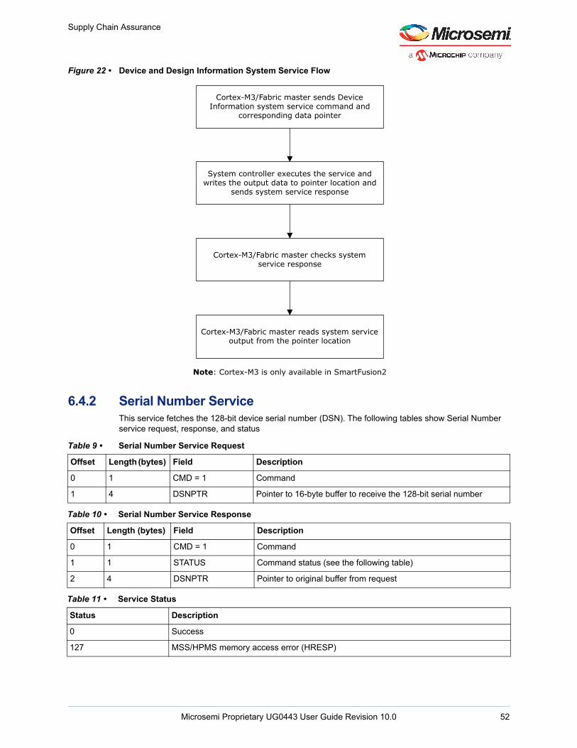
Supply Chain Assurance
Figure 22 • Device and Design Information System Service Flow
6.4.2 Serial Number ServiceThis service fetches the 128-bit device serial number (DSN). The following tables show Serial Number service request, response, and status
Table 9 • Serial Number Service Request
Offset Length (bytes) Field Description
0 1 CMD = 1 Command
1 4 DSNPTR Pointer to 16-byte buffer to receive the 128-bit serial number
Table 10 • Serial Number Service Response
Offset Length (bytes) Field Description
0 1 CMD = 1 Command
1 1 STATUS Command status (see the following table)
2 4 DSNPTR Pointer to original buffer from request
Table 11 • Service Status
Status Description
0 Success
127 MSS/HPMS memory access error (HRESP)
Cortex-M3/Fabric master sends Device Information system service command and
corresponding data pointer
System controller executes the service and writes the output data to pointer location and
sends system service response
Cortex-M3/Fabric master checks system service response
Cortex-M3/Fabric master reads system service output from the pointer location
Note: Cortex-M3 is only available in SmartFusion2
Microsemi Proprietary UG0443 User Guide Revision 10.0 52
Supply Chain Assurance
6.4.3 USERCODE ServiceThis service fetches the 32-bit JTAG USERCODE programmed by the user. The following tables show the USERCODE service request and service response.
6.4.4 User Design Version ServiceThis service fetches the 16-bit user design version. The following tables show the Design Version service request and service response.
6.4.5 Security SettingsWhen security settings are exported they are reflective of the permanent settings stored in the user lock security NVM segment, not the current state as it may be temporarily unlocked after a successful passcode match. The programmer tool can interpret and display or print the security settings in a readable format.
6.4.6 Exporting User SRAM-PUF Activation CodesIn larger “TS” Class devices, the user may enroll his own SRAM-PUF base activation code and key codes after receiving the devices. The first two keys, a 256-bit symmetric key and a 384-bit ECC private key, are reserved for design security purposes. Additional data security keys of variable length may also be enrolled. These data security keys can be reconstructed by Quiddikey and exported in plaintext form from the system controller to the design running internally in the FPGA.
The user activation code and user key codes can be exported internally in their entirety in ciphertext form by the system controller to the design running internally in the FPGA. From there, the user can choose to export them off-chip, using any available interface, such as Ethernet for example, as a function of their hardware or software design.
Once exported, the activation code and key codes must be re-imported in order to regenerate any of the enrolled keys. There is an external programming command for importing the base activation code and
Table 12 • USERCODE Service Request
Offset Length (bytes) Field Description
0 1 CMD = 4 Command
1 4 USERCODEPTR Pointer to 4-byte buffer to receive the 32-bit USERCODE
Table 13 • USERCODE Service Response
Offset Length (bytes) Field Description
0 1 CMD = 4 Command
1 1 STATUS Command status (see Table 11, page 52)
2 4 USERCODEPTR Pointer to original buffer from request
Table 14 • Design Version Service Request
Offset Length (bytes) Field Description
0 1 CMD = 5 Command
1 4 DESIGNVERPTR Pointer to 2-byte buffer to receive the 16-bit design version
Table 15 • Design Version Service Response
Offset Length (bytes) Field Description
0 1 CMD = 5 Command
1 1 STATUS Command status (see Table 11, page 52)
2 4 DESIGNVERPTR Pointer to original buffer from request
Microsemi Proprietary UG0443 User Guide Revision 10.0 53

Supply Chain Assurance
either of the key codes associated with the two reserved design security keys. There is an internal system service for importing the activation code and the key codes for the user’s data security keys so that the data security keys can be regenerated.
For more about the SRAM-PUF system services, see SRAM-PUF Services, page 101.
6.4.7 Configuration Read Back in User ModeSmartFusion2 and IGLOO2 devices do not allow to read the FPGA fabric configuration in the user mode, either internally or externally. Some public data elements stored in the security segments may be exported either internally or externally as explained in the previous section. Some of these services, such as exporting of the design digests externally, may be prohibited by user-set lock-bits. This mode has no ability to read any crypto-variables such as keys or passcodes.
Unless prohibited by the user or factory page-level write-protect bits, or by the user hardware firewalls (available in “S” class devices), the eNVM array can be read internally by any (internal) bus master. In the larger devices (-060, -090, -150) the top 8KB of eNVM is private to the system controller, and cannot be read by the user, though some of the data (for example, the device certificate) stored in the top of eNVM may be accessible via internal system services or external JTAG/SPI commands.
6.4.8 Configuration Read Back in Factory Test ModeFactory test mode used by Microsemi during the manufacturing and provisioning process to ensure the quality and reliability of the devices being provided has powerful capabilities. For instance, this mode allows scan-based testing of much of the logic circuitry in the device, to help ensure with high probability there are no “stuck-at” -type hardware faults in the logic being tested.
In SmartFusion2 and IGLOO2 FPGAs some of the production testing is done using the system controller, which also has powerful capabilities. For security reasons, and to conserve on-chip memory, many of the system controller test capabilities are not fully implemented inside the device and have to be downloaded to the device while in factory test mode in order to complete the test capability. During the testing of the devices, at both the wafer probe test stage and after the parts are assembled, multiple such downloads are used to run different tests. This downloaded code is treated by Microsemi as confidential and sensitive information. The downloaded images are encrypted and authenticated in a DPA-resistant manner similar to the way factory and user bitstreams are encrypted and authenticated, with the encryption keys managed by Microsemi owned NIST-certified HSMs. Access to the test programs is restricted to a limited number of trusted Microsemi test engineers.
Factory test mode is essential to ship working parts to customers, and acts as a great utility to an adversary trying to subvert the security of a device. For example, it is at least theoretically possible that the user’s design IP can be read out of the device while in factory test mode, if (hypothetically) the properly encrypted and authenticated test programs are downloaded to the device. Of course, before devices are shipped from Microsemi the factory test mode is disabled using factory lock-bits and other security features.
Unless disabled by the user, there is a method to roll-back the lock-bits and security so the device can be put into the factory test mode again. This procedure is used when failure analysis needs to be performed. This allows Microsemi reliability engineers to understand the root cause of failures, and to take corrective action. In security-critical applications the ability to perform failure analysis may not be as important as a higher assurance that the device cannot be put into factory test mode. For these applications there are a number of additional measures the user can take to permanently lock the device. When the locking is done, the ability to perform failure analysis is permanently lost, but the security is increased.
Entering factory test mode requires the matching of two factory passcodes, called the Factory Passcode (FPK) and the Factory Passcode Passkey (PPK). The matching of these two factory passcodes is always locked by a user lock-bit that is automatically set when the user programs the keys, passcodes, and security settings. In other words, once the user programs a device, the factory passcodes are automatically disabled. In order to roll back this lock to re-enable the factory passcodes, the User FlashLock Passcode (UPK1) must first be matched. The user also has the option to permanently prohibit factory test mode with a different User-set lock-bit, in which case there is no mechanism to roll back security to re-enter the factory test mode. In other words, there is a reversible lock set by default and also a permanent (irreversible) lock the user can optionally set.
Microsemi Proprietary UG0443 User Guide Revision 10.0 54
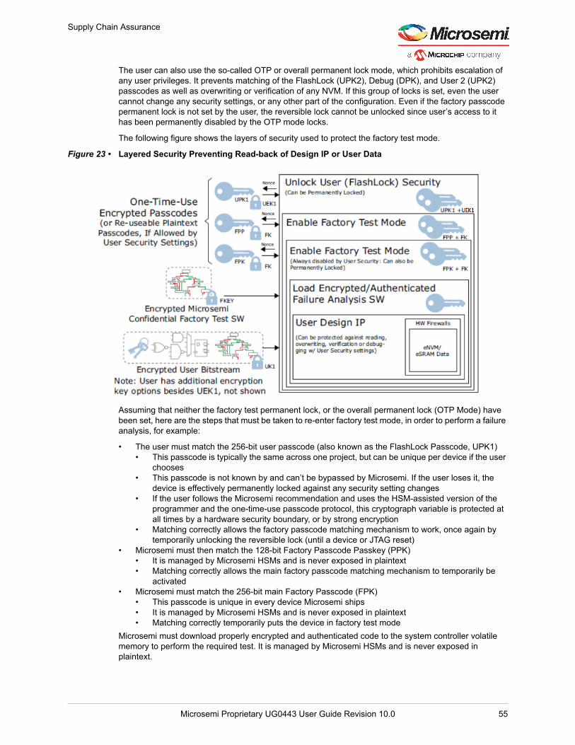
Supply Chain Assurance
The user can also use the so-called OTP or overall permanent lock mode, which prohibits escalation of any user privileges. It prevents matching of the FlashLock (UPK2), Debug (DPK), and User 2 (UPK2) passcodes as well as overwriting or verification of any NVM. If this group of locks is set, even the user cannot change any security settings, or any other part of the configuration. Even if the factory passcode permanent lock is not set by the user, the reversible lock cannot be unlocked since user’s access to it has been permanently disabled by the OTP mode locks.
The following figure shows the layers of security used to protect the factory test mode.
Figure 23 • Layered Security Preventing Read-back of Design IP or User Data
Assuming that neither the factory test permanent lock, or the overall permanent lock (OTP Mode) have been set, here are the steps that must be taken to re-enter factory test mode, in order to perform a failure analysis, for example:
• The user must match the 256-bit user passcode (also known as the FlashLock Passcode, UPK1)• This passcode is typically the same across one project, but can be unique per device if the user
chooses• This passcode is not known by and can’t be bypassed by Microsemi. If the user loses it, the
device is effectively permanently locked against any security setting changes• If the user follows the Microsemi recommendation and uses the HSM-assisted version of the
programmer and the one-time-use passcode protocol, this cryptograph variable is protected at all times by a hardware security boundary, or by strong encryption
• Matching correctly allows the factory passcode matching mechanism to work, once again by temporarily unlocking the reversible lock (until a device or JTAG reset)
• Microsemi must then match the 128-bit Factory Passcode Passkey (PPK)• It is managed by Microsemi HSMs and is never exposed in plaintext• Matching correctly allows the main factory passcode matching mechanism to temporarily be
activated• Microsemi must match the 256-bit main Factory Passcode (FPK)
• This passcode is unique in every device Microsemi ships• It is managed by Microsemi HSMs and is never exposed in plaintext• Matching correctly temporarily puts the device in factory test mode
Microsemi must download properly encrypted and authenticated code to the system controller volatile memory to perform the required test. It is managed by Microsemi HSMs and is never exposed in plaintext.
Microsemi Proprietary UG0443 User Guide Revision 10.0 55
Supply Chain Assurance
An additional recommended precaution can be taken which makes the passcode matching mechanism even stronger. There is a user lock-bit option that prohibits matching of any of the passcodes in plaintext. This effectively forces the use of the one-time-use encrypted passcode protocol to escalate User or factory privileges. This protocol, only available in SPPS, requires not only the knowledge of the passcode, but also another key, when selected using the appropriate key mode. Thus, in this case, a minimum of 1152 bits of symmetric keying material, split between the user and the factory, must be used to re-enter factory test mode and download test code to the device. A minimum of seven separate authentication and passcode-matching tests have to be passed to enter into the factory test mode.
Microsemi Proprietary UG0443 User Guide Revision 10.0 56
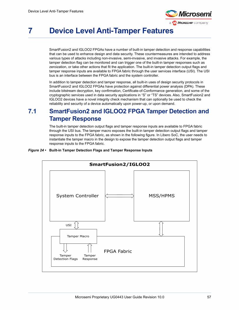
Device Level Anti-Tamper Features
7 Device Level Anti-Tamper Features
SmartFusion2 and IGLOO2 FPGAs have a number of built-in tamper detection and response capabilities that can be used to enhance design and data security. These countermeasures are intended to address various types of attacks including non-invasive, semi-invasive, and invasive attacks. For example, the tamper detection flag can be monitored and can trigger one of the built-in tamper responses such as zeroization, or take other actions that fit the application. The built-in tamper detection output flags and tamper response inputs are available to FPGA fabric through the user services interface (USI). The USI bus is an interface between the FPGA fabric and the system controller.
In addition to tamper detection and tamper response, all built-in uses of design security protocols in SmartFusion2 and IGLOO2 FPGAs have protection against differential power analysis (DPA). These include bitstream decryption, key confirmation, Certificate-of-Conformance generation, and some of the cryptographic services used in data security applications in “S” or “TS” devices. Also, SmartFusion2 and IGLOO2 devices have a novel integrity check mechanism that can optionally be used to check the reliability and security of a device automatically upon power-up, or upon demand.
7.1 SmartFusion2 and IGLOO2 FPGA Tamper Detection and Tamper ResponseThe built-in tamper detection output flags and tamper response inputs are available to FPGA fabric through the USI bus. The tamper macro exposes the built-in tamper detection output flags and tamper response inputs to the FPGA fabric, as shown in the following figure. In Libero SoC, the user needs to instantiate the tamper macro in the design to expose the tamper detection output flags and tamper response inputs to the FPGA fabric.
Figure 24 • Built-in Tamper Detection Flags and Tamper Response Inputs
SmartFusion2/IGLOO2
System Controller MSS/HPMS
FPGA Fabric
Tamper Macro
Tamper Detection Flags
Tamper Response
USI
Microsemi Proprietary UG0443 User Guide Revision 10.0 57
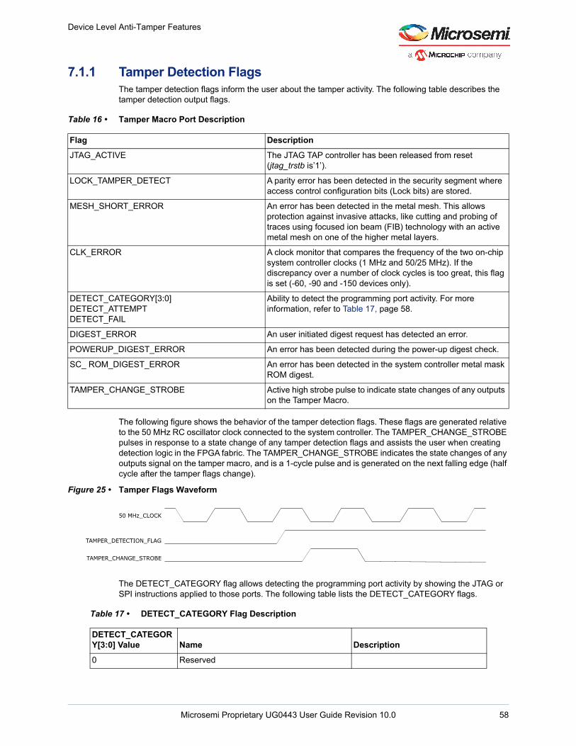
Device Level Anti-Tamper Features
7.1.1 Tamper Detection FlagsThe tamper detection flags inform the user about the tamper activity. The following table describes the tamper detection output flags.
The following figure shows the behavior of the tamper detection flags. These flags are generated relative to the 50 MHz RC oscillator clock connected to the system controller. The TAMPER_CHANGE_STROBE pulses in response to a state change of any tamper detection flags and assists the user when creating detection logic in the FPGA fabric. The TAMPER_CHANGE_STROBE indicates the state changes of any outputs signal on the tamper macro, and is a 1-cycle pulse and is generated on the next falling edge (half cycle after the tamper flags change).
Figure 25 • Tamper Flags Waveform
The DETECT_CATEGORY flag allows detecting the programming port activity by showing the JTAG or SPI instructions applied to those ports. The following table lists the DETECT_CATEGORY flags.
Table 16 • Tamper Macro Port Description
Flag Description
JTAG_ACTIVE The JTAG TAP controller has been released from reset (jtag_trstb is’1’).
LOCK_TAMPER_DETECT A parity error has been detected in the security segment where access control configuration bits (Lock bits) are stored.
MESH_SHORT_ERROR An error has been detected in the metal mesh. This allows protection against invasive attacks, like cutting and probing of traces using focused ion beam (FIB) technology with an active metal mesh on one of the higher metal layers.
CLK_ERROR A clock monitor that compares the frequency of the two on-chip system controller clocks (1 MHz and 50/25 MHz). If the discrepancy over a number of clock cycles is too great, this flag is set (-60, -90 and -150 devices only).
DETECT_CATEGORY[3:0]DETECT_ATTEMPTDETECT_FAIL
Ability to detect the programming port activity. For more information, refer to Table 17, page 58.
DIGEST_ERROR An user initiated digest request has detected an error.
POWERUP_DIGEST_ERROR An error has been detected during the power-up digest check.
SC_ ROM_DIGEST_ERROR An error has been detected in the system controller metal mask ROM digest.
TAMPER_CHANGE_STROBE Active high strobe pulse to indicate state changes of any outputs on the Tamper Macro.
Table 17 • DETECT_CATEGORY Flag Description
DETECT_CATEGORY[3:0] Value Name Description
0 Reserved
50 MHz_CLOCK
TAMPER_DETECTION_FLAG
TAMPER_CHANGE_STROBE
Microsemi Proprietary UG0443 User Guide Revision 10.0 58
Device Level Anti-Tamper Features
The following figure shows the behavior of the DETECT_CATEGORY and DETECT_ATTEMPT flags. The DETECT_CATEGORY flags are set first on the positive edge of 50 MHz RC oscillator clock based on the JTAG or SPI port activity. The DETECT_ATTEMPT flag is set next on the positive edge of the 50 MHz RC oscillator clock. The DETECT_CATEGORY flag is valid at the time the DETECT_ATTEMPT is asserted. After several cycles the DETECT_ATTEMPT flag is cleared. The TAMPER_CHANGE_STROBE which indicates the state changes of the DETECT_CATEGORY or DETECT_ATTEMPT flags is a 1-cycle pulse and is generated on the next falling edge after DETECT_CATEGORY or DETECT_ATTEMPT flags are asserted (half cycle after the DETECT_CATEGORY or DETECT_ATTEMPT flags change).
1 BUFFER_ACCESS The flag is asserted when read/write access is performed tosystem controller’s shared buffer using JTAG/SPI interface. Theshared buffer holds the data requested by JTAG/SPI instructions
2 DEBUG This flag is asserted when debug instruction executed
3 CHECK_DIGESTS This flag is asserted when an external digest check has beenrequested
4 ECC_SETUP_INSTRUCTION This flag is asserted when elliptic curve slave instructions havebeen used
5 RESERVED
6 KEY_VALIDATION This flag is asserted when key validation protocol is requested
7 RESERVED
8 PASSCODE_MATCH This flag is asserted when an attempt has made to match apasscode
9 PASSCODE_SETUP_INSTRUCTION This flag is asserted when the one-time-passcode protocol isinitiated
10 PROGRAMMING This flag is asserted when an external programming instructionhas been used
11 PUBLIC_INFORMATION This flag is asserted when a request for device public informationis issued
12 PUF_KEY_MANAGEMENT The flag is asserted when the PUF key management instructions are executed
13 Reserved
14 Reserved
15 ZEROIZATION_RECOVERY This flag is asserted when a zeroization recovery has beenattempted
Table 17 • DETECT_CATEGORY Flag Description
Microsemi Proprietary UG0443 User Guide Revision 10.0 59
Device Level Anti-Tamper Features
Figure 26 • DETECT_CATEGORY Flags Waveform
The following figure shows the behavior of the DETECT_FAIL flag. The DETECT_FAIL flag is set next on the positives edge of the 50 MHz RC oscillator clock.
Note: The DETECT_CATEGORY flag is not valid at the time the DETECT_FAIL is asserted.
After several cycles the DETECT_FAIL flag is cleared. The TAMPER_CHANGE_STROBE which indicates the state changes of the DETECT_FAIL flag is a 1-cycle pulse and is generated on the next falling edge after DETECT_FAIL flag is asserted (half cycle after the DETECT_FAIL flag change).
Figure 27 • DETECT_FAIL Flags Waveform
7.1.2 Tamper ResponseSmartFusion2 and IGLOO2 FPGAs have four built-in tamper responses that can be triggered through the USI bus connected to the FPGA Fabric. Table 18, page 60 summarizes the built-in tamper responses.
Commanding tamper responses, such as zeroization, must always be done by the user design. There are no built-in triggers that automatically command zeroization or any of the other built-in tamper penalties. The built-in tamper flags should be as the inputs into the user logic or firmware that makes the decision to zeroize or respond to the tamper activity. The user can include other tamper detectors as part of their hardware or software design. For example, the JTAG inputs can be monitored by a user design via the UJTAG FPGA macro. It is expected that in many cases additional tamper detection inputs are provided as external inputs to the FPGA from outside sources, such as detecting that a volume protection scheme has been compromised or that the power supply voltage is likely being tampered with.
7.1.3 LOCKDOWN_ALL_NThe LOCKDOWN_ALL_N response causes all the user lock-bits to behave as if they are locked. This signal is available through the tamper macro. As long as this signal is asserted, the device will not respond to any programming command that can be blocked by a lock-bit, or perform any cryptographic service. All erase, write, and verify programming operations are blocked. Also, it will prevent all eSRAM, eNVM, and MDDR memory read or writes accesses. Refer to FlashLock Passcode Security (256-bit), page 34 for details on the effect of setting the lock-bits.
To restart the device after lock down, the FPGA fabric design must de-assert LOCKDOWN_ALL_N and this must be followed by resetting the MSS in SmartFusion2 or HPMS in IGLOO2.
Note: This lock down feature is incompatible with the zeroize feature, and must be de-asserted before zeroize is triggered or zeroization does not take effect.
Table 18 • Built-in Tamper Response Options
Response Polarity Description
LOCKDOWN_ALL_N Active low Activate all locking mechanisms
DISABLE_ALL_IOS_N Active low All I/Os are disabled and tri-state
RESET_N Active low Reset system controller
ZEROIZE _N Active low Destroy stored data as per security settings
50 MHz_CLOCK
TAMPER_CHANGE_STROBE
DETECT_ATTEMPT
OLD NEWDETECT_CATEGORY [3:0]
50 MHz_RCOSC
TAMPER_CHANGE_STROBE
DETECT_FAIL
OLDDETECT_CATEGORY [3:0]
Microsemi Proprietary UG0443 User Guide Revision 10.0 60
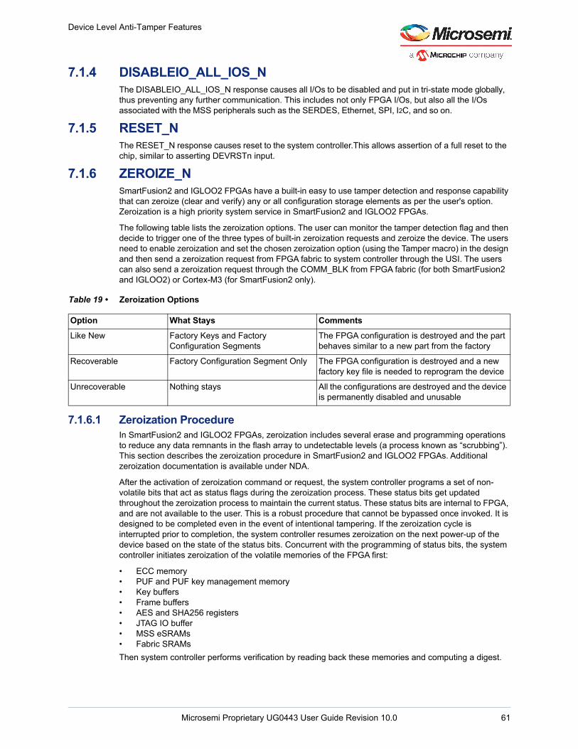
Device Level Anti-Tamper Features
7.1.4 DISABLEIO_ALL_IOS_NThe DISABLEIO_ALL_IOS_N response causes all I/Os to be disabled and put in tri-state mode globally, thus preventing any further communication. This includes not only FPGA I/Os, but also all the I/Os associated with the MSS peripherals such as the SERDES, Ethernet, SPI, I2C, and so on.
7.1.5 RESET_NThe RESET_N response causes reset to the system controller.This allows assertion of a full reset to the chip, similar to asserting DEVRSTn input.
7.1.6 ZEROIZE_NSmartFusion2 and IGLOO2 FPGAs have a built-in easy to use tamper detection and response capability that can zeroize (clear and verify) any or all configuration storage elements as per the user's option. Zeroization is a high priority system service in SmartFusion2 and IGLOO2 FPGAs.
The following table lists the zeroization options. The user can monitor the tamper detection flag and then decide to trigger one of the three types of built-in zeroization requests and zeroize the device. The users need to enable zeroization and set the chosen zeroization option (using the Tamper macro) in the design and then send a zeroization request from FPGA fabric to system controller through the USI. The users can also send a zeroization request through the COMM_BLK from FPGA fabric (for both SmartFusion2 and IGLOO2) or Cortex-M3 (for SmartFusion2 only).
7.1.6.1 Zeroization ProcedureIn SmartFusion2 and IGLOO2 FPGAs, zeroization includes several erase and programming operations to reduce any data remnants in the flash array to undetectable levels (a process known as “scrubbing”). This section describes the zeroization procedure in SmartFusion2 and IGLOO2 FPGAs. Additional zeroization documentation is available under NDA.
After the activation of zeroization command or request, the system controller programs a set of non- volatile bits that act as status flags during the zeroization process. These status bits get updated throughout the zeroization process to maintain the current status. These status bits are internal to FPGA, and are not available to the user. This is a robust procedure that cannot be bypassed once invoked. It is designed to be completed even in the event of intentional tampering. If the zeroization cycle is interrupted prior to completion, the system controller resumes zeroization on the next power-up of the device based on the state of the status bits. Concurrent with the programming of status bits, the system controller initiates zeroization of the volatile memories of the FPGA first:
• ECC memory• PUF and PUF key management memory• Key buffers• Frame buffers• AES and SHA256 registers• JTAG IO buffer• MSS eSRAMs• Fabric SRAMs
Then system controller performs verification by reading back these memories and computing a digest.
Table 19 • Zeroization Options
Option What Stays Comments
Like New Factory Keys and Factory Configuration Segments
The FPGA configuration is destroyed and the part behaves similar to a new part from the factory
Recoverable Factory Configuration Segment Only The FPGA configuration is destroyed and a new factory key file is needed to reprogram the device
Unrecoverable Nothing stays All the configurations are destroyed and the device is permanently disabled and unusable
Microsemi Proprietary UG0443 User Guide Revision 10.0 61
Device Level Anti-Tamper Features
After the volatile memories of the FPGA are zeroized, the non-volatile memory segments are destroyed starting with eNVM. Finally, the FPGA flash configuration array, user security segments, and factory security segments (if applicable, depending on the zeroization option selected) are erased. After all relevant memories are cleared and scrubbed; the system controller performs a read back operation on the memory segments and calculates a digest for volatile memories, eNVM, security segments, and the fabric configuration flash. After both the erase and verify portions of zeroization are complete, a secure protocol confirms zeroization is completed successfully.
In SmartFusion2, the Cortex-M3 is held in reset during the entire zeroization process. The zeroization system service does not zeroize the instruction cache as there is no physical path for the system controller to do so. If it is desired to clear the Cortex-M3 instruction cache, this should be done by the user from the Cortex-M3 before the zeroization command is asserted. In addition, if the user locks the fabric access, the user is responsible for clearing the particular LSRAM or uSRAM.
Certain internal states of the system controller must remain active during the zeroization process, which the system controller controls, and are not erased unless until the device power is removed. These state variables do not contain any sensitive data such as crypto-variables.
After the internal zeroization process has completed and been verified by the device, a certificate containing un-forgeable authenticated data that contains the device serial number and additional data that proves the part is successfully zeroized can be generated. This data can optionally be read out of the FPGA by the user’s system using the JTAG or SPI interface after zeroization is completed. (This “certificate” is different from the X.509 device certificate.) Un-keyed portions of this certificate can be examined to verify that zeroization is successful; i.e., all verified memories are in a known state such as all zeroes or all ones. A cryptographic validation of this certificate can be performed by the user with the Microsemi-supplied HSM-assisted programmer (as part of the optional Secure Production Programming Solution, SPPS), or by Microsemi at their headquarters, that detects any replayed or otherwise forged certificates.
7.1.6.2 “Like New” Zeroization ModeThe first zeroization option is Like New, which destroys all the user programmed configuration data (that is, it erases the user design information). This mode erases the device into a new device state. In other words, the device behaves the way it was when it was shipped from Microsemi originally, with no user design or user key information stored and is immediately ready for programming by the user. There is almost no logistical impact beyond reprogramming the device to get it back into operation.
Selecting the Like New zeroization mode may not be advisable for some high security applications because, like a new part, once zeroized the part can be reprogrammed by whoever has access to it.
The like new zeroization mode is useful when devices go through repeated zeroization, such as when an information assurance device is being intentionally erased after a mission, for routine re-keying.
One consideration with frequent use of zeroization is the number of erase/write cycles being applied to the configuration NVM. Because of the scrubbing process, each zeroization and subsequent reprogramming uses several erase/write cycles. However, the device guaranteed reliability for 20 years after the last programming cycle is valid only if the number of rated erase/write cycles is not exceeded, please refer to DS0128: IGLOO2 and SmartFusion2 Datasheet for the maximum programming cycles allowed. If the programming cycles exceed, either the reliability at 20 years is degraded, or the rated reliability can only be achieved for a fewer number of years based on the usage. In cases where the device is being zeroized and reprogrammed frequently it may not be required for the device to retain a configuration for a full 20 years, since it will be reprogrammed again before that time is up. Number of programming cycles that are performed can be queried using one of the available device information services. The information of number of programming cycles is available with the data that is erased during zeroization. Thus, the user externally keeps track of the number of times a device is programmed
7.1.6.3 Recoverable Zeroization ModeIf the recoverable zeroization option is activated, a number of the factory keys are erased by clearing the factory keys segment in its entirety. This is in addition to the programming data erased in the “Like New Zeroization Mode”. The factory keys that are erased include:
• Factory key (FK)• Default key-loading key (KLK)
Microsemi Proprietary UG0443 User Guide Revision 10.0 62
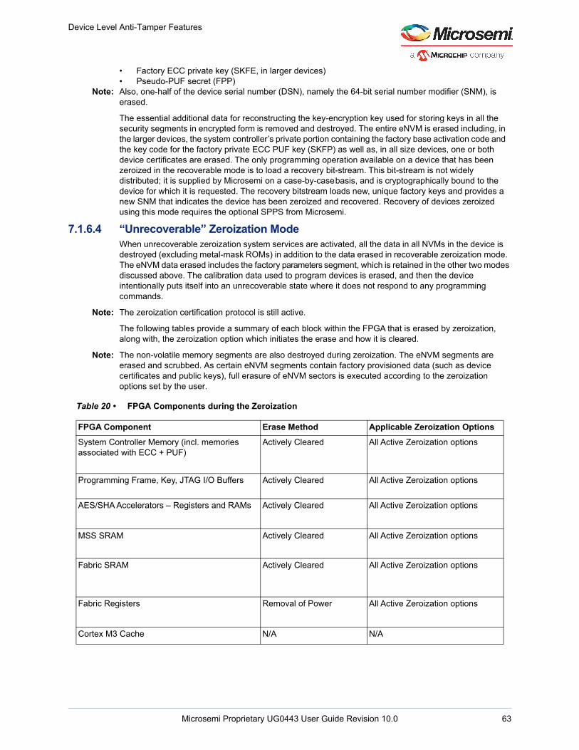
Device Level Anti-Tamper Features
• Factory ECC private key (SKFE, in larger devices)• Pseudo-PUF secret (FPP)
Note: Also, one-half of the device serial number (DSN), namely the 64-bit serial number modifier (SNM), is erased.
The essential additional data for reconstructing the key-encryption key used for storing keys in all the security segments in encrypted form is removed and destroyed. The entire eNVM is erased including, in the larger devices, the system controller’s private portion containing the factory base activation code and the key code for the factory private ECC PUF key (SKFP) as well as, in all size devices, one or both device certificates are erased. The only programming operation available on a device that has been zeroized in the recoverable mode is to load a recovery bit-stream. This bit-stream is not widely distributed; it is supplied by Microsemi on a case-by-case basis, and is cryptographically bound to the device for which it is requested. The recovery bitstream loads new, unique factory keys and provides a new SNM that indicates the device has been zeroized and recovered. Recovery of devices zeroized using this mode requires the optional SPPS from Microsemi.
7.1.6.4 “Unrecoverable” Zeroization ModeWhen unrecoverable zeroization system services are activated, all the data in all NVMs in the device is destroyed (excluding metal-mask ROMs) in addition to the data erased in recoverable zeroization mode. The eNVM data erased includes the factory parameters segment, which is retained in the other two modes discussed above. The calibration data used to program devices is erased, and then the device intentionally puts itself into an unrecoverable state where it does not respond to any programming commands.
Note: The zeroization certification protocol is still active.
The following tables provide a summary of each block within the FPGA that is erased by zeroization, along with, the zeroization option which initiates the erase and how it is cleared.
Note: The non-volatile memory segments are also destroyed during zeroization. The eNVM segments are erased and scrubbed. As certain eNVM segments contain factory provisioned data (such as device certificates and public keys), full erasure of eNVM sectors is executed according to the zeroization options set by the user.
Table 20 • FPGA Components during the Zeroization
FPGA Component Erase Method Applicable Zeroization Options
System Controller Memory (incl. memories associated with ECC + PUF)
Actively Cleared All Active Zeroization options
Programming Frame, Key, JTAG I/O Buffers Actively Cleared All Active Zeroization options
AES/SHA Accelerators – Registers and RAMs Actively Cleared All Active Zeroization options
MSS SRAM Actively Cleared All Active Zeroization options
Fabric SRAM Actively Cleared All Active Zeroization options
Fabric Registers Removal of Power All Active Zeroization options
Cortex M3 Cache N/A N/A
Microsemi Proprietary UG0443 User Guide Revision 10.0 63

Device Level Anti-Tamper Features
For more information about how to use zeroization feature in SmartFusion2 and IGLOO2 FPGAs, refer to Zeroization Procedure, page 61.
7.1.6.5 Zeroization Recovery Process After zeroization using the recoverable” mode, the factory keys (and all user data) are not available and the part cannot be reprogrammed with new user keys or other bitstreams until a new set of factory keys is loaded. A post-zeroization recovery request is generated by the device and read out using the Microsemi programming tool (the SPPS). It contains un-forgeable authenticated encrypted information that proves to Microsemi that the device is genuine, and that it has been completely zeroized, along with the globally-unique remaining half of the serial number and a random nonce. When this request certificate is validated by Microsemi, an encrypted recovery bitstream is generated that can only be authenticated, decrypted, and loaded into that one device.
When recovery takes place all the new keys (FK, KLK, plus SKFE in -60, -090 and -150 devices), the new device certificate(s), and the serial number modifier (SNM) are reloaded with the special bitstream from Microsemi.
7.1.6.6 Using Zeroization to Decommission DevicesUser may have a requirement to decommission the devices. One scenario would be a new system that is not meeting all its specifications. Another scenario would be at the end of the useful life of the system. Ideally, decommissioning reduces the already low risk of valuable intellectual property or secrets such as cryptographic keys from being extracted to completely negligible values.
Zeroization can be used as part of a decommissioning process. Microsemi can supply a special bitstream for each type of device whose sole purpose is to zeroize the device using the “unrecoverable” zeroization mode, on the next reset. Successful loading of the program can be proven by the C-o-C mechanism (if the optional SPPS, is used). After that the device is reset or power-cycled, and it goes through the zeroization process till it is used. Even if power is interrupted during the zeroization process, when the power is reapplied the zeroization process restarts.
Fabric Configuration Flash Cells Erased + Scrubbed by zeorization command
All Active Zeroization options
Table 21 • Security Segments during the Zeroization
FPGA Component Erase Method Applicable Zeroization Options
Security Segment – User Lock bits Actively Cleared + Scrubbed
All Active Zeroization options
Security Segment – User Keys (UEK1&2, Passkeys)
Actively Cleared + Scrubbed
All Active Zeroization options
Security Segment - Factory Keys Actively Cleared + Scrubbed
Recoverable, Unrecoverable Zeroization Options
Security Segment – Factory Parameter Segment
Actively Cleared + Scrubbed
Unrecoverable Zeroization Option
eNVM – Factory Data Actively Cleared + Scrubbed
Recoverable, Unrecoverable Zeroization Options
Table 20 • FPGA Components during the Zeroization
Microsemi Proprietary UG0443 User Guide Revision 10.0 64
Device Level Anti-Tamper Features
After zeroization is complete, the device can be queried for a “certificate” that proves that all the memories are in a known safe state. It can be queried via JTAG/SPI-Slave using FETCH_ZEROIZATION_RESULT command or DEVICE_INFO command that prints the information if the device is zeroized. This instruction returns a HASH and a VALIDATOR. The HASH is an expected plaintext value that can be verified visually or by any tool. The VALIDATOR part of the certificate is an un-forgeable keyed authentication tag that can be verified manually by Microsemi.
In some cases, where devices are partially or completely failed, the decommissioning process may fail. In this case, the process used to decommission devices depends upon the level of certainty the legitimate user’s requirements have. For instance, the user may require all such parts be physically returned to him to for disposition. In an alternate scenario the user trusts his agents to dispose of a number of failed devices, so long as the percentage of such devices is within the tolerable limits.
The goal of the automated decommissioning process is to reduce the number of devices requiring special handling by offering an alternate low-cost high-assurance method to decommission and account for most devices in a less-trusted environment such as a factory floor or a repair depot.
7.1.6.7 Zeroizing Only Crypto-Variables (CVs)The Microsemi built-in zeroization mode options are all designed to destroy the User’s user’s design configuration, and design security keys and security settings.If the zeroization mode is desired to perform a more surgical destruction of just the most sensitive data such as data security keys, without erasing the user’s design or bitstream keys, then it is recommended that the user’s application be programmed to do it. For example, SmartFusion2 and IGLOO2 have a feature called hardware firewalls that allow certain regions of memory to be protected with hardware-level security. The hardware firewalls’ features are ideal for setting up safer memory locations where crypto-variables can be stored. A user application can be designed to zeroize just these portions of memory.
Larger devices (-60, -090 and -150 devices) have the SRAM-PUF feature. This is the best possible key storage mechanism in these devices, and holds good for any silicon device currently being produced. The system controller provides a range of system services for managing these keys, including commands for deleting their individual key codes, and also for deleting the base activation code. When key codes or activation codes are erased, the system service command verifies that the operation is successful by reading back the memory locations and confirming they are all zero. If the values are not equal to zero, the command status shows failure, and the user’s design may retry or take other corrective action. The activation code and key codes are not sensitive cryptographic variables. Zeroizing Only Crypto-Variables (CVs) is just another added layer of security to prevent any attacks against the PUF-protected keys
7.2 Differential Power or Side-Channel Analysis ResistanceDPA is an analysis technique that relies upon multiple measurements of a security device's instantaneous power consumption in order to recreate a secret being manipulated inside the device. SmartFusion2 and IGLOO2 FPGAs are the first devices in the PLD industry incorporating DPA countermeasures to protect the bitstream keys from discovery using side-channel analysis. Generally, the DPA techniques use statistical methods to amplify the effects of small unintentional leakages of the secret information in power consumption measurements, buried in large amounts of noise. For example, if the same secret key is used to process multiple independent blocks of data, a DPA attack may be mounted to determine the secret key used anywhere from a handful of power consumption traces to over a million, depending upon the magnitude of the leak, the amount of noise which may be obscuring the secret data, and which countermeasures are being used. In SmartFusion2 and IGLOO2 FPGAs, all built-in uses of design security protocols have protection against DPA. These include bitstream decryption, key confirmation, Certificate-of-Conformance generation, and so on. In addition, some of the cryptographic services used in data security applications in “S” or “TS” devices have DPA resistance.
Microsemi Proprietary UG0443 User Guide Revision 10.0 65
Device Level Anti-Tamper Features
Figure 28 • DPA Logo
The seven protocols used for design security purposes have been assessed with respect to their DPA resistance by an independent third-party security laboratory, Riscure, which has been accredited by Cryptography Research Inc. (CRI)/Rambus to perform such assessments. Based on Riscure’s assessment, which includes both physical side channel current, EMI (Electromagnetic Interference) measurement and review of the protocol designs, all SmartFusion2 and IGLOO2 FPGAs design security protocols have been certified by CRI under the Countermeasures Validation Program (CVP) scheme. Microsemi is allowed to use the CRI DPA “Padlock” security logo, shown here in association with these products. The seven protocols included in the assessment are the:
• Bitstream Loading Protocol, BSP• Bitstream Authentication Service, BAS• Key Verification Protocol, KVP• Plaintext Passcode Matching & Privilege Escalation, PTP• One-Time • Passcode, OTP• Device Certificate Service DCS• Pseudo-PUF Challenge/Response Service, PPS
The underlying cryptographic primitives (AES, ECC, SHA) are also used along with these protocols.
7.3 CRI Pass-Through DPA Patent LicenseSide-channel attacks, using Differential Power Analysis (DPA) and related attacks such as Differential Electro-Magnetic Analysis (DEMA), can be mitigated by using Cryptographic Research Incorporated (CRI, now a division of Rambus) DPA-resistant technology. Microsemi has obtained a license from CRI for the DPA patent portfolio, consisting of more than fifty patents. In the “S” or “TS” version of SmartFusion2 and IGLOO2 FPGAs, the CRI patent portfolio license is extended to the end users of the devices for use in their data security applications. The buyers of these devices may use CRI's current and future patented techniques in the intellectual property (IP) they purchase from licensed third parties, many of whom are Microsemi partners, or use the techniques in IP they develop, without having to obtain an additional license from CRI. In effect, Microsemi pre-pays the CRI royalty on these selected devices. Once paid; the CRI patented techniques can be used in any design configuration downloaded to those specific devices. The patented techniques may be implemented in the FPGA fabric or the firmware running on the ARM Cortex-M3 processor
7.4 Fabric Configuration and eNVM Integrity TestsSmartFusion2 and IGLOO2 devices have a number of methods that are used at different times to verify the device configuration.
7.4.1 Legacy Verification Method – Resubmitting BitstreamThe first method is the legacy method where the encrypted/authenticated bitstream is resubmitted to the device a second time, after using it the first time for programming the device. When used for verification the bitstream is read, authenticated, and decrypted by the device, but instead of loading the NVM with it, the existing NVM is compared to the incoming bitstream and a pass-fail indication is returned after the whole incoming bitstream has been processed. Only the portions of NVM configured by that particular bitstream are verified.
This method can be prohibited for a specific bitstream when the bitstream is generated and encrypted by the programming tool; or by the device using a lock-bit.
Microsemi Proprietary UG0443 User Guide Revision 10.0 66
Device Level Anti-Tamper Features
7.4.2 Digest-Based Verification MethodThe second method is based on the use of message digests computed using SHA-256. SmartFusion2 and IGLOO2 FPGAs have a novel NVM integrity check mechanism that can optionally be used to check the reliability and security of a device automatically upon power-up, or upon demand. When the bitstream file is prepared, that is, generated and encrypted by the programmer, the data in each bitstream component (for example, FPGA,eNVM eNVM and so on.) is digested and the resulting hash value is retained along with the bitstream file.
During programming of the device all data that the bitstream configures is written into the internal NVM when the bitstream is loaded, and then for each bitstream component a message digest is calculated by the device and exported. Thus, when the programmer actually configures a device it computes the hash values and compares the expected hash values. Unless the bitstream is using variations, the results from all the devices in a project should be identical for each bitstream component. In case of partial programming, only some pages of eNVM are overwritten and only the NVM locations affected are included in the check.
Since no secret keys are required, this comparison can be done by a less-trusted entity such as a contract manufacturer. Conversely, the data is easy to forge, so while the verification provides a good integrity check of what got programmed, it doesn’t really provide security against malicious attacks. One advantage of the digest method over the “resubmit” method is that the bitstream does not need to be loaded and decrypted a second time, therefore it is faster.
A single 256-bit message digest is computed over the entire FPGA fabric and this digest is stored in the security segment. In the devices having only one eNVM controller (-005, -010, -025, -050 and -060 devices), a single eNVM digest is additionally computed and stored in one of the factory-reserved pages at the top of the memory. The devices with two eNVM controllers (-090 and -150 devices) have four 256-bit digests: one for the user portion of the first eNVM array, a second digest for the user portion of the second eNVM array, and finally two more for the portion of the eNVM array that is private to the system controller. Two are used instead of one for the private eNVM for the better usage of system controller so that the portions such as the user SRAM-PUF activation code and key codes that are updated on user’s request can be separate from the parts more closely associated with the factory.
All four eNVM digests are stored in the private region of the eNVM. eNVM pages can be write-protected using the factory write-protect bits, set by the user using the programmer tool when the bitstream is created, thus making them like ROM (read only memory). The digest only includes user eNVM pages that are write-protected. Pages which are not write-protected are assumed to be R/W memory, and may be updated by any un-authorized bus master during run-time.
Please note that the system controller metal-mask ROM also holds a digest of its own contents), that is checked when the system controller boots up.
Microsemi Proprietary UG0443 User Guide Revision 10.0 67
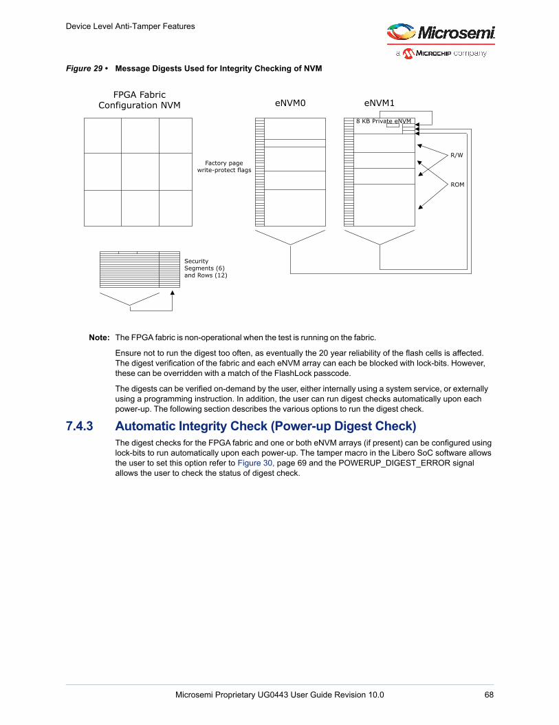
Device Level Anti-Tamper Features
Figure 29 • Message Digests Used for Integrity Checking of NVM
Note: The FPGA fabric is non-operational when the test is running on the fabric.
Ensure not to run the digest too often, as eventually the 20 year reliability of the flash cells is affected. The digest verification of the fabric and each eNVM array can each be blocked with lock-bits. However, these can be overridden with a match of the FlashLock passcode.
The digests can be verified on-demand by the user, either internally using a system service, or externally using a programming instruction. In addition, the user can run digest checks automatically upon each power-up. The following section describes the various options to run the digest check.
7.4.3 Automatic Integrity Check (Power-up Digest Check)The digest checks for the FPGA fabric and one or both eNVM arrays (if present) can be configured using lock-bits to run automatically upon each power-up. The tamper macro in the Libero SoC software allows the user to set this option refer to Figure 30, page 69 and the POWERUP_DIGEST_ERROR signal allows the user to check the status of digest check.
8 KB Private eNVM
eNVM0 eNVM1FPGA Fabric
Configuration NVM
Factory page write-protect flags
Security Segments (6) and Rows (12)
R/W
ROM
Microsemi Proprietary UG0443 User Guide Revision 10.0 68
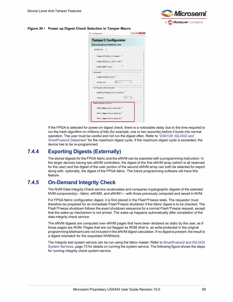
Device Level Anti-Tamper Features
Figure 30 • Power up Digest Check Selection in Tamper Macro
If the FPGA is selected for power-on digest check, there is a noticeable delay due to the time required to run the hash algorithm on millions of bits (for example, one or two seconds) before it boots into normal operation. The user must be careful and not run the digest often. Refer to “DS0128: IGLOO2 and SmartFusion2 Datasheet” for the maximum digest cycle. If the maximum digest cycle is exceeded, the device has to be re-programmed.
7.4.4 Exporting Digests (Externally)The stored digests for the FPGA fabric and the eNVM can be exported with a programming instruction. In the larger devices having two eNVM controllers, the digest of the first eNVM array (which is all reserved for the user) and the digest of the user portion of the second eNVM array can both be selected for export along with, optionally, the digest of the FPGA fabric. The future programming software will have this feature.
7.4.5 On-Demand Integrity CheckThe NVM Data Integrity Check service recalculates and compares cryptographic digests of the selected NVM component(s) - fabric, eNVM0, and eNVM1— with those previously computed and saved in NVM.
For FPGA fabric configuration digest, it is first placed in the Flash*Freeze state. The requestor must therefore be prepared for an immediate Flash*Freeze shutdown if the fabric digest is to be checked. The Flash*Freeze shutdown follows the exact shutdown sequence for a normal Flash*Freeze request, except that the wake-up mechanism is not armed. The wake-up happens automatically after completion of the data integrity check service.
The eNVM digests are computed over eNVM pages that have been declared as static by the user, as if those pages are ROM. Pages that are not flagged as ROM (that is, as write-protected in the original programming bitstream) are not included in the eNVM digest calculation. If no digest is present, the result is a digest mismatch for the requested NVM block.
The Integrity test system service can be run using the fabric master. Refer to SmartFusion2 and IGLOO2 System Services, page 73 for details on running the system service. The following figure shows the steps for running integrity check system service.
Microsemi Proprietary UG0443 User Guide Revision 10.0 69
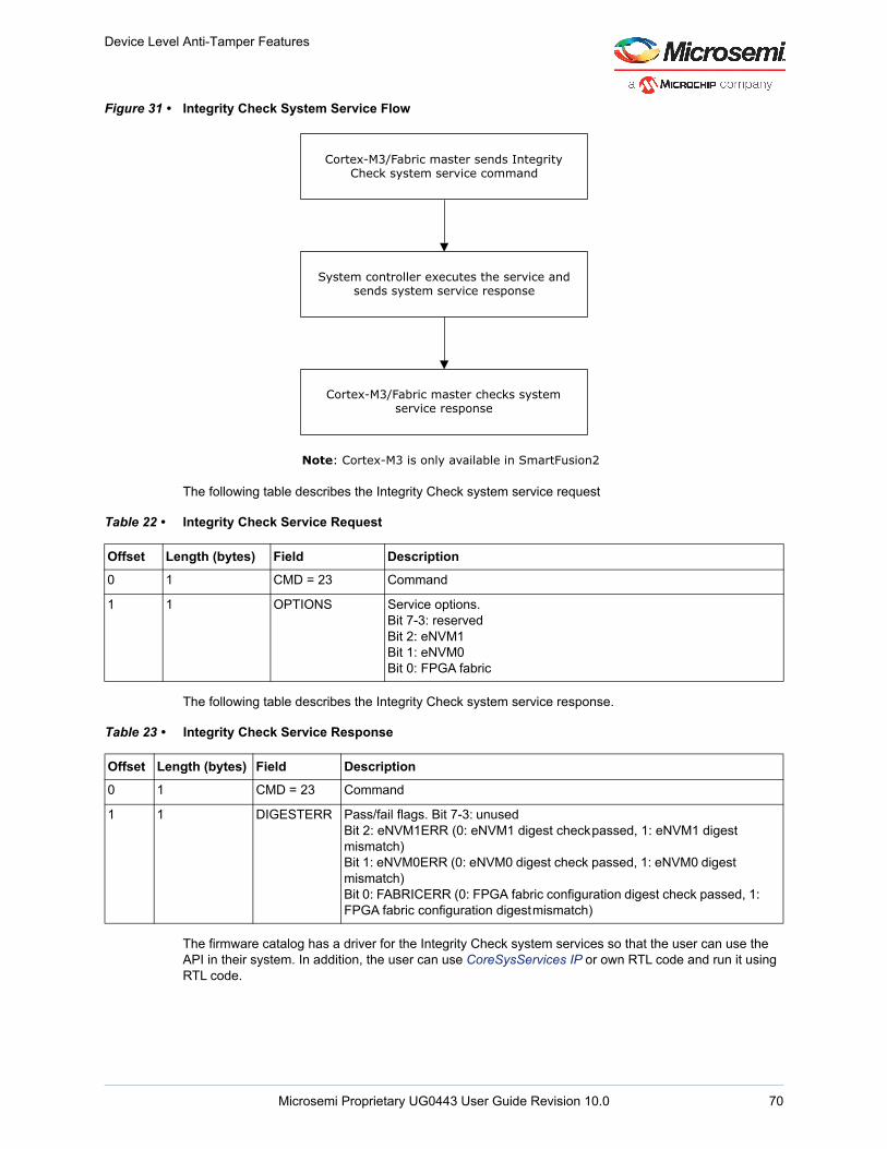
Device Level Anti-Tamper Features
Figure 31 • Integrity Check System Service Flow
The following table describes the Integrity Check system service request
The following table describes the Integrity Check system service response.
The firmware catalog has a driver for the Integrity Check system services so that the user can use the API in their system. In addition, the user can use CoreSysServices IP or own RTL code and run it using RTL code.
Table 22 • Integrity Check Service Request
Offset Length (bytes) Field Description
0 1 CMD = 23 Command
1 1 OPTIONS Service options. Bit 7-3: reservedBit 2: eNVM1Bit 1: eNVM0Bit 0: FPGA fabric
Table 23 • Integrity Check Service Response
Offset Length (bytes) Field Description
0 1 CMD = 23 Command
1 1 DIGESTERR Pass/fail flags. Bit 7-3: unusedBit 2: eNVM1ERR (0: eNVM1 digest check passed, 1: eNVM1 digest mismatch)Bit 1: eNVM0ERR (0: eNVM0 digest check passed, 1: eNVM0 digest mismatch)Bit 0: FABRICERR (0: FPGA fabric configuration digest check passed, 1: FPGA fabric configuration digest mismatch)
Note: Cortex-M3 is only available in SmartFusion2
Cortex-M3/Fabric master sends Integrity Check system service command
System controller executes the service and sends system service response
Cortex-M3/Fabric master checks system service response
Microsemi Proprietary UG0443 User Guide Revision 10.0 70
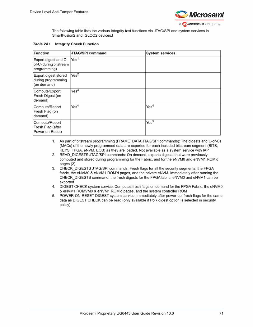
Device Level Anti-Tamper Features
The following table lists the various Integrity test functions via JTAG/SPI and system services in SmartFusion2 and IGLOO2 devices.I
1. As part of bitstream programming (FRAME_DATA JTAG/SPI commands): The digests and C-of-Cs (MACs) of the newly programmed data are exported for each included bitstream segment (BITS, KEYS, FPGA, eNVM, EOB) as they are loaded. Not available as a system service with IAP
2. READ_DIGESTS JTAG/SPI commands: On demand, exports digests that were previously computed and stored during programming for the Fabric, and for the eNVM0 and eNVM1 ROM’d pages (2)
3. CHECK_DIGESTS JTAG/SPI commands: Fresh flags for all the security segments, the FPGA fabric, the eNVM0 & eNVM1 ROM’d pages, and the private eNVM. Immediately after running the CHECK_DIGESTS command, the fresh digests for the FPGA fabric, eNVM0 and eNVM1 can be exported
4. DIGEST CHECK system service: Computes fresh flags on demand for the FPGA Fabric, the eNVM0 & eNVM1 ROMVM0 & eNVM1 ROM’d pages, and the system controller ROM
5. POWER-ON-RESET DIGEST system service: Immediately after power-up, fresh flags for the same data as DIGEST CHECK can be read (only available if PoR digest option is selected in security policy)
Table 24 • Integrity Check Function
Function JTAG/SPI command System services
Export digest and C-of-C (during bitstream programming)
Yes1
Export digest stored during programming (on demand)
Yes2
Compute/Export Fresh Digest (on demand)
Yes3
Compute/Report Fresh Flag (on demand)
Yes4 Yes4
Compute/Report Fresh Flag (after Power-on-Reset)
Yes5
Microsemi Proprietary UG0443 User Guide Revision 10.0 71
Data Security Through System Services
8 Data Security Through System Services
Data security is protecting the information the FPGA is storing, processing, or communicating in its role in the end application. Most of the data security features in SmartFusion2 and IGLOO2 FPGAs are used by running the various system services implemented by the SmartFusion2 and IGLOO2 system controller. The data security features are only available in the “S” or “TS” version of the device. Some of the data security features are only available in the larger devices (-060, -090 and -150 devices). Table 25, page 72 lists the device specific data security features in SmartFusion2 and IGLOO2 FPGAs.
There are some additional data security features, which were explained in the preceding chapters.
Note: During JTAG or SPI-Slave programming, do not run any of the AES/DRBG/ECC Point Multiplication system services. If the user design requests AES/DRBG/Point Multiplication system services when System controller is processing initial component of the bitstream during JTAG or SPI-Slave programming, the system service may corrupt the bitstream information. This issue does not exist in Auto-update, IAP, or programming recovery. If these security system services must be run during programming, you must generate a STAPL/DAT file using Libero 11.8 SP3 or later. Contact [email protected] to use older Libero versions.
The system services can greatly enhance many data security applications. Many moderate performance information assurance applications may be implemented with these services using only minimal additional FPGA resources. The availability of these services can reduce the need for expensive custom
Table 25 • SmartFusion2 and IGLOO2 Data Security Features through System Service
Data Security Features
M2S005S M2S010S/TS M2S025TS M2S050TSM2GL005S M2GL 010S/TS M2GL 025TS M2GL 050TS
M2S060TS M2S090TS M2S150TSM2GL060TS M2GL 090TS M2GL 150TS
Non-Deterministic Random Bit Generator (NRBG) system service x x
AES-128/256 system service (ECB, OFB, CTR, CBC modes) x x
SHA-256 system service x x
HMAC-SHA-256 system service x x
Key Tree system service x x
PUF Emulation (Pseudo-PUF) system service x
SRAM-PUF system services• Create User Activation Code (AC) or Delete User Activation Code
AC Service• Get Number of Key Code (KC) Service• Create User KC for an Intrinsic Key Service• Create User KC for an Extrinsic Key Service• Export all KC Service• Import all KC Service• Delete User KC Service• Fetch a User PUF Key Service• Get a PUF Seed Service
x
Elliptic Curve Cryptography (ECC) system services• ECC Point-Multiplication system service• ECC Point-Addition system service
x
Microsemi Proprietary UG0443 User Guide Revision 10.0 72
Data Security Through System Services
or third-party IP. For example: Quality true random bits are required in many cryptographic (and gaming) applications. Designing a quality NRBG, implemented using conventional FPGA resources such as LUTs (Look-Up Tables) and FFs(Flip_Flops) requires considerable effort both in the original design and in characterizing it over process, voltage, temperature, and life. Similarly, the SRAM-PUF provides a revolutionary set of key management features having the highest security available on almost any integrated circuit, whether an ASIC, ASSP, or FPGA.
8.1 SmartFusion2 and IGLOO2 System ServicesSmartFusion2 and IGLOO2 system services are system controller actions initiated by asynchronous events from the ARM Cortex-M3 processor or a master in the FPGA fabric. Similarly, IGLOO2 system services are system controller actions initiated by asynchronous events from a master in the FPGA fabric. For performance ratings of the various cryptographic system services, refer to the DS0128: SmartFusion2 and IGLOO2 Datasheet. The system services use the Communication Block (COMM_BLK) that interfaces between the MSS/HPMS and system controller. There are two COMM_BLK instances: one in the MSS/HPMS that the user interfaces with and one that communicates with the first one that is located in the system controller. The COMM_BLK consists of an APB interface, eight byte transmit FIFO, and an eight byte receive FIFO. The communication block (COMM_BLK) provides a bidirectional message passing facility between the MSS/HPMS and the system controller.
Microsemi Proprietary UG0443 User Guide Revision 10.0 73
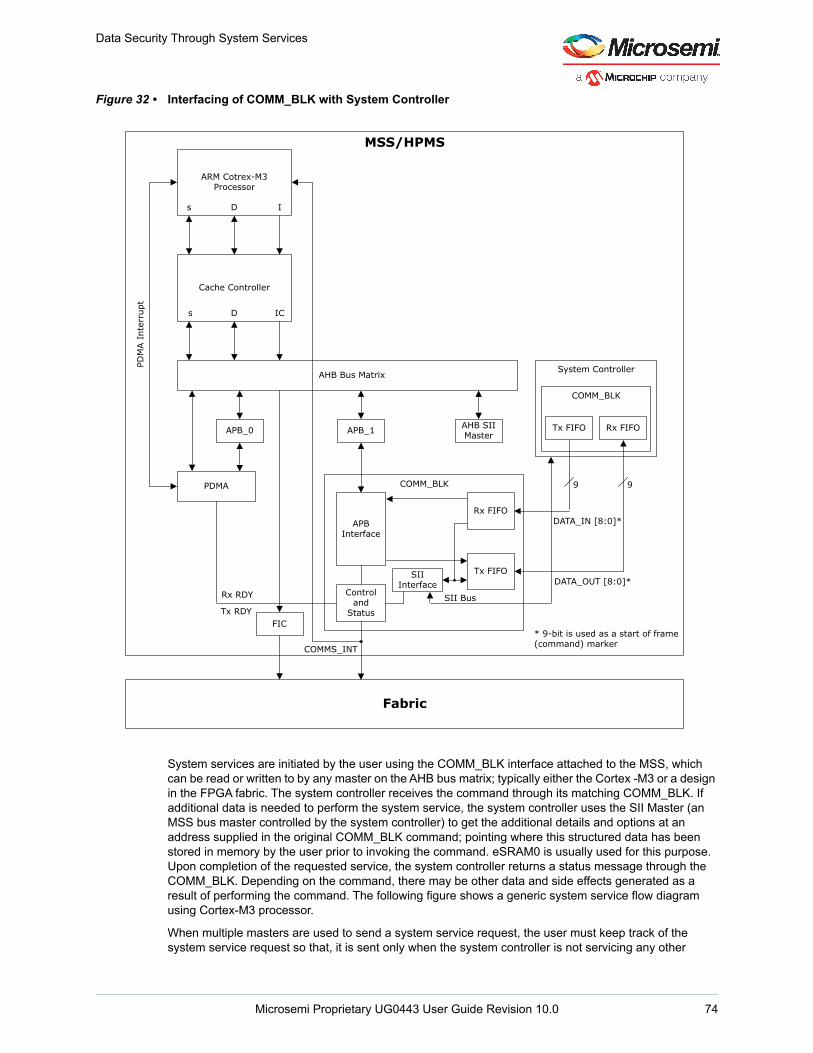
Data Security Through System Services
Figure 32 • Interfacing of COMM_BLK with System Controller
System services are initiated by the user using the COMM_BLK interface attached to the MSS, which can be read or written to by any master on the AHB bus matrix; typically either the Cortex -M3 or a design in the FPGA fabric. The system controller receives the command through its matching COMM_BLK. If additional data is needed to perform the system service, the system controller uses the SII Master (an MSS bus master controlled by the system controller) to get the additional details and options at an address supplied in the original COMM_BLK command; pointing where this structured data has been stored in memory by the user prior to invoking the command. eSRAM0 is usually used for this purpose. Upon completion of the requested service, the system controller returns a status message through the COMM_BLK. Depending on the command, there may be other data and side effects generated as a result of performing the command. The following figure shows a generic system service flow diagram using Cortex-M3 processor.
When multiple masters are used to send a system service request, the user must keep track of the system service request so that, it is sent only when the system controller is not servicing any other
ARM Cotrex-M3 Processor
Cache Controller
s D I
s D IC
AHB Bus Matrix
PDMA
APB_0 APB_1 AHB SII Master
System Controller
Tx FIFO Rx FIFO
COMM_BLK
COMM_BLK
Rx FIFO
SII Interface
Tx FIFO
APB Interface
Control and
StatusFIC
MSS/HPMS
99
DATA_IN [8:0]*
DATA_OUT [8:0]*
SII Bus
COMMS_INT
Fabric
* 9-bit is used as a start of frame (command) marker
PDM
A I
nter
rupt
Rx RDY
Tx RDY
Microsemi Proprietary UG0443 User Guide Revision 10.0 74
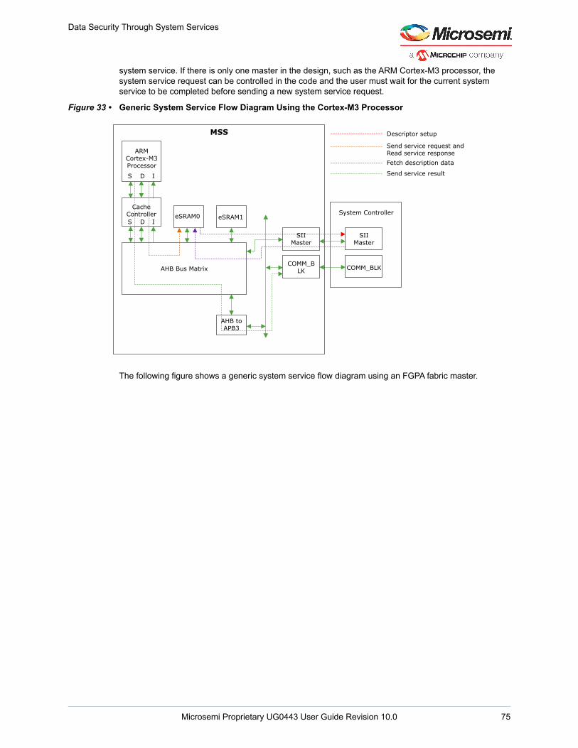
Data Security Through System Services
system service. If there is only one master in the design, such as the ARM Cortex-M3 processor, the system service request can be controlled in the code and the user must wait for the current system service to be completed before sending a new system service request.
Figure 33 • Generic System Service Flow Diagram Using the Cortex-M3 Processor
The following figure shows a generic system service flow diagram using an FGPA fabric master.
AHB Bus Matrix
System Controller
ARMCortex-M3Processor
CacheController eSRAM0 eSRAM1
SIIMaster
COMM_BLK
SIIMaster
COMM_BLK
Descriptor setup
Fetch description data
Send service request and Read service response
Send service resultS D I
S D I
AHB toAPB3
MSS
Microsemi Proprietary UG0443 User Guide Revision 10.0 75
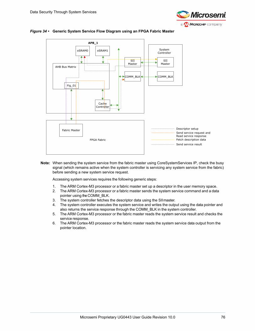
Data Security Through System Services
Figure 34 • Generic System Service Flow Diagram using an FPGA Fabric Master
Note: When sending the system service from the fabric master using CoreSystemServices IP, check the busy signal (which remains active when the system controller is servicing any system service from the fabric) before sending a new system service request.
Accessing system services requires the following generic steps:
1. The ARM Cortex-M3 processor or a fabric master set up a descriptor in the user memory space.2. The ARM Cortex-M3 processor or a fabric master sends the system service command and a data
pointer using the COMM_BLK.3. The system controller fetches the descriptor data using the SII master.4. The system controller executes the system service and writes the output using the data pointer and
also returns the service response through the COMM_BLK in the system controller.5. The ARM Cortex-M3 processor or the fabric master reads the system service result and checks the
service response.6. The ARM Cortex-M3 processor or the fabric master reads the system service data output from the
pointer location.
FPGA Fabric
SystemController
CacheController
SIIMaster
COMM_BLK
SIIMaster
COMM_BLK
Fabric Master Descriptor setup
Fetch description data
Send service request and Read service response
Send service result
APB_1
eSRAM0 eSRAM1
AHB Bus Matrix
Fig_01
Microsemi Proprietary UG0443 User Guide Revision 10.0 76
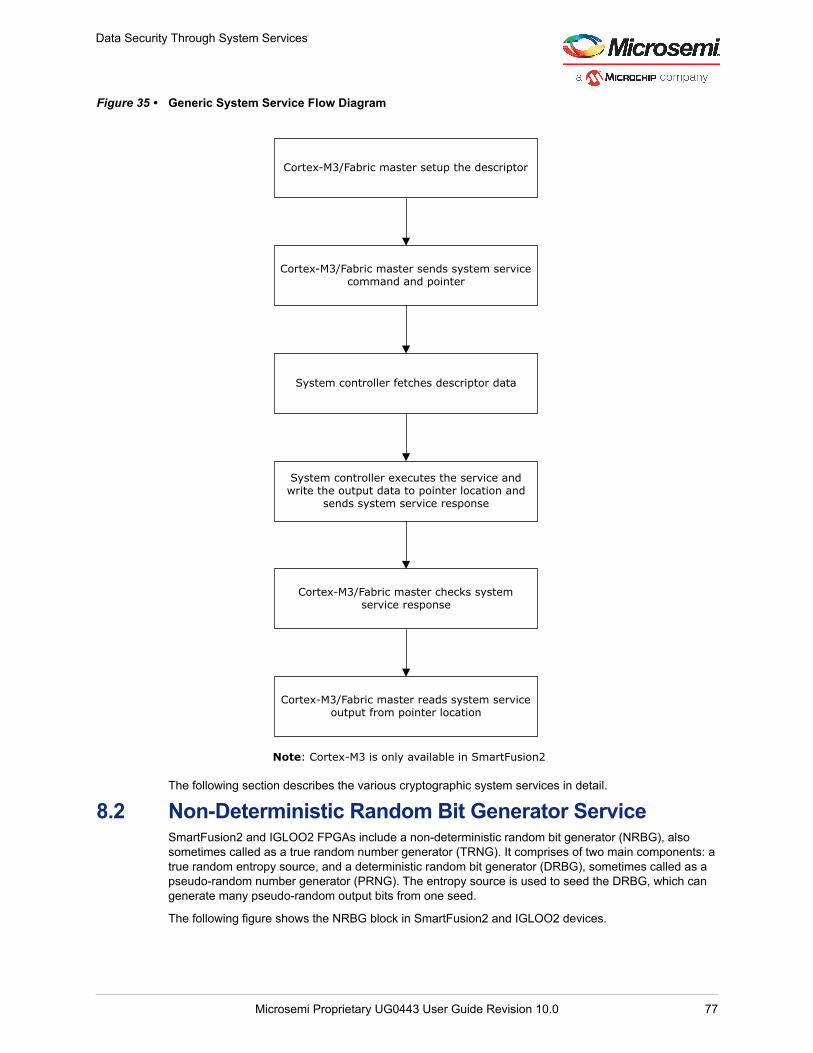
Data Security Through System Services
Figure 35 • Generic System Service Flow Diagram
The following section describes the various cryptographic system services in detail.
8.2 Non-Deterministic Random Bit Generator ServiceSmartFusion2 and IGLOO2 FPGAs include a non-deterministic random bit generator (NRBG), also sometimes called as a true random number generator (TRNG). It comprises of two main components: a true random entropy source, and a deterministic random bit generator (DRBG), sometimes called as a pseudo-random number generator (PRNG). The entropy source is used to seed the DRBG, which can generate many pseudo-random output bits from one seed.
The following figure shows the NRBG block in SmartFusion2 and IGLOO2 devices.
Note: Cortex-M3 is only available in SmartFusion2
Cortex-M3/Fabric master setup the descriptor
Cortex-M3/Fabric master sends system service command and pointer
System controller fetches descriptor data
System controller executes the service and write the output data to pointer location and
sends system service response
Cortex-M3/Fabric master checks system service response
Cortex-M3/Fabric master reads system service output from pointer location
Microsemi Proprietary UG0443 User Guide Revision 10.0 77
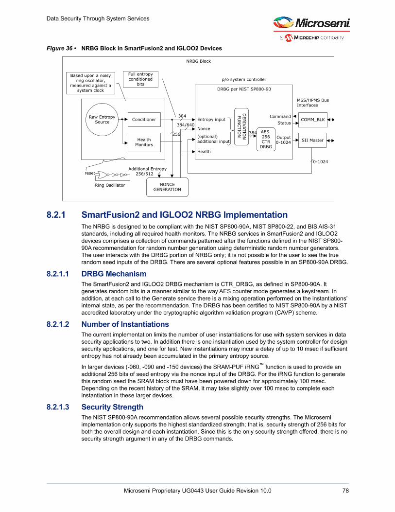
Data Security Through System Services
Figure 36 • NRBG Block in SmartFusion2 and IGLOO2 Devices
8.2.1 SmartFusion2 and IGLOO2 NRBG Implementation The NRBG is designed to be compliant with the NIST SP800-90A, NIST SP800-22, and BIS AIS-31 standards, including all required health monitors. The NRBG services in SmartFusion2 and IGLOO2 devices comprises a collection of commands patterned after the functions defined in the NIST SP800-90A recommendation for random number generation using deterministic random number generators. The user interacts with the DRBG portion of NRBG only; it is not possible for the user to see the true random seed inputs of the DRBG. There are several optional features possible in an SP800-90A DRBG.
8.2.1.1 DRBG MechanismThe SmartFusion2 and IGLOO2 DRBG mechanism is CTR_DRBG, as defined in SP800-90A. It generates random bits in a manner similar to the way AES counter mode generates a keystream. In addition, at each call to the Generate service there is a mixing operation performed on the instantiations’ internal state, as per the recommendation. The DRBG has been certified to NIST SP800-90A by a NIST accredited laboratory under the cryptographic algorithm validation program (CAVP) scheme.
8.2.1.2 Number of InstantiationsThe current implementation limits the number of user instantiations for use with system services in data security applications to two. In addition there is one instantiation used by the system controller for design security applications, and one for test. New instantiations may incur a delay of up to 10 msec if sufficient entropy has not already been accumulated in the primary entropy source.
In larger devices (-060, -090 and -150 devices) the SRAM-PUF iRNG™ function is used to provide an additional 256 bits of seed entropy via the nonce input of the DRBG. For the iRNG function to generate this random seed the SRAM block must have been powered down for approximately 100 msec. Depending on the recent history of the SRAM, it may take slightly over 100 msec to complete each instantiation in these larger devices.
8.2.1.3 Security StrengthThe NIST SP800-90A recommendation allows several possible security strengths. The Microsemi implementation only supports the highest standardized strength; that is, security strength of 256 bits for both the overall design and each instantiation. Since this is the only security strength offered, there is no security strength argument in any of the DRBG commands.
NRBG Block
Based upon a noisy ring oscillator,
measured against a system clock
Raw Entropy Source Conditioner
Health Monitors
DRBG per NIST SP800-90
DER
IVATION
FU
NCTIO
N AES-256 CTR
DRBG
Entropy input
Nonce
(optional) additional input
Health
COMM_BLK
SII Master
p/o system controller
CommandStatus
Output0-1024
NONCE GENERATION
Additional Entropy 256/512
Ring Oscillator
reset
Full entropy conditioned
bits
MSS/HPMS Bus Interfaces
384
384
384/640
256
0-1024
Microsemi Proprietary UG0443 User Guide Revision 10.0 78
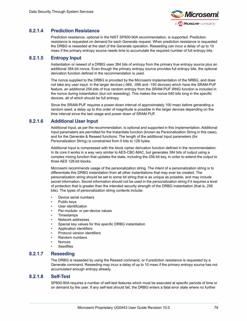
Data Security Through System Services
8.2.1.4 Prediction ResistancePrediction resistance, optional in the NIST SP800-90A recommendation, is supported. Prediction resistance is requested on demand for each Generate request. When prediction resistance is requested the DRBG is reseeded at the start of the Generate operation. Reseeding can incur a delay of up to 10 msec if the primary entropy source needs time to accumulate the required number of full entropy bits.
8.2.1.5 Entropy InputInstantiation or reseed of a DRBG uses 384 bits of entropy from the primary true entropy source plus an additional 384-bit nonce. Even though the primary entropy source provides full entropy bits, the optional derivation function defined in the recommendation is used.
The nonce supplied to the DRBG is provided by the Microsemi implementation of the NRBG, and does not take any user input. In the larger devices (-060, -090 and -150 devices) which have the SRAM-PUF feature, an additional 256-bits of true random entropy from the SRAM-PUF iRNG function is included in the nonce during instantiation (but not reseeding). This makes the nonce 640 bits long in the specific devices, all of which should be full entropy.
Since the SRAM-PUF requires a power-down interval of approximately 100 msec before generating a random seed, a delay up to this order of magnitude is possible in the larger devices depending on the time interval since the last usage and power down of SRAM PUF.
8.2.1.6 Additional User InputAdditional Input, as per the recommendation, is optional and supported in this implementation. Additional Input parameters are permitted for the Instantiate function (known as Personalization String in this case), and for the Generate & Reseed functions. The length of the additional Input parameters (for Personalization String) is constrained from 0 bits to 128 bytes.
Additional Input is compressed with the block cipher derivation function defined in the recommendation. In its core it works in a way very similar to AES-CBC-MAC, but generates 384 bits of output using a complex mixing function that updates the state, including the 256-bit key, in order to extend the output to three AES 128-bit blocks.
Microsemi recommends usage of the personalization string. The intent of a personalization string is to differentiate this DRBG instantiation from all other instantiations that may ever be created. The personalization string should be set to some bit string that is as unique as possible, and may include secret information. Secret information should not be used in the personalization string if it requires a level of protection that is greater than the intended security strength of the DRBG instantiation (that is, 256 bits). The types of personalization string contents include:
• Device serial numbers• Public keys• User identification• Per-module- or per-device values• Timestamps• Network addresses• Special key values for this specific DRBG instantiation• Application identifiers• Protocol version identifiers• Random numbers• Nonces• Seedfiles
8.2.1.7 ReseedingThe DRBG is reseeded by using the Reseed command, or if prediction resistance is requested by a Generate command. Reseeding may incur a delay of up to 10 msec if the primary entropy source has not accumulated enough entropy already.
8.2.1.8 Self-TestSP800-90A requires a number of self-test features which must be executed at specific periods of time or on demand by the user. If any self-test should fail, the DRBG enters a fatal error state where no further
Microsemi Proprietary UG0443 User Guide Revision 10.0 79
Data Security Through System Services
DRBG functions can be executed. Further self-tests are inhibited until the DRBG is reinitialized using the Reset command.
8.2.1.9 Generate SizeThe DRBG computes and outputs random bits using the Generate command. Its output is limited from 0 to 1024 bits (128 bytes) per call.
The following sections describe in the detail steps to run the various NRBG system services in SmartFusion2 and IGLOO2 devices.
8.2.2 Self Test ServiceThis service invokes all DRBG health tests. If any health test fails, a fatal error condition is entered, otherwise the state of the DRBG and all instantiations are not affected. The fatal error condition can only be removed by a device reset or user invocation of the DRBG reset service. The following figure shows the steps for running DRBG Self Test Check system service.
Figure 37 • DRBG Self Test Check System Service Flow
Note: Cortex-M3 is only available in SmartFusion2
Cortex-M3/Fabric master sends DRBG Selftest system service command and pointer
System controller executes the service and sends system service response
Cortex-M3/Fabric master checks system service response
Microsemi Proprietary UG0443 User Guide Revision 10.0 80
Data Security Through System Services
The following three tables provide details about the DRBG Self Test Check system service request, DRBG Self Test Check system service response, and Self Test response status codes, respectively.
8.2.3 Instantiate ServiceThe Instantiate service checks the validity of the input parameters, determines the security strength for the DRBG instantiation, obtains entropy input with entropy sufficient to support the security strength, obtains the nonce (if required), determines the initial internal state using the instantiate algorithm and returns a state handle for the internal state. In SmartFusion2 and IGLOO2 devices, the Instantiate service instantiates a DRBG with an optional personalization string. The personalization string must be in the range between 0-128 bytes, inclusive. An error is displayed from the DRBG if the value of the personalization string is out of range. The following is the flow diagram for DRBG instantiate system service.
Table 26 • DRBG Self Test Check System Service Request
Offset Length (bytes) Field Description
0 1 CMD = 40 Command
Table 27 • DRBG Self Test Check System Service Response
Offset Length (bytes) Field Description
0 1 CMD = 40 Command
1 1 STATUS Command result status (see Table 28, page 81)
Table 28 • DRBG Service Response Status Codes
STATUS Description
0 Success (DRBGHANDLE is valid)
1 Fatal error
2 Maximum instantiations exceeded
3 Invalid handle
4 Generate request too big
5 Maximum length of additional data exceeded
127 HRESP error occurred during MSS/HPMS transfer
253 Not licensed
254 Service disabled by factory security
255 Service disabled by user security
Microsemi Proprietary UG0443 User Guide Revision 10.0 81
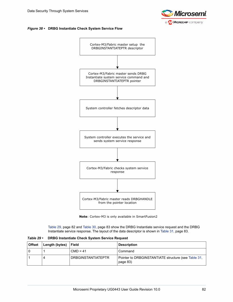
Data Security Through System Services
Figure 38 • DRBG Instantiate Check System Service Flow
Table 29, page 82 and Table 30, page 83 show the DRBG Instantiate service request and the DRBG Instantiate service response. The layout of the data descriptor is shown in Table 31, page 83.
Table 29 • DRBG Instantiate Check System Service Request
Offset Length (bytes) Field Description
0 1 CMD = 41 Command
1 4 DRBGINSTANTIATEPTR Pointer to DRBGINSTANTIATE structure (see Table 31, page 83)
Note: Cortex-M3 is only available in SmartFusion2
Cortex-M3/Fabric master setup the DRBGINSTANTIATEPTR descriptor
Cortex-M3/Fabric master sends DRBG Instantiate system service command and
DRBGINSTANTIATEPTR pointer
System controller fetches descriptor data
System controller executes the service and sends system service response
Cortex-M3/Fabric checks system service response
Cortex-M3/Fabric master reads DRBGHANDLE from the pointer location
Microsemi Proprietary UG0443 User Guide Revision 10.0 82
Data Security Through System Services
8.2.4 Generate ServiceThis service generates a random bit sequence up to 128 bytes long. An error is displayed from the DRBG if this field is out of range. The following figure shows the steps for running DRBG Generate system service.
Table 30 • DRBG Instantiate Check System Service Response
Offset Length (bytes) Field Description
0 1 CMD = 41 Command
1 1 STATUS Command status (see Table 28, page 81)
2 4 DRBGINSTANTIATEPTR Pointer to DRBGINSTANTIATE structure
Table 31 • DRBGINSTANTIATE Data Descriptor Structure
Offset Length (bytes) Field Description
0 4 PER_STRING_PTR Pointer to RBG personalization string
4 1 PER_STRING_LENGTH Length of personalization string in bytes. Length must be in the range 0-128 bytes inclusive.
5 1 RESERVED Reserved
6 1 DRBGHANDLE Returned DRBG handle
Microsemi Proprietary UG0443 User Guide Revision 10.0 83
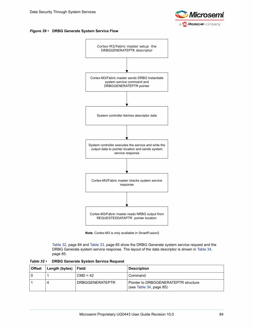
Data Security Through System Services
Figure 39 • DRBG Generate System Service Flow
Table 32, page 84 and Table 33, page 85 show the DRBG Generate system service request and the DRBG Generate system service response. The layout of the data descriptor is shown in Table 34, page 85.
Table 32 • DRBG Generate System Service Request
Offset Length (bytes) Field Description
0 1 CMD = 42 Command
1 4 DRBGGENERATEPTR Pointer to DRBGGENERATEPTR structure (see Table 34, page 85)
Note: Cortex-M3 is only available in SmartFusion2
Cortex-M3/Fabric master setup the DRBGGENERATEPTR descriptor
Cortex-M3/Fabric master sends DRBG Instantiate system service command and DRBGGENERATEPTR pointer
System controller fetches descriptor data
System controller executes the service and write the output data to pointer location and sends system
service response
Cortex-M3/Fabric master checks system service response
Cortex-M3/Fabric master reads NRBG output from REQUESTEDDATAPTR pointer location
Microsemi Proprietary UG0443 User Guide Revision 10.0 84

Data Security Through System Services
8.2.5 Reseed ServiceIn SmartFusion2 and IGLOO2 FPGAs, this service is used to force a Reseed operation. The NIST recommendation (from SP800-90A) is that DRBG must be reseeded after every 248 generate requests. The system controller automatically forces the DRBG to be reseeded after 65535 generate requests. The following is the flow diagram for DRBG Reseed system service.
Table 33 • DRBG Generate System Service Response
Offset Length (bytes) Field Description
0 1 CMD = 42 Command
1 1 STATUS Command status (see Table 28, page 81)
2 4 DRBGGENERATEPTR Pointer to DRBGGENERATE structure
Table 34 • DRBGGENERATE Data Descriptor Structure
Offset Length (bytes) Field Description
0 4 REQUESTEDDATAPTR Pointer to buffer to receive generated random data
4 4 ADDITIONALINPUTPTR Pointer to additional input data
8 1 REQUESTEDLENGTH Number of bytes of random data to generate. Length must be in the range between 0–128 bytes inclusive. An error is displayed from the DRBG if this field is out of range.
9 1 ADDITIONALINPUTLENGTH Length of additional input in bytes. Length must be in the range 0–128 bytes inclusive.
10 1 PRREQ Prediction resistance request. If PRREQ is non-zero, prediction resistance is provided.
11 1 DRBGHANDLE DRBG handle specifies which random bit generator instance is to be used to generate the random data. The value of DRBG handle is obtained as a result of a call to the DRBG Instantiate service.
Microsemi Proprietary UG0443 User Guide Revision 10.0 85
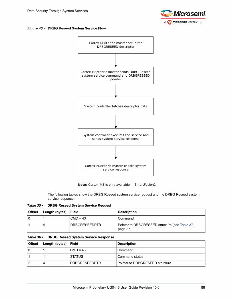
Data Security Through System Services
Figure 40 • DRBG Reseed System Service Flow
The following tables show the DRBG Reseed system service request and the DRBG Reseed system service response.
Table 35 • DRBG Reseed System Service Request
Offset Length (bytes) Field Description
0 1 CMD = 43 Command
1 4 DRBGRESEEDPTR Pointer to DRBGRESEED structure (see Table 37, page 87)
Table 36 • DRBG Reseed System Service Response
Offset Length (bytes) Field Description
0 1 CMD = 43 Command
1 1 STATUS Command status
2 4 DRBGRESEEDPTR Pointer to DRBGRESEED structure
Note: Cortex-M3 is only available in SmartFusion2
Cortex-M3/Fabric master setup the DRBGRESEED descriptor
Cortex-M3/Fabric master sends DRBG Reseed system service command and DRBGRESEED
pointer
System controller fetches descriptor data
System controller executes the service and sends system service response
Cortex-M3/Fabric master checks system service response
Microsemi Proprietary UG0443 User Guide Revision 10.0 86
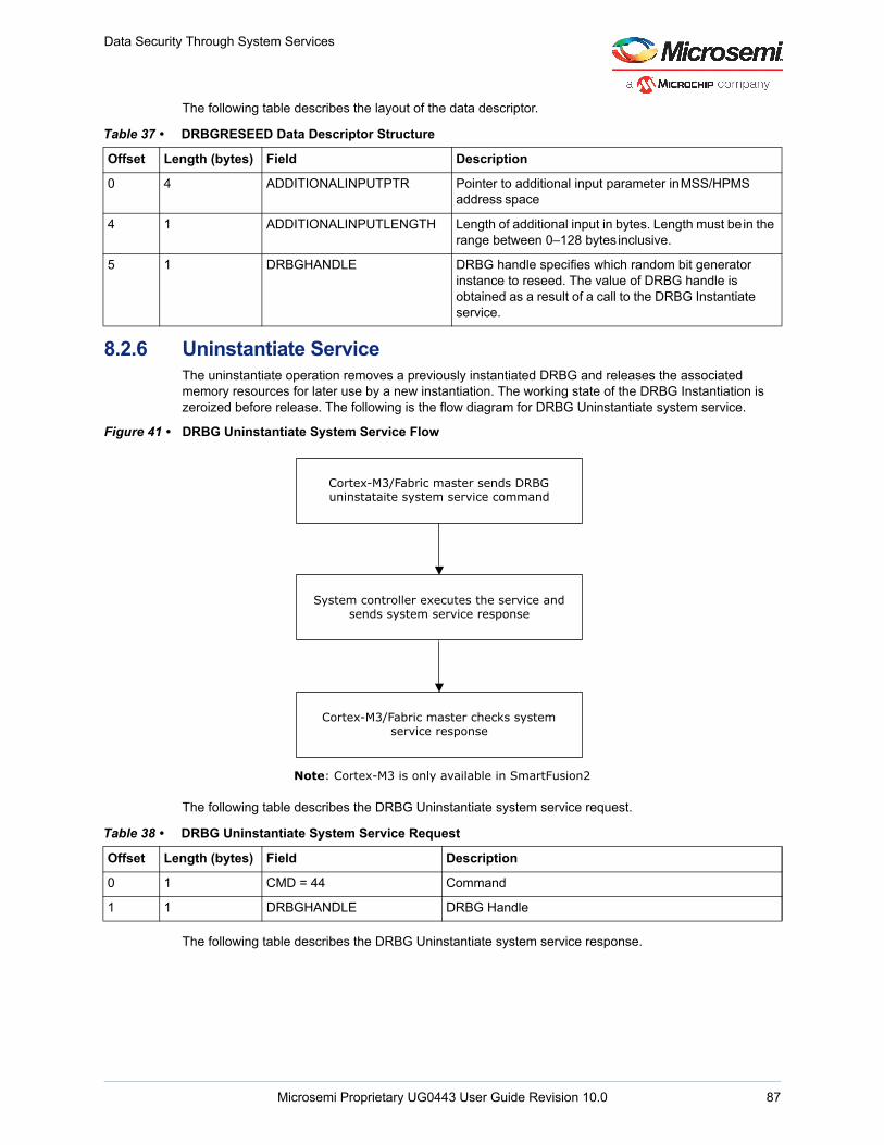
Data Security Through System Services
The following table describes the layout of the data descriptor.
8.2.6 Uninstantiate ServiceThe uninstantiate operation removes a previously instantiated DRBG and releases the associated memory resources for later use by a new instantiation. The working state of the DRBG Instantiation is zeroized before release. The following is the flow diagram for DRBG Uninstantiate system service.
Figure 41 • DRBG Uninstantiate System Service Flow
The following table describes the DRBG Uninstantiate system service request.
The following table describes the DRBG Uninstantiate system service response.
Table 37 • DRBGRESEED Data Descriptor Structure
Offset Length (bytes) Field Description
0 4 ADDITIONALINPUTPTR Pointer to additional input parameter in MSS/HPMS address space
4 1 ADDITIONALINPUTLENGTH Length of additional input in bytes. Length must be in the range between 0–128 bytes inclusive.
5 1 DRBGHANDLE DRBG handle specifies which random bit generator instance to reseed. The value of DRBG handle is obtained as a result of a call to the DRBG Instantiate service.
Table 38 • DRBG Uninstantiate System Service Request
Offset Length (bytes) Field Description
0 1 CMD = 44 Command
1 1 DRBGHANDLE DRBG Handle
Note: Cortex-M3 is only available in SmartFusion2
Cortex-M3/Fabric master sends DRBG uninstataite system service command
System controller executes the service and sends system service response
Cortex-M3/Fabric master checks system service response
Microsemi Proprietary UG0443 User Guide Revision 10.0 87
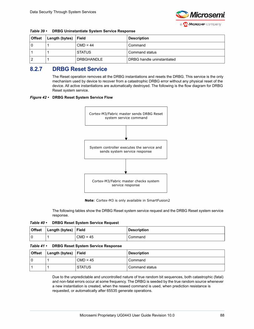
Data Security Through System Services
8.2.7 DRBG Reset ServiceThe Reset operation removes all the DRBG instantiations and resets the DRBG. This service is the only mechanism used by device to recover from a catastrophic DRBG error without any physical reset of the device. All active instantiations are automatically destroyed. The following is the flow diagram for DRBG Reset system service.
Figure 42 • DRBG Reset System Service Flow
The following tables show the DRBG Reset system service request and the DRBG Reset system service response.
Due to the unpredictable and uncontrolled nature of true random bit sequences, both catastrophic (fatal) and non-fatal errors occur at some frequency. The DRBG is seeded by the true random source whenever a new instantiation is created, when the reseed command is used, when prediction resistance is requested, or automatically after 65535 generate operations.
Table 39 • DRBG Uninstantiate System Service Response
Offset Length (bytes) Field Description
0 1 CMD = 44 Command
1 1 STATUS Command status
2 1 DRBGHANDLE DRBG handle uninstantiated
Table 40 • DRBG Reset System Service Request
Offset Length (bytes) Field Description
0 1 CMD = 45 Command
Table 41 • DRBG Reset System Service Response
Offset Length (bytes) Field Description
0 1 CMD = 45 Command
1 1 STATUS Command status
Note: Cortex-M3 is only available in SmartFusion2
Cortex-M3/Fabric master sends DRBG Reset system service command
System controller executes the service and sends system service response
Cortex-M3/Fabric master checks system service response
Microsemi Proprietary UG0443 User Guide Revision 10.0 88
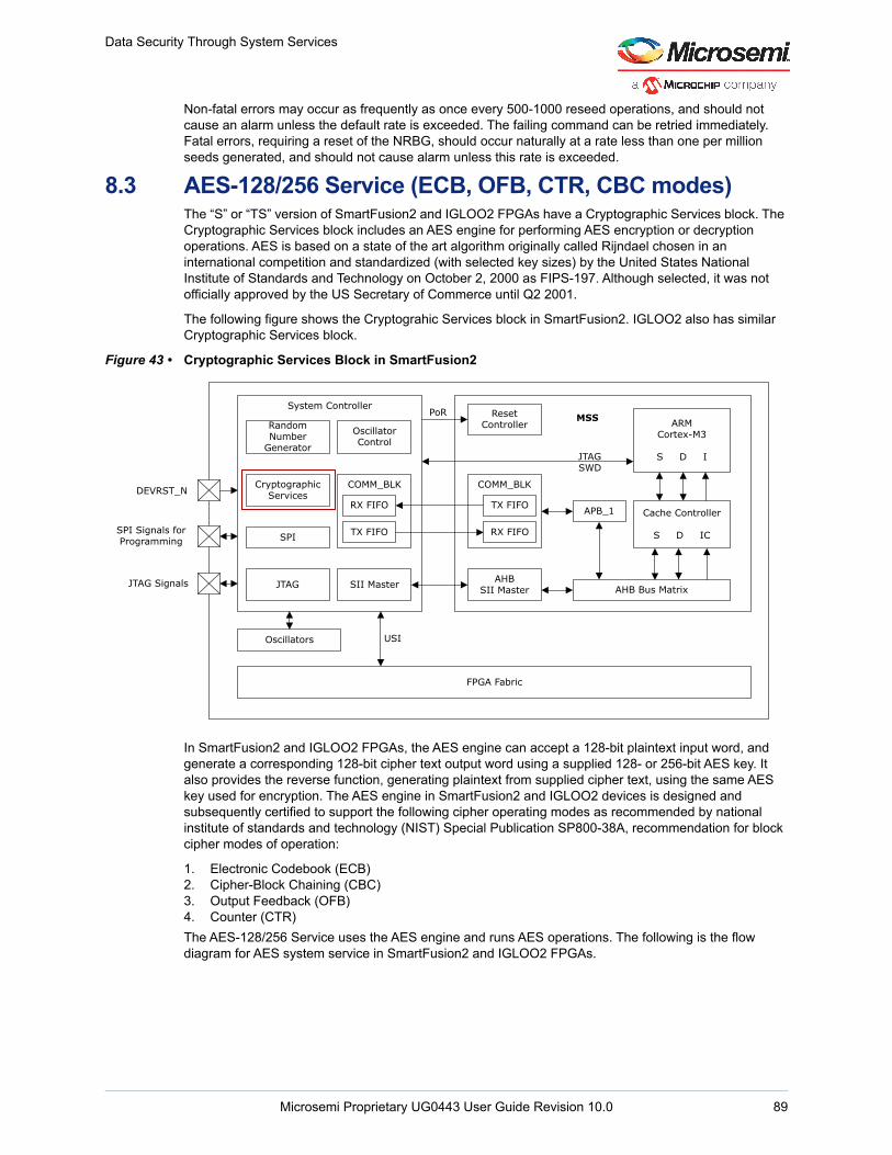
Data Security Through System Services
Non-fatal errors may occur as frequently as once every 500-1000 reseed operations, and should not cause an alarm unless the default rate is exceeded. The failing command can be retried immediately. Fatal errors, requiring a reset of the NRBG, should occur naturally at a rate less than one per million seeds generated, and should not cause alarm unless this rate is exceeded.
8.3 AES-128/256 Service (ECB, OFB, CTR, CBC modes)The “S” or “TS” version of SmartFusion2 and IGLOO2 FPGAs have a Cryptographic Services block. The Cryptographic Services block includes an AES engine for performing AES encryption or decryption operations. AES is based on a state of the art algorithm originally called Rijndael chosen in an international competition and standardized (with selected key sizes) by the United States National Institute of Standards and Technology on October 2, 2000 as FIPS-197. Although selected, it was not officially approved by the US Secretary of Commerce until Q2 2001.
The following figure shows the Cryptograhic Services block in SmartFusion2. IGLOO2 also has similar Cryptographic Services block.
Figure 43 • Cryptographic Services Block in SmartFusion2
In SmartFusion2 and IGLOO2 FPGAs, the AES engine can accept a 128-bit plaintext input word, and generate a corresponding 128-bit cipher text output word using a supplied 128- or 256-bit AES key. It also provides the reverse function, generating plaintext from supplied cipher text, using the same AES key used for encryption. The AES engine in SmartFusion2 and IGLOO2 devices is designed and subsequently certified to support the following cipher operating modes as recommended by national institute of standards and technology (NIST) Special Publication SP800-38A, recommendation for block cipher modes of operation:
1. Electronic Codebook (ECB)2. Cipher-Block Chaining (CBC)3. Output Feedback (OFB)4. Counter (CTR)
The AES-128/256 Service uses the AES engine and runs AES operations. The following is the flow diagram for AES system service in SmartFusion2 and IGLOO2 FPGAs.
System Controller
Random Number
Generator
Oscillator Control
Cryptographic Services
SPI
JTAG
COMM_BLK
SII Master
RX FIFO
TX FIFO
Oscillators
COMM_BLK
TX FIFO
RX FIFO
AHBSII Master
Reset Controller ARM
Cortex-M3
S D I
Cache Controller
S D IC
APB_1
AHB Bus Matrix
PoR MSS
JTAGSWD
USI
DEVRST_N
SPI Signals for Programming
JTAG Signals
FPGA Fabric
Microsemi Proprietary UG0443 User Guide Revision 10.0 89
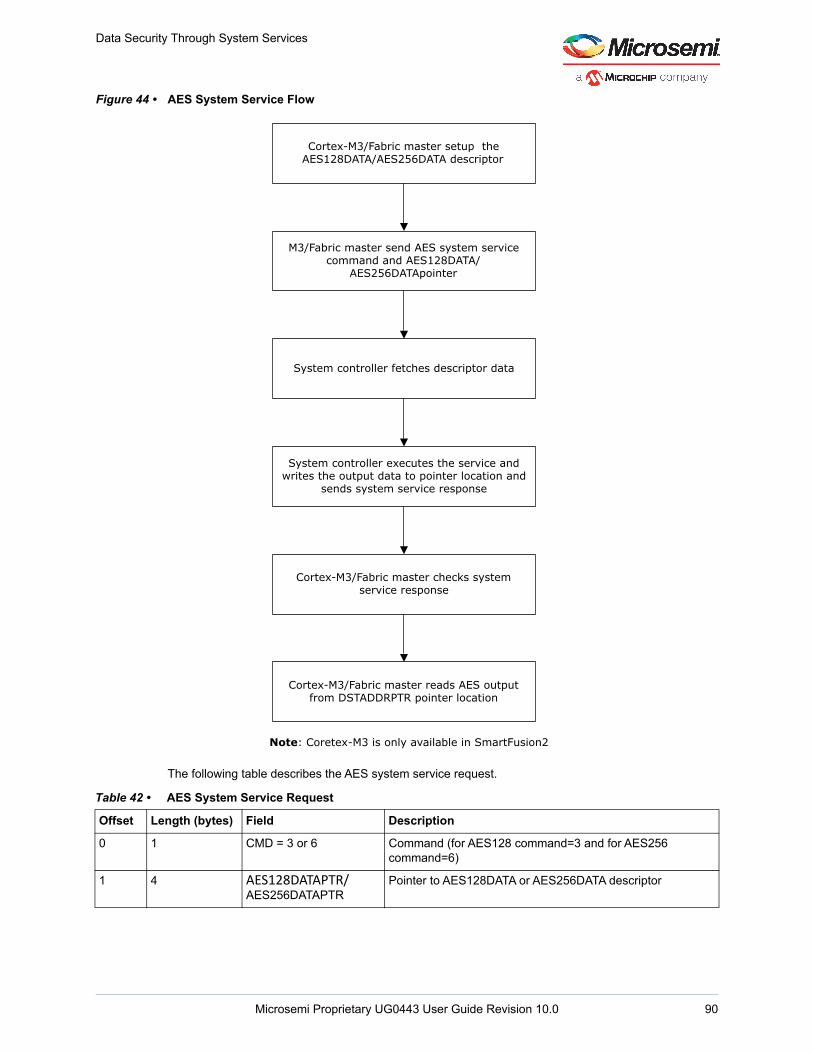
Data Security Through System Services
Figure 44 • AES System Service Flow
The following table describes the AES system service request.
Table 42 • AES System Service Request
Offset Length (bytes) Field Description
0 1 CMD = 3 or 6 Command (for AES128 command=3 and for AES256 command=6)
1 4 AES128DATAPTR/ AES256DATAPTR
Pointer to AES128DATA or AES256DATA descriptor
Cortex-M3/Fabric master setup the AES128DATA/AES256DATA descriptor
M3/Fabric master send AES system service command and AES128DATA/
AES256DATApointer
System controller fetches descriptor data
System controller executes the service and writes the output data to pointer location and
sends system service response
Cortex-M3/Fabric master checks system service response
Cortex-M3/Fabric master reads AES output from DSTADDRPTR pointer location
Note: Coretex-M3 is only available in SmartFusion2
Microsemi Proprietary UG0443 User Guide Revision 10.0 90
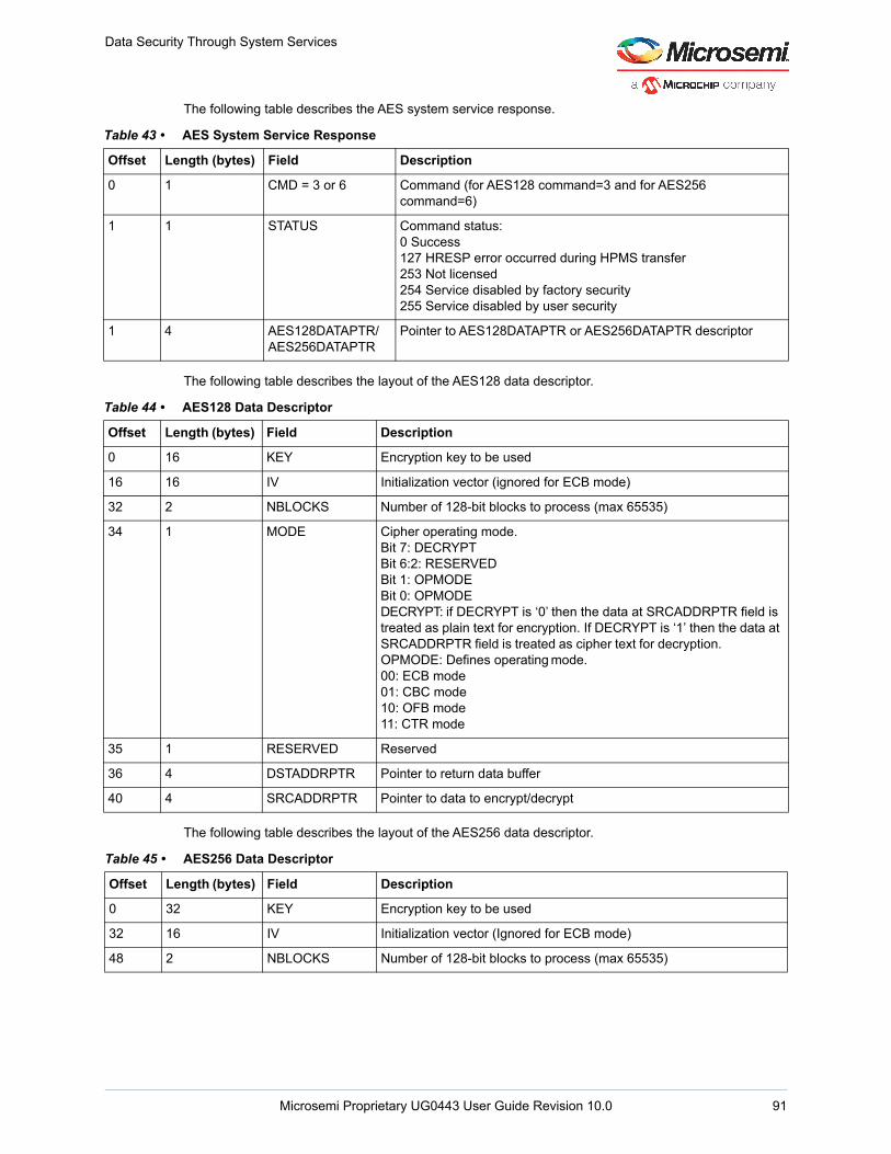
Data Security Through System Services
The following table describes the AES system service response.
The following table describes the layout of the AES128 data descriptor.
The following table describes the layout of the AES256 data descriptor.
Table 43 • AES System Service Response
Offset Length (bytes) Field Description
0 1 CMD = 3 or 6 Command (for AES128 command=3 and for AES256 command=6)
1 1 STATUS Command status:0 Success 127 HRESP error occurred during HPMS transfer253 Not licensed 254 Service disabled by factory security 255 Service disabled by user security
1 4 AES128DATAPTR/ AES256DATAPTR
Pointer to AES128DATAPTR or AES256DATAPTR descriptor
Table 44 • AES128 Data Descriptor
Offset Length (bytes) Field Description
0 16 KEY Encryption key to be used
16 16 IV Initialization vector (ignored for ECB mode)
32 2 NBLOCKS Number of 128-bit blocks to process (max 65535)
34 1 MODE Cipher operating mode.Bit 7: DECRYPTBit 6:2: RESERVEDBit 1: OPMODEBit 0: OPMODEDECRYPT: if DECRYPT is ‘0’ then the data at SRCADDRPTR field is treated as plain text for encryption. If DECRYPT is ‘1’ then the data at SRCADDRPTR field is treated as cipher text for decryption.OPMODE: Defines operating mode. 00: ECB mode01: CBC mode10: OFB mode11: CTR mode
35 1 RESERVED Reserved
36 4 DSTADDRPTR Pointer to return data buffer
40 4 SRCADDRPTR Pointer to data to encrypt/decrypt
Table 45 • AES256 Data Descriptor
Offset Length (bytes) Field Description
0 32 KEY Encryption key to be used
32 16 IV Initialization vector (Ignored for ECB mode)
48 2 NBLOCKS Number of 128-bit blocks to process (max 65535)
Microsemi Proprietary UG0443 User Guide Revision 10.0 91
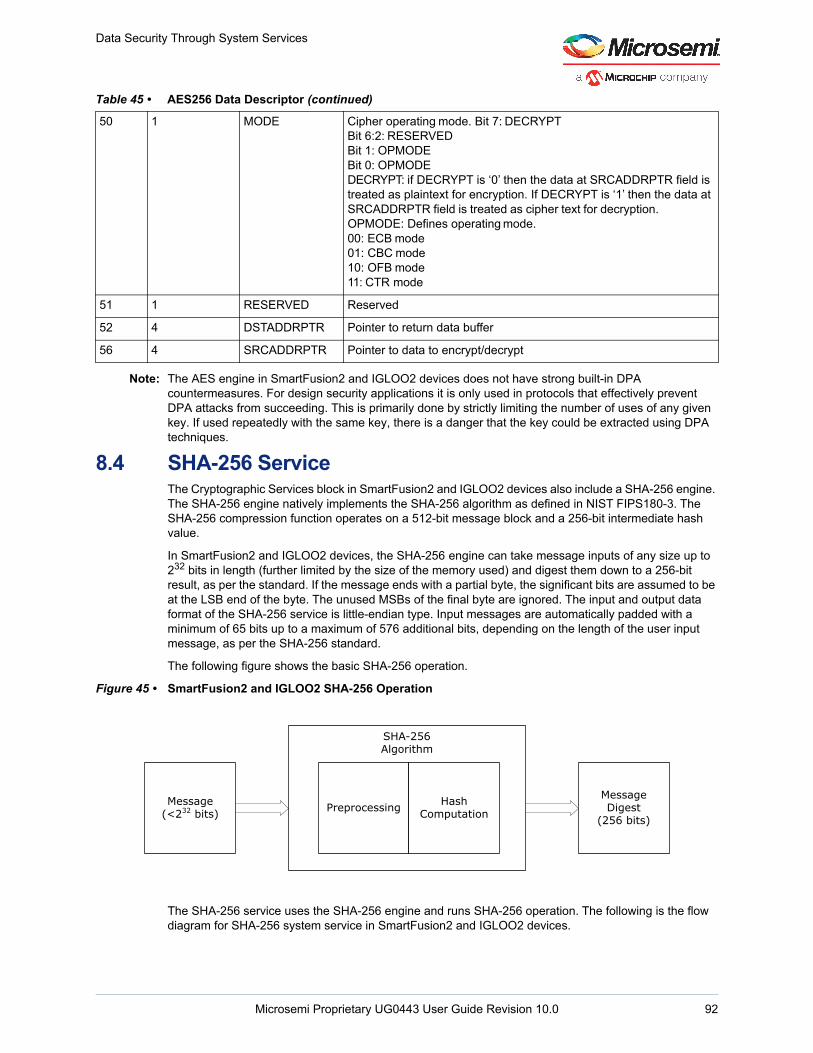
Data Security Through System Services
Note: The AES engine in SmartFusion2 and IGLOO2 devices does not have strong built-in DPA countermeasures. For design security applications it is only used in protocols that effectively prevent DPA attacks from succeeding. This is primarily done by strictly limiting the number of uses of any given key. If used repeatedly with the same key, there is a danger that the key could be extracted using DPA techniques.
8.4 SHA-256 ServiceThe Cryptographic Services block in SmartFusion2 and IGLOO2 devices also include a SHA-256 engine. The SHA-256 engine natively implements the SHA-256 algorithm as defined in NIST FIPS180-3. The SHA-256 compression function operates on a 512-bit message block and a 256-bit intermediate hash value.
In SmartFusion2 and IGLOO2 devices, the SHA-256 engine can take message inputs of any size up to 232 bits in length (further limited by the size of the memory used) and digest them down to a 256-bit result, as per the standard. If the message ends with a partial byte, the significant bits are assumed to be at the LSB end of the byte. The unused MSBs of the final byte are ignored. The input and output data format of the SHA-256 service is little-endian type. Input messages are automatically padded with a minimum of 65 bits up to a maximum of 576 additional bits, depending on the length of the user input message, as per the SHA-256 standard.
The following figure shows the basic SHA-256 operation.
Figure 45 • SmartFusion2 and IGLOO2 SHA-256 Operation
The SHA-256 service uses the SHA-256 engine and runs SHA-256 operation. The following is the flow diagram for SHA-256 system service in SmartFusion2 and IGLOO2 devices.
50 1 MODE Cipher operating mode. Bit 7: DECRYPTBit 6:2: RESERVEDBit 1: OPMODEBit 0: OPMODEDECRYPT: if DECRYPT is ‘0’ then the data at SRCADDRPTR field is treated as plaintext for encryption. If DECRYPT is ‘1’ then the data at SRCADDRPTR field is treated as cipher text for decryption.OPMODE: Defines operating mode. 00: ECB mode01: CBC mode10: OFB mode 11: CTR mode
51 1 RESERVED Reserved
52 4 DSTADDRPTR Pointer to return data buffer
56 4 SRCADDRPTR Pointer to data to encrypt/decrypt
Table 45 • AES256 Data Descriptor (continued)
Preprocessing Hash Computation
Message Digest
(256 bits)
Message(<232 bits)
SHA-256Algorithm
Microsemi Proprietary UG0443 User Guide Revision 10.0 92

Data Security Through System Services
Figure 46 • SHA-256 System Service Flow
The following table describes the SHA-256 system service request.
Table 46 • SHA-256 System Service Request
Offset Length (bytes) Field Description
0 1 CMD = 10 Command
1 4 SHA256DATAPTR Pointer to SHA256DATA structure
Note: Cortex-M3 is only available in SmartFusion2
Cortex-M3/Fabric master setup the SHA256DATA descriptor
Cortex-M3/Fabric master send SHA-256 system service command and SHA256DATA
pointer
System Controller fetches descriptor data
System Controller executes the service and writes the output data to pointer location and
sends system service response
Cortex-M3/Fabric master checks system service response
Cortex-M3/Fabric master reads SHA-256 output from HASHRESULTPTR pointer location
Microsemi Proprietary UG0443 User Guide Revision 10.0 93
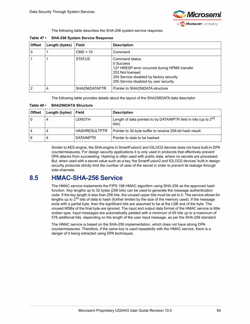
Data Security Through System Services
The following table describes the SHA-256 system service response.
The following table provides details about the layout of the SHA256DATA data descriptor
Similar to AES engine, the SHA engine in SmartFusion2 and IGLOO2 devices does not have built-in DPA countermeasures. For design security applications it is only used in protocols that effectively prevent DPA attacks from succeeding. Hashing is often used with public data, where no secrets are processed. But, when used with a secret value such as a key, the SmartFusion2 and IGLOO2 devices' built-in design security protocols strictly limit the number of uses of the secret in order to prevent its leakage through side-channels.
8.5 HMAC-SHA-256 ServiceThe HMAC service implements the FIPS 198 HMAC algorithm using SHA-256 as the approved hash function. Key lengths up to 32 bytes (256 bits) can be used to generate the message authentication code. If the key length is less than 256 bits, the unused upper bits must be set to 0. The service allows for lengths up to 232 bits of data to hash (further limited by the size of the memory used). If the message ends with a partial byte, then the significant bits are assumed to be at the LSB end of the byte. The unused MSBs of the final byte are ignored. The input and output data format of the HMAC service is little endian type. Input messages are automatically padded with a minimum of 65 bits up to a maximum of 576 additional bits, depending on the length of the user input message, as per the SHA-256 standard.
The HMAC service is based on the SHA-256 implementation, which does not have strong DPA countermeasures. Therefore, if the same key is used repeatedly with the HMAC service, there is a danger of it being extracted using DPA techniques.
Table 47 • SHA-256 System Service Response
Offset Length (bytes) Field Description
0 1 CMD = 10 Command
1 1 STATUS Command status:0 Success 127 HRESP error occurred during HPMS transfer253 Not licensed 254 Service disabled by factory security 255 Service disabled by user security
2 4 SHA256DATAPTR Pointer to SHA256DATA structure
Table 48 • SHA256DATA Structure
Offset Length (bytes) Field Description
0 4 LENGTH Length of data pointed to by DATAINPTR field in bits (up to 232 bits).
4 4 HASHRESULTPTR Pointer to 32-byte buffer to receive 256-bit hash result.
8 4 DATAINPTR Pointer to data to be hashed
Microsemi Proprietary UG0443 User Guide Revision 10.0 94
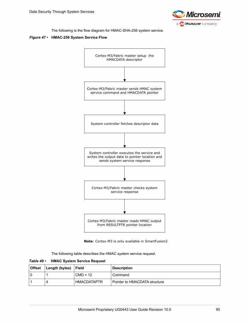
Data Security Through System Services
The following is the flow diagram for HMAC-SHA-256 system service.
Figure 47 • HMAC-256 System Service Flow
The following table describes the HMAC system service request.
Table 49 • HMAC System Service Request
Offset Length (bytes) Field Description
0 1 CMD = 12 Command
1 4 HMACDATAPTR Pointer to HMACDATA structure
Note: Cortex-M3 is only available in SmartFusion2
Cortex-M3/Fabric master setup the HMACDATA descriptor
Cortex-M3/Fabric master sends HMAC system service command and HMACDATA pointer
System controller fetches descriptor data
System controller executes the service and writes the output data to pointer location and
sends system service response
Cortex-M3/Fabric master checks system service response
Cortex-M3/Fabric master reads HMAC output from RESULTPTR pointer location
Microsemi Proprietary UG0443 User Guide Revision 10.0 95
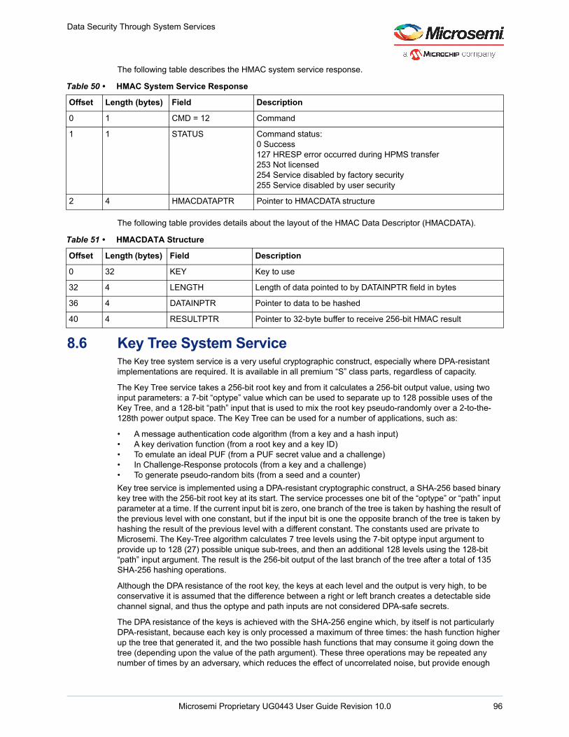
Data Security Through System Services
The following table describes the HMAC system service response.
The following table provides details about the layout of the HMAC Data Descriptor (HMACDATA).
8.6 Key Tree System ServiceThe Key tree system service is a very useful cryptographic construct, especially where DPA-resistant implementations are required. It is available in all premium “S” class parts, regardless of capacity.
The Key Tree service takes a 256-bit root key and from it calculates a 256-bit output value, using two input parameters: a 7-bit “optype” value which can be used to separate up to 128 possible uses of the Key Tree, and a 128-bit “path” input that is used to mix the root key pseudo-randomly over a 2-to-the-128th power output space. The Key Tree can be used for a number of applications, such as:
• A message authentication code algorithm (from a key and a hash input)• A key derivation function (from a root key and a key ID)• To emulate an ideal PUF (from a PUF secret value and a challenge)• In Challenge-Response protocols (from a key and a challenge)• To generate pseudo-random bits (from a seed and a counter)
Key tree service is implemented using a DPA-resistant cryptographic construct, a SHA-256 based binary key tree with the 256-bit root key at its start. The service processes one bit of the “optype” or “path” input parameter at a time. If the current input bit is zero, one branch of the tree is taken by hashing the result of the previous level with one constant, but if the input bit is one the opposite branch of the tree is taken by hashing the result of the previous level with a different constant. The constants used are private to Microsemi. The Key-Tree algorithm calculates 7 tree levels using the 7-bit optype input argument to provide up to 128 (27) possible unique sub-trees, and then an additional 128 levels using the 128-bit “path” input argument. The result is the 256-bit output of the last branch of the tree after a total of 135 SHA-256 hashing operations.
Although the DPA resistance of the root key, the keys at each level and the output is very high, to be conservative it is assumed that the difference between a right or left branch creates a detectable side channel signal, and thus the optype and path inputs are not considered DPA-safe secrets.
The DPA resistance of the keys is achieved with the SHA-256 engine which, by itself is not particularly DPA-resistant, because each key is only processed a maximum of three times: the hash function higher up the tree that generated it, and the two possible hash functions that may consume it going down the tree (depending upon the value of the path argument). These three operations may be repeated any number of times by an adversary, which reduces the effect of uncorrelated noise, but provide enough
Table 50 • HMAC System Service Response
Offset Length (bytes) Field Description
0 1 CMD = 12 Command
1 1 STATUS Command status:0 Success 127 HRESP error occurred during HPMS transfer253 Not licensed 254 Service disabled by factory security 255 Service disabled by user security
2 4 HMACDATAPTR Pointer to HMACDATA structure
Table 51 • HMACDATA Structure
Offset Length (bytes) Field Description
0 32 KEY Key to use
32 4 LENGTH Length of data pointed to by DATAINPTR field in bytes
36 4 DATAINPTR Pointer to data to be hashed
40 4 RESULTPTR Pointer to 32-byte buffer to receive 256-bit HMAC result
Microsemi Proprietary UG0443 User Guide Revision 10.0 96
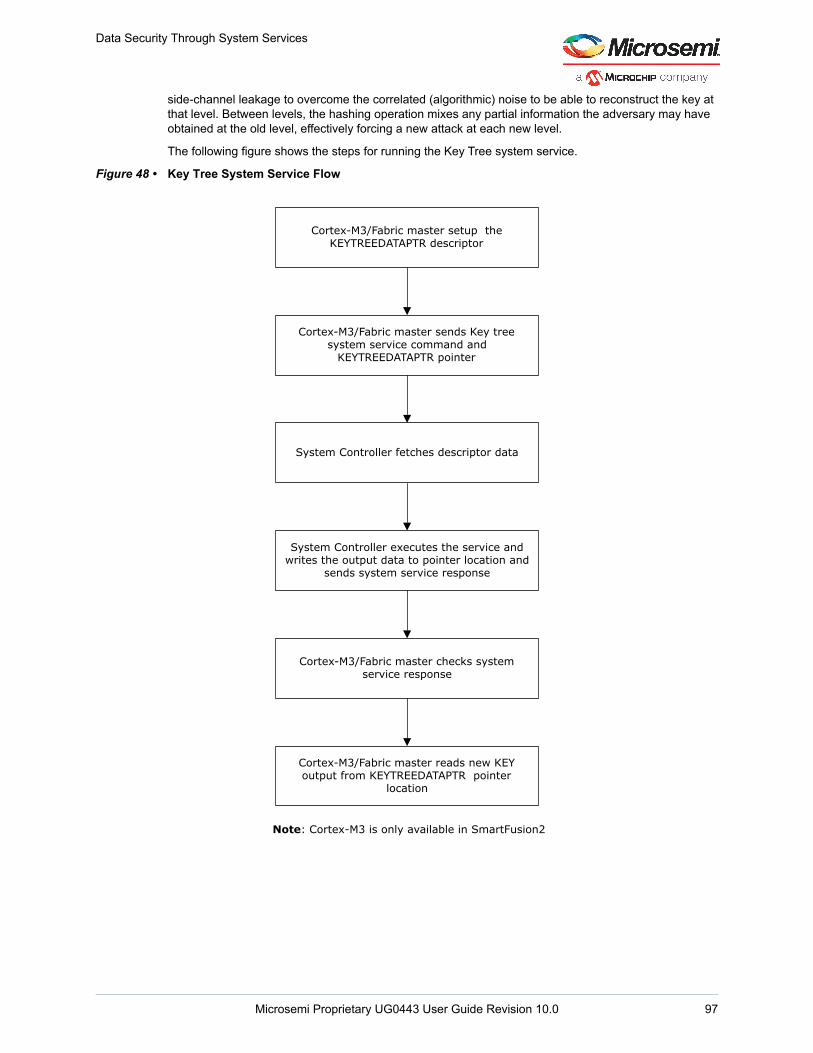
Data Security Through System Services
side-channel leakage to overcome the correlated (algorithmic) noise to be able to reconstruct the key at that level. Between levels, the hashing operation mixes any partial information the adversary may have obtained at the old level, effectively forcing a new attack at each new level.
The following figure shows the steps for running the Key Tree system service.
Figure 48 • Key Tree System Service Flow
Note: Cortex-M3 is only available in SmartFusion2
Cortex-M3/Fabric master setup the KEYTREEDATAPTR descriptor
Cortex-M3/Fabric master sends Key tree system service command and
KEYTREEDATAPTR pointer
System Controller fetches descriptor data
System Controller executes the service and writes the output data to pointer location and
sends system service response
Cortex-M3/Fabric master checks system service response
Cortex-M3/Fabric master reads new KEY output from KEYTREEDATAPTR pointer
location
Microsemi Proprietary UG0443 User Guide Revision 10.0 97
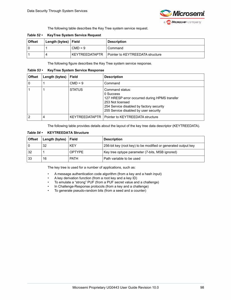
Data Security Through System Services
The following table describes the Key Tree system service request.
The following figure describes the Key Tree system service response.
The following table provides details about the layout of the key tree data descriptor (KEYTREEDATA).
The key tree is used for a number of applications, such as:
• A message authentication code algorithm (from a key and a hash input)• A key derivation function (from a root key and a key ID)• To emulate a “strong” PUF (from a PUF secret value and a challenge)• In Challenge-Response protocols (from a key and a challenge)• To generate pseudo-random bits (from a seed and a counter)
Table 52 • KeyTree System Service Request
Offset Length (bytes) Field Description
0 1 CMD = 9 Command
1 4 KEYTREEDATAPTR Pointer to KEYTREEDATA structure
Table 53 • KeyTree System Service Response
Offset Length (bytes) Field Description
0 1 CMD = 9 Command
1 1 STATUS Command status: 0 Success 127 HRESP error occurred during HPMS transfer 253 Not licensed 254 Service disabled by factory security 255 Service disabled by user security
2 4 KEYTREEDATAPTR Pointer to KEYTREEDATA structure
Table 54 • KEYTREEDATA Structure
Offset Length (bytes) Field Description
0 32 KEY 256-bit key (root key) to be modified or generated output key
32 1 OPTYPE Key tree optype parameter (7-bits, MSB ignored)
33 16 PATH Path variable to be used
Microsemi Proprietary UG0443 User Guide Revision 10.0 98
Data Security Through System Services
8.7 PUF Emulation (Pseudo-PUF) ServiceThe pseudo-PUF is used to emulate the functionality of a real PUF. It is based on a 256-bit secret generated by the device's own non-deterministic random bit generator (NRBG) during manufacturing of the device, and stored permanently in the factory keys security NVM segment. It is used in a challenge- response type of protocol. Unlike the other factory installed keys, the pseudo-PUF key is not ever known by Microsemi. The key is not even disclosed to the user. To use it, one or several challenges are generated by the user, and the responses are recorded during an enrollment phase. Later, a challenge whose response is known can be provided to the device to prove it is the same enrolled device. The Pseudo-PUF service performs the CRI-patented DPA-safe key tree algorithm using a 256-bit static random key generated and stored by the device during its manufacture as the starting secret. The Pseudo-PUF-based PUF Emulation service is available in -005, -010, -025 and -050 devices. In the -060, -090 and -150 devices, the PUF emulation service is based on the SRAM-PUF as explained in the SRAM-PUF section.
A strong PUF is a PUF with a cryptographically large input domain and output range. Most of the strong PUFs have had difficulty achieving even 2-to-the-24th power element input domain or output ranges, and may have modeling or other non-randomness kinds of weaknesses. The pseudo-PUF does not meet the ideal of unclonablity, since the secret is just stored in NVM and likewise the input-output non-linear mapping is not based on an unclonable intrinsic function of the silicon, but rather on standard mathematical cryptographic algorithms. As a black box however, pseudo -PUF emulates an ideal physically-unclonable function, A total of 128 different ideal strong physically-unclonable functions are emulated, each with a 2128element input domain and output range.
Microsemi Proprietary UG0443 User Guide Revision 10.0 99
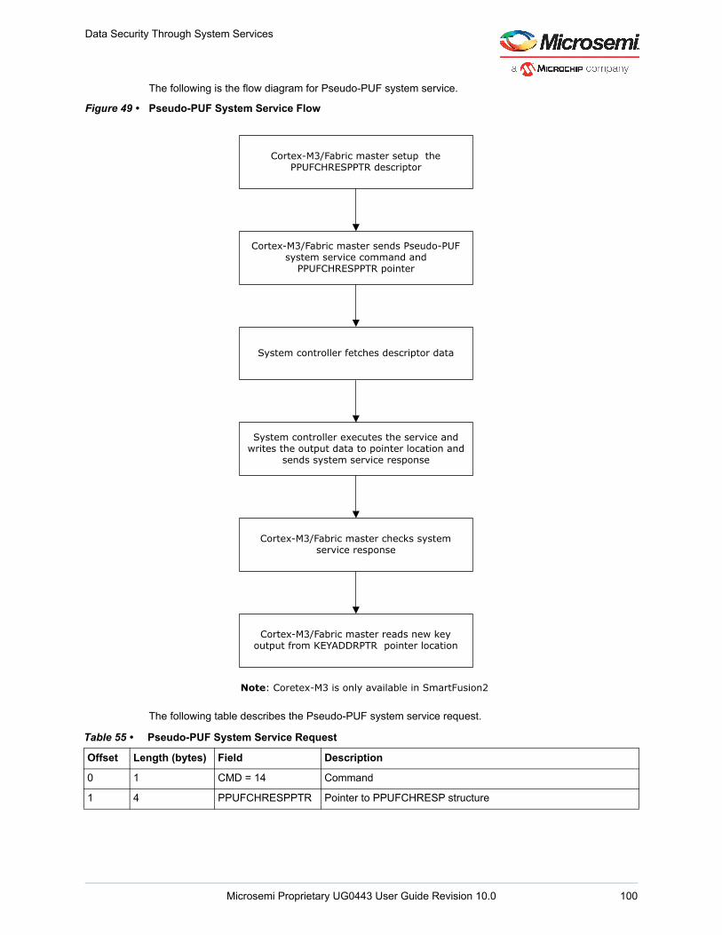
Data Security Through System Services
The following is the flow diagram for Pseudo-PUF system service.
Figure 49 • Pseudo-PUF System Service Flow
The following table describes the Pseudo-PUF system service request.
Table 55 • Pseudo-PUF System Service Request
Offset Length (bytes) Field Description
0 1 CMD = 14 Command
1 4 PPUFCHRESPPTR Pointer to PPUFCHRESP structure
Note: Coretex-M3 is only available in SmartFusion2
Cortex-M3/Fabric master setup the PPUFCHRESPPTR descriptor
Cortex-M3/Fabric master sends Pseudo-PUF system service command and
PPUFCHRESPPTR pointer
System controller fetches descriptor data
System controller executes the service and writes the output data to pointer location and
sends system service response
Cortex-M3/Fabric master checks system service response
Cortex-M3/Fabric master reads new key output from KEYADDRPTR pointer location
Microsemi Proprietary UG0443 User Guide Revision 10.0 100
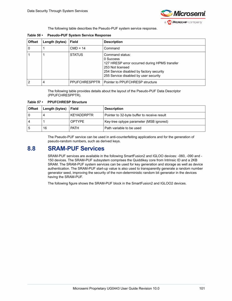
Data Security Through System Services
The following table describes the Pseudo-PUF system service response.
The following table provides details about the layout of the Pseudo-PUF Data Descriptor (PPUFCHRESPPTR).
The Pseudo-PUF service can be used in anti-counterfeiting applications and for the generation of pseudo-random numbers, such as derived keys.
8.8 SRAM-PUF ServicesSRAM-PUF services are available in the following SmartFusion2 and IGLOO devices: -060, -090 and -150 devices. The SRAM-PUF subsystem comprises the Quiddikey core from Intrinsic ID and a 2KB SRAM. The SRAM-PUF system services can be used for key generation and storage as well as device authentication. The SRAM-PUF start-up value is also used to transparently generate a random number generator seed, improving the security of the non-deterministic random bit generator in the devices having the SRAM-PUF.
The following figure shows the SRAM-PUF block in the SmartFusion2 and IGLOO2 devices.
Table 56 • Pseudo-PUF System Service Response
Offset Length (bytes) Field Description
0 1 CMD = 14 Command
1 1 STATUS Command status:0 Success 127 HRESP error occurred during HPMS transfer 253 Not licensed 254 Service disabled by factory security 255 Service disabled by user security
2 4 PPUFCHRESPPTR Pointer to PPUFCHRESP structure
Table 57 • PPUFCHRESP Structure
Offset Length (bytes) Field Description
0 4 KEYADDRPTR Pointer to 32-byte buffer to receive result
4 1 OPTYPE Key-tree optype parameter (MSB ignored)
5 16 PATH Path variable to be used
Microsemi Proprietary UG0443 User Guide Revision 10.0 101
Data Security Through System Services
Figure 50 • SRAM-PUF Block in SmartFusion2 and IGLOO2 Devices
The first time the SRAM-PUF is used, a particular intrinsic secret is determined in a process called enrollment. To detect the exact same secret on each subsequent power-up cycle, in spite of bit-level turn-on to turn-on noise, a base activation code (effectively parity data) is stored in a dedicated read- and write-protected region of the eNVM block. During subsequent turn-on cycles Quiddikey reads the SRAM start-up values and applies the base activation code to regenerate the PUF secret. This is a strong analogy to a fingerprint. Each time a fingerprint is scanned the measurement is slightly different due to noise, but still close enough (and unique enough) to be able to identify the person.
The SRAM-PUF system services provide a Physically Unclonable Function (PUF) that can be used for key generation and storage as well as device authentication. The various SRAM-PUF services available in the larger SmartFusion2 and IGLOO2 devices include:
• Create User Activation Code (AC) or Delete User Activation Code(AC) Service• Get Number of Key Code (KC) Service• Create User KC for an Intrinsic Key Service• Create User KC for an Extrinsic Key Service• Export all KC Service• Import all KC Service• Delete User KC Service• Fetch a User PUF Key Service• Get a PUF Seed Service
8.8.1 Create User AC or Delete User AC ServiceThis service enrolls a new user activation code or deletes the user activation code. The activation code (AC) is required by the SRAM-PUF to regenerate the intrinsic secret from the SRAM-PUF start-up value. The start-up value of the PUF's SRAM block is slightly different from one power-up to the next. In order to be able to determine the exact same secret on each subsequent power-up cycle, in spite of bit-level turn- on to turn-on noise, some processing is performed on the PUF's SRAM start-up value. This processing is performed using the activation code, which functions as parity bits that are used to reconstruct the same PUF intrinsic secret each time.
The larger SmartFusion2 and IGLOO2 devices (-060, -090 and -150 devices) are shipped with one activation code enrolled during the manufacturing process. In “S” and “TS” devices, the user may optionally enroll a second activation code. The activation code is usually generated only once, typically when the system containing the SartFusion2 or IGLOO2 devices are being commissioned using a JTAG
System Controller
Random Number
Generator
Oscillator Control
Cryptographic Services
SPI
JTAG
COMM_BLK
SII Master
RX FIFO
TX FIFO
Oscillators
COMM_BLK
TX FIFO
RX FIFO
AHBSII Master
Reset Controller ARM
Cortex-M3
S D I
Cache Controller
S D ICAPB_1
AHB Bus Matrix
PoR MSS
JTAGSWD
USI UJTAG
DEVRST_N
SPI Signals for Programming
JTAG Signals
FPGA Fabric
SRAM-PUF
Microsemi Proprietary UG0443 User Guide Revision 10.0 102
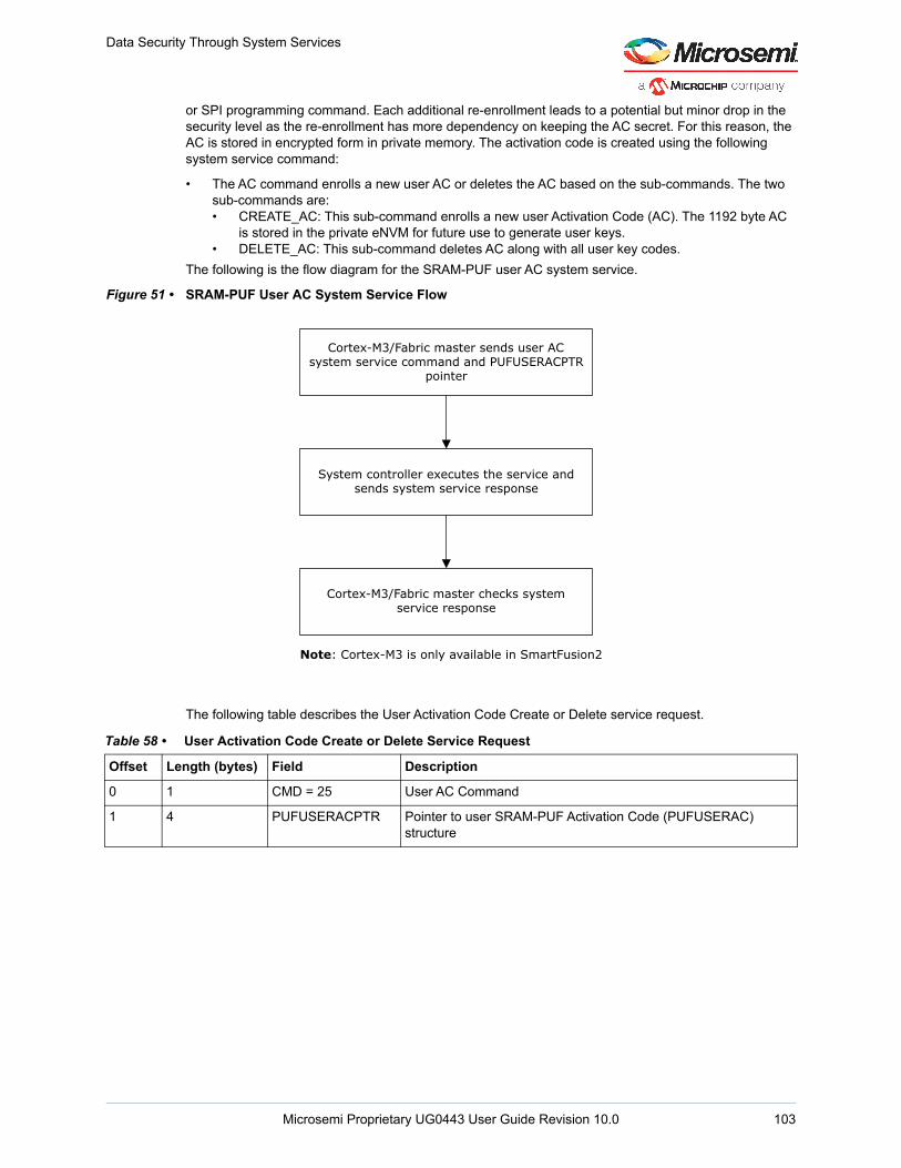
Data Security Through System Services
or SPI programming command. Each additional re-enrollment leads to a potential but minor drop in the security level as the re-enrollment has more dependency on keeping the AC secret. For this reason, the AC is stored in encrypted form in private memory. The activation code is created using the following system service command:
• The AC command enrolls a new user AC or deletes the AC based on the sub-commands. The two sub-commands are:• CREATE_AC: This sub-command enrolls a new user Activation Code (AC). The 1192 byte AC
is stored in the private eNVM for future use to generate user keys.• DELETE_AC: This sub-command deletes AC along with all user key codes.
The following is the flow diagram for the SRAM-PUF user AC system service.
Figure 51 • SRAM-PUF User AC System Service Flow
The following table describes the User Activation Code Create or Delete service request.
Table 58 • User Activation Code Create or Delete Service Request
Offset Length (bytes) Field Description
0 1 CMD = 25 User AC Command
1 4 PUFUSERACPTR Pointer to user SRAM-PUF Activation Code (PUFUSERAC) structure
Note: Cortex-M3 is only available in SmartFusion2
Cortex-M3/Fabric master sends user AC system service command and PUFUSERACPTR
pointer
System controller executes the service and sends system service response
Cortex-M3/Fabric master checks system service response
Microsemi Proprietary UG0443 User Guide Revision 10.0 103

Data Security Through System Services
The following table describes the User Activation Code Create or Delete service response.
The following table provides details about the layout of the User SRAM-PUF Activation Code (PUFUSERAC) data descriptor.
This user AC may be used in the case the first user activation code is intentionally deleted and a new one is desired. The base activation code does not have to be kept confidential because the secret is not stored in the activation code. The secret is rooted in the start-up behavior of the SRAM block. As an added security precaution in the SmartFusion2 and IGLOO2 SRAM-PUF implementation of Quiddikey, the activation code components are stored in a private section of the eNVM.
8.8.2 Create Delete Export Import User Key CodeThis system service is used for key codes (KC). The SRAM-PUF can be used to enroll cryptographic keys. The keys are stored in such a way that the key’s actual value never appears in the system unless it is retrieved by the user. A key code is generated when a key is enrolled and is stored in the private eNVM instead of the key’s value. The key code value is created from the enrolled key’s plaintext value and the intrinsic secret value by encrypting it using the AES block cipher. The KC also includes some meta-data about the key, and a message authentication code. The key’s value can later be regenerated from the key code value and intrinsic secret value upon user’s request and authenticated.
Table 59 • User Activation Code Create or Delete Service Response
Offset Length (bytes) Field Description
0 1 CMD = 25 Command
1 1 STATUS 0: Success completion1: eNVM MSS/HPMS error2: PUF error, during creation3: Invalid subcmd4: eNVM program error7: eNVM verify error127: HRESP error occurred during MSS/HPMS transfer253: License not available in the device254: Service disabled by factory security255: Service disabled by user security
Table 60 • User SRAM-PUF Activation Code (PUFUSERAC) structure
Offset Length (bytes) Field Description
0 1 SUBCMD 0 CREATE_AC: The PUF core is requested to enroll a new user activation code. The 1192 byte AC is stored in eNVM.1 DELETE_AC: The user AC gets deleted along with all user keycodes and ECC public key.
Microsemi Proprietary UG0443 User Guide Revision 10.0 104
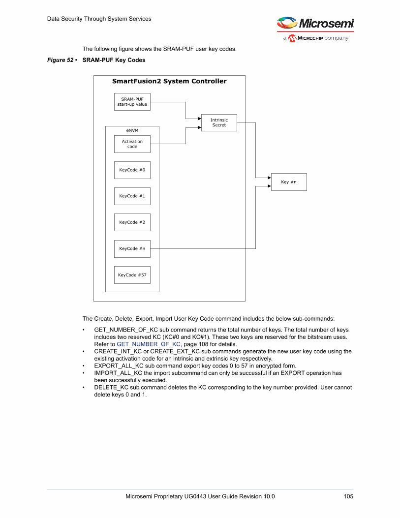
Data Security Through System Services
The following figure shows the SRAM-PUF user key codes.
Figure 52 • SRAM-PUF Key Codes
The Create, Delete, Export, Import User Key Code command includes the below sub-commands:
• GET_NUMBER_OF_KC sub command returns the total number of keys. The total number of keys includes two reserved KC (KC#0 and KC#1). These two keys are reserved for the bitstream uses. Refer to GET_NUMBER_OF_KC, page 108 for details.
• CREATE_INT_KC or CREATE_EXT_KC sub commands generate the new user key code using the existing activation code for an intrinsic and extrinsic key respectively.
• EXPORT_ALL_KC sub command export key codes 0 to 57 in encrypted form.• IMPORT_ALL_KC the import subcommand can only be successful if an EXPORT operation has
been successfully executed.• DELETE_KC sub command deletes the KC corresponding to the key number provided. User cannot
delete keys 0 and 1.
SRAM-PUF start-up value
Activation code
KeyCode #0
KeyCode #1
KeyCode #2
KeyCode #n
KeyCode #57
eNVM
Intrinsic Secret
Key #n
SmartFusion2 System Controller
Microsemi Proprietary UG0443 User Guide Revision 10.0 105
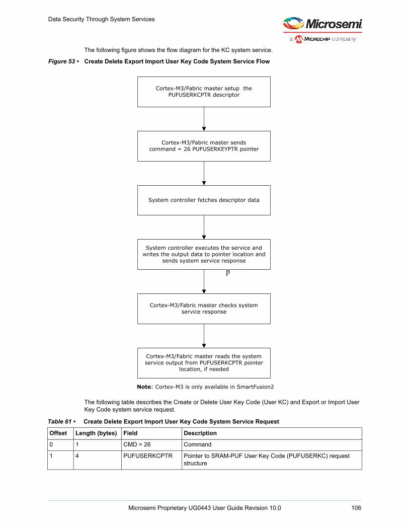
Data Security Through System Services
The following figure shows the flow diagram for the KC system service.
Figure 53 • Create Delete Export Import User Key Code System Service Flow
The following table describes the Create or Delete User Key Code (User KC) and Export or Import User Key Code system service request.
Table 61 • Create Delete Export Import User Key Code System Service Request
Offset Length (bytes) Field Description
0 1 CMD = 26 Command
1 4 PUFUSERKCPTR Pointer to SRAM-PUF User Key Code (PUFUSERKC) request structure
Note: Cortex-M3 is only available in SmartFusion2
Cortex-M3/Fabric master setup the PUFUSERKCPTR descriptor
Cortex-M3/Fabric master sends command = 26 PUFUSERKEYPTR pointer
System controller fetches descriptor data
System controller executes the service and writes the output data to pointer location and
sends system service response
Cortex-M3/Fabric master checks system service response
Cortex-M3/Fabric master reads the system service output from PUFUSERKCPTR pointer
location, if needed
p
Microsemi Proprietary UG0443 User Guide Revision 10.0 106
Data Security Through System Services
The following table describes the Create or Delete User Key Code (User KC) and Export or Import User Key Code system service response.
The following table provides details about the layout of the SRAM-PUF User Key Code (PUFUSERKC).
Table 62 • Create Delete Export Import User Key Code System Service Response
Offset Length (bytes) Field Description
0 1 CMD = 26 Command
1 1 STATUS 0: Success completion 1: eNVM MSS error42: PUF error, during creation3: Invalid request or KC, during export or import4: eNVM program error45: Invalid hash26: Invalid user AC1 7: eNVM verify error48: Incorrect keysize for renewing a kc 10: Private eNVM user digest mismatch 11: Invalid subcmd12: DRBG error3127: HRESP error occurred during MSS transfer 253: License not available in device254: Service disabled by factory security 255: Service disabled by user security
Table 63 • SRAM-PUF User Key Code (PUFUSERKC) Structure
Offset Length (bytes) Field Description
0 1 SUBCMD Sub Command0: GET_NUMBER_OF_KC1: CREATE_EXT_KC2: CREATE_INT_KC3: EXPORT_ALL_KC4: IMPORT_ALL_KC5: DELETE_KC
1 4 PUFUSERKEYADDR
PUF User Key Fetch address, when creating PUF User KC address, to export to or import
5 4 USEREXTRINSICKEYADDR
User Extrinsic Key address
9 1 KEYNUM Key number from 2 to 57
10 1 KEYSIZE Size of the Key. The key size value can be 0 to 63:0 - 4096 bit1 - 64 bit2 - 2*64 = 128 bit……………….63 - 63*64 = 4032 bit
Note: 0,1,2 to 64 denote key size value in above examples and the bits in the right hand side denote the total size of the key
Microsemi Proprietary UG0443 User Guide Revision 10.0 107

Data Security Through System Services
The following sections describe the various sub-commands in detail.
8.8.2.1 GET_NUMBER_OF_KCKeys are identified by a number and are enrolled sequentially. This sub command returns the total number of user keys returned in KEYNUM of PUFUSERKC structure. This valid numbers range from 2 to 57. Key codes #0 and #1 are reserved as a 256-bit symmetric extrinsic key and a 384-bit private asymmetric intrinsic key, both used for design security only, and are enrolled by JTAG (or SPI) programming commands. So the total number of keys are a minimum of 2 (KC#0 and KC#1). All keys, valid and invalid are counted up to the last valid key. An invalid key is one that is deleted, since it is followed by a valid key. You can only create new keys in sequence from this number onwards till the maximum key number.
8.8.2.2 CREATE_INT_KC or CREATE_EXT_KCThis sub command generates the new user key code using the existing activation code for an intrinsic and extrinsic key respectively. The user key code is stored in the private eNVM, for future use to generate the user keys. The user can request the generation of key code from 2 to 57. The keys can only be created in sequence. The key size supported is 64 bits to 4096 bits; refer to KEYSIZE in Table 63, page 107. The total number of keycodes is limited by the amount of memory allocated to this function by the system controller. The maximum number of keycodes (58) is only possible if all the user keys (2 to 57) are 256 bits or less in size.
An extrinsic key is created by enrolling the key pointed at by USEREXTRINSICKEYADDR. It is up to the user to manage this key and remove it from memory if no longer needed. Both the KC and the 4 byte address PUFUSERKEYADDR are stored in eNVM. The PUFUSERKEYADDR address is defined by the user at the time of creation and is used when fetching a PUF user key. This address must be unique for each key. When importing the keycodes, all keys are automatically generated and stored in memory pointed by these addresses. As a security precaution, when keys are regenerated they must be regenerated into the same address as used when the keycode was first created. In combination with other security features (such as the HW firewalls), the legitimate user can make it more difficult for an adversary to regenerate and extract the keys protected by the PUF as keycodes.
8.8.2.3 EXPORT_ALL_KCThis subcommand exports the AC and KC, 0 to 57 from the system controller's private memory to the FPGA user in encrypted form. One use model is to export the AC and KCs for long-term storage off-chip, or even somewhere else on the network the system is attached to. This can provide extra security since without the AC it is effectively impossible to reconstruct the PUF intrinsic secret enrolled by that AC, due to the existence of a noise floor in the PUF SRAM's start-up values, even if the values are known to an adversary.
The stored user AC and all KCs are first XORed with the one-time pad and copied to a contiguous memory space specified by the user (PUFUSERKEYADDR). The one time pad is stored in its place in the private eNVM and is composed of a 32 byte hash (SHA-256), and the remainder is populated by random bits from the DRBG. The exported activation and key codes can only be decrypted by the unique device that exported them. The digest checks when the AC and KCs are re-imported, makes sure the AC and all the KC values are equal to the original exported values.
The exported KCs vary in size, between 44 and 524 bytes and are preceded by their KC size. If the KC size is 0, it means this KC has been deleted, and the following two bytes signify the KC size of the next key. If the KC size is 525, which is one byte more than the maximum defined key code size, it denotes that all the valid KCs have been exported and this marks the end. The maximum possible size of the complete export record is 1318+56*46=3894 bytes.
Table 64 • PUFUSERACKCEXPORT Memory View
Offset Length (bytes) Field Description
0 1192 User AC User activation code, encrypted
1192 2 Size KC#0 Size in bytes of KC#0
1194 44 KC#0 KC#0 encrypted
Microsemi Proprietary UG0443 User Guide Revision 10.0 108
Data Security Through System Services
The export key code operation can only be successful if a CREATE_INT_KC or CREATE_EXT_KC operation has been successful previously and no prior export operation was subsequently carried out. User can only export once and after export he can import as many times as needed. The user KC and create user KC can be deleted by the user.
8.8.2.4 IMPORT_ALL_KCThe AC and all the key codes are re-imported using this subcommand. It reads the user AC and all KC's from a contiguous memory space, addressed by PUFUSERKEYADDR, defined in the PUFUSERKC structure. This memory space is identical to the structure, defined in Table 64, page 108. The user AC and all the KCs are then verified to be last created by the device.
The individual private keys are automatically regenerated from the PUF on import and are copied into the individual memory address spaces defined by the CREATE_EXT_KC or CREATE_INT_KC sub commands and stored in private eNVM. The Import operation can only be successful if an EXPORT operation is successfully executed.
As a result of the operation, the memory space, addressed by PUFUSERKEYADDR contains the addresses of all user keys.
8.8.2.5 DELETE_KCThis sub command deletes the KC corresponding to key number provided. User cannot delete KC#0 and KC#1. The KC is cleared in eNVM storage and in the memory address. The key index is maintained the way all other valid keys, maintain their index.
8.8.3 Fetch a User PUF KeyThe Fetch a User PUF Key system service regenerates the key using the existing activation code and key code located in the eNVM memory. The identification number of the key to be fetched is passed as KEYNUM parameter to this system service. The requested key's value is regenerated and copied to the PUFUSERKEYADDR location. The key's value then becomes available for use unless until it is required and wiped, by the user's application, from the memory buffer it was fetched into. If exported, Fetch a User PUF Key system service cannot be used. Also if the key has been deleted using DELETE_KC of
1238 2 Size KC#1 Size in bytes of KC#1
1240 76 KC#1 KC#1 encrypted
1316 2 Size KC#2 Size in bytes of KC#2
1318 User defined KC#2 KC#2 encrypted
... ... ... ...
User defined 2 Size KC#n Size in bytes of KC#n
User defined User defined KC#n KC#n encrypted
User defined 2 End marker End marker is 525,one more than the maximum keycode size
Table 65 • PUFUSERACKCIMPORT Memory View
Offset Length (bytes) Field Description
0 4 Key#2_address MSS/HPMS address where user Key #2 is regenerated
4 4 Key#3_address MSS/HPMS address where user Key #3 is regenerated
8 4 Key#4_address MSS/HPMS address where user Key #4 is regenerated
... ...
220 4 Key#57_address MSS/HPMS address where user Key #57 is regenerated
Table 64 • PUFUSERACKCEXPORT Memory View
Microsemi Proprietary UG0443 User Guide Revision 10.0 109
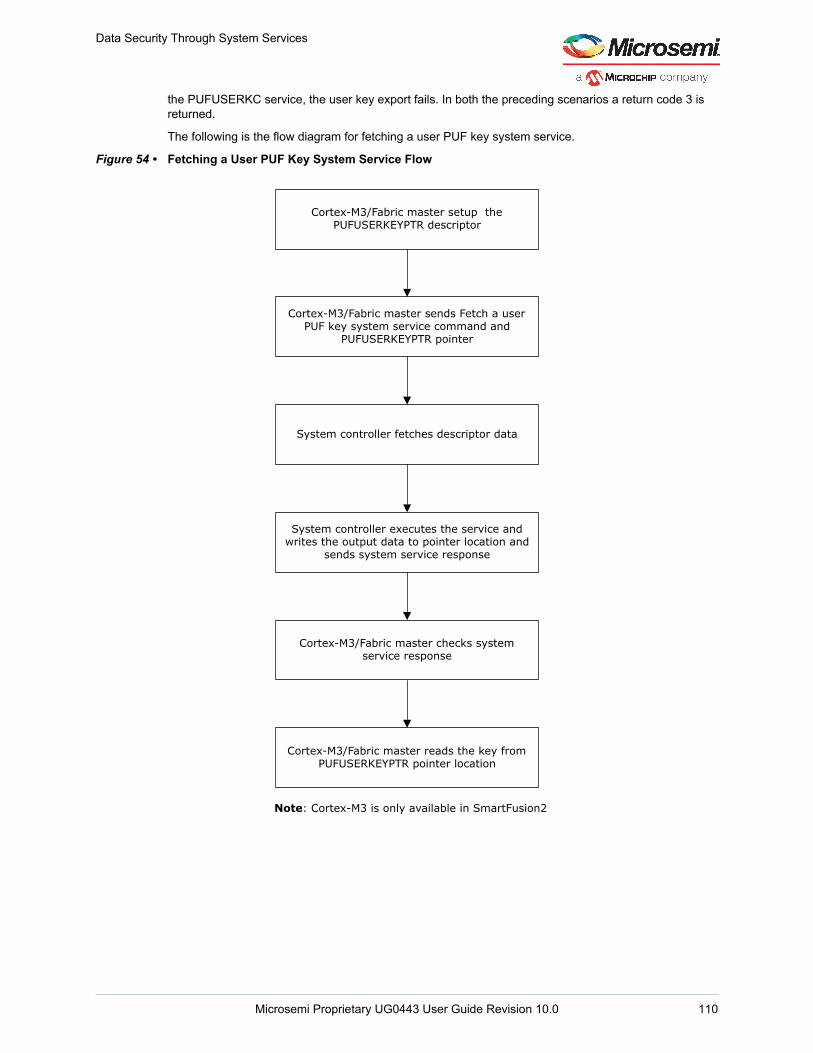
Data Security Through System Services
the PUFUSERKC service, the user key export fails. In both the preceding scenarios a return code 3 is returned.
The following is the flow diagram for fetching a user PUF key system service.
Figure 54 • Fetching a User PUF Key System Service Flow
Note: Cortex-M3 is only available in SmartFusion2
Cortex-M3/Fabric master setup the PUFUSERKEYPTR descriptor
Cortex-M3/Fabric master sends Fetch a user PUF key system service command and
PUFUSERKEYPTR pointer
System controller fetches descriptor data
System controller executes the service and writes the output data to pointer location and
sends system service response
Cortex-M3/Fabric master checks system service response
Cortex-M3/Fabric master reads the key from PUFUSERKEYPTR pointer location
Microsemi Proprietary UG0443 User Guide Revision 10.0 110
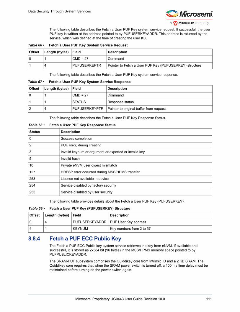
Data Security Through System Services
The following table describes the Fetch a User PUF Key system service request. If successful, the user PUF key is written at the address pointed to by PUFUSERKEYADDR. This address is returned by the service, which was defined at the time of creating the user KC.
The following table describes the Fetch a User PUF Key system service response.
The following table describes the Fetch a User PUF Key Response Status.
The following table provides details about the Fetch a User PUF Key (PUFUSERKEY).
8.8.4 Fetch a PUF ECC Public KeyThe Fetch a PUF ECC Public key system service retrieves the key from eNVM. If available and successful, it is stored as 2x384 bit (96 bytes) in the MSS/HPMS memory space pointed to by PUFPUBLICKEYADDR.
The SRAM-PUF subsystem comprises the Quiddikey core from Intrinsic ID and a 2 KB SRAM. The Quiddikey core requires that when the SRAM power switch is turned off, a 100 ms time delay must be maintained before turning on the power switch again.
Table 66 • Fetch a User PUF Key System Service Request
Offset Length (bytes) Field Description
0 1 CMD = 27 Command
1 4 PUFUSERKEPTR Pointer to Fetch a User PUF Key (PUFUSERKEY) structure
Table 67 • Fetch a User PUF Key System Service Response
Offset Length (bytes) Field Description
0 1 CMD = 27 Command
1 1 STATUS Response status
2 4 PUFUSERKEYPTR Pointer to original buffer from request
Table 68 • Fetch a User PUF Key Response Status
Status Description
0 Success completion
2 PUF error, during creating
3 Invalid keynum or argument or exported or invalid key
5 Invalid hash
10 Private eNVM user digest mismatch
127 HRESP error occurred during MSS/HPMS transfer
253 License not available in device
254 Service disabled by factory security
255 Service disabled by user security
Table 69 • Fetch a User PUF Key (PUFUSERKEY) Structure
Offset Length (bytes) Field Description
0 4 PUFUSERKEYADDR PUF User Key address
4 1 KEYNUM Key numbers from 2 to 57
Microsemi Proprietary UG0443 User Guide Revision 10.0 111
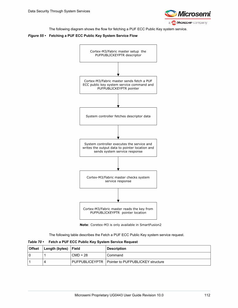
Data Security Through System Services
The following diagram shows the flow for fetching a PUF ECC Public Key system service.
Figure 55 • Fetching a PUF ECC Public Key System Service Flow
The following table describes the Fetch a PUF ECC Public Key system service request.
Table 70 • Fetch a PUF ECC Public Key System Service Request
Offset Length (bytes) Field Description
0 1 CMD = 28 Command
1 4 PUFPUBLICEYPTR Pointer to PUFPUBLICKEY structure
Note: Coretex-M3 is only available in SmartFusion2
Cortex-M3/Fabric master setup the PUFPUBLICKEYPTR descriptor
Cortex-M3/Fabric master sends fetch a PUF ECC public key system service command and
PUFPUBLICKEYPTR pointer
System controller fetches descriptor data
System controller executes the service and writes the output data to pointer location and
sends system service response
Cortex-M3/Fabric master checks system service response
Cortex-M3/Fabric master reads the key from PUFPUBLICKEYPTR pointer location
Microsemi Proprietary UG0443 User Guide Revision 10.0 112
Data Security Through System Services
The following table provides details about the layout of the Fetch a PUF ECC Public key (PUFPUBLICKE) descriptor.
The following table describes the Fetch a PUF ECC Public Key system service response.
8.8.5 Get a PUF SeedThe Get a PUF Seed system service generates a 256-bit seed. The PUF Seed is a true random number that is generated using the PUF's SRAM start up values and a DRBG called iRNG by Intrinsic-ID that is totally independent of the SmartFusion2 and IGLOO2 primary NRBG described in Non-Deterministic Random Bit Generator Service, page 77. The following figure shows the flow for the Get a PUF Seed system service. If successful, the PUF seed is written at the address pointed to by PUFSEEDADDR. In the -060 and larger devices, a 256-bit PUF seed is used in generating the nonce used as additional seed material when the primary NRBG instantiates a DRBG, thus making the primary NRBG more secure.
Table 71 • Fetch a PUF ECC Public key Descriptor Structure
Offset Length (bytes) Field Description
1 4 PUFPUBLICKEYADDR PUF Public Key address
Table 72 • Fetch a PUF ECC Public Key System Service Response
Offset Length (bytes) Field Description
0 1 CMD=28 Command
1 1 STATUS Command Status
2 4 PUFPUBLICKEYPTR Pointer to original buffer from request
Table 73 • Fetch a PUF ECC Public key Status
Status Description
0 Success completion
3 No valid public key present in eNVM
10 Private eNVM user digest mismatch
127 HRESP error occurred during MSS/HPMS transfer
253 License not available in device
254 Service disabled by factory security
255 Service disabled by user security
Microsemi Proprietary UG0443 User Guide Revision 10.0 113
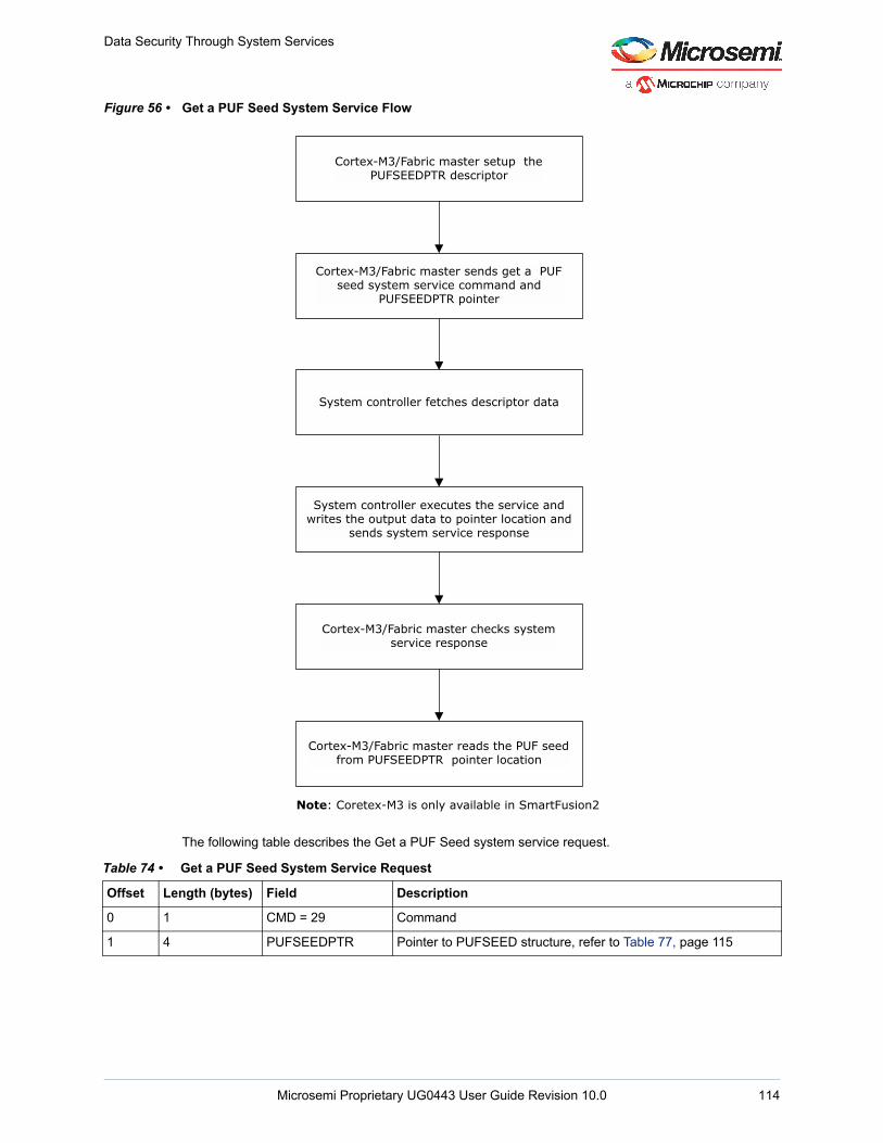
Data Security Through System Services
Figure 56 • Get a PUF Seed System Service Flow
The following table describes the Get a PUF Seed system service request.
Table 74 • Get a PUF Seed System Service Request
Offset Length (bytes) Field Description
0 1 CMD = 29 Command
1 4 PUFSEEDPTR Pointer to PUFSEED structure, refer to Table 77, page 115
Note: Coretex-M3 is only available in SmartFusion2
Cortex-M3/Fabric master setup the PUFSEEDPTR descriptor
Cortex-M3/Fabric master sends get a PUF seed system service command and
PUFSEEDPTR pointer
System controller fetches descriptor data
System controller executes the service and writes the output data to pointer location and
sends system service response
Cortex-M3/Fabric master checks system service response
Cortex-M3/Fabric master reads the PUF seed from PUFSEEDPTR pointer location
Microsemi Proprietary UG0443 User Guide Revision 10.0 114

Data Security Through System Services
The following table describes the Get a PUF Seed system service response
The following table lists the PUFSEED Response Status Codes.
The following table provides details about the layout of the PUF Seed descriptor (PUFSEEDPTR).
8.9 Elliptic Curve Cryptography (ECC) ServicesCertain SmartFusion2 and IGLOO2 devices (-060, -090 and -150 devices) are equipped with a hardware accelerator for performing common elliptic curve cryptography (ECC) operations. The ECC accelerator can be used directly by the user for data security applications. It provides two mathematical services: scalar point multiplication and point addition, computed using the NIST P-384 Elliptic Curve domain parameters. These are the most compute intensive operations typically used in the ECC cryptosystem – especially the point multiplication operation. The P-384 domain parameters are defined in NIST FIPS PUB 186-3 Appendix D.1.2.4. As of now this is the only elliptic curve approved for protecting classified information up to and including the top secret present in the NIST Suite B list of approved algorithms and in the Commercial National Security Algorithm (CNSA) Suite approved for National Secure Systems (NSS) by the Committee for National Security Systems (CNSS).
The ECC point multiplication service multiplies a point by a scalar. The scalar is a 384-bit integer, and points are defined by two 384 bit integers depicting the point’s “X” and “Y” coordinates. The point coordinates are restricted to the Galois Field defined by the P-384 domain parameters. The input scalar is normally restricted to the range of values that map directly to the unique points in the curve; and for use as keys; certain values (such as zero and one) may also be excluded. The input point must be on the elliptic curve, as defined by a simple 3rd-order algebraic equation with the coefficients given in the domain parameters, with all calculations being done in the Galois Field.
Point addition is defined as an arbitrary operation involving the (x, y) coordinates of both input points and the elliptic curve equation, resulting in another (x, y) point on the curve. This has a geometrical interpretation when done in a real number field, but is nonrepresentational when done in a Galois Field.
When using the ECC scalar-times-point multiplication service or the ECC point-plus-point addition service, in order to avoid known attacks, it is required that the elliptic curve input point(s) are verified (by the user) as valid points on the NIST P-384 curve before any outputs from the service are revealed to a
Table 75 • Get a PUF Seed System Service Response
Offset Length (bytes) Field Description
0 1 CMD = 29 Command
1 1 STATUS PUFSEED Response Status Codes
2 4 PUFSEEDPTR Pointer to original buffer from request
Table 76 • Get a PUF Seed Response Status Codes
Status Description
0 Success completion
2 PUF error, during creation
127 HRESP error occurred during MSS/HPMS transfer
253 License not available in device
254 Service disabled by factory security
255 Service disabled by user security
Table 77 • PUFSEEDPTR Structure
Offset Length (bytes) Field Description
1 4 PUFSEEDADDR PUF Seed address pointer
Microsemi Proprietary UG0443 User Guide Revision 10.0 115
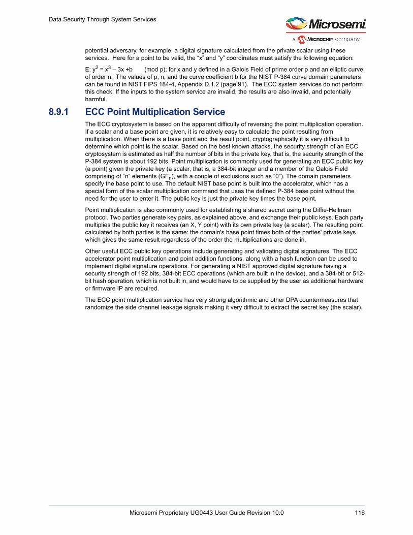
Data Security Through System Services
potential adversary, for example, a digital signature calculated from the private scalar using these services. Here for a point to be valid, the “x” and “y” coordinates must satisfy the following equation:
E: y2 = x3 – 3x +b (mod p); for x and y defined in a Galois Field of prime order p and an elliptic curve of order n. The values of p, n, and the curve coefficient b for the NIST P-384 curve domain parameters can be found in NIST FIPS 184-4, Appendix D.1.2 (page 91). The ECC system services do not perform this check. If the inputs to the system service are invalid, the results are also invalid, and potentially harmful.
8.9.1 ECC Point Multiplication ServiceThe ECC cryptosystem is based on the apparent difficulty of reversing the point multiplication operation. If a scalar and a base point are given, it is relatively easy to calculate the point resulting from multiplication. When there is a base point and the result point, cryptographically it is very difficult to determine which point is the scalar. Based on the best known attacks, the security strength of an ECC cryptosystem is estimated as half the number of bits in the private key, that is, the security strength of the P-384 system is about 192 bits. Point multiplication is commonly used for generating an ECC public key (a point) given the private key (a scalar, that is, a 384-bit integer and a member of the Galois Field comprising of “n” elements (GFn), with a couple of exclusions such as “0”). The domain parameters specify the base point to use. The default NIST base point is built into the accelerator, which has a special form of the scalar multiplication command that uses the defined P-384 base point without the need for the user to enter it. The public key is just the private key times the base point.
Point multiplication is also commonly used for establishing a shared secret using the Diffie-Hellman protocol. Two parties generate key pairs, as explained above, and exchange their public keys. Each party multiplies the public key it receives (an X, Y point) with its own private key (a scalar). The resulting point calculated by both parties is the same: the domain's base point times both of the parties' private keys which gives the same result regardless of the order the multiplications are done in.
Other useful ECC public key operations include generating and validating digital signatures. The ECC accelerator point multiplication and point addition functions, along with a hash function can be used to implement digital signature operations. For generating a NIST approved digital signature having a security strength of 192 bits, 384-bit ECC operations (which are built in the device), and a 384-bit or 512-bit hash operation, which is not built in, and would have to be supplied by the user as additional hardware or firmware IP are required.
The ECC point multiplication service has very strong algorithmic and other DPA countermeasures that randomize the side channel leakage signals making it very difficult to extract the secret key (the scalar).
Microsemi Proprietary UG0443 User Guide Revision 10.0 116
Data Security Through System Services
The following is the flow diagram for ECC point multiplication system service.
Figure 57 • ECC Point Multiplication System Service Flow
The following table describes the ECC Point Multiplication system service request.
Table 78 • ECC Point Multiplication System Service Request
Offset Length (bytes) Field Description
0 1 CMD = 16 Command
1 4 ECCPMULTPTR Pointer to ECCPMULT structure
Note: Cortex-M3 is only available in SmartFusion2
Cortex-M3/Fabric master setup the ECCPMULTPTR descriptor
Cortex-M3/Fabric master send ECC Point Multiplier system service command and
ECCPMULTPTR pointer
System controller fetches descriptor data
System controller executes the service and writes the output data to pointer location and
sends system service response
M3/Fabric checks system service response
Cortex-M3/Fabric master reads the ECC multiplier output from QPTR pointer location
Microsemi Proprietary UG0443 User Guide Revision 10.0 117

Data Security Through System Services
The following table describes the ECC Point Multiplication system service response.
The following table provides details about the layout of the ECC Point Multiplication Data Descriptor (ECCPMULT).
The ECC point multiplication service has very strong algorithmic and other DPA countermeasures that randomize the side-channel leakage signals making it very difficult to extract the secret key (that is, the scalar). The ECC point multiplication services can be used in data security applications, for example, to generate public keys, to perform key establishment, to do encryption or decryption, and to generate or verify digital signatures.
8.10 Elliptic Curve Cryptography (ECC) Point-Addition ServiceThe ECC point addition service “adds” two points according to the commonly accepted definition of elliptic curve point addition. The inputs are two (x, y) points, each lying on the P-384 curve, and the result is another (x, y) point which is guaranteed to be on the curve (or be the point at infinity). The input points are not checked by the service to see if they are legal points, but if they are, then the result point is guaranteed by design to be correct.
The point addition operation is designed to be timing-invariant, independent of the input data, that prevents timing analysis, and, to have insignificant amplitude leakage, which prevents simple power analysis or simple electromagnetic analysis. The operation has weak DPA countermeasures, so if the same secret is used many times with different data that is known to the adversary, a DPA attack may succeed. The “points” are never secrets in the common ECC algorithms, only the scalar in point multiplication is a secret. Therefore, there may be no need for DPA protection for point addition, which deals only with points. It is up to the user to be sure of using this service in a safe way to meet the security needs of the application.
Table 79 • ECC Point Multiplication System Service Response
Offset Length (bytes) Field Description
0 1 CMD = 16 Command
1 1 STATUS Command status:0 Success 127 HRESP error occurred during HPMS transfer 253 Not licensed 254 Service disabled by factory security 255 Service disabled by user security
2 4 ECCPMULTPTR Pointer to ECCPMULT structure
Table 80 • ECCPMULT Structure
Offset Length (bytes) Field Description
0 4 DPTR Pointer to 384-bit scalar, (big endian)
4 4 PPTR Pointer to (X,Y) coordinates of P
8 4 QPTR Pointer to (X,Y) coordinates of result Q
Microsemi Proprietary UG0443 User Guide Revision 10.0 118
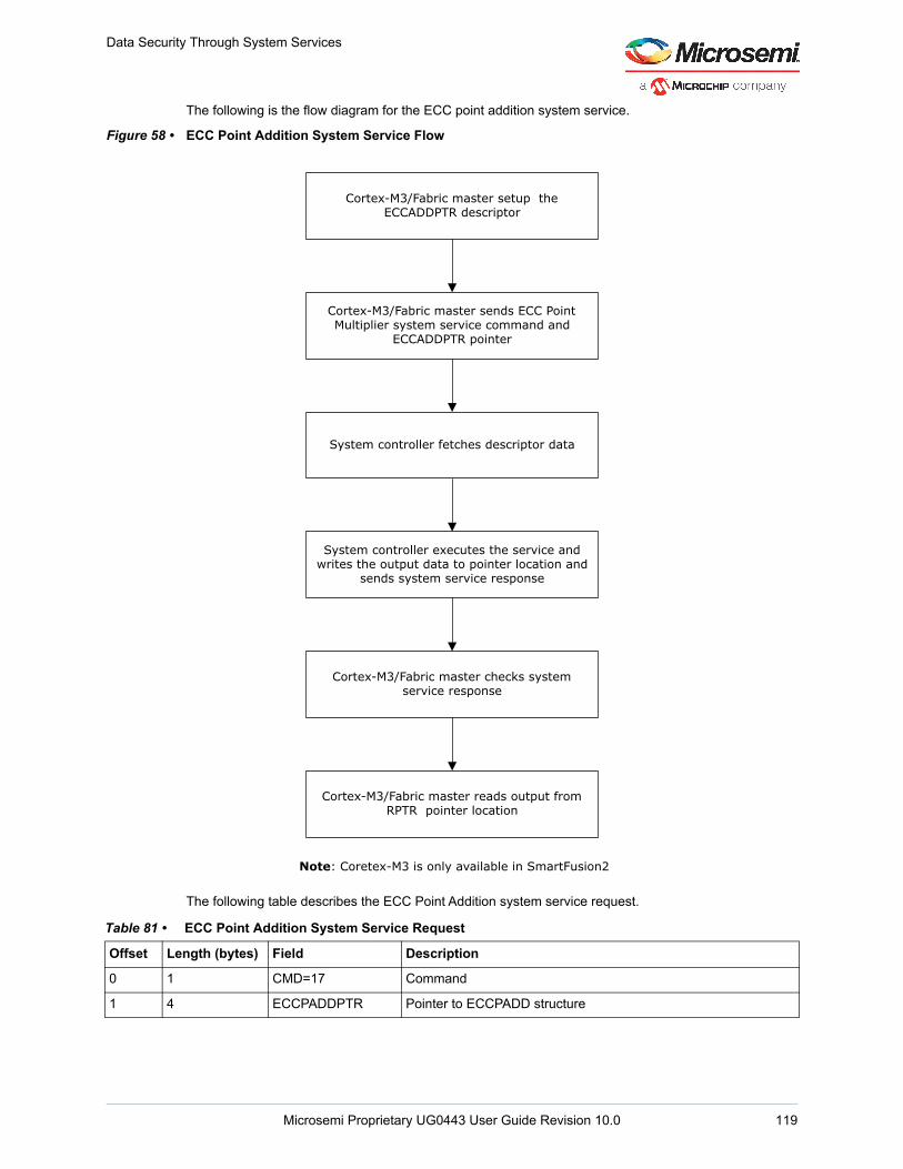
Data Security Through System Services
The following is the flow diagram for the ECC point addition system service.
Figure 58 • ECC Point Addition System Service Flow
The following table describes the ECC Point Addition system service request.
Table 81 • ECC Point Addition System Service Request
Offset Length (bytes) Field Description
0 1 CMD=17 Command
1 4 ECCPADDPTR Pointer to ECCPADD structure
Note: Coretex-M3 is only available in SmartFusion2
Cortex-M3/Fabric master setup the ECCADDPTR descriptor
Cortex-M3/Fabric master sends ECC Point Multiplier system service command and
ECCADDPTR pointer
System controller fetches descriptor data
System controller executes the service and writes the output data to pointer location and
sends system service response
Cortex-M3/Fabric master checks system service response
Cortex-M3/Fabric master reads output from RPTR pointer location
Microsemi Proprietary UG0443 User Guide Revision 10.0 119
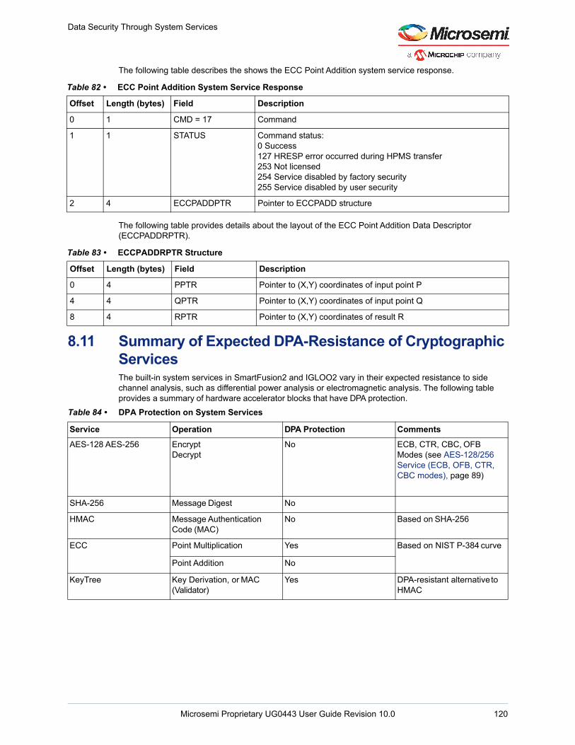
Data Security Through System Services
The following table describes the shows the ECC Point Addition system service response.
The following table provides details about the layout of the ECC Point Addition Data Descriptor (ECCPADDRPTR).
8.11 Summary of Expected DPA-Resistance of Cryptographic ServicesThe built-in system services in SmartFusion2 and IGLOO2 vary in their expected resistance to side channel analysis, such as differential power analysis or electromagnetic analysis. The following table provides a summary of hardware accelerator blocks that have DPA protection.
Table 82 • ECC Point Addition System Service Response
Offset Length (bytes) Field Description
0 1 CMD = 17 Command
1 1 STATUS Command status:0 Success 127 HRESP error occurred during HPMS transfer 253 Not licensed 254 Service disabled by factory security 255 Service disabled by user security
2 4 ECCPADDPTR Pointer to ECCPADD structure
Table 83 • ECCPADDRPTR Structure
Offset Length (bytes) Field Description
0 4 PPTR Pointer to (X,Y) coordinates of input point P
4 4 QPTR Pointer to (X,Y) coordinates of input point Q
8 4 RPTR Pointer to (X,Y) coordinates of result R
Table 84 • DPA Protection on System Services
Service Operation DPA Protection Comments
AES-128 AES-256 Encrypt Decrypt
No ECB, CTR, CBC, OFBModes (see AES-128/256 Service (ECB, OFB, CTR, CBC modes), page 89)
SHA-256 Message Digest No
HMAC Message Authentication Code (MAC)
No Based on SHA-256
ECC Point Multiplication Yes Based on NIST P-384 curve
Point Addition No
KeyTree Key Derivation, or MAC (Validator)
Yes DPA-resistant alternative to HMAC
Microsemi Proprietary UG0443 User Guide Revision 10.0 120
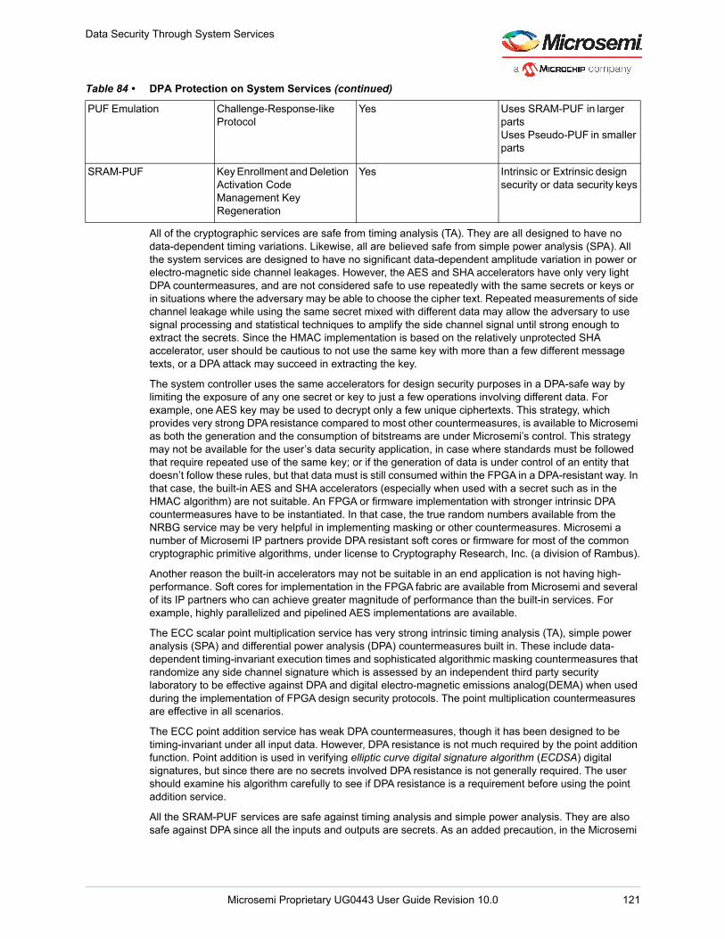
Data Security Through System Services
All of the cryptographic services are safe from timing analysis (TA). They are all designed to have no data-dependent timing variations. Likewise, all are believed safe from simple power analysis (SPA). All the system services are designed to have no significant data-dependent amplitude variation in power or electro-magnetic side channel leakages. However, the AES and SHA accelerators have only very light DPA countermeasures, and are not considered safe to use repeatedly with the same secrets or keys or in situations where the adversary may be able to choose the cipher text. Repeated measurements of side channel leakage while using the same secret mixed with different data may allow the adversary to use signal processing and statistical techniques to amplify the side channel signal until strong enough to extract the secrets. Since the HMAC implementation is based on the relatively unprotected SHA accelerator, user should be cautious to not use the same key with more than a few different message texts, or a DPA attack may succeed in extracting the key.
The system controller uses the same accelerators for design security purposes in a DPA-safe way by limiting the exposure of any one secret or key to just a few operations involving different data. For example, one AES key may be used to decrypt only a few unique ciphertexts. This strategy, which provides very strong DPA resistance compared to most other countermeasures, is available to Microsemi as both the generation and the consumption of bitstreams are under Microsemi’s control. This strategy may not be available for the user’s data security application, in case where standards must be followed that require repeated use of the same key; or if the generation of data is under control of an entity that doesn’t follow these rules, but that data must is still consumed within the FPGA in a DPA-resistant way. In that case, the built-in AES and SHA accelerators (especially when used with a secret such as in the HMAC algorithm) are not suitable. An FPGA or firmware implementation with stronger intrinsic DPA countermeasures have to be instantiated. In that case, the true random numbers available from the NRBG service may be very helpful in implementing masking or other countermeasures. Microsemi a number of Microsemi IP partners provide DPA resistant soft cores or firmware for most of the common cryptographic primitive algorithms, under license to Cryptography Research, Inc. (a division of Rambus).
Another reason the built-in accelerators may not be suitable in an end application is not having high- performance. Soft cores for implementation in the FPGA fabric are available from Microsemi and several of its IP partners who can achieve greater magnitude of performance than the built-in services. For example, highly parallelized and pipelined AES implementations are available.
The ECC scalar point multiplication service has very strong intrinsic timing analysis (TA), simple power analysis (SPA) and differential power analysis (DPA) countermeasures built in. These include data-dependent timing-invariant execution times and sophisticated algorithmic masking countermeasures that randomize any side channel signature which is assessed by an independent third party security laboratory to be effective against DPA and digital electro-magnetic emissions analog(DEMA) when used during the implementation of FPGA design security protocols. The point multiplication countermeasures are effective in all scenarios.
The ECC point addition service has weak DPA countermeasures, though it has been designed to be timing-invariant under all input data. However, DPA resistance is not much required by the point addition function. Point addition is used in verifying elliptic curve digital signature algorithm (ECDSA) digital signatures, but since there are no secrets involved DPA resistance is not generally required. The user should examine his algorithm carefully to see if DPA resistance is a requirement before using the point addition service.
All the SRAM-PUF services are safe against timing analysis and simple power analysis. They are also safe against DPA since all the inputs and outputs are secrets. As an added precaution, in the Microsemi
PUF Emulation Challenge-Response-like Protocol
Yes Uses SRAM-PUF in larger partsUses Pseudo-PUF in smaller parts
SRAM-PUF Key Enrollment and Deletion Activation Code Management Key Regeneration
Yes Intrinsic or Extrinsic design security or data security keys
Table 84 • DPA Protection on System Services (continued)
Microsemi Proprietary UG0443 User Guide Revision 10.0 121
Data Security Through System Services
implementation of Quiddikey the base activation code and all key codes are stored in read and write protected eNVM, along with authentication and other countermeasures.
The PUF emulation service uses the key tree algorithm, which is also available as a system service.
The Key Tree service is intrinsically DPA safe because it limits the use of any secret key to just three possible operations: the hash function higher up the tree that generated it, and the two possible hash functions that may consume it going down the tree (depending upon the value of the path argument). No matter how many times the same key is used, with the same or a different path variable, any given root, intermediate or result key can have, at most, these three operations (possibly multiple times) which can leak information about it. While multiple measurements repeatedly using the same data may help the adversary normalize the effects of uncorrelated noise, it does nothing to reduce the effects of an algorithmic noise. The side channel leakage of the SHA accelerator is less compared to the self-generated algorithmic noise and prevents significant reduction in key entropy with just three measurements. Between levels of the key tree, the intermediate keys are hashed, thus effectively destroying any information gained by the adversary at a level preceding the next. As an added precaution, the two constants used in the right and left branches of the key tree, respectively, are maintained as secrets.
All the NIST standard cryptographic algorithms implemented in SmartFusion2 and IGLOO2 FPGAs have been certified by a NIST accredited laboratory under the NIST cryptographic algorithm validation program (CAVP) scheme. See the Hardware Cryptographic Accelerators, page 10 for the NIST certificate numbers.
Microsemi Proprietary UG0443 User Guide Revision 10.0 122
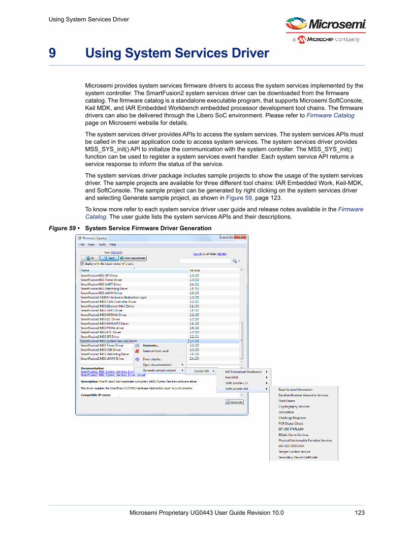
Using System Services Driver
Microsemi Proprietary UG0443 User Guide Revision 10.0 123
9 Using System Services Driver
Microsemi provides system services firmware drivers to access the system services implemented by the system controller. The SmartFusion2 system services driver can be downloaded from the firmware catalog. The firmware catalog is a standalone executable program, that supports Microsemi SoftConsole, Keil MDK, and IAR Embedded Workbench embedded processor development tool chains. The firmware drivers can also be delivered through the Libero SoC environment. Please refer to Firmware Catalog page on Microsemi website for details.
The system services driver provides APIs to access the system services. The system services APIs must be called in the user application code to access system services. The system services driver provides MSS_SYS_init() API to initialize the communication with the system controller. The MSS_SYS_init() function can be used to register a system services event handler. Each system service API returns a service response to inform the status of the service.
The system services driver package includes sample projects to show the usage of the system services driver. The sample projects are available for three different tool chains: IAR Embedded Work, Keil-MDK, and SoftConsole. The sample project can be generated by right clicking on the system services driver and selecting Generate sample project, as shown in Figure 59, page 123.
To know more refer to each system service driver user guide and release notes available in the Firmware Catalog. The user guide lists the system services APIs and their descriptions.
Figure 59 • System Service Firmware Driver Generation
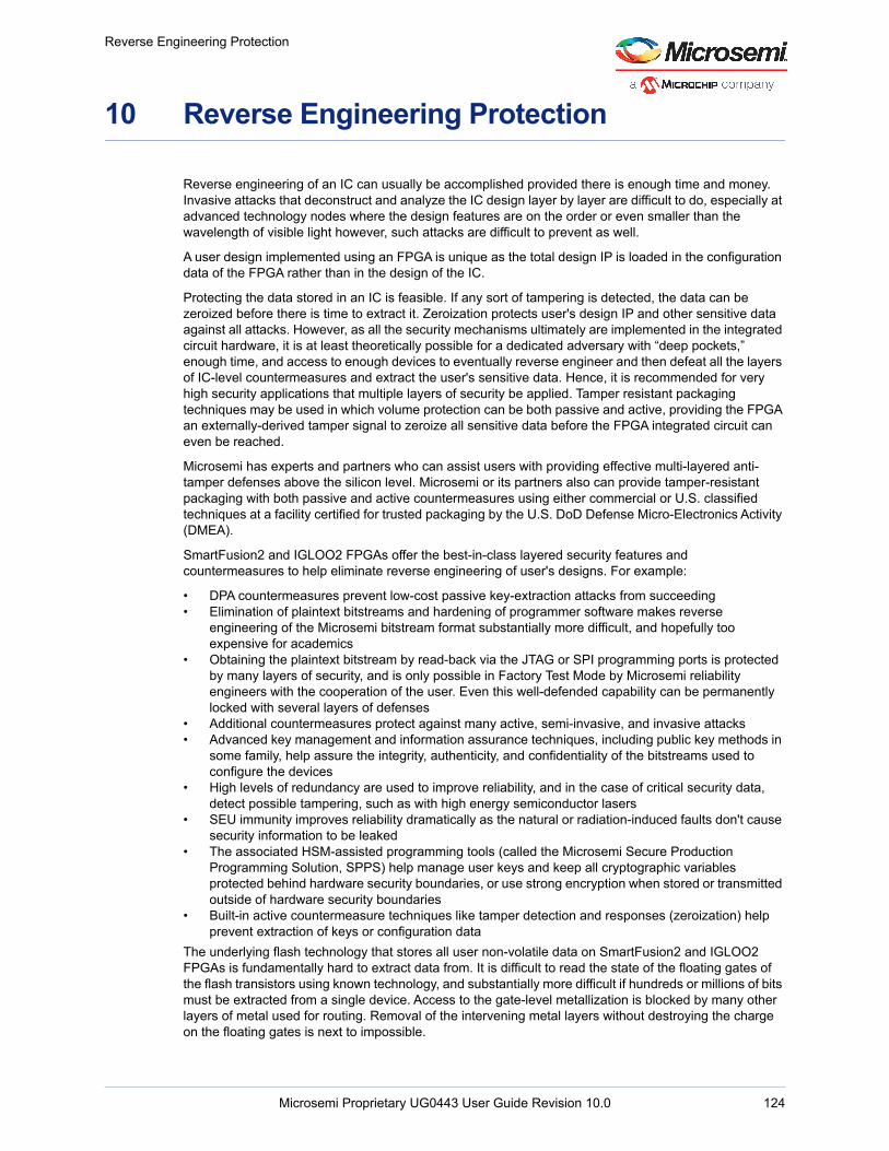
Reverse Engineering Protection
10 Reverse Engineering Protection
Reverse engineering of an IC can usually be accomplished provided there is enough time and money. Invasive attacks that deconstruct and analyze the IC design layer by layer are difficult to do, especially at advanced technology nodes where the design features are on the order or even smaller than the wavelength of visible light however, such attacks are difficult to prevent as well.
A user design implemented using an FPGA is unique as the total design IP is loaded in the configuration data of the FPGA rather than in the design of the IC.
Protecting the data stored in an IC is feasible. If any sort of tampering is detected, the data can be zeroized before there is time to extract it. Zeroization protects user's design IP and other sensitive data against all attacks. However, as all the security mechanisms ultimately are implemented in the integrated circuit hardware, it is at least theoretically possible for a dedicated adversary with “deep pockets,” enough time, and access to enough devices to eventually reverse engineer and then defeat all the layers of IC-level countermeasures and extract the user's sensitive data. Hence, it is recommended for very high security applications that multiple layers of security be applied. Tamper resistant packaging techniques may be used in which volume protection can be both passive and active, providing the FPGA an externally-derived tamper signal to zeroize all sensitive data before the FPGA integrated circuit can even be reached.
Microsemi has experts and partners who can assist users with providing effective multi-layered anti-tamper defenses above the silicon level. Microsemi or its partners also can provide tamper-resistant packaging with both passive and active countermeasures using either commercial or U.S. classified techniques at a facility certified for trusted packaging by the U.S. DoD Defense Micro-Electronics Activity (DMEA).
SmartFusion2 and IGLOO2 FPGAs offer the best-in-class layered security features and countermeasures to help eliminate reverse engineering of user's designs. For example:
• DPA countermeasures prevent low-cost passive key-extraction attacks from succeeding• Elimination of plaintext bitstreams and hardening of programmer software makes reverse
engineering of the Microsemi bitstream format substantially more difficult, and hopefully too expensive for academics
• Obtaining the plaintext bitstream by read-back via the JTAG or SPI programming ports is protected by many layers of security, and is only possible in Factory Test Mode by Microsemi reliability engineers with the cooperation of the user. Even this well-defended capability can be permanently locked with several layers of defenses
• Additional countermeasures protect against many active, semi-invasive, and invasive attacks• Advanced key management and information assurance techniques, including public key methods in
some family, help assure the integrity, authenticity, and confidentiality of the bitstreams used to configure the devices
• High levels of redundancy are used to improve reliability, and in the case of critical security data, detect possible tampering, such as with high energy semiconductor lasers
• SEU immunity improves reliability dramatically as the natural or radiation-induced faults don't cause security information to be leaked
• The associated HSM-assisted programming tools (called the Microsemi Secure Production Programming Solution, SPPS) help manage user keys and keep all cryptographic variables protected behind hardware security boundaries, or use strong encryption when stored or transmitted outside of hardware security boundaries
• Built-in active countermeasure techniques like tamper detection and responses (zeroization) help prevent extraction of keys or configuration data
The underlying flash technology that stores all user non-volatile data on SmartFusion2 and IGLOO2 FPGAs is fundamentally hard to extract data from. It is difficult to read the state of the floating gates of the flash transistors using known technology, and substantially more difficult if hundreds or millions of bits must be extracted from a single device. Access to the gate-level metallization is blocked by many other layers of metal used for routing. Removal of the intervening metal layers without destroying the charge on the floating gates is next to impossible.
Microsemi Proprietary UG0443 User Guide Revision 10.0 124
Reverse Engineering Protection
Even attacks using optical emissions through the base silicon are becoming difficult as the feature size becomes smaller than the optical wavelengths that can be transmitted through silicon. Besides using an advanced technology node, Microsemi has included several countermeasures in SmartFusion2 and IGLOO2 against certain such types of attack.
10.1 Configuration Port SecurityThe main configuration ports for SmartFusion2 and IGLOO2 are the JTAG and SPI-slave ports. They support a nearly identical set of programming instructions. JTAG supports the JTAG-defined boundary scan instructions, decodes the optional user JTAG instruction range.
As described in FPGA Lock-bits, page 34 there is a user lock-bit that disables the JTAG boundary scan instructions, and there are other lock bits that can disable all JTAG programming instructions. Few other lock-bits also disable the similar SPI Slave programming instructions.
SmartFusion2 and IGLOO2 FPGAs can be configured in SPI master mode by asserting the FLASH_GOLDEN_N external pin on the device. This causes the system controller to read the SPI port and look for a valid bitstream. If found, the bitstream is loaded. This operation can be blocked by a user lock-bit.
Finally, SmartFusion2 and IGLOO2 FPGAs can also be configured using a system service called in-application programming (IAP). In SmartFusion2 this would typically be done using firmware running on the Cortex-M3. The bitstream can be imported to the device via any supported media (e.g., Ethernet) and then routed into the internal system service via the Comm_Blk bus slave from where the system controller can write it to an external (but local) SPI PROM, verify it via another IAP system service, and then load it with another; or it can be loaded immediately (with somewhat greater risk of a denial-of-service if it arrived over the media corrupted). In any case, the IAP system service(s) can be blocked with a lock-bit, thus providing a hardware level of protection. Even if the Cortex-M3 has caught a virus and is executing malware, it can't override any lock-bits as they can only be changed by an authenticated/encrypted bitstream file. As this “port” is blocked by the current lock-bit setting, any such bitstream would have to come in via one of the other ports mentioned above that wasn't currently blocked.
10.2 User JTAG (UJTAG) Security ConsiderationsSmartFusion2 has two JTAG tap controllers: The primary one is for the system controller and various device testing facilities; the second one is the Cortex-M3 tap controller, which allows the use of standard ARM debug tools. Essentially, the two tap controllers are mutually exclusive, sharing the same input and output pins. The tap controller selection is made using an external input pin, “JTAG_SEL,” which would normally have a pull-up resistor at the board level so that without any other connections (such as a debugger tool) the default would be to select the system controller tap controller.The selection is forced to the system controller tap controller if Cortex-M3 debugging is disabled via the lock-bit, in this scenario the unselected tap controller is held in reset
The system controller JTAG tap controller has an 8-bit instruction register, which is used to identify the command that is being executed, that is which data register is selected. The range from 0x10 to 0x7F (inclusive; 16 to 127 in decimal notation) is decoded and reserved for User JTAG.
The UJTAG capability can be used to monitor the JTAG data input, or to add additional JTAG data registers, via the FPGA fabric. They can also be useful during the debugging phase to instrument the design. This is done by instantiating the UJTAG macro in the user design, and connecting to its ports to the User's custom user logic (or logic inserted by debugging tools). Microsemi offers a Security Monitor soft IP macro that, amongst other things connects to the UJTAG pins, looking for suspicious JTAG activity and imposing an appropriate penalty, if found.
Microsemi Proprietary UG0443 User Guide Revision 10.0 125
Reverse Engineering Protection
Figure 60 • JTAG Controllers CBlock Diagram (Including UJTAG Data Registers)
If the UJTAG macro is used during development, for accessing and scanning out potentially sensitive internal signals (for debugging purposes), then it should be certain that it is removed from the final design UJTAG is used by Identify® (from Synopsys), one of the third-party debugging tools Microsemi supplies, and possibly by other third-party tools as well.
A great many of the JTAG commands can be disabled by user lock-bits. For example, the IEEE 1149.1 JTAG boundary scan instructions that are so useful for board-level testing can be disabled with a lock-bit. Likewise, groups of debugging-related commands, programming commands, passcode entry commands, can be disabled with lock-bits. See FPGA Lock-bits, page 34 for further description of these and other lock-bit features.
10.3 Programming Port MonitorIn all models, most JTAG and all SPI Slave instructions are monitored and reported in fourteen logical groups via the asynchronous USI bus attached to the FPGA fabric. These signals can be monitored by the logic in the FPGA fabric by instantiating the Tamper macro in the user's design, and connecting to its
TDO
HW-only Data Registers
Fireware Data Registers
TDI
TMS
TCK
TRSTB
Instruction Register
Decode
UREG [7:0]JTAG State Machine
UJTAG Data Reister
System Controller JTAG tap controller
User JTAG (UJTAG) FPGA Fabric Design
UREG [7:0] 0 × 10 ≤ Instr ≤ 0 × 7F
Cortex-M3 Debug Data Registers
Cortex-M3 JTAG Tap Controller
JTAG State Machine
JTAG Input Pins
Instruction Register
Decode
UD
RCAP
UD
RSH
UD
RU
PD
URSTB
1
0
Sel
= JTAGSEL + M3DEBUG
Sel = JTAGSEL + M3DEBUG
JTAGSEL
M3DEBUG
User Lock-bit
(“1” Enabled debugging)
UTDO
JTAG output pin
UTDI
UTCK
Microsemi Proprietary UG0443 User Guide Revision 10.0 126
Reverse Engineering Protection
ports. Refer to SmartFusion2 and IGLOO2 FPGA Tamper Detection and Tamper Response, page 57 for detail.
10.4 Intrusion Detection and ProtectionSmartFusion2 and IGLOO2 FPGAs have a number of built-in tamper detection and response capabilities that can be used to enhance design and data security. Microsemi offers a flexible Security Monitor IP core that takes advantages of many of the built-in tamper detection and response capabilities, and allows external tamper flags to be monitored, as well.
10.5 Side Channel Analysis (SCA), Passive & Active, Non- and Semi-InvasiveWhenever any electronic device performs internal operations, there is information leakage via the energy lost to various so-called side channels. Common side channels used as attack vectors include device power consumption and electromagnetic radiation (radio spectrum), leading to power analysis (PA) and electromagnetic analysis (EMA). Photons (in the light spectrum) can also be used as a side channel, but generally de-packaging of the device is required to gain access (semi-invasive), whereas PA and EMA can be non-invasive or even performed from a distance of up to several meters.
By monitoring the side channel (for example, fluctuations in the power consumption), sometimes there is enough leakage that with a single or just a few measurements an attacker can reconstruct secrets the device is using in what is called Simple Power Analysis (SPA). In less favorable (to the attacker) signal-to-noise ratio situations, additional known information such as the encrypted bitstream and measurements over many operations using the same secret (such as the bitstream decryption key) are needed to determine the secret using Differential Power Analysis (DPA).
Published reports from researchers have shown that no FPGA, microcontroller or ASIC is immune from this vulnerability of the bitstream keys (used for FPGA design security), and keys used in cryptographic algorithms running in the FPGA fabric or on an embedded microcontroller (used in various data security applications) have all been reported in numerous studies to have been extracted using DPA techniques. In reports analyzing several types of SRAM FPGAs, one team of researchers learned enough information from one power-up cycle (per device) to reconstruct the bitstream key used by that device by monitoring the devices power consumption. In another study, the keys in a technologically advanced SRAM FPGA were extracted using a form of differential electro-magnetic analysis (DEMA) using only 5000 measurements.
Because of the severity of this vulnerability, nearly all the secure processors in the smartcards used in the financial industry, set-top boxes, trusted platform modules in personal computers and encrypted disk drives, amounting to approximately six billion chips per year, incorporate countermeasures to DPA.
Figure 61 • DPA Logo
SmartFusion2 SoC FPGAs and IGLOO2 FPGAs are the first devices in the programmable logic device (PLD) industry incorporating DPA countermeasures to protect the bitstream key(s) from discovery using side channel analysis. All built-in uses of design security secret keys have been protected against side-channel analysis. Many of the countermeasures used are licensed from Cryptography Research Inc. (CRI), a division of Rambus, Inc., who holds the patents thereto. Microsemi is a licensee of Cryptography Research's DPA patent portfolio, thus CRI allows Microsemi to use their trademarked “Licensed DPA Countermeasures” logo, shown here.
Microsemi Proprietary UG0443 User Guide Revision 10.0 127
Reverse Engineering Protection
All SmartFusion2 and IGLOO2 devices incorporate strong DPA countermeasures for all design security features, The DPA countermeasures are certified as effective by CRI based on an assessment from an independent third-party lab (Riscure) under Rambus-CRI's DPA Validation Program (DVP) scheme.
All design security cryptographic keys and secrets managed by the Programming system controller are automatically protected against DPA and related passive non-invasive side channel attacks such as DEMA without the user having to do anything. The paragraphs immediately following discuss protections these devices have against a broad range of side channel attacks.
Microsemi Proprietary UG0443 User Guide Revision 10.0 128
Internal Security Features
11 Internal Security Features
11.1 Single Event Upset RobustnessIn complementary metal-oxide-semiconductor (CMOS) technology, memories such as SRAM and flip-flops can have their state changed by radiation particles. These particles can come from high-energy particles hitting atmospheric molecules, causing them to emit sub-atomic particles such as neutrons that (when they strike the silicon) can create charged particles. Another source of alpha radiation is from device packaging materials such as epoxy. The net result is that radiation can cause the state of a memory cell to flip. The effect, called SEU is worse at some latitudes (due mainly to the shape of the Earth's magnetic field) and altitudes. In general it gets worse from sea-level to approximately 60,000 ft, and then drops up to the radiation belts circling the Earth where the radiation is quite high. Even at sea-level, it is usually by far the largest single source of failures in SRAM FPGAs, and the effect can go up several orders of magnitude at commercial airliner or military aircraft altitudes.
Configuration memory, which is supposed to hold its state statically for the entire duration of operation of the device is especially susceptible because of its large size (that is, number of memory cells), the long and constant exposure, and the persistence and severity of effects of a fault. Until corrected, the fundamental operation of the FPGA routing and logic may be affected. Unless special measures are taken to detect and correct such configuration memory faults, the firm errors may persist for long times by affecting a large amount of data or even completely destroying the function of the FPGA. Since triple redundancy is considered too expensive on such a large amount of memory, usually a compromise approach is taken where it takes some time for a scrubber to detect and correct a firm error. In some devices, the entire configuration memory needs to be reloaded from the external source, causing a large down-time that is unacceptable in many applications.
This is generally more severe and effective than a flip-flop in the data-path is affected. In this case, the problem is often transient and usually very quickly self-corrected. When the flip-flop is next enabled and clocked, it latches a new, correct value, which often happens within nanoseconds. How far the false value propagates down the data-path is subject to the algorithm design. Also, because there are far fewer flip-flops than configuration memory cells (by two to three orders of magnitude), the probability of such an upset is much lower. In high-reliability applications, single flip-flops can be automatically replaced with triple-redundant flip-flops in the user programmable design by tools provided by Microsemi EDA partners. The two unaffected flip-flops will automatically vote away and correct an SEU in the affected flip-flop.
SmartFusion2 and IGLOO2 FPGAs incorporate flash configuration memory that is virtually SEU immune with error detection and correction (EDAC) techniques on nearly all the SRAM blocks throughout the MSS and HPMS. This implementation makes these devices substantially more reliable than most typical commercial microcontrollers that do not incorporate EDAC so widely (if at all) and far more reliable than any comparably-sized SRAM FPGAs.
11.1.1 FPGA Fabric Configuration MemoryThe flash configuration memory in SmartFusion2 and IGLOO2 FPGAs are virtually immune to SEU. Since this is typically the largest single source of failures in SRAM FPGAs, this single attribute of Microsemi flash FPGAs makes them by far the most reliable in the industry. Because of their inherent high-immunity to SEUs and high overall reliability over their rated life, no periodic scrubber circuitry is required to detect and fix errors after the fact. The SEU errors normally never occur in the first place.
Integrity check mechanisms can be used to ensure that there are no failed bits at power-on or on demand (whether caused naturally or maliciously) by checking the cryptographic grade digest computed over the entire FPGA configuration NVM.
Microsemi Proprietary UG0443 User Guide Revision 10.0 129
Internal Security Features
11.1.2 Security Non-Volatile Memory (NVM)The SNVM is used where factory and user design security keys and lock-bits are stored. The SNVM is designed with the same long-life high-reliability SEU-immune characteristics as the FPGA fabric flash-configuration memory. Because of the sensitivity of the data it contains, to achieve ultra-high reliability including protection against malicious attacks, each row of security data has single-error correction, double-error detection (SECDEC) error detection and correction (EDAC) circuitry.
Unlike typical row-and-column addressed memory arrays, any bit stored in the SmartFusion2 and IGLOO2 SNVM are designed by Microsemi to be continuously output on a logic signal in parallel with others, regardless of the rows or columns they have or other such memory cells are in. This is similar to the difference between a register file and an SRAM array in volatile memory technology. The SRAM can only read one row at a time, but any bit can be brought out of a register file in parallel with any others. Many lock-bits are used to control other hardware security features directly using these parallel output signals. Critical lock-bits have continuously-on detection circuitry that monitors these logic signals in real time and generates a tamper flag if there are any natural or malicious faults in these bits especially security-sensitive bits, guaranteeing detection of the faults immediately.
In addition, each row of security data also contains cryptographic-grade digest of the row's contents.
11.1.3 Embedded NVM ArrayThe eNVM applies SECDEC standard EDAC techniques using hidden parity bits stored in addition to user data in each page of data.
The cryptographic-grade digest computed over the ROM (that is, static) portions of user's eNVM space can be used at each power-on cycle, or on demand, to check the integrity of the memory. One digest is available for the user memory portion for each of the NVM controllers in the device, that is, one in -005, -010, -025, -050 devices, and -060 devices, two in -090, and -150 devices. In -090 and -150 devices, two additional digests are used to cover the system controllers private eNVM pages in the second eNVM array.
11.1.4 MSS embedded SRAM (eSRAM) The two 64 KByte eSRAM blocks attached to the MSS bus switch have an option to apply SECDEC EDAC techniques to each row of data saved and read. This can help to mitigate SEU or other types of errors. This feature is set by default.
If even higher reliability is required where data is stored statically in SRAM for very long time periods, a scrubber may be designed either in firmware or a bus master in logic in the FPGA that periodically reads each memory location and overwrites it with the corrected data if a correctable error was detected.
If EDAC is not required, the bits which are used for parity may be used instead of user data, increasing the capacity of these memories from 64 Kbytes to 80 Kbytes, each.
11.1.5 Miscellaneous SRAM Blocks Throughout the MSSEssentially, all the smaller SRAM blocks scattered throughout the MSS have SECDEC EDAC circuitry. For example, FIFOs in the Ethernet, CAN, and USB controllers. The instruction cache for the Cortex-M3 processor automatically corrects errors or flushes uncorrectable pages and re-fetches them, if possible.
This provides SEU immunity and reliability above-and-beyond that of most microcontrollers in the market.
11.1.6 DDR Memory ControllersSmartFusion2 and IGLOO2 devices contain on-chip controllers (and PHY) for off-chip DDR SDRAM-type memories. These controllers have an option to calculate parity bits when writing to the DDR memories and apply EDAC to the results that are read back, so long as user provides required external memory for the extra bits in each word that are required. This automatically improves the reliability and SEU immunity of the external DDR memories.
The primary usage of the external DDR memory is to hold the Cortex-M3 programs that are too large to fit in the on-chip memory. Therefore, an SEU error in this memory will be equivalent to a design error and could have disastrous security implications. EDAC significantly enhances the reliability of these
Microsemi Proprietary UG0443 User Guide Revision 10.0 130
Internal Security Features
memories for natural failures, such as caused by weak bits, noise, and SEU failures. If protection against malicious failures (for example, caused by board-level tampering) is also required then either in-line encryption or authentication techniques or both can be implemented for the FDDR memory using master in the FPGA fabric.
Note: The FDDR memory is only available in -050 and -150 devices
11.1.7 FPGA Fabric SRAM BlocksThe FPGA fabric tightly-coupled SRAM blocks do not have EDAC built-in. If EDAC or scrubbing are required, the additional logic required for these functions can easily be implemented using the FPGA fabric soft logic. Microsemi provides CoreEDAC Directcore IP that can generate EDAC circuitry for both internal (on-chip) and external RAM blocks.
11.1.8 System Controller SRAM BuffersThe system controller has a small SRAM buffer used for temporary storage. In consideration of SEU effects, SRAM buffer's usage is designed so that it is used only for very short term storage. In general, the system controller is in sleep mode most of the time. Data is not held over in SRAM storage while the system controller is in sleep mode. Between the small size of this SRAM and short times and duty factors where it is used, the risk caused by SEUs is minimal.
In -060, -090 and -150 devices, the ECC engine and the SRAM-PUF have small SRAM blocks associated. As with the system controller memory, long-term usage of the SRAM is not available, which will expose relatively static stored values to potential SEUs. The duty factor on these memories is extremely small. The ECC engine is used mainly during initial configuration of the user keys, and occasionally used after that for device authentication or user data security demands. In many systems, the entire lifetime usage is spread over 20 years may only amount to something measured in seconds.
Similarly, the SRAM-PUF memory block is very low-duty cycle, and is even in its own power domain where the power is removed nearly all the time. It is only used for a few milliseconds during enrollment and each time keys are reconstructed or a new random seed is requested. By design, there is a proportionately long power-down time of 100 msec between uses.
Furthermore, even if there is an SEU, the most probable outcome is that a protocol or command will detect the failure. In the case, of the SRAM-PUF, the algorithm is designed to be tolerant of turn-on noise. A bit failing during a more sensitive step might cause the reconstructed key to fail to match its built-in authentication tag and a failure will be flagged rather than returning an erroneous key. Generating random seeds is relatively tolerant of errors as a failure will most often just appear as another source of entropy; and these errors are very unlikely due to the small size and low-duty factory.
Performance an ECC operation such as point multiplication with an SRAM bit failure will likely cause an erroneous result. If even the low failure rates expected are of concern, the resulting point can be checked to see if it is on the elliptic curve or the computations can be run twice. Either of these will have the beneficial effect of helping to detect malicious faults injected by an adversary as well as any faults caused by SEUs.
In design security uses of the ECC engine, any SEU (or malicious) failure will be detected by a downstream authentication or validation protocol. But it should be emphasized that failures are expected with a very low probability. Compared to the size of a configuration memory of 50 million bits with 100% duty factor requirement, a small SRAM (for example, 16 Kbits) with a <<1% duty factory has a lower failure rate more than five or six orders of magnitude less all other things being equal. All other things are not equal in flash FPGAs since the configuration memory has an essentially zero SEU sensitivity for atmospheric neutrons; at least four or five orders of magnitude less than SRAM and perhaps more.
In summary, the exposure of the system controller and cryptographic SRAM blocks to SEUs is low because of the small number of SRAM bits, and the low-duty factor. Many of the possible failures have tolerable effects, such as a detected failure of a command or a result that is still useable.
In certain high-reliability applications such as avionics, there may be some residual concerns regarding the SEU-induced failure rate of the system controller, and concerns perhaps also driven by certification requirements. In this case, SmartFusion2 and IGLOO2 FPGAs also offer a mode where, once the device is booted instead of just going into sleep mode until an interrupt, the system controller goes asleep until the next reset. This is called Suspend mode. System services such as user cryptographic algorithm and
Microsemi Proprietary UG0443 User Guide Revision 10.0 131
Internal Security Features
random bit generator services, the zeroization service, or the Flash*Freeze service are not available in Suspend mode.
11.1.9 FPGA Fabric User Flip-FlopsFabric flip-flops are less in number compared to configuration bits. Thus, the probability of an SEU in a fabric flip-flop is relatively low.
Even if this low probability is still a concern, user can use triple-redundant flip-flops instead of single flip-flops or use error-tolerant coding techniques, especially in key state machines where an error will have a more catastrophic long-lasting effect. One such technique is to choose a state encoding that includes redundancy, such as Hamming or one-hot encoding, where any single failure (at a minimum) can be detected and a safe response taken.
By selectively using these techniques in the portions of the logic which will have the most damaging impact in the case of a failure (for example, in important state machines and control-path logic) and conventional design in those portions of the design where the effect of a failure may only be transient or will have a less serious impact (for example, in much of the data-path) the overall reliability and security of the design in the face of SEU or other failures can be increased at a very low cost.
For very high assurance applications, entire blocks of logic can be duplicated at macro level, and voting circuitry used to detect failures by looking for mismatches in their outputs using fail-safe design assurance (FSDA) techniques. If malicious faults are also a concern, then time-shifting the calculations done by the redundant logic can also improve the resilience of the overall system to attacks.
11.2 Environmental MonitoringSmartFusion2 and IGLOO2 devices do not have any built-in environmental monitors. Supply voltages are monitored during turn-on, and the boot process is held-off until the voltages reach acceptable levels.
11.3 Partial Reconfiguration SecuritySmartFusion2 and IGLOO2 devices can be partially reconfigured as long as atomic units are either fully reprogrammed, or not reprogrammed at all. The most common scenario for partial reconfiguration with these devices is to reload just a portion of the eNVM array. The atomic unit for the eNVM array is a page, consisting of 1024 bits of user data and some additional hidden data such as write-protect flags and parity bits that are automatically taken care of.
Each security segment can be erased and written as an atomic unit. This includes the three user security NVM segments:
• User Key segment• User 2 Key segment• User Lock segment.
The FPGA fabric is always treated as a single atomic unit. Partial reconfiguration of the FPGA fabric is not supported.
Programming any part of SmartFusion2 or IGLOO2 device requires an encrypted and authenticated bitstream containing the desired components. Any of the available programming methods can be used. The bitstream is authenticated as a whole; it is not possible to remove a portion of it. For example, a page of eNVM (even though eNVM pages are atomic units) without detection.
User with write privileges to eNVM can also write to its pages from internal FPGA or Cortex-M3 design application after importing the data. However, using the built-in bitstream loading mechanisms, whether through IAP or ISP, has the advantages of automating much of the key management and all the cryptography associated with the encryption and authentication of the incoming data, and is already designed to be safe from DPA attacks in all SmartFusion2 and IGLOO2 models regardless of their capacity.
11.4 User Test and Debug ModesThis paragraph discusses the user design debug capabilities of the SmartFusion2 and IGLOO2 devices from a security viewpoint.
Microsemi Proprietary UG0443 User Guide Revision 10.0 132

Internal Security Features
These debugging features are powerful tools to help in bringing a design to a working state. They are equally powerful tools for an adversary to observe the workings of a system, if it is not properly protected.
11.4.1 FPGA Fabric Real-Time Probes and Probe Read/Write FeaturesSmartFusion2 and IGLOO2 devices offer a unique feature for debugging the user design in the FPGA fabric in real time. Any two user flip-flop outputs can be routed to external debug pins at one time and monitored with a high-speed oscilloscope or logic analyzer. Some additional FPGA fabric IP blocks, such as fabric SRAMs and DSP blocks also have probe points.
In addition, the probe mechanism can also read (peek) and write (poke) values to individual flip-flops or to banks of flip-flops. It is possible to read and restore the entire state of the design with these features. These features are available in Live Probe and Active Probes tabs in SmartDebug tool.
Read and write operations and the Live Probe feature are not available during Flash*Freeze mode or during programming, and are blocked with separate read and write debug lock-bits. The read debug lock-bit blocks probe-read and live-probe. The write debug lock-bit blocks probe-write. These locks are stored in the user security segments and can be temporarily overridden by matching the Debug Passcode (DPK) or the FlashLock Passcode (UPK1).
Additionally, there are fabric cluster row probe read-locks that prevent reading of any probe-points in the fabric cluster row, as another layer of protection. These locks are part of the FPGA fabric flash segments, and can only be cleared by erasing the entire FPGA fabric design configuration along with the row locks. FPGA fabric erasing and overwriting is controlled by additional lock-bits as described in the FPGA Lock-bits, page 34.
The FPGA configuration non-volatile memory is not accessible via the probe mechanism, and can only be inferred indirectly by probing the dynamic signals processed by the User's FPGA logic.
11.4.2 System IP Interface (SII) Bus Test ModesThe SII bus has access to various FPGA fabric blocks including:
• LSRAM blocks • µSRAM blocks• Built-in self-test logic for the SRAMs• Clock conditioning circuit (CCC) blocks• Fabric control circuitry
The DSP blocks are the only type of IP blocks in the FPGA fabric not attached to the SII bus. The eNVM and eSRAM blocks, which are clearly outside the fabric, are not attached to the SII bus. The SII bus is used for testing new devices in the Microsemi production environment, and by the system controller for some system services. It also has an external debug interface, accessed via the JTAG or SPI-slave programming ports.
The debug interface is mostly used by the Microsemi user debugging tools to read and write to the FPGA fabric SRAM blocks.
This debugging feature is disabled by the same read and write debug locks: the read debug lock blocks reading of the SRAM and the write debug lock blocks writing to the SRAM.
11.4.3 Cortex - M3 Debugging ModesThe debug system of the Cortex-M3 processor is based on the ARM CoreSight architecture. CoreSight based designs enable the memory and peripheral registers to be examined even when the CPU is running. The Cortex-M3 debugging features are only available in SmartFusion2 devices, and not in IGLOO2 devices.
The debug port uses a serial wire JTAG debug port (SWJ-DP). This enables either the JTAG or the Serial Wire Debug (SWD) to be used for debugging. The SWJ-DP defaults to JTAG mode at power-up and can be switched to SWD mode by applying a specific sequence to the debug pins.
The trace port interface unit (TPIU) is configured to support Instruction Trace Module (ITM) debug trace and Embedded Trace Module (ETM) debug trace.
The Cortex-M3 processor provides the following debug Interfaces:
Microsemi Proprietary UG0443 User Guide Revision 10.0 133
Internal Security Features
11.4.3.0.1 JTAG DebuggerSWJ-DP: JTAG is the industry-standard interface used to download and debug programs on a target processor, as well as for other functions. It offers access to all of the ARM Cortex-M3 processor CoreSight debug capabilities. The JTAG pins are shared with the main JTAG tap controller and the Cortex-M3 JTAG tap controller under control of an external device pin.
11.4.3.0.2 Serial-Wire DebuggerSW-DP: The serial wire debug (SWD) mode is an alternative to the standard JTAG interface. SWD uses 2-pins to provide the same debug functionality as JTAG with no performance penalty, and introduces data trace capabilities with the Serial Wire Viewer (SWV). The SWD interface pins are overlaid with the JTAG signals, allowing standard target connectors to be used.
SWV: It provides real-time data trace information from various sources within the Cortex-M3 processor. This is output via the single SWO pin while the system processor continues running at full speed. SWV can only be used with the SWD Interface
11.4.3.0.3 Embedded Trace Module (ETM)The embedded trace macrocell provides high bandwidth instruction trace via four dedicated trace pins.
It also includes trace capabilities as:
• Data Trace: Generating events to record data reads/writes, exceptions/interrupts, and PC (program counter) sampling information.
• Software Trace: Supporting output of debug messages (for example, printf) to the host.• Instruction trace: Collecting a sequence of every executed instruction continuously for a selected
portion of your application.
Trace results are generated in the form of packets, which can be of various lengths. The trace components transfer the packets using the advanced trace bus (ATB) to the TPIU which formats the packets into the trace interface protocol (TIP). The data is then captured by an external trace capture device such as a trace port analyzer (TPA).
11.4.4 MSS Debug FeaturesThe MSS bus switch and slaves can be mastered by the system controller, allowing it access to any of the slaves attached to the bus switch. The system controller provides a debug interface via the external JTAG or SPI-slave programming ports to read or write via its bus mastering capability. The primary benefit of this debug interface is to read or write the MSS eSRAM or eNVM memories.
Note: In SmartFusion2 devices, this functionality is duplicated by the ARM Cortex-M3 debug capabilities and it depends on the debugging tool used as to which underlying hardware debug capability is used.
Some portions of the MSS memory space that are off-limits to the user, such as the system controller private eNVM pages in -090 and -150 devices, are also always blocked to the debug interface. However, the hardware firewalls that may optionally block access to all or parts of the eSRAM and eNVM by some selected bus masters do not block these debug accesses since these transactions are treated as having originated from the system controller bus master. eNVM page-level write-protect flags are still effective, though.
As with most of the other debug features, the read debug lock-bit disables reading from any bus slave (for example, eSRAM or eNVM) via the bus master and the write debug lock disables writing.
11.4.5 Activating and Deactivating Debugging FeaturesDebugging features are deactivated using user lock-bits. There is one for read operations, one for write operations, and one for Cortex-M3 -related debugging features. There are also FPGA fabric row locks for blocking the probe-read and the live-probe real-time-monitoring debug capabilities.
Debug lock-bits (except the row locks) can be temporarily overridden by matching the Debug Passcode. Microsemi recommends to disable plaintext passcode matching (with another lock-bit) and use only the one-time-use encrypted passcode protocol. Thus, the debugging session is opened up for just one debugging session, that is to say, until the device is reset or the JTAG reset is applied. The one-time-use protocol cannot be replayed to unlock debugging again, as a plaintext passcode can be.
Microsemi Proprietary UG0443 User Guide Revision 10.0 134
Internal Security Features
The row locks can only be overridden by erasing the entire FPGA fabric, including the parts of the user design.
11.5 Flash*Freeze ServiceFlash*Freeze is a system service that places the FPGA fabric into a very low power mode. User design is stopped, the state of all the FPGA fabric flip-flops is mirrored into lower-power latches in a separate power domain, and then the FPGA is powered down. When the FPGA is woken up, power is applied to the FPGA fabric again, the mirrored state is restored to the main fabric flip-flops, and user design restarted. The power savings are substantial, and the area cost is minimal due to the clever way the low power latches are designed and integrated with other circuitry. The read-, write-, and live-probe debug features are inoperable while in Flash*Freeze mode. The FPGA configuration non-volatile memory is unaffected by Flash*Freeze mode. It is even more secure than during normal operation, since the power is removed.
11.6 System Controller Suspend ModeFor a few high-reliability applications, such as avionics applications, the system controller can be suspended once the initial power-on boot sequence is finished. In general, the system controller goes into a sleep mode and waits for interrupts such as may be generated by system service requests. When it is put into suspend mode, it does not wake up and respond to any such interrupts. Hence, none of the system services can be used. The services that are disabled during suspend mode include (for example, the cryptographic services) the tamper flags or tamper responses such as the zeroization service, and the Flash*Freeze service.
The suspend operation is controlled by a user configuration lock-bit, and that is set or cleared via the programming tool.
Microsemi Proprietary UG0443 User Guide Revision 10.0 135
Security Glossary
12 Security Glossary
12.1 A
12.1.1 Advanced Encryption Standard (AES)AES is a 128-bit block cipher with a choice of a 128-bit, 192-bit, or 256-bit key.
AES is based on a state of the art algorithm originally called Clarinda chosen in an international competition and standardized (with selected key sizes) by the United States National Institute of Standards and Technology on October 2, 2000 as FIPS-197. Although selected, it was not officially “approved” by the US Secretary of Commerce until Q2 2001.
12.1.2 AESSee Advanced Encryption Standard (AES), page 136.
12.1.3 ANSIAmerican National Standards Institute is one of the main organizations responsible for furthering technology standards within the USA. ANSI is also a key player with the International Standards Organization (ISO).
12.1.4 AuthenticationAuthentication refers to the verification of the authenticity of either a person or of data. An example is a message authenticated as originating from its claimed source. Authentication techniques usually form the basis for all forms of access control to systems and data.
12.1.5 AuthorizationAuthorization is the process whereby a person approves a specific event or action. In companies with access rights hierarchies, it is important that audit trails identify both the creator and the authorizer of new or amended data. It is an unacceptably high risk situation for one to have the power to create new entries and then to authorize those same entries oneself.
12.2 B
12.2.1 Block CipherA block cipher is a type of cipher that works on a block of data. For example, the DES block cipher works on a block size of 64 bits and the AES block cipher works on a block size of 128 bits.
Most block ciphers operate by alternately performing a reversible (“affine”) non-linear transformation on groups of bits in the block (often using a small carefully designed look-up table), then permuting bits or small groups of bits and then mixing in key information all in a series of “rounds” which are repeated a number of times with different parts of the key or with sub-keys derived from the key.
12.2.1.1 Block Cipher Modes of OperationSince block ciphers only work on relatively small blocks of data, such as 64 or 128 bits, some form of unambiguous padding is required for messages that are not exact multiples of the block size, and a scheme for handling multiple blocks is needed.
One way to pad is to add a one to the end of the message, and then fill with zeroes until the next block boundary.
The simplest mode for handling multiple blocks of data is just to encrypt each block individually using the same secret key. This is called Electronic Codebook (ECB) mode, since it is equivalent to using a hypothetical (albeit humongous) code book with 2128 input-output pairs recorded in it (for the case of a 128-bit block cipher like AES). Though this efficiently scrambles the contents of each block, it is
Microsemi Proprietary UG0443 User Guide Revision 10.0 136
Security Glossary
unsuitable for use in most cases because repeated message blocks are encrypted exactly the same way; a situation that is all too common in real messages.
Popular modes of operation that overcome this problem include Cipher Block Chaining (CBC) mode. In this mode, the output ciphertext of each block is used to randomize the input to the next block using a bit-wise XOR operation. Counter (CTR) mode increments and then encrypts an ever increasing count value, and then uses the result as keying material that is XORed with the plaintext, as in a stream cipher.
The NIST recommended block cipher modes are documented in Special Publication (SP) 800-38 parts A, B, C, D, and E:
• SP 800-38A—Electronic Codebook (ECB), Cipher Block Chaining (CBC), Cipher Feedback (CFB), Output Feedback (OFB), and Counter(CTR) modes
• SP 800-38B—A block cipher-based Message Authentication Code (CMAC)• SP 800-38C—Counter with Cipher Block Chaining Message Authentication Code (CCM) mode• SP 800-38D—Galois/Counter Mode (GCM) and Galois Message Authentication Code (GMAC)• SP 800-38E—XEX Tweakable Block Cipher with CipherText Stealing (XTS) mode, for use with
storage devices
12.3 C
12.3.1 CERTThe Computer Emergency Response Team is recognized as the Internet's official emergency team. It was established in the USA by the Defense Advanced Research Projects Agency (DARPA) in 1988 following the Morris computer Worm incident, which crippled approximately 10% of all computers connected to the Internet.
CERT is located at the Software Engineering Institute, a US government funded research and development center operated by Carnegie Mellon University, and focuses on security breaches, denial-of-service incidents, providing alerts, and establishing incident-handling and avoidance guidelines. CERT also covers hardware and component security deficiencies that may compromise existing systems.
CERT is the publisher of Information Security alerts, training, and awareness campaigns. CERT website is www.cert.org.
12.3.2 ChecksumChecksum is a technique whereby the individual binary values of a string of storage locations on your computer are totaled, and the total retained for future reference. On subsequent accesses, the summing procedure is repeated, and the total compared to the one derived previously. A difference indicates that an element of the data has changed during the intervening period. Agreement provides a high degree of assurance (but not total assurance) that the data has not changed during the intervening period.
A checksum is also used to verify that a network transmission has been successful. If the counts agree it is assumed that the transmission was completed correctly.
A checksum also refers to the unique number that results from adding up every element of a pattern in a programmable logic design. Typically either a four or eight digit hex number, it is a quick way to identify a pattern, since it is very unlikely any two randomly selected patterns will ever have the same checksum. Because they are linear functions, checksums are virtually useless in the face of a malicious adversary who can easily find two messages with the same checksum.
See also the entries for Cyclic Redundancy Check (CRC), page 139, Hash Function, page 143, and Message Digest, page 144.
12.3.3 CipherA cipher is the generic term used to describe a means of encrypting data. In addition, the term cipher can refer to the encrypted text itself (ciphertext, as opposed to the unencrypted plaintext). Encryption ciphers will use an algorithm, which is a complex mathematical calculation required to scramble the text and a key. Knowledge of the key allows the encrypted data to be decrypted.
Microsemi Proprietary UG0443 User Guide Revision 10.0 137
Security Glossary
Ciphers scramble bits or digits or characters or blocks of bits, whereas codes replace natural language words or phrases with another word or symbol. Modern block ciphers like AES use alternating non-linear substitutions and permutations repeated for a number of “rounds” to encrypt the data. AES, for example, does byte-wide operations on the contents of a 16-byte data block for 10, 12, or 14 rounds, depending upon the key size chosen. Modern ciphers such as AES can be very resistant to mathematical cryptanalysis, requiring an infeasible number of messages encrypted under the same key and a practically infinite amount of computing power to break them.
12.3.4 CodeCodes are a technique for encrypting data, usually in a natural language such as English, by substituting each word or phrase with a secret word or symbol. Because codes require the cumbersome distribution of large code books (essentially a dictionary-like look-up table) to all the participants they are seldom used. Ciphers are used instead; they work at the alphabet or binary level and require only a relatively short (256-bit) key to be shared by the users.
Codes can be broken through the use of word frequency analysis, and by correctly guessing plaintext words from the message. For example, it may be known that a weather report is sent at a certain time each day, and by examining several of these messages from known locations the code for “rain” can be guessed. Codes were traditionally used both for confidentiality, and to make telegraph messages, which were charged by length, shorter. Sometimes codes are cascaded with a cipher, a weak form of double-encryption.
12.3.5 CloningCloning is the act of copying a design without making any changes. No understanding of the design or the ability to modify the design is required.
12.3.6 ConfigurationThe act of programming an FPGA. For SRAM-based FPGAs this must be done at each system power-up to make it functional. Configuration of SRAM FPGAs require the use of an external configuration device, which is typically a PROM (see the entry for PROM) or other type of nonvolatile memory which must be present in the system.
Since they are nonvolatile, flash and anti fuse based FPGAs only require configuring once, usually during the system assembly process. Flash FPGAs have the option of being reconfigured but anti fuse FPGAs are intrinsically one-time programmable.
12.3.7 Corrupt DataCorrupt data is data that has been received, stored, or changed, so that it cannot be read or used by the program that originally created the data.
12.3.8 CPLDA complex programmable logic device is usually a simple low density programmable logic solution. It typically contains macrocells that are interconnected through a central global routing pool. This type of architecture provides moderate speed and predictable performance. CPLDs are traditionally targeted towards low end consumer products.
12.3.9 CRCSee Cyclic Redundancy Check (CRC), page 139.
12.3.10 CryptographyThe subject of cryptography is primarily concerned with maintaining the privacy of communications and modern methods use a number of techniques to achieve this. Encryption is the transformation of data into another usually unrecognizable form. The only means to read the data is to decrypt the data using a secret key. Other common cryptographic services include ensuring data integrity, authentication of data sources, and digital signatures.
Microsemi Proprietary UG0443 User Guide Revision 10.0 138
Security Glossary
12.3.11 Cyclic Redundancy Check (CRC)A class of algorithms for computing a short digest value from an arbitrarily long message, similar to a checksum or hash. CRC may also refer to the resulting digest value itself. The “cyclic” in CRC refers to the underlying cyclic codes describing the mathematics of the algorithm. More precisely, CRC algorithms use linear operations in a Galois Field (usually a binary extension field) which are similar to polynomial division using a generator polynomial.
Common CRC algorithms and their generator polynomials have been standardized for many uses, such as detection of bit errors in data transmission. CRC codes are efficient in detecting large bursts of errors, which matches well to some types of storage media or transmission channels. Examples of some standardized CRC algorithms are CRC-16-CCITT, which is used by Bluetooth (personal area wireless network), CRC-32-IEEE, which is used in 802.3 (wired Ethernet), and MPEG-2 (video).
Because they are linear operations, they are unsuitable for use in the presence of malicious attacks. An attacker can easily create messages with arbitrary CRC digest values. Cryptographic hash functions must be used instead of a CRC in applications such as digital signatures, data integrity, and authentication where there might be non-random errors (malicious attacks).
See also the entry for Hash Function, page 143.
12.4 D
12.4.1 Data EncryptionData encryption is a means of scrambling the data so that it can only be read by the person(s) holding the key—a password of some sort. Without the key, the cipher (hopefully) cannot be broken and the data remains secure. Using the key, the cipher is decrypted and the data is returned to its original value or state.
Using the DES cipher, a key from approximately 72,000,000,000,000,000 possible key variations is randomly generated and is used to encrypt the data. The same key must be made known to the receiver so the data can be decrypted at the receiving end. DES can be broken in a matter of hours using a brute-force search because the number of possible keys is too low by today’s standards.
See also Public Key Cryptography, page 145.
12.4.2 Data Encryption Standard (DES)An unclassified cryptographic algorithm adopted by the U.S. National Bureau of Standards (NBS, now called the National Institute of Standards and Technology, NIST) for public and government use as Federal Information Processing Standard (FIPS) 46. It is a 64-bit block cipher with a 56-bit effective key length.
DES is a data encryption standard for the scrambling of data to protect its confidentiality. It was developed by IBM in cooperation with the United States National Security Agency (NSA) and published in 1974 by NIST. It has become extremely popular and, because at the time it was thought to be so difficult to break, with approximately 72,000,000,000,000,000 possible key variations, was banned from export from the USA. However, restrictions by the US Government on the export of encryption technology were lifted in 2000 to the countries of Europe and a number of other countries.
DES was cracked by researchers in 96 days in 1997 by the DESSHALL project and again in 41 days by distributed.net, both projects using thousands of distributed personal computers, where they showed that DES was susceptible to brute force attacks. One of the final blows to the short 56-bit key length of DES was in 1998 when the Electronic Frontier Foundation (EFF) and Cryptography Research, Inc. (CRI) discovered several DES keys, first in 56 hours and then later in only 22 hours, using a custom-designed computer called DES Cracker. The industry then turned to Triple DES, which uses DES three times, as a short term standard to secure transactions. Generally sluggish performance caused an outcry that resulted in a new standard. The NIST has since standardized the Advanced Encryption Standard (AES), based on the Rijndael algorithm, as recommended for all new block cipher applications, although Triple DES is still used extensively in the finance industry for legacy reasons.
Microsemi Proprietary UG0443 User Guide Revision 10.0 139
Security Glossary
12.4.3 DecryptionThe process by which encrypted data is restored to its original form in order to be understood/usable by another computer or person.
12.4.4 Denial of ServiceDenial of service (DoS) attacks deny service to valid users trying to access a site. Consistently ranked as the single greatest security problem for IT professionals, DoS attack is an Internet attack against a website whereby a client is denied the level of service expected. In a mild case, the impact can be unexpectedly poor performance. In the worst case, the server can become so overloaded as to cause a crash of the system.
DoS attacks do not usually have theft or corruption of data as their primary motive and will often be executed by persons who have a grudge against the organization concerned. The following are the main types of DoS attack:
• Buffer Overflow Attacks whereby data is sent to the server at a rate and volume that exceeds the capacity of the system, causing errors. This could be just a single long message that exceeds the size of the receiving buffer.
• SYN Attack. This takes places when connection requests to the server are not properly responded to, causing a delay in connection. Although these failed connections will eventually time out, they can result in denial of access to other legitimate requests for access should they occur in volume.
• Teardrop Attack. The exploitation of features of the TCP/IP protocol whereby large packets of data are split into bite-sized chunks, with each fragment being identified to the next by an offset marker. Later the fragments are supposed to be reassembled by the receiving system. In the teardrop attack, the attacker enters a confusing offset value in the second (or later) fragment, which can crash the recipient's system.
• Ping Attack. This is where an illegitimate attention request or Ping is sent to a system, with the return address being that of the target host (to be attacked). The intermediate system responds to the Ping request but responds to the unsuspecting victim system. If the receipt of such responses becomes excessive, the target system will be unable to distinguish between legitimate and illegitimate traffic.
• Viruses. Viruses are not usually targeted but where the host server becomes infected, it can cause a DoS.
• Physical Attacks. A physical attack may be little more than cutting the power supply, or perhaps the removal of a network cable.
12.4.5 DESSee Data Encryption Standard (DES), page 139.
12.4.6 Differential Power Analysis (DPA)An analysis technique that relies upon multiple measurements of a security device's instantaneous power consumption in order to recreate a secret being manipulated inside the device. Simple and Differential Power Analysis was first reported by Paul Kocher et al in 1990. Generally this class of techniques uses statistical methods to amplify the effects of small unintentional leakages of the secret information in power consumption measurements, buried in large amounts of noise.
For example, if the same secret key is used to process multiple independent blocks of data, a DPA attack might be mounted to determine the secret key using anywhere from a handful of power consumption traces to over a million, depending upon the magnitude of the leak, the amount of noise which may be obscuring the secret data, and what countermeasures are being used. Systems that handle large amounts of data using the same key, or which can be repeatedly be given random or chosen input data which is then processed using the secret key, are especially vulnerable to DPA.
12.4.7 Diffie-Hellman Key ExchangeThe Diffie-Hellman key exchange algorithm, named after Whitfield Diffie and Martin Hellman, was the first public key algorithm ever published, in 1976. The third inventor was Ralph Merkle. With it, they revolutionized the field of cryptology, and made secure communication over the Internet feasible.
Microsemi Proprietary UG0443 User Guide Revision 10.0 140
Security Glossary
It is based upon the difference in difficulty of a particular function and its inverse, namely the ease of exponentiation and the difficulty of computing the discrete logarithm (both) in a finite field. When the numbers involved are large (i.e., over one thousand bits) the difference in difficulty is approximately 30 orders of magnitude, and grows with the size of the numbers.
The Diffie-Hellman protocol allows two entities (computers or people) who do not have nor have ever had a secure channel between them to compute a common secret using public information they send to each other. Anyone eavesdropping on the conversation would find it computationally infeasible to learn the shared secret, even though they see all the messages. This is because each of the parties to the computation holds one secret they do not transmit, but use in the exponentiation formula to compute a value that is practically impossible to reverse; and this is the value that is sent over the insecure channel.
Prior to this invention, secret communications always involved having a shared secret key. This shared key had to be transmitted securely between the parties by a trusted courier or some similar means before encrypted communication over an insecure medium such as radio or telegraph could be done using the shared secret key. Since each possible pair of entities might need a unique shared key, the system did not scale well to large groups where the number of combinations can be exceedingly large.
12.4.8 Digital SignaturesWith the advent of public key cryptography a number of new cryptographic services were born, with digital signatures perhaps being the most important.
The concept of digital signatures is that the signer performs a computation using a secret key that only the signer knows, but which can be confirmed by anyone having the matching public key.
Using the RSA cryptosystem, this is done by interchanging the usual role of the private and public keys: In “normal” encryption, any sender encrypts the message using the recipient's public key and the recipient decrypts it using the private key that only the recipient knows. In the RSA digital signature algorithm, the signer “encrypts” the message using the private key that only the signer knows, and any verifier can “decrypt” the signature and verify it is the same as the message using the freely available public key.
Since only the signer has a copy of the private key, it is difficult for the signer to repudiate any valid signatures. This is different from symmetric (shared key) systems where at least two parties must be in possession of a key for it to have any use.
In practice, the whole message is not signed. Because of computational efficiency, and to reduce the size of the signature that has to be transmitted along with the message, a hybrid scheme is used. The message is first hashed; that is, a short digest is computed from the message, and it is this digest that is signed using the private key. The verifier also hashes the received message, and verifies the signature matches the hash using the public key.
There are variations of this hybrid signature scheme using Elgamal and elliptic curve cryptosystems.
12.4.9 DisableDisabling is the process by which hardware or software is deliberately prevented from functioning in some way. For hardware, it may be as simple as switching off a piece of equipment, or disconnecting a cable. It is more commonly associated with software, particularly shareware or promotional software, which has been supplied to a user at little or no cost, to try before paying the full purchase or registration fee. Such software may be described as “crippled”, in that certain functions, such as saving or printing files, are not permitted. Some in-house development staff may well disable parts of a new program, so that the user can try out the parts that have been developed, while work continues on the disabled functions.
Disabling is also often used as a security measure. For example, the risk of virus infection through the use of infected floppy diskettes can be greatly reduced by disconnecting a cable within the PC, thereby disabling the floppy drive. Even greater protection is achieved by removing the drive altogether, thereby creating a diskless PC.
Microsemi Proprietary UG0443 User Guide Revision 10.0 141

Security Glossary
12.5 E
12.5.1 Electromagnetic Analysis (EMA)A form of side-channel analysis where the unintentional information leakage from the cryptographic system is via electromagnetic (EM) emissions. Electromagnetic emissions have been a well known source of leakage, prompting the US government to specify EM requirements for secure applications in what are called TEMPEST requirements. In one example of EM leakage, the van Eck radiation of a display terminal is read from a distance of hundreds of meters using simple equipment.
Many power analysis (PA) classifications have an EMA analog where a similar attack can be performed using essentially the same method for EMA as for PA. For instance, differential electromagnetic analysis (DEMA) is the analog of differential power analysis (DPA), and can be used to extract the AES key, for example, from an unprotected device using an RF antenna and amplifier instead of a current monitor. One important difference is that in EMA the usable signal is often more strongly modulated on harmonics of the fundamental frequencies due to the better propagation properties of higher frequencies; therefore demodulation is often used to bring these harmonic-related signals back to baseband before completing the analysis.
12.5.2 Elliptic Curve Cryptography (ECC)Elliptic curve cryptography is a public key cryptographic system defined using elliptic curve polynomials in finite fields. The important principle is related to the Diffie-Hellman problem of finding discrete logarithms in finite fields, but instead of exponentiation the group operator is scalar point multiplication. Since some of the most efficient algorithms available for finding discrete logarithms do not work on elliptic curves, the key sizes required for elliptic curves can be much shorter than for the Diffie-Hellman (or RSA) cryptosystems for a roughly equivalent security strength.
12.5.3 EncryptionThe process by which data is temporarily rearranged into an unreadable or unintelligible form for confidentiality, transmission, or other security purposes.
12.5.4 EntropyIn information theory, entropy is a measure of the uncertainty of a system. For example, if all the bits of an n-bit binary number are unbiased (equal probability of a one or zero) and independent (not correlated with any other bits) and are unknown, then the number “contains” n bits of entropy and is said to have full entropy.
In this case, there would be no better method of guessing the number than a brute force search attempting every possible value (2n values), with an expected match after about one half the values had been tried. However, if the bits were known to be biased (e.g., 1/3 were randomly selected as zero, and 2/3 as one), then the entropy would be less than n bits and a more efficient search could be performed that started by guessing more ones than zeroes, with an expected match much earlier than in the unbiased case.
In cryptographic applications it is usually critically important that random numbers, such as those used for secret keys, have full entropy.
There is a beautiful and unexpected relationship between entropy as used in information theory and entropy as used in the physical sciences (such as thermodynamics), but in most practical applications the two uses are distinct.
12.6 H
12.6.1 HackerA hacker is an individual whose primary aim in life is to penetrate the security defenses of large, sophisticated, computer systems. A truly skilled hacker can penetrate a system right to the core and withdraw again without leaving a trace of the activity. Hackers are a threat to all computer systems that allow access from outside the organization's premises, and the fact that most hacking is just an
Microsemi Proprietary UG0443 User Guide Revision 10.0 142
Security Glossary
intellectual challenge should not allow it to be dismissed as a prank. Clumsy hacking can do extensive damage to systems even when such damage was not intentional.
Statistics suggest that the world's primary hacker target, the Pentagon, is attacked, on average, once every three minutes. How many of those attacks are from hackers and how many from Government Agencies, criminals, and terrorists, around the world is another question entirely.
12.6.2 Hash FunctionA cryptographic hash, also called a message digest, is a publicly-known function that takes as its input a message of (almost) any length and compresses it into a random-like short message called a digest or fingerprint. “Hash” may refer to either the function or the output digest value itself. Commonly used digest output lengths are from 160 to 512 bits. Hash functions are important components of integrity, authentication, and digital signature schemes, amongst other uses.
A good cryptographic hash is required to have several properties: 1) pre-image resistance: it must be infeasible to determine any part of the input message from the output digest; 2) second pre-image resistance: it must be infeasible to generate any input message with a given output digest; 3) collision resistance: it must be infeasible to find any two input messages with the same output digest. These imply a strong one-way-ness property for cryptographic hash functions. For a good hash function, if even one bit of the input message is changed, roughly one-half of the output bits will change.
Commonly used hash functions are MD5, SHA-1, and the SHA-2 family of hashes, including SHA-256, SHA-384, and SHA-512. Though still in widespread use, MD5 is considered broken, and SHA-1 has some serious weaknesses. The US government agency NIST is recently completed a competition for a new family of hash functions called SHA-3 that must have better security than the current standard hash functions. An algorithm called Keccak was selected as the winner. It uses different principles than most prior hash functions, and is very efficient in hardware implementations.
Cryptographic hashes are related to, but not the same as hashes used in computer science for creating tables for looking up data by value. Those hash functions do not have the three security properties (above) required for a cryptographic hash and as a result must never be used in a cryptographic (adversarial) setting.
See also the entries for Cyclic Redundancy Check (CRC), page 139 and Security Strength, page 146.
12.6.3 HEX / HexadecimalHexadecimal, or hex, is a numbering system using base 16 (as opposed to the usual base 10). Hex is a useful way to express binary computer numbers. A byte is normally expressed as having 8 bits. Two hex characters represent eight binary digits, also known as a byte.
12.7 I
12.7.1 IAPSee In-Application Programming (IAP), page 143.
12.7.2 In-Application Programming (IAP)IAP is the ability of a microcontroller to run an application that reconfigures (reprograms) its own nonvolatile program code storage. Some flash FPGAs having a built-in microcontroller natively support both IAP and ISP.
See also the entries for In-System Programming (ISP), page 143.
12.7.3 In-System Programming (ISP)ISP is the ability to program and reprogram an FPGA that is mounted on a circuit as part of a functional system. Flash and SRAM-based FPGA technologies support ISP.
12.7.4 Intellectual Property (IP)Intellectual property is defined as creative, technical, and intellectual products, often associated with custom circuit designs implemented in ASIC or programmable logic architectures.
Microsemi Proprietary UG0443 User Guide Revision 10.0 143
Security Glossary
12.7.5 Invasive AttackInvasive attack is an attack on a semiconductor to determine its functionality and requires physical entry to the part. Typical methods include probing, etching, and FIB (focused ion beam) intrusion.
See also the entries for Noninvasive Attack, page 145 and Semi-Invasive Attack, page 147.
12.7.6 ISPSee In-System Programming (ISP), page 143.
12.8 M
12.8.1 Malicious CodeMalicious code includes all and any programs (including macros and scripts) that are deliberately coded in order to cause an unexpected (and usually unwanted) event on a PC or other system. However, whereas antivirus definitions (vaccines) are released weekly or monthly, they operate retrospectively. In other words, someone's PC has to become infected with the virus before the antivirus definition can be developed. In May 2000, when the Love Bug was discovered, although the antivirus vendors worked around the clock, the virus had already infected tens of thousands of organizations around the world, before the vaccine became available.
12.8.2 Message Authentication CodeA Message Authentication Code (MAC) is similar to a hash function in that it computes a random-like output digest from any size input message, but unlike a hash, which is a public function that anyone can compute, a MAC uses a secret key so that only those in possession of the secret can correctly create or verify it.
12.8.3 Message DigestSee Hash Function, page 143.
12.8.4 Modes of OperationSee Block Cipher Modes of Operation, page 136.
12.9 N
12.9.1 National Institute of Standards and Technology (NIST)NIST was formerly the National Bureau of Standards (NBS). NIST is the government agency that sets weights and measures for the United States. It is an agency of the Commerce Department. In security and cryptography, NIST works closely with the National Security Agency (NSA), a part of the Defense Department, to set government standards and make recommendations for private sector use.
12.9.2 NonceA number used only once. Nonces are an important element of many protocols because they help protect against replay attacks. By incorporating a unique nonce in the protocol the attacker cannot replay data from an earlier run of the protocol that, by definition, used a different nonce. Nonces are also often required for initialization vectors such as those used with some block cipher modes of operation, or stream ciphers. If the same initialization vector is used with the same key on more than one message, the security of the cipher mode can be very seriously compromised.
Common ways of generating nonces are by counting, using a time stamp, or using a sufficiently large random number whose chance of repeating is vanishingly small. The best choice depends upon the circumstances, because each of these has its own difficulties and advantages. For instance, in many systems it is very difficult to be sure of a secure time source. With a counter, the issue is to make sure that it is never reset or a count value used twice, even if the power supply is tampered with. In other systems there may not be a good source of entropy with which to create sufficiently large random numbers.
Microsemi Proprietary UG0443 User Guide Revision 10.0 144
Security Glossary
12.9.3 Noninvasive AttackA noninvasive attack is an attack on a semiconductor to determine its functionality that does not require physical entry to the part. Types of attacks include varying voltage levels to gain access, and side-channel analysis.
See also the entries for Invasive Attack, page 144, Semi-Invasive Attack, page 147, and Side-Channel Analysis, page 147.
12.9.4 NonvolatileA device is nonvolatile if it does not lose its contents when its power is removed. Nonvolatile memory is useful in microcomputer circuits because it can provide instructions for a CPU as soon as the power is applied, before secondary devices, such as disk, can be accessed. Nonvolatile memories include metal-mask read-only memory (ROM), fusible-link programmable ROM (PROM), ultra-voilet-erasable electrically-programmable ROM (UV-EPROM), and electrically-erasable PROM (EEPROM) including “flash” memory, a special type of EEPROM where the memory is erased in large blocks rather than by individual bytes or words, making it much faster and also less expensive.
12.10 O
12.10.1 OverbuildingUnscrupulous contract manufacturers (CM) will overbuild on a program or contract and sell the excess on the gray market.
12.11 P
12.11.1 Power AnalysisSee Side-Channel Analysis, page 147 (a super-set of power analysis), Simple Power Analysis, page 147, and Differential Power Analysis (DPA), page 140 (both sub-types).
12.11.2 Public Key CryptographyPublic key cryptography is based upon the revolutionary principle that instead of using a shared secret key for two or more parties to communicate privately, as in all ciphers and codes before 1976, a key can have two parts: a public part and a secret part. The public part may be communicated to anyone and does not have to be kept secret. It can be used for encryption, thus allowing anyone in the world to encrypt a message intended for a given recipient. Only the recipient, namely the holder of the secret part of the key, can perform the decryption.
The first public key scheme, called the Diffie-Hellman key exchange algorithm, was published by Whitfield Diffie, Martin Hellman, and Ralph Merkle, in which they used mathematics based upon the difficulty of the discrete logarithm problem to generate a shared secret key between two parties that had no prior secret communication. This was later expanded into the Elgamal encryption system for enciphering messages. Shortly after, Ron Rivest, Adi Shamir, and Len Adleman published the now well known RSA encryption scheme named after them, based upon the difficulty of factoring large primes.
Besides greatly simplifying key distribution between anonymous parties, public key cryptography also introduced a new cryptographic service called digital signatures. The holder of the secret key “signs” a message with a message-dependent code only they can generate, and anyone in possession of the public key can verify the integrity of the data and the correctness of the signature. Since only one person holds the private key (unlike in symmetric key systems where at least two people have the key), it makes it much more difficult for the signer to later repudiate their signature.
Though attributed to the inventors mentioned above who were the first to publish their results, it is now known that public key cryptography had been invented a few years earlier by James Ellis, Clifford Cocks and Malcolm Williamson, employees of the General Communications Headquarters (GCHQ), a British government agency, which kept their results secret and largely failed to recognize the importance of the discoveries.
Microsemi Proprietary UG0443 User Guide Revision 10.0 145
Security Glossary
12.12 R
12.12.1 Random NumbersRandom numbers are used extensively in cryptography, for generating secret keys and nonces, for example. In most implementations, they are binary numbers. The random numbers must be unknown and unpredictable to an adversary. An n-bit binary number which is completely unpredictable and unknown to an adversary is said to contain n bits of entropy; if the adversary has a better than 50%-50% chance of guessing some of the bits, the entropy is reduced.
True random numbers are derived from an unpredictable physical source, most often some form of electrical noise although radiation decay and some other physical processes are also sufficiently random though less practical. If each bit generated by the physical process is unbiased and uncorrelated with all the other bits then it has one bit of entropy. By gathering many such bits, one can accumulate a large amount of entropy.
Pseudo-random numbers are derived from a deterministic computational process. With good algorithms pseudo-random bits can be computationally indistinguishable from true random bits. However, no matter how many such bits are generated, the entropy content is limited by the lesser of the initial true random seed used to initialize the computation process and the number of bits of internal state storage. If an adversary were able to learn the internal state of a pseudo-random generator (by guessing or other means) he could predict all future values, and may even learn something about past values.
Important standards related to random numbers include:
• SP 800-90—(NIST) Recommendation for Random Number Generation Using Deterministic Random Bit Generators
• FIPS 140-2 Annex C—(NIST) Approved Random Number Generators for FIPS PUB 140-2• SP 800-22—(NIST) A Statistical Test Suite for Random and Pseudorandom Number Generators for
Cryptographic Applications• Test Suite—(BSI) Random number Test Suite• AIS-31—(BSI) Functionality classes and evaluation methodology for physical random number
generators
12.12.2 Reverse EngineeringReverse engineering is the act of examining a design to understand exactly how it works, with the intent to copy the design. The design is then altered to differentiate it from the original design for the purpose of improving upon it or to prevent legal action because of the theft, or to insert a “Trojan Horse”.
12.13 S
12.13.1 Security StrengthSecurity strength is a rough measure of the work effort, log base 2, required to attack a given cryptographic problem. For a well-designed block cipher, the best approach an attacker has is a brute force search over all the possible keys. In this case the security strength, measured in bits, is the same as the length of the key (in bits). For example, AES-128 (the version of AES using a 128-bit key) has an estimated security strength of 128 bits since the best known attack is a brute force search of all 2128
keys.
For a well-designed hash function, the security strength varies depending upon which of the security properties is being depended upon in its usage (see the entry for Hash Function). For pre-image resistance and 2nd-pre-image resistance, the security strength is the same as the digest output size (in bits). For collisions, the security strength is very nearly half the number of bits in the output. The reduced strength is due to the Birthday attack, which is applicable in this situation.
For public key algorithms, the security strength is a complicated function of the key size but also depends upon the most efficient attack algorithm known. Since the most efficient attacks on RSA or Elgamal do not work on elliptic curve algorithms, shorter keys can be used with elliptic curve cryptography for a given security strength. For elliptic curve algorithms, the keys must be roughly twice as long as for symmetric algorithms such as AES. RSA, Diffie-Hellman, and Elgamal all require comparable (to each other) but
Microsemi Proprietary UG0443 User Guide Revision 10.0 146
Security Glossary
much longer keys. For example, a one-thousand bit RSA key is roughly equivalent in security strength to an 80-bit symmetric key and a 160-bit elliptic curve key.
Not all block ciphers and hash functions have the ideal security strength shown above. If some attacks are known that reduce the work factor to find the key (or pre-image, or collision, etc.) caused by a weakness in the algorithm, then the security strength is correspondingly downgraded. For instance, the MD5 hash algorithm design in 1994, which has a digest size of 128 bits, must have a collision resistance security factor of 64 bits (which in itself is marginal), but attacks had been found by 2006 that reduced the work factor to less than 224, (one trillion times easier) making it unsuitable for cryptographic applications since the latest/best attack algorithm known can find an MD5 collision in less than one minute on a standard notebook computer.
Security strength is often equated with the length of time the algorithm or secret data will be used. For short term (ephemeral) use, 80 bits may be enough for strong security, but for data that has to last a few years 100 bits or more is recommended, and for data that may have to keep secret for several decades, 128 bits is recommended. This is because attacks only get better, and computing equipment has been getting faster and cheaper due to Moore's Law.
12.13.2 Semi-Invasive AttackA semi-invasive attack is an attack on a cryptographic device such as an integrated circuit which may involve removing all or part of the package, but does not require internal probing or cutting of circuit lines. Instead, the attack is carried out using optical observations or by injecting (temporary) faults optically, which do not require the active device to be touched. This family of attacks is generally less expensive to conduct than invasive attacks but more expensive than other types of fault attack or side-channel analysis.
See also the entries on Invasive Attack, page 144, Noninvasive Attack, page 145, and Side-Channel Analysis, page 147.
12.13.3 Side-Channel AnalysisSide-channel analysis is a noninvasive (or occasionally a semi-invasive) analysis technique which attempts to break the security of a cryptographic system by observing information unintentionally leaked via side-channels. These side-channels could be power consumption, electromagnetic emissions, optical emissions, thermal signatures, or timing of response times, for example. As all “real world” implementations of cryptographic systems have unintended side-channels, they represent a serious threat to the security provided by these systems.
See also Simple Power Analysis, page 147, Differential Power Analysis (DPA), page 140, and Electromagnetic Analysis (EMA), page 142.
12.13.4 Simple Power AnalysisSimple power analysis is a side-channel analysis technique based upon one or just a few measurements of a security device's power consumption. Information about secrets being manipulated inside the device are unintentionally leaked out via the instantaneous power consumption of the device. In some cases, a secret key can be read more-or-less directly from simple observations of a single oscilloscope trace.
12.13.5 SRAM FPGAAn SRAM FPGA is an FPGA that utilizes SRAM (Static Random Access Memory) technology to make the interconnect and to define the logic. SRAM FPGAs are re programmable, volatile, and require a boot-up process to initialize. SRAM FPGAs are generally considered less secure than flash or anti fuse technology based FPGAs because the design configuration bitstream has to be loaded from an external component at each power-up cycle.
See also Differential Power Analysis (DPA), page 140.
Microsemi Proprietary UG0443 User Guide Revision 10.0 147
Security Glossary
12.14 T
12.14.1 Tamper DetectionTamper detection is an alarm set off when any of a number of possible tamper detection sources is triggered. Common tamper detectors for high-end security integrated circuits include voltage, clock and temperature alarms, internal redundancy violations, physical tampering alarms such as a failure of a mesh covering important circuits, etc.
See also the entry on Zeroization, page 148, which is one possible response to a tamper detection alarm.
12.14.2 Tamper Resistant PackagingOften used in smart card systems, tamper resistant packaging is designed to render electronics inoperable if the product is physically (invasively) attacked.
See also the entries on Zeroization, page 148 and Tamper Detection, page 148.
12.15 V
12.15.1 VolatileAs applied to memory technology, volatile memory loses its data when power is removed. SRAM and DRAM technologies are volatile, while flash, EEPROM, and fuse-type memories are nonvolatile. The inability of an SRAM-based FPGA to maintain its configuration when power is removed is a function of the volatile memory technology upon which it is based. Thus, SRAM-based FPGAs require additional external nonvolatile memory components, and the sensitive data must be securely transported from the external device to the FPGA at each power-up cycle.
12.16 Z
12.16.1 ZeroizationActive zeroization is used to erase critical information, followed by verification that the erase operation was successful. It can be used as one of many possible responses to a tamper detection alarm.
See also the entry for Tamper Detection, page 148.
Passive zeroization is erasure of nonvolatile memory by removal of the power source. Verification may be infeasible in this case.
Microsemi Proprietary UG0443 User Guide Revision 10.0 148