FPGA Implementation of an Asynchronous Processor with ...
10
FPGA Implementation of an Asynchronous Processor with Both Online and Offline Testing Capabilities Nikolaos Minas, Matthew Marshall, Gordon Russell, Alex Yakovlev Newcastle University, UK {Nikolaos.Minas,M.J.Marshall,G.Russell,Alex.Yakovlev}@ncl.ac.uk Abstract Due to aggressive technology scaling VLSI circuits have become more susceptible to transient errors. The associated reduction in supply voltages has decreased noise margins, causing system reliability to be reduced increasingly at a time when electronic systems are being used in “safety critical” applications. Clock distribution issues as well as the demands for low power circuits have exposed the limitations of the synchronous design paradigm. Asynchronous circuits appear to be an alternative, offering low power and low EMI. However the design complexity involved, the lack of CAD tools and the issues of testability have made this class of circuits unfavourable with digital designers. In this paper an asynchronous RISC based processor is introduced with both online and offline testing capabilities, thus offering a solution to the testability problem. The processor uses a Concurrent Error Detection (CED) scheme to identify transient errors. Detection of hard errors is done using an embedded asynchronous functional tester, where the asynchronous Device Under Test (DUT) is able to control the tester rather than being dictated by the clock in synchronous ATE. The processor and the equivalent test circuitry have been implemented on a Xilinx Virtex2 1000 FPGA. 1. Introduction The illusion that all components inside a chip receive the (active) clock edge at the same point in time can only be sustained with considerable hardware design effort. In addition, the power consumption of a CMOS circuit is proportional to the applied clock frequency - thus the increasing clock frequency coupled with today's high level of integration density escalates the associated heating problem. Asynchronous circuits on the other hand can offer solutions to the problems of clock distribution and power consumption. Their operation is based on (local) handshake mechanisms instead of a global clock [1], this removes the overhead associated with clock distribution networks. Asynchronous circuits are also event-driven, hence they consume energy only when useful work has to be performed, in contrast to synchronous circuits, where the device is permanently triggered by the clock signal [2]. However, asynchronous designs exhibit the unfortunate characteristic of higher error probabilities in comparison to their synchronous counterparts, especially in the case of a short duration error which could trigger one of the asynchronous control signals. As a result an incorrect state transition might occur, this could lead to a deadlock with disastrous results in both fully asynchronous and the Globally Asynchronous Locally Synchronous (GALS) approaches. Testing asynchronous circuits is another of the major issues as Automatic Test Equipment (ATE) implicitly assumes the circuit under test is synchronous. As a result completely asynchronous circuits need to be switched into an artificial mode of operation, where any matched delay elements are ignored for the purpose of testing resulting in a partially tested circuit. Furthermore, due to smaller feature sizes, lower supply voltage and higher clock rates, devices are becoming more susceptible to transient errors caused by Single Event Upsets (SEUs), which can cause for example bit inversion errors within memories. Single Event Transients (SETs) on the other hand are temporary glitches which cause a logic signal to momentarily change state and then return to its original value. Transient faults manifest themselves randomly as short duration errors. In typical test strategies using BIST or scanpath for instance, which are only applied periodically (for example power on tests), are unable to detect this type of error unless they occur during the test period. The occurrence of 'soft errors' can lead to 'silent data corruption’ [3], whereby a single bit inversion resulting from a transient fault can cause an operand to be affected and then used in later calculations, causing further errors. For this reason it is necessary to implement some form of Concurrent Error Detection where testing is performed at the same time as normal operation. This is particularly important with long pipelined functions, such as those within DSP structures, where the opportunity for data corruption increases as the number of functions increases. An error which occurs during the first pipe stage has the potential to propagate to the end of the pipeline before being checked, having passed through multiple execution units in the processor. Circuit hardening [4] and hardware redundancy [5] methods have been adopted to enhance circuit reliability in “safety critical” applications against potential effects of SEUs. However, the associated 14th IEEE International Symposium on Asynchronous Circuits and Systems 1522-8681/08 $25.00 © 2008 IEEE DOI 10.1109/ASYNC.2008.13 62 14th IEEE International Symposium on Asynchronous Circuits and Systems 1522-8681/08 $25.00 © 2008 IEEE DOI 10.1109/ASYNC.2008.13 128 Authorized licensed use limited to: Newcastle University. Downloaded on May 27,2010 at 15:28:24 UTC from IEEE Xplore. Restrictions apply.
-
Upload
khangminh22 -
Category
Documents
-
view
2 -
download
0
Transcript of FPGA Implementation of an Asynchronous Processor with ...

FPGA Implementation of an Asynchronous Processor with Both Online and Offline Testing Capabilities
Nikolaos Minas, Matthew Marshall, Gordon Russell, Alex Yakovlev
Newcastle University, UK {Nikolaos.Minas,M.J.Marshall,G.Russell,Alex.Yakovlev}@ncl.ac.uk
Abstract
Due to aggressive technology scaling VLSI circuits have become more susceptible to transient errors. The associated reduction in supply voltages has decreased noise margins, causing system reliability to be reduced increasingly at a time when electronic systems are being used in “safety critical” applications. Clock distribution issues as well as the demands for low power circuits have exposed the limitations of the synchronous design paradigm. Asynchronous circuits appear to be an alternative, offering low power and low EMI. However the design complexity involved, the lack of CAD tools and the issues of testability have made this class of circuits unfavourable with digital designers. In this paper an asynchronous RISC based processor is introduced with both online and offline testing capabilities, thus offering a solution to the testability problem. The processor uses a Concurrent Error Detection (CED) scheme to identify transient errors. Detection of hard errors is done using an embedded asynchronous functional tester, where the asynchronous Device Under Test (DUT) is able to control the tester rather than being dictated by the clock in synchronous ATE. The processor and the equivalent test circuitry have been implemented on a Xilinx Virtex2 1000 FPGA. 1. Introduction The illusion that all components inside a chip receive the (active) clock edge at the same point in time can only be sustained with considerable hardware design effort. In addition, the power consumption of a CMOS circuit is proportional to the applied clock frequency - thus the increasing clock frequency coupled with today's high level of integration density escalates the associated heating problem. Asynchronous circuits on the other hand can offer solutions to the problems of clock distribution and power consumption. Their operation is based on (local) handshake mechanisms instead of a global clock [1], this removes the overhead associated with clock distribution networks. Asynchronous circuits are also event-driven, hence they consume energy only when useful work has to be performed, in contrast to synchronous circuits, where the device is permanently triggered by the clock signal [2]. However, asynchronous designs exhibit the unfortunate characteristic of higher error
probabilities in comparison to their synchronous counterparts, especially in the case of a short duration error which could trigger one of the asynchronous control signals. As a result an incorrect state transition might occur, this could lead to a deadlock with disastrous results in both fully asynchronous and the Globally Asynchronous Locally Synchronous (GALS) approaches. Testing asynchronous circuits is another of the major issues as Automatic Test Equipment (ATE) implicitly assumes the circuit under test is synchronous. As a result completely asynchronous circuits need to be switched into an artificial mode of operation, where any matched delay elements are ignored for the purpose of testing resulting in a partially tested circuit. Furthermore, due to smaller feature sizes, lower supply voltage and higher clock rates, devices are becoming more susceptible to transient errors caused by Single Event Upsets (SEUs), which can cause for example bit inversion errors within memories. Single Event Transients (SETs) on the other hand are temporary glitches which cause a logic signal to momentarily change state and then return to its original value. Transient faults manifest themselves randomly as short duration errors. In typical test strategies using BIST or scanpath for instance, which are only applied periodically (for example power on tests), are unable to detect this type of error unless they occur during the test period. The occurrence of 'soft errors' can lead to 'silent data corruption’ [3], whereby a single bit inversion resulting from a transient fault can cause an operand to be affected and then used in later calculations, causing further errors. For this reason it is necessary to implement some form of Concurrent Error Detection where testing is performed at the same time as normal operation. This is particularly important with long pipelined functions, such as those within DSP structures, where the opportunity for data corruption increases as the number of functions increases. An error which occurs during the first pipe stage has the potential to propagate to the end of the pipeline before being checked, having passed through multiple execution units in the processor. Circuit hardening [4] and hardware redundancy [5] methods have been adopted to enhance circuit reliability in “safety critical” applications against potential effects of SEUs. However, the associated
14th IEEE International Symposium on Asynchronous Circuits and Systems
1522-8681/08 $25.00 © 2008 IEEEDOI 10.1109/ASYNC.2008.13
62
14th IEEE International Symposium on Asynchronous Circuits and Systems
1522-8681/08 $25.00 © 2008 IEEEDOI 10.1109/ASYNC.2008.13
128
Authorized licensed use limited to: Newcastle University. Downloaded on May 27,2010 at 15:28:24 UTC from IEEE Xplore. Restrictions apply.

penalties are unacceptable for main stream applications where reduction in performance and large area overheads may not be acceptable. Moreover, the analysis and implementation of a redundant method requires greater effort which affects the design cycle. Therefore, there is not only a need for area efficient, enhanced transient error tolerant design techniques, but also a requirement of integrating these techniques within the existing design flow. This paper describes the FPGA implementation of an asynchronous RISC-based processor, with both online and offline test capabilities. Section 2 describes the implementation of a scheme which allows the detection of errors during asynchronous and synchronous operations, utilising Dong’s Code [6], which is a modified version of Berger’s Code [7]. Dong’s Code uses the technique of Check Symbol Prediction (CSP) to generate the ‘expected’ check bits resulting from a given computation. In section 3, the development of the Dong’s Code CSP equations is described for the arithmetic and logical operations which are used in the RISC pipeline processor later described in section 4. The benefits of using an asynchronous design style with respect to error detection and recovery are described in section 5. The implementation of an asynchronous functional tester which allows the asynchronous DUT to be tested in its normal mode of operation rather than being switched to an artificial synchronous test mode is described in section 6. The results of the analysis in terms of fault coverage, power dissipation and area overhead are discussed in Section 7. The reasons for using FPGAs along with a discussion regarding the experiences gained from implementing asynchronous circuits are described in section 8. Finally conclusions are discussed in section 9. 2. Error Detection/Correction Many different methods for the detection of faults within systems have been implemented, ranging in their complexity, cost of manufacture and fault and error coverage. Hardware, time or information redundancy methods may be used, each with its own advantages and disadvantages as shown in Table 1. Hardware Time Information Speed FAST SLOW MEDIUM Area HIGH MEDIUM MEDIUM Power HIGH MEDIUM LOW
Table 1: Redundancy Overview
The implementation of time redundancy leads to time penalties as operations take much longer due to re-computation of results, it also has the area overhead associated with multiplexing or rotating operands to provide diversity[8]. The cost for a hardware redundant system often outweighs that of the information or time redundant systems making
hardware redundancy less popular with chip producers unless extremely high reliability is required and high power consumption can be tolerated. Information redundancy is a coding technique used to provide a mechanism for implementing CED in VLSI circuits. Several RISC processors which have been designed and fabricated [9] incorporate information redundant schemes to provide error aware designs. However, the incorporation of a CED scheme incurs penalties in terms of area overheads. This is a function of the number of check bits used in the coding scheme, as an increase in the number of check bits used results in more storage being required. Amongst all separable codes used in CED schemes, Berger Code is the least redundant separable code capable of detecting all unidirectional errors. However, for less “safety critical” applications the detection of all unidirectional errors is potentially unnecessary. This has led to the development of a modified version of the Berger Code, namely Dong’s Code . Within Dong’s Code the number of check bits used is a function of the error detection capability required, it does not depend on the number of information bits in the data word as with the Berger Code. This gives the designer a degree of flexibility, trading area overhead for its implementation, against error detection capability. Dong’s Code is made up of two parts, C1 and C2. C1 is a count of the number of zeroes mod(2k) within the data word, where k is the number of check bits required for the check symbol. C2 is the number of zeroes in C1, providing a check on the check bits themselves. The completed check symbol, ScDong, is thus C1|C2 and requires
2[log ]n k k= + bits, where
k is a positive integer value. Making the number of bits required no longer a function of the data word length as with the Berger Code. By increasing the value of ‘k’, the error coverage may be increased with a tradeoff against area overhead. For a 32 bit information word, with k=3 for the first part of Dong’s Code (C1) and two bits for the second part (C2), 98.54% of all unidirectional errors can be detected [10] with detection capabilities as shown in Table 2 [11], where ‘m’ is the maximum weight of unidirectional errors detected by Dong's Code.
Type of error affecting the information bits
Type of error affecting the check bits
Number of errors detected by the code
Unidirectional 1→0 OR 0→1 Error free
Errors of weight ≠ (m+1) or multiples
Unidirectional 1→0 OR 0→1
Unidirectional 1→0 OR 0→1 All errors
Bi-directional 1→0 AND 0→1
Unidirectional 1→0 OR 0→1 All errors
Table 2: Dong's Code error detection capability
63129
Authorized licensed use limited to: Newcastle University. Downloaded on May 27,2010 at 15:28:24 UTC from IEEE Xplore. Restrictions apply.

This level of detection will be suitable for many medium error tolerant systems such as a data logging DSP processor. 3. ALU Error Detection The operational principle involved in a CED scheme incorporating CSP, as shown in Figure 1, is to compare the check symbol generated from the result of an operation with a predicted value, so that errors can be detected. The CSP and CSG functions are performed in parallel, thus the CSP function is based on the input data for the operation. As an example, the multiplication operation uses the CSP block to predict the check symbol which should be observed at the output of the Check Symbol Generator (CSG) which processes the data bits of the result of the multiplication from the output of the ALU. Equation (1) shows the Berger Code check symbol prediction calculation for the multiplication operation [12]; this equation can subsequently be modified as shown in equation (2) for CSP using Dong’s Code. For the multiplication of two binary values X and Y,
Sc=nXc+nYc-XcYc-Cc+n (1)
Where; Sc: Berger check symbol, Xc: Number of zeroes in operand X, Yc: Number of zeroes in operand Y, Cc: Number of zeroes within the carries register, n: Number of bits in operands. Equation (1) may then be modified to provide the Dong’s Code equivalent,
kDong nCcXcYcnYcnXcSc 2mod)( +−−+= (2)
For a n=32, k=3 circuit, terms nXc, nYc and n are terms which will not contain any bits lower in magnitude than 8, thus may be ignored due to the proceeding modulus. Hence equation (2) may be simplified, by using the 2’s complement of the XcYc and Cc terms to make the hardware implementation simpler, as shown in Equation (3).
1)2)(( ++= kDong ModCcXcYcSc (3)
The CED scheme for the multiplier function, as shown in equation 3, may then be incorporated into the CSP block as shown in Figure 1, with the CSP equation facilitator performing the necessary functions in order to calculate the output value, ScDong, from the input data. In order to provide detection of errors within further operations, there must be predictive equations for check symbol generation for each operation required;
examples of some of the equations for the more common ALU functions are shown in Table 3. Increment and Decrement functions are also available as protected arithmetic operations, being special cases of the ADD and SUB functions.
ALU function
CSG
S
0 s counter
0 s counter Yc
Xc
CSP
TSC
Result
X Y
Error Signal
CSP Equation facilitator
ScDong
ScDong
Figure 1: Generalised circuit incorporating CED
using CSP
Operation CSP Equation ADD
c c in c outC1 (X Y -C -C C ) mod 2k= + + SUB c c out c inC1 (X Y C -C -C ) mod 2k= + + AND
c c CC1 (X Y - (XvY) ) mod 2 k= + OR
C C CC1 (X Y (X^Y) ) mod 2 k= +
XOR C C CC1 (X Y 2(X^Y) ) mod 2k= +
NAND C C CC1 (-X -Y (XvY) ) mod 2 k= +
NOR c c cC1 (-X -Y (X^Y) ) mod 2 k= +
ASHL c outC1 (X C ) mod 2 k= +
ASHR c out nC1 (X C - X ) mod 2k= +
LSHL/LSHR c out inC1 (X C -C ) mod 2 k= +
MUL 1)2)((1 ++= kModCcXcYcC ROL/ROR
cC1 X mod 2k=
LOAD/STORE cC1 X mod 2k=
Table 3: Dong’s Code CSP equations
The CSP equations listed in Table 3 are used to generate the first part (C1) of Dong’s Code. C2 is then generated from C1 as a count of the number of zeroes within C1. The complete predicted check symbol, ScDong, is formed from C1|C2, and is then compared to the generated check symbol based on the output from the ALU or register unit in order to detect errors within the operation. Example: X=5=b0000 0000 0000 0101, thus, Xc=14 Y=85=b0000 0000 0101 0101, thus, Yc=12
Cc
TOTALLY SELF CHECKING CHECKER
64130
Authorized licensed use limited to: Newcastle University. Downloaded on May 27,2010 at 15:28:24 UTC from IEEE Xplore. Restrictions apply.
For the operation X×Y, the multiplication of 2×16 bit numbers; the carry register (from the Braun’s Array), Cc=237;
Berger Code: Sc=nXc+nYc-XcYc-Cc+n=16×14 + 16×12 – 14×12 – 237 + 16=27=b11011 Check: 5x85=425=b0000 0000 0000 0000 0000 0001 1010 1001, thus Sc=27=b11011
From equation (3); Dong’s Code for k=3:
1)2mod)2371214((1 ++×= kC = =+1)5( b010+1= b011, C2=1=b01, thus ScDong=01101 Check: 4×85=425=b0000 0000 0000 0000 0000 0001 1010 1001, thus C1=27 mod 8 =3=b011 thus C2=1=b01, thus ScDong=01101 4. CED Pipeline Operation
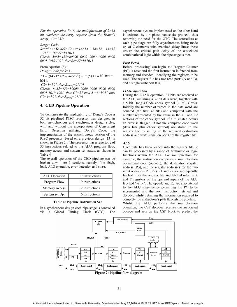
To demonstrate the applicability of Dong’s Code a 32 bit pipelined RISC processor was designed in both asynchronous and synchronous design styles, with and without the incorporation of Concurrent Error Detection utilising Dong’s Code, the implementation of the asynchronous version of the RISC processor, based on a previous design [13] is shown in Figure 2 . The processor has a repertoire of 35 instructions related to the ALU, program flow, memory access and system set status, as shown in Table 4. The overall operation of the CED pipeline can be broken down into 5 sections, namely, first fetch, load, ALU operation, error detection and store.
ALU Operation 18 instructions Program Flow 9 instructions
Memory Access 2 instructions
System set Op. 6 instructions
Table 4: Pipeline Instruction Set
In a synchronous design each pipe stage is controlled via a Global Timing Clock (GTC). The
asynchronous system implemented on the other hand is activated by a 4 phase handshake protocol, thus removing the need for the GTC. The controllers at each pipe stage are fully asynchronous being made up of C-elements with matched delay lines; these ensure the critical path delay of the associated combinational logic within the pipe stage is met. First Fetch Before ‘processing’ can begin, the Program Counter (PC) is reset and the first instruction is fetched from memory and decoded; identifying the registers to be used. The register file has two read ports (A and B), and a single write port (C). LOAD operation During the LOAD operation, 37 bits are received at the ALU, assuming a 32 bit data word, together with a 5 bit Dong’s Code check symbol (C1=3, C2=2). Initially the number of zeroes in the data word are counted (the first 32 bits) and compared with the number represented by the value in the C1 and C2 sections of the check symbol. If a mismatch occurs an error is flagged, if not the complete code word (data bits plus check symbol) are stored in the register file by setting up the required destination address and write signal on port C of the register file. ALU Once data has been loaded into the register file, it can be processed by a range of arithmetic or logic functions within the ALU. For multiplication for example, the instruction comprises a multiplication operational code (opcode), the destination register address (R3), and the register addresses for the two input operands (R1, R2). R1 and R2 are subsequently fetched from the register file and latched into the X and Y registers on the operand inputs of the ALU labelled ‘value’. The opcode and R3 are also latched to the ALU stage hence permitting the PC to be incremented and the next instruction fetched and decoded whilst retaining the information required to complete the instruction’s path through the pipeline. Whilst the ALU performs the multiplication operation, the CSP decoder receives the associated opcode and sets up the CSP block to predict the
Figure 2: Pipeline flow diagram
65131
Authorized licensed use limited to: Newcastle University. Downloaded on May 27,2010 at 15:28:24 UTC from IEEE Xplore. Restrictions apply.

checkbits of this function. This is performed in parallel to the ALU operation so does not affect throughput. ALU Error detection The result of the ALU operation is fed to the CSG unit which determines the Dong’s Code Check Symbol, which is subsequently compared, with that predicted earlier, using a Totally Self Checking (TSC) checker. If a mismatch occurs an error flag is raised. This method detects those errors as shown in Table 2, as a result of an erroneous ALU operation, or register load/store functions. No error detection is performed within the register selection; however, as two decoders are used to address data and check-bits storage, any failure in a decoder would result in a mismatch between check-bits generated from the data itself and those extracted from the register file . This methodology is also used to protect against similar faults in the CSP and ALU as each have their own decoder, thus protecting against common mode errors. If an error affects one unit, this will cause a mismatch in the output stage when the check symbols are compared. STORE operation If the predicted and generated check symbols of the operation match, the result of the operation is written back to the register file via Port C to the destination address Rd. 5. Online Test Operation Concurrent Error Detection within an asynchronous system provides an alternative method of recovery from soft errors. As a transient fault occurs the system produces the error signal, this error may then be interpreted by the environment in different ways. In synchronous systems, a detected error means the system would have to restart the affected process, recalculate and recheck, stalling the entire pipeline until the error had cleared. Asynchronous systems may interpret the error signal in two ways. • Transient error, attempt recovery This method allows the pipeline stage affected to wait for the transient error to pass. When the error is flagged the “completed” signal is not allowed to be active, until the error signal clears. Without the concurrent operation of the testing system this inherent transient error would propagate leading to data corruption. With a fully synchronous system the wait method would require several whole clock cycles to pass before allowing the system to continue, leading to larger delays, especially in the preceding pipe stages. • Extreme transient/permanent fault Assuming the asynchronous system is affected only by transient errors, which exist for a short period, the system will be prone to lock-up in the case of permanent faults as an error signal will be flagged
indefinitely if using the transient error recovery method at all times. To avoid this, the application of a maximum length recovery time could be implemented which subsequently forces a reset (via a watchdog timer etc.). Such timers have relatively small area overheads and are a commonly used block in many microprocessors. The pipe stage controller logic can also be affected by transient errors [14] affecting the handshake communication between blocks. When this occurs in the implemented design, due to the different decoders used by the CSP and ALU blocks the check symbol outputs will be mismatched, causing an error to be flagged. This can then be interpreted by the environment as the extreme transient/permanent fault which can result in the watchdog timer issuing a reset to the pipeline and causing an Initial Program Load (IPL). As with asynchronous systems, permanent faults may also cause lock-up in synchronous systems. Again this may be resolved through the use of watchdog timers, however, the period to detect and attempt recovery from the error leads to larger delays than in the asynchronous design. The benefits of utilising a “sit and wait” procedure within asynchronous designs provide a much faster method for recovery when compared to their synchronous counterparts. Processor operations are allowed to continue as soon as the error clears without having to wait for the next clock cycle or affecting any proceeding pipe operation. This also has ramifications in terms of power consumption as the GTC will continue to operate in a synchronous design, despite the pipeline being unable to perform any 'useful' operation. 6. Asynchronous Reconfigurable Tester The increased complexity of modern VLSI circuits has made test generation one the most complicated and time-consuming problems in digital design as circuits grow in size, so does the cost of testing. One way of reducing this associated cost with testing is utilising embedded FPGAs where a system can be tested and evaluated using a built in tester. FPGAs have been used before as embedded test platforms to test synchronous memory chips [15] and also for fault emulation within synchronous sequential designs [16]. However, testing asynchronous circuits can be troublesome, especially for complex systems such as processors. The reason being that asynchronous circuits do not rely on a global clock signal to establish communication; instead they use a handshake communication protocol using Request (Req) and Acknowledge (Ack) signals. ATEs use a global clock signal to apply the test stimuli to the DUT, thus asynchronous devices would be required
66132
Authorized licensed use limited to: Newcastle University. Downloaded on May 27,2010 at 15:28:24 UTC from IEEE Xplore. Restrictions apply.
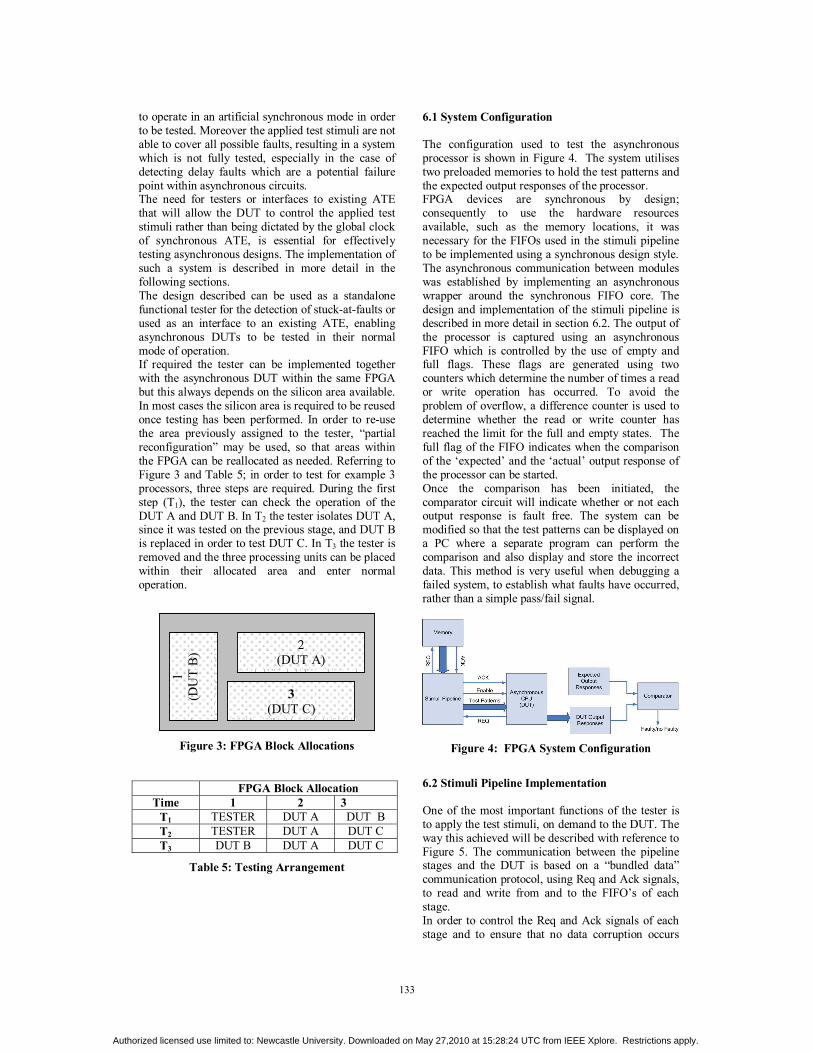
to operate in an artificial synchronous mode in order to be tested. Moreover the applied test stimuli are not able to cover all possible faults, resulting in a system which is not fully tested, especially in the case of detecting delay faults which are a potential failure point within asynchronous circuits. The need for testers or interfaces to existing ATE that will allow the DUT to control the applied test stimuli rather than being dictated by the global clock of synchronous ATE, is essential for effectively testing asynchronous designs. The implementation of such a system is described in more detail in the following sections. The design described can be used as a standalone functional tester for the detection of stuck-at-faults or used as an interface to an existing ATE, enabling asynchronous DUTs to be tested in their normal mode of operation. If required the tester can be implemented together with the asynchronous DUT within the same FPGA but this always depends on the silicon area available. In most cases the silicon area is required to be reused once testing has been performed. In order to re-use the area previously assigned to the tester, “partial reconfiguration” may be used, so that areas within the FPGA can be reallocated as needed. Referring to Figure 3 and Table 5; in order to test for example 3 processors, three steps are required. During the first step (T1), the tester can check the operation of the DUT A and DUT B. In T2 the tester isolates DUT A, since it was tested on the previous stage, and DUT B is replaced in order to test DUT C. In T3 the tester is removed and the three processing units can be placed within their allocated area and enter normal operation.
Figure 3: FPGA Block Allocations
FPGA Block Allocation Time 1 2 3
T1 TESTER DUT A DUT B T2 TESTER DUT A DUT C T3 DUT B DUT A DUT C
Table 5: Testing Arrangement
6.1 System Configuration The configuration used to test the asynchronous processor is shown in Figure 4. The system utilises two preloaded memories to hold the test patterns and the expected output responses of the processor. FPGA devices are synchronous by design; consequently to use the hardware resources available, such as the memory locations, it was necessary for the FIFOs used in the stimuli pipeline to be implemented using a synchronous design style. The asynchronous communication between modules was established by implementing an asynchronous wrapper around the synchronous FIFO core. The design and implementation of the stimuli pipeline is described in more detail in section 6.2. The output of the processor is captured using an asynchronous FIFO which is controlled by the use of empty and full flags. These flags are generated using two counters which determine the number of times a read or write operation has occurred. To avoid the problem of overflow, a difference counter is used to determine whether the read or write counter has reached the limit for the full and empty states. The full flag of the FIFO indicates when the comparison of the ‘expected’ and the ‘actual’ output response of the processor can be started. Once the comparison has been initiated, the comparator circuit will indicate whether or not each output response is fault free. The system can be modified so that the test patterns can be displayed on a PC where a separate program can perform the comparison and also display and store the incorrect data. This method is very useful when debugging a failed system, to establish what faults have occurred, rather than a simple pass/fail signal.
Figure 4: FPGA System Configuration
6.2 Stimuli Pipeline Implementation One of the most important functions of the tester is to apply the test stimuli, on demand to the DUT. The way this achieved will be described with reference to Figure 5. The communication between the pipeline stages and the DUT is based on a “bundled data” communication protocol, using Req and Ack signals, to read and write from and to the FIFO’s of each stage. In order to control the Req and Ack signals of each stage and to ensure that no data corruption occurs
1 (D
UT
B) 2
(DUT A)
3 (DUT C)
67133
Authorized licensed use limited to: Newcastle University. Downloaded on May 27,2010 at 15:28:24 UTC from IEEE Xplore. Restrictions apply.

during the data transfer between them, each FIFO stage uses an Enable signal which indicates that the pipeline stage is full and data is available to be read. This method prevents any write or read operation to occur before the pipeline stage is full, which can cause data corruption or lock the stimuli pipeline. The Enable signal of the last stimuli pipeline stage is used to indicate to the asynchronous DUT that test patterns are available and testing can be initiated.
Figure 5: Stimuli Pipeline
The FIFO stages have been implemented in such a way that their size can be scaled to any desired number of test patterns (limited by hardware resources). In order to use these resources more efficiently, the FIFOs were designed in a synchronous design style, so that they could be mapped into specific RAM blocks on the FPGA. The FIFOs were then embedded in an asynchronous wrapper to enable them to communicate between FIFO stages and the DUT. The controllers then generate the Request and Enable signals, this technique uses a Globally Asynchronous Locally Synchronous (GALS) approach. The asynchronous signals were then defined as being clock inputs to the FIFO of the next stage. The assignment of these critical signals as clocks helped to achieve timing closure in the automatic design placement process, as the system is given a better understanding of the operation allowing the placement to be performed as for a synchronous system. The FIFO design including the extra circuits used for the generation of Request and Enable signals is shown in Figure 6.
Figure 6: FIFO design
To ensure that no race conditions would occur between critical signals, such as Wr_Req and Rd_Req, matched delays had to be used. The delays were implemented using the XORCY gates, which are gates implemented within the CLB structure of the Xilinx FPGAs and are typically used in carry
operations; the main advantage of using these types of gates instead of LUTs (for instance using an inverter chain) is that they are not removed during the optimisation process, as they are not seen as redundant elements. Furthermore they can be placed in any desired part of the FPGA to achieve uniform delays across the entire system. Although it was possible to use IP blocks already offered by the FPGA manufacturer to generate the FIFOs, these modules lack some of the functions required for the correct operation of an asynchronous system, such as the generation of Request (Req), Acknowledge (Ack) and Enable signals. Consequently, a bespoke design was implemented using VHDL, this made it possible to generate the required asynchronous signals into a single unit. Thus, a FIFO module could then be implemented, for which the size and the length of the data stored in the two memories can be accommodated by the tester and tailored to DUT requirements. 7. Results This paper presents an FPGA implementation of an asynchronous RISC based processor with both online and offline testing capabilities. To ensure the correct operation of the test circuit implemented several simulated faults were injected into the design by applying incorrect values to operand and opcode inputs as shown in Figure 7. The black and white stars indicate the presence of operand and opcode errors respectively at the input of the register file or instruction decoder. These errors result in an erroneous output which will then propagate through the ALU to the register file. As a result, errors simulated as instruction memory faults, or operand faults will propagate and pose as alternate errors whilst passing through the system. For example, a grounded memory bit within the instruction memory may change the instruction from 44225000 (ADD R1, R2) to 40225000. This result will then be decoded and the erroneous output propagated to the ALU for execution.
Figure 7: Error Mapping
This creates an incorrect (non matching) output when compared to the expected result from the tester. Similarly, faulty operand values which are fetched from a memory unit are loaded into the ALU register
68134
Authorized licensed use limited to: Newcastle University. Downloaded on May 27,2010 at 15:28:24 UTC from IEEE Xplore. Restrictions apply.

file. These values will affect the output from any ALU operation. This in combination with the potential error from the instruction decoder will result in an error to the writeback phase. To demonstrate the operation of the CED method and the asynchronous functional tester, several faults were injected by altering the stimuli file used to load the processor pipeline. The outputs from the DUT (MMU_data_out) and the stored expected values (CONFIRMEDOUT) are compared to indicate whether or not each output response is fault free. The CED circuit uses the dual rail output “not_error” / “error” to signal the presence of a fault in the ALU. The following results are based on post route simulation of the design using a Xilinx xc2v1000-6fg456 FPGA and the Modelsim simulator. The result from an addition operation with error free inputs is shown in Figure 8 a) with an output response 7fe000a1; as a result both the tester and the CED indicate a non faulty output response. When an operand error is injected the output response of the DUT is 7fe000a0 instead of the correct response of 7fe000a1, as shown in Figure 8 b), both the online and offline test circuit indicate the presence of a fault.
(a)
(b)
(c)
Figure 8: Fault Injection Results (a) non faulty, (b) operand fault, (c) opcode fault
An operand error was also injected into the processor resulting in the faulty trace output shown in Figure 8
c) with a result of ef0ca9f2 instead of the correct response of 7fe000a1. These injected errors propagated through the system as shown in Figure 7, being observable at the primary outputs of the circuit. A comparison in terms of area overhead between the asynchronous RISC processor with and without CED and its synchronous equivalent was also performed. The results shown in this section are based on reports from the Xilinx xc2v1000-6fg456 FPGA. As shown in Table 6 for an FPGA design a decrease in the equivalent gate count of 5% was obtained in utilising asynchronous design style over its synchronous counterpart. This was possible in the case of FPGA implementation since no clock tree insertion was necessary and as a result the associated hardware was not used. The equivalent gate count for a CED design increases by 26% and 20% for synchronous and asynchronous implementations respectively when compared to their non CED equivalents. The processor comprises 5375 LUTs and the asynchronous tester 517 LUTs and 6 RAM blocks used within the FIFO stages. The complete layout of the processor and the tester is shown in Figure 9. Power savings have also been found by utilising the asynchronous design method described. As shown in Table 7, savings of 35% for the non CED asynchronous system over the synchronous equivalent and 40% on the CED asynchronous system against the synchronous equivalent. These values were obtained using a test bench of 32 operations, including load, store and a number of ALU operations. The power usage values were obtained from XPower software from Xilinx in conjunction with the Modelsim simulator. Pipe architecture Area Overhead
(1) Synchronous, FPGA 45949 (gate count) Reference (0%)
(2) Asynchronous, FPGA
43851 (gate count) 4% less than (1)
(3) Synchronous CED Dong’s Code, FPGA
58018 (gate count)
26% more than (1)
(4) Asynchronous CED Dong’s Code, FPGA
52927 (gate count)
20% more than (2)
Table 6: Asynchronous vs. Synchronous areas
Pipe architecture (FPGA)
Power (mW) Difference
(1) Synchronous 610 Reference (0%) (2) Asynchronous 450 35% less than (1)
(3) Synchronous CED 720 18% greater than (1) 40% greater than (2)
(4) Asynchronous CED 511 19% less than (1) 40% less than (3)
Table 7: Asynchronous vs. Synchronous power dissipation
The results do not include the power generated from the global clock in the synchronous design and are based on internal switching activity only, showing
69135
Authorized licensed use limited to: Newcastle University. Downloaded on May 27,2010 at 15:28:24 UTC from IEEE Xplore. Restrictions apply.

the inherent power saving ability of asynchronous architecture due to the natural ‘sleep’ ability which blocks switching from occurring during unused (or inactive) pipe stages.
Figure 9: FPGA placement
8. Asynchronous Design for FPGAs FPGAs are excellent vehicles for prototyping a potential ASIC design. In recent years, FPGA complexity has progressed to a point where single FPGAs can be used for the implementation of a complete System-on-Chip (SoC). Both equivalent gate counts and features have increased dramatically, competing with markets which once could only be supplied by ASIC manufacturers. FPGAs are becoming a prominent implementation target for “safety critical” applications since by their nature they are highly resistant to SETs [17] due to the large capacitive loading of signal paths, which is many times greater than that of the loading in an ASIC. On the other hand commercially available FPGAs are synchronous by design, so the implementation of a complex asynchronous circuit requires a considerable effort and in-depth knowledge of the software used for the design and implementation. By adopting a design flow that is compatible with the synchronous nature of FPGAs, it is possible to design an asynchronous system which is highly reliable and low in power when compared to its synchronous equivalent and relieves the issues associated with clock distribution to reduce skew. Asynchronous design relies on handshake communication protocols instead of global clocks; however the software supplied by the FPGA vendors has been designed for implementing synchronous circuits. This specification is enforced to enable timing closure to be achieved without considerable effort from the designer. However, certain optimisation features within the synthesis process are detrimental to asynchronous design; this
includes ‘intentional redundant elements’ (such as delay elements) necessary for correct functionality. Moreover timing closure is difficult to achieve, which can lead to incorrect operation or reduced performance. The optimisation process within the FPGA software is essential in order to provide the most efficient implementation of a given operation, specific to a defined target device, as such it cannot be switched off; consequently it is necessary to find an alternative approach to the optimisation issues presented. Although constraints can be applied to each individual element within an LUT delay chain, such as the “KEEP” constraint, it has been observed that optimisation still takes place and delay elements for example are not placed in optimum positions within the FPGA. This results in unpredictable delays when modifying a design and therefore affects the functionality and performance of the design. By using XORCY gates, which are normally applied to carry propagation within adder structures, it is possible to avoid the problem associated with optimisation of redundant elements. The delays associated with these gates are predictable and prove ideal for implementing matched delays. The next issue is in regard to timing closure. It is necessary to ensure that “area constraints” are used to create a design that is transferable but also not affected by the addition of extra logic in the place and route stage of the design. Rather than create a single area constraint for the complete design, each component of the asynchronous processor and the tester is constrained individually; this ensures maximum control over placement of the most critical parts and the minimisation of the routing delays between these components. The most critical signals were assigned the “CLOCK attribute” constraint which ensures that the design is presented to the software as multi-clock synchronous implementation rather than asynchronous. These signals could then be placed by the software the same way as a synchronous system thus achieving timing closure. By implementing the above workarounds, asynchronous circuits can be designed successfully in an FPGA with relative ease. 9. Conclusions Clock skew issues are a major concern in present day high performance synchronous designs. By adopting an asynchronous design style this problem is alleviated. Asynchronous design provides an inherent power savings due to the removal of the clock and the associated clock distribution network. However, testing asynchronous circuits is a major issue, since current ATE designs are not capable of testing asynchronous circuits in their normal mode of operation. In this paper a low power asynchronous RISC based processor was designed with both online and offline
70136
Authorized licensed use limited to: Newcastle University. Downloaded on May 27,2010 at 15:28:24 UTC from IEEE Xplore. Restrictions apply.
testing capabilities, allowing the system to be tested post manufacture using the offline test function and also whilst ‘in the field’ using online testing methods. The design uses a Xilinx FPGA to make use of the reconfigurability and inherent tolerance to certain transient errors caused by SEUs. The CED technique used for the online testing of the processor utilises Dong’s Code. This code provides the flexibility of tailoring fault coverage to application thus reducing area overheads. An asynchronous functional tester was also designed, which could be used as a standalone or an integrated tester to an asynchronous DUT. The tester offers a solution to the ATE problem of testing asynchronous circuits in their natural environment by allowing the asynchronous DUT to control the tester rather than being dictated by the global clock supplied by the synchronous ATE. The implementation of an asynchronous processor on an FPGA showed a reduction in power consumption of 35%, as well as a reduction in area of 4% when compared with the synchronous equivalent. It has also been shown that power and area can be reduced by 40% and 9% respectively for the asynchronous CED system. By following a modified synchronous design flow and through extensive use of “constraints” it is possible to design a stable and transferable system. Although the design of an asynchronous system requires effort in areas which typically were automated by EDA tools, design issues associated with clock distribution are eliminated and the advantages of reduced power dissipation and Electro-Magnetic Interference (EMI) are gained inherently. The design presented provides a complete system which can be verified both post manufacture and whilst “in the field”. It has been demonstrated that FPGAs can be used for the implementation of complex systems and due to their inherent design advantages they can be considered for environments requiring reconfigurable, as well as “safety critical” applications. 10. References [1] C.J.Myers, “Asynchronous Circuit Design”, John Wiley & Sons, Inc., February 2002. [2] J.Sparso, S.Furber, “ Principles of Asynchronous Circuit Design: A System Perspective”, Springer, 2002 [3] C. Constantinescu, “Dependability Benchmarking Using Environmental test Tools”, Proceedings of the Annual reliability and Maintainability Symposium, 2005, pp. 567-571. [4] S. Caranhac, J.L.Coutures, "Comparative evolution of various CCD image sensors hardening techniques with ionizing radiation", Second European Conference on Radiation and its Effects on Components and Systems (RADECS93), pp. 396 - 400, 1993.
[5] B.W. Johnson, J.H. Aylor, H.H. Hana, "Efficient use of Time and Hardware Redundancy For Concurrent Error Detection in a 32-bit VLSI Adder", IEEE Journal of Solid State Circuits, vol. 23, pp. 208 - 215, 1988. [6] H. Dong, “Modified Berger Codes for the Detection of unidirectional Errors”, IEEE Transactions on Computers, Volume C-33, Number 6, June 1984, pp 575 – 575. [7] J.C. Lo, , S. Thanawastien, T.R.N. Rao, ”Concurrent error detection in arithmetic and logical operations using Berger codes”, Proceedings of 9th Symposium on Computer Arithmetic, September 1989, pp 233 – 240. [8] H. Al-Asaad, E. Czeck, "Concurrent error correction in iterative circuits by recomputing with partitioning and voting", Eleventh IEEE VLSI Test Symposium, pp. 174 - 177, 1993. [9] P.M. O'Neill, G.D.Badhwar, NASA, “Single Event Upsets for Space Shuttle Flights of New General Purpose Computer Memory Devices“, IEEE Trans. on Nuclear Science, vol. 41, No. 5, pp. 1755 – 1764, 1995. [10] B. Parhami, “Approach to the design of parity-checked arithmetic circuits”, Conference Record of the Thirty-Sixth Asilomar Conference on Signals, Systems and Computers, Volume 2, November 2002, pp 1084 – 1088. [11] G. Russell, A. Maamar, “Check bit prediction scheme using Dong’s Code for concurrent error detection in VLSI processors”, IEE Proceedings on Digital Computing, volume 147, number 6, November 2000, pp 467 – 471. [12] J.C. Lo, S. Thanawastien, T.R.N. Rao, “Berger Check Prediction for Array Multipliers and Array Dividers”, IEEE Transactions on Computers, Volume 42, Number 7, July 1993, pp 892 – 896. [13] P.D. Hyde, “A Pipelined Asynchronous Self-Checking RISC based Processor”, Thesis (PhD), University of Newcastle-upon-Tyne, 2004.
[14] C. Galke, M. Pflanz, H. T. Vierhaus, "On-line Detection and Compensation of Transient Errors in Processor Pipeline-Structures," Proceedings of The Eighth IEEE International On-Line Testing Workshop (IOLTW'02), p.178, 2002 [15] J.R. Huang, C.K. Ong, K.T. Cheng, C.W. Wu,“An FPGA-based Re-configurable Functional Tester for Memory Chip” Proc Asian Test Symposium (ATS.00), 2000, pp.51-57. [16] P.Ellervee, J.Raik, K.Tammemae, R.J.Ubar, “FPGA-based fault emulation of synchronous sequential circuits”, IET Computers and Digital Techniques, 2007, 1, pp. 70-76. [17] A. Lesea, S. Drimer, J.J. Fabula, C. Carmichael, P. Alfke, “The Rosetta Experiment: Atmospheric Soft Error Rate testing in Differing technology FPGAs”, IEEE transactions on Device and Material Reliability, September 2005, Volume 5, pp. 317-318.
71137
Authorized licensed use limited to: Newcastle University. Downloaded on May 27,2010 at 15:28:24 UTC from IEEE Xplore. Restrictions apply.