unit v digital signal processor
46
UNIT V DIGITAL SIGNAL PROCESSOR INTRODUCTION A digital signal processor (DSP) is a specialized microprocessor (or a SIP block), with its architecture optimized for the operational needs of digital signal processing. The goal of DSP is usually to measure, filter or compress continuous real-world analog signals. Most general-purpose microprocessors can also execute digital signal processing algorithms successfully, but may not be able to keep up with such processing continuously in real-time. Also, dedicated DSPs usually have better power efficiency, thus they are more suitable in portable devices such as mobile phones because of power consumption constraints. DSPs often use special memory architectures that are able to fetch multiple data or instructions at the same time. Circular Buffering Digital Signal Processors are designed to quickly carry out FIR filters and similar techniques. To understand the hardware, we must first understand the algorithms. In this section we will make a detailed list of the steps needed to implement an FIR filter. In the next section we will see how DSPs are designed to perform these steps as efficiently as possible. To start, we need to distinguish between off-line processing and real-time processing. In off- line processing, the entire input signal resides in the computer at the same time. For example, a geophysicist might use a seismometer to record the ground movement during an earthquake. After the shaking is over, the information may be read into a computer and analyzed in some way. Another example of off-line processing is medical imaging, such as computed tomography and MRI. The data set is acquired while the patient is inside the machine, but the image reconstruction may be delayed until a later time. The key point is that all of the information is simultaneously available to the processing program. This is common in scientific research and engineering, but not in consumer products. Off-line processing is the realm of personal computers and mainframes. In real-time processing, the output signal is produced at the same time that the input signal is being acquired. For example, this is needed in telephone communication, hearing aids, and radar. These applications must have the information immediately available, although it can be delayed by a short amount. For instance, a 10 millisecond delay in a telephone call cannot be detected by the speaker or listener. Likewise, it makes no difference if a radar signal is delayed by a few seconds before being displayed to the operator. Real-time applications input a sample, perform the algorithm, and output a sample, over-and-over. Alternatively, they may input a group
-
Upload
khangminh22 -
Category
Documents
-
view
4 -
download
0
Transcript of unit v digital signal processor

UNIT V DIGITAL SIGNAL PROCESSOR
INTRODUCTION
A digital signal processor (DSP) is a specialized microprocessor (or a SIP block), with its
architecture optimized for the operational needs of digital signal processing.
The goal of DSP is usually to measure, filter or compress continuous real-world analog signals.
Most general-purpose microprocessors can also execute digital signal processing algorithms
successfully, but may not be able to keep up with such processing continuously in real-time.
Also, dedicated DSPs usually have better power efficiency, thus they are more suitable in
portable devices such as mobile phones because of power consumption constraints. DSPs often
use special memory architectures that are able to fetch multiple data or instructions at the same
time.
Circular Buffering
Digital Signal Processors are designed to quickly carry out FIR filters and similar techniques. To
understand the hardware, we must first understand the algorithms. In this section we will make a
detailed list of the steps needed to implement an FIR filter. In the next section we will see how
DSPs are designed to perform these steps as efficiently as possible.
To start, we need to distinguish between off-line processing and real-time processing. In off-
line processing, the entire input signal resides in the computer at the same time. For example, a
geophysicist might use a seismometer to record the ground movement during an earthquake.
After the shaking is over, the information may be read into a computer and analyzed in some
way. Another example of off-line processing is medical imaging, such as computed tomography
and MRI. The data set is acquired while the patient is inside the machine, but the image
reconstruction may be delayed until a later time. The key point is that all of the information is
simultaneously available to the processing program. This is common in scientific research and
engineering, but not in consumer products. Off-line processing is the realm of personal
computers and mainframes.
In real-time processing, the output signal is produced at the same time that the input signal is
being acquired. For example, this is needed in telephone communication, hearing aids, and radar.
These applications must have the information immediately available, although it can be delayed
by a short amount. For instance, a 10 millisecond delay in a telephone call cannot be detected by
the speaker or listener. Likewise, it makes no difference if a radar signal is delayed by a few
seconds before being displayed to the operator. Real-time applications input a sample, perform
the algorithm, and output a sample, over-and-over. Alternatively, they may input a group

of samples, perform the algorithm, and output a group of samples. This is the world of Digital
Signal Processors.
Now look at Fig. 28-2 and imagine that this is an FIR filter being implemented in real-time. To
calculate the output sample, we must have access to a certain number of the most recent samples
from the input. For example, suppose we use eight coefficients in this filter, a0, a1, … a7. This
means we must know the value of the eight most recent samples from the input signal, x[n], x[n-
1], … x[n-7]. These eight samples must be stored in memory and continually updated as new
samples are acquired. What is the best way to manage these stored samples? The answer
is circular buffering.
Figure 28-3 illustrates an eight sample circular buffer. We have placed this circular buffer in
eight consecutive memory locations, 20041 to 20048. Figure (a) shows how the eight samples
from the input might be stored at one particular instant in time, while (b) shows the changes after
the next sample is acquired. The idea of circular buffering is that the end of this linear array is
connected to its beginning; memory location 20041 is viewed as being next to 20048, just as
20044 is next to 20045. You keep track of the array by a pointer (a variable whose value is
an address) that indicates where the most recent sample resides.
For instance, in (a) the pointer contains the address 20044, while in (b) it contains 20045. When
a new sample is acquired, it replaces the oldest sample in the array, and the pointer is moved one
address ahead. Circular buffers are efficient because only one value needs to be changed when a
new sample is acquired.
Four parameters are needed to manage a circular buffer. First, there must be a pointer that
indicates the start of the circular buffer in memory (in this example, 20041). Second, there must
be a pointer indicating the end of the array (e.g., 20048), or a variable that holds its length (e.g.,
8). Third, the step size of the memory addressing must be specified. In Fig. 28-3 the step size
is one, for example: address 20043 contains one sample, address 20044 contains the next sample,
and so on. This is frequently not the case. For instance, the addressing may refer to bytes, and
each sample may require two or four bytes to hold its value. In these cases, the step size would
need to be two or four, respectively.
These three values define the size and configuration of the circular buffer, and will not change
during the program operation. The fourth value, the pointer to the most recent sample, must be

modified as each new sample is acquired. In other words, there must be program logic that
controls how this fourth value is updated based on the value of the first three values. While this
logic is quite simple, it must be very fast. This is the whole point of this discussion; DSPs should
be optimized at managing circular buffers to achieve the highest possible execution speed.
As an aside, circular buffering is also useful in off-line processing. Consider a program where
both the input and the output signals are completely contained in memory. Circular buffering
isn't needed for a convolution calculation, because every sample can be immediately accessed.
However, many algorithms are implemented in stages, with an intermediate signal being created
between each stage. For instance, a recursive filter carried out as a series of biquads operates in
this way. The brute force method is to store the entire length of each intermediate signal in
memory. Circular buffering provides another option: store only those intermediate samples
needed for the calculation at hand. This reduces the required amount of memory, at the expense
of a more complicated algorithm. The important idea is that circular buffers are useful for off-
line processing, but critical for real-time applications.
Now we can look at the steps needed to implement an FIR filter using circular buffers for both
the input signal and the coefficients. This list may seem trivial and overexamined- it's not! The
efficient handling of these individual tasks is what separates a DSP from a traditional
microprocessor. For each new sample, all the following steps need to be taken:
The goal is to make these steps execute quickly. Since steps 6-12 will be repeated many times
(once for each coefficient in the filter), special attention must be given to these operations.
Traditional microprocessors must generally carry out these 14 steps in serial (one after another),
while DSPs are designed to perform them in parallel. In some cases, all of the operations within
the loop (steps 6-12) can be completed in a single clock cycle. Let's look at the internal
architecture that allows this magnificent performance.

ARCHITECTURE OF THE DIGITAL SIGNAL PROCESSOR
One of the biggest bottlenecks in executing DSP algorithms is transferring information to and
from memory. This includes data, such as samples from the input signal and the filter
coefficients, as well as program instructions, the binary codes that go into the program
sequencer. For example, suppose we need to multiply two numbers that reside somewhere in
memory. To do this, we must fetch three binary values from memory, the numbers to be
multiplied, plus the program instruction describing what to do.
Figure 28-4a shows how this seemingly simple task is done in a traditional microprocessor. This
is often called a Von Neumann architecture, after the brilliant American mathematician John
Von Neumann (1903-1957). Von Neumann guided the mathematics of many important
discoveries of the early twentieth century. His many achievements include: developing the
concept of a stored program computer, formalizing the mathematics of quantum mechanics, and
work on the atomic bomb. If it was new and exciting, Von Neumann was there!
As shown in (a), a Von Neumann architecture contains a single memory and a single bus for
transferring data into and out of the central processing unit (CPU). Multiplying two numbers
requires at least three clock cycles, one to transfer each of the three numbers over the bus from
the memory to the CPU. We don't count the time to transfer the result back to memory, because
we assume that it remains in the CPU for additional manipulation (such as the sum of products in
an FIR filter). The Von Neumann design is quite satisfactory when you are content to execute all
of the required tasks in serial. In fact, most computers today are of the Von Neumann design. We
only need other architectures when very fast processing is required, and we are willing to pay the
price of increased complexity.
This leads us to the Harvard architecture, shown in (b). This is named for the work done at
Harvard University in the 1940s under the leadership of Howard Aiken (1900-1973). As shown
in this illustration, Aiken insisted on separate memories for data and program instructions, with
separate buses for each. Since the buses operate independently, program instructions and data
can be fetched at the same time, improving the speed over the single bus design. Most present
day DSPs use this dual bus architecture.
Figure (c) illustrates the next level of sophistication, the Super Harvard Architecture. This
term was coined by Analog Devices to describe the internal operation of their ADSP-2106x and
new ADSP-211xx families of Digital Signal Processors. These are called SHARC® DSPs, a
contraction of the longer term, Super Harvard ARChitecture. The idea is to build upon the
Harvard architecture by adding features to improve the throughput. While the SHARC DSPs are
optimized in dozens of ways, two areas are important enough to be included in Fig. 28-4c:
an instruction cache, and an I/O controller.

First, let's look at how the instruction cache improves the performance of the Harvard
architecture. A handicap of the basic Harvard design is that the data memory bus is busier than
the program memory bus. When two numbers are multiplied, two binary values (the numbers)
must be passed over the data memory bus, while only one binary value (the program instruction)
is passed over the program memory bus. To improve upon this situation, we start by relocating
part of the "data" to program memory. For instance, we might place the filter coefficients in
program memory, while keeping the input signal in data memory. (This relocated data is called
"secondary data" in the illustration). At first glance, this doesn't seem to help the situation; now
we must transfer one value over the data memory bus (the input signal sample), but two values
over the program memory bus (the program instruction and the coefficient). In fact, if we were
executing random instructions, this situation would be no better at all.
However, DSP algorithms generally spend most of their execution time in loops, such as
instructions 6-12 of Table 28-1. This means that the same set of program instructions will
continually pass from program memory to the CPU. The Super Harvard architecture takes
advantage of this situation by including an instruction cache in the CPU. This is a small
memory that contains about 32 of the most recent program instructions. The first time through a
loop, the program instructions must be passed over the program memory bus. This results in
slower operation because of the conflict with the coefficients that must also be fetched along this
path. However, on additional executions of the loop, the program instructions can be pulled from
the instruction cache. This means that all of the memory to CPU information transfers can be
accomplished in a single cycle: the sample from the input signal comes over the data memory
bus, the coefficient comes over the program memory bus, and the program instruction comes
from the instruction cache. In the jargon of the field, this efficient transfer of data is called a high
memory-access bandwidth.
Figure 28-5 presents a more detailed view of the SHARC architecture, showing the I/O
controller connected to data memory. This is how the signals enter and exit the system. For
instance, the SHARC DSPs provides both serial and parallel communications ports. These are
extremely high speed connections. For example, at a 40 MHz clock speed, there are two serial
ports that operate at 40 Mbits/second each, while six parallel ports each provide a 40
Mbytes/second data transfer. When all six parallel ports are used together, the data transfer rate
is an incredible 240 Mbytes/second.

This is fast enough to transfer the entire text of this book in only 2 milliseconds! Just as
important, dedicated hardware allows these data streams to be transferred directly into memory
(Direct Memory Access, or DMA), without having to pass through the CPU's registers. In other
words, tasks 1 & 14 on our list happen independently and simultaneously with the other tasks; no
cycles are stolen from the CPU. The main buses (program memory bus and data memory bus)
are also accessible from outside the chip, providing an additional interface to off-chip memory
and peripherals. This allows the SHARC DSPs to use a four Gigaword (16 Gbyte) memory,
accessible at 40 Mwords/second (160 Mbytes/second), for 32 bit data. Wow!
This type of high speed I/O is a key characteristic of DSPs. The overriding goal is to move the
data in, perform the math, and move the data out before the next sample is available. Everything
else is secondary. Some DSPs have on-board analog-to-digital and digital-to-analog converters, a
feature called mixed signal. However, all DSPs can interface with external converters through
serial or parallel ports.
Now let's look inside the CPU. At the top of the diagram are two blocks labeled Data Address
Generator (DAG), one for each of the two memories. These control the addresses sent to the
program and data memories, specifying where the information is to be read from or written to. In
simpler microprocessors this task is handled as an inherent part of the program sequencer, and is
quite transparent to the programmer. However, DSPs are designed to operate with circular
buffers, and benefit from the extra hardware to manage them efficiently. This avoids needing to
use precious CPU clock cycles to keep track of how the data are stored. For instance, in the
SHARC DSPs, each of the two DAGs can control eight circular buffers. This means that each
DAG holds 32 variables (4 per buffer), plus the required logic.
Why so many circular buffers? Some DSP algorithms are best carried out in stages. For instance,
IIR filters are more stable if implemented as a cascade of biquads (a stage containing two poles
and up to two zeros). Multiple stages require multiple circular buffers for the fastest operation.
The DAGs in the SHARC DSPs are also designed to efficiently carry out the Fast Fourier
transform. In this mode, the DAGs are configured to generate bit-reversed addresses into the
circular buffers, a necessary part of the FFT algorithm. In addition, an abundance of circular
buffers greatly simplifies DSP code generation- both for the human programmer as well as high-
level language compilers, such as C.
The data register section of the CPU is used in the same way as in traditional microprocessors. In
the ADSP-2106x SHARC DSPs, there are 16 general purpose registers of 40 bits each. These
can hold intermediate calculations, prepare data for the math processor, serve as a buffer for data
transfer, hold flags for program control, and so on. If needed, these registers can also be used to
control loops and counters; however, the SHARC DSPs have extra hardware registers to carry
out many of these functions.
The math processing is broken into three sections, a multiplier, an arithmetic logic unit (ALU),
and a barrel shifter. The multiplier takes the values from two registers, multiplies them, and
places the result into another register. The ALU performs addition, subtraction, absolute value,
logical operations (AND, OR, XOR, NOT), conversion between fixed and floating point formats,
and similar functions. Elementary binary operations are carried out by the barrel shifter, such as
shifting, rotating, extracting and depositing segments, and so on. A powerful feature of the
SHARC family is that the multiplier and the ALU can be accessed in parallel. In a single clock
cycle, data from registers 0-7 can be passed to the multiplier, data from registers 8-15 can be
passed to the ALU, and the two results returned to any of the 16 registers.
There are also many important features of the SHARC family architecture that aren't shown in
this simplified illustration. For instance, an 80 bit accumulator is built into the multiplier to
reduce the round-off error associated with multiple fixed-point math operations. Another
interesting

feature is the use of shadow registers for all the CPU's key registers. These are duplicate
registers that can be switched with their counterparts in a single clock cycle. They are used
for fast context switching, the ability to handle interrupts quickly. When an interrupt occurs in
traditional microprocessors, all the internal data must be saved before the interrupt can be
handled. This usually involves pushing all of the occupied registers onto the stack, one at a time.
In comparison, an interrupt in the SHARC family is handled by moving the internal data into the
shadow registers in a single clock cycle. When the interrupt routine is completed, the registers
are just as quickly restored. This feature allows step 4 on our list (managing the sample-ready
interrupt) to be handled very quickly and efficiently.
Now we come to the critical performance of the architecture, how many of the operations within
the loop (steps 6-12 of Table 28-1) can be carried out at the same time. Because of its highly
parallel nature, the SHARC DSP can simultaneously carry out all of these tasks. Specifically,
within a single clock cycle, it can perform a multiply (step 11), an addition (step 12), two data
moves (steps 7 and 9), update two circular buffer pointers (steps 8 and 10), and control the loop
(step 6). There will be extra clock cycles associated with beginning and ending the loop (steps 3,
4, 5 and 13, plus moving initial values into place); however, these tasks are also handled very
efficiently. If the loop is executed more than a few times, this overhead will be negligible. As an
example, suppose you write an efficient FIR filter program using 100 coefficients. You can

expect it to require about 105 to 110 clock cycles per sample to execute (i.e., 100 coefficient
loops plus overhead). This is very impressive; a traditional microprocessor requires many
thousands of clock cycles for this algorithm.
FIXED VERSUS FLOATING POINT
Digital Signal Processing can be divided into two categories, fixed point and floating point.
These refer to the format used to store and manipulate numbers within the devices.
Fixed point DSPs usually represent each number with a minimum of 16 bits, although a different
length can be used. For instance, Motorola manufactures a family of fixed point DSPs that use 24
bits. There are four common ways that these 216
= 65536 possible bit patterns can represent a
number.
In unsigned integer, the stored number can take on any integer value from 0 to 65,535.
Similarly, signed integer uses two's complement to make the range include negative numbers,
from -32,768 to 32,767. With unsigned fraction notation, the 65,536 levels are spread uniformly
between 0 and 1. Lastly, the signed fraction format allows negative numbers, equally spaced
between -1 and 1.
In comparison, floating point DSPs typically use a minimum of 32 bits to store each value. This
results in many more bit patterns than for fixed point, 232
= 4,294,967,296 to be exact. A key
feature of floating point notation is that the represented numbers are not uniformly spaced. In the
most common format (ANSI/IEEE Std. 754-1985), the largest and smallest numbers are
±3.4×1038
and �1.2�10-38
, respectively.
The represented values are unequally spaced between these two extremes, such that the gap
between any two numbers is about ten-million times smaller than the value of the numbers. This
is important because it places large gaps between large numbers, but small gaps between small
numbers. Floating point notation is discussed in more detail in Chapter 4.
All floating point DSPs can also handle fixed point numbers, a necessity to implement counters,
loops, and signals coming from the ADC and going to the DAC. However, this doesn't mean that
fixed point math will be carried out as quickly as the floating point operations; it depends on the
internal architecture. For instance, the SHARC DSPs are optimized for both floating point and
fixed point operations, and executes them with equal efficiency. For this reason, the SHARC
devices are often referred to as "32-bit DSPs," rather than just "Floating Point."
Figure 28-6 illustrates the primary trade-offs between fixed and floating point DSPs. In Chapter
3 we stressed that fixed point arithmetic is much

faster than floating point in general purpose computers. However, with DSPs the speed is about
the same, a result of the hardware being highly optimized for math operations. The internal
architecture of a floating point DSP is more complicated than for a fixed point device. All the
registers and data buses must be 32 bits wide instead of only 16; the multiplier and ALU must be
able to quickly perform floating point arithmetic, the instruction set must be larger (so that they
can handle both floating and fixed point numbers), and so on. Floating point (32 bit) has better
precision and a higher dynamic range than fixed point (16 bit) .
In addition, floating point programs often have a shorter development cycle, since the
programmer doesn't generally need to worry about issues such as overflow, underflow, and
round-off error.
On the other hand, fixed point DSPs have traditionally been cheaper than floating point devices.
Nothing changes more rapidly than the price of electronics; anything you find in a book will be
out-of-date before it is printed. Nevertheless, cost is a key factor in understanding how DSPs are
evolving, and we need to give you a general idea. When this book was completed in 1999, fixed
point DSPs sold for between $5 and $100, while floating point devices were in the range of $10
to $300. This difference in cost can be viewed as a measure of the relative complexity between
the devices. If you want to find out what the prices are today, you need to look today.
Now let's turn our attention to performance; what can a 32-bit floating point system do that a 16-
bit fixed point can't? The answer to this question is signal-to-noise ratio. Suppose we store a
number in a 32 bit floating point format. As previously mentioned, the gap between this number
and its adjacent neighbor is about one ten-millionth of the value of the number. To store the
number, it must be round up or down by a maximum of one-half the gap size. In other words,
each time we store a number in floating point notation, we add noise to the signal.
The same thing happens when a number is stored as a 16-bit fixed point value, except that the
added noise is much worse. This is because the gaps between adjacent numbers are much larger.
For instance, suppose we store the number 10,000 as a signed integer (running from -32,768 to
32,767). The gap between numbers is one ten-thousandth of the value of the number we are

storing. If we want to store the number 1000, the gap between numbers is only one one-
thousandth of the value.
Noise in signals is usually represented by its standard deviation. This was discussed in detail in
Chapter 2. For here, the important fact is that the standard deviation of this quantization noise is
about one-third of the gap size. This means that the signal-to-noise ratio for storing a floating
point number is about 30 million to one, while for a fixed point number it is only about ten-
thousand to one. In other words, floating point has roughly 30,000 times less quantization noise
than fixed point.
This brings up an important way that DSPs are different from traditional microprocessors.
Suppose we implement an FIR filter in fixed point. To do this, we loop through each coefficient,
multiply it by the appropriate sample from the input signal, and add the product to an
accumulator. Here's the problem. In traditional microprocessors, this accumulator is just another
16 bit fixed point variable. To avoid overflow, we need to scale the values being added, and will
correspondingly add quantization noise on each step. In the worst case, this quantization noise
will simply add, greatly lowering the signal-to-noise ratio of the system. For instance, in a 500
coefficient FIR filter, the noise on each output sample may be 500 times the noise on each input
sample. The signal-to-noise ratio of ten-thousand to one has dropped to a ghastly twenty to
one. Although this is an extreme case, it illustrates the main point: when many operations are
carried out on each sample, it's bad, really bad. See Chapter 3 for more details.
DSPs handle this problem by using an extended precision accumulator. This is a special
register that has 2-3 times as many bits as the other memory locations. For example, in a 16 bit
DSP it may have 32 to 40 bits, while in the SHARC DSPs it contains 80 bits for fixed point use.
This extended range virtually eliminates round-off noise while the accumulation is in progress.
The only round-off error suffered is when the accumulator is scaled and stored in the 16 bit
memory. This strategy works very well, although it does limit how some algorithms must be
carried out. In comparison, floating point has such low quantization noise that these techniques
are usually not necessary.
In addition to having lower quantization noise, floating point systems are also easier to develop
algorithms for. Most DSP techniques are based on repeated multiplications and additions. In
fixed point, the possibility of an overflow or underflow needs to be considered after each
operation. The programmer needs to continually understand the amplitude of the numbers, how
the quantization errors are accumulating, and what scaling needs to take place. In comparison,
these issues do not arise in floating point; the numbers take care of themselves (except in rare
cases).
To give you a better understanding of this issue, Fig. 28-7 shows a table from the SHARC user
manual. This describes the ways that multiplication can be carried out for both fixed and floating

point formats. First, look at how floating point numbers can be multiplied; there is only one way!
That
is, Fn = Fx * Fy, where Fn, Fx, and Fy are any of the 16 data registers. It could not be any
simpler. In comparison, look at all the possible commands for fixed point multiplication. These
are the many options needed to efficiently handle the problems of round-off, scaling, and format.
In Fig. 28-7, Rn, Rx, and Ry refer to any of the 16 data registers, and MRF and MRB are 80 bit
accumulators. The vertical lines indicate options. For instance, the top-left entry in this table
means that all the following are valid commands: Rn = Rx * Ry, MRF = Rx * Ry, and MRB =
Rx * Ry. In other words, the value of any two registers can be multiplied and placed into another
register, or into one of the extended precision accumulators. This table also shows that the

numbers may be either signed or unsigned (S or U), and may be fractional or integer (F or I). The
RND and SAT options are ways of controlling rounding and register overflow.
There are other details and options in the table, but they are not important for our present
discussion. The important idea is that the fixed point programmer must understand dozens of
ways to carry out the very basic task of multiplication. In contrast, the floating point programmer
can spend his time concentrating on the algorithm.
Given these tradeoffs between fixed and floating point, how do you choose which to use? Here
are some things to consider. First, look at how many bits are used in the ADC and DAC. In many
applications, 12-14 bits per sample is the crossover for using fixed versus floating point. For
instance, television and other video signals typically use 8 bit ADC and DAC, and the precision
of fixed point is acceptable. In comparison, professional audio applications can sample with as
high as 20 or 24 bits, and almost certainly need floating point to capture the large dynamic range.
The next thing to look at is the complexity of the algorithm that will be run. If it is relatively
simple, think fixed point; if it is more complicated, think floating point. For example, FIR
filtering and other operations in the time domain only require a few dozen lines of code, making
them suitable for fixed point. In contrast, frequency domain algorithms, such as spectral analysis
and FFT convolution, are very detailed and can be much more difficult to program. While they
can be written in fixed point, the development time will be greatly reduced if floating point is
used.
Lastly, think about the money: how important is the cost of the product, and how important is the
cost of the development? When fixed point is chosen, the cost of the product will be reduced, but
the development cost will probably be higher due to the more difficult algorithms. In the reverse
manner, floating point will generally result in a quicker and cheaper development cycle, but a
more expensive final product.
Figure 28-8 shows some of the major trends in DSPs. Figure (a) illustrates the impact that Digital
Signal Processors have had on the embedded market. These are applications that use a
microprocessor to directly operate and control some larger system, such as a cellular telephone,
microwave oven, or automotive instrument display panel. The name "microcontroller" is often
used in referring to these devices, to distinguish them from the microprocessors used in personal
computers. As shown in (a), about 38% of embedded designers have already started using DSPs,
and another 49% are considering the switch. The high throughput and computational power of
DSPs often makes them an ideal choice for embedded designs.
As illustrated in (b), about twice as many engineers currently use fixed point as use floating point
DSPs. However, this depends greatly on the application. Fixed point is more popular in
competitive consumer products where the cost of the electronics must be kept very low. A good

example of this is cellular telephones. When you are in competition to sell millions of your
product, a cost difference of only a few dollars can be the difference between success and failure.
In comparison, floating point is more common when greater performance is needed and cost is
not important. For
instance, suppose you are designing a medical imaging system, such a computed tomography
scanner. Only a few hundred of the model will ever be sold, at a price of several hundred-
thousand dollars each. For this application, the cost of the DSP is insignificant, but the
performance is critical. In spite of the larger number of fixed point DSPs being used, the floating
point market is the fastest growing segment. As shown in (c), over one-half of engineers using
16-bits devices plan to migrate to floating point at some time in the near future.
Before leaving this topic, we should reemphasize that floating point and fixed point usually use
32 bits and 16 bits, respectively, but not always. For instance, the SHARC family can represent
numbers in 32-bit fixed point, a mode that is common in digital audio applications. This makes
the 232
quantization levels spaced uniformly over a relatively small range, say, between -1 and 1.
In comparison, floating point notation places the 232
quantization levels logarithmically over a

huge range, typically ±3.4×1038
. This gives 32-bit fixed point better precision, that is, the
quantization error on any one sample will be lower. However, 32-bit floating point has a
higher dynamic range, meaning there is a greater difference between the largest number and the
smallest number that can be represented.
Fixed Point DSP Processor Architecture:
1.1 TMS320 DSP Family Overview
TMS320 DSP family consists of fixed-point, floating-point, and multiprocessor digital signal
processors (DSPs). The TMS320 DSP architecture is designed specifically for real-time
signal processing. The following characteristics make this family the ideal choice for a wide
range of processing applications: Very flexible instruction set Inherent operational flexibility
High-speed performance Innovative parallel architecture Cost-effectiveness C-friendly
architecture
1.1.1 History, Development, and Advantages of TMS320 DSPs In 1982, Texas Instruments
introduced the TMS32010 — the first fixed-point DSP in the TMS320 DSP family.
Before the end of the year, Electronic Products magazine awarded the TMS32010 the
title “Product of the Year”. The TMS32010 became the model for future TMS320 DSP
generations.
Today, the TMS320 DSP family consists of three supported DSP platforms:
TMS320C2000, TMS320C5000, and TMS320C6000. Within the C5000 DSP platform
there are three generations, the TMS320C5x, TMS320C54x, and TMS320C55x. Devices
within the C5000 DSP platform use a similar CPU structure that is combined with a
variety of on-chip memory and peripheral configurations. These various configurations
satisfy a wide range of needs in the worldwide electronics market. When memory and
peripherals are integrated with a CPU onto a single chip, overall system cost is greatly
reduced and circuit board space is reduced. Figure 1–1 shows the performance gains of
the TMS320 DSP family of de

1.1.2 Typical Applications for the TMS320 DSP Family
The C54x DSPs use an advanced modified Harvard architecture that
maximizes processing power with eight buses. Separate program and data spaces allow
simultaneous access to program instructions and data, providing a high degree of parallelism. For
example, three reads and one write can be performed in a single cycle. Instructions with parallel
store and application-specific instructions fully utilize this architecture. In addition, data can be
transferred between data and program spaces. Such parallelism supports a powerful set of
arithmetic, logic, and bit-manipulation operations that can all be performed in a single machine
cycle. Also, the C54x DSP includes the control mechanisms to manage interrupts, repeated
operations, and function calling.

1.2.1 Central Processing Unit (CPU)
The CPU of the ’54x devices contains:
A 40-bit arithmetic logic unit (ALU)
Two 40-bit accumulators

A barrel shifter
A 17 × 17-bit multiplier/adder
A compare, select, and store unit (CSSU)
1.2.2 Arithmetic Logic Unit (ALU)
The ’54x devices perform 2s-complement arithmetic using a 40-bit ALU and two 40-bit
accumulators (ACCA and ACCB). The ALU also can perform Boolean operations.
The ALU can function as two 16-bit ALUs and perform two 16-bit operations simultaneously
when the C16 bit in status register 1 (ST1) is set.
1.2.3 Accumulators
The accumulators, ACCA and ACCB, store the output from the ALU or the multiplier / adder
block; the accumulators can also provide a second input to the ALU or the multiplier / adder. The
bits in each accumulator is grouped as follows:
Guard bits (bits 32–39)
A high-order word (bits 16–31)
A low-order word (bits 0–15)
Instructions are provided for storing the guard bits, the high-order and the low-order accumulator
words in data memory, and for manipulating 32-bit accumulator words in or out of data memory.
Also, any of the accumulators can be used as temporary storage for the other.
1.2.4 Barrel Shifter
The ’54x’s barrel shifter has a 40-bit input connected to the accumulator or data memory (CB,
DB) and a 40-bit output connected to the ALU or data memory (EB). The barrel shifter produces
a left shift of 0 to 31 bits and a right shift of 0 to 16 bits on the input data. The shift requirements
are defined in the shift-count field (ASM) of ST1 or defined in the temporary register (TREG),
which is designated as a shift-count register. This shifter and the exponent detector normalize the
values in an accumulator in a single cycle. The least significant bits (LSBs) of the output are
filled with 0s and the most significant bits (MSBs) can be either zero-filled or sign-extended,
depending on the state of the sign-extended mode bit (SXM) of ST1. Additional shift capabilities
enable the processor to perform numerical scaling, bit extraction, extended arithmetic, and
overflow prevention operations.
1.2.5 Multiplier/Adder
The multiplier / adder performs 17 × 17-bit 2s-complement multiplication with a 40-bit
accumulation in a single instruction cycle. The multiplier / adder block consists of several
elements: a multiplier, adder, signed/unsigned input control, fractional control, a zero detector, a
rounder (2s-complement), overflow/saturation logic, and TREG. The multiplier has two inputs:
one input is selected from the TREG, a data-memory operand, or an accumulator; the other is
selected from the program memory, the data memory, an accumulator, or an immediate value.
The fast on-chip multiplier allows the ’54x to perform operations such as convolution,
correlation, and filtering efficiently. In addition, the multiplier and ALU together execute
multiply/accumulate (MAC) computations and ALU operations in parallel in a single instruction
cycle. This function is used in determining the Euclid distance, and in implementing symmetrical
and least mean square (LMS) filters, which are required for complex DSP algorithms.
1.2.6 Compare, Select, and Store Unit (CSSU)
The compare, select, and store unit (CSSU) performs maximum comparisons between the
accumulator’s high and low words, allows the test/control (TC) flag bit of status register 0 (ST0)
and the transition (TRN) register to keep their transition histories, and selects the larger word in
the accumulator to be stored in data memory. The CSSU also accelerates Viterbi-type butterfly
computation with optimized on-chip hardware.
1.2.7 Program Control
Program control is provided by several hardware and software mechanisms: The program
controller decodes instructions, manages the pipeline, stores the status of operations, and decodes
conditional operations. Some of the hardware elements included in the program controller are the
program counter, the status and control register, the stack, and the address-generation logic.
Some of the software mechanisms used for program control include branches, calls, conditional
instructions, a repeat instruction, reset, and interrupts. The ’54x supports both the use of
hardware and software interrupts for program control. Interrupt service routines are vectored
through a relocatable interrupt vector table. Interrupts can be globally enabled/disabled and can
be individually masked through the interrupt mask register (IMR). Pending interrupts are
indicated in the interrupt flag register (IFR). For detailed information on the structure of the
interrupt vector table, the IMR and the IFR, see the device-specific data sheets.
1.2.8 Status Registers (ST0, ST1)
The status registers, ST0 and ST1, contain the status of the various conditions and modes for the
’54x devices. ST0 contains the flags (OV, C, and TC) produced by arithmetic operations and bit
manipulations in addition to the data page pointer (DP) and the auxiliary register pointer (ARP)
fields. ST1 contains the various modes and instructions that the processor operates on and
executes.
1.2.9 Auxiliary Registers (AR0–AR7)
The eight 16-bit auxiliary registers (AR0–AR7) can be accessed by the central airthmetic logic
unit (CALU) and modified by the auxiliary register arithmetic units (ARAUs). The primary
function of the auxiliary registers is generating 16-bit addresses for data space. However, these
registers also can act as general-purpose registers or counters.
1.2.10 Temporary Register (TREG)
The TREG is used to hold one of the multiplicands for multiply and multiply/accumulate
instructions. It can hold a dynamic (execution-time programmable) shift count for instructions
with a shift operation such as ADD, LD, and SUB. It also can hold a dynamic bit address for the
BITT instruction. The EXP instruction stores the exponent value computed into the TREG, while
the NORM instruction uses the TREG value to normalize the number. For ACS operation of
Viterbi decoding, TREG holds branch metrics used by the DADST and DSADT instructions.
1.2.11 Transition Register (TRN)
The TRN is a 16-bit register that is used to hold the transition decision for the path to new
metrics to perform the Viterbi algorithm. The CMPS (compare, select, max, and store)
instruction updates the contents of the TRN based on the comparison between the accumulator
high word and the accumulator low word. 1.2.12 Stack-Pointer Register (SP) The SP is a 16-bit
register that contains the address at the top of the system stack. The SP always points to the last
element pushed onto the stack. The stack is manipulated by interrupts, traps, calls, returns, and
the PUSHD, PSHM, POPD, and POPM instructions. Pushes and pops of the stack predecrement
and postincrement, respectively, all 16 bits of the SP. 1.2.13 Circular-Buffer-Size Register (BK)
The 16-bit BK is used by the ARAUs in circular addressing to specify the data block size
1.2.14 Block-Repeat Registers (BRC, RSA, REA) The block-repeat counter (BRC) is a 16-bit
register used to specify the number of times a block of code is to be repeated when performing a
block repeat. The block-repeat start address (RSA) is a 16-bit register containing the starting
address of the block of program memory to be repeated when operating in the repeat mode. The
16-bit block-repeat end address (REA) contains the ending address if the block of program
memory is to be repeated when operating in the repeat mode. 1.2.15 Interrupt Registers (IMR,
IFR) The interrupt-mask register (IMR) is used to mask off specific interrupts individually at
required times. The interrupt-flag register (IFR) indicates the current status of the interrupts.
1.2.16 Processor-Mode Status Register (PMST) The processor-mode status register (PMST)
controls memory configurations of the ’54x devices. 1.2.17 Power-Down Modes There are three
power-down modes, activated by the IDLE1, IDLE2, and IDLE3 instructions. In these modes,
the ’54x devices enter a dormant state and dissipate considerably less power than in normal
operation. The IDLE1 instruction is used to shut down the CPU. The IDLE2 instruction is used
to shut down the CPU and on-chip peripherals. The IDLE3 instruction is used to shut down the
’54x processor completely. This instruction stops the PLL circuitry as well as the CPU and
peripherals.

ARITHMETIC AND LOGICAL UNIT
The 40-bit ALU, shown in Figure 4–4, implements a wide range of arithmetic and logical
functions, most of which execute in a single clock cycle. After an operation is performed in the
ALU, the result is usually transferred to a destination accumulator (accumulator A or B).
Instructions that perform memory-tomemory operations (ADDM, ANDM, ORM, and XORM)
are exceptions.
ALU input takes several forms from several sources. The X input source to the ALU is either of
two values: The shifter output (a 32-bit or 16-bit data-memory operand or a shifted accumulator
value) A data-memory operand from data bus
The Y input source to the ALU is any of three values:
The value in one of the accumulators (A or B)
A data-memory operand from data bus CB
The value in the T register

When a 16-bit data-memory operand is fed through data bus CB or DB, the 40-bit ALU input is
constructed in one of two ways:
If bits 15 through 0 contain the data-memory operand, bits 39 through 16 are zero filled (SXM =
0) or sign-extended (SXM = 1).
If bits 31 through 16 contain the data-memory operand, bits 15 through 0
are zero filled, and bits 39 through 32 are either zero filled (SXM = 0) or sign extended (SXM
The Carry Bit
The ALU has an associated carry bit (C) that is affected by most arithmetic ALU instructions,
including rotate and shift operations. The carry bit supports efficient computation of extended-
precision arithmetic operations. The carry bit is not affected by loading the accumulator,
performing logical operations, or executing other nonarithmetic or control instructions, so it can
be used for overflow management. Two conditional operands, C and NC, enable branching,
calling, returning, and conditionally executing according to the status (set or cleared) of the carry
bit. Also, the RSBX and SSBX instructions can be used to load the carry bit. The carry bit is set
on a hardware re.4 Dual 16-Bit Mode For arithmetic operations, the ALU can operate in a special
dual 16-bit arithmetic mode that performs two 16-bit operations (for instance, two additions or
two subtractions) in one cycle. You can select this mode by setting the C16 field of ST1. This
mode is especially useful for the Viterbi add/compare/select operation.
BARREL SHIFTER
The barrel shifter is used for scaling operations such as:
Prescaling an input data-memory operand or the accumulator value before an ALU operation
Performing a logical or arithmetic shift of the accumulator value Normalizing the accumulator
Postscaling the accumulator before storing the accumulator value into data memory
The 40-bit shifter (see Figure 4–7 on page 4-18) is connected as follows:
The input is connected to:
DB for a 16-bit data input operand
DB and CB for a 32-bit data input operand
Either one of the two 40-bit accumulators
The output is connected to:
One of the ALU inputs

The EB bus through the MSW/LSW write select unit
The SXM bit controls signed/unsigned extension of the data operands; when the bit is set, sign
extension is performed. Some instructions, such as ADDS, LDU, MAC, and SUBS operate with
unsigned memory operands and do not perform sign extension, regardless of the SXM value.
The shift count determines how many bits to shift. Positive shift values correspond to left shifts,
whereas negative values correspond to right shifts. The shift count is specified as a 2s-
complement value in several ways, depending on the instruction type. An immediate operand,
the accumulator shift mode (ASM) field of ST1, or T can be used to define the shift count:
A 4 or 5-bit immediate value specified in the operand of an instruction represents a shift count
value in the –16 to 15 range. For example:
ADD A,-4,B ; Add accumulator A (right-shifted ; 4 bits) to accumulator B ; (one word, one
cycle).
SFTL A,+8 ; Shift (logical) accumulator A eight ; bits left (one word, one cycle)
The ASM value represents a shift count value in the –16 to 15 range and can be loaded by the
LD instruction (with an immediate operand or with a data-memory operand). For example:
ADD A, ASM, B ; Add accumulator A to accumulator B ; with a shift specified by ASM
The six LSBs of T represent a shift count value in the –16 to 31 range. For example:
NORM A ; Normalize accumulator A (T ; contains the exponent value)

MULTIPLIER/ADDER UNIT
-bit × 17-bit hardware multiplier coupled to a 40-bit dedicated adder.
This multiplier/adder unit provides multiply and accumulate (MAC) capability in one pipeline
phase cycle. The multiplier/adder unit is shown in Figure 4–8 on page 4-20.
The multiplier can perform signed, unsigned, and signed/unsigned multiplication with the
following constraints:
For signed multiplication, each 16-bit memory operand is assumed to be a 17-bit word with sign
extension. For unsigned multiplication, a 0 is added to the MSB (bit 16) in each input operand.
For signed/unsigned multiplication, one of the operands is sign extended, and the other is
extended with a 0 in the MSB (zero filled). The multiplier output can be shifted left by one bit to
compensate for the extra sign bit generated by multiplying two 16-bit 2s-complement numbers in
fractional mode. (Fractional mode is selected when the FRCT bit = 1 in ST1.)
The adder in the multiplier/adder unit contains a zero detector, a rounder (2s complement), and
overflow/saturation logic. Rounding consists of adding 215 to the result and then clearing the
lower 16 bits of the destination accumulator.
Rounding is performed in some multiply, MAC, and multiply/subtract (MAS) instructions when
the suffix R is included with the instruction. The LMS instruction also rounds to minimize
quantization errors in updated coefficients.
The adder’s inputs come from the multiplier’s output and from one of the accumulators. Once
any multiply operation is performed in the unit, the result is transferred to a destination
accumulator (A or B)

Multiplier Input Sources This section lists sources for multiplier inputs and discusses how
multiplier inputs can be selected for various instructions.
The XM input source to the multiplier is any of the following values:
The temporary register (T)
A data-memory operand from data bus DB
Accumulator A bits 32 –16
The YM input source to the multiplier is any of the following values:
A data-memory operand from data bus DB
A data-memory operand from data bus CB
A program-memory operand from program bus PB
Accumulator A bits 32 – 16
Table 4–5 shows how the multiplier inputs are obtained for several instructions.

There are a total of nine combinations of multiplier inputs that are actually used. For instructions
using T as one input, the second input may be obtained as an immediate value or from data
memory via a data bus (DB), or from accumulator A. For instructions using single data-memory
operand addressing, one operand is fed into the multiplier via DB. The second operand may
come from T, as an immediate value or from program memory via PB, or from accumulator A.
For instructions using dual data-memory operand addressing, DB and CB carry the data into the
multiplier. The last two cases are used with the FIRS instruction and the SQUR and SQDST
instructions. The FIRS instruction obtains inputs from PB and accumulator A. The SQUR and
SQDST obtain both inputs from accumulator A
T provides one operand for multiply and multiply/accumulate instructions; the other memory
operand is a single data-memory operand. T also provides an operand for multiply instructions
with parallel load or parallel store, such as LD||MAC, LD||MAS, ST||MAC, ST||MAS, and
ST||MPY. T can be loaded explicitly by instructions that support a memory-mapped register
addressing mode or implicitly during multiply operations. Since bits A(32–16) can be an input to
the multiplier, some sequences that require storing the result of one computation in memory and
feeding this result to the multiplier can be made faster. For some application-specific instructions
(FIRS, SQDST, ABDST, and POLY), the contents of accumulator A can be computed by the
ALU and then input to the multiplier without any overhead.
Multiply/Accumulate (MAC) Instructions MAC instructions use the multiplier’s computational
bandwidth to simultaneously process two operands. Multiple arithmetic operations can be
performed in a single cycle by the multiplier/adder unit. In the MAC, MAS, and MACSU
instructions with dual data-memory operand addressing, data can be transferred to the multiplier
during each cycle via CB and DB and multiplied and added in a single cycle. Data addresses for
these operands are generated by ARAU0 and ARAU1, the auxiliary register arithmetic units. For
information about ARAU0 and ARAU1, see section 5.5.2, ARAU and Address-Generation
Operation, on page 5-11. In the MACD and MACP instructions, data can be transferred to the
multiplier during each cycle via DB and PB. DB retrieves data from data memory, and PB
retrieves coefficients from program memory. When MACD and MACP are used with repeat
instructions (RPT and RPTZ), they perform single-cycle MAC operations with sequential access
of data and coefficients. Data addresses are generated by ARAU0 and the program address
register (PAR). The datamemory address is updated by ARAU0 according to a single data-
memory operand in the indirect addressing mode; the program-memory address is incremented
by PAGEN. The repeated MACD instruction supports filtering constructs (weighted running
average). While the sum-of-products is executed, the sample data is shifted in memory to make
room for the next sample and to throw away the oldest sample. MAC and MACP instructions
with circular addressing can also support filter implementation. The FIRS instruction implements
an efficient symmetric structure for the FIR filter when circular addressing is used. The MPYU
and MACSU instructions facilitate extended-precision arithmetic operations. The MPYU
instruction performs an unsigned multiplication. The unsigned contents of T are multiplied by
the unsigned contents of the addressed data-memory location, and the result is placed in the
specified accumulator. The MACSU instruction performs a signed/unsigned multiplication and
addition. The unsigned contents of one data-memory location are multiplied by the signed
contents of another data-memory location, and the result is added to the accumulator. This
operation allows operands greater than 16 bits to be broken down into 16-bit words and then
processed separately to generate products that are larger than 32 bits. The square/add (SQURA)
and square/subtract (SQURS) instructions pass the same data value to both inputs of the
multiplier to square the value. The result is added to (SQURA) or subtracted from (SQURS) the
accumulator at the adder level. The SQUR instruction squares a data-memory value or the
contents of accumulator A.
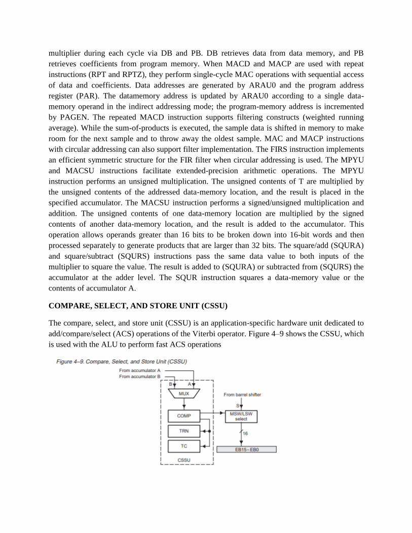
COMPARE, SELECT, AND STORE UNIT (CSSU)
The compare, select, and store unit (CSSU) is an application-specific hardware unit dedicated to
add/compare/select (ACS) operations of the Viterbi operator. Figure 4–9 shows the CSSU, which
is used with the ALU to perform fast ACS operations

The CSSU allows the C54x device to support various Viterbi butterfly algorithms used in
equalizers and channel decoders. The add function of the Viterbi operator (see Figure 4–10) is
performed by the ALU. This function consists of a double addition function (Met1 D1 and Met2
D2). Double addition is completed in one machine cycle if the ALU is configured for dual 16-bit
mode by setting the C16 bit in ST1. With the ALU configured in dual 16-bit mode, all the long-
word (32-bit) instructions become dual 16-bit arithmetic instructions. T is connected to the ALU
input (as a dual 16-bit operand) and is used as local storage in order to minimize memory access.
Table 4–6 shows the instructions that perform dual 16-bit ALU operation

PIPELINE OPERATION
-level deep instruction pipeline. The six stages of the pipeline are
independent of each other, which allows overlapping execution of instructions. During any given
cycle, from one to six different instructions can be active, each at a different stage of completion.
The six levels and functions of the pipeline structure are: Program prefetch. Program address bus
(PAB) is loaded with the address of the next instruction to be fetched. Program fetch. An
instruction word is fetched from the program bus (PB) and loaded into the instruction register
(IR). This completes an instruction fetch sequence that consists of this and the previous cycle.
Decode.
The contents of the instruction register (IR) are decoded to determine the type of memory access
operation and the control sequence at the data-address generation unit (DAGEN) and the CPU.
Access. DAGEN outputs the read operand’s address on the data address bus, DAB. If a second
operand is required, the other data address bus, CAB, is also loaded with an appropriate address.
Auxiliary registers in indirect addressing mode and the stack pointer (SP) are also updated.
This is considered the first of the 2-stage operand read sequence. Read. The read data operand(s),
if any, are read from the data buses, DB and CB. This completes the two-stage operand read
sequence. At the same time, the two-stage operand write sequence begins.
The data address of the write operand, if any, is loaded into the data write address bus (EAB).
For memory-mapped registers, the read data operand is read from memory and written into the
selected memory-mapped registers using the DB. Execute. The operand write sequence is
completed by writing the data using the data write bus (EB).
The instruction is executed in this phase. Figure 7–1 shows the six stages of the pipeline and the
events that occur in each stage. The first two stages of the pipeline, prefetch and fetch, are the
instruction fetch sequence. In one cycle, the address of a new instruction is loaded. In the
following cycle, an instruction word is read. In case of multiword instructions, several such
instruction fetch sequences are needed.

During the third stage of the pipeline, decode, the fetched instruction is decoded so that
appropriate control sequences are activated for proper execution of the instruction.
The next two pipeline stages, access and read, are an operand read sequence. If required by the
instruction, the data address of one or two operands are loaded in the access phase and the
operand or operands are read in the following read phase. Any write operation is spread over two
stages of the pipeline, the read and execute stages.
During the read phase, the data address of the write operand is loaded onto EAB. In the
following cycle, the operand is written to memory using EB. Each memory access is performed
in two phases by the C54x DSP pipeline. In the first phase, an address bus is loaded with the
memory address. In the second phase, a corresponding data bus reads from or writes to that
memory address.
Figure 7–2 shows how various memory accesses are performed by the C54x DSP pipeline. It is
assumed that all memory accesses in the figure are performed by single-cycle, single-word
instructions to on-chip dual-access memory. The on-chip dual-access memory can actually
support two accesses in a single pipeline cycle. This is discussed in section 7.3, Dual-Access
Memory and the Pipeline, on page 7-27.

The following sections provide examples that demonstrate how the pipeline works while
executing different types of instructions. Unless otherwise noted, all instructions shown in the
examples are considered single-cycle, singleword instructions residing in on-chip memory. The
pipeline is depicted in these examples as a set of staggered rows in which each row corresponds

to one instruction word moving through the stages of the pipeline. Example 7–1 is a sample
pipeline diagram.
1.5.4 DIRECT MEMORY ACCESS (DMA) CONTROLLER
The ’54x direct memory access (DMA) controller transfers data between points in the memory
map without intervention by the CPU. The DMA allows movements of data to and from internal
program/data memory, internal peripherals (such as the McBSPs), or external memory devices to
occur in the background of CPU operation. The DMA has six independent programmable
channels, allowing six different contexts for DMA operation. The DMA has the following

features: The DMA operates independently of the CPU. The DMA has six channels. The DMA
can keep track of the contexts of six independent block transfers. The DMA has higher priority
than the CPU for both internal and external accesses. Each channel has independently
programmable priorities. Each channel’s source and destination address registers can have
configurable indexes through memory on each read and write transfer, respectively. The address
may remain constant, postincrement, postdecrement, or be adjusted by a programmable value.
Each read or write transfer may be initialized by selected events. On completion of a half-block
or full-block transfer, each DMA channel may send an interrupt to the CPU. On-chip-RAM-to-
off-chip-memory DMA transfer requires 5 cycles while off-chip-memory-to-on-chip-RAM
DMA transfer requires 5 cycles. The DMA can perform double-word transfers (a 32-bit transfer
of two 16-bit words).
1.5.4.1 DMA Memory Map
The DMA memory map includes access to on-chip memory on all devices and access to external
memory on selected devices. The DMA memory map for on-chip memory is unaffected by the
state of the memory control bits: MP/MC, DROM, and OVLY. For specific information on
DMA implementations and memory maps, see the device-specific data sheets.
1.5.4.2 DMA Priority Level
Each DMA channel can be independently assigned high or low priority relative to each other.
Multiple DMA channels that are assigned to the same priority level are handled in a round-robin
manner.
1.5.4.3 DMA Source/Destination Address Modification
The DMA provides flexible address-indexing modes for easy implementation of data
management schemes such as autobuffers and circular buffers. Source and destination addresses
can be indexed separately and can be postincremented, postdecremented, or postincremented
with a specified index offset.
1.5.4.4 DMA in Autoinitialization Mode
The DMA can automatically reinitialize itself after completion of a block transfer. Some of the
DMA registers can be preloaded for the next block transfer through DMA global reload registers
(DMGSA, DMGDA, and DMGCR). Autoinitialization allows: Continuous operation. Normally,
the CPU would have to reinitialize the DMA immediately after the completion of the current
block transfer; with the global reload registers, it can reinitialize these values for the next block
transfer any time after the current block transfer begins. Repetitive operation. The CPU does not
preload the global reload register with new values for each block transfer but only loads them on
the first block transfer. The DMA global reload register sets are sharred by all channels.
However, select DMAs have been enhanced to expand the DMA global reload register set to

provide each DMA channel its own DMA global reload register set. For example, the DMA
global reload register set for channel 0 includes DMGSA0, DMGDA0, DMGCR0, and
DMGFR0 while DMA channed 1 registers include DMGSA1, DMGDA1, DMGCR1, and
DMGFR1.
1.5.4.5 DMA Transfer Counting
The DMA channel element count register (DMCTRx) and the frame count register (DMFRCx)
contain bit fields that represent the number of frames and number of elements per frame to be
transferred. Frame count. This 8-bit value defines the total number of frames in the block
transfer. The maximum number of frames per block transfer is 128 (FRAME COUNT= 0ffh).
The counter is decremented upon the last read transfer in a frame transfer. Once the last frame is
transferred, the selected 8-bit counter is reloaded with the DMA global frame reload register
(DMGFR) if the AUTOINIT is set to 1. A frame count of 0 (default value) means the block
transfer contains a single frame. Element count. This 16-bit value defines the number of elements
per frame. This counter is decremented after the read transfer of each element. The maximum
number of elements per frame is 65536 (DMCTRn = 0ffffh). In autoinitialization mode, once the
last frame is transferred, the counter is reloaded with the DMA global count reload register
(DMGCR).
1.5.4.6 DMA Transfer in Double-Word Mode
Double-word mode allows the DMA to transfer 32-bit words in any index mode. In double-word
mode, two consecutive 16-bit transfers are initiated and the source and destination addresses are
automatically updated following each transfer. In this mode, each 32-bit word is considered to be
one element.
1.5.4.7 DMA Channel Index Registers
The particular DMA channel index register is selected by way of the SIND and DIND field in
the DMA mode control register (DMMCRx). Unlike basic address adjustment, in conjunction
with the frame index DMFRI0 and DMFRI1, the DMA allows different adjustment amount
depending on whether or not the element transfer is the last in the current frame. The normal
adjustment value (element index) is contained in the element index registers, DMIDX0 and
DMIDX1. The adjustment value (frame index) for the end of the frame, is determined by the
selected DMA frame index register, either DMFRI0 or DMFRI1. The element index and the
frame index affect address adjustment as follows: Element index. For all except the last transfer
in the frame, element index determines the amount to be added to the DMA channel for the

source/destination address register (DMSRCx/DMDSTx) as selected by the SIND/DIND bits.
Frame index. If the transfer is the last in a frame, frame index is used for address adjustment as
selected by the SIND/DIND bits. This occurs in both single-frame and multiframe transfer.
1.5.4.8 DMA Interrupts
The ability of the DMA to interrupt the CPU based on the status of the data transfer is
configurable and is determined by the IMOD and DINM bits in the DMA channel mode control
register (DMMCRn). The available modes are shown in Table 1–7.


Scanned by CamScanner

Scanned by CamScanner

Scanned by CamScanner

Scanned by CamScanner

Scanned by CamScanner

Scanned by CamScanner

Scanned by CamScanner

Scanned by CamScanner

Scanned by CamScanner