AN IMPLEMENTATION OF A DUAL-PROCESSOR SYSTEM ON FPGA
45
AN IMPLEMENTATION OF A DUAL-PROCESSOR SYSTEM ON FPGA by Mohammed Eqbal A Project Presented to the Faculty of the American University of Sharjah College of Engineering in Partial Fulfillment of the Requirements for the Degree of Master of Science in Computer Engineering Sharjah, United Arab Emirates May 2014
Transcript of AN IMPLEMENTATION OF A DUAL-PROCESSOR SYSTEM ON FPGA

AN IMPLEMENTATION OF A DUAL-PROCESSOR
SYSTEM ON FPGA
by
Mohammed Eqbal
A Project Presented to the Faculty of the
American University of Sharjah
College of Engineering
in Partial Fulfillment
of the Requirements
for the Degree of
Master of Science in
Computer Engineering
Sharjah, United Arab Emirates
May 2014

© 2014 Mohammed Eqbal. All rights reserved.

Approval Signatures
We, the undersigned, approve the Master’s Project of Mohammed Eqbal.
Project Title: An Implementation of a Dual-Processor System on FPGA.
Signature Date of Signature
(dd/mm/yyyy)
___________________________ _______________
Dr. Assim Sagahyroon
Professor, Department of Computer Science and Engineering
Project Advisor
___________________________ _______________
Dr. Fadi Aloul
Associate Professor, Department of Computer Science and Engineering
Project Co-Advisor
___________________________ _______________
Dr. Abdul-Rahman Al-Ali
Professor, Department of Computer Science and Engineering
Project Committee Member
___________________________ _______________
Dr. Tarik Ozkul
Professor, Department of Computer Science and Engineering
Project Committee Member
___________________________ _______________
Dr. Assim Sagahyroon
Head, Department of Computer Science and Engineering
___________________________ _______________
Dr. Hany El-Kadi
Associate Dean, College of Engineering
___________________________ _______________
Dr. Leland Blank
Dean, College of Engineering
___________________________ _______________
Dr. Khaled Assaleh
Director of Graduate Studies
Acknowledgment
I have taken much time and effort in this project. However, it would not have
been possible without the kind support and help of many individuals. I would like to
extend my sincere thanks to all of them.
I am highly indebted to Dr. Assim Sagahyroon for his guidance and constant
supervision as well as for providing necessary information regarding the project and
also for his support in completing the project.
I would like to express my gratitude towards my professors, especially Dr.
Abdul-Rahman Al-Ali, and all the other members of the Computer Engineering
Department family for their kind co-operation and encouragement which helped me in
the completion of this project.
My thanks and appreciations also go to my family and friends in developing the
project who have helped me out with their emotional support.

5
Abstract
In recent years, Field-Programmable Gate Arrays (FPGA) have evolved rapidly paving
the way for a whole new range of computing paradigms. On the other hand, computer
applications are evolving. There is a rising demand for a system that is general-purpose
and yet has the processing abilities to accommodate current trends in application
processing. This work proposes a design and implementation of a tightly-coupled
FPGA-based dual-processor platform. We architect a platform that optimizes the
utilization of FPGA resources and allows for the investigation of practical
implementation issues such as cache design. The performance of the proposed
prototype is then evaluated, as different configurations of a uniprocessor and a dual-
processor system are studied and compared against each other and against published
results for common industry-standard CPU platforms. The proposed implementation
utilizes the Nios II 32-bit embedded soft-core processor architecture designed for the
Altera Cyclone III family of FPGAs.
Search Terms: FPGA, uniprocessor system, dual-processor system, Nios II processor,
Dhrystone.

6
Table of Contents
Abstract ............................................................................................................ 5
List of Figures ........................................................................................................... 8
List of Tables ............................................................................................................ 9
Chapter 1: Introduction ............................................................................................ 10
1.1 Problem Statement ......................................................................................... 10
1.1.1 Characteristics of modern applications. ................................................... 11
1.2 Background Information on FPGA Technology ............................................. 12
1.2.1 The altera family of FPGAs. .................................................................... 12
1.2.2 The cyclone FPGA. ................................................................................. 13
1.2.3 The quratus ii platform. ........................................................................... 13
1.2.4 The SoPC builder. ................................................................................... 13
1.2.5 Soft-hardware components. ..................................................................... 14
1.2.6 The nios ii processor. .............................................................................. 14
1.3 Literature Review and Related Work.............................................................. 15
1.3.1 Multiprocessor systems on multiple chips................................................ 16
1.3.2 Multiprocessor system-on-chip (MPSoC). ............................................... 16
1.4 Work Outline ................................................................................................. 19
Chapter 2: Proposed System Design and Testing Strategy ........................................ 20
2.1 Design Overview and System Components .................................................... 20
2.2 Testing Strategy ............................................................................................. 22
2.3 Design Trade-off ............................................................................................ 22
2.4 Benchmark Selection ..................................................................................... 23
Chapter 3: Results and Discussion ........................................................................... 24
3.1 Experiment 1 ................................................................................................. 24
3.1.1 Resource usage. ....................................................................................... 26
3.2 Experiment 2 ................................................................................................. 27
3.2.1 Resource usage. ....................................................................................... 29
3.3 Conclusions from the Experiments ................................................................. 31
3.4 Design Evaluation .......................................................................................... 31
3.4.1 Benchmark results. .................................................................................. 32
3.5 Comparison with Industry-Standard Benchmark Results ................................ 33

7
Chapter 4: Conclusion ............................................................................................. 34
Chapter 5: Future Work and Recommendations ....................................................... 35
References .......................................................................................................... 37
Appendix A .......................................................................................................... 41

8
List of Figures
Figure 1: A Typical Nios II Processor Block Diagram [14] ...................................... 15
Figure 2: Components of a Uniprocessor System ..................................................... 20
Figure 3: Components of a Dual-processor System .................................................. 21
Figure 4: Instruction Cache and Number of CPU Analysis ....................................... 25
Figure 5: Data Cache and Number of CPU Analysis ................................................ 28

9
List of Tables
Table 1: Instruction Cache and Number of CPU Analysis ........................................ 24
Table 2: Resource Usage for IC 16 KB, 2 CPUs ...................................................... 26
Table 3: Data Cache and Number of CPU Analysis ................................................. 27
Table 4: Resource Usage for IC 8 KB, DC 32 KB, 1 CPU ....................................... 29
Table 5: Resource Usage for IC 8 KB, DC 8 KB, 2 CPUs ........................................ 30
Table 6: Proposed Nios II Dual-Processor System Design Configuration ................. 32
Table 7: Proposed Nios II Dual-Processor System Benchmark Results .................... 32
Table 8: VAX MIPS 1.1 Benchmark Results on PCs ............................................... 33
Table 9: VAX MIPS 2.1 Benchmark Results on PCs ............................................... 33

10
Chapter 1: Introduction
Computer applications are evolving over time. Multimedia applications have
lately become a dominant workload on general desktops and workstations, and they are
becoming the modern trend [1]. Contemporary applications are rich with multimedia
contents. With the explosion of the World-Wide Web and the Internet, workloads in the
future are expected to be even more dominated by multimedia [2]. The high degrees of
parallelism and large volumes of data, for instance, within such applications have been
well-researched, but less well-understood is how to design a processor that is capable
of accommodating these intensive applications [3]. Such applications exhibit slightly
different characteristics and behavior compared to general applications.
1.1 Problem Statement
Traditional superscalar architectures are poorly suited to the demands of modern
applications [4]. To enhance the processing of such new trends in applications,
engineers have been designing systems that consist of general multi-purpose processors
augmented with another Application-Specific Integrated Circuit (AISC) which is
typically a Graphics Processing Unit (GPU) that assists in the execution of applications.
In the context of embedded systems where efficiency is highly demanded, augmenting
the main CPU with a GPU is less desired however. Having the two units on separate
chips needs a bus in between for communications which impedes performance in terms
of power consumption and execution time. Buses usually run at much-slower speeds
(clock frequencies) than the CPU clocks. Buses also require more power to transfer
information.
There is a growing demand for a system that is general-purpose and yet has the
processing capabilities to accommodate the modern trends in application processing.
Computer architects, therefore, had to respond to this need by modifying their
architectures and evaluating each against the other, in terms of handling contemporary
applications. In this work, we propose the design of a Dual-processor System using
Field-Programmable Gate Array (FPGA) technology.

11
1.1.1 Characteristics of modern applications.
We have established that modern applications are rich with multimedia
contents, and in the near future “workloads are believed to be even more multimedia
dominant” [2]. In order to be able to propose or design a computer platform that is
general-purpose and yet suits the needs of modern applications, we will initially
overview the inherent characteristics of such applications and highlight the differences
from other general-purpose applications. Understanding this will enable us to propose
a practical dual-processor design.
A very thorough study of multimedia applications’ behavior was conducted in
Princeton University by Jason Fritts and his colleagues [3]. In their study, Fritts and his
colleagues studied a multimedia benchmark called ‘MediaBench suite’ that is used as
an industry standard benchmark to evaluate both compilers and processors. The
benchmarks were ranging from image and video processing to audio and speech
processing, and even encryption and computer graphics. The compiler used in the study
was the IMPACT compiler [3], which allows for extracting and recording the execution
behavior. A summary of the results are discussed below.
The study shows that the operation frequencies profile for multimedia is
relatively close to the operation frequencies profile of general-purpose applications.
Slight differences exist, however, such as the fact that “there is little overall floating
point usage”, compared to integer operations [3]. Besides, integer transfers (load and
store) occur more frequently. Therefore, we can conclude that multimedia applications
are very memory-intensive applications.
To further understand multimedia applications, few other results have been
reported [4], [5]. They concluded that multimedia applications normally had large data
sets and seemed to have little data-reuse. Spatial locality was a clear characteristic for
these applications, and yet they demonstrated very little global temporal locality. The
researchers in [5] also argued that that cache design is more important than main
memory design, while the study in [4] claimed that multimedia applications have a high
degree of inherent parallelism. This large amount of parallelism can be exploited on
parallel processors.
12
In Section 1.2, we elaborate more on the FPGA technology.
1.2 Background Information on FPGA Technology
FPGA is defined as Field-Programmable Gate Array. It is “a semiconductor
device that can be programmed after manufacturing. Instead of being restricted to any
predetermined hardware function, an FPGA allows you to program product features
and functions, adapt to new standards, and reconfigure hardware for specific
applications even after the product has been installed in the field—hence the name
‘field-programmable’. You can use an FPGA to implement any logical function that an
Application-Specific Integrated Circuit (ASIC) could perform” [6]. Basically, “every
FPGA chip is made up of a finite number of predefined resources with programmable
interconnects to implement a reconfigurable digital circuit” [7].
FPGA technology allows us to design virtually any computer system in software
and then download it to the FPGA chip. This chip then functions according to the design
specified using the software as if it was a custom-made ASIC. This technology allows
researchers to come up with their own system design, write it as software (in a Hardware
Description Language-HDL), download it to the chip, and then test the hardware
design. FPGAs are especially suited for industrial and embedded applications as they
are “very powerful, relatively inexpensive, and adaptable, since their configuration is
specified in an abstract hardware description language” [8].
1.2.1 The altera family of FPGAs.
The platform that we are going to use is manufactured by Altera [9]. Altera is a
major manufacturer of high-end Programmable Logic Devices (PLD), and is a leading
company in the field of programmable logic solutions. The platform solution provided
by Altera allows semiconductor companies to quickly and cost-effectively design and
build their systems. The company offers FPGAs, System-on-Chips (SoCs) with
embedded processor systems, and Complex Programmable Logic Devices (CPLD) in
combination with software tools.

13
1.2.2 The cyclone FPGA.
Cyclone III is a member of the Cyclone FPGA family manufactured by Altera.
Altera claims that it offers a combination of low power, high functionality, and low
cost. Cyclone III FPGA is a good choice for testing our design, as it has features such
as “200K logic elements, 8 Mbits of embedded memory, and 396 embedded
multipliers”. Altera claims that Cyclone III FPGAs are ideal for Video and image
processing [10]. Building a Dual-processor System-on-Programmable-Chip can be
quite a challenge. We have also selected the Cyclone III FPGA for the
comprehensiveness of the documentation available that supports working in a
multiprocessor environment.
1.2.3 The quratus ii platform.
The system will be implemented using Quartus II platform. Quartus II platform
consists of an FPGA Cyclone board complemented with a Quartus II software
environment. Quartus II software is a Computer Aided Design (CAD) environment
which is basically a tool that enables designing systems on the FPGAs. It is purposely
designed to work with the entire range of the FPGA family made by Altera.
1.2.4 The SoPC builder.
Part of the Quartus II software environment for FPGAs is a tool called System-
on-Programmable-Chip Builder (SoPC Builder). Developers using the SoPC Builder
tool can design and build multiprocessor systems. Systems that incorporate two or more
processors working together are referred to as multiprocessor systems, and when
implemented as a system on a single chip they are commonly referred to as
Multiprocessor System-on-Chip (MPSoC). Similarly, ‘tightly-coupled’
multiprocessors refer to systems that have all processors are residing on the same
physical chip.
SoPC Builder is a system development tool for creating SoPC and MPSoC
design systems by using components such as processors, peripherals, and memories as
building blocks [11]. It automates the task of generating and integrating such hardware
components. Traditionally, designers must first write the code in Hardware Depiction
Language (HDL) for each hardware component, and then manually write other HDL

14
modules to connect together all these components in the system. However, in SoPC
Builder, designers can select the system components (as it incorporates a library of
components such as the Nios II soft processor, memory controllers, interfaces, and
peripherals), configure each component in depth, and then SoPC Builder generates the
HDL files required for the components and the interconnect logics automatically.
Interconnections are made though the Avalon bus. SoPC Builder generates either
Verilog HDL or VHDL equally [12].
1.2.5 Soft-hardware components.
The term ‘soft-hardware components’ refers to hardware-equivalent
components that are programmed on the FPGA. Soft-hardware components are first
designed in software in HDL, and then downloaded on FPGAs to act like typical
hardware. According to [13], “a soft-core microprocessor is a Hardware Description
Language (HDL) model of a specific processor (CPU) that can be customized for a
given application and synthesized for an ASIC or FPGA target. In many applications,
soft-core processors provide several advantages over custom designed processors such
as reduced cost, flexibility, platform independence and greater immunity to
obsolescence. Embedded systems are hardware and software components working
together to perform a specific function”.
1.2.6 The nios ii processor.
Nios II is a 32-bit embedded soft-core processor architecture designed by
Altera. Nios II includes many improvements over the original (16-bit) Nios
architecture. According to [14], the Nios II processor can be illustrated as shown in
Figure 1.

15
Figure 1: A Typical Nios II Processor Block Diagram [14]
According to [15], “the Nios II processor has a Reduced Instruction Set
Computer (RISC) architecture. Its arithmetic and logic operations are performed on
operands in the general purpose registers. The data is moved between the memory and
these registers by means of Load and Store instructions. The word length of the Nios II
processor is 32 bits. All registers are 32 bits long. Byte addresses in a 32-bit word can
be assigned in either little-endian or big-endian style. The assignment style is one of
the options that the user may select at configuration time. The Nios II architecture uses
separate instruction and data buses, which is often referred to as the Harvard
architecture”.
1.3 Literature Review and Related Work
In the context of implementing a tightly-coupled dual-processor system on an
FPGA that is tailored for modern applications, we discuss some of the work that has
been completed and highlight the differences when compared to our approach.

16
1.3.1 Multiprocessor systems on multiple chips.
To achieve higher performance, engineers sometimes utilize heterogeneous
multiprocessor platforms which are tuned for a certain well-defined application
domain. FPGA is known for providing designers with several benefits in hardware
system design customization. In this type of design, the processors are usually laid on
different physical chips. The work in [16] discusses the design of an FPGA-based
heterogeneous multiprocessor system consisting of four Nios II soft-cores and one
ARM core. The ARM core is the central controller of the whole system, and four Nios
II cores serve as slaves under control by the ARM core. The ARM core and Nios II
cores cooperate and work in parallel to accomplish each task. The System was
implemented on Altera Stratix II. Having one central processor governing the Nios soft-
core is one approach. In our design, however, we attempt to avoid this by having the
dual-processor system on the same chip and thus eradicating any external bus
bottleneck possibilities.
1.3.2 Multiprocessor system-on-chip (MPSoC).
When creating a multiprocessor system, one approach is to lay multiple
processors on different chips (as explored earlier). Another approach is to have the
processors on the same chip. This increases system efficiency and performance at the
expense of the FPGA chip’s real-estate [17].
The study in [18] presented an implementation of a ‘tightly coupled’, cache-
coherent Symmetric Multiprocessing (SMP) architecture using a vendor-provided soft-
core processor. By definition, according to [19], SMP is a system “where two or more
identical processors connect to one another through a shared memory. Each processor
has equal access to the shared memory”. Tightly-coupled multiprocessing refers to
chip-level multiprocessing, where all processors are residing on the same physical chip.
According to [19], in tightly-coupled multiprocessing systems “multiple CPUs are
connected via a shared bus (or an interconnect fabric) to a shared memory. Each
processor also has its own fast memory. The tightly-coupled nature such systems allows
very short physical distances between processors and memory and, therefore, minimal
memory access latency and higher performance. This type of architecture works well
in multi-threaded applications where threads can be distributed across the processors to

17
operate in parallel”. The work in [18] provided a framework for designing an SMP
system. Vendor-provided soft-core processors (such as Altera’s Nios II) often support
advanced features such as caching that work well in uniprocessor or multiprocessor
architectures. However, it is a challenge to implement Symmetric Multiprocessor
System-on-Programmable-Chip (SMP-SoPC). Given the scope of our project, we will
not attempt to provide a framework for Symmetric Multiprocessing (SMP) systems but
rather focus on the design aspects of building a tightly-coupled multiprocessor system.
Furthermore, the paper in [18] presented results on cache coherency and FPGA
utilization. However, it didn’t present benchmark results. In our work, we will measure
the performance of our implemented system by running a benchmark on it.
A further attempt was made to provide a solid foundation for SMP parallel
processing. The researchers in [20] proposed a system called MultiFlex which is
basically “an application-to-platform mapping tool that integrates heterogeneous
parallel components H/W or S/W into a homogeneous platform programming
environment”. In our project, we will not attempt to provide a framework for running
applications parallel for SMP systems but rather focus on the design aspects of building
a tightly-coupled multiprocessor system and its performance. Furthermore in [20] after
proposing the mapping tool, an actual Multiprocessor System-on-Chip (MPSoC) was
implemented to handle networking and multimedia applications. Testing this proposed
system was done by running an internet traffic management application and an MPEG4
video encoder. This work measured the performance in terms of processor utilization
percentage which ranged between 85%-91%.
In another work by Tseng and Chen [21] however, an attempt to benchmark the
CPU was made. An implementation of an FPGA Nios II based MPSoC was presented
and tested. They ran two simple benchmarks that they developed. The first benchmark
(VAR) was basically an array that required all processers to operate on the same set of
data simultaneously. The second benchmark (ARRAY) was computations for a huge
array that was segregated in advance, and distributed to all processors. Processors in
the second case were competing against each other only to grab the hardware mutex for
accessing the same memory. The researchers designed a four-processor system using
Nios II soft-core and implemented an MPSoC architecture. The results showed that “the

18
quad-core system architecture that they proposed can execute the program concurrently
at the same time”. No industry-standard benchmark was used. Interestingly enough
though, they stated that in future work researchers should aim at how to utilize the
characteristics of multiprocessor to design multimedia applications. While the work in
[21] made a genuine attempt to assess the parallel capabilities of MPSoCs, in our
approach we would attempt to run industry-standard benchmark in order to be able to
compare our system to other published results, rather than developing the benchmark
ourselves.
The work in [22] made a better attempt to evaluate a multiprocessor FPGA
implementation. The authors first designed a configurable and scalable multiprocessor
system on Xilinx Virtex-5 FPGA (a competitor of the Altera Cyclone FPGA). Then,
the performance of a uniprocessor system and a multiprocessor implementation of
widely used Fast Fourier Transform (FFT) functions was analyzed, as this was the main
objective of the work. On the other hand, this work also presented benchmark results
for their implemented systems using CoreMark benchmark which is a part of the
EEMBC benchmark suite. The study also concludes that the benchmark “score
increases linearly with the number of processors in a multiprocessor system”.
While in some work (above) attempts to design, build, and test Multiprocessor
System-on-Chip (MPSoC) implementations were made, others only provided a process
design flow for building SoC-based embedded systems [17], [23]. Furthermore, other
researches considered it enough to simply present an overview of FPGA-based
multiprocessor systems, describe the main characteristics, and comment on several
FPGA-based multiprocessor systems appearing in the research community for the last
five years [24].
When developing a multiprocessor system using Altera’s platforms, developers
can choose among several memory architectures and configurations of Multiprocessor
systems (e.g. shared buffer only and shared memory only, shared nothing …etc.).
Sections 1.4 and 2.1 elaborate more on the different architectures supported for
designing multiprocessor systems, provide an overview of creating one, and propose a
synopsis of our prototype.

19
1.4 Work Outline
Our work in this project can be outlined as follows. After conducting a literature
survey and reviewing work that was relevant to ours, we propose a multiprocessor-
based system that is designed with the aim of speeding up the execution of applications.
We propose a prototype for a uniprocessor and a dual-processor system, using Altera’s
Quartus II platform and based on the Nios II soft-core processor architecture.
Subsequently, we test the performance of the proposed prototypes. We study
different configurations of the uniprocessor and dual-processor system and compare
them against each other and against published results for common industry-standard
CPU platforms.

20
Chapter 2: Proposed System Design and Testing Strategy
2.1 Design Overview and System Components
We exhibit the following system diagrams showing the components used in our
uniprocessor system (Figure 2) and dual-processor system (Figure 3). These
components can be designed and implemented and connected using the ‘SoPC Builder’
environment.
Figure 2: Components of a Uniprocessor System
Following is a brief description for the components shown in Figure 2 and
Figure 3.
Each CPU is a Nios II soft-core which consist of a six-stage pipeline running at
66.5 MHz.
Each CPU has a timer.
Each CPU has its own separate instruction and data caches. As it was
demonstrated (in the Literature Review and Related Work section), heavy
emphasis on cache was made.
Main Memory is physically shared for the two CPUs. However, each CPU is
assigned to a different segment of the memory.
Ava
lon
Bu
s
CPU
Timer
Insctruction Cache
Data CacheMain Memory
JTAG/UART

21
Mailbox is the mechanism for the dual-processors to exchange messages. These
messages are stored in linked-list structure inside the buffer.
Mailbox buffer is implemented using the on-chip memory. The on-chip memory
can be configured either as the main memory for the CPU, or as buffers for the
mailboxes for synchronization. In our case, part of the on-chip memory will be
configured as a buffer for the mailbox.
Mailbox Mutex is a hardware module that governs and guarantees
synchronization for accessing the mailbox.
Avalon bus is the cross-connect fabric that is capable of interconnecting the
different components in the system. It is a reconfigurable switch fabric that can
interface embedded peripherals and system components.
JTAG and UART are modules for downloading the design onto the Field-
Programmable Gate Array (FPGA) and are also used for debugging.
Figure 3: Components of a Dual-processor System
Ava
lon
Bu
s
CPU1
Timer
Instruction Cache
Data Cache
CPU2
Timer
Instruction Cache
Data CacheMain Memory
Mailbox
Mailbox Buffer
Mailbox Mutex
JTAG/UART

22
Given all the established background information, we can draw the following
conclusions that engineers should consider when designing a system that suits modern
applications: Cache size is heavily emphasized upon and must be well designed and
thoroughly tested, and parallelism is an also important aspect. We have already said
that cache and especially data cache is very crucial. The bigger the data cache size, the
better the performance. Furthermore, newer applications require a very high degree of
parallelism, having a dual-processor system should, therefore, increase the
performance. Additionally, having all hardware components on the same chip (tightly-
coupled) must yield efficiency and better performance.
2.2 Testing Strategy
We will first build a uniprocessor system and test it with the benchmark. Next,
we will build a dual-processor system and similarly examine it, and then compare both.
We will also build different systems, with different instruction cache sizes and
different data cache sizes. We will examine how varying any of these aspects improves
the performance and produces different results.
2.3 Design Trade-off
Furthermore, when designing FPGAs, like any other computer system, an
important factor is chip real-estate. When building a dual-processor system, for
example, cache sizes are limited to a certain size limit because the FPGA has to simply
accommodate more CPU cores which comprise of high-speed registers. Cache also is a
very high speed memory. Both CPU cores and cache are implemented on the FPGA
using fast M9K memory blocks. In Altera FPGAs, “the embedded memory structure
consists of columns of M9K memory blocks”. These fast memory blocks can be
configured “to provide various memory functions, such as RAM, shift registers, ROM,
and FIFO buffers” [25]. In our analysis, we will attempt to answer the following
question: To achieve the maximum performance which component is more important
and more useful for investing with the given real-estate, cache or the number of CPUs?

23
2.4 Benchmark Selection
We considered ‘Dhrystone’ benchmark for testing our prototype [26].
Dhrystone is a benchmark program developed in by Reinhold Weicker. Dhrystone grew
to become the industry-standard for assessing processors in terms of their
performances. Weicker designed Dhrystone by gathering meta-data from a wide range
of softwares. Then, he characterized these programs in terms of various common
aspects such as procedure calls, pointer indirections, assignments, etc. From this he
managed to build the Dhrystone benchmark [27]. One important characteristic of the
Dhrystone benchmark is that it is a strong indicator of general-purpose CPU’s integer
performance. A strong character of multimedia application, as Dhrystone benchmark
contains no floating point operations.
According to [28], “the C version of Dhrystone is the one mainly used in
industry. The original Dhrystone benchmark is still used to measure CPU performance
today. The original intent with Dhrystone was to create a short benchmark program that
was representative of system (integer) programming. The Dhrystone code is dominated
by simple integer arithmetic, string operations, logic decisions, and memory accesses
intended to reflect the CPU activities in most general purpose computing applications.
The Dhrystone result is determined by measuring the average time a processor takes to
perform many iterations of a single loop containing a fixed sequence of instructions
that make up the benchmark. When Dhrystone is referenced, it is usually quoted as
‘DMIPS’, or Dhrystone MIPS/MHz”. Furthermore, details on the Dhrystone
benchmark can further be examined in Appendix A.
The most two popular versions of Dhrystone benchmark are version 1.1 and
version 2.1. The difference between the two versions is that the second generation was
developed to prevent compiler optimization and provide a true representation of the
hardware being tested. In this work, we will use versions 1.1 and 2.1.

24
Chapter 3: Results and Discussion
As discussed earlier, we attempt to address the following factors as to how they
affect the performance of our system: instruction cache, data cache, and parallelism.
3.1 Experiment 1
In this experiment, we build and run different configurations of the system. To
be able to study one factor at a time, we remove data cache temporarily from our design
in this experiment, and build several systems while varying the instruction cache size.
The following instruction cache sizes are used: 2 KB, 4 KB, 8 KB, and 16 KB, when
building uniprocessor systems. We also use the same instruction cache sizes set for
dual-processor system this time to observe the difference. It is important to note that
while studying a certain aspect of the design (such as instruction cache) other factors
are fixed. In Table 1, each row represents a certain configuration of the system being
tested.
Table 1: Instruction Cache and Number of CPU Analysis
Number
of CPUs
IC
Size
DC
Size
Dhrystones
1.1/Second
Dhrystones
2.1/Second
1 2 KB 0 10000 10204
1 4 KB 0 10638 10537
1 8 KB 0 11238 10870
1 16 KB 0 11297 11364
2 2 KB 0 19999 20409
2 4 KB 0 21277 21074
2 8 KB 0 22471 21738
2 16 KB 0 22473 22727
The first column (in Table 1) indicates the number of CPUs used in each
configuration. The second column indicates the instruction cache size (in KB) that is
used. The third column shows that data cache is not implemented in this experiment.
The forth and the fifth columns show the benchmark results for Dhrystone versions 1.1

25
and 2.1, respectively, recorded in Dhrystones per seconds for the given hardware
configuration.
From the results shown in Table 1, we first observe that introducing a second
CPU yields a speedup factor of around 2 consistently and throughout all instruction
cache size variations.
Figure 4 shows a plot of the benchmark results, over the different configurations
of the system that are implemented. On the y-axis, the values are in Dhrystones per
seconds. The blue curve represents the benchmark results for Dhrystone version 1.1,
while the red curve represents the benchmark results for Dhrystone version 2.1. On the
x-axis, we start by having one CPU (uniprocessor system) with an instruction cache of
size 2 KB. Then, we increase the instruction cache gradually by using the following
sizes for the instruction cache: 4 KB, 8 KB, and 16 KB. Next, we add a second CPU
(dual-processor system), and set the instruction cache size back to 2 KB. Similarly, we
increase the instruction cache gradually by using the following sizes for the instruction
cache: 4 KB, 8 KB, and 16 KB.
Figure 4: Instruction Cache and Number of CPU Analysis
0
5000
10000
15000
20000
25000
2 KB 4 KB 8 KB 16 KB 2 KB 4 KB 8 KB 16 KB
1 1 1 1 2 2 2 2
Dh
ryst
on
es/
Seco
nd
Dhrystones 1.1/Second
Dhrystones 2.1/Second
Instruction Cache
Number of CPUs

26
The Feld-Programmable Gate Array (FPGA) resources does not allow to
increase the instruction cache size any further beyond 16 KB, as we will discuss in the
‘Resource usage’ section.
As seen in Figure 4, if we consider the first set of four configurations (when the
number of CPUs is 1), we notice that increasing the instruction cache increases the
performance only slightly. The same can be observed with the second set of four
configurations (when the number of CPU is 2).
3.1.1 Resource usage.
Referring to the last row in Table 1, it is important to note that the Cyclone III
FPGA simply cannot fit two CPUs with more than 16 KB of instruction cache. Table 2
shows the FPGA hardware usage summary for this particular configuration. Note that
for the M9K blocks (defined in Section 2.3), 51 blocks are already used out of the 66
available blocks. If we increase the instruction cache to more than 16 KB the design
simply will not fit the FPGA anymore.
In Table 2, the first column lists the different hardware resources that are
available on the FPGA. The second column shows, for the given resource, how many
are used out of the total number of available resources on the FPGA in this system
configuration. This is also represented as a percentage (in parentheses) in the second
column.
Table 2: Resource Usage for IC 16 KB, 2 CPUs
Resource Usage
Total logic elements 9,718 / 24,624 ( 39 % )
Total registers 5,460 / 25,629 ( 21 % )
Total LABs: partially or completely used 790 / 1,539 ( 51 % )
I/O pins 131 / 216 ( 61 % )
M9Ks 51 / 66 ( 77 % )
Total block memory bits 338,592 / 608,256 ( 56 % )
Total block memory implementation bits 470,016 / 608,256 ( 77 % )
Embedded Multiplier 9-bit elements 8 / 132 ( 6 % )
PLLs 1 / 4 ( 25 % )
Global clocks 20 / 20 ( 100 % )

27
JTAGs 1 / 1 ( 100 % )
CRC blocks 0 / 1 ( 0 % )
ASMI blocks 0 / 1 ( 0 % )
Impedance control blocks 0 / 4 ( 0 % )
From the results presented in Table 2, we conclude the following: Increasing
the instruction cache size increased the performance slightly, while introducing a
second CPU doubled the performance.
3.2 Experiment 2
In this experiment, we attempt to study the effect of varying the data cache size.
Hence, we fix the instruction cache size at 8 KB. We also vary the number of CPUs
used. Table 3 shows the results of this experiment.
Table 3: Data Cache and Number of CPU Analysis
Number
of CPUs
IC
Size
DC
Size
Dhrystones
1.1/Second
Dhrystones
2.1/Second
1 8 KB 4 KB 41666 41667
1 8 KB 8 KB 41670 41667
1 8 KB 16 KB 45450 41667
1 8 KB 32 KB 45454 41667
2 8 KB 4 KB 83332 68234
2 8 KB 8 KB 87118 71428
In Table 3, the first column shows the number of CPUs implemented. The
second column indicates the instruction cache size (in KB) that was used. The third
column indicates the data cache size (in KB) that was used. The forth and the fifth
columns show the benchmark results for Dhrystone versions 1.1 and 2.1, respectively.
When comparing the results for this experiment (in Table 3) with the results in
the previous experiment (in Table 1), the first observation to make is that in the previous
experiment the overall maximum number of Dhrystones 1.1 per second that we

28
achieved was only 22473. Similarly, for the Dhrystones 2.1 per second, the maximum
number was 22727. Note that the sizes of the instruction cache used in the previous
experiment were up to 16 KB. In this experiment however, when we introduce a data
cache of only 4 KB, the benchmark results nearly double. We also notice that, after the
data cache was added, increasing the data cache size increases the performance
slightly. This can be clearly observed in Figure 5.
Figure 5: Data Cache and Number of CPU Analysis
Figure 5 shows a plot of the benchmark results. On the y-axis, the values are in
Dhrystones per seconds. On the x-axis, the first system configuration used is as follows:
Number of CPU is one, instruction cache size is 8 KB, and data cache size is 4 KB. We
fix the instruction cache size at 8 KB throughout this experiment. We increase the data
cache gradually by using the following sizes for the data cache: 4 KB, 8 KB, 16 KB,
and 32 KB. The FPGA resources does not allow to increase the data cache size any
further. Next, we set the data cache size back to 4 KB and add a second CPU. Similarly,
we increase the data cache size to 4 KB, and then to 8 KB. The resources of the FPGA
does not allow to increase the data cache size any further.
0
10000
20000
30000
40000
50000
60000
70000
80000
90000
100000
4 KB 8 KB 16 KB 32 KB 4 KB 8 KB
8 KB 8 KB 8 KB 8 KB 8 KB 8 KB
1 1 1 1 2 2
Dh
ryst
on
es/S
eco
nd
Dhrystones 1.1/Second
Dhrystones 2.1/Second
Data Cache
Instruction Cache
Number of CPUs

29
We observe that (similar to the results obtained in the previous experiment)
marginal performance speedup was gained when we increased the data cache size. We
believe that this is due to the limitation of the benchmark that we are using. A different
(larger, in working data set) benchmark would have exploited the larger data cache
more effectively and yielded even better results.
Furthermore, if we take the second configuration and the sixth configuration in
Table 3, we notice that for both configurations, the data and instruction cache size was
8 KB, but a second CPU was added to the latter one. We hence conclude that adding a
second CPU nearly doubled the performance.
3.2.1 Resource usage.
To establish the last conclusion to be drawn from this experiment, we assess the
resource utilization report for the fourth and the sixth configuration (in Table 3). For
the fourth configuration (in Table 3), when the number of CPU is 1 and the instruction
cache size is fixed at 8 KB, the maximum data cache size that can fit the Cyclone III
FPGA is 32 KB. The ‘Quratus II Fitter’ tool basically cannot accommodate a data cache
size of 64 KB for this particular configuration (refer to Table 4 to review the resource
utilization report). We can observe from the table that 80% the M9K blocks are already
used.
In Table 4, the first column lists the resources available on the FPGA. The
second column shows how many resources were used out of the available resources on
the FPGA in this particular configuration (1 CPU, 8 KB instruction cache, 32 KB data
cache).
Table 4: Resource Usage for IC 8 KB, DC 32 KB, 1 CPU
Resource Usage
Total logic elements 8,937 / 24,624 ( 36 % )
Total registers 5,492 / 25,629 ( 21 % )
Total LABs: partially or completely used 682 / 1,539 ( 44 % )
I/O pins 131 / 216 ( 61 % )
M9Ks 53 / 66 ( 80 % )
Total block memory bits 374,944 / 608,256 ( 62 % )

30
Total block memory implementation bits 488,448 / 608,256 ( 80 % )
Embedded Multiplier 9-bit elements 4 / 132 ( 3 % )
PLLs 1 / 4 ( 25 % )
Global clocks 20 / 20 ( 100 % )
JTAGs 1 / 1 ( 100 % )
CRC blocks 0 / 1 ( 0 % )
ASMI blocks 0 / 1 ( 0 % )
Impedance control blocks 0 / 4 ( 0 % )
Similarly for the sixth configuration (the last row in Table 3), the utilization
report is shown in Table 5.
Table 5: Resource Usage for IC 8 KB, DC 8 KB, 2 CPUs
Resource Usage
Total logic elements 11,813 / 24,624 ( 48 % )
Total registers 6,631 / 25,629 ( 26 % )
Total LABs: partially or completely used 906 / 1,539 ( 59 % )
I/O pins 131 / 216 ( 61 % )
M9Ks 55 / 66 ( 83 % )
Total block memory bits 366,752 / 608,256 ( 60 % )
Total block memory implementation bits 506,880 / 608,256 ( 83 % )
Embedded Multiplier 9-bit elements 8 / 132 ( 6 % )
PLLs 1 / 4 ( 25 % )
Global clocks 20 / 20 ( 100 % )
JTAGs 1 / 1 ( 100 % )
CRC blocks 0 / 1 ( 0 % )
ASMI blocks 0 / 1 ( 0 % )
Impedance control blocks 0 / 4 ( 0 % )
In Table 5, the first column lists the different hardware resources that are
available. The second column shows how many resources are used out of the available
resources on the FPGA in this particular configuration (2 CPU, 8 KB instruction cache,
8 KB data cache). Note the number of M9K blocks used. Having a larger data cache
sizes with 2 CPUs fitted on the same FPGA is not physically possible.

31
A very important factor is to be considered at this point and a solid conclusion
must be drawn. When designing a tightly-coupled system, designers are often
confronted with the following challenge: Given the same real estate on the chip, which
is more important, number of CPUs or cache size? In other words, to fully utilize the
chip resources and optimize the execution should the designer add more cores or should
the designer take advantage of the chip area by having bigger cache size? We clearly
answer this question by reviewing the results of this experiment: Larger number of
CPUs adds more performance than increasing data cache.
We can now summarize the findings in this experiment as follows. Having a
data cache is very critical for performance. Introducing a data cache in a system nearly
doubles the benchmark results. Increasing the data cache size increases the performance
slightly. Adding a second CPU nearly doubles the performance. Higher number of
CPUs enhances performance more than increasing the data cache size.
3.3 Conclusions from the Experiments
From the two experiments above we can summarize all our findings as follows.
Increasing the instruction cache size increased the performance slightly.
Adding a data cache, nearly doubles the performance.
Increasing the data cache size increases the performance only slightly.
Introducing a second CPU doubles the performance.
Having more CPU cores enhances the performance more than increasing data
cache.
3.4 Design Evaluation
By combining all the findings above, we can consider the following system with
the following configuration (Table 6) for designing a Dual-processor System on a
Cyclone III FPGA. The source code for the proposed dual-processor system can be
examined in Error! Reference source not found.. This Nios II Dual-processor System
configuration can be compared to other industry-standard CPU platforms.

32
Table 6: Proposed Nios II Dual-Processor System Design Configuration
Number of CPUs: 2 CPUs
Instruction Cache Size: 8 KB
Data Cache Size: 8 KB
3.4.1 Benchmark results.
The benchmark results for the described system design (in Table 6) are shown
in Table 7.
Table 7: Proposed Nios II Dual-Processor System Benchmark Results
Dhrystone Version or Type Results
Dhrystones 1.1/Second 87118
Dhrystones 2.1/Second 71428
VAX MIPS (1.1) 49.58
VAX MIPS (2.1) 40.65
The first two benchmark results in the first two rows (in Table 7) are recorded
in terms of Dhrystones per second. To obtain VAX MIPS results, we convert by
dividing Dhrystones per second (for both versions 1.1 and 2.1) by 1757 which is the
DEC VAX 11/780 result. According to [29], “the VAX-11 was a family of
minicomputers developed and manufactured by Digital Equipment Corporation (DEC).
The VAX-11/780 was the first VAX computer”. Researchers decided to record the
Dhrystone benchmark on this machine and record the result. Then, other machines’
results must be divided by the result of this machine (the VAX-11/780). This would
give us the ratio between the performances of the machines being tested to the
performance of the VAX-11/780 which was 1757 Dhrystones/Seconds.

33
3.5 Comparison with Industry-Standard Benchmark Results
Table 8 and Table 9 show benchmark results of Dhrystone 1.1 and 2.1
respectively, for several industry-standard CPUs, including our Proposed Nios II Dual-
Processor System [30]. The first column shows the name of the CPU. The second
column represents the clock speed (frequency, in MHz) that the CPU runs at. The third
column shows the Dhrystone benchmark results in VAX MIPS format.
Table 8: VAX MIPS 1.1 Benchmark Results on PCs
CPU MHz VAX MIPS 1.1
AMD 80386 40 4.32
IBM 486D2 50 7.89
AMD 5X86 133 9.37
IBM 486BL 100 12
80486 DX2 66 12
Nios II Dual-Processor System 66.5 49.58
AMD K62 500 77.8
AMD K63 450 76.3
Table 9: VAX MIPS 2.1 Benchmark Results on PCs
CPU MHz VAX MIPS 2.1
AMD 80386 40 4.53
IBM 486D2 50 7.89
AMD 5X86 133 9.42
IBM 486BL 100 11.8
80486 DX2 66 12.4
Nios II Dual-Processor System 66.5 40.65
AMD K6 200 43.3
IBM 6x86 150 43.9
Note that our proposed Nios II Dual-Processor System’s performance (that is
running at 66.5 MHz) is better than the 80486 DX2, according to the results
demonstrated in Table 8 and in Table 9.

34
Chapter 4: Conclusion
Field-Programmable Gate Arrays (FPGA) are excellent platforms to test and
evaluate computer hardware architectures. Tightly-coupled Multiprocessor systems
eliminate bottle-necks and provide a better performance than multiprocessor systems
on multiple chips (loosely-coupled systems).
In multiprocessor systems, increasing the instruction cache size increases the
performance slightly. Moreover, having a data cache is very critical for performance,
as adding a data cache to the design nearly doubles the performance. After adding the
data cache, increasing its size also increases the performance slightly. As for the number
of CPU cores in the system, adding a second CPU doubles the performance. Increasing
the number of CPUs increases the performance linearly.
When designing a tightly-coupled system, engineers are often confronted with
the following challenge: Given the same real estate on the chip, which is more
important, number of CPUs or cache size? Based on this work we conclude that having
more CPUs enhances performance more than increasing data cache.

35
Chapter 5: Future Work and Recommendations
As an expansion for this work the following aspects can be considered.
We ran the design on a Cyclone III chip. Yet, newer versions of Cyclone family
are available. However, the issue with newer platforms is that as Altera is keen on
rolling out new versions of their FPGAs into the market to maintain a competitive edge,
support from both Altera and the developers community remains poor for newer
models, especially for designing multiprocessor platforms. At the moment, designing a
multiprocessor system on Cyclone III remains very well established in this regard.
Nonetheless, for future expansions new versions must be considered.
The Nios II was running at 66.5 MHz, which is one of the available frequencies
on the educational board. The FPGA can run on higher frequencies if faster clocks are
available.
Researchers must consider running benchmarks from the Embedded
Microprocessor Benchmark Consortium (EEMBC) on the design configuration of Nios
II Dual-Processor System that we proposed. EEMBC is a well-established organization
that is specialized in systems benchmarking and publishing benchmark results. All
EEMBC benchmarks are licensed and need to be purchased before using [31]. Given
the resources allocated for this project, we were not able to purchase the license.
It is worth mentioning that before selecting Dhrystone as the benchmark to test
our prototype, we examined the following benchmarks: ALPBench [32], Berkeley
multimedia workload [33], MiBench [34], OpenMPBench [35]. The issue with the first
three mentioned benchmarks is that they all are based on the concept of receiving ‘files’
as an input and producing an output in the form of ‘files’ as well. Most embedded
systems do not support (and especially Nios II) a file system. As a workaround for this
issue, (using the debugging software) the input files can be ‘fed’ into the Nios II’s
memory as a ‘stream of bytes’, one by one. The downside of this approach is that this
will hinder the performance dramatically and the benchmark results will not truly
reflect the capability of the system hardware being tested. Furthermore, there is an issue
that we faced with the ALPBench and Barklay workloads. The issue was that the source
code for both benchmarks contained ‘in-line assembly’ code. Assembly language is

36
CPU-architecture-specific, and running it on Nios II requires practically re-writing the
whole benchmark core.
In summary, all the benchmarks mentioned above are simple academic projects
that are mere attempts to create acceptable benchmarks for embedded systems. This
shows that there is great demand for such applications and room for research in this
area.

37
References
[1] D. Talla and L. K. John, "MediaBreeze: A Decoupled Architecture for
Accelerating Multimedia Applications," ACM SIGARCH Computer Architecture
News, ACM Press, vol. 29, no. 5, pp. 62-67, 2001.
[2] D. Talla, "Architectural Techniques to Accelerate Multimedia Applications on
General-Purpose Processors," 2001. [Online]. Available:
http://lca.ece.utexas.edu/pubs/deepu_talla_dissertation.pdf. [Accessed 19 May
2014].
[3] J. Fritts, W. Wolf and B. Liu, "Understanding Multimedia Application
Characteristics for Designing Programmable Media Processors," in Proceedings
of the International Society for Optics and Photonics (SPIE), Media Processors,
pp. 2-13, 1998.
[4] N. Jayasena, S. Rivoire, P. W. Lee and W. Qadeer, "Data Parallel
Architectures," 3 April 2003. [Online]. Available:
http://www.stanford.edu/class/ee392c/notes/lec02/notes02.pdf. [Accessed 19
April 2014].
[5] Z. Xu, S. Sohoni, R. Min and Y. Hu, "An Analysis of Cache Performance of
Multimedia Applications," IEEE Transactions on Computers, vol. 53, no. 1, pp.
20-38, 2004.
[6] "FPGAs," Altera Corporation, 2014. [Online]. Available:
http://www.altera.com/products/fpga.html. [Accessed 11 May 2014].
[7] "FPGA Fundamentals," National Instruments, 3 May 2012. [Online]. Available:
http://www.ni.com/white-paper/6983/en/. [Accessed 11 May 2014].
[8] R. Joost and R. Salomon, "Advantages of FPGA-Based Multiprocessor Systems
in Industrial Applications," in Proceedings of the 31st Annual Conference of
IEEE Industrial Electronics Society (IECON), Raleigh, p. 6, 2005.
[9] "About Us," Altera Corporation, 2014. [Online]. Available:
http://www.altera.com/corporate/about_us/abt-index.html. [Accessed 5 May
2014].
[10] "Cyclone III FPGA Family: Unlimited Possibilities," Altera Corporation, 2014.
[Online]. Available: http://www.altera.com/products/devices/cyclone3/cy3-
index.jsp. [Accessed 19 May 2014].
[11] "Creating Nios II Multiprocessor: Tutorial," June 2011. [Online]. Available:
http://www.altera.com/literature/tt/tt_nios2_multiprocessor_tutorial.pdf.
[Accessed 19 April 2014].

38
[12] "SOPC Builder User Guide," December 2010. [Online]. Available:
http://www.altera.com/literature/ug/ug_sopc_builder.pdf. [Accessed 19 April
2014].
[13] J. Tong, I. Anderson and M. Khalid, "Soft-Core Processors for Embedded
Systems," in International Conference on Microelectronics (ICM), Dhahran, pp.
170-173, 2006.
[14] "Nios II Processor Handbook," February 2014. [Online]. Available:
http://www.altera.com/literature/hb/nios2/n2cpu_nii5v1.pdf. [Accessed 19 April
2014].
[15] "Introduction to the Altera Nios II Soft Processor," 2006. [Online]. Available:
http://www.ict.kth.se/courses/IL2206/1011/doc/tut_nios2_introduction.pdf.
[Accessed 20 April 2014].
[16] W.-T. Zhang, L.-F. Geng, D.-L. Zhang, G.-M. Du, M.-L. Gao, W. Zhang, N.
Hou and Y.-H. Tang, "Design of Heterogeneous MPSoC on FPGA," in
Proceedings of the 7th International Conference on ASIC (ASICON), Guilin, pp.
102-105, 2007.
[17] D. Lyonnard, S. Yoo, A. Baghdadi and A. A. Jerraya, "Automatic Generation of
Application-Specific Architectures for Heterogeneous Multiprocessor System-
on-Chip," in Proceedings of the 38th Annual Design Automation Conference,
New York, pp. 518-523, 2001.
[18] A. Hung, W. Bishop and A. Kennings, "Symmetric Multiprocessing on
Programmable Chips Made Easy," in Proceedings of Design, Automation and
Test in Europe, pp. 240-245, 2005.
[19] M. T. Jones, "Linux and Symmetric Multiprocessing," IBM Corporation, 2007.
[Online]. Available:
https://arquivo.sarava.org/conteudo/links.sarava.org/assets/73835a668016ce9e3
424a07c5f723870bc3e4221/www.ibm.com/developerworks/linux/library/l-
linux-smp/l-linux-smp-pdf.pdf. [Accessed 20 April 2014].
[20] P. Paulin, C. Pilkington, M. Langevin, E. Bensoudane, D. Lyonnard, O. Benny,
B. Lavigueur, D. Lo, G. Beltrame, V. Gagne and G. Nicolescu, "Parallel
Programming Models for a Multiprocessor SoC Platform Applied to
Networking and Multimedia," Very Large Scale Integration (VLSI) Systems,
IEEE Transactions, vol. 14, no. 7, pp. 667-680, 2006.
[21] C.-Y. Tseng and Y.-C. Chen, "Design and Implementation of Multiprocessor
System on a Chip (MPSoC) Based on FPGA," in Proceedings of the
International Computer Symposium (ICS), 2009.
[22] J. Dave, P. Lakhiya and N. Gajjar, "Design and Performance Evaluation of FFT
Algorithms on FPGA-based Multi-Processor Systems," in Proceedings of the
International Conference on Signals, Systems and Automation (ICSSA), Gujarat,
pp. 247-251, 2009.

39
[23] H. Nikolov, M. Thompson, T. Stefanov, A. Pimentel, S. Polstra, R. Bose, C.
Zissulescu and E. Deprettere, "Daedalus: Toward Composable Multimedia MP-
SoC Design," in Proceedings of the 45th annual Design Automation Conference
(DAC), New York, pp. 574-579, 2008.
[24] T. Dorta, J. Jiménez, J. L. Martín, U. Bidarte and A. Astarloa, "Overview of
FPGA-Based Multiprocessor Systems," in Proceedings of the International
Conference on Reconfigurable Computing and FPGAs, Quintana Roo, pp. 273-
278, 2009.
[25] "Memory Blocks in Cyclone IV Devices, Cyclone IV Device Handbook,"
November 2011. [Online]. Available:
http://www.altera.com/literature/hb/cyclone-iv/cyiv-51003.pdf. [Accessed 16
April 2014].
[26] R. P. Weicker, "Dhrystone: A Synthetic Systems Programming Benchmark,"
Communications of the ACM, vol. 27, no. 10, pp. 1013-1030, 1987.
[27] University of Strathclyde, "Embedded Systems: CS402 Notes," 2007. [Online].
Available:
https://personal.cis.strath.ac.uk/duncan.smeed/teaching/esd/downloads/CS402_
Buses_and_Performance_6up.pdf. [Accessed 21 April 2014].
[28] R. York, "Benchmarking in Context: Dhrystone," March 2002. [Online].
Available:
http://www.iuma.ulpgc.es/users/nunez/procesadoresILP/DhrystoneMIPS-
CriticismbyARM.pdf. [Accessed 21 April 2014].
[29] Wikipedia Contributors, "VAX-11," Wikipedia, The Free Encyclopedia, 11
October 2013. [Online]. Available:
http://en.wikipedia.org/w/index.php?title=VAX-11&oldid=576686123.
[Accessed 7 January 2014].
[30] R. Longbottom, "Dhrystone Benchmark Results on PCs," 2013. [Online].
Available: http://www.roylongbottom.org.uk/dhrystone%20results.htm.
[Accessed 7 January 2014].
[31] "System Benchmarks," The Embedded Microprocessor Benchmark Consortium
(EEMBC), 2014. [Online]. Available:
http://www.eembc.org/benchmark/products.php. [Accessed 1 May 2014].
[32] "ALP: All Levels of Parallelism for Multimedia," University of Illinois at
Urbana-Champaign, [Online]. Available:
http://rsim.cs.illinois.edu/alp/alpbench/download.html. [Accessed 19 January
2014].
[33] N. Slingerland and A. J. Smith, "Architectures and Workloads for Multimedia,"
Berkeley University of California, 24 March 2006. [Online]. Available:
http://www.cs.berkeley.edu/~slingn/. [Accessed 19 January 2014].

40
[34] M. R. Guthaus, J. S. Ringenberg, D. Ernst, T. M. Austin, T. Mudge and R. B.
Brown, "MiBench: A Free, Commercially Representative Embedded
Benchmark Suite," in Proceedings of the IEEE 4th International Workshop on
Workload Characterization, Austin, pp. 3-14, 2001.
[35] "OpenMPBench: Multiprocessor-Benchmark," 2010. [Online]. Available:
https://code.google.com/p/multiprocessor-benchmark/. [Accessed 19 Jan 2014].
[36] "Dhrystone Benchmark: Rationale for Version 2 and Measurement Rules,"
Netlib Repository, 7 January 2014. [Online]. Available:
http://www.netlib.org/benchmark/dhry-c. [Accessed 19 April 2014].
41
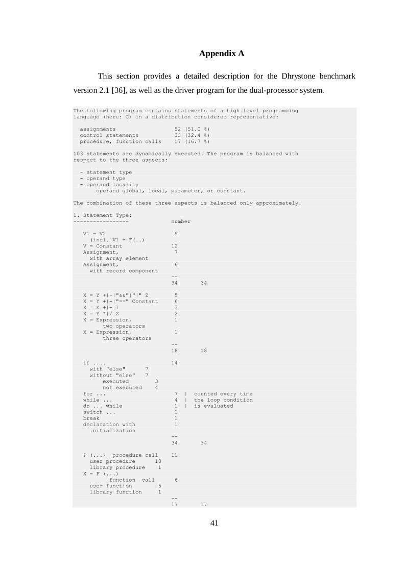
Appendix A
This section provides a detailed description for the Dhrystone benchmark
version 2.1 [36], as well as the driver program for the dual-processor system.
The following program contains statements of a high level programming
language (here: C) in a distribution considered representative:
assignments 52 (51.0 %)
control statements 33 (32.4 %)
procedure, function calls 17 (16.7 %)
103 statements are dynamically executed. The program is balanced with
respect to the three aspects:
- statement type
- operand type
- operand locality
operand global, local, parameter, or constant.
The combination of these three aspects is balanced only approximately.
1. Statement Type:
----------------- number
V1 = V2 9
(incl. V1 = F(..)
V = Constant 12
Assignment, 7
with array element
Assignment, 6
with record component
--
34 34
X = Y +|-|"&&"|"|" Z 5
X = Y +|-|"==" Constant 6
X = X +|- 1 3
X = Y *|/ Z 2
X = Expression, 1
two operators
X = Expression, 1
three operators
--
18 18
if .... 14
with "else" 7
without "else" 7
executed 3
not executed 4
for ... 7 | counted every time
while ... 4 | the loop condition
do ... while 1 | is evaluated
switch ... 1
break 1
declaration with 1
initialization
--
34 34
P (...) procedure call 11
user procedure 10
library procedure 1
X = F (...)
function call 6
user function 5
library function 1
--
17 17

42
---
103
The average number of parameters in procedure or function calls
is 1.82
2. Operators
------------
number approximate
percentage
Arithmetic 32 50.8
+ 21 33.3
- 7 11.1
* 3 4.8
/ (int div) 1 1.6
Comparison 27 42.8
== 9 14.3
/= 4 6.3
> 1 1.6
< 3 4.8
>= 1 1.6
<= 9 14.3
Logic 4 6.3
&& (AND-THEN) 1 1.6
| (OR) 1 1.6
! (NOT) 2 3.2
-- -----
63 100.1
3. Operand Type (counted once per operand reference):
---------------
number approximate
percentage
Integer 175 72.3 %
Character 45 18.6 %
Pointer 12 5.0 %
String30 6 2.5 %
Array 2 0.8 %
Record 2 0.8 %
--- -------
242 100.0 %
When there is an access path leading to the final operand (e.g. a record
component), only the final data type on the access path is counted.
4. Operand Locality:
-------------------
number approximate
percentage
local variable 114 47.1 %
global variable 22 9.1 %
parameter 45 18.6 %
value 23 9.5 %
reference 22 9.1 %
function result 6 2.5 %
constant 55 22.7 %
--- -------
242 100.0 %
The program does not compute anything meaningful, but it is syntactically
and semantically correct. All variables have a value assigned to them
before they are used as a source operand.

43
There has been no explicit effort to account for the effects of a
cache, or to balance the use of long or short displacements for code or
data.
The following program shows the source code of the driver program for the dual-
processor system.
/***********************************Main CPU1************************************/
#include <stdio.h>
#include "nios2.h"
#include "altera_avalon_mailbox.h"
#include "dhrystoneNIOS.h"
int main()
{
// CPU ID, var. initializations
int id=0;
int r2=0;
int r1=0;
int error_code = 0;
// Pointer to our mailbox device
alt_mailbox_dev* mailbox = NULL;
// Get our processor ID
NIOS2_READ_CPUID(id);
printf ("Hello from CPU%d!\n\r", id);
/*
* Open the mailbox which provides mutually exclusive access to the messages
to CPU2.
*/
mailbox = altera_avalon_mailbox_open("/dev/message_buffer_mailbox");
//0x0400d514;
/*
* Check for successful mailbox open.
*/
if (mailbox)
{
while(1)
{
printf ("CPU%d: Running Dhrystones!\n\r", id);
r1=dhrystone();
printf ("CPU%d: My Dhrystone result is %d\n", id, r1);
//i++;
printf ("CPU%d: Waiting to read from CPU2.\n", id);
r2=altera_avalon_mailbox_get(mailbox, &error_code); //This function
is non-blocking!
printf ("CPU%d: CPU2's Dhrystone result is %d\n", id, r2, error_code);
}
}
else
{
printf ("CPU%d: Cannot open Mailbox!\n\r", id);
}/* mailbox */
return 0;
}

44
/***********************************Main CPU2************************************/
#include <stdio.h>
#include "nios2.h"
#include "altera_avalon_mailbox.h"
#include "dhrystoneNIOS.h"
int main()
{
// CPU ID
int id=0;
int flag=0;
int r=0;
// Pointer to our mailbox device
alt_mailbox_dev* mailbox = NULL;
// Get our processor ID
NIOS2_READ_CPUID(id);
//printf ("Hello from CPU%d!\n\r", id);
/*
* Open the mailbox which provides mutually exclusive access to the messages
to CPU2.
*/
mailbox = altera_avalon_mailbox_open("/dev/message_buffer_mailbox");
/*
* Check for successful mailbox open.
*/
if (mailbox)
{
while(1)
{
//printf ("CPU%d: Running Dhrystones!\n\r", id);
r=dhrystone();
if (altera_avalon_mailbox_post (mailbox, r))
{
//printf ("CPU%d: Mailbox full! i=%d\n\r", id, r);
}
//i++;
}
}
else
{
//printf ("CPU%d: Cannot open Mailbox!\n\r", id);
}/* mailbox */
return 0;
}
//PROJECT REPORT VER 16 REDUCED

Vita
Mohammed Eqbal was born in 1985 in Aden, Yemen. He was educated in local
public schools, and later travelled to the United Arab Emirates to get his high school
education. He graduated from Al-Shola Private School in 2003 in Sharjah, with a grade
average of 96.3%. He was given many certificates and awards in each of the three years
of high school education. This allowed him to receive a Scholarship from the American
University of Sharjah, from where he graduated in 2008 with a Bachelor’s degree in
Computer Engineering.
Upon graduation, Mr. Eqbal began his Master’s education and was offered a
Graduate Teaching Assistantship at the American University of Sharjah, where he
worked as a Laboratory Assistant for two years.
Mr. Mohammed Eqbal currently works as the Group I.T. Manager at Grand
Capital group of companies in Dubai, United Arab Emirates. He is also an active
member of the Association for Computer Machinery (ACM) and the IEEE - Computer
Society. He has published a paper in 2010 titled “Drawing on the Benefits of RFID and
Bluetooth Technologies”, at the IEEE Asia Pacific Conference on Circuits and Systems.