FPGA Based Visual Object Tracking
70
1 1 1 Equation Chapter 1 Section 1 FPGA Based Visual Object Tracking Contents ACKNOWLEDGEMENT.....................................................V LIST OF FIGURES....................................................IX LIST OF TABLES......................................................X ABSTRACT...........................................................XI ACRONYMS..........................................................XII CHAPTER 1 INTRODUCTION............................................1 1.1 STATEMENT OF NEED...............................................1 1.2 VISUAL OBJECT TRACKING...........................................2 1.3 FIELD PROGRAMMABLE GATE ARRAYS....................................2 1.3.1 FPGA Programming..........................................2 1.4 PROJECT APPLICATIONS.............................................2 1.5 PROJECT SCOPE...................................................3 CHAPTER 2 SPARTAN-3E FPGA STARTER KIT BOARD.......................4 2.1 SPARTAN 3E (XC3S500E) FPGA....................................4 2.1.1 Overview of architecture and features.....................4 2.2 KEY COMPONENTS AND FEATURES.......................................5 2.3 WHY FPGA?.....................................................7 CHAPTER 3 IMAGE PROCESSING........................................8 3.1 A SURVEY ON VISUAL OBJECT TRACKING.................................8 3.2 STEPS INVOLVED..................................................8 3.2.1 Object Detection..........................................9 3.2.2 Tracking.................................................10 CHAPTER 4..........................................................12
-
Upload
independent -
Category
Documents
-
view
3 -
download
0
Transcript of FPGA Based Visual Object Tracking

111Equation Chapter 1 Section 1 FPGABased Visual Object Tracking
ContentsACKNOWLEDGEMENT.....................................................V
LIST OF FIGURES....................................................IX
LIST OF TABLES......................................................X
ABSTRACT...........................................................XI
ACRONYMS..........................................................XII
CHAPTER 1 INTRODUCTION............................................1
1.1 STATEMENT OF NEED...............................................1
1.2 VISUAL OBJECT TRACKING...........................................2
1.3 FIELD PROGRAMMABLE GATE ARRAYS....................................2
1.3.1 FPGA Programming..........................................2
1.4 PROJECT APPLICATIONS.............................................2
1.5 PROJECT SCOPE...................................................3
CHAPTER 2 SPARTAN-3E FPGA STARTER KIT BOARD.......................4
2.1 SPARTAN 3E (XC3S500E) FPGA....................................4
2.1.1 Overview of architecture and features.....................4
2.2 KEY COMPONENTS AND FEATURES.......................................5
2.3 WHY FPGA?.....................................................7
CHAPTER 3 IMAGE PROCESSING........................................8
3.1 A SURVEY ON VISUAL OBJECT TRACKING.................................8
3.2 STEPS INVOLVED..................................................8
3.2.1 Object Detection..........................................9
3.2.2 Tracking.................................................10
CHAPTER 4..........................................................12

SOFTWARE SIMULATIONS USING MATLAB..................................12
4.1 BASIC IMAGE PROCESSING ALGORITHMS.................................12
4.1.1 Grayscale Conversion.....................................12
4.1.2 Thresholding.............................................13
4.1.3 Image Enhancement using Arithmetic Operations............13
4.1.4 Edge Detection:..........................................14
4.1.5 Image Dilation...........................................14
4.1.6 Image Erosion............................................15
4.1.7 Image closing............................................15
4.1.8 2D Histogram.............................................15
4.1.9 Histogram Equalizer......................................16
4.2 OBJECT TRACKING USING MATLAB....................................16
4.2.1 Normalized Cross Correlation.............................17
4.2.2 Steps Involved in Object Detection:......................17
CHAPTER 5 VGA DISPLAY............................................19
5.1 VGA DISPLAY PORT..............................................19
5.2 VGA SIGNAL TIMINGS.............................................20
5.3 IMPLEMENTATION OF THE VGA DISPLAY.................................22
CHAPTER 6 HARDWARE BASED IMPLEMENTATION..........................23
6.1 BLOCK DIAGRAM OF THE PROPOSED APPROACH............................23
6.2 IMAGE TO RAW DATA CONVERSION....................................23
6.2.1 Raw Data.................................................23
6.2.2 Implementation...........................................24
6.3 DIGITAL CLOCK MANAGER (DCM).....................................24
6.3.1 Introduction.............................................24
6.3.2 DCM Module I/O Signals...................................25
6.3.3 Functional Description...................................25
6.3.4 25MHz Clock Generation...................................26
6.4 SINGLE PORT BRAM USING IP-CORES................................27
ii

6.4.1 BRAMs in SPARTAN 3E......................................27
6.4.2 Single-port BRAM Module I/O Signals......................27
6.4.3 IP-Core Generator block..................................28
6.4.4 Content Initialization...................................28
6.5 .COE FILE GENERATION............................................28
6.5.1 Using IP-CORE Generator..................................29
6.5.2 Writing .Coe File........................................29
6.6 VGA DISPLAY...................................................29
6.7 FPGA DESIGN UTILIZATION SUMMARY IN OUR PROJECT.....................31
CHAPTER 7..........................................................32
MICROBLAZE AND EMBEDDED DEVELOPMENT KIT............................32
7.1 MICROBLAZE ARCHITECTURE.........................................32
7.1.1 Features.................................................32
7.1.2 Data Types and Endianness................................33
7.1.3 Instructions.............................................33
7.1.4 Registers................................................33
7.1.5 Pipeline Architecture....................................33
7.1.6 Memory Architecture......................................34
7.1.7 Floating Point Unit (FPU)................................34
7.1.8 Fast Simplex Link (FSL)..................................34
7.2 EMBEDDED DEVELOPMENT KIT (EDK)..................................35
7.2.1 Xilinx Platform Studio (XPS).............................35
7.2.2 Xilinx Software Development Kit (SDK)....................36
7.2.3 Experiment done on EDK...................................36
CHAPTER 8 CONCLUSIONS AND RECOMMENDATIONS........................38
8.1 TASKS COMPLETED................................................38
8.2 FUTURE WORK...................................................38
REFERENCES.........................................................39
APPENDIX...........................................................40
iii

A.1 CODE FOR TRACKING AND DISPLAY(MAIN MODULE).........................40
A.2 VGA DISPLAY...................................................42
A.3 CODE FOR IMAGE TO RAW DATA CONVERSION.............................49
A.4 (.COE FILE GENERATION IN MATLAB.................................49
A.5 C CODE FOR MICROBLAZE...........................................50
iv

List of FiguresFIGURE 1-1-1 BASIC BLOCK DIAGRAM.......................................1
FIGURE 2-2-1SPARTAN 3E STARTER KIT.....................................4
FIGURE 3-1 OBJECT REPRESENTATION........................................9
FIGURE 3-2 TYPES OF TRACKING..........................................11
FIGURE 4-1 TEST IMAGE................................................12
FIGURE 4-2 GRAY SCALED IMAGE..........................................12
FIGURE 4-3THRESHOLDED IMAGE...........................................13
FIGURE 4-4ARITHMETICALLY ENHANCED IMAGE.................................13
FIGURE 4-5 EDGE DETECTION OF THE IMAGE..................................14
FIGURE 4-6 DILATED IMAGE..............................................14
FIGURE 4-7 ERODED IMAGE..............................................15
FIGURE 4-8 CLOSED IMAGE..............................................15
FIGURE 4-9 2-D HISTOGRAM.............................................16
FIGURE 4-10 HISTOGRAM EQUALIZER........................................16
FIGURE 4-11 OBJECT DETECTION IN SOFTWARE................................17
FIGURE 4-12 1 IS THE ORIGINAL IMAGE, 2 IS THRESHOLDED IMAGE AND 3 USES EDGE DETECTION.......................................................18
FIGURE 4-13 OBJECT BEING TRACKED.......................................18
FIGURE 5-1 DB15 CONNECTOR............................................19
FIGURE 5-2 VGA CONNECTOR ON FPGA......................................19
FIGURE 5-3VGA SIGNALS................................................20
FIGURE 6-1STEPS INVOLVED IN HARDWARE BASED IMPLEMENTATION OF VOT............23
FIGURE 6-2 IMAGE TO RAW DATA CONVERSION.................................24
FIGURE 6-3 FUNCTION DIAGRAM OF DCM.....................................25
v

FIGURE 6-4 ARWZ SETTINGS FOR DCM......................................26
FIGURE 6-5 ATTRIBUTES OF THE GENERATED CLOCK.............................26
FIGURE 6-6 SINGLE PORT BRAM..........................................27
FIGURE 6-7 BRAM WIDTH AND DEPTH.......................................28
FIGURE 6-8 IMAGE CONTENT INITIALIZATION.................................28
FIGURE 6-9 VGA TEST RESULTS...........................................29
FIGURE 6-10 VGA IMAGE DISPLAY.........................................30
FIGURE 6-11SETUP FOR VGA IMAGE DISPLAY.................................30
List of TablesTABLE 5-1 3-BIT DISPLAY COLOR CODES....................................20
TABLE 5-2 VGA TIMING................................................22
TABLE 6-1 DCM I/O SIGNAL............................................25
TABLE 6-2 XC3S500E BRAM SPECIFICATIONS................................27
TABLE 6-3 BRAM I/O SIGNALS...........................................27
TABLE 6-4 DESIGN UTILIZATION SUMMARY....................................31
vi

vii

AbstractIn today’s technology world high speed computers, inexpensive video cameras are available everywhere. So the need of analyzing the automated videos has put a great interest in the field of object tracking. Visual object tracking is the technique to trackthe target of interest in consecutive frames. It has immense applications in security and surveillance systems, robotics, medical imaging and traffic control.
This thesis describes the implementation of visual object tracking algorithms on Field programmable gate arrays (FPGA). FPGAs are efficient, high speed and low cost devices, provides fast execution of IP algorithms which is not possible with the serial microcontrollers. Verilog Spatan 3E board is used to implement the project logic and the visual object tracking algorithms.
viii

AcronymsVOT Visual Object Tracking
FPGA Field Programmable Gate Array
I/O Input/output
RAM Random Access Memory
USB Universal Serial Bus
UART Universal Asynchronous Receiver/Transmitter
IP Image Processing
LSI Large scale integration
DSP Digital Signal Processing
DCM Digital Clock Manager
ARWZ Architecture Wizard
VGA Visual Graphics Array
ix

IntroductionThe basic theme of this project is to design such a system that can give a track the object of interest in consecutive frames of a video. This is done using basic image processing algorithms. The images are first stored in memory of FPGA and then the image processing algorithms are implemented in FPGA using Verilog and finally displayed on VGA. The basic block diagram of the project is shown in the Figure 1-1-1.
Read Write
Figure 1-1-1 Basic Block Diagram
Statement of NeedIn today’s world the need of flexible and high speed image processing is highly increasing. As the data of image is very large so this cannot be done using the conventional microprocessors. This is because microprocessor scans the image pixel one by one and the data is processed sequentially. This scheme of image processing is too slow for real time because the processing speed becomes low.
Therefore, reconfigurable hardware in the form of FPGAs has been proposed to pbtain high performance for computationally intensiveDSP application. FPGAs have programmable logic blocks with the small width and the programmable interconnections provide a greatflexibility for the real time, parallel processing design.
1
Image Frames
ComputerFPGA
VGA
Display
Memory
Image
Processin
MATLAB
Xilinx

Visual Object TrackingTo mark the position of a target of interest in consecutive imageframes of a video is called visual object tracking. After the video has been received, different algorithms of image processingare applied to analyze the frame. These algorithms not only locate the desired object but also give much more information about it. This information can be the object’s shape, size, average speed, directions and total time in motion. These algorithms involve real time processing at high rates.
Field Programmable Gate ArraysField programmable means that the function of FPGA’s is defined by the programmer not the manufacturer. So its functioning id carried out by writing some program depending on the particular application. This is how FPGAs give flexibility to the users. FPGAs are prefabricated chips that contains logic block that are interconnected. These interconnections are programmable wires. Complex functions can be performed on the logic blocks. There area number of input/output blocks. These fast and bidirectional I/Oblocks communicate with the external environment of the FPGA. FPGA’s have their built in on-chip memory.
FPGA ProgrammingTo program the FPGA particular software is required. In or project we used the Xilinx ISE 14.2 to write, compile and synthesize the codes. It translates the code and then places and routes to create the final programming file which is the .bit file. This software is also used to burn these files onto the FPGA.
Project ApplicationsObject tracking has an increasing number of application with time. A list of few applications is given below
Surveillance systems Traffic control Sports Analytics
2

Medical Imaging Mobile Robotics Human Computer interaction
Project ScopeThe following tasks are to be performed in his project:
Studying the basic image processing Writing image processing algorithms in MATLAB Running the MATLAB codes to verify object tracking
algorithms Code writing and understanding in Verilog Exploring features of the Spartan 3E starter board Checking the compatibility of the proposed design for the
kit Implementing RAM Sending image data to FPGA Applying the image processing algorithms to images stored in
memory Study VGA and display the data on VGA monitor Study Architecture of MicroBlaze soft core processor
3

Spartan-3E FPGA Starter Kit Board
SPARTAN 3E (XC3S500E) FPGASPARTAN 3E is used for the implementation of image processing algorithms. The Spartan-3E FPGA is embedded with the 90nm technology. Spartan-3E FPGAs deliver up to 1.6 million system gates, up to 376 I/o’s, and versatile platform FPGA architecture with the lowest cost per-logic in the industry.
Figure 2-2-2Spartan 3E Starter Kit
4

Overview of architecture and featuresFPGAs have incorporated blocks of commonly used functionality such as RAM, clock management, and DSP. The following are the basic components in an FPGA.
Configurable Logic Blocks (CLBs)The CLB is the basic logic unit in a FPGA. It provides the basic logic and storage functionality for a target application design. Every CLB consists of a configurable switch matrix with 4 or 6 inputs, some selection circuitry (MUX, etc), and flip-flops. The switch matrix is highly flexible and can be configured to handle combinatorial logic, shift registers or RAM.
Configurable IO blocks (IOBs)A Configurable input/output (I/O) Block is used to bring signals onto the chip and send them back off again. The polarity of the output can usually be programmed for active high or active low output, and often the slew rate of the output can be programmed for fast or slow rise and fall times. There are typically flip-flops on outputs so that clocked signals can be output directly to the pins without encountering significant delay, more easily meeting the setup time requirement for external devices. Similarly, flip-flops on the inputs reduce delay on a signal before reaching a flip-flop, thus reducing the hold time requirement of the FPGA.
InterconnectWhile the CLB provides the logic capability, flexible interconnect routing routes the signals between CLBs and to and from I/Os. Routing comes in several flavors, from that designed to interconnect between CLBs to fast horizontal and vertical longlines spanning the device to global low-skew routing for Clockingand other global signals.
MemoryDistributed RAM, Embedded Block RAM, SRAM, DDR RAM is available in most FPGAs, which allows for on-chip memory for design. There is also single and dual port RAMs.
5

Digital clock managementDigital clock management is provided by most FPGAs that provide precision clock synthesis required for many designs.
Key Components and FeaturesThe key features of the Spartan-3E Starter Kit board are:
• Xilinx XC3S500E Spartan-3E FPGA
• Up to 232 user-I/O pins
• 320-pin FBGA package
• Over 10,000 logic cells
• Xilinx 4 Mbit Platform Flash configuration PROM
• Xilinx 64-macrocell XC2C64A CoolRunner™ CPLD
• 64 MByte (512 Mbit) of DDR SDRAM, x16 data interface, 100+ MHz
• 16 MByte (128 Mbit) of parallel NOR Flash (Intel StrataFlash)
• FPGA configuration storage
• MicroBlaze code storage/shadowing
• 16 Mbits of SPI serial Flash (STMicro)
• FPGA configuration storage
• MicroBlaze code shadowing
• 2-line, 16-character LCD screen
• PS/2 mouse or keyboard port
• VGA display port
• 10/100 Ethernet PHY (requires Ethernet MAC in FPGA)
• Two 9-pin RS-232 ports (DTE- and DCE-style)
• On-board USB-based FPGA/CPLD download/debug interface
• 50 MHz clock oscillator
• SHA-1 1-wire serial EEPROM for bitstream copy protection
• Hirose FX2 expansion connector
• Three Digilent 6-pin expansion connectors
• Four-output, SPI-based Digital-to-Analog Converter (DAC)6

• Two-input, SPI-based Analog-to-Digital Converter (ADC) with programmable-gain pre-amplifier
• ChipScope™ SoftTouch debugging port
• Rotary-encoder with push-button shaft
• Eight discrete LEDs
• Four slide switches
• Four push-button switches
• SMA clock input
• 8-pin DIP socket for auxiliary clock oscillator
Why FPGA?When the number of objects to be detected (tracked) increase, processing becomes difficult by a digital processor such as a PC.This is because a large number of operations are to be performed on each frame. Such a large number of operations per second couldbe achieved effectively by using FPGA (Field Programmable Gate Arrays). The FPGA’s provide high level of parallelism which makes processing of the video frames fast and efficient. FGPA’s consists of reprogrammable logic blocks. These logic blocks are interconnected and allow application specific hardware implementation. So they offer a high level of flexibility.
FPGA’s are a compromise between a processor based system and the application specific IC’s (ASIC). There are a large number of benefits of using FPGA. Some of them are listed below:
Parallelism Time to market Performance Speed Flexibility Reliability Low Power Consumption
7

1.
8

Image Processing
A survey on Visual Object TrackingVisual object tracking has become a significant technique in the last few years. A large number of papers have been published in this field in the past decade. One reason behind the great attraction of people in this field is that it is a challenging scientific problem. Secondly, visual object tracking is a part ofmany high level problems such as mobile robotics, human computer interaction, surveillance systems, traffic control, sports analytics, medical imaging etc. they include problem like motion detection, activity understanding and event detection etc. Other main reason behind the development of this field is the higher requirement and advancement of HW/SW technology. With the advancement of this technology new tracking algorithms are being developed. The major constraint in the field is the performance of the system, as a large data set is required to perform the complex operation on the image. As the algorithms being used become more complex and advance, it is required that the processing of these algorithms is fast and is less prone to error. To address this issue, the processing has been extended for the serial processor used in the computer to another alternative that can perform several operations on every pixel ofthe image resulting in larger number of operations per second. This is perfectly achieved by the use of FPGA. In our experimental results, we will show that there is a significant improvement in performance can be achieved as compared to processor based design.
Steps involvedA lot of work has been done in the field and various algorithms for object tracking have been proposed. Object tracking is basically completed in two steps.
1. Object detection2. Tracking of the detected object
9

There are various algorithms to perform the above mentioned tasks. We look at the overview of these.
Object DetectionDifferent methodologies involved in object tracking are briefly described one by one in the section below.[7]
Object Representation:To track the object of interest from the scene, it must be represented in some form. Different algorithms used for object tracking imply different representation and it is usually application based.
Shape based tracking is done by the shape information of the moving region of object. This can be done by representing object shape by points, geometric shapes, Object silhouette and contour,articulated shape models and skeletal models etc.
Figure 3-3 Object Representation
Object can also be represented on the basis of other than shape, or other features are combined with the shape representation. Some feature representations are probability densities of object’s appearance, templates formed using shapes, combining shape and appearance of object r multi-view appearance models.
Object features:Features of an object include its color, boundaries, texture and optical flow. The features for tracking are selected on the basisof particular application. This can be done by visualizing that how the targeted object is different from the background. There
10

are various methods of feature selection. Higher the prominence of the feature higher would its discrimination.
Strategies for detection of object:Object detection is an important step in tracking, once a detecting scheme has been applied the focus of attention is then only the moving region. Only these regions are then considered for further processes. Some of the approaches for object detection are briefly described below.
Point detectors: the interested points are detected. These points should be clear, well positioned, significant texture in its localities and stable to the illumination or view-point changes. These are useful in image matching and recognition.
Background subtraction: this technique is mostly used for relatively static background. It takes the difference between two consecutive frames of the video and then the thresh holding is done to extract the moving segment. As it takes pixel by pixel difference of the current image with the reference, so it is extremely sensitive to the changes in environment.
Image Segmentation:Image segmentation partitions image into small regions to identify objects. Different techniques have been used for segmentation by different people. Some of them are:
Color based segmentation e.g. K-means clustering and Mean shiftclustering.
Thresh holding methods e.g. Otsu’s method. Transform methods e.g. watershed segmentation Texture methods e.g. texture filters
11

TrackingThe purpose tracking is to make trajectory of object in the frame. Classification of object tracking algorithms is given below.
Figure 3-4 Types of Tracking
Point tracking:Once he object is detected the purpose of point tracking is to represent it in the form of points, previous object state is taken as a reference. Then these points are joined to make the object trajectory. Different approaches can be used e.g. multi point correspondence, parametric transformation or contour evaluation. The most common point tracking algorithms that have been used are MCE tracker, GOA tracker, Kalman filter JPDAF, PMHT.
Kernel trackingThis is the tracking based on the object features, shape and appearance. Kernel of any shape can be chosen to track the object; motion of the kernel shows the motion of the object in consecutive frames. The algorithms for kernel tracking are, mean-shift, KTL, layering.
Silhouette trackingThe object region is tracked by matching or contour evaluation byusing the information of the object like its volume, surface density by its shape models. A silhouette is formed in the objectregion. The representative work for silhouette tracking are state
12
Visual Object
Tracking
Point Tracking
Deterministic
Probalistic
kernel tracking
Multi View based
Template based
silhouette
trackking
Contour Evolution
Shape Matching

space models, vibrational models, heuristic models, Hausdorff, histogram.
In our project we used the kernel tracking algorithms to track the object in software implementation. While for the hardware implementation on FPGA we had to use relatively simpler technique. So the technique of background subtraction has been used in FPGA.
Software Simulations using MATLAB
Basic Image Processing AlgorithmsFollowing are some of the basic image processing algorithms required for Visual object tracking in our project.[8] We choose a simple image and illustrate various operations, learned in the Image Processing, on MATLAB.
Original im age
Figure 4-5 Test Image
13

Grayscale ConversionGrayscale or intensity image is an image where each pixel is a sample that holds intensity information. [8] The value of each pixel ranges from 0-255 and each pixel is of 8-bits or 1 Byte.
Original Im age
Figure 4-6 Gray Scaled Image
ThresholdingImage thresholding means transforming a grayscale image to a binary image i.e. the pixel values are either 1 or 0. We set a specific pixel value i.e. X for thresholding and define that values above X will be considered 1 and that below X would be considered 0.
Output = 0 if Image<=X; Output = 255 ifImage>X
The below image is a thresholded image which has either black or white pixel values.
Thresholded Im age
Figure 4-7Thresholded Image
14

Image Enhancement using Arithmetic OperationsImage Enhancement is a technique used to manipulate and transforman image to our requirement by various operations on the image. It may be Spatial Transformations (directly dealing with image pixels) or Frequency Domain Transformations (dealing with the Fourier transform of the image). The best way to enhance an imageis by addition, subtraction, multiplication and division. Subtraction and multiplication is used to enhance the image below:
Figure 4-8Arithmetically Enhanced Image
Edge Detection:The process of identifying the points in an image where intensityof an image changes suddenly or jumps is called Edge Detection. Edge Detection is best performed on a grayscale image.
Figure 4-9 Edge Detection of the Image15

Image DilationImage Dilation is one of the basic operations of Image processingon which other operations are based. It can be most simply statedas to probe and expand the bright area in the image or higher pixel values in a grayscale image.
Dilated Im age
Figure 4-10 Dilated Image
Image ErosionImage Erosion is another of the basic operations of Image processing on which other operations are based. Contrary to ImageDilation it expands the darker area in the image or lower pixel values in a gray scale image
16

Eroded Im age
Figure 4-11 Eroded Image
Image closingImage Closing opposite to image opening can simply be defined as the Erosion of the Dilation of an Image. It is another of the image enhancement techniques.
Original im age Closed im age
Figure 4-12 Closed Image
2D HistogramImage Histogram is graphical representation of the intensity distribution in an image. It plots number of pixels on the y-axisfor intensity values on the x-axis. By knowledge of the histogramof an image, viewer is able to know the whole intensity distribution in the image.
17

-0.2 0 0.2 0.4 0.6 0.8 10
200
400
600
800
1000
1200
Figure 4-13 2-D Histogram
Histogram EqualizerHistogram Equalization is a technique of image enhancement using contrast adjustment. The contrast of the below image is enhanced to get the better image.
Enhanced Im age after histogram equalization
Figure 4-14 Histogram Equalizer
Object Tracking Using MATLABOur video was a simple one with only one black object, a ball, ona white background.
The method used to track the object was Normalized 2D cross Correlation. This type of tracking is called Kernel Tracking.
18

Normalized Cross CorrelationCross Correlation is a measure of similarity of two images which are spaced in time. The idea is to select the target object and cross correlate it with the image samples. The tracking is done on the basis of the maximization of similarity on the image.
Normalized Cross Correlation function is represented by the command normxcorr2.
The command uses following algorithm in its processing:
1. It computes the cross correlation in the spatial or frequency domain.
2. Calculates local sums by pre-computing running sums.
3. Uses the local sums to normalize the cross-correlation toget correlation coefficients.
Steps Involved in Object Detection:Following steps were involved in software based Object Tracking:
Figure 4-15 Object Detection in Software
First of all the video is converted to frames. MTALAB generates 15 frames per second; this rate can be adjusted to the desired frame rate. The next steps involve Grayscale Conversion, thresholding, image enhancement, edge detection, object identification and finally object tracking using normalized crosscorrelation.
19
GrayscaleConversion
Thresholding
Image Enhancement/ Noise Filtering
Edge Detection
Object Identification
Window Tracking

The algorithms in this section have already been discussed in theprevious section.
Target Object
Given below is the target object:
Figure 4-16 1 is the original image, 2 is thresholded image and 3 uses edge detection.
Object Tracking original Video Frames:
Figure 4-17 Object being Tracked
20

VGA DisplayVGA Display PortThe Spartan 3E board includes a VGA display port via DB15 connector.
\
Figure 5-18 DB15 Connector
Figure 5-19 VGA Connector on FPGA
The Spartan 3E FPGA drives five signals to display the respectivedata on the screen. The signal are the red blue and green one
21

that show colors on the screen. Combination of theses three signals give eight colors as shown in the table 5.1. the other two signal are the horizontal synchornisation signal and the vertical synchronization signal written as hsync and vsync respectively. These two signal help to display the pixel data on the screen in a correct manner.[9]
Figure 5-20VGA Signals
Table 5-1 3-bit display color codes
VGA_RED VGA_GREEN VGA_BLUE Resulting Color0 0 0 Black
0 0 1 Blue
0 1 0 Green
0 1 1 Cyan
1 0 0 Red
1 0 1 Magenta
1 1 0 Yellow
1 1 1 White
22

VGA signal timingsIn our project we used the CRT based monitor that uses an electron beam that has been modulated and the information of images is displayed on the phosphor screen. The electron beams are deflected by a strong magnetic field in bot top to bottom andleft to right direction. The beam takes some time to return back.As shown in the figure 6-4 he information is displayed on the screen during the time when the beam is moving forward. The resolution of the displayed data depends on the size and frequency of the beams.
As shown in Figure 6-4, the VGA controller generates the horizontal sync (HS) and vertical sync (VS) timings signals and the data is displayed on each pixel clock. The time to display one pixel on the screen defines the pixel clock. The VS signal defines the refresh frequency of the display, or the frequency atwhich all information on the display is redrawn. The minimum practical refresh frequency is 60 Hz and can go up to 120Hz.
Figure 5-4 CRT Display Timings
23

The signal timings in Table 6-2 are derived for a 640-pixel by 480-row display using a 25 MHz pixel clock and 60 Hz ± 1 refresh.Figure 6-4 shows the relation between each of the timing symbols.The timing for the sync pulse width (TPW) and front and back porch intervals (TFP and TBP) are based on observations from various VGA displays. The front and back porch intervals are the pre- and post-sync pulse times. Information cannot be displayed during these times.
Table 5-2 VGA Timing
Symbol ParameterVertical Sync Horizontal Sync
Time Clocks Lines Time ClocksTS Sync pulse
time16.7 ms 416,800 521 32 μs 800
TDISP Display time 15.36 ms
384,000 480 25.6 μs 640
TPW Pulse width 64 μs 1,600 2 3.84 μs 96
TFP Front porch 320 μs 8,000 10 640 ns 16
TBP Back porch 928 μs 23,200 29 1.92 μs 48
Figure 5-5 VGA Control Timing
Two separate counters are used that are clocked by the pixel clock. The horizontal counter controls the horizontal timings andthe vertical counter controls the vertical timings of the pixel data. The source code used for VGA display is shown in the Appendix.
24
Implementation of the VGA displayThe VGA timing was first set for 640x480 display screen. The first step was to display the eight colors on the screen vertically. This was successfully achieved. The display that was seen on the monitor is shown in the figure 6-6.
The next step was to display an image. The image data was stored in Bram and was read from there.
Finally tracking of the target Object was achieved and then displayed on the VGA monitor.
25

Hardware Based Implementation
Block Diagram of the Proposed ApproachIn order to accomplish the task of successful tracking of an object, following sequence of steps was observed in our particular approach towards VOT
Figure 6-21Steps involved in hardware based implementation of VOT
Image to RAW Data ConversionRaw Data
Raw data of an image is the digital value of each pixel in the image, starting from the pixel at top left corner to the pixel at the bottom right corner. The range of pixel data may vary depending on the bits of data of each image pixel. For gray scale image each pixel can have a value between 0~255. For monochrome image the data is single bit so only 2 values are possible. i.e. ‘0’ or ‘1’.
In a digital camera when the imaging chip is exposed to capture the image, it records the amount of light that has hit each pixel. This is recorded as a voltage level. The camera's analog to digital converter circuitry changes the analog voltage signal to a digital value. Depending on the camera's circuitry if
26
MATLAB
Image to RAW Data Conversi
onin text file. Xi
linx ARWZ
25MHz Clock Generation (DCM) using IPCORES Xi
linx ARWZ
Single-Port BRAM
Generation using IPCORES
MATLAB
Xilinx
Verilog
VGA
DISPLAY.COE FILEGENERATION

8 bits of data are recorded then each pixel can handle 255 brightness levels.
ImplementationWe extracted images from a short video and each of these
images was reduced to the pixel size of 200x150. From these images initially a text file was generated using MATLAB which contained the raw data of the image i.e. the values of each pixelwithout any header or excessive information. The code for writingraw data of an image to text file is in the appendix.
Digital Clock Manager (DCM)IntroductionThe Digital Clock Manager (DCM) primitive in Xilinx FPGA parts isused to implement the following:
Delay locked loop (DLL) Digital frequency synthesizer (DFS) Digital phase shifter (DPS) Digital spread spectrum (DSS)
Spartan 3E Starters Board has 8 internal global clock buses, and 4 Digital Clock Managers. Out of these 4 DCM’s a single DCM is used in this project.
The Digital Clock Manger allows:
Multiplying of an external clock Division of an external clock
27
Images in Video Format
Video Frames extraction (MATLAB)
Image format conversion to text file
format
Figure 6-22 Image to Raw data conversion

Clock skew compensation by phase difference correction. Phase shifting of clock signals
DCM Module I/O SignalsA single DCM has following main input output signals:
Table 6-3 DCM I/O Signal
Signal I/O Description
RST I If C_EXT_RESET_HIGH = 0, an inverter is inserted. Then three DFFs are inserted before this signal is connected tothe equivalent pin of DCM.
CLKIN I If C_CLKIN_BUF = true, a BUFG is inserted; otherwise, thissignal is connected to the equivalent pin of DCM directly.
CLKFB I If C_CLKIN_BUF = true, a BUFG is inserted; otherwise, thissignal is connected to the equivalent pin of DCM directly.
CLK0 O If C_CLKIN_BUF = true, a BUFG is inserted; otherwise, thissignal is connected to the equivalent pin of DCM directly.
CLK90 O If C_CLK90_BUF = true, a BUFG is inserted; otherwise, thissignal is connected to the equivalent pin of DCM directly.
CLK180 O If C_CLK180_BUF = true, a BUFG is inserted; otherwise, this signal is connected to the equivalent pin of DCM directly.
CLK270 O If C_CLK270_BUF = true, a BUFG is inserted; otherwise, this signal is connected to the equivalent pin of DCM directly.
CLK2X O If C_CLKFX_BUF = true, a BUFG is inserted; otherwise, thissignal is connected to the equivalent pin of DCM directly.
CLK2X180 O If C_CLK2X180_BUF = true, a BUFG is inserted; otherwise, this signal is connected to the equivalent pin of DCM directly.
CLKDV O If C_CLKDV_BUF = true, a BUFG is inserted; otherwise, thissignal is connected to the equivalent pin of DCM directly.
28

CLKFX O If C_CLKFX_BUF = true, a BUFG is inserted; otherwise, thissignal is connected to the equivalent pin of DCM directly.
CLKFX180 O If C_CLKFX180_BUF = true, a BUFG is inserted; otherwise, this signal is connected to the equivalent pin of DCM directly.
LOCKED O Connect to the equivalent pin of DCM directly
Functional DescriptionFunctional Description of various signals is demonstrated in the figure below:
Figure 6-23 Function Diagram of DCM
25MHz Clock GenerationSince VGA and BRAM both work on a clock frequency of 25MHz. Therefore a clock of 25MHz was generated from external FPGA clockof 50MHZ using a single DCM block. This single DCM block was generated using IP-Cores Xilinx Architecture Wizard (ARWZ) in Xilinx Design Suite. The DCM module had the RST checked but the output of the clock was not “Locked”. DFS is enabled
Signals used in out generated DCM include:
RST: reset for the DCM CLKIN: external clock of 50MHz CLKFB: internal feedback of DCM
29

CLK0: buffered input clock (dived by 2 for this particular case)
Figure 6-24 ARWZ settings for DCM
Attributes in the particular Application:
The CLK0 signal was provided as clock to the BRAM and VGA blocks.
Single Port BRAM using IP-CORESBRAMs in SPARTAN 3ESpartan 3E has a total of 20 BRAMS available out of which we used18 BRAMS for our project.
Table 6-4 XC3S500E BRAM Specifications
Device RAMColumns
RAMBlocksper
Total RAMBlocks
Total RAMbits
TotalRAM
30
Figure 6-25 Attributes of the generated clock

Columns Kbits
XC3S500E 2 10 20 368640 360
Single-port BRAM Module I/O SignalsA single-port BRAM module has following main input output signals:
Figure 6-26 Single Port BRAM
Table 6-5 BRAM I/O Signals
Signal I/O Description
DI I Data Input bus
DIP I Parity Data Input Bus (available only for byte-wideand wider organizations)
ADDR I Address Bus
CLK I Clock
SSR I Synchronous Set/Reset
EN I Clock Enable
WE I Write Enable
DO O Data Output Bus.
DOP O Parity Data Output (available only for byte-wide andwider organizations)
IP-Core Generator blockSpecify the depth and width of the data in the core generator block. In our design we required only a single pixel in 1 row of
31

memory for convenience in our VGA Display process therefore the width and depth were specified as shown in the figure. The depth was 30000 for images of 200x150 pixels each which took our memoryspace of 6 BRAMs.
Figure 6-27 BRAM width and Depth
Content InitializationTo specify the initial RAM contents for a CORE Generator block RAM function, create a coefficients (.coe) file. A simple exampleof a coefficients file appears in Figure 7. At a minimum, define the radix for the initialization data—i.e., base 2, 10, or 16—andthen specify the RAM contents starting with the data at location 0, followed by data at subsequent locations. To include the coefficients file, locate the appropriate section in the CORE Generator wizard and check Load Init File, as shown in Figure 8. Then, click Load File and select the coefficients file.
Figure 6-28 Image content Initialization
.coe File GenerationThere are basically two main methods of generating a .coe file.
1) Using IP core generators for generation the .coe file.
2) Writing a .coe file
32

Using IP-CORE GeneratorIP-Core generators have a wizard that guides through the .coe file generation process and through it you can manually write desired data values into the BRAM. This is a good procedure to befollowed when data to be stored is small.
Writing .Coe FileThe problem with the above technique was that image data is huge and it was not possible for us to manually write all the data to create the .Coe file so we switched to the 2nd approach.
In this approach we generated a MATLAB code that would write the data in a text file in the format same as that of a .Coe file andthen the extension was changed to .txt to .Coe. This generated .Coe file was used in the BRAM for data of pixels up to(300x300) pixels which utilized about 15/20 BRAMs. MATLAB code isattached in the Appendix.
VGA DisplayVGA was initially tested and 8 colors were displayed on it in order to check it’s working.[10]
Figure 6-29 VGA test results
For display, an image of 320x240 was chosen and displayed on the VGA as out test image which used about 15 BRAMs.
33

Figure 6-30 VGA Image Display
FPGA was connected with the laptop for storing image data and burning the code in the FPGA and FPGA was connected to another monitor through DB-15 connector to display the image.
Figure 6-31Setup for VGA Image display
34

FPGA Design Utilization Summary in ourProjectTable 6-6 Design Utilization Summary
Logic Utilization Used Available Utilization:
Number of Slice Flip Flops 42 9,312 1%
Number of 4 input LUTs 144 9,312 1%
Number of occupied Slices 87 4,656 1%
Number of Slices containing only related logic
87 87 100%
Number of Slices containing unrelated logic
0 87 0%
Total no. of 4 input LUTs 158 9,312 1%
Number used as logic 144
Numbers used as route-thru 14
Number of bonded IOBs 14 232 6%
DCM 1 4 25%
Number of RAMB16s 18 20 90%
Number of BUFGMUXs 2 24 8%
35

MicroBlaze and Embedded Development Kit
MicroBlaze ArchitectureMicroBlaze is an embedded soft core processor. It is an optimizedversion of a reduced instruction set computer (RISC) designed by Xilinx, Inc. It is implemented in many Xilinx FPGAs. Fig shows the block diagram of MicroBlaze
Figure 7- 1: MicroBlaze Block Diagram
Features Some of the features of MicroBlaze are given below
32 bit general purpose registers 32 bit instruction word 32 bit address bus
36

LMB BRAM memory Instruction and Data Caches Single issue pipeline stages
Data Types and EndiannessMicroBlaze uses Big-Endian, bit-reversed format to represent data. The data types which the hardware supports for MicroBlaze are word, half word and byte.
InstructionsAll MicroBlaze instructions are 32 bits wide. Instructions are of2 types, Type A or Type B. Type A instructions have up to two source register operands and one destination register operand. Type B instructions have one source register; a 16-bit immediate operand and a single destination register operand.
RegistersMicroBlaze has an orthogonal instruction set architecture. It has32-bit general purpose registers and up to seven 32-bit special purposes registers, depending on configured options.
Pipeline ArchitectureMicroBlaze uses pipeline architecture for the execution of instructions. The pipeline is divided into five stages: Fetch (IF), Decode (OF), Execute (EX), Access Memory (MEM), and Write back (WB).
For most instructions, each stage takes one clock cycle to complete. A specific instruction takes five clock cycles to complete, and one instruction is completed on every cycle. A few instructions require multiple clock cycles in the execute stage to complete. This is achieved by stalling the pipeline.
37

Figure 7- 2: Stages of Pipelining
Memory ArchitectureMicroBlaze is implemented with Harvard memory architecture, i.e. instruction and data accesses are done in separate storage and signal conduits. Each address space has
a 32 bit range which can handle up to 4GByte of instructions and data memory. Both instruction and data interfaces of MicroBlaze are 32 bit wide.
Data and instruction accesses must be aligned, unless the processor is configured to support unaligned exceptions.
MicroBlaze uses memory mapped I/O. The processor has up to threeinterfaces for memory accesses:
Local Memory Bus (LMB)It provides on chip access to dual port block RAM.
On-Chip Peripheral Bus(OPB)It provides access to on- chip and off-chip peripherals.
Xilinx Cache LinkIt is used with the external memory controllers.
The LMB memory address range must not overlap with OPB or XCL ranges.
Floating Point Unit (FPU)The MicroBlaze floating point unit uses IEEE 754 single precisionfloating point format, which includes definitions for infinity, not-a-number (NaN) and zero. It also supports addition,
38

subtraction, multiplication, division, and comparison instructions, implements round-to-nearest mode, generate sticky status bits for: underflow, overflow, and invalid operation.
Fast Simplex Link (FSL)MicroBlaze can be configured with Fast Simplex Link (FSL) interfaces, each consisting of one input and one output port. TheFSL channels are dedicated unidirectional point to-point data streaming interfaces. Each FSL provides a low latency dedicated interface to the processor pipeline. Thus they are ideal for extending the processors execution unit with custom hardware accelerators.
Embedded Development Kit (EDK)EDK is software available in ISE design suite. It helps the user to build processor based system.
The software has a good graphical design and many wizards available to configure the embedded processor and peripherals.
The tools provided with EDK are designed to assist in all phases of the embedded design process, as illustrated in the following figure.
39
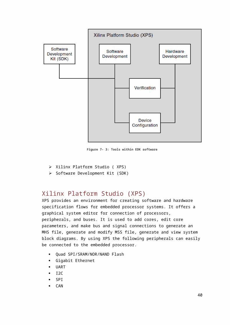
Figure 7- 3: Tools within EDK software
Xilinx Platform Studio ( XPS) Software Development Kit (SDK)
Xilinx Platform Studio (XPS)XPS provides an environment for creating software and hardware specification flows for embedded processor systems. It offers a graphical system editor for connection of processors, peripherals, and buses. It is used to add cores, edit core parameters, and make bus and signal connections to generate an MHS file, generate and modify MSS file, generate and view system block diagrams. By using XPS the following peripherals can easilybe connected to the embedded processor.
Quad SPI/SRAM/NOR/NAND Flash Gigabit Ethernet UART I2C SPI CAN
40
GPIO
Xilinx Software Development Kit (SDK)The Xilinx SDK is a GUI which provides a development environment for software application projects. SDK is based on the Eclipse open-source standard. It has C/C++ code editor, compilation environment, application build configuration and automatic make file generation
Experiment done on EDKFirstly, image data is converted to text file. Image data is sentto MicroBlaze through uart. MicroBlaze stored the image data in DDR SDRAM. The data is read through DDR SDRAM and displayed on hyper terminal of PC.
Fig shows the block diagram of the overall hardware system.
41

The functionality code of the above hardware is written in C language using SDK.
42

Conclusions and RecommendationsTasks CompletedWe have learnt a lot from this project. We have got deep understanding of embedded system (Spartan 3e) and related software’s (Xilinx ISE, EDK).
The tasks we completed in this project are:
Implementation of BRAM (using ip core) VGA display. Implementation of Digital clock manager (using ip core) Object tracking in images stored in BRAM. MicroBlaze hardware and software design.
Future WorkIn this project we have done tracking on few images because of the constraints on the availability of BRAMs in Spartan 3e.So thefuture task is to
Implement SDRAM and store the whole video in it Perform more advance image processing algorithm for object
tracking.
43

References
[1]. Xilinx, MicroBlaze Processor Reference Guide, Embedded Development Kit EDK 14.1
URL: http://www.xilinx.com/support/documentation/sw_manuals/
xilinx14_1/mb_ref_guide.pdf
[2]. Xilinx, Embedded System Tools, Reference Manual, Embedded Development Kit
URL: https://www.xilinx.com/support/documentation/sw_manuals/edk10_est
_rm.pdf
[3]. Xilinx, Application Note, “Using Block RAM in Spartan-3 Generation FPGAs”, XAPP463 (v2.0) March 1, 2005.
[4]. Xilinx, Application Note, “Digital Clock Manager (DCM) Module”, DS485 April 24, 2009.
[5]. Xilinx, “Spartan-3E FPGA Starter Kit Board User Guide”, UG230 (v1.2) January 20, 2011.
[6]. EE3810, “Advanced Features of Xilinx FPGA”, dcm_module.
[7]. Alper Yilmaz, “Object tracking: A survey”, University of Central Florida, ACM Computing Surveys (CSUR) Surveys Homepage archive Volume 38 Issue 4, 2006
44

[8]. Rafael C. Gonzalez, Richard Eugene Woods, 2nd edition, “Digital Image processing”.
[9]. Radi H.R., Caleb W.W.K., M.N.Shah Zainudin., M.Muzafar Ismail., “The Design and Implementation of VGA Controller onFPGA”, University Teknikal Malaysia Melaka Hang Tuah Jaya 76100 Durian Tunggal, Melaka, Malaysia.
[10]. ZAHEERUDDIN SYED, MUNWAR SHAIK, “FPGA IMPLEMENTATION OF VGACONTROLLER”, KITS warangal, Kakatiya University, Hasanparthy, Warangal -506015,Andhara Pradesh.
AppendixA.1 Code for tracking and display(mainmodule)module vga_top(
input wire clk, //master clock = 50MHz
input wire clr, //right-most pushbutton for reset BTN east
output wire red, //red vga output
output wire green, //green vga output
output wire blue, //blue vga output
output wire hsync, //horizontal sync out
output wire vsync, //vertical sync out45

output wire [2:0]douta,
output wire [2:0]douta2,
//input [5:0]addra,
input wea
);
// VGA display clock interconnect
wire dclk;
wire [14:0]addra;
//wire [13:0]addra1;
wire [2:0]douta3;
wire [2:0]douta4;
wire [2:0]douta5;
// generate display clock
clockdiv U1 (
.CLKIN_IN(clk),
.RST_IN(RST_IN),
.CLKIN_IBUFG_OUT(CLKIN_IBUFG_OUT),
.CLK0_OUT(dclk)
);
//----------- Begin Cut here for INSTANTIATION Template ---// INST_TAG
bram100 foo(
46

.clka(dclk), // input clka
.wea(wea), // input [0 : 0] wea
.addra(addra), // input [13 : 0] addra
.dina(), // input [2 : 0] dina
.douta(douta) // output [2 : 0] douta
);
// INST_TAG_END ------ End INSTANTIATION Template ---------
//----------- Begin Cut here for INSTANTIATION Template ---// INST_TAG
bram100_2 foo1(
.clka(dclk), // input clka
.wea(wea), // input [0 : 0] wea
.addra(addra), // input [13 : 0] addra
.dina(), // input [2 : 0] dina
.douta(douta2) // output [2 : 0] douta
);
// INST_TAG_END ------ End INSTANTIATION Template ---------
//----------- Begin Cut here for INSTANTIATION Template ---// INST_TAG
bram100_3 foo2(
.clka(dclk), // input clka
.wea(wea), // input [0 : 0] wea
.addra(addra), // input [13 : 0] addra
.dina(), // input [2 : 0] dina
.douta(douta4) // output [2 : 0] douta
);
// INST_TAG_END ------ End INSTANTIATION Template ---------47

assign douta3=douta~^douta2;
assign douta5=douta4~^douta2;
// VGA controller
vga640x480 U3(
.dclk(dclk),
.clr(clr),
.hsync(hsync),
.vsync(vsync),
.red(red),
.green(green),
.blue(blue),
.douta(douta),
.douta2(douta2),
.douta3(douta3),
.douta4(douta4),
.douta5(douta5),
.addra(addra)
//.addra1(addra1)
);
48

A.2 VGA displaymodule vga640x480(
input wire dclk, //pixel clock: 25MHz
input wire clr, //asynchronous reset
output wire hsync, //horizontal sync out
output wire vsync, //vertical sync out
output reg red, //red vga output
output reg green, //green vga output
output reg blue, //blue vga output
input [2:0]douta,
input [2:0]douta2,
input [2:0]douta3,
input [2:0]douta4,
input [2:0]douta5,
output reg [14:0]addra
//output reg [13:0]addra1
// output [2:0]LED
);
//reg [11:0]j;
//parameter jlimit=4000;
parameter address=29999;
//parameter address2=16383;
// video structure constants
parameter hpixels = 800;// horizontal pixels per line
parameter vlines = 521; // vertical lines per frame
parameter hpulse = 96; // hsync pulse length
parameter vpulse = 2; // vsync pulse length
parameter hbp = 144; // end of horizontal back porch49

parameter hfp = 784; // beginning of horizontal front porch
parameter vbp = 31; // end of vertical back porch
parameter vfp = 511; // beginning of vertical front porch
// active horizontal video is therefore: 784 - 144 = 640
// active vertical video is therefore: 511 - 31 = 480
// registers for storing the horizontal & vertical counters
reg [9:0] hc;
reg [9:0] vc;
// Horizontal & vertical counters --
// this is how we keep track of where we are on the screen.
// ------------------------
// Sequential "always block", which is a block that is
// only triggered on signal transitions or "edges".
// posedge = rising edge & negedge = falling edge
// Assignment statements can only be used on type "reg" and need to be of the "non-blocking" type: <=
always @(posedge dclk or posedge clr)
begin
// reset condition
if (clr == 1)
begin
//addra<=17'b0;
hc <= 0;
vc <= 0;
end
else
50

begin
// keep counting until the end of the line
if (hc < hpixels - 1)
hc <= hc + 1;
else
// When we hit the end of the line, reset the horizontal
// counter and increment the vertical counter.
// If vertical counter is at the end of the frame, then
// reset that one too.
begin
hc <= 0;
if (vc < vlines - 1)
vc <= vc + 1;
else
vc <= 0;
end
end
end
// generate sync pulses (active low)
// ----------------
// "assign" statements are a quick way to
// give values to variables of type: wire
assign hsync = (hc < hpulse) ? 0:1;
assign vsync = (vc < vpulse) ? 0:1;
51

// display 100% saturation colorbars
// ------------------------
// Combinational "always block", which is a block that is
// triggered when anything in the "sensitivity list" changes.
// The asterisk implies that everything that is capable of triggering the block
// is automatically included in the sensitivty list. In this case, it would be
// equivalent to the following: always @(hc, vc)
// Assignment statements can only be used on type "reg" and should be of the "blocking" type: =
always @(posedge dclk)
begin
if((vc < vbp)&&(hc < hbp))
begin
addra<=15'b0;
//addra1<=14'b0;
//j<=12'b0;
end
// first check if we're within vertical active video range
// else if(addra!=address)
// begin
// now display different colors every 80 pixels
// while we're within the active horizontal range
// -----------------
// display white bar
else if (vc >= vbp+10 && vc < (vbp+160))
begin
52

if (hc >= hbp+100 && hc < (hbp+300)&&(addra!=address))
begin
//{red,green,blue} = douta;
addra<=addra+1'b1;
if(({red,green,blue}==3'b111)&&(douta == 3'b000))
{red,green,blue} = 3'b011;
else if(({red,green,blue}==3'b000)&&(douta3 == 3'b111))
{red,green,blue} = 3'b010;
else
{red,green,blue} = douta;
end
else
begin
red = 0;
green = 0;
blue = 0;
end
end
// we're outside active vertical range so display black
else if(vc >= vbp+160 && vc < (vbp+170))
begin
red = 0;
green = 0;
blue = 0;
addra<=13'b0;
end53

else if (vc >= vbp+170 && vc < (vbp+320))
begin
if (hc >= hbp+100 && hc < (hbp+300)&&(addra!=address))
begin
addra<=addra+1'b1;
//if((hc>=hbp+130)&&(hc<=hbp+150)&&({red,green,blue}==3'b111)&&(vc >= vbp+130) && (vc < vbp+150))
if(({red,green,blue}==3'b111)&&(douta3 == 3'b000))
{red,green,blue} = 3'b110;
else if(({red,green,blue}==3'b000)&&(douta3 == 3'b000))
{red,green,blue} = 3'b011;
else if(({red,green,blue}==3'b000)&&(douta3 == 3'b111))
{red,green,blue} = 3'b010;
else
{red,green,blue} = douta2;
//end
end
else
begin
54

red = 0;
green = 0;
blue = 0;
end
end
else if(vc >= vbp+320 && vc < (vbp+330))
begin
red = 0;
green = 0;
blue = 0;
addra<=13'b0;
end
else if (vc >= vbp+330 && vc < (vbp+480))
begin
if (hc >= hbp+100 && hc < (hbp+300)&&(addra!=address))
begin
//{red,green,blue} = douta;
addra<=addra+1'b1;
//if((hc>=hbp+130)&&(hc<=hbp+150)&&({red,green,blue}==3'b111)&&(vc >= vbp+130) && (vc < vbp+150))
if(({red,green,blue}==3'b111)&&(douta5 == 3'b000))
{red,green,blue} = 3'b110;
55

else if(({red,green,blue}==3'b000)&&(douta5 == 3'b000))
{red,green,blue} = 3'b011;
else if(({red,green,blue}==3'b000)&&(douta5 == 3'b111))
{red,green,blue} = 3'b010;
else
{red,green,blue} = douta4;
//end
end
else
begin
red = 0;
green = 0;
blue = 0;
end
end
else
{red,green,blue}=3'b000;
end
endmodule
56

57
A.3 Code for Image to RAW data Conversionclc;
clf;
clear all;
hautothresh = video.Autothresholder('ThresholdOutputPort',true,'ThresholdScaleFactor',1);
Image=imread('C:\Users\abu g\Desktop\paint.jpg');
ImageG=rgb2gray(Image);
z1 = step(hautothresh,ImageG);
%Gray=rgb2gray(Image);
%Image2=not(Image);
F=double(Image);
%save File3.txt -ascii F
dlmwrite('C:\Users\ abu g \Desktop\test_file.txt',z1,'delimiter',' ');
k = dlmread('C:\Users\ abu g \Desktop\test_file.txt');
imshow(k)
58

A.4 (.coe File Generation in MATLABimg = imread('C:\Users\ abu g \Desktop\paint video\myim3.jpg');
height = size(img, 1);
width = size(img, 2);
img2=rgb2gray(img);
BW = im2bw(img2,0.7);
imshow(BW);
fid = fopen('C:\Users\ abu g \Desktop\paint video\myim3.txt','w');
fprintf(fid,'MEMORY_INITIALIZATION_RADIX=2;\r\n');
%fprintf(fid,'Coefficient_Width = 3;\r\n' );
fprintf(fid,'MEMORY_INITIALIZATION_VECTOR=\r\n');
for r=1:height
for c=1:width
%cnt = cnt + 1;
R = BW(r,c,1);
G = BW(r,c,1);
B = BW(r,c,1);
y = [R;G;B];
fprintf(fid,'%X%X%X,\r\n',y);
% fprintf(fid,',\n');
end
end
fclose(fid);
59

A.5 C code for MicroBlaze#include <stdio.h>
#include "platform.h"
#include "xparameters.h"
#include "xutil.h"
#include "xuartlite_l.h"
void print(char *str);
int main()
{
init_platform();
int uch;
int memory_word, value;
int count;
int* SDRAM_address = (int*)(XPAR_DDR_SDRAM_MPMC_BASEADDR);
print("I am in program \n\r");
memory_word = 0;
// reading from the com port
for(count = 0; count <4; count++)
{
uch = XUartLite_RecvByte(STDIN_BASEADDRESS);
xil_printf("-- input value %c --\r\n", uch);
// combining 4 digits in 32 bit word
memory_word = (memory_word << 8)| (0xff & uch);
xil_printf("-- input value %c --\r\n", memory_word);
}
xil_printf("-- input value %c --\r\n", memory_word);
// putting 32 bit word in SDRAM
60

*SDRAM_address = memory_word;
// reading from SDRAM
value = *SDRAM_address;
xil_printf("-- Value = %c --\r\n", value);
print("End of program \n\r");
cleanup_platform();
return 0;
}
61
![KLV-30MR1 - Error: [object Object]](https://static.fdokumen.com/doc/165x107/631786651e5d335f8d0a6a63/klv-30mr1-error-object-object.jpg)