CAD for VLSI: Symple: a symbolic layout tool for bipolar and MOS VLSI
Upload
independentCategory
view
3download
0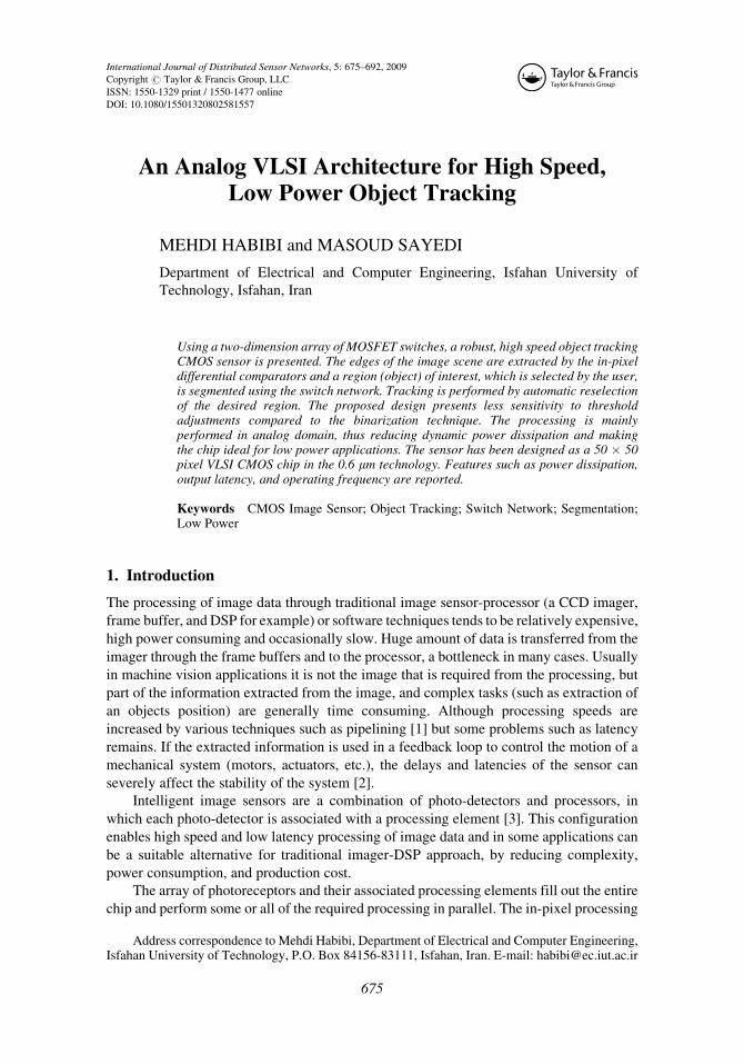
An Analog VLSI Architecture for High Speed,Low Power Object Tracking
MEHDI HABIBI and MASOUD SAYEDI
Department of Electrical and Computer Engineering, Isfahan University of
Technology, Isfahan, Iran
Using a two-dimension array of MOSFET switches, a robust, high speed object trackingCMOS sensor is presented. The edges of the image scene are extracted by the in-pixeldifferential comparators and a region (object) of interest, which is selected by the user,is segmented using the switch network. Tracking is performed by automatic reselectionof the desired region. The proposed design presents less sensitivity to thresholdadjustments compared to the binarization technique. The processing is mainlyperformed in analog domain, thus reducing dynamic power dissipation and makingthe chip ideal for low power applications. The sensor has been designed as a 50 � 50pixel VLSI CMOS chip in the 0.6 mm technology. Features such as power dissipation,output latency, and operating frequency are reported.
Keywords CMOS Image Sensor; Object Tracking; Switch Network; Segmentation;Low Power
1. Introduction
The processing of image data through traditional image sensor-processor (a CCD imager,
frame buffer, and DSP for example) or software techniques tends to be relatively expensive,
high power consuming and occasionally slow. Huge amount of data is transferred from the
imager through the frame buffers and to the processor, a bottleneck in many cases. Usually
in machine vision applications it is not the image that is required from the processing, but
part of the information extracted from the image, and complex tasks (such as extraction of
an objects position) are generally time consuming. Although processing speeds are
increased by various techniques such as pipelining [1] but some problems such as latency
remains. If the extracted information is used in a feedback loop to control the motion of a
mechanical system (motors, actuators, etc.), the delays and latencies of the sensor can
severely affect the stability of the system [2].
Intelligent image sensors are a combination of photo-detectors and processors, in
which each photo-detector is associated with a processing element [3]. This configuration
enables high speed and low latency processing of image data and in some applications can
be a suitable alternative for traditional imager-DSP approach, by reducing complexity,
power consumption, and production cost.
The array of photoreceptors and their associated processing elements fill out the entire
chip and perform some or all of the required processing in parallel. The in-pixel processing
International Journal of Distributed Sensor Networks, 5: 675–692, 2009
Copyright # Taylor & Francis Group, LLC
ISSN: 1550-1329 print / 1550-1477 online
DOI: 10.1080/15501320802581557
Address correspondence to Mehdi Habibi, Department of Electrical and Computer Engineering,Isfahan University of Technology, P.O. Box 84156-83111, Isfahan, Iran. E-mail: [email protected]
675

of image and inter-pixel transfer of data makes temporal and spatial vision processing
possible.
The extraction of an object’s movement is a demanding need in machine vision
algorithms [4]. Different sensors have been proposed to obtain information on the move-
ment of a target in the scene. Some of these sensors extract velocity and direction only [5],
whereas in some position control applications, not only velocity, but also the sensed
position of the object is also required. The sensors presented in [6] and [7] extract the
position of a desired object in the scene. In these sensors image binarization is performed at
the first stage of processing and thus a variable threshold is required. Furthermore, tracking
is only performed on light objects in a darker background. Some presented sensors perform
tracking on a specific feature of the desired region [8–10]. [8] and [9], for example, track the
local maximum of the desired object. As reported, this method is more of use in the tracking
of bright light spots or laser pointers. The tracking sensor proposed in [11] performs motion
vector calculation to identify the motion direction of the target and requires the movement
of the chip to lock on the desired target, which can be a limitation in some cases.
In this article an object tracking sensor which tracks the position of a target inside the
visual scene is presented. The target or object of interest is selected manually from an initial
state. Different approaches can be used for initial selection; like starting the target move-
ment from an initial position and loading the chip with the predetermined coordinates of the
position (tracking linear actuators for example), or sensing the target in some initial
locations and loading the chip with the corresponding coordinates (tracking cars passing
checkpoint for example). Similar to many previously proposed designs, the tracking
architecture described here reduces the computational cost of the processing stages by
performing the computation at the focal plane itself and transmitting only the result of the
process (the coordinates of the tracked object), instead of the image data. It differs from the
previously proposed designs in that the feature to be tracked is assumed to be the region
inside an edge contour. With this assumption the segmentation technique can be used to
extract homogenous regions and tracking is performed on the segment containing the object
of interest. The segmentation process is less sensitive to threshold adjustments, compared
to the single threshold value binarization techniques [6, 7], enabling better operation in the
actual working environment.
The first part of the article describes the overall architecture of the chip and presents its
different blocks. The second part focuses on the details of each block including the basic
pixel. The layout of the chip and simulation results are presented next. In the conclusion,
specific applications of the sensor are presented.
2. The Proposed Architecture
2.1. Overall Structure
The block diagram of the designed architecture is shown in Fig. 1. The main blocks that
construct the sensor are: the basic pixels or cells (block A), the coordinate generator
circuitry (block B), the coordinate register (block C), and the one-hot coordinate data to
analog data converter (block D). The image is focused on the two-dimensional array of
basic pixels (block A). Each basic pixel contains photoreceptor circuitry and analog
processing elements. The photoreceptors sample one frame of the scene and the processing
elements divide the scene into homogenous regions by detecting edges and performing
image segmentation, and project the selected segment on axes X and Y. Segment selection
is initially performed according to an initial point in the image scene provided by the user,
676 M. Habibi and M. Sayedi
which represents the desired target to be tracked. The selection process in subsequent
frames is performed according to the coordinate extracted from the previous frame. The
coordinate generator (block B) at each axis assigns a one-hot code to the projection of the
selected segment. The points assigned in axes X and Y represent the coordinates of the
object (region) under track and are stored at the corresponding coordinate registers (block
C). The tracking cycle and the segment selection continues from these new coordinates.
The coordinate at each axis is converted to analog form and outputted at the chip pins (block
D). The analog signal can be used to interface with analog controlling systems. In the case
of digital controlling systems, the one-hot coordinate representation can be simply coded to
binary format and outputted at the chip pins.
As the target moves across the scene, the region highlighted by the previous coordi-
nates also changes its position and new coordinates are obtained for the new cycle. If the
displacement of the selected segment in two consecutive cycles is less than half of its
expansion, the produced coordinates, select the same region as of the previous cycle and the
new coordinates follow the target with a latency of one cycle. The shutter speed of the photo
detector circuitry is limited by the properties of the photodevice element. Typical photo
detectors provide shutter speeds as fast as 0.1 ms in moderate illumination levels [12].
Considering this limitation, the chip is designed for the operation in a clock cycle frequency
of 10 KHz. With this operation frequency, the sensor can reliably track moving objects with
speeds less than u pixels/s, where u is 10 K � half of the object expansion expressed in the
pixel unit. Since the image acquisition and processing is performed at 10 KHz, and new
tracking coordinates are produced in each cycle, the latency of the sensor will be 0.1 ms, a
reliable value for controlling high speed mechanical movements. Traditional imaging
bloc
k B
block B
block C
bloc
k C
block D Outputpin
Outputpin
Inputpin
Inputpin
blockA
blockA
Data path between adjacent pixels
Segment projection
Center coordinate
Center coordinate of previous frame
bloc
k D
Figure 1. Block diagram of the proposed chip and corresponding interconnections.
High Speed Object Tracking CMOS Sensor 677

devices have much higher latencies between the image acquisition phase, image to memory
data transfer and data processing stages.
The next sections will describe in detail the structure of each block.
2.2. The Basic Pixels (Block A)
As explained in the overall structure, the array of basic pixels has the function of image
segmentation, segment selection, and projection of the selected segment (region). Each
pixel of the array is composed of a photoreceptor circuitry, and analog processing elements
(Fig. 2). Metal layer 3 is used as a light mask, covering the entire chip except the
photoreceptors. Each pixel is interconnected with its adjacent neighbors, and the array of
pixels contains the comparators network layer, the switch network layer, and the row-
column adder layer. An interconnected array of 3 � 3 basic pixels is shown in Fig. 3. For
clarity, the comparators and the photo detection circuitry are illustrated as blocks.
Edges of the image are detected by the network of edge detecting comparators. It
evaluates the function |v1-v2| > Vcmp, where v1 and v2 are the inputs to be compared, and
Vcmp is the threshold value for edge detection. As can be seen in Fig. 3b, each cell contains
two comparators that compare the light intensity level of the related pixel with those of the
adjacent pixels in the right and bottom. The result is a digitized data, ‘1’ to indicate that no
edge is detected and ‘0’ to indicate an edge is detected. With the edges obtained, segmenta-
tion can be performed by using the switch network [13]. The switch network layer of the
basic pixels array is shown separately in Fig. 3c. Each switch in the network is opened when
an edge is detected and closed when the comparators indicate no edge. A specific spreading
node, corresponding to a point of the desired object, is set to high (activated) when the
relative row and column lines of that point are active in the coordinate registers. Assuming
out
out
in1
in2
Photoreceptorcircuitry
Edge detectingcomparator
Figure 2. Structure of a single basic pixel block.
678 M. Habibi and M. Sayedi

that the borders of the switch network are connected to the ground and starting with the high
voltage (‘1’) on the spreading node, the value spreads in the network nodes through the
closed switches and up to the points that the switches are opened. The result is the selection
of a homogenous region (segment) inside the target filled with ‘1’s, and the rest of the
image filled with ‘0’s. The situation is illustrated in Fig. 4.
When spreading starts from an activated point, the current is drawn from the switches,
introducing some voltage drop; but as the node capacitors fill up, the current reaches zero
and in equilibrium, all nodes inside the selected region take the same voltage as the
activated point. In this configuration no path from the spreading nodes to ground should
exist. A problem arises with the lack of this discharge path when the target moves and some
‘1’ nodes fall outside the contour with no path to discharge. (Similar to the switch network
Center coordinate detector
Cen
ter
coor
dina
te d
etec
tor
Cen
ter
coor
dina
te d
etec
tor
Center coordinate detector
...
...
y2
y1
y0
y2
y1
y0
Latch extractedcoordinate
Center coordinate register
Cen
ter
coor
dina
te r
egis
ter
(a) (b)
(c) (d)
Latch extractedcoordinate
Cen
ter
coor
dina
te r
egis
ter
x0 x1 x2
x0 x1 x2
Center coordinate register
Figure 3. A 3 � 3 array of basic pixels and their connection with other blocks. (a) The complete
array. (b)–(d) The decomposition of the array into the comparator network layer, switch network layer
together with the activation transistors and the row-column adder layer, respectively.
High Speed Object Tracking CMOS Sensor 679

presented in [13], there could exist a path from a specified node through the switch network
and to the grounded borders of the network, but for isolated regions, this is not always the
case.) The solution used here is to reset the existing ‘1’s at the beginning of each cycle by
setting the row lines of the activation transistors in Fig. 3c to ‘0’ and the column lines to ‘1’
and thus discharge the spreading nodes of the switch network. Since the object coordinates
in the previous frame are stored in the coordinate registers, the target will not be lost by
resetting the switch network. To optimize the area, the switches are chosen to be NMOS
instead of NMOS-PMOS pass transistors. This structure needs a spreading (activation)
voltage less than VDD-Vg so that all paths operate in the triode region. A voltage of VDD/2
is used for this purpose. This voltage is also used in the comparator section.
At this point the three-dimensional data of the image (two dimensions for the two axes
and one for the level of intensity) is converted to a two-dimensional data representing a
homogenous region of the object, and tracking is performed on this special feature. In order
to assign specific coordinates to the extracted segment, the region is projected on the two
axes. In this way the coordinate assigned to the projection (using the coordinate generator
blocks) in each axis, can be assumed to be the coordinate representation of the segment
itself (Fig. 5).
The projection structure is an analog adder, adding up the number of pixels in the
segment at each row, to extract the projection on the Y-axis, and at each column to extract
the projection on the X-axis. The process of converting the two-dimensional data to two
one-dimensional data is shown in Fig. 6. The adder, built up from a 3 � 3 array of
transistors, is shown in Fig. 3d. The diagonal lines in the figure are connected to the
spreading nodes which are ‘‘high’’ if the pixel corresponds to the selected segment, and
are ‘‘low’’ if it does not. These voltages are used as the inputs to the vertical and horizontal
analog adders. Vertical data lines produce projection on axis X and horizontal data lines
produce projection on axis Y.
2.2.1. The Basic Pixel Comparators. The comparators perform edge detection based on
the difference between voltages that represent the light intensity of the adjacent pixels. If
the absolute value of the voltage difference (|v1-v2|) exceeds a threshold voltage then an
edge exists and a ‘0’ is returned. If the absolute value does not exceed the threshold voltage
then the two adjacent pixels belong to the same segment and a ‘1’ is produced. Simulation
results showed that a threshold voltage of 200 mV produces acceptable segmentation
(a) (b)
VCC
Figure 4. Image segmentation of the switch network in an array of 6� 6 basic pixels. (a) A grayscale
input image. (b) The pass transistors states resulting from the input image. The nodes represent each
pixel and the vertexes between them represent the pass transistors.
680 M. Habibi and M. Sayedi

results. The function |v1-v2| > Vcmp is implemented by evaluating ‘‘v1-v2 > 200 mV OR
–(v1-v2) > 200 mV.’’ Since a double ended differential amplifier produces both terms (v1-v2)
and –(v1-v2), the function can be implemented using the circuit shown in Fig. 7. Transistors
M1, M2, M3, and M4 build the differential amplifier with outputs F1¼ Av� (v1 - v2)þ Vdc
and F2 ¼ –Av � (v1 - v2) þ Vdc on nodes B and A, respectively (in the equations Av is the
circuit differential voltage gain and Vdc is the output offset voltage). Gate M5 and M6
evaluate F1 > Vref - Vth and F2 > Vref - Vth, respectively, and their parallel connection
extracts ‘‘F1 > Vref - Vth OR F2 > Vref - Vth,’’ where Vth is the threshold voltage of the
transistors. An inverter is used in the output stage of the comparator to digitize the result to ‘0’
or ‘1’. Since the biasing current of the differential pair is adjusted to have a dc offset (Vdc)
near the voltage Vref - Vth for nodes A and B, the relationship between Vcmp and Vref is
roughly Vcmp¼ Vref/Av, thus Vcmp can be adjusted by varying Vref and Av. The amplifier is
designed with diode connected loads, providing Av ¼ 10. VDD/2 is chosen for Vref to
Column
Number of cellsactivated in the column
Number of cellsactivated in the row
Row
Figure 6. Region projection procedure using analog row and column adders.
One dimensionaldata
Two dimensionaltarget segment
Calculated coordinate onX axis
Calculated coordinate onY axis
Coordination assigned totracked target with respect to
the extracted coordinates
Figure 5. Target coordination assignment based on the coordinates extracted from the projections.
High Speed Object Tracking CMOS Sensor 681

provide the required Vcmp ¼ 200 mV. Furthermore, VDD/2 is used in the switch network
circuit as explained earlier and also for the dc offset of the photo circuit output.
Since the differential pair is designed with diode connected loads, the gain of the
differential pair is independent of the operation point and as it is shown in Eq. (1) it is
related to the driver transistor (W/L)n and load transistor (W/L)p dimensions. Hence, the
output voltage of the differential pair is relatively linear over the differential input voltage
range and the only limitation on the differential and common mode input voltage swings is
the operation of the transistors in the saturation region.
Av ¼ffiffiffiffiffiffiffiffiffiffiffiffiffiffiffiffiðW=LÞnðW=LÞp
s(1)
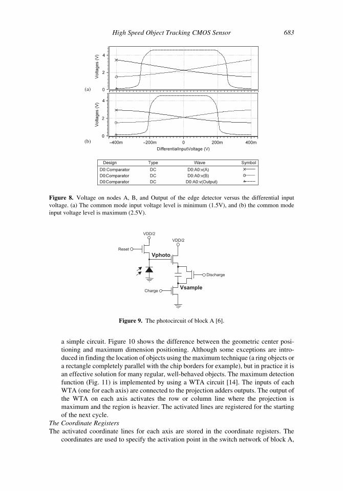
The input-output voltage transfer curve of the edge detector is shown in Fig. 8. As it can be
seen from the voltages on nodes A and B, the differential pair of Fig. 7 operates in a linear
region for differential inputs from zero to the comparison threshold voltage and for
common mode inputs from 1.5 V to 2.5 V. The transistors marginally enter the triode
region for high common mode inputs. It changes the comparison level to some degree.
Other factors that affect the comparison level are the mismatches and noise which will be
examined in the simulation results section.
As the number of comparators is relatively high throughout the chip, they are only
activated when the integration cycle of the photocircuit is completed and the processing is
required. This consideration effectively decreases power consumption.
2.2.2. The Basic Pixel Photocircuit. The basic photo circuit used in the design is the
conventional sample and hold circuit consisting of a photodiode, sample capacitor, and
switches shown in Fig. 9 [6].
The Coordinate Generators (Block B)
The function expected from this block is to locate the center part of a projected region; but
an alternative to finding the center, is finding the position of the maximum, resulting in
VDD
V2
Vbias 1
V1
Output
M1 M2
M3 M4
M6M5A B
Vref
Figure 7. The edge detector of block A.
682 M. Habibi and M. Sayedi
a simple circuit. Figure 10 shows the difference between the geometric center posi-
tioning and maximum dimension positioning. Although some exceptions are intro-
duced in finding the location of objects using the maximum technique (a ring objects or
a rectangle completely parallel with the chip borders for example), but in practice it is
an effective solution for many regular, well-behaved objects. The maximum detection
function (Fig. 11) is implemented by using a WTA circuit [14]. The inputs of each
WTA (one for each axis) are connected to the projection adders outputs. The output of
the WTA on each axis activates the row or column line where the projection is
maximum and the region is heavier. The activated lines are registered for the starting
of the next cycle.
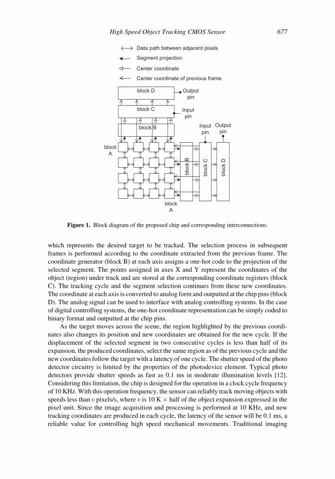
The Coordinate Registers
The activated coordinate lines for each axis are stored in the coordinate registers. The
coordinates are used to specify the activation point in the switch network of block A,
Reset
VDD/2
VDD/2
Charge
Discharge
Vphoto
Vsample
Figure 9. The photocircuit of block A [6].
(a)
(b)
Figure 8. Voltage on nodes A, B, and Output of the edge detector versus the differential input
voltage. (a) The common mode input voltage level is minimum (1.5V), and (b) the common mode
input voltage level is maximum (2.5V).
High Speed Object Tracking CMOS Sensor 683

for subsequent processing cycles. The registers are also used when the array of block A
is at idle cycle (The state where the comparators are turned off to reduce power
consumption and the switch network is cleared by setting the outputs of the X-axis
coordinate register to ‘1’ and the outputs of the Y-axis to ‘0’.) In this state the target
position remains valid in the registers.
3. Chip Layout
One of the challenges in CMOS image sensor design is to overcome the tradeoff between
processing power, the fill factor, and the chip area. Since the basic pixel block is repeated
throughout the chip, proper design of its processing elements is necessary. In a constant
chip area and pixel resolution, increasing the size of the processing elements for more
computational power, means reducing the size of the photoreceptors and thus reduction of
Projection of target region
Central geometryCentral mass
Figure 10. Extraction of geometric center coordinates vs. maximum dimension coordinates.
In1
Vbias2
Out1
In2
Out2
In3
Out3
In50
Out50
Min
2
Mde
2
Min
1
Mde
1
Min
3
Mde
3
Min
50
Mde
50
. . .
VDD
Figure 11. The WTA circuit used for coordinate generation on one axis. The projected column/row
adders are connected to the input lines of the WTA (In1-In50) and the output lines (Out1-Out50) are
connected to the coordinate registers for each axis.
684 M. Habibi and M. Sayedi
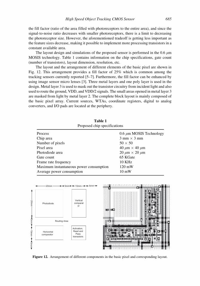
the fill factor (ratio of the area filled with photoreceptors to the entire area), and since the
signal-to-noise ratio decreases with smaller photoreceptors, there is a limit to decreasing
the photoreceptor size. However, the aforementioned tradeoff is getting less important as
the feature sizes decrease, making it possible to implement more processing transistors in a
constant available area.
The layout design and simulations of the proposed sensor is performed in the 0.6 mm
MOSIS technology. Table 1 contains information on the chip specifications, gate count
(number of transistors), layout dimension, resolution, etc.
The layout and the arrangement of different elements of the basic pixel are shown in
Fig. 12. This arrangement provides a fill factor of 25% which is common among the
tracking sensors currently reported [5–7]. Furthermore, the fill factor can be enhanced by
using image sensor micro lenses [3]. Three metal layers and one poly layer is used in the
design. Metal layer 3 is used to mask out the transistor circuitry from incident light and also
used to route the ground, VDD, and VDD/2 signals. The small areas opened in metal layer 3
are masked from light by metal layer 2. The complete block layout is mainly composed of
the basic pixel array. Current sources, WTAs, coordinate registers, digital to analog
converters, and I/O pads are located at the periphery.
Table 1
Proposed chip specifications
Process 0.6 mm MOSIS Technology
Chip area 3 mm � 3 mm
Number of pixels 50 � 50
Pixel area 40 mm � 40 mm
Photodiode area 20 mm � 20 mm
Gate count 65 KGate
Frame rate frequency 10 KHz
Maximum instantaneous power consumption 120 mW
Average power consumption 10 mW
PhotodiodeVertical
comparator
Horizontalcomparator
Activation, Read and
Passtransistors
20mm 10mm
20mm
10mm
5mm
5mm Routing Area
5mm
5mm
Figure 12. Arrangement of different components in the basic pixel and corresponding layout.
High Speed Object Tracking CMOS Sensor 685
4. Simulation Results
The first part of this section presents the sensor limitations by using HSpice Monte Carlo
and noise analyses. In the second part, the overall simulation of the sensor is presented.
4.1. Sensor Operation Constraints
In the following, different issues that affect the output results of the edge detection stage,
segment projection stage, and the WTA stage are discussed. In the analyses it is assumed
that a segment with uniform intensity Isegment is placed against a background with local
intensity Ibackground. The maximum allowable fluctuation (intensity variations) in the
segment is noted by �Isegment/pixel.
The edge detection stage suffers from various non-ideal issues. The dominant effects
are the offset voltage due to mismatches, the input referred rms noise voltage, and the offset
voltage due to common mode gain (common mode voltage swing/CMRR). These effects
can be referred to the comparators inputs and eventually considered as the Vcmp compar-
ison level changes. Furthermore, the photodiode shot noise and reset noise will also change
the actual inputs to the comparator, while the photodiodes mismatch effects are negligible
since the photocurrent and the photodiode capacitance are scaled proportionally thus the
photodiode voltage output remains constant [3].
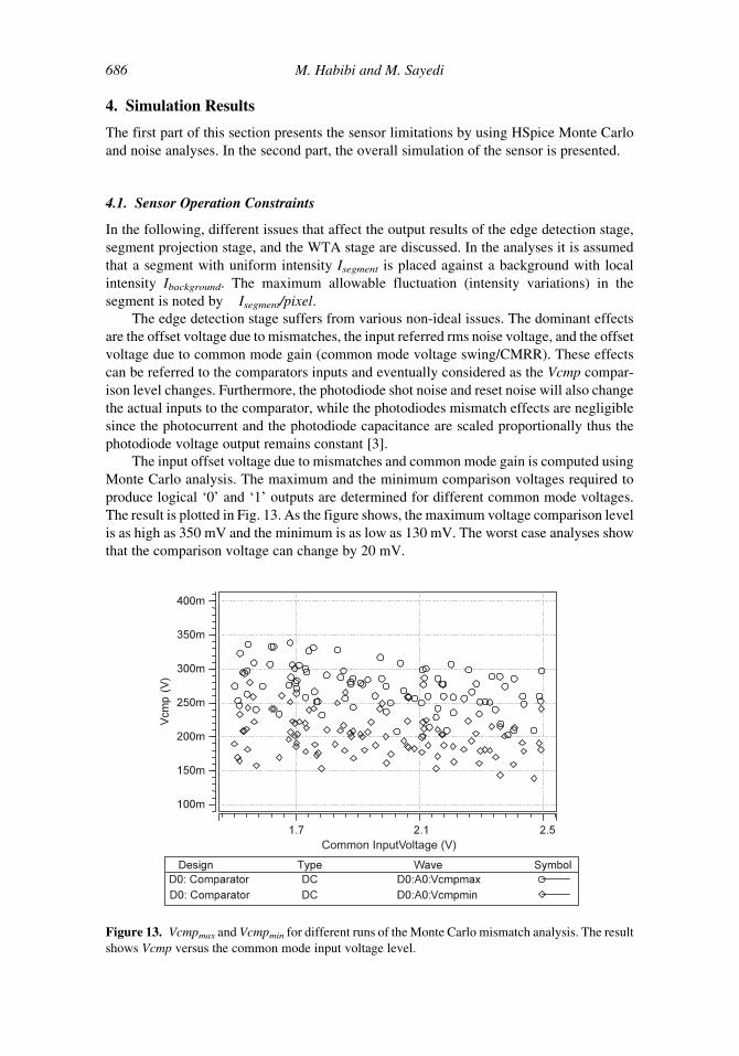
The input offset voltage due to mismatches and common mode gain is computed using
Monte Carlo analysis. The maximum and the minimum comparison voltages required to
produce logical ‘0’ and ‘1’ outputs are determined for different common mode voltages.
The result is plotted in Fig. 13. As the figure shows, the maximum voltage comparison level
is as high as 350 mV and the minimum is as low as 130 mV. The worst case analyses show
that the comparison voltage can change by 20 mV.
Common InputVoltage (V)
Figure 13. Vcmpmax and Vcmpmin for different runs of the Monte Carlo mismatch analysis. The result
shows Vcmp versus the common mode input voltage level.
686 M. Habibi and M. Sayedi
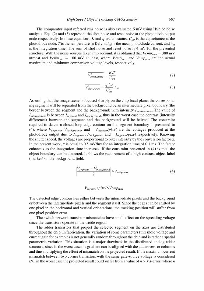
The comparator input referred rms noise is also evaluated 6 mV using HSpice noise
analysis. Eqs. (2) and (3) represent the shot noise and reset noise at the photodiode output
node respectively. In these equations, K and q are constants, Cint is the capacitance at the
photodiode node, T is the temperature in Kelvin, ipd is the mean photodiode current, and tint
is the integration time. The sum of shot noise and reset noise is 4 mV for the presented
structure. With the noise sources taken into account, it is obtained that Vcmpmax¼ 380 mV
utmost and Vcmpmin ¼ 100 mV at least, where Vcmpmax and Vcmpmin are the actual
maximum and minimum comparison voltage levels, respectively.
V2reset noise ¼
K:T
Cint
(2)
V2shot noise ¼
q:ipd
C2int
:tint (3)
Assuming that the image scene is focused sharply on the chip focal plane, the correspond-
ing segment will be separated from the background by an intermediate pixel boundary (the
border between the segment and the background) with intensity Iintermediate. The value of
Iintermediate is between Isegment and Ibackground, thus in the worst case the contrast (intensity
difference) between the segment and the background will be halved. The constraint
required to detect a closed loop edge contour on the segment boundary is presented in
(4), where Vsegment, Vbackground, and �Vsegment/pixel are the voltages produced at the
photodiode output due to Isegment, Ibackground and �Isegment/pixel respectively. Knowing
the shutter speed, the voltages are proportional to pixel intensity by the conversion factor a.
In the present work, a is equal to 0.5 mV/lux for an integration time of 0.1 ms. The factor
enhances as the integration time increases. If the constraint presented in (4) is met, the
object boundary can be detected. It shows the requirement of a high contrast object label
(marker) on the background field.
Vsegment � Vbackground
2
��������>Vcmpmax (4)
�Vsegment=pixel<Vcmpmin
The detected edge contour lies either between the intermediate pixels and the background
or between the intermediate pixels and the segment itself. Since the edges can be shifted by
one pixel in the horizontal and vertical orientations, the tracking position will suffer from
one pixel position error.
The switch network transistor mismatches have small effect on the spreading voltage
since the transistors operate in the triode region.
The adder transistors that project the selected segment on the axes are distributed
throughout the chip. In fabrication, the variation of some parameters (threshold voltage and
current gain for example) is not generally random throughout the chip and is rather a spatial
parametric variation. This situation is a major drawback in the distributed analog adder
structure, since in the worst case the gradient can be aligned with the adder rows or columns
and thus multiplying the effect of mismatch on the projected result. If the maximum current
mismatch between two corner transistors with the same gate-source voltage is considered
k%, in the worst case the projected result could suffer from a value of n� k% error, where n
High Speed Object Tracking CMOS Sensor 687
is the number of pixels in a row or column of the selected segment. Furthermore, as n
increases, the current noise component of the adder increases, but it is negligible compared
to the error due to mismatches. To properly detect the maximum feature on each axis, the
current error due to mismatch (n � k � ITadder), subtracted from the current produced by a
single adder transistor (ITadder), should be larger than the WTA minimum detectable current
difference (IDmin reported in [15]). The equation is shown in (5)
ITadder � n:k:ITadder>ID min (5)
Since ITadder ¼ 40uA, IDmin ¼ 2uA and k¼ 5%, the maximum segment expansion over the
vertical or horizontal axis should be limit to 19 pixels. As shown earlier, smaller segments
should move slower to avoid tracking lost. Simulation results confirm that the maximum
feature is detected correctly in the presence of mismatch if the criterion is met.
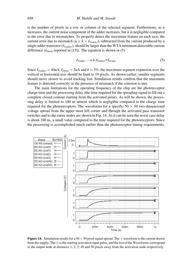
The main limitations for the operating frequency of the chip are the photoreceptor
charge time and the processing delay (the time required for the spreading signal to fill out a
complete closed contour starting from the activated point). As will be shown, the proces-
sing delay is limited to 100 ns utmost which is negligible compared to the charge time
required for the photoreceptors. The waveforms for a specific 50 � 50 two-dimensional
voltage spread from the upper most left corner and through the activated pass transistor
switches and to the entire nodes are shown in Fig. 14. As it can be seen the worst case delay
is about 100 ns, a small value compared to the time required for the photoreceptors. Since
the processing is accomplished much earlier than the photoreceptor timing requirements,
Figure 14. Simulation results for a 50� 50 pixel signal spread. Theþwaveform is the current drawn
from the supply, The} is the starting activation input pulse, and the rest of the Waveforms correspond
to the output node at distances 1, 2, 3, 49 and 50 pixels away from the activation node respectively.
688 M. Habibi and M. Sayedi
the processing elements are sent to an idle state to reduce power consumption. Simulation
results show that a 10 KHz clock rate is enough to track the position of a rotary motor shaft
spinning at a speed of 1500 rpm with the accuracy of one pixel error.
The next part presents the overall simulation of the structure.
4.2. Overall Sensor Simulation
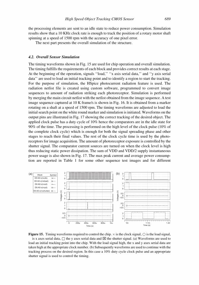
The timing waveforms shown in Fig. 15 are used for chip operation and overall simulation.
The timing fulfills the requirements of each block and provides correct results at each stage.
At the beginning of the operation, signals ‘‘load,’’ ‘‘x axis serial data,’’ and ‘‘y axis serial
data’’ are used to load an initial tracking point and to identify a region to start the tracking.
For the purpose of simulation, the HSpice photocurrent radiation feature is used. The
radiation netlist file is created using custom software, programmed to convert image
sequences to amount of radiation striking each photoreceptor. Simulation is performed
by merging the main circuit netlist with the netlist obtained from the image sequence. A test
image sequence captured at 10 K frame/s is shown in Fig. 16. It is obtained from a marker
rotating on a shaft at a speed of 1500 rpm. The timing waveforms are adjusted to load the
initial search point on the white round marker and simulation is initiated. Waveforms on the
output pins are illustrated in Fig. 17 showing the correct tracking of the desired object. The
applied clock pulse has a duty cycle of 10% hence the comparators are in the idle state for
90% of the time. The processing is performed on the high level of the clock pulse (10% of
the complete clock cycle) which is enough for both the signal spreading phase and other
stages to reach their final values. The rest of the clock cycle time is used by the photo-
receptors for image acquisition. The amount of photoreceptor exposure is controlled by the
shutter signal. The comparator current sources are turned on when the clock level is high
thus reducing static power dissipation. The sum of VDD and VDD/2 supply instantaneous
power usage is also shown in Fig. 17. The max peak current and average power consump-
tion are reported in Table 1 for some other sequence test images and for different
(a) (b)
Figure 15. Timing waveforms required to control the chip.� is the clock signal, * is the load signal,
� is x axes serial data, & the y axes serial data and x the shutter signal. (a) Waveforms are used to
load an initial tracking point into the chip. With the load signal high, the x and y axes serial data are
taken high at the appropriate clock number. (b) Subsequently waveforms are used to continue with the
tracking process on the desired region. In this case a 10% duty cycle clock pulse and an appropriate
shutter signal is used to control the timing.
High Speed Object Tracking CMOS Sensor 689

illuminations. Since the major power consumption is related to the static power dissipation
of the comparator biasing, and dynamic power dissipation is negligible at the operating
frequency of 10 KHz, the power consumption is relatively low compared to the previously
reported tracking sensors which operate at high clock frequencies (the tracking speeds of
these sensors still remain the same or even less) [5, 6, 9].
5. Conclusion
A high speed object tracking sensor was designed and the layout masks were created for the
0.6 mm MOSIS technology. The post layout simulation results showed successful tracking
of a marker rotating at a speed of 1500 rpm. The sensor produced correct analog outputs
representing the position of the marker at the X and Y axes in each cycle. The output is
suitable for analog controlling systems. The latency from the chip is small enough to use the
chip as a feedback sensor to control high speed mechanical systems. Furthermore, the low
power consumption of the chip makes it a choice in mobile and wireless applications.
Wireless sensors are opening their way in many applications, providing the ability to access
data from hard reaching areas [16]. These sensors are usually powered independently using
solar energy and backup battery, thus low energy consumption is an essence. On the other
hand low bandwidth data transmission helps both reduce power consumption and save
wireless channel usage. The implementation of the proposed sensor in a wireless image
tracking system would be of interest since the wireless image system does not need to
transmit images but only part of the processed data that is required.
Contact-free feedback from isolated mechanical system (chemical hazardous areas for
example) is another application of the chip where feedback is provided from a distance and
no mechanical coupling with the actuator, motor and the moving parts is required.
About the Authors
Mehdi Habibi was born in 1981. He received the B.S. and M.S. degrees in electrical
engineering from Isfahan University of Technology, Isfahan, Iran in 2003 and 2005
n = 1 n = 10 n = 20 n = 30
n = 40 n = 50 n = 290 n = 395
Figure 16. Image sequence used to simulate the chip. The parameter ‘n’ shows the frame number.
A total of 400 frames are captured in each shaft cycle.
690 M. Habibi and M. Sayedi
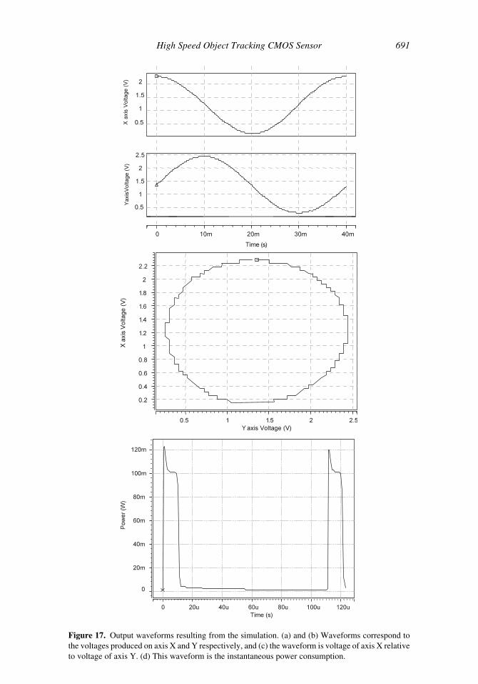
Figure 17. Output waveforms resulting from the simulation. (a) and (b) Waveforms correspond to
the voltages produced on axis X and Y respectively, and (c) the waveform is voltage of axis X relative
to voltage of axis Y. (d) This waveform is the instantaneous power consumption.
High Speed Object Tracking CMOS Sensor 691

respectively and is currently working toward the Ph.D. degree at Isfahan University of
Technology.
He was a member of the IUT Robocup team and earned the third rank in the 2002 small
size and 2003 middle size international Robocup leagues in Germany and Italy. His
research interest includes CMOS vision sensors.
Sayed M. Sayedi was born in 1960. He received the B.S. and M.S. degrees in electrical
engineering from Isfahan University of Technology, Isfahan, Iran in 1986 and 1988
respectively and the Ph.D. degree in electrical engineering from Concordia University,
Montreal, Canada in 1997.
He is currently an associate professor in the faculty of Electrical & Computer
Engineering at Isfahan University of Technology. His research interest includes the study
of VLSI fabrication processes and analysis and design of microelectronic circuits.
References
1. O. Deforges and N. Normand, ‘‘A generic systolic processor for real time grayscale morphol-
ogy,’’ in Proc. of the IEEE International Conf. on Acoustics, Speech, and Signal Processing
(ICASSP 000), Istanbul, 5–9 June 2000, vol. 6, pp. 3331–3334.
2. R. C. Dorf and R. H. Bishop, ‘‘Modern Control System,’’ 8th. ed., Addison-Wesley, Boston,
1997, pp. 767–770.
3. A. El Gamal and H. Eltoukhy, ‘‘CMOS image sensors,’’ IEEE Circuits and Devices Magazine,
May-June 2005, vol. 21, pp. 6–20.
4. W. Hu, T. Tan, L. Wang and S. Maybank, ‘‘A survey on visual surveillance of object motion and
behaviors,’’ IEEE Trans. on Systems, Man and Cybernetics, 34 (2004) 334–352.
5. M. H. Lei and T. D. Chiueh, ‘‘An analog motion field detection chip for image segmentation,’’
IEEE Trans. on Circuits and Systems for Video Technology, vol. 12, no. 5, 2002, pp. 299–308.
6. R. D. Burns, J. Shah, C. Hong, S. Pepic, J. S. Lee, R. I. Hornsey and P. Thomas, Object location
and centroiding techniques with CMOS active pixel sensors, IEEE Trans. Electron Devices,
vol. 50, no. 12, 2002, pp. 2369–2377.
7. T. Komuro, I. Ishii, M. Ishikawa and A. Yoshida, ‘‘A digital vision chip specialized for high-
speed target tracking,’’ IEEE Trans. on Electron Devices, vol. 50, no. 1, 2002, pp. 191–199.
8. N. Viarani, N. Massari, L. Gonzo, M. Gottardi, D. Stoppa and A. Simoni, ‘‘A fast and low power
CMOS sensor for optical tracking,’’ in Proc. of the 2003 International Symposium on Circuits
and Systems (ISCAS 003), 2003, vol. 4, pp. 796–799.
9. V. Brajovic and T. Kanade, ‘‘Computational sensor for visual tracking with attention,’’ IEEE
Journal of Solid-State Circuits, vol. 33, no. 8, 1998, pp. 1199–1207.
10. I. Ishii, K. Yamamoto and M. Kubozono, ‘‘Higher order autocorrelation vision chip,’’ IEEE
Trans. on Electron Devices, vol. 53, no. 8, 2006, pp. 1797–1804.
11. R. E. Cummings, J. V. Spiegel, P. Mueller and M. Z. Zhang, ‘‘A foveated silicon retina for two-
dimensional tracking,’’ IEEE Trans. on Circuits and Systems, vol. 47, no. 6, 2000, pp. 504–517.
12. S. Kleinfelder, S. Lim, X. Liu and A. El Gamal, ‘‘A 10 000 frames/s CMOS digital pixel sensor,’’
IEEE Journal of Solid State Circuits, vol. 36, no. 12, 2001, pp. 2049–2059.
13. J. Luo, C. Koch and B. Mathur, ‘‘Figure-ground segregation using an analog VLSI chip,’’ IEEE
Micro., vol. 12, no. 6, 1992, pp. 46–57.
14. G. Inviveri, ‘‘Neuromorphic analog VLSI sensor for visual tracking: circuits and application
examples,’’ IEEE Trans. on Circuits and Systems, vol. 46, no. 11, 1999, pp. 1337–1347.
15. J. A. Starzyk and X. Fang, ‘‘CMOS current mode winner-take-all circuit with both excitatory and
inhibitory feedback,’’ Electronics Letters, vol. 29, no. 10, 1993, pp. 908–910.
16. R. Min, M. Bhardwaj, C. Seong-Hwan, E. Shih, A. Sinha, A. Wang and A. Chandrakasan, ‘‘Low-
power wireless sensor networks,’’ in Proc. of the Fourteenth International Conf. on VLSI Design,
3–7 Jan. 2001, pp. 205–210.
692 M. Habibi and M. Sayedi

Submit your manuscripts athttp://www.hindawi.com
VLSI Design
Hindawi Publishing Corporationhttp://www.hindawi.com Volume 2014
International Journal of
RotatingMachinery
Hindawi Publishing Corporationhttp://www.hindawi.com Volume 2014
Hindawi Publishing Corporation http://www.hindawi.com
Journal ofEngineeringVolume 2014
Hindawi Publishing Corporationhttp://www.hindawi.com Volume 2014
Shock and Vibration
Hindawi Publishing Corporationhttp://www.hindawi.com Volume 2014
Mechanical Engineering
Advances in
Hindawi Publishing Corporationhttp://www.hindawi.com Volume 2014
Civil EngineeringAdvances in
Acoustics and VibrationAdvances in
Hindawi Publishing Corporationhttp://www.hindawi.com Volume 2014
Hindawi Publishing Corporationhttp://www.hindawi.com Volume 2014
Electrical and Computer Engineering
Journal of
Hindawi Publishing Corporationhttp://www.hindawi.com Volume 2014
Distributed Sensor Networks
International Journal of
The Scientific World JournalHindawi Publishing Corporation http://www.hindawi.com Volume 2014
SensorsJournal of
Hindawi Publishing Corporationhttp://www.hindawi.com Volume 2014
Modelling & Simulation in EngineeringHindawi Publishing Corporation http://www.hindawi.com Volume 2014
Hindawi Publishing Corporationhttp://www.hindawi.com Volume 2014
Active and Passive Electronic Components
Hindawi Publishing Corporationhttp://www.hindawi.com Volume 2014
Chemical EngineeringInternational Journal of
Control Scienceand Engineering
Journal of
Hindawi Publishing Corporationhttp://www.hindawi.com Volume 2014
Antennas andPropagation
International Journal of
Hindawi Publishing Corporationhttp://www.hindawi.com Volume 2014
Hindawi Publishing Corporationhttp://www.hindawi.com Volume 2014
Navigation and Observation
International Journal of
Advances inOptoElectronics
Hindawi Publishing Corporation http://www.hindawi.com
Volume 2014
RoboticsJournal of
Hindawi Publishing Corporationhttp://www.hindawi.com Volume 2014
Copyright © 2022 FDOKUMEN