Cavity Control System – Optimization Methods For Single Cavity Driving and Envelope Detection
Upload
independentCategory
view
0download
0
TESLA-FEL 2006-07
Superconducting cavity driving with FPGA controller
Tomasz Czarski, Waldemar Koprek, Krzysztof T. Poźniak, Ryszard S. Romaniuk,
Warsaw University of Technology Stefan Simrock, Alexander Brand
DESY, Hamburg
Brian Chase, Ruben Carcagno, Gustavo Cancelo FERMILAB, Batavia IL, 60510
Timothy W. Koeth,
RUTGERS, The State University of New Jersey, USA
ABSTRACT The digital control of several superconducting cavities for a linear accelerator is presented. The laboratory setup of the CHECHIA cavity and ACC1 module of the VU-FEL TTF in DESY-Hamburg have both been driven by a Field Programmable Gate Array (FPGA) based system. Additionally, a single 9-cell TESLA Superconducting cavity of the FNPL Photo Injector [1] at FERMILAB has been remotely controlled from WUT-ISE laboratory with the support of the DESY team using the same FPGA control system. These experiments focused attention on the general recognition of the cavity features and projected control methods. An electrical model of the resonator was taken as a starting point. Calibration of the signal path is considered key in preparation for the efficient driving of a cavity. Identification of the resonator parameters has been proven to be a successful approach in achieving required performance; i.e. driving on resonance during filling and field stabilization during flattop time while requiring reasonable levels of power consumption. Feed-forward and feedback modes were successfully applied in operating the cavities. Representative results of the experiments are presented for different levels of the cavity field gradient.
Keywords: TESLA cavity control, CHECHIA driving, FPGA, system identification, LLRF control,
1. INTRODUCTION The LLRF – Low Level Radio Frequency cavity control system is still under development in order to improve regulation of accelerating fields in the resonators [1] (figure 1). The controlled section, powered by one klystron, may consist of many cavities. The fast amplitude and phase control of the cavity field is accomplished by modulation of the klystrons driving signal using a vector modulator. The cavities are driven with pulses of 1.3 ms duration to an average accelerating gradient of 25 MV/m. The cavity RF pickup signal is down-converted to an intermediate frequency of 250 KHz while preserving the amplitude and phase information. The ADC and DAC converters link the analog and digital parts of the system with a sampling interval of 1 µs. The digital signal processing is executed in the FPGA system to obtain field vector detection (I/Q Detector), calibration and filtering. The control feedback system regulates the vector sum of the pulsed accelerating fields in multiple cavities. The FPGA based controller stabilizes the detected real (in-phase) and imaginary (quadrature) components of the incident wave according to the given set point. Additionally, the adaptive feed-forward is applied to improve the compensation of repetitive perturbations induced by the beam loading and by the dynamic Lorentz force detuning. The control block applies the value of the cavity parameters estimated in the identification system and generates the required data for the FPGA based controller.
A comprehensive system model was developed for investigating the optimal control method of the cavity [3]. The design of a fast and efficient digital controller is a challenging task and it is an important contribution to the optimization of a linear accelerator.
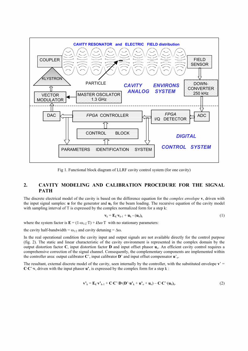
Fig 1. Functional block diagram of LLRF cavity control system (for one cavity)
2. CAVITY MODELING AND CALIBRATION PROCEDURE FOR THE SIGNAL PATH
The discrete electrical model of the cavity is based on the difference equation for the complex envelope v, driven with the input signal samples: u for the generator and ub for the beam loading. The recursive equation of the cavity model with sampling interval of T is expressed by the complex normalized form for a step k:
vk = Ek·vk-1 + uk - (ub)k (1)
where the system factor is E = (1-ω1/2·T) + i∆ω·T with no stationary parameters:
the cavity half-bandwidth = ω1/2 and cavity detuning = ∆ω.
In the real operational condition the cavity input and output signals are not available directly for the control purpose (fig. 2). The static and linear characteristic of the cavity environment is represented in the complex domain by the output distortion factor C, input distortion factor D and input offset phasor uo. An efficient cavity control requires a comprehensive correction of the signal channel. Consequently, the complementary components are implemented within the controller area: output calibrator C’, input calibrator D’ and input offset compensator u’o.
The resultant, external discrete model of the cavity, seen internally by the controller, with the substituted envelope v’ = C·C’·v, driven with the input phasor u’, is expressed by the complex form for a step k :
v’k = Ek·v’k-1 + C·C’·D·(D’·u’k + u’o + uo) – C·C’·(ub)k. (2)
DOWN-CONVERTER
250 kHzVECTOR MODULATOR
CAVITY ENVIRONS ANALOG SYSTEM
FPGA CONTROLLER FPGA I/Q DETECTOR
KLYSTRON
PARAMETERS IDENTIFICATION SYSTEM
MASTER OSCILATOR1.3 GHz
CONTROL BLOCK
PARTICLE
FIELD SENSOR
COUPLER
ADC
DIGITAL
CONTROL SYSTEM
CAVITY RESONATOR and ELECTRIC FIELD distribution
DAC

Fig. 2. Algebraic model of cavity environment system
The calibration procedure is carried out experimentally applying the feed-forward driving in the following steps.
1. Initial calibration for the signal of the intermediate frequency 250 kHz is performed as follows: - signal scaling to match the range of the FPGA registers - signal level shifting to compensate the down-converter offset.
2. Input offset compensation The required input offset compensator value u’o= -uo is determined, so to minimize the output gradient |v’| (equivalent to the condition: u = 0).
3. Output scaling The required scaling factor |C’| = 1/|C| is determined, so the detected value |v’| corresponds to the real cavity gradient.
4. Input scaling The required scaling component |D’| = 1/|D| is determined, so the detected gradient |v’| corresponds to the output of the cavity MATLAB model driven in the same condition with the input phasor u’ and the parameter factor E.
5. Loop phase calibration The required phase value arg(C’·D’) = -arg(C·D) is determined, so the input phase arg(u’) equals the output phase arg(v’) for the initial condition of the cavity operation (k=1). The desired output phase calibration, so arg(C’) = - arg(C), requires beam transient procedure. The output phase calibration has not been performed.
Consequently, the reduced cavity model seen internally by the controller is expressed, after calibration procedure:
v’k = Ek·v’k-1 + Fk·u’k - (u’b)k for u’b = C·C’·ub (3)
Actually, due to circuit nonlinearities the loop factor F = C·C’·D’·D is no stationary during a pulse.
Internal CAVITY model
Output calibrator
Input offset compensator
Input calibrator
+
u v
Input offset phasor
uo
Input distortion factor
D C
C’ + u’o
D’
Input phasor
Output phasor
External CAVITY model
v’k = Ek·v’k-1 + C·C’·D·(D’·u’k + u’o + uo) – C·C’·(ub)k
v’
u’
Output distortion factor
FPGA controller area
Internal CAVITY model Internal CAVITY model
CAVITY environs
vk = Ek·vk-1 + uk - (ub)k
E = (1-ω1/2·T) + i∆ω·T

3. IDENTIFICATION OF CAVITY PARAMETERS. The identification of the cavity parameters is an essential task for the comprehensive control algorithm [2], [4]. The feed-forward, considered as a direct control according to the recognized model of the process, can satisfactorily support the feed-back mode. The following considerations are for a single cavity without beam. Two complex parameters: E = (1-ω1/2T) + i∆ωT and F = Fr + iFi = F·exp(iψ) should be identified for the cavity model (3). The cavity’s discrete model (3) without beam can be expanded to the scalar equations, applying the real (vr, ur) and imaginary (vi, ui) components of the envelope v’ and u’ respectively, for step k and k-1 as follows:
(vr)k = (1- ω1/2T)·(vr)k-1 - ∆ωT·(vi)k-1 + Fr·(ur)k - Fi·(ui)k (4) (vi)k = (1- ω1/2T)·(vi)k-1 + ∆ωT·(vr)k-1 + Fr·(ui)k + Fi·(ur)k (5)
Actually, only two scalar unknowns can be estimated for each k-th step of the process described by two equations (4) and (5) involving measured input and output data. The identification algorithm by least square method in a noisy and non stationary condition is proposed within a given approximation range. Each time varying factor is approximated by a discrete series of base functions: polynomial or cubic B-spline set as follows:
Y = W * x where,
YNx1 – vector of estimated values for N steps xLx1 – vector of L-order series coefficients WNxL– matrix of base functions. Consequently, the step-varying factors in equations (4) and (5) are substituted by their linear decomposition. For a measurement range of M steps (M≤N), the cavity model without beam consists of 2M equations expressed by the matrix form as follows:
V = Z*z where,
V – total output vector Z – total structure matrix z – resultant vector of unknown coefficients
The vector z can be effectively estimated for the over-determined matrix equation created from a sufficiently long range of M steps. Multiplying two sides of the above equation by matrix transposition ZT, the solution for the vector z is given by:
z = (ZT*Z)-1*ZT*V. (8) It is the unique and optimal solution, according to the least square (LS) method for the measured data of the vector V and the structure matrix Z. The comprehensive algorithm for the identification of cavity parameters was implemented in the Matlab system with several possible variants of its application.
The three stages of the different operational condition: filling, flattop, decay are considered for the successive cavity parameters estimation according to equations (4), (5) reduced respectively for these stages. During the first stage of the operation, the cavity is filling with a constant forward power, resulting in an exponential increase of the electromagnetic field, according to its natural behavior in resonance condition. When cavity gradient has reached the required final value, the forward wave is modulated such that a steady-state flattop operation results. Removing the generator power yields an exponential decay of the cavity field. During decay stage (u = 0, ub = 0) two unknowns factors (1-ω1/2T) and ∆ωT are decomposed by base functions and are estimated according to the LS method. An alternative possibility is to determine the solution of the continuous cavity model for complex envelope v(t) described as follows:
v(t) = v(t0)·exp[-ω1/2·(t - t0)]·exp[iφ(t)] where dφ(t)/dt = ∆ω(t). (4)
The cavity half-bandwidth ω1/2 is supposed as a constant value and is estimated as follows:
ω1/2 = ln(|v(t0)/v(t)|)/(t - t0). (5)
The time varying cavity detuning ∆ω(t) is estimated during the decay period from the phase derivative dφ(t)/dt.

During the filling stage (ub = 0) the cavity is driven with constant forward power and for this stable condition we assume, that arg(D) = const. and that the loop phase calibration was performed correctly, thus ψ=arg(F) = 0 and factor F is a scalar value F = Fr. Therefore, two unknowns factors ∆ωT and F are decomposed by base functions and are estimated according to the LS method.
During flattop stage the klystron power is modulated, so as to compensate for the cavity detuning and stabilize the cavity field. A variation of the klystron gain and phase is expected due to a change of its power. In accordance with experimental results, the linearly time varying detuning is a reasonable assumption between filling and decay stage. Consequently, the residual two unknowns Fr and Fi are decomposed by base functions and are estimated according to the LS method. The table below recapitulates the successive procedure of the parameters estimation for three ranges of the cavity operation.
RANGE Signal condition Assumption Estimated value
DECAY u = 0, ub = 0 – ω1/2 and ∆ω(t)
FILLIG ub = 0 arg(F) = 0, ω1/2 = const. |F(t)| and ∆ω(t)
FLATTOP ub = 0 ∆ω(t) – linear, ω1/2 = const. F(t)
4. SC CAVITY CONTROL
4.1. Cavity controller algorithm The functional diagram of the controller algorithm is presented in fig. 3.
Fig. 3. The functional diagram of the FPGA controller
The digital processing is performed in I/Q detector applying the signal of intermediate frequency 250 kHz from a down-converter after AD conversion. The cavity voltage envelope (I, Q) is filtered and calibrated in the next unit, so to compensate the measurement channel attenuation and phase shifting for an individual cavity. The Set-Point table delivers the required signal level, which is compared to the actual cavity voltage. The multiplier as the proportional controller amplifies the signal error according to data from the GAIN table and closes the feedback loop. Additionally the Feed-Forward Table is applied to improve compensation of the repetitive perturbations induced by the beam loading and by the dynamic Lorentz force detuning. The resultant output signal after calibration and DA conversion drives a vector modulator.
I/Q DETECTOR
FEED-FORWARD TABLE
+
GAIN TABLE
– +
CALIBRATION CALIBRATION
& FILTERING
F P G A C O N T R O L L E R
SET-POINTTABLE
ADC DAC

4.2. Feed-forward driving
Fig. 4. Functional diagram of testing system for superconductive cavity driven with FPGA controller supported by MATLAB system
The cavity testing is carried out according to the scheme of figure 4. The control data generated by Matlab system is loaded to the part of the internal FPGA memory as a feed-forward (FF) table driving the cavity. The output data of the cavity is acquired to another area of the memory during a pulse operation of the controller. Subsequently, the input and output data are conveyed to the Matlab system for the parameters identification processing between pulses. For the comparison, the Matlab cavity model is driven in the same condition: with the same FF table applying the estimated parameters – cavity half-bandwidth ω1/2, detuning ∆ω(t) and loop factor F(t).
The required cavity performance can be achieved iteratively applying the estimated real cavity parameters to generate an improved feed-forward table for a next pulse, assuming repeatable conditions for succeeding pulses (fig. 5). The cavity system is decomposed by static and dynamic components characterized by the vectors of no stationary complex factors [F]n and [E]n respectively for n-the cycle. The input vector [U]n and output vector [V]n are considered for the parameters estimation in n-the cycle. The input vector [U]n+1 for a next cycle is estimated as an inverse solution of the system equation with the required output vector [V0]. This iterative processing quickly converges to the desired state of the cavity.
CAVITY SYSTEM
CONTROLLER
CONTROL DATA
PARAMETERS IDENTIFICATION
CAVITY MODEL ≈
MEMORY
FPGA SYSTEM
MATLAB SYSTEM
VU

Fig. 5. Schematic diagram for n-the cycle of the adaptive control process
The required input phasor u (for the feed-forward table) is calculated for desired output phasor v according to the cavity electrical model (3) without the beam for the supposed values of the cavity parameters.
During the flattop operation, the envelope v0 = V0·exp(iΦ) of the cavity voltage is stable and the inverse solution of the equation (3) without the beam for a steady state is as follows:
uk = v0·(ω1/2 - i∆ωk)·T/Fk. (9)
During the filling time, the input envelope uk = U0·exp(iφk)/Fk is estimated in order to drive the cavity with stable forward power in the resonance condition, so the required constant amplitude equals U0 = 2V0·T·ω1/2 and time varying phase equals φk = φk-1 + T·∆ωk.
The cavity control was performed for different flattop levels of the field gradient within the range of gradient V = 10 ÷30 MV with the preferred phase Φ = 0. Due to potential circuit nonlinearities, the calibration procedure was accomplished for each desired flattop level.
The cavity has been driven with an initial FF table striving to achieve required performance: driving on resonance during filling and field stabilization during flattop time. The supposed detuning (arbitrary taken) determines the desired FF table according to the cavity model. The broken line with different slopes for filling and flattop was taken as the supposed cavity detuning curve for the control purpose. Additionally, for CHECHIA setup, the Master Oscillator frequency has been tuned to the supposed cavity detuning vector, so to optimize the klystron power distribution during the flattop level. The presented experiment tries to verify the Matlab cavity model and reliability of the identification algorithm. The cavity and Matlab model responses are compared, while driven in the same condition. The results of experiments are presented in the figures 6 - 8 for different cavities and diverse conditions. A quite good agreement for the envelopes of cavity and MATLAB model is observed in all cases, and two curves are hardly distinguishable in that scale. Therefore, the Matlab model of the cavity was confirmed and the cavity parameters identification was verified for the control application.
4.3. Feed-forward with feedback driving The required data for the set point table are chosen according to the cavity electrical model (1) for the supposed values of the cavity parameters. During the filling time, required envelope vk = Vk·exp(iφk) is estimated in order to drive the cavity with stable forward power in the resonance condition, so the amplitude equals Vk = 2V0·(1–exp(-ω1/2·kT)) and time varying phase equals φk = φk-1 + T·∆ωk. During the flattop operation, the complex envelope equals v0 = V0·exp(iΦ) and is stable for the set point table.
The table below combines the analytical solution for two control modes and two ranges of the cavity operation.
[F]n Static component
[E]n Dynamic component
[U]n [V]n
[V0]Inverse solution
[vk = Ek·vk-1 + Fk·uk]n
[U]n+1
Parameters identification
z-1

MODE RANGE FEED-FORWARD SET-POINT
FILLIG uk = U0·exp(iφk)/Fk
U0 = 2V0·T·ω1/2, φk = φk-1 + T·∆ωk
vk = Vk·exp(iφk)
Vk = 2V0·(1–exp(-ω1/2·kT)), φk = φk-1 + T·∆ωk
FLATTOP uk = v0·(ω1/2 - i∆ωk)·T/Fk v0 = V0·exp(iΦ)
The test of the feed-forward cavity driving was repeated and the feedback loop was closed starting with a small value of a loop gain. No filter has been applied. A loop gain was gradually increased to the possible maximum value for a stable condition. The loop gain of ~250 and ~150 was achieved for the flattop cavity gradient of 10 MV and 20 MV respectively for CHECHIA cavity. The results of experiments with loop gain of 100 are presented in the figures 9-14 for different cavities and diverse conditions.
5. HARDWARE AND SOFTWARE SETUP The experiment with the FNPL module in the A0 laboratory at FNAL was done in cooperation of three laboratories: FNAL, DESY and WUT-ISE. DESY and WUT-ISE communicated with FNAL using RealVNC program (figure 6). All software was running on SUN machine installed in a VME crate located at FNAL. The configuration of software and hardware is as follows.
Fig. 6. Diagram of data and operator connections between three laboratories during the A0 control
FNAL
SIMCON 2.1
WUT-ISE
DESY
VNC Client VNC Client
Software server VNC Server
Skype voice

5.1. Hardware configuration A commercial set up XtremeDSP Development Kit by Nallatech was used. The board was embedded on VME backbone board of own construction. There was implemented main board BenONE integrated with daughter board BenADDA (see. fig. 7). The set-up is functionally optimized for realization of fast hardware based DSP algorithms. It possesses two fast 14-bit DAC and ADC converters and a programmable circuit FPGA Xilinx VirtexII V3000-4. The chip has inbuilt fast multiplication blocks 18x18 bit. In these experiments, SUN station was used as a VME controller. Fitting of the set-up for cooperation with VME-bus was done via embedding the whole system on a dedicated VME baseboard 6HE EURO-VME. The baseboard has FPGA ACEX chip by Altera. The chip services VME-BUS protocol and provides direct communication with VirtexII circuit embedded on BenADDA board.
There was implemented access to VME of the type A24D32 (there are used 24 address bus lines and 32 lines of data bus) in the SLAVE work mode (AM=39H) or in the mode MASTER (AM=3DH). SIMCON also requires 26624 bytes (hex 0x6800) of the address space within the SUN address space. The Developer should know the address space configuration, in particular the VME crate to make address allocation for SIMCON.
When the address is asserted on the VME address bus by VME controller, the address monitor component inside ALTERA chip compares the four most significant lines from the bus (A23-A20) with the four most significant switches from address switches. Both boards have FPGA chips with internal logic and internal space of addresses. A method is needed to distinguish these two addressing spaces. For this purpose lines 19 to 16 are used on the VME address bus. The ALTERA chip has address 0xF0000 and the XILINX chip has address 0x00000. In order to address a specific chip the address of the chip should be added to base address of whole board.
Fig. 8. Software configuration with SIMCON and SUN controller
Fig. 7. XtremeDSP Development Kit embedded on a carrier board
EURO-6HE with VME interface.
V M E B u s
S U N
S I M C O N 2.1
SIMULATOR
CONTROLLER
INTERNAL INTERFACE
VME COMMUNICATION COMPONENT VME CHANNEL LIBRARY
INTERNAL INTERFACE ENGINE
DOOCS MATLAB
VME crate
ANALOG INPUT 1ANALOG INPUT 2EXTERNAL CLOCK
ANALOG OUTPUT 1ANALOG OUTPUT 2
DIGITAL INPUT 1DIGITAL INPUT 2DIGITAL INPUT 3
DIGITAL OUTPUT 1DIGITAL OUTPUT 2DIGITAL OUTPUT3
LEDS
VME-BU
S IN
TERFACE
COMMUNICATION INTERFACE FROM ALTERA BASED VME INTERFACE TO NALLATECH XTREME DSP BOARD
VME BASEADDRESSSWITCH

5.2. Software configuration Matlab 7.0 software was used to control hardware. It was only necessary to copy several files to install the Matlab software. The files can be divided in a few groups. List of theses files can be found in attachment A. These files except GUI files can work in Matlab version 6.5 or 7. GUI files are only for Matlab 7 since they are incompatible with Matlab 6.5.
Direct access to FPGA register functions
This kind of function works as MEX-functions in Matlab and they are basis for all other m-files described in following chapters. There is only one way to get access to FPGA registers and memories through these functions. They are used to operate on physical elements of FPGA system (i.e. bits, registers, memories). Direct access functions are described in details in TESLA report [5].
Configuration files
Configuration files are used to perform basic operation on sets of FPGA registers. For example, to write a new version of the FeedForward table many operation must have been performed on the FPGA using direct access functions. In order to simplify such kind of operations several m-functions have been prepared. These m-functions can be used to operate on functional blocks of FPGA controller and simulator (i.e. operating tables, rotation matrixes, IQ Detector parameters, etc.). Developers who have worked out their own control algorithms in Matlab can use these functions to download control tables and parameters to the FPGA and readout the results.
Algorithm files
This set of m-files contains one version of a successful algorithm developed for FPGA controller. Details of this algorithm for simulator and controller are presented in TESLA report 2003-28, 2003-08 and have been presented in this document.
GUI files
All files described above are used in graphic user interfaces. GUI were made using the Matlab tool “GUI Builder”. There are several GUI windows: for simulator, controller and for readouts. Fig. 9 presents the control panel for SIMCON 2.1 which was used in the presented experiment.
Fig. 9. SIMCON control panels for SUN controller at FNAL hardware test setup

6. CONCLUSIONS Initial tests in the application of an FPGA based controller have been carried out on the TESLA type superconducting cavity in DESY. DESY’s CHECHIA cavity was successfully driven with feed-forward and feedback modes. The analogous experiments have been repeated on DESY’s ACC1 module of VUV-FEL and the remotely controlled FNPL PhotoInjector’s cavity module at FERMILAB. The calibration procedure is presented as it is required for efficient control of the cavity. It has been proposed that the parameter identification algorithm, according to the algebraic model of the superconductive cavity, be incorporated into the control system’s development. The over-determined matrix equation for the input-output relation is considered with the least squares solution for unknown parameters. The polynomial approximation or cubic B-spline functions are employed in the estimation of time varying parameters. The electrical model of the cavity has been confirmed and the algorithm of the cavity parameters identification has been verified for the control purpose.
7. ACKNOWLEDGMENTS The authors would like to thank DESY Directorate for providing excellent conditions to perform the work described in this paper.
We acknowledge the support of the European Community Research Infrastructure Activity under the FP6 “Structuring the European Research Area” program (CARE, contract number RII3-CT-2003-506395).
8. REFERENCES
1. T. Schilcher, “Vector Sum Control of Pulsed Accelerating Fields in Lorentz Force Detuned Superconducting Cavities”, Ph. D. thesis, Hamburg, 1998.
2. M. Huning, S. and N. Simrock, “System identification for the digital RF control system at the TESLA Test Facility”, Proc. EPAC’98, Stockholm.
3. T. Czarski, R.S. Romaniuk, K.T. Pozniak, and S. Simrock: “TESLA cavity modeling and digital implementation in FPGA technology for control system development”, Nuclear Instruments and Methods in Physics Research Section A: Accelerators, Spectrometers, Detectors and Associated Equipment -Volume 556, Issue 2, 15 January 2006, Pages 565-576.
4. T. Czarski, R.S. Romaniuk, K.T. Pozniak, S. Simrock; “Cavity parameters identification for TESLA control system development” Nuclear Instruments and Methods in Physics Research Section A: Accelerators, Spectrometers, Detectors and Associated Equipment -Volume 548, Issue 3, 21 August 2005, Pages 283-618.
5. Waldemar Koprek, Pawel Kaleta, Jaroslaw Szewinski, Krzysztof T. Pozniak, Tomasz Czarski, Ryszard S. Romaniuk; Software Layer for FPGA-Based TESLA Cavity Control System (Part I) - TESLA Technical Note, 2004-10, DESY- Hamburg.
Paper published in NIM-A 2006

Figure 10. Feed-forward driving for CHECHIA cavity: selected readout for 30 MV flattop level
0 500 1000 1500 2000-10
-5
0
5
10
15
20
25
30
35
time [10-6 s]
Cavity output envelope [MV]
sold line - cavity dashed line - MATLAB model
Amplitude
In-phase
Quadrature
0 500 1000 1500 2000-20
-15
-10
-5
0
5
10
15
20
25
time [10-6 s]
Controller output [mA]
Klystron output estimation - dashed line
Amplitude
In-phase
Quadrature
0 500 1000 1500 2000
-1.5
-1
-0.5
0
0.5
1
time [10-6 s]
Phase of cavity and controller output [rad]
Klystron output estmation - dashed line
0 500 1000 1500 2000-200
-100
0
100
200
300
400
500
600
700
800
time [10-6 s]
Cavity detuning [Hz]
Controller
Cavity
supposed detuningestimated detuning
filling
flattop
decay
half-bandwidth = 215 Hz

Figure 11. Feed-forward driving for the cavity nr 8 of ACC1 module
0 500 1000 1500 2000-5
0
5
10
15
20
time [10-6 s]
Cavity output envelope [MV]
Amplitude
In-phase
Quadrature
0 500 1000 1500 2000-10
-5
0
5
10
15
time [10-6 s]
Controller output [mA]
Klystron output estimation - dashed line
AmplitudeIn-phase
Quadrature
0 500 1000 1500 2000-1
-0.5
0
0.5
time [10-6 s]
Phase of cavity and controller output [rad]
Klystron output estmation - dashed line
Cavity
Controller
0 500 1000 1500 2000-100
0
100
200
300
400
500
600
time [10-6 s]
Cavity detuning [Hz]
supposed detuningestimated detuning
half-bandwidth = 215 Hz

Figure 12. Feed-forward driving for the cavity of A0 module
0 500 1000 1500-2
0
2
4
6
8
10
12
time [10-6 s]
Cavity output envelope [MV]
Amplitude
In-phase
Quadrature
0 500 1000 1500-3
-2
-1
0
1
2
3
4
5
time [10-6 s]
Controller output [mA]
Klystron output estimation - dashed line
In-phase
Quadrature
Amplitude
0 500 1000 1500
-1
-0.8
-0.6
-0.4
-0.2
0
0.2
0.4
time [10-6 s]
Phase of cavity and controller output [rad]
Klystron output estmation - dashed line
Cavity
Controller
time [10-6 s]0 500 1000 1500
100
110
120
130
140
150
160
170
180
190
200Cavity detuning [Hz]
supposed detuningestimated detuning
half-bandwidth = 95 Hz

Figure 13. Feed-forward with feedback driving for CHECHIA cavity
0 500 1000 1500 2000
-5
0
5
10
15
20
25
Cavity output envelope [MV]
filling
flattop
decay
time [10-6 s]0 500 1000 1500 2000
-15
-10
-5
0
5
10
15
20Controller output [mA]
0 500 1000 1500 2000
-1.2
-1
-0.8
-0.6
-0.4
-0.2
0
0.2
0.4
0.6
0.8Phase of cavity and controller output [rad]
0 500 1000 1500 2000-200
-100
0
100
200
300
400
500
600Cavity detuning [Hz]
time [10-6 s]
time [10-6 s]time [10-6 s]
supposed detuningestimated detuning
Amplitude
In-phase
Quadrature
Amplitude
In-phase
Quadrature
Controller
Cavity

Figure 14. Feed-forward with feedback driving for the cavity nr 5 of ACC1 module
0 500 1000 1500 2000
0
5
10
15
20Cavity output envelope [MV]
time [10-6 s] time [10-6 s]
time [10-6 s]time [10-6 s]
0 500 1000 1500-10
-5
0
5
10
15Controller output [mA]
Klystron output estimation- dashed line
0 500 1000 1500 2000-1
-0.5
0
0.5Phase of cavity and controller output [rad]
0 500 1000 1500 2000-100
0
100
200
300
400
500
600Cavity detuning [Hz]
supposed detuningestimated detuning
Amplitude
In-phase
Quadrature
AmplitudeIn-phase
Quadrature
Cavity
Klystron
Klystron output estimation - dashed line

Figure 15. Feed-forward with feedback driving for the cavity of A0 module
0 500 1000 1500-2
0
2
4
6
8
10
12
time [10-6 s]
Cavity output envelope [MV]
Amplitude
In-phase
Quadrature
0 500 1000 1500-1
-0.5
0
0.5
time [10-6 s]
Phase of cavity and controller output [rad]
Cavity
Controller
Copyright © 2022 FDOKUMEN