DSP hardware design for fingerprint binarization and thinning on FPGA
6
2014 International Conference on Control, Instrumentation, Energy & Communication(CIEC) 544 DSP Hardware Design for Fingerprint Binarization and Thinning on FPGA Rahul Kr Das*, Abhishek De*, Chandrajit Pal t , Amlan Chakrabarti t *Dept. of Electronic Science, University of Calcutta rahulkd.das @gmail.com, amab333 @gmail.com t A.K. Choudhury School of Information Technology, University of Calcutta [email protected], achakra 12 @yahoo.com Abstract-Binarization and thinning are the two critical pre- processing stages designed for accurate extraction of minutiae features from the preprocessed image in fingerprint identification system. In this work an efficient design of DSP hardware for binarization and thinning of fingerprint images has been achieved based on Otsu's thresholding method for binarization and Zhang and Suen's method for thinning. Optimization has been achieved in our proposed hardware design, which improved the performance in terms of execution speed. The algorithms are designed in Xilinx System Generator using DSP hardware blocks and executed on Xilinx Spartan 6 FPGA ( field programmable gate array) device. Keywords: DSP hardware, System Generator, binarization, thinning thinning, the execution on our hardware architecture on FPGA is about 10 times faster than previously achieved [5]. The utilization of hardware resources is a critical factor in hardware design and a detailed analysis has been given in this paper with reference to other papers [4] [5] [6]. In section II, we provide the mathematical analysis for Otsu's algorithm and the hardware design for binarization. In section III, the referenced algorithm for thinning and its hardware architecture has been provided. In section IV, the result analysis of the FPGA implementation has been given and finally the device resource utilization and the timing analysis has been provided in section V. II. FINGERPRINT BINARIZATION Fig. 1: Fingerprint authentication system Fingerprint Matching -<::==J Minutiae Extraction EJ:=::> [ Enhancement H Binanzation H Thinning J Fingerprint Pre-processing (2) (1) g(x, y) == a if f(x, y) > T = b iff(x,y) < T B. Computation of Between Class Variance The between-class variance is given by: a1(t) == Wl(t)W2(t)[/Ll(t) - /L2(t)]2 A. Introduction In computer VISIon and image processing, Otsus global thresholding method [7] is used to perform histogram based image thresholding, which reduces a grayscale image into a bi- nary image. Otsu's algorithm is based on finding the maximum between-class variance of the input grayscale image f(x,y) and hence the optimal threshold T is found, which segments the image into two classes as foreground and background. Thus a binary image g(x,y) is defined as: I. INTRODUCTION In automatic fingerprint identification system (AFIS) [1] in Fig. 1, the fingerprint image acquired by the sensors is preprocessed in a sequential manner through different pre- processing stages. The preprocessing stages include image enhancement [2] to improve the quality of the input image. In automatic identification system, the performance of the minutiae extraction algorithms [3] relies heavily on the quality of the fingerprint image. The minutiae features can be easily detected by feature extractor if the objects of the image (ridges) are well defined. Processing of low quality fingerprint images will lead to detection of false minutiae and hence the identification system will not work. Fingerprint binarization and thinning are the next preprocessing stages, they accept the enhanced grayscale image as input and produce a thinned binary image (skeleton image). The thinned binary image can be used for feature extraction depending on the specific application under consideration. Previous work has been done on FPGA implementation of binarization [4] and thinning [5][6] using Otsu's algorithm for binarization and Zhang and Suen's algorithm for thinning. Our work targets designing of custom DSP hardware of fingerprint binarization and thinning in Xilinx System Gener- ator, and its implementation on FPGA. FPGA implementation has been done to meet the high speed requirements for the proposed algorithms. For binarization [4], we have developed a histogram hardware architecture processing one pixel per clock cycle with low design-complexity for optimizing the hardware design. Experimental results suggested that the execution is about 10 times faster than the software implementation. For 978-1-4799-2044-0/14/$31.00©2014IEEE
Transcript of DSP hardware design for fingerprint binarization and thinning on FPGA

2014 International Conference on Control, Instrumentation, Energy & Communication(CIEC) 544
DSP Hardware Design for Fingerprint Binarizationand Thinning on FPGA
Rahul Kr Das*, Abhishek De*, Chandrajit Palt , Amlan Chakrabartit*Dept. of Electronic Science, University of Calcutta
rahulkd.das @gmail.com, amab333 @gmail.comtA.K. Choudhury School of Information Technology, University of Calcutta
palchandraj [email protected], [email protected]
Abstract-Binarization and thinning are the two critical preprocessing stages designed for accurate extraction of minutiaefeatures from the preprocessed image in fingerprint identificationsystem. In this work an efficient design of DSP hardwarefor binarization and thinning of fingerprint images has beenachieved based on Otsu's thresholding method for binarizationand Zhang and Suen's method for thinning. Optimization hasbeen achieved in our proposed hardware design, which improvedthe performance in terms of execution speed. The algorithms aredesigned in Xilinx System Generator using DSP hardware blocksand executed on Xilinx Spartan 6 FPGA ( field programmablegate array) device.
Keywords: DSP hardware, System Generator, binarization,thinning
thinning, the execution on our hardware architecture on FPGAis about 10 times faster than previously achieved [5]. Theutilization of hardware resources is a critical factor in hardwaredesign and a detailed analysis has been given in this paper withreference to other papers [4] [5] [6].
In section II, we provide the mathematical analysis forOtsu's algorithm and the hardware design for binarization.In section III, the referenced algorithm for thinning and itshardware architecture has been provided. In section IV, theresult analysis of the FPGA implementation has been given andfinally the device resource utilization and the timing analysishas been provided in section V.
II. FINGERPRINT BINARIZATION
Fig. 1: Fingerprint authentication system
Fingerprint Matching -<::==J Minutiae Extraction
EJ:=::> [Enhancement H Binanzation H Thinning JFingerprint Pre-processi ng
(2)
(1)g(x, y) == a if f(x, y) > T
=b iff(x,y) < T
B. Computation of Between Class Variance
The between-class variance is given by:
a1(t) == Wl(t)W2(t)[/Ll(t) - /L2(t)]2
A. Introduction
In computer VISIon and image processing, Otsus globalthresholding method [7] is used to perform histogram basedimage thresholding, which reduces a grayscale image into a binary image. Otsu's algorithm is based on finding the maximumbetween-class variance of the input grayscale image f(x,y) andhence the optimal threshold T is found, which segments theimage into two classes as foreground and background. Thus abinary image g(x,y) is defined as:
I. INTRODUCTION
In automatic fingerprint identification system (AFIS) [1]in Fig. 1, the fingerprint image acquired by the sensors ispreprocessed in a sequential manner through different preprocessing stages. The preprocessing stages include imageenhancement [2] to improve the quality of the input image.In automatic identification system, the performance of theminutiae extraction algorithms [3] relies heavily on the qualityof the fingerprint image. The minutiae features can be easilydetected by feature extractor if the objects of the image(ridges) are well defined. Processing of low quality fingerprintimages will lead to detection of false minutiae and hence theidentification system will not work. Fingerprint binarizationand thinning are the next preprocessing stages, they acceptthe enhanced grayscale image as input and produce a thinnedbinary image (skeleton image). The thinned binary imagecan be used for feature extraction depending on the specificapplication under consideration.
Previous work has been done on FPGA implementation ofbinarization [4] and thinning [5][6] using Otsu's algorithm forbinarization and Zhang and Suen's algorithm for thinning.
Our work targets designing of custom DSP hardware offingerprint binarization and thinning in Xilinx System Generator, and its implementation on FPGA. FPGA implementationhas been done to meet the high speed requirements for theproposed algorithms. For binarization [4], we have developed ahistogram hardware architecture processing one pixel per clockcycle with low design-complexity for optimizing the hardwaredesign. Experimental results suggested that the execution isabout 10 times faster than the software implementation. For
978-1-4799-2044-0/14/$31.00©2014IEEE

2014 International Conference on Control, Instrumentation, Energy & Communication(CIEC) 545
The probabilities of the two classes are computed from theimage histogram as:
E. Hardware Design
BW mode
D. Algorithm for Fingerprint Binarization
• Histogram Computation Mode
• Histogram Read Mode
Fig. 3: Histogram module
The Histogram module works in two modes:
In the histogram computation mode, the pixels are readfrom the memory module sequentially into the histogrammodule as shown in the block diagram in Fig. 2. The histogrammodule shown in Fig. 3 uses a dual-port RAM to store theimage histogram and a control unit, which controls the wholehistogram operation by generating necessary control signals.During histogram computation, the image pixels are used asport addresses. Dual-port memory is used with one port beingused to read the memory and the other port to write the result.
The count for every pixel is updated in the histogrammemory by reading the memory content from port a in thefirst clock cycle. The pixel value is buffered in the register sothat the updated count is written to the same memory location(port b) in the following clock cycle. But if the subsequentpixel has the same value, the count value from memory is notyet updated for read operation. In this case, instead of readingfrom memory, the buffered count value from the register isincremented to update the count. This will be written to theport b once the subsequent pixel has a different value.
The pixels count updating process takes 3 clock cyclesshown in the timing analysis in Fig. 4. In the first clockcycle, the pixel comparator compares the current pixel withthe preceding pixel to enable either memory read or registerread operation in the following clock cycle. The last cycle isused for write operation.
After the image histogram is computed and stored in dualport memory, the histogram address generator is enabled forhistogram read operation. Histogram data and its corresponding grayscale intensities are read at each clock cycle as shownin the timing analysis in Fig. 5. During the read operation, thehistogram values are stored in the respective histogram andgrayscale buffers of the BCVC module. The rst signal is usedto reset the histogram and grayscale register to 0 after theread operation is completed. The modectr becomes 1 whichenables the Otsu grayscale counter for the optimal thresholdcomputation.
(5)
(6)
(3)
(4)
where Pi == ni/Nt
WI (t) == LPii=O
Step 3 : for t == 0 to L - 1 and modedr +----- 1 (Otsumode). a1 (t) is computed in the BCVC moduleusing equation (7).
Step 4 : Optimal threshold (t*) == max(a1(t)) is computed in the optimal threshold module.
Step 5 : BWmode +----- 1 (pixel counter is enabled). Theimage is binarized using the optimal threshold asshown in equation (1).
Step 1 : Read image pixels p(i,j) from memory module.
Step 2 : Image histogram is computed in the histogram module and stored in histogram memory.modedr +----- 0 (histogram mode)
a : histaddr +----- p(i, j)b : update the count for every pixelc : histdata +----- count
c. Top Level Model Architecture
Fig. 2: Modules in fingerprint binarization
The optimal threshold (t*) for image thresholding is given as
t* == M ax (a1 (t )) (8)
£-1
/12(t) == L ipi/W2i=t+l
Substituting (3) to (6) in (2) and neglecting constant N ,
a1(t) = (~ni *i~lni)*(~ i:i -i~l i:i)2(7)
£-1
W2(t) == L Pii=t+l
The mean of the two classes are computed as:t
/11 (t) == L ipi/W l
i=O
2014 International Conference on Control, Instrumentation, Energy & Communication(CIEC) 546
Pixel Counter :.JEnable
Histogram
A7~~Pixel Address ®~
Pixel Data ®
Clock
Port A(addr)
Port B(addr)
MemWR
>------< 01
OptimalThreshold
Module
Port B(data)Histogram
>-----i---:----~ H1 H2 HS : Fig. 6: Otsu model
Fig. 4: Timing diagram of histogram computation mode
Clock
Grayscale Counter UEnable
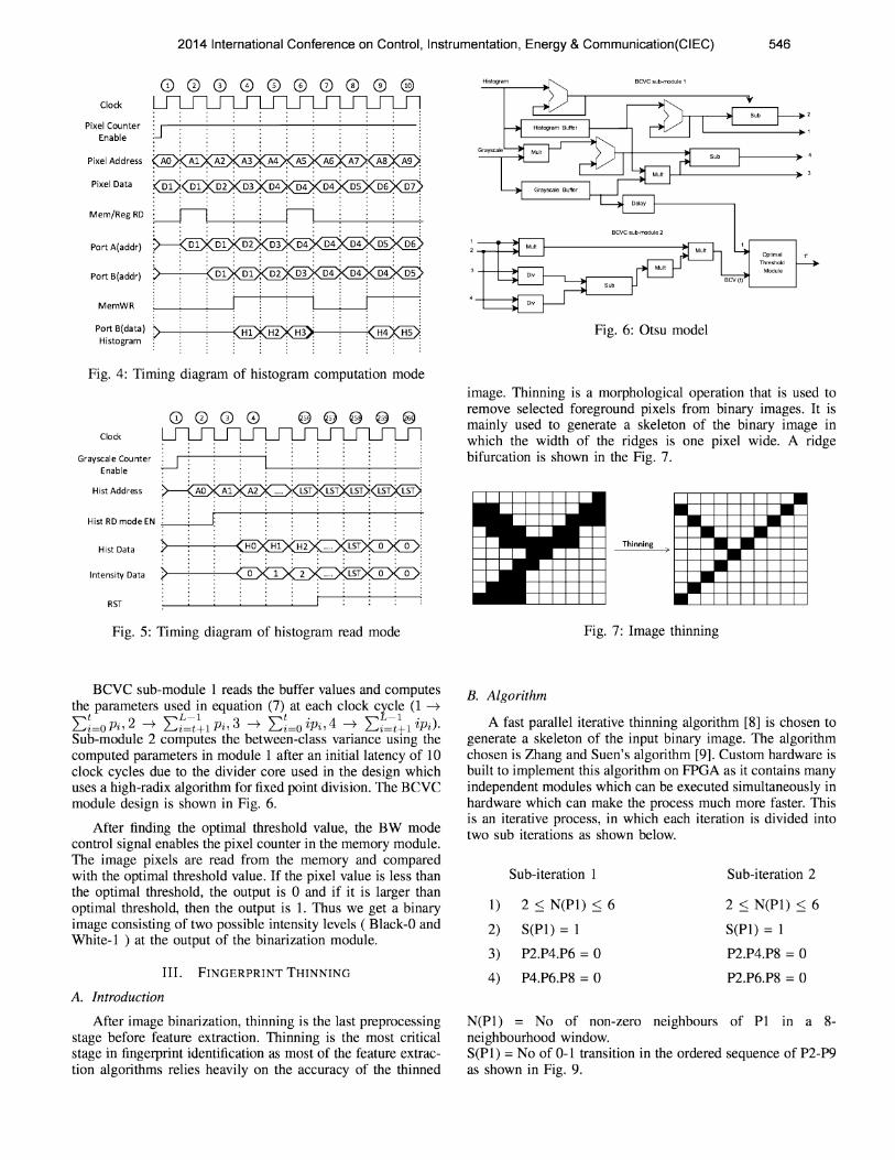
image. Thinning is a morphological operation that is used toremove selected foreground pixels from binary images. It ismainIy used to generate a skeleton of the binary image inwhich the width of the ridges is one pixel wide. A ridgebifurcation is shown in the Fig. 7.
RST
Hist Address •• •• •• •• ••••••
Thinning)
Intensity Data
Hist Data
Fig. 5: Timing diagram of histogram read mode Fig. 7: Image thinning
N(Pl) = No of non-zero neighbours of PI in a 8neighbourhood window.S(Pl) =No of 0-1 transition in the ordered sequence of P2-P9as shown in Fig. 9.
B. Algorithm
A fast parallel iterative thinning algorithm [8] is chosen togenerate a skeleton of the input binary image. The algorithmchosen is Zhang and Suen's algorithm [9]. Custom hardware isbuilt to implement this algorithm on FPGA as it contains manyindependent modules which can be executed simultaneously inhardware which can make the process much more faster. Thisis an iterative process, in which each iteration is divided intotwo sub iterations as shown below.
BCVC sub-module 1 reads the buffer values and computesthe parameters used in equation (7) at each clock cycle (1 ----+~t 2 ~L-l 3 ~t • 4 ~1-1.)Di=O Pi, ----+ Di=t+1 Pi, ----+ Di=O ~Pi, ----+ Di=t+1 ~Pi .Sub-module 2 computes the between-class variance using thecomputed parameters in module 1 after an initial latency of 10clock cycles due to the divider core used in the design whichuses a high-radix algorithm for fixed point division. The BCVCmodule design is shown in Fig. 6.
After finding the optimal threshold value, the BW modecontrol signal enables the pixel counter in the memory module.The image pixels are read from the memory and comparedwith the optimal threshold value. If the pixel value is less thanthe optimal threshold, the output is 0 and if it is larger thanoptimal threshold, then the output is 1. Thus we get a binaryimage consisting of two possible intensity levels ( Black-O andWhite-l ) at the output of the binarization module.
III. FINGERPRINT THINNING
A. Introduction
After image binarization, thinning is the last preprocessingstage before feature extraction. Thinning is the most criticalstage in fingerprint identification as most of the feature extraction algorithms relies heavily on the accuracy of the thinned
Sub-iteration 1
1) 2:::; N(P1) :::; 6
2) S(Pl) = 1
3) P2.P4.P6 = 0
4) P4.P6.P8 = 0
Sub-iteration 2
2 :::; N(Pl) :::; 6
S(Pl) = 1
P2.P4.P8 = 0
P2.P6.P8 = 0

2014 International Conference on Control, Instrumentation, Energy & Communication(CIEC) 547
Flagged Pixel Addresses
4 1n1
Binary pixel~ In
P4 .... In2
P3
OJI4 P6 .... In3
P2 In4
OJ15~ln5
OJI6 :: In6
P9
flag .... MemWR
~ .... ln1Oul1 f---
Window Extraction Module
I---__~ Delay
Memory Module 1
......... In2
Pixel
Address
OJlg ------. In9L....-__...... .....---.-_----1
L..---+~_.......B_elaYCenlerpixel
~ln2
Memory Module 2
~Jn3
iteration c ntrol
Pixel address Oul 1 -I-- UID controlt-----+........ In 1
~ In2 ~~ll: _~J
r .....'n_3 ~_~::......r--t:::=*=::::+--_----4~,.....ln_4 ......
Iprog counter EN
Programmable Counter Values
RIWControl
Pixel counter EN
Fig. 8: Hardware architecture for fingerprint thinning
counter is initialized for sub-iteration 1.
Fig. 10: Memory module 1Fig. 9: 8 neighbourhood connectivity
Step 1 : The conditions of sub-iteration 1 are appliedon each 8-neighborhood window to determinewhether the center pixel PI is deletable or not.
Step 2 : The Center Pixel PI is marked for deletion if itsvalue is 1 (object pixel) and all the conditions aresatisfied.
Step 3 : After the execution of sub-iteration 1 on the entireimage, the marked pixels are deleted.
Step 4 : The above steps are repeated for sub-iteration 2on the modified image data.
Step 5 : This completes one iteration of the algorithm. Theiteration continues until there are no pixels to bedeleted
c. Hardware Design
The thinning hardware architecture shown in Fig. 8 consistsof 5 modules. The memory module 1 shown in Fig. 10 consistsof a single-port RAM to store the input binary image. A pixelcounter is used to generate the pixel addresses. The pixel
The window extraction module [5] is responsible for extracting 3x3 window from the image matrix. It reads the dataserially at each clock cycle from the memory module 1 andlatch the data in the respective buffers, thus generating a 3x3window. This is known as a sliding window which slides overthe entire image to generate a window for every pixel in theimage. After forming each window for a pixel(center pixel), itsends the window to the Zhang and Suen module.
Zhang and Suen module implements the conditions givenin the respective sub-iteration on the 8-neighbourhood inputwindow to flag the center pixel for deletion. This moduleexecutes the functions simultaneously for each window at eachclock cycle and due to this parallel computation, the hardwareexecution speed increases.
Memory module 2 shown in Fig. 11 is used to flag thepixels for deletion based on the output flag condition of theprevious module and the value of the center pixel. It consistsof an address generator for the single-port RAM to store theflagged pixel addresses in the memory. The address generatorused is a programmable up/down counter which generatesaddresses for the memory only if any deletable pixel is found.
After the execution of sub-iteration 1, the flagged pixel addresses are read into memory module 1. Using these addresses,

2014 International Conference on Control, Instrumentation, Energy & Communication(CIEC) 548
Fig. 11: Memory module 2
the flagged pixels are deleted from module 1 and the modifieddata is stored in the memory. This completes the first subiteration. This modified data is used for the next sub-iterationof the algorithm.
Step 6 : progcounterEN f- 0When the read out operation from module 2 iscompleted,the address generator is disabled so thatit does not generate any address unless the nextiteration starts.
IV. EXPERIMENTAL RESULTS
The hardware designs for binarization and thinningare implemented on Spartan 6 LX45 device with a clockfrequency of 100 MHz and the execution results are shownin Fig. 13 and Fig. 14. Thinning of a binary image dependson the quality of the image and the thickness of the ridgestructures. Thus the thinning time will be more for low qualityimage and hence we can say enhancement is a very criticalstage in fingerprint preprocessing. Thinning execution timedepends on the no of iterations which depends on the qualityand size of the input image. The iteration times are not fixed.In our case, no of iterations for the 280x265 binary image is 10.
Fig. 12: Thinning control unit
Design factors formulization:
(9)
t f is the hardware processing time for an image, C is thetotal clock cycles used for processing one frame of M pixels,f is the clock frequency, N is the no of iterations, tp is the noof pixels processed per clock cycle with one processing unit,L is the latency in clock cycles and n c is the no of processingunits [10].
The thinning control unit shown in Fig. 12 controls the behavior of the whole thinning system by generating appropriatecontrol signals to control the individual modules in the design.The algorithm for the thinning control unit and the status ofthe control signals is shown below.
(74200.2 ) 1t fbin == + 531 . == 1.489 ms. (10)
1 1.100MHz
For thinning, L is not fixed and the execution terminates itselfonce the skeleton is found.
. C 767282tfthm = 7 = lOOMHz = 7.673ms. (11)
(b) Binary image(a) Grayscale image
Fig. 13: Fingerprint Binarization, a : Input image (size = 280x 265, bit-depth = 8 and resolution = 300 DPI) and b :
Output image
Step 1 : Read binary image b[i,j] from memory 1.pixelcounterEN f- 1iterationctr f- O(sub - iteration1)R/Wcontrol f- 0(Memory module 1 in read mode)
Step 2 : pixelcounterEN f- 0Pixel counter is disabled after image read-out.
Step 3 : U/ Dcontrol f- 0progcounterEN f- 1During the sub-iteration, the programmablecounter is used as an address generator for memory module 2.
Step 4 : U/ Dcontrol f- 1After the execution of the sub-iteration, flaggedpixel addresses are read for deletion.
Step 5 : R/Wcontrol f- 1(Memory module 1 in write mode)

2014 International Conference on Control, Instrumentation, Energy & Communication(CIEC) 549
Fig. 14: Fingerprint Thinning, a = Input image (size = 280 x265, bit-depth = 1 and resolution = 300 DPI) and b = output
image
(a) Binary image (b) Thinned image
VII. ACKNOWLEDGMENT
This work has been supported by the Department ofScience and Technology, Govt of India under grant NoDST/INSPIRE FELLOWSHIP/2012/320 and TEQIP-II (CoE)project of University of Calcutta.
REFERENCES[1] D. Maltoni, D, Maio, A. K. Jain, S. Prabhakar, "Handbook of fingerprint
recognition", in Springer, New York, 2003.
[2] L. Hong, Y. Wan, A. Jain, "Fingerprint image enhancement algorithmand performance evaluation",in IEEE transaction on pattern analysisand machine intelligence, vol. 20, NO.8, 0162-8828, pp. 777-789, 1998.
TABLE I: FPGA Resource Utilization on Spartan 6 LX45
FPGA Image Size (280x265)
Resources Binarization Thinning % Utilization
Slice registers (54,576) 1898 590 3% 1%
Slice luts (27,288) 1859 852 6% 3%
Occupied slices (6,822) 735 292 10% 4%
lOBs (218) 10 2 4% 1%
BRAMs (348) 44 82 12.6% 24%
TABLE II: Timing Analysis
Platform Clock Speed Binarization ThinningFPGA 100 MHz 1.489 illS 7.673 illS
MATLAB 2.2 GHz 14.726 illS 80.40 illS
V. PERFORMANCE ANALYSIS
The resource utilization and timing analysis are shown inTABLE I and TABLE II respectively. The resource and timinganalysis clearly indicates that the proposed design with a clockfrequency of 100 MHz utilizes less FPGA resources and alsoworks at a higher speed than that of the software implementation with a frequency of 2.2 GHz. It is clearly evident that theFPGA implementation for binarization and thinning is about10 times faster than the software implementation in MATLAB.
With increased speed and minimal utilization of FPGAresources, our design is commercially viable in terms of itsimplementation cost when implemented on Spartan 6 FPGAdevice due to the increased use and availability of the FPGAdevices in the market. Moreover, FPGA based implementationstake less design time and design cost to that of the ASIC basedhardware designs, hence our design is well tailored in termsof commercialization.
VI. CONCLUSION AND FUTURE WORK
This paper proposes an efficient hardware implementationof the fingerprint preprocessing stages in automatic authentication system. Our future work will be based on implementingthe complete fingerprint authentication system which includesminutiae feature extraction and classification [11] and the lastpostprocessing stage. We will emphasis more on the parallelarchitecture implementation of the algorithms on FPGA toenhance the execution speed of the system.
[3] F. Zhao, X. Tang, "Preprocessing and postprocessing for skeleton-basedfingerprint minutiae extraction" ,in Science direct on pattern recognition,0031-3203, pp. 1270-1281,2006.
[4] W. Jianlai,Y. Chunling, Z. Min, W. Changhui, "Implementation of Otsu'sthresholding process based on FPGA" ,in IEEE conference on industrialelectronics and applications, 978-1-4244-2800-7, pp. 479-483, ICIEA2009.
[5] L. Hermanto, S. A. Sudiro, E. P. Wibowo, "Hardware implementationof fingerprint image thinning algorithm in FPGA device", in IEEEconference on networking and information technology, 978-1-42447578-0, pp. 187-191,2010.
[6] H. Xu, Y. Qu, Y. Zhang, F. Zhao, "FPGA based parallel thinning forbinary fingerprint image", 978-1-4244-4199-0, pp. 1-4, 2009.
[7] N. Otsu, "A threshold selection method from gray-level histograms",inIEEE transactions, sys, cyber, man, doi:l0.ll09/ TSMC.1979.4310076,pp. 62-66, 1979.
[8] D. Kocharyan, "A modified fingerprint image thinning algorithm",in American journal of software engineering and applications,doi: 10.11648/j .ajsea.20130201.11, pp.I-6, 2013.
[9] T. Y. Zhang, C. Y. Suen, "A fast parallel algorithm for thinning digitalpatterns" ,in Communications of the ACM, 1984.
[10] W. Wu, S. T. Acton, J. Lach, "Real time processing of ultrasoundimages with speckle reducing an-isotropic diffusion",in IEEEtransactions on image processing, 1097762, vol. 11, no. 11, doi:10.1109/TIP.2002.804276, ISSN 1057-7149, pp. 1260-1270,2002.
[11] Cappelli, R, Lumini, A, Maio, D, Maltoni, D, "Fingerprint classification by directional image partitioning" ,in IEEE transactions on patternanalysis and machine intelligence, vol. 21, issue. 5, ISSN: 0162-8828,Doi: 10.1109/34.765653, pp. 402-421, 1999.