Exploiting DSP Block Capabilities in FPGA High Level Design ...
230
NANYANG TECHNOLOGICAL UNIVERSITY Exploiting DSP Block Capabilities in FPGA High Level Design Flows Ronak Bajaj School of Computer Engineering A thesis submitted to Nanyang Technological University in partial fulfilment of the requirements for the degree of Doctor of Philosophy July 30, 2016
-
Upload
khangminh22 -
Category
Documents
-
view
2 -
download
0
Transcript of Exploiting DSP Block Capabilities in FPGA High Level Design ...

NANYANG TECHNOLOGICAL UNIVERSITY
Exploiting DSP Block Capabilities
in FPGA High Level Design Flows
Ronak Bajaj
School of Computer Engineering
A thesis submitted to Nanyang Technological University
in partial fulfilment of the requirements for the degree of
Doctor of Philosophy
July 30, 2016

THESIS ABSTRACT
Exploiting DSP Block Capabilities in FPGA High Level
Design Flows
by
Ronak BajajDoctor of Philosophy
School of Computer Engineering
Nanyang Technological University, Singapore
The embedded DSP blocks in modern Field Programmable Gate Arrays (FPGAs)
are highly capable and support a variety of different datapath configurations.
These evolved to support a range of applications requiring significant amounts
of fast arithmetic. In addition to all the computational capabilities, DSP blocks
support runtime reconfigurability, which allows a single DSP block to be used as a
different computational block in every clock cycle. Vendor synthesis tools can infer
the use of these resources but they do not exploit their full capabilities, especially
the dynamic configuration. Specific language structures are suggested for imple-
menting standard applications but others that do not fit these standard designs
can suffer from inefficient mapping. High-level synthesis (HLS) tools rely on the
backend synthesis tools to map efficiently to the target architecture.
This thesis explores how DSP blocks can be exploited to produce high throughput
computational kernels at close the theoretical limit of the primitives, and how their
dynamic configurability can be exploited to create efficient implementations. We
show that this can be achieved using a high level description, but only by consider-
ing architectural information at higher levels. An automated tool flow is presented
that takes a high-level description of a computational kernel in C and generates
synthesisable Verilog that achieves performance close to theoretical limits of the
DSP block with hand-optimised designs. We extend this tool to support proposed
techniques for resource sharing of DSP blocks, adapting traditional approaches for
the high latency of the DSP blocks, and also applying multi-pumping in this new
context. This detailed design results in circuits that always operate at close to the
theoretical limits, and offer full utilisation of the DSP block.

Acknowledgements
First and foremost, I extend deep gratitude to my supervisor, Prof. Suhaib A
Fahmy, who gave me the opportunity to work on this project, and then, expertly
guided me through graduate education. His unwavering enthusiasm and excite-
ment helped me carry out my research with composure and confidence. His ideas
and suggestions helped me formulate my work for this thesis. He has been ever
generous in taking out time to help me correct my mistakes and improve my tech-
nical writing. He has been of invaluable support through these years of discovery.
I am also thankful to Prof. Anupam Chattopadhyay for his continual guidance,
support, and suggestions.
I would also like to express appreciation for my friends and colleagues at Hardware
& Embedded Systems Lab (HESL), especially Abhishek Jain, Shreejith Shanker,
Rakesh Varier, Dr. Vipin Kizheppat, Abhishek Ambede, and Sumedh Dhabu for
their invaluable support and encouragement. I am also thankful to Jeremiah for
his priceless technical assistance.
My friends, especially here at Singapore Divya Rao, Rishabh Ranjan, Achiranshu
Garg, Vipra Guneta, Abhinav Chaitanya, and Lokesh Dhakar enlivened home with
good humour, and sustained positivity that helped me get through the highs and
lows of my PhD journey.
I would also like to take this opportunity to thank my previous employer Xilinx
India, especially Chidamber Kulkarni, who was one of my first mentors and gave
me early insights into choosing an area of research, and applying to universities.
Above ground, I’m thankful to God whose blessings have made me who I am today;
and I’m indebted to my family whose value to me only grows with age, who have
always encouraged me to aim high and perform to the best of my abilities.
ii

Contents
Acknowledgements ii
List of Abbreviations xi
1 Introduction 1
1.1 Motivation . . . . . . . . . . . . . . . . . . . . . . . . . . . . . . . . 6
1.2 Objectives . . . . . . . . . . . . . . . . . . . . . . . . . . . . . . . . 7
1.3 Contributions . . . . . . . . . . . . . . . . . . . . . . . . . . . . . . 8
1.4 Thesis Organisation . . . . . . . . . . . . . . . . . . . . . . . . . . . 9
1.5 Publications . . . . . . . . . . . . . . . . . . . . . . . . . . . . . . . 10
2 Background and Literature Review 12
2.1 Field Programmable Gate Array . . . . . . . . . . . . . . . . . . . . 12
2.1.1 Programmable Logic Blocks . . . . . . . . . . . . . . . . . . 14
2.1.2 Flexible Routing Fabric . . . . . . . . . . . . . . . . . . . . 14
2.1.3 I/O Resources . . . . . . . . . . . . . . . . . . . . . . . . . . 14
2.1.4 Embedded Blocks . . . . . . . . . . . . . . . . . . . . . . . . 15
2.1.4.1 Block RAMs . . . . . . . . . . . . . . . . . . . . . 15
2.1.4.2 DSP Blocks . . . . . . . . . . . . . . . . . . . . . . 16
2.2 FPGA Design Flow . . . . . . . . . . . . . . . . . . . . . . . . . . . 16
2.3 Graph Computations . . . . . . . . . . . . . . . . . . . . . . . . . . 18
2.3.1 Undirected Graphs . . . . . . . . . . . . . . . . . . . . . . . 19
2.3.2 Directed Graphs . . . . . . . . . . . . . . . . . . . . . . . . 20
2.4 Technology Mapping . . . . . . . . . . . . . . . . . . . . . . . . . . 22
2.4.1 Preliminaries and Basic Definitions . . . . . . . . . . . . . . 22
2.4.2 Overview . . . . . . . . . . . . . . . . . . . . . . . . . . . . 24
2.4.3 Related Work . . . . . . . . . . . . . . . . . . . . . . . . . . 28
2.4.3.1 LUT Mapping . . . . . . . . . . . . . . . . . . . . 28
2.4.3.2 Mapping to Other Resources . . . . . . . . . . . . 34
2.5 Verilog-to-Routing (VTR) . . . . . . . . . . . . . . . . . . . . . . . 36
2.5.1 ODIN-II . . . . . . . . . . . . . . . . . . . . . . . . . . . . . 37
2.5.2 ABC . . . . . . . . . . . . . . . . . . . . . . . . . . . . . . . 39
2.5.3 VPR . . . . . . . . . . . . . . . . . . . . . . . . . . . . . . . 39
2.6 High Level Synthesis . . . . . . . . . . . . . . . . . . . . . . . . . . 42
2.7 Resource Sharing . . . . . . . . . . . . . . . . . . . . . . . . . . . . 50
iii

2.8 Summary . . . . . . . . . . . . . . . . . . . . . . . . . . . . . . . . 55
3 The DSP48E1 DSP Block Primitive 56
3.1 DSP Block Evolution . . . . . . . . . . . . . . . . . . . . . . . . . . 57
3.2 The DSP48E1 Primitive . . . . . . . . . . . . . . . . . . . . . . . . 59
3.2.1 Attributes . . . . . . . . . . . . . . . . . . . . . . . . . . . . 61
3.2.1.1 Register Control Attributes . . . . . . . . . . . . . 62
3.2.1.2 Feature Control Attributes . . . . . . . . . . . . . 62
3.2.2 Input Ports . . . . . . . . . . . . . . . . . . . . . . . . . . . 62
3.2.3 Output Ports . . . . . . . . . . . . . . . . . . . . . . . . . . 67
3.3 DSP48E1 Template Database . . . . . . . . . . . . . . . . . . . . . 67
3.4 DSP48E1 Characterisation . . . . . . . . . . . . . . . . . . . . . . . 68
3.5 Dynamic Programmability . . . . . . . . . . . . . . . . . . . . . . . 71
3.6 Summary . . . . . . . . . . . . . . . . . . . . . . . . . . . . . . . . 75
4 Automated Mapping to DSP Blocks from Flow Graphs 76
4.1 Introduction . . . . . . . . . . . . . . . . . . . . . . . . . . . . . . . 76
4.2 Related Work . . . . . . . . . . . . . . . . . . . . . . . . . . . . . . 79
4.3 Dataflow Graph Representation . . . . . . . . . . . . . . . . . . . . 81
4.4 Dataflow Graph Implementation . . . . . . . . . . . . . . . . . . . . 82
4.4.1 Combinational Logic with Re-timing: Comb . . . . . . . . . 85
4.4.2 Scheduled Pipelined RTL: Pipe . . . . . . . . . . . . . . . . 85
4.4.3 High-Level Synthesis: HLS . . . . . . . . . . . . . . . . . . . 86
4.4.4 Direct DSP Block Instantiation: Inst . . . . . . . . . . . . . 86
4.4.5 DSP Block Architecture Aware RTL: DSPRTL . . . . . . . 86
4.4.6 Ensuring a Fair Comparison . . . . . . . . . . . . . . . . . . 87
4.5 DFG Segmentation for DSP Blocks . . . . . . . . . . . . . . . . . . 88
4.5.1 Greedy Segmentation . . . . . . . . . . . . . . . . . . . . . . 89
4.5.2 Improved Segmentation . . . . . . . . . . . . . . . . . . . . 90
4.6 Automated Mapping Tool . . . . . . . . . . . . . . . . . . . . . . . 93
4.6.1 C-to-DOT . . . . . . . . . . . . . . . . . . . . . . . . . . . . 94
4.6.2 DFG Generation . . . . . . . . . . . . . . . . . . . . . . . . 95
4.6.3 Graph Partitioning . . . . . . . . . . . . . . . . . . . . . . . 96
4.6.4 Pre-processing . . . . . . . . . . . . . . . . . . . . . . . . . . 96
4.6.5 RTL Generation . . . . . . . . . . . . . . . . . . . . . . . . . 97
4.6.6 Vendor Tool Flow . . . . . . . . . . . . . . . . . . . . . . . . 98
4.7 Experiments and Analysis . . . . . . . . . . . . . . . . . . . . . . . 99
4.7.1 Tool Runtime . . . . . . . . . . . . . . . . . . . . . . . . . . 101
4.7.2 Resource Usage and Frequency . . . . . . . . . . . . . . . . 101
4.7.3 Case Study . . . . . . . . . . . . . . . . . . . . . . . . . . . 107
4.8 Summary . . . . . . . . . . . . . . . . . . . . . . . . . . . . . . . . 108
5 Error Minimisation 109
5.1 Introduction . . . . . . . . . . . . . . . . . . . . . . . . . . . . . . . 109
5.2 Related Work . . . . . . . . . . . . . . . . . . . . . . . . . . . . . . 111
iv

5.3 Error Minimisation . . . . . . . . . . . . . . . . . . . . . . . . . . . 112
5.3.1 Ideal Wordlength Calculation . . . . . . . . . . . . . . . . . 113
5.3.2 Resegmentation . . . . . . . . . . . . . . . . . . . . . . . . . 114
5.4 Updated Tool Flow . . . . . . . . . . . . . . . . . . . . . . . . . . . 115
5.4.1 DFG Generation and Ideal Wordlength Calculation . . . . . 115
5.4.2 Error Minimisation . . . . . . . . . . . . . . . . . . . . . . . 115
5.5 Experiments and Analysis . . . . . . . . . . . . . . . . . . . . . . . 117
5.5.1 Tool Runtime . . . . . . . . . . . . . . . . . . . . . . . . . . 117
5.5.2 Error Minimisation . . . . . . . . . . . . . . . . . . . . . . . 119
5.6 Summary . . . . . . . . . . . . . . . . . . . . . . . . . . . . . . . . 122
6 Improved Resource Sharing for DSP Blocks 123
6.1 Introduction . . . . . . . . . . . . . . . . . . . . . . . . . . . . . . . 123
6.2 Related Work . . . . . . . . . . . . . . . . . . . . . . . . . . . . . . 126
6.3 Traditional Resource Sharing (TRS) . . . . . . . . . . . . . . . . . . 127
6.3.1 Scheduling . . . . . . . . . . . . . . . . . . . . . . . . . . . . 128
6.3.1.1 Initialise LP problem . . . . . . . . . . . . . . . . . 128
6.3.1.2 Modelling scheduling constraints . . . . . . . . . . 129
6.3.1.3 Formulate objective function . . . . . . . . . . . . 130
6.3.1.4 Solve LP and determine schedule time . . . . . . . 131
6.3.2 Implementation . . . . . . . . . . . . . . . . . . . . . . . . . 131
6.3.3 An Illustrative Example . . . . . . . . . . . . . . . . . . . . 133
6.4 Improved Resource Sharing (IRS) . . . . . . . . . . . . . . . . . . . 136
6.4.1 Scheduling . . . . . . . . . . . . . . . . . . . . . . . . . . . . 136
6.4.2 Implementation . . . . . . . . . . . . . . . . . . . . . . . . . 138
6.4.3 An Illustrative Example . . . . . . . . . . . . . . . . . . . . 140
6.5 Automated Tool Flow . . . . . . . . . . . . . . . . . . . . . . . . . 140
6.5.1 Pre-processing . . . . . . . . . . . . . . . . . . . . . . . . . . 142
6.5.2 RTL Generation . . . . . . . . . . . . . . . . . . . . . . . . . 142
6.6 Experiments and Analysis . . . . . . . . . . . . . . . . . . . . . . . 143
6.6.1 Resource Usage and Frequency . . . . . . . . . . . . . . . . 143
6.6.2 Tool Runtime . . . . . . . . . . . . . . . . . . . . . . . . . . 152
6.7 Summary . . . . . . . . . . . . . . . . . . . . . . . . . . . . . . . . 152
7 Multi-pumping Flexible DSP Blocks 154
7.1 Introduction . . . . . . . . . . . . . . . . . . . . . . . . . . . . . . . 154
7.2 Related Work . . . . . . . . . . . . . . . . . . . . . . . . . . . . . . 158
7.3 Vendor Tools Case Study . . . . . . . . . . . . . . . . . . . . . . . . 159
7.3.1 Xilinx ISE . . . . . . . . . . . . . . . . . . . . . . . . . . . . 160
7.3.2 Vivado HLS . . . . . . . . . . . . . . . . . . . . . . . . . . . 161
7.4 Resource Sharing and Multi-Pumping . . . . . . . . . . . . . . . . . 161
7.5 Multi-pumped DSP Block Architecture . . . . . . . . . . . . . . . . 163
7.6 Multi-Pumping Scheduling . . . . . . . . . . . . . . . . . . . . . . . 165
7.6.1 Brute-Force Scheduling . . . . . . . . . . . . . . . . . . . . . 166
v
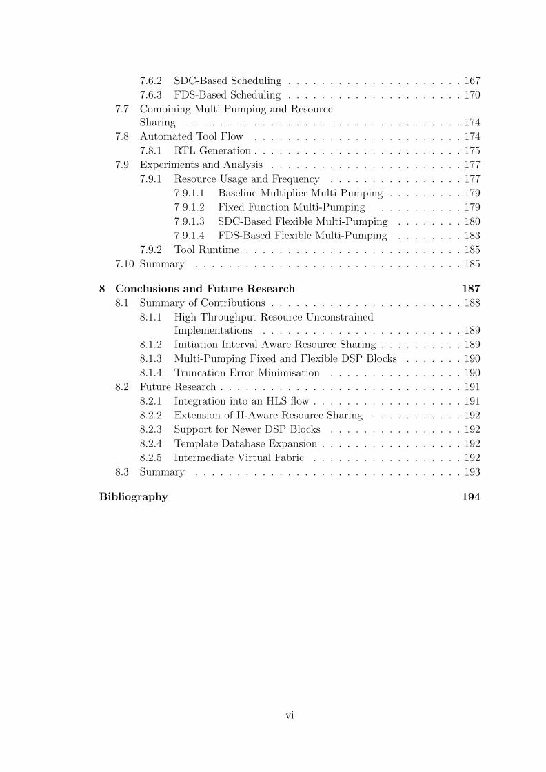
7.6.2 SDC-Based Scheduling . . . . . . . . . . . . . . . . . . . . . 167
7.6.3 FDS-Based Scheduling . . . . . . . . . . . . . . . . . . . . . 170
7.7 Combining Multi-Pumping and ResourceSharing . . . . . . . . . . . . . . . . . . . . . . . . . . . . . . . . . 174
7.8 Automated Tool Flow . . . . . . . . . . . . . . . . . . . . . . . . . 174
7.8.1 RTL Generation . . . . . . . . . . . . . . . . . . . . . . . . . 175
7.9 Experiments and Analysis . . . . . . . . . . . . . . . . . . . . . . . 177
7.9.1 Resource Usage and Frequency . . . . . . . . . . . . . . . . 177
7.9.1.1 Baseline Multiplier Multi-Pumping . . . . . . . . . 179
7.9.1.2 Fixed Function Multi-Pumping . . . . . . . . . . . 179
7.9.1.3 SDC-Based Flexible Multi-Pumping . . . . . . . . 180
7.9.1.4 FDS-Based Flexible Multi-Pumping . . . . . . . . 183
7.9.2 Tool Runtime . . . . . . . . . . . . . . . . . . . . . . . . . . 185
7.10 Summary . . . . . . . . . . . . . . . . . . . . . . . . . . . . . . . . 185
8 Conclusions and Future Research 187
8.1 Summary of Contributions . . . . . . . . . . . . . . . . . . . . . . . 188
8.1.1 High-Throughput Resource UnconstrainedImplementations . . . . . . . . . . . . . . . . . . . . . . . . 189
8.1.2 Initiation Interval Aware Resource Sharing . . . . . . . . . . 189
8.1.3 Multi-Pumping Fixed and Flexible DSP Blocks . . . . . . . 190
8.1.4 Truncation Error Minimisation . . . . . . . . . . . . . . . . 190
8.2 Future Research . . . . . . . . . . . . . . . . . . . . . . . . . . . . . 191
8.2.1 Integration into an HLS flow . . . . . . . . . . . . . . . . . . 191
8.2.2 Extension of II-Aware Resource Sharing . . . . . . . . . . . 192
8.2.3 Support for Newer DSP Blocks . . . . . . . . . . . . . . . . 192
8.2.4 Template Database Expansion . . . . . . . . . . . . . . . . . 192
8.2.5 Intermediate Virtual Fabric . . . . . . . . . . . . . . . . . . 192
8.3 Summary . . . . . . . . . . . . . . . . . . . . . . . . . . . . . . . . 193
Bibliography 194
vi

List of Figures
2.1 Xilinx FPGA architecture. . . . . . . . . . . . . . . . . . . . . . . . 13
2.2 Configurable Logic Block (CLB). . . . . . . . . . . . . . . . . . . . 14
2.3 FPGA design flow. . . . . . . . . . . . . . . . . . . . . . . . . . . . 17
2.4 (a) Undirected graph (b) Undirected graph with loop (c) Directedgraph (d) Directed graph with loop. . . . . . . . . . . . . . . . . . . 19
2.5 Complete undirected graph. . . . . . . . . . . . . . . . . . . . . . . 20
2.6 Directed graph with cycle. . . . . . . . . . . . . . . . . . . . . . . . 21
2.7 A simple dataflow graph. . . . . . . . . . . . . . . . . . . . . . . . . 22
2.8 Directed acyclic graph. . . . . . . . . . . . . . . . . . . . . . . . . . 23
2.9 Technology mapping for 3-LUT. . . . . . . . . . . . . . . . . . . . . 28
3.1 Basic structure of the DSP48E1 primitive. . . . . . . . . . . . . . . 59
3.2 Detailed block diagram of the DSP48E1 primitive. . . . . . . . . . . 60
3.3 Dataflow graphs for expressions (a) A×B (b) (D+A)×B (c) (D−A)×B (d) C + (A×B) (e) C + ((D+A)×B) (f) out = out+ (D+A)×B. . . . . . . . . . . . . . . . . . . . . . . . . . . . . . . . . . . 69
3.4 Maximum frequency of a DSP48E1 for different configurations, withvarying number of pipeline stages. (PA=Pre-adder). . . . . . . . . . 69
3.5 Setup for DSP48E1 characterisation. . . . . . . . . . . . . . . . . . 70
3.6 DSP48E1 configuration word. . . . . . . . . . . . . . . . . . . . . . 71
3.7 Timing diagram for DSP block with dynamic programmability. . . . 72
3.8 Implementation of Equation 3.1 (a) without using dynamic pro-grammability (b) using dynamic programmability. . . . . . . . . . . 73
3.9 Timing diagram for case study example. . . . . . . . . . . . . . . . 74
4.1 Basic structure of the DSP48E1 primitive. . . . . . . . . . . . . . . 77
4.2 Dataflow graph for expression 16x5 − 20x3 + 5x. . . . . . . . . . . . 82
4.3 Sample Verilog code for Comb. . . . . . . . . . . . . . . . . . . . . 85
4.4 Sample Verilog code for DSPRTL. . . . . . . . . . . . . . . . . . . . 87
4.5 Dataflow through the DSP48E1 primitive. . . . . . . . . . . . . . . 88
4.6 Tool flow for exploring DSP block mapping. . . . . . . . . . . . . . 94
4.7 config file format. . . . . . . . . . . . . . . . . . . . . . . . . . . . . 95
4.8 Resource usage and maximum frequency for 18 benchmarks usingthe different mapping techniques. . . . . . . . . . . . . . . . . . . . 102
4.9 DSP48E1 primitive sub-block utilisation. . . . . . . . . . . . . . . . 103
4.10 Frequency Area trade-off, normalised against HLS. . . . . . . . . . 104
vii

4.11 Segmented dataflow graph for Color Saturation Correction. . . . . . 107
5.1 Example Gappa script for expression x(4x2(4x2 − 0.625) + 0.625). . 113
5.2 Tool flow for DSP block mapping with error minimisation. . . . . . 116
5.3 Area and Frequency trade-off for error minimisation, normalisedagainst implementation without error minimisation. (R: inputsrange; P: inputs precision) . . . . . . . . . . . . . . . . . . . . . . . 121
6.1 Dataflow graph of case study example. . . . . . . . . . . . . . . . . 133
6.2 Resource sharing design architecture. . . . . . . . . . . . . . . . . . 134
6.3 Timing diagram for TRS with #DSP = 3 (I: Inputs set; O: Outputsset). . . . . . . . . . . . . . . . . . . . . . . . . . . . . . . . . . . . 135
6.4 Timing diagram for IRS with II = 6 (I: Inputs set; O: Outputs set). 139
6.5 Tool flow for resource sharing implementations. . . . . . . . . . . . 141
6.6 DSP block and LUT usage tradeoff with varying extent of resourcesharing. 196 is ratio of available LUTs to DSP blocks available onVirtex 6 XC6VLX240T. . . . . . . . . . . . . . . . . . . . . . . . . 145
6.7 Resource sharing and maximum frequency trade-off. . . . . . . . . . 146
6.8 Frequency and Area tradeoff for constraints on number of DSPsvarying from 5 to 1, normalized with constraint of 5 DSPs. . . . . . 148
6.9 Throughput improvements with the increase in DSP block usage forbenchmark ARF. Vertical line presents the maximum throughputimplementation using TRS. . . . . . . . . . . . . . . . . . . . . . . 148
6.10 Tradeoff between increase in DSP blocks usage and throughputimprovement. Throughput values are normalised with maximumthroughput achieved using TRS. . . . . . . . . . . . . . . . . . . . . 149
6.11 Total number of DSP blocks and number of different DSP configu-rations. . . . . . . . . . . . . . . . . . . . . . . . . . . . . . . . . . . 150
7.1 Plot of reported frequencies on Xilinx Virtex devices for over 350designs published in FPGA conferences. Also shown are the DSPblock maximum frequency and half that value as would be requiredfor multi-pumping. . . . . . . . . . . . . . . . . . . . . . . . . . . . 155
7.2 Logical code for three case study scenarios (ignoring timing). . . . . 160
7.3 (a) Input dataflow graph (b) Traditional resource sharing (Numberof multipliers available = 2) (c) Multi-pumping multipliers only (d)Multi-pumping same configuration DSP blocks (e) Multi-pumpingDSP blocks with dynamic programmability. . . . . . . . . . . . . . 162
7.4 Clock follower circuit diagram. . . . . . . . . . . . . . . . . . . . . . 164
7.5 Multi-pumped DSP block (mpDSP) architecture. . . . . . . . . . . 165
7.6 DSP48E1-LUT usage trade-off for SDC-based scheduling. . . . . . . 182
8.1 Tool flow overview including all the proposed techniques. . . . . . . 188
viii

List of Tables
3.1 DSP blocks evolution on Xilinx Virtex devices. . . . . . . . . . . . . 58
3.2 DSP48E1 Attributes. . . . . . . . . . . . . . . . . . . . . . . . . . . 61
3.3 INMODE[3:0] configurations. . . . . . . . . . . . . . . . . . . . . . 64
3.4 INMODE[4] configurations. . . . . . . . . . . . . . . . . . . . . . . 64
3.5 OPMODE control bits to select X Multiplexer output. . . . . . . . 65
3.6 OPMODE control bits to select Y Multiplexer output. . . . . . . . 65
3.7 OPMODE control bits to select Z Multiplexer output. . . . . . . . . 65
3.8 ALUMODE configurations. . . . . . . . . . . . . . . . . . . . . . . 66
3.9 CARRYINSEL encoding. . . . . . . . . . . . . . . . . . . . . . . . . 66
3.10 Template Database. . . . . . . . . . . . . . . . . . . . . . . . . . . . 68
4.1 Graph nodes I/O and operations. . . . . . . . . . . . . . . . . . . . 99
4.2 Run time (in ms) for Inst using greedy and improved segmentation 100
4.3 Pipeline depth for Pipe and other approaches. . . . . . . . . . . . . 105
4.4 Resource usage and frequency for Color Saturation Correction casestudy. . . . . . . . . . . . . . . . . . . . . . . . . . . . . . . . . . . 108
5.1 Run time (in ms) for Inst without and with error minimisation. . . 118
5.2 Error reduction using Gappa based error minimisation. . . . . . . . 120
6.1 Schedule length and II achieved for different TRS constraints. . . . 134
6.2 Schedule length and number of DSP used for different IRS constraints.139
6.3 Graph nodes I/O and operations. . . . . . . . . . . . . . . . . . . . 144
6.4 Initiation interval (II) for different DSP block constraint. . . . . . . 147
6.5 Run time (in ms). DSP constraint for TRS = 3. II constraint forIRS = 6. . . . . . . . . . . . . . . . . . . . . . . . . . . . . . . . . . 151
7.1 Graph nodes I/O and operations. . . . . . . . . . . . . . . . . . . . 176
7.2 Resource usage and maximum frequency for mpDSP block. (PA:Pre-adder sub-block; Freq in MHz) . . . . . . . . . . . . . . . . . . 177
7.3 Geometric mean of resource usage and maximum frequency acrossall implementations, using brute-force, SDC-based, and FDS-basedscheduling techniques for 13 benchmarks. Freq in MHz. . . . . . . . 180
7.4 Resource usage and maximum frequency across all implementations,using SDC-based scheduling. Freq in MHz. . . . . . . . . . . . . . . 181
7.5 Resource usage and maximum frequency across all implementations,using FDS-based scheduling. Freq in MHz. . . . . . . . . . . . . . . 183
ix

7.6 Geometric mean of resource usage and maximum frequency acrossall implementations, using SDC-based and FDS-based schedulingtechniques. Freq in MHz. . . . . . . . . . . . . . . . . . . . . . . . . 184
7.7 Run time for generating RTL from C (ms) for all scenarios. . . . . . 185
x

List of Abbreviations
AAA Adequation Algorithm Architecture
AIG AND-Inverter Graph
ALAP As Late As Possible
ALU Arithmetic Logic Unit
ASAP As Soon As Possible
ASIC Application Specific Integrated Circuit
AST Abstract Syntax Tree
AXI Advanced eXtensible Interface
BLIF Berkeley Logic Intermediate Format
BRAM Block Random Access Memory
CDFG Control and Data Flow Graph
CFG Control Flow Graph
CGRA Coarse-Grained Reconfigurable Architecture
CHiMPS Compiling High-level Languages into Massively Pipelined Systems
CLB Configurable Logic Block
COTS Commercial Off The Shelf
CPU Central Processing Unit
CTL CHiMPS Target Language
DAG Directed Acyclic Graph
xi

DDFG DSP Data Flow Graph
DDR Double Data Rate
DFG Data Flow Graph
DSP Digital Signal Processing
FDS Force-directed Scheduling
FFC Fanout-Free Cone
FIFO First In First Out
FloPoCo Floating Point Cores
FLUT Fracturable Look-Up Table
FPGA Field Programmable Gate Array
FSM Finite State Machine
GDL Graph Description Language
HDL Hardware Description Language
HLL High-Level Language
HLS High-level Synthesis
HPC High-Performance Computing
I/O Input/Output
II Initiation interval
ILP Integer Linear Programming
IMS Iterative Modulo Scheduling
IOB Input/Output Block
IR Intermediate Representation
IRS Improved Resource Sharing
LP Linear Programming
LSB Least Significant Bit
xii

LUT Look-Up Table
MFFS Maximum Fanout Free Subgraph
mpDDFG Multi-pumped DSP Data Flow Graph
mpDSP Multi-pumped Digital Signal Processing
MSB Most Significant Bit
NRE Non-recurring Engineering
PA Pre-adder
PACT Power Aware Architecture and Compilation Techniques
PI Primary Input
PO Primary Output
RAM Random Access Memory
RMS Root Mean Square
ROM Read Only Memory
RTL Register Transfer Level
SDC System of Difference Constraints
SIMD Single Instruction Multiple Data
SpC Synthesis of Pointers in C
ST Schedule Time
SUIF Stanford University Intermediate Format
TD Transition Density
TGFF Task Graphs For Free
Torc Tools for Open Reconfigurable Computing
TRS Traditional Resource Sharing
VCG Visualization of Compiler Graphs
VHDL VHSIC Hardware Description Language
xiii

VPR Versatile Place and Route
VTR Verilog-to-Routing
XDL Xilinx Design Language
xiv

1Introduction
Field Programmable Gate Arrays (FPGAs) are pre-fabricated silicon devices that
can be electrically programmed to become almost any kind of digital circuit or
system [1]. FPGAs are built around a matrix of configurable logic blocks (CLBs)
connected via programmable interconnect [2]. Any design that fits within the
available resources can be mapped to the FPGA by setting these programmable
resources to implement the desired circuit. Changes can be made and a new con-
figuration loaded should requirements change. This feature distinguishes FPGAs
from Application Specific Integrated Circuits (ASICs), which are manufactured
for specific fixed tasks and cannot be changed.
The evolution of FPGAs has dramatically changed the process of designing digital
systems. FPGAs first appeared in the 1980s, and they have evolved significantly
in the last couple of decades. Some of the key advantages of FPGAs over other
1

1 Introduction 2
available implementation platforms includes reprogrammability as compared to
ASICs, lower power consumption than multicore processors and GPUs, capability
in real-time execution without depending on operating systems, caches, or other
non-deterministic latency sources, and most importantly, high spatial parallelism
which can be used to significantly accelerate complex algorithms.
Initially, although FPGAs provided programmable logic and routing interconnect;
they were large, slow, and consumed significantly more power compared to ASICs.
Because of these limitations, FPGAs were mainly used for small glue logic, or
for prototyping designs which would then be implemented in ASICs. Due to the
advancements in process technologies, the evolution in FPGA architecture, and the
rising cost and complexity of ASIC design, the gap between FPGAs and ASICs is
shrinking with each generation of FPGAs. FPGAs are typically two manufacturing
process nodes ahead of affordable ASIC processes. As a result, FPGAs are now
used for implementing large complex circuits, and are being deployed in production
systems, replacing ASICs in areas like networking, where algorithms and protocols
change fast and it is not feasible to implement them on ASICs. The high non-
recurring engineering (NRE) costs, high manufacturing costs, and long design time
for ASICs are also motivating designers to use more FPGAs, for which turn-around
time is much reduced.
As FPGAs have gained wider adoption, vendors have sought to improve the ef-
ficiency of implementing a wide range of designs. One trend has been to intro-
duce ASIC-like embedded hard blocks that make common functions more efficient.
These embedded blocks are varied, and include DSP blocks, Block RAMs, embed-
ded processors and more. These are spread around the FPGA for efficient place-
ment and routing. With these embedded blocks, FPGAs have found applications
in many different areas like digital signal processing, image processing, software de-
fined radio, automotive systems, high-performance computing, security, and many
more.
Though FPGAs are challenging ASICs due to the reasons discussed above, adop-
tion of FPGAs for systems which are traditionally implemented using software

1 Introduction 3
on generic computing platforms is somewhat lacking. The performance of many
applications can be improved manyfold compared to software implementations.
However, these benefits are not being realised in general purpose computing sce-
narios. Two primary reasons for this are:
• Implementation Complexity
• High compilation time
Implementing a system on FPGAs requires an understanding of how hardware
works. High-level languages (HLLs) like C/C++ used for software development are
sequential and hardware-description languages (HDLs) used for describing hard-
ware are essentially structural and require an understanding of low level hardware
details. Additionally, as many systems are already implemented in HLLs, trans-
lating these to hardware can be a very time consuming task. As FPGAs become
more functional and complex, highly skilled hardware engineers are required to effi-
ciently utilise all the capabilities available. Another obstacle causing slow adoption
of FPGAs is high compilation time. Software engineers are accustomed to compile
times of a few seconds to a few hours for large systems. Hardware implementation,
on the other hand, is very time consuming, especially the backend flow that does
the final mapping to the target FPGA. For large designs, this can be many hours
or even days, significantly affecting design productivity. Furthermore, many state-
of-the-art compilers for software compile incrementally, meaning small changes do
not consume a significant amount of time to test. FPGA design tools are only
just starting to address this issue through hierarchical compilation. For the most
part, small changes still require significant re-implementation in the tools, making
design iteration slow.
Researchers in the area of reconfigurable computing have been working to address
all these obstacles. For implementation complexity, a large body of work has fo-
cused on high-level synthesis (HLS). The idea of HLS is to allow designs to be
described using higher level languages, in many case, the same as those used for

1 Introduction 4
software programming. This allows software programmers to easily port appli-
cations to hardware platforms. The higher abstraction level hides some of the
complexities of design implementation at a lower level, in exchange for sacrificing
control over individual elements and a variable performance loss in some cases.
HLS tools takes a design description in HLLs like C/C++ and generate synthesis-
able Verilog/VHDL code, which can be mapped on to FPGAs using vendor tools.
This allows the designers to implement complex system quickly and easily. The
evolution of input languages for hardware design has been similar to that of the
software domain. Initially, machine code was the only way to program a com-
puter. As computers became more functional and complex, assembly languages
were developed. Assembly languages were platform dependent, inflexible, and not
portable. This led to the development of HLLs and associated compilers. Systems
could be implemented once and run on different platforms using the corresponding
compilers, which translated the HLL code to low-level assembly or machine code.
Hardware design has also followed a similar pattern, evolving from hand-coding
systems at the transistor level, to sophisticated HLS tools. Following Moore’s Law,
the size of ICs approximately doubled every 18 months, so has the complexity of
systems, and designing and testing at a low-level became infeasible. This led to
the automation of the design and test processes. Tools were developed to perform
cycle-accurate simulations, automated synthesis and place-and-route, for end-to-
end development. The development of HDLs, such as Verilog and VHDL played
a crucial role, enabling wider adoption of these automated tools.
In the context of FPGA development, although most design development is still
done at the HDL level, HLS tools have gained momentum in the past decade. Us-
ing HLS tools, the designer implements an untimed design in an HLL and different
design possibilities can be explored. From the same high-level description, the de-
signer can perform design space exploration by tweaking configurations, to find an
implementation best suited for a set of given constraints. Mainstream HLS tools
available for FPGA design include Xilinx Vivado HLS [3] for Xilinx FPGAs, and
an open-source academic tool, LegUp [4], which is mainly optimised for Altera FP-
GAs. In addition to these, other major HLS tools commercially available include

1 Introduction 5
BlueSpec [5], MATLAB, Synphony C from Synopsys [6], Cadence’s C-to-Silicon,
and Catapult C from Mentor Graphics [7].
Vivado HLS requires the user to follow guidelines on coding style to effectively
translate the HLL code to RTL. It supports C, C++, and SystemC input lan-
guages. Data types in generic C/C++ are fixed at 8, 16, 32, or 64 bit wordlengths.
Using these data types can result in unoptimised hardware, by implementing wide
operations where it is not required. Vivado HLS supports arbitrary precision data
types for both C and C++, which can be exploited to specify the exact wordlength
of the signals in HLL code. Hardware generation is guided by directives, which
can be used to further optimise the hardware generated by the tool. Effective use
of directives requires knowledge of the hardware. LegUp accepts ANSI C code,
without the need for directives or special keywords. The synthesis flow is driven
by a set of TCL scripts and Makefiles. This results in less control over the hard-
ware generated, but makes it easier to use for a developer who does not have an
in-depth understanding of hardware design.
HLS tools can significantly improve development times through abstraction, how-
ever they are seen as an additional step in the design flow, generating RTL code
which must then go through the backend implementation flow which is very time
consuming. Though there are research efforts attempting to address this problem,
it is a challenging one as the designs and devices continue to grow in size [8, 9]. An-
other approach that has been pursued to overcome these compilation times is vir-
tualising the architecture. Overlay architectures or intermediate fabrics are more
coarse grained architectures built on top of the FPGA that can be programmed
through customised flows with much smaller configuration overheads. Coarse-
grained reconfigurable architectures (CGRAs) are implemented on an FPGA, of-
fering a large number of processing elements and a somewhat flexible interconnec-
tion fabric for whole words. By raising the level of the target architecture, the
configuration space is significantly reduced. Different applications can be mapped
onto virtual architectures, with fast compilation since there is no need for the time
consuming backend flow with each new application. However, overlays typically

1 Introduction 6
entail significant overheads in terms of both area and performance compared to
custom designs.
This thesis explores how the detailed understanding of low-level architecture can
benefit high level design flows, offering comparable performance to custom design
but with high level design definitions.
1.1 Motivation
When designing systems on FPGAs, we wish to maximise the performance and
efficiency of our circuits. This means making best use of all types of resources avail-
able to us. Since designers generally write behavioral code that is then mapped by
the implementation tools, performance and efficiency are controlled for the most
part by the capabilities of these tools. As architectures evolve with more complex
resources, the tools have to work harder to make full use of them. As FPGAs find
use in a wider range of domains, from wireless systems [10, 11], through connected
and autonomous vehicles [12, 13], to general cloud computing [14], the drive to-
wards high-level design will become stronger. While HLS tools allow higher level
design description, the final mapping remains the purview of the backend tools. If
these cannot map general RTL code to exploit the capabilities of the architecture,
the resulting implementations can be inefficient. More importantly, information
contained in the high level design description may be helpful in achieving this, but
be lost in the translation to generic RTL.
A primary example is the DSP blocks in modern Xilinx FPGAs, which are highly
configurable, but generally underutilised in the vendor flow. Targeted applications
like signal processing and digital image processing can make acceptable use of
DSP blocks, but given their extensive capabilities, even these are sometimes not
maximised, and more general applications suffer even more. It has been observed
that synthesising standard RTL code and relying on vendor synthesis tools to
correctly infer the use of DSP blocks results in sub-optimal implementations [15].
DSP blocks available on modern FPGAs can be configured in many different ways,

1 Introduction 7
but current vendor tools do not explore all these possibilities while mapping to
them. In addition to all the computational capabilities, DSP blocks support run-
time reconfigurability, which allows a single DSP block to be used as a different
computational block in every clock cycle. This can be exploited for designs with
constraints on resources or for designs with low-throughput requirement. In this
thesis, the DSP block is taken as a case study, demonstrating the importance of
architecture awareness in high level design flows. It is shown that information
about the low-level architectural capabilities of such resources can be used to
make decisions at higher levels, which results in significant improvements in the
final implementations.
1.2 Objectives
The key question that is to be answered is whether high level design can exploit
the significant capabilities of evolving hard blocks like the DSP blocks in Xilinx
FPGAs while preserving high abstraction levels.
We first set out to demonstrate that standard vendor tools do not exploit the full
potential of modern DSP blocks. We show that even when designed at RTL level,
datapaths that do not exactly match those of the DSP block result in sub-optimal
implementations. Furthermore, we show that the dynamic programmability of the
DSP blocks is ignored by the tools in almost all situations.
We then show that by considering the capabilities and structure of the DSP block,
it is indeed possible to build tools that output implementations of comparable
performance and efficiency as hand-optimised implementations, and that exploit
capabilities of DSP block fully to support high throughput, and resource shared
implementations.
The main objectives of this thesis are to:
1. Quantify the losses incurred when designing at higher levels of abstraction
without regard for low-level architecture.

1 Introduction 8
2. Develop an automated tool to generate multiple implementations from high
level descriptions, that demonstrate the techniques developed with compar-
ison to standard approaches.
3. Devise an automated flow that takes high level descriptions of computational
kernels and produces implementations that approach the theoretical limits
of the DSP block.
4. Show how dynamic reconfigurability of the DSP blocks can be exploited to
implement resource constrained implementations.
1.3 Contributions
The main contributions of this thesis include tools, techniques, and algorithms for
efficient implementation of computationally intensive mathematical expressions
onto the DSP blocks in modern Xilinx FPGAs.
These contributions include:
1. A detailed study of high-level synthesis approaches and tools, including tech-
niques for technology mapping and placement and routing which are integral
parts of implementation of designs on FPGAs.
2. A thorough investigation of the efficiency of mapping to DSP blocks, showing
that there is a discrepancy between hand-coded instantiation and inference.
3. An automated design tool that takes high level descriptions of computa-
tional dataflow graphs and generates traditional implementations, including
pipelined RTL and Vivado HLS, alongside the proposed approaches for fair
comparison.
4. Techniques for resource constrained implementations that take advantage
of the DSP block’s dynamic programmability, overcoming the long latency
of the block to offer improved initiation intervals compared to traditional
approaches.

1 Introduction 9
5. Techniques for multi-pumping flexible DSP blocks demonstrating that this
flexibility offers a significant advantage over fixed configurations, leading to
more efficient implementations.
6. An approach for minimising error due to truncation when building graphs
out of DSP blocks, applicable with all the above approaches.
1.4 Thesis Organisation
The remainder of this thesis is organised as follows. Chapter 2 presents a de-
tailed background on Xilinx FPGA architecture, building blocks, and the design
flow. It then reviews work done on technology mapping and place and route
techniques. It explores approaches and tools proposed in the area of high-level
synthesis and resource sharing techniques in the context of high-level synthesis.
Chapter 3 presents the detailed architecture of the DSP48E1 hard block available
on modern Xilinx FPGAs and discusses how to utilise its different functionalities
including dynamic reconfigurability. Chapter 4 introduces an automated tool flow
for mapping arithmetic functions onto DSP blocks, exploiting their capabilities.
The tool also generates generic RTL implementations for comparison. In Chap-
ter 5, we present a technique for minimising error when mapping graphs to DSP
blocks, taking into account their limited wordlengths. Chapter 6 discusses schedul-
ing and implementation techniques for resource sharing. We present an initiation
interval (II) driven resource sharing technique that offers resource savings while
improving II compared to traditional methods. In Chapter 7, we demonstrate how
multi-pumping of the DSP block can offer significant resource savings. We show
that incorporating all DSP block sub-blocks offers improved savings over multi-
pumping of just multipliers. We then show that dynamic programmability offers
further improvements, and propose two scheduling approaches for this. Finally,
Chapter 8 concludes the work presented in this thesis and outlines future research
directions.

1 Introduction 10
1.5 Publications
The work presented in this thesis has been submitted or published in a number of
conference and journal papers.
1. Bajaj Ronak and Suhaib A. Fahmy, Evaluating the Efficiency of DSP Block
Synthesis Inference from Flow Graphs in Proceedings of the International
Conference on Field Programmable Logic and Applications (FPL), Oslo,
Norway, 2012, pp. 727-730. [15]
2. Bajaj Ronak and Suhaib A. Fahmy, Experiments in Mapping Expressions
to DSP Blocks, poster in Proceedings of the IEEE Symposium on Field
programmable Custom Computing Machines (FCCM), Boston, MA, May
2014, pp 101. [16]
3. Bajaj Ronak and Suhaib A. Fahmy, Efficient Mapping of Mathematical Ex-
pressions into DSP Blocks, in Proceedings of the International Conference
on Field Programmable Logic and Applications (FPL), Munich, Germany,
September 2014, pp. 1-4. [17]
4. Bajaj Ronak and Suhaib A. Fahmy, Minimising DSP Block Usage Through
Multi-Pumping, in Proceedings of the International Conference on Field Pro-
grammable Technology (FPT), Queenstown, New Zealand, December 2015,
pp. 184-187. [18]
5. Bajaj Ronak and Suhaib A. Fahmy, Mapping for Maximum Performance
on FPGA DSP Blocks in IEEE Transactions on Computer-Aided Design of
Integrated Circuits and Systems (TCAD), vol. 35, no. 4, pp. 573-585, April
2016. [19]
6. Bajaj Ronak and Suhaib A. Fahmy, Initiation Interval Aware Resource Shar-
ing for FPGA DSP Blocks, in Proceedings of IEEE Symposium on Field pro-
grammable Custom Computing Machines (FCCM), Washington, DC, May
2016. [20]

1 Introduction 11
7. Bajaj Ronak and Suhaib A. Fahmy, Improved Resource Sharing for FPGA
DSP Blocks, in Proceedings of the International Conference on Field Pro-
grammable Logic and Applications (FPL), Lausanne, Switzerland, Septem-
ber 2016. [21]
8. Bajaj Ronak and Suhaib A. Fahmy, Multi-pumping Flexible DSP Blocks for
Resource Reduction on Xilinx FPGAs, IEEE Transactions on Computer-
Aided Design of Integrated Circuits and Systems (TCAD) [under review].

2Background and Literature Review
In this chapter, we cover necessary background on FPGA architecture and the
design flow. We discuss some basic graph concepts and explain how computations
are represented using dataflow graphs. We talk about technology mapping, in
which patterns of computational nodes are discovered in dataflow graphs and
assigned to specific hardware resources, and how this is done in tools. We then
review various tool flows including academic and commercial tools for high level
synthesis.
2.1 Field Programmable Gate Array
Modern state-of-the-art FPGAs consist mainly of:
12
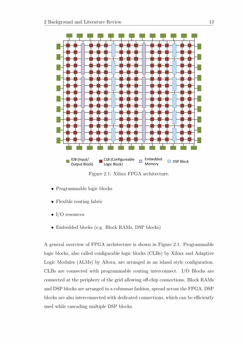
2 Background and Literature Review 13
IOB (Input/Output Block)
CLB (Configureable Logic Block)
Embedded Memory
DSP Block
Figure 2.1: Xilinx FPGA architecture.
• Programmable logic blocks
• Flexible routing fabric
• I/O resources
• Embedded blocks (e.g. Block RAMs, DSP blocks)
A general overview of FPGA architecture is shown in Figure 2.1. Programmable
logic blocks, also called configurable logic blocks (CLBs) by Xilinx and Adaptive
Logic Modules (ALMs) by Altera, are arranged in an island style configuration.
CLBs are connected with programmable routing interconnect. I/O Blocks are
connected at the periphery of the grid allowing off-chip connections. Block RAMs
and DSP blocks are arranged in a columnar fashion, spread across the FPGA. DSP
blocks are also interconnected with dedicated connections, which can be efficiently
used while cascading multiple DSP blocks.

2 Background and Literature Review 14
Slice(1)
Cin Cin
Cout
Slice(0)
Cout
CLB
Figure 2.2: Configurable Logic Block (CLB).
2.1.1 Programmable Logic Blocks
In recent FPGAs, CLBs consists of eight Lookup Tables (LUTs) divided into two
slices that can work independently. Each slice consists of four LUTs, storage ele-
ments (flip-flops), multiplexers, and carry logic. Multiplexers are used to combine
LUTs to generate different functions. The basic internal structure of a CLB is
shown in Figure 2.2. CLBs interface with the programmable logic interconnect
that consumes most of the area (as high as 80–90%) on FPGA.
2.1.2 Flexible Routing Fabric
The programmable routing interconnect consists of switch boxes and connection
boxes, that facilitate connections between all the compute primitives on the FPGA.
When a design is mapped to an FPGA, the tools must determine how to make
all the necessary connections between placed primitives, and this is generally the
most time-consuming process of the back-end implementation.
2.1.3 I/O Resources
I/O blocks are located at the periphery of the FPGA, connecting it to the outside
world. A key benefit of using FPGAs to implement digital systems is their support

2 Background and Literature Review 15
for a wide range of I/O standards including high speed serial standards. I/O blocks
are grouped into banks, each supporting a subset of standards.
2.1.4 Embedded Blocks
CLBs can be configured and combined to implement arbitrary arithmetic opera-
tions, and can also be used as small memories. However, for many such functions,
CLBs are slow and consume significant area. As more designers seek to use FPGAs
to implement computing systems, modern FPGAs have gained hard-wired ASIC
like embedded blocks which are optimised for specific functionalities. These include
Block RAMs (BRAMs) and DSPs. Functions mapped onto embedded blocks im-
prove performance and power consumption compared to the same functions built
out of CLBs. Complex functions built out of CLBs consume considerable routing
resources, increase the complexity of mapping and place and route, and adversely
affect timing. Embedded blocks also save the general purpose resources for use in
other parts of the design.
2.1.4.1 Block RAMs
BRAMs are dedicated, dual-port memory blocks with separate read/write ports,
which can store several kilobits of data. These can be configured as single or dual
port memories, with different port widths and serve as efficient on-chip memory,
which can be accessed in every clock cycle. BRAMs also support cascading, which
can be used to create a large memory block. The latest FPGAs support different
operating modes, allowing them to be used as FIFOs, register files, circular buffers,
and more.

2 Background and Literature Review 16
2.1.4.2 DSP Blocks
DSPs were initially introduced on FPGAs to improve the performance of com-
monly used operations in signal processing applications like multiply and multiply-
accumulate. However, over the generations, these blocks have evolved into highly
functional arithmetic blocks, which can perform many operations. In addition to
arithmetic operations, the latest DSP blocks support logical operations, shift op-
erations, pattern detection, magnitude comparison, etc. Similar to BRAMs, DSP
blocks can also be cascaded to implement operations wider than the port-widths
supported, with dedicated internal connections for efficient implementations. Mod-
ern DSP blocks are discussed in more detail in Chapter 3.
2.2 FPGA Design Flow
The process of implementing a design on an FPGA starts with describing the de-
sign in a HDL like Verilog or VHSIC Hardware Description Language (VHDL),
and ends with a stream of bits, which is loaded into the FPGA’s configuration
memory. The configuration memory controls all the low level features of the fab-
ric, determining the logic contents of the LUTs, how all primitives are connected,
and which features are used. As more and more complex systems are being im-
plemented on FPGAs, a significant amount of research effort is being focused on
how best to describe such systems at a higher level of abstraction to improve the
design and verification tasks. This includes research into tools that can convert
high-level languages like SystemC, C, and C++ into hardware. Normally these
tools take the design description in a high-level language and translate them into
synthesisable Verilog or VHDL code which is then processed through the steps of
the standard tool flow.
After describing the design in HDL, the first step is functional verification (simula-
tion) of the behavioral model of the design. The process of generating a bit-stream
from the HDL description can be divided into three major steps. These are:

2 Background and Literature Review 17
Simulation
Verilog Input Files Testbench
Functional Verification
Synthesis
Technology Mapping
Placement and RoutingTiming
Constraints
Bit-stream generation
Figure 2.3: FPGA design flow.
1. Synthesis
2. Technology Mapping
3. Placement and Routing
Figure 2.3 shows the design flow for FPGAs.
Synthesis transforms the input HDL to a hierarchical network of basic building
blocks, including LUTs for Boolean logic, flip-flops for synchronous components,
efficient basic circuits for arithmetic, and in modern tools, even to some device
specific hard blocks. Various technology-independent optimisation techniques are
applied on the generated network at this stage to minimise the number of logic
gates, which can reduce the total area and delay of the final implementation of the
design. The output of a synthesis stage is a network of Boolean logic elements,
flip-flops, basic circuits, hard blocks, and wiring connections between them.

2 Background and Literature Review 18
Given a set of library cells, technology mapping is generally defined as mapping
the network to the library cells such that each node is assigned to one type of
resource. In the case of FPGAs, this library is composed of k-LUTs, flip-flops,
basic arithmetic circuits like adders, and advanced hard blocks. Therefore, the
technology mapping for FPGAs consists of segmenting the Boolean network into
set of nodes that can be mapped to one of these basic building blocks.
Placement is the process of determining which specific logic blocks on FPGA
should be used for a particular instance of a logic block in the network. Place-
ment can be done with different objectives. Wire length driven placement places
connected blocks as close as possible to each other, Routability driven placement
tries to balance the wiring density across the FPGA, and Timing driven placement
tries to place blocks in such a way that delay can be minimised.
Routing is the process of configuring the interconnect so that the placed logic
blocks are properly connected. This stage tries to connect all logic blocks in such
a way that routing delay can be minimised. This is a challenging problem, and
may require iterations with re-placement of some blocks.
After successful execution of all these steps, a bit-stream can be generated. This is
a sequence of configuration words that captures the configuration of all necessary
blocks and the routing configuration for all used wires. Loaded into the config-
uration memory of the FPGA, this creates the circuit originally described in the
HDL.
2.3 Graph Computations
A graph is an ordered pair G = (V,E), comprising a non-empty set V of vertices
(or nodes) and a set E of edges, which is a binary relation on the set of vertices
V [22]. Graphs can be broadly divided into two categories:
1. Undirected Graphs

2 Background and Literature Review 19
v1
v2 v3
v4
e1 = {v
1,v2}
e5 = {v
3,v4}
e2 = {v1,v3}e3 = {v1
,v4}e4 = {v2,v4}
(a)
v1
v2 v3
v4
e1 = {v
1,v2}
e5 = {v
3,v4}
e2 = {v1,v3}e3 = {v1
,v4}e4 = {v2,v4}
e6 =
{v2
,v2
}
(b)
v1
v2 v3
v4
e1 = (v
1,v2)
e5 = (v
3,v4)
e2 = (v1,v3)e3 = (v1
,v4)e4 = (v2,v4)
(c)
v1
v2 v3
v4
e1 = (v
1,v2)
e5 = (v
3,v4)
e2 = (v1,v3)e3 = (v1
,v4)e4 = (v2,v4)
e6 =
(v2
,v2
)
(d)
Figure 2.4: (a) Undirected graph (b) Undirected graph with loop (c) Di-rected graph (d) Directed graph with loop.
2. Directed Graphs
In undirected graphs, edges are unordered pairs of vertices denoted by {vi, vj},where viεV and vjεV . In a directed graph (or digraph), the edges are ordered
pairs of vertices. An edge directed from vertex vi to vj is denoted by (vi, vj).
Example undirected and directed graphs are shown in Figure 2.4a and Figure 2.4c
respectively.
2.3.1 Undirected Graphs
The edges in an undirected graph are unordered pairs of vertices. The degree of
a vertex in an undirected graph is the number of edges connected to the vertex.
The degrees of vertices v1, v2, v3, and v4 in Figure 2.4a are 3, 2, 2, 3 respectively.
A vertex vi is said to be adjacent to another vertex vj if there is an edge {vi, vj}connecting the two vertices. In Figure 2.4a, vertices v2, v3, v4 are all adjacent to

2 Background and Literature Review 20
v1
v2 v3
v4
e1 = {v
1,v2}
e5 = {v
3,v4}
e2 = {v1,v3}
e3 = {v1
,v4}
e4 = {v2,v4}
e6 = {v2,v3}
Figure 2.5: Complete undirected graph.
vertex v1. An edge which starts and ends on the same vertex is called a loop.
Undirected and directed graph examples with loops are shown in Figure 2.4b and
Figure 2.4d respectively. Edge e6 in both graphs makes a loop at vertex v2.
Graphs without any loops and no two edges connecting the same set of vertices
are called simple graphs.
A graph is called a complete graph when each vertex is connected to all other
vertices of the graph. A complete four node graph is shown in Figure 2.5.
A subgraph of a graph G(V,E) is a graph whose vertex and edge sets are subsets
of sets V and E respectively.
2.3.2 Directed Graphs
The definitions discussed above for undirected graphs can be extended for directed
graphs, with additional terms specific to directed graphs.
For any directed edge (vi, vj), vertex vj is called the head of the edge and vertex
vi is called the tail. The degree of a vertex is the total number of edges it is
connected to. The number of edges for a vertex where it is the head is called the
indegree of the vertex, and outdegree is the number of edges where it is the
tail.
A walk for a directed graph is an alternating sequence of vertices and edges with
the same direction. A cycle is a walk for which the start and end vertices are the

2 Background and Literature Review 21
v1
v2 v3
v4
e1 = (v
1,v2)
e5 = (v
3,v4)
e2 = (v1,v3)e3 = (v1
,v4)e4 = (v2,v4)
Figure 2.6: Directed graph with cycle.
same. An example directed graph with a cycle is shown in Figure 2.6. A walk
from v1 to e1 to v2 to e4 to v4 to e3 to v1 is a cycle.
A graph with no cycles is called an acyclic graph. Directed graphs without any
cycles are called Directed Acyclic Graphs (DAGs). A path in a graph is a walk
with different vertices and edges. For a path in a DFG, a vertex vi is called the
successor of vertex vj if vi is head of a path whose tail is vj. Similarly, vi is called
a predecessor of vj if vi is tail of path with head vj.
Many algorithms and mathematical expressions can be represented as DFGs where
each node represents some function or expression. Additionally, graphs are used
as intermediate representations in the implementation of circuits. An example
dataflow graph of the expression (a × b + c × d) is shown in Figure 2.7. DFGs
are widely used to represent electronic circuits and their transformed Boolean
networks. Circuits are modelled as blocks performing different operations and
connected to each other. Each block doing its computations can be represented as
a node and connections between these different blocks transmitting data can be
represented as the edges of the graph. Similarly, in the case of Boolean networks,
each node represents a gate and edges connect different gates. The indegree and
outdegree of a node in a graph can be interpreted as the fan-in and fan-out of
gates.
For large systems, a node can represent a functional block, and the graph can
represent how these blocks communicate to comprise the full system. In these

2 Background and Literature Review 22
X
+
X
a b c d
v1 v2
v3
e1 e2
Figure 2.7: A simple dataflow graph.
representations, a node can perform multiple functions and the graph can be
understood as a hierarchical graph, where each node can be a complex circuit
which can be then represented as a graph or set of graphs when we go down the
hierarchy.
2.4 Technology Mapping
Technology mapping is the process of transforming a technology-independent de-
scription of a logic circuit to a technology specific description. The input to tech-
nology mapping algorithms are directed acyclic graphs (DAGs), which are Boolean
networks generated after technology-independent optimisations.
2.4.1 Preliminaries and Basic Definitions
A Boolean network is represented as a Directed Acyclic Graph (DAG) (as discussed
in Section 2.3). An example Boolean network is shown in Figure 2.8.
• Each node represents a logic gate (u,v,w in Figure 2.8)
• Directed edge (u,v) exists if the output of gate u is an input of gate v
• PI are the primary inputs of the network. PI nodes do not have any incoming
edge.
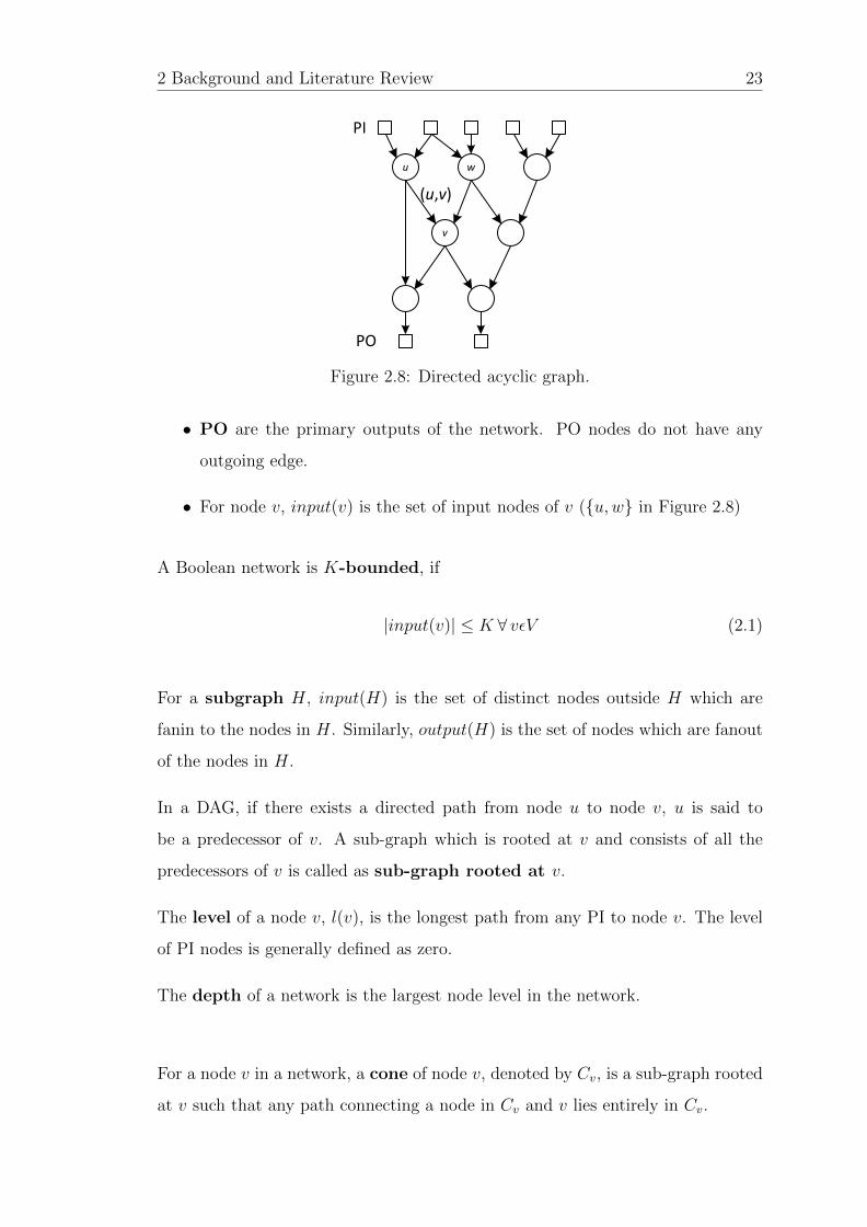
2 Background and Literature Review 23
u w
v
PO
PI
(u,v)
Figure 2.8: Directed acyclic graph.
• PO are the primary outputs of the network. PO nodes do not have any
outgoing edge.
• For node v, input(v) is the set of input nodes of v ({u,w} in Figure 2.8)
A Boolean network is K-bounded, if
|input(v)| ≤ K ∀ vεV (2.1)
For a subgraph H, input(H) is the set of distinct nodes outside H which are
fanin to the nodes in H. Similarly, output(H) is the set of nodes which are fanout
of the nodes in H.
In a DAG, if there exists a directed path from node u to node v, u is said to
be a predecessor of v. A sub-graph which is rooted at v and consists of all the
predecessors of v is called as sub-graph rooted at v.
The level of a node v, l(v), is the longest path from any PI to node v. The level
of PI nodes is generally defined as zero.
The depth of a network is the largest node level in the network.
For a node v in a network, a cone of node v, denoted by Cv, is a sub-graph rooted
at v such that any path connecting a node in Cv and v lies entirely in Cv.

2 Background and Literature Review 24
A cone Cv is a fanout-free cone (FFC) of node v, denoted by FFCv, if:
• for any node u 6= v, output(u) ⊆ FFCv
A cone Cv is a K-feasible cone of node v, if:
• |input(Cv)| ≤ K
Several concepts about cuts in a network:
Given a network N = (V (N) , E (N)), with a source s and a sink t, a cut(X,X
)is a partition of nodes in V (N) such that sεX and tεX
A cut(X,X
)is K-feasible, if n
(X,X
)≤ K, where n
(X,X
)is the node cut-size
of(X,X
).
The node cut-size of(X,X
), n(X,X
), is the number of nodes in X that are
adjacent to some node in X, i.e.,
n(X,X
)= |x : (x, y)εE(N), xεX and yεX| (2.2)
2.4.2 Overview
The aim of technology mapping is to map the given technology-independent de-
scription to a specific technology while satisfying different cost metrics and con-
straints provided by the user. Details of the specific technology are available as
libraries which are used in the process. These libraries are composed of gates and
other basic logic components like delay elements. Details about library compo-
nents like their functional description, delay, area, power, and other properties are
available, which are then used in evaluating the cost of the mapping.
The basic elements of the input logic circuit or Boolean network may not be
directly mapped to the basic blocks available in a technology-library. Therefore,
transformations are applied on an input Boolean network to convert it into a
2 Background and Literature Review 25
functionally equivalent circuit which can be then mapped to the elements of the
given library. Broadly, the process of technology mapping can be divided into two
stages [23, 24]. The first stage is determining the functionally equivalent network
which consists of basic elements of the library, and elements from the library that
match at each node are enumerated. This is called the matching stage. Only
the functionality of the components is considered in this stage; ignoring area,
timing, and other parameters. The second stage is the selection stage, which
can be thought of as a covering, in which the best of these matches are selected
satisfying given constraints. Covers are selected in such a way that the inputs of
selected covers are outputs of other covers, unless the inputs are primary inputs
of the Boolean network. One of the most widely used algorithms for covering is
binate covering.
Approaches to solving the technology mapping problem can be broadly categorised
into two categories [24]:
1. Rule-based
2. Algorithm-based
Rule-based Techniques
Rule-based approaches are based on a set of rules or transformations, which can
be applied on an input Boolean network as a pair of logically equivalent configu-
rations. This set of transformations is called a rule-base. For each transformation,
a cost is calculated which estimates its effect on the network and if the estimate
shows improvement in some metric, the transformation or ‘rule’ is applied. These
transformations are applied unless either no transformation can be applied (which
results in improvement on some metric) or the previous transformations have re-
sulted in a network which satisfies the constraints. Some of the basic transforma-
tions used are decomposition of gates into simpler gates, merging of several gates
into a single gate, and more.

2 Background and Literature Review 26
The performance of rule-based methods highly depends on the quality of the rule-
base for the technology. The rule-base should cover all possibilities for good results.
With a properly defined rule-base, these methods can achieve optimal or close to
optimal solutions. One of the biggest drawbacks of these methods is their run-
time is non-deterministic. Depending on the input Boolean network, they may
take a long time, applying different transformations to meet constraints. Also,
these methods do not show how far the solution is from the optimal solution.
Some rule-based algorithms for technology mapping proposed in the literature are
LSS [25, 26], TRIP [27], LORES/EX [28], Socrates [29].
LSS [26] was one of the first rule-based methods to solve the problem of technology
mapping. Initially, only basic gates were supported, though support for more
complex gates was later added. This, however, resulted in a significantly expanded
rule base. TRIP [27] performs technology mapping as well as logic optimizations.
To determine the logic equivalence of circuits before and after applying a rule,
TRIP simulates both the circuits. It also supports partitioning of large Boolean
networks by the user into smaller networks to keep the size of designs manageable.
LORES/EX [28] is similar to TRIP as it also depends on partitioning of large
designs by user. However, instead of directly applying ‘rules’ to input circuits, it
first converts them into a standard format which simplifies the technology mapping
process while also limiting the set of rules. Socrates [29] attempts to achieve a
globally optimal solution. Instead of evaluating the effect of a rule immediately
after applying it, Socrates evaluates the overall effect of several rules.
Algorithm-based Techniques
Algorithm-based approaches completely transform the generic Boolean network
into a technology-specific network. Different operations, often in a particular order,
are applied on input Boolean networks to transform them into networks with
elements of the specific technology.
One important stage of these methods is pattern matching, which determines dif-
ferent patterns from the Boolean network that can be mapped to restricted sets

2 Background and Literature Review 27
of logic blocks available for the target technology. Input boolean networks, repre-
sented as DFGs are split into a forest of trees, then each tree is mapped indepen-
dently, and these are merged at the final stage.
To find different patterns from these trees, both top-down and bottom-up traver-
sals are performed. Top-down traversals are performed to determine all possible
patterns and then bottom-up traversal, which is a graph covering problem, selects
the best patterns from patterns determined during top-down traversal.
The run-time of algorithm-based methods is significantly shorter compared to
rule-based methods and is deterministic. As these methods follow a set of specific
stages, one-by-one, different approaches can be properly evaluated before applying
them on DFGs.
The first algorithm-based technology mapping algorithm was proposed by Kahr
in [30] by adapting the twig [31] system developed for compilers. Some other
algorithm-based solutions proposed for technology mapping are MIS [32, 33],
TECHMAP [34], McMAP [35].
The methods discussed above are mainly used for mapping a general Boolean
network to a standard-cell library, which contains some basic logic gates as well
as complex ones. But most modern FPGAs are LookUp-Table (LUT)-based, in
which boolean logic is mapped onto LUTs. A LUT with k inputs is called as
k-LUT. Each k-LUT can implement any k-variable logic function. In the case
of FPGAs, logic synthesis tools transform the logic to be implemented into a
technology-independent description, i.e., independent of underlying architecture
of FPGA. Therefore, the technology mapping problem for LUT-based FPGAs is
to cover a general Boolean network generated by logic synthesis using k-LUTs.
The result is a network of k-LUTs which is functionally equivalent to the original
Boolean network. An example of mapping for 3-LUTs is shown in Figure 2.9.
Conventional library-based technology mapping techniques are not feasible for
these LUT-based FPGAs. A k-LUT can implement 22k different functions and it is
not desired to enumerate all these functions in a library as the number of functions

2 Background and Literature Review 28
3-LUT 3-LUT
3-LUT
Technology Mapping
Figure 2.9: Technology mapping for 3-LUT.
increases exponentially with k. Now we discuss various methods proposed in the
literature to solve the technology mapping problem for LUT-based FPGAs.
2.4.3 Related Work
The optimisation objectives for LUT-based FPGA mapping approaches can be
categorised into four:
1. Minimising delay
2. Minimising area
3. Maximising routability
4. Minimising power
5. Multiple objectives
There are various algorithms and approaches proposed in the literature which
focus on one of the four objectives mentioned above. There are many algorithms
that attempt to optimise multiple parameters. One parameter is considered as the
primary objective and some other(s) as secondary objective(s).
2.4.3.1 LUT Mapping
The mis-pga technology mapping algorithm was first proposed in [36]. It maps
the Boolean network to LUTs in two stages. In the first stage, infeasible nodes

2 Background and Literature Review 29
(whose number of inputs are more than the number of LUT inputs available) are
decomposed and converted into feasible ones. mis-pga uses Roth-Karp decom-
position [37] for converting infeasible gates into feasible gates and hence feasible
Boolean networks. The second phase is node minimisation. Either a greedy ap-
proach is used to select pairs of nodes which can be collapsed into one or the
problem is formulated as binate covering and heuristic algorithms are used.
Chortle-crf was proposed in [38] which uses an algorithm based on bin packing
for gate level decomposition. This significantly enhanced the performance and
results in less LUT usage compared to mis-pga. Using bin packing drastically
reduces the run-time which makes use of local optimisation techniques practical.
Two local optimisation techniques, reconvergent paths and duplication of logic at
fanout nodes were exploited to further reduce the number of LUTs.
mis-pga was extended to mis-pga-new in [39], which used a bin packing algorithm
similar to [38]. In addition to bin packing, three other decomposition techniques:
cofactoring, AND-OR decomposition, and disjoint composition were also used.
Chortle-crf [38] focused on minimising area and was extended to Chortle-d in [40],
which focuses on technology mapping for delay optimisation. It assumes that all
the LUTs have same delay and routing delays are constant. With these assump-
tions, critical path delay is calculated as the number of LUTs on the critical path
and the task of the algorithm is to minimise this. Chortle-d results in depth opti-
mal solutions for LUT sizes less than or equal to 6. Both Chortle-crf and Chortle-d
make use of dynamic programming.
mis-pga, mis-pga-new, Chortle-crf, Chortle-d, are all based on decomposition of
Boolean networks into fanout-free trees. Xmap, proposed in [41], with the opti-
misation goal of minimising area, differs from these methods. It is based on an
if-then-else representation of dataflow graphs and does not decompose graphs into
fanout-free trees. A tree is fanout-free if each input and output of each node con-
nects to at most one node. But one of the major drawbacks of Xmap is it does
not guarantee optimality. Technology mapping is done in two stages: Marking
and Building the logic blocks. To reduce area further, if possible, logic blocks are

2 Background and Literature Review 30
shared. Suppose the LUT size is k and if there are logic blocks with the same
set of inputs that use only (k − 1) inputs, then instead of using different k-LUTs,
these are merged into a single LUT, saving area. This feature is fully supported
in FPGA LUTs.
DAG-Map for delay optimised technology mapping based on Lawler’s labelling
algorithm [42] was proposed in [43]. DAG-Map is mainly divided into three stages.
In the first stage, the Boolean network is transformed into a two-input network.
In the second stage the the two-input network is mapped to a network of k-LUTs.
And the final stage performs optimisations for reducing area without affecting
depth, i.e., delay of the solution. The second stage, technology mapping, is done in
two steps: labelling and mapping. Nodes are labelled in topological order, starting
from the PI (Primary Input) nodes with label zero. After labelling, starting from
the PO (Primary Output) node, the algorithms starts mapping the nodes to LUTs
such that the number of inputs of each cluster does not exceed the LUT size.
FlowMap [44], is also focused on mapping for delay optimisation. Algorithms
proposed before [44] were heuristic in nature and it was difficult to analyse how
close the solution was to optimal. In this paper, the authors proposed a tech-
nique, called FlowMap, which solves the problem of technology mapping opti-
mally in polynomial time for general k-bounded Boolean networks. A key step
of FlowMap is the computation of a minimum height K-feasible cut of the net-
work in polynomial time. Although the primary objective is minimising delay,
FlowMap also minimises LUT count by maximising the volume of each cut and
some post-processing (i.e., after LUT mapping) operations. The algorithm runs
in two phases. The first phase is the labelling phase which computes a label for
each node which reflects the k-LUT level implementing that node in an optimal
mapping. The second phase uses the labels of phase one and generates the final
mapping solution. FlowMap uses the unit-delay model to estimate the delay of
generated mapping solutions. In [45], the authors extended FlowMap, which uses
a unit-delay model to FlowMap-d, which considers arbitrary net-delay models.

2 Background and Literature Review 31
Edge-map [46] proposed by Yang et al is also a non-trivial generalisation of
FlowMap which uses a general delay model. It differs from FlowMap in the la-
belling phase, where instead of labeling only nodes, Edge-map labels the edges
too, representing edge delay. Different edges coming from the same node can have
different delays.
FlowMap-r [47] and CutMap [48] minimise the area while maintaining minimum
depth. FlowMap-r starts with the depth-optimal solution produced by FlowMap [44]
and is modified in two phases. In the first phase, depth-relaxation techniques like
remapping perform the node packing for the non-critical paths (as it doesn’t change
the optimal depth mapping solution generated by FlowMap). In the second phase,
FlowMap-r remaps the output of phase one to minimise area. It first uses DF-Map
to generate a duplication-free mapping solution and then applies MP-Pack from
DAG-Map [43] and Flow-Pack [49], which allows necessary node duplication. After
generating an area-optimised solution with bounded depth, it gradually increases
the depth bounds and generates a set of mapping solutions which trade-off area
and depth.
FlowMap works on homogeneous FPGAs, i.e., containing only one type of LUT.
In [50], a technology mapping solution for heterogeneous FPGAs was proposed,
optimised for minimising area. But this approach assumes FPGAs with only
two types of LUTs, with their ratio on the device known apriori. The proposed
approach runs the technology mapping solution multiple times. Suppose the device
contains k1-LUTs and k2-LUTs. In the first iteration, it is assumed that only k1-
LUTs are available and area is minimised; in the second iteration, area is minimised
with the constraint that only one k2-LUT is available and the number of k1-LUTs
is minimised, and so on until the number of k1-LUTs required becomes zero. The
solutions of all these mappings are recorded and the solution which results in
minimum area is selected as the final solution. This approach cannot be easily
extended to FPGAs with more than two types of LUTs.
In [51], the authors extended FlowMap further for FPGAs with LUTs of multiple
sizes, named HeteroMap. HeteroMap is not restricted to a particular number of

2 Background and Literature Review 32
type of LUTs, and is general in nature. Similar to FlowMap, technology mapping
is done in two phases: Labelling and Mapping. In the labelling phase, the label is
calculated considering all LUT sizes and the LUTs which result in minimum delay
are chosen. The mapping phase is similar to FlowMap. The primary objective
of HeteroMap is delay minimisation and it also tries to minimise the area for
minimum delay mapping.
A power-aware technology mapping solution was proposed by Farrahi and Sar-
rafzadeh in [52]. Similar to estimating power in CMOS circuits, the contribution
of static power is considered as negligible and the algorithm tries to minimise dy-
namic power consumption, which depends on the activity of the circuit. Therefore,
the primary objective of the algorithm is to map a circuit onto k-LUTs such that
highly active signals are hidden inside the LUTs, i.e., minimise the activity on the
edges of a graph of k-LUTs. The input Boolean network is scanned and a transi-
tion density (TD) is calculated for each node, and both the TD and contribution
of a vertex factors in the selection of fanin nodes for LUT assignment. For each
node v, contribution represents the contribution of a node v to the dependency
of its fanout nodes, which is the number of PIs or LUTs that feed the vertex v.
The cost of different cuts is calculated and the most suitable cut selected for the
mapping phase.
In [53], the authors proposed a power-aware mapping solution called Power-Map
which exploits the cut enumeration technique to generate a mapping solution.
Power-Map completes the technology mapping in three phases. The first phase
calculates the transition density of each node of the network in topological order.
In the second phase, at each node, all the possible K-feasible cuts are enumer-
ated. Depending on the cost of power consumption for each cut, the p most
power-efficient cuts are selected for the next stage. The final mapping solution is
generated in the third mapping phase.
Li et al [54] proposed another power-aware technology mapping solution, called
PowerMap which uses the concept of min-weight K-feasible cut to select the most-
power efficient cut. On the critical path, min-height K-feasible cuts are generated

2 Background and Literature Review 33
which optimise the depth, and min-weight K-feasible cuts are used for nodes
on non-critical paths. The first phase of PowerMap is similar to FlowMap [44] in
generaing a depth-optimal mapping solution. In the second phase, before mapping
a node v to a LUT, the algorithm calculates if the depth of the LUT implementing
that node can be relaxed without increasing overall depth. If possible, it calculates
a min-weightK-feasible cut for that node, which is optimised for minimising power.
Similar to [52], a power-aware technology mapping solution was proposed in [55]
which tries to keep nets with high-switching activity out of the FPGA routing by
including those nets in sub-graphs that are then mapped to LUTs. In addition
to this, the effect of logic replication is also considered for its consequences on
power. The proposed algorithm explores the depth/power curve to trade-off one
criteria for another. Logic replication is widely used in algorithms focused on
depth optimisation. Replicating a node for depth minimisation covers a fanout
of the node within a LUT, but increases the fanout of the node’s fanins, and
the activity/depth relationship implies that the activity of signals whose fanout
is increased is slightly higher, and thus replication is generally undesirable from
a power perspective and has to be analysed properly considering both delay and
power. The approach is divided into three major steps. First is generation of
K-feasible cuts for all nodes, second is selecting the best of these cuts, and the
final step is transforming these cuts to LUTs. In step 2, the best cut is selected
by using a cost function which includes costs of depth, power, as well as logic
replication. Step 3 is similar to the one proposed in [44].
WireMap proposed in [56] is focused on technology mapping solutions which are
easily routable, with a secondary objective of minimising the number of LUTs
required. A heuristic algorithm is used in WireMap, called edge flow, which tries
to reduce the number of edges without affecting area and delay. WireMap reduces
the number of 5- and 6-LUTs on the critical path, which results in smaller depth
while increasing the number of smaller (2-, 3-, and 4-LUTs). These are then
merged and implemented on dual-output LUTs available on modern FPGAs using
maximum cardinality matching to find the maximum number of disjoint pairs of
LUTs which can be merged.

2 Background and Literature Review 34
An iterative technology mapping tool called IMap was presented in [57]. Solu-
tions generated from IMap can be generated for three different objectives: depth-
oriented (for which area is a secondary objective), area-oriented (for which depth is
a secondary objective), and for duplication-free modes. This algorithm first gener-
ates the set of all K-feasible cones for each node in the graph using the algorithms
described in [58, 59]. After this, it traverse the graph forward and backward to
optimise the initial set of K-feasible cones. The number of iterations is limited
by a user specified maximum value. The forward traversal selects a cone for each
node, and updates the depth and area-flow for every node and edge it encounters.
A cone for the node can be selected for depth optimisation or area optimisation.
Backward traversal selects a set of cones to cover the graph, and traverse the graph
from primary output. Every backward traversal affects the next forward traversal.
Instead of using the commonly used unit delay model, IMap uses the edge delay
model, in which arbitrary delay values can be assigned to branches of the graph.
These values are generally estimated from placement and routing delays.
2.4.3.2 Mapping to Other Resources
With the evolution in FPGA architectures, multiple resource types became preva-
lent on the same chip. Technology mapping for these hybrid FPGAs is different
from LUT-only FPGAs.
Kaviani in [60] proposed a technology mapping solution for FPGAs containing
both LUTs and PLAs. Before applying any technology mapping algorithm, the
input tree is partially collapsed. Partial collapsing can be done for either depth
optimisation or area optimisation. After collapsing, all the nodes are divided into
two groups of high-fanin nodes and low-fanin nodes. Nodes with a number of
inputs greater than the number of LUT inputs are high-fanin nodes. High-fainin
nodes are packed onto a minimum number of PLAs using a bin packing algorithm
and low-fanin nodes are, if-possible merged, and then packed into a minimum
number of LUTs. Traditional LUT-based technology mapping solutions can be
used for this step.

2 Background and Literature Review 35
Krishnamoorthy et al in [61] proposed a technology mapping tool called Hy-
bridMap, optimised for Altera’s APEX20KE FPGAs, which contained both LUTs
and PLAs. While the algorithm proposed by Kaviani in [60] was based on single-
output logic cones, the algorithm used by HybridMap is based on Maximum
Fanout Free Subgraphs (MFFSs) [62]. The criteria for sub-graphs to be imple-
mented on PLA is high fan-in with a limited number of product terms. Deter-
mination of the logic to be implemented on PLAs is done in three steps, which
are, sub-graph generation, product term estimation, and sub-graph combining.
FlowMap [44] is used for mapping the remaining logic onto LUTs.
In modern FPGAs, LUTs are designed in such a way that they can be used
as either a k-LUT or two (k − 1)-LUTs sharing inputs (and in some cases two
(k/2)-LUT can be mapped to a k-LUT. These type of LUTs are called fracturable
LUTs (FLUTs). One of the main objectives of technology mapping is to minimise
the number of LUTs used but traditional technology mapping techniques do not
leverage this feature of modern LUTs. Two LUTs which share inputs (with a
number of inputs less than or equal to k-1) can be mapped to a single FLUT,
reducing the number of LUTs used.
Dicken in [63] merged the edge-recovery technique of WireMap [56] with the LUT
balancing approach of [64] with the objective of minimising the number of FLUTs
used. It is shown that combining the techniques of WireMap and LUT balancing
results in reduce usage of FLUTs compared to using only one of the approaches.
Chen et al in [65] proposed a method in which the input to the algorithm is a
k-LUT mapped network (generated by technology mapper Glitchmap [59]) and
it optimises the network further with the primary objective of power reduction
and secondary objective of area reduction. The output of the algorithm is a LUT
network which utilises fracturable LUTs with reduced power and area. Similar to
methods proposed earlier for power-reduction, it tries to hide high-activity nets
inside LUTs, and for area-reduction it tries to take advantage of input-sharing and
input underutilisation of LUTs. The algorithm is divided into three steps. Step one
is identification of LUTs which can be merged into a fracturable LUT. Step two is

2 Background and Literature Review 36
generating a LUT-network and only those LUTs which can be merged (determined
in step one) are connected by edges. In the final step, the algorithm assigns weights
to the LUT-graph generated in step two and applies the max-weight matching
algorithm [66]. Weights are decided to minimise the power consumption.
The technology mapping algorithms discussed above process input graphs, cut the
graph into sub-graphs, which are them mapped to the basic logic elements of the
architecture. The algorithms used to split graphs into sub-graphs depend on the
optimisation criteria adopted for the algorithms. For delay or depth optimisation,
the algorithms try to minimise delay on the critical path. For minimising area, the
algorithms try to fit as much logic as possible into the basic building blocks of the
architecture so that the number of logic blocks used can be minimised. Since power
consumption depends on the switching activity of the circuits, power-optimising
algorithms try to map the edges with higher activity into the building blocks,
which in turn minimises activity on the lines connecting logic blocks. Algorithms
define appropriate cost functions, according to optimisation criteria, to select the
best cuts, which results in optimal implementations. The focus of our work is to
map dataflow graphs onto DSP blocks. Most of the algorithms we have reviewed
are designed for mapping to k-LUTs, which are distinctly different. They have
functionally equivalent inputs, and map arbitrary Boolean functions. However,
we still learn from these algorithms proposed in the literature and these help us
develop mapping techniques for DSP blocks.
2.5 Verilog-to-Routing (VTR)
Research on FPGA architecture and CAD tools was significantly invigorated by
a collaborative open-source research project, Verilog-to-Routing (VTR), involving
multiple research groups, proposed in [67] and available online [68]. VTR is an
end-to-end tool which takes a description of a circuit in Verilog HDL and a file de-
scribing the architecture of an FPGA as input and elaborates, synthesises, packs,
places, and routes the circuit, and also performs timing analysis of the design after

2 Background and Literature Review 37
implementation. One of the major advantage of VPR over other available tools is
its capability to not only allow the designers to design and test systems for already
available FPGA architectures, but allows to explore new architectures. [67] also
extended the area-driven packing algorithm of [69] to timing-driven. Further im-
provements have been made in VTR 7.0 [70]. These include support for multiple
clock domains, an efficient packing algorithm, and fast compilation times. VTR
mainly integrates three different tools to perform all the stages mentioned above.
The front-end of the tool is ODIN-II [71], which performs elaboration and front-
end hard-block synthesis. ABC [72, 73] is used for technology-independent logic
optimisation and technology mapping on the soft-logic portion of the BLIF (Berke-
ley Logic Intermediate Format). Packing (timing-driven), placement, routing, and
timing analysis is done by VPR [69, 74].
2.5.1 ODIN-II
ODIN-II [71] parses the input Verilog file and converts the Verilog syntax into a
netlist targeting the logic fabric. For logic to be implemented on embedded cores
or ‘hard logic’, it uses the information passed about the architecture of the FPGA
in the architecture file and performs a partial-mapping, which determines how
to pack the design structure into the hard cores available on the target FPGA.
For embedded cores, ODIN-II is optimised for invoking embedded multipliers and
memories, which are available in all modern FPGA devices. And, in addition to
multipliers and memories, it also supports the integration of arbitrary embedded
cores, which must be described in the architecture file.
As it is inefficient to use large hard multipliers to implement small multipliers,
ODIN-II has a parameter which decides if the multiplication operator in an input
file should be implemented using a hard multiplier block or soft logic. When it
detects any multiplication operator (*) in the input circuit, the tool first checks
its wordlength. Small multipliers are implemented using LUTs. If the multiplier
is large enough that it should be implemented using a hard multiplier, the tool
will synthesise that multiplier directly to a hard block. One more possibility is the
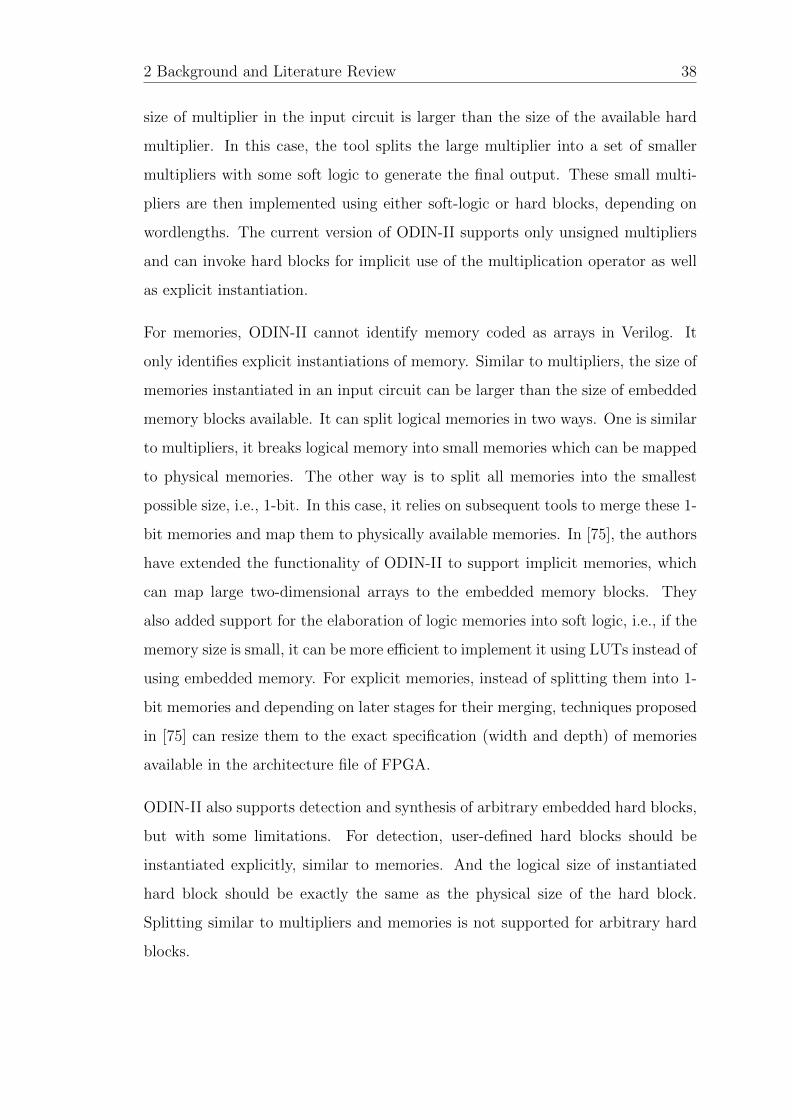
2 Background and Literature Review 38
size of multiplier in the input circuit is larger than the size of the available hard
multiplier. In this case, the tool splits the large multiplier into a set of smaller
multipliers with some soft logic to generate the final output. These small multi-
pliers are then implemented using either soft-logic or hard blocks, depending on
wordlengths. The current version of ODIN-II supports only unsigned multipliers
and can invoke hard blocks for implicit use of the multiplication operator as well
as explicit instantiation.
For memories, ODIN-II cannot identify memory coded as arrays in Verilog. It
only identifies explicit instantiations of memory. Similar to multipliers, the size of
memories instantiated in an input circuit can be larger than the size of embedded
memory blocks available. It can split logical memories in two ways. One is similar
to multipliers, it breaks logical memory into small memories which can be mapped
to physical memories. The other way is to split all memories into the smallest
possible size, i.e., 1-bit. In this case, it relies on subsequent tools to merge these 1-
bit memories and map them to physically available memories. In [75], the authors
have extended the functionality of ODIN-II to support implicit memories, which
can map large two-dimensional arrays to the embedded memory blocks. They
also added support for the elaboration of logic memories into soft logic, i.e., if the
memory size is small, it can be more efficient to implement it using LUTs instead of
using embedded memory. For explicit memories, instead of splitting them into 1-
bit memories and depending on later stages for their merging, techniques proposed
in [75] can resize them to the exact specification (width and depth) of memories
available in the architecture file of FPGA.
ODIN-II also supports detection and synthesis of arbitrary embedded hard blocks,
but with some limitations. For detection, user-defined hard blocks should be
instantiated explicitly, similar to memories. And the logical size of instantiated
hard block should be exactly the same as the physical size of the hard block.
Splitting similar to multipliers and memories is not supported for arbitrary hard
blocks.

2 Background and Literature Review 39
ODIN-II also provides support for functional verification of the input circuit. It
integrates a logic simulator proposed in [76] which can simulate either the Verilog
input file after elaboration done by ODIN-II or the generated BLIF netlist. For
arbitrary hard blocks, a C-description of the functionality of the block must be
added by the developer. As multipliers and memory blocks are common, their
functionality is built in.
2.5.2 ABC
The BLIF netlist generated by ODIN-II is used as an input to ABC [72], which
performs the technology-independent logic optimisation and technology mapping
to LUTs and flip-flops. In ABC, soft logic, i.e., logic to be implemented using LUTs
and flip-flops is represented as an AND-Inverter Graph (AIG) and embedded hard
cores like multipliers, memories, and user-defined hard-cores are represented as
black-boxes. WireMap [56] is also integrated for technology-mapping the AIG
into K-LUTs.
2.5.3 VPR
Versatile Place and Route (VPR) is a state-of-the-art, widely used open-source
tool for placement and routing. It was first proposed by Betz and Rose in [77].
The major advantage of VPR is, it can place and route circuits on a wide variety
of custom FPGA architectures designed and developed by researchers, for which
standard vendor tools cannot be used. VPR places a circuit and can then perform
either global routing or combined global and detailed routing.
The input to VPR is a technology-mapped netlist generated by ABC in the pre-
vious stage and a text file describing the FPGA architecture, and the output is a
placed and routed design, as well as statistics like routed wire-length, track count,
maximum net length, etc. VPACK is a logic block packing algorithm used in
VPR which reads a BLIF netlist of a circuit which has been technology mapped

2 Background and Literature Review 40
to LUTs and flip-flops. It then packs the LUTs and flip-flops to the desired FPGA
logic blocks and outputs a netlist in VPR’s netlist format.
VPR’s placement algorithm is based on simulated annealing [78] and uses a linear
congestion cost function [79]. This cost function penalises placements which oc-
cupy areas of the FPGAs that have narrower channels. An annealing schedule is
also proposed in [77] which automatically adjusts annealing parameters to differ-
ent cost functions and circuit sizes. Placement is an iterative process which starts
with a random placement of the circuit.
The routing algorithm is based on the Pathfinder negotiated congestion algo-
rithm [80, 79]. At first, ignoring any constraints on the number of wire segments
or logic block pins, it routes all the nets by the shortest path. The cost function
of a routing resource is a function of overuse of that resource in the current iter-
ation as well as in all previous iterations. Each iteration of the router consists of
sequentially re-routing all nets of the circuit by the lowest cost path found for that
net. The number of iterations is fixed apriori and if the circuit is not successfully
routed in a given number of tracks, the design is considered as unroutable with
the available channels.
With various developments over the years, many improvements and features have
been added to VPR. VPR 5.0 was proposed in [81] and includes many new features.
Out of these, the four main new features are:
• Broad range of support for single-driver routing architectures
• It can now model and place and route architectures with heterogeneous hard
blocks like embedded memories and multipliers
• Optimised electrical models in different technologies for wide range of FPGA
architectures. It also includes a wide range of area-delay trade-offs for each
architecture
• VPR 5.0 includes a set of regression tests to ease the development and en-
hancement of features

2 Background and Literature Review 41
For packing and clustering of technology-mapped circuits, instead of using VPACK,
VPR 5.0 use T-Vpack [82], which performs a timing-driven packing. After pack-
ing, placement and routing is done. And, finally timing analysis is performed to
determine the performance of the circuit.
All modern FPGA architectures include hard blocks like embedded memories and
multipliers. The addition of the ability to place and route architectures with
heterogeneous hard blocks is one of the most significant contributions of VPR
5.0. This capability also opens the doors for exploring what hard blocks should
be included into FPGAs instead of implementing those functions in FPGA fabric.
To maintain the structure of FPGAs for efficient placement and routing, VPR
5.0 assumes that the width of these hard blocks is equal to the width of one grid
(the unit of a soft logic cluster) so that they are restricted to one column. The
height of these hard blocks is restricted to an integral number of grid units so that
no area is wasted in empty slots. In addition to this, it is also assumed that for
multigrid height hard blocks, the horizontal routing tracks at every grid location
are passed through as if there are no hard blocks to ensure efficient routability of
soft logic. But the packing algorithm of VPR 5.0 does not support the clustering
of nodes by breaking these heterogeneous blocks into sub-modules, so it supports
the placement and routing for monolithic heterogeneous blocks only.
Early versions of VPR had different data structures for modelling logic blocks and
I/O, and did not support embedded hard blocks. In VPR 5.0, support for hard
blocks was added and data structures for different blocks were unified, allowing
the user to add new types of hard blocks easily while also simplifying the code.
To further strengthen the support for hard blocks, VPR 5.0 uses an XML-based
architecture file format to leverage convenient modelling hierarchy in XML.
A new language (also based on XML syntax) for describing architecture and an
architecture-aware packing algorithm AAPack were proposed as VPR 6.0 beta
in [69]. Complex logic blocks with arbitrary internal routing structure and hierar-
chy can be easily described in this language. In addition to this, it also supports
different modes for each logic block, which can represent different functionalities
2 Background and Literature Review 42
and routing structures for these block. These modes represent different ways of
using the embedded logic block. Similar to earlier version of VPR, the input to
this packing algorithm is a technology mapped netlist and architecture file. The
algorithm tries to pack the input circuit into a minimum number of complex logic
blocks defined in the architecture file and generates a packed output netlist which
is functionally equivalent to the input netlist. The latest version of VTR extends
the AAPack packing algorithm of VPR 6.0 beta, which supported only area-driven
packing with timing-driven packing.
After passing a circuit through ODIN-II and ABC, VPR in non-timing driven
mode is run multiple times to determine the minimum channel width (W ), and
then after determining the W , VPR is invoked again in timing driven mode, with
width slightly higher than calculated in non-timing driven mode, to complete final
placement and routing.
2.6 High Level Synthesis
As the complexity of systems implemented on FPGAs increases, a significant
amount of work is being done on increasing the level of abstraction for describing
complex computations. This helps reduce development time, which is critical in
modern fast-changing technologies and also helps to explore the design space.
Research so far can be broadly categorised into three categories:
1. Tools that take high-level descriptions as input and generate RTL which can
then be synthesised using commercially available vendor tools.
2. Tools that take a dataflow graph as input and generate synthesisable RTL.
These can be sub-categorised into:
(a) Those focused on implementation of algorithms on heterogeneous hard-
ware components which can be a hybrid of one or more of conventional
processors, DSP processors, and FPGAs [83, 4].

2 Background and Literature Review 43
(b) Those focused on implementing algorithms on FPGAs only.
3. Research focused on extracting dataflow graphs from high-level descrip-
tions and relying on other tools for further implementation from generated
dataflow graphs.
We discuss various techniques and tools proposed in the literature that focus on
implementation of algorithms from high-level descriptions or dataflow graphs.
Many tools have been developed to increase the level of abstraction of hardware
design to high-level languages like C/C++. Although the adoption of HLS was
slow in early generations of the tools, there has been a rapid growth in development
and demand lately. As discussed in [84] and [85], some of the motivations and
demands for high-level synthesis are:
• Increasing complexity with expectations of reduced design time, along with
significantly reduced verification time, which is critical in complex systems.
• More complex and capable architectures requiring significant exploration of
the design space to achieve effective use of resources.
• Embedded systems increasingly blending hardware and software, requiring
considered partitioning of systems, and a preference for unified description.
• An abundance of legacy code in high-level languages like C/C++ that can
serve as a springboard for building complex systems.
There are, however, some inherent limitations of high-level languages like C/C++
for hardware design. Some of these include [84]:
• Hardware circuits can be highly parallel but most high-level languages do
not support concurrency natively and algorithms are described sequentially.
• Timing specifications are very important for hardware design, but most pro-
gramming languages do not consider timing.

2 Background and Literature Review 44
• For efficient implementations, hardware designers tends to pass structural
information like input/output ports and data formats across these ports, and
also specific constraints for some portions of the circuit. These functionalities
are not supported by conventional programming languages.
Some of these limitations and more are discussed in detail in [86]. To overcome
these limitations, many tools use modified versions of languages, which both ex-
tend and restrict constructs of the programming language. Extensions are needed
to express concurrency, structural information (partitions, I/O, data formats) and
various constraints. Restrictions are generally motivated by constructs which ei-
ther do not have hardware equivalents or constructs which are hard to map to
hardware blocks (like pointers).
Some high-level synthesis (HLS) tools proposed in the literature or commercially
available are: HardwareC [87], Handel-C [88], Catapult C [89], Impulse-C [90],
PACT HDL [91], CHiMPS [92], Bluespec [5], Xilinx Autopilot [3], LegUp [4].
In [93], the authors proposed an integrated synthesis environment, which syn-
thesises the control and data path of an architecture simultaneously. The main
focus was to use more global information which can be extracted from a high-
level description, instead of doing local optimisations in subsequent stages. In the
proposed system, both scheduling and binding are based on simulated annealing,
and the datapath is optimised for area, performance, and interconnect lengths.
The input is a high-level description of the algorithm, which is converted into
a hierarchical dataflow graph. The scheduling process runs iteratively, applying
small transformations to the architecture, and then accepts or rejects the changes
according to a probability criterion, and runs as long as the algorithm does not
converge.
In [94, 95, 96], the authors tried to efficiently map arbitrary C code with support
for pointers and malloc/free, and complex data structures into hardware. [94] pro-
posed a solution named Synthesis of Pointers in C (SpC) which can synthesise and
optimise a C model with pointers. Pointers are synthesised to multiple variables

2 Background and Literature Review 45
and array elements. It takes a C description, which can contain pointers, and gen-
erates a synthesisable Verilog module. As a continuation of [94], in [95] and [96],
the authors extended the capabilities of SpC to support malloc/free which are
used for dynamic memory allocation. To implement malloc/free, the SpC uses
a library of hardware components implementing malloc and free. The first step
is flow- and context- sensitive pointer analysis, and then a hardware component,
called allocator (or virtual memory manager) is generated which manages differ-
ent memory spaces and resolves all malloc and free instructions. Implementation
is based on the SUIF (Stanford University Intermediate Format) [97] framework,
developed at Stanford University.
PACT (Power Aware Architecture and Compilation Techniques) HDL [91] is a
C to HDL compiler, designed with the aim of generating power-aware architec-
tures. PACT HDL supports arbitrary architectures, including both application
specific and reconfigurable hardware. It translates input C code into synthesis-
able HDL code in three stages. The first stage is the translation of input C code
into an Abstract Syntax Tree (AST). Optimisations independent of architecture
like precision analysis, loop unrolling are also performed in this stage. The AST is
then converted into an HDL AST representation, adding architecture information,
which is then used to generate RTL in final stage. PACT HDL is best suited for
image and signal processing applications. Power optimisation is done by pipelin-
ing functional units, reverse code levelisation, and support for integrating power
efficient IP cores.
A C-based accelerator compiler CHiMPS (Compiling High-level Languages into
Massively Pipelined Systems), targeting acceleration of high-performance com-
puting (HPC) applications on CPU-FPGA platforms is proposed in [92]. It takes
ANSI-C code as input and generates VHDL blocks. The hybrid CPU-FPGA model
used for CHiMPS consists of one or more conventional CPUs with FPGAs con-
nected to the CPU sockets, all sharing a common bus. Each instruction in C
is translated into an intermediate representation, which is an assembly-like lan-
guage called CHiMPS Target Language (CTL), which in turn produces a VHDL

2 Background and Literature Review 46
implementation. If the design is too big to fit on a single FPGA, it uses time-
multiplexing of FPGA resources or uses a MicroBlaze [98] soft processor to reduce
resource requirements. One major contributor to performance enhancement is the
many-cache memory model, where many small independent memory blocks avail-
able on the FPGA are used as caches. For designers with hardware expertise, the
tool supports pragmas which can result in greater performance improvements.
[99] and [100] extends the Adequation Algorithm Architecture (AAA) methodol-
ogy and the associated software tool SynDEx, first proposed in [101], to implement
algorithms on heterogeneous architectures. The goal of the AAA methodology is
to discover the best implementation of an algorithm for a multi-component archi-
tecture, which also meets the real-time constraints of the application. [99] uses
the AAA methodology to extend the tool SynDEx for FPGAs named SynDEx-IC.
SynDEx-IC generates synthesisable VHDL code for a single FPGA architecture.
[100] proposed an automatic design generation methodology for telecommunication
applications using DSPs and FPGAs. It also leverage the partial reconfiguration
capabilities of modern FPGAs.
Catapult C [89] is a commercially available HLS tool by Mentor Graphics, which
accepts ANSI-C as an input and generates synthesisable RTL which can be easily
integrated with the rest of the tool flow. It can be used for FPGAs as well as
ASICs. In addition to RTL, the tool also generates a SystemC testbench, which
compares the outputs of both the C descriptions and generated RTL and validates
the functional correctness of the generated RTL. RTL generation can be optimised
by applying various synthesis constraints for I/O, loops, and memory elements, in
addition to system level constraints.
LegUp [4] is an open-source HLS tool developed at the University of Toronto.
LegUp accepts a standard C description of the design as input and can generate
hardware solutions for either a hybrid architecture containing an FPGA-based
MIPS soft processor and custom hardware or a full hardware implementation. It
uses the LLVM compiler framework to translate the C description into an machine
independent intermediate representation (IR), which is then used to generate RTL.

2 Background and Literature Review 47
In [102], LegUp added support for parallel hardware generation with the integra-
tion of Pthreads and OpenMP. Parallel code segments in C are directly translated
into sub-circuits working in parallel. LegUp also offers a software-like debugging
framework for generated hardware [103]. The framework allows a user to inspect
the program at input C, LLVM IR, as well as Verilog. It is primarily optimised
for Altera FPGAs. The latest version of the tool [104] supports Xilinx devices as
well, though somewhat limited.
A case study presented in [105] compares the performance of K-means clustering
for two different implementations: one is a simple data-flow centric implemen-
tation and another uses dynamic memory allocation and recursion, for Xilinx’s
Vivado HLS. Vivado HLS does not support pointers in high-level descriptions.
The authors propose a source-to-source translation of the recursive C code using
dynamic memory allocation to transform it into format acceptable by Vivado HLS.
Tools for extracting control and data flow graphs from high-level descriptions have
been proposed in [106], [107]. [106] is focused on extracting task graphs from C. It
does not support some of the features of C like functions defined within functions
and pointers to functions. As a first step, it divides the C code into tokens, which
are then organised into an abstract syntax tree (AST) using Lex and YACC. The
next step is keyword extraction. Then, dependence analysis based on ordered list
of events is performed, generating a dependence graph. The tool proposed in [107]
can extract control and data flow graphs (CDFG) from behavioral descriptions
of algorithm in VHDL. Similar to [106], it also uses Lex and YACC for parsing
VHDL code, to generate a parse tree, which is then converted into a CDFG. A
tool called Task Graphs For Free (TGFF) was proposed in [108], which generates
pseudo-random task graphs, which can be used to verify allocation and scheduling
algorithms.
The high-level synthesis system Helios, proposed in [109] takes a behavioral de-
scription of an algorithm in a C-like language and generates a synthesisable RTL
code for the algorithm. The process is divided into four major steps: DFG genera-
tion, Scheduling, Resource Binding, and HDL Generation. Helios does not restrict

2 Background and Literature Review 48
the design space at the stage of DFG generation, i.e., instead of generating only
one DFG in first stage, it generates multiple DFGs of the algorithm by apply-
ing different transformations, which includes tree height reduction and retiming.
From the generated DFGs, a fast scheduling and resource binding process is exe-
cuted on each selected DFG and a small number of good datapath candidates are
selected based on their cost and performance. Optimum scheduling and resource
binding algorithms are applied to these selected DFGs and a final datapath design
is obtained, for which HDL files are generated.
In the process of implementing designs onto FPGAs, designs are flattened to gates
and further steps are applied on these Boolean networks. In [110], the authors pro-
posed a different approach. Instead of flattening the design to gates, the datapath
is preserved. The idea is to preserve the structure, which can allow exploitation
of specialised datapath features in FPGAs. Another extreme approach is to map
each node of the datapath to a pre-fabricated module. But, this approach restricts
the optimisations which can be done across different nodes, and also results in un-
derutilisation of resources. The ideal approach can be merging operations across
different nodes while maintaining the regularity of the datapath. The proposed
approach is implemented in a datapath mapping tool GAMA [110]. GAMA does
not flatten the modules to gates and tries to leverage features of hard-blocks of
FPGAs like fast carry logic. GAMA performs module placement simultaneously
with mapping, but it does not guarantee optimal results for placement.
In [111] and [112], Sun et al. proposed a methodology for pipelined implementa-
tions of untimed synchronous dataflow graph while merging module selection and
resource sharing stages to obtain better results. The proposed approach performs
pipeline scheduling, considering user-specified throughput constraints, rather than
latency or resource usage as constraints. It schedules the dataflow descriptions
onto pre-pipelined library elements. This library contains multiple implemen-
tations of each behavioral operation, with different number of pipeline stages,
operating frequency, area, etc. This results in a large library of pre-pipelined im-
plementations and thus, design space exploration becomes critical. Two different
algorithms are proposed for design space explorations. The first approach is a

2 Background and Literature Review 49
recursive branch-and-bound algorithm, which uses As Soon As Possible (ASAP)
scheduling. Although this algorithm results in decent results, it is very computa-
tionally expensive and is not practical for large circuits. The second approach is
a heuristic approach which is based on iterative modulo scheduling (IMS) [113].
This approach allows backtracing to explore solutions which cannot be attained by
the greedy branch-and-bound algorithm. Although, both the algorithms explore
the trade-off between various library modules of operations, the large size of the
library becomes a limiting factor, which grows exponentially with the number of
operations.
FloPoCo (Floating-Point Cores) is an open-source tool written in C++, to gener-
ate custom arithmetic cores with floating-point operations [114]. The output of the
tool is synthesisable VHDL with an option of generating a testbench too. FloPoCo
is a collection of some basic operators which are highly parameterised, and can be
used to generate custom architectures satisfying user-defined parameters. These
parameters include the precision of inputs/outputs and target frequency. It can
also generate a pipelined implementation of these operators, which can be enabled
or disabled. Pipelining done by FloPoCo is frequency-directed, i.e., depending
on the target frequency, the tool automatically manages the number of pipeline
stages required. FloPoCo supports a wide range of FPGA devices and optimised
architectures are generated depending on the device selected. It also provides the
functionality to enable/disable the use of DSP blocks, widely available on mod-
ern FPGAs. Devices supported by the latest version of FloPoCo are the Xilinx
Spartan III, Virtex IV, V, 6, and the Altera Stratix II, III, IV, V, Cyclone III, IV,
V [115].
With advancements in HLS tools, significant research has been undertaken to im-
prove the productivity of tools and widen support for data structures like pointers.
Runtimes of the back-end tool flow chains remain one of the major bottlenecks for
HLS tools and they affect productivity in a major way. For most HLS tool, any
small change in the code requires a full re-compile. Recent work in [116] proposes
a back-end tool flow chain which is able to re-use pre-compiled (synthesised and
placed) modules of the design. These pre-compiled sub-circuits are called “macros”

2 Background and Literature Review 50
and stored in a library. For HLS, the functionality of the designs is described in a
high-level language and back-end tools generate the RTL. For the proposed tool
flow, instead of generating RTL, optimum pre-compiled sub-circuits are selected
from the library and stitched together, bypassing the synthesis and place-and-route
stages of the implementations, thus, significantly reducing the design runtime.
RapidSmith [117], RapidSmith 2 [8], and Torc (Tools for Open Reconfigurable
Computing) [118] are open-source frameworks for CAD tool development and ar-
chitecture exploration for Xilinx FPGAs. Xilinx devices are detailed in a verbose
way in XDL (Xilinx Design Language) descriptions, which provide an insight into
the architecture, however, these files are very verbose. RapidSmith use a custom
compact file format which provides all the necessary information required to de-
velop CAD algorithms for a wide range of devices. It also includes an API for
modifying XDL designs for the purpose. RapidSmith provides access to Xilinx
FPGAs at the level of Slices. In RapidSmith 2 [8], the authors further improved
the tools and enable the user to access the lowest level logic blocks: LUTs and
registers. One of the important advantage of RapidSmith is its ability to interface
with vendor tools. This allows modification of individual stages without breaking
the vendor tool chain. Torc [118] provides four set of APIs to interface with and
modify the Xilinx tool chain. The four APIs are for: generic netlist, physical
netlist, device architecture, and bitstream stages of the design flow.
2.7 Resource Sharing
Generally, the resources available on FPGAs are mapped to by partitioning a dat-
apath into spatially interconnected functional units, assuming sufficient resources
are available to map the entire design on the target device. Designs with high
performance requirements adopt this strategy. However, this is not preferable or
possible in two cases:
1. The device does not have sufficient resource to fully implement the design

2 Background and Literature Review 51
2. The throughput requirements of the design are lower than those achieved by
a fully pipelined implementation
In the first case, resources can be shared in a time-multiplexed manner in order to
fit the full design on a device. For the second, if the throughput requirement is not
high, resources should be shared to the extent possible while meeting the required
throughput. A fully pipelined implementation would represent under-utilisation
of resources, which could otherwise be freed up for other uses.
Resource sharing should be applied where possible, however, the impact of resource
sharing also depends on the type of hardware blocks being shared. Generally,
resource sharing requires multiplexers at the inputs and demultiplexers at the
outputs of hardware blocks to be shared. A simple criterion is if the cost of
control logic required for the resource sharing is less than the resources saved,
resource sharing is beneficial. Hadjis et al in [119] argue that the architecture of
an FPGA logic element determines the utility of resource sharing and they present
a cost-benefit analysis. The authors first show that operators like add/sub do not
result in significant savings for 4-LUTs, however, for 6-LUT architectures, some
resources are saved. Sharing resource intensive operations like multipliers results
in significant savings. [119] also presents a pattern discovery and sharing approach,
considering multiple operations as a composite operation. Sharing these patterns
can result in considerable area reduction for composite operations consisting of
add/sub too. In [120], the authors evaluate the impact of various resource sharing
techniques. In addition to sharing computational resources, the impact of register
sharing and register renaming is also discussed on the area and performance of
large designs.
In many medium-rate DSP applications, the design goal is to minimise the total
system area cost by mapping the computation onto the smallest (i.e., cheapest)
possible FPGA device. Currently, designers manage this problem by manually se-
lecting more area-efficient arithmetic implementations and/or constructing control
logic to time share multiple operations on a single arithmetic unit. Automated
synthesis of datapaths with fine-granularity optimisations in area and throughput

2 Background and Literature Review 52
gives designers the options to meet the increasing demands of design productivity,
high performance, limited memory bandwidth, and FPGA resources.
Scheduling is an important step in the process of implementing a design onto
FPGAs, whether RTL is generated using an HLS tool or manually optimised
hand-written RTL. Scheduling greatly impacts the cost and performance of the
final design. A significant amount of research has been done on automated resource
sharing by providing either:
• A constraint on the resources available
• A target throughput constraint
The Sehwa tool in ADAM allows generation of pipelined implementations and ex-
ploration of the design space by generating multiple solutions [121]. The authors
developed two heuristics for pruning the search space of an exhaustive pipeline
scheduler. Sehwa breaks synthesis into three steps: scheduling, resource alloca-
tion, and register-transfer synthesis. High-level synthesis (HLS) tools developed
since continue to follow these three basic steps. In [122], the authors proposed
PLS (a scheduler) to evaluate the area-time trade-off and compared the generated
implementations with [121].
Constrained scheduling problems can be broadly categorised into: resource con-
strained, time constrained, and resource and time constrained. A constraint on
resources limits the number of functional units of each type available to implement
the datapath. Given the available resource, the objective is to find a schedule with
maximum performance. Given the constraint on throughput, the objective is to
find a schedule consuming minimum hardware. Resource and time constrained
schedules generally determine the feasibility of a possible solution satisfying both
resource and time constraints.
A significant amount of work has been done on resource sharing at RTL level as
well as in HLS. List scheduling was first used for microcode compaction in [123].
Variants with different optimisation goals for list scheduling have been explored

2 Background and Literature Review 53
in [124, 125]. Force-Directed Scheduling (FDS) [126] is a heuristic scheduling
algorithm which can perform scheduling and resource allocation simultaneously.
It takes a dataflow graph as an input and determines the number of different
functional units required to implement the graph and simultaneously determines
the schedule depending on data dependencies between the different nodes. FDS
constrains the schedule according to input timing-constraints and tries to minimise
the number of resources required to satisfy the schedule. It computes the mobility
of the nodes from As Soon As Possible (ASAP) and As Late As Possible (ALAP)
scheduling algorithms and then nodes with non-zero mobility are scheduled to
achieve minimum resource usage. Variants of FDS presented in [127, 128, 129, 130]
have optimised the algorithm for different optimisation goals, such as, throughput,
dynamic power, hardware/software partitioning. Recently, an algorithm based on
FDS specifically targeted for streaming applications was proposed in [131].
Problem formulations based on integer linear programming (ILP) for scheduling in
high-level synthesis have been explored in [132]. This paper discuss ILP formula-
tions for resource constrained and time constrained scheduling. In addition to this,
a “feasible scheduling” is also discussed, which explores the design space to pro-
vide a trade-off between both the resource and time constraints. The scheduling
algorithm attempts to determine a schedule which satisfies both the constraints.
[133] present simultaneous allocation and scheduling based on ILP to determine
the global optimum solution.
Heuristic scheduling algorithms such as list scheduling [124] or FDS [126] can gen-
erate a sub-optimal schedule, as these methods attempt to determine a locally
optimum solution instead of applying global optimisations. ILP [132] can pro-
vide a globally optimum solution, however, these formulations are difficult to scale
for large designs. Recently, an efficient and scalable approach called the system
of difference constraints (SDC) based on a linear-programming formulation was
proposed [134]. Scheduling constraints are converted into a set of difference con-
straints, with objective function also as a linear function, which can be solved using
linear programming solvers. SDC supports a wide range of optimisation goals like
resource constraints, timing constraints, latency constraints. For control and data

2 Background and Literature Review 54
flow graph (CDFG), inter-basic-block constraints are handled at the boundary of
basic blocks. Resource sharing across basic blocks is not considered. [135] presents
scheduling heuristics addressing the problem of global resource sharing for CDFGs.
The proposed techniques focuses on inter-basic-block sharing, in addition to re-
source sharing for each basic block. Computational modules across basic blocks
are analysed to minimise connections and functional resources. Patterns for com-
bining resources are extracted and prioritised, resulting in more effective sharing
than when considered individually.
More recent work in [112] has focused on resource sharing and loop optimisa-
tions targeting fully pipelined functional units from HLS descriptions. The au-
thors introduced a pipeline synthesis flow which exploits resource sharing and
module selection, yielding a 2–3× reduction in resources compared to existing
approaches. The authors proposed approaches to address the need for improved
pipeline synthesis techniques for FPGAs; for design space exploration aimed at au-
tomatically identifying the lowest cost circuit architecture that meets a minimum
throughput constraint; for scheduling data-flow specifications onto pre-pipelined
library elements. In [136], the authors describe a heuristic for generating an I/O
port-constrained pipeline for an arbitrary acyclic DFG and compare its results in
terms of resource overhead and routing complexity (in terms of fan-in and fan-
out) against those of an exhaustive branch-and-bound enumeration and those of
a state-of-the-art commercial HLS tool.
An approach based on extracting patterns from the dataflow graphs of designs to
maximise resource sharing was proposed in [137]. It mainly consists of two impor-
tant tasks: pattern matching and pattern recognition. The proposed techniques
attempt to determine the common pattern, i.e., a set of operations occurring
repetitively, so that different instances of the same pattern can share the same
hardware resources. Finding and sharing exactly the same pattern does not result
in significant resource sharing opportunities. In order to share patterns which are
not exactly the same but similar, the authors use a graph similarity index, called
the edit distance [138] to handle variations in ports, wordlengths, operation types,
and other properties. To avoid small sub-graphs, which can also be sub-graphs of

2 Background and Literature Review 55
identified patterns, sub-graph enumeration and pruning is proposed. To find large
and useful patterns, the authors propose an approach combining the benefits of
breath-first search and depth-first search.
In [139], the authors propose an area-efficient design for binary tree shaped ex-
pressions (n input) having a latency of (3n+ (α− 1) lg n− 2) as upper bound (α
is the latency of one floating point FU). The authors use one floating-point core
for each operation type to evaluate an expression whose inputs arrive sequentially.
The area efficient architecture and algorithm reuses the same core for a series of
floating-point computations which are dependent upon one another. However, the
algorithm is limited to generating pipelines that can receive only one input every
clock cycle.
2.8 Summary
The increased capabilities of FPGAs mean a wider range of algorithms can be
completely implemented on FPGAs. Our focus is on exploiting the DSP blocks
available on modern FPGAs to efficiently implement computational kernels of
large applications, exploiting the capabilities of these blocks. One of the major
limitations of most of the available tools is they do not consider the architectural
details of the DSP block and rather rely on vendor tools to use them. Information
available in the high-level of design description is lost during this translation, and
thus, the backend tools cannot utilise these blocks optimally.
The techniques proposed in this thesis are independent of much of the existing work
we have covered, meaning that our approaches can be included in existing tools.
We are focused on exploiting both the computational and control capabilities of
DSP blocks. This means using the multiple sub-blocks offered, and using the
dynamic flexibility. Both of these offer us opportunities for implementing more
efficient designs.

3The DSP48E1 DSP Block Primitive
For computationally-dominated applications, one fundamental step to bridge the
gap between FPGAs and ASICs is to ensure that arithmetic is performed as ef-
ficiently as possible. In this chapter, we discuss the evolution of DSP blocks on
FPGAs to improve the speed and efficiency of arithmetic. We then discuss the
architecture of the modern DSP48E1 available on Xilinx Virtex-6 and 7 series
devices. DSP48E1 blocks can be configured in many different ways to perform
different arithmetic operations and support internal pipelining. We discuss how
the performance of these blocks varies depending on configuration and also demon-
strate how dynamic programmability can be exploited to implement different func-
tions using a single DSP block.
The versatility of DSP blocks has been used in a variety of ways in literature.
In [140, 141], a soft processor called iDEA was built around the DSP block. By
56

3 The DSP48E1 DSP Block Primitive 57
exploiting its dynamic flexibility, most of the functions of the soft processor could
be absorbed into the DSP block leading to a highly compact design which could
still run at very high frequency. In [142], the authors proposed a general floating
point operator, again using the DSP block’s dynamic programmability to enable
a number of different operations in a single general purpose floating point block.
In [143], the authors showed how a general purpose FPGA overlay architecture
called DySER [144] could be significantly improved by swapping the functional
unit for a flexibly configured DSP block. A more capable overlay was proposed
in [145], again using the DSP block at close to its maximum frequency in a general
purpose overlay.
3.1 DSP Block Evolution
With the growing application of FPGAs to different areas like digital signal pro-
cessing and image processing, vendors sought to improve the efficiency of oper-
ations that find widespread use across these applications. Implementations of
multipliers using LUTs are slow and consume significant amounts of resources. To
speed-up these operations, Xilinx first introduced hard-wired multipliers in the
Virtex-II family of FPGAs. With growing performance demands, many features
have been added in subsequent generations to support wide range of operations.
Xilinx first introduced 18×18 bit hard-wired multipliers, which could generate
a new result every clock cycle and can operate at frequency of 150 MHz in the
Virtex-II. In the Virtex-IV, these multiplier blocks were extended to DSP blocks
(DSP48), by adding a 48-bit adder/subtractor, with a maximum frequency of up
to 500 MHz. In the Virtex-V, the width of the multiplier was increased from
18×18 bits to 25×18 bits, with a maximum frequency of 550 MHz. Adding more
functionality, in the Virtex-VI DSP blocks (DSP48E1), a 25-bit pre-adder was
included at the multiplier input, and DSP48E1 can generate outputs at 600 MHz.
More importantly, in the latest 7 Series FPGAs from Xilinx, the same DSP block
is used across all device families and they are capable of running at up to 740 MHz.

3 The DSP48E1 DSP Block Primitive 58
Device Capabilities Speed No of DSP Blocks
Virtex-2 18×18 bit multiplier Up to 150 MHz 4 - 168
18×18 bit multiplier Up to 500 MHz 32 - 512
Virtex-4 48-bit adder/subtractor
(DSP48)
18×25 bit multiplier Up to 550 MHz 32 - 1056
Virtex-5 48-bit ALU
(DSP48E)
25-bit pre-adder Up to 600 MHz 288 - 2016
Virtex-6 18×25 bit multiplier
48-bit ALU (DSP48E1)
25-bit pre-adder Up to 740 MHz 60 - 2520
Virtex-7 18×25 bit multiplier
48-bit ALU (DSP48E1)
27-bit pre-adder Up to 740 MHz 600 - 2880
Virtex-Ultrascale 18×27 bit multiplier
48-bit ALU (DSP48E2)
Table 3.1: DSP blocks evolution on Xilinx Virtex devices.
The number of DSP blocks available on devices has also increased significantly
over the generations. Virtex-II and Virtex-II Pro had between 4 to 168 and 12
to 444 hard-wired 18×18 multipliers respectively. After introducing full-fledged
DSP blocks, Virtex-4 had between 32 to 512 DSP48 blocks. Virtex-5 devices
had a minimum of 32 DSP48Es to a maximum of 1056. Virtex-6 have number
of DSP48E1 blocks between 288 to 2016. Table 3.1 shows the evolution of DSP
blocks over generations on Xilinx FPGAs.

3 The DSP48E1 DSP Block Primitive 59
+/-
+ -D
/
/
/
/
18
30
25
48
/48
B
A
D
C
P
Multiplier25x18
Pre-adder25-bit
X
/48 A:B
ALU 48-bit
INMODE OPMODE ALUMODE
Figure 3.1: Basic structure of the DSP48E1 primitive.
3.2 The DSP48E1 Primitive
The latest DSP blocks support many functions, including add-multiply, multi-
ply, multiply-accumulate, multiply-add, three-input add, barrel shift, bitwise logic
functions, pattern detection, and wide-counters. One of the most important fea-
tures of the DSP blocks is dynamic programmability. The functionality of these
DSP blocks can be modified in every clock cycle, greatly enhancing the flexi-
bility of these blocks. Pipeline registers are also embedded in DSP blocks to
enhance throughput. Dedicated connections are available for cascading multiple
DSP blocks without using the FPGA fabric. This results in better performance
and saves resources for other uses. A simplified representation of DSP48E1 block
is shown in Figure 3.1.
The DSP48E1 is available on the latest generation of Xilinx’s FPGAs [146]. These
DSP blocks can be divided into three stages: pre-adder, multiplier, and ALU. The
Pre-adder is a 25-bit two-input adder/subtractor. Its output is fed as one of the
inputs of the Multiplier which has asymmetric 18-bit and 25-bit inputs. The
ALU is 48 bits wide and operates on the output of the multiplier and another
input. When using the ALU for Boolean logic, the multiplier cannot be used.
Logic functions supported by the ALU are AND, OR, NOT, NAND, NOR, XOR,
and XNOR. Three multiplexers X, Y, and Z, are used to select appropriate inputs
for the ALU block. A detailed internal view of the DSP48E1 is shown in Figure 3.2.

3 The DSP48E1 DSP Block Primitive 60
A 1
A 2
D
+/-
A D
B 1
B 2
M C
Du
al B
Reg
iste
r
Du
al A
an
d D
Reg
iste
rs+
-P
INM
OD
E
OP
MO
DE
CA
RRY
IN
AB D C
CA
RR
YIN
OP
MO
DE
CA
RR
YIN
SEL
INM
OD
E
ALU
MO
DE
ACINBCIN
ACOUTBCOUT
41
P
17
-bit
Sh
ift
17
-bit
Sh
ift
PCIN
CARRYCASCIN
A:B
48
25-b
it
Pre
-Ad
der
PCOUT
25
x18
Mu
ltA
LUM
OD
E
X Y Z
Fig
ure
3.2:
Det
aile
dblo
ckdia
gram
ofth
eD
SP
48E
1pri
mit
ive.

3 The DSP48E1 DSP Block Primitive 61
Register Control Attributes
AREG ACASCREG BREG BCASCREG
CREG DREG MREG PREG
ALUMODEREG INMODEREG OPMODEREG
CARRYINREG CARRYINSELREG
Feature Control Attributes
A INPUT B INPUT USE DPORT USE MULT
USE SIMD
Table 3.2: DSP48E1 Attributes.
Specific configuration inputs determine which components should be used. As
different components support multiple functions, configuration inputs also set the
operation of these components. Multiple pipeline registers are also available which
can be configured according to requirements of the application.
As we can see in Figure 3.2, the DSP48E1 can be divided into a maximum of four
pipeline stages. Two of the pipeline stages are available at inputs A and B, one
at the output of the multiplier, and one at the output of the ALU. These pipeline
stages are parametrised, i.e., the pipeline stages are configured while instantiating
the primitive, and cannot be enabled/disabled dynamically. However, pipeline
registers can be clock-gated.
Multiplication is done in two stages. In the first stage, the multiplier block gen-
erates two 43-bit partial products. These partial products are then sign-extended
to 48-bits in the X and Y multiplexers. In the second stage, the ALU block adds
these two partial products to generate the final multiplier output. Therefore, when
the multiplier is used, the ALU effectively becomes a two-input adder/subtractor.
We now discuss various attributes and input/output ports of DSP48E1 primitive.
3.2.1 Attributes
Attributes are set at the time of instantiation. They can be divided into attributes
that control pipeline registers and the attributes that control functionality. A list
3 The DSP48E1 DSP Block Primitive 62
of all the attributes is shown in Table 3.2.
3.2.1.1 Register Control Attributes
AREG, ACASCREG, BREG, BCASCREG set the number of input pipeline reg-
isters at input ports A and B. These can be set to 0, 1, or 2. All other attributes
can be either 0 or 1 which disable or enable the corresponding pipeline register.
3.2.1.2 Feature Control Attributes
A INPUT and B INPUT can have values DIRECT or CASCADE, which select
from where port A and port B receive their inputs respectively. In DIRECT mode,
A is connected to the DSP block input, while in CASCADE mode, it is connected
to the adjacent DSP block.
USE DPORT determines whether to use the D port and pre-adder block.
The multiplier block can be used in three modes. It can be either disabled (when
the DSP block is used as a two-input 48-bit adder/subtractor or for Boolean
logic operations), enabled (when it is always used as multiplier), or in dynamic
mode (when the application is required to switch operations between multiplier
or two-input 48-bit adder/subtractor). These correspond to values of NONE,
MULTIPLY, or DYNAMIC assigned to USE MULT.
The 48-bit ALU block can be used as a single 48-bit ALU Block or can be split
into multiple small wordlength ALU blocks, which is determined by USE SIMD,
with possible values of ONE48, TWO24, or FOUR12.
3.2.2 Input Ports
The main input ports of the DSP48E1 primitive are: A, ACIN, B, BCIN, C,
D, CARRYIN, CARRYCASCIN, INMODE, OPMODE, ALUMODE, CARRYIN-
SEL, PCIN, and MULTSIGNIN, along with their clock enables and reset inputs.
3 The DSP48E1 DSP Block Primitive 63
Input ports A, B, C, and D are connected to the input paths of the pre-adder,
multiplier, or ALU. These inputs are of different wordlengths. A, B, C, and D are
30 bits, 18 bits, 48 bits, and 25 bits wide respectively. ACIN, BCIN, and PCIN
are cascaded inputs which are 30 bits, 18 bits, and 48 bits wide respectively, and
are used when multiple DSP blocks are cascaded to implement wide operations.
PCIN and 17-bit shifted PCIN are inputs to the Z multiplexer, which connects one
of the inputs of the ALU block. CARRYIN and CARRYCASCIN are each 1-bit
wide carry inputs. CARRYIN is the direct carry input and CARRYCASCIN is
the cascaded carry input port, which is the carry output of the adjacent DSP48E1
block. Four control inputs are used to control and configure the operations of
DSP48E1. These are INMODE, OPMODE, ALUMODE, and CARRYINSEL.
MULTSIGNIN is the sign of the multiplied result of the previous DSP block which
is used when cascading multiple DSP blocks.
A, ACIN, B, BCIN, C, D
Port A or ACIN serves as the input to the pre-adder and the multiplier blocks.
As the pre-adder is 25 bits wide and one of the inputs of the multiplier is also 25
bits wide, the lower 25 bits of A (or ACIN) are used. The full 30 bits of A (or
ACIN) are used when the DSP48E1 is used as a two-input 48-bit adder/subtractor,
bypassing the multiplier block.
Port B or BCIN serves as the 18-bit operand of the multiplier block. Port C is an
input to the ALU block, which can be selected by properly configuring multiplexer
Y or Z (depending on the configuration of the multiplier block). Port D is an input
to the pre-adder block. It can also be used as an alternative input to the multiplier
block.
When the ALU block is used as a 48-bit adder, the multiplier is bypassed and
48-bit wide concatenated A and B ports (A:B) through X multiplexer are used as
one of the inputs of the ALU. The other input is the output of the Z multiplexer.
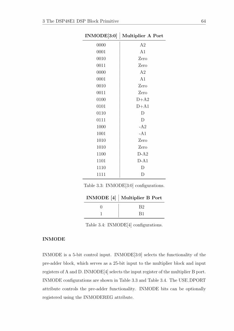
3 The DSP48E1 DSP Block Primitive 64
INMODE[3:0] Multiplier A Port
0000 A2
0001 A1
0010 Zero
0011 Zero
0000 A2
0001 A1
0010 Zero
0011 Zero
0100 D+A2
0101 D+A1
0110 D
0111 D
1000 -A2
1001 -A1
1010 Zero
1010 Zero
1100 D-A2
1101 D-A1
1110 D
1111 D
Table 3.3: INMODE[3:0] configurations.
INMODE [4] Multiplier B Port
0 B2
1 B1
Table 3.4: INMODE[4] configurations.
INMODE
INMODE is a 5-bit control input. INMODE[3:0] selects the functionality of the
pre-adder block, which serves as a 25-bit input to the multiplier block and input
registers of A and D. INMODE[4] selects the input register of the multiplier B port.
INMODE configurations are shown in Table 3.3 and Table 3.4. The USE DPORT
attribute controls the pre-adder functionality. INMODE bits can be optionally
registered using the INMODEREG attribute.

3 The DSP48E1 DSP Block Primitive 65
Z Y X X
OPMODE[6:4] OPMODE[3:2] OPMODE[1:0] Mux Output
xxx xx 00 0
xxx 01 01 M
xxx xx 10 P
xxx xx 11 A:B
Table 3.5: OPMODE control bits to select X Multiplexer output.
OPMODE
Z Y X Y
OPMODE[6:4] OPMODE[3:2] OPMODE[1:0] Mux Output
xxx 00 xx 0
xxx 01 01 M
xxx 10 xx 48’FFFFFFFFFFFF
xxx 11 xx C
Table 3.6: OPMODE control bits to select Y Multiplexer output.
Z Y X Z
OPMODE[6:4] OPMODE[3:2] OPMODE[1:0] Mux Output
000 xx xx 0
001 xx xx PCIN
010 xx xx P
011 xx xx C
100 10 00 P
101 xx xx 17-bit shift (PCIN)
110 xx xx 17-bit shift (P)
111 xx xx xx
Table 3.7: OPMODE control bits to select Z Multiplexer output.
OPMODE is a 7-bit control input, that controls the outputs of the X, Y, and
Z multiplexers. OPMODE[1:0] selects the X multiplexer input as shown in Ta-
ble 3.5, OPMODE[3:2] selects the Y multiplexer input as shown in Table 3.6, and
OPMODE[6:4] selects the Z multiplexer input as shown in Table 3.7. OPMODE
bits can be optionally registered using the OPMODEREG attribute.
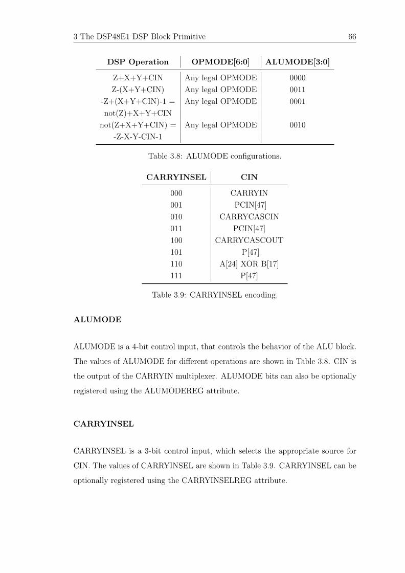
3 The DSP48E1 DSP Block Primitive 66
DSP Operation OPMODE[6:0] ALUMODE[3:0]
Z+X+Y+CIN Any legal OPMODE 0000
Z-(X+Y+CIN) Any legal OPMODE 0011
-Z+(X+Y+CIN)-1 = Any legal OPMODE 0001
not(Z)+X+Y+CIN
not(Z+X+Y+CIN) = Any legal OPMODE 0010
-Z-X-Y-CIN-1
Table 3.8: ALUMODE configurations.
CARRYINSEL CIN
000 CARRYIN
001 PCIN[47]
010 CARRYCASCIN
011 PCIN[47]
100 CARRYCASCOUT
101 P[47]
110 A[24] XOR B[17]
111 P[47]
Table 3.9: CARRYINSEL encoding.
ALUMODE
ALUMODE is a 4-bit control input, that controls the behavior of the ALU block.
The values of ALUMODE for different operations are shown in Table 3.8. CIN is
the output of the CARRYIN multiplexer. ALUMODE bits can also be optionally
registered using the ALUMODEREG attribute.
CARRYINSEL
CARRYINSEL is a 3-bit control input, which selects the appropriate source for
CIN. The values of CARRYINSEL are shown in Table 3.9. CARRYINSEL can be
optionally registered using the CARRYINSELREG attribute.

3 The DSP48E1 DSP Block Primitive 67
3.2.3 Output Ports
The main output ports of the DSP48E1 primitive are: P, PCOUT, CARRYOUT,
CARRYCASCOUT, MULTSIGNOUT, ACOUT, BCOUT.
P and PCOUT are each 48 bits wide. P is the main output of the DSP block,
which comes from the ALU block. The output is also connected to the adjacent
DSP block through PCOUT port for cascading multiple DSP blocks.
CARRYOUT and CARRYCASCOUT are each 4 bits wide. CARRYOUT[3] is
the valid carry output if the DSP block is used in non-SIMD (Single Instruction
Multiple Data) mode. Other bits are used in SIMD mode. CARRYCASCOUT is
the cascaded carry output which is directly connected to the adjacent DSP block.
MULTSIGNOUT is a 1-bit output, which is the sign bit (MSB) of the multiplier
output. This is mainly used for implementing wide multipliers.
ACOUT and BCOUT are 30 bits and 18 bits wide respectively, and pass the inputs
A and B to adjacent DSP blocks, when they are used in cascaded fashion.
3.3 DSP48E1 Template Database
As discussed in Section 3.2, DSP48E1 primitive blocks can be configured in many
ways and support dynamic programmability in every clock cycle. We analysed
all the possible configurations of DSP48E1 primitive, and prepared a database
of all configurations. We call this the “template database” and it consists of 29
arithmetic configurations of the DSP48E1. Many more templates can be generated
for bitwise logic operations, barrel shift functionality, magnitude comparison, and
pattern detection, however these are of limited use in arithmetic datapaths, so we
have restricted the database to configurations containing pre-adder, multiply, and
ALU blocks only. A list of all 29 templates with their equivalent expressions is
shown in Table 3.10 and dataflow graphs of some of these templates are shown in
Figure 3.3. Templates T1–T5 use the pre-adder and multiplier only (ALU block is

3 The DSP48E1 DSP Block Primitive 68
Template Expression Template Expression
T1 (A×B) + CIN T6 C + (A:B + CIN)
T2 (−A×B) + CIN T7 C − (A:B + CIN)
T3 ((D+A)×B) + CIN T8 −C + (A:B), CIN=1
T4 ((D−A)×B) + CIN T9 [−C − (A:B + CIN) −1]
T5 (D×B) + CIN
T10 C + [A×B + CIN] T20 −C + [A×B + CIN]
T11 C − [A×B + CIN] T21 −C − [A×B + CIN]
T12 C + [(−A)×B + CIN] T22 −C + [(−A)×B + CIN]
T13 C − [(−A)×B + CIN] T23 −C − [(−A)×B + CIN]
T14 C + [((D+A)×B) + CIN] T24 −C + [((D+A)×B) + CIN]
T15 C − [((D+A)×B) + CIN] T25 −C − [((D+A)×B) + CIN]
T16 C + [((D−A)×B) + CIN] T26 −C + [((D−A)×B) + CIN]
T17 C − [((D−A)×B) + CIN] T27 −C − [((D−A)×B) + CIN]
T18 C + [(D×B) + CIN] T28 −C + [(D×B) + CIN]
T19 C − [(D×B) + CIN] T29 −C − [(D×B) + CIN]
Table 3.10: Template Database.
used only for adding partial products of multiplier), templates T6–T9 bypass the
multiplier and the DSP block is used as a 48 bit wide adder/subtractor, templates
T10–T29 use the multiplier and ALU blocks with some templates also using the
pre-adder.
3.4 DSP48E1 Characterisation
The DSP48E1 includes internal pipelining that can allow significantly increased
throughput without using additional FPGA resources. This results in a trade-
off between latency and frequency, and can be configured effectively depending
on the design requirements. Depending on the arithmetic configuration chosen,
pipelining benefits can be gained with fewer or more stages.
Figure 3.4 shows the maximum achievable frequency for different arithmetic con-
figurations, as pipeline depth varies. The DSP48E1 supports up to four internal
pipeline stages; two at the inputs, one at the output of multiplier, and one at

3 The DSP48E1 DSP Block Primitive 69
×
A B
out
(a)
+
D A
×
B
out
(b)
−
D A
×
B
out
(c)
×
A B
+
C
out
(d)
+
A D
×
B
+
C
out
(e)
+
A D
×
B
+
out
(f)
Figure 3.3: Dataflow graphs for expressions (a) A×B (b) (D+A)×B (c)(D−A)×B (d) C + (A×B) (e) C + ((D +A)×B) (f) out = out+ (D +A)×B.
0 1 2 3 4
200
300
400
500
#Pipeline Stages
MaxFreq(M
Hz)
ALU Mul PA-Mul
Mul-ALU PA-Mul-ALU
Figure 3.4: Maximum frequency of a DSP48E1 for different configurations,with varying number of pipeline stages. (PA=Pre-adder).

3 The DSP48E1 DSP Block Primitive 70
+/-
+ -D
/
/
/
/
18
30
25
48
/48
B
A
D
C
P
Multiplier25x18
Pre-adder25-bit
X
48 A:B
ALU 48-bit
/
Figure 3.5: Setup for DSP48E1 characterisation.
the output of ALU. We add one pipeline stage at the inputs and one at output
to determine the maximum frequency for different configurations (as shown in
Figure 3.5).
Pipeline depths:
• Zero: No internal pipeline stage is enabled and the DSP block is used as
a combinational block. Configurations using the pre-adder cannot be used
without enabling at least one input pipeline stage.
• One: One pipeline stage is added at either the inputs, output, or at the
output of the multiplier. For configurations using the multiplier but not
using the pre-adder, a pipeline stage at the output of the multiplier results
in the best performance. Configurations with the pre-adder require a pipeline
stage at the inputs. For configurations not using the multiplier, a pipeline
stage at output results in best performance.
• Two: Any two pipeline stages can be selected. For configurations using
the multiplier, pipeline stages at inputs and output result in the best per-
formance. A pipeline stage at the output of multiplier does not affect the
performance for non-multiplier configurations since it is not in the datapath.
• Three: For configurations using the multiplier, pipeline stages at the output
of multiplier are also enabled. For non-multiplier configurations, we enable
another pipeline stage at the inputs.

3 The DSP48E1 DSP Block Primitive 71
016
CINALUMODEOPMODEINMODE
1512
Figure 3.6: DSP48E1 configuration word.
• Four: All four pipeline stages are enabled for all configurations. Enabling
the fourth pipeline stage improves the performance of configurations using
the pre-adder.
For configurations using just the multiplier or the multiplier and ALU, the DSP
block can achieve maximum frequency using three pipeline stages. However, when
the pre-adder is also enabled, all four pipeline stages are necessary to achieve
maximum performance. For configurations without the multiplier, two stages are
sufficient to achieve maximum performance. With this trade-off between maximum
frequency and latency, appropriate pipeline depth can be chosen to satisfy design
constraints.
3.5 Dynamic Programmability
As discussed above, the control inputs of the DSP48E1 (INMODE, OPMODE,
and ALUMODE ) allow it to be configured to implement different operations. A
key feature of the Xilinx DSP block is its dynamic programmability. This allows
the functionality of DSP block to be modified at runtime in each clock cycle.
This feature greatly enhances the usability of the DSP block as same specific
primitive can be used to implement different arithmetic operations. The DSP block
configuration can be dynamically changed to any of the 29 templates discussed in
Section 3.3. The configuration word for the DSP block is 17 bits wide, as shown
in Figure 3.6.
Figure 3.7 shows the timing diagram of a DSP48E1 primitive when its function-
ality is modified in each clock cycle, assuming all four pipeline stages are enabled.
Input control signals (INMODE, OPMODE, and ALUMODE) are also internally

3 The DSP48E1 DSP Block Primitive 72
Clock
inA ina1 ina2 ina3 ina4 ina5 ina6
inB inb1 inb2 inb3 inb4 inb5 inb6
inC inc1 inc2 inc3 inc4 inc5 inc6
inINMODE inm1 inm2 inm3 inm4 inm5 inm6
inOPMODE opm1 opm2 opm3 opm4 opm5 opm6
inALUMODE alum1 alum2 alum3 alum4 alum5 alum6
A1 ina1 ina2 ina3 ina4 ina5
B1 inb1 inb2 inb3 inb4 inb5
regC1 inc1 inc2 inc3 inc4 inc5
INMODE inm1 inm2 inm3 inm4 inm5
regOPMODE1 opm1 opm2 opm3 opm4 opm5
regALUMODE1 alum1 alum2 alum3 alum4 alum5
A2 ina1 ina2 ina3 ina4
B2 inb1 inb2 inb3 inb4
regC2 inc1 inc2 inc3 inc4
regOPMODE2 opm1 opm2 opm3 opm4
regALUMODE2 alum1 alum2 alum3 alum4
M p1 p2 p3
C inc1 inc2 inc3
OPMODE opm1 opm2 opm3
ALUMODE alum1 alum2 alum3
P out1 out2
Figure 3.7: Timing diagram for DSP block with dynamic programmability.
registered. Signals prefixed with in and reg are input signals to the DSP block
primitive (inA, inB, inC, inINMODE, inOPMODE, inALUMODE) and external
registers required to balance the latency of DSP block (regC1, regC2, regOP-
MODE1, regOPMODE2, regALUMODE1, regALUMODE2), respectively. The
remaining signals are internal to the DSP block primitive and not accessible from
the fabric (refer to Figure 3.2). Inputs C, OPMODE, and ALUMODE requires
two extra registers as these are consumed after the second cycle. In Figure 3.7,
we assume that the pre-adder block is not utilised, however, the timing diagram
can be easily extended to include the D input in that case.

3 The DSP48E1 DSP Block Primitive 73
X +X -
a
x
b x
cDSP1
DSP2
(a)
X +/-
Control Unit
config
(b)
Figure 3.8: Implementation of Equation 3.1 (a) without using dynamicprogrammability (b) using dynamic programmability.
We use a polynomial implementation as a case study to demonstrate the dynamic
programmability feature of the DSP48E1. The required polynomial to compute
is:
outp = yx2 + zx− w (3.1)
This equation can be broken into two steps:
t1 = y × x+ z (3.2)
outp = x× t1− w (3.3)
Each of the above equations (3.2 and 3.3) can be mapped to a DSP block. For
Equation 3.2, the DSP block should be configured with the multiplier enabled
and the ALU block used as an adder. Similarly, for Equation 3.3, the DSP block
should be configured with the multiplier enabled and the ALU block used as a
subtractor. Hence, the polynomial can be implemented fully and parallely using
two DSP blocks and no additional logic.
It is also possible to implement the whole computation on a single DSP block by
using dynamic programmability to change the functionality of the DSP block on-
the-fly. Figure 3.8a shows the implementation of Equation 3.1, using multiple DSP
blocks. The configuration word for DSP1 should be: “00101 0110101 0000 0”
and for DSP2 it should be: ”00101 0110101 0001 1”. Assuming the DSPs are
fully pipelined, i.e., 4 stages, the latency will be 8 cycles, and a new input can be
processed in every clock cycle.

3 The DSP48E1 DSP Block Primitive 74
Clock
x 1 5
y 2 10
z 3 15
w 4 20
A 1 1 5 5
B 2 5 10 65
C 3 4 15 20
INMODE 00101
OPMODE 0110101
ALUMODE 0000 0001 0000 0001
P 5 1 65 305
Figure 3.9: Timing diagram for case study example.
Figure 3.8b shows an implementation using only one DSP block. This uses the
dynamic programmability feature to execute equations 3.2 and 3.3 on the same
DSP block successively. Implementing multiple operations on one DSP block re-
quires a control unit to connect the correct inputs and generate configurations
for the DSP block. Generally, when consecutive operations are not dependent,
the functionality of DSP blocks can be changed in every clock cycle. However,
in this case study example, the input of Equation 3.3 is dependent on the output
of Equation 3.2. Considering fully pipelined DSP blocks (4 stages), the result of
Equation 3.2 is generated after 4 clock cycles, and in fifth clock cycle, the control
unit can change the configuration of the DSP block, and apply the correct inputs.
The system can take a new input in every sixth cycle. Figure 3.9 shows the timing
diagram for the case study example. The output of Equation 3.2 is generated
after the fourth clock cycle, and then used as input for Equation 3.3, by chang-
ing the DSP block configuration after the fourth cycle. As computations for the
next set of operations do not depend on outputs of the previous set of inputs, the
DSP block can be programmed for next set of inputs after one clock cycle. The

3 The DSP48E1 DSP Block Primitive 75
latency remains same at 8 clock cycles for final output, though the throughput is
drastically reduced.
3.6 Summary
In this chapter, we discussed how 18 × 18-bit multipliers evolved into the highly
functional DSP blocks we have today. Alongside arithmetic functions like mul-
tiply, multiply-add, add-multiply-add, multiply-accumulate, DSP blocks can also
be used for bitwise logic, pattern detection, and other functions. We described the
internal architecture of DSP48E1 primitive in detail and showed how they can be
configured for implementing different functions. We also presented a “template
database” containing all arithmetic configurations of the DSP block. We charac-
terised their performance as a function of configuration. Finally, we discussed the
dynamic programmability that allows them to implement different functions on
successive clock cycles.

4Automated Mapping to DSP Blocks from
Flow Graphs
4.1 Introduction
As discussed in Chapter 3, DSP blocks have advanced from simple hard-wired
multipliers to highly functional DSP48E1 blocks, which can be efficiently used
to speed up computationally intensive applications on FPGAs. By performing
arithmetic operations in optimised silicon rather than building these datapaths out
of LUTs, significant gains in performance and efficiency are achieved. A simplified
DSP48E1 primitive is shown in Figure 4.1 (reproduced from Figure 3.1).
76

4 Automated Mapping to DSP Blocks from Flow Graphs 77
+/-
+ -D
/
/
/
/
18
30
25
48
/48
B
A
D
C
P
Multiplier25x18
Pre-adder25-bit
X
/48 A:B
ALU 48-bit
INMODE OPMODE ALUMODE
Figure 4.1: Basic structure of the DSP48E1 primitive.
The DSP48E1 primitive with its sub-blocks provides a wide range of configu-
rations which can be exploited to implement circuits with high-throughput and
low resource usage. However, the increased functionality of the DSP blocks also
increases the complexity of tools that are required to efficiently utilise all these
capabilities. Traditionally, designs are described using either high-level languages
like C/C++, which are then translated to RTL HDL using HLS tools or directly
implemented in RTL HDL. These are then implemented onto FPGAs using ven-
dor tools that optimise designs according to the target device. We have observed
that vendor tools have not always developed to take full advantage of the evolving
hardware capabilities, and hence, there is a gap between expected and achieved
performance.
Pipelined RTL code can be mapped to DSP blocks by vendor tools when its struc-
ture is similar to one of its possible configurations. However, complex functions
requiring multiple DSP blocks do not achieve performance close to the capabilities
of the DSP blocks because the vendor tools fail to effectively map them to the DSP
blocks. Our experiments in [15] show that mapping is primarily focused around
using the multipliers in the DSP block, and often other operators are simply im-
plemented in LUTs.
In this chapter, we present an automated tool that can map complex mathemati-
cal functions to DSP blocks, achieving throughput close to their theoretical limit.
Our focus is on exploiting the full capabilities of the DSP block while maintaining

4 Automated Mapping to DSP Blocks from Flow Graphs 78
throughput through matched pipelining throughout the computational graph. A
function graph is first segmented into sub-graphs that match the various possible
configurations of the DSP block primitive, then balancing pipeline registers are
inserted to correctly align all datapaths. We show that generic RTL mapped in
this manner achieves identical performance to code that instantiates the DSP48E1
primitives directly. The proposed mapping approach can be incorporated into a
high-level synthesis flow to allow inner loops involving significant amounts of arith-
metic to be mapped for maximum throughput. To understand the effectiveness
of the proposed methods, we compare the implementations generated by the tool
with a number of techniques, discussed in detail in further sections. We also
compare the implementations generated by our tool with Xilinx Vivado HLS, a
state-of-the-art HLS tool for Xilinx FPGAs, to understand if HLS tools are capable
of exploiting DSP block functionalities to generate high-throughput implementa-
tions.
The main contributions of this chapter are:
• A tool to segment complex mathematical expressions across DSP blocks,
considering their internal capabilities and pipeline registers, with both a
greedy and improved heuristic method demonstrated.
• Automation of mapping to a number of different techniques, including pipeli-
ned RTL and Vivado HLS, to demonstrate the effectiveness of our approach.
• Full automation of the design flow for both the proposed and comparison
methods, allowing a thorough investigation of the performance metrics.
• Comparison of the proposed approach against the other methods for 18
benchmarks, as well as a case study application, demonstrating significant
improvements in throughput over other methods.
The work presented in this chapter has also been discussed in:
• Bajaj Ronak and Suhaib A. Fahmy, Evaluating the Efficiency of DSP Block
Synthesis Inference from Flow Graphs in Proceedings of the International

4 Automated Mapping to DSP Blocks from Flow Graphs 79
Conference on Field Programmable Logic and Applications (FPL), Oslo,
Norway, 2012, pp. 727-730. [15]
• Bajaj Ronak and Suhaib A. Fahmy, Experiments in Mapping Expressions
to DSP Blocks, poster in Proceedings of the IEEE Symposium on Field
programmable Custom Computing Machines (FCCM), Boston, MA, May
2014, pp 101. [16]
• Bajaj Ronak and Suhaib A. Fahmy, Efficient Mapping of Mathematical Ex-
pressions into DSP Blocks, in Proceedings of the International Conference
on Field Programmable Logic and Applications (FPL), Munich, Germany,
September 2014, pp. 1-4. [17]
• Bajaj Ronak and Suhaib A. Fahmy, Mapping for Maximum Performance
on FPGA DSP Blocks in IEEE Transactions on Computer-Aided Design of
Integrated Circuits and Systems (TCAD), vol. 35, no. 4, pp. 573-585, April
2016. [19]
4.2 Related Work
As DSP blocks can offer increased performance when mapping computationally
intensive datapaths, many algorithms have been implemented with careful map-
ping to these blocks. Examples include colour space conversion [147], floating
point operators [148], and filters [149, 150], where the DSP blocks offer an overall
increase in system performance over LUT-only implementations. This requires
the datapaths to be manually tailored around the low-level structure of the DSP
block, maximising use of the various features provided. More general application
to polynomial evaluation has also been proposed, again with detailed low-level
optimisation around the DSP block structure [151].
While synthesis tools can infer DSP blocks from general pipelined RTL code,
system design is increasingly being done at higher levels of abstraction. Widely
used High-level synthesis (HLS) tools today include Impulse-C [90], Bluespec [5],

4 Automated Mapping to DSP Blocks from Flow Graphs 80
LegUp [4], Xilinx Vivado HLS [3]. These tools synthesise to general RTL code
which is then mapped through vendor tools to a specific target device. The main
challenge here is that some optimisations made in the conversion to RTL may
prevent efficient mapping to the hard macros available in the device, especially
when the functionality to be mapped is beyond the “standard” behaviour of a
single block. In a typical HLS flow, the datapath is extracted from the high-level
description and scheduled before RTL is generated. This scheduling is architecture
agnostic and primitives are inferred instead during the synthesis and mapping
phases. Hence, if the scheduling does not fit the structure of the DSP block, it
may not be inferred to the fullest extent.
FloPoCo [152] is an open-source tool written in C++, that generates custom
arithmetic cores using optimised floating-point operators, generating synthesis-
able VHDL. It comprises a collection of parametrised basic operators and can be
used to generate custom architectures satisfying user-defined constraints, including
precision and target frequency. It also includes a polynomial function evaluator,
which can implement arbitrary single-variable polynomial circuits. However, it
generally uses DSP blocks as fast multipliers, and does not consider the other sub-
blocks (pre-adder and ALU), except insofar as the synthesis tool is able to infer
them.
General mapping to hard blocks has been considered in various implementation
flows. Verilog-to-Routing (VTR) [67] is an end-to-end tool which takes a de-
scription of a circuit in Verilog HDL and a file describing the architecture of the
target FPGA and elaborates, synthesises, packs, places, and routes the circuit,
also performing timing analysis on the design after implementation. Its front-end
synthesis is done using ODIN-II [71], which is optimised for some embedded blocks,
like multipliers and memories. For more complex embedded blocks, the user must
explicitly instantiate them, and they are considered “black boxes” by the tool.
As HLS tools map to RTL code, and experienced designers use RTL design, the
vendor flows integrate hard blocks primarily at the mapping phase. This means

4 Automated Mapping to DSP Blocks from Flow Graphs 81
RTL code (which has already been pipelined) that does not directly fit the struc-
ture of the DSP block and its internal sub-blocks and register stages can result in
poor mapping, as we demonstrate in this chapter. This is especially true of flexible
primitives like the DSP48E1 in modern Xilinx devices that support a variety of
configurations. At present, there are no tools that automatically map to flexible,
multi-function hard macro blocks efficiently because this is left to the mapping
stage. We present a DSP block mapping flow that results in hardware implemen-
tations that operate at close to maximum frequency, while consuming comparable
resources to HLS tools. This flow could be integrated into an HLS tool to allow
its benefits to be gained in larger, more complex applications.
4.3 Dataflow Graph Representation
A digital system can be described in multiple ways, at various levels of abstraction.
For high-level description, it can be represented in one of the high-level languages
like C/C++ or a behavioural description of the design in HDLs like Verilog and
VHDL. Designs can also be described at RTL level using Verilog and VHDL, which
is generally more complex compared to behavioural description.
As discussed in Section 2.2, the three major steps of hardware implementation
are: synthesis, technology mapping, and place-and-route. However, before the
implementation processes, the high-level description of the designs are generally
translated to a graph-based representation. The goal of this is to generate a
representation of the system which describes the operations to be executed, with
their dependencies and constraints. Control and data flow graphs (CDFGs) are
widely used for this intermediate representation.
A CDFG is a directed flow graph, which is a combination of the control flow graph
(CFG) and data flow graph (DFG) of the design. Nodes of the CFG include the
decision nodes, which determine the flow of the graph, i.e., selecting the operations
required to be executed for the current state of the design. DFG includes the
computation operations and their dependencies.

4 Automated Mapping to DSP Blocks from Flow Graphs 82
4
mul
mul
x
sub
mul
x
5
add
mul
5
out
x
Figure 4.2: Dataflow graph for expression 16x5 − 20x3 + 5x.
In our work, we are mainly focused on an efficient implementation of a compu-
tationally intensive inner loop of a larger system. Thus, we use DFGs as an
intermediate representation of the benchmark algorithms. An important charac-
teristic of DFGs in the context of our work is the ease of determining computation
patterns. An example DFG of a mathematical expression 16x5− 20x3 + 5x, which
can be equivalently represented as, x(((4×x)×x)× ((4×x)×x−5)+5), is shown
in Figure 4.2.
4.4 Dataflow Graph Implementation
We consider graphs of add-multiply nodes typical of a wide range of algorithms.
Recall that we are focused here on what would be the inner loop mapping for a

4 Automated Mapping to DSP Blocks from Flow Graphs 83
typical HLS design. Ideally, these graphs can make use of the various sub-blocks
present in the DSP48E1 primitive, as shown in Figure 4.1, if mapped correctly,
meaning extra LUT-based circuitry is reduced, and the resulting mapping should
reach close to the DSP block maximum frequency of around 500 MHz (on the Vir-
tex 6 family). The configuration inputs to DSP48E1 primitive determine how data
passes through the block, and which sub-blocks are enabled. These configuration
inputs can be set at run time, or fixed at design time. Considering all combina-
tions of arithmetic operations, the DSP48E1 supports 29 different datapath con-
figurations, which we store in a template database (as discussed in Section 3.3).
In addition to these 29 DSP templates, we have two templates for LUT-based
parametrised adders and subtracters for nodes that are not merged into DSP
blocks. The template database can also be expanded to include custom-designed
optimised operators like division or wide multiplications, allowing operations like
normalisation to be supported. Note that such templates would typically map
a single graph node, since they take advantage of multiple DSP blocks and their
sub-blocks internally, hence they do not exhibit the same flexibility we are exploit-
ing in the DSP blocks. For our work, we have limited our scope to add-multiply
graphs to explore the limits of individual DSP blocks.
Mapping an add-multiply flow graph to a circuit can be done in various ways.
A very simple and naive approach that fully relies on vendor tools, is to write
combinational Verilog statements that represent the required flow and add registers
at the output, allowing the tools to redistribute these during re-timing, with the
mapping phase then inferring DSP blocks. Synthesis tools can generally map
individual Verilog arithmetic operators efficiently. A more informed approach is
to write a pipelined RTL implementation, after scheduling the flow graph, and
to ensure the addition of pipeline registers between stages. Alternatively, the
dataflow graph can be described in a high level language and high-level synthesis
tools used to map this to a hardware implementation.
Although, none of these techniques take into account the internal structure of the
DSP blocks, we expect the vendor mapping tool to efficiently utilise the different

4 Automated Mapping to DSP Blocks from Flow Graphs 84
configurations of the DSP blocks in implementation. In the combinational imple-
mentation with re-timing, we expect the synthesis tools to re-time the design, by
absorbing the output registers into the datapath, allowing portions of graph to be
mapped to the sub-blocks and pipeline stages of the DSP blocks. However, our
experiments show that vendor tools do not re-time deeply into the graph, resulting
in DSP blocks being used only for multiplication.
In a scheduled pipelined RTL implementation, depending on the scheduling algo-
rithm used, the schedule of operations has been fixed, and the tools have little
flexibility to re-time the design, but will nonetheless map to DSP block config-
urations when a set of subsequent operations and intermediate registers match.
High-level synthesis tools generate a generic intermediate RTL representation, sim-
ilar to manually scheduled pipelined RTL, though we might expect them to do this
in a more intelligent manner when dealing with DSP blocks. Our experiments have
shown that none of the above methods result in implementations that maximise
DSP block usage or achieve high performance, as we discuss in Section 4.7.
The tool discussed in this chapter translates an add-multiply dataflow graph to
RTL code that maximises performance through efficient mapping to FPGA DSP
blocks. First, the graph is segmented into portions, or sub-graphs, which can be
mapped to one of the DSP block configurations in the template database discussed
earlier. The sub-graphs can then be converted to either direct instantiations of
DSP48E1 primitives with the correct configuration inputs, or RTL representations
of the same templates. While direct instantiation ensures the DSP blocks are
adequately used, it makes the output code less portable and readable, and this
might not be preferable where the flow graph is only a part of larger system. The
tool creates different implementations from any given input graph and generates
the area and frequency results for comparison. We now discuss how these different
techniques are implemented.

4 Automated Mapping to DSP Blocks from Flow Graphs 85
always @(*) creg1 = D + A;
always @(*) creg2 = creg1 * B;
always @(*) creg3 = creg2 + C;
always @ (posedge CLK)
begin
preg1 <= creg3;
preg2 <= preg1;
preg3 <= preg2;
preg4 <= preg3;
end
assign outp = preg4;
Figure 4.3: Sample Verilog code for Comb.
4.4.1 Combinational Logic with Re-timing: Comb
All nodes of the dataflow graph are implemented as combinational Verilog assign
statements. Sufficient pipeline stages are added at the output node(s) to allow
retiming. We enable the register balancing Synthesis Process property in Xilinx
ISE. Ideally, this should allow the tool to re-time the design, pulling register stages
back through the datapath to allow more efficient DSP block mapping. A sample
code for expression [(D + A)×B + C] is shown in Figure 4.3.
4.4.2 Scheduled Pipelined RTL: Pipe
Pipe represents how an experienced designer implements a DFG. We generate
schedule variations using two of the commonly used scheduling algorithms, As
Soon As Possible (ASAP) and As Late As Possible (ALAP), with pipeline stages
inserted between dependent nodes, mirroring what a typical RTL designer might
do. Additional registers are added to ensure all branches are correctly aligned.

4 Automated Mapping to DSP Blocks from Flow Graphs 86
4.4.3 High-Level Synthesis: HLS
We use Vivado HLS from Xilinx because it is likely to be the most architecture
aware of any of the HLS tools available for Xilinx devices. Similar to Comb, each
node is implemented as an expression, and directives are used to guide the RTL
implementation to fully pipeline the design. Since C++ code can have only one
return value, dataflow graphs with multiple outputs are implemented by concate-
nating all the outputs, which can later be sliced to obtain individual outputs.
4.4.4 Direct DSP Block Instantiation: Inst
The dataflow graph is segmented into sub-graphs that can be mapped to one of
the DSP48E1 templates identified earlier. Two graph segmentation approaches
are explored. The first is a greedy approach, in which the graph is traversed
from input to output with appropriate sub-graphs identified during traversal. The
second approach applies a heuristic to try and fit as many nodes as possible into
each sub-graph. Both of these methods are discussed in Section 4.5. For Inst, the
determined sub-graphs are then swapped for direct instantiations of the DSP48E1
primitive, with all the control inputs set to the required values. Additional registers
are added to ensure all branches are correctly aligned.
4.4.5 DSP Block Architecture Aware RTL: DSPRTL
Rather than instantiating the DSP48E1 primitives directly, we replace each sub-
graph with its equivalent RTL code directly reflecting the template’s structure.
This variation will make it clear if it is the instantiation of the primitives, or the
structure of the graph that has a fundamental effect on performance. Sample code
for expression [(D + A) × B + C], which represents a DSP template utilising all
three sub-blocks with four pipeline stages, is shown in Figure 4.4. In this case,
two extra registers will be required to balance the datapath of input C, similar to
Inst.

4 Automated Mapping to DSP Blocks from Flow Graphs 87
always @ (posedge CLK)
begin
pregA1 <= A;
pregB1 <= B;
pregD <= D;
pregB2 <= pregB1;
pregAD <= pregD + pregA1;
pregC <= C;
pregM <= pregAD * pregB2;
pregP <= pregM + pregC;
end
assign outp = pregP;
Figure 4.4: Sample Verilog code for DSPRTL.
4.4.6 Ensuring a Fair Comparison
Along with generating all 5 different implementations from the same graph de-
scription, a number of factors must be considered to ensure a fair comparison.
The first is the overall latency of an implementation, as it impacts the resource re-
quirements. Inst uses fully pipelined DSP blocks, which results in a deep pipeline,
and thus many balancing registers. For Comb, we add as many pipeline stages
after the combinational logic for re-timing, as there are pipeline stages in Inst.
This gives more flexibility to the tools to re-time the circuit, and ensures that
there are sufficient cycles for a similarly pipelined implementation to be achiev-
able in theory. Similarly, for HLS, we enforce a constraint on latency, equal to
the latency of Inst, using a directive in the Tcl file. However, for Pipe, we let the
schedule determine the number of pipeline stages as this reflects what an expert
designer might do, and adding more stages might increase area for the purposes
of comparison.
Another factor is wordlength. The input and output ports of the DSP block have
different wordlengths. When the output of a DSP block is passed to another’s
input, it must be either truncated, or the latter operations should be wider. We
choose to truncate wide outputs. This is equivalent to a multi-stage fixed point

4 Automated Mapping to DSP Blocks from Flow Graphs 88
X
+/-
+/-
D A
B
C
P
+/-
+-D
////
1830
25
48
/ 48
BADC
P
Mu
ltiplie
r2
5x18
Pre
-add
er
25-b
it
X
/4
8A
:B
ALU
4
8-bit
Figure 4.5: Dataflow through the DSP48E1 primitive.
implementation, although we can optimise for known and fixed inputs. Primary
inputs that are narrower than the input ports of the DSP block are sign extended.
To ensure that comparisons between all implementation techniques are fair, we
manually handle the intermediate wordlengths in Comb, Pipe, and HLS to match
those determined for Inst for all operations. This is necessary, because, other
techniques may implement wider operations in intermediate stages, thus skewing
resource usage as well as accuracy, resulting incomparable implementations. Note
that in the case where the designer does require wider intermediate operations, the
tool can be modified to instantiate optimised multi-DSP-block operators thereby
still guaranteeing performance. Finally, since Comb requires the register balancing
synthesis feature to be enabled, we do so for all methods.
4.5 DFG Segmentation for DSP Blocks
For the proposed mapping (Inst and DSPRTL), we attempt to map as many nodes
as possible of the dataflow graph to DSP blocks, as this should result in high op-
erating frequency without consuming additional LUT resources. In order to map

4 Automated Mapping to DSP Blocks from Flow Graphs 89
as many nodes to DSP blocks, we first segment the input dataflow graph into sub-
graphs, such that each matches a DSP block template as defined in Section 3.3.
A DSP48E1 primitive can perform up to three operations, so a DSP48E1 primi-
tive can be represented as a dataflow graph comprising three nodes, as shown in
Figure 4.5.
Segmentation is a critical step in our flow, as the performance of the final imple-
mentation largely depends on how operations are mapped on to DSP48E1 prim-
itives. We explore two approaches to this segmentation problem. The first is
a greedy algorithm, which selects the best sub-graph for the current node while
stepping through the graph. The second approach applies a more global heuristic
optimisation to maximise the number of nodes in each sub-graph, i.e., maximising
the utilisation of each DSP block instantiated.
4.5.1 Greedy Segmentation
The input to the segmentation algorithm is the DFG of the input application and
it starts with a randomly selected primary input node. A primary input node
is a node where both inputs are either one of the primary inputs or a constant.
If that node has multiple outputs, it cannot be combined with a child node into
a DSP block template since the DSP48E1 primitive is designed in such a way
that intermediate outputs of sub-blocks cannot be accessed externally without
bypassing later sub-blocks. If the node has a single child, they are combined into
a sub-graph, and the same process is repeated to add a third node to the sub-graph
if possible. Sub-graph merging is also terminated if a node is a primary output of
the graph.
Each time a sub-graph of 1, 2, or 3 nodes is extracted, it is matched against the
template database, and if a match is found, those nodes are marked as checked
and not considered in subsequent iterations. If only a partial match is found,
only those matched nodes are marked as checked and the remaining nodes are
re-separated to be considered for further iterations. The process is repeated until

4 Automated Mapping to DSP Blocks from Flow Graphs 90
all nodes are checked. Sub-graphs combining two add/sub nodes with no multiply
nodes are re-separated with the root node implemented in LUTs, and the child
node left for re-merging with other nodes in further iterations. The output of this
process is a graph consisting of DSP block templates (each with an associated
latency) and some adder/subtractor nodes to be implemented in logic, and we call
this the DSP Dataflow Graph (DDFG).
In each iteration, Greedy Segmentation selects the best sub-graph, i.e., the one
with the maximum number of nodes, with the current node at its root. The
solution is considered globally optimal when the sub-block utilisation is maximum
for the extracted set of sub-graphs. Greedy Segmentation cannot always achieve
an optimal solution as root nodes for sub-graphs are selected in the order in which
they are traversed. The determined solution is only optimal when the structure
of input DFG is such that order of root nodes results in maximum sub-block
utilisation.
The runtime complexity of the greedy segmentation algorithm is directly propor-
tional to n, where n is the number of nodes in the graph.
The algorithm is detailed in Algorithm 1.
4.5.2 Improved Segmentation
The greedy algorithm discussed above can result in sub-optimal segmentation as
it only considers local information starting from the inputs. We try an improved
algorithm that instead first finds possible sub-graphs which can be mapped to
a DSP block template utilising all three sub-blocks, then subsequently finds the
sub-graphs with two nodes, and then remaining single nodes.
The segmentation process is broken into four iterations. In the first iteration, only
valid sub-graphs of three nodes are matched to the template database, as discussed
in Section 4.5.1, and if a full match is found, these nodes are marked as checked. If
only a partial match is found, all nodes are re-separated. In the second and third

4 Automated Mapping to DSP Blocks from Flow Graphs 91
Algorithm 1: Greedy Segmentation
def greedySeg(dfg, outNodes):Data: Dataflow Graph (dfg); List of output nodes (outNodes)Result: Dataflow graph of identified templates (ddfg)
begin#dataflow graph of templates identifiedddfg = [ ]
#for each node n in dfgfor n in dfg:
#empty graph of 3 nodessubGraph = [0, 0, 0]if n not checked :
subGraph[0]=nif terminateSubGraph(n, outNodes):
template = getTemplate(subGraph)else:
nNext = n[out]if nNext not checked :
subGraph[1]=nNextif terminateSubGraph(nNext, outNodes):
template = getTemplate(subGraph)else:
nNextNext = nNext[out]if nNextNext not checked :
subGraph[2]=nNextNext
template = getTemplate(subGraph)
else:template = getTemplate(subGraph)
if template:ddfg.add(template)#mark nodes of subGraph assigned to template checkedsubGraph.checked()
else:continue
return ddfg
def terminateSubGraph(n, outNodes):#if the node has been assigned to a templateif n is checked :
return True#if output going to multiple nodesif len(n[out]) > 1 :
return True#if output is primary outputif n[out] in outNodes:
return Truereturn False

4 Automated Mapping to DSP Blocks from Flow Graphs 92
Algorithm 2: Improved Segmentation
def improvedSeg(dfg, outNodes):Data: Dataflow Graph (dfg); List of output nodes (outNodes)Result: Dataflow graph of identified templates (ddfg)ddfg = [ ] #dataflow graph of templates identifiednumNodesList = [3, 2, 2, 1] #add-mul-add, mul-add, add-mul, mul/addfor numNodes in numNodesList:
for n in dfg:subGraph = getNextNodes(n, numNodes, dfg, outNodes)if subGraph:
template = getTemplate(segList)if template.valid():
ddfg.add(template)subGraph.checked()
else:continue
return ddfg
def getNextNodes(startNode, numNodes, dfg, outNodes):for n in dfg:
subGraph = [0, 0, 0] #empty graph of 3 nodesif n[name] == startNode[name]:
if n not checked :subGraph[0]=nif numNodes == 1 :
return subGraph
if terminateSubGraph(n,outNodes):return 0
else:nNext = n[out]if nNext not checked :
subGraph[1]=nNextif numNodes == 2 :
return subGraph
if terminateSubGraph(nNext,outNodess):return 0
else:nNextNext = nNext[out]if nNextNext not checked :
subGraph[2]=nNextNextif numNodes == 3 :
return subGraph
return 0
else:return 0
else:return 0
return 0

4 Automated Mapping to DSP Blocks from Flow Graphs 93
iterations, the same process is applied to all remaining unchecked nodes for sub-
graphs of two nodes. There are two types of two-node templates: those that include
the pre-adder and multiplier sub-blocks, and those with the multiplier and ALU
sub-blocks. Since the ALU wordlength is wider than the pre-adder, we consider
sub-graphs of the latter type in this second iteration, as the default option. This
also has the benefit of allowing a 1-cycle reduced latency through the DSP block
(recall the discussion on pipelining in Section 3.4), resulting in a shorter overall
pipeline depth, and hence reduced resource usage. Matched sub-graph nodes are
then marked as checked. In the third iteration two-node sub-graphs using the
pre-adder are matched. The second and third iterations can easily be swapped
using a configuration in the tool, for experimentation. In the fourth iteration
the remaining uncovered nodes are considered individually and mapped to DSP
blocks for multiply operations, or LUTs for additions/subtractions. Similar to
greedy algorithm, improved segmentation also outputs a DDFG.
The runtime complexity of the improved segmentation algorithm is up to four
times higher than for the greedy algorithm, since four passes must be completed
on the graph.
The improved algorithm is detailed in Algorithm 2.
4.6 Automated Mapping Tool
Bringing together the techniques discussed thus far, we have developed a fully
automated mapping tool. It takes a C/C++ description of a mathematical ex-
pression as input, and prepares synthesisable RTL implementations for all the
mapping methods described in Section 4.4 (Comb, Pipe, HLS, Inst, and DSPRTL),
using either of the segmentation algorithms discussed in Section 4.5 for Inst and
DSPRTL. A flow diagram of the proposed tool is shown in the Figure 4.6.

4 Automated Mapping to DSP Blocks from Flow Graphs 94
DFG Generation
Input C File
DFG Scheduling DDFG Scheduling
Pipeline Balancing
HLS Project Generation
Pipeline Balancing
RTL Generation RTL Generation RTL GenerationRTL Generation
Xilinx ISE Project Generation
Comb HLS Inst DSPRTL
Vendor tool flowReports
Generation
Vendor Tool Flow
Register Insertion
Pipe
Pre-processing
C-to-DOT
DFG Partitioning
Graph Partitioning
RTL Generation
RTL Projects Execution
Template Database
DFG Generation
DFG
DDFG
Update Wordlength
Figure 4.6: Tool flow for exploring DSP block mapping.
4.6.1 C-to-DOT
The front-end of the tool accepts a computation kernel description in C, with the
list of inputs with their ranges and precision provided in a separate text file (config
file). For the purposes of functional verification, the config file can also contain
set of test vectors for each input. If these are provided, the tool also generates
testbenches for all the resultant implementations. Format of the config file is
shown in Figure 4.7. Precision is discussed in Chapter 5.

4 Automated Mapping to DSP Blocks from Flow Graphs 95
inputs = <list of inputs separated by comma (,)>
input_ranges = <list of range of inputs in {min,max} format,
separated by (;)>
precision = <precision>
test_inputs [optional]
<input1> = <list of test inputs separated by comma>
<input2> = <list of test inputs separated by comma>
...
<inputN> = <list of test inputs separated by comma>
-------------------------------------------------------
N: No of inputs; M: No of instructions
Figure 4.7: config file format.
In the current format of the tool, the expression is written as a series of two
operand operations.
Example: 16x5 − 20x3 + 5x⇒ (x(4× x× x× (4× x× x− 5) + 5))
LLVM is used to translate the input C file in to a set of DOT files, one for each
function. We use LLVM’s frontend compiler clang for compilation, which generates
an intermediate bitcode. We then use opt, LLVM’s optimiser passes, to convert
the bitcode to a readable DOT format, which is a plain text graph description
format.
4.6.2 DFG Generation
After generating DOT files using LLVM, the DOT file of the computation kernel
is parsed and translated into a DFG, with each node in the graph representing
an operation from the input C file. Fixed power-of-2 multiplications can be im-
plemented using shifts, saving multipliers. While translating DOT to DFG, we
combine these multiplications with successive operations.
Example: (x(4× x× x× (4× x× x− 5) + 5))⇒ (x(4x× x× (4x× x− 5) + 5))
Each node in the DFG is tagged with a tool-generated identification name of
the node, its operation (multiplication or addition or subtraction), inputs, and

4 Automated Mapping to DSP Blocks from Flow Graphs 96
outputs. Additional information is added to these nodes in the subsequent stages,
wherever required.
4.6.3 Graph Partitioning
The DFG generated in the previous stage is then translated into a DDFG by par-
titioning it into sub-graphs using either of the algorithms discussed in Section 4.5.
the user can select between greedy (Section 4.5.1) and improved (Section 4.5.2)
segmentation. For improved segmentation, the preference between ‘Pre-adder mul-
tiply’ and ‘multiply ALU’ combinations is also user selectable for experimental
purposes. Each node of the DDFG is either mapped to one of the DSP templates
in the template database or a LUT-based adder/subtractor with input and output
edges mapped to appropriate ports.
4.6.4 Pre-processing
The tool now has a DFG generated from the input C file and a DDFG, in which
each node is either a DSP template from the template database or LUT-based
adder/subtractor. For the different implementation methods, some pre-processing
is necessary to allow generation of synthesisable RTL. Methods Comb, Pipe, and
HLS operates on the DFG; Inst and DSPRTL operate on the DDFG generated
during the graph partitioning stage. Before processing the DFG and DDFG for
individual techniques, we update the wordlengths of the inputs and outputs of
each node in the DFG according to the mapping to DSP blocks in the DDFG, to
ensure a fair comparison.
Comb:
As discussed in Section 4.4, pipeline registers are added at the output node(s)
of the graph to facilitate re-timing during the synthesis process. The number of
pipeline stages added is equal to the pipeline depth of Inst.
Pipe:

4 Automated Mapping to DSP Blocks from Flow Graphs 97
The input DFG is scheduled according to generic scheduling techniques, as an
experienced designer would do. We implement both As Soon As Possible (ASAP)
and As Late As Possible (ALAP) schedules. Pipeline registers are added between
dependent nodes.
Pipeline balancing is then applied to ensure that dataflows through the DFG are
correctly aligned. Nodes of the DFG are assigned a level according to the schedule.
The level of each node input is compared with the level of its source registers, and,
if the difference is greater than 1, balancing registers are added to correctly align
the datapaths.
HLS:
We use Xilinx Vivado HLS for this method. The input expression is converted to
C++, with each node of the DFG implemented as an instruction. We use fixed
wordlengths in C++, and ensure that wordlengths of operations are the same as of
Inst for fair comparison. If unit tests are given in the input file, a C++ testbench
is also generated. Vivado HLS directives are used to set the pipeline latency, which
is set equal to the latency of Inst. Other files required for the Vivado HLS project
are also generated.
Inst, DSPRTL:
After generating the DDFG in the Graph Partitioning stage, a schedule of the
DDFG is generated which is used for RTL generation. We implement both ASAP
and ALAP scheduling techniques, which can be selected by the user. After schedul-
ing, datapaths of the DDFG are balanced to correctly align data flow, as for Pipe.
4.6.5 RTL Generation
The Verilog code implementing the datapaths for all the implementation tech-
niques, with their testbenches (if test vectors are provided in the config file) are
generated. For all the techniques, the wordlengths of the inputs and outputs of
each node are explicitly set to the same as those of Inst for fair comparison.

4 Automated Mapping to DSP Blocks from Flow Graphs 98
For Comb, RTL implementing each node as combinational logic is generated, with
pipeline registers at the output(s), for re-timing.
For Pipe, all the node operations and registers scheduled in a particular schedule
time are implemented as a pipeline stage, in one Verilog always block. Registers
required for pipeline balancing are also generated and assigned accordingly. As
discussed above, we do not add extra pipeline registers at the outputs for Pipe.
For HLS, we run the Vivado HLS project generated in the previous stage, which
translates the high-level C++ implementation of the input expression into syn-
thesisable RTL. It also generates an equivalent RTL testbench from the C++
testbench.
For Inst, Verilog RTL for instantiations of the DSP block templates along with
the balancing registers are generated. DSPRTL is an RTL equivalent of Inst,
reflecting the internal structure of Inst implementation. Instead of instantiating
the DSP48E1 primitive itself, equivalent behavioural Verilog blocks that represent
each of the DSP block templates are used. Intermediate signals are first shifted
then truncated depending on the destination wordlength.
4.6.6 Vendor Tool Flow
The RTL files for all above methods are then synthesised through the vendor
tools. Since this can be time consuming, we have automated the process through
a series of scripts. First, ISE Projects are generated for all the techniques. This
includes setting the specific device and timing constraints. Synthesis is then run,
and the reports stored. The tool then runs the implementation stages iteratively
to determine the best performance, i.e., minimum clock period. It first uses a
default timing constraint, then if the design fails, it reduces the constraint until it
finds the minimum clock period for which the design constraints are satisfied post
place and route. Resource requirements are also extracted from the post place and
route reports for analysis.

4 Automated Mapping to DSP Blocks from Flow Graphs 99
Graph Inputs Outputs Adders/Subs Muls
ARF 26 2 12 16
Chebyshev 1 1 2 3
EWF 21 5 26 8
FIR2 17 1 15 8
Horner Bezier 12 4 6 8
Mibench2 3 1 8 6
Motion Vector 25 4 12 12
Poly1 2 1 5 4
Poly2 2 1 3 5
Poly3 6 1 4 6
Poly4 5 1 3 3
Poly5 3 1 13 11
Poly6 3 1 19 23
Poly7 3 1 18 17
Poly8 3 1 16 15
Quad Spline 7 1 4 13
SG Filter 2 1 6 6
Smooth Triangle 29 14 20 17
Table 4.1: Graph nodes I/O and operations.
4.7 Experiments and Analysis
To explore the effectiveness of our DSP block mapping technique against the other
standard methods described, we implemented a number of benchmark multiply-
add flow graphs. These include the Chebyshev polynomial, Mibench2 filter, Quadr-
atic Spline, and the Savitzky-Golay filter from [153]; The ARF, EWF, FIR2,
Horner Bezier, Motion Vector, and Smooth Triangle from [154]; and 8 polyno-
mials of varied complexity from the Polynomial Test Suite [155]. We prepared
input C files for all 18 of these expressions, and processed them through the auto-
mated tool. Table 4.1 shows the number of inputs, outputs, and number of each
type of operation (add/sub, multiplier), for all benchmarks.

4 Automated Mapping to DSP Blocks from Flow Graphs 100
Benchmarks Greedy Segmentation Improved Segmentation
ARF 12.8 13.0
Chebyshev 36.2 37.9
EWF 67.4 70.7
FIR2 22.2 21.7
Horner Bezier 20.8 21.7
Mibenc2 18.3 17.8
Motion Vector 26.3 27.8
Poly1 18.4 18.8
Poly2 75.7 79.1
Poly3 308.3 363.2
Poly4 231.7 244.9
Poly5 108.3 124.6
Poly6 251.9 266.7
Poly7 358.1 378.3
Poly8 126.0 124.9
Quad Spline 34.4 32.8
SG Filter 45.5 43.8
Smooth Triangle 600.1 606.0
Geometric Mean 67.3 69.6
Table 4.2: Run time (in ms) for Inst using greedy and improved segmen-tation
As discussed in Section 3.4, a 3-cycle pipeline offers maximum performance when
the pre-adder is not used, and a 4-cycle pipeline is required to achieve the same
frequency if the pre-adder is used. We map only to template configurations that
achieve this maximum frequency of 473 MHz to allow the overall circuit to achieve
near to this limit.

4 Automated Mapping to DSP Blocks from Flow Graphs 101
4.7.1 Tool Runtime
The proposed tool is run on an Intel Xeon E5-2695 running at 2.4GHz with 16GB
RAM.
The times taken to generate synthesisable RTL from the high-level description for
both segmentation methods, averaged over 100 executions, are shown in Table 4.2.
The runtimes are entirely tolerable as part of a larger design flow. Smooth Tri-
angle, which results in the highest number of templates after segmentation, takes
under a second. On an average, a benchmark can generate RTL for the proposed
Inst method in less than 70 ms. Although the time complexity for Improved Seg-
mentation is higher than for Greedy Segmentation, the total runtime depends on
other factors like the number of templates considered, and file operations (read-
/write). This means some benchmarks show marginally higher run time for Greedy
compared to Improved.
4.7.2 Resource Usage and Frequency
All implementations target the Virtex 6 XC6VLX240T-1 FPGA as found on the
ML605 development board, and use the Xilinx ISE 14.6 and Xilinx Vivado HLS
2013.4 tools.
Resource usage and maximum achievable frequency for all 18 benchmarks, with all
5 methods using the improved segmentation method are shown in Figure 4.8. The
improved segmentation method results in more templates with higher sub-block
usage but overall DSP block usage is the same as for greedy segmentation, since
the multipliers generally determine this.
As the number of DSPs and LUTs cannot be compared directly, and to understand
overall resource usage, we compare the area in terms of equivalent LUTs also,
where LUT eqv = nLUT + nDSP × (196), where 196 is the ratio of number of
LUTs (150720) to number of DSP blocks (768) available on the target device
used. This gives a proxy for overall area consumption.

4 Automated Mapping to DSP Blocks from Flow Graphs 102
Com
bPipe
HLS
DSPRTL
Inst
Com
bPipe
HLS
DSPRTL
Inst
Com
bPipe
HLS
DSPRTL
Inst
Com
bPipe
HLS
DSPRTL
Inst
Com
bPipe
HLS
DSPRTL
Inst
Com
bPipe
HLS
DSPRTL
Inst
Com
bPipe
HLS
DSPRTL
Inst
Com
bPipe
HLS
DSPRTL
Inst
Com
bPipe
HLS
DSPRTL
Inst
0
2,000
4,000
6,000
8,000
Chebyshev Mibench2 FIR2 SG Filter Horner Bezier Poly1 Poly2 Poly3 Poly4Algorithm
Resou
rces
DSPs×196 LUTs Regs
0
100
200
300
400
500
Max
imum
frequency
(MHz)
Freq
(a)
Com
bPipe
HLS
DSPRTL
Inst
Com
bPipe
HLS
DSPRTL
Inst
Com
bPipe
HLS
DSPRTL
Inst
Com
bPipe
HLS
DSPRTL
Inst
Com
bPipe
HLS
DSPRTL
Inst
Com
bPipe
HLS
DSPRTL
Inst
Com
bPipe
HLS
DSPRTL
Inst
Com
bPipe
HLS
DSPRTL
Inst
Com
bPipe
HLS
DSPRTL
Inst
0
2,000
4,000
6,000
8,000
Poly5 Poly6 Poly7 Poly8 Quad Spline ARF EWF Motion Vector Smooth TriangleAlgorithm
Resou
rces
DSPs×196 LUTs Regs
0
100
200
300
400
500
Max
imum
frequen
cy(M
Hz)
Freq
(b)
Figure 4.8: Resource usage and maximum frequency for 18 benchmarksusing the different mapping techniques.
It is clear that the performance of Comb is the worst among all methods. The ven-
dor tools are not able to absorb registers into a very deep combinational datapath.
The maximum frequency for Inst is generally much improved (3.4–15.6×) over
Comb, at a cost of LUT eqv usage going up to 1.3×. Although the throughput of
Pipe and HLS improve significantly, they do not approach the maximum frequency
supported by the DSP blocks (450–500 MHz) for most benchmarks. For Pipe, we
implemented both ASAP and ALAP schedules, and chose the one with higher
throughput. The performance of HLS is generally better than Pipe. For the ARF
and Smooth Triangle benchmarks, which have regular repetitive structures, HLS
is able to achieve a frequency close to that achieved by the Inst method. However,
for FIR2 and Motion Vector, which also have a regular structure, HLS falls short.
The Chebyshev dataflow graph is very narrow, and HLS is able to implement it

4 Automated Mapping to DSP Blocks from Flow Graphs 103
Comb Pipe HLS DSPRTL Inst
0
20
40
60
80
100
PreAdd-Mul-ALU Mul-ALU PreAdd-Mul Mul
Figure 4.9: DSP48E1 primitive sub-block utilisation.
efficiently. For Motion Vector and EWF, Pipe achieves a higher frequency than
HLS. For Motion Vector, the Pipe graph schedule and structure fit well with the
DSP blocks, and also allow the mapping tool to take advantage of the internal cas-
cade connection between PCOUT(DSP1) to PCIN(DSP2), reducing routing delay
significantly. For EWF, the schedule of the dataflow graph feeds forward with
no parallal delay paths. As a result, all the sub-blocks are used in 4 DSP blocks
while the other 4 use 2 sub-blocks, leading to high throughput. On the contrary,
HLS uses the DSP blocks mostly for multiplications (7 out of 8) with extra nodes
in logic. For complex graphs, both Pipe and HLS are unable to come close the
frequency achievable using our proposed method. The maximum frequency for
Inst is up to 3× and 1.4× better than Pipe and HLS respectively. We expect
Vivado HLS, being the most architecture aware high-level synthesis tool for Xilinx
devices, to represent the most competitive HLS tool for such mappings.
To understand how arithmetic operations are mapped on to DSP blocks in Pipe
and HLS, we analysed the configurations of the DSP blocks used by vendor tools
for implementation of these methods. For Pipe, the vendor tool utilise sub-blocks
of the DSP blocks well but does not use all the pipeline stages of the DSP blocks
due to the fixed schedule and only one register stage is present between dependent
nodes. This significantly affects the throughput, as shown in Figure 3.4. For

4 Automated Mapping to DSP Blocks from Flow Graphs 104
0.8 1 1.2 1.4 1.6 1.8 2
200
300
400
500
Regs+LUTs
Max
Frequen
cy
2 stage 3 stage Inst HLS
Figure 4.10: Frequency Area trade-off, normalised against HLS.
HLS, we have observed that the sub-blocks of the DSP blocks are not heavily
used. Across all 169 DSP48E1 primitives used by HLS across all benchmarks,
none use all three sub-blocks, while for Inst, 46 such instances exist. Since we set
the pipeline latency for HLS to equal that of Inst, it has sufficient slack to achieve
similar performance, and this also explains some of its advantage over Pipe.
An overview of usage of different sub-blocks of the DSP48E1, across all benchmarks
is shown in Figure 4.8. For Comb and Pipe, over half the DSP blocks are used only
for multiplication, and this is even higher for HLS. The proposed DSPRTL and
Inst methods make more use of the sub-blocks including around 20% of instances
using all three sub-blocks.
Overall, we see that the throughput achievable by existing methods is significantly
less than what we are able to achieve through our proposed Inst and DSPRTL
approaches, though the proposed methods suffer from higher resource usage due to
heavily pipelined structures. The proposed methods use DSP block templates with
either 3 or 4 stages (depending on the sub-blocks used). This pipelining within
the DSP block is “free” since those registers are not implemented in the fabric,
however, extra registers are then required to balance other paths through the
graph. Register utilisation for Inst is higher than for DSPRTL. Since DSPRTL uses

4 Automated Mapping to DSP Blocks from Flow Graphs 105
Benchmarks Pipe Comb/HLS/ Benchmarks Pipe Comb/HLS/
Inst/DSPRTL Inst/DSPRTL
ARF 9 26 Poly5 10 24
Chebyshev 6 14 Poly6 12 31
EWF 15 28 Poly7 13 34
FIR2 10 27 Poly8 12 31
Mibenc2 7 16 Horner Bezier 5 12
Poly1 5 13 Motion Vector 5 11
Poly2 5 13 Quad Spline 7 22
Poly3 6 15 SG Filter 8 14
Poly4 5 12 Smooth Triangle 7 21
Table 4.3: Pipeline depth for Pipe and other approaches.
an RTL equivalent of the DSP block configuration rather than direct instantiation,
this affords the vendor tools more flexibility in how to map registers onto the FPGA
logic, including better optimisation of chains of registers.
Figure 4.10 shows the area and throughput trade-off across HLS and Inst using
DSP block templates of different pipeline depths. The data points for ‘2 stage’ and
‘3 stage’ refer to implementations with the pipeline depth of the DSP blocks set
to 2 or 3 respectively. Resource usage (#Regs + #LUTs) is normalised against
HLS for all benchmarks. Out of 18 benchmarks, only 6 achieve over 400 MHz
using HLS, while Inst implementations can run at frequencies above 450 MHz for
all benchmarks. This higher frequency comes at the expense of resources required
for balancing registers. The Poly3 benchmark in HLS utilises fewer DSP blocks
as it optimises the fixed coefficient multipliers in logic. Inst uses DSP blocks for
these to maintain high frequency and design flexibility.
Benchmarks with no pre-adder templates can achieve high throughput using 2 and
3 stage DSP block templates (as evident from Figure 3.4).
Pipeline depths for the Pipe and other approaches are shown in Table 4.3.

4 Automated Mapping to DSP Blocks from Flow Graphs 106
The two segmentation algorithms result in the same maximum frequency but the
improved algorithm marginally improves the LUT eqv usage by 1–3% in some cases.
Combining frequency results across all benchmarks, the geometric mean in the
frequency improvement of Inst is 7.4× over Comb, 2× over Pipe, and 1.2× over
HLS. These gains are at the cost of 1.1-1.23× LUT eqv usage, compared to other
methods.
A key positive finding of this study is that maximum DSP block frequency can
be achieved without architecture-specific instantiation of the DSP48E1 primitive.
Explicit instantiation of primitives is not desirable as it leads to complex code
and hinders portability to other architectures. With DSPRTL, we instead replace
those direct instantiations with behavioural Verilog code that exactly matches
the required template configuration, including pipeline configuration. We can see
that this offers almost the same performance as Inst but with code that remains
portable. The tools can correctly map these general templates to DSP blocks,
including internal pipeline stages. Just offering sufficient pipeline stages (as we
do for HLS ) does not guarantee maximum throughput. It is essential to take into
account the structure of the DSP blocks when translating the dataflow graph into
Verilog for implementation.
Note, however, that initial experiments with DSPRTL did not demonstrate this
high level of performance. Rather, it was necessary to add an additional register
stage after each extracted DSP block template, likely because the tools could only
correctly map to the DSP blocks with a margin of one cycle between them to break
the possible long routing paths between subsequent DSP blocks and reduce routing
delays. Although there are cascade wires that allow DSP blocks in a column to
be connected without going through the routing fabric, these connect the output
of a DSP block to only the ALU input of the subsequent block, limiting their use
in general mapping where the output of a DSP block may need to be connected
to any other inputs of a subsequent block. This tweak significantly improved the
performance of DSPRTL from a mean frequency of 383 MHz to 470 MHz, close the
471 MHz of Inst, without significantly impacting the final area results.

4 Automated Mapping to DSP Blocks from Flow Graphs 107
redIn
n1mul
n8sub
70
redIn
n2mul
n9add n11add
30greenIn
n3mul
n7add
59
greenIn
n4mul
n12sub
41
blueIn
n5mul
n13add
11
blueIn
n6mul
n10sub
89
n14mul n15muln16mul
n17add n18add n19add
sat satsat
redOut greenOut blueOut
Figure 4.11: Segmented dataflow graph for Color Saturation Correction.
4.7.3 Case Study
We also designed an end-to-end case study implementation of “Colour Saturation
Correction”, from high-level description, to implementation, and testing on the
Xilinx ML605 development board. The algorithm takes RGB values, with a per-
centage value of saturation which represents the amount of color to be added back
to the luminance of an image, and outputs the saturation-corrected image.
We use the improved segmentation method with error minimisation using Gappa
(discussed in Chapter 5). The resulting segmented dataflow graph is shown in
Figure 4.11. We validated the generated RTL on board, using the open-source
DyRACT framework [156], which allowed us to test the design with multiple im-
ages easily, interfacing over PCIe.
The resource usage and maximum frequency for all methods are shown in Table 4.4.
Inst achieves a frequency improvement of 5.2× over Comb, 1.8× over Pipe, and
1.3× over HLS. These gains are at the cost of a 4-13% increase in equivalent LUT

4 Automated Mapping to DSP Blocks from Flow Graphs 108
Resource Comb Pipe HLS DSPRTL Inst
Registers 144 110 346 488 495
LUTs 136 68 180 206 210
DSP48E1s 9 9 8 9 9
Eqv LUTs 1900 1832 1748 1970 1974
Max Freq (MHz) 91 263 358 473 473
Table 4.4: Resource usage and frequency for Color Saturation Correctioncase study.
usage. We verified the correctness of the implementation against a Python model
of the same algorithm, with negligible error recorded.
4.8 Summary
In this chapter, we have presented an automated tool for mapping arbitrary add-
multiply expressions to FPGA DSP blocks at maximum throughput. This is done
by considering DSP block structure in an initial graph partitioning step prior
to scheduling. A high level description of the expression is partitioned across
DSP blocks, exploiting the various supported configurations and enabling pipeline
stages as needed to achieve maximum throughput, including balancing of paral-
lel flows. We modified our tool to produce a number of other typical mappings
and presented detailed results comparing our approach. We were able to show
consistently better throughput than all other methods, including a mean 1.2×and 2× improvement over Vivado HLS and generic ASAP/ALAP schedule imple-
mentations respectively, at the cost of a 1.1–1.23× increase in LUT area. The
key take-away has been that primitive structure is an important consideration in
scheduling, and hence, this architectural information should be taken into account
further up the design flow than at RTL level.

5Error Minimisation
5.1 Introduction
As discussed in Section 3.2, the DSP48E1 primitive has varied input and output
wordlengths. Inputs A, B, C, D are 30 bits, 18 bits, 48 bits, and 25 bits respectively
and output P is 48 bits wide. So while mapping operations onto DSP blocks, the
output of one DSP block that serves as an input to another DSP block must be
either truncated to fit input width or the operation must be widened. In the work
discussed in Chapter 4, we chose to truncate wide outputs to fit the narrow inputs
of subsequent DSPs. However, this truncation leads to errors in the final output.
In Chapter 4, we determined the required wordlengths of intermediate outputs
by considering the maximum possible output wordlength. Since the inputs are in
109

5 Error Minimisation 110
fixed-point representation, we truncate intermediate signals when necessary while
ensuring that the integer part is preserved; only the least significant fractional
bits are trimmed. This is equivalent to multi-stage fixed-point implementation,
though we can optimise for known and fixed inputs. For example, for a 25×18 bit
multiplication, we always assume that the required wordlength for the output is at
least 43 bits. This could lead to over-pessimistic implementations as the required
wordlength for the output mainly depends on the real range of inputs rather than
their wordlengths. Pessimistic wordlength calculation leads to extra truncation at
earlier stages in the graph than required since an over-conservative integer width
leads to more truncation of the fractional part, adding error. Gappa [157] is an
open-source tool, which analyses a mathematical expression and produces a tight
bound on the output range of each operation, for a given input range. Avoiding
the over-pessimistic wordlengths considered in the previous chapter, we integrate
Gappa in our tool to determine realistic wordlengths and apply truncation accord-
ingly to minimise error.
In this chapter, we first introduce some preliminary steps used when binding nodes
of a DFG to DSP block ports, which reduces the error to some extent. Then, we
discuss a technique to minimise errors by determining tight bounds for interme-
diate outputs using Gappa. First, ideal wordlengths for each operation are de-
termined using Gappa, and then the DFG is resegmented considering the ideal
wordlengths, which results in either wide operations or intelligent truncation of
intermediate data. The updated tool flow is also presented, with the integration
of error minimisation techniques discussed. As the error minimisation process re-
sults in multiple executions of the segmentation stage, we discuss how it affects
the runtime of the tool and then we discuss the impact of Gappa on error in the
final output for all the benchmarks discussed in Chapter 4.
The main contributions of this chapter are:
• Error minimisation methodology based on realistic wordlength calculation
for intermediate outputs using Gappa.
5 Error Minimisation 111
• Integration of Gappa error minimisation for improved mapping to minimise
error.
• Demonstration of the accuracy benefits of this error minimisation and its
impact on area usage.
The work presented in this chapter has also been discussed in:
• Bajaj Ronak and Suhaib A. Fahmy, Mapping for Maximum Performance
on FPGA DSP Blocks in IEEE Transactions on Computer-Aided Design of
Integrated Circuits and Systems (TCAD), vol. 35, no. 4, pp. 573-585, April
2016. [19]
5.2 Related Work
Traditionally, for designs implemented directly in RTL, the designer explicitly sets
the wordlengths of all the operations, depending on the acceptable error tolerance.
In many cases, this is done on worst-case assumptions, though additional tools can
be used to inform this process. In the case of HLS tools, most of the tools assume
worst-case pessimistic width and automatically generate these for internal signals,
while explicitly declared signals are truncated to the user defined wordlengths.
HLS tools accepts a design description in high-level languages like C/C++, which
supports standard data types, which are of 8, 16, 32, and 64 bits wide. Vivado
HLS supports arbitrary precision data types which can be used to enforce exact
wordlengths. However, for composite mathematical operations, worst-case widths
are considered for intermediate outputs. LegUp [4] uses a range and bitmask anal-
ysis to minimise the wordlengths of operations [158]. Authors presents the case
for both the range analysis and bitmask analysis individually as well as together
and show that combination of both the techniques can significantly improve the
wordlengths compared to using one of the techniques individually. In [159], au-
thors presented an approach where hardware is generated for the common input

5 Error Minimisation 112
cases, instead of considering worst-case inputs. To address the worst case sce-
narios, a software implementation is also generated. Although this approach can
significantly reduce the wordlengths, it is applicable to only cases where FPGAs
are used as an accelerator instead of as an end-to-end system.
Gappa [157] is an open-source tool intended for verification and formal proof gen-
eration on numerical expressions, supporting both fixed-point as well as floating-
point arithmetic. It can generate tight bounds on computational error at interme-
diate and output nodes, and can be used for output range determination for given
input ranges. In [160, 161, 162], the authors use Gappa to determine tight bounds
for datapath optimisation and precision analysis for polynomial evaluation. Gappa
was used for formal verification of floating-point implementations in [163]. Gappa
and Gappa++ [164] were also used for dataflow computation function precision
analysis for SPICE simulations in [165] and [166]. We integrate Gappa in our flow
to help improve the accuracy of the resulting implementations.
5.3 Error Minimisation
There are two straightforward ways to reduce error when mapping to DSP blocks.
The first is to ensure that we consider the width of operands when assigning them
to inputs. Wider inputs should be bound to the wider inputs of the DSP block,
especially when dealing with the 25× 18-bit multiplier. Secondly, when mapping
a two-node sub-graph to a DSP block template, those that use the ALU sub-
block are preferred to those using the pre-adder since that offers a wider 48-bit
adder/subtractor, compared to the 25 bits of the pre-adder.
Although, these improvements reduce the error to some extent, we must still con-
sider situations where the output of one DSP block is used as the input to another.
Consider the output of a DSP block performing a 25×18 bit multiplication con-
nected to the 25-bit pre-adder of a subsequent DSP block, a naive truncation of

5 Error Minimisation 113
18 bits could introduce significant error. However, analysing the range of the mul-
tiplier operands we may find that the result precision does not in fact exceed 25
bits, and hence truncation can be done without introducing error.
Gappa [157] is an open-source tool, which analyses a mathematical expression
and produces a tight bound on the output range of each operation, for a given
input ranges. We have integrated Gappa into our tool flow to determine realistic,
tight bounds for output ranges, to avoid over-pessimistic implementation, while
minimising error in our mapping.
Error minimisation using Gappa is done in two steps.
5.3.1 Ideal Wordlength Calculation
From the dataflow graph of the input expression, ideal wordlengths for all inter-
mediate outputs are determined using Gappa, based on the provided input range
and precision. A Gappa script is generated and executed; an example is shown in
Figure 5.1.
xMul4 = fixed<-15,ne>(4) * fixed<-15,ne>(x);
node1 = fixed<-15,ne>(xMul4) * fixed<-15,ne>(x);
node2 = fixed<-15,ne>(node1) - fixed<-15,ne>(0.625);
node3 = fixed<-15,ne>(node2) * fixed<-15,ne>(node1);
node4 = fixed<-15,ne>(node3) + fixed<-15,ne>(0.625);
node5 = fixed<-15,ne>(node4) * fixed<-15,ne>(x);
{
(x in [0,1]) ->
(
xMul4 in ? /\
node1 in ? /\
node2 in ? /\
node3 in ? /\
node4 in ? /\
node5 in ?
)
}
Figure 5.1: Example Gappa script for expression x(4x2(4x2 − 0.625) +0.625).

5 Error Minimisation 114
This script has been generated for input x between 0 and 1, with the precision
of 15 bits. Numbers are rounded to nearest, with tie breaking to even mantis-
sas. Execution of this script gives the range of all six intermediate outputs, from
which the wordlengths of each intermediate output are calculated, ignoring the
wordlength constraints of the DSP blocks, resulting in ideal wordlengths for an
error-free implementation.
5.3.2 Resegmentation
Firstly, the segmented graph’s intermediate outputs are bound to template ports
based on signal width. Using this initial binding and the ideal wordlengths calcu-
lated in the previous step, an iterative process follows, which identifies intermediate
outputs not satisfying the ideal wordlength and tries to minimise the error.
The segmented graph is reformed in terms of the templates used (DDFG), and all
nodes are initially marked as unchecked. In each iteration, the DDFG is traversed
from the inputs down. For each DDFG node, all the corresponding nodes in the
DFG are checked for error and if they satisfy the ideal wordlength, the DDFG
node is marked as checked for all further iterations. If any DFG node does not
meet the required wordlength, it is marked as an error node. If the error node
is an add/sub node, it is moved out of the DSP template, and is mapped to a
LUT-based adder/subtractor template of width matching the ideal wordlength
and then marked as checked. The remaining unchecked nodes are then segmented
again (re-segmentation) for further iterations. As we are using single DSP block
templates, if the error node is a multiply node, inputs to the node are truncated
to fit the wordlength of the DSP block port it is bound to.
After each iteration, the wordlengths of the checked nodes can be wider (if ideal
wordlength is less than the DSP port width) or narrower (if multiply node inputs
are truncated) than the ideal wordlengths. For further error analysis for unchecked
nodes, Gappa scripts are generated, using the updated wordlengths of the checked
nodes. This iterative process is terminated once all nodes have been checked for

5 Error Minimisation 115
error. Using Gappa in this manner allows us to ensure that truncations take into
account range properties to minimise error significantly.
5.4 Updated Tool Flow
As discussed above, integrating error minimisation using Gappa adds two stages in
the tool flow. Ideal wordlength calculation is integrated with the DFG generation
stage, where the DFG is generated from DOT files. Then, an initial graph par-
titioning is performed (using one of the methods discussed in Section 4.5). Error
minimisation is performed using the ideal wordlengths and the initial DDFG. The
updated tool flow integrating error minimisation is shown in Figure 5.2.
5.4.1 DFG Generation and Ideal Wordlength Calculation
First, the DFG is generated from DOT files, as discussed in Section 4.6.2. The
tool then generates a Gappa script for the DFG to determine the range and ideal
wordlengths of all the intermediate outputs and primary outputs, based on the in-
put precision and ranges provided in the config file. Each node of the graph is then
tagged with its input and output ideal wordlengths. Restrictions based on DSP
block wordlengths and segmentation are not considered during ideal wordlength
calculation as we are determining the wordlengths for given input ranges which
would result in an error-free implementation.
5.4.2 Error Minimisation
After calculating ideal wordlengths for the DFG and initial partitioning, Gappa
with resegmentation is used to iteratively minimise errors due to truncation and
port assignment, as discussed in Section 5.3.2. Signal wordlengths after segmen-
tation are compared with ideal wordlengths to determine nodes with truncation
error. If the error nodes are add/sub, these nodes are implemented using wide

5 Error Minimisation 116
DFG Generation
Input C File
DFG Scheduling DDFG Scheduling
Pipeline Balancing
HLS Project Generation
Pipeline Balancing
RTL Generation RTL Generation RTL GenerationRTL Generation
Xilinx ISE Project Generation
Comb HLS Inst DSPRTL
Vendor tool flowReports
Generation
Vendor Tool Flow
Register Insertion
Pipe
Pre-processing
C-to-DOT
DFG Partitioning
Intermediate Error Calculation
Repartition Graph?
Yes
No
Template Database
Gappa Script Generation
Gappa Wordlength Calculation
Graph Repartition
Gappa Script Generation & Execution
Graph Partitioning
DFG Generation & Ideal Wordlength Calculation
Error Minimization
RTL Generation
RTL Projects Execution
DFG
DDFG
Update Wordlength
Figure 5.2: Tool flow for DSP block mapping with error minimisation.

5 Error Minimisation 117
operators in the logic fabric. For multiply nodes, inputs are truncated to match
the template’s input port widths. The remaining nodes are then re-segmented and
the process is repeated until all nodes of the graph have minimised error.
All further steps, after determining the DDFG remain as discussed in Section 4.6.
5.5 Experiments and Analysis
To explore the effectiveness of error minimisation techniques, we implement all 18
benchmarks discussed in Chapter 4, with error minimisation using Gappa enabled.
5.5.1 Tool Runtime
The updated tool is run on an Intel Xeon E5-2695 running at 2.4GHz with 16GB
RAM. The times taken to generate synthesisable RTL from the high-level descrip-
tion for both segmentation methods, with and without the error minimisation step,
averaged over 100 executions, are shown in Table 5.1. These runtimes include the
times taken by Gappa to determine intermediate signal wordlengths for inputs in
range [0, 1] with 15-bit precision.
Q5(b). We have chosen an input range of [0,1] with 15-bit precision, as this is
common in signal processing applications. However, to explore the scalability of
our technique, we also tested input ranges of [0,1] with 31-bit precision and [0,15]
with both 15-bit and 31-bit precision.
As shown in Table 5.1, using Gappa error minimisation noticeably increases tool
runtime, compared to generating RTL without error minimisation. For greedy
segmentation, the increase in runtimes varies from a modest 10% for Poly3 to
almost doubling (104%) for SG Filter. For improved segmentation, the increase in
runtimes rises to 115% for SG Filter. On an average, for both the segmentation

5 Error Minimisation 118
Benchmarks Greedy Segmentation Improved Segmentation
w/o Gappa w/ Gappa w/o Gappa w/ Gappa
ARF 12.8 21.5 13.0 21.5
Chebyshev 36.2 48.6 37.9 49.1
EWF 67.4 81.3 70.7 82.5
FIR2 22.2 32.4 21.7 31.5
Horner Bezier 20.8 29.6 21.7 30.0
Mibenc2 18.3 26.6 17.8 25.9
Motion Vector 26.3 36.3 27.8 37.2
Poly1 18.4 25.8 18.8 25.8
Poly2 75.7 94.4 79.1 95.3
Poly3 308.3 339.4 363.2 377.5
Poly4 231.7 274.2 244.9 276.9
Poly5 108.3 144.2 124.6 156.3
Poly6 251.9 326.8 266.7 328.3
Poly7 358.1 505.7 378.3 509.7
Poly8 126.0 213.9 124.9 217.9
Quad Spline 34.4 68.1 32.8 68.8
SG Filter 45.5 92.7 43.8 94.1
Smooth Triangle 600.1 884.1 606.0 854.4
Geometric Mean 67.3 96.3 69.6 97.6
Table 5.1: Run time (in ms) for Inst without and with error minimisation.
algorithms, the tool can generate RTL in under 70 ms without error minimisa-
tion and this increases to under 100 ms with error minimisation, which remains
acceptable.
Runtime primarily depends on the number of nodes in the dataflow graph of
the input design. The time taken for the process of minimising truncation error
using Gappa is also directly related to the number of nodes, as the number of
re-segmentation iterations scales with that. Even with the larger inputs range,
the upper limit of re-segmentation depends on the number of nodes.

5 Error Minimisation 119
We measured the runtime for a synthetically generated dataflow graph of 36 inputs,
9 outputs, and 225 nodes. The tool took 3.85 seconds (Greedy Segmentation) and
4 seconds (Improved Segmentation) to generate RTL from a high-level description
in this case. This would represent a significant proportion of the DSP blocks on a
moderate sized FPGA.
I/O wordlength does not affect the runtime if error minimisation is not applied,
as intermediate outputs are simply truncated. Error minimisation means the seg-
mentation process is repeated to minimise error and runtime does increase with
I/O wordlength, although runtime does not increase significantly. The maximum
runtime for a benchmark with an input range [0, 15] and 31-bit precision is ap-
proximately 1.2 seconds.
5.5.2 Error Minimisation
As discussed in Section 5.3, we have used Gappa to iterate and re-segment the
graph to minimise error. To analyse the impact on error due to incorporating
Gappa, we have compared the error results with and without the Gappa analysis,
over 1000 randomly generated test inputs, distributed uniformly between the range
of inputs.
Error is calculated as follows:
error =
1000∑i=1
|outi−idealouti|idealouti
1000(5.1)
All 18 benchmarks together produce 42 outputs (Table 4.1). We can explore the
effect of the Gappa optimisation across all the benchmark outputs using the root
mean square (RMS):
rmsError =
√√√√√ 42∑i=1
(errori)2
42(5.2)

5 Error Minimisation 120
rmsErrorwoGappa rmsErrorwGappa Error Error
Improvement (×) Improvement (%age)
range: [0, 1] 0.0020 0.0013 1.54 35
precision: 15
range: [0, 15] 0.0922 0.0013 70.92 98.6
precision: 15
range: [0, 1] 0.0021 0.0009 2.33 57.1
precision: 31
range: [0, 15] 0.0919 0.0008 114.88 99.13
precision: 31
Table 5.2: Error reduction using Gappa based error minimisation.
To analyse how error varies with the increase in wordlengths, we run these error
experiments on a set of four inputs ranges and precisions. With a precision of
15 bits, we calculate error for inputs ranges of [0, 1] and [0, 15]; and we repeat
this with a precision of 31 bits. The results are shown in Table 5.2 for improved
segmentation. We can see that for smaller inputs ranges, error is not very sig-
nificant even without using the Gappa optimisation. This is because the integer
parts of intermediate outputs do not exceed DSP block input port ranges for most
intermediate outputs, and for those where the range is exceeded, only fractional
bits are trimmed, adding a small amount of error.
However, with the larger input range of [0, 15], we see a significant increase in er-
ror, from approximately 0.2% to more than 9%. Without the Gappa optimisation,
intermediate wordlengths are calculated by considering the maximum possible out-
put ranges, resulting in wider intermediate outputs and more truncation in the
fractional part, and in some cases, truncation in lower significant bits of integer
part. This results in significant error. We also find that the preference of the ALU
over the pre-adder for 2-node templates had negligible impact on overall error.
The Gappa optimisation, allows our tool to determine tighter bounds for interme-
diate outputs, resulting in the ability to trim unnecessary integer MSBs without
introducing error. Overall, adding this Gappa optimisation allows much larger in-
put ranges to be mapped with comparable error. As we can see in Table 5.2, with

5 Error Minimisation 121
1 1.1 1.2 1.3
0.9
0.95
1
1.05
1.1
LUTeqv
Max
Frequen
cy
R:[0, 1]P:15 R:[0, 1]P:31
R:[0, 15]P:15 R:[0, 15]P:31
Figure 5.3: Area and Frequency trade-off for error minimisation, nor-malised against implementation without error minimisation. (R: inputsrange; P: inputs precision)
error minimisation, we are being able to reduce the error of up to 9.2% down to
a maximum error of 0.1% across all wordlengths. With short input range ([0, 1]),
we are being able to reduce the error by 1.54× and 2.33× for precision of 15 bits
and 31 bits respectively, however, with wide range of inputs ([0, 15]), error im-
provement is significantly higher (71× and 115× for precision of 15 and 31 bits
respectively), reducing from up to 9% to less than 0.1%.
Error minimisation significantly improves the error tolerance, however, as some op-
erations are moved from DSP blocks to LUTs, there is an increase in LUT usage.
Figure 5.3 shows the area (LUTeqv) and frequency trade-off for error minimisation,
across all the four wordlengths for all the benchmarks, normalised against corre-
sponding wordlength implementations without error minimisation. As shown in
Figure 5.3, LUTeqv overhead for both the inputs ranges with 15-bit precision is not
significant. The maximum LUTeqv overhead is 4% and 5% for inputs range of [0, 1]
and [0, 15] respectively. However, for higher precision inputs range, LUTeqv goes
up to 20% and 29% with inputs range of [0, 1] and [0, 15] respectively. Although,
compared to the improvement in error (71× and 115×), this is reasonable. The
impact of error minimisation on frequency is minimal for most cases.

5 Error Minimisation 122
5.6 Summary
Due to the different wordlengths of DSP block inputs and outputs, mapping opera-
tions onto the DSP blocks requires either truncation or using multiple DSP blocks
to implement wide operations. In our work, we choose to truncate the interme-
diate outputs to fit them on to DSP blocks. Considering the worst-case scenario
while determining output wordlength of an operation can lead to over-pessimistic
implementations. In this chapter, we discussed an error minimisation technique
using Gappa, which determines a tight bound on output wordlengths, allowing
the truncation to be applied intelligently thereby minimising error in the final
output. We updated the tool flow proposed in Chapter 4 to integrate the Gappa
error minimisation. This resulted in significantly minimising the error in the final
output. For four different inputs range and precision, reduction in error can be
up to 115× compared to implementations without error minimisation. However,
as some operations are moved from DSP blocks to LUTs, there is an increase in
LUT usage, although DSP block utilisation remains same. LUTeqv area increases
by 4% for short wordlengths, up to 29% for the long wordlengths.

6Improved Resource Sharing for DSP
Blocks
6.1 Introduction
Designing complex systems at the RTL level is challenging, and so significant ef-
fort has been made in the area of high-level design, as we have seen. High-level
synthesis (HLS) raises the level of design abstraction, allowing the designer to de-
scribe a system in a high-level language like C/C++ which is then translated to
synthesisable RTL. However, we have shown that this generic RTL can sometimes
fail to take advantage of the features of hard blocks like the DSP blocks in mod-
ern Xilinx FPGAs. One key advantage of HLS is the ability to explore different
designs that trade off area and performance, allowing implementations tailored
123

6 Improved Resource Sharing for DSP Blocks 124
to specific constraints. In the context of hard blocks, these are often limited in
number and can be quickly consumed by large designs. In Chapter 4 we focused
on exploiting DSP block capabilities to create high throughput implementations,
ignoring any constraint on resource availability. However, in many designs the
throughput requirements are restricted by external interfaces, or by the remainder
of the system, thereby not offering the opportunity to take advantage of this high
throughput.
DSP block features can enable resource sharing to free up these resources for other
uses. Sharing LUT-based add/sub blocks on FPGAs is not recommended, as the
savings are nullified with the increase in resources required for multiplexers and
de-multiplexers [119]. However, complex blocks like the DSP block are limited in
number and perform much more complex computation.
Traditionally, operations scheduled in non-overlapping time schedules can be map-
ped to the same hardware resource in the binding stage. The same hardware is
re-used by adding multiplexers at the inputs and de-multiplexers at the outputs.
The major disadvantages of the traditional resource sharing are:
• High initiation interval (II)
• Increase in schedule length
DSP blocks achieve high performance when internal pipeline stages are enabled.
Also, as pipeline stages are internal to DSP blocks, enabling them does not increase
LUT usage even thought performance increases significantly. The multi-cycle na-
ture of DSP blocks offers high performance but also significantly impact the II
when shared between different operations.
In this chapter, we discuss a scheduling and implementation technique for resource
sharing, that is II-driven offering significant improvements compared to traditional
resource sharing. Instead of reconfiguring a set of DSP blocks to implement all
operations, we use multiple sets of DSP blocks controlled using different state ma-
chines such that each set achieves the target II. Using traditional resource sharing,

6 Improved Resource Sharing for DSP Blocks 125
the structure of the dataflow graph limits the achievable II due to the long latency
of the DSP blocks. To reduce the II beyond that threshold, the design must be
re-implemented without resource sharing (an II of 1), demanding as many DSP
blocks as there are DSP nodes in the graph. The II-aware resource sharing dis-
cussed in this chapter is able to generate implementations for intermediate IIs,
offering significant resource savings compared to resource unconstrained imple-
mentations.
The main contributions of this chapter are:
• A traditional resource sharing implementation technique, exploiting dynamic
reconfigurability of the DSP blocks using system of difference constraints
(SDC) scheduling.
• A scheduling technique based on SDC for generating schedules constrained
by II that exploit DSP block dynamic reconfigurability.
• Integration of these resource sharing techniques into the automated tool flow
presented in Chapter 4, generating synthesisable RTL implementations from
a C description.
• Evaluation of these techniques across DSP block utilisation, II, LUTs and
registers.
The work presented in this chapter has also been discussed in:
• Bajaj Ronak and Suhaib A. Fahmy, Initiation Interval Aware Resource Shar-
ing for FPGA DSP Blocks, in Proceedings of IEEE Symposium on Field pro-
grammable Custom Computing Machines (FCCM), Washington, DC, May
2016. [20]
• Bajaj Ronak and Suhaib A. Fahmy, Improved Resource Sharing for FPGA
DSP Blocks, in Proceedings of the International Conference on Field Pro-
grammable Logic and Applications (FPL), Lausanne, Switzerland, Septem-
ber 2016. [21]

6 Improved Resource Sharing for DSP Blocks 126
6.2 Related Work
A significant amount of research has been done on resource sharing at the RTL
level as well as in high-level synthesis [167, 168, 135, 112]. A typical HLS tool
flow consists of three major steps: allocation, scheduling, and binding. [168] pro-
posed an algorithm combining temporal partitioning, resource sharing, scheduling,
allocation, and binding to obtain resource efficient implementations. Instead of
a partitioning the design first and then applying resource sharing for each parti-
tion, resource sharing is explored in each temporal partition to minimise resource
requirements, resulting in a reduced number of partitions and more logic imple-
mented in each partition. Five heuristics for global resource sharing were proposed
in [135] which focuses on inter-basic-block sharing in addition to resource sharing
for each basic block. Computational modules across basic blocks are analysed to
minimise connections and functional resources. Patterns for combining resources
are extracted and prioritised, resulting in more effective sharing than when con-
sidered individually. This is similar to the mapping of multiple compute nodes to
compound resources like DSP blocks.
[112] combined module selection and resource sharing to minimise area while
achieving throughput requirements. For a given throughput constraint, the pro-
posed technique explores implementations with different frequencies and IIs to
achieve the required throughput. A pipeline scheduling technique based on an
MILP formulation of modulo scheduling, optimizing mapping of operations to
LUTs and registers is proposed in [169]. The algorithm accepts multiple con-
straints like clock period, II, resource constraints, and generates a schedule sat-
isfying all the constraints while considering LUT mapping while generating the
schedule. Generally, HLS tools use static scheduling to determine the extent of
resource sharing possible. Work proposed in [170] proposed a source-to-source
transformation which improves the efficiency and II using dynamic scheduling
techniques. Dynamic scheduling can exploit the extent of resource sharing on-the-
fly, however, extra logic required for complex decision making during execution
results in a resource overhead. A recent algorithm proposed in [171] attempts to

6 Improved Resource Sharing for DSP Blocks 127
optimise resource usage and II for different loops in a design to achieve maximum
throughput. Instead of optimising different loops individually and selecting the
minimum II, authors propose a global resource sharing approach enabling resource
sharing across different loops. A method to reduce resource usage by determin-
ing a pattern of operations, which is then used for efficient binding was proposed
in [137]. Studies in [119, 120] have analysed the impact of resource sharing on the
performance of FPGA designs. They show the cases for which resource sharing is
advantageous and where it can adversely affect performance.
Scheduling is a critical step as it determines the degree of possible resource shar-
ing. Various heuristics have been proposed including list scheduling, force-directed
scheduling [172], and a recent scheduler based on system of difference constraints
(SDC) was proposed in [134]. We are not aware of any work that focuses on
multi-cycle flexible hard blocks like the DSP48E1. These present unique chal-
lenges in their ability to share different computations on the same hardware, and
the complex latency constraints enforced by their pipeline configuration.
6.3 Traditional Resource Sharing (TRS)
Traditional resource sharing (TRS) involves utilising the same hardware resource
(like DSP blocks) for implementing multiple operations, thus reducing overall re-
source usage. Fully pipelined designs without constraints on resources can gener-
ally achieve an II of 1, i.e., accept inputs at every clock cycle. However, as multiple
operations are mapped onto the same hardware block for resource-constrained de-
signs, resource sharing can result in a high II. In this section, we discuss a technique
based on the system of difference constraints (SDC) scheduling approach [134] for
generating implementations with TRS, with a constraint on the number of DSP
blocks and discuss the architecture for designs implemented with TRS.

6 Improved Resource Sharing for DSP Blocks 128
6.3.1 Scheduling
We use SDC scheduling for generating optimised schedules for resource sharing, for
a given constraint on the number of DSP blocks. SDC formulates the scheduling
problem mathematically as a set of linear constraints that can be solved using a
linear programming (LP) solver. One of the main strengths of SDC scheduling
over other techniques is the ability to handle various optimisations using a unified
mathematical programming framework.
We discuss the SDC scheduling framework and how it is utilised to generate
resource-constrained schedules, and use lpsolve, an open-source linear (integer)
programming solver based on the simplex method and branch-and-bound method
for the integers [173]. For TRS, inputs to the scheduling algorithm are a dataflow
graph (DFG) to be scheduled and a constraint on the number of DSP blocks.
Generating the final schedule using SDC can be divided into four steps:
1. Initialise LP problem
2. Modelling scheduling constraints
3. Formulate objective function
4. Solve LP and determine schedule time
6.3.1.1 Initialise LP problem
This step includes initialising the LP problem and determining scheduling variables
for each node in the DFG. Each node in the DFG is associated with one or more
scheduling variables, equal to the latency of the operation implemented by the
node. For a DFG G(V,E), where V is the set of all the nodes (vertices) and E
is the set of all edges of the DFG, for a vertex v with latency L, there is a set
of scheduling variables {svi(v)|iε[0, L]}. For each node v in G, these should be
satisfied:

6 Improved Resource Sharing for DSP Blocks 129
∀vεV, ∀iε[0, L] : sviεN ∪ {0} (6.1)
ifL ≥ 1,∀vεV, ∀iε[1, L] : svi(v) = svi−1(v) + 1 (6.2)
For each vertex v, we denote svstart(v) = sv0(v) and svend(v) = svL(v).
6.3.1.2 Modelling scheduling constraints
To generate a valid schedule, which satisfies the dependencies of the input DFG,
where the number of DSP blocks scheduled in a schedule time is always less than or
equal to the input constraint, we add the following constraints to the LP problem
generated in the previous step.
Multicycle Constraints:
For each multi-cycle operation, each vertex has multiple scheduling variables (equal
to the latency of the block). Constraints are added such that the difference between
the scheduling variables of a node is 1.
∀iε[1, L] : svi(v)− svi+1(v) = 1 (6.3)
Dependency Constraints:
All vertices of the DFG should be scheduled such that the flow of operations is
correct, i.e., no operation should be scheduled before vertices of its input edges
complete their execution. To ensure the correct flow of operations, constraints are
added for each dependent pair of nodes such that the start time of the destination
node is always greater than end time of the source node.
∀e(vi, vj)εE : svend(vi)− svstart(vj) ≥ 0 (6.4)
Resource Constraints:

6 Improved Resource Sharing for DSP Blocks 130
For a resource constraint of RC, constraints are added to ensure that the difference
between the schedule time between the ith and (i + RC)th DSP block is always
greater than or equal to the latency of a DSP blocks. This ensures that the
maximum number of DSP blocks scheduled in any schedule time is not more than
RC.
For all DSP block vertices in graph G, before adding resource constraints, a topo-
logical linear order is generated. It can be generated in two ways: either using
the ALAP schedule time as primary key and ASAP schedule time as a tie breaker
or the reverse. After determining the linear order, constraints for resources are
added such that for DSP block vertex vi,
∀viεV, ∀iε(1, Vtotal −RC) : svstart(vi+RC)− svstart(vi) ≥ DSPlatency (6.5)
where, Vtotal is the total number of DSP block vertices. The start time difference
of DSPlatency between every ith and (i + RC)th DSP block ensures that previous
computations are completed before new configurations are loaded to DSP blocks.
6.3.1.3 Formulate objective function
After adding all the required constraints to the LP problem, we formulate the
objective function for which the LP is solved to determine the schedule. We
implement ASAP and ALAP scheduling objectives, which can be selected by the
user. For ASAP, vertices are scheduled at the earliest possible schedule time,
while satisfying all the constraints added to the LP problem in the above step.
The objective function for ASAP is to minimise the sum of start times for all
nodes, which is formulated as:
min∑vεV
svstart(v) (6.6)
Similarly, for ALAP, each vertex is deferred until all its successors are scheduled.
The objective function for ALAP maximises start times and is formulated as:

6 Improved Resource Sharing for DSP Blocks 131
max∑vεV
svstart(v) (6.7)
As ALAP maximises the objective function, constraints for the maximum schedule
time are added for each output node, such that the end time of each node is less
than or equal to maximum schedule time. If λ is the maximum schedule time and
vOut is the set of output vertices, the constraint for ALAP is formulated as:
∀viεvOut : svend(vi) ≤ λ (6.8)
6.3.1.4 Solve LP and determine schedule time
The LP, with the objective function defined in the previous step, can then be
solved subject to the defined constraints using an LP solver. We use the open-
source “lpsolve” [173]. lpsolve outputs an array of size equal to the number of
scheduling variables, with each value indicating the schedule time of the variable.
We extract start times for all the vertices in the DFG and assign schedule times,
which are then used in generating RTL.
The algorithm is detailed in Algorithm 3. Inputs to the algorithm are the DSP
dataflow graph (DDFG); a constraint on the number of DSP blocks (RC); topo-
logical order priority for resource sharing constraints (rsPriority); the scheduling
objective (ASAP or ALAP) (schObjective), and the maximum schedule time if
the scheduling objective is ALAP (λ). The output is the scheduled DDFG with
schedule time assigned to each node, such that in each schedule time, the number
of DSP blocks used is always less than the input constraint RC.
6.3.2 Implementation
For implementing resource-constrained designs, multiple operations are mapped to
a hardware block, and multiplexers and demultiplexers are used at the inputs and

6 Improved Resource Sharing for DSP Blocks 132
Algorithm 3: Traditional resource sharing scheduling
def rsSchedule(ddfg, RC, rsPriority, schObjective, λ):Data: DSP Dataflow Graph (ddfg), RC, rsPriority, schObjective, λResult: Scheduled ddfg (schDDFG)
beginasap(ddfg)alap(ddfg)
lp = initialiseLP(ddfg) #initialise LP problemlp = addMulticycleConstraints(lp, ddfg)lp = addDependencyConstraints(lp, ddfg)
#select DDFG priority orderif rsPriority == ‘ASAP’ :
sortedDDFG = sort(ddfg, ‘ASAP’, ‘ALAP’)else:
sortedDDFG = sort(ddfg, ‘ALAP’, ‘ASAP’)
lp = addResourceConstraints(lp, sortedDDFG, RC)lp = addObjFunc(lp, schObjective, λ) #add objective function to LP
#solve formulated LPschDDFG = solveLP(lp)return schDDFG
outputs respectively. Depending on the current state of the system, i.e. clock cycle
number in the context of resource-constrained implementations, these multiplexers
and demultiplexers select the correct inputs and route outputs accordingly. As
discussed in Chapter 4, after graph partitioning, we have a DSP dataflow graph
(DDFG), where each node is either a DSP block or a LUT-based add/sub block.
Resource sharing of add/sub blocks on FPGAs is not recommended, as the resource
savings are minimal with a negative impact on design performance.
For a given constraint on the number of DSP blocks (RC), the first step is to
schedule the DDFG such that a maximum of RC DSP blocks are used in each
schedule time, as discussed above. Implementation can be divided into the data
path and control path portions. The data path includes the DSP blocks, with
multiplexers at their inputs, add/sub blocks, and an extra register for each DSP
block operation in the DDFG to store results. DSP blocks are fully pipelined at
four stages to achieve maximum throughput. At each clock cycle, depending on
the current state, each of these extra registers either retains its value or is updated
with the DSP block output when the corresponding operation is executed in the

6 Improved Resource Sharing for DSP Blocks 133
OP1 OP2 OP3
OP4 OP5 OP6
OP7 OP8 OP9
OP10 OP11 OP12
In1 In2 In3 In4 In5 In6
Out1 Out2 Out3
Figure 6.1: Dataflow graph of case study example.
DSP block. The control path includes a microcoded read-only memory (ROM)
initialised with control signals depending on the schedule generated and latency of
each stage. The output of the ROM is used to set the control signals for the input
multiplexers of the DSP blocks, selecting the correct input and configuration for
each clock cycle. Inputs to the DSP blocks are either primary inputs or outputs of
previously computed operations for the current set of inputs. Each configuration
of the DSP block takes five cycles to generate an output. Four for the DSP
computation and one to write the output to the register. Reading control signals
from the ROM is done in parallel with register assignment and does not require
an extra clock cycle.
6.3.3 An Illustrative Example
We illustrate our approach for TRS using a simple example as a case study. In
the DFG shown in Figure 6.1, each node (OP1 – OP12) represents a configuration
of the DSP48E1 primitive.

6 Improved Resource Sharing for DSP Blocks 134
ROM DSP1
. . . .
A D
CONFIG
DSP2
. . . .
A D
CONFIG
DSP3
. . . .
A D
CONFIG
OP1
OP2
OP12
. . .
Reg
Generate DSP Inputs
sel
DSP schedule time
Inputs
ROM output
Figure 6.2: Resource sharing design architecture.
#DSP=1 #DSP=2 #DSP = 3
Schedule length 62 32 22
II 56 26 16
Table 6.1: Schedule length and II achieved for different TRS constraints.
For the above DFG, the maximum number of DSP blocks in a schedule time
is three due to data dependencies. For DSP block constraints of 1, 2, and 3,
different implementations can be generated, with different II achieved. Increasing
the number of DSP blocks results in same schedule as with a constraint of 3 DSPs
since dependencies prevent further sharing, until we have 12 DSP blocks to support
a fully pipelined implementation.
Here, we define control step, which equals the clock cycles required to complete
the computation for one set of configurations of the DSP blocks. In our case, each
control step is five clock cycles, as the latency of the DSP blocks is five (including
the external register). With a constraint of 1 DSP block, the resulting schedule
will have 12 control steps, one for each DSP block operation. Similarly, with

6 Improved Resource Sharing for DSP Blocks 135
Clock
Inputs I1 I2
DSP1 OP1(I1) OP4(I1) OP7(I1) OP10(I1) OP1(I2)
DSP2 OP2(I1) OP5(I1) OP8(I1) OP11(I1) OP2(I2)
DSP3 OP3(I1) OP6(I1) OP9(I1) OP12(I1) OP3(I2)
Outputs O1
Figure 6.3: Timing diagram for TRS with #DSP = 3 (I: Inputs set; O:Outputs set).
constraints of 2 DSPs and 3 DSPs, schedules with 6 and 4 control steps will be
generated. Schedule length and II for all three constraints is shown in Table 6.1.
The schedule length is calculated as (#ControlSteps×5)+2. The extra two clock
cycles are for input and output register stages. Figure 6.2 shows the architecture
for a DSP constraint of 3 DSPs.
The II is the number of clock cycles after which the circuit can take a new set
of inputs. Ideally, the DSP blocks can be reconfigured in each clock cycle and a
new set of inputs can be applied. However, for all control steps except the last,
the inputs of the current control step can depend on previous steps, and hence it
cannot start execution before the previous control step is completed. Thus, the
DSP blocks cannot be reconfigured for five clock cycles. For the final control step,
the DSP block can be reconfigured immediately, as the new iteration does not
depend on previous outputs, and so, a new set of inputs can be accepted in the
next clock cycle. The II achieved for a TRS implementation can be calculated as
(#ControlStep − 1) × 5 + 1. As shown in Table 6.1, the best II achievable with
TRS is 16 clock cycles. Figure 6.3 shows the timing diagram for a DSP block
constraint of 3. Operations OP1, OP4, OP7, and OP10 are mapped on to DSP1,
and so on. For the first three control steps, the DSP blocks are reconfigured after
five clock cycles and for last control step, the DSP blocks are reconfigured after
one cycle with a new set of inputs. However, it still takes a further five clock cycles
to complete the computations, thus, the final outputs are received in clock cycle
22.

6 Improved Resource Sharing for DSP Blocks 136
6.4 Improved Resource Sharing (IRS)
Generally, for TRS, an input constraint on the number of resource to be used is
given and the design is scheduled and implemented to abide by this constraint.
Traditional resource sharing can be used to implement large designs with fewer
resources, however, a major disadvantage is a significant increase in II and hence
a decrease in throughput. For applications with high throughput requirements,
TRS becomes infeasible as a result. In this section, we discuss an approach for
resource reduction, constrained by II rather than DSP block usage. The proposed
improved resource sharing (IRS) approach minimises the number of DSP blocks
used as primary objective and reduces schedule length as a secondary objective,
while achieving the target II.
6.4.1 Scheduling
For TRS, the number of DSP blocks is constrained, and depending on data depen-
dencies, II is determined. This means TRS generally results in high II. For IRS,
we generate a schedule that achieves an II constraint while minimising the number
of DSP blocks as a primary goal and reducing schedule length as a secondary goal.
Implementations with TRS use a set of DSP blocks to implement different op-
erations by reconfiguring the DSP blocks. Configurations are controlled using a
state machine, selecting the correct configuration depending on the current sched-
ule time for a particular input. The II is determined by the maximum number
of configurations required per DSP block, i.e. the level of re-use, as we saw in
Section6.3. For IRS, we restrict the number of configurations for a DSP block,
such that the input II constraint is achieved. Multiple sets of DSP blocks are used,
each implementing a number of DSP block operations, instead of mapping all op-
erations to a single set resulting in high II. To determine the optimum schedule
satisfying the II constraint with minimum DSP block usage and schedule length,
we generate multiple schedules with different DSP block constraints and choose
6 Improved Resource Sharing for DSP Blocks 137
the one with optimum trade-off between the number of DSP blocks and schedule
length.
For an input dataflow graph with DSPtotal DSP block operations, the DSP block
constraint can vary between 1 and DSPtotal. However, this is over-optimistic. A
DSP constraint greater than the maximum number of DSP blocks which can be
scheduled in a cycle will result in same schedule. To generate an II-aware sched-
ule, firstly, we generate ASAP and ALAP schedules and determine the maximum
number of DSP blocks in a schedule time. These are used as an upper limit for the
constraint on number of DSPs (DSPmax). We then generate multiple schedules
with DSP constraints varying from 1 to DSPmax, using the scheduling technique
for TRS (Section 6.3.1). Note that most of these schedules do not satisfy the input
II constraint (IImax). For each of the schedules, we identify the set of stages which
should be merged to achieve the IImax. The II achieved depends on the number
of times a DSP block is shared for different computations. From IImax, the maxi-
mum number of DSP block stages which can be merged is (IImax− 1)/5 + 1. This
results in an increase in DSP block usage but achieves the II constraint.
Now, all the schedules meet the II requirement, though they require different
numbers of DSPs and have different schedule lengths. To select the final schedule
out of these, we follow a three stage process:
1. If there are multiple possible schedules with the same DSP block require-
ments, we select the schedule with minimum schedule length.
2. For schedules with same schedule length, we select the schedule with mini-
mum DSP block requirement and discard others.
3. If there are still multiple possible schedules, the product of DSP requirement
and schedule length (area-delay product) is used as a tie breaker.
The algorithm is detailed in Algorithm 4. Inputs to the algorithm are the DSP
dataflow graph (DDFG); topological priority for order for resource sharing con-
straints (rsPriority); scheduling objective, which can be either ASAP or ALAP

6 Improved Resource Sharing for DSP Blocks 138
Algorithm 4: Improved resource sharing scheduling
def iiSchedule(ddfg, IImax, rsPriority, schObjective, λ):Data: DSP Dataflow Graph (ddfg), IImax, rsPriority, schObjective, λResult: Scheduled ddfg (schDDFG)
begin#determine maximum number of stages which can be merged, achieving IImaxnumMergeStages = (IImax+DSPdepth-1)/(DSPdepth)
asap(ddfg)alap(ddfg)maxDSP = determineMaxDSP(ddfg)
#generate resource constrained schedulesallSchedules = [ ]for i in range(1,maxDSP+1):
sch = rsSchedule(ddfg, i, rsPriority, schObjective, λ)allSchedules.append(sch)
#for each schedule, identify stages to merge and determine number of DSPsrequiredfor sch in allSchedules:
sch[‘mergeStages’] = getMergeStages(sch, IImax)sch[‘numDSPs’] = getDSPreq(sch, mergeStages)
schDDFG = getMinAreaDelaySch(allSchedules) #select optimum schedulereturn schDDFG
(schObjective); and maximum schedule time if the scheduling objective is ALAP
(λ). DSPdepth is the latency of a DSP block in cycles. Output is the scheduled
DDFG with schedule time assigned to each node, such that using multiple sets of
DSP blocks, IImax is achieved.
6.4.2 Implementation
For IRS, instead of constraining the number of DSP blocks, the user provides
an II constraint. For TRS, we use a set of DSP blocks to implement all the
operations and exploit dynamic programmability. However, for IRS, as discussed
above, multiple sets of DSP blocks are used, each set implementing some stages
of the DFG, thus, achieving the target II.
For a given constraint on II (IImax), the first step is to schedule the DDFG such
that the II achieved is less than or equal to IImax, as discussed in the previous

6 Improved Resource Sharing for DSP Blocks 139
Clock
Inputs I1 I2 I3 I4
DSP1 OP1(I1) OP4(I1) OP1(I2) OP4(I2) OP1(I3) OP4(I3) OP1(I4)
DSP2 OP2(I1) OP5(I1) OP2(I2) OP5(I2) OP2(I3) OP5(I3) OP2(I4)
DSP3 OP3(I1) OP6(I1) OP3(I2) OP6(I2) OP3(I3) OP6(I3) OP3(I4)
DSP4 OP7(I1) OP10(I1) OP7(I2)
DSP5 OP8(I1) OP11(I1) OP8(I2)
DSP6 OP9(I1) OP12(I1) OP9(I2)
Outputs O1
Figure 6.4: Timing diagram for IRS with II = 6 (I: Inputs set; O: Outputsset).
II=1 II=6 II=11 II=16
Schedule length 22 22 32 22
#DSPs 12 6 4 3
Table 6.2: Schedule length and number of DSP used for different IRSconstraints.
section. IRS can also be divided into the control path and data paths. Similar to
TRS, the data path includes DSP blocks, with multiplexers at the inputs, add/sub
blocks, and an extra register for each DSP block to store the output. DSP blocks
are fully pipelined to four stages to achieve maximum throughput. However, the
control path for IRS varies from TRS. The control path consists of multiple state
machines, one for each set of DSP blocks. For each state machine, a microcoded
ROM is initialised with the correct control signals, depending on the schedule time
of the nodes which are controlled using that state machine. Due to the pipeline
depth of five for the DSP blocks and their output register, the II constraint can
be given in increments of five, starting from 1. Thus, possible constraints include
1, 6, 11, and so on. An II of 1 implies a fully pipelined resource-unconstrained
implementation, where each DSP block is used for only one operation.

6 Improved Resource Sharing for DSP Blocks 140
6.4.3 An Illustrative Example
Here, we consider the same example discussed in Section 6.3. As discussed above,
to achieve a target II for IRS implementation, multiple schedules with different
constraints on number of DSP blocks are generated. For a given constraint of
IImax, with each control step of five cycles, the number of stages which can be
implemented using a set of DSP blocks is determined as (IImax + 4)/5. Table 6.2
shows the schedule length and number of DSP blocks used for II constraints of 1,
6, 11, and 16. For II constraints of 1, 6, and 16, the optimum schedule is found to
be with a DSP constraint of 3 (the total number of DSPs used is a multiple of 3),
thus the schedule length is 22 clock cycles. For an II constraint of 11, schedules
with a constraint of 3 and 2 DSPs result in a total of 6 and 4 DSPs with schedules
lengths of 22 and 32 respectively. The schedule length product determines selection
of the 4 DSP block implementation. Figure 6.4 shows the timing diagram for an
II constraint of 6. The first two stages of the DFG are mapped to a set of 3 DSPs:
DSP1, DSP2, and DSP3; and the last two stages are mapped another set: DSP4,
DSP5, and DSP6 to achieve an II of 6, thus, requiring two state machines, one for
each set of DSP blocks. The first set process OP1–6 while the second set process
OP 7–12. Since OP4–6 outputs are used by the second set, the first set can start
processing the next set of inputs (I2) after a single cycle. After the results for
OP4–6 emerge, the second set starts, and that way the II of 6 is achieved.
6.5 Automated Tool Flow
We extend the tool flow discussed in Chapter 5, integrating the scheduling and
implementation techniques discussed in this chapter, to automatically generate
synthesisable RTL using resource shared implementations from an input C de-
scription. We integrate the TRS and IRS scheduling techniques into the tool.
In addition to TRS and IRS, we also generate Vivado HLS implementations to
understand how Xilinx’s HLS tool performs with different constraints on II. We
use Vivado HLS because it is likely to be the most architecture aware of any of

6 Improved Resource Sharing for DSP Blocks 141
TRS Scheduling
Pipeline Balancing
Pipeline Balancing
HLS Project Generation
RTL Generation RTL Generation RTL Generation
Xilinx ISE Project Generation
HLS
Vendor tool flowReports
Generation
Vendor Tool Flow
TRS
Pre-processing
RTL Generation
RTL Projects Execution
Update Wordlength
II-aware Scheduling
IRS
DFG Generation
Input C File
C-to-DOT
DFG Partitioning
Intermediate Error Calculation
Repartition Graph?
Yes
No
Template Database
Gappa Script Generation
Gappa Wordlength Calculation
Graph Repartition
Gappa Script Generation & Execution
Graph Partitioning
DFG Generation & Ideal Wordlength Calculation
Error Minimization
DFG
DFG DDFG
Figure 6.5: Tool flow for resource sharing implementations.
the HLS tools available for Xilinx devices. Vivado HLS uses directives to guide

6 Improved Resource Sharing for DSP Blocks 142
the RTL implementations. A flow diagram of the automated tool for resource
minimisation techniques is shown in Figure 6.5.
The first three stages of the tool flow: DFG Generation & Ideal Wordlength Calcu-
lation, Graph Partitioning, and Error Minimisation remain as discussed in Chap-
ters 4 and 5. Error Minimisation outputs a dataflow graph (DFG) of the input
C description and DSP dataflow graph (DDFG) which is determined after par-
titioning of the DFG such that each sub-graph can be mapped to a DSP block
configuration. The DDFG comprises nodes that are either DSP48E1 primitive
configurations or adders/subtractors that cannot be merged with multipliers in
the DFG to map to DSP block configurations.
6.5.1 Pre-processing
For TRS and IRS, the DDFG generated in the previous stage is scheduled accord-
ing to techniques discussed in Sections 6.3.1 and 6.4.1 respectively. The relevant
constraints on DSP blocks or II are provided to the respective scheduling algo-
rithms. Pipeline balancing is then applied to ensure that dataflows through the
DDFG are correctly aligned. If an output generated by a node is not utilised in the
next cycle, a set of registers is inserted between source and destination registers
to ensure that data at the destination node arrives at correct clock cycle.
For HLS, each node in the DFG is implemented as an instruction in C++ for
Vivado HLS. We use fixed wordlengths equal to wordlengths in the DDFG for fair
comparison. The Vivado HLS directive for pipelining is used with the input II
constraint. Other files required for Vivado HLS project are also generated.
6.5.2 RTL Generation
In the RTL generation stage, the tool generates synthesisable Verilog implemen-
tation for TRS and IRS. For both the TRS and IRS, we exploit dynamic pro-
grammability to implement different operations onto DSP blocks, as discussed in

6 Improved Resource Sharing for DSP Blocks 143
previous sections. Configurations for all the DSP block operations are passed as
parameters, which are selected depending on current state of the system. For TRS,
as all the operations are mapped onto a set of DSP blocks, with a state machine
stored in a microcoded read-only memory (ROM). IRS uses multiple sets of DSP
blocks to achieve the target II, requiring multiple state machines, each machine
controlling one set of DSP blocks.
For HLS, we run the Vivado HLS project generated in the previous stage, which
translates the high-level C++ implementation into synthesisable RTL.
Pipeline balancing registers discussed in the previous stage are also instantiated
and assigned, so that dataflows are correctly aligned.
The RTL files generated are then automatically synthesised through the vendor
tools to determine final resource usage and maximum frequency achieved post
place and route.
6.6 Experiments and Analysis
To explore the effectiveness of our proposed methods for resource-constrained
implementations (TRS and IRS), we implemented all benchmark multiply-add
flow graphs discussed in Chapter 4. All the implementations target the Virtex 6
XC6VLX240T-1 FPGA found on the ML605 development board, and use Xilinx
ISE 14.6 and Xilinx Vivado HLS 2013.4. We run the updated tool flow to generate
TRS and IRS RTL implementations on an Intel Xeon E5-2695 running at 2.4 GHz
with 16 GB RAM. Table 4.1 (reproduced here in Table 6.3) shows the number of
inputs, outputs, and number of each type of operation for each of the benchmarks.
6.6.1 Resource Usage and Frequency
In this section, we discuss the resource usage and maximum frequency achieved
using different resource minimisation techniques discussed above. For traditional

6 Improved Resource Sharing for DSP Blocks 144
Graph Inputs Outputs Adders/Subs Muls
Chebyshev 1 1 2 3
Mibench2 3 1 8 6
FIR2 17 1 15 8
SG Filter 2 1 6 6
Horner Bezier 12 4 6 8
Poly1 2 1 5 4
Poly2 2 1 3 5
Poly3 6 1 4 6
Poly4 5 1 3 3
Poly5 3 1 14 11
Poly6 3 1 19 23
Poly7 3 1 18 17
Poly8 3 1 16 15
Quad Spline 7 1 4 13
ARF 26 2 12 16
EWF 21 5 26 8
Motion Vector 25 4 12 12
Smooth Triangle 29 14 20 17
Table 6.3: Graph nodes I/O and operations.
resource sharing, DFGs are scheduled such that in each schedule time-step (ST),
the number of DSPs used is not more than indicated by the constraint. IRS
achieves the input II constraint, minimising the number of DSP blocks utilised.
Resource reduction results in a trade-off between DSP blocks and LUT usage. As
DSP blocks and LUTs cannot be compared directly, and to understand overall
resource usage, in addition to comparing the trade-off between DSP reduction
and LUT increment, we also compare the area in terms of equivalent LUTs, where
LUT eqv = nLUT +nDSP×(196). 196 is the ratio of the number of LUTs (150720)
to the number of DSP blocks (768) available on the target device used. This gives
a proxy for overall area consumption.

6 Improved Resource Sharing for DSP Blocks 145
0 5 10 15 20 25
0
500
1,000
1,500
2,000 196× x
#DSPs
#LUTs
II=1 II=11 II=21
II=36 Max II (DSP used = 1)
Figure 6.6: DSP block and LUT usage tradeoff with varying extent ofresource sharing. 196 is ratio of available LUTs to DSP blocks availableon Virtex 6 XC6VLX240T.
Figure 6.6 shows the DSP block and LUT usage for all the benchmarks with
varying extents of DSP block reuse using dynamic programmability. The straight
line represents the ratio of LUTs to DSP blocks on the target device; a desirable
balanced usage of both types of resources. Figure 6.6 clearly shows that resource
sharing improves the DSP/LUT usage ratio, which is important as the design
scales. However, excessive resource sharing also adversely affects performance due
to extra circuitry and can over-use LUTs.
Figure 6.7 shows the effect of sharing on the achievable frequency for these bench-
marks. We can see that moderate sharing does not impact frequency too signif-
icantly, though throughput would of course be affected due to the increased II.
Beyond 4 computations mapped to a DSP block, frequency falls more significantly
due to the multiplexing and control circuitry.
Table 6.4 shows the best achievable resource shared configuration offering the
lowest II, and the resulting throughput. As previously discussed, adding more
DSP blocks using traditional resource sharing does not improve II or throughput.
For some benchmarks, the best achievable IIs are extremely high, hence making
resource sharing infeasible in these cases. When throughput requirements are

6 Improved Resource Sharing for DSP Blocks 146
1 2 3 4 5 6 7 8 9 10 11 12
250
300
350
400
450
Number of times a DSP block is shared
Frequency
(MHz)
Figure 6.7: Resource sharing and maximum frequency trade-off.
moderate, only fully pipelined designs with an II of 1 are possible, resulting in
over-use of DSP blocks. For our benchmark suite, the maximum number of DSP
blocks in a schedule time is 9 for Poly6, and hence beyond this number, no benefit
is gained. In fact, the best resource shared implementations only use at most 5
DSP blocks (Smooth Triangle, see Table 6.4).
We present the trade-off between post-place-and-route area (LUTs and registers)
and throughput in Figure 6.8. All values are normalized to the resources used
and maximum frequency achieved for implementation with 5 DSPs since TRS
does not utilise more than 5 for any of the benchmarks. We can see that with
fewer DSP blocks, as schedule length increase resulting in more balancing registers
being required, and as more operations are mapped onto the same DSP blocks,
the complexity of the state machines increases, contributing to increases in LUTs
and registers.
Using the proposed technique, we are able to generate implementations for all
possible II constraints (in increments of DSP block depth used), including those
infeasible with TRS resulting in reduced DSP block utilisation compared to fully-
parallel implementations.
Figure 6.9 shows how throughput improves as the II improves, and at a cost of
how many DSP blocks for ARF from the benchmark suite. Points to the right

6 Improved Resource Sharing for DSP Blocks 147
Benchmarks Max DSPs #DSP Throughput
Chebyshev 1 1 41.42
Mibench2 2 2 28.47
FIR2 1 1 10.33
SG Filter 4 4 41.51
Horner Bezier 4 3 37.99
Poly1 2 2 29.37
Poly2 3 2 39.63
Poly3 2 2 27.28
Poly4 1 1 42.11
Poly5 4 3 14.8
Poly6 9 4 10.31
Poly7 5 3 9.39
Poly8 5 3 10.69
Quad Spline 5 3 14.91
ARF 5 4 8.27
EWF 3 3 18.32
Motion Vector 4 4 39.58
Smooth Triangle 6 5 18.39
Table 6.4: Initiation interval (II) for different DSP block constraint.
of the dashed line are only feasible using our proposed method, offering up to a
5× throughput improvement over the other resource shared designs. A resource
unconstrained implementation of the ARF would require 16 DSP blocks.
Figure 6.10 shows the throughput gain as more DSP blocks are added for all
benchmarks in our set. Increase in number of DSPs is with reference to the
number of DSP blocks used for implementation achieving maximum throughput
using TRS. The traditional approach achieves a best II of 11 for more than half of
the designs but cannot achieve 6 for any. For an II of 11, the improved approach
offers an average throughput improvement of 1.8× (0.92×-4×) at the cost of 1.4×DSP blocks. For an II of 6, throughput improvements are up to 8× (Poly6) at
the cost of a 3× increase in DSP blocks. Our proposed approach hence enables

6 Improved Resource Sharing for DSP Blocks 148
5 4 3 2 1
1
1.5
2
2.5
3
#DSPs
Resou
rces
Regs LUTs
5 4 3 2 1
0
0.2
0.4
0.6
0.8
1
1.2
Max
Frequency
(Mhz)
Freq
Figure 6.8: Frequency and Area tradeoff for constraints on number of DSPsvarying from 5 to 1, normalized with constraint of 5 DSPs.
1 2 3 4 5 6 8
0
20
40
60
#DSPs
Through
put(M
inputs/s)
Figure 6.9: Throughput improvements with the increase in DSP blockusage for benchmark ARF. Vertical line presents the maximum throughputimplementation using TRS.
possible design points between resource unconstrained implementations and the
best throughput achievable using the traditional approach (design points shown
in Figure 6.10), allowing designers more flexibility in the area-throughput trade-
off. Within the context of a high-level synthesis tool, this means computational
sections of code can be optimised to minimise resource usage given the throughput
constraints imposed by the rest of the design, rather than over-using DSP blocks

6 Improved Resource Sharing for DSP Blocks 149
2 4 6 8
2
4
6
8
Increase in #DSP
Through
putim
provement
Chebyshev Mibench2 FIR2
SG Filter Horner Bezier Poly1
Poly2 Poly3 Poly4
Poly5 Poly6 Poly7
Poly8 Quad Spline ARF
EWF Motion Vector Smooth Triangle
Figure 6.10: Tradeoff between increase in DSP blocks usage and through-put improvement. Throughput values are normalised with maximumthroughput achieved using TRS.
but clocking them at reduced rates.
Compared to resource unconstrained implementations (II=1), our approach achieves
up to a 50% reduction in DSP blocks for an II of 6, and up to 67% for II of 11.
Recall that these configurations are not achievable with TRS for many bench-
marks. For fairness, both TRS and IRS implementations explored use the DSP
block’s dynamic programmability, such that different operations can be mapped
to the DSP48E1 primitives in different cycles. These configurations are passed as
parameters, which are controlled by the state machines discussed in Section 6.5.
Figure 6.11 shows the total number of nodes in the DDFG for each benchmarks
(refer Section 6.5) and the number of different DSP block configurations. This
clearly shows that the possible resource sharing would be significantly impacted
without exploiting the dynamic programmability of the DSP blocks, as resource
sharing could then only be performed between DDFG nodes with the same DSP
block configuration.

6 Improved Resource Sharing for DSP Blocks 150
0
5
10
15
20
3
6
8
6
8
45
6
3
12
23
17
15
13
16
8
12
17
2
4
2
43 3 3 3 3
5
11
5 5
2 2 21
4
Benchmarks
#D
SP
s
Different DSP configurations Total DSP blocks
Figure 6.11: Total number of DSP blocks and number of different DSPconfigurations.
In addition to benchmark suite discussed above, we also implemented a large
synthetically generated dataflow graph with 36 inputs, 9 outputs, and 225 nodes.
This dataflow graph consists of 144 multiply operations and 81 add/sub operations.
A resource unconstrained implementation of the design utilises 2959 LUTs and 144
DSP blocks operating at 334 MHz. At the other extreme, using traditional resource
sharing with 1 DSP block utilises 27,364 LUTs running at 83 MHz with a very large
II of 716 cycles. The best II achievable using TRS is 36, utilising 18 DSP block
and 6499 LUTs running at 228 MHz. Using the proposed technique, we are able to
achieve intermediate IIs between 6 and 16 to explore the trade-off between design
throughput and resource utilisation. This result in throughput improvements of
1.45–3.21× at a cost of 2.5–4× DSP blocks over the traditional approach, with a
best achievable throughput of half the unconstrained approach. This demonstrates
that our approach is scalable to very large computational graphs.
For all the experiments discussed above, we fully pipeline the DSP block to max-
imum throughput at 4 cycles. This resulted in frequency ranges of 370–450 MHz.
We also explored performance with 3-cycle DSP blocks, however, despite reducing
the II and allowing smaller increments between steps, the reduced frequencies of
280–290 MHz resulting from not fully pipelining the DSP blocks resulted in lower

6 Improved Resource Sharing for DSP Blocks 151
Benchmarks Resource Traditional II-aware
unconstrained resource sharing resource sharing
Chebyshev 3.1 4.0 4.4
Mibench2 7.4 8.5 9.9
FIR2 12.1 13.1 14.7
SG Filter 6.2 7.1 9.2
Horner Bezier 8.4 9.4 11.9
Poly1 5.0 6.0 7.0
Poly2 4.5 5.3 6.5
Poly3 6.0 6.9 7.9
Poly4 3.6 4.4 4.7
Poly5 11.7 13.1 16.6
Poly6 19.2 20.8 33.1
Poly7 15.1 16.6 19.4
Poly8 12.2 13.9 15.1
Quad Spline 8.0 9.2 10.2
ARF 13.8 15.6 17.0
EWF 14.9 16.7 16.7
Motion Vector 10.3 11.4 11.6
Smooth Triangle 15.4 17.7 20.3
Geometric Mean 9.7 9.9 11.5
Table 6.5: Run time (in ms). DSP constraint for TRS = 3. II constraintfor IRS = 6.
throughput overall. We used Vivado HLS with II constraints of 1, 6, and 11, and
compared with IRS implementations. The Vivado HLS implementations do not
exploit DSP block dynamic programmability, which is crucial in our work. For an
II of 1, equivalent to an unconstrained implementation, DSP block utilisation for
HLS is similar to that of IRS. However, for higher II constraints, the tool does
not optimise area for the relaxed II constraints, resulting in designs without a
reduction in DSP block utilisation.

6 Improved Resource Sharing for DSP Blocks 152
6.6.2 Tool Runtime
The times taken to generate synthesisable RTL from the high-level description,
including scheduling of DDFG, for resource unconstrained, TRS, and IRS tech-
niques, averaged over 100 executions are shown in the Table 6.5. For TRS and
IRS, the times shown are for constraints of 3 DSPs and II 6 respectively. The
time taken to generate TRS implementations is comparable with resource un-
constrained implementations. However, runtimes for IRS are slightly longer as
multiple resource-constrained schedules are generated to obtain the optimal IRS
schedule. We also computed the runtime for TRS with DSP constraints varying
from 1 to 9 and for IRS with II constraint varying from 6 to 41 and observed
that change in runtime is negligible (in the order of less than 1 ms). On aver-
age across all the benchmarks, varying in size from 5 nodes to 35 nodes, the tool
takes approximately 9.7 ms, 9.9 ms, and 11.5 ms to generate the RTL for resource
unconstrained, TRS, and IRS respectively, which is tolerable.
6.7 Summary
We have demonstrated various techniques for reducing DSP block usage for com-
putationally intensive kernels. Traditional resource sharing with constraints on
number of DSP blocks can result in resource savings. And by using the dynamic
programmability of the DSP block, it is possible to have a greater degree of shar-
ing. However, this is at the cost of a significant increase in II. As a result, any sort
of sharing, results in very low throughputs that are insufficient for many appli-
cations. Meanwhile, resource unconstrained implementations often achieve higher
frequencies and throughputs than needed, at a cost of excessive DSP block usage.
In this chapter, we have presented an SDC based scheduling technique that allows
for lower IIs than are achievable using the traditional approach. Out of the 18
benchmarks, only 6 benchmarks can achieve an II of 11 and none achieves an II
of 6 using traditional resource sharing. II-aware resource sharing, on average, im-
proves throughput by 1.8× and 3.3× at the cost of an increase in DSP blocks by

6 Improved Resource Sharing for DSP Blocks 153
1.3× and 2× for II constraints of 11 and 6 respectively. Note that if for II require-
ments below the threshold achieved by traditional resource sharing, a design would
have to be implemented with sharing, resulting in under utilisation of resources.
Compared to a resource-unconstrained implementation, II-aware resource sharing
can result in up to 50% and 33% reduction in DSP block usage for IIs of 6 and
11 respectively. We also showed that the proposed approach is scalable to large
computational graphs, and that Vivado HLS does not offer the same DSP block
savings when opting for lower IIs.

7Multi-pumping Flexible DSP Blocks
7.1 Introduction
As discussed in Chapter 6, hard blocks are typically a limited resource, and hence
resource sharing should be applied where possible to free up more for other uses,
however, traditional resource sharing generally result in an increase II and schedule
length. In the previous chapter, we presented an II aware resource sharing tech-
nique, which can generate implementations with lower IIs than traditional resource
sharing. While II can indeed be improved using that approach, this still results
in an increased scheduled length, and hence latency. Multi-pumping is another
technique that has been demonstrated for reducing hard block utilisation, without
an increase in schedule length. It involves running a resource at a frequency that
154

7 Multi-pumping Flexible DSP Blocks 155
V2Pro V4 V5 V6 V7
0
200
400
600
800
Device
Frequency
(MHz)
MaxFreq
MaxFreq/2
Figure 7.1: Plot of reported frequencies on Xilinx Virtex devices for over350 designs published in FPGA conferences. Also shown are the DSPblock maximum frequency and half that value as would be required formulti-pumping.
is a multiple of the surrounding circuit, hence offering multiple computational cy-
cles per global cycle. This is possible with DSP blocks since they can typically
be run at a much higher frequency than the rest of the datapath, and therefore,
if clocked at a multiple frequency of the surrounding circuit, multiple operations
can be scheduled in the same clock cycle. In [174], the authors demonstrated the
technique by mapping two multiply operations on to a single multi-pumped DSP
block per global clock. Here, a single function, the multiplier in the DSP block,
becomes a shared resource that can be mapped to by finding multiple multiplica-
tions that can be scheduled in the same cycle. Multi-pumping was also used in
[175] to enable multiported memories with fewer resources.
The DSP blocks in modern Xilinx FPGAs can run at high frequencies of nearly
500 MHz on a Virtex 6 [146], while complete systems will typically have a fre-
quency of around 150–250 MHz. Multi-pumping relies on there being a significant
difference between overall circuit frequency and the supported frequency of the
hard block to be multi-pumped. In our case, a factor of two makes multi-pumping
feasible.

7 Multi-pumping Flexible DSP Blocks 156
To explore the feasibility of multi-pumping further, we have analysed FPGA de-
signs presented from 2010 onwards at four key FPGA conferences: the ACM/SIGDA
International Symposium on Field Programmable Gate Arrays (FPGA), the IEEE
International Symposium on Field-Programmable Custom Computing Machines
(FCCM), the International Conference on Field Programmable Logic and Applica-
tions (FPL), and the International Conference on Field Programmable Technology
(FPT). Figure 7.1 shows a box plot of the reported operating frequencies for de-
signs in all the papers analysed, split across Virtex device families. In total, we
analysed 1530 papers, out of which 360 papers presented designs implemented on
Xilinx Virtex family devices. We have also indicated the maximum operating fre-
quency of the DSP blocks for each family and marked the half frequency point.
We can see that the median design frequency has not increased at the same rate
as supported DSP block frequencies in recent device generations, and that over
half of designs (the inter-quartile range) are comfortably below half the supported
DSP block frequency. In summary, the majority of FPGA designs do not operate
at frequencies close to the maximum supported by the DSP blocks. The included
outliers are typically small designs, or those manually optimised around these hard
blocks for maximum performance. A recent study presented in [176] also analysed
papers presented at FCCM between 1995 and 2014 and concluded that embedded
blocks have significantly improved design performance across different vendors and
devices, but that the rate of improvement in design frequency is lagging behind
improvements in FPGA architecture.
The results in Figure 7.1 suggest that multi-pumping (or specifically dual-pumping)
of DSP blocks remains a feasible method for resource sharing. DSP blocks have
also increased in complexity, supporting more operations. The multi-pumping
method in [174] considered only the multiplier within the DSP block. In this
chapter, we first show how the multiple sub-blocks can be multi-pumped through
a brute-force schedule analysis. Then, we explore how functional flexibility offers
improved opportunities for multi-pumping over fixed-function DSP blocks. In-
stead of finding opportunities in the schedule for identical operations mapped to
DSP blocks to share, this flexibility allows different configurations of supported

7 Multi-pumping Flexible DSP Blocks 157
datapaths to share the same DSP block. To the best of our knowledge, this is the
first work in which multi-pumping has been applied to dynamically configurable
DSP blocks, mapping logic utilising different sub-blocks onto a single DSP.
In this chapter, we first explore the capabilities of vendor tools in regard to re-
source sharing of DSP blocks in light of their flexibility. For this, we consider
Xilinx ISE and Xilinx’s HLS tool Vivado HLS. We demonstrate the limitations
of vendor tools for re-using DSP blocks for fairly simple use cases and argue the
incapability of vendor tools to maximise DSP block utilisation when throughput
requirements for the design to be implemented are not high. We then discuss
the architecture of a reconfigurable multi-pumped DSP Block (mpDSP), allowing
multi-pumping of DSP blocks with identical or different configurations. We present
a brute-force method for exhaustively searching all possible schedules to determine
an optimum schedule for multi-pumping and show the benefits of multi-pumping
DSP blocks with their sub-blocks, instead of using them for multiplication only.
The exhaustive search limits the size of the DFGs that can be processed. So we
then introduce two improved scheduling techniques for multi-pumping that are
able to determine a schedule in deterministic time, while exploiting dynamic pro-
grammability of DSP blocks for further sharing. One is based on SDC scheduling
discussed for traditional resource sharing in the previous chapter and the other is
based on force-directed scheduling (FDS).
Ideally, multi-pumping can reduce DSP block usage by half, however, that is not
always achievable due to the data dependencies among nodes in the DFGs. We
also introduce an implementation technique which can overcome this limitation by
combining the concepts of resource sharing and multi-pumping, ensuring reduction
of DSP blocks by half, irrespective of data dependencies.
The main contributions of this chapter are:
• A Xilinx DSP48E1 primitive based multi-pumped DSP block architecture
and brute-force scheduling technique for minimising DSP block utilisation
of fully pipelined datapaths.

7 Multi-pumping Flexible DSP Blocks 158
• Improved scheduling using SDC and FDS techniques while exploiting dy-
namic programmability of DSP blocks.
• An approach combining the concepts of traditional resource sharing and
multi-pumping, that results in a reduction in DSP blocks usage by half.
• Integration of these techniques into the automated tool flow presented in
previous chapters.
• Evaluation of multi-pumping techniques across the benchmark suite.
The work presented in this chapter has also been discussed in:
• Bajaj Ronak and Suhaib A. Fahmy, Minimising DSP Block Usage Through
Multi-Pumping, in Proceedings of the International Conference on Field Pro-
grammable Technology (FPT), Queenstown, New Zealand, December 2015,
pp. 184-187. [18]
• Bajaj Ronak and Suhaib A. Fahmy, Multi-pumping Flexible DSP Blocks for
Resource Reduction on Xilinx FPGAs, IEEE Transactions on Computer-
Aided Design of Integrated Circuits and Systems (TCAD) [under review].
7.2 Related Work
In Section 6.2, we presented an overview of research done in the area of resource
sharing and scheduling techniques to minimise resource utilisation. Here, we re-
view previous work on multi-pumping.
The concept of multi-pumping has been applied previously in other areas. A com-
mon example is Double-Data-Rate (DDR) memories, that allow read/write data
at double the system clock frequency. It has been extensively used in designing
register files [177], and multi-ported memories [178, 179]. A whitepaper by Xil-
inx [180] used multi-pumped DSP blocks with lower input data rates than the
DSP block throughput. However, this capability has not been incorporated in the

7 Multi-pumping Flexible DSP Blocks 159
Xilinx Vivado HLS tool. Canis et al. applied multi-pumping to reduce DSP block
utilisation [174] in the open-source LegUp high-level synthesis tool [4]. Our work
differs from that in [174] primarily in that we consider the DSP blocks as fully
featured blocks supporting different configurations that can be dynamically recon-
figured rather than just multipliers. In this chapter, we show that multi-pumping
only multipliers can have a detrimental effect on area usage as other sub-block
operations mapped to DSP blocks must then be implemented in logic and that
it is possible to multipump the DSP block including its other sub-blocks with a
brute force schedule analysis. We then extend it to take advantage of the dynamic
flexibility of the DSP block, showing that this offers more opportunities to take
advantage of multi-pumping, further reducing area.
7.3 Vendor Tools Case Study
In this section, we present a case study that explores how vendor tools (Xilinx
ISE and Xilinx Vivado HLS) utilise the flexibility of DSP blocks when mapping
designs to FPGAs.
The two main purposes of this study are to determine whether the vendor tools
can:
1. use the same DSP block for different operations that are temporally inde-
pendent,
2. exploit the dynamic reconfigurability of the DSP48E1 primitive to minimise
resource utilisation.
All implementations use Xilinx ISE 14.6 and Xilinx Vivado HLS 2013.4.
We implement three different scenarios in Verilog RTL for Xilinx ISE and C++
for Vivado HLS, and analyse the post-place-and-route results. The logical code
for these is shown in Figure 7.2.

7 Multi-pumping Flexible DSP Blocks 160
If (mode==1) out = A1 * B1 else out = A2 * B2
(a) Case 1
If (mode==1) out = A * Belse out_temp = A * B out = out_temp + C
(b) Case 2
If (mode==1) out = A * Belse out_temp = A + C out = out_temp * B
(c) Case 3
Figure 7.2: Logical code for three case study scenarios (ignoring timing).
Ideally, all three scenarios can be implemented using a single DSP block, as only
one of the multiplication operation will be performed at a time. To analyse if
the vendor tools are intelligent enough to extract this information from the code
segment and implement the logic using a single DSP, we coded the logic in Verilog
RTL and implemented the design using Xilinx ISE. We also used Vivado HLS to
generate RTL from C code to explore if the HLS tool can generate more efficient
RTL utilising only one DSP block.
For Case 1, as only one of the two multipliers is required at a time, we expect an
implementation using a single DSP block, with multiplexers selecting its inputs.
For Case 2 and Case 3, the logic can be implemented using a single DSP block
without extra LUTs since the addition can be absorbed into the pre-adder or post-
adder. The “mode” input can either change the DSP block configuration through
the configuration inputs, or the extra input could be multiplexed to select a zero
when “mode” is 0.
7.3.1 Xilinx ISE
Post-place-and-route implementation analysis shows that two DSP blocks are used
for Case 1 and Case 3, while only one is used for Case 2. This is because Case 3 is
seen as two different sets of multiplier inputs. Case 2 and Case 3 have a different
number of operations in the different branches and hence different latency. We
implement a variation for these cases modifying the RTL to balance the number of
pipeline stages for both branches, by adding an extra register after multiplication

7 Multi-pumping Flexible DSP Blocks 161
and before multiplication for Case 2 and Case 3 respectively. This resulted in a
reduction of one DSP primitive for Case 3, however the adder was implemented
in LUTs for both cases, and not absorbed into the DSP block.
7.3.2 Vivado HLS
Vivado HLS translates high-level C++ code to synthesisable RTL and uses di-
rectives to guide the RTL implementations. One of the directive which can be
applied to these scenarios is config bind, which allows the designer to set micro-
architecture binding options. The min op option of the config bind directive tells
the HLS tool to minimise the number of instances of a particular operation. We
implement all three scenarios in C++ and generate RTL with and without the
config bind directive set to minimise the number of multipliers.
Post-place-and-route analysis for the RTL generated by Vivado HLS shows that
for Case 1, without the directive, the generated RTL uses two DSP blocks. With
the directive enabled, only a single DSP block is used for both branches, with
multiplexers at the inputs. Though it is a straightforward optimisation, Vivado
HLS must be directed to do this. For Case 2 and Case 3, the DSP block is used
only for multiplication and the adder is implemented using LUTs.
We can see that the HLS tools can optimally utilise embedded block resources in
simple cases. However, this is limited to specific combinations only, and in general,
it fails to fully exploit the different sub-blocks in the primitive. RTL-level design
in Xilinx ISE does not show as much optimisation and may or may not share
resources depending on the specific coding style used.
7.4 Resource Sharing and Multi-Pumping
Traditional resource sharing allows the same resource to be shared in a time-
multiplexed manner by multiplexing its inputs, and demultiplexing the output.
Complex embedded blocks in FPGAs are an ideal target for resource sharing

7 Multi-pumping Flexible DSP Blocks 162
+
X X X X
-
+
1
2
3
(a)
+
X X
X X
-
+
1
2
3
4
(b)
+
X X X X
-
+
1
2
3
(c)
DSPDSP
mpDSP
+
X
X
+
1
2
3
-
X
X
(d)
DSPmpDSP
mpDSP
+
X
X
+
1
2
3
-
X
X
(e)
Figure 7.3: (a) Input dataflow graph (b) Traditional resource sharing(Number of multipliers available = 2) (c) Multi-pumping multipliers only(d) Multi-pumping same configuration DSP blocks (e) Multi-pumpingDSP blocks with dynamic programmability.
since they are scarce compared to other resources. Multipliers consume significant
resources and offer poor performance when implemented using LUTs and registers,
though adders and subtractors can be efficient in general logic. Resource sharing
is not advisable for simple adders since the multiplexing overheads negate the
benefits of sharing [119]. In traditional resource sharing, we search for independent
uses of the same resource that are not scheduled at the same time, and add the
resource sharing circuitry around the resource. If there are M multipliers available,
for example, we can schedule the dataflow graph such that, in each schedule time,
there are no more than M multiplication operations, but this can result in a longer
schedule.
Multi-pumping achieves resource reduction by mapping two operations onto the
same resource by over-clocking it, thereby giving it two execution cycles in the
time of one global cycle. We illustrate this using a simple dataflow graph, which
is part of larger design, shown in Figure 7.3a. Without any resource sharing, the
dataflow graph can be scheduled in 3 cycles, using 4 multipliers and 3 adders. Using
traditional resource sharing, the graph can be implemented using 2 multipliers

7 Multi-pumping Flexible DSP Blocks 163
and 3 adders, re-using multipliers, but at the expense of increased latency and
initiation interval, as shown in Figure 7.3b. With multi-pumped multipliers, all 4
multiplication operations can be mapped to 2 multipliers (Figure 7.3c), saving two
multipliers without an increase in schedule time. When we use embedded DSP
blocks to implement multiple operations, blocks implementing the same operations
can be multi-pumped, reducing the number of DSP blocks as well as generic FPGA
resources required to implement other add/sub operation which are merged with
multiplication (Figure 7.3d). By exploiting dynamic programmability of DSP
blocks, resource usage can be further minimised, as different configurations of the
DSP block can also be multi-pumped together, as shown in Figure 7.3e.
The primary condition for multi-pumping to achieve significant resource reduction
is that the embedded block should support a frequency that is double the frequency
requirement of the overall design. To maximise multi-pumping, the dataflow graph
should be scheduled such that an even number of DSP block operations can be
scheduled in each schedule time, so that these can then be shared across multi-
pumped DSP blocks.
7.5 Multi-pumped DSP Block Architecture
We have designed a multi-pumped DSP block (mpDSP), based on the Xilinx
DSP48E1 primitive, exploiting the full set of sub-blocks and dynamic programma-
bility. We assume the mpDSP runs at double the speed of surrounding logic,
requiring two clock domains. Theoretically, an application with lower frequency
requirements could offer 4× multi-pumping, however, overheads incurred by the
data and control multiplexers and the increased complexity of identifying sharing
possibilities in the schedule would mean diminished benefits.
A block diagram of the mpDSP is shown in Figure 7.5. Clk2 is aligned with and
exactly twice Clk1 . Clk1 Follower follows the system clock (Clk1 ), and is fed to
the multiplexer select signal to choose between inputs to the DSP48E1 primitive.

7 Multi-pumping Flexible DSP Blocks 164
T Q
Clk1
Clk1Follower
Clk2
1
Figure 7.4: Clock follower circuit diagram.
We do not use Clk1 directly to avoid possible hold-time violations [180]. Figure 7.4
shows the clock follower circuit diagram [180].
The three sub-blocks: pre-adder, multiplier, and ALU can be enabled/disabled/re-
configured in each clock cycle, depending on the logic to be mapped to the mpDSP.
In our mapping of operations to DSP blocks, the multiplier is always used, and is
always enabled. All four pipeline stages of the DSP48E1 primitive are enabled to
achieve maximum frequency for Clk2 . In configurations for which the ALU block
is used, two extra registers are added to align the C input of the DSP48E1 primi-
tive. The configuration word for the DSP48E1 primitive is 17 bits long, consisting
of 5-bit INMODE, 7-bit OPMODE, 4-bit ALUMODE, and 1-bit CARRYIN sig-
nals (Figure 3.6). The CARRYIN input is the carry input to the ALU sub-block,
which must be set to 1 when the output of the multiplier is subtracted from input
C.
The mpDSP has a maximum of 8 inputs and 2 outputs, when both temporal
configurations utilise all three sub-blocks. Configurations of the DSP48E1 primi-
tive are passed through parameters. If a configuration does not utilise either the
pre-adder or ALU sub-blocks, the corresponding inputs are held at zero in the in-
stantiation of the mpDSP, and these are then optimised away by the vendor tools.
At each positive edge of the system clock (Clk1 ), inputs I1 (A1, B1, C1, D1) and
I2 (A2, B2, C2, D2) arrive at the multiplexers. For the first half of the system
clock, Clk1Follower causes the multiplexer to pass the I1 inputs to the DSP48E1
primitive and the corresponding configuration bits are applied. The I2 inputs are
selected in the second half of the system clock. The latency of the mpDSP is

7 Multi-pumping Flexible DSP Blocks 165
+/-
+ -D
X
CONFIG1 CONFIG2
ALU
MODE
OPMODE
INMODE
A1
B1
B2
A2
D1
D2
C1
C2
Clkx1 Follower
O1
O2
Clkx1 Clkx1Clkx2
Figure 7.5: Multi-pumped DSP block (mpDSP) architecture.
equivalent to 3 system clock cycles, after which the outputs corresponding to both
sets of inputs arrive at O1 and O2.
The maximum frequency for a design using mpDSP blocks is calculated asmin(fClk1, fClk2/2).
On more modern devices where the DSP block can reach 700 MHz, this translates
to a 350 MHz system clock which is above the maximum achievable frequency for
most larger designs as shown in Figure 7.1.
7.6 Multi-Pumping Scheduling
To utilise the full potential of the multi-pumped DSP blocks discussed above,
the DDFG should be scheduled in such a way that in each schedule time (ST)
i, an even number, 2Mi, of DSP nodes are scheduled. 2Mi DSP48E1 primitive
templates then can be mapped to Mi multi-pumped DSP blocks.
We first discuss a brute-force search based technique to determine an optimal
schedule for multi-pumping. However, this search becomes complex for large
graphs or when we consider the full flexibility of the DSP block. We then dis-
cuss two scheduling techniques which can determine schedule for multi-pumping

7 Multi-pumping Flexible DSP Blocks 166
in deterministic time. First, we extend SDC scheduling, then we adapt Force-
directed scheduling (FDS).
7.6.1 Brute-Force Scheduling
The schedule for multi-pumping is determined in two stages. We first determine a
schedule which results in the minimum number of mpDSPs, which is the primary
optimisation goal. If there are multiple schedules with the same mpDSP usage, we
choose the one that consumes fewer extra registers to balancing pipeline stages.
Firstly, the ASAP and ALAP schedules of the DDFG are determined to compute
the mobility of each node. This is the measure of flexibility with which the node
can be scheduled in different STs; the difference between the ALAP and ASAP
STs. Nodes with zero mobility are those which must be scheduled in a particular
ST to maintain data dependencies. Nodes with non-zero mobility can be exploited
to arrive at a schedule which maximises opportunities for multi-pumping.
A list of nodes with non-zero mobility is produced and all possible schedules are
generated for these mobilities. This exhaustive list of schedules ignores dependen-
cies. In the next step schedules that do not satisfy dependencies are discarded. For
the remaining valid schedules, we calculate the mpDSP block requirement for each
schedule. We also keep track of the minimum number of mpDSPs required (min-
MpDSPs) among all the schedules. Since the primary goal is to minimise usage of
DSP blocks, we select all schedules that require minMpDSPs blocks and discard
others. This can result in multiple schedules with the same mpDSP consumption.
To resolve this tie, we estimate the number of pipeline balancing registers required
for each schedule. These are required to ensure that dataflows through the graph
are correctly aligned. The schedule requiring the minimum number of balancing
registers is then selected as the final schedule. If multiple schedules are equivalent
at this point, the first is chosen. The algorithm is detailed in Algorithm 5.
Although this approach results in an optimised schedule, the exhaustive search
does not scale well to large dataflow graphs.

7 Multi-pumping Flexible DSP Blocks 167
Algorithm 5: Brute-force based multi-pumping
def bfMpSchedule(ddfg):Data: DSP Dataflow Graph (ddfg)Result: Scheduled ddfg (schDDFG)
beginasap(ddfg)alap(ddfg)
flexiNodes = [ ] #list of nodes with mobility>0fixedNodes = [ ] #list of nodes with mobility=0#for each dsp node n in ddfgfor n in ddfg:
nmobility = talap − tasapif nmobility>0:
flexiNodes.append(n)else:
fixedNodes.append(n)
allSchedules = generateAllSchedules(flexiNodes)minMpDSPs = len(ddfg) #minimum multi-pumped DSPs required
#discard invalid schedules and calcualte multi-pumped DSPs required for eachvalid schedulefor schedule in allSchedules:
if isValid(schedule):schedule[numMpDSPs] = calcNumMpDSPs(schedule)if minMpDSPs>schedule[numMpDSPs] :
minMpDSPs = schedule[numMpDSPs]else:
continue
else:allSchedules.remove(schedule)
if len(allSchedules)>1 :numBR = [ ] #list of number of balancing registers required for eachschedulefor schedule in allSchedules:
numBR.append(estimateBR(schedule))
schDDFG = allSchedules.index(min(numBR))else:
schDDFG = allSchedules[0]
schDDFG += fixedNodesreturn schDDFG
7.6.2 SDC-Based Scheduling
As discussed in Section 6.3.1, SDC scheduling is based on linear programming
and is very flexible. It can be extended to generate schedules with different opti-
misation goals. Here, for multi-pumping optimised scheduling, compared earlier

7 Multi-pumping Flexible DSP Blocks 168
scheduling for traditional resource sharing, we do not require constraints on the
number of resources. To arrive at a schedule for multi-pumping, we identify pairs
of DSP blocks that can be multi-pumped, and add constraints such that those
DSP blocks are scheduled at the same ST.
Maximising the number of pairs of DSP blocks to be multi-pumped can be solved
by finding the maximum matching for a graph where each vertex is a DSP block
and those sharing a schedule time are connected via edges. We use the Edmond
Matching (EM) algorithm [181] to determine maximum matchings. Vertices of
the input DDFG are either a DSP block performing a combination of operations
or add/sub blocks implemented using FPGA logic, and edges representing data
dependencies between nodes.
From the input DDFG, we generate the EMDDFG which is used to determine
multi-pumping matchings. In the EMDDFG, each edge connecting vertices vi and
vj shows that the DSP blocks can be multi-pumped. An edge is added between vi
and vj if:
• vi and vj do not depend on each other, i.e., there should not be any path
connecting the output of vi to vj and vice versa.
• The schedule time of vi and vj overlap, to allow multi-pumping. The ST of
a node in the ASAP schedule is the earliest a node can be scheduled and
ALAP ST is latest ST for a node. Nodes are considered as overlapping if
the ASAP ST of vi is less than ALAP ST of vj and ASAP ST of vj is less
than ALAP ST of vi.
Firstly, the DDFG is scheduled according to ASAP and ALAP scheduling methods.
From the input DDFG, we extract the DSP nodes, determine overlapping nodes
and dependencies using the ASAP and ALAP STs, and generate EMDDFG as
mentioned above. The output of the EM algorithm is a set of edges from the
DDFG that results in maximum matching. DSP blocks connected by an edge can
be multi-pumped together.

7 Multi-pumping Flexible DSP Blocks 169
Algorithm 6: SDC based multi-pumping
def sdcMpSchedule(ddfg, schObjective, λ):Data: DSP Dataflow Graph (ddfg), schObjective, λResult: Scheduled ddfg (schDDFG)
beginasap(ddfg)alap(ddfg)
#generate edmond matching dataflow graph and determine multi-pumpingmatchingsEMDDFG = generateEMDDFG(ddfg)matchings = getMatchings(EMDDFG)
lp = initialiseLP(ddfg) #initialise LP problemlp = addMulticycleConstraints(lp, ddfg)lp = addMultipumpConstraints(lp, ddfg, matchings)lp = addObjFunc(lp, schObjective, λ) #add objective function to LP
schDDFG = solveLP(lp) #solve formulated LP
#remove infeasibility if formulated LP is infeasibleif (schDDFG == -1):
lp = removeInfeasibility(lp, matchings, EMDDFG, ddfg)schDDFG = solveLP(lp)return schDDFG
else:return schDDFG
As discussed in Section 6.3.1, the LP problem is initialised and multicycle and
dependency constraints are added to the LP problem. We then add constraints
for multi-pumping. For each set of vertices (vi, vj) which can be multi-pumped, a
constraint is added such that start times for both nodes is the same.
svstart(vi)− svstart(vj) = 0 (7.1)
After adding all the required constraints to the LP problem, we formulate the
objective function according to the user inputs (ASAP or ALAP) and solve the
LP using the open-source “lpsolve” solver [173].
In the EMDDFG, independent overlapping nodes are connected by edges, but,
information on data dependencies between nodes is not captured. Due to this,
some matchings generated by the EM algorithm can result in infeasible LP for-
mulations, for which no solution exists that satisfies all the constraints. In order

7 Multi-pumping Flexible DSP Blocks 170
to resolve this, we iteratively follow the following four steps until the formulated
LP results in a solution:
1. Identify incorrect matching, i.e., a multi-pumping constraint due to which
the LP is infeasible.
2. Remove the edge corresponding to the identified matching from the EMDDFG.
3. Rerun the EM algorithm to the updated EMDDFG, resulting in a new set
of matchings.
4. Solve the LP with the multi-pumping constraints for the new matchings.
In order to identify the source of infeasibility, i.e., incorrect matching (step 1), we
add a variable (α) to the LP formulation which is currently infeasible, whose multi-
pumping constraints are of the form shown in Equation 7.1. Incorrect matching
implies that start times of both the vertices of a multi-pumping pair cannot be
equal. For each multi-pumping constraint, we iteratively modify the constraint
by replacing 0 with α, relaxing the constraint, and then attempt to solve the LP.
The relaxed constraint for which the LP results in a feasible solution after the
above replacement is the incorrect matching, and the corresponding edge must be
removed from the EMDDFG.
The algorithm is detailed in Algorithm 6.
7.6.3 FDS-Based Scheduling
Force-directed scheduling (FDS) [172] is a heuristic method for generating a sched-
ule using a deterministically greedy approach without backtracking. Although
FDS follows a greedy approach, all possible schedule times of the node being
scheduled are explored with consideration for the effect on other nodes before a
schedule time is assigned, resulting in a satisfactory schedule.
We use FDS with a modification to generate a multi-pumping optimised schedule.
Instead of directly selecting the ST of minimum force for a node, we explore the

7 Multi-pumping Flexible DSP Blocks 171
Algorithm 7: Modified FDS for multi-pumping
def fdsMpSchedule(ddfg):Data: DSP Dataflow Graph (ddfg)Result: Scheduled ddfg
beginasap(ddfg)alap(ddfg)
#for each dsp node n in ddfgfor n in ddfg:
n[mobility] = n[talap]− n[tasap]
#assign schedule time to nodes with zero mobility; -1 for other nodesinitialiseSchedule(ddfg)#initialise an empty list of nodes which are paired for multi-pumpingmatchedNodes = [ ]for n in ddfg:
if n[schTime] != -1 :continue
else:currDG = getDistributionGraph(n[type], n)nodeForces = [0]*(n[mobility] + 1)#for each schedule time of node nfor i in (n[tasap], n[talap] + 1):
nodeForces[i] += calcSelfForce(currDG,i,ddfg)nodeForces[i] += calcPredForce(currDG,i,ddfg)nodeForces[i] += calcSuccForce(currDG,i,ddfg)
minForceIndex = nodeForces.index(min(nodeForces))if n[type] is addsub:
n[schTime] = n[tasap] + minForceIndexelse:
[matchedNode,forceIndex] = findMpNode(nodeForces, ddfg)if matchedNode:
n[schTime] = n[tasap] + forceIndexmatchedNodes.append(n)matchedNodes.append(matchedNode)
else:n[schTime] = n[tasap] + minForceIndex
return ddfg
possibilities of multi-pumping the node with previously scheduled nodes. If a
match is found, that ST is selected for the node, otherwise the minimum force ST
is selected. The algorithm is detailed in Algorithm 7.
Firstly, the DDFG is scheduled according to ASAP and ALAP scheduling methods.
ALAP and ASAP schedule times are used to compute the mobility of each node.

7 Multi-pumping Flexible DSP Blocks 172
We then create a priority list of nodes in the DDFG, which orders the traversal for
scheduling. We sort the nodes in DDFG according to their ASAP ST, and ALAP
STs are used as a tie-breaker. We initialise the DDFG schedule by assigning nodes
with zero mobility an ST equal to their ASAP schedule time, and −1 for other
nodes for further processing. A schedule time of −1 indicates that the node is yet
to be scheduled.
We traverse the nodes in the DDFG according to the priority determined above
and schedule one unscheduled node in each iteration through three stages. In the
first stage, we create a distribution graph of the operation of the current node.
Each node can be of two types. It can either be a DSP node, implementing a
set of operations using a DSP48E1 primitive, or can be an add/sub node, to be
implemented using a LUT based adder/subtractor. The Distribution graph (DG)
is a set of sums of probabilities of scheduling an operation, in a particular ST.
For each operation Op, DG(i) =∑N
n=1 Prob(n, i), where N is the total number of
nodes in the DDFG, and Prob(n, i) is 1/(n[mobility] + 1) if n[tasap] ≤ i ≤ n[talap],
0 otherwise.
The second stage is to calculate the force for the node, for each possible ST. The
force for a node is a measure of the cost of scheduling the node in a particular
schedule time, and is the product of the value of the DG of the schedule time
and the change in the operation’s probability if it is scheduled in that ST. Force
for an operation assigned schedule time i is calculated as, Force(i) = DG(i) ×∆Prob(Op, i), where ∆Prob(Op, i) is the change in probability. Three type of
force are associated with each node. First is the self force, which is the sum of
forces for each possible ST, calculated using the change in probabilities of the
current node, which is being scheduled. While calculating the self force for ST
i, the probabilities of the node changes to 1 for ST i, 0 otherwise; these are the
probability changes used. Assigning the node in a schedule time can affect the
mobility of its predecessor and successor nodes. Similar to self force, predecessor
force and successor force are calculated for nodes whose mobility is affected due
to the current node ST. The total force for the current ST is the sum of all three
forces.

7 Multi-pumping Flexible DSP Blocks 173
In the third stage, traditional FDS selects the ST with minimum force. For the
multi-pumping optimised FDS, we modify this stage. Starting from the ST with
minimum force, we check if there are nodes scheduled in the same ST that are not
yet paired with any other node for multi-pumping. If a match is found, we assign
the ST of the matched node. We continue to check STs with ascending force to
find a match. Both the current node and the matched node are flagged as matched
and are not considered for matching for all further iterations. If no match if found,
the node is assigned to the ST with minimum force.
Brute-force based scheduling works for multi-pumping fixed DSP block configura-
tions, with their sub-blocks. However, the approach is limited by the size of the
dataflow graph and the addition of DSP block flexibility compounds this. SDC and
FDS based scheduling can generate schedules in deterministic time while also ex-
ploiting the dynamic programmability of DSP blocks to maximise multi-pumping.
The overheads of using mpDSP blocks include the multiplexers required to select
two different sets of inputs, the control to switch DSP block configuration, and
two extra 48-bit registers required to balance the input C. One advantages of the
FDS-based approach over the SDC-based approach is that it can prioritise multi-
pumping of identical DSP block configurations, whereas the EM algorithm used
for matching in the SDC approach treats all DSP blocks the same.
Multi-pumping with the same configuration results in savings in terms of LUTs as
there is no need for the configuration control circuitry. Consider a scenario where
four DSP blocks can be schedule in an ST, mapping to two mpDSPs. Among
the four DSP blocks, two are utilising only the multiply sub-block (mul) and the
other two utilise all three sub-blocks (add-mul-add). In SDC, the identified pairs
could each be mul and add-mul-add, requiring an extra input and control register
for both the mpDSPs. However, in FDS, both mul operations will constitute
one pair and add-mul-add operations another pair. Thus, only one mpDSP block
will require extra registers compared to both the blocks for SDC. And since both
configurations are the same, the configuration circuitry is optimised away, saving
LUTs.

7 Multi-pumping Flexible DSP Blocks 174
7.7 Combining Multi-Pumping and Resource
Sharing
We have shown that multi-pumping can be applied using the above scheduling
methods to pair DSP blocks in the same ST. Ideally, for a dataflow graph with n
DSP blocks, multi-pumping should result in a DSP block reduction from n to⌈n2
⌉.
However, this is not always feasible due to the data dependencies and structure of
the input dataflow graph that may result in STs with odd numbers of DSP blocks.
In such cases, the (2n + 1) DSP blocks are mapped to n mpDSPs and a single
DSP48E1 primitive. In large graphs with multiple STs with odd numbers of DSP
blocks, this can limit the benefits of multi-pumping.
We can overcome this by applying traditional resource sharing to these lone DSP
blocks using an mpDSP. In this case, we take two lone DSP blocks scheduled in
different times, and treat them as two separate phases of an mpDSP, effectively
virtualising the resource as two, since there are two possible input sets per global
clock. Firstly, we schedule the DDFG according to either the SDC-based or FDS-
based scheduled techniques as discussed in Section 7.6.2 and Section 7.6.3. We
multipump the pairs as previously described, then map remaining individual nodes
to DSP blocks. A second pass searches for these non multi-pumped DSP blocks
and pairs them into an mpDSP. Thus, without affecting the rest of the datapath
(including pipeline balancing registers) and II, and without requiring any extra
control logic, DSP blocks scheduled in different STs can also be multi-pumped
and mapped onto mpDSPs.
7.8 Automated Tool Flow
The tool flow discussed in Section 6.5 is adapted to generate multi-pumping im-
plementations. The first three stages remain as discussed in Chapters 4 and 5.

7 Multi-pumping Flexible DSP Blocks 175
The Pre-processing stage discussed in Section 6.5 is replaced with the three multi-
pumping scheduling techniques discussed in this chapter. Since the implementa-
tions for multi-pumped implementations differs significantly, we discuss the RTL
Generation stage in this section. The final RTL Project Execution stage remains
the same as discussed in Section 4.6.
7.8.1 RTL Generation
The schedule determined for the DDFG in the Pre-processing stage is used to
transform the DDFG into an mpDDFG (multi-pumped DSP Dataflow Graph),
each node representing one of these three type of blocks: a mpDSP block, a
DSP48E1 primitive, or a LUT based add/sub block. To achieve a DSP block
reduction of a half, ideally the number of DSP block nodes in each schedule time
should be a multiple of two, though this is not always possible due to dependency
constraints. For brute-force scheduling (Section 7.6.1), DSP nodes in the same
ST with the same configuration are mapped to mpDSPs. For SDC and FDS
based techniques (Sections 7.6.2 and 7.6.3), if the number of nodes scheduled in
the DDFG is even (2M), we utilise M mpDSP blocks. Ports corresponding to
the nodes in the DDFG (up to 4 × 2M) are mapped to the corresponding 8×Mports of M mpDSPs. If an odd number of DSP blocks (2M +1) are scheduled in a
schedule time, we utilise M multi-pumped DSPs and similarly map the ports of the
DDFG nodes to mpDDFG, and the remaining DDFG node is mapped directly to
a DSP block with the correct configuration running at the system clock frequency.
Although the single DDFG node can also be mapped to a mpDSP with input set
I2 left unconnected, mapping the node directly to a DSP48E1 primitive saves on
the extra circuitry required in a mpDSP.
For the combined multi-pumping and resource sharing implementation, DSP blocks
scheduled in different schedule times are also mapped to mpDSP blocks. The
mpDDFG for this technique can still have a single DSP48E1 node if the total
number of DSP block nodes is odd.

7 Multi-pumping Flexible DSP Blocks 176
Graph Inputs Outputs Adders/Subs Muls
Chebyshev 1 1 2 3
Mibench2 3 1 8 6
FIR2 17 1 15 8
SG Filter 2 1 6 6
Horner Bezier 12 4 6 8
Poly1 2 1 5 4
Poly2 2 1 3 5
Poly3 6 1 4 6
Poly4 5 1 3 3
Poly5 3 1 14 11
Poly6 3 1 19 23
Poly7 3 1 18 17
Poly8 3 1 16 15
Quad Spline 7 1 4 13
ARF 26 2 12 16
EWF 21 5 26 8
Motion Vector 25 4 12 12
Smooth Triangle 29 14 20 17
Table 7.1: Graph nodes I/O and operations.
From the mpDDFG, Verilog RTL instantiations of the multi-pumped DSP blocks,
DSP48E1 primitives, and add/sub blocks are generated along with the pipeline
balancing registers. For mpDSP blocks, the two configurations are passed as pa-
rameters, which are either the same or alternate in each positive and negative
edge of the system clock, as discussed in Section 7.5. If the two multi-pumped
configurations are identical, the configuration is hard-wired.

7 Multi-pumping Flexible DSP Blocks 177
Sub-blocks DSPs LUTs LUTeqv Reg Freq
Mul 1 45 241 51 235
PA-Mul 1 70 266 51 230
Mul-ALU 1 69 265 147 227
PA-Mul-ALU 1 102 298 147 229
Table 7.2: Resource usage and maximum frequency for mpDSP block.(PA: Pre-adder sub-block; Freq in MHz)
7.9 Experiments and Analysis
To explore the effectiveness of proposed methods for multi-pumping, we imple-
mented all benchmark multiply-add flow graphs discussed in Chapter 4. Table 4.1
(reproduced here in Table 7.1) shows the number of inputs, outputs, and number of
each type of operation for each of the benchmarks. All the implementations target
the Virtex 6 XC6VLX240T-1 FPGA found on the ML605 development board, and
use the Xilinx ISE 14.6 and Xilinx Vivado HLS 2013.4. We ran the updated tool
flow to generate multi-pumped RTL implementations on an Intel Xeon E5-2695
running at 2.4 GHz with 16 GB RAM.
7.9.1 Resource Usage and Frequency
Multi-pumping results in a trade-off between DSP block and LUT usage. As
DSP blocks and LUTs cannot be compared directly, and to understand overall
resource usage, we compare the area in terms of equivalent LUTs, where LUT eqv =
nLUT + nDSP × (196). 196 is the ratio of the number of LUTs (150720) to the
number of DSP blocks (768) available on the target device used. This gives a
proxy for overall area consumption.
Table 7.2 shows the resource usage and maximum frequency for a single mpDSP
block which does not utilise dynamic programmability. Each row represents a
combination of sub-blocks used. The number of LUTs required increases as we
use more sub-blocks, since more inputs need to be multiplexed. When DSP blocks

7 Multi-pumping Flexible DSP Blocks 178
with different configurations are mapped onto a mpDSP, a 17-bit multiplexer is
required for switching between configurations (as shown in Figure 7.5), consuming
a maximum of up to 17 extra LUTs. This multiplexer is optimised away if the
configurations of both the DSP operations are the same. Registers required to
hold intermediate outputs and the outputs of both the operations are the same
for all four combinations. However, configurations for which the ALU sub-block
is used, require 2 extra 48-bit registers to balance the C input of the DSP block
primitive.
As discussed above, a DSP48E1 primitive is equivalent to 196 LUTs in logic.
Even after considering the extra 17 LUTs required to select configurations, the
number of extra LUTs required by the mpDSP is always fewer than the LUTeqv
of a DSP block (up to 119(102+17)), and thus always results in an overall area
saving. Though there remains an overhead of extra register utilisation, required
to balance the internal stages and intermediate output storage. The maximum
frequency achieved by all the configurations remains largely the same.
We compare four different scenarios to understand the effect of multi-pumping on
resource utilisation and frequency. The first (Original) does not use multi-pumping
but maps efficiently to fully pipelined DSP blocks, as discussed in Chapter 4. The
second (MulOnlyMP) multipumps only multipliers (similar to [174]). This gives
us a baseline against which to compare our approach. Since only the multipli-
ers are multi-pumped, all adders and subtracters are forced into the logic fabric.
The third(MP) multipumps DSP blocks including all sub-blocks using either of
the three scheduling approaches described in this chapter. A pair of DSP blocks
scheduled in the same schedule time, with the same configuration, i.e., implement-
ing the same combination of operations, is implemented using a single mpDSP
block, with the same configurations. The fourth method (RTRMP), exploits all
the functionality of the DSP48E1 primitives, including run-time programmability.
Exploiting run-time programmability, DSP block nodes implementing different op-
erations including different sub-block usage are implemented using a single mpDSP

7 Multi-pumping Flexible DSP Blocks 179
block. RTRMP implementations are generated for SDC and FDS based schedul-
ing approaches only, as the brute-force scheduling only works for DSP blocks with
the same configurations.
7.9.1.1 Baseline Multiplier Multi-Pumping
Due to the exhaustive nature of the brute force approach discussed in Section 7.6.1,
we are not able to generate schedules for five benchmarks (FIR2, Poly6, Poly7,
Poly8, and Smooth Triangle). The high mobility of multiple nodes in these bench-
marks results in a very large number of possible schedules, resulting in full memory
utilisation on our test machine. For the remaining 13 benchmarks, compared to
Original, MulOnlyMP reduces DSP block usage by 33–50%, averaging 42%, at
a cost of increased LUT and register usage of 2.7× and 1.7× respectively. The
significant increase in LUTs and registers is due to DSP blocks being used for
multiplication only and all add/sub blocks being implemented in LUTs. Despite
this significant increase, multi-pumping results in an average reduction in LUTeqv
of 12%, and achieves almost half the maximum frequency of Original (242 MHz
on an average).
7.9.1.2 Fixed Function Multi-Pumping
Considering MulOnlyMP as a baseline, MP utilises 15% more DSP blocks due to
the limited possibilities for multi-pumping, since the configurations must agree.
However, as full DSP blocks are multi-pumped, add/sub blocks are included, sig-
nificantly reducing resource consumption. MP utilises 60% fewer LUTs and 43%
fewer registers compared to MulOnlyMP, with an improvement in average max-
imum frequency by 1%. Compared to Original, MP results in a 33% reduction
in DSP block usage with an increase of 8% LUTs while reducing register usage
by 2%, effectively saving 22% LUTeqv area. This represents DSP block savings
comparable to MulOnlyMP with significantly less impact on LUTs and registers.

7 Multi-pumping Flexible DSP Blocks 180
Scheduling DSPs LUTs LUTeqv Regs Freq
Original 6.9 202 1585 471 471
MulOnlyMP BF 4.0 573 1397 812 242
SDC 4.0 525 1378 795 245
FDS 4.0 518 1375 784 242
MP BF 4.6 219 1240 460 239
SDC 5.4 187 1332 397 245
FDS 4.9 205 1259 438 242
Table 7.3: Geometric mean of resource usage and maximum frequencyacross all implementations, using brute-force, SDC-based, and FDS-basedscheduling techniques for 13 benchmarks. Freq in MHz.
Table 7.3 shows the geometric mean of resource usage and maximum frequency
for 13 benchmarks, for the first three scenarios. The five benchmarks which could
not be scheduled using brute-force scheduling have been excluded for SDC-based
and FDS-based scheduling as well. For MulOnlyMP, resource reduction using all
three scheduling techniques is comparable, however, for MP, as exhaustive search
explores all the possibilities, DSP reduction is higher compared to SDC and FDS
based techniques. FDS-based scheduling performs better compared to SDC as
multi-pumping of same configuration DSP blocks is prioritised. Multi-pumping
only multipliers does not result in significant savings, as mapping of add/sub
operations onto LUTs eliminates the savings in DSP block usage.
7.9.1.3 SDC-Based Flexible Multi-Pumping
Table 7.4 shows resource utilisation and maximum frequency for all four scenarios,
using SDC-based scheduling. Ideally, for a benchmark using n DSP blocks, multi-
pumping can result in savings up to⌈n2
⌉DSP blocks. However, this is not always
achievable due to node dependencies in the dataflow graph, and this is evident in
Table 7.4. Out of the 18 benchmarks, half of the benchmarks (Mibench2, Horner

7 Multi-pumping Flexible DSP Blocks 181
Original MulOnlyMP MP RTRMP
Benchmarks DSPs LUTs Regs Freq DSPs LUTs Regs Freq DSPs LUTs Regs Freq DSPs LUTs Regs Freq
Chebyshev 3 47 132 473 3 60 124 473 3 13 34 292 3 13 34 292
Mibench2 6 200 400 473 3 606 874 227 3 324 596 228 3 324 596 228
FIR2 8 519 1030 473 4 884 1919 230 8 384 982 292 8 384 982 292
SG Filter 6 89 252 473 4 416 555 236 5 69 167 236 4 112 243 231
Horner Bezier 8 272 619 473 4 714 1073 232 7 247 560 236 4 460 934 228
Poly1 4 119 246 473 2 286 367 233 3 79 218 236 3 79 218 236
Poly2 5 95 204 473 3 279 414 236 4 73 176 236 3 102 226 236
Poly3 6 150 402 473 4 398 671 236 5 169 331 236 4 221 492 236
Poly4 3 102 272 473 2 282 441 236 3 86 199 292 3 86 199 292
Poly5 12 268 594 473 7 1066 1332 229 12 181 354 292 7 378 911 227
Poly6 23 455 918 455 12 1976 2417 217 22 375 775 236 12 1097 1767 228
Poly7 17 406 800 473 9 1550 1890 218 17 249 629 286 10 723 1275 228
Poly8 15 326 694 473 8 1484 1782 228 14 235 541 236 10 335 921 229
Quad Spline 13 195 565 469 7 590 982 228 9 307 611 231 7 461 789 229
ARF 16 745 1486 473 8 1520 2299 227 14 749 1607 236 8 1275 2471 227
EWF 8 1191 1955 458 4 1870 2694 223 6 1345 1876 233 4 1516 2240 227
Motion Vector 12 506 1290 473 6 1347 2165 232 6 1017 1976 218 6 1017 1976 218
Smooth Triangle 17 751 1861 464 9 2068 3115 184 16 922 1772 232 9 1364 2592 163
Geo Mean 8.5 256 580 470 4.8 707 1052 236 7.1 227 492 248 5.3 324 678 234
Impv (%) 1 1 1 1 -48 68 53 5.1 -10.4 54 36 -0.8
LUTeqv Impv (%) 1 1 14
Table 7.4: Resource usage and maximum frequency across all implemen-tations, using SDC-based scheduling. Freq in MHz.
Bezier, Poly2, Poly6, Quad Spline, ARF, EWF, Motion Vector, and Smooth Tri-
angle) do offer maximum DSP block reduction, while the other benchmarks save
between 33–42% DSP blocks for the fully flexible RTRMP approach.
Row “Geo Mean” in Table 7.4 shows the geometric mean of resource utilisation
across benchmarks, for all four scenarios we have implemented. MulOnlyMP re-
sults in a 44% reduction in DSP utilisation compared to Original, however this is
at the cost of almost 2.8× and 1.8× increase in LUTs and Regs respectively. Note,
however, that these values are for a computation kernel in a larger system, which
can utilise many LUTs for the surrounding logic. Thus, the percentage increase in
LUT usage for the full system may not be significant, also demonstrated in [174].
Despite the significant increase in LUTs, LUTeqv is reduced by 13%. As expected,
the frequency achieved using MulOnlyMP is almost half of the Original.
As discussed earlier, the decrease in DSP block usage is at a cost of increased LUT

7 Multi-pumping Flexible DSP Blocks 182
0 1 2 3 4 5
0.6
0.8
1
LUTs
DSP48E1s
OriginalMulOnlyMP
MPRTRMP
Figure 7.6: DSP48E1-LUT usage trade-off for SDC-based scheduling.
usage. Figure 7.6 shows the trade-off between relative DSP block and LUT us-
age for all variations of multi-pumping, for SDC-based scheduling. We normalise
DSP48E1 and LUT count for each benchmark against the non-multi-pumped im-
plementation. MulOnlyMP implementations use a significantly increased number
of LUTs, compared to MP and and RTRMP. This is due to the mapping of add/-
sub operations in the FPGA fabric since only the multipliers are multi-pumped.
The LUT overheads for MP and RTRMP are significantly reduced, as full DSP
block functionality is multi-pumped. For MP, DSP block usage is higher than
RTRMP due to the limited opportunities of multi-pumping DSP blocks with same
configurations. We can also see that RTRMP tends to save more DSP blocks with
a comparable LUT count to MP.
Compared to MulOnlyMP, MP utilises 48% more DSP blocks, however, as the
sub-blocks of DSPs are also utilised, it uses 68% fewer LUTs and 53% fewer
Regs. RTRMP exploits both the sub-blocks and dynamic programmability of
DSP blocks, thus multi-pumping same number of DSP blocks as MulOnlyMP for
most of the cases, with a significant reduction in LUTs and Regs of 54% and 36%
respectively. Compared to Original, RTRMP results in a 38% reduction in DSP
block usage, and 27% and 17% increase in LUT and Register usage respectively,
effectively saving 25% LUTeqv.

7 Multi-pumping Flexible DSP Blocks 183
MulOnlyMP MP RTRMP
Benchmarks DSPs LUTs Regs Freq DSPs LUTs Regs Freq DSPs LUTs Regs Freq
Chebyshev 3 67 124 473 3 13 34 292 3 13 34 292
Mibench2 3 557 832 233 3 325 593 230 3 325 593 230
FIR2 4 1019 1919 229 8 384 982 292 8 384 982 292
SG Filter 4 417 569 228 5 99 199 236 4 119 267 236
Horner Bezier 4 689 1071 234 4 430 911 230 4 430 911 230
Poly1 2 265 367 229 3 96 218 236 3 96 218 236
Poly2 3 279 414 236 4 73 176 236 3 115 226 236
Poly3 4 365 642 228 5 152 331 236 4 198 473 234
Poly4 2 286 429 236 3 87 199 292 3 87 199 292
Poly5 8 975 1319 233 10 198 458 236 7 453 910 232
Poly6 14 1609 2227 218 19 367 886 209 13 616 1574 227
Poly7 10 1373 1799 205 14 390 810 236 11 545 1259 219
Poly8 10 1321 1765 221 13 261 645 231 11 229 814 229
Quad Spline 7 589 931 229 10 321 620 236 8 424 798 228
ARF 8 1546 2231 230 8 1103 2228 229 8 1103 2228 229
EWF 4 1904 2694 218 6 1337 1876 236 4 1460 2215 179
Motion Vector 6 1382 2165 210 6 702 1976 228 6 702 1976 228
Smooth Triangle 9 2159 3161 189 15 883 1674 229 10 1341 2373 218
Geo Mean 5 690 1033 233 6.5 249 542 241 5.5 298 669 236
Impv (%) 1 1 1 1 -30 64 48 3.4 -10 57 36 1.3
LUTeqv Impv (%) 1 7 16
Table 7.5: Resource usage and maximum frequency across all implemen-tations, using FDS-based scheduling. Freq in MHz.
7.9.1.4 FDS-Based Flexible Multi-Pumping
Table 7.5 shows the resource usage and maximum frequency across all the bench-
marks using FDS-based scheduling. Table 7.6 shows the geometric mean across all
the benchmarks of resource usage and maximum frequency, for all the implemen-
tation scenarios. We see similar patterns to the results for SDC-based scheduling
with some slight improvements.
As shown in Table 7.6, both SDC-based and FDS-based scheduling are not able
to achieve DSP block reduction by half for RTRMP due to odd numbers of DSPs
being scheduled in some STs. The combined technique discussed in Section 7.7
overcomes this (MPRS ). MPRS is able to achieve a 47% DSP block reduction for

7 Multi-pumping Flexible DSP Blocks 184
Scheduling DSPs LUTs LUTeqv Regs Freq
Original 8.5 256 1973 580 470
MulOnlyMP SDC 4.8 707 1724 1052 236
FDS 5.0 690 1739 1033 233
MP SDC 7.1 227 1715 492 248
FDS 6.5 249 1611 542 241
RTRMP SDC 5.3 324 1478 678 234
FDS 5.5 298 1470 663 236
MPRS SDC 4.5 475 1409 874 225
FDS 4.5 446 1374 846 229
Table 7.6: Geometric mean of resource usage and maximum frequencyacross all implementations, using SDC-based and FDS-based schedulingtechniques. Freq in MHz.
both the SDC-based and FDS-based scheduling techniques. These savings are at
the cost of 86% LUTs and 51% registers for SDC-based scheduling, effectively sav-
ing 29% LUTeqv area. For FDS-based scheduling, as multi-pumping of DSP blocks
with same configurations is prioritised, the LUTs and registers are marginally less
(74% LUTs and 46% registers), with LUTeqv area savings of 30%.
As discussed earlier, multi-pumping is feasible only if the throughput requirement
of the full system is half of the maximum throughput supported by the embedded
DSP blocks. Here, we are focused on the area efficient implementation of a compu-
tationally intensive inner loop of a larger system. As DSP48E1 primitives on the
Xilinx Virtex 6 can run at a maximum frequency of 473 MHz (Figure 3.4), imple-
mentations with multi-pumping can achieve a maximum system clock frequency of
up to 236 MHz (half the maximum DSP48E1 frequency). On more modern Virtex
7 devices where the DSP block can reach 700 MHz, this translates to a 350 MHz
system clock which is above the maximum achievable frequency for most larger
designs, as shown in Figure 7.1. As shown in Table 7.4 and Table 7.5, for most of
the benchmarks, multi-pumping is able to achieve a frequency of around 236 MHz.

7 Multi-pumping Flexible DSP Blocks 185
Brute-force SDC FDS
Benchmarks Original MulOnlyMP MP MulOnlyMP MP RTRMP MPRS MulOnlyMP MP RTRMP MPRS
Chebyshev 3.7 4.1 3.7 4.5 3.9 3.8 3.9 4.1 3.7 3.7 3.7
Mibench2 8.4 15.4 8.2 10.0 8.6 8.2 8.6 9.5 8.2 8.2 8.2
FIR2 13.8 - - 16.6 13.7 13.0 13.6 16.2 13.3 13.3 13.2
SG Filter 6.7 8.9 6.9 8.4 7.2 6.8 7.0 7.9 6.8 6.7 6.6
Horner Bezier 9.2 12.8 9.7 10.8 9.7 9.1 9.5 10.3 9.3 9.2 9.2
Poly1 5.6 6.3 5.7 6.5 5.9 5.7 5.9 6.2 5.7 5.7 5.6
Poly2 5.0 5.6 5.2 5.9 5.3 5.1 5.2 5.5 5.1 5.0 5.0
Poly3 6.6 8.1 7.0 7.7 7.1 6.8 6.9 7.3 6.8 6.6 6.7
Poly4 4.1 4.8 4.4 4.9 4.5 4.3 4.4 4.6 4.3 4.2 4.2
Poly5 12.8 132.6 13.5 16.4 13.7 13.0 13.4 15.3 13.1 12.7 12.8
Poly6 20.5 - - 30.4 23.7 22.4 23.1 25.5 22.1 21.5 21.4
Poly7 16.1 - - 21.1 18.1 17.2 17.6 20.0 17.0 17.0 16.6
Poly8 13.3 - - 16.3 14.7 13.8 14.4 15.8 13.7 13.7 13.4
Quad Spline 8.7 11.8 18.0 9.1 9.5 8.9 9.6 9.1 9.2 9.1 9.0
ARF 15.3 258.0 215.5 16.6 18.5 17.3 18.6 15.7 15.8 15.9 15.9
EWF 16.6 390.3 17.9 17.5 17.1 15.9 17.1 18.0 17.1 17.1 16.8
Motion Vector 11.3 30.4 6.3 12.0 11.6 11.0 11.8 12.2 11.7 11.8 11.2
Smooth Triangle 16.9 - - 18.1 17.9 17.4 18.0 19.9 18.7 18.6 17.8
Geo Mean 9.6 19.2 10.1 11.3 10.3 9.8 10.2 10.9 9.9 9.8 9.7
Table 7.7: Run time for generating RTL from C (ms) for all scenarios.
7.9.2 Tool Runtime
The times taken to generate synthesisable RTL from the inputs C file, including
graph partitioning and scheduling, for all the techniques discussed in this chapter
are shown in Table 7.7. Runtimes for MulOnlyMP are slightly higher compared to
other implementations due to increased number of nodes. Runtimes for exhaustive
search based scheduling are much higher compared to other techniques; up to 4s
for EWF. For SDC and FDS based scheduling, runtimes vary from just 3.7 ms to
a maximum of 31 ms across all benchmarks, which is reasonable for a small step
of the design flow, considering that this includes all the intermediate steps of RTL
generation.
7.10 Summary
In this chapter, we have demonstrated the concept of multi-pumping applied to
the flexible DSP blocks in modern Xilinx FPGAs. Since these blocks can run
at significantly higher frequencies than most large designs, we can clock them

7 Multi-pumping Flexible DSP Blocks 186
at double the system clock, allowing them to be shared by two operations in a
single system clock cycle. We first demonstrates the benefits of multi-pumping
embedded DSP blocks with sub-blocks instead of just the multiplier as in previous
work. Compared to multi-pumping multipliers only, this utilises 15% more DSP
blocks but reduces LUTs and registers by 60% and 43% respectively, resulting
in an 11% LUTeqv area reduction. The exhaustive schedule search makes this
approach infeasible for large designs.
We proposed two scheduling techniques, one based on the SDC framework and an-
other based on force-directed scheduling, that could both generate multi-pumped
schedule for flexible DSP blocks in deterministic time. With improved scheduling
techniques and using dynamic programmability, we showed that multi-pumping
can result in a reduction of DSP block usage by 38% and 39% and LUTeqv area
by 14% and 16% for SDC and FDS based scheduling respectively.
Finally, we presented an approach for improving savings further by sharing across
schedule times through multi-pumping, resulting in DSP block reduction by 47%,
effectively saving 30% LUTeqv area compared to non multi-pumped implementa-
tions.

8Conclusions and Future Research
Wider adoption of FPGAs to implement complex, computationally intensive ap-
plications has driven enhancements in FPGA architecture. Embedded hard blocks
like DSP blocks have improved significantly over time in their functionality and
performance. However, these enhancements also increase the complexity of au-
tomatically mapping hardware design code to implementations that exploit these
capabilities. And this is compounded by the fact that even high level synthesis
tools still target generic RTL that lacks the flexibility required to create optimal
mappings. In this thesis, we have demonstrated that current vendor tools do not
in fact fully utilise DSP blocks with all their capabilities, specifically their flexi-
bility. This is true at both the HLS and RTL levels. DSP blocks support internal
pipelining, which significantly improves the throughput at no additional resource
187
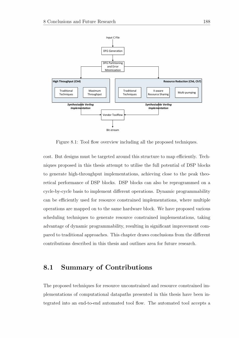
8 Conclusions and Future Research 188
Resource Reduction (Ch6, Ch7)High Throughput (Ch4)
DFG Generation
Input C File
DFG Partitioning and Error
Minimization
Traditional Techniques
Maximum Throughput
Traditional Techniques
II-aware Resource Sharing
Multi-pumping
Vendor Toolflow
Synthesisable Verilog Implementation
Synthesisable Verilog Implementation
Bit-stream
Figure 8.1: Tool flow overview including all the proposed techniques.
cost. But designs must be targeted around this structure to map efficiently. Tech-
niques proposed in this thesis attempt to utilise the full potential of DSP blocks
to generate high-throughput implementations, achieving close to the peak theo-
retical performance of DSP blocks. DSP blocks can also be reprogrammed on a
cycle-by-cycle basis to implement different operations. Dynamic programmability
can be efficiently used for resource constrained implementations, where multiple
operations are mapped on to the same hardware block. We have proposed various
scheduling techniques to generate resource constrained implementations, taking
advantage of dynamic programmability, resulting in significant improvement com-
pared to traditional approaches. This chapter draws conclusions from the different
contributions described in this thesis and outlines area for future research.
8.1 Summary of Contributions
The proposed techniques for resource unconstrained and resource constrained im-
plementations of computational datapaths presented in this thesis have been in-
tegrated into an end-to-end automated tool flow. The automated tool accepts a

8 Conclusions and Future Research 189
design description in C and generates synthesisable RTL which can be directly
fed to the vendor tool chain for final mapping to specific devices. It also gener-
ates testbenches for verification. An overview of the tool flow including all the
implementations techniques is shown in Figure 8.1.
8.1.1 High-Throughput Resource Unconstrained
Implementations
After discussing the evolution of DSP blocks from a hard-wired multipliers to
fully functional DSP blocks, we discussed the internal structure in detail, and
elaborated the possible arithmetic configurations into a “template database” in
Chapter 3. In Chapter 4, we presented an automated tool flow, that takes a com-
putational dataflow graph and maps to DSP blocks by matching sub-graphs from
this database. The dataflow graph is generated from a C description, then parti-
tioned using both a greedy and improved heuristic method. We built the tool to
also generate other implementations including Vivado HLS for comparison. We
found that instantiating DSP48E1 primitives could be avoided by simply generat-
ing RTL code that matches the structure of the DSP block templates. Exploiting
the architectural features of DSP blocks, we were able to show consistently better
throughput than all other methods, including mean 1.2× and 2× improvements
over Vivado HLS and generic ASAP/ALAP schedule implementations respectively.
Performance of implementations with direct instantiation of DSP blocks is com-
pared to replacing instantiations with equivalent RTL code.
8.1.2 Initiation Interval Aware Resource Sharing
In Chapter 6, we explored how we could share DSP blocks taking into account
their flexibility. We presented an SDC based scheduling technique, constrained
by initiation interval (II) instead of the number of resources available. With the
high latency of a fully-pipelined DSP block, resource sharing can have a significant
impact on the II of a circuit, since each iteration through the block must wait for

8 Conclusions and Future Research 190
the previous to complete. We presented an II-aware resource sharing technique
that could improve II by considering the pipeline structure of the DSP blocks.
Exploiting the dynamic programmability of the DSP block offered significantly
more sharing opportunities and a lower cost as more computational nodes could
be absorbed.
8.1.3 Multi-Pumping Fixed and Flexible DSP Blocks
Traditional and II aware resource sharing generally increase the schedule length
of the design. Multi-pumping is another technique which can reduce DSP block
utilisation without significant impact on schedule length. This is done by run-
ning the DSP block at twice the speed of the surrounding logic, allowing it to
complete two processing steps in a single global clock. In Chapter 7, we first
demonstrated multi-pumping with fixed configuration DSP blocks to reduce DSP
block utilisation as well as FPGA logic resources through use of the pre-adder and
ALU sub-blocks of the DSP48E1. We then exploit the dynamic programmability
of the DSP blocks to multi-pump DSP blocks performing different operations as
well. Two scheduling techniques based on SDC and FDS were discussed, which
can generate optimised schedules to maximise the extent of multi-pumping among
different operations, achieving up to a 50% reduction in DSP block utilisation.
However, the structure of the dataflow graph can mean an odd number of DSP
blocks are scheduled in a single timestep and hence not all can be combined. We
proposed an improved approach that could then share these remaining individual
DSP blocks to always achieve a 50% reduction in DSP block usage.
8.1.4 Truncation Error Minimisation
The DSP48E1 primitive has varied input and output wordlengths. Hence, while
partitioning the dataflow graph for mapping onto DSP blocks, intermediate DSP
block outputs must be truncated to fit input port widths. Truncating based on
wordlength alone leads to over-pessimistic implementations with high error. In

8 Conclusions and Future Research 191
Chapter 5, we presented an error minimisation technique to minimise the trun-
cation error in our mapping to DSP block primitives. We used an open-source
tool, Gappa, to determine realistic wordlengths for all intermediate outputs, and
then truncated the least significant fractional bits to minimise the error. With
realistic wordlengths, we are able to reduce the error on average by 5× for short
wordlengths and by 115× for longer wordlengths. This was incorporated into our
tool flow and applied to all techniques described above.
8.2 Future Research
We have shown that highly capable hard blocks in modern FPGAs can be exploited
to produce high performance and efficient datapaths, and that information from
the higher level computation description should be combined with architectural
information to arrive at an optimal RTL implementation. We plan to release the
automated tool flow discussed in this thesis for use by other researchers interested
in these investigations. In addition to this, we have identified numerous possible
extensions to the different aspects of the work presented which can be explored in
future research.
8.2.1 Integration into an HLS flow
The tool flow we presented generates synthesisable RTL implementations from a
C description of a computational kernel. As we were optimising around a low-level
primitive and keen to explore the limits, this was sufficient. However, integration
of these proposed techniques within a functional HLS flow would allow them to be
exploited in more complex designs. Open source HLS frameworks like LegUp [4]
could be extended to add these features.

8 Conclusions and Future Research 192
8.2.2 Extension of II-Aware Resource Sharing
The II-aware resource sharing presented in Chapter 6 accepts II constraints in
increments of the latency of the DSP block. This could be extended to more
advanced scheduling techniques that interleave start times to to generate sched-
ules for II constraints with different values. However, this will also increase the
complexity of control logic required to configure the DSP blocks.
8.2.3 Support for Newer DSP Blocks
We have used DSP48E1 primitive, available on Xilinx Virtex-6 and 7 series de-
vices. The latest Ultrascale devices from Xilinx have advanced DSP48E2 DSP
blocks, which are similar in structure but with other features like native support
for computing squares. We have designed our tool in such a way that all partition-
ing techniques discussed in Chapter 4 can be easily extended for the newer devices.
Since the latest DSP blocks can run even faster and accept wider operands, multi-
pumping would make more sense, and errors could be improved further.
8.2.4 Template Database Expansion
The template database discussed in Chapter 4 consists of operations using a single
DSP block. Many signal processing and image processing applications use specific
functions like normalisation. The template database can be expanded to include
these operations by adding custom-optimised implementations as templates. Oper-
ations like division or wide-multiplications can also be included to further minimise
the error for applications with strict requirement of exact computations.
8.2.5 Intermediate Virtual Fabric
The fundamental argument demonstrated in this thesis is that a better interme-
diate representation between high level languages and the back-end flow would

8 Conclusions and Future Research 193
help facilitate better implementations. This intermediate representation would
incorporate aspects of the architectural features of the target device and allow
manipulations that take into account the constraints of the target hardware re-
sources.
8.3 Summary
This thesis has explored ways of exploiting modern DSP block capabilities to
arrive at better implementations of arithmetic kernels. A thorough evaluation,
development of a modular tool flow, and new techniques have demonstrated that
the gap between algorithm and architecture can be bridged. We are hopeful that
this work encourages discussions about alternative ways of facilitating high level
design, and proves the benefits of flexibility in hard blocks.
Bibliography
[1] I. Kuon, R. Tessier, and J. Rose. FPGA architecture: Survey and challenges.
Proceedings of Foundations and Trends in Electronic Design Automation,
2(2):135–253, February 2008.
[2] [Online] Field Programmable Gate Array (FPGA). http://www.xilinx.
com/training/fpga/fpga-field-programmable-gate-array.htm.
[3] [Online] Xilinx Autopilot. http://www.xilinx.com/.
[4] A. Canis, J. Choi, M. Aldham, V. Zhang, A. Kammoona, J. Anderson,
S. Brown, and T. Czajkowski. LegUp: high-level synthesis for FPGA-based
Processor/Accelerator systems. In Proceedings of the ACM/SIGDA Inter-
national Symposium on Field Programmable Gate Arrays (FPGA), pages
33–36, 2011.
[5] [Online] Bluespec. http://www.bluespec.com/.
[6] [Online] Synphony C from Synopsys. https://www.synopsys.com/Tools/
Implementation/RTLSynthesis/Pages/SynphonyC-Compiler.aspx.
[7] [Online] Catapult C from Mentor Graphics. https://www.mentor.com/
hls-lp/catapult-high-level-synthesis/.
[8] T. Haroldsen, B. Nelson, and B. Hutchings. RapidSmith 2: A framework
for BEL-level CAD exploration on Xilinx FPGAs. In Proceedings of the
194

BIBLIOGRAPHY 195
ACM/SIGDA International Symposium on Field Programmable Gate Arrays
(FPGA), pages 66–69, 2015.
[9] C. Lavin, M. Padilla, J. Lamprecht, P. Lundrigan, B. Nelson, and B. Hutch-
ings. HMFlow: Accelerating FPGA compilation with hard macros for rapid
prototyping. In IEEE International Symposium on Field-Programmable Cus-
tom Computing Machines (FCCM), pages 117–124, May 2011.
[10] J. Lotze, S. A. Fahmy, J. Noguera, B. Ozgul, L. Doyle, and R. Esser.
Development framework for implementing FPGA-based cognitive network
nodes. In Proceedings of the IEEE Global Telecommunications Confer-
ence(GLOBECOM), 2009.
[11] J.-P. Delahaye, J. Palicot, C. Moy, and P. Leray. Partial reconfiguration
of FPGAs for dynamical reconfiguration of a software radio platform. In
Proceedings of the IST Mobile and Wireless Communications Summit, 2007.
[12] J. Kok, L. F. Gonzalez, and N. Kelson. FPGA implementation of an evo-
lutionary algorithm for autonomous unmanned aerial vehicle on-board path
planning. IEEE Transactions on Evolutionary Computation, 17(2):272–281,
2013.
[13] S. Shreejith, S. A. Fahmy, and M. Lukasiewycz. Reconfigurable computing
in next-generation automotive networks. IEEE Embedded Systems Letters,
5(1):12–15, 2013.
[14] S. A. Fahmy, K. Vipin, and S. Shreejith. Virtualized FPGA accelerators for
efficient cloud computing. In Proceedings of the International Conference
on Cloud Computing Technology and Science (CloudCom), pages 430–435,
2015.
[15] B. Ronak and S. A. Fahmy. Evaluating the efficiency of DSP block synthesis
inference from flow graphs. In Proceedings of the International Conference
on Field-Programmable Logic and Applications (FPL), pages 727 –730, Aug
2012.

BIBLIOGRAPHY 196
[16] B. Ronak and S. A. Fahmy. Experiments in mapping expressions to DSP
blocks. In Proceedings of the IEEE International Symposium on Field-
Programmable Custom Computing Machines (FCCM), pages 101–101, May
2014.
[17] B. Ronak and S. A. Fahmy. Efficient mapping of mathematical expressions
into DSP blocks. In Proceedings of the International Conference on Field-
Programmable Logic and Applications (FPL), pages 1–4, Sept 2014.
[18] B. Ronak and S. A. Fahmy. Minimising DSP block usage through multi-
pumping. In Proceedings of the IEEE International Conference on Field-
Programmable Technology (FPT), pages 184–187, Dec 2015.
[19] B. Ronak and S. A. Fahmy. Mapping for maximum performance on FPGA
DSP blocks. Proceedings of IEEE Transactions on Computer-Aided Design
of Integrated Circuits and Systems (TCAD), 35(4):573–585, April 2016.
[20] B. Ronak and S. A. Fahmy. Initiation interval aware resource sharing for
FPGA DSP blocks. In Proceedings of the IEEE International Symposium
on Field-Programmable Custom Computing Machines (FCCM), May 2016.
[21] B. Ronak and S. A. Fahmy. Improved resource sharing for FPGA
DSP blocks. In Proceedings of the International Conference on Field-
Programmable Logic and Applications (FPL), Sept 2016.
[22] G. de Micheli. Synthesis and Optimization of Digital Circuits. Tata McGraw-
Hill, 2003.
[23] S. Chatterjee. On Algorithms for Technology Mapping. PhD thesis, Univer-
sity of California, Berkeley, 2007.
[24] F. Mailhot. Technology Mapping for VLSI Circuits exploiting Boolean Prop-
erties and Operations. PhD thesis, Stanford University, 1991.
[25] J. A. Darringer, D. Brand, J. V. Gerbi, W. H. Joyner, and L. Trevillyan.
LSS: A system for production logic synthesis. Proceedings of IBM Journal
of Research and Development, 28(5):537–545, 1984.

BIBLIOGRAPHY 197
[26] W. H. Joyner, Jr., L. H. Trevillyan, D. Brand, T. A. Nix, and S. C.
Gundersen. Technology adaption in logic synthesis. In Proceedings of the
ACM/IEEE Design Automation Conference (DAC), pages 94–100, 1986.
[27] S. Suzuki, T. Bitoh, M. Kakimoto, K. Takahashi, and T. Sugimoto. TRIP:
an automated technology mapping system. In Proceedings of the ACM/IEEE
Design Automation Conference (DAC), pages 523–529, 1987.
[28] J. Ishikawa, H. Sato, M. Hiramine, K. Ishida, S. Oguri, Y. Kazuma, and
S. Murai. A rule based logic reorganization system LORES/EX. In Proceed-
ings of the IEEE International Conference on Computer Design: VLSI in
Computers and Processors, pages 262–266, 1988.
[29] D. Gregory, K. Bartlett, A. de Geus, and G. Hachtel. SOCRATES: a system
for automatically synthesizing and optimizing combinational logic. In Pro-
ceedings of the ACM/IEEE Design Automation Conference (DAC), pages
79–85, 1986.
[30] K. Keutzer. DAGON: Technology binding and local optimization by DAG
matching. In Proceedings of Papers on Twenty-five years of electronic design
automation, pages 617–624, 1988.
[31] A. V. Aho and M. Ganapathi. Efficient tree pattern matching (extended
abstract): an aid to code generation. In Proceedings of the ACM SIGACT-
SIGPLAN Symposium on Principles of Programming Languages, pages 334–
340, New York, NY, USA, 1985. ACM.
[32] E. Detjens, G. Gannot, R. Rudell, A. Sangiovanni-Vincentelli, and A. Wang.
Technology mapping in MIS. In Proceedings of the IEEE/ACM International
Conference on Computer-Aided Design (ICCAD), volume 87, pages 116–119,
1987.
[33] R. Rudell. Logic Synthesis for VLSI Design. PhD thesis, University of
California, Berkeley, 1989.

BIBLIOGRAPHY 198
[34] C. R. Morrison, R. M. Jacoby, and G. D. Hachtel. TECHMAP: Technol-
ogy mapping with delay and area optimization. Proceedings of Logic and
Architecture Synthesis for Silicon Compilers, pages 53–64, 1989.
[35] R. Lisanke, F. Brglez, and G. Kedem. McMAP: a fast technology mapping
procedure for multi-level logic synthesis. In Proceedings of the IEEE Interna-
tional Conference on Computer Design: VLSI in Computers and Processors,
pages 252–256, 1988.
[36] R. Murgai, Y. Nishizaki, N. Shenoy, R. K. Brayton, and A. Sangiovanni-
Vincentelli. Logic synthesis for programmable gate arrays. In Proceedings
of the ACM/IEEE Design Automation Conference (DAC), pages 620–625,
1990.
[37] J. P. Roth and R. M. Karp. Minimization over Boolean graphs. Proceedings
of IBM Journal of Research and Development, 6(2):227–238, April 1962.
[38] R. Francis, J. Rose, and Z. Vranesic. Chortle-crf: Fast technology mapping
for lookup table-based FPGAs. In Proceedings of the ACM/IEEE Design
Automation Conference (DAC), pages 227–233, 1991.
[39] R. Murgai, N. Shenoy, R. K. Brayton, and A. Sangiovanni-Vincentelli. Im-
proved logic synthesis algorithms for table look up architectures. In Proceed-
ings of the IEEE/ACM International Conference on Computer-Aided Design
(ICCAD), pages 564–567, Nov 1991.
[40] R. J. Francis, J. Rose, and Z. Vranesic. Technology mapping of lookup table-
based FPGAs for performance. In Proceedings of the IEEE/ACM Interna-
tional Conference on Computer-Aided Design (ICCAD), pages 568–571, Nov
1991.
[41] K. Karplus. Xmap: a technology mapper for table-lookup field-
programmable gate arrays. In Proceedings of the ACM/IEEE Design Au-
tomation Conference (DAC), pages 240–243, 1991.

BIBLIOGRAPHY 199
[42] E. L. Lawler, K. N. Levitt, and J. Turner. Module clustering to minimize
delay in digital networks. Proceedings of IEEE Transactions on Computers,
C-18(1):47–57, 1969.
[43] K.-C. Chen, J. Cong, Y. Ding, A. B. Kahng, and P. Trajmar. DAG-Map:
graph-based FPGA technology mapping for delay optimization. Proceedings
of IEEE Design Test of Computers, 9:7–20, 1992.
[44] J. Cong and Y. Ding. FlowMap: an optimal technology mapping algorithm
for delay optimization in lookup-table based FPGA designs. Proceedings of
IEEE Transactions on Computer-Aided Design of Integrated Circuits and
Systems (TCAD), 13:1–12, Jan 1994.
[45] J. Cong, Y. Ding, T. Gao, and K.-C. Chen. LUT-based FPGA technology
mapping under arbitrary net-delay models. Proceedings of Computers &
Graphics, 18(4):507–516, 1994.
[46] H. Yang and D. F. Wong. Edge-map: Optimal performance driven technol-
ogy mapping for iterative LUT based FPGA designs. In Proceedings of the
IEEE/ACM International Conference on Computer-Aided Design (ICCAD),
pages 150–155, 1994.
[47] J. Cong and Y. Ding. On area/depth trade-off in LUT-based FPGA tech-
nology mapping. Proceedings of IEEE Transactions on Very Large Scale
Integration (VLSI) Systems, 2(2):137–148, 1994.
[48] J. Cong and Y.-Y. Hwang. Simultaneous depth and area minimization in
LUT-based FPGA mapping. In Proceedings of the ACM/SIGDA Interna-
tional Symposium on Field Programmable Gate Arrays (FPGA), pages 68–
74, 1995.
[49] J. Cong and Y. Ding. An optimal technology mapping for delay optimization
for lookup-table based FPGA designs. In Proceedings of the IEEE/ACM
International Conference on Computer-Aided Design (ICCAD), pages 48–
53, Nov 1992.

BIBLIOGRAPHY 200
[50] J. He and J. Rose. Technology mapping for heterogeneous FPGAs. Proceed-
ings of the ACM/SIGDA International Symposium on Field Programmable
Gate Arrays (FPGA), Feb 1994.
[51] J. Cong and S. Xu. Delay-optimal technology mapping for FPGAs with
heterogeneous LUTs. In Proceedings of the ACM/IEEE Design Automation
Conference (DAC), pages 704–707, June 1998.
[52] A. H. Farrahi and M. Sarrafzadeh. FPGA technology mapping for power
minimization. In Proceedings of Field-Programmable Logic Architectures,
Synthesis and Applications, volume 849, pages 66–77. Springer Berlin Hei-
delberg, 1994.
[53] Z.-H. Wang, E.-C. Liu, J. Lai, and T.-C. Wang. Power minimization in
LUT-based FPGA technology mapping. In Proceedings of the Asia and
South Pacific-Design Automation Conference (ASP-DAC), pages 635–640,
2001.
[54] H. Li, W.-K. Mak, and S. Katkoori. LUT-based FPGA technology mapping
for power minimization with optimal depth. In Proceedings IEEE Computer
Society Workshop on VLSI, pages 123–128, 2001.
[55] J. Anderson and F. N. Najm. Power-aware technology mapping for LUT-
based FPGAs. In Proceedings of the IEEE International Conference on
Field-Programmable Technology (FPT), pages 211–218, 2002.
[56] S. Jang, B. Chan, K. Chung, and A. Mishchenko. WireMap: FPGA tech-
nology mapping for improved routability and enhanced LUT merging. Pro-
ceedings of ACM Transactions on Reconfigurable Technology and Systems
(TRETS), 2(2):14:1–14:24, June 2009.
[57] V. Manohararajah, S. D. Brown, and Z. G. Vranesic. Heuristics for area min-
imization in LUT-Based FPGA technology mapping. Proceedings of IEEE
Transsactions on Computer-Aided Design of Integrated Circuits and Systems
(TCAD), 25(11):2331–2340, November 2006.

BIBLIOGRAPHY 201
[58] M. Schlag, J. Kong, and P. K. Chan. Routability-driven technology map-
ping for lookup table-based FPGAs. In Proceedings of International Confer-
ence on Computer Design: VLSI in Computers and Processors, pages 86–90,
1992.
[59] J. Cong, C. Wu, and Y. Ding. Cut ranking and pruning: enabling a general
and efficient FPGA mapping solution. In Proceedings of the ACM/SIGDA
International Symposium on Field Programmable Gate Arrays (FPGA),
pages 29–35, 1999.
[60] A. Kaviani and S. Brown. Technology mapping issues for an FPGA with
lookup tables and PLA-like blocks. In Proceedings of the ACM/SIGDA In-
ternational Symposium on Field Programmable Gate Arrays (FPGA), pages
60–66, 2000.
[61] S. Krishnamoorthy, S. Swaminathan, and R. Tessier. Area-optimized tech-
nology mapping for hybrid FPGAs. In Proceedings of the International Con-
ference on Field-Programmable Logic and Applications (FPL), pages 181–
190, 2000.
[62] A. H. Farrahi and M. Sarrafzadeh. Complexity of the lookup-table min-
imization problem for FPGA technology mapping. Proceedings of IEEE
Transsactions on Computer-Aided Design of Integrated Circuits and Systems
(TCAD), 13(11):1319–1332, November 2006.
[63] D. Dickin and L. Shannon. Exploring FPGA technology mapping for frac-
turable LUT minimization. In Proceedings of the IEEE International Con-
ference on Field-Programmable Technology (FPT), pages 1–8, 2011.
[64] M. Hutton, J. Schleicher, D. M. Lewis, B. Pedersen, R. Yuan, S. Kap-
tanoglu, G. Baeckler, B. Ratchev, K. Padalia, M. Bourgeault, A. Lee,
H. Kim, and R. Saini. Improving FPGA performance and area using an
adaptive logic module. In Proceedings of the International Conference on
Field-Programmable Logic and Applications (FPL), pages 135–144, 2004.

BIBLIOGRAPHY 202
[65] W. Chen, X. Zhang, T. Yoshimura, and Y. Nakamura. A low power technol-
ogy mapping method for adaptive logic module. In Proceedings of the IEEE
International Conference on Field-Programmable Technology (FPT), pages
1–5, 2011.
[66] E. Lehman, Y. Watanabe, J. Grodstein, and H. Harkness. Logic decom-
position during technology mapping. Proceedings of IEEE Transactions
on Computer-Aided Design of Integrated Circuits and Systems (TCAD),
16(8):813–834, 1997.
[67] J. Rose, J. Luu, C. W. Yu, O. Densmore, J. Goeders, A. Somerville, K. B.
Kent, P. Jamieson, and J. Anderson. The VTR project: architecture and
CAD for FPGAs from verilog to routing. In Proceedings of the ACM/SIGDA
International Symposium on Field Programmable Gate Arrays (FPGA),
pages 77–86, 2012.
[68] [Online] The Verilog-to-Routing (VTR) Project for FPGAs. https://
github.com/verilog-to-routing/vtr-verilog-to-routing/.
[69] J. Luu, J. H. Anderson, and J. S. Rose. Architecture description and packing
for logic blocks with hierarchy, modes and complex interconnect. In Proceed-
ings of the ACM/SIGDA International Symposium on Field Programmable
Gate Arrays (FPGA), pages 227–236, 2011.
[70] J. Luu, J. Goeders, M. Wainberg, A. Somerville, T. Yu, K. Nasartschuk,
M. Nasr, S. Wang, T. Liu, N. Ahmed, K. B. Kent, J. Anderson, J. Rose,
and V. Betz. VTR 7.0: Next generation architecture and CAD system for
FPGAs. Proceedings of ACM Transactions on Reconfigurable Technology
and Systems (TRETS), 7(2):6:1–6:30, June 2014.
[71] P. Jamieson, K. B. Kent, F. Gharibian, and L. Shannon. Odin II - an open-
source Verilog HDL synthesis tool for CAD research. In Proceedings of the
IEEE International Symposium on Field-Programmable Custom Computing
Machines (FCCM), pages 149–156, 2010.

BIBLIOGRAPHY 203
[72] R. Brayton and A. Mishchenko. ABC: an academic industrial-strength veri-
fication tool. In Proceedings of International Conference on Computer Aided
Verification (CAV), pages 24–40. Springer-Verlag, 2010.
[73] [Online] ABC: A System for Sequential Synthesis and Verification. http:
//www.eecs.berkeley.edu/~alanmi/abc/.
[74] [Online] VPR 6.0. http://code.google.com/p/
vtr-verilog-to-routing/wiki/VPR.
[75] A. Somerville and K. B. Kent. Improving memory support in the VTR flow.
In Proceedings of the International Conference on Field-Programmable Logic
and Applications (FPL), pages 197–202, 2012.
[76] J. C. Libby, A. Furrow, P. O’Brien, and K. B. Kent. A framework for ver-
ifying functional correctness in Odin II. In Proceedings of the IEEE Inter-
national Conference on Field-Programmable Technology (FPT), pages 1–6,
2011.
[77] V. Betz and J. Rose. VPR: a new packing, placement and routing tool for
FPGA research. In Proceedings of the International Conference on Field-
Programmable Logic and Applications (FPL), pages 213–222. Springer Berlin
Heidelberg, 1997.
[78] S. Kirkpatrick, C. D. Gelatt, and M. P. Vecchi. Optimization by simulated
annealing. Proceedings of Science, 220(4598):pp. 671–680, 1983.
[79] V. Betz and J. Rose. Directional bias and non-uniformity in FPGA global
routing architectures. In Proceedings of the IEEE/ACM International Con-
ference on Computer-Aided Design (ICCAD), pages 652–659, 1996.
[80] C. Ebeling, L. McMurchie, S. A. Hauck, and S. Burns. Placement and
routing tools for the Triptych FPGA. Proceedings of IEEE Transactions on
Very Large Scale Integration (VLSI) Systems, 3(4):473–482, 1995.
[81] J. Luu, I. Kuon, P. Jamieson, T. Campbell, A. Ye, W. M. Fang, K. Kent,
and J. Rose. VPR 5.0: FPGA CAD and architecture exploration tools

BIBLIOGRAPHY 204
with single-driver routing, heterogeneity and process scaling. Proceedings
of ACM Transactions on Reconfigurable Technology and Systems (TRETS),
4(4):32:1–32:23, December 2011.
[82] Marquardt A. R. Cluster-Based architecture, timing-driven packing and
timing-driven placement for FPGAs. Master’s thesis, University of Toronto,
1999.
[83] [Online] Xilinx SDSoC. http://www.xilinx.com/products/
design-tools/software-zone/sdsoc.html.
[84] G. de Micheli. Hardware synthesis from C/C++ models. In Proceedings
of the International Conference on Design, Automation and Test in Europe
(DATE), pages 382–383, 1999.
[85] J. Cong, B. Liu, S. Neuendorffer, J. Noguera, K. Vissers, and Z. Zhang. High-
level synthesis for FPGAs: From prototyping to deployment. Proceedings of
IEEE Transactions on Computer-Aided Design of Integrated Circuits and
Systems (TCAD), 30(4):473–491, April 2011.
[86] S. A. Edwards. The challenges of synthesizing hardware from C-like lan-
guages. Proceedings of IEEE Design Test of Computers, 23(5):375–386, 2006.
[87] D. Ku and G. de Micheli. Hardware C - A Language for Hardware Design
(Version 2.0). Stanford, CA Tech. Report, 1990.
[88] [Online] Handel-C. http://celoxica.com/.
[89] [Online] Catapult. http://www.mentor.com/products/esl/high_level_
synthesis/catapult_synthesis/.
[90] [Online] Impulse-C. http://www.impulsec.com/.
[91] A. Jones, D. Bagchi, S. Pal, X. Tang, A. Choudhary, and P. Banerjee. PACT
HDL: a C compiler targeting ASICs and FPGAs with power and performance
optimizations. In Proceedings of the International Conference on Compilers,
Architecture, and Synthesis for Embedded Systems, pages 188–197, 2002.

BIBLIOGRAPHY 205
[92] A. Putnam, D. Bennett, E. Dellinger, J. Mason, P. Sundararajan, and S. Eg-
gers. CHiMPS: A C-level compilation flow for hybrid CPU-FPGA architec-
tures. In Proceedings of the International Conference on Field-Programmable
Logic and Applications (FPL), pages 173–178, Sep 2008.
[93] F. Verdier and B. Zavidovique. A complete environment for global archi-
tecture synthesis. In Proceedings of Computer Architectures for Machine
Perception, pages 77–81, Dec 1993.
[94] L. Semeria and G. de Micheli. SpC: synthesis of pointers in C application
of pointer analysis to the behavioral synthesis from C. In Proceedings of the
IEEE/ACM International Conference on Computer-Aided Design (ICCAD),
pages 340–346, Nov 1998.
[95] L. Semeria, K. Sato, and G. de Micheli. Resolution of dynamic memory
allocation and pointers for the behavioral synthesis form C. In Proceedings
of the International Conference on Design, Automation and Test in Europe
(DATE), pages 312–319, 2000.
[96] L. Semeria, K. Sato, and G. de Micheli. Synthesis of hardware models in C
with pointers and complex data structures. Proceedings of IEEE Transac-
tions on Very Large Scale Integration (VLSI) Systems, 9(6):743 –756, Dec
2001.
[97] M. W. Hall, J. M. Anderson, S. P. Amarasinghe, B. R. Murphy, S.-W. Liao,
E. Bugnion, and M. S. Lam. Maximizing multiprocessor performance with
the SUIF compiler. Proceedings of Computer, 29(12):84–89, December 1996.
[98] Xilinx. MicroBlaze Processor Reference Guide, v9.0 edition, 2008.
[99] L. Kaouane, M. Akil, T. Grandpierre, and Y. Sorel. A methodology to
implement real-time applications onto reconfigurable circuits. Proceedings
of The Journal of Supercomputing, 30:283–301, 2004.
[100] F. Berthelot, F. Nouvel, and D. Houzet. Design methodology for runtime
reconfigurable FPGA: from high level specification down to implementation.

BIBLIOGRAPHY 206
In Proceedings of IEEE Workshop on Signal Processing Systems Design and
Implementation, pages 497–502, Nov 2005.
[101] T. Grandpierre, C. Lavarenne, and Y. Sorel. Optimized rapid prototyping
for real-time embedded heterogeneous multiprocessors. In Proceedings of
International Workshop on Hardware/Software Co-Design(CODES), May
1999.
[102] Jongsok C., S. Brown, and J. Anderson. From software threads to parallel
hardware in high-level synthesis for FPGAs. In Proceedings of the IEEE
International Conference on Field-Programmable Technology (FPT), pages
270–277, Dec 2013.
[103] N. Calagar, S. D. Brown, and J. Anderson. Source-level debugging for FPGA
high-level synthesis. In Proceedings of the International Conference on Field-
Programmable Logic and Applications (FPL), pages 1–8, Sept 2014.
[104] [Online] LegUp 4.0. http://legup.eecg.utoronto.ca/docs/4.0/.
[105] F. Winterstein, S. Bayliss, and G. A. Constantinides. High-level synthesis
of dynamic data structures: A case study using Vivado HLS. In Proceedings
of the IEEE International Conference on Field-Programmable Technology
(FPT), pages 362–365, Dec 2013.
[106] K. S. Vallerio and N. K. Jha. Task graph extraction for embedded system
synthesis. In Proceedings on VLSI Design, pages 480 – 486, Jan 2003.
[107] R. Namballa, N. Ranganathan, and A. Ejnioui. Control and data flow graph
extraction for high-level synthesis. In Proceedings IEEE Computer society
Annual Symposium on VLSI, pages 187 – 192, Feb. 2004.
[108] R. P. Dick, D. L. Rhodes, and W. Wolf. TGFF: task graphs for free. In
Proceedings of the International Workshop on Hardware/Software Codesign
(CODES/CASHE), pages 97 –101, Mar 1998.
[109] N. Togawa, T. Hisaki, M. Yanagisawa, and T. Ohtsuki. A high-level synthesis
system for digital signal processing based on enumerating data-flow graphs.

BIBLIOGRAPHY 207
In Proceedings of the Asia and South Pacific-Design Automation Conference
(ASP-DAC), pages 265–274, Feb 1998.
[110] T. J. Callahan, P. Chong, A. DeHon, and J. Wawrzynek. Fast module
mapping and placement for datapaths in FPGAs. In Proceedings of the
ACM/SIGDA International Symposium on Field Programmable Gate Arrays
(FPGA), pages 123–132, 1998.
[111] W. Sun, M. J. Wirthlin, and S. Neuendorffer. Combining module selection
and resource sharing for efficient FPGA pipeline synthesis. In Proceedings
of the ACM/SIGDA International Symposium on Field Programmable Gate
Arrays (FPGA), pages 179–188, 2006.
[112] W. Sun, M. J. Wirthlin, and S. Neuendorffer. FPGA pipeline synthesis
design exploration using module selection and resource sharing. Proceedings
of IEEE Transactions on Computer-Aided Design of Integrated Circuits and
Systems (TCAD), 26(2):254–265, Feb 2007.
[113] B. R. Rau. Iterative modulo scheduling: an algorithm for software pipelin-
ing loops. In Proceedings of International Symposium on Microarchitecture,
pages 63–74, 1994.
[114] [Online] FloPoCo. http://flopoco.gforge.inria.fr/.
[115] [Online] FloPoCo developer manual. http://flopoco.gforge.inria.fr/
flopoco_developer_manual.pdf.
[116] M. Gort and J. Anderson. Design re-use for compile time reduction in FPGA
high-level synthesis flows. In Proceedings of the IEEE International Confer-
ence on Field-Programmable Technology (FPT), pages 4–11, Dec 2014.
[117] C. Lavin, M. Padilla, J. Lamprecht, P. Lundrigan, B. Nelson, and B. Hutch-
ings. RapidSmith: Do-it-yourself CAD tools for Xilinx FPGAs. In Pro-
ceedings of the International Conference on Field-Programmable Logic and
Applications (FPL), pages 349–355, 2011.
BIBLIOGRAPHY 208
[118] N. Steiner, A. Wood, H. Shojaei, J. Couch, P. Athanas, and M. French. Torc:
Towards an open-source tool flow. In Proceedings of the ACM/SIGDA In-
ternational Symposium on Field Programmable Gate Arrays (FPGA), pages
41–44, 2011.
[119] S. Hadjis, A. Canis, J. H. Anderson, J. Choi, K. Nam, S. Brown, and T. Cza-
jkowski. Impact of FPGA architecture on resource sharing in high-level
synthesis. In Proceedings of the ACM/SIGDA International Symposium on
Field Programmable Gate Arrays (FPGA), pages 111–114, 2012.
[120] Y. Hara-Azumi, T. Matsuba, H. Tomiyama, S. Honda, and H. Takada. Im-
pact of resource sharing and register retiming on area and performance of
FPGA-based designs. Proceedings of Information and Media Technologies,
9(1):26–34, 2014.
[121] R. Jain, A. Parker, and N. Park. Predicting area-time tradeoffs for pipelined
design. In Proceedings of Conference on Design Automation, pages 35–41,
June 1987.
[122] C.-T. Hwang, Y.-C. Hsu, and Y.-L. Lin. PLS: a scheduler for pipeline syn-
thesis. Proceedings of IEEE Transactions on Computer-Aided Design of
Integrated Circuits and Systems (TCAD), 12(9):1279–1286, Sep 1993.
[123] S. Davidson, D. Landskov, B. D. Shriver, and P. W. Mallett. Some exper-
iments in local microcode compaction for horizontal machines. Proceedings
of IEEE Transactions on Computers, C-30:460–477, July 1981.
[124] T. L. Adam, K. M. Chandy, and J. R. Dickson. A comparison of list schedules
for parallel processing systems. Proceedings of Communications of the ACM,
17:685–690, December 1974.
[125] A. Parker, J. Pizarro, and M. Mlinar. MAHA: A program for datapath
synthesis. In Proceedings of the ACM/IEEE Design Automation Conference
(DAC), pages 461–466, June 1986.

BIBLIOGRAPHY 209
[126] P. G. Paulin and J. P. Knight. Force-directed scheduling for the behavioral
synthesis of ASICs. Proceedings of IEEE Transactions on Computer-Aided
Design of Integrated Circuits and Systems (TCAD), 8(6):661–679, 1989.
[127] W. F. J. Verhaegh, P. E. R. Lippens, E. H. L. Aarts, J. H. M. Korst, J. L.
Van Meerbergen, and A. van der Werf. Improved force-directed scheduling in
high-throughput digital signal processing. Proceedings of IEEE Transactions
on Computer-Aided Design of Integrated Circuits and Systems (TCAD),
14:945–960, Aug 1995.
[128] F. Rousseau, J. Benzakki, J. M. Berge, and M. Israel. Adaptation of force-
directed scheduling algorithm for hardware/software partitioning. In Pro-
ceedings of IEEE International Workshop on Rapid System Prototyping,
pages 33–37, Jun 1995.
[129] S. Gupta and S. Katkoori. Force-directed scheduling for dynamic power
optimization. In Proceedings of IEEE Computer Society Annual Symposium
on VLSI, pages 68–73, 2002.
[130] A. K. Allam and J. Ramanujam. Modified force-directed scheduling for
peak and average power optimization using multiple supply-voltages. In
Proceedings of IEEE International Conference on Integrated Circuit Design
and Technology, pages 1–5, 2006.
[131] M. Areno, B. Eames, and J. Templin. A force-directed scheduling based
architecture generation algorithm and design tool for FPGAs. Proceedings
of Journal of Systems Architecture, 56:124–135, Feb 2010.
[132] C.-T. Hwang, J.-H. Lee, and Y.-C. Hsu. A formal approach to the schedul-
ing problem in high level synthesis. Proceedings of IEEE Transactions
on Computer-Aided Design of Integrated Circuits and Systems (TCAD),
10(4):464–475, Apr 1991.
[133] C. H. Gebotys and M. I. Elmasry. Global optimization approach for ar-
chitectural synthesis. Proceedings of IEEE Transactions on Computer-Aided
Design of Integrated Circuits and Systems (TCAD), 12:1266–1278, Sep 1993.

BIBLIOGRAPHY 210
[134] J. Cong and Z. Zhang. An efficient and versatile scheduling algorithm based
on SDC formulation. In Proceedings of the ACM/IEEE Design Automation
Conference (DAC), pages 433–438, 2006.
[135] S. O. Memik, G. Memik, R. Jafari, and E. Kursun. Global resource sharing
for synthesis of control data flow graphs on FPGAs. In Proceedings of the
ACM/IEEE Design Automation Conference (DAC), pages 604–609, June
2003.
[136] Z. Jin and J. D. Bakos. A heuristic scheduler for port-constrained floating-
point pipelines. Proceedings of International Journal of Reconfigurable Com-
pututing, 2013:1:1–1:1, Jan 2013.
[137] J. Cong and W. Jiang. Pattern-based behavior synthesis for FPGA resource
reduction. In Proceedings of the ACM/SIGDA International Symposium on
Field Programmable Gate Arrays (FPGA), pages 107–116, 2008.
[138] B. T. Messmer and H. Bunke. A new algorithm for error-tolerant subgraph
isomorphism detection. IEEE Transactions on Pattern Analysis and Ma-
chine Intelligence, 20(5):493–504, May 1998.
[139] R. Scrofano, L. Zhuo, and V. K. Prasanna. Area-efficient arithmetic ex-
pression evaluation using deeply pipelined floating-point cores. Proceed-
ings of IEEE Transactions on Very Large Scale Integration (VLSI) Systems,
16(2):167–176, Feb 2008.
[140] H. Y. Cheah, S. A. Fahmy, and D. L. Maskell. iDEA: A DSP block based
FPGA soft processor. In Proceedings of the IEEE International Conference
on Field-Programmable Technology (FPT), pages 151–158, Dec 2012.
[141] H. Y. Cheah, F. Brosser, S. A. Fahmy, and D. L. Maskell. The iDEA DSP
block-based soft processor for FPGAs. Proceedings of ACM Transactions on
Reconfigurable Technology and Systems (TRETS), 7(3):19:1–19:23, Septem-
ber 2014.

BIBLIOGRAPHY 211
[142] F. Brosser, H. Y. Cheah, and S. A. Fahmy. Iterative floating point computa-
tion using FPGA DSP blocks. In Proceedings of the International Conference
on Field Programmable Logic and Applications (FPL), pages 1–6, Sept 2013.
[143] A. K. Jain, X. Li, S. A. Fahmy, and D. L. Maskell. Adapting the DySER
architecture with DSP blocks as an overlay for the Xilinx Zynq. In Proceed-
ings of the International Symposium on Highly-Efficient Accelerators and
Reconfigurable Technologies (HEART), Jun 2015.
[144] J. Benson, R. Cofell, C. Frericks, C.-H. Ho, V. Govindaraju, T. Nowatzki,
and K. Sankaralingam. Design, integration and implementation of the
DySER hardware accelerator into OpenSPARC. In Proceedings of Inter-
national Symposium on High Performance Computer Architecture (HPCA),
pages 1–12, Feb 2012.
[145] A. K. Jain, D. A. Maskell, and S. A. Fahmy. Throughput oriented FPGA
overlays using DSP blocks. In Proceedings of the International Conference
on Design, Automation and Test in Europe (DATE), March 2016.
[146] Xilinx Inc. UG479: 7 Series DSP48E1 Slice User Guide, 2013.
[147] Z. Chun, Z. Yongjun, C. Xin, and G. Xiaoguang. Research on technology
of color space conversion based on DSP48E. In Proceedings of Interna-
tional Conference on Measuring Technology and Mechatronics Automation
(ICMTMA), volume 3, pages 87–90, 2011.
[148] G. Conde and G. W. Donohoe. Reconfigurable block floating point process-
ing elements in Virtex platforms. In Proceedings of International Conference
on Reconfigurable Computing and FPGAs (ReConFig), pages 509–512, 2011.
[149] R. Mehra and S. Devi. FPGA implementation of high speed pulse shaping
filter for SDR applications. In Proceedings of Recent Trends in Networks and
Communications. Springer Berlin Heidelberg, 2010.

BIBLIOGRAPHY 212
[150] H. M. Kamboh and S. A. Khan. An algorithmic transformation for FPGA
implementation of high throughput filters. In Proceedings of International
Conference on Emerging Technologies (ICET), pages 1–6, 2011.
[151] S. Xu, S. A. Fahmy, and I. V. McLoughlin. Square-rich fixed point poly-
nomial evaluation on FPGAs. In Proceedings of the ACM/SIGDA Inter-
national Symposium on Field Programmable Gate Arrays (FPGA), pages
99–108, 2014.
[152] F. de Dinechin and B. Pasca. Designing custom arithmetic data paths with
FloPoCo. Proceedings of IEEE Design & Test of Computers, 28(4):18–27,
2011.
[153] S. Gopalakrishnan, P. Kalla, M. B. Meredith, and F. Enescu. Finding linear
building-blocks for RTL synthesis of polynomial datapaths with fixed-size
bit-vectors. In Proceedings of the IEEE/ACM International Conference on
Computer-Aided Design (ICCAD), pages 143–148, Nov 2007.
[154] C. Lee, M. Potkonjak, and W. H. Mangione-Smith. MediaBench: a tool for
evaluating and synthesizing multimedia and communications systems. In
Proceedings of International Symposium on Microarchitecture, pages 330–
335, Dec 1997.
[155] [Online] Polynomial Test Suite. http://www-sop.inria.fr/saga/POL/.
[156] K. Vipin and S. A. Fahmy. DyRACT: A partial reconfiguration enabled
accelerator and test platform. In Proceedings of the International Conference
on Field-Programmable Logic and Applications (FPL), pages 1–7, Sept 2014.
[157] F. de Dinechin, C. Q. Lauter, and G. Melquiond. Assisted verification of
elementary functions using Gappa. In Proceedings of the ACM Symposium
on Applied Computing, pages 1318–1322, 2006.
[158] M. Gort and J. Anderson. Range and bitmask analysis for hardware op-
timization in high-level synthesis. In Proceedings of the Asia and South

BIBLIOGRAPHY 213
Pacific-Design Automation Conference (ASP-DAC), pages 773–779, Jan
2013.
[159] A. Klimovic and J. Anderson. Bitwidth-optimized hardware accelerators
with software fallback. In Proceedings of the IEEE International Conference
on Field-Programmable Technology (FPT), pages 136–143, Dec 2013.
[160] A. Tisserand. Automatic generation of low-power circuits for the evaluation
of polynomials. In Proceedings of Asilomar Conference on Signals, Systems
and Computers (ACSSC), pages 2053–2057, Oct 2006.
[161] A. Tisserand. Hardware reciprocation using degree-3 polynomials but only 1
complete multiplication. In Proceedings of Midwest Symposium on Circuits
and Systems (MWSCAS), pages 301–304, Aug 2007.
[162] A. Tisserand. Function approximation based on estimated arithmetic oper-
ators. In Proceedings of International Conference on Signals, Systems and
Computers, pages 1798–1802, Nov 2009.
[163] F. de Dinechin, C. Lauter, and G. Melquiond. Certifying the floating-point
implementation of an elementary function using Gappa. Proceedings of IEEE
Transactions on Computers, 60(2):242–253, Feb 2011.
[164] M. D. Linderman, M. Ho, D. L. Dill, T. H. Meng, and G. P. Nolan. Towards
program optimization through automated analysis of numerical precision. In
Proceedings of the IEEE/ACM International Symposium on Code Genera-
tion and Optimization, pages 230–237, 2010.
[165] H. Martorell and N. Kapre. FX-SCORE: A framework for fixed-point com-
pilation of SPICE device models using Gappa++. In Proceedings of the
IEEE International Symposium on Field-Programmable Custom Computing
Machines (FCCM), pages 77–84, April 2012.
[166] D. Ye and N. Kapre. MixFX-SCORE: Heterogeneous fixed-point compila-
tion of dataflow computations. In Proceedings of the IEEE International

BIBLIOGRAPHY 214
Symposium on Field-Programmable Custom Computing Machines (FCCM),
pages 206–209, 2014.
[167] S. Raje and R. A. Bergamaschi. Generalized resource sharing. In Proceed-
ings of the IEEE/ACM International Conference on Computer-Aided Design
(ICCAD), pages 326–332, 1997.
[168] J. M. P. Cardoso. A novel algorithm combining temporal partitioning and
sharing of functional units. In Proceedings of the IEEE International Sympo-
sium on Field-Programmable Custom Computing Machines (FCCM), pages
31–40, March 2001.
[169] R. Zhao, M. Tan, S. Dai, and Z. Zhang. Area-efficient pipelining for FPGA-
targeted high-level synthesis. In Proceedings of the ACM/IEEE Design Au-
tomation Conference (DAC), pages 157:1–157:6, 2015.
[170] M. Alle, A. Morvan, and S. Derrien. Runtime dependency analysis for loop
pipelining in high-level synthesis. In Proceedings of the ACM/IEEE Design
Automation Conference (DAC), pages 1–10, May 2013.
[171] P. Li, P. Zhang, L.-N. Pouchet, and J. Cong. Resource-aware throughput
optimization for high-level synthesis. In Proceedings of the ACM/SIGDA In-
ternational Symposium on Field Programmable Gate Arrays (FPGA), pages
200–209, 2015.
[172] P. G. Paulin and J. P. Knight. Force-directed scheduling in automatic data
path synthesis. In Proceedings of the ACM/IEEE Design Automation Con-
ference (DAC), pages 195–202, 1987.
[173] [Online] LP Solve 5.5. http://lpsolve.sourceforge.net/5.5/.
[174] A. Canis, J. H. Anderson, and S. D. Brown. Multi-pumping for resource
reduction in FPGA high-level synthesis. In Proceedings of the International
Conference on Design, Automation and Test in Europe (DATE), pages 194–
197, March 2013.

BIBLIOGRAPHY 215
[175] C. E. Laforest and J. G. Steffan. Efficient multi-ported memories for FP-
GAs. In Proceedings of the ACM/SIGDA International Symposium on Field
Programmable Gate Arrays, pages 41–50, 2010.
[176] L. Shannon, V. Cojocaru, C. N. Dao, and P. H. W. Leong. Technology scaling
in FPGAs: Trends in applications and architectures. In Proceedings of the
IEEE International Symposium on Field-Programmable Custom Computing
Machines (FCCM), pages 1–8, May 2015.
[177] H. E. Yantir, S. Bayar, and A. Yurdakul. Efficient implementations of multi-
pumped multi-port register files in FPGAs. In Proceedings of Euromicro
Conference on Digital System Design (DSD), pages 185–192, Sept 2013.
[178] F. Anjam, S. Wong, and F. Nadeem. A multiported register file with register
renaming for configurable softcore VLIW processors. In Proceedings of the
IEEE International Conference on Field-Programmable Technology (FPT),
pages 403–408, Dec 2010.
[179] C. E. Laforest, M. G. Liu, E. R. Rapati, and J. G. Steffan. Multi-ported
memories for FPGAs via XOR. In Proceedings of the ACM/SIGDA Inter-
national Symposium on Field Programmable Gate Arrays (FPGA), pages
209–218, 2012.
[180] R. P. Tidwell. XAPP706: Alpha Blending Two Data Streams Using a DSP48
DDR Technique. Xilinx Inc, 2005.
[181] J. Edmonds. Paths, trees, and flowers. In Classic Papers in Combinatorics,
Modern Birkhuser Classics, pages 361–379. Birkhuser Boston, 1987.