Architectural synthesis for DSP silicon compilers
17
IEEE TRANSACTIONS ON COMPUTER-AIDED DESIGN, VOL. 8, NO. 4, APRIL 1989 43 1 Architectural Synthesis for DSP Silicon Compilers BAHER S. HAROUN AND MOHAMED I. ELMASRY, FELLOW, IEEE Absfmcf-A novel design methodology for automated mapping of DSP algorithms into VLSI architectures is presented. The methodology takes into account explicit algorithm requirements on throughput and latency, in addition to VLSI technology constraints on silicon area and power dissipation. Algorithm structure, design style of functional units and parallelism of the architecture are all explored in the design space. The synthesized architecture is a multi-bus multi-functional unit pro- cessor matched to the implemented algorithm. The architecture has a linear topology and uses a lower number of interconnects and multi- plexer inputs compared to other synthesized architectures with ran- dom topology having the same performance. The synthesized processor is a self-timed element externally, while it is internally synchronous. The methodology is implemented in a design aid tool called SPAID. Results obtained using SPAID for two DSP algorithms compare favor- ably over other synthesis techniques. I. INTRODUCTION ILICON compilation [ 13 is used to automate VLSI de- S sign of DSP systems. Architectural synthesis, an im- portant front end task in such a compiler, is a transfor- mation from the primitives of the initial algorithm specifications to the primitives of the architectural repre- sentation, and, in general, is a one-to-many mapping. The output of the transformation has to preserve behavioral coherence with the input. The steering of the transfor- mations is influenced by global performance requirements and technology constraints. The large number of possi- bilities in the search space are pruned by the use of expert knowledge in the architectural synthesis process. This pa- per offers a novel methodology for architectural design automation to be used at the front end of a silicon com- piler for the VLSI implementation of a given DSP algo- rithm. Synthesis of VLSI architectures from a DSP algorithm behavioral description has been addressed in a number of approaches. One approach is based on using a single fixed architecture with a parameterizable data path and control unit. This approach is used in Lager [2], [3], ALGIC [4] and SPIL [5] and produces a solution for low to medium speed applications. The main drawback of this approach is that the throughput requirements have to be adapted to the limitations imposed by the given architecture. This drawback is alleviated in other data path synthe- sizers like HAL [6], SEHWA [7], BUD [8], CATREE Manuscript received June 18, 1987; revised May 23, 1988 and Novem- ber 11, 1988. This work was supported by research grants from BNR, GE, and the NSERC. The review of this paper was arranged by Associate Editor M. R. Lightner. The authors are with the Department of Electrical Engineering, Univer- sity of Waterloo, Waterloo, Ont., N2L 3G1 Canada. IEEE Log Number 8826348. [9], MAHA [lo], and S(P)LICER [ 1 I]. They can produce architectures that are matched to the algorithm throughput requirements, due to the flexibility in the allocation of functional units and the use of pipelining. Their architec- tures can achieve the highest possible throughput for a given set of functional units. A common feature in these synthesis approaches is that they delay the allocation and binding of interconnections between functional units to a late phase in their architectural synthesis procedure. In the interconnection binding phase heuristics are used to minimize the number of interconnects by merging them into busses, or by using two level multiplexing. However, such approaches have drawbacks since they result in a high number of global and local under utilized intercon- nects. They also use, generally, a random interconnection topology between the multiplexers, individual registers and the functional units. Alternatively, CATHEDRAL-I1 [12], [13] selects from a finite set of fixed architecture parameterizable data paths. CATHEDRAL-I1 resolves the bus contention problem by heuristically and iteratively using rescheduling after analyzing bus conflicts at the end of the synthesis. Less busses are used, which results in a linear topology. The limitation in CATHEDRAL-I1 comes from the presynthesis constraint on the architecture to have registers in register files on each functional unit input. Conflicts in accessing those register files in synthesis may result in not achieving the highest possible throughput for a given set of functional units. In addition to requiring more registers to support data duplication, and the num- ber of register files. The processors produced by HAL, SEHWA, BUD, CATREE, MAHA, and S(P)LICER have totally syn- chronous interfaces. Multiprocessor systems are not ad- dressed in their synthesis methodology as they do not ad- dress specifically DSP applications. On the other hand, Lager supports bit serial synchronous interprocessor com- munication for multiprocessor systems. Cathedral-I1 uses a set of synchronous interprocessor communication pro- tocols for multiprocessor systems. It is required when implementing a DSP algorithm on a multiprocessor system that every processor is matched to the different partition of the DSP algorithm it executes. In order to have maximum utilization of the hardware the clock of each processor has to be matched to its compo- nents. The flexibility in this matching is reduced if the different processors of a multiprocessor system are locked in synchrony by a global clock. In addition, large inter- processor communication delays and clock skews which are inevitable in large systems, contribute in determining 0278-0070/89/0400-0431$01 .OO O 1989 IEEE
-
Upload
independent -
Category
Documents
-
view
0 -
download
0
Transcript of Architectural synthesis for DSP silicon compilers
IEEE TRANSACTIONS ON COMPUTER-AIDED DESIGN, VOL. 8, NO. 4, APRIL 1989 43 1
Architectural Synthesis for DSP Silicon Compilers BAHER S. HAROUN AND MOHAMED I. ELMASRY, FELLOW, IEEE
Absfmcf-A novel design methodology for automated mapping of DSP algorithms into VLSI architectures is presented. The methodology takes into account explicit algorithm requirements on throughput and latency, in addition to VLSI technology constraints on silicon area and power dissipation. Algorithm structure, design style of functional units and parallelism of the architecture are all explored in the design space. The synthesized architecture i s a multi-bus multi-functional unit pro- cessor matched to the implemented algorithm. The architecture has a linear topology and uses a lower number of interconnects and multi- plexer inputs compared to other synthesized architectures with ran- dom topology having the same performance. The synthesized processor is a self-timed element externally, while it is internally synchronous. The methodology is implemented in a design aid tool called SPAID. Results obtained using SPAID for two DSP algorithms compare favor- ably over other synthesis techniques.
I. INTRODUCTION ILICON compilation [ 13 is used to automate VLSI de- S sign of DSP systems. Architectural synthesis, an im-
portant front end task in such a compiler, is a transfor- mation from the primitives of the initial algorithm specifications to the primitives of the architectural repre- sentation, and, in general, is a one-to-many mapping. The output of the transformation has to preserve behavioral coherence with the input. The steering of the transfor- mations is influenced by global performance requirements and technology constraints. The large number of possi- bilities in the search space are pruned by the use of expert knowledge in the architectural synthesis process. This pa- per offers a novel methodology for architectural design automation to be used at the front end of a silicon com- piler for the VLSI implementation of a given DSP algo- rithm.
Synthesis of VLSI architectures from a DSP algorithm behavioral description has been addressed in a number of approaches. One approach is based on using a single fixed architecture with a parameterizable data path and control unit. This approach is used in Lager [2], [3], ALGIC [4] and SPIL [5] and produces a solution for low to medium speed applications. The main drawback of this approach is that the throughput requirements have to be adapted to the limitations imposed by the given architecture.
This drawback is alleviated in other data path synthe- sizers like HAL [6], SEHWA [7], BUD [8], CATREE
Manuscript received June 18, 1987; revised May 23, 1988 and Novem- ber 11 , 1988. This work was supported by research grants from BNR, GE, and the NSERC. The review of this paper was arranged by Associate Editor M. R. Lightner.
The authors are with the Department of Electrical Engineering, Univer- sity of Waterloo, Waterloo, Ont., N2L 3G1 Canada.
IEEE Log Number 8826348.
[9], MAHA [lo], and S(P)LICER [ 1 I] . They can produce architectures that are matched to the algorithm throughput requirements, due to the flexibility in the allocation of functional units and the use of pipelining. Their architec- tures can achieve the highest possible throughput for a given set of functional units. A common feature in these synthesis approaches is that they delay the allocation and binding of interconnections between functional units to a late phase in their architectural synthesis procedure. In the interconnection binding phase heuristics are used to minimize the number of interconnects by merging them into busses, or by using two level multiplexing. However, such approaches have drawbacks since they result in a high number of global and local under utilized intercon- nects. They also use, generally, a random interconnection topology between the multiplexers, individual registers and the functional units. Alternatively, CATHEDRAL-I1 [12], [13] selects from a finite set of fixed architecture parameterizable data paths. CATHEDRAL-I1 resolves the bus contention problem by heuristically and iteratively using rescheduling after analyzing bus conflicts at the end of the synthesis. Less busses are used, which results in a linear topology. The limitation in CATHEDRAL-I1 comes from the presynthesis constraint on the architecture to have registers in register files on each functional unit input. Conflicts in accessing those register files in synthesis may result in not achieving the highest possible throughput for a given set of functional units. In addition to requiring more registers to support data duplication, and the num- ber of register files.
The processors produced by HAL, SEHWA, BUD, CATREE, MAHA, and S(P)LICER have totally syn- chronous interfaces. Multiprocessor systems are not ad- dressed in their synthesis methodology as they do not ad- dress specifically DSP applications. On the other hand, Lager supports bit serial synchronous interprocessor com- munication for multiprocessor systems. Cathedral-I1 uses a set of synchronous interprocessor communication pro- tocols for multiprocessor systems.
It is required when implementing a DSP algorithm on a multiprocessor system that every processor is matched to the different partition of the DSP algorithm it executes. In order to have maximum utilization of the hardware the clock of each processor has to be matched to its compo- nents. The flexibility in this matching is reduced if the different processors of a multiprocessor system are locked in synchrony by a global clock. In addition, large inter- processor communication delays and clock skews which are inevitable in large systems, contribute in determining
0278-0070/89/0400-0431$01 .OO O 1989 IEEE

432 IEEE TRANSACTIONS ON COMPUTER-AIDED DESIGN, VOL. 8, NO. 4. APRIL 1989
the global system clock [ 141. To alleviate the necessity of using a global clock and to remove the effect imposed by the large interprocessor communication delays and clock skews in synchronous multiprocessor systems, other self timed techniques for multiprocessor systems are proposed
When designing a high performance architecture for DSP, improving the implemented algorithm structure is of immense value [16], which is a dimension not ade- quately supported in previous synthesis approaches for DSP applications.
In this paper a methodology for synthesis of architec- tures given the description of a DSP algorithm will be described. The methodology is employed in a silicon compiler environment, called SPAID. SPAID provides a human user or an expert system with design tools to ex- plore the design space as described in the methodology. The methodology described in this paper offers a new ar- chitecture synthesis approach. The methodology incor- porates presynthesis use of algorithm structural transfor- mations to obtain the highest throughput possible for an equibehavior algorithm, this may result in obtaining higher throughputs not obtainable by the previous synthe- sis approaches. The methodology offers full flexibility in allocation of the hardware from among the existing func- tional units in the available library. It supports pipelined and nonpipelined implementations, multicycle execution of operations, and multi-function functional units (e.g., ALU). The synthesis procedure used in our methodology includes the interconnects among the constrained re- sources in the allocation phase before the scheduling and binding. The architecture uses a two phase bus cycle for data transfers. These result in a much lower number of highly utilized interconnects and a lower number of mul- tiplexer inputs compared to other synthesis approaches that achieve the same throughput. The synthesized pro- cessor has a linear topology with obvious benefits in the VLSI layout area compared to the random topology used by the other synthesis systems. It achieves the through- puts of the random topology architectures with the area savings of the linear topology ones, for a given set of functional units. The synthesized processor satisfies a self- timed interprocessor communication paradigm, which is a more suitable interface paradigm for high throughput DSP systems since it relieves the processor clock from dependencies on delays and skews of interprocessor links. In addition to these improvements over previous ap- proaches, the synthesized processor can handle high di- mensionality data arrays efficiently both in the I/O inter- face and in the internal storage requirements.
The layout of the paper is as follows. Section I1 defines the problem addressed by the methodo!ogy presented in this paper. Section I11 gives an overview of the design space, and the degrees of freedom involved, and suggests an exploration procedure of the design space. Section IV describes the DSP algorithm representation and its limi- tations. Section V describes the selection of a specific set of function units and the determination of appropriate
1151.
clock cycle durations. Section VI describes behavior pre- serving algorithm transformations. Section VI1 describes the self-timed interface of the synthesized processor, in- terprocessor communication, and conditions on partition- ing a DSP algorithm among processors. Section VI11 de- scribes the salient features of the hardware synthesis of a processor which is the main core of the methodology. Section IX presents design examples and compares them with previous work. Finally, Section X indicates areas of improvement and further research.
11. PROBLEM STATEMENT This paper reports on a methodology to synthesize an
architecture that executes a DSP algorithm repetitively for an infinite input sequence of data sets. The number of computations executed per data set are finite and bounded. The synthesized architecture accepts a new data set every sample (initiation) period T , where T is the reciprocal of the throughput rate specified by the DSP algorithm. The synthesized architecture has a response latency time (or delay) D which is defined as the time separating the ap- pearance of some data on an input port to the appearance of a corresponding response at an output port. Either the targeted latency time D or latency, X = [ D / T ] is speci- fied by the DSP algorithm.
In addition to the throughput and latency constraints, the synthesized architecture takes into account area or power dissipation limits indicated by the VLSI implemen- tation technology. Moreover, the architecture fulfills an interface paradigm. The interface paradigm allows for large interprocessor delays, high throughputs and inde- pendent processor clocks. Partitioning any DSP algorithm among processors is possible within this interface para- digm. Any heuristics employed during the synthesis steps are to be tailored for highest throughput implementations and to minimize the hardware.
The implementation of such a methodology is in the form of a design aid environment that provides different tools to explore the different architectural alternatives. A human user or an expert system will use those tools to arrive at an acceptable architecture. As a result, any heu- ristics used io tools involving critical decision making are made easily controllable by the human designer or the ex- pert system. The organization and strategies used in such an expert system is not addressed in this paper, though essential guide lines for the use of these tools will be pre- sented.
111. DESIGN SPACE A three-dimensional design space is explored in our
methodology. These are briefly outlined below to be dis- cussed in detail in the following sections.
1) The design style dimension is influenced by the se- lection of the functional units (operators). Also, it is influenced by the determination of the architecture clock cycle duration for the selected design style. The limitations in this dimension depend on the available library of functional units.

HAROUN A N D ELMASRY. DSP SILICON COMPILERS 433
The second dimension is the use of structural trans- formations that do not change behavioral intent of the algorithm to optimize/satisfy throughput and/or latency. The limitations in this dimension depend on the strength of the transformations used to explore all possible equibehavior algorithms. The third dimension is the synthesis of the architec- ture that has a specified minimum throughput. In this dimension, the concurrency in the execution of op- erations is changed by changing the architecture par- allelism till a minimum cost architecture that satis- fies the throughput is found, if it exists. The limitations in this dimension are those of the pro- posed architecture and the exhaustiveness of the synthesis methodology.
The design space is explored in the above order. Thus algorithm transformations are done after execution delay information of functional units are known and then the synthesis is done on the improved algorithm. Backtrack- ing among these three dimensions can explore all the pos- sible architectural outcomes. This backtracking among these dimensions is currently left for the user of SPAID, where it will be provided for by the use of an expert sys- tem on top of SPAID in the future.
IV. ALGORITHM DESCRIPTION In our methodology, the DSP algorithm is behaviorally
described using a generalized signal flow graph (GSFG) which is a finite edge-weighted, node-weighted directed multi-graph G ( N , E ) . N is the set of nodes, where each node n is a pair ( p , d ) corresponding to an arithmetic or a logic operation p with a fixed predefined input-output relation and the corresponding time delay d incurred in this operation. E is the set of edges e , where each edge e is a triple ( U , U , w ) where U and U are nodes of G and e represents a unidirectional communication path from U to U . w is a nonnegative number of separator registers on this communication path called the order of the separator reg- ister. Edges represent data interconnection and determine precedence and temporal relations between data. The sep- arator registers correspond to the delay element z - ' in the conventional flow graph representation of Z-transform transfer functions. The GSFG is a powerful representa- tion, its expressiveness depends on the primitive set used for the node functions (which in turn depend on the func- tional unit library).
The following restrictions are imposed on the GSFGs when used to describe DSP algorithms:
The graph is computable, i.e., there are no separa- tor-free directed loops [ 171. Imposing this restric- tion alleviates the possibility of having problems with races, oscillations and asynchronous latching which arise when having loops not interrupted by a register at some point. The graph is finite, hence terminating. Bounded it- erations can be unfolded into a finite graph.
3 ) Conditional and data dependent execution is done by using a conditional data selector node. This re- sults in redundant execution of mutual exclusive op- erations. This is not suitable for large scale condi- tional execution which is uncommon in signal processing.
4) A single throughput only is allowed for all the GSFG. This does not prevent from using down sam- pling (converting a high throughput one dimensional sequence into a low throughput multidimensional (vector) sequence) or up sampling (reverse of down sampling) at the interfaces of the graph. Signal pro- cessing systems that include more than one through- put can be transformed to a single throughput using up/down sampling on its interfaces [ 181, [ 191, hence this restriction is not a serious one.
Flow graphs have been previously used in hardware synthesis, as in value-trace for microprocessors [20] and for software for statically scheduling DSP algorithms on synchronous general purpose multiprocessors [ 181, [2 11, [22]. The use of GSFG representation facilitates the tim- ing analysis and application of structural transformations, in addition to being a suitable representation for DSP.
V . DESIGN STYLE SELECTION For every type of functional unit there are a number of
VLSI implementations with different trade offs between area, delay and throughput. For example, a multiplier unit implementation can be shift-add, non-pipelined array, or pipelined with carry save adder rows. The selection of a specific implementation for any functional unit can be crucial in determining whether a synthesized architecture can satisfy the execution time constraints within given technology limitations.
The selection of functional units with specific imple- mentations out of the library of functional units, and the assignment of operations (nodes of GSFG) to a type of functional unit is called Design Style Selection. As an ex- ample, two different addition operations in a GSFG can be assigned to an ALU and to an Adder respectively in one design style, while in another design style both can be assigned to one ALU. The assignment is made to the type of the functional unit and does not bind to a specific functional unit. The actual binding is done in the synthe- sis stage. If only one to one assignments exist from op- erations to functional unit types in the design style, then obviously there is a unique assignment of GSFG nodes to functional units.
For every type of operation in the GSFG, SPAID pro- duces a list of available functional units types that can perform such an operation. The user or the expert system selects at least one from every list for every type covering all operations within the GSFG. For such a chosen design style, all unique assignments of operations to functional unit types are done by SPAID, otherwise the user is prompted to make the choice or let SPAID make a heu- ristic assignment during the synthesis phase.
434 IEEE TRANSACTIONS ON COMPUTER-AIDED DESIGN, VOL. 8. NO. 4. APRIL 1989
Another selection in this dimension, is the clock cycle duration to determine the number of cycles a functional unit requires for a given operation. Allowing a functional unit to execute an operation in more than one cycle (mul- ticycling) is an important feature because functional units with wide differences in their delays can be used in the same architecture without underutilizing the faster func- tional units. This is done by selecting short clock cycle durations so that faster functional units can use less num- ber of cycles than the slower ones. Multicycling is achieved at the expense of a possible increase in the num- ber of states of the control unit. Also, multicycle units can be pipelined, and new input data after an initiation period is allowed while the current operation is executing. For the pipelined units, the number of cycles for the ex- ecution delay and the initiation period is also determined.
SPAID provides the user with the time to transfer data to and from a functional unit and a register file for an architecture using the minimum number of the selected functional units. The data transfer time depends on the allocation of functional units because of. bus loading ef- fects. Section VIII-D specifies how these delays are ob- tained. SPAID also provides the execution delays of the type of functional units belonging to the selected design style, these are obtained directly from the functional unit library. The user or expert system specifies an initial clock duration which should be at least greater than the data transfer delay. The number of clocks necessary to execute an operation are assigned by SPAID to the functional units. The number of clocks is obtained from
Number-of- Clocks,,
1 = [ (Data-transfer-time + Execution-delay,, ) Clock-duration
For an allocation other than the minimum allocation, the clock duration increases because bus loading increases and data transfer time increases. The number of clocks as- signed to functional units does not change throughout the synthesis.
VI. ALGORITHM STRUCTURAL TRANSFORMATIONS For a specific design style, the number of clock cycles
required to execute every operation is known. Hence, for a GSFG G, the minimum sample period T( G ) can be cal- culated. T( G ) is not in general the absolute minimum for the given algorithm. This minimum T( G ) can be further reduced by applying transformations on the structure of G without changing its behavioral intent. Also, the structure of G for absolute minimum T ( G ) for one design style is not, in general, the same for other design styles. These structural transformations have either a global or local ef- fect on G. The theory behind such transformations in our methodology is now discussed.
The global transformations are systolic transformations based on manipulating the separator registers in the given GSFG to minimize T( G ) and satisfy the latency con- straints. They are of two types. The first, and most im-
portant, is the retiming transformation [ 2 3 ] , where a lin- ear programming formulation is used in SPAID. Retiming optimizes the positions of the separator registers to obtain the shortest critical paths with smaller execution time and hence possible higher throughput implementations. The retiming formulation used in SPAID allows for extra reg- isters to be placed between the input and output of G (this is called hold-up [24]). The hold-up is limited by the al- lowable latency as specified in the algorithm description. The effect of hold-up with retiming is to effectively pipe- line the execution with a possible throughput improve- ment.
The execution of the operations of G can only start after input data to G are available because of a self-timed data driven implementation of G, as will be discussed in Sec- tion VII. This restriction makes the latency delay an in- teger multiple of the sample period. The integer multiple is equal to the smallest number of separator registers on any path from the input to the output. Latency may in- crease with retiming as defined in SPAID because of the possible inclusion of hold-up registers and the timing re- strictions in execution imposed by the self-timed interface (Section VII). The fact that retiming does not increase latency [23 ] is valid if hold-up is not allowed and there are no restrictions on clocking separator registers.
The other global transformation used is the interleave transformation [25] which effectively allows multiplexing different data streams on one architecture performing the same algorithm on all data streams. Also, in case a large graph G is to be partitioned into sub-algorithms and for each sub-algorithm to be implemented on more than one processor, cutsets are identifed in G by the user or the expert system or by using heuristic algorithms for graph partitioning [26]. Applying interleaving and retiming with the constraints of having one or more separator registers on every edge of the cutset, will always produce a systolic partition of the graph [25]. The systolic partitioning is a requirement of the interface paradigm for multiprocessors implementation (Section VII). Providing for the inter- leave transformation in the methodology is a necessity for systolic partitioning.
Another set of function preserving transformations used are local transformations. For software compilers, local transformations were developed to make the generated code both faster and more concise [27]. These techniques have also been applied for hardware synthesis in [ 2 8 ] - [30]. Other synthesis systems like S(P)LICER, HAL, SEHWA do not provide for such transformations though they can definitely benefit from their use. The advantage of local transformations is their relatively simple decision criteria, and that they can result in incremental improve- ments in the final synthesis outcome. However, this does not guarantee that a specific sequence of such transfor- mation does not miss a better solution because of the lack of global perspective in those decision criteria.
In our methodology, local transformations are applied mainly to reduce the delay on the critical path of G, or reduce the number of the operations by removing redun-

HAROUN A N D ELMASRY: DSP SILICON COMPILERS 435
dant operations or reordering them. This will result in either speeding up execution or decreasing the implemen- tation area, depending on the concurrency used in the im- plementation. One type of transformations uses the asso- ciative or distributive properties of some operations. These transformations may have side effects on the finite word length behavior of the DSP algorithm. One useful type of these transformations is the one which reduces the height of an addition sequence by transforming it to an addition tree. Another type of transformation are those without side effects. For example, replacing a multipli- cation by a constant with shifts, additions and subtrac- tions using CSD coding [3 1 3 . Another example of a trans- formation without side effect would be the elimination of a redundant operation from G if the same operation with the same inputs exists somewhere else in the graph, and the output of the latter is used instead. Examples of local transformations are given in Fig. 1 .
SPAID provides the user with a menu of local transfor- mations (for the list of all local transformations provided by SPAID please refer to [19]). The user selects the type of transformation and applies it. If the transformation has no side effects, it is applied on all the possible instances. If the transformation has a side effect the user is informed on which nodes it can be applied to and prompted for ap- proval.
VII. INTERFACE PARADIGM Large DSP algorithms may require an implementation
on more than one processor. Processors may be imple- mented on the same or separate VLSI chips. The algo- rithm then will have to be partitioned into subalgorithms. Each processor is synthesized to match the subalgorithm which it executes. Also, those processors have to com- munite data amongst them. As was previously mentioned in Section I, an alternative and better approach to syn- chronous interprocessor communication is the use of self- timed data communication schemes between the proces- sors that constitute the system [15], [32].
To employ self-timing in interprocessor communica- tion, every processor is considered externally as a self- timed element as described in [32]. The processor inter- nally is synchronous. The clock in the processor is started asynchronously when all the input data are available (by data validation signals), the processor then begins com- puting and after it jinishes it makes its outputs available then stops its clock. There is no problem with metastabil- ity in latching input data in such a scheme [33], and it allows the processor to be subordinate to data availability from another systems.
To see what restrictions self-timing imposes on the ex- ecution timing of operations for a given DSP algorithm represented by a GSFG, an example on a simple graph will be used. In Fig. 2, a GSFG using three types of op- erations A , B and C is shown. Their corresponding func- tional units have delays equal to 1 , 2, 3 time units, re- spectively. S 1 and S 2 are separator registers used to store the state which is updated every sample period. To show
a) Equivalence
k
& Shif B
b) Association X
(A x B) + (A x C) A x (B + C) c) Distribution
Fig. 1. Examples of local transformations
n
0 OUT
Delay of: A= 1 tu B= 2 tu c= 3 tu
Fig. 2. An example of a GSFG
how the execution of the operations will be sequenced in time (execution scheme), the data dependencyltime graph (DDTG) is used and is shown in Fig. 3. Two consecutive sample periods, nth and ( n + 1 ) th are shown. The boxes S1" and S2" in Fig. 3 indicate when the state for the nth sample period is strobed. The vertical length indicates ex- ecution time.
The DDTG in Fig. 3 shows an execution scheme with- out restriction on timing and strobing of separator regis- ters. This execution scheme achieves a minimum sample period (time between two inputs) of 4 time units. The la- tency delay (time between an input and its corresponding output) is 5 time units. Note that the operations A and B1 of the n + 1 sample period are executed at the same time the operation B3 of the nth sample period is executed. This execution scheme has full flexibility in strobing data, as can be seen from Fig. 3 the separator registers IN or S 2 , S 1, and OUT are strobed at different times.
When self-timing is used, then the execution of all the operations of G can only start after input data to G are available while the next sample period computation can only start after all computations of the current sample pe- riod are finished. The DDTG for such a case is shown in Fig. 4. The sample period becomes 5 time units. The la-

436 IEEE TRANSACTIONS ON COMPUTER-AIDED DESIGN, VOL. S. NO, 4, APRIL 1989
1 tu
-
Sample Period
n 4 tu
Sample Period
n+ 1 4 t u
Fig. 3. The DDTG for the GSFG in Fig. 2 with no constraints clocking registers.
IN SI" 5'2"
Sample Period
n
5 t u
Sample Period
n+1
5 tu
- OUT
Fig. 4. The DDTG for the GSFG in Fig. 2 with all registers clocked by one clock.
tency delay is also 5 time units. Note that for the self- timed execution data are strobed at the same time in the separator registers. If retiming is applied to the GSFG we obtain Fig. 5 . The DDTG of Fig. 5 is shown in Fig. 6 . The sample period is now 4 time units, the absolute min-
Fig. 5. The GSFG of Fig. 2 after retiming.
IN S2" S3" SI'
BI
' Latency * ; & * ? OUT -
Delay
8 t"
f Sample Period
Fig. 6. The DDTG for the GSFG in Fig. 5 with all registers clocked by one clock.
imum. The execution scheme of Fig. 6 is typical to what SPAID uses for a clock cycle of one time unit. To obtain the latency from Fig. 6 , we can see that an input on the nth sample period only affects the output on the n + 1 sample period, hence the latency delay is 2 x 4 = 8 time units, or twice the sample period which is higher than the original latency as obtained in Fig. 3 .
Although self-timing puts restrictions on the timing of the execution and the strobing of data, the combined use of retiming and self-timing achieved the same throughput of the execution scheme without restriction in the pre- vious example. In general, because of the self timing con- ditions which requires all separator registers to be strobed at the same time, and the extra hold-up registers that may be introduced by retiming (as implemented in SPAID), the latency delay may increase. Since all separator regis- ters are strobed at the same time then it takes a number of sample periods equal to the minimum number of separator registers (including the output register) on a path between the input and output registers of the GSFG to get the re- sponse strobed at the output register.
Self-timing requires also that all input data to a proces- sor has to be latched in separator registers. For a multi- processor implementation, this implies that any edge be- tween any two subalgorithms of an algorithm represented by G has to have at least one separator register (the order of the edge greater than zero). This means that the algo- rithm is implemented on a systolic interconnection of pro- cessors each executing a subalgorithm. For a definition of

HAROUN AND ELMASRY: DSP SILICON COMPILERS 437 , NB Register Files , W bit BUS , #NB
I :#I
Addr Dee
One of Parameters One of the
Data output Valid 'e Control Signals (Y) for Tritak Bus Buffers, M u m & FU Input Registers
Control Signals
for I o Units Rs, RsNB
1- + I '' I I 1 .... , Microsequencer & Decoders
Initialize
Data Valid Inputs DM
RS: Register Address
RE: Register file enable
W : Write enable
R : read enable
V : Multiplexor Input
: Tristate Bus Driver
Fig. 7 . The multi-bus multi-functional unit architecture with self-timed in- terface.
a systolic system see for example [34]. Each processor of the systolic multiprocessor system is self-timed. For an acyclic communication graph where nodes of the graph are the processors and the directed edges are the com- munication links between processors, it is easy to see that the system will function properly if the relative commu- nication delays of input data to one processor are less than one sample period T, i.e., they all arrive at the inputs in the same sample period. In case of a cyclic communica- tion graph, special initialization procedures has to be pro- vided in order to prevent a dead lock [19], [35]. Com- munication delays in such a case will affect the sampling frequency of the system (the delays of the communication link become part of the loops of the DSP algorithm), which the user should allow for when specifying execu- tion time of the algorithm to SPAID. Also, when the user applies systolic partitioning [25] of an algorithm into sub- algorithms, it is beneficial that any strongly connected component of the GSFG to be included in one sub-algo- rithm (hence executed in one processor) whenever possi- ble and that the partitioning minimizes interprocessor communication links.
There are classes of DSP algorithms that have high reg- ularity and can be implemented as systolic arrays [36]. SPAID can be used in such a case to implement the pro- cessing elements of these arrays given the subalgorithm
that each processing element has to perform. The arrays synthesized by SPAID are of the wavefront array types since the synthesized processors have self timed inter- faces.
The support for a self-timed interface is explained in Section VIII-A as related to the general architecture of Fig. 7.
VIII. HARDWARE SYNTHESIS The input to the hardware synthesis step is a retimed
GSFG which can achieve the minimum sample period for a full parallel implementation. Hardware synthesis should perform the following:
1) an optimum allocation of hardware; 2) scheduling and bindings of the operations of the
GSFG. These tasks include the following assign- ments to achieve a minimum execution time T, for a given optimal hardware; Assigning operations to states (clock cycles), operations to functional units, variables to registers, and variables to busses.
The synthesis problem at hand is at least an NP-hard problem, because it involves NP-complete problems. For NP-problems heuristics are normally used in the solution (exhaustive solutions are computationally expensive). A heuristic solution may arrive at a near-optimal solution,

438 IEEE TRANSACTIONS ON COMPUTER-AIDED DESIGN, VOL. 8. NO. 4. APRIL 1989
and may miss a much better solution because of some early heuristic binding decision. Previous data path synthesiz- ers like HAL, SEHWA, BUD, CATREE, MAHA and S(P)LICER have different heuristics in allocation, sched- uling and binding but they have one common feature; they make an early binding of operations to clock cycles and functional units assuming no constraints in scheduling on the availability of interconnections for data transfers be- tween registers and functional units. Since the data are transferred to their destinations immediately on their availability without constraints, a large number of inter- connects may be required to sustain all these parallel data transfers that might occur on any of the cycles. Those interconnects could not be merged latter on in the synthe- sis because they carry different data in the same cycle. Hence, even if an exhaustive search like the one done in S(P)LICER for connectivity binding is used, nothing could be done to reduce this number of interconnects be- cause of the early binding decision on data transfers. The binding of interconnects in those synthesizers are gener- ally done by point to point interconnections between the functional units, multiplexers and registers, where heuris- tics are used to merge interconnections that do not carry data in the same cycles to busses. This interconnection paradigm results in a random topology of the architecture which may have a large number of under-utilized inter- connects. Consequently, more area and possibly higher delays may be achieved. CATHEDRAL-I1 reduces the in- terconnects by analyzing the bus utilization, and by bind- ing data transfers to busses and rescheduling iteratively a better interconnection and schedule is obtained. The re- duced number of busses used in CATHEDRAL11 results in a linear topology. A constrained architecture is used in CATHEDRAL-11, with register files on the input of each functional unit input. With this constraint the maximum throughput for a given set of functional units can not be guaranteed as is the case with random topology architec- tures. Moreover, duplicate variables used in different functional units will have to be stored individually and cannot be merged since they are in different register files. Therefore, more registers are usually used.
To achieve both the high throughputs of random topol- ogy and the lower area of linear topology an alternative synthesis methodology is proposed to synthesize an ar- chitecture with efficient use of busses and registers with no constraints on register access in the synthesis. The only restrictions before synthesis is to have an early commit- ment to a fixed number of busses to be included among the constrained resources when searching for an optimal allocation. The operations are scheduled and bound with these restrictions. A two-phase clock cycle is used, where the direction of data transfer in every phase is specified. This results in efficient use of busses and in the grouping of registers into one register file per bus, as described later. Also by latching the data at the inputs of functional units, execution time of operations is allowed to increase till the output data finds an available bus, hence maxi- mizing the utilization of the busses. In addition, fixing the
number of busses gives a linear topology for the architec- ture, with the obvious benefits of easier placement and routing hence better compaction, and more accurate bus delay, area and power estimates during the synthesis. Binding of data transfers to busses and binding variables to registers is done in a post-scheduling step where opti- mal/sub-optimal algorithms are used to minimize storage and multiplexing hardware.
A. The Data Path Architecture Initially, an architecture that has maximum accessibil-
ity between registers and functional units is assumed in the binding phase of the synthesis. From this initial ar- chitecture the final one is obtained by minimizing the number of register files, registers and multiplexer inputs. The final synthesized architecture will be described first. The initial architecture is defined later to show the flexi- bility it offers to the scheduling and binding phase in the synthesis.
The synthesized final architecture of a processor is shown in Fig. 7. The processor has N B busses. To every bus only one register file is connected. Data input to the system is through border input registers BI as a single data input port. Data output from the system is through border output registers BO as a single data output port. To input an array of data, a double buffered memory is used. The data is input sequentially from an input link and are read in parallel with the NB busses of the processor. To output data arrays, the data is written in parallel from the NB busses to the double buffered memory. The data is then output sequentially on the output link. A similar structure is used for adaptive parameters (constants of DSP algo- rithms) that are updated at a lower rate than the data. A number of functional units of different types can be con- nected to the multi-bus. Some of the busses are connected to the inputs of the functional units through multiplexers, and the outputs of the functional units are connected to some of the busses through tristate bus buffers (in imple- mentation a precharged bus may be used instead of tristate buffers).
The architecture uses a two phase clock cycle, Fig. 8. On one phase (a, ) data are transferred from the border input registers or the register files to the input registers of the functional units. On the other phase (a2), data are transfered from the outputs of functional units to the reg- ister files or border output registers. The microcode con- troller outputs a new control word on every clock phase.
There is a data validation signal accompanying each in- put communication link. The latest of all data validation signals produces a run signal (block L,,,) which starts the clock and lets the data path of the processor execute the computation on the current sample period. At the end of the execution time T,, the output data are latched and a stop signal stops the clock. An idle state is entered while waiting for another run signal for the next sample period. All data are latched in registers on both sides of the com- munication link. The two registers on both sides of a com- munication link store only one data value every sample
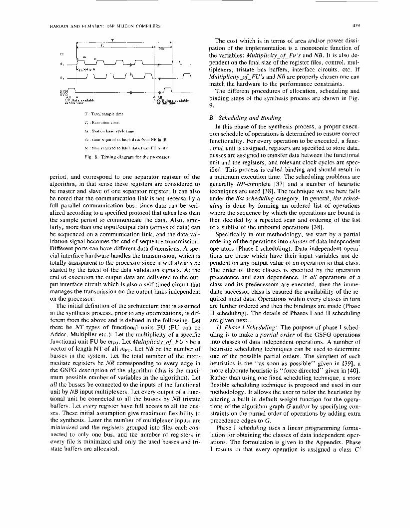
HAROUN A N D ELMASRY: DSP SILICON COMPILERS 439
CI
T ’ Total sample time
rl: Execution time
ta : System basic cycle time
tb : time required to latch data from RF in IR
tc ’ time required to latch data from FU t o RF
Fig. 8 . Timing diagram for the processor
period, and correspond to one separator register of the algorithm, in that sense these registers are considered to be master and slave of one separator register. It can also be noted that the communication link is not necessarily a full parallel communication bus, since data can be seri- alized according to a specified protocol that takes less than the sample period to communicate the data. Also, simi- larly, more than one input/output data (arrays of data) can be sequenced on a communication link, and the data val- idation signal becomes the end of sequence transmission. Different ports can have different data dimensions. A spe- cial interface hardware handles the transmission, which is totally transparent to the processor since it will always be started by the latest of the data validation signals. At the end of execution the output data are delivered to the out- put interface circuit which is also a self-timed circuit that manages the transmission on the output links independent on the processor.
The initial definition of the architecture that is assumed in the synthesis process, prior to any optimizations, is dif- ferent from the above and is defined in the following. Let there be NT types of functional units FU (FU can be Adder, Multiplier etc.). Let the multiplicity of a specific functional unit FU be mFU. Let Multiplicity-of- FU’s be a vector of length NT of all m F U . Let NB be the number of busses in the system. Let the total number of the inter- mediate registers be NR corresponding to every edge in the GSFG description of the algorithm (this is the maxi- mum possible number of variables in the algorithm). Let all the busses be connected to the inputs of the functional unit by NB input multiplexers. Let every output of a func- tional unit be connected to all the busses by NB tristate buffers. Let every register have full access to all the bus- ses. These initial assumption give maximum flexibility to the synthesis. Later the number of multiplexer inputs are minimized and the registers grouped into files each con- nected to only one bus, and the number of registers in every file is minimized and only the used busses and tri- state buffers are allocated.
The cost which is in terms of area and/or power dissi- pation of the implementation is a monotonic function of the variables: Multiplicity-of-Fu’s and NB. It is also de- pendent on the final size of the register files, control, mul- tiplexers, tristate bus buffers, interface circuits, etc. If Multiplicityof-FUS and NB are properly chosen one can match the hardware to the performance constraints.
The different procedures of allocation, scheduling and binding steps of the synthesis process are shown in Fig. 9.
B. Scheduling and Binding In this phase of the synthesis process, a proper execu-
tion schedule of operations is determined to ensure correct functionality. For every operation to be executed, a func- tional unit is assigned, registers are specified to store data, busses are assigned to transfer data between the functional unit and the registers, and relevant clock cycles are spec- ified. This process is called binding and should result in a minimum execution time. The scheduling problems are generally NP-complete [37] and a number of heuristic techniques are used [38]. The technique we use here falls under the list scheduling category. In general, list sched- uling is done by forming an ordered list of operations where the sequence by which the operations are bound is then decided by a repeated scan and ordering of the list or a sublist of the unbound operations [38].
Specifically in our methodology, we start by a partial ordering of the operations into classes of data independent operators (Phase I scheduling). Data independent opera- tions are those which have their input variables not de- pendent on any output value of an operation in that class. The order of these classes is specified by the operation precedence and data dependence. If all operations of a class and its predecessors are executed, then the imme- diate successor class is ensured the availability of the re- quired input data. Operations within every classes in turn are further ordered and then the bindings are made (Phase I1 scheduling). The details of Phases I and I1 scheduling are given next.
1) Phase I Scheduling: The purpose of phase I sched- uling is to make a partial order of the GSFG operations into classes of data independent operations. A number of heuristic scheduling techniques can be used to determine one of the possible partial orders. The simplest of such heuristics is the “as soon as possible” given in [39], a more elaborate heuristic is “force directed” given in [40]. Rather than using one fixed scheduling technique, a more flexible scheduling technique is proposed and used in our methodology. It allows the user to tailor the heuristics by altering a built in default weight function for the opera- tions of the algorithm graph G and/or by specifying con- straints on the partial order of operations by adding extra precedence edges to G .
Phase I scheduling uses a linear programming formu- lation for obtaining the classes of data independent oper- ations. The formulation is given in the Appendix. Phase I results in that every operation is assigned a class C’

440 IEEE TR .ANSACTIONS ON COMPUTER-AIDED DESIGN, VOL. 8, NO. 4, APRIL 1989
0 Control of Heuristiu
(precedence COMtrainta I and Operation Weishta)
RcAllocate I Allocation
Phase II Analysis
.1 Bounds
Done
Fig. 9. The hardware synthesis procedure.
where i = 0-k - 1 . Operations in class C' precede those in CJ in binding if i c j . The default weight function used in SPAID without any precedence constraints results in as late as possible (ALAP) schedule. Note that there is no binding to clock cycles done in Phase I, only a partial order. The number of operations of a type belonging to a class gives an indication of the amount of parallelism that exists in the algorithm G.
2) Phase ZZ Scheduling and Binding: After an initial allocation is made for the number of the different func- tional units and the number of busses, the operations of every class (starting at CO to Ck-') are further ordered and then binding is done on each operation in turn.
The order of executing operations within a class CJ is not of importance to functionality because of data inde- pendence, but affects the final execution time for the al- located hardware. For the NT types of functional units in the architecture, there are
NT
II nJFU! F U = I
permutations that will produce a different order for the operations of the jth class, where the nku is the number of operations in C' which will be executed on a functional unit of type FU. Because of the combinatorially large number of alternative schedules a greedy heuristic is used to determine the order of binding operations in every class.
The ordering of operations within a class CJ is done as follows:
a) Operations are ordered according to a priority given
to the type of functional unit they are executed on. The functional unit type with a higher busy time BT is given a higher priority.
where dFU is the number of clock cycles a functional unit of type FU requires to execute its operation. BT gives preference in the binding to a type of opera- tions that will take a larger number of clocks in that class on the average, so that it takes priority in using the busses and hence may require less time.
b) To determine which operation of the same type has priority, the one with earliest data available is cho- sen. Note that because the default scheduling in Phase I makes an ALAP partial order, the operations on non-critical paths are deferred to latter classes. The operations with the most number of successors are given a lower class and hence priority over oth- ers in binding. If two operations with the same type fall in the same class, this would mean they have the same number of successors. In such a case, choos- ing the operation with the earliest data available minimizes the idle time for the functional unit it will execute on.
The choice of the functional unit on which the chosen operation will be bound is done as follows:
a) For the chosen operation, choose a corresponding functional unit of a type that thi's operation is as- signed to execute on. That functional unit has a non busy time that will best fit the time the input data of the operation is available. The functional unit with the best fit is the one which results in the minimum idle time of the functional units and if all of them result in zero idle time then the functional unit that will result in the minimum postponement of the op- eration execution. In case of a tie, choose the fastest of the functional units.
b) Choose the first available clock on any of the busses for the data transfers to and from the functional units. Resultants of operations may have to wait at the output of a functional unit till a bus is available. This means that effectively the functional unit exe- cution time has increased for such an operation be- cause of the unavailability of any of the busses. Nat- urally, the functional unit cannot accept new input data till the output is stored. In case of pipelined functional units, new input data are accepted in a functional unit when their resultant output will only appear after the previous outputs were stored.
Ties are broken randomly. The heuristics are greedy because once an operation is on for binding, it is bound as early as possible, in fact, operations from later classes can actually precede operations from former classes in time if no data dependence is violated and according to the availability of the functional units and busses. Also no unused functional unit or bus will be used unless ac-

HAROUN A N D ELMASRY: DSP SILICON COMPILERS 44 1
tually needed to reduce the execution time (for the given order of binding). Reservation lists are used for every functional unit and bus and is updated after every binding of every operation. The read and the write times of the NR intermediate registers are also determined during this binding phase.
Phase I and I1 combined can exhaustively produce all the possible permutations of the list of operations that do not violate data dependence. This can be seen by noting that in Phase I , if k is chosen to be equal to the number of operations in the graph and the user specifies enough precedence constraints on the operations for a specific or- der, Phase I will produce a full ordering of operations where every class contains only one operation, rather than a partial ordering. Phase I1 in this case makes no choices other than binding the operations in the order given by Phase I. This methodology can obviously span all the pos- sible schedules for a given architecture. Nevertheless, the default case where Phase I makes an ALAP partial order and Phase I1 makes an ASAP binding of operations, re- sults in a combined effective heuristic which effectively balances operation distribution. In the examples to be pre- sented in Section IX, one to three trials were done in Phase I by making minor changes in the weights associated with the operations. Changing the sign of the weights in Phase I changes the tendency of an operation from being sched- uled ALAP to ASAP or vice versa.
The procedure for the search for an allocation of hard- ware that will satisfy both the execution time T, and the cost constraints is given next.
C. Allocution of Busses and Functional Units The procedure for obtaining a new allocation from the
initial one is based on an exhaustive best first search strat- egy [41]. There are NT + 1 allocation variables that are determined before scheduling and binding. These are NT variables in Multiplicity-of- FU’s and the number of bus- ses NB. These variables have a minimum of unity. The upper bound on these variables is inflicted by the total area and power dissipation of the architecture and the pos- sible parallelism in the algorithm. The upper bound is typ- ically small, which reduces the space for exhaustive search. The use of the best first search strategy may help in arriving at a feasible solution early in the search. Henceforth, cost stands for both area and power dissipa- tion. A presynthesis cost is calculated for all possible al- locations that can be obtained from the current allocation by a unit increment in the multiplicity of a functional unit or bus
COST = Current-Cost + Cost-FU + Cost-increment
(Incremented- FU, Current-NB)
The cost increment depends on the number of busses and the multiplicity of functional units, because extra multi- plexer inputs and tristate bus buffers are also needed in addition to the incremented busses or functional units. The Current-Cost accounts for all other costs of registers and
control assuming, as an approximation, that it will not change with the new allocation. Only the allocations that do not exceed the cost bounds are considered.
From the current synthesized hardware, the bindings are analyzed to produce a utilization measure for both func- tional units and busses. For every type of functional unit the utilization measure is equal to the minimum number of cycles a functional unit is busy. This number is nor- malized to a nominal utilization defined as the total exe- cution time of all operations executed on this type of func- tional unit divided by the multiplicity of that functional unit. For busses the utilization measure is equal to the minimum number of cycles a bus is busy normalized to a nominal utilization defined as the total number of data transfers (NR) divided by the number of busses. The greedy heuristics used in the binding rarely uses any func- tion unit or bus if it is not needed to reduce execution time. Therefore, a low utilization measure for a type of functional units or for a bus indicates that increasing its multiplicity in the hardware will not decrease much the execution time. The considered allocations are ordered such that the one with an incremented functional unit or bus with highest utilization measure has highest priority. In case of a tie, the one with the least cost will be given priority.
For a selected allocation the architecture is synthesized. After the synthesis of the architecture is complete, the ex- ecution time is calculated (see next section). The cost for the new architecture is calculated by summing all the costs of its individual components. These are the functional units, register files, multiplexers, bus drivers, busses, lo- cal interconnects, I/O registers and control. The area of the global busses is determined as a linear function of the layout width of the functional units in the data path, to account for the length of the bus. The bit resolution is assumed equal for all components and is a global param- eter for the calculation of the individual costs. The exe- cution time T, or the cost are compared with the bounds. If the bounds are violated or the user fails the obtained solution, the search for a new allocation continues.
SPAID assumes an initial minimum allocation if the user does not specify it. The partial ordering of operations in Phase I can be used by the user as a guide to provide an initial allocation. Rather than performing an exhaus- tive search, the user can also specify to SPAID a limited list of different allocations to be all synthesized.
D. Determination of Clock Cycle Duration After synthesis for a certain allocation, the maximum
number of clock cycles used is multiplied by the clock cycle duration to determine the execution time. For every allocation the clock cycle duration can be different de- pending on the bus loading. The clock cycle duration is recalculated before calculating the execution time.
The clock cycle duration tu is determined from the fol- lowing equation:
tu = datu transfer delay
+ Max. delay for FU with one cycle.
442 IEEE TRANSACTIONS ON COMPUTER-AIDED DESIGN, VOL. 8, NO. 4. APRIL 1989
The functional unit with one cycle execution has a con- stant execution delay independent on the allocation. The data transfer delay is the only one that is affected by the allocation. The data transfer delay is given by
Data transfer delay = RdRF + RF-MwrI t Mux-FUI
+ FUO-RF + WrRF
where RdRF is the delay needed for reading the data stored in a register to be valid on the output of the register file. RF-MuxI is the delay incurred in driving the bus for the data to be valid at the multiplexer input. MuxI-FUI is the delay from the multiplexer input to the output of the input register of the functional unit. FUO-RF is the delay in- curred for the tristate buffers to drive the bus for the data to be valid at the register file input. Wr-RF is the time needed for the data to be written in a register of a register file. The delays RF-MuxI and FUO-RF are strongly de- pendent on the bus loading, hence are allocation depen- dent. As an approximation all the other delays are consid- ered independent of the allocation. The model of the bus delay used in SPAID is a heuristic linear function of the maximum number of connections (multiplexer inputs or tristate driver outputs) made to any of the busses in the system. The linear term in the linear function is specified by the user for the design style. After the new bus delay is calculated the increment from the bus delay of the min- imum architecture is added to the clock cycle duration. This value is used in obtaining the execution time. Note that this is a crude model for delays since it does not ac- count for address settling time for the register files and the decoder delays of the multiplexers, and the depen- dence of multiplexer delays on the number of inputs, etc. In our model these are considered second order effects that may be included in a more elaborate time calculation in the future.
E. Allocation of Registers and Multiplexers The intermediate registers used in the binding can be
grouped into NB register files, i.e., one register file per bus. Intermediate registers can reuse actual hardware reg- isters hence drastically reducing the number of required hardware registers from the initial number NR. Previ- ously, similar register allocation problems in hardware synthesis [20] were posed as clique partitioning, or as general graph coloring problems in software compiler register allocation [27], and since those problems are NPC [37] heuristics were used to solve them. In this approach, the structure of the register allocation problem has been beneficially exploited and optimal/sub-optimal algorithms are used and are described next.
1) Register Grouping and Multiplexer Minimiza- tion: From Phase 11, each intermediate register has a write clock time tw and a read clock time tr. During all the clock periods in between tw and tr the register is busy storing data (if tr < rw then the register is busy from tw to T, and from 0 to t r ) . Registers storing different data and having the same write time f w , or the same read time
tr cannot share the same register file since each has to be reached from a different bus. Because the reading from a register was assigned a different phase from the writing to the registers, there is no conflict between READ and W R I T E
times. Since there are only NB busses then there are at most NB writes or reads at the same clock. These two facts are necessary to be able to divide registers into one register file per bus, as described next.
It is required to divide the intermediate registers into the minimum number of groups such that every register in one group does not conflict in both the read or the write time with any other register of the same group. Each group will represent the registers in a register file. This is an edge coloring problem of a bipartite multigraph, where the two types of nodes in the graph are write and read times. An edge connects two nodes U and v, if U is a reg- ister read time and U is a register write time. Each edge represents a register. The resulting graph is the conflict graph H . Each node is connected to at maximum NB other edges (no more than NB registers will be written into, or read from in the same clock). Finding a group of registers that do not have a READ (or WRITE) time in common is equivalent to coloring the edges of H such that no two edges with the same color share a node. With the previous restriction on the degree of the nodes and for bipartite graphs [42] the edges of H can be colored in NB colors in polynomial time. All registers that are read by one func- tional unit input should be assigned the minimum number of register files to minimize the number of multiplexer inputs. Also all registers that are written into by one func- tional unit should assigned the minimum number of reg- ister files to minimize the number of tristate output bus buffers. In SPAID, an algorithm for bipartite edge color- ing which runs in time O(NR’) [43], is used. The bipar- tite edge coloring algorithm is modified using a heuristic to maximize the registers that have identical data and have a common WRITE and/or READ times to be assigned the same register file (color). Those registers store the data represented by edges of the algorithm graph G that have a common source node. Registers with identical data as- signed to one register file are merged together prior to performing register optimization. This reduces duplica- tion of data storage but does not eliminate it since dupli- cate data can occur in different register files. Also, to this algorithm a heuristic minimization for the number of mul- tiplexer inputs is added. The heuristic is based on initially assigning as much of the registers required to be in one register file a single color, then color conflicts are re- solved by the edge coloring algorithm. Also, the con- stants are assigned to the register files that do not have registers that conflict with their read time.
Since each register file is connected to a single bus, reading from it is done on 9, and writing in it is done on
the implementation of the register file is that of a RAM.
When arrays of data are used as input of an algorithm G , each input data transfer from the array is assigned to a specific bus in this step of register grouping. Hence the

HAROUN AND ELMASRY: DSP SILICON COMPILERS 443
array variables are automatically grouped into one register files connected to each bus. This register file is imple- mented separate from the one having the intermediate reg- isters of the algorithm so that these registers can be up- dated externally to the processor. The implementation is that of a double buffered RAM connected internally to one bus from one port and updated externally from another port. To output arrays from the processor, each data trans- fer to output an array variable is also assigned to a specific bus, and hence the output data array is also automatically grouped into one register file connected to each bus. The implementation of these register files is similar to that of the input array. Full parallelism of the existing busses is used to access the array data in SPAID’s architecture, rather than having all the array accessed sequentially from a RAM (e.g., as in Lager or CATHEDRAL-11).
2) Register Optimization: The second step is to reduce the number of register within each register file by re-using the same register more than once. Since the execution in the processor is periodic, the life times of the registers are periodic too with a period T,. For each register file, every intermediate register (as determined in the previous step), is represented by a node in a graph. An edge exists be- tween two nodes U , U if the life time of the two registers overlap. Because of the periodic nature of the execution of a DSP algorithm, register utilization is periodic with period T,, and we actually have a circular overlap of reg- ister life times around T,. This type of graph is called circular arc graph [44]. Coloring the vertices of this graph for every register file into the minimum number of colors, gives the minimum number of registers in their respective register file. Nodes with the same color represent data storages of different intermediate data using one register in the register file. Coloring a circular arc graph is NP- complete 1371. The resulting graph may also be an over- lap graph which has a polynomial time minimum coloring algorithm (left edge algorithm) 1441-1461. The algorithm developed and used in SPAID to color the circular arc graph first identifies if the graph is an overlap graph and colors it with the minimum colors in polynomial time ( N log N ). If the graph is a circular arc then a heuristic is used where the minimum number of edges are removed from the graph to obtain an overlap graph. The overlap graph is then colored using minimum colors 1451, 1461. The removed edges are also colored with the minimum non-conflicting colors. This polynomial time algorithm to color a circular arc graph uses a number of colors bounded by the best known upper bound for circular arc graphs. The upper bound is given in [47]. Also, note that the problem has been reduced before this step by the previous step of grouping into register files.
Duplicate data may be stored in the same time in dif- ferent register files. Having duplicate data in different reg- ister files is the price one has to pay for having only one bus connected to each register file. On the other hand, the other synthesis approaches that use a random topology like HAL, SEHWA, CATREE or S(P)LICER, the registers are separate and not in register files. Every register is con-
nected by a separate input and output interconnect. While in CATHEDRAL-I1 the register files are implemented using master slave type registers with an input and an out- put ports. Since these register files are connected to each functional unit input, they are limited in the number of registers they can have (eight) 1121. In fact, one cannot compare the area of registers in these architectures with the area of registers in the architecture synthesized by SPAID by merely comparing the number of registers. The savings in area due to the use of register files implemented as RAMS and connected to a single bus in SPAID should be taken in perspective in the comparison.
F, Microcode Generation and Architecture Dejnition From the bindings made in Phase I1 the register allo-
cation, and the allocation of the functional units and bus- ses, the microcode for the controller can be directly ob- tained. The controller used is very simple because it implements a static schedule without branching (condi- tional execution is done in the data path redundantly as noted earlier). On every phase a microcode word is gen- erated from the controller. On 9, the architecture is con- figured so that on every bus data are transferred from the register file or an input registers to one input of a func- tional unit. On a2, the architecture is configured so that for every bus data from functional unit outputs are trans- fered to the register file or an output register. The micro- code word on @, has a field for every register file with the addrss of the register that outputs data to the bus, another field for every bus to determine the destination multi- plexer inputs that input the data from the bus to the func- tional units. The microcode word on G2 has a field for every register file with the address of the register that in- puts data from the bus, another field for every bus to de- termine the single source tristate output that outputs the data to the bus from a functional unit. Other fields in- cludes, a field for functional unit modes (for ALU’s) and for input-output units to indicate start and end of execu- tion so that data I/O and data valid outputs can be gen- erated. Fields of the microcode can also be vertically coded and reused between the two phases by dynamic de- coding.
For the architecture that has satisfied all the bounds, a full architecture description is produced to the user. VHDL is being considered to describe the architectures produced by SPAID where it can act as language for sim- ulation of the architecture, and as an input to another sil- icon compiler tool, one which accepts architecture defi- nition and produces a silicon layout.
IX. DESIGN EXAMPLES Two design examples are used to demonstrate the meth-
odology. The first is the 16-point FIR filter used in SEHWA 171, and also in HAL [48]. Their original graph is shown in Fig. 10. A number of retimings and local transformations were used on the graph to obtain the best synthesis. In Phase I scheduling, different weights were assigned to different nodes (e.g., addition and multipli-

444 IEEE TRANSACTIONS ON COMPUTER-AIDED DESIGN, VOL. 8. NO 4, APRIL 1989
Fig. 10. 16-point FIR Filter used in Sehwa and HAL
I I I I I I I I
cation nodes 1, 2 and 3 were given a negative weight to be assigned to an earlier class). The transformed graph and the assignment of operations to classes in Phase I is shown in Fig. 11 by means of the dividing lines. The val- ues of the delays used in HAL for the functional units were assumed; an adder has a delay of 40 ns and a mul- tiplier has a delay of 80 ns, and the system cycle is taken as 20 ns. This results in a 3-cycle execution for the adder (40 ns execution delay plus 20 ns for data read and write), and a 5-cycle execution for the multiplier. SPAID pro- duced an architecture with 4 adders, 3 multipliers, and 6 busses which has a T, = l/throughput of 300 ns, and a latency delay time of 600 ns. The throughput and latency are equal to the values obtained by both SEHWA and HAL which use 5 adders and 3 multipliers. This is the best pos- sible allocation their synthesis methodology can produce (SEHWA has optimal exhaustive scheduling). The sched- ule and binding produced by SPAID for such an example is shown in Fig. 12. The use of retiming and local trans- formation on the algorithm representation and the multi- cycle execution of the addition and multiplication are the reason for SPAID’s architecture having one less adder than that of HAL or SEHWA for the same performance.
Another more elaborate example is the elliptic filter originally described in K&K [49] and used by HAL in [48]. This example was chosen as a bench mark for the 1988 ACM/IEEE Workshop on High-Level Synthesis [50]. Retiming of the elliptic filter was applied to obtain the filter shown in Fig. 13. Table 1 shows a comparison of the results obtained in K&K [49], by HAL [48], by SPLICER [51], and by SPAID. The designs obtained by SPAID take on the average 60 CPU seconds for the syn- thesis of each design on a SUN 3/160. SPAID is written in Prolog. Retiming and phase I use a linear programming subroutine which is run once for all the examples and took 40 CPU seconds for retiming and 12 CPU seconds for phase I. The retiming linear programming subroutine is written in Fortran and called from Prolog.
In Table I, a regular design uses non-pipelined multi- pliers requiring two clock cycles. In pipelined design, the multiplier is pipelined requiring two clock cycles to pro- duce an output, and can be initiated every clock cycle. A comparison of Table I entries reveals the following.
1) The total interconnect count given in Table I is cal- culated by adding the number of busses to the num- ber of local interconnects representing interconnects
‘9ri c3
Fig. 1 1 . 16-point FIR Filter after applying transformations. The partial order of operations into data independent classes in Phase 1 is shown.
AI+ Bus Cycle=POns A2+ Adder delay=4Ons A3+ Mult. Delay=BOns A4+ M1 M2 M3
0 100 200 300 nsec
Fig. 12. The execution schedule of the operations in the FIR example on 4 adders and 3 multipliers.
Fig. 13. The elliptic filter bench mark example
from the multiplexers to the inputs of the functional unit, and from the output of the functional unit to the tristate bus buffers. On the other hand, the num- ber of interconnects in HAL include both local and global interconnects. The distinction between local and global interconnects is not available for HAL. For the SPAID design with 17 clock cycles, 6 bus- ses, and 15 local interconnects are used. While HAL requires 56 interconnects. The same number of adders and multipliers are used. This shows a sig- nificant reduction of interconnect in the SPAID de- sign, in addition to the regularity of the linear to- pology used, both are an asset in a VLSI implementation. For the design with 19 clock cycles, SPAID uses also much less interconnects relative to HAL’S design. For the design with 17 clock cycles SPAID also uses less number of busses than the bus design by CATREE. CATREE uses a multiplexer style, similar to that of HAL, for the 16 clock cycles design. The number of interconnects are near to those of HAL, exact values are not currently avail- able.

HAROUN A N D ELMASRY: DSP SILICON COMPILERS 445
TABLE 1 A COMPARISON OF SPAID's SYNTHESIS FOR T H E ELLIPTIC FILTER W I T H
HAL, SPLICER, K&K A N D CATREE
SPAID uses less number of multiplexer inputs than those used in HAL, SPLICER, or CATREE. For the 17 cycle design, SPAID uses 6 register files with a total of 17 registers. In HAL 12 separate in- dividual registers are used. A practical comparison has to include the overhead of having separate reg- isters each accessed by two interconnects as in HAL or CATREE's designs, and the area savings for using register files used in SPAID. The number of registers tend to decrease for slower implementa- tions in SPAID because duplicate data storage can almost be eliminated. SPAID obtains a solution with 16 cycles which is not obtained by HAL or K&K. This is because re- timing was used on the initial specification. CA- TREE uses the same retimed graph as the one used in SPAID. SPAID can produce a wide range of implementa- tions, so a user can quickly get many designs with performance-area tradeoffs. It took less than 12 CPU minutes to produce all the outcomes of Table I.
Note that using exhaustive search for the elliptic filter example is a feasible task. The number of different allo- cations for a given design style that give all the different execution times is only equal to
NB""" X m2Ar X mg;, = 7 X 4 X 2 = 56.
X . CONCLUSION A novel methodology for architectural synthesis of a
processor architecture with multiple functional units and multiple busses from a signal flow graph description of a DSP algorithm has been described. The synthesized ar- chitecture can be matched to the throughput and latency requirements of the DSP algorithm.
The methodology supports large multi-processor sys- tems by employing a self-timed interprocessor commu- nication paradigm, which solves the problem of clock de- lay and skew in large systems. The self-timed interface supports sequential input output of multidimensional data.
The methodology is implemented as a design tool called SPAID. Using SPAID a designer or an expert system can explore a large design space with great flexibility. The designer can alter the initial specification of the algorithm by applying behavior preserving transformations to op- timize the algorithm description for maximum through-
put. SPAID allows the selection of design style from among available library modules. The designer has full control over the scheduling heuristics used in the hard- ware synthesis up to totally overriding the heuristics. SPAID allows a quick exploration of different architec- tural alternatives.
The synthesized architecture compares favorably over other synthesis techniques on a bench mark example. A processor with multiple busses and functional units and one bus per register file is synthesized. The synthesis methodology supports both non-pipelined and pipelined functional units with an execution time of one or more clock cycles. The resulting architecture has a linear to- pology which is regular and suitable for VLSI implemen- tation. Compared to other synthesized architectures, the architecture presented here uses significantly less number of interconnections. It also uses less .number of multi- plexer inputs. Data arrays can be sequentially input/out- put to a processor every sample period and are internally stored in NB register files that can be accessed in parallel each by a single bus. This feature can have an implemen- tation area advantage over other synthesis systems that use separate individual registers accessed by an input and an output bus which may be suitable for a small number of inputs and outputs but not for arrays of large dimen- sions. Data arrays are a common occurrence in DSP al- gorithms, for example, in FFT or block processing of data.
The use of a bus architecture may have a draw back specifically when the busses are heavily loaded, implying large bus delays. This can be reduced by using larger area bus drivers. In view of the possible use of new technol- ogies like, BiCMOS [52] having small area buffers driv- ing long heavily loaded busses, the area and delay over head can be reduced.
As for the DSP algorithm representation, the signal flow graph is used which is very familiar to designers with DSP background which are the potential users of SPAID. The GSFG can also be defined hierarchically in SPAID, and the designer can benefit from predesigned algorithm mod- ules (e.g. second order sections) to compose his algorithm description.
Areas of improvement for the methodology described here and implemented in SPAID are currently under in- vestigation. Some are: 1) A graphical interface, ACE, for specifying a GSFG and viewing it under transformations

446 IEEE TRANSACTIONS ON COMPUTER-AIDED DESIGN, VOL. 8, NO. 4, APRIL 1989
is under development, 2) large scale conditional opera- tions (a function selector node rather than a data selector node) for the algorithm representation are being studied, and the synthesis methodology is being extended to sup- port it, 3) more elaborate control structures are being con- sidered, other than the straight microcode execution, to support mutual exclusion in execution of conditional op- erations, 4) chaining of functional units in one clock cycle is to be supported, and for such a purpose local intercon- nections between functional units, and limited local stor- age at the function units are investigated, and 5) support- ing different bit widths efficiently in the same processor is also considered.
APPENDIX The formulation of the linear programming problem to
obtain a partial order on the operations of a given GSFG; G which satisfies data precedence is given. The partial order is done by determining an ordered set of classes of operations. Systolization of a graph G is used as a tool to obtain this partial order.
There are some restrictions to be imposed on the GSFG for the synthesis to be valid. Let G ( N , E ) be a GSFG; the edges of G are restricted to have w ( e ) 5 1 which can be achieved by inserting dummy transfer nodes on edges with w ( e ) > 1 . One intermediate register stores the data communicated (on edges of G ) between operations dur- ing one sample period. The restriction w ( e ) I 1 guar- antees that storage time of data on the edges are less than or equal to one sample period. The formulation is as fol- lows. A k-slow graph is obtained by multiplying the order of the separator registers on every edge of G by the slow down factor k . The k-slow graph is then fully systolized by retiming, with the constraint that the order of separator register of the resultant graph GS is greater than or equal to one [23], [34]. GS has operations that are naturally di- vided into k equivalence classes. This can be shown by following one of the k interleaved data streams input to GS and observing which operations are active on that stream every clock tick for k clock ticks. Let k be a pos- itive integer. Let r ( U ) be a function from the set of nodes v E N to integers. A graph GS is obtained if the weights w ( e ) of G are transformed to w, ( e ) in GS; as given by w , ( e ) = k * w ( e ) + r ( v ) - r ( u ) .
The function r ( U ) gives an equivalent graph GS with 1 I w sub s ( e ) I k ; if:
r ( U , ) = r ( vi) = 0 where U , is the output node, and vi is the input node. This condition ensures no change in the number of registers on the path be- tween input and output, hence latency will not change. - r ( u ) + r ( u ) 2 1 - ( k * w ( e ) ) forevery edge e ( u , U ) in G , which ensures that every edge will have at least one register. - r ( v ) + r ( u ) 2 k * ( w ( e ) - 1)foreveryedge e ( u , U ) in G , which ensures that every edge will have at most k registers.
The previous set of constraint equations can be solved to get r ( v ) values using linear programming, by maxi- mizing an objective function
C e * . ( U ) all 1’
where e,, is a weight factor that determines the scheduling heuristics (e.g. all weights strictly positive and equal gives as late as possible scheduling).
An operation U is assigned a class C’, j = ( k - 1 ) + ( r ( u ) ) mod k .
ACKNOWLEDGMENT The authors are grateful to the reviewers for the many
helpful and constructive comments.
REFERENCES D. Gajski, Silicon Compilation. Reading, MA: Addison-Wesley, 1988. J . Rabaey, S . Pope, and R . Brodersen, “An integrated automatic lay- out generation system,” IEEE Trans. Computer-Aided Design, vol.
P. Ruetz er al., “Computer generation of digital filter banks,” IEEE Trans. Computer-Aided Design, vol. CAD-5, pp. 256-265, Apr. 1986. J . Schuck, M . Glesner, and M . Lacken, “First results and design experience with silicon compiler ALGIC,” in VLSI Signal Processing /I. B. Petersen, B . White, D. Solomon, and M . Elmasry, “SPIL: A sil- icon compiler with performance evaluation,” in Proc. ICCAD, pp.
P. Paulin, J . Knight, and E. Gyrczyc, “HAL: A multi-paradigm ap- proach to automatic data path synthesis,” in Proc. 23rd Design Au- tomation Conf., pp. 263-270, 1986. N. Park and A. Parker, “Sehwa: A software package for synthesis of pipelines from behavioral specifications,” IEEE Trans. Computer- Aided Design, vol. 7 , pp. 356-370, Mar. 1988. M. McFarland, “Using bottom up design techniques in synthesis of digital hardware from abstract behavioral descriptions,” in Proc. 23rd Design Automation Conf., pp. 474-480, 1986. C. Gebotys and M. I. Elmasry, “VLSI design synthesis with test- ability,” in Design Automated Conf., 1988. A. Parker, J . Pizarro, and M. Mlinon, “MAHA: A program for data path synthesis,” in 23rd Design Automation Conf. 86, pp. 461-466, 1986. B. Pangrie and D. Gajski. “State synthesis & connectivity binding for microarchitecture compilation,” in Proc. ICCAD86, Nov. 1986. G. Goesens et al., “A CAD methodology for mapping DSP Algo- rithms onto MP custom architectures,” in Proc. IEEE ICCAS 86, May 1986. J . Rabaey, H. De Man, J . Vanhoof, G. Goosens, and F. Catthoor, “CATHEDRAL-11: A synthesis system for multiprocessor DSP sys- tems,” in Silicon Compilation, D. Gajsk. Ed. Reading, MA: Ad- dison-Wesley, pp. 31 1-360, 1988. M. Hatamian and G. Cash, “Parallel bit-level pipelined VLSI design for high speed signal processing,” Proc. IEEE, vol. 75. pp. 1192- 1202, Sept. 1987. A. Fisher and H. Kung, “Synchronizing large VLSI processor ar- rays,” IEEE Trans. Computers. vol. C-33. pp. 734-740. Aug. 1985. J . Allen, “Computer architecture for DSP.” Proc. IEEE, vol. 73, pp. 852-873, May 1985. A. Fettweis, “Realisability of digital filter networks,” AEU, vol. 30, 1976. E. A. Lee and D. G. Messerschmitt. “Synchronous data flow,” Proc. IEEE, vol. 75, pp. 1235-1245. Sept. 1987. B . Haroun and M. I. Elmasry. “SPAID,” Tech. Rep. UWiICR 88- 06, Ur.iv. Waterloo, Canada, 1988. C . Tseng and P . Seviourek. “Automated synthesis of data paths in digital systems,” IEEE Trans. Computrr-Aided Design, pp. 379-395, July 1986. T . Barnwell I11 and D. Schwarz. “Optical implementation of flow
CAD-4, pp. 285-296, July 1985.
New York: IEEE Press, Nov. 1986.
500-503, NOV. 1986.

HAKOUN A N D kLMASKY DSP SILICON ('OblPILFRS 447
graphs o n synchronous tiiultiprocessors." i n l i ir . Coii,/. o i i ASSP 84. 1984. D. Schunrtz and T . Barnwell 111. "Cyclo static \oIution. Optimal iiiu It ipr realisation of recurs i ve al gori I h nis. ' ' in VLSl Sigiicil Proce.s.\ - iit,q I / . New York: IEEE Press. No\. I986 F. Rose. C . Lcixraon. and J . Saxe. "Optimihing sqnchronous cir- cuitry by retiming." in P i - o c C(r//c,di Coil/. o r 1 VI-SI. pp. 41-67, Computer Sei. Press. 1983. L. Glasser a n d D . Dohherpuhl. The Dr,\igii t r i i t l A i io /x \ i \ of VLSI Cir- c . r r ; / . \ . Reading. MA: Addi\on-Wtr\lcy. 1985. D. Schuartr and T . Harnuell 111. "A graph theoretic techniquc lor the generation of systol ic itiipleiiientatiOn." i n Proc. Asrloiritrr CO~I/: o t i CAS 84. 1984. B. Kernighan and S. Lin. "An efticient heuristic procedure for par- titioning graphs." Re/ / $!\/. 7 i .d i . J . . pp 29 1-307. Feb. 1970. A Aho. R. Sethi. and J Ullman. Coriipi/ci-.\ Reading. MA: Ad- dison-Wr\le), 1986. H. Lipp. "Methodical aspects of logic s>nthe\i\." P ~ o c , . IEEE. v o l . 71. vol. pp. 88-97. Jan . 83. J . Bhasher. "An optimirer f o r hiirduarc s) nthesi\." S(.ic,iirific. H o i i ( , ! i w / / r r , pp. 23-34, Winter 1987. H . Trickeq. "Flamel: A high-level harduare compiler." IEEE Troti.\. ( ' ~ , i r i / ) i / / t , r - A i t / ~ , ~ / Dcti,qii. v o l . CAD-6. pp. 259-269. Mar. 1987. K Hwang. Coiiipiirt,r Ar;r/iiiic,/ic~. New York Wiley. 1979. C . Scitz. "Systcii i timing." in /irrrotlrrc./iori 10 VLSl ~Y\\rt,tii.! C Mead and L . Conuay . Eds. M . Pechouceh. "Anomalou\ re\pon\c times of input s) nchronizers." l E E E Trciric. Coi?ipr/cr-.\, vol . C-25. pp 133-139. Feh. 1976. C. L e i s e r w n and J . Saxe. "Optimi\ing \ynchronous sys tems. " J . VLSI & C~ri ip . .Sy\r.. \ o I . I . no. I . pp. 41-67, 1983. A. Yiikovlc\. "Designing self timed systcins." VLSl S\\rc,iri Dc,.\i,yii.
S. Y . Kung. VLSl A m i ! Prow\.\or.\. Englewood Cliffs. NJ: Prcn- tice Hall. 1988. Michael Garcy a n d David Johnson. C'oitrpir/<jr-\ mid / i i r r r i < ~ / ~ i / ~ i / ; / ! .
San Francisco. CA: Freeman. New York. 1979. E. G . Cofiiian. Coiiiptrrcr- r r i i r l J d - S h o p S d i e ~ / r ~ / i i i ~ q Thtvjr!. Nev. York: Wiley. 1976. T. C . Hu. "Parallel sequencing and assembly line prohlems." f I /wr . Rc.\.. vol. 9. pp. 841-848. 1961. P. Paulin and J . Knight. "Force-directcd scheduling in automatic data path aynthesis." in ACM//I.JL.E 24th DAC. 1987. E. Rich. Arrifrcitil / i i / c , / / i g r i r c . c , .
Claude Berge. Grtiphs. New Yorh: Elwvicr Sci.. 1985. H Gabon and 0. Karib. "Algorithms for edge coloring bipartite graphs and multigrnphs," SIAM J . C ~ ~ i r i p ~ / . . vol . 1 1 . pp 117-129. Feh. 1982.
Reading. MA: Addison-Wesley. 1981.
pp. 70-86. Sept. 1985.
Ne\+ York: McCrau-Hil l . 1983.
1441 Mar t in Golumhic. A/gorir/ir?iic Grtip/i Tlicwr-v u r i c / Pc,r:/ccr Grop/i\. New York: Academic. I980
1451 B Kernighan. D . Schw'eikert. and G . Pcnky . " A n optimum channel routing algorithm for polycell l a q o u t \ ot integrated circuits." in Pro<.. l U r h Desisii A i r / o i r i t i / i o r i C'orij' . pp . 50-59. I973
1461 U . Gupta. D. Lec. a n d J . Leung. "An optiin;il w l u t i o n for channel a\sigtitiient problem." I Tr<im. Cofrl/ l~/r~~r\. 101. c - 2 8 . pp . 807- 810. Nov. 1979.
1471 A. Tucker. "Coloring a family of circular arc graph\." S I A M J . Appl . M u r h . , vol 29. pp. 493. 502 (1975) .
1481 P. Paulin a n d J Knight. "Scheduling and :illocation for pipelined a$ic\." in CCVLSl 87. Oct. 1987.
1491 S . Y . Kung. H . Whitehouse. and T . K a i l a t h . V I S / & Motlcr-ii S i , y i i i i /
frow.\.siii<y. [ S O ] ACMIIEEE W(J~L.Y/IO[J 011 H i g h L e , \ ~ l S\ , i r / tc ' \ is . Orcti.\ / . \ / t i t id . J a n .
1988. 1511 B. M . Pnngrle. "Splicer: A heuristic approach to connecti\ i t ) bincl-
ing." in 25rh DAC. pp. 536-541. 1988. 1521 M . Kubo e/ ( I / . . "Perhpective o n BiCMOS VLSI." lEEE J . Solid-
Srti tc C;r-ciri/.\. vol. 23. Feb. 1988.
Englewood Cliffs, NJ: Prentice-Hall. 1985.
*
Baher S. Haroun received the B.Sc. (Di\tinction with Honors) and M.Sc. degrees i n electrical en- gineering from Ain Shams Univeni ty , Egypt. in
1981 and 1984, re5pectively. Currently he is working toward the Ph.D. degree i n electrical en- gineering in the University o l Waterloo, Ont. . Canada.
His current research interests include silicon compilation and the development of algorithms and VLSl architectures for DSP application\ and neural networks.
*
Xlohamed 1. Elmasry (S'69-M'73-SM'79-F'88) received the B.Sc. degree from Cairo Universitq. Cairo. Egypt, and the M.A.Sc . and Ph.D. degree5 from the University of Ottawa. Ont. , Canada. in 1965. 1970. and 1974. respectively. all in electri- c a l engineering. He has worked in the area of dig- ital integrated circuits and system design for the last 2 3 years. From 1965 to 1968 he was u i th Cairo Uni\-er\it) and from 1972 to 1974 with Bell- Northern Research. Ottawa. He has been with the Department of Electrical Engineering. and a l s o the
Department of Computer Science. University of Waterloo. Waterloo, Can- ada. since 1974. uhe re he is a Professor and founding Director o f the VLSI Research Group. He has a cross appointment with the Dcpartincnt of Com- puter Science uhe re he is a Professor. He holds the NSERCiBNR Chair in
VLSI design at the s a m e University. He has wrved as a consultant to sev- eral research and development laboratories in both Canada and the US. i n the area of LSliVLSI digital circuitisuhsystem design. During 1980- 1981 and 1987- 1988 he was at the Micro Component\ Organization. Burroughs Corporation (Unisys), San Diego. California. Kuwait University. Kuwait and Swi\\ Federal Institute of Technology. Lausannc. Switzerland on leaves from the Univeraity of Waterloo. He has authored and co-authored over 100 papers o n integrated circuit design and design automation. He has se\- era1 patents t o his credit. He %!as the editor of "Dicqirtr/ MOS /rirc~cyrtrrc~t/ Circ,uir\." ( IEEE Press. 1981) and "Digitti/ V I S I sy.src~iii.s." (1EEE-Press. 1985) and the author of "Di,yirtil hipoltrr iri /c~~qrtr/etl c.ircxi/.\." ( J o h n Wiley. 1983) has served in man) professional organizations i n different position\ including the Chairman of the technical arlviaory committee of the Cana- dian Microelectronic\ Corporation. a founding member of the Canadian VLSI Conference. and the lounding prc\idcnt of Picc Electron~cs Inc.
Dr. Elnia\ry i s a member of the A\sociation of Professional Engineer\ of Ontario.