ADSP-218x DSP Hardware Reference
26
ADSP-218x DSP Hardware Reference 1-1 1 INTRODUCTION Figure 1-0. Table 1-0. Listing 1-0. Purpose The ADSP-218x DSP Hardware Reference provides architectural and design information about the ADSP-218x family of digital signal proces- sors (DSPs). The architectural descriptions cover functional blocks, busses, and ports. The ADSP-218x DSP Instruction Set Reference manual covers programming information. The ADSP-218x data sheets for each member of the family cover timing, electrical, and packaging specifica- tions, as well as, many other topics related to the features and design of the specific processor. Audience This manual is developed primarily for DSP designers and programmers. The manual assumes that the audience is familiar with signal processing concepts and has a working knowledge of microcomputer technology and DSP-related mathematics.
-
Upload
khangminh22 -
Category
Documents
-
view
0 -
download
0
Transcript of ADSP-218x DSP Hardware Reference

1 INTRODUCTIONFigure 1-0.
Table 1-0.
Listing 1-0.
PurposeThe ADSP-218x DSP Hardware Reference provides architectural and design information about the ADSP-218x family of digital signal proces-sors (DSPs). The architectural descriptions cover functional blocks, busses, and ports. The ADSP-218x DSP Instruction Set Reference manual covers programming information. The ADSP-218x data sheets for each member of the family cover timing, electrical, and packaging specifica-tions, as well as, many other topics related to the features and design of the specific processor.
AudienceThis manual is developed primarily for DSP designers and programmers. The manual assumes that the audience is familiar with signal processing concepts and has a working knowledge of microcomputer technology and DSP-related mathematics.
ADSP-218x DSP Hardware Reference 1-1

Overview
OverviewThe ADSP-218x family is a collection of programmable single-chip microprocessors that share a common base architecture optimized for dig-ital signal processing (DSP) and other high-speed numeric processing applications.
These processors can be used in such diverse applications as:
• Speaker phones
• Smart phones
• Smart-card readers
• POS terminals
• Digital speech interpolation
• Video conferencing
• Data encryption
• ISDN modems
• Pattern matching
• Global positioning
• Navigation
1-2 ADSP-218x DSP Hardware Reference

Introduction
The ADSP-218x family processor architecture includes the following features:
• Three computational units
• Two data address generators
• A program sequencer
• Two bidirectional serial ports
• A 16-bit internal DMA port
• A byte DMA port
• A programmable timer
• Flag I/O
• Extensive interrupt capabilities
• On-chip Program and Data Memory
The ADSP-218x family members differ principally in the following:
• Amount of on-chip memory (Program and Data RAM)
• Supply voltage
• Instruction processing rate (MIPS)
• External memory interface modes
This manual provides the information necessary to understand and evalu-ate the processors’ architecture, and to determine which device best meets your needs for a particular application. Together with the data sheets describing the individual devices, this manual provides all the information required to design a DSP system.
ADSP-218x DSP Hardware Reference 1-3

Overview
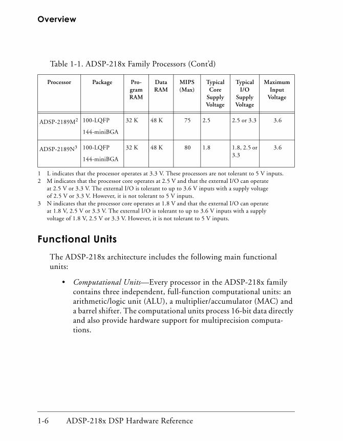
ADSP-218x Family ProcessorsThe ADSP-218x family includes 18 members. Table 1-1 lists the members and identifies their basic distinguishing features. For additional features, see Chapter C, “Advanced Product Features.”
Table 1-1. ADSP-218x Family Processors
Processor Package Pro-gramRAM
DataRAM
MIPS(Max)
TypicalCore
Supply Voltage
Typical I/O
SupplyVoltage
MaximumInput
Voltage
ADSP-2181 128-LQFP
128-MQFP
16 K 16 K 40 5.0 Supply + .5
ADSP-2183 128-LQFP
144-miniBGA
16 K 16 K 52 3.3 Supply + .5
ADSP-2184 100-LQFP 4 K 4 K 40 5.0 Supply + .5
ADSP-2184L1 100-LQFP 4 K 4 K 40 3.3 Supply + .5
ADSP-2184N3 100-LQFP
144-miniBGA
4 K 4 K 80 1.8 1.8, 2.5 or 3.3
3.6
ADSP-2185 100-LQFP 16 K 16 K 33 5.0 Supply + .5
ADSP-2185L1 100-LQFP
144-miniBGA
16 K 16 K 52 3.3 Supply + .5
ADSP-2185M2 100-LQFP
144-miniBGA
16 K 16 K 75 2.5 2.5 or 3.3 3.6
ADSP-2185N3 100-LQFP
144-miniBGA
16 K 16 K 80 1.8 1.8, 2.5 or 3.3
3.6
1-4 ADSP-218x DSP Hardware Reference

Introduction
ADSP-2186 100-LQFP
144-miniBGA
8 K 8 K 40 5.0 Supply + .5
ADSP-2186L1 100-LQFP
144-miniBGA
8 K 8 K 40 3.3 Supply + .5
ADSP-2186M2 100-LQFP
144-miniBGA
8 K 8 K 75 2.5 2.5 or 3.3 3.6
ADSP-2186N3 100-LQFP
144-miniBGA
8 K 8 K 80 1.8 1.8, 2.5 or 3.3
3.6
ADSP-2187L1 100-LQFP 32 K 32 K 52 3.3 Supply + .5
ADSP-2187N3 100-LQFP
144-miniBGA
32 K 32 K 80 1.8 1.8, 2.5 or 3.3
3.6
ADSP-2188M2 100-LQFP
144-miniBGA
48 K 56 K 75 2.5 2.5 or 3.3 3.6
ADSP-2188N3 100-LQFP
144-miniBGA
48 K 56 K 80 1.8 1.8, 2.5 or 3.3
3.6
Table 1-1. ADSP-218x Family Processors (Cont’d)
Processor Package Pro-gramRAM
DataRAM
MIPS(Max)
TypicalCore
Supply Voltage
Typical I/O
SupplyVoltage
MaximumInput
Voltage
ADSP-218x DSP Hardware Reference 1-5
Overview
Functional UnitsThe ADSP-218x architecture includes the following main functional units:
• Computational Units—Every processor in the ADSP-218x family contains three independent, full-function computational units: an arithmetic/logic unit (ALU), a multiplier/accumulator (MAC) and a barrel shifter. The computational units process 16-bit data directly and also provide hardware support for multiprecision computa-tions.
ADSP-2189M2 100-LQFP
144-miniBGA
32 K 48 K 75 2.5 2.5 or 3.3 3.6
ADSP-2189N3 100-LQFP
144-miniBGA
32 K 48 K 80 1.8 1.8, 2.5 or 3.3
3.6
1 L indicates that the processor operates at 3.3 V. These processors are not tolerant to 5 V inputs.2 M indicates that the processor core operates at 2.5 V and that the external I/O can operate
at 2.5 V or 3.3 V. The external I/O is tolerant to up to 3.6 V inputs with a supply voltage of 2.5 V or 3.3 V. However, it is not tolerant to 5 V inputs.
3 N indicates that the processor core operates at 1.8 V and that the external I/O can operate at 1.8 V, 2.5 V or 3.3 V. The external I/O is tolerant to up to 3.6 V inputs with a supply voltage of 1.8 V, 2.5 V or 3.3 V. However, it is not tolerant to 5 V inputs.
Table 1-1. ADSP-218x Family Processors (Cont’d)
Processor Package Pro-gramRAM
DataRAM
MIPS(Max)
TypicalCore
Supply Voltage
Typical I/O
SupplyVoltage
MaximumInput
Voltage
1-6 ADSP-218x DSP Hardware Reference

Introduction
• Data Address Generators & Program Sequencer—Two dedicated address generators and a program sequencer supply addresses for on-chip or external memory access. The sequencer supports sin-gle-cycle conditional branching and executes program loops with zero overhead. Dual data address generators allow the processor to generate simultaneous addresses for dual operand fetches. Together the sequencer and data address generators keep the com-putational units continuously working, maximizing throughput.
• Memory—The ADSP-218x family uses a modified Harvard archi-tecture in which Data Memory stores data and Program Memory stores both instructions and data. All ADSP-218x family processors contain on-chip RAM that comprises a portion of the Program Memory space and Data Memory space. (Program Memory and Data Memory are directly addressable off-chip.) The speed of the on-chip memory allows the processor to fetch two operands (one from Data Memory and one from Program Memory) and an instruction (from Program Memory) in a single cycle.
• Serial Ports—The serial ports (SPORTs) provide a complete serial interface with hardware companding for data compression and expansion. Both µ-law and A-law companding are supported. The SPORTs interface easily and directly to a wide variety of popular serial devices. Each SPORT can generate a programmable internal clock or accept an external clock. SPORT0 includes a multichannel option.
• Timer—A programmable timer/counter with 8-bit prescaler pro-vides periodic interrupt generation.
ADSP-218x DSP Hardware Reference 1-7

Overview
• DMA Ports—The Internal DMA Port (IDMA) and Byte DMA Port (BDMA) in the ADSP-218x processors allow efficient data transfers to and from internal memory. The IDMA port is a slave port inter-face that has a 16-bit multiplexed address and data bus, which also supports 24-bit Program Memory accesses. The IDMA port is com-pletely asynchronous and can be written to while the ADSP-218x is operating at full speed. The Byte Memory DMA port is a master port that allows boot loading and storing of program instructions and data at or during runtime.
The ADSP-218x family architecture exhibits a high degree of parallelism, tailored to DSP requirements. In a single cycle, any device in the family can:
• Generate the next program address
• Fetch the next instruction
• Perform one or two data moves
• Update one or two data address pointers
• Perform a computation
In that same cycle, processors can also:
• Receive and/or transmit data through the serial ports
• Receive or transmit data through the internal DMA port
• Receive or transmit data via through byte DMA port
• Decrement timer
1-8 ADSP-218x DSP Hardware Reference

Introduction
Memory and System InterfaceIn each ADSP-218x processor, five on-chip buses connect internal mem-ory with the other functional units:
• Data Memory Address bus (14-bits)
• Data Memory Data bus (16-bits)
• Program Memory Address bus (14-bits)
• Program Memory Data bus (24-bits)
A single external address bus (14-bits) and a single external data bus (24-bits) are extended off-chip; these buses can be used for either Program or Data Memory accesses.
All ADSP-218x processors (except for the ADSP-2181 and ADSP-2183 processors) can be configured in either a Host Mode or a Full Memory Mode. In Host Mode, each processor has an Internal DMA (IDMA) port for connection to external host systems. The IDMA port provides trans-parent, direct access to the DSP’s on-chip Program and Data RAM. Since the ADSP-2181and ADSP-2183 processors have complete address, data, and IDMA busses, these two processors provide both IDMA and BDMA functionality concurrently, giving you greater system functionality with-out additional external logic.
In Full Memory Mode, the ADSP-218x processors have complete use of the external address and data busses. In this mode, the processors behave in exactly the same manner as the ADSP-2181 and ADSP-2183 processor with the IDMA port removed.
An interface to low cost byte-wide memory is provided by the Byte DMA port (BDMA) port. The BDMA port is bidirectional and can directly address up to four megabytes of external RAM or ROM for off-chip stor-age of program overlays or data tables.
ADSP-218x DSP Hardware Reference 1-9

Overview
Boot circuitry provides for loading on-chip Program Memory automati-cally after reset. This can be done through the BDMA port. Multiple programs can be selected and loaded with no additional hardware.
External devices can gain control of the processor’s buses with the bus request and bus grant signals (BR, BG). The ADSP-218x processors can continue running while the buses are granted to another device (when Go mode is enabled for the processor core) as long as an external memory operation is not required.
The ADSP-218x processors support memory-mapped peripherals with programmable wait state generation through a dedicated 2048 location I/O Memory space.
All ADSP-218x family processors operate in the same manner in their response to interrupts. The program sequencer allows the processor to respond with minimum latency. Interrupts can be nested with no addi-tional latency. External interrupts can be configured as edge- or level-sensitive. Internal interrupts can be generated from the timer, the host interface port, the serial ports, and the BDMA port.
Instruction SetThe ADSP-218x family shares a single unified instruction set designed for upward compatibility with higher-integration devices.
The ADSP-218x family instruction set provides flexible data moves. Mul-tifunction instructions combine one or more data moves with a computation. Every instruction can be executed in a single processor cycle. The assembly language uses an algebraic syntax for readability and ease of coding. A comprehensive set of software and hardware tools sup-ports program development. The instruction set is detailed in the ADSP-218x DSP Instruction Set Reference.
1-10 ADSP-218x DSP Hardware Reference

Introduction
DSP PerformanceSignal processing applications make special performance demands which distinguish DSP architectures from other microprocessor and microcon-troller architectures. Not only must instruction execution be fast, but DSPs must also perform well in each of the following areas:
• Fast and Flexible Arithmetic—The ADSP-218x family base architec-ture provides single-cycle computation for multiplication, multipli-cation with accumulation, arbitrary amounts of shifting, and standard arithmetic and logical operations. In addition, the arith-metic units allow for any sequence of computations so that a given DSP algorithm can be executed without being reformulated.
• Extended Dynamic Range—Extended sums-of-products, common in DSP algorithms, are supported in the multiply/accumulate units of the ADSP-218x family. A 40-bit accumulator provides eight bits of protection against overflow in successive additions to ensure that no loss of data or range occurs; 256 overflows would have to occur before any data is lost. Special instructions are provided for imple-menting block floating-point scaling of data.
• Single-Cycle Fetch of Two Operands—In extended sums-of-products calculations, two operands are needed on each cycle to feed the cal-culation. All members of the ADSP-218x family are able to sustain two-operand data throughput, whether the data is stored on-chip or off.
• Hardware Circular Buffers—A large class of DSP algorithms, includ-ing digital filters, requires circular data buffers. The ADSP-218x family base architecture includes hardware to handle address pointer wraparound, simplifying the implementation of circular buffers both on- and off-chip, and reducing overhead (thereby improving performance).
ADSP-218x DSP Hardware Reference 1-11

Core Architecture
• Zero-Overhead Looping and Branching—DSP algorithms are repeti-tive and are most logically expressed as loops. The program sequencer in the ADSP-218x family supports looped code with zero overhead, combining excellent performance with the clearest pro-gram structure. Likewise, there are no overhead penalties for condi-tional branches.
Core ArchitectureThis section gives a summary of the ADSP-218x family core architecture. Each component of the core architecture is described in detail in this man-ual. The following list identifies the ADSP-218x family’s core architectural components and specifies the chapters that cover each component:
• Arithmetic/logic unit (ALU)—Chapter 2, Computational Units
• Multiplier/accumulator (MAC)—Chapter 2, Computational Units
• Barrel shifter—Chapter 2, Computational Units
• Program sequencer—Chapter 3, Program Sequencer
• Status registers and stacks—Chapter 3, Program Sequencer
• Data Address generators (DAGs)—Chapter 4, Data Address Gener-ators
• PMD-DMD bus exchange (PX registers)—Chapter 4, Data Address Generators
1-12 ADSP-218x DSP Hardware Reference

Introduction
Figure 1-1 shows the ADSP-218x family core architecture. The sections that follow provide a brief summary of each core unit.
INPUT REGS
OUTPUT REGS
SHIFTER
INPUT REGS
OUTPUT REGS
ALU
INPUT REGS
OUTPUT REGS
MAC
R BUS 16
DMD BUS
PMD BUS
DATAADDRESS
GENERATOR#2
DATAADDRESS
GENERATOR#1
DMA BUS
PMA BUS14
14
24
16
PROGRAMSEQUENCER
Figure 1-1. Core Architecture
ADSP-218x DSP Hardware Reference 1-13
Core Architecture
Computational UnitsEvery processor in the ADSP-218x family contains three independent, full-function computational units: an arithmetic/logic unit (ALU), a mul-tiplier/accumulator (MAC) and a barrel shifter. The computation units process 16-bit data directly and provide hardware support for multipreci-sion computation as well.
The ALU performs a standard set of arithmetic and logic operations in addition to division primitives. The MAC performs single-cycle multiply, multiply/add and multiply/subtract operations. The shifter performs logi-cal and arithmetic shifts, normalization, denormalization, and derive-exponent operations. The shifter implements numeric format con-trol including multiword floating-point representations. The computational units are arranged side-by-side, instead of serially, so that the output of any unit may be the input of any unit on the next cycle. The internal result (R) bus directly connects the computational units to make this possible.
All three units contain input and output registers that are accessible from the internal Data Memory data (DMD) bus. Computational operations generally take their operands from input registers and load the result into an output register. The registers act as a stopover point for data between memory and the computational circuitry. This feature introduces one level of pipelining on input and one level on output. The R bus allows the result of a previous computation to be used directly as the input to another computation. This avoids excessive pipeline delays when a series of different operations are performed.
1-14 ADSP-218x DSP Hardware Reference
Introduction
Address Generators and Program SequencerTwo dedicated data address generators and a powerful program sequencer ensure efficient use of the computational units. The data address genera-tors (DAGs) provide memory addresses when memory data is transferred to or from the input or output registers. Each DAG keeps track of up to four address pointers. When a pointer is used for indirect addressing, it is post-modified by a value in a specified register. With two independent DAGs, the processor can generate two addresses simultaneously for dual operand fetches.
A length value may be associated with each pointer to implement auto-matic modulo addressing for circular buffers. (The circular buffer feature is also used by the serial ports for automatic data transfers. Refer to the Chapter 5, “Serial Ports.” for additional information.)
! For linear buffers, the length value must be set to zero.
DAG1 can supply addresses to Data Memory only; DAG2 can supply addresses to either Data Memory or Program Memory. When the appro-priate mode bit is set in the mode status register (MSTAT), the output address of DAG1 is bit-reversed before being driven onto the address bus. This feature facilitates addressing in radix-2 Fast Fourier Transform (FFT) algorithms.
The program sequencer supplies instruction addresses to the Program Memory. The sequencer is driven by the instruction register, which holds the currently executing instruction. The instruction register introduces a single level of pipelining into the program flow. Instructions are fetched and loaded into the instruction register during one processor cycle, and executed during the following cycle while the next instruction is prefetched. To minimize overhead cycles, the sequencer supports condi-tional jumps, subroutine calls and returns in a single cycle. With an internal loop counter and loop stack, the processor executes looped code with zero overhead. No explicit jump instructions are required to loop.
ADSP-218x DSP Hardware Reference 1-15

Core Architecture
BusesThe processors have five internal buses:
• Program Memory Address (PMA) and Data Memory Address (DMA) buses— Used internally for the addresses associated with Program and Data Memory.
• Program Memory Data (PMD) and Data Memory Data (DMD) buses — Used for the data associated with memory spaces. These buses are multiplexed into a single external address bus and a single external data bus; the BMS, DMS and PMS signals select the different address spaces.
• Result (R) bus—Transfers intermediate results directly between the various computational units.
The PMA bus is 14 bits wide allowing direct access of up to 16 K words of mixed instruction code and data. The PMD bus is 24 bits wide to accom-modate the 24-bit instruction width.
The DMA bus is 14 bits wide allowing direct access of up to 16 K words of data. The Data Memory data (DMD) bus is 16 bits wide. The DMD bus provides a path for the contents of any register in the processor to be transferred to any other register or to any Data Memory location in a sin-gle cycle. The Data Memory address comes from two sources: an absolute value specified in the instruction code (direct addressing) or the output of a data address generator (indirect addressing). Only indirect addressing is supported for data fetches from Program Memory.
The Program Memory data (PMD) bus can also be used to transfer data to and from the computational units through direct paths or via the PMD-DMD bus exchange unit. The PMD-DMD bus exchange unit per-mits data to be passed from one bus to the other. It contains hardware to overcome the 8-bit width discrepancy between the two buses, when necessary.
1-16 ADSP-218x DSP Hardware Reference

Introduction
On-chip PeripheralsThis section describes the additional functional units which are included in the ADSP-218x family processors.
Serial PortsThe ADSP-218x processors have two bidirectional, double-buffered serial ports (SPORTs) for serial communications. The SPORTs are synchronous and use framing signals to control data flow. Each SPORT can generate its serial clock internally or use an external clock. The framing sync signals may be generated internally or by an external device. Word lengths may vary from three to sixteen bits. One serial port, SPORT0, has a multi-channel capability that allows the receiving or transmitting of arbitrary data words from a 24-word or 32-word bitstream. The other serial port, SPORT1, may optionally be configured as two additional external inter-rupt pins (IRQ1 and IRQ0)and the Flag Out (FO) and Flag In (FI) pins.
TimerThe programmable interval timer provides periodic interrupt generation. An 8-bit prescaler register allows the timer to decrement a 16-bit count register over a range from each cycle to every 256 cycles. An interrupt is generated when this count register decrements to zero. The count register is automatically reloaded from a 16-bit period register after the timer interrupt is generated; the count resumes immediately.
ADSP-218x DSP Hardware Reference 1-17
On-chip Peripherals
DMA PortsThe ADSP-218x contains two DMA ports, an Internal DMA (IDMA) port and a Byte DMA (BDMA) port. The IDMA port provides an effi-cient means of communication between a host system and the DSP. The port is used to access the on-chip Program Memory and Data Memory of the DSP with only one cycle per word of overhead. The IDMA port has a 16-bit multiplexed address and data bus and supports 24-bit Program Memory. The IDMA port is completely asynchronous and can be written to while an ADSP-218x family processor is operating at full speed.
The internal memory address is latched and then automatically incre-mented after each IDMA transaction. An external device can therefore access a block of sequentially addressed memory by specifying only the starting address of the block.
The Byte Memory DMA controller allows loading and storing of program instructions and data using the Byte Memory space. The BDMA circuitry is able to access the Byte Memory space while the processor is operating normally and steals only one processor cycle per 8-, 16-, or 24-bit word transferred.
1-18 ADSP-218x DSP Hardware Reference

Introduction
Development ToolsThe ADSP 218x is supported by VisualDSP®, an easy-to-use program-ming environment, comprised of an Integrated Development Environment (IDE) and Debugger. VisualDSP lets you manage projects from within a single, integrated interface. Because the project develop-ment and debug environments are integrated, you can move easily between editing, building, and debugging activities.
Integrated Development EnvironmentThe IDE includes access to all the activities necessary to create and debug DSP projects. You can create or modify source files or view listing or map files with the IDE Editor. This Editor includes multiple language syntax highlighting, OLE drag and drop, bookmarks, and standard editing opera-tions such as undo/redo, find/replace, copy/paste/cut, and go to.
Also, the IDE includes access to the DSP C Compiler, C Runtime Library, Assembler, Linker, Loader, Simulator, and Splitter. You specify options for these Tools through Property Page dialogs. Property Page dia-logs are easy to use, and make configuring, changing, and managing your projects simple. These options control how the tools process inputs and generate outputs, and have a one-to-one correspondence to the tools’ command line switches. You can define these options once, or modify them to meet changing development needs. You can also access the Tools from the operating system command line if you choose.
ADSP-218x DSP Hardware Reference 1-19

Development Tools
DebuggerThe Debugger has an easy-to-use, common interface for all processor sim-ulators and emulators available through Analog Devices and third parties or custom developments. The Debugger has many features that greatly reduce debugging time. You can view C source interspersed with the resulting Assembly code. You can profile execution of a range of instruc-tions in a program; set simulated watch points on hardware and software registers, Program and Data Memory; and trace instruction execution and memory accesses. These features enable you to correct coding errors, iden-tify bottlenecks, and examine DSP performance.
You can use the custom register option to select any combination of regis-ters to view in a single window. The Debugger can also generate inputs, outputs, and interrupts so you can simulate real world application conditions.
Software Development ToolsSoftware Development Tools, which support the ADSP-218x family, let you develop applications that take full advantage of the architecture, including shared memory and memory overlays. Software Development Tools include C Compiler, C Runtime Library, DSP and Math Libraries, Assembler, Linker, Loader, Simulator, and Splitter.
C Compiler and Assembler
The C Compiler generates efficient code that is optimized for both code density and execution time. The C Compiler allows you to include Assem-bly language statements inline. Because of this, you can program in C and still use Assembly for time-critical loops. You can also use pretested Math, DSP, and C Runtime Library routines to help shorten your time to mar-ket. The ADSP-218x family assembly language is based on an algebraic syntax that is easy to learn, program, and debug.
1-20 ADSP-218x DSP Hardware Reference

Introduction
Linker and Loader
The Linker provides flexible system definition through Linker Description Files (.LDF). In a single Linker Description File, you can define different types of executables for a single or multiprocessor system. The Linker resolves symbols over multiple executables, maximizes memory use, and easily shares common code among multiple processors. The Loader sup-ports creation of host and PROM boot images. The Simulator is a cycle-accurate, instruction-level simulator — allowing you to simulate your application in real time.
Hardware Development ToolsAnalog Devices’ hardware development tools for the ADSP-218x include
the EZ-KIT Lite™ evaluation board and the EZ-ICE® serial emulator.
EZ-KIT Lite
The EZ-KIT Lite allows users to investigate ADSP-218x family processors and begin to develop applications. It consists of a stand-alone ADSP-218x processor-based evaluation board with fully functional code generation debug software. It contains a complete set of development tools, including a C compiler, assembler, linker, and the latest evaluation suite of
VisualDSP® development environment. (All software tools are limited to use with the EZ-KIT Lite product.)
Demonstration programs are shipped with the product and include com-mon signal processing algorithms, such as convolution and Fibonacci calculations. Also included are programs that demonstrate the use of ADSP-218x hardware features, such as interrupts, overlays, timers, and an on-board codec.
ADSP-218x DSP Hardware Reference 1-21

Development Tools
EZ-ICE
The ADSP-218x EZ-ICE is a serial emulator that provides a controlled environment for observing, debugging, and testing activities in a target system. The EZ-ICE connects directly to the target processor through the emulation interface port. Its key features include the following:
• Support for all ADSP-218x processors
• High-speed RS232 serial port
• Shielded enclosure with reset switch accessibility
• I/O voltage setting confirmation LEDs
• Support for 1.8, 2.5, 3.3, and 5.0 volt DSPs
• CE certified
For additional information about EZ-ICE and how to use it, see “Target System Hardware” in Chapter 7, System Interface.
Third Party ProductsThe VisualDSP environment enables third-party companies to add value using Analog Devices’ published set of Application Programming Inter-faces (API). Third party products—realtime operating systems, emulators, high-level language compilers, multiprocessor hardware —can interface seamlessly with VisualDSP thereby simplifying the tools integration task. VisualDSP follows the COM API format.
1-22 ADSP-218x DSP Hardware Reference
Introduction
Two API tools, Target Wizard and API Tester, are also available for use with the API set. These tools help speed the time-to-market for vendor products. Target Wizard builds the programming shell based on API fea-tures the vendor requires. The API tester exercises the individual features independently of VisualDSP. Third parties can use a subset of these APIs that meet their application needs. The interfaces are fully supported and backward compatible.
Further details and ordering information are available in the VisualDSP Development Tools data sheet. This data sheet can be requested from any Analog Devices sales office or distributor.
Information OnlineAnalog Devices is online on the internet at http://www.analog.com. Our Web pages provide information on the company and products, including access to technical information and documentation, product overviews, and product announcements.
You may also obtain additional information about Analog Devices and its products in any of the following ways:
• Visit our World Wide Web site at www.analog.com
• FAX questions or requests for information to 1(781)461-3010.
• Access the DSP Division File Transfer Protocol (FTP) site at ftp ftp.analog.com or ftp 137.71.23.21 or ftp://ftp.analog.com.
ADSP-218x DSP Hardware Reference 1-23

Customer Support
Customer Support You can reach our Customer Support group in the following ways:
• E-mail questions to [email protected] or [email protected] (European customer support)
• Telex questions to 924491, TWX:710/394-6577
• Cable questions to ANALOG NORWOODMASS
• Contact your local ADI sales office or an authorized ADI distributor
• Send questions by mail to:Analog Devices, Inc.DSP DivisionOne Technology WayP.O. Box 9106Norwood, MA 02062-9106USA
Related DocumentsFor more information about Analog Devices DSPs and development products, see the following documents:
• DSP Microcomputer Data Sheets for the ADSP-218x Family Mem-bers
• ADSP-218x DSP Instruction Set Reference
• ADSP-2100 Family DSP Applications, Vol. 1 and Vol. 2
• VisualDSP User’s Guide for ADSP-218x & ADSP-219x Family DSPs
• C Compiler & Library Manual for ADSP-218x & ADSP-219x Family DSPs
1-24 ADSP-218x DSP Hardware Reference

Introduction
• Assembler Manual for ADSP-218x & ADSP-219x Family DSPs
• Linker & Utilities Manual for ADSP-218x & ADSP-219x Family DSPs
All the manuals are included in the software distribution CD-ROM. To access these manuals, use the Help Topics command in the VisualDSP environment’s Help menu and select the Online Manuals book. From this Help topic, you can open any of the manuals, which are in Adobe Acrobat PDF format.
ConventionsThe following are conventions that apply to all chapters. Note that addi-tional conventions, which apply only to specific chapters, appear throughout this document.
Table 1-2. Notation Conventions
Example Description
AX0, SR, PX Register names appear in UPPERCASE and keyword font
CLKOUT, RESET Pin names appear in UPPERCASE and keyword font; active low signals appear with an OVERBAR.
IF, DO/UNTIL Assembler instructions (mnemonics) appear in UPPERCASE and keyword font
[this,that]
|this,that|
Assembler instruction syntax summaries show optional items two ways. When the items are optional and none is required, the list is shown enclosed in square brackets, []. When the choices are optional, but one is required, the list is shown enclosed in vertical bars, ||.
0xabcd, b#1111 A 0x prefix indicates hexadecimal; a b# prefix indicates binary
ADSP-218x DSP Hardware Reference 1-25

Conventions
! A note, providing information of special interest or identifying a related DSP topic.
" A caution, providing information on critical design or program-ming issues that influence operation of the DSP.
Click Here In the online version of this document, a cross reference acts as a hypertext link to the item being referenced. Click on blue refer-ences (Table, Figure, or section names) to jump to the location.
Table 1-2. Notation Conventions
Example Description
1-26 ADSP-218x DSP Hardware Reference