ADSP-21160 SHARC DSP Hardware Reference, Data ...
26
ADSP-21160 SHARC DSP Hardware Reference 4-1 4 DATA ADDRESS GENERATORS Figure 4-0. Table 4-0. Listing 4-0. Overview The DSP’s Data Address Generators (DAGs) generate addresses for data moves to and from Data Memory (DM) and Program Memory (PM). By generating addresses, the DAGs let programs refer to addresses indirectly, using a DAG register instead of an absolute address. The DAGs architec- ture, which appears in Figure 4-1, supports several functions that minimize overhead in data access routines. These functions include: • Supply address and post-modify—provides an address during a data move and auto-increments the stored address for the next move. • Supply pre-modified address—provides a modified address during a data move without incrementing the stored address. • Modify address—increments the stored address without performing a data move. • Bit-reverse address—provides a bit-reversed address during a data move without reversing the stored address. • Broadcast data moves—performs dual data moves to complemen- tary registers in each processing element to support SIMD mode.
-
Upload
khangminh22 -
Category
Documents
-
view
0 -
download
0
Transcript of ADSP-21160 SHARC DSP Hardware Reference, Data ...
ADSP-21160 SHARC DSP Hardware Reference 4-1
4 DATA ADDRESS GENERATORS
Figure 4-0.
Table 4-0.
Listing 4-0.
Overview
The DSP’s Data Address Generators (DAGs) generate addresses for data moves to and from Data Memory (DM) and Program Memory (PM). By generating addresses, the DAGs let programs refer to addresses indirectly, using a DAG register instead of an absolute address. The DAGs architec-ture, which appears in Figure 4-1, supports several functions that minimize overhead in data access routines. These functions include:
• Supply address and post-modify—provides an address during a data move and auto-increments the stored address for the next move.
• Supply pre-modified address—provides a modified address during a data move without incrementing the stored address.
• Modify address—increments the stored address without performing a data move.
• Bit-reverse address—provides a bit-reversed address during a data move without reversing the stored address.
• Broadcast data moves—performs dual data moves to complemen-tary registers in each processing element to support SIMD mode.
Setting DAG Modes
4-2 ADSP-21160 SHARC DSP Hardware Reference
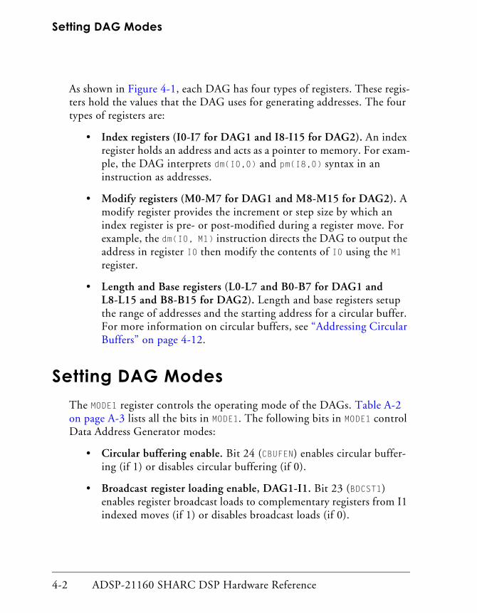
As shown in Figure 4-1, each DAG has four types of registers. These regis-ters hold the values that the DAG uses for generating addresses. The four types of registers are:
• Index registers (I0-I7 for DAG1 and I8-I15 for DAG2). An index register holds an address and acts as a pointer to memory. For exam-ple, the DAG interprets dm(I0,0) and pm(I8,0) syntax in an instruction as addresses.
• Modify registers (M0-M7 for DAG1 and M8-M15 for DAG2). A modify register provides the increment or step size by which an index register is pre- or post-modified during a register move. For example, the dm(I0, M1) instruction directs the DAG to output the address in register I0 then modify the contents of I0 using the M1 register.
• Length and Base registers (L0-L7 and B0-B7 for DAG1 and L8-L15 and B8-B15 for DAG2). Length and base registers setup the range of addresses and the starting address for a circular buffer. For more information on circular buffers, see “Addressing Circular Buffers” on page 4-12.
Setting DAG Modes
The MODE1 register controls the operating mode of the DAGs. Table A-2 on page A-3 lists all the bits in MODE1. The following bits in MODE1 control Data Address Generator modes:
• Circular buffering enable. Bit 24 (CBUFEN) enables circular buffer-ing (if 1) or disables circular buffering (if 0).
• Broadcast register loading enable, DAG1-I1. Bit 23 (BDCST1) enables register broadcast loads to complementary registers from I1 indexed moves (if 1) or disables broadcast loads (if 0).
ADSP-21160 SHARC DSP Hardware Reference 4-3
Data Address Generators
��������������������������������������������������������������������������������������������������������������������
��������������������������������������������������������������������������������������������������������������������
��������������������������������������������������������������������������������������������������������������������
��������������������������������������������������������������������������������������������������������������������
��������������������������������������������������������������������������������������������������������������������
������������������������������������������������������������������������������������������������������������������������
��������������������������������������������������������������������������������������������������������������������
������������������������������������������������������������������������������������������������������������������������
STKYX
M O DE2
M O DE1
M UX
M UX
A DD
IREGISTERS
8 X 32
32
32
32
3232
IM M EDIA TEVA LUE FRO MIN STRUCTIO N
ADDRESS A DJUSTM EN T PER W O RD SIZE (SHORT, NORM AL, OR LON G)
OPTION AL B IT-R EVERSE FOR I0-DA G1 & I8-DA G2OPTION AL BROA DCA ST FOR I1-DA G1 & I9-DA G2
MREGISTERS
8 X 32
DM ADDRESS BUS (DA G1 - I,M ,L,B0-7)
PM ADDRESS BUS (DA G2 - I,M ,L,B8-15)
32 32
DM OR PM DA TA BUS
LREGISTERS
8 X 32
BREGISTERS
8 X 32
M ODULUSLOG IC
BIT-REVERSE(OPTION A L)
3232
UPDATE32
PRE-M O DIFYADDRESSING
PO ST-M O DIFYADDRESSING
Figure 4-1. Data Address Generator (DAG) Block Diagram
Setting DAG Modes
4-4 ADSP-21160 SHARC DSP Hardware Reference
• Broadcast register loading enable, DAG2-I9. Bit 22 (BDCST9) enables register broadcast loads to complementary registers from I9 indexed moves (if 1) or disables broadcast loads (if 0)
• SIMD mode enable. Bit 21 (PEYEN) enables computations in PEy—SIMD mode—(if 1) or disables PEy—SISD mode—(if 0). For more information on SIMD mode, see “Secondary Processing Element (PEy)” on page 2-36.
• Secondary registers for DAG2 lo, I,M,L,B8-11. Bit 6 (SRD2L)Secondary registers for DAG2 hi, I,M,L,B12-15. Bit 5 (SRD2H)Secondary registers for DAG1 lo, I,M,L,B0-3. Bit 4 (SRD1L)Secondary registers for DAG1 hi, I,M,L,B4-7. Bit 3 (SRD1H)These bits select the corresponding secondary register set (if 1) or select the corresponding primary register set—the set that is avail-able at reset—(if 0).
• Bit-reverse addressing enable, DAG1-I0. Bit 1 (BR0) enables bit-reversed addressing on I0 indexed moves (if 1) or disables bit-reversed addressing (if 0).
• Bit-reverse addressing enable, DAG2-I8. Bit 0 (BR8) enables bit-reversed addressing on I8 indexed moves (if 1) or disables bit-reversed addressing (if 0).
Circular Buffering Mode
The CBUFEN bit in the MODE1 register enables circular buffering—a mode in which the DAG supplies addresses ranging within a constrained buffer length (set with an L register), starting at a base address (set with a B regis-ter), and incrementing the addresses on each access by a modify value (set with an M register).
ADSP-21160 SHARC DSP Hardware Reference 4-5
Data Address Generators
! On previous SHARC DSP’s (ADSP-2106x family), circular buffer-ing is always enabled. For code compatibility, programs ported to the ADSP-21160 should include the instruction:
Bit Set Mode1 CBUFEN;
This instruction enables circular buffering. For more information on set-ting up and using circular buffers, see “Addressing Circular Buffers” on page 4-12. When using circular buffers, the DAGs can generate an inter-rupt on buffer overflow (wrap around). For more information, see “Using DAG Status” on page 4-9.
Broadcast Loading Mode
The BDCST1 and BDCST9 bits in the MODE1 register enable broadcast loading mode—multiple register loads from a single load command. When the BDCST1 bit is set (1), the DAG performs a dual data register load on instructions that use the I1 register for the address. The DAG loads both the named register (explicit register) in one processing element and loads that register’s complementary register (implicit register) in the other pro-cessing element. The BDCST9 bit in the MODE1 register enables this feature for the I9 register.
Enabling either DAG1 or DAG2 register load broadcasting has no effect on register stores or loads to universal registers other than the register file data registers. Table 4-1 demonstrates the effects of a register load opera-
Setting DAG Modes
4-6 ADSP-21160 SHARC DSP Hardware Reference
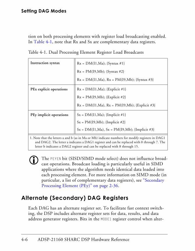
tion on both processing elements with register load broadcasting enabled. In Table 4-1, note that Rx and Sx are complementary data registers.
! The PEYEN bit (SISD/SIMD mode select) does not influence broad-cast operations. Broadcast loading is particularly useful in SIMD applications where the algorithm needs identical data loaded into each processing element. For more information on SIMD mode (in particular, a list of complementary data registers), see “Secondary Processing Element (PEy)” on page 2-36.
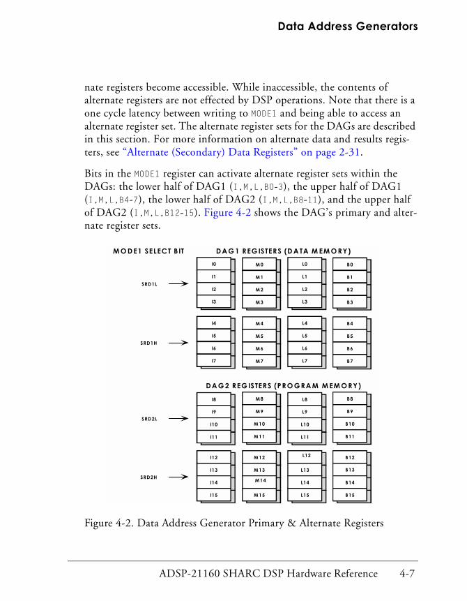
Alternate (Secondary) DAG Registers
Each DAG has an alternate register set. To facilitate fast context switch-ing, the DSP includes alternate register sets for data, results, and data address generator registers. Bits in the MODE1 register control when alter-
Table 4-1. Dual Processing Element Register Load Broadcasts
Instruction syntax Rx = DM(I1,Ma); {Syntax #1}
Rx = PM(I9,Mb); {Syntax #2}
Rx = DM(I1,Ma), Rx = PM(I9,Mb); {Syntax #3}
PEx explicit operations Rx = DM(I1,Ma); {Explicit #1}
Rx = PM(I9,Mb); {Explicit #2}
Rx = DM(I1,Ma), Rx = PM(I9,Mb); {Explicit #3}
PEy implicit operations Sx = DM(I1,Ma); {Implicit #1}
Sx = PM(I9,Mb); {Implicit #2}
Sx = DM(I1,Ma), Sx = PM(I9,Mb); {Implicit #3}
1. Note that the letters a and b (as in Ma or Mb) indicate numbers for modify registers in DAG1 and DAG2. The letter a indicates a DAG1 register and can be replaced with 0 through 7. The letter b indicates a DAG2 register and can be replaced with 8 through 15.
ADSP-21160 SHARC DSP Hardware Reference 4-7
Data Address Generators
nate registers become accessible. While inaccessible, the contents of alternate registers are not effected by DSP operations. Note that there is a one cycle latency between writing to MODE1 and being able to access an alternate register set. The alternate register sets for the DAGs are described in this section. For more information on alternate data and results regis-ters, see “Alternate (Secondary) Data Registers” on page 2-31.
Bits in the MODE1 register can activate alternate register sets within the DAGs: the lower half of DAG1 (I,M,L,B0-3), the upper half of DAG1 (I,M,L,B4-7), the lower half of DAG2 (I,M,L,B8-11), and the upper half of DAG2 (I,M,L,B12-15). Figure 4-2 shows the DAG’s primary and alter-nate register sets.
I0
I1
I2
I3
M 0
M 1
M 2
M 3
L0
L1
L2
L3
B0
B1
B2
B3
I4
I5
I6
I7
M 4
M 5
M 6
M 7
L4
L5
L6
L7
B4
B5
B6
B7
I8
I9
I10
I11
M 8
M 9
M 10
M 11
L8
L9
L10
L11
B8
B9
B10
B11
I12
I13
I14
I15
M 12
M 13
M 14
M 15
L12
L13
L14
L15
B12
B13
B14
B15
M O D E1 SELEC T B IT
SRD1L
SRD1H
SRD2L
SRD2H
D A G 1 REG ISTERS (D A TA M EM O RY)
D A G 2 REG ISTERS (PRO G RA M M EM O RY)
Figure 4-2. Data Address Generator Primary & Alternate Registers
Setting DAG Modes
4-8 ADSP-21160 SHARC DSP Hardware Reference
To share data between contexts, a program places the data to be shared in one half of either the current DAG’s registers or the other DAG’s registers and activates the alternate register set of the other half. The following example demonstrates how code should handle the one cycle of latency from the instruction setting the bit in MODE1 to when the alternate registers may be accessed:
BIT SET MODE1 SRD1L; /* activate alternate dag1 lo regs */NOP; /* wait for access to alternates */R0=dm(i0,m1);
Bit-reverse Addressing Mode
The BR0 and BR8 bits in the MODE1 register enable bit-reverse addressing mode—outputting addresses in reverse bit order. When BR0 is set (1), DAG1 bit-reverses 32-bit addresses output from I0. When BR8 is set (1), DAG2 bit-reverses 32-bit addresses output from I8. The DAGs only bit-reverse the address output from I0 or I8; the contents of these registers are not reversed. Bit-reverse addressing mode effects both pre-modify and post-modify operations. The following example demonstrates how bit-reverse mode effects address output:
Bit Set Mode1 BR0;/* enables bit-rev. addressing for DAG1 */I0=0x8a000; /* loads I0 with the bit reverse of the
buffer’s base address, DM(0x51000) */M0=0x4000000; /* loads M0 with value for post-modify */R1=DM(I0,M0); /* loads r1 with contents of DM address
DM(0x51000), which is the bit-reverse of 0x8a000, then post modifies I0 for the next access with (0x8a000 + 0x4000000)=0x408a000, which is the bit-reverse of DM(0x51020) */
In addition to bit-reverse addressing mode, the DSP supports a bit-reverse instruction (Bitrev). This instruction bit-reverses the contents of the selected register. For more information on the Bitrev instruction, see “Modifying DAG Registers” on page 4-17 or the ADSP-21160 SHARC DSP Instruction Set Reference.
ADSP-21160 SHARC DSP Hardware Reference 4-9
Data Address Generators
Using DAG Status
As described in “Addressing Circular Buffers” on page 4-12, the DAGs can provide addressing for a constrained range of addresses, repeatedly cycling through this data (or buffer). A buffer overflow (or wrap around) occurs each time the DAG circles past the buffer’s base address.
The DAGs can provide buffer overflow information when executing circu-lar buffer addressing for I7 or I15. When a buffer overflow occurs (a circular buffering operation increments the I register past the end of the buffer), the appropriate DAG updates a buffer overflow flag in a sticky status (STKYx) register. A buffer overflow can also generate a maskable interrupt. Two ways to use buffer overflows from circular buffering are:
• Interrupts. Enable interrupts and use an interrupt service routine to handle the overflow condition immediately. This method is appro-priate if it is important to handle all overflows as they occur; for example in a “ping-pong” or swap I/O buffer pointers routine.
• STKYx registers. Use the Bit Tst instruction to examine overflow flags in the STKY register after a series of operations. If an overflow flag is set, the buffer has overflowed—wrapped around—at least once. This method is useful when overflow handling is not critical.
DAG Operations
4-10 ADSP-21160 SHARC DSP Hardware Reference
DAG Operations
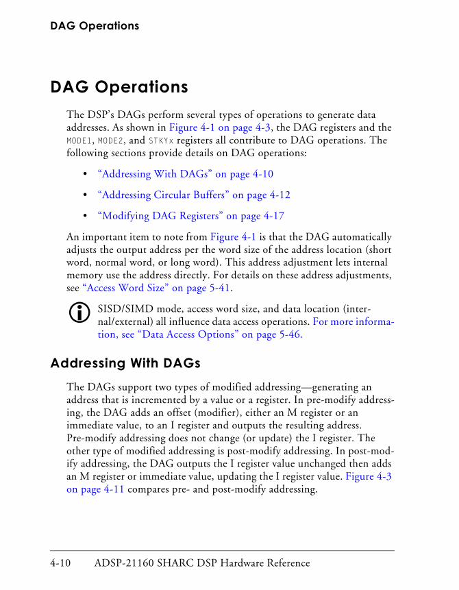
The DSP’s DAGs perform several types of operations to generate data addresses. As shown in Figure 4-1 on page 4-3, the DAG registers and the MODE1, MODE2, and STKYx registers all contribute to DAG operations. The following sections provide details on DAG operations:
• “Addressing With DAGs” on page 4-10
• “Addressing Circular Buffers” on page 4-12
• “Modifying DAG Registers” on page 4-17
An important item to note from Figure 4-1 is that the DAG automatically adjusts the output address per the word size of the address location (short word, normal word, or long word). This address adjustment lets internal memory use the address directly. For details on these address adjustments, see “Access Word Size” on page 5-41.
! SISD/SIMD mode, access word size, and data location (inter-nal/external) all influence data access operations. For more informa-tion, see “Data Access Options” on page 5-46.
Addressing With DAGs
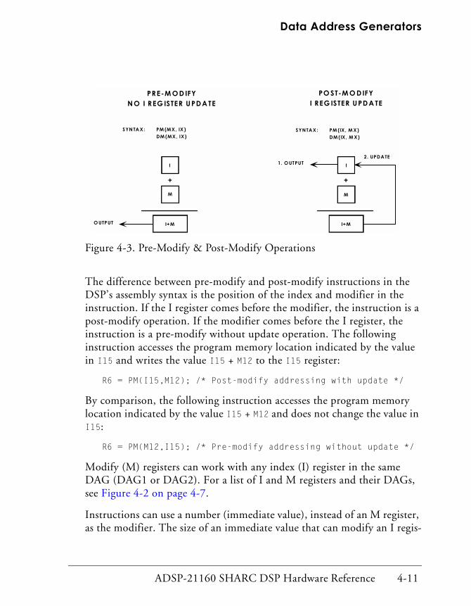
The DAGs support two types of modified addressing—generating an address that is incremented by a value or a register. In pre-modify address-ing, the DAG adds an offset (modifier), either an M register or an immediate value, to an I register and outputs the resulting address. Pre-modify addressing does not change (or update) the I register. The other type of modified addressing is post-modify addressing. In post-mod-ify addressing, the DAG outputs the I register value unchanged then adds an M register or immediate value, updating the I register value. Figure 4-3 on page 4-11 compares pre- and post-modify addressing.
ADSP-21160 SHARC DSP Hardware Reference 4-11
Data Address Generators
The difference between pre-modify and post-modify instructions in the DSP’s assembly syntax is the position of the index and modifier in the instruction. If the I register comes before the modifier, the instruction is a post-modify operation. If the modifier comes before the I register, the instruction is a pre-modify without update operation. The following instruction accesses the program memory location indicated by the value in I15 and writes the value I15 + M12 to the I15 register:
R6 = PM(I15,M12); /* Post-modify addressing with update */
By comparison, the following instruction accesses the program memory location indicated by the value I15 + M12 and does not change the value in I15:
R6 = PM(M12,I15); /* Pre-modify addressing without update */
Modify (M) registers can work with any index (I) register in the same DAG (DAG1 or DAG2). For a list of I and M registers and their DAGs, see Figure 4-2 on page 4-7.
Instructions can use a number (immediate value), instead of an M register, as the modifier. The size of an immediate value that can modify an I regis-
I
M
+
O UTPUT I+M
PRE-M O D IFYN O I REG ISTER UPD A TE
SYN TA X: PM (MX, IX )DM (MX, IX)
1. OUTPUT I
M
I+M
+
2. UPDATE
PO ST-M O D IFYI REG ISTER UPD A TE
SYNTAX: PM (IX, M X)DM (IX, M X)
Figure 4-3. Pre-Modify & Post-Modify Operations
DAG Operations
4-12 ADSP-21160 SHARC DSP Hardware Reference
ter depends on the instruction type. For all single data access operations, modify immediate values can be up to 32 bits wide. Instructions that com-bine DAG addressing with computations limit the size of the modify immediate value. In these instructions (multifunction computations), the modify immediate values can be up to 6 bits wide. The following example instruction accepts up to 32-bit modifiers:
R1=DM(0x40000000,I1); /* DM address = I1+0x4000 0000 */
The following example instruction accepts up to 6-bit modifiers:
F6=F1+F2,PM(I8,0x0B)=ASTAT; /* PM address = I8, I8=I8+0x0B */
Note that pre-modify addressing operations must not change the memory space of the address. For example, pre-modifying an address in the DSP’s internal memory space should not generate an address in external memory space. For more information, see “Access Word Size” on page 5-41.
Addressing Circular Buffers
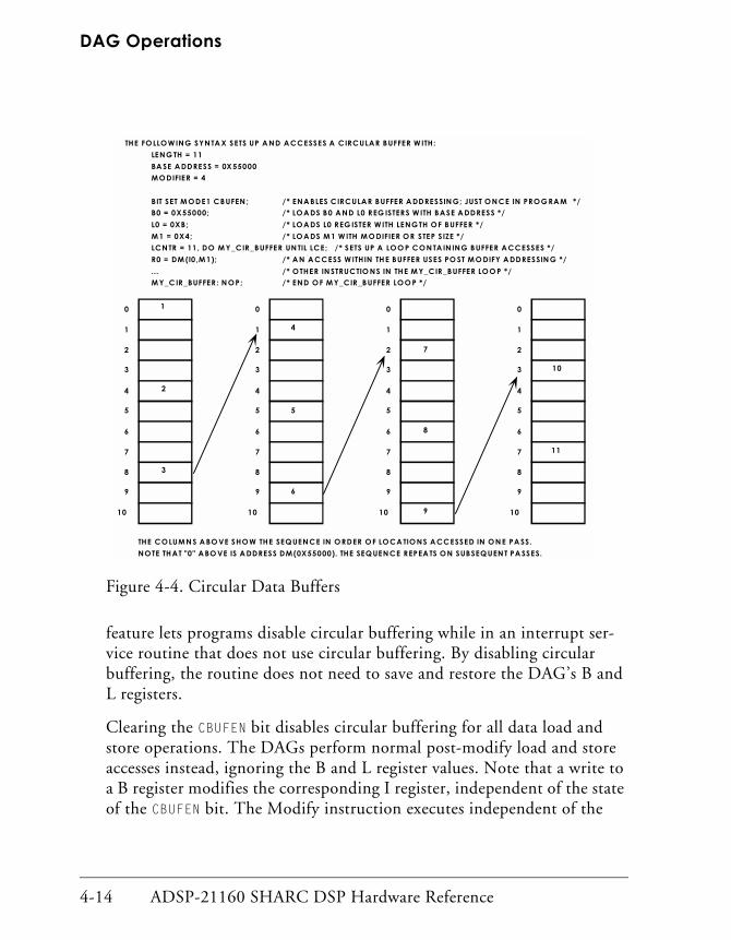
The DAGs support addressing circular buffers—a range of addresses con-taining data that the DAG steps through repeatedly, “wrapping around” to repeat stepping through the range of addresses in a circular pattern. To address a circular buffer, the DAG steps the index pointer (I register) through the buffer, post-modifying and updating the index on each access with a positive or negative modify value (M register or immediate value). If the index pointer falls outside the buffer, the DAG subtracts or adds the length of the buffer from or to the value, wrapping the index pointer back to the start of the buffer. The DAG’s support for circular buffer address-ing appears in Figure 4-1 on page 4-3, and an example of circular buffer addressing appears in Figure 4-4.
The starting address that the DAG wraps around is called the buffer’s base address (B register). There are no restrictions on the value of the base address for a circular buffer.
ADSP-21160 SHARC DSP Hardware Reference 4-13
Data Address Generators
! Circular buffering may only use post-modify addressing. The DAG’s architecture, as shown in Figure 4-1 on page 4-3, cannot support pre-modify addressing for circular buffering, because circu-lar buffering requires that the index be updated on each access.
It is important to note that the DAGs do not detect memory map over-flow or underflow. If the address post-modify produces I+M > 0xffffffff or I–M < 0, circular buffering may not function correctly. Also, the length of a circular buffer should not let the buffer straddle the top of the memory map. For more information on the DSP’s memory map, see “ADSP-21160 Memory Map” on page 5-12.
As shown in Figure 4-4, programs use the following steps to set up a circu-lar buffer:
1. Enable circular buffering (Bit Set Mode1 CBUFEN;). This operation is only needed once in a program.
2. Load the buffer’s base address into the B register. This operation automatically loads the corresponding I register.
3. Load the buffer’s length into the corresponding L register. For example, L0 corresponds to B0.
4. Load the modify value (step size) into an M register in the corre-sponding DAG. For example, M0 through M7 correspond to B0. Alternatively, the program can use an immediate value for the modifier.
After this set up, the DAGs use the modulus logic in Figure 4-1 on page 4-3 to process circular buffer addressing.
On the ADSP-21160, programs enable circular buffering by setting the CBUFEN bit in the MODE1 register. This bit has a corresponding mask bit in the MMASK register. Setting the corresponding MMASK bit causes the CBUFEN bit to be cleared following a push status instruction (Push Sts), the execu-tion of an external interrupt, timer interrupt, or vectored interrupt. This
DAG Operations
4-14 ADSP-21160 SHARC DSP Hardware Reference
feature lets programs disable circular buffering while in an interrupt ser-vice routine that does not use circular buffering. By disabling circular buffering, the routine does not need to save and restore the DAG’s B and L registers.
Clearing the CBUFEN bit disables circular buffering for all data load and store operations. The DAGs perform normal post-modify load and store accesses instead, ignoring the B and L register values. Note that a write to a B register modifies the corresponding I register, independent of the state of the CBUFEN bit. The Modify instruction executes independent of the
0
1
2
3
4
5
6
7
8
9
10
1
2
3
0
1
2
3
4
5
6
7
8
9
10
4
5
6
0
1
2
3
4
5
6
7
8
9
10
7
8
9
0
1
2
3
4
5
6
7
8
9
10
10
11
THE COLUM N S A BO VE SHOW THE SEQUEN CE IN ORDER OF LOCA TIONS A CCESSED IN ON E PA SS.
NOTE THAT "0" A BO VE IS A DDRESS DM (0X55000). THE SEQUEN CE REPEA TS ON SUBSEQUEN T PA SSES.
THE FOLLOW ING SYN TA X SETS UP A ND A CCESSES A CIRCULAR BUFFER W ITH:
LENG TH = 11
BA SE A DDRESS = 0X55000
MODIFIER = 4
BIT SET M ODE1 CBUFEN ; /* ENA BLES CIRCULAR BUFFER A DDRESSIN G; JUST ON CE IN PROG RA M */B0 = 0X55000; /* LOA DS B0 A ND L0 REG ISTERS W ITH BASE A DDRESS */
L0 = 0XB; /* LOA DS L0 REG ISTER W ITH LENGTH OF BUFFER */
M 1 = 0X4; /* LOA DS M 1 W ITH M O DIFIER OR STEP SIZE */
LCN TR = 11, DO M Y_CIR_BUFFER UN TIL LCE; /* SETS UP A LOO P CON TA IN ING BUFFER A CCESSES */
R0 = DM (I0,M 1); /* A N A CCESS W ITHIN THE BUFFER USES PO ST M O DIFY A DDRESSIN G */
... /* OTHER IN STRUCTIO NS IN THE M Y_CIR_BUFFER LOO P */M Y_C IR_BUFFER: N OP; /* END OF M Y_CIR _BUFFER LOO P */
Figure 4-4. Circular Data Buffers
ADSP-21160 SHARC DSP Hardware Reference 4-15
Data Address Generators
state of the CBUFEN bit. The Modify instruction always performs circular buffer modify of the index registers if the corresponding B and L registers are set up, independent of the state of the CBUFEN bit.
! On previous SHARC DSP’s (ADSP-2106x family), circular buffer-ing is always enabled. For code compatibility, programs ported to the ADSP-21160 should enable circular buffering (CBUFEN=1).
On the first post-modify access to the buffer, the DAG outputs the I regis-ter value on the address bus then modifies the address by adding the modify value. If the updated index value is within the buffer length, the DAG writes the value to the I register. If the updated value is outside the buffer length, the DAG subtracts (positive) or adds (negative) the L regis-ter value before writing the updated index value to the I register. In equation form, these post-modify and wrap around operations work as follows:
• If M is positive:
Inew = Iold + M if Iold + M < Buffer base + length (end of buffer)
Inew = Iold + M – L if Iold + M ≥ Buffer base + length (end of buffer)
• If M is negative:
Inew = Iold + M if Iold + M ≥ Buffer base (start of buffer)
Inew = Iold + M + L if Iold + M < Buffer base (start of buffer)
The DAGs use all four types of DAG registers for addressing circular buff-ers. These registers operate as follows for circular buffering:
• The index (I) register contains the value that the DAG outputs on the address bus.
• The modify (M) register contains the post-modify amount (positive or negative) that the DAG adds to the I register at the end of each memory access. The M register can be any M register in the same
DAG Operations
4-16 ADSP-21160 SHARC DSP Hardware Reference
DAG as the I register and does not have to have the same number. The modify value also can be an immediate value instead of an M register. The size of the modify value, whether from an M register or immediate, must be less than the length (L register) of the circular buffer.
• The length (L) register sets the size of the circular buffer and the address range that the DAG circulates the I register through. L must
be positive and cannot have a value greater than 231 – 1. If an L reg-ister’s value is zero, its circular buffer operation is disabled.
• The base (B) register, or the B register plus the L register, is the value that the DAG compares the modified I value with after each access. When the B register is loaded, the corresponding I register is simul-taneously loaded with the same value. When I is loaded, B is not changed. Programs can read the B and I registers independently.
There is one set of registers (I7 and I15) in each DAG that can generate an interrupt on circular buffer overflow (address wraparound). For more information, see “Using DAG Status” on page 4-9.
When a program needs to use I7 or I15 without circular buffering and the DSP has the circular buffer overflow interrupts unmasked, the program should disable the generation of these interrupts by setting the B7/B15 and L7/L15 registers to values that prevent the interrupts from occurring. If I7 were accessing the address range 0x1000–0x2000, the program could set B7=0x0000 and L7=0xFFFF. Because the DSP generates the circular buffer interrupt based on the wrap around equations on page 4-15, setting the L register to zero does not necessarily achieve the desired results. If the pro-gram is using either of the circular buffer overflow interrupts, it should avoid using the corresponding I register(s) (I7 or I15) where interrupt branching is not needed.
ADSP-21160 SHARC DSP Hardware Reference 4-17
Data Address Generators
! When a Long word access, SIMD access, or Normal word access (with LW option) crosses the end of the circular buffer, the DSP completes the access before responding to the end of buffer condi-tion.
Modifying DAG Registers
The DAGs support two operations that modify an address value in an index register without outputting an address. These two operations, address bit-reversal and address modify, are useful for bit-reverse address-ing and maintaining pointers.
The Modify instruction modifies addresses in any DAG index register (I0-I15) without accessing memory. If the I register’s corresponding B and L registers are set up for circular buffering, a Modify instruction performs the specified buffer wrap around (if needed). The syntax for Modify is similar to post-modify addressing (index, then modifier). Modify accepts either a 32-bit immediate values or an M register as the modifier. The fol-lowing example adds 4 to I1 and updates I1 with the new value:
Modify(I1,4);
The Bitrev instruction modifies and bit-reverses addresses in any DAG index register (I0-I15) without accessing memory. This instruction is independent of the bit-reverse mode. The Bitrev instruction adds a 32-bit immediate value to a DAG index register, bit-reverses the result, and writes the result back to the same index register. The following example adds 4 to I1, bit-reverses the result, and updates I1 with the new value:
Bitrev(I1,4);
Addressing in SISD & SIMD Modes
Single-Instruction, Multiple-Data (SIMD) mode (PEYEN bit=1) does not change the addressing operations in the DAGs, but it does change the amount of data that moves during each access. The DAGs put the same
DAGs, Registers, & Memory
4-18 ADSP-21160 SHARC DSP Hardware Reference
addresses on the address buses in SIMD and SISD modes. In SIMD mode, the DSP’s memory and processing elements get data from the loca-tions named (explicit) in the instruction syntax and complementary (implicit) locations. For more information on data moves between regis-ters, see “Secondary Processing Element (PEy)” on page 2-36. For more information on data accesses and memory, see “Data Access Options” on page 5-46.
DAGs, Registers, & Memory
DAG registers are part of the DSP’s universal register set. Programs may load the DAG registers from memory, from another universal register, or with an immediate value. Programs may store DAG registers’ contents to memory or to another universal register.
The DAG’s registers support the bidirectional register-to-register transfers that are described in “SIMD (Computational) Operations” on page 2-40. When the DAG register is a source of the transfer, the destination can be a register file data register. This transfer results in the contents of the single source register being duplicated in complementary data registers in each processing element.
Programs should use care in the case where the DAG register is a destina-tion of a transfer from a register file data register source. Programs should use a conditional operation to select either one processing element or nei-ther as the source. Having both processing elements contribute a source value results in the PEx element’s write having precedence over the PEy element’s write.
In the case where a DAG register is both source and destination, the data move operation executes the same as it would if SIMD mode were dis-abled (PEYEN cleared).
ADSP-21160 SHARC DSP Hardware Reference 4-19
Data Address Generators
DAG Register-to-bus Alignment
There are three word alignment cases for DAG registers and PM or DM data buses: Normal word, Extended-precision Normal word, and Long word.
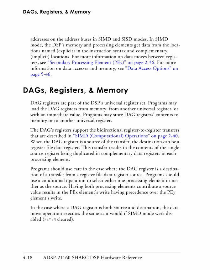
The DAGs align normal word (32-bit) addressed transfers to the low order bits of the buses. These transfers between memory and 32-bit DAG1or DAG2 registers use the 64-bit DM and PM data buses. Figure 4-5 illus-trates these transfers.
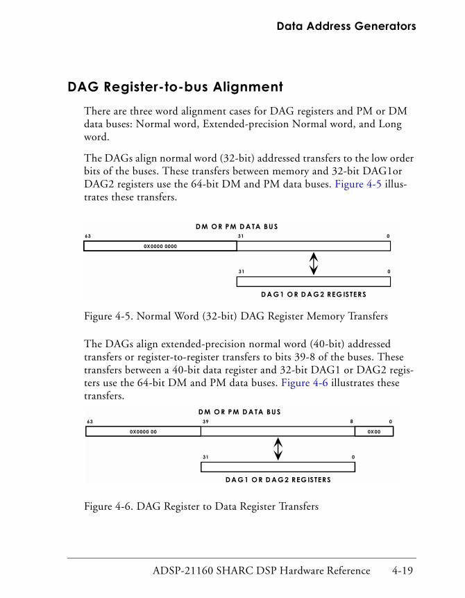
The DAGs align extended-precision normal word (40-bit) addressed transfers or register-to-register transfers to bits 39-8 of the buses. These transfers between a 40-bit data register and 32-bit DAG1 or DAG2 regis-ters use the 64-bit DM and PM data buses. Figure 4-6 illustrates these transfers.
D A G 1 O R D A G 2 REG ISTERS
03163��������������������������������������������������������������������������������������������������������������������������������������������������������������������������������0X0000 0000
D M O R PM D A TA BUS
031
Figure 4-5. Normal Word (32-bit) DAG Register Memory Transfers
D A G 1 O R D A G 2 REG ISTERS
031
03963����������������������������������������������������������������������������������������������������������������������������������
0X0000 00
D M O R PM D A TA BUS����������������������������������������������
0X00
8
Figure 4-6. DAG Register to Data Register Transfers
DAGs, Registers, & Memory
4-20 ADSP-21160 SHARC DSP Hardware Reference
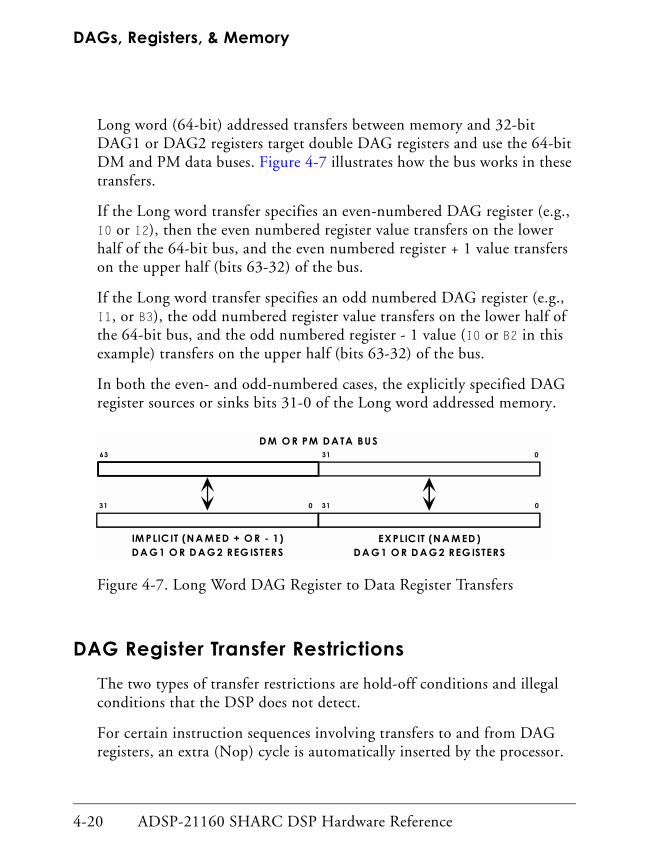
Long word (64-bit) addressed transfers between memory and 32-bit DAG1 or DAG2 registers target double DAG registers and use the 64-bit DM and PM data buses. Figure 4-7 illustrates how the bus works in these transfers.
If the Long word transfer specifies an even-numbered DAG register (e.g., I0 or I2), then the even numbered register value transfers on the lower half of the 64-bit bus, and the even numbered register + 1 value transfers on the upper half (bits 63-32) of the bus.
If the Long word transfer specifies an odd numbered DAG register (e.g., I1, or B3), the odd numbered register value transfers on the lower half of the 64-bit bus, and the odd numbered register - 1 value (I0 or B2 in this example) transfers on the upper half (bits 63-32) of the bus.
In both the even- and odd-numbered cases, the explicitly specified DAG register sources or sinks bits 31-0 of the Long word addressed memory.
DAG Register Transfer Restrictions
The two types of transfer restrictions are hold-off conditions and illegal conditions that the DSP does not detect.
For certain instruction sequences involving transfers to and from DAG registers, an extra (Nop) cycle is automatically inserted by the processor.
EX PLIC IT (N A M ED )D A G 1 O R D A G 2 REG ISTERS
031
03163
D M O R PM D A TA BUS
IM PLIC IT (N A M ED + O R - 1)D A G 1 O R D A G 2 REG ISTERS
031
Figure 4-7. Long Word DAG Register to Data Register Transfers
ADSP-21160 SHARC DSP Hardware Reference 4-21
Data Address Generators
When an instruction that loads a DAG register is followed by an instruc-
tion that uses any register in the same DAG register pair1 for data addressing, modify instructions, or indirect jumps, the DSP inserts an extra (Nop) cycle between the two instructions. This hold-off happens because the same bus is needed by both operations in the same cycle. So, the second operation must be delayed. The following case causes a delay because it exhibits a write/read dependency in which I0 is written in one cycle. The results of that register write are not available to a register read for one cycle. Note that if either instruction had specified I1, the stall would still occur, because the DSP’s DAG register transfers can occur in pairs. The DAG detects write/read dependencies with a register pair granularity:
I0=8;DM(I0,M1)=R1;
Certain other sequences of instructions cause incorrect results on the DSP and are flagged as errors by DSP assembler software. These types of instructions can execute on the processor, but cause incorrect results:
• An instruction that stores a DAG register in memory using indirect addressing from the same DAG, with or without update of the index register. The instruction writes the wrong data to memory or updates the wrong index register.
Do not try these: DM(M2,I1)=I0; or DM(I1,M2)=I0;These example instructions do not work because I0 and I1 are both DAG1 registers.
1 DAG register are accessible in pair granularity for single-cycle access. The pairings are odd-even. For example I0 and I1 are a pair, and I2 and I3 are a pair.

DAGs, Registers, & Memory
4-22 ADSP-21160 SHARC DSP Hardware Reference
• An instruction that loads a DAG register from memory using indi-rect addressing from the same DAG, with update of the index reg-ister. The instruction will either load the DAG register or update the index register, but not both.
Do not try this: L2=DM(I1,M0);This example instruction does not work because L2 and I1 are both DAG1 registers.
ADSP-21160 SHARC DSP Hardware Reference 4-23
Data Address Generators
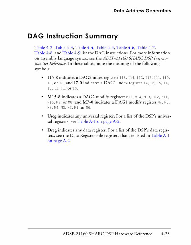
DAG Instruction Summary
Table 4-2, Table 4-3, Table 4-4, Table 4-5, Table 4-6, Table 4-7, Table 4-8, and Table 4-9 list the DAG instructions. For more information on assembly language syntax, see the ADSP-21160 SHARC DSP Instruc-tion Set Reference. In these tables, note the meaning of the following symbols:
• I15-8 indicates a DAG2 index register: I15, I14, I13, I12, I11, I10, I9, or I8, and I7-0 indicates a DAG1 index register I7, I6, I5, I4, I3, I2, I1, or I0.
• M15-8 indicates a DAG2 modify register: M15, M14, M13, M12, M11, M10, M9, or M8, and M7-0 indicates a DAG1 modify register M7, M6, M5, M4, M3, M2, M1, or M0.
• Ureg indicates any universal register; For a list of the DSP’s univer-sal registers, see Table A-1 on page A-2.
• Dreg indicates any data register; For a list of the DSP’s data regis-ters, see the Data Register File registers that are listed in Table A-1 on page A-2.
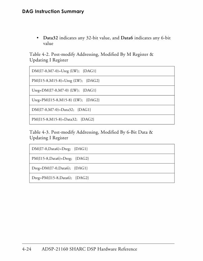
DAG Instruction Summary
4-24 ADSP-21160 SHARC DSP Hardware Reference
• Data32 indicates any 32-bit value, and Data6 indicates any 6-bit value
Table 4-2. Post-modify Addressing, Modified By M Register & Updating I Register
DM(I7-0,M7-0)=Ureg (LW); {DAG1}
PM(I15-8,M15-8)=Ureg (LW); {DAG2}
Ureg=DM(I7-0,M7-0) (LW); {DAG1}
Ureg=PM(I15-8,M15-8) (LW); {DAG2}
DM(I7-0,M7-0)=Data32; {DAG1}
PM(I15-8,M15-8)=Data32; {DAG2}
Table 4-3. Post-modify Addressing, Modified By 6-Bit Data & Updating I Register
DM(I7-0,Data6)=Dreg; {DAG1}
PM(I15-8,Data6)=Dreg; {DAG2}
Dreg=DM(I7-0,Data6); {DAG1}
Dreg=PM(I15-8,Data6); {DAG2}
ADSP-21160 SHARC DSP Hardware Reference 4-25
Data Address Generators
Table 4-4. Pre-modify Addressing, Modified By M Register (No I Register Update)
DM(M7-0,I7-0)=Ureg (LW); {DAG1}
PM(M15-8,I15-8)=Ureg (LW); {DAG2}
Ureg=DM(M7-0,I7-0) (LW); {DAG1}
Ureg=PM(M15-8,I15-8) (LW); {DAG2}
Table 4-5. Pre-modify Addressing, Modified By 6-Bit Data (No I Register Update)
DM(Data6,I7-0)=Dreg; {DAG1}
PM(Data6,I15-8)=Dreg; {DAG2}
Dreg=DM(Data6,I7-0); {DAG1}
Dreg=PM(Data6,I15-8); {DAG2}
Table 4-6. Pre-modify Addressing, Modified By 32-Bit Data (No I Register Update)
Ureg=DM(Data32,I7-0) (LW); {DAG1}
Ureg=PM(Data32,I15-8) (LW); {DAG2}
DM(Data32,I7-0)=Ureg (LW); {DAG1}
PM(Data32,I15-8)=Ureg (LW); {DAG2}
DAG Instruction Summary
4-26 ADSP-21160 SHARC DSP Hardware Reference
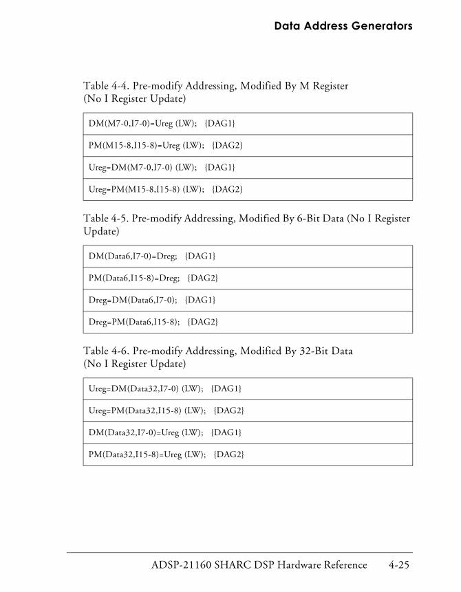
Table 4-7. Update (Modify) I Register, Modified By M Register
Modify(I7-0,M7-0); {DAG1}
Modify(I15-8,M15-8); {DAG2}
Table 4-8. Update (Modify) I Register, Modified By 32-Bit Data
Modify(I7-0,Data32); {DAG1}
Modify(I15-8,Data32); {DAG2}
Table 4-9. Bit-Reverse & Update I Register, Modified By 32-Bit Data
Bitrev(I7-0,Data32); {DAG1}
Bitrev(I15-8,Data32); {DAG2}