Gowin_EMPU_M1 Hardware Design
59
Gowin_EMPU_M1 Hardware Design Reference Manual IPUG531-1.9E, 10/12/2021
-
Upload
khangminh22 -
Category
Documents
-
view
0 -
download
0
Transcript of Gowin_EMPU_M1 Hardware Design

Gowin_EMPU_M1 Hardware Design
Reference Manual
IPUG531-1.9E, 10/12/2021

Copyright © 2021 Guangdong Gowin Semiconductor Corporation. All Rights Reserved.
, , Gowin, GowinSynthesis, and GOWINSEMI are trademarks of Guangdong Gowin Semiconductor Corporation and are registered in China, the U.S. Patent and Trademark Office, and other countries. All other words and logos identified as trademarks or service marks are the property of their respective holders. No part of this document may be reproduced or transmitted in any form or by any denotes, electronic, mechanical, photocopying, recording or otherwise, without the prior written consent of GOWINSEMI.
Disclaimer
GOWINSEMI assumes no liability and provides no warranty (either expressed or implied) and is not responsible for any damage incurred to your hardware, software, data, or property resulting from usage of the materials or intellectual property except as outlined in the GOWINSEMI Terms and Conditions of Sale. All information in this document should be treated as preliminary. GOWINSEMI may make changes to this document at any time without prior notice. Anyone relying on this documentation should contact GOWINSEMI for the current documentation and errata.

Revision History
Date Version Description
02/19/2019 1.0E Initial version published.
07/18/2019 1.1E MCU hardware design supports extended peripherals: CAN, Ethernet, SPI-Flash, RTC, DualTimer, TRNG, I
2C, SPI, SD-Card.
08/18/2019 1.2E
MCU hardware design and software programming design support extended peripheral: DD3 Memory.
Fixed known issues of ITCM, DTCM Size and IDE.
09/27/2019 1.3E
MCU hardware design and software programming design support read, write and erasure of SPI-Flash.
MCU software programming design supports a continuous multi-byte read and write of I
2C.
Fixed known issues of address mapping of AHB2 and APB2 extended interface in MCU software programming design.
Fixed known issues of continuous read and write of DDR3 Memory in MCU software programming design.
12/06/2019 1.4E
MCU hardware design and software programming design supports PSRAM.
Updated MCU compiling software GMD V1.0.
RTOS reference design updated.
Hardware and software reference design of AHB2 and APB2 extension bus interface added.
03/03/2020 1.5E
MCU hardware design supports read and write of SPI-Card.
Fixed known issues of data read and write of DDR when "synplify Pro" synthesizes.
The FPGA devices of GW2A-18C/GW2AR-18C/GW2A-55C supported.
06/12/2020 1.6E
MCU supports External instruction memory.
MCU supports External data memory.
6 AHB bus interfaces extended.
16 APB bus interfaces extended.
GPIO supports multiple interface types.
I2C supports multiple interface types.
01/25/2021 1.7E
Fixed known issues of SPI-Flash initialization.
The reference design of GW1N-9C, GW2A-18C, GW2A-55C (Version C) updated.
The reference design of version Gowin Software updated.
The reference supports of external interrupt signal added.
07/21/2021 1.8E
GW1N-9C/GW1NR-9C supports embedded UserFlash as instruction memory.
Known issues of read and write for SPI full-duplex fixed.
The reference design of SynplifyPro deleted.
The reference design and the version of Gowin Software updated.
2021/10/12 1.9E
ITCM and DTCM size of GW2AN-9X/GW2AN-18X modified.
GW2AN-9X/GW2AN-18X does not support external DDR3.
DK-START-GW2AR18 V1.1 development board reference design updated.

Date Version Description
Non-BlockRAM ITCM/DTCM solution added.

Contents
IPUG531-1.9E i
Contents
Contents ............................................................................................................... i
List of Figures .................................................................................................... iii
List of Tables ....................................................................................................... v
1 Hardware Architecture .................................................................................... 1
1.1 System Architecture ............................................................................................................ 1
1.2 System Feature .................................................................................................................. 1
1.2.1 Cortex-M1 Core System .................................................................................................. 2
1.2.2 AHB-Lite Extension Sub-system ...................................................................................... 3
1.3 System Ports ...................................................................................................................... 3
1.4 System Resource Statistics .............................................................................................. 15
2 Hardware Design Flow .................................................................................. 16
2.1 Hardware Environment ..................................................................................................... 16
2.2 Software Environment ...................................................................................................... 16
2.3 IP Core Generator Tool ..................................................................................................... 16
2.4 Download Tool .................................................................................................................. 16
2.5 Design Flow ...................................................................................................................... 17
3 Project Template ........................................................................................... 18
3.1 Project Creation ................................................................................................................ 18
3.1.1 Create a New Project .................................................................................................... 18
3.1.2 Set Project Name and Path ........................................................................................... 19
3.1.3 Select Device ................................................................................................................. 19
3.1.4 Project Creation Completed .......................................................................................... 20
3.2 Hardware Design .............................................................................................................. 20
3.2.1 Cortex-M1 Hardware Design ......................................................................................... 21
3.2.2 AHB-Lite Extension Hardware Design ........................................................................... 27
3.3 User Design ...................................................................................................................... 42
3.4 Constraint ......................................................................................................................... 43
3.5 Configuration .................................................................................................................... 43
3.5.1 Synthesis Configuration ................................................................................................. 43
3.5.2 Post-Place File Configuration ........................................................................................ 44
3.5.3 Dual-Purpose Pin Configuration .................................................................................... 44

Contents
IPUG531-1.9E ii
3.6 Synthesize ........................................................................................................................ 45
3.7 Place & Route ................................................................................................................... 45
3.8 Download .......................................................................................................................... 46
4 Reference Design .......................................................................................... 49

List of Figures
IPUG531-1.9E iii
List of Figures
Figure 1-1 System Architecture .......................................................................................................... 1
Figure 3-1 Create a FPGA Design Project ......................................................................................... 18
Figure 3-2 Set Project Name and Path .............................................................................................. 19
Figure 3-3 Select Device .................................................................................................................... 19
Figure 3-4 Complete Project Creating ............................................................................................... 20
Figure 3-5 Select Gowin_EMPU_M1 ................................................................................................. 20
Figure 3-6 System Configuration ....................................................................................................... 21
Figure 3-7 Cortex-M1 Configuration Option ....................................................................................... 22
Figure 3-8 Cortex-M1 Common Configuration ................................................................................... 23
Figure 3-9 Cortex-M1 Debugging Configuration ................................................................................ 24
Figure 3-10 Cortex-M1 Memory Configuration .................................................................................. 25
Figure 3-11 GPIO Configuration ........................................................................................................ 29
Figure 3-12 CAN Configuration .......................................................................................................... 29
Figure 3-13 Ethernet Configuration.................................................................................................... 30
Figure 3-14 DDR3 Configuration ....................................................................................................... 31
Figure 3-15 SPI-Flash Configuration ................................................................................................. 32
Figure 3-16 AHB Master [1-6] ............................................................................................................ 33
Figure 3-17 UART Configuration ....................................................................................................... 34
Figure 3-18 Timer Configuration ........................................................................................................ 34
Figure 3-19 WatchDog Configuration ................................................................................................ 35
Figure 3-20 RTC Configuration .......................................................................................................... 36
Figure 3-21 DualTimer Configuration ................................................................................................. 36
Figure 3-22 TRNG Configuration ....................................................................................................... 37
Figure 3-23 I2C Configuration ............................................................................................................ 38
Figure 3-24 SPI Configuration ........................................................................................................... 38
Figure 3-25 SD-Card Configuration ................................................................................................... 39
Figure 3-26 APB Master [1-16] Configuration .................................................................................... 41
Figure 3-27 PSRAM Configuration .................................................................................................... 42
Figure 3-28 Synthesis Option Configuration ...................................................................................... 43
Figure 3-29 Post-Place File Configuration ......................................................................................... 44
Figure 3-30 Dual-Purpose Pin Configuration ..................................................................................... 44
Figure 3-31 Synthesis ........................................................................................................................ 45

List of Figures
IPUG531-1.9E iv
Figure 3-32 Place & Route ................................................................................................................. 45
Figure 3-33 GW1N Series of Device Configuration ........................................................................... 46
Figure 3-34 GW1N(R)-9C Device Configuration ............................................................................... 47
Figure 3-35 GW2A Series of Device Configuration ........................................................................... 48

List of Tables
IPUG531-1.9E v
List of Tables
Table 1-1 System Ports Definition ...................................................................................................... 3
Table 1-2 System Resource Statistics ............................................................................................... 15
Table 3-1 Cortex-M1 Configuration Option ........................................................................................ 21
Table 3-2 AHB-Lite Extension Configuration Options ........................................................................ 27
Table 3-3 AHB Master [1-6] Address Definition .................................................................................. 33
Table 3-4 APB Master [1-16] Address Definition ................................................................................ 41

1 Hardware Architecture 1.1 System Architecture
IPUG531-1.9E 1((49)
1 Hardware Architecture
1.1 System Architecture Gowin_EMPU_M1 architecture consists of three levels, as shown in
Figure 1-1.
Figure 1-1 System Architecture
First level: Cortex-M1 core, ITCM, and DTCM
Second level: AHB bus, GPIO, CAN, Ethernet, DDR3 Memory, PSRAM, SPI-Flash and AHB Master [1-6].
Third level: APB bus, UART0, UART1, Timer0, Timer1, Watch Dog, RTC, TRNG, DualTimer, I2C Master, SPI Master, SD-Card and APB Master [1-16].
1.2 System Feature Gowin_EMPU_M1 includes two sub-systems:
Cortex-M1 core system:
AHB-Lite extension AHB bus, APB bus and peripheral interface

1 Hardware Architecture 1.2 System Feature
IPUG531-1.9E 2(49)
sub-system.
1.2.1 Cortex-M1 Core System
Processor Core
ARM architecture v6-M Thumb, the instruction set architecture, supports 16-bit Thumb and 32-bit Thumb2 instruction set;
Configurable extension operation system;
System exception handling;
Interrupt exception handling and normal thread model;
One stack pointer for normal operation system and two stack pointers for extension operation system;
Big/Little-endian format.
- Configurable Big/Little-endian format
- Little-endian format for instructions and system control register
- Little-endian format for debugging system
NVIC
Number of external interrupts can be configured: 1, 8, 16, 32;
Four priority levels;
Saves processor status automatically during interrupts handling and recovers automatically at the end of interrupt handling.
Debug System
Control the debugging system through configuration options.
If you turn off the debugging system, Cortex-M1 core will not support it.
If you turn on the debugging system, Cortex-M1 core will support it.
- Full mode and reduced mode can be configured
a) Full mode: Four BreakPoint Units and two Data Watchpoints; b) Reduced mode: Two BreakPoint Units and one Data
Watchpoints;
- Configurable DAP ports
a) JTAG/SW b) JTAG c) SW
Memory
ITCM: instruction memory
- You can select internal instruction memory or external instruction memory.
- You can configure the Size of internal instruction memory as 1/2/4/8/16/32/64/128/256KB.
1 Hardware Architecture 1.3 System Ports
IPUG531-1.9E 3(49)
- You can configure the initial value of internal instruction memory.
DTCM: data memory
- You can select internal data memory or external data memory.
- You can configure the Size of internal data memory as 1/2/4/8/16/32/64/128/256KB.
32 Bits Hardware Multiplier
Normal mode
Small mode
1.2.2 AHB-Lite Extension Sub-system
AHB bus, GPIO, CAN, Ethernet, DDR3 Memory, PSRAM, SPI-Flash and AHB Master [1-6].
APB bus, UART0, UART1, Timer0, Timer1, Watch Dog, RTC, TRNG, DualTimer, I2C Master, SPI Master, SD-Card and APB Master [1-16].
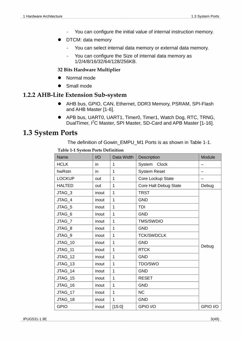
1.3 System Ports The definition of Gowin_EMPU_M1 Ports is as shown in Table 1-1.
Table 1-1 System Ports Definition
Name I/O Data Width Description Module
HCLK in 1 System Clock –
hwRstn in 1 System Reset –
LOCKUP out 1 Core Lockup State –
HALTED out 1 Core Halt Debug State Debug
JTAG_3 inout 1 TRST
Debug
JTAG_4 inout 1 GND
JTAG_5 inout 1 TDI
JTAG_6 inout 1 GND
JTAG_7 inout 1 TMS/SWDIO
JTAG_8 inout 1 GND
JTAG_9 inout 1 TCK/SWDCLK
JTAG_10 inout 1 GND
JTAG_11 inout 1 RTCK
JTAG_12 inout 1 GND
JTAG_13 inout 1 TDO/SWO
JTAG_14 inout 1 GND
JTAG_15 inout 1 RESET
JTAG_16 inout 1 GND
JTAG_17 inout 1 NC
JTAG_18 inout 1 GND
GPIO inout [15:0] GPIO I/O GPIO I/O

1 Hardware Architecture 1.3 System Ports
IPUG531-1.9E 4(49)
Name I/O Data Width Description Module
GPIOIN in [15:0] GPIO input GPIO non-I/O
GPIOOUT out [15:0] GPIO output
GPIOOUTEN out [15:0] GPIO output enable
UART0RXD in 1 UART0 receive UART0
UART0TXD out 1 UART0 transmit
UART1RXD int 1 UART1 receive UART1
UART1TXD out 1 UART1 transmit
TIMER0EXTIN in 1 Timer0 external interrupt Timer0
TIMER1EXTIN in 1 Timer1 external interrupt Timer1
RTCSRCCLK in 1 RTC clock source: 32.768KHz RTC
SCL inout 1 Serial Clock I2C I/O
SDA inout 1 Serial data
SCLIN in 1 Serial clock input
I2C
non-I/O
SCLOUT out 1 Serial clock output
SCLOUTEN out 1 Serial clock output enable
SDAIN in 1 Serial clock input
SDAOUT out 1 Serial clock output
SDAOUTEN out 1 Serial clock output enable
MOSI out 1 Master output/Slave input
SPI MISO in 1 Master input/Slave output
SCLK out 1 Clock signal
NSS out 1 Slave select signal
SD_SPICLK in 1 SPI clock signal
SD-Card
SD_CLK out 1 SD clock signal
SD_CS out 1 Chip select signal
SD_DATAIN in 1 Data input
SD_DATAOUT out 1 Data output
SD_CARD_INIT out 1 Initialization "0"
SD_CHECKIN in 1 Input check
SD_CHECKOUT out 1 Output check
CAN_RX in 1 Data input CAN
CAN_TX out 1 Data output
RGMII_TXC out 1 RGMII transmitting clock
Ethernet RGMII Interface
RGMII_TX_CTL out 1 RGMII transmitting control
RGMII_TXD out [3:0] RGMII transmitting data
RGMII_TXD in 1 RGMII receiving clock
RGMII_RX_CTL in 10 RGMII receiving control
RGMII_RXD in [3:0] RGMII/MII receiving data

1 Hardware Architecture 1.3 System Ports
IPUG531-1.9E 5(49)
Name I/O Data Width Description Module
GTX_CLK in 1 RGMII 125MHz clock input
GMII_RX_CLK in 1 GMII receiving clock
Ethernet GMII Interface
GMII_RX_DV in 1 GMII receiving enable
GMII_RXD in [7:0] GMII receiving data
GMII_RX_ER in 1 GMII receiving error
GTX_CLK in 1 GMII 125MHz clock input
GMII_GTX_CLK out 1 GMII receiving clock
GMII_TXD out [7:0] GMII transmitting data
GMII_TX_EN out 1 GMII transmitting enable
GMII_TX_ER out 1 GMII transmitting error
MII_RX_CLK in 1 MII receiving clock
Ethernet MII Interface
MII_RXD in [3:0] MII receiving data
MII_RX_DV in 1 MII receiving enable
MII_RX_ER in 1 MII receiving error
MII_TX_CLK in 1 MII transmitting clock
MII_TXD out [3:0] MII transmitting data
MII_TX_EN out 1 MII transmitting enable
MII_TX_ER out 1 MII transmitting error
MII_COL in 1 MII conflicting signal
MII_CRS in 1 MII carrier signal
MDC out 1 Manage channel clock Ethernet
MDIO inout 1 Manage channel data
DDR_CLK_I in 1 50MHz clock input
DDR3
DDR_INIT_COMPLETE_O
out 1 Initialization completed signal
DDR_ADDR_O out [15:0] Row address, Column address
DDR_BA_O out [2:0] Bank address
DDR_CS_N_O out 1 Chip select signal
DDR_RAS_N_O out 1 Row address strobe signal
DDR_CAS_N_O out 1 Column address strobe signal
DDR_WE_N_O out 1 Row write enable
DDR_CLK_O out 1 A clock signal provided to DDR3 SDRAM
DDR_CLK_N_O out 1 Compose a differential signal with DDR_CLK_O
DDR_CKE_O out 1 DDR3 SDRAM clock enable signal
DDR_ODT_O out 1 Terminating resistor control of memory signal
DDR_RESET_N_O
out 1 DDR3 SDRAM reset signal
DDR_DQM_O out [1:0] DDR3 SDRAM data masking

1 Hardware Architecture 1.3 System Ports
IPUG531-1.9E 6(49)
Name I/O Data Width Description Module
signal
DDR_DQ_IO inout [15:0] DDR3 SDRAM data
DDR_DQS_IO inout [1:0] DDR3 SDRAM data strobe signal
DDR_DQS_N_IO inout [1:0] Compose a differential signal with DDR_DQS_IO
O_psram_ck out [1:0] A clock signal provided to PSRAM
PSRAM
O_psram_ck_n out [1:0] Compose the difference signal with the O_psram_ck
IO_psram_rwds inout [1:0] PSRAM data selection signal and mask signal
IO_psram_dq inout [15:0] PSRAM data
O_psram_reset_n
out [1:0] PSRAM reset signal
O_psram_cs_n out [1:0] Chip selected, active-low.
init_calib out 1 Initialization completed signal
psram_ref_clk in 1 Reference input clock, it is usually on-board crystal oscillator clock.
psram_memory_clk
in 1
You can input chip working clock, which is generally a high clock of PLL frequency multiplication, or not use PLL.
FLASH_SPI_HOLDN
inout 1 NC
SPI-Flash
FLASH_SPI_CSN
inout 1 Slave select signal
FLASH_SPI_MISO
inout 1 Master input/Slave output
FLASH_SPI_MOSI
inout 1 Master output/Slave input
FLASH_SPI_WPN
inout 1 NC
FLASH_SPI_CLK inout 1 Clock signal
APB1PSTRB out [3:0] APB1 PSTRB
APB1 Master [1]
APB1PPROT out [2:0] APB1 PPROT
APB1PSEL out 1 APB1 PSEL
APB1PENABLE out 1 APB1 PENABLE
APB1PADDR out [31:0] APB1 PADDR
APB1PWRITE out 1 APB1 PWRITE
APB1PWDATA out [31:0] APB1 PWDATA
APB1PRDATA in [31:0] APB1 PRDATA
APB1PREADY in 1 APB1 PREADY
APB1PSLVERR in 1 APB1 PSLVERR
APB1PCLK out 1 APB1 PCLK
APB1PRESET out 1 APB1 RESET

1 Hardware Architecture 1.3 System Ports
IPUG531-1.9E 7(49)
Name I/O Data Width Description Module
APB2PSTRB out [3:0] APB2 PSTRB
APB Master [2]
APB2PPROT out [2:0] APB2 PPROT
APB2PSEL out 1 APB2 PSEL
APB2PENABLE out 1 APB2 PENABLE
APB2PADDR out [31:0] APB2 PADDR
APB2PWRITE out 1 APB2 PWRITE
APB2PWDATA out [31:0] APB2 PWDATA
APB2PRDATA in [31:0] APB2 PRDATA
APB2PREADY in 1 APB2 PREADY
APB2PSLVERR in 1 APB2 PSLVERR
APB2PCLK out 1 APB2 PCLK
APB2PRESET out 1 APB2 RESET
APB3PSTRB out [3:0] APB3 PSTRB
APB Master [3]
APB3PPROT out [2:0] APB3 PPROT
APB3PSEL out 1 APB3 PSEL
APB3PENABLE out 1 APB3 PENABLE
APB3PADDR out [31:0] APB3 PADDR
APB3PWRITE out 1 APB3 PWRITE
APB3PWDATA out [31:0] APB3 PWDATA
APB3PRDATA in [31:0] APB3 PRDATA
APB3PREADY in 1 APB3 PREADY
APB3PSLVERR in 1 APB3 PSLVERR
APB3PCLK out 1 APB3 PCLK
APB3PRESET out 1 APB3 RESET
APB4PSTRB out [3:0] APB4 PSTRB
APB Master [4]
APB4PPROT out [2:0] APB4 PPROT
APB4PSEL out 1 APB4 PSEL
APB4PENABLE out 1 APB4 PENABLE
APB4PADDR out [31:0] APB4 PADDR
APB4PWRITE out 1 APB4 PWRITE
APB4PWDATA out [31:0] APB4 PWDATA
APB4PRDATA in [31:0] APB4 PRDATA
APB4PREADY in 1 APB4 PREADY
APB4PSLVERR in 1 APB4 PSLVERR
APB4PCLK out 1 APB4 PCLK
APB4PRESET out 1 APB4 RESET
APB5PSTRB out [3:0] APB5 PSTRB APB Master APB5PPROT out [2:0] APB5 PPROT

1 Hardware Architecture 1.3 System Ports
IPUG531-1.9E 8(49)
Name I/O Data Width Description Module
APB5PSEL out 1 APB5 PSEL [5]
APB5PENABLE out 1 APB5 PENABLE
APB5PADDR out [31:0] APB5 PADDR
APB5PWRITE out 1 APB5 PWRITE
APB5PWDATA out [31:0] APB5 PWDATA
APB5PRDATA in [31:0] APB5 PRDATA
APB5PREADY in 1 APB5 PREADY
APB5PSLVERR in 1 APB5 PSLVERR
APB5PCLK out 1 APB5 PCLK
APB5PRESET out 1 APB5 RESET
APB6PSTRB out [3:0] APB6 PSTRB
APB Master [6]
APB6PPROT out [2:0] APB6 PPROT
APB6PSEL out 1 APB6 PSEL
APB6PENABLE out 1 APB6 PENABLE
APB6PADDR out [31:0] APB6 PADDR
APB6PWRITE out 1 APB6 PWRITE
APB6PWDATA out [31:0] APB6 PWDATA
APB6PRDATA in [31:0] APB6 PRDATA
APB6PREADY in 1 APB6 PREADY
APB6PSLVERR in 1 APB6 PSLVERR
APB6PCLK out 1 APB6 PCLK
APB6PRESET out 1 APB6 RESET
APB7PSTRB out [3:0] APB7 PSTRB
APB Master [7]
APB7PPROT out [2:0] APB7 PPROT
APB7PSEL out 1 APB7 PSEL
APB7PENABLE out 1 APB7 PENABLE
APB7PADDR out [31:0] APB7 PADDR
APB7PWRITE out 1 APB7 PWRITE
APB7PWDATA out [31:0] APB7 PWDATA
APB7PRDATA in [31:0] APB7 PRDATA
APB7PREADY in 1 APB7 PREADY
APB7PSLVERR in 1 APB7 PSLVERR
APB7PCLK out 1 APB7 PCLK
APB7PRESET out 1 APB7 RESET
APB8PSTRB out [3:0] APB8 PSTRB
APB Master [8]
APB8PPROT out [2:0] APB8 PPROT
APB8PSEL out 1 APB8 PSEL
APB8PENABLE out 1 APB8 PENABLE

1 Hardware Architecture 1.3 System Ports
IPUG531-1.9E 9(49)
Name I/O Data Width Description Module
APB8PADDR out [31:0] APB8 PADDR
APB8PWRITE out 1 APB8 PWRITE
APB8PWDATA out [31:0] APB8 PWDATA
APB8PRDATA in [31:0] APB8 PRDATA
APB8PREADY in 1 APB8 PREADY
APB8PSLVERR in 1 APB8 PSLVERR
APB8PCLK out 1 APB8 PCLK
APB8PRESET out 1 APB8 RESET
APB9PSTRB out [3:0] APB9 PSTRB
APB Master [9]
APB9PPROT out [2:0] APB9 PPROT
APB9PSEL out 1 APB9 PSEL
APB9PENABLE out 1 APB9 PENABLE
APB9PADDR out [31:0] APB9 PADDR
APB9PWRITE out 1 APB9 PWRITE
APB9PWDATA out [31:0] APB9 PWDATA
APB9PRDATA in [31:0] APB9 PRDATA
APB9PREADY in 1 APB9 PREADY
APB9PSLVERR in 1 APB9 PSLVERR
APB9PCLK out 1 APB9 PCLK
APB9PRESET out 1 APB9 RESET
APB10PSTRB out [3:0] APB10 PSTRB
APB Master [10]
APB10PPROT out [2:0] APB10 PPROT
APB10PSEL out 1 APB10 PSEL
APB10PENABLE out 1 APB10 PENABLE
APB10PADDR out [31:0] APB10 PADDR
APB10PWRITE out 1 APB10 PWRITE
APB10PWDATA out [31:0] APB10 PWDATA
APB10PRDATA in [31:0] APB10 PRDATA
APB10PREADY in 1 APB10 PREADY
APB10PSLVERR in 1 APB10 PSLVERR
APB10PCLK out 1 APB10 PCLK
APB10PRESET out 1 APB10 RESET
APB11PSTRB out [3:0] APB11 PSTRB
APB Master [11]
APB11PPROT out [2:0] APB11 PPROT
APB11PSEL out 1 APB11 PSEL
APB11PENABLE out 1 APB11 PENABLE
APB11PADDR out [31:0] APB11 PADDR
APB11PWRITE out 1 APB11 PWRITE

1 Hardware Architecture 1.3 System Ports
IPUG531-1.9E 10(49)
Name I/O Data Width Description Module
APB11PWDATA out [31:0] APB11 PWDATA
APB11PRDATA in [31:0] APB11 PRDATA
APB11PREADY in 1 APB11 PREADY
APB11PSLVERR in 1 APB11 PSLVERR
APB11PCLK out 1 APB11 PCLK
APB11PRESET out 1 APB11 RESET
APB12PSTRB out [3:0] APB12 PSTRB
APB Master [12]
APB12PPROT out [2:0] APB12 PPROT
APB12PSEL out 1 APB12 PSEL
APB12PENABLE out 1 APB12 PENABLE
APB12PADDR out [31:0] APB12 PADDR
APB12PWRITE out 1 APB12 PWRITE
APB12PWDATA out [31:0] APB12 PWDATA
APB12PRDATA in [31:0] APB12 PRDATA
APB12PREADY in 1 APB12 PREADY
APB12PSLVERR in 1 APB12 PSLVERR
APB12PCLK out 1 APB12 PCLK
APB12PRESET out 1 APB12 RESET
APB13PSTRB out [3:0] APB13 PSTRB
APB Master [13]
APB13PPROT out [2:0] APB13 PPROT
APB13PSEL out 1 APB13 PSEL
APB13PENABLE out 1 APB13 PENABLE
APB13PADDR out [31:0] APB13 PADDR
APB13PWRITE out 1 APB13 PWRITE
APB13PWDATA out [31:0] APB13 PWDATA
APB13PRDATA in [31:0] APB13 PRDATA
APB13PREADY in 1 APB13 PREADY
APB13PSLVERR in 1 APB13 PSLVERR
APB13PCLK out 1 APB13 PCLK
APB13PRESET out 1 APB13 RESET
APB14PSTRB out [3:0] APB14 PSTRB
APB Master [14]
APB14PPROT out [2:0] APB14 PPROT
APB14PSEL out 1 APB14 PSEL
APB14PENABLE out 1 APB14 PENABLE
APB14PADDR out [31:0] APB14 PADDR
APB14PWRITE out 1 APB14 PWRITE
APB14PWDATA out [31:0] APB14 PWDATA
APB14PRDATA in [31:0] APB14 PRDATA

1 Hardware Architecture 1.3 System Ports
IPUG531-1.9E 11(49)
Name I/O Data Width Description Module
APB14PREADY in 1 APB14 PREADY
APB14PSLVERR in 1 APB14 PSLVERR
APB14PCLK out 1 APB14 PCLK
APB14PRESET out 1 APB14 RESET
APB15PSTRB out [3:0] APB15 PSTRB
APB Master [15]
APB15PPROT out [2:0] APB15 PPROT
APB15PSEL out 1 APB15 PSEL
APB15PENABLE out 1 APB15 PENABLE
APB15PADDR out [31:0] APB15 PADDR
APB15PWRITE out 1 APB15 PWRITE
APB15PWDATA out [31:0] APB15 PWDATA
APB15PRDATA in [31:0] APB15 PRDATA
APB15PREADY in 1 APB15 PREADY
APB15PSLVERR in 1 APB15 PSLVERR
APB15PCLK out 1 APB15 PCLK
APB15PRESET out 1 APB15 RESET
APB16PSTRB out [3:0] APB16 PSTRB
APB Master [16]
APB16PPROT out [2:0] APB16 PPROT
APB16PSEL out 1 APB16 PSEL
APB16PENABLE out 1 APB16 PENABLE
APB16PADDR out [31:0] APB16 PADDR
APB16PWRITE out 1 APB16 PWRITE
APB16PWDATA out [31:0] APB16 PWDATA
APB16PRDATA in [31:0] APB16 PRDATA
APB16PREADY in 1 APB16 PREADY
APB16PSLVERR in 1 APB16 PSLVERR
APB16PCLK out 1 APB16 PCLK
APB16PRESET out 1 APB16 RESET
EXTFLASH0HSEL
out 1 External Flash HSEL
External Instruction Memory
EXTFLASH0HADDR
out [31:0] External Flash HADDR
EXTFLASH0HTRANS
out [1:0] External Flash HTRANS
EXTFLASH0HWRITE
out 1 External Flash HWRITE
EXTFLASH0HSIZE
out [2:0] External Flash HSIZE
EXTFLASH0HBURST
out [2:0] External Flash HBURST
EXTFLASH0HPROT
out [3:0] External Flash HPROT

1 Hardware Architecture 1.3 System Ports
IPUG531-1.9E 12(49)
Name I/O Data Width Description Module
EXTFLASH0HWDATA
out [31:0] External Flash HWDATA
EXTFLASH0HMASTLOCK
out 1 External Flash HMASTLOCK
EXTFLASH0HREADYMUX
out 1 External Flash HREADYMUX
EXTFLASH0HRDATA
in [31:0] External Flash HRDATA
EXTFLASH0HREADYOUT
in 1 External Flash HREDAYOUT
EXTFLASH0HRESP
in [1:0] External Flash HRESP
EXTFLASH0HMASTER
out [3:0] External Flash MASTER
EXTFLASH0HCLK
out 1 External Flash HCLK
EXTFLASH0HRESET
out 1 External Flash RESET
EXTSRAM0HSEL
out 1 External SRAM HSEL
External Data Memory
EXTSRAM0HADDR
out [31:0] External SRAM HADDR
EXTSRAM0HTRANS
out [1:0] External SRAM HTRANS
EXTSRAM0HWRITE
out 1 External SRAM HWRITE
EXTSRAM0HSIZE
out [2:0] External SRAM HSIZE
EXTSRAM0HBURST
out [2:0] External SRAM HBURST
EXTSRAM0HPROT
out [3:0] External SRAM HPROT
EXTSRAM0HWDATA
out [31:0] External SRAM HWDATA
EXTSRAM0HMASTLOCK
out 1 External SRAM HMASTLOCK
EXTSRAM0HREADYMUX
out 1 External SRAM HREADYMUX
EXTSRAM0HRDATA
in [31:0] External SRAM HRDATA
EXTSRAM0HREADYOUT
in 1 External SRAM HREDAYOUT
EXTSRAM0HRESP
in [1:0] External SRAM HRESP
EXTSRAM0HMASTER
out [3:0] External SRAM MASTER
EXTSRAM0HCLK
out 1 External SRAM HCLK
EXTSRAM0HRESET
out 1 External SRAM RESET
AHB1HSEL out 1 AHB1 HSEL AHB Master [1]
AHB1HADDR out [31:0] AHB1 HADDR
AHB1HTRANS out [1:0] AHB1 HTRANS

1 Hardware Architecture 1.3 System Ports
IPUG531-1.9E 13(49)
Name I/O Data Width Description Module
AHB1HWRITE out 1 AHB1 HWRITE
AHB1HSIZE out [2:0] AHB1 HSIZE
AHB1HBURST out [2:0] AHB1 HBURST
AHB1HPROT out [3:0] AHB1 HPROT
AHB1HWDATA out [31:0] AHB1 HWDATA
AHB1HMASTLOCK
out 1 AHB1 HMASTLOCK
AHB1HREADYMUX
out 1 AHB1 HREADYMUX
AHB1HRDATA in [31:0] AHB1 HRDATA
AHB1HREADYOUT
in 1 AHB1 HREDAYOUT
AHB1HRESP in [1:0] AHB1 HRESP
AHB1HMASTER out [3:0] AHB1 MASTER
AHB1HCLK out 1 AHB1 HCLK
AHB1HRESET out 1 AHB1 RESET
AHB2HSEL out 1 AHB2 HSEL
AHB Master [2]
AHB2HADDR out [31:0] AHB2 HADDR
AHB2HTRANS out [1:0] AHB2 HTRANS
AHB2HWRITE out 1 AHB2 HWRITE
AHB2HSIZE out [2:0] AHB2 HSIZE
AHB2HBURST out [2:0] AHB2 HBURST
AHB2HPROT out [3:0] AHB2 HPROT
AHB2HWDATA out [31:0] AHB2 HWDATA
AHB2HMASTLOCK
out 1 AHB2 HMASTLOCK
AHB2HREADYMUX
out 1 AHB2 HREADYMUX
AHB2HRDATA in [31:0] AHB2 HRDATA
AHB2HREADYOUT
in 1 AHB2 HREDAYOUT
AHB2HRESP in [1:0] AHB2 HRESP
AHB2HMASTER out [3:0] AHB2 MASTER
AHB2HCLK out 1 AHB2 HCLK
AHB2HRESET out 1 AHB2 RESET
AHB3HSEL out 1 AHB3 HSEL
AHB Master [3]
AHB3HADDR out [31:0] AHB3 HADDR
AHB3HTRANS out [1:0] AHB3 HTRANS
AHB3HWRITE out 1 AHB3 HWRITE
AHB3HSIZE out [2:0] AHB3 HSIZE
AHB3HBURST out [2:0] AHB3 HBURST
AHB3HPROT out [3:0] AHB3 HPROT

1 Hardware Architecture 1.3 System Ports
IPUG531-1.9E 14(49)
Name I/O Data Width Description Module
AHB3HWDATA out [31:0] AHB3 HWDATA
AHB3HMASTLOCK
out 1 AHB3 HMASTLOCK
AHB3HREADYMUX
out 1 AHB3 HREADYMUX
AHB3HRDATA in [31:0] AHB3 HRDATA
AHB3HREADYOUT
in 1 AHB3 HREDAYOUT
AHB3HRESP in [1:0] AHB3 HRESP
AHB3HMASTER out [3:0] AHB3 MASTER
AHB3HCLK out 1 AHB3 HCLK
AHB3HRESET out 1 AHB3 RESET
AHB4HSEL out 1 AHB4 HSEL
AHB Master [4]
AHB4HADDR out [31:0] AHB4 HADDR
AHB4HTRANS out [1:0] AHB4 HTRANS
AHB4HWRITE out 1 AHB4 HWRITE
AHB4HSIZE out [2:0] AHB4 HSIZE
AHB4HBURST out [2:0] AHB4 HBURST
AHB4HPROT out [3:0] AHB4 HPROT
AHB4HWDATA out [31:0] AHB4 HWDATA
AHB4HMASTLOCK
out 1 AHB4 HMASTLOCK
AHB4HREADYMUX
out 1 AHB4 HREADYMUX
AHB4HRDATA in [31:0] AHB4 HRDATA
AHB4HREADYOUT
in 1 AHB4 HREDAYOUT
AHB4HRESP in [1:0] AHB4 HRESP
AHB4HMASTER out [3:0] AHB4 MASTER
AHB4HCLK out 1 AHB4 HCLK
AHB4HRESET out 1 AHB4 RESET
AHB5HSEL out 1 AHB5 HSEL
AHB Master [5]
AHB5HADDR out [31:0] AHB5 HADDR
AHB5HTRANS out [1:0] AHB5 HTRANS
AHB5HWRITE out 1 AHB5 HWRITE
AHB5HSIZE out [2:0] AHB5 HSIZE
AHB5HBURST out [2:0] AHB5 HBURST
AHB5HPROT out [3:0] AHB5 HPROT
AHB5HWDATA out [31:0] AHB5 HWDATA
AHB5HMASTLOCK
out 1 AHB5 HMASTLOCK
AHB5HREADYMUX
out 1 AHB5 HREADYMUX

1 Hardware Architecture 1.4 System Resource Statistics
IPUG531-1.9E 15(49)
Name I/O Data Width Description Module
AHB5HRDATA in [31:0] AHB5 HRDATA
AHB5HREADYOUT
in 1 AHB5 HREDAYOUT
AHB5HRESP in [1:0] AHB5 HRESP
AHB5HMASTER out [3:0] AHB5 MASTER
AHB5HCLK out 1 AHB5 HCLK
AHB5HRESET out 1 AHB5 RESET
AHB6HSEL out 1 AHB6 HSEL
AHB Master [6]
AHB6HADDR out [31:0] AHB6 HADDR
AHB6HTRANS out [1:0] AHB6 HTRANS
AHB6HWRITE out 1 AHB6 HWRITE
AHB6HSIZE out [2:0] AHB6 HSIZE
AHB6HBURST out [2:0] AHB6 HBURST
AHB6HPROT out [3:0] AHB6 HPROT
AHB6HWDATA out [31:0] AHB6 HWDATA
AHB6HMASTLOCK
out 1 AHB6 HMASTLOCK
AHB6HREADYMUX
out 1 AHB6 HREADYMUX
AHB6HRDATA in [31:0] AHB6 HRDATA
AHB6HREADYOUT
in 1 AHB6 HREDAYOUT
AHB6HRESP in [1:0] AHB6 HRESP
AHB6HMASTER out [3:0] AHB6 MASTER
AHB6HCLK out 1 AHB6 HCLK
AHB6HRESET out 1 AHB6 RESET
1.4 System Resource Statistics The system resource statistics of Gowin_EMPU_M1 is as shown in
Table 1-2.
Table 1-2 System Resource Statistics
Resources Configuration
LUTs Registers BSRAMs DSP Macros
Cortex-M1 Minimum and No Peripherals 3034 1046 8 0
Cortex-M1 Default and No Peripherals 5237 2322 32 2
Cortex-M1 Default and Peripherals (GPIO/UART/Timer/WatchDog)
6961 3103 32 2
Cortex-M1 Default and All Peripherals 21029 12929 48 2

2 Hardware Design Flow 2.1 Hardware Environment
IPUG531-1.9E 16(49)
2 Hardware Design Flow
2.1 Hardware Environment DK-START-GW2A18 V2.0
GW2A-LV18PG256C8/I7
GW2A-18C (Version C)
DK-START-GW1N9 V1.1
GW1N-LV9EQ144C6/I5
GW1N-9C (Version C)
DK-START-GW2A55 V1.3
GW2A-LV55PG484C8/I7
GW2A-55C (Version C)
DK-START-GW2AR18 V1.1
GW2AR-LV18EQ144PC8/I7
GW2AR-18C (Version C)
2.2 Software Environment Gowin_V1.9.8.01 and above
2.3 IP Core Generator Tool Configure and generate Gowin_EMPU_M1 hardware design using IP
Core Generator tool of Gowin Software.
2.4 Download Tool Download the bitstream file of the hardware design using Gowin
Programmer.
For the usage of Gowin Programmer, please see SUG502, Gowin Programmer User Guide.

2 Hardware Design Flow 2.5 Design Flow
IPUG531-1.9E 17(49)
2.5 Design Flow Gowin_EMPU_M1 hardware design flow is as follows:
1. Use IP Core Generator to configure Cortex-M1, APB Bus Peripherals and AHB Bus Peripherals. Then generate Gowin_EMPU_M1 hardware design. Import to project.
2. Instantiate Gowin_EMPU_M1 Top Module, import user designs, and connect user designs with Gowin_EMPU_M1 Top Module.
3. Add physical and timing Constraints.
4. Use GowinSynthesis® as the synthesis tool to synthesize.
5. Run Place & Route tool to generate the bitstream files of the hardware design.
6. Download the bitstream file to chips using Gowin Programmer.
3 Project Template 3.1 Project Creation
IPUG531-1.9E 18(49)
3 Project Template
3.1 Project Creation
3.1.1 Create a New Project
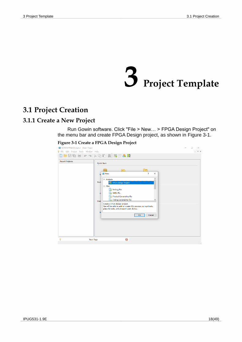
Run Gowin software. Click "File > New… > FPGA Design Project" on the menu bar and create FPGA Design project, as shown in Figure 3-1.
Figure 3-1 Create a FPGA Design Project

3 Project Template 3.1 Project Creation
IPUG531-1.9E 19(49)
3.1.2 Set Project Name and Path
Enter the project name and select the project path, as shown in Figure 3-2.
Figure 3-2 Set Project Name and Path
3.1.3 Select Device
Select Device, Package, Speed, and Part Number, as shown in Figure 3-3.
Take DK-START-GW2A18 V2.0 reference design in SDK for an instance.
Series: GW2A
Device: GW2A-18C
Package: PBGA256
Speed: C8/I7
Part Number: GW2A-LV18PG256C8/I7
Figure 3-3 Select Device

3 Project Template 3.2 Hardware Design
IPUG531-1.9E 20(49)
3.1.4 Project Creation Completed
As shown in Figure 3-4, new project creation is completed.
Figure 3-4 Complete Project Creating
3.2 Hardware Design Use IP Core Generator to generate Gowin_EMPU_M1 hardware
designs.
Select "Tools > IP Core Generator" in the menu bar or " " to open the IP Core Generator.
Select "Soft IP Core > Microprocessor System > Soft-Core-MCU > Gowin_EMPU_M1 1.6" as shown in Figure 3-5.
Figure 3-5 Select Gowin_EMPU_M1

3 Project Template 3.2 Hardware Design
IPUG531-1.9E 21(49)
Open Gowin_EMPU_M1. Gowin_EMPU_M1 system configuration options are as shown in Figure 3-6, including Cortex-M1, APB Bus Peripherals and AHB Bus Peripherals.
Figure 3-6 System Configuration
3.2.1 Cortex-M1 Hardware Design
Cortex-M1 hardware design configuration is as shown in Table 3-1.
Table 3-1 Cortex-M1 Configuration Option
Options Description
Number of interrupts Configure external interrupts number of Cortex-M1, which can be selected as 1, 8, 16, or 32. The default value is 32.
OS Extension Configure Cortex-M1 whether to support operation system. The default is suppot.
Small Multiplier Configure hardware multiplier in Cortex-M1 small mode. The default is normal mode.
Big Endian Configure Cortex-M1 data in big endian format. The default is small endian.
Enable Debug Enable Cortex-M1 Debug. The default is Enable Debug.
Debug Port Select Configure debugger interface, which can be selected as JTAG, Serial Wire, or JTAG and Serial Wire. The default is JTAG and Serial Wire.
Small Debug Configure debugger in Small mode. The default is Full mode.
ITCM Select Select internal instruction memory or external instruction memory. The default is internal instruction memory.
ITCM Size
Configure the Size of internal instruction memory as 1/2/4/8/16/32/64/128/256KB.
For GW1N-9/GW1NR-9/GW1N-9C/GW1NR-9C, the maximum size is 32KB, and the default is 16KB.
For GW2AN-9X/GW2AN-18X, the maximum size is 32KB, and the

3 Project Template 3.2 Hardware Design
IPUG531-1.9E 22(49)
Options Description
default is 16KB.
For GW2A-18/GW2A-18C/GW2AR-18/GW2AR-18C/GW2ANR-18C, the maximum size is 64KB, and the default is 32KB.
For GW2A-55/GW2A-55C/GW2AN-55C, the maximum size is 256KB. And the default is 64KB.
Initialize ITCM Enable ITCM Initialization. The default is disabled.
ITCM Initialization Path ITCM Initial value file path
DTCM Select Select internal data memory or external data memory. The default is internal data memory.
DTCM Size
Configure the Size of internal data memory as 1/2/4/8/16/32/64/128/256KB.
For GW1N-9/GW1NR-9/GW1N-9C/GW1NR-9C, the maximum size is 32KB, and the default is 16KB.
For GW2AN-9X/GW2AN-18X, the maximum size is 32KB, and the default is 16KB.
For GW2A-18/GW2A-18C/GW2AR-18/GW2AR-18C/GW2ANR-18C, the maximum size is 64KB. And the default is 32KB;
For GW2A-55/GW2A-55C/GW2AN-55C, the maximum size is 256KB. And the default is 64KB.
Double click Cortex-M1 to open the Cortex-M1 configuration option including common configuration, debug configuration, and memory configuration, as shown in Figure 3-7.
Figure 3-7 Cortex-M1 Configuration Option
Common
Select "Common", you can configure number of interrupts, OS extension, multiplier mode, and data storage mode, as shown in Figure 3-8.

3 Project Template 3.2 Hardware Design
IPUG531-1.9E 23(49)
Figure 3-8 Cortex-M1 Common Configuration
Number of Interrupts Select 1,8,26 or 32, you can configure 1,8,26 or 32 external interrupts. The default is 32.
OS Extension If OS Extension is selected, Cortex-M1 will support operation system extension. The default is support.
Multiplier Mode If Multiplier Mode is selected, Cortex-M1 supports Small multiplier; if not, it will support Normal multiplier. The default is Normal multiplier.
Data Storage Format If Data Storage Format is selected, Cortex-M1 will support big endian format; if not, it will support small endian format. The default is small endian format.
Debug
Select Debugging Configuration, you can configure enable debugging, debugging interface and debugger, as shown in Figure 3-9.

3 Project Template 3.2 Hardware Design
IPUG531-1.9E 24(49)
Figure 3-9 Cortex-M1 Debugging Configuration
Enable Debug If Enable Debug is selected, Cortex-M1 will support debugging; if not, it will not support debugging. The default is Enable Debug.
Debugging Interface You can select JTAG, Serial Wire, or JTAG and Serial Wire. The default is JTAG and Serial Wire.
Debugger Mode If "Small Debug" is selected, Cortex-M1 will support small mode debugger; if not, it will support Full mode debugger. The default is Full mode debugger.
Memory
Select Memory, you can configure ITCM and DTCM, as shown in Figure 3-10.

3 Project Template 3.2 Hardware Design
IPUG531-1.9E 25(49)
Figure 3-10 Cortex-M1 Memory Configuration
ITCM Select
- You can select Internal Instruction Memory or External Instruction Memory, and the default is Internal Instruction Memory.
- Internal Instruction Memory: On-chip Block RAM hardware storage resource; start address 0x00000000.
- External Instruction Memory: Such as DDR3/Flash; start address 0x00000000.
ITCM Size
- Prerequisite: Internal Instruction Memory has been selected.
- You can select 1KB, 2KB, 4KB, 8KB, 16KB, 32KB, 64KB, 128KB, or 256KB.
- For GW1N-9/GW1NR-9/GW1N-9C/GW1NR-9C, the maximum ITCM Size is 64KB, and the default is 16KB.
- For GW2AN-9X/GW2AN-18X, the maximum ITCM Size is 32KB, and the default is 16KB.
- For GW2A-18/GW2A-18C/GW2AR-18/GW2AR-18C/GW2ANR-18C, the maximum ITCM Size is 64KB, and the default is 32KB.
- For GW2A-55/GW2A-55C/GW2AN-55C, the maximum ITCM Size is 256KB, and the default is 64KB.
ITCM Initialization
- Prerequisite: Internal Instruction Memory has been selected;
- If Initialize ITCM is selected, ITCM initialization is supported. You
3 Project Template 3.2 Hardware Design
IPUG531-1.9E 26(49)
can import ITCM initial value file path.
- If Off-chip SPI-Flash downloading and startup is selected, ITCM initial value imports the different bootload file path according to different ITCM Size.
Note!
The ITCM Initialization Path cannot contain numbers or escape characters such as "\r" and "\n".
DTCM Select
- You can select Internal Data Memory or External Data Memory,
and the default is Internal Data Memory.
- Internal Data Memory: On-chip Block RAM hardware storage resource; start address 0x00000000.
- External Data Memory: such as DDR3; start address 0x00000000.
DTCM Size
- Prerequisite: Internal Data Memory has been selected;
- You can select 1KB, 2KB, 4KB, 8KB, 16KB, 32KB, 64KB, 128KB, or 256KB.
- For GW1N-9/GW1NR-9/GW1N-9C/GW1NR-9C, the maximum DTCM Size is 64KB, and the default is 16KB.
- For GW2AN-9X/GW2AN-18X, the maximum DTCM Size is 32KB, and the default is 16KB.
- For GW2A-18/GW2A-18C/GW2AR-18/GW2AR-18C/GW2ANR-18C, the maximum DTCM Size is 64KB, and the default is 32KB.
- For GW2A-55/GW2A-55C/GW2AN-55C, the maximum DTCM Size is 256KB, and the default is 64KB.
ITCM and DTCM Configuration Limits
- Prerequisite: Internal Instruction Memory and Internal Data Memory has been selected.
- For GW1N-9/GW1NR-9/GW1N-9C/GW1NR-9C, ITCM or DTCM can be configured up to 32KB. If ITCM or DTCM has been configured to 32KB, the other can only be configured up to 16KB.
- For GW2AN-9X/GW2AN-18X, ITCM or DTCM can be configured up to 32KB. If ITCM or DTCM has been configured to 32KB, the other can only be configured up to 16KB.
- For GW2A-18/GW2A-18C/GW2AR-18/GW2AR-18C/GW2ANR-18C, ITCM or DTCM can be configured up to 64KB. If ITCM or DTCM has been configured to 64KB, the other can only be configured up to 16KB.
- For GW2A-55/GW2A-55C/GW2AN-55C, ITCM or DTCM can be configured up to 256KB. If ITCM or DTCM has been configured to

3 Project Template 3.2 Hardware Design
IPUG531-1.9E 27(49)
32KB, the other can only be configured up to 16KB.
Non-BlockRAM ITCM/DTCM Solution
- Use embedded UserFlash as instruction memory. For GW1N-9C/GW1NR-9C, you can choose embedded UserFlash as instruction memory. You can see ...\solution\running_in_userflash\DK_START_GW1N9_V1.1 in the reference design for details; and instruction memory start address is 0x00000000.
- Use off-chip DDR3 as instruction memory and data memory. You can see …\solution\running_in_ddr3\DK_START_GW2A55_V1.3 in the reference design for details; instruction memeory start address is 0x100000, and data memory start address is 0x20100000.
Note!
The software programming BIN file is downloaded to the off-chip SPI-Flash, from which the code is carried to the DDR3 instruction memory address field to start after power-up.
3.2.2 AHB-Lite Extension Hardware Design
AHB-Lite Extension configuration options are described in Table 3-2.
Table 3-2 AHB-Lite Extension Configuration Options
Options Description
Enable GPIO Enable GPIO, disable by default.
Enable GPIO I/O Enable GPIO inout, enable by default.
Enable CAN Enable CAN, disable by default.
Buffer Depth CAN selects Buffer Depth. The default Value is 256.
Enable Ethernet Enable Ethernet, disable by default.
Interface Ethernet selects Interface (RGMII/GMII/MII). The default is RGMII.
RGMII Input Delay RGMII input delay. The default Value is 100.
MIIM Clock Divider MIIM clock divider. The default Value is 20.
Enable DDR3 Enable DDR3 Memory, disable by default.
Enable PSRAM Enable PSRAM, disable by default.
Enable SPI-Flash Enable SPI-Flash functions including download and read, write and erasure of Memory, disable by default.
Enable AHB Master [1] Enable AHB Master[1], disable by default.
Enable AHB Master [2] Enable AHB Master[2], disable by default.
Enable AHB Master [3] Enable AHB Master[3], disable by default.
Enable AHB Master [4] Enable AHB Master[4], disable by default.
Enable AHB Master [5] Enable AHB Master[5], disable by default.
Enable AHB Master [6] Enable AHB Master[6], disable by default.
Enable UART0 Enable Serial Port0, disable by default.
Enable UART1 Enable Serial Port1, disable by default.
Enable Timer0 Enable Timer0, disable by default.

3 Project Template 3.2 Hardware Design
IPUG531-1.9E 28(49)
Options Description
Enable Timer1 Enable Timer1, disable by default.
Enable WatchDog Enable Watchdog, disable by default.
Enable RTC Enable RTC, disable by default.
Enable TRNG Enable TRNG, disable by default.
Enable DualTimer Enable DualTimer, disable by default.
Enable I2C Enable I
2C, disable by default.
Enable I2C I/O Enable I
2C inout, enable by default.
Enable SPI Enable SPI, disable by default.
Enable SD-Card Enable SPI-Card, disable by default
Enable APB Master [1] Enable APB Master[1], disable by default.
Enable APB Master [2] Enable APB Master[2], disable by default.
Enable APB Master [3] Enable APB Master[3], disable by default.
Enable APB Master [4] Enable APB Master[4], disable by default.
Enable APB Master [5] Enable APB Master[5], disable by default.
Enable APB Master [6] Enable APB Master[6], disable by default.
Enable APB Master [7] Enable APB Master[7], disable by default.
Enable APB Master [8] Enable APB Master[8], disable by default.
Enable APB Master [9] Enable APB Master[9], disable by default.
Enable APB Master [10] Enable APB Master[10], disable by default.
Enable APB Master [11] Enable APB Master[11], disable by default.
Enable APB Master [12] Enable APB Master[12], disable by default.
Enable APB Master [13] Enable APB Master[13], disable by default.
Enable APB Master [14] Enable APB Master[14], disable by default.
Enable APB Master [15] Enable APB Master[15], disable by default.
Enable APB Master [16] Enable APB Master[16], disable by default.
GPIO
Double click to configure GPIO, as shown in Figure 3-11.
If Enable GPIO is selected, Gowin_EMPU_M1 supports GPIO, disable by default;
If Enable GPIO has been selected, GPIO port type can be configured.
If Enable GPIO I/O is selected, GPIO supports inout port type. The default is support.

3 Project Template 3.2 Hardware Design
IPUG531-1.9E 29(49)
Figure 3-11 GPIO Configuration
CAN
Double click to open CAN, as shown in Figure 3-12.
If Enable CAN is selected, Gowin_EMPU_M1 supports CAN, disable by default;
If Enable CAN has been selected, Buffer Depth can be configured;
Select and configure Buffer Depth. The default value is 256.
Figure 3-12 CAN Configuration

3 Project Template 3.2 Hardware Design
IPUG531-1.9E 30(49)
Ethernet
Double click to open Ethernet, as shown in Figure 3-13.
If Enable Ethernet is selected, Gowin_EMPU_M1 will support Ethernet,disable by default.
If Enable Ethernet has been selected, you can configure Interface,RGMII Input Delay, and MIIM Clock Divider.
- Select Interface. You can configure RGMII, GMII, MII, or GMII/MII.The default is RGMII;
- If RGMII is selected, you can configure RGMII Input Delay. Thedefault value is 100;
- If MIIM Clock Divider is selected, you can configure MIIM ClockDivider. The default value is 20.
If RGMII or GMII is selected, 125MHz clock input must be provided toGTX_CLK.
Figure 3-13 Ethernet Configuration
DDR3
Double click to configure DDR3, as shown in Figure 3-14.
If Enable DDR3 is selected, Gowin_EMPU_M1 will support DDR3 Memory, disable by default.
The internal clock frequency of DDR3 is 150MHz.
50MHz clock input must be provided to the DDR3 port DDR_CLK_I.
GW2AN-9X/GW2AN-18X does not support DDR3.
GW1N-9/GW1N-9C/GW1NR-9/GW1NR-9C does not support DDR3.

3 Project Template 3.2 Hardware Design
IPUG531-1.9E 31(49)
Figure 3-14 DDR3 Configuration
SPI-Flash
SPI-Flash supports the functions including download, and the read, write and erasure of Memory.
Double click to configure SPI-Flash, as shown in Figure 3-15.
If Enable SPI-Flash is selected, Gowin_EMPU_M1 supports SPI-Flash,disable by default.
If Gowin_EMPU_M1 uses off-chip SPI-Flash downloading and startup,Enable SPI-Flash must be selected.

3 Project Template 3.2 Hardware Design
IPUG531-1.9E 32(49)
Figure 3-15 SPI-Flash Configuration
AHB Master [1-6]
Double click to open AHB Master[1-6], you can configure AHB Master [1-6] user AHB bus extension interface, as shown in Figure 3-16 ;
If Enable AHB Master [1] is selected, Gowin_EMPU_M1 will supportAHB Master [1] user AHB bus extension interface. You can extend AHBperipherals, disable by default.
If Enable AHB Master [2] is selected, Gowin_EMPU_M1 will supportAHB Master [2] user AHB bus extension interface. You can extend AHBperipherals, disable by default.
If Enable AHB Master [3] is selected, Gowin_EMPU_M1 will supportAHB Master [3] user AHB bus extension interface. You can extendeAHB peripherals, disable by default.
If Enable AHB Master [4] is selected, Gowin_EMPU_M1 will supportAHB Master [4] user AHB bus extension interface. You can extend AHBperipherals, disable by default.
If Enable AHB Master [5] is selected, Gowin_EMPU_M1 will supportAHB Master [5] user AHB bus extension interface. You can extend AHBperipherals, disable by default.
If Enable AHB Master [6] is selected, Gowin_EMPU_M1 will supportAHB Master [6] user AHB bus extension interface. You can extend AHBperipherals, disable by default.

3 Project Template 3.2 Hardware Design
IPUG531-1.9E 33(49)
Figure 3-16 AHB Master [1-6]
The start address and the address space definition of AHB Master [1-6] user AHB bus extension interface are shown in Table 3-3.
Table 3-3 AHB Master [1-6] Address Definition
AHB interface Start Address Size (MB)
AHB Master [1] 0x80000000 16
AHB Master [2] 0x81000000 16
AHB Master [3] 0x86000000 16
AHB Master [4] 0x89000000 16
AHB Master [5] 0x8A000000 16
AHB Master [6] 0x8B000000 16
If you need to support external interrupt signal for the AHB external device extended on this AHB extension interface, please refer to the following two ways:
Use GPIO [15:0] to analog external interrupt signal.
Or contact Gowin sales or FAE for customization.
UART
Double click UART0 or UART1, as shown in Figure 3-17.
If Enable UART0 is selected, Gowin_EMPU_M1 supports UART0,disable by default;
If Enable UART1 is selected, Gowin_EMPU_M1 supports UART1,disable by default.

3 Project Template 3.2 Hardware Design
IPUG531-1.9E 34(49)
Figure 3-17 UART Configuration
Timer
Double click to configure Timer0 or Timer1, as shown in Figure 3-18.
If Enable Timer0 is selected, Gowin_EMPU_M1 supports UART0,disable by default.
If Enable Timer1 is selected, Gowin_EMPU_M1 supports Timer1,disable by default.
Figure 3-18 Timer Configuration

3 Project Template 3.2 Hardware Design
IPUG531-1.9E 35(49)
WatchDog
Double click to configure WatchDog, as shown in Figure 3-19.
If Enable WatchDog is selected, Gowin_EMPU_M1 supports WatchDog, disable by default.
Figure 3-19 WatchDog Configuration
RTC
Double click to configure RTC, as shown in Figure 3-20.
If Enable RTC is selected, Gowin_EMPU_M1 supports RTC, disable by default;
3.072MHz clock input must be provided to RTCSRCCL. The division in RTC is 1Hz.

3 Project Template 3.2 Hardware Design
IPUG531-1.9E 36(49)
Figure 3-20 RTC Configuration
DualTimer
Double click to open DualTimer, as shown in Figure 3-21.
If Enable DualTimer is selected, Gowin_EMPU_M1 supports DualTimer, disable by default.
Figure 3-21 DualTimer Configuration
TRNG
Double click to open TRNG, as shown in Figure 3-22.
If Enable TRNG is selected, Gowin_EMPU_M1 supports TRNG,

3 Project Template 3.2 Hardware Design
IPUG531-1.9E 37(49)
disable by default.
Figure 3-22 TRNG Configuration
I2C
Double click to open I2C, and configure I2C Master, as shown in Figure 3-23.
If Enable I2C is selected, Gowin_EMPU_M1 supports I2C Master, disable by default.
If Enable I2C has been selected, I2C Master port type can be configured.
If Enable I2C I/O is selected, I2C Master supports inout port type. The default is support.

3 Project Template 3.2 Hardware Design
IPUG531-1.9E 38(49)
Figure 3-23 I2C Configuration
SPI
Double click to configure SPI Master, as shown in Figure 3-24.
If Enable SPI is selected, Gowin_EMPU_M1 supports SPI Master, disable by default.
Figure 3-24 SPI Configuration
SD-Card Configuration
Double click to configure SD-Card, as shown in Figure 3-25.

3 Project Template 3.2 Hardware Design
IPUG531-1.9E 39(49)
If Enable SD-Card is selected, Gowin_EMPU_M1 supports SD-Card, disable by default;
30MHz clock input must be provided to SD_SPICLK.
Figure 3-25 SD-Card Configuration
APB Master [1-16]
Double click to open APB Master [1-16], and configure APB Master [1-16], as shown in Figure 3-26.
If Enable APB Master [1] is selected, Gowin_EMPU_M1 will support APB Master [1] user APB bus extension interface. You can extend APB peripherals, disable by default.
If Enable APB Master [2] is selected, Gowin_EMPU_M1 will support APB Master [2] user APB bus extension interface. You can extend APB peripherals, disable by default.
If Enable APB Master [3] is selected, Gowin_EMPU_M1 will support APB Master [3] user APB bus extension interface. You can extend APB peripherals, disable by default.
If Enable APB Master [4] is selected, Gowin_EMPU_M1 will support APB Master [4] user APB bus extension interface. You can extend APB peripherals, disable by default.
If Enable APB Master [5] is selected, Gowin_EMPU_M1 will support APB Master [5] user APB bus extension interface. You can extend APB peripherals, disable by default.
If Enable APB Master [6] is selected, Gowin_EMPU_M1 will support APB Master [6] user APB bus extension interface. You can extend APB peripherals, disable by default.

3 Project Template 3.2 Hardware Design
IPUG531-1.9E 40(49)
If Enable APB Master [7] is selected, Gowin_EMPU_M1 will support APB Master [7] user APB bus extension interface. You can extend APB peripherals, disable by default.
If Enable APB Master [8] is selected, Gowin_EMPU_M1 will support APB Master [8] user APB bus extension interface. You can extend APB peripherals, disable by default.
If Enable APB Master [9] is selected, Gowin_EMPU_M1 will support APB Master [9] user APB bus extension interface. You can extend APB peripherals, disable by default.
If Enable APB Master [10] is selected, Gowin_EMPU_M1 will support APB Master [10] user APB bus extension interface. You can extend APB peripherals, disable by default.
If Enable APB Master [11] is selected, Gowin_EMPU_M1 will support APB Master [11] user APB bus extension interface. You can extend APB peripherals, disable by default.
If Enable APB Master [12] is selected, Gowin_EMPU_M1 will support APB Master [12] user APB bus extension interface. You can extend APB peripherals, disable by default.
If Enable APB Master [13] is selected, Gowin_EMPU_M1 will support APB Master [13] user APB bus extension interface. You can extend APB peripherals, disable by default.
If Enable APB Master [14] is selected, Gowin_EMPU_M1 will support APB Master [14] user APB bus extension interface. You can extend APB peripherals, disable by default.
If Enable APB Master [15] is selected, Gowin_EMPU_M1 will support APB Master [15] user APB bus extension interface. You can extend APB peripherals, disable by default.
If Enable APB Master [16] is selected, Gowin_EMPU_M1 will support APB Master [16] user APB bus extension interface. You can extend APB peripherals, disable by default.

3 Project Template 3.2 Hardware Design
IPUG531-1.9E 41(49)
Figure 3-26 APB Master [1-16] Configuration
The start address and the address space definition of APB Master [1-16] user APB bus extension interface are shown in Table 3-4.
Table 3-4 APB Master [1-16] Address Definition
APB bus interface Start Address Size (MB)
APB Master [1] 0x60000000 1
APB Master [2] 0x60100000 1
APB Master [3] 0x60200000 1
APB Master [4] 0x60300000 1
APB Master [5] 0x60400000 1
APB Master [6] 0x60500000 1
APB Master [7] 0x60600000 1
APB Master [8] 0x60700000 1
APB Master [9] 0x60800000 1
APB Master [10] 0x60900000 1
APB Master [11] 0x60A00000 1
APB Master [12] 0x60B00000 1
APB Master [13] 0x60C00000 1
APB Master [14] 0x60D00000 1
APB Master [15] 0x60E00000 1
APB Master [16] 0x60F00000 1
If you need to support external interrupt signal for the APB external device extended on this APB extension interface, please refer to the

3 Project Template 3.3 User Design
IPUG531-1.9E 42(49)
following two ways:
Use GPIO [15:0] to analog external interrupt signal;
Please contact Gowin sales staff or FAE for customization.
PSRAM Configuration
Double click to open PSRAM, and configure PSRAM, as shown in Figure 3-27;
If Enable PSRAM is selected, Gowin_EMPU_M1 supports PSRAM, disable by default;
GW2AR-18/GW2AR-18C supports Gowin_EMPU_M1 PSRAM:
- GW2AR-LV18QN88PC8/I7
- GW2AR-LV18QN88PC7/I6
- GW2AR-LV18EQ144PC8/I7
- GW2AR-LV18EQ144PC7/I6
- GW2AR-LV18EQ144PC9/I8
Figure 3-27 PSRAM Configuration
3.3 User Design After the configuration of Gowin_EMPU_M1, you can generate
Gowin_EMPU_M1 hardware design;
Instantiate Gowin_EMPU_M1 Top Module;
Import user designs and connect it with Gowin_EMPU_M1 to form a complete RTL design.

3 Project Template 3.4 Constraint
IPUG531-1.9E 43(49)
3.4 Constraint After the user RTL design is completed, physical constraints can be
generated according to the used development board and the IO.
Timing constraints file can be generated according to timing requirements.
How to generate physical constraints, please refer to SUG101, Gowin Design Constraints Guide.
3.5 Configuration
3.5.1 Synthesis Configuration
The configuration is as shown in Figure 3-28.
Configure "Top Module/Entity" according to the top module name in the design.
Configure "Include Path according to the actual file path in the design.
Configure "Verilog Language" according to System Verilog 2017.
Figure 3-28 Synthesis Option Configuration

3 Project Template 3.5 Configuration
IPUG531-1.9E 44(49)
3.5.2 Post-Place File Configuration
If using download of software programming and hardware automatically merged, you can configure "Place & Route > General > Generate Post-Place File" to generate Post-Place File, as shown in Figure 3-29.
Figure 3-29 Post-Place File Configuration
3.5.3 Dual-Purpose Pin Configuration
If Gowin_EMPU_M1 uses off-chip SPI-Flash downloading and startup, use MSPI as regular IO, as shown in Figure 3-30, or pin reuse is not required.
Figure 3-30 Dual-Purpose Pin Configuration

3 Project Template 3.6 Synthesize
IPUG531-1.9E 45(49)
3.6 Synthesize Run GowinSynthesis®, the synthesis tool for Gowin Software, to
complete the synthesis of RTL design, as shown in Figure 3-31.
Figure 3-31 Synthesis
For the synthesis tool usage, please refer to SUG100, Gowin Software User Guide.
3.7 Place & Route Run "Place & Route", the Place & Route tool of Gowin Software, to
generate the bitstream files, as shown in Figure 3-32.
Figure 3-32 Place & Route

3 Project Template 3.8 Download
IPUG531-1.9E 46(49)
For the Place & Route tool usage, please refer to SUG100, Gowin Software User Guide.
3.8 Download Run the "Programmer", the download tool of Gowin Software, to
download Hardware Design the bitstream file.
Run Programmer in Gowin Software or software installation path, click
"Edit/Configure Device" or Configure Device " " in the tool bar to open the "Device configuration" .
If "ITCM Select" is configured as "Internal Instruction Memory", then configuration options for GW1N-9/GW1NR-9/GW1N-9C/GW1NR-9C are as shown in Figure 3-33.
Select "Embedded Flash Mode" in "Access Mode" drop-down list.
Select "embFlash Erase, Program" or "embFlash Erase, Program, Verify" in "Operation" drop-down list.
Import the hardware design bitstream file required to download in "Programming Options > File name" option.
Click "Save" to complete the configuration of the hardware design bitstream file required to download.
Figure 3-33 GW1N Series of Device Configuration
If ITCM Select is configured as External Instruction Memory, and select embedded UserFlash as instruction memeory, then configuration options for GW1N-9C/GW1NR-9C are as shown in Figure 3-34.
Select "MCU Model L" in "Access Mode" drop-down list.
Select "Firmware Erase, Program" or "Firmware Erase, Program, Verify" in "Operation" drop-down list.
Import the hardware design bitstream files required to download in

3 Project Template 3.8 Download
IPUG531-1.9E 47(49)
"Programming Options > File name" option.
Import the software programming design BIN files in a binary format required to download in "FW/MCU/Binary Input Options > Firmware/Binary File" option.
Click "Save" to complete the configuration of the hardware design bitstream files and software programming design BIN files in a binary format required to download.
Figure 3-34 GW1N(R)-9C Device Configuration
Configuration options for GW2AN-9X/GW2A-18/GW2A-18C/GW2AR-18/GW2AR-18C/GW2ANR-18C/GW2AN-18X/GW2A-55/GW2A-55C/GW2AN-55C are as shown in Figure 3-35.
Select "External Flash Mode" in "Access Mode" drop-down list.
Select "exFlash Erase, Program thru GAO-Bridge" or "exFlash Erase, Program, Verify thru GAO-Bridge" in "Operation" drop-down list.
Import the hardware design bitstream file required to download in "Programming Options > File name" option.
Select based on the on-board Flash in "External Flash Options > Device" (such as Winbond W25Q64BV).
Configure the start address as "0x000000" in "External Flash Options > Start Address" option.
Click "Save" to complete the configuration of the hardware design bitstream file required to download.

3 Project Template 3.8 Download
IPUG531-1.9E 48(49)
Figure 3-35 GW2A Series of Device Configuration
After device configuration, click Program/Configure " " in the Programmer toolbar to complete the download of bitstream files in hardaware design (If GW1N-9C/GW1NR-9C uses UserFlash as instruction memory, then download software programming BIN files in a binary format at the same time).
For the usage of Programmer, please see SUG502, Gowin Programmer User Guide.

4 Reference Design
IPUG531-1.9E 49((49)
4 Reference Design
Gowin_EMPU_M1 provides reference design with Debug and No Debug versions:
Gowin_EMPU_M1\ref_design\FPGA_RefDesign\Debug_RefDesign
Gowin_EMPU_M1\ref_design\FPGA_RefDesign\NoDebug_RefDesign
Gowin_EMPU_M1provides solution reference design:
Gowin_EMPU_M1\solution\rtos
Gowin_EMPU_M1\solution\running_in_ddr3
Gowin_EMPU_M1\solution\running_in_userflash