
HARDWARE DESIGN FOR THE JOT M10 TEST BOX ...
36
Jesse Järvinen HARDWARE DESIGN FOR THE JOT M10 TEST BOX CONTROLLER
-
Upload
khangminh22 -
Category
Documents
-
view
3 -
download
0
Transcript of HARDWARE DESIGN FOR THE JOT M10 TEST BOX ...

Jesse Järvinen
HARDWARE DESIGN FOR THE JOT M10 TEST BOX
CONTROLLER

HARDWARE DESIGN FOR THE JOT M10 TEST BOX CONTROLLER
Jesse Järvinen Bachelor’s Thesis Autumn 2020 Information technology Oulu University of Applied Sciences

3
ABSTRACT
Oulu University of Applied Sciences Information technology, Option of Device and Product Design Author: Jesse Järvinen Title of the bachelor’s thesis: Hardware Design for the JOT M10 Test Box Controller Supervisor: Timo Vainio Term and year of completion: Autumn 2020 Number of pages: 36 The objective of this thesis was to design and test a controller that could be used for controlling JOT M10 Test Boxes. The thesis was commissioned by JOT Automation Oy. The design aimed to replace the currently used controller setup consisting of multiple PCBs. New features and improvements were added in addition to the features in the currently used setup. One of the main requirements for the new design was to support the Linux operating system.
The design uses a Computer on Module manufactured by Toradex to provide the processing capabilities to run the Linux operating system. The hardware design process consisted of creating schematics and a layout for a carrier board PCB, onto which the selected Computer on Module was mounted. The hardware design aimed to take software development concerns into account when selecting components. The implementation of the design was accomplished using PADS, provided by Mentor Graphics. The manufactured PCB was thoroughly tested to ensure that all the features were functional within the specified operating conditions. Overall, the design was successful as all the main features were fully functional for further software development and prototyping.
Keywords: PCB design, printed circuit board, Computer on Module, Mentor PADS

4
CONTENTS
ABSTRACT 3
CONTENTS 4
ABBREVIATIONS 5
1 INTRODUCTION 6
2 COMPUTER ON MODULE OPERATION THEORY 9
2.1 Computer on Module 9
2.2 Toradex Computer on Module Selection 11
2.3 Operating System 12
3 SCHEMATICS DESIGN 13
3.1 Overview 13
3.2 Used Software 14
3.3 Power Supply 15
3.4 Peripheral Interfaces 17
3.5 Input and Output Lines 18
3.6 Input Line 19
3.7 Output Line 21
4 LAYOUT DESIGN 23
4.1 Overview 23
4.2 PCB Build-up 23
4.3 EMI Radiation 25
5 RESULTS 28
5.1 Testing Phase 28
5.2 Future Improvements 29
6 CONCLUSION 33
REFERENCES 34

5
ABBREVIATIONS
ADC Analog-to-Digital Converter
CAN Controller Area Network
COM Computer-on-Module
CPU Central Processing Unit
EMI Electromagnetic Interference
ESD Electrostatic Discharge
FET Field Effect Transistor
GPIO General Purpose Input/Output
I2C Inter-integrated Circuit
ICT In Circuit Test
IO Input/Output
LED Light Emitting Diode
OS Operating System
OTA Over-the-Air
PCB Printed Circuit Board
PMIC Power Management Integrated Circuit
RAM Random-access Memory
RF Radio Frequency
SO-DIMM Small Outline Dual In-line Memory Module
USB Universal Serial Bus

6
1 INTRODUCTION
JOT Automation provides solutions for automated testing and production in the
electronics industry. The JOT M10 Test Concept is a test solution that JOT
Automation offers. It is used for testing a wide range of applications, such as
PCB-level functional, ICT and RF testing. It can also be used for flashing
microchips with software. All the testing and flashing is performed inside JOT
M10 Test Boxes. The M10 Test Box can be used either as a stand-alone test
unit or as a part of the M10 Test Concept [1]. A JOT M10 Test Box is shown in
FIGURE 1.
FIGURE 1. JOT M10 Test Box [1].
The system can be automated by mounting multiple M10 Test Boxes inside a
JOT M10 Test Rack which is then controlled by JOT M10 Test Handler. The
M10 Handler can then load and unload the M10 Test Boxes with target PCBs.
The complete system with the M10 Handler and Rack behind the handler can
be seen in FIGURE 2.

7
FIGURE 2. JOT M10 Handler and Rack [1].
The electronics inside the JOT M10 Test Box is controlled by a setup,
consisting of a control card and two IO boards. The aim of this thesis was to
design and test a PCB, used for controlling JOT M10 Test Boxes. The reason
for designing a new controller is that the currently used setup is based on PIC
microcontrollers with some limitations and usually requires external IO boards
for operation. Adding new features to the software used in the current setup is
very time consuming. JOT Automation already has a controller, used for other
purposes, which runs a Linux operating system. Having only one software
family instead of multiple software families would simplify the software
development.
The design would replace the currently used controller setup and add more
features. The main requirements for the new design were to offer at least all the
same features as the currently used setup includes. The new design should not
cost more than the old setup does and all the used components should have a
long-term and reliable availability. Required key features are as following:
• Support Linux operating system.
• I2C interface which is suitable for use over long cable lengths.

8
• CAN bus.
• 2 Ethernet interfaces.
• 16 well protected input lines.
• 16 output lines.

9
2 COMPUTER ON MODULE OPERATION THEORY
2.1 Computer on Module
Computer on Module (COM) is a term used for a computer that is integrated
into a single module. A microprocessor is the main component of the COM and
all the other components are there to support the microprocessor. The main
parts required for the processor to work are as following:
• RAM (random-access memory) is a fast speed memory that is used for
data transmissions that need to be quickly accessed by the processor.
RAM is a volatile memory, meaning that any data in RAM will be lost
when RAM is unpowered [2].
• Flash memory is needed for saving the operating system and other data
that should retain when powered off. A flash memory is much slower
than RAM and therefore it should only be used as a data storage.
• Microprocessors usually require a variety of different supply voltages to
operate. Power management is usually implemented using a PMIC which
offers multi-channel power management in the same IC.
The COM is mounted onto a separate circuit board that is called a carrier board.
As the COMs are designed with strict size constricts and focus on offering a
high customizability for the carrier board, they do not house connectors for
peripheral interfaces. Instead the carrier board must include connectors and
other components needed by the interfaces. The carrier board must also
provide the required power management for the COM. FIGURE 3 represents a
Toradex Colibri iMX6 DualLite 512MB IT COM [3].

10
FIGURE 3. Toradex Colibri iMX6 DualLite 512MB IT COM [3].
The COMs are housed with microprocessor units that come with high pin count
BGA packages. For instance, the MCIMX6U7CVM08AC microprocessor, used
in Toradex Colibri iMX 6 DualLite 512MB IT boards, is packed into a 624-pin
MAPBGA package. MAPBGA is a type of a high-pitch-ball-grid-array package.
For a high-pin count and a small-pitch microprocessor, signal routing on the
PCB is particularly important. For example, signals connecting the CPU to a
memory interface must be impedance controlled and length matched. For this
reason, the PCBs with microprocessors usually contain at least 6 or 8 copper
layers. For the carrier board the layout can be less than 6 layers, since the most
crucial PCB traces have been made on the COM.
Upsides of using a COM is that the design has already been tested by the
manufacturer's customers in several applications and proven to be reliable. In
low volumes it is cheaper and less risky to use an already confirmed design
than developing complex PCBs that require expensive manufacturing methods.
When the carrier board is used in large setups where there are multiple external
devices connected, the chance of damaging the carrier board increases. Even if
the carrier board connections are ESD protected, the damage could still occur
by misconnections or if the external device gets damaged. In a case where

11
either the module or the carrier board gets severely damaged, the whole setup
does not need to be replaced but instead only the broken partition.
Designs that are planned for mass production with tens of thousands of built
PCB units do not benefit from using a COM, as the manufacturing and
component ordering costs decrease on high volume production. In that case it
should be cost wise more sensible to create a design for the microprocessor
unit.
2.2 Toradex Computer on Module selection
JOT Automation has already experience in using Toradex Apalis COMs. To
keep software implementation as compatible as possible with the other design
that is using a Toradex Apalis COM, the design for this thesis should also use a
module manufactured by Toradex. The module should preferably be based on a
microprocessor unit from the same microprocessor family.
Toradex offers 3 families of COMs, each focusing on different use cases. COMs
within the same family are pin-compatible with other modules in the same
family. All the modules are based on processors developed by NXP. The
Toradex COM families and their main features are as following:
• The Apalis Arm family offers the widest range of peripherals and the
highest processing speeds amongst the Toradex COM families. The
Apalis Arm family is heavily oriented in offering high-end graphics
processing and supporting advanced multimedia. The module format is
physically larger and is priced higher than the other two families.
• The Colibri Arm family is a cheaper and physically smaller alternative to
the Apalis Arm family, with less pins and a substantially smaller number
of features.
• The Verdin Arm family is a compromise between Apalis and Colibri
families as it offers more pins than the Colibri family with slightly larger
dimensions. The Verdin Arm family offers the best price to the
performance ratio of COM families.

12
2.3 Operating System
Toradex modules support a variety of operating systems, such as Windows 10
IoT Core, Android, FreeRTOS and multiple distributions of Linux. Many of the
readily accessible Linux images are optimized for a specific purpose, such as
software solutions made by a third-party company.
For the thesis it was desired that the design would support Toradex Embedded
Linux reference images and preferably also TorizonCore Embedded Linux
images. Both operating systems are open source which allows for total system
customization according to any requirements.
A Toradex Embedded Linux reference image is based on the Linux Yocto
project with a basic software setup to support using the features of Toradex
modules. Toradex provides and regularly updates Board Support Packages
(BSP) of the embedded Linux for each of their COMs. The embedded Linux
BSPs are specifically made for optimizing the usage of Toradex COMs [4].
Torizon is built upon a Toradex Embedded Linux BSP image. Torizon’s main
advantage is that it allows scalable software and simplified system
configuration. Torizon includes a Docker Container Runtime which provides the
usage of containers. A container is an application that is isolated from the
system but includes all the necessary files for running processes [5].
By using containers, it is possible to pack each possible use case into a
separate container. Depending on the use case, only the appropriate container
would then be run.
Torizon also offers Over-the-Air (OTA) updates, granting the containers easy
updateability without affecting the rest of the system. Instead of recompiling the
whole Linux image it is possible to update only the container or other specific
software layer. Toradex Embedded Linux is a more lightweight solution whereas
Torizon requires slightly more resources.

13
3 SCHEMATICS DESIGN
3.1 Overview
The main aim of the thesis was to design a carrier board for mounting a COM.
This chapter describes the architecture of the hardware partition of the designed
carrier board.
The Toradex Colibri Arm COM family was selected for the design due to the
Verdin family still being in development and due to the Apalis Arm family
offering an unnecessarily high number of features. Colibri family offers fewer
features, but more than enough for the design needs. Using Apalis Arm family
COMs would also increase the size of the carrier board. On the other hand,
using the Apalis Arm family would support using same software solutions as are
used with the other Apalis Arm family COM which has already been used in
JOT Automation.
COMs for each family are pin-compatible with other COMs within the same
family. Due to pin-compatibility, the used module can be easily changed to a
less or more powerful one. Although some features do not either share the
same pins within the COM family or simply are not supported at all.
The negative side of the Colibri family is that the modules come with only one
Ethernet interface and two USB interfaces. As one of the requirements for the
design was to include two Ethernet interfaces, the second Ethernet interface
would need to be implemented by adding an external SPI or USB based
Ethernet bridge device.
The modules from Colibri family uses a 200-pin SO-DIMM format for interfacing
with a carrier board. The SO-DIMM connector format is commonly used by
specific RAM modules, therefore the availability of suitable, sturdy connectors
should be guaranteed for a long time.
The key factors when selecting an appropriate COM from the Colibri Arm family
were supported operating systems, needed peripherals and cost. Toradex

14
Colibri iMX6 Solo 256MB was chosen due to its relatively cheap price compared
to the more versatile modules. The selected COM is also the cheapest COM
that supports the Torizon operating system, but it should still be able to perform
well on any common case tasks without stuttering. A summary of the main
features of the selected COM can be seen in TABLE 1.
TABLE 1. Colibri iMX6 Solo 256MB feature summary [3].
Type Computer on Module
Operating System Embedded Linux / Torizon
CPU Name NXP® i.MX 6Solo
CPU Clock 1.0 GHz
RAM 256MB DDR3 (32 Bit)
Flash 4GB Flash
USB 2.0 1x Host / 1x OTH
Ethernet 10/100 Mbit with IEEE 1588
I2C 3x
CAN 2x
GPIO Up to 154
3.2 Used software
Schematics design for the carrier board was made using PADS Logic, provided
by Mentor Graphics. Schematics design included creating schematic symbols
for components not found in the symbol library used in JOT Automation.
LTspice software was used for simulating a few small partitions of the design.
The modules from the Colibri COM family are limited to 200 pins. As the
selected Colibri iMX6 offers up to 154 GPIOs and a wide range of peripheral
interfaces, it is clear that not all of them can be used simultaneously. Instead,
the processor supports a feature called pin muxing, where most of the module
pins can be configured with a single function from a set of multiple different
functions.
Toradex Pinout Designer is a tool by Toradex that helps selecting an
appropriate pin configuration for the design [6]. The view from Pinout Designer
can be seen in FIGURE 4. The tool is also used for determining pinout
differences between other modules within the same COM family.

15
FIGURE 4. View of the pin muxing configuration in Toradex Pinout Designer.
The design is made so that the used Colibri COM can be interchanged either to
a more powerful or to a less powerful COM, depending on the need. There are
some pins that do not share same functions within the Colibri Arm family. For
instance, when comparing Colibri iMX6 and Colibri iMX7 modules, the pins for
the I2C-1 bus are located in different pins.
The PCB design contains jumpers for connecting lines which are not located in
the same module pins, to route the signals to correct pins. Therefore, with small
modifications to the PCB, the COM is made interchangeable with other modules
from the same COM family.
3.3 Power supply
The carrier board supports an input voltage range, either +5VDC or from
+6.2VDC to +32VDC. The wide input voltage is achieved by using a buck
converter to convert voltage to +5VDC. The buck converter is enabled when the
input voltage is higher than +6.2VDC. Buck converters, unlike linear regulators,

16
can be very efficient on regulating source voltages which can be multiple times
higher than the output voltage. The reason being that a linear regulator
dissipates the difference between output and input voltages, while a buck
converter effectively converts the voltage down to a lower voltage.
In a case where the input voltage is +32VDC, a +5VDC linear regulator would
have the efficiency rating of less than 16%. The efficiency of a linear regulator is
estimated by:
𝑒𝑓𝑓 =Vout
Vin∗ 100 EQUATION 1
eff = Efficiency of the regulator
Vout = Output voltage
Vin = Input voltage
The buck converter LMR33640 by Texas Instruments that was selected for the
design has the efficiency of around 91% according to the datasheet [7]. The
efficiency of a buck converter greatly depends on the PCB layout and the
selected components.
To make it possible to power up the carrier board from a +5VDC power source,
the input voltage range is selected by placing a jumper in an appropriate
position. When powered from the +5VDC source, the +5VDC buck regulator is
bypassed, as for an ordinary buck converter the output voltage must be lower
than the input voltage. By using a buck-boost converter, which allows the output
voltage to be either less or greater than the input voltage, the same regulator
could be used for the whole +5VDC to +32VDC range. A buck-boost converter
was not chosen for the design as it adds complexity to the design and is a
multiple times more expensive solution than a buck converter.
The largest power consumer on the carrier board is the Toradex COM with the
maximum power consumption of around 800mA at +3.3VDC. Compared to the
COM, the peripheral interfaces are minor power consumers.

17
3.4 Peripheral interfaces
I2C is typically used for short distance connections where all the devices are
preferably on the same circuit board. The I2C specification defines a maximum
capacitance of 400 pF in the I2C bus. Each connected device adds capacitance
to the bus, where the amount of capacitance depends on the connected device.
A cable adds approximately capacitance of 40 pF to the bus per each meter. In
a long cable, EMI from an inductive source could induce a large enough voltage
spike to the cable, which could cause the I2C receiver to believe it has received
a high signal. FIGURE 5 demonstrates such a case where the EMI disturbance
causes unexpecting results on the receiver side [8].
FIGURE 5. EMI causing disturbance during nondifferential transmission [8].
The preferred option for long range I2C bus connections is to use differential
I2C, which converts I2C’s SDA and SCL signals into a total of four signals. Both
the SDA and SCL are converted into a plus and minus signals. The plus and
minus signals contain the same data with the minus signal being inverted. The
receiver side contains a subtractor that will convert the voltage difference
between the differential signals to a nondifferential signal. The advantage of
using differential signalling is that any received EMI will be mitigated when the
differential I2C is converted back to nondifferential I2C, as can be seen in
FIGURE 6.
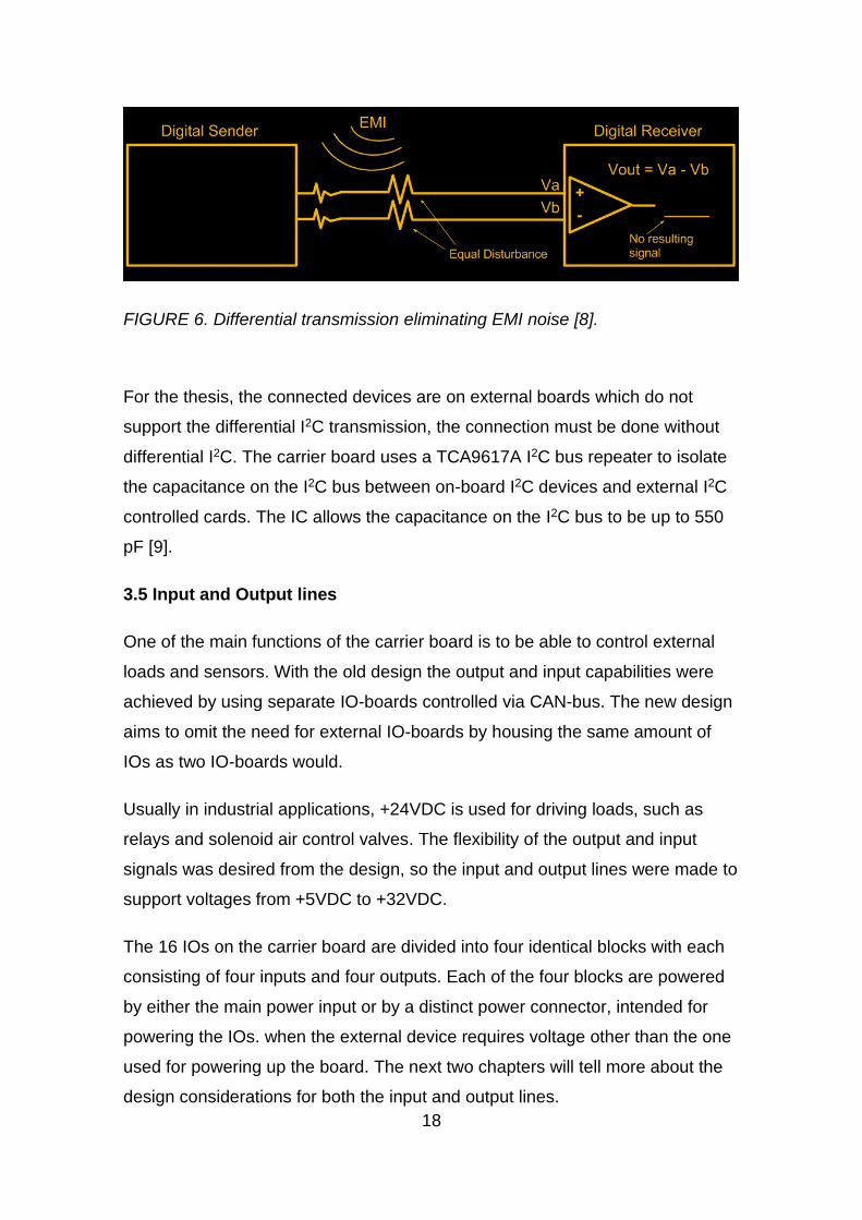
18
FIGURE 6. Differential transmission eliminating EMI noise [8].
For the thesis, the connected devices are on external boards which do not
support the differential I2C transmission, the connection must be done without
differential I2C. The carrier board uses a TCA9617A I2C bus repeater to isolate
the capacitance on the I2C bus between on-board I2C devices and external I2C
controlled cards. The IC allows the capacitance on the I2C bus to be up to 550
pF [9].
3.5 Input and Output lines
One of the main functions of the carrier board is to be able to control external
loads and sensors. With the old design the output and input capabilities were
achieved by using separate IO-boards controlled via CAN-bus. The new design
aims to omit the need for external IO-boards by housing the same amount of
IOs as two IO-boards would.
Usually in industrial applications, +24VDC is used for driving loads, such as
relays and solenoid air control valves. The flexibility of the output and input
signals was desired from the design, so the input and output lines were made to
support voltages from +5VDC to +32VDC.
The 16 IOs on the carrier board are divided into four identical blocks with each
consisting of four inputs and four outputs. Each of the four blocks are powered
by either the main power input or by a distinct power connector, intended for
powering the IOs. when the external device requires voltage other than the one
used for powering up the board. The next two chapters will tell more about the
design considerations for both the input and output lines.
19
3.6 Input line
In the general operating cases, the input lines are connected to a variety of
sensors inside the JOT M10 Test Box. The used sensors have a digital output
with the output being either digital high or digital low. The output voltage of the
sensor is dependant of the voltage fed to it. As the input pins on the COM do
not support voltages higher than +3.3VDC and the signal on the input connector
pin can be as high as +32VDC, the voltage to the COM must be reduced to max
+3.3VDC. The circuit used for reducing the voltage should also be able to
sustain voltage spikes without getting damaged.
An optocoupler is a device that consists of a LED and a phototransistor, isolated
from each other by a transparent insulating gap. A photosensitive detector
drives a transistor from light generated by the LED. The current across the LED
affects to transistor’s amplification. An optocoupler offers a complete electrical
isolation from the input source [10].
Driving too much current through the LED can damage the optocoupler. On the
other hand, if the current is too low, then the photosensitive detector cannot
generate enough energy to drive the transistor reliably. To drive the optocoupler
reliably without damaging it, the current should be constant within the whole
input voltage range, which for the design is from 5VDC to 32VDC.
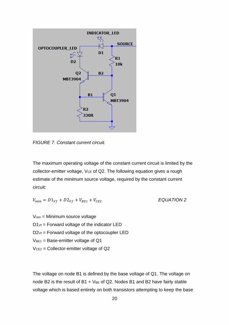
In the carrier board design, all the inputs use an optocoupler combined with a
constant current circuit. The constant current circuit, illustrated inFIGURE 7,
provides a constant current of 2.2mA across the LED inside the optocoupler. In
this case LED D1 represents the indicator LED and D2 represents the LED
inside the optocoupler. SOURCE is connected to the output of a sensor.
20
FIGURE 7. Constant current circuit.
The maximum operating voltage of the constant current circuit is limited by the
collector-emitter voltage, VCE of Q2. The following equation gives a rough
estimate of the minimum source voltage, required by the constant current
circuit:
𝑉𝑚𝑖𝑛 = 𝐷1𝑉𝑓 + 𝐷2𝑉𝑓 + 𝑉𝐵𝐸1 + 𝑉𝐶𝐸2 EQUATION 2
Vmin = Minimum source voltage
D1Vf = Forward voltage of the indicator LED
D2Vf = Forward voltage of the optocoupler LED
VBE1 = Base-emitter voltage of Q1
VCE2 = Collector-emitter voltage of Q2
The voltage on node B1 is defined by the base voltage of Q1. The voltage on
node B2 is the result of B1 + VBE of Q2. Nodes B1 and B2 have fairly stable
voltage which is based entirely on both transistors attempting to keep the base

21
voltage at VBE. The resistor R1 is used for supplying current to base of the Q2
and Q1 collector.
The circuit operates by the resistor R2 creating a voltage drop and the transistor
Q1 attempting to keep the voltage drop at a nominal value of VBE. Q1 shunts the
base current away from Q2 as the voltage drop across R2 increases to VBE of
Q1. As a result, Q1 attempts to keep its base voltage at 2*VBE which also
results in the collector current being constant.
The current through the LEDs is almost the same as the current through the
resistor R2. Isink, the constant current through the LEDs, can be calculated using
the following equation:
𝐼𝑠𝑖𝑛𝑘 =VBE1
𝑅2 EQUATION 3
Isink = Constant current through the LEDs
VBE1 = Base-emitter voltage of Q1
R2 = Resistance of R2
3.7 Output line
An intelligent high-side driver is a type of switch, used for controlling a wide
variety of loads. It is based on MOSFETs with added protection against many
common fault cases. An intelligent high-side driver aims to replace other
MOSFET-based switch circuits and relays by combining reliability, price and
heavy load capabilities together. Unlike a relay, a high-side switch supports a
pulse-width modulation (PWM) control [11].
The selected high-side driver TPS4H160 has four outputs with the maximum
current output capability of 2.5A. FIGURE 8 illustrates the functional block
diagram of TPS4H160. The IC comes with 2 different versions with the
difference being in diagnostics functionality. For the version A, each output has
a dedicated diagnostic pin that can be connected to an input of the COM. The
diagnostic pin is set high when any fault state is detected, while a low state
means that no fault is detected. The version B of the IC has a single analog

22
output that can be used for receiving more detailed information of the fault case.
A negative side being that the analog output has to be connected to an ADC on
the COM side and the status for each of the outputs must be checked one by
one [12].
The version A of TPS4H160 was selected for the design since having a
dedicated status pin offers simplicity by not having to use ADC inputs. Instead,
each status pin can be set as an interrupt pin in the software.
In the design the status pins are also connected to LEDs visual identification of
the status when configurating and testing the system. Status pins give an option
for an autonomous system to have self-diagnostics for some of the possible
fault cases. Status pins can be used to detect fault cases with the connected
load such as shorted load or over temperature. Status pins also report of open-
load connection, meaning that no load is connected to the output, which could
be caused by connection issues.
FIGURE 9. Functional block diagram of TPS4H160 [12].

23
4 LAYOUT DESIGN
4.1 Overview
Layout design for the carrier board was accomplished using PADS Layout and
PADS Router, provided by Mentor Graphics. Layout design included creating
footprints for components not found in the footprint library used in JOT
Automation.
PADS Layout was mainly used for giving the components a general placement
in the PCB layout. After initial component placement, one of the main things
was to decide the build-up of the PCB.
4.2 PCB build-up
A PCB build-up defines the total number of layers and the composition of the
PCB. Thickness of the conductive copper layers and insulating prepreg layers
have a major effect on trace properties when routing impedance matched
signals. High-speed digital signals, such as USB and Ethernet, must be treated
as impedance matched transmission lines on a PCB. To achieve impedance
matching and to protect from crosstalk, the high-speed transmission lines
should have a reference ground plane in adjacent layers to them.
Return current for high-speed signals follows the path of least inductance, which
lies directly under the signal conductor. The reference plane should be either
ground or power plane. Return current for low-speed signals follow the path of
least resistance and therefore do not require solid reference plane under them
[13, p.189.].
A 2-layer build-up consists of 2 copper layers and is most often used for
designs with fairly low number of components. Routing high-speed transmission
lines can be difficult on a 2-layer PCB due to them requiring a reference plane
beneath the traces.
24
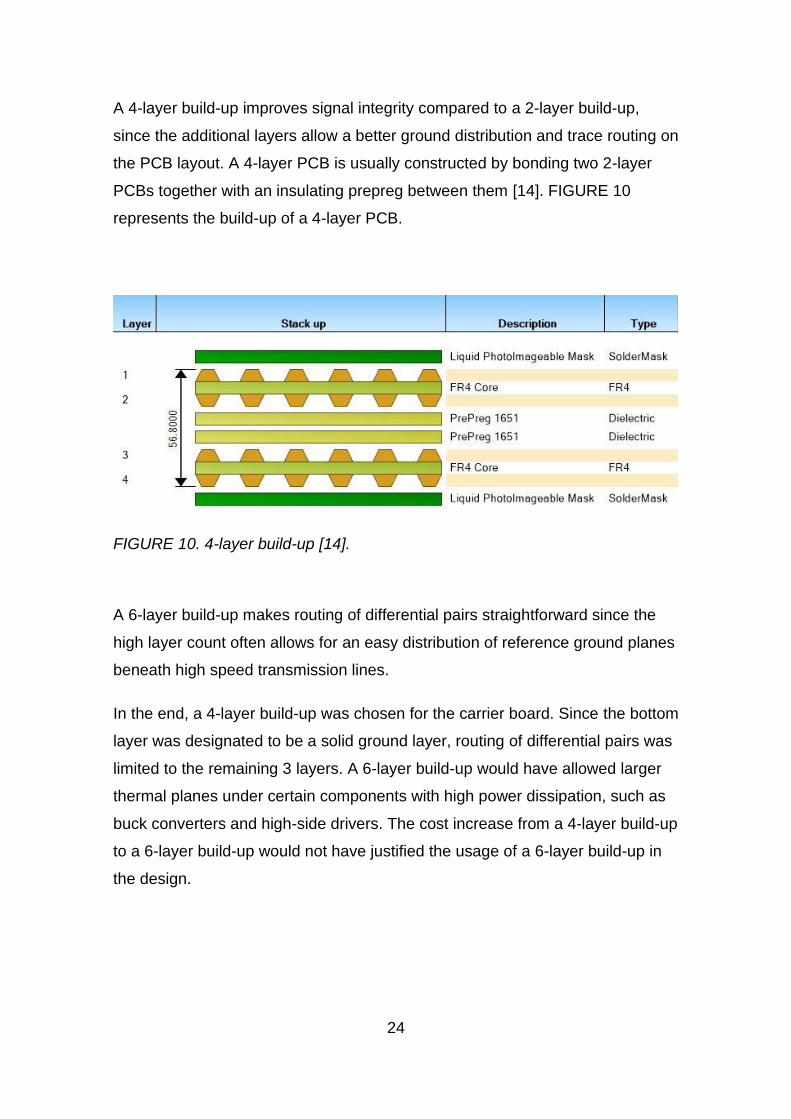
A 4-layer build-up improves signal integrity compared to a 2-layer build-up,
since the additional layers allow a better ground distribution and trace routing on
the PCB layout. A 4-layer PCB is usually constructed by bonding two 2-layer
PCBs together with an insulating prepreg between them [14]. FIGURE 10
represents the build-up of a 4-layer PCB.
FIGURE 10. 4-layer build-up [14].
A 6-layer build-up makes routing of differential pairs straightforward since the
high layer count often allows for an easy distribution of reference ground planes
beneath high speed transmission lines.
In the end, a 4-layer build-up was chosen for the carrier board. Since the bottom
layer was designated to be a solid ground layer, routing of differential pairs was
limited to the remaining 3 layers. A 6-layer build-up would have allowed larger
thermal planes under certain components with high power dissipation, such as
buck converters and high-side drivers. The cost increase from a 4-layer build-up
to a 6-layer build-up would not have justified the usage of a 6-layer build-up in
the design.
25
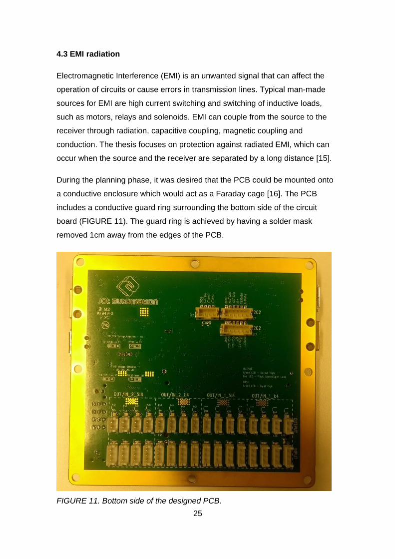
4.3 EMI radiation
Electromagnetic Interference (EMI) is an unwanted signal that can affect the
operation of circuits or cause errors in transmission lines. Typical man-made
sources for EMI are high current switching and switching of inductive loads,
such as motors, relays and solenoids. EMI can couple from the source to the
receiver through radiation, capacitive coupling, magnetic coupling and
conduction. The thesis focuses on protection against radiated EMI, which can
occur when the source and the receiver are separated by a long distance [15].
During the planning phase, it was desired that the PCB could be mounted onto
a conductive enclosure which would act as a Faraday cage [16]. The PCB
includes a conductive guard ring surrounding the bottom side of the circuit
board (FIGURE 11). The guard ring is achieved by having a solder mask
removed 1cm away from the edges of the PCB.
FIGURE 11. Bottom side of the designed PCB.

26
Faraday cages can be used for preventing radiation from both leaving and from
entering the cage. The enclosure could be used for taking high frequency
measurements from the PCB inside the enclosure. In this case the Faraday
cage should inhibit radiation from entering the enclosure, which could interfere
the measurements.
To prevent components and traces from producing electromagnetic radiation
inside the enclosure, only LEDs for the IO interface and connectors for I2C,
CAN and IO interfaces are assembled on the bottom side of the PCB. The
bottom side of the PCB is preserved as a solid ground plane which will ensure
that the Faraday cage is completely closed when bonded to the conductive
enclosure. The solid ground plane effectively blocks EMI from passing the
ground plane. FIGURE 12 illustrates reflection and absorption by a shield which
in this case would represent the ground plane of the PCB [17].
FIGURE 12. Reflection and absorption by a shield [17].

27
Most of the connectors on top side of the PCB are surface mounted connectors.
The through-hole pin of the connector often leaves behind a stub which
represents as an unterminated portion in the transmission path. In high-speed
transmission lines a stub in the transmission line acts as an antenna that could
cause radiation inside the enclosure [18]. A connection to surface mounted
connectors are made on the same layer as the connector which ensures that
there are no stubs in the transmission line.

28
5 RESULTS
5.1 Testing phase
After the layout was finished and the carrier board was manufactured, it was
time to test the board. The testing phase consisted of verifying that all the
features were functional within the required operating ranges. A summary of the
main features on the designed carrier board can be seen in TABLE 2.
FIGURE 13 illustrates the top side of the finished carrier board with a Toradex
Colibri COM mounted on it.
TABLE 2. Summary of features on the designed carrier board.
Feature Toradex Colibri Carrier board
Input voltage range Selectable, either +5VDC or from +6.2VDC to +32VDC
Ethernet 2x
USB 1x USB Host, 1x USB Debug
I2C 3x
CAN 2x
UART 1x UART, 1x RS-323
Inputs 16x, with input voltage range, from +5VDC to +32VDC
Outputs 16x, with selectable output voltage range, from +5VDC to +32VDC

29
FIGURE 13. Top side of the designed PCB.
The original plan was to use a Toradex Colibri iMX6 Solo 256MB COM with the
carrier board, but it was found out that the Torizon operating system did not run
well on that module. After upgrading the COM to a Colibri iMX6 DualLite 512MB
the Torizon OS started to work flawlessly. The issues were likely caused by the
amount of RAM being too limited since upgrading the COM increased the
amount of RAM from 256MB to 512MB. It could be possible to use the less
powerful COM if the operating system is configured to be more optimized.
5.2 I2C testing
The I2C bus requires clock and data signals to reach a high state within a
certain period of time which is based on the used clock frequency. If the rise
time of the high pulse is too slow, it could be registered as a low pulse by the
receiver. This would lead to further issues with communication or to a complete
data disconnection.

30
The I2C bus of the carrier board is tested to confirm that that the used I2C buffer
implementation is adequate for common use cases where cabling of the I2C bus
can be multiple meters long. The test setup consists of commonly used I2C
slave devices that are connected to the designed carrier board using varying
length of cabling. The test is executed by scanning I2C addresses on the I2C
bus and then by measuring the I2C clock signal with an oscilloscope.
In the first test setup one external I2C device is attached to the carrier board via
a 2.5-meter-long cable. FIGURE 14 illustrates the signal pulse that is slightly
affected by the slow rise time.
FIGURE 14. Clock signal of I2C bus with one I2C device connected.
In the second test setup, four external I2C devices are attached to the carrier
board with a total cable length of 3.5 meters. FIGURE 15 shows the measured
signal rise time of the second test setup. It can be seen that the rising edge of
the pulse gets more rounded when more I2C devices and cabling is added.

31
FIGURE 15. Clock signal of I2C bus with four I2C devices connected.
In both setups the I2C communication is fully functional, despite the slow rise
time of the signals. The bus should be able to withstand even more connected
I2C devices before the signal rise time would be slow enough to cause issues.
The rise time could be made faster by increasing pull-up of the I2C signal lines,
but it would also mean increased power dissipation.
5.3 High-side driver testing
During testing of the high-side drivers switching inductive loads, it was found
that the negative voltage spikes at turnoff can be as high as -46VDC. The used
TPS4H160-Q1 high-side drivers are integrated with a clamp that limits and
dissipates the spikes [12]. The integrated clamp mechanism limits the voltage
between drain and source of the switch, as can be seen from test results in
FIGURE 16. The few milli second lasting negative spikes should be harmless
since the energy is safely dissipated by the IC.
The negative voltage spikes could be mitigated to -0.2V by adding a Schottky
diode parallel to the load to function as a freewheeling diode. A freewheeling
diode would take longer to dissipate the energy, but the voltage spike would be
minimal [19].

32
FIGURE 16. Inductive load turn-off.
5.4 Future improvements
The carrier board that was designed for the thesis is the first hardware version
of the design that would be used as the new controller for JOT M10 Test Boxes.
The design would be modified based on the results of hardware testing. New
features that have become apparent during further software development would
be implemented.
As the new setup contains only one PCB instead of three individual PCBs, the
manufacturing cost is brought down by a bit. The highest cost increase
compared to old setup comes from using the Toradex Colibri COM. The new
design uses more recent components as opposed to the currently used setup
as the component manufacturers have brought more efficient and yet cheaper
components into the markets.

33
6 CONCLUSION
The main aim of the thesis was to design a controller that could be used for
controlling JOT M10 test boxes. The purpose of the design was to replace and
offer improvements to the currently used controller setup, consisting of a control
card and two IO boards. The new controller consists of a carrier board which
was designed to support the usage of Toradex Colibri COMs.
The design was thoroughly tested to ensure that all the features are functional
in any planned use case. Although there were minor issues, the design was
overall successful as all the main features are fully functional for software
development and prototyping. The main aims, such as being cost-effective
compared to the old setup, running the Linux operating system and containing
all the needed features, were achieved.
The cost of the hardware could be brought down a bit by using an operating
system with lower processing requirements so that a cheaper COM could be
used, as the module is the most expensive single component of the design. The
total cost could be further reduced by decreasing the amount of IOs. Lowering
the amount of IOs would be a matter of leaving components related to them
unassembled.

34
REFERENCES
[1] JOT Automation Ltd, "JOT M10 Test Concept," 2020. [Online].
Available: https://www.jotautomation.com/products/jot-m10-test-
concept.html. [Accessed 20 August 2020].
[2] M. Rouse, "TechTarget," August 2019. [Online]. Available:
https://searchstorage.techtarget.com/definition/RAM-random-access-
memory. [Accessed 23 August 2020].
[3] Toradex, "Colibri iMX6 product page," [Online]. Available:
https://www.toradex.com/computer-on-modules/colibri-arm-family/nxp-
freescale-imx6. [Accessed 17 August 2020].
[4] Toradex, "BSP Layers and Reference Images for Yocto Project
Software," [Online]. Available:
https://developer.toradex.com/software/linux/linux-software. [Accessed
11 August 2020].
[5] Docker Inc, "Container Runtime product page," [Online]. Available:
https://www.docker.com/products/container-runtime. [Accessed 11
August 2020].
[6] Toradex, "Pinout Designer," 15 May 2020. [Online]. Available:
https://developer.toradex.com/knowledge-base/pinout-designer.
[Accessed 11 August 2020].
[7] "LMR33640 datasheet," Texas Instruments, May 2020. [Online].
Available: https://www.ti.com/lit/ds/symlink/lmr33640.pdf. [Accessed 27
July 2020].
[8] J. Vasquez, "AN INTRODUCTION TO DIFFERENTIAL I²C," 31 March
2017. [Online]. Available: https://hackaday.com/2017/03/31/an-
introduction-to-differential-i²c/. [Accessed 12 August 2020].

35
[9] Texas Instruments, "TCA9617A," December 2018. [Online]. Available:
https://www.ti.com/lit/ds/symlink/tca9617a.pdf. [Accessed 12 August
2020].
[10] ON Semiconductor, "Application Note AN-3001," 30 April 2002. [Online].
Available: https://www.onsemi.com/pub/Collateral/AN-3001.pdf.pdf.
[Accessed 11 August 2020].
[11] D. Swanson, "The Future is in High-Side Drivers," STMicroelectronics,
01 September 2006. [Online]. Available:
https://www.electronicdesign.com/markets/automotive/article/21796971/t
he-future-is-in-highside-drivers. [Accessed 17 August 2020].
[12] Texas Instruments, "TPS4H160-Q1 Datasheet," December 2019.
[Online]. Available: https://www.ti.com/lit/ds/symlink/tps4h160-q1.pdf.
[Accessed 17 August 2020].
[13] J. &. Graham, High Speed Digital Design: A Handbook of Black Magic,
Pearson; 1th edition, 1993.
[14] Polar Instruments, "PCB Stackup or Buildup – a brief history," [Online].
Available:
https://www.polarinstruments.com/support/stackup/AP537.html.
[Accessed 17 July 2020].
[15] Electronics Notes, "EMI Electromagnetic Interference: the
fundamentals," [Online]. Available: https://www.electronics-
notes.com/articles/analogue_circuits/emc-emi-electromagnetic-
interference-compatibility/what-is-emi-basics-tutorial.php. [Accessed 23
August 2020].
[16] K. Knack, "Building a Faraday Cage To Contain EMI, Part 1," Altium
Limited, 4 November 2019. [Online]. Available:
36
https://resources.altium.com/p/building-a-faraday-cage-to-contain-emi-
part-1. [Accessed 21 August 2020].
[17] EMC Standards, "EMC techniques in electronic design Part 4 -
Shielding," May 2009. [Online]. Available:
https://www.emcstandards.co.uk/files/part_4_text_and_graphics_21_ma
y_09.pdf. [Accessed 17 August 2020].
[18] Texas Instruments, "High-Speed Interface Layout Guidelines," October
2018. [Online]. Available:
https://www.ti.com/lit/an/spraar7h/spraar7h.pdf. [Accessed 17 August
2020].
[19] S. Unnikrishnan, "Inductive Loads with Smart High Side Switches,"
Texas Instruments, 2018. [Online]. Available:
https://training.ti.com/sites/default/files/system-level-design-
considerations-for-driving-and-diagnosing-inductive-load.pdf. [Accessed
23 July 2020].