Infineon AURIX™ Microcontrollers Intelligent solutions for ...
Upload
khangminh22Category
view
4download
0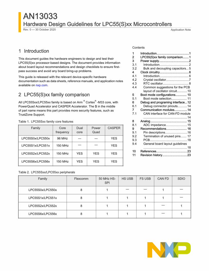
1 IntroductionThis document guides the hardware engineers to design and test their LPC55(S)xx processor-based designs. The document provides information about board layout recommendations and design checklists to ensure firstpass success and avoid any board bring-up problems.
This guide is released with the relevant device-specific hardware documentation such as data sheets, reference manuals, and application notes available on nxp.com.
2 LPC55(S)xx family comparisonAll LPC55Sxx/LPC55xx family is based on Arm ® Cortex® -M33 core, with PowerQuad Accelerator and CASPER Accelerator. The S in the middle of part name means this part provides more security features, such as TrustZone Support.
Table 1. LPC55Sxx family core features
Family Core frequency
Dual core
Power Quad
CASPER
LPC55S0x/LPC550x 96 MHz — — YES
LPC55S1x/LPC551x 150 MHz — — YES
LPC55S2x/LPC552x 150 MHz YES YES YES
LPC55S6x/LPC556x 150 MHz YES YES YES
Table 2. LPC55Sxx/LPC55xx peripherals
Family Flexcomm 50 MHz HS-SPI
HS USB FS USB CAN FD SDIO
LPC55S0x/LPC550x 8 1 — — 1 —
LPC55S1x/LPC551x 8 1 1 1 1 —
LPC55S2x/LPC552x 8 1 1 1 — 1
LPC55S6x/LPC556x 8 1 1 1 — 1
Contents
1 Introduction......................................12 LPC55(S)xx family comparison.......13 Power supply...................................23.1 Introduction.................................. 23.2 Bulk and decoupling capacitors... 54 Clock circuitry..................................64.1 Introduction.................................. 64.2 Crystal oscillator...........................74.3 RTC oscillator.............................. 84.4 Common suggestions for the PCB
layout of oscillator circuit............105 Boot mode configurations............. 105.1 Boot mode selection.................. 116 Debug and programing interface...126.1 Debug connector pinouts...........147 Communication modules...............147.1 CAN interface for CAN-FD module
...................................................148 Analog........................................... 158.1 ADC impedance.........................159 Recommendations........................ 169.1 Pin descriptions..........................169.2 Termination of unused pins....... 179.3 PCB............................................189.4 General board layout guidelines
...................................................1810 References....................................2311 Revision history.............................23
AN13033Hardware Design Guidelines for LPC55(S)xx MicrocontrollersRev. 0 — 30 October 2020 Application Note
Table 3. LPC55Sxx/LPC55xx Timers
Family CTimer SCT MRT WWDT Code WDT
RTC OS-Timer
LPC55S0x/LPC550x 5 1 1 1 1 1 1
LPC55S1x/LPC551x 5 1 1 1 1 1 1
LPC55S2x/LPC552x 5 1 1 1 — 1 1
LPC55S6x/LPC556x 5 1 1 1 — 1 1
Table 4. LPC55Sxx/LPC55xx analog peripherals
Family 16 bit ADC Comparator 12 bit DAC
LPC55S0x/LPC550x 1 (10ch)/2 Msps 1 (5 inputs) —
LPC55S1x/LPC551x 1 (10ch)/2 Msps 1 (5 inputs) —
LPC55S2x/LPC552x 1 (10ch)/1 Msps 1 (5 inputs) —
LPC55S6x/LPC556x 1 (10ch)/1 Msps 1 (5 inputs) —
Table 5. LPC55Sxx/LPC55xx packages
Family HVQFN 48 HVQFN 64 HTQFP 64 VFBGA 98 HLQFP 100
HLQFP 144
VBGA 196
LPC55S0x/LPC550x / /
LPC55S1x/LPC551x / / /
LPC55S2x/LPC552x / / /
LPC55S6x/LPC556x / / /
For details, see the latest version of the Datasheet and User Manuel on www.nxp.com.
3 Power supply
3.1 IntroductionLPC55Sxx series requires single 1.8 to 3.6 V operation voltage supply.
LPC55S0x/LPC550x, LPC55S1x/LPC551x, LPC55S2x/LPC552x and LPC55S6x/LPC556x internal core’s voltage are supplied by internal DC/DC regulator, this DC/DC regulator needs external inductance and two or three capacitors. For details, see Using the DCDC feature (document AN12325).
NXP SemiconductorsPower supply
Hardware Design Guidelines for LPC55(S)xx Microcontrollers, Rev. 0, 30 October 2020Application Note 2 / 24
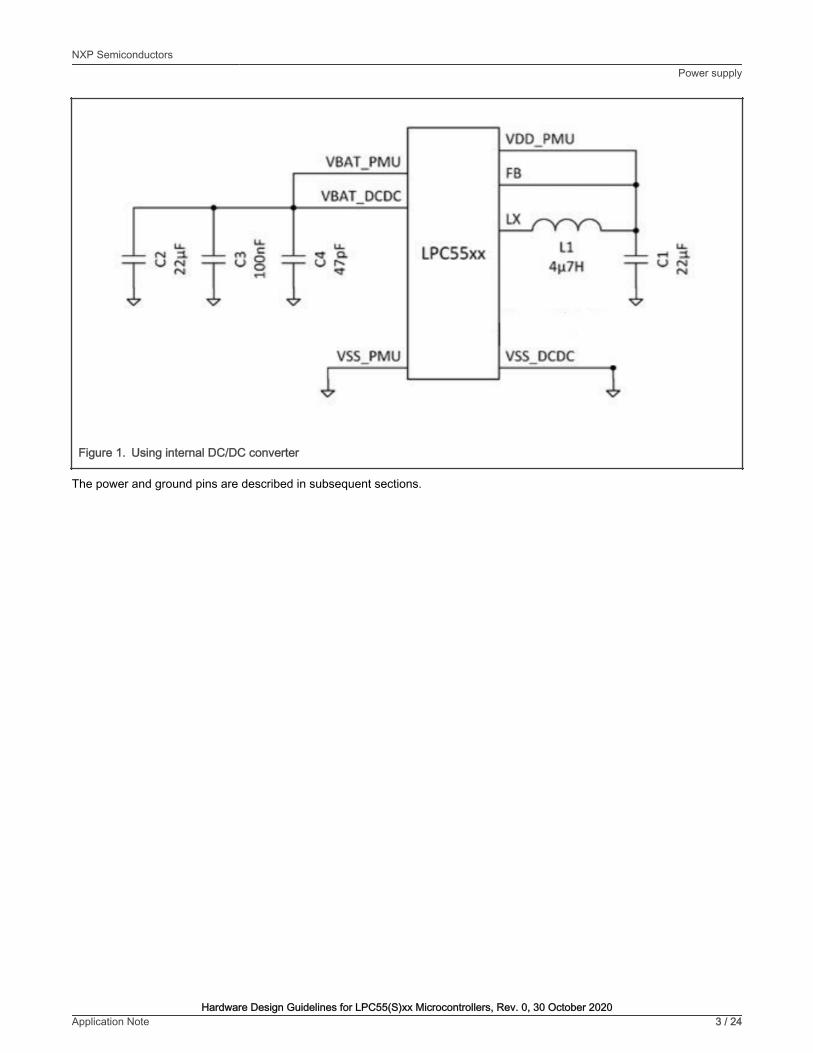
Figure 1. Using internal DC/DC converter
The power and ground pins are described in subsequent sections.
NXP SemiconductorsPower supply
Hardware Design Guidelines for LPC55(S)xx Microcontrollers, Rev. 0, 30 October 2020Application Note 3 / 24
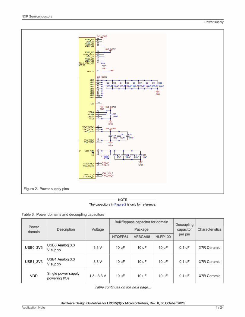
Figure 2. Power supply pins
The capacitors in Figure 2 is only for reference.
NOTE
Table 6. Power domains and decoupling capacitors
Power domain Description Voltage
Bulk/Bypass capacitor for domainDecoupling capacitor per pin
CharacteristicsPackage
HTQFP64 VFBGA98 HLFP100
USB0_3V3 USB0 Analog 3.3 V supply 3.3 V 10 uF 10 uF 10 uF 0.1 uF X7R Ceramic
USB1_3V3 USB1 Analog 3.3 V supply 3.3 V 10 uF 10 uF 10 uF 0.1 uF X7R Ceramic
VDD Single power supply powering I/Os 1.8 - 3.3 V 10 uF 10 uF 10 uF 0.1 uF X7R Ceramic
Table continues on the next page...
NXP SemiconductorsPower supply
Hardware Design Guidelines for LPC55(S)xx Microcontrollers, Rev. 0, 30 October 2020Application Note 4 / 24
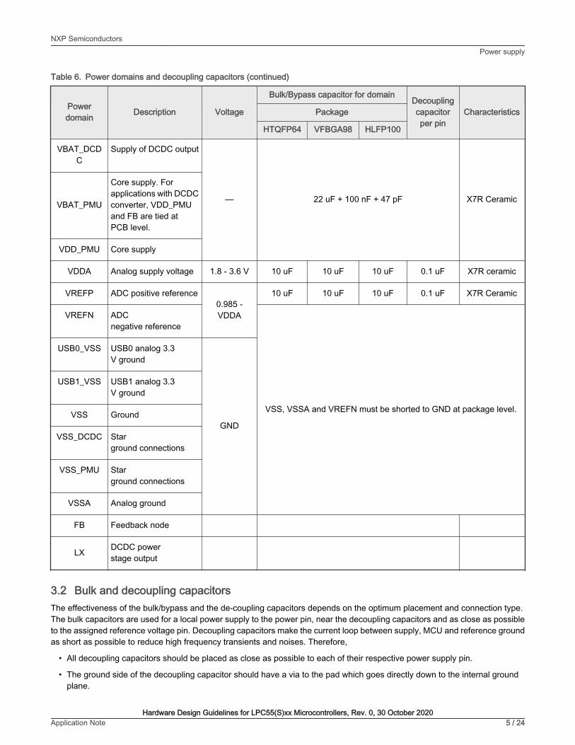
Table 6. Power domains and decoupling capacitors (continued)
Power domain Description Voltage
Bulk/Bypass capacitor for domainDecoupling capacitor per pin
CharacteristicsPackage
HTQFP64 VFBGA98 HLFP100
VBAT_DCDC
Supply of DCDC output
— 22 uF + 100 nF + 47 pF X7R CeramicVBAT_PMU
Core supply. For applications with DCDC converter, VDD_PMU and FB are tied at PCB level.
VDD_PMU Core supply
VDDA Analog supply voltage 1.8 - 3.6 V 10 uF 10 uF 10 uF 0.1 uF X7R ceramic
VREFP ADC positive reference0.985 - VDDA
10 uF 10 uF 10 uF 0.1 uF X7R Ceramic
VREFN ADC negative reference
VSS, VSSA and VREFN must be shorted to GND at package level.
USB0_VSS USB0 analog 3.3 V ground
GND
USB1_VSS USB1 analog 3.3 V ground
VSS Ground
VSS_DCDC Star ground connections
VSS_PMU Star ground connections
VSSA Analog ground
FB Feedback node
LX DCDC power stage output
3.2 Bulk and decoupling capacitorsThe effectiveness of the bulk/bypass and the de-coupling capacitors depends on the optimum placement and connection type. The bulk capacitors are used for a local power supply to the power pin, near the decoupling capacitors and as close as possible to the assigned reference voltage pin. Decoupling capacitors make the current loop between supply, MCU and reference ground as short as possible to reduce high frequency transients and noises. Therefore,
• All decoupling capacitors should be placed as close as possible to each of their respective power supply pin.
• The ground side of the decoupling capacitor should have a via to the pad which goes directly down to the internal ground plane.
NXP SemiconductorsPower supply
Hardware Design Guidelines for LPC55(S)xx Microcontrollers, Rev. 0, 30 October 2020Application Note 5 / 24
• The route distance between the capacitors to the power plane should be as short as possible.
Figure 3. Bulk and decoupling capacitor connection
4 Clock circuitry
4.1 IntroductionThe LPC55S1x/2x/6x has the following clock sources:
• Internal Free Running Oscillator (FRO). This oscillator provides a selectable 96 MHz output, and a 12 MHz output (divided down from the selected higher frequency) that can be used as a system clock. The FRO is trimmed to +/- 2% accuracy over the entire voltage and temperature range.
• 32 kHz Internal Free Running Oscillator FRO. The FRO is trimmed to +/- 2% accuracy over the entire voltage and temperature range.
• Internal low power oscillator (FRO 1 MHz) trimmed to +/- 15% accuracy over the entire voltage and temperature range.
• Crystal oscillator with an operating frequency of 16 MHz or 32 MHz. Option for external clock input (bypass mode) for clock frequencies of up to 24 MHz.
• Crystal oscillator with 32.768 kHz operating frequency. Option for external clock input (bypass mode) for clock frequencies of up to 100 kHz.
• PLL0 and PLL1 allow CPU operation up to the maximum CPU rate without the need for a high-frequency external clock. PLL0 and PLL1 can run from the internal FRO 12 MHz output, the external oscillator, internal FRO 1 MHz output, or the 32.768 kHz RTC oscillator.
• Clock output function with divider to monitor internal clocks.
• Frequency measurement unit for measuring the frequency of any on-chip or off-chip clock signal.
For external crystal oscillator and RTC oscillator, LPC55Sxx have capacitor bank feature. It means that the stabilizing capacitors can be unsoldered on both 32 K and 16 MHz XTAL. We also suggest users to keep the two stabilizing capacitors as DNP/Do Not Populate on PCB.
NOTE
NXP SemiconductorsClock circuitry
Hardware Design Guidelines for LPC55(S)xx Microcontrollers, Rev. 0, 30 October 2020Application Note 6 / 24
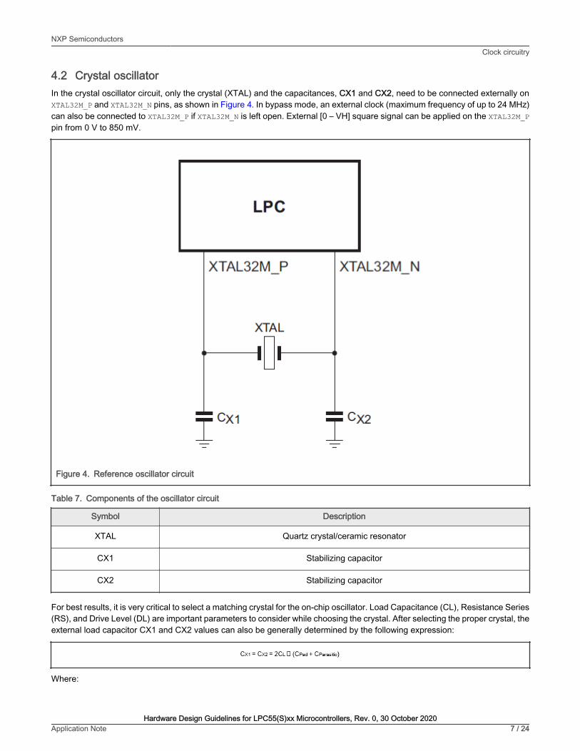
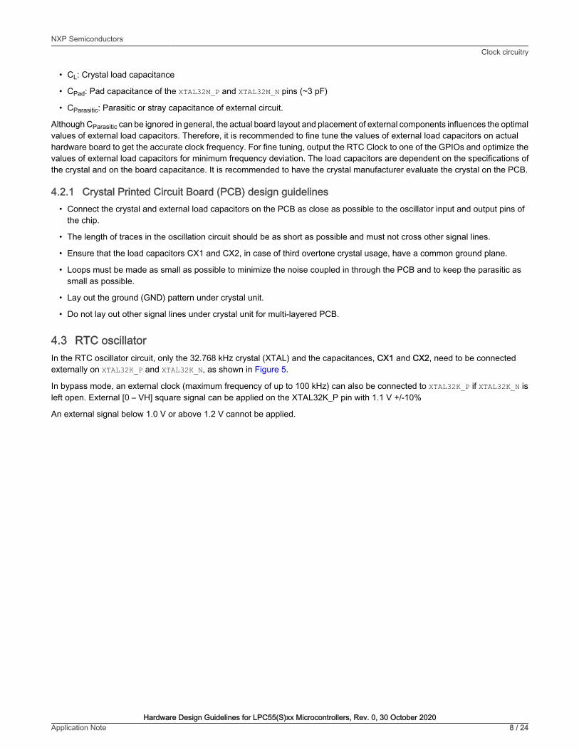
4.2 Crystal oscillatorIn the crystal oscillator circuit, only the crystal (XTAL) and the capacitances, CX1 and CX2, need to be connected externally on XTAL32M_P and XTAL32M_N pins, as shown in Figure 4. In bypass mode, an external clock (maximum frequency of up to 24 MHz) can also be connected to XTAL32M_P if XTAL32M_N is left open. External [0 – VH] square signal can be applied on the XTAL32M_P pin from 0 V to 850 mV.
Figure 4. Reference oscillator circuit
Table 7. Components of the oscillator circuit
Symbol Description
XTAL Quartz crystal/ceramic resonator
CX1 Stabilizing capacitor
CX2 Stabilizing capacitor
For best results, it is very critical to select a matching crystal for the on-chip oscillator. Load Capacitance (CL), Resistance Series (RS), and Drive Level (DL) are important parameters to consider while choosing the crystal. After selecting the proper crystal, the external load capacitor CX1 and CX2 values can also be generally determined by the following expression:
Where:
NXP SemiconductorsClock circuitry
Hardware Design Guidelines for LPC55(S)xx Microcontrollers, Rev. 0, 30 October 2020Application Note 7 / 24
• CL: Crystal load capacitance
• CPad: Pad capacitance of the XTAL32M_P and XTAL32M_N pins (~3 pF)
• CParasitic: Parasitic or stray capacitance of external circuit.
Although CParasitic can be ignored in general, the actual board layout and placement of external components influences the optimal values of external load capacitors. Therefore, it is recommended to fine tune the values of external load capacitors on actual hardware board to get the accurate clock frequency. For fine tuning, output the RTC Clock to one of the GPIOs and optimize the values of external load capacitors for minimum frequency deviation. The load capacitors are dependent on the specifications of the crystal and on the board capacitance. It is recommended to have the crystal manufacturer evaluate the crystal on the PCB.
4.2.1 Crystal Printed Circuit Board (PCB) design guidelines• Connect the crystal and external load capacitors on the PCB as close as possible to the oscillator input and output pins of
the chip.
• The length of traces in the oscillation circuit should be as short as possible and must not cross other signal lines.
• Ensure that the load capacitors CX1 and CX2, in case of third overtone crystal usage, have a common ground plane.
• Loops must be made as small as possible to minimize the noise coupled in through the PCB and to keep the parasitic as small as possible.
• Lay out the ground (GND) pattern under crystal unit.
• Do not lay out other signal lines under crystal unit for multi-layered PCB.
4.3 RTC oscillatorIn the RTC oscillator circuit, only the 32.768 kHz crystal (XTAL) and the capacitances, CX1 and CX2, need to be connected externally on XTAL32K_P and XTAL32K_N, as shown in Figure 5.
In bypass mode, an external clock (maximum frequency of up to 100 kHz) can also be connected to XTAL32K_P if XTAL32K_N is left open. External [0 – VH] square signal can be applied on the XTAL32K_P pin with 1.1 V +/-10%
An external signal below 1.0 V or above 1.2 V cannot be applied.
NXP SemiconductorsClock circuitry
Hardware Design Guidelines for LPC55(S)xx Microcontrollers, Rev. 0, 30 October 2020Application Note 8 / 24
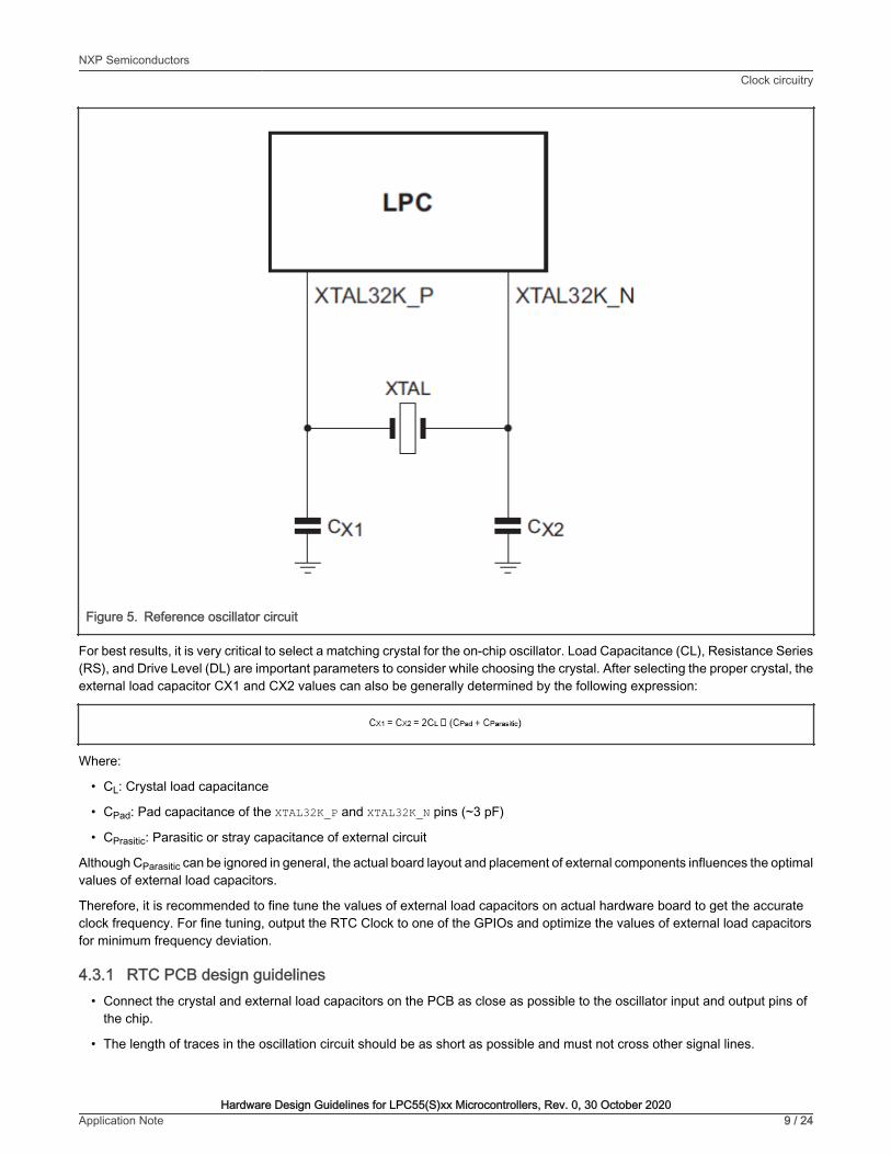
Figure 5. Reference oscillator circuit
For best results, it is very critical to select a matching crystal for the on-chip oscillator. Load Capacitance (CL), Resistance Series (RS), and Drive Level (DL) are important parameters to consider while choosing the crystal. After selecting the proper crystal, the external load capacitor CX1 and CX2 values can also be generally determined by the following expression:
Where:
• CL: Crystal load capacitance
• CPad: Pad capacitance of the XTAL32K_P and XTAL32K_N pins (~3 pF)
• CPrasitic: Parasitic or stray capacitance of external circuit
Although CParasitic can be ignored in general, the actual board layout and placement of external components influences the optimal values of external load capacitors.
Therefore, it is recommended to fine tune the values of external load capacitors on actual hardware board to get the accurate clock frequency. For fine tuning, output the RTC Clock to one of the GPIOs and optimize the values of external load capacitors for minimum frequency deviation.
4.3.1 RTC PCB design guidelines• Connect the crystal and external load capacitors on the PCB as close as possible to the oscillator input and output pins of
the chip.
• The length of traces in the oscillation circuit should be as short as possible and must not cross other signal lines.
NXP SemiconductorsClock circuitry
Hardware Design Guidelines for LPC55(S)xx Microcontrollers, Rev. 0, 30 October 2020Application Note 9 / 24
• Ensure that the load capacitors CX1, CX2, and CX3, in case of third overtone crystal usage, have a common ground plane.
• Loops must be made as small as possible to minimize the noise coupled in through the PCB and to keep the parasitics as small as possible.
• Lay out the GND pattern under crystal unit.
• Do not lay out other signal lines under crystal unit for multi-layered PCB.
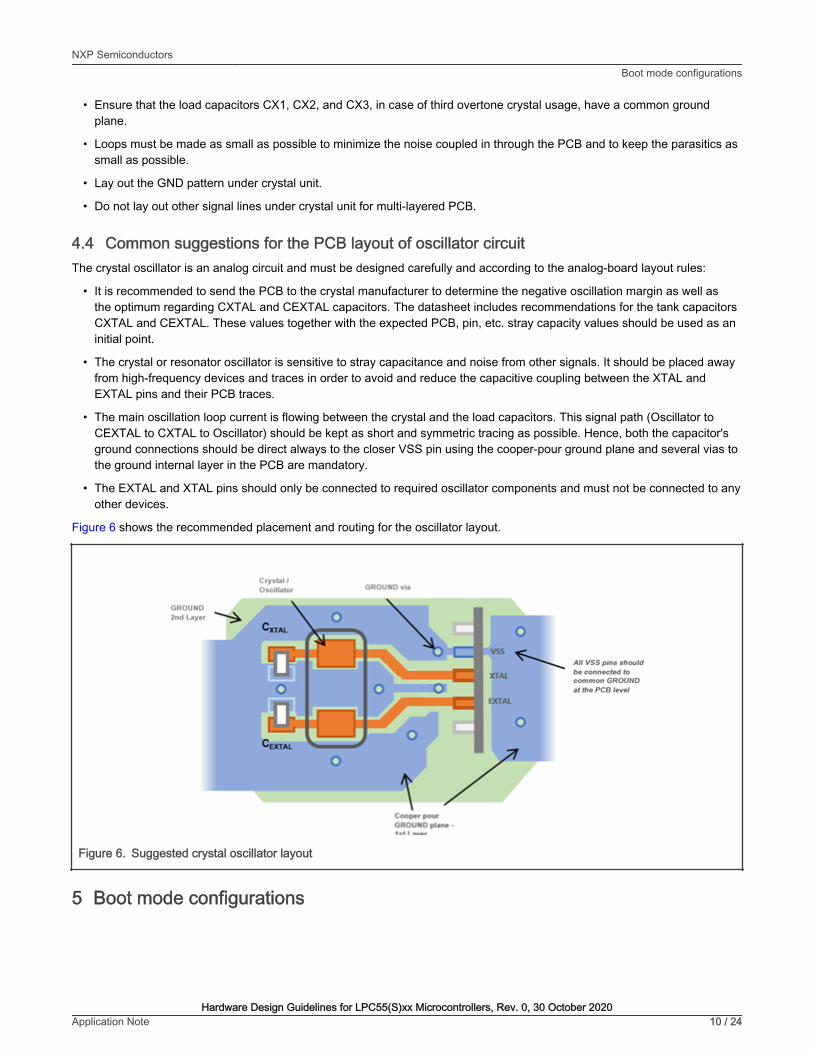
4.4 Common suggestions for the PCB layout of oscillator circuitThe crystal oscillator is an analog circuit and must be designed carefully and according to the analog-board layout rules:
• It is recommended to send the PCB to the crystal manufacturer to determine the negative oscillation margin as well as the optimum regarding CXTAL and CEXTAL capacitors. The datasheet includes recommendations for the tank capacitors CXTAL and CEXTAL. These values together with the expected PCB, pin, etc. stray capacity values should be used as an initial point.
• The crystal or resonator oscillator is sensitive to stray capacitance and noise from other signals. It should be placed away from high-frequency devices and traces in order to avoid and reduce the capacitive coupling between the XTAL and EXTAL pins and their PCB traces.
• The main oscillation loop current is flowing between the crystal and the load capacitors. This signal path (Oscillator to CEXTAL to CXTAL to Oscillator) should be kept as short and symmetric tracing as possible. Hence, both the capacitor's ground connections should be direct always to the closer VSS pin using the cooper-pour ground plane and several vias to the ground internal layer in the PCB are mandatory.
• The EXTAL and XTAL pins should only be connected to required oscillator components and must not be connected to any other devices.
Figure 6 shows the recommended placement and routing for the oscillator layout.
Figure 6. Suggested crystal oscillator layout
5 Boot mode configurations
NXP SemiconductorsBoot mode configurations
Hardware Design Guidelines for LPC55(S)xx Microcontrollers, Rev. 0, 30 October 2020Application Note 10 / 24
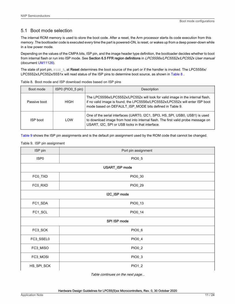
5.1 Boot mode selectionThe internal ROM memory is used to store the boot code. After a reset, the Arm processor starts its code execution from this memory. The bootloader code is executed every time the part is powered-ON, is reset, or wakes up from a deep power-down while in a low power mode.
Depending on the values of the CMPA bits, ISP pin, and the image header type definition, the bootloader decides whether to boot from internal flash or run into ISP mode. See Section 6.5 FFR region definitions in LPC55S6x/LPC55S2x/LPC552x User manual (document UM11126).
The state of port pin, PIO0_5, at Reset determines the boot source of the part or if the handler is invoked. The LPC55S6x/LPC55S2x/LPC552x/55S1x will read status of the ISP pins to determine boot source, as shown in Table 8 .
Table 8. Boot mode and ISP download modes based on ISP pins
Boot mode ISP0 (PIO0_5 pin) Description
Passive boot HIGHThe LPC55S6x/LPC55S2x/LPC552x will look for valid image in the internal flash, if no valid image is found, the LPC55S6x/LPC55S2x/LPC552x will enter ISP boot mode based on DEFAULT_ISP_MODE bits defined in Table 9.
ISP boot LOWOne of the serial interfaces (UART0, I2C1, SPI3, HS_SPI, USB0, USB1) is used to download image from host into internal flash. The first valid probe message on USART, I2C, SPI or USB locks in that interface.
Table 9 shows the ISP pin assignments and is the default pin assignment used by the ROM code that cannot be changed.
Table 9. ISP pin assignment
ISP pin Port pin assignment
ISP0 PIO0_5
USART_ISP mode
FC0_TXD PIO0_30
FC0_RXD PIO0_29
I2C_ISP mode
FC1_SDA PIO0_13
FC1_SCL PIO0_14
SPI ISP mode
FC3_SCK PIO0_6
FC3_SSEL0 PIO0_4
FC3_MISO PIO0_2
FC3_MOSI PIO0_3
HS_SPI_SCK PIO1_2
Table continues on the next page...
NXP SemiconductorsBoot mode configurations
Hardware Design Guidelines for LPC55(S)xx Microcontrollers, Rev. 0, 30 October 2020Application Note 11 / 24
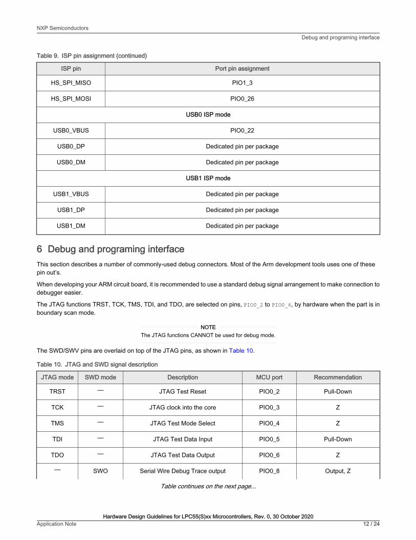
Table 9. ISP pin assignment (continued)
ISP pin Port pin assignment
HS_SPI_MISO PIO1_3
HS_SPI_MOSI PIO0_26
USB0 ISP mode
USB0_VBUS PIO0_22
USB0_DP Dedicated pin per package
USB0_DM Dedicated pin per package
USB1 ISP mode
USB1_VBUS Dedicated pin per package
USB1_DP Dedicated pin per package
USB1_DM Dedicated pin per package
6 Debug and programing interfaceThis section describes a number of commonly-used debug connectors. Most of the Arm development tools uses one of these pin out’s.
When developing your ARM circuit board, it is recommended to use a standard debug signal arrangement to make connection to debugger easier.
The JTAG functions TRST, TCK, TMS, TDI, and TDO, are selected on pins, PIO0_2 to PIO0_6, by hardware when the part is in boundary scan mode.
The JTAG functions CANNOT be used for debug mode.
NOTE
The SWD/SWV pins are overlaid on top of the JTAG pins, as shown in Table 10.
Table 10. JTAG and SWD signal description
JTAG mode SWD mode Description MCU port Recommendation
TRST — JTAG Test Reset PIO0_2 Pull-Down
TCK — JTAG clock into the core PIO0_3 Z
TMS — JTAG Test Mode Select PIO0_4 Z
TDI — JTAG Test Data Input PIO0_5 Pull-Down
TDO — JTAG Test Data Output PIO0_6 Z
— SWO Serial Wire Debug Trace output PIO0_8 Output, Z
Table continues on the next page...
NXP SemiconductorsDebug and programing interface
Hardware Design Guidelines for LPC55(S)xx Microcontrollers, Rev. 0, 30 October 2020Application Note 12 / 24
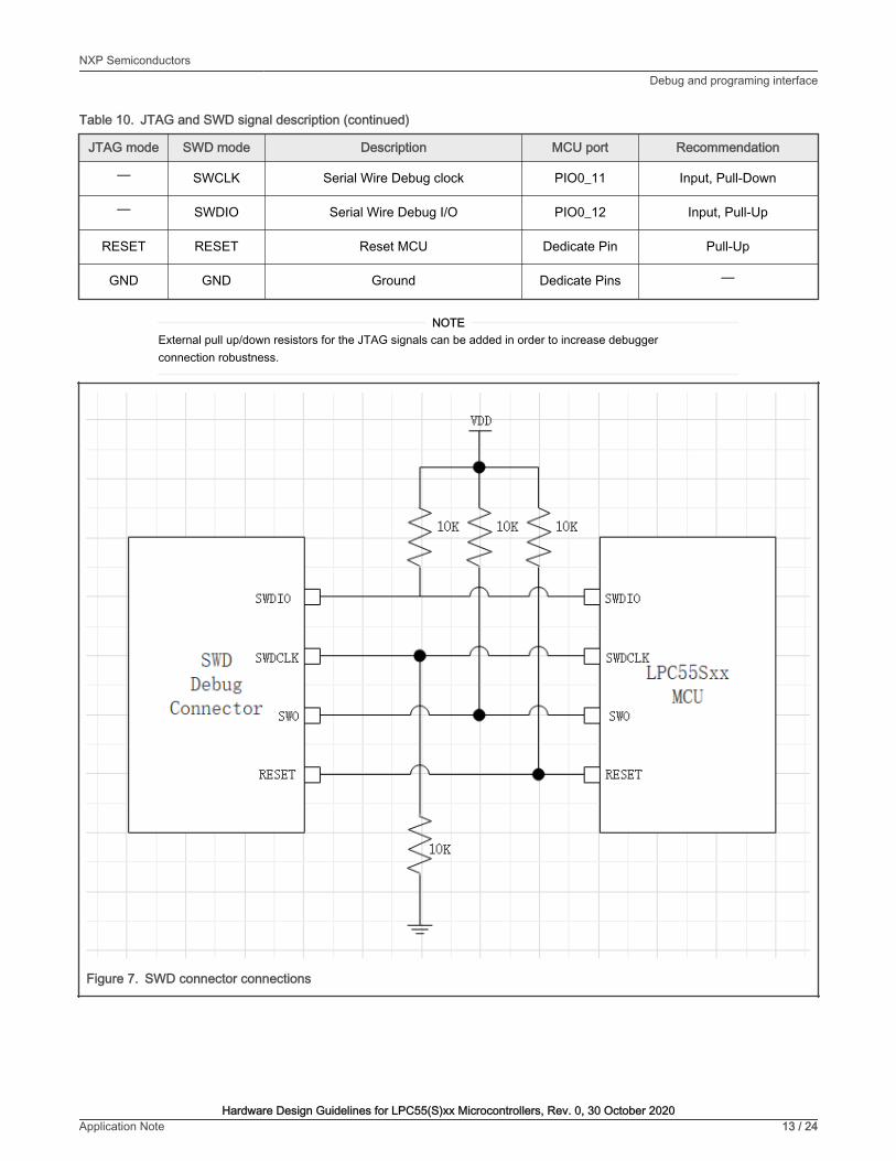
Table 10. JTAG and SWD signal description (continued)
JTAG mode SWD mode Description MCU port Recommendation
— SWCLK Serial Wire Debug clock PIO0_11 Input, Pull-Down
— SWDIO Serial Wire Debug I/O PIO0_12 Input, Pull-Up
RESET RESET Reset MCU Dedicate Pin Pull-Up
GND GND Ground Dedicate Pins —
External pull up/down resistors for the JTAG signals can be added in order to increase debugger connection robustness.
NOTE
Figure 7. SWD connector connections
NXP SemiconductorsDebug and programing interface
Hardware Design Guidelines for LPC55(S)xx Microcontrollers, Rev. 0, 30 October 2020Application Note 13 / 24
6.1 Debug connector pinoutsAs the LPC55Sxx’s JTAG only for BSDL scan, you can use an even smaller 0.05" 10-pin connector (Samtec FTSH-105) for debug. Similar to the 20-pin Cortex Debug D ETM connector, both JTAG and Serial-Wire debug protocols are supported in the 10-pin version.
The JTAG functions TRST, TCK, TMS, TDI, and TDO, are selected on pins, PIO0_2 to PIO0_6, by hardware when the part is in boundary scan mode. The JTAG functions cannot be used for debug mode.
NOTE
Figure 8. SWD signal connections
7 Communication modules
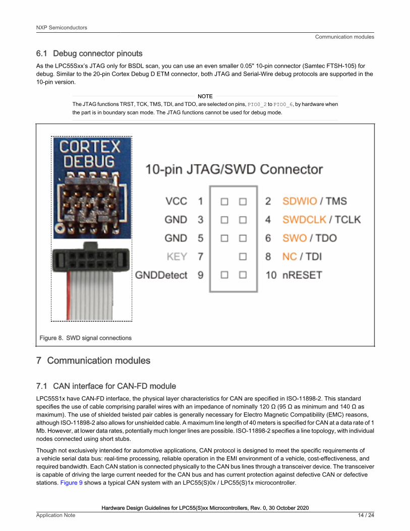
7.1 CAN interface for CAN-FD moduleLPC55S1x have CAN-FD interface, the physical layer characteristics for CAN are specified in ISO-11898-2. This standard specifies the use of cable comprising parallel wires with an impedance of nominally 120 Ω (95 Ω as minimum and 140 Ω as maximum). The use of shielded twisted pair cables is generally necessary for Electro Magnetic Compatibility (EMC) reasons, although ISO-11898-2 also allows for unshielded cable. A maximum line length of 40 meters is specified for CAN at a data rate of 1 Mb. However, at lower data rates, potentially much longer lines are possible. ISO-11898-2 specifies a line topology, with individual nodes connected using short stubs.
Though not exclusively intended for automotive applications, CAN protocol is designed to meet the specific requirements of a vehicle serial data bus: real-time processing, reliable operation in the EMI environment of a vehicle, cost-effectiveness, and required bandwidth. Each CAN station is connected physically to the CAN bus lines through a transceiver device. The transceiver is capable of driving the large current needed for the CAN bus and has current protection against defective CAN or defective stations. Figure 9 shows a typical CAN system with an LPC55(S)0x / LPC55(S)1x microcontroller.
NXP SemiconductorsCommunication modules
Hardware Design Guidelines for LPC55(S)xx Microcontrollers, Rev. 0, 30 October 2020Application Note 14 / 24
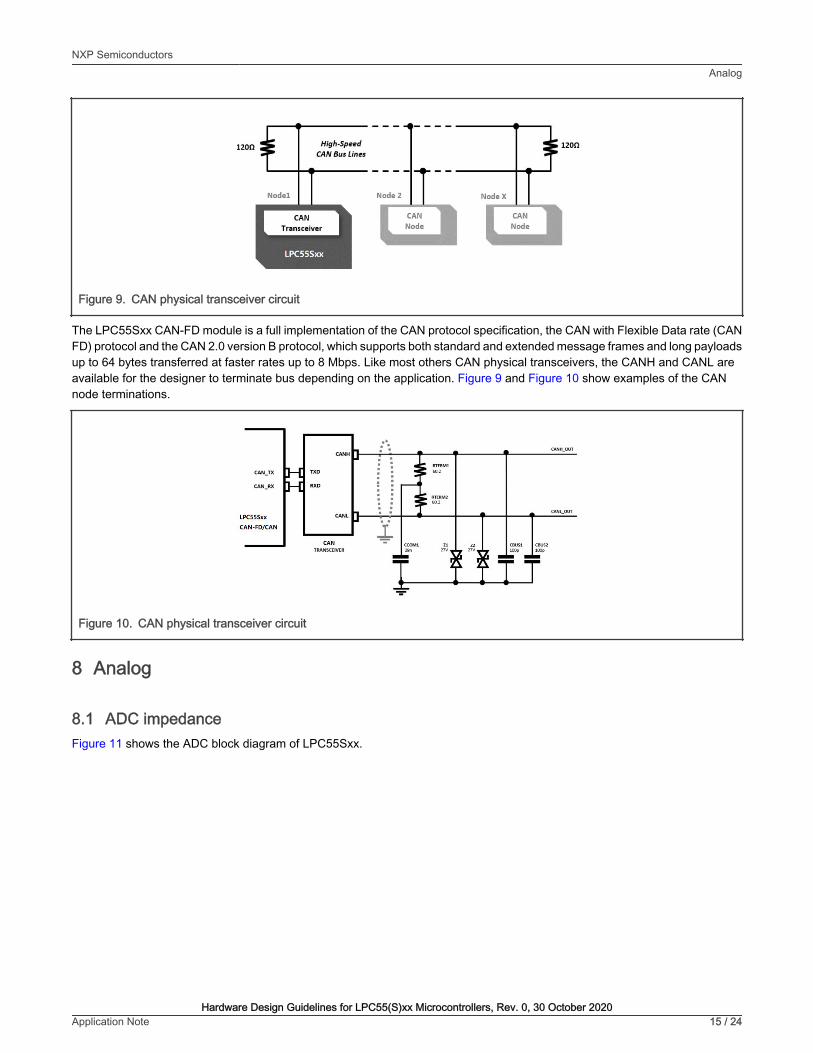
Figure 9. CAN physical transceiver circuit
The LPC55Sxx CAN-FD module is a full implementation of the CAN protocol specification, the CAN with Flexible Data rate (CAN FD) protocol and the CAN 2.0 version B protocol, which supports both standard and extended message frames and long payloads up to 64 bytes transferred at faster rates up to 8 Mbps. Like most others CAN physical transceivers, the CANH and CANL are available for the designer to terminate bus depending on the application. Figure 9 and Figure 10 show examples of the CAN node terminations.
Figure 10. CAN physical transceiver circuit
8 Analog
8.1 ADC impedanceFigure 11 shows the ADC block diagram of LPC55Sxx.
NXP SemiconductorsAnalog
Hardware Design Guidelines for LPC55(S)xx Microcontrollers, Rev. 0, 30 October 2020Application Note 15 / 24
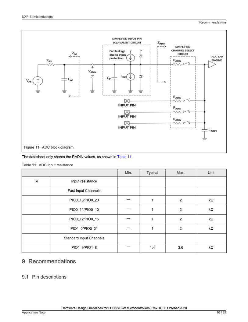
Figure 11. ADC block diagram
The datasheet only shares the RADIN values, as shown in Table 11.
Table 11. ADC input resistance
Min. Typical Max. Unit
Ri Input resistance
Fast Input Channels
PIO0_16/PIO0_23 — 1 2 kΩ
PIO0_11/PIO0_10 — 1 2 kΩ
PIO0_12/PIO0_15 — 1 2 kΩ
PIO1_0/PIO0_31 — 1 2 kΩ
Standard Input Channels
PIO1_9/PIO1_8 — 1.4 3.6 kΩ
9 Recommendations
9.1 Pin descriptions
NXP SemiconductorsRecommendations
Hardware Design Guidelines for LPC55(S)xx Microcontrollers, Rev. 0, 30 October 2020Application Note 16 / 24
9.1.1 Pin’s pull-up/down and open-drainAll pins have all pull-ups, pull-downs, and inputs turned off at reset except PIO0_2, PIO0_5, PIO0_11, PIO0_12, PIO0_13, and PIO0_14 pins. This prevents power loss through pins prior to software configuration. Due to special pin functions, some pins have a different reset configuration. PIO0_5 and PIO0_12 pins have internal pull-up enabled by default, and PIO0_2 and PIO0_11 have internal pull-down enabled by default. PIO0_13 and PIO0_14 are true open drain pins.
9.1.2 ADC pinsSome functions, such as ADC or comparator inputs, are available only on specific pins when digital functions are disabled on those pins. By default, the GPIO function is selected except on pins PIO0_11 and PIO0_12, which are the serial wire debug pins. This allows debug to operate through reset.
9.1.3 Wakeup pinsThe external reset pin or three wake-up pins can trigger a wake-up from deep power-down mode. For the wake-up pins, do not assign any function to this pin if it will be used as a wake-up input when using deep power-down mode. If not in deep power-down mode, a function can be assigned to this pin. If the pin is used for wake-up, it should be pulled HIGH externally before entering deep power-down mode. A LOW-going pulse as short as 50 ns causes the chip to exit deep power-down mode wakes up the part.
9.1.4 JTAG function pins
The JTAG functions, TRST, TCK, TMS, TDI, and TDO, are selected on pins, PIO0_2 to PIO0_6, by hardware when the part is in boundary scan mode. The JTAG functions cannot be used for debug mode.
NOTE
9.2 Termination of unused pinsTable 12 shows how to terminate pins that are not used in the application. In many cases, unused pins should be connected externally or configured correctly by software to minimize the overall power consumption of the part.
Unused pins with GPIO function should be configured as outputs set to LOW with their internal pull-up disabled. To configure a GPIO pin as output and drive it LOW, select the GPIO function in the IOCON register, select output in the GPIO DIR register, and write a 0 to the GPIO PORT register for that pin. Disable the pull-up in the pin’s IOCON register.
In addition, it is recommended to configure all GPIO pins that are not bonded out on smaller packages as outputs driven LOW with their internal pull-up disabled.
Table 12. Termination of unused pins
Pin Default state Recommended termination of unused pins
RESET Input, pull-up Can be left unconnected if the application does not use it.
All PIOn_m
(not open-drain)
Input, pull-up Can be left unconnected if driven LOW and configured as GPIO output with pull-up or pull-down disabled by software.
PIOn_m
(I2C open-drain)
Inactive
No pull-up or down
Can be left unconnected if driven LOW and configured as GPIO output by software.
XTAL32K_P — Connect to ground. When grounded, the RTC oscillator is disabled.
XTAL32K_N — Can be left unconnected.
VREFP — Tie to VBAT_DCDC
Table continues on the next page...
NXP SemiconductorsRecommendations
Hardware Design Guidelines for LPC55(S)xx Microcontrollers, Rev. 0, 30 October 2020Application Note 17 / 24
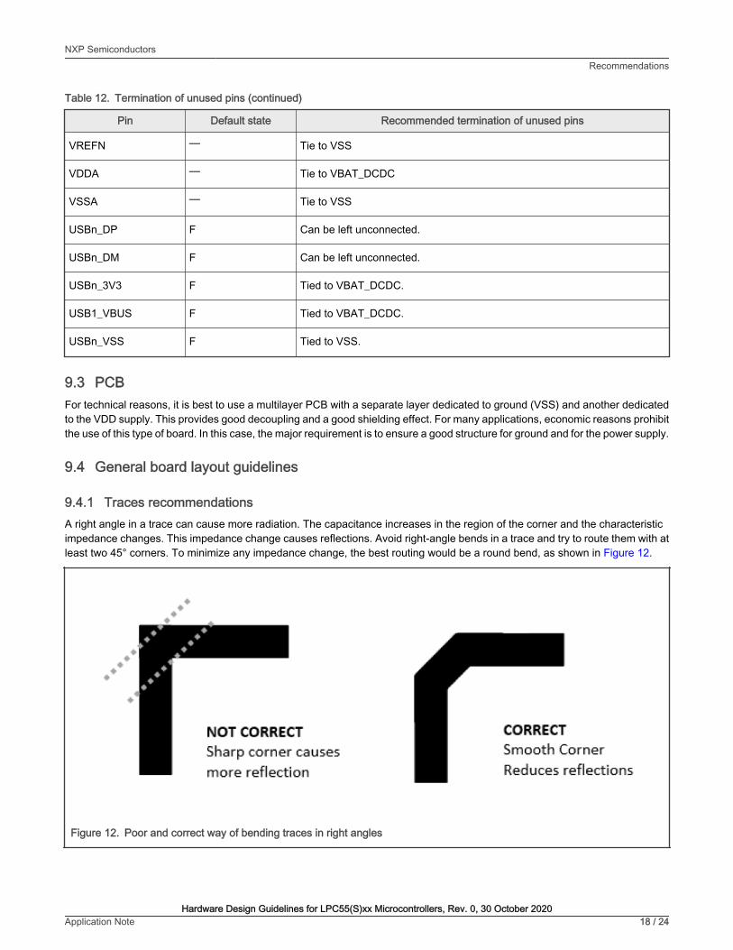
Table 12. Termination of unused pins (continued)
Pin Default state Recommended termination of unused pins
VREFN — Tie to VSS
VDDA — Tie to VBAT_DCDC
VSSA — Tie to VSS
USBn_DP F Can be left unconnected.
USBn_DM F Can be left unconnected.
USBn_3V3 F Tied to VBAT_DCDC.
USB1_VBUS F Tied to VBAT_DCDC.
USBn_VSS F Tied to VSS.
9.3 PCBFor technical reasons, it is best to use a multilayer PCB with a separate layer dedicated to ground (VSS) and another dedicated to the VDD supply. This provides good decoupling and a good shielding effect. For many applications, economic reasons prohibit the use of this type of board. In this case, the major requirement is to ensure a good structure for ground and for the power supply.
9.4 General board layout guidelines
9.4.1 Traces recommendationsA right angle in a trace can cause more radiation. The capacitance increases in the region of the corner and the characteristic impedance changes. This impedance change causes reflections. Avoid right-angle bends in a trace and try to route them with at least two 45° corners. To minimize any impedance change, the best routing would be a round bend, as shown in Figure 12.
Figure 12. Poor and correct way of bending traces in right angles
NXP SemiconductorsRecommendations
Hardware Design Guidelines for LPC55(S)xx Microcontrollers, Rev. 0, 30 October 2020Application Note 18 / 24
To minimize crosstalk, not only between two signals on one layer but also between adjacent layers, route them 90° to each other. Complex boards need to use vias while routing; you have to be careful when using them. These add additional capacitance and inductance, and reflections occur due to the change in the characteristic impedance. Vias also increase the trace length. While using differential signals, use vias in both traces or compensate the delay in the other trace.
9.4.2 GroundingGrounding techniques apply to both multi-layer and single-layer PCBs. The objective of grounding techniques is to minimize the ground impedance and thus to reduce the potential of the ground loop from circuit back to the supply.
• Route high-speed signals above a solid and unbroken ground plane.
• Do not split the ground plane into separate planes for analog, digital, and power pins. A single and continuous ground plane is recommended.
• There should be no floating metal/shape of any kind near any area close to the microcontroller pins. Fill copper in the unused area of signal planes and connect these coppers to the ground plane through vias.
NXP SemiconductorsRecommendations
Hardware Design Guidelines for LPC55(S)xx Microcontrollers, Rev. 0, 30 October 2020Application Note 19 / 24
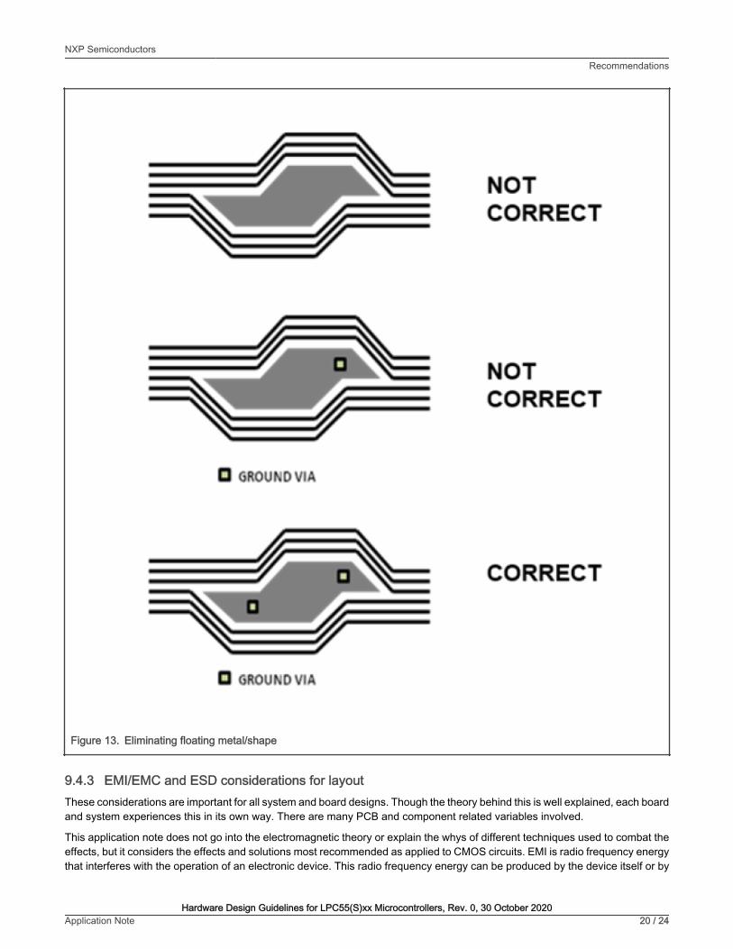
Figure 13. Eliminating floating metal/shape
9.4.3 EMI/EMC and ESD considerations for layoutThese considerations are important for all system and board designs. Though the theory behind this is well explained, each board and system experiences this in its own way. There are many PCB and component related variables involved.
This application note does not go into the electromagnetic theory or explain the whys of different techniques used to combat the effects, but it considers the effects and solutions most recommended as applied to CMOS circuits. EMI is radio frequency energy that interferes with the operation of an electronic device. This radio frequency energy can be produced by the device itself or by
NXP SemiconductorsRecommendations
Hardware Design Guidelines for LPC55(S)xx Microcontrollers, Rev. 0, 30 October 2020Application Note 20 / 24
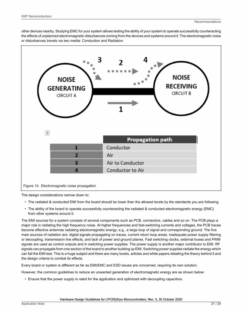
other devices nearby. Studying EMC for your system allows testing the ability of your system to operate successfully counteracting the effects of unplanned electromagnetic disturbances coming from the devices and systems around it. The electromagnetic noise or disturbances travels via two media: Conduction and Radiation.
Figure 14. Electromagnetic noise propagation
The design considerations narrow down to:
• The radiated & conducted EMI from the board should be lower than the allowed levels by the standards you are following.
• The ability of the board to operate successfully counteracting the radiated & conducted electromagnetic energy (EMC) from other systems around it.
The EMI sources for a system consists of several components such as PCB, connectors, cables and so on. The PCB plays a major role in radiating the high frequency noise. At higher frequencies and fast-switching currents and voltages, the PCB traces become effective antennas radiating electromagnetic energy; e.g., a large loop of signal and corresponding ground. The five main sources of radiation are: digital signals propagating on traces, current return loop areas, inadequate power supply filtering or decoupling, transmission line effects, and lack of power and ground planes. Fast switching clocks, external buses and PWM signals are used as control outputs and in switching power supplies. The power supply is another major contributor to EMI. RF signals can propagate from one section of the board to another building up EMI. Switching power supplies radiate the energy which can fail the EMI test. This is a huge subject and there are many books, articles and white papers detailing the theory behind it and the design criteria to combat its effects.
Every board or system is different as far as EMI/EMC and ESD issues are concerned, requiring its own solution.
However, the common guidelines to reduce an unwanted generation of electromagnetic energy are as shown below:
• Ensure that the power supply is rated for the application and optimized with decoupling capacitors.
NXP SemiconductorsRecommendations
Hardware Design Guidelines for LPC55(S)xx Microcontrollers, Rev. 0, 30 October 2020Application Note 21 / 24
• Provide adequate filter capacitors on the power supply source. The bulk/bypass and decoupling capacitors should have low equivalent series inductance (ESL).
• Create ground planes if there are spaces available on the routing layers. Connect these ground areas to the ground plane with vias.
• Keep the current loops as small as possible. Add as many decoupling capacitors as possible. Always apply current return rules to reduce loop areas.
• Keep high-speed signals away from other signals and especially away from input and output ports or connectors.
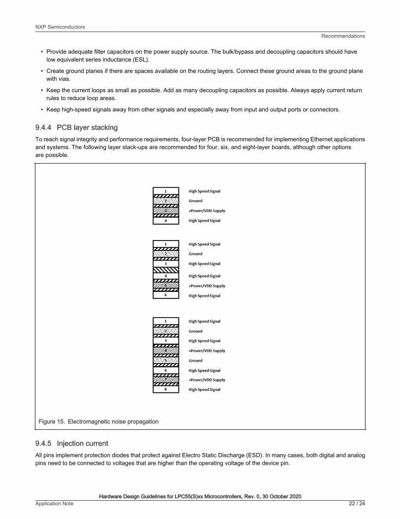
9.4.4 PCB layer stackingTo reach signal integrity and performance requirements, four-layer PCB is recommended for implementing Ethernet applications and systems. The following layer stack-ups are recommended for four, six, and eight-layer boards, although other options are possible.
Figure 15. Electromagnetic noise propagation
9.4.5 Injection currentAll pins implement protection diodes that protect against Electro Static Discharge (ESD). In many cases, both digital and analog pins need to be connected to voltages that are higher than the operating voltage of the device pin.
NXP SemiconductorsRecommendations
Hardware Design Guidelines for LPC55(S)xx Microcontrollers, Rev. 0, 30 October 2020Application Note 22 / 24
The internal ESD diodes of the microcontroller are designed for short discharge pulses only, and these do not sustain a constant current over time. Therefore, the maximum continuous voltage that drops over them is specified in the DC electrical parameters and the maximum high input voltage should not be higher than VDD + 0.5 V, and the current injection also should be limited as defined in the device data sheet. In other words, the voltage and current of an input signal must be within the electrical parameter allowed. The outcome of violating these specifications causes unexpected behavior, stuck operation or a major damage in the MCU.
10 References1. Hardware Design Guidelines for S32K1xx Microcontrollers (document AN5426)
2. LPC55S1x User manual (document UM11295)
3. LPC55S2x/LPC552x/LPC55S6x/LPC556x User manual (document UM11126)
11 Revision history
Rev. Date Description
0 30 October 2020 Initial release
NXP SemiconductorsReferences
Hardware Design Guidelines for LPC55(S)xx Microcontrollers, Rev. 0, 30 October 2020Application Note 23 / 24
How To Reach Us
Home Page:
nxp.com
Web Support:
nxp.com/support
Information in this document is provided solely to enable system and software implementers to use NXP products. There are no express or implied copyright licenses granted hereunder to design or fabricate any integrated circuits based on the information in this document. NXP reserves the right to make changes without further notice to any products herein.
NXP makes no warranty, representation, or guarantee regarding the suitability of its products for any particular purpose, nor does NXP assume any liability arising out of the application or use of any product or circuit, and specifically disclaims any and all liability, including without limitation consequential or incidental damages. “Typical” parameters that may be provided in NXP data sheets and/or specifications can and do vary in different applications, and actual performance may vary over time. All operating parameters, including “typicals,” must be validated for each customer application by customer's technical experts. NXP does not convey any license under its patent rights nor the rights of others. NXP sells products pursuant to standard terms and conditions of sale, which can be found at the following address: nxp.com/SalesTermsandConditions.
While NXP has implemented advanced security features, all products may be subject to unidentified vulnerabilities. Customers are responsible for the design and operation of their applications and products to reduce the effect of these vulnerabilities on customer’s applications and products, and NXP accepts no liability for any vulnerability that is discovered. Customers should implement appropriate design and operating safeguards to minimize the risks associated with their applications and products.
NXP, the NXP logo, NXP SECURE CONNECTIONS FOR A SMARTER WORLD, COOLFLUX, EMBRACE, GREENCHIP, HITAG, ICODE, JCOP, LIFE VIBES, MIFARE, MIFARE CLASSIC, MIFARE DESFire, MIFARE PLUS, MIFARE FLEX, MANTIS, MIFARE ULTRALIGHT, MIFARE4MOBILE, MIGLO, NTAG, ROADLINK, SMARTLX, SMARTMX, STARPLUG, TOPFET, TRENCHMOS, UCODE, Freescale, the Freescale logo, AltiVec, CodeWarrior, ColdFire, ColdFire+, the Energy Efficient Solutions logo, Kinetis, Layerscape, MagniV, mobileGT, PEG, PowerQUICC, Processor Expert, QorIQ, QorIQ Qonverge, SafeAssure, the SafeAssure logo, StarCore, Symphony, VortiQa, Vybrid, Airfast, BeeKit, BeeStack, CoreNet, Flexis, MXC, Platform in a Package, QUICC Engine, Tower, TurboLink, EdgeScale, EdgeLock, eIQ, and Immersive3D are trademarks of NXP B.V. All other product or service names are the property of their respective owners. AMBA, Arm, Arm7, Arm7TDMI, Arm9, Arm11, Artisan, big.LITTLE, Cordio, CoreLink, CoreSight, Cortex, DesignStart, DynamIQ, Jazelle, Keil, Mali, Mbed, Mbed Enabled, NEON, POP, RealView, SecurCore, Socrates, Thumb, TrustZone, ULINK, ULINK2, ULINK-ME, ULINK-PLUS, ULINKpro, µVision, Versatile are trademarks or registered trademarks of Arm Limited (or its subsidiaries) in the US and/or elsewhere. The related technology may be protected by any or all of patents, copyrights, designs and trade secrets. All rights reserved. Oracle and Java are registered trademarks of Oracle and/or its affiliates. The Power Architecture and Power.org word marks and the Power and Power.org logos and related marks are trademarks and service marks licensed by Power.org.
© NXP B.V. 2020-2022. All rights reserved.
For more information, please visit: http://www.nxp.comFor sales office addresses, please send an email to: [email protected]
Date of release: 30 October 2020Document identifier: AN13033
Copyright © 2022 FDOKUMEN