Renesas Microcontrollers RL78 Family - RS Components
63
2017.07 RL78 FAMILY Renesas Microcontrollers
-
Upload
khangminh22 -
Category
Documents
-
view
0 -
download
0
Transcript of Renesas Microcontrollers RL78 Family - RS Components

www.renesas.com 2017.07
RL78 FAMILYRenesas Microcontrollers

01-02
General-purpose
LCD
ASSP
Automotiveproducts
Enhanced analog functionsConfigurable amplifier, 12-bit ADC
64 to 80pins Sub-GHz256K to 512KB
64pin
Compact
Enhancedperipheral
Enhancedperipheral
Enhanced analog, High Function16KB, 20 to 25pin
Enhanced analog functions12-bitADC, DAC, AMP
48K to 128KB, 80 to 100pin
Bluetooth LE128K to 256KB
48pin
Simple1K to 4KB
10 to 16pin
Small Motor8K to 16KB30 to 44pin
For wireless systems
USB control32KB, 32 to 48pin
High Function16K to 512KB30 to 100pin
Standard16K to 512KB20 to 128pin
Small2K to 16KB20 to 30pin
Standard16K to 128 KB
64 to 80 pin
USB control64K to 256 KB80 to 100 pin
Small8K to 32 KB32 to 64 pin
Lighting, Power SupplyDedicated Timer
32K to 64KB20 to 38pin
Sensors8K to 32KB20 to 48pin
Enhanced analog functions for sensors24-bit Sigma-delta ADC,12bit-DAC, Config AMP
32KB, 32 to 36pin
Electricity meters (AMR/AMI)High performance, Security64K to 256KB, 64 to 100pin
Electricity meters24-bit Sigma-delta ADC
64K to 128KB, 80 to 100pin
SmallLIN, Safety8K to 64KB20 to 64pin
12-bitADC, 25 to 64pin
G1E
G1A
G1G
G10
G1C
G14
G13
G12
L13
L12
I1A
20 to 64pin
F12
I1D
I1B
L1C
G1H
G1D
G1F
G11
L1A
I1E
I1C
GxNext
GxNext
LxNext
For motor systems
For compact systems
Enhancedperipheral
IxNext
Enhancedperipheral
FxNext
~2014 2015 2016 2017
In planning stageUnder developmentNew productMass-produced product
CAN/LIN, Safety16K to 128KB20 to 80pin
CAN/LIN, Motor, Safety48K to 256KB30 to 100pin
F13Standard
F14High Function
CAN/LIN/IEBus, Motor, Safety128K to 512KB48 to 144pinF15
High Function
Multiple Functions, Sensor-less32K to 64KB24 to 64pin
45.5 µA/MHz operation*1
0.57 µA (RTC + LVD) New SNOOZE modeNote: 1. Power supply current value during basic
RL78/G10 operation
32 MHz ±1% high-precision on-chip oscillator On-chip power-on reset, low-voltage detection
circuit, temperature sensor, data flash memory, etc.
Integrated development tools for more efficient development
Support for powerful tools from Renesas partners
Comprehensive Development Tools
Memory with ECC Compliant with Safety Standard for
Household Appliances (IEC 60730) Support for high operating tempera-
tures (up to 150°C) Abnormal operation
detection/avoidance function
Reliable Safety Functions
Low Power Consumption
10 to 128 pins/1 to 512 KB Extensive product lineup to meet
a broad range of requirements Pin compatibility Ability to reassign peripheral function
pins
Broad Scalability
High processing performance of 1.39 DMIPS/MHz
Support for power supply voltages from 1.6 to 5.5 V
Max. 32 MHz operation
High Performance
Reduced System Cost
RL78 application fields
The RL78 Family is utilized in a wide variety of applications.
The RL78 Family is the new generation of power-efficient microcontrollers from Renesas. It enables customers to build compact and energy-efficient systems at lower cost.The RL78 is a new generation of power-efficient microcontrollers that combine the excellent CPU performance of the 78K0R with the superior on-chip functions of the R8C and 78K. It delivers higher performance and lower power consumption than previous microcontrollers while enabling customers to utilize software resources developed for the R8C and 78K.
RL: Renesas Low powerRL products deliver reduced power consumption.
RL78 roadmap
Industrial AutomationG14 G11 I1A I1E
Lineup of microcontrollers for industrial applications requiring high reliability
Broad array of compact packages Operating temperature range of –40°C to
+105°C, and support available for higher temperatures
Home AutomationG13 G1D G1H
Power efficiency among the best in the industry for extended battery life
Support for low-voltage operation (1.6 V to (G1H: 1.8 V and above))
Standby function with newly added SNOOZE mode for low power consumption during intermittent operation
Power ToolsG1F G14
Proven track record supplying consistently high-quality microcontrollers over the long term
Ideal microcontroller platform for system development with lineup covering wide range of memory capacities, pin counts, and package options
AutomotiveF13 F14 F15
Lineup of highly reliable microcontrollers for automotive applications
Support for high operating temperatures (up to +150°C)
CAN communication, safety functions, etc., for automotive applications
Medical/HealthcareL1A L13 I1E G1D
Lineup of compact packages Proven track record supplying major medical
equipment manufacturers Active member of Continua Health Alliance
Consumer ElectronicsG13 G12 G10
Calendar function (RTC) as standard feature
Serial communication, timers, and on-chip high-speed oscillator as standard features
MeteringI1B I1C L13 G1H
Standby function that is ideal for low-power applications such as meters and measuring devices
On-chip analog functions for smartmeters Proven track record supplying the meter field
for over 30 years
White GoodsG13 G12 L13
Hardware support for European safety stan-dard for household appliances (IEC60730)
Standard temperature range of –40°C to +85°C, and support available for higher temperatures
On-chip high-speed on-chip oscillator, power-on reset, etc., ideal for cost-sensitive electric household appliances
Motor ControlG14 G1F G1G
On-chip advanced-functionality timers for motor control
High-speed on-chip oscillator with accuracy of ±1%, ideal for low-cost, high-precision solutions
Lighting, Power SupplyI1A G11
High-resolution PWM output for lighting and power supply control applications
Easy-to-use Applilet software (free of charge) supporting program development for lighting applications
Support for DALI, DMX512, PMBus, and SMBus communication
DetectorI1D G11
Improved analog functions necessary for detecting very small sensor signals
Support for power-efficient detection when returning to high-speed operation from STOP mode
* Specifications vary depending on the application. Please refer to each product page for details.

03-04
Low Power Consumption New SNOOZE mode for more power savingsIn SNOOZE mode the CPU is halted while A/D conversion and data reception are enabled. By transitioning from STOP mode (clock stopped) to SNOOZE mode, it is possible to start the on-chip oscillator and operate peripheral functions while the CPU remains inactive.
Broad Scalability
SNOOZE mode It is not necessary to activate the CPU for data reception.
Using the exclusive SNOOZE mode, peripheral functions such as the ADC or UART can operate when in standby mode.
Power consumption is one-tenth of normal operation.
SNOOZE mode: 0.5 mA, RUN mode (ADC): 5 mA
HALT and STOP modes The standby function stops CPU operation, reducing overall
microcontroller current consumption by 80%.
The STOP mode disables the microcontroller’s on-chip functions, reducing power consumption to the lowest level possible.
Low-power, high-performance products for lower system power consumption overallIn the most common operating modes, the RL78 Family delivers an operating current of 65.5 µA/MHz (while operating at 32 MHz) and a standby current of 0.57 µA (in SUB-HALT mode, with the RTC and LVD operating). Also, a newly developed SNOOZE mode has been added to the previ-ously implemented HALT and STOP low-power operation modes. In SNOOZE mode the CPU is in the standby state while A/D conversion and serial communication are enabled, and the CPU is activated only when required. This mode is excellent for battery-powered systems as it greatly increases battery life.
Extensive memory size and package options The extensive lineup includes more than 300 product versions, with
memory sizes from 1 KB to 512 KB and package pin counts from 10 pins to 128 pins. This extensive selection provides support for a broad range of application fields, including consumer, automotive, industrial, and communications.
The wide range of options means that developers are covered if there are changes made to the specifications or more ROM capac-ity than originally estimated becomes necessary in the middle of the development process.
Customers can rely on the same microcontroller series when developing product models ranging from the low-end to the high-end. Total development man-hours are reduced.
Excellent pin compatibility Scalability is maintained because the general location of
peripheral function pins and input/output pins remains the same even when the pin count changes. Customers can continue to use the RL78 Family of microcontrollers with confidence in the future.
Customers can use standardized boards for product models ranging from the low-end to the high-end and boost the efficiency of the verification process.
Ability to reassign pin functions with PIOR register settingsPin assignments can be changed for added board layout flexibility. The locations of peripheral function pins can be optimized.Note: Not all pins can be reassigned.
NEW
: Running
: Stopped
HALTPeripheralfunctionClockCPU
MAIN RUNPeripheralfunctionClockCPU
STOPPeripheralfunctionClockCPU
Power consumption can be reduced even more than in HALT mode.
SNOOZEPeripheralfunctionClockCPU
A/D conversion, serial data reception, multiply and divide operations, multiply-accumulate operations, and DMA operations are possible.
Example of A/D conversion in SNOOZE mode
ADC activated by timer
ADC values out of range: CPU is activated to process out-of-range values.
Analog input
Upper Limit
Lower Limit
Time
Source: Product data sheets and actual measurement
5.1µA3.4µA
10.3µA
14.3µA
0.53µA
RL78/G13
STOP mode current comparison (WDT + LVD)
Company A
Company B
Company C
Company D
0.53µA
14.3µA
10.3µA
5.6µA3.6µA
10.6µA12.5µA
0.57µA
RL78/G13
Operating current comparison during clock operation (32.768 kHz, RTC + LVD)
Company A
Company B
Company C
Company D
10.6µA
3.6µA
12.5µA
5.6µA213µA
65.5µA150µA
363µA 380µA
RL78/G13
Operating current comparison (µA/MHz)
Company A
Company B
Company C
Company D
65.5µA
380µA363µA
150µA213µA
Example of I/O port assignments on RL78/G1x
P0
P1
P2
P5
P7
System Pins
I2C_A0 INTP10 Timer 05I/O
SystemI/O
AnalogI/O
Timer 0 I/O
PIOR
Before change After change
I2C_A0
INTPn
I2C_A0
INTP10
Timer 05I/O
SystemI/O
AnalogI/O
Timer 0 I/O
PIOR
I2C_A0
INTPn
Flash(KB)
512
384
256
192
128
96
64
48
32
16
12
8
4
2
1
20 24 2510 16 30 32 36 38 40 44 48 52 64 80 85 100 128 Pin

05-06
Error detection
These functions check to make sure that the microcontroller’s
internal CPU and memory are operating properly. When an error is detected,
measures such as an internal reset of the microcontroller can help to prevent the
system from malfunctioning.• Watchdog timer (WDT) as standard feature• Flash memory CRC calculation • RAM parity error detection • RAM ECC function*1 • CPU stack pointer monitoring function*1
• Illegal memory access detection function*1
Memory guard
This function disables writing to selected addresses in the RAM and SFRs.*2 It
makes it possible to protect settings in RAM and the
SFRs, contributing to improved reliability for the customer’s system.• RAM accidental write protection • SFR accidental write protection
Fault detection
This function is for checking the operation of the microcontroller’s clock generator
circuit, A/D converter, and I/O pins. It simplifies the task of verifying microcontroller
operation and makes it easier for customers to ensure safe and reliable operation of
their systems.
• Frequency detection • Simple A/D testing
• I/O power output level detection • Clock monitoring function*1
Notes: 1. Available on the RL78/F13 and RL78/F14.2. SFR (special function register): Registers that store settings related to special functions such as clock
control, the low-voltage detection circuit, port control, and interrupts.
RL78 CPU Core Three-stage pipeline CISC architecture Max. operating frequency: 32 MHz Support for multiply, divide, and
multiply-accumulate instructionsMemory Support for 1.8 V flash programming and boot swap Program flash: 1 KB–512 KB SRAM: 2.5 KB–48 KB Data flash: 4 KB/8 KB
System High-speed on-chip oscillator: 32 MHz ±1%
(operation supported on timer RD only, 64/48 MHz) Power management Operating current: 66 µA/MHz*1
HALT current: 0.57 µA (RTC + LVD)*1
STOP current: 240 nA (SRAM data retained)*1
SNOOZE current: 700 µA (UART), 1.2 mA (ADC)
Safety Compliant with European safety standard for
household appliances (IEC/UL 60730)Timers Advanced-functionality timer array unit (TAU) Timer RD for three-phase motor control
Timer RG with two-phase encoder PWM function
Watchdog timer, real-time clockAnalog On-chip ADC: 10-bit × 20 channels,
conversion time: 2.1 µs On-chip DAC: 8-bit × 2 channels, comparator
× 2 channelsCommunication CSI, UART, I2C, Simple I2C
Package 10-pin–144-pin
Note: 1. Power supply current for RL78/G14 Group, 64-pin, ROM = 64 KB product.
High Performance RL78 microcontrollers with CPU core employing three-stage pipeline and Harvard architectureCPU processing performance is substantially improved compared with previous Renesas products.
Reliable Safety Functions Safety functions built into the microcontroller that enhance system reliabilityGenerally speaking a microcontroller is expected to operate normally even when exposed to noise. The RL78 Family of microcontrollers have a number of safety functions that allow confirmation of normal operation. Customers can use these functions to easily perform self-diagnostics on microcontrollers. The self-diagnostic functions of the RL78 Family contribute to enhanced system reliability.
Comprehensive Development Tools A full lineup of tools that provides powerful support for efficient developmentRenesas provides support for all stages of RL78 application development. The CS+ integrated development environment is easy to use and learn, helping shorten development cycles. A variety of debugging and programming environments are available to meet specific customer needs. Finally, Renesas partner vendors offer a rich array of tools and services covering a broad range of requirements.
Reduced System Cost Helping customers reduce system size and costOn-chip peripheral functions include a high precision (±1%) high-speed on-chip oscillator, background operation data flash supporting 1 million erase/program cycles, a temperature sensor, and multiple power supply interface ports. The RL78 Family is fabricated using a newly developed 130 nm process that enables customers to achieve reduced system cost and smaller overall system size.
Data flash with advanced functionality (background operation) for substantially reduced programming time Data access unit: 1 byte Data flash size: 4 KB (erasure unit: 1 KB) Number of overwrites: 1 million (typ.) (target) Dedicated library: Simplifies operations
(Reference) RL78: Block diagram of G14 Group 100-pin product.
Memory
Program flashUp to 512 KB
SRAMup to 48 KB
Data flashUp to 8 KB
Power management
HALTRTS, DTC enabled
SNOOZESerial, ADC enabled
STOPSRAM on
System
DTC39 sources
ELC26 sources
POR, LVD
Interrupt controller4 levels
Clock generationOCO, external
DebugSingle-wire
RL78 CPU core32 MHz operation
CISC Harvard architecture3-stage pipeline
MUL, DIV, MACInstruction
16-bit barrel shifter
4 register banksSafety
RAMParity check
ADCSelf-diagnostics
ClockMonitoring
MemoryCRC
I/O PortRead back
Timers
Timer array unit16-bit, 8 channels
Interval timer 12-bit, 1 channel
Timer RD 16-bit, 2 channels
Timer RG 16-bit, 1 channel
Timer RJ 16-bit, 1 channel
WDT 17-bit
RTC Calendar
Communication
2 × l2CMulti-Master
2 × CSI/UART(LIN-bus)/2 × simple I2C
2 × CSI/UART/2 × simple I2C
2 × CSI/UART/2 × simple I2C
2 × CSI/UART/2 × simple I2C
Analog
ADC10-bit, 20 channels
Internal Vref
Temp. sensor
10
20
30
40
A(16-bit,16MHz)
B(32-bit,24MHz)
RL78(16-bit,32MHz)
30DMIPS(1.25DMIPS/
MHz)
44DMIPS(1.39DMIPS/
MHz)
16DMIPS(1DMIPS/
MHz)
DM
IPS/
MH
z
• Power supply detection circuit• Temperature sensor • Multiple power supply interface ports
Resonator
EEPROM
Reset and WDT IC
Neat and compact design
RL78
Data programming/erase Data programming/eraseData programmin
User programoperation
/erase Data programmin
User programoperation
/erase
User programoperation
User programoperation
User programoperation
User programoperation
Data programming/erase Data programming/erase
Greatly reduced programming time
Simultaneous execution possible
example of 78K0R/Kx3
Previous product
Fault detection
Error detection
Memoryguard
Debugging on PC
Debugging with basic functions
Instruction simulator
Full-spec emulator
On-chip debugging emulator with programming functions
Debugging
Debugging with advanced functions
CS+
E1 E2 Lite
IECUBE
Programming based on specifications when ordering ROM
Programming under PC control
Programming service from Renesas Electronics
Flash memory programmer
On-chip debugging emulator with programming functions
Programming
Programming under PC control or standalone
Programmed
E1
PG-FP5
E2 LiteCoding, building, device drivers
Simple operation, easy-to-access support
Integrated development environment
Real-time OS
CS+
Software development
Itron basedOS
Coding, building, device drivers
easy-to-access support
07-08
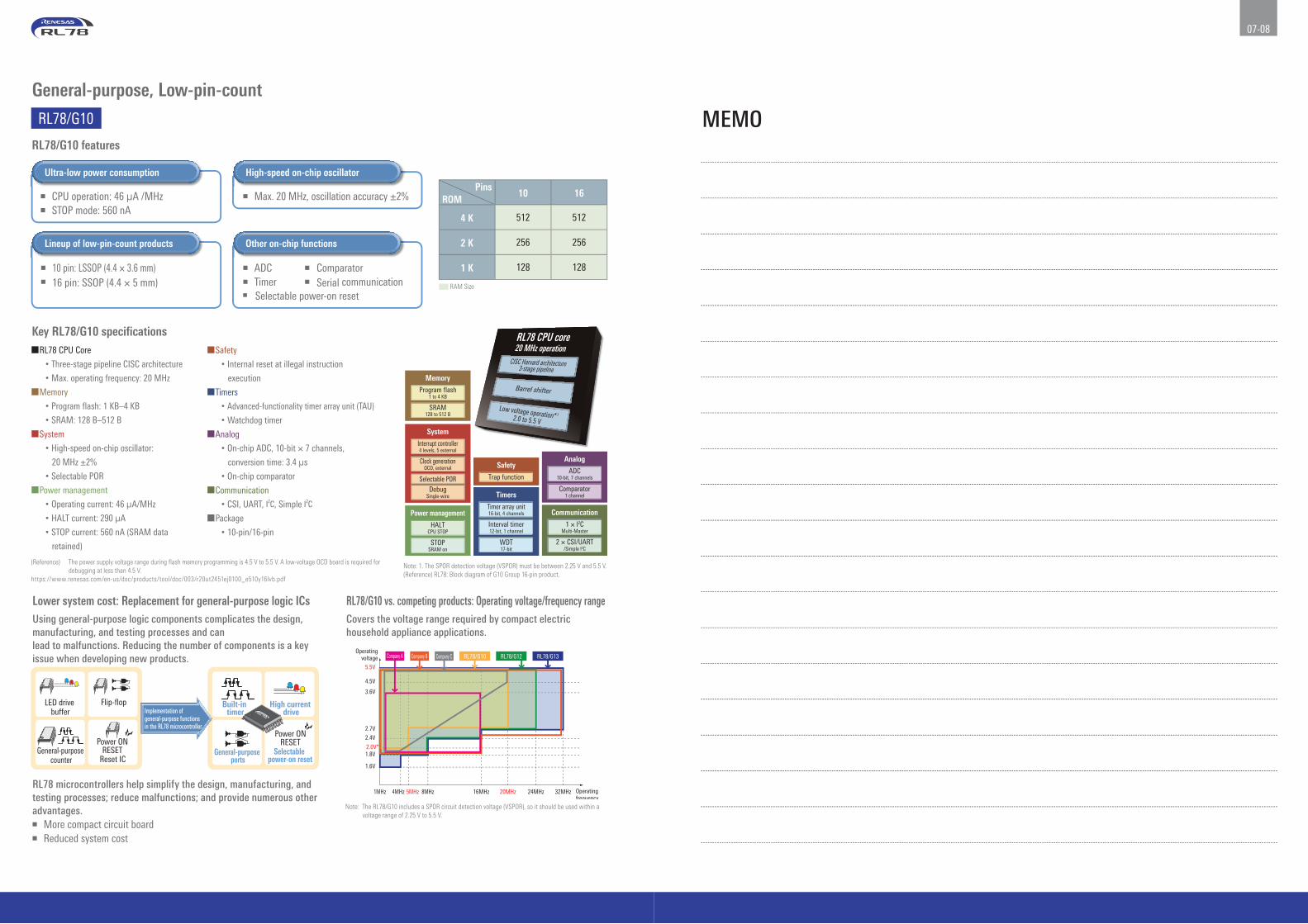
RL78/G10 features
Key RL78/G10 specificationsRL78 CPU Core
• Three-stage pipeline CISC architecture• Max. operating frequency: 20 MHz
Memory• Program flash: 1 KB–4 KB• SRAM: 128 B–512 B
System• High-speed on-chip oscillator:
20 MHz ±2%• Selectable POR
Power management• Operating current: 46 µA/MHz• HALT current: 290 µA• STOP current: 560 nA (SRAM data
retained)
Safety• Internal reset at illegal instruction
execution
Timers• Advanced-functionality timer array unit (TAU)• Watchdog timer
Analog• On-chip ADC, 10-bit × 7 channels,
conversion time: 3.4 µs• On-chip comparator
Communication• CSI, UART, I2C, Simple I2C
Package• 10-pin/16-pin
(Reference) The power supply voltage range during flash memory programming is 4.5 V to 5.5 V. A low-voltage OCD board is required for debugging at less than 4.5 V.
https://www.renesas.com/en-us/doc/products/tool/doc/003/r20ut2451ej0100_e510y16lvb.pdf
Note: 1. The SPOR detection voltage (VSPOR) must be between 2.25 V and 5.5 V.(Reference) RL78: Block diagram of G10 Group 16-pin product.
RL78 microcontrollers help simplify the design, manufacturing, and testing processes; reduce malfunctions; and provide numerous other advantages. More compact circuit board Reduced system cost
Note: The RL78/G10 includes a SPOR circuit detection voltage (VSPOR), so it should be used within a voltage range of 2.25 V to 5.5 V.
ROM Pins
10 16
4 K 512 512
2 K 256 256
1 K 128 128
RAM Size
ADC Comparator Timer Serial communication Selectable power-on reset
Other on-chip functions
10 pin: LSSOP (4.4 × 3.6 mm) 16 pin: SSOP (4.4 × 5 mm)
Lineup of low-pin-count products
CPU operation: 46 µA /MHz STOP mode: 560 nA
Ultra-low power consumption High-speed on-chip oscillator
Max. 20 MHz, oscillation accuracy ±2%
RL78/G10
General-purpose, Low-pin-count
MEMO
Lower system cost: Replacement for general-purpose logic ICsUsing general-purpose logic components complicates the design, manufacturing, and testing processes and can lead to malfunctions. Reducing the number of components is a key issue when developing new products.
RL78/G10 vs. competing products: Operating voltage/frequency rangeCovers the voltage range required by compact electric household appliance applications.
Memory
Program flash1 to 4 KB
SRAM128 to 512 B
Analog
ADC10-bit, 7 channels
Comparator1 channel
Safety
Trap function
Communication
1 × l2CMulti-Master
2 × CSI/UART/Simple l2C
Timers
Timer array unit16-bit, 4 channels
Interval timer12-bit, 1 channel
WDT17-bit
Power management
HALTCPU STOP
STOPSRAM on
System
Interrupt controller4 levels, 5 external
Clock generationOCO, external
Selectable PORDebug
Single-wire
RL78 CPU core20 MHz operation
CISC Harvard architecture3-stage pipeline
Barrel shifter
Low voltage operation*12.0 to 5.5 V
Built-in timer
High current drive
General-purpose ports
Selectable power-on reset
Power ONRESET
LED drive buffer
Flip-flop
General-purpose counter Reset IC
Power ONRESET
Implementation of general-purpose functions in the RL78 microcontroller
5.5V
Operatingvoltage
Operating frequency
4.5V
3.6V
2.7V
2.4V
2.0V*1.8V
1.6V
1MHz 4MHz 8MHz 16MHz 20MHz 24MHz 32MHz5MHz
Company A Company B Company C RL78/G10 RL78/G12 RL78/G13

09-10
RL78/G12, G13
Extensive lineup: RL78/G12, G13Choose with confidence. Extensive lineup of 284 products.
Block diagramRL78 CPU Core Three-stage pipeline CISC architecture Max. operating frequency: 32 MHz
Memory Support for 1.8 V flash programming and boot swap Program flash: 2 KB–512 KB SRAM: 256 B–32 KB Data flash: 2 KB/4 KB/8 KB/None
System High-speed on-chip oscillator: 32 MHz ±1% Library support for multiply/divide and
multiply-accumulate operation unit Power management Operating current: 66 µA/MHz*1
HALT current: 0.57 µA (RTC + LVD)*1
STOP current: 230 nA (SRAM data retained)*1
SNOOZE current: 700 µA (UART), 1.2 mA (ADC)Safety Compliant with European safety standard for household appliances
(IEC/UL 60730) Illegal memory access detection
Timers Advanced-functionality timer array unit (TAU) Watchdog timer, real-time clock
Analog 1.6 V (VDD) operation On-chip ADC, 10-bit × 26 channels,
conversion time: 2.1 µs Internal reference voltage (1.45 V)
Communication CSI, UART, I2C, Simple I2C
Package 20-pin–128-pin
Note: 1. Power supply current RL78/G13 Group product with 64 pins and 64 KB of ROM.
Extensive lineup: Compact packagesAvailable compact package options are ideal for miniaturized products.
High performance: Low-voltage operationExpanded operating range compared with previous products and support for A/D conversion at voltages from 1.6 V
High performance: Multiply and divide/multiply-accumulate operation unitOn-chip multiply-accumulate operation unit for reduced operation load on CPU
Completion interrupt generated for divide operations only. Multiply-accumulate operation overflow/underflow interrupt
generated when the cumulative result of multiply-accumulate operations causes an overflow or underflow.
Combined-use divide completion interrupt and multiply-accumulate operation overflow/underflow interrupt.
Whether an overflow or underflow occurred can be determined by referencing a status flag.
Since the C lacks multiply-accumulate operation instructions, library functions are provided.
Multiply and divide circuit with support for multiply-accumulate operationsoperation exec cycle
Signed multiply16 bits×16 bits=32 bits 1 clock
Unsigned multiply
Unsigned divide 32 bits/32 bits=32 bits ... 32 bits 16 clock
Signed multiply-accumulate16 bits×16 bits+32 bits=32 bits 2 clock
Unsigned multiply-accumulate
General-purpose, Standard
(Reference) RL78: Block diagram of G13 Group 128-pin product.
Memory
Program flashUp to 512 KB
SRAMUp to 32 KB
Data flashUp to 8 KB/none
Analog
ADC10-bit, 26 channels
Internal Vref
Temp. sensor
Safety
RAMParity check
ADCSelf-diagnostics
ClockMonitoring
MemoryCRC Communication
2 × I2CMulti-Master
2 × CSI/UART/2 × simple l2C
2 × CSI/UART/2 × simple l2C
2 × CSI/UART(LIN-bus)
/2 × simple l2C
2 × CSI/UART/2 × simple l2C
Timers
Timer array unit16-bit, 16 channels
Interval timer12-bit, 1 channel
WDT17-bit, 1 channel
RTCCalendar
Power management
HALTRTS, DMA enabled
SNOOZESerial, ADC enabled
STOPSRAM on
System
DMA4 channels
Interrupt controller4 levels, 20 pins
Clock generationOCO, external
POR, LVD
MUL, DIV, MAC
DebugSingle-wire
RL78 CPU core32 MHz operationCISC Harvard architecture
3-stage pipeline
4 register banks
16-bit barrel shifter
20
512 KBROM
Pins
384 KB256 KB192 KB128 KB96 KB64 KB48 KB32 KB
16 KB
12 KB
8 KB4 KB2 KB
24 25 30 32 36 40 44 48 52 64 80 100 128
4 K3 K2 K2 K
1.5 K1 K768512256
4 K3 K2 K2 K
1.5 K1 K768
4 K3 K2 K2 K
1.5 K1 K768512512
4 K3 K2 K
4 K3 K2 K2 K2 K
4 K3 K
12 K8 K
2 K0K0K2 K
4 K3 K
12 K8 K
2 K2 K
4 K3 K
12 K8 K
2 K2 K
4 K3 K
12 K16 K
8 K
2 K2 K
4 K3 K
12 K16 K20 K24 K32 K
8 K
2 K
4 K3 K
12 K16 K20 K24 K32 K
8 K
2 K2 K2 K
4 K3 K
12 K16 K20 K24 K32 K
8 K
2 K
12 K16 K20 K24 K32 K
8 K12 K16 K20 K24 K32 K
8 K
2 K1 K768512
4 K3 K
12 K16 K20 K24 K32 K
8 K
2 K2 K
4 K3 K
12 K16 K20 K24 K
4 K3 K
12 K16 K20 K24 K32 K
8 K
2 K2 K
32 K
8 K
2 K
4 K3 K
12 K16 K20 K24 K
4 K3 K
12 K16 K20 K24 K32 K
8 K
2 K
32 K
8 K
2 K
12 K16 K20 K24 K32 K
8 K12 K16 K20 K24 K32 K
8 K
16 K20 K24 K32 K
4 K3 K2 K2 K
1.5 K1 K768512256
4 K3 K
12 K8 K
2 K2 K2 K1 K768512
4 K3 K
12 K8 K
2 K2 K
4 K3 K
12 K8 K
2 K2 K
4 K3 K
12 K16 K
8 K
2 K2 K
16 K20 K24 K32 K
RL78/G13
1. For 20-pin packages, the pin spacing of the RL78/G12 is 225 mil and that of the RL78/G13 is 300 mil.2. For the 64-pin BGA (4 × 4) package products, the ROM capacity ranges from 32 KB to 256 KB.
RAM No data flash RAM Equipped with data flash
RL78/G12
Reduced system cost: On-chip high-precision, high-speed oscillatorOn-chip high-precision, high-speed oscillator to support UART communication
• On-chip high-speed clock generator circuit with precision of ±1%*1
• Selectable frequencies: 32 MHz,*2 24 MHz, 16 MHz, 12 MHz, 8 MHz, 6 MHz, 4 MHz, 3 MHz, 2 MHz, and 1 MHz
• Oscillation accuracy correction register for even higher precisionNotes: 1. ±5% on R5F103x 2. RL78/G13 only
HOCO oscillation frequency accuracy
+5.5+5.0
+1.5+1.0
0.0
1.6 1.8 2.4 2.7 5.5
Accu
racy
(%)
Voltage(V)
– 1.0– 1.5
– 5.0– 5.5
TA= –20 to+85ºCTA= –40 to– 20ºC
CPU
A/D
Timer
UART
12MHz8MHz6MHz4MHz3MHz2MHz1MHz
Selectable among 10 frequencies
Oscillation accuracy correction register
Other IC
32MHz*2
24MHz16MHz
Correction enablingeven higher precision
for reference frequencies of subclock, etc.
High-precision oscillation enabling UART communication
RL78/G12
Operating frequency range extended to 32 MHz*1
Operation at 1.8 V supported up to 8 MHz
5.5V
2.7V
2.4V
1.8V
1.6V
1MHz 4MHz 8MHz 12MHz 16MHzFrequency
Oper
atin
g vo
ltage
20MHz 24MHz 32MHz
Operation supported at 1.6 V and above*2
Flash self-programming supported at 1.8 V and above
RL78/G13Earlier Renesas microcontrollers (R8C and 78K)
Notes: 1. 24 MHz (max.) on RL78/G12 2. Operation supported at 1.8 V and above on RL78/G12
A/D converter operation supported at 1.6 V and above*2
25pin WFLGAThickness: 0.76 mm
3×3mmPicth: 0.5 mm
64pin VFBGAÞ Thickness: 0.99 mm
4×4mmPicth: 0.4 mm
Ultracompact Ultracompact

11-12
ROM Pins
20 24 25
16 KB 1.5 K 2 K 1.5 K 2 K 1.5 K 2 K
RAM Size DATA Flash
Continues the low power consumption of the RL78 Family. Current consumption can be minimized by using the appropriate operating
mode setting (HS, LS, LV, or LP). Fast wakeup makes intermittent operation more efficient.
Reduced current consumption contributes to extended battery life.
Ultralow power consumption for extended battery life
Organic internal connections eliminate the need for external analog wiring (PGA + ADC + VBGR, PGA + CMP + DAC/VBGR, etc.).
Analog functions operate at low voltages, supporting voltage monitoring at 1.8 V and above (ADC = 1.6 V and above, VBGR = 1.8 V and above, CMP1 = 1.6 V and above, DAC = 1.6 V and above)
Analog functions connected to the microcontroller internally
Advanced-functionality timers (timer KB, TAU) Support for forced shutoff of PWM output (timer KB + external interrupts/CMP) Interval timer (8-/12-/16-bit) supporting intermittent operation with long periods
Advanced-functionality timers supporting PWM forced shutoff
RL78/G11
RL78/G11 features
Outline of RL78/G11 specificationsRL78 CPU Core 3-stage pipeline, CISC architecture Support for multiply, divide, and
multiply-and-accumulate instructionsMemory Support for 1.8 V flash programming and boot swapping Code Flash: 16KB SRAM: 1.5KB Data Flash: 2KB Support for shipment of pre-programmed
microcontrollersSystem Operating voltage range: 1.6 V to 5.5 V Operation state control
(flash operating mode transition) High-speed on-chip oscillator: 24 MHz ±1% Medium-speed on-chip oscillator: 4 MHz ±12% DTC, ELC, DOC, INTFO Support for POR, LVD, different-potential communication
Power management (target) Normal operation: 58.3 µA/MHz Halt mode: 0.65 µA (LVD) Stop mode: 0.25 µA (data retained) SNOOZE mode: 0.7mA (UART), 0.67mA (ADC)
Safety Support for household safety standards (IEC/UL 60730
and IEC 61508)Timers Timer array unit (TAU) × 4 channels Timer KB × 1 channel (max. 48 MHz operation),
support for PWM forced stop Interval timer (8-bit, 12-bit, or 16-bit) Watchdog timer (WDT)
Analog ADC 10-bit × 11 channels, conversion time: 2.1 µs DAC 8-bit × 2 channels Comparator ×2 channels PGA × 1 channel Internal reference voltage (VDD = operation at 1.8 V
and above)Communication CSI, UART, I2C, Simple I2C
Package 20pin / 24pin / 25pin
Operating temperature range -40ºC to +85ºC / +105ºC
(Note) This is the SPEC of RL78/G11 25-pin product.
General-purpose, Advanced functionality
MEMO
Ability to check battery voltage at low power supply voltages (VDD = 1.8 V and above) and with no analog wiring ADC + internal constant voltage (1.45 V) Battery connection to microcontroller power supply/GND A/D conversion of internal constant voltage (1.45 V) Internal constant voltage: Operation at VDD = 1.8 V - 5.5 V ADC: Operation at VDD = 1.6 V - 5.5 V Back-calculation of VDD voltage from A/D conversion results Battery voltage checking
Quantitative measurement of minute analog signals using only a single pin (PGAI)PGA + ADC (+ internal constant voltage) Amplification of analog signal by PGA Input to ADC of PGA output PGA amplification setting: ×4 to ×32 Connections are internal to the microcontroller,
so no external wiring is needed. The ADC full-scale voltage is the internal constant voltage. Quantitative measurement of minute voltages
using a single pin
Detection of minute voltages using a single pin and setting of detection threshold using microcontroller’s on-chip DACPGA + CMP0 + DAC Amplification of analog signal by PGA Input to CMP0 of PGA output Connection of on-chip DAC to CMP0 reference voltage (−) PGA amplification setting: ×4 to ×32 Connections are internal to the microcontroller,
so no external wiring is needed. The on-chip DAC output can be set using software. Setting of threshold in software for detection of minute voltages
VSS
×4 - ×32
A/D conversion results (10-bit)
10ADC
Internal constant voltage (1.45 V)
PGA+
−
VSS
Analog signal
PGAIBattery
(external)
Full-scale voltage=VDD
Zero-scale voltage=VSS
<Operating power supply voltage range>ADC: 1.6V - 5.5VInternal constant voltage VBGR: 1.8V - 5.5V
Internal constant voltage (1.45 V)
A/D conversion results (10-bit)
10
ADC
VDD
VSS
×4 - ×32
PGA+
−
VSS
DAC(Ch0)
CMP0+
−
Analog signal
PGAI
Memory
Program Flash16 KB
SRAM1.5 KB
Data Flash2 KB
Power Management
HALTDTC Enabled
SNOOZESerial, ADC Enabled
STOPSRAM On
System
DTC24 sources
Interrupt Controller4 Levels
POR, LVD
ELC, DOC, INTFO
DebugSingle-Wire
Clock GenerationOCO, External
Timers
Timer Array Unit16-bit×4 channels
Timer KB16-bit×1 channel
Interval Timer8-bit×2 channels
Interval Timer12-bit×1 channel
WDT 17-bit
Safety
RAMParity Check
ADCSelf-diagnostic
ClockMonitoring
MemoryCRC
Communication
2×l2CMulti-Master
CSI×2 / UART×1/Simple I2C×2
CSI×2 / UART×1/Simple I2C×2
Analog
ADC10-bit, 11 channels
DAC8-bit, 2 channels
PGA
Comparator 2 channels
Temp. Sensor
Internal Vref.
RL78 CPU Core24MHz Operation
CISC Harvard Architecture3-stage Pipeline
MUL/DIV/MACInstruction
4-Register Banks
16-bit Barrel Shifter

13-14
RL78/G14 Ideal for consumer and industrial products such as motor control applications, household appliances, and mobile devices
Overview of multiply, divide, and multiply-accumulate instructions
operation exec cycle
Multiply8 bits×8 bits=16 bits 1 clock
16 bits×16 bits=32 bits 2 clock
Divide16 bits / 16 bits=16 bits ... 16 bits 9 clock
32 bits / 32 bits=32 bits ... 32 bits 17 clock
Multiply-accumulate
16 bits×16 bits+32 bits=32 bits 3 clock
Points of difference from multiply and divide/multiply- accumulate operation unit on RL78/G12 and RL78/G13
No interrupts are generated.
A carry flag is set when the cumulative result of multiply-accumulate operations causes an overflow or underflow.
CPU core supporting multiply and divide/multiply-accumulate instructionsAdded multiply, divide, and multiply-accumulate instructions that enable high-speed operation by direct execution without needing to utilize library functions
Featured function: Event link controller (ELC)
Featured function: Timer RD (complementary PWM mode)High-resolution three-phase complementary PWM output ideal for driving DC brushless motors
Ability to output three sets of PWM waveforms with no overlap between the forward and reverse phases
Use of on-chip high-speed oscillator (64 MHz or 48 MHz) as count source supported
Ability to operate using multiples of the CPU clock frequency for reduced power consumption
Featured function: Timer RG (phase counting mode)
This function counts (increments or decrements a counter) at both edges when two pulse signals with different phases are input to pins TRGCLKA and TRGCLKB. It is ideal for counting in a two-phase encoder.
TRGCLKBpin
TRGCLKApin
Bits CNTEN7 to CNTEN0 in
TRGCNTC register
CNTEN7
CNTEN6
CNTEN5
CNTEN4
CNTEN3
CNTEN2
CNTEN1
CNTEN0
Setting value of TRGCNT register
1 1 1 1 1 1 1 1
Increment/decrement counter +1 +1 +1 +1 –1 –1 –1 –1
In combination with the TRGCNTC register value, this function performs phase counting by incrementing or decrement-ing a counter when a user-defined input state occurs.
Comparison of DMA and DTC
DMA(G13 100pin) DTC(G14 100pin)
Number of channels 4 channels 24 channels
Transfer address space 4 KB 64 KB
Max. transfer count/block size 1024/1024 bytes 256/512 bytes
Transfer target SFR RAM SFR RAMFlash memory SFR, RAM
Number of activation sources 21 39
Other —— Repeat and chain transfers supported
General-purpose, Advanced functionality
Featured function: Data transfer controller (DTC)
The DTC provides functionality to transfer data from one memory location to another, bypassing the CPU. Increased number of transfer channels and activation sources for
improved flexibility Support for data transfers among SFRs, on-chip RAM, and flash memory*1
Note: 1. The DTC can only read data from flash memory.
Featured function: Comparator (products with ROM capacity of 96 KB or more only)
Comparator with two channels and support for switching between high-speed and low-speed modes (one channel on 30-pin SOP products)
High-speed mode: Support for high-speed operation for motor control feedback, etc.Low-speed mode: Support for low power consumption during battery monitoring, etc.
Ability to use as a window function by combining channels
Featured function: D/A converter (products with ROM capacity of 96 KB or more only)On-chip 8-bit D/A converter (2 channels) that simplifies control of analog output for applications such as audio playback or power supply control
D/A converter operation1. Normal mode D/A conversion is started by a write operation to the DACSn
(n = 0 or 1) register.2. Real-time output mode D/A conversion is started using the real-time output signal
input by the ELC as the activation trigger.
Comparator block diagramIVCMP0
IVCMP0
IVref0IVCMP1
IVref1
+−
+−
Comparator interrupt
Reference input voltage[IVref 1:0]
Reference voltage (H:0.76×VDD)
Interrupt generation
Interrupt A: Inside window
Analog input voltage[IVCmp 1:0]
Analog input voltage
Normal operation
Window operation
Reference voltage (L:0.24×VDD)
Interrupt B: Outside window
Comparator block diagram
IVref00.24×Vdd
0.76×Vdd+−
Comparator interrupt
+−
0
1DACE0 bit
DA0
R-2R ladder resistor
DACS1 register
DACS0 register ELC
R-2R ladder resistor
0
1DACE1 bit
DA1
ELC
Dat
a bu
s
Direct links between hardware modules
A/Dconverter
timer
Interruptcontroller CPU
ELCEvent
…
External interrupt, timer interrupt,
count-match, capture-match, ...
Direct and immediate activation
Quicker activation
High-speed module activation
Interrupt
ELC
(Number of cycles)
RET instruction, PC store
Link handling
Interrupt handling
The ELC function bypasses the interrupt controller, allowing direct activation of modules by events.
No CPU operation needed
A/Dconverter
timer
Interruptcontroller CPU
ELC
CPU in sleep state
Zzzz…
Activation occurs even with CPU in sleep state.
Lower power consumption
The ELC function enables activation of modules by events even when the CPU is in the sleep (halted) state.
Event
…
External interrupt, timer interrupt,
count-match, capture-match, ...
CPU
DTC
CPU
DTC
Peripheral function memory
Address bus
Data bus
Peripheral function memory
Address bus
Data bus
DTC disabled DTC enabled
TRGCLKB pin
TRGCLKA pin
Counter value
0000h Time
Increment Decrement
Complementary PWM mode operation example
TRDGRA0TRDGRB0TRDGRA1
TRD0TRD1
TRDGRB1
H’0000
TRDIOB0TRDIOD0
TRDIOA1TRDIOC1
TRDIOB1TRDIOD1
Time
Timer output
Register value
TRD0
Compare-match with TRDGRA0

15-16
(Reference) RL78: Block diagram of G1A Group 64-pin product.
Memory
Program flashUp to 64 KB
SRAMUp to 4 KB
Data flash4 KB
Analog
ADC12-bit, 28 channels
Internal Vref
Temp. sensor
Safety
RAMParity check
ADCSelf-diagnostics
ClockMonitoring
MemoryCRC
Communication
1 × l2CMulti-Master
2 × CSI/UART/2 × simple l2C
2 × CSI/UART/2 × simple l2C
2 × CSI/UART(LIN-bus)/2 × simple l2C
Timers
Timer array unit16-bit, 8 channels
Interval timer12-bit, 1 channel
WDT17-bit, 1 channel
RTCCalendar
Power management
HALTRTC, DMA enabled
SNOOZESerial, ADC enabled
STOPSRAM on
System
DMA2 channels
Interrupt controller4 levels
Clock generationInternal, external
POR, LVD
MUL, DIV, MAC
DebugSingle-wire
RL78 CPU core32 MHz operation
CISC Harvard architecture3-stage pipeline
4 register banks
16-bit barrel shifter
Memory
Program Flashup to 512 KB
SRAMup to 48 KB
Data Flash8 KB
Analog
ADC10-bit, 6 channels
Safety
RAMParity Check
ADCSelf-diagnostic
ClockMonitoring
MemoryCRC
I/O PortRead back
Communication
1x l2CMulti-Master
3x CSI7-, 8-bit
2 x UART7-, 8-bit
Timers
Timer Array16-bit, 4 channels + 4 channels
Timer RJ16-bit, 1 channel
Interval Timer12-bit, 1 channel
WDT17-bit, 1 channel
RTCCalendar
Power Management
HALTRTC, DTC Enabled
SNOOZEADC Enabled
STOPSRAM On
IEEE802.15.4 e/g
MAC
PHY/RF863 to 928 MHz
Cipher
AES
RNG
System
DTC21 sources
Clock GenerationOCO, External
ELC13 events
Interrupt controller
POR, LVD
Debug w/ traceSingle-Wire
RL78 CPU CoreCISC Harvard Architecture
3-stage Pipeline
MUL/DIV/MACInstruction
4-Register Banks
16-bit Barrel Shifter
ROM Pins 64
512 KB 48 KB 8 KB
384 KB 32 KB 8 KB
256 KB 24 KB 8 KB
RAM Size Data Flash Size
RL78/G1A
12-bit A/D converter Total error: ±1.7 LSB (typ.) Conversion time: 3.375 µs
Multi-channel analog input 28 analog input channels (max.) to support
input from multiple sensors
High-precision A/D converter
Low power consumption Carries on the low power consumption of
the RL78 Family Operating current: 66 µA/MHz STOP current: 0.23 µA
Standby mode Three modes: HALT, SNOOZE, and STOP Reduced average current during
intermittent operation
Low power consumption/standby mode
Compact package 3 × 3 mm square : 25-pin LGA package 4 × 4 mm square : 64-pin BGA package
Extensive peripheral functions Timer (16-bit × 8 channels) Data flash (nonvolatile memory for data) Serial communication (CSI, UART, I2C, etc.) Fault detection (safety functions)
Compact package/extensive peripheral functions
Memory lineup
Compact packages and extensive memory capacity options
ROM Pins 25 32 48 64
64K 4K 4KB 4K 4KB 4K 4KB 4K 4KB
48K 3K 4KB 3K 4KB 3K 4KB 3K 4KB
32K 2K 4KB 2K 4KB 2K 4KB 2K 4KB
16K 2K 4KB 2K 4KB 2K 4KB
RAM Size DATA Flash
Support for multiple sensors of various types
Multi-channel analog input support among the best in the industry with 12-bit A/D converter
Features
New family RL78 CPU core High-performance 16-bit CPU High-speed 32 MHz operation Low power consumption 66 µA/MHz when running 0.57 µA/MHz during
standby (SUB + RTC + LVD)
High performance peripheral functions High-resolution 12-bit A/D
converter Improved sensing precision, max. 28 channels
On-chip high-precision high-speed clock generator circuit Precision: ±1%
Data flash: 4 KB Support for background operation
Multiply and divide/multiply-accumulate operation unit Reduced CPU load
RL78/G1H
RF peripheral balun and filter functions are integrated into the chip. This contributes to a substantial reduction in the design workload and system cost.
RF reception: 6.3 mA,*1 RF reception standby: 5.8 mA*1
Reception sensitivity: −105 dBm*2
Notes: 1. Typ., VDD = 3.3 V 2. 2GFSK, 100 kbps, BER < 0.1%
Generates in hardware wireless frames compliant with IEEE 802.15.4g. Provides integrated functionality to automatically distinguish two systems of communication
addresses. This reduces the development load, since software it not needed for this processing. Supports ACK reply/receive functionality, including the enhanced format required under the Wi-SUN specification, and
CSMA-CA functionality in hardware. This reduces the need to implement complicated timing control processing in software.
Integration of RF peripheral circuits Ultralow current consumption during reception, among the lowest in the industry
IEEE 802.15.4e/g–compliant hardware for reduced CPU load
RL78/G1H features
Power-efficient microcontroller with sub-GHz band transceiver compliant with IEEE 802.15.4g standard
Outline of RL78/G1H specificationsRL78 CPU Core 3-stage pipeline, CISC architecture Max. operating frequency: 32MHz Support for multiply, divide, and
multiply-and-accumulate instructionsMemory Support for 1.8 V flash programming and boot swapping Program Flash: 256 KB, 384 KB, 512 KB SRAM: 24 KB, 32 KB, 48 KB Data Flash: 8 KB
IEEE802.15.4e/g IEEE 802.15.4g compliant sub-GHz band transceiver
System High-speed on-chip oscillator: 32 MHz/24 MHz/16 MHz/
12 MHz/8 MHz/6 MHz/4 MHz/3 MHz/2 MHz/1 MHz Data transfer controller Event link controller
Power management (target) Power-on reset Voltage detection circuit
Safety Compliant with European household safety
standard (IEC/UL 60730)Timers Advanced-functionality timer array unit (TAU) Interval timer Watchdog timer, real-time clock
Analog On-chip ADC, 10-bit × 6 channels
Communication CSI×3, UART×2, I2C×2
Package HVQFN 9×9mm 64pin, 0.5mm pitch
Sub-GHz band transceiver Compliant with IEEE 802.15.4g specification RF frequency range: 863 to 928 MHz Modulation method: 2FSK/GFSK, 4FSK/GFSK Data rate: 10 to 300 kbps for 2FSK/GFSK, 200/400 kbps for 4FSK/GFSK Forward error correction (FEC) function RF reception current: 6.9 mA (typ.) at 3.0 V, 100 Kbps, 2FSK/MCU block stop mode RF transmission current: 21 mA (typ.) at 3.0 V, 100 Kbps, 2FSK, +10
dBm/MCU block stop mode; 36 mA (typ.) at 3.0 V, 100 Kbps, 2FSK, +13 dBm/MCU block stop mode
2-system address filtering Provides integrated hardware functionality to automatically distinguish
two systems of communication addresses. This makes it simple to use a single chip to process communications for two networks. It also reduces the development load, since software it not needed for this processing.
Pass-through data can be selected conditionally based of the following information in receive frames: transmission destination PAN identifier (PAN ID), transmission destination short address, or transmission extended address.
General-purpose, Analog General-purpose, Wireless
RL78/G1A features
Overview of RL78/G1A
Lineup of RL78 Family products with enhanced analog functions
Key RL78/G1A specificationsRL78 CPU Core Three-stage pipeline CISC architecture Max. operating frequency: 32 MHz
Memory Support for 1.8 V flash programming
and boot swap Program flash: 16 KB–64 KB SRAM: 2 KB–4 KB Data flash: 4 KB
System High-speed on-chip oscillator: 32 MHz ±1% Library support for multiply/divide and multiply-
accumulate operation unit Power management Operating current: 66 µA/MHz HALT current: 0.57 µA (SUB + RTC + LVD) STOP current: 0.23 µA (SRAM data retained) SNOOZE current: 700 µA (UART),
1020 µA (ADC)
Safety Compliant with European safety standard for
household appliances (IEC/UL 60730) Illegal memory access detection
Timers Advanced-functionality timer array unit (TAU) Watchdog timer, real-time clock
Analog 1.6 V (VDD) operation On-chip ADC, 12-bit × 28 channels, conversion
time: 3.375 µs Internal reference voltage (1.45 V)
Communication CSI, UART(LIN) I2C, Simple I2C
Package 25-pin LGA (3 × 3 mm square) 32-pin QFN (5 × 5 mm square) 48-pin QFP (7 × 7 mm square) QFN (7 × 7 mm square) 64-pin QFP (10 × 10 mm square) BGA (4 × 4 mm square)
B route network
Smart meter HAN
HANnetwork
920 MHz band
<Application example>
920 MHz bandHEMS
ApplicationECHONET Lite
User API Interface
RF driver
NWK task#0 NWK task#1
MAC task#0(B route)
MAC task#1(HAN)
Provided by Renesas
DiscardedPAN ID
Short address
Extended address
Filter B
PAN ID
Short address
Extended address
Filter A
Yes Yes
No No
Automatic address discrimination function (hardware implementation)
Processing for HANProcessing for B route
HANB route
Infrared sensors, ultrasonic sensors, acceleration sensors, gyro sensors, pressure sensors, thermistors, etc.
RL78/G1A

17-18
RL78/G1D
RL78/G1D module
RL78/G1D featuresPower-efficient low-end microcontrollers with Bluetooth® low energy RF with ultra-low current consumption
4.3 mA during RF transmission, 3.5 mA during RF reception (using on-chip DC-DC converter, 3 V operation) Average current: 9.1 µA (1-second intervals, connection maintained CC-RL compiler)
Contributes to reduced system cost and more compact mounting board. Integrates circuit components necessary for antenna connection. Simplifies circuit design and reduces number of external components
required. Contributes to smaller mounting area and reduced product cost. Adaptable RF technology
Automatic adjustment of transmission output (transmission operating current) to match the communication distance Optimization that prioritizes low current consumption at short distances and
prioritizes the communication distance at long distances
RL78/G1D module featuresRetains the many function pins of the RL78/G1D.Module is compliant with radio laws and Bluetooth® SIG.
RL78/G1D (ROM: 256 KB, RAM: 20 KB) Convenient compact size (8.95 × 13.35 × 1.7 24 GPIO output pins can be used as
microcontroller peripheral function pins. Current consumption among the lowest in the
industry Certified compliant with radio laws of Japan
(MIC), Europe (CE), and North America (FCC/IC) Bluetooth® SIG certified*1 QD ID: 82194
Key RL78/G1D specificationsRL78 CPU Core Three-stage pipeline CISC architecture Max. operating frequency: 32 MHz
Memory Support for 1.8 V flash programming and
boot swap Program flash: 128 KB, 192 KB,
256 KB SRAM: 12 KB, 16 KB, 20 KB Data flash: 8 KB
System High-speed on-chip oscillator: 32 MHz Library support for multiply/divide and
multiply-accumulate operation unitRF Bluetooth 4.1 Single mode
Master/Slave RF unit power management On-chip oscillator circuit for RF: 32.768 kHz
Power management Transmission current (MCU: STOP): 4.3 mA at 3 V
Reception current (MCU: STOP): 3.5 mA at 3 V Sleep current (MCU: STOP, RF: DEEP_
SLEEP): 1.4 µA Stop current (MCU: STOP, RF: POWER_
DOWN): 0.3 µASafety Compliant with European safety standard
for household appliances (IEC/UL 60730) Illegal memory access detection
Timers Advanced-functionality timer array unit
(TAU) Watchdog timer, real-time clock
Analog On-chip ADC, 10-bit × 8 channels,
conversion time: 2.1 µs Internal reference voltage (1.45 V)
Communication• CSI × 2, UART × 2, I2C × 1, Simple I2C × 2
Package WQFN 6 × 6 mm 48-pin, 0.4 mm pitch
RL78/G1D lineup
ROM Pins
48
256 KB 20 K 8 K
192 KB 16 K 8 K
128 KB 12 K 8 K
RAM Size DATA Flash
RF transmit and receive currents among the world’s smallest
Tx Rx
0
2
4
6
8
10
12
(mA)
A B C RL78/G1D
10.99
6.1 5.9 5.5 5.54.3 3.5
GOODNotes: 1. It is only necessary to register the final product. 2. 1.8 to 3.6 V when using on-chip DC/DC converter.
Operating voltage: 1.6 to 3.6 V*2
Operating temperature: −25 to +75°CPin count: 42 pins
RL78/G1D usage configuration examples It is possible to develop a modem configuration in which the RL78/G1D is controlled
by the host microcontroller via a serial connection. This provides flexible support for adding wireless capabilities to applications.
Renesas microcontroller host samples are available. By making use of a host sample, the customer can reduce the development workload.
It is possible to develop a combined configuration that makes use of the many peripheral functions of the RL78/G1D. Power-efficient applications can be realized using the RL78/G1D alone.
General-purpose, Wireless
RL78/G1D module lineup
ROM Pins
48
256 KB 20 K 8 K
RAM Size DATA Flash
Supported profiles Bluetooth® SIG standard profiles
• Proximity • FInd Me• Heart Rate • Time• Alert Notification • Running Speed and Cadence• Health Thermometer • Blood Pressure• Glucose • Phone Alert Status
Custom profiles• General-purpose bidirectional communication• Firmware Update
Connections to the host microcontroller use UART 2-wire branch connection.
Host MCU or PC
RxD TxD
GND
RL78/G1D module
TxD(P12/TxD0)RxD(P11/RxD0)WAKE UP(30/INTP3)GND
7
8
2
Applications employing Bluetooth® low energy Applications utilizing Bluetooth® low energy to connect wirelessly with devices such as smartphones while using little power are proliferating rapidly, and include products incorporating wireless tags, such as healthcare and fitness devices, home appliances, and beacons. Renesas provides solutions that support Bluetooth® low energy and enable reliable connections with current consumption levels among the lowest in the industry.
2.4 GHz RF transceiver Compliant with Bluetooth® v4.1 Low Energy (Single Mode, Master/Slave) specification Reception sensitivity: –90 dBm Max. transmission output power: 0 dBm Support for wireless updates Software protocol stack provided at no charge
Block diagram of RL78/G1D module functions On-chip antenna, LC for DC/DC converter, and 32 MHz crystal oscillator are
ready for immediate use. 32.768 kHz supplied as default by on-chip oscillator. Lower power consumption can be achieved by using an external 32.768 kHz clock.
Supplied by host microcontroller Supplied by an external crystal resonator (XT1 or XT2)
Software for checking operation Software is provided to check the operation of the modem configuration used
for control by the host microcontroller via the UART. Multiple profiles are supported. Customers can also use Renesas custom profiles.
The RL78/G1D module can be used in a combined configuration that makes use of the many peripheral functions of the RL78/G1D. The module provides a good balance between size and the number of function pins, making it easy to use in a combined configuration.
Flexible adaptation of modem configurationto match application changes
Embedded configuration allowing implementationof application using single microcontroller
Modem Configuration
RL78/G1D UART or SPI Application microcontroller
Blood Pressure
Weight Scale
Hart rate MonitorGlucose meter
Pedometer
Embedded Configuration
RL78/G1DA/D,I2C,SPI
PORT
PORT Portable accessoryGadget
Sensor
Switch
LED display
Bluetooth® low energy
Memory
Program flash128 to 256 KB
SRAM12 to 20 KB
Data flash8 KB
Power management
HALTRTC, DMA enabled
SNOOZESerial, ADC enabled
STOPSRAM on
System
DMA4 channels
Interrupt controller4 levels
Clock generationOCO, external
POR, LVD
MUL, DIV, MAC
DebugSingle-wire
Timers
Timer array unit16-bit, 8 channels
Interval timer12-bit, 1 channel
WDT17-bit
RTCCalendar
Safety
RAMParity check
ADCSelf-diagnostics
ClockMonitoring
MemoryCRC
RL78 CPU core32 MHz operation
CISC Harvard architecture3-stage pipeline
4 register banks
16-bit barrel shifter
Communication
1 × l2CMulti-Master
CSI/UART/Simple l2C
CSISimple l2C
UART
RFBluetooth 4.1
Single-mode Master/Slave
Resonator clock: 32 MHz
Sub clock OCO: 32.768 kHz
RF unit power management
AES engine
Analog
ADC10-bit, 8 channels
Internal Vref
Temp. sensor

19-20
RL78/G1F
RL78/G1F featuresPeripheral functions and flexibility have been improved while retaining the same ROM sizes as the
RL78/G14. In particular, analog functions have been strengthened, and the on-chip functions are
ideal for motor control.
[Main improvements to peripheral functions compared with RL78/G14] Input capture timer (timer RX) for motor control Programmable-gain amplifier (PGA)
High slew rate of 3.0 V/µs (min.) (VDD ≥ 4.0 V) 2-channel comparator (CMP0 and CMP1)
Fast response time of 70 ns (typ.) (1/8 that of RL78/G14) D/A converter (1 or 2 channels) IrDA communication function Debug functions including real-time trace
Motor control functions of the RL78/G1F1 120-degree conducting control for sensor-less brushless DC motors On-chip 4-input-selectable high-speed comparator (CMP1) and timer RX for
rotor position detection without the use of sensors
Enables detection of the rotor position when stopped and during high-speed rotation.
Programmable-gain amplifier (PGA) for boosting sensor signalsThe amplification factor for boosting very small signals is selectable among ×4, ×8,
×16, and ×32. The slew rate ranges from a minimum
of 3.0 V/µsec. (3.5 V/µsec. (min.) at other than ×32 V (VDD ≥ 4.0 V)). The dedicated
GND input (PGAGND pin) ensures that amplification is not affected by internal noise.
36-pin LGA package (4 × 4 mm) suitable for mobile devices Some functions support separate power supplies on 36-pin and
64-pin products. By providing separate power supplies (VDD and EVDD)
it is possible to perform communication with an SoC, etc., at low voltage with
running the CPU at high speed. The 36-pin products allow use of a 32.768 kHz subsystem clock oscillator (XT1)
despite low pin count.
2 Overcurrent detection and forced cutoff of PWM output On-chip high-speed PGA for overcurrent detection + high-speed comparator
(CMP0) and control output signal forced cutoff function (PWMOPA)
Supports quick detection of overcurrent conditions and immediate cutoff of
PWM output.
RL78/G1G
RL78/G1G
Motor control timer Three-phase complementary PWM
6 channels (48 MHz operation supported)
Forced shutoff Supported (Hi-Z, H/L output settings supported)
Overcurrent detection Programmable-gain amplifier 1 channel (on-chip amplifying resistor)
Comparator 2 channels (response time: 0.15 µs [max.])
Comparator reference voltage 8-bit DAC or internal reference voltage of 1.45 V
Application example: Three-phase synchronous PWM support and overcurrent detection circuit for reduced system cost
RL78/G1G Block diagram
ROM Pins 30 32 44
16 K 1.5 KB 1.5 KB 1.5 KB
8 K 1.5 KB 1.5 KB 1.5 KB
RAM Size Note: The RL/G1G is not equipped with data flash.
Ideal for DC brushless motor applications Consumer applications onlySupport for power-efficient maintenance-free motor operation
General-purpose, Motor
Lineup of products with low pin count and small ROM capacityLQFP with 0.8 mm pin pitch for easy mounting using flow soldering
Other functions
Operating current : 75 µA/MHz
STOP current : 240 nA (SRAM contents retained)
On-chip oscillator : 24 MHz ±2% (Ta = –40 to +85˚C)
(48 MHz supply by timer RD for motor control supported)
Compliant with European safety standard for household appliances (IEC/UL 60730)
RL78 CPU core32 MHz operation
MUL, DIV, MACInstruction
4 register banks
16-bit barrel shifterMemory
Program flashUp to 64 KB
SRAM5.5 KB
Data flash4 KB
Power management
HALTRTC, DTC enabled
SNOOZESerial, ADC enabled
STOPSRAM on
Safety
RAMParity check
ADCSelf-diagnostics
ClockMonitoring
MemoryCRC
I/O portsRead back
Timers
Timer array unit16-bit, 4 channels
Timer RD16-bit, 2 channels
Timer RG16-bit, 1 channel
Timer RJ16-bit, 1 channel
Interval timer12-bit, 1 channel
WDT17-bit, 1 channel
RTCCalendar
Timer RX16-bit, 1 channel
Communication
1 × l2CMulti-Master
6 × CSI/SPI7-, 8-bit
3 × UART7-, 8-, 9-bit
1 × LIN1 channel
IrDA
6 × l2C Master
Analog
ADC10-bit, 17 channels
DAC8-bit, 2 channels
Input selectablecomparator
Internal Vref
Temp. sensor
Comparator
PGA
System
DTC33 sources
Internal clock generator, external subclock
ELC22 events
Interrupt controller4 levels
Debug with traceSingle-wire
POR, LVD
: Functions added to RL78/G1G
CMP0
CMP1+−
ADC
DAC
DAC
Sensor-less brushless DC motor
Timer RX(max. 64 MHz)
Timer RD(max. 64 MHz)
I/OPort
(Input capture)
PWMOPA
P0+−
Inverter
Detection of the rotor’s rotation
position is essential.
RL78/G1F Timer RD
PWM control
Position detection(during low-speed rotation)
Overcurrent detectionOutput forced cutoffPosition detection
(stopped state and during high-speed
rotation)
S
N
PGAPGA
PGAI
×4
×8
×16
×32
Sele
ctor
PGA
Very small signal
Amplification
Noise
Amplification is unaffected by noise
internal to the microcontroller.
(Other than 24-pin products)PGAGND
Internal Vss
Vss
External GND
ADC,CMP0 (+)
Sele
ctor
AMP
High slew rate of 3.0 V/µsec. (min.)
(VDD ≥ 4.0 V)
Selectable amplification factor
Amplification
• Processed by CPU as A/D conversion
or• Compared with
specified voltage by comparator
SoCSystem block driven by EVDD
System block driven by VDD
X1/X2
XT1/XT2
GPIO
PGA
DAC
CMP
ADC
Timer
UART/IrDA
CSI(SPI)
I2C
RL78/G1F
36-pin WFLGA system configuration example
VDD=2.7V
EVDD=1.8V
VDD=2.7V
CPU operating frequency1 to 32 MHz : 2.7 to 5.5 V1 to 16 MHz : 2.4 to 5.5 V1 to 8 MHz : 1.8 to 5.5 V1 to 4 MHz : 1.6 to 5.5 V
Resonator/oscillator main clock
Resonator/oscillator 32.768 kHz
IC
Sensor
10bitADC
Three-phase complementary PWM6 channels (timer RD)
Timer output forced stop circuit
8-bit DAC or 1.45 V
PWM outputRL78/G1G
DC brushless motor
PGA+−
Inverter
Overcurrent detection
Comparator slew rate: 0.15 µs [max.]
×4 to ×16 using on-chip circuit
On-chip reference voltage
Three-phase synchronous PWM
Pin mode control
A/D measurement also supported
RL78/G1G Block diagram RL78 CPU core24 MHz operation
CISC Harvard architecture3-stage pipeline
MUL, DIV, MACInstruction
16-bit barrel shifter
4 register banks
Memory
Program flash16 KB/8 K
SRAM1.5 KB
System
Power Management
SNOOZESerial, ADC enabled
STOPSRAM on
HALT
POR, LVD
Event link controller
DebugSingle-wire
Interrupt controller4 levels
Clock generationInternal, external
Timers
Timer array unit16-bit, 4 channels
Timer RD16-bit, 2 channels
Timer RJ16-bit, 1 channel
Interval timer12-bit, 1 channel
WDT17-bit, 1 channel
Safety
RAMParity check
ADCSelf-diagnostics
ClockMonitoring
MemoryCRC
Communication
AnalogADC
10-bit, 8 channels/12 channels
Internal Vref
1 × CSI(slave select)
1 × simple I2C
2 × UART
Comparator2 channels
PGA1 channel
21-22
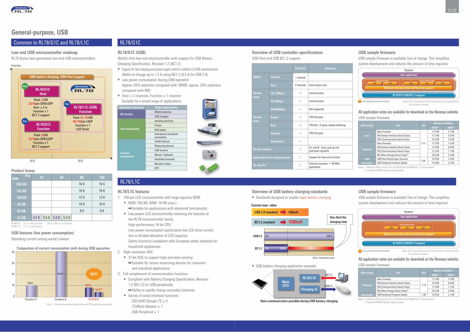
Note: 1. Non-communication state when only SOF packets are accepted
USB features (low power consumption)Operating current among world’s lowest
Comparison of current consumption (mA) during USB operation
4mA*1
Company A Company B RL78/G1C0
10
20
30
40
10mA
40mA
8mA
BEST
Common to RL78/G1C and RL78/L1C
Low-end USB microcontroller roadmapRL78 Series next-generation low-end USB microcontrollers
RL78/G1C (USB)World’s first low-end microcontroller with support for USB Battery Charging Specification, Revision 1.2 (BC1.2) Support for fast charging and power supply control in addition to USB communication Ability to charge up to 1.5 A using BC1.2 (0.5 A for USB 2.0) Low power consumption during USB operation Approx. 65% reduction compared with 78K0R, approx. 20% reduction
compared with R8C Host × 2 channels, Function × 1 channel Suitable for a broad range of applications
RL78/L1C features1. 100-pin LCD microcontroller with large-capacity ROM ROM: 256 KB, RAM: 16 KB (max.)
Suitable for applications with advanced functionality Low-power LCD microcontroller retaining the features of
the RL78 microcontroller family High-performance 16-bit CPU Low power consumption (particularly low LCD drive current due to divided allocation of LCD capacity)Safety functions (compliant with European safety standard for household appliances)
2. High-resolution ADC 12-bit ADC to support high-precision sensing Suitable for sensor measuring devices for consumer
and industrial applications3. Full complement of communication functions Compliant with Battery Charging Specification, Revision
1.2 (BC1.2) for USB peripherals Ability to rapidly charge secondary batteries Variety of serial interface functions CSI/UART/Simple I2C × 4 I2C(Multi-Master) × 1 USB Peripheral × 1
Overview of USB battery charging standards Standards designed to enable rapid battery charging
USB sample firmwareUSB sample firmware is available free of charge. This simplifies system development and reduces the amount of time required.
RL78/G1C
RL78/L1C
Necessary Functions Target Applications
BC functionMobile batteries
USB chargers
Host functionality
Vending machines
Printer
DVD player
Smartphone peripheral accessories
Function functionality
Health devices
Measuring devices
USB memory
Mouse / keyboard
Handheld terminals
Barcode readers
UPS
RL78/G1C Reference
USB2.0 Function 1 channel
Host 2 channels Host version only
Transferspeed
LS(1.5Mbps) Host/Function
FS(12Mbps) Host/Function
HS(480Mbps) Not supported
Transfermode
Control FIFO 64 bytes
Bulk FIFO 64 × 2 bytes, double buffering
Interrupt FIFO 64 bytes
Isochronous
On-chip resistorsD+ and D– lines, pull-up and pull-down resistors
Supported battery charging classes Support for Host and Function
On-chip PLLExternal resonator 48 MHz generation
All application notes are available for download on the Renesas website.USB sample firmware
USB function Title RevMemory size[kByte]
ROM*1 RAM*2
Host
Basic firmware
2.13
17.9 KB 2.7 KB
HID (Human Interface Device Class) 17.2 KB 2.0 KB
CDC (Communication Device Class) 19.5 KB 1.9 KB
Peripheral
Basic firmware 11.3 KB 1.5 KB
HID (Human Interface Device Class) 12.0 KB 0.9 KB
CDC (Communication Device Class) 11.2 KB 1.1 KB
MS (Mass Storage Device Class)*2 18.2 KB 2.5 KB
AOA USB Host Android Open Accesory1.00
15.9 KB 1.6 KB
Downloader USB Peripheral Firmware Update 12.8 KB 3.1 KB
Notes: 1. ROM and RAM sizes for CS+ (V3.00.00) and CA78K0R (V1.71) environments2. Includes EEPROM devices used as media.
All application notes are available for download on the Renesas website.USB sample firmware
USB function Title RevMemory size[kByte]
ROM*1 RAM*2
Peripheral
Basic firmware
2.13
11.3 KB 1.5 KB
HID (Human Interface Device Class) 12.0 KB 0.9 KB
CDC (Communication Device Class) 11.2 KB 1.1 KB
MS (Mass Storage Device Class)*2 18.2 KB 2.5 KB
Downloader USB Peripheral Firmware Update 1.00 12.8 KB 3.1 KB
Notes: 1. ROM and RAM sizes for CS+ (V3.00.00) and CA78K0R (V1.71) environments2. Includes EEPROM devices used as media.
USB battery charging application example
Product lineup
ROM Pins 32 48 80 100
256 KB 16 K 16 K
192 KB 16 K 16 K
128 KB 12 K 12 K
96 KB 10 K 10 K
64 KB 8 K 8 K
32 KB 5.5 K 5.5 K 5.5 K 5.5 K
RL78/G1C : 1 x only Function 2 x Host or 1 x FunctionRL78/L1C : 1 x only Function
General-purpose, USB
Overview of USB controller specificationsUSB Host and USB BC1.2 support
USB sample firmwareUSB sample firmware is available free of charge. This simplifies system development and reduces the amount of time required.
2012
Function
2013
Flash 32KB32/48pin QFN/LQFP
Host x 2 or Function x 1
BC1.2 support
Flash 32KB32/48pin QFN/LQFP
Function x 1BC1.2 support
RL78/G1C Host
Host
RL78/G1CFunction
PeriFlash 64-256KB80/100pin LQFP
Function x 1LCD Driver
RL78/L1C (USB)Function
Peri
USB battery charging, USB Host support
MainCPU
RL78/L1C
Charging IC
Data communication possible during USB battery charging
BC1.2
USB2.0
System
Note: BC1.2 detection control functionality is implemented for all device classes.
Free sample software (firmware)
User application
RL78/G1C (USB BC1.2 support)
Function device class
USB basic firmware (Host and Function support)
MSC HID CDC
Current max. value
USB 2.0 standard 500mA
BC1.2 standard 1500mA
USB2.0
BC1.2
Note: Calculated value
0%
0% 100%
100%
One-third the charging time
SystemUser application
RL78/G1C (USB BC1.2 support)
Free sample software (firmware) Note: BC1.2 detection control functionality is implemented for all device classes.
USB basic firmware (Host and Function support)
Host device class Function device class
HID CDC MSC HID CDC

23-24
RL78/L12, L13, L1C
LCD microcontroller product roadmapNew successor products combining the features of earlier LCD microcontrollers
Capacitor split type for generating LCD drive voltage 89% reduction in current consumption
compared with previous product Particularly large reduction in LCD drive current
Low-power LCD driver
Resistance division type suitable for large panels Voltage boost type suitable for battery
powered systems Capacitor split type suitable for very small currents
Support for many segment LCD panel types
Max. display segment count: 416
Return of panels with very large segment counts
L12 L13 L1C
Healthcare
Blood pressure meters
Composition meters
Blood glucose meter
Pedometers
Thermometers
Electric household appliances
Rice cookers
Microwave ovens
Hot water pots
Compact electric household appliances
LCD remote controls
Hot water heaters
Telephones
Kitchen tools
Measuring devices
Temperature controllers
Sensor modules
RL78/L12, L13, L1C Product lineupROM
Pins 32 44 48 52 64 80 100256 KB 16 K 16 K192 KB 16 K 16 K128 KB 8 K 8 K 12 K 12 K96 KB 6 K 6 K 10 K 10 K64 KB 4 K 4 K 8 K 8 K48 KB 2 K 2 K32 KB 1.5 K 1.5 K 1.5 K 1.5 K 1.5 K 1.5 K 1.5 K16 KB 1 K 1 K 1 K 1 K 1 K 1 K 1 K
8 K 1 K 1 K 1 K 1 KRAM RL78/L12 : 32-pin - 64-pin RAM RL78/L13 : 64-pin - 80-pin RAM RL78/L1C : 80-pin - 100-pin
RL78/L12
RL78/L13
RL78/L1C
Pins 32 48 52 64 80 100 128
50 or more 51 56 56 54
45 - 49 48
40 - 44 40 40
35 - 39 39 40
30 - 34 30 32 32 32 31 32
25 - 29 26 24
20 - 24 22 24 24
15 - 19
9 - 14 13 9
RL78/L1x 78K0R/Lx3 78K0/Lx3 R8C/L3xx R8C/LAxx
Seg count(4 com)
Renesas RL78/L1x CompanyA
CompanyB
CompanyC
CompanyD
Resistance division method*2 11.6 µA (typ.)
11.7 µA(@2.2 V)
Not implemented
12.0 µA(@1.8 V)
Not implemented
Capacitor split method
7.35 µA (typ.) Not implemented
Not implemented
Not implemented
Not implemented
Voltage boost method
21.19 µA (typ.) 24.5 µA 22.9 µA Not implemented 23.7 µA
Notes: 1. Current value including sub-oscillator, RTC operation, LCD operation and current flow to LCD panel. The calculation assumes an LCD panel drive current of 10 µA when using the resistance division method. (The value differs depending on the drive method.)
2. Calculated using an external resistance value of 1,000 kΩ for the external resistance division method.
Curre
nt d
urin
g LC
D dr
ive*1
7.35 µA (typ.)
Supports the three typically used LCD drive methods. Enables LCD circuits with ultra-low power consumption.
LCD
RL78/L12, RL78/L13, and RL78/L1C product concept
LCD display seg × com lineupAt each pin count the new products support higher segment counts than earlier products.
Ultra-low standby current consumption (clock counter + LCD display)Capacitor split provides extremely low current consumption when
driving LCD panels.20121H
~ 2011 20122H
20131H
78KOR/Lx3
R8C/L3x
78KO/Lx3
R8C/LAx
Ultra-low-power LCD microcontrollers
Low Pin CountRL78/L12
LCD StandardRL78/L13
USB AnalogRL78/L1C80-pin to 128-pin
52-pin to 100-pin
32-pin to 80-pin
48-pin to 80-pin
No change when power supply voltage from battery, etc., drops, so no dimming of display.
For heavy-duty LCD/AC power supply applicationsUsing resistance division to generate the drive voltage achieves high LCD drive capacity at low cost. External resistors are used for voltage division to generate the LCD drive voltage. The ability to input an external voltage means that external resistors and capacitors can be used to adjust the operating current and drive capacity.
For battery-powered applicationsThe operating current is small and the drive voltage remains constant even when the battery voltage drops, so there is no dimming of the LCD display. The reference voltage is generated internally, and external capacitors are used to boost the voltage. The reference voltage can be adjusted by software in order to modify the LCD contrast. (On the RL78/L12, 18 setting steps are supported.)
For battery-powered applicationsThis method uses the smallest operating current. The LCD display dims when the battery voltage drops. It can be used without modification in cases where the aim is to dim the display according to the remaining battery capacity. To prevent the display from dimming as the battery voltage drops, the system can switch to the internal voltage boost method when the battery voltage is low. It is also possible to use the internal voltage boost method with the capacitor split method implemented in an external circuit.
Microwave ovens
LCD remote controls
Resistance division method
Internal voltage boost
method
Capacitor split method
Features/anticipated applications
Suitable for large LCD panels 10.4 µA[typ.]*1
Standard
Very small
current
Dependent on VDD
Small current
Constant
High
High
Standard Dependent on VDD
0.63µA [typ.]*
0.12µA [typ.]*1Display dims as power supply voltage drops.
Display dims as power supply voltage drops.
Activity metersActivity metersThermometers
Composition meters
Kitchen tools
Microwave ovens
Composition meters
Thermometers
Kitchen toolsKitchen toolsKitchen toolsKitchen tools
Note: 1. Drive voltage: 3 V, 1/3 bias, external resistance value: 1,000 kΩ, no LCD panel connected
Rice cookers
Washing machinesGood
Good VeryGood
GoodGood

25-26
RL78/L1A
RL78/L1A features
On-chip analog functions, low current consumption, low-voltage analog,
on-chip LCD driver
This power-efficient 16-bit LCD microcontroller is ideal for use in portable
healthcare devices such as blood glucose meter.
World-top-class power efficiency
Current consumption during operation: 66 µA/MHz
In RTC mode: 1 µA or less
Notable analog functions
On-chip 12-bit ADC and 12-bit DAC that maintain consistent accuracy up to 2.0 V
Rail-to-rail op-amp with analog switch
Low-voltage operation of analog functions
Analog functions maintain accuracy while operating at 2.0 V. Low-voltage
operation contributes to extended battery life.
RL78/L1A lineup
ROM Pins
80 100
128 K 5.5 K 8 KB
96 K 5.5 K 8 KB 5.5 K 8 KB
64 K 5.5 K 8 KB 5.5 K 8 KB
48 K 5.5 K 8 KB
RAM size DATA flash
Analog frontend function configurationBlood glucose meter use case
Features of analog functionsI/V conversionTransimpedance amplifier
Switching among the external feedback resistors using analog switches can be accomplished by means of software. It is possible to create a common board design mounted with external resistors for use with multiple product types.
RL78/L1A RPBs (Renesas promotion boards)
RL78/L1A RPBs are available for evaluation of various types of products.
Features
Operates on USB power supply.
Temperature sensor
Outputs trace data via USB.
Supports connection of an LCD display.
Supports connection of an 128 ×
128 matrix PMOD.
RL78/L1A blood glucose meter reference solution
Renesas plans to expand its range of reference solutions and
application notes to include a blood glucose meter that utilizes the
on-chip functions of the RL78/L1A, such as 12-bit A/D and 12-bit D/A
converters and op-amps .
VREF
DAC012-bit
VREFRail to Rail
OPA-+
12-bit SAR ADC
RL78 16-bit CPU24 MHz
33 DMIPS
1.8 – 3.6 V-40 to +85 °C
ANALOGBGR REF VREF
SWcontrol AVdd
AD_VREFPAD_VREFM
OPA3
VREF
VREF
VREFOPA1
Rail to Rail
OPA2
Rail to Rail
-+ Charge
Pump
-+
-+
DAC012bit
DAC012bit
TEST STRIP
12bit SAR ADC
AVdd
Enhanced on-chip microcontroller functions to reduce the number of system components
Peripheral functions such as AFE, main clock, and EEPROM are incorporated into the microcontroller. This reduces the number of additional components required.
-+
-+
SW
12-bitDAC MCU MCU
LCD
12-bitADC
UART
RTC
CSI
I2C EEPROM
BLE
IC IC
I/O
Teststrip
SWMain clock
32.768 kHz
Bat.Buzzer
Diode
LCDdriver
UART
Calibration
Reset
Detect reverse battery
Teststrip
Tempsensor
On-chip OSC
DiodeDetect reverse battery
Bat.Buzzer
CSI BLE
Buzzer
RTC
Buzzer
I2C
I/O12-bitADC
SW
12-bitADC
-+
LCD driver-
+
Reset
32.768 kHz
Tempsensor SW
Calibration
LCD
CompanyA
Example discharge characteristics of lithium-ion coin battery*
RL78/L1A
3.6V
2.7V
2.2V
2.0V
1.8VADC and DAC operate even at less than 2.0 V.
References* : Maxcell CR2032** :Toshiba LR6
Example discharge characteristics of alkaline batteries (× 2)**
Time
LCD, Analog
Analog
ADC12-bit, up to 14 channel
DAC12-bit, 2 channel
OpAMP w/up to 4 MUX, 2 channel
OpAMP 1 channel
Comparator1 channel
Temp Sensor1 channel
On-chip Vref1 channel
Safety
RAMParity Check
ADCSelf-diagnostic
ClockMonitoring
MemoryCRC
WDTw/independent clock
Memory
Program Flashup to 128 KB
SRAM5.5 KB
Data Flash8 KB
Communication
l2C1 channel
CSI/SPI/Simple l2C3 channel
Timers
Timer Array Unit16-bit, 8 channel
Interval Timer16-bit/8-bit, 1 channel/2 channel
Interval Timer12-bit, 1 channel
RTCCalendar
Power Management
HALTRTC, DTC Enabled
SNOOZESerial, ADC Enabled
STOPSRAM On
System
DTC
Interrupt controller
Clock GenerationInternal, External
POR, LVD
ELC
Debug w/ traceSingle-Wire
RL78 CPU Core24 MHz 33 DMIPS
MUL/DIV/MACInstruction
Registers
Barrel ShifterOverview of RL78/L1A specifications ROM/RAM: 48KB/5.5KB, 64KB/5.5KB,
96KB/5.5KB, 128KB/5.5KB Data flash: 8 KB On-chip oscillator circuits: HOCO: 24 MHz,
LOCO: 15 kHz Main clock: 1 to 20 MHz Subclock: 32.768 kHz DTC: Data transfer controller (DTC) Serial interfaces: 3 × SCI: Simple SPI/simple I2C/
UART Timers: TAU (timer array unit), 6 channels × 16-bit,
2 channels × 16-/8-bit, interval timer: 8-/16-bit timer, RTC (real-time clock)
Analog: 12-bit A/D converter × 14 channels, 2-channel 12-bit D/A converter, 2-channel high-precision op-amps (4MUX), 1-channel general-purpose op-amp,
internal reference voltage (Vref), comparator (CMP) × 1 channel, TEMPS (temperature sensor)
Other functions: POR (power-on reset), LVD (low-voltage detection circuit)
LCD control: 32 seg. × 4 com. (80-pin), 40 seg. × 4 com. (100-pin)
Safety functions: IWDT (watchdog timer), RAM parity error detection function, ADC test function, frequency detection function, memory CRC, IEC/UL 60730 support

27-28
RL78/I1A RL78/I1B
RL78/I1A features Basic peripheral functions for lighting and power supply applications
Timers for LED control and PFC control
– 64 MHz source clock, zero current detection, forced output stop function Analog functions for feedback
– 10-bit A/D converter (2.125 µs. conversion), PGA, comparator Support for high temperatures up to 105°C or 125°C
Current consumption LED power supply control: 3.3 mA (main operation), CPU clock: 16 MHz,
timer KB clock: 64 MHz, PLL: on UART (DALI) receive standby: 0.23 µA (STOP current)
Full complement of connectivity functions Communication functions (DALI, PMBus, SMBus, DMX512, UART, I2C, CSI)
Special peripheral functions for “intelligent” operation and improved efficiency Dithering function (0.98 ns pseudo-resolution), software start function, max.
frequency limit function, interleaved PFC, standby communication wait
RL78/I1A lineup
ROM Pins
20 30 38
64 KB 4 K 4 K
32 KB 2 K 2 K
RAM size
Operating temperature ranges up to 105°C or 125°C supported
System configuration example: PFC control + LED constant current control
Advantages of RL78/I1A
Target electricity meter markets of RL78/I1B Electricity meter typesThere are various types of meters to match the information required in different countries.
Wiring Type Main Applications Main Regions
Single-phase, two-wire Home Europe, China, India
Single-phase, three-wire Home Japan, U.S.A
Three-phase, three-wire Commercial/industrial Worldwide
Product lineup and conceptProduct lineup to accommodate various meter types
Four products
ROM Pins 80 100
128 KB 8 K 8 K
64 KB 6 K 6 K RAM size
Aiming for low power consumption Low power consumption among the best in its class: Power efficient during both calculations and backup operation Low power consumption
Operating current: 96 µA/MHz Standby current: 0.69 µA (during RTC or LVD operation)
Newly developed 24-bit ∆Σ ADC Current during ADC operation: 0.53 mA/channel
RL78/I1B A B C64/128 KB Up to 32 KB Up to 120 KB Up to 128 KB
ADC 3-channel operation at each CPU operating frequency (MHz)
3 2.8 4.35 5.1 3.525
6 3.3 5.55 6.6 4.595
12 4.2 — 9.6 6.695
24 6 — — 10.725
CPU Frequency(MHz)
MCU
∆Σ ADC with improved functionality for electricity metersImplementation in hardware of functions essential for power measurementPhase correction circuit, high-pass filter
High-speed on-chip oscillator with accuracy of ±0.05%Subclock resonator single-crystal systemExclusive Renesas system is more robust than conventional PLL designs.
Newly developed 24-bit ADC Designed for low power consumption Reduced CPU operating frequency that contributes to lower power
consumption (on-chip PHC and HPF)
To further cut power consumption ... Support for multiple sampling frequencies (3.906 kHz and 1.953 kHz)
High-precision clock: ±0.05% (high-speed on-chip oscillator with correction circuit) Correction of on-chip oscillator by subclock (exclusive Renesas circuit)
Safety functions: Clock system High-speed on-chip oscillator maintains oscillation at ±1% accuracy
even if external resonator stops operating.
Main applications LED lighting Digital power supplies Illumination fixtures Laser printers Microwave ovens Vacuum cleaners Communication devices
(CRn1-CRn0) +1 (CRn3-CRn2) +1
• Delivers min. average resolution of 0.98 ns.
Fine-grained lighting and voltage control
TKBOn1
TKBOn1
0000hCR0
CR2CR1
CR3FFFFh
Timer restart function Forced output stop function(Hi-Z/Hi/Lo)
PFC control Protection function
Counter
TKBOxx
INTP2x
TKBOxx
TKBOxx
INTCMPx
Linked operation of 16-bit timer KB and INTP comparator
AC/DC (PFC) control circuitBoost converterFlyback converter
DC/DC control circuitBuck converterBoost converterFlyback converterHalf-bridgeFull-bridge
PFC control modeCRM-PFC control (DCM or CCM also supported)
Constant-current control mode
Average-current controlPeak-current control
Support for multiple power supply control methods
Implementation in hardware of communication functions for lighting
• Manchester coding• Transmit/receive data: 8-, 16-, 17-, or 24-bit
DALIRxD4
DALITxD4
DALI master/slave communication functions
Dithering function
Communication
AC input detection
DALI/DMX512/IRcommunication
PFC control
Over currentprotection
Zero currentdetection
AC input voltage feedback
4
Protection
PFC control LED control×4ch
Interrupt
AC powersupply
4LED current feedback/over current protection
LED current control/dimming control4
CMP/CMPCOM
DALI/UART
INTP/TI00
Hi-ZControl
CMP
INTP
PFC
Restart
Timer KB2
PI calculation
CPU process-PFC feedback-LED feedback-Dimming control
-Communication-AC input detection
A/D Converter
High-resolution
Timer KB0 Soft-start/Dithering
Timer KB1 Soft-start/Dithering
Gatecontrol
Timer KC
Color mixing
Low-sense resistor
PGA
Hi-Zcontrol
Hi-Zcontrol
CMP
CMP
CMP
CMP
RL78/I1A
PFC output voltage feedback
Bird’s eye view of electricity meter standards
Europe Standard: IECVoltage: 220 V
U.S.A.Standard: ANSI Voltage: 110 V
ChinaStandard: GB/T Voltage: 220 VAnti-tampering
Bird’s eye view of electricity meter standards
IndiaStandard: CESC Voltage: 220 V Anti-tamperingSingle-phase, two-wire
V1
I2
I1
Source Meter Load Source Meter Load
Single-phase, three-wire
V1
V2
I2
I1
Source Meter Load
Three-phase, three-wire
V1
I2
I1
V2
Bird’s eye view of electricity meter standardsBird’s eye view of electricity meter standards
JapanStandard:
JIS standardVoltage: 100 V
12
10
8
6
4
2
00 5 10 15 20 25 30 MHz
mA
Best!
Lowest power consumption at all operating frequencies
C B ARL78/I1B
1
0
2
3
4
5
6
7
B C DRL78/I1B
3.3mA
Over7mA
4.5mA
6.6mA 25%
Note: 1. Based on research by Renesas
7
25% lower power consumption than competing products*1
CPU@6MHz & ADC3ch operation
RL78CPU core
High-speedOCO
Temp.sensor
Error detection
Sub-Clkcompensate
circuit
Clock calibration with temperature distortion
RL78/I1B system
RTCclock
20 MHz(option)
SystemClockSW
The microcontroller can continue operating using the on-chip oscillator if the external resonator stops.
20 MHz
High-speedoscillator
Error detection with comparing to sub-clock
Conventional clock system
CPU core
PLL
Temp.sensor
Sub-Clkcompensate
circuit
Current system
RTCclock
16 MHz16 MHz16 MHz16 MHz
Clock instability due to PLL self-oscillation
16 MHz
High-speedOCO
Sub-Clkoscillator
ClockSW
The microcontroller can continue operating using 16 MHz16 MHz
Frequencytrimming
Sub-Clkoscillator
Trouble32.768 kHz
Trouble32.768 kHz
GND
GND GND
RL78/I1BAFE
Load
+−
+−
∆Σ ADC ch0(Current channel)
Digitalfilter
∆Σ ADC ch1(Voltage channel)
Phasecontrol(PHC)
Highpassfilter(HPF)
Original waveform
Digitalfilter
Before phase compensation After phase compensation Reduced DC noise
DC Noise
4
4
3
3
21
12
ASSP, Lighting/Power supply ASSP, Electricity meter

29-30
RL78/I1DRL78/I1C
RL78/I1D features Low power consumption for extended battery life
High-speed recovery from STOP mode in just 3.4 µs, and supply
of operating current in 124 µA when operating at 1 MHz.
Ability to operate peripheral circuits (sensor activation, signal
amplification, obtaining A/D conversion results) without CPU
intervention. Ability to determine whether it is necessary to
activate the CPU based on A/D conversion results.
On-chip analog functions needed for security and emergency
applications
On-chip general-purpose op-amp, 12-bit A/D converter, and
comparator
RL78/I1D lineup
ROM Pins 20 24 30 32 48
32 KB 3 K 3 K 3 K
16 KB 2 K 2 K 2 K 2 K 2 K
8 KB 0.7 K 0.7 K 0.7 K
RAM Size
Target electricity meter markets of RL78/I1C
Electricity meter types
Wiring Type Main Applications Main Regions
Single-phase, two-wire Home Europe, China, India
Single-phase, three-wire Home Japan, U.S.A
Three-phase, three-wire Commercial/industrial Worldwide
Three-phase, four-wireCommercial/industrialAgriculture/urban housing
Worldwide
Target markets Ideal for smart meters, including those using DLMS
communication. Suitable for a wide variety of power platforms, from single-phase
two-wire to three-phase four-wire.
Available flash memory configurations are 256 KB for DLMS or three-phase meters, 128 KB for single-phase meters or low-end three-phase meters, and 64 KB for low-end single-phase meters.
Available package pin counts are 100 for three-phase meters or single-phase meters for advanced economies, 80 for single-phase meters for emerging economies, and 64 for applications where space is restricted.
A total of seven product versions are available.
Product lineup and concept
ROM Pins 64 80 100
256 KB 16 K 16 K
128 KB 8 K 8 K 8 K
64 KB 6 K 6 K
RAM Size
Improved security functions and arithmetic performance First in the industry to implement AES GCM mode in hardware, as
required by the DLMS standard. Encryption and decryption are over 20 times faster than the
software processing used on previous Renesas products. Approx. 30% improvement in arithmetic capacity required for
power calculation. On-chip PLL boosts the maximum operating frequency from 24
MHz to 32 MHz.
32-bit multiplier/divider and multiply-and accumulate unit dramatically reduce the software burden when performing calculations on 24-bit data converted by the 24-bit ∆Σ A/D converter.
Power measurement processing and DLMS processing on a single chip. Ability to handle DLMS communication while power measurement
processing is taking place. Approx. 30% reduction in power consumption compared with
two-chip solutions combining an earlier meter microcontroller and a dedicated microcontroller for DLMS processing.
Contributes to reduced system cost.Retaining and improving the power efficiency of the RL78/I1C Independent power supply real-time clock
Current consumption of 0.7 µA (typ.) during operation Enhanced power supply monitoring function
Low-voltage monitoring of power supply pins using LVD and improved battery backup function to deliver power to the CPU and peripheral functions when power is interrupted.
I/O power supply (EVDD)
I/O power supply (VDD)
Flash/RAM CPU
RTC
VRTC Power domain
SubOSC
Peripherals
Discrete power supplies
10bit ADC Tamperdetect
LVD
LVD
LVD RTCBattery
(CR2032)
ExtraBattery
(CR2032)
SuperCap
Main supplyNeutral-IN
Voltage detection circuitsfor power supply pins2.2 V
EVDD1
EVDD0
VDD
EXLVD
VRTC
Register
Regulator
LVD
AC/DC
Energy-efficient poweroutage/recovery detection
Independent power supply RTC domain
VBAT
ΣADC
SNOOZE mode operation example
Operation procedure
sensor activation, ADC activation, obtaining A/D conversion results,
storing A/D conversion results in RAM, transmission of A/D conversion results to DOC (determination of need for CPU activation)
1 2 3
4 5
Sensor signalAmplification
Sub clock12-bit timer
RAM
Amplification
Op-ampDTCData
transfer controller
DOC
ADC
Op-amp activation
DTC activation
ADC activation
Determination of need for
CPU activation
Sub clock8-bit timer
GND
Switch
Sensor
1
2
3
4
5
ASSP, Electricity meter ASSP, Detector/Sensor
Key RL78/I1D specificationsRL78 CPU Core Three-stage pipeline CISC architecture Max. operating frequency: 24 MHz Support for multiply, divide, and
multiply-accumulate instructionsMemory Support for 1.8 V flash programming and boot swap Program flash: 8 KB–32 KB SRAM: 0.7 KB–3 KB Data flash: 2 KB
System High-speed on-chip oscillator: 24 MHz ±1% Middle-speed on-chip oscillator: 4 MHz ±12%
(support for high-speed wakeup in 3.4 µs)Power management Operating current: 58.3 µA/MHz HALT current: 0.64 µA (RTC + LVD) STOP current: 220 nA (SRAM data retained) SNOOZE current: 700 µA (UART), 500 µA
(ADC)
Safety Compliant with European safety standard for
household appliances (IEC/UL 60730)Timers Advanced-functionality timer array unit (TAU) 8-bit interval timer (can be used as 16-bit
interval timer) Watchdog timer, real-time clock
Analog 1.6 V (VDD) operation On-chip ADC, 12-bit × 17 channels, conversion
time: 3.375 µs Internal reference voltage (1.8 V) Op-amp × 4 channels (high-speed and
low-power modes) Comparator × 2 channels (window mode support)
Communication CSI, UART, Simple I2C
Package 20-pin, 24-pin, 30-pin, 32-pin, 48-pin (Reference) RL78: Block diagram of 11D Group 48-pin product.
Communication2 × CSI/UART
/2 × simple I2C
MemoryProgram flash
8 to 32 KB
SRAM0.7 to 3 KB
Data flash2KB
Power ManagementHALT
RTC, DTC enabled
SNOOZESerial, ADC enabled
STOPSRAM on
Fast Wake up3.4 µs
System
DTCMax. 23 sources
ELCLink src. Max. 20Link dst. Max. 7
Interrupt controller4 levels
POR, LVD
DOC
DebugSingle-wire
Clock generationOCO, external
TimersTimer array unit16-bit, 4 channels
Interval timer12-bit, 1 channel
Interval timer8-bit, 4 channels
(16-bit(2 × 8-bit), 2 channels)
WDT 17-bitRTC
Calendar
SafetyRAM
Parity check
ADCSelf-diagnostics
ClockMonitoring
MemoryCRC
I/O PortRead back
AnalogADC
12-bit, 17 channels
Internal Vref
Temp. sensor
Comparator2 channels
Op-Amp4 channels
Safety
RL78 CPU core24 MHz operation
CISC Harvard architecture3-stage pipeline
MUL, DIV, MACInstruction
16-bit barrel shifter
4 register banks

31-32
RL78/I1E
On-chip configurable amplifier General-purpose analog I/O ports and configurable switches
enable configuration of a variety of op-amp circuits.
Integrated peripheral analog functions
RL78/I1E lineup
ROM Pins
32 36
32 KB 8 KB 8 KB
RAM Size
MEMO
(Reference) RL78: Block diagram of I1E Group 36-pin product.
RL78/I1E features High-precision analog functions
24-bit ∆Σ A/D converter × 4 channels
10-bit SAR A/D converter × 10 channels
Configurable amplifier × 3 channels
12-bit D/A converter × 1 channel
Sensor power supply × 1 channel
Compact package
4 mm square: 36-pin FBGA
5 mm square: 32-pin VQFN
Support for high temperatures
−40 to 125°C
On-chip 24-bit ∆Σ A/D converter AFE* circuits for many types of sensor measurements, including
using pressure sensors, load cells, and thermocouples, integrated
on a single chip.
Ability to use common sensor power supply and ADC reference
voltage, minimizing ratiometric error.*AFE: Analog Front End
Configurable amplifier settings
Code generation tool for RL78/I1E
This GUI-based tool lets you specify a variety of information and
automatically generates code for analog circuit control programs.
PGA + ∆Σ A/D converter settings
* Uses external resistors.
As a general-purpose amplifier
As a DAC output amplifier
–+ –
+
12-bitDAC
Iin
To 10-bitA/D converter
12-bitDAC
–+
Vin
–+
To 10-bitA/D converter
ConfigAMP
ConfigAMP
ConfigAMP
12bitDAC
10bitSAR-ADC
24-bitDSADC
InputMux2
Temperaturesensor
InputMux1
Sensorbias VREF LDO2
DigitalFilter(SINC3)
PGIA
Codeflash
RAM
Dataflash
Memory
UART
SPI
I2C
Serial I/F
LDO1
CPU
OSC
Timer
As a programmable-gain non-inverting amplifier*
As a programmable-gain IV amplifier*
Configuration examples
AMAMAMPPP
ConnfffiiigggAMAMAMPPP
ConnfffiiigggAMAMAMPPP
SAR-ADCInputMux2
CPU
Reference voltage source
Integrated temperature sensor
24-bit∆ΣADC
DigitalFilter
(SINC3)
Common power supplyfor single-end input
Sensorpowersupply
Instrumentationamplifier
Memory
Program Flash32 KB
SRAM8 KB
Data Flash4 KB
Analog
Delta-Sigma ADCwith
Instrumentation amp24-bit, 4 channels
SAR ADC10-bit, 10 channels
OPAMP3 channels
DAC12-bit, 1 channel
TemperatureÞsensor
Sensor Bias
Safety
CMOS In/Out11 channels
CMOS Input3 channels
Communication
2x CSI/2x UART
/2x Simplified I2C(exclusive)
Timers
Timer Array Unit16-bit, 6 channels
Timer RG16-bit, 1 channel
Timer RJ16-bit, 1 channel
Interval Timer15-bit, 1 channel
WDT
RTC
Power Management
Main OSC1-20 MHz
HOCO32 MHz/24MHz
LOCO15 kHz
PLL32 MHz/24MHz
System
DTC23 sources
ELC16 sources
Interrupt Controller4 Levels
POR, LVD
On chip DebugSingle-Wire
RL78 CPU Core32MHz Operation
CISC Harvard Architecture3-stage Pipeline
MUL, DIV, MACInstruction
16-bit Barrel Shifter
4 Register Banks
ASSP, Analog

33-34
Microcontroller with on-chip analog frontend for sensor applications (and ability to control analog frontend circuit configuration and characteristics from microcontroller) The RL78/G1E Smart Analog microcontroller is based on the RL78/G1A and incorporates an on-chip analog frontend. It is suitable for a variety of sensor applications and will contribute to the realization of sensor systems that are more compact and lower in cost while also reducing the time required for development.
Application fields: Suitable for a variety of sensor applications
The RL78/G1E (with variable amplifier circuit configuration) incorporates a configurable amplifier*1 in its analog frontend circuit block. Using software control it is possible to change the analog circuit configuration and characteristics (adjusting the variable gain, offset and bias voltage, etc.) while the microcontroller is operating. Applications employing multiple sensors are supported by the ability to switch the analog circuit configuration in time-sharing fashion using software. This makes it possible to support a variety of different sensors. The RL78/G1E can be used as a common platform analog frontend IC.
Suitable for products incorporating sensors, such as electric household appliances, industrial equipment, and healthcare devices
Smart AnalogSmart Analog products allow you to use software to change the circuit configuration or characteristics in order to provide support for multiple types of sensors and drivers. Smart Analog functionality is available on Smart Analog ICs, which contain analog circuits only, and on the RL78/G1E Smart Analog microcontroller, which integrates a Smart Analog IC.
RL78/G1E features
Improved analog functions such as configurable amplifier, adjustable-gain amplifier, filters, D/A converter, and temperature sensor
Multiple ADC channels (max. 17 channels) to support input from a variety of sensors
Support for high-speed, high-precision A/D conversion
Analog frontend functions essential for sensor control
On-chip oscillator accuracy of ±1%, support for UART communication (TA = –20 to +85°C, VDD = 1.8 to 5.5 V)
Frequency selectable among 32, 24, 16, 12, 8, 6, 4, 3, 2, and 1 MHz
88.4 µA/MHz during CPU operation, 0.67 µA during standby
Even lower power consumption in SNOOZE mode
12-bit A/D conversion
Product lineup
ROM Pins
64 80
64 KB 4 K 4 K 4 K 4 K
48 KB 3 K 4 K 3 K 4 K
32 KB 2 K 4 K 2 K 4 K
RAM Data Flash
RL78/G1E specificationsRL78-S2 CPU Core Three-stage pipeline CISC architecture Max. operating frequency: 32 MHz
Memory Support for 1.8 V flash programming and boot swap Program flash: 32 KB–64 KB SRAM: 2 KB–4 KB Data flash: 4 KB
System High-speed on-chip oscillator: 32 MHz ±1% (target) Library support for multiply/divide and multiply-
accumulate operation unit Power management Operating current: 88.4 µA/MHz (when operating
at 32 MHz, configurable amplifier channels 1 to 3 and D/A converter channel 3 operating)
HALT current: 145 µA (high-speed on-chip oscillator stopped, AFE stopped)
STOP current: 370 nA (SRAM data retained, AFE stopped)
SNOOZE current: 700 µA (UART operating, AFE stopped), 420 µA (ADC operating, AFE stopped)
Safety Compliant with European safety standard for
household appliances (IEC/UL 60730) Illegal memory access detection
Timers Advanced-functionality timer array unit (TAU) Watchdog timer
Analog Power supply voltage range: 3.0 V to 5.5 V (excluding ADC) On-chip ADC, 12-bit × 17 channels, conversion
time: 3.375 µs On-chip DAC: 8-bit × 4 channels Configurable amplifier × 3 channels, gain amplifier × 1 channel Low-pass filter, high-pass filter
Communication CSI, UART (LIN), Simple I2C
Package 64-pin/80-pin
Smart Analog roadmap
https://www.renesas.com/smart_analogSmart Analog website
A variety of sensor types can be accommodated by switching the analog circuit configurationNotes: 1. Selectable among non-inverting amplifier, inverting amplifier, differential amplifier, and I/V conversion amplifier.
2. The three-channel configurable amplifier is configured as a single-channel instrumentation amplifier operating on multiple channels.
Smart Analog
RL78/G1E
Low Power ConsumptionHigh-precision, high-speed on-chip oscillator
General Purpose
ASSP Industrial/Consumer Sensor
Configurable
SAIC 500
FY2012 FY2013 FY2014 FY2015 FY2016
Instrumentation
SAIC 501
High speed
SAIC 502
Low voltage
SAIC 300
Low voltage
SAIC 301
16-bit ∆ΣADC& Flash
SAIC 101
SAIC500 + RL78/G1A
SAMCU RL78/G1E
24-bit ∆ΣADCConfigurable Amp
SAMCU RL78/xxx SAMCU Next
Instrumentation amplifier Amplifier with variable circuit configuration
: Samples now shipping: In development: In product design stage
Analog Front-End (No MCU Integrated)
Analog Front-End + MCU Integrated
SAIC
SAIC
SAMCU
SAMCU
Making possible more compact and lower cost sensor systems
Integrating the peripheral components on a single chip reduces the component count by 90% and the board size by 75% compared with the use of discrete components for the analog frontend circuit (according to a comparison by Renesas).
Configuration using discrete components
Approx. 75% smaller board size
Examples of supported applicationsCircuit configuration
Non-inverting amplifier
Instrumentation amplifier
I/V amplifier
Pressure sensors
Gyro sensor
Photo diode
Magnetic sensor
Human sensor
Infrared sensor
Distortion gauge
Non-contact temperature sensor
Blood glucosemeter
Analog Front-end IC
Variable Gain
DAC
Parameter setting
PressureSensor
A/DCPU
Arithmeticprocessing
Biaspoint
setting Instrumentation AMP
MCU
RL78/G1E
Photodiode
Variable Resistor
Parameter setting
A/D
Arithmeticprocessing
Biaspoint
setting
Transimpedance AMP
Analog Front-end IC MCU
CPU
DAC
RL78/G1E
Smart Analog MCU(product combining Smart Analog IC and microcontroller)
Smart Analog IC(software-configurable analog frontend circuit)
MCU(digital control)
Thermometers
Photo diodes
Pressure sensors
Acceleration sensors
Angular velocity sensors
Impact sensors
Hall sensors
Position sensors
Inverting amplifier
Op-amp circuit
Subtractor (differential) amplifier
Summing amplifier
Instrumentation amplifier
I/V amplifier Non-inverting amplifier
(Reference) RL78: Block diagram of G1E Group 80-pin product.
Memory
Program flash32 to 64 KB
SRAM2 to 4 KB
Data flash4 KB
AnalogADC 12-bit, 17 channels
Config AMP 3 channels
FilterHigh-pass, low-pass
DAC 8-bit, 4 channels
Internal Vref
Temp. sensor
Gain AMP 1 channelSafety
RAMParity check
ADCSelf-diagnostics
ClockMonitoring
MemoryCRC Communication
4 × CSI7-, 8-bit
3 × UART7-, 8-, 9-bit
3 × simple I2C
1 × LIN-bus1 channel
Timers
Timer array unit16-bit, 8 channels
Interval timer12-bit, 1 channel
WDT17-bit, 1 channel
Power management
HALTDMA enabled
SNOOZESerial, ADC enabled
STOPSRAM on
System
DMA2 channels
Interrupt controller4 levels
Clock generationInternal, external
POR, LVD
MUL, DIV, MAC
DebugSingle-wire
RL78 CPU core32 MHz operation
CISC Harvard architecture3-stage pipeline
4 register banks
16-bit barrel shifter
Setting the analog circuit (configurable amplifier) as an instrumentation amplifier*2 for use
with pressure sensors
Setting the analog circuit (configurable amplifier) as an I/V amplifier for use with photodiodes

35-36
RL78/F13, F14, F15
The RL78/F1x microcontrollers are the successors to the 78K0R and R8C families. They combine high performance with low power consumption, and features such as
CAN/LIN communication functions, advanced-functionality timers, and safety functions make them ideal for both automotive and industrial applications.
Suitable for automotive applications and for industrial applications as well
RL78/F13, F14, F15 lineup
RL78/F13ROM
Pins 20 30 32 48 64 80
128 KB 8 K 8 K 8 K 8 K 8 K 8 K 8 K 8 K
96 KB 6 K 6 K 6 K 6 K 6 K 6 K 6 K 6 K
64 KB 4 K 4 K 4 K 4 K 4 K 4 K 4 K 4 K 4 K 4 K 4 K
48 KB 3 K 3 K 3 K 3 K 3 K 3 K 3 K 3 K 3 K
32 KB 2 K 2 K 2 K 2 K 2 K 2 K 2 K 2 K 2 K
16 KB 1 K 1 K 1 K 1 K
RL78/F14
ROM Pins 30 32 48 64 80 100
256 KB 20 K 20 K 20 K 20 K
192 KB 16 K 16 K 16 K 16 K
128 KB 10 K 10 K 10 K 10 K
96 KB 8 K 8 K 8 K 8 K
64 KB 6 K 6 K 6 K 6 K 6 K 6 K
48 KB 4 K 4 K 4 K
RL78/F15ROM
Pins 48 64 80 100 144
512 KB 32 K 32 K 32 K 32 K 32 K
384 KB 26 K 26 K 26 K 26 K 26 K
256 KB 20 K 20 K
152 KB 16 K 16 K
128 KB 10 K 10 K
LIN CAN 1ch CAN 2ch White numbers indicate RAM Size (B)
RL78/F14 block diagram
CAN module Architecture enabling continued
utilization of legacy communication software specifications— Retains functionality of previous
CAN module Reduced load for interrupt handling
— Implementation in hardware of typical interrupt-related functions
— Reduction of overhead from interrupts at CAN transmit/receive completion
— Suppression of interrupts at completion of CAN reception of unneeded messages
Improved self-diagnostic functions— Support for read/write testing of RAM used by CAN
Implementation in hardware of communication control software processing for reduced CPU load— Partial implementation in hardware of AUTOSAR-compliant
CAN MCAL block and Pdu_Router
— Implementation in hardware of ECU self-diagnostic functions (OBD II support functions)
LIN module Retains LIN protocol engine with proven track
record on R32C and M16C. Full implementation in hardware of master
and slave functionality Responses from header transmit/receive Handling of responses at transmit/receive completion and error
detection are completely automated. Compliant with LIN revisions 1.3, 2.x, and SAEJ2602 Functions designed for AUTOSAR (ability to issue frame headers
and responses with separate commands, etc.)
RL78/F13 features Lineup of pin counts from 20 to 80 pins and memory from 16 KB to 128 KB CAN products and non-CAN products are pin compatible. Compatible with RL78/F14 and RL78/F15 for easy migration
RL78/F14 features AUTOSAR support Renesas is currently an AUTOSAR Alliance Partner. Expanded motor functionality Comparator and D/A converter can be combined with timer RD for
applications such as brushless DC motor control. Compatible with RL78/F13 and RL78/F15 for easy migration
RL78/F15 features Compatible with RL78/F13 and RL78/F14 for easy migration Expanded number of CAN and LIN channels, on-chip IEBus
controller. Enhanced functions suitable for use in automotive gateway products.
More advanced functionality 32 MHz operation (2.7 V to 5.5 V at 105°C) Three-phase waveform output function (timer RD) 4 KB BGO data flash (RL78/F13) 8 KB BGO data flash (RL78/F14) 16 KB BGO data flash (RL78/F15) High-speed on-chip oscillator (±2% at −40 to +105°C)
CPU: 32 MHz, peripheral:64MHz (timerRD) Advanced on-chip debugging functionality
Hot pluginDTC real-time RAM monitor (RRM) and dynamic memory modification (DMM)On-chip trace
Functional safety support Compact package QFN Package lineup
Ex.32-pin SSOP 32-pin QFN High temperature support Operation at Ta = 150°C (RL78/F13, F14)
The high reliability required by automotive applications makes these microcontrollers suitable for industrial applications as well.
RL78/F1x applications
The RL78/F1x Group supports high operating temperatures and offers LIN/CAN communication functionality, making it suitable for a wide range of automotive applications. Some typical applications are listed below.
AdjustableAnchor MotorAdjustableAnchor Motor
Electric Sunroof MotorElectric Sunroof Motor
Rear Wiper MotorRear Wiper Motor
Door Closer MotorDoor Closer Motor
Power WindowMotor
Power WindowMotor
Tilt SteeringColumn MotorTilt SteeringColumn Motor
Blower MotorBlower Motor
Front Wiper MotorFront Wiper Motor
Electric Water Pump MotorElectric Water Pump Motor
Power AntennaMotorPower AntennaMotor
Power SeatMotorPower SeatMotor
Motor forAir ConditionerMotor forAir Conditioner
Adjustable PedalMotorAdjustable PedalMotor
Electronic VariableGear-ratio Motor
Electronic VariableGear-ratio Motor
ElectronicThrottle ValveControl Motor
ElectronicThrottle ValveControl MotorMotor for
Headlight LevelingMotor forHeadlight Leveling
Cooling Fan MotorCooling Fan Motor
ElectronicStability ControlMotor
ElectronicStability ControlMotor
Variable NozzleTurbo Motor
Variable NozzleTurbo Motor
Motor forHeadlight SwivelMotor forHeadlight Swivel
ElectricPower Steering MotorElectricPower Steering Motor
Motor forElectric-VariableValve Timing
Motor forElectric-VariableValve Timing
Door-Mirror MotorDoor-Mirror Motor
Various types of motor control Various types of body control Car audio
Powertrain (sub-microcontroller) Airbags (sub-microcontroller)
RL78 CAN
R8CM16CCAN
78KCAN
100-pin product
Memory
Program flashUp to 256 KB
SRAMUp to 20 KB
Data flashUp to 8 KB
Power Management
HALTRTS, DMA, enabled
SNOOZESerial, ADC, enabled
STOPSRAM on
System
ELC(Event Link Controller)
Link src. Max. 26Link dst. Max. 9
DTC(Data Transfer Controller)
Max. 44 sources
POR, LVD
External INT 16 channelsKey Return 8 channels
Int. high-speed oscillator(CPU:32 MHz, IP:64 MHz)
Int. low-speed oscillator(15 kHz)
On chip debugHot plugin with live debug
Ext. oscillator(1 to 20 MHz, 32.768 kHz)
Safety
RAM ECC
ADCSelf-diagnostic
ClockMonitoring
MemoryCRC
Timers
Timer array16-bit, 16 channels
Motor control timer2 units
Timer (Timer RJ)16-bit, 1 channel
WDTWindow WDT, 1 channel
RTC Calendar
Communication
1 × I2CMulti-Master
4 × CSI/2 × UART4 × simple I2C
1 × CAN
1 × LIN/UART
1 × LIN/UART
Analog
ADC10-bit, 31 channels
DAC8-bit, 1 channel
Comparator 1 channel(With multiplexer)
RL78 CPU core32 MHz operation
CISC Harvard architecture3-stage pipeline
4 register banks
MUL, MAC, DIV instructions
69%down
Automotive

37-38
EEL Pack01 EEL Pack02
Virtual board and current consumption simulator (e2 studio)
Renesas Electronics supports all aspects of application development for the RL78 Family with products such as the integrated develop-
ment environment CS+, real-time OSes, and programming tools.
Now you can easily develop prototypes using RL78 microcontrollers and run current consumption simulations without having to purchase developer tools.
Web http://www.renesas.com/RL78-WebSimulator
Renesas supplies evaluation boards for a variety of purposes, including microcontroller performance evaluation, initial operation confirmation, evaluation circuit creation, and prototyping of application products.
Current consumption calcula-tion toolJust enter microcontroller operating
settings and this tool instantly
calculates the current consumption,
including peripheral functions.
There is no need to consult the
hardware manual or write a
program.
Use the virtual board to check the
operation of microcontroller peripheral
functions, external switches, LEDs, etc.
It is also possible to monitor
microcontroller I/O signals and get
started with initial evaluation before
actually purchasing a board or emulator.
The virtual board is useful for everything
from analyzing program operation to
calculating current consumption with a
high degree of accuracy.
Renesas starter kit features and usage example
CPU board features and usage example
CS+An integrated development environment for 8-bit to 32-bit microcontrollers from
Renesas. Even novices will find CS+ simple, convenient, and safe to use. Highly
recommended for developers making extensive use of Renesas microcontrollers.
e2 studioBased on the “Eclipse” open-source integrated development environment, e2
studio supports the Renesas RL78 Family of microcontrollers. Ideal for developers
who are familiar with the Eclipse environment or who wish to utilize the many
plugins available in the open-source ecosystem.
Evaluation software toolsSoftware tools for evaluating product functions and performance are available
free of charge.
Web https://www.renesas.com/tool_evaluation
Renesas offers IECUBE, E1 Emulator, and E2 Emulator Lite to meet the debugging requirements of customers.
Code generation pluginIncluded in CS+ and e2 studio. It automatically generates code for device drivers,
the software that controls microcontroller peripheral functions, based on settings
entered via a GUI. A pin table can be displayed to check the settings of
multiplexed pins.
These custom software libraries for flash programming can be used to write programs or data to microcontrollers that require programming in the field following shipment.
Code flash libraryWeb https://www.renesas.com/flash_libraries/self_prg
Data flash libraryWeb https://www.renesas.com/flash_libraries/data_flash
- FSL Type01: Library for writing user programs to fl ash memory- FDL Type04: Library for writing data to data fl ash- EEL Pack01/EEL Pack02: Library for EEPROM emulation*
* Allows writing and reading of user data without consideration for the designated location for user data (data flash). Also, since data is appended it is written to scattered locations, and this increases the number of write cycles for EEL target data.
Ample sample code for microcontroller peripheral functions is provided. This lets you begin trying out
software on the starter board immediately.
After operation confirmation, the code can be integrated
into the target system. The bundled emulator also supports full-scale
development.
Microcontroller testing before system development
Development environment
CD/DVDTutorial sample code
Note: 1. An even more affordable package without the E1 is also available.
Starter boardMounted with
components such as LCDs, potentiometers,
etc.
Bundled emulator
Code generation
Illustration of code generation
Updating the RL78 firmware in a camera
Flash self-programming
Bundled emulatorTarget system
E1 emulator *1
System developed previously using other microcontroller
CPU board
IC clips, etc.
Emulator connector
Finished device driver
The GUI lets you specify microcontroller peripheral function operations with a few mouse clicks.
Actual development
Lineup Features TraceFunction
Time Measurement Function
CoverageFunction
Flash ProgrammingFunction
DeviceEquivalence
IECUBESupport for powerful debugging functions
Advanced debugging functions including tracing of all instructions, measurement of time between events, and coverage.
Yes 2*2 Yes No *4
E1 EmulatorBasic debugging functions
An on-chip debugging emulator and on-board programmer that supports a wide range of Renesas microcontrollers.
Yes*1 1*3 No Yes *5
E2 Emulator LiteConvenience for study or hobby use
An affordably priced on-chip debugging emulator and on-board programmer that provides debugging functionality equivalent to the E1 Emulator.
RL78 Family self-programming library correlation chart
User application (user program)
User program area Data flash area
FSL Type01(Flash self programming
library)
EEL Type01(EEPROM emulation library)
EEL Type02(EEPROM emulation library)
FDL Type01(Data flash library)
FDL Type02(Data flash library)
FDL Type04(Data flash library)
Note: EEL Pack01 and Pack02 each include a custom data flash library (FDL).
Software(program
)Device
Renesas Flash Programmer flash programming software
PG-FP5 flash programmer
E1 on-chip debugging emulator
Integrated developmente2 studio
Integrated development environment CS+
Code generation function
Software
Middleware
Self-programming library
Drivers
OSSample code
Starter kit
CPU board
RL78 web simulator
E2 Emulator Lite on-chip debugging emulator
IECUBE full-spec emulator
Mass productionDevelopmentIntroduction/initial development
Software tool free evaluation version
free evaluation
version
RL78 Family development environment https://www.renesas.com/rl78_tools
LED × 2 for operation confirmation
Clock
Universal area
Switch (interrupt pin) for operation confirmation
Through holes for signal monitoring (all microcontroller signals)
RL78 web simulator
Integrated development environments
Evaluation boards: Enabling smooth introduction of new microcontrollers
RL78 Family self-programming libraries
Emulators
Build
Coding Debug
Notes: 1. Microcontrollers with on-chip trace support only 2. Capable of measuring time between events 3. Capable of measuring run-break duration 4. Emulation of device operation for FPGA, etc 5. Actual device operating

39-40
A high-quality real-time multitasking environment for embedded systems Complies with worldwide standard µITRON 4.0 specification. Compact design suitable for ROM storage Full complement of service calls Excellent real-time performance (interrupt response time, task switching time) Support for convenient functions when used in conjunction with the CS+
integrated development environment (automatic setting of options required to build the OS, display of the state of objects managed by the OS such as tasks and semaphores, graphical display of task operation history and service call issue history)
Illustration of function screens in conjunction with CS+
Extensive lineup for RL78 applications, including audio, file system, and memory drivers Common interface design with flexible support for the entire RL78 Family Sample programs included. Highly efficient design process for less time to product completion
Renesas provides sample programs with documentation describing how to use microcontroller peripheral functions as well as system examples. Sample code for RL78, constantly expanding lineup Extensive sample code including register definition files Substantial reduction in time to completion for products incorporating RL78 Family microcontrollers
Visit the following URL to download sample code based on the philosophy of “simpler and faster.”http://www.renesas.com/software
RL78 Family middleware lineup Audio ADPCM encoder/decoder Signal processing Digital filters (FIR, IIR) FFT library Security AES library SHA hash function library RSA library*1
File system Open source FAT file system (TFAT) Memory drivers SPI mode MultiMediaCard driver SPI mode MMC/SD memory card driver SPI serial flash driver SPI single master driver Renesas SPI serial EEPROM driver Renesas I2C serial EEPROM driver I2C single master driver Note: 1. Under development
Simulator for CS+
Simulator enabling source-level debugging of applications in the CS+ integrated development environment before the target system exists Rich break functions and coverage measurement functions Ability to evaluate software modules in a manner very similar to evaluation on the
actual device
Ability to control flash programming from a PC using the E1 or a serial connection Two programming operation modes (Basic mode and Full mode) Ability to automate programming by running scripts Ability to embed unique code
Stand-alone programming Programming controlled by a PC using a dedicated GUI Ability to store settings for up to eight environments Ideal for use on the production line (command control, remote control) Ability to embed unique code
Programming controlled by a PC [Renesas Flash Programmer flash programming software] Programming controlled by a PC or stand-alone programming [PG-FP5 flash programmer]
Pre-programmed flash memory products from Renesas ElectronicsNote: 1. The support status differs depending on the product. Please contact a Renesas
sales company or agent for details.
Ordering pre-programmed ROM (growing number of products supported)*1
A high-performance full-spec emulator with more advanced functions Trace with time-tag function • Provides access via a GUI to more powerful debugging
capabilities, including a duration measurement function and coverage function.
Debugging with high-level functions [IECUBE full-spec emulator]
Basic debugging capabilities at an inexpensive price. This emulator also supports on-chip trace functionality.*1 Simple to connect. Allows debugging via a connection to an RL78
microcontroller mounted in the system under development. Also functions as a flash programmer. Environmentally friendly. All materials from the components to the
packaging are RoHS compliant.Notes: The E20 emulator may be used as well, but the supported debugging functions are equivalent to those of the E1.
1. On microcontrollers with on-chip trace support only
Debugging with basic functions [E1 on-chip debugging emulator]
https://www.renesas.com/smart_analog_tools
Smart Analog IC 300 SeriesSmart Analog IC 500 SeriesSmart Analog MCU (RL78/G1E)
Supported devices Smart Analog IC 101 SeriesSmart Analog IC 300 SeriesSmart Analog IC 500 SeriesSmart Analog MCU (RL78/G1E)
Supported devices
Analog circuit design Free of chargeSensor selection Free of charge
Try it now. Web http://www.renesas.com/renesas_va Web http://www.renesas.com/sa_designer
GUI-based circuit design(with ability to import analog frontend
register files generated by Renesas VA)
Output as C source code of new circuit design
Search for a sensor to use. Design the analog frontend.
Do signal simulation and download analog frontend
register files.
Smart Analog Easy Starter, an GUI-based evaluation tool, lets you do circuit design on analog frontends for sensors and monitor waveforms.
It is possible to connect an option board to a Renesas Starter Kit. The first such product is mounted with the Smart Analog IC101 and sensor elements.
Web https://www.renesas.com/products/smart-analog/evalution-gui-tools/easystarter.html
TSA-IC300/TSA-IC301*1 evaluation board mounted with
Smart Analog IC300/301
Note: 1. A product of Tessera Technology Inc.Renesas Starter Kit
(Photo shows Renesas Starter Kit for RL78/L13.)
TSA-OP-IC101*1 RSK option evaluation board mounted
with Smart Analog IC101
RL78/G1E StickStarter Kit*1
TSA-IC500*1 evaluation board mounted with
Smart Analog IC500
Three types of debugging environment to match your development style
Three types of programming environment to match your development goals and circumstances
Middleware
Smart Analog development toolsRI78V4 real-time OS compliant with µITRON standard
Application notes and sample code
Debugging on a PC [CS+ simulator for RL78 Family, 78K0R, and 78K0]
E1
IECUBE
Renesas Flash Programmer flash programming software
E1
Serial
E1
SerialUser system
QB-COMMON-PW-xx*1 AC adapter (sold separately)
Note: 1. The portion represented by xx differs depending on the target region.User system
PG-FP5
Smart Analog devices allow you to change the circuit configuration and characteristics by making settings in software, thereby enabling support for multiple types of sensors and drivers. Smart Analog development tools include the standard development tools for RL78 Family microcontrollers as well as Renesas VA, SA-Designer, and evaluation boards and kits.
This cloud-based tool lets you perform analog circuit design and simulations combining Smart Analog devices and approximately 1,000 varieties of sensors.
A selection of starter kits and evaluation boards provide the ideal way to get started with Smart Analog.
This tool lets you actually design the analog frontend circuit of your Smart Analog product and then outputs the circuit data as C source code.
Lineup of development tools utilizing Smart Analog functions
Sensor selection without the actual device: Renesas VA web simulator
Smart Analog evaluation boards to simplify testing of Smart Analog systems
Simple circuit design with a few mouse clicks: SA-Designer
Flash programmingSystem testingCode developmentAnalog circuit designSensor selection
C source code forcircuit settings
PG-FP5 flash programmer
Emulator (controlled by CS+)
CS+integrated development environment
E1on-chip debugging emulator
IECUBE full-spec emulator
Renesas Flash Programmer flash programming
software
Connection via E1 or serial
cable Stand-alone operation also
supported
Smart Analog Stick USB stick for testing*1
Various evaluation boards and kitsTesting
integrated development environment
Coding
Debug BuildAnalog frontend
register files
Renesas VAweb simulator
C source code for circuit
settings
SA-Designercircuit design tool
Note: 1. A product of Tessera Technology Inc.
User system

41-42
A wide variety of products for the RL78 Family, such as compilers, and programmers, are available from Renesas’ alliance partners. https://www.renesas.com/rl78_toolsGet the latest information here.
Microcontroller
Starter kit CPU board Real-time OS
Integrated development environment (including
compiler and simulator)
Software tool
On-chipdebuggingemulator
Full-specemulator
Flash memory programming tools
Series GroupFlash
programmingsoftware
Flash memoryprogrammer
RL78/G1x
RL78/G10 —QB-R5F10Y16-TB*13
orRTE510Y470TGB00000R*13
RI78V4*6
(R0R07800TCW01w)*7 CS+
C compiler package (with
integrated development
environment) for RL78 and 78K
Families*8
(R0C07800QSW01D)(R0C07800QSW01N)
E1*9 *10
(R0E000010KCE00)
IECUBE*11
(QB-RL78xxx)
Renesas Flash Programmer for E1
(R0C00000FDW12R)*12
or PGFP5 software
E1or
PG-FP5
RL78/G11 — YQB-R5F1057A-TB —
RL78/G12 — QB-R5F1026A-TB
IECUBE*11
(QB-RL78xxx)
RL78/G13
Renesas Starter Kit forRL78/G13*1
(Part No.: R0K50100LS000BE) QB-R5F100LE-TB*2
orQB-R5F100SL-TB*2Renesas Starter Kit for
RL78/G13 (without E1)*12
(Part No.: R0K50100LS900BE)
RL78/G14
Renesas Starter Kit forRL78/G14*1
(Part No.: R0K50104PS000BE) QB-R5F104LE-TB*3
orQB-R5F104PJ-TB*3Renesas Starter Kit for
RL78/G14 (without E1)*12
(Part No.: R0K50104PS900BE)
RL78/G1A — QB-R5F10ELE-TB
RL78/G1C
Renesas Starter Kit forRL78/G1C*1
(Part No.: R0K5010JGS000BE)QB-R5F10JGC-TB
Renesas Starter Kit forRL78/G1C (without E1)*12
(Part No.: R0K5010JGS900BE)
RL78/G1D (Evaluation kit available*15) — —
RL78/G1F — YQB-R5F11BLE-TB*16 IECUBE*11
(QB-RL78xxx)
RL78/G1G
Renesas Starter Kit forRL78/G1G*1 **
(Part No.: R0K5011EFS000BE) Alternative products available*14 —
Renesas Starter Kit forRL78/G1G (without E1)*12 **(Part No.: R0K5011EFS900BE)
RL78/G1E*4 Smart Analog Stick*5 QB-R5F10FME-TB
IECUBE*11
(QB-RL78xxx)
RL78/I1x
RL78/I1A — QB-R5F107DE-TB
RL78/I1B — RTE510MPG0TGB00000R
RL78/I1D — RTE5117GC0TGB00000R
RL78/L1x
RL78/L12Renesas Starter Kit for
RL78/L12*1 **(Part No.: R0K5010RLS000BE)
QB-R5F10RLC-TB
RL78/L13
Renesas Starter Kit forRL78/L13*1
(Part No.: R0K5010WMS000BE)QB-R5F10WMG-TB
Renesas Starter Kit forRL78/L13 (without E1)*12
(Part No.: R0K5010WMS900BE)
RL78/L1C
Renesas Starter Kit forRL78/L1C*1
(Part No.: R0K50110PS000BE)QB-R5F110PJ-TB
Renesas Starter Kit forRL78/L1C (without E1)*12
(Part No.: R0K50110PS900BE)
RL78/F1x
RL78/F12 — QB-R5F109GE-TB
RL78/F13 — QB-R5F10BMG-TB
RL78/F14 — QB-R5F10PPJ-TB
RL78/F15 — —
https://www.renesas.com/rl78_partnersGet the latest information here.
Alliance partners Development tools for RL78 Family
Compiler
IAR Systems AB
RTOS
CMX Systems, Inc.
FreeRTOS.org
Micrium
SEGGER Microcontroller
Programming Services*1
Falcon Denshi K.K.
(Exclusive distributor of
HI-LO SYSTEMS for Japanese
customers)
Flash Support Group Company
Programmers*2
Data I/O Corporation
E-Globaledge Corporation
Falcon Denshi K.K.
Flash Support Group
Company*3
HI-LO System Research
Co., Ltd.*3
HOKUTO DENSHI Co., LTD.
iFORCOM KYOEI Co., LTD.
MINATO ELECTRONICS INC.
NAITO DENSEI MACHIDA
MFG. CO., LTD.
SMH Technologies*3
SUISEI ELECTRONICS
SYSTEM CO., LTD.
TESSERA
TECHNOLOGY INC.
Wave Technology Co., Ltd.
DTS INSIGHT Corporation
Notes: 1. Currently supported or support planned. 2. Contact the manufacturer to determine if use on a mass production line is supported. 3. Under development or to be developed.
Notes: 1. Includes CPU board, E1 on-chip debugging emulator, software (CS+ integrated development environment), and the evaluation version of Renesas Flash Programmer.
2. The QB-R5F100LE-TB supports the RL78/G13 with 64 KB of flash memory. The QB-R5F100SL-TB supports the RL78/G13 with 512 KB of flash memory.
3. The QB-R5F104LE-TB supports the RL78/G14 with 64 KB of flash memory. The QB-R5F104PJ-TB supports the RL78/G14 with 256 KB of flash memory.A board (product number: FB-R5F104PL-TB) that supports the RL78/G14 with 512 KB of flash memory is available from Naito Densei Machida Mfg. Co., Ltd.
4. The Renesas VA web simulator and SA-Designer circuit design software are available as analog design tools.5. A separate USB cable is required. The custom GUI design software is available for download on the web. (The URL is
printed in the product’s user’s manual.)6. Evaluation licenses and mass-production licenses are available.7. The lowercase letter w denotes the type of license. It can stands for one of the following numeral and letters:
1 : Evaluation license: The real-time OS can be installed on one host computer.A : Evaluation license: The real-time OS can be installed on an unlimited number of host computers.K : Mass-production license: The real-time OS can be embedded in up to 3,000 products with the source code closed.U : Mass-production license: The real-time OS can be embedded in an unlimited number of products with the source code closed.Z : Mass-production license: The real-time OS can be embedded in an unlimited number of products with the source code disclosed.
8. Product No. R0C07800QSW01D is supplied with install media (DVD), and product No. R0C07800QSW01N does not include install media.
9. The E1 emulator product includes an E1 emulator unit, USB interface cable, target system interface cable, and software CD-ROM.
10. The E20 emulator may be used as well, but the supported debugging functions are equivalent to those of the E1.11. The IECUBE product includes an IECUBE emulator unit, USB interface cable, and software CD-ROM. For details of the
system configuration, see “List of constituent products of IECUBE (QB-RL78xxx) full-spec emulator system” below.12. In response to requests from many customers who already own the E1 emulator, Renesas now offers a more affordably
priced Renesas Starter Kit (without E1) package. The only difference from the standard Renesas Starter Kit package is that the E1 is not included. As with the standard Renesas Starter Kit package, a CPU board, cables, evaluation versions of development tools (compiler, etc.), and manuals are included. These can be used with the customer’s own E1 emulator for application prototyping and microcontroller evaluation.
13. The QB-R5F10Y16-TB supports the 10-pin version of the RL78/G10 with 2 KB of flash memory. The RTE510Y470TGB00000R supports the 16-pin version of the RL78/G10 with 4 KB of flash memory.
14. Available from RS Components (Product No.: YQB-R5F11EFA-TB)15. Evaluation possible using RL78/G1D evaluation board (RTK0EN0001D01001BZ).16. Available from RS Components and Digi-Key.* The products (RI78V4, CS+, Renesas Flash Programmer, and PG-FP5) require a personal computer running Microsoft
Windows® 7, Microsoft Windows Vista®, or Microsoft Windows® XP. Refer to http://www.renesas.com/ja-jp/windows for details regarding the operating environment.
* See the next and flowing pages for details on microcontroller production status.** Under development

43-44
OverviewThe RL78/L1C HMI solution kit (R0K578L1CD000BR) is a human-machine interface (HMI) solution
kit that includes a segment LCD display circuit, audio playback circuit, and capacitive touch key sensor circuit.
It simplifies the development and evaluation of products with HMI and USB support, such as electric
household appliances and healthcare devices, that are also equipped with communication functions.
Features Segment LCD display, capacitive touch key input, and audio playback circuit
Simplifies the development and evaluation the products with human-machine interfaces such
as electric household appliances and healthcare devices
— The inclusion of the touch key interface makes it easy to achieve a more attractive design.
— Includes audio middleware (Sodiac from AREX Corporation) for audio playback and voice
speed conversion.
— The LCD display uses the internal voltage boost method to deliver even lower power consumption. Sensor control system for M2M
Applications
The USB Function capability and serial flash memory of the RL78/L1C can be used in healthcare devices to store measurement data
and transfer or manage data on a smartphone or PC via a USB connection.
• ECHONET Lite can be used to implement communication support. Operation has been confirmed using external modules
for 920 MHz (sub-GHz) band communication, ZigBee RF4CE communication, and PLC communication (DSCK).
OverviewThe RL78/G1C USB charger solution kit (R0K578G1CD010BR) is an evaluation kit equipped with the
RL78/G1C, which integrates USB Host and Peripheral capabilities, a charge control IC, serial EEPROM,
character LCDs, and brightness and temperature sensors. It simplifies the development and evaluation of
products implementing rapid battery charging using USB Battery Charging Specification, Revision 1.2 (USB
BC 1.2) and products with USB support. Users choosing this solution will be able to move quickly from the
planning to the design stage of system development and to reduce the number of prototype iterations, thus
achieving more efficient development.
Features Enables development of systems utilizing interoperation with smartphones via USB connections
(auxiliary batteries, data transfer).
— The USB Host capability of the RL78/G1C can be used to implement data transfer to a smartphones compatible with Android™ Open Accessory.
— The USB BC 1.2 detection function can be used to identify whether devices are compatible with USB BC 1.2 or not.
— The nickel-metal hydride batteries of the solution kit can be used to supply the optimal current to a smartphone. Enables development of systems utilizing interoperation with PCs via USB connections (rapid chargers, USB mice, USB storage).
— The USB Peripheral capability of the RL78/G1C can be used to implement data transfer from serial EEPROM to a PC.
— USB mouse (HID class) functionality and USB storage (mass storage class) functionality can both be supported at once.
— The USB BC 1.2 detection function can be used to identify whether PCs are compatible with USB BC 1.2 or not or to identify dedicated chargers.
— The nickel-metal hydride batteries of the solution kit can be charged rapidly and safely. Standalone operation (brightness or temperature sensor, recording of measurement results, clock)
— Brightness and temperature sensor measurement data can be displayed on the LCD, stored in the serial EEPROM, and time stamped.
— Support for battery remaining indication and sleep mode.
Product specifications
Item Description Remarks
Product No. R0K578L1CD000BR —
Power supply[1] Size AA batteries (3)[2] USB VBUS
[1] or [2] selectable using jumper
Input voltage 2.6 to 5.5 V —
Current consumption Normal operation: Approx. 10 mA, low-power mode: Approx. 0.1 mA —
Dimensions Main unit: 120 × 70 × 22 mm, battery box: 70 × 48 × 20 mm —
Environmental conditions Operation: 10 to 35°C, storage: –10 to 50°C No condensation
Microcontroller RL78/L1C (ROM: 256 KB, RAM: 16 KB, 100-pin) R5F110PJAFB
External flash memory M25PX16 (2 MB) SPI communication
Standard interface USB micro-B —
Debugging interface E1 connector —
Functions
Brightness measurement (1 digital brightness sensor) —
Temperature measurement (1 analog temperature sensor) Offset setting function
Display (1 LCD and 2 LEDs) —
Key input (4 touch keys, 1 push button, 1 reset button) —
Audio output (on-board speaker or external output via earphone jack) Audio middleware for volume adjustment
USB-UART conversion —
Product specificationsItem Description Remarks
Product No. R0K578G1CD010BR —Power supply Nickel-metal hydride batteries: 6 size AAA batteries —Current consumption Operation: 10 mA, sleep: 0.5 mA —
Dimensions 90 × 55 × 28 [mm] —
Environmental conditions Operation: 10 to 35°C, storage: –10 to 50°C No condensation
MCU RL78/G1C (ROM: 32 KB, RAM: 5.5 KB, 48-pin QFP) R5F10JGCAFB
Main clock: 12.000 MHz, subclock: 32.768 kHz —EEPROM R1EX25512ATA00A (64KB) SPI communication
USB interfaceStandard-A connector Host
micro-B connector PeripheralCharging USB (input from micro-B connector) 5VSupply power USB (input from standard-A connector) 5V
Operationfunctions
When connected toa smartphone
Power to smartphone —Communication with smartphone Android™ Open Accessory “DemoKit” required.
When connected toa PC
USB mouse —Reading and writing log records (brightness, temperature, battery voltage, power voltage, charging current)
—
Charging of main unit —
Standaloneoperation
Display and logging of brightness and temperature —Display of clock or remaining battery, sleep function —
Displayfunctions
Brightness 0 to 65,535 lux, 1 lux units —Temperature 0 to 99°C, 1°C units —Battery voltage 0 to 5,000 mV, 1 mV units —Clock 24-hour display, 1 minute units —Charging current 1 to 500 mA, 1 mA units —Supply power current 1 to 1,500 mA, 1 mA units —Other USB BC 1.2 detection, VID, PID —
RL78/L1C HMI solution kit RL78/G1C USB charger solution kit

45-46
RL78/G10 (10 to 16 pins) R5F104AGASP Top: Product name
(16 K/8 K) Bottom: (RAM/Data flash (bytes))
Series RL78/G10
Pin countROM(bytes)
10-pin 16-pin
512K
384K
256K
192K
128K
96K
64K
48K
32K
24K
16K
8K
4KR5F10Y17ASP*1
(512/—)R5F10Y47ASP*1
(512/—)
2KR5F10Y16ASP*1
(256/—)R5F10Y46ASP*1
(256/—)
1KR5F10Y14ASP*1
(128/—)R5F10Y44ASP*1
(128/—)
Package
10-pin LSSOPSP thickness: 1.45 mm
4.4 × 3.6 mmPitch: 0.65 mm
16-pin SSOPSP thickness: 1.725 mm
4.4 × 5.0 mmPitch: 0.65 mm
Note: 1. D version for industrial applications with operating temperature range of –40 to +85°C also available.
RL78 lineup
Series RL78/G12
Pin countROM(bytes)
20-pin 24-pin 30-pin
512K
384K
256K
192K
128K
96K
64K
48K
32K
16KR5F1036AASP*1
(1.5K/—)R5F1026AASP*1
(1.5K/2K)R5F1037AANA*1
(1.5K/—)R5F1027AANA*1
(1.5K/2K)R5F103AAASP*1
(2K/—)R5F102AAASP*1
(2K/2K)
12KR5F10369ASP*1
(1K/—)R5F10269ASP*1
(1K/2K)R5F10379ANA*1
(1K/—)R5F10279ANA*1
(1K/2K)R5F103A9ASP*1
(1K/—)R5F102A9ASP*1
(1K/2K)
8KR5F10368ASP*1
(768/—)R5F10268ASP*1
(768/2K)R5F10378ANA*1
(768/—)R5F10278ANA*1
(768/2K)R5F103A8ASP*1
(768/—)R5F102A8ASP*1
(768/2K)
4KR5F10367ASP*1
(512/—)R5F10267ASP*1
(512/2K)R5F10377ANA*1
(512/—)R5F10277ANA*1
(512/2K)R5F103A7ASP*1
(512/—)R5F102A7ASP*1
(512/2K)
2KR5F10366ASP*1
(256/—)R5F10266ASP*1
(256/2K)
1K
Package
20-pin LSSOPSP thickness: 1.45 mm
4.4 × 6.5 mmPitch: 0.65 mm
24-pin HWQFNNA thickness: 0.80 mm
4 × 4 mmPitch: 0.50 mm
30-pin LSSOPSP thickness: 1.40 mm
7.62 mm (300 mil)Pitch: 0.65 mm
Note: 1. D version for industrial applications with operating temperature range of –40 to +85°C and G version (products with data flash only) for industrial applications with operating temperature range of –40 to +105°C also available.
RL78/G12 (20 to 30 pins) R5F104AGASP Top: Product name
(16 K/8 K) Bottom: (RAM/Data flash (bytes))

47-48
R5F104AGASP Top: Product name
(16 K/8 K) Bottom: (RAM/Data flash (bytes))
Series RL78/G13
Pin countROM(bytes)
20-pin 24-pin 25-pin 30-pin 32-pin 36-pin 40-pin 44-pin 48-pin
512KR5F100FLAFP (32K/8K)*2 R5F101FLAFP (32K/—)*2
R5F100GLAFB (32K/8K)*2 R5F101GLAFB (32K/—)*2
R5F100GLANA (32K/8K)*2 R5F101GLANA (32K/—)*2
384K R5F100FKAFP (24K/8K)*2 R5F101FKAFP (24K/—)*2
R5F100GKAFB (24K/8K)*2 R5F101GKAFB (24K/—)*2
R5F100GKANA (24K/8K)*2 R5F101GKANA (24K/—)*2
256K R5F100FJAFP (20K/8K)*1 R5F101FJAFP (20K/—)*1
R5F100GJAFB (20K/8K)*1 R5F101GJAFB (20K/—)*1
R5F100GJANA (20K/8K)*1 R5F101GJANA (20K/—)*1
192KR5F100EHANA (16K/8K)*1 R5F101EHANA (16K/—)*1
R5F100FHAFP (16K/8K)*1 R5F101FHAFP (16K/—)*1
R5F100GHAFB (16K/8K)*1 R5F101GHAFB (16K/—)*1
R5F100GHANA (16K/8K)*1 R5F101GHANA (16K/—)*1
128KR5F100AGASP (12K/8K)*1 R5F101AGASP (12K/—)*1
R5F100BGANA (12K/8K)*1 R5F101BGANA (12K/—)*1
R5F100CGALA (12K/8K)*3 R5F101CGALA (12K/—)*3
R5F100EGANA (12K/8K)*1 R5F101EGANA (12K/—)*1
R5F100FGAFP (12K/8K)*1 R5F101FGAFP (12K/—)*1
R5F100GGAFB (12K/8K)*1 R5F101GGAFB (12K/—)*1
R5F100GGANA (12K/8K)*1 R5F101GGANA (12K/—)*1
96KR5F100AFASP (8K/8K)*1 R5F101AFASP (8K/—)*1
R5F100BFANA (8K/8K)*1 R5F101BFANA (8K/—)*1
R5F100CFALA (8K/8K)*3 R5F101CFALA (8K/—)*3
R5F100EFANA (8K/8K)*1 R5F101EFANA (8K/—)*1
R5F100FFAFP (8K/8K)*1 R5F101FFAFP (8K/—)*1
R5F100GFAFB (8K/8K)*1 R5F101GFAFB (8K/—)*1
R5F100GFANA (8K/8K)*1 R5F101GFANA (8K/—)*1
64KR5F1006EASP (4K/4K)*1
R5F1016EASP (4K/—)*1
R5F1007EANA (4K/4K)*1 R5F1017EANA (4K/—)*1
R5F1008EALA (4K/4K)*3 R5F1018EALA (4K/—)*3
R5F100AEASP (4K/4K)*1 R5F101AEASP (4K/—)*1
R5F100BEANA (4K/4K)*1 R5F101BEANA (4K/—)*1
R5F100CEALA (4K/4K)*3 R5F101CEALA (4K/—)*3
R5F100EEANA (4K/4K)*1 R5F101EEANA (4K/—)*1
R5F100FEAFP (4K/4K)*1 R5F101FEAFP (4K/—)*1
R5F100GEAFB (4K/4K)*1 R5F101GEAFB (4K/—)*1
R5F100GEANA (4K/4K)*1 R5F101GEANA (4K/—)*1
48KR5F1006DASP (3K/4K)*1
R5F1016DASP (3K/—)*1
R5F1007DANA (3K/4K)*1 R5F1017DANA (3K/—)*1
R5F1008DALA (3K/4K)*3 R5F1018DALA (3K/—)*3
R5F100ADASP (3K/4K)*1 R5F101ADASP (3K/—)*1
R5F100BDANA (3K/4K)*1 R5F101BDANA (3K/—)*1
R5F100CDALA (3K/4K)*3 R5F101CDALA (3K/—)*3
R5F100EDANA (3K/4K)*1 R5F101EDANA (3K/—)*1
R5F100FDAFP (3K/4K)*1 R5F101FDAFP (3K/—)*1
R5F100GDAFB (3K/4K)*1 R5F101GDAFB (3K/—)*1
R5F100GDANA (3K/4K)*1 R5F101GDANA (3K/—)*1
32KR5F1006CASP (2K/4K)*1 R5F1016CASP (2K/—)*1
R5F1007CANA (2K/4K)*1 R5F1017CANA (2K/—)*1
R5F1008CALA (2K/4K)*3 R5F1018CALA (2K/—)*3
R5F100ACASP (2K/4K)*1 R5F101ACASP (2K/—)*1
R5F100BCANA (2K/4K)*1 R5F101BCANA (2K/—)*1
R5F100CCALA (2K/4K)*3 R5F101CCALA (2K/—)*3
R5F100ECANA (2K/4K)*1 R5F101ECANA (2K/—)*1
R5F100FCAFP (2K/4K)*1 R5F101FCAFP (2K/—)*1
R5F100GCAFB (2K/4K)*1 R5F101GCAFB (2K/—)*1
R5F100GCANA (2K/4K)*1 R5F101GCANA (2K/—)*1
16KR5F1006AASP (2K/4K)*1 R5F1016AASP (2K/—)*1
R5F1007AANA (2K/4K)*1 R5F1017AANA (2K/—)*1
R5F1008AALA (2K/4K)*3 R5F1018AALA (2K/—)*3
R5F100AAASP (2K/4K)*1 R5F101AAASP (2K/—)*1
R5F100BAANA (2K/4K)*1 R5F101BAANA (2K/—)*1
R5F100CAALA (2K/4K)*3 R5F101CAALA (2K/—)*3
R5F100EAANA (2K/4K)*1 R5F101EAANA (2K/—)*1
R5F100FAAFP (2K/4K)*1 R5F101FAAFP (2K/—)*1
R5F100GAAFB (2K/4K)*1 R5F101GAAFB (2K/—)*1
R5F100GAANA (2K/4K)*1 R5F101GAANA (2K/—)*1
12K
8K
4K
2K
1K
Package
20-pin LSSOPSP thickness: 1.40 mm
7.62 mm (300 mil)Pitch: 0.65 mm
24-pin HWQFNNA thickness: 0.80 mm
4 × 4 mmPitch: 0.50 mm
25-pin WFLGALA thickness: 0.76 mm
3 × 3 mmPitch: 0.50 mm
30-pin LSSOPSP thickness: 1.40 mm
7.62 mm (300 mil)Pitch: 0.65 mm
32-pin HWQFNNA thickness: 0.80 mm
5 × 5 mmPitch: 0.50 mm
36-pin WFLGALA thickness: 0.76 mm
4 × 4 mmPitch: 0.50 mm
40-pin HWQFNNA thickness: 0.80 mm
6 × 6 mmPitch: 0.50 mm
44-pin LQFPFP thickness: 1.60 mm
10 × 10 mmPitch: 0.80 mm
48-pin LFQFPFB thickness: 1.60 mm
7 × 7 mmPitch: 0.50 mm
48-pin HWQFNNA thickness: 0.80 mm
7 × 7 mmPitch: 0.50 mm
Notes: 1. D version for industrial applications with operating temperature range of –40 to +85°C and G version for industrial applications with operating temperature range of –40 to +105°C also available. 2. D version for industrial applications with operating temperature range of –40 to +85°C also available. 3. G version for industrial applications with operating temperature range of –40 to +105°C also available.
RL78/G13 (20 to 48 pins)

49-50
R5F104AGASP Top: Product name
(16 K/8 K) Bottom: (RAM/Data flash (bytes))
Series RL78/G13
Pin countROM(bytes)
52-pin 64-pin 80-pin 100-pin 128-pin
512KR5F100JLAFA (32 K/8 K)*2 R5F101JLAFA (32 K/—)*2
R5F100LLAFB (32 K/8 K)*2 R5F101LLAFB (32 K/—)*2
R5F100LLAFA (32 K/8 K)*2 R5F101LLAFA (32 K/—)*2
R5F100MLAFB (32 K/8 K)*2 R5F101MLAFB (32 K/—)*2
R5F100MLAFA (32 K/8 K)*2 R5F101MLAFA (32 K/—)*2
R5F100PLAFB (32 K/8 K)*2 R5F101PLAFB (32 K/—)*2
R5F100PLAFA (32 K/8 K)*2 R5F101PLAFA (32 K/—)*2
R5F100SLAFB (32 K/8 K)*2 R5F101SLAFB (32 K/—)*2
384KR5F100JKAFA (24 K/8 K)*2 R5F101JKAFA (24 K/—)*2
R5F100LKAFB (24 K/8 K)*2 R5F101LKAFB (24 K/—)*2
R5F100LKAFA (24 K/8 K)*2 R5F101LKAFA (24 K/—)*2
R5F100MKAFB (24 K/8 K)*2 R5F101MKAFB (24 K/—)*2
R5F100MKAFA (24 K/8 K)*2 R5F101MKAFA (24 K/—)*2
R5F100PKAFB (24 K/8 K)*2 R5F101PKAFB (24 K/—)*2
R5F100PKAFA (24 K/8 K)*2 R5F101PKAFA (24 K/—)*2
R5F100SKAFB (24 K/8 K)*2 R5F101SKAFB (24 K/—)*2
256KR5F100JJAFA (20 K/8 K)*1 R5F101JJAFA (20 K/—)*1
R5F100LJAFB (20 K/8 K)*1 R5F101LJAFB (20 K/—)*1
R5F100LJAFA (20 K/8 K)*1 R5F101LJAFA (20 K/—)*1
R5F100LJABG (20 K/8 K)*3 R5F101LJABG (20 K/—)*3
R5F100MJAFB (20 K/8 K)*1 R5F101MJAFB (20 K/—)*1
R5F100MJAFA (20 K/8 K)*1 R5F101MJAFA (20 K/—)*1
R5F100PJAFB (20 K/8 K)*1 R5F101PJAFB (20 K/—)*1
R5F100PJAFA (20 K/8 K)*1 R5F101PJAFA (20 K/—)*1
R5F100SJAFB (20 K/8 K)*2 R5F101SJAFB (20 K/—)*2
192KR5F100JHAFA (16 K/8 K)*1 R5F101JHAFA (16 K/—)*1
R5F100LHAFB (16 K/8 K)*1 R5F101LHAFB (16 K/—)*1
R5F100LHAFA (16 K/8 K)*1 R5F101LHAFA (16 K/—)*1
R5F100LHABG (16 K/8 K)*3 R5F101LHABG (16 K/—)*3
R5F100MHAFB (16 K/8 K)*1 R5F101MHAFB (16 K/—)*1
R5F100MHAFA (16 K/8 K)*1 R5F101MHAFA (16 K/—)*1
R5F100PHAFB (16 K/8 K)*1 R5F101PHAFB (16 K/—)*1
R5F100PHAFA (16 K/8 K)*1 R5F101PHAFA (16 K/—)*1
R5F100SHAFB (16 K/8 K)*2 R5F101SHAFB (16 K/—)*2
128KR5F100JGAFA (12 K/8 K)*1 R5F101JGAFA (12 K/—)*1
R5F100LGAFB (12 K/8 K)*1 R5F101LGAFB (12 K/—)*1
R5F100LGAFA (12 K/8 K)*1 R5F101LGAFA (12 K/—)*1
R5F100LGABG (12 K/8 K)*3 R5F101LGABG (12 K/—)*3
R5F100MGAFB (12 K/8 K)*1 R5F101MGAFB (12 K/—)*1
R5F100MGAFA (12 K/8 K)*1 R5F101MGAFA (12 K/—)*1
R5F100PGAFB (12 K/8 K)*1 R5F101PGAFB (12 K/—)*1
R5F100PGAFA (12 K/8 K)*1 R5F101PGAFA (12 K/—)*1
96KR5F100JFAFA (8 K/8 K)*1 R5F101JFAFA (8 K/—)*1
R5F100LFAFB (8 K/8 K)*1 R5F101LFAFB (8 K/—)*1
R5F100LFAFA (8 K/8 K)*1 R5F101LFAFA (8 K/—)*1
R5F100LFABG (8 K/8 K)*3 R5F101LFABG (8 K/—)*3
R5F100MFAFB (8 K/8 K)*1 R5F101MFAFB (8 K/—)*1
R5F100MFAFA (8 K/8 K)*1 R5F101MFAFA (8 K/—)*1
R5F100PFAFB (8 K/8 K)*1 R5F101PFAFB (8 K/—)*1
R5F100PFAFA (8 K/8 K)*1 R5F101PFAFA (8 K/—)*1
64KR5F100JEAFA (4 K/4 K)*1 R5F101JEAFA (4 K/—)*1
R5F100LEAFB (4 K/4 K)*1 R5F101LEAFB (4 K/—)*1
R5F100LEAFA (4 K/4 K)*1 R5F101LEAFA (4 K/—)*1
R5F100LEABG (4 K/4 K)*3 R5F101LEABG (4 K/—)*3
48KR5F100JDAFA (3 K/4 K)*1 R5F101JDAFA (3 K/—)*1
R5F100LDAFB (3 K/4 K)*1 R5F101LDAFB (3 K/—)*1
R5F100LDAFA (3 K/4 K)*1 R5F101LDAFA (3 K/—)*1
R5F100LDABG (3 K/4 K)*3 R5F101LDABG (3 K/—)*3
32KR5F100JCAFA (2 K/4 K)*1 R5F101JCAFA (2 K/—)*1
R5F100LCAFB (2 K/4 K)*1 R5F101LCAFB (2 K/—)*1
R5F100LCAFA (2 K/4 K)*1 R5F101LCAFA (2 K/—)*1
R5F100LCABG (2 K/4 K)*3 R5F101LCABG (2 K/—)*3
16K
12K
8K
4K
2K
1K
Package
52-pin LQFPFA thickness: 1.70 mm
10 × 10 mmPitch: 0.65 mm
64-pin LFQFPFB thickness: 1.60 mm
10 × 10 mmPitch: 0.50 mm
64-pin LQFPFA thickness: 1.60 mm
12 × 12 mmPitch: 0.65 mm
64-pin VFBGABG thickness: 0.99 mm
4 × 4 mmPitch: 0.40 mm
80-pin LFQFPFB thickness: 1.60 mm
12 × 12 mmPitch: 0.50 mm
80-pin LQFPFA thickness: 1.70 mm
14 × 14 mmPitch: 0.65 mm
100-pin LFQFPFB thickness: 1.60 mm
14 × 14 mmPitch: 0.50 mm
100-pin LQFPFA thickness: 1.60 mm
14 × 20 mmPitch: 0.65 mm
128-pin LFQFPFB thickness: 1.60 mm
14 × 20 mmPitch: 0.50 mm
Notes: 1. D version for industrial applications with operating temperature range of –40 to +85°C and G version for industrial applications with operating temperature range of –40 to +105°C also available. 2. D version for industrial applications with operating temperature range of –40 to +85°C also available. 3. G version for industrial applications with operating temperature range of –40 to +105°C also available.
RL78/G13 (52 to 128 pins)

51-52
MEMORL78/G11 (20 to 25 pins) R5F104AGASP Top: Product name
(16 K/8 K) Bottom: (RAM/Data flash (bytes))
Series RL78/G11
Pin countROM(bytes)
20-pin 24-pin 25-pin
512K
384K
256K
192K
128K
96K
64K
48K
32K
24K
16KR5F1056AASP*1
(1.5 K/2 K)R5F1057AANA*1
(1.5 K/2 K)R5F1058AALA*1
(1.5 K/2 K)
8K
4K
2K
1K
Package
20-pin LSSOPSP thickness: 1.45 mm
4.4 × 6.5 mmPitch: 0.65 mm
24-pin HWQFNNA thickness: 0.80 mm
4 × 4 mmPitch: 0.50 mm
25-pin WFLGALA thickness: 0.76 mm
3 × 3 mmPitch: 0.50 mm
Note: 1. G version for industrial applications with operating temperature range of –40 to +105°C also available.

53-54
R5F104AGASP Top: Product name
(16 K/8 K) Bottom: (RAM/Data flash (bytes))
Series RL78/G14
Pin countROM(bytes)
30-pin 32-pin 36-pin 40-pin 44-pin 48-pin 52-pin 64-pin 80-pin 100-pin
512KR5F104GLAFB*2
(48 K/8 K)R5F104GLANA*2
(48 K/8 K)R5F104LLAFB*2
(48 K/8 K)R5F104LLAFA*2
(48 K/8 K)R5F104LLALA*2
(48 K/8 K)R5F104MLAFB*2
(48 K/8 K)R5F104MLAFA*2
(48 K/8 K)R5F104PLAFB*2
(48 K/8 K)R5F104PLAFA*2
(48 K/8 K)
384KR5F104GKAFB*2
(32 K/8 K)R5F104GKANA*2
(32 K/8 K)R5F104LKAFB*2
(32 K/8 K)R5F104LKAFA*2
(32 K/8 K)R5F104LKALA*2
(32 K/8 K)R5F104MKAFB*2
(32 K/8 K)R5F104MKAFA*2
(32 K/8 K)R5F104PKAFB*2
(32 K/8 K)R5F104PKAFA*2
(32 K/8 K)
256KR5F104FJAFP*1
(24 K/8 K)R5F104GJAFB*1
(24 K/8 K)R5F104GJANA*1
(24 K/8 K)R5F104JJAFA*1
(24 K/8 K)R5F104LJAFB*1
(24 K/8 K)R5F104LJAFA*1
(24 K/8 K)R5F104LJAFP*1
(24 K/8 K)R5F104LJALA*2
(24 K/8 K)R5F104MJAFB*1
(24 K/8 K)R5F104MJAFA*1
(24 K/8 K)R5F104PJAFB*1
(24 K/8 K)R5F104PJAFA*1
(24 K/8 K)
192KR5F104EHANA*1
(20 K/8 K)R5F104FHAFP*1
(20 K/8 K)R5F104GHAFB*1
(20 K/8 K)R5F104GHANA*1
(20 K/8 K)R5F104JHAFA*1
(20 K/8 K)R5F104LHAFB*1
(20 K/8 K)R5F104LHAFA*1
(20 K/8 K)R5F104LHAFP*1
(20 K/8 K)R5F104LHALA*2
(20 K/8 K)R5F104MHAFB*1
(20 K/8 K)R5F104MHAFA*1
(20 K/8 K)R5F104PHAFB*1
(20 K/8 K)R5F104PHAFA*1
(20 K/8 K)
128KR5F104AGASP*1
(16 K/8 K)R5F104BGANA*1
(16 K/8 K)R5F104BGAFP*1
(16 K/8 K)R5F104CGALA*2
(16 K/8 K)R5F104EGANA*1
(16 K/8 K)R5F104FGAFP*1
(16 K/8 K)R5F104GGAFB*1
(16 K/8 K)R5F104GGANA*1
(16 K/8 K)R5F104JGAFA*1
(16 K/8 K)R5F104LGAFB*1
(16 K/8 K)R5F104LGAFA*1
(16 K/8 K)R5F104LGAFP*1
(16 K/8 K)R5F104LGALA*2
(16 K/8 K)R5F104MGAFB*1
(16 K/8 K)R5F104MGAFA*1
(16 K/8 K)R5F104PGAFB*1
(16 K/8 K)R5F104PGAFA*1
(16 K/8 K)
96KR5F104AFASP*1
(12 K/8 K)R5F104BFANA*1
(12 K/8 K)R5F104BFAFP*1
(12 K/8 K)R5F104CFALA*2
(12 K/8 K)R5F104EFANA*1
(12 K/8 K)R5F104FFAFP*1
(12 K/8 K)R5F104GFAFB*1
(12 K/8 K)R5F104GFANA*1
(12 K/8 K)R5F104JFAFA*1
(12 K/8 K)R5F104LFAFB*1
(12 K/8 K)R5F104LFAFA*1
(12 K/8 K)R5F104LFAFP*1
(12 K/8 K)R5F104LFALA*2
(12 K/8 K)R5F104MFAFB*1
(12 K/8 K)R5F104MFAFA*1
(12 K/8 K)R5F104PFAFB*1
(12 K/8 K)R5F104PFAFA*1
(12 K/8 K)
64KR5F104AEASP*1
(5.5 K/4 K)R5F104BEANA*1
(5.5 K/4 K)R5F104BEAFP*1
(5.5 K/4 K)R5F104CEALA*2
(5.5 K/4 K)R5F104EEANA*1
(5.5 K/4 K)R5F104FEAFP*1
(5.5 K/4 K)R5F104GEAFB*1
(5.5 K/4 K)R5F104GEANA*1
(5.5 K/4 K)R5F104JEAFA*1
(5.5 K/4 K)R5F104LEAFB*1
(5.5 K/4 K)R5F104LEAFA*1
(5.5 K/4 K)R5F104LEAFP*1
(5.5 K/4 K)R5F104LEALA*2
(5.5 K/4 K)
48KR5F104ADASP*1
(5.5 K/4 K)R5F104BDANA*1
(5.5 K/4 K)R5F104BDAFP*1
(5.5 K/4 K)R5F104CDALA*2
(5.5 K/4 K)R5F104EDANA*1
(5.5 K/4 K)R5F104FDAFP*1
(5.5 K/4 K)R5F104GDAFB*1
(5.5 K/4 K)R5F104GDANA*1
(5.5 K/4 K)R5F104JDAFA*1
(5.5 K/4 K)R5F104LDAFB*1
(5.5 K/4 K)R5F104LDAFA*1
(5.5 K/4 K)R5F104LDAFP*1
(5.5 K/4 K)R5F104LDALA*2
(5.5 K/4 K)
32KR5F104ACASP*1
(4 K/4 K)R5F104BCANA*1
(4 K/4 K)R5F104BCAFP*1
(4 K/4 K)R5F104CCALA*2
(4 K/4 K)R5F104ECANA*1
(4 K/4 K)R5F104FCAFP*1
(4 K/4 K)R5F104GCAFB*1
(4 K/4 K)R5F104GCANA*1
(4 K/4 K)R5F104JCAFA*1
(4 K/4 K)R5F104LCAFB*1
(4 K/4 K)R5F104LCAFA*1
(4 K/4 K)R5F104LCAFP*1
(4 K/4 K)R5F104LCALA*2
(4 K/4 K)
16KR5F104AAASP*1
(2.5 K/4 K)R5F104BAANA*1
(2.5 K/4 K)R5F104BAAFP*1
(2.5 K/4 K)R5F104CAALA*2
(2.5 K/4 K)R5F104EAANA*1
(2.5 K/4 K)R5F104FAAFP*1
(2.5 K/4 K)R5F104GAAFB*1
(2.5 K/4 K)R5F104GAANA*1
(2.5 K/4 K)
12K
8K
4K
2K
1K
Package
30-pin LSSOPSP thickness: 1.40 mm7.62 mm (300 mil)
Pitch: 0.65 mm
32-pin HWQFNNA thickness: 0.80 mm
5 × 5 mmPitch: 0.50 mm
32-pin LQFPFP thickness: 1.70 mm
7 × 7 mmPitch: 0.80 mm
36-pin WFLGALA thickness: 0.76 mm
4 × 4 mmPitch: 0.50 mm
40-pin HWQFNNA thickness: 0.80 mm
6 × 6 mmPitch: 0.50 mm
44-pin LQFPFP thickness: 1.60 mm
10 × 10 mmPitch: 0.80 mm
48-pin LFQFPFB thickness: 1.60 mm*3
7 × 7 mmPitch: 0.50 mm
48-pin HWQFNNA thickness: 0.80 mm
7 × 7 mmPitch: 0.50 mm
52-pin LQFPFA thickness: 1.70 mm
10 × 10 mmPitch: 0.65 mm
64-pin LFQFPFB thickness: 1.60 mm*3
10 × 10 mmPitch: 0.50 mm
64-pin LQFPFA thickness: 1.60 mm
12 × 12 mmPitch: 0.65 mm
64-pin LQFPFP thickness: 1.70 mm
14 × 14 mmPitch: 0.80 mm
64-pin WFLGALA thickness: 0.76 mm
5 × 5 mmPitch: 0.50 mm
80-pin LFQFPFB thickness: 1.60 mm*3
12 × 12 mmPitch: 0.50 mm
80-pin LQFPFA thickness: 1.70 mm
14 × 14 mmPitch: 0.65 mm
100-pin LFQFPFB thickness: 1.60 mm*3
14 × 14 mmPitch: 0.50 mm
100-pin LQFPFA thickness: 1.60 mm
14 × 20 mmPitch: 0.65 mm
Notes: 1. D version for industrial applications with operating temperature range of –40 to +85°C and G version for industrial applications with operating temperature range of –40 to +105°C also available. 2. G version for industrial applications with operating temperature range of –40 to +105°C also available. 3. Products with 384 KB or 512 KB of ROM are 1.70 mm thick.
RL78/G14 (30 to 100 pins)

55-56
R5F104AGASP Top: Product name
(16 K/8 K) Bottom: (RAM/Data flash (bytes))
Series RL78/G1A
Pin countROM(bytes)
25-pin 32-pin 48-pin 64-pin
512K
384K
256K
192K
128K
96K
64KR5F10E8EALA*1
(4 K/4 K)R5F10EBEANA*1
(4 K/4 K)R5F10EGEAFB*1
(4 K/4 K)R5F10EGEANA*1
(4 K/4 K)R5F10ELEAFB*1
(4 K/4 K)R5F10ELEABG*1
(4 K/4 K)
48KR5F10E8DALA*1
(3 K/4 K)R5F10EBDANA*1
(3 K/4 K)R5F10EGDAFB*1
(3 K/4 K)R5F10EGDANA*1
(3 K/4 K)R5F10ELDAFB*1
(3 K/4 K)R5F10ELDABG*1
(3 K/4 K)
32KR5F10E8CALA*1
(2 K/4 K)R5F10EBCANA*1
(2 K/4 K)R5F10EGCAFB*1
(2 K/4 K)R5F10EGCANA*1
(2 K/4 K)R5F10ELCAFB*1
(2 K/4 K)R5F10ELCABG*1
(2 K/4 K)
16KR5F10E8AALA*1
(2 K/4 K)R5F10EBAANA*1
(2 K/4 K)R5F10EGAAFB*1
(2 K/4 K)R5F10EGAANA*1
(2 K/4 K)
12K
8K
4K
2K
1K
Package
25-pin WFLGALA thickness: 0.76 mm
3 × 3 mmPitch: 0.50 mm
32-pin HWQFNNA thickness: 0.80 mm
5 × 5 mmPitch: 0.50 mm
48-pin LFQFPFB thickness: 1.60 mm
7 × 7 mmPitch: 0.50 mm
48-pin HWQFNNA thickness: 0.80 mm
7 × 7 mmPitch: 0.50 mm
64-pin LFQFPFB thickness: 1.60 mm
10 × 10 mmPitch: 0.50 mm
64-pin VFBGABG thickness: 0.99 mm
4 × 4 mmPitch: 0.40 mm
Note: 1. G version for industrial applications with operating temperature range of –40 to +105°C also available.
RL78/G1A (25 to 64 pins) R5F104AGASP Top: Product name
(16 K/8 K) Bottom: (RAM/Data flash (bytes))
Series RL78/G1H
Pin countROM(bytes)
64-pin
512KR5F11FLLANA*1
(48 K/8 K)
384KR5F11FLKANA*1
(32 K/8 K)
256KR5F11FLJANA*1
(24 K/8 K)
192K
128K
96K
64K
48K
32K
24K
16K
8K
4K
2K
1K
Package
64-pin HVQFNNA thickness: 1.00 mm
9 × 9 mmPitch: 0.50 mm
Note: 1. D version for industrial applications with operating temperature range of –40 to +85°C also available.
RL78/G1H (64 pins)

57-58
R5F104AGASP Top: Product name
(16 K/8 K) Bottom: (RAM/Data flash (bytes))
Series RL78/G1D
Pin countROM(bytes)
48-pin
512K
384K
256KR5F11AGJANB*1
(20 K/8 K)
192KR5F11AGHANB*1
(16 K/8 K)
128KR5F11AGGANB*1
(12 K/8 K)
96K
64K
48K
32K
16K
12K
8K
4K
2K
1K
Package
48-pin HWQFNNA thickness: 0.80mm
6 × 6 mmPitch: 0.40 mm
Note: 1. D version for industrial applications with operating temperature range of –40 to +85°C also available.
RL78/G1D Module
42-pin
RY7011A0000DZ00*1
(20 K/8 K)
42-pin LGAThickness: 1.7 mm8.95 × 13.35 mmPitch: 0.85 mm
Note: 1. Operating temperature range: –25 to +75°C
RL78/G1D (48 pins), RL78/G1D Module (42 pins) R5F104AGASP Top: Product name
(16 K/8 K) Bottom: (RAM/Data flash (bytes))
Series RL78/G1F
Pin countROM(bytes)
24-pin 32-pin 36-pin 48-pin 64-pin
512K
384K
256K
192K
128K
96K
64KR5F11B7EANA*1
(5.5 K/4 K)R5F11BBEAFP*1
(5.5 K/4 K)R5F11BCEALA*1
(5.5 K/4 K)R5F11BGEAFB*1
(5.5 K/4 K)R5F11BLEAFB*1
(5.5 K/4 K)
48K
32KR5F11B7CANA*1
(5.5 K/4 K)R5F11BBCAFP*1
(5.5 K/4 K)R5F11BCCALA*1
(5.5 K/4 K)R5F11BGCAFB*1
(5.5 K/4 K)R5F11BLCAFB*1
(5.5 K/4 K)
16K
12K
8K
4K
2K
1K
Package
24-pin HWQFNNA thickness: 0.80 mm
4 × 4 mmPitch: 0.50 mm
32-pin LQFPFP thickness: 1.70 mm
7 × 7 mmPitch: 0.80 mm
36-pin WFLGALA thickness: 0.76 mm
4 × 4 mmPitch: 0.50 mm
48-pin LFQFPFB thickness: 1.70 mm
7 × 7 mmPitch: 0.50 mm
64-pin LFQFPFB thickness: 1.70 mm
10 × 10 mmPitch: 0.50 mm
Note: 1. G version for industrial applications with operating temperature range of –40 to +105°C also available.
RL78/G1F (24 to 64 pins)

59-60
R5F104AGASP Top: Product name
(16 K/8 K) Bottom: (RAM/Data flash (bytes))
Series RL78/G1G
Pin countROM(bytes)
30-pin 32-pin 44-pin
512K
384K
256K
192K
128K
96K
64K
48K
32K
16KR5F11EAAASP
(1.5 K/—)R5F11EBAAFP
(1.5 K/—)R5F11EFAAFP
(1.5 K/—)
12K
8KR5F11EA8ASP
(1.5 K/—)R5F11EB8AFP
(1.5 K/—)R5F11EF8AFP
(1.5 K/—)
4K
2K
1K
Package
30-pin LSSOPSP thickness: 1.40 mm
7.62 mm (300 mil)Pitch: 0.65 mm
32-pin LQFPFP thickness: 1.70 mm
7 × 7 mmPitch: 0.80 mm
44-pin LQFPFP thickness: 1.60 mm
10 × 10 mmPitch: 0.80 mm
RL78/G1G (30 to 44 pins) R5F104AGASP Top: Product name
(16 K/8 K) Bottom: (RAM/Data flash (bytes))
Series RL78/G1C
Pin countROM(bytes)
32-pin 48-pin
512K
384K
256K
192K
128K
96K
64K
48K
32KR5F10JBCANA*1
(5.5 K/2 K)Host/Function
R5F10JBCAFP*1
(5.5 K/2 K)Host/Function
R5F10KBCANA*1
(5.5 K/2 K)Function only
R5F10KBCAFP*1
(5.5 K/2 K)Function only
R5F10JGCANA*1
(5.5 K/2 K)Host/Function
R5F10JGCAFB*1
(5.5 K/2 K)Host/Function
R5F10KGCANA*1
(5.5 K/2 K)Function only
R5F10KGCAFB*1
(5.5 K/2 K)Function only
24K
16K
8K
4K
2K
1K
Package
32-pin HWQFNNA thickness: 0.80 mm
5 × 5 mmPitch: 0.50 mm
32-pin LQFPFP thickness: 1.70 mm
7 × 7 mmPitch: 0.80 mm
32-pin HWQFNNA thickness: 0.80 mm
5 × 5 mmPitch: 0.50 mm
32-pin LQFPFP thickness: 1.70 mm
7 × 7 mmPitch: 0.80 mm
48-pin HWQFNNA thickness: 0.80 mm
7 × 7 mmPitch: 0.50 mm
48-pin LFQFPFB thickness: 1.60 mm
7 × 7 mmPitch: 0.50 mm
48-pin HWQFNNA thickness: 0.80 mm
7 × 7 mmPitch: 0.50 mm
48-pin LFQFPFB thickness: 1.60 mm
7 × 7 mmPitch: 0.50 mm
Note: 1. G version for industrial applications with operating temperature range of –40 to +105°C also available.
RL78/G1C (32 to 48 pins)
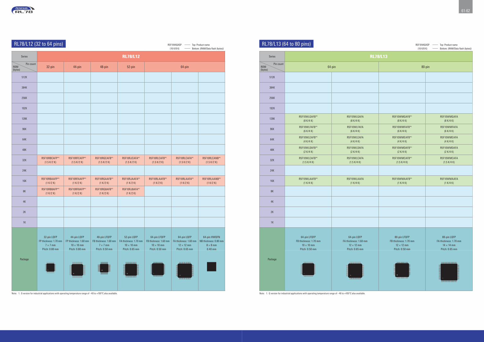
61-62
R5F104AGASP Top: Product name
(16 K/8 K) Bottom: (RAM/Data flash (bytes))
Series RL78/L12
Pin countROM(bytes)
32-pin 44-pin 48-pin 52-pin 64-pin
512K
384K
256K
192K
128K
96K
64K
48K
32KR5F10RBCAFP*1
(1.5 K/2 K)R5F10RFCAFP*1
(1.5 K/2 K)R5F10RGCAFB*1
(1.5 K/2 K)R5F10RJCAFA*1
(1.5 K/2 K)R5F10RLCAFB*1
(1.5 K/2 K)R5F10RLCAFA*1
(1.5 K/2 K)R5F10RLCANB*1
(1.5 K/2 K)
24K
16KR5F10RBAAFP*1
(1 K/2 K)R5F10RFAAFP*1
(1 K/2 K)R5F10RGAAFB*1
(1 K/2 K)R5F10RJAAFA*1
(1 K/2 K)R5F10RLAAFB*1
(1 K/2 K)R5F10RLAAFA*1
(1 K/2 K)R5F10RLAANB*1
(1 K/2 K)
8KR5F10RB8AFP*1
(1 K/2 K)R5F10RF8AFP*1
(1 K/2 K)R5F10RG8AFB*1
(1 K/2 K)R5F10RJ8AFA*1
(1 K/2 K)
4K
2K
1K
Package
32-pin LQFPFP thickness: 1.70 mm
7 × 7 mmPitch: 0.80 mm
44-pin LQFPFP thickness: 1.60 mm
10 × 10 mmPitch: 0.80 mm
48-pin LFQFP FB thickness: 1.60 mm
7 × 7 mmPitch: 0.50 mm
52-pin LQFPFA thickness: 1.70 mm
10 × 10 mmPitch: 0.65 mm
64-pin LFQFPFB thickness: 1.60 mm
10 × 10 mmPitch: 0.50 mm
64-pin LQFPFA thickness: 1.60 mm
12 × 12 mmPitch: 0.65 mm
64-pin HWQFNNB thickness: 0.80 mm
8 × 8 mm0.40 mm
Note: 1. G version for industrial applications with operating temperature range of –40 to +105°C also available.
R5F104AGASP Top: Product name
(16 K/8 K) Bottom: (RAM/Data flash (bytes))
Series RL78/L13
Pin countROM(bytes)
64-pin 80-pin
512K
384K
256K
192K
128KR5F10WLGAFB*1
(8 K/4 K)R5F10WLGAFA
(8 K/4 K)R5F10WMGAFB*1
(8 K/4 K)R5F10WMGAFA
(8 K/4 K)
96KR5F10WLFAFB*1
(6 K/4 K)R5F10WLFAFA
(6 K/4 K)R5F10WMFAFB*1
(6 K/4 K)R5F10WMFAFA
(6 K/4 K)
64KR5F10WLEAFB*1
(4 K/4 K)R5F10WLEAFA
(4 K/4 K)R5F10WMEAFB*1
(4 K/4 K)R5F10WMEAFA
(4 K/4 K)
48KR5F10WLDAFB*1
(2 K/4 K)R5F10WLDAFA
(2 K/4 K)R5F10WMDAFB*1
(2 K/4 K)R5F10WMDAFA
(2 K/4 K)
32KR5F10WLCAFB*1
(1.5 K/4 K)R5F10WLCAFA
(1.5 K/4 K)R5F10WMCAFB*1
(1.5 K/4 K)R5F10WMCAFA
(1.5 K/4 K)
24K
16KR5F10WLAAFB*1
(1 K/4 K)R5F10WLAAFA
(1 K/4 K)R5F10WMAAFB*1
(1 K/4 K)R5F10WMAAFA
(1 K/4 K)
8K
4K
2K
1K
Package
64-pin LFQFPFB thickness: 1.70 mm
10 × 10 mmPitch: 0.50 mm
64-pin LQFPFA thickness: 1.60 mm
12 × 12 mmPitch: 0.65 mm
80-pin LFQFPFB thickness: 1.70 mm
12 × 12 mmPitch: 0.50 mm
80-pin LQFPFA thickness: 1.70 mm
14 × 14 mmPitch: 0.65 mm
Note: 1. G version for industrial applications with operating temperature range of –40 to +105°C also available.
RL78/L12 (32 to 64 pins) RL78/L13 (64 to 80 pins)

63-64
R5F104AGASP Top: Product name
(16 K/8 K) Bottom: (RAM/Data flash (bytes))
Series RL78/L1C (USB)
Pin countROM(bytes)
80-pin 85-pin 100-pin
512K
384K
256KR5F110MJAFB*1
(16 K/8 K)R5F110NJALA*1
(16 K/8 K)R5F110PJAFB*1
(16 K/8 K)
192KR5F110MHAFB*1
(16 K/8 K)R5F110NHALA*1
(16 K/8 K)R5F110PHAFB*1
(16 K/8 K)
128KR5F110MGAFB*1
(12 K/8 K)R5F110NGALA*1
(12 K/8 K)R5F110PGAFB*1
(12 K/8 K)
96KR5F110MFAFB*1
(10 K/8 K)R5F110NFALA*1
(10 K/8 K)R5F110PFAFB*1
(10 K/8 K)
64KR5F110MEAFB*1
(8 K/8 K)R5F110NEALA*1
(8 K/8 K)R5F110PEAFB*1
(8 K/8 K)
48K
32K
24K
16K
8K
4K
2K
1K
Package
80-pin LFQFPFB thickness: 1.70 mm
12 × 12 mmPitch: 0.50 mm
85-pin VFLGALA thickness: 1.00 mm
7 × 7 mmPitch: 0.65 mm
100-pin LFQFPFB thickness: 1.70 mm
14 × 14 mmPitch: 0.50 mm
Note: 1. G version for industrial applications with operating temperature range of –40 to +105°C also available.
RL78/L1C (no USB)
80-pin 85-pin 100-pin
R5F111MJAFB*1 (16 K/8 K)
R5F111NJALA*1
(16 K/8 K)R5F111PJAFB
(16 K/8 K)
R5F111MHAFB*1 (16 K/8 K)
R5F111NHALA*1
(16 K/8 K)R5F111PHAFB
(16 K/8 K)
R5F111MGAFB*1 (12 K/8 K)
R5F111NGALA*1
(12 K/8 K)R5F111PGAFB
(12 K/8 K)
R5F111MFAFB*1 (10 K/8 K)
R5F111NFALA*1
(10 K/8 K)R5F111PFAFB
(10 K/8 K)
R5F111MEAFB*1 (8 K/8 K)
R5F111NEALA*1
(8 K/8 K)R5F111PEAFB
(8 K/8 K)
80-pin LFQFPFB thickness: 1.70 mm
12 × 12 mmPitch: 0.50 mm
85-pin VFLGALA thickness: 1.00 mm
7 × 7 mmPitch: 0.65 mm
100-pin LFQFPFB thickness: 1.70 mm
14 × 14 mmPitch: 0.50 mm
Note: 1. G version for industrial applications with operating temperature range of –40 to +105°C also available.
RL78/L1C (80 to 100 pins) R5F104AGASP Top: Product name
(16 K/8 K) Bottom: (RAM/Data flash (bytes))
Series RL78/L1A
Pin countROM(bytes)
80-pin 100-pin
512K
384K
256K
192K
128KR5F11MPGAFB(8 KB/5.5 KB)
96KR5F11MMFAFB(8 KB/5.5 KB)
R5F11MPFAFB(8 KB/5.5 KB)
64KR5F11MMEAFB(8 KB/5.5 KB)
R5F11MPEAFB(8 KB/5.5 KB)
48KR5F11MMDAFB
(8 KB/5.5 KB)
32K
24K
16K
8K
4K
2K
1K
Package
80-pin LFQFPFB thickness: 1.60 mm
12 × 12 mmPitch: 0.50 mm
100-pin LFQFPFB thickness: 1.60 mm
14 × 14 mmPitch: 0.50 mm
RL78/L1A (80 to 100 pins)

65-66
R5F104AGASP Top: Product name
(16 K/8 K) Bottom: (RAM/Data flash (bytes))
Series RL78/I1A
Pin countROM(bytes)
20-pin 30-pin 38-pin
512K
384K
256K
192K
128K
96K
64KR5F107AEGSP*1
R5F107AEMSP*2
(4 K/4 K)
R5F107DEGSP*1
R5F107DEMSP*2
(4 K/4 K)
48K
32KR5F1076CGSP*1
R5F1076CMSP*2
(2 K/4 K)
R5F107ACGSP*1
R5F107ACMSP*2
(2 K/4 K)
16K
12K
8K
4K
2K
1K
Package
20-pin LSSOPSP thickness: 1.45 mm
4.4 × 6.5 mmPitch: 0.65 mm
30-pin LSSOPSP thickness: 1.40 mm
7.62 mm (300 mil)Pitch: 0.65 mm
38-pin SSOPSP thickness: 2.00 mm
7.62 mm (300 mil)Pitch: 0.65 mm
Notes: 1. Operating temperature range: –40 to +105°C 2. Operating temperature range: –40 to +125°C
RL78/I1A (20 to 38 pins) R5F104AGASP Top: Product name
(16 K/8 K) Bottom: (RAM/Data flash (bytes))
Series RL78/I1B
Pin countROM(bytes)
80-pin 100-pin
512K
384K
256K
192K
128KR5F10MMGDFB
(8 K/—)R5F10MPGDFB
(8 K/—)
96K
64KR5F10MMEDFB
(6 /—)R5F10MPEDFB
(6 K/—)
48K
32K
24K
16K
8K
4K
2K
1K
Package
80-pin LFQFPFB thickness: 1.70 mm
12 × 12 mmPitch: 0.50 mm
100-pin LFQFPFB thickness: 1.70 mm
14 × 14 mmPitch: 0.50 mm
RL78/I1C
64-pin 80-pin 100-pin
R5F10NMJDFB(16 K/2 K)
R5F10NPJDFB(16 K/2 K)
R5F10NLGDFB(8 K/2 K)
R5F10NMGDFB(8 K/2 K)
R5F10NPGDFB(8 K/2 K)
R5F10NLEDFB(6 K/2 K)
R5F10NMEDFB(6 K/2 K)
64-pin LFQFPFB thickness: 1.70 mm
10 × 10 mmPitch: 0.50 mm
80-pin LFQFPFB thickness: 1.70mm
12 × 12 mmPitch: 0.50 mm
100-pin LFQFPFB thickness: 1.70mm
14 × 14 mmPitch: 0.50 mm
RL78/I1B (80 to 100 pins), RL78/I1C (64 to 100 pins)

67-68
R5F104AGASP Top: Product name
(16 K/8 K) Bottom: (RAM/Data flash (bytes))
R5F104AGASP Top: Product name
(16 K/8 K) Bottom: (RAM/Data flash (bytes))
Series RL78/I1D
Pin countROM(bytes)
20-pin 24-pin 30-pin 32-pin 48-pin
512K
384K
256K
192K
128K
96K
64K
48K
32KR5F117ACGSP
(3 K/2 K)R5F117BCGNA
(3 K/2 K)R5F117BCGFP
(3 K/2 K)R5F117GCGFB
(3 K/2 K)
24K
16KR5F1176AGSP
(2 K/2 K)R5F1177AGNA
(2 K/2 K)R5F117AAGSP
(2 K/2 K)R5F117BAGNA
(2 K/2 K)R5F117BAGFP
(2 K/2 K)R5F117GAGFB
(2 K/2 K)
8KR5F11768GSP
(0.7 K/2 K)R5F11778GNA
(0.7 K/2 K)R5F117A8GSP
(0.7 K/2 K)
4K
2K
1K
Package
20-pin LSSOPSP thickness: 1.45 mm
4.4 × 6.5 mmPitch: 0.65 mm
24-pin HWQFNNA thickness: 0.80 mm
4 × 4 mmPitch: 0.50 mm
30-pin LSSOPSP thickness: 1.40 mm
7.62 mm (300 mil)Pitch: 0.65 mm
32-pin HVQFNNA thickness: 0.90 mm
5 × 5 mmPitch: 0.50 mm
32-pin LQFPFP thickness: 1.70 mm
7 × 7 mmPitch: 0.80 mm
48-pin LFQFPFB thickness: 1.70 mm
7 × 7 mmPitch: 0.50 mm
Series RL78/I1E
Pin countROM(bytes)
32-pin 36-pin
512K
384K
256K
192K
128K
96K
64K
48K
32KR5F11CBCGNA*1
(8 K/4 K)R5F11CCCGBG*1
(8 K/4 K)
24K
16K
8K
4K
2K
1K
Package
32-pin HVQFNNA thickness: 0.90 mm
5 × 5 mmPitch: 0.50 mm
36-pin TFBGABG thickness: 1.10 mm
4 × 4 mmPitch: 0.50 mm
Note: 1. M version for industrial applications with operating temperature range of –40 to +125°C also available.
RL78/I1D (20 to 48 pins) RL78/I1E (32 to 36 pins)

69-70
R5F104AGASP Top: Product name
(16 K/8 K) Bottom: (RAM/Data flash (bytes))
Series RL78/G1E
Pin countROM(bytes)
64-pin 80-pin
512K
384K
256K
192K
128K
96K
64KR5F10FLEANA*1
(4 K/4 K)R5F10FMEAFB*1
(4 K/4 K)
48KR5F10FLDANA*1
(3 K/4 K)R5F10FMDAFB*1
(3 K/4 K)
32KR5F10FLCANA*1
(2 K/4 K)R5F10FMCAFB*1
(2 K/4 K)
16K
12K
8K
4K
2K
1K
Package
64-pin HWQFNNA thickness: 0.80 mm
9 × 9 mmPitch: 0.50 mm
80-pin LFQFP FB thickness: 1.60 mm
12 × 12 mmPitch: 0.50 mm
Note: 1. D version for industrial applications with operating temperature range of –40 to +85°C also available.
MEMORL78/G1E (64 to 80 pins)

71-72
R5F104AGASP Top: Product name
(16 K/8 K) Bottom: (RAM/Data flash (bytes))
Series RL78/F13 (CAN&LIN)
Pin countROM(bytes)
30-pin 32-pin 48-pin 64-pin 80-pin
512K
384K
256K
192K
128KR5F10BAGLSP*1
(8 K/4 K)R5F10BBGLNA*1
(8 K/4 K)R5F10BGGLFB*1
(8 K/4 K)R5F10BGGLNA*1
(8 K/4 K)R5F10BLGLFB*1
(8 K/4 K)R5F10BMGLFB*1
(8 K/4 K)
96KR5F10BAFLSP*1
(6 K/4 K)R5F10BBFLNA*1
(6 K/4 K)R5F10BGFLFB*1
(6 K/4 K)R5F10BGFLNA*1
(6 K/4 K)R5F10BLFLFB*1
(6 K/4 K)R5F10BMFLFB*1
(6 K/4 K)
64KR5F10BAELSP*1
(4 K/4 K)R5F10BBELNA*1
(4 K/4 K)R5F10BGELFB*1
(4 K/4 K)R5F10BGELNA*1
(4 K/4 K)R5F10BLELFB*1
(4 K/4 K)R5F10BMELFB*1
(4 K/4 K)
48KR5F10BADLSP*1
(3 K/4 K)R5F10BBDLNA*1
(3 K/4 K)R5F10BGDLFB*1
(3 K/4 K)R5F10BGDLNA*1
(3 K/4 K)R5F10BLDLFB*1
(3 K/4 K)
32KR5F10BACLSP*1
(2 K/4 K)R5F10BBCLNA*1
(2 K/4 K)R5F10BGCLFB*1
(2 K/4 K)R5F10BGCLNA*1
(2 K/4 K)R5F10BLCLFB*1
(2 K/4 K)
24K
16K
8K
4K
2K
1K
Package
30-pin LSSOPSP thickness: 1.40 mm
7.62 mm (300 mil)Pitch: 0.65 mm
32-pin HVQFNNA thickness: 0.90 mm
5 × 5 mmPitch: 0.50 mm
48-pin LFQFPFB thickness: 1.60 mm
7 × 7 mmPitch: 0.50 mm
48-pin HVQFNNA thickness: 0.90 mm
7 × 7 mmPitch: 0.50 mm
64-pin LFQFPFB thickness: 1.60 mm
10 × 10 mmPitch: 0.50 mm
80-pin LFQFPFB thickness: 1.60 mm
12 × 12 mmPitch: 0.50 mm
Note: 1. K version for automotive applications with operating temperature range of –40 to +125°C and Y version for automotive applications with operating temperature range of –40 to +150°C also available.
Series RL78/F13 (LIN)
Pin countROM(bytes)
20-pin 30-pin 32-pin 48-pin 64-pin 80-pin
512K
384K
256K
192K
128KR5F10AGGLFB*1
(8 K/4 K)R5F10AGGLNA*1
(8 K/4 K)R5F10ALGLFB*1
(8 K/4 K)R5F10AMGLFB*1
(8 K/4 K)
96KR5F10AGFLFB*1
(6 K/4 K)R5F10AGFLNA*1
(6 K/4 K)R5F10ALFLFB*1
(6 K/4 K)R5F10AMFLFB*1
(6 K/4 K)
64KR5F10A6ELSP*1
(4 K/4 K)R5F10AAELSP*1
(4 K/4 K)R5F10ABELNA*1
(4 K/4 K)R5F10AGELFB*1
(4 K/4 K)R5F10AGELNA*1
(4 K/4 K)R5F10ALELFB*1
(4 K/4 K)R5F10AMELFB*1
(4 K/4 K)
48KR5F10A6DLSP*1
(3 K/4 K)R5F10AADLSP*1
(3 K/4 K)R5F10ABDLNA*1
(3 K/4 K)R5F10AGDLFB*1
(3 K/4 K)R5F10AGDLNA*1
(3 K/4 K)R5F10ALDLFB*1
(3 K/4 K)
32KR5F10A6CLSP*1
(2 K/4 K)R5F10AACLSP*1
(2 K/4 K)R5F10ABCLNA*1
(2 K/4 K)R5F10AGCLFB*1
(2 K/4 K)R5F10AGCLNA*1
(2 K/4 K)R5F10ALCLFB*1
(2 K/4 K)
24K
16KR5F10A6ALSP*1
(1 K/4 K)R5F10AAALSP*1
(1 K/4 K)R5F10ABALNA*1
(1 K/4 K)R5F10AGALFB*1
(1 K/4 K)R5F10AGALNA*1
(1 K/4 K)
8K
4K
2K
1K
Package
20-pin LSSOPSP thickness: 1.40 mm
7.62 mm (300 mil)Pitch: 0.65 mm
30-pin LSSOPSP thickness: 1.40 mm
7.62 mm (300 mil)Pitch: 0.65 mm
32-pin HVQFNNA thickness: 0.90 mm
5 × 5 mmPitch: 0.50 mm
48-pin LFQFPFB thickness: 1.60 mm
7 × 7 mmPitch: 0.50 mm
48-pin HVQFNNA thickness: 0.90 mm
7 × 7 mmPitch: 0.50 mm
64-pin LFQFPFB thickness: 1.60 mm
10 × 10 mmPitch: 0.50 mm
80-pin LFQFPFB thickness: 1.60 mm
12 × 12 mmPitch: 0.50 mm
Note: 1. K version for automotive applications with operating temperature range of –40 to +125°C and Y version for automotive applications with operating temperature range of –40 to +150°C also available.
R5F104AGASP Top: Product name
(16 K/8 K) Bottom: (RAM/Data flash (bytes))RL78/F13 (20 to 80 pins)

73-74
Series RL78/F14
Pin countROM(bytes)
30-pin 32-pin 48-pin 64-pin 80-pin 100-pin
512K
384K
256KR5F10PGJLFB*1
(20 K/8 K)R5F10PGJLNA*1
(20 K/8 K)R5F10PLJLFB*1
(20 K/8 K)R5F10PMJLFB*1
(20 K/8 K)R5F10PPJLFB*1
(20 K/8 K)
192KR5F10PGHLFB*1
(16 K/8 K)R5F10PGHLNA*1
(16 K/8 K)R5F10PLHLFB*1
(16 K/8 K)R5F10PMHLFB*1
(16 K/8 K)R5F10PPHLFB*1
(16 K/8 K)
128KR5F10PGGLFB*1
(10 K/8 K)R5F10PGGLNA*1
(10 K/8 K)R5F10PLGLFB*1
(10 K/8 K)R5F10PMGLFB*1
(10 K/8 K)R5F10PPGLFB*1
(10 K/8 K)
96KR5F10PGFLFB*1
(8 K/4 K)R5F10PGFLNA*1
(8 K/4 K)R5F10PLFLFB*1
(8 K/4 K)R5F10PMFLFB*1
(8 K/4 K)R5F10PPFLFB*1
(8 K/4 K)
64KR5F10PAELSP*1
(6 K/4 K)R5F10PBELNA*1
(6 K/4 K)R5F10PGELFB*1
(6 K/4 K)R5F10PGELNA*1
(6 K/4 K)R5F10PLELFB*1
(6 K/4 K)R5F10PMELFB*1
(6 K/4 K)R5F10PPELFB*1
(6 K/4 K)
48KR5F10PADLSP*1
(4 K/4 K)R5F10PBDLNA*1
(4 K/4 K)R5F10PGDLFB*1
(4 K/4 K)R5F10PGDLNA*1
(4 K/4 K)
32K
24K
16K
8K
4K
2K
1K
Package
30-pin LSSOPSP thickness: 1.40 mm
7.62 mm (300 mil)Pitch: 0.65 mm
32-pin HVQFNNA thickness: 0.90 mm
5 × 5 mmPitch: 0.50 mm
48-pin LFQFPFB thickness: 1.60 mm
7 × 7 mmPitch: 0.50 mm
48-pin HVQFNNA thickness: 0.90 mm
7 × 7 mmPitch: 0.50 mm
64-pin LFQFPFB thickness: 1.60 mm
10 × 10 mmPitch: 0.50 mm
80-pin LFQFPFB thickness: 1.60 mm
12 × 12 mmPitch: 0.50 mm
100-pin LFQFPFB thickness: 1.60 mm
14 × 14 mmPitch: 0.50 mm
Note: 1. K version for automotive applications with operating temperature range of –40 to +125°C and Y version for automotive applications with operating temperature range of –40 to +150°C also available.
R5F104AGASP Top: Product name
(16 K/8 K) Bottom: (RAM/Data flash (bytes))R5F104AGASP Top: Product name
(16 K/8 K) Bottom: (RAM/Data flash (bytes))
Series RL78/F15
Pin countROM(bytes)
48-pin 64-pin 80-pin 100-pin 144-pin
512KR5F113GLLFB*1
(32 K/16 K)R5F113GLLNA*1
(32 K/16 K)R5F113LLLFB*1
(32 K/16 K)R5F113MLLFB*1
(32 K/16 K)R5F113PLLFB*1
(32 K/16 K)R5F113TLLFB*1
(32 K/16 K)
384KR5F113GKLFB*1
(26 K/16 K)R5F113GKLNA*1
(26 K/16 K)R5F113LKLFB*1
(26 K/16 K)R5F113MKLFB*1
(26 K/16 K)R5F113PKLFB*1
(26 K/16 K)R5F113TKLFB*1
(26 K/16 K)
256KR5F113PJLFB*1
(20 K/8 K)R5F113TJLFB*1
(20 K/8 K)
192KR5F113PHLFB*1
(16 K/8 K)R5F113THLFB*1
(16 K/8 K)
128KR5F113PGLFB*1
(10 K/8 K)R5F113TGLFB*1
(10 K/8 K)
96K
64K
48K
32K
24K
16K
8K
4K
2K
1K
Package
48-pin LFQFPFB thickness: 1.60 mm
7 × 7 mmPitch: 0.50 mm
48-pin HVQFNNA thickness: 0.90 mm
7 × 7 mmPitch: 0.50 mm
64-pin LFQFPFB thickness: 1.60 mm
10 × 10 mmPitch: 0.50 mm
80-pin LFQFPFB thickness: 1.60 mm
12 × 12mmPitch: 0.50 mm
100-pin LFQFPFB thickness: 1.60 mm
14 × 14 mmPitch: 0.50 mm
144-pin LFQFPFB thickness: 1.60 mm
20 × 20 mmPitch: 0.50 mm
Note: 1. K version for automotive applications with operating temperature range of –40 to +125°C also available.
RL78/F14 (30 to 100 pins) RL78/F15 (48 to 144 pins)

75-76
Series RL78/G10Pin count 10-pin 16-pin
Product name
R5F1
0Y14
ASP *3
R5F1
0Y16
ASP *3
R5F1
0Y17
ASP *3
R5F1
0Y44
ASP *3
R5F1
0Y46
ASP *3
R5F1
0Y47
ASP *3
CPU RL78 CPU core
Memory Flash ROM [bytes] 1 K 2 K 4 K 1 K 2 K 4 K
Data flash [bytes]
RAM [bytes] 128 256 512 128 256 512
Operating clocks
Maximum operating frequency [Hz]
On-chip oscillator clock 20 MHz
External resonator 20 MHz
Clock generator circuit
Crystal/ceramic oscillator [Hz] 1 to 20 MHz (VDD = 2.7 to 5.5 V), 1 to 5 MHz (VDD = 2.0 to 5.5 V) *1
High-speed on-chip oscillator [Hz] 1.25 to 20 MHz (VDD = 2.7 to 5.5 V), 1.25 to 5 MHz (VDD = 2.0 to 5.5 V) *1
Low-speed on-chip oscillator [Hz] 15 kHz (VDD = 2.0 to 5.5 V) *1
Subclock (32.768 kHz)
I/O I/O ports 8 14
N-channel open drain (6 V tolerance)
N-channel open drain (VDD tolerance) 2 4
Timers 16-bit timer TAU [channels] 2, PWM output × 1 4, PWM output × 3
Real-time clock (RTC) [channels]
Watchdog timer (WDT) [channels] 1
Interval timer [channels] 12-bit × 1
Serial interfaces CSI × 1, UART × 1, simplified I2C × 1 1
CSI × 2, UART × 1, simplified I2C × 1 1
I2C × 1 1
DMA [channels]
External interrupt pins [count] 8 10
OCD On-chip debugging Yes
Peripheralfunctions
8/10-bit A/D converter [channels] 4 7
Comparator [channels] 1
Multiplier/divider/multiply-accumulator
Multiplier (8-bit × 8-bit)
Other functions Selectable power-on reset (SPOR), clock/buzzer output × 1
Safety functions Internal reset at illegal instruction execution*2
Other Power supply voltage [V] VDD = 2.0 to 5.5 V*1
Operating ambient temperature [°C] TA = –40 to +85˚C (A: Consumer applications, D: Industrial applications) *3
Package (size [mm]) 10-LSSOP (4.4 × 3.6 mm) 16-SSOP (4.4 × 5.0 mm)
Notes: 1. Selectable power-on reset (SPOR) includes a detection voltage (VSPOR), which should be within the range of 2.25 to 5.5 V. 2. An internal reset is generated when the FFH instruction code is executed. No reset occurs when an illegal instruction is executed during emulation using OCD. 3. The version for industrial applications with an operating temperature range of –40 to +85°C is the R5F10YxxDxx. For details, see “How to read RL78 Family product numbers” on page 122.
RL78 specifications
RL78/G10 (10 to 16 pins)MEMO

77-78
Series RL78/G12Pin count 20-pin 24-pin 30-pin
Product name
R5F1
0266
ASP *1 *
2
R5F1
0267
ASP *1 *
2
R5F1
0268
ASP *1 *
2
R5F1
0269
ASP *1 *
2
R5F1
026A
ASP *1 *
2
R5F1
0366
ASP *1
R5F1
0367
ASP *1
R5F1
0368
ASP *1
R5F1
0369
ASP *1
R5F1
036A
ASP *1
R5F1
0277
ANA *1 *
2
R5F1
0278
ANA *1 *
2
R5F1
0279
ANA *1 *
2
R5F1
027A
ANA *1 *
2
R5F1
0377
ANA *1
R5F1
0378
ANA *1
R5F1
0379
ANA *1
R5F1
037A
ANA *1
R5F1
02A7
ASP *1 *
2
R5F1
02A8
ASP *1 *
2
R5F1
02A9
ASP *1 *
2
R5F1
02AA
ASP *1 *
2
R5F1
03A7
ASP *1
R5F1
03A8
ASP *1
R5F1
03A9
ASP *1
R5F1
03AA
ASP *1
CPU RL78 CPU core
Memory Flash ROM [bytes] 2 K 4 K 8 K 12 K 16 K 2 K 4 K 8 K 12 K 16 K 4 K 8 K 12 K 16 K 4 K 8 K 12 K 16 K 4 K 8 K 12 K 16 K 4 K 8 K 12 K 16 K
Data flash [bytes] 2 K 2 K 2 K
RAM [bytes] 256 512 768 1 K 1.5 K 256 512 768 1 K 1.5 K 512 768 1 K 1.5 K 512 768 1 K 1.5 K 512 768 1 K 2 K 512 768 1 K 2 K
Operating clocks
Maximum operating frequency [Hz]
On-chip oscillator clock 24 MHz
External resonator 20 MHz
Clock generator circuit
Crystal/ceramic oscillator [Hz] 1 to 20 MHz (VDD = 2.7 to 5.5 V), 1 to 8 MHz (VDD = 1.8 to 5.5 V)
High-speed on-chip oscillator [Hz] 1 to 24 MHz (VDD = 2.7 to 5.5 V), 1 to 16 MHz (VDD = 2.4 to 5.5 V), 1 to 8 MHz (VDD = 1.8 to 5.5 V)
Low-speed on-chip oscillator [Hz] 15 kHz (VDD = 1.8 to 5.5 V)
Subclock (32.768 kHz)
I/O I/O ports 18 22 26
N-channel open drain (6 V tolerance) 2
N-channel open drain (VDD tolerance) 4 5 9
Timers 16-bit timer TAU [channels] 4, PWM output × 3 8, PWM output × 3 (7) *3
Real-time clock (RTC) [channels]
Watchdog timer (WDT) [channels] 1
Interval timer [channels] 12-bit × 1
Serial interfaces CSI × 1, UART × 1 1 1 1
CSI × 2, UART × 1, simplified I2C × 2 1 1
CSI × 1, UART × 1, simplified I2C × 1 3
I2C × 1 1
DMA [channels] 2 2 2
External interrupt pins [count] 10 14 6
OCD On-chip debugging Yes
Peripheralfunctions
8/10-bit A/D converter [channels] 11 8
Multiplier/divider/multiply-accumulator
Library support for multiply/divide/multiply-accumulate operations (equipped with functional unit)Multiply: 16-bit × 16-bit = 32-bit (signed/unsigned)
Divide: 32-bit ÷ 32-bit = 32-bit (unsigned)Multiply- accumulate: 16-bit × 16-bit + 32-bit = 32-bit (signed/unsigned)
Other functions Power-on reset (POR), low-voltage detection circuit (LVD), clock/buzzer output × 1 Power-on reset (POR), low-voltage detection circuit (LVD), clock/buzzer output × 2
Safety functions RAM parity error detection function, illegal memory access detection function, frequency detection function, A/D converter test function
CRC calculation function (general-purpose), RAM guard function, SFR guard function
CRC calculation function (general-purpose),
RAM guard function, SFR guard function
CRC calculation function (general-purpose),
RAM guard function, SFR guard function
Other Power supply voltage [V] VDD = 1.8 to 5.5 V
Operating ambient temperature [°C] TA = –40 to + 85˚C (A: Consumer applications, D: Industrial applications) *1
TA = –40 to +105˚C (G: Industrial applications) *2
Package (size [mm]) 20-LSSOP (4.4 × 6.5 mm) 24-HWQFN (4 × 4 mm) 30-LSSOP (7.62 mm (300 mil))
Notes: A dedicated library (approx. 8.1 KB) is required to use the data flash. 1. The version for industrial applications with an operating temperature range of –40 to +85°C is the R5F10xxxDxx. For details, see “How to read RL78 Family product numbers” on page 122. 2. The version for industrial applications with an operating temperature range of –40 to +105°C is the R5F10xxxGxx. For details, see “How to read RL78 Family product numbers” on page 122. 3. Figures in parentheses ( ) are when the PIOR function is used.
RL78/G12 (20 to 30 pins)

79-80
Series RL78/G13Pin count 20-pin 24-pin 25-pin 30-pin 32-pin
Product name
R5F1
006A
ASP *2 *
3
R5F1
006C
ASP *2 *
3
R5F1
006D
ASP *2 *
3
R5F1
006E
ASP *2 *
3
R5F1
016A
ASP *2
R5F1
016C
ASP *2
R5F1
016D
ASP *2
R5F1
016E
ASP *2
R5F1
007A
ANA *2 *
3
R5F1
007C
ANA *2 *
3
R5F1
007D
ANA *2 *
3
R5F1
007E
ANA *2 *
3
R5F1
017A
ANA *2
R5F1
017C
ANA *2
R5F1
017D
ANA *2
R5F1
017E
ANA *2
R5F1
008A
ALA *3
R5F1
008C
ALA *3
R5F1
008D
ALA *3
R5F1
008E
ALA *3
R5F1
018A
ALA
R5F1
018C
ALA
R5F1
018D
ALA
R5F1
018E
ALA
R5F1
00AA
ASP *2 *
3
R5F1
00AC
ASP *2 *
3
R5F1
00AD
ASP *2 *
3
R5F1
00AE
ASP *2 *
3
R5F1
00AF
ASP *2 *
3
R5F1
00AG
ASP *2 *
3
R5F1
01AA
ASP *2
R5F1
01AC
ASP *2
R5F1
01AD
ASP *2
R5F1
01AE
ASP *2
R5F1
01AF
ASP *2
R5F1
01AG
ASP *2
R5F1
00BA
ANA *2 *
3
R5F1
00BC
ANA *2 *
3
R5F1
00BD
ANA *2 *
3
R5F1
00BE
ANA *2 *
3
R5F1
00BF
ANA *2 *
3
R5F1
00BG
ANA *2 *
3
R5F1
01BA
ANA *2
R5F1
01BC
ANA *2
R5F1
01BD
ANA *2
R5F1
01BE
ANA *2
R5F1
01BF
ANA *2
R5F1
01BG
ANA *2
CPU RL78 CPU core
Memory Flash ROM [bytes] 16 K 32 K 48 K 64 K 16 K 32 K 48 K 64 K 16 K 32 K 48 K 64 K 16 K 32 K 48 K 64 K 16 K 32 K 48 K 64 K 16 K 32 K 48 K 64 K 16 K 32 K 48 K 64 K 96 K 128 K 16 K 32 K 48 K 64 K 96 K 128 K 16 K 32 K 48 K 64 K 96 K 128 K 16 K 32 K 48 K 64 K 96 K 128 K
Data flash [bytes] 4 K 4 K 4 K 4 K 8 K 4 K 8 K
RAM [bytes] 2 K 2 K 3 K 4 K 2 K 2 K 3 K 4 K 2 K 2 K 3 K 4 K 2 K 2 K 3 K 4 K 2 K 2 K 3 K 4 K 2 K 2 K 3 K 4 K 2 K 2 K 3 K 4 K 8 K 12 K 2 K 2 K 3 K 4 K 8 K 12 K 2 K 2 K 3 K 4 K 8 K 12 K 2 K 2 K 3 K 4 K 8 K 12 K
Operating clocks
Maximum operating frequency [Hz]
On-chip oscillator clock 32 MHz
External resonator 20 MHz
Clock generator circuit
Crystal/ceramic oscillator [Hz] 1 to 20 MHz (VDD = 2.7 to 5.5 V), 1 to 16 MHz (VDD = 2.4 to 5.5 V), 1 to 8 MHz (VDD = 1.8 to 5.5 V), 1 to 4 MHz (VDD = 1.6 to 5.5 V)
High-speed on-chip oscillator [Hz] 1 to 32 MHz (VDD = 2.7 to 5.5 V), 1 to 16 MHz (VDD = 2.4 to 5.5 V), 1 to 8 MHz (VDD = 1.8 to 5.5 V), 1 to 4 MHz (VDD = 1.6 to 5.5 V)
Low-speed on-chip oscillator [Hz] 15 kHz (VDD = 1.6 to 5.5 V)
Subclock (32.768 kHz)
I/O I/O ports 16 20 21 26 28
N-channel open drain (6 V tolerance) 2 3
N-channel open drain (VDD tolerance) 5 6 9
Timers 16-bit timer TAU [channels] 8, PWM output × 2 8, PWM output × 3 8, PWM output × 3 (7) *4
Real-time clock (RTC) [channels] 1*1
Watchdog timer (WDT) [channels] 1
Interval timer [channels] 12-bit × 1
Serial interfaces CSI × 1, UART × 1, simplified I2C × 1 2
CSI × 2, UART × 1, simplified I2C × 2
CSI × 1, UART (LIN bus support) × 1, simplified I2C × 1
1
CSI × 2, UART (LIN bus support) × 1, simplified I2C × 2
I2C × 1 1
DMA [channels] 2
External interrupt pins [count] 3 5 6
OCD On-chip debugging Yes
Peripheralfunctions
8/10-bit A/D converter [channels] 6 8
Multiplier/divider/multiply-accumulator
Library support for multiply/divide/multiply-accumulate operations (equipped with functional unit)Multiply: 16-bit × 16-bit = 32-bit (signed/unsigned)
Divide: 32-bit ÷ 32-bit = 32-bit (unsigned)Multiply- accumulate: 16-bit ×16-bit + 32-bit = 32-bit (signed/unsigned)
Other functions Power-on reset (POR), low-voltage detection circuit (LVD) Power-on reset (POR), low-voltage detection circuit (LVD), clock/buzzer output × 1 Power-on reset (POR), low-voltage detection circuit (LVD), clock/buzzer output × 2
Safety functions Flash memory CRC calculation function (high-speed), CRC calculation function (general-purpose), RAM parity error detection function, RAM guard function, SFR guard function, illegal memory access detection function, frequency detection function, A/D converter test function
Other Power supply voltage [V] VDD = 1.6 to 5.5 V
Operating ambient temperature [°C] TA = –40 to +85˚C (A: Consumer applications, D: Industrial applications) *2
TA = –40 to +105˚C (G: Industrial applications) *3
Package (size [mm]) 20-LSSOP (7.62 mm (300 mil)) 24-HWQFN (4 × 4 mm) 25-WFLGA (3 × 3 mm) 30-LSSOP (7.62 mm (300 mil)) 32-HWQFN (5 × 5 mm)
Notes: A dedicated library is required to overwrite the data flash. Refer to [Development Environments] – [Flash Programming Tools] – [Self-Programming Library] on the Renesas website. https://www.renesas.com/flash_libraries 1. Products with pin counts from 20 to 32 pins are not equipped with a subsystem clock, so only the fixed-cycle interrupt function using the low-speed on-chip oscillator clock (15 kHz) is available for use. 2. The version for industrial applications with an operating temperature range of –40 to +85°C is the R5F10xxxDxx. For details, see “How to read RL78 Family product numbers” on page 122. 3. The version for industrial applications with an operating temperature range of –40 to +105°C is the R5F10xxxGxx. For details, see “How to read RL78 Family product numbers” on page 122. 4. Figures in parentheses ( ) are when the PIOR function is used.
RL78/G13 (20 to 32 pins)

81-82
Series RL78/G13Pin count 36-pin 40-pin 44-pin
Product name
R5F1
00CA
ALA *3
R5F1
00CC
ALA *3
R5F1
00CD
ALA *3
R5F1
00CE
ALA *3
R5F1
00CF
ALA *3
R5F1
00CG
ALA *3
R5F1
01CA
ALA
R5F1
01CC
ALA
R5F1
01CD
ALA
R5F1
01CE
ALA
R5F1
01CF
ALA
R5F1
01CG
ALA
R5F1
00EA
ANA *2 *
3
R5F1
00EC
ANA *2 *
3
R5F1
00ED
ANA *2 *
3
R5F1
00EE
ANA *2 *
3
R5F1
00EF
ANA *2 *
3
R5F1
00EG
ANA *2 *
3
R5F1
00EH
ANA *2 *
3
R5F1
01EA
ANA *2
R5F1
01EC
ANA *2
R5F1
01ED
ANA *2
R5F1
01EE
ANA *2
R5F1
01EF
ANA *2
R5F1
01EG
ANA *2
R5F1
01EH
ANA *2
R5F1
00FA
AFP *2 *
3
R5F1
00FC
AFP *2 *
3
R5F1
00FD
AFP *2 *
3
R5F1
00FE
AFP *2 *
3
R5F1
00FF
AFP *2 *
3
R5F1
00FG
AFP *2 *
3
R5F1
00FH
AFP *2 *
3
R5F1
00FJ
AFP *2 *
3
R5F1
00FK
AFP *2
R5F1
00FL
AFP *2
R5F1
01FA
AFP *2
R5F1
01FC
AFP *2
R5F1
01FD
AFP *2
R5F1
01FE
AFP *2
R5F1
01FF
AFP *2
R5F1
01FG
AFP *2
R5F1
01FH
AFP *2
R5F1
01FJ
AFP *2
R5F1
01FK
AFP *2
R5F1
01FL
AFP *2
CPU RL78 CPU core
Memory Flash ROM [bytes] 16 K 32 K 48 K 64 K 96 K 128 K 16 K 32 K 48 K 64 K 96 K 128 K 16 K 32 K 48 K 64 K 96 K 128 K 192 K 16 K 32 K 48 K 64 K 96 K 128 K 192 K 16 K 32 K 48 K 64 K 96 K 128 K 192 K 256 K 384 K 512 K 16 K 32 K 48 K 64 K 96 K 128 K 192 K 256 K 384 K 512 K
Data flash [bytes] 4 K 8 K 4 K 8 K 4 K 8 K
RAM [bytes] 2 K 2 K 3 K 4 K 8 K 12 K 2 K 2 K 3 K 4 K 8 K 12 K 2 K 2 K 3 K 4 K 8 K 12 K 16 K 2 K 2 K 3 K 4 K 8 K 12 K 16 K 2 K 2 K 3 K 4 K 8 K 12 K 16 K 20 K 24 K 32 K 2 K 2 K 3 K 4 K 8 K 12 K 16 K 20 K 24 K 32 K
Operating clocks
Maximum operating frequency [Hz]
On-chip oscillator clock 32 MHz
External resonator 20 MHz
Clock generator circuit
Crystal/ceramic oscillator [Hz] 1 to 20 MHz (VDD = 2.7 to 5.5 V), 1 to 16 MHz (VDD = 2.4 to 5.5 V), 1 to 8 MHz (VDD = 1.8 to 5.5 V), 1 to 4 MHz (VDD = 1.6 to 5.5 V)
High-speed on-chip oscillator [Hz] 1 to 32 MHz (VDD = 2.7 to 5.5 V), 1 to 16 MHz (VDD = 2.4 to 5.5 V), 1 to 8 MHz (VDD = 1.8 to 5.5 V), 1 to 4 MHz (VDD = 1.6 to 5.5 V)
Low-speed on-chip oscillator [Hz] 15 kHz (VDD = 1.6 to 5.5 V)
Subclock (32.768 kHz) 32.768 kHz (VDD = 1.6 to 5.5 V)
I/O I/O ports 32 36 40
N-channel open drain (6 V tolerance) 3 4
N-channel open drain (VDD tolerance) 10
Timers 16-bit timer TAU [channels] 8, PWM output × 3 (7) *4 8, PWM output × 4 (7) *4
Real-time clock (RTC) [channels] 1*1 1
Watchdog timer (WDT) [channels] 1
Interval timer [channels] 12-bit × 1
Serial interfaces CSI × 1, UART × 1, simplified I2C × 1 2
CSI × 2, UART × 1, simplified I2C × 2
CSI × 1, UART (LIN bus support) × 1, simplified I2C × 1
CSI × 2, UART (LIN bus support) × 1, simplified I2C × 2
1
I2C × 1 1
DMA [channels] 2
External interrupt pins [count] 6 10
OCD On-chip debugging Yes
Peripheralfunctions
8/10-bit A/D converter [channels] 8 9 10
Multiplier/divider/multiply-accumulator
Library support for multiply/divide/multiply-accumulate operations (equipped with functional unit)Multiply: 16-bit × 16-bit = 32-bit (signed/unsigned)
Divide: 32-bit ÷ 32-bit = 32-bit (unsigned)Multiply- accumulate: 16-bit × 16-bit + 32-bit = 32-bit (signed/unsigned)
Other functions Power-on reset (POR), low-voltage detection circuit (LVD), clock/buzzer output × 2
Safety functions Flash memory CRC calculation function (high-speed), CRC calculation function (general-purpose), RAM parity error detection function, RAM guard function, SFR guard function, illegal memory access detection function, frequency detection function, A/D converter test function
Other Power supply voltage [V] VDD = 1.6 to 5.5 V
Operating ambient temperature [°C] TA = –40 to +85˚C (A: Consumer applications, D: Industrial applications) *2
TA = –40 to +105˚C (G: Industrial applications) *3
Package (size [mm]) 36-WFLGA (4 × 4 mm) 40-HWQFN (6 × 6 mm) 44-LQFP (10 × 10 mm)
Notes: A dedicated library is required to overwrite the data flash. Refer to [Development Environments] – [Flash Programming Tools] – [Self-Programming Library] on the Renesas website. https://www.renesas.com/flash_libraries 1. Products with a pin count of 36 pins are not equipped with a subsystem clock, so only the fixed-cycle interrupt function using the low-speed on-chip oscillator clock (15 kHz) is available for use. 2. The version for industrial applications with an operating temperature range of –40 to +85°C is the R5F10xxxDxx. For details, see “How to read RL78 Family product numbers” on page 122. 3. The version for industrial applications with an operating temperature range of –40 to +105°C is the R5F10xxxGxx. For details, see “How to read RL78 Family product numbers” on page 122. 4. Figures in parentheses ( ) are when the PIOR function is used.
RL78/G13 (36 to 44 pins)

83-84
Series RL78/G13Pin count 48-pin 52-pin
Product name
1R5
F100
GAAF
B *1 *2
2R5
F100
GAAN
A*1 *
2
1R5
F100
GCAF
B *1 *2
2R5
F100
GCAN
A*1 *
2
1R5
F100
GDAF
B *1 *2
2R5
F100
GDAN
A*1 *
2
1R5
F100
GEAF
B *1 *2
2R5
F100
GEAN
A*1 *
2
1R5
F100
GFAF
B *1 *2
2R5
F100
GFAN
A *1 *2
1R5
F100
GGAF
B *1 *2
2R5
F100
GGAN
A*1 *
2
1R5
F100
GHAF
B *1 *2
2R5
F100
GHAN
A*1 *
2
1R5
F100
GJAF
B *1 *2
2R5
F100
GJAN
A*1 *
2
1R5
F100
GKAF
B *1
2R5
F100
GKAN
A *1
1R5
F100
GLAF
B *1
2R5
F100
GLAN
A *1
1R5
F101
GAAF
B *1
2R5
F101
GAAN
A *1
1R5
F101
GCAF
B *1
2R5
F101
GCAN
A *1
1R5
F101
GDAF
B *1
2R5
F101
GDAN
A *1
1R5
F101
GEAF
B *1
2R5
F101
GEAN
A *1
1R5
F101
GFAF
B *1
2R5
F101
GFAN
A *1
1R5
F101
GGAF
B *1
2R5
F101
GGAN
A *1
1R5
F101
GHAF
B *1
2R5
F101
GHAN
A *1
1R5
F101
GJAF
B *1
2R5
F101
GJAN
A *1
1R5
F101
GKAF
B *1
2R5
F101
GKAN
A *1
1R5
F101
GLAF
B *1
2R5
F101
GLAN
A *1
R5F1
00JC
AFA *1 *
2
R5F1
00JD
AFA *1 *
2
R5F1
00JE
AFA *1 *
2
R5F1
00JF
AFA *1 *
2
R5F1
00JG
AFA *1 *
2
R5F1
00JH
AFA *1 *
2
R5F1
00JJ
AFA *1 *
2
R5F1
00JK
AFA
*1
R5F1
00JL
AFA
*1
R5F1
01JC
AFA
*1
R5F1
01JD
AFA
*1
R5F1
01JE
AFA
*1
R5F1
01JF
AFA
*1
R5F1
01JG
AFA
*1
R5F1
01JH
AFA *1
R5F1
01JJ
AFA
*1
R5F1
01JK
AFA
*1
R5F1
01JL
AFA
*1
CPU RL78 CPU core
Memory Flash ROM [bytes] 16 K 32 K 48 K 64 K 96 K 128 K 192 K 256 K 384 K 512 K 16 K 32 K 48 K 64 K 96 K 128 K 192 K 256 K 384 K 512 K 32 K 48 K 64 K 96 K 128 K 192 K 256 K 384 K 512 K 32 K 48 K 64 K 96 K 128 K 192 K 256 K 384 K 512 K
Data flash [bytes] 4 K 8 K 4 K 8 K
RAM [bytes] 2 K 2 K 3 K 4 K 8 K 12 K 16 K 20 K 24 K 32 K 2 K 2 K 3 K 4 K 8 K 12 K 16 K 20 K 24 K 32 K 2 K 3 K 4 K 8 K 12 K 16 K 20 K 24 K 32 K 2 K 3 K 4 K 8 K 12 K 16 K 20 K 24 K 32 K
Operating clocks
Maximum operating frequency [Hz]
On-chip oscillator clock 32 MHz
External resonator 20 MHz
Clock generator circuit
Crystal/ceramic oscillator [Hz] 1 to 20 MHz (VDD = 2.7 to 5.5 V), 1 to 16 MHz (VDD = 2.4 to 5.5 V), 1 to 8 MHz (VDD = 1.8 to 5.5 V), 1 to 4 MHz (VDD = 1.6 to 5.5 V)
High-speed on-chip oscillator [Hz] 1 to 32 MHz (VDD = 2.7 to 5.5 V), 1 to 16 MHz (VDD = 2.4 to 5.5 V), 1 to 8 MHz (VDD = 1.8 to 5.5 V), 1 to 4 MHz (VDD = 1.6 to 5.5 V)
Low-speed on-chip oscillator [Hz] 15 kHz (VDD = 1.6 to 5.5 V)
Subclock (32.768 kHz) 32.768 kHz (VDD = 1.6 to 5.5 V)
I/O I/O ports 44 48
N-channel open drain (6 V tolerance) 4
N-channel open drain (VDD tolerance) 11 13
Timers 16-bit timer TAU [channels] 8, PWM output × 4 (7) *3
Real-time clock (RTC) [channels] 1
Watchdog timer (WDT) [channels] 1
Interval timer [channels] 12-bit × 1
Serial interfaces CSI × 1, UART × 1, simplified I2C × 1 1
CSI × 2, UART × 1, simplified I2C × 2 1
CSI × 1, UART (LIN bus support) × 1, simplified I2C × 1
CSI × 2, UART (LIN bus support) × 1, simplified I2C × 2
1
I2C × 1 1
DMA [channels] 2
External interrupt pins [count] 13 15
OCD On-chip debugging Yes
Peripheralfunctions
8/10-bit A/D converter [channels] 10 12
Multiplier/divider/multiply-accumulator
Library support for multiply/divide/multiply-accumulate operations (equipped with functional unit)Multiply: 16-bit × 16-bit = 32-bit (signed/unsigned)
Divide: 32-bit ÷ 32-bit = 32-bit (unsigned)Multiply- accumulate: 16-bit × 16-bit + 32-bit = 32-bit (signed/unsigned)
Other functions Power-on reset (POR), low-voltage detection circuit (LVD), clock/buzzer output × 2
Safety functions Flash memory CRC calculation function (high-speed), CRC calculation function (general-purpose), RAM parity error detection function, RAM guard function, SFR guard function, illegal memory access detection function, frequency detection function, A/D converter test function
Other Power supply voltage [V] VDD = 1.6 to 5.5 V
Operating ambient temperature [°C] TA = –40 to +85˚C (A: Consumer applications, D: Industrial applications) *1
TA = –40 to +105˚C (G: Industrial applications) *2
Package (size [mm]) 148-LFQFP (7 × 7 mm) 248-HWQFN (7 × 7 mm) 52-LQFP (10 × 10 mm)
Notes: A dedicated library is required to overwrite the data flash. Refer to [Development Environments] – [Flash Programming Tools] – [Self-Programming Library] on the Renesas website. https://www.renesas.com/flash_libraries 1. The version for industrial applications with an operating temperature range of –40 to +85°C is the R5F10xxxDxx. For details, see “How to read RL78 Family product numbers” on page 122. 2. The version for industrial applications with an operating temperature range of –40 to +105°C is the R5F10xxxGxx. For details, see “How to read RL78 Family product numbers” on page 122. 3. Figures in parentheses ( ) are when the PIOR function is used.
RL78/G13 (48 to 52 pins)

85-86
RL78/G13 (64 pins)
Series RL78/G13Pin count 64-pin
Product name
1R5
F100
LCAF
A *1 *2
2R5
F100
LCAF
B *1 *2
3R5
F100
LCAB
G *2
1R5
F100
LDAF
A *1 *2
2R5
F100
LDAF
B *1 *2
3R5
F100
LDAB
G *2
1R5
F100
LEAF
A *1 *2
2R5
F100
LEAF
B *1 *2
3R5
F100
LEAB
G *2
1R5
F100
LFAF
A *1 *2
2R5
F100
LFAF
B *1 *2
3R5
F100
LFAB
G *2
1R5
F100
LGAF
A *1 *2
2R5
F100
LGAF
B *1 *2
3R5
F100
LGAB
G *2
1R5
F100
LHAF
A *1 *2
2R5
F100
LHAF
B *1 *2
3R5
F100
LHAB
G *2
1R5
F100
LJAF
A *1 *2
2R5
F100
LJAF
B *1 *2
3R5
F100
LJAB
G *2
1R5
F100
LKAF
A *1
2R5
F100
LKAF
B *1
1R5
F100
LLAF
A *1
2R5
F100
LLAF
B *1
1R5
F101
LCAF
A *1
2R5
F101
LCAF
B *1
3R5
F101
LCAB
G
1R5
F101
LDAF
A *1
2R5
F101
LDAF
B *1
3R5
F101
LDAB
G
1R5
F101
LEAF
A *1
2R5
F101
LEAF
B *1
3R5
F101
LEAB
G
1R5
F101
LFAF
A *1
2R5
F101
LFAF
B *1
3R5
F101
LFAB
G
1R5
F101
LGAF
A *1
2R5
F101
LGAF
B *1
3R5
F101
LGAB
G
1R5
F101
LHAF
A *1
2R5
F101
LHAF
B *1
3R5
F101
LHAB
G
1R5
F101
LJAF
A *1
2R5
F101
LJAF
B *1
3R5
F101
LJAB
G
1R5
F101
LKAF
A *1
2R5
F101
LKAF
B *1
1R5
F101
LLAF
A *1
2R5
F100
LLAF
B *1
CPU RL78 CPU core
Memory Flash ROM [bytes] 32 K 48 K 64 K 96 K 128 K 192 K 256 K 384 K 512 K 32 K 48 K 64 K 96 K 128 K 192 K 256 K 384 K 512 K
Data flash [bytes] 4 K 8 K
RAM [bytes] 2 K 3 K 4 K 8 K 12 K 16 K 20 K 24 K 32 K 2 K 3 K 4 K 8 K 12 K 16 K 20 K 24 K 32 K
Operating clocks
Maximum operating frequency [Hz]
On-chip oscillator clock 32 MHz
External resonator 20 MHz
Clock generator circuit
Crystal/ceramic oscillator [Hz] 1 to 20 MHz (VDD = 2.7 to 5.5 V), 1 to 16 MHz (VDD = 2.4 to 5.5 V), 1 to 8 MHz (VDD = 1.8 to 5.5 V), 1 to 4 MHz (VDD = 1.6 to 5.5 V)
High-speed on-chip oscillator [Hz] 1 to 32 MHz (VDD = 2.7 to 5.5 V), 1 to 16 MHz (VDD = 2.4 to 5.5 V), 1 to 8 MHz (VDD = 1.8 to 5.5 V), 1 to 4 MHz (VDD = 1.6 to 5.5 V)
Low-speed on-chip oscillator [Hz] 15 kHz (VDD = 1.6 to 5.5 V)
Subclock (32.768 kHz) 32.768 kHz (VDD = 1.6 to 5.5 V)
I/O I/O ports 58
N-channel open drain (6 V tolerance) 4
N-channel open drain (VDD tolerance) 15
Timers 16-bit timer TAU [channels] 8, PWM output × 7
Real-time clock (RTC) [channels] 1
Watchdog timer (WDT) [channels] 1
Interval timer [channels] 12-bit × 1
Serial interfaces CSI × 1, UART × 1, simplified I2C × 1
CSI × 2, UART × 1, simplified I2C × 2 2
CSI × 1, UART (LIN bus support) × 1, simplified I2C × 1
CSI × 2, UART (LIN bus support) × 1, simplified I2C × 2
1
I2C × 1 1
DMA [channels] 2
External interrupt pins [count] 16 (18) *3
OCD On-chip debugging Yes
Peripheralfunctions
8/10-bit A/D converter [channels] 12
Multiplier/divider/multiply-accumulator
Library support for multiply/divide/multiply-accumulate operations (equipped with functional unit)Multiply: 16-bit × 16-bit = 32-bit (signed/unsigned)
Divide: 32-bit ÷ 32-bit = 32-bit (unsigned)Multiply- accumulate: 16-bit × 16-bit + 32-bit = 32-bit (signed/unsigned)
Other functions Power-on reset (POR), low-voltage detection circuit (LVD), clock/buzzer output × 2
Safety functions Flash memory CRC calculation function (high-speed), CRC calculation function (general-purpose), RAM parity error detection function, RAM guard function, SFR guard function, illegal memory access detection function, frequency detection function, A/D converter test function
Other Power supply voltage [V] VDD = 1.6 to 5.5 V
Operating ambient temperature [°C] TA = –40 to +85˚C (A: Consumer applications, D: Industrial applications) *1
TA = –40 to +105˚C (G: Industrial applications) *2
Package (size [mm]) 164-LQFP (12 × 12 mm) 264-LFQFP (10 × 10 mm) 364-VFBGA (4 × 4 mm)
Notes: A dedicated library is required to overwrite the data flash. Refer to [Development Environments] – [Flash Programming Tools] – [Self-Programming Library] on the Renesas website. https://www.renesas.com/flash_libraries 1. The version for industrial applications with an operating temperature range of –40 to +85°C is the R5F10xxxDxx. For details, see “How to read RL78 Family product numbers” on page 122. 2. The version for industrial applications with an operating temperature range of –40 to +105°C is the R5F10xxxGxx. For details, see “How to read RL78 Family product numbers” on page 122. 3. Figures in parentheses ( ) are when the PIOR function is used.

87-88
Series RL78/G13Pin count 80-pin 100-pin 128-pin
Product name
1R5
F100
MFA
FB *1 *2
2R5
F100
MFA
FA *1 *2
1R5
F100
MGA
FB *1 *2
2R5
F100
MGA
FA *1 *2
1R5
F100
MH
AFB
*1 *2
2R5
F100
MH
AFA
*1 *2
1R5
F100
MJA
FB *1 *2
2R5
F100
MJA
FA *1 *2
1R5
F100
MKA
FB *1
2R5
F100
MKA
FA *1
1R5
F100
MLA
FB *1
2R5
F100
MLA
FA *1
1R5
F101
MFA
FB *1
2R5
F101
MFA
FA *1
1R5
F101
MGA
FB *1
2R5
F101
MGA
FA *1
1R5
F101
MH
AFB *1
2R5
F101
MH
AFA *1
1R5
F101
MJA
FB *1
2R5
F101
MJA
FA *1
1R5
F101
MKA
FB *1
2R5
F101
MKA
FA *1
1R5
F101
MLA
FB *1
2R5
F101
MLA
FA *1
1R5
F100
PFA
FB *1 *2
2R5
F100
PFA
FA *1 *2
1R5
F100
PGA
FB *1 *2
2R5
F100
PGA
FA *1 *2
1R5
F100
PHA
FB *1 *2
2R5
F100
PHA
FA *1 *2
1R5
F100
PJA
FB *1 *2
2R5
F100
PJA
FA *1 *2
1R5
F100
PKA
FB *1
2R5
F100
PKA
FA *1
1R5
F100
PLA
FB *1
2R5
F100
PLA
FA *1
1R5
F101
PFA
FB*1
2R5
F101
PFA
FA*1
1R5
F101
PGA
FB *1
2R5
F101
PGA
FA *1
1R5
F101
PHA
FB *1
2R5
F101
PHA
FA *1
1R5
F101
PJA
FB*1
2R5
F101
PJA
FA*1
1R5
F101
PKA
FB *1
2R5
F101
PKA
FA *1
1R5
F101
PLA
FB*1
2R5
F101
PLA
FA*1
R5F1
00SH
AFB*
1
R5F1
00SJ
AFB*
1
R5F1
00SK
AFB*
1
R5F1
00SL
AFB*
1
R5F1
01SH
AFB*
1
R5F1
01SJ
AFB*
1
R5F1
01SK
AFB*
1
R5F1
01SL
AFB*
1
CPU RL78 CPU core
Memory Flash ROM [bytes] 96 K 128 K 192 K 256 K 384 K 512 K 96 K 128 K 192 K 256 K 384 K 512 K 96 K 128 K 192 K 256 K 384 K 512 K 96 K 128 K 192 K 256 K 384 K 512 K 192 K 256 K 384 K 512 K 192 K 256 K 384 K 512 K
Data flash [bytes] 8 K 8 K 8 K
RAM [bytes] 8 K 12 K 16 K 20 K 24 K 32 K 8 K 12 K 16 K 20 K 24 K 32 K 8 K 12 K 16 K 20 K 24 K 32 K 8 K 12 K 16 K 20 K 24 K 32 K 16 K 20 K 24 K 32 K 16 K 20 K 24 K 32 K
Operating clocks
Maximum operating frequency [Hz]
On-chip oscillator clock 32 MHz
External resonator 20 MHz
Clock generator circuit
Crystal/ceramic oscillator [Hz] 1 to 20 MHz (VDD = 2.7 to 5.5 V), 1 to 16 MHz (VDD = 2.4 to 5.5 V), 1 to 8 MHz (VDD = 1.8 to 5.5 V), 1 to 4 MHz (VDD = 1.6 to 5.5 V)
High-speed on-chip oscillator [Hz] 1 to 32 MHz (VDD = 2.7 to 5.5 V), 1 to 16 MHz (VDD = 2.4 to 5.5 V), 1 to 8 MHz (VDD = 1.8 to 5.5 V), 1 to 4 MHz (VDD = 1.6 to 5.5 V)
Low-speed on-chip oscillator [Hz] 15 kHz (VDD = 1.6 to 5.5 V)
Subclock (32.768 kHz) 32.768 kHz (VDD = 1.6 to 5.5 V)
I/O I/O ports 74 92 120
N-channel open drain (6 V tolerance) 4
N-channel open drain (VDD tolerance) 21 24 25
Timers 16-bit timer TAU [channels] 12, PWM output × 10 16, PWM output × 14
Real-time clock (RTC) [channels] 1
Watchdog timer (WDT) [channels] 1
Interval timer [channels] 12-bit × 1
Serial interfaces CSI × 1, UART × 1, simplified I2C × 1
CSI × 2, UART × 1, simplified I2C × 2 3
CSI × 1, UART (LIN bus support) × 1, simplified I2C × 1
CSI × 2, UART (LIN bus support) × 1, simplified I2C × 2
1
I2C × 1 2
DMA [channels] 4
External interrupt pins [count] 16 (18) *3 16 (20) *3
OCD On-chip debugging Yes
Peripheralfunctions
8/10-bit A/D converter [channels] 17 20 26
Multiplier/divider/multiply-accumulator
Library support for multiply/divide/multiply-accumulate operations (equipped with functional unit)Multiply: 16-bit × 16-bit = 32-bit (signed/unsigned)
Divide: 32-bit ÷ 32-bit = 32-bit (unsigned)Multiply- accumulate: 16-bit × 16-bit + 32-bit = 32-bit (signed/unsigned)
Other functions Power-on reset (POR), low-voltage detection circuit (LVD), clock/buzzer output × 2
Safety functions Flash memory CRC calculation function (high-speed), CRC calculation function (general-purpose), RAM parity error detection function, RAM guard function, SFR guard function, illegal memory access detection function, frequency detection function, A/D converter test function
Other Power supply voltage [V] VDD = 1.6 to 5.5 V
Operating ambient temperature [°C] TA = –40 to +85˚C (A: Consumer applications, D: Industrial applications) *1
TA = –40 to +105˚C (G: Industrial applications) *2
Package (size [mm]) 180-LFQFP (12 × 12 mm) 280-LQFP (14 × 14 mm) 1100-LFQFP (14 × 14 mm) 2100-LQFP (14 × 20 mm) 128-LFQFP (14 × 20 mm)
Notes: A dedicated library is required to overwrite the data flash. Refer to [Development Environments] – [Flash Programming Tools] – [Self-Programming Library] on the Renesas website. https://www.renesas.com/flash_libraries 1. The version for industrial applications with an operating temperature range of –40 to +85°C is the R5F10xxxDxx. For details, see “How to read RL78 Family product numbers” on page 122. 2. The version for industrial applications with an operating temperature range of –40 to +105°C is the R5F10xxxGxx. For details, see “How to read RL78 Family product numbers” on page 122. 3. Figures in parentheses ( ) are when the PIOR function is used.
RL78/G13 (80 to 128 pins)

89-90
RL78/G11 (20-Pin to 25-Pin)
Group RL78/G11Pin count 20-pin 24-pin 25-pin
Name of product
R5F1
056A
ASP *1
R5F1
057A
ANA *1
R5F1
058A
ALA *1
CPU RL78 CPU core
Memory Flash ROM [bytes] 16 KB
Data flash [bytes] 2 KB
RAM [bytes] 1.5 KB
Operating clocks
Maximum operating frequency [Hz]
On-chip oscillator clock 24 MHz
External resonator 20 MHz
Clock generator circuit
Crystal/ceramic oscillator [Hz] 1 to 20 MHz (VDD = 2.7 to 5.5 V), 1 to 16 MHz (VDD = 2.4 to 2.7 V), 1 to 8 MHz (VDD = 1.8 to 2.4 V), 1 to 4 MHz (VDD = 1.6 to 1.8 V)
High-speed on-chip oscillator [Hz]: 24 MHz (max.) 1 to 24 MHz (VDD = 2.7 to 5.5 V): HS mode, 1 to 16 MHz (VDD = 2.4 to 5.5 V): HS mode,
1 to 8 MHz (VDD = 1.8 to 5.5 V): LS mode, 1 to 4 MHz (VDD = 1.6 to 5.5 V): LV mode, 1 MHz (VDD = 1.8 to 5.5 V): LP modeMedium-speed on-chip oscillator [Hz]: 4 MHz (max.)
Low-speed on-chip oscillator [Hz] 15 kHz (TYP.): VDD = 1.6 to 5.5 V
Subclock (32.768 kHz)
I/O I/O ports 17 21
N-channel open drain (6 V tolerance)
N-channel open drain (VDD tolerance) 9 14
Timers 16-bit timer TAU [channels] 4, PWM × 3
Real-time clock [channels]
Watchdog timer [channels] 1
Timer KB [channels] 1, PWM × 2
Interval timer [channels] 8-bit × 2 / 16-bit × 1, 12-bit × 1
Serial interface CSI × 1, UART × 1, simple I2C × 1 1
CSI × 2, UART × 1, simple I2C × 2 1 2
I2C × 1 2
DMA/DTC DTC × 23 sources DTC × 24 sources
ELC [channels] 17 inputs 18 inputs
External interrupt pins [count] 14 20
OCD On-chip debugging Yes
Peripheral functions
8-/10-bit A/D converter [channels] 10 11
8-bit D/A converter [channels] 2
Comparator [channels] 2
PGA [channels] 1
Multiplier/divider/multiply-accumulator
Multiply/divide/multiply-accumulate instructions supported (included in CPU instruction set)Multiply: 16-bit × 16-bit = 32-bit (signed/unsigned)
Divide: 32-bit ÷ 32-bit = 32-bit (unsigned)Multiply-accumulate: 16-bit × 16-bit + 32-bit = 32-bit (signed/unsigned)
Other functions Power-on reset (POR), low-voltage detection circuit (LVD), internal reference voltage (VBGR), data operation circuit (DOC), clock/buzzer output × 2, Interrupt flag output (INTFO)
Safety functions Flash memory CRC calculation function (high-speed), CRC calculation function (general-purpose), RAM parity error detection function, RAM guard function, SFR guard function, illegal memory access detection function, frequency detection function,
A/D converter test function, I/O power output signal level detection function
Other Power supply voltage [V] VDD = 1.6 to 5.5 V
Operating ambient temperature [°C] TA = −40 to + 85°C (A: Consumer applications), TA = −40 to +105°C (G: Industrial applications)
Package (size [mm]) 20-LSSOP (4.4 × 6.5 mm) 24-HWQFN (4 × 4 mm) 25-WFLGA (3 × 3 mm)
Note: The version for industrial applications with an operating temperature range of −40 to +105°C is the R5F105xxGxx. For details, see “How to read RL78 Family product numbers” on page 122.
MEMO

91-92
Series RL78/G14Pin count 30-pin 32-pin 36-pin 40-pin 44-pin 48-pin
Product name
R5F1
04AA
ASP *2 *
3
R5F1
04AC
ASP *2 *
3
R5F1
04AD
ASP *2 *
3
R5F1
04AE
ASP *2 *
3
R5F1
04AF
ASP *2 *
3
R5F1
04AG
ASP *2 *
3
1R5
F104
BAAN
A*2 *
3
2R5
F104
BAAF
P *2 *3
1R5
F104
BCAN
A*2 *
3
2R5
F104
BCAF
P *2 *3
1R5
F104
BDAN
A*2 *
3
2R5
F104
BDAF
P *2 *3
1R5
F104
BEAN
A*2 *
3
2R5
F104
BEAF
P *2 *3
1R5
F104
BFAN
A *2 *3
2R5
F104
BFAF
P *2 *3
1R5
F104
BGAN
A*2 *
3
2R5
F104
BGAF
P *2 *3
R5F1
04CA
ALA
*3
R5F1
04CC
ALA
*3
R5F1
04CD
ALA
*3
R5F1
04CE
ALA
*3
R5F1
04CF
ALA
*3
R5F1
04CG
ALA
*3
R5F1
04EA
ANA *2 *
3
R5F1
04EC
ANA *2 *
3
R5F1
04ED
ANA *2 *
3
R5F1
04EE
ANA *2 *
3
R5F1
04EF
ANA *2 *
3
R5F1
04EG
ANA *2 *
3
R5F1
04EH
ANA *2 *
3
R5F1
04FA
AFP
*2 *3
R5F1
04FC
AFP
*2 *3
R5F1
04FD
AFP
*2 *3
R5F1
04FE
AFP
*2 *3
R5F1
04FF
AFP
*2 *3
R5F1
04FG
AFP
*2 *3
R5F1
04FH
AFP *2 *
3
R5F1
04FJ
AFP
*2 *3
1R5
F104
GAAF
B *2 *3
2R5
F104
GAAN
A*2 *
3
1R5
F104
GCAF
B *2 *3
2R5
F104
GCAN
A*2 *
3
1R5
F104
GDAF
B *2 *3
2R5
F104
GDAN
A*2 *
3
1R5
F104
GEAF
B *2 *3
2R5
F104
GEAN
A*2 *
3
1R5
F104
GFAF
B *2 *3
2R5
F104
GFAN
A *2 *3
1R5
F104
GGAF
B *2 *3
2R5
F104
GGAN
A*2 *
3
1R5
F104
GHAF
B *2 *3
2R5
F104
GHAN
A*2 *
3
1R5
F104
GJAF
B *2 *3
2R5
F104
GJAN
A*2 *
3
1R5
F104
GKAF
B *3
2R5
F104
GKAN
A *3
1R5
F104
GLAF
B *3
2R5
F104
GLAN
A *3
CPU RL78 CPU core
Memory Flash ROM [bytes] 16 K 32 K 48 K 64 K 96 K 128 K 16 K 32 K 48 K 64 K 96 K 128 K 16 K 32 K 48 K 64 K 96 K 128 K 16 K 32 K 48 K 64 K 96 K 128 K 192 K 16 K 32 K 48 K 64 K 96 K 128 K 192 K 256 K 16 K 32 K 48 K 64 K 96 K 128 K 192 K 256 K 384 K 512 K
Data flash [bytes] 4 K 8 K 4 K 8 K 4 K 8 K 4 K 8 K 4 K 8 K 4 K 8 K
RAM [bytes] 2.5 K 4 K 5.5 K 12 K 16 K 2.5 K 4 K 5.5 K 12 K 16 K 2.5 K 4 K 5.5 K 12 K 16 K 2.5 K 4 K 5.5 K 12 K 16 K 20 K 2.5 K 4 K 5.5 K 12 K 16 K 20 K 24 K 2.5 K 4 K 5.5 K 12 K 16 K 20 K 24 K 32 K 48 K
Operating clocks
Maximum operating frequency [Hz]
On-chip oscillator clock 32 MHz
External resonator 20 MHz
Timer RD clock 64 MHz (VDD = 2.7 to 5.5 V)
Clock generator circuit
Crystal/ceramic oscillator [Hz] 1 to 20 MHz (VDD = 2.7 to 5.5 V), 1 to 16 MHz (VDD = 2.4 to 5.5 V), 1 to 8 MHz (VDD = 1.8 to 5.5 V), 1 to 4 MHz (VDD = 1.6 to 5.5 V)
High-speed on-chip oscillator [Hz] 1 to 64 MHz (VDD = 2.7 to 5.5 V), 1 to 16 MHz (VDD = 2.4 to 5.5 V), 1 to 8 MHz (VDD = 1.8 to 5.5 V), 1 to 4 MHz (VDD = 1.6 to 5.5 V) *Timer RD only, operation at 48 or 64 MHz supported
Low-speed on-chip oscillator [Hz] 15 kHz (VDD = 1.6 to 5.5 V)
Subclock (32.768 kHz) 32.768 kHz (VDD = 1.6 to 5.5 V)
I/O I/O ports 26 28 32 36 40 44
N-channel open drain (6 V tolerance) 2 3 4
N-channel open drain (VDD tolerance) 10 11 12
Timers 16-bit timer TAU [channels] 4, PWM output × 3
16-bit timer RJ [channels] 1
16-bit timer RD [channels] 2, PWM output × 6
16-bit timer RG [channels] 1, PWM output × 1
Real-time clock (RTC) [channels] 1*1
Watchdog timer (WDT) [channels] 1
Interval timer [channels] 12-bit × 1
Serial interfaces CSI × 1, UART × 1, simplified I2C × 1 2 1
CSI × 2, UART × 1, simplified I2C × 2 1
CSI × 1, UART (LIN bus support) × 1, simplified I2C × 1
1
CSI × 2, UART (LIN bus support) × 1, simplified I2C × 2
1
I2C × 1 1
DTC (sources) 28 30 28 30 28 30 29 31 29 31 30 32
ELC (inputs/trigger outputs) 19/7 21/8 19/7 21/9 19/7 21/9 20/7 22/9 20/7 22/9 20/7 22/9
External interrupt pins [count] 6 10 13
OCD On-chip debugging Yes
Peripheralfunctions
8/10-bit A/D converter [channels] 8 9 10
8-bit D/A converter [channels] 1 2 2 2 2 2
Multiplier/divider/multiply-accumulator
Multiply/divide/ multiply-accumulate instructions supported (included in CPU instruction set)Multiply: 16-bit × 16-bit = 32-bit (signed/unsigned)
Divide: 32-bit ÷ 32-bit = 32-bit (unsigned)Multiply- accumulate: 16-bit × 16-bit + 32-bit = 32-bit (signed/unsigned)
Comparator 2 2 2 2 2 2
Other functions Power-on reset (POR), low-voltage detection circuit (LVD), clock/buzzer output × 2
Safety functions Flash memory CRC calculation function (high-speed), CRC calculation function (general-purpose), RAM parity error detection function, RAM guard function, SFR guard function, illegal memory access detection function, frequency detection function, A/D converter test function, I/O power output signal level detection function
Other Power supply voltage [V] VDD = 1.6 to 5.5 V
Operating ambient temperature [°C] TA = –40 to +85˚C (A: Consumer applications, D: Industrial applications) *2, TA = –40 to +105˚C (G: Industrial applications) *3
Package (size [mm]) 30-LSSOP (7.62 mm (300 mil)) 132-HWQFN (5 × 5 mm) 232-LQFP (7 × 7 mm) 36-WFLGA (4 × 4 mm) 40-HWQFN (6 × 6 mm) 44-LQFP (10 × 10 mm) 148-LFQFP (7 × 7 mm) 28-HWQFN (7 × 7 mm)
Notes: A dedicated library is required to overwrite the data flash. Refer to [Development Environments] – [Flash Programming Tools] – [Self-Programming Library] on the Renesas website. https://www.renesas.com/flash_libraries 1. Products with pin counts from 30 to 36 pins are not equipped with a subsystem clock, so only the fixed-cycle interrupt function using the low-speed on-chip oscillator clock (15 kHz) is available for use. 2. The version for industrial applications with an operating temperature range of –40 to +85°C is the R5F104xxDxx. For details, see “How to read RL78 Family product numbers” on page 122. 3. The version for industrial applications with an operating temperature range of –40 to +105°C is the R5F104xxGxx. For details, see “How to read RL78 Family product numbers” on page 122.
RL78/G14 (30 to 48 pins)

93-94
Series RL78/G14Pin count 52-pin 64-pin 80-pin 100-pin
Product name
R5F1
04JC
AFA
*1 *2
R5F1
04JD
AFA
*1 *2
R5F1
04JE
AFA
*1 *2
R5F1
04JF
AFA
*1 *2
R5F1
04JG
AFA
*1 *2
R5F1
04JH
AFA *1 *
2
R5F1
04JJ
AFA
*1 *2
1R5
F104
LCAF
B *1 *2
2R5
F104
LCAF
A *1 *2
3R5
F104
LCAF
P *1 *2
4R5
F104
LCAL
A *2
1R5
F104
LDAF
B *1 *2
2R5
F104
LDAF
A *1 *2
3R5
F104
LDAF
P *1 *2
4R5
F104
LDAL
A *2
1R5
F104
LEAF
B *1 *2
2R5
F104
LEAF
A *1 *2
3R5
F104
LEAF
P *1 *2
4R5
F104
LEAL
A *2
1R5
F104
LFAF
B *1 *2
2R5
F104
LFAF
A *1 *2
3R5
F104
LFAF
P *1 *2
4R5
F104
LFAL
A *2
1R5
F104
LGAF
B *1 *2
2R5
F104
LGAF
A *1 *2
3R5
F104
LGAF
P *1 *2
4R5
F104
LGAL
A *2
1R5
F104
LHAF
B *1 *2
2R5
F104
LHAF
A *1 *2
3R5
F104
LHAF
P *1 *2
4R5
F104
LHAL
A *2
1R5
F104
LJAF
B *1 *2
2R5
F104
LJAF
A *1 *2
3R5
F104
LJAF
P *1 *2
4R5
F104
LJAL
A *2
1R5
F104
LKAF
B *2
2R5
F104
LKAF
A *2
4R5
F104
LKAL
A *2
1R5
F104
LLAF
B *2
2R5
F104
LLAF
A *2
4R5
F104
LLAL
A *2
1R5
F104
MFA
FB *1 *2
2R5
F104
MFA
FA *1 *2
1R5
F104
MGA
FB *1 *2
2R5
F104
MGA
FA *1 *2
1R5
F104
MHA
FB *1 *2
2R5
F104
MHA
FA *1 *2
1R5
F104
MJA
FB *1 *2
2R5
F104
MJA
FA *1 *2
1R5
F104
MKA
FB *2
2R5
F104
MKA
FA *2
1R5
F104
MLA
FB *2
2R5
F104
MLA
FA *2
1R5
F104
PFAF
B *1 *2
2R5
F104
PFAF
A *1 *2
1R5
F104
PGAF
B *1 *2
2R5
F104
PGAF
A *1 *2
1R5
F104
PHAF
B *1 *2
2R5
F104
PHAF
A *1 *2
1R5
F104
PJAF
B *1 *2
2R5
F104
PJAF
A *1 *2
1R5
F104
PKAF
B *2
2R5
F104
PKAF
A *2
1R5
F104
PLAF
B *2
2R5
F104
PLAF
A *2
CPU RL78 CPU core
Memory Flash ROM [bytes] 32 K 48 K 64 K 96 K 128 K 192 K 256 K 32 K 48 K 64 K 96 K 128 K 192 K 256 K 384 K 512 K 96 K 128 K 192 K 256 K 384 K 512 K 96 K 128 K 192 K 256 K 384 K 512 K
Data flash [bytes] 4 K 8 K 4 K 8 K
RAM [bytes] 4 K 5.5 K 12 K 16 K 20 K 24 K 4 K 5.5 K 12 K 16 K 20 K 24 K 32 K 48 K 12 K 16 K 20 K 24 K 32 K 48 K 12 K 16 K 20 K 24 K 32 K 48 K
Operating clocks
Maximum operating frequency [Hz]
On-chip oscillator clock 32 MHz
External resonator 20 MHz
Timer RD clock 64 MHz (VDD = 2.7 to 5.5 V)
Clock generator circuit
Crystal/ceramic oscillator [Hz] 1 to 20 MHz (VDD = 2.7 to 5.5 V), 1 to 16 MHz (VDD = 2.4 to 5.5 V), 1 to 8 MHz (VDD = 1.8 to 5.5 V), 1 to 4 MHz (VDD = 1.6 to 5.5 V)
High-speed on-chip oscillator [Hz] 1 to 64 MHz (VDD = 2.7 to 5.5 V), 1 to 16 MHz (VDD = 2.4 to 5.5 V), 1 to 8 MHz (VDD = 1.8 to 5.5 V), 1 to 4 MHz (VDD = 1.6 to 5.5 V) *Timer RD only, operation at 48 or 64 MHz supported
Low-speed on-chip oscillator [Hz] 15 kHz (VDD = 1.6 to 5.5 V)
Subclock (32.768 kHz) 32.768 kHz (VDD = 1.6 to 5.5 V)
I/O I/O ports 48 58 74 92
N-channel open drain (6 V tolerance) 4
N-channel open drain (VDD tolerance) 14 16 25 28
Timers 16-bit timer TAU [channels] 4, PWM output × 3 8, PWM output × 6
16-bit timer RJ [channels] 1
16-bit timer RD [channels] 2, PWM output × 6
16-bit timer RG [channels] 1, PWM output × 1
Real-time clock (RTC) [channels] 1
Watchdog timer (WDT) [channels] 1
Interval timer [channels] 12-bit × 1
Serial interfaces CSI × 1, UART × 1, simplified I2C × 1 1
CSI × 2, UART × 1, simplified I2C × 2 1 2 3
CSI × 1, UART (LIN bus support) × 1, simplified I2C × 1
CSI × 2, UART (LIN bus support) × 1, simplified I2C × 2
1
I2C × 1 1 2
DTC (sources) 30 32 31 33 39
ELC (inputs/trigger outputs) 20/7 22/9 20/7 22/9 26/9
External interrupt pins [count] 15 15 (19) *3 15 (19) *3 16 (20) *3
OCD On-chip debugging Yes
Peripheralfunctions
8/10-bit A/D converter [channels] 12 17 20
8-bit D/A converter [channels] 2 2
Multiplier/divider/multiply-accumulator
Multiply/divide/ multiply-accumulate instructions supported (included in CPU instruction set)Multiply: 16-bit × 16-bit = 32-bit (signed/unsigned)
Divide: 32-bit ÷ 32-bit = 32-bit (unsigned)Multiply- accumulate: 16-bit × 16-bit + 32-bit = 32-bit (signed/unsigned)
Comparator 2 2
Other functions Power-on reset (POR), low-voltage detection circuit (LVD), clock/buzzer output × 2
Safety functions Flash memory CRC calculation function (high-speed), CRC calculation function (general-purpose), RAM parity error detection function, RAM guard function, SFR guard function, illegal memory access detection function, frequency detection function, A/D converter test function, I/O power output signal level detection function
Other Power supply voltage [V] VDD = 1.6 to 5.5 V
Operating ambient temperature [°C] TA = –40 to +85˚C (A: Consumer applications, D: Industrial applications) *1, TA = –40 to +105˚C (G: Industrial applications) *2
Package (size [mm]) 52-LQFP (10 × 10 mm) 164-LFQFP (10 × 10 mm) 264-LQFP (12 × 12 mm) 364-LQFP (14 × 14 mm) 264-WFLGA (5 × 5 mm) 180-LFQFP (12 × 12 mm) 280-LQFP (14 × 14 mm) 1100-LFQFP (14 × 14 mm) 2100-LQFP (14 × 20 mm)
Notes: A dedicated library is required to overwrite the data flash. Refer to [Development Environments] – [Flash Programming Tools] – [Self-Programming Library] on the Renesas website. https://www.renesas.com/flash_libraries 1. The version for industrial applications with an operating temperature range of –40 to +85°C is the R5F104xxDxx. For details, see “How to read RL78 Family product numbers” on page 122. 2. The version for industrial applications with an operating temperature range of –40 to +105°C is the R5F104xxGxx. For details, see “How to read RL78 Family product numbers” on page 122. 3. Figures in parentheses ( ) are when the PIOR function is used.
RL78/G14 (52 to 100 pins)

95-96
Series RL78/G1APin count 25-pin 32-pin 48-pin 64-pin
Product name
R5F1
0E8A
ALA
*2
R5F1
0E8C
ALA
*2
R5F1
0E8D
ALA
*2
R5F1
0E8E
ALA
*2
R5F1
0EBA
ANA
*2
R5F1
0EBC
ANA
*2
R5F1
0EBD
ANA
*2
R5F1
0EBE
ANA
*2
1R5
F10E
GAAF
B *2
2R5
F10E
GAAN
A *2
1R5
F10E
GCAF
B *2
2R5
F10E
GCAN
A *2
1R5
F10E
GDAF
B *2
2R5
F10E
GDAN
A *2
1R5
F10E
GEAF
B *2
2R5
F10E
GEAN
A *2
1R5
F10E
LCAF
B *2
2R5
F10E
LCAB
G *2
1R5
F10E
LDAF
B *2
2R5
F10E
LDAB
G *2
1R5
F10E
LEAF
B *2
2R5
F10E
LEAB
G *2
CPU RL78 CPU core
Memory Flash ROM [bytes] 16 K 32 K 48 K 64 K 16 K 32 K 48 K 64 K 16 K 32 K 48 K 64 K 32 K 48 K 64 K
Data flash [bytes] 4 K
RAM [bytes] 2 K 3 K 4 K 2 K 3 K 4 K 2 K 3 K 4 K 2 K 3 K 4 K
Operating clocks
Maximum operating frequency [Hz]
On-chip oscillator clock 32 MHz
External resonator 20 MHz
Clock generator circuit
Crystal/ceramic oscillator [Hz] 1 to 20 MHz (VDD = 2.7 to 3.6 V), 1 to 8 MHz (VDD = 1.8 to 3.6 V), 1 to 4 MHz (VDD = 1.6 to 3.6 V)
High-speed on-chip oscillator [Hz] 1 to 32 MHz (VDD = 2.7 to 3.6 V), 1 to 16 MHz (VDD = 2.4 to 3.6 V), 1 to 8 MHz (VDD = 1.8 to 3.6 V), 1 to 4 MHz (VDD = 1.6 to 3.6 V)
Low-speed on-chip oscillator [Hz] 15 kHz (VDD = 1.6 to 3.6 V)
Subclock (32.768 kHz) 32.768 kHz (VDD = 1.6 to 3.6 V)
I/O I/O ports 19 26 42 56
N-channel open drain (6 V tolerance) 2 3 4
N-channel open drain (VDD tolerance) 6 9 11 12
Timers 16-bit timer TAU [channels] 8, PWM output × 1 8, PWM output × 3 8, PWM output × 6
Real-time clock (RTC) [channels] 1*1
Watchdog timer (WDT) [channels] 1
Interval timer [channels] 12-bit × 1
Serial interfaces CSI × 1, UART × 1, simplified I2C × 1 2 1
CSI × 2, UART × 1, simplified I2C × 2 1 2
CSI × 1, UART (LIN bus support) × 1, simplified I2C × 1
1
CSI × 2, UART (LIN bus support) × 1, simplified I2C × 2
1
I2C × 1 1
DMA [channels] 2
External interrupts 6 10 13
OCD On-chip debugging Yes
Peripheralfunctions
8/12-bit A/D converter [channels] 13 18 24 28
Multiplier/divider/multiply-accumulator
Library support for multiply/divide/multiply-accumulate operations (equipped with functional unit)Multiply: 16-bit × 16-bit = 32-bit (signed/unsigned)
Divide: 32-bit ÷ 32-bit = 32-bit (unsigned)Multiply-accumulate: 16-bit × 16-bit + 32-bit = 32-bit (signed/unsigned)
Other functions Power-on reset (POR), low-voltage detection circuit (LVD)
Safety functions Flash memory CRC calculation function (high-speed), CRC calculation function (general-purpose), RAM parity error detection function, RAM guard function, SFR guard function,
illegal memory access detection function, frequency detection function, A/D converter test function
Other Power supply voltage [V] VDD = 1.6 to 3.6 V
Operating ambient temperature [°C] TA = –40 to +85˚C (A: Consumer applications), TA = –40 to +105˚C (G: Industrial applications) *2
Package (size [mm]) 25-WFLGA (3 × 3 mm) 32-HWQFN (5 × 5 mm) 148-LFQFP (7 × 7 mm) 248-HWQFN (7 × 7 mm)
164-LFQFP (10 × 10 mm) 264-VFBGA (4 × 4 mm)
Notes: A dedicated library is required to overwrite the data flash. Refer to [Development Environments] – [Flash Programming Tools] – [Self-Programming Library] on the Renesas website. https://www.renesas.com/flash_libraries
1. Products with pin counts from 25 or 32 pins are not equipped with a subsystem clock, so only the fixed-cycle interrupt function using the low-speed on-chip oscillator clock (15 kHz) is available for use. 2. The version for industrial applications with an operating temperature range of –40 to +105°C is the R5F10ExxGxx. For details, see “How to read RL78 Family product numbers” on page 122.
Series RL78/G1HPin count 64-pin
Product name
R5F1
1FLJ
ANA *1
R5F1
1FLK
ANA *1
R5F1
1FLL
ANA *1
CPU RL78 CPU core
Memory Flash ROM [bytes] 256 KB 384 KB 512 KB
Data flash [bytes] 8 KB
RAM [bytes] 24 KB 32 KB 48 KB
Main system clocks
High-speed system clock X1 (crystal/ceramic) oscillator, external main system clock input (EXCLK), HS (high-speed main) mode: 1 to 32 MHz (VDD = 2.7 to 3.6 V), HS (high-speed main) mode: 1 to 16 MHz (VDD = 2.4 to 3.6 V), LS (low-speed main) mode: 1 to 8 MHz (VDD = 1.8 to 3.6 V)
High-speed on-chip oscillator clock HS (high-speed main) mode: 1 to 32 MHz (VDD = 2.7 to 3.6 V), HS (high-speed main) mode: 1 to 16 MHz (VDD = 2.4 to 3.6 V),LS (low-speed main) mode: 1 to 8 MHz (VDD = 1.8 to 3.6 V)
Subclock (32.768 kHz) XT1 (crystal) oscillator, external subsystem clock input (EXCLKS)
Low-speed on-chip oscillator [Hz] 15 kHz (TYP.)
RF reference clock 48 MHz (TYP.)
General-purpose registers 8-bit × 32 registers (8-bit × 8 registers × 4 bank)
Min. instruction execution time 0.03125μs (high-speed on-chip oscillator clock: fIH = 32 MHz operation)
0.05μs (high-speed system clock: fMX = 20 MHz operation)
30.5μs (subsystem clock: fSUB = 32.768 kHz operation)
Instruction set • Data transfer (8-/16-bit), • Add/subtract or logical operation (8-/16-bit), • Multiply (8-bit × 8-bit, 16-bit × 16-bit), divide (16-bit ÷ 16-bit, 32-bit ÷ 32-bit), • Multiply accumulator (16-bit × 16-bit + 32-bit), • Rotate, barrel shift, bit manipulation (set, reset, test, Boolean), etc.
I/O ports Total 41
CMOS I/O 26
CMOS input 5
CMOS output 1
N-channel O.D. I/O (6 V tolerance) 4
GPIO (RF block) 5
Sub-GHz RF transceiver
Operating frequency band 863 to 928 MHz
Modulation method/data rate (kbps) 2FSK/GFSK: 10/20/40/50/100/150/200/300, 4FSK/GFSK: 200/400
Current consumption (RF block) Vcc = 3.3 V, typ., reception: 6.3 mA, reception standby: 5.8 mA/transmission: 20 mA (+10 dBm)
Reception sensitivity –114 dBm (GFSK 10Kbps, BER<0.1%), –104 dBm (GFSK 100Kbps, BER<0.1%)
IEEE 802.15.4g/4e–compliant hardware functions
Support for function to automatically distinguish two systems of addresses, function to automatically generate transmit frames (preamble length: 4 to 1,000 bytes, selectable), and automatic ACK return/receive function
Timers 16-bit timer [channels] 9
Watchdog timer (WDT) [channels] 1
Real-time clock (RTC) [channels] 1
12-bit Interval timer [channels] 1
Timer output 1
Serial interface • CSI/UART: 2 channels • CSI: 2 channels (of which 1 channel used for internal communication between microcontroller and RF transceiver)
I2C bus 2 channels
DTC (sources) 21
Vector interrupt sources
Internal 26
External 7
OCD On-chip debugging Yes
Peripheralfunctions
10-bit resolution A/D converter 6 channels
Multiplier/divider/multiply-accumulator
Multiply: 16-bit × 16-bit = 32-bit (signed/unsigned)Divide: 32-bit ÷ 32-bit = 32-bit (unsigned)
Multiply-accumulate: 16-bit × 16-bit + 32-bit = 32-bit (signed/unsigned)
Reset • Reset by RESET# pin • Internal reset by watchdog timer • Internal reset by power-on reset• Internal reset by voltage detection circuit • Internal reset at execution of illegal instruction
• Internal reset at RAM parity error • Internal reset at illegal memory access
Power-on reset • Power-on reset: 1.51 (typ.) • Power-down reset: 1.50 (typ.)
Voltage detection circuit • Rise: 1.88 to 3.13 V (10 stages) • Fall: 1.84 to 3.06 V (10 stages)
Clock output/buzzer output 2
• 2.44 kHz, 4.88 kHz, 9.76 kHz, 1.25 MHz, 2.5 MHz, 5 MHz, 10 MHz (main system clock: fMAIN = 20 MHz operation)• 256 Hz, 512 Hz, 1.024 kHz, 2.048 kHz, 4.096 kHz, 8.192 kHz, 16.384 kHz, 32.768 kHz (sub system clock: fSUB = 32.768 kHz operation)
Other Power supply voltage [V] VDD = 1.8 to 3.6 V
Operating ambient temperature [°C] TA = –40 to +85˚C (A: Consumer applications, D: Industrial applications)
Package (size [mm]) 64-HVQFN (9 × 9 mm)
Note: 1. The version for industrial applications with an operating temperature range of –40 to +85°C is the R5F11FLxDNA.
RL78/G1A (25 to 64 pins) RL78/G1H (64 pins)
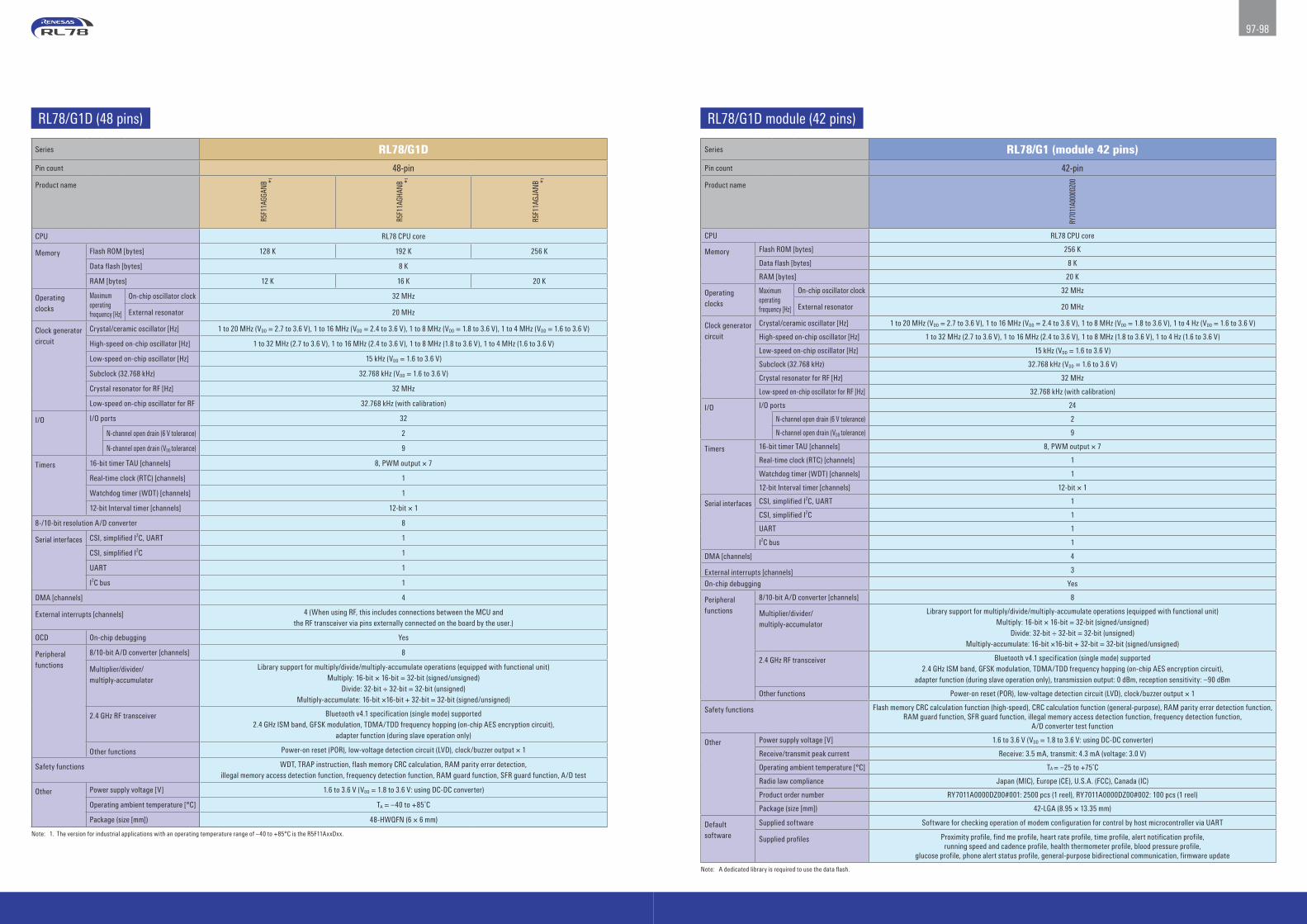
97-98
Series RL78/G1DPin count 48-pin
Product name
R5F1
1AGG
ANB *1
R5F1
1AGH
ANB *1
R5F1
1AGJ
ANB *1
CPU RL78 CPU core
Memory Flash ROM [bytes] 128 K 192 K 256 K
Data flash [bytes] 8 K
RAM [bytes] 12 K 16 K 20 K
Operating clocks
Maximum operating frequency [Hz]
On-chip oscillator clock 32 MHz
External resonator 20 MHz
Clock generator circuit
Crystal/ceramic oscillator [Hz] 1 to 20 MHz (VDD = 2.7 to 3.6 V), 1 to 16 MHz (VDD = 2.4 to 3.6 V), 1 to 8 MHz (VDD = 1.8 to 3.6 V), 1 to 4 MHz (VDD = 1.6 to 3.6 V)
High-speed on-chip oscillator [Hz] 1 to 32 MHz (2.7 to 3.6 V), 1 to 16 MHz (2.4 to 3.6 V), 1 to 8 MHz (1.8 to 3.6 V), 1 to 4 MHz (1.6 to 3.6 V)
Low-speed on-chip oscillator [Hz] 15 kHz (VDD = 1.6 to 3.6 V)
Subclock (32.768 kHz) 32.768 kHz (VDD = 1.6 to 3.6 V)
Crystal resonator for RF [Hz] 32 MHz
Low-speed on-chip oscillator for RF 32.768 kHz (with calibration)
I/O I/O ports 32
N-channel open drain (6 V tolerance) 2
N-channel open drain (VDD tolerance) 9
Timers 16-bit timer TAU [channels] 8, PWM output × 7
Real-time clock (RTC) [channels] 1
Watchdog timer (WDT) [channels] 1
12-bit Interval timer [channels] 12-bit × 1
8-/10-bit resolution A/D converter 8
Serial interfaces CSI, simplified I2C, UART 1
CSI, simplified I2C 1
UART 1
I2C bus 1
DMA [channels] 4
External interrupts [channels] 4 (When using RF, this includes connections between the MCU and the RF transceiver via pins externally connected on the board by the user.)
OCD On-chip debugging Yes
Peripheralfunctions
8/10-bit A/D converter [channels] 8
Multiplier/divider/multiply-accumulator
Library support for multiply/divide/multiply-accumulate operations (equipped with functional unit)Multiply: 16-bit × 16-bit = 32-bit (signed/unsigned)
Divide: 32-bit ÷ 32-bit = 32-bit (unsigned)Multiply-accumulate: 16-bit ×16-bit + 32-bit = 32-bit (signed/unsigned)
2.4 GHz RF transceiver Bluetooth v4.1 specification (single mode) supported2.4 GHz ISM band, GFSK modulation, TDMA/TDD frequency hopping (on-chip AES encryption circuit),
adapter function (during slave operation only)
Other functions Power-on reset (POR), low-voltage detection circuit (LVD), clock/buzzer output × 1
Safety functions WDT, TRAP instruction, flash memory CRC calculation, RAM parity error detection,illegal memory access detection function, frequency detection function, RAM guard function, SFR guard function, A/D test
Other Power supply voltage [V] 1.6 to 3.6 V (VDD = 1.8 to 3.6 V: using DC-DC converter)
Operating ambient temperature [°C] TA = –40 to +85˚C
Package (size [mm]) 48-HWQFN (6 × 6 mm)
Note: 1. The version for industrial applications with an operating temperature range of –40 to +85°C is the R5F11AxxDxx.
Series RL78/G1 (module 42 pins)Pin count 42-pin
Product name
RY70
11A0
000D
Z00
CPU RL78 CPU core
Memory Flash ROM [bytes] 256 K
Data flash [bytes] 8 K
RAM [bytes] 20 K
Operating clocks
Maximum operating frequency [Hz]
On-chip oscillator clock 32 MHz
External resonator 20 MHz
Clock generator circuit
Crystal/ceramic oscillator [Hz] 1 to 20 MHz (VDD = 2.7 to 3.6 V), 1 to 16 MHz (VDD = 2.4 to 3.6 V), 1 to 8 MHz (VDD = 1.8 to 3.6 V), 1 to 4 Hz (VDD = 1.6 to 3.6 V)
High-speed on-chip oscillator [Hz] 1 to 32 MHz (2.7 to 3.6 V), 1 to 16 MHz (2.4 to 3.6 V), 1 to 8 MHz (1.8 to 3.6 V), 1 to 4 Hz (1.6 to 3.6 V)
Low-speed on-chip oscillator [Hz] 15 kHz (VDD = 1.6 to 3.6 V)
Subclock (32.768 kHz) 32.768 kHz (VDD = 1.6 to 3.6 V)
Crystal resonator for RF [Hz] 32 MHz
Low-speed on-chip oscillator for RF [Hz] 32.768 kHz (with calibration)
I/O I/O ports 24
N-channel open drain (6 V tolerance) 2
N-channel open drain (VDD tolerance) 9
Timers 16-bit timer TAU [channels] 8, PWM output × 7
Real-time clock (RTC) [channels] 1
Watchdog timer (WDT) [channels] 1
12-bit Interval timer [channels] 12-bit × 1
Serial interfaces CSI, simplified I2C, UART 1
CSI, simplified I2C 1
UART 1
I2C bus 1
DMA [channels] 4
External interrupts [channels] 3
On-chip debugging Yes
Peripheralfunctions
8/10-bit A/D converter [channels] 8
Multiplier/divider/multiply-accumulator
Library support for multiply/divide/multiply-accumulate operations (equipped with functional unit)Multiply: 16-bit × 16-bit = 32-bit (signed/unsigned)
Divide: 32-bit ÷ 32-bit = 32-bit (unsigned)Multiply-accumulate: 16-bit ×16-bit + 32-bit = 32-bit (signed/unsigned)
2.4 GHz RF transceiver Bluetooth v4.1 specification (single mode) supported2.4 GHz ISM band, GFSK modulation, TDMA/TDD frequency hopping (on-chip AES encryption circuit),
adapter function (during slave operation only), transmission output: 0 dBm, reception sensitivity: –90 dBm
Other functions Power-on reset (POR), low-voltage detection circuit (LVD), clock/buzzer output × 1
Safety functions Flash memory CRC calculation function (high-speed), CRC calculation function (general-purpose), RAM parity error detection function, RAM guard function, SFR guard function, illegal memory access detection function, frequency detection function,
A/D converter test function
Other Power supply voltage [V] 1.6 to 3.6 V (VDD = 1.8 to 3.6 V: using DC-DC converter)
Receive/transmit peak current Receive: 3.5 mA, transmit: 4.3 mA (voltage: 3.0 V)
Operating ambient temperature [°C] TA = –25 to +75˚C
Radio law compliance Japan (MIC), Europe (CE), U.S.A. (FCC), Canada (IC)
Product order number RY7011A0000DZ00#001: 2500 pcs (1 reel), RY7011A0000DZ00#002: 100 pcs (1 reel)
Package (size [mm]) 42-LGA (8.95 × 13.35 mm)
Default software
Supplied software Software for checking operation of modem configuration for control by host microcontroller via UART
Supplied profiles Proximity profile, find me profile, heart rate profile, time profile, alert notification profile, running speed and cadence profile, health thermometer profile, blood pressure profile,
glucose profile, phone alert status profile, general-purpose bidirectional communication, firmware update
Note: A dedicated library is required to use the data flash.
RL78/G1D module (42 pins)RL78/G1D (48 pins)

99-100
RL78/G1F (24 to 64 pins)
Series RL78/G1FPin count 24-pin 32-pin 36-pin 48-pin 64-pin
Product name
R5F1
1B7C
ANA *2
R5F1
1B7E
ANA *2
R5F1
1BBC
AFP *2
R5F1
1BBE
AFP *2
R5F1
1BCC
ALA *2
R5F1
1BCE
ALA *2
R5F1
1BGC
AFB *2
R5F1
1BGE
AFB *2
R5F1
1BLC
AFB *2
R5F1
1BLE
AFB *2
CPU RL78 CPU core
Memory Flash ROM [bytes] 32 K 64 K 32 K 64 K 32 K 64 K 32 K 64 K 32 K 64 K
Data flash [bytes] 4 K
RAM [bytes] 5.5 K
Operating clocks
Maximum operating frequency [Hz]
On-chip oscillator clock 32 MHz
External resonator 20 MHz
Clock for timer RD/RX 64 MHz (VDD = 2.7 to 5.5 V)
Clock generator circuit
Crystal/ceramic oscillator [Hz] 1 to 20 MHz (VDD = 2.7 to 5.5 V), 1 to 16 MHz (VDD = 2.4 to 5.5 V), 1 to 8 MHz (VDD = 1.8 to 5.5 V), 1 to 4Hz (VDD = 1.6 to 5.5 V)
High-speed on-chip oscillator [Hz] 1 to 32 MHz (VDD = 2.7 to 5.5 V), 1 to 16 MHz (VDD = 2.4 to 5.5 V), 1 to 8 MHz (VDD = 1.8 to 5.5 V), 1 to 4Hz (VDD = 1.6 to 5.5 V) *Timer RD, RX only, operation at 48 or 64 MHz supported
Low-speed on-chip oscillator [Hz] 15 kHz (VDD = 1.6 to 5.5 V)
Subclock (32.768 kHz) 32.768 kHz (VDD = 1.6 to 5.5 V)
I/O I/O ports 20 28 31 44 58
N-channel open drain (6 V tolerance) 2 4 4
N-channel open drain (VDD tolerance) 10 12 10 12 16
Timers 16-bit timer TAU [channels] 4, PWM output × 3
16-bit timer RJ [channels] 1
16-bit timer RD [channels] 2, PWM output × 6
16-bit timer RG [channels] 1, PWM output × 1
16-bit timer RX [channels] 1
Real-time clock (RTC) [channels] 1*1
Watchdog timer (WDT) [channels] 1
Interval timer [channels] 12-bit × 1
Serial interfaces CSI × 1, UART × 1, simplified I2C × 1 2 (including 1 UART with IrDA support) 1
CSI × 2, UART × 1, simplified I2C × 2 1 (including 1 UART with IrDA support) 2 (including 1 UART with IrDA support)
CSI × 1, UART (LIN bus support) × 1, simplified I2C × 1
1
CSI × 2, UART (LIN bus support) × 1, simplified I2C × 2
1
I2C × 1 1
DTC (sources) 30 32 31 32 33
ELC (inputs/trigger outputs) 21 22
External interrupt pins [count] 9 11 10 16 20
OCD On-chip debugging Yes
Peripheralfunctions
8/10-bit A/D converter [channels] 8 13 15 17 17
8-bit D/A converter [channels] 1 2
Multiplier/divider/multiply-accumulator
Multiply/divide/multiply-accumulate instructions supported (included in CPU instruction set)Multiply: 16-bit × 16-bit = 32-bit (signed/unsigned)
Divide: 32-bit ÷ 32-bit = 32-bit (unsigned)Multiply-accumulate: 16-bit × 16-bit ÷ 32-bit = 32-bit (signed/unsigned)
Comparator 2
Programmable-gain amplifier 1
Other functions Power-on reset (POR), low-voltage detection circuit (LVD), clock/buzzer output (48-pin: 1 channel, 64-pin: 2 channels)
Safety functions Flash memory CRC calculation function (high-speed), CRC calculation function (general-purpose), RAM parity error detection function, RAM guard function, SFR guard function, illegal memory access detection function, frequency detection function, A/D converter test function, I/O power output signal level detection function
Other Power supply voltage [V] VDD = 1.6 to 5.5 V VDD = 1.6 to 5.5 V (EVDD support) VDD = 1.6 to 5.5 V VDD = 1.6 to 5.5 V (EVDD support)
Operating ambient temperature [°C] TA = –40 to +85˚C (A: Consumer applications), TA = –40 to +105˚C (G: Industrial applications) *2
Package (size [mm]) 24-HWQFN (4 × 4 mm) 32-LQFP (7 × 7 mm) 36-WFLGA (4 × 4 mm) 48-LFQFP (7 × 7 mm) 64-LFQFP (10 × 10 mm)
Notes: A dedicated library is required to use the data flash. 1. Products with pin counts from 24 or 32 pins are not equipped with a subsystem clock, so only the fixed-cycle interrupt function using the low-speed on-chip oscillator clock (15 kHz) is available for use. 2. The version for industrial applications with an operating temperature range of –40 to +105°C is the R5F11BxxGxx. For details, see “How to read RL78 Family product numbers” on page 122.
Series RL78/G1GPin count 30-pin 32-pin 44-pin
Product name
R5F1
1EA8
ASP
R5F1
1EAA
ASP
R5F1
1EB8
AFP
R5F1
1EBA
AFP
R5F1
1EF8
AFP
R5F1
1EFA
AFP
CPU RL78 CPU core
Memory Flash ROM [bytes] 8 K 16 K 8 K 16 K 8 K 16 K
Data flash [bytes]
RAM [bytes] 1.5 K
Operating clocks
Maximum operating frequency [Hz]
On-chip oscillator clock 24 MHz
External resonator 20 MHz
Clock generator circuit
Crystal/ceramic oscillator [Hz] 1 to 20 MHz (VDD = 2.7 to 5.5 V)
High-speed on-chip oscillator [Hz] 1 to 24 MHz (VDD = 2.7 to 5.5 V)
Low-speed on-chip oscillator [Hz] 15 kHz (VDD = 2.7 to 5.5 V)
Subclock (32.768 kHz)
I/O I/O ports 26 28 40
N-channel open drain (6 V tolerance)
N-channel open drain (VDD tolerance) 7
Timers 16-bit timer TAU [channels] 4, PWM output × 3
16-bit timer RJ [channels] 1
16-bit timer RD [channels] 2, PWM output × 6
Real-time clock (RTC) [channels]
Watchdog timer (WDT) [channels] 1
Interval timer [channels] 12-bit × 1
Serial interfaces CSI × 1, UART × 1, simplified I2C × 1 1
UART × 1 1
ELC (inputs/trigger outputs) 18/6 19/6
External interrupts [channels] 6 7
OCD On-chip debugging Yes
Peripheralfunctions
8/10-bit A/D converter [channels] 8 12
Multiplier/divider/multiply-accumulator
Multiply/divide/multiply-accumulate instructions supported (included in CPU instruction set)Multiply: 16-bit × 16-bit = 32-bit (signed/unsigned)
Divide: 32-bit ÷ 32-bit = 32-bit (unsigned)Multiply-accumulate: 16-bit × 16-bit + 32-bit = 32-bit (signed/unsigned)
Comparator [channels] 2
Programmable-gain amplifier 1
Other functions Power-on reset (POR), low-voltage detection circuit (LVD), clock/buzzer output
Safety functions Flash memory CRC calculation function (high-speed), CRC calculation function (general-purpose), RAM parity error detection function, RAM guard function, SFR guard function, illegal memory access detection function, frequency detection function,
A/D converter test function, I/O power output signal level detection function
Other Power supply voltage [V] VDD = 2.7 to 5.5 V
Operating ambient temperature [°C] TA = –40 to +85˚C (A: Consumer applications)
Package (size [mm]) 30-LSSOP (7.62 mm) 32-LQFP (7 × 7 mm) 44-LQFP (10 × 10 mm)
RL78/G1G (30 to 44 pins)

101-102
RL78/L12 (32 to 64 pins)
Series RL78/G1CPin count 32-pin 48-pin
Product name
1R5
F10J
BCAN
A *1
2R5
F10J
BCAF
P *1
1R5
F10K
BCAN
A *1
2R5
F10K
BCAF
P *1
1R5
F10J
GCAN
A *1
2R5
F10J
GCAF
B *1
1R5
F10K
GCAN
A *1
2R5
F10K
GCAF
B *1
CPU RL78 CPU core
Memory Flash ROM [bytes] 32 K
Data flash [bytes] 2 K
RAM [bytes] 5.5 K
Operating clocks
Maximum operating frequency [Hz]
On-chip oscillator clock 24 MHz
External resonator 20 MHz
USB clock 48 MHz
Clock generator circuit
Crystal/ceramic oscillator [Hz] 1 to 20 MHz (VDD = 2.7 to 5.5 V), 1 to 16 MHz (VDD = 2.4 to 5.5 V)
High-speed on-chip oscillator [Hz] 1 to 48 MHz (VDD = 2.7 to 5.5 V)
Low-speed on-chip oscillator [Hz] 15 kHz (VDD = 2.4 to 5.5 V)
Subclock (32.768 kHz) 32.768 kHz (VDD = 2.4 to 5.5 V)
I/O Total I/O ports and dedicated USB pins 28*2 26*3 44*2 42*3
I/O ports 22 38
N-channel open drain (6 V tolerance) 3 4
Timers 16-bit timer TAU [channels] 4
Real-time clock (RTC) [channels] 1
Watchdog timer (WDT) [channels] 1
Interval timer [channels] 12-bit × 1
Serial interfaces CSI × 2, UART × 1, simplified I2C × 2 1
I2C × 1 1
USB Host [channels] 2 2
Function [channels] 1
DMA [channels] 2
External interrupts [channels] 8 10
OCD On-chip debugging Yes
Peripheralfunctions
8/10-bit A/D converter [channels] 8 9
Multiplier/divider/multiply-accumulator
Library support for multiply/divide/multiply-accumulate operations (equipped with functional unit)Multiply: 16-bit × 16-bit = 32-bit (signed/unsigned)
Divide: 32-bit ÷ 32-bit = 32-bit (unsigned)Multiply-accumulate: 16-bit × 16-bit + 32-bit = 32-bit (signed/unsigned)
Other functions Power-on reset (POR), low-voltage detection circuit (LVD), clock/buzzer output × 2
RTC output (1Hz) × 1
Safety functions Flash memory CRC calculation function (high-speed), CRC calculation function (general-purpose), RAM parity error detection function, RAM guard function, SFR guard function, illegal memory access detection function, frequency detection function,
A/D converter test function, I/O power output signal level detection function
Other Power supply voltage [V] VDD = 2.4 to 5.5 V
Operating ambient temperature [°C] TA = –40 to +85˚C (A: Consumer applications), TA = –40 to +105˚C (G: Industrial applications) *1
Package (size [mm]) 132-HWQFN (5 × 5 mm) 232-LFQFP (7 × 7 mm) 148-HWQFN (7 × 7 mm) 248-LFQFP (7 × 7 mm)
Notes: 1. The version for industrial applications with an operating temperature range of –40 to +105°C is the R5F10xxxGxx. For details, see “How to read RL78 Family product numbers” on page 122. 2. USB uses pins UVBUS, UVDD, UDP0, UDM0, UDP1, and UDM1. 3. USB uses pins UVBUS, UVDD, UDP0, and UDM0.
Series RL78/L12Pin count 32-pin 44-pin 48-pin 52-pin 64-pin
Product name
R5F1
0RB8
AFP
*4
R5F1
0RBA
AFP
*4
R5F1
0RBC
AFP
*4
R5F1
0RF8
AFP
*4
R5F1
0RFA
AFP
*4
R5F1
0RFC
AFP
*4
R5F1
0RG8
AFB
*4
R5F1
0RGA
AFB
*4
R5F1
0RGC
AFB
*4
R5F1
0RJ8
AFA
*4
R5F1
0RJA
AFA
*4
R5F1
0RJC
AFA
*4
1R5
F10R
LAAF
B*4
2R5
F10R
LAAF
A*4
3R5
F10R
LAAN
B *4
1R5
F10R
LCAF
B*4
2R5
F10R
LCAF
A*4
3R5
F10R
LCAN
B *4
CPU RL78 CPU core
Memory Flash ROM [bytes] 8 K 16 K 32 K 8 K 16 K 32 K 8 K 16 K 32 K 8 K 16 K 32 K 16 K 32 K
Data flash [bytes] 2 K
RAM [bytes]*1 1 K 1 K 1.5 K 1 K 1 K 1.5 K 1 K 1 K 1.5 K 1 K 1 K 1.5 K 1 K 1.5 K
Operating clocks
Maximum operating frequency [Hz]
On-chip oscillator clock 24 MHz
External resonator 20 MHz
Clock generator circuit
Crystal/ceramic oscillator [Hz] 1 to 20 MHz (VDD = 2.7 to 5.5 V), 1 to 16 MHz (VDD = 2.4 to 5.5 V), 1 to 8 MHz (VDD = 1.8 to 5.5 V), 1 to 4 MHz (VDD = 1.6 to 5.5 V)
High-speed on-chip oscillator [Hz] 1 to 24 MHz (VDD = 2.7 to 5.5 V), 1 to 16 MHz (VDD = 2.4 to 5.5 V), 1 to 8 MHz (VDD = 1.8 to 5.5 V), 1 to 4 MHz (VDD = 1.6 to 5.5 V)
Low-speed on-chip oscillator [Hz] 15 kHz (VDD = 1.6 to 5.5 V)
Subclock (32.768 kHz) 32.768 kHz (VDD = 1.6 to 5.5 V)
I/O Total I/O ports and LCD pins (SEG and COM) 28 40 44 48 58
I/O ports 20 29 33 37 47
N-channel open drain (EVDD tolerance) 2
LCD controller/Driver Selectable among internal voltage boost, capacitor split, and external resistance division
Segment signal outputs 13 22 (18) *2 26 (22) *2 30 (26) *2 39 (35) *2
Common signal outputs 4 4 (8) *2
Timers 16-bit timer TAU [channels] 4, PWM output × 3 5, PWM output × 4 6, PWM output × 5 8, PWM output × 7
Real-time clock (RTC) [channels] 1*3
Watchdog timer (WDT) [channels] 1
Interval timer [channels] 1
Serial interfaces CSI × 2, UART (LIN bus support) × 1 1
I2C × 1 1
DMA [channels] 2
External interrupts [channels] 4 6 7 9
OCD On-chip debugging Yes
Peripheralfunctions
8/10-bit A/D converter [channels] 4 7 9 10
Multiplier/divider/multiply-accumulator
Library support for multiply/divide/multiply-accumulate operations (equipped with functional unit)Multiply: 16-bit × 16-bit = 32-bit (signed/unsigned)
Divide: 32-bit ÷ 32-bit = 32-bit (unsigned)Multiply-accumulate: 16-bit × 16-bit + 32-bit = 32-bit (signed/unsigned)
Other functions Power-on reset (POR), low-voltage detection circuit (LVD), clock/buzzer output, Remote control carrier wave output × 1
Safety functions Flash memory CRC calculation function (high-speed), CRC calculation function (general-purpose), RAM parity error detection function,RAM guard function, SFR guard function, illegal memory access detection function,
frequency detection function, A/D converter test function
Other Power supply voltage [V] VDD = 1.6 to 5.5 V
Operating ambient temperature [°C] TA = –40 to +85˚C (A: Consumer applications)TA = –40 to +105˚C (G: Industrial applications) *4
Package (size [mm]) 32-LQFP(7 × 7mm)
44-LQFP(10 × 10 mm)
48-LFQFP(7 × 7 mm)
52-LQFP(10 × 10 mm)
164-LFQFP (10 × 10 mm)264-LQFP (12 × 12 mm)364-HWQFN (8 × 8 mm)
164-LFQFP (10 × 10 mm)264-LQFP (12 × 12 mm)364-HWQFN (8 × 8 mm)
Notes: 1. 630 bytes when using self-programming function and data flash function. 2. Figure in parentheses ( ) is number of signal lines when using 8 COM. 3. Products with a pin count of 32 pins are not equipped with a subsystem clock, so only the fixed-cycle interrupt function using the low-speed on-chip oscillator clock (15 kHz) is available for use. 4. The version for industrial applications with an operating temperature range of –40 to +105°C is the R5F10RxxGxx. For details, see “How to read RL78 Family product numbers” on page 122.
RL78/G1C (32 to 48 pins)

103-104
RL78/L13 (64 to 80 pins)
Series RL78/L13
Pin count 64-pin 80-pin
Product name
1R5
F10W
LAAF
B *2
2R5
F10W
LAAF
A
1R5
F10W
LCAF
B *2
2R5
F10W
LCAF
A
1R5
F10W
LDAF
B *2
2R5
F10W
LDAF
A
1R5
F10W
LEAF
B *2
2R5
F10W
LEAF
A
1R5
F10W
LFAF
B *2
2R5
F10W
LFAF
A
1R5
F10W
LGAF
B *2
2R5
F10W
LGAF
A
1R5
F10W
MAA
FB *2
2R5
F10W
MAA
FA
1R5
F10W
MCA
FB *2
2R5
F10W
MCA
FA
1R5
F10W
MDA
FB *2
2R5
F10W
MDA
FA
1R5
F10W
MEA
FB *2
2R5
F10W
MEA
FA
1R5
F10W
MFA
FB *2
2R5
F10W
MFA
FA
1R5
F10W
MGA
FB *2
2R5
F10W
MGA
FA
CPU RL78 CPU core
Memory Flash ROM [bytes] 16 K 32 K 48 K 64 K 96 K 128 K 16 K 32 K 48 K 64 K 96 K 128 K
Data flash [bytes] 4 K
RAM [bytes] 1 K 1.5 K 2 K 4 K 6 K 8 K 1 K 1.5 K 2 K 4 K 6 K 8 K
Operating clocks
Maximum operating frequency [Hz]
On-chip oscillator clock 24 MHz
External resonator 20 MHz
Timer KB20 clock 48 MHz (VDD = 2.7 to 5.5 V)
Clock generator circuit
Crystal/ceramic oscillator [Hz] 1 to 20 MHz (VDD = 2.7 to 5.5 V), 1 to 16 MHz (VDD = 2.4 to 5.5 V), 1 to 8 MHz (VDD = 1.8 to 5.5 V), 1 to 4 MHz (VDD = 1.6 to 5.5 V)
High-speed on-chip oscillator [Hz] 1 to 24 MHz (VDD = 2.7 to 5.5 V), 1 to 16 MHz (VDD = 2.4 to 5.5 V), 1 to 8 MHz (VDD = 1.8 to 5.5 V), 1 to 4 MHz (VDD = 1.6 to 5.5 V)
Low-speed on-chip oscillator [Hz] 15 kHz (VDD = 1.6 to 5.5 V)
Subclock (32.768 kHz) 32.768 kHz (VDD = 1.6 to 5.5 V)
I/O Total I/O ports and LCD pins (SEG and COM) 57 73
I/O ports 49 65
N-channel open drain (6 V tolerance) 2
LCD controller LCD drive voltage generation method Selectable among internal voltage boost, capacitor split, and external resistance division
Segment signal outputs 36 (32) *1 51 (47) *1
Common signal outputs 4 (8) *1
Timers 16-bit timer TAU [channels] 8 , PWM output × 7
16-bit timer KB20 [channels] 1, PWM output × 2
Real-time clock2 (RTC2) [channels] 1 (0.96 ppm minimum resolution)
Watchdog timer (WDT) [channels] 1
Interval timer [channels] 12-bit × 1
Serial interfaces CSI × 1, UART (LIN bus support) × 1, simplified I2C × 1
1
CSI × 1, UART × 1, simplified I2C × 1 1
UART × 1 1 2
I2C × 1 1
DMA [channels] 4
External interrupts [channels] 9
OCD On-chip debugging Yes
Peripheral functions
8/10-bit A/D converter [channels] 9 12
Comparator [channels] 2
Multiplier/divider/multiply-accumulator
Library support for multiply/divide/multiply-accumulate operations (equipped with functional unit)Multiply: 16-bit × 16-bit = 32-bit (signed/unsigned)
Divide: 32-bit ÷ 32-bit = 32-bit (unsigned)Multiply- accumulate: 16-bit × 16-bit + 32-bit = 32-bit (signed/unsigned)
Other functions Power-on reset (POR), low-voltage detection circuit (LVD), RTC output (1 Hz) × 1, clock/buzzer output × 2, remote control carrier wave output × 1
Safety functions Flash memory CRC calculation function (high-speed), CRC calculation function (general-purpose), RAM parity error detection function, RAM guard function, SFR guard function, illegal memory access detection function, frequency detection function, A/D converter test function, I/O power output signal level detection function
Other Power supply voltage [V] VDD = 1.6 to 5.5 V
Operating ambient temperature [°C] TA = –40 to +85˚C (A: Consumer applications)TA = –40 to +105˚C (G: Industrial applications) *2
Package (size [mm]) 164-LFQFP (10 × 10 mm)264-LQFP (12 × 12 mm)
180-LFQFP (12 × 12 mm)280-LQFP (14 × 14 mm)
Notes: 1. Figure in parentheses ( ) is number of signal lines when using 8 COM. 2. The version for industrial applications with an operating temperature range of –40 to +105°C is the R5F10WxxGxx. For details, see “How to read RL78 Family product numbers” on page 122.

105-106
RL78/L1C (80 to 100 pins) RL78/L1C (80 to 100 pins)
Series RL78/L1C (USB)Pin count 80-pin 85-pin 100-pin
Product name
R5F1
10M
EAFB
*2
R5F1
10M
FAFB
*2
R5F1
10M
GAFB
*2
R5F1
10M
HAFB
*2
R5F1
10M
JAFB
*2
R5F1
10N
EALA
*2
R5F1
10N
FALA
*2
R5F1
10N
GALA
*2
R5F1
10N
HALA
*2
R5F1
10N
JALA
*2
R5F1
10PE
AFB
*2
R5F1
10PF
AFB
*2
R5F1
10PG
AFB
*2
R5F1
10PH
AFB
*2
R5F1
10PJ
AFB
*2
CPU RL78 CPU core
Memory Flash ROM [bytes] 64 K 96 K 128 K 192 K 256 K 64 K 96 K 128 K 192 K 256 K 64 K 96 K 128 K 192 K 256 K
Data flash [bytes] 8 K
RAM [bytes] 8 K 10 K 12 K 16 K 16 K 8 K 10 K 12 K 16 K 16 K 8 K 10 K 12 K 16 K 16 K
Operating clocks
Maximum operating frequency [Hz]
On-chip oscillator clock 24 MHz
External resonator 20 MHz
Timer KB2 clock, USB clock
48 MHz (VDD = 2.7 to 3.6 V)
Clock generator circuit
Crystal/ceramic oscillator [Hz] 1 to 20 MHz (VDD = 2.7 to 3.6 V), 1 to 16 MHz (VDD = 2.4 to 3.6 V), 1 to 8 MHz (VDD = 1.8 to 3.6 V), 1 to 4 MHz (VDD = 1.6 to 3.6 V)
High-speed on-chip oscillator [Hz] 1 to 48 MHz (VDD = 2.7 to 3.6 V), 1 to 16 MHz (VDD = 2.4 to 3.6 V), 1 to 8 MHz (VDD = 1.8 to 3.6 V), 1 to 4 MHz (VDD = 1.6 to 3.6 V)
Low-speed on-chip oscillator [Hz] 15 kHz (VDD = 1.6 to 3.6 V)
Subclock (32.768 kHz) 32.768 kHz (VDD = 1.6 to 3.6 V)
I/O Total I/O ports and LCD and USB pins*3 71 89
I/O ports 59 77
N-channel open drain (6 V tolerance) 2
LCD controller LCD drive voltage generation method Selectable among internal voltage boost, capacitor split, and external resistance division
Segment signal outputs 44 (40) *1 56 (52) *1
Common signal outputs 4 (8) *1
Timers 16-bit timer TAU [channels] 8 (PWM output × 7)
16-bit timer KB20 [channels] 3 (PWM output × 6)
Real-time clock2 (RTC2) [channels] 1 (0.96 ppm accuracy correction)
Watchdog timer (WDT) [channels] 1
Interval timer [channels] 12-bit × 1
Serial interfaces CSI × 1, UART (LIN bus support) × 1, simplified I2C × 1
1
CSI × 1, UART × 1, simplified I2C × 1 3
I2C × 1 1
USB Function [channels] 1
DTC (sources) 32 33
ELC (inputs/trigger outputs) 30 31
External interrupts [channels] 9
OCD On-chip debugging Yes
Peripheralfunctions
8/12-bit A/D converter [channels] 9 13
8-bit D/A converter [channels] 2
Comparator [channels] 1 2
Multiplier/divider/multiply-accumulator
Multiply/divide/multiply-accumulate instructions supported (included in CPU instruction set)Multiply: 16-bit × 16-bit = 32-bit (signed/unsigned)
Divide: 32-bit ÷ 32-bit = 32-bit (unsigned)Multiply-accumulate: 16-bit × 16-bit + 32-bit = 32-bit (signed/unsigned)
Other functions Power-on reset (POR), low-voltage detection circuit (LVD), RTC output (1 Hz) × 1, clock/buzzer output × 2, remote control carrier wave output × 1
Safety functions Flash memory CRC calculation function (high-speed), CRC calculation function (general-purpose), RAM parity error detection function, RAM guard function, SFR guard function, illegal memory access detection function, frequency detection function,
A/D converter test function, I/O power output signal level detection function
Other Power supply voltage [V] VDD = 1.6 to 3.6 V
Operating ambient temperature [°C] TA = –40 to +85˚C (A: Consumer applications), TA = –40 to +105˚C (G: Industrial applications) *2
Package (size [mm]) 80-LFQFP (12 × 12 mm) 85-VFLGA (7 × 7 mm) 100-LFQFP (14 × 14 mm)
Notes: 1. Figure in parentheses ( ) is number of signal lines when using 8 COM. 2. The version for industrial applications with an operating temperature range of –40 to +105°C is the R5F110xxGxx. For details, see “How to read RL78 Family product numbers” on page 122. 3. LCD uses SEG pins and COM pins. USB uses UVBUS, UREGC, UDP, and UDM pins.
Series RL78/L1C (no USB)Pin count 80-pin 85-pin 100-pin
Product name
R5F1
11M
EAFB
*2
R5F1
11M
FAFB
*2
R5F1
11M
GAFB
*2
R5F1
11M
HAFB
*2
R5F1
11M
JAFB
*2
R5F1
11N
EALA
*2
R5F1
11N
FALA
*2
R5F1
11N
GALA
*2
R5F1
11N
HALA
*2
R5F1
11N
JALA
*2
R5F1
11PE
AFB
*2
R5F1
11PF
AFB
*2
R5F1
11PG
AFB
*2
R5F1
11PH
AFB
*2
R5F1
11PJ
AFB
*2
CPU RL78 CPU core
Memory Flash ROM [bytes] 64 K 96 K 128 K 192 K 256 K 64 K 96 K 128 K 192 K 256 K 64 K 96 K 128 K 192 K 256 K
Data flash [bytes] 8 K
RAM [bytes] 8 K 10 K 12 K 16 K 16 K 8 K 10 K 12 K 16 K 16 K 8 K 10 K 12 K 16 K 16 K
Operating clocks
Maximum operating frequency [Hz]
On-chip oscillator clock 24 MHz
External resonator 20 MHz
Timer KB2 clock, USB clock
48 MHz (VDD = 2.7 to 3.6 V)
Clock generator circuit
Crystal/ceramic oscillator [Hz] 1 to 20 MHz (VDD = 2.7 to 3.6 V), 1 to 16 MHz (VDD = 2.4 to 3.6 V), 1 to 8 MHz (VDD = 1.8 to 3.6 V), 1 to 4 MHz (VDD = 1.6 to 3.6 V)
High-speed on-chip oscillator [Hz] 1 to 48 MHz (VDD = 2.7 to 3.6 V), 1 to 16 MHz (VDD = 2.4 to 3.6 V), 1 to 8 MHz (VDD = 1.8 to 3.6 V), 1 to 4 MHz (VDD = 1.6 to 3.6 V)
Low-speed on-chip oscillator [Hz] 15 kHz (TYP.) : VDD = 1.6 to 3.6 V
Subclock (32.768 kHz) 32.768 kHz (VDD = 1.6 to 3.6 V)
I/O Total I/O ports and LCD pins (SEG and COM) 71 89
I/O ports 63 81
N-channel open drain (6 V tolerance) 2
LCD controller LCD drive voltage generation method Selectable among internal voltage boost, capacitor split, and external resistance division
Segment signal outputs 44 (40) *1 56 (52) *1
Common signal outputs 4 (8) *1
Timers 16-bit timer TAU [channels] 8 (PWM output × 7)
16-bit timer KB20 [channels] 3 (PWM output × 6)
Real-time clock2 (RTC2) [channels] 1 (0.96 ppm accuracy correction)
Watchdog timer (WDT) [channels] 1
Interval timer [channels] 12-bit × 1
Serial interfaces CSI × 1, UART (LIN bus support) × 1, simplified I2C × 1
1
CSI × 1, UART × 1, simplified I2C × 1 3
I2C × 1 1
DTC (sources) 30 31
ELC (inputs/trigger outputs) 30 31
External interrupts [channels] 9
OCD On-chip debugging Yes
Peripheralfunctions
8/12-bit A/D converter [channels] 11 13
8-bit D/A converter [channels] 2
Comparator [channels] 1 2
Multiplier/divider/multiply-accumulator
Multiply/divide/multiply-accumulate instructions supported (included in CPU instruction set)Multiply: 16-bit × 16-bit = 32-bit (signed/unsigned)
Divide: 32-bit ÷ 32-bit = 32-bit (unsigned)Multiply-accumulate: 16-bit × 16-bit + 32-bit = 32-bit (signed/unsigned)
Other functions Power-on reset (POR), low-voltage detection circuit (LVD), RTC output (1 Hz) × 1, clock/buzzer output × 2, remote control carrier wave output × 1
Safety functions Flash memory CRC calculation function (high-speed), CRC calculation function (general-purpose), RAM parity error detection function, RAM guard function, SFR guard function, illegal memory access detection function, frequency detection function,
A/D converter test function, I/O power output signal level detection function
Other Power supply voltage [V] VDD = 1.6 to 3.6 V
Operating ambient temperature [°C] TA = –40 to +85˚C (A: Consumer applications), TA = –40 to +105˚C (G: Industrial applications) *2
Package (size [mm]) 80-LFQFP (12 × 12 mm) 85-VFLGA (7 × 7 mm) 100-LFQFP (14 × 14 mm)
Notes: 1. Figure in parentheses ( ) is number of signal lines when using 8 COM. 2. The version for industrial applications with an operating temperature range of –40 to +105°C is the R5F111xxGxx. For details, see “How to read RL78 Family product numbers” on page 122.

107-108
Series RL78/L1APin count 80-pin 100-pin
Product name
R5F1
1MM
DAFB
R5F1
1MM
EAFB
R5F1
1MM
FAFB
R5F1
1MPE
AFB
R5F1
1MPF
AFB
R5F1
1MPG
AFB
CPU RL78 CPU core
Memory Flash ROM [bytes] 48 K 64 K 96 K 64 K 96 K 128 K
Data flash [bytes] 8 K
RAM [bytes] 5.5 K
Operating clocks
Maximum operating frequency [Hz]
On-chip oscillator clock 24 MHz
External resonator 20 MHz
Clock generator circuit
Crystal/ceramic oscillator [Hz] 1 to 20 MHz: VDD = 2.7 to 3.6V, 1 to 8 MHz: VDD = 1.8 to 2.7 V
High-speed on-chip oscillator [Hz] 1 to 24 MHz (VDD = 2.7 to 3.6V), 1 to 16 MHz (VDD = 2.4 to 3.6 V), 1 to 8MHz (VDD = 1.8 to 3.6 V)
Low-speed on-chip oscillator [Hz] 15 kHz (VDD = 1.8 to 3.6 V)
Subclock (32.768 kHz) 32.768 kHz (VDD = 1.8 to 3.6 V)
I/O I/O ports, Total I/O ports and CD pins 59 79
LCD controller LCD drive voltage generation method Selectable among internal voltage boost, capacitor split, and external resistance division
Segment signal outputs 32 (28) *1 45 (41) *1
Common signal outputs 4 (8) *1
Timers 16-bit timer TAU [channels] 8 (Timer output × 8, PWM output × 7)
8/16-bit interval timer [channels] 2 (8-bit)/1 (16-bit)
Real-time clock2 (RTC2) [channels] 1
Watchdog timer (WDT) [channels] 1
12-bit interval timer [channels] 1
Serial interfaces CSI × 1, UART (LIN bus support) × 1, simplified I2C × 1
1
CSI × 1, UART × 1, simplified I2C × 1 3
I2C × 1 1
DTC (sources) 30
ELC (inputs/trigger outputs) Event inputs: 22, event outputs: 8
External interrupts [channels] 8
OCD On-chip debugging Yes
Peripheralfunctions
8/12-bit A/D converter [channels] 10 14
12-bit D/A converter [channels] 3
Op-amp [channels] 3 (of which, 2 channels have 2 I/O switches) 3 (of which, 2 channels have 4 I/O switches)
Reference voltage 2.5/2.048/1.8/1.5 V
Comparator [channels] 1
Multiplier/divider/multiply-accumulator
Multiply/divide/multiply-accumulate instructions supported (included in CPU instruction set)Multiply: 16-bit × 16-bit = 32-bit (signed/unsigned)
Divide: 32-bit ÷ 32-bit = 32-bit (unsigned)Multiply-accumulate: 16-bit × 16-bit + 32-bit = 32-bit (signed/unsigned)
Other functions Power-on reset (POR), low-voltage detection circuit (LVD), RTC output (1 Hz) × 1, clock/buzzer output × 2
Safety functions Flash memory CRC calculation function (high-speed), CRC calculation function (general-purpose), RAM parity error detection function, RAM guard function, SFR guard function, illegal memory access detection function, frequency detection function,
A/D converter test function, I/O power output signal level detection function
Other Power supply voltage [V] VDD = 1.8 to 3.6 V
Operating ambient temperature [°C] TA = –40 to +85˚C (A: Consumer applications)
Package (size [mm]) 80-LQFP (12 × 12 mm) 100-LQFP (14 × 14 mm)
Notes: 1. Figure in parentheses ( ) is number of signal lines when using 8 COM.
Series RL78/I1APin count 20-pin 30-pin 38-pin
Product name
1R5
F107
6CGS
P2
R5F1
076C
MSP
1R5
F107
ACGS
P2
R5F1
07AC
MSP
1R5
F107
AEGS
P2
R5F1
07AE
MSP
1R5
F107
DEGS
P2
R5F1
07DE
MSP
CPU RL78 CPU core
Memory Flash ROM [bytes] 32 K 64 K
Data flash [bytes] 4 K
RAM [bytes] 2 K 4 K
Operating clocks
Maximum operating frequency [Hz]
On-chip oscillator clock 32 MHz (TA = –40 to +105˚C), 16 MHz (TA = 105 to 125˚C)
External resonator 20 MHz
Clock generator circuit
Crystal/ceramic oscillator [Hz] 1 to 20 MHz (VDD = 2.7 to 5.5 V)
High-speed on-chip oscillator [Hz] 1 to 32 MHz (VDD = 2.7 to 5.5 V), 1 to 8 MHz (VDD = 2.7 to 5.5 V)
Low-speed on-chip oscillator [Hz] 15 kHz (VDD = 2.7 to 5.5 V)
Subclock (32.768 kHz) 32.768 kHz (VDD = 2.7 to 5.5 V)
I/O I/O ports 16 26 34
N-channel open drain (6 V tolerance)
N-channel open drain (VDD tolerance) 6 10 11
Timers 16-bit timer TAU [channels] 8 8, PWM output × 1 8, PWM output × 3
16-bit timer KB 2, PWM output × 4 3, PWM output × 6 3, PWM output × 6
16-bit timer KC 1, PWM output × 3 1, PWM output × 6 1, PWM output × 6
Real-time clock (RTC) [channels] 1*1
Watchdog timer (WDT) [channels] 1
Interval timer [channels] 12-bit × 1
Serial interfaces UART × 1 1
CSI × 1, UART (LIN bus and DMX512 support) × 1 1
UART (LIN bus and DMX512 support) × 1*2 1
UART (DALI communication support) × 1*2 1
I2C × 1 1
DMA [channels] 2
External interrupts [channels] 7 10 11
OCD On-chip debugging Yes
Peripheralfunctions
8/10-bit A/D converter [channels] 6 11
Comparator [channels] 4 6
PGA [channels] 1
Multiplier/divider/multiply-accumulator
Library support for multiply/divide/multiply-accumulate operations (equipped with functional unit)Multiply: 16-bit × 16-bit = 32-bit (signed/unsigned)
Divide: 32-bit ÷ 32-bit = 32-bit (unsigned)Multiply-accumulate: 16-bit × 16-bit + 32-bit = 32-bit (signed/unsigned)
Other functions Power-on reset (POR), low-voltage detection circuit (LVD)
Safety functions Flash memory CRC calculation function (high-speed), CRC calculation function (general-purpose), RAM parity error detection function, RAM guard function, SFR guard function,
illegal memory access detection function, frequency detection function, A/D converter test function
Other Power supply voltage [V] VDD = 2.7 to 5.5 V
Operating ambient temperature [°C] 1TA = –40 to +105˚C (G: Industrial applications), 2TA = –40 to +125˚C (M: Industrial applications)
Package (size [mm]) 20-LSSOP (4.4 × 6.5 mm) 30-LSSOP (7.62 mm (300 mil)) 38-SSOP (7.62 mm (300 mil))
Notes: A dedicated library is required to overwrite the data flash. Refer to [Development Environments] – [Flash Programming Tools] – [Self-Programming Library] on the Renesas website. https://www.renesas.com/flash_libraries
1. Products with pin counts from 20 or 30 pins are not equipped with a subsystem clock, so only the fixed-cycle interrupt function using the low-speed on-chip oscillator clock (15 kHz) is available for use. 2. The same pin is used for both functions on 20-pin products, so only one function may be used at any given time.
RL78/L1A (80 to 100 pins) RL78/I1A (20 to 38 pins)

109-110
Series RL78/I1BPin count 80-pin 100-pin
Product name
R5F1
0MM
EDFB
R5F1
0MM
GDFB
R5F1
0MPE
DFB
R5F1
0MPG
DFB
CPU RL78 CPU core
Memory Flash ROM [bytes] 64 K 128 K 64 K 128 K
Data flash [bytes]
RAM [bytes] 6 K 8 K 6 K 8 K
Operating clocks
Maximum operating frequency [Hz]
On-chip oscillator clock 24 MHz
External resonator 20 MHz
Clock generator circuit
Crystal/ceramic oscillator [Hz] 1 to 20 MHz (VDD = 2.7 to 5.5 V), 1 to 8 MHz (VDD = 1.9 to 5.5 V)
High-speed on-chip oscillator [Hz] 24/12/6/3 MHz (VDD = 2.7 to 5.5 V), 12/6/3 MHz (VDD = 2.4 to 5.5 V), 6/3 MHz (VDD = 1.9 to 5.5 V)
Low-speed on-chip oscillator [Hz] 15 kHz (VDD = 1.9 to 5.5 V)
Subclock (32.768 kHz) 32.768 kHz (VDD = 1.9 to 5.5 V)
I/O Total I/O ports and LCD pins (SEG and COM) 61 77
I/O ports 53 69
N-channel open drain (6 V tolerance) 3
Timers 16-bit timer TAU [channels] 8, PWM output × 7
Real-time clock (RTC) [channels] 1 (high-precision, 0.96 ppm minimum resolution)
Watchdog timer (WDT) [channels] 1
Interval timer [channels] 12-bit × 1, 8-bit × 4
Serial interfaces CSI × 1, UART × 1, simplified I2C × 1 1
UART × 1, simplified I2C × 1 1
UART × 1, IrDA × 1 1
I2C × 1 1
LCD controller LCD drive voltage generation method Selectable among internal voltage boost, capacitor split, and external resistance division
Segment signal outputs 34 (30) *1 42 (38) *1
Common signal outputs 4 (8) *1
DTC (sources) 30
External interrupts [channels] 10
OCD On-chip debugging Yes
Peripheralfunctions
8/10-bit A/D converter [channels] 4 6
24-bit Δ∑ A/D converter [channels] 3 4
Comparator [channels] 2
PGA [channels] 1
Multiplier/divider/multiply-accumulator
Multiply/divide/multiply-accumulate instructions supported (included in CPU instruction set)Multiply: 16-bit × 16-bit = 32-bit (signed/unsigned)
Divide: 32-bit ÷ 32-bit = 32-bit (unsigned)Multiply-accumulate: 16-bit × 16-bit + 32-bit = 32-bit (signed/unsigned)
Other functions Power-on reset (POR), low-voltage detection circuit (LVD), battery backup function, RTC output (1 Hz) × 1
Safety functions Flash memory CRC calculation function (high-speed), CRC calculation function (general-purpose), RAM parity error detection function, RAM guard function, SFR guard function, illegal memory access detection function, frequency detection function,
A/D converter test function, I/O power output signal level detection function
Other Power supply voltage [V] VDD = 1.9 to 5.5 V
Operating ambient temperature [°C] TA = –40 to +85˚C (D: Industrial applications)
Package (size [mm]) 80-LFQFP (12 × 12 mm) 100-LFQFP (14 × 14 mm)
Notes: 1. Figure in parentheses ( ) is number of signal lines when using 8 COM.
Series RL78/I1CPin count 64-pin 80-pin 100-pin
Product name
R5F1
0NLE
/G
R5F1
0NM
E/G
R5F1
0NM
J
R5F1
0NPJ
/G
Code flash [bytes] 64 to 128 K 64 to 128 K 256 K 128 to 256 K
Date flash [bytes] 2 K
RAM [bytes] 6 to 8 K 6 to 8 K 16 K 8 to 16 K
System clocks External High-speed clock 1 to 20 MHz, Low-speed clock 32.768 kHz
On-chip oscillator clock High-speed 1.5 to 24 MHz, Middle-speed 1 to 4 MHz, Low-speed 15 kHz
PLL clock 32 MHz
High-speed on-chip oscillator clock frequency correction function Yes
24-bit Δ∑ A/D converter
Input channels 4 3 3 4
SNDR to 80dB (gain ×1)
Sampling frequency 3.906 kHz/1.953 kHz
PGA × 1, × 2, × 4, × 8, × 16, (× 32)
Internal reference voltage (temperature coefficient)
0.8 V (10 ppm/°C)
Zero-cross detection HW Zero-cross detection
8/10-bit A/D converter 4 channels 6 channels
32-bit multiply-and accumulate circuit Yes
LCD controller Segment/common signal combinations 15/8, 9/4 30/8, 34/4 30/8, 34/4 38/8, 42/4
Drive voltage generation method Selectable among internal voltage boost, capacitor split, and external resistance division
Timer functions 16-bit timer array unit: 8 ch
12-bit Interval timer: 1 ch
8-bit Interval timer: 4 ch
RTC with independent power supply 1 ch
Serial interfaces CSI, UART0, simplified I2C0 1 ch
CSI1, UART1, simplified I2C1 1 ch
UART2, IrDA 1 ch
CSI3, UART3, simple I2C3 1 ch
MultiMaster I2C 1 ch
DTC (sources) 29 31
ELC 22 event generation sources, 5 selectable event output destinations
Battery backup functions
CPU VDD/VBAT
24-bit Δ∑ A/D converter VDD/VBAT
RTC VRTC (independent power supply)
Low-voltage detection circuit (LVD) Internal VDD, VDD pin, VBAT pin, VRTC pin, external pin
AES HW Encryption mode: GCM/ECB/CBC, encryption key length: 128/192/256-bit
Key interrupts 5 pins 8 pins
Other peripheral functions Watchdog timer, power-on reset (POR), safety function
Power supply voltage [V] 1.7 to 5.5 V
Operating ambient temperature [°C] –40 to +85°C
Package (size [mm]) 64-LFQFP (10 × 10 mm) 80-LFQFP (12 × 12 mm) 100-LFQFP (14 × 14 mm)
RL78/I1B (80 to 100 pins) RL78/I1C (64 to 100 pins)

111-112
Series RL78/I1DPin count 20-pin 24-pin 30-pin 32-pin 48-pin
Product name
R5F1
1768
GSP
R5F1
176A
GSP
R5F1
1778
GNA
R5F1
177A
GNA
R5F1
17A8
GSP
R5F1
17AA
GSP
R5F1
17AC
GSP
R5F1
17BA
GNA
R5F1
17BC
GNA
R5F1
17BA
GFP
R5F1
17BC
GFP
R5F1
17GA
GFB
R5F1
17GC
GFB
CPU RL78 CPU core
Memory
Flash ROM [bytes] 8 K 16 K 8 K 16 K 8 K 16 K 32 K 16 K 32 K 16 K 32 K 16 K 32 K
Data flash [bytes] 2 K
RAM [bytes] 0.7 K 2 K 0.7 K 2 K 0.7 K 2 K 3 K 2 K 3 K 2 K 3 K 2 K 3 K
Operating clocks
Maximum operating frequency [Hz]
On-chip oscillator clock 24 MHz
External resonator 20 MHz
Clock generator circuit
Crystal/ceramic oscillator [Hz] 1 to 20 MHz (VDD = 2.7 to 3.6 V), 1 to 8 MHz (VDD = 1.8 to 2.7 V), 1 to 4 MHz (VDD = 1.6 to 1.8 V)
High-speed on-chip oscillator [Hz] 1 to 24 MHz (VDD = 2.7 to 3.6 V), 1 to 16 MHz (VDD = 2.4 to 3.6 V), 1 to 8 MHz (VDD = 1.8 to 3.6 V), 1 to 4 MHz (VDD = 1.6 to 3.6 V), 1 MHz (VDD = 1.8 to 3.6 V) Middle-speed on-chip oscillator [Hz]
Low-speed on-chip oscillator [Hz] 15 kHz (VDD = 1.6 to 3.6 V)
Subclock (32.768 kHz) 32.768 kHz (VDD = 1.6 to 3.6 V)
I/O I/O ports 14 18 24 26 42
N-channel open drain (6 V tolerance) 4
N-channel open drain (VDD tolerance)
Timers 16-bit timer TAU [channels] 4
Real-time clock (RTC) [channels] 1*1
Watchdog timer (WDT) [channels] 1
Interval timer [channels] 8-bit × 4 (or 16-bit × 2), 12-bit × 1
Serial interfaces CSI × 1, UART × 1, simplified I2C × 1 1 1
CSI × 2, UART × 1, simplified I2C × 2 1 1 1
DTC (sources) 16 20 19 20 23
ELC (inputs/trigger outputs) 13/5 17/5 16/7 17/7 20/7
External interrupt pins [count] 3 5 8
OCD On-chip debugging Yes
Peripheralfunctions
12-bit A/D converter [channels] 6 12 17
Multiplier/divider/multiply-accumulator
Multiply/divide/multiply-accumulate instructions supported (included in CPU instruction set)Multiply: 16-bit × 16-bit = 32-bit (signed/unsigned)
Divide: 32-bit ÷ 32-bit = 32-bit (unsigned)Multiply-accumulate: 16-bit × 16-bit + 32-bit = 32-bit (signed/unsigned)
Op-amp [channels] 2 4
Comparator [channels] 2
Other functions Power-on reset (POR), low-voltage detection circuit (LVD), clock/buzzer output, data operation circuit (DOC)
Safety functions Flash memory CRC calculation function (high-speed), CRC calculation function (general-purpose), RAM parity error detection function, RAM guard function, SFR guard function, illegal memory access detection function, frequency detection function,
A/D converter test function, I/O power output signal level detection function
Other Power supply voltage [V] VDD = 1.6 to 3.6
Operating ambient temperature [°C] –40 to +105˚C (G: Industrial applications)
Package (size [mm]) 20-LSSOP(4.4 × 6.5 mm)
24-HWQFN(4 × 4 mm)
30-LSSOP(7.62 mm (300 mil))
32-HVQFN(5 × 5 mm)
32-LQFP(7 × 7 mm)
48-LFQFP(7 × 7 mm)
Notes: A dedicated library is required to overwrite the data flash. Refer to [Development Environments] – [Flash Programming Tools] – [Self-Programming Library] on the Renesas website. https://www.renesas.com/flash_ libraries
1. Products with pin counts from 20 or 24 pins are not equipped with a subsystem clock, so only the fixed-cycle interrupt function using the low-speed on-chip oscillator clock (15 kHz) is available for use.
Series RL78/I1EPin count 32-pin 36-pin
Product name
R5F1
1CBC
GNA
R5F1
1CBC
MN
A
R5F1
1CCC
GBG
R5F1
1CCC
MBG
CPU RL78 CPU core
Memory
Flash ROM [bytes] 32 K
Data flash [bytes] 4 K
RAM [bytes] 8 K
Operating clocks
Maximum operating frequency [Hz]
On-chip oscillator clock 32 MHz
External resonator 20 MHz
Clock generator circuit
Crystal/ceramic oscillator [Hz] 1 to 20 MHz (2.7 to 5.5V), 1 to 16 MHz (2.4 to 2.7 V)
High-speed on-chip oscillator [Hz] 1 to 32 MHz (2.7 to 5.5 V) 1 to 24 MHz (2.7 to 5.5 V) 1 to 32 MHz (2.7 to 5.5 V) 1 to 24 MHz (2.7 to 5.5 V)
1 to 16 MHz (2.4 to 2. 7V)
Low-speed on-chip oscillator [Hz] 15 kHz
Subclock (32.768 kHz)
I/O I/O ports 10 14
N-channel open drain (6 V tolerance)
N-channel open drain (VDD tolerance) 6
Timers 16-bit timer TAU [channels] 6
16-bit timer RJ [channels] 1
16-bit timer RG [channels] 1
Real-time clock (RTC) [channels] 1
Watchdog timer (WDT) [channels] 1
Interval timer [channels] 15-bit × 1
Serial interfaces CSI × 2, UART × 1, simplified I2C × 2 1
UART × 1 1
DTC (sources) 23
ELC (inputs/trigger outputs) 16/7
External interrupt pins [count] 7 8
OCD On-chip debugging Yes
Peripheralfunctions
Instrumentation amplifier + 24-bit Δ∑ A/D converter [channels]
3 4
8/10-bit A/D converter [channels] 8 10
12-bit D/A converter [channels] 1
Configurable amplifier [channels] 3
Multiplier/divider/multiply-accumulator
Library support for multiply/divide/multiply-accumulate operations (equipped with functional unit)Multiply: 16-bit × 16-bit = 32-bit (signed/unsigned)
Divide: 32-bit ÷ 32-bit = 32-bit (unsigned)Multiply-accumulate: 16-bit × 16-bit + 32-bit = 32-bit (signed/unsigned)
Other functions Power-on reset (POR), low-voltage detection circuit (LVD), temperature sensor, reference voltage generation circuit
Safety functions Flash memory CRC calculation function (high-speed), CRC calculation function (general-purpose), RAM parity error detection function, RAM guard function, SFR guard function, illegal memory access detection function, frequency detection function,
A/D converter test function, I/O power output signal level detection function
Other Power supply voltage [V] Vcc = 2.4 to 5.5 V
Operating ambient temperature [°C] Ta = –40 to +105˚C(G: Industrial applications)
Ta = –40 to +125˚C(M: Industrial applications)
Ta = –40 to +105˚C(G: Industrial applications)
Ta = –40 to +125˚C(M: Industrial applications)
Package (size [mm]) 32-HVQFN (5 × 5 mm) 36-TFBGA (4 × 4 mm)
RL78/I1D (20 to 48 pins) RL78/I1E (32 to 36 pins)

113-114
Series RL78/G1EPin count 64-pin 80-pin
Product name
R5F1
0FLC
ANA *1
R5F1
0FLD
ANA *1
R5F1
0FLE
ANA *1
R5F1
0FM
CAFB
*1
R5F1
0FM
DAFB
*1
R5F1
0FM
EAFB
*1
CPU RL78 CPU core
Memory Flash ROM [bytes] 32 K 48 K 64 K 32 K 48 K 64 K
Data flash [bytes] 4 K
RAM [bytes] 2 K 3 K 4 K 2 K 3 K 4 K
Operating clocks
Maximum operating frequency [Hz]
On-chip oscillator clock 32 MHz
External resonator 20 MHz
Clock generator circuit
Crystal/ceramic oscillator [Hz] 1 to 20 MHz (VDD = 2.7 to 5.5 V), 1 to 8 MHz (VDD = 1.8 to 5.5 V), 1 to 4 MHz (VDD = 1.6 to 5.5 V)
High-speed on-chip oscillator [Hz] 1 to 32 MHz (VDD = 2.7 to 5.5 V), 1 to 16 MHz (VDD = 2.4 to 5.5 V), 1 to 8 MHz (VDD = 1.8 to 5.5 V), 1 to 4 MHz (VDD = 1.6 to 5.5 V)
Low-speed on-chip oscillator [Hz] 15 kHz (VDD = 1.6 to 5.5 V)
Subclock (32.768 kHz)
I/O I/O ports 24 30
N-channel open drain (6 V tolerance)
N-channel open drain (VDD tolerance) 7 10
Timers 16-bit timer TAU [channels] 8, PWM output × 2
Real-time clock (RTC) [channels]
Watchdog timer (WDT) [channels] 1
Interval timer [channels] 1
Serial interfaces CSI × 1, UART × 1, simplified I2C × 1 1 2
UART × 1 1
CSI × 1, UART (LIN bus support) × 1 1
CSI × 2, UART (LIN bus support) × 1, simplified I2C × 1
1
DMA [channels] 2
External interrupts [channels] 2 5
OCD On-chip debugging Yes
Peripheralfunctions
8/12-bit A/D converter [channels] 13 17
8-bit D/A converter [channels] 4
Multiplier/divider/multiply-accumulator
Library support for multiply/divide/multiply-accumulate operations (equipped with functional unit)Multiply: 16-bit × 16-bit = 32-bit (signed/unsigned)
Divide: 32-bit ÷ 32-bit = 32-bit (unsigned)Multiply-accumulate: 16-bit × 16-bit + 32-bit = 32-bit (signed/unsigned)
Other functions Power-on reset (POR), low-voltage detection circuit (LVD), configurable amplifier, adjustable-gain amplifier, low-pass filter, output voltage variable regulator,
reference voltage generation circuit, temperature sensor
Power-on reset (POR), low-voltage detection circuit (LVD), configurable amplifier, adjustable-gain amplifier,*
low-pass filter, high-pass filter, output voltage variable regulator, reference voltage generation circuit, temperature sensor
Safety functions Flash memory CRC calculation function (high-speed), CRC calculation function (general-purpose), RAM parity error detection function, RAM guard function, SFR guard function,
illegal memory access detection function, frequency detection function, A/D converter test function
Other Power supply voltage [V] Microcontroller block: 1.6 to 5.5 V (AVDD = 1.6 to 3.6 V), analog block: 3.0 to 5.5 V
Operating ambient temperature [°C] TA = –40 to +85˚C (A: Consumer applications, D: Industrial applications) *1
Package (size [mm]) 64-HWQFN (9 × 9 mm) 80-LFQFP (12 × 12 mm)
Notes: With synchronous wave detection function 1. The version for industrial applications with an operating temperature range of –40 to +85°C is the R5F10FxxDxx. For details, see “How to read RL78 Family product numbers” on page 122.
MEMORL78/G1E (64 to 80 pins)

115-116
RL78/F13 (20 to 80 pins)
Series RL78/F13 (CAN and LIN versions) Pin count 30-pin 32-pin 48-pin 64-pin 80-pin
Product name
R5F1
0BAC
LSP*
1
R5F1
0BAD
LSP*
1
R5F1
0BAE
LSP*
1
R5F1
0BAF
LSP*
1
R5F1
0BAG
LSP*
1
R5F1
0BBC
LNA*
1
R5F1
0BBD
LNA*
1
R5F1
0BBE
LNA*
1
R5F1
0BBF
LNA*
1
R5F1
0BBG
LNA*
1
1R5
F10B
GCLF
B*1
2R5
F10B
GCLN
A*1
1R5
F10B
GDLF
B*1
2R5
F10B
GDLN
A*1
1R5
F10B
GELF
B*1
2R5
F10B
GELN
A*1
1R5
F10B
GFLF
B*1
2R5
F10B
GFLN
A*1
1R5
F10B
GGLF
B*1
2R5
F10B
GGLN
A*1
R5F1
0BLC
LFB*
1
R5F1
0BLD
LFB*
1
R5F1
0BLE
LFB*
1
R5F1
0BLF
LFB*
1
R5F1
0BLG
LFB*
1
R5F1
0BM
ELFB
*1
R5F1
0BM
FLFB
*1
R5F1
0BM
GLFB
*1
CPU RL78 CPU core
Memory Flash ROM [bytes] 32 K 48 K 64 K 96 K 128 K 32 K 48 K 64 K 96 K 128 K 32 K 48 K 64 K 96 K 128 K 32 K 48 K 64 K 96 K 128 K 64 K 96 K 128 K
Data flash [bytes] 4 K 4 K 4 K 4 K 4 K
RAM [bytes] 2 K 3 K 4 K 6 K 8 K 2 K 3 K 4 K 6 K 8 K 2 K 3 K 4 K 6 K 8 K 2 K 3 K 4 K 6 K 8 K 4 K 6 K 8 K
Operating clocks
Maximum operating frequency [Hz]
On-chip oscillator clock 32 MHz (automotive applications, TA = –40 to +105°C), 24 MHz (automotive applications, TA = –40 to +125°C)
External resonator 20 MHz
Timer RD clock 64 MHz (VDD = 2.7 to 5.5 V)
Clock generator circuit
Crystal/ceramic oscillator [Hz] 1 to 20 MHz (VDD = 2.7 to 5.5 V)
High-speed on-chip oscillator [Hz] 64 MHz (±2%): VDD = 2.7 to 5.5 V (automotive applications/TA = –40 to +105˚C), 48 MHz (±3%): VDD = 2.7 to 5.5 V (automotive applications/TA = –40 to +125˚C)
Low-speed on-chip oscillator [Hz] 15 kHz (VDD = 2.7 to 5.5 V)
Subclock (32.768 kHz) 32.768 kHz (VDD = 2.7 to 5.5 V)
PLL Multiplication factors: ×3, ×4, ×6, ×8
I/O I/O ports 23 25 38 52 68
N-channel open drain (6 V tolerance)
N-channel open drain (EVDD tolerance) 9 13 16
Timers 16-bit timer TAU [channels] 16
Timer RJ 1
Timer RD 2
Real-time clock (RTC) [channels] 1
Watchdog timer (WDT) [channels] 1
Serial interfaces CSI × 2, UART × 1, simplified I2C × 2 1
CSI × 4, UART × 2, simplified I2C × 4 1
UART × 1, LIN (RLIN3) × 1 1
CAN (RS-CAN lite) × 1 1
Multi-master I2C × 1 1
DTC (sources) 36 37
External interrupts [channels] 9 13 14
OCD On-chip debugging Supported (hot plugin, trace)
Peripheralfunctions
8/10-bit A/D converter [channels] 12 10 15 19 20
8-bit D/A converter [channels]
Comparator [channels]
Multiplier/divider/multiply-accumulator
Multiply/divide/multiply-accumulate instructions supported (included in CPU instruction set)Multiply: 16-bit × 16-bit = 32-bit (signed/unsigned)
Divide: 32-bit ÷ 32-bit = 32-bit (unsigned)Multiply-accumulate: 16-bit × 16-bit + 32-bit = 32-bit (signed/unsigned)
Other functions Power-on reset (POR), low-voltage detection circuit (LVD), RTC output (1 Hz) × 1
clock/buzzer output × 1
Safety functions Flash memory CRC calculation function (high-speed), CRC calculation function (general-purpose), SRAM ECC function, CPU stack pointer monitor function, clock monitor function, RAM guard function, SFR guard function, illegal memory access detection function, frequency detection function, A/D converter test function,
I/O power output signal level detection function
Other Power supply voltage [V] VDD = 2.7 to 5.5 V
Operating ambient temperature [°C] TA = –40 to +105°C (L: automotive applications), TA = –40 to +125°C (K: automotive applications) *1
Package (size [mm]) 30-LSSOP(6.1 × 9.85 mm)
32-HVQFN (5 × 5 mm) 148-LFQFP (7 × 7 mm)248-HVQFN (7 × 7 mm)
64-LFQFP (10 × 10 mm) 80-LFQFP
(12 × 12 mm)
Note: 1. The K version for industrial applications with an operating temperature range of –40 to +125°C is the R5F10BxxKxx, and the Y version for industrial applications with an operating temperature range of –40 to +150°C is the R5F10BxxYxx. For details, see “How to read RL78 Family product numbers” on page 122.
Series RL78/F13 (LIN version)Pin count 20-pin 30-pin 32-pin 48-pin 64-pin 80-pin
Product name
R5F1
0A6A
LSP*
1
R5F1
0A6C
LSP*
1
R5F1
0A6D
LSP*
1
R5F1
0A6E
LSP*
1
R5F1
0AAA
LSP*
1
R5F1
0AAC
LSP*
1
R5F1
0AAD
LSP*
1
R5F1
0AAE
LSP*
1
R5F1
0ABA
LNA*
1
R5F1
0ABC
LNA*
1
R5F1
0ABD
LNA*
1
R5F1
0ABE
LNA*
1
1R5
F10A
GALF
B*1
2R5
F10A
GALN
A*1
1R5
F10A
GCLF
B*1
2R5
F10A
GCLN
A*1
1R5
F10A
GDLF
B*1
2R5
F10A
GDLN
A*1
1R5
F10A
GELF
B*1
2R5
F10A
GELN
A*1
1R5
F10A
GFLF
B*1
2R5
F10A
GFLN
A*1
1R5
F10A
GGLF
B*1
2R5
F10A
GGLN
A*1
R5F1
0ALC
LFB*
1
R5F1
0ALD
LFB*
1
R5F1
0ALE
LFB*
1
R5F1
0ALF
LFB*
1
R5F1
0ALG
LFB*
1
R5F1
0AM
ELFB
*1
R5F1
0AM
FLFB
*1
R5F1
0AM
GLFB
*1
CPU RL78 CPU core
Memory Flash ROM [bytes] 16 K 32 K 48 K 64 K 16 K 32 K 48 K 64 K 16 K 32 K 48 K 64 K 16 K 32 K 48 K 64 K 96 K 128 K 32 K 48 K 64 K 96 K 128 K 64 K 96 K 128 K
Data flash [bytes] 4 K 4 K 4 K 4 K 4 K
RAM [bytes] 1 K 2 K 3 K 4 K 1 K 2 K 3 K 4 K 1 K 2 K 3 K 4 K 1 K 2 K 3 K 4 K 6 K 8 K 2 K 3 K 4 K 6 K 8 K 4 K 6 K 8 K
Operating clocks
Maximum operating frequency [Hz]
On-chip oscillator clock 32 MHz (automotive applications, TA = –40 to +105°C), 24 MHz (automotive applications, TA = –40 to +125°C)
External resonator 20 MHz
Timer RD clock 64 MHz (VDD = 2.7 to 5.5 V)
Clock generator circuit
Crystal/ceramic oscillator [Hz] 1 to 20 MHz (VDD = 2.7 to 5.5 V)
High-speed on-chip oscillator [Hz] 64 MHz (±2%): VDD = 2.7 to 5.5 V (automotive applications/TA = –40 to +105˚C), 48 MHz (±3%): VDD = 2.7 to 5.5 V (automotive applications/TA = –40 to +125˚C)
Low-speed on-chip oscillator [Hz] 15 kHz (VDD = 2.7 to 5.5 V)
Subclock (32.768 kHz) 32.768 kHz (VDD = 2.7 to 5.5 V)
PLL Multiplication factors: ×3, ×4, ×6, ×8
I/O I/O ports 13 23 25 38 52 68
N-channel open drain (6 V tolerance)
N-channel open drain (EVDD tolerance) 6 10 16/13 16/13 16
Timers 16-bit timer TAU [channels] 8 12 8 12
Timer RJ 1
Timer RD 2
Real-time clock (RTC) [channels] 1
Watchdog timer (WDT) [channels] 1
Serial interfaces CSI × 2, UART × 1, simplified I2C × 2 1 1
CSI × 4, UART × 2, simplified I2C × 4 1
UART × 1, LIN (RLIN3) × 1 1
CAN (RS-CAN lite) × 1
Multi-master I2C × 1 1 1
DTC (sources) 28 29 30 36 30 36
External interrupts [channels] 7 8 10 12 10 13
OCD On-chip debugging Supported (hot plugin, trace)
Peripheralfunctions
8/10-bit A/D converter [channels] 4 10 8 12 15 12 19 20
8-bit D/A converter [channels]
Comparator [channels]
Multiplier/divider/multiply-accumulator
Multiply/divide/multiply-accumulate instructions supported (included in CPU instruction set)Multiply: 16-bit × 16-bit = 32-bit (signed/unsigned)
Divide: 32-bit ÷ 32-bit = 32-bit (unsigned)Multiply-accumulate: 16-bit × 16-bit + 32-bit = 32-bit (signed/unsigned)
Other functions Power-on reset (POR), low-voltage detection circuit (LVD), RTC output (1 Hz) × 1
clock/buzzer output × 1
Safety functions Flash memory CRC calculation function (high-speed), CRC calculation function (general-purpose), SRAM ECC function, CPU stack pointer monitor function, clock monitor function, RAM guard function, SFR guard function, illegal memory access detection function, frequency detection function, A/D converter test function,
I/O power output signal level detection function
Other Power supply voltage [V] VDD = 2.7 to 5.5 V
Operating ambient temperature [°C] TA = –40 to +105˚C (L: automotive applications), TA = –40 to +125˚C (K: automotive applications) *1
Package (size [mm]) 20-LSSOP(6.1 × 6.65 mm)
30-LSSOP(6.1 × 9.85 mm)
32-HVQFN(5 × 5 mm)
148-LFQFP (7 × 7 mm) 248-HVQFN (7 × 7 mm)
64-LFQFP(10 × 10 mm)
80-LFQFP(12 × 12 mm)
Note: 1. The K version for industrial applications with an operating temperature range of –40 to +125°C is the R5F10AxxKxx, and the Y version for industrial applications with an operating temperature range of –40 to +150°C is the R5F10AxxYxx. For details, see “How to read RL78 Family product numbers” on page 122.
RL78/F13 (20 to 80 pins)

117-118
Series RL78/F14
Pin count 30-pin 32-pin 48-pin 64-pin 80-pin 100-pin
Product name
R5F1
0PAD
LSP *
1
R5F1
0PAE
LSP *
1
R5F1
0PBD
LNA*
1
R5F1
0PBE
LNA *
1
1R5
F10P
GDLF
B *1
2R5
F10P
GDLN
A *1
1R5
F10P
GELF
B *1
2R5
F10P
GELN
A *1
1R5
F10P
GFLF
B *1
2R5
F10P
GFLN
A *1
1R5
F10P
GGLF
B *1
2R5
F10P
GGLN
A *1
1R5
F10P
GHLF
B *1
2R5
F10P
GHLN
A *1
1R5
F10P
GJLF
B *1
2R5
F10P
GJLN
A *1
R5F1
0PLE
LFB
*1
R5F1
0PLF
LFB
*1
R5F1
0PLG
LFB *
1
R5F1
0PLH
LFB *
1
R5F1
0PLJ
LFB
*1
R5F1
0PM
ELFB
*1
R5F1
0PM
FLFB
*1
R5F1
0PM
GLFB
*1
R5F1
0PM
HLFB
*1
R5F1
0PM
JLFB
*1
R5F1
0PPE
LFB
*1
R5F1
0PPF
LFB
*1
R5F1
0PPG
LFB
*1
R5F1
0PPH
LFB *
1
R5F1
0PPJ
LFB *
1
CPU RL78 CPU core
Memory Flash ROM [bytes] 48 K 64 K 48 K 64 K 48 K 64 K 96 K 128 K 192 K 256 K 64 K 96 K 128 K 192 K 256 K 64 K 96 K 128 K 192 K 256 K 64 K 96 K 128 K 192 K 256 K
Data flash [bytes] 4 K 4 K 4 K 8 K 4 K 8 K 4 K 8 K 4 K 8 K
RAM [bytes] 4 K 6 K 4 K 6 K 4 K 6 K 8 K 10 K 16 K 20 K 6 K 8 K 10 K 16 K 20 K 6 K 8 K 10 K 16 K 20 K 6 K 8 K 10 K 16 K 20 K
Operating clocks
Maximum operating frequency [Hz]
On-chip oscillator clock 32 MHz (automotive applications, TA = –40 to +105°C), 24 MHz (automotive applications, TA = –40 to +125°C), 24 MHz (automotive applications, TA = –40 to +150°C)
External resonator 20 MHz
Timer RD clock 64 MHz
Clock generator circuit
Crystal/ceramic oscillator [Hz] 1 to 20 MHz (VDD = 2.7 to 5.5 V)
High-speed on-chip oscillator [Hz] 64 MHz (±2%): VDD = 2.7 to 5.5 V (automotive applications/TA = –40 to +105˚C), 48 MHz (±3%): VDD = 2.7 to 5.5 V (automotive applications/TA = –40 to +125˚C), 48 MHz (±5%): VDD = 2.7 to 5.5 V (automotive applications/TA = –40 to +150˚C)
Low-speed on-chip oscillator [Hz] 15 kHz (VDD = 2.7 to 5.5 V)
Subclock (32.768 kHz) 32.768 kHz (VDD = 2.7 to 5.5 V)
PLL Multiplication factors: ×3, ×4, ×6, ×8
I/O I/O ports 23 25 38 52 68 86
N-channel open drain (6 V tolerance)
N-channel open drain (EVDD tolerance) 9 13 16
Timers 16-bit timer TAU [channels] 12 16 or 12
16-bit timer RJ [channels] 1
16-bit timer RD [channels] 2
Real-time clock (RTC) [channels] 1
Watchdog timer (WDT) [channels] 1
Serial interfaces CSI × 3, UART × 2, simplified I2C × 3 1
CSI × 4, UART × 2, simplified I2C × 4 1
UART × 1, LIN (RLIN3) × 1 1 2 or 1 2
CAN (RS-CAN lite) × 1 1
Multi-master I2C × 1 1
DTC (sources) 37 44/38 44
ELC (inputs/trigger outputs) 20/7 26 (20) /9 (7) 26/9
External interrupts [channels] 9 14 or 13 15 or 14 16 or 14 16
OCD On-chip debugging Supported (hot plugin, trace)
Peripheralfunctions
8/10-bit A/D converter [channels] 10 8 13 17 or 16 18 or 16 24
8-bit D/A converter [channels] 1
Comparator [channels] 1
Multiplier/divider/multiply-accumulator
Multiply/divide/ multiply-accumulate instructions supported (included in CPU instruction set)Multiply: 16-bit × 16-bit = 32-bit (signed/unsigned)
Divide: 32-bit ÷ 32-bit = 32-bit (unsigned)Multiply- accumulate: 16-bit × 16-bit + 32-bit = 32-bit (signed/unsigned)
Other functions Power-on reset (POR), low-voltage detection circuit (LVD), RTC output (1 Hz) × 1, clock/buzzer output × 2
Safety functions Flash memory CRC calculation function (high-speed), CRC calculation function (general-purpose), SRAM ECC function, CPU stack pointer monitor function, clock monitor function, RAM guard function, SFR guard function, illegal memory access detection function, frequency detection function, A/D converter test function, I/O power output signal level detection function
Other Power supply voltage [V] VDD = 2.7 to 5.5 V
Operating ambient temperature [°C] TA = –40 to +105˚C (L: automotive applications), TA = –40 to +125˚C (K: automotive applications), TA = –40 to +150˚C (Y: automotive applications) *1
Package (size [mm]) 30-LSSOP(6.1 × 9.85 mm)
32-HVQFN(5 × 5 mm)
148-LFQFP (7 × 7 mm)248-HVQFN (7 × 7 mm)
64-LFQFP (10 × 10 mm) 80-LFQFP (12 × 12 mm) 100-LFQFP (14 × 14 mm)
Note: 1. The K version for industrial applications with an operating temperature range of –40 to +125°C is the R5F10PxxKxx, and the Y version for industrial applications with an operating temperaturerange of –40 to +150°C is the R5F10Pxx Yxx. For details, see “How to read RL78 Family product numbers” on page 122.
RL78/F14 (30 to 100 pins)

119-120
Series RL78/F15Pin count 48-pin 64-pin 80-pin 100-pin 144-pin
Product name
R5F1
13GK
LFB*
1
R5F1
13GL
LFB*
1
R5F1
13GK
LNA*
1
R5F1
13GL
LNA*
1
R5F1
13LK
LFB*
1
R5F1
13LL
LFB*
1
R5F1
13M
KLFB
*1
R5F1
13M
LLFB
*1
R5F1
13PG
LFB*
1
R5F1
13PH
LFB*
1
R5F1
13PJ
LFB*
1
R5F1
13PK
LFB*
1
R5F1
13PL
LFB*
1
R5F1
13TG
LFB*
1
R5F1
13TH
LFB*
1
R5F1
13TJ
LFB*
1
R5F1
13TK
LFB*
1
R5F1
13TL
LFB*
1
CPU RL78 CPU core
Memory Flash ROM [bytes] 384 K 512 K 384 K 512 K 384 K 512 K 384 K 512 K 128 K 192 K 256 K 384 K 512 K 128 K 192 K 256 K 384 K 512 K
Data flash [bytes] 16 K 8 K 16 K 8 K 16 K
RAM [bytes] 26 K 32 K 26 K 32 K 26 K 32 K 26 K 32 K 10 K 16 K 20 K 26 K 32 K 10 K 16 K 20 K 26 K 32 K
Operating clocks
Maximum operating frequency [Hz]
On-chip oscillator clock 32 MHz (automotive applications, TA = –40 to +105°C), 24 MHz (automotive applications, TA = –40 to +125°C)
External resonator 20 MHz
Timer RD clock 64 MHz
Clock generator circuit
Crystal/ceramic oscillator [Hz] 1 to 20 MHz (VDD = 2.7 to 5.5 V)
High-speed on-chip oscillator [Hz] 64 MHz (±2%): VDD = 2.7 to 5.5 V (automotive applications/TA = –40 to +105˚C), 48 MHz (±3%): VDD = 2.7 to 5.5 V (automotive applications/TA = –40 to +125˚C)
Low-speed on-chip oscillator [Hz] 15 kHz (VDD = 2.7 to 5.5 V)
Subclock (32.768 kHz) 32.768 kHz (VDD = 2.7 to 5.5 V)
PLL Multiplication factors: ×3, ×4, ×6, ×8
I/O I/O ports 38 52 68 86 130
N-channel open drain (6 V tolerance)
N-channel open drain (EVDD tolerance) 16
Timers 16-bit timer TAU [channels] 16 24
16-bit timer RJ [channels] 1
16-bit timer RD [channels] 2
Real-time clock (RTC) [channels] 1
Watchdog timer (WDT) [channels] 1
Serial interfaces CSI × 6, UART × 3, simplified I2C × 4 1
CSI × 3, UART × 2, simplified I2C × 3 1
CSI × 4, UART × 2, simplified I2C × 4 1
UART × 1, LIN (RLIN3) × 1 2 3
CAN (RS-CAN lite) × 1 2
IEBus controller 1
Multi-master I2C × 1 1
DTC (sources) 46 50 52
ELC (inputs/trigger outputs) 26/9
External interrupts [channels] 15 18 19 20 22
OCD On-chip debugging Supported (hot plugin, trace)
Peripheralfunctions
8/10-bit A/D converter [channels] 13 17 18 24
8-bit D/A converter [channels] 1
Comparator [channels] 1
Multiplier/divider/multiply-accumulator
Multiply/divide/ multiply-accumulate instructions supported (included in CPU instruction set)Multiply: 16-bit × 16-bit = 32-bit (signed/unsigned)
Divide: 32-bit ÷ 32-bit = 32-bit (unsigned)Multiply- accumulate: 16-bit × 16-bit + 32-bit = 32-bit (signed/unsigned)
Other functions Power-on reset (POR), low-voltage detection circuit (LVD), RTC output (1 Hz) × 1, clock/buzzer output × 2
Safety functions Flash memory CRC calculation function (high-speed), CRC calculation function (general-purpose), SRAM ECC function, CPU stack pointer monitor function, clock monitor function, RAM guard function,
SFR guard function, illegal memory access detection function, frequency detection function, A/D converter test function, I/O power output signal level detection function
Other Power supply voltage [V] VDD = 2.7 to 5.5 V
Operating ambient temperature [°C] TA = –40 to +105˚C (L: automotive applications), TA = –40 to +125˚C (K: automotive applications)
Package (size [mm]) 48-LFQFP(7 × 7 mm)
48-HVQFN(7 × 7 mm)
64-LFQFP(10 × 10 mm)
80-LFQFP(12 × 12 mm)
100-LFQFP (14 × 14 mm) 144-LFQFP (20 × 20 mm)
Note: 1. K version for automotive applications with operating temperature range of –40 to +125°C also available.
RL78/F15 (48 to 144 pins)

121-122
RL78 Family Package lineup
48PIN
PitchThickness (max.)Used by
0.50 mm1.60 mmRL78/G13, G14, G1A, G1C, L12, F13, F14
1.70 mmRL78/G14, G1F, I1D
48-LFQFP (7 × 7 mm)
PitchThickness (max.)Used by
0.50 mm1.60 mmRL78/G13, G14, G1A, L12, F13, F14
1.70 mmRL78/G14, G1F, I1C, L13
64-LFQFP (10 × 10 mm)
64PIN
PitchThickness (max.)Used by
0.50 mm1.60 mmRL78/G13, G14, G1E, L1A, F13, F14
1.70 mmRL78/G14, I1B, I1C, L13, L1C
80-LFQFP (12 × 12 mm)
80PIN
PitchThickness (max.)Used by
0.50 mm1.60 mmRL78/G13
128-LFQFP (14 × 20 mm)
128PIN
PitchThickness (max.)Used by
0.50 mm1.60 mmRL78/F15
144-LFQFP (20 × 20 mm)PitchThickness (max.)Used by
0.50 mm1.60 mmRL78/G13, G14, L1A, F14
1.70 mmRL78/G14, I1B, I1C, L1C
100-LFQFP (14 × 14 mm)
100PIN
LQFP
32PIN
64PIN
100PIN
PitchThickness (max.)Used by
0.80 mm1.70 mmRL78/G14, G1C, G1F, G1G, I1D, L12
32-LQFP ( 7 × 7 mm)
PitchThickness (max.)Used by
0.80 mm1.70 mmRL78/G14
64-LQFP (14 × 14 mm)
44PIN
PitchThickness (max.)Used by
0.80 mm1.60 mmRL78/G13, G14, G1G, L12
44-LQFP (10 × 10 mm)
PitchThickness (max.)Used by
0.65 mm1.70 mmRL78/G13, G14, L13
80-LQFP (14 × 14 mm)
52PIN
PitchThickness (max.)Used by
0.65 mm1.70 mmRL78/G13, G14, L12
52-LQFP (10 × 10 mm)
PitchThickness (max.)Used by
0.65 mm1.60 mmRL78/G13, G14
100-LQFP (14 × 20 mm)
PitchThickness (max.)Used by
0.65 mm1.60 mmRL78/G13, G14, L12, L13
64-LQFP (12 × 12 mm)
80PIN
64PIN
144PIN
LFQFP
VFBGA
64PIN
PitchThickness (max.)Used by
0.40 mm0.99 mmRL78/G13, G1A
64-VFBGA (4 × 4 mm)
TFBGA
36PIN
PitchThickness (max.)Used by
0.50 mm1.10mmRL78/l1E
36-TFBGA (4 × 4 mm)
WFLGA
PitchThickness (max.)Used by
0.50 mm0.76 mmRL78/G11, G13, G1A
25-WFLGA (3 × 3 mm)
25PIN
PitchThickness (max.)Used by
0.50 mm0.76 mmRL78/G13, G14, G1F
36-WFLGA (4 × 4 mm)
36PIN
PitchThickness (max.)Used by
0.50 mm0.76 mmRL78/G14
64-WFLGA (5 × 5 mm)
64PIN
SSOP
PitchThickness (max.)Used by
0.65 mm1.725 mmRL78/G10
16-SSOP (4.4 × 5 mm)
PIN16
PitchThickness (max.)Used by
0.65 mm1.45 mmRL78/G10
10-LSSOP (4.4 × 3.6 mm)
10PIN
PitchThickness (max.)Used by
0.65 mm2.00 mmRL78/I1A
38-SSOP (7.62 mm(300 mil))
38PIN
PitchThickness (max.)Used by
0.65 mm1.45 mmRL78/G11, G12, I1A, I1D
20-LSSOP (4.4 × 6.5 mm)
20PIN
PitchThickness (max.)Used by
0.65 mm1.40 mmRL78/G12, G13, G14, G1G, I1A, I1D, F13, F14
30-LSSOP (7.62 mm(300 mil))
30PIN
20PIN
PitchThickness (max.)Used by
0.65 mm1.40 mmRL78/G13, F13
20-LSSOP (7.62 mm(300 mil))
LSSOP
HVQFN
PitchThickness (max.)Used by
0.50 mm0.90 mmRL78/I1D, I1E, F13, F14
32-HVQFN (5 × 5 mm)
32PIN 48
PIN
PitchThickness (max.)Used by
0.50 mm0.90 mmRL78/F13, F14
48-HVQFN (7 × 7 mm)
24PIN
PitchThickness (max.)Used by
0.50 mm0.80 mmRL78/G11, G12, G13, G1F, I1D
24-HWQFN (4 × 4 mm)
32PIN
PitchThickness (max.)Used by
0.50 mm0.80 mmRL78/G13, G14, G1A, G1C
32-HWQFN (5 × 5 mm)
40PIN
PitchThickness (max.)Used by
0.50 mm0.80 mmRL78/G13, G14
40-HWQFN (6 × 6 mm)PitchThickness (max.)Used by
0.40 mm0.80 mmRL78/G1D
48-HWQFN (6 × 6 mm)
HWQFN
PitchThickness (max.)Used by
0.50 mm1.00 mmRL78/G1H
64-HVQFN (9 × 9 mm)
64PIN
48PIN
PitchThickness (max.)Used by
0.50 mm0.80 mmRL78/G13, G14, G1A, G1C
48-HWQFN (7 × 7 mm)
48PIN
PitchThickness (max.)Used by
0.40 mm0.80 mmRL78/L12
64-HWQFN (8 × 8 mm)
64PIN
PitchThickness (max.)Used by
0.50 mm0.80 mmRL78/G1E
64-HWQFN (9 × 9 mm)
64PIN
VFLGA
85PIN
PitchThickness (max.)Used by
0.65 mm1.00 mmRL78/L1C
85-VFLGA (7 × 7 mm)
R5 F 1 00 6 E A SP #V0RenesasMCU
ROM TypeF: Flash
RL78Series
Notes: Product information for the RL78/G13 (20-pin) with product number R5F1006EASP#V0 is shown as an example. 1. For 20-pin RL78/G12 and RL78/I1A LSSOP products only the package specifi cation is tube.
Package typeSP SSOP 0.65 mm LA WFLGA 0.5 mm
LSSOP 0.65 mm VFLGA 0.65 mm
NA HWQFN 0.5 mm BG VFBGA 0.4 mm
HVQFN 0.5 mm TFBGA 0.5mm
NB HWQFN 0.65 mm FA LQFP 0.65 mm
HWQFN 0.4 mm FB LFQFP 0.5 mm
FP LQFP 0.8 mm
Application categoryA -40˚C to 85˚C Consumer
D -40˚C to 85˚C Industrial
G -40˚C to 105˚C Industrial
M -40˚C to 125˚C Industrial
J -40˚C to 85˚C Automotive
L -40˚C to 105˚C Automotive
K -40˚C to 125˚C Automotive
Y -40˚C to 150˚C Automotive
Packing specification
#U, #2Tray(HWQFN, HVQFN, VFBGA, WFLGA, VFBGA)
#V, #3 Tray*1
(LFQFP, LQFP, LSSOP, SSOP)
#W, #4Embossed Tape(HWQFN, HVQFN, VFBGA, WFLGA, VFBGA)
#X, #5 Embossed Tape(LFQFP, LQFP, LSSOP, SSOP)
ROM capacity (KB)
4 1
6 2
7 4
8 8
9 12
A 16
C 32
D 48
E 64
F 96
G 128
H 192
J 256
K 384
L 512
Product group00
G13Data fl ash
01 No data fl ash02
G12Data fl ash
03 No data fl ash04 G1405 G1107 I1A09 F120A
F13LIN
0B LIN & CAN0E G1A0F G1E0J
G1CUSB host & function
0K USB function0M I1B0N I1C0P F140R L120W L130Y G1010
L1CLCD & USB function
11 LCD13 F1517 I1D1A G1D1B G1F1C I1E1E G1G1F G1H1M L1A
How to read RL78 Family product numbers
Pin count
1 10
4 16
6 20
7 24
8 25
A 30
B 32
C 36
D 38
E 40
F 44
G 48
J 52
L 64
M 80
P 100
S 128
T 144
www.renesas.com© 2017 Renesas Electronics Corporation.
All rights reserved.Document No. R01CP0003EJ0800