F1375 Datasheet - Renesas
27
DPD Demodulator for PA Linearization 1300MHz to 2900MHz F1375 Datasheet Zero-Distortion TM , Glitch-Free TM DPD Receiver 1 February 7, 2022 DESCRIPTION This document describes the preliminary specification for the F1375 Digital Pre-Distortion Demodulator for PA linearization. This series of devices is offered in two frequency variants to cover common UTRA bands. COMPETITIVE ADVANTAGE In typical basestation transmitters digital pre-distortion is employed to improve the Transmitter performance. The signal out of the PA is sampled and the incoming Tx chain I&Q data is pre-distorted to counteract the distortion inherent in the PA. The PA signal is adjusted via a digital step attenuator to a lower level and then sub- sampled at an IF frequency of ~200 MHz which necessitates the need for a highly linear demodulator to downmix to quadrature IF from the Transmit frequency. By sampling IF_I and IF_Q independently and then digitally combining these signals, an effective doubling of the sample rate can be achieved. Any distortion in this path will degrade the performance of the DPD algorithm. By utilizing an ultra-linear demodulator w/integrated DSA such as the F1375, the ACLR and/or power consumption of the full Tx system can be improved significantly. DPD full path ACLR: ⇓ ⇓ 1 dB Icc: DPD function Power Consumption ⇓ ⇓ 40% Zero-Distortion TM Demod eliminates 2 IF amps Integrates 2 BPFs, 2 Baluns, SP2T RF switch Glitch-Free TM gain control PART# MATRIX Part# RF range UTRA bands IF freq range Typ. Gain Injection F1325 550 - 1150 5,6,8,12,13, 14,17 20 - 350 8.2 High Side or Low Side F1375 1300 - 2900 1,2,3,4,9,10 7,21, 24, 38 20 - 500 9 High Side or Low Side FEATURES (I OR Q PATH) • Wide flat performance IF BW • Wide RF and LO BWs (~ 1.6 GHz) • Ideal for Multi-Carrier Systems • Drives ADC directly • Ultra linear +40 dBm IP3O • Low Noise Figure • Excellent ACLR performance • 100Ω output impedance • Fully integrated DPD demodulator • 6 x 6 mm 36-pin package • Standby Mode w/Fast Recovery • ICC: 270 mA DEVICE BLOCK DIAGRAM ORDERING INFORMATION IFI IBIAS Bias Control STBY IFQ 90 O DEC CLK SPI CSb SDI RFIN_X RFIN_Y . SPLIT LOIN ISET 2 RF_SEL RF VCO F1375NBGI8 0.8 mm height package Green Industrial Temp range RF product Line Tape & Reel Glitch-Free TM Glitch-Free TM
-
Upload
khangminh22 -
Category
Documents
-
view
1 -
download
0
Transcript of F1375 Datasheet - Renesas

DPD Demodulator for PA Linearization 1300MHz to 2900MHz
F1375 Datasheet
Zero-DistortionTM, Glitch-FreeTM DPD Receiver 1 February 7, 2022
DESCRIPTION This document describes the preliminary specification for the F1375 Digital Pre-Distortion Demodulator for PA linearization. This series of devices is offered in two frequency variants to cover common UTRA bands.
COMPETITIVE ADVANTAGE In typical basestation transmitters digital pre-distortion is employed to improve the Transmitter performance. The signal out of the PA is sampled and the incoming Tx chain I&Q data is pre-distorted to counteract the distortion inherent in the PA. The PA signal is adjusted via a digital step attenuator to a lower level and then sub-sampled at an IF frequency of ~200 MHz which necessitates the need for a highly linear demodulator to downmix to quadrature IF from the Transmit frequency. By sampling IF_I and IF_Q independently and then digitally combining these signals, an effective doubling of the sample rate can be achieved. Any distortion in this path will degrade the performance of the DPD algorithm. By utilizing an ultra-linear demodulator w/integrated DSA such as the F1375, the ACLR and/or power consumption of the full Tx system can be improved significantly.
DDPPDD ffuullll ppaatthh AACCLLRR:: ⇓⇓ 11 ddBB IIcccc:: DDPPDD ffuunnccttiioonn PPoowweerr
CCoonnssuummppttiioonn ⇓⇓ 4400%% ZZeerroo--DDiissttoorrttiioonnTTMM DDeemmoodd
eelliimmiinnaatteess 22 IIFF aammppss IInntteeggrraatteess 22 BBPPFFss,, 22 BBaalluunnss,,
SSPP22TT RRFF sswwiittcchh GGlliittcchh--FFrreeeeTTMM ggaaiinn ccoonnttrrooll
PART# MATRIX
Part# RF range UTRA bands
IF freq range
Typ. Gain
Injection
FF11332255 555500 -- 11115500 55,,66,,88,,1122,,1133,,1144,,1177 2200 -- 335500 88..22 HHiigghh SSiiddee
oorr LLooww SSiiddee
FF11337755 11330000 -- 22990000 11,,22,,33,,44,,99,,1100 77,,2211,, 2244,, 3388
2200 -- 550000 99 HHiigghh SSiiddee oorr LLooww SSiiddee
FEATURES (I OR Q PATH) • Wide flat performance IF BW • Wide RF and LO BWs (~ 1.6 GHz) • Ideal for Multi-Carrier Systems •• DDrriivveess AADDCC ddiirreeccttllyy • Ultra linear ++4400 ddBBmm IIPP33OO • Low Noise Figure • Excellent ACLR performance • 100Ω output impedance • Fully integrated DPD demodulator •• 66 xx 66 mmmm 3366--ppiinn ppaacckkaaggee • Standby Mode w/Fast Recovery • ICC: 227700 mmAA
DEVICE BLOCK DIAGRAM
ORDERING INFORMATION
IFI
IBIAS
BiasControl
STBY
IFQ
90O
DEC
CLK
SPI
CSb SDI
RFIN_X
RFIN_Y
.
SPLIT
LOIN
ISET2
RF_SEL
RF VCO
F1375NBGI8 0.8 mm height
package
Green Industrial Temp range
RF product Line
Tape & Reel
Glitch-FreeTMGlitch-FreeTM

DPD Demodulator for PA Linearization 1300MHz to 2900MHz
F1375 Datasheet
Zero-DistortionTM, Glitch-FreeTM DPD Receiver 2 February 7, 2022
DATASHEET ABSOLUTE MAXIMUM RATINGS
VCC to GND -0.3V to +5.5V SW_Latch, DATA, CSb, CLK, RF_SEL 0V to 3.6V STBY 0V to VCC IF_I+, IF_I-, IF_Q+, IF_Q- 1V to (Vcc + 0.3V) LO_IN -0.3V to +0.3V RF_INX, RF_INY -0.3V to +0.3V IF_BiasI, IF_BiasQ to GND -0.3V to +1.2V LO_ADJ to GND 2.1V to 4.0V RF Input Power (Into RFIN_X or RFIN_Y) +27 dBm Continuous Power Dissipation 2.5W θJA (Junction – Ambient) +40°C/W θJC (Junction – Case) The Case is defined as the exposed paddle +3°C/W Operating Temperature Range (Case Temperature) TC = -40°C to +105°C Maximum Junction Temperature 150°C Storage Temperature Range -65°C to +150°C Moisture Sensitivity Level 11 Lead Temperature (soldering, 10s) +260°C
Stresses above those listed above may cause permanent damage to the device. Functional operation of the device at these or any other conditions above those indicated in the operational section of this specification is not implied. Exposure to absolute maximum rating conditions for extended periods may affect device reliability.
ESD Caution
This product features proprietary protection circuitry. However, it may be damaged if subjected to high energy ESD. Please use proper ESD precautions when handling to avoid damage or loss of performance.

DPD Demodulator for PA Linearization 1300MHz to 2900MHz
F1375 Datasheet
Zero-DistortionTM, Glitch-FreeTM DPD Receiver 3 February 7, 2022
DATASHEET F1375 SPECIFICATION See typical application circuit. Specifications apply at VCC = +5.0V, TC = 25C, FRF = 2100 MHz, FLO = 1900 MHz, Gain = GMAX, PLO = 0 dBm, TC= +25°C, STBY = GND unless otherwise noted. Full Lineup measured through to I or Q path. IF Transformers and RF input trace losses de-embedded.
Parameter Comment Symbol Min Typ Max Units Logic Input High For STBY, DATA, CSb, CLK, SB_Latch VIH 1.1 V Logic Input Low For STBY, DATA, CSb, CLK, SB_Latch VIL 0.5 V Logic Current VH = 2.3V, VL = 0V IIH, IIL -100 +10 μA
Supply Voltage(s) All VCC (operating range) VCC 4.75 to 5.25 V
Temperature Range Operating Range TCASE -40 +105 degC Supply Current Total VCC ISUPP 270 300 mA Supply Current Standby Mode: STBY > VIH ISTBY 26 30 mA RF Freq Range Sets LO freq range FRF 1450 2700 MHz IF center Freq Range Sets LO freq range FIF 100 300 MHz
Oversample RF Range Measure Gain at I&Q Gain setting = GMAX FLO = 1800 MHz, 2920 MHz Gain Delta < 2.5 dB
FRFD 1300 2900 MHz
Oversample IF Range Measure Gain at I&Q Gain setting = GMAX FLO = 1800 MHz, 2920 MHz Gain Delta < 2.5 dB
FIFD 20 500 MHz
IF Linearity BW IP3O > +36 dBm PIN = -8 dBm per tone Gain setting = GMAX
IFLIN 100 300 MHz
RF Linearity BW IF Freq = 200 MHz IP3O > +35 dBm PIN = -8 dBm per tone Gain setting = GMAX
RFLIN 1600 2700 MHz
LO Freq Range FLOH 1300 2900 MHz LO Power PLO -3 to +3 dBm RF Input Impedance Single Ended (RL > 10 dB) ZRF 50 Ω IF Output Impedance Differential (RL > 10 dB) ZIF 100 Ω LO port Impedance Single Ended (RL > 10 dB) ZLO 50 Ω
Gain maximum From RF_INX to I+,I- & Q+,Q- Gain setting = GMAX Pin = -8 dBm
GMAX 7.61 9 10.4 dB
Gain minimum From RF_INX to I+,I Gain setting = GMIN Pin = +14 dBm
GMin -17.5 -16.5 -15.5 dB

DPD Demodulator for PA Linearization 1300MHz to 2900MHz
F1375 Datasheet
Zero-DistortionTM, Glitch-FreeTM DPD Receiver 4 February 7, 2022
DATASHEET F1375 SPECIFICATION - CONTINUED See typical application circuit. Specifications apply at VCC = +5.0V, TC = 25C, FRF = 2100 MHz, FLO = 1900 MHz, Gain = GMAX, PLO = 0 dBm, TC= +25°C, STBY = GND unless otherwise noted. Full Lineup measured through to I or Q path. IF Transformers and RF input trace losses de-embedded.
Parameter Comment Symbol Min Typ Max Units
Noise Figure From RF_INX to I+,I- out Gain setting = GMAX NF 18.2 dB
Output IP3 – GMAX Measured at I+,I- and Q+,Q- PIN = -8 dBm per tone 5 MHz Tone Separation Gain setting = GMAX
IP3MAX 36 40 dBm
Output IP3 – G-15 Measured at I+,I- and Q+,Q- PIN = +7 dBm per tone 5 MHz Tone Separation Gain setting = G-15
IP3-15 382 41 dBm
2nd Harmonic Measured at I+,I- and Q+,Q- PIN = -8 dBm Gain setting = GMAX
H2 -60 -75 dBc
Output IP2 Measured at I+,I- and Q+,Q- PIN = -8 dBm per tone 5 MHz Tone Separation Gain setting = GMAX
IP2O 50 60 dBm
Input compression Measured at I+,I- and Q+,Q- PIN = +4 dBm Gain setting = GMAX
C 0.3 1 dB
Gain Ripple RF = 1800 to 2280 MHz IF = 20 to 500 MHz Ripple 1.5 dB
Quadrature Amplitude Balance LO = 1900MHz BALG -0.3 0.3 dB
Quadrature Phase Balance
LO = 1900MHz Measure with 20 GSa/sec scope BALΦ -2.3 0 degrees
Amplitude Balance over environmentals
Tc = -40C to 105C LO drive = -3 dBm to +3 dBm Measure with 20 GSa/sec scope
BALG∆ -0.5 +0.5 dB
Quadrature Phase Balance over environmentals
Tc = -40C to 105C LO drive = -3 dBm to +3 dBm Measure with 20 GSa/sec scope
BALΦ∆ -3 +1 degrees
LO to IF leakage Output balun not de-embedded ISOLI -30 -25 dBm
LO to RF leakage ISOLR -42 dBm
RF to IF isolation RF leakage at IF relative to IF level Output balun not de-embedded ISORI -47 -43 dBc
Attenuator Range Range 25.5 dB

DPD Demodulator for PA Linearization 1300MHz to 2900MHz
F1375 Datasheet
Zero-DistortionTM, Glitch-FreeTM DPD Receiver 5 February 7, 2022
DATASHEET F1375 SPECIFICATION - CONTINUED See typical application circuit. Specifications apply at VCC = +5.0V, TC = 25C, FRF = 2100 MHz, FLO = 1900 MHz, Gain = GMAX, PLO = 0 dBm, TC= +25°C, STBY = GND unless otherwise noted. Full Lineup measured through to I or Q path. IF Transformers and RF input trace losses de-embedded. Parameter Comment Symbol Min Typ Max Units
Attenuator Glitching Step from 15.5 to 16 dB Step from 16 to 15.5 dB Measure maximum excursion
ATTNG 0.5 dB
Attenuator Step Accuracy DNL 0.2 dB
Attenuator Abs. Accuracy 0.5dB to 25.5dB range INL 0.2 1 dB
Attenuator Resolution LSB 0.5 dB
Serial Clock Speed SPI 3 wire bus FCLOCK 20 50 MHz
Data to Clock Setup SPI 3 wire bus TS 3 ns
Data to Clock Hold SPI 3 wire bus TH 3 ns
Clock to CS Setup SPI 3 wire bus TEN 3 ns
Clock Pulse Width SPI 3 wire bus TW 5 ns
RF Switch Isolation FRF < 2.0 GHz RF_INX selected ISORFSW -47 dBc
RF Switch and attenuator settling times3
EN bit on
• LO_INA: 1900MHz, 0dBm • RF_INX: 2100MHz, -8dBm
ENON 100
EN bit off ENOFF 50 RF switched X to Y (no Y signal) RFSWXY 150
RF switched Y to X (no Y signal) RFSWYX 200
Attenuator switched 0dB to 25.5dB (max)
ATTSETL
300
Attenuator switched 25.5dB (max) to 0dB 300
Attenuator switched 15.5dB to 16dB 250
Attenuator switched 16dB to 15.5dB 250
SPECIFICATION NOTES:
1 – Items in min/max columns in bold italics are Guaranteed by Test 2 – All other Items in min/max columns are Guaranteed by Design Characterization 3 – Excludes SPI write time

DPD Demodulator for PA Linearization 1300MHz to 2900MHz
F1375 Datasheet
Zero-DistortionTM, Glitch-FreeTM DPD Receiver 6 February 7, 2022
DATASHEET POWER-ON SEQUENCE The power-on sequence ensures F1375 works in default mode once powered on. If the F1375 is programmed after applying DC power, the following power-on sequence is not needed. Note: To use power on sequence, SW_LATCH cannot be grounded permanently. The power-on sequence should be:
1. CSb & SW_LATCH must be set low at power-on 2. Once powered on, first set SW_LATCH high, then set CSb high 3. Proceed with normal programming.
The default state after using power-on sequence:
• Maximum attenuation • RF_INX selected • Normal operation (not Standby Mode)
SERIAL PROGRAMMING The device is programmed via the serial port by asserting Chip Select (CSb). Note: Most-Significant-Bit first, where the Address Word is the Most-Significant-Byte.
Serial mode timing diagram high level:
Address Word A7 – A0 Data Word D7 – D0
D5 D4 D0D3 D1D2
16 dB
RFSW
CLK
DATA
Data Word Latched into
Register
LSB
CS
RSVRSV RSV RSVRSV RSVRSV
0 0
ENb
0 0 0 00
1 2 3 4 5 6 7 8 9 10 11 12 13 14 15 16
8 dB 4 dB 2 dB 1 dB 0.5 dB
MSB
1 = RFY0 = RFX
1 = OFF0 = ON
Polarity:1 = ATTN ON0 = ATTN OFF
SW_Latch
Clock in MSB first
Increasing time
RSV
0
D6D7A5 A4 A0A3 A1A2A6A7

DPD Demodulator for PA Linearization 1300MHz to 2900MHz
F1375 Datasheet
Zero-DistortionTM, Glitch-FreeTM DPD Receiver 7 February 7, 2022
DATASHEET TO PROGRAM THE SERIAL INTERFACE: If CSb is de-asserted (set to high), the serial interface will ignore the CLK line. Once CSb is asserted (set to low), the serial interface will recognize the CLK and any data present on DATA will be clocked into the registers with each rising CLK edge. After the 16th CLK cycle, and before the 17th CLK cycle, CSb must be de-asserted to successfully program the part with the desired bytes. If CSb is de-asserted before the 16th CLK cycle, or after the 17th CLK cycle, there is no guarantee that the correct bytes will be programmed and the user will have to re-program the interface in accordance with the aforementioned procedure. SW_LATCH PROGRAMMING SEQUENCE
• When SW_LATCH is pinned high during the programming sequence, “RFSW” and “ENb” registers cannot be programmed and therefore will not toggle.
• If SW_LATCH is pinned low during the programming sequence, the “RFSW” and “ENb” register will toggle. This can be prevented with the “Programming Sequence” below.
SEQUENCE FOR PROGRAMMING REGISTERS A<2>:A<0>
1) SW_Latch = 1; CSb = 0 2) CLK in 8- or 16-bit word, do not de-assert (pull high) CSb 3) Set SW_LATCH = 0 while CSb = 0 remains) 4) With SW_Latch = 0, set CSb = 1 5) Set SW_Latch = 1 6) Program complete
SPECIAL NOTE REGARDING PHASE OF I & Q:
• When LO is high-side injected, IF_I leads IF_Q by 90 degrees • When LO is low-side injected, IF_Q leads IF_I by 90 degrees
SDATA
1 2 3 4 5 6 7 8 9 10 11 12 13 14 15 16
SCLK
0 0 0 0 0 1 0 1RFSW ENb
CSb (solid)SW_LATCH (dashed)
RFSW

DPD Demodulator for PA Linearization 1300MHz to 2900MHz
F1375 Datasheet
Zero-DistortionTM, Glitch-FreeTM DPD Receiver 8 February 7, 2022
DATASHEET SERIAL MODE TIMING DIAGRAM ZOOM:
• Data is shifted with the rising edge of CLK when /CS is low • The rising edge of /CS latches data into the device
LOGIC TRUTH TABLE:
STBY SW_LATCH MODE WRITE ACCESS 0 0 Operating Mode A2:A0 Enabled, D7:D0 Enabled 0 1 Operating Mode A2:A0 Disabled, D7:D0 Enabled 1 0 Off A2:A0 Enabled, D7:D0 Enabled 1 1 Off A2:A0 Disabled, D7:D0 Enabled
Ten
/CS
CLK
DATA
Ts
Th
Ten
/CS
ThTs
DATA A7 A6
CLK

DPD Demodulator for PA Linearization 1300MHz to 2900MHz
F1375 Datasheet
Zero-DistortionTM, Glitch-FreeTM DPD Receiver 9 February 7, 2022
DATASHEET F1375 ATTENUATION TABLE The F1375 gain/attenuation setting is controlled by 6 bits in the data word. The device provides an added attenuation range from 0 dB to 25.5 dB in 0.5 dB steps. A “high” or “1” bit corresponds to attenuation stepped IN, while a “low” or “0” bit corresponds to attenuation stepped OUT.
Because the first and last bits of the Data Word are not presently used by the F1375, two additional hex character pairs exists for each of those in this table. For example, data words of either H00, H80, or H01 (binary “00000000,” “10000000,” or 00000001) will place the F1375 in its minimum attenuation state. Likewise, data words of either H66, HE6, or H67 (binary “01100110” or “11100110” or “01100111”) will place the F1375 in its maximum attenuation state of 25.5 added attenuation.
F1375 DPD Demodulator - Attenuation Table (Data Word D7-D0)BINARY HEX Added Atten (dB) BINARY HEX Added Atten (dB)
00000000 00 0 00110100 34 1300000010 02 0.5 00110110 36 13.500000100 04 1 00111000 38 1400000110 06 1.5 00111010 3A 14.500001000 08 2 00111100 3C 1500001010 0A 2.5 00111110 3E 15.500001100 0C 3 01000000 40 1600001110 0E 3.5 01000010 42 16.500010000 10 4 01000100 44 1700010010 12 4.5 01000110 46 17.500010100 14 5 01001000 48 1800010110 16 5.5 01001010 4A 18.500011000 18 6 01001100 4C 1900011010 1A 6.5 01001110 4E 19.500011100 1C 7 01010000 50 2000011110 1E 7.5 01010010 52 20.500100000 20 8 01010100 54 2100100010 22 8.5 01010110 56 21.500100100 24 9 01011000 58 2200100110 26 9.5 01011010 5A 22.500101000 28 10 01011100 5C 2300101010 2A 10.5 01011110 5E 23.500101100 2C 11 01100000 60 2400101110 2E 11.5 01100010 62 24.500110000 30 12 01100100 64 2500110010 32 12.5 01100110 66 25.5

DPD Demodulator for PA Linearization 1300MHz to 2900MHz
F1375 Datasheet
Zero-DistortionTM, Glitch-FreeTM DPD Receiver 10 February 7, 2022
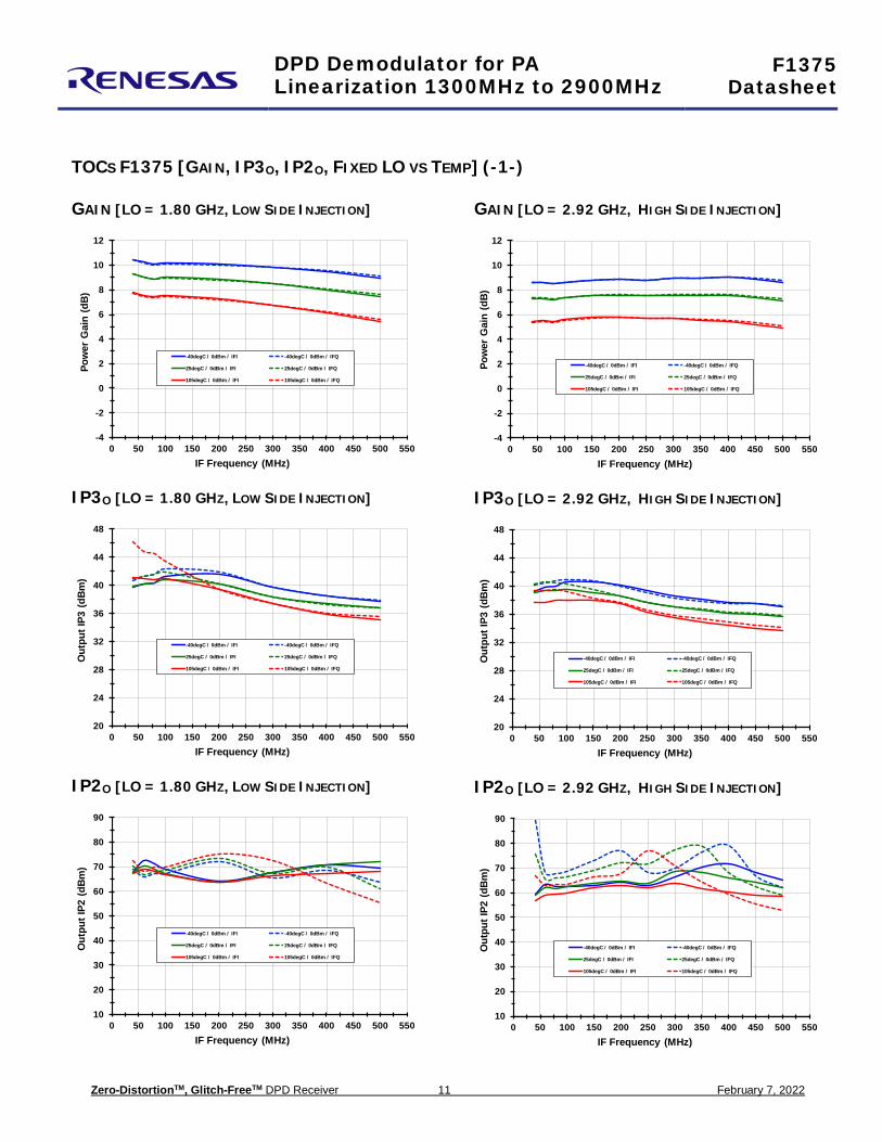
DATASHEET TYPICAL OPERATING CONDITIONS Unless otherwise noted, for the TOC graphs on the following pages, the following conditions apply
• IF = 200 MHz • Tone spacing = 5 MHz • Pin = - 8 dBm / Tone • Pout ~ 1 dBm / Tone • RF_X, IF_Q selected • Minimum Attenuation selected (0 dB ATTN) • VCC = 5.00 V • LO level = 0 dBm • Case Temperature = 25C • All Temperatures are Case Temperature (TCASE) • Output Transformers are de-embedded • Input RF trace losses are de-embedded
DPD Demodulator for PA Linearization 1300MHz to 2900MHz
F1375 Datasheet
Zero-DistortionTM, Glitch-FreeTM DPD Receiver 11 February 7, 2022
DATASHEET TOCS F1375 [GAIN, IP3O, IP2O, FIXED LO VS TEMP] (-1-) GAIN [LO = 1.80 GHZ, LOW SIDE INJECTION]
IP3O [LO = 1.80 GHZ, LOW SIDE INJECTION]
IP2O [LO = 1.80 GHZ, LOW SIDE INJECTION]
GAIN [LO = 2.92 GHZ, HIGH SIDE INJECTION]
IP3O [LO = 2.92 GHZ, HIGH SIDE INJECTION]
IP2O [LO = 2.92 GHZ, HIGH SIDE INJECTION]
-4
-2
0
2
4
6
8
10
12
0 50 100 150 200 250 300 350 400 450 500 550
Pow
er G
ain
(dB)
IF Frequency (MHz)
-40degC / 0dBm / IFI -40degC / 0dBm / IFQ
25degC / 0dBm / IFI 25degC / 0dBm / IFQ
105degC / 0dBm / IFI 105degC / 0dBm / IFQ
20
24
28
32
36
40
44
48
0 50 100 150 200 250 300 350 400 450 500 550
Out
put I
P3 (d
Bm)
IF Frequency (MHz)
-40degC / 0dBm / IFI -40degC / 0dBm / IFQ
25degC / 0dBm / IFI 25degC / 0dBm / IFQ
105degC / 0dBm / IFI 105degC / 0dBm / IFQ
10
20
30
40
50
60
70
80
90
0 50 100 150 200 250 300 350 400 450 500 550
Out
put I
P2 (d
Bm)
IF Frequency (MHz)
-40degC / 0dBm / IFI -40degC / 0dBm / IFQ
25degC / 0dBm / IFI 25degC / 0dBm / IFQ
105degC / 0dBm / IFI 105degC / 0dBm / IFQ

DPD Demodulator for PA Linearization 1300MHz to 2900MHz
F1375 Datasheet
Zero-DistortionTM, Glitch-FreeTM DPD Receiver 12 February 7, 2022
DATASHEET TOCS F1375 [H2 FIXED LO VS TEMP, TRANSFORMER LOSS, RF TRACE LOSS] (-2-) H2 [LO = 1.8 GHZ, LOW SIDE INJECTION]
IF TRANSFORMER LOSS
H2 [LO = 2.92 GHZ, HIGH SIDE INJECTION]
EVKIT RF TRACE LOSS
-100
-90
-80
-70
-60
-50
-40
-30
-20
-10
0 50 100 150 200 250 300 350 400 450 500 550
2ndHa
rmon
ic (
dBc)
IF Frequency (MHz)
-40degC / 0dBm / IFI -40degC / 0dBm / IFQ
25degC / 0dBm / IFI 25degC / 0dBm / IFQ
105degC / 0dBm / IFI 105degC / 0dBm / IFQ
POUT = 0.36 VPP = -8 dBm
-1.6
-1.4
-1.2
-1.0
-0.8
-0.6
-0.4
-0.2
0.0
0 100 200 300 400 500 600
TC2-
72T
loss
(dB)
IF Frequency (MHz)
-40C 25C 100C
-100
-90
-80
-70
-60
-50
-40
-30
-20
-10
0 50 100 150 200 250 300 350 400 450 500 5502nd
Harm
onic
(dB
c)IF Frequency (MHz)
-40degC / 0dBm / IFI -40degC / 0dBm / IFQ
25degC / 0dBm / IFI 25degC / 0dBm / IFQ
105degC / 0dBm / IFI 105degC / 0dBm / IFQ
POUT = 0.36 VPP = -8 dBm
0.0
0.2
0.4
0.6
0.8
1.0
1.8 1.9 2.0 2.1 2.2 2.3 2.4 2.5 2.6 2.7 2.8
EVki
t RF
Trac
e Lo
ss (d
B)
RF Freq (GHz)
-40C RFX 25C RFX 100C RFX
-40C RFY 25C RFY 100C RFY

DPD Demodulator for PA Linearization 1300MHz to 2900MHz
F1375 Datasheet
Zero-DistortionTM, Glitch-FreeTM DPD Receiver 13 February 7, 2022
DATASHEET TOCS F1375 [FIXED IF = 200MHZ GAIN, IP3O, IP2O] (-3-) GAIN [VS. TCASE]
IP3O [VS. TCASE]
IP2O [VS. TCASE]
GAIN [VS. LO LEVEL]
IP3O [VS. LO LEVEL]
IP2O [VS. LO LEVEL]
-10
-8
-6
-4
-2
0
2
4
6
8
10
12
1.4 1.6 1.8 2.0 2.2 2.4 2.6 2.8
Pow
er G
ain
(dB)
RF Frequency (GHz)
-40degC / 0dBm / 0attn / LS Injection -40degC / 0dBm / 15attn / LS Injection
25degC / 0dBm / 0attn / LS Injection 25degC / 0dBm / 15attn / LS Injection
105degC / 0dBm / 0attn / LS Injection 105degC / 0dBm / 15attn / LS Injection
20
24
28
32
36
40
44
48
1.4 1.6 1.8 2.0 2.2 2.4 2.6 2.8
Out
put I
P3 (d
Bm)
RF Frequency (GHz)
-40degC / 0dBm / 0attn / LS Injection -40degC / 0dBm / 15attn / LS Injection
25degC / 0dBm / 0attn / LS Injection 25degC / 0dBm / 15attn / LS Injection
105degC / 0dBm / 0attn / LS Injection 105degC / 0dBm / 15attn / LS Injection
10
20
30
40
50
60
70
80
90
1.4 1.6 1.8 2.0 2.2 2.4 2.6 2.8
Out
put I
P2 (d
Bm)
RF Frequency (GHz)
-40degC / 0dBm / 0attn / LS Injection -40degC / 0dBm / 15attn / LS Injection
25degC / 0dBm / 0attn / LS Injection 25degC / 0dBm / 15attn / LS Injection
105degC / 0dBm / 0attn / LS Injection 105degC / 0dBm / 15attn / LS Injection
0
2
4
6
8
10
12
1.4 1.6 1.8 2.0 2.2 2.4 2.6 2.8
Pow
er G
ain
(dB)
RF Frequency (GHz)
25degC / 3dBm / 0attn / LS Injection 25degC / 3dBm / 0attn / HS Injection
25degC / 0dBm / 0attn / LS Injection 25degC / 0dBm / 0attn / HS Injection
25degC / -3dBm / 0attn / LS Injection 25degC / -3dBm / 0attn / HS Injection
20
24
28
32
36
40
44
48
1.4 1.6 1.8 2.0 2.2 2.4 2.6 2.8
Out
put I
P3 (d
Bm)
RF Frequency (GHz)
25degC / 3dBm / 0attn / LS Injection 25degC / 3dBm / 0attn / HS Injection
25degC / 0dBm / 0attn / LS Injection 25degC / 0dBm / 0attn / HS Injection
25degC / -3dBm / 0attn / LS Injection 25degC / -3dBm / 0attn / HS Injection
10
20
30
40
50
60
70
80
90
1.4 1.6 1.8 2.0 2.2 2.4 2.6 2.8
Out
put I
P2 (d
Bm)
RF Frequency (GHz)
25degC / 3dBm / 0attn / LS Injection 25degC / 3dBm / 0attn / HS Injection
25degC / 0dBm / 0attn / LS Injection 25degC / 0dBm / 0attn / HS Injection
25degC / -3dBm / 0attn / LS Injection 25degC / -3dBm / 0attn / HS Injection

DPD Demodulator for PA Linearization 1300MHz to 2900MHz
F1375 Datasheet
IDT Zero-DistortionTM, Glitch-FreeTM DPD Receiver 14 Rev1, January 2014
DATASHEET TOCS F1375 [FIXED IF = 200MHZ, H2, LO – IF LEAKAGE, ICC] (-4-) H2 [VS. TCASE]
LO - IF [VS. TCASE]
ICC [VS. TCASE]
H2 [VS. LO LEVEL]
LO - IF [VS. LO LEVEL]
ICC [VS. LO LEVEL]
-100
-90
-80
-70
-60
-50
-40
-30
-20
-10
1.4 1.6 1.8 2.0 2.2 2.4 2.6 2.8
2ndHa
rmon
ic (
dBc)
RF Frequency (GHz)
-40degC / 0dBm / 0attn / LS Injection -40degC / 0dBm / 15attn / LS Injection
25degC / 0dBm / 0attn / LS Injection 25degC / 0dBm / 15attn / LS Injection
105degC / 0dBm / 0attn / LS Injection 105degC / 0dBm / 15attn / LS Injection
POUT = 0.36 VPP = -8 dBm
-60
-50
-40
-30
-20
-10
0
1.4 1.6 1.8 2.0 2.2 2.4 2.6 2.8
LO to
IF L
eaka
ge (
dBm
)
RF Frequency (GHz)
-40degC / 0dBm / 0attn / LS Injection -40degC / 0dBm / 15attn / LS Injection
25degC / 0dBm / 0attn / LS Injection 25degC / 0dBm / 15attn / LS Injection
105degC / 0dBm / 0attn / LS Injection 105degC / 0dBm / 15attn / LS Injection
230
240
250
260
270
280
290
300
310
320
330
1.4 1.6 1.8 2.0 2.2 2.4 2.6 2.8
Tota
l IC
C(m
A)
RF Frequency (GHz)
-40degC / 0dBm / 0attn / LS Injection -40degC / 0dBm / 15attn / LS Injection
25degC / 0dBm / 0attn / LS Injection 25degC / 0dBm / 15attn / LS Injection
105degC / 0dBm / 0attn / LS Injection 105degC / 0dBm / 15attn / LS Injection
-100
-90
-80
-70
-60
-50
-40
-30
-20
-10
1.4 1.6 1.8 2.0 2.2 2.4 2.6 2.8
2ndHa
rmon
ic (
dBc)
RF Frequency (GHz)
25degC / 3dBm / 0attn / LS Injection 25degC / 3dBm / 0attn / HS Injection
25degC / 0dBm / 0attn / LS Injection 25degC / 0dBm / 0attn / HS Injection
25degC / -3dBm / 0attn / LS Injection 25degC / -3dBm / 0attn / HS Injection
POUT = 0.36 VPP = -8 dBm
-60
-50
-40
-30
-20
-10
0
1.4 1.6 1.8 2.0 2.2 2.4 2.6 2.8
LO to
IF L
eaka
ge (
dBm
)
RF Frequency (GHz)
25degC / 3dBm / 0attn / LS Injection 25degC / 3dBm / 0attn / HS Injection
25degC / 0dBm / 0attn / LS Injection 25degC / 0dBm / 0attn / HS Injection
25degC / -3dBm / 0attn / LS Injection 25degC / -3dBm / 0attn / HS Injection
230
240
250
260
270
280
290
300
310
320
330
1.4 1.6 1.8 2.0 2.2 2.4 2.6 2.8
Tota
l IC
C(m
A)
RF Frequency (GHz)
25degC / 3dBm / 0attn / LS Injection 25degC / 3dBm / 0attn / HS Injection
25degC / 0dBm / 0attn / LS Injection 25degC / 0dBm / 0attn / HS Injection
25degC / -3dBm / 0attn / LS Injection 25degC / -3dBm / 0attn / HS Injection

DPD Demodulator for PA Linearization 1300MHz to 2900MHz
F1375 Datasheet
IDT Zero-DistortionTM, Glitch-FreeTM DPD Receiver 15 Rev1, January 2014
DATASHEET TOCS F1375 [FIXED IF CONFIGURATION, GAIN, IP3O, IP2O, H2, LEAKAGE] (-5-) GAIN
IP2O
LO – IF
IP3O
H2
RF - IF
-10
-8
-6
-4
-2
0
2
4
6
8
10
12
1.4 1.6 1.8 2.0 2.2 2.4 2.6 2.8
RFX IFI 0attn RFX IFI 15attnRFX IFQ 0attn RFX IFQ 15attnRFY IFI 0attn RFY IFI 15attnRFY IFQ 0attn RFY IFQ 15attn
RF Frequency (GHz)
Pow
er G
ain
(dB) TCASE = 25C, VCC = 5.00 V, LO Level = 0 dBm, Low Side Injection
10
20
30
40
50
60
70
80
90
1.4 1.6 1.8 2.0 2.2 2.4 2.6 2.8
RFX IFI 0attn RFX IFI 15attnRFX IFQ 0attn RFX IFQ 15attnRFY IFI 0attn RFY IFI 15attnRFY IFQ 0attn RFY IFQ 15attn
RF Frequency (GHz)
Out
put I
P2 (d
Bm)
TCASE = 25C, VCC = 5.00 V, LO Level = 0 dBm, Low Side Injection
-60
-50
-40
-30
-20
-10
0
1.4 1.6 1.8 2.0 2.2 2.4 2.6 2.8
RFX IFI 0attn RFX IFI 15attnRFX IFQ 0attn RFX IFQ 15attnRFY IFI 0attn RFY IFI 15attnRFY IFQ 0attn RFY IFQ 15attn
RF Frequency (GHz)
LO to
IF L
eaka
ge (
dBm
)
TCASE = 25C, VCC = 5.00 V, LO Level = 0 dBm, Low Side Injection
20
24
28
32
36
40
44
48
1.4 1.6 1.8 2.0 2.2 2.4 2.6 2.8
RFX IFI 0attn RFX IFI 15attnRFX IFQ 0attn RFX IFQ 15attnRFY IFI 0attn RFY IFI 15attnRFY IFQ 0attn RFY IFQ 15attn
RF Frequency (GHz)
Out
put I
P3 (d
Bm)
TCASE = 25C, VCC = 5.00 V, LO Level = 0 dBm, Low Side Injection
-100
-90
-80
-70
-60
-50
-40
-30
-20
-10
1.4 1.6 1.8 2.0 2.2 2.4 2.6 2.8
RFX IFI 0attn RFX IFI 15attnRFX IFQ 0attn RFX IFQ 15attnRFY IFI 0attn RFY IFI 15attnRFY IFQ 0attn RFY IFQ 15attn
RF Frequency (GHz)
2ndHa
rmon
ic (
dBc)
TCASE = 25C, VCC = 5.00 V, LO Level = 0 dBm, Low Side Injection POUT = 0.36 VPP = -8 dBm
-70
-60
-50
-40
-30
-20
-10
0
1.4 1.6 1.8 2.0 2.2 2.4 2.6 2.8
RFX IFI 0attn RFX IFI 15attnRFX IFQ 0attn RFX IFQ 15attnRFY IFI 0attn RFY IFI 15attnRFY IFQ 0attn RFY IFQ 15attn
RF Frequency (GHz)
RF
to IF
Lea
kage
(dB
c)
TCASE = 25C, VCC = 5.00 V, LO Level = 0 dBm, Low Side Injection

DPD Demodulator for PA Linearization 1300MHz to 2900MHz
F1375 Datasheet
IDT Zero-DistortionTM, Glitch-FreeTM DPD Receiver 16 Rev1, January 2014
DATASHEET TOCS F1375 [QUADRATURE, ATTN ACCURACY, AND IF IMPEDANCE] (-6-) I/Q AMPLITUDE [VS. TCASE]
I/Q PHASE [VS. TCASE]
OUTPUT P1dB [VS. TCASE]
I/Q AMPLITUDE [VS. LO LEVEL]
I/Q PHASE [VS. LO LEVEL]
OUTPUT P1dB [VS. LO LEVEL]
-1.00
-0.75
-0.50
-0.25
0.00
0.25
0.50
0.75
1.00
1.5 1.6 1.7 1.8 1.9 2.0 2.1 2.2 2.3 2.4 2.5 2.6 2.7 2.8
I/Q A
mpl
itude
Bal
ance
(dB
)
LO Frequency (GHz)
-40degC / 0dBm LO
25degC / 0dBm LO
105degC / 0dBm LO
-10
-8
-6
-4
-2
0
2
4
6
8
10
1.5 1.6 1.7 1.8 1.9 2.0 2.1 2.2 2.3 2.4 2.5 2.6 2.7 2.8
I/Q P
hase
Err
or (d
egre
es)
LO Frequency (GHz)
-40degC / 0dBm
25degC / 0dBm
105degC / 0dBm
13
14
15
16
17
18
19
1.4 1.6 1.8 2.0 2.2 2.4 2.6 2.8
Out
put P
1dB
(dBm
)
RF Frequency (GHz)
-40degC / 0dBm / 0attn / LS Injection -40degC / 0dBm / 0attn / HS Injection
25degC / 0dBm / 0attn / LS Injection 25degC / 0dBm / 0attn / HS Injection
105degC / 0dBm / 0attn / LS Injection 105degC / 0dBm / 0attn / HS Injection
-1.00
-0.75
-0.50
-0.25
0.00
0.25
0.50
0.75
1.00
1.5 1.6 1.7 1.8 1.9 2.0 2.1 2.2 2.3 2.4 2.5 2.6 2.7 2.8
I/Q A
mpl
itude
Bal
ance
(dB
)
LO Frequency (GHz)
25degC / 3dBm LO
25degC / 0dBm LO
25degC / -3dBm LO
-10
-8
-6
-4
-2
0
2
4
6
8
10
1.5 1.6 1.7 1.8 1.9 2.0 2.1 2.2 2.3 2.4 2.5 2.6 2.7 2.8
I/Q P
hase
Err
or (d
egre
es)
LO Frequency (GHz)
25degC / 3dBm
25degC / 0dBm
25degC / -3dBm
13
14
15
16
17
18
19
1.4 1.6 1.8 2.0 2.2 2.4 2.6 2.8
Out
put P
1dB
(dBm
)
RF Frequency (GHz)
25degC / 3dBm / 0attn / LS Injection 25degC / 3dBm / 0attn / HS Injection
25degC / 0dBm / 0attn / LS Injection 25degC / 0dBm / 0attn / HS Injection
25degC / -3dBm / 0attn / LS Injection 25degC / -3dBm / 0attn / HS Injection

DPD Demodulator for PA Linearization 1300MHz to 2900MHz
F1375 Datasheet
IDT Zero-DistortionTM, Glitch-FreeTM DPD Receiver 17 Rev1, January 2014
DATASHEET TOCS F1375 [ATTN ACCURACY, NOISE FIGURE] (-7-) ATTENUATION ACCURACY [1.7 GHZ]
ATTENUATION ACCURACY [2.7 GHZ]
NOISE FIGURE [25C, VS. CONFIGURATION]
ATTENUATION ACCURACY [2.1 GHZ]
NOISE FIGURE [VS. TCASE, MEASURED RFX TO IFI]
OIP3 HISTOGRAM [N=1440]
-1.25
-1.00
-0.75
-0.50
-0.25
0.00
0.25
0.50
0.75
1.00
1.25
0 2 4 6 8 10 12 14 16 18 20 22
Abso
lute
Atte
nuat
ion
Erro
r (dB
)
Attenuation Setting (dB)
-40degC / RFX -40degC / RFY
25degC / RFX 25degC / RFY
105degC / RFX 105degC / RFY
-1.25
-1.00
-0.75
-0.50
-0.25
0.00
0.25
0.50
0.75
1.00
1.25
0 2 4 6 8 10 12 14 16 18 20 22
Abso
lute
Atte
nuat
ion
Erro
r (dB
)
Attenuation Setting (dB)
-40degC / RFX -40degC / RFY
25degC / RFX 25degC / RFY
105degC / RFX 105degC / RFY
10
12
14
16
18
20
22
24
1500 1700 1900 2100 2300 2500 2700 2900
Nois
e Fi
gure
(dB)
RF Frequency (MHz)
25C / RFX / IFI 25C / RFY / IFI
25C / RFX / IFQ 25C / RFY / IFQ
-1.25
-1.00
-0.75
-0.50
-0.25
0.00
0.25
0.50
0.75
1.00
1.25
0 2 4 6 8 10 12 14 16 18 20 22
Abso
lute
Atte
nuat
ion
Erro
r (dB
)
Attenuation Setting (dB)
-40degC / RFX -40degC / RFY
25degC / RFX 25degC / RFY
105degC / RFX 105degC / RFY
10
12
14
16
18
20
22
24
1500 1700 1900 2100 2300 2500 2700 2900
Nois
e Fi
gure
(dB)
RF Frequency (MHz)
-40C / RFX / IFI
25C / RFX / IFI
105C / RFX / IFI
0%
5%
10%
15%
20%
25%
30%
35%
Perc
enta
ge
Output IP3 Bin (dBm)
OIP3
LO Frequency = 1900 MHzRF Frequency = 2100 MHzWortscase of I and Q Channels

DPD Demodulator for PA Linearization 1300MHz to 2900MHz
F1375 Datasheet
IDT Zero-DistortionTM, Glitch-FreeTM DPD Receiver 18 Rev1, January 2014
DATASHEET TOCS F1375 [ISOLATION, RETURN LOSS, HISTOGRAMS] (-8-) RF PORT RETURN LOSS
IF PORT RETURN LOSS
I/Q ERROR HISTOGRAM [N = 1440]
LO PORT RETURN LOSS
RF SP2T ISOLATION
BAND EDGE GAIN DELTA [N = 1440]
-35
-30
-25
-20
-15
-10
-5
0
1400 1600 1800 2000 2200 2400 2600 2800
RF
Port
Ret
urn
Loss
(dB)
RF Frequency (MHz)
RFX_0dB RFY_0dB
RFX_10dB RFY_10dB
RFX_20dB RFY_20dB
-30
-25
-20
-15
-10
-5
0
10 100 1,000
IF P
ort R
etur
n Lo
ss (d
B)
IF Frequency (MHz)
IF_I
IF_Q
0%
5%
10%
15%
20%
25%
30%
35%
40%
45%
Perc
enta
ge
I/Q Amplitude Balance Bin (dB)
1900M LO
2900M LO
-35
-30
-25
-20
-15
-10
-5
0
1400 1600 1800 2000 2200 2400 2600 2800 3000
LO P
ort R
etur
n Lo
ss (d
B)
LO Frequency (MHz)
LO (Enabled)
LO (STBY)
-75
-70
-65
-60
-55
-50
-45
-40
-35
-30
-25
1400 1600 1800 2000 2200 2400 2600 2800
X Selected / 0dB ATTN Y Selected / 0dB ATTN
X Selected / 15dB ATTN YSelected / 15dB ATTN
RF Frequency (MHz)
RF
Switc
h Is
olta
ion
(dB)
0%
5%
10%
15%
20%
25%
30%
35%
40%
45%
50%
Perc
enta
ge
Gain Delta Bin (dB)
IF_I IF_QGain Delta Between:RF = 1300 MHz, LO = 1800 MHz, IF = 500 MHzRF = 2900 MHz, LO = 2920 MHz , IF = 20 MHz
DPD Demodulator for PA Linearization 1300MHz to 2900MHz
F1375 Datasheet
Zero-DistortionTM, Glitch-FreeTM DPD Receiver 19 February 7, 2022
PACKAGE OUTLINE DRAWINGS The package outline drawings are located at the end of this document and are accessible from the Renesas website The package information is the most current data available and is subject to change without revision of this document.
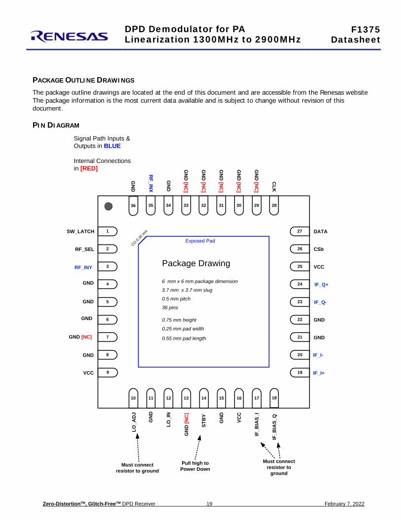
PIN DIAGRAM
Package Drawing
6 mm x 6 mm package dimension
3.7 mm x 3.7 mm slug
0.5 mm pitch
36 pins
0.75 mm height
0.25 mm pad width
0.55 mm pad length
RF_INY
SW_LATCH
GND
VCC
LO_A
DJ
GN
D
VCC
CSb
DATA
CLK
VCC
IF_I-
IF_Q+
IF_B
IAS_
I
IF_Q-
IF_B
IAS_
Q
IF_I+
LO_I
N
STB
Y
RF_IN
X
GN
D
GND
Exposed Pad
9
8
7
6
5
4
3
2
1
181716151413121110
27
26
25
24
23
22
21
20
19
36 35 34 33 32 31 30 29 28
CO 0.35
mm
Pull high to Power Down
Must connect resistor to ground
GND
GN
D [N
C]
GND
Signal Path Inputs & Outputs in BLUE
Internal Connections in [RED]
Must connect resistor to
ground
RF_SEL
GN
D
GND
GN
D
GN
D [N
C]
GN
D [N
C]
GN
D [N
C]
GN
D [N
C]
GN
D [N
C]
GND
GND [NC]

DPD Demodulator for PA Linearization 1300MHz to 2900MHz
F1375 Datasheet
Zero-DistortionTM, Glitch-FreeTM DPD Receiver 20 February 7, 2022
PIN DESCRIPTIONS
Pins Name Function
1 SW_LATCH Stand-by latch. Pull Low or Ground for Normal Operation. If left floating, this input will be internally pulled high, disabling SPI writes to ENb (Standby) and RF SW bits (A0, A2).
2 RF_SEL RF input selection. Pull high to select RF_INY. Pull low to select RF_INX.
3 RF_INY Alternate RF Input. Pull pin 2 high to select RF_INY. AC couple to this pin. Separated from RF_INX by internal SP2T. Internally matched to 50 ohms.
4, 5, 6, 8, 11,15, 21, 22, 34, 36
GND Ground these Pins.
7, 13, 29, 30, 31, 32, 33 NC No Connection. Not internally connected. OK to connect to Vcc.
Recommended Connection is Ground
9, 16, 25 VCC Power Supply. Bypass to GND with capacitors shown in the Typical Application Circuit as close as possible to pin.
10 LO_ADJ Connect the specified resistor from this pin to ground to set the LO path ICC. This IS a current setting resistor
12 LO_IN LO Input. AC couple to this pin. Internally matched to 50 ohms
14 STBY STBY Mode. Pull this pin high for Standby mode (~26 mA). Pull low or Ground for normal Operation
17, 18 IF_BIAS_I IF_BIAS_Q
Connect the specified resistor from this pin to ground to set the IF amplifier bias reference. This is NOT a current setting resistor
19, 20 IF_I+, IF_I- In-Phase Mixer Differential IF Output. Connect pullup inductors from each of these pins to VCC (see the Typical Application Circuit).
23, 24 IF_Q-, IF_Q+ Quadrature Mixer Differential IF Output. Connect pullup inductors from each of these pins to VCC (see the Typical Application Circuit).
26 CSb Chip Select Bar. The falling edge initiates a programming cycle and the rising edge latches the programmed shift register data into the active register.
27 DATA Serial Data Input
28 CLK Serial Clock Input
35 RF_INX Main RF Input. Pull pin 2 low to select RF_INX. AC couple to this pin. Separated from RF_INY by internal SP2T. Internally matched to 50 ohms
— EP
Exposed Pad. Internally connected to GND. Solder this exposed pad to a PCB pad that uses multiple ground vias to provide heat transfer out of the device into the PCB ground planes. These multiple via grounds are also required to achieve the noted RF performance.

DPD Demodulator for PA Linearization 1300MHz to 2900MHz
F1375 Datasheet
Zero-DistortionTM, Glitch-FreeTM DPD Receiver 21 February 7, 2022
CONTROL PIN VOLTAGE & RESISTANCE VALUES (PINS NOT CONNECTED) The following table provides open-circuit DC voltage and resistance values referenced to ground for each of the control pins listed.
Pin Name DC voltage (volts) Resistance (ohms)
1 SW_LATCH 1.75 1.6M
2 RF_SEL 1.75 800K
14 STBY 5 50K
26 CSb 1.75 1.6M
27 DATA 1.75 1.6M
28 CLK 1.75 1.6M
POWER SUPPLIES All supply pins should be bypassed with external capacitors to minimize noise and fast transients. Supply noise can degrade noise figure and fast transients can trigger ESD clamps and cause them to fail. Supply voltage change or transients should have a slew rate smaller than 1V/20uS. In addition, all control pins should remain at 0V (+/-0.3V) while the supply voltage ramps or while it returns to zero.
DPD Demodulator for PA Linearization 1300MHz to 2900MHz
F1375 Datasheet
Zero-DistortionTM, Glitch-FreeTM DPD Receiver 22 February 7, 2022
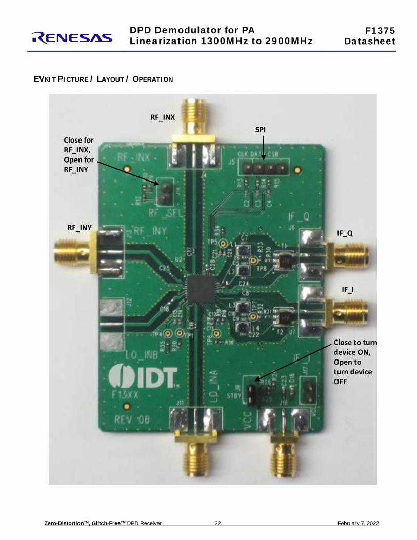
EVKIT PICTURE / LAYOUT / OPERATION
SPIRF_INX
RF_INY
Close for RF_INX, Open for RF_INY
Close to turn device ON, Open to turn device OFF
IF_Q
IF_I

DPD Demodulator for PA Linearization 1300MHz to 2900MHz
F1375 Datasheet
Zero-DistortionTM, Glitch-FreeTM DPD Receiver 23 February 7, 2022
EVKIT / APPLICATION CIRCUIT

DPD Demodulator for PA Linearization 1300MHz to 2900MHz
F1375 Datasheet
Zero-DistortionTM, Glitch-FreeTM DPD Receiver 24 February 7, 2022
EVKIT BOMS
TOP MARKINGS
Revision Date Description
February 7, 2022 Rebranded to Renesas.
January 16, 2014 Initial release.
F1375
Item # Value Size/Re Desc Mfr. Part # Mfr. Supplier Part # Supplier Part Reference Qty
1 10nF 0402 CAP CER 10000PF 16V 10% X7R 0402 GRM155R71C103KA01MURATA 490-1313-1-ND Digikey C6,7,8,9,12,14,21,22 9
2 1000pF 0402 CAP CER 1000PF 50V C0G 0402 GRM1555C1H102JA01 MURATA 490-3244-1-ND Digikey C5,10,11,15,20,23 63 39pF 0402 CAP CER 39PF 50V 5% C0G 0402 GRM1555C1H390JZ010MURATA 490-1286-1-ND Digikey C17,19,25 34 100pF 0402 CAP CER 100PF 50V 5% NP0 0402 GRM1555C1H101JZ01DMURATA 490-3458-1-ND Digikey C2,3,4 35 10uF 0603 CAP CER 10UF 6.3V X5R 0603 GRM188R60J106ME47 MURATA 490-3896-1-ND Digikey C16 1
6 Header 2 Pin TH 2 CONN HEADER VERT SGL 2POS GOLD 961102-6404-AR 3M 3M9447-ND Digikey J9,14,17 3
7 Header 4 Pin TH 4 CONN HEADER VERT SGL 4POS GOLD961104-6404-AR 3M 3M9449-ND Digikey J5 18 SMA_END_LAUNCH .062 SMA_END_LAUNCH (Small) 142-0711-821 Emerson Johnson 530-142-0711-821 Mouser J6,7,18 39 SMA_END_LAUNCH .062 SMA_END_LAUNCH (Big) 142-0701-851 Emerson Johnson 530-142-0701-851 Mouser J4,11,13 3
10 1uH 0805 0805LS (2012) Ceramic Chip Inductor 0805LS-102XJLB COILCRAFT 0805LS-102XJLB COILCRAFT L1,2,3,4 411 43K 0402 RES 43K OHM 1/10W 1% 0402 SMD ERJ-2RKF4302X Panasonic P43.0KLCT-ND Digikey R9,26 212 75K 0402 RES 75K OHM 1/10W 1% 0402 SMD ERJ-2RKF7502X Panasonic P75.0KLCT-ND Digikey R10,24 213 2.37K 0402 RES 2.37K OHM 1/10W 1% 0402 SMD ERJ-2RKF2371X Panasonic P2.37KLCT-ND Digikey R20 114 130 0402 RES 130 OHM 1/10W 1% 0402 SMD ERJ-2RKF1300X Panasonic P130LCT-ND Digikey R18,19 2
15 47K 0402 RES 47.0K OHM 1/16W 1% 0402 SMD RC0402FR-0747KL Yageo 311-47.0KLRCT-NDDigikey R12,25 2
16 100 0402 RES 100 OHM 1/10W 1% 0402 SMD ERJ-2RKF1000X Panasonic P100LCT-ND Digikey R13-15 317 0 0402 RES 0.0 OHM 1/10W 0402 SMD ERJ-2GE0R00X Panasonic P0.0JCT-ND Digikey R30-36 718 2:1 Balun SM-22 2:1 Center Tap Balun TC2-72T+ Mini Circuits TC2-72T+ Mini Circuits T1,2 219 F1375 QFN-36 DPD Demodulator F1375 IDT F1375 IDT U1 120 PCB 06 Printed Circuit Board F13XX Rev 06 SBC 121 BOM 10 Bill Of Material22 DNP 0402 C18
Total 59
12/4/2013
IDTF1375NBGIZC1327A
Q03C019MY
Part Number
Date Code [YYWW](Week 27 of 2013)
Lot CodeDie Step

36-VFQFPN, Package Outline Drawing6.00 x 6.00 x 0.75 mm Body, 3.70 x 3.70 mm Epad, 0.5mm Pitch
NB/NBG36P1, PSC-4311-01, Rev 01, Page 1
© Renesas Electronics Corporation

© Renesas Electronics Corporation
01
Apr 6, 2016 00 Initial Release
Package Revision HistoryRev No.Date Created Description
Nov 8, 2021 Update IDT format to Renesas format
36-VFQFPN, Package Outline Drawing6.00 x 6.00 x 0.75 mm Body, 3.70 x 3.70 mm Epad, 0.5mm Pitch
NB/NBG36P1, PSC-4311-01, Rev 01, Page 2

Corporate HeadquartersTOYOSU FORESIA, 3-2-24 Toyosu,Koto-ku, Tokyo 135-0061, Japanwww.renesas.com
Contact InformationFor further information on a product, technology, the most up-to-date version of a document, or your nearest sales office, please visit:www.renesas.com/contact/
TrademarksRenesas and the Renesas logo are trademarks of Renesas Electronics Corporation. All trademarks and registered trademarks are the property of their respective owners.
IMPORTANT NOTICE AND DISCLAIMER
RENESAS ELECTRONICS CORPORATION AND ITS SUBSIDIARIES (“RENESAS”) PROVIDES TECHNICAL SPECIFICATIONS AND RELIABILITY DATA (INCLUDING DATASHEETS), DESIGN RESOURCES (INCLUDING REFERENCE DESIGNS), APPLICATION OR OTHER DESIGN ADVICE, WEB TOOLS, SAFETY INFORMATION, AND OTHER RESOURCES “AS IS” AND WITH ALL FAULTS, AND DISCLAIMS ALL WARRANTIES, EXPRESS OR IMPLIED, INCLUDING, WITHOUT LIMITATION, ANY IMPLIED WARRANTIES OF MERCHANTABILITY, FITNESS FOR A PARTICULAR PURPOSE, OR NON-INFRINGEMENT OF THIRD PARTY INTELLECTUAL PROPERTY RIGHTS.
These resources are intended for developers skilled in the art designing with Renesas products. You are solely responsible for (1) selecting the appropriate products for your application, (2) designing, validating, and testing your application, and (3) ensuring your application meets applicable standards, and any other safety, security, or other requirements. These resources are subject to change without notice. Renesas grants you permission to use these resources only for development of an application that uses Renesas products. Other reproduction or use of these resources is strictly prohibited. No license is granted to any other Renesas intellectual property or to any third party intellectual property. Renesas disclaims responsibility for, and you will fully indemnify Renesas and its representatives against, any claims, damages, costs, losses, or liabilities arising out of your use of these resources. Renesas' products are provided only subject to Renesas' Terms and Conditions of Sale or other applicable terms agreed to in writing. No use of any Renesas resources expands or otherwise alters any applicable warranties or warranty disclaimers for these products.
(Rev.1.0 Mar 2020)
© 2020 Renesas Electronics Corporation. All rights reserved.