GD25LB128D DATASHEET - GigaDevice
75
1.8V Uniform Sector Dual and Quad Serial Flash GD25LB128D 1 GD25LB128D DATASHEET
-
Upload
khangminh22 -
Category
Documents
-
view
0 -
download
0
Transcript of GD25LB128D DATASHEET - GigaDevice
1.8V Uniform Sector Dual and Quad Serial Flash GD25LB128D
1
GD25LB128D
DATASHEET
1.8V Uniform Sector Dual and Quad Serial Flash GD25LB128D
2
Contents
1. FEATURES ......................................................................................................................................................... 4
2. GENERAL DESCRIPTION ................................................................................................................................ 5
3. MEMORY ORGANIZATION ............................................................................................................................... 7
4. DEVICE OPERATION ........................................................................................................................................ 8
5. DATA PROTECTION .......................................................................................................................................... 9
6. STATUS REGISTER......................................................................................................................................... 11
7. COMMANDS DESCRIPTION .......................................................................................................................... 13
7.1. WRITE ENABLE (WREN) (06H) ................................................................................................................................ 17
7.2. WRITE DISABLE (WRDI) (04H) ................................................................................................................................ 18
7.3. WRITE ENABLE FOR VOLATILE STATUS REGISTER (50H) ................................................................................................. 19
7.4. READ STATUS REGISTER (RDSR) (05H OR 35H OR 15H) .............................................................................................. 20
7.5. WRITE STATUS REGISTER (WRSR) (01H) ................................................................................................................... 21
7.6. READ DATA BYTES (READ) (03H) ............................................................................................................................. 22
7.7. READ DATA BYTES AT HIGHER SPEED (FAST READ) (0BH) .............................................................................................. 23
7.8. DUAL OUTPUT FAST READ (3BH) .............................................................................................................................. 24
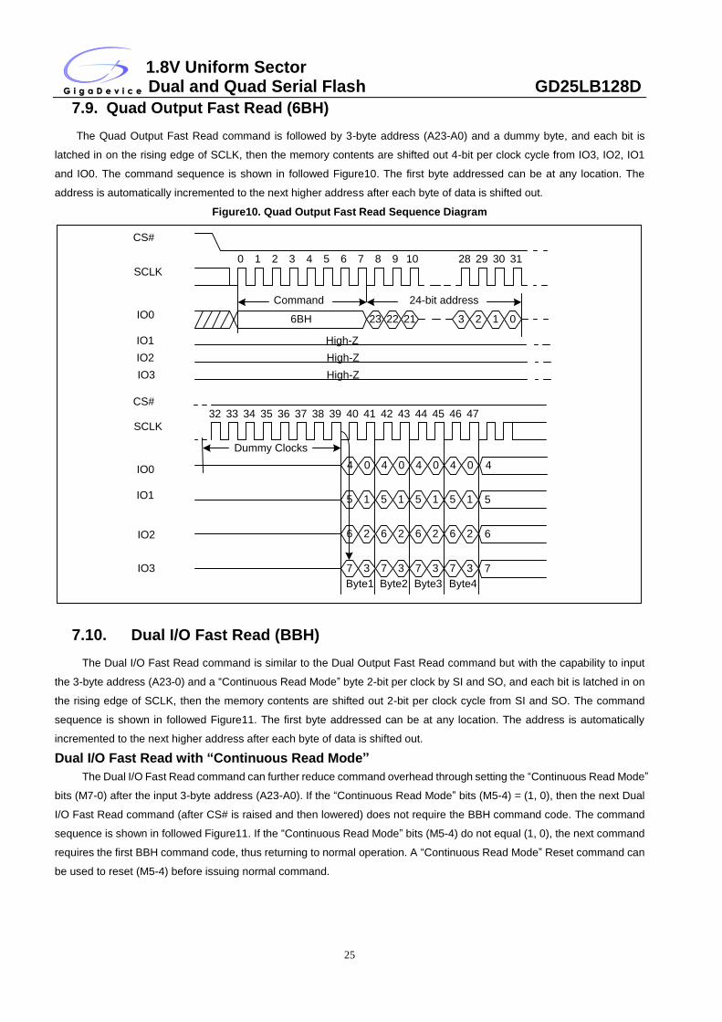
7.9. QUAD OUTPUT FAST READ (6BH) ............................................................................................................................. 25
7.10. DUAL I/O FAST READ (BBH) .................................................................................................................................... 25
7.11. QUAD I/O FAST READ (EBH) ................................................................................................................................... 27
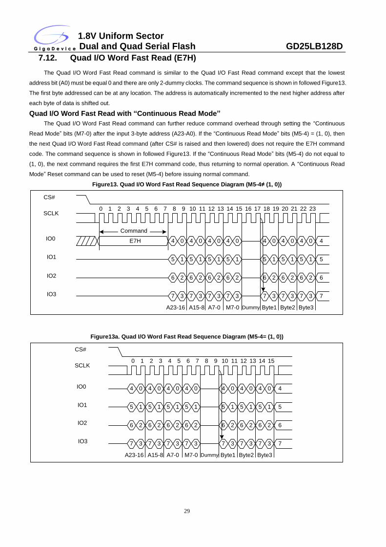
7.12. QUAD I/O WORD FAST READ (E7H) ......................................................................................................................... 29
7.13. SET BURST WITH WRAP (77H) ................................................................................................................................. 30
7.14. PAGE PROGRAM (PP) (02H) .................................................................................................................................... 31
7.15. QUAD PAGE PROGRAM (32H) .................................................................................................................................. 32
7.16. SECTOR ERASE (SE) (20H) ....................................................................................................................................... 34
7.17. 32KB BLOCK ERASE (BE) (52H) ............................................................................................................................... 35
7.18. 64KB BLOCK ERASE (BE) (D8H) ............................................................................................................................... 36
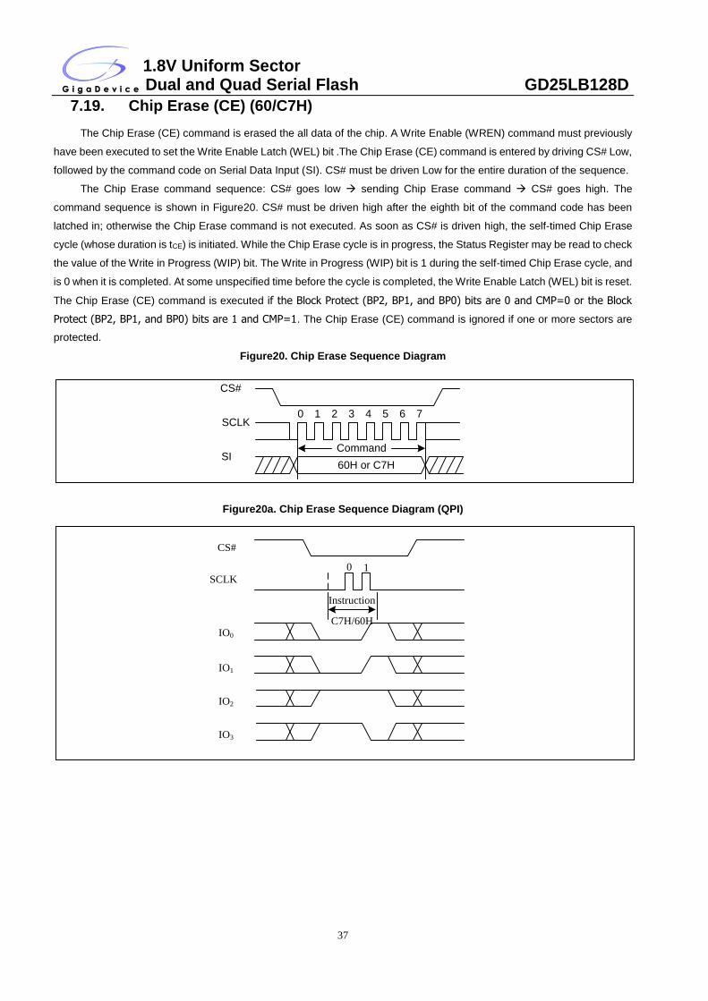
7.19. CHIP ERASE (CE) (60/C7H) ..................................................................................................................................... 37
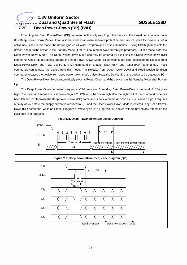
7.20. DEEP POWER-DOWN (DP) (B9H) ............................................................................................................................. 38
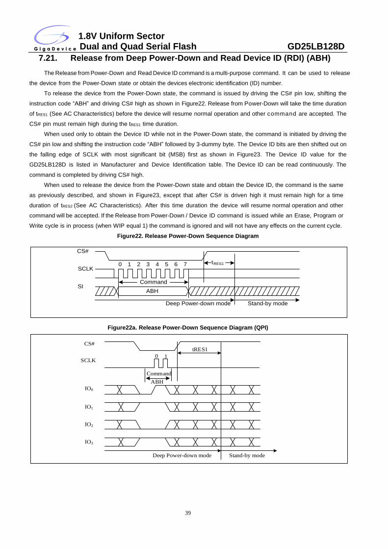
7.21. RELEASE FROM DEEP POWER-DOWN AND READ DEVICE ID (RDI) (ABH) ......................................................................... 39
7.22. READ MANUFACTURE ID/ DEVICE ID (REMS) (90H) ................................................................................................... 41
7.23. READ MANUFACTURE ID/ DEVICE ID DUAL I/O (92H) ................................................................................................. 42
7.24. READ MANUFACTURE ID/ DEVICE ID QUAD I/O (94H)................................................................................................. 43
7.25. READ IDENTIFICATION (RDID) (9FH) ......................................................................................................................... 44
7.26. PROGRAM/ERASE SUSPEND (PES) (75H) ................................................................................................................... 45
7.27. PROGRAM/ERASE RESUME (PER) (7AH) ................................................................................................................... 46
7.28. READ UNIQUE ID (4BH) .......................................................................................................................................... 47
7.29. ERASE SECURITY REGISTERS (44H) ............................................................................................................................ 47
7.30. PROGRAM SECURITY REGISTERS (42H) ....................................................................................................................... 48
7.31. READ SECURITY REGISTERS (48H) ............................................................................................................................. 49
7.32. SET READ PARAMETERS (C0H) ................................................................................................................................. 50
1.8V Uniform Sector Dual and Quad Serial Flash GD25LB128D
3
7.33. BURST READ WITH WRAP (0CH) ............................................................................................................................... 51
7.34. ENABLE QPI (38H)................................................................................................................................................. 51
7.35. DISABLE QPI (FFH) ................................................................................................................................................ 52
7.36. ENABLE RESET (66H) AND RESET (99H) ..................................................................................................................... 53
7.37. READ SERIAL FLASH DISCOVERABLE PARAMETER (5AH) ................................................................................................. 54
8. ELECTRICAL CHARACTERISTICS .............................................................................................................. 59
8.1. POWER-ON TIMING ........................................................................................................................................... 59
8.2. INITIAL DELIVERY STATE ..................................................................................................................................... 59
8.3. ABSOLUTE MAXIMUM RATINGS ........................................................................................................................ 59
8.4. CAPACITANCE MEASUREMENT CONDITIONS .................................................................................................... 60
8.5. DC CHARACTERISTICS ......................................................................................................................................... 61
8.6. AC CHARACTERISTICS ......................................................................................................................................... 64
9. ORDERING INFORMATION ............................................................................................................................ 68
9.1. VALID PART NUMBERS ............................................................................................................................................ 69
10. PACKAGE INFORMATION ............................................................................................................................. 70
10.1. PACKAGE SOP8 208MIL ........................................................................................................................................ 70
10.2. PACKAGE VSOP8 208MIL ...................................................................................................................................... 71
10.3. PACKAGE WSON8 (6*5MM) ................................................................................................................................... 72
10.4. PACKAGE WLCSP .................................................................................................................................................. 73
11. REVISION HISTORY ........................................................................................................................................ 74
1.8V Uniform Sector Dual and Quad Serial Flash GD25LB128D
4
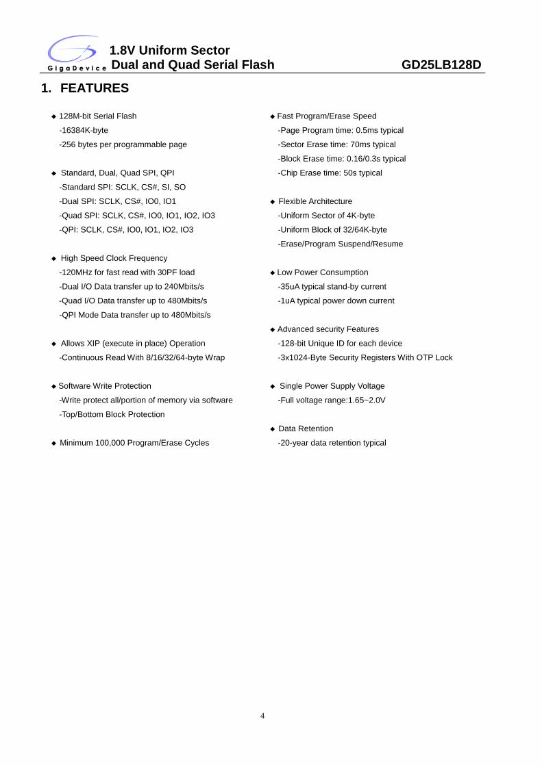
1. FEATURES
◆ 128M-bit Serial Flash ◆ Fast Program/Erase Speed
-16384K-byte -Page Program time: 0.5ms typical
-256 bytes per programmable page -Sector Erase time: 70ms typical
-Block Erase time: 0.16/0.3s typical
◆ Standard, Dual, Quad SPI, QPI -Chip Erase time: 50s typical
-Standard SPI: SCLK, CS#, SI, SO
-Dual SPI: SCLK, CS#, IO0, IO1 ◆ Flexible Architecture
-Quad SPI: SCLK, CS#, IO0, IO1, IO2, IO3 -Uniform Sector of 4K-byte
-QPI: SCLK, CS#, IO0, IO1, IO2, IO3 -Uniform Block of 32/64K-byte
-Erase/Program Suspend/Resume
◆ High Speed Clock Frequency
-120MHz for fast read with 30PF load ◆ Low Power Consumption
-Dual I/O Data transfer up to 240Mbits/s -35uA typical stand-by current
-Quad I/O Data transfer up to 480Mbits/s -1uA typical power down current
-QPI Mode Data transfer up to 480Mbits/s
◆ Advanced security Features
◆ Allows XIP (execute in place) Operation -128-bit Unique ID for each device
-Continuous Read With 8/16/32/64-byte Wrap -3x1024-Byte Security Registers With OTP Lock
◆ Software Write Protection ◆ Single Power Supply Voltage
-Write protect all/portion of memory via software -Full voltage range:1.65~2.0V
-Top/Bottom Block Protection
◆ Data Retention
◆ Minimum 100,000 Program/Erase Cycles -20-year data retention typical
1.8V Uniform Sector Dual and Quad Serial Flash GD25LB128D
5
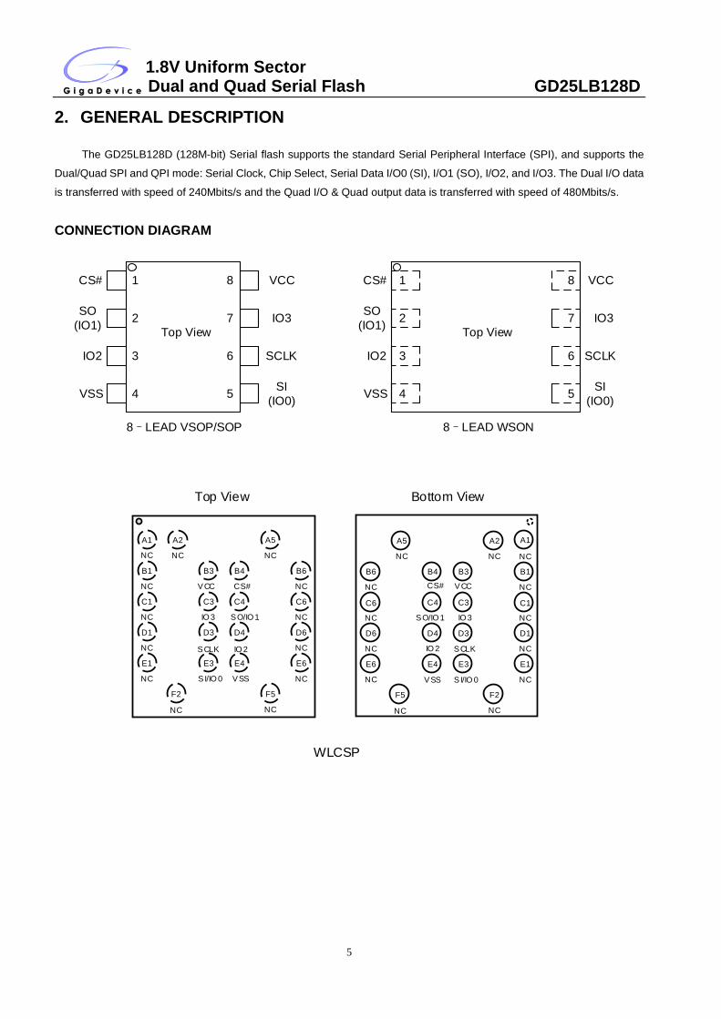
2. GENERAL DESCRIPTION
The GD25LB128D (128M-bit) Serial flash supports the standard Serial Peripheral Interface (SPI), and supports the
Dual/Quad SPI and QPI mode: Serial Clock, Chip Select, Serial Data I/O0 (SI), I/O1 (SO), I/O2, and I/O3. The Dual I/O data
is transferred with speed of 240Mbits/s and the Quad I/O & Quad output data is transferred with speed of 480Mbits/s.
CONNECTION DIAGRAM
CS#
SO
(IO1)
IO2
VSS
Top View
VCC
IO3
SCLK
SI
(IO0)
8–LEAD VSOP/SOP
1
2
3
4 5
6
7
8 CS#
SO
(IO1)
IO2
VSS
Top View
VCC
IO3
SCLK
SI
(IO0)
8–LEAD WSON
1
2
3
4 5
6
7
8
NC
NC
NC
NC
NC
NC NC NC
NC
NC
NC
NC
NC
CS#VCC
IO 3
IO 2SCLK
SO/IO 1
SI/IO 0 VSS
WLCSP
Top View
NC
NC
NC
NC
NC
NC NC
NC
NC
NC
NC
NC
CS#
IO 3
IO 2 SCLK
SO/IO 1
SI/IO 0VSS
NC
Bottom View
A1 A2 A5
B1 B3 B4 B6
C1 C3 C4 C6
D1 D3 D4 D6
E1 E3 E4 E6
F2 F5
A5 A2 A1
B1B3B4B6
C6 C4 C3 C1
D1D3D4D6
E1E3E4E6
F5 F2
VCC
1.8V Uniform Sector Dual and Quad Serial Flash GD25LB128D
6
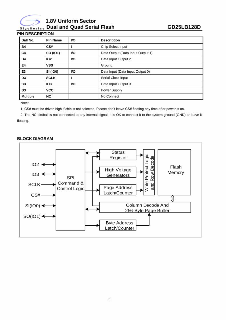
PIN DESCRIPTION
Ball No. Pin Name I/O Description
B4 CS# I Chip Select Input
C4 SO (IO1) I/O Data Output (Data Input Output 1)
D4 IO2 I/O Data Input Output 2
E4 VSS Ground
E3 SI (IO0) I/O Data Input (Data Input Output 0)
D3 SCLK I Serial Clock Input
C3 IO3 I/O Data Input Output 3
B3 VCC Power Supply
Multiple NC No Connect
Note:
1. CS# must be driven high if chip is not selected. Please don’t leave CS# floating any time after power is on.
2. The NC pin/ball is not connected to any internal signal. It is OK to connect it to the system ground (GND) or leave it
floating.
BLOCK DIAGRAM
SPI
Command &
Control Logic
High Voltage
Generators
Page Address
Latch/Counter
Status
Register
Byte Address
Latch/Counter
Column Decode And
256-Byte Page Buffer
Wri
te P
rote
ct
Lo
gic
and
Ro
w D
eco
de
Flash
Memory
CS#
SCLK
SI(IO0)
SO(IO1)
IO3
IO2
1.8V Uniform Sector Dual and Quad Serial Flash GD25LB128D
7
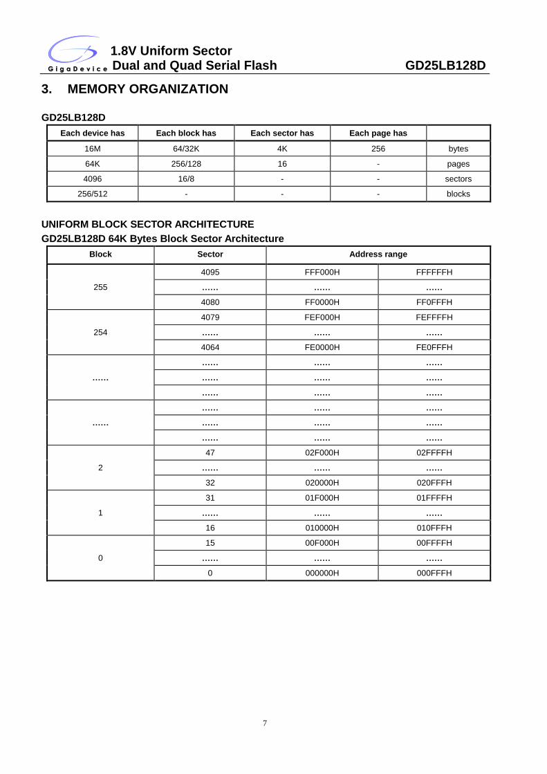
3. MEMORY ORGANIZATION
GD25LB128D
Each device has Each block has Each sector has Each page has
16M 64/32K 4K 256 bytes
64K 256/128 16 - pages
4096 16/8 - - sectors
256/512 - - - blocks
UNIFORM BLOCK SECTOR ARCHITECTURE
GD25LB128D 64K Bytes Block Sector Architecture
Block Sector Address range
255
4095 FFF000H FFFFFFH
…… …… ……
4080 FF0000H FF0FFFH
254
4079 FEF000H FEFFFFH
…… …… ……
4064 FE0000H FE0FFFH
……
…… …… ……
…… …… ……
…… …… ……
……
…… …… ……
…… …… ……
…… …… ……
2
47 02F000H 02FFFFH
…… …… ……
32 020000H 020FFFH
1
31 01F000H 01FFFFH
…… …… ……
16 010000H 010FFFH
0
15 00F000H 00FFFFH
…… …… ……
0 000000H 000FFFH
1.8V Uniform Sector Dual and Quad Serial Flash GD25LB128D
8
4. DEVICE OPERATION
SPI Mode
Standard SPI
The GD25LB128D features a serial peripheral interface on 4 signals bus: Serial Clock (SCLK), Chip Select (CS#),
Serial Data Input (SI) and Serial Data Output (SO). Both SPI bus mode 0 and 3 are supported. Input data is latched on the
rising edge of SCLK and data shifts out on the falling edge of SCLK.
Dual SPI
The GD25LB128D supports Dual SPI operation when using the “Dual Output Fast Read” and “Dual I/O Fast Read”
(3BH and BBH) commands. These commands allow data to be transferred to or from the device at twice times the rate of
the standard SPI. When using the Dual SPI command the SI and SO pins become bidirectional I/O pins: IO0 and IO1.
Quad SPI
The GD25LB128D supports Quad SPI operation when using the “Quad Output Fast Read”,” Quad I/O Fast Read”,
“Quad I/O Word Fast Read”, “Quad Page Program” (6BH, EBH, E7H, 32H) commands. These commands allow data to be
transferred to or from the device at four times the rate of the standard SPI. When using the Quad SPI command the SI and
SO pins become bidirectional I/O pins: IO0 and IO1.
QPI
The GD25LB128D supports Quad Peripheral Interface (QPI) operations only when the device is switched from
Standard/Dual/Quad SPI mode to QPI mode using the “Enable the QPI (38H)” command. The QPI mode utilizes all four IO
pins to input the command code. Standard/Dual/Quad SPI mode and QPI mode are exclusive. Only one mode can be active
at any given times. “Enable the QPI (38H)” and “Disable the QPI (FFH)” commands are used to switch between these two
modes. Upon power-up and after software reset using “”Reset (99H)” command, the default state of the device is
Standard/Dual/Quad SPI mode.
1.8V Uniform Sector Dual and Quad Serial Flash GD25LB128D
9
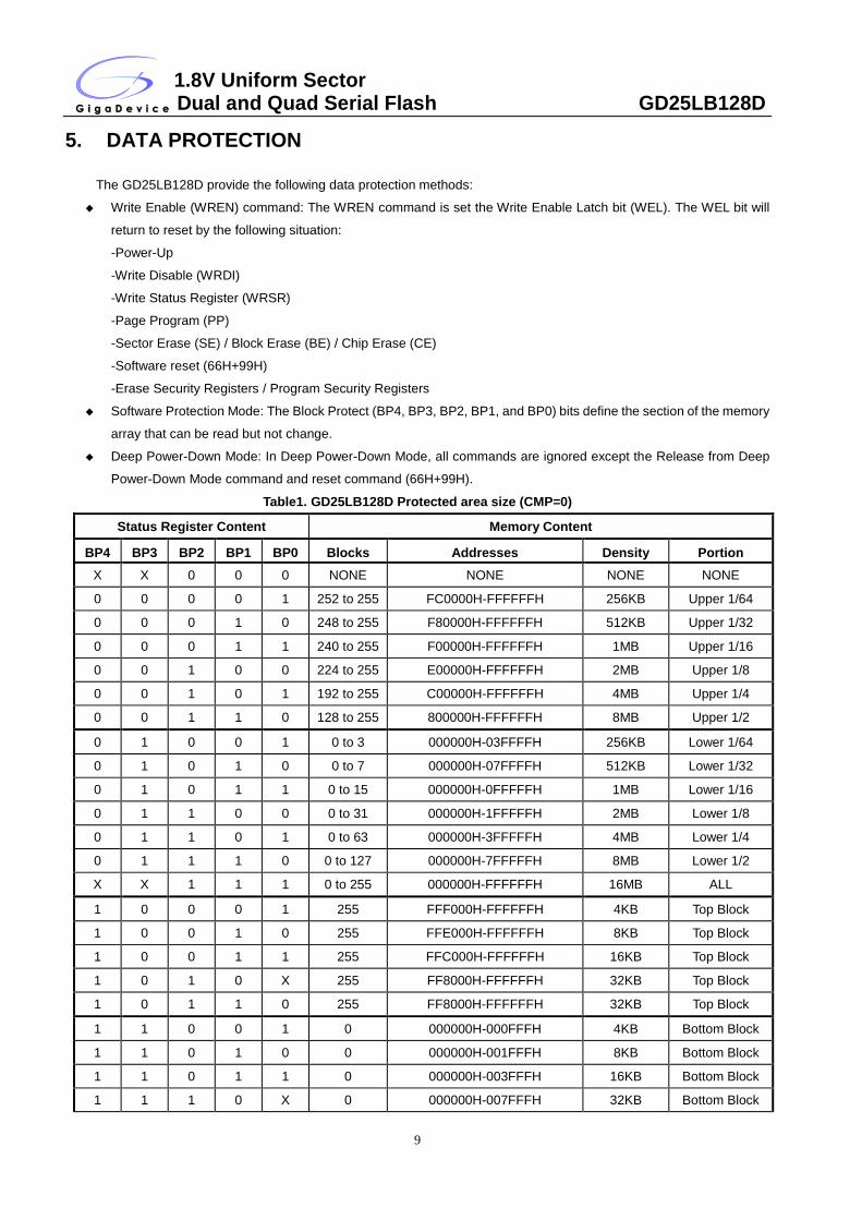
5. DATA PROTECTION
The GD25LB128D provide the following data protection methods:
◆ Write Enable (WREN) command: The WREN command is set the Write Enable Latch bit (WEL). The WEL bit will
return to reset by the following situation:
-Power-Up
-Write Disable (WRDI)
-Write Status Register (WRSR)
-Page Program (PP)
-Sector Erase (SE) / Block Erase (BE) / Chip Erase (CE)
-Software reset (66H+99H)
-Erase Security Registers / Program Security Registers
◆ Software Protection Mode: The Block Protect (BP4, BP3, BP2, BP1, and BP0) bits define the section of the memory
array that can be read but not change.
◆ Deep Power-Down Mode: In Deep Power-Down Mode, all commands are ignored except the Release from Deep
Power-Down Mode command and reset command (66H+99H).
Table1. GD25LB128D Protected area size (CMP=0)
Status Register Content Memory Content
BP4 BP3 BP2 BP1 BP0 Blocks Addresses Density Portion
X X 0 0 0 NONE NONE NONE NONE
0 0 0 0 1 252 to 255 FC0000H-FFFFFFH 256KB Upper 1/64
0 0 0 1 0 248 to 255 F80000H-FFFFFFH 512KB Upper 1/32
0 0 0 1 1 240 to 255 F00000H-FFFFFFH 1MB Upper 1/16
0 0 1 0 0 224 to 255 E00000H-FFFFFFH 2MB Upper 1/8
0 0 1 0 1 192 to 255 C00000H-FFFFFFH 4MB Upper 1/4
0 0 1 1 0 128 to 255 800000H-FFFFFFH 8MB Upper 1/2
0 1 0 0 1 0 to 3 000000H-03FFFFH 256KB Lower 1/64
0 1 0 1 0 0 to 7 000000H-07FFFFH 512KB Lower 1/32
0 1 0 1 1 0 to 15 000000H-0FFFFFH 1MB Lower 1/16
0 1 1 0 0 0 to 31 000000H-1FFFFFH 2MB Lower 1/8
0 1 1 0 1 0 to 63 000000H-3FFFFFH 4MB Lower 1/4
0 1 1 1 0 0 to 127 000000H-7FFFFFH 8MB Lower 1/2
X X 1 1 1 0 to 255 000000H-FFFFFFH 16MB ALL
1 0 0 0 1 255 FFF000H-FFFFFFH 4KB Top Block
1 0 0 1 0 255 FFE000H-FFFFFFH 8KB Top Block
1 0 0 1 1 255 FFC000H-FFFFFFH 16KB Top Block
1 0 1 0 X 255 FF8000H-FFFFFFH 32KB Top Block
1 0 1 1 0 255 FF8000H-FFFFFFH 32KB Top Block
1 1 0 0 1 0 000000H-000FFFH 4KB Bottom Block
1 1 0 1 0 0 000000H-001FFFH 8KB Bottom Block
1 1 0 1 1 0 000000H-003FFFH 16KB Bottom Block
1 1 1 0 X 0 000000H-007FFFH 32KB Bottom Block
1.8V Uniform Sector Dual and Quad Serial Flash GD25LB128D
10
1 1 1 1 0 0 000000H-007FFFH 32KB Bottom Block
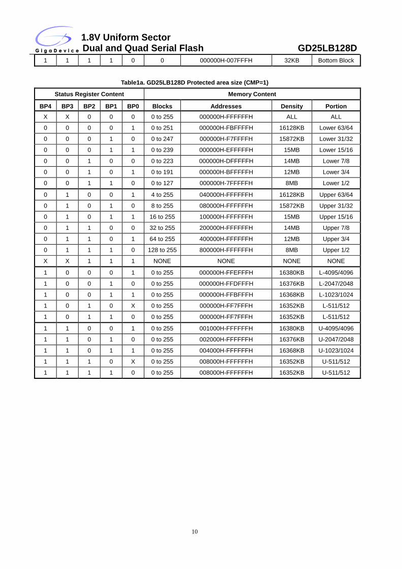
Table1a. GD25LB128D Protected area size (CMP=1)
Status Register Content Memory Content
BP4 BP3 BP2 BP1 BP0 Blocks Addresses Density Portion
X X 0 0 0 0 to 255 000000H-FFFFFFH ALL ALL
0 0 0 0 1 0 to 251 000000H-FBFFFFH 16128KB Lower 63/64
0 0 0 1 0 0 to 247 000000H-F7FFFFH 15872KB Lower 31/32
0 0 0 1 1 0 to 239 000000H-EFFFFFH 15MB Lower 15/16
0 0 1 0 0 0 to 223 000000H-DFFFFFH 14MB Lower 7/8
0 0 1 0 1 0 to 191 000000H-BFFFFFH 12MB Lower 3/4
0 0 1 1 0 0 to 127 000000H-7FFFFFH 8MB Lower 1/2
0 1 0 0 1 4 to 255 040000H-FFFFFFH 16128KB Upper 63/64
0 1 0 1 0 8 to 255 080000H-FFFFFFH 15872KB Upper 31/32
0 1 0 1 1 16 to 255 100000H-FFFFFFH 15MB Upper 15/16
0 1 1 0 0 32 to 255 200000H-FFFFFFH 14MB Upper 7/8
0 1 1 0 1 64 to 255 400000H-FFFFFFH 12MB Upper 3/4
0 1 1 1 0 128 to 255 800000H-FFFFFFH 8MB Upper 1/2
X X 1 1 1 NONE NONE NONE NONE
1 0 0 0 1 0 to 255 000000H-FFEFFFH 16380KB L-4095/4096
1 0 0 1 0 0 to 255 000000H-FFDFFFH 16376KB L-2047/2048
1 0 0 1 1 0 to 255 000000H-FFBFFFH 16368KB L-1023/1024
1 0 1 0 X 0 to 255 000000H-FF7FFFH 16352KB L-511/512
1 0 1 1 0 0 to 255 000000H-FF7FFFH 16352KB L-511/512
1 1 0 0 1 0 to 255 001000H-FFFFFFH 16380KB U-4095/4096
1 1 0 1 0 0 to 255 002000H-FFFFFFH 16376KB U-2047/2048
1 1 0 1 1 0 to 255 004000H-FFFFFFH 16368KB U-1023/1024
1 1 1 0 X 0 to 255 008000H-FFFFFFH 16352KB U-511/512
1 1 1 1 0 0 to 255 008000H-FFFFFFH 16352KB U-511/512
1.8V Uniform Sector Dual and Quad Serial Flash GD25LB128D
11
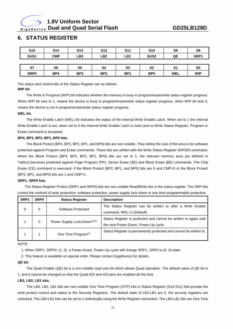
6. STATUS REGISTER
S15 S14 S13 S12 S11 S10 S9 S8
SUS1 CMP LB3 LB2 LB1 SUS2 QE SRP1
S7 S6 S5 S4 S3 S2 S1 S0
SRP0 BP4 BP3 BP2 BP1 BP0 WEL WIP
The status and control bits of the Status Register are as follows:
WIP bit.
The Write in Progress (WIP) bit indicates whether the memory is busy in program/erase/write status register progress.
When WIP bit sets to 1, means the device is busy in program/erase/write status register progress, when WIP bit sets 0,
means the device is not in program/erase/write status register progress.
WEL bit.
The Write Enable Latch (WEL) bit indicates the status of the internal Write Enable Latch. When set to 1 the internal
Write Enable Latch is set, when set to 0 the internal Write Enable Latch is reset and no Write Status Register, Program or
Erase command is accepted.
BP4, BP3, BP2, BP1, BP0 bits.
The Block Protect (BP4, BP3, BP2, BP1, and BP0) bits are non-volatile. They define the size of the area to be software
protected against Program and Erase commands. These bits are written with the Write Status Register (WRSR) command.
When the Block Protect (BP4, BP3, BP2, BP1, BP0) bits are set to 1, the relevant memory area (as defined in
Table1).becomes protected against Page Program (PP), Sector Erase (SE) and Block Erase (BE) commands. The Chip
Erase (CE) command is executed, if the Block Protect (BP2, BP1, and BP0) bits are 0 and CMP=0 or the Block Protect
(BP2, BP1, and BP0) bits are 1 and CMP=1.
SRP1, SRP0 bits.
The Status Register Protect (SRP1 and SRP0) bits are non-volatile Read/Write bits in the status register. The SRP bits
control the method of write protection: software protection, power supply lock-down or one time programmable protection.
SRP1 SRP0 Status Register Description
0 X Software Protected The Status Register can be written to after a Write Enable
command, WEL=1.(Default)
1 0 Power Supply Lock-Down(1)(2) Status Register is protected and cannot be written to again until
the next Power-Down, Power-Up cycle.
1 1 One Time Program(2) Status Register is permanently protected and cannot be written to.
NOTE:
1. When SRP1, SRP0= (1, 0), a Power-Down, Power-Up cycle will change SRP1, SRP0 to (0, 0) state.
2. This feature is available on special order. Please contact GigaDevice for details.
QE bit.
The Quad Enable (QE) bit is a non-volatile read only bit which allows Quad operation. The default value of QE bit is
1, and it cannot be changed so that the Quad IO2 and IO3 pins are enabled all the time.
LB3, LB2, LB1 bits.
The LB3, LB2, LB1 bits are non-volatile One Time Program (OTP) bits in Status Register (S13-S11) that provide the
write protect control and status to the Security Registers. The default state of LB3-LB1 are 0, the security registers are
unlocked. The LB3-LB1 bits can be set to 1 individually using the Write Register instruction. The LB3-LB1 bits are One Time

1.8V Uniform Sector Dual and Quad Serial Flash GD25LB128D
12
Programmable, once they are set to 1, the Security Registers will become read-only permanently.
CMP bit
The CMP bit is a non-volatile Read/Write bit in the Status Register (S14). It is used in conjunction with the BP4-BP0
bits to provide more flexibility for the array protection. Please see the Status registers Memory Protection table for details.
The default setting is CMP=0.
SUS1, SUS2 bits
The SUS1 and SUS2 bits are read only bit in the status register (S15 and S10) that are set to 1 after executing an
Program/Erase Suspend (75H) command (The Erase Suspend will set the SUS1 to 1,and the Program Suspend will set the
SUS2 to 1). The SUS1 and SUS2 bit are cleared to 0 by Program/Erase Resume (7AH) command as well as a power-down,
power-up cycle.
1.8V Uniform Sector Dual and Quad Serial Flash GD25LB128D
13
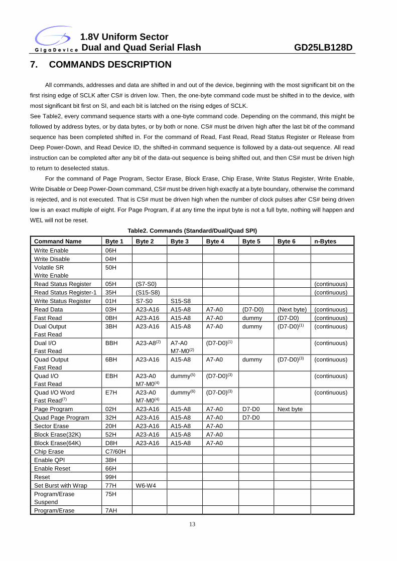
7. COMMANDS DESCRIPTION
All commands, addresses and data are shifted in and out of the device, beginning with the most significant bit on the
first rising edge of SCLK after CS# is driven low. Then, the one-byte command code must be shifted in to the device, with
most significant bit first on SI, and each bit is latched on the rising edges of SCLK.
See Table2, every command sequence starts with a one-byte command code. Depending on the command, this might be
followed by address bytes, or by data bytes, or by both or none. CS# must be driven high after the last bit of the command
sequence has been completed shifted in. For the command of Read, Fast Read, Read Status Register or Release from
Deep Power-Down, and Read Device ID, the shifted-in command sequence is followed by a data-out sequence. All read
instruction can be completed after any bit of the data-out sequence is being shifted out, and then CS# must be driven high
to return to deselected status.
For the command of Page Program, Sector Erase, Block Erase, Chip Erase, Write Status Register, Write Enable,
Write Disable or Deep Power-Down command, CS# must be driven high exactly at a byte boundary, otherwise the command
is rejected, and is not executed. That is CS# must be driven high when the number of clock pulses after CS# being driven
low is an exact multiple of eight. For Page Program, if at any time the input byte is not a full byte, nothing will happen and
WEL will not be reset.
Table2. Commands (Standard/Dual/Quad SPI)
Command Name Byte 1 Byte 2 Byte 3 Byte 4 Byte 5 Byte 6 n-Bytes
Write Enable 06H
Write Disable 04H
Volatile SR
Write Enable
50H
Read Status Register 05H (S7-S0) (continuous)
Read Status Register-1 35H (S15-S8) (continuous)
Write Status Register 01H S7-S0 S15-S8
Read Data 03H A23-A16 A15-A8 A7-A0 (D7-D0) (Next byte) (continuous)
Fast Read 0BH A23-A16 A15-A8 A7-A0 dummy (D7-D0) (continuous)
Dual Output
Fast Read
3BH A23-A16 A15-A8 A7-A0 dummy (D7-D0)(1) (continuous)
Dual I/O
Fast Read
BBH A23-A8(2) A7-A0
M7-M0(2)
(D7-D0)(1) (continuous)
Quad Output
Fast Read
6BH A23-A16 A15-A8 A7-A0 dummy (D7-D0)(3) (continuous)
Quad I/O
Fast Read
EBH A23-A0
M7-M0(4)
dummy(5) (D7-D0)(3) (continuous)
Quad I/O Word
Fast Read(7)
E7H A23-A0
M7-M0(4)
dummy(6) (D7-D0)(3) (continuous)
Page Program 02H A23-A16 A15-A8 A7-A0 D7-D0 Next byte
Quad Page Program 32H A23-A16 A15-A8 A7-A0 D7-D0
Sector Erase 20H A23-A16 A15-A8 A7-A0
Block Erase(32K) 52H A23-A16 A15-A8 A7-A0
Block Erase(64K) D8H A23-A16 A15-A8 A7-A0
Chip Erase C7/60H
Enable QPI 38H
Enable Reset 66H
Reset 99H
Set Burst with Wrap 77H W6-W4
Program/Erase
Suspend
75H
Program/Erase 7AH
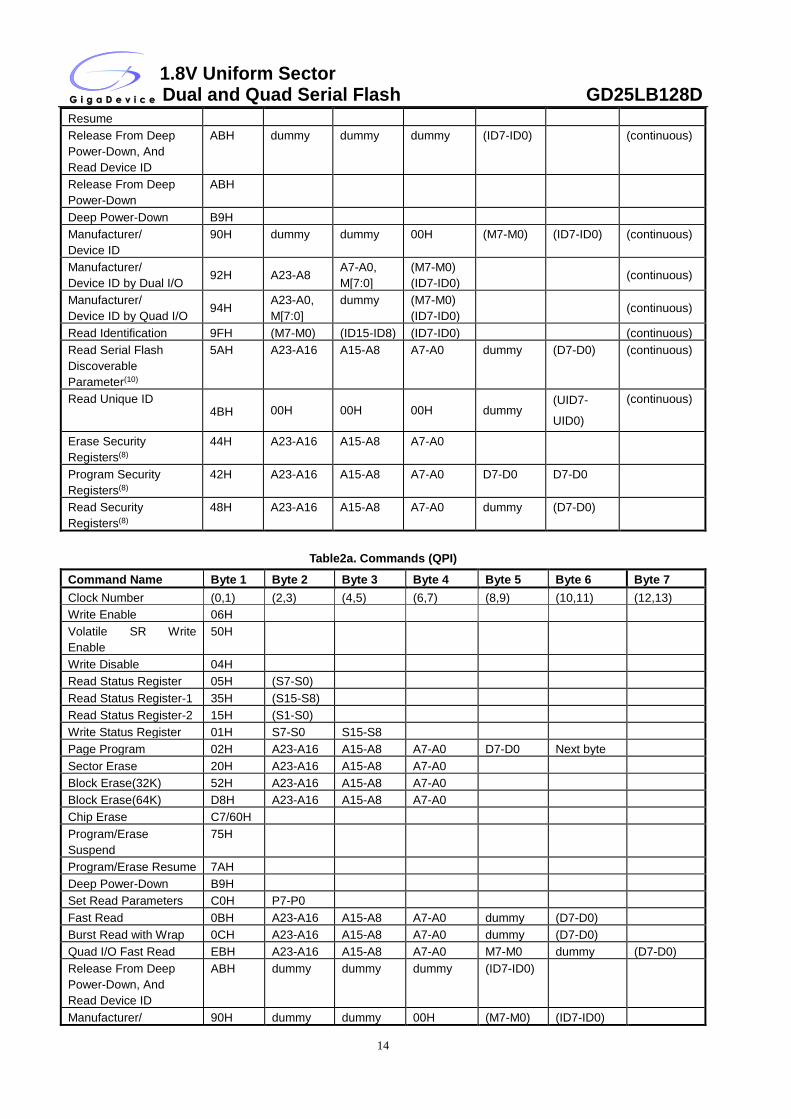
1.8V Uniform Sector Dual and Quad Serial Flash GD25LB128D
14
Resume
Release From Deep
Power-Down, And
Read Device ID
ABH dummy dummy dummy (ID7-ID0) (continuous)
Release From Deep
Power-Down
ABH
Deep Power-Down B9H
Manufacturer/
Device ID
90H dummy dummy 00H (M7-M0) (ID7-ID0) (continuous)
Manufacturer/
Device ID by Dual I/O 92H A23-A8
A7-A0,
M[7:0]
(M7-M0)
(ID7-ID0) (continuous)
Manufacturer/
Device ID by Quad I/O 94H
A23-A0,
M[7:0]
dummy (M7-M0)
(ID7-ID0) (continuous)
Read Identification 9FH (M7-M0) (ID15-ID8) (ID7-ID0) (continuous)
Read Serial Flash
Discoverable
Parameter(10)
5AH A23-A16 A15-A8 A7-A0 dummy (D7-D0) (continuous)
Read Unique ID 4BH 00H 00H 00H dummy
(UID7-
UID0)
(continuous)
Erase Security
Registers(8)
44H A23-A16 A15-A8 A7-A0
Program Security
Registers(8)
42H A23-A16 A15-A8 A7-A0 D7-D0 D7-D0
Read Security
Registers(8)
48H A23-A16 A15-A8 A7-A0 dummy (D7-D0)
Table2a. Commands (QPI)
Command Name Byte 1 Byte 2 Byte 3 Byte 4 Byte 5 Byte 6 Byte 7
Clock Number (0,1) (2,3) (4,5) (6,7) (8,9) (10,11) (12,13)
Write Enable 06H
Volatile SR Write
Enable
50H
Write Disable 04H
Read Status Register 05H (S7-S0)
Read Status Register-1 35H (S15-S8)
Read Status Register-2 15H (S1-S0)
Write Status Register 01H S7-S0 S15-S8
Page Program 02H A23-A16 A15-A8 A7-A0 D7-D0 Next byte
Sector Erase 20H A23-A16 A15-A8 A7-A0
Block Erase(32K) 52H A23-A16 A15-A8 A7-A0
Block Erase(64K) D8H A23-A16 A15-A8 A7-A0
Chip Erase C7/60H
Program/Erase
Suspend
75H
Program/Erase Resume 7AH
Deep Power-Down B9H
Set Read Parameters C0H P7-P0
Fast Read 0BH A23-A16 A15-A8 A7-A0 dummy (D7-D0)
Burst Read with Wrap 0CH A23-A16 A15-A8 A7-A0 dummy (D7-D0)
Quad I/O Fast Read EBH A23-A16 A15-A8 A7-A0 M7-M0 dummy (D7-D0)
Release From Deep
Power-Down, And
Read Device ID
ABH dummy dummy dummy (ID7-ID0)
Manufacturer/ 90H dummy dummy 00H (M7-M0) (ID7-ID0)
1.8V Uniform Sector Dual and Quad Serial Flash GD25LB128D
15
Device ID
Read Identification 9FH (M7-M0) (ID15-ID8) (ID7-ID0)
Read Serial Flash
Discoverable
Parameter(10)
5AH A23-A16 A15-A8 A7-A0 dummy (D7-D0)
Disable QPI FFH
Enable Reset 66H
Reset 99H
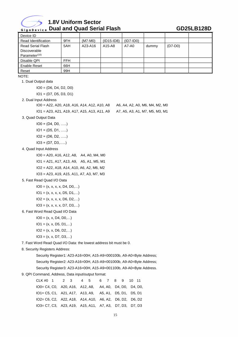
NOTE:
1. Dual Output data
IO0 = (D6, D4, D2, D0)
IO1 = (D7, D5, D3, D1)
2. Dual Input Address
IO0 = A22, A20, A18, A16, A14, A12, A10, A8 A6, A4, A2, A0, M6, M4, M2, M0
IO1 = A23, A21, A19, A17, A15, A13, A11, A9 A7, A5, A3, A1, M7, M5, M3, M1
3. Quad Output Data
IO0 = (D4, D0, …..)
IO1 = (D5, D1, …..)
IO2 = (D6, D2, …..)
IO3 = (D7, D3,…..)
4. Quad Input Address
IO0 = A20, A16, A12, A8, A4, A0, M4, M0
IO1 = A21, A17, A13, A9, A5, A1, M5, M1
IO2 = A22, A18, A14, A10, A6, A2, M6, M2
IO3 = A23, A19, A15, A11, A7, A3, M7, M3
5. Fast Read Quad I/O Data
IO0 = (x, x, x, x, D4, D0,…)
IO1 = (x, x, x, x, D5, D1,…)
IO2 = (x, x, x, x, D6, D2,…)
IO3 = (x, x, x, x, D7, D3,…)
6. Fast Word Read Quad I/O Data
IO0 = (x, x, D4, D0,…)
IO1 = (x, x, D5, D1,…)
IO2 = (x, x, D6, D2,…)
IO3 = (x, x, D7, D3,…)
7. Fast Word Read Quad I/O Data: the lowest address bit must be 0.
8. Security Registers Address:
Security Register1: A23-A16=00H, A15-A9=000100b, A9-A0=Byte Address;
Security Register2: A23-A16=00H, A15-A9=001000b, A9-A0=Byte Address;
Security Register3: A23-A16=00H, A15-A9=001100b, A9-A0=Byte Address.
9. QPI Command, Address, Data input/output format:
CLK #0 1 2 3 4 5 6 7 8 9 10 11
IO0= C4, C0, A20, A16, A12, A8, A4, A0, D4, D0, D4, D0,
IO1= C5, C1, A21, A17, A13, A9, A5, A1, D5, D1, D5, D1
IO2= C6, C2, A22, A18, A14, A10, A6, A2, D6, D2, D6, D2
IO3= C7, C3, A23, A19, A15, A11, A7, A3, D7, D3, D7, D3
1.8V Uniform Sector Dual and Quad Serial Flash GD25LB128D
16
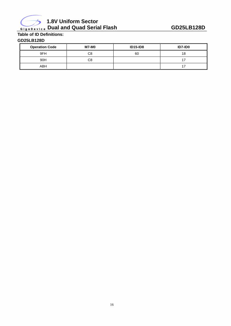
Table of ID Definitions:
GD25LB128D
Operation Code M7-M0 ID15-ID8 ID7-ID0
9FH C8 60 18
90H C8 17
ABH 17
1.8V Uniform Sector Dual and Quad Serial Flash GD25LB128D
17
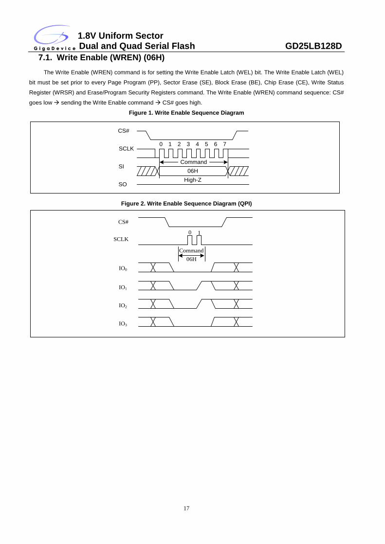
7.1. Write Enable (WREN) (06H)
The Write Enable (WREN) command is for setting the Write Enable Latch (WEL) bit. The Write Enable Latch (WEL)
bit must be set prior to every Page Program (PP), Sector Erase (SE), Block Erase (BE), Chip Erase (CE), Write Status
Register (WRSR) and Erase/Program Security Registers command. The Write Enable (WREN) command sequence: CS#
goes low sending the Write Enable command CS# goes high.
Figure 1. Write Enable Sequence Diagram
Command
0 1 2 3 4 5 6 7
06H
CS#
SCLK
SI
SOHigh-Z
Figure 2. Write Enable Sequence Diagram (QPI)
CS#
SCLK
IO0
IO1
IO2
IO3
0 1
Command
06H
1.8V Uniform Sector Dual and Quad Serial Flash GD25LB128D
18
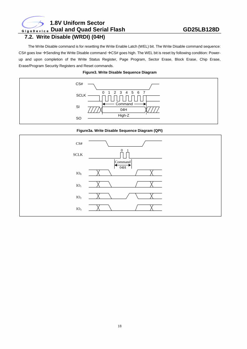
7.2. Write Disable (WRDI) (04H)
The Write Disable command is for resetting the Write Enable Latch (WEL) bit. The Write Disable command sequence:
CS# goes low Sending the Write Disable command CS# goes high. The WEL bit is reset by following condition: Power-
up and upon completion of the Write Status Register, Page Program, Sector Erase, Block Erase, Chip Erase,
Erase/Program Security Registers and Reset commands.
Figure3. Write Disable Sequence Diagram
Command
0 1 2 3 4 5 6 7
04H
CS#
SCLK
SI
SOHigh-Z
Figure3a. Write Disable Sequence Diagram (QPI)
CS#
SCLK
IO0
IO1
IO2
IO3
0 1
Command
04H
1.8V Uniform Sector Dual and Quad Serial Flash GD25LB128D
19
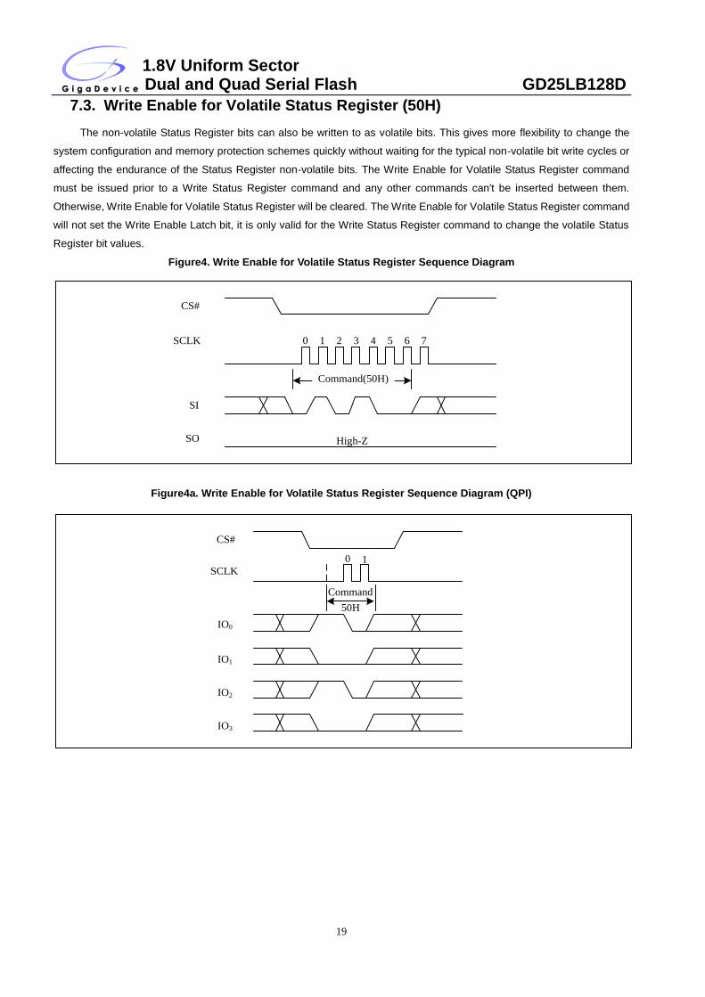
7.3. Write Enable for Volatile Status Register (50H)
The non-volatile Status Register bits can also be written to as volatile bits. This gives more flexibility to change the
system configuration and memory protection schemes quickly without waiting for the typical non-volatile bit write cycles or
affecting the endurance of the Status Register non-volatile bits. The Write Enable for Volatile Status Register command
must be issued prior to a Write Status Register command and any other commands can't be inserted between them.
Otherwise, Write Enable for Volatile Status Register will be cleared. The Write Enable for Volatile Status Register command
will not set the Write Enable Latch bit, it is only valid for the Write Status Register command to change the volatile Status
Register bit values.
Figure4. Write Enable for Volatile Status Register Sequence Diagram
CS#
SCLK
Command(50H)
SI
SO
0 1 2 3 4 5 6 7
High-Z
Figure4a. Write Enable for Volatile Status Register Sequence Diagram (QPI)
CS#
SCLK
IO0
IO1
IO2
IO3
0 1
Command
50H
1.8V Uniform Sector Dual and Quad Serial Flash GD25LB128D
20
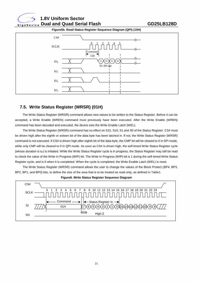
7.4. Read Status Register (RDSR) (05H or 35H or 15H)
The Read Status Register (RDSR) command is for reading the Status Register. The Status Register may be read at
any time, even while a Program, Erase or Write Status Register cycle is in progress. When one of these cycles is in progress,
it is recommended to check the Write in Progress (WIP) bit before sending a new command to the device. It is also possible
to read the Status Register continuously. For command code “05H” / “35H”, the SO will output Status Register bits S7~S0
/ S15-S8. The command code “15H” only supports the QPI mode, the I/O0 will output Status Register S1-S0. (For 120MHz
Frequency, the 15H will better than 05H to check the WIP bit)
Figure5. Read Status Register Sequence Diagram
Command
0 1 2 3 4 5 6 7
05H or 35H
CS#
SCLK
SI
SO High-Z
8 9 10 11 12 13 14 15
7 6 5 4 3 2 1 0 7 6 5 4 3 2 1 0 7
MSB
S7~S0 or S15~S8 out S7~S0 or S15~S8 out
MSB
Figure5a. Read Status Register Sequence Diagram (QPI)
CS#
SCLK
IO0
IO1
IO2
IO3
0 1 2 3 4 5
Command
05H or 35H
4 40 0
5 51 1
4
5
6 2 6 2 6
7 3 7 3 7
S7-S0 or S15-S8 out
1.8V Uniform Sector Dual and Quad Serial Flash GD25LB128D
21
Figure5b. Read Status Register Sequence Diagram (QPI) (15H)
CS#
SCLK
IO0
IO1
IO2
IO3
0 1 2 3 4 5
Command
15H
S1 S1S0 S0
S1-S0 out
7.5. Write Status Register (WRSR) (01H)
The Write Status Register (WRSR) command allows new values to be written to the Status Register. Before it can be
accepted, a Write Enable (WREN) command must previously have been executed. After the Write Enable (WREN)
command has been decoded and executed, the device sets the Write Enable Latch (WEL).
The Write Status Register (WRSR) command has no effect on S15, S10, S1 and S0 of the Status Register. CS# must
be driven high after the eighth or sixteen bit of the data byte has been latched in. If not, the Write Status Register (WRSR)
command is not executed. If CS# is driven high after eighth bit of the data byte, the CMP bit will be cleared to 0 in SPI mode,
while only CMP will be cleared to 0 in QPI mode. As soon as CS# is driven high, the self-timed Write Status Register cycle
(whose duration is tW) is initiated. While the Write Status Register cycle is in progress, the Status Register may still be read
to check the value of the Write In Progress (WIP) bit. The Write In Progress (WIP) bit is 1 during the self-timed Write Status
Register cycle, and is 0 when it is completed. When the cycle is completed, the Write Enable Latch (WEL) is reset.
The Write Status Register (WRSR) command allows the user to change the values of the Block Protect (BP4, BP3,
BP2, BP1, and BP0) bits, to define the size of the area that is to be treated as read-only, as defined in Table1.
Figure6. Write Status Register Sequence Diagram
Command
0 1 2 3 4 5 6 7
01H
CS#
SCLK
SI
SO High-Z
8 9 10 11 12 13 14 15
MSB
7 6 5 4 3 2 1 0
Status Register in
16 17 18 19 20 21 22 23
15 14 13 12 11 10 9 8
1.8V Uniform Sector Dual and Quad Serial Flash GD25LB128D
22
Figure6a. Write Status Register Sequence Diagram (QPI)
CS#
SCLK
IO0
IO1
IO2
IO3
0 1 2 3 4 5
Command
01H
4 120 8
5 131 9
14 10
7 3 15 11
Status Register in
6 2
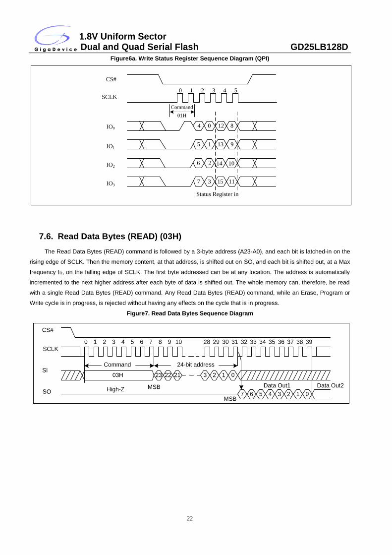
7.6. Read Data Bytes (READ) (03H)
The Read Data Bytes (READ) command is followed by a 3-byte address (A23-A0), and each bit is latched-in on the
rising edge of SCLK. Then the memory content, at that address, is shifted out on SO, and each bit is shifted out, at a Max
frequency fR, on the falling edge of SCLK. The first byte addressed can be at any location. The address is automatically
incremented to the next higher address after each byte of data is shifted out. The whole memory can, therefore, be read
with a single Read Data Bytes (READ) command. Any Read Data Bytes (READ) command, while an Erase, Program or
Write cycle is in progress, is rejected without having any effects on the cycle that is in progress.
Figure7. Read Data Bytes Sequence Diagram
Command
0 1 2 3 4 5 6 7
03H
CS#
SCLK
SI
SO High-Z
8 9 10 28 29 30 31 32
MSB
3 2 1 0
34 35 36 3733
23 22 21
7 6 5 4 3 2 1 0
38 39
24-bit address
MSB
Data Out1 Data Out2
1.8V Uniform Sector Dual and Quad Serial Flash GD25LB128D
23
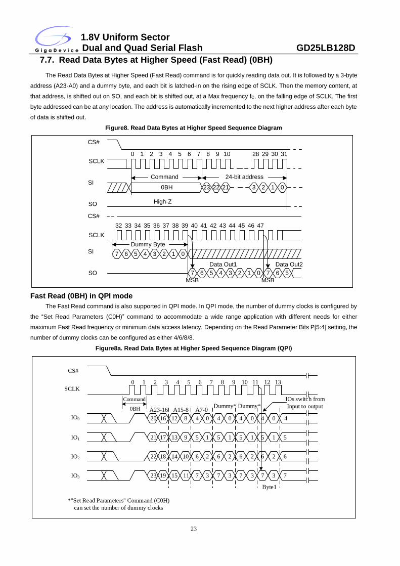
7.7. Read Data Bytes at Higher Speed (Fast Read) (0BH)
The Read Data Bytes at Higher Speed (Fast Read) command is for quickly reading data out. It is followed by a 3-byte
address (A23-A0) and a dummy byte, and each bit is latched-in on the rising edge of SCLK. Then the memory content, at
that address, is shifted out on SO, and each bit is shifted out, at a Max frequency fC, on the falling edge of SCLK. The first
byte addressed can be at any location. The address is automatically incremented to the next higher address after each byte
of data is shifted out.
Figure8. Read Data Bytes at Higher Speed Sequence Diagram
Command
0 1 2 3 4 5 6 7
0BH
CS#
SCLK
SI
SO High-Z
8 9 10 28 29 30 31
3 2 1 023 22 21
24-bit address
MSB
34 35 36 3733
6 5 4 3 2 1 0
38 39
Data Out1
32 42 43 44 4541 46 4740
7
6 5 4 3 2 1 07
6 57
Data Out2
CS#
SCLK
SI
SO
MSB
Dummy Byte
Fast Read (0BH) in QPI mode
The Fast Read command is also supported in QPI mode. In QPI mode, the number of dummy clocks is configured by
the “Set Read Parameters (C0H)” command to accommodate a wide range application with different needs for either
maximum Fast Read frequency or minimum data access latency. Depending on the Read Parameter Bits P[5:4] setting, the
number of dummy clocks can be configured as either 4/6/8/8.
Figure8a. Read Data Bytes at Higher Speed Sequence Diagram (QPI)
CS#
SCLK
IO0
IO1
IO2
IO3
0 1 2 3 4 5
Command
0BH
20 1216 8
6 7 8 9 10
4 40 0 4 0 4 0 4
21 1317 9 5 51 1 5 1 5 1 5
22 1418 10 6 62 2 6 2 6 2 6
23 1519 11 7 73 3 7 3 7 3 7
A23-16 A15-8 A7-0Dummy*
11 12 13
IOs switch from
Input to output
Byte1
*"Set Read Parameters" Command (C0H)
can set the number of dummy clocks
Dummy*
1.8V Uniform Sector Dual and Quad Serial Flash GD25LB128D
24
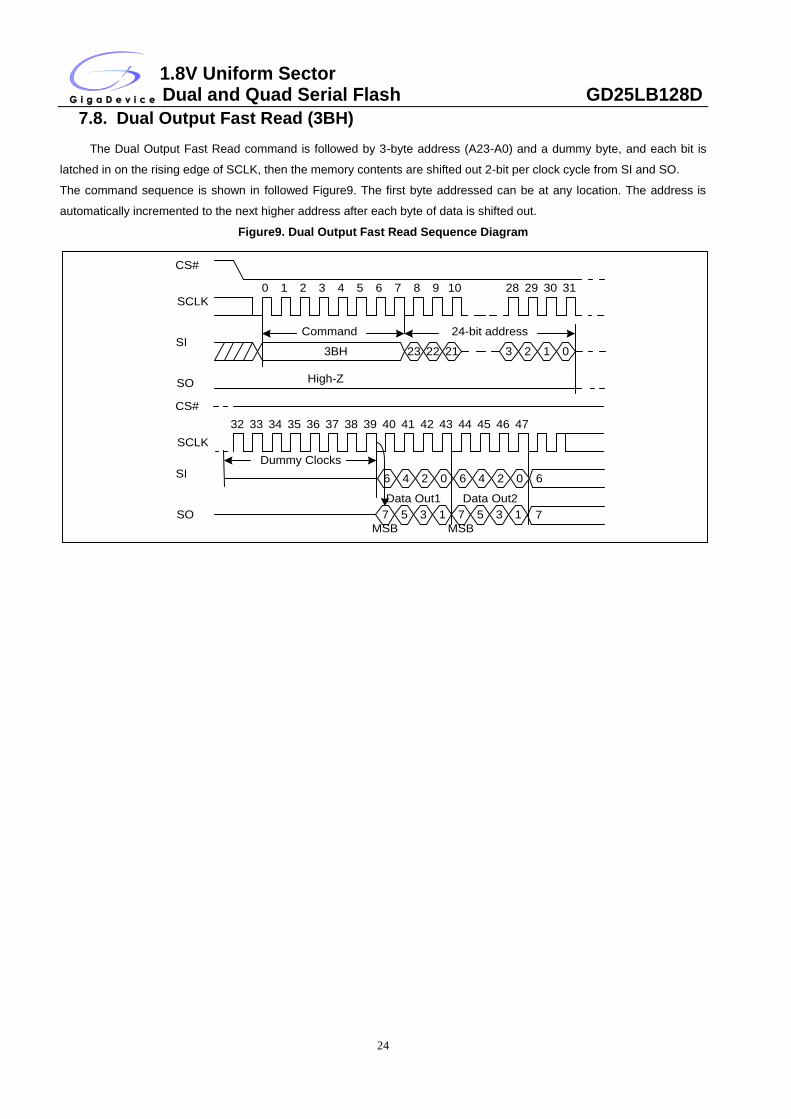
7.8. Dual Output Fast Read (3BH)
The Dual Output Fast Read command is followed by 3-byte address (A23-A0) and a dummy byte, and each bit is
latched in on the rising edge of SCLK, then the memory contents are shifted out 2-bit per clock cycle from SI and SO.
The command sequence is shown in followed Figure9. The first byte addressed can be at any location. The address is
automatically incremented to the next higher address after each byte of data is shifted out.
Figure9. Dual Output Fast Read Sequence Diagram
Command
0 1 2 3 4 5 6 7
3BH
CS#
SCLK
SI
SO High-Z
8 9 10 28 29 30 31
3 2 1 023 22 21
24-bit address
MSB
34 35 36 3733
5 3 1 7 5 3 1
38 39
Data Out1
32 42 43 44 4541 46 4740
7
Data Out2
CS#
SCLK
SI
SO
MSB
Dummy Clocks
4 2 0 6 4 2 06 6
7
1.8V Uniform Sector Dual and Quad Serial Flash GD25LB128D
25
7.9. Quad Output Fast Read (6BH)
The Quad Output Fast Read command is followed by 3-byte address (A23-A0) and a dummy byte, and each bit is
latched in on the rising edge of SCLK, then the memory contents are shifted out 4-bit per clock cycle from IO3, IO2, IO1
and IO0. The command sequence is shown in followed Figure10. The first byte addressed can be at any location. The
address is automatically incremented to the next higher address after each byte of data is shifted out.
Figure10. Quad Output Fast Read Sequence Diagram
7.10. Dual I/O Fast Read (BBH)
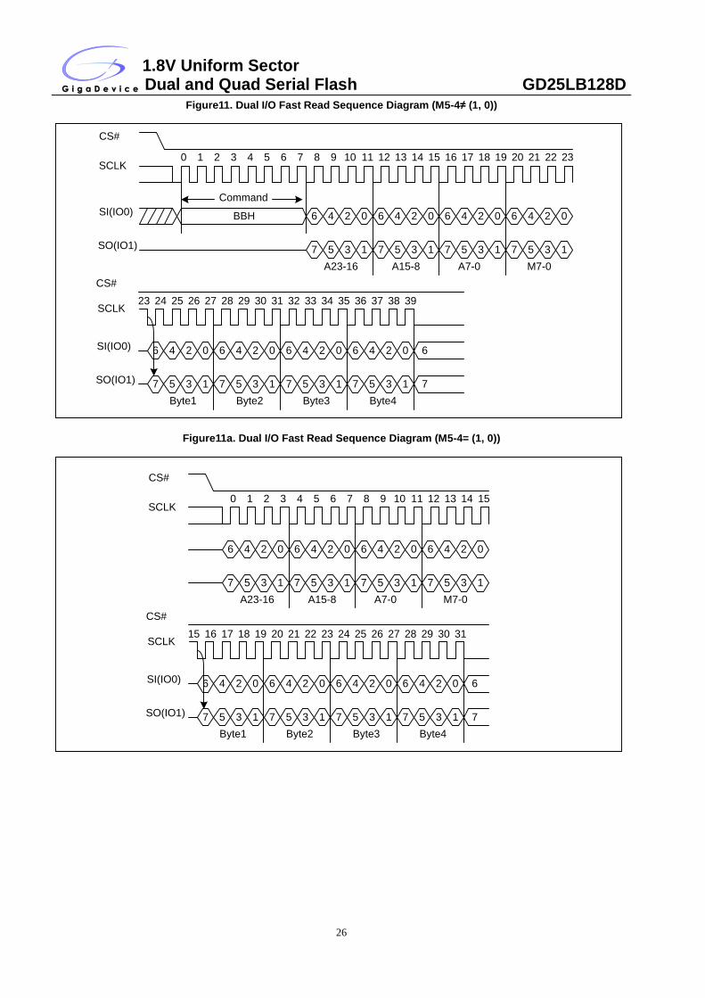
The Dual I/O Fast Read command is similar to the Dual Output Fast Read command but with the capability to input
the 3-byte address (A23-0) and a “Continuous Read Mode” byte 2-bit per clock by SI and SO, and each bit is latched in on
the rising edge of SCLK, then the memory contents are shifted out 2-bit per clock cycle from SI and SO. The command
sequence is shown in followed Figure11. The first byte addressed can be at any location. The address is automatically
incremented to the next higher address after each byte of data is shifted out.
Dual I/O Fast Read with “Continuous Read Mode”
The Dual I/O Fast Read command can further reduce command overhead through setting the “Continuous Read Mode”
bits (M7-0) after the input 3-byte address (A23-A0). If the “Continuous Read Mode” bits (M5-4) = (1, 0), then the next Dual
I/O Fast Read command (after CS# is raised and then lowered) does not require the BBH command code. The command
sequence is shown in followed Figure11. If the “Continuous Read Mode” bits (M5-4) do not equal (1, 0), the next command
requires the first BBH command code, thus returning to normal operation. A “Continuous Read Mode” Reset command can
be used to reset (M5-4) before issuing normal command.
Command
0 1 2 3 4 5 6 7
6BH
CS#
SCLK
IO0
IO1 High-Z
8 9 10 28 29 30 31
3 2 1 023 22 21
24-bit address
34 35 36 3733
1 5 1 5 1 5 1
38 39
Byte1
32 42 43 44 4541 46 4740
5
Dummy Clocks
0 4 0 4 0 4 04 4
5
IO2 High-Z
IO3 High-Z
CS#
SCLK
IO0
IO1
2 6 2 6 2 6 26 6
3 7 3 7 3 7 37 7
Byte2 Byte3 Byte4
IO2
IO3
1.8V Uniform Sector Dual and Quad Serial Flash GD25LB128D
26
Figure11. Dual I/O Fast Read Sequence Diagram (M5-4≠ (1, 0))
Command
0 1 2 3 4 5 6 7
BBH
CS#
SCLK
SI(IO0)
SO(IO1)
8 9 10 11 12 13 14 15
6 4 2 0 6 4 2 0
16 17 18 19 20 21 22 23
6 4 2 0 6 4 2 0
7 5 3 1 7 5 3 1 7 5 3 1 7 5 3 1
A23-16 A15-8 A7-0 M7-0
CS#
23 24 25 26 27 28 29 30 31 32 33 34 35 36 37 38 39
SI(IO0)
SO(IO1)
6 4 2 0 6 4 2 0 6 4 2 0 6 4 2 0
7 5 3 1 7 5 3 1 7 5 3 1 7 5 3 1
SCLK
6
7
Byte1 Byte2 Byte3 Byte4
Figure11a. Dual I/O Fast Read Sequence Diagram (M5-4= (1, 0))
0 1 2 3 4 5 6 7
CS#
SCLK8 9 10 11 12 13 14 15
6 4 2 0 6 4 2 0 6 4 2 0 6 4 2 0
7 5 3 1 7 5 3 1 7 5 3 1 7 5 3 1
A23-16 A15-8 A7-0 M7-0
CS#
23 24 25 26 27 28 29 30 31
SI(IO0)
SO(IO1)
6 4 2 0 6 4 2 0 6 4 2 0 6 4 2 0
7 5 3 1 7 5 3 1 7 5 3 1 7 5 3 1
SCLK
6
7
Byte1 Byte2 Byte3 Byte4
15 16 17 18 19 20 21 22
1.8V Uniform Sector Dual and Quad Serial Flash GD25LB128D
27
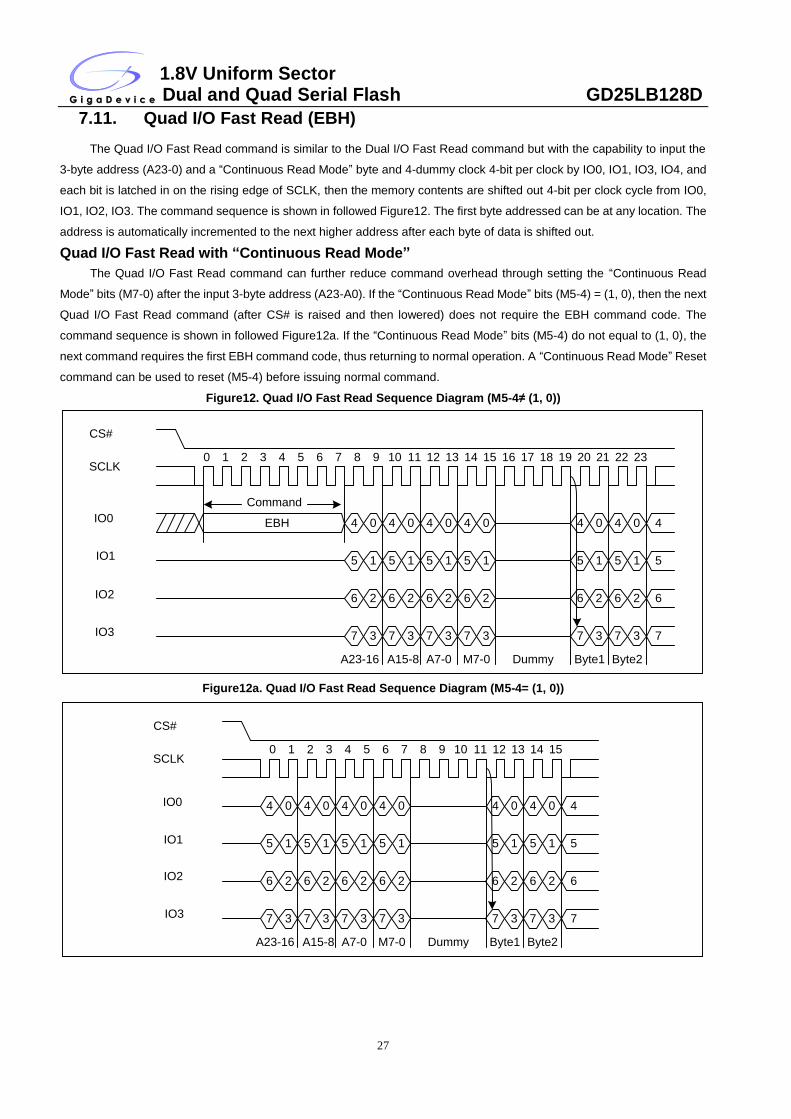
7.11. Quad I/O Fast Read (EBH)
The Quad I/O Fast Read command is similar to the Dual I/O Fast Read command but with the capability to input the
3-byte address (A23-0) and a “Continuous Read Mode” byte and 4-dummy clock 4-bit per clock by IO0, IO1, IO3, IO4, and
each bit is latched in on the rising edge of SCLK, then the memory contents are shifted out 4-bit per clock cycle from IO0,
IO1, IO2, IO3. The command sequence is shown in followed Figure12. The first byte addressed can be at any location. The
address is automatically incremented to the next higher address after each byte of data is shifted out.
Quad I/O Fast Read with “Continuous Read Mode”
The Quad I/O Fast Read command can further reduce command overhead through setting the “Continuous Read
Mode” bits (M7-0) after the input 3-byte address (A23-A0). If the “Continuous Read Mode” bits (M5-4) = (1, 0), then the next
Quad I/O Fast Read command (after CS# is raised and then lowered) does not require the EBH command code. The
command sequence is shown in followed Figure12a. If the “Continuous Read Mode” bits (M5-4) do not equal to (1, 0), the
next command requires the first EBH command code, thus returning to normal operation. A “Continuous Read Mode” Reset
command can be used to reset (M5-4) before issuing normal command.
Figure12. Quad I/O Fast Read Sequence Diagram (M5-4≠ (1, 0))
Figure12a. Quad I/O Fast Read Sequence Diagram (M5-4= (1, 0))
Command
0 1 2 3 4 5 6 7
EBH
CS#
SCLK
IO0
IO1
8 9 10 11 12 13 14 15
4 0 4 0 4 0 4 0
16 17 18 19 20 21 22 23
4 0 4 0
5 1 5 1 5 1 5 1 5 1 5 1
A23-16 A15-8 A7-0 M7-0
6 2 6 2 6 2 6 2 6 2 6 2
7 3 7 3 7 3 7 3 7 3 7 3
IO2
IO3
4
5
6
7
Dummy Byte1 Byte2
0 1 2 3 4 5 6 7
CS#
SCLK8 9 10 11 12 13 14 15
IO0
IO1
IO2
IO3
4 0 4 0
5 1 5 1
6 2 6 2
7 3 7 3
4 0 4 0
5 1 5 1
6 2 6 2
7 3 7 3
4 0 4 0
5 1 5 1
6 2 6 2
7 3 7 3
4
5
6
7
A23-16 A15-8 A7-0 M7-0 Dummy Byte1 Byte2
1.8V Uniform Sector Dual and Quad Serial Flash GD25LB128D
28
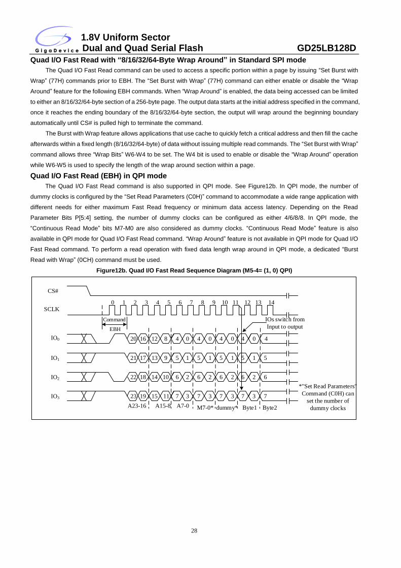
Quad I/O Fast Read with “8/16/32/64-Byte Wrap Around” in Standard SPI mode
The Quad I/O Fast Read command can be used to access a specific portion within a page by issuing “Set Burst with
Wrap” (77H) commands prior to EBH. The “Set Burst with Wrap” (77H) command can either enable or disable the “Wrap
Around” feature for the following EBH commands. When “Wrap Around” is enabled, the data being accessed can be limited
to either an 8/16/32/64-byte section of a 256-byte page. The output data starts at the initial address specified in the command,
once it reaches the ending boundary of the 8/16/32/64-byte section, the output will wrap around the beginning boundary
automatically until CS# is pulled high to terminate the command.
The Burst with Wrap feature allows applications that use cache to quickly fetch a critical address and then fill the cache
afterwards within a fixed length (8/16/32/64-byte) of data without issuing multiple read commands. The “Set Burst with Wrap”
command allows three “Wrap Bits” W6-W4 to be set. The W4 bit is used to enable or disable the “Wrap Around” operation
while W6-W5 is used to specify the length of the wrap around section within a page.
Quad I/O Fast Read (EBH) in QPI mode
The Quad I/O Fast Read command is also supported in QPI mode. See Figure12b. In QPI mode, the number of
dummy clocks is configured by the “Set Read Parameters (C0H)” command to accommodate a wide range application with
different needs for either maximum Fast Read frequency or minimum data access latency. Depending on the Read
Parameter Bits P[5:4] setting, the number of dummy clocks can be configured as either 4/6/8/8. In QPI mode, the
“Continuous Read Mode” bits M7-M0 are also considered as dummy clocks. “Continuous Read Mode” feature is also
available in QPI mode for Quad I/O Fast Read command. “Wrap Around” feature is not available in QPI mode for Quad I/O
Fast Read command. To perform a read operation with fixed data length wrap around in QPI mode, a dedicated “Burst
Read with Wrap” (0CH) command must be used.
Figure12b. Quad I/O Fast Read Sequence Diagram (M5-4= (1, 0) QPI)
CS#
SCLK
IO0
IO1
IO2
IO3
0 1 2 3 4 5
Command
EBH
20 1216 8
6 7 8 9 10
4 40 0 4 0 4 0 4
21 1317 9 5 51 1 5 1 5 1 5
22 1418 10 6 62 2 6 2 6 2 6
23 1519 11 7 73 3 7 3 7 3 7
A23-16 A15-8 A7-0 M7-0*
11 12 13 14
IOs switch from
Input to output
dummy* Byte1 Byte2
*"Set Read Parameters"
Command (C0H) can
set the number of
dummy clocks
1.8V Uniform Sector Dual and Quad Serial Flash GD25LB128D
29
7.12. Quad I/O Word Fast Read (E7H)
The Quad I/O Word Fast Read command is similar to the Quad I/O Fast Read command except that the lowest
address bit (A0) must be equal 0 and there are only 2-dummy clocks. The command sequence is shown in followed Figure13.
The first byte addressed can be at any location. The address is automatically incremented to the next higher address after
each byte of data is shifted out.
Quad I/O Word Fast Read with “Continuous Read Mode”
The Quad I/O Word Fast Read command can further reduce command overhead through setting the “Continuous
Read Mode” bits (M7-0) after the input 3-byte address (A23-A0). If the “Continuous Read Mode” bits (M5-4) = (1, 0), then
the next Quad I/O Word Fast Read command (after CS# is raised and then lowered) does not require the E7H command
code. The command sequence is shown in followed Figure13. If the “Continuous Read Mode” bits (M5-4) do not equal to
(1, 0), the next command requires the first E7H command code, thus returning to normal operation. A “Continuous Read
Mode” Reset command can be used to reset (M5-4) before issuing normal command.
Figure13. Quad I/O Word Fast Read Sequence Diagram (M5-4≠ (1, 0))
Figure13a. Quad I/O Word Fast Read Sequence Diagram (M5-4= (1, 0))
Command
0 1 2 3 4 5 6 7
E7H
CS#
SCLK
IO0
IO1
8 9 10 11 12 13 14 15
4 0 4 0 4 0 4 0
16 17 18 19 20 21 22 23
4 0 4 0
5 1 5 1 5 1 5 1 5 1 5 1
A23-16 A15-8 A7-0 M7-0
6 2 6 2 6 2 6 2 6 2 6 2
7 3 7 3 7 3 7 3 7 3 7 3
IO2
IO3
4
5
6
7
Dummy Byte1 Byte2
4 0
5 1
6 2
7 3
Byte3
0 1 2 3 4 5 6 7
CS#
SCLK8 9 10 11 12 13 14 15
IO0
IO1
IO2
IO3
4 0 4 0
5 1 5 1
6 2 6 2
7 3 7 3
4 0 4 0
5 1 5 1
6 2 6 2
7 3 7 3
4 0 4 0
5 1 5 1
6 2 6 2
7 3 7 3
4
5
6
7
A23-16 A15-8 A7-0 M7-0 Dummy Byte1 Byte2
4 0
5 1
6 2
7 3
Byte3
1.8V Uniform Sector Dual and Quad Serial Flash GD25LB128D
30
Quad I/O Word Fast Read with “8/16/32/64-Byte Wrap Around” in Standard SPI mode
The Quad I/O Word Fast Read command can be used to access a specific portion within a page by issuing “Set Burst
with Wrap” (77H) commands prior to E7H. The “Set Burst with Wrap” (77H) command can either enable or disable the “Wrap
Around” feature for the following E7H commands. When “Wrap Around” is enabled, the data being accessed can be limited
to either an 8/16/32/64-byte section of a 256-byte page. The output data starts at the initial address specified in the command,
once it reaches the ending boundary of the 8/16/32/64-byte section, the output will wrap around the beginning boundary
automatically until CS# is pulled high to terminate the command.
The Burst with Wrap feature allows applications that use cache to quickly fetch a critical address and then fill the cache
afterwards within a fixed length (8/16/32/64-byte) of data without issuing multiple read commands. The “Set Burst with Wrap”
command allows three “Wrap Bits” W6-W4 to be set. The W4 bit is used to enable or disable the “Wrap Around” operation
while W6-W5 is used to specify the length of the wrap around section within a page.
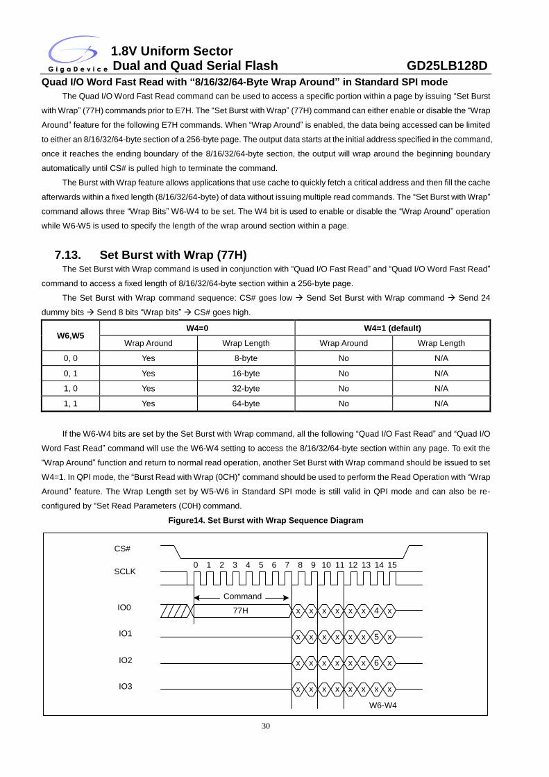
7.13. Set Burst with Wrap (77H) The Set Burst with Wrap command is used in conjunction with “Quad I/O Fast Read” and “Quad I/O Word Fast Read”
command to access a fixed length of 8/16/32/64-byte section within a 256-byte page.
The Set Burst with Wrap command sequence: CS# goes low Send Set Burst with Wrap command Send 24
dummy bits Send 8 bits “Wrap bits” CS# goes high.
W6,W5 W4=0 W4=1 (default)
Wrap Around Wrap Length Wrap Around Wrap Length
0, 0 Yes 8-byte No N/A
0, 1 Yes 16-byte No N/A
1, 0 Yes 32-byte No N/A
1, 1 Yes 64-byte No N/A
If the W6-W4 bits are set by the Set Burst with Wrap command, all the following “Quad I/O Fast Read” and “Quad I/O
Word Fast Read” command will use the W6-W4 setting to access the 8/16/32/64-byte section within any page. To exit the
“Wrap Around” function and return to normal read operation, another Set Burst with Wrap command should be issued to set
W4=1. In QPI mode, the “Burst Read with Wrap (0CH)” command should be used to perform the Read Operation with “Wrap
Around” feature. The Wrap Length set by W5-W6 in Standard SPI mode is still valid in QPI mode and can also be re-
configured by “Set Read Parameters (C0H) command.
Figure14. Set Burst with Wrap Sequence Diagram
Command
0 1 2 3 4 5 6 7
77H
CS#
SCLK
IO0
IO1
8 9 10 11 12 13 14 15
x x x x x x 4 x
x x x x x x 5 x
W6-W4
x x x x x x 6 x
x x x x x x x x
IO2
IO3
1.8V Uniform Sector Dual and Quad Serial Flash GD25LB128D
31
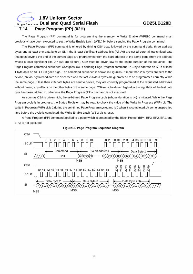
7.14. Page Program (PP) (02H)
The Page Program (PP) command is for programming the memory. A Write Enable (WREN) command must
previously have been executed to set the Write Enable Latch (WEL) bit before sending the Page Program command.
The Page Program (PP) command is entered by driving CS# Low, followed by the command code, three address
bytes and at least one data byte on SI. If the 8 least significant address bits (A7-A0) are not all zero, all transmitted data
that goes beyond the end of the current page are programmed from the start address of the same page (from the address
whose 8 least significant bits (A7-A0) are all zero). CS# must be driven low for the entire duration of the sequence. The
Page Program command sequence: CS# goes low sending Page Program command 3-byte address on SI at least
1 byte data on SI CS# goes high. The command sequence is shown in Figure15. If more than 256 bytes are sent to the
device, previously latched data are discarded and the last 256 data bytes are guaranteed to be programmed correctly within
the same page. If less than 256 data bytes are sent to device, they are correctly programmed at the requested addresses
without having any effects on the other bytes of the same page. CS# must be driven high after the eighth bit of the last data
byte has been latched in; otherwise the Page Program (PP) command is not executed.
As soon as CS# is driven high, the self-timed Page Program cycle (whose duration is tPP) is initiated. While the Page
Program cycle is in progress, the Status Register may be read to check the value of the Write in Progress (WIP) bit. The
Write in Progress (WIP) bit is 1 during the self-timed Page Program cycle, and is 0 when it is completed. At some unspecified
time before the cycle is completed, the Write Enable Latch (WEL) bit is reset.
A Page Program (PP) command applied to a page which is protected by the Block Protect (BP4, BP3, BP2, BP1, and
BP0) is not executed.
Figure15. Page Program Sequence Diagram
Command
0 1 2 3 4 5 6 7
02H
CS#
SCLK
SI
8 9 10 28 29 30 31
3 2 1 023 22 21
24-bit address
42 43 44 4541 46 4740 50 51 52 5349 54 5548
6 5 4 3 2 1 07
CS#
SCLK
SI
MSB
Data Byte 2
32 33 34 35
7 6 5 4 3 2 1 0
MSB
6 5 4 3 2 1 07 6 5 4 3 2 1 07
Data Byte 1
Data Byte 3 Data Byte 256
MSB MSB MSB
36 37 38 39
20
72
20
73
20
74
20
75
20
76
20
77
20
78
20
79
1.8V Uniform Sector Dual and Quad Serial Flash GD25LB128D
32
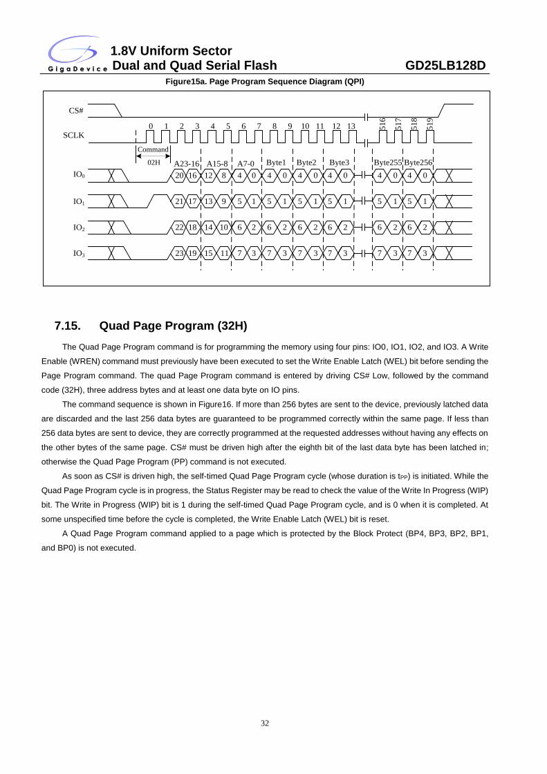
Figure15a. Page Program Sequence Diagram (QPI)
CS#
SCLK
IO0
IO1
IO2
IO3
0 1 2 3 4 5
Command
02H
20 1216 8
6 7 8 9 10
4 40 0 4 0 4 0
21 1317 9 5 51 1 5 1 5 1
22 1418 10 6 62 2 6 2 6 2
23 1519 11 7 73 3 7 3 7 3
A23-16 A15-8 A7-0
11 12 13
Byte1 Byte2
4 0 4 0
5 1 5 1
6 2 6 2
7 3 7 3
51
6
51
7
51
8
51
9
Byte3 Byte255 Byte256
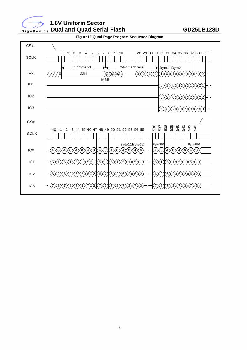
7.15. Quad Page Program (32H)
The Quad Page Program command is for programming the memory using four pins: IO0, IO1, IO2, and IO3. A Write
Enable (WREN) command must previously have been executed to set the Write Enable Latch (WEL) bit before sending the
Page Program command. The quad Page Program command is entered by driving CS# Low, followed by the command
code (32H), three address bytes and at least one data byte on IO pins.
The command sequence is shown in Figure16. If more than 256 bytes are sent to the device, previously latched data
are discarded and the last 256 data bytes are guaranteed to be programmed correctly within the same page. If less than
256 data bytes are sent to device, they are correctly programmed at the requested addresses without having any effects on
the other bytes of the same page. CS# must be driven high after the eighth bit of the last data byte has been latched in;
otherwise the Quad Page Program (PP) command is not executed.
As soon as CS# is driven high, the self-timed Quad Page Program cycle (whose duration is tPP) is initiated. While the
Quad Page Program cycle is in progress, the Status Register may be read to check the value of the Write In Progress (WIP)
bit. The Write in Progress (WIP) bit is 1 during the self-timed Quad Page Program cycle, and is 0 when it is completed. At
some unspecified time before the cycle is completed, the Write Enable Latch (WEL) bit is reset.
A Quad Page Program command applied to a page which is protected by the Block Protect (BP4, BP3, BP2, BP1,
and BP0) is not executed.
1.8V Uniform Sector Dual and Quad Serial Flash GD25LB128D
33
Figure16.Quad Page Program Sequence Diagram
Command
0 1 2 3 4 5 6 7
32H
CS#
SCLK
8 9 10 28 29 30 31
3 2 1 023 22 21
24-bit address
32 33 34 35
4 0
MSB
36 37 38 39
IO0
IO1
IO2
IO3
5 1
6 2
7 3
4 0
5 1
6 2
7 3
4 0
5 1
6 2
7 3
4 0
5 1
6 2
7 3
Byte1 Byte2
CS#
SCLK42 43 44 4541 46 4740 50 51 52 5349 54 5548 5
36
53
7
53
8
53
9
54
0
54
1
54
2
54
3
4 0
5 1
6 2
7 3
4 0
5 1
6 2
7 3
4 0
5 1
6 2
7 3
4 0
5 1
6 2
7 3
4 0
5 1
6 2
7 3
4 0
5 1
6 2
7 3
4 0
5 1
6 2
7 3
Byte11
4 0
5 1
6 2
7 3
Byte12
4 0
5 1
6 2
7 3
Byte253
4 0
5 1
6 2
7 3
4 0
5 1
6 2
7 3
4 0
5 1
6 2
7 3
Byte256
IO0
IO1
IO2
IO3
1.8V Uniform Sector Dual and Quad Serial Flash GD25LB128D
34
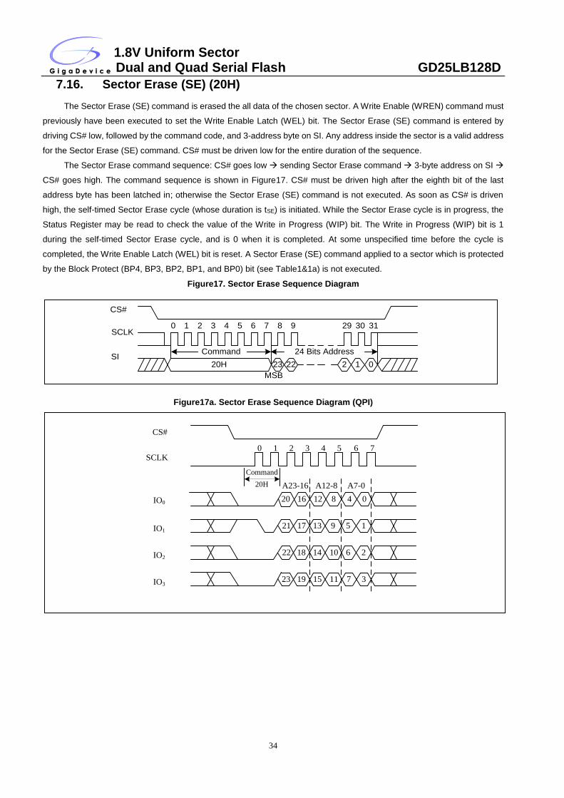
7.16. Sector Erase (SE) (20H)
The Sector Erase (SE) command is erased the all data of the chosen sector. A Write Enable (WREN) command must
previously have been executed to set the Write Enable Latch (WEL) bit. The Sector Erase (SE) command is entered by
driving CS# low, followed by the command code, and 3-address byte on SI. Any address inside the sector is a valid address
for the Sector Erase (SE) command. CS# must be driven low for the entire duration of the sequence.
The Sector Erase command sequence: CS# goes low sending Sector Erase command 3-byte address on SI
CS# goes high. The command sequence is shown in Figure17. CS# must be driven high after the eighth bit of the last
address byte has been latched in; otherwise the Sector Erase (SE) command is not executed. As soon as CS# is driven
high, the self-timed Sector Erase cycle (whose duration is tSE) is initiated. While the Sector Erase cycle is in progress, the
Status Register may be read to check the value of the Write in Progress (WIP) bit. The Write in Progress (WIP) bit is 1
during the self-timed Sector Erase cycle, and is 0 when it is completed. At some unspecified time before the cycle is
completed, the Write Enable Latch (WEL) bit is reset. A Sector Erase (SE) command applied to a sector which is protected
by the Block Protect (BP4, BP3, BP2, BP1, and BP0) bit (see Table1&1a) is not executed.
Figure17. Sector Erase Sequence Diagram
Command
0 1 2 3 4 5 6 7
20H
CS#
SCLK
SI
8 9 29 30 31
MSB
2 1 0
24 Bits Address
23 22
Figure17a. Sector Erase Sequence Diagram (QPI)
CS#
SCLK
IO0
IO1
IO2
IO3
0 1 2 3 4 5
Command
20H
20 1216 8
A23-16 A12-8
6 7
0
21 1317 9 1
23 1519 11 3
22 1418 10 2
4
5
6
7
A7-0
1.8V Uniform Sector Dual and Quad Serial Flash GD25LB128D
35
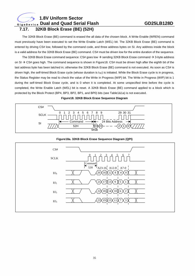
7.17. 32KB Block Erase (BE) (52H)
The 32KB Block Erase (BE) command is erased the all data of the chosen block. A Write Enable (WREN) command
must previously have been executed to set the Write Enable Latch (WEL) bit. The 32KB Block Erase (BE) command is
entered by driving CS# low, followed by the command code, and three address bytes on SI. Any address inside the block
is a valid address for the 32KB Block Erase (BE) command. CS# must be driven low for the entire duration of the sequence.
The 32KB Block Erase command sequence: CS# goes low sending 32KB Block Erase command 3-byte address
on SI CS# goes high. The command sequence is shown in Figure18. CS# must be driven high after the eighth bit of the
last address byte has been latched in; otherwise the 32KB Block Erase (BE) command is not executed. As soon as CS# is
driven high, the self-timed Block Erase cycle (whose duration is tSE) is initiated. While the Block Erase cycle is in progress,
the Status Register may be read to check the value of the Write in Progress (WIP) bit. The Write in Progress (WIP) bit is 1
during the self-timed Block Erase cycle, and is 0 when it is completed. At some unspecified time before the cycle is
completed, the Write Enable Latch (WEL) bit is reset. A 32KB Block Erase (BE) command applied to a block which is
protected by the Block Protect (BP4, BP3, BP2, BP1, and BP0) bits (see Table1&1a) is not executed.
Figure18. 32KB Block Erase Sequence Diagram
Command
0 1 2 3 4 5 6 7
52H
CS#
SCLK
SI
8 9 29 30 31
MSB
2 1 0
24 Bits Address
23 22
Figure18a. 32KB Block Erase Sequence Diagram (QPI)
CS#
SCLK
IO0
IO1
IO2
IO3
0 1 2 3 4 5
Command
52H
20 1216 8
A23-16 A12-8
6 7
0
21 1317 9 1
23 1519 11 3
22 1418 10 2
4
5
6
7
A7-0
1.8V Uniform Sector Dual and Quad Serial Flash GD25LB128D
36
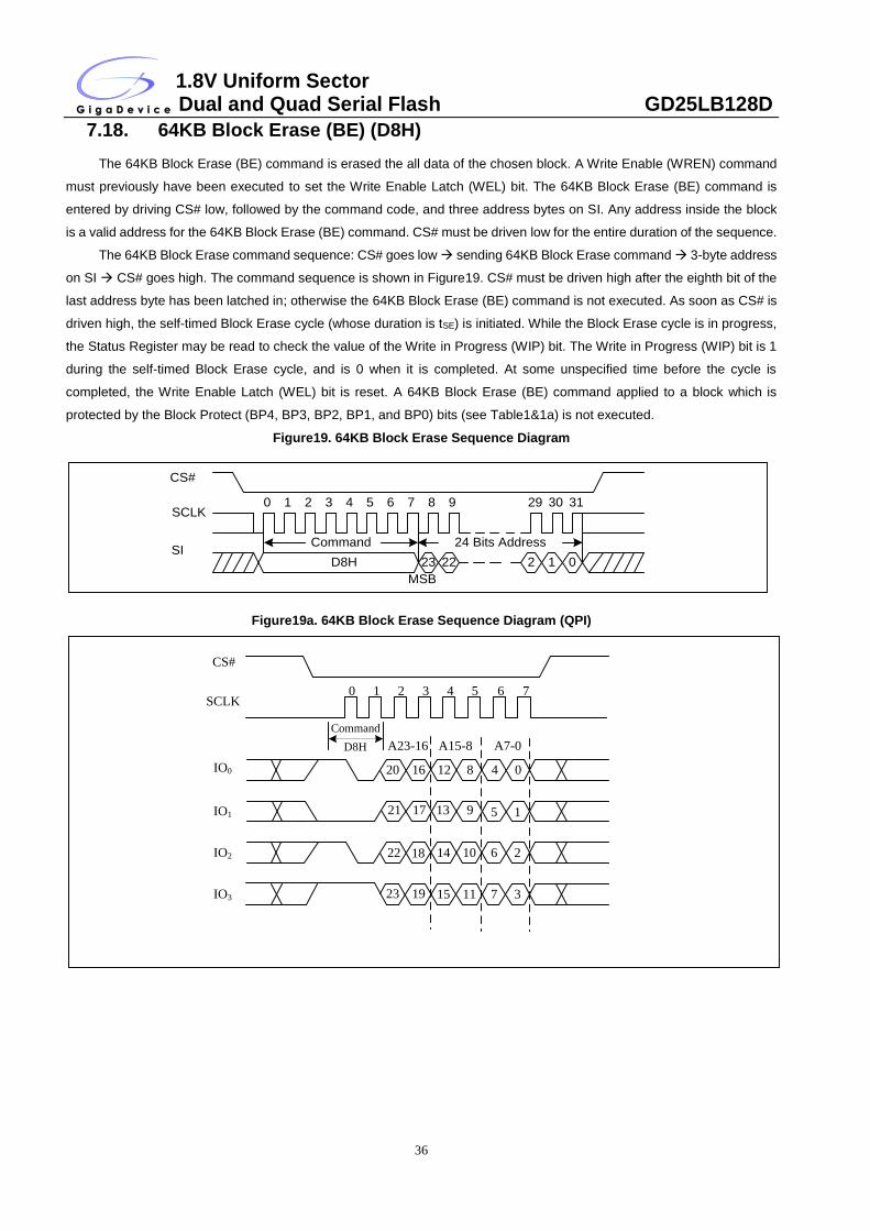
7.18. 64KB Block Erase (BE) (D8H)
The 64KB Block Erase (BE) command is erased the all data of the chosen block. A Write Enable (WREN) command
must previously have been executed to set the Write Enable Latch (WEL) bit. The 64KB Block Erase (BE) command is
entered by driving CS# low, followed by the command code, and three address bytes on SI. Any address inside the block
is a valid address for the 64KB Block Erase (BE) command. CS# must be driven low for the entire duration of the sequence.
The 64KB Block Erase command sequence: CS# goes low sending 64KB Block Erase command 3-byte address
on SI CS# goes high. The command sequence is shown in Figure19. CS# must be driven high after the eighth bit of the
last address byte has been latched in; otherwise the 64KB Block Erase (BE) command is not executed. As soon as CS# is
driven high, the self-timed Block Erase cycle (whose duration is tSE) is initiated. While the Block Erase cycle is in progress,
the Status Register may be read to check the value of the Write in Progress (WIP) bit. The Write in Progress (WIP) bit is 1
during the self-timed Block Erase cycle, and is 0 when it is completed. At some unspecified time before the cycle is
completed, the Write Enable Latch (WEL) bit is reset. A 64KB Block Erase (BE) command applied to a block which is
protected by the Block Protect (BP4, BP3, BP2, BP1, and BP0) bits (see Table1&1a) is not executed.
Figure19. 64KB Block Erase Sequence Diagram
Command
0 1 2 3 4 5 6 7
D8H
CS#
SCLK
SI
8 9 29 30 31
MSB
2 1 0
24 Bits Address
23 22
Figure19a. 64KB Block Erase Sequence Diagram (QPI)
CS#
SCLK
IO0
IO1
IO2
IO3
0 1 2 3 4 5
Command
D8H
6 7
A23-16 A15-8 A7-0
20 16 12 8 4 0
13 9 5 1
14 10 6 2
15 11 7 323 19
22 18
21 17
1.8V Uniform Sector Dual and Quad Serial Flash GD25LB128D
37
7.19. Chip Erase (CE) (60/C7H)
The Chip Erase (CE) command is erased the all data of the chip. A Write Enable (WREN) command must previously
have been executed to set the Write Enable Latch (WEL) bit .The Chip Erase (CE) command is entered by driving CS# Low,
followed by the command code on Serial Data Input (SI). CS# must be driven Low for the entire duration of the sequence.
The Chip Erase command sequence: CS# goes low sending Chip Erase command CS# goes high. The
command sequence is shown in Figure20. CS# must be driven high after the eighth bit of the command code has been
latched in; otherwise the Chip Erase command is not executed. As soon as CS# is driven high, the self-timed Chip Erase
cycle (whose duration is tCE) is initiated. While the Chip Erase cycle is in progress, the Status Register may be read to check
the value of the Write in Progress (WIP) bit. The Write in Progress (WIP) bit is 1 during the self-timed Chip Erase cycle, and
is 0 when it is completed. At some unspecified time before the cycle is completed, the Write Enable Latch (WEL) bit is reset.
The Chip Erase (CE) command is executed if the Block Protect (BP2, BP1, and BP0) bits are 0 and CMP=0 or the Block
Protect (BP2, BP1, and BP0) bits are 1 and CMP=1. The Chip Erase (CE) command is ignored if one or more sectors are
protected.
Figure20. Chip Erase Sequence Diagram
Command
0 1 2 3 4 5 6 7
60H or C7H
CS#
SCLK
SI
Figure20a. Chip Erase Sequence Diagram (QPI)
CS#
SCLK
IO0
IO1
IO2
IO3
0 1
Instruction
C7H/60H
1.8V Uniform Sector Dual and Quad Serial Flash GD25LB128D
38
7.20. Deep Power-Down (DP) (B9H)
Executing the Deep Power-Down (DP) command is the only way to put the device in the lowest consumption mode
(the Deep Power-Down Mode). It can also be used as an extra software protection mechanism, while the device is not in
active use, since in this mode, the device ignores all Write, Program and Erase commands. Driving CS# high deselects the
device, and puts the device in the Standby Mode (if there is no internal cycle currently in progress). But this mode is not the
Deep Power-Down Mode. The Deep Power-Down Mode can only be entered by executing the Deep Power-Down (DP)
command. Once the device has entered the Deep Power-Down Mode, all commands are ignored except the Release from
Deep Power-Down and Read Device ID (RDI) command or Enable Reset (66H) and Reset (99H) commands.. These
commands can release the device from this mode. The Release from Deep Power-Down and Read Device ID (RDI)
command releases the device from deep power down mode , also allows the Device ID of the device to be output on SO.
The Deep Power-Down Mode automatically stops at Power-Down, and the device is in the Standby Mode after Power-
Up.
The Deep Power-Down command sequence: CS# goes low sending Deep Power-Down command CS# goes
high. The command sequence is shown in Figure21. CS# must be driven high after the eighth bit of the command code has
been latched in; otherwise the Deep Power-Down (DP) command is not executed. As soon as CS# is driven high, it requires
a delay of tDP before the supply current is reduced to ICC2 and the Deep Power-Down Mode is entered. Any Deep Power-
Down (DP) command, while an Erase, Program or Write cycle is in progress, is rejected without having any effects on the
cycle that is in progress.
Figure21. Deep Power-Down Sequence Diagram
Command
0 1 2 3 4 5 6 7
B9H
CS#
SCLK
SI
tDP
Stand-by mode Deep Power-down mode
Figure21a. Deep Power-Down Sequence Diagram (QPI)
CS#
SCLK
IO0
IO1
IO2
IO3
0 1
Command
B9H
tDP
Deep Power-down modeStand-by mode
1.8V Uniform Sector Dual and Quad Serial Flash GD25LB128D
39
7.21. Release from Deep Power-Down and Read Device ID (RDI) (ABH)
The Release from Power-Down and Read Device ID command is a multi-purpose command. It can be used to release
the device from the Power-Down state or obtain the devices electronic identification (ID) number.
To release the device from the Power-Down state, the command is issued by driving the CS# pin low, shifting the
instruction code “ABH” and driving CS# high as shown in Figure22. Release from Power-Down will take the time duration
of tRES1 (See AC Characteristics) before the device will resume normal operation and other command are accepted. The
CS# pin must remain high during the tRES1 time duration.
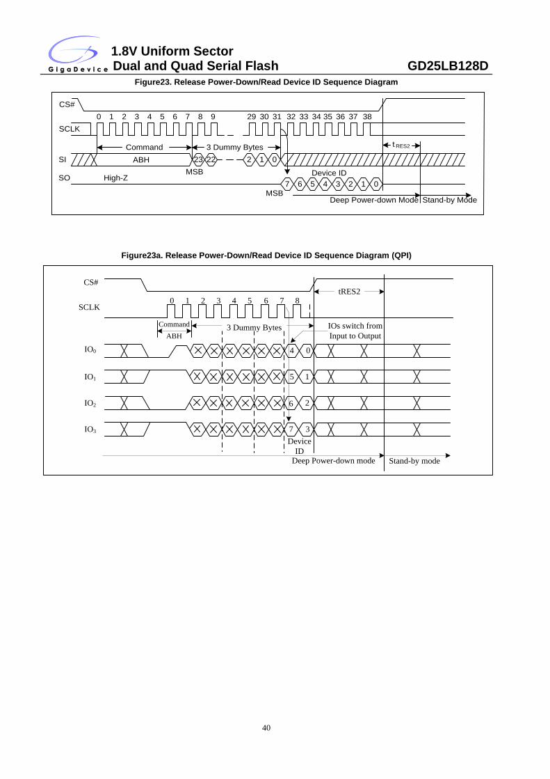
When used only to obtain the Device ID while not in the Power-Down state, the command is initiated by driving the
CS# pin low and shifting the instruction code “ABH” followed by 3-dummy byte. The Device ID bits are then shifted out on
the falling edge of SCLK with most significant bit (MSB) first as shown in Figure23. The Device ID value for the
GD25LB128D is listed in Manufacturer and Device Identification table. The Device ID can be read continuously. The
command is completed by driving CS# high.
When used to release the device from the Power-Down state and obtain the Device ID, the command is the same
as previously described, and shown in Figure23, except that after CS# is driven high it must remain high for a time
duration of tRES2 (See AC Characteristics). After this time duration the device will resume normal operation and other
command will be accepted. If the Release from Power-Down / Device ID command is issued while an Erase, Program or
Write cycle is in process (when WIP equal 1) the command is ignored and will not have any effects on the current cycle.
Figure22. Release Power-Down Sequence Diagram
Command
0 1 2 3 4 5 6 7
ABH
CS#
SCLK
SI
RES1
Stand-by modeDeep Power-down mode
t
Figure22a. Release Power-Down Sequence Diagram (QPI)
CS#
SCLK
IO0
IO1
IO2
IO3
0 1
Command
ABH
tRES1
Deep Power-down mode Stand-by mode
1.8V Uniform Sector Dual and Quad Serial Flash GD25LB128D
40
Figure23. Release Power-Down/Read Device ID Sequence Diagram
Command
0 1 2 3 4 5 6 7
ABH
CS#
SCLK
SI
8 9 29 30 31
MSB
2 1 0
3 Dummy Bytes
23 22
32 33 34 35 36 37 38
7 6 5 4 3 2 1 0SO
MSB
t RES2
Stand-by ModeDeep Power-down Mode
High-ZDevice ID
Figure23a. Release Power-Down/Read Device ID Sequence Diagram (QPI)
CS#
SCLK
IO0
IO1
IO2
IO3
0 1 2 3 4 5
Command
ABH
6 7 8
0
1
3
4
5
7
26
IOs switch from
Input to Output3 Dummy Bytes
Device
ID
tRES2
Deep Power-down mode Stand-by mode
1.8V Uniform Sector Dual and Quad Serial Flash GD25LB128D
41
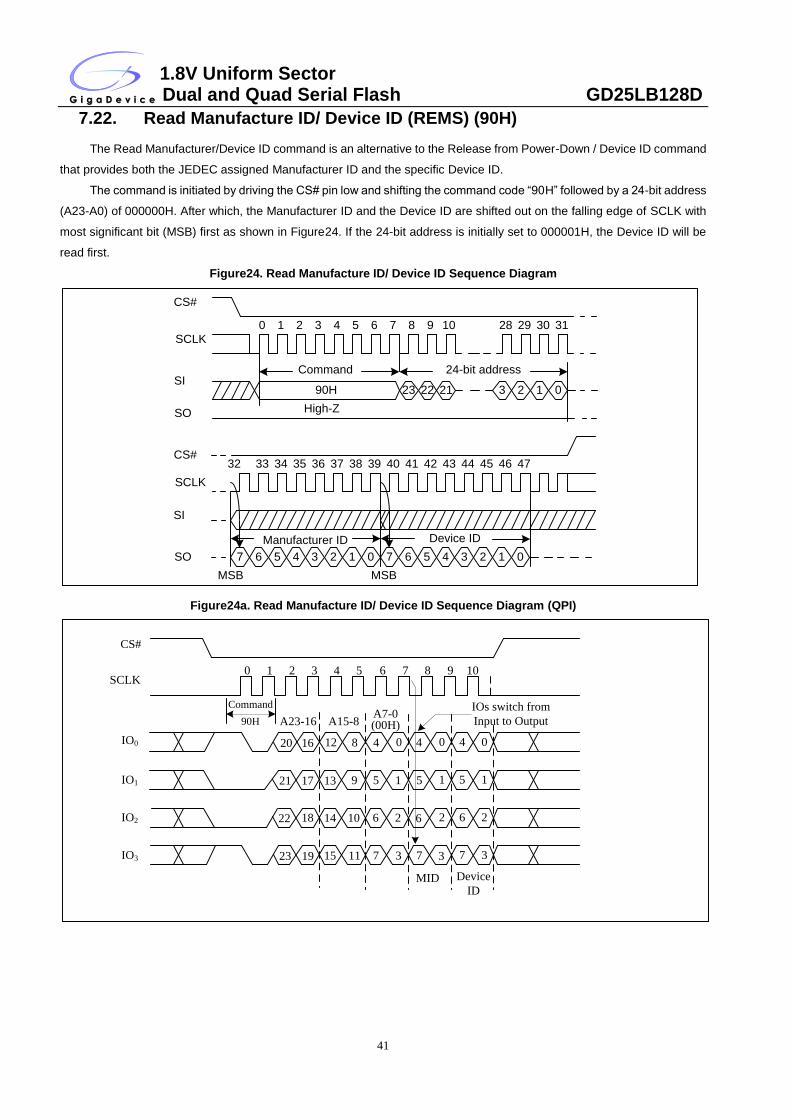
7.22. Read Manufacture ID/ Device ID (REMS) (90H)
The Read Manufacturer/Device ID command is an alternative to the Release from Power-Down / Device ID command
that provides both the JEDEC assigned Manufacturer ID and the specific Device ID.
The command is initiated by driving the CS# pin low and shifting the command code “90H” followed by a 24-bit address
(A23-A0) of 000000H. After which, the Manufacturer ID and the Device ID are shifted out on the falling edge of SCLK with
most significant bit (MSB) first as shown in Figure24. If the 24-bit address is initially set to 000001H, the Device ID will be
read first.
Figure24. Read Manufacture ID/ Device ID Sequence Diagram
Command
0 1 2 3 4 5 6 7
90H
CS#
SCLK
SI
SO High-Z
8 9 10 28 29 30 31
3 2 1 023 22 21
24-bit address
MSB
34 35 36 3733
6 5 4 3 2 1 0
38 3932 42 43 44 4541 46 4740
7
Device ID
CS#
SCLK
SI
SO
MSB
Manufacturer ID
6 5 4 3 2 1 07
Figure24a. Read Manufacture ID/ Device ID Sequence Diagram (QPI)
CS#
SCLK
IO0
IO1
IO2
IO3
0 1 2 3 4 5
Command
90H
6 7 8
0
1
3
4
5
7
26
IOs switch from
Input to Output
Device
IDMID
04
15
26
3737
26
15
04
9 10
A23-16 A15-8A7-0
8
9
19
12
13
23
1014
1115
1822
1721
1620
(00H)
1.8V Uniform Sector Dual and Quad Serial Flash GD25LB128D
42
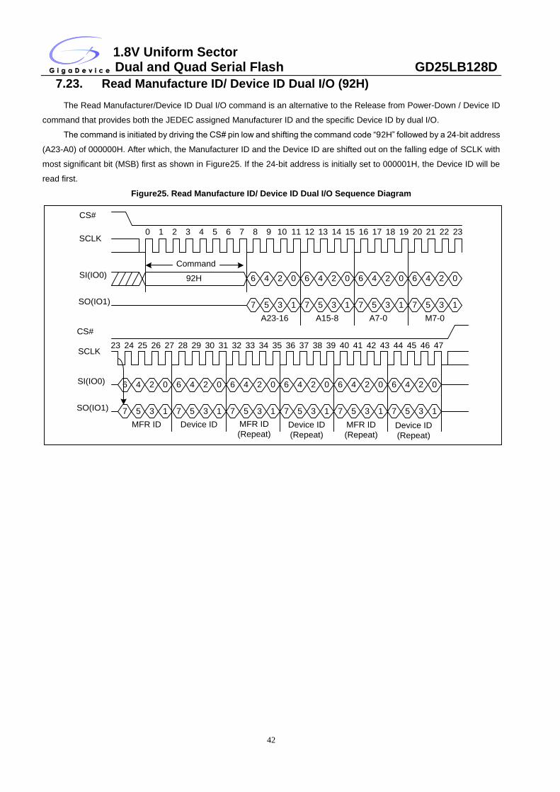
7.23. Read Manufacture ID/ Device ID Dual I/O (92H)
The Read Manufacturer/Device ID Dual I/O command is an alternative to the Release from Power-Down / Device ID
command that provides both the JEDEC assigned Manufacturer ID and the specific Device ID by dual I/O.
The command is initiated by driving the CS# pin low and shifting the command code “92H” followed by a 24-bit address
(A23-A0) of 000000H. After which, the Manufacturer ID and the Device ID are shifted out on the falling edge of SCLK with
most significant bit (MSB) first as shown in Figure25. If the 24-bit address is initially set to 000001H, the Device ID will be
read first.
Figure25. Read Manufacture ID/ Device ID Dual I/O Sequence Diagram
Command
0 1 2 3 4 5 6 7
92H
CS#
SCLK
SI(IO0)
SO(IO1)
8 9 10 11 12 13 14 15
6 4 2 0 6 4 2 0
16 17 18 19 20 21 22 23
6 4 2 0 6 4 2 0
7 5 3 1 7 5 3 1 7 5 3 1 7 5 3 1
A23-16 A15-8 A7-0 M7-0
CS#
23 24 25 26 27 28 29 30 31 32 33 34 35 36 37 38 39
SI(IO0)
SO(IO1)
6 4 2 0 6 4 2 0 6 4 2 0 6 4 2 0
7 5 3 1 7 5 3 1 7 5 3 1 7 5 3 1
SCLK
MFR ID Device ID
40 41 42 43
6 4 2 0
7 5 3 1
44 45 46 47
6 4 2 0
7 5 3 1
MFR ID
(Repeat)Device ID
(Repeat)
MFR ID
(Repeat)Device ID
(Repeat)
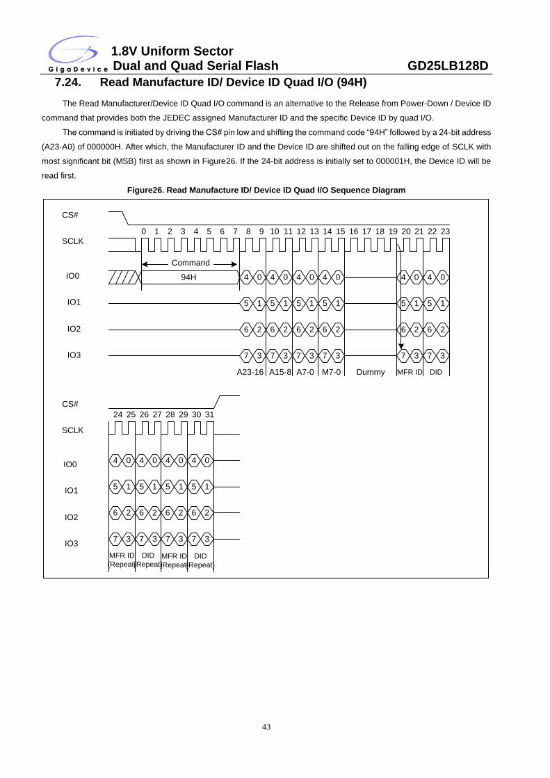
1.8V Uniform Sector Dual and Quad Serial Flash GD25LB128D
43
7.24. Read Manufacture ID/ Device ID Quad I/O (94H)
The Read Manufacturer/Device ID Quad I/O command is an alternative to the Release from Power-Down / Device ID
command that provides both the JEDEC assigned Manufacturer ID and the specific Device ID by quad I/O.
The command is initiated by driving the CS# pin low and shifting the command code “94H” followed by a 24-bit address
(A23-A0) of 000000H. After which, the Manufacturer ID and the Device ID are shifted out on the falling edge of SCLK with
most significant bit (MSB) first as shown in Figure26. If the 24-bit address is initially set to 000001H, the Device ID will be
read first.
Figure26. Read Manufacture ID/ Device ID Quad I/O Sequence Diagram
Command
0 1 2 3 4 5 6 7
94H
CS#
SCLK
IO0
IO1
8 9 10 11 12 13 14 15
4 0 4 0 4 0 4 0
16 17 18 19 20 21 22 23
4 0 4 0
5 1 5 1 5 1 5 1 5 1 5 1
A23-16 A15-8 A7-0 M7-0
6 2 6 2 6 2 6 2 6 2 6 2
7 3 7 3 7 3 7 3 7 3 7 3
IO2
IO3
Dummy MFR ID DID
CS#
SCLK
24 25 26 27 28 29 30 31
4 0 4 0
5 1 5 1
6 2 6 2
7 3 7 3
MFR ID
(Repeat)
DID
(Repeat)
4 0 4 0
5 1 5 1
6 2 6 2
7 3 7 3
MFR ID
(Repeat)
DID
(Repeat)
IO0
IO1
IO2
IO3
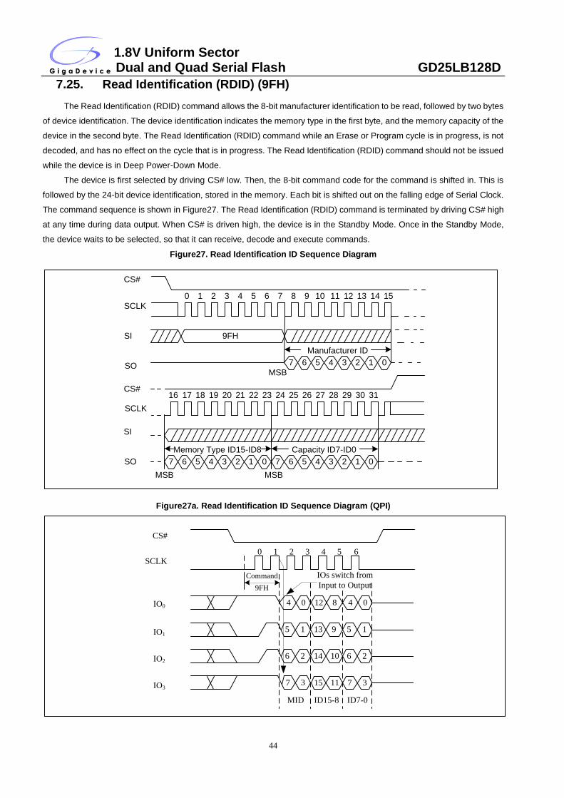
1.8V Uniform Sector Dual and Quad Serial Flash GD25LB128D
44
7.25. Read Identification (RDID) (9FH)
The Read Identification (RDID) command allows the 8-bit manufacturer identification to be read, followed by two bytes
of device identification. The device identification indicates the memory type in the first byte, and the memory capacity of the
device in the second byte. The Read Identification (RDID) command while an Erase or Program cycle is in progress, is not
decoded, and has no effect on the cycle that is in progress. The Read Identification (RDID) command should not be issued
while the device is in Deep Power-Down Mode.
The device is first selected by driving CS# low. Then, the 8-bit command code for the command is shifted in. This is
followed by the 24-bit device identification, stored in the memory. Each bit is shifted out on the falling edge of Serial Clock.
The command sequence is shown in Figure27. The Read Identification (RDID) command is terminated by driving CS# high
at any time during data output. When CS# is driven high, the device is in the Standby Mode. Once in the Standby Mode,
the device waits to be selected, so that it can receive, decode and execute commands.
Figure27. Read Identification ID Sequence Diagram
0 1 2 3 4 5 6 7
CS#
SCLK
SI
SO
8 9 10
MSB
18 19 20 2117
6 5 4 3 2 1 0
22 2316 26 27 28 2925 30 3124
7
Capacity ID7-ID0
CS#
SCLK
SI
SO
MSB
Memory Type ID15-ID8
6 5 4 3 2 1 07
11 12 13 14 15
9FH
6 5 4 3 2 1 07
Manufacturer ID
MSB
Figure27a. Read Identification ID Sequence Diagram (QPI)
CS#
SCLK
IO0
IO1
IO2
IO3
0 1 2 3 4 5
Command
9FH
12 8
6
0
13 9 1
15 11 3
14 10 2
4
5
6
7
IOs switch from
Input to Output
MID ID15-8 ID7-0
0
1
3
2
4
5
6
7
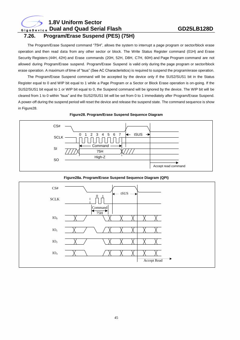
1.8V Uniform Sector Dual and Quad Serial Flash GD25LB128D
45
7.26. Program/Erase Suspend (PES) (75H)
The Program/Erase Suspend command “75H”, allows the system to interrupt a page program or sector/block erase
operation and then read data from any other sector or block. The Write Status Register command (01H) and Erase
Security Registers (44H, 42H) and Erase commands (20H, 52H, D8H, C7H, 60H) and Page Program command are not
allowed during Program/Erase suspend. Program/Erase Suspend is valid only during the page program or sector/block
erase operation. A maximum of time of “tsus” (See AC Characteristics) is required to suspend the program/erase operation.
The Program/Erase Suspend command will be accepted by the device only if the SUS2/SUS1 bit in the Status
Register equal to 0 and WIP bit equal to 1 while a Page Program or a Sector or Block Erase operation is on-going. If the
SUS2/SUS1 bit equal to 1 or WIP bit equal to 0, the Suspend command will be ignored by the device. The WIP bit will be
cleared from 1 to 0 within “tsus” and the SUS2/SUS1 bit will be set from 0 to 1 immediately after Program/Erase Suspend.
A power-off during the suspend period will reset the device and release the suspend state. The command sequence is show
in Figure28.
Figure28. Program/Erase Suspend Sequence Diagram
Command
0 1 2 3 4 5 6 7
75H
CS#
SCLK
SI
SOHigh-Z
tSUS
Accept read command
Figure28a. Program/Erase Suspend Sequence Diagram (QPI)
CS#
SCLK
IO0
IO1
IO2
IO3
0 1
Command
75H
tSUS
Accept Read
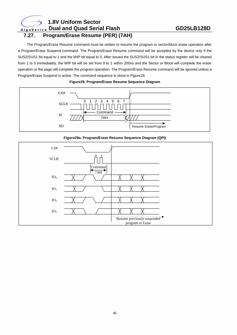
1.8V Uniform Sector Dual and Quad Serial Flash GD25LB128D
46
7.27. Program/Erase Resume (PER) (7AH)
The Program/Erase Resume command must be written to resume the program or sector/block erase operation after
a Program/Erase Suspend command. The Program/Erase Resume command will be accepted by the device only if the
SUS2/SUS1 bit equal to 1 and the WIP bit equal to 0. After issued the SUS2/SUS1 bit in the status register will be cleared
from 1 to 0 immediately, the WIP bit will be set from 0 to 1 within 200ns and the Sector or Block will complete the erase
operation or the page will complete the program operation. The Program/Erase Resume command will be ignored unless a
Program/Erase Suspend is active. The command sequence is show in Figure29.
Figure29. Program/Erase Resume Sequence Diagram
Command
0 1 2 3 4 5 6 7
7AH
CS#
SCLK
SI
SO Resume Erase/Program
Figure29a. Program/Erase Resume Sequence Diagram (QPI)
CS#
SCLK
IO0
IO1
IO2
IO3
0 1
Command
7AH
Resume previously suspended
program or Erase
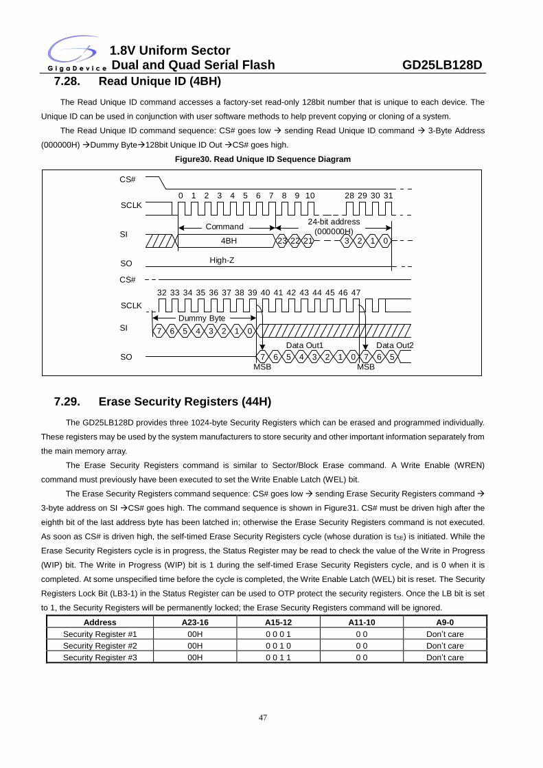
1.8V Uniform Sector Dual and Quad Serial Flash GD25LB128D
47
7.28. Read Unique ID (4BH)
The Read Unique ID command accesses a factory-set read-only 128bit number that is unique to each device. The
Unique ID can be used in conjunction with user software methods to help prevent copying or cloning of a system.
The Read Unique ID command sequence: CS# goes low sending Read Unique ID command 3-Byte Address
(000000H) Dummy Byte128bit Unique ID Out CS# goes high.
Figure30. Read Unique ID Sequence Diagram
Command
0 1 2 3 4 5 6 7
4BH
CS#
SCLK
SI
SO High-Z
8 9 10 28 29 30 31
3 2 1 023 22 21
24-bit address
(000000H)
MSB
34 35 36 3733
6 5 4 3 2 1 0
38 39
Data Out1
32 42 43 44 4541 46 4740
7
6 5 4 3 2 1 07
6 57
Data Out2
CS#
SCLK
SI
SO
MSB
Dummy Byte
7.29. Erase Security Registers (44H)
The GD25LB128D provides three 1024-byte Security Registers which can be erased and programmed individually.
These registers may be used by the system manufacturers to store security and other important information separately from
the main memory array.
The Erase Security Registers command is similar to Sector/Block Erase command. A Write Enable (WREN)
command must previously have been executed to set the Write Enable Latch (WEL) bit.
The Erase Security Registers command sequence: CS# goes low sending Erase Security Registers command
3-byte address on SI CS# goes high. The command sequence is shown in Figure31. CS# must be driven high after the
eighth bit of the last address byte has been latched in; otherwise the Erase Security Registers command is not executed.
As soon as CS# is driven high, the self-timed Erase Security Registers cycle (whose duration is tSE) is initiated. While the
Erase Security Registers cycle is in progress, the Status Register may be read to check the value of the Write in Progress
(WIP) bit. The Write in Progress (WIP) bit is 1 during the self-timed Erase Security Registers cycle, and is 0 when it is
completed. At some unspecified time before the cycle is completed, the Write Enable Latch (WEL) bit is reset. The Security
Registers Lock Bit (LB3-1) in the Status Register can be used to OTP protect the security registers. Once the LB bit is set
to 1, the Security Registers will be permanently locked; the Erase Security Registers command will be ignored.
Address A23-16 A15-12 A11-10 A9-0
Security Register #1 00H 0 0 0 1 0 0 Don’t care
Security Register #2 00H 0 0 1 0 0 0 Don’t care
Security Register #3 00H 0 0 1 1 0 0 Don’t care
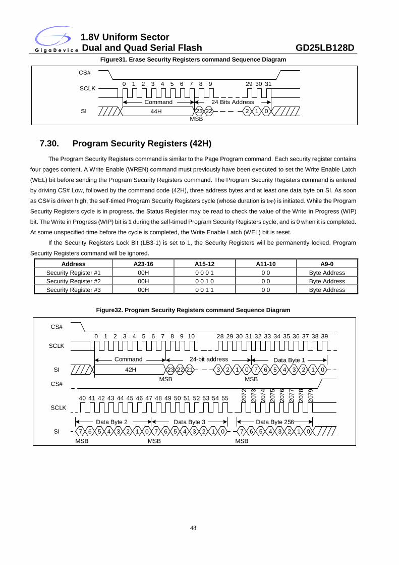
1.8V Uniform Sector Dual and Quad Serial Flash GD25LB128D
48
Figure31. Erase Security Registers command Sequence Diagram
Command
0 1 2 3 4 5 6 7
44H
CS#
SCLK
SI
8 9 29 30 31
MSB
2 1 0
24 Bits Address
23 22
7.30. Program Security Registers (42H)
The Program Security Registers command is similar to the Page Program command. Each security register contains
four pages content. A Write Enable (WREN) command must previously have been executed to set the Write Enable Latch
(WEL) bit before sending the Program Security Registers command. The Program Security Registers command is entered
by driving CS# Low, followed by the command code (42H), three address bytes and at least one data byte on SI. As soon
as CS# is driven high, the self-timed Program Security Registers cycle (whose duration is tPP) is initiated. While the Program
Security Registers cycle is in progress, the Status Register may be read to check the value of the Write in Progress (WIP)
bit. The Write in Progress (WIP) bit is 1 during the self-timed Program Security Registers cycle, and is 0 when it is completed.
At some unspecified time before the cycle is completed, the Write Enable Latch (WEL) bit is reset.
If the Security Registers Lock Bit (LB3-1) is set to 1, the Security Registers will be permanently locked. Program
Security Registers command will be ignored.
Address A23-16 A15-12 A11-10 A9-0
Security Register #1 00H 0 0 0 1 0 0 Byte Address
Security Register #2 00H 0 0 1 0 0 0 Byte Address
Security Register #3 00H 0 0 1 1 0 0 Byte Address
Figure32. Program Security Registers command Sequence Diagram
Command
0 1 2 3 4 5 6 7
42H
CS#
SCLK
SI
8 9 10 28 29 30 31
3 2 1 023 22 21
24-bit address
42 43 44 4541 46 4740 50 51 52 5349 54 5548
6 5 4 3 2 1 07
CS#
SCLK
SI
MSB
Data Byte 2
32 33 34 35
7 6 5 4 3 2 1 0
MSB
6 5 4 3 2 1 07 6 5 4 3 2 1 07
Data Byte 1
Data Byte 3 Data Byte 256
MSB MSB
36 37 38 39
207
2
207
3
207
4
207
5
207
6
207
7
207
8
207
9
MSB
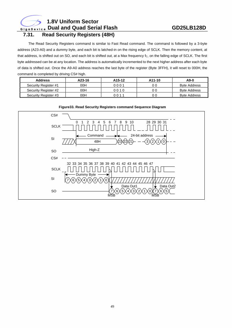
1.8V Uniform Sector Dual and Quad Serial Flash GD25LB128D
49
7.31. Read Security Registers (48H)
The Read Security Registers command is similar to Fast Read command. The command is followed by a 3-byte
address (A23-A0) and a dummy byte, and each bit is latched-in on the rising edge of SCLK. Then the memory content, at
that address, is shifted out on SO, and each bit is shifted out, at a Max frequency fC, on the falling edge of SCLK. The first
byte addressed can be at any location. The address is automatically incremented to the next higher address after each byte
of data is shifted out. Once the A9-A0 address reaches the last byte of the register (Byte 3FFH), it will reset to 000H, the
command is completed by driving CS# high.
Address A23-16 A15-12 A11-10 A9-0
Security Register #1 00H 0 0 0 1 0 0 Byte Address
Security Register #2 00H 0 0 1 0 0 0 Byte Address
Security Register #3 00H 0 0 1 1 0 0 Byte Address
Figure33. Read Security Registers command Sequence Diagram
Command
0 1 2 3 4 5 6 7
48H
CS#
SCLK
SI
SO High-Z
8 9 10 28 29 30 31
3 2 1 023 22 21
24-bit address
MSB
34 35 36 3733
6 5 4 3 2 1 0
38 39
Data Out1
32 42 43 44 4541 46 4740
7
6 5 4 3 2 1 07
6 57
Data Out2
CS#
SCLK
SI
SO
MSB
Dummy Byte
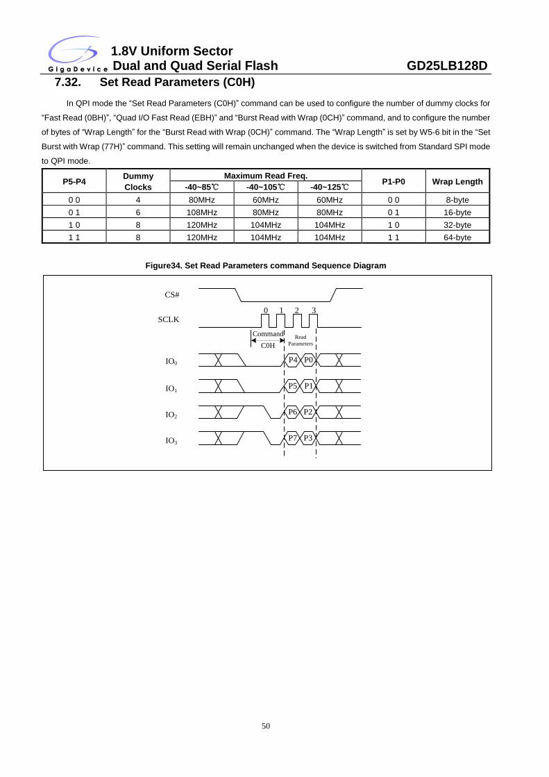
1.8V Uniform Sector Dual and Quad Serial Flash GD25LB128D
50
7.32. Set Read Parameters (C0H)
In QPI mode the “Set Read Parameters (C0H)” command can be used to configure the number of dummy clocks for
“Fast Read (0BH)”, “Quad I/O Fast Read (EBH)” and “Burst Read with Wrap (0CH)” command, and to configure the number
of bytes of “Wrap Length” for the “Burst Read with Wrap (0CH)” command. The “Wrap Length” is set by W5-6 bit in the “Set
Burst with Wrap (77H)” command. This setting will remain unchanged when the device is switched from Standard SPI mode
to QPI mode.
P5-P4 Dummy
Clocks
Maximum Read Freq. P1-P0 Wrap Length
-40~85℃ -40~105℃ -40~125℃
0 0 4 80MHz 60MHz 60MHz 0 0 8-byte
0 1 6 108MHz 80MHz 80MHz 0 1 16-byte
1 0 8 120MHz 104MHz 104MHz 1 0 32-byte
1 1 8 120MHz 104MHz 104MHz 1 1 64-byte
Figure34. Set Read Parameters command Sequence Diagram
CS#
SCLK
IO0
IO1
IO2
IO3
0 1 2 3
Command
C0H
P4 P0
P6 P2
P7 P3
P5 P1
Read
Parameters
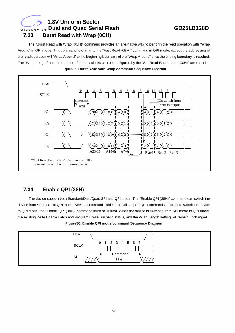
1.8V Uniform Sector Dual and Quad Serial Flash GD25LB128D
51
7.33. Burst Read with Wrap (0CH)
The “Burst Read with Wrap (0CH)” command provides an alternative way to perform the read operation with “Wrap
Around” in QPI mode. This command is similar to the “Fast Read (0BH)” command in QPI mode, except the addressing of
the read operation will “Wrap Around” to the beginning boundary of the “Wrap Around” once the ending boundary is reached.
The “Wrap Length” and the number of dummy clocks can be configured by the “Set Read Parameters (C0H)” command.
Figure35. Burst Read with Wrap command Sequence Diagram
CS#
SCLK
IO0
IO1
IO2
IO3
0 1 2 3 4 5
Command
0CH
20 1216 8
6 7 8 9 10
4 0 4 0 4 0 4
21 1317 9 5 1 5 1 5 1 5
22 1418 10 6 2 6 2 6 2 6
23 1519 11 7 3 7 3 7 3 7
A23-16 A15-8 A7-0Dummy*
11 12 13 14
IOs switch from
Input to output
Byte1 Byte2 Byte3
*"Set Read Parameters" Command (C0H)
can set the number of dummy clocks
7.34. Enable QPI (38H)
The device support both Standard/Dual/Quad SPI and QPI mode. The “Enable QPI (38H)” command can switch the
device from SPI mode to QPI mode. See the command Table 2a for all support QPI commands. In order to switch the device
to QPI mode, the “Enable QPI (38H)” command must be issued. When the device is switched from SPI mode to QPI mode,
the existing Write Enable Latch and Program/Erase Suspend status, and the Wrap Length setting will remain unchanged.
Figure36. Enable QPI mode command Sequence Diagram
Command
0 1 2 3 4 5 6 7
38H
CS#
SCLK
SI
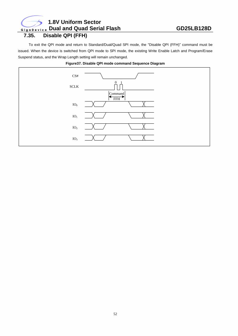
1.8V Uniform Sector Dual and Quad Serial Flash GD25LB128D
52
7.35. Disable QPI (FFH)
To exit the QPI mode and return to Standard/Dual/Quad SPI mode, the “Disable QPI (FFH)” command must be
issued. When the device is switched from QPI mode to SPI mode, the existing Write Enable Latch and Program/Erase
Suspend status, and the Wrap Length setting will remain unchanged.
Figure37. Disable QPI mode command Sequence Diagram
CS#
SCLK
IO0
IO1
IO2
IO3
0 1
Command
FFH
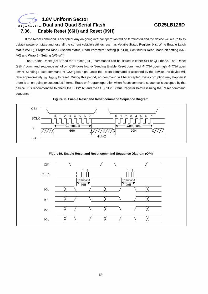
1.8V Uniform Sector Dual and Quad Serial Flash GD25LB128D
53
7.36. Enable Reset (66H) and Reset (99H)
If the Reset command is accepted, any on-going internal operation will be terminated and the device will return to its
default power-on state and lose all the current volatile settings, such as Volatile Status Register bits, Write Enable Latch
status (WEL), Program/Erase Suspend status, Read Parameter setting (P7-P0), Continuous Read Mode bit setting (M7-
M0) and Wrap Bit Setting (W6-W4).
The “Enable Reset (66H)” and the “Reset (99H)” commands can be issued in either SPI or QPI mode. The “Reset
(99H)” command sequence as follow: CS# goes low Sending Enable Reset command CS# goes high CS# goes
low Sending Reset command CS# goes high. Once the Reset command is accepted by the device, the device will
take approximately tRST/tRST_E to reset. During this period, no command will be accepted. Data corruption may happen if
there is an on-going or suspended internal Erase or Program operation when Reset command sequence is accepted by the
device. It is recommended to check the BUSY bit and the SUS bit in Status Register before issuing the Reset command
sequence.
Figure38. Enable Reset and Reset command Sequence Diagram
Command
0 1 2 3 4 5 6 7
66H
CS#
SCLK
SI
SOHigh-Z
Command
0 1 2 3 4 5 6 7
99H
Figure39. Enable Reset and Reset command Sequence Diagram (QPI)
CS#
SCLK
IO0
IO1
IO2
IO3
0 1
Command
66H
0 1
Command
99H
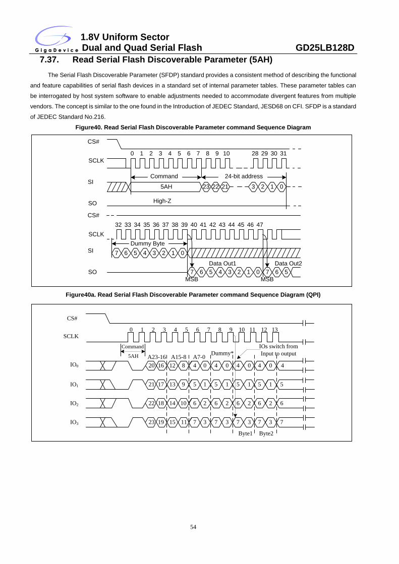
1.8V Uniform Sector Dual and Quad Serial Flash GD25LB128D
54
7.37. Read Serial Flash Discoverable Parameter (5AH)
The Serial Flash Discoverable Parameter (SFDP) standard provides a consistent method of describing the functional
and feature capabilities of serial flash devices in a standard set of internal parameter tables. These parameter tables can
be interrogated by host system software to enable adjustments needed to accommodate divergent features from multiple
vendors. The concept is similar to the one found in the Introduction of JEDEC Standard, JESD68 on CFI. SFDP is a standard
of JEDEC Standard No.216.
Figure40. Read Serial Flash Discoverable Parameter command Sequence Diagram
Command
0 1 2 3 4 5 6 7
5AH
CS#
SCLK
SI
SO High-Z
8 9 10 28 29 30 31
3 2 1 023 22 21
24-bit address
MSB
34 35 36 3733
6 5 4 3 2 1 0
38 39
Data Out1
32 42 43 44 4541 46 4740
7
6 5 4 3 2 1 07
6 57
Data Out2
CS#
SCLK
SI
SO
MSB
Dummy Byte
Figure40a. Read Serial Flash Discoverable Parameter command Sequence Diagram (QPI)
CS#
SCLK
IO0
IO1
IO2
IO3
0 1 2 3 4 5
Command
5AH
20 1216 8
6 7 8 9 10
4 40 0 4 0 4 0 4
21 1317 9 5 51 1 5 1 5 1 5
22 1418 10 6 62 2 6 2 6 2 6
23 1519 11 7 73 3 7 3 7 3 7
A23-16 A15-8 A7-0Dummy*
11 12 13
IOs switch from
Input to output
Byte1 Byte2
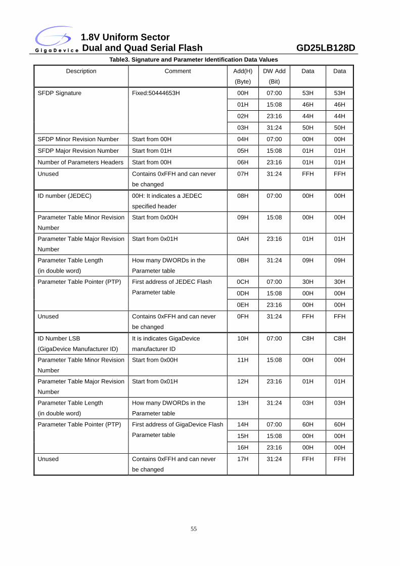
1.8V Uniform Sector Dual and Quad Serial Flash GD25LB128D
55
Table3. Signature and Parameter Identification Data Values
Description Comment Add(H)
(Byte)
DW Add
(Bit)
Data Data
SFDP Signature Fixed:50444653H 00H 07:00 53H 53H
01H 15:08 46H 46H
02H 23:16 44H 44H
03H 31:24 50H 50H
SFDP Minor Revision Number Start from 00H 04H 07:00 00H 00H
SFDP Major Revision Number Start from 01H 05H 15:08 01H 01H
Number of Parameters Headers Start from 00H 06H 23:16 01H 01H
Unused Contains 0xFFH and can never
be changed
07H 31:24 FFH FFH
ID number (JEDEC) 00H: It indicates a JEDEC
specified header
08H 07:00 00H 00H
Parameter Table Minor Revision
Number
Start from 0x00H 09H 15:08 00H 00H
Parameter Table Major Revision
Number
Start from 0x01H 0AH 23:16 01H 01H
Parameter Table Length
(in double word)
How many DWORDs in the
Parameter table
0BH 31:24 09H 09H
Parameter Table Pointer (PTP) First address of JEDEC Flash
Parameter table
0CH 07:00 30H 30H
0DH 15:08 00H 00H
0EH 23:16 00H 00H
Unused Contains 0xFFH and can never
be changed
0FH 31:24 FFH FFH
ID Number LSB
(GigaDevice Manufacturer ID)
It is indicates GigaDevice
manufacturer ID
10H 07:00 C8H C8H
Parameter Table Minor Revision
Number
Start from 0x00H 11H 15:08 00H 00H
Parameter Table Major Revision
Number
Start from 0x01H 12H 23:16 01H 01H
Parameter Table Length
(in double word)
How many DWORDs in the
Parameter table
13H 31:24 03H 03H
Parameter Table Pointer (PTP) First address of GigaDevice Flash
Parameter table
14H 07:00 60H 60H
15H 15:08 00H 00H
16H 23:16 00H 00H
Unused Contains 0xFFH and can never
be changed
17H 31:24 FFH FFH
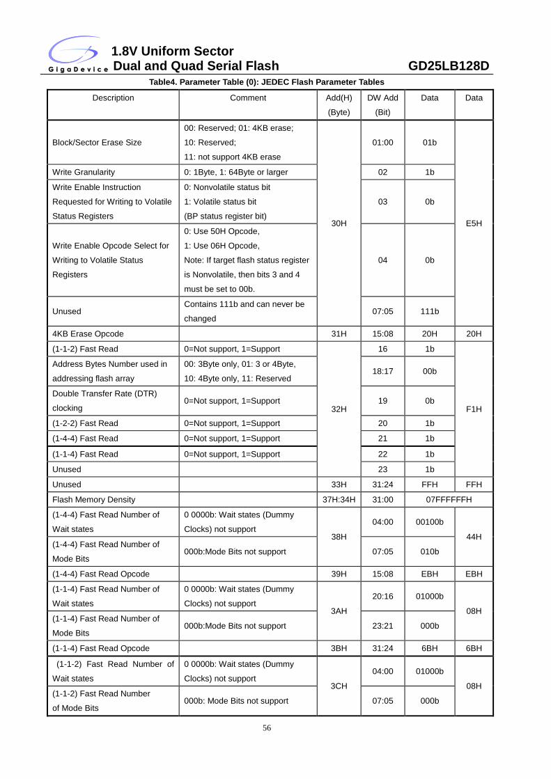
1.8V Uniform Sector Dual and Quad Serial Flash GD25LB128D
56
Table4. Parameter Table (0): JEDEC Flash Parameter Tables
Description Comment Add(H)
(Byte)
DW Add
(Bit)
Data Data
Block/Sector Erase Size
00: Reserved; 01: 4KB erase;
10: Reserved;
11: not support 4KB erase
30H
01:00 01b
E5H
Write Granularity 0: 1Byte, 1: 64Byte or larger 02 1b
Write Enable Instruction
Requested for Writing to Volatile
Status Registers
0: Nonvolatile status bit
1: Volatile status bit
(BP status register bit)
03 0b
Write Enable Opcode Select for
Writing to Volatile Status
Registers
0: Use 50H Opcode,
1: Use 06H Opcode,
Note: If target flash status register
is Nonvolatile, then bits 3 and 4
must be set to 00b.
04 0b
Unused Contains 111b and can never be
changed 07:05 111b
4KB Erase Opcode 31H 15:08 20H 20H
(1-1-2) Fast Read 0=Not support, 1=Support
32H
16 1b
F1H
Address Bytes Number used in
addressing flash array
00: 3Byte only, 01: 3 or 4Byte,
10: 4Byte only, 11: Reserved 18:17 00b
Double Transfer Rate (DTR)
clocking 0=Not support, 1=Support 19 0b
(1-2-2) Fast Read 0=Not support, 1=Support 20 1b
(1-4-4) Fast Read 0=Not support, 1=Support 21 1b
(1-1-4) Fast Read 0=Not support, 1=Support 22 1b
Unused 23 1b
Unused 33H 31:24 FFH FFH
Flash Memory Density 37H:34H 31:00 07FFFFFFH
(1-4-4) Fast Read Number of
Wait states
0 0000b: Wait states (Dummy
Clocks) not support 38H
04:00 00100b
44H (1-4-4) Fast Read Number of
Mode Bits 000b:Mode Bits not support 07:05 010b
(1-4-4) Fast Read Opcode 39H 15:08 EBH EBH
(1-1-4) Fast Read Number of
Wait states
0 0000b: Wait states (Dummy
Clocks) not support 3AH
20:16 01000b
08H (1-1-4) Fast Read Number of
Mode Bits 000b:Mode Bits not support 23:21 000b
(1-1-4) Fast Read Opcode 3BH 31:24 6BH 6BH
(1-1-2) Fast Read Number of
Wait states
0 0000b: Wait states (Dummy
Clocks) not support 3CH
04:00 01000b
08H (1-1-2) Fast Read Number
of Mode Bits 000b: Mode Bits not support 07:05 000b
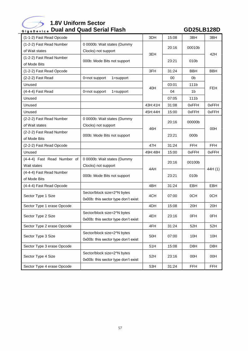
1.8V Uniform Sector Dual and Quad Serial Flash GD25LB128D
57
(1-1-2) Fast Read Opcode 3DH 15:08 3BH 3BH
(1-2-2) Fast Read Number
of Wait states
0 0000b: Wait states (Dummy
Clocks) not support 3EH
20:16 00010b
42H (1-2-2) Fast Read Number
of Mode Bits 000b: Mode Bits not support 23:21 010b
(1-2-2) Fast Read Opcode 3FH 31:24 BBH BBH
(2-2-2) Fast Read 0=not support 1=support
40H
00 0b
FEH Unused 03:01 111b
(4-4-4) Fast Read 0=not support 1=support 04 1b
Unused 07:05 111b
Unused 43H:41H 31:08 0xFFH 0xFFH
Unused 45H:44H 15:00 0xFFH 0xFFH
(2-2-2) Fast Read Number
of Wait states
0 0000b: Wait states (Dummy
Clocks) not support 46H
20:16 00000b
00H (2-2-2) Fast Read Number
of Mode Bits 000b: Mode Bits not support 23:21 000b
(2-2-2) Fast Read Opcode 47H 31:24 FFH FFH
Unused 49H:48H 15:00 0xFFH 0xFFH
(4-4-4) Fast Read Number of
Wait states
0 0000b: Wait states (Dummy
Clocks) not support 4AH
20:16 00100b
44H (1) (4-4-4) Fast Read Number
of Mode Bits 000b: Mode Bits not support 23:21 010b
(4-4-4) Fast Read Opcode 4BH 31:24 EBH EBH
Sector Type 1 Size Sector/block size=2^N bytes
0x00b: this sector type don’t exist 4CH 07:00 0CH 0CH
Sector Type 1 erase Opcode 4DH 15:08 20H 20H
Sector Type 2 Size Sector/block size=2^N bytes
0x00b: this sector type don’t exist 4EH 23:16 0FH 0FH
Sector Type 2 erase Opcode 4FH 31:24 52H 52H
Sector Type 3 Size Sector/block size=2^N bytes
0x00b: this sector type don’t exist 50H 07:00 10H 10H
Sector Type 3 erase Opcode 51H 15:08 D8H D8H
Sector Type 4 Size Sector/block size=2^N bytes
0x00b: this sector type don’t exist 52H 23:16 00H 00H
Sector Type 4 erase Opcode 53H 31:24 FFH FFH
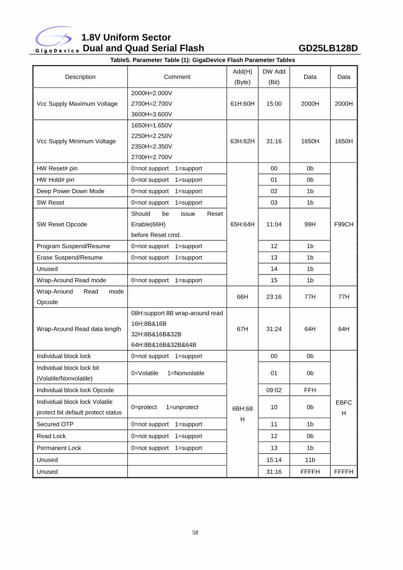
1.8V Uniform Sector Dual and Quad Serial Flash GD25LB128D
58
Table5. Parameter Table (1): GigaDevice Flash Parameter Tables
Description Comment Add(H)
(Byte)
DW Add
(Bit) Data Data
Vcc Supply Maximum Voltage
2000H=2.000V
2700H=2.700V
3600H=3.600V
61H:60H 15:00 2000H 2000H
Vcc Supply Minimum Voltage
1650H=1.650V
2250H=2.250V
2350H=2.350V
2700H=2.700V
63H:62H 31:16 1650H 1650H
HW Reset# pin 0=not support 1=support
65H:64H
00 0b
F99CH
HW Hold# pin 0=not support 1=support 01 0b
Deep Power Down Mode 0=not support 1=support 02 1b
SW Reset 0=not support 1=support 03 1b
SW Reset Opcode
Should be issue Reset
Enable(66H)
before Reset cmd.
11:04 99H
Program Suspend/Resume 0=not support 1=support 12 1b
Erase Suspend/Resume 0=not support 1=support 13 1b
Unused 14 1b
Wrap-Around Read mode 0=not support 1=support 15 1b
Wrap-Around Read mode
Opcode 66H 23:16 77H 77H
Wrap-Around Read data length
08H:support 8B wrap-around read
16H:8B&16B
32H:8B&16B&32B
64H:8B&16B&32B&64B
67H 31:24 64H 64H
Individual block lock 0=not support 1=support
6BH:68
H
00 0b
EBFC
H
Individual block lock bit
(Volatile/Nonvolatile) 0=Volatile 1=Nonvolatile 01 0b
Individual block lock Opcode 09:02 FFH
Individual block lock Volatile
protect bit default protect status 0=protect 1=unprotect 10 0b
Secured OTP 0=not support 1=support 11 1b
Read Lock 0=not support 1=support 12 0b
Permanent Lock 0=not support 1=support 13 1b
Unused 15:14 11b
Unused 31:16 FFFFH FFFFH
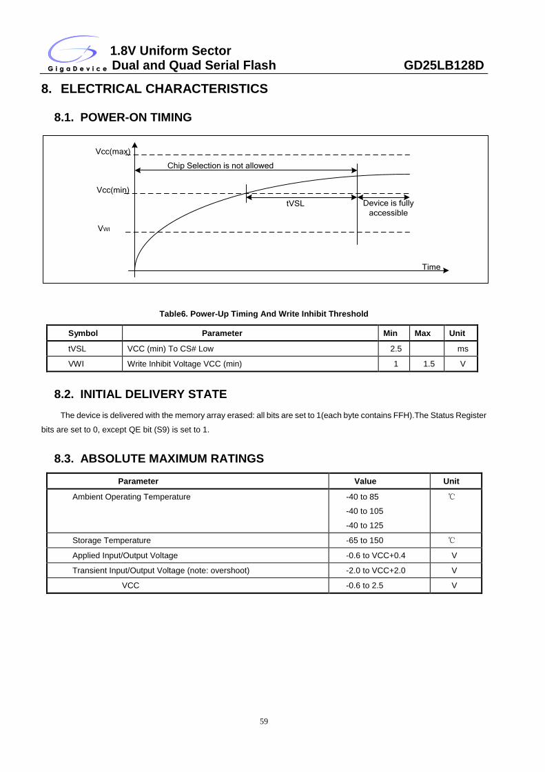
1.8V Uniform Sector Dual and Quad Serial Flash GD25LB128D
59
8. ELECTRICAL CHARACTERISTICS
8.1. POWER-ON TIMING
Vcc(max)
Vcc(min)
VWI
tVSL
Chip Selection is not allowed
Device is fully
accessible
Time
Table6. Power-Up Timing And Write Inhibit Threshold
Symbol Parameter Min Max Unit
tVSL VCC (min) To CS# Low 2.5 ms
VWI Write Inhibit Voltage VCC (min) 1 1.5 V
8.2. INITIAL DELIVERY STATE
The device is delivered with the memory array erased: all bits are set to 1(each byte contains FFH).The Status Register
bits are set to 0, except QE bit (S9) is set to 1.
8.3. ABSOLUTE MAXIMUM RATINGS
Parameter Value Unit
Ambient Operating Temperature -40 to 85
-40 to 105
-40 to 125
℃
Storage Temperature -65 to 150 ℃
Applied Input/Output Voltage -0.6 to VCC+0.4 V
Transient Input/Output Voltage (note: overshoot) -2.0 to VCC+2.0 V
VCC -0.6 to 2.5 V
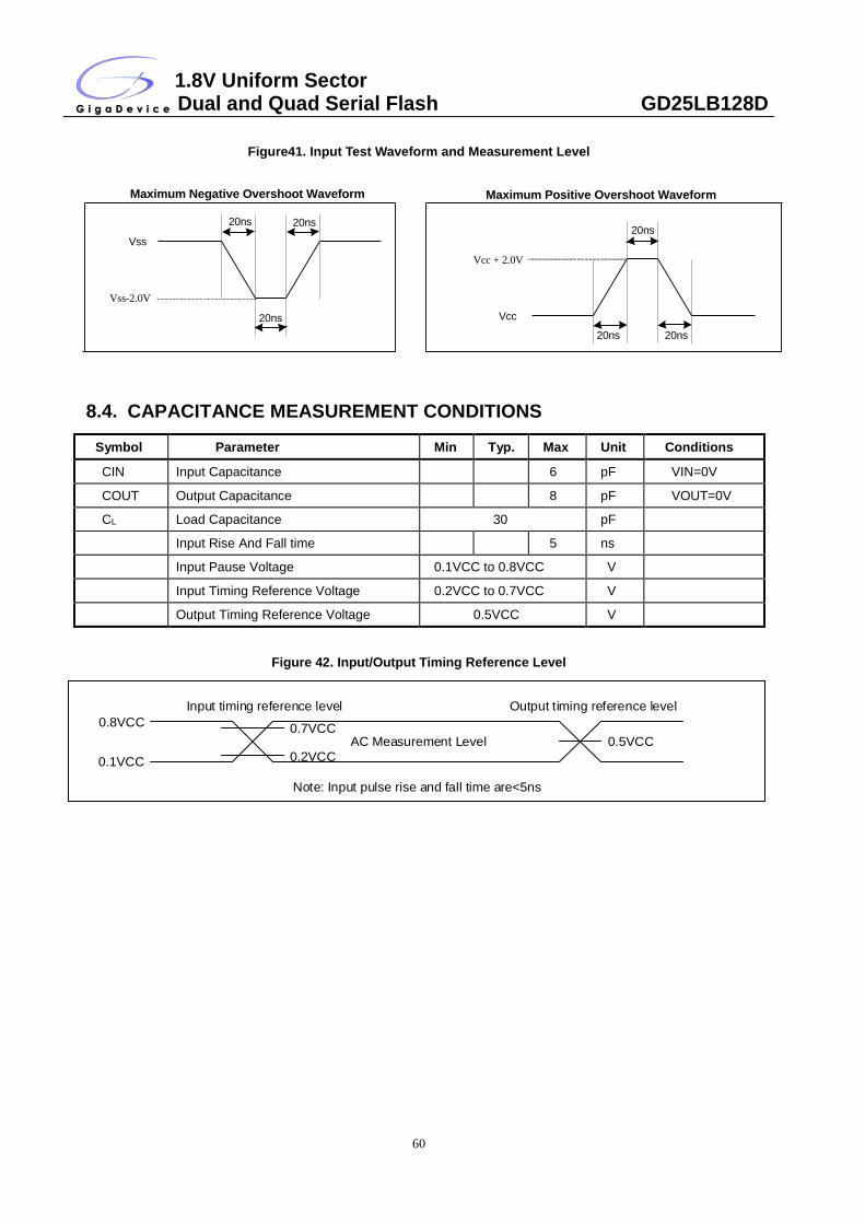
1.8V Uniform Sector Dual and Quad Serial Flash GD25LB128D
60
Figure41. Input Test Waveform and Measurement Level
8.4. CAPACITANCE MEASUREMENT CONDITIONS
Symbol Parameter Min Typ. Max Unit Conditions
CIN Input Capacitance 6 pF VIN=0V
COUT Output Capacitance 8 pF VOUT=0V
CL Load Capacitance 30 pF
Input Rise And Fall time 5 ns
Input Pause Voltage 0.1VCC to 0.8VCC V
Input Timing Reference Voltage 0.2VCC to 0.7VCC V
Output Timing Reference Voltage 0.5VCC V
Figure 42. Input/Output Timing Reference Level
0.8VCC
0.1VCC
0.7VCC
0.2VCC
0.5VCCAC Measurement Level
Input timing reference level Output timing reference level
Note: Input pulse rise and fall time are<5ns
Vss
20ns
Maximum Negative Overshoot Waveform Maximum Positive Overshoot Waveform
20ns
20ns
Vss-2.0V
Vcc
20ns
20ns
20ns
Vcc + 2.0V
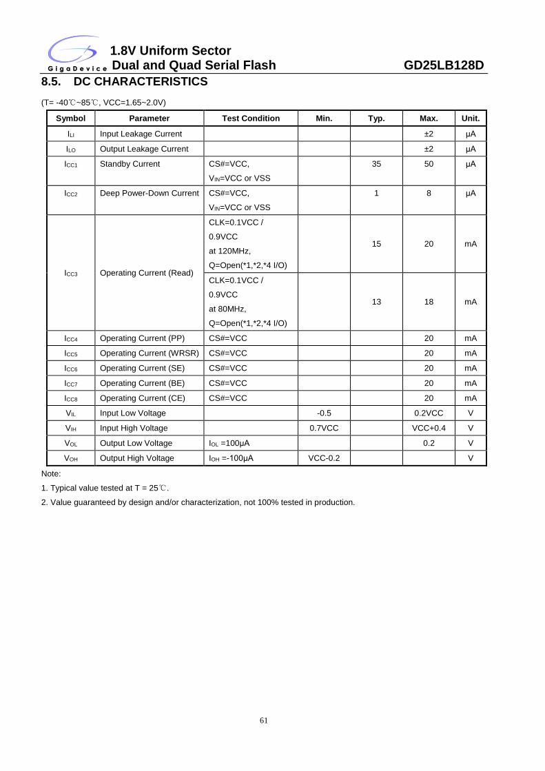
1.8V Uniform Sector Dual and Quad Serial Flash GD25LB128D
61
8.5. DC CHARACTERISTICS
(T= -40℃~85℃, VCC=1.65~2.0V)
Symbol Parameter Test Condition Min. Typ. Max. Unit.
ILI Input Leakage Current ±2 μA
ILO Output Leakage Current ±2 μA
ICC1 Standby Current CS#=VCC,
VIN=VCC or VSS
35 50 μA
ICC2 Deep Power-Down Current CS#=VCC,
VIN=VCC or VSS
1 8 μA
ICC3 Operating Current (Read)
CLK=0.1VCC /
0.9VCC
at 120MHz,
Q=Open(*1,*2,*4 I/O)
15 20 mA
CLK=0.1VCC /
0.9VCC
at 80MHz,
Q=Open(*1,*2,*4 I/O)
13 18 mA
ICC4 Operating Current (PP) CS#=VCC 20 mA
ICC5 Operating Current (WRSR) CS#=VCC 20 mA
ICC6 Operating Current (SE) CS#=VCC 20 mA
ICC7 Operating Current (BE) CS#=VCC 20 mA
ICC8 Operating Current (CE) CS#=VCC 20 mA
VIL Input Low Voltage -0.5 0.2VCC V
VIH Input High Voltage 0.7VCC VCC+0.4 V
VOL Output Low Voltage IOL =100μA 0.2 V
VOH Output High Voltage IOH =-100μA VCC-0.2 V
Note:
1. Typical value tested at T = 25℃.
2. Value guaranteed by design and/or characterization, not 100% tested in production.

1.8V Uniform Sector Dual and Quad Serial Flash GD25LB128D
62
(T= -40℃~105℃, VCC=1.65~2.0V)
Symbol Parameter Test Condition Min. Typ. Max. Unit.
ILI Input Leakage Current ±2 μA
ILO Output Leakage Current ±2 μA
ICC1 Standby Current CS#=VCC,
VIN=VCC or VSS
35 100 μA
ICC2 Deep Power-Down Current CS#=VCC,
VIN=VCC or VSS
1 30 μA
ICC3 Operating Current (Read)
CLK=0.1VCC /
0.9VCC
at 104MHz,
Q=Open(*1,*2,*4 I/O)
15 20 mA
CLK=0.1VCC /
0.9VCC
at 80MHz,
Q=Open(*1,*2,*4 I/O)
13 18 mA
ICC4 Operating Current (PP) CS#=VCC 25 mA
ICC5 Operating Current (WRSR) CS#=VCC 25 mA
ICC6 Operating Current (SE) CS#=VCC 25 mA
ICC7 Operating Current (BE) CS#=VCC 25 mA
ICC8 Operating Current (CE) CS#=VCC 25 mA
VIL Input Low Voltage -0.5 0.2VCC V
VIH Input High Voltage 0.7VCC VCC+0.4 V
VOL Output Low Voltage IOL =100μA 0.2 V
VOH Output High Voltage IOH =-100μA VCC-0.2 V
Note:
1. Typical value tested at T = 25℃.
2. Value guaranteed by design and/or characterization, not 100% tested in production.
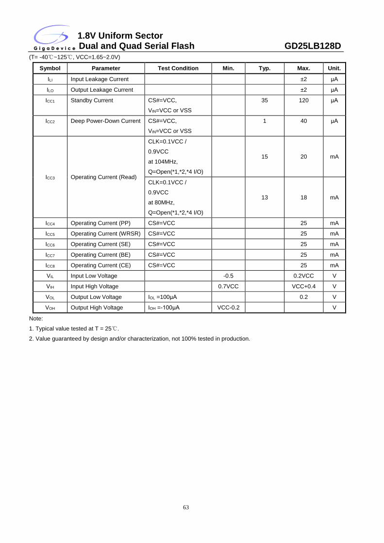
1.8V Uniform Sector Dual and Quad Serial Flash GD25LB128D
63
(T= -40℃~125℃, VCC=1.65~2.0V)
Symbol Parameter Test Condition Min. Typ. Max. Unit.
ILI Input Leakage Current ±2 μA
ILO Output Leakage Current ±2 μA
ICC1 Standby Current CS#=VCC,
VIN=VCC or VSS
35 120 μA
ICC2 Deep Power-Down Current CS#=VCC,
VIN=VCC or VSS
1 40 μA
ICC3 Operating Current (Read)
CLK=0.1VCC /
0.9VCC
at 104MHz,
Q=Open(*1,*2,*4 I/O)
15 20 mA
CLK=0.1VCC /
0.9VCC
at 80MHz,
Q=Open(*1,*2,*4 I/O)
13 18 mA
ICC4 Operating Current (PP) CS#=VCC 25 mA
ICC5 Operating Current (WRSR) CS#=VCC 25 mA
ICC6 Operating Current (SE) CS#=VCC 25 mA
ICC7 Operating Current (BE) CS#=VCC 25 mA
ICC8 Operating Current (CE) CS#=VCC 25 mA
VIL Input Low Voltage -0.5 0.2VCC V
VIH Input High Voltage 0.7VCC VCC+0.4 V
VOL Output Low Voltage IOL =100μA 0.2 V
VOH Output High Voltage IOH =-100μA VCC-0.2 V
Note:
1. Typical value tested at T = 25℃.
2. Value guaranteed by design and/or characterization, not 100% tested in production.
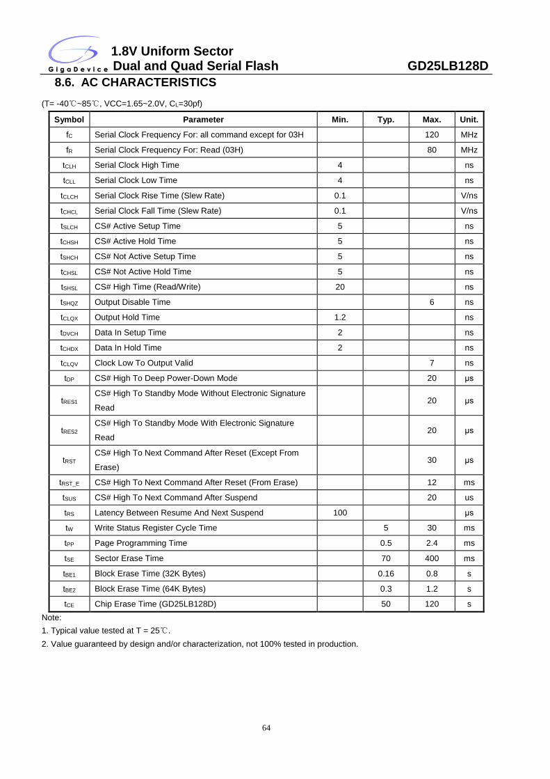
1.8V Uniform Sector Dual and Quad Serial Flash GD25LB128D
64
8.6. AC CHARACTERISTICS
(T= -40℃~85℃, VCC=1.65~2.0V, CL=30pf)
Symbol Parameter Min. Typ. Max. Unit.
fC Serial Clock Frequency For: all command except for 03H 120 MHz
fR Serial Clock Frequency For: Read (03H) 80 MHz
tCLH Serial Clock High Time 4 ns
tCLL Serial Clock Low Time 4 ns
tCLCH Serial Clock Rise Time (Slew Rate) 0.1 V/ns
tCHCL Serial Clock Fall Time (Slew Rate) 0.1 V/ns
tSLCH CS# Active Setup Time 5 ns
tCHSH CS# Active Hold Time 5 ns
tSHCH CS# Not Active Setup Time 5 ns
tCHSL CS# Not Active Hold Time 5 ns
tSHSL CS# High Time (Read/Write) 20 ns
tSHQZ Output Disable Time 6 ns
tCLQX Output Hold Time 1.2 ns
tDVCH Data In Setup Time 2 ns
tCHDX Data In Hold Time 2 ns
tCLQV Clock Low To Output Valid 7 ns
tDP CS# High To Deep Power-Down Mode 20 μs
tRES1 CS# High To Standby Mode Without Electronic Signature
Read 20 μs
tRES2 CS# High To Standby Mode With Electronic Signature
Read 20 μs
tRST CS# High To Next Command After Reset (Except From
Erase) 30 μs
tRST_E CS# High To Next Command After Reset (From Erase) 12 ms
tSUS CS# High To Next Command After Suspend 20 us
tRS Latency Between Resume And Next Suspend 100 μs
tW Write Status Register Cycle Time 5 30 ms
tPP Page Programming Time 0.5 2.4 ms
tSE Sector Erase Time 70 400 ms
tBE1 Block Erase Time (32K Bytes) 0.16 0.8 s
tBE2 Block Erase Time (64K Bytes) 0.3 1.2 s
tCE Chip Erase Time (GD25LB128D) 50 120 s
Note:
1. Typical value tested at T = 25℃.
2. Value guaranteed by design and/or characterization, not 100% tested in production.
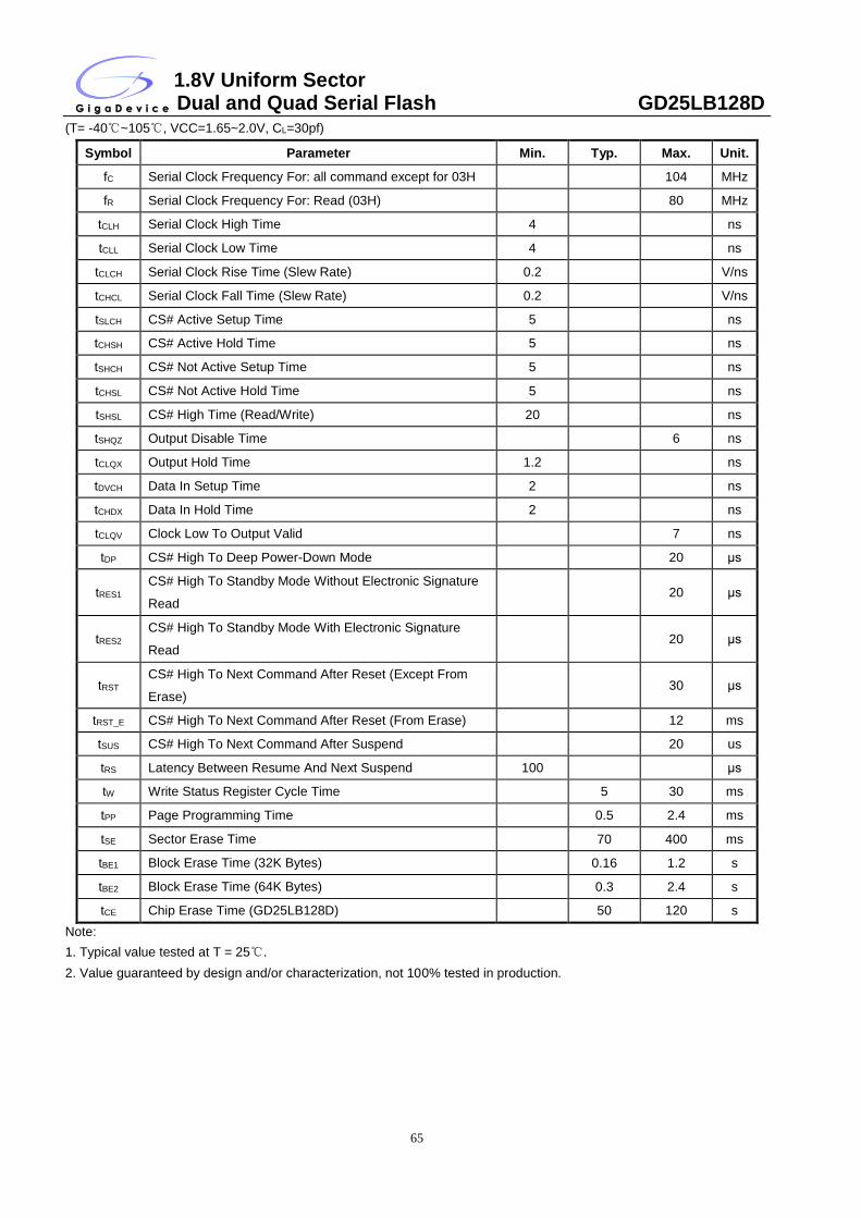
1.8V Uniform Sector Dual and Quad Serial Flash GD25LB128D
65
(T= -40℃~105℃, VCC=1.65~2.0V, CL=30pf)
Symbol Parameter Min. Typ. Max. Unit.
fC Serial Clock Frequency For: all command except for 03H 104 MHz
fR Serial Clock Frequency For: Read (03H) 80 MHz
tCLH Serial Clock High Time 4 ns
tCLL Serial Clock Low Time 4 ns
tCLCH Serial Clock Rise Time (Slew Rate) 0.2 V/ns
tCHCL Serial Clock Fall Time (Slew Rate) 0.2 V/ns
tSLCH CS# Active Setup Time 5 ns
tCHSH CS# Active Hold Time 5 ns
tSHCH CS# Not Active Setup Time 5 ns
tCHSL CS# Not Active Hold Time 5 ns
tSHSL CS# High Time (Read/Write) 20 ns
tSHQZ Output Disable Time 6 ns
tCLQX Output Hold Time 1.2 ns
tDVCH Data In Setup Time 2 ns
tCHDX Data In Hold Time 2 ns
tCLQV Clock Low To Output Valid 7 ns
tDP CS# High To Deep Power-Down Mode 20 μs
tRES1 CS# High To Standby Mode Without Electronic Signature
Read 20 μs
tRES2 CS# High To Standby Mode With Electronic Signature
Read 20 μs
tRST CS# High To Next Command After Reset (Except From
Erase) 30 μs
tRST_E CS# High To Next Command After Reset (From Erase) 12 ms
tSUS CS# High To Next Command After Suspend 20 us
tRS Latency Between Resume And Next Suspend 100 μs
tW Write Status Register Cycle Time 5 30 ms
tPP Page Programming Time 0.5 2.4 ms
tSE Sector Erase Time 70 400 ms
tBE1 Block Erase Time (32K Bytes) 0.16 1.2 s
tBE2 Block Erase Time (64K Bytes) 0.3 2.4 s
tCE Chip Erase Time (GD25LB128D) 50 120 s
Note:
1. Typical value tested at T = 25℃.
2. Value guaranteed by design and/or characterization, not 100% tested in production.

1.8V Uniform Sector Dual and Quad Serial Flash GD25LB128D
66
(T= -40℃~125℃, VCC=1.65~2.0V, CL=30pf)
Symbol Parameter Min. Typ. Max. Unit.
fC Serial Clock Frequency For: all command except for 03H 104 MHz
fR Serial Clock Frequency For: Read (03H) 80 MHz
tCLH Serial Clock High Time 4 ns
tCLL Serial Clock Low Time 4 ns
tCLCH Serial Clock Rise Time (Slew Rate) 0.2 V/ns
tCHCL Serial Clock Fall Time (Slew Rate) 0.2 V/ns
tSLCH CS# Active Setup Time 5 ns
tCHSH CS# Active Hold Time 5 ns
tSHCH CS# Not Active Setup Time 5 ns
tCHSL CS# Not Active Hold Time 5 ns
tSHSL CS# High Time (Read/Write) 20 ns
tSHQZ Output Disable Time 6 ns
tCLQX Output Hold Time 1.2 ns
tDVCH Data In Setup Time 2 ns
tCHDX Data In Hold Time 2 ns
tCLQV Clock Low To Output Valid 7 ns
tDP CS# High To Deep Power-Down Mode 20 μs
tRES1 CS# High To Standby Mode Without Electronic Signature
Read 20 μs
tRES2 CS# High To Standby Mode With Electronic Signature
Read 20 μs
tRST CS# High To Next Command After Reset (Except From
Erase) 30 μs
tRST_E CS# High To Next Command After Reset (From Erase) 12 ms
tSUS CS# High To Next Command After Suspend 20 us
tRS Latency Between Resume And Next Suspend 100 μs
tW Write Status Register Cycle Time 5 30 ms
tPP Page Programming Time 0.5 4 ms
tSE Sector Erase Time 70 500 ms
tBE1 Block Erase Time (32K Bytes) 0.16 1.5 s
tBE2 Block Erase Time (64K Bytes) 0.3 3.0 s
tCE Chip Erase Time (GD25LB128D) 50 150 s
Note:
1. Typical value tested at T = 25℃.
2. Value guaranteed by design and/or characterization, not 100% tested in production.
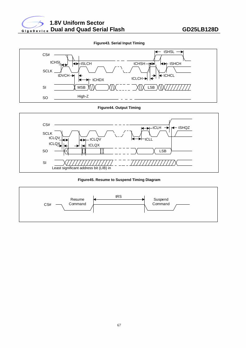
1.8V Uniform Sector Dual and Quad Serial Flash GD25LB128D
67
Figure43. Serial Input Timing
SCLK
CS#
SI MSB
SO High-Z
LSB
tCHSL tSLCH
tDVCHtCHDX
tSHCHtCHSH
tCHCLtCLCH
tSHSL
Figure44. Output Timing
Figure45. Resume to Suspend Timing Diagram
CS#
SCLK
SO
SI
Least significant address bit (LIB) in
tCLQV
tCLQX tCLQX
tCLQV
tCLH
tCLL
tSHQZ
LSB
CS#
Resume
Command
tRSSuspend
Command
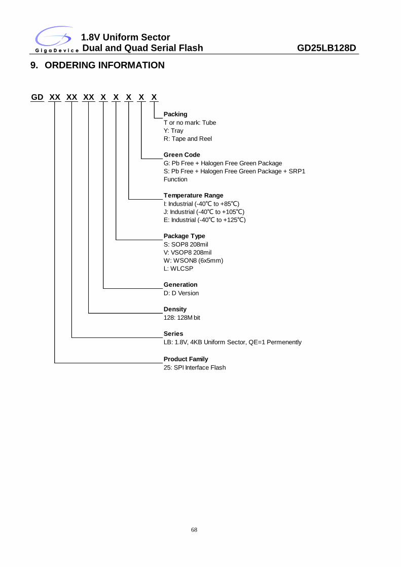
1.8V Uniform Sector Dual and Quad Serial Flash GD25LB128D
68
9. ORDERING INFORMATION
Packing
T or no mark: Tube
Y: Tray
R: Tape and Reel
Green Code
G: Pb Free + Halogen Free Green Package
S: Pb Free + Halogen Free Green Package + SRP1
Function
Temperature Range
I: Industrial (-40℃ to +85℃)
J: Industrial (-40℃ to +105℃)
E: Industrial (-40℃ to +125℃)
Package Type
S: SOP8 208mil
V: VSOP8 208mil
W: WSON8 (6x5mm)
L: WLCSP
Generation
D: D Version
Density
128: 128M bit
Series
LB: 1.8V, 4KB Uniform Sector, QE=1 Permenently
Product Family
25: SPI Interface Flash
X X XGD XX XX XX X X
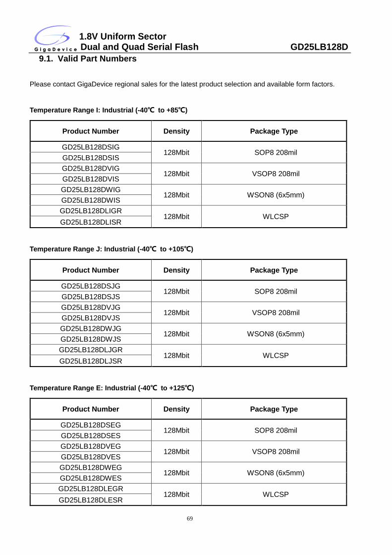
1.8V Uniform Sector Dual and Quad Serial Flash GD25LB128D
69
9.1. Valid Part Numbers
Please contact GigaDevice regional sales for the latest product selection and available form factors.
Temperature Range I: Industrial (-40℃ to +85℃)
Product Number Density Package Type
GD25LB128DSIG 128Mbit SOP8 208mil
GD25LB128DSIS
GD25LB128DVIG 128Mbit VSOP8 208mil
GD25LB128DVIS
GD25LB128DWIG 128Mbit WSON8 (6x5mm)
GD25LB128DWIS
GD25LB128DLIGR 128Mbit WLCSP
GD25LB128DLISR
Temperature Range J: Industrial (-40℃ to +105℃)
Product Number Density Package Type
GD25LB128DSJG 128Mbit SOP8 208mil
GD25LB128DSJS
GD25LB128DVJG 128Mbit VSOP8 208mil
GD25LB128DVJS
GD25LB128DWJG 128Mbit WSON8 (6x5mm)
GD25LB128DWJS
GD25LB128DLJGR 128Mbit WLCSP
GD25LB128DLJSR
Temperature Range E: Industrial (-40℃ to +125℃)
Product Number Density Package Type
GD25LB128DSEG 128Mbit SOP8 208mil
GD25LB128DSES
GD25LB128DVEG 128Mbit VSOP8 208mil
GD25LB128DVES
GD25LB128DWEG 128Mbit WSON8 (6x5mm)
GD25LB128DWES
GD25LB128DLEGR 128Mbit WLCSP
GD25LB128DLESR
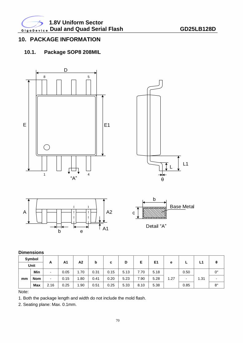
1.8V Uniform Sector Dual and Quad Serial Flash GD25LB128D
70
10. PACKAGE INFORMATION
10.1. Package SOP8 208MIL
D
E E1
A A2
A1b e
“A”
L1L
θ
b
c
Base Metal
Detail “A”
1 4
8 5
Dimensions
Symbol A A1 A2 b c D E E1 e L L1 θ
Unit
mm
Min - 0.05 1.70 0.31 0.15 5.13 7.70 5.18
1.27
0.50
1.31
0°
Nom - 0.15 1.80 0.41 0.20 5.23 7.90 5.28 - -
Max 2.16 0.25 1.90 0.51 0.25 5.33 8.10 5.38 0.85 8°
Note:
1. Both the package length and width do not include the mold flash.
2. Seating plane: Max. 0.1mm.
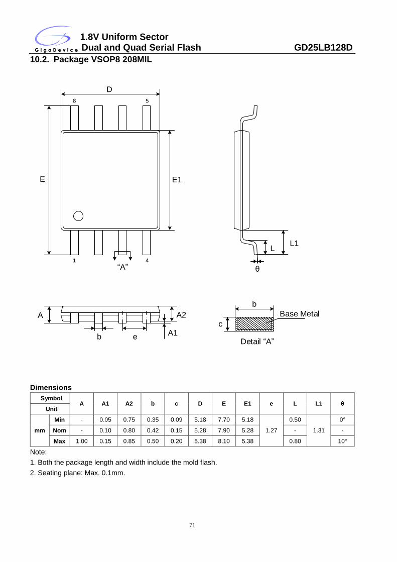
1.8V Uniform Sector Dual and Quad Serial Flash GD25LB128D
71
10.2. Package VSOP8 208MIL
D
E E1
A A2
A1b e
“A”
L1L
b
c
Base Metal
Detail “A”
θ 1 4
8 5
Dimensions
Symbol A A1 A2 b c D E E1 e L L1 θ
Unit
mm
Min - 0.05 0.75 0.35 0.09 5.18 7.70 5.18
1.27
0.50
1.31
0°
Nom - 0.10 0.80 0.42 0.15 5.28 7.90 5.28 - -
Max 1.00 0.15 0.85 0.50 0.20 5.38 8.10 5.38 0.80 10°
Note:
1. Both the package length and width include the mold flash.
2. Seating plane: Max. 0.1mm.
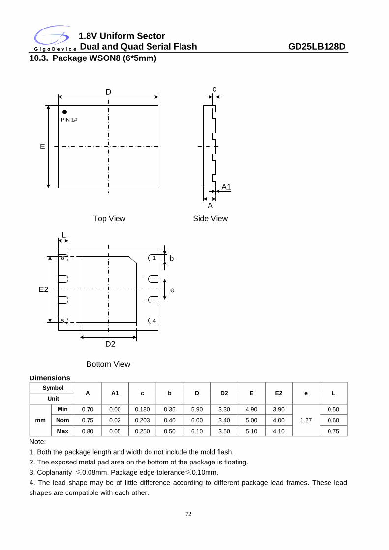
1.8V Uniform Sector Dual and Quad Serial Flash GD25LB128D
72
10.3. Package WSON8 (6*5mm)
D
E
Top View
D2
E2
L
b
e
Bottom View
c
A1
A
Side View
PIN 1#
1
4
8
5
Dimensions
Symbol A A1 c b D D2 E E2 e L
Unit
mm
Min 0.70 0.00 0.180 0.35 5.90 3.30 4.90 3.90
1.27
0.50
Nom 0.75 0.02 0.203 0.40 6.00 3.40 5.00 4.00 0.60
Max 0.80 0.05 0.250 0.50 6.10 3.50 5.10 4.10 0.75
Note:
1. Both the package length and width do not include the mold flash.
2. The exposed metal pad area on the bottom of the package is floating.
3. Coplanarity ≤0.08mm. Package edge tolerance≤0.10mm.
4. The lead shape may be of little difference according to different package lead frames. These lead
shapes are compatible with each other.
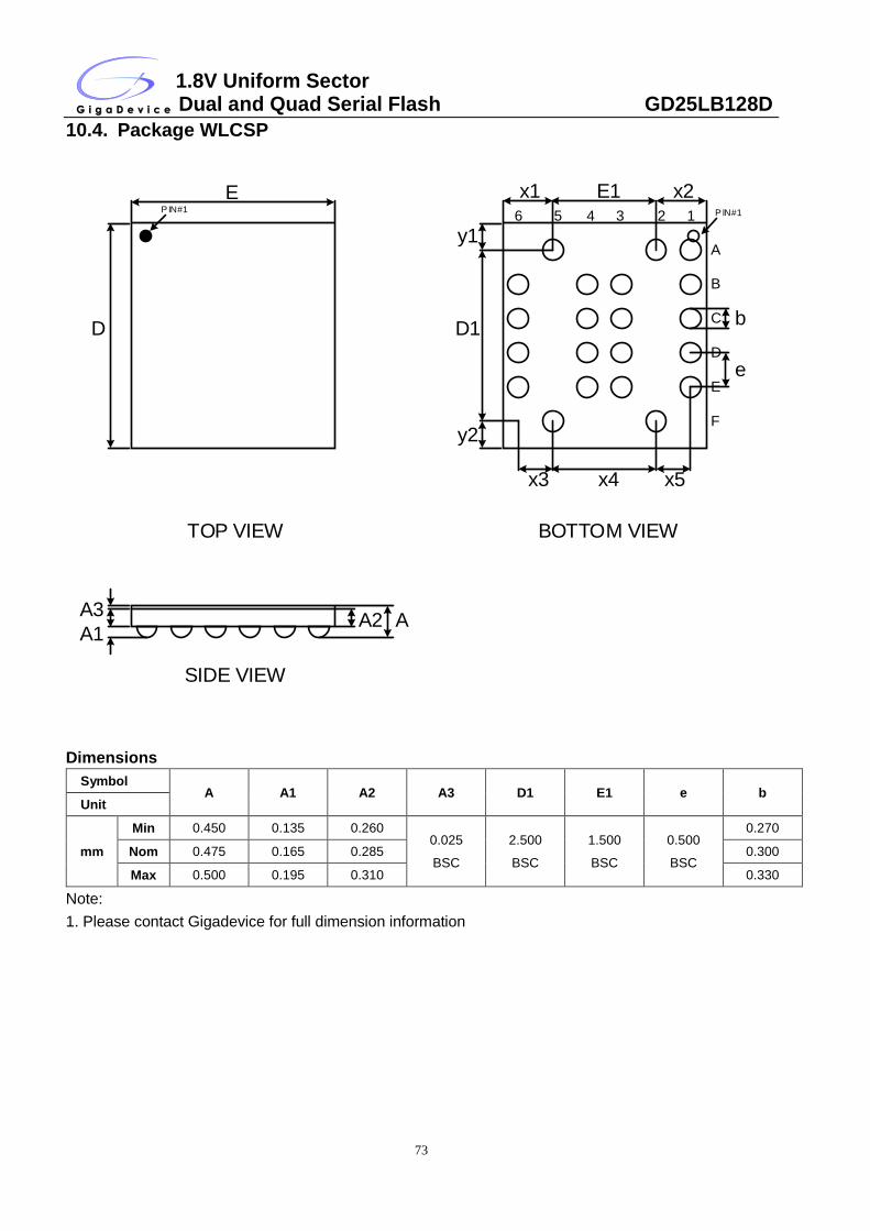
1.8V Uniform Sector Dual and Quad Serial Flash GD25LB128D
73
10.4. Package WLCSP
E E1x1 x2
y1
D1
y2
b
e
D
A3
A1A2 A
TOP VIEW BOTTOM VIEW
SIDE VIEW
PIN#1
x4x3 x5
123456
A
B
C
D
E
F
PIN#1
Dimensions
Symbol A A1 A2 A3 D1 E1 e b
Unit
mm
Min 0.450 0.135 0.260 0.025
BSC
2.500
BSC
1.500
BSC
0.500
BSC
0.270
Nom 0.475 0.165 0.285 0.300
Max 0.500 0.195 0.310 0.330
Note:
1. Please contact Gigadevice for full dimension information
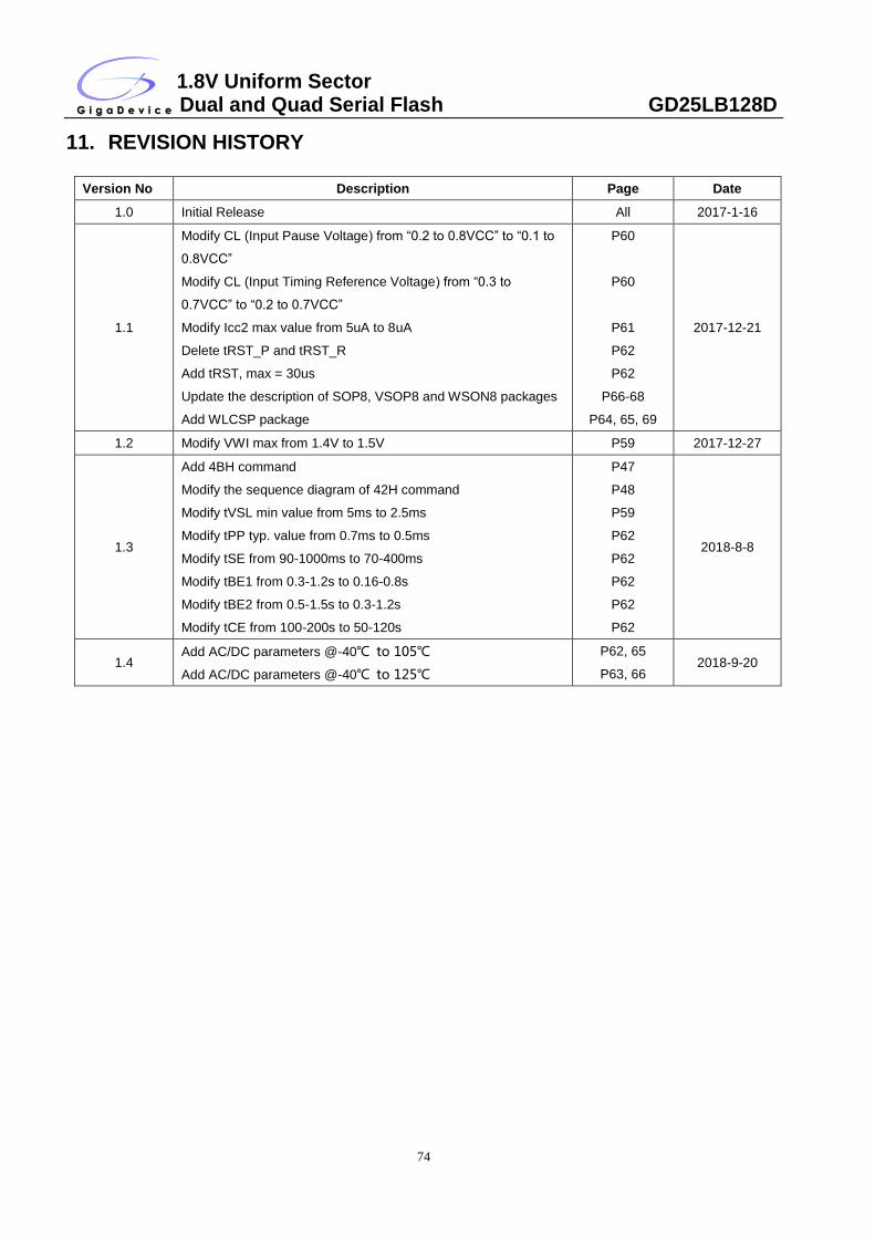
1.8V Uniform Sector Dual and Quad Serial Flash GD25LB128D
74
11. REVISION HISTORY
Version No Description Page Date
1.0 Initial Release All 2017-1-16
1.1
Modify CL (Input Pause Voltage) from “0.2 to 0.8VCC” to “0.1 to
0.8VCC”
Modify CL (Input Timing Reference Voltage) from “0.3 to
0.7VCC” to “0.2 to 0.7VCC”
Modify Icc2 max value from 5uA to 8uA
Delete tRST_P and tRST_R
Add tRST, max = 30us
Update the description of SOP8, VSOP8 and WSON8 packages
Add WLCSP package
P60
P60
P61
P62
P62
P66-68
P64, 65, 69
2017-12-21
1.2 Modify VWI max from 1.4V to 1.5V P59 2017-12-27
1.3
Add 4BH command
Modify the sequence diagram of 42H command
Modify tVSL min value from 5ms to 2.5ms
Modify tPP typ. value from 0.7ms to 0.5ms
Modify tSE from 90-1000ms to 70-400ms
Modify tBE1 from 0.3-1.2s to 0.16-0.8s
Modify tBE2 from 0.5-1.5s to 0.3-1.2s
Modify tCE from 100-200s to 50-120s
P47
P48
P59
P62
P62
P62
P62
P62
2018-8-8
1.4 Add AC/DC parameters @-40℃ to 105℃
Add AC/DC parameters @-40℃ to 125℃
P62, 65
P63, 66 2018-9-20
1.8V Uniform Sector Dual and Quad Serial Flash GD25LB128D
75
Important Notice
This document is the property of GigaDevice Semiconductor (Beijing) Inc. and its subsidiaries (the "Company"). This
document, including any product of the Company described in this document (the “Product”), is owned by the Company
under the intellectual property laws and treaties of the People’s Republic of China and other jurisd ictions worldwide. The
Company reserves all rights under such laws and treaties and does not grant any license under its patents, copyrights,
trademarks, or other intellectual property rights. The names and brands of third party referred thereto (if any) are the property
of their respective owner and referred to for identification purposes only.
The Company makes no warranty of any kind, express or implied, with regard to this document or any Product,
including, but not limited to, the implied warranties of merchantability and fitness for a particular purpose. The Company
does not assume any liability arising out of the application or use of any Product described in this document. Any information
provided in this document is provided only for reference purposes. It is the responsibility of the user of this document to
properly design, program, and test the functionality and safety of any application made of this information and any resulting
product. Except for customized products which has been expressly identified in the applicable agreement, the Products are
designed, developed, and/or manufactured for ordinary business, industrial, personal, and/or household applications only.
The Products are not designed, intended, or authorized for use as components in systems designed or intended for the
operation of weapons, weapons systems, nuclear installations, atomic energy control instruments, combustion control
instruments, airplane or spaceship instruments, traffic signal instruments, life-support devices or systems, other medical
devices or systems (including resuscitation equipment and surgical implants), pollution control or hazardous substances
management, or other uses where the failure of the device or Product could cause personal injury, death, property or
environmental damage ("Unintended Uses"). Customers shall take any and all actions to ensure using and selling the
Products in accordance with the applicable laws and regulations. The Company is not liable, in whole or in part, and
customers shall and hereby do release the Company as well as it’s suppliers and/or distributors from any claim, damage,
or other liability arising from or related to all Unintended Uses of the Products. Customers shall indemnify and hold the
Company as well as it’s suppliers and/or distributors harmless from and against all claims, costs, damages, and other
liabilities, including claims for personal injury or death, arising from or related to any Unintended Uses of the Products.
Information in this document is provided solely in connection with the Products. The Company reserves the
right to make changes, corrections, modifications or improvements to this document and the Products and
services described herein at any time, without notice.