ZSSC3230 Datasheet - Renesas
39
Capacitive Sensor Signal Conditioner IC ZSSC3230 Datasheet © 2019 Integrated Device Technology, Inc. 1 October 15, 2019 Description The ZSSC3230 is a CMOS integrated circuit for accurate capaci- tance-to-digital conversion and sensor-specific correction of capacitive sensor signals. Digital compensation of sensor offset, sensitivity, and temperature drift is accomplished via an internal digital signal processor running a correction algorithm with calibration coefficients stored in a nonvolatile, multiple-time programmable (NVM) memory. Programming the ZSSC3230 is simple via the serial interface. The interface is used for the PC- controlled calibration procedure, which programs the set of calibration coefficients in memory. The ZSSC3230 is configurable for capacitive sensors with capacitances up to 30pF and will provide an output resolution that is scalable up to 18-bit. It is compatible with single-ended capacitive sensors. Measured and corrected sensor values can be output as I2C (≤ 3.4MHz). The ZSSC3230 provides accelerated signal processing, increased resolution, and improved noise immunity in order to support high- speed control, safety, and real-time sensing applications with the highest requirements for energy efficiency. Basic Application Diagram VSS SDA SCL VSS C0 EOC SDA SCL C1 CC VDD VDD ZSSC3230 Typical Applications Humidity sensors Pressure sensors, level sensors Smart, digital, capacitive sensors for energy-efficient solutions Consumer / white goods (e.g., HVAC) Medical applications Features Low current consumption: 1.3μA at 1 sample per second Maximum target input capacitance: 30pF Programmable capacitance span and offset High sampling rate with 2ms at 14-bit resolution ADC resolution: Adjustable in speed and resolution, 18-bit maximum Internal auto-compensated temperature sensor; not stress sensitive Programmable measurement sequence, single-shot and automatic cycling of measurements with end-of-sequence interrupt output Oversampling modes using internal averaging Interrupt features Integrated NVM for configuration and free space for customer use Small die size External reset pin (low active) No external trimming components required Highly integrated CMOS design Physical Characteristics Supply voltage VDD: 1.68V to 3.6V Operating temperature: -40°C to 125°C depending on the part code I2C Interface compatible, supporting Standard Mode(100kHz) Fast Mode (400kHz) High-Speed Mode (3.4MHz) Capacitive input range 0 to 30pF Capacitive offset compensation 0 to 15pF Available in 4 4 mm 2 24-PQFN package or as die
-
Upload
khangminh22 -
Category
Documents
-
view
0 -
download
0
Transcript of ZSSC3230 Datasheet - Renesas

Capacitive Sensor Signal Conditioner IC
ZSSC3230 Datasheet
© 2019 Integrated Device Technology, Inc. 1 October 15, 2019
Description
The ZSSC3230 is a CMOS integrated circuit for accurate capaci-tance-to-digital conversion and sensor-specific correction of capacitive sensor signals. Digital compensation of sensor offset, sensitivity, and temperature drift is accomplished via an internal digital signal processor running a correction algorithm with calibration coefficients stored in a nonvolatile, multiple-time programmable (NVM) memory. Programming the ZSSC3230 is simple via the serial interface. The interface is used for the PC-controlled calibration procedure, which programs the set of calibration coefficients in memory. The ZSSC3230 is configurable for capacitive sensors with capacitances up to 30pF and will provide an output resolution that is scalable up to 18-bit. It is compatible with single-ended capacitive sensors. Measured and corrected sensor values can be output as I2C (≤ 3.4MHz).
The ZSSC3230 provides accelerated signal processing, increased resolution, and improved noise immunity in order to support high-speed control, safety, and real-time sensing applications with the highest requirements for energy efficiency.
Basic Application Diagram
VSS
SDASCL
VSS
C0
EOC
SDASCL
C1
CC
VDD
VDD
ZSSC3230
Typical Applications
Humidity sensors
Pressure sensors, level sensors
Smart, digital, capacitive sensors for energy-efficient solutions
Consumer / white goods (e.g., HVAC)
Medical applications
Features
Low current consumption: 1.3µA at 1 sample per second
Maximum target input capacitance: 30pF
Programmable capacitance span and offset
High sampling rate with 2ms at 14-bit resolution
ADC resolution: Adjustable in speed and resolution, 18-bitmaximum
Internal auto-compensated temperature sensor; not stresssensitive
Programmable measurement sequence, single-shot andautomatic cycling of measurements with end-of-sequenceinterrupt output
Oversampling modes using internal averaging
Interrupt features
Integrated NVM for configuration and free space forcustomer use
Small die size
External reset pin (low active)
No external trimming components required
Highly integrated CMOS design
Physical Characteristics
Supply voltage VDD: 1.68V to 3.6V
Operating temperature: -40°C to 125°C depending on the partcode
I2C Interface compatible, supporting
Standard Mode(100kHz)
Fast Mode (400kHz)
High-Speed Mode (3.4MHz)
Capacitive input range 0 to 30pF
Capacitive offset compensation 0 to 15pF
Available in 4 4 mm2 24-PQFN package or as die

ZSSC3230 Datasheet
© 2019 Integrated Device Technology, Inc. 2 October 15, 2019
Block Diagram
AGND / CM
Generator
Bias Current
Generator
Power-ON
Reset
DSP Core
(Calculations,
Communication)
MTP
ROM
Pre-Amplifier
VTP
VTN
EOC
VDD
Ring
Oscillator
Clock
Generator
I2C
SCL
RESQ
SDA
VSS
Voltage Regulator
Power Ctr.
Vreg int
A
D
18 Bit
ZSSC3230
Cha
rge-
Vol
tage
Con
vert
er
C0
CC
Cmeasure
System
Control Unit
Temperature
Reference
Sensor
Mul
tiple
xer
CC
PDM

ZSSC3230 Datasheet
© 2019 Integrated Device Technology, Inc. 3 October 15, 2019
Typical Application Examples
Figure 1. Isolated C Mode Figure 2. Grounded C Mode
C0
CC
CC
ZSSC3230
VDD
VSSSDA
SCL
RESQ
EOC
Vsupply
GND
µC
with
I2C
Mas
ter
C0
CC
CC
ZSSC3230
VDD
VSSSDA
SCL
RESQ
EOC
Vsupply
GND
µC
with
I2C
Mas
ter

ZSSC3230 Datasheet
© 2019 Integrated Device Technology, Inc. 4 October 15, 2019
Contents
1. Pin Assignments ...........................................................................................................................................................................................6
2. Pin Descriptions ............................................................................................................................................................................................7
3. Absolute Maximum Ratings ..........................................................................................................................................................................8
4. Recommended Operating Conditions ..........................................................................................................................................................8
5. Electrical Characteristics ..............................................................................................................................................................................9
6. Device Description ......................................................................................................................................................................................11
6.1 Signal Flow ........................................................................................................................................................................................12
6.2 Capacitive Sensor Front-End ............................................................................................................................................................13
6.2.1 Differential Mode ................................................................................................................................................................14
6.2.2 Single-Ended Mode ............................................................................................................................................................14
6.2.3 Sensor Leakage Compensation .........................................................................................................................................14
6.2.4 Shield Driver Mode .............................................................................................................................................................15
6.2.5 Subtraction Mode ...............................................................................................................................................................16
6.3 Temperature Sensor ..........................................................................................................................................................................16
6.4 Analog to Digital Converter (ADC) .....................................................................................................................................................16
6.5 Calibration Math ................................................................................................................................................................................17
6.5.1 1/C Pre-compensation ........................................................................................................................................................17
6.5.2 Sensor Signal Compensation Math ....................................................................................................................................18
6.5.3 Temperature Signal Compensation ....................................................................................................................................20
6.6 Output Stages ....................................................................................................................................................................................20
6.6.1 PDM Output Stage .............................................................................................................................................................20
6.6.2 I2C Output ..........................................................................................................................................................................21
6.6.3 EOC and Output Interrupt Signaling ...................................................................................................................................24
6.7 Measurement and Output Options ....................................................................................................................................................26
6.7.1 Single Measurements: Digital Raw and SSC Results ........................................................................................................26
6.7.2 Digital Commands ..............................................................................................................................................................27
6.7.3 Nonvolatile Memory (NVM) ................................................................................................................................................28
6.7.4 Memory Contents ...............................................................................................................................................................29
7. Package Outline Drawings .........................................................................................................................................................................34
8. Marking Diagram ........................................................................................................................................................................................34
9. Ordering Information ...................................................................................................................................................................................34
10. Glossary .....................................................................................................................................................................................................35
11. Revision History ..........................................................................................................................................................................................36

ZSSC3230 Datasheet
© 2019 Integrated Device Technology, Inc. 5 October 15, 2019
List of Figures
Figure 1. Isolated C Mode ..................................................................................................................................................................................3
Figure 2. Grounded C Mode ...............................................................................................................................................................................3
Figure 3. Pin Assignments for 4 4 mm 24-PQFN Package – Top View ..........................................................................................................6
Figure 4. Pin (Pad) Assignments for Bare-Die ....................................................................................................................................................6
Figure 5. Main Operating Modes of the ZSSC3230 ..........................................................................................................................................11
Figure 6. Capacitive Input Signal Conditions ....................................................................................................................................................13
Figure 7. Capacitive Input in Differential Mode .................................................................................................................................................14
Figure 8. Capacitive Input in Single-Ended Mode.............................................................................................................................................15
Figure 9. Shield Driver Mode ............................................................................................................................................................................15
Figure 10. Subtraction Mode ..............................................................................................................................................................................16
Figure 11. Principal Compensation Flow ............................................................................................................................................................17
Figure 12. System Transfer Function for 1/C ......................................................................................................................................................18
Figure 13. PDM Output Configuration ................................................................................................................................................................21
Figure 14. I2C Command Request .....................................................................................................................................................................22
Figure 15. I2C Read Data ...................................................................................................................................................................................23
Figure 16. I2C Read Status ................................................................................................................................................................................23
Figure 17 EOC and Interrupt Thresholds ...........................................................................................................................................................25
List of Tables
Table 1. Pin Descriptions ...................................................................................................................................................................................7
Table 2. Absolute Maximum Ratings .................................................................................................................................................................8
Table 3. Recommended Operating Conditions .................................................................................................................................................8
Table 4. Electrical Characteristics .....................................................................................................................................................................9
Table 5. Conversion Time for Full Temperature Compensated Measurement ................................................................................................12
Table 6. ADC Resolution and Conversion Times for a Single Analog-to-Digital Conversion with Auto-Zero ..................................................16
Table 7. Data Format of Calibration Coefficients in Memory ...........................................................................................................................20
Table 8. Analog Output Performance by External Capacitor Value .................................................................................................................21
Table 9. General Status Byte ..........................................................................................................................................................................21
Table 10. Mode Status ......................................................................................................................................................................................22
Table 11. I2C Interface Parameters ..................................................................................................................................................................23
Table 12. Data Format of Interrupt Thresholds (TRSH1 and TRSH2) ...............................................................................................................24
Table 13. Data Format of Raw ADC Readings ..................................................................................................................................................26
Table 14. Data Format of Corrected SSC Results.............................................................................................................................................26
Table 15. Command List ...................................................................................................................................................................................27
Table 16. Memory (NVM) Content Assignments ...............................................................................................................................................29

ZSSC3230 Datasheet
© 2019 Integrated Device Technology, Inc. 6 October 15, 2019
1. Pin Assignments
The ZSSC3230 is available as 8-inch wafer* and QFN24 package. Details about the package are provided in section 7.
Figure 3. Pin Assignments for 4 4 mm 24-PQFN Package – Top View
ZSSC3230
1
6
12
18
24
n.c.
n.c.
IDT-Test
CC
n.c.
n.c.
CC
PDM
n.c.
IDT-Test
n.c.
SC
L
n.c.
n.c.
SD
A
VD
D
n.c.
VS
S
n.c.
n.c.
C0
EOCRESQn.
c.
2
3
4
5
117 8 9 10
17
16
15
14
13
23 22 21 20 19
Figure 4. Pin (Pad) Assignments for Bare-Die
Seal Ring
CC
VSS
IDT-Test
VDD
C0
SDA
RESQ EOC
PDM
SCL
IDT-Test
CC‘
IC Core
* Detailed information about wafer-shipments, etc., is available on request. See last page for contact information.

ZSSC3230 Datasheet
© 2019 Integrated Device Technology, Inc. 7 October 15, 2019
2. Pin Descriptions
Table 1. Pin Descriptions
Pin Number Name Type Description
1 n.c. – No connection. Leave pin floating.
2 C0 Analog Input Capacitor input signal.
3 CC’ Analog Input Capacitor input signal, duplicate of CC (pin 17).
4 RESQ Digital Input RESET, low active; internal pull-up.
5 IDT-Test – Connect to VSS; otherwise no connection; leave pin floating.
6 n.c. – No connection. Leave pin floating.
7 n.c. – No connection. Leave pin floating.
8 SCL Digital Input Clock input for I2C interface.
9 n.c. – No connection. Leave pin floating.
10 n.c. – No connection. Leave pin floating.
11 SDA Digital Input/Output Bi-directional data I/O for I2C. Pull-up to VDD.
12 n.c. – No connection. Leave pin floating.
13 n.c. – No connection. Leave pin floating.
14 IDT-Test – Connect to VSS; otherwise no connection; leave pin floating.
15 EOC Digital Output End-of-conversion and output interrupt signal.
16 PDM Digital Output Digital output for pulse-density modulated output.
17 CC Analog Input Capacitor input signal, duplicate to CC’ (pin 3).
18 n.c. – No connection. Leave pin floating.
19 n.c. – No connection. Leave pin floating.
20 VSS Ground Power supply ground.
21 n.c. – No connection. Leave pin floating.
22 n.c. – No connection. Leave pin floating.
23 VDD Supply Power supply.
24 n.c. – No connection. Leave pin floating.

ZSSC3230 Datasheet
© 2019 Integrated Device Technology, Inc. 8 October 15, 2019
3. Absolute Maximum Ratings
The absolute maximum ratings are stress ratings only. Stresses greater than those listed below can cause permanent damage to the device. Functional operation of the ZSSC3230 at absolute maximum ratings is not implied. Exposure to absolute maximum rating conditions may affect device reliability.
Table 2. Absolute Maximum Ratings
Symbol Parameter Conditions Minimum Maximum Units
TJ Junction temperature – 135 °C
TS Storage temperature -45 150 °C
ESD – Human Body Model – 2000 V
ESD – Charged Device Model – 750 V
Latch-up -100 +100 mA
VDDmax Voltage supply range Referenced to VSS -0.3 3.63 V
VIF_max Voltage at digital interface pins I2C pins: SDA, SCL -0.3 VDD +0.5V or 3.63V
max.
V
4. Recommended Operating Conditions
Table 3. Recommended Operating Conditions
Symbol Parameter Minimum Typical Maximum Units
VDD Power supply voltage 1.68 – 3.6 V
TA Ambient temperature -40 – 125 °C
CVDD External (parasitic) capacitance between VDD and VSS 0 10 – nF
SRVDD_POR Recommended VDD rise slew rate for power-on-reset (POR)[a] 10 – – V/ms
[a] Per design, there is no (theoretical) minimum VDD slew-rate to trigger a clean POR; however, a reasonable slew rate is recommended.

ZSSC3230 Datasheet
© 2019 Integrated Device Technology, Inc. 9 October 15, 2019
5. Electrical Characteristics
All parameter values are valid only under specified operating conditions. All voltages are referenced to VSS.
Table 4. Electrical Characteristics
Symbol Parameter Conditions Minimum Typical Maximum Units
IC Supply
IIC Current consumption, active ZSSC3230
Excluding connected sensor elements; noise_mode = 0; see Table 16
– 750 1100 µA
IIDLE Idle current consumption, ZSSC3230 in Sleep State
– 0.07 1 µA
IAVE Average current draw Mean current consumption for one complete SSC-measurement cycle per second at 14-bit digital-only output, noise_mode = 0
– 1.7 3.3 µA
PSRR Static power supply rejection ratio (PSRR)
VDD = 3V – 40 – dB
CDC Characteristics
CRANGE Sensor capacitance range
0 – 30 pF
COFFSET Absolute sensor capacitance offset
0 – 15 pF
CSIGNAL Effective sensor capacitance
-15 – 15 pF
fclk Analog base clock frequency
– 750 – kHz
ENOB Effective number of bits,
±3Noise
rADC = 18-bit, no oversampling – 14.4 – Bit
Analog-to-Digital Converter (ADC, A2D)
rADC Resolution 12 – 18 Bit
fS,RAW Conversion rate; conversions per second
Single external sensor A2D conversion (including auto-zero measurement AZ); resolution and mode dependent
94 – 1250 Hz
fS,CORR SSC-conversion rate for full SSC cycle; conversions per second
Full SSC-measurements per second: temperature (14-bit) + capacitance (12 to18 bit)
86 – 555 Hz
fS,TEMP SSC-conversion rate for temperature measurement
14-bit resolution – 960 – Hz
ADCnoise ADC-noise sigma rADC = 16-bit – 1 – LSB
ENOB Effective number of bits,
±3Noise
rADC = 18-bit, no oversampling – 16 – Bit
ZSSC3230 Datasheet
© 2019 Integrated Device Technology, Inc. 10 October 15, 2019
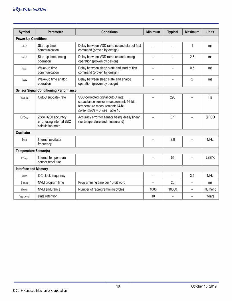
Symbol Parameter Conditions Minimum Typical Maximum Units
Power-Up Conditions
tstup1 Start-up time communication
Delay between VDD ramp up and start of first command (proven by design)
– – 1 ms
tstup2 Start-up time analog operation
Delay between VDD ramp up and analog operation (proven by design)
– – 2.5 ms
twup1 Wake-up time communication
Delay between sleep state and start of first command (proven by design)
– – 0.5 ms
twup2 Wake-up time analog operation
Delay between sleep state and analog operation (proven by design)
– – 2 ms
Sensor Signal Conditioning Performance
fSSCout Output (update) rate SSC-corrected digital output rate; capacitance sensor measurement: 16-bit; temperature measurement: 14-bit; noise_mode = 0; see Table 16
– 290 – Hz
ErrA,IC ZSSC3230 accuracy error using internal SSC calculation math
Accuracy error for sensor being ideally linear (for temperature and measurand)
– 0.1 – %FSO
Oscillator
fCLK Internal oscillator frequency
– 3.0 – MHz
Temperature Sensor(s)
rTemp Internal temperature sensor resolution
– 55 – LSB/K
Interface and Memory
fC,I2C I2C clock frequency – – 3.4 MHz
tPROG NVM program time Programming time per 16-bit word – 20 – ms
nNVM NVM endurance Number of reprogramming cycles 1000 10000 – Numeric
tRET,NVM Data retention 10 – – Years

ZSSC3230 Datasheet
© 2019 Integrated Device Technology, Inc. 11 October 15, 2019
6. Device Description
The ZSSC3230 can be set up for one of three main operating modes:
Sleep Mode – Sleep Mode based operation is recommended for smart sensors for the lowest average power consumption. TheZSSC3230 automatically enters an idle state after command execution for minimum current consumption; however, the interface is stilllistening and accepts commands. After receiving of a valid command, the ZSSC3230 wakes up, executes the command, and provides theresults at the digital interface and then returns to Sleep State.
Command Mode – Command Mode is most appropriate for evaluation, test, and calibration purposes. In this mode, all commands areavailable, both digital and analog outputs are supported, and no restrictions for any functionality need to be considered. Command Modecan be used for applications requiring re-occurring (or even continuous) digital interaction and minimum latency. Applications inCommand Mode are only active on command request. See Table 15 for definitions of the commands.
Cyclic Measurement Mode – Cyclic operation means autonomous, cyclically repeated sensor measurements and related digital andoutput updates.
After power-on, the voltage regulators are switched on, and the ZSSC3230’s low-voltage section (LV) is active while the related interface configuration information is read from memory. Then the LV section is switched off, the ZSSC3230 goes into Sleep Mode, and the interface is ready to receive commands. The interface is always powered by VDD, so it is referred to as the high voltage section (HV).
Figure 5 shows the ZSSC3230 main operation modes: Normal Mode (which uses two operation principles: “Sleep” and “Cyclic”) and Command Mode. The Normal Mode automatically returns to Sleep Mode after executing the requested measurements, or periodically wakes up and conducts another measurement according to the setting for the sleep duration configured by the CYC_period (bits[14:12] in memory register 02HEX; see Table 16). In Command Mode, the ZSSC3230 remains active if a dedicated command (e.g., Start_NOM) is sent, which is helpful during calibration. Command Mode can only be entered if a Start_CM (command A9HEX; see Table 15) is the first command received after a POR.
Figure 5. Main Operating Modes of the ZSSC3230
Power-On (VDD)
Reset
Initialization(Load from configurations from NVM,
interfaces, default_mode, etc.)
PDM_enable
Sleep Mode(Wake-up on command; automatic sleep
after command execution; no PDM
output)
Command Mode(Activity on command; digital output
supported; fastest response; all
commands available)
Cyclic Measurement Mode(Autonomous measurements; digital
and PDM output supported; limited
commands)
Yes
No
START_CYC
START_CYC
START_CM
START_SLEEP START_SLEEP
Stop PDM

ZSSC3230 Datasheet
© 2019 Integrated Device Technology, Inc. 12 October 15, 2019
6.1 Signal Flow
See Figure 1 and Figure 2 for the ZSSC3230 block diagram sensors input options. The CC pin is duplicated as CC’ depending on the preferred physical sensor connection. Selecting CC or CC’ can be done using the signal setup CC_pin_selection bits[1:0] in memory register 19HEX (see Table 16).
Two sensor connections are possible:
Differential Measurement Mode, which is an isolated C mode with CMEAS connected between CC and C0 or CC’ and C0 so that both endsof the capacitor are connected to the ZSSC3230.
Single-Ended Measurement Mode, which is a grounded C mode with CMEAS connected between CC and VSS or CC’ and VSS/ground. Inthis mode, C0 is switched to VSS. In this mode, only one capacitor input pin needs to be directly connected to the ZSSC3230.
The capacitance amplifier (CapAmp), which is also referred to as the charge-voltage converter (CVC), measures an external capacitance value, CMEAS and provides a differential output voltage proportional to the capacitance (change) to the subsequent ADC. Thereby CMEAS is connected with both ends to the IC or with one pin to VSS.
The bias current for the stage (CapAmp) can be programmed (using the setup signal noise_mode bit 8 in the Sensor_config memory register 12HEX; see Table 16) to allow a trade-off between current consumption and achievable signal to noise ratio (SNR).
The system control unit controls the analog circuitry to perform the measurement types for the external capacitive sensor and internal temperature. The multiplexer selects the signal input to the amplifier, which can be the voltage-converted signals of the external capacitive sensor or the internal temperature reference sensor signal. A full measurement request will trigger an automatic sequence of all measurement types and all input signals.
The gain amplifier (PGA) adjusts the respective signal from the capacitance-to-voltage converter or internal temperature sensor. The ZSSC3230 employs a programmable analog-to-digital converter (ADC) optimized for conversion speed and noise suppression. The programmable resolution from 12 to 18 bits provides flexibility for adapting the conversion characteristics.
The math core accomplishes the auto-zero, span, and 1st and 2nd order temperature compensation of the measured external sensor signal. The correction coefficients are stored in the nonvolatile memory. The ZSSC3230 supports I2C interface communication for controlling the ZSSC3230, configuration, and measurement result output. An adequate PDM signal for the compensated sensor signal can be provided in Cyclic Measurement Mode at the PDM pin.
Table 5 lists the conversion time of a full corrected and compensated measurement. The temperature measurement always has a 14-bit resolution. The conversion time for the sensor channels includes a full ADC conversion plus auto-zero measurement and the corresponding CVC conversion time for this channel and the respective temperature measurement and math calculation. The 2 noise modes (bit[8] in memory register 12HEX) are listed separately.
Table 5. Conversion Time for Full Temperature Compensated Measurement
adc_bits[7:6] ADC Resolution [Bits]
Conversion Time for Full Temperature Compensated Measurement, Typical [µs]
bit[7] bit[6] noise_mode = 0 noise_mode = 1
0 0 12 1770 2550
0 1 14 2310 3850
1 0 16 3390 6440
1 1 18 5520 11630

ZSSC3230 Datasheet
© 2019 Integrated Device Technology, Inc. 13 October 15, 2019
6.2 Capacitive Sensor Front-End
The capacitance amplifier input range (CRANGE) must be adjusted to the external capacitance conditions for signal (CSIGNAL) and offset shift (COFFSET) as given in Equation 1. See Figure 6 for an illustration of the terms.
CRANGE
= COFFSET
+ CSIGNAL
Equation 1
COFFSET operates as a zero-shift capacitance to cancel a given offset by the sensor. The offset-shift capacitance must not exceed the selected input capacitance range CRANGE. For COFFSET, the respective configuration must be set up in the EEPROM for the shift_cap parameter (bits[5:0] in memory register 12HEX; see Table 16).
The correlating setup for CSIGNAL must be done in the EEPROM for parameter cap_range (bits[13:9] in memory register 12HEX). In Table 16, the respective values are given. These values can be measured in the positive and negative direction, so the effective range of CSIGNAL will be doubled compared to the cap_range setting. The principle is shown in Figure 6.
Figure 6. Capacitive Input Signal Conditions
C0
CC
CC
ZSSC3230
VDD
VSSSDA
SCL
RESQ
EOCCOFFSET
CSIGNAL
COFFSET
+ Capacitance Range
– Capacitance Range
Sensor Characteristic
CSIGNAL
COFFSETCSIGNAL

ZSSC3230 Datasheet
© 2019 Integrated Device Technology, Inc. 14 October 15, 2019
6.2.1 Differential Mode
The most relevant measurement mode is the Differential Measurement Mode, with CMEAS connected between CC and C0 or CC’ and C0 so that both ends of the capacitor are connected to the ZSSC3230. For electrical connections, see Figure 7.
For the ZSSC3230 for the Differential Measurement Mode, the configuration must be done in the EEPROM for parameter sensecap_type (bit[15] in memory register 12HEX; see Table 16). When the sensecap_type is 0, the differential mode is selected, which is the default configuration.
Figure 7. Capacitive Input in Differential Mode
C0
CC
CC
ZSSC3230
Vsup VDD
VSSSDA
SCL
RESQ
EOC C0
CC
CC
ZSSC3230
Vsup VDD
VSSSDA
SCL
RESQ
EOC
CC Configuration CC Configuration
6.2.2 Single-Ended Mode
Another measurement mode is the single ended measurement mode, with CMEAS connected between CC and VSS or CC’ and VSS/ground. In this mode C0 is switched to VSS. In this mode only 1 Pin needs to be directly connected to the IC.
Configuring the ZSSC3230 for Single-Ended Input Mode must be done in the EEPROM via the parameter sensecap_type (bit[15] in memory register 12HEX; see Table 16). Since the respective bit is defined as “0” in the default configuration for Differential Mode, the bit must be programmed to “1.”
6.2.3 Sensor Leakage Compensation
Sensor leakage compensation is an additional option for Single-Ended Mode to enable the sensor element’s leakage current compensation. The leakage current is caused by the sensor element’s parasitic resistance. Enabling this function via the sensor_leakage bit[14] in memory register 12HEX leads to loss of dynamic range and a decrease in the SNR. With losing 1-bit effective resolution on leakage compensation, the respective capacitive input range for CSIGNAL will be doubled compared to the description in section 6.2.

ZSSC3230 Datasheet
© 2019 Integrated Device Technology, Inc. 15 October 15, 2019
Figure 8. Capacitive Input in Single-Ended Mode
C0
CC
CC
ZSSC3230
Vsup VDD
VSSSDA
SCL
Resq
EOC C0
CC
CC
ZSSC3230
Vsup VDD
VSSSDA
SCL
Resq
EOC
CC Configuration CC Configuration
6.2.4 Shield Driver Mode
The Shield Driver Mode is a special sub-mode for Single-Ended Mode. In this mode, the C0 pin will be forced to the same level as the CC/CC’ pin. This pin can be used to drive a shield, so the shield parasitic capacitance does not have an effect on the measurement. The Shield Driver Mode can be enabled by setting the EEPROM parameter En_shlddrv (bit[4] in memory register 19HEX) to “1” (see Table 16).
Figure 9. Shield Driver Mode
C0
CC
CC
ZSSC3230
Vsup VDD
VSSSDA
SCL
RESQ
EOC C0
CC
CC
ZSSC3230
Vsup VDD
VSSSDA
SCL
RESQ
EOC
CC Configuration CC Configuration

ZSSC3230 Datasheet
© 2019 Integrated Device Technology, Inc. 16 October 15, 2019
6.2.5 Subtraction Mode
The Subtraction Mode is a special sub-mode for Single-Ended Mode. It is activated by setting the En_sh2 bit to “1” (bit[3] in memory register 19HEX; see Table 16). In this mode, C0 is charged to the opposite reference of the CC/CC’ node level. In conversion phase the charge of CC/CC’ and C0 are integrated. In this mode, the integrated capacitance corresponds to “Cx-Cy”; thus this mode can provide an additional range extension.
Figure 10. Subtraction Mode
C0
CC
CC
ZSSC3230
Vsup VDD
VSSSDA
SCL
RESQ
EOC C0
CC
CC
ZSSC3230
Vsup VDD
VSSSDA
SCL
RESQ
EOC
CC Configuration CC Configuration
Cx
Cy
Cx
Cy
6.3 Temperature Sensor
The ZSSC3230 provides a PTAT-based internal temperature sensor measurement to allow compensation for temperature effects. The temperature output signal is a differential voltage that is adapted by the amplifier (PGA) for the ADC input. For IC-internal temperature measurements, the respective settings are defined and programmed in the NVM by IDT. The resolution setting for temperature measurements is defined as 14-bit.
6.4 Analog to Digital Converter (ADC)
An analog-to-digital converter (ADC) is used to digitize the amplifier signal. To allow optimizing the trade-off between conversion time and resolution, the resolution can be programmed from 12-bit to 18-bit by configuring the parameter adc_bits, (bits [7:6] in memory register 12HEX; see Table 16). The ADC processes differential input signals provided by the internal amplifier for sensor measurement and temperature measurement. The application default setting is 16-bit. The corresponding conversion times are listed in Table 6. The conversion time for the sensor channels includes a full ADC conversion as well as the corresponding CVC conversion time for this channel. There are 2 noise modes (selected with bit[8] in memory register 12HEX). The listed conversion times are valid for raw measurements including auto-zero compensation.
Table 6. ADC Resolution and Conversion Times for a Single Analog-to-Digital Conversion with Auto-Zero
adc_bits[7:6]
ADC Resolution [Bits]
Conversion Time ADC (including CVC), typical [µs] Conversion Time
Temperature, Typical [µs] bit[7] bit[6] noise_mode = 0 noise_mode = 1
0 0 12 770 1550 630
0 1 14 1310 2850 1040
1 0 16 2390 5440 1810
1 1 18 4550 10620 3470

ZSSC3230 Datasheet
© 2019 Integrated Device Technology, Inc. 17 October 15, 2019
6.5 Calibration Math
The data path internally calculates with a 26-bit two’s-complement integer representation. The coefficients in the memory are stored as integers in sign-magnitude representation (1-bit sign + 23-bit magnitude). Each multiplication scales the product by 223. There is an option to preprocess the data by applying a 1/C algorithm. 1/C is typically used to pre-process transfer characteristics for capacitive pressure sensors. A principle flow is shown in Figure 11.
Internal overflows and underflows are detected and the result is automatically saturated. The saturation is reported in the status byte.
Figure 11. Principal Compensation Flow
ADC-Conversion:Raw-result SM
Apply 1-1/C calculation?
YesNo
S_rawi:=1-1/S_rawS_raw:=S_raw
SSC-Correction Math (using S_raw or S_rawi;T_raw)
Result S
S_out = S
6.5.1 1/C Pre-compensation
For capacitive pressure sensors, a pre-compensation of the ADC signal might be beneficial. Using this function will help to fit the typical pressure sensor transfer characteristic to matching the second-order compensation input requirements for more accurate compensation results. If the 1/C pre-compensation is activated, it will apply only in Normal Measurement Mode with math compensation, not in RAW measurements using Command Mode. The respective 1/C calculation for determination of calibration coefficients is handled in the respective calibration.dll. This feature can be enabled by setting the corresponding bit siginv (bit[11] in memory register 02HEX; see Table 16). Before the 1/C math is applied, the ADC value of the respective sensor input signal will be inverted.
This leads to the following transfer function for S_raw with the system transfer function that is shown in Figure 12.
Srawi = [224 −
246
Sraw
]-2
25
225 - 1
Equation 2
Note: For the application, if a “Crange/CSens” inversion will be performed, the shift capacitor must to be set to “0.”

ZSSC3230 Datasheet
© 2019 Integrated Device Technology, Inc. 18 October 15, 2019
Figure 12. System Transfer Function for 1/C
6.5.2 Sensor Signal Compensation Math
The SOT_curve (bit [15] in EEPROM word 02HEX; see Table 16) selects whether second-order equations compensate for sensor nonlinearity with a parabolic or S-shaped curve. The parabolic compensation is recommended.
Equations for the Parabolic SOT_curve Setting (SOT_curve = 0):
The coefficients from the memory (23-bit absolute and 1-bit sign; see Table 7) are read into 26-bit-wide registers in the calculation block. The 24-bit-memory coefficients are shifted by two bits so that the MSB of the 24-bit memory coefficient is placed at the MSB of the 26-bit calculationregister coefficient.
Simplified:
K1 = 223 +T_Raw
223
∙ (4 ∙ SOT_tcg
223
∙ T_Raw + 4 ∙ Tcg) Equation 3
K2 = 4 ∙ Offset_S + S_Raw + T_Raw
223 ∙ (
4 ∙ SOT_tco
223 ∙ T_Raw + 4 ∙ Tco)
Equation 4
ZSP = 4 ∙ Gain_S
223 ∙
K1
223 ∙ K2 + 223
(Bounded to positive number range) Equation 5
S = ZSP
223 ∙ (
4 ∙ SOT_sensor
223 ∙ ZSP + 2
23) + Sensor_Shift (Bounded to positive number range) Equation 6
-2 -1.5 -1 -0.5 0 0.5 1 1.5 2-4
-3
-2
-1
0
1
2
3
4
Relative input capacitance (Sraw
) input
Rela
tive
Sra
wi o
utp
ut
Full transfer function
Normal
1/c

ZSSC3230 Datasheet
© 2019 Integrated Device Technology, Inc. 19 October 15, 2019
Equations for the S-shaped SOT_curve Setting (SOT_curve = 1):
Simplified:
ZSS = 4 ∙ Gain_S
223 ∙
K1
223 ∙ K2 Equation 7
S = ZSS
223 ∙ (
4 ∙ SOT_sensor
223 ∙ |ZSS| + 223) + 2
23+ Sensor_Shift (Bounded to positive number range)
Equation 8
Complete:
2525
2525
2 12 1
1221 23
22
2 2
SS
KGain _SZ K
Equation 9
2425
2525
2525
25
2 12 1
2 12 1
23 23
23 212
22
0
2 22 2
SSSS
Z SOT_ sensorS Z Sensor _Shift
Equation 10
Where the following representations are valid:
S Corrected capacitive sensor reading output via I2C; range: [0 to FFFFFFHEX]
S_Raw Raw capacitive sensor reading from ADC (after auto-zero correction); shifted range to: [-7FFFFFHEX to 7FFFFFHEX]
Gain_S Capacitive sensor gain term; range: [-7FFFFFHEX to 7FFFFFHEX]
Offset_S Capacitive sensor offset term; range: [-7FFFFFHEX to 7FFFFFHEX]
Tcg Temperature coefficient gain term; range: [-7FFFFFHEX to 7FFFFFHEX]
Tco Temperature coefficient offset term; range: [-7FFFFFHEX to 7FFFFFHEX]
T_Raw Raw temperature reading (after AZ correction); shifted range to: [-7FFFFFHEX to 7FFFFFHEX]
SOT_tcg Second-order term for Tcg non-linearity; range: [-7FFFFFHEX to 7FFFFFHEX]
SOT_tco Second-order term for Tco non-linearity; range: [-7FFFFFHEX to 7FFFFFHEX]
SOT_sensor Second-order term for sensor non-linearity; range: [-7FFFFFHEX to 7FFFFFHEX]
Sensor_shift Post-calibration, post-assembly offset shift; range: [-7FFFFFHEX to 7FFFFFHEX]
Absolute value
ul
ll Bound number range from ll to ul; if needed, apply saturation at the limits ll or ul and report overflow/underflow in the
status byte

ZSSC3230 Datasheet
© 2019 Integrated Device Technology, Inc. 20 October 15, 2019
6.5.3 Temperature Signal Compensation
Temperature is measured internally. Temperature correction contains both linear gain and offset terms as well as a second-order term to correct for any nonlinearities. For temperature, second-order compensation for nonlinearity is always parabolic:
Simplified:
ZT = 4 ∙ Gain_T
223 ∙ (T_Raw + 4 ∙ Offset_T) + 2
23(Bounded to positive number range)
Equation 11
T = ZT
223 ∙ (
4 ∙ SOT_T
223 ∙ ZT + 2
23) + T_Shift (Bounded to positive number range) Equation 12
Where
T Corrected Temperature reading output via I2C; range [0HEX to 0xFFFFFFHEX]
Gain_T Gain coefficient for temperature; range [-7FFFFFHEX to 7FFFFFHEX]
T_Raw Raw temperature reading after AZ correction; shifted range to [-7FFFFFHEX to 7FFFFFHEX]
Offset_T Offset coefficient for temperature; range [-7FFFFFHEX to 7FFFFFHEX]
SOT_T Second-order term for temperature source non-linearity; range [-7FFFFFHEX to 7FFFFFHEX]
T_Shift Shift for post-calibration/post-assembly offset compensation [-7FFFFFHEX to 7FFFFFHEX]
Table 7. Data Format of Calibration Coefficients in Memory
Bit Number: 23 22 21 20 … 2 1 0
Meaning, Weighting: 0 = Positive 1 = Negative
21 20 2-1 … 2-19 2-20 2-21
6.6 Output Stages
The ZSSC3230 supports signal output via a PDM output pin and I2C output. Measured values are provided at an I2C output interface and at a pulse-density modulation (PDM) output. The digital interface can be used for configuration and the calibration procedure using the user’s computer in order to program a set of calibration coefficients into the on-chip memory.
6.6.1 PDM Output Stage
To use the ZSSC3230 in PDM Output Mode, the Cyclic Measurement Mode is required. The ZSSC3230 will not go into Sleep Mode or power-down between measurements. The PDM Output Mode can be enabled via the PDM_enable bit (bit[9] in memory register 02HEX; see Table 16). In this case, the PDM output will be started after power-on reset.
Note: If the ZSSC3230 is not used in PDM Output Mode, the PDM pin should not be connected.
The ZSSC3230 provides a pseudo-analog output of a sigma-delta modulator, i.e. a pulse-density stream, which can be converted into an analog DAC-like output by external low-pass filtering. The PDM signal will be output selectively at the PDM pin. The PDM output is available for the compensated sensor signal. The PDM output is scaled to a 16-bit wide output signal.
When the PDM output is used, an external capacitor must be connected to the PDM output as shown in Figure 13.

ZSSC3230 Datasheet
© 2019 Integrated Device Technology, Inc. 21 October 15, 2019
Table 8. Analog Output Performance by External Capacitor Value
Filter Capacitance (nF) Vout Ripple (µV/V) 0 to 90%Settling Time (ms) Analog Output Resolution (Bit)
100 1000.0 2.3 10
400 250 9.2 12
1600 62 36.8 14
6400 16 147.2 16
Figure 13. PDM Output Configuration
C0
CC
CC
ZSSC3230
VDD
VSS
RESQ
PDM
VSS
VDD
AOUT
6.6.2 I2C Output
The ZSSC3230 supports an I2C slave interface for digital output operation. The implementation of the interfaces is such that the available commands (see section 6.7.2) and request codes for the ZSSC3230 are the same regardless on the interface type used.
Initially after power-up or reset, the I2C slave address is loaded from the on-chip NVM from the Slave_Addr bits [6:0] in register 02HEX; see Table 16). There is a general status byte, which is part of the ZSSC3230’s digital response on READ requests. Every response starts with a status byte followed by the data word. The data word depends on the previous command. It is possible to read the same data more than once if the read request is repeated. The next command invalidates any previous data.
Table 9. General Status Byte
Bit-Number: 7 6 5 4 3 2 1 0
Meaning: 0 Powered? Busy? Mode Memory Error?
ADC Overflow Math Saturation
Bit 7 is intentionally not assigned in order to allow for a 1 bit-length time.
Bit 6 indicates power: 1 if device is powered, 0 if not powered.
Bit 5 indicates whether the ZSSC3230 is busy. The data for the last command is not available yet. No new commands are processed ifthe device is busy. It is “1” if the device is busy.

ZSSC3230 Datasheet
© 2019 Integrated Device Technology, Inc. 22 October 15, 2019
Bit 3 and 4 indicate the actual mode of the ZSSC3230: 00 = Normal Operation Mode; 01 = Command Mode; 10 = Test Mode. See Table10.
Bit 2 shows whether there has been a memory integrity/error as indicated by whether the checksum-based integrity check passed orfailed: 0 if the integrity test passed; 1 if the test failed.
Bit 1 shows whether there has been an ADC overflow, which is detected if the raw ADC-output value for capacitive measurementexceeded the nominal, digital ADC-output range, depending on the selected ADC resolution. This check is only for the raw results for thecapacitive measurement.
Bit 0 shows the status Information regarding ALU saturation. If the last executed command was a measurement request, this bit is 0 if anyintermediate value and the final SSC result are in a valid range and no SSC-calculation internal saturation occurred. If the last commandwas a measurement request, this bit is 1 if an SSC-calculation internal saturation occurred. This bit is also 0 for any non-measurementcommand.
Table 10. Mode Status
Status[4:3] Mode
00 Normal Operation Mode (sleep and cyclic operations)
01 Command Mode
10 IDT Reserved for Test Mode
11 IDT Reserved
The I2C interface is compliant with the NXP I2C Bus Specification, Rev. 06 (UM10204, 4 April 2014). All modes up to High Speed Mode are supported. Slave address codes 04HEX to 07HEX must not be programmed to the ZSSC3230 since they are exclusively used for the High Speed Mode. The ZSSC3230 will support 7 bit addressing only.
In I2C Mode, each command is started as shown in Figure 14. Only the number of bytes that are needed for the command must be sent. An exception is the I2C High Speed Mode where 3 bytes must always be sent. After the execution of a command (busy = 0), the expected data can be read as illustrated in Figure 15 or if no data are returned by the command, the next command can be sent. The status can be read at any time as described in Figure 16.
Figure 14. I2C Command Request
S SlaveAddr A0 Command A P
S SlaveAddr 0 A Command ACmdDat
<15:8>A
CmdDat
<7:0>A P
Command Request (I2C Write)
write
write
from master to slave
from slave to master
S START condition
P STOP condition
A
N
acknowledge
not acknowledge

ZSSC3230 Datasheet
© 2019 Integrated Device Technology, Inc. 23 October 15, 2019
Figure 15. I2C Read Data
S SlaveAddr 1 A Status AMemDat
<15:8>A
MemDat
<7:0>N P
S SlaveAddr 1 A Status ASensorDat
<15:8>A
SensorDat
<7:0>N PA
TempDat
<15:8>A
TempDat
<7:0>
Read Data (I2C Read)
(a) Example: after the completion of a Memory Read command
read
(b) Example: after the completion of a Measure command (AAHEX)
read
ASensorDat
<23:16>
TempDat
<23:16>A
Figure 16. I2C Read Status
S SlaveAddr 1 A Status N P
Read Status (I2C Read)
read
Table 11. I2C Interface Parameters
Symbol Parameter Conditions Minimum Typical Maximum Units
fSCL Interface clock 0.1 – 3.4 MHz
DSPI Duty cycle 33 – 50 %
Vhigh,I2C Input HIGH level voltage Referenced to the external supply voltage VDD
0.7 – 1.0 VDD
Vlow,I2C Input LOW level voltage 0.0 – 0.3 VDD
CSDA Capacitive load at input pin, SDA
100pF maximum for Standard andFast Mode; in High-Speed ModefSCL,max = 3.4MHz
400pF only in High-Speed Mode,fSCL,max = 1.7MHz
– 100 400 pF
IOL LOW level output current VSDA=0.4V, Standard and Fast Mode with 400kHz; 400pF load
3 6 40 mA
Details for timing and protocol of the ZSSC3230-supported I2C communication in Standard Mode, Fast Mode, and High-Speed Mode are given in the I2C-Bus Specification, Rev.6, UM10204.

ZSSC3230 Datasheet
© 2019 Integrated Device Technology, Inc. 24 October 15, 2019
6.6.3 EOC and Output Interrupt Signaling
The EOC pin can be programmed to operate either as a “measurement busy” indicator and end-of-conversion (EOC) transducer, or as a configurable interrupt transducer. The respective basic operation must be programmed into INT_setup bits in the memory (bits[8:7] in NVM register 02HEX; see Table 16). One or two 24-bit-quantized thresholds can be programmed (see the Interrupt Level Setup memory registers: 13HEX, 14HEX and 15HEX). Depending on the INT_setup selection, the EOC pin provides a logic 1 or logic 0 according to the SSC-corrected measurement result. The respective thresholds are programmed left-aligned in the memory, such that they must be programmed with the threshold’s MSB in the memory register’s MSB, etc. The LSBs of the 24-bit threshold in the memory must be ignored according to the number of bits of the selected ADC resolution (according to adc_bits).
If only the effective end-of-conversion is signalized (INT_setup = 00BIN), the EOC signal is pulse of approximately 5µs. The next command will be executed only after this EOC-signaling period.
The interrupt functionality is only available for digital values from the SSC-calculation unit. The interrupt feature cannot monitor any type of raw values. The encoding and data format of the interrupt thresholds is the same as for SSC-corrected measurement results (see Table 12).
Table 12. Data Format of Interrupt Thresholds (TRSH1 and TRSH2)
Bit-Number: 23 22 21 20 … 2 1 0
Meaning, Weighting: 20 2-1 2-2 2-3 … 2-21 2-22 2-23

ZSSC3230 Datasheet
© 2019 Integrated Device Technology, Inc. 25 October 15, 2019
Figure 17 EOC and Interrupt Thresholds
Time
Measurement
Result
0
max.
threshold 1
threshold 2
Time0
1
EOC / INT
Case A:
threshold1 > threshold2
Time
Measurement
Result
0
max.
threshold 2
threshold 1
Time0
1
EOC / INT
Case B:
threshold1 < threshold2
Time
Measurement
Result
0
max.
threshold 1
Time0
1
EOC / INT
INT_setup = 01:
Measurement > threshold1
Time
Measurement
Result
0
max.
threshold 1
Time0
1
EOC / INT
INT_setup = 10:
Measurement < threshold1
INT_setup = 11

ZSSC3230 Datasheet
© 2019 Integrated Device Technology, Inc. 26 October 15, 2019
6.7 Measurement and Output Options
Sensor measurement results of the ZSSC3230 are provided in digital at the I2C interface. This will be the main active interaction path, and it can combined with the PDM output configuration.
6.7.1 Single Measurements: Digital Raw and SSC Results
The ZSSC3230 generates digital raw values, which are processed by the IC-internal math-core generating the SSC-corrected (linearized, temperature-compensated) output signal; see section 6.5.2 for details about SSC math, etc. In addition to the SSC-corrected digital measurement results, the ZSSC3230 can provide raw values with or without SSC correction for evaluation and/or calibration purposes. The respective results are provided at the digital interface as a 24-bit-wide data word. Raw values are LSB-aligned. SSC results are MSB-aligned.
Table 13. Data Format of Raw ADC Readings
Bit-Number: 23 22 21 20 … 2 1 0
Meaning, Weighting: -20 2-1 2-2 2-3 … 2-21 2-22 2-23
Table 14. Data Format of Corrected SSC Results
Bit-Number: 23 22 21 20 … 2 1 0
Meaning, Weighting: 20 2-1 2-2 2-3 … 2-21 2-22 2-23
The ZSSC3230 can process and digitize the following signals:
Direct sensor signal inputs; i.e. perform sensor measurements, SM
Auto-zero signals for the sensor channel, referred to as AZS
Direct temperature signal inputs; i.e. perform temperature measurements, TM
Auto-zero signals for the temperature channel, referred to as AZT
The utilization of auto-zero measurements allows inherent compensation for long-term drift effects of the ZSSC3230, such that the risk of lifetime signal degradation for the application and smart sensor is minimized. For the auto-zero measurement, the sensor signal remains the input for the auto-zero measurement with the gain and ADC setups the same as for the original signal measurement, but with swapped inputs and offset configurations of the PGA and ADC such that the following holds for the resulting raw value:
Sensor raw value with auto-zero: S_raw = 0.5 (SM – AZS)
Temperature raw value with auto-zero: T_raw = 0.5 (TM – AZT)
Enabling auto-zero measurements is strongly recommended.
The NVM configuration and measurement request commands can be used to select which effective measurements are conducted, processed, and provided at the digital interface. The possible options for a single measurement request and output are the following:
SSC-corrected sensor readings (requested by the “Measure” command AAHEX) generating an output of SSC-corrected, 24-bit sensor datafollowed by SSC-corrected, 24-bit temperature data.
Raw sensor measurement with auto-zero correction (requested by the “Raw Sensor Measure” command A2HEX) generating an output ofraw, 24-bit sensor data.
Raw temperature measurement with auto-zero correction (requested by the “Raw Temperature Measure” command A6HEX) generating anoutput of raw, 24-bit temperature data.

ZSSC3230 Datasheet
© 2019 Integrated Device Technology, Inc. 27 October 15, 2019
6.7.2 Digital Commands
The availability of commands depends on the active Main Operating Mode: Command, Sleep, or Cyclic Measurement Mode.
Table 15. Command List
Command Code (Byte) Return Description A
vaila
ble
in
Sle
ep M
od
e
Ava
ilab
le in
Co
mm
and
Mo
de
Ava
ilab
le in
Cyc
lic
Mea
sure
men
t M
od
e
00HEX to 1F HEX 16-bit data Memory Read: Read address 00HEX to 1FHEX. Yes Yes No
20HEX to 3CHEX followed by data (0000HEX to FFFFHEX)
– Memory Write: Write data to addresses 00HEX to 1CHEX (the NVM-register address is the command minus 20HEX). Note: If the NVM is locked, write requests are not acknowledged or ignored.
Yes Yes No
90HEX – Calculate NVM Checksum: Calculate the checksum for the NVM and write it to the memory.
Yes Yes No
A2HEX followed by data 0000HEX
24-bit raw data Raw Sensor Measurement:* Conduct a sensor measurement without SSC correction. The configuration is loaded to the controlling shadow registers from the Sensor_config register in NVM.
Note: The auto-zero sensor measurement is also performed.
Yes Yes No
A3HEX followed by data ssssHEX
24-bit raw data Raw Sensor Measurement:* Conduct a sensor measurement without SSC correction. The ssss is the user’s configuration setting for the measurement provided via the interface. The format and purpose of the configuration bits must be according to the definitions for Sensor_config.
Note: The auto-zero sensor measurement is also performed.
Yes Yes No
A6HEX followed by data 0000HEX
24-bit raw data Raw Temperature Measurement:* Conduct a temperature measurement without SSC correction. The configuration is loaded to the controlling shadow registers from the extTemp_Config1/2 or T_config1/2 registers in NVM as well as the SSF1/2 registers.
Note: Auto-zero-sensor measurement is performed.
Yes Yes No
A8HEX – START_SLEEP: Exit Command Mode or Cyclic Measurement Mode and transition to Sleep Mode.
Note: The response to Start_Sleep is only the status byte.
No Yes Yes
A9HEX – START_CM: Enter Command Mode and enable/allow respective commands. This command must be sent as the first command after power-up.
No Yes No
AAHEX 24-bit SSC-correctedsensor data and24-bit SSC-correctedtemperature data
Measure – trigger a full measurement (auto-zero-sensor, sensor, auto-zero-temperature, temperature) and perform the SSC correction.
Yes Yes No
* These commands can be used to conduct a measurement without SSC correction; e.g., during smart sensor calibration procedure. No digital correction is performedon the measurement result.

ZSSC3230 Datasheet
© 2019 Integrated Device Technology, Inc. 28 October 15, 2019
Command Code (Byte) Return Description A
vaila
ble
in
Sle
ep M
od
e
Ava
ilab
le in
Co
mm
and
Mo
de
Ava
ilab
le in
Cyc
lic
Mea
sure
men
t M
od
e
ABHEX 24-bit SSC-correctedsensor data and24-bit SSC-correctedtemperature data
START_CYC: Enter Cyclic Measurement Mode: continuous measurement cycles, SSC corrections, and automatic, continuous digital output updates.
Yes Yes No
ACHEX
24-bit SSC-correctedsensor data and24-bit SSC-correctedtemperature data
Oversample-2 Measure:* Complete multiple measurements for mean-value generation: 2 full measurements are performed (the same as measurements triggered with AAHEX, not cyclic) and the resulting mean value is provided as output.
Yes Yes No
ADHEX Oversample-4 Measure:* Complete multiple measurements for mean-value generation: 4 full measurements are performed (the same as AAHEX measurements, not cyclic) and the resulting mean value is provided as output.
Yes Yes No
AEHEX Oversample-8 Measure:* Complete multiple measurements for mean-value generation: 8 full measurements are performed (the same as AAHEX measurements, not cyclic) and the resulting mean value is provided as output.
Yes Yes No
AFHEX Oversample-16 Measure:* Complete multiple measurements for mean-value generation: 16 full measurements are performed (the same as AAHEX measurements, not cyclic) and the resulting mean value is provided as output.
Yes Yes No
B0HEX 16-bit data output
0 pass / 1 fail
Broken Chip: Test resistance of corner wire. Yes Yes No
B4HEX - Stop PDM: This command can be used to stop the PDM in order to change the PDM enable in NVM.
This command does not sent an ack.
No No Yes
FXHEX X followed by data XXHEX
- Soft-Reset: Full reset of digital part.
Note: Any FXHEX command extended by one arbitrary data byte results in the soft reset. This command will not be answered by an acknowledge
Yes Yes Yes
6.7.3 Nonvolatile Memory (NVM)
In the ZSSC3230, the memory is organized in 16-bit wide registers and can be programmed multiple times (approximately 10000). There are 28 x 16-bit registers available for customer use. Each register can be re-programmed. Basically, there are two NVM content sectors:
Customer Use – Accessible by means of regular WRITE operations: 20HEX to 3CHEX. It contains the customer ID, interface setup data,measurement setup information, calibration coefficients, etc.
IDT Use – Only accessible for WRITE operations by IDT. This sector contains specific trim information and is programmed duringmanufacturing test by IDT; e.g., configurations for the internal temperature sensor are stored there.
* Use oversample measurements to obtain noise-minimized measurement results in Sleep or Command Mode. With higher oversampling factors, the commandexecution time increases proportionally.

ZSSC3230 Datasheet
© 2019 Integrated Device Technology, Inc. 29 October 15, 2019
6.7.4 Memory Contents
Table 16. Memory (NVM) Content Assignments
NVM Address
Word/Bit Range
Default Setting
Word/Bit Field Name Description
00HEX 15:0 0000HEX Cust_ID0 Customer ID byte 0 (combines with memory word 01HEX to form the customer ID).*
01HEX 15:0 0000HEX Cust_ID1 Customer ID byte 1 (combines with memory word 00HEX to form the customer ID).
Interface Configuration
02HEX
6:0 000 0000BIN Slave_Addr
I2C and OWI slave address; valid range: 00HEX to 7FHEX (default: 00HEX).
Note: Address codes 04HEX to 07HEX are reserved for entering the I2C High Speed Mode.
8:7 00BIN INT_setup
Interrupt configuration, EOC pin functionality:
00 End-of-conversion signal
01 0-1 transition if threshold1 (TRSH1) is exceeded and 1-0 transition ifthreshold1 is underrun again
10 0-1 transition if threshold1 is underrun and 1-0 transition if threshold1 isexceeded again
11 EOC is determined by threshold settings (see section 6.6.3):
If (TRSH1 > TRSH2) then EOC/INT (interrupt level) = 0 if (TRSH1 > MEAS ≥ TRSH2) where MEAS is the conditioned measurement result.
Otherwise EOC/INT=1.
If (TRSH1 ≤ TRSH2) then EOC = 1 if (TRSH1 ≤ MEAS < TRSH2).
Otherwise EOC = 0.
9 0BIN PDM_enable
Enables PDM-output:
0 PDM output disabled 1 PDM output enabled
If PDM_enable bit is 1, the ZSSC3230 will start after reset without any further command in Cyclic Measurement Mode
10 0BIN Reserved
11 0BIN siginv Enables input signal inversion (“1-1/C”) in conditioning math:
0 “1-1/C” disabled 1 “1-1/C” enabled
14:12 000BIN CYC_period
Update period (ZSSC3230 sleep time, except oscillator) in cyclic operation:
000 0.0ms (= PDM default) 100 1333ms
001 167ms 101 2667ms
010 333ms 110 5333ms
011 666ms 111 Not assigned
15 0BIN SOT_curve Type/shape of second-order curve correction for the sensor signal.
0 parabolic curve 1 s-shaped curve
* For I3C operation, this should contain the Legacy Virtual Register “LVR” info: 0x1X … Index 0; Fast Mode supported.
ZSSC3230 Datasheet
© 2019 Integrated Device Technology, Inc. 30 October 15, 2019
NVM Address
Word/Bit Range
Default Setting
Word/Bit Field Name Description
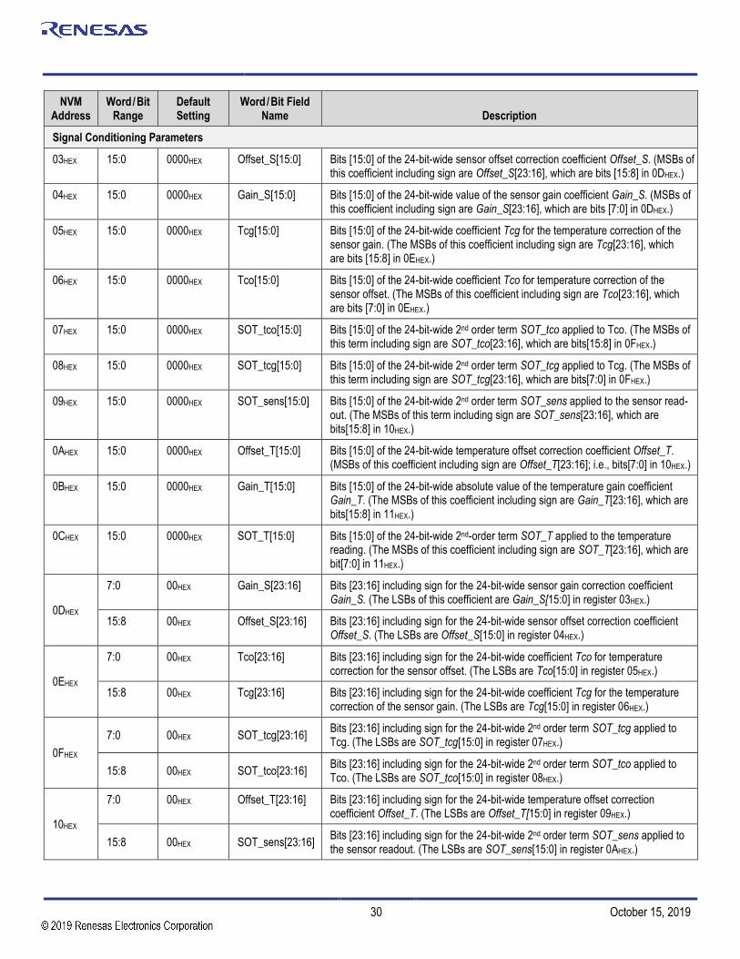
Signal Conditioning Parameters
03HEX 15:0 0000HEX Offset_S[15:0] Bits [15:0] of the 24-bit-wide sensor offset correction coefficient Offset_S. (MSBs of this coefficient including sign are Offset_S[23:16], which are bits [15:8] in 0DHEX.)
04HEX 15:0 0000HEX Gain_S[15:0] Bits [15:0] of the 24-bit-wide value of the sensor gain coefficient Gain_S. (MSBs of this coefficient including sign are Gain_S[23:16], which are bits [7:0] in 0DHEX.)
05HEX 15:0 0000HEX Tcg[15:0] Bits [15:0] of the 24-bit-wide coefficient Tcg for the temperature correction of the sensor gain. (The MSBs of this coefficient including sign are Tcg[23:16], which are bits [15:8] in 0EHEX.)
06HEX 15:0 0000HEX Tco[15:0] Bits [15:0] of the 24-bit-wide coefficient Tco for temperature correction of the sensor offset. (The MSBs of this coefficient including sign are Tco[23:16], which are bits [7:0] in 0EHEX.)
07HEX 15:0 0000HEX SOT_tco[15:0] Bits [15:0] of the 24-bit-wide 2nd order term SOT_tco applied to Tco. (The MSBs of this term including sign are SOT_tco[23:16], which are bits[15:8] in 0FHEX.)
08HEX 15:0 0000HEX SOT_tcg[15:0] Bits [15:0] of the 24-bit-wide 2nd order term SOT_tcg applied to Tcg. (The MSBs of this term including sign are SOT_tcg[23:16], which are bits[7:0] in 0FHEX.)
09HEX 15:0 0000HEX SOT_sens[15:0] Bits [15:0] of the 24-bit-wide 2nd order term SOT_sens applied to the sensor read-out. (The MSBs of this term including sign are SOT_sens[23:16], which are bits[15:8] in 10HEX.)
0AHEX 15:0 0000HEX Offset_T[15:0] Bits [15:0] of the 24-bit-wide temperature offset correction coefficient Offset_T. (MSBs of this coefficient including sign are Offset_T[23:16]; i.e., bits[7:0] in 10HEX.)
0BHEX 15:0 0000HEX Gain_T[15:0] Bits [15:0] of the 24-bit-wide absolute value of the temperature gain coefficient Gain_T. (The MSBs of this coefficient including sign are Gain_T[23:16], which are bits[15:8] in 11HEX.)
0CHEX 15:0 0000HEX SOT_T[15:0] Bits [15:0] of the 24-bit-wide 2nd-order term SOT_T applied to the temperature reading. (The MSBs of this coefficient including sign are SOT_T[23:16], which are bit[7:0] in 11HEX.)
0DHEX
7:0 00HEX Gain_S[23:16] Bits [23:16] including sign for the 24-bit-wide sensor gain correction coefficient Gain_S. (The LSBs of this coefficient are Gain_S[15:0] in register 03HEX.)
15:8 00HEX Offset_S[23:16] Bits [23:16] including sign for the 24-bit-wide sensor offset correction coefficient Offset_S. (The LSBs are Offset_S[15:0] in register 04HEX.)
0EHEX
7:0 00HEX Tco[23:16] Bits [23:16] including sign for the 24-bit-wide coefficient Tco for temperature correction for the sensor offset. (The LSBs are Tco[15:0] in register 05HEX.)
15:8 00HEX Tcg[23:16] Bits [23:16] including sign for the 24-bit-wide coefficient Tcg for the temperature correction of the sensor gain. (The LSBs are Tcg[15:0] in register 06HEX.)
0FHEX
7:0 00HEX SOT_tcg[23:16] Bits [23:16] including sign for the 24-bit-wide 2nd order term SOT_tcg applied to Tcg. (The LSBs are SOT_tcg[15:0] in register 07HEX.)
15:8 00HEX SOT_tco[23:16] Bits [23:16] including sign for the 24-bit-wide 2nd order term SOT_tco applied to Tco. (The LSBs are SOT_tco[15:0] in register 08HEX.)
10HEX
7:0 00HEX Offset_T[23:16] Bits [23:16] including sign for the 24-bit-wide temperature offset correction coefficient Offset_T. (The LSBs are Offset_T[15:0] in register 09HEX.)
15:8 00HEX SOT_sens[23:16] Bits [23:16] including sign for the 24-bit-wide 2nd order term SOT_sens applied to the sensor readout. (The LSBs are SOT_sens[15:0] in register 0AHEX.)

ZSSC3230 Datasheet
© 2019 Integrated Device Technology, Inc. 31 October 15, 2019
NVM Address
Word/Bit Range
Default Setting
Word/Bit Field Name Description
11HEX
7:0 00HEX SOT_T[23:16] Bits [23:16] including sign for the 24-bit-wide 2nd-order term SOT_T applied to the temperature reading. (The LSBs are SOT_T[15:0] in register 0BHEX.)
15:8 00HEX Gain_T[23:16] Bits [23:16] including sign for the 24-bit-wide absolute value of the temperature gain coefficient Gain_T. (The LSBs are Gain_T[15:0] in register 0CHEX.)
Measurement Configuration (Sensor_config) Register
12HEX
5:0 00 0000BIN shift_cap
Defines the zero shift capacitance input offset shift to cancel the static input capacitance of the sensor:
00 0000 no offset shift 00 0111 1.75pF
00 0001 0.25pF 00 1000 2.00pF
00 0010 0.50pF 00 1001 2.25pF
00 0011 0.75pF …
00 0100 1.00pF 11 1101 15.00pF
00 0101 1.25pF 11 1110 15.50pF
00 0110 1.50pF 11 1111 15.75pF
Note: the offset shift capacitance must not exceed the selected input capacitance’s range (see cap_range).
7:6 00BIN adc_bits
Defines the absolute number of bits for the A2D conversion:
00 12-bit 10 16-bit
01 14-bit (default) 11 18-bit
8 0BIN noise_mode
Select between control sequences for noise-quality vs. energy consumption optimization:
0 Low Current Mode 1 Low Noise Mode
13:9 0 0000BIN cap_range
Selection maximum possible external signal capacitance; i.e. the capacitance sensor range (without any offset):
00000 0.5pF 10000 8.5pF
00001 1.0pF 10001 9.0pF
00010 1.5pF 10010 9.5pF
00011 2.0pF 10011 10.0pF
00100 2.5pF 10100 10.5pF
00101 3.0pF 10101 11.0pF
00110 3.5pF 10110 11.5pF
00111 4.0pF 10111 12.0pF
01000 4.5pF 11000 12.5pF
01001 5.0pF 11001 13.0pF
01010 5.5pF 11010 13.5pF
01011 6.0pF 11011 14.0pF
01100 6.5pF 11100 14.5pF
01101 7.0pF 11101 15.0pF
01110 7.5pF 11110 15.5pF
01111 8.0pF 11111 16.0pF

ZSSC3230 Datasheet
© 2019 Integrated Device Technology, Inc. 32 October 15, 2019
NVM Address
Word/Bit Range
Default Setting
Word/Bit Field Name Description
12HEX
(Continued)
14 0BIN sensor_leakage
Option to enable sensor element’s leakage current compensation (due to sensor element’s parasitic resistance) leakage cancellation leads to loss of dynamic range and decrease of SNR (loss of 1 bit of effective resolution).
The following setups are possible:
0 no sensor leakage cancellation; full internal dynamic range; full Vref applied to external sensor
1 sensor leakage cancellation enabled; applied voltage at external sensor
of 0.5 Vref (loss of 1 bit of effective resolution)
15 0BIN sensecap_type
Selection of applied (external) sensor capacitance:
0 “differential” sensor capacitance between C0 and CC (CC’) pads
1 single ended sensor capacitance between VSS and CC (CC’) pad; applied voltage at external sensor of 0.5 × Vref (loss of 1 bit of effective resolution)
Interrupt Level Setup and Post-Calibration (Digital) Offset Calibration
13HEX 15:0 0000HEX TRSH1[15:0] Bits [15:0] of the 24-bit-wide interrupt threshold1, TRSH1. (The MSBs for this threshold are TRSH1[23:16], which are bits [7:0] of register 15HEX.)
14HEX 15:0 0000HEX TRSH2[15:0] Bits [15:0] of the 24-bit-wide interrupt threshold2, TRSH2. (The MSBs for this threshold are TRSH2[23:16], which are bits[15:8] of register 15HEX.)
15HEX
7:0 00HEX TRSH1[23:16] Bits [23:16] of the 24-bit-wide interrupt threshold1, TRSH1. (The LSBs for this threshold are TRSH1[15:0], which are bits[15:0] of register 13HEX.)
15:8 00HEX TRSH2[23:16] Bits [23:16] of the 24-bit-wide interrupt threshold2, TRSH2. (The LSBs for this threshold are TRSH2[15:0], which are bits[15:0] of register 14HEX.)
16HEX 15:0 0000HEX SENS_Shift[15:0] Bits [15:0] of the post-calibration sensor offset shift coefficient SENS_Shift. (The MSBs of SENS_Shift are bits [7:0] of register 18HEX.)
17HEX 15:0 0000HEX T_Shift[15:0] Bits [15:0] of the post-calibration temperature offset shift coefficient T_Shift. (The MSBs of T_Shift are bits [15:8] of register 18HEX.)
18HEX
7:0 00HEX SENS_Shift[23:16] Bits [23:16] of the post-calibration sensor offset shift coefficient SENS_Shift. (The LSBs of SENS_Shift are in register 16HEX.)
15:8 00HEX T_Shift[23:16] Bits [23:16] of the post-calibration temperature offset shift coefficient T_Shift. (The LSBs of T_Shift are in register 17HEX.)

ZSSC3230 Datasheet
© 2019 Integrated Device Technology, Inc. 33 October 15, 2019
NVM Address
Word/Bit Range
Default Setting
Word/Bit Field Name Description
Configuration Register
19HEX
1:0 00BIN CC_pin_selection
Defines which pin is used for measurement (CC and/or CC’):
00 no input
01 CC
10 CC’
11 CC and CC’
2 0BIN Dither Enable/disable digital dithering to improve EMI performance:
0 No dithering 1 Dithering enabled
3 0BIN En_sh2 Enable Subtraction Mode in grounded mode (see section 6.2.5):
0 Disabled 1 Enabled
4 0BIN En_shlddrv Enable active shield drive at the C0 pin (see section 6.2.4):
0 Disabled 1 Enabled
5 0BIN Dyn_imp
Enables higher drive current in analog front end, which will be needed if the sensor range is much smaller than the shift capacitor:
0 Disabled 1 Enabled
6 0BIN Test_cap
Enables an internal reference sensor capacitor of approx. 2pF in parallel to sensor input:
0 Disabled 1 Enabled
15:7 Reserved IDT lot tracking information; can be overwritten and used as free space for customer use.
1AHEX 15:0 0000HEX Reserved IDT lot tracking information; can be overwritten and used as free space for
customer use.
1BHEX 15:0 0000HEX Reserved IDT lot tracking information; can be overwritten and used as free space for
customer use.
1CHEX 15:0 0000HEX CRC Generated checksum (CRC) for whole memory through a linear feedback shift register (LFSR); Signature is checked upon power-up to ensure memory content integrity
The NVM-consistency checksum is calculated (IC-internally for the whole NVM) using the polynomial: x16 + x15 + x2 + 1. The checksum verification is only realized directly after VDD power-on. If the checksum is successfully verified, then the “Memory Error” status bit is set to 0BIN.

ZSSC3230 Datasheet
© 2019 Integrated Device Technology, Inc. 34 October 15, 2019
7. Package Outline Drawings
The package outline drawings VFQFPN package are appended at the end of this document and are accessible from the link below. The package information is the most current data available.
https://www.idt.com/document/psc/24-vfqfpn-package-outline-drawing-40-x-40-x-090-mm-body050mm-pitchepad-245-x-245-mm-nlg24p1
8. Marking Diagram
1. Line 1 is the truncated part number.
2. Line 2 – “YYWW” are the last two digit of the year and week that the part wasassembled.
3. Line 3 – “XXXXX” denotes assembly lot number.
9. Ordering Information
Orderable Part Number Description and Package MSL Rating Carrier Type Temperature
ZSSC3230BC1B Dice on 304µm wafer no inking Not applicable Wafer Box -40 to 85°C
ZSSC3230BC2B Dice on 725µm wafer no inking Not applicable Wafer Box -40 to 85°C
ZSSC3230BI1B Dice on 304µm wafer no inking Not applicable Wafer Box -40 to 125°C
ZSSC3230BI2B Dice on 725µm wafer no inking Not applicable Wafer Box -40 to 125°C
ZSSC3230BC5B Dice on 304µm wafer with inking Not applicable Wafer Box -40 to 85°C
ZSSC3230BC6B Dice on 725µm wafer with inking Not applicable Wafer Box -40 to 85°C
ZSSC3230BI5B Dice on 304µm wafer with inking Not applicable Wafer Box -40 to 125°C
ZSSC3230BI6B Dice on 725µm wafer with inking Not applicable Wafer Box -40 to 125°C
ZSSC3230BC3R 4 4 mm2 PQFN MSL1 13” Reel -40 to 85°C
ZSSC3230BI3R 4 4 mm2 PQFN MSL1 13” Reel -40 to 125°C
ZSSC3230BI3W 4 4 mm2 PQFN MSL1 7” Reel -40 to 125°C
ZSSC3230KIT ZSSC3230 Evaluation Board with USB Cable and 5 Samples

ZSSC3230 Datasheet
© 2019 Integrated Device Technology, Inc. 35 October 15, 2019
10. Glossary
Term Description
A2D Analog-to-Digital
ACK Acknowledge (interface’s protocol indicator for successful data/command transfer)
ADC Analog-to-Digital Converter or Conversion
AGND Analog Ground
AZ Auto-Zero (unspecific)
AZS Auto-Zero Measurement for (External) Sensor Path
AZT Auto-Zero Measurement for (External or Internal) Temperature Path
CLK Clock
CVC Charge-Voltage Converter
DAC Digital-to-Analog Converter or Conversion
EOC End of Conversion
FSO Full Scale Output (value in percent relative to the ADC maximum output code; resolution dependent)
HVAC Heating, Ventilation, and Air Conditioning
LFSR Linear Feedback Shift Register
LSB Least Significant Bit
MSB Most Significant Bit
MSL Moisture Sensitivity Level
NACK Not Acknowledge (interface’s protocol indicator for unsuccessful data/command transfer)
NVM Nonvolatile Memory
OpAmp Operating Amplifier
PGA Programmable Gain Amplifier
POR Power-On Reset
PSRR Power Supply (Disturbance) Rejection Ratio
PTAT Proportional to Absolute Temperature
S SSC-Corrected Sensor Readout / Result
SM Sensor Measurement
SNR Signal to Noise Ratio
SOT Second-Order Term
SSF Smart-Sensor Function (specific NVM registers)
T SSC-Corrected (additional) Temperature Readout / Result
TC Temperature Coefficient

ZSSC3230 Datasheet
© 2019 Integrated Device Technology, Inc. 36 October 15, 2019
11. Revision History
Revision Date Description of Change
October 15, 2019 Values updated for Power-up conditions
Conditions updated for equations for the S-shaped SOT_curve setting
September 10, 2019 Initial release.
Corporate Headquarters
6024 Silver Creek Valley Road San Jose, CA 95138 www.IDT.com
Sales
1-800-345-7015 or 408-284-8200Fax: 408-284-2775www.IDT.com/go/sales
Tech Support
www.IDT.com/go/support
DISCLAIMER Integrated Device Technology, Inc. (IDT) and its affiliated companies (herein referred to as “IDT”) reserve the ri ght to modify the products and/or specifications described herein at any time, without notice, at IDT's sole discretion. Performance specifications and operating parameters of the described products are determined in an independe nt state and are not guaranteed to perform the same way when installed in customer products. The information contained herein is provided without representation or warranty of any kind, whether express or implied, including, but not limited to, the suitabi lity of IDT's products for any particular purpose, an implied warranty of merchantability, or non -infringement of the intellectual property rights of others. This document is presented only as a guide and does not convey any license under intellectual property rights of IDT or any third parties.
IDT's products are not intended for use in applications involving extreme environmental conditions or in life support systems or similar devices where the failure or malfunction of an IDT product can be reasonably expected to significantly affect the health or safety of users. Anyone using an IDT product in such a manner does so at their own risk, absent an express, written agreement by IDT.
Integrated Device Technology, IDT and the IDT logo are trademarks or registered trademarks of IDT and its subsidiaries in the United States and other countries. Other trademarks used herein are the property of IDT or their respective third party owners. For datasheet type definitions and a glossary of common terms, visit www.idt.com/go/glossary. All contents of this document are copyright of Integrated Device Technology, Inc. All rights reserved.

© Integrated Device Technology, Inc.
24-VFQFPN, Package Outline Drawing
4.0 x 4.0 x 0.90 mm Body,0.50mm Pitch,Epad 2.45 x 2.45 mmNLG24P1, PSC-4192-01, Rev 02, Page 1
AutoCAD SHX Text
C0.30
AutoCAD SHX Text
PIN 1
AutoCAD SHX Text
INDEX AREA
AutoCAD SHX Text
2X
AutoCAD SHX Text
2X
AutoCAD SHX Text
TOP VIEW
AutoCAD SHX Text
SIDE VIEW
AutoCAD SHX Text
SEATING PLANE
AutoCAD SHX Text
BOTTOM VIEW
AutoCAD SHX Text
(DATUM A)
AutoCAD SHX Text
(DATUM B)
AutoCAD SHX Text
NOTES:
AutoCAD SHX Text
1. DIMENSIONING AND TOLERANCING CONFORME TO ASME Y14.5M-1994.
AutoCAD SHX Text
2. ALL DIMENSIONS ARE IN MILLIMETERS.
AutoCAD SHX Text
1
AutoCAD SHX Text
6
AutoCAD SHX Text
7
AutoCAD SHX Text
12
AutoCAD SHX Text
13
AutoCAD SHX Text
18
AutoCAD SHX Text
19
AutoCAD SHX Text
24

© Integrated Device Technology, Inc.
24-VFQFPN, Package Outline Drawing
4.0 x 4.0 x 0.90 mm Body,0.50mm Pitch,Epad 2.45 x 2.45 mmNLG24P1, PSC-4192-01, Rev 02, Page 2
Package Revision HistoryRev No.Date Created Description
Rev 02 New Format, Recalculate Land Pattern Change QFN to VFQFPNSept 13, 2018
Rev 01 Add Chamfer on EpadSept 9, 2016
AutoCAD SHX Text
RECOMMENDED LAND PATTERN DIMENSION
AutoCAD SHX Text
1. ALL DIMENSIONS ARE IN MM. ANGLES IN DEGREES.
AutoCAD SHX Text
2. TOP DOWN VIEW, AS VIEWED ON PCB.
AutoCAD SHX Text
3. LAND PATTERN RECOMMENDATION PER IPC-7351B GENERIC REQUIREMENT
AutoCAD SHX Text
NOTES:
AutoCAD SHX Text
FOR SURFACE MOUNT DESIGN AND LAND PATTERN.

20
Corporate HeadquartersTOYOSU FORESIA, 3-2-24 Toyosu,Koto-ku, Tokyo 135-0061, Japanwww.renesas.com
Contact InformationFor further information on a product, technology, the most up-to-date version of a document, or your nearest sales office, please visit:www.renesas.com/contact/
TrademarksRenesas and the Renesas logo are trademarks of Renesas Electronics Corporation. All trademarks and registered trademarks are the property of their respective owners.