9TCS1083 - Datasheet Archive
39
PRELIMINARY DATASHEET MOBILE ACCESS™—CLOCK SYNTHESIZER, TEMPERATURE SENSOR, & PWM FAN CONTROLLER FOR PORTABLE DEVICES 9TCS1083 IDT® MOBILE ACCESS™—CLOCK SYNTHESIZER, TEMPERATURE SENSOR, & PWM FAN CONTROLLER FOR PORTABLE DEVICES 1 9TCS1083 REV 0.8 011612 Description The 9TCS1083 is a highly programmable IC that integrates clock synthesizers with a PWM Fan controller and multiple temperature sensors for hardware thermal protection. The device has an ultra-low-power 32.768 kHz frequency generator to support Real Time Clocks (RTC). This device can generate the 32.768 kHz frequency up to four years of life powered by a CR2032 coincell battery. The 9TCS1083 can output computer system clock frequencies of 24, 25, 27 and 48 MHz which reduces the component count on the circuit board. The fan controller is pulsed width modulated (PWM) used for the temperature proportional speed control. The device is highly configurable through I2C for ease and flexibility of use. The fan controller has three different modes of operations and will work with multiple pole, brushless DC fans. An integrated Start-up Timer ensures reliable motor start-up and turn-on or follows a detected fault condition. The 9TCS1083 includes temperature monitor function that measures through two external diodes. The temperature sensor is optimized to be accurate within ±1°C between the temperature range of 60°C to 100°C. This device is highly programmable through the use of I 2 C to set high and low limits for all the temperature channels as well as setting critical limits. The hardware limits drive dedicated ALERT and THERM pins for system shutdown. The 9TCS1083 is available in a 32-pin QFN package and is available for commercial temperature range. Applications • Notebook Computers • Netbook Computers • Smartbook Computers • Consumer Portable Devices • Embedded Systems • Networking Equipment (i.e. Routers, Switches) • Network Area Storage Features Thermal Sensor • Two temperature sensor channels • Both H/W & S/W programmable over/under temperature alarms • No Calibration required in application • Diode failure detection • Support SMBUS Alert • Accuracy: ±1°C (+60°C to +100°C); ±2°C (0°C to +100°C) • Offset register for system calibration • Series resistor cancellation feature Fan Controller • High frequency or low frequency PWM outputs for use with 4-Wire Fans • TACH inputs to measure fan speed • OS Independent Automatic Fan Speed Control based on thermal information • Dynamic TMIN Control Mode to optimize system acoustics • Default startup at 100% PWM for all fans for robust operation System Clock PLL Synthesizers • Scalable low voltage VDD I/O (1.5V to 1.05V) to reduce power consumption (applies to 25MHz output) • Integrated series termination resistors • Selectable – Single-ended 24MHz/27MHz/48MHz clock output @ VDD3.3V • 3 – Single ended 25MHz clock outputs (buffer out) • 32.768 kHz outputs with < 1.8μA power consumption for system RTC circuit
-
Upload
khangminh22 -
Category
Documents
-
view
2 -
download
0
Transcript of 9TCS1083 - Datasheet Archive

PRELIMINARY DATASHEET
MOBILE ACCESS™—CLOCK SYNTHESIZER, TEMPERATURE SENSOR,& PWM FAN CONTROLLER FOR PORTABLE DEVICES
9TCS1083
IDT® MOBILE ACCESS™—CLOCK SYNTHESIZER, TEMPERATURE SENSOR, & PWM FAN CONTROLLER FOR PORTABLE DEVICES 1
9TCS1083 REV 0.8 011612
Description
The 9TCS1083 is a highly programmable IC that integrates clock synthesizers with a PWM Fan controller and multiple temperature sensors for hardware thermal protection.
The device has an ultra-low-power 32.768 kHz frequency generator to support Real Time Clocks (RTC). This device can generate the 32.768 kHz frequency up to four years of life powered by a CR2032 coincell battery. The 9TCS1083 can output computer system clock frequencies of 24, 25, 27 and 48 MHz which reduces the component count on the circuit board.
The fan controller is pulsed width modulated (PWM) used for the temperature proportional speed control. The device is highly configurable through I2C for ease and flexibility of use. The fan controller has three different modes of operations and will work with multiple pole, brushless DC fans. An integrated Start-up Timer ensures reliable motor start-up and turn-on or follows a detected fault condition.
The 9TCS1083 includes temperature monitor function that measures through two external diodes. The temperature sensor is optimized to be accurate within ±1°C between the temperature range of 60°C to 100°C. This device is highly programmable through the use of I2C to set high and low limits for all the temperature channels as well as setting critical limits. The hardware limits drive dedicated ALERT and THERM pins for system shutdown.
The 9TCS1083 is available in a 32-pin QFN package and is available for commercial temperature range.
Applications
• Notebook Computers• Netbook Computers• Smartbook Computers• Consumer Portable Devices• Embedded Systems• Networking Equipment (i.e. Routers, Switches)• Network Area Storage
Features
Thermal Sensor• Two temperature sensor channels• Both H/W & S/W programmable over/under temperature
alarms• No Calibration required in application• Diode failure detection• Support SMBUS Alert• Accuracy: ±1°C (+60°C to +100°C); ±2°C (0°C to
+100°C)• Offset register for system calibration• Series resistor cancellation feature
Fan Controller• High frequency or low frequency PWM outputs for use
with 4-Wire Fans• TACH inputs to measure fan speed• OS Independent Automatic Fan Speed Control based on
thermal information• Dynamic TMIN Control Mode to optimize system
acoustics• Default startup at 100% PWM for all fans for robust
operation
System Clock PLL Synthesizers• Scalable low voltage VDD I/O (1.5V to 1.05V) to reduce
power consumption (applies to 25MHz output)• Integrated series termination resistors• Selectable – Single-ended 24MHz/27MHz/48MHz clock
output @ VDD3.3V• 3 – Single ended 25MHz clock outputs (buffer out)• 32.768 kHz outputs with < 1.8µA power consumption for
system RTC circuit

9TCS1083
MOBILE ACCESS™—CLOCK SYNTHESIZER, TEMPERATURE SENSOR, & PWM FAN CONTROLLER FOR PORTABLE DEVICES
IDT® MOBILE ACCESS™—CLOCK SYNTHESIZER, TEMPERATURE SENSOR, & PWM FAN CONTROLLER FOR PORTABLE DEVICES 2
9TCS1083 REV 0.8 011612
Block Diagram
Preferred drive strengths for single-ended outputs. Transmission lines to load do not share series resistors.Desktop (Zo=50Ω) and mobile (Zo=55Ω) have the same drive strength.
1 Load Rs = 2 Loads Rs= 3 Loads Rs =
10.56 / 33
(17Ω)33Ω [39Ω] - -
20.92 / 66
(14Ω)39Ω [43Ω] 22Ω [27Ω] -
31.15 / 99 (11.6Ω)
43Ω [43Ω] 27Ω [33Ω] 15Ω [22Ω]
D.C.Drive Strength
Number of Loads to Drive
Number of Loads Actually Driven. Match Point for N & P Voltage / Current (mA)
VDD_RTCV_bat
SMBCLK
Channel 1
V_3.3
Fan ControllerPWM
TACH
SMBDAT
ALERT#
THERM#
Channel 2
Analog MUX
Sample Current
Digital11 bitsADC
Regulator
RAM
ReferenceVoltage
Fault Detect
PowerSwitch
POR
XtalX1
X2
GND
AmplitudeControl
32.768KDCO
32K_A_IO
32K_B_IO
32K_A
32K_B / 25M_C
VDD_32KB
25M_IO 25M_A
VDDIO_25MA
25M_IO 25M_B
VDD_25MB
UltraLow Power
PLL
24/48M_IO 24M_48M
VDD_24M
27/48M_IO 27M_48M
VDD_27M
Fraction NDivider
VDD_TS
SMBUS

9TCS1083
MOBILE ACCESS™—CLOCK SYNTHESIZER, TEMPERATURE SENSOR, & PWM FAN CONTROLLER FOR PORTABLE DEVICES
IDT® MOBILE ACCESS™—CLOCK SYNTHESIZER, TEMPERATURE SENSOR, & PWM FAN CONTROLLER FOR PORTABLE DEVICES 3
9TCS1083 REV 0.8 011612
Pin Assignment
Power Group
The
rmal
_DX
P1
The
rmal
_DX
N1
VB
AT
VD
D_3
2KB
SE
L25*
/32K
_B_2
5M_C
GN
D
VD
D_T
S
GN
D_T
S
32 31 30 29 28 27 26 25
Thermal_DXP2 1 24 THERM#
Thermal_DXN2 2 23 ALERT#
32K_A 3 22 VDD_RTC_OUT
VDDIO_25MA 4 21 V_3.3
GND 5 20 X2
25M_A 6 19 X1
VDD_24 7 18 SMBDATA
SEL_24*/24M_48M 8 17 SMBCLK
9 10 11 12 13 14 15 16
SE
L_27
*/27
M_4
8M
VD
D_2
7
25M
_B
GN
D
VD
D_2
5MB
PW
RG
D/P
D#
TA
CH
PW
M
* Internal Pull-Up Resistor24M/27M/48Mhz outputs require external series resistors on Board.
9TCS1083
VDD GND
4 33 VDDIO_25MA IO power
7 5 VDDIO_24 IO power
10 12 VDDIO_27
13 33 VDDIO_25B IO Power
21 33 V3.3
22 27 VDD_RTC_Out
26 25 VDD_TS power
29 27 VDDIO_32KB Power
30 27 VBAT power
* Pin33: Thermal pad (connect to GND)
Pin NumberDescription

9TCS1083
MOBILE ACCESS™—CLOCK SYNTHESIZER, TEMPERATURE SENSOR, & PWM FAN CONTROLLER FOR PORTABLE DEVICES
IDT® MOBILE ACCESS™—CLOCK SYNTHESIZER, TEMPERATURE SENSOR, & PWM FAN CONTROLLER FOR PORTABLE DEVICES 4
9TCS1083 REV 0.8 011612
Pin DescriptionsPIN # PIN NAME TYPE DESCRIPTION
1 Thermal_DXP2 IN External thermal diode P (Channel 2)
2 Thermal_DXN2 IN External thermal diode N (Channel 2)
3 32K_A OUT RTC clock 32.768KHz output A, typical 1V peak to peak.
4 VDDIO_25MA PWR Power for 25MHz_A output, typical 1.05V to 1.8V.
5 GND PWR Ground pin
6 25M_A OUT 25MHz_A output, typical 1.05V to 1.8V pending on VDDIO_25MA voltage.
7 VDD_24M PWR Power for 24/48MHz output, typical 3.3V.
24MHz enable latched input / Programmable free‐running 24/48M clock output.
SEL_24 selects the functionality of 24_48M output as the following:
1 = 24M output (Default)
0 = 48M output
27MHz enable latched input / Programmable free‐running 27/48M clock output.
SEL_27 selects the functionality of 27_48M output as the following:
1 = 27M output (default)
0 = 48M output
10 VDD_27M PWR Power for 27/48 MHz output, typical 3.3V.
11 25M_B OUT 25MHz_B output, typical 3.3V peak to peak.
12 GND PWR Ground pin
13 VDD_25MB PWR Power for LDO and main circuit.
14 PWRGD/PD# INThis 3.3V LVTTL input notifies device to sample latched inputs and start up on first high assertion or
exit powerdown mode on subsequent assertions. Low enters powerdown mode.
15 TACH IN Fan controller TACH signal input
16 PWM OUT Fan controller PWM signal output
17 SMBCLK IN SMBUS clock. 3.3V tolerant.
18 SMBDAT I/O SMBUS data. 3.3V tolerant.
19 X1 IN Crystal input. Connect to 25MHz crystal.
20 X2 OUT Crystal output. Connect to 25MHz crystal.
21 V_3.3 PWR Power for 32K PLL core. Connect to system's 3.3V standby power rail.
22 VDD_RTC_OUT OUT Power for chipset RTC circuit.
23 ALERT# OUT Open drain interrupt output for SMBUS alert pin.
24 THERM# OUT Open drain interrupt output for external hardware connection.
25 GND_TS PWR Ground pin for thermal sensor function
26 VDD_TS PWR Power for thermal sensor function, typical 3.3V.
27 GND PWR Ground pin
25MHz_C output select pin / Programmable free‐running 32.768khz or 25MHz clock output.
SEL_25 selects the functionality of 32K_25M output as the following:
1 = 25MHz output (Default)
0 = 32.768kHz output
29 VDD_32KB PWR Power for 32.768kHz_B output, typical 3.3V.
30 VBAT PWR Power for 32kHz_A output. Connect to coin cell battery
31 Thermal_DXN1 IN external thermal diode N
32 Thermal_DXP1 IN external thermal diode P
33 Thermal Pad PWR Connect to GND.
28 SEL_25*/32KB_25M_C I/O
8 SEL_24*/24M_48M I/O
9 SEL_27*/27M_48M I/O

9TCS1083
MOBILE ACCESS™—CLOCK SYNTHESIZER, TEMPERATURE SENSOR, & PWM FAN CONTROLLER FOR PORTABLE DEVICES
IDT® MOBILE ACCESS™—CLOCK SYNTHESIZER, TEMPERATURE SENSOR, & PWM FAN CONTROLLER FOR PORTABLE DEVICES 5
9TCS1083 REV 0.8 011612
Frequency and Output Selection Tables
Pin number Setting OutputL 48MHz
H 24MHz
L 48MHz
H 27MHz
L 32.768kHz_B
H 25MHz_C
-default, internal pull high
Clock Output Selection Table
Remark
8
-default, internal pull high
9
default, internal pull high
-28
Output Selection Table A
V_Bat V_3.3 VDD_32KB VDDIO_25A VDD_25B 32K_A 32K_B 25M_A 25M_B VDD_RTC
2.3~3.0 0 0 0 0 ON OFF OFF OFF Vbat2.3~3.0 3.31 0 0 0 ON OFF OFF OFF V3.3
2.3~3.0 3.31 3.3 0 0 ON ON OFF OFF V3.3
2.3~3.0 3.31 3.3 1.05~1.52 0 ON ON ON OFF V3.3
2.3~3.0 3.31 3.3 1.05~1.52 3.3 ON ON ON ON V3.3
Note 2: If amplitude greater than 1.5V is required on 25MHz_A output, please contact IDT support.Note 1: When V3.3 is applied, XTAL will always be ON. 32K source will switch to an analog PLL. Fan control will be ON.
Power Supply VDDIO_Control Outputs
Output Selection Table B
V_3.3 VDD_24M1 VDD_27M VDD_TS 24_48M 27_48M Fan ControlThermal Sensor
3.3 0 0 0 OFF OFF ON OFF3.3 3.3 0 0 ON OFF ON OFF3.3 3.3 3.3 0 ON ON ON OFF3.3 3.3 3.3 3.3 ON ON ON ON
Note 1: When either VDD_24M, VDD_27M or VDD_TS is ON, V_3.3 should be ON.
OutputsPower Supply

9TCS1083
MOBILE ACCESS™—CLOCK SYNTHESIZER, TEMPERATURE SENSOR, & PWM FAN CONTROLLER FOR PORTABLE DEVICES
IDT® MOBILE ACCESS™—CLOCK SYNTHESIZER, TEMPERATURE SENSOR, & PWM FAN CONTROLLER FOR PORTABLE DEVICES 6
9TCS1083 REV 0.8 011612
Absolute Maximum Ratings
Stresses above the ratings listed below can cause permanent damage to the 9TCS1083. These ratings, which are standard values for IDT commercially rated parts, are stress ratings only. Functional operation of the device at these or any other conditions above those indicated in the operational sections of the specifications is not implied. Exposure to absolute maximum rating conditions for extended periods can affect product reliability. Electrical parameters are guaranteed only over the recommended operating temperature range.
Electrical Characteristics–SMBus Interface
AC Electrical Characteristics–Input/Common Parameters
PARAMETER SYMBOL CONDITIONS MIN MAX UNITS Notes
Maximum Supply Voltage VDDxxx Core/Logic Supply 3.6 V 1,2
Maximum Supply Voltage VDDIOxxx Core/Logic Supply 3.6 V 1,2
Maximum Input Voltage VIH 3.3V LVCMOS Inputs 3.6 V 1,2,3
Minimum Input Voltage VIL Any Input GND - 0.5 V 1,2
Storage Temperature Ts - -65 150 °C 1,2Case Temperature Tcase - 115 °C 1,2
1 Unless otherwise noted, guaranteed by design and characterization, not 100% tested in production.2 Operation under these conditions is neither implied, nor guaranteed.3 Maximum input voltage is not to exceed maximum VDD
PARAMETER SYMBOL CONDITIONS MIN MAX UNITS Notes SMBus Voltage VDD 2.7 3.6 V 1
Low-level Output Voltage VOLSMB @ IPULLUP 0.4 V 1Current sinking at
VOLSMB = 0.4 VIPULLUP SMB Data Pin 4 mA 1
SCLK/SDATAClock/Data Rise Time
TRI2C(Max VIL - 0.15) to (Min VIH + 0.15)
1000 ns 1
SCLK/SDATAClock/Data Fall Time
TFI2C(Min VIH + 0.15) to
(Max VIL - 0.15)300 ns 1
Maximum SMBus Operating Frequency
FSMBUS Block Mode 400 kHz 1
1 Unless otherwise noted, guaranteed by design and characterization, not 100% tested in production.
PARAMETER SYMBOL CONDITIONS MIN MAX UNITS Notes
Clk Stabilization TSTABFrom VDD Power-Up or de-assertion of PD# to 1st clock
1.8 ms 1
Tdrive_PD# TDRPDDifferential output enable after
PD# de-assertion300 us 1
1 Unless otherwise noted, guaranteed by design and characterization, not 100% tested in production.

9TCS1083
MOBILE ACCESS™—CLOCK SYNTHESIZER, TEMPERATURE SENSOR, & PWM FAN CONTROLLER FOR PORTABLE DEVICES
IDT® MOBILE ACCESS™—CLOCK SYNTHESIZER, TEMPERATURE SENSOR, & PWM FAN CONTROLLER FOR PORTABLE DEVICES 7
9TCS1083 REV 0.8 011612
Electrical Characteristics–Input/Supply/Common ParametersPARAMETER SYMBOL CONDITIONS MIN MAX UNITS Notes
Ambient Operating Temp Tambient - 0 70 °C
Supply Voltage V_3.3 Supply Voltage 3.135 3.465 V
Supply Voltage VDD_xx Other Supply Voltages 3.135 3.465 V
Supply Voltage VDDIO_25MA Supply Voltage 0.9975 1.575 V
Supply Voltage V_bat Supply Voltage 2.3 3.465 V
Input High Voltage VIHSE Single-ended inputs 2 VDD + 0.3 V 1,4
Input Low Voltage VILSE Single-ended inputs VSS - 0.3 0.8 V 1,4Low Threshold Input-
High VoltageVIH_FS 3.3 V +/-5% 0.7 VDD + 0.3 V 1
Low Threshold Input-Low Voltage
VIL_FS 3.3 V +/-5% VSS - 0.3 0.35 V 1
Input Leakage Current IIN VIN = VDD , VIN = GND -5 5 uA 1,3
Input Leakage Current IINRES
Inputs with pull or pull down resistors
VIN = VDD , VIN = GND-200 200 uA 1
Output High Voltage VOHSESingle-ended outputs, IOH = -
1mA2.4 V 1,2
Output Low Voltage VOLSE Single-ended outputs, IOL = 1 mA 0.4 V 1,2
IDD3.3OPFull active mode, CL = Full load,
3.3V Rail50 mA 1
IDD3.3PD# Complete Power-Down, 3.3V Rail 10 mA 1
IDD3.3WOLWOL Mode with 25MA running,
3.3V Rail25 mA 1
IDD3.3RTCRTC Mode with 32KA running,
3.3V Rail0.1 uA 1
IDDIO_OPFull active mode, CL = Full load,
VDDIO Rails5 mA 1
IDDIO_PD#Complete Power-Down,
VDDIO Rails1 mA 1
IDDDIO_WOLWOL Mode with 25MA running,
VDDIO Rails10 mA 1
IDDIO_RTCRTC Mode with only 32KA
running, VDDIO Rails0.5 uA 1
V_bat Operating Supply Current
IDD_V_batRTC Mode with 32KA running,
V_bat Rail1.8 uA 1
Input Frequency Fi VDD = 3.3 V MHz 1
Pin Inductance Lpin 7 nH 1
CIN Logic Inputs 1.5 5 pF 1
COUT Output pin capacitance 6 pF 1
CINX X1 & X2 pins 6 pF 1*TA = 0 - 70°C; Supply Voltage V_3.3 = VDD_TS = 3.3 V +/-5%, VDD_24M = VDD_27M = VDD_25MB = 3.3V +/- 5%, VDD_25MA = 1.05V +/- 5%, VDD_32KB = 3.3V +/- 5%, CL = 5pF with Rs = 27Ω (unless otherwise specified)
3.3V Operating Supply Current
VDDIO Operating Supply Current
25MHz Typical
Input Capacitance
1 Unless otherwise noted, guaranteed by design and characterization, not 100% tested in production.2Signal is required to be monotonic in this region.3 Input leakage current does not include inputs with pull-up or pull-down resistors4 3.3V referenced inputs are: SCLK, SDATA, SEL_25, SEL_24, SEL_27, PWRGD.
9TCS1083
MOBILE ACCESS™—CLOCK SYNTHESIZER, TEMPERATURE SENSOR, & PWM FAN CONTROLLER FOR PORTABLE DEVICES
IDT® MOBILE ACCESS™—CLOCK SYNTHESIZER, TEMPERATURE SENSOR, & PWM FAN CONTROLLER FOR PORTABLE DEVICES 8
9TCS1083 REV 0.8 011612
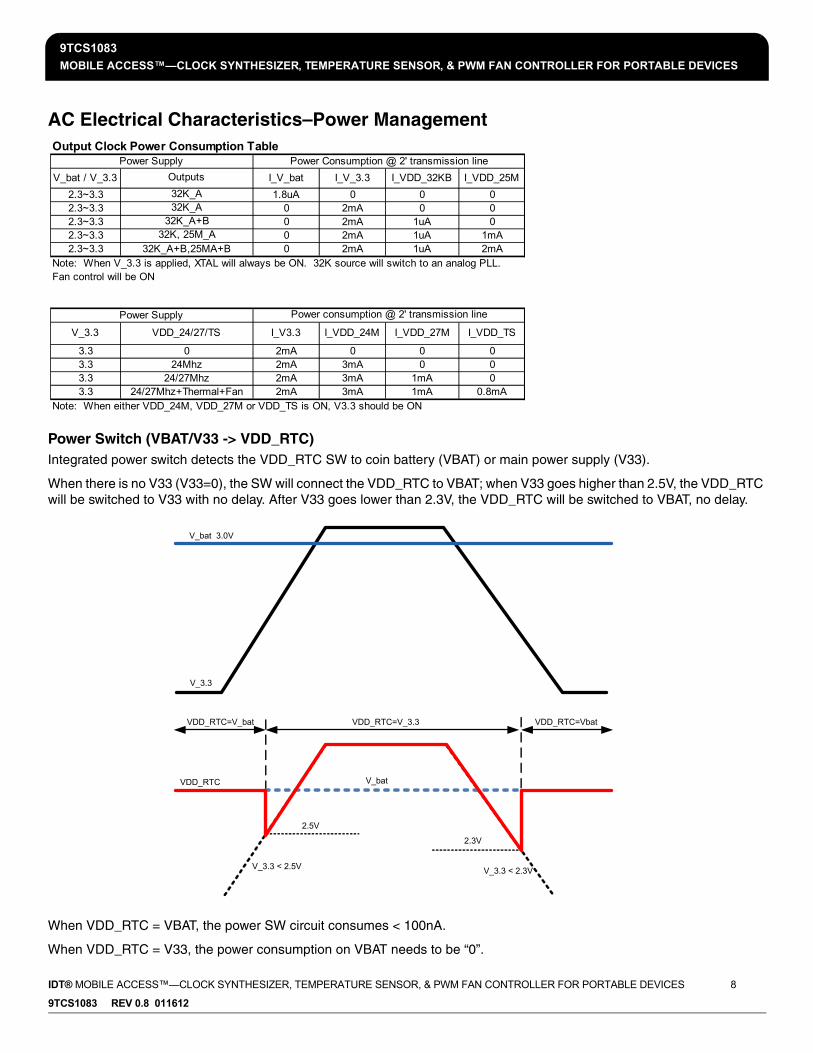
AC Electrical Characteristics–Power Management
Power Switch (VBAT/V33 -> VDD_RTC)Integrated power switch detects the VDD_RTC SW to coin battery (VBAT) or main power supply (V33).
When there is no V33 (V33=0), the SW will connect the VDD_RTC to VBAT; when V33 goes higher than 2.5V, the VDD_RTC will be switched to V33 with no delay. After V33 goes lower than 2.3V, the VDD_RTC will be switched to VBAT, no delay.
When VDD_RTC = VBAT, the power SW circuit consumes < 100nA.
When VDD_RTC = V33, the power consumption on VBAT needs to be “0”.
Output Clock Power Consumption Table
V_bat / V_3.3 I_V_bat I_V_3.3 I_VDD_32KB I_VDD_25M
2.3~3.3 1.8uA 0 0 02.3~3.3 0 2mA 0 02.3~3.3 0 2mA 1uA 02.3~3.3 0 2mA 1uA 1mA2.3~3.3 0 2mA 1uA 2mA
V_3.3 I_V3.3 I_VDD_24M I_VDD_27M I_VDD_TS
3.3 2mA 0 0 03.3 2mA 3mA 0 03.3 2mA 3mA 1mA 03.3 2mA 3mA 1mA 0.8mA
Note: When V_3.3 is applied, XTAL will always be ON. 32K source will switch to an analog PLL. Fan control will be ON
Power consumption @ 2' transmission line
Note: When either VDD_24M, VDD_27M or VDD_TS is ON, V3.3 should be ON
32K_A+B32K, 25M_A
Power Supply
Power Supply
VDD_24/27/TS
24/27Mhz+Thermal+Fan24/27Mhz
24Mhz0
Outputs
32K_A32K_A
32K_A+B,25MA+B
Power Consumption @ 2' transmission line
VDD_RTC=Vbat
V_bat 3.0V
VDD_RTC=V_bat
V_3.3 < 2.5V V_3.3 < 2.3V
VDD_RTC=V_3.3
VDD_RTC
V_3.3
V_bat
2.5V
2.3V

9TCS1083
MOBILE ACCESS™—CLOCK SYNTHESIZER, TEMPERATURE SENSOR, & PWM FAN CONTROLLER FOR PORTABLE DEVICES
IDT® MOBILE ACCESS™—CLOCK SYNTHESIZER, TEMPERATURE SENSOR, & PWM FAN CONTROLLER FOR PORTABLE DEVICES 9
9TCS1083 REV 0.8 011612
Electrical Characteristics–USB48MHz
Electrical Characteristics–24MHz
PARAMETER SYMBOL CONDITIONS MIN MAX UNITS NOTESLong Accuracy ppm see Tperiod min-max values -100 100 ppm 1,2Clock period Tperiod 48.00MHz output nominal 20.8313 20.8354 ns 1,2
Output High Voltage VOH IOH = -1 mA 2.4 V 1
Output Low Voltage VOL IOL = 1 mA 0.4 V 1
V OH @MIN = 1.0 V -33 mA 1
VOH@MAX = 3.135 V -33 mA 1
VOL @ MIN = 1.95 V 30 mA 1
VOL @ MAX = 0.4 V 38 mA 1
Rising Edge Slew Rate tSLR Measured from 0.8 to 2.0 V 0.5 2.5 V/ns 1
Falling Edge Slew Rate tSLR Measured from 2.0 to 0.8 V 0.5 2.5 V/ns 1
Duty Cycle dt1 VT = 1.5 V 45 55 % 1
Jitter, Cycle to cycle tjcyc-cyc VT = 1.5 V 350 ps 1*TA = 0 - 70°C; Supply Voltage V_3.3 = VDD_TS = 3.3 V +/-5%, VDD_24M = VDD_27M = VDD_25MB = 3.3V +/- 5%, VDD_25MA = 1.05V +/- 5%, VDD_32KB = 3.3V +/- 5%, CL = 5pF with Rs = 27Ω (unless otherwise specified)1Guaranteed by design and characterization, not 100% tested in production.2 All Long Term Accuracy and Clock Period specifications are guaranteed assuming that REFOUT is at 25.000000MHz
IOH
Output Low Current IOL
Output High Current
PARAMETER SYMBOL CONDITIONS MIN MAX UNITS NOTESLong Accuracy ppm see Tperiod min-max values -100 100 ppm 1,2Clock period Tperiod 24.00MHz output nominal 41.6625 41.6708 ns 1,2
Output High Voltage VOH IOH = -1 mA 2.4 V 1
Output Low Voltage VOL IOL = 1 mA 0.4 V 1
V OH @MIN = 1.0 V -33 mA 1
VOH@MAX = 3.135 V -33 mA 1
VOL @ MIN = 1.95 V 30 mA 1
VOL @ MAX = 0.4 V 38 mA 1
Rising Edge Slew Rate tSLR Measured from 0.8 to 2.0 V 0.5 4 V/ns 1
Falling Edge Slew Rate tSLR Measured from 2.0 to 0.8 V 0.5 4 V/ns 1
Duty Cycle dt1 VT = 1.5 V 45 55 % 1
Jitter, Cycle to cycle tjcyc-cyc VT = 1.5 V 350 ps 1*TA = 0 - 70°C; Supply Voltage V_3.3 = VDD_TS = 3.3 V +/-5%, VDD_24M = VDD_27M = VDD_25MB = 3.3V +/- 5%, VDD_25MA = 1.05V +/- 5%, VDD_32KB = 3.3V +/- 5%, CL = 5pF with Rs = 27Ω (unless otherwise specified)1Guaranteed by design and characterization, not 100% tested in production.2 All Long Term Accuracy and Clock Period specifications are guaranteed assuming that REFOUT is at 25.000000MHz
Output Low Current IOL
Output High Current IOH

9TCS1083
MOBILE ACCESS™—CLOCK SYNTHESIZER, TEMPERATURE SENSOR, & PWM FAN CONTROLLER FOR PORTABLE DEVICES
IDT® MOBILE ACCESS™—CLOCK SYNTHESIZER, TEMPERATURE SENSOR, & PWM FAN CONTROLLER FOR PORTABLE DEVICES 10
9TCS1083 REV 0.8 011612
Electrical Characteristics–25M_B & 25M_C
Electrical Characteristics–25MHz_A (Low Voltage output)
PARAMETER SYMBOL CONDITIONS MIN MAX UNITS NOTESLong Accuracy ppm see Tperiod min-max values -100 100 ppm 1,2Clock period Tperiod 25.00MHz output nominal 39.99600 40.00400 ns 1,2
Output High Voltage VOH IOH = -1 mA 2.4 V 1
Output Low Voltage VOL IOL = 1 mA 0.4 V 1
V OH @MIN = 1.0 V -29 mA 1
VOH@MAX = 3.135 V -23 mA 1
VOL @ MIN = 1.95 V 29 mA 1
VOL @ MAX = 0.4 V 27 mA 1
Rising Edge Slew Rate tSLR Measured from 0.8 to 2.0 V 0.5 4 V/ns 1
Falling Edge Slew Rate tSLR Measured from 2.0 to 0.8 V 0.5 4 V/ns 1
Duty Cycle dt1 VT = 1.5 V 40 60 % 1
Jitter, Cycle to cycle tjcyc-cyc VT = 1.5 V 500 ps 1*TA = 0 - 70°C; Supply Voltage V_3.3 = VDD_TS = 3.3 V +/-5%, VDD_24M = VDD_27M = VDD_25MB = 3.3V +/- 5%, VDD_25MA = 1.05V +/- 5%, VDD_32KB = 3.3V +/- 5%, CL = 5pF with Rs =0Ω (unless otherwise specified)1Guaranteed by design and characterization, not 100% tested in production.2 All Long Term Accuracy and Clock Period specifications are guaranteed assuming that REFOUT is at 25.000000MHz
Output High Current IOH
Output Low Current IOL
PARAMETER SYMBOL CONDITIONS MIN MAX UNITS NotesLong Accuracy ppm see Tperiod min-max values -100 100 ppm 1,2Clock period Tperiod 25.00MHz output nominal 39.99600 40.00400 ns 1,2
Output High Voltage VOH IOH = -1 mA Vtop-0.1 V 1
Output Low Voltage VOL IOL = 1 mA 0.1 V 1
Output High Current IOH VOH =0.83xVtop -3 -16 mA 1
Output Low Current IOL VOL = 0.13V 25 mA 1
Rising Edge Slew Rate tSLR Measured from 20% to 80% 0.5 4 V/ns 1,3
Falling Edge Slew Rate tFLR Measured from 80% to 20% 0.5 4 V/ns 1,3
Duty Cycle dt1 VT = Vtop/2 40 60 % 1,4
Jitter tjcyc-cyc VT = Vtop/2 500 ps 1,4*TA = 0 - 70°C; Supply Voltage V_3.3 = VDD_TS = 3.3 V +/-5%, VDD_24M = VDD_27M = VDD_25MB = 3.3V +/- 5%, VDD_25MA = 1.05V +/- 5%, VDD_32KB = 3.3V +/- 5%, CL = 5pF with Rs = 0Ω (unless otherwise specified)1Guaranteed by design and characterization, not 100% tested in production.2 All Long Term Accuracy and Clock Period specifications are guaranteed assuming that REFOUT is at 25.000000MHz

9TCS1083
MOBILE ACCESS™—CLOCK SYNTHESIZER, TEMPERATURE SENSOR, & PWM FAN CONTROLLER FOR PORTABLE DEVICES
IDT® MOBILE ACCESS™—CLOCK SYNTHESIZER, TEMPERATURE SENSOR, & PWM FAN CONTROLLER FOR PORTABLE DEVICES 11
9TCS1083 REV 0.8 011612
Electrical Characteristics–27MHz
Electrical Characteristics–32KHz_A (Low Voltage Output)
Electrical Characteristics–32KHz_B
PARAMETER SYMBOL CONDITIONS MIN MAX UNITS NotesLong Accuracy ppm see Tperiod min-max values -50 50 ppm 1,2Clock period Tperiod 27.000MHz output nominal 37.0365 37.0376 ns 1,2
Output High Voltage VOH IOH = -1 mA 2.4 V 1
Output Low Voltage VOL IOL = 1 mA 0.4 V 1
V OH @MIN = 1.0 V -29 mA 1
VOH@MAX = 3.135 V -23 mA 1
VOL @ MIN = 1.95 V 29 mA 1
VOL @ MAX = 0.4 V 27 mA 1
Rising Edge Slew Rate tSLR Measured from 0.8 to 2.0 V 1 4 V/ns 1
Falling Edge Slew Rate tFLR Measured from 2.0 to 0.8 V 1 4 V/ns 1
Duty Cycle dt1 VT = 1.5 V 45 55 % 1
Jitter, Cycle to cycle tjcyc-cyc Cycle to Cycle, VT = 1.5 V 200 ps 1*TA = 0 - 70°C; Supply Voltage V_3.3 = VDD_TS = 3.3 V +/-5%, VDD_24M = VDD_27M = VDD_25MB = 3.3V +/- 5%, VDD_25MA = 1.05V +/- 5%, VDD_32KB = 3.3V +/- 5%, CL = 5pF with Rs = 27Ω (unless otherwise specified)1Guaranteed by design and characterization, not 100% tested in production.2 All Long Term Accuracy and Clock Period specifications are guaranteed assuming that REFOUT is at 25.000000MHz
IOH
Output Low Current
Output High Current
IOL
PARAMETER SYMBOL CONDITIONS MIN MAX UNITS NotesLong Accuracy ppm see Tperiod min-max values kHz 1,2
Output High Voltage VOH 32K_A Output 0.8 1.2 V 1
Output Low Voltage VOL 32K_A Output 0.3 V 1+/-10 ppm 10.86 sec/day 1
RTC Frequency Error 32KRTC_7D 7-day measurement 8 sec 1
Rising Edge Slew Rate tSLR Measured from 20% to 80% V/ns 1
Falling Edge Slew Rate tFLR Measured from 80% to 20% V/ns 1
Duty Cycle dt1 VT = V_bat/2 40 60 % 1*TA = 0 - 70°C; Supply Voltage V_3.3 = VDD_TS = 3.3 V +/-5%, VDD_24M = VDD_27M = VDD_25MB = 3.3V +/- 5%, VDD_25MA = 1.05V +/- 5%, VDD_32KB = 3.3V +/- 5%, CL = 2pF with Rs = 0Ω (unless otherwise specified)1Guaranteed by design and characterization, not 100% tested in production.2 All Long Term Accuracy and Clock Period specifications are guaranteed assuming that REFOUT is at 25.000000MHz
32KINI
0.03 typ
0C to 70C
0.03 typ
Initial Frequency Error
32.768 Typical
PARAMETER SYMBOL CONDITIONS MIN MAX UNITS NotesLong Accuracy ppm see Tperiod min-max values kHz 1,2
Output High Voltage VOH 32K_B Output 0.9975 3.465 V 1
Output Low Voltage VOL 32K_B Output 0.3 V 1+/-10 ppm 10.86 sec/day 1
Rising Edge Slew Rate tSLR Measured from 20% to 80% 0.3 2 V/ns 1
Falling Edge Slew Rate tFLR Measured from 80% to 20% 0.3 2 V/ns 1
Duty Cycle dt1 VT = V_bat/2 40 60 % 1*TA = 0 - 70°C; Supply Voltage V_3.3 = VDD_TS = 3.3 V +/-5%, VDD_24M = VDD_27M = VDD_25MB = 3.3V +/- 5%, VDD_25MA = 1.05V +/- 5%, VDD_32KB = 3.3V +/- 5%, CL = 2pF with Rs = 0Ω (unless otherwise specified)1Guaranteed by design and characterization, not 100% tested in production.2 All Long Term Accuracy and Clock Period specifications are guaranteed assuming that REFOUT is at 25.000000MHz
32.768 Typical
Initial Frequency Error 32KINI 0C to 70C

9TCS1083
MOBILE ACCESS™—CLOCK SYNTHESIZER, TEMPERATURE SENSOR, & PWM FAN CONTROLLER FOR PORTABLE DEVICES
IDT® MOBILE ACCESS™—CLOCK SYNTHESIZER, TEMPERATURE SENSOR, & PWM FAN CONTROLLER FOR PORTABLE DEVICES 12
9TCS1083 REV 0.8 011612
Recommended 25MHz Crystal Specification
Electrical Characteristics–Thermal Sensor Controller
Electrical Characteristics–Fan Controller
PARAMETER SYMBOL CONDITIONS MIN MAX UNITS NOTES
Frequency Accuracy Faccur @25C +/-10 ppm 1
Frequency Error over temperature
Ferrt -10C ~ 70C +/-10 ppm 1
Frequency Aging Faging 1 year +/-1 ppm 1
Driver Level DL 100 uW 1
Crystal Load Capacitance CL Parallel Resonance pF 1
*TA = 0 - 70°C; Supply Voltage V_3.3 = VDD_TS = 3.3 V +/-5%, VDD_24M = VDD_27M = VDD_25MB = 3.3V +/- 5%, VDD_25MA = 1.05V +/- 5%, VDD_32KB = 3.3V +/- 5% (unless otherwise specified)1Guaranteed by design and characterization, not 100% tested in production.
8pF Typical
PARAMETER SYMBOL CONDITIONS MIN MAX UNITS Notes0C<TA<60C 2 C 1
60C<TA<100C 1 C 1Resolution 1 C 1
0C<TA<60C 2 C 160C<TA<100C 1 C 1
Resolution Rs 1 C 1Conversion Rate CR 16 1/64 Sec 1
*TA = 0 - 70°C; Supply Voltage V_3.3 = VDD_TS = 3.3 V +/-5%, VDD_24M = VDD_27M = VDD_25MB = 3.3V +/- 5%, VDD_25MA = 1.05V +/- 5%, VDD_32KB = 3.3V +/- 5% (unless otherwise specified)1Guaranteed by design and characterization, not 100% tested in production.
Remote Sensor Accuracy Raccu
Local Sensor Accuracy
PARAMETER SYMBOL CONDITIONS MIN MAX UNITS NotesPWM frequency PWM 25 27 kHz 1PWM Duty Cycle DUTY 100 % 1
Tachometer Range TACH 1 4 POLE 1*TA = 0 - 70°C; Supply Voltage V_3.3 = VDD_TS = 3.3 V +/-5%, VDD_24M = VDD_27M = VDD_25MB = 3.3V +/- 5%, VDD_25MA = 1.05V +/- 5%, VDD_32KB = 3.3V +/- 5% (unless otherwise specified)1Guaranteed by design and characterization, not 100% tested in production.

9TCS1083
MOBILE ACCESS™—CLOCK SYNTHESIZER, TEMPERATURE SENSOR, & PWM FAN CONTROLLER FOR PORTABLE DEVICES
IDT® MOBILE ACCESS™—CLOCK SYNTHESIZER, TEMPERATURE SENSOR, & PWM FAN CONTROLLER FOR PORTABLE DEVICES 13
9TCS1083 REV 0.8 011612
General SMBus Serial Interface Information for 9TCS1083
How to Write• Controller (host) sends a start bit• Controller (host) sends the write address• IDT clock will acknowledge• Controller (host) sends the beginning byte location = N• IDT clock will acknowledge• Controller (host) sends the byte count = X• IDT clock will acknowledge• Controller (host) starts sending Byte N through Byte
N+X-1• IDT clock will acknowledge each byte one at a time• Controller (host) sends a Stop bit
How to Read• Controller (host) will send a start bit• Controller (host) sends the write address• IDT clock will acknowledge• Controller (host) sends the beginning byte location = N• IDT clock will acknowledge• Controller (host) will send a separate start bit• Controller (host) sends the read address • IDT clock will acknowledge• IDT clock will send the data byte count = X• IDT clock sends Byte N+X-1• IDT clock sends Byte 0 through Byte X (if X(H) was
written to Byte 8)• Controller (host) will need to acknowledge each byte• Controller (host) will send a not acknowledge bit• Controller (host) will send a stop bit
Index Block Write Operation
Controller (Host) IDT (Slave/Receiver)
T starT bit
Slave Address
WR WRite
ACK
Beginning Byte = N
ACK
Data Byte Count = X
ACK
Beginning Byte NX
Byte
ACK
O
O O
O O
O
Byte N + X - 1
ACK
P stoP bit
Read Address Write Address
D3H) D2(H)
Index Block Read Operation
Controller (Host) IDT (Slave/Receiver)
T starT bit
Slave Address
WR WRite
ACK
Beginning Byte = N
ACK
RT Repeat starT
Slave Address
RD ReaD
ACK
Data Byte Count=X
ACK
X B
yte
Beginning Byte N
ACK
O
O O
O O
O
Byte N + X - 1
N Not acknowledge
P stoP bit

9TCS1083
MOBILE ACCESS™—CLOCK SYNTHESIZER, TEMPERATURE SENSOR, & PWM FAN CONTROLLER FOR PORTABLE DEVICES
IDT® MOBILE ACCESS™—CLOCK SYNTHESIZER, TEMPERATURE SENSOR, & PWM FAN CONTROLLER FOR PORTABLE DEVICES 14
9TCS1083 REV 0.8 011612
Byte0 Name Control Function Type 0 1 PWD
Bit7 SIGN 0
Bit6 64C 1
Bit5 32C 1
Bit4 16C 1
Bit3 8C 1
Bit2 4C 1
Bit1 2C 1
Bit0 1C 1
Note: Register readback uses 2's Complement
Byte1 Name Control Function Type 0 1 PWD
Bit7 SIGN 0
Bit6 64C 1
Bit5 32C 1
Bit4 16C 1
Bit3 8C 1
Bit2 4C 1
Bit1 2C 1
Bit0 1C 1
Note: Register readback uses 2's Complement
Byte 2 Reserved Register
Byte3 Name Control Function Type 0 1 PWD
Bit7 SIGN 1
Bit6 64C 0
Bit5 32C 0
Bit4 16C 0
Bit3 8C 0
Bit2 4C 0
Bit1 2C 0
Bit0 1C 1
Note: Register readback uses 2's Complement
Byte4 Name Control Function Type 0 1 PWD
Bit7 SIGN 1
Bit6 64C 0
Bit5 32C 0
Bit4 16C 0
Bit3 8C 0
Bit2 4C 0
Bit1 2C 0
Bit0 1C 1
Note: Register readback uses 2's Complement
Byte 5 Reserved Register
RW -ALERT_TL2CH2 Diode ALERT Low
Temperature Limit
ALERT_TH1CH1 Diode ALERT High
Temperature LimitRW -
ALERT_TH2CH2 Diode ALERT High
Temperature LimitRW -
ALERT_TL1CH1 Diode ALERT Low
Temperature LimitRW -

9TCS1083
MOBILE ACCESS™—CLOCK SYNTHESIZER, TEMPERATURE SENSOR, & PWM FAN CONTROLLER FOR PORTABLE DEVICES
IDT® MOBILE ACCESS™—CLOCK SYNTHESIZER, TEMPERATURE SENSOR, & PWM FAN CONTROLLER FOR PORTABLE DEVICES 15
9TCS1083 REV 0.8 011612
Byte6 Name Control Function Type 0 1 PWD
Bit7 CH1_EN Enable Temp-Sensor Channel1 RW Disable Enable 0
Bit6 CH2_EN Enable Temp-Sensor Channel2 RW Disable Enable 0
Bit5 Reserved Reserved RW - - 1
Bit4 Reserved Reserved RW - - 0
Bit3 RW 00 = 1 01 = 2 0
Bit2 RW 10 = 3 11 = 4 0
Bit1 RW 00 = 1 01 = 4 0
Bit0 RW 10 = 8 11 = 16 0
Byte7 Name Control Function Type 0 1 PWD
Bit7 Reserved 0
Bit6 64C 1
Bit5 32C 1
Bit4 16C 1
Bit3 8C 1
Bit2 4C 1
Bit1 2C 1
Bit0 1C 1
Byte8 Name Control Function Type 0 1 PWD
Bit7 Reserved 0
Bit6 64C 1
Bit5 32C 1
Bit4 16C 1
Bit3 8C 1
Bit2 4C 1
Bit1 2C 1
Bit0 1C 1
Byte 9 Reserved Register
Byte10 Name Control Function Type 0 1 PWD
Bit7 RW 1.28C 1
Bit6 RW 0.64C 0
Bit5 RW 0.32C 0
Bit4 RW 0.16C 0
Bit3 RW 4C 1
Bit2 RW 2C 0
Bit1 RW 1C 0
Bit0 RW 0.5C 0
D_A1
RW
CH1 Gain (Slope) Coefficient
-
D_B1
-
CH1 Offset Coefficient
Consecutive ALERT Consecutive ALERT Report
Average_Fact Average the converted temperature
THERMAL1CH1 Diode THERMALTemperature
Limit-
THERMAL2CH2 Diode THERMALTemperature
LimitRW

9TCS1083
MOBILE ACCESS™—CLOCK SYNTHESIZER, TEMPERATURE SENSOR, & PWM FAN CONTROLLER FOR PORTABLE DEVICES
IDT® MOBILE ACCESS™—CLOCK SYNTHESIZER, TEMPERATURE SENSOR, & PWM FAN CONTROLLER FOR PORTABLE DEVICES 16
9TCS1083 REV 0.8 011612
Byte11 Name Control Function Type 0 1 PWD
Bit7 RW 1.28C 1
Bit6 RW 0.64C 0
Bit5 RW 0.32C 0
Bit4 RW 0.16C 0
Bit3 RW 4C 1
Bit2 RW 2C 0
Bit1 RW 1C 0
Bit0 RW 0.5C 0
Byte12 Name Control Function Type 0 1 PWD
Bit7 Reserved Reserved RW - - 0
Bit6 MASK2 MASK Channel2 ALERT RW Non-Mask Mask 0
Bit5 MASK1 MASK Channel1 ALERT RW Non-Mask Mask 0
Bit4 RW 16C 0
Bit3 RW 8C 0
Bit2 RW 4C 1
Bit1 RW 2C 0
Bit0 RW 1C 0
Byte13 Name Control Function Type 0 1 PWD
Bit7 Reserved Reserved R - - 0
Bit6 Reserved Reserved R - - 0
Bit5 CH2 High Channel 2 ALERT High Alarm R Non-Flag Flag 0
Bit4 CH2 Low Channel 2 ALERT Low Alarm R Non-Flag Flag 0
Bit3 CH1 High Channel 1 ALERT High Alarm R Non-Flag Flag 0
Bit2 CH1 Low Channel 1 ALERT Low Alarm R Non-Flag Flag 0
Bit1 CH1 Fault Channel 1 Diode Fault (Open) R Non-Flag Flag 0
Bit0 CH2 Fault Channel 2 Diode Fault (Open) R Non-Flag Flag 0
Byte14 Name Control Function Type 0 1 PWD
Bit7 BUSY ADC is converting R Non-Flag Flag 0
Bit6 HIGH One of the Channels ALERT High R Non-Flag Flag 0
Bit5 LOW One of the Channels ALERT Low R Non-Flag Flag 0
Bit4 FAULTOne of the EXT-Channel
Open/ShortR Non-Flag Flag 0
Bit3 Reserved Reserved R - - 0
Bit2 CH1_THERMAL Channel1 THERMAL Alarm R Non-Flag Flag 0
Bit1 CH2_THERMAL Channel2 THERMAL Alarm R Non-Flag Flag 0
Bit0 Reserved Reserved R - - 0
Byte15 Name Control Function Type 0 1 PWD
Bit7 Fault_Clear Clear all the Alarm Flag RW No Clear Clear 0
Bit6 One-Shot One-Shot Temperature Conversion RW Disable Oneshot Do OneShot 0
Bit5 DYN_AVE_EN Enable Dynamic average RW Disable Dynamic Average Enable Dynamic Average 0
Bit4 Conv. Rate 3 RW 0
Bit3 Conv. Rate 2 RW 0
Bit2 Conv. Rate 1 RW 1
Bit1 Conv. Rate 0 RW 0
Bit0 Reserved Reserved RW - - 0
-
-
D_A2 CH2 Gain (Slope) Coefficient
D_B2 CH2 Offset Coefficient
THERMAL_HYS THERMAL Limit Hysteresis
See Detail From Convert Ratio Table
9TCS1083
MOBILE ACCESS™—CLOCK SYNTHESIZER, TEMPERATURE SENSOR, & PWM FAN CONTROLLER FOR PORTABLE DEVICES
IDT® MOBILE ACCESS™—CLOCK SYNTHESIZER, TEMPERATURE SENSOR, & PWM FAN CONTROLLER FOR PORTABLE DEVICES 17
9TCS1083 REV 0.8 011612
Byte16 Name Control Function Type 0 1 PWD
Bit7 R SIGN 0
Bit6 R 64 0
Bit5 R 32 0
Bit4 R 16 0
Bit3 R 8 0
Bit2 R 4 0
Bit1 R 2 0
Bit0 R 1 0
Byte17 Name Control Function Type 0 1 PWD
Bit7 Reserved Reserved R - - 0
Bit6 Reserved Reserved R - - 0
Bit5 Reserved Reserved R - - 0
Bit4 Reserved Reserved R - - 0
Bit3 Reserved Reserved R - - 0
Bit2 R 0.5 0
Bit1 R 0.25 0
Bit0 R 0.125 0
Byte18 Name Control Function Type 0 1 PWD
Bit7 R SIGN 0
Bit6 R 64 0
Bit5 R 32 0
Bit4 R 16 0
Bit3 R 8 0
Bit2 R 4 0
Bit1 R 2 0
Bit0 R 1 0
Byte19 Name Control Function Type 0 1 PWD
Bit7 Reserved Reserved R - - 0
Bit6 Reserved Reserved R - - 0
Bit5 Reserved Reserved R - - 0
Bit4 Reserved Reserved R - - 0
Bit3 Reserved Reserved R - - 0
Bit2 R 0.5 0
Bit1 R 0.25 0
Bit0 R 0.125 0
Byte 20 ~ Byte 21 Reserved Registers
Byte22 Name Control Function Type 0 1 PWD
Bit7 R 128 0
Bit6 R 64 0
Bit5 R 32 0
Bit4 R 16 0
Bit3 R 8 0
Bit2 R 4 0
Bit1 R 2 0
Bit0 R 1 0
TEMP_CH1<10:3> MSB of Channel 1 Temperature
TEMP_CH1<2:0> LSB of Channel 1 Temperature
TEMP_CH2<10:3> MSB of Channel 2 Temperature
TEMP_CH2<2:0> LSB of Channel 2 Temperature
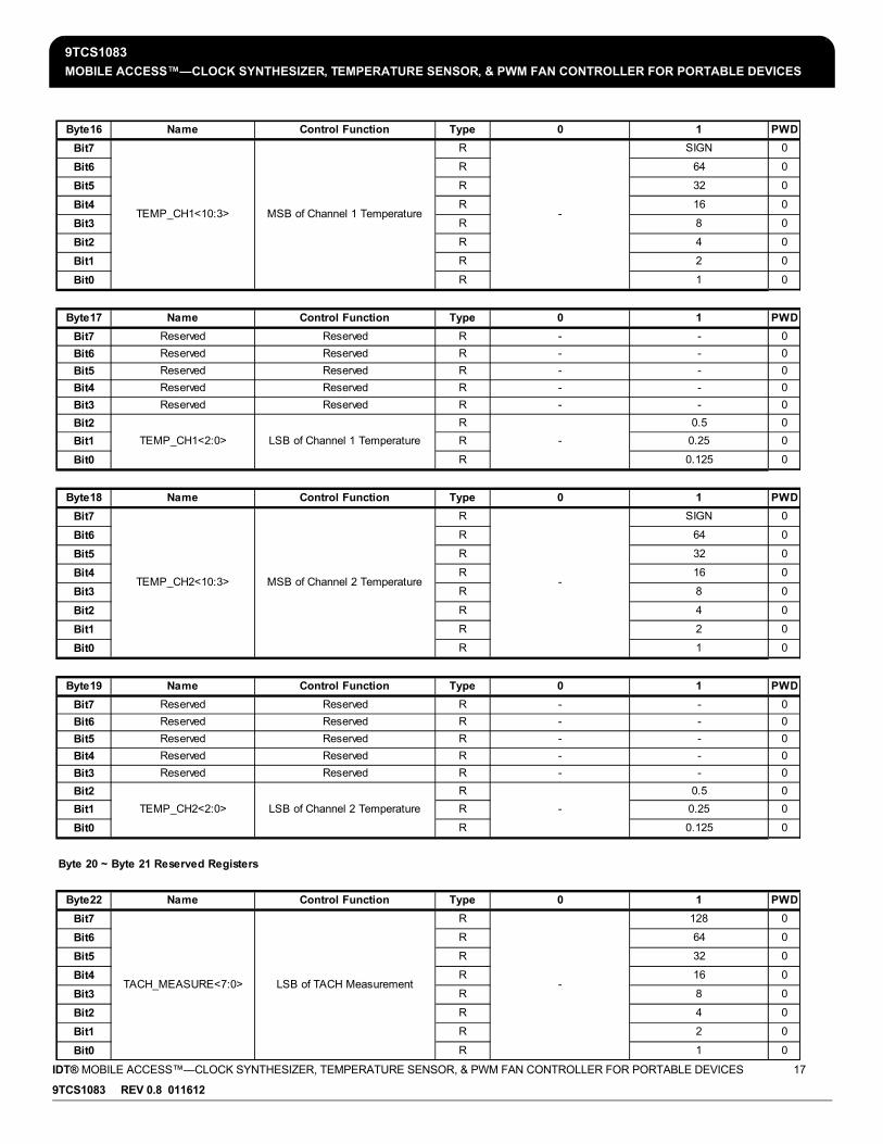
TACH_MEASURE<7:0> LSB of TACH Measurement
-
-
-
-
-

9TCS1083
MOBILE ACCESS™—CLOCK SYNTHESIZER, TEMPERATURE SENSOR, & PWM FAN CONTROLLER FOR PORTABLE DEVICES
IDT® MOBILE ACCESS™—CLOCK SYNTHESIZER, TEMPERATURE SENSOR, & PWM FAN CONTROLLER FOR PORTABLE DEVICES 18
9TCS1083 REV 0.8 011612
Byte23 Name Control Function Type 0 1 PWD
Bit7 Reserved Reserved R - - 0
Bit6 Reserved Reserved R - - 0
Bit5 Reserved Reserved R - - 0
Bit4 R 4096 0
Bit3 R 2048 0
Bit2 R 1024 0
Bit1 R 512 0
Bit0 R 256 0
Byte24 Name Control Function Type 0 1 PWD
Bit7 RW 00 - Direct Drive Mode 01 - Thermal Trigger Mode 1
Bit6 RW 10 - Dynamic PWM Mode 11 - Reserved 0
Bit5 RW 00 - 25KHz 01 - 22KHz 0
Bit4 RW 10 - 27KHz 11 - Reserved 0
Bit3 RW 00 - 1Pole FAN 01 - 2 Poles FAN 0
Bit2 RW 10 - 3 Poles FAN 11 - 4 Poles FAN 1
Bit1 RW 00 - 0 01 - 32 0
Bit0 RW 10 - 64 11 - 128 1
Byte25 Name Control Function Type 0 1 PWD
Bit7 RW 00 - 250ms 01 - 500ms 0
Bit6 RW 10 - 1s 11 - 2s 1
Bit5 RW 1
Bit4 RW 1
Bit3 RW 0
Bit2 RW 00 - 3 01 - 4 0
Bit1 RW 10 - 5 11 - 6 1
Bit0 Reserved Reserved RW - - 0
Byte26 Name Control Function Type 0 1 PWD
Bit7 RW 1 0
Bit6 RW 1/2 0
Bit5 RW 1/4 0
Bit4 RW 1/8 0
Bit3 RW 1/16 0
Bit2 RW 1/32 0
Bit1 RW 1/64 0
Bit0 RW 1/128 0
Byte27 Name Control Function Type 0 1 PWD
Bit7 RW 1/256 0
Bit6 RW 1/512 0
Bit5 RW 1/1024 0
Bit4 RW 0
Bit3 RW 1
Bit2 RW 1
Bit1 RW 00 - 2C 01 - 5C 0
Bit0 RW 10 - 10C 11 - 15C 1
Freq_Sel Select the PWM frequency
TACH_MEASURE<12:8> MSB of TACH Measurement
Mode Select Select the FAN Operating Mode
Edge FAN Type Selection
Error Range TACH Detect Tolerant Error Rang
Spin-Up Time The Time For Spin-Up
Spin-Up Duty PWM Duty-Cycle For Spin-Up
Spin-Up cnt Time Out Times For Spin-Up
Duty_Cycle<10:3> MSB of PWM Duty-Cycle Setting -
Duty_Cycle<2:0> LSB of PWM Duty-Cycle Setting -
Update Time TACH Detect Update Time
T_HysTemperature Hysteresis For FAN's
Trigger Point
000 - 30%, 001 - 35%, 010 - 40%, 011 - 45%, 100 - 50%, 101 - 55%,
110 - 60%, 111 - 65%
000 - 100ms, 001 - 200ms, 010 - 300ms, 011 - 400m, 100 - 500ms, 101 - 600ms, 110 - 700ms, 111 - 800ms
-

9TCS1083
MOBILE ACCESS™—CLOCK SYNTHESIZER, TEMPERATURE SENSOR, & PWM FAN CONTROLLER FOR PORTABLE DEVICES
IDT® MOBILE ACCESS™—CLOCK SYNTHESIZER, TEMPERATURE SENSOR, & PWM FAN CONTROLLER FOR PORTABLE DEVICES 19
9TCS1083 REV 0.8 011612
Byte28 Name Control Function Type 0 1 PWD
Bit7 RW Reserved 0
Bit6 RW 64C 1
Bit5 RW 32C 1
Bit4 RW 16C 1
Bit3 RW 8C 1
Bit2 RW 4C 1
Bit1 RW 2C 1
Bit0 RW 1C 1
Byte29 Name Control Function Type 0 1 PWD
Bit7 RW Reserved 0
Bit6 RW 64C 1
Bit5 RW 32C 1
Bit4 RW 16C 1
Bit3 RW 8C 1
Bit2 RW 4C 1
Bit1 RW 2C 1
Bit0 RW 1C 1
Byte30 Name Control Function Type 0 1 PWD
Bit7 RW 4096 1
Bit6 RW 2048 1
Bit5 RW 1024 1
Bit4 RW 512 1
Bit3 RW 256 1
Bit2 RW 128 1
Bit1 RW 64 1
Bit0 RW 32 1
Byte31 Name Control Function Type 0 1 PWD
Bit7 RW 512 0
Bit6 RW 256 0
Bit5 RW 128 0
Bit4 RW 64 0
Bit3 RW 32 0
Bit2 RW 16 0
Bit1 RW 8 0
Bit0 RW 4 0
Byte32 Name Control Function Type 0 1 PWD
Bit7 RW 4096 0
Bit6 RW 2048 0
Bit5 RW 1024 0
Bit4 RW 512 0
Bit3 RW 256 0
Bit2 RW 128 0
Bit1 RW 64 0
Bit0 RW 32 0
TL_FANFirst Temperature Trigger Point of
FAN-
TH_FANSecond Temperature Trigger Point
of FAN-
TACH_MAXThe Maximum Limit of TACH
Number-
MSB TACH threshold of Static Mode(T>TL_FAN)
-
TACH_MINThe Minimum Limit of TACH
Number-
TACH_S1<12:5>

9TCS1083
MOBILE ACCESS™—CLOCK SYNTHESIZER, TEMPERATURE SENSOR, & PWM FAN CONTROLLER FOR PORTABLE DEVICES
IDT® MOBILE ACCESS™—CLOCK SYNTHESIZER, TEMPERATURE SENSOR, & PWM FAN CONTROLLER FOR PORTABLE DEVICES 20
9TCS1083 REV 0.8 011612
Byte33 Name Control Function Type 0 1 PWD
Bit7 RW 16 0
Bit6 RW 8 0
Bit5 RW 4 0
Bit4 RW 2 0
Bit3 RW 1 0
Bit2 Reserved Reserved RW - - 0
Bit1 RW 00 - CH1 01 - CH2 1
Bit0 RW 10 - Reserved 11 - Reserved 0
Byte34 Name Control Function Type 0 1 PWD
Bit7 RW 4096 0
Bit6 RW 2048 0
Bit5 RW 1024 0
Bit4 RW 512 0
Bit3 RW 256 0
Bit2 RW 128 0
Bit1 RW 64 0
Bit0 RW 32 0
Byte35 Name Control Function Type 0 1 PWD
Bit7 RW 16 0
Bit6 RW 8 0
Bit5 RW 4 0
Bit4 RW 2 0
Bit3 RW 1 0
Bit2 FAN MASK Mask Fan Fault RW 0=normal 1=masked 0
Bit1 RW00 - ALERT=Temp-Sensor
Alert01 - ALERT=FAN Fault 0
Bit0 RW10 - ALERT=Temp-Senso
Alert or FAN Fault10 - ALERT=Temp-Senso
Alert and FAN Fault0
Byte36 Name Control Function Type 0 1 PWD
Bit7 RW 128 0
Bit6 RW 64 0
Bit5 RW 32 0
Bit4 RW 16 0
Bit3 RW 8 1
Bit2 RW 4 0
Bit1 RW 2 0
Bit0 RW 1 0
Byte37 Name Control Function Type 0 1 PWD
Bit7 Reserved Reserved R - - 0
Bit6 Reserved Reserved R - - 0
Bit5 Reserved Reserved R - - 0
Bit4 Reserved Reserved R - - 0
Bit3 Reserved Reserved R - - 0
Bit2 Reserved Reserved R - - 0
Bit1 FAN_Fault1FAN TACH measurement is <
Minimum limit (Too Fast)R Non-Flag Flag 0
Bit0 FAN_Fault2FAN TACH measurement is >
Maximum limit (Too Slow)R Non-Flag Flag 0
-
-
SEL_ALERT Select the ALERT Source
TACH_S2<4:0>LSB TACH threshold of Static
Mode(T>TH_FAN)
FAN_CH_SELTemperature Channel Selection For
Fan
TACH_S2<12:5>MSB TACH threshold of Static
Mode(T>TH_FAN)
TACH_S1<4:0>LSB TACH threshold of Static
Mode(T>TL_FAN) -
-PWM StepThe PWM DutyCycle
Incremental/Decremental Step

9TCS1083
MOBILE ACCESS™—CLOCK SYNTHESIZER, TEMPERATURE SENSOR, & PWM FAN CONTROLLER FOR PORTABLE DEVICES
IDT® MOBILE ACCESS™—CLOCK SYNTHESIZER, TEMPERATURE SENSOR, & PWM FAN CONTROLLER FOR PORTABLE DEVICES 21
9TCS1083 REV 0.8 011612
Byte38 Name Control Function Type 0 1 PWD
Bit7 R - - 0
Bit6 R - - 0
Bit5 R - - 0
Bit4 R - - 0
Bit3 R - - 0
Bit2 R - - 0
Bit1 R - - 0
Bit0 R - - 0
Byte39 Name Control Function Type 0 1 PWD
Bit7 Reserved Reserved RW - - 0
Bit6 Reserved Reserved RW - - 0
Bit5 Reserved Reserved RW - - 0
Bit4 Reserved Reserved RW - - 0
Bit3 Reserved Reserved RW - - 0
Bit2 Reserved Reserved RW - - 0
Bit1 SEL_DIV2 Temp-Sensor Reference CLK DIV2 RW TS_REF=25MHz TS_REF=12.5M 0
Bit0 SEL_XTAL I2C Clock Source selection RW Free-Run OSC XTAL 0
Byte 40 Reserved Register
Byte41 Name Control Function Type 0 1 PWD
Bit7 STOP_27M_48M Stop 27M_48M output RW Stopped Run 1
Bit6 STOP_24M_48M Stop 24M 48M output RW Stopped Run 1
Bit5 EN_STOP25M_CEnable pin for 25M_C after at
PWRGD=0RW Free-Run Stoppable 1
Bit4 EN_STOP25M_BEnable pin for 25M_B after at
PWRGD=0RW Free-Run Stoppable 1
Bit3 EN_STOP25M_AEnable pin for 25M_A after at
PWRGD=0RW Free-Run Stoppable 0
Bit2 STOP_25M_C Stop 25M_C output RW Stopped Run 1
Bit1 STOP_25M_B Stop 25M_B output RW Stopped Run 1
Bit0 STOP_25M_A Stop 25M_A output RW Stopped Run 1
Byte42 Name Control Function Type 0 1 PWD
Bit7 MSB RW - - 0
Bit6 - RW - - 0
Bit5 - RW - - 0
Bit4 - RW - - 1
Bit3 - RW - - 1
Bit2 - RW - - 1
Bit1 - RW - - 1
Bit0 LSB RW - - 1
Byte 43 ~ Byte 46 Reserved Registers
Byte47 Name Control Function Type 0 1 PWD
Bit7 RW - - 0
Bit6 RW - - 0
Bit5 RW - - 0
Bit4 RW - - 0
Bit3 RW - - 0
Bit2 RW - - 0
Bit1 RW - - 0
Bit0 RW - - 1
VENDOR_ID
BYTE COUNT Register Bit[7:0]
Revision ID
Vendor ID (IDT=0001)
REV_ID
TACH_AIM_OUT Targeted TACH Readback

9TCS1083
MOBILE ACCESS™—CLOCK SYNTHESIZER, TEMPERATURE SENSOR, & PWM FAN CONTROLLER FOR PORTABLE DEVICES
IDT® MOBILE ACCESS™—CLOCK SYNTHESIZER, TEMPERATURE SENSOR, & PWM FAN CONTROLLER FOR PORTABLE DEVICES 22
9TCS1083 REV 0.8 011612
Byte 48 ~ Byte 63 Reserved Registers
Byte64 Name Control Function Type 0 1 PWD
Bit7 LCKBYPASSB PLL Lock Bypassb RW Bypass Not Bypas 1
Bit6 RW - - 0
Bit5 RW - - 0
Bit4 RW - - 1
Bit3 RW - - 1
Bit2 RW - - 0
Bit1 RW - - 0
Bit0 RW - - 1
Byte65 Name Control Function Type 0 1 PWD
Bit7 RW - - 0
Bit6 RW - - 0
Bit5 RW - - 0
Bit4 RW - - 1
Bit3 RW - - 1
Bit2 RW - - 0
Bit1 RW - - 1
Bit0 RW - - 1
Byte 66 Reserved Register
Byte67 Name Control Function Type 0 1 PWD
Bit7 RW 00 = 0.5V/ns 01 = 1.0V/ns 0
Bit6 RW 10 = 1.0V/ns 11 = 1.5V/ns 1
Bit5 RW 00 = 1,0V/ns 01 = 1.5V/ns 0
Bit4 RW 10 = 1.5V/ns 11 = 2.0V/ns 1
Bit3 RW 00 = 1,0V/ns 01 = 1.5V/ns 0
Bit2 RW 10 = 1.5V/ns 11 = 2.0V/ns 1
Bit1 RW 00 = 1,0V/ns 01 = 1.5V/ns 0
Bit0 RW 10 = 1.5V/ns 11 = 2.0V/ns 1
SL<1:0>(25MHzB) 25M_B Slew Rate Control
SL<1:0>(25MHzA) 25M_A Slew Rate Control
REF COUNT<6:0> PLL M Counter
PLL N COUNTERVCO COUNT<9:2>
SL<1:0>(27MHz) 27M Slew Rate Control
SL<1:0>(24MHz) 24M Slew Rate Control
All reserved bits and reserved bytes in this SMBus table should not be overwritten at any instance. Writing to these reserved bits and bytes may cause unexpected behavior. IDT does not warrant any application issue going
forward if continuing to overwrite these reserve bits and bytes.
*****************************************************************************************************************************************************************************

9TCS1083
MOBILE ACCESS™—CLOCK SYNTHESIZER, TEMPERATURE SENSOR, & PWM FAN CONTROLLER FOR PORTABLE DEVICES
IDT® MOBILE ACCESS™—CLOCK SYNTHESIZER, TEMPERATURE SENSOR, & PWM FAN CONTROLLER FOR PORTABLE DEVICES 23
9TCS1083 REV 0.8 011612
Frequency Generator 32.768 kHz
Recommended 25MHz Quartz Crystal Specifications
SMD 25MHz AT cut crystal and maximum driver level at 100µW, for example TXC.
VBAT Battery Recommendations and Connection Considerations
Recommended to use coin cell battery CR2032, CR2025 or equivalent.
The normal coin cell battery storage capacity is 170 mAh to 220mAh and the average total RTC circuit current required 5uA, the battery life will be at least:
170,000 µAh / 5 µA = 34,000 hours = 3.88 years
The RTC circuit (PCH) usually consumes 3µA power, thus the 32.768kHz clock generator circuit needs be less than 2µA. The IDT9TCS1083/1085 32.768kHz generator averaged operation current is less than 2µA.
The coin cell battery with IDT 9TCS1083/1085 VBAT power pin connection requires a 100 ohm and 22µF ceramic capacitor current limitation and noise filtering. The RC needs to be added to the battery to limit the current spikes effects.
The VDD_RTC connect to the Intel PCH/ICH chip and the 9TCS1083/1085 provide seamless power switching between main V_3.3 and V_bat.
32.768K Clocks Operation
The IDT9TCS1083/1085 32.768K clock output operates in two modes:
1. When the system is not power ON, V_3.3 is not ready and IDT 9TCS1083 is powered with the coin cell battery. The 32kHz comes from the DCO with the digital calibration to keep the accuracy.
2. After V_3.3 is ready, the 9TCS1083 creates a seamless switch power from V_bat to V_3.3 and the calibration will go to full speed: this will happen every 2~3ms to keep the accuracy and the 32K source will be switched to 25MHz oscillator with Fraction-N divider to get to 0ppm.
32.768K DCO uses a 25Mhz crystal oscillator for calibration reference, thus the 25MHz oscillator must be fine tuned in order to get the best 32.768kHz accuracy.
RTC Routing Guidelines
V_bat
VDD_RTC
CR2032H
100ohm
10~22uF
9TCS1083Power Switch
V_3.3
1uf
Single Trace impedance Length NotesX1 50 ohm 6 inchesX2 50 ohm 6 inches

9TCS1083
MOBILE ACCESS™—CLOCK SYNTHESIZER, TEMPERATURE SENSOR, & PWM FAN CONTROLLER FOR PORTABLE DEVICES
IDT® MOBILE ACCESS™—CLOCK SYNTHESIZER, TEMPERATURE SENSOR, & PWM FAN CONTROLLER FOR PORTABLE DEVICES 24
9TCS1083 REV 0.8 011612
Reference Schematic For VBAT and VDD_RTC
VDD_RTC
V_bat
SMBCLK
DXN2
V_3.3
PWMTACH
SMBDAT
ALERT#
THERM#
9TCS1083
X1
X2GND
32K_A
32K_B / 25M_C
VDD_32KB
25M_A
VDDIO_25MA
25M_B
VDD_25MB
24M_48M
VDD_24/48M
VDD_27/48M
VDD_TS
VCCPWM
TACHGND
5V/12V 4-wire FAN
5V/12V5V/12V
10K
10K
3.3V/5V
10K4.7K
DXP2
DXP1DXN1
To Vdd_RTC
CLK
CLK
100 ohm
10uf
To Smbus master
25Mhz crystal
To system I2C or Int.
To system H/W or Int.
V_bat (Coin Cell
battery)
V_3.3
V_3.3
CLK
CLK
CLK
27M_48M CLK
1uf
VDD_32KB
VDDIO_25MA
VDD_25MB
VDD_24M
VDD_27M

9TCS1083
MOBILE ACCESS™—CLOCK SYNTHESIZER, TEMPERATURE SENSOR, & PWM FAN CONTROLLER FOR PORTABLE DEVICES
IDT® MOBILE ACCESS™—CLOCK SYNTHESIZER, TEMPERATURE SENSOR, & PWM FAN CONTROLLER FOR PORTABLE DEVICES 25
9TCS1083 REV 0.8 011612
Frequency Synthesizer – 24/48/27/25 MHz
IDT9TCS1083/1085 includes a low power PLL to generate 24/27/48 MHz clock outputs. The PLL uses an external 25MHz crystal for reference clock input, thus all 25MHz clock outputs are through a fanout buffer directly for optimal performance. Fine tunning on the external crystal cap load is required to get an accurate 25MHz reference clock.
25MHz_A Connection Recommendations
a. VDDIO_25A range is from 1.05V to 3.3V.
b. Optimize range is 1.05V to 1.5V.
c. Pull up strength is 50 ohm@VDDIO_25A=1.5V
d. Pull down strength is 50 ohm.
e. No on-board series resistor is required.
25MHz_B/C Connection Recommendations
a. VDD_25B/C range is from 1.05V to 3.3V.
b. Optimized for 3.3V VDDIO.
c. Pull up strength is 50 ohm@VDD_25B/C=3.3V
d. Pull down strength is 50 ohm.
e. No on-board series resistor is required.
24/27/48MHz Connection Recommendations
a. Default 2X push-pull IO drive strength for 24/48/27MHz.
b. On board 27 ohm series resistor for each path.
c. Rising/falling slew rate: 0.5v/ns~4v/ns
d. 2 bits (3 steps) I2C for the Slew Rate.
CLK_25A
VDDIO_25
4pF
Z= 50 ohm0 ohm
CLK_25B/C
VDDIO_25
5pF
Z= 50 ohm0 ohm
CLK_24/48/27M
VDD_24M/27M
5pF
Z=50 ohm
5pF
Z=50 ohm27 ohm
27 ohm

9TCS1083
MOBILE ACCESS™—CLOCK SYNTHESIZER, TEMPERATURE SENSOR, & PWM FAN CONTROLLER FOR PORTABLE DEVICES
IDT® MOBILE ACCESS™—CLOCK SYNTHESIZER, TEMPERATURE SENSOR, & PWM FAN CONTROLLER FOR PORTABLE DEVICES 26
9TCS1083 REV 0.8 011612
Thermal Sensor
The thermal sensor in the 9TCS1083 is a low power and highly accurate temperature sensor. It is optimized to operate between 60°C to 100°C. There are two external thermal diode connection input temperature sensors. The chip supports diode faults and temperature alerts for the thermal sensor; Moreover, the thermal sensor has the capability to go into standby mode for power savings.
The temperature sensor's analog to digital converter (ADC) has 11 bits of resolution. One LSB is equal to 0.125°C. The accuracy of the temperature sensor is ±1°C between 60°C - 100°C for the two sensors.
The 9TCS1083 temperature sensor has the ability to cancel the series resistance on the remote diode inputs. Parasitic resistances to the DXP and DXN inputs seen in series with the remote diode are caused by PCB trace resistance along with the overall length, bulk parasitic resistance in the remote temperature transistor junctions, and series resistance in the CPU. This resistance appears as a temperature offset in the thermal sensor measurement and is approximately +0.7°C per Ohm. The 9TCS1083 has the ability to cancel up to 100Ω of series resistance.
The thermal sensor in 9TCS1083 outputs the measured temperature from a beta compensated temperature reading from an external diode. The temperature sensor architecture uses an on-chip ADC as shown to convert the analog temperature into an 11-bit digital code. Using averaging techniques along with the ADC architecture allows accurate temperature measurements. The ability to have programmable conversion rates and adjustable averaging schemes allow the user the flexibility to balance accuracy versus conversion speed per the system requirements.
The temperature measurement relies on the characteristics of a semiconductor junction operating at a fixed current level. Forcing a fixed current through the temperature diodes and detecting the changes in VBE, the forward voltage of the diode, the temperature proportionality can be determined.
External Thermal Diode Selection
The 9TCS1083 supports the following temperature diodes:
• Typical remote substrate transistor (i.e. CPU substrate PNP intrinsic diode)• Discrete PNP transistor diode (i.e. 2N3906)• Discrete NPN transistor diode (i.e. 2N3904)
NPN 2N3904
NPN 2N3904
Analog MUX
Channel 1
Channel 2
Local
Current Driver BGP Ref
Temp SensorDector
Timing Generator
11 bit ADC
Channel 1 Temp Reg
Channel 2 Temp Reg

9TCS1083
MOBILE ACCESS™—CLOCK SYNTHESIZER, TEMPERATURE SENSOR, & PWM FAN CONTROLLER FOR PORTABLE DEVICES
IDT® MOBILE ACCESS™—CLOCK SYNTHESIZER, TEMPERATURE SENSOR, & PWM FAN CONTROLLER FOR PORTABLE DEVICES 27
9TCS1083 REV 0.8 011612
When the thermal sensor is used in a noisy environment, a capacitor can be connected across DXP and DXN to provide some noise filtering capabilities. However, large capacitances affect the accuracy of the temperature measurement. A maximum capacitance of 300pF can be used to help mitigate the noise.
Temperature Sensor Channel SelectionTo enable the temperature sensors, register byte[6], bit[7:6]. Bit[7] is CH1 and bit[6] is CH2.
Thermal Diode Fault Conditions
9TCS1083 has the ability to detect an open or a short condition for each temperature sensor diode. An external diode fault is defined as one of the following:
• An open between DXP and DXN• A short from VDD to DXP• A short from VDD to DXN
The diode fault monitoring is enabled at the start of every temperature measurement. When an external diode fault is detected, the ALERT# pin asserts and the temperature data reads 00h in the MSB and LSB of the corresponding temperature registers:
• DX1 MSB - byte[17], bit[2:0]• DX1 LSB - byte[16], bit[7:0]• DX2 MSB - byte[19], bit[2:0]• DX2 LSB - byte[18], bit[7:0]
During the fault condition, byte[13], bit[1] or bit[0], will be set depending on the channel that has the fault. Bit[1] corresponds to DX1, and Bit[0] corresponds to DX2; furthermore, an open/short fault flag will be set in register byte[14], bit[4].
DXP
DXN
PNPtransistori.e. to CPU
DXP
DXN
PNPtransistori.e. 2N3906
DXP
DXN
NPN transisteri.e. 2N3904

9TCS1083
MOBILE ACCESS™—CLOCK SYNTHESIZER, TEMPERATURE SENSOR, & PWM FAN CONTROLLER FOR PORTABLE DEVICES
IDT® MOBILE ACCESS™—CLOCK SYNTHESIZER, TEMPERATURE SENSOR, & PWM FAN CONTROLLER FOR PORTABLE DEVICES 28
9TCS1083 REV 0.8 011612
Temperature Threshold Alerts
Through register writes, the high and low temperature limits can be set such that it will trigger an alert. This alert can be monitored through the registers or can be sent to the ALERT# pin. Each channel has its own programmable register to set the thresholds as follows:
(1) High Temperature Alert (default 127°C)
Where byte[0] is the high temperature alert for DX1, byte[1] is for DX2.
(2) Low Temperature Alert (default 127°C)
Where byte[3] is the low alert for DX1, byte[4] is for DX2.
Temperature Threshold Alert StatusWhen a temperature threshold alert is activated, a status indicator bit is also set. Register byte[14], bit[6:5] will be set depending on the high or low alert. Bit[6] is the high and bit[5] is the low alert flag. To clear the alert, register byte[15], bit[7] needs to be written with a "1". Writing this bit will also clear the critical thermal warnings.
Temperature Threshold ALERT# PinThe temperature threshold alerts are sent to the ALERT# pin. To mask this alert being sent to the ALERT# pin, set register byte[12], bit[7:6] to logic 1. Bit[7] is CH1 and bit[6] is CH2.
Consecutive Alerts
The number of temperature threshold alerts before the assertion of the ALERT# pin can be set by the user through register byte[6], bit[3:2] as follows:
Temperature Threshold Alert Alarm RegisterThe two temperature channels have readable registers, byte[13], bit[5:2] that is set when a temperature threshold alert has occurred.
Critical Thermal Warnings
The 9TCS1083 will have register programmable critical thermal threshold warnings for all temperature sensor channels. Similar to the temperature threshold alerts, the critical high temperatures can be set such that a warning can be dispatched to the THERM# pin and the readable registers. The thermal warnings also have programmable hysteresis. Each channel has its own programmable register to set the thresholds as follows:
(1) Critical Thermal Warning (default 127°C)
Where byte[7] is the critical thermal warning for DX1, byte[8] is for DX2.
Byte[2:0], Bit[7:0] Temperature
Bit[7] Sign Bit
Bit[6] 64°C
Bit[5] 32°C
Bit[4] 16°C
Bit[3] 8°C
Bit[2] 4°C
Bit[1] 2°C
Bit[0] 1°C
Byte[5:3], Bit[7:0] Temperature
Bit[7] Sign Bit
Bit[6] 64°C
Bit[5] 32°C
Bit[4] 16°C
Bit[3] 8°C
Bit[2] 4°C
Bit[1] 2°C
Bit[0] 1°C
Byte[6], Bit[3:2] Number of Alert Events
[00] (default) 1
[01] 2
[10] 3
[11] 4
Byte[9:7], Bit[6:0] Temperature
Bit[6] 64°C
Bit[5] 32°C
Bit[4] 16°C
Bit[3] 8°C
Bit[2] 4°C
Bit[1] 2°C
Bit[0] 1°C

9TCS1083
MOBILE ACCESS™—CLOCK SYNTHESIZER, TEMPERATURE SENSOR, & PWM FAN CONTROLLER FOR PORTABLE DEVICES
IDT® MOBILE ACCESS™—CLOCK SYNTHESIZER, TEMPERATURE SENSOR, & PWM FAN CONTROLLER FOR PORTABLE DEVICES 29
9TCS1083 REV 0.8 011612
(2) Critical Thermal Warning Temperature Hysteresis (default 4°C)
Critical Thermal Warning StatusWhen a critical warning is activated, a status indicator bit is also set. Register byte[14], bit[2:1] will be set depending on which channel had the critical event. Bit[2] is for channel 1, bit[1] is for channel 2.
Critical Thermal Warning THERM# PinThe critical thermal warnings are sent to the THERM# pin and requires a system register write to byte[15], bit[7] to reset. This fault clear I2C write will also clear the temperature threshold alerts
Active/Standby Mode
The thermal sensor has two modes in the temperature conversion process:
(1) Active mode – In this mode the ADC will have a selectable conversion rate for the temperature sensing.
(2) Standby mode – The system will command via I2C the 9TCS1083 to sample the temperature sensors. Once the temperature reading from the ADC is updated, the temperature sensor will be on stand-by awaiting the next system request.
Register byte[15], bit[6] controls whether the thermal sensor is in active or standby mode.
The conversion rate programmable register detail is as follows:
* Valid when only one temperature sensor channel is used.
** Valid when the number of temperature sensor channel is two.
The thermal sensor architecture has dynamic averaging to smooth out the temperature conversion readings. To select the number of temperature reading averages requires the dynamic averaging function to be enabled, register byte[15], bit[5]. The number of averages is then selected as follows:
Byte[12], Bit[4:0] Temperature
Bit[4] 16°C
Bit[3] 8°C
Bit[2] (default) 4°C
Bit[1] 2°C
Bit[0] 1°C
Byte[17], Bit[4:1] Conversion Rate
[0000] 16/sec *
[0001] 8/sec **
[0010] (default) 4/sec
[0011] 2/sec
[0100] 1/sec
[0101] 1/2 sec
[0110] 1/4 sec
[0111] 1/8 sec
[1000] 1/16 sec
[1001] 1/32 sec
[1010] 1/64 sec
Byte[6], Bit[1:0] Average the ADC Temperature
[00] 1
[01] 4
[10] 8
[11] 16

9TCS1083
MOBILE ACCESS™—CLOCK SYNTHESIZER, TEMPERATURE SENSOR, & PWM FAN CONTROLLER FOR PORTABLE DEVICES
IDT® MOBILE ACCESS™—CLOCK SYNTHESIZER, TEMPERATURE SENSOR, & PWM FAN CONTROLLER FOR PORTABLE DEVICES 30
9TCS1083 REV 0.8 011612
Fan Controller
Fan Controller Description
The fan driver for the 9TCS1083 controls a 4-wire, 12V or 5V, multiple pole DC fan. The fan controller has three modes of operation: (1) direct drive, (2) thermal trigger, and (3) Dynamic PWM. All modes have register programmability for the user to set the desired fan speed and necessary parameters. The controller is also capable of detecting stalled fans and upon detection will set the appropriate alerts. The 9TCS1083 also has user configuration registers to adjust both the ramp-rate and the spin-up routine to accommodate different fan start up requirements.
The fan controller uses the input from the user selectable external diode connections, DX1 or DX2. The 9TCS1083 fan controller can be set to run a user specified fan speed. In this mode the tachometer signal from the fan will be ignored. In thermal trigger mode, the user specifies the temperature thresholds, the temperature threshold hysteresis, and the corresponding fan speed (fan tachometer target) for the different temperature zones defined by the thresholds. The controller will then run the fan at the specified fixed fan speed settings depending on the temperature from the sensors. In dynamic PWM mode, the fan controller will adjust the PWM duty cycle to maintain the system defined fan speed. In this mode, the system reads a temperature sensor and the corresponding fan speed, tachometer reading. The system will then determine and update the 9TCS1083 directly by writing the accessible registers byte 32 and byte 33. 9TCS1083 will then adjust the PWM to achieve the desired system fan speed.
The PWM has ten bits of duty cycle resolution with a 25kHz frequency. The PWM frequency is selectable between 22, 25, and 27kHz.
The 9TCS1083 includes hardware programmable temperature limits and dedicated system shutdown output for thermal protection.
Fan Controller System Diagram (Schematic Example)
Fan Selection DetailThe 9TCS1083 fan controller will control 5V - 12V Brushless DC fans. The fans need to be 4-wire fans and can have one to four poles. The number of fan poles is specified in Register byte[24], bit[3:2]. A 2-pole fan is the default.
Modes of OperationThe 9TCS1083 fan controller has three user selectable methods to control the fan speed. The default fan speed control mode is Dynamic PWM. The modes are selected by writing the I2C register byte[24], bit[7:6] as follows:
The PWM frequency can be set by writing register byte[24], bit[5:4] as follows:
Byte[24], Bit[3:2] Fan Poles
[00] 1
[01] (default) 2
[10] 3
[11] 4
Fan Controller Modes Byte[24], Bit[7:6]
Direct Drive [00]
Thermal Trigger [01]
Dynamic PWM (default) [10]
PWM Frequency
Duty Cycle Resolution [# bits]
Byte[24], Bit[5:4]
25kHz (default) 10 00
22kHz 11 01
27kHz 9 10
IDTMobileAccess9TCS1083/85
PWM
TACH
VCC
PWM
TACH
GND
5V/12V 4-wire FAN
5V/12V5V/12V
10K
10K
3.3V/5V
10K
4.7K

9TCS1083
MOBILE ACCESS™—CLOCK SYNTHESIZER, TEMPERATURE SENSOR, & PWM FAN CONTROLLER FOR PORTABLE DEVICES
IDT® MOBILE ACCESS™—CLOCK SYNTHESIZER, TEMPERATURE SENSOR, & PWM FAN CONTROLLER FOR PORTABLE DEVICES 31
9TCS1083 REV 0.8 011612
Direct Drive ModeIn Direct Drive Mode, the fan speed is directly controlled by setting a fixed PWM duty cycle. After a proper fan speed spin-up, the tachometer signal will be ignored and the 9TCS1083 will output the fixed programmed PWM duty cycle to the fan.
To operate in direct drive mode, Register byte[24], bit[7:6] = [00].
The duty cycle is selectable through registers by writing byte[26], bit[7:0] and byte[27], bit[7:5] as follows:
It is important to also set the required fan spin-up specifics for proper use. The 9TCS1083 after completion of the fan spin-up routine will then put out the correct programmed PWM duty cycle.
Thermal Trigger ModeIn this mode the 9TCS1083 fan speed controller is programmed to run at different fan speeds. The 9TCS1083 will monitor the fan tachometer and depending on the temperature from a thermal sensor diode and the pre-programmed temperature settings, the 9TCS1083 will adjust the fan speed to the targeted tachometer settings.
Register byte[24], bit[7:6] = [01] will put 9TCS1083 into thermal trigger mode.
Temperature Sensor
The temperature can be set to read from the external thermal sensors, DX1 or DX2. It is selectable by writing Byte[33].
FAN_CH_SEL - byte[33], bit[1:0]
Tachometer Update
The tachometer reading can be updated at a rate of 700msec up to 100msecs. Tachometer Update Time, byte[27], bit[4:2]
Byte[26], Bit[7:0] Logic "1", Selects Duty Cycle
Bit[7] 1
Bit[6] 1/2
Bit[5] 1/4
Bit[4] 1/8
Bit[3] 1/16
Bit[2] 1/32
Bit[1] 1/64
Bit[0] 1/128
Byte[27], Bit[7:5] Logic "1", Selects Duty Cycle
Bit[7] 1/256
Bit[6] 1/512
Bit[5] 1/1024
Byte[33], bit[1:0] Temperature Sensor Selection
[00] CH1
[01] CH2
Byte[27], bit[4:2] Tachometer Update Time
[000] 100 msec
[001] 200 msec
[010] 300 msec
[011] (default) 400 msec
[100] 500 msec
[101] 600 msec
[110] 700 msec
[111] 800 msec

9TCS1083
MOBILE ACCESS™—CLOCK SYNTHESIZER, TEMPERATURE SENSOR, & PWM FAN CONTROLLER FOR PORTABLE DEVICES
IDT® MOBILE ACCESS™—CLOCK SYNTHESIZER, TEMPERATURE SENSOR, & PWM FAN CONTROLLER FOR PORTABLE DEVICES 32
9TCS1083 REV 0.8 011612
Example of Thermal Trigger Mode Setup
The figure below shows how the programmable thresholds relate to the fan speed settings.
From the figure above, it can be seen that the fan speed will adjust between the tachometer settings TACH_S1 and TACH_S2 given the temperature from the thermal sensor. The temperature thresholds are set by TH_FAN and TL_FAN along with the temperature hysteresis, T_HYS. In this mode, the fan will have active fault condition monitoring along with fan spin-up control. The rate at which the fan will speed up or slow down, going from one TACH setting to the other, can be programmed by the user. Lastly, the fan speed tolerance can also be selectable via registers.
To set up the fan speed controller in Thermal Trigger Mode, the following registers will need to be programmed.
(1) Temperature Thresholds:
a. TL_FAN - byte[28], bit[6:0] (default 127°C)
b. TH_FAN - byte[29], bit[6:0] (default 127°C)
To set TL_FAN and TH_FAN a logic "1" is written into the proper register. For example, to get 70°C, a "1" would be written for Bit[6], Bit[2], and Bit[1].
(2) Temperature Hysteresis, T_HYS, byte[27], bit[1:0]:
(3) Tachometer Targets:
a. TACH_S1 - byte[32], bit[7:0] and byte[33], bit[7:3]
Byte[28], Bit[7:0] Logic "1", Selects Temp Threshold
Bit[7] —
Bit[6] 64°C
Bit[5] 32°C
Bit[4] 16°C
Bit[3] 8°C
Bit[2] 4°C
Bit[1] 2°C
Bit[0] 1°C
Te
mpS
enser Tem
perature
Fa
n Spe
ed
Thermal Hysteresis
Thermal Hysteresis
TACH_S2
TACH_S1
FAN OFF
TH_FAN
TL_FAN
Byte[29], Bit[7:0] Logic "1", Selects Temp Threshold
Bit[7] —
Bit[6] 64°C
Bit[5] 32°C
Bit[4] 16°C
Bit[3] 8°C
Bit[2] 4°C
Bit[1] 2°C
Bit[0] 1°C
Byte[27], bit[1:0] Temperature Threshold Hysteresis
[00] 2°C
[01] 5°C
[10] 10°C
[11] (default) 15°C
Byte[32], bit[7:0] Logic "1" selects Tachometer Reading
Bit[7] 4096
Bit[6] 2048
Bit[5] 1024
Bit[4] 512
Bit[3] 256
Bit[2] 128
Bit[1] 64
Bit[0] 32

9TCS1083
MOBILE ACCESS™—CLOCK SYNTHESIZER, TEMPERATURE SENSOR, & PWM FAN CONTROLLER FOR PORTABLE DEVICES
IDT® MOBILE ACCESS™—CLOCK SYNTHESIZER, TEMPERATURE SENSOR, & PWM FAN CONTROLLER FOR PORTABLE DEVICES 33
9TCS1083 REV 0.8 011612
b. TACH_S2 - byte[34], bit[7:0] and byte[35], bit[7:3]
The TACH_S1/S2 is set using the following RPM formula:
where: RPM - fan revolution per minute Fsample - 25kHz sample internal clock sample rateTACH_Reading - user programmable registers Byte[32] through Byte[35]
(4) To Set the minimum and maximum fan speed, use the RPM formula, “Formula 1”.
a. TACH_MIN - byte[31], bit[7:0]
b. TACH_MAX - byte[30, bit[7:0]
(5) To adjust the rate at which the fan speed will transition from one TACH setting to the other, the RPM equation, “Formula 1” is again applied to determine the incremental or decremental fan speed step size.
Tachometer PWM Step Control - byte[36], bit[7:0]
Byte[33], bit[7:3]
Logic "1" selects Tachometer Reading
Bit[7] 16
Bit[6] 8
Bit[5] 4
Bit[4] 2
Bit[3] 1
Byte[34], bit[7:0] Logic "1" selects Tachometer Reading
Bit[7] 4096
Bit[6] 2048
Bit[5] 1024
Bit[4] 512
Bit[3] 256
Bit[2] 128
Bit[1] 64
Bit[0] 32
Byte[35], bit[7:3] Logic "1" selects Tachometer Reading
Bit[7] 16
Bit[6] 8
Bit[5] 4
Bit[4] 2
Bit[3] 1
60_ Re
2 sample TACH adingRPM F= × × (Formula 1)
Byte[31], bit[7:0] Logic "1" selects Tachometer Reading
Bit[7] 512
Bit[6] 256
Bit[5] 128
Bit[4] 64
Bit[3] 32
Bit[2] 16
Bit[1] 8
Bit[0] 4
Byte[30], bit[7:0] Logic "1" selects Tachometer Reading
Bit[7] 4096
Bit[6] 2048
Bit[5] 1024
Bit[4] 512
Bit[3] 256
Bit[2] 128
Bit[1] 64
Bit[0] 32
Byte[36], bit[7:0] Logic "1" selects Tachometer Reading
Bit[7] 128
Bit[6] 64
Bit[5] 32
Bit[4] 16
Bit[3] 8
Bit[2] 4
Bit[1] 2
Bit[0] 1

9TCS1083
MOBILE ACCESS™—CLOCK SYNTHESIZER, TEMPERATURE SENSOR, & PWM FAN CONTROLLER FOR PORTABLE DEVICES
IDT® MOBILE ACCESS™—CLOCK SYNTHESIZER, TEMPERATURE SENSOR, & PWM FAN CONTROLLER FOR PORTABLE DEVICES 34
9TCS1083 REV 0.8 011612
Spin-up
In this mode the fan controller will also have spin-up control capabilities. At any time the fan attempts to go from a zero RPM to a higher fan speed, the fan will always go through the proper spin-up routine. The time allotted for fan spin-up as well as the spin-up PWM duty cycle can be adjusted via registers by writing byte[25], bit[7:3] as follows:
Spin-up Time - byte[25], bit[7:6]
Spin-up PWM duty cycle - byte[25], bit[5:3]
Dynamic PWM ModeThe 9TCS1083 in this mode will be directed by the system via registers as to the target RPM by which the fan speed should be running. The system will read a temperature sensor along with the fan tachometer information and make the determination as to what the nominal fan speed should be. This information is fed back to the 9TCS1083 via register writes. 9TCS1083 will comply and attempt to run the fan at the requested speed.
To put the 9TCS1083 in Dynamic PWM mode register byte[24], bit[7:6] = [10]
The system will poll byte[22], bit[7:0], and byte[23], bit[4:0] for the TACH reading which will correlate to the current fan speed by the RPM equation, “Formula 1”.
The system can read the temperature sensor diodes from the 9TCS1083 or from any sensor available to the system to determine the necessary adjustments to the fan speed.
Byte[25], bit[7:6] Spin-up Time
Bit[7:6] = [00] 250msec
Bit[7:6] = [01] (default) 500msec
Bit[7:6] = [10] 1sec
Bit[7:6] = [11] 2sec
Byte[25], bit[5:3] Spin-up PWM duty cycle
Bit[5:3] = [000] 30%
Bit[5:3] = [001] 35%
Bit[5:3] = [010] 40%
Bit[5:3] = [011] 45%
Bit[5:3] = [100] 50%
Bit[5:3] = [101] 55%
Bit[5:3] = [110] (default) 60%
Bit[5:3] = [111] 65%
Byte[22], bit[7:0] Logic "1" selects Tachometer Reading
Bit[7] 128
Bit[6] 64
Bit[5] 32
Bit[4] 16
Bit[3] 8
Bit[2] 4
Bit[1] 2
Bit[0] 1
Byte[23], bit[4:0] Logic "1" selects Tachometer Reading
Bit[7] 4096
Bit[6] 2048
Bit[5] 1024
Bit[4] 512
Bit[3] 256

9TCS1083
MOBILE ACCESS™—CLOCK SYNTHESIZER, TEMPERATURE SENSOR, & PWM FAN CONTROLLER FOR PORTABLE DEVICES
IDT® MOBILE ACCESS™—CLOCK SYNTHESIZER, TEMPERATURE SENSOR, & PWM FAN CONTROLLER FOR PORTABLE DEVICES 35
9TCS1083 REV 0.8 011612
System Direct Tachometer Control
The system will directly write to register byte[32], bit[7:0] and byte[33], bit[7:3] a desired TACH setting.
The tachometer setting is related to the fan speed by the RPM equation, “Formula 1”.
Setting Minimum and Maximum Tachometer RPM
The minimum and maximum tachometer settings can be set for the fan faults.
a. TACH_MIN - byte[31], bit[7:0]
b. TACH_MAX - byte[30, bit[7:0]
Fan Fault Conditions
The fan fault conditions will be activated and reported if the minimum or maximum fan speed is detected. During a FAULT1, maximum fan speed, 9TCS1083 will stop the fan and then wait for the FAULT1 flag to be cleared. For a FAULT2 condition, stalled fan, 9TCS1083 will go through the spin-up procedure to try to start the fan. The number of attempts to try to restart the fan is programmable. The fan fault conditions are reported via register on byte[37], bit[1;0].
Fan Fault Conditions
The number of times for spin-up retries:
Byte[32], bit[7:0] Logic "1" selects Tachometer Reading
Bit[7] 4096
Bit[6] 2048
Bit[5] 1024
Bit[4] 512
Bit[3] 256
Bit[2] 128
Bit[1] 64
Bit[0] 32
Byte[33], bit[7:3] Logic "1" selects Tachometer Reading
Bit[7] 16
Bit[6] 8
Bit[5] 4
Bit[4] 2
Bit[3] 1
Byte[31], bit[7:0] Logic "1" selects Tachometer Reading
Bit[7] 512
Bit[6] 256
Bit[5] 128
Bit[4] 64
Bit[3] 32
Bit[2] 16
Bit[1] 8
Bit[0] 4
Byte[30], bit[7:0] Logic "1" selects Tachometer Reading
Bit[7] 4096
Bit[6] 2048
Bit[5] 1024
Bit[4] 512
Bit[3] 256
Bit[2] 128
Bit[1] 64
Bit[0] 32
Byte[37], bit[1:0] Logic "1" = FAULT CONDITION
Bit[1] Fault1 - Fan speed too fast
Bit[0] Fault2 - Fan speed too slow
Byte[25], bit[2:1] Number of Spin-up Attempts
[00] 3
[01] (default) 4
[10] 5
[11] 6

9TCS1083
MOBILE ACCESS™—CLOCK SYNTHESIZER, TEMPERATURE SENSOR, & PWM FAN CONTROLLER FOR PORTABLE DEVICES
IDT® MOBILE ACCESS™—CLOCK SYNTHESIZER, TEMPERATURE SENSOR, & PWM FAN CONTROLLER FOR PORTABLE DEVICES 36
9TCS1083 REV 0.8 011612
Spin-up Details
1. The spin-up time can be specified in register byte[25], bit[7:6].
Spin-up Time - byte[25], bit[7:6]
2. During spin-up, the PWM duty cycle can be set to 100% for one quarter of the total spin-up time by register byte[25], bit[0].
3. The next three quarters of the spin-up time, the PWM duty cycle is set by register[25], bit[5:3].
Spin-up PWM duty cycle - byte[25], bit[5:3]
Fan Controller Temperature Diode Sensor
The fan controller can use either one of the two channels for temperature sensing. To specify which temperature sensor is used for the fan controller, register byte[33], bit[1:0].
100% *
30%~65%
Target count
Step
Step¼ of
spin up time
UpdateTime
UpdateTime
UpdateTime
Spin Up TimeTarget count reached
Step
Byte[25], bit[7:6] Spin-up Time
Bit[7:6] = [00] 250msec
Bit[7:6] = [01] (default) 500msec
Bit[7:6] = [10] 1sec
Bit[7:6] = [11] 2sec
Byte[25], bit[5:3] Spin-up PWM duty cycle
Bit[5:3] = [000] 30%
Bit[5:3] = [001] 35%
Bit[5:3] = [010] 40%
Bit[5:3] = [011] 45%
Bit[5:3] = [100] 50%
Bit[5:3] = [101] 55%
Bit[5:3] = [110] (default) 60%
Bit[5:3] = [111] 65%

9TCS1083
MOBILE ACCESS™—CLOCK SYNTHESIZER, TEMPERATURE SENSOR, & PWM FAN CONTROLLER FOR PORTABLE DEVICES
IDT® MOBILE ACCESS™—CLOCK SYNTHESIZER, TEMPERATURE SENSOR, & PWM FAN CONTROLLER FOR PORTABLE DEVICES 37
9TCS1083 REV 0.8 011612
Marking Diagram (NLG32)
Notes:
1. “######” is the lot number.
2. YYWW is the last two digits of the year and week that the part was assembled.
3. “$$$” is the assembly mark code..
4. “B” at the end of the part number is the device revision desigantor; does not correlate with the datasheet revision.
5. Bottom marking: country of origin if not USA.
Thermal Characteristics 32-pin VFQFPN
IDT9TCS1083B$$$YYWW######
Parameter Symbol Conditions Min. Typ. Max. UnitsThermal Resistance Junction to Ambient
θJA Still air 34 ° C/W
θJA 1 m/s air flow 29 ° C/W
θJA 3 m/s air flow 27 ° C/W
Thermal Resistance Junction to Case θJC 32 ° C/W

9TCS1083
MOBILE ACCESS™—CLOCK SYNTHESIZER, TEMPERATURE SENSOR, & PWM FAN CONTROLLER FOR PORTABLE DEVICES
IDT® MOBILE ACCESS™—CLOCK SYNTHESIZER, TEMPERATURE SENSOR, & PWM FAN CONTROLLER FOR PORTABLE DEVICES 38
9TCS1083 REV 0.8 011612
Package Outline and Package Dimensions (32-pin VFQFPN, 0.50mm pitch) Package dimensions are kept current with JEDEC Publication No. 95
Ordering Information
“G” after the two-letter package code are the Pb-Free configuration and are RoHS compliant.While the information presented herein has been checked for both accuracy and reliability, Integrated Device Technology (IDT) assumes no responsibility for either its use or for the infringement of any patents or other rights of third parties, which would result from its use. No other circuits, patents, or licenses are implied. This product is intended for use in normal commercial applications. Any other applications such as those requiring extended temperature range, high reliability, or other extraordinary environmental requirements are not recommended without additional processing by IDT. IDT reserves the right to change any circuitry or specifications without notice. IDT does not authorize or warrant any IDT product for use in life support devices or critical medical instruments.
Part / Order Number Marking Shipping Packaging Package Temperature9TCS1083BNLG see page 37 Trays 32-pin VFQFPN 0 to +70° C9TCS1083BNLG8 Tape and Reel 32-pin VFQFPN 0 to +70° C

© 2010 Integrated Device Technology, Inc. All rights reserved. Product specifications subject to change without notice. IDT and the IDT logo are trademarks of Integrated DeviceTechnology, Inc. Accelerated Thinking is a service mark of Integrated Device Technology, Inc. All other brands, product names and marks are or may be trademarks or registeredtrademarks used to identify products or services of their respective owners. Printed in USA
Corporate HeadquartersIntegrated Device Technology, Inc.
www.idt.com
For Sales800-345-7015
408-284-8200
Fax: 408-284-2775
For Tech Supportwww.idt.com/go/clockhelp
Innovate with IDT and accelerate your future networks. Contact:
www.IDT.com
9TCS1083
MOBILE ACCESS™—CLOCK SYNTHESIZER, TEMPERATURE SENSOR, & PWM FAN CONTROLLER FOR PORTABLE DEVICES