DATASHEET SEARCH SITE ==
38
DESCRIPTION The LR38666Y is a CMOS digital signal processor for color digital still camera systems of 1 310 k/ 2 140 k/ 3 300 k/3 370 k/4 200 k-pixel CCDs with primary color mosaic filters. FEATURES • ARM7TDMI is used as the CPU core • CCD signal processor modules – Supported image size : 1 310 k/ 2 140 k/3 300 k/ 3 370 k/4 200 k pixels – R, G and B primary color mosaic filters : Bayer matrix, 10 bits per color – Built-in auto focus, auto exposure and auto white balance functions – Built-in digital clamp and gamma correction functions • Video encoder module – Composite analog signal output mode : Switchable between NTSC and PAL – Built-in OSDC function • JPEG encoding/decoding module : Built-in circuits for encoding and decoding – Encoding rate : Max. 66 ms per frame (for 1/10-compression in VGA mode) – Decoding rate : Max. 66 ms per frame (for decompression in VGA mode) (Assuming that SDRAM is used and the internal bus is occupied by the JPEG module) • SDRAM/flash memory controller module • Synchronous/asynchronous SIO • USB 1.0 is supported • General purpose I/O ports • Built-in audio I/F • Built-in resizing function • Built-in CompactFlash I/F • Built-in SmartMedia I/F • Power supplies – +2.5 V for digital/analog circuits – +3.3 V for digital circuits • Package : 240-ball CSP (T-TFBGA240-1414) LR38666Y 1 LR38666Y One-chip System LSI for Digital Still Cameras In the absence of confirmation by device specification sheets, SHARP takes no responsibility for any defects that may occur in equipment using any SHARP devices shown in catalogs, data books, etc. Contact SHARP in order to obtain the latest device specification sheets before using any SHARP device. BACK
-
Upload
khangminh22 -
Category
Documents
-
view
2 -
download
0
Transcript of DATASHEET SEARCH SITE ==

DESCRIPTIONThe LR38666Y is a CMOS digital signal processor
for color digital still camera systems of 1 310 k/ 2 140 k/
3 300 k/3 370 k/4 200 k-pixel CCDs with primary
color mosaic filters.
FEATURES• ARM7TDMI is used as the CPU core
• CCD signal processor modules
– Supported image size : 1 310 k/ 2 140 k/3 300 k/
3 370 k/4 200 k pixels
– R, G and B primary color mosaic filters :
Bayer matrix, 10 bits per color
– Built-in auto focus, auto exposure and auto
white balance functions
– Built-in digital clamp and gamma correction
functions
• Video encoder module
– Composite analog signal output mode :
Switchable between NTSC and PAL
– Built-in OSDC function
• JPEG encoding/decoding module :
Built-in circuits for encoding and decoding
– Encoding rate : Max. 66 ms per frame
(for 1/10-compression in VGA mode)
– Decoding rate : Max. 66 ms per frame
(for decompression in VGA mode)
(Assuming that SDRAM is used and the internal
bus is occupied by the JPEG module)
• SDRAM/flash memory controller module
• Synchronous/asynchronous SIO
• USB 1.0 is supported
• General purpose I/O ports
• Built-in audio I/F
• Built-in resizing function
• Built-in CompactFlash I/F
• Built-in SmartMedia I/F
• Power supplies
– +2.5 V for digital/analog circuits
– +3.3 V for digital circuits
• Package : 240-ball CSP (T-TFBGA240-1414)
LR38666Y
1
LR38666YOne-chip System LSI for Digital Still
Cameras
In the absence of confirmation by device specification sheets, SHARP takes no responsibility for any defects that may occur in equipment using any SHARP devices shown incatalogs, data books, etc. Contact SHARP in order to obtain the latest device specification sheets before using any SHARP device.
BACK
2
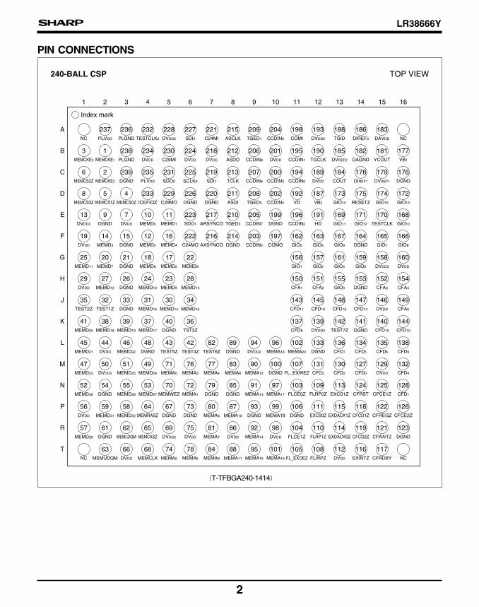
LR38666Y
237PLVDD
1
A
B
C
D
E
F
G
H
J
K
L
M
N
P
R
T
2 3 4 5 6 7 8 9 10 11 12 13 14 15 16
1MEMCKE1
2MEMCKE2
5MEMCS1Z
14MEMD3
20MEMD7
27MEMD12
32TEST1Z
38MEMD18
44DVDD
50DVDD2
54DGND
MEMD31
236PLGND
232TESTCLK2
228DVDD2
227SDI0
221C24MI
215ASCLK
209TGED1
204CCDIN6
198COMI
193DVDD2
188 186 183DIREF2 DAVDD
238PLGND
234DVDD
230C29MI
224DVDD
218DVDD
212ASDO
206CCDIN8
201DVDD
195CCDIN1
190TGCLK
185DVREF2
182DAGND
181YCOUT
239DGND
235PLVDD
231SDO0
225SCLK0
219SDI1
213TCLK
207CCDIN9
200CCDIN3
194CCDIN0
189 184COUT
178DIREF1
179DVREF1
4MEMCS0Z
233ICEFIQZ C29MO
226DGND
220DGND
211ASDI
208TGED0
202CCDIN4
192VD
187VB2
173GIO14
175RESETZ
174GIO15
15DGND
12MEMD2
16MEMD4
222C24MO AXSYNCO COMO
162197CCDIN5
203DGND
214216GIO5
163GIO6
167GIO9
164DGND
165GIO7
21DGND
18MEMD6
17MEMD5
22MEMD8
156GIO1
157GIO2
161GIO4
159GIO3
158DVDD2
26DGND
24MEMD10
23MEMD9
28MEMD13
150CFA1
151CFA2
155GIO0
153DGND
152CFA3
33DGND
31MEMD15
30MEMD14
34MEMD16 CFD11
145CFD13
148CFD15
147CFD14
146DVDD
39MEMD19
37MEMD17
40DGND
36TST3Z CFD8 DVDD2 TEST7Z
141DGND
140CFD10
46MEMD22
48DGND
43TEST5Z
42TEST4Z
82TEST6Z
89DGND
94DVDD2 MEMA20
96MEMA16 DGND CFD7
134CFD5
135CFD6
51MEMD25
49MEMD24
71MEMA0
76MEMA3
77MEMA4
83MEMA8
90MEMA12 FL_EXWEZ
100DGND CFD3 CFD2
127CFD0
129DVDD
55MEMD28
53MEMD27
70MEMWEZ
72MEMA1
79DGND
85DGND
91MEMA13 FLCE0Z
97MEMA17 FLRP0Z EXCS1Z
124CFRST
125CFCE1Z
585956MEMD30
64MEMRASZ
67DGND
73DGND
80MEMA6
87MEMA10
93DGND DGND
99MEMA18 EXCS0Z EXDACK1Z
118 122 126CFCD1Z CFREGZ
TGID
DVDD
229
9DGND
7DVDD
NC
3MEMCKE3
6MEMCS2Z
8MEMCS3Z
19DVDD
25MEMD11
29DVDD
35TEST2Z
41MEMD20
45MEMD21
47MEMD23
52MEMD26
DVDD
13DVDD2
10MEMD0 MEMD1
223SDO1
217ARSYNCO
210TGED2
205CCDIN7
199DGND
196CCDIN2
191HD
169GIO11
171GIO12
170TESTCLK
NC
177VB1
176DGND
172GIO13
166GIO8
160DVDD
154CFA4
149CFA0
144CFD12
138CFD9
132CFD4
128CFD1
CFCE2Z
168GIO10
11
143
137 139 142
102 133 136
107 131 130
103 109 113
106 111 115
DGND
626157MEMLDQM
65MEMCASZ
69DVDD2
75DVDD
81MEMA7
86DVDD
92MEMA14 FLCE1Z
98DVDD FLRP1Z EXDACK0Z
119 121 123CFCD2Z CFWAITZMEMD29 DGND
104 110 114
MEMUDQM
6663DVDD
68MEMCLK
74MEMA2
78MEMA5
84MEMA9
88MEMA11
95MEMA15 FL_EXOEZ
101MEMA19 FLWPZ DVDD
116 117EXINTZ CFRDBYNC NC
105 108 112
Index mark
(T-TFBGA240-1414)
PIN CONNECTIONS
240-BALL CSP TOP VIEW

LR38666Y
3
TG
ID
HD
VD
CC
DIN
0-
CC
DIN
9
CO
NT
RO
LS
IGN
AL
(NO
TE
3)
CO
NT
RO
LS
IGN
AL
(NO
TE
2)
CO
NT
RO
LS
IGN
AL
(NO
TE
1)
ME
MA
0-
ME
MA
20
ME
MD
0-
ME
MD
31
USB
CCD SIGNALPROCESSOR 2
JPEG COMPRESSOR/DECOMPRESSOR
RESIZE
CCD SIGNALPROCESSOR 1
PLL
LOCAL SRAM4 K BYTES
CPUPERIPHERAL
ARM7TDMI
MEMORY CONTROLLER
D/A CONVERTER
NTSC/PALENCODER
TIMER
DMAC
DECODER
BUS CONTROLLER
YCOUT
COUT
DVREF1, DVREF2
DIREF1, DIREF2
VB1, VB2
GIO
0-G
IO1
5
(NO
TE
4)
TGCLKTGED0-TGED2
COMICOMOC24MI
C24MOC29MI
C29MOASDI
ASDOASCLK
AXSYNCOARSYNCOTESTCLK
TESTCLK2
TCLKTEST1Z-TEST7Z
SDI0SDO0
SCLK0
SDI1SDO1
RESETZ
ICEFIQZ
CFD0-CFD15
(NOTE 5)
CFA0-CFA4
CLOCKGENERATOR
AUDIOI/F
UART
USART
GIO
BLOCK DIAGRAM
NOTES : 1. Control signal for SDRAM
MEMCLK, MEMLDQM, MEMUDQM, MEMWEZ,
MEMCASZ, MEMRASZ, MEMCKE1, MEMCS0Z-
MEMCS3Z
Control signal for SDRAM or general purpose I/O.
MEMCKE2 = GIO16, MEMCKE3 = GIO17 (set by
register)
2. Control signal for flash memory and external device.
FLCE0Z, FL_EXOEZ, FL_EXWEZ, FLWPZ, FLRP0Z,
EXCS0Z, CFREGZ, CFRST, CFCE1Z to CFCE2Z
Control signal for flash memory and external device or
general purpose I/O
FLCE1Z = GIO18, FLRP1Z = GIO19, EXCS1Z =
GIO20 (set by register)
3. Input signal from external device
EXDACK0Z, EXINTZ, CFWAITZ, CFRDBY
Input signal from external device or general purpose
I/O.
EXDACK1Z = GIO21, CFCD1Z = GIO22, CFCD2Z =
GIO23 (set by register)
4. General purpose I/O or PWM.
GIO0 to GIO2 = CCDGEO0 to CCDGEO2, GIO9 =
TX_VPO, GIO10 = TX_VMO, GIO11 = TX_OE_N,
GIO12 = SUSPEND_N, GIO13 = RX_VPI, GIO14 =
RX_VMI, GIO15 = RX_DATA (set by register)
5. Data I/O for CompactFlash or general purpose I/O.
CFD8 = GIO24, CFD9 = GIO25, CFD10 = GIO26,
CFD11 = GIO27, CFD12 = GIO28, CFD13 = GIO29,
CFD14 = GIO30, CFD15 = GIO31 (set by register)

4
LR38666Y
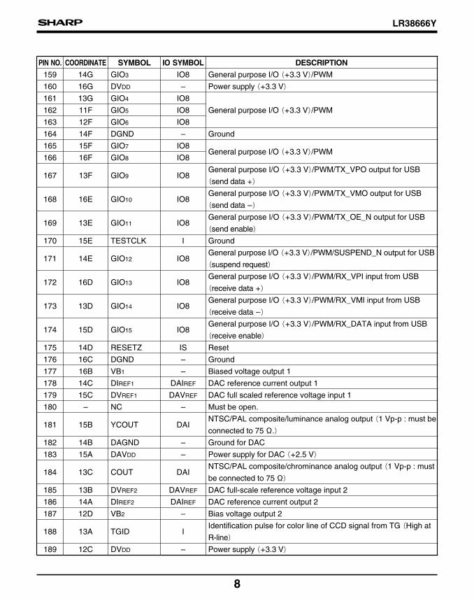
PIN DESCRIPTIONPIN NO. COORDINATE SYMBOL DESCRIPTIONIO SYMBOL
1 2B MEMCKE1 IO8 SDRAM clock enable, Block 1
2 2C MEMCKE2 IO8 SDRAM clock enable, Block 2/GIO16
3 1B MEMCKE3 IO8 SDRAM clock enable, Block 3/GIO17
4 3D MEMCS0Z IO8 SDRAM chip select, Block 0
5 2D MEMCS1Z IO8 SDRAM chip select, Block 1
6 1C MEMCS2Z IO816-bit data mode : SDRAM chip select, Block 2
32-bit data mode : Control MEMD15 to MEMD8 of SDRAM
7 3E DVDD – Power supply (+3.3 V)
8 1D MEMCS3Z IO816-bit data mode : SDRAM chip select, Block 3
32-bit data mode : Control MEMD7 to MEMD0 of SDRAM
9 2E DGND – Ground
10 4E MEMD0 IO12U
Data I/O for SDRAM/flash memory/external device11 5E MEMD1 IO12U
12 4F MEMD2 IO12U
13 1E DVDD2 – Internal power supply (+2.5 V)
14 2F MEMD3 IO12U Data I/O for SDRAM/flash memory/external device
15 3F DGND – Ground
16 5F MEMD4 IO12U
Data I/O for SDRAM/flash memory/external device17 5G MEMD5 IO12U
18 4G MEMD6 IO12U
19 1F DVDD – Power supply (+3.3 V)
20 2G MEMD7 IO12U Data I/O for SDRAM/flash memory/external device
21 3G DGND – Ground
22 6G MEMD8 IO12U
Data I/O for SDRAM/flash memory/external device23 5H MEMD9 IO12U
24 4H MEMD10 IO12U
25 1G MEMD11 IO12U
26 3H DGND – Ground
27 2H MEMD12 IO12UData I/O for SDRAM/flash memory/external device
28 6H MEMD13 IO12U
29 1H DVDD – Power supply (+3.3 V)
30 5J MEMD14 IO12UData I/O for SDRAM/flash memory/external device
31 4J MEMD15 IO12U
32 2J TEST1Z IU Test (Must be open.)
33 3J DGND – Ground
34 6J MEMD16 IO12U Data I/O for SDRAM/external device/GIO16
35 1J TEST2Z IUTest (Must be open.)
36 6K TEST3Z IU
37 4K MEMD17 IO12U Data I/O for SDRAM/external device/GIO17
38 2K MEMD18 IO12U Data I/O for SDRAM/external device/GIO18
39 3K MEMD19 IO12U Data I/O for SDRAM/external device/GIO19
LR38666Y
5
40 5K DGND – Ground
41 1K MEMD20 IO12U Data I/O for SDRAM/external device/GIO20
42 6L TEST4Z IUTest (Must be open.)
43 5L TEST5Z IU
44 2L DVDD – Power supply (+3.3 V)
45 1L MEMD21 IO12U Data I/O for SDRAM/external device/GIO21
46 3L MEMD22 IO12U Data I/O for SDRAM/external device/GIO22
47 1M MEMD23 IO12U Data I/O for SDRAM/external device/GIO23
48 4L DGND – Ground
49 4M MEMD24 IO12U Data I/O for SDRAM/external device/GIO24
50 2M DVDD2 – Internal power supply (+2.5 V)
51 3M MEMD25 IO12U Data I/O for SDRAM/external device/GIO25
52 1N MEMD26 IO12U Data I/O for SDRAM/external device/GIO26
53 4N MEMD27 IO12U Data I/O for SDRAM/external device/GIO27
54 2N DGND – Ground
55 3N MEMD28 IO12U Data I/O for SDRAM/external device/GIO28
56 1P DVDD – Power supply (+3.3 V)
57 1R MEMD29 IO12U Data I/O for SDRAM/external device/GIO29
58 3P MEMD30 IO12U Data I/O for SDRAM/external device/GIO30
59 2P MEMD31 IO12U Data I/O for SDRAM/external device/GIO31
60 – NC – Must be open.
61 2R DGND – Ground
62 3R MEMLDQM O1216-bit data mode : Control MEMD7-MEMD0 of SDRAM
32-bit data mode : Control MEMD23-MEMD16 of SDRAM
63 2T MEMUDQM O1216-bit data mode : Control MEMD15-MEMD8 of SDRAM
32-bit data mode : Control MEMD31-MEMD24 of SDRAM
64 4P MEMRASZ O12 SDRAM row address strobe
65 4R MEMCASZ O12 SDRAM column address strobe
66 3T DVDD – Power supply (+3.3 V)
67 5P DGND – Ground
68 4T MEMCLK IO12 SDRAM clock output (49.0908 MHz : double of C24MI input)
69 5R DVDD2 – Internal power supply (+2.5 V)
70 5N MEMWEZ O12 SDRAM write enable
71 5M MEMA0 O12Address for SDRAM/flash memory/external device
72 6N MEMA1 O12
73 6P DGND – Ground
74 5T MEMA2 O12 Address for SDRAM/flash memory/external device
75 6R DVDD – Power supply (+3.3 V)
PIN NO. COORDINATE SYMBOL DESCRIPTIONIO SYMBOL
76 6M MEMA3 O12 Address for SDRAM/flash memory/external device
77 7M MEMA4 O12 Address for SDRAM/flash memory/external device
79 7N DGND – Ground
78 6T MEMA5 O12 Address for SDRAM/flash memory/external device
6
LR38666Y
80 7P MEMA6 O12 Address for SDRAM/flash memory/external device
81 7R MEMA7 O12 Address for SDRAM/flash memory/external device
82 7L TEST6Z IU Test (Must be open.)
83 8M MEMA8 O12 Address for SDRAM/flash memory/external device
84 7T MEMA9 O12 Address for SDRAM/flash memory/external device
85 8N DGND – Ground
86 8R DVDD – Power supply (+3.3 V)
87 8P MEMA10 O12 Address for SDRAM/flash memory/external device
88 8T MEMA11 O12 Address for SDRAM/flash memory/external device
89 8L DGND – Ground
90 9M MEMA12 O12 Address for SDRAM/flash memory/external device
91 9N MEMA13 O12 Address for SDRAM/flash memory/external device
92 9R MEMA14 O12 Address for SDRAM/flash memory/external device
93 9P DGND – Ground
94 9L DVDD2 – Internal power supply (+2.5 V)
95 9T MEMA15 O12 Address for flash memory/external device/CompactFlash (CFA5)
96 10L MEMA16 O12 Address for flash memory/external device/CompactFlash (CFA6)
97 10N MEMA17 O12 Address for flash memory/external device/CompactFlash (CFA7)
98 10R DVDD – Power supply (+3.3 V)
99 10P MEMA18 O12 Address for flash memory/external device/CompactFlash (CFA8)
100 10M DGND – Ground
101 10T MEMA19 O12 Address for flash memory/external device/CompactFlash (CFA9)
102 11L MEMA20 O12 Address for flash memory/external device/CompactFlash (CFA10)
103 11N FLCE0Z O8 Chip enable for flash memory, Block 0
104 11R FLCE1Z IO8 Chip enable for flash memory, Block 1/GIO18
105 11T FL_EXOEZ O8 Output enable for flash memory/external device/CompactFlash
106 11P DGND – Ground
107 11M FL_EXWEZ O8 Write enable for flash memory/external device/CompactFlash
108 12T FLWPZ O8 Write protect for flash memory
109 12N FLRP0Z O8 Reset/deep power down for flash memory, Block 0
110 12R FLRP1Z IO8 Reset/deep power down for flash memory, Block 1/GIO19
111 12P EXCS0Z O8 Chip select 0 for external device
112 13T DVDD – Power supply (+3.3 V)
PIN NO. COORDINATE SYMBOL DESCRIPTIONIO SYMBOL
113 13N EXCS1Z IO8 Chip select 1 for external device/GIO20
114 13R EXDACK0Z IU Data acknowledge 0 for external device
115 13P EXDACK1Z IO8U Data acknowledge 1 for external device/GIO21
116 14T EXINTZ IU External device interrupt
117 15T CFRDBY IU CompactFlash/SmartMedia READY/BUSY
118 14P CFCD1Z IO8U CompactFlash/SmartMedia card detect signal 1/GIO22
119 14R CFCD2Z IO8UCompactFlash card detect signal 2/SmartMedia write protect
detect/GIO23
120 – NC – Must be open.
LR38666Y
7
121 15R CFWAITZ IU CompactFlash –WAIT signal
122 15P CFREGZ IO8 CompactFlash –REG signal
123 16R DGND – Ground
124 14N CFRST IO8
125 15N CFCE1Z IO8
126 16P CFCE2Z IO8 Card enable 2 for CompactFlash (–CE2)
127 14M CFD0 IO8UData I/O for CompactFlash/SmartMedia
128 16N CFD1 IO8U
129 15M DVDD – Power supply (+3.3 V)
130 13M CFD2 IO8U
Data I/O for CompactFlash/SmartMedia131 12M CFD3 IO8U
132 16M CFD4 IO8U
133 12L DGND – Ground
134 14L CFD5 IO8U
Data I/O for CompactFlash/SmartMedia135 15L CFD6 IO8U
136 13L CFD7 IO8U
137 11K CFD8 IO8U Data I/O for CompactFlash/GIO24
138 16L CFD9 IO8U Data I/O for CompactFlash/GIO25
139 12K DVDD2 – Internal power supply (+2.5 V)
140 15K CFD10 IO8U
141 14K DGND – Ground
142 13K TEST7Z IU Test (Must be open.)
143 11J CFD11 IO8U
144 16K CFD12 IO8U
145 12J CFD13 IO8U Data I/O for CompactFlash/GIO29
146 15J DVDD – Power supply (+3.3 V)
147 14J CFD14 IO8U
148 13J CFD15 IO8U
149 16J CFA0 IO8 Address for CompactFlash/read enable for SmartMedia (–RE)
150 11H CFA1 IO8 Address for CompactFlash/write enable for SmartMedia (–WE)
151 12H CFA2 IO8 Address for CompactFlash/write protect for SmartMedia (–WP)
152 15H CFA3 IO8Address for CompactFlash/address latch enable for SmartMedia
(ALE)
153 14H DGND – Ground
154 16H CFA4 IO8Address for CompactFlash/command latch enable for
SmartMedia (CLE)
155 13H GIO0 IO8
General purpose I/O (+3.3 V)/PWM/CCD general purpose output156 11G GIO1 IO8
157 12G GIO2 IO8
158 15G DVDD2 –
PIN NO. COORDINATE SYMBOL DESCRIPTIONIO SYMBOL
Data I/O for CompactFlash/GIO26
Data I/O for CompactFlash/GIO27
Data I/O for CompactFlash/GIO28
Data I/O for CompactFlash/GIO30
Data I/O for CompactFlash/GIO31
CompactFlash reset signal (RESET)/SmartMedia chip enable
(–CE)
Card enable 1 for CompactFlash (–CE1)
Internal power supply (+2.5 V)
8
LR38666Y
PIN NO. COORDINATE SYMBOL DESCRIPTIONIO SYMBOL
159 14G GIO3 IO8 General purpose I/O (+3.3 V)/PWM
160 16G DVDD – Power supply (+3.3 V)
161 13G GIO4 IO8
General purpose I/O (+3.3 V)/PWM162 11F GIO5 IO8
163 12F GIO6 IO8
164 14F DGND – Ground
165 15F GIO7 IO8General purpose I/O (+3.3 V)/PWM
166 16F GIO8 IO8
167 13F GIO9 IO8General purpose I/O (+3.3 V)/PWM/TX_VPO output for USB
(send data +)
168 16E GIO10 IO8General purpose I/O (+3.3 V)/PWM/TX_VMO output for USB
(send data –)
169 13E GIO11 IO8General purpose I/O (+3.3 V)/PWM/TX_OE_N output for USB
(send enable)
170 15E TESTCLK I Ground
171 14E GIO12 IO8General purpose I/O (+3.3 V)/PWM/SUSPEND_N output for USB
(suspend request)
172 16D GIO13 IO8General purpose I/O (+3.3 V)/PWM/RX_VPI input from USB
(receive data +)
173 13D GIO14 IO8General purpose I/O (+3.3 V)/PWM/RX_VMI input from USB
(receive data –)
174 15D GIO15 IO8General purpose I/O (+3.3 V)/PWM/RX_DATA input from USB
(receive enable)
175 14D RESETZ IS Reset
176 16C DGND – Ground
177 16B VB1 – Biased voltage output 1
178 14C DIREF1 DAIREF DAC reference current output 1
179 15C DVREF1 DAVREF DAC full scaled reference voltage input 1
180 – NC – Must be open.
181 15B YCOUT DAINTSC/PAL composite/luminance analog output (1 Vp-p : must be
connected to 75 $.)
182 14B DAGND – Ground for DAC
183 15A DAVDD – Power supply for DAC (+2.5 V)
184 13C COUT DAINTSC/PAL composite/chrominance analog output (1 Vp-p : must
be connected to 75 $)
185 13B DVREF2 DAVREF DAC full-scale reference voltage input 2
186 14A DIREF2 DAIREF DAC reference current output 2
187 12D VB2 – Bias voltage output 2
188 13A TGID IIdentification pulse for color line of CCD signal from TG (High at
R-line)
189 12C DVDD – Power supply (+3.3 V)

LR38666Y
9
190 12B TGCLK I Pixel clock input from TG
191 12E HD IO8 Horizontal synchronization pulse for CCD
192 11D VD IO8 Vertical synchronization pulse for CCD
193 12A DVDD2 – Internal power supply (+2.5 V)
194 11C CCDIN0 I
RGB input from CCD 195 11B CCDIN1 I
196 11E CCDIN2 I
197 10F COMO OSC 24 MHz crystal oscillator output
198 11A COMI IA 24 MHz crystal oscillator input (for communication)
199 10E DGND – Ground
200 10C CCDIN3 I RGB input from CCD
201 10B DVDD – Power supply (+3.3 V)
202 10D CCDIN4 I
RGB input from CCD
203 9F CCDIN5 I
204 10A CCDIN6 I
205 9E CCDIN7 I
206 9B CCDIN8 I
207 9C CCDIN9 I
208 9D TGED0 IO8
Serial signal output for setting register of TG209 9A TGED1 IO8
210 8E TGED2 O8
211 8D ASDI IU Input data for audio serial I/F
212 8B ASDO O8 Output data for audio serial I/F
213 8C TCLK I Master clock input for audio serial I/F
214 8F DGND – Ground
215 8A ASCLK O8 Shift clock for audio serial I/F
216 7F AXSYNCO O8 Transmit synchronous signal for audio serial I/F
217 7E ARSYNCO O8 Receive synchronous signal for audio serial I/F
218 7B DVDD – Power supply (+3.3 V)
219 7C SDI1 I Input data for asynchronous serial I/F
220 7D DGND – Ground
221 7A C24MI IA 24.5454 MHz crystal oscillator input (system clock)
222 6F C24MO OSC 24.5454 MHz crystal oscillator output
223 6E SDO1 O8 Output data for asynchronous serial I/F
224 6B DVDD – Power supply (+3.3 V)
225 6C SCLK0 IO8U Clock for synchronous serial I/F
226 6D DGND – Ground
227 6A SDI0 I Input data for synchronous serial I/F
228 5A DVDD2 – Internal power supply (+2.5 V)
229 5D C29MO OSC 29.5 MHz crystal oscillator output
230 5B C29MI IA 29.5 MHz crystal oscillator input (for PAL)
PIN NO. COORDINATE SYMBOL DESCRIPTIONIO SYMBOL
10
LR38666Y
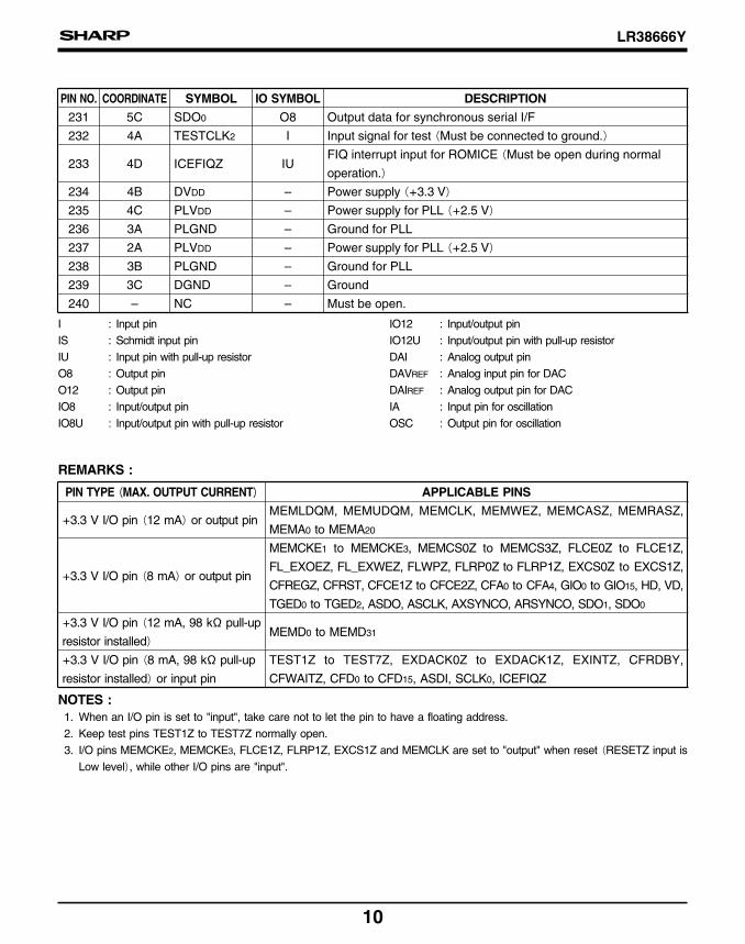
PIN NO. COORDINATE SYMBOL DESCRIPTIONIO SYMBOL
231 5C SDO0 O8 Output data for synchronous serial I/F
232 4A TESTCLK2 I Input signal for test (Must be connected to ground.)
233 4D ICEFIQZ IUFIQ interrupt input for ROMICE (Must be open during normal
operation.)
234 4B DVDD – Power supply (+3.3 V)
235 4C PLVDD – Power supply for PLL (+2.5 V)
236 3A PLGND – Ground for PLL
237 2A PLVDD – Power supply for PLL (+2.5 V)
238 3B PLGND – Ground for PLL
239 3C DGND – Ground
240
I : Input pin
IS : Schmidt input pin
IU : Input pin with pull-up resistor
O8 : Output pin
O12 : Output pin
IO8 : Input/output pin
IO8U : Input/output pin with pull-up resistor
IO12 : Input/output pin
IO12U : Input/output pin with pull-up resistor
DAI : Analog output pin
DAVREF : Analog input pin for DAC
DAIREF : Analog output pin for DAC
IA : Input pin for oscillation
OSC : Output pin for oscillation
– NC – Must be open.
PIN TYPE (MAX. OUTPUT CURRENT)
REMARKS :
APPLICABLE PINS
+3.3 V I/O pin (12 mA) or output pinMEMLDQM, MEMUDQM, MEMCLK, MEMWEZ, MEMCASZ, MEMRASZ,
MEMA0 to MEMA20
+3.3 V I/O pin (8 mA) or output pin
MEMCKE1 to MEMCKE3, MEMCS0Z to MEMCS3Z, FLCE0Z to FLCE1Z,
FL_EXOEZ, FL_EXWEZ, FLWPZ, FLRP0Z to FLRP1Z, EXCS0Z to EXCS1Z,
CFREGZ, CFRST, CFCE1Z to CFCE2Z, CFA0 to CFA4, GIO0 to GIO15, HD, VD,
TGED0 to TGED2, ASDO, ASCLK, AXSYNCO, ARSYNCO, SDO1, SDO0
+3.3 V I/O pin (12 mA, 98 k$ pull-up
resistor installed)MEMD0 to MEMD31
+3.3 V I/O pin (8 mA, 98 k$ pull-up
resistor installed) or input pin
TEST1Z to TEST7Z, EXDACK0Z to EXDACK1Z, EXINTZ, CFRDBY,
CFWAITZ, CFD0 to CFD15, ASDI, SCLK0, ICEFIQZ
NOTES :1. When an I/O pin is set to "input", take care not to let the pin to have a floating address.
2. Keep test pins TEST1Z to TEST7Z normally open.
3. I/O pins MEMCKE2, MEMCKE3, FLCE1Z, FLRP1Z, EXCS1Z and MEMCLK are set to "output" when reset (RESETZ input is
Low level), while other I/O pins are "input".
LR38666Y
11
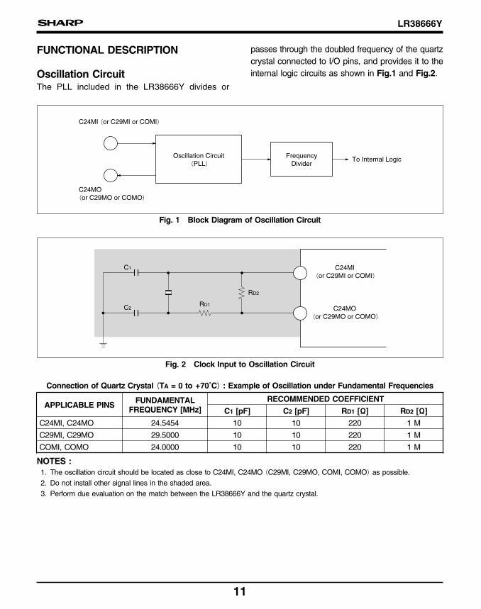
FUNCTIONAL DESCRIPTION
Oscillation CircuitThe PLL included in the LR38666Y divides or
passes through the doubled frequency of the quartz
crystal connected to I/O pins, and provides it to the
internal logic circuits as shown in Fig.1 and Fig.2.
C24MI (or C29MI or COMI)
Oscillation Circuit(PLL)
FrequencyDivider
To Internal Logic
C24MO(or C29MO or COMO)
Fig. 1 Block Diagram of Oscillation Circuit
RD1
RD2
C1
C2
C24MI(or C29MI or COMI)
C24MO(or C29MO or COMO)
Connection of Quartz Crystal (TA = 0 to +70˚C) : Example of Oscillation under Fundamental Frequencies
APPLICABLE PINSFUNDAMENTAL
FREQUENCY [MHz]
RECOMMENDED COEFFICIENT
C1 [pF] C2 [pF] RD1 [$] RD2 [$]
C24MI, C24MO 24.5454 10 10 220 1 M
C29MI, C29MO 29.5000 10 10 220 1 M
COMI, COMO 24.0000 10 10 220 1 M
NOTES : 1. The oscillation circuit should be located as close to C24MI, C24MO (C29MI, C29MO, COMI, COMO) as possible.
2. Do not install other signal lines in the shaded area.
3. Perform due evaluation on the match between the LR38666Y and the quartz crystal.
Fig. 2 Clock Input to Oscillation Circuit

12
LR38666Y
ClockThe clock supplied to C24MI is doubled in
frequency by an internal PLL and then is used as
the main system clock. This clock is also used by
the NTSC/PAL module in NTSC mode.
The clock supplied to C29MI is doubled in
frequency by an internal PLL and then is used by
the NTSC/PAL module in PAL mode only. The
PAL mode allows clock oscillation. If the PAL
mode is not used, fix the input level to High or Low.
Note that, in NTSC mode, the accuracy of burst
signals (deflection from the specified frequency) for
video output depends on the accuracy of the clock
supplied to C24MI. In PAL mode, the accuracy of
burst signals (deflection from the specified
frequency) for video output depends on the
accuracy of the clock supplied to C29MI.
The clock supplied to COMI is doubled in frequency
by an internal PLL and then is used by the UART,
USART, USB and AUDIOIF modules. Only 24 MHz
frequency can be used.
Note that the accuracy of the clock supplied to
COMI influences the pulse width of the I/O signals.
Supply the clock (synchronized with CCD data) to
TGCLK. Use as low a noise level signal as possible.
Note that accuracy of the clock supplied to TCLK
influences the accuracy of the clock of AUDIOIF.
If TCLK is not used, fix the input level to High or
Low.
Power Supply PinsConnect low noise power lines to the PLL power
supply pin (PLVDD), the PLL ground pin (PLGND),
the DA converter power supply pin (DAVDD) and
the DA converter ground pin (DAGND).
Note that PLVDD and DAVDD are connected to
DVDD2, and PLGND and DAGND are connected to
DGND inside the LR38666Y.
Power ON/OFF SequenceTwo power supplies are used with the LR38666Y.
One (DVDD) is used for I/O buffer and the other
(DVDD2) is used for the core logic circuits.
Power ON : Be sure to turn ON the internal power
supply of DVDD2 first.
Power OFF : Be sure to turn OFF the I/O buffer of
DVDD first.
CVR VREF
RREF
CVB
DAVDD
ROUT
RB1
RB2
DAVDD
DAVDD
YCOUT/COUTAnalog Output
DVREF1/2
DIREF1/2
VB1/2
DAGND
Recommended DAC Circuit (Example)
LR38666Y
13
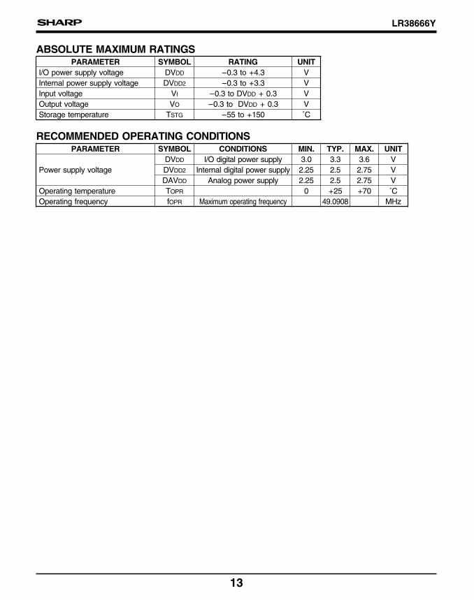
ABSOLUTE MAXIMUM RATINGSPARAMETER SYMBOL RATING UNIT
I/O power supply voltage DVDD –0.3 to +4.3 V
Internal power supply voltage DVDD2 –0.3 to +3.3 V
Input voltage VI –0.3 to DVDD + 0.3 V
Output voltage VO –0.3 to DVDD + 0.3
–55 to +150
V
Storage temperature TSTG ˚C
RECOMMENDED OPERATING CONDITIONSPARAMETER SYMBOL CONDITIONS MIN. TYP. MAX. UNIT
Power supply voltage
DVDD I/O digital power supply 3.0 3.3 3.6 V
DVDD2 Internal digital power supply 2.25 2.5 2.75 V
Operating temperature TOPR 0 +25 +70 ˚C
Operating frequency fOPR Maximum operating frequency 49.0908 MHz
V2.752.52.25Analog power supplyDAVDD

14
LR38666Y
ELECTRICAL CHARACTERISTICS
DC Characteristics (DVDD = 3.3 V, DVDD2 = 2.5 V, TA = 0 to +70˚C)
PARAMETER SYMBOL CONDITIONS MIN. TYP. MAX. UNIT NOTE
Input "Low" voltage VIL 0.2 DVDD V1
Input "High" voltage VIH 0.8 DVDD V
Positive trigger voltage VT+ 1.37 V
2Negative trigger voltage VT– 1.33 V
Hysteresis VT+ – VT– 0.2 V
Input leakage current II
VIN = 0 V to DVDD –1.0 +1.0 µA 3
VIN = DVDD
[with pull-up 98 k$]–5.0 +5.0 µA 4
Input "Low" current IILVIN = 0 V
[with pull-up 98 k$]–35 µA 4
Output "Low" voltage 1 VOL1 IOL = 8 mA 0.5 V5
Output "High" voltage 1 VOH1 IOH = –8 mA DVDD – 0.5 V
Output "Low" voltage 2 VOL2 IOL = 12 mA 0.5 V6
Output "High" voltage 2 VOH2 IOH = –12 mA DVDD – 0.5 V
Resolution RES 9 Bit
7
Linearity error EL VREF = 1.24 V
RREF = 4.8 k$
ROUT = 75 $
CVB = 0.1 µF
–3.0 +6.0 LSB
Differential linearity error ED –1.0 +1.0 LSB
Full-scale current IFS 16.5 mA
Output load resistance ROUT 75 $
Reference voltage VREF 1.12 1.24 1.36 V 8
Reference resistance RREF 4.8 k$ 9
Oscillation frequency 1 FOSC1 24.5454 MHz 10
Oscillation frequency 2 FOSC2 29.5000 MHz 11
Oscillation frequency 3 FOSC3 24.0000 MHz 12
Supply current (a)
(DVDD)IDDa
Input image display mode :
1/4 VGA
55 mA
13Supply current (a)
(DVDD2, DAVDD, PLVDD)IDD2a 115 mA
Supply current (b)
(DVDD)IDDb Input image display &
capture image mode :
VGA
70 mA
14Supply current (b)
(DVDD2, DAVDD, PLVDD)IDD2b 125 mA
Standby current
(DVDD)IDDSB
waiting for ARM operation
with 1/4 clock
25 mA
15Standby current
(DVDD2, DAVDD, PLVDD)IDD2SB 15 mA
LR38666Y
15
NOTES : 1. Applicable to IO symbols I, IU, IO8, IO8U, IO12, IO12U.
2. Applicable to IO symbol IS.
3. Applicable to IO symbols I, IO8, IO12, IS.
4. Applicable to IO symbols IU, IO8U, IO12U.
5. Applicable to IO symbols O8, IO8, IO8U.
6. Applicable to IO symbols O12, IO12, IO12U.
7. Applicable to IO symbol DAI.
8. Applicable to IO symbol DAVREF.
9. External resistance value. Applicable to IO symbol
DAIREF.
10. Applicable to IO symbols IA (C24MI), OSC (C24MO).
11. Applicable to IO symbols IA (C29MI), OSC (C29MO).
12. Applicable to IO symbols IA (COMI), OSC (COMO).
13. Supply voltage DVDD : 3.3 V, DVDD2 : 2.5 V
Measuring conditions : 1 310 k-pixel CCD is used.
CCD1 output image size 640 x 240,
CCD2 output image size 320 x 240,
16 bits external bus width, Local SRAM is not used.
Always active modules :
ARM, CCD1, CCD2, VENC, MEMC, DMAC
Inactive modules :
JPEG, SRAM, USART, UART, USB, RESIZE, PLL (for
PAL), AUDIOIF, GIO
14. Supply voltage DVDD : 3.3 V, DVDD2 : 2.5 V
Measuring conditions : 1 310 k-pixel CCD is used.
CCD1 output image size 640 x 480,
CCD2 output image size 640 x 480,
16 bits external bus width, Local SRAM is not used.
Always active modules :
ARM, CCD1, CCD2, JPEG, VENC, MEMC, DMAC
Inactive modules :
SRAM, USART, UART, USB, RESIZE, PLL (for PAL),
AUDIOIF, GIO
15. Supply voltage DVDD : 3.3 V, DVDD2 : 2.5 V
Always active modules :
ARM, MEMC, DMAC (Internal clock is divided into 1/4.)
Inactive modules :
JPEG, CCD1, CCD2, VENC, SRAM, USART, UART,
USB, RESIZE, PLL (for PAL), AUDIOIF, GIO
16
LR38666Y
AC Characteristics
SDRAM INTERFACE TIMING
0.8 DVDD
TMCLKL TMCLKH
0.8 DVDD
0.2 DVDD
0.8 DVDD
0.2 DVDD
0.2 DVDD
TMCSD
TMCASD
TMRASD
TMWED
TMCKED
TMDQMD
MEMCLK
MEMCS0Z-MEMCS3ZMEMRASZMEMCASZMEMWEZMEMCKE1-MEMCKE3
MEML(U)DQMCommon to all waveformsshown above
MEMD [31 : 0]MEMA [14 : 0]Common to allwaveforms shown above
TMCSD
TMCASD
TMRASD
TMWED
TMCKED
TMDQMD
TMAD
TMDD
TMAD
TMDD
TMCLK
Fig. 3 SDRAM Output Timing
Fig. 4 SDRAM Input Timing
NOTE : MEMCLK is also used as the data latch clock inside the LR38666Y. Check the waveform of the incoming MEMCLK
signal for no distortion.
0.8 DVDD
0.8 DVDD
0.2 DVDD
TMDS TMDH
0.2 DVDD
MEMCLK (NOTE)
MEMD [31 : 0]

LR38666Y
17
(DVDD = 3.3 V, DVDD2 = 2.5 V, C24MI = 24.5454 MHz, TA = 0 to +70˚C)
PARAMETER SYMBOLCONDITIONS
UNIT NOTEMIN. TYP. MAX.
Clock cycle TMCLK 20 ns 2
Pulse width (High) TMCLKH 9 ns 2
Pulse width (Low) TMCLKL 9 ns 2
Chip select delay TMCSD 0 7 ns 1
MEMRASZ output delay TMRASD 0 7 ns 2
MEMCASZ output delay TMCASD 0 7 ns 2
Write enable delay TMWED 0 7 ns 2
Addressing delay TMAD 0 7 ns 2
MEMCKE1 to MEMCKE3 output delay TMCKED 0 7 ns 1
MEML(U)DQM output delay TMDQMD 0 7 ns 2
Data output delay (write cycle) TMDD 0 7 ns 2
Data setup delay (read cycle) TMDS 10 ns
Data hold delay (read cycle)
NOTES :1. Output load capacity CL = 10 pF
2. Output load capacity CL = 50 pF
TMDH 3 ns
18
LR38666Y
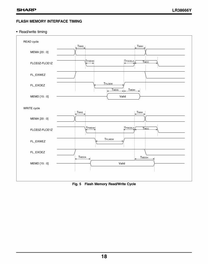
FLASH MEMORY INTERFACE TIMING
• Read/write timing
TFWCELHFWCELH
TFOEHHTFOEHH
TMDIS TMDIH
TFWCELH TMCC
TMAS TMAH
TFOCELH
TFLOEW
Valid
TMAS
TFWEHH
TMDOA TMDOH
TMAH
Valid
TFLWEW
MEMA [20 : 0]
READ cycle
FLCE0Z-FLCE1Z
FL_EXWEZ
FL_EXOEZ
MEMD [15 : 0]
MEMA [20 : 0]
WRITE cycle
FLCE0Z-FLCE1Z
FL_EXWEZ
FL_EXOEZ
MEMD [15 : 0]
TMCC
Fig. 5 Flash Memory Read/Write Cycle
LR38666Y
19
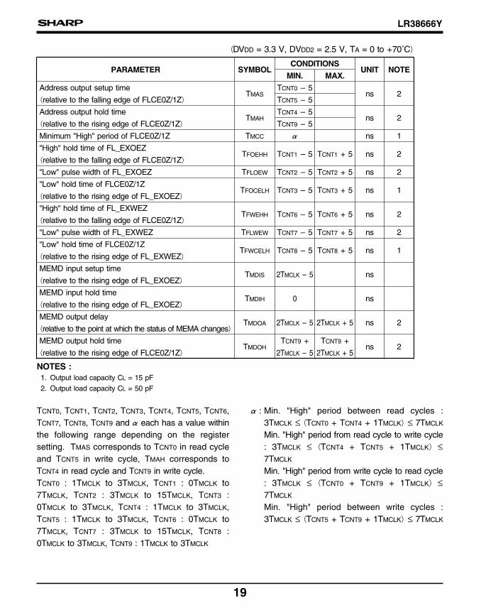
NOTES :1. Output load capacity CL = 15 pF
2. Output load capacity CL = 50 pF
(DVDD = 3.3 V, DVDD2 = 2.5 V, TA = 0 to +70˚C)
PARAMETER SYMBOLCONDITIONS
UNIT NOTEMIN. MAX.
Address output setup time
(relative to the falling edge of FLCE0Z/1Z)TMAS
TCNT0 – 5ns 2
TCNT5 – 5
Address output hold time
(relative to the rising edge of FLCE0Z/1Z)TMAH
TCNT4 – 5ns 2
Minimum "High" period of FLCE0Z/1Z TMCC Ω ns 1
"High" hold time of FL_EXOEZ
(relative to the falling edge of FLCE0Z/1Z)TFOEHH TCNT1 – 5 TCNT1 + 5 ns 2
"Low" hold time of FLCE0Z/1Z
(relative to the rising edge of FL_EXOEZ)TFOCELH TCNT3 – 5 TCNT3 + 5 ns 1
"High" hold time of FL_EXWEZ
(relative to the falling edge of FLCE0Z/1Z)TFWEHH TCNT6 – 5 TCNT6 + 5 ns 2
"Low" pulse width of FL_EXWEZ TFLWEW TCNT7 – 5 TCNT7 + 5 ns 2
"Low" hold time of FLCE0Z/1Z
(relative to the rising edge of FL_EXWEZ)TFWCELH TCNT8 – 5 TCNT8 + 5 ns 1
MEMD input setup time
(relative to the rising edge of FL_EXOEZ)TMDIS 2TMCLK – 5 ns
MEMD output delay
(relative to the point at which the status of MEMA changes)TMDOA 2TMCLK – 5 2TMCLK + 5 ns 2
MEMD output hold time
(relative to the rising edge of FLCE0Z/1Z)TMDOH
TCNT9 +
2TMCLK – 5
TCNT9 +
2TMCLK + 5ns 2
TCNT9 – 5
2nsTCNT2 + 5TCNT2 – 5TFLOEW"Low" pulse width of FL_EXOEZ
ns0TMDIHMEMD input hold time
(relative to the rising edge of FL_EXOEZ)
TCNT0, TCNT1, TCNT2, TCNT3, TCNT4, TCNT5, TCNT6,
TCNT7, TCNT8, TCNT9 and Ω each has a value within
the following range depending on the register
setting. TMAS corresponds to TCNT0 in read cycle
and TCNT5 in write cycle, TMAH corresponds to
TCNT4 in read cycle and TCNT9 in write cycle.
TCNT0 : 1TMCLK to 3TMCLK, TCNT1 : 0TMCLK to
7TMCLK, TCNT2 : 3TMCLK to 15TMCLK, TCNT3 :
0TMCLK to 3TMCLK, TCNT4 : 1TMCLK to 3TMCLK,
TCNT5 : 1TMCLK to 3TMCLK, TCNT6 : 0TMCLK to
7TMCLK, TCNT7 : 3TMCLK to 15TMCLK, TCNT8 :
0TMCLK to 3TMCLK, TCNT9 : 1TMCLK to 3TMCLK
Ω : Min. "High" period between read cycles :
3TMCLK ≤ (TCNT0 + TCNT4 + 1TMCLK) ≤ 7TMCLK
Min. "High" period from read cycle to write cycle
: 3TMCLK ≤ (TCNT4 + TCNT5 + 1TMCLK) ≤
7TMCLK
Min. "High" period from write cycle to read cycle
: 3TMCLK ≤ (TCNT0 + TCNT9 + 1TMCLK) ≤
7TMCLK
Min. "High" period between write cycles :
3TMCLK ≤ (TCNT5 + TCNT9 + 1TMCLK) ≤ 7TMCLK

20
LR38666Y
NOTES :1. Output load capacity CL = 15 pF
2. When the internal bus of the LR38666Y accesses to the flash memory during TRPH, it is made to wait.
• Flash memory hard reset timing
TRPL
RESETZ
FLRP0Z/1Z
TRPH
Fig. 6 Flash Memory Reset Cycle
PARAMETER SYMBOLCONDITIONS
UNIT NOTEMIN. MAX.
"Low" pulse period of FLRP0Z/1Z
(relative to the rising edge of RESETZ)TRPL 11TMCLK 12TMCLK ns 1
"High" pulse period of FLRP0Z/1Z
(relative to the rising edge of FLR0/1Z)TRPH 98TMCLK ns 1, 2
(DVDD = 3.3 V, DVDD2 = 2.5 V, TA = 0 to +70˚C)
• Flash memory initialization timing
TRPL
FLRP0Z/1Z
Fig. 7 Flash Memory Initialization Cycle
PARAMETER SYMBOLCONDITIONS
UNIT NOTEMIN.
(DVDD = 3.3 V, DVDD2 = 2.5 V, TA = 0 to +70˚C)
NOTE :1. Output load capacity CL = 15 pF
1ns12TMCLK
MAX.
12TMCLK"Low" pulse period of FLRP0Z/1Z TRPL
LR38666Y
21
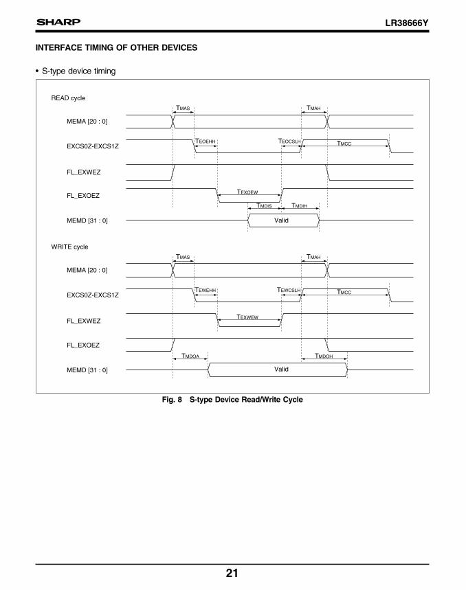
INTERFACE TIMING OF OTHER DEVICES
• S-type device timing
TEOEHH TEOCSLHEOCSLHTEOCSLH TMCC
TEXOEW
TMDIS
Valid
TMDIH
TMAS TMAH
TEWEHH TEWCSLHEWCSLHTEWCSLH TMCC
TEXWEW
TMDOA
Valid
TMDOH
TMAS TMAH
MEMA [20 : 0]
READ cycle
EXCS0Z-EXCS1Z
FL_EXWEZ
FL_EXOEZ
MEMD [31 : 0]
MEMA [20 : 0]
WRITE cycle
EXCS0Z-EXCS1Z
FL_EXWEZ
FL_EXOEZ
MEMD [31 : 0]
Fig. 8 S-type Device Read/Write Cycle

22
LR38666Y
(DVDD = 3.3 V, DVDD2 = 2.5 V, TA = –10 to +70˚C)
PARAMETER SYMBOLCONDITIONS
UNIT NOTEMIN. MAX.
Output setup period of MEMA
(relative to the falling edge of EXCS0Z/1Z)TMAS
TCNT00 – 5ns 2
TCNT05 – 5
Output hold period of MEMA
(relative to the rising edge of EXCS0Z/1Z)TMAH
TCNT04 – 5ns 2
Minimum "High" period of EXCS0Z/1Z TMCC Ω ns 1
"High" hold period of FL_EXOEZ
(relative to the falling edge of EXCS0Z/1Z)TEOEHH TCNT01 – 5 TCNT01 + 5 ns 2
"Low" pulse width of FL_EXOEZ TEXOEW TCNT02 – 5 TCNT02 + 5 ns 2
"Low" hold period of EXCS0Z/1Z
(relative to the rising edge of FL_EXOEZ)TEWCSLH TCNT03 – 5 TCNT03 + 5 ns 1
"High" hold period of FL_EXWEZ
(relative to the falling edge of EXCS0Z/1Z)TEWEHH TCNT06 – 5 TCNT06 + 5 ns 2
"Low" pulse width of FL_EXWEZ TEXWEW TCNT07 – 5 TCNT07 + 5 ns 2
"Low" hold period of EXCS0Z/1Z
(relative to the rising edge of FL_EXWEZ)TEWCSLH TCNT08 – 5 TCNT08 + 5 ns 1
Input setup period of MEMD
(relative to the rising edge of FL_EXOEZ)TMDIS 2TMCLK – 5 ns
Input hold period of MEMD
(relative to the rising edge of FL_EXOEZ)TMDIH 0 ns
Output delay period of MEMD (relative to MEMA) TMDOA 2TMCLK – 5 2TMCLK + 5 ns 2
Output hold period of MEMD
(relative to the rising edge of EXCS0Z/1Z)
NOTES :1. Output load capacity CL = 15 pF
2. Output load capacity CL = 50 pF
TMDOHTCNT09 +
2TMCLK – 5
TCNT09 +
2TMCLK + 5ns 2
TCNT00, TCNT01, TCNT02, TCNT03, TCNT04, TCNT05,
TCNT06, TCNT07, TCNT08, TCNT09 and Ω each has a
value within the following range depending on the
register setting.
TMAS corresponds to TCNT00 in read cycle and
TCNT05 in write cycle, and TCNT04 in read cycle and
TCNT09 in write cycle.
TCNT00 : 1TMCLK to 3TMCLK, TCNT01 : 0TMCLK to
3TMCLK, TCNT02 : 3TMCLK to 15TMCLK, TCNT03 :
0TMCLK to 7TMCLK, TCNT04 : 1TMCLK to 7TMCLK,
TCNT05 : 1TMCLK to 3TMCLK, TCNT06 : 0TMCLK to
3TMCLK, TCNT07 : 3TMCLK to 15TMCLK, TCNT08 :
0TMCLK to 7TMCLK, TCNT09 : 1TMCLK to 7TMCLK
Ω : Min. "High" period between read cycles :
3TMCLK ≤ (TCNT00 + TCNT04 + 1TMCLK) ≤
11TMCLK
Min. "High" period from read cycle to write cycle
: 3TMCLK ≤ (TCNT04 + TCNT05 + 1TMCLK) ≤
11TMCLK
Min. "High" period from write cycle to read cycle
: 3TMCLK ≤ (TCNT00 + TCNT09 + 1TMCLK) ≤
11TMCLK
Min. "High" period between write cycles :
3TMCLK ≤ (TCNT05 + TCNT09 + 1TMCLK) ≤
11TMCLK
TCNT09 – 5

LR38666Y
23
• I-type timing
TEOEHH TEOCSL TMCC
TMDISTMDIS
TMDIS
TMCACK
TMDIHMDIHTMDIH
TMAS TMAH
TEWEHH TEWCSLHEWCSLHTEWCSLH TMCC
TMDOA TMDOH
TMAS TMAH
MEMA [20 : 0]
READ cycle
EXCS0Z-EXCS1Z
FL_EXWEZ
FL_EXOEZ
MEMD [31 : 0]
EXDACK0Z-EXDACK1Z
MEMA [20 : 0]
WRITE cycle
EXCS0Z-EXCS1Z
FL_EXWEZ
FL_EXOEZ
MEMD [31 : 0]
EXDACK0Z-EXDACK1Z
Valid
TMACKCTMACKHMACKHTMACKH
TMCACK
TMACKCTMACKHMACKHTMACKH
Valid
Fig. 9 I-type Read/Write Cycle
NOTE :It is able to invert the polarity of EXDACK0Z/1Z by internal register.
24
LR38666Y
(DVDD = 3.3 V, DVDD2 = 2.5 V, TA = –10 to +70˚C)
PARAMETER SYMBOLCONDITIONS
UNIT NOTEMIN. MAX.
Output setup period of MEMA
(relative to the falling edge of EXCS0Z/1Z)TMAS
TCNT10 – 5ns 2
TCNT14 – 5
Output hold period of MEMA
(relative to the rising edge of EXCS0Z/1Z)TMAH
TCNT13 – 5ns 2
Minimum "High" period of EXCS0Z/1Z TMCC Ω ns 1
"High" hold period of FL_EXOEZ
(relative to the falling edge of EXCS0Z/1Z)TEOEHH TCNT11 – 5 TCNT11 + 5 ns 2
"Low" hold period of EXCS0Z/1Z
(relative to the rising edge of FL_EXOEZ)TEOCSLH TCNT12 – 5 TCNT12 + 5 ns 1
"High" hold period of FL_EXWEZ
(relative to the falling edge of EXCS0Z/1Z)TEWEHH TCNT15 – 5 TCNT15 + 5 ns 2
"Low" hold period of EXCS0Z/1Z
(relative to the rising edge of FL_EXWEZ)TEWCSLH TCNT16 – 5 TCNT16 + 5 ns 1
Input setup period of MEMD
(relative to the falling edge of EXDACK0Z/1Z)TMDIS 0 ns
Input hold period of MEMD
(relative to the rising edge of FL_EXOEZ)TMDIH 0 ns
Output delay period of MEMD (relative to MEMA) TMDOA 2TMCLK – 5 2TMCLK + 5 ns 2
Output hold period of MEMD
(relative to the rising edge of EXCS0Z/1Z)TMDOH
TCNT17 +
2TMCLK – 5
TCNT17 +
2TMCLK + 5ns 2
Setup period of EXDACK0Z/1Z
(relative to the falling edge of FL_EXOEZ, FL_EXWEZ)TMCACK 0 ns
Rising period of FL_EXOEZ/FL_EXWEZ
(relative to the falling edge of EXDACK0Z/1Z)
NOTES :1. Output load capacity CL = 15 pF
2. Output load capacity CL = 50 pF
TMACKC 2TMCLK – 5 3TMCLK + 5 ns 2
TCNT10, TCNT11, TCNT12, TCNT13, TCNT14, TCNT15,
TCNT16, TCNT17, and Ω each has a value within the
following range depending on the register setting.
TMAS corresponds to TCNT10 in read cycle and
TCNT14 in write cycle. TMAH corresponds to TCNT13
in read cycle and TCNT17 in write cycle.
TCNT10 : 1TMCLK to 3TMCLK, TCNT11 : 0TMCLK to
3TMCLK, TCNT12 : 0TMCLK to 3TMCLK, TCNT13 :
1TMCLK to 3TMCLK, TCNT14 : 1TMCLK to 3TMCLK,
TCNT15 : 0TMCLK to 3TMCLK, TCNT16 : 0TMCLK to
3TMCLK, TCNT17 : 1TMCLK to 3TMCLK
Ω : Min. "High" period between read cycles :
3TMCLK ≤ (TCNT10 + TCNT13 + 1TMCLK) ≤
7TMCLK
Min. "High" period from read cycle to write cycle
: 3TMCLK ≤ (TCNT13 + TCNT14 + 1TMCLK) ≤
7TMCLK
Min. "High" period from write cycle to read cycle
: 3TMCLK ≤ (TCNT10 + TCNT17 + 1TMCLK) ≤
7TMCLK
Min. "High" period between write cycles :
3TMCLK ≤ (TCNT14 + TCNT17 + 1TMCLK) ≤
7TMCLK
TCNT17 – 5
ns0TMACKHHold period of EXDACK0Z/1Z
(relative to the rising edge of EXCS0Z/1Z)
LR38666Y
25
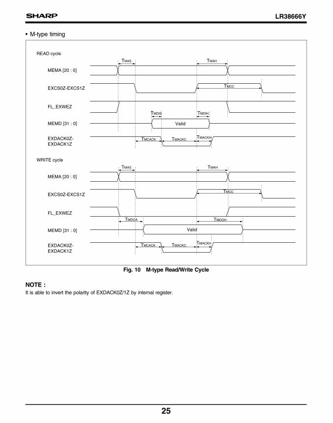
• M-type timing
TMCACK
TMDIH
TMAS TMAH
TMDOH
TMAS TMAH
MEMA [20 : 0]
READ cycle
EXCS0Z-EXCS1Z
FL_EXWEZ
MEMD [31 : 0]
EXDACK0Z-EXDACK1Z
MEMA [20 : 0]
WRITE cycle
EXCS0Z-EXCS1Z
FL_EXWEZ
MEMD [31 : 0]
EXDACK0Z-EXDACK1Z
TMACKCTMACKH
TMCACK TMACKCTMACKHMACKHTMACKH
TMDISTMDIS
Valid
Valid
TMCC
TMCC
TMDOA
Fig. 10 M-type Read/Write Cycle
NOTE :It is able to invert the polarity of EXDACK0Z/1Z by internal register.
26
LR38666Y
(DVDD = 3.3 V, DVDD2 = 2.5 V, TA = 0 to +70˚C)
PARAMETER SYMBOLCONDITIONS
UNIT NOTEMIN. MAX.
Output setup period of MEMA
(relative to the falling edge of EXCS0Z/1Z)TMAS
TCNT20 – 5ns 2
TCNT22 – 5
Output hold period of MEMA
(relative to the rising edge of EXCS0Z/1Z)TMAH
TCNT21 – 5ns 2
Minimum "High" period of EXCS0Z/1Z TMCC Ω ns 1
Input setup period of MEMD
(relative to the falling edge of EXDACKZ)TMDIS 0 ns
Input hold period of MEMD
(relative to the rising edge of EXCS0Z/1Z)TMDIH 0 ns
Output delay period of MEMD (relative to MEMA) TMDOA 2TMCLK – 5 2TMCLK + 5 ns 2
Output hold period of MEMD
(relative to the rising edge of EXCS0Z/1Z)TMDOH
TCNT23 +
2TMCLK – 5
TCNT23 +
2TMCLK + 5ns 2
Setup period of EXDACK0Z/1Z
(relative to the falling edge of EXCS0Z/1Z)TMCACK 0 ns
Rising period of EXCS0Z/1Z
(relative to the falling edge of EXDACK0Z/1Z)TMACKC 2TMCLK – 5 3TMCLK + 5 ns 1
Hold period of EXDACK0Z/1Z
(relative to the rising edge of EXCS0Z/1Z)TMACKH 0 ns
NOTES :1. Output load capacity CL = 15 pF
2. Output load capacity CL = 50 pF
TCNT20, TCNT21, TCNT22, TCNT23, and Ω each has a
value within the following range depending on the
register setting. TMAS corresponds to TCNT20 in
read cycle and TCNT22 in write cycle, and TMAH
corresponds to TCNT21 in read cycle and TCNT23 in
write cycle.
TCNT20 : 1TMCLK to 3TMCLK, TCNT21 : 1TMCLK to
3TMCLK, TCNT22 : 1TMCLK to 3TMCLK, TCNT23 :
1TMCLK to 3TMCLK
Ω : Min. "High" period between read cycles :
3TMCLK ≤ (TCNT20 + TCNT21 + 1TMCLK) ≤
7TMCLK
Min. "High" period from read cycle to write cycle
: 3TMCLK ≤ (TCNT21 + TCNT22 + 1TMCLK) ≤
7TMCLK
Min. "High" period from write cycle to read cycle
: 3TMCLK ≤ (TCNT20 + TCNT23 + 1TMCLK) ≤
7TMCLK
Min. "High" period between write cycles :
3TMCLK ≤ (TCNT22 + TCNT23 + 1TMCLK) ≤
7TMCLK
TCNT23 – 5
LR38666Y
27
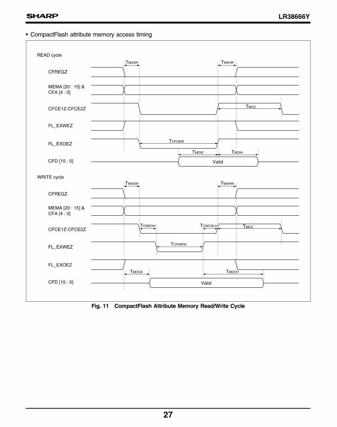
• CompactFlash attribute memory access timing
TCFOEW
TMASR TMAHR
TMDIS TMDIH
TCWEHH TCWCSLHCWCSLHTCWCSLH
TMASW TMAHW
TMCC
CFREGZ
READ cycle
MEMA [20 : 15] &CFA [4 : 0]
CFCE1Z-CFCE2Z
FL_EXWEZ
FL_EXOEZ
CFD [15 : 0]
CFREGZ
WRITE cycle
MEMA [20 : 15] &CFA [4 : 0]
CFCE1Z-CFCE2Z
FL_EXWEZ
FL_EXOEZ
CFD [15 : 0]
TCFWEW
TMCC
Valid
Valid
TMDOHTMDOA
Fig. 11 CompactFlash Attribute Memory Read/Write Cycle
28
LR38666Y
(DVDD = 3.3 V, DVDD2 = 2.5 V, TA = 0 to +70˚C)
PARAMETER SYMBOLCONDITIONS
UNIT NOTEMIN. MAX.
Output setup period of MEMA [20 : 15] & CFA at
reading (relative to the falling edge of CFCE1Z/2Z)TMASR 2TMCLK – 5 ns 2
Output setup period of MEMA [20 : 15] & CFA at
writing (relative to the falling edge of CFCE1Z/2Z)TMASW TMCLK – 5 ns 2
Output hold period of MEMA [20 : 15] & CFA at
reading (relative to the rising edge of CFCE1Z/2Z)TMAHR 3TMCLK – 5 ns 2
Output hold period of MEMA [20 : 15] & CFA at writing
(relative to the rising edge of CFCE1Z/2Z)TMAHW TMCLK – 5 ns 2
Minimum "High" period of CFCE1Z/2Z TMCC 3TMCLK – 5 ns 1
"Low" pulse width of FL_EXOEZ TCFOEW 17TMCLK – 5 17TMCLK + 5 ns 1
"High" hold period of FL_EXWEZ
(relative to the falling edge of CFCE1Z/2Z)TCWEHH 2TMCLK – 5 2TMCLK + 5 ns 1
"Low" pulse width of FL_EXWEZ TCFWEW 8TMCLK – 5 8TMCLK + 5 ns 1
"Low" hold period of CFCE1Z/2Z
(relative to the rising edge of FL_EXWEZ)TCWCSLH 2TMCLK – 5 2TMCLK + 5 ns 1
Input setup period of CFD
(relative to the rising edge of FL_EXOEZ)TMDIS 2TMCLK – 5 ns
NOTES :1. Output load capacity CL = 50 pF
2. MEMA [20 : 15] output load capacity CL = 50 pF, CFA [4 : 0] output load capacity CL = 30 pF.
1ns5TMCLK + 55TMCLK – 5TMDOHOutput hold period of CFD
(relative to the rising edge of FL_EXWEZ)
1ns2TMCLK + 52TMCLK – 5TMDOAOutput delay period of CFD
(relative to MEMA [20 : 15] & CFA)
ns0TMDIHInput hold period of CFD
(relative to the rising edge of FL_EXOEZ)
LR38666Y
29
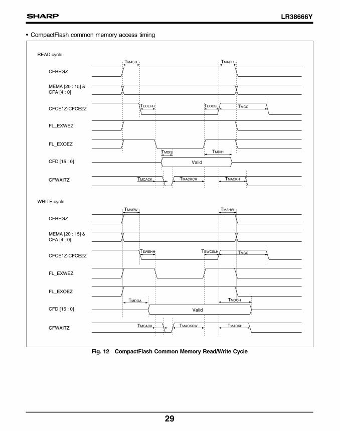
• CompactFlash common memory access timing
Valid
TMASR
TEOEHH
TMDIS
TMCACK TMACKCR TMACKH
TEOCSL
TMAHR
TMCC
CFREGZ
READ cycle
MEMA [20 : 15] &CFA [4 : 0]
CFCE1Z-CFCE2Z
FL_EXWEZ
FL_EXOEZ
CFD [15 : 0]
CFWAITZ
CFREGZ
WRITE cycle
MEMA [20 : 15] &CFA [4 : 0]
CFCE1Z-CFCE2Z
FL_EXWEZ
FL_EXOEZ
CFD [15 : 0]
CFWAITZ
Valid
TMASW
TEWEHH
TMDOA
TMCACK TMACKCW TMACKH
TEWCSLHEWCSLHTEWCSLH
TMAHW
TMCC
TMDOH
TMDIH
Fig. 12 CompactFlash Common Memory Read/Write Cycle
30
LR38666Y
(DVDD = 3.3 V, DVDD2 = 2.5 V, TA = 0 to +70˚C)
PARAMETER SYMBOLCONDITIONS
UNIT NOTEMIN. MAX.
Output setup period of MEMA [20 : 15] & CFA at
reading (relative to the falling edge of CFCE1Z/2Z)TMASR TMCLK – 5 ns 2
Output setup period of MEMA [20 : 15] & CFA at
writing (relative to the falling edge of CFCE1Z/2Z)TMASW TMCLK – 5 ns 2
Output hold period of MEMA [20 : 15] & CFA at
reading (relative to the rising edge of CFCE1Z/2Z)TMAHR 2TMCLK – 5 ns 2
Output hold period of MEMA [20 : 15] & CFA at writing
(relative to the rising edge of CFCE1Z/2Z)TMAHW TMCLK – 5 ns 2
Minimum "High" period of CFCE1Z/2Z TMCC 3TMCLK – 5 ns 1
"High" hold period of FL_EXOEZ
(relative to the falling edge of CFCE1Z/2Z)TEOEHH TMCLK – 5 TMCLK + 5 ns 1
"Low" hold period of CFCE1Z/2Z
(relative to the rising edge of FL_EXOEZ)TEOCSLH 2TMCLK – 5 2TMCLK + 5 ns 1
"High" hold period of FL_EXWEZ
(relative to the falling edge of CFCE1Z/2Z)TEWEHH TMCLK – 5 TMCLK + 5 ns 1
"Low" hold period of CFCE1Z/2Z
(relative to the rising edge of FL_EXWEZ)TEWCSLH 2TMCLK – 5 2TMCLK + 5 ns 1
Input setup period of CFD
(relative to the rising edge of CFWAITZ)TMDIS 0 ns
NOTES :1. Output load capacity CL = 50 pF
2. MEMA [20 : 15] output load capacity CL = 50 pF, CFA [4 : 0] output load capacity CL = 30 pF.
1ns5TMCLK + 55TMCLK – 5TMDOHOutput hold period of CFD
(relative to the rising edge of CFCE1Z/2Z)
1ns2TMCLK + 52TMCLK – 5TMDOAOutput delay period of CFD
(relative to MEMA [20 : 15] & CFA)
ns0TMDIHInput hold period of CFD
(relative to the rising edge of FL_EXOEZ)
Hold period of CFWAITZ
(relative to the rising edge of EXDACK0Z/1Z)TMACKH 0 ns
Rising period of FL_EXWEZ
(relative to the rising edge of CFWAITZ)TMACKCW 4TMCLK – 5 5TMCLK + 5 ns 1
Rising period of FL_EXOEZ
(relative to the rising edge of CFWAITZ)TMACKCR 2TMCLK – 5 3TMCLK + 5 ns 1
Determination period of CFWAITZ
(relative to the falling edge of FL_EXOEZ/FL_EXWEZ)TMCACK 2TMCLK + 5 ns
LR38666Y
31
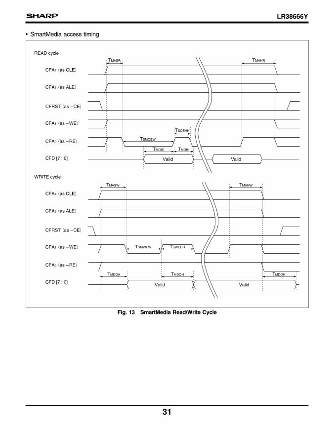
• SmartMedia access timing
CFA4 (as CLE)
READ cycle
CFA3 (as ALE)
CFRST (as –CE)
CFA1 (as –WE)
CFA0 (as –RE)
CFD [7 : 0]
CFA4 (as CLE)
WRITE cycle
CFA3 (as ALE)
CFRST (as –CE)
CFA1 (as –WE)
CFA0 (as –RE)
CFD [7 : 0]
TMASR TMAHR
TMASW
TMDIS TMDIH
Valid Valid
ValidValid
TSOEHH
TSMOEW
TMAHW
TSMWEW TSWEHH
TMDOA TMDOH TMDOH
Fig. 13 SmartMedia Read/Write Cycle
32
LR38666Y
(DVDD = 3.3 V, DVDD2 = 2.5 V, TA = 0 to +70˚C)
PARAMETER SYMBOLCONDITIONS
UNIT NOTEMIN. MAX.
Output setup period of CLE, ALE, –WE at reading
(relative to the falling edge of –RE)TMASR 2TMCLK – 5 ns 1
Output setup period of CLE, ALE, –RE at writing
(relative to the falling edge of –WE)TMASW 2TMCLK – 5 ns 1
Output hold period of CLE, ALE, –WE at reading
(relative to the rising edge of –RE)TMAHR 3TMCLK – 5 ns 1
Output hold period of CLE, ALE, –RE at writing
(relative to the rising edge of –WE)TMAHW 3TMCLK – 5 ns 1
"Low" pulse width of –RE TSMOEW 4TMCLK – 5 4TMCLK + 5 ns 1
"High" pulse width of –RE TSOEHH 2TMCLK – 5 2TMCLK + 5 ns 1
"Low" pulse width of –WE TSMWEW 3TMCLK – 5 3TMCLK + 5 ns 1
"High" pulse width of –WE TSWEHH 2TMCLK – 5 2TMCLK + 5 ns
Input setup period of CFD [7 : 0]
(relative to the rising edge of –RE)TMDIS 2TMCLK – 5 ns
Input hold period of CFD [7 : 0]
(relative to the rising edge of –RE)TMDIH 0 ns
NOTE :1. Output load capacity CL = 50 pF
1ns2TMCLK + 52TMCLK – 5TMDOHOutput hold period of CFD [7 : 0]
(relative to the rising edge of –WE)
1ns2TMCLK + 52TMCLK – 5TMDOAOutput delay period of CFD [7 : 0]
(relative to the rising edge of CLE, ALE)

LR38666Y
33
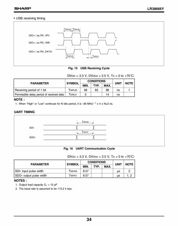
USB TIMING
• USB transmitting timing
(DVDD = 3.3 V, DVDD2 = 2.5 V, TA = 0 to +70˚C)
PARAMETER SYMBOLCONDITIONS
UNIT NOTEMIN. TYP. MAX.
Transmission period of 1 bit TWPUT 80 83 86 ns 1, 2
Output delay period of TX_OE_N TOED 162 167 172 ns 2
NOTES :1. When "High" or "Low" continues for N bits period, it is (48 MHz)–1 x 4 x N±3 ns.
2. Output load capacity CL = 15 pF
3. USB module will be reset when SE0 status (GIO13 = GIO14 = "Low") is input longer than 2.5 µs, in
transmitting, so choose USB transceiver IC carefully.
TWPUT
TWPUT TOEDTOED
TWPUT
GIO9 (as TX_VPO)
GIO10 (as TX_VMO)
GIO11 (as TX_OE_N)
GIO12 (as SUSPEND_N)
Fig. 14 USB Transmitting Cycle
34
LR38666Y
(DVDD = 3.3 V, DVDD2 = 2.5 V, TA = 0 to +70˚C)
PARAMETER SYMBOLCONDITIONS
UNIT NOTEMIN. TYP. MAX.
Receiving period of 1 bit TWPUR 68 83 98 ns 1
Permissible delay period of received data TDRCV 0 14 ns
NOTE :1. When "High" or "Low" continues for N bits period, it is (48 MHz)–1 x 4 x N±3 ns.
UART TIMING
TWPAR
SDI1
SDO1
TWPAT
Fig. 16 UART Communication Cycle
PARAMETER SYMBOLCONDITIONS
UNIT NOTEMIN. TYP. MAX.
SDI1 input pulse width TWPAR 8.57 µs 2
SDO1 output pulse width
NOTES :1. Output load capacity CL = 15 pF
2. The baud rate is assumed to be 115.2 k bps.
TWPAT 8.57 µs 1, 2
(DVDD = 3.3 V, DVDD2 = 2.5 V, TA = 0 to +70˚C)
• USB receiving timing
TWPUR
TWPUR TDRCV
TWPUR
GIO13 (as RX_VPI)
GIO14 (as RX_VMI)
GIO15 (as RX_DATA)
Fig. 15 USB Receiving Cycle
LR38666Y
35
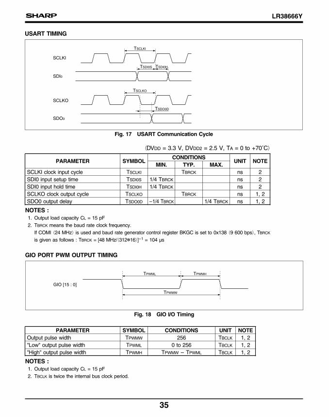
GIO PORT PWM OUTPUT TIMING
TPWML TPWMH
GIO [15 : 0]
TPWMW
Fig. 18 GIO I/O Timing
PARAMETER SYMBOL CONDITIONS UNIT NOTE
Output pulse width TPWMW 256 TBCLK 1, 2
"Low" output pulse width TPWML 0 to 256 TBCLK 1, 2
"High" output pulse width
NOTES :1. Output load capacity CL = 15 pF
2. TBCLK is twice the internal bus clock period.
TPWMH TPWMW – TPWML TBCLK 1, 2
(DVDD = 3.3 V, DVDD2 = 2.5 V, TA = 0 to +70˚C)
PARAMETER SYMBOLCONDITIONS
UNIT NOTEMIN. TYP. MAX.
SCLKI clock input cycle TSCLKI TBRCK ns 2
SDI0 input setup time TSDI0S 1/4 TBRCK ns 2
SDI0 input hold time TSDI0H 1/4 TBRCK ns 2
SCLKO clock output cycle TSCLKO TBRCK ns 1, 2
SDO0 output delay
NOTES :1. Output load capacity CL = 15 pF
2. TBRCK means the baud rate clock frequency.
If COMI (24 MHz) is used and baud rate generator control register BKGC is set to 0x138 (9 600 bps), TBRCK
is given as follows : TBRCK = [48 MHz/(312*16)]–1 = 104 µs
TSDO0D –1/4 TBRCK 1/4 TBRCK ns 1, 2
USART TIMING
SCLKI
SDI0
SDO0
SCLKO
TSCLKI
TSCLKO
TSDI0S TSDI0HTSDI0H
TSDO0D
Fig. 17 USART Communication Cycle
36
LR38666Y
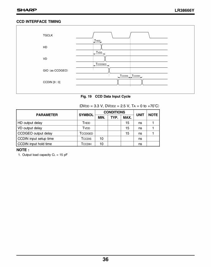
CCD INTERFACE TIMING
TGCLK
HD
VD
GIO (as CCDGEO)
CCDIN [9 : 0]
THDD
TVDD
TCCDIS TCCDIH
TCCDGED
Fig. 19 CCD Data Input Cycle
(DVDD = 3.3 V, DVDD2 = 2.5 V, TA = 0 to +70˚C)
PARAMETER SYMBOLCONDITIONS
UNIT NOTEMIN. TYP. MAX.
HD output delay THDD 15 ns 1
VD output delay TVDD 15 ns 1
CCDGEO output delay TCCDGED 15 ns 1
CCDIN input setup time TCCDIS 10 ns
CCDIN input hold time
NOTE :1. Output load capacity CL = 15 pF
TCCDIH 10 ns
LR38666Y
37
AUDIOIF TIMING
TASCLK
TASCLK
TASDISTASDIS TASDIHTASDIH
TASDISTASDIS
TASDODTASDOD
TARSYNCODTARSYNCOD
TAXSYNCODTAXSYNCOD
TASDODTASDOD
TARSYNCODTARSYNCOD
TAXSYNCODTAXSYNCOD
TASDIHTASDIH
ASCLK
ASDI
ARSYNCO
AXSYNCO
ASCLK
ASDI
ASDO
ARSYNCO
AXSYNCO
ASDO
Fig. 20 AUDIOIF Communication Cycle
(DVDD = 3.3 V, DVDD2 = 2.5 V, TA = 0 to +70˚C)
PARAMETER SYMBOLCONDITIONS
UNIT NOTEMIN. TYP. MAX.
Input setup period of ASDI TASDIS 1/4 TASCK ns 2
Input hold period of ASDI TASDIH 1/4 TASCK ns 2
Clock output cycle of ASCLK TASCLK TASCK ns 1, 2
Output delay period of ASDO TASDOD 20 ns 1
Output delay period of ARSYNCO
NOTES :1. Output load capacity CL = 15 pF
2. TASCK means the clock period of bit-shift-clock.
If the sampling clock frequency is 32 kHz, TCLK input is 16.384 MHz (512 fs) and bit-shift-clock
register (BSCG) is set to 0x0010 (bit-shift-clock is 1.024 MHz or 32 fs), TASCK is given as follows :
TASCK = (16.384 MHz/16)–1 = 976.5625 ns
TARSYNCOD 20 ns 1
1ns20TAXSYNCODOutput delay period of AXSYNCO
38
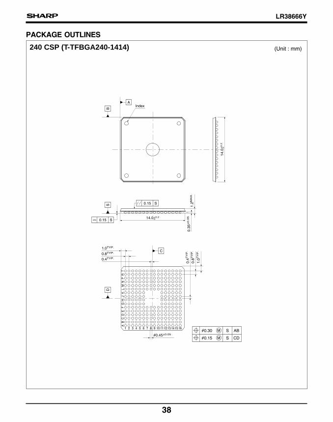
LR38666Y
1 2 3 4 5 6 7 8 9 10111213141516
AB
CD
EF
GH
JK
LM
NP
RT
IndexA
B
14
.0+
0.2
0
0.15 SS
0.15 S
1.2
MA
X.
0.3
5±
0.0
514.0+0.20
C
D
1.0TYP.
0.8TYP.
0.4TYP.
1.0
TY
P.
0.8
TY
P.
0.4
TY
P.
Ø0.45±0.05
SMØ0.30 AB
S CDMØ0.15
240 CSP (T-TFBGA240-1414) (Unit : mm)
PACKAGE OUTLINES