FPGA-based GNSS "Search Engine" using Parallel Techniques in the Time-Domain
Upload
khangminh22Category
view
3download
0
♦ No products described or contained herein are intended for use in surgical implants, life-support systems, aerospace equipment, nuclear power control systems, vehicles, disaster/crime-prevention equipment and the like, the failure of which may directly or indirectly cause injury, death or property loss.
♦ Anyone purchasing any products described or contained herein for an above-mentioned use shall : 1) Accept full responsibility and indemnify and defend SANYO ELECTRIC CO., LTD., its affiliates,
subsidiaries and distributors and all their officers and employees, jointly and severally, against any and all claims and litigation and all damages, cost and expenses associated with such use :
2) Not impose any responsibility for any fault or negligence which may be cited in any such claim or litigation on SANYO ELECTRIC CO., LTD., its affiliates, subsidiaries and distributors or any of their officers and employees jointly or severally.
♦ Information (including circuit diagrams and circuit parameters) herein is for example only ; it is not guaranteed for volume production. SANYO believes information herein is accurate and reliable, but no guarantees are made or implied regarding its use or any infringements of intellectual property rights or other rights of third parties.
Note : This product includes the IIC bus interface circuit. If you intend to use the IIC bus interface, please
notify us of this in advance of our receiving your program ROM code order. Purchase of SANYO IIC components conveys a license under the Philips IIC Patents Rights to use these
components in an IIC system, provided that the system conforms to the IIC Standard Specification as defined by Philips.
Trademarks IIC is a trademark of Philips Corporation.
This production is produced and sold by SANYO under license of the Silicon Storage Technology Inc. This catalog provides information as of December 2000. Specifications and information herein are subject to change without notice.
SANYO Electric Co., Ltd. Semiconductor Company SYSTEM-LSI Div. System-Microcomputer Development Dep.
1-1-1, Sakata Oizumi-Machi, Gunma, JAPAN
Ver.1.00 2000-12-27 SYSTEM-LSI M.Sato 1/23
8-BIT SINGLE CHIP MICROCONTROLLER Preliminary LC86F3364A
LC86F3364A 8-bit Single Chip Microcontroller with on-chip 96K-byte Flash Memory (ROM 64K -byte + CGROM 16K-byte + Extended ROM 16k-byte),on-chip 640-byte RAM and 352 × 9 bit Display RAM
Overview The LC86F3364A is a CMOS 8-bit single chip microcontroller with Flash Memory for the LC863300series. This microcontroller contains the following on-chip functional blocks:
- CPU : Operable at a minimum bus cycle time of 0.424µs - On-chip ROM capacity : 96K bytes Flash Memory
Program ROM : 64K bytes CGROM : 16K bytes Extended ROM : 16K bytes
- On-chip RAM capacity : 640 bytes - Display RAM : 352 × 9 bits - On-screen display controller - Five channels × 8-bit AD Converter - Three channels × 7-bit PWM - Two 16-bit timer/counters, 14-bit base timer - 8-bit synchronous serial interface circuit - IIC-bus compliant serial interface circuit (Multi-master type) - ROM correct function - 15-source 9-vectored interrupt system - Integrated system clock generator and display clock generator
Only one X’tal oscillator (32.768kHz) for PLL reference is used for both generators All of the above functions are fabricated on a single chip.
The program is rewritable by using the on-board writing system after the LSI has been installed on the application board.

LC86F3364A
2/23 Ver.1.00
Features
(1) Built-in Flash Memory : 96K bytes - Program ROM 64K bytes - Character ROM 16K bytes - Extended ROM 16K bytes - Rewritable in page units 128 bytes / page - Page erase / program cycle 100 cycle per page
(2) Built-in Random Access Memory (RAM) : 640 × 8 bits (including 128 bytes for ROM correction function) 352 × 9 bits (for CRT display)
The LC86F3364A consists of 64K of ROM space and 640 bytes of RAM space. For this microcontroller, the usable program ROM capacity and RAM capacity are the same size for the mask ROM version.
Mask ROM versions compatible with the LC86F3364A
Program ROM limit set for the LC86F3364A
RAM limit set for the LC86F3364A (including 128 bytes for the ROM correction function)
LC863364 65024 bytes 640 bytes
LC863356 57344 bytes 640 bytes
LC863348 49152 bytes 640 bytes
LC863340 40960 bytes 640 bytes
LC863332 32768 bytes 512 bytes
LC863328 28672 bytes 512 bytes
LC863324 24576 bytes 512 bytes
LC863320 20480 bytes 512 bytes
LC863316 16384 bytes 512 bytes
(3) OSD functions
- Screen display : 36 characters × 16 lines (by software) - RAM : 352 words (9 bits per word) Display area : 36 words × 8 lines Control area : 8 words × 8 lines - Characters Up to 252 kinds of 16 × 32 dot characters (4 characters including 1 test character are not programmable) Each font can be divided into two parts and used as two fonts (Ex. 16 × 16 dot character font × 2) - Various character attributes Character colors : 16 colors Character background colors : 16 colors Fringe / shadow colors : 16 colors Full screen colors : 16 colors Rounding Underline Italic character (slanting) - Attribute can be changed without spacing - Vertical display start line number can be set for each row independently (Rows can be overlapped) - Horizontal display start position can be set for each row independently - Horizontal pitch (9 - 16 dot)*1 and vertical pitch (1 - 32 dot) can be set for each row independently - Different display modes can be set for each row independently Caption • Text mode / OSD mode 1 / OSD mode 2 (Quarter size) / Simplified graphic mode - Ten character sizes*1 Horiz. × Vert. = (1 × 1), (1 × 2), (2 × 2), (2 × 4)
(1.5 × 1), (1.5 × 2), (3 × 2), (3 × 4), (0.5 × 0.5), (0.75 × 0.5)

LC86F3364A
Ver.1.00 3/23
- Shuttering and scrolling on each row - Simplified Graphic Display *1 Note : range depends on display mode : refer to manual for details.
(4) Bus Cycle Time / Instruction-Cycle Time
Bus cycle time Instruction cycle time System clock oscillation Oscillation Frequency Voltage
0.424µs 0.848µs Internal VCO (Ref : X’tal 32.768kHz)
14.156MHz 4.5V to 5.5V
7.5µs 15.0µs Internal RC 800kHz 4.5V to 5.5V
183.1µs 366.2µs Crystal 32.768kHz 4.5V to 5.5V
(5) Ports
- Input / Output Ports : 5 ports (28 terminals) Data direction programmable in nibble units : 1 port (8 terminals) (If the N-ch open drain output is selected by option, the corresponding port data can be read in output mode.) Data direction programmable for each bit individually: 4 ports (20 terminals)
- Input Port : 1 port (1 terminal) (6) AD converter - 5-channels × 8-bit AD converters (7) Serial interfaces - IIC-bus compatible serial interface (Multi-master type)
Consists of a single built-in circuit with two I/O channels the two data lines and two clock lines can be short circuited internally.
- Synchronous 8-bit serial interface (8) PWM output
- 3-channels × 7-bit PWM (9) Timer - Timer 0 : 16-bit timer/counter
With 2-bit prescaler + 8-bit built-in programmable prescaler Mode 0 : Two 8-bit timers with a programmable prescaler Mode 1 : 8-bit timer with a programmable prescaler + 8-bit counter Mode 2 : 16-bit timer with a programmable prescaler Mode 3 : 16-bit counter The resolution of timer is 1 tCYC.
- Timer 1 : 16-bit timer/PWM Mode 0 : Two 8-bit timers Mode 1 : 8-bit timer + 8-bit PWM Mode 2 : 16-bit timer Mode 3 : Variable bit PWM (9 to 16 bits) In mode 0/1, the resolution of Timer1/PWM is 1 tCYC In mode 2/3, the resolution is selectable by program; tCYC or 1/2 tCYC
- Base timer Generate every 500ms overflow for a clock application (using 32.768kHz crystal oscillation for the base timer clock) Generate every 976µs, 3.9ms, 15.6ms, 62.5ms overflow (using 32.768kHz crystal oscillation for the base timer clock) Clock for the base timer is selectable from 32.768kHz crystal oscillation, system clock or programmable prescaler output of Timer 0

LC86F3364A
4/23 Ver.1.00
(10) Remote control receiver circuit (connected to the P73/INT3/T0IN terminal) - Noise rejection function - Polarity switching
(11) Watchdog timer External RC circuit is required Interrupt or system reset is activated when the timer overflows
(12) ROM correction function
Max 128 bytes/2 address (13) Interrupts
- 15-sources 9-vectored interrupts 1. External Interrupt INT0 2. External Interrupt INT1 3. External Interrupt INT2, Timer/counter T0L (Lower 8 bits) 4. External Interrupt INT3, base timer 5. Timer/counter T0H (Upper 8 bits) 6. Timer T1H,T1L 7. SIO0 8. Vertical synchronous signal interrupt ( VS ), scanning line, AD 9. IIC, Port 0 - Interrupt priority control
Three interrupt priorities are supported (low, high and highest) and multi-level nesting is possible. Low or high priority can be assigned to the interrupts from 3 to 9 listed above. For the external interrupt INT0 and INT1, high or highest priority can be set.
(14) Sub-routine stack level - A maximum of 128 levels (stack area is assigned on the internal RAM) (15) Multiplication/division instruction - 16 bits × 8 bits (7 instruction cycle times) - 16 bits / 8 bits (7 instruction cycle times) (16) 3 oscillation circuits - Built-in RC oscillation circuit used for the system clock - Built-in VCO circuit used for the system clock and OSD clock
- On-chip X’tal oscillation circuit used for PLL reference and the system clock and base timer clock
(17) Standby function - HALT mode
The HALT mode is used to reduce the power dissipation. In this operation mode, the program execution is stopped. This mode can be released by the interrupt request signals or the system reset.
- HOLD mode The HOLD mode is used to stop oscillations ; the RC (internal),VCO, and the X’tal oscillations. This mode can be released by the following conditions.
• Pull the reset terminal ( RES ) to low level.
• Feed the selected level to either P70/INT0 or P71/INT1.
• Feed the Port 0 interrupt condition (18) Applicable mask ROM version
- LC863364/ LC863356/ LC863348 / LC863340/ LC863332 / LC863328 / LC863324 / LC863320 / LC863316

LC86F3364A
Ver.1.00 5/23
(19) Package - DIP42S - QIP48E
(20) Development tools
- Evaluation chip: LC863096 - Emulator: EVA86000(main) + ECB863200(evaluation chip board)
+ POD863300(pod:DIP42S) or POD863301(QIP48E) Write Flash Memory SANYO provides special services including writing data to Flash Memory and stamping. There is a charge for these services. Please feel free to ask our sales persons for details.

LC86F3364A
6/23 Ver.1.00
System Block Diagram
ALU
ACC
PSW
RAR
RAM
IIC
Timer 0
ADC
PWM
CGROM
VRAM
Base Timer
OSDControlCircuit
B Register
C Register
Stack Pointer
Port 0
Watch Dog Timer
Timer 1
Port 8
Port 7
Port 6
Port 1
Bus Interface
SIO 0
ROM Correct Control
XRAM
PC
CEOEWE
D0-D7A0-A16
Interrupt Control
Standby Control
Clo
ckG
en
era
torX'tal
RC
VCO
PLL
IR PLA
Flash MemoryControl
Flash Memory(96KB)
INT0 - 3Noise Rejection Filter

LC86F3364A
Ver.1.00 7/23
Pin Assignment
• DIP42S
1
2
3
4
5
6
7
8
9
11
12
13
14
15
16
17
18
19
20
21
10
P16
VSS
XT1
XT2
VDD
P07
P06
P05
P04
P03
P02
P01
P00
P73/INT3/T0IN
P72/INT2/T0IN
P71/INT1
P70/INT0
P84/AN4
P85/AN5
P87/AN7
P86/AN6
42
41
40
39
38
37
36
35
34
33
32
31
30
29
28
27
26
25
24
23
22
RES
VS
HS
P17/PWM
P15/PWM3
P14/PWM2
P13/PWM1
I
R
G
B
BL
P63/SCLK1
P62/SDA1
P61/SCLK0
P60/SDA0
P10/SO0
P11/SI0
P12/SCK0
FILT
P83/AN3
• QIP48E
1
2
3
4
5
6
7
8
9
10
11
12
36
35
34
33
32
31
30
29
28
27
26
25
37
38
39
40
41
42
43
44
45
46
47
48
13
16
17
18
19
20
21
22
23
24
P15/PWM3
P16
P17/PWM
VSS
XT1
XT2
VDD
NC
P84/AN4
P85/AN5
P86/AN6
P87/AN7
NC
P14/PWM2
P13/PWM1
P12/SCK0
P11/SI0
P10/SO0
NC
P07
P06
P05
P04
P03
P02
P01
P00
NC
P71/INT1
P70/INT0
P63/SCLK1
P62/SDA1
P61/SCLK0
P60/SDA0
NCI
BLBGR
HS
VS
RES
P73/INT3/T0IN
P72/INT2/T0IN
15
14
FILT
NC
P83/AN3

LC86F3364A
8/23 Ver.1.00
Pin Description Pin Description Table
Terminal I/O Function Description Option Flash memory mode (Parallel input/ output mode)
VSS - Negative power supply XT1 I Input terminal for crystal oscillator XT2 O Output terminal for crystal oscillator VDD - Positive power supply
RES I Reset terminal Input to set up mode
FILT O Filter terminal for PLL Address input A16
VS I Vertical synchronization signal input terminal Input to set up mode
HS I Horizontal synchronization signal input terminal
R O Red (R) output terminal of RGB image output G O Green (G) output terminal of RGB image output B O Blue (B) output terminal of RGB image output Address input A15 I O Intensity ( I ) output terminal of RGB image output Address input A13 BL O Fast blanking control signal
Switch TV image signal and caption/ OSD image signal
Address input A14
Port 0 P00 - P07
I/O
•8-bit input/output port, Input/output can be specified in nibble unit •Other functions HOLD release input Interrupt input
Pull-up register Present/ not present Output Format CMOS/Nch-OD
Address input A0 to A7
Port 1 •8-bit input/output port Input/output can be specified in a bit •Other functions P10
P11 P12 P13 P14 P15 P17
SIO0 data output SIO0 data input/bus input/output SIO0 clock input/output PWM1 output PWM2 output PWM3 output Timer1 (PWM) output
P10 - P17
I/O
Output Format CMOS/Nch-OD
Data input/output D0 to D7
Port 6 •4-bit input/output port Input/output can be specified for each bit •Other functions P60
P61 P62 P63
IIC0 data I/O IIC0 clock output IIC1 data I/O IIC1 clock output
P60 - P63
I/O
control signal CE
control signal OE
control signal WE Address input A12

LC86F3364A
Ver.1.00 9/23
Terminal I/O Function Description Option Flash memory mode
(Parallel input/ output mode)
Port 7 •4-bit input/output port Input or output can be specified for each bit •Other function P70
P71 P72 P73
INT0 input/HOLD release input/ Nch-Tr. output for watchdog timer INT1 input/HOLD release input INT2 input/Timer 0 event input INT3 input (noise rejection filter attached)/Timer 0 event input
Interrupt receiver format, vector addresses
Address input A8 to A11
rising falling rising/ falling
H level L level vector
INT0 enable enable disable enable enable 03H INT1 enable enable disable enable enable 0BH INT2 enable enable enable disable disable 13H
P70 P71 - P73
I/O
INT3 enable enable enable disable disable 1BH
Port 8 P83
I
P84 - P87 I/O
•1-bit input port •4-bit input/output port Input or output can be specified for each bit •Other function AD converter input port (5 lines)
NC - unused terminal Leave open
• Output form and existence of pull-up resistor for every port can be specified for each bit. • Programmable pull-up resister is always connected regardless of port option, CMOS or N-ch open drain output
in port 1. User options User options can be changed using Flash Memory data.
A kind of option Pin, Circuits Port 0 (Specified in a bit)
1. Input : Without pull-up MOS Tr. Output : N-channel open drain 2. Input : With pull-up MOS Tr. Output : CMOS
Input/output form of input/output ports
Port 1 (Specified in a bit)
1. Input : With programmable pull-up MOS Tr. Output : N-channel open drain 2. Input : With programmable pull-up MOS Tr. Output : CMOS

LC86F3364A
10/23 Ver.1.00
Notice for use - Input level of terminal RES at power on
Terminal RES must be held low for at least 200µs after the supply voltage exceeds the power supply lower limit.
Power supply
RES
VDD limit0V
more than 200ƒÊs
-difference between the Mask version and Flash version(LC86F3364A) 1. the operation after release of reset: The mask version operates the program from the address 0 in the
program counter as soon as detecting the H level on the reset port. The flash version operates the program from the address 0 in the program counter after setting the option.
2. Current dissipation: The current dissipation of the flash version is bigger than that of the mask version. Please refer to the latest semiconductor news.
- Conditions during reset and after release of reset Port options are set using Flash Memory data. Port options are set internally within approximately 3ms after logic HIGH is applied to the RESET terminal. The configuration of the port outputs change over the duration of this period. Then the Program Counter is set to 0 and program execution begins. During reset, and in the few hundred milliseconds after reset is released, the port options on certain of the ports will not yet have been set. The conditions of the various ports during reset or on release of reset have been collected in the following table. Please refer to it when analyzing circuits where these conditions apply.
Pins Options Condition during and on release of reset
Input : Without pull up MOS transistor Output : N-channel open drain
Output -off Input mode : High impedance
P0
Input : With pull up MOS transistor Output : CMOS
Output-off During reset and in the first few hundred µs after reset is released, the pull-up MOS transistor is OFF. Thereafter, set to input mode with pull-up MOS Tr. ON
Input : With programmable pull up MOS transistor Output : N-channel open drain
P1
Input : With programmable pull up MOS transistor Output : CMOS
Output-off Input mode : Pull up MOS transistor off
P6 No options Output : N-channel open drain
Output -off Input mode : High impedance
P7 No options Input : With programmable pull up MOS transistor Output : N-channel open drain (P70) CMOS (P71 - P73)
Output-off Input mode : Pull up MOS transistor off
P8 No options Input : With programmable pull up MOS transistor (excluding P83) Output : CMOS (P83 is input only)
Output-off Input mode : Pull up MOS transistor off

LC86F3364A
Ver.1.00 11/23
On-board writing system The LC86F3364A has the On-board writing system. The program is renewable by using SANYO Flash On-board System after the LSI has been installed on the application board. This system is composed of 4 types divided by the combination of mode setting pin and communication pin. Each type system has to connect the 6 pins (VDD, VSS, RES, communication pins) with the interface board of SANYO Flash On-board System. It is necessary that the pins to be used for the rewriting system should be able to be separated from the application board properly. The system type is selected by the option setting program (Su86K.exe). types mode setting pin communication pins type1 RES pin (high voltage(12V) applied) P00(DATA1),P01(DATA0),P02(CLK) type2 RES pin (high voltage(12V) applied) P00(DATA1),P60(DATA0),P61(CLK) type3 P00 pin (High level voltage applied) P00(ENA/DATA1),P01(DATA0),P02(CLK) type4 P00 pin (High level voltage applied) P00(ENA/DATA1),P60(DATA0),P61(CLK)
• Type 3 or 4 is selected : P00 is exclusive for the on-board system. This pin must always be pulled-down, so this pin can’t be used for other applications. Please set P00 pin N-channel open drain output. (option setting) In the user program, “0” is always set to the P00 latch (bit 0 in the Port 0 latch (140h)) because the P0 interrupt must not be requested on the P00 pin .
• The loader program must be written into the ROM to use On-board writing system. The loader program should be written into the ROM before the LSI has been installed on the board by the the general purpose PROM programs. When the option setting selects the this system to use, the loader program automatically links to the extended ROM field(14000h-147FFh) on the user program linking. Please ask to our sales persons before using On-board writing system.
Use of PROM Conversion board When reading or writing data to the LC86F3364A using our exclusive conversion board (W86F3264D, W86F3264Q) general purpose PROM programs can be used. (1) Name of conversion boards
- W86F3264D • • • DIP42S purpose - W86F3264Q • • • QIP48E purpose
(2) Available PROM programs
The LC86F3364A does not support a silicon signature feature. Do not use the feature (automatic device type selection) when programming this device.
•For the address range, 0 to 17FFFh should be specified (fixed data ‘00’ is read if 1800h to 1FFFFh is specified).
Single word write Manufacture Name of device version applicable device (code) Data protection
setting after write operation
Minato Electronics MODEL 1890A + OU-910 V4.1 SST Co., Ltd. 29EE010 (D734) Protected Ando AF-9708 01.00 SST Co., Ltd. 29EE010 (47101) Protected Data I. O. ChipLab V5.3 SST Co., Ltd. 29EE010 Selectable

LC86F3364A
12/23 Ver.1.00
Write multiple words Manufacture Name of device version applicable device (code) Data protection
setting after write operation
Minato Electronics MODEL 1892 + TYPE9102A V4.1 SST Co., Ltd. 29EE010 (D734) Protected
(3) Notes When using the conversion board, all of the jumper SW must be set to the OFF position. If set to the ON position, read/write operations will not perform correctly. (4) Location of pin 1 Pin 1 of the conversion board should be located as indicated below. W86F3264D : when viewing from the edge closest to jumper SW, pin 1 is located on the lower right of both the chip and conversion board. W86F3264Q : when viewing from the edge closest to jumper SW, pin 1 of the chip is located on the upper right while pin 1 of the conversion board is located on the lower right.
W86F3264D W86F3264Q
chip : pin1
pin1 pin1
Set jumper SW to OFF Set jumper SW to OFF

LC86F3364A
Ver.1.00 13/23
1. Absolute maximum ratings / VSS=0V and Ta=25°C
Limits Parameter Symbol Pins Conditions VDD[V] min. typ. max. unit
Supply voltage VDDMAX VDD -0.3 +6.0 Input voltage VI(1) • RES , HS , VS ,
P83
-0.3 VDD+0.3
Output voltage VO(1) R, G, B, I, BL, FILT
-0.3 VDD+0.3
Input/output voltage
VIO •Ports 0, 1, 6, 7, 84-87
-0.3 VDD+0.3
V
IOPH(1) •Ports 0, 1, 7, 84-87
•CMOS output •For each pin.
-4 Peak output current IOPH(2) R, G, B, I, BL •CMOS output
•For each pin. -5
∑IOAH(1) •Ports 0, 1 The total of all pins.
-20
∑IOAH(2) Ports 7, 84-87 The total of all pins.
-10
High level output current
Total output current
∑IOAH(3) R, G, B, I, BL The total of all pins.
-15
IOPL(1) Ports 0, 1, 6, 84-87
For each pin. 20
IOPL(2) Port 7 For each pin. 15
Peak output current
IOPL(3) R, G, B, I, BL For each pin. 5 ∑IOAL(1) Ports 0, 1 The total of all
pins. 40
∑IOAL(2) Ports 6, 7, 84-87 The total of all pins.
30
Low level output current
Total output current
∑IOAL(3) R, G, B, I, BL The total of all pins.
15
mA
DIP42S 850 Maximum power dissipation
Pdmax QIP48E
Ta= -10 to +70°C 440
mW
Operating temperature range
Topr -10 +70
Storage temperature range
Tstg -55 +125
°C
LC86F3364A
14/23 Ver.1.00
2. Recommended operating range / Ta= -10°C to +70°C, VSS=0V
Limits Parameter Symbol Pins Conditions VDD[V] min. typ. max. unit
VDD(1) 0.844µs ≤ tCYC ≤ 0.852µs
4.5 5.5 Operating supply voltage range VDD(2)
VDD
4µs ≤ tCYC ≤ 400µs
4.5 5.5
Hold voltage VHD VDD RAMs and the registers data are kept in HOLD mode.
2.0 5.5
VIH(1) Port 0 (Schumitt) Output disable 4.5 - 5.5 0.6VDD VDD
VIH(2) •Ports 1,6 (Schumitt) •Port 7 (Schumitt) port input/interrupt
• HS , VS , RES (Schumitt)
Output disable 4.5 - 5.5 0.75VDD VDD
VIH(3) Port 70 Watchdog timer input
Output disable 4.5 - 5.5 VDD-0.5 VDD
High level input voltage
VIH(4) •Port 8 port input
Output disable 4.5 - 5.5 0.7VDD VDD
VIL(1) Port 0 (Schumitt) Output disable 4.5 - 5.5 VSS 0.2VDD VIL(2) •Ports 1,6 (Schumitt)
•Port 7 (Schumitt) port input/interrupt
• HS , VS , RES (Schumitt)
Output disable 4.5 - 5.5 VSS 0.25VDD
VIL(3) Port 70 Watchdog timer input
Output disable 4.5 - 5.5 VSS 0.6VDD
Low level input voltage
VIL(4) Port 8 port input
Output disable 4.5 - 5.5 VSS 0.3VDD
V
tCYC(1) •All functions operationg
4.5 - 5.5 0.844 0.848 0.852
tCYC(2) •AD converter operationg •OSD is not operating
4.5 - 5.5 0.844 30
Operation cycle time
tCYC(3) •OSD, AD converter are not operating
4.5 - 5.5 0.844 400
µs
Oscillation frequency range
FmRC Internal RC oscillation
4.5 - 5.5 0.4 0.8 3.0 MHz
* Vp-p : Peak-to-peak voltage

LC86F3364A
Ver.1.00 15/23
3. Electrical characteristics / Ta= -10°C to +70°C, VSS=0V
Limits Parameter Symbol Pins Conditions VDD[V] min. typ. max. unit
IIH(1) Ports 0, 1, 6, 7, 8, •Output disable •Pull-up MOS Tr. OFF •VIN=VDD (including the off- leak current of the output Tr.)
4.5 - 5.5 1 High level input current
IIH(2) • RES
• HS , VS
•VIN=VDD 4.5 - 5.5 1
IIL(1) Ports 0, 1, 6, 7, 8, •Output disable •Pull-up MOS Tr. OFF •VIN=VSS (including the off- leak current of the output Tr.)
4.5 - 5.5 -1 Low level input current
IIL(2) • RES
• HS , VS
VIN=VSS 4.5 - 5.5 -1
µA
VOH(1) •CMOS output of ports 0,1,71-73, 84-87
IOH=-1.0mA 4.5 - 5.5 VDD-1 High level output voltage
VOH(2) R, G, B, I, BL IOH=-0.1mA 4.5 - 5.5 VDD-0.5 VOL(1) Ports 0,1,71-73,
84-87 IOL=10mA 4.5 - 5.5 1.5
VOL(2) Ports 0,1,71-73, 84-87
IOL=1.6mA 4.5 - 5.5 0.4
VOL(3) •R, G, B, I, BL •Port 6
IOL=3.0mA 4.5 - 5.5 0.4
VOL(4) Port 6 IOL=6.0mA 4.5 - 5.5 0.6
Low level output voltage
VOL(5) Port 70 IOL=1mA 4.5 - 5.5 0.4
V
Pull-up MOS Tr. resistance
Rpu •Ports 0, 1, 7, 84-87
VOH=0.9VDD 4.5 - 5.5 13 38 80 kΩ
Bus terminal short circuit resistance (SCL0-SCL1, SDA0-SDA1)
RBS •P60-P62 •P61-P63
4.5 - 5.5 130 Ω
Hysteresis voltage
VHIS •Ports 0, 1, 6, 7
• RES
• HS , VS
Output disable 4.5 - 5.5 0.1VDD V
Pin capacitance
CP All pins •f=1MHz •Every other terminals are connected to VSS. •Ta=25°C
4.5 - 5.5 10 pF
LC86F3364A
16/23 Ver.1.00
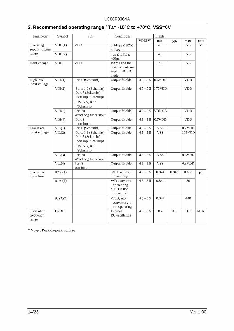
4. Serial input/output characteristics / Ta= -10°C to +70°C, VSS=0V
Limits Parameter Symbol Pins Conditions VDD[V] min. typ. max. unit
Cycle
tCKCY(1) 2
Low Level pulse width
tCKL(1) 1
Inpu
t clo
ck
High Level pulse width
tCKH(1)
•SCK0 •SCLK0
Refer to figure 4. 4.5 - 5.5
1
Cycle
tCKCY(2) 2
Low Level pulse width
tCKL(2) 1/2tCKCY
Ser
ial c
lock
Out
put c
lock
High Level pulse width
tCKH(2)
•SCK0 •SCLK0
•Use pull-up resistor (1kΩ) when Nch open- drain output. •Refer to figure 4.
4.5 - 5.5
1/2tCKCY
tCYC
Data set up time
tICK 0.1
Ser
ial i
nput
Data hold time
tCKI
SI0 •Data set-up to SCK0. •Data hold from SCK0. •Refer to figure 4.
4.5 - 5.5
0.1
Output delay time (Using external
clock)
tCKO(1) SO0 4.5 - 5.5 7/12tCYC +0.2
Ser
ial o
utpu
t
Output delay time (Using internal
clock)
tCKO(2) SO0
•Data hold from SCK0. •Use pull-up resistor (1kΩ) when Nch open- drain output. •Refer to figure 4.
4.5 - 5.5 1/3tCYC +0.2
µs
5. IIC input/output conditions / Ta= -10°C to +70°C, VSS=0V
Standard High speed Parameter Symbol min. max. min. max.
unit
SCL Frequency fSCL 0 100 0 400 kHz BUS free time between stop - start tBUF 4.7 - 1.3 - µs HOLD time of start, restart condition tHD;STA 4.0 - 0.6 - µs L time of SCL tLOW 4.7 - 1.3 - µs H time of SCL tHIGH 4.0 - 0.6 - µs Set-up time of restart condition tSU;STA 4.7 - 0.6 - µs HOLD time of SDA tHD;DAT 0 - 0 0.9 µs Set-up time of SDA tSU;DAT 250 - 100 - ns Rising time of SDA, SCL tR - 1000 20+0.1Cb 300 ns Falling time of SDA, SCL tF - 300 20+0.1Cb 300 ns Set-up time of stop condition tSU;STO 4.0 - 0.6 - µs
Refer to figure 9 (Note) Cb : Total capacitance of all BUS (unit : pF)

LC86F3364A
Ver.1.00 17/23
6. Pulse input conditions / Ta= -10°C to +70°C, VSS=0V
Limits Parameter Symbol Pins Conditions VDD[V] min. typ. max. unit
tPIH(1) tPIL(1)
•INT0, INT1 •INT2/T0IN
•Interrupt acceptable •Timer0-countable
4.5 - 5.5 1
tPIH(2) tPIL(2)
INT3/T0IN (The noise rejection clock is selected to 1tCYC.)
•Interrupt acceptable •Timer0-countable
4.5 - 5.5 2
tPIH(3) tPIL(3)
INT3/T0IN (The noise rejection clock is selected to 16tCYC.)
•Interrupt acceptable •Timer0-countable
4.5 - 5.5 32
tPIH(4) tPIL(4)
INT3/T0IN (The noise rejection clock is selected to 64tCYC.)
•Interrupt acceptable •Timer0-countable
4.5 - 5.5 128
tCYC
tPIL(5) RES Reset acceptable 4.5 - 5.5 200
High/low level pulse width
tPIH(6) tPIL(6)
HS , VS •Display position controllable (Note) •The active edge of
HS and VS must be apart at least 1 tCYC. •Refer to figure 6.
4.5 - 5.5 8
µs
Rising/falling time
tTHL tTLH
HS Refer to figure 6. 4.5 - 5.5 500 ns
7. AD converter characteristics / Ta= -10°C to + 70°C, VSS=0V
Limits Parameter Symbol Pins Conditions VDD[V] min. typ. max. unit
Resolution N 8 bit Absolute precision
ET (Note 3) ±1.5 LSB
ADCR2=0 (Note 4) 16 Conversion time
tCAD ADCR2=1 (Note 4) 32
tCYC
Analog input voltage range
VAIN VSS VDD V
IAINH VAIN=VDD 1 Analog port input current IAINL
AN3 - AN7
VAIN=VSS
4.5 – 5.5
-1 µA
(Note 3) Absolute precision does not include quantizing error (1/2LSB). (Note 4) Conversion time is the time till the complete digital conversion value for analog input value is set to a
register after the instruction to start conversion is sent.
LC86F3364A
18/23 Ver.1.00
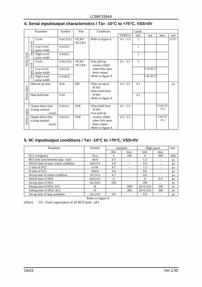
8. Sample current dissipation characteristics / Ta= -10°C to +70°C, VSS=0V The sample current dissipation characteristics is the measurement result of Sanyo provided evaluation board when the recommended circuit parameters shown in the sample oscillation circuit characteristics are used externally. The currents through the output transistors and the pull-up MOS transistors are ignored.
Limits Parameter Symbol Pins Conditions VDD[V] min. typ. max. unit
IDDOP(1) VDD •FmX’tal=32.768kHz X’tal oscillation •System clock : VCO for system •VCO for OSD operating •Internal RC oscillation stops
4.5 - 5.5 28 45 mA Current dissipation during basic operation
(Note 3)
IDDHALT(1) VDD •HALT mode
•FmX’tal=32.768kHz X’tal oscillation •System clock : VCO for system •VCO for OSD stops •Internal RC oscillation stops
4.5 - 5.5 7 11 mA
IDDHALT(2) VDD •HALT mode •FmX’tal=32.768kHz X’tal oscillation •VCO for system stops •VCO for OSD stops •System clock : Internal RC
4.5 - 5.5 500 1200
Current dissipation in HALT mode
(Note 3)
IDDHALT(3) VDD •HALT mode •FmX’tal=32.768kHz X’tal oscillation •VCO for system stops •VCO for OSD stops •System clock : X’tal
4.5 - 5.5 60 200
µA
Current dissipation in HOLD mode
(Note 3)
IDDHOLD VDD •HOLD mode •All oscillation stops.
4.5 - 5.5 0.05 20 µA
(Note 3) The currents of the output transistors and the pull-up MOS transistors are ignored.

LC86F3364A
Ver.1.00 19/23
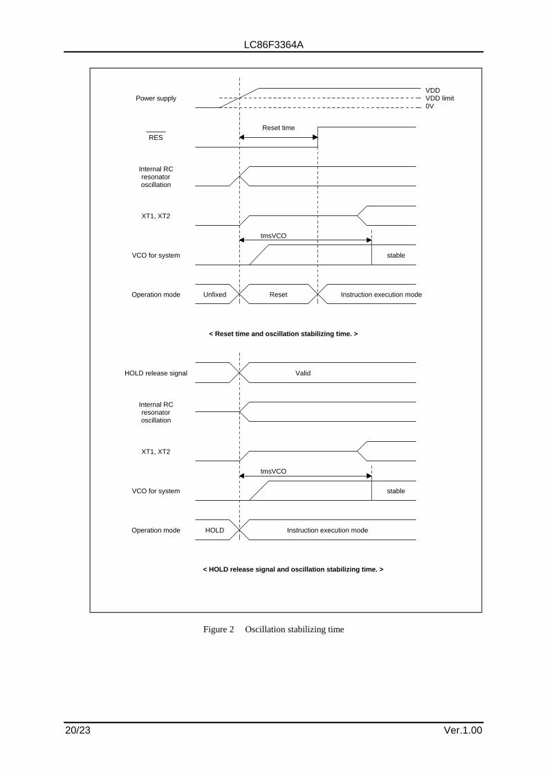
Recommended Oscillation Circuit and Sample Characteristics The sample oscillation circuit characteristics in the table below is based on the following conditions:
• Recommended circuit parameters are verified by an oscillator manufacturer using a Sanyo provided oscillation evaluation board.
• Sample characteristics are the result of the evaluation with the recommended circuit parameters connected externally.
Recommended oscillation circuit and sample characteristics (Ta = -10 to +70°C)
Recommended circuit parameters
Oscillation stabilizing
time
Frequency Manufacturer Oscillator
C1 C2 Rf Rd
Operating supply voltage
range typ. max
Notes
32.768kHz Seiko Epson C-002RX 18pF 18pF Open 680kΩ 4.5-5.5V 1.00s 1.50s
Notes The oscillation stabilizing time period is the time until the VCO oscillation for the internal system
becomes stable after the following conditions. (Refer to Figure 2.)
1. The VDD becomes higher than the minimum operating voltage after the power is supplied. 2. The HOLD mode is released.
The sample oscillation circuit characteristics may differ applications. For further assistance, please contact with oscillator manufacturer with the following notes in your mind.
• Since the oscillation frequency precision is affected by wiring capacity of the application board, etc., adjust the oscillation frequency on the production board.
• The above oscillation frequency and the operating supply voltage range are based on the operating temperature of -10°C to + 70°C. For the use with the temperature outside of the range herein, or in the application requiring high reliability such as car products, please consult with oscillator manufacturer.
• When using the oscillator which is not shown in the sample oscillation circuit characteristics, please consult with Sanyo sales personnel.
Since the oscillation circuit characteristics are affected by the noise or wiring capacity because the circuit is designed with low gain in order to reduce the power dissipation, refer to the following notices.
• The distance between the clock I/O terminal (XT1 terminal XT2 terminal) and external parts should be as short as possible.
• The capacitors’ VSS should be allocated close to the microcontroller’s GND terminal and be away from other GND.
• The signal lines with rapid state change or with large current should be allocated away from the oscillation circuit.
XT1 XT2
X'tal
RdRf
C2C1
Figure 1 Recommended oscillation circuit
LC86F3364A
20/23 Ver.1.00
VCO for system stable
Operation mode HOLD Instruction execution mode
< HOLD release signal and oscillation stabilizing time. >
Power supply
RES
Internal RCresonatoroscillation
XT1, XT2
VCO for system
HOLD release signal
Operation mode
Internal RCresonatoroscillation
XT1, XT2
< Reset time and oscillation stabilizing time. >
Unfixed Reset Instruction execution mode
Valid
Reset time
tmsVCO
stable
tmsVCO
VDDVDD limit0V
Figure 2 Oscillation stabilizing time

LC86F3364A
Ver.1.00 21/23
RES
VDD
RRES
CRES
Figure 3 Reset circuit
0.5VDD
< AC timing measurement point >
tICK tCKI
tCKL tCKH
tCKCY VDD
1kĦ
50pFSB0
SO0
SI0
SCK0
tCKO
< Timing > < Test load >
Figure 4 Serial input / output test condition
tPIL tPIH
Figure 5 Pulse input timing condition - 1
(Note) Determine the CRES, RRES value to
get more than 200µs reset time.

LC86F3364A
22/23 Ver.1.00
HS
VS
tTLH
0.75VDD
0.25VDD
more than 1tCYC
tPIL(6)
tPIL(6)
Figure 6 Pulse input timing condition - 2
HS
C536
10kĦ
HS
LC86F3364A
Figure 7 Recommended Interface circuit
-
FILT
+1MĦ
100Ħ
33000pF2.2ƒÊF
Figure 8 FILT recommended circuit
(Note) Place FILT parts on board as close to the microcomputer as possible.

LC86F3364A
Ver.1.00 23/23
tRtHD;STA
tHD;DAT
tLOW tHIGH
tF
tSU;DAT
tHD;STA
tSU;STA
tsp
tSU;STO
SCL
Sr P
SDA
tBUF
P S
S : start condition tsp : Spike suppression Standard mode : not exist P : stop condition High speed mode : less than 50ns Sr : restart condition
Figure 9 IIC timing
© 2000 SANYO
Copyright © 2022 FDOKUMEN