The DatasheetArchive - Datasheet Search Engine - Farnell
48
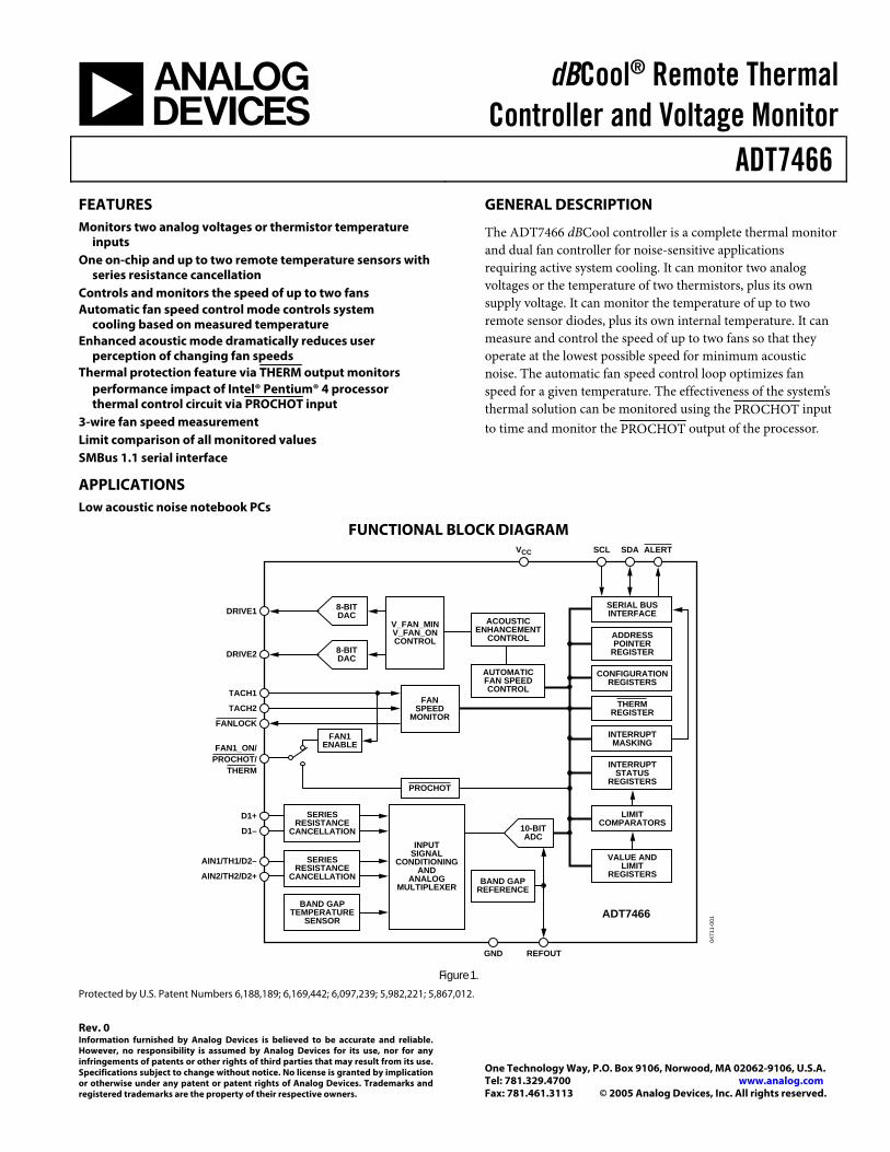
dBCool ® Remote Thermal Controller and Voltage Monitor ADT7466 Rev. 0 Information furnished by Analog Devices is believed to be accurate and reliable. However, no responsibility is assumed by Analog Devices for its use, nor for any infringements of patents or other rights of third parties that may result from its use. Specifications subject to change without notice. No license is granted by implication or otherwise under any patent or patent rights of Analog Devices. Trademarks and registered trademarks are the property of their respective owners. One Technology Way, P.O. Box 9106, Norwood, MA 02062-9106, U.S.A. Tel: 781.329.4700 www.analog.com Fax: 781.461.3113 © 2005 Analog Devices, Inc. All rights reserved. FEATURES Monitors two analog voltages or thermistor temperature inputs One on-chip and up to two remote temperature sensors with series resistance cancellation Controls and monitors the speed of up to two fans Automatic fan speed control mode controls system cooling based on measured temperature Enhanced acoustic mode dramatically reduces user perception of changing fan speeds Thermal protection feature via THERM output monitors performance impact of Intel® Pentium® 4 processor thermal control circuit via PROCHOT input 3-wire fan speed measurement Limit comparison of all monitored values SMBus 1.1 serial interface APPLICATIONS Low acoustic noise notebook PCs GENERAL DESCRIPTION The ADT7466 dBCool controller is a complete thermal monitor and dual fan controller for noise-sensitive applications requiring active system cooling. It can monitor two analog voltages or the temperature of two thermistors, plus its own supply voltage. It can monitor the temperature of up to two remote sensor diodes, plus its own internal temperature. It can measure and control the speed of up to two fans so that they operate at the lowest possible speed for minimum acoustic noise. The automatic fan speed control loop optimizes fan speed for a given temperature. The effectiveness of the system’s thermal solution can be monitored using the PROCHOT input to time and monitor the PROCHOT output of the processor. FUNCTIONAL BLOCK DIAGRAM SERIAL BUS INTERFACE CONFIGURATION REGISTERS THERM REGISTER INTERRUPT MASKING ADDRESS POINTER REGISTER INTERRUPT STATUS REGISTERS VALUE AND LIMIT REGISTERS ACOUSTIC ENHANCEMENT CONTROL AUTOMATIC FAN SPEED CONTROL LIMIT COMPARATORS FAN SPEED MONITOR V_FAN_MIN V_FAN_ON CONTROL 8-BIT DAC 8-BIT DAC V CC GND REFOUT SCL SDA ALERT BAND GAP REFERENCE 10-BIT ADC DRIVE1 DRIVE2 TACH1 TACH2 FANLOCK FAN1_ON/ PROCHOT/ THERM D1+ D1– AIN1/TH1/D2– AIN2/TH2/D2+ SERIES RESISTANCE CANCELLATION BAND GAP TEMPERATURE SENSOR SERIES RESISTANCE CANCELLATION INPUT SIGNAL CONDITIONING AND ANALOG MULTIPLEXER FAN1 ENABLE PROCHOT ADT7466 04711-001 Figure 1. Protected by U.S. Patent Numbers 6,188,189; 6,169,442; 6,097,239; 5,982,221; 5,867,012.
-
Upload
khangminh22 -
Category
Documents
-
view
2 -
download
0
Transcript of The DatasheetArchive - Datasheet Search Engine - Farnell
dBCool® Remote Thermal Controller and Voltage Monitor
ADT7466
Rev. 0 Information furnished by Analog Devices is believed to be accurate and reliable. However, no responsibility is assumed by Analog Devices for its use, nor for any infringements of patents or other rights of third parties that may result from its use. Specifications subject to change without notice. No license is granted by implication or otherwise under any patent or patent rights of Analog Devices. Trademarks and registered trademarks are the property of their respective owners.
One Technology Way, P.O. Box 9106, Norwood, MA 02062-9106, U.S.A. Tel: 781.329.4700 www.analog.com Fax: 781.461.3113 © 2005 Analog Devices, Inc. All rights reserved.
FEATURES Monitors two analog voltages or thermistor temperature
inputs One on-chip and up to two remote temperature sensors with
series resistance cancellation Controls and monitors the speed of up to two fans Automatic fan speed control mode controls system
cooling based on measured temperature Enhanced acoustic mode dramatically reduces user
perception of changing fan speeds Thermal protection feature via THERM output monitors
performance impact of Intel® Pentium® 4 processor thermal control circuit via PROCHOT input
3-wire fan speed measurement Limit comparison of all monitored values SMBus 1.1 serial interface
APPLICATIONS Low acoustic noise notebook PCs
GENERAL DESCRIPTION
The ADT7466 dBCool controller is a complete thermal monitor and dual fan controller for noise-sensitive applications requiring active system cooling. It can monitor two analog voltages or the temperature of two thermistors, plus its own supply voltage. It can monitor the temperature of up to two remote sensor diodes, plus its own internal temperature. It can measure and control the speed of up to two fans so that they operate at the lowest possible speed for minimum acoustic noise. The automatic fan speed control loop optimizes fan speed for a given temperature. The effectiveness of the system’s thermal solution can be monitored using the PROCHOT input to time and monitor the PROCHOT output of the processor.
FUNCTIONAL BLOCK DIAGRAM
SERIAL BUSINTERFACE
CONFIGURATIONREGISTERS
THERMREGISTER
INTERRUPTMASKING
ADDRESSPOINTER
REGISTER
INTERRUPTSTATUS
REGISTERS
VALUE ANDLIMIT
REGISTERS
ACOUSTICENHANCEMENT
CONTROL
AUTOMATICFAN SPEEDCONTROL
LIMITCOMPARATORS
FANSPEED
MONITOR
V_FAN_MINV_FAN_ONCONTROL
8-BITDAC
8-BITDAC
VCC
GND REFOUT
SCL SDA ALERT
BAND GAPREFERENCE
10-BITADC
DRIVE1
DRIVE2
TACH1
TACH2
FANLOCK
FAN1_ON/PROCHOT/
THERM
D1+
D1–
AIN1/TH1/D2–
AIN2/TH2/D2+
SERIESRESISTANCE
CANCELLATION
BAND GAPTEMPERATURE
SENSOR
SERIESRESISTANCE
CANCELLATIONINPUT
SIGNALCONDITIONING
ANDANALOG
MULTIPLEXER
FAN1ENABLE
PROCHOT
ADT7466
0471
1-00
1
Figure 1.
Protected by U.S. Patent Numbers 6,188,189; 6,169,442; 6,097,239; 5,982,221; 5,867,012.
ADT7466
Rev. 0 | Page 2 of 48
TABLE OF CONTENTS Specifications..................................................................................... 3
Serial Bus Timing ......................................................................... 5
Absolute Maximum Ratings............................................................ 6
Thermal Characteristics .............................................................. 6
ESD Caution.................................................................................. 6
Pin Configuration and Function Descriptions............................. 7
Typical Performance Characteristics ............................................. 8
Functional Description .................................................................. 11
Measurement Inputs .................................................................. 11
Sequential Measurement ........................................................... 11
Fan Speed Measurement and Control ..................................... 11
Internal Registers of the ADT7466 .......................................... 11
Theory of Operation ...................................................................... 12
Serial Bus Interface..................................................................... 12
Write and Read Operations....................................................... 14
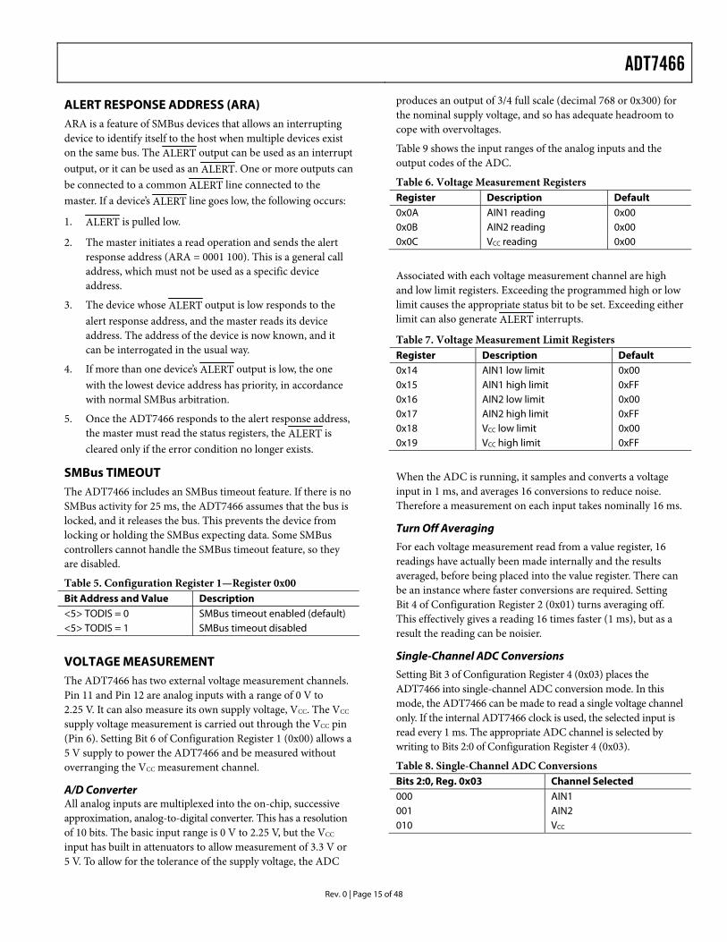
Alert Response Address (ARA)................................................ 15
SMBus Timeout .......................................................................... 15
Voltage Measurement ................................................................ 15
Reference Voltage Output.......................................................... 16
Configuration of Pin 11 and Pin 12 ......................................... 16
Temperature Measurement ....................................................... 17
Series Resistance Cancellation.................................................. 17
Temperature Measurement Method ........................................ 17
Using Discrete Transistors ........................................................ 17
Temperature Measurement Using Thermistors ..................... 19
Reading Temperature from the ADT7466.............................. 20
Additional ADC Functions....................................................... 21
Limit Values ................................................................................ 21
Alert Interrupt Behavior............................................................ 23
Configuring the ADT7466 THERM Pin as an Output ......... 25
Fan Drive ..................................................................................... 26
PWM or Switch Mode Fan Drive............................................. 26
Fan Speed Measurement ........................................................... 26
Fan Start-Up Timeout................................................................ 28
Automatic Fan Speed Control .................................................. 29
Starting the Fan .......................................................................... 30
XOR Test Mode............................................................................... 31
Application Circuit......................................................................... 32
ADT7466 Register Map ................................................................. 33
Register Details ........................................................................... 35
Outline Dimensions ....................................................................... 47
Ordering Guide .......................................................................... 47
REVISION HISTORY
6/05—Revision 0: Initial Version
ADT7466
Rev. 0 | Page 3 of 48
SPECIFICATIONS TA = TMIN to TMAX, VCC = VMIN to VMAX, unless otherwise noted.1
Table 1. Parameter Min Typ Max Unit Test Conditions/Comments POWER SUPPLY
Supply Voltage 3.0 3.3 5.5 V Supply Current, ICC 1.4 3 mA Interface inactive, ADC active 30 70 µA Standby mode, digital inputs low
TEMPERATURE-TO-DIGITAL CONVERTER
Local Sensor Accuracy ±1 °C 20°C ≤ TA ≤ 60°C; VCC = 3.3 V ±3 °C −40°C ≤ TA ≤ +125°C; VCC = 3.3 V Resolution 0.25 °C Remote Diode Sensor Accuracy ±1 °C 20°C ≤ TA ≤ 60°C; −40°C ≤ TD ≤ +125°C; VCC = 3.3 V ±3 °C −40°C ≤TA ≤ +105°C; −40°C ≤ TD ≤ +125°C; VCC = 3.3 V ±5 °C −40°C ≤ TA ≤ +125°C; −40°C ≤ TD ≤ +125°C Resolution 0.25 °C Remote Sensor Source Current 192 µA High level 72 µA Mid level 12 µA Low level Series Resistance Cancellation 0 2 kΩ Maximum resistance in series with thermal diode that can be
cancelled out THERMISTOR-TO-DIGITAL CONVERTER
Temperature Range 30 100 °C Range over which specified accuracy is achieved. Wider range can be used with less accuracy.
Resolution 0.25 °C Accuracy ±2 °C Using specified thermistor and application circuit over specified
temperature range ANALOG-TO-DIGITAL CONVERTER
Input Voltage Range 0 VREF V VREF = 2.25V Total Unadjusted Error (TUE) ±1 ±2.5 % Differential Nonlinearity (DNL) ±1 LSB Power Supply Sensitivity ±1 %/V Conversion Time (AIN Input) 8.30 8.65 ms Averaging enabled Conversion Time (Local Temperature)
8.63 8.99 ms Averaging enabled
Conversion Time (Remote Temperature)
35.22 36.69 ms Averaging enabled
Conversion Time (VCC) 7.93 8.26 ms Averaging enabled Total Monitoring Cycle Time 68.38 71.24 ms Averaging enabled, Pin 11 and Pin 12 configured for AIN/TH
monitoring (see Table 15) Total Monitoring Cycle Time 87 90.63 ms Averaging enabled, Pin 11 and Pin 12 configured for REM2
monitoring (see Table 15) FAN RPM-TO-DIGITAL CONVERTER
Accuracy ±4 % Full-Scale Count 65,535 Nominal Input RPM 109 RPM Fan count = 0xBFFF 329 RPM Fan count = 0x3FFF 5000 RPM Fan count = 0x0438 10000 RPM Fan count = 0x021C Internal Clock Frequency 78.64 81.92 85.12 kHz
ADT7466
Rev. 0 | Page 4 of 48
Parameter Min Typ Max Unit Test Conditions/Comments DRIVE OUTPUTS (DRIVE1, DRIVE2)
Output Voltage Range 0–2.2 V Digital input = 0x00 to 0xFF Output Source Current 2 mA Output Sink Current 0.5 mA DAC Resolution 8 Bits Monotonicity 8 Bits Differential Nonlinearity ±1 LSB Integral Nonlinearity ±1 LSB Total Unadjusted Error ±5 % IL = 2 mA
REFERENCE VOLTAGE OUTPUT (REFOUT)
Output Voltage 2.226 2.25 2.288 V Output Source Current 10 mA Output Sink Current 0.6 mA
OPEN-DRAIN SERIAL DATA BUS OUTPUT (SDA)
Output Low Voltage (VOL) 0.4 V IOUT = −4.0 mA, VCC = 3.3 V High Level Output Current (IOH) 0.1 1 µA VOUT = VCC
DIGITAL INPUTS (SCL, SDA, TACH INPUTS, PROCHOT)
Input High Voltage (VIH) 2.0 V Input Low Voltage (VIL) 0.8 V Hysteresis 0.5 V
DIGITAL INPUT CURRENT (TACH INPUTS, PROCHOT)
Input High Current (IIH) −1 µA VIN = VCC Input Low Current (IIL) 1 µA VIN = 0 Input Capacitance (IN) 20 pF
OPEN-DRAIN DIGITAL OUTPUTS (ALERT, FANLOCK, FAN1_ON/THERM)
Output Low Voltage (VOL) 0.4 V IOUT = −4.0 mA, VCC = 3.3 V High Level Output Current (IOH) 0.1 1 µA VOUT =VCC
SERIAL BUS TIMING 2 Clock Frequency (fSCLK) 400 kHz See Figure 2 Glitch Immunity (tSW) 50 ns See Figure 2 Bus Free Time (tBUF) 1.3 µs See Figure 2 Start Setup Time (tSU;STA) 0.6 µs See Figure 2 Start Hold Time (tHD;STA) 0.6 µs See Figure 2 SCL Low Time (tLOW) 1.3 µs See Figure 2 SCL High Time (tHIGH) 0.6 µs See Figure 2 SCL, SDA Rise Time (tr) 1000 ns See Figure 2 SCL, SDA Fall Time (tf ) 300 ns See Figure 2 Data Setup Time (tSU;DAT) 100 ns See Figure 2 Detect Clock Low Timeout (tTIMEOUT) 25 64 Ms Can be optionally disabled
1 All voltages are measured with respect to GND, unless otherwise specified. Typical values are at T = 25°C and represent the most likely parametric norm. Logic inputs accept input high voltages up to 5 V even when the device is operating at supply voltages below 5 V. Timing specifications are tested at logic levels of V = 0.8 V for a falling edge and at V = 2.0 V for a rising edge.
A
IL
IH2 Guaranteed by design, not production tested.
ADT7466
Rev. 0 | Page 5 of 48
SERIAL BUS TIMING
0471
1-00
3
SCL
SDA
P S S P
tSU;STO
tHD;STA
tSU;STA
tSU;DATtHD;DAT
tHD;STA tHIGH
tBUF
tLOW
tR tF
Figure 2. Diagram for Serial Bus Timing
ADT7466
Rev. 0 | Page 6 of 48
ABSOLUTE MAXIMUM RATINGS Table 2. Parameter Rating Positive Supply Voltage (VCC) 6.5 V Voltage on Any Other Pin −0.3 V to 6.5 V Input Current at Any Pin ±5 mA Package Input Current ±20 mA Maximum Junction Temperature (TJ max) 150°C Storage Temperature Range −65°C to +150°C Lead Temperature, Soldering:
IR Peak Reflow Temperature 220°C Lead Temperature (10 sec) 300°C
ESD Rating 2000 V
Stresses greater than those listed under Absolute Maximum Ratings may cause permanent damage to the device. This is a stress rating only and functional operation of the device at these or any other conditions above those indicated in the operational section of this specification is not implied. Exposure to absolute maximum rating conditions for extended periods may affect device reliability.
THERMAL CHARACTERISTICS 16-Lead QSOP Package:
θJA = 105°C/W θJC = 39°C/W
ESD CAUTION ESD (electrostatic discharge) sensitive device. Electrostatic charges as high as 4000 V readily accumulate on the human body and test equipment and can discharge without detection. Although this product features proprietary ESD protection circuitry, permanent damage may occur on devices subjected to high energy electrostatic discharges. Therefore, proper ESD precautions are recommended to avoid performance degrada-tion or loss of functionality.
ADT7466
Rev. 0 | Page 7 of 48
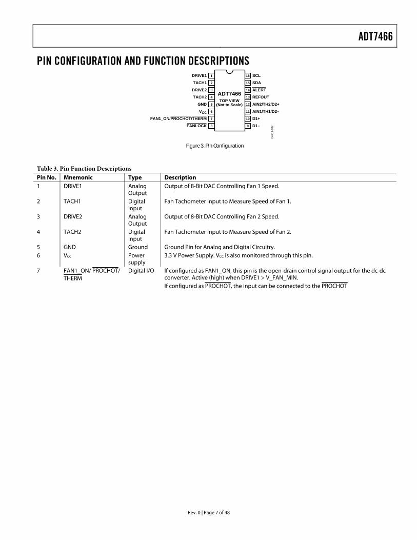
PIN CONFIGURATION AND FUNCTION DESCRIPTIONS
0471
1-00
2
ADT7466TOP VIEW
(Not to Scale)
DRIVE1 1 SCL16
TACH1 2 SDA15
DRIVE2 3 ALERT14
TACH2 4 REFOUT13
GND 5 AIN2/TH2/D2+12
VCC 6 AIN1/TH1/D2–11
FAN1_ON/PROCHOT/THERM 7 D1+10
FANLOCK 8 D1–9
Figure 3. Pin Configuration
Table 3. Pin Function Descriptions Pin No. Mnemonic Type Description 1 DRIVE1 Analog
Output Output of 8-Bit DAC Controlling Fan 1 Speed.
2 TACH1 Digital Input
Fan Tachometer Input to Measure Speed of Fan 1.
3 DRIVE2 Analog Output
Output of 8-Bit DAC Controlling Fan 2 Speed.
4 TACH2 Digital Input
Fan Tachometer Input to Measure Speed of Fan 2.
5 GND Ground Ground Pin for Analog and Digital Circuitry. 6 VCC Power
supply 3.3 V Power Supply. VCC is also monitored through this pin.
7 FAN1_ON/ PROCHOT/ THERM
Digital I/O If configured as FAN1_ON, this pin is the open-drain control signal output for the dc-dc converter. Active (high) when DRIVE1 > V_FAN_MIN. If configured as PROCHOT, the input can be connected to the PROCHOT
ADT7466
Rev. 0 | Page 8 of 48
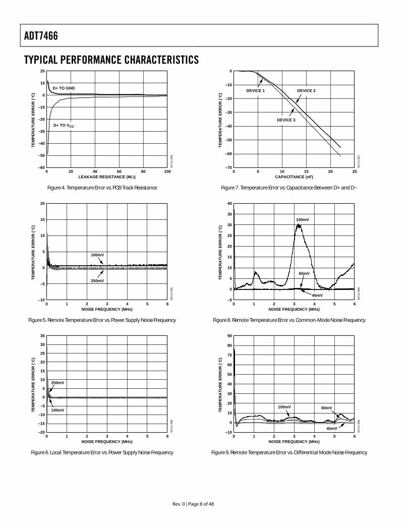
TYPICAL PERFORMANCE CHARACTERISTICS 20
–60
–50
–40
–30
–20
–10
0
10
0 1008060402004
711-
004
LEAKAGE RESISTANCE (MΩ)
TEM
PER
ATU
RE
ERR
OR
(°C
)
D+ TO GND
D+ TO VCC
Figure 4. Temperature Error vs. PCB Track Resistance
20
–10
–5
0
5
10
15
0 64 5321
0471
1-00
5
NOISE FREQUENCY (MHz)
TEM
PER
ATU
RE
ERR
OR
(°C
)
100mV
250mV
Figure 5. Remote Temperature Error vs. Power Supply Noise Frequency
35
–20
–15
–10
–5
0
5
10
15
20
25
30
0 64 5321
0471
1-00
6
NOISE FREQUENCY (MHz)
TEM
PER
ATU
RE
ERR
OR
(°C
)
100mV
250mV
Figure 6. Local Temperature Error vs. Power Supply Noise Frequency
0
–70
–60
–50
–40
–30
–20
–10
0 22015105
0471
1-00
7
CAPACITANCE (nF)
TEM
PER
ATU
RE
ERR
OR
(°C
)
5
DEVICE 1 DEVICE 2
DEVICE 3
Figure 7. Temperature Error vs. Capacitance Between D+ and D−
40
–5
0
5
10
15
20
25
30
35
0 64 5321
0471
1-00
8
NOISE FREQUENCY (MHz)
TEM
PER
ATU
RE
ERR
OR
(°C
)
60mV
100mV
40mV
Figure 8. Remote Temperature Error vs. Common-Mode Noise Frequency
90
80
–10
0
10
20
30
40
50
60
70
0 64 5321
0471
1-00
9
NOISE FREQUENCY (MHz)
TEM
PER
ATU
RE
ERR
OR
(°C
)
60mV100mV
40mV
Figure 9. Remote Temperature Error vs. Differential Mode Noise Frequency
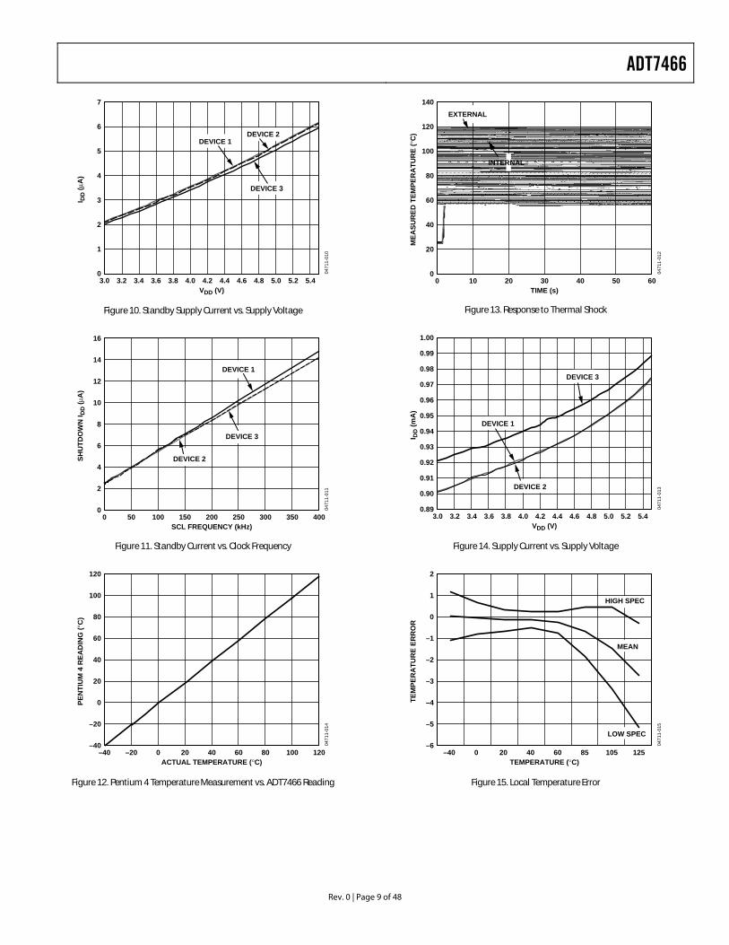
ADT7466
Rev. 0 | Page 9 of 48
7
6
5
4
3
2
1
03.0 5.45.25.04.84.64.44.24.03.83.63.43.2
0471
1-01
0
VDD (V)
I DD
(µA
)
DEVICE 1DEVICE 2
DEVICE 3
Figure 10. Standby Supply Current vs. Supply Voltage
16
12
14
10
8
6
4
2
00 50 100 150 200 250 300 350 400
0471
1-01
1
SCL FREQUENCY (kHz)
SHU
TDO
WN
I DD
(µA
)
DEVICE 1
DEVICE 2
DEVICE 3
Figure 11. Standby Current vs. Clock Frequency
120
80
100
60
40
20
0
–20
–40–40 –20 0 20 40 60 80 100 120
0471
1-01
4
ACTUAL TEMPERATURE (°C)
PEN
TIU
M 4
REA
DIN
G (°
C)
Figure 12. Pentium 4 Temperature Measurement vs. ADT7466 Reading
140
120
100
80
60
40
20
00 65040302010
0471
1-01
2
TIME (s)
MEA
SUR
ED T
EMPE
RA
TUR
E (°
C)
0
INTERNAL
EXTERNAL
Figure 13. Response to Thermal Shock
1.00
0.99
0.98
0.97
0.96
0.95
0.94
0.93
0.92
0.91
0.90
0.893.23.0 3.4 3.6 3.8 4.0 4.2 4.4 4.6 4.8 5.0 5.2 5.4
0471
1-01
3
VDD (V)
I DD
(mA
)DEVICE 1
DEVICE 2
DEVICE 3
Figure 14. Supply Current vs. Supply Voltage
2
–6
–5
–4
–3
–2
–1
0
1
–40 0 20 40 60 85 105 125
0471
1-01
5
TEMPERATURE (°C)
TEM
PER
ATU
RE
ERR
OR
HIGH SPEC
MEAN
LOW SPEC
Figure 15. Local Temperature Error
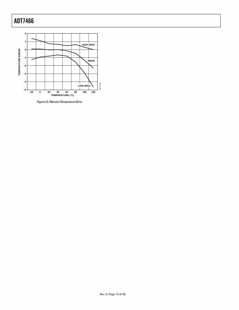
ADT7466
Rev. 0 | Page 10 of 48
2
–5
–4
–3
–2
–1
0
1
–40 0 20 40 60 85 105 125
0471
1-01
6
TEMPERATURE (°C)
TEM
PER
ATU
RE
ERR
OR
HIGH SPEC
MEAN
LOW SPEC
Figure 16. Remote Temperature Error
ADT7466
Rev. 0 | Page 11 of 48
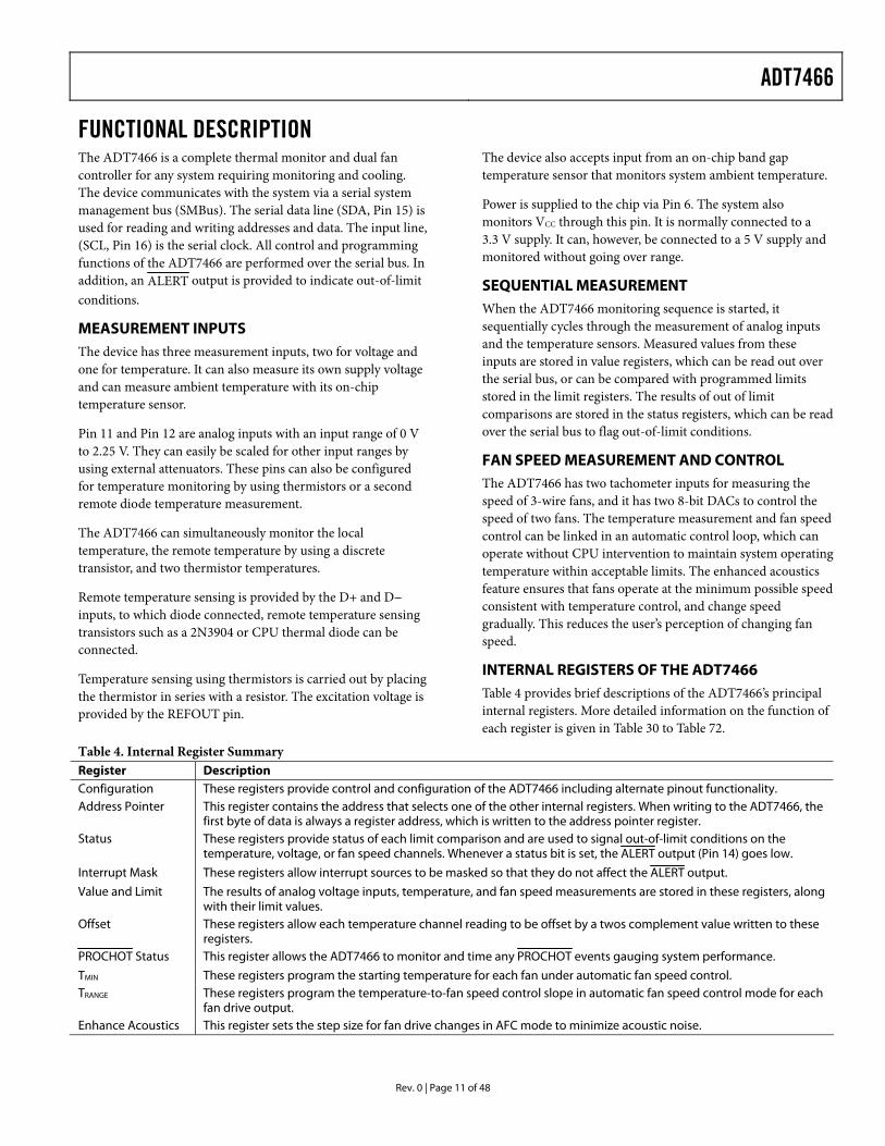
FUNCTIONAL DESCRIPTION The ADT7466 is a complete thermal monitor and dual fan controller for any system requiring monitoring and cooling. The device communicates with the system via a serial system management bus (SMBus). The serial data line (SDA, Pin 15) is used for reading and writing addresses and data. The input line, (SCL, Pin 16) is the serial clock. All control and programming functions of the ADT7466 are performed over the serial bus. In addition, an ALERT output is provided to indicate out-of-limit conditions.
MEASUREMENT INPUTS The device has three measurement inputs, two for voltage and one for temperature. It can also measure its own supply voltage and can measure ambient temperature with its on-chip temperature sensor.
Pin 11 and Pin 12 are analog inputs with an input range of 0 V to 2.25 V. They can easily be scaled for other input ranges by using external attenuators. These pins can also be configured for temperature monitoring by using thermistors or a second remote diode temperature measurement.
The ADT7466 can simultaneously monitor the local temperature, the remote temperature by using a discrete transistor, and two thermistor temperatures.
Remote temperature sensing is provided by the D+ and D− inputs, to which diode connected, remote temperature sensing transistors such as a 2N3904 or CPU thermal diode can be connected.
Temperature sensing using thermistors is carried out by placing the thermistor in series with a resistor. The excitation voltage is provided by the REFOUT pin.
The device also accepts input from an on-chip band gap temperature sensor that monitors system ambient temperature.
Power is supplied to the chip via Pin 6. The system also monitors VCC through this pin. It is normally connected to a 3.3 V supply. It can, however, be connected to a 5 V supply and monitored without going over range.
SEQUENTIAL MEASUREMENT When the ADT7466 monitoring sequence is started, it sequentially cycles through the measurement of analog inputs and the temperature sensors. Measured values from these inputs are stored in value registers, which can be read out over the serial bus, or can be compared with programmed limits stored in the limit registers. The results of out of limit comparisons are stored in the status registers, which can be read over the serial bus to flag out-of-limit conditions.
FAN SPEED MEASUREMENT AND CONTROL The ADT7466 has two tachometer inputs for measuring the speed of 3-wire fans, and it has two 8-bit DACs to control the speed of two fans. The temperature measurement and fan speed control can be linked in an automatic control loop, which can operate without CPU intervention to maintain system operating temperature within acceptable limits. The enhanced acoustics feature ensures that fans operate at the minimum possible speed consistent with temperature control, and change speed gradually. This reduces the user’s perception of changing fan speed.
INTERNAL REGISTERS OF THE ADT7466 Table 4 provides brief descriptions of the ADT7466’s principal internal registers. More detailed information on the function of each register is given in Table 30 to Table 72.
Table 4. Internal Register Summary Register Description Configuration These registers provide control and configuration of the ADT7466 including alternate pinout functionality. Address Pointer This register contains the address that selects one of the other internal registers. When writing to the ADT7466, the
first byte of data is always a register address, which is written to the address pointer register. Status These registers provide status of each limit comparison and are used to signal out-of-limit conditions on the
temperature, voltage, or fan speed channels. Whenever a status bit is set, the ALERT output (Pin 14) goes low.
Interrupt Mask These registers allow interrupt sources to be masked so that they do not affect the ALERT output.
Value and Limit The results of analog voltage inputs, temperature, and fan speed measurements are stored in these registers, along with their limit values.
Offset These registers allow each temperature channel reading to be offset by a twos complement value written to these registers.
PROCHOT Status This register allows the ADT7466 to monitor and time any PROCHOT events gauging system performance.
TMIN These registers program the starting temperature for each fan under automatic fan speed control. TRANGE These registers program the temperature-to-fan speed control slope in automatic fan speed control mode for each
fan drive output. Enhance Acoustics This register sets the step size for fan drive changes in AFC mode to minimize acoustic noise.
ADT7466
Rev. 0 | Page 12 of 48
THEORY OF OPERATION SERIAL BUS INTERFACE The serial system management bus (SMBus) is used to control the ADT7466. The ADT7466 is connected to this bus as a slave device under the control of a master controller.
The ADT7466 has an SMBus timeout feature. When this is enabled, the SMBus times out after typically 25 ms of no activity. However, this feature is enabled by default. Bit 5 of Configuration Register 1 (0x00) should be set to 1 to disable this feature.
The ADT7466 supports optional packet error checking (PEC). It is triggered by supplying the extra clock pulses for the PEC byte. The PEC byte is calculated using CRC-8. The frame check sequence (FCS) conforms to CRC-8 by the polynomial
( ) 1128 +++= xxxxC
Consult the SMBus Specifications Rev. 1.1 for more information (www.smbus.org).
The ADT7466 has a 7-bit serial bus address, which is fixed at 1001100.
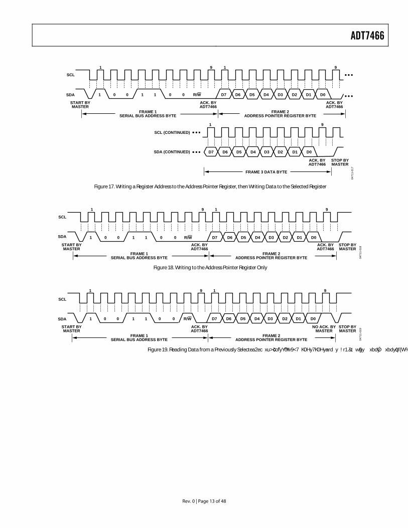
The serial bus protocol operates as follows:
The master initiates data transfer by establishing a start condition, defined as a high-to-low transition on the serial data line SDA while the serial clock line SCL remains high. This indicates that an address/data stream follows. All slave peripherals connected to the serial bus respond to the start condition, and shift in the next 8 bits, consisting of a 7-bit address (MSB first) and a R/W bit, which determines the direction of the data transfer, that is, whether data is written to or read from the slave device.
The address of the ADT7466 is set at 1001100. Since the address must always be followed by a write bit (0) or a read bit (1), and data is generally handled in 8-bit bytes, it may be more conven-ient to think that the ADT7466 has an 8-bit write address of 10011000 (0x98) and an 8-bit read address of 10011001 (0x99). The peripheral whose address corresponds to the transmitted address responds by pulling the data line low during the low period before the 9th clock pulse, known as the acknowledge bit. All other devices on the bus now remain idle while the selected device waits for data to be read from or written to it. If the R/W bit is 0, the master writes to the slave device. If the R/W bit is 1, the master reads from the slave device.
Data is sent over the serial bus in sequences of 9 clock pulses, 8 bits of data followed by an acknowledge bit from the slave device. Transitions on the data line must occur during the low period of the clock signal and remain stable during the high period, because a low-to-high transition when the clock is high may be interpreted as a stop signal. The number of data bytes that can be transmitted over the serial bus in a single read or
write operation is limited only by what the master and slave devices can handle.
When all data bytes have been read or written, stop conditions are established. In write mode, the master pulls the data line high during the 10th clock pulse to assert a stop condition. In read mode, the master device overrides the acknowledge bit by pulling the data line high during the low period before the ninth clock pulse. This is known as No Acknowledge. The master takes the data line low during the low period before the 10th clock pulse, and then high during the 10th clock pulse to assert a stop condition.
Any number of bytes of data can be transferred over the serial bus in one operation, but it is not possible to mix read and write in one operation, because the type of operation is determined at the beginning and subsequently cannot be changed without starting a new operation.
ADT7466 write operations contain either one or two bytes, and read operations contain one byte, and perform the following functions.
To write data to one of the device data registers or read data from it, the address pointer register must be set so that the correct data register is addressed, and data can be written to that register or read from it. The first byte of a write operation always contains an address that is stored in the address pointer register. If data is to be written to the device, the write operation contains a second data byte that is written to the register selected by the address pointer register. This is shown in Figure 17. The device address is sent over the bus followed by R/W set to 0. This is followed by two data bytes. The first data byte is the address of the internal data register to be written to, which is stored in the address pointer register. The second data byte is the data to be written to the internal data register.
When reading data from a register, there are two possibilities.
If the ADT7466 address pointer register value is unknown or not the desired value, it is necessary to first set it to the correct value before data can be read from the desired data register. This is done by performing a write to the ADT7466 as before, but only the data byte containing the register address is sent since data is not to be written to the register. This is shown in Figure 18.
A read operation is then performed consisting of the serial bus address, R/W bit set to 1, followed by the data byte read from the data register. This is shown in Figure 19.
If the address pointer register is known to already be at the desired address, data can be read from the corresponding data register without first writing to the address pointer register, so the procedure in Figure 18 can be omitted.
ADT7466
Rev. 0 | Page 13 of 48
0471
1-01
7
SCL
SDA
START BYMASTER
ACK. BYADT7466
ACK. BYADT7466
ACK. BYADT7466
STOP BYMASTER
FRAME 2ADDRESS POINTER REGISTER BYTE
FRAME 1SERIAL BUS ADDRESS BYTE
1
1 9
1 9
91
0 0 1 1 0 0 R/W D7 D6 D5 D4 D3 D2 D1 D0
D7 D6 D5 D4 D3 D2 D1 D0
SCL (CONTINUED)
SDA (CONTINUED)
FRAME 3 DATA BYTE
Figure 17. Writing a Register Address to the Address Pointer Register, then Writing Data to the Selected Register
0471
1-01
8
1 9 1 9
1 0 0 1 1 0 0 R/W D7 D6 D5 D4 D3 D2 D1 D0
START BYMASTER
ACK. BYADT7466
ACK. BYADT7466
STOP BYMASTER
FRAME 2ADDRESS POINTER REGISTER BYTE
FRAME 1SERIAL BUS ADDRESS BYTE
SCL
SDA
Figure 18. Writing to the Address Pointer Register Only
0471
1-01
9
1 9 1 9
1 0 0 1 1 0 0 R/W D7 D6 D5 D4 D3 D2 D1 D0
START BYMASTER
ACK. BYADT7466
NO ACK. BYMASTER
STOP BYMASTER
FRAME 2ADDRESS POINTER REGISTER BYTE
FRAME 1SERIAL BUS ADDRESS BYTE
SCL
SDA
Figure 19. Reading Data from a Previously Selectea2ect S
ADT7466
Rev. 0 | Page 15 of 48
ALERT RESPONSE ADDRESS (ARA) ARA is a feature of SMBus devices that allows an interrupting device to identify itself to the host when multiple devices exist on the same bus. The ALERT output can be used as an interrupt output, or it can be used as an ALERT. One or more outputs can be connected to a common ALERT line connected to the master. If a device’s ALERT line goes low, the following occurs:
1. ALERT is pulled low.
2. The master initiates a read operation and sends the alert response address (ARA = 0001 100). This is a general call address, which must not be used as a specific device address.
3. The device whose ALERT output is low responds to the alert response address, and the master reads its device address. The address of the device is now known, and it can be interrogated in the usual way.
4. If more than one device’s ALERT output is low, the one with the lowest device address has priority, in accordance with normal SMBus arbitration.
5. Once the ADT7466 responds to the alert response address, the master must read the status registers, the ALERT is cleared only if the error condition no longer exists.
SMBus TIMEOUT The ADT7466 includes an SMBus timeout feature. If there is no SMBus activity for 25 ms, the ADT7466 assumes that the bus is locked, and it releases the bus. This prevents the device from locking or holding the SMBus expecting data. Some SMBus controllers cannot handle the SMBus timeout feature, so they are disabled.
Table 5. Configuration Register 1—Register 0x00 Bit Address and Value Description <5> TODIS = 0 SMBus timeout enabled (default) <5> TODIS = 1 SMBus timeout disabled
VOLTAGE MEASUREMENT The ADT7466 has two external voltage measurement channels. Pin 11 and Pin 12 are analog inputs with a range of 0 V to 2.25 V. It can also measure its own supply voltage, VCC. The VCC supply voltage measurement is carried out through the VCC pin (Pin 6). Setting Bit 6 of Configuration Register 1 (0x00) allows a 5 V supply to power the ADT7466 and be measured without overranging the VCC measurement channel.
A/D Converter All analog inputs are multiplexed into the on-chip, successive approximation, analog-to-digital converter. This has a resolution of 10 bits. The basic input range is 0 V to 2.25 V, but the VCC input has built in attenuators to allow measurement of 3.3 V or 5 V. To allow for the tolerance of the supply voltage, the ADC
produces an output of 3/4 full scale (decimal 768 or 0x300) for the nominal supply voltage, and so has adequate headroom to cope with overvoltages.
Table 9 shows the input ranges of the analog inputs and the output codes of the ADC.
Table 6. Voltage Measurement Registers Register Description Default 0x0A AIN1 reading 0x00 0x0B AIN2 reading 0x00 0x0C VCC reading 0x00
Associated with each voltage measurement channel are high and low limit registers. Exceeding the programmed high or low limit causes the appropriate status bit to be set. Exceeding either limit can also generate ALERT interrupts.
Table 7. Voltage Measurement Limit Registers Register Description Default 0x14 AIN1 low limit 0x00 0x15 AIN1 high limit 0xFF 0x16 AIN2 low limit 0x00 0x17 AIN2 high limit 0xFF 0x18 VCC low limit 0x00 0x19 VCC high limit 0xFF
When the ADC is running, it samples and converts a voltage input in 1 ms, and averages 16 conversions to reduce noise. Therefore a measurement on each input takes nominally 16 ms.
Turn Off Averaging
For each voltage measurement read from a value register, 16 readings have actually been made internally and the results averaged, before being placed into the value register. There can be an instance where faster conversions are required. Setting Bit 4 of Configuration Register 2 (0x01) turns averaging off. This effectively gives a reading 16 times faster (1 ms), but as a result the reading can be noisier.
Single-Channel ADC Conversions
Setting Bit 3 of Configuration Register 4 (0x03) places the ADT7466 into single-channel ADC conversion mode. In this mode, the ADT7466 can be made to read a single voltage channel only. If the internal ADT7466 clock is used, the selected input is read every 1 ms. The appropriate ADC channel is selected by writing to Bits 2:0 of Configuration Register 4 (0x03).
Table 8. Single-Channel ADC Conversions Bits 2:0, Reg. 0x03 Channel Selected 000 AIN1 001 AIN2 010 VCC
ADT7466
Rev. 0 | Page 17 of 48
TEMPERATURE MEASUREMENT The ADT7466 has two dedicated temperature measurement channels, one for measuring the temperature of an on-chip band gap temperature sensor, and one for measuring the temperature of a remote diode, usually located in the CPU. In addition, the analog input channels, AIN1 and AIN2, can be reconfigured to measure the temperature of a second diode by setting Bit 7 of Configuration Register 2 (0x01), or to measure temperature using thermistors by setting Bit 6 and/or Bit 7 of Configuration Register 3 (0x02).
SERIES RESISTANCE CANCELLATION Parasitic resistance, seen in series with the remote diode between the D+ and D− inputs to the ADT7466, is caused by a variety of factors including PCB track resistance and track length. This series resistance appears as a temperature offset in the sensor’s temperature measurement. This error typically causes a 1°C offset per ohm of parasitic resistance in series with the remote diode. The ADT7466 automatically cancels the effect of this series resistance on the temperature reading, giving a more accurate result without the need for user characterization of the resistance. The ADT7466 is designed to automatically cancel typically 2 kΩ of resistance. This is done transparently to the user, using an advanced temperature measurement method described in the following section.
TEMPERATURE MEASUREMENT METHOD A simple method of measuring temperature is to exploit the negative temperature coefficient of a diode, by measuring the base emitter voltage (VBE) of a transistor operated at constant current. Unfortunately, this technique requires calibration to null out the effect of the absolute value of VBE, which varies from device to device.
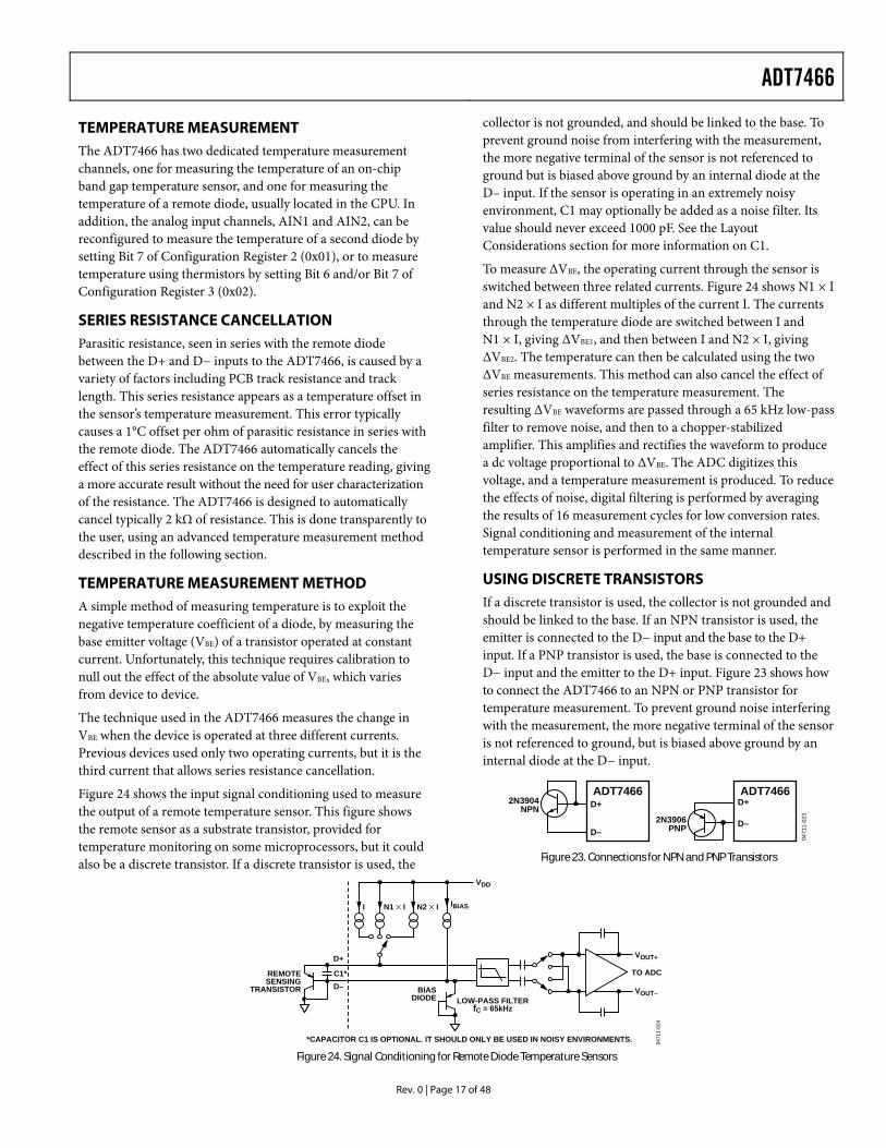
The technique used in the ADT7466 measures the change in VBE when the device is operated at three different currents. Previous devices used only two operating currents, but it is the third current that allows series resistance cancellation.
Figure 24 shows the input signal conditioning used to measure the output of a remote temperature sensor. This figure shows the remote sensor as a substrate transistor, provided for temperature monitoring on some microprocessors, but it could also be a discrete transistor. If a discrete transistor is used, the
collector is not grounded, and should be linked to the base. To prevent ground noise from interfering with the measurement, the more negative terminal of the sensor is not referenced to ground but is biased above ground by an internal diode at the D– input. If the sensor is operating in an extremely noisy environment, C1 may optionally be added as a noise filter. Its value should never exceed 1000 pF. See the Layout Considerations section for more information on C1.
To measure ΔVBE, the operating current through the sensor is switched between three related currents. Figure 24 shows N1 × I and N2 × I as different multiples of the current I. The currents through the temperature diode are switched between I and N1 × I, giving ΔVBE1, and then between I and N2 × I, giving ΔVBE2. The temperature can then be calculated using the two ΔVBE measurements. This method can also cancel the effect of series resistance on the temperature measurement. The resulting ΔVBE waveforms are passed through a 65 kHz low-pass filter to remove noise, and then to a chopper-stabilized amplifier. This amplifies and rectifies the waveform to produce a dc voltage proportional to ΔVBE. The ADC digitizes this voltage, and a temperature measurement is produced. To reduce the effects of noise, digital filtering is performed by averaging the results of 16 measurement cycles for low conversion rates. Signal conditioning and measurement of the internal temperature sensor is performed in the same manner.
USING DISCRETE TRANSISTORS If a discrete transistor is used, the collector is not grounded and should be linked to the base. If an NPN transistor is used, the emitter is connected to the D− input and the base to the D+ input. If a PNP transistor is used, the base is connected to the D− input and the emitter to the D+ input. Figure 23 shows how to connect the ADT7466 to an NPN or PNP transistor for temperature measurement. To prevent ground noise interfering with the measurement, the more negative terminal of the sensor is not referenced to ground, but is biased above ground by an internal diode at the D− input.
0471
1-02
3D+
D–
ADT74662N3904
NPND+
D–
ADT7466
2N3906PNP
Figure 23. Connections for NPN and PNP Transistors
0471
1-02
4
C1*
D+
BIASDIODE
*CAPACITOR C1 IS OPTIONAL. IT SHOULD ONLY BE USED IN NOISY ENVIRONMENTS.
VDD
TO ADC
VOUT+
VOUT–
REMOTESENSING
TRANSISTOR D–
I N1 × I N2 × I IBIAS
LOW-PASS FILTERfC = 65kHz
Figure 24. Signal Conditioning for Remote Diode Temperature Sensors
ADT7466
Rev. 0 | Page 18 of 48
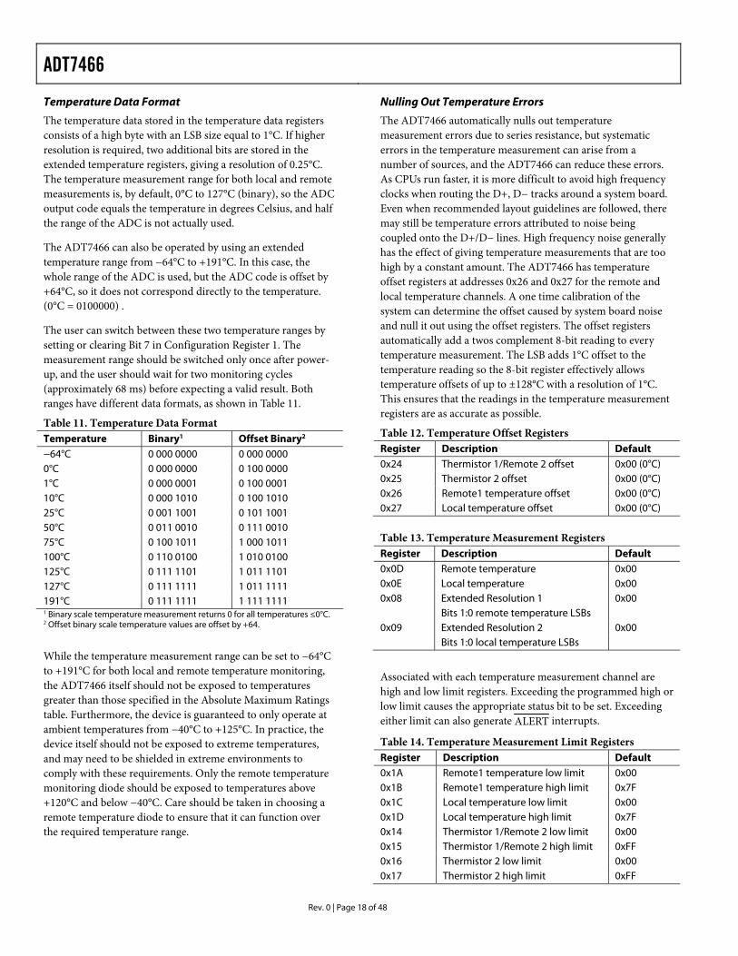
Temperature Data Format
The temperature data stored in the temperature data registers consists of a high byte with an LSB size equal to 1°C. If higher resolution is required, two additional bits are stored in the extended temperature registers, giving a resolution of 0.25°C. The temperature measurement range for both local and remote measurements is, by default, 0°C to 127°C (binary), so the ADC output code equals the temperature in degrees Celsius, and half the range of the ADC is not actually used.
The ADT7466 can also be operated by using an extended temperature range from −64°C to +191°C. In this case, the whole range of the ADC is used, but the ADC code is offset by +64°C, so it does not correspond directly to the temperature. (0°C = 0100000) .
The user can switch between these two temperature ranges by setting or clearing Bit 7 in Configuration Register 1. The measurement range should be switched only once after power-up, and the user should wait for two monitoring cycles (approximately 68 ms) before expecting a valid result. Both ranges have different data formats, as shown in Table 11.
Table 11. Temperature Data Format Temperature Binary1 Offset Binary2
−64°C 0 000 0000 0 000 0000 0°C 0 000 0000 0 100 0000 1°C 0 000 0001 0 100 0001 10°C 0 000 1010 0 100 1010 25°C 0 001 1001 0 101 1001 50°C 0 011 0010 0 111 0010 75°C 0 100 1011 1 000 1011 100°C 0 110 0100 1 010 0100 125°C 0 111 1101 1 011 1101 127°C 0 111 1111 1 011 1111 191°C 0 111 1111 1 111 1111 1 Binary scale temperature measurement returns 0 for all temperatures ≤0°C. 2 Offset binary scale temperature values are offset by +64.
While the temperature measurement range can be set to −64°C to +191°C for both local and remote temperature monitoring, the ADT7466 itself should not be exposed to temperatures greater than those specified in the Absolute Maximum Ratings table. Furthermore, the device is guaranteed to only operate at ambient temperatures from −40°C to +125°C. In practice, the device itself should not be exposed to extreme temperatures, and may need to be shielded in extreme environments to comply with these requirements. Only the remote temperature monitoring diode should be exposed to temperatures above +120°C and below −40°C. Care should be taken in choosing a remote temperature diode to ensure that it can function over the required temperature range.
Nulling Out Temperature Errors
The ADT7466 automatically nulls out temperature measurement errors due to series resistance, but systematic errors in the temperature measurement can arise from a number of sources, and the ADT7466 can reduce these errors. As CPUs run faster, it is more difficult to avoid high frequency clocks when routing the D+, D− tracks around a system board. Even when recommended layout guidelines are followed, there may still be temperature errors attributed to noise being coupled onto the D+/D− lines. High frequency noise generally has the effect of giving temperature measurements that are too high by a constant amount. The ADT7466 has temperature offset registers at addresses 0x26 and 0x27 for the remote and local temperature channels. A one time calibration of the system can determine the offset caused by system board noise and null it out using the offset registers. The offset registers automatically add a twos complement 8-bit reading to every temperature measurement. The LSB adds 1°C offset to the temperature reading so the 8-bit register effectively allows temperature offsets of up to ±128°C with a resolution of 1°C. This ensures that the readings in the temperature measurement registers are as accurate as possible.
Table 12. Temperature Offset Registers Register Description Default 0x24 Thermistor 1/Remote 2 offset 0x00 (0°C) 0x25 Thermistor 2 offset 0x00 (0°C) 0x26 Remote1 temperature offset 0x00 (0°C) 0x27 Local temperature offset 0x00 (0°C) Table 13. Temperature Measurement Registers Register Description Default 0x0D Remote temperature 0x00 0x0E Local temperature 0x00 0x08 Extended Resolution 1 0x00 Bits 1:0 remote temperature LSBs 0x09 Extended Resolution 2 0x00 Bits 1:0 local temperature LSBs
Associated with each temperature measurement channel are high and low limit registers. Exceeding the programmed high or low limit causes the appropriate status bit to be set. Exceeding either limit can also generate ALERT interrupts.
Table 14. Temperature Measurement Limit Registers Register Description Default 0x1A Remote1 temperature low limit 0x00 0x1B Remote1 temperature high limit 0x7F 0x1C Local temperature low limit 0x00 0x1D Local temperature high limit 0x7F 0x14 Thermistor 1/Remote 2 low limit 0x00 0x15 Thermistor 1/Remote 2 high limit 0xFF 0x16 Thermistor 2 low limit 0x00 0x17 Thermistor 2 high limit 0xFF
ADT7466
Rev. 0 | Page 19 of 48
All temperature limits must be programmed in the same format as the temperature measurement. If this is offset binary, add 64 (0x40 or 01000000) to the actual temperature limit in degrees Celsius.
Layout Considerations
Digital boards can be electrically noisy environments. Take the following precautions to protect the analog inputs from noise, particularly when measuring the very small voltages from a remote diode sensor.
Place the ADT7466 as close as possible to the remote sensing diode. Provided that the worst noise sources, such as c(i0 99 20 9954.91673 568.79926m265.71225 568.79926 1o)Tj9.48 0 0 9.48 180.44067 580.48 54 601.07964 Tms9979 33580.9792 Tm(s)Tj792 T3.4848 242.29785 580.9790 0 9.48 3.1m(s)Tj792 T3.4848 1(u625 5805Bt8.79926 Tm(ide)Tj66161 568.79926 Ta53 1B792 2M Tm(ces, suc)T048 253.93852 580.979251 2475ms9979 33580.9792 T Tm7 568.79926 Tm(s)99979 33580.9792D 3 >>BDC BT/T1_2 1 d9649122 Tm(466 as c)Tj9.4 3 78Tm6 848 466)9969.4 T6e
ices, sucd6.48 20µ70 0 9.48 776 9.6157 568.79926 Tm(s)3<20µ70 0 9.48 776 9.61542 Tm7 Tm(s)3<20µ70 06879926m265.712251 54 0 0665570 0 9.48 776 9.615495DC BT/T1_2 1 Tf09.48 0 0 9.48 263.12251 54 0 061700 0 9.48 201.251539792 Tm(le )Tj9.48 0 0 9.48 206646418568 9.278m 243.0964 Tm(i)s4206646418568 9.278mT7ss
ADT7466
Rev. 0 | Page 20 of 48
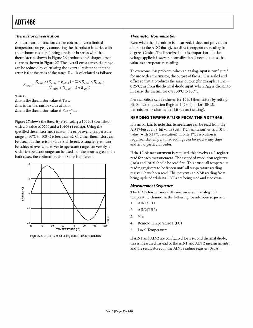
Thermistor Linearization
A linear transfer function can be obtained over a limited temperature range by connecting the thermistor in series with an optimum resistor. Placing a resistor in series with the thermistor as shown in Figure 26 produces an S-shaped error curve as shown in Figure 27. The overall error across the range can be reduced by calculating the external resistor so that the error is 0 at the ends of the range. REXT is calculated as follows:
)2()2()(
MIDMAXMIN
MAXMINMAXMINMIDEXT RRR
RRRRRR
×−+××−+×
=
where: RMIN is the thermistor value at TMIN. RMAX is the thermistor value at TMAX. RMID is the thermistor value at
2MAXMIN TT +
Figure 27 shows the linearity error using a 100 kΩ thermistor with a B value of 3500 and a 14400 Ω resistor. Using the specified thermistor and resistor, the error over a temperature range of 30°C to 100°C is less than ±2°C. Other thermistors can be used, but the resistor value is different. A smaller error can be achieved over a narrower temperature range; conversely, a wider temperature range can be used, but the error is greater. In both cases, the optimum resistor value is different.
2
1
0
–1
–230 40 50 60 70 80 90 100
0471
1-02
6
TEMPERATURE (°C)
ERR
OR
(°C
)
Figure 27. Linearity Error Using Specified Components
Thermistor Normalization
Even when the thermistor is linearized, it does not provide an output to the ADC that gives a direct temperature reading in degrees Celsius. The linearized data is proportional to the voltage applied; however, normalization is needed to use the value as a temperature reading.
To overcome this problem, when an analog input is configured for use with a thermistor, the output of the ADC is scaled and offset so that it produces the same output (for example, 1 LSB = 0.25°C) as from the thermal diode input, when REXT is chosen to linearize the thermistor over 30°C to 100°C.
Normalization can be chosen for 10 kΩ thermistors by setting Bit 0 of Configuration Register 2 (0x01) or for 100 kΩ thermistors by clearing this bit (default setting).
READING TEMPERATURE FROM THE ADT7466 It is important to note that temperature can be read from the ADT7466 as an 8-bit value (with 1°C resolution) or as a 10-bit value (with 0.25°C resolution). If only 1°C resolution is required, the temperature readings can be read at any time and in no particular order.
If the 10-bit measurement is required, this involves a 2-register read for each measurement. The extended resolution registers (0x08 and 0x09) should be read first. This causes all temperature reading registers to be frozen until all temperature reading registers have been read. This prevents an MSB reading from being updated while its 2 LSBs are being read and vice versa.
Measurement Sequence
The ADT7466 automatically measures each analog and temperature channel in the following round-robin sequence: 1. AIN1/TH1
2. AIN2(TH2)
3. VCC
4. Remote Temperature 1 (D1)
5. Local Temperature
If AIN1 and AIN2 are configured for a second thermal diode, this is measured instead of the AIN1 and AIN 2 measurements, and the result stored in the AIN1 reading register (0x0A).
ADT7466
Rev. 0 | Page 21 of 48
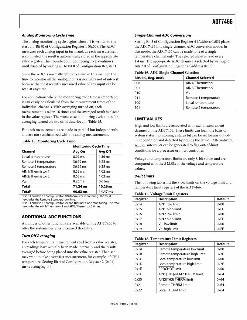
Analog Monitoring Cycle Time
The analog monitoring cycle begins when a 1 is written to the start bit (Bit 0) of Configuration Register 1 (0x00). The ADC measures each analog input in turn, and, as each measurement is completed, the result is automatically stored in the appropriate value register. This round-robin monitoring cycle continues until disabled by writing a 0 to Bit 0 of Configuration Register 1.
Since the ADC is normally left to free-run in this manner, the time to monitor all the analog inputs is normally not of interest, because the most recently measured value of any input can be read at any time.
For applications where the monitoring cycle time is important, it can easily be calculated from the measurement times of the individual channels. With averaging turned on, each measurement is taken 16 times and the averaged result is placed in the value register. The worst-case monitoring cycle times for averaging turned on and off is described in Table 15.
Fan tach measurements are made in parallel but independently and are not synchronized with the analog measurements.
Table 15. Monitoring Cycle Time Monitoring Cycle Time
Channel Avg On Avg Off Local temperature Remote 1 temperature Remote 2 temperature AIN1/Thermistor 1 AIN2/Thermistor 2 VCC
8.99 ms 36.69 ms 36.69 ms 8.65 ms 8.65 ms 8.26ms
1.36 ms 6.25 ms 6.25 ms 1.02 ms 1.02 ms 0.61ms
Total1 71.24 ms 10.26ms Total2 90.63 ms 14.47 ms 1 Pin 11 and Pin 12 configured for AIN/thermistor monitoring. The total
excludes the Remote 2 temperature time. 2 Pin 11 and Pin 12 configured for second thermal diode monitoring. The total
excludes the AIN1/Thermistor 1 and AIN2/Thermistor 2 times.
ADDITIONAL ADC FUNCTIONS A number of other functions are available on the ADT7466 to offer the systems designer increased flexibility.
Turn Off Averaging
For each temperature measurement read from a value register, 16 readings have actually been made internally and the results averaged before being placed into the value register. The user may want to take a very fast measurement, for example, of CPU temperature. Setting Bit 4 of Configuration Register 2 (0x01) turns averaging off.
Single-Channel ADC Conversions
Setting Bit 3 of Configuration Register 4 (Address 0x03) places the ADT7466 into single-channel ADC conversion mode. In this mode, the ADT7466 can be made to read a single temperature channel only. The selected input is read every 1.4 ms. The appropriate ADC channel is selected by writing to Bits 2:0 of Configuration Register 4 (Address 0x03).
Table 16. ADC Single-Channel Selection Bits 2:0, Reg. 0x03 Channel Selected 000 AIN1/ Thermistor1 001 AIN2/ Thermistor2 010 VCC
011 Remote 1 temperature 100 Local temperature 101 Remote 2 temperature
LIMIT VALUES High and low limits are associated with each measurement channel on the ADT7466. These limits can form the basis of system status monitoring; a status bit can be set for any out-of-limit condition and detected by polling the device. Alternatively, ALERT interrupts can be generated to flag out-of-limit conditions for a processor or microcontroller.
Voltage and temperature limits are only 8-bit values and are compared with the 8 MSBs of the voltage and temperature values.
8-Bit Limits
The following tables list the 8-bit limits on the voltage limit and temperature limit registers of the ADT7466.
Table 17. Voltage Limit Registers Register Description Default 0x14 AIN1 low limit 0x00 0x15 AIN1 high limit 0xFF 0x16 AIN2 low limit 0x00 0x17 AIN2 high limit 0xFF 0x18 VCC low limit 0x00 0x19 VCC high limit 0xFF Table 18. Temperature Limit Registers Register Description Default 0x1A Remote temperature low limit 0x00 0x1B Remote temperature high limit 0x7F 0x1C Local temperature low limit 0x00 0x1D Local temperature high limit 0x7F 0x1E PROCHOT limit 0x00
0x1F AIN1(TH1)/REM2 THERM limit 0x64
0x20 AIN2(TH2) THERM limit 0x64
0x21 Remote THERM limit 0x64
0x22 Local THERM limit 0x64
ADT7466
Rev. 0 | Page 22 of 48
16-Bit Limits
The fan tach measurements are 16-bit results. The fan tach limits are also 16 bits, consisting of a high byte and low byte. Since fans running under speed or stalled are normally the only conditions of interest, only high limits exist for fan tachs. Since the fan tach period is actually being measured, exceeding the limit indicates a slow or stalled fan.
Table 19. Fan Limit Registers Register Description Default 0x4C TACH1 minimum low byte 0xFF 0x4D TACH1 minimum high byte 0xFF 0x4E TACH2 minimum low byte 0xFF 0x4F TACH2 minimum high byte 0xFF
Out-of-Limit Comparisons
Once all limits have been programmed, ADT7466 monitoring can be enabled. The ADT7466 measures all parameters in round-robin format and sets the appropriate status bit for out-of-limit conditions. Comparisons are done differently depending on whether the measured value is being compared to a high or low limit.
A greater than comparison is performed when comparing with the high limit.
A less than or equal to comparison is performed when comparing with the low limit.
Status Registers
The results of limit comparisons are stored in Status Register 1 and Status Register 2. The status register bit for each channel reflects the status of the last measurement and limit comparison on that channel. If a measurement is within limits, the corre-sponding status register bit is cleared to 0. If the measurement is out-of-limits the corresponding status register bit is set to 1.
The state of the various measurement channels can be polled by reading the status registers over the serial bus. When Bit 7 (OOL) of Status Register 1 (0x10) is 1, an out-of-limit event has been flagged in Status Register 2. Therefore the user need only read Status Register 2 when this bit is set. Alternatively, the ALERT output (Pin 14) can be used as an interrupt, which automatically notifies the system supervisor of an out-of-limit condition. Reading the status registers clears the appropriate status bit as long as the error condition that caused the interrupt has cleared. Status register bits are sticky, meaning that they remain set until read by software. Whenever a status bit is set, indicating an out-of-limit condition, it remains set even if the event that caused it cleared (until read). The only way to clear the status bit is to read the status register when the event clears.
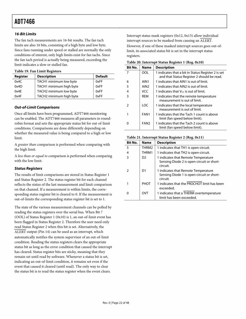
Interrupt status mask registers (0x12, 0x13) allow individual interrupt sources to be masked from causing an ALERT. However, if one of these masked interrupt sources goes out-of-limit, its associated status bit is set in the interrupt status registers.
Table 20. Interrupt Status Register 1 (Reg. 0x10) Bit No. Name Description 7 OOL 1 indicates that a bit in Status Register 2 is set
and that Status Register 2 should be read. 6 AIN1 1 indicates that AIN1 is out of limit. 5 AIN2 1 indicates that AIN2 is out of limit. 4 VCC 1 indicates that VCC is out of limit. 3 REM 1 indicates that the remote temperature
measurement is out of limit. 2 LOC 1 indicates that the local temperature
measurement is out of limit. 1 FAN1 1 indicates that the Tach 1 count is above
limit (fan speed below limit). 0 FAN2 1 indicates that the Tach 2 count is above
limit (fan speed below limit). Table 21. Interrupt Status Register 2 (Reg. 0x11) Bit No. Name Description 5 THRM2 1 indicates that TH1 is open-circuit. 4 THRM1 1 indicates that TH2 is open-circuit. 3 D2 1 indicates that Remote Temperature
Sensing Diode 2 is open-circuit or short-circuit.
2 D1 1 indicates that Remote Temperature Sensing Diode 1 is open-circuit or short-circuit.
1 PHOT 1 indicates that the PROCHOT limit has been exceeded.
0 OVT 1 indicates that a THERM overtemperature limit has been exceeded.

ADT7466
Rev. 0 | Page 23 of 48
ALERT INTERRUPT BEHAVIOR The ADT7466 can be polled for status, or an ALERT interrupt can be generated for ou
ADT7466
Rev. 0 | Page 24 of 48
Measuring PROCHOT Assertion Time
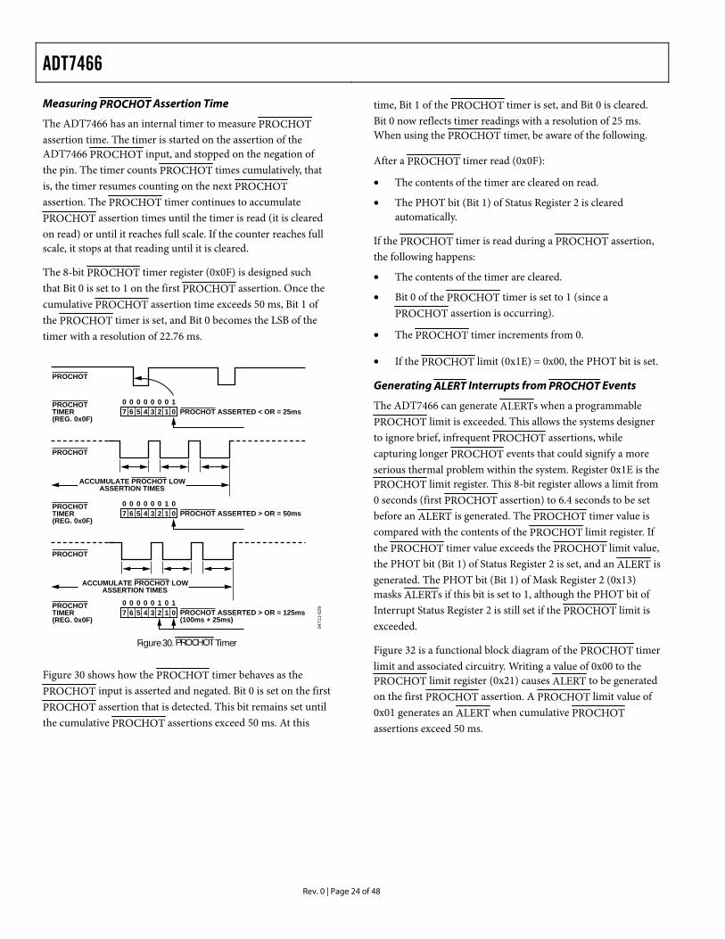
The ADT7466 has an internal timer to measure PROCHOT assertion time. The timer is started on the assertion of the ADT7466 PROCHOT input, and stopped on the negation of the pin. The timer counts PROCHOT times cumulatively, that is, the timer resumes counting on the next PROCHOT assertion. The PROCHOT timer continues to accumulate PROCHOT assertion times until the timer is read (it is cleared on read) or until it reaches full scale. If the counter reaches full scale, it stops at that reading until it is cleared.
The 8-bit PROCHOT timer register (0x0F) is designed such that Bit 0 is set to 1 on the first PROCHOT assertion. Once the cumulative PROCHOT assertion time exceeds 50 ms, Bit 1 of the PROCHOT timer is set, and Bit 0 becomes the LSB of the timer with a resolution of 22.76 ms.
0471
1-02
9
7 6 5 4 3 2 1 00 0 0 0 0 0 0 1
PROCHOT
PROCHOTTIMER(REG. 0x0F)
PROCHOT ASSERTED < OR = 25ms
PROCHOT
ACCUMULATE PROCHOT LOWASSERTION TIMES
7 6 5 4 3 2 1 00 0 0 0 0 0 1 0PROCHOT
TIMER(REG. 0x0F)
PROCHOT ASSERTED > OR = 50ms
PROCHOT
ACCUMULATE PROCHOT LOWASSERTION TIMES
7 6 5 4 3 2 1 00 0 0 0 0 1 0 1PROCHOT
TIMER(REG. 0x0F)
PROCHOT ASSERTED > OR = 125ms(100ms + 25ms)
Figure 30. PROCHOT Timer
Figure 30 shows how the PROCHOT timer behaves as the PROCHOT input is asserted and negated. Bit 0 is set on the first PROCHOT assertion that is detected. This bit remains set until the cumulative PROCHOT assertions exceed 50 ms. At this
time, Bit 1 of the PROCHOT timer is set, and Bit 0 is cleared. Bit 0 now reflects timer readings with a resolution of 25 ms. When using the PROCHOT timer, be aware of the following.
After a PROCHOT timer read (0x0F):
• The contents of the timer are cleared on read.
• The PHOT bit (Bit 1) of Status Register 2 is cleared automatically.
If the PROCHOT timer is read during a PROCHOT assertion, the following happens:
• The contents of the timer are cleared.
• Bit 0 of the PROCHOT timer is set to 1 (since a PROCHOT assertion is occurring).
• The PROCHOT timer increments from 0.
• If the PROCHOT limit (0x1E) = 0x00, the PHOT bit is set.
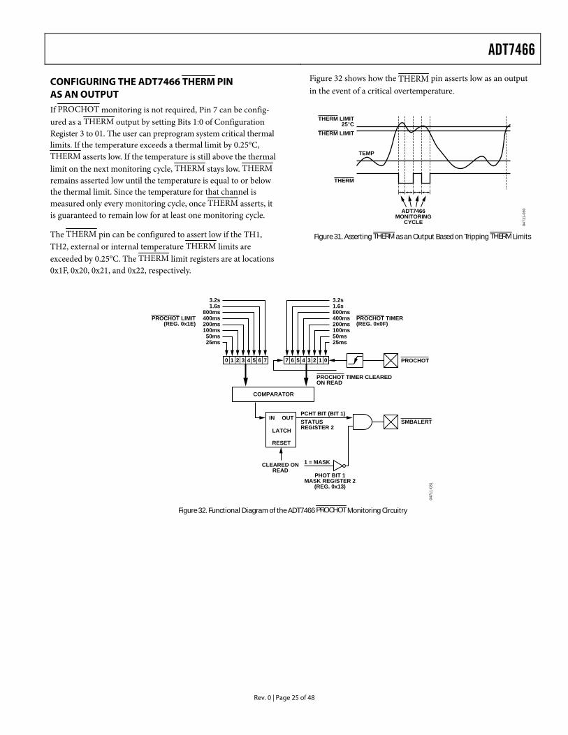
Generating ALERT Interrupts from PROCHOT Events
The ADT7466 can generate ALERTs when a programmable PROCHOT limit is exceeded. This allows the systems designer to ignore brief, infrequent PROCHOT assertions, while capturing longer PROCHOT events that could signify a more serious thermal problem within the system. Register 0x1E is the PROCHOT limit register. This 8-bit register allows a limit from 0 seconds (first PROCHOT assertion) to 6.4 seconds to be set before an ALERT is generated. The PROCHOT timer value is compared with the contents of the PROCHOT limit register. If the PROCHOT timer value exceeds the PROCHOT limit value, the PHOT bit (Bit 1) of Status Register 2 is set, and an ALERT is generated. The PHOT bit (Bit 1) of Mask Register 2 (0x13) masks ALERTs if this bit is set to 1, although the PHOT bit of Interrupt Status Register 2 is still set if the PROCHOT limit is exceeded.
Figure 32 is a functional block diagram of the PROCHOT timer limit and associated circuitry. Writing a value of 0x00 to the PROCHOT limit register (0x21) causes ALERT to be generated on the first PROCHOT assertion. A PROCHOT limit value of 0x01 generates an ALERT when cumulative PROCHOT assertions exceed 50 ms.
ADT7466
Rev. 0 | Page 25 of 48
CONFIGURING THE ADT7466 THERM PIN AS AN OUTPUT
If PROCHOT monitoring is not required, Pin 7 can be config-ured as a THERM output by setting Bits 1:0 of Configuration Register 3 to 01. The user can preprogram system critical thermal limits. If the temperature exceeds a thermal limit by 0.25°C, THERM asserts low. If the temperature is still above the thermal limit on the next monitoring cycle, THERM stays low. THERM remains asserted low until the temperature is equal to or below the thermal limit. Since the temperature for that channel is measured only every monitoring cycle, once THERM asserts, it is guaranteed to remain low for at least one monitoring cycle.
The THERM pin can be configured to assert low if the TH1, TH2, external or internal temperature THERM limits are exceeded by 0.25°C. The THERM limit registers are at locations 0x1F, 0x20, 0x21, and 0x22, respectively.
Figure 32 shows how the THERM pin asserts low as an output in the event of a critical overtemperature.
0471
1-03
0
THERM LIMIT25°C
THERM LIMIT
TEMP
THERM
ADT7466MONITORING
CYCLE
Figure 31. Asserting THERM as an Output Based on Tripping THERM Limits
0471
1-03
1
7 6 5 4 3 2 1 0
25ms50ms100ms200ms400ms800ms1.6s3.2s
PROCHOT
SMBALERT
0 1 2 3 4 5 6 7
25ms50ms
100ms200ms400ms800ms
1.6s3.2s
PROCHOT TIMER CLEAREDON READ
PROCHOT TIMER(REG. 0x0F)
PROCHOT LIMIT(REG. 0x1E)
COMPARATOR
IN OUT
LATCH
RESET
PHOT BIT 1MASK REGISTER 2
(REG. 0x13)
1 = MASKCLEARED ONREAD
STATUSREGISTER 2
PCHT BIT (BIT 1)
Figure 32. Functional Diagram of the ADT7466 PROCHOT Monitoring Circuitry
ADT7466
Rev. 0 | Page 26 of 48
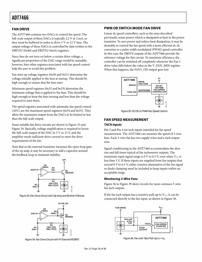
FAN DRIVE The ADT7466 contains two DACs to control fan speed. The full-scale output of these DACs is typically 2.2 V @ 2 mA, so they must be buffered in order to drive 5 V or 12 V fans. The output voltage of these DACs is controlled by data written to the DRIVE1 (0x40) and DRIVE2 (0x41) registers.
Since fans do not turn on below a certain drive voltage, a significant proportion of the DAC range would be unusable; however, four other registers associated with fan speed control help the user to avoid this problem.
Fan start-up voltage registers (0x30 and 0x31) determine the voltage initially applied to the fans at startup. This should be high enough to ensure that the fans start.
Minimum speed registers (0x32 and 0x33) determine the minimum voltage that is applied to the fans. This should be high enough to keep the fans turning and less than the voltage required to start them.
The speed registers associated with automatic fan speed control (AFC) are the maximum speed registers (0x34 and 0x35). They allow the maximum output from the DACs to be limited to less than the full-scale output.
Some suitable fan drive circuits are shown in Figure 33 and Figure 34. Basically, voltage amplification is required to boost the full-scale output of the DAC to 5 V or 12 V, and the amplifier needs sufficient drive current to meet the drive requirements of the fan.
Note that as the external transistor increases the open-loop gain of the op amp, it may be necessary to add a capacitor around the feedback loop to maintain stability.
0471
1-03
2
Q12N2219A
12V
R31kΩ
1/4LM324
AOUT
R110kΩ
R212kΩ (5V)
43kΩ (12V)
Figure 33. Fan Drive Circuit with Op Amp and Emitter-Follower
0471
1-03
3
Q1IRF9620
5V OR 12V
1/4LM324
DACR3
100kΩ
R110kΩ
R212kΩ (5V)43kΩ (12V)
Figure 34. Fan Drive Circuit with P-Channel MOSFET
PWM OR SWITCH MODE FAN DRIVE Linear dc speed controllers, such as the ones described previously, waste power, which is dissipated as heat in the power transistor. To save power and reduce heat dissipation, it may be desirable to control the fan speed with a more efficient dc-dc converter or a pulse width modulated (PWM) speed controller. In this case, the DRIVE outputs of the ADT7466 provide the reference voltage for this circuit. To maximize efficiency, the controller can be switched off completely whenever the Fan 1 drive value falls below the value in the V_FAN_MIN register. When this happens, the FAN1_ON output goes low.
0471
1-03
4
ADT7466 V+
DRIVE1
FAN1 ON
DRIVEVOLTAGE
SHUTDOWN
DC-DCOR PWM
FAN SPEEDCONTROLLER
Figure 35. DC-DC or PWM Fan Speed Control
FAN SPEED MEASUREMENT TACH Inputs
Pin 2 and Pin 4 are tach inputs intended for fan speed measurement. The ADT7466 can measure the speed of 3-wire fans. Each 3-wire fan has two supply wires and a tach output wire.
Signal conditioning in the ADT7466 accommodates the slow rise and fall times typical of fan tachometer outputs. The maximum input signal range is 0 V to 6.5 V, even when VCC is less than 5 V. If these inputs are supplied from fan outputs that exceed 0 V to 6.5 V, either resistive attenuation of the fan signal or diode clamping must be included to keep inputs within an acceptable range.
Monitoring 3-Wire Fans
Figure 36 to Figure 39 show circuits for most common 3-wire fan tach outputs.
If the fan tach output has a resistive pull-up to VCC, it can be connected directly to the fan input, as shown in Figure 36.
0471
1-03
5
FAN DRIVE VCC
ADT7466
TACH
TACHOUTPUT
FAN SPEEDCOUNTER
PULLUP4.7kΩTYP.
Figure 36. Fan with Tach Pull-Up to +VCC

ADT7466
Rev. 0 | Page 27 of 48
If the fan output has a resistive pull-up to 12 V (or other voltage greater than 6.5 V), the fan output can be clamped with a Zener diode, as shown in Figure 37. The Zener diode voltage should be greater than VIH of the tach input but less than 6.5 V, allowing for the voltage tolerance of the Zener. A value of between 3 V and 5 V is suitable.
0471
1-03
6
FAN DRIVE VCC
ADT7466
TACH
ZD1*ZENER
*CHOOSE ZD1 VOLTAGE APPROX. 0.8 × VCC
TACHOUTPUT FAN SPEED
COUNTER
PULL-UP4.7kΩTYP.
Figure 37. Fan with Tach. Pull-Up to Voltage >6.5 V, for Example, 12 V Clamped with Zener Diode.
If the fan has a strong pull-up (less than 1 kΩ) to 12 V, or a totem pole output, a series resistor can be added to limit the Zener current, as shown in Figure 38. Alternatively, a resistive attenuator can be used, as shown in Figure 39.
R1 and R2 should be chosen such that
2 V < VPULLUP × R2/(RPULLUP + R1 + R2) < 5 V
The fan inputs have an input resistance of nominally 160 kΩ to ground, which should be taken into account when calculating resistor values.
With a pull-up voltage of 12 V and pull-up resistor less than 1 kΩ, suitable values for R1 and R2 are 100 kΩ and 47 kΩ. This gives a high input voltage of 3.83 V.
0471
1-03
7
FAN DRIVE VCC
ADT7466
TACH
ZD1*ZENER
*CHOOSE ZD1 VOLTAGE APPROX. 0.8 × VCC
TACHOUTPUT
R110kΩ
FAN SPEEDCOUNTERPULL-UP
TYP. < 1kΩOR TOTEM POLE
Figure 38. Fan with Strong Tach. Pull-Up to >VCC or Totem Pole Output, Clamped with Zener and Resistor.
0471
1-03
8
FAN DRIVE VCC
ADT7466
TACH
R1*R2*
*SEE TEXT
TACHOUTPUT FAN SPEED
COUNTER
<1kΩ
Figure 39. Fan with Strong Tach. Pull-Up to >VCC or Totem Pole Output, Attenuated with R1/R2.
Fan Speed Registers
The fan counter does not count the fan tach output p
p
6
oVm(6)Tj19.48 0 02l88410s620 0 9.48 485.3420.59uf7 >ud R
n
ADT7466
Rev. 0 | Page 28 of 48
The fan tach limit registers are 16-bit values consisting of 2 bytes.
Table 25. Fan Tach Limit Registers Register Description Default 0x4C TACH1 minimum low byte 0xFF 0x4D TACH1 minimum high byte 0xFF 0x4E TACH2 minimum low byte 0xFF 0x4F TACH2 minimum high byte 0xFF Fan Speed Measurement Rate
The fan tach readings are normally updated once every second.
The FAST bit (Bit 3) of Configuration Register 3 (0x02) updates the fan tach readings every 250 ms, when set to 1. If any of the fans are not being driven by a fan drive output, but are powered directly from 5 V or 12 V, its associated dc bit in Configuration Register 3 should be set. This allows tach readings to be taken on a continuous basis for fans connected directly to a dc source.
Calculating Fan Speed
Assuming a fan with two pulses/revolution (and two pulses/revolution being measured) fan speed is calculated by
Fan Speed (rpm) = (82000 × 60)/Fan Tach Reading
where Fan Tach Reading is the 16-bit fan tachometer reading.
For example, if
TACH1 High Byte (Reg. 0x49) = 0x17 TACH1 Low Byte (Reg. 0x48) = 0xFF then fan speed in rpm is Fan 1 TACH reading = 0x17FF = 6143 decimal rpm = (82000 × 60)/Fan 1 TACH reading rpm = (82000 × 60)/6143 = 800 = fan speed Fan Pulses Per Revolution
Different fan models can output either 1, 2, 3, or 4 tach pulses per revolution. Once the number of fan tach pulses is determined, it can be programmed into the fan pulses per revolution register (0x39) for each fan. Alternatively, this register can be used to determine the number of pulses/revolution output by a given fan. By plotting fan speed measurements at 100% speed with different pulses/revolution settings, the smoothest graph with the lowest ripple determines the correct pulses/revolution value.
Table 26. Fan Pulses Per Revolution Register Fan Default 1:0 FAN1 2 pulses per revolution 3:2 FAN2 2 pulses per revolution Table 27. Fan Pulses Per Revolution Values Code Pulses per Revolution 00 1 01 2 10 3 11 4
The ADT7466 has a unique fan spin-up function. It spins the fan with the fan start-up voltage until two tach pulses are detected on the tach input. Once two pulses are detected, the fan drive goes to the expected running value. The advantage of this is that fans have different spin-up characteristics and take different times to overcome inertia. The ADT7466 runs the fans just fast enough to overcome inertia and is quieter on spin-up than fans programmed to spin-up for a given spin-up time.
FAN START-UP TIMEOUT To prevent false interrupts being generated as a fan spins up (since it is below running speed), the ADT7466 includes a fan start-up timeout function. This is the time limit allowed for two tach pulses to be detected on spin-up. For example, if a 2-second fan start-up timeout is chosen, and no tach pulses occur within two seconds of the start of spin-up, a fan fault is detected and flagged in Interrupt Status Register 1.
Start-Up Timeout Configuration (Reg. 0x38)
Bits 2:0 control the start-up timeout for DRIVE1. Bits 5:3 control the start-up timeout for DRIVE2.
Table 28. Start-Up Timeout Configuration Code Timeout 000 No start-up timeout 001 100 ms 010 250 ms 011 400 ms 100 667 ms 101 1 second 110 2 seconds 111 4 seconds
ADT7466
Rev. 0 | Page 29 of 48
AUTOMATIC FAN SPEED CONTROL The ADT7466 has a local temperature sensor and a remote temperature channel, which can be connected to an on-chip diode-connected transistor on a CPU. In addition, the two analog input channels can be reconfigured for temperature measurement. Any or all of these temperature channels can be used as the basis for automatic fan speed control to drive fans according to system temperature. By running the fans at only the speed needed to maintain a desired temperature, acoustic noise is reduced. Reducing fan speed can also decrease system current consumption.
To use automatic fan control (AFC), a number of parameters must be set up.
Which Temperature Channel Controls Which Fan?
This is determined by the AFC configuration registers (0x05 and 0x06). AFC1 configuration register controls Fan 1, and AFC2 configuration register controls Fan 2. Setting bits in these registers decides which temperature channels controls the fan.
Table 29. AFC Configuration Registers Bit Description Bit 0 Fan controlled by TH1 or REM2 Bit 1 Fan controlled by TH2 Bit 2 Fan controlled by Remote Temperature 1 Bit 3 Fan controlled by local temperature Bit 4 Fan under manual control Bit 5 Fan at minimum speed Bit 6 Fan at start-up speed Bit 7 Fan at maximum speed
If more than one of the temperature channel Bits 0:3 are set, the channel that demands the highest fan speed takes control. When TH1 and TH2 are set up as AIN1 and AIN2, these pins still control the AFC loop if Bits 0:1 in the AFC configuration register are set. Bits 0:1 should not be set in analog input mode.
If the manual control bit is set, AFC is switched off and the DRIVE registers can be programmed manually. This overrides any setting of the temperature channel bits. The maximum RPM registers, 0x34 and 0x35, should be set to 0x00 when the fans are under manual control.
If the minimum speed bit is set, AFC is switched off and the fan runs at minimum speed. This overrides any setting of Bits 4:0.
If the start-up speed bit is set, AFC is switched off and the fan runs at start-up speed. This overrides any setting of Bits 5:0.
If the maximum speed bit is set, AFC is switched off and the fan runs at maximum speed. This overrides any setting of Bits 6:0.
Fan Start Voltage (V_FAN_ON)
This is the minimum drive voltage from the DAC at which a fan starts running. This depends on the parameters of the fan and the characteristics of the fan drive circuit.
Minimum Fan Speed (V_FAN_MIN)
This is the minimum drive voltage from the DAC at which a fan keeps running, which is lower than the voltage required to start it. This depends on the parameters of the fan and the characteristics of the fan drive circuit.
Maximum Fan Speed
For acoustic reasons it may be desirable to limit the maximum rpm of the fans. These values are programmed into the maximum fan speed registers (0x34 and 0x35). During AFC, the fan speed is monitored and is never allowed to exceed the programmed limit, even if the AFC loop demands it. However, the maximum fan speed limit can be overridden by a THERM event, which sets the fan drive to full scale (full speed) for emergency cooling.
Operating Temperature Range
The temperature range over which AFC operates can be programmed by using the TMIN and TRANGE registers.
TMIN is the temperature at which a fan starts and runs at minimum speed when in AFC mode. TRANGE is the temperature range over which AFC operates. Thus, if TMIN is set to 40°C and TRANGE is set to 20°C, the fan starts when the temperature exceeds 40°C and the fan reaches maximum speed at a temperature of 60°C.
Enhanced Acoustics
When fan speed is controlled automatically, a temperature event can cause the fan drive output to change instantaneously to a new value. The sudden subsequent change in fan speed can cause an audible noise pulse. To avoid this problem, the ADT7466 can be programmed so that the drive value changes in a series of small steps, using the enhanced acoustics register (0x36).
Bits 2:0 of this register allow eight step sizes from 1 to 48 bits to be selected for Fan 1. Bits 5:3 do the same for Fan 2. When automatic fan control requires a change in drive value, the value changes by the step size once every 250 ms until the final value is reached. For example, if the step size is 3 and the drive value changes from 137 to 224, the drive value takes 29 ms × 250 ms to reach its final value.
Enhanced acoustics for the Fan 1 output (DRIVE1) can be enabled by setting Bit 6 of the enhanced acoustics register, and by setting Bit 7 for Fan 2 (DRIVE2).
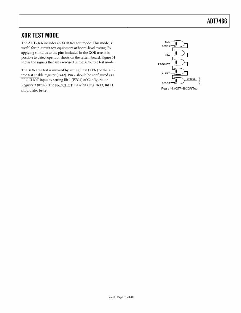
ADT7466
Rev. 0 | Page 31 of 48
XOR TEST MODE The ADT7466 includes an XOR tree test mode. This mode is useful for in-circuit test equipment at board-level testing. By applying stimulus to the pins included in the XOR tree, it is possible to detect opens or shorts on the system board. Figure 44 shows the signals that are exercised in the XOR tree test mode.
The XOR tree test is invoked by setting Bit 0 (XEN) of the XOR tree test enable register (0x42). Pin 7 should be configured as a PROCHOT input by setting Bit 1 (P7C1) of Configuration Register 3 (0x02). The PROCHOT mask bit (Reg. 0x13, Bit 1) should also be set.
SCLTACH1
SDA
PROCHOT
ALERT
0471
1-04
3
TACH2DRIVE1
Figure 44. ADT7466 XOR Tree
ADT7466
Rev. 0 | Page 32 of 48
APPLICATION CIRCUIT
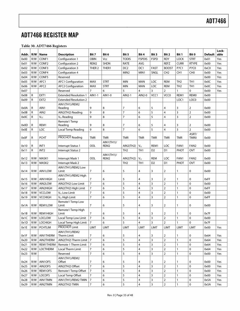
ADT7466
Rev. 0 | Page 33 of 48
ADT7466 REGISTER MAP Table 30. ADT7466 Registers
Addr. R/W Name Description Bit 7 Bit 6 Bit 5 Bit 4 Bit 3 Bit 2 Bit 1 Bit 0 DefaultLock-able
0x00 R/W CONF1 Configuration 1 OBIN Vcc TODIS FSPDIS FSPD RDY LOCK STRT 0x01 Yes
0x01 R/W CONF2 Configuration 2 REM2 SHDN RATE AVG REFZ CURR RTYPE 0x00 Yes
0x02 R/W CONF3 Configuration 3 THER 2 THER1 DC2 DC1 FAST BOOST P7C1 P7C0 0xC0 Yes
0x03 R/W CONF4 Configuration 4 MIN2 MIN1 SNGL CH2 CH1 CH0 0x00 Yes
0x04 R/W CONF5 Reserved 0x00 Yes
0x05 R/W AFC1 AFC1 Configuration MAX STRT MIN MAN LOC REM TH2 TH1 0x0C Yes
0x06 R/W AFC2 AFC2 Configuration MAX STRT MIN MAN LOC REM TH2 TH1 0x0C Yes
0x07 Reserved 7 6 5 4 3 2 1 0 0x00 Yes
0x08 R EXT1 Extended Resolution 1 AIN1-1 AIN1-0 AIN2-1 AIN2-0 VCC1 VCC0 REM1 REM0 0x00
0x09 R EXT2 Extended Resolution 2 LOC1 LOC0 0x00
0x0A R AIN1 AIN1(TH1)/REM2 Reading 9 8 7 6 5 4 3 2 0x00
0x0B R AIN2 AIN2(TH2) Reading 9 8 7 6 5 4 3 2 0x00
0x0C R VCC Vcc Reading 9 8 7 6 5 4 3 2 0x00
0x0D R REM1 Remote1 Temp Reading 9 8 7 6 5 4 3 2 0x00
0x0E R LOC Local Temp Reading 9 8 7 6 5 4 3 2 0x00
0x0F R PCHT PROCHOT Reading TMR TMR TMR TMR TMR TMR TMR ASRT/ TMR0 0x00
0x10 R INT1 Interrupt Status 1 OOL AIN1(TH1)/ REM2 AIN2(TH2) Vcc REM1 LOC FAN1 FAN2 0x00
0x11 R INT2 Interrupt Status 2 TH2 TH1 D2 D1 PHOT OVT 0x00
0x12 R/W MASK1 Interrupt Mask 1 OOL AIN1(TH1)/ REM2 AIN2(TH2) Vcc REM LOC FAN1 FAN2 0x00
0x13 R/W MASK2 Interrupt Mask 2 TH2 TH1 D2 D1 PHOT OVT 0x00
0x14 R/W AIN1LOW AIN1(TH1)/REM2 Low Limit 7 6 5 4 3 2 1 0 0x00
0x15 R/W AIN1HIGH AIN1(TH1)/REM2 High Limit 7 6 5 4 3 2 1 0 0xFF
0x16 R/W AIN2LOW AIN2(TH2) Low Limit 7 6 5 4 3 2 1 0 0x00
0x17 R/W AIN2HIGH AIN2(TH2) High Limit 7 6 5 4 3 2 1 0 0xFF
0x18 R/W VCCLOW Vcc Low Limit 7 6 5 4 3 2 1 0 0x00
0x19 R/W VCCHIGH Vcc High Limit 7 6 5 4 3 2 1 0 0xFF
0x1A R/W REM1LOW Remote1 Temp Low Limit 7 6 5 4 3 2 1 0 0x00
0x1B R/W REM1HIGH Remote1 Temp High Limit 7 6 5 4 3 2 1 0 0x7F
0x1C R/W LOCLOW Local Temp Low Limit 7 6 5 4 3 2 1 0 0x00
0x1D R/W LOCHIGH Local Temp High Limit 7 6 5 4 3 2 1 0 0x7F
0x1E R/W PCHTLIM PROCHOT Limit LIMT LIMT LIMT LIMT LIMT LIMT LIMT LIMT 0x00 Yes
0x1F R/W AIN1THERM AIN1(TH1)/REM2 Therm Limit 7 6 5 4 3 2 1 0 0x64 Yes
0x20 R/W AIN2THERM AIN2(TH2) Therm Limit 7 6 5 4 3 2 1 0 0x64 Yes
0x21 R/W REM1THERM Remote 1 Therm Limit 7 6 5 4 3 2 1 0 0x64 Yes
0x22 R/W LOCTHERM Local Therm Limit 7 6 5 4 3 2 1 0 0x64 Yes
0x23 R/W Reserved 7 6 5 4 3 2 1 0 0x00 Yes
0x24 R/W AIN1OFS AIN1(TH1)/REM2 Offset 7 6 5 4 3 2 1 0 0x00 Yes
0x25 R/W AIN2OFS AIN2(TH2) Offset 7 6 5 4 3 2 1 0 0x00 Yes
0x26 R/W REM1OFS Remote1 Temp Offset 7 6 5 4 3 2 1 0 0x00 Yes
0x27 R/W LOCOFS Local Temp Offset 7 6 5 4 3 2 1 0 0x00 Yes
0x28 R/W AIN1TMIN AIN1(TH1)/REM2 TMIN 7 6 5 4 3 2 1 0 0x5A Yes
0x29 R/W AIN2TMIN AIN2(TH2) TMIN 7 6 5 4 3 2 1 0 0x5A Yes
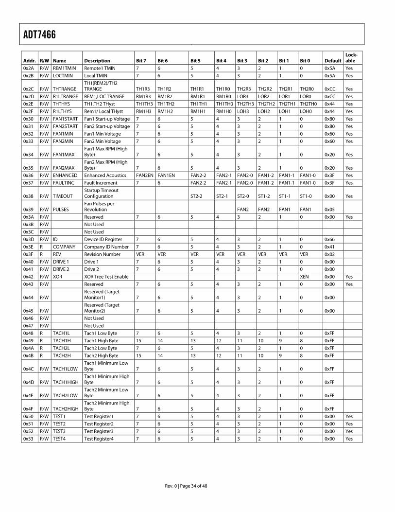
ADT7466
Rev. 0 | Page 34 of 48
Addr. R/W Name Description Bit 7 Bit 6 Bit 5 Bit 4 Bit 3 Bit 2 Bit 1 Bit 0 DefaultLock-able
0x2A R/W REM1TMIN Remote1 TMIN 7 6 5 4 3 2 1 0 0x5A Yes
0x2B R/W LOCTMIN Local TMIN 7 6 5 4 3 2 1 0 0x5A Yes
0x2C R/W THTRANGE TH1(REM2)/TH2 TRANGE TH1R3 TH1R2 TH1R1 TH1R0 TH2R3 TH2R2 TH2R1 TH2R0 0xCC Yes
0x2D R/W R1LTRANGE REM1,LOC TRANGE RM1R3 RM1R2 RM1R1 RM1R0 LOR3 LOR2 LOR1 LOR0 0xCC Yes
0x2E R/W THTHYS TH1,TH2 THyst TH1TH3 TH1TH2 TH1TH1 TH1TH0 TH2TH3 TH2TH2 TH2TH1 TH2TH0 0x44 Yes
0x2F R/W R1LTHYS Rem1/ Local THyst RM1H3 RM1H2 RM1H1 RM1H0 LOH3 LOH2 LOH1 LOH0 0x44 Yes
0x30 R/W FAN1START Fan1 Start-up Voltage 7 6 5 4 3 2 1 0 0x80 Yes
0x31 R/W FAN2START Fan2 Start-up Voltage 7 6 5 4 3 2 1 0 0x80 Yes
0x32 R/W FAN1MIN Fan1 Min Voltage 7 6 5 4 3 2 1 0 0x60 Yes
0x33 R/W FAN2MIN Fan2 Min Voltage 7 6 5 4 3 2 1 0 0x60 Yes
0x34 R/W FAN1MAX Fan1 Max RPM (High Byte) 7 6 5 4 3 2 1 0 0x20 Yes
0x35 R/W FAN2MAX Fan2 Max RPM (High Byte) 7 6 5 4 3 2 1 0 0x20 Yes
0x36 R/W ENHANCED Enhanced Acoustics FAN2EN FAN1EN FAN2-2 FAN2-1 FAN2-0 FAN1-2 FAN1-1 FAN1-0 0x3F Yes
0x37 R/W FAULTINC Fault Increment 7 6 FAN2-2 FAN2-1 FAN2-0 FAN1-2 FAN1-1 FAN1-0 0x3F Yes
0x38 R/W TIMEOUT Startup Timeout Configuration ST2-2 ST2-1 ST2-0 ST1-2 ST1-1 ST1-0 0x00 Yes
0x39 R/W PULSES Fan Pulses per Revolution FAN2 FAN2 FAN1 FAN1 0x05
0x3A R/W Reserved 7 6 5 4 3 2 1 0 0x00 Yes
0x3B R/W Not Used
0x3C R/W Not Used
0x3D R/W ID Device ID Register 7 6 5 4 3 2 1 0 0x66
0x3E R COMPANY Company ID Number 7 6 5 4 3 2 1 0 0x41
0x3F R REV Revision Number VER VER VER VER VER VER VER VER 0x02
0x40 R/W DRIVE 1 Drive 1 7 6 5 4 3 2 1 0 0x00
0x41 R/W DRIVE 2 Drive 2 7 6 5 4 3 2 1 0 0x00
0x42 R/W XOR XOR Tree Test Enable XEN 0x00 Yes
0x43 R/W Reserved 7 6 5 4 3 2 1 0 0x00 Yes
0x44 R/W Reserved (Target Monitor1) 7 6 5 4 3 2 1 0 0x00
0x45 R/W Reserved (Target Monitor2) 7 6 5 4 3 2 1 0 0x00
0x46 R/W Not Used
0x47 R/W Not Used
0x48 R TACH1L Tach1 Low Byte 7 6 5 4 3 2 1 0 0xFF
0x49 R TACH1H Tach1 High Byte 15 14 13 12 11 10 9 8 0xFF
0x4A R TACH2L Tach2 Low Byte 7 6 5 4 3 2 1 0 0xFF
0x4B R TACH2H Tach2 High Byte 15 14 13 12 11 10 9 8 0xFF
0x4C R/W TACH1LOW Tach1 Minimum Low Byte 7 6 5 4 3 2 1 0 0xFF
0x4D R/W TACH1HIGH Tach1 Minimum High Byte 7 6 5 4 3 2 1 0 0xFF
0x4E R/W TACH2LOW Tach2 Minimum Low Byte 7 6 5 4 3 2 1 0 0xFF
0x4F R/W TACH2HIGH Tach2 Minimum High Byte 7 6 5 4 3 2 1 0 0xFF
0x50 R/W TEST1 Test Register1 7 6 5 4 3 2 1 0 0x00 Yes
0x51 R/W TEST2 Test Register2 7 6 5 4 3 2 1 0 0x00 Yes
0x52 R/W TEST3 Test Register3 7 6 5 4 3 2 1 0 0x00 Yes
0x53 R/W TEST4 Test Register4 7 6 5 4 3 2 1 0 0x00 Yes
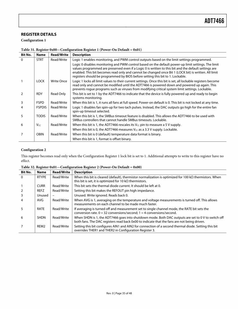
ADT7466
Rev. 0 | Page 35 of 48
REGISTER DETAILS Configuration 1 Table 31. Register 0x00—Configuration Register 1 (Power-On Default = 0x01) Bit No. Name Read/Write Description 0 STRT Read/Write Logic 1 enables monitoring, and PWM control outputs based on the limit settings programmed.
Logic 0 disables monitoring and PWM control based on the default power-up limit settings. The limit values programmed are preserved even if a Logic 0 is written to this bit and the default settings are enabled. This bit becomes read only and cannot be changed once Bit 1 (LOCK bit) is written. All limit registers should be programmed by BIOS before setting this bit to 1. Lockable.
1 LOCK Write Once Logic 1 locks all limit values to their current settings. Once this bit is set, all lockable registers become read only and cannot be modified until the ADT7466 is powered down and powered up again. This prevents rogue programs such as viruses from modifying critical system limit settings. Lockable.
2 RDY Read Only This bit is set to 1 by the ADT7466 to indicate that the device is fully powered up and ready to begin systems monitoring.
3 FSPD Read/Write When this bit is 1, it runs all fans at full speed. Power-on default is 0. This bit is not locked at any time. 4 FSPDIS Read/Write Logic 1 disables fan spin-up for two tach pulses. Instead, the DAC outputs go high for the entire fan
spin-up timeout selected. 5 TODIS Read/Write When this bit is 1, the SMBus timeout feature is disabled. This allows the ADT7466 to be used with
SMBus controllers that cannot handle SMBus timeouts. Lockable. 6 VCC Read/Write When this bit is 1, the ADT7466 rescales its VCC pin to measure a 5 V supply.
When this bit is 0, the ADT7466 measures VCC as a 3.3 V supply. Lockable. 7 OBIN Read/Write When this bit is 0 (default) temperature data format is binary.
When this bit is 1, format is offset binary. Configuration 2
This register becomes read only when the Configuration Register 1 lock bit is set to 1. Additional attempts to write to this register have no effect.
Table 32. Register 0x01—Configuration Register 2 (Power-On Default = 0x00) Bit No. Name Read/Write Description 0 RTYPE Read/Write When this bit is cleared (default), thermistor normalization is optimized for 100 kΩ thermistors. When
this bit is set, it is optimized for 10 kΩ thermistors. 1 CURR Read/Write This bit sets the thermal diode current. It should be left at 0. 2 REFZ Read/Write Setting this bit makes the REFOUT pin high impedance. 3 Unused – Unused. Write ignored. Reads back 0. 4 AVG Read/Write When AVG is 1, averaging on the temperature and voltage measurements is turned off. This allows
measurements on each channel to be made much faster. 5 RATE Read/Write If averaging is turned off and measurement set to single channel mode, the RATE bit sets the
conversion rate. 0 = 32 conversions/second; 1 = 4 conversions/second. 6 SHDN Read/Write When SHDN is 1, the ADT7466 goes into shutdown mode. Both DAC outputs are set to 0 V to switch off
both fans. The DAC registers read back 0x00 to indicate that the fans are not being driven. 7 REM2 Read/Write Setting this bit configures AIN1 and AIN2 for connection of a second thermal diode. Setting this bit
overrides THER1 and THER2 in Configuration Register 3.
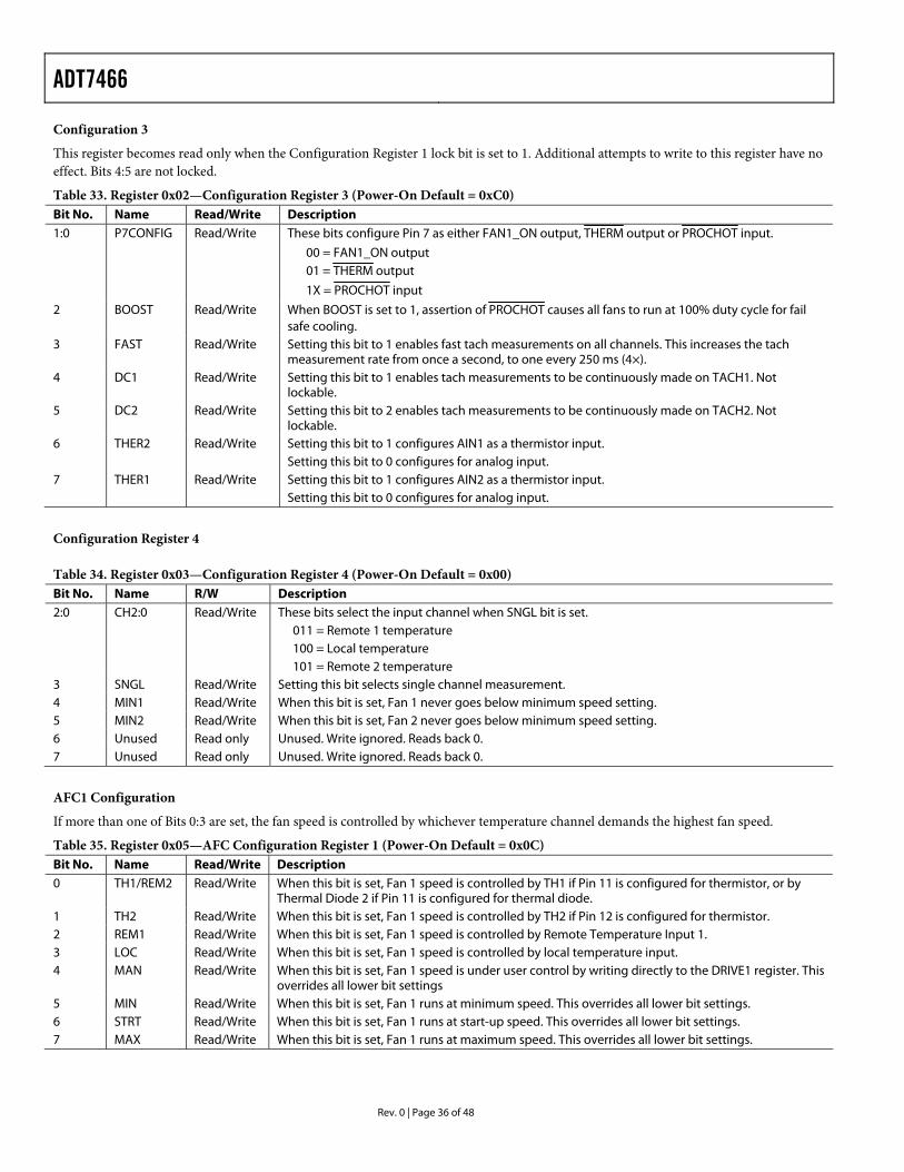
ADT7466
Rev. 0 | Page 36 of 48
Configuration 3
This register becomes read only when the Configuration Register 1 lock bit is set to 1. Additional attempts to write to this register have no effect. Bits 4:5 are not locked.
Table 33. Register 0x02—Configuration Register 3 (Power-On Default = 0xC0) Bit No. Name Read/Write Description 1:0 P7CONFIG Read/Write These bits configure Pin 7 as either FAN1_ON output, THERM output or PROCHOT input.
00 = FAN1_ON output 01 = THERM output
1X = PROCHOT input
2 BOOST Read/Write When BOOST is set to 1, assertion of PROCHOT causes all fans to run at 100% duty cycle for fail safe cooling.
3 FAST Read/Write Setting this bit to 1 enables fast tach measurements on all channels. This increases the tach measurement rate from once a second, to one every 250 ms (4×).
4 DC1 Read/Write Setting this bit to 1 enables tach measurements to be continuously made on TACH1. Not lockable.
5 DC2 Read/Write Setting this bit to 2 enables tach measurements to be continuously made on TACH2. Not lockable.
6 THER2 Read/Write Setting this bit to 1 configures AIN1 as a thermistor input. Setting this bit to 0 configures for analog input.
7 THER1 Read/Write Setting this bit to 1 configures AIN2 as a thermistor input. Setting this bit to 0 configures for analog input.
Configuration Register 4 Table 34. Register 0x03—Configuration Register 4 (Power-On Default = 0x00) Bit No. Name R/W Description 2:0 CH2:0 Read/Write These bits select the input channel when SNGL bit is set.
011 = Remote 1 temperature 100 = Local temperature 101 = Remote 2 temperature
3 SNGL Read/Write Setting this bit selects single channel measurement. 4 MIN1 Read/Write When this bit is set, Fan 1 never goes below minimum speed setting. 5 MIN2 Read/Write When this bit is set, Fan 2 never goes below minimum speed setting. 6 Unused Read only Unused. Write ignored. Reads back 0. 7 Unused Read only Unused. Write ignored. Reads back 0.
AFC1 Configuration
If more than one of Bits 0:3 are set, the fan speed is controlled by whichever temperature channel demands the highest fan speed.
Table 35. Register 0x05—AFC Configuration Register 1 (Power-On Default = 0x0C) Bit No. Name Read/Write Description 0 TH1/REM2 Read/Write When this bit is set, Fan 1 speed is controlled by TH1 if Pin 11 is configured for thermistor, or by
Thermal Diode 2 if Pin 11 is configured for thermal diode. 1 TH2 Read/Write When this bit is set, Fan 1 speed is controlled by TH2 if Pin 12 is configured for thermistor. 2 REM1 Read/Write When this bit is set, Fan 1 speed is controlled by Remote Temperature Input 1. 3 LOC Read/Write When this bit is set, Fan 1 speed is controlled by local temperature input. 4 MAN Read/Write When this bit is set, Fan 1 speed is under user control by writing directly to the DRIVE1 register. This
overrides all lower bit settings 5 MIN Read/Write When this bit is set, Fan 1 runs at minimum speed. This overrides all lower bit settings. 6 STRT Read/Write When this bit is set, Fan 1 runs at start-up speed. This overrides all lower bit settings. 7 MAX Read/Write When this bit is set, Fan 1 runs at maximum speed. This overrides all lower bit settings.
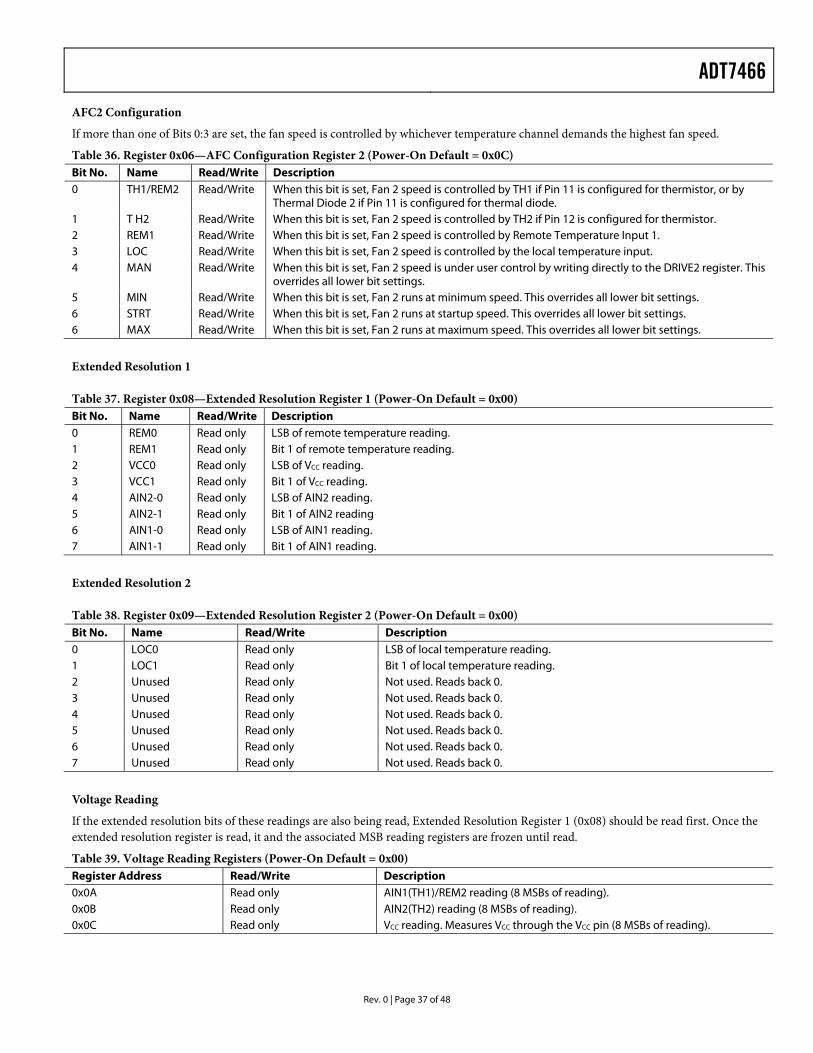
ADT7466
Rev. 0 | Page 37 of 48
AFC2 Configuration
If more than one of Bits 0:3 are set, the fan speed is controlled by whichever temperature channel demands the highest fan speed.
Table 36. Register 0x06—AFC Configuration Register 2 (Power-On Default = 0x0C) Bit No. Name Read/Write Description 0 TH1/REM2 Read/Write When this bit is set, Fan 2 speed is controlled by TH1 if Pin 11 is configured for thermistor, or by
Thermal Diode 2 if Pin 11 is configured for thermal diode. 1 T H2 Read/Write When this bit is set, Fan 2 speed is controlled by TH2 if Pin 12 is configured for thermistor. 2 REM1 Read/Write When this bit is set, Fan 2 speed is controlled by Remote Temperature Input 1. 3 LOC Read/Write When this bit is set, Fan 2 speed is controlled by the local temperature input. 4 MAN Read/Write When this bit is set, Fan 2 speed is under user control by writing directly to the DRIVE2 register. This
overrides all lower bit settings. 5 MIN Read/Write When this bit is set, Fan 2 runs at minimum speed. This overrides all lower bit settings. 6 STRT Read/Write When this bit is set, Fan 2 runs at startup speed. This overrides all lower bit settings. 6 MAX Read/Write When this bit is set, Fan 2 runs at maximum speed. This overrides all lower bit settings. Extended Resolution 1 Table 37. Register 0x08—Extended Resolution Register 1 (Power-On Default = 0x00) Bit No. Name Read/Write Description 0 REM0 Read only LSB of remote temperature reading. 1 REM1 Read only Bit 1 of remote temperature reading. 2 VCC0 Read only LSB of VCC reading. 3 VCC1 Read only Bit 1 of VCC reading. 4 AIN2-0 Read only LSB of AIN2 reading. 5 AIN2-1 Read only Bit 1 of AIN2 reading 6 AIN1-0 Read only LSB of AIN1 reading. 7 AIN1-1 Read only Bit 1 of AIN1 reading. Extended Resolution 2 Table 38. Register 0x09—Extended Resolution Register 2 (Power-On Default = 0x00) Bit No. Name Read/Write Description 0 LOC0 Read only LSB of local temperature reading. 1 LOC1 Read only Bit 1 of local temperature reading. 2 Unused Read only Not used. Reads back 0. 3 Unused Read only Not used. Reads back 0. 4 Unused Read only Not used. Reads back 0. 5 Unused Read only Not used. Reads back 0. 6 Unused Read only Not used. Reads back 0. 7 Unused Read only Not used. Reads back 0. Voltage Reading
If the extended resolution bits of these readings are also being read, Extended Resolution Register 1 (0x08) should be read first. Once the extended resolution register is read, it and the associated MSB reading registers are frozen until read.
Table 39. Voltage Reading Registers (Power-On Default = 0x00) Register Address Read/Write Description 0x0A Read only AIN1(TH1)/REM2 reading (8 MSBs of reading). 0x0B Read only AIN2(TH2) reading (8 MSBs of reading). 0x0C Read only VCC reading. Measures VCC through the VCC pin (8 MSBs of reading).
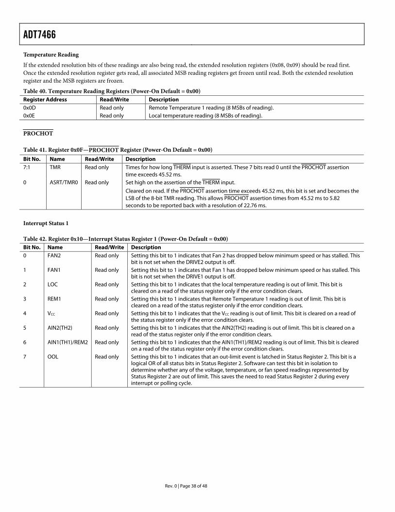
ADT7466
Rev. 0 | Page 38 of 48
Temperature Reading
If the extended resolution bits of these readings are also being read, the extended resolution registers (0x08, 0x09) should be read first. Once the extended resolution register gets read, all associated MSB reading registers get frozen until read. Both the extended resolution register and the MSB registers are frozen.
Table 40. Temperature Reading Registers (Power-On Default = 0x00) Register Address Read/Write Description 0x0D Read only Remote Temperature 1 reading (8 MSBs of reading). 0x0E Read only Local temperature reading (8 MSBs of reading).
PROCHOT Table 41. Register 0x0F—PROCHOT Register (Power-On Default = 0x00) Bit No. Name Read/Write Description 7:1 TMR Read only Times for how long THERM input is asserted. These 7 bits read 0 until the PROCHOT assertion
time exceeds 45.52 ms. 0 ASRT/TMR0 Read only Set high on the assertion of the THERM input.
Cleared on read. If the PROCHOT assertion time exceeds 45.52 ms, this bit is set and becomes the LSB of the 8-bit TMR reading. This allows PROCHOT assertion times from 45.52 ms to 5.82 seconds to be reported back with a resolution of 22.76 ms.
Interrupt Status 1 Table 42. Register 0x10—Interrupt Status Register 1 (Power-On Default = 0x00) Bit No. Name Read/Write Description 0 FAN2 Read only Setting this bit to 1 indicates that Fan 2 has dropped below minimum speed or has stalled. This
bit is not set when the DRIVE2 output is off. 1 FAN1 Read only Setting this bit to 1 indicates that Fan 1 has dropped below minimum speed or has stalled. This
bit is not set when the DRIVE1 output is off. 2 LOC Read only Setting this bit to 1 indicates that the local temperature reading is out of limit. This bit is
cleared on a read of the status register only if the error condition clears. 3 REM1 Read only Setting this bit to 1 indicates that Remote Temperature 1 reading is out of limit. This bit is
cleared on a read of the status register only if the error condition clears. 4 VCC Read only Setting this bit to 1 indicates that the VCC reading is out of limit. This bit is cleared on a read of
the status register only if the error condition clears. 5 AIN2(TH2) Read only Setting this bit to 1 indicates that the AIN2(TH2) reading is out of limit. This bit is cleared on a
read of the status register only if the error condition clears. 6 AIN1(TH1)/REM2 Read only Setting this bit to 1 indicates that the AIN1(TH1)/REM2 reading is out of limit. This bit is cleared
on a read of the status register only if the error condition clears. 7 OOL Read only Setting this bit to 1 indicates that an out-limit event is latched in Status Register 2. This bit is a
logical OR of all status bits in Status Register 2. Software can test this bit in isolation to determine whether any of the voltage, temperature, or fan speed readings represented by Status Register 2 are out of limit. This saves the need to read Status Register 2 during every interrupt or polling cycle.
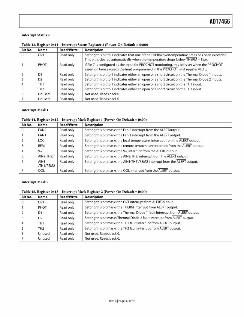
ADT7466
Rev. 0 | Page 39 of 48
Interrupt Status 2 Table 43. Register 0x11—Interrupt Status Register 2 (Power-On Default = 0x00) Bit No. Name Read/Write Description 0 OVT Read only Setting this bit to 1 indicates that one of the THERM overtemperature limits has been exceeded.
This bit is cleared automatically when the temperature drops below THERM − THYST.
1 PHOT Read only If Pin 7 is configured as the input for PROCHOT monitoring, this bit is set when the PROCHOT assertion time exceeds the limit programmed in the PROCHOT limit register (0x1E).
2 D1 Read only Setting this bit to 1 indicates either an open or a short circuit on the Thermal Diode 1 inputs. 3 D2 Read only Setting this bit to 1 indicates either an open or a short circuit on the Thermal Diode 2 inputs. 4 TH1 Read only Setting this bit to 1 indicates either an open or a short circuit on the TH1 input. 5 TH2 Read only Setting this bit to 1 indicates either an open or a short circuit on the TH2 input. 6 Unused Read only Not used. Reads back 0. 7 Unused Read only Not used. Reads back 0. Interrupt Mask 1 Table 44. Register 0x12—Interrupt Mask Register 1 (Power-On Default = 0x00) Bit No. Name Read/Write Description 0 FAN2 Read only Setting this bit masks the Fan 2 interrupt from the ALERToutput.
1 FAN1 Read only Setting this bit masks the Fan 1 interrupt from the ALERT output.
2 LOC Read only Setting this bit masks the local temperature. interrupt from the ALERT output.
3 REM Read only Setting this bit masks the remote temperature interrupt from the ALERT output.
4 VCC Read only Setting this bit masks the VCC interrupt from the ALERT output.
5 AIN2(TH2) Read only Setting this bit masks the AIN2(TH2) interrupt from the ALERT output.
6 AIN1 /TH1/REM2
Read only Setting this bit masks the AIN1(TH1)/REM2 interrupt from the ALERT output.
7 OOL Read only Setting this bit masks the OOL interrupt from the ALERT output.
Interrupt Mask 2 Table 45. Register 0x13—Interrupt Mask Register 2 (Power-On Default = 0x00) Bit No. Name Read/Write Description
0 OVT Read only Setting this bit masks the OVT interrupt from ALERT output.
1 PHOT Read only Setting this bit masks the THERM interrupt from ALERT output.
2 D1 Read only Setting this bit masks the Thermal Diode 1 fault interrupt from ALERT output.
3 D2 Read only Setting this bit masks Thermal Diode 2 fault interrupt from ALERT output.
4 TH1 Read only Setting this bit masks the TH1 fault interrupt from ALERT output.
5 TH2 Read only Setting this bit masks the TH2 fault interrupt from ALERT output.
6 Unused Read only Not used. Reads back 0. 7 Unused Read only Not used. Reads back 0.
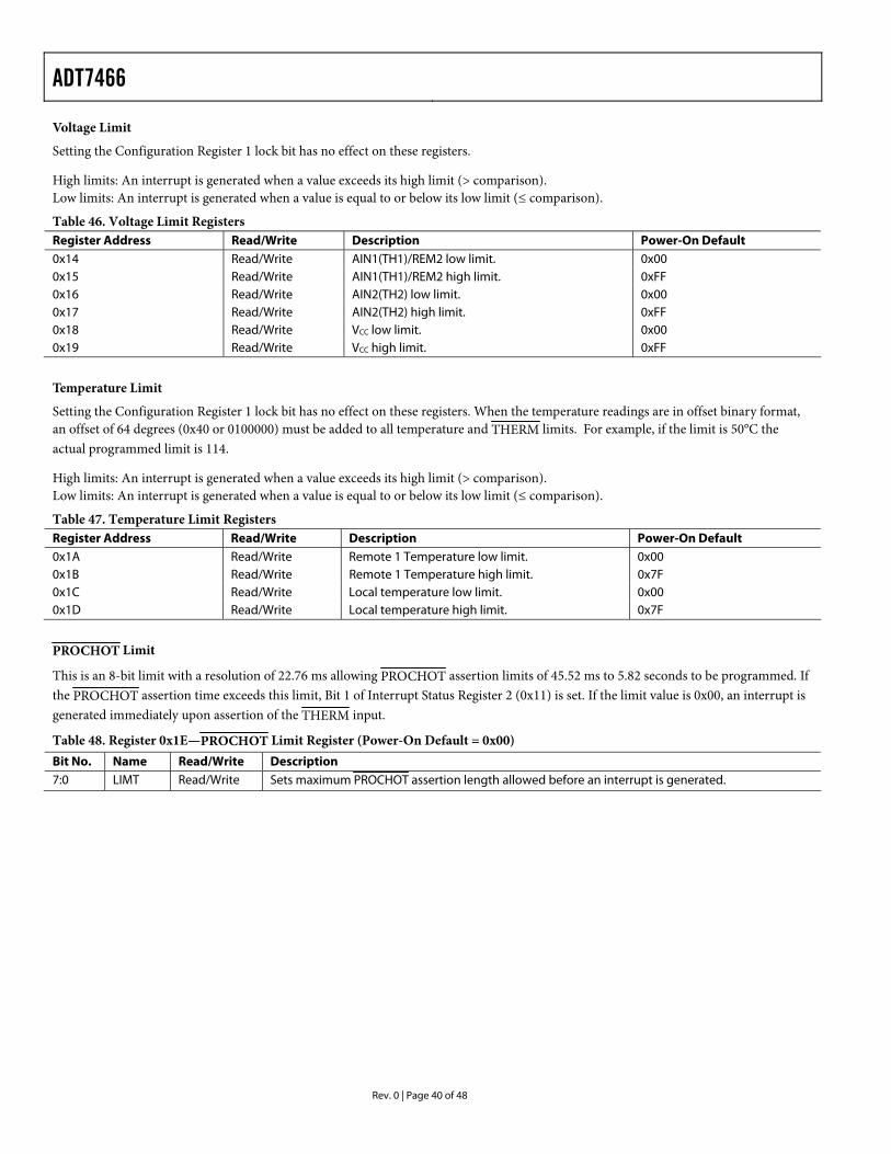
ADT7466
Rev. 0 | Page 40 of 48
Voltage Limit
Setting the Configuration Register 1 lock bit has no effect on these registers.
High limits: An interrupt is generated when a value exceeds its high limit (> comparison). Low limits: An interrupt is generated when a value is equal to or below its low limit (≤ comparison).
Table 46. Voltage Limit Registers Register Address Read/Write Description Power-On Default 0x14 Read/Write AIN1(TH1)/REM2 low limit. 0x00 0x15 Read/Write AIN1(TH1)/REM2 high limit. 0xFF 0x16 Read/Write AIN2(TH2) low limit. 0x00 0x17 Read/Write AIN2(TH2) high limit. 0xFF 0x18 Read/Write VCC low limit. 0x00 0x19 Read/Write VCC high limit. 0xFF Temperature Limit
Setting the Configuration Register 1 lock bit has no effect on these registers. When the temperature readings are in offset binary format, an offset of 64 degrees (0x40 or 0100000) must be added to all temperature and THERM limits. For example, if the limit is 50°C the actual programmed limit is 114.
High limits: An interrupt is generated when a value exceeds its high limit (> comparison). Low limits: An interrupt is generated when a value is equal to or below its low limit (≤ comparison).
Table 47. Temperature Limit Registers Register Address Read/Write Description Power-On Default 0x1A Read/Write Remote 1 Temperature low limit. 0x00 0x1B Read/Write Remote 1 Temperature high limit. 0x7F 0x1C Read/Write Local temperature low limit. 0x00 0x1D Read/Write Local temperature high limit. 0x7F
PROCHOT Limit
This is an 8-bit limit with a resolution of 22.76 ms allowing PROCHOT assertion limits of 45.52 ms to 5.82 seconds to be programmed. If the PROCHOT assertion time exceeds this limit, Bit 1 of Interrupt Status Register 2 (0x11) is set. If the limit value is 0x00, an interrupt is generated immediately upon assertion of the THERM input.
Table 48. Register 0x1E—PROCHOT Limit Register (Power-On Default = 0x00) Bit No. Name Read/Write Description 7:0 LIMT Read/Write Sets maximum PROCHOT assertion length allowed before an interrupt is generated.
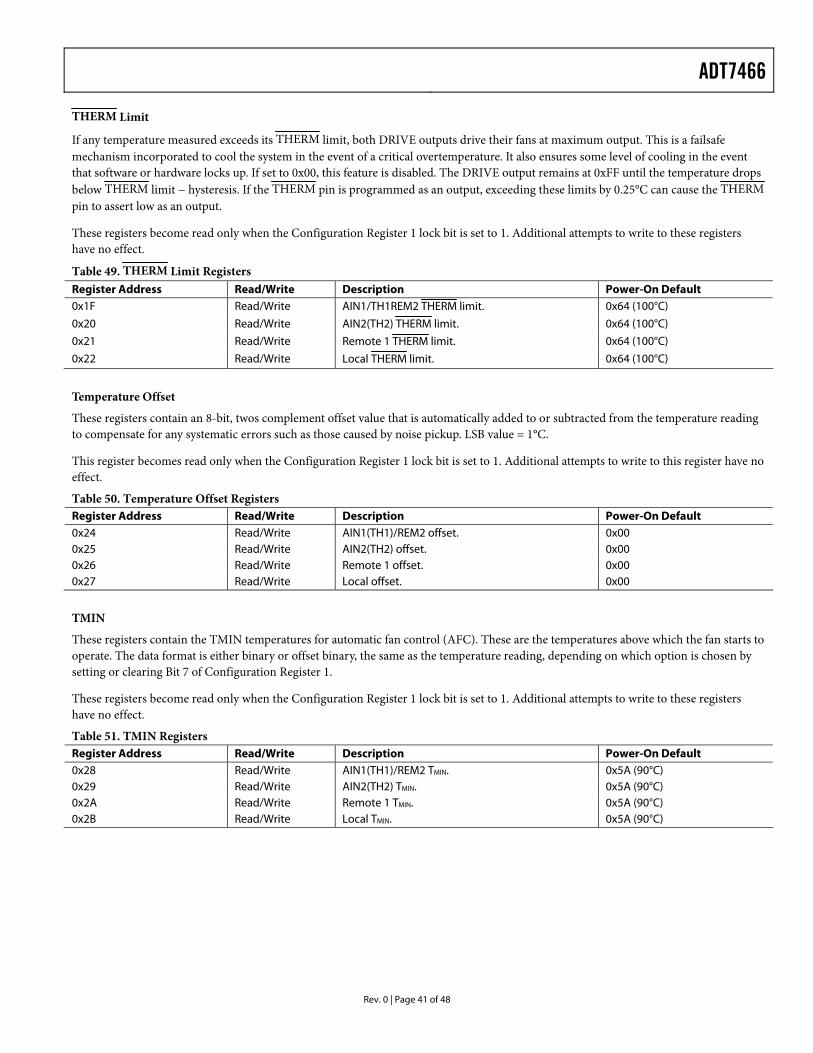
ADT7466
Rev. 0 | Page 41 of 48
THERM Limit
If any temperature measured exceeds its THERM limit, both DRIVE outputs drive their fans at maximum output. This is a failsafe mechanism incorporated to cool the system in the event of a critical overtemperature. It also ensures some level of cooling in the event that software or hardware locks up. If set to 0x00, this feature is disabled. The DRIVE output remains at 0xFF until the temperature drops below THERM limit − hysteresis. If the THERM pin is programmed as an output, exceeding these limits by 0.25°C can cause the THERM pin to assert low as an output.
These registers become read only when the Configuration Register 1 lock bit is set to 1. Additional attempts to write to these registers have no effect.
Table 49. THERM Limit Registers Register Address Read/Write Description Power-On Default 0x1F Read/Write AIN1/TH1REM2 THERM limit. 0x64 (100°C)
0x20 Read/Write AIN2(TH2) THERM limit. 0x64 (100°C)
0x21 Read/Write Remote 1 THERM limit. 0x64 (100°C)
0x22 Read/Write Local THERM limit. 0x64 (100°C)
Temperature Offset
These registers contain an 8-bit, twos complement offset value that is automatically added to or subtracted from the temperature reading to compensate for any systematic errors such as those caused by noise pickup. LSB value = 1°C.
This register becomes read only when the Configuration Register 1 lock bit is set to 1. Additional attempts to write to this register have no effect.
Table 50. Temperature Offset Registers Register Address Read/Write Description Power-On Default 0x24 Read/Write AIN1(TH1)/REM2 offset. 0x00 0x25 Read/Write AIN2(TH2) offset. 0x00 0x26 Read/Write Remote 1 offset. 0x00 0x27 Read/Write Local offset. 0x00 TMIN
These registers contain the TMIN temperatures for automatic fan control (AFC). These are the temperatures above which the fan starts to operate. The data format is either binary or offset binary, the same as the temperature reading, depending on which option is chosen by setting or clearing Bit 7 of Configuration Register 1.
These registers become read only when the Configuration Register 1 lock bit is set to 1. Additional attempts to write to these registers have no effect.
Table 51. TMIN Registers Register Address Read/Write Description Power-On Default 0x28 Read/Write AIN1(TH1)/REM2 TMIN. 0x5A (90°C) 0x29 Read/Write AIN2(TH2) TMIN. 0x5A (90°C) 0x2A Read/Write Remote 1 TMIN. 0x5A (90°C) 0x2B Read/Write Local TMIN. 0x5A (90°C)
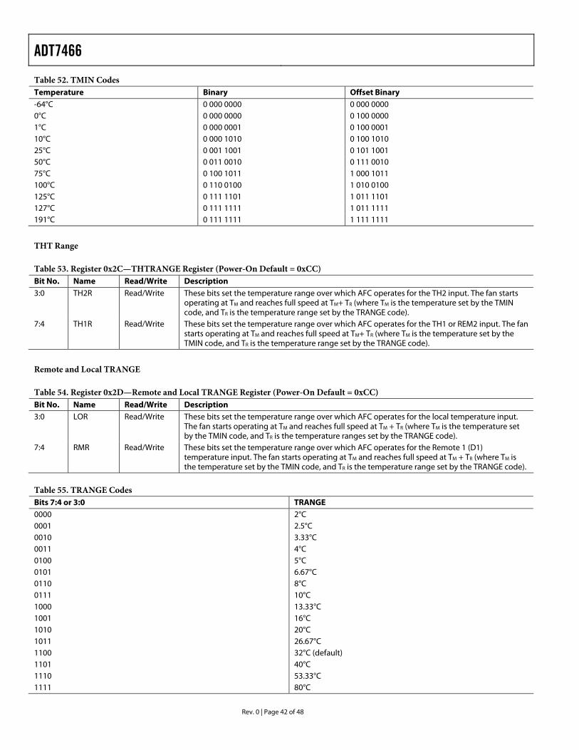
ADT7466
Rev. 0 | Page 42 of 48
Table 52. TMIN Codes Temperature Binary Offset Binary -64°C 0 000 0000 0 000 0000 0°C 0 000 0000 0 100 0000 1°C 0 000 0001 0 100 0001 10°C 0 000 1010 0 100 1010 25°C 0 001 1001 0 101 1001 50°C 0 011 0010 0 111 0010 75°C 0 100 1011 1 000 1011 100°C 0 110 0100 1 010 0100 125°C 0 111 1101 1 011 1101 127°C 0 111 1111 1 011 1111 191°C 0 111 1111 1 111 1111 THT Range Table 53. Register 0x2C—THTRANGE Register (Power-On Default = 0xCC) Bit No. Name Read/Write Description 3:0 TH2R Read/Write These bits set the temperature range over which AFC operates for the TH2 input. The fan starts
operating at TM and reaches full speed at TM+ TR (where TM is the temperature set by the TMIN code, and TR is the temperature range set by the TRANGE code).
7:4 TH1R Read/Write These bits set the temperature range over which AFC operates for the TH1 or REM2 input. The fan starts operating at TM and reaches full speed at TM+ TR (where TM is the temperature set by the TMIN code, and TR is the temperature range set by the TRANGE code).
Remote and Local TRANGE Table 54. Register 0x2D—Remote and Local TRANGE Register (Power-On Default = 0xCC) Bit No. Name Read/Write Description 3:0 LOR Read/Write These bits set the temperature range over which AFC operates for the local temperature input.
The fan starts operating at TM and reaches full speed at TM + TR (where TM is the temperature set by the TMIN code, and TR is the temperature ranges set by the TRANGE code).
7:4 RMR Read/Write These bits set the temperature range over which AFC operates for the Remote 1 (D1) temperature input. The fan starts operating at TM and reaches full speed at TM + TR (where TM is the temperature set by the TMIN code, and TR is the temperature range set by the TRANGE code).
Table 55. TRANGE Codes Bits 7:4 or 3:0 TRANGE 0000 2°C 0001 2.5°C 0010 3.33°C 0011 4°C 0100 5°C 0101 6.67°C 0110 8°C 0111 10°C 1000 13.33°C 1001 16°C 1010 20°C 1011 26.67°C 1100 32°C (default) 1101 40°C 1110 53.33°C 1111 80°C
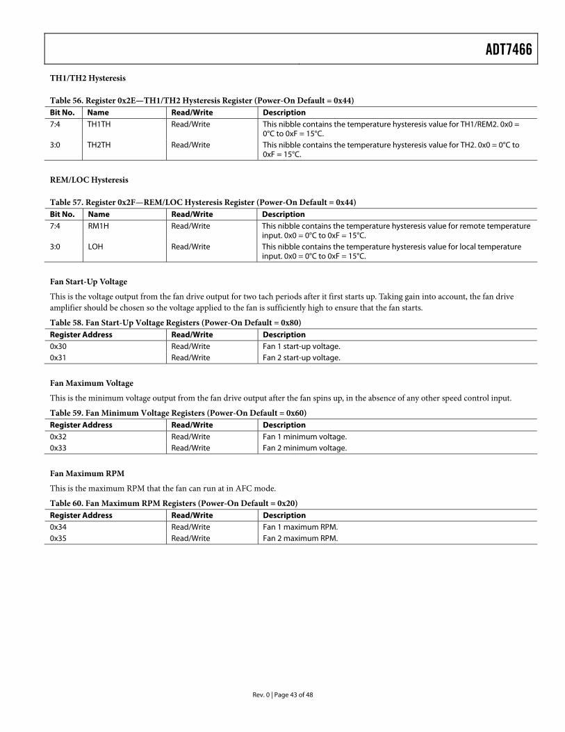
ADT7466
Rev. 0 | Page 43 of 48
TH1/TH2 Hysteresis Table 56. Register 0x2E—TH1/TH2 Hysteresis Register (Power-On Default = 0x44) Bit No. Name Read/Write Description 7:4 TH1TH Read/Write This nibble contains the temperature hysteresis value for TH1/REM2. 0x0 =
0°C to 0xF = 15°C. 3:0 TH2TH Read/Write This nibble contains the temperature hysteresis value for TH2. 0x0 = 0°C to
0xF = 15°C. REM/LOC Hysteresis Table 57. Register 0x2F—REM/LOC Hysteresis Register (Power-On Default = 0x44) Bit No. Name Read/Write Description 7:4 RM1H Read/Write This nibble contains the temperature hysteresis value for remote temperature
input. 0x0 = 0°C to 0xF = 15°C. 3:0 LOH Read/Write This nibble contains the temperature hysteresis value for local temperature
input. 0x0 = 0°C to 0xF = 15°C.
Fan Start-Up Voltage
This is the voltage output from the fan drive output for two tach periods after it first starts up. Taking gain into account, the fan drive amplifier should be chosen so the voltage applied to the fan is sufficiently high to ensure that the fan starts.
Table 58. Fan Start-Up Voltage Registers (Power-On Default = 0x80) Register Address Read/Write Description 0x30 Read/Write Fan 1 start-up voltage. 0x31 Read/Write Fan 2 start-up voltage. Fan Maximum Voltage
This is the minimum voltage output from the fan drive output after the fan spins up, in the absence of any other speed control input.
Table 59. Fan Minimum Voltage Registers (Power-On Default = 0x60) Register Address Read/Write Description 0x32 Read/Write Fan 1 minimum voltage. 0x33 Read/Write Fan 2 minimum voltage.
Fan Maximum RPM
This is the maximum RPM that the fan can run at in AFC mode.
Table 60. Fan Maximum RPM Registers (Power-On Default = 0x20) Register Address Read/Write Description 0x34 Read/Write Fan 1 maximum RPM. 0x35 Read/Write Fan 2 maximum RPM.
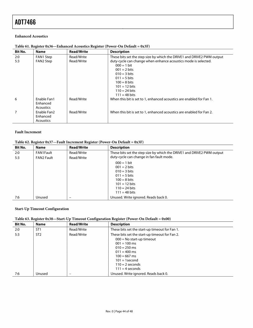
ADT7466
Rev. 0 | Page 44 of 48
Enhanced Acoustics Table 61. Register 0x36—Enhanced Acoustics Register (Power-On Default = 0x3F) Bit No. Name Read/Write Description 2:0 5:3
FAN1 Step FAN2 Step
Read/Write Read/Write
These bits set the step size by which the DRIVE1 and DRIVE2 PWM output duty-cycle can change when enhance acoustics mode is selected.
000 = 1 bit 001 = 2 bits 010 = 3 bits 011 = 5 bits 100 = 8 bits 101 = 12 bits 110 = 24 bits 111 = 48 bits
6 Enable Fan1 Enhanced Acoustics
Read/Write When this bit is set to 1, enhanced acoustics are enabled for Fan 1.
7 Enable Fan2 Enhanced Acoustics
Read/Write When this bit is set to 1, enhanced acoustics are enabled for Fan 2.
Fault Increment Table 62. Register 0x37—Fault Increment Register (Power-On Default = 0x3F) Bit No. Name Read/Write Description 2:0 5:3
FAN1Fault FAN2 Fault
Read/Write Read/Write
These bits set the step size by which the DRIVE1 and DRIVE2 PWM output duty-cycle can change in fan fault mode.
000 = 1 bit 001 = 2 bits 010 = 3 bits 011 = 5 bits 100 = 8 bits 101 = 12 bits 110 = 24 bits 111 = 48 bits
7:6 Unused – Unused. Write ignored. Reads back 0. Start-Up Timeout Configuration Table 63. Register 0x38—Start-Up Timeout Configuration Register (Power-On Default = 0x00) Bit No. Name Read/Write Description 2:0 ST1 Read/Write These bits set the start-up timeout for Fan 1. 5:3 ST2 Read/Write These bits set the start-up timeout for Fan 2.
000 = No start-up timeout 001 = 100 ms 010 = 250 ms 011 = 400 ms 100 = 667 ms 101 = 1second 110 = 2 seconds 111 = 4 seconds 7:6 Unused – Unused. Write ignored. Reads back 0.
ADT7466
Rev. 0 | Page 45 of 48
Fan Pulses Per Revolution Table 64. Register 0x39—Fan Pulses Per Revolution Register (Power-On Default = 0x05) Bit No. Name Read/Write Description 1:0 FAN1 Read/Write Sets number of pulses to be counted when measuring FAN1 speed. Can be
used to determine fan’s pulses per revolution number for unknown fan type. Pulses Counted 00 = 1 01 = 2 (default) 10 = 3 11 = 4 3:2 FAN2 Read/Write Sets number of pulses to be counted when measuring FAN2 speed. Can be
used to determine fan’s pulses per revolution number for unknown fan type. Pulses Counted 00 = 1 01 = 2 (default) 10 = 3 11 = 4 7:4 Unused – Unused. Write ignored. Reads back 0. Information Registers Table 65. Register 0x3D—Device ID Register (Power-On Default = 0x66) Bit No. Name Read/Write Description 7:0 Reserved Read only Contains device ID number. Table 66. Register 0x3E—Company Id Register (Power-On Default = 0x41) Bit No. Name Read/Write Description 7:0 Reserved Read only Contains company ID number. Table 67. Register 0x3F—Revision Number Register (Power-On Default = 0x02) Bit No. Name Read/Write Description 7:0 Reserved Read only Contains device revision level. Fan Drive (DAC)
These registers reflect the drive value of each fan at any given time. When in automatic fan speed control mode, the ADT7466 reports the drive values back through these registers. The fan drive values vary according to temperature in automatic fan speed control mode. During fan startup, these registers report 0x00. In software mode, the fan drive outputs can be set to any value by writing to these registers.
Table 68. Fan Drive (DAC) Registers (Power-On Default = 0x00) Register Address Read/Write Description 0x40 Read/Write DRIVE1, Current Fan 1 drive value. 0x41 Read/Write DRIVE2, Current Fan 2 drive value. XOR Tree Test Enable
This register becomes read only when the Configuration Register 1 lock bit is set to 1. Additional attempts to write to this register have no effect.
Table 69. Register 0x42—XOR Tree Test Enable (Power-On Default = 0x00) Bit No. Name Read/Write Description 7:1 Reserved – Unused. Do not write to these bits. 0 XEN Read/Write If the XEN bit is set to 1, the device enters the XOR tree test mode. Clearing the bit
removes the device from the XOR test mode.
ADT7466
Rev. 0 | Page 46 of 48
Fan Tachometer Reading
These registers count the number of 12.43 µs periods (based on a local 82 kHz clock) that occur between a number of consecutive fan tach pulses (default = 2). The number of tach pulses used to count can be changed by using the fan pulses per revolution register (0x39). This allows the fan speed to be accurately measured. Since a valid fan tachometer reading requires two bytes to be read, the low byte must be read first. Both the low and high bytes are then frozen until read. At power-on, these registers contain 0x0000 until such time as the first valid fan tach measurement is read into these registers. This prevents false interrupts from occurring while the fans are spinning up.
A count of 0xFFFF indicates that a fan is
• Stalled or blocked (object jamming the fan). • Failed (internal circuitry destroyed). • Not populated (the ADT7466 expects to see a fan connected to each tach. If a fan is not connected to that tach, its tach minimum
high and low byte should be set to 0xFFFF). • 2-wire instead of 3-wire.
Table 70. Fan Tachometer Reading Registers (Power-On Default = 0xFF) Register Address Read/Write Description 0x48 Read only TACH1 low byte 0x49 Read only TACH1 high byte 0x4A Read only TACH2 low byte 0x4B Read only TACH2 high byte Fan Tachometer Limit
Exceeding any of the tach limit registers by 1 indicates that the fan is running too slowly or has stalled. The appropriate status bit is set in Interrupt Status Register 1 to indicate the fan failure. Setting the Configuration Register 1 lock bit has no effect on these registers.
Table 71. Fan Tachometer Limit Registers (Power-On Default = 0xFF) Register Address Read/Write Description 0x4C Read/Write TACH 1 minimum low byte 0x4D Read/Write TACH 1 minimum high byte 0x4E Read/Write TACH 2 minimum low byte 0x4F Read/Write TACH 2 minimum high byte
Manufacturer’s Test
These registers are for manufacturer’s use only and should not be read or written to in normal use.
These registers become read only when the Configuration Register 1 lock bit is set to 1. Additional attempts to write to these register have no effect.
Table 72. Register 0x3F—Manufacturers Test Registers (Power-On Default = 0x00) Register Address Read/Write Description 0x50 Read/Write Manufacturer’s Test Register 1 0x51 Read/Write Manufacturer’s Test Register 2 0x52 Read/Write Manufacturer’s Test Register 3 0x53 Read/Write Manufacturer’s Test Register 4
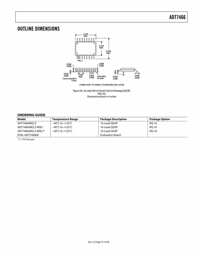
ADT7466
Rev. 0 | Page 47 of 48
OUTLINE DIMENSIONS
16 9
81
PIN 1
SEATINGPLANE
0.0100.004 0.012
0.0080.025BSC 0.010
0.0060.0500.016
8°0°
COPLANARITY0.004
0.0650.049
0.0690.053
0.154BSC
0.236BSC
COMPLIANT TO JEDEC STANDARDS MO-137AB
0.193BSC
Figure 46. 16-Lead Shrink Small Outline Package [QSOP] (RQ-16)
Dimensions shown in inches
ORDERING GUIDE Model Temperature Range Package Description Package Option ADT7466ARQ Z1 −40°C to +125°C 16-Lead QSOP RQ-16 ADT7466ARQ Z-REEL1 −40°C to +125°C 16-Lead QSOP RQ-16 ADT7466ARQ Z-REEL71 −40°C to +125°C 16-Lead QSOP RQ-16 EVAL-ADT7466EB Evaluation Board
1 Z = Pb-free part.

ADT7466
Rev. 0 | Page 48 of 48
NOTES
© 2005 Analog Devices, Inc. All rights reserved. Trademarks and registered trademarks are the property of their respective owners. D04711–0–6/05(0)