WM828CC6 Datasheet
39
WM828CC6 Datasheet Dual-Band (2.4/5 GHz) Wi-Fi IEEE 802.11 ac/a/b/g/n Bluetooth v4.2/BLE (Dual-Mode/Smart-Ready) Revision 1.04 October 26, 2018 Copyright © 2018 Wi2Wi, Inc. 2107 N. 1st Street, Ste. 680, San Jose, CA 95131, United States Email: [email protected] | Phone: 1-408-416-4200 | Fax: 1-608-831-3343
-
Upload
khangminh22 -
Category
Documents
-
view
1 -
download
0
Transcript of WM828CC6 Datasheet
WM828CC6 Datasheet
Dual-Band (2.4/5 GHz) Wi-Fi IEEE 802.11 ac/a/b/g/n Bluetooth v4.2/BLE (Dual-Mode/Smart-Ready)
Revision 1.04
October 26, 2018
Copyright © 2018 Wi2Wi, Inc.
2107 N. 1st Street, Ste. 680, San Jose, CA 95131, United States Email: [email protected] | Phone: 1-408-416-4200 | Fax: 1-608-831-3343

Copyright © 2018 Wi2Wi, Inc.
Send feedback to [email protected] Page 2 of 38
WM828CC6
Disclaimers Wi2Wi, Inc. PRODUCTS ARE NOT AUTHORIZED FOR USE AS CRITICAL COMPONENTS IN LIFE SUPPORT DEVICES OR SYSTEMS WITHOUT THE EXPRESS WRITTEN APPROVAL OF THE MANAGING DIRECTOR OF Wi2Wi, Inc. The definitions used herein are: a) Life support devices or systems are devices which (1) are intended for surgical implant into the body, or (2) support or sustain life and whose failure to perform when properly used in accordance with the instructions for use provided in the labeling can reasonably be expected to result in a significant injury to the user. b) A critical component is any component of a life support device or system whose failure to perform can be reasonably expected to cause the failure of the life support device or system, or to affect its safety or effectiveness. Wi2Wi does not assume responsibility for use of any of the circuitry described, no circuit patent licenses are implied and Wi2Wi reserves the right at any time to change without notice said circuitry and specifications. The content of this document is to be treated as strictly confidential and is not to be disclosed, reproduced or used, except as authorized in writing by Wi2Wi, Inc.
Copyright © 2018 Wi2Wi, Inc.
Send feedback to [email protected] Page 3 of 38
WM828CC6
Table of Contents 1. General Description ............................................................................ 5
1.1 WLAN Client Features .................................................................................................................. 5 1.2 Access Point Features .................................................................................................................. 8 1.3 WiFi Direct / P2P features ........................................................................................................... 11 1.4 Simultaneous AP-STA Operation................................................................................................ 11 1.5 Bluetooth Features ...................................................................................................................... 11 1.6 Applications ................................................................................................................................. 12
2. System Description ........................................................................... 13 2.1 Block Diagram ............................................................................................................................. 13 2.2 Functional Mode Pin Configuration ............................................................................................. 13 2.3 Reset Configuration .................................................................................................................... 13 2.4 Pin Diagram................................................................................................................................. 14 2.5 Pin Description ............................................................................................................................ 15 2.6 Physical Dimensions and Pad Locations .................................................................................... 18
3. Module Characteristics ..................................................................... 19
4. Voltage Domains ............................................................................... 23
5. WLAN External Host Interface .......................................................... 24 5.1 SDIO Full Speed and High Speed Timing Diagrams .................................................................. 24 5.2 SDIO 3.0 SDR12, SDR25, SDR50 Modes (up to 100 MHz) (1.8 V) ........................................... 25 5.3 SDIO 3.0 SDR104 Mode (208 MHz) (1.8 V) ............................................................................... 26 5.4 DDR50 Mode (50 MHz) (1.8 V) ................................................................................................... 27
6. WLAN Power-Save Modes ................................................................ 29 6.1 Full Power-Down Mode ............................................................................................................... 29 6.2 IEEE Power Save ........................................................................................................................ 29 6.3 Deep Sleep.................................................................................................................................. 29
7. Antenna and Clock ............................................................................ 30 7.1 Antenna ....................................................................................................................................... 30 7.2 Clock ........................................................................................................................................... 30
8. Software ...................................................................................... 30
9. Reference Schematics ...................................................................... 31
10. Manufacturing Notes ......................................................................... 33 10.1 Shield Marking............................................................................................................................. 33 10.2 Storage and Baking Instructions ................................................................................................. 33 10.3 Recommended Reflow Profile ..................................................................................................... 33 10.4 Data Sheet Status ....................................................................................................................... 34
11. Ordering Information ........................................................................ 35
12. Data Sheet Status .............................................................................. 35
13. Certifications ..................................................................................... 36
14. References ...................................................................................... 38 14.1 Specifications .............................................................................................................................. 38 14.2 Trademarks, Patents and Licenses ............................................................................................ 38 14.3 Other ........................................................................................................................................... 38
Copyright © 2018 Wi2Wi, Inc.
Send feedback to [email protected] Page 4 of 38
WM828CC6
List of Figures
Figure 1: Block Diagram ....................................................................................................................................... 13 Figure 2:WM828CC6 Module Pin Diagram (TOP View) ......................................................................................... 14 Figure 3: SDIO FS Timing ...................................................................................................................................... 24 Figure 4: SDIO HS Timing...................................................................................................................................... 24 Figure 5: SDIO 3.0 SDR12, SDR25, SDR50 modes (up to 100 MHz) (1.8 V) ............................................................. 25 Figure 6: SDIO 3.0 SDR104 modes (up to 208 MHz) (1.8 V) ................................................................................... 26 Figure 7: SDIO 3.0 Command Timing for DDR50 mode (50 MHz) (1.8 V) ............................................................... 27 Figure 8: SDIO 3.0 Data Timing for DDR50 mode (50 MHz) (1.8 V) ....................................................................... 27 Figure 9: Reference Schematics
1 ......................................................................................................................... 31
Figure 10: Reference Schematics.......................................................................................................................... 32 Figure 11: Shield Marking (Top View) .................................................................................................................. 33 Figure 12: Recommended Reflow Profile ............................................................................................................. 34
List of Table Table 1: Pin Configuration for Firmware Boot Options ......................................................................................... 13 Table 2: Pin Description ....................................................................................................................................... 17 Table 3: Module Characteristics ........................................................................................................................... 22 Table 4: 3.3V Voltage Domain Signal Limits ......................................................................................................... 23 Table 5: 1.8V Voltage Domain Signal Limits ......................................................................................................... 23 Table 6: SDIO Timing Data ................................................................................................................................... 25 Table 7: SDIO Timing Data for SDR12, SDR25, SDR50 modes (up to 100 MHz) (1.8 V) .......................................... 26 Table 8: SDIO 3.0 Timing Data for SDR104 mode (208 MHz) ................................................................................ 26 Table 9: SDIO 3.0 Timing data for DDR50 mode (50 MHz) .................................................................................... 28 Table 10: Ordering Information for Modules ....................................................................................................... 35 Table 11: Ordering Information for Evaluation Kits .............................................................................................. 35
Revision History:
Revision Revision Date Originator Changes
1.00 12/19/2016 Wi2Wi Initial version Datasheet
1.03 05/30/2017 Suresh Only format changes
1.04 10/26/2018 Dhruv Added regulatory statements
Copyright © 2018 Wi2Wi, Inc.
Send feedback to [email protected] Page 5 of 38
WM828CC6
1. General Description
The WM828CC6 is a complete wireless subsystem supporting simultaneous or independent operation of 802.11ac/a/b/g/n Wi-Fi and Bluetooth 4.2 (BT)/Bluetooth Low Energy (BLE). This module comes with SDIO 3.0 host interface in a small form factor. WM828CC6 includes a crystal, switch, filter, Diplexer, local OTP memory for calibration data and MAC address storage. It has been fully optimized to yield high throughput and excellent receiver sensitivity. This module supports SDIO host interfaces and available in Extended temperature grades.
1.1 WLAN Client Features
1. 802.11ac – Very High Throughput
5GHz Band Operation
20/40/80 MHz Channel Bandwidth
11ac Data rates – Up to 433 Mbps (MCS0 to MCS9)
256 QAM Modulation – MCS8 and MCS9
SU-AMPDU Tx/Rx Support
AMSDU-4K Tx/Rx Support
Backward Compatibility with non-VHT devices
VHT Tx Rate Adaptation
2. 802.11n – High Throughput (Infrastructure Mode)
2.4GHz Band Operation
5GHz Band Operation
20MHz and 40MHz channel Bandwidth
Short/Long Guard Interval (400ns/800ns)
Green Field Operation
1 Spatial stream (1x1)
11n Data rates – Up to 300 Mbps (MCS0 to MCS15)
HT Duplicate mode (MCS32)
Tx MCS Rate Adaptation (ABGN)
AMPDU Tx and Rx Support
AMSDU-4k Tx and Rx Support
AMSDU-8k – Only Tx Support
Implicit and Explicit Beam forming
HT Protection Mechanisms
20/40 MHz Coexistence Support
STBC Rx
LDPC Parity
Copyright © 2018 Wi2Wi, Inc.
Send feedback to [email protected] Page 6 of 38
WM828CC6
3. 802.11a/b/g Features
Data Rates (Up to 54 Mbps)
Tx Rate Adaptation (ABG)
Tx of RTS/CTS based upon RTS Threshold
Fragmentation/Defragmentation
ERP protection, Slot time, Preamble
ERP Protection using mac ctrl command (RTS-CTS/Self-CTS)
4. 802.11d & 802.11h
802.11d – Regulatory Domain/Operating Class/Country Info
802.11h – DFS – Radar Detection and CSA
DFS Radar Detection Tests for FCC/FCC1/ETSI/MJKK for W53/W56 channels
5. 802.11e –QoS
EDCA[Enhanced Distributed Channel Access] / WMM (Wireless Multi-Media)
U-APSD [Unscheduled Automatic Power Save and Delivery]/ WMM-Power save
6. 802.11i - Security
Open and Shared Authentication
Auto Auth
WEP Security (64/128 bit)
WPA-PSK, WPA2-PSK Security (TKIP and AES-CCMP Encryption)
802.1x EAP Authentication methods (TLS, TTLS, PEAP, SIM, AKA, AKA-PRIME, FAST, LEAP)
Open source WPA Supplicant Support
Embedded Supplicant Support
7. 802.11w - Protected Management Frames (PMF)
PMF Require and Capable
Unicast Management Frames - Encrypt/Decryption -using CCMP
Broadcast Management Frames - Encrypt/Decryption - using BIP
SA Query Request/Response
PMF Support (Open source WPA Supplicant)
PMF Support (Embedded Supplicant)
8. Security WAPI
WAPI-PSK
WAPI-CERT
WAPI-PKCS12
9. General Features
Auto Deep Sleep

Copyright © 2018 Wi2Wi, Inc.
Send feedback to [email protected] Page 7 of 38
WM828CC6
Host Sleep (hscfg)
Background Scan
User Defined Scan (setuserscan)
Specific scan (scancfg)
Network Scan (iwlist scan)
ARP Filter
Inactivity time out
Subscriber Event
Wakeup on Wireless (WoW)
Auto Response (MEF)
Auto Tx
Vendor Specific IE (Custom IE)
Broadcast/Multicast data Tx/Rx Support
Antenna Config Command Tests
Signal Commands Tests (RSSI/SNR)
10. Power Save Modes
IEEE PS (Infrastructure Mode)
PPS
Inactivity Timeout
Listen Interval
11. Loading Driver - Optional Parameters
Configuring MAC Address during driver load using init_cfg file
Loading Driver Using CFG80211 and mlanutl commands
Loading Driver Using WEXT
Setting Deep sleep.
Setting Power save
12. WPS/WSC2.0 Functionality
PIN Config Method - 8 Digit/4 Digit
PIN Config Method - Static/Dynamic PIN
PBC - Virtual Push Button Config Method
PBC Session Overlap Detection
STA as Enrollee
STA as Registrar
Auto PIN
Auto PBC
Configuring ER and Adding an Enrollee (UPnP)
Standalone ER
Backward Compatibility with WPS1.0 Devices
Using mwu_cli app with Embedded Supplicant
Copyright © 2018 Wi2Wi, Inc.
Send feedback to [email protected] Page 8 of 38
WM828CC6
Using mwu_cli app with Opensource WPA Supplicant
Using wpa_supplicant
13. TDLS
TDLS Setup(req/res/confirm)
TDLS Teardown(send/receive)
TDLS Discovery
Max. 2 concurrent TDLS links supported
14. 802.11r – FT – Fast BSS Transition
Active Roaming
FT over Air
FT over DS (Distribution System)
15. 802.11u – Hotspot 2.0 R1 / Passpoint Release1
GAS/ANQP Query
NAI Home Realm Query
Operating Class Indication
EAP SIM and EAP- AKA Methods
Re-association using Stored/preferred Credentials
Proxy ARP Service – Discards Gratuitous ARP/ Unsolicited Neighbor Advertisement
1.2 Access Point Features
1. 802.11a/b/g Features
Data Rates (Up to 54 Mbps)
Tx Rate Adaptation (ABG)
Tx of RTS/CTS based upon RTS Threshold
Fragmentation/Defragmentation
ERP protection, Slot time, Preamble
Handling Associated STAs with IEEE PS - PS-Poll and Null Data
2. 802.11d & 802.11h
802.11d - Regulatory Domain/Operating Class/Country Info
802.11h - DFS - Radar Detection and CSA
DFS Radar Detection Tests for FCC/FCC1/ETSI/MJKK for W53/W56 channels
3. 802.11e –QoS
EDCA[Enhanced Distributed Channel Access] / WMM (Wireless Multi-Media)
U-APSD[Unscheduled Automatic Power save and Delivery]/ WMM-Power save
Copyright © 2018 Wi2Wi, Inc.
Send feedback to [email protected] Page 9 of 38
WM828CC6
4. 802.11i – Security
Open and Shared Authentication
Auto Auth
WEP Security (64/128 bit)
WPA-PSK, WPA2-PSK Security (TKIP and AES-CCMP Encryption)
802.1x EAP Authentication methods (using Hostapd only)(TLS, TTLS, PEAP, SIM, AKA, AKA-PRIME, FAST, LEAP)
Opensource Host based Authenticator Support (Hostapd)
Embedded Authenticator Support
Group Key Refresh (Rekeying GTK)
5. 802.11w – Protected Management Frames (PMF)
PMF Require and Capable
Unicast Management Frames - Encrypt/Decryption -using CCMP
Broadcast Management Frames - Encrypt/Decryption - using BIP
SA Query Request/Response
PMF Support (Hostapd)
6. Security WAPI
WAPI-PSK
WAPI-CERT
WAPI-PKCS12
7. 802.11n – High Throughput
2.4GHz Band Operation
5GHz Band Operation
20/40 MHz channel Bandwidth
Short/Long Guard Interval (400ns/800ns)
Green Field Operation
1 Spatial stream (1x1)
11n Data rates – Up to 300 Mbps (MCS 0 to MCS 15)
HT Duplicate mode (MCS32)
Tx MCS Rate Adaptation (ABGN)
AMPDU Tx and Rx Support
AMSDU 4K Tx/Rx Support
AMSDU-8k Tx Support
HT Protection Mechanisms
20/40 MHz Coexistence Support
Beamformee
Beamformer - Implicit
Beamformer - Explicit
SM Power save (MIMO Power save)
Copyright © 2018 Wi2Wi, Inc.
Send feedback to [email protected] Page 10 of 38
WM828CC6
LDPC Parity
8. 802.11ac – Very High Throughput
5GHz Band Operation
20/40/80 MHz channel Bandwidth
11ac Data rates – Up to 433 Mbps (MCS 0 to MCS 9)
256 QAM Modulation - MCS8 and MCS9
SU-AMPDU Tx/Rx Support
AMSDU - 4K Tx/Rx Support
Backward Compatibility with non-VHT devices
VHT Tx Rate Adaptation
9. General Features
Auto Deep Sleep
Host Sleep (hscfg)
Simultaneous client and access point operation (up to 10 clients supported)
Automatic Channel Selection (ACS)
Hidden SSID (Broadcast SSID Disabled)
MAC Address Filter (Allowed/Denied List)
Vendor Specific IE (Custom IE)
STA Age out Feature for non-PS clients
STA Age out Feature for Power save clients
Configurable MAX Supported Stations (Up to 8)
Configurable Retry Limit
Configurable Unicast Data Rate
Configurable Broadcast/Multicast Data Rate
Broadcast/Multicast data Tx/Rx Support
Antenna Config Command Tests
MMH Events
BSS Privacy Control (Packet forward Control) or AP Isolation
Sticky TIM
10. MH (Mobile hotspot) Power Save Modes
Inactivity based Power save
11. Multi-BSS support
MAX MMH BSS = 2
MMH power save in MBSS scenario
Independent security configurations on different interfaces (All Security Methods)
12. Loading Driver - Optional Parameters
Configuring MAC Address during driver load using init_cfg file
Copyright © 2018 Wi2Wi, Inc.
Send feedback to [email protected] Page 11 of 38
WM828CC6
Loading Driver Using CFG80211 and mlanutl commands
Loading Driver Using WEXT
Setting Deepsleep
Loading MMH configuration using uaputl.conf file 13. WPS/WSC2.0 Functionality
PIN Config Method - 8 Digit/4 Digit
PIN Config Method - Static/Dynamic PIN
PBC - Virtual Push Button Config Method
AP Setup Locked State - PIN Method
PBC Session Overlap Detection
MMH as Enrollee
MMH as Wireless Registrar
MMH as Wired ER (Bridging uap0 and eth interfaces)
MMH as Proxy - Configuration by ER and Adding an Enrollee (UPnP)
Using mwu_cli app
1.3 WiFi Direct / P2P features
Autonomous Group Owner (GO) Mode
P2P Client Mode
Non P2P Client Association with GO
P2P client association with WLAN AP
P2P Client Power save
P2P Client WMM PS (uAPSD)
GO WMM PS for associated P2P Clients
GO IEEE PS for associated P2P Clients
8 Client Support
1.4 Simultaneous AP-STA Operation
Independent security configurations on different interfaces.
Enhanced Power Save (AP-STA simultaneous power save)
1.5 Bluetooth Features
BT 4.2
BT Class 1.5 and Class 2 support
Automatic Packet Type Selection
2.5 scatternet support
Maximum of seven simultaneous ACL connections
Maximum of three SCO/eSCO links
On chip SBC offload for WBS
ACL (DM1, DH1, DM3, DH3, DM5, DH5, 2-DH1, 2-DH3, 2-DH5, 3-DH1, 3-DH3, 3-DH5)
SCO (HV1, HV3)
Copyright © 2018 Wi2Wi, Inc.
Send feedback to [email protected] Page 12 of 38
WM828CC6
eSCO (EV3, EV4, EV5, 2EV3, 3EV3, 2EV5, 3EV5)
Deep Sleep
BT A2DP/PAN traffic distinction
Wake on BT
BR/EDR secure connections
LE 4.2 features – LE secure connection, LE Privacy 1.2
Time/Spatial Coexistence with Wi-Fi
1.6 Applications
IoT (Internet of Things)
M2M (Machine-to-Machine)
Imaging platforms (printer, digital camera)
Internet enabled consumer devices
Wi-Fi enabled security cameras
Home/mobile audio and video streaming
Simultaneous multiple Ultra High Definition (UHD) video streaming (DTV, DVD/Blu-ray players)
Video conferencing, Vo-Fi (Voice over Wi-Fi)
Hands-free audio (Bluetooth)
Automotive applications and aftermarket
Warehousing and logistics handhelds
Medical imaging and monitoring equipment
Gaming platforms
Mobile routers (Mi-Fi) or Mobile hotspot
Smart homes
Smart energy
Wireless control terminals and point-to-point backhaul
Outdoor content distribution (for indoor use only, when operating in 5GHz U-NII-1 sub-band, 5150-5250 MHz)
Copyright © 2018 Wi2Wi, Inc.
Send feedback to [email protected] Page 13 of 38
WM828CC6
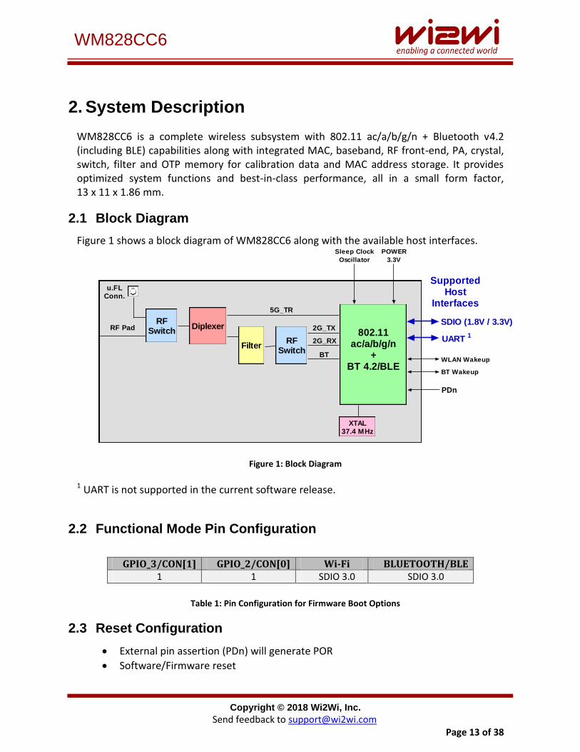
2. System Description
WM828CC6 is a complete wireless subsystem with 802.11 ac/a/b/g/n + Bluetooth v4.2 (including BLE) capabilities along with integrated MAC, baseband, RF front-end, PA, crystal, switch, filter and OTP memory for calibration data and MAC address storage. It provides optimized system functions and best-in-class performance, all in a small form factor, 13 x 11 x 1.86 mm.
2.1 Block Diagram
Figure 1 shows a block diagram of WM828CC6 along with the available host interfaces.
802.11ac/a/b/g/n
+BT 4.2/BLE
XTAL37.4 MHz
Filter
RFSwitch
PDn
BT Wakeup
u.FLConn.
SupportedHost
Interfaces
RFSwitch
Diplexer 2G_TX
2G_RX
5G_TR
BTWLAN Wakeup
SDIO (1.8V / 3.3V)
UART1
Sleep Clock
Oscillator
POWER
3.3V
RF Pad
Figure 1: Block Diagram
1 UART is not supported in the current software release.
2.2 Functional Mode Pin Configuration
GPIO_3/CON[1] GPIO_2/CON[0] Wi-Fi BLUETOOTH/BLE 1 1 SDIO 3.0 SDIO 3.0
Table 1: Pin Configuration for Firmware Boot Options
2.3 Reset Configuration
External pin assertion (PDn) will generate POR
Software/Firmware reset
Copyright © 2018 Wi2Wi, Inc.
Send feedback to [email protected] Page 14 of 38
WM828CC6
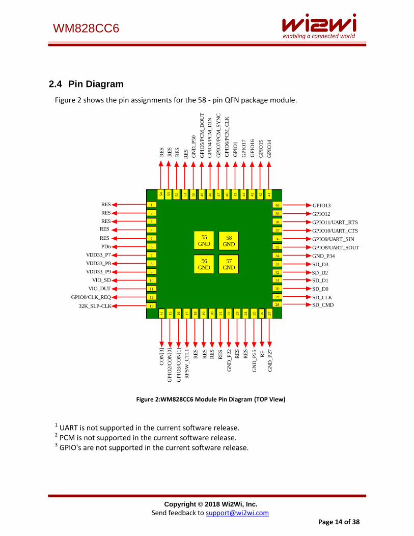
2.4 Pin Diagram
Figure 2 shows the pin assignments for the 58 - pin QFN package module.
1
2
3
4
5
6
7
8
9
10
11
12
39
38
37
36
35
34
33
32
40
31
30
29
14
15
16
17
18
19
20
21
22
23
24
25
52
51
50
49
48
47
46
45
44
43
42
41
58GND
55GND
56GND
57GND
RES
RES
RES
RES
RES
PDn
VDD33_P7
VDD33_P8
VDD33_P9
VIO_SD
VIO_DUT
GPIO0/CLK_REQ
CO
N[3
]
GP
IO2/C
ON
[0]
GP
IO3/C
ON
[1]
RF
SW
_C
TL
1
RE
S
RE
S
RE
S
GN
D_P
22
RE
S
RE
S
GN
D_P
25
GPIO12
GPIO11/UART_RTS
GPIO10/UART_CTS
GPIO9/UART_SIN
GPIO8/UART_SOUT
GND_P34
SD_D3
SD_D2
GPIO13
SD_D1
SD_D0
SD_CLK
RE
S
RE
S
GN
D_P
50
GP
IO5/P
CM
_D
OU
T
GP
IO4/P
CM
_D
IN
GP
IO7/P
CM
_S
YN
C
GP
IO6/P
CM
_C
LK
GP
IO1
GP
IO17
GP
IO16
GP
IO15
GP
IO14
13 28
26
54
53
27
32K_SLP-CLK
RE
S
RF
GN
D_P
27
SD_CMD
RE
S
RE
S
Figure 2:WM828CC6 Module Pin Diagram (TOP View)
1 UART is not supported in the current software release. 2 PCM is not supported in the current software release. 3 GPIO's are not supported in the current software release.
Copyright © 2018 Wi2Wi, Inc.
Send feedback to [email protected] Page 15 of 38
WM828CC6
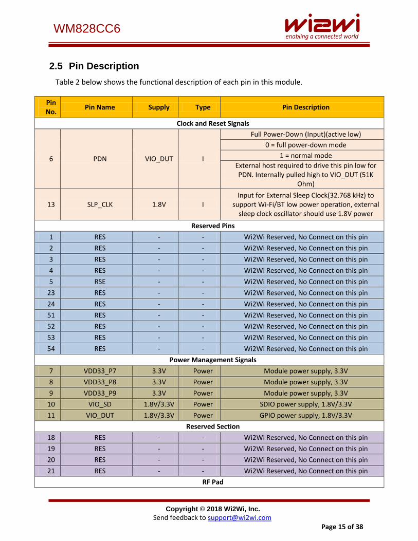
2.5 Pin Description
Table 2 below shows the functional description of each pin in this module.
Pin No.
Pin Name Supply Type Pin Description
Clock and Reset Signals
6 PDN VIO_DUT I
Full Power-Down (Input)(active low)
0 = full power-down mode
1 = normal mode
External host required to drive this pin low for PDN. Internally pulled high to VIO_DUT (51K
Ohm)
13 SLP_CLK 1.8V I Input for External Sleep Clock(32.768 kHz) to
support Wi-Fi/BT low power operation, external sleep clock oscillator should use 1.8V power
Reserved Pins
1 RES - - Wi2Wi Reserved, No Connect on this pin
2 RES - - Wi2Wi Reserved, No Connect on this pin
3 RES - - Wi2Wi Reserved, No Connect on this pin
4 RES - - Wi2Wi Reserved, No Connect on this pin
5 RSE - - Wi2Wi Reserved, No Connect on this pin
23 RES - - Wi2Wi Reserved, No Connect on this pin
24 RES - - Wi2Wi Reserved, No Connect on this pin
51 RES - - Wi2Wi Reserved, No Connect on this pin
52 RES - - Wi2Wi Reserved, No Connect on this pin
53 RES - - Wi2Wi Reserved, No Connect on this pin
54 RES - - Wi2Wi Reserved, No Connect on this pin
Power Management Signals
7 VDD33_P7 3.3V Power Module power supply, 3.3V
8 VDD33_P8 3.3V Power Module power supply, 3.3V
9 VDD33_P9 3.3V Power Module power supply, 3.3V
10 VIO_SD 1.8V/3.3V Power SDIO power supply, 1.8V/3.3V
11 VIO_DUT 1.8V/3.3V Power GPIO power supply, 1.8V/3.3V
Reserved Section
18 RES - - Wi2Wi Reserved, No Connect on this pin
19 RES - - Wi2Wi Reserved, No Connect on this pin
20 RES - - Wi2Wi Reserved, No Connect on this pin
21 RES - - Wi2Wi Reserved, No Connect on this pin
RF Pad
Copyright © 2018 Wi2Wi, Inc.
Send feedback to [email protected] Page 16 of 38
WM828CC6
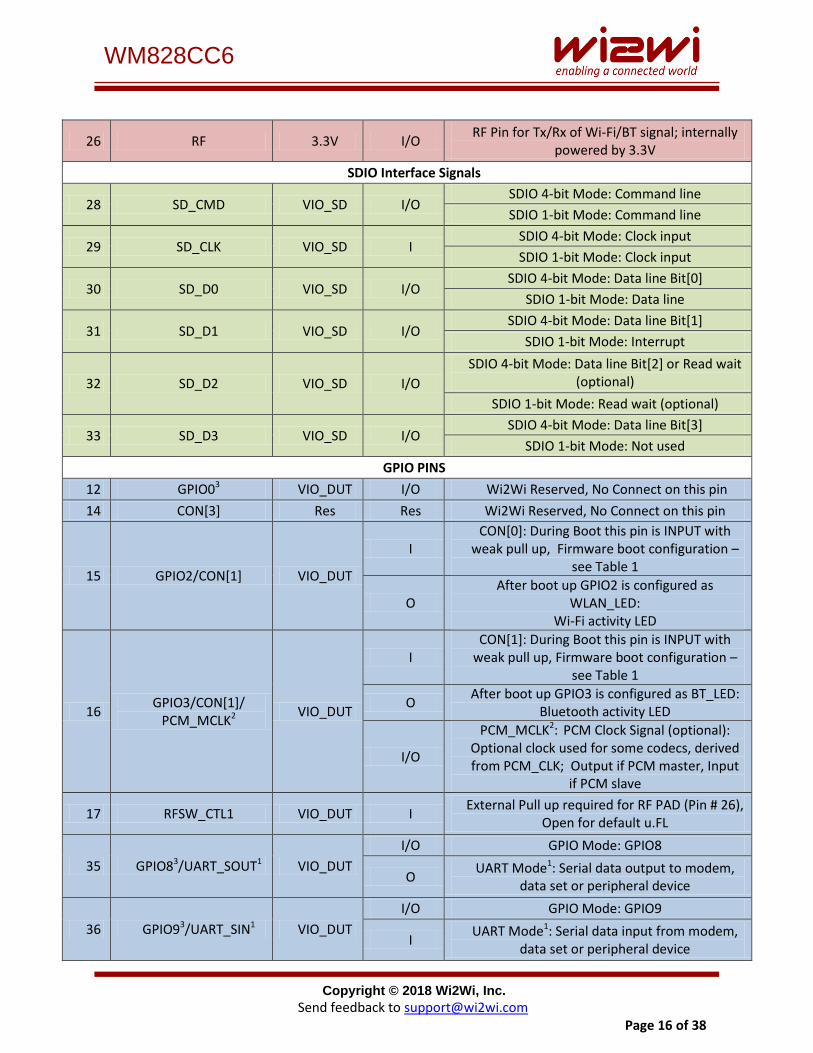
26 RF 3.3V I/O RF Pin for Tx/Rx of Wi-Fi/BT signal; internally
powered by 3.3V
SDIO Interface Signals
28 SD_CMD VIO_SD I/O SDIO 4-bit Mode: Command line
SDIO 1-bit Mode: Command line
29 SD_CLK VIO_SD I SDIO 4-bit Mode: Clock input
SDIO 1-bit Mode: Clock input
30 SD_D0 VIO_SD I/O SDIO 4-bit Mode: Data line Bit[0]
SDIO 1-bit Mode: Data line
31 SD_D1 VIO_SD I/O SDIO 4-bit Mode: Data line Bit[1]
SDIO 1-bit Mode: Interrupt
32 SD_D2 VIO_SD I/O
SDIO 4-bit Mode: Data line Bit[2] or Read wait (optional)
SDIO 1-bit Mode: Read wait (optional)
33 SD_D3 VIO_SD I/O SDIO 4-bit Mode: Data line Bit[3]
SDIO 1-bit Mode: Not used
GPIO PINS
12 GPIO03 VIO_DUT I/O Wi2Wi Reserved, No Connect on this pin
14 CON[3] Res Res Wi2Wi Reserved, No Connect on this pin
15 GPIO2/CON[1] VIO_DUT
I CON[0]: During Boot this pin is INPUT with
weak pull up, Firmware boot configuration – see Table 1
O After boot up GPIO2 is configured as
WLAN_LED: Wi-Fi activity LED
16 GPIO3/CON[1]/
PCM_MCLK2 VIO_DUT
I CON[1]: During Boot this pin is INPUT with
weak pull up, Firmware boot configuration – see Table 1
O After boot up GPIO3 is configured as BT_LED:
Bluetooth activity LED
I/O
PCM_MCLK2: PCM Clock Signal (optional): Optional clock used for some codecs, derived from PCM_CLK; Output if PCM master, Input
if PCM slave
17 RFSW_CTL1 VIO_DUT I External Pull up required for RF PAD (Pin # 26),
Open for default u.FL
35 GPIO83/UART_SOUT1 VIO_DUT
I/O GPIO Mode: GPIO8
O UART Mode1: Serial data output to modem,
data set or peripheral device
36 GPIO93/UART_SIN1 VIO_DUT
I/O GPIO Mode: GPIO9
I UART Mode1: Serial data input from modem,
data set or peripheral device
Copyright © 2018 Wi2Wi, Inc.
Send feedback to [email protected] Page 17 of 38
WM828CC6
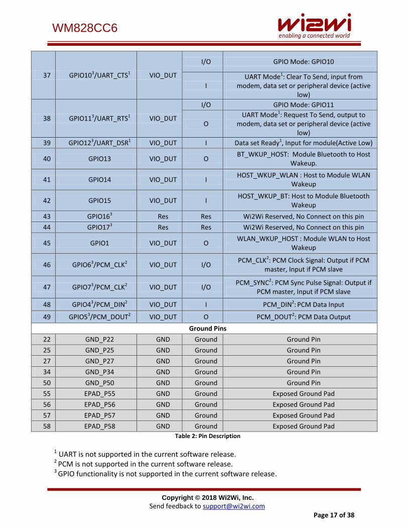
37 GPIO103/UART_CTS1 VIO_DUT
I/O GPIO Mode: GPIO10
I UART Mode1: Clear To Send, input from
modem, data set or peripheral device (active low)
38 GPIO113/UART_RTS1 VIO_DUT
I/O GPIO Mode: GPIO11
O UART Mode1: Request To Send, output to
modem, data set or peripheral device (active low)
39 GPIO123/UART_DSR1 VIO_DUT I Data set Ready1, Input for module(Active Low)
40 GPIO13 VIO_DUT O BT_WKUP_HOST: Module Bluetooth to Host
Wakeup.
41 GPIO14 VIO_DUT I HOST_WKUP_WLAN : Host to Module WLAN
Wakeup
42 GPIO15 VIO_DUT I HOST_WKUP_BT: Host to Module Bluetooth
Wakeup
43 GPIO163 Res Res Wi2Wi Reserved, No Connect on this pin
44 GPIO173 Res Res Wi2Wi Reserved, No Connect on this pin
45 GPIO1 VIO_DUT O WLAN_WKUP_HOST : Module WLAN to Host
Wakeup
46 GPIO63/PCM_CLK2 VIO_DUT I/O PCM_CLK2: PCM Clock Signal: Output if PCM
master, Input if PCM slave
47 GPIO73/PCM_CLK2 VIO_DUT I/O PCM_SYNC2: PCM Sync Pulse Signal: Output if
PCM master, Input if PCM slave
48 GPIO43/PCM_DIN2 VIO_DUT I PCM_DIN2: PCM Data Input
49 GPIO53/PCM_DOUT2 VIO_DUT O PCM_DOUT2: PCM Data Output
Ground Pins
22 GND_P22 GND Ground Ground Pin
25 GND_P25 GND Ground Ground Pin
27 GND_P27 GND Ground Ground Pin
34 GND_P34 GND Ground Ground Pin
50 GND_P50 GND Ground Ground Pin
55 EPAD_P55 GND Ground Exposed Ground Pad
56 EPAD_P56 GND Ground Exposed Ground Pad
57 EPAD_P57 GND Ground Exposed Ground Pad
58 EPAD_P58 GND Ground Exposed Ground Pad
Table 2: Pin Description
1 UART is not supported in the current software release. 2 PCM is not supported in the current software release. 3 GPIO functionality is not supported in the current software release.

Copyright © 2018 Wi2Wi, Inc.
Send feedback to [email protected] Page 18 of 38
WM828CC6
2.6 Physical Dimensions and Pad Locations
Module Physical Size: 13 x 11 x 1.86 mm (including shield)
Solder Pad Size: 0.4 x 0.4 mm
Pad to Pad Space: 0.350 mm
Pad Pitch: 0.750 mm
Last Pad to Module Edge: 0.3 mm
Pad Finish: ENIG (Electro-less Nickel Immersion Gold)
Pads: [ (four sides (13 + 14 + 13 + 14) + 4 Ground Pads in the middle) ]
Note: For Hardware Application notes, module dimensions and symbol library files please contact Wi2Wi sales or send an email to [email protected]
Copyright © 2018 Wi2Wi, Inc.
Send feedback to [email protected] Page 19 of 38
WM828CC6
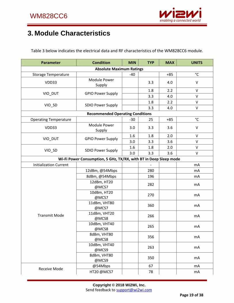
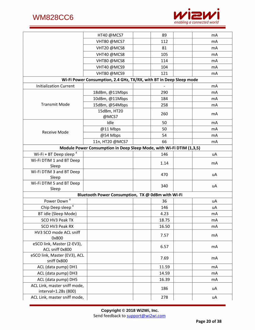
3. Module Characteristics
Table 3 below indicates the electrical data and RF characteristics of the WM828CC6 module.
Parameter Condition MIN TYP MAX UNITS
Absolute Maximum Ratings
Storage Temperature -40 +85 °C
VDD33 Module Power
Supply 3.3 4.0 V
VIO_DUT GPIO Power Supply 1.8 2.2 V
3.3 4.0 V
VIO_SD SDIO Power Supply 1.8 2.2 V
3.3 4.0 V
Recommended Operating Conditions
Operating Temperature -30 25 +85 °C
VDD33 Module Power
Supply 3.0 3.3 3.6 V
VIO_DUT GPIO Power Supply 1.6 1.8 2.0 V
3.0 3.3 3.6 V
VIO_SD SDIO Power Supply 1.6 1.8 2.0 V
3.0 3.3 3.6 V
Wi-Fi Power Consumption, 5 GHz, TX/RX, with BT in Deep Sleep mode
Initialization Current - mA
Transmit Mode
12dBm, @54Mbps 280 mA
8dBm, @54Mbps 196 mA
12dBm, HT20 @MCS7
282 mA
10dBm, HT20 @MCS7
270 mA
11dBm, VHT80 @MCS7
360 mA
11dBm, VHT20 @MCS8
266 mA
10dBm, VHT40 @MCS8
265 mA
8dBm, VHT80 @MCS8
356 mA
10dBm, VHT40 @MCS9
263 mA
8dBm, VHT80 @MCS9
350 mA
Receive Mode @54Mbps 67 mA
HT20 @MCS7 78 mA
Copyright © 2018 Wi2Wi, Inc.
Send feedback to [email protected] Page 20 of 38
WM828CC6
HT40 @MCS7 89 mA
VHT80 @MCS7 112 mA
VHT20 @MCS8 81 mA
VHT40 @MCS8 105 mA
VHT80 @MCS8 114 mA
VHT40 @MCS9 104 mA
VHT80 @MCS9 121 mA
Wi-Fi Power Consumption, 2.4 GHz, TX/RX, with BT in Deep Sleep mode
Initialization Current - mA
Transmit Mode
18dBm, @11Mbps 290 mA
10dBm, @11Mbps 184 mA
15dBm, @54Mbps 258 mA
15dBm, HT20 @MCS7
260 mA
Receive Mode
Idle 50 mA
@11 Mbps 50 mA
@54 Mbps 54 mA
11n, HT20 @MCS7 66 mA
Module Power Consumption in Deep Sleep Mode, with Wi-Fi DTIM (1,3,5)
Wi-Fi + BT Deep sleep 4 146 uA
Wi-Fi DTIM 1 and BT Deep Sleep
1.14 mA
Wi-Fi DTIM 3 and BT Deep Sleep
470 uA
Wi-Fi DTIM 5 and BT Deep Sleep
340 uA
Bluetooth Power Consumption, TX @ 0dBm with Wi-Fi
Power Down 4 36 uA
Chip Deep sleep 4 146 uA
BT idle (Sleep Mode) 4.23 mA
SCO HV3 Peak TX 18.75 mA
SCO HV3 Peak RX 16.50 mA
HV3 SCO mode ACL sniff 0x800
7.57 mA
eSCO link, Master (2-EV3), ACL sniff 0x800
6.57 mA
eSCO link, Master (EV3), ACL sniff 0x800
7.69 mA
ACL (data pump) DH1 11.59 mA
ACL (data pump) DH3 14.59 mA
ACL (data pump) DH5 16.39 mA
ACL Link, master sniff mode, interval=1.28s (800)
186 uA
ACL Link, master sniff mode, 278 uA
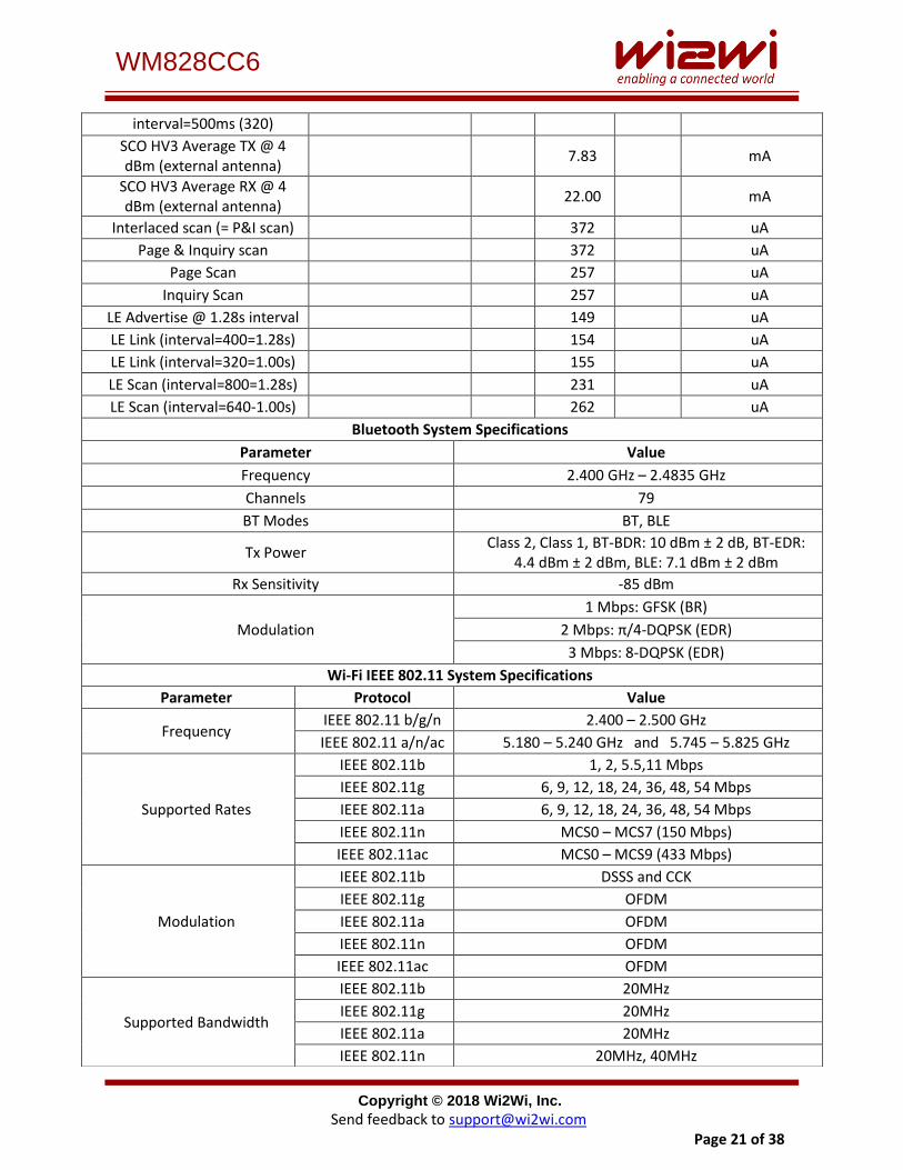
Copyright © 2018 Wi2Wi, Inc.
Send feedback to [email protected] Page 21 of 38
WM828CC6
interval=500ms (320)
SCO HV3 Average TX @ 4 dBm (external antenna)
7.83 mA
SCO HV3 Average RX @ 4 dBm (external antenna)
22.00 mA
Interlaced scan (= P&I scan) 372 uA
Page & Inquiry scan 372 uA
Page Scan 257 uA
Inquiry Scan 257 uA
LE Advertise @ 1.28s interval 149 uA
LE Link (interval=400=1.28s) 154 uA
LE Link (interval=320=1.00s) 155 uA
LE Scan (interval=800=1.28s) 231 uA
LE Scan (interval=640-1.00s) 262 uA
Bluetooth System Specifications
Parameter Value
Frequency 2.400 GHz – 2.4835 GHz
Channels 79
BT Modes BT, BLE
Tx Power Class 2, Class 1, BT-BDR: 10 dBm ± 2 dB, BT-EDR:
4.4 dBm ± 2 dBm, BLE: 7.1 dBm ± 2 dBm
Rx Sensitivity -85 dBm
Modulation
1 Mbps: GFSK (BR)
2 Mbps: π/4-DQPSK (EDR)
3 Mbps: 8-DQPSK (EDR)
Wi-Fi IEEE 802.11 System Specifications
Parameter Protocol Value
Frequency IEEE 802.11 b/g/n 2.400 – 2.500 GHz
IEEE 802.11 a/n/ac 5.180 – 5.240 GHz and 5.745 – 5.825 GHz
Supported Rates
IEEE 802.11b 1, 2, 5.5,11 Mbps
IEEE 802.11g 6, 9, 12, 18, 24, 36, 48, 54 Mbps
IEEE 802.11a 6, 9, 12, 18, 24, 36, 48, 54 Mbps
IEEE 802.11n MCS0 – MCS7 (150 Mbps)
IEEE 802.11ac MCS0 – MCS9 (433 Mbps)
Modulation
IEEE 802.11b DSSS and CCK
IEEE 802.11g OFDM
IEEE 802.11a OFDM
IEEE 802.11n OFDM
IEEE 802.11ac OFDM
Supported Bandwidth
IEEE 802.11b 20MHz
IEEE 802.11g 20MHz
IEEE 802.11a 20MHz
IEEE 802.11n 20MHz, 40MHz
Copyright © 2018 Wi2Wi, Inc.
Send feedback to [email protected] Page 22 of 38
WM828CC6
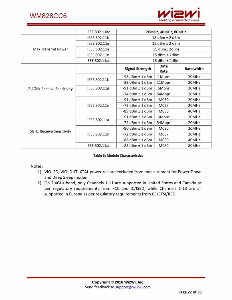
Table 3: Module Characteristics
Notes:
1) VIO_SD, VIO_DUT, XTAL power rail are excluded from measurement for Power Down and Deep Sleep modes
2) On 2.4GHz band, only Channels 1-11 are supported in United States and Canada as per regulatory requirements from FCC and IC/ISED, while Channels 1-13 are all supported in Europe as per regulatory requirements from CE/ETSI/RED
IEEE 802.11ac 20MHz, 40MHz, 80MHz
Max Transmit Power
IEEE 802.11b 18 dBm ± 2 dBm
IEEE 802.11g 15 dBm ± 2 dBm
IEEE 802.11a 15 dBm± 2dBm
IEEE 802.11n 15 dBm ± 2dBm
IEEE 802.11ac 15 dBm ± 2dBm
2.4GHz Receive Sensitivity
Signal Strength Data Rate
Bandwidth
IEEE 802.11b -98 dBm ± 1 dBm 1Mbps 20MHz
-89 dBm ± 1 dBm 11Mbps 20MHz
IEEE 802.11g -91 dBm ± 1 dBm 6Mbps 20MHz
-74 dBm ± 1 dBm 54Mbps 20MHz
IEEE 802.11n
-91 dBm ± 1 dBm MCS0 20MHz
-73 dBm ± 1 dBm MCS7 20MHz
-89 dBm ± 1 dBm MCS0 40MHz
5GHz Receive Sensitivity
IEEE 802.11a -91 dBm ± 1 dBm 6Mbps 20MHz
-74 dBm ± 1 dBm 54Mbps 20MHz
IEEE 802.11n
-90 dBm ± 1 dBm MCS0 20MHz
-72 dBm ± 1 dBm MCS7 20MHz
-88 dBm ± 1 dBm MCS0 40MHz
IEEE 802.11ac -85 dBm ± 1 dBm MCS0 80MHz
Copyright © 2018 Wi2Wi, Inc.
Send feedback to [email protected] Page 23 of 38
WM828CC6
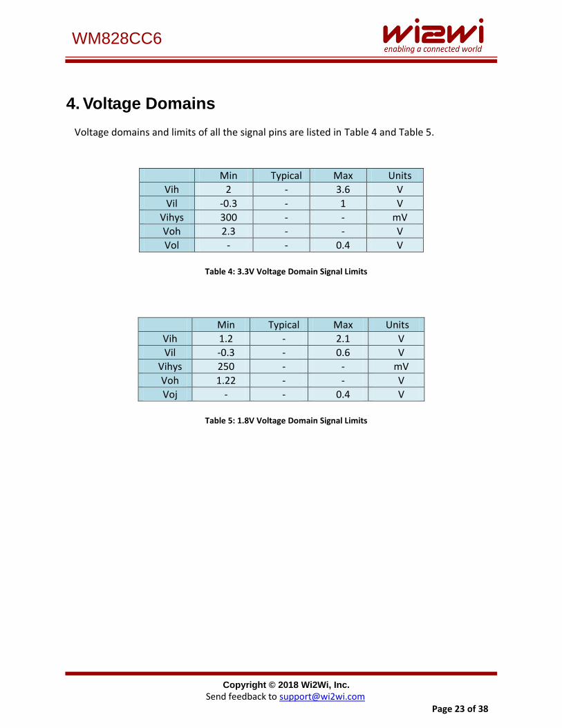
4. Voltage Domains
Voltage domains and limits of all the signal pins are listed in Table 4 and Table 5.
Min Typical Max Units
Vih 2 - 3.6 V
Vil -0.3 - 1 V
Vihys 300 - - mV
Voh 2.3 - - V
Vol - - 0.4 V
Table 4: 3.3V Voltage Domain Signal Limits
Min Typical Max Units
Vih 1.2 - 2.1 V
Vil -0.3 - 0.6 V
Vihys 250 - - mV
Voh 1.22 - - V
Voj - - 0.4 V
Table 5: 1.8V Voltage Domain Signal Limits
Copyright © 2018 Wi2Wi, Inc.
Send feedback to [email protected] Page 24 of 38
WM828CC6
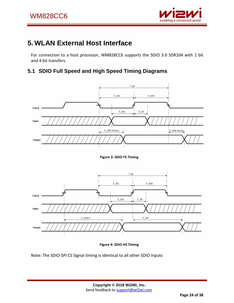
5. WLAN External Host Interface
For connection to a host processor, WM828CC6 supports the SDIO 3.0 SDR104 with 1 bit and 4 bit transfers.
5.1 SDIO Full Speed and High Speed Timing Diagrams
f_pp
T_WL T_WH
T_ISU T_IH
T_ODLY(max) T_ODLY(min)
Clock
Input
Output
Figure 3: SDIO FS Timing
f_pp
T_WL T_WH
T_ISU T_IH
T_ODLY T_OH
Clock
Input
Output
Figure 4: SDIO HS Timing
Note: The SDIO-SPI CS Signal timing is identical to all other SDIO inputs
Copyright © 2018 Wi2Wi, Inc.
Send feedback to [email protected] Page 25 of 38
WM828CC6
Symbol Parameter Condition Min Typical Max Units f_pp Clock
Frequency Normal 0 -- 25 MHz
High speed 0 -- 50 MHz
T_WL Clock Low Time
Normal 10 -- -- ns
High speed 7 -- -- ns
T_WH Clock High Time
Normal 10 -- -- ns
High speed 7 -- -- ns
T_ISU Input Setup Time
Normal 5 -- -- ns
High speed 6 -- --
T_IH Input Hold Time
Normal 5 -- -- ns
High speed 2 -- --
T_ODLY
(max) Max Output Delay Time
Normal 14 ns
T_ODLY
(min) Min Output Delay Time
Normal 0 ns
T_ODLY Output Delay Time
Normal -- 14 ns
T_OH Output Hold Time
High Speed
2.5 -- -- ns
Table 6: SDIO Timing Data
Note: Over full range of values specified in the Recommended Operating Conditions unless otherwise specified
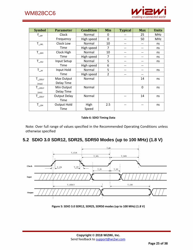
5.2 SDIO 3.0 SDR12, SDR25, SDR50 Modes (up to 100 MHz) (1.8 V)
f_pp
T_WL T_WH
T_IS T_IH
T_ODLY T_OH
Clock
Input
Output
T_CR T_CF
T_CLK
Figure 5: SDIO 3.0 SDR12, SDR25, SDR50 modes (up to 100 MHz) (1.8 V)
Copyright © 2018 Wi2Wi, Inc.
Send feedback to [email protected] Page 26 of 38
WM828CC6
Symbol Parameter Condition Min Typical Max Units
f_pp Clock Frequency SDR12/25/50 25 -- 100 MHz
T_IS Input Setup Time SDR12/25/50 3 -- -- ns
T_IH Input Hold Time SDR12/25/50 0.8 -- -- ns
T_CLK Clock Time SDR12/25/50 10 -- 40 ns
T_CR, T_CF Rise Time, Fall Time
SDR12/25/50 -- 0.2x TCLK ns
T_ODLY Output Delay Time SDR12/25/50 7.5 ns
T_OH Output Hold Time SDR12/25/50 1.5 -- -- ns
Table 7: SDIO Timing Data for SDR12, SDR25, SDR50 modes (up to 100 MHz) (1.8 V)
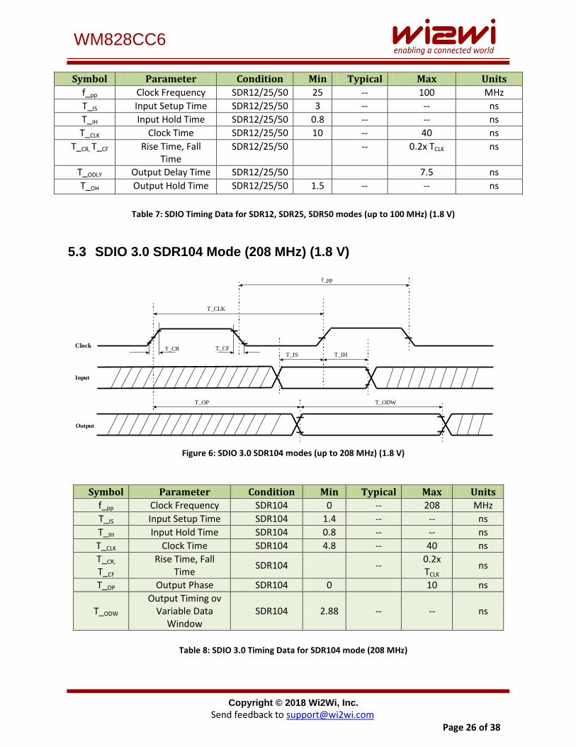
5.3 SDIO 3.0 SDR104 Mode (208 MHz) (1.8 V)
Figure 6: SDIO 3.0 SDR104 modes (up to 208 MHz) (1.8 V)
Symbol Parameter Condition Min Typical Max Units
f_pp Clock Frequency SDR104 0 -- 208 MHz
T_IS Input Setup Time SDR104 1.4 -- -- ns
T_IH Input Hold Time SDR104 0.8 -- -- ns
T_CLK Clock Time SDR104 4.8 -- 40 ns
T_CR,
T_CF Rise Time, Fall
Time SDR104 --
0.2x TCLK
ns
T_OP Output Phase SDR104 0 10 ns
T_ODW Output Timing ov
Variable Data Window
SDR104 2.88 -- -- ns
Table 8: SDIO 3.0 Timing Data for SDR104 mode (208 MHz)
f_pp
T_IS T_IH
Clock
Input
T_CR T_CF
T_CLK
T_OP T_ODW
Output
Copyright © 2018 Wi2Wi, Inc.
Send feedback to [email protected] Page 27 of 38
WM828CC6
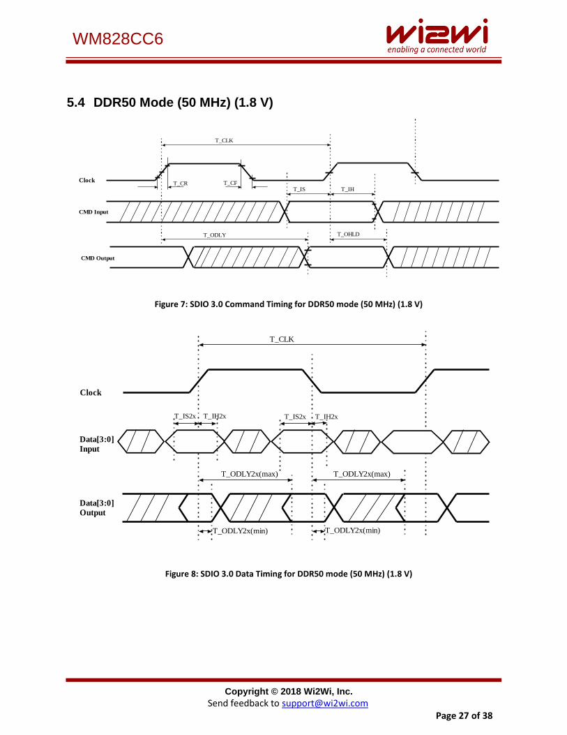
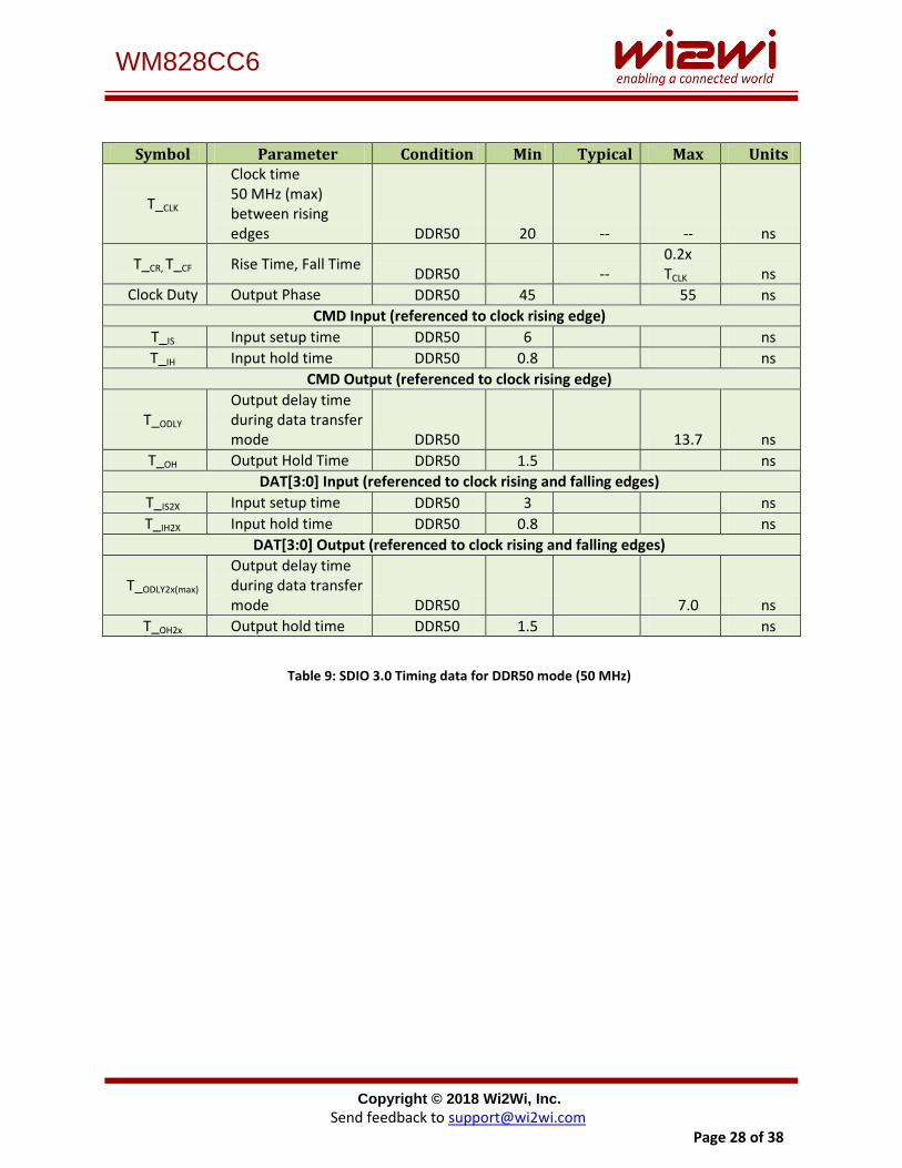
5.4 DDR50 Mode (50 MHz) (1.8 V)
T_IS T_IH
T_ODLY T_OHLD
Clock
CMD Input
CMD Output
T_CR T_CF
T_CLK
Figure 7: SDIO 3.0 Command Timing for DDR50 mode (50 MHz) (1.8 V)
Clock
T_CLK
Data[3:0]
Input
Data[3:0]
Output
T_IS2x T_IH2x T_IS2x T_IH2x
T_ODLY2x(max) T_ODLY2x(max)
T_ODLY2x(min) T_ODLY2x(min)
Figure 8: SDIO 3.0 Data Timing for DDR50 mode (50 MHz) (1.8 V)
Copyright © 2018 Wi2Wi, Inc.
Send feedback to [email protected] Page 28 of 38
WM828CC6
Symbol Parameter Condition Min Typical Max Units
T_CLK
Clock time 50 MHz (max) between rising edges DDR50 20 -- -- ns
T_CR, T_CF Rise Time, Fall Time DDR50 --
0.2x TCLK ns
Clock Duty Output Phase DDR50 45 55 ns
CMD Input (referenced to clock rising edge)
T_IS Input setup time DDR50 6 ns
T_IH Input hold time DDR50 0.8 ns
CMD Output (referenced to clock rising edge)
T_ODLY Output delay time during data transfer mode DDR50 13.7 ns
T_OH Output Hold Time DDR50 1.5 ns
DAT[3:0] Input (referenced to clock rising and falling edges)
T_IS2X Input setup time DDR50 3 ns
T_IH2X Input hold time DDR50 0.8 ns
DAT[3:0] Output (referenced to clock rising and falling edges)
T_ODLY2x(max) Output delay time during data transfer mode DDR50 7.0 ns
T_OH2x Output hold time DDR50 1.5 ns
Table 9: SDIO 3.0 Timing data for DDR50 mode (50 MHz)
Copyright © 2018 Wi2Wi, Inc.
Send feedback to [email protected] Page 29 of 38
WM828CC6
6. WLAN Power-Save Modes
Three types of power save modes can be used by the WM828CC6. They are Full Power-Down mode, IEEE Power Save mode, and Deep Sleep mode. The key difference between the three modes is the current consumption, and the time it takes to the transition from the power save mode to normal Wi-Fi operation.
6.1 Full Power-Down Mode
In this mode all internal clocks are shutdown, register and memory states are not maintained. Upon exiting power down mode, a reset is automatically performed and a firmware re-download is required to re-enter any of the other modes.
6.2 IEEE Power Save
This mode puts sections of the Wi-Fi into “sleep with periodic wake” mode. This mode is entered when the appropriate command is sent by the host processor to the Wi-Fi. The device automatically wakes up to receive beacons periodically, and if there is no traffic indicated for the device, it will go back to sleep. Power consumption is dependent on the DTIM value of the AP it is connected to. When DTIM=1, the device wakes up every 100ms to receive and acknowledge the beacon from AP to maintain association.
6.3 Deep Sleep
This mode puts the complete Wi-Fi section into deep sleep mode, which is the same as the IEEE mode above except there are no periodic wake-ups to receive beacons. Thus it offers lower power consumption than IEEE mode. This mode is entered when the host processor sends the appropriate command. In deep sleep mode, the device is not listening for packets or beacons from the AP, so it cannot maintain an association with it. When the host processor sends a command to take the device out of deep sleep mode, the device will have to re-associate with the AP. This is a low-power used in the sleeps state of many power save modes. It is a low-power state where the external reference clock and many blocks in the chip are switched off. Only a slow sleep clock is used to maintain register and memory states. Wake-up does not require a firmware re-download.
Copyright © 2018 Wi2Wi, Inc.
Send feedback to [email protected] Page 30 of 38
WM828CC6
7. Antenna and Clock
7.1 Antenna
WM828CC6 module has an MHF4 IPEX connector for antenna. The antenna RF PAD on WM828CC6 module has 50 Ohm impedance trace.
7.2 Clock
WM828CC6module has an internal 37.4 MHz crystal to serve clock requirements. In order to enable sleep clock functionality in power save modes, an external sleep clock oscillator (32.768 KHz) should be connected to the WM828CC6 module.
8. Software
End-user drivers needed for full operation of the WM828CC6 module are available from Wi2Wi. This driver is specific to the operating system, processor and host bus, and cannot be used for any other processors, operating systems or host buses. Since the operating system and platform matrix is quite large, it is not possible to have all the combinations available off the shelf. Please contact your sales representative for cost and availability. Wi2Wi can also provide custom driver development services based on customers’ requirements at an added cost.
Wi2Wi provides Linux device drivers, once you sign the License Agreement (EULA) with Wi2Wi. Driver release package includes the following:
Linux Kernel drivers for Wi-Fi, Bluetooth/BLE
Firmware image which will be loaded to module during initialization
User Guide
Manufacturing and Configuration Software
Copyright © 2018 Wi2Wi, Inc.
Send feedback to [email protected] Page 31 of 38
WM828CC6
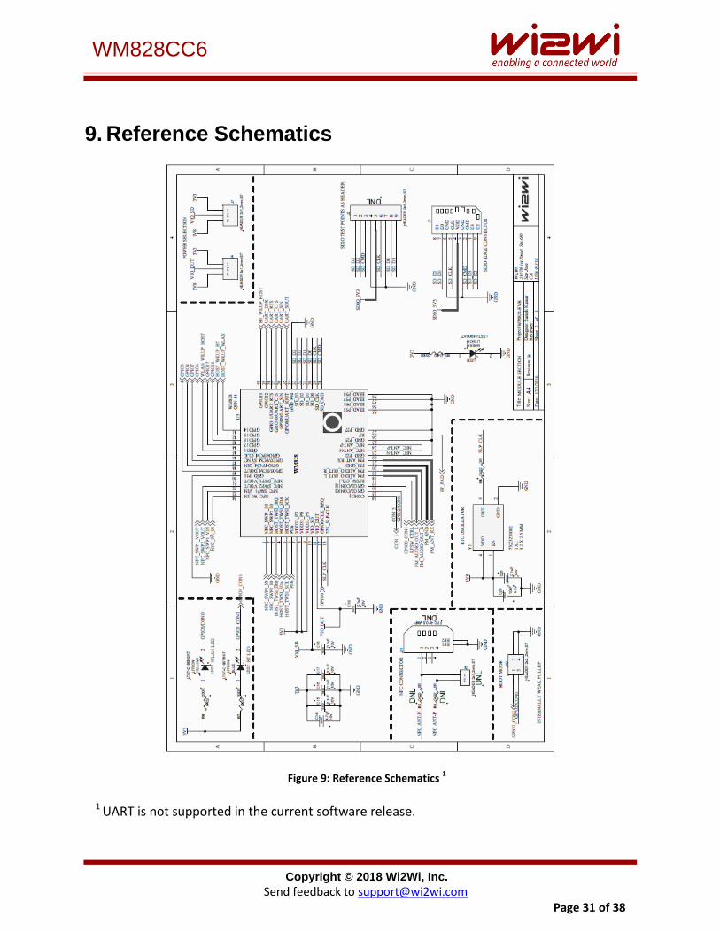
9. Reference Schematics
Figure 9: Reference Schematics 1
1 UART is not supported in the current software release.
Copyright © 2018 Wi2Wi, Inc.
Send feedback to [email protected] Page 32 of 38
WM828CC6
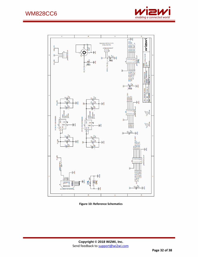
Figure 10: Reference Schematics
Copyright © 2018 Wi2Wi, Inc.
Send feedback to [email protected] Page 33 of 38
WM828CC6
10. Manufacturing Notes
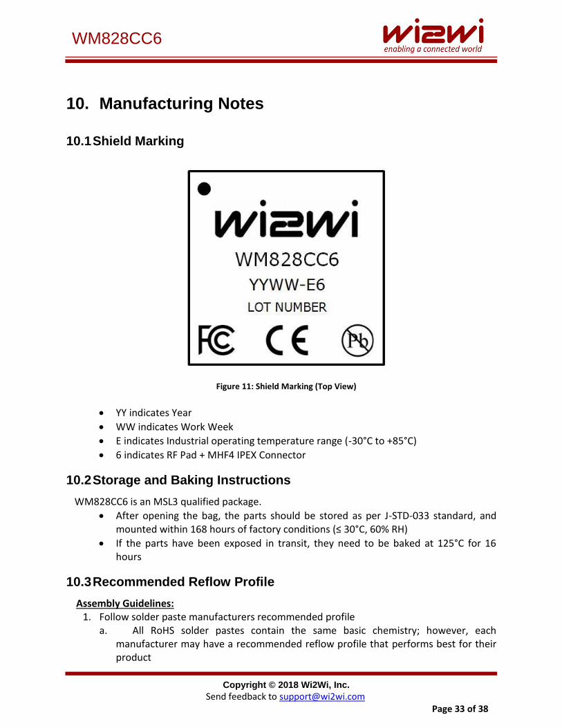
10.1 Shield Marking
Figure 11: Shield Marking (Top View)
YY indicates Year
WW indicates Work Week
E indicates Industrial operating temperature range (-30°C to +85°C)
6 indicates RF Pad + MHF4 IPEX Connector
10.2 Storage and Baking Instructions
WM828CC6 is an MSL3 qualified package.
After opening the bag, the parts should be stored as per J-STD-033 standard, and mounted within 168 hours of factory conditions (≤ 30°C, 60% RH)
If the parts have been exposed in transit, they need to be baked at 125°C for 16 hours
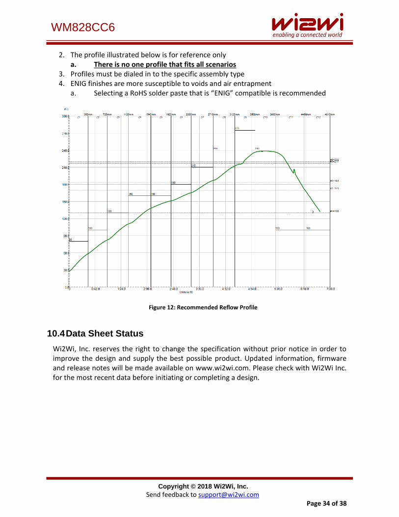
10.3 Recommended Reflow Profile
Assembly Guidelines: 1. Follow solder paste manufacturers recommended profile
a. All RoHS solder pastes contain the same basic chemistry; however, each manufacturer may have a recommended reflow profile that performs best for their product
Copyright © 2018 Wi2Wi, Inc.
Send feedback to [email protected] Page 34 of 38
WM828CC6
2. The profile illustrated below is for reference only a. There is no one profile that fits all scenarios
3. Profiles must be dialed in to the specific assembly type 4. ENIG finishes are more susceptible to voids and air entrapment
a. Selecting a RoHS solder paste that is “ENIG” compatible is recommended
Figure 12: Recommended Reflow Profile
10.4 Data Sheet Status
Wi2Wi, Inc. reserves the right to change the specification without prior notice in order to improve the design and supply the best possible product. Updated information, firmware and release notes will be made available on www.wi2wi.com. Please check with Wi2Wi Inc. for the most recent data before initiating or completing a design.
Copyright © 2018 Wi2Wi, Inc.
Send feedback to [email protected] Page 35 of 38
WM828CC6
11. Ordering Information
Part Order
Number Features Operating Temperature Packaging
WM828CC6-E6QT 802.11ac/a/b/g/n
+ BT 4.2/BLE Extended: -30°C to +85°C Tray
WM828CC6-E6QR 802.11ac/a/b/g/n
+ BT 4.2/BLE Extended: -30°C to +85°C Tape & Reel
Table 10: Ordering Information for Modules
Part Order Number
Features Contents of the Evaluation
Kit Packaging
WM828CC6-EVK6 802.11ac/a/b/g/n
+ BT 4.2/BLE
WM828CC6 Evaluation Board, Dual-Band Rubber-Duck
Antenna, u.FL Cable Box
WM828CC6-DVK6 802.11ac/a/b/g/n
+ BT 4.2/BLE
WM828CC6 Evaluation Board, iMX6 Processor Board, Dual-Band Rubber-Duck Antenna,
u.FL Cable
Box
Table 11: Ordering Information for Evaluation Kits
12. Data Sheet Status
Wi2Wi, Inc. reserves the right to change the specification without prior notice in order to improve the design and supply the best possible product. Updated information, firmware and release notes will be made available on www.wi2wi.com. Please check with Wi2Wi Inc. for the most recent data before initiating or completing a design.
Copyright © 2018 Wi2Wi, Inc.
Send feedback to [email protected] Page 36 of 38
WM828CC6
13. Certifications
WM828CC6 module complies with the following standards: FCC: 15C IC/ISED: RSS-247 CE/ETSI: EN 300 328 V2.1.1, EN 301 489-1 V2.2.0, EN 301 489-17 V3.2.0, EN 62311, EN 300 893 V2.1.1, EN 300 440 V2.1.1, EN 60950-1:2016+A2:2013
FCC Statement: This equipment has been tested and found to comply with the limits for a Class B digital device, pursuant to Part 15 of the FCC Rules. These limits are designed to provide reasonable protection against harmful interference in a residential installation. This equipment generates, uses and can radiate radio frequency energy and, if not installed and used in accordance with the instructions, may cause harmful interference to radio communications. However, there is no guarantee that interference will not occur in a particular installation. If this equipment does cause harmful interference to radio or television reception, which can be determined by turning the equipment off and on, the user is encouraged to try to correct the interference by one or more of the following measures:
- Reorient or relocate the receiving antenna. - Increase the separation between the equipment and receiver. - Connect the equipment into an outlet on a circuit different from that to which the
receiver is connected. - Consult the dealer or an experienced radio/TV technician for help.
This device complies with Part 15 of the FCC Rules. Operation is subject to the following two conditions: (1) This device may not cause harmful interference, and (2) this device must accept any interference received, including interference that may cause undesired operation. The FCC requires the user to be notified that any changes or modifications made to this device that are not expressly approved by Wi2Wi may void the user’s authority to operate the equipment.
FCC Radiation Exposure Statement: This equipment complies with FCC radiation exposure limits set forth for an uncontrolled environment. End users must follow the specific operating instructions for satisfying RF exposure compliance. This transmitter must be at least 20 cm from the user and must not be co-located or operating in conjunction with any other antenna or transmitter.
IC/ISEDC Statement: English: This device complies with Industry Canada license-exempt RSS standard(s). Operation is subject to the following two conditions:
Copyright © 2018 Wi2Wi, Inc.
Send feedback to [email protected] Page 37 of 38
WM828CC6
1. This device may not cause harmful interference; 2. This device must accept any interference received, including interference that may cause undesired operation of the device. Français: Cet appareil est conforme à Industrie Canada une licence standard RSS exonérés (s). Son fonctionnement est soumis aux deux conditions suivantes: 1. Cet appareil ne doit pas provoquer d'interférences; 2. Cet appareil doit accepter toute interférence reçue, y compris les interférences pouvant provoquer un fonctionnement indésirable de l'appareil.
IC/ISEDC Radiation Exposure Statement: English: This equipment complies with the IC RSS-102 radiation exposure limits set forth for an uncontrolled environment. This equipment should be installed and operated with a minimum distance of 20 cm between the radiator and your body. Français: Cet équipement est conforme aux limites d'exposition au rayonnement IC RSS-102 définies pour un environnement non contrôlé. Cet équipement doit être installé et utilisé avec une distance minimale de 20 cm entre le radiateur et votre corps.
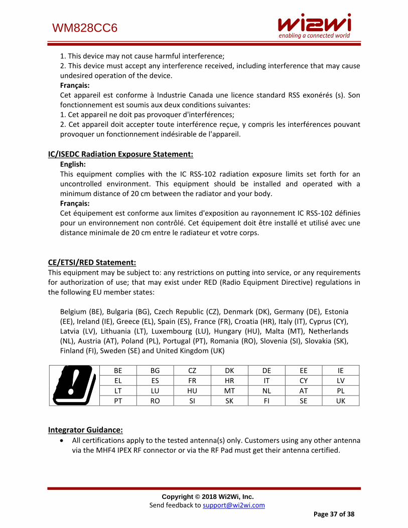
CE/ETSI/RED Statement: This equipment may be subject to: any restrictions on putting into service, or any requirements for authorization of use; that may exist under RED (Radio Equipment Directive) regulations in the following EU member states:
Belgium (BE), Bulgaria (BG), Czech Republic (CZ), Denmark (DK), Germany (DE), Estonia (EE), Ireland (IE), Greece (EL), Spain (ES), France (FR), Croatia (HR), Italy (IT), Cyprus (CY), Latvia (LV), Lithuania (LT), Luxembourg (LU), Hungary (HU), Malta (MT), Netherlands (NL), Austria (AT), Poland (PL), Portugal (PT), Romania (RO), Slovenia (SI), Slovakia (SK), Finland (FI), Sweden (SE) and United Kingdom (UK)
BE BG CZ DK DE EE IE
EL ES FR HR IT CY LV
LT LU HU MT NL AT PL
PT RO SI SK FI SE UK
Integrator Guidance: All certifications apply to the tested antenna(s) only. Customers using any other antenna
via the MHF4 IPEX RF connector or via the RF Pad must get their antenna certified.
Copyright © 2018 Wi2Wi, Inc.
Send feedback to [email protected] Page 38 of 38
WM828CC6
Only the antenna(s) described in the filings under this FCC ID or equivalent antenna(s) with equal or lesser gain may be used with this transmitter. Any new antenna type, or higher gain antenna would require a Class II permissive change.
If the operation of the equipment is for portable use (within 20 cm of user), or where co-location configuration use is required; the end product, including the transmitter will require re-evaluation in accordance to the FCC rules.
Labeling: The final end product must be labeled in a visible area with the following text: “Contains FCC ID: U9RWM828CC6, IC: 7089A-WM828CC6”, where:
“U9RWM828CC6”is the approved FCC ID of this module
“7089A-WM828CC6” is the approved IC ID of this module The grantee's FCC/IC ID can be used only when all FCC/IC compliance requirements are met.
14. References
14.1 Specifications
IEEE 802.11 ac/a/b/g/n Wireless LAN Specification Bluetooth 4.2/BLE (Low Energy) SDIO, SDIO HS, 1-bit, 4-bit Specifications
14.2 Trademarks, Patents and Licenses
Trademarks: Wi-Fi, Bluetooth.
14.3 Other
WM828CC6-EVK6: Evaluation Board WM828CC6-DVK6: Development Kit
Mouser Electronics
Authorized Distributor
Click to View Pricing, Inventory, Delivery & Lifecycle Information: Wi2Wi:
WM828CC6-M2-2230-E6QT WM828CC6-M2-1216-E6QT